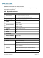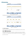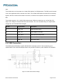
1
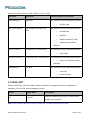
G610 Hardware User Manual Version:V1.0.5 Date:2015.08.25 1 Copyright Copyright ©2015 Fibocom Wireless Inc . All rights reserved. Without the prior written permission of the copyright holder, any company or individual is prohibited to excerpt, copy any part of or the entire document, or transmit the document in any form. Attention The document is subject to update from time to time owing to the product version upgrade or other reasons. Unless otherwise specified, the document only serves as the user guide. All the statements, information and suggestions contained in the document do not constitute any explicit or implicit guarantee. Trademark The trademark is registered and owned by Fibocom Wireless Inc. Revision History Version Date Remarks V1.0.0 2013-10-28 The initial revision V1.0.1 2014-04-25 Update product type V1.0.2 2014-12-26 The company name is changed. V1.0.3 2015-02-06 Update the interface description V1.0.4 2015-04-21 Add the description of “Top View” in PCB Layout V1.0.5 2015-08-25 Update the logo. G610 Hardware User Manual Page 2 of 41 Applicability Type No. Type Note 1 G610-A20-00 Auto on 2 G610-A20-01 Non-auto off 3 G610-Q20-00 G610 Hardware User Manual Page 3 of 41 Content 1 Introduction................................................................................................................................................................ 6 1.1 Scope.............................................................................................................................................................. 6 1.2 Audience......................................................................................................................................................... 6 1.3 Applicable Documents..................................................................................................................................6 1.4 Standards....................................................................................................................................................... 6 2 Overview.....................................................................................................................................................................7 2.1 Description......................................................................................................................................................7 2.2 Specifications................................................................................................................................................. 8 3 Hardware Interface Description........................................................................................................................... 10 3.1 Block Diagram............................................................................................................................................. 10 3.2 Operating Modes.........................................................................................................................................11 3.3 Power Supply...............................................................................................................................................12 3.3.1 Power Supply Design......................................................................................................................13 3.3.2 Power Consumption........................................................................................................................14 3.4 Power On/Off Operation............................................................................................................................ 16 3.4.1 Turning on the Module....................................................................................................................17 3.4.2 Turning off the Module....................................................................................................................17 3.5 Sleep Mode.................................................................................................................................................. 18 3.5.1 Activating Sleep Mode.................................................................................................................... 18 3.5.2 Serial Interface during Sleep Mode.............................................................................................. 19 3.5.3 Terminating Sleep Mode................................................................................................................ 19 3.5.3.1 Temporary Termination of Low Power Mode.................................................................. 19 3.5.3.2 Permanent Termination of Sleep Mode........................................................................... 20 3.6 Real Time Clock.......................................................................................................................................... 20 3.6.1 RTC Description...............................................................................................................................21 3.6.2 RTC Application............................................................................................................................... 21 3.6.3 RTC Consumption........................................................................................................................... 21 3.7 UART.............................................................................................................................................................21 3.7.1 UART1............................................................................................................................................... 22 3.7.2 UART2............................................................................................................................................... 23 3.7.3 HOST UART.....................................................................................................................................23 3.7.4 Ring Indicate.....................................................................................................................................23 G610 Hardware User Manual Page 4 of 41 3.7.5 DCD Indicate.................................................................................................................................... 24 3.8 SIM Interface................................................................................................................................................24 3.8.1 SIM Connection............................................................................................................................... 25 3.8.2 SIM Design Guidelines................................................................................................................... 26 3.9 I2C Interface.................................................................................................................................................26 3.10 PCM Interface............................................................................................................................................27 3.11 Audio Interface...........................................................................................................................................27 3.11.1 1st Audio Channel: Microphone................................................................................................... 28 3.11.2 1st Audio Channel: Receiver........................................................................................................ 28 3.11.3 2nd Audio Channel: Microphone.................................................................................................. 28 3.11.4 2nd Audio Channel: Speaker........................................................................................................ 28 3.11.5 Audio Design.................................................................................................................................. 28 3.12 Controls and Indicators Interface........................................................................................................... 29 3.12.1 VDD Reference Regulator........................................................................................................... 29 3.12.2 RESET_N....................................................................................................................................... 30 3.12.3 LPG..................................................................................................................................................30 3.12.4 HS_DET.......................................................................................................................................... 31 3.12.5 General ADC.................................................................................................................................. 32 3.12.6 General-purpose I/O..................................................................................................................... 32 4 Electrical and Environmental Features...............................................................................................................33 4.1 Absolute Maximum Ratings.......................................................................................................................33 4.2 Environmental Specifications....................................................................................................................33 4.3 Application Interface Specifications......................................................................................................... 34 4.4 Pin Definitions..............................................................................................................................................37 5 Mechanical Design................................................................................................................................................. 38 5.1 Mechanical Specifications......................................................................................................................... 38 5.2 Recommended PCB Layout......................................................................................................................39 6 Ordering Information.............................................................................................................................................. 40 Appendix: Glossary................................................................................................................................................... 41 G610 Hardware User Manual Page 5 of 41 1 Introduction 1.1 Scope This document describes the hardware application interfaces that are provided when FIBOCOM G610 GPRS module is used. This document helps you to understand the interface specifications, electrical features and related product information of the G610 module. 1.2 Audience This manual is intended for all members of the integration team who are responsible for integrating the G610 module into the host OEM device, including representatives from hardware, software and RF engineering disciplines. 1.3 Applicable Documents G610 Hardware Design Application Note AT Commands User Manual G610 SMT Application Note EVK-GT8629 User Manual 1.4 Standards ETSI ETS 300 916 (GSM 07.07 version 5.9.1 Release 1996) ETSI TS 100 585 (GSM 07.05 version 7.0.1 Release 1998) ETSI ETS 300 901 (GSM 03.40 version 5.8.1 Release 1996) ETSI TS 100 900 (GSM 03.38 version 7.2.0 Release 1998) ETSI EN 300 607-1 (GSM 11.10-1 version 8.1.1 Release 1999) ETSI TS 100 907 (GSM 02.30 version 6.1.0 Release 1997) ETSI TS 100 549 (GSM 03.90 version 7.0.0 Release 1998) ETSI TS 101 267 (GSM 11.14 version 6.3.0 Release 1997) ETSI TS 100 977 (GSM 11.11 version 6.3.0 Release 1997) ETSI EN 300 908 (GSM 05.02 version 8.5.1 Release 1999) ETSI TS 101 356 (3GPP TS 07.60 version 7.2.0 Release 1998) G610 Hardware User Manual Page 6 of 41 2 Overview This chapter gives a general description of the G610 module. 2.1 Description G610-Q20-00 module supports GSM Quad Band 850/900/1800/1900 MHz, G610-A20-00 module supports GSM Dual Band 900/1800MHz. With GPRS multi-slot class 10, G610 can operate on any GSM/GPRS network to provide data communications. The G610 is similar to a condensed cellular phone core, which can be integrated into any system or product that needs to transfer voice or data information over a cellular network. Thus, it significantly enhances the system's capabilities, transforming it from a standalone, isolated product to a powerful high-performance system with global communications capabilities. Built around a cost effective 32-bit XCPU RISC core running at up to 312MHz with 4k of Instruction cache and 4k of Data cache, RDA8851BL offers plenty of processing power for multimedia applications. A high performance proprietary 16/32-bit digital signal processing engine can further improve overall performance and user experience when performing complex multimedia tasks. The G610 is designed as a complete GSM/GPRS communications solution with all the controls, interfaces and features to support a broad range of applications: Low cost Mini size A variety set of indicators and control signals Lower power consumption All these features and interfaces are easily controlled and configured using a versatile AT command interface that provides full control over the G610 operation. The G610 control and indication interface extends its capabilities beyond GSM communications. This includes a regulated output voltage for supplying external circuits. With these interfaces, the G610 can operate and control external applications and receive feedback from external environment and circuits. The G610 interface design, using a single 42 pin SMT, through which all application interfaces are managed, facilitates fast and easy integration. It significantly shortens the development process, and minimizes the product's time to market. The G610 is extremely compact in size with a slim mechanical design, which makes it space saving on G610 Hardware User Manual Page 7 of 41 the application board and easily fitted into any board design. The advanced power supply management significantly reduces power consumption to a necessary minimum and prolongs battery life. 2.2 Specifications Product Features Operating Bands G610-A20-00: Dual Band 900/1800 MHz G610-Q20-00:Quad Band850/900/1800/1900 MH Operating Voltage 3.3 – 4.5 V (4.0V is recommended) 2 W, 900 MHz Tx power 1 W, 1800 MHz Rx Sensitivity (Typical Value) 900MHz: -108dBm 1800MHz: -107dBm Dimensions 31.3mm x 20.2mm x 3.0 mm Weight 3.5g Mounting LCC Environmental Operating Temperature -40°C to +85°C Storage Temperature -40°C to +85°C Interfaces SIM Card External SIM connectivity 1.8V / 3.0 V UART1: 8 wire serial bus interface. Baud rate range: 2400bps~460800bps Serial Ports UART2: 2 wire serial bus interface. The default baud rate is 115200bps; it supports a few AT commands. HOST UART: 2 wire serial bus interface for debugging. G610 Hardware User Manual Page 8 of 41 Data Features GPRS Multi-slot class 10 (4Rx / 2 Tx / 5 Sum) Coding scheme CS1-CS4 Class B GSM 07.10 multiplexing protocol SMS MO/MT Text and PDU modes Cell broadcast G610 Hardware User Manual Page 9 of 41 3 Hardware Interface Description The following section describes in details the hardware requirements for properly interfacing and operating the G610 module. 3.1 Block Diagram Figure 3-1 shows the block diagram of the module. The module contains the following parts: Digital block, analog block and GSM transceiver block. Figure 3- 1 Block Diagram Digital Baseband Block Integrated Flash Integrated PSRAM Serial communications interfaces SIM card Real Time Clock (RTC) subsystem G610 Hardware User Manual Page 10 of 41 DSP CPU Analog Block Power management Analog audio interface management ADC GSM Transceiver Block Transceiver: RF receiver, which includes Mixers, PLL, I/Q inputs and outputs(baseband part) FEM: RF front end circuit, which includes antenna switch circuit, Receive low noise amplifier and filter circuit, matched transmitted signal and power amplification circuit.(PA and RF signal input and output part) 3.2 Operating Modes The module incorporates several operating modes. Each operating mode is different in the active features and interfaces. The following table summarizes the general characteristics of the module operating modes and provides general guidelines for operation. Operating Description Modes Not Powered BATT & VBACKUP supply is disconnected. Features The module is off. Any signals connected to the interface connector must be set low or tri-state. Power off Mode Valid BATT supply but not power on. VBCAKUP output 2.8Vand VDD is off. The power management circuit of the module turns off the RF power and part of baseband power, only supplies power for RTC circuit. Any signals connected to the interface connector must be set low or tri-state. G610 Hardware User Manual Page 11 of 41 RTC Mode VBACKUP connects to backup VBACKUP supplies the power for RTC battery, after the module is off; circuit. disconnect BATT, backup battery supplies power for RTC circuit. Idle Mode connector must be set low or tri-state. Power on is succeeded and VDD The module is fully active, registered to output. the GSM/GPRS network and ready to CTS_N and DSR_N signals are Sleep Mode Any signals connected to the interface communicate. enabled (low). This is the default power-on mode. The module is in low power mode. The application interfaces are disabled, but, module continues to monitor the GSM network. Call or GPRS data LPG signal is toggling. A GSM voice or data call is in progress. When the call terminates, the module returns to the last operating state (Idle or Sleep). 3.3 Power Supply The module power supply must be a single external DC voltage source of 3.3V to 4.5V. The power supply must be able to sustain the voltage level during a GSM transmit burst current serge, which may reach 2.0A. The module interface connector has 2 pins for the main power supply, as described in the table. All these contacts must be used for proper operation. The following table shows the definitions of the pins on the power supply interfaces: Pin No. Signal Name Description DC power supply. 26 BATT 27 BATT = 3.3 V to 4.5 V 4.0V is recommended 1 21 GND Ground 22 24 G610 Hardware User Manual Page 12 of 41 25 28 46 3.3.1 Power Supply Design Special care must be taken when designing the power supply of the module. The single external DC power source indirectly supplies all the digital and analog interfaces, but also directly supplies the RF power amplifier (PA). Therefore, any degradation in the power supply performance, due to losses, noises or transients, will directly affect the module performance. The burst-mode operation of the GSM transmission and reception draws instantaneous current surges from the power supply, which causes temporary voltage drops of the power supply level. The transmission bursts consume the most instantaneous current, and therefore cause the largest voltage drop. If the voltage drops are not minimized, the frequent voltage fluctuations may degrade the module performance. It is recommended that the voltage drops during a transmit burst will not exceed 300mV, measured on the module interface connector. In any case, the module supply input must not drop below the minimum operating level during a transmit burst. Dropping below the minimum operating level may result in a low voltage detection, which will initiate an automatic power-off. To minimize the losses and transients on the power supply lines, please follow these guidelines: Use a 1000 uF, or greater, low ESR capacitor on the module supply inputs. The capacitor should be located as near to the module interface connector as possible. Use low impedance power source, cabling and board routing. Use cabling and routing as short as possible. Filter the module supply lines using filtering capacitors, as described in the table. Recommended Capacitor 1000uF Usage Description GSM Transmit current Minimizes power supply losses during serge transmit bursts. Use maximum possible value. 10nF, 100nF G610 Hardware User Manual Digital switching noise Filters digital logic noises from clocks. Page 13 of 41 8.2 pF, 10 pF DCS1800/PCS1900 MHz Filters transmission EMI. GSM bands 33 pF, 39 pF GSM850/GSM900 MHz Filters transmission EMI. GSM bands 3.3.2 Power Consumption The table specifies typical module current consumption ratings in various operating modes. The current ratings refer to the overall module current consumption over the BATT supply. Measurements were taken under the following conditions: BATT= 4.0 V Operating temperature 25°C Registered to a GSM/GPRS network The actual current ratings may vary from the listed values due to changes in the module's operating and environment conditions. This includes temperature, power supply level and application interface settings. Para meter I off Description Conditions Connect power to the module, M in Typ M Unit ical ax 120 150 µA 310 350 µA but not power on the module I off Connect power to the module, power on the module and then power it off I idle Idle mode GSM only, mA DRX=2, Cell power= 21 -85dBm GSM900 I sleep Low power mode GSM900 DRX=2 G610 Hardware User Manual mA 2.3 Page 14 of 41 I gsm-avg 5 2.0 9 1.4 Average current GSM900 GSM voice PCL=5 225.0 10 118.3 15 87.5 19 79.8 1 TX slot 1 Rx slot mA DCS1800 I gsm-max GSM voice PCL=0 172.0 5 112.5 10 93.7 15 87.5 GSM900 PCL=5 mA 1569.1 10 610.3 15 305.1 19 220.0 DCS1800 PCL=0 G610 Hardware User Manual 1013.8 5 456.8 10 267.8 15 219.3 Page 15 of 41 I gprs-avg Average current GPRS Class 10 GSM900 PCL=5 2 TX slot 2 Rx slot 19 mA 343.2 78.8 DCS1800 PCL=0 15 237.0 75.7 3.4 Power On/Off Operation The module power on and off is the two primary phases, which are related at the interface connector by the hardware signals POWER_ON, VDD. The POWER_ON signal is main controller. The VDD level indicates whether module is powered on or off. When this signal is disabling (0V), module is powered-off. When it is output (2.85V), module is powered-on. The following table shows definitions of the pins for Power on/off. Pin No. Signal Name Description 10 POWER_ON Power on and off module Low level activated 9 VDD Illustrating module start up LDO power output 0V : module is power off LDO power output 2.85V : module is start up Note: By default, G610-A20-00 automatically powered on after BATT is loaded, G610-A20-01can be powered on after Power_ON pin is pulled down. G610 Hardware User Manual Page 16 of 41 3.4.1 Turning on the Module When the module is powered off, the PMU operates at low power mode, with only the RTC timer active. The module will power on again when the POWER_ON signal is falling edge. Asserting the POWER_ON signal low for a minimum of 800 milliseconds will turn module on. The following figure shows power on succeeded. Figure 3- 2 Power on succeed 3.4.2 Turning off the Module There are two ways to turn off G610: Asserting the POWER_ON signal to low state for at least 3 Seconds then the module will Power Down automatically. Or alternatively the module can be Power OFF using AT Command, please refer to AT Commands User Manual. 1. POWER_ON Signal The POWER_ON signal is set high using an internal pull up resistor when power is applied to module. When the POWER_ON signal is falling edge and keeping low for a minimum of 3 secondswill turn module off. This will initiate a normal power-off process, which includes disabling of all applications interfaces (UART, SIM card, etc.) and logout the network connection. Figure 3- 3 Power off succeed G610 Hardware User Manual Page 17 of 41 2. AT command +MRST The AT+MRST command initiates a G610 power off operation, which powers off directly. +CFUN The AT+CFUN=0 command initiates a G610 power off operation, which De-Registration first, and then powers off . 3.5 Sleep Mode The module incorporates an optional low power mode, called Sleep Mode, in which it operates in minimum functionality, and therefore draws significantly less current. During Sleep Mode the module network connection is not lost. The module will be waked up cycled and monitored the GSM network constantly for any incoming calls or data. During Sleep mode, all of the G610 interface signals are inactive and are kept in their previous state, prior to activating low power mode. To save power, all the G610 internal clocks and circuits are shut down, and therefore serial communications is limited. G610 will not enter Sleep mode in any case when there is data present on the serial interface or incoming from the GSM network or an internal system task is running. Only when processing of any external or internal system task has completed, G610 will enter Sleep mode according to the ATS24 command settings. 3.5.1 Activating Sleep Mode By default, the module powers on in Idle Mode. The ATS24 default is 0. In this mode the module interfaces and features are functional and the module is fully active. Sleep mode is activated by the ATS24 command. Such as ATS24=2 would be activated Sleep mode at soon. G610 Hardware User Manual Page 18 of 41 Figure 3- 4 ats24=2, set module to sleep Mode after 2s Note: In sleep mode, AVDD voltage switches to low power consumption mode, subsequent sleep status can be referenced by this pin. AVDD is the internal signal of the module. 3.5.2 Serial Interface during Sleep Mode The module wakes up periodically from Sleep mode to page the GSM network for any incoming calls or data. After this short paging is completed, module returns to sleep mode. In the Sleep Mode, the UART is limited. 3.5.3 Terminating Sleep Mode Terminating the Sleep mode, or wake-up, is defined as the transition of the module operating state from Sleep mode to Idle mode. There are several ways to wake-up module from Sleep mode as described below. During Sleep mode the G610 internal clocks and circuits are disabled, in order to minimize power consumption. When terminating the Sleep mode, and switching to Idle mode, G610 requires a minimal delay time to reactivate and stabilize its internal circuits before it can respond to application data. This delay is typically of 5ms. The delay guarantees that data on the serial interface is not lost or misinterpreted. 3.5.3.1 Temporary Termination of Low Power Mode Temporary termination of Sleep mode occurs when module switches from Sleep mode to Idle mode for a defined period, and then returns automatically to Sleep mode. Low power mode may be terminated temporarily by several sources, some of which are user initiated and others are initiated by the system. G610 Hardware User Manual Page 19 of 41 Incoming Network Data During Sleep mode, module continues monitoring the GSM network for any incoming data, message or voice calls. When module receives an indication from the network that an incoming voice call, message or data is available, it automatically wakes up from Sleep mode to alert the application. When module wakes up to Idle mode all its interfaces are enabled. DTR_N Signal DTR_N connects to a GPIO on CPU; the external circuit can wake up module by controlling this GPIO, when DTR_N receives external interruption (input signal changes), the module wakes up. Pull down DTR_N, wake up module, as shown in the following figure: Figure 3- 5 Pull down DTR_N, wake up the module for 2 seconds 3.5.3.2 Permanent Termination of Sleep Mode If the module is in sleep mode already, please wake it up temporarily, otherwise you cannot send any AT command. After you wake up the module, send AT command “ATS24 = 0”, the module exit from sleep mode. 3.6 Real Time Clock The main function of Real Time Clock (RTC) is keeping time. The RTC subsystem is embedded in the PMU and operates in the entire module operating modes (Off, Idle, Sleep), as long as power is supplied above the minimum operating level. If the main power is not available, the backup battery or capacitor can be supplied to RTC by the connector RTC pin. When the main power and RTC power of VBACKUP are disconnected, the timer will reset and the current G610 Hardware User Manual Page 20 of 41 time and date will be lost. When the module power on again, please reconfigure the time and date. 3.6.1 RTC Description The following table shows the definitions of the pins for RTC: Pin No. Signal Name Description 8 VBACKUP Real time clock power 3.6.2 RTC Application Here are the methods to set the time and date of the module: Automatically retrieved from the GSM network. In case module is operated in a GSM network that supports automatic time zone updating, it will update the RTC with the local time and date upon connection to the network. The RTC will continue to keep the time from that point. Using the AT+CCLK command. Setting the time and date manually by this AT commands overrides the automatic network update. Once the time and date are manually updated, the RTC timer will keep the time and date synchronized regardless of the module operating state. VBACKUP (pin6) input voltage range: 2.0V~3.3V. If the VBACKUP voltage is lower than 2.0V, the current time and date will be lost. 3.6.3 RTC Consumption The following table shows the consumption of the module when the power is supplied by RTC only. VBACKUP Voltage Consumption Value VBACKUP=2.0V 190uA VBACKUP=3.3V 260uA 3.7 UART The module has 3 UART ports. UART1 is a completely independent 8 wire serial bus interface. This is the main UART. UART2 is a 2 wire serial bus interface, it only supports a few AT commands. HOST UART is a debug UART, which is used for downloading, calibrating, trace and so on, it doesn’t support any AT command. G610 Hardware User Manual Page 21 of 41 3.7.1 UART1 The module UART1 is the main UART. It is a standard 8 wire serial bus interface. This UART is used for all the communications with module - AT commands interface, GPRS data programming and software upgrade. The module is defined as a DCE device, and the user application is defined as the DTE device. These definitions apply for the UART signals naming conventions, and the direction of data flow, as described in the figure. Pin No. Signal Name Description Notes 44 TXD_N Module Received Data G610 Received Data 45 RXD_N Module Transmitted Data G610 Transmitted Data 43 CTS_N Module Clear To Send G610 Switch To Received Mode 42 RTS_N Request To Send G610 Notice DTE Requested To Send 40 DTR_N Data Terminal Ready DTE Was Ready 38 DSR_N Module Data Set Ready G610 Was Ready 39 RING_N Module Ring indicator G610 Notice DTE Remote Call 41 DCD_N Data Carrier Detect G610 Notice DTE that Data Carrier Was Online Recommended connection: Application MCU Direction Module TXD Pin 44 TXD_N RXD Pin 45 RXD_N RI Pin 39 RING_N DSR Pin 38 DSR_N RTS Pin 42 RTS_N DTR Pin 40 DTR_N CTS Pin 43 CTS_N DCD Pin 41 DCD_N G610 Hardware User Manual Page 22 of 41 All flow control handshakes are supported: hardware or none. The UART1 default port configuration is 8 data bits, 1 stop bit and no parity, with none flow control and auto baud rate detect enabled. 3.7.2 UART2 UART2 supports a few AT commands, please refer to AT Command User Manual for details. Pin No. Signal Name Description 30 UART2_TXD Module Received Data G610 Received Data 29 UART2_RXD Module Transmitted Data G610 Transmitted Data Application MCU Direction Feature Module TXD Pin 30 UART2_TXD RXD Pin 29 UART2_RXD 3.7.3 HOST UART HOST UART is a debug UART, which is used for downloading, calibrating, trace and so on; it doesn’t support any AT command. This interface is only used when debugging, users only need to connect to the test point. Application MCU Direction Module TXD Pin 48 HST_TXD RXD Pin 55 HST_RXD 3.7.4 Ring Indicate The UART1_RING signal serves to indicate incoming calls and other data (such as SMS). It can also be used to send pulses to the host application, for example to wake up the application from power saving state. The following figure illustrates the module gets a message. G610 Hardware User Manual Page 23 of 41 Figure 3- 6 Module gets a message The following figure shows the RING_N signal status when there is an incoming call. Figure 3- 7 An incoming call 3.7.5 DCD Indicate The DCD_N signal serves to indicate GPRS data mode. The detail definition refers to AT&C command. 3.8 SIM Interface The SIM interface follows the GSM 11.11 and GSM 11.12 standards, which are based on the ISO/IEC 7816 standard. These standards define the electrical, signaling and protocol specifications of a GSM SIM G610 Hardware User Manual Page 24 of 41 card. The module does not incorporate an on-board SIM card tray for SIM placement. The SIM must be located on the user application board, external to the G610. The module SIM interface includes all the necessary signals, which are routed to the interface connector, for a direct and complete connection to an external SIM. The module supports 1.8V or 2.85V SIM card automatic. While the module turn on. At first SIM_VCC output 1.8V voltage for external SIM card communication. If it is not successful SIM_VCC output 2.85V voltage and communicated SIM card again. Pin No. Signal Name Description 5 SIM_CLK Serial 3.25 MHz clock 2 SIM_VCC 2.85V Supply to the SIM 4 SIM_DATA Serial input and output data 6 SIM_RST Active low SIM reset signal 3 SIM_CD SIM card hot-plug 3.8.1 SIM Connection The following figure illustrates a typical SIM interface connection to G610. This connection type is implemented on the module Developer Board, using an MOLEX SIM tray, PN 912283001 & 912360001. Figure 3- 8 SIM card reference design G610 Hardware User Manual Page 25 of 41 3.8.2 SIM Design Guidelines The SIM interface and signals design is extremely important for proper operation of module and the SIM card. There are several design guidelines that must be followed to achieve a robust and stable design that meets the required standards and regulations. The SIM should be located, and its signals should be routed, away from any possible EMI sources, such as the RF antenna and digital switching signals. The SIM interface signals length should not exceed 100 mm between the module interface connector and the SIM tray. This is to meet with EMC regulations and improve signal integrity. To avoid crosstalk between the SIM clock and data signals (SIM_CLK and SIM_DATA), it is recommended to rout them separately on the application board, and preferably isolated by a surrounding ground plane. The SIM card signals should be protected from ESD using very low capacitance protective elements (zener diodes, etc.). The recommended part no of ESD isAVR-M1005C270MAAB (TDK) We also recommended the ESD component should layout with SIM hold closely. 3.9 I2C Interface G610 supports I2C interface, two lines: one serial data line SDA, one serial clock line SCL. Features: Reaches up to 400kbit/s Open drain output Generate start bit and stop bit automatically Response and confirm automatically Application hardware I2C protocol Pin No. Signal Name Description 36 SDA/GPIO19 I2C data signal 37 SCL/GPIO18 I2C clock signal Note: If the customer needs this function, please adjust the software based on the specific device. G610 Hardware User Manual Page 26 of 41 3.10 PCM Interface G610 supports PCM (Pulse Code Modulation) function. Pulse Code modulation is a method used to digitally represent sampled analog signals. It is the standard form of digital audio in computers, Compact Discs, digital telephony and other digital audio applications. In a PCM stream, the amplitude of the analog signal is sampled regularly at uniform intervals, and each sample is quantized to the nearest value within a range of digital steps. PCM samples the signal 8000 times a second; each sample is represented by 8 bits for a total of 64 kbps. Pin No. Signal Name Description 50 PCM_FS Digital voice sync signal 51 PCM_DOUT Module Digital voice data output 53 PCM_DIN Digital voice data input 52 PCM_CLK Digital voice clock signal Recommended connection: Application MCU Direction Module PCM_SYNC Pin 50 PCM_FS PCM_OUT Pin 53 PCM_DIN PCM_DIN Pin 51 PCM_DOUT PCM_CLK Pin 52 PCM_CLK 3.11Audio Interface The module audio interface supports two channel audio devices and operating modes. The audio interface's operating modes, active devices, amplification levels and speech processing algorithms are fully controlled by the host application, through advanced programming options and a versatile AT commands set. Pin No. 14 Signal Name MIC1+ G610 Hardware User Manual Description 1st Audio channel Page 27 of 41 13 MIC1- Balanced microphone input 11 AUXI+ 2nd Audio channel 12 AUXI- Balanced microphone input 18 AUXO+ 2nd Audio channel 17 AUXO- Output is balanced and can directly operate a hand free speaker 15 EAR+ 1st Audio channel 16 EAR- Output is balanced and can directly operate a head set 3.11.11st Audio Channel: Microphone This channel is the module power-up default active audio channel. The microphone input includes all the necessary circuitry to support a direct connection to an external microphone device. It incorporates an internal bias voltage which can be adjusted by AT command. We recommended you choose microphone with 2k Ω impedance. 3.11.21st Audio Channel: Receiver This channel is the module power-up default active output for voice calls and DTMF tones. It is designed as a differential output with 32Ω impedance. 3.11.32nd Audio Channel: Microphone This channel can be switched by AT Command. The microphone input includes all the necessary circuitry to support a direct connection to an external microphone device. It incorporates an internal bias voltage which can be adjusted by AT command. We recommended you choose microphone with 2k Ω impedance. 3.11.42nd Audio Channel: Speaker This channel can be switched by AT Command. It is designed as a differential output and can be droved an 8Ω speaker directly. 3.11.5Audio Design The audio quality delivered by module is highly affected by the application audio design, particularly when using the analog audio interface. Therefore, special care must be taken when designing the module audio interface. Improper design and implementation of the audio interface will result in poor audio quality. Poor audio quality is a result of electrical interference, or noises, from circuits surrounding the audio interface. There are several possible sources for the audio noise: G610 Hardware User Manual Page 28 of 41 Transients and losses on the power supply EMI from antenna radiations Digital logic switching noise Most of the audio noise originates from the GSM transmit burst current surges (217 Hz TDMA buzz), which appear on the main power supply lines and antenna, but also indirectly penetrate the internal application's supplies and signals. The noises are transferred into the module 's audio circuits through the microphone input signals and then are amplified by the module 's internal audio amplifiers. To minimize the audio noise and improve the audio performance the microphone and speaker signals must be designed with sufficient protection from surrounding noises. The following guidelines should be followed to achieve best audio performance: 1. Keep the audio circuits away from the antenna. 2. Use RF filtering capacitors on the audio signals. 3. The audio signals should not be routed adjacent to digital signals. 4. Isolate the audio signals by a surrounding ground plane or shields. 3.12 Controls and Indicators Interface The module incorporates several interface signals for controlling and monitoring the module's operation. The following paragraph describes these signals and their operation. Pin No. Signal Name Description 9 VDD LDO power output Illustrating module start up 49 LPG Module work status indicator 7 RESET_N Reset 40 47 DTR_N HS_DET Wake up the module Headphone detect input, when the headphone is accessed, low level 3.12.1VDD Reference Regulator After the module is powered on, VDD outputs 2.8V voltage (you can test the voltage of VDD to see the module is powered on or not) , this power can be used as reference regulator. Note: The VDD regulator is powered from the G610's main power supply, and therefore any current sourced through this regulator originates from the G610 BATT supply. The overall current consumed by G610 is directly affected by the VDD operation. The G610 current consumption raises with respect to the G610 Hardware User Manual Page 29 of 41 current sourced through VDD. Parameter Conditions Min Typical Max Unit Vout Lout=30mA 2.6 2.8 3.0 V Imax The MAX Current - - 200 mA 3.12.2RESET_N RESET_N is high when G610 is running, and it is low when G610 is disconnected from power. When G610 is working, pull down RESET_N externally, G610 is reset. Note: This signal is used only when the system has serious problems, such as when there is no response from software for a long time, reset by sending AT commands doesn’t take effect (By sending “AT+CFUN=15” can reset the module). For G610-A20-01, when you pull down RESET_N, the module is powered off. Parameter Conditions T width Min Typical Max Unit 100 200 400 mS 3.12.3LPG As an alternative to generating the synchronization signal, the control pin can be used to drive a status LED on application platform. The timing of LPG, it can be indicated the module status straight. Referenced circuits: Figure 3- 9 G610 Hardware User Manual LPG reference design Page 30 of 41 States of the LED vs PIN: LED Off = HIGH. LED On = LOW. LED state LPG Level Operating status of the module Permanently off High level The module is in one of the following modes: 600 ms off / 600 ms 600 ms high level /600 ms low on level SLEEP mode The module is in one of the following status: NO SIM card SIM PIN Register network (T<15S) Register network failure (always) 3 s off / 75 ms on 3 s high level / 75 ms low level The module is in one of the following status: 75 ms off / 75 ms on 75 ms high level / 75 ms low level IDLE mode The module is in one of the following status: One or more GPRS contexts activated. Permanently on Low level The module is in one of the following status: Voice call Power off mode 3.12.4HS_DET G610 provides a HS_DET pin to detect whether headphone is plugged in, when the headphone is plugged in, it is low level, when unplugged, it is high. Pin No. Signal Name 47 HS_DET Description Headphone detect interrupt input, low level when headphone is plugged in. Note: If the customer needs this function, please pull up external resistor100K to VDD. G610 Hardware User Manual Page 31 of 41 3.12.5General ADC G610 provides an auxiliary ADC (analog to digital converter) channel. When input voltage to this pin, the module can measure the corresponding voltage value, and then obtain some related input analog signal parameters (such as voltage and temperature). Users can read the voltage value on the pin by sending AT command “at+mmad”. Pin No. Signal Name Description 20 ADC1 General ADC Parameter Conditions Min Input voltage range 0 Typical Resolution 0.5 Sampling resolution 10bit Max Unit 1.8 V % 3.12.6General-purpose I/O G610 integrated 6 GPIO, users can control it through AT commands, the GPIO can be input or output, and you can set the input level or read the external input level by AT commands. Pin No. Signal Name 35 GPIO01 34 GPIO02 33 GPIO03 32 GPIO04 31 GPIO07 54 GPIO36 G610 Hardware User Manual Description Page 32 of 41 4 Electrical and Environmental Features 4.1 Absolute Maximum Ratings The table gives the maximum electrical characteristics of the module interface signals. Note: Using the module beyond these conditions may result in permanent damage to the module. Parameter Conditions BATT Supply Digital Input Signals (UART, GPIOM PCM and so on) Audio interfaces ,Analog Input module powered on Min Max Unit -0.2 4.5 V -0.2 3.3 V -0.2 2.75 V VDD module powered on Signals 4.2 Environmental Specifications The table gives the environmental operating conditions of the module. Note: Using the module beyond these conditions may result in permanent damage to the module. Parameter Min Max Unit Operating Temperature -40 85 °C Storage Temperature -40 85 °C ±8 KV ESD Conditions (Contact) Antenna connector (Air) ± 15 Antenna connector G610 Hardware User Manual Page 33 of 41 4.3 Application Interface Specifications The table summarizes the DC electrical specifications of the application interface connector signals. Note: Interface signals that are not used by the customer application must be left unconnected. Do not connect any components to, or apply any voltage on, signals that are not used by the application. Pin# Signal Name Description I/O BATT DC power supply I GND Ground VBACKUP Real time clock power Reset level Idle level Level Character Power 26 3.3V ~ 4.5V 27 1 21 22 24 25 28 46 8 I/O 2.8V 2.8V Input voltage: 2.0V~3.3V Output voltage: 2.5V~3.3V Control & Status 49 LPG Work mode indicator O VOLMAX=0.3V VOHMIN=VDD-0.35V 9 VDD LDO outputs high O 2.85V 2.85V level, VOLMAX=0.3V VOHMIN=VDD-0.35V Illustrating start up 7 RESET_N Emergency Power Off I H H VILMAX=0.2*VDD VIHMIN=0.7*VDD 10 POWER_ON Turn on module I H H 2.5V~3.3V Low level activated UART (Module DCE) 45 RXD_N Transmitted Data O T H VOLMAX=0.3V 44 TXD_N Received Data I H H/100k PU VOHMIN=VDD-0.35V VILMAX=0.2*VDD G610 Hardware User Manual Page 34 of 41 VIHMIN=0.7*VDD 39 RING_N Ring indicator O L H 38 DSR_N Data Set Ready O H L 42 RTS_N Request To Send I H H/51k PU 40 DTR_N Data Terminal Ready I H H/51k PU 43 CTS_N Clear To Send O L L 41 DCD_N Data Carrier Detect O H H UART2 30 UART2_TXD Received Data I H H/100k PU 29 UART2_RXD Transmitted Data O H H HOST 48 HST_TXD Received Data I H 55 HST_RXD Transmitted Data O H SIM Interface 2 SIM_VCC SIM power O 0.3V 1.8V or 2.85V 5 SIM_CLK SIM clock O T 3.25MHz 4 SIM_DATA SIM data I/O 6 SIM_RST SIM reset O T 3 SIM_CD SIM card hot-plug I T VOHMIN=VSIM-0.35V L MIC1+ 13 MIC1- VILMAX=0.2*VSIM VIHMIN=0.7*VSIM VILMAX=0.2*VDD Audio 14 VOLMAX=0.3V VIHMIN=0.7*VDD 1st Audio channel (default) I I Balanced input 11 AUXI+ 12 AUXI- 18 AUXO+ 17 AUXO- 15 EAR+ 16 EAR- 2nd Audio channel Balanced input 2nd Audio channel Balanced output 1st Audio channel (default) I I O O O O Balanced output 20 ADC1 General A / D G610 Hardware User Manual I 0V 0V 0V ~ 1.800V Page 35 of 41 19 NC 53 PCM_DIN 50 PCM_FS 52 PCM_CLK 51 PCM_DOUT Module PCM data input Module PCM Synchronous clock I 0V 0V O 0V 0V O 0V 0V O 0V 0V Module PCM clock output Module PCM data output Others 23 RF_ANT RF antenna port I/O VILMAX=0.2*VDD 47 HS_DET Headphone detection VIHMIN=0.7*VDD I VIHMAX=1.1*VDD 36 SDA/GPIO19 I2C_SDA I/O OD OD 37 SCL/GPIO18 I2C_SCL I/O OD OD 31 GPIO07 General-purpose IO I T T 35 GPIO01 General-purpose IO IO T T 34 GPIO02 General-purpose IO IO T T 33 GPIO03 General-purpose IO IO T T 32 GPIO04 General-purpose IO IO T T 54 GPIO36 General-purpose IO IO T T VOLMAX=0.35V VOHMIN=VDD-0.35V VILMAX=0.2V VIHMIN=0.7*VDD VIHMAX=1.1VDD Note: T=Tristate I=Input OD=Open Drain O=Output PU=Pull up L=Low level PD=Pull down H=High level G610 Hardware User Manual Page 36 of 41 4.4 Pin Definitions Figure 4- 1 Pin Definitions G610 Hardware User Manual Page 37 of 41 5 Mechanical Design 5.1 Mechanical Specifications The following figure shows the mechanical specifications of the module in details: Top view Side view Bottom view Figure 5- 1 Mechanical Specifications G610 Hardware User Manual Page 38 of 41 5.2 Recommended PCB Layout The following figure shows recommended PCB layout: Figure 5- 2 Recommended PCB layouts ( Top View) G610 Hardware User Manual Page 39 of 41 6 Ordering Information Product Name: G610 Ordering Name: G610-XXX-YY XXX: Technical feature, ex: A20=Dual Band YY: Detail feature, ex: 00=Normal For more information, please contact with sales or technical support engineers. G610 Hardware User Manual Page 40 of 41 Appendix: Glossary Name Description AFC Automatic Frequency Control ETS European Telecommunication Standard ESD Electronic Static Discharge EMC Electromagnetic Compatibility EMI Electro Magnetic Interference FEM Front end module GPRS General Packet Radio Service GSM Global Standard for Mobile Communications LNA Low Noise Amplifier PCB Printed Circuit Board PCL Power Control Level PLL Phase-Locked Loop PMU Power manager unit RTC Real Time Clock RFPA Radio frequency power amplifier SIM Subscriber Identification Module SMS Short Message Service SMD Surface Mounted Devices UART Universal Asynchronous Receiver Transmitter, asynchronous serial port VSWR Voltage Standing Wave Ratio VCO Voltage Controlled Oscillator G610 Hardware User Manual Page 41 of 41