1
RUBY-D716VG2AR
Industrial Motherboard
ATX Board
User's Manual
Version 1.0
Copyright © Portwell, Inc., 2013 All rights reserved.
All other brand names are registered trademarks of their respective owners.
Preface
Table of Contents
How to Use This Manual
Chapter 1 System Overview.......................................................................................................1-1
1.1 Introduction ....................................................................................................... 1-1
1.2 Check List........................................................................................................... 1-1
1.3 Product Specification........................................................................................ 1-1
1.3.1 Mechanical Drawing ............................................................................... 1-4
1.4 System Architecture.......................................................................................... 1-6
Chapter 2 Hardware Configuration ...........................................................................................2-1
2.1 Jumper Setting ................................................................................................... 2-1
2.2 Connector Allocation........................................................................................ 2-4
Chapter 3 System Installation....................................................................................................3-1
3.1 Intel® Dual Core/Quad Core processor ....................................................... 3-1
3.2 Main Memory .................................................................................................... 3-5
3.3 Installing the Single Board Computer............................................................ 3-7
3.3.1 Chipset Component Driver .................................................................... 3-7
3.3.2 Intel® HD Graphics Family.................................................................... 3-7
3.3.3 Intel® PROSet Gigabit Ethernet Controlle ........................................... 3-7
3.3.4 Audio Controller ...................................................................................... 3-8
3.3.5 Intel® Active Management Technology (Intel® AMT)...................... 3-8
3.4 Clear CMOS Operation .................................................................................... 3-8
3.5 WDT Function ................................................................................................... 3-8
3.6 GPIO.................................................................................................................. 3-12
Chapter 4 BIOS Setup Information............................................................................................4-1
4.1 Entering Setup -- Launch System Setup ........................................................ 4-1
4.2 Main .................................................................................................................... 4-2
4.3 Configuration .................................................................................................... 4-3
4.4 Security ............................................................................................................. 4-27
4.5 Boot ................................................................................................................... 4-28
4.6 Exit..................................................................................................................... 4-29
Chapter 5 Troubleshooting.........................................................................................................5-1
5.1 Hardware Quick Installation........................................................................... 5-1
5.2 BIOS Setting ....................................................................................................... 5-2
5.3 FAQ ..................................................................................................................... 5-5
5.4 System Memory Address Map ....................................................................... 5-6
Appendix A
Appendix B
Preface
How to Use This Manual
The manual describes how to configure your RUBY-D716VG2AR system board to
meet various operating requirements. It is divided into five chapters, with each
chapter addressing a basic concept and operation of Single Host Board.
Chapter 1: System Overview. Presents what you have in the box and give you an
overview of the product specifications and basic system architecture for this series
model of single host board.
Chapter 2: Hardware Configuration. Show the definitions and locations of Jumpers
and Connectors that you can easily configure your system.
Chapter 3: System Installation. Describes how to properly mount the CPU, main
memory and Compact Flash to get a safe installation and provides a programming
guide of Watch Dog Timer function.
Chapter 4: BIOS Setup Information. Specifies the meaning of each setup
parameters, how to get advanced BIOS performance and update new BIOS. In
addition, POST checkpoint list will give users some guidelines of trouble-shooting.
Chapter 5: Troubleshooting. Provide various of useful tips to quickly get RUBYD716VG2AR running with success. As basic hardware installation has been
addressed in Chapter 3, this chapter will basically focus on system integration issues,
in terms of backplane setup, BIOS setting, and OS diagnostics.
The content of this manual is subject to change without prior notice. These changes
will be incorporated in new editions of the document. The vendor may make
supplement or change in the products described in this document at any time
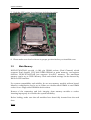
System Overview
Chapter 1
System Overview
1.1
Introduction
Powell Inc., a world-leading innovator in the Industrial PC (IPC) market and a
member of the Intel® Communications Alliance, has launched its new RUBYD716VG2AR in response to market demand for a simplified embedded system board
(ESB) that combines a smaller footprint, lower power consumption, robust
computing power and with longevity support.
Against the pre-generation chipset RUBY-D716VG2AR based on Q87 chipset, Q87
offers Core i5/i7 processors, VGA, DVI-D, HDMI port, USB 3.0 and SATA III
support which USB 3.0 is first integrated.
RUBY-D716VG2AR based on the Intel® Core™ Processor which offers 22nm
Hi-K process technology with energy efficient architecture. RUBY- D716VG2AR
adopts four channels DDR3 long DIMM up to 32GB.
Desktop solution is still popular in the market of DVR and Factory Automation
which can fulfill most of these applications; therefore, with high performance and
high-end specifications, Q87 is our first generation Ivy bridge chip architecture on
ATX line.
1.2
Check List
The RUBY-D716VG2AR package should cover the following basic items
One RUBY-D716VG2AR Industrial Mother board
One SATA III Cable
One I/O Shield bracket
One Installation Resources CD-Title
If any of these items is damaged or missing, please contact your vendor and keep all
packing materials for future replacement and maintenance.
1.3
Product Specification
z Main Processor
-Intel® Dual Core/Quad Core LGA1150 processor
z Chipset
-Intel® Q87 Express chipset
RUBY-D716VG2AR User’s Manual
1-1
System Overview
z System BIOS
-Phoenix UEFI BIOS
z Main Memory
-Four 240-pin DDR3 DIMM socket support up to 32GB dual channel
1600/1333MHz memory(supports Non-ECC memory)
z Expansion Interface
-One PCIe x16 slot (Gen 3.0 8GT/s)
-Two PCIe x4 slot
-Two PCIe x1 slot
-Two PCI slots
z SATA Interface
-Five SATA ports(SATA 6Gb/s)
-One CFEX (SATA 3Gb/s interface)
z Serial Port
-Support total six com ports(one RS232 and one RS232/422/485 on rear S/O,
three RS232 and one RS232/422/485 on board header)
z USB Interface
-Support Twelve USB ports, four on rear I/O(USB3.0) and Eight on board
header(USB2.0) for internal devices
z Audio Interface
-Connector for Mic-In, Line-In and Line-Out
z Real Time Clock/Calendar (RTC)
-Support Y2K Real Time Clock/Calendar
z Watch Dog Timer
-Support WDT function through software programming for enable/disable
and interval setting General system reset
z On-board Ethernet LAN
-Two Gigabit Ethernet (10/100/1000 Mbits/sec) LAN ports using Intel
WGI217LM & WGI210AT GbE Ethernet Controller
z High Drive GPIO
-One pin-header for 8 bit GPIO(4bit in & 4bit out)
z System Monitoring Feature
-Monitor system temperature and major power sources.
z Outline Dimension (L x W)
-304.8mm (12”) X 243.8mm (9.6”)
RUBY-D716VG2AR User’s Manual
1-2
System Overview
z
Power Requirements
Power ON
Full Loading
10Min
Full Loading
30Min
CPU +12V
1.07A
1.83A
2.10A
System +12V
0.93A
1.28A
1.40A
System +3.3V
0.69A
0.93A
1.01A
System +5V
1.20A
2.02A
1.97A
System+ Device +12V
2.42A
3.42A
3.96A
System+ Device +5V
2.22A
2.81A
2.89A
Item
USB Loading Test
z Configuration:
SBC BIOS
VGA Card
VGA Driver
LAN Card
LAN Driver
Audio Card
Audio Driver
Chip Driver
USB 3.0 Driver
SATA HDD
Power Supply
4.75~4.85V/ 580 mA
Portwell, Inc. RUBY-D716VG2AR TEST BIOS
Intel Haswell HD Graphics –GT2
Intel Haswell HD Graphics –GT2 Version:9.17.10.2895
Onboard Intel® I217-LM / I210 Gigabit Network Connection
Intel®
I217-LM/I210
Gigabit
Network
Connection
Version:12.5.19.0 /12.4.36.
On board Realtek ALC886 High Definition Audio
Realtek ALC886 High Definition Audio Version :6.0.1.6662
Intel® Chipset Device Software Version:9.4.0.1011
Intel® USB3.0 eXtensible Host Controller Version:2.0.2.100
Seagate ST3250312CS 250GB
FSP GROUP INC, FSP350-60GLC
z Operating Temperature
0 °C ~ 60 °C
z Storage temperature
-20 ~ 80 °C
z Relative Humidity
0% ~ 90%, non-condensing
RUBY-D716VG2AR User’s Manual
1-3
System Overview
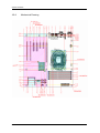
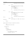
1.3.1
Mechanical Drawing
RUBY-D716VG2AR User’s Manual
1-4
System Overview
RUBY-D716VG2AR User’s Manual
1-5
System Overview
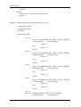
1.4
System Architecture
All of details operating relations are shown in RUBY-D716VG2AR System Block
Diagram.
RUBY-D716VG2AR System Block Diagram
RUBY-D716VG2AR User’s Manual
1-6
Hardware Configuration
Chapter 2
Hardware Configuration
This chapter indicates jumpers’, headers’ and connectors’ locations. Users may find useful
information related to hardware settings in this chapter.
2.1
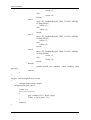
Jumper Setting
For users to customize RUBY-D716VG2AR’s features. In the following sections, Short
means covering a jumper cap over jumper pins; Open or N/C (Not Connected) means
removing a jumper cap from jumper pins. Users can refer to Figure 1 for the Jumper
allocations.
Figure 1-1 RUBY-D716VG2AR Top View
RUBY-D716VG2AR User’s Manual
2-1
Hardware Configuration
Jump Function List
Jump
JP1
JP2
JP3
JP4
JP5
JP6
JP8
JP11
Function
Clear CMOS
COM Port1 RI POWER Select
CONFIG / RECOVERY JUMPER
Watch Dog Time Disable/Enable
ATX & AT mode
GPIO Out Level
PCI Express* Bifurcation r
COM Port6 mode Select
Remark
PH3Px1/2.54mm
Header3Px2/2mm
PH3Px1/2.54mm
PH2Px1/2.54mm
PH2Px1/2.54mm
PH3Px1/2.54mm
Header2Px2/2.54mm
Header11Px2 2mm
Pin Assignments of Connectors
JP1: Clear CMOS
PIN No.
1-2, Short
2-3, Short
Signal Description
Normal
Ì
Clear CMOS
JP2: COM Port1 RI POWER Select
PIN No.
1-2, Short
3-4, Short
5-6, Short
Signal Description
5V
RI Ì
12V
J3: CONFIG / RECOVERY JUMPER
PIN No.
1-2, Short
2-3, Short
JUMPER REMOVED
Signal Description
NORMAL
Ì
CONFIGURE
RECOVERY
RUBY-D716VG2AR User’s Manual
2-2
Hardware Configuration
JP4: Watch Dog Time Disable/Enable
PIN No.
1-2 Short
1-2 Open
Signal Description
Enable Ì
Disable
JP5: ATX & AT mode
PIN No.
1-2 Short
1-2 Open
Signal Description
AT mode
ATX mode Ì
JP6: GPIO Out Level
PIN No.
1-2, Short
2-3, Short
Signal Description
5V
3.3V
JP8: PCI Express* Bifurcation
PIN No.
1-2, Short
3-4, Short
1-2, Open
3-4, Short
1-2, Short
3-4, Open
1-2, Open
3-4, Open
Signal Description
1x8 , 2x4
reserved
2x8
1x16 Ì
RUBY-D716VG2AR User’s Manual
2-3
Hardware Configuration
JP11: COM Port6 mode Select
PIN No.
5-6,9-11,10-12,
15-17,16-18
3-4,7-9,8-10,13-15,
14-16,21-22
1-2,7-9,8-10,19-20
2.2
Signal Description
RS-232 Ì
RS-422
RS-485
Connector Allocation
I/O peripheral devices are connected to the interface connectors.
Connector Function List
Connector
Function
Remark
U1
HDMI Port
J1
DVI & VGA Port
QH11121-DBGH-4F.
Foxconn
J2
COM Port 1 . 2
D-SUB 9Mx2
J3
J4
J5
J6
J7
J8
J9
J11
J12/J13/J14/J15
/J17/J18/J19/J20
J16
J21/J26/J27/J28
J25/J24/J23/J22
J29/J30/J33/J34/J3
7
Audio connector
USB 3.0/100M/1G Lan Connector
(LAN1) LAN WGI217LM
USB 3.0/100M/1G Lan Connector
(LAN2) LAN WGI210AT
Front Panel System Connector
ATX 4Pin 12V Power Connector
Triple_AudioJack
RJ45+USB3.0x2
RJ45+USB3.0x2
HEADER 8PX2
MA 2Px2. ATX4PT-L.
TechBest
SMBus Connector
PH5Px1-Pin2/2.54mm
PS/2 Keyboard/Mouse Connector HEADER5X2/nc3,4
GPIO
Header5Px2/2.54mm
COM3~COM10 Serial Port
BH5Px2/2.54mm
Connector
CPU FAN Power Connector
FAN_Header4Px1
DDR3 Long DIMM Connector
DDR3-Slot/240Pin
External USB Connector
HEADER 5PX2(-9)
SATA Connector(6Gb/s)
SATA/Blue
RUBY-D716VG2AR User’s Manual
2-4
Hardware Configuration
J31
J32
J35
J36
TPM(Trusted Platform Module)
Connector
CFEX Slot
ATX Power
SYSTEM FAN Power Connector
BH10Px2/2.0mm
CFEX
ATX24/180D
Connector3Px1/2.54mm
J6: Front Panel System Connector
PIN No.
1
3
5
7
9
11
13
15
Signal Description
PWR_LED(+)
PWR_LED(-)
LAN1_ACT(+)
LAN1_LINK(-)
LAN2_LINK(-)
LAN2_ACT(+)
HDD_LED(+)
HDD_LED(-)
PIN No.
2
4
6
8
10
12
14
16
Signal Description
VCC
N/C
N/C
BUZZER
GND
Power Button
Rest
GND
J7: ATX 4Pin 12V Power Connector
PIN No.
1
2
3
4
Signal Description
Ground
Ground
+12V
+12V
RUBY-D716VG2AR User’s Manual
2-5
Hardware Configuration
J8: SMBus Connector
PIN No.
1
2
3
4
5
Signal Description
SMBus_CLK
N/C
Ground
SMBus_DAT
+5V
J9: PS/2 Keyboard/Mouse Connector
PIN No.
1
3
5
7
9
Signal Description
Mouse Data
N/C
Ground
PS2 Power
Mouse Clock
PIN No.
2
4
6
8
10
Signal Description
Keyboard Data
N/C
Ground
PS2 Power
Keyboard Clock
Signal Description
LPC_GPIO0
LPC_GPIO1
LPC_GPIO2
LPC_GPIO3
GND
PIN No.
2
4
6
8
10
Signal Description
LPC_GPO4
LPC_GPO2
LPC_GPO3
LPC_GPO4
Vcc
J11: GPIO
PIN No.
1
3
5
7
9
RUBY-D716VG2AR User’s Manual
2-6
Hardware Configuration
J12/J13/J14/J15/J17/J18/J19/J20: COM3~COM10 Serial Port Connector
PIN No.
1
3
5
7
9
Signal Description
DCD (Data Carrier Detect)
RXD (Receive Data)
TXD (Transmit Data)
DTR (Data Terminal
Ready)
GND (Ground)
PIN No.
2
4
6
8
Signal Description
DSR (Data Set Ready)
RTS (Request to Send)
CTS (Clear to Send)
RI (Ring Indicator)
10
N/C
J16: CPU FAN Power Connector
PIN No.
1
2
3
4
Signal Description
Ground
+12V
Fan on/off output
Fan Speed control
J25/J24/J23/J22: External USB Connector
PIN No.
1
3
5
7
9
Signal Description
5V Dual
USBUSB+
Ground
RUBY-D716VG2AR User’s Manual
PIN No.
2
4
6
8
10
Signal Description
5V Dual
USBUSB+
Ground
N/C
2-7
Hardware Configuration
J29/J30/J33/J34/J37: SATA Connector(6Gb/s)
PIN No.
1
2
3
4
5
6
7
Signal Description
GND1
TX+
TXGND2
RXRX+
GND3
J31 TPM(Trusted Platform Module) Connector
PIN No.
1
3
5
7
9
11
13
15
17
19
Signal Description
PCLK_TPM
LFRAME#
PLT_RST_N
LAD3
VCC3
LAD0
SMB_CLK_MAIN
3VSB
LPCPD#
Ground
RUBY-D716VG2AR User’s Manual
PIN No.
2
4
6
8
10
12
14
16
18
20
Signal Description
Ground
N/C
LAD2
LAD1
Ground
SMB_DATA_MAIN
SERIRQ
N/C
LDRQ#1
Ground
2-8
Hardware Configuration
J35 ATX Power
PIN No.
1
2
3
4
5
6
7
8
9
10
11
12
Signal Description
+3.3V
+3.3V
Ground
+5V
Ground
+5V
Ground
ATX_PWROK
+5VSB
+12V1
+12V1
+3.3V
PIN No.
13
14
15
16
17
18
19
20
21
22
23
24
Signal Description
+3.3V
-12V
Ground
PS_ON#
Ground
Ground
Ground
-5V
+5V
+5V
+5V
Ground
J36: SYSTEM FAN Power Connector
PIN No.
1
2
3
Signal Description
Ground
Fan speed control
Fan on/off output
RUBY-D716VG2AR User’s Manual
2-9
System Installation
Chapter 3
System Installation
This chapter provides the instructions to set up the system. The additional
information is enclosed to help you set up onboard devices
3.1
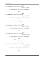
Intel® Dual Core/Quad Core processor
LGA-1150 CPU Socket
Pin1 corner of the CPU Socket
LGA-1150 CPU
Yellow Triangle Pin1 of the CPU
Alignment key
Notch
RUBY-D716VG2AR User’s Manual
3-1
System Installation
Please remember to locate the alignment keys on the CPU socket of the
motherboard and the notches on the CPU.
LGA-1150 CPU Installation Steps
Before install the CPU, please make sure to turn off the power first!!
1. Open the load lever.
2. Lift the load lever up to fully open
RUBY-D716VG2AR User’s Manual
3-2
System Installation
3. Remove the plastic cap on the CPU socket. Before you install the CPU, always
cover it to protect the socket pin.
4. After confirming the CPU direction for correct mating, put down the CPU in the
socket housing frame. Note that alignment keys are matched.
RUBY-D716VG2AR User’s Manual
3-3
System Installation
5. Make sure the CPU has been seated well into the socket. If not, take out the CPU
and reinstall.
6. Engage the load lever while pressing down lightly onto the load plate.
RUBY-D716VG2AR User’s Manual
3-4
System Installation
7. Push the CPU socket lever back into its locked position
8. Please make sure four hooks are in proper position before you install the core.
3.2
Main Memory
RUBY-D716VG2AR provide 4 x240 pin DIMM sockets (Dual Channel) which
supports Dual channel 1333/1600 DDR3-SDRAM as main memory, non-register
function. RUBY-D716VG2AR just supports Non-ECC memory. The maximum
memory can be up to 32GB. Memory clock and related settings can be detected by
BIOS via SPD interface.
For system compatibility and stability, do not use memory module without brand.
Memory configuration can be set to either one double-sided DIMM in one DIMM
socket or two single-sided DIMM in both sockets.
Beware of the connection and lock integrity from memory module to socket.
Inserting improperly it will affect the system reliability.
Before locking, make sure that all modules have been fully inserted into the card
slots
Note:
RUBY-D716VG2AR User’s Manual
3-5
System Installation
To insure the system stability, please do not change any of DRAM parameters in
BIOS setup to modify system the performance without acquired technical
information.
RUBY-D716VG2AR User’s Manual
3-6
System Installation
3.3
Installing the Single Board Computer
To install your RUBY-D716VG2AR into
environment, please perform the following:
standard
chassis
or
proprietary
Step 1 : Check all jumpers setting on proper position
Step 2 : Install and configure CPU and memory module at right position
Step 3 : Place RUBY-D716VG2AR into the dedicated position in the system
Step 4 : Attach cables to existing peripheral devices and secure it
WARNING
Please ensure that SBC is properly inserted and fixed by mechanism.
Note
Please refer to section 3.3.1 to 3.3.7 to install INF/VGA/LAN/Audio drivers.
3.3.1
Chipset Component Driver
RUBY-D716VG2AR uses state-of-art Intel® Panther Point chipset. It’s a new chipset
that some old operating systems might not be able to recognize. To overcome this
compatibility issue, for previous Windows Operating Systems such as Windows XP,
please install its INF before any of other Drivers are installed. You can find very
easily this chipset component driver in RUBY-D716VG2AR CD-title.
Moreover, if using some old OS, the driver may not be supported anymore. We
recommend to change the different OS to comply with this new chipset.
3.3.2
Intel® HD Graphics Family
With latest Intel® Core Ivy Bridge series structure, RUBY-D716VG2AR Intel® HD
Graphic is built in with CPU. Therefore 2nd Generation Core and 3nd Generation
Core CPUs provide HD integrated Graphic support sharing on board physical
memories. RUBY-D716VG2AR has both internal VGA & DVI interface. This
combination makes RUBY-D716VG2AR an excellent piece of multimedia hardware
With no additional video adaptor, this onboard video will usually be the system
display output. By adjusting the BIOS setting to disable on-board VGA, an add-on
PCI-Express Graphic card can take over the system display.
※To use Intel® Integrated HD Graphic, it’s required to choose the CPU which has
Integrated Graphic built-in. Otherwise there will be no display whatsoever.
3.3.3
Intel® PROSet Gigabit Ethernet Controlle
Drivers Support
Please find Intel® WG1218LM and WG1210AT LAN driver in /Ethernet directory of
RUBY-D716VG2AR CD-title. The driver supports Windows Win7 64-bits.
RUBY-D716VG2AR User’s Manual
3-7
System Installation
3.3.4
Audio Controller
Please find Intel® High Definition Audio driver form RUBY-D716VG2AR CD-title.
The driver supports Windows Win7 64-bits.
3.3.5
Intel® Active Management Technology (Intel® AMT)
Please find the latest Intel®AMT 9.0 driver from RUBY-D716VG2AR CD-title. The
driver supports Windows Win7 64-bits.
3.4
Clear CMOS Operation
JP1: CLEAR CMOS
PIN No.
1-2 Short
2-3 Short
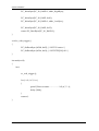
3.5
Signal Description
Normal Operation Clear CMOS Contents
WDT Function
The Watchdog Timer of motherboard consists of 8-bit programmable time-out
counter and a control and status register.
WDT Controller Register
There are two PNP I/O port addresses that can be used to configure WDT.
WDT Control Mode Register
The working algorithm of the WDT function can be simply described as a counting
process. The Time-Out Interval can be set through software programming. The
availability of the time-out interval settings by software or hardware varies from
boards to boards.
RUBY-D716VG2AR User’s Manual
3-8
System Installation
RUBY-D716VG2AR allows users to control WDT through dynamic software
programming. The WDT starts counting when it is activated. It sends out a signal to
system reset or to non-maskable interrupt (NMI), when time-out interval ends. To
prevent the time-out interval from running out, a re-trigger signal will need to be
sent before the counting reaches its end. This action will restart the counting process.
A well-written WDT program should keep the counting process running under
normal condition. WDT should never generate a system reset or NMI signal unless
the system runs into troubles.
The related Control Registers of WDT are all included in the following sample
program that is written in C language. User can fill a non-zero value into the Timeout Value Register to enable/refresh WDT. System will be reset after the Time-out
Value to be counted down to zero. Or user can directly fill a zero value into Time-out
Value Register to disable WDT immediately. To ensure a successful accessing to the
content of desired Control Register, the sequence of following program codes should
be step-by-step run again when each register is accessed.
Additionally, there are maximum 2 seconds of counting tolerance that should be
considered into user’ application program.
There are two PNP I/O port addresses that can be used to configure WDT,
WDT Control Command Example
#include <stdio.h>
#include <dos.h>
#define
EC_BASE
#define
EC_IO_BASE
0x4E
0x2E
/* EC controll function */
static void EC_WriteByte (unsigned char index, unsigned char data)
{
outportb (EC_BASE, index);
delay(2);
outportb (EC_BASE+1, data);
delay(2);
}
/* Function to read value to SMFI via LPC */
RUBY-D716VG2AR User’s Manual
3-9
System Installation
static unsigned char EC_ReadByte (unsigned char index)
{
unsigned char tmp;
outportb (EC_BASE, index);
delay(2);
tmp = inportb (EC_BASE+1);
delay(2);
return tmp;
}
void EC_SetRamByte (int address, unsigned char data)
{
int addr_HighByte, addr_LowByte;
addr_HighByte = (address >> 8) & 0xFF;
addr_LowByte = address & 0xFF;
EC_WriteByte(EC_IO_BASE, 0x11);
EC_WriteByte(EC_IO_BASE+1, addr_HighByte);
EC_WriteByte(EC_IO_BASE, 0x10);
EC_WriteByte(EC_IO_BASE+1, addr_LowByte);
EC_WriteByte(EC_IO_BASE, 0x12);
EC_WriteByte(EC_IO_BASE+1, data);
}
unsigned char EC_GetRamByte (int address)
{
int addr_HighByte, addr_LowByte;
addr_HighByte = (address >> 8) & 0xFF;
addr_LowByte = address & 0xFF;
EC_WriteByte(EC_IO_BASE, 0x11);
RUBY-D716VG2AR User’s Manual
3-10
System Installation
EC_WriteByte(EC_IO_BASE+1, addr_HighByte);
EC_WriteByte(EC_IO_BASE, 0x10);
EC_WriteByte(EC_IO_BASE+1, addr_LowByte);
EC_WriteByte(EC_IO_BASE, 0x12);
return EC_ReadByte(EC_IO_BASE+1);
}
void ec_wdt_trigger ()
{
EC_SetRamByte (0x308, 0x05); /* WDT Counter */
EC_SetRamByte (0x306, 0x01); /* WDTCFG[1:0]=01 */
}
int main(void)
{
int i;
ec_wdt_trigger ();
for (i = 0; i < 5; i++)
{
printf ("Reset counter ...................%d\n", 5 - i);
delay (1000);
}
return 0;
}
RUBY-D716VG2AR User’s Manual
3-11
System Installation
3.6
GPIO
The motherboard provides 4 input / output ports that can be individually
configured to perform a simple basic I/O function.
GPIO Pin Assignment
The RUBY-D716VG2AR provides 4 input/output ports that can be individually
configured to perform a simple basic I/O function. Users can configure each
individual port to become an input or output port by programming register bit of
I/O Selection. To invert port value, the setting of Inversion Register has to be made.
Port values can be set to read or write through Data Register.
The GPIO port is located on J11 shown as follows. Please note: Do not short the Pin 9
and Pin 10 of the J11!
The control for the GPIO signals is handled through a separate 1-byte I/O space.
J11: General Purpose I/O Connector
PIN No.
Signal Description
1
GPIO0
3
GPIO1
5
GPIO2
7
GPIO3
9
GND
PIN No.
2
4
6
8
10
Signal Description
GPIO4
GPIO5
GPIO6
GPIO7
VCC
GPIO Control Command Example (C Language)
#include <stdio.h>
#include <dos.h>
#define
#define
EC_BASE
EC_IO_BASE
#define
#define
#define
#define
#define
#define
#define
#define
EC_PIN1_VALUE_ADDR
EC_PIN2_VALUE_ADDR
EC_PIN3_VALUE_ADDR
EC_PIN4_VALUE_ADDR
EC_PIN5_VALUE_ADDR
EC_PIN6_VALUE_ADDR
EC_PIN7_VALUE_ADDR
EC_PIN8_VALUE_ADDR
#define
#define
#define
#define
EC_PIN1_CTL_ADDR
EC_PIN2_CTL_ADDR
EC_PIN3_CTL_ADDR
EC_PIN4_CTL_ADDR
RUBY-D716VG2AR User’s Manual
0x4E
0x2E
0x160A
0x160A
0x160A
0x160A
0x1605
0x1605
0x1603
0x1607
/*bit 0*/
/*bit 1*/
/*bit 2*/
/*bit 3*/
/*bit 0*/
/*bit 7*/
/*bit 0*/
/*bit 0*/
0x1658 //J0 ~ J3
0x1659
0x165A
0x165B
3-12
System Installation
#define
#define
#define
#define
#define
#define
#define
#define
#define
#define
#define
#define
EC_PIN5_CTL_ADDR
EC_PIN6_CTL_ADDR
EC_PIN7_CTL_ADDR
EC_PIN8_CTL_ADDR
0x1630
0x1637
0x1620
0x1640
// E0
// E7
// C0
// G0
EC_Bit0
EC_Bit1
EC_Bit2
EC_Bit3
EC_Bit4
EC_Bit5
EC_Bit6
EC_Bit7
0x01
0x02
0x04
0x08
0x01
0x80
0x01
0x01
/* EC controll function */
static void EC_WriteByte (unsigned char index, unsigned char data)
{
outportb (EC_BASE, index);
delay(2);
outportb (EC_BASE+1, data);
delay(2);
}
/* Function to read value to SMFI via LPC */
static unsigned char EC_ReadByte (unsigned char index)
{
unsigned char tmp;
outportb (EC_BASE, index);
delay(2);
tmp = inportb (EC_BASE+1);
delay(2);
return tmp;
}
void EC_SetRamByte (int address, unsigned char data)
{
int addr_HighByte, addr_LowByte;
addr_HighByte = (address >> 8) & 0xFF;
addr_LowByte = address & 0xFF;
EC_WriteByte(EC_IO_BASE, 0x11);
EC_WriteByte(EC_IO_BASE+1, addr_HighByte);
EC_WriteByte(EC_IO_BASE, 0x10);
EC_WriteByte(EC_IO_BASE+1, addr_LowByte);
RUBY-D716VG2AR User’s Manual
3-13
System Installation
EC_WriteByte(EC_IO_BASE, 0x12);
EC_WriteByte(EC_IO_BASE+1, data);
}
unsigned char EC_GetRamByte (int address)
{
int addr_HighByte, addr_LowByte;
addr_HighByte = (address >> 8) & 0xFF;
addr_LowByte = address & 0xFF;
EC_WriteByte(EC_IO_BASE, 0x11);
EC_WriteByte(EC_IO_BASE+1, addr_HighByte);
EC_WriteByte(EC_IO_BASE, 0x10);
EC_WriteByte(EC_IO_BASE+1, addr_LowByte);
EC_WriteByte(EC_IO_BASE, 0x12);
return EC_ReadByte(EC_IO_BASE+1);
}
/* GPIO controll function */
int gpio_setpindirection (int pin_num, unsigned char io_direction)
{
unsigned char data;
unsigned char tmp;
switch (pin_num)
{
case 1:
if(io_direction)
{
tmp
=
EC_GetRamByte(EC_PIN1_CTL_ADDR);
tmp
=
0x84;
/*set input*/
tmp &= ~0x40;
EC_SetRamByte(EC_PIN1_CTL_ADDR, tmp);
}
else
{
tmp
=
EC_GetRamByte(EC_PIN1_CTL_ADDR);
tmp = 0x40;
RUBY-D716VG2AR User’s Manual
/*set output*/
tmp &= ~0x80;
3-14
System Installation
EC_SetRamByte(EC_PIN1_CTL_ADDR, tmp);
}
break;
case 2:
if (io_direction)
{
tmp
EC_GetRamByte(EC_PIN2_CTL_ADDR);
tmp = 0x84;
tmp &= ~0x40;
EC_SetRamByte(EC_PIN2_CTL_ADDR,
tmp);
}
else
{
tmp
EC_GetRamByte(EC_PIN2_CTL_ADDR);
tmp = 0x40;
tmp &= ~0x80;
EC_SetRamByte(EC_PIN2_CTL_ADDR,
tmp);
}
break;
case 3:
if (io_direction)
{
tmp
EC_GetRamByte(EC_PIN3_CTL_ADDR);
tmp = 0x84;
tmp &= ~0x40;
EC_SetRamByte(EC_PIN3_CTL_ADDR,
tmp);
}
else
{
tmp
EC_GetRamByte(EC_PIN3_CTL_ADDR);
tmp = 0x40;
tmp &= ~0x80;
EC_SetRamByte(EC_PIN3_CTL_ADDR,
tmp);
}
break;
case 4:
if (io_direction)
RUBY-D716VG2AR User’s Manual
=
=
=
=
3-15
System Installation
{
tmp
=
EC_GetRamByte(EC_PIN4_CTL_ADDR);
tmp = 0x84;
tmp &= ~0x40;
EC_SetRamByte(EC_PIN4_CTL_ADDR,
tmp);
}
else
{
tmp
=
EC_GetRamByte(EC_PIN4_CTL_ADDR);
tmp = 0x40;
tmp &= ~0x80;
EC_SetRamByte(EC_PIN4_CTL_ADDR,
tmp);
}
break;
case 5:
if (io_direction)
{
tmp
=
EC_GetRamByte(EC_PIN5_CTL_ADDR);
tmp = 0x84;
tmp &= ~0x40;
EC_SetRamByte(EC_PIN5_CTL_ADDR,
tmp);
}
else
{
tmp
=
EC_GetRamByte(EC_PIN5_CTL_ADDR);
tmp = 0x40;
tmp &= ~0x80;
EC_SetRamByte(EC_PIN5_CTL_ADDR,
tmp);
}
break;
case 6:
if (io_direction)
{
tmp
=
EC_GetRamByte(EC_PIN6_CTL_ADDR);
tmp = 0x84;
tmp &= ~0x40;
RUBY-D716VG2AR User’s Manual
3-16
System Installation
EC_SetRamByte(EC_PIN6_CTL_ADDR,
tmp);
}
else
{
tmp
=
EC_GetRamByte(EC_PIN6_CTL_ADDR);
tmp = 0x40;
tmp &= ~0x80;
EC_SetRamByte(EC_PIN6_CTL_ADDR,
tmp);
}
break;
case 7:
if (io_direction)
{
tmp
=
EC_GetRamByte(EC_PIN7_CTL_ADDR);
tmp = 0x84;
tmp &= ~0x40;
EC_SetRamByte(EC_PIN7_CTL_ADDR,
tmp);
}
else
{
tmp
=
EC_GetRamByte(EC_PIN7_CTL_ADDR);
tmp = 0x40;
tmp &= ~0x80;
EC_SetRamByte(EC_PIN7_CTL_ADDR,
tmp);
}
break;
case 8:
if (io_direction)
{
tmp
=
EC_GetRamByte(EC_PIN8_CTL_ADDR);
tmp = 0x84;
tmp &= ~0x40;
EC_SetRamByte(EC_PIN8_CTL_ADDR,
tmp);
}
else
{
RUBY-D716VG2AR User’s Manual
3-17
System Installation
tmp
=
EC_GetRamByte(EC_PIN8_CTL_ADDR);
tmp = 0x40;
tmp &= ~0x80;
EC_SetRamByte(EC_PIN8_CTL_ADDR,
tmp);
}
break;
default:
printf("invalid
pin
number
when
writing
to
gpio\n");
}
return 0;
}
int gpio_setdirection (unsigned char io_direction)
{
unsigned char data;
int i;
for (i = 0; i < 8; i++)
gpio_setpindirection (gpio_set, i+1, (io_direction & (0x01 <<
i)));
return 0;
}
int gpio_readpindirection (int pin_num, unsigned char *io_direction)
{
unsigned char data;
unsigned char tmp;
switch(pin_num)
{
case 1:
tmp = EC_GetRamByte(EC_PIN1_CTL_ADDR);
if( tmp & 0x80 )
/* means in */
*io_direction = 1;
else if ( tmp & 0x40 )
/* means out */
*io_direction = 0;
else
printf("unknown GPIO pin direction in
EC\n");
break;
case 2:
tmp = EC_GetRamByte(EC_PIN2_CTL_ADDR);
RUBY-D716VG2AR User’s Manual
3-18
System Installation
if( tmp & 0x80 )
*io_direction = 1;
else if ( tmp & 0x40 )
*io_direction = 0;
else
printf("unknown GPIO pin direction in
EC\n");
break;
case 3:
tmp = EC_GetRamByte(EC_PIN3_CTL_ADDR);
if( tmp & 0x80 )
*io_direction = 1;
else if ( tmp & 0x40 )
*io_direction = 0;
else
printf("unknown GPIO pin direction in
EC\n");
break;
case 4:
tmp = EC_GetRamByte(EC_PIN4_CTL_ADDR);
if( tmp & 0x80 )
*io_direction = 1;
else if ( tmp & 0x40 )
*io_direction = 0;
else
printf("unknown GPIO pin direction in
EC\n");
break;
case 5:
tmp = EC_GetRamByte(EC_PIN5_CTL_ADDR);
if( tmp & 0x80 )
*io_direction = 1;
else if ( tmp & 0x40 )
*io_direction = 0;
else
printf("unknown GPIO pin direction in
EC\n");
break;
case 6:
tmp = EC_GetRamByte(EC_PIN6_CTL_ADDR);
if( tmp & 0x80 )
*io_direction = 1;
else if ( tmp & 0x40 )
*io_direction = 0;
else
RUBY-D716VG2AR User’s Manual
3-19
System Installation
printf("unknown GPIO pin direction in
EC\n");
break;
case 7:
tmp = EC_GetRamByte(EC_PIN7_CTL_ADDR);
if( tmp & 0x80 )
*io_direction = 1;
else if ( tmp & 0x40 )
*io_direction = 0;
else
printf("unknown GPIO pin direction in
EC\n");
break;
case 8:
tmp = EC_GetRamByte(EC_PIN8_CTL_ADDR);
if( tmp & 0x80 )
*io_direction = 1;
else if ( tmp & 0x40 )
*io_direction = 0;
else
printf("unknown GPIO pin direction in
EC\n");
break;
default:
printf("unsupport pin number when read pin
direction\n");
}
return 0;
}
int gpio_readdirection (int gpio_set, unsigned char *io_direction)
{
int i;
unsigned char data, temp, temp2;
switch (gpio_set)
{
case 1:
return 0;
case 2:
*io_direction = 0;
for (i = 0; i < 8; i++)
{
gpio_readpindirection (2, i+1, &data);
*io_direction |= (data << i);
}
RUBY-D716VG2AR User’s Manual
3-20
System Installation
return 0;
default:
printf ("error: no read gpio direction\n");
return 1;
}
}
int gpio_readpin (int pin_num, unsigned char *value)
{
unsigned char data;
unsigned char tmp;
int action;
switch (pin_num)
{
case 1:
tmp = EC_GetRamByte(EC_PIN1_VALUE_ADDR);
if (tmp & 0x10)
/* means high*/
*value = 1;
else
*value = 0;
break;
case 2:
tmp = EC_GetRamByte(EC_PIN2_VALUE_ADDR);
if( tmp & 0x40 )
/* means high */
*value = 1;
else
*value = 0;
break;
case 3:
tmp = EC_GetRamByte(EC_PIN3_VALUE_ADDR);
if( tmp & 0x20 )
/* means high */
*value = 1;
else
*value = 0;
break;
case 4:
tmp = EC_GetRamByte(EC_PIN4_VALUE_ADDR);
if( tmp & 0x08 )
/* means high */
*value = 1;
else
*value = 0;
break;
case 5:
tmp = EC_GetRamByte(EC_PIN5_VALUE_ADDR);
if( tmp & 0x80 )
/* means high */
RUBY-D716VG2AR User’s Manual
3-21
System Installation
*value = 1;
else
*value = 0;
break;
case 6:
tmp = EC_GetRamByte(EC_PIN6_VALUE_ADDR);
if( tmp & 0x01 )
*value = 1;
else
*value = 0;
break;
case 7:
tmp = EC_GetRamByte(EC_PIN7_VALUE_ADDR);
if( tmp & 0x02 )
*value = 1;
else
*value = 0;
break;
case 8:
tmp = EC_GetRamByte(EC_PIN8_VALUE_ADDR);
if( tmp & 0x04 )
*value = 1;
else
*value = 0;
break;
default:
printf("invalid pin number when reading from
gpio\n");
return 1;
}
}
int gpio_read (unsigned char *value)
{
unsigned char temp, temp2;
unsigned char pch_data, i;
*value = 0;
for (i = 0; i < 8; i++)
{
gpio_readpin (2, i+1, &pch_data);
*value |= (pch_data << i);
}
return 0;
}
RUBY-D716VG2AR User’s Manual
3-22
System Installation
int gpio_writepin (int pin_num, unsigned char value)
{
unsigned char data;
unsigned char tmp;
switch (pin_num)
{
case 1:
if( value )
{
tmp
EC_GetRamByte(EC_PIN1_VALUE_ADDR);
tmp |= EC_Bit0;
EC_SetRamByte(EC_PIN1_VALUE_ADDR, tmp);
}
else
{
tmp
EC_GetRamByte(EC_PIN1_VALUE_ADDR);
tmp &= ~EC_Bit0;
EC_SetRamByte(EC_PIN1_VALUE_ADDR, tmp);
}
break;
case 2:
if( value )
{
tmp
EC_GetRamByte(EC_PIN2_VALUE_ADDR);
tmp |= EC_Bit1;
EC_SetRamByte(EC_PIN2_VALUE_ADDR, tmp);
}
else
{
tmp
EC_GetRamByte(EC_PIN2_VALUE_ADDR);
tmp &= ~EC_Bit1;
=
=
=
=
EC_SetRamByte(EC_PIN2_VALUE_ADDR, tmp);
}
break;
case 3:
if( value )
{
RUBY-D716VG2AR User’s Manual
3-23
System Installation
tmp
EC_GetRamByte(EC_PIN3_VALUE_ADDR);
tmp |= EC_Bit2;
EC_SetRamByte(EC_PIN3_VALUE_ADDR, tmp);
}
else
{
tmp
EC_GetRamByte(EC_PIN3_VALUE_ADDR);
tmp &= ~EC_Bit2;
EC_SetRamByte(EC_PIN3_VALUE_ADDR, tmp);
}
break;
case 4:
if( value )
{
tmp
EC_GetRamByte(EC_PIN4_VALUE_ADDR);
tmp |= EC_Bit3;
EC_SetRamByte(EC_PIN4_VALUE_ADDR, tmp);
}
else
{
tmp
EC_GetRamByte(EC_PIN4_VALUE_ADDR);
tmp &= ~EC_Bit3;
EC_SetRamByte(EC_PIN4_VALUE_ADDR, tmp);
}
break;
case 5:
if( value )
{
tmp
EC_GetRamByte(EC_PIN5_VALUE_ADDR);
//tmp |= EC_Bit4;
tmp &= ~EC_Bit4;
=
=
=
=
=
EC_SetRamByte(EC_PIN5_VALUE_ADDR, tmp);
}
else
{
RUBY-D716VG2AR User’s Manual
3-24
System Installation
tmp
EC_GetRamByte(EC_PIN5_VALUE_ADDR);
//tmp &= ~EC_Bit4;
tmp |= EC_Bit4;
EC_SetRamByte(EC_PIN5_VALUE_ADDR, tmp);
}
break;
case 6:
if( value )
{
tmp
EC_GetRamByte(EC_PIN6_VALUE_ADDR);
tmp &= ~EC_Bit5;
EC_SetRamByte(EC_PIN6_VALUE_ADDR, tmp);
}
else
{
tmp
EC_GetRamByte(EC_PIN6_VALUE_ADDR);
tmp |= EC_Bit5;
EC_SetRamByte(EC_PIN6_VALUE_ADDR, tmp);
}
break;
case 7:
if( value )
{
tmp
EC_GetRamByte(EC_PIN7_VALUE_ADDR);
tmp &= ~EC_Bit6;
EC_SetRamByte(EC_PIN7_VALUE_ADDR, tmp);
}
else
{
tmp
EC_GetRamByte(EC_PIN7_VALUE_ADDR);
tmp |= EC_Bit6;
=
=
=
=
=
EC_SetRamByte(EC_PIN7_VALUE_ADDR, tmp);
}
break;
case 8:
if( value )
RUBY-D716VG2AR User’s Manual
3-25
System Installation
{
tmp
EC_GetRamByte(EC_PIN8_VALUE_ADDR);
tmp &= ~EC_Bit7;
=
EC_SetRamByte(EC_PIN8_VALUE_ADDR, tmp);
}
else
{
tmp
EC_GetRamByte(EC_PIN8_VALUE_ADDR);
tmp |= EC_Bit7;
EC_SetRamByte(EC_PIN8_VALUE_ADDR, tmp);
}
break;
default:
printf("invalid pin number
=
when
writing
to
gpio\n");
return 1;
}
return 0;
}
int gpio_write (unsigned char value)
{
unsigned char data;
int i;
for (i = 0; i < 8; i++)
gpio_writepin (2, i+1, value & (0x01 << i));
return 0;
}
int main(void)
{
unsigned char gpio_dir;
unsigned char gpio_value;
int i;
unsigned char gpio_pin, gpio_direction;
unsigned char d2;
printf("RUBY-D716VG2AR GPIO (EC line) TEST Program v1.0\n");
printf("Please short the following pins with jumper on GPIO\n");
RUBY-D716VG2AR User’s Manual
3-26
System Installation
printf("PIN 1,2,3,4 is output ; PIN 5,6,7,8 is input\n");
printf("GPIO 1 ---> GPIO 5\n");
printf("GPIO 2 ---> GPIO 6\n");
printf("GPIO 3 ---> GPIO 7\n");
printf("GPIO 4 ---> GPIO 8\n");
printf("GND
xxxx VCC <===PWR/GND pins, DO NOT short them!\n");
printf("Test Begins...\n");
gpio_setdirection (0xF0);
gpio_write (0x00);
gpio_readpin (5, &d2);
delay (2);
if (d2 == 0)
printf ("GPIO 1->GPIO 5 test PASS !!! (pull low)\n");
else
printf ("GPIO 1->GPIO 5 test FAIL !!! (pull high) \n");
gpio_readpin (6, &d2);
delay (2);
if (d2 == 0)
printf ("GPIO 2->GPIO 6 test PASS !!! (pull low)\n");
else
printf ("GPIO 2->GPIO 6 test FAIL !!! (pull high)\n");
gpio_readpin (7, &d2);
delay (2);
if (d2 == 0)
printf ("GPIO 3->GPIO 7 test PASS !!! (pull low)\n");
else
printf ("GPIO 3->GPIO 7 test FAIL !!! (pull high)\n");
gpio_readpin (8, &d2);
delay (2);
if (d2 == 0)
printf ("GPIO 4->GPIO 8 test PASS !!! (pull low)\n");
else
printf ("GPIO 4->GPIO 8 test FAIL !!! (pull high)\n");
return 0;
}
RUBY-D716VG2AR User’s Manual
3-27
BIOS Setup Information
Chapter 4
BIOS Setup Information
RUBY-D716VG2ARVG2AR is equipped with the Phoenix BIOS stored in Flash ROM.
These BIOS has a built-in Setup program that allows users to modify the basic
system configuration easily. This type of information is stored in CMOS RAM so that
it is retained during power-off periods. When system is turned on, RUBYD716VG2ARVG2AR communicates with peripheral devices and checks its hardware
resources against the configuration information stored in the CMOS memory. If any
error is detected, or the CMOS parameters need to be initially defined, the diagnostic
program will prompt the user to enter the SETUP program. Some errors are
significant enough to abort the start up.
4.1
Entering Setup -- Launch System Setup
Power on the computer and the system will start POST (Power On Self Test) process.
When the message below appears on the screen, press <F2> key will enter BIOS
setup screen.
Press <F2> to enter SETUP
If the message disappears before responding and still wish to enter Setup, please
restart the system by turning it OFF and On or pressing the RESET button. It can be
also restarted by pressing <Ctrl>, <Alt>, and <Delete> keys on keyboard
simultaneously.
Press <F1> to Run General Help or Resume
The BIOS setup program provides a General Help screen. The menu can be easily
called up from any menu by pressing <F1>. The Help screen lists all the possible
keys to use and the selections for the highlighted item. Press <Esc> to exit the Help
Screen.
RUBY-D716VG2AR User’s Manual
4-1
BIOS Setup Information
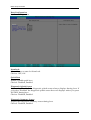
4.2
Main
Use this menu for basic system configurations, such as time, date etc.
System Date
The date format is <Day>, <Month> <Date> <Year>. Use [+] or [-] to configure
system Date.
System Time
The time format is <Hour> <Minute> <Second>. Use [+] or [-] to configure system
Time.
RUBY-D716VG2AR User’s Manual
4-2
BIOS Setup Information
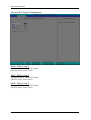
4.3
Configuration
Use this menu to set up the items of special enhanced features
RUBY-D716VG2AR User’s Manual
4-3
BIOS Setup Information
Boot Configuration
Set Boot Configuration.
NumLock:
Selects Power-on state for NumLock.
Choices: OFF, ON.
Quick Boot
Enable/Disable quick boot.
Choices: Disabled, Enabled.
Diagnostic Splash Screen
If you select ‘Enabled’ the diagnostic splash screen always displays during boot. If
you select ‘Disabled’ the diagnostic splash screen does not displays unless you press
HOTKEY during boot.
Choices: Disabled, Enabled.
Diagnostic Summary Screen
Display the Diagnostic summary screen during boot.
Choices: Disabled, Enabled.
RUBY-D716VG2AR User’s Manual
4-4
BIOS Setup Information
Allow Hotkey in S4 resume
Enable hotkey detection when system resuming from Hibernate state.
Choices: Disabled, Enabled.
UEFI Boot
Enable the UEFI boot.
Choices: Disabled, Enabled.
PCI/PCIE Configuration
Configure PCI/PCI Express slot.
RUBY-D716VG2AR User’s Manual
4-5
BIOS Setup Information
Processor PCI Express Configuration
FEG0 PEG0 – Gen X
Configure PFG0 B0:D0:F0 Speed.
Choices: Gen1, Gen2, Gen3
FEG1 PEG1 – Gen X
Configure PFG1 B0:D0:F1 Speed.
Choices: Gen1, Gen2, Gen3
FEG2 PEG2 – Gen X
Configure PFG2 B0:D0:F2 Speed.
Choices: Gen1, Gen2, Gen3
RUBY-D716VG2AR User’s Manual
4-6
BIOS Setup Information
ICH PCI Express Configuration
DMI Link ASPM Control
The control of active state Power Management on both NB side of the DMI Link.
Choices: Disabled, L0s, L1, L0sL1.
RUBY-D716VG2AR User’s Manual
4-7
BIOS Setup Information
PCI Express Root Port 1, 5-8
Control PCI Express root port.
PCI Express Root Port 1, 5-8
Control PCI Express root port.
Choices: Disabled, Enabled.
PCIe Speed
Select PCIe Speed to Gen1 or Gen2
Choices: Auto, Gen1, Gen2.
ASPM
Control PCIe Active State Power Management settings.
Choices: Disabled, L0S, L1, L0S And L1, Auto.
HOT PLUG
PCI Express Hot Plug Enabled/Disabled.
Choices: Disabled, Enabled.
URR
PCI Express Unsupported Request Reporting Enable/Disable.
Choices: Disabled, Enabled.
RUBY-D716VG2AR User’s Manual
4-8
BIOS Setup Information
FER
PCI Express Device Fatal Error Reporting Enable/Disable.
Choices: Disabled, Enabled.
NFER
PCI Express Device Non-Fatal Error Reporting Enable/Disable.
Choices: Disabled, Enabled.
CER
PCI Express Device Correctable Error Reporting Enable/Disable.
Choices: Disabled, Enabled.
SEFE
Root PCI Express System Error on Fatal Error Enable/Disable.
Choices: Disabled, Enabled.
SENFE
Root PCI Express System Error on Non-Fatal Error Enable/Disable.
Choices: Disabled, Enabled.
SECE
Root PCI Express System Error on Correctable Error Enable/Disable.
Choices: Disabled, Enabled.
PME Interrupt
Root PCI Express PME Interrupt Enable/Disable.
Choices: Disabled, Enabled.
PME SCI
PCI Express PME SCI
Choices: Disabled, Enabled.
RUBY-D716VG2AR User’s Manual
4-9
BIOS Setup Information
Power Control Configuration
Configure ACPI and RTC wake up setting.
Restore AC Power Loss
Select AC Power state when power is re-applied after a power failure.
Choices: Power Off, Power On, Last State.
SLP_S4 Assertion stretch Enable
Choices: Disabled, Enabled
Wake system with Fixed Time
Enable or disable system wake on alarm event. When Enabled, system will wake on
the hr::min::sec specified.
Choices: Disabled, Enabled
Wake up By PS/2 Keyboard
Choices: Enabled, Disabled.
Wake up By PS/2 Mouse
Choices: Enabled, Disabled.
RUBY-D716VG2AR User’s Manual
4-10
BIOS Setup Information
Wake up By Ring
Choices: Enabled, Disabled.
CPU configuration
Configure the specific active core(s) and advanced processor management
technologies.
Hyper-Threading
Enabled for Windows XP and Linux (OS optimized for Hyper-Threading
Technology) and Disabled for other OS (OS not optimized for Hyper-Threading
Technology). When Disabled only one.
Choices: Disabled, Enabled.
Active Processor Cores
Select the number of physical cores to enable in each processor package.
Choices: All, 1.
Limit CPUID Maximum
Disabled for Windows XP.
Choices: Disabled, Enabled.
Execute Disabled Bit
Enabled Execute Disabled functionality. Also known as Data Execution Prevention
(DEP).
Choices: Disabled, Enabled.
RUBY-D716VG2AR User’s Manual
4-11
BIOS Setup Information
EIST
Choices: Disabled, Enabled.
Turbo Mode
Choices: Disabled, Enabled.
C-States
Choices: Disabled, Enabled.
VT-x
When enabled, a VWM can utilize the additional hardware capabilities provided by
Vanderpool Technology.
Choices: Disabled, Enabled.
Local x2APIC
Choices: Disabled, Enabled.
LAN Configuration
Configure onboard LAN device.
RUBY-D716VG2AR User’s Manual
4-12
BIOS Setup Information
Intel WG1217-LM GbE LAN
Enabled/Disabled Intel WG1217-LM GbE LAN.
Choices: Disabled, Enabled.
Wake on LAN
Enabled/Disabled Wake on LAN Function.
Choices: Disabled, Enabled.
LAN Boot ROM
Control LAN Boot ROM (PXE) function.
Choices: Disabled, Enabled.
LAN4
Enabled/Disabled LAN4.
Choices: Disabled, Enabled.
Wake on LAN
Enabled/Disabled Wake on LAN Function.
Choices: Disabled, Enabled.
Chipset Configuration
Configure Chipset provide feature.
RUBY-D716VG2AR User’s Manual
4-13
BIOS Setup Information
VT-d
Check to enable VT-d function on MCH.
Choices: Disabled, Enabled.
NB PCIe Configuration
Config NB PCI Express Settings.
Always Enable PEG
To Enable the PEG Slot.
Choices: Disabled, Enabled.
PEG ASPM
Control ASPM Support for the PEG Device. This has mp effect if PEF is not the
current active sevice.
Choices: Disabled, Auto, ASPM L0s, ASPM L1, ASPM L0sL1.
RUBY-D716VG2AR User’s Manual
4-14
BIOS Setup Information
Memory Configuration
Memory Configuration Parameters.
Max TOLUD
Maximum Value of TOLUD. Dynamic assignment would adjust TOLUD
automatically based on largest MMIO length of installed graphic controller.
Choices: 1GB, 1.25GB, 1.5GB, 1.75GB, 2GB, 2.25GB, 2.5GB, 2.75GB, 3GB, 3.25GB.
Memory Frequency
Maximum Memory Frequency Selections in Mhz.
Choices: Auto, 1067, 1333, 1600, 1867, 2133.
RUBY-D716VG2AR User’s Manual
4-15
BIOS Setup Information
SB Azalia Config
SB Azalia Config Parameters.
Azalia
Control Detection of the Azalia device.
Choices: Disabled, Enabled.
RUBY-D716VG2AR User’s Manual
4-16
BIOS Setup Information
Graphic Configuration
Configure integrated Graphic like Boot display, video memory and external Graphic
feature.
Primary Display
Select which of IGFX/PEG/PCI Graphics device should be Primary Display Or
select SG for Switchable Gfx.
Choices: Auto, IGFX, PEG.
Internal Graphics
Keep IGD Enabled Based on the setup options,
Choices: Auto, Disabled, Enabled.
Aperture Size
Select the Aperture Size
Choices: 128MB, 256MB, 512MB.
DVMT Pre-Allocated
Select DVMT 5.0 Pre-Allocated Graphics Memory size used by the Internal Graphics
Device.
Choices: 0M, 32M, 64M, 96M, 128M, 160M, 192M, 224M, 256M, 288M, 320M , 352M,
384M, 416M, 448M, 480M, 512M.
RUBY-D716VG2AR User’s Manual
4-17
BIOS Setup Information
DVMT Total Gfx Mem
Select DVMT 5.0 Total Graphics Memory size used by the Internal Graphics Device.
Choices: 128MB, 256MB, MAX.
Primay Boot display
Choices: VBIOS Default, CRT, DVI, HDMI.
SATA Configuration
Configure SATA controller and view detected HDD
Information.
SATA Controller (s)
Determines how SATA controllers (s) operate.
Choices: Disabled, Enabled.
Launch Storage OpROM
Enable or Disable Boot Option for Legacy Mass Storage Devices with Option ROM.
Choices: Enabled, Disabled.
SATA Mode
Determines how SATA controllers (s) operate.
Choices: Disabled, IDE, AHCI, RAID.
RUBY-D716VG2AR User’s Manual
4-18
BIOS Setup Information
Serial ATA Port 0-5
Display the identity of the device attached.
Choices: Empty.
Port 0-5
Enabled or Disabled SATA Port.
Choices: Disabled, Enabled.
Hot Plug
Designates this port as Hot Pluggable.
Choices: Disabled, Enabled.
External Port
External SATA Support.
Choices: Disabled, Enabled.
SATA Device Type
Select ”Solid State Drive” only if a Solid State Drive is connected to this SATA port.
Choices: Hard Disk Driver, Solid State Driver.
USB Configuration
Configure USB controller and other advanced setting.
RUBY-D716VG2AR User’s Manual
4-19
BIOS Setup Information
Legacy USB Support
Enables Legacy USB support. AUTO option disables legacy support if no USB
devices are connected. DISABLE option will keep USB devices available only for EFI
applications.
Choices: Enabled, Disabled.
PCH USB Configuration
Control each of the USB ports disabling.
USB Ports Per-Port Disable
Choices: Enabled, Disabled.
RUBY-D716VG2AR User’s Manual
4-20
BIOS Setup Information
ME Configuration
Configure Management Engine Technology Parameters.
Intel (R) ME
Enable/Disable Intel (R) Management Engine.
Choices: Enabled, Disabled.
fTPM Switch Selection
Selects the desired fTPM solution to be used.
Choices: GPDMA Work-Around, MSFT QFE Solution.
RUBY-D716VG2AR User’s Manual
4-21
BIOS Setup Information
Super IO Configuration
Configure LPC Super IO.
Serial Port 1-10
Choices: Disabled, 2E8/IRQ4, 2F8/IRQ3, 4E0/IRQ10, 4E8/IRQ10, 4F0/IRQ10,
4F8/IRQ10, 3E0/IRQ11, 3E8/IRQ11, 3F0/IRQ11, 3F8/IRQ11
COM2 Configuration
Select Com2 Configuration.
Choices: RS-232, RS422, RS485.
Watch Dog Timer Select
Choices: Disabled, 15 secs, 30 secs, 1 min, 2 mins, 3 mins.
RUBY-D716VG2AR User’s Manual
4-22
BIOS Setup Information
Hardware Monitor
Provide on board sensor reading information. (Show only)
RUBY-D716VG2AR User’s Manual
4-23
BIOS Setup Information
CPU Fan Feature
CPU/System Fan Control
Smart Fan Control
Choices: Enabled, Disabled.
RUBY-D716VG2AR User’s Manual
4-24
BIOS Setup Information
Serial Port Console Configuration
Configure console redirection on serial port.
Console Redirection
Control Console Redirection enable/disable.
Choices: Enabled, Disabled
RUBY-D716VG2AR User’s Manual
4-25
BIOS Setup Information
SMBIOS Event Log
Clears SMBIOS events.
Choices: Enter
RUBY-D716VG2AR User’s Manual
4-26
BIOS Setup Information
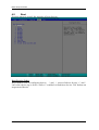
4.4
Security
This section lets you set security passwords to control access to the system at boot
time and/or when entering the BIOS setup program.
Set Supervisor Password
Set or clear the Supervisor account’s password.
Supervisor Hint String
Press Enter to type Supervisor Hint String.
Set User Password
Set or clear the User account’ password.
Supervisor Hint String
Press Enter to type User Hint String.
Min. password length
Set the minimum number of characters for password (1-20).
RUBY-D716VG2AR User’s Manual
4-27
BIOS Setup Information
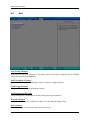
4.5
Boot
Use this menu to specify the priority of boot devices.
Boot Priority Order
Keys used to view or configure devices: ↑ and ↓ arrows Select a device. ‘+’ and ‘‘move the device up or down. ‘Shift + 1’ enabled or disables a device. ‘Del’ deletes an
unprotected device.
RUBY-D716VG2AR User’s Manual
4-28
BIOS Setup Information
4.6
Exit
Exit Saving Changes
Equal to F10, save all changes of all menus, then exit setup configure driver. Finally
resets the system automatically.
Exit Discarding Changes
Equal to ESC, never save changes, then exit setup configure driver.
Load Setup Defaults
Equal to F9. Load standard default values.
Load Optimized Defaults
Load settings for optimized boot time and system performance.
Discard Changes
Load the original value of this boot time. Not the default Setup value.
Save Changes
Save all changes of all menus, but do not reset sys
RUBY-D716VG2AR User’s Manual
4-29
Troubleshooting
Chapter 5
Troubleshooting
This chapter provides a few useful tips to quickly get RUBY-D716VG2ARVG2AR
running with success. As basic hardware installation has been addressed in Chapter
2, this chapter will focus on system integration issues, in terms of BIOS setting, and
OS diagnostics.
5.1
Hardware Quick Installation
ATX Power Setting
RUBY-D716VG2AR supports ATX. Therefore, there is no other setting that really
needs to be set up. However, there are only two connectors that must be connected—
J7 (4 pins CPU +12V main power connector) & J35 (24 pins ATX Power Connector)
RUBY-D716VG2AR User’s Manual
5-1
Troubleshooting
Serial ATA Hard Disk Setting for IDE/RAID/AHCI
Unlike IDE bus, each Serial ATA channel can only connect to one SATA hard disk at
a time; there are total six connectors, SATA1~6 port. The installation of Serial ATA is
simpler and easier than IDE, because SATA hard disk doesn’t require setting up
Master and Slave, which can reduce mistake of hardware installation. All you need
to operate IDE, RAID (0/1/5/10) and AHCI application for system, please follow up
setting guide in BIOS setup utility
5.2
BIOS Setting
It is assumed that users have correctly adopted modules and connected all the
devices cables required before turning on ATX power. CPU, CPU Fan, 204-pin DDR3
memory, keyboard, mouse, floppy drive, SATA hard disk, DVI-I connector, but it
only can use on DVI-D function, doesn’t support DVI-I function, device power
cables,
ATX accessories are good examples that deserve attention. With no assurance of
properly and correctly accommodating these modules and devices, it is very possible
to encounter system failures that result in malfunction of any device.
To make sure that you have a successful start with RUBY-D716VG2AR, it is
recommended, when going with the boot-up sequence, to hit “DEL” key and enter
the BIOS setup menu to tune up a stable BIOS configuration so that you can wake up
your system far well.
Loading the default optimal setting
When prompted with the main setup menu, please scroll down to “Load Optimal
Defaults”, press “Enter” and “Y” to load in default optimal BIOS setup. This will
force your BIOS setting back to the initial factory configuration. It is recommended
to
do this so you can be sure the system is running with the BIOS setting that Portwell
has highly endorsed. As a matter of fact, users can load the default BIOS setting any
RUBY-D716VG2AR User’s Manual
5-2
Troubleshooting
time when system appears to be unstable in boot up sequence.
Auto Detect Hard Disks
In the BIOS => Standard CMOS setup menu, pick up any one from
Primary/Secondary Master/Slave IDE ports, and press “Enter”. Setup the selected
IDE port and its access mode to “Auto”. This will force system to automatically pick
up the IDE devices that are being connected each time system boots up.
Improper disable operation
There are too many occasions where users disable a certain device/feature in one
application through BIOS setting. These variables may not be set back to the original
values when needed. These devices/features will certainly fail to be detected.
When the above conditions happen, it is strongly recommended to check the BIOS
settings. Make sure certain items are set as they should be. These include the COM1/
COM2 ports, USB ports, external cache, on-board VGA and Ethernet.
It is also very common that users would like to disable a certain device/port to
release IRQ resource. A few good examples are
Disable COM1 serial port to release IRQ #4
Disable COM2 serial port to release IRQ #3
Etc…
A quick review of the basic IRQ mapping is given below for your reference.
Interrupt Request Lines IRQ
IRQ#
IRQ 0
IRQ 1
IRQ 2
IRQ 3
IRQ 4
IRQ 5
IRQ 6
IRQ 7
IRQ 8
IRQ 9
IRQ 10
IRQ 11
IRQ 12
IRQ 13
IRQ 14
IRQ 15
Current Use
Unused
System ROM
【Unassigned】
System ROM
System ROM
【Unassigned】
System ROM
Unused
System ROM
【Unassigned】
【Unassigned】
【Unassigned】
System ROM
System ROM
System ROM
【Unassigned】
RUBY-D716VG2AR User’s Manual
Default Use
System Timer
Keyboard Event
Usable IRQ
COM2
COM1
Usable IRQ
Diskette Event
Usable IRQ
Real-Time Clock
Usable IRQ
Usable IRQ
Usable IRQ
IBM Mouse Event
Coprocessor Error
Hard Disk Event
Usable IRQ
5-3
Troubleshooting
RUBY-D716VG2AR User’s Manual
5-4
Troubleshooting
It is then very easy to find out which IRQ resource is ready for additional
peripherals. If IRQ resource is not enough, please disable some devices listed above
to release further IRQ numbers.
5.3
FAQ
Installation Problem
Question: How to update the BIOS file of the RUBY-D716VG2AR?
Answer:
Please visit web site of the Portwell download center as below hyperlink and
registeran account. http://www.portwell.com.tw/support/ Input your User name
and password to log in the download center. Select the "Search download" to input
the keyword "RUBY-D716VG2AR". Find the "BIOS" page to download the ROM file
and flash utility.
Execute the zip file to root of the bootable USB Pen drive.
Insert your bootable USB Pen drive in RUBY-D716VG2AR board and power-on.
Input the "FPT /f XXXXX.ROM /BIOS" to start to update BIOS. (“XXXXX” is the file
name of the ROM file.)
Switch "Off" the Power Supply when you finished the update process.
To short the JP1 2-3 jumper for 5 seconds then set back to normal. (Clear
CMOS)
Switch "ON" the Power Supply then press the "del" key to BIOS to load "Restore
Defaults" then save them to exit.
Note:
Please visit our technical web site at http://www.portwell.com.tw
For additional technical information, which is not covered in this manual, you can
mail to [email protected] or to our sales for further assistance. Thank you.
RUBY-D716VG2AR User’s Manual
5-5
Troubleshooting
5.4
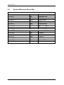
System Memory Address Map
System Memory Address Map
Memory Area
0000-003F
0040-004F
0050-006F
0070-0548
0549-0FC2
0FC3-9AFF
9B00-9CFF
First Meg
9D00-9DFF
9G00-9FFF
A000-AFFF
B000-B7FF
B800-BFFF
C000-CE9F
CEA0-D09F
RUBY-D716VG2AR User’s Manual
Size
Description
1K
Interrupt Area
0.3K
BIOS Data Area
0.5K
System Data
19K
DOS
41K
Program Area
556K
【Available】
8K
Unused
-- Conventional memory end at 628K -4K
8K
64K
32K
32K
58K
8K
Extended BIOS Area
Unused
VGA Graphics
Unused
VGA Text
Video ROM
Unused
5-6