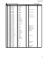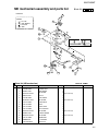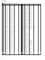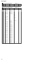
1
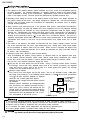
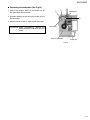
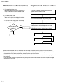
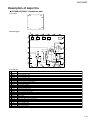
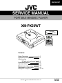
XM-PX50WT
SERVICE MANUAL
PORTABLE MINIDISC PLAYER
XM-PX50WT
UB
Area Suffix
Hong Kong
Contents
Safety Precautions
Important for laser products
Attention when
MD pick up is exchanged
Disassembly method
Adjustment method
Maintenance of laser pickup
Replacement of laser pickup
Description of major ICs
COPYRIGHT
1-2
1-3
1-4
1-5
1-11
1-12
1-12
1-13~25
2001 VICTOR COMPANY OF JAPAN, LTD.
No.20902
Jan. 2001
XM-PX50WT
1. This design of this product contains special hardware and many circuits and components specially
for safety purposes. For continued protection, no changes should be made to the original design
unless authorized in writing by the manufacturer. Replacement parts must be identical to those
used in the original circuits. Services should be performed by qualified personnel only.
2. Alterations of the design or circuitry of the product should not be made. Any design alterations of
the product should not be made. Any design alterations or additions will void the manufacturer`s
warranty and will further relieve the manufacture of responsibility for personal injury or property
damage resulting therefrom.
3. Many electrical and mechanical parts in the products have special safety-related characteristics.
These characteristics are often not evident from visual inspection nor can the protection afforded
by them necessarily be obtained by using replacement components rated for higher voltage,
wattage, etc. Replacement parts which have these special safety characteristics are identified in
the Parts List of Service Manual. Electrical components having such features are identified by
shading on the schematics and by ( ) on the Parts List in the Service Manual. The use of a
substitute replacement which does not have the same safety characteristics as the recommended
replacement parts shown in the Parts List of Service Manual may create shock, fire, or other
hazards.
4. The leads in the products are routed and dressed with ties, clamps, tubings, barriers and the
like to be separated from live parts, high temperature parts, moving parts and/or sharp edges
for the prevention of electric shock and fire hazard. When service is required, the original lead
routing and dress should be observed, and it should be confirmed that they have been returned
to normal, after re-assembling.
5. Leakage currnet check (Electrical shock hazard testing)
After re-assembling the product, always perform an isolation check on the exposed metal parts
of the product (antenna terminals, knobs, metal cabinet, screw heads, headphone jack, control
shafts, etc.) to be sure the product is safe to operate without danger of electrical shock.
Do not use a line isolation transformer during this check.
Plug the AC line cord directly into the AC outlet. Using a "Leakage Current Tester", measure
the leakage current from each exposed metal parts of the cabinet , particularly any exposed
metal part having a return path to the chassis, to a known good earth ground. Any leakage
current must not exceed 0.5mA AC (r.m.s.)
Alternate check method
Plug the AC line cord directly into the AC outlet. Use an AC voltmeter having, 1,000 ohms
per volt or more sensitivity in the following manner. Connect a 1,500 10W resistor paralleled by
a 0.15 F AC-type capacitor between an exposed
AC VOLTMETER
metal part and a known good earth ground.
(Having 1000
Measure the AC voltage across the resistor with the
ohms/volts,
or more sensitivity)
AC voltmeter.
Move the resistor connection to eachexposed metal
part, particularly any exposed metal part having a
0.15 F AC TYPE
return path to the chassis, and meausre the AC
Place this
voltage across the resistor. Now, reverse the plug in
probe on
the AC outlet and repeat each measurement. voltage
each exposed
1500 10W
metal part.
measured Any must not exceed 0.75 V AC (r.m.s.).
This corresponds to 0.5 mA AC (r.m.s.).
Good earth ground
1. This equipment has been designed and manufactured to meet international safety standards.
2. It is the legal responsibility of the repairer to ensure that these safety standards are maintained.
3. Repairs must be made in accordance with the relevant safety standards.
4. It is essential that safety critical components are replaced by approved parts.
5. If mains voltage selector is provided, check setting for local voltage.
!
1-2
Burrs formed during molding may be left over on some parts of the chassis. Therefore,
pay attention to such burrs in the case of preforming repair of this system.
XM-PX50WT
Important for laser products
5.CAUTION : If safety switches malfunction, the laser is able
1.CLASS 1 LASER PRODUCT
2.DANGER : Invisible laser radiation when open and inter
lock failed or defeated. Avoid direct exposure to beam.
3.CAUTION : There are no serviceable parts inside the
Laser Unit. Do not disassemble the Laser Unit. Replace
to function.
6.CAUTION : Use of controls, adjustments or performance of
procedures other than those specified herein may result in
hazardous radiation exposure.
the complete Laser Unit if it malfunctions.
4.CAUTION : The compact disc player uses invisible
! CAUTION Please use enough caution not to
see the beam directly or touch it
in case of an adjustment or operation
check.
laserradiation and is equipped with safety switches
whichprevent emission of radiation when the drawer is
open and the safety interlocks have failed or are de
feated. It is dangerous to defeat the safety switches.
VARNING : Osynlig laserstrålning är denna del är öppnad
ADVARSEL : Usynlig laserstråling ved åbning , når
och spårren är urkopplad. Betrakta ej strålen.
VARO
sikkerhedsafbrydere er ude af funktion. Undgå
: Avattaessa ja suojalukitus ohitettaessa olet
alttiina näkymättömälle lasersäteilylle.Älä katso
udsættelse for stråling.
ADVARSEL : Usynlig laserstråling ved åpning,når
säteeseen.
sikkerhetsbryteren er avslott. unngå utsettelse
for stråling.
REPRODUCTION AND POSITION OF LABELS
WARNING LABEL
DANGER : Invisibie laser radiation
VARO : Avattaessa ja suojalukitus
when open and interlock or
ohitettaessa olet alttiina
defeated.
näkymättömälle lasersäteilylle.Älä
AVOID DIRECT EXPOSURE TO
BEAM
katso säteeseen.
(d)
(e)
VARNING : Osynlig laserstrålning är
ADVARSEL :Usynlig laserstråling
denna del är öppnad och spårren är
ved åbning , når
urkopplad. Betrakta ej strålen.
sikkerhedsafbrydere er ude af
(s)
funktion. Undgå udsættelse for
stråling.
(f)
1-3
XM-PX50WT
Attention when MD pickup is exchanged
1. About the static electricity protection measures
The laser diode in the traverse unit (optical pick up) is easy to be destroyed by clothes and the human body
to the electrified static electricity.
Please note the explosion by static electricity when repairing.
2. About the earth processing for the electrostatic destruction prevention
In the equipment which uses an optical pick up (laser diode), an optical pick up is destroyed by the static
electricity of the work environment.
Please do the earth processing and work.
1) Earth of work stand
Please pull the conductive material (conductive sheet) or the iron plate to the depository
place of the traverse unit (optical pick up), and take the earth to ground.
2) Human body earth
Please use the anti-static wrist strap to exhaust the electrified static electricity to the human body.
anti-static wrist strap
3.
Handling the optical pick up
Conductive material (conductive
sheet) or the iron plate
1) Please return according to a correct procedure based on short processing after exchanging
parts.
2) Do not use a tester to check the condition of the laser diode in the optical pick up .The tester 's internal
power source can easily destroy the laser diode.
4. Attention when unit is disassembled
Please refer to "Disassembling method" for how to detach .
1) Please be sure to solder before a flexible wire is removed from connector on a main printed
circuit board as shown.
if you removes without soldering.the MD picking up assembly might destroy
2) When installing , solder in the part of short round should be removed after a flexible wire is connected with
connector.
Solder short
1-4
XM-PX50WT
MD door assembly
Disassembly method
Removing the MD door assembly
(See Fig.1 and 2)
1. Shift the door lever to open the door.
2. Remove the four screws A and detach the MD door
assembly from the main body.
A
Door lever
Fig.1
Removing the holder assembly
(See Fig.3 and 4)
MD door assembly
Prior to performing the following procedure, remove
the MD door assembly.
1. Turn the Holder assembly as shown in Fig.3.
2. Pull the side arm (L) marked a and remove outward.
Open the Holder assembly as shown in Fig.4.
A
Door lever
3. Move the “U-shaped” notch marked b in the direction
of the arrow and release it from the shaft.
4. Move the part c inward and pull out the Holder
assembly from the shaft.
Fig.2
Holder assembly
ATTENTION: When reassembling, first reattach the
part c to the shaft of the Chassis
assembly. And next, fit the “U-shaped”
notch to the shaft.
Part a
Holder assembly
Side arm (L)
”U-shaped” notch
Fig.3
Holder assembly
Holder assembly
Part c Shaft
Part b
Part c
Fig.4
1-5
XM-PX50WT
Chassis assembly
Removing the chassis assembly
(See Fig.5 to 7)
Side arm (R)
Prior to performing the following procedure, remove
the MD door assembly and the holder assembly.
1. Open the battery lid. Release the tab d and pull out
the battery lid.
2. Remove the screw B and pull out the side arm (R)
upward.
Tab d
Joint e
3. Remove the two screws C and pull out the eject unit.
Joints e
B
4. Remove the screw D, E, F and G attaching the
chassis assembly respectively.
Battery lid
Fig.5
5. Disengage the three joints e of the bottom case and
the battery holder. Remove the chassis assembly
and the jack cover at once.
Battery lid
Eject unit
C
C
Chassis assembly
Fig.6
D
Chassis assembly
Joint e
G
Joints e
Bottom case
E
F
Battery holder
Fig.7
1-6
XM-PX50WT
Removing the main board and the
battery holder (See Fig.8 and 9)
Battery holder
CN401
Soldering f
CN301
Prior to performing the following procedures, remove
the MD door assembly, the holder assembly and the
chassis assembly.
ATTENTION: Before disconnecting the flexible wire
extending from the pickup, make sure to
solder the short circuit round to prevent
damage to the pickup.
H
Short circuit
round
1. Solder the short circuit round of the flexible wire on
the main board.
Disconnect the flexible wires from connector CN301
and CN401 on the main board.
Headphone jack assembly
Main board Soldering f
Fig.8
Remove the one screw H attaching the main board.
Remove the main board with the battery holder .
CN401
Short circuit round
Unsolder the four soldered parts f retaining the main
board and the battery holder.
ATTENTION: When reassembling, connect the
flexible wire extending from the pickup
to the connector on the main board
and unsolder the short circuit round.
CN301
Fig.9
Headphone jack assembly
Battery holder
CN601
Removing the headphone jack assembly
(See Fig.10)
Prior to performing the following procedures, remove
the MD door assembly, the holder assembly, chassis
assembly and the main board.
1. Disconnect the flexible wire extending from the
headphone jack from connector CN601 on the main
board.
Main board
Fig.10
1-7
XM-PX50WT
<Removal of the MD
mechanism section>
Slit washer
Worm gear
Shaft holder
J
Soldering g
Prior to performing the following procedures, remove
the MD door assembly, the holder assembly, the
chassis assembly and the main board.
I
Removing the spindle motor
(See Fig.11)
1. Unsolder the part g on the flexible wire extending
from the underside of the Chassis assembly to the
spindle motor.
ATTENTION: Do not spill flux on the gear and others.
2. Remove the three screws I
motor.
Spindle motor
Chassis assembly
Part i
Part h
Pickup unit
Fig.11
attaching the spindle
Lead screw
K
Removing the pickup unit (See Fig.11)
ATTENTION: When handling the Pickup unit, touch the
parts marked in Fig.13 only.
1. Remove the slit washer and the worm gear from the
underside of the Chassis assembly.
Lead spring
2. Remove the screw J attaching the shaft holder and
draw out the shaft (lead screw).
3. Pull out the Pickup unit and the lead screw while
disengaging the part h and i.
Pickup
Fig.12
Removing the pickup (See Fig.12 and 13)
Touch these parts only.
ATTENTION: When handling the pickup unit, touch the
parts marked in Fig.13 only.
1. Remove the screw K and the lead spring.
2. Pull out the shaft from the pickup.
Fig.13
1-8
XM-PX50WT
Removing the feed motor (See Fig.14)
1. Peel off the adhesive tape j on the flexible wire on
the underside of the feed motor.
j
L
Soldering k
2. Unsolder soldering k connecting the flexible wire to
the feed motor.
L
3. Remove the two screws L attaching the feed motor.
ATTENTION: When reassembling, reattach the
flexible wire with an adhesive tape and
solder.
Feed motor
Chassis assembly
Pickup unit
Fig.14
1-9
XM-PX50WT
<Charge stand>
A
A
Removing the charge board
(See Fig.1 to 3)
1. Remove the four screws A on the bottom of the
body.
2. Remove the top cover upward while pushing the
front part a. Pull out the charge board from the
bottom cover.
A
Fig.1
A
Top cover
Push
Part a
Fig.2
Charge board
Bottom cover
Fig.3
1-10
XM-PX50WT
Adjustment method
This model is auto adjustment by Remote Controller.
Please adjust the attached remote controller.
Equipments----- 1. Remote controller
2. DC power supply
3. Laser power meter
4. MO disc (AU-1)
5. Pre master disc (TGYS 1)
<Test mode setting method>
Press < PLAY MODE + DISPLAY + BASS > and < PLAY >key together more than 3sec. at power off condition.
< VOL > next item .< VOL+ >before item.
LCD indication
0.
TMD-V2
Test mode setting OK. Indicate at 2sec.
When LCD indicate [NG] at another item,
Return back this item by press (STOP) key
Resume initialize
LCD Indication change :
*
*
Initializing
Resume
Servo initialize
LCD Indication change : [
]
Initializing
Servo
PLAY LASER Insert the laser power meter.
Executes by < BASS >
LCD Indication change :[XX:YY]
Up by < VOL+> .Down by <VOL > LCD Indication change :[VW.YY]
Setting by <STOP>
LCD Indication change :[ OK
]
PLAY
LASER
Laser power adjust
560
adjust
Adjust power-supply voltage 1.5v
20mv before the laser power is adjusted and stops.
FEED
Executes by < BASS >
LCD Indication change :[FwdBwd]
<VOL+> :Pickup is go to outside < VOL-> :Pickup is go to inside
Press < STOP >
LCD Indication change :[OK
5. M o T G
7.
MO TG Insert the Recordable disc.
Executes by < BASS >
LCD Indication change : [
*
MO DISC ADJUST
Executes by < BASS >
LCD Indication change : [
*
Press < STOP >
LCD Indication change : [OK
*
Pre TG Insert the Pre master disc.
Executes by < BASS >
LCD Indication change : [
*
Pre DISC ADJUST
]
FEED
*
]
Adjusting
]
Adjusting
]
MO DISC ADJUST
]
Adjusting
Executes by < BASS >
LCD Indication change : [
XXYYZZ ]
Press < STOP >
Adjusting
*
RESET
Executes by < BASS >
LCD Indication : Left out the test mode ,power off ,and END.
1-11
XM-PX50WT
Maintenance of laser pickup
(1) Cleaning the pick up lens
Before you replace the pick up, please try to
clean the lens with a alcohol soaked cotton
swab.
(2) Life of the laser diode
When the life of the laser diode has expired,
the following symptoms will appear.
Replacement of laser pickup
Turn off the power switch and,disconnect the
power cord from the ac outlet.
Replace the pickup with a normal one.(Refer
to "Pickup Removal" on the previous page)
1. The level of RF output (EFM output:ampli
tude of eye pattern) will below.
Is the level of
RFOUT under
0.35Vp-p?
NO
Replace it.
Plug the power cord in,and turn the power on.
At this time,check that the laser emits for
about 3seconds and the objective lens moves
up and down.
Note: Do not observe the laser beam directly.
YES
O.K
Play a disc.
Check the eye-pattern at TP1.
Finish.
(3) Semi-fixed resistor on the APC PC board The semi-fixed resistor on the APC printed circuit board which is
attached to the pickup is used to adjust the laser power.Since this adjustment should be performed to match the
characteristics of the whole optical block, do not touch the semi-fixed resistor.
If the laser power is lower than the specified value,the laser diode is almost worn out, and the laser pickup should
be replaced.
If the semi-fixed resistor is adjusted while the pickup is functioning normally,the laser pickup may be damaged
due to excessive current.
1-12
XM-PX50WT
Description of major ICs
JCV8002-W (IC601) : Head phone amp
1. Pin layout
19
18
~
12 13
~
~
~
24
1
6 7
2. Block diagram
PW
SW
18
MT
TC
19
MT 17
SW
PW
SW
MT
SW
16
BST
SW
BST
SW
BEEP
IN
15
14
13
Vref
IN
GND
BEEP
Vref
12
Vref
V
CC1
20
11
ADD
IN
IN B
21
10
BST1
BST
NF1
IN A
22
9
LPF2
BEEP
OUT B
BST2
PW
A
23
PW
B
8
BST
NF2
BEEP
OUTA
24
V
CC2
1
CUTA
2
PWR
GND
3
OUT
B
BST
AGC
4
DET
5
AGC
IN
7
6
BST
OUT
3. Pin function
Pin Symbol
no.
1
VCC2
2
OUTA
3 PWR GND
4
OUTB
5
DET
6 AGC IN
7 BST OUT
8 BST NF2
9
LPF 2
10 BST NF1
11 ADD IN
12
V ref
13 Vref IN
14 GND
15 BEEP IN
16 BST SW
17 MT SW
18 PW SW
19 MT TC
20
VCC1
21
IN B
22
IN A
23 BEEP OUT B
24 BEEP OUT A
FUNCTION
VCC2 (+B) in power amplifier output steps
Power amplifier output
GND in power amplifier output steps
Power amplifier output
Smoothness of level detection of boost AGC
BST amplifier input signal level variable control by input lever to boost AGC input terminal
Output terminal of BST amplifier2
Terminal NF of BST amplifier2
Output BST amplifier1
NF of BST amplifier1
ADD amplifier input
Standard potential circuit
Standard potential circuit
Power part input steps GND
Beep input terminal
Beep output terminal
Mute switch
Power On/OFF switch
Mute smoothing Power mute switch
Main parts V CC
Power amplifier input
Power amplifier input
Beep output terminal
Beep output terminal
1-13
1-14
VCREF
OSC SLOPE
CLOCK RESET FG FG2 FC
Full Wave
Rectifilter
PGND
GND
CF
Sample
and Hard
RF
WOUT
VOUT
13
UOUT
48
VCONT
F/R
Controllor
Sensoeless Logic
~
COM
WIN
~
VIN
UIN
~
PWM
WF VS
Voltage
Driver
VF
24
BRAKE
CPOUT COMFUF
37
S/S
CP3
Charge Pump
CP2
~
1/8
VCO
VCO CP1
CPC3
2. Block diagram
Phase
Comparator
RMIN
CPC2
1
Timing
controllor
VCOIN
CPC1
36
CLKSEL
MCLOCK
VCC
RMAX
XM-PX50WT
CXA8059Q (IC450) : Motor driver
1. Pin layout
25
12
XM-PX50WT
3.Pin function
Pin Symbol
no.
1
2
3
4
5
6
7
8
9
10
11
12
13
14
15
16
17
18
19
20
21
22
23
24
25
26
27
28
29
30
31
32
33
34
35
36
37
38
39
40
41
42
43
44
45
46
47
48
PGND
COM
VS
CPOUT
CPC3
CP3
CPC2
CP2
CPC1
CP1
GND
S/S
BRAKE
VCONT
VCREF
FC
CF
FG
FG2
VCO
RMAX
RMIN
VCOIN
CLKSEL
OSC
SLOPE
CLOCK
GND
WF
VF
UF
COMF
VCC
MCLOCK
VS
RESET
RF
NC
NC
WIN
WOUT
VIN
VOUT
UIN
UOUT
NC
NC
RF
Function
The GND to guard the power stage.
The terminal to detect the voltage.
The terminal to supply the voltage for the power stage.
The terminal to connect the capacitor in the final charge pump.
The terminal to connect the capacitor in the third charge pump.
The terminal to connect the capacitor in the third charge pump.
The terminal to connect the capacitor in the second charge pump.
The terminal to connect the capacitor in the second charge pump.
The terminal to connect the capacitor in the first charge pump.
The terminal to connect the capacitor in the first charge pump.
The GND for the part except the power section.
The terminal for start and stop.
The terminal for braking.
The terminal for controlling velocity.
The terminal as referable voltage of controlling velocity.
The terminal to compensate the frequency characteristics of the loop controlling velocity.
The terminal of sampling and holding for detecting motor current.
The terminal to output FG pulse.
The terminal to output FG pulse divided Pin15 signal by 2.
The terminal to set oscillation frequency of VCO.
The terminal to set maximum oscillation frequency of VCO.
The terminal to set minimum oscillation frequency of VCO.
The terminal to control oscillation frequency of VCO.
The terminal to select inside and outside clock.
The terminal to oscillation sawtooth for PWM signal.
The terminal to oscillation sawtooth for soft-switching signal.
The terminal to monitor CLOCK signal.
The GND for the part except the power section.
The terminal to shape waveform of motor voltage.
The terminal to shape waveform of motor voltage.
The terminal to shape waveform of motor voltage.
The terminal to shape waveform of motor voltage.
The terminal to supply the voltage except the power section.
The terminal to input clock.
The terminal to supply the voltage for the power stage.
The terminal to reset a register for checking the movement.
The terminal to monitor current.
Non connect
Non connect
The terminal to sense the back electro magnetic force of coils.
The terminal to supply the motor current.
The terminal to sense the back electro magnetic force of coils.
The terminal to supply the motor current.
The terminal to sense the back electro magnetic force of coils.
The terminal to supply the motor current.
Non connect
Non connect
The terminal to monitor current.
1-15
XM-PX50WT
CXD2672GA(IC351):DSP
1.Pin layout
17
LDDR DTRF VSI02 ADFG ADRB AVS2
16
APCR CKRF FOCN
APC
ADI0
VC
FILI
AVS1
ASYI DVSS1
ABCD CLTV
PCO
BIAS
ASYO XWE
RFI
AVD1 MVCI
SE
ADRT
TE
AVD2 AUX1 BOTH
TST6
15
TFDR TRDR
14
FRDR FFDR VDC4
13
VSC4 SRDR
12
SPFD SPRD SFDR
D1
11
TEST2 TEST1 FGIN
A09
XRAS
IXOE
10
TST2
A07
A10
A08
DVI01
A00
VSI01
XLRF VDI02 DCHG
FILO
FS4
EFM0 TEST3
TOP
VIEW
PD0
A11
XOE
DVDD1
D3
VSC3
VDC3
D0
D2
XCAS IXWE
9
VSI03 TST3 VDI03
8
SPCU SPDW SPDV
A05
A01
A06
7
TST4 SPCW SPCV
A03
A04
A02
6
VSC5 SLDW SLDV
F256 XBCK VSC2
5
SLCV
SLCU VDC5
VDC2 DADT LRCK
4
BYPS
TST5 SLCW
VDI00 TST8 ADDT
3
MNT1 MNT0
VDI
DA
DA
VDC0 SENS XRST RPWR OSC DVDD0 VDDL VDDR VREFR TST1
2
MNT2 SWDT SRDT SQSY XINT
1
MNT3 SCLK
A
B
C
D
XLAT VSCO DQSY
E
F
G
A-1
A-2
A-3
B-1
B-2
B-3
C-1
C-2
C-3
D-1
D-2
D-3
TX
OSCO
VSI
OSC
H
J
K
Symbol
NC
NC
MNT1
NC
NC
MNT0
MNT3
MNT2
NC
SCLK
SWDT
VDC0
VDC1 TST0
DATAI TST7
MT
MT
DA
OSCI DVSS0 AOUTL VREFL AOUTR XTSL DOUT FLGL FLGR PWMRP
2.Pin function (1)
Pin
No.
1-16
PEAK
FE
I/O
Function
O
I/O
O
O
I
I
-
Open
Open
Monitor output
Open
Open
Monitor in/output
Monitor output
Monitor output
Open
Micon serial bus clock input
Micon serial bus data write input
Internal logic VDD(1.8V)
DA
DA
VSSL VSSR VSC1
L
M
N
DA
DA
DIN1 VSI00
PWMLP PWMLN
P
R
T
U
XM-PX50WT
2.Pin function(2)
Symbol
I/O
E-1
XLAT
I
E-2
SRDT
O
E-3
SENS
O
F-1
VSC0
F-2
SQSY
O
F-3
XRST
I
G-1
DQSY
O
G-2
XINT
O
G-3
RPWR
I
H-1
TX
I
H-2
OSCI
I
H-3
VDIOSC
J-1
OSCO
O
J-2
DVSS0
J-3
DVDD0
K-1
VSIOSC
K-2
AOUTL
O
K-3 DAVDDL
L-1
DAVSSL
L-2
VREFL
O
L-3 DAVDDR
M-1 DAVSSR
M-2
AOUTR
O
M-3
VREFR
O
N-1
VSC1
N-2
XTSL
I
N-3
TST1
I
P-1
DIN1
I
P-2
DOUT
O
P-3
VDC1
U-1 DAPWMLN O
T-1 DAPWMLP O
R-1
VSIO0
U-2 DAPWMRP O
T-2
MTFLGR
O
R-2 MTFLGL
O
U-3
TST7
I
T-3
DATAI
I
R-3
TST0
O
U-4
ADDT
I
T-4
TST8
I
R-4
VDIO0
U-5
LRCK
O
T-5
DADT
O
R-5
VDC2
U-6
VSC2
T-6
XBCK
O
R-6
F256
O
U-7
A02
O
T-7
A04
O
R-7
A03
O
U-8
A06
O
T-8
A01
O
R-8
A05
O
Pin No.
Function
Micon serial bus latch input
Micon serial bus data read out output
Internal output of micon serial bus address
Internal logic GND
PTGR=0 ADIPsink output / PTGR=1 DISC SUB-Q sink output
Reset input L:reset
Ubit SUB-Q sink output from digital audio input from MD or CD
Request status output L:request status
Laser power select input (H=rec power / L=playback power)
Output permit input of recorded data
X'tal osc circuit input
OSC sel VDD (2.5V)
X'tal osc circuit output
Internal 16bit DRAM GND
Internal 16bit DRAM GND
OSC sel GND
Internal DAC Lch output
Internal DAC VDD (Lch,2.5V)
Internal DAC GND
Internal DAC GND VREF(Lch)
Internal DAC VDD (Rch,2.5V)
Internal DAC GND (Rch)
Internal DAC Rch output
Internal DAC VREF (Rch)
Internal logic GND
X'tal frequency select (L=45.1584MHz/H=22.5792MHz)
Test terminal Connect to GND
Digital audio input Outer I/F mode EXRQ input
Digital audio output
Internal logic VDD (1.8V)
Internal DAC PWM output LInternal DAC PWM output L+
2.5V I/O VSS
Internal DAC PWM output R+
Internal DAC zero detect flag (Rch)
Internal DAC zero detect flag (Lch)
Test terminal Connect to GND
Serial data input
Open
Data input from A/D converter
Test terminal Connect to GND
2.5V I/O VDD
LR clock(44.1kHz) for A/D, internal DAC
Data output for internal DAC / Internal DAC PWM output RInternal logic VDD (1.8V)
Internal logic GND
A/D, internal DAC bit clock (2.8224MHz)
11.2896MHz clock output (X'tal)
External DRAM address output
External DRAM address output
External DRAM address output
External DRAM address output
External DRAM address output
External DRAM address output
1-17
XM-PX50WT
2.Pin function (3)
Symbol
U-9
VSIO1
T-9
A00
R-9
ADIO1
U-10
A08
T-10
A10
R-10
A07
U-11
IXOE
T-11
XRAS
R-11
A09
U-12
IXWE
T-12
XCAS
R-12
D1
U-13
D2
T-13
D0
R-13
VDC3
U-14
VSC3
T-14
D3
R-14
DVDD1
U-17
NC
U-16
NC
U-15
XOE
T-17
NC
T-16
TST6
T-15
A11
R-17
DVSS1
R-16
XWE
R-15
PDO
P-17
ASYI
P-16
ASYO
P-15
MVCI
N-17
AVS1
N-16
BIAS
N-15
AVD1
M-17
FILI
M-16
PCO
M-15
RFI
L-17
PEAK
L-16
CLTV
L-15
FILO
K-17
FE
K-16
ABCD
K-15 BOTOM
J-17
ADIO
J-16
VC
J-15
AUX1
H-17
AVS2
H-16
ADRT
H-15
AVD2
G-17
ADRB
G-16
SE
G-15
TE
F-17
ADFG
F-16
APC
F-15
DCHG
Pin No.
1-18
I/O
O
O
O
O
O
O
O
O
O
I/O
I/O
I/O
I/O
O
O
O
O
O
I
O
I
I
O
I
I
I
O
I
I
I
O
I
I
I
I
I
I
I
I
I
I
Function
2.5V I/O sel Vss
External DRAM address output
2.5V I/O sel VDD
External DRAM address output
External DRAM address output
External DRAM address output
Open
External DRAM RAS output
External DRAM address output
Open
External DRAM CAS output
External DRAM data input/output
External DRAM data input/output
External DRAM data input/output
Internal logic VDD
Internal logic GND
External DRAM data input/output
Internal 16Mbit DRAM VDD
Open
Open
External DRAM output chip enable output
Open
Open
Open
Internal 16Mbit DRAM GND
External DRAM write enable output
Analog PLL phase compare output
Playback EFM comparator slice level input
Playback EFM binarization signal output
Clock input from external VCO
Analog GND
Playback EFM comparator bias current input
Analog power supply (2.5V)
Filter input for playback EFM system mastering PLL
Phase comparison output for playback EFM system mastering PLL
Playback EFM RF signal input
Peak holding input optical amount signal
Internal VCO control voltage input for playback EFM system mastering PLL
Filter output for playback EFN system mastering PLL
Focus error signal input
Optical amount signal input
Bottom holding input of optical amount signal
Open
Middle point voltage input
Assistance A/D input
Analog GND
A/D converter operation range upper bound voltage input
Analog power supply (2.5V)
A/D converter operation range lower bound voltage input
Sled error input
Tracking error input
ADIP binary-coded FM signal input
Error signal input for laser digital APC
Connects with an analog power supply of low impedance
XM-PX50WT
2.Pin function (4)
Pin No.
E-17
E-16
E-15
D-17
D-16
D-15
A-17
B-17
C-17
A-16
B-16
C-16
A-15
B-15
C-15
A-14
B-14
C-14
A-13
B-13
C-13
A-12
B-12
C-12
A-11
B-11
C-11
A-10
B-10
C-10
A-9
B-9
C-9
A-8
B-8
C-8
A-7
B-7
C-7
A-6
B-6
C-6
A-5
B-5
C-5
A-4
B-4
C-4
Symbol
VSIO2
F0CN
VDIO2
DTRF
CKRF
XLRF
NC
NC
LDDR
NC
NC
APCR
TFDR
TRDR
NC
FRDR
FFDR
VDC4
VSC4
SRDR
FS4
SPFD
SPRD
SFRD
TEST2
TEST1
FGIN
TST2
EFMO
TEST3
VSIO3
TST3
VDIO3
SPCU
SPDW
SPDV
TST4
SPCW
SPCV
VSC5
SLDW
SLDV
SLCV
SLCU
VDC5
BYPS
TST5
SLCW
I/O
O
O
O
O
O
O
O
O
O
O
O
O
O
O
O
I
I
I
O
O
I
O
I
O
O
O
I
I
O
O
I
I
O
O
I/O
Function
2.5V I/O Vss
Filter cutoff control output
2.5V I/O VDD
Controller data output
Controller clock output
Controller latch output
Open
Open
Laser digital APC PWM output
Open
Open
Laser APC reference PWM output
Tracking servo drive PWM output (+)
Tracking servo drive PWM output (-)
Open
Focus servo drive PWM output (-)
Focus servo drive PWM output (+)
Internal logic VDD (1.8V)
Internal logic GND
Sled servo drive PWM output (-)
176.4kHz clock output (X'tal system)
Spindle servo drive output
Spindle servo drive output
Sled servo drive PWM output (+)
Test terminal Connect to GND
Test terminal Connect to GND
Spindle CAV servo FG input
Test terminal Open
EFM output at recording
Test terminal Connect to GND
2.5V I/O Vss
Test terminal Open
2.5V I/O VDD
Blush less spindle motor drive comparate input (U)
Blush less spindle motor 3 phase drive truth output (W)
Blush less spindle motor 3 phase drive truth output (V)
Test terminal Open
Blush less spindle motor drive comparete input (W)
Blush less spindle motor drive comparate input (V)
Internal logic GND
Blush less sled motor 3 phase drive truth output (W)
Blush less sled motor 3 phase drive truth output (V)
Blush less sled motor 3 phase drive comparate input (V)
Blush less sled motor 3 phase drive comparate input (U)
Internal logic VDD (1.8V)
Open
Test terminal Open
Blush less sled motor 3 phase drive comparate input
1-19
XM-PX50WT
AK93C55BH-W (IC502) : EEPROM
1. Pin layout
2.Pin function
CS
1
8
VCC
SK
2
7
NC
DI
3
6
PE
DO
4
5
GND
Pin name
CS
SK
DI
DO
PE
VCC
GND
NC
Fnction
Chip select
Serial data clock
Serial data input
Serial data output
Program enable
Ground
Power supply
Not connected
3. Block diagram
DO
DATA
REGISTER
DI
INSTRUCTION
REGISTER
INSTRUCTION
DECODE,
CONTROL
AND
CLOCK
GENERATION
16
R/W AMPS
AND
AUTO ERASE
16
EEPROM
2048bit
ADD.
BUFFER
DECODER
128 X 16
CS
VPP SW
SK
PE
VREF
TC75S51F-X(IC505):Ope amp
1.Pin layout/Block diagram
VDD
5
OUT
4
1
2
3
IN(+) Vss IN(-)
1-20
VPP
GENERATOR
WBLADJ
TE
CSLED
SE
ADIN
ADAGC
ADFG
AUX
FE
ABCD
BOTM
CXA2588R (IC300) : RF amp.
1. Pin layout & block diagram
ADFM
XM-PX50WT
36 35 34 33 32 31 30 29 28 27 26 25
Peak,Bottom Detector
ADIP Amp
PEAK 37
AGC,EQ
RF 38
RFAGC 39
AGCI 40
TE/SE Amp
24 Vcc
FE Amp
23 3TADJ
22 EQADJ
21 VREF
NC 41
20 F0CNT
NC 42
19 XSTBY
ADDC 43
18 XLAT
0/-2dB
RF Amp
RFO 46
MORFI 47
MORFO 48
ABCD Amp
OP
Amp
I-V
Amp
1
2
3
4
5
6
7
8
9
10
11
12
13
14
15
16
17
18
19
20
21
22
23
24
I
J
VC
A
B
C
D
E
F
PD
APC
APCREF
GND
OPOUT
OPIN
SWDT
SCLK
XLAT
XSTBY
F0CNT
VREF
EQADJ
3TADJ
Vcc
I
I
O
I
I
I
I
I
I
I
O
I
O
I
I
I
I
I
I
O
I/O
I/O
-
15 OP IN
14 OP OUT
VC
A
B
7
8
9 10 11 12
Function
I-V converted RF signal I input
I-V converted RF signal J input
Vcc/2 voltage output
A current input for main beam servo signal
B current input for main beam servo signal
C current input for main beam servo signal
D current input for main beam servo signal
E current input for side beam servo signal
F current input for side beam servo signal
Reflection light q'ty monitor signal input
Laser APC output
Ref. voltage input for laser power intensity setting
Ground
Ope. amp output terminal
21dB ope. amp input terminal
Serial data input terminal
Shift clock input terminal
Latch input terminal
Stand by setting terminal
F0 count setting terminal
Reference voltage output terminal
EQ IF setting terminal
BPF3T IF setting terminal
Power supply
Pin
No.
25
26
27
28
29
30
31
32
33
34
35
36
37
38
39
40
41
42
43
44
45
46
47
48
Symbol I/O
WBLADJ
TE
CSLED
SE
ADFM
ADIN
ADAGC
ADFG
AUX
FE
ABCD
BOTM
PEAK
RF
RFAGC
AGCI
NC
NC
ADDC
NC
TEGC
RFO
MORFI
MORFO
I/O
O
O
O
I
O
O
O
O
O
O
O
I
I/O
I
O
I
O
APCREF
J
6
APC
5
F
4
E
3
2.Pin function
Symbol I/O
16 SWDT
APC
D
2
C
1
I
I-V Amp
Pin
No.
17 SCLK
13 GND
PD
TEGC 45
3T Detector
NC 44
CPU
Command
I/F
Function
BPF3T IF setting terminal
Tracking error signal output terminal
Sled error signal LPF capacitor connect terminal
Sled error signal output terminal
ADIP FM signal output terminal
ADIP signal completer input terminal
ADIP AGC capacitor connect terminal
ADIP binary signal output
I3 output/temp.signal output
Focus error signal output
Reflection light q'ty signal output for main beam servo detector
RF/ABCD bottom-hold signal output
RF/ABCD peak-hold signal output
RF equalizer output
RFAGC capacitor connection
RFAGC input
Non connect
Non connect
ADIP amp. feedback circuit capacitor connection
Non connection
TE amp. gain switching
RF amp. output
Groove RF signal AC-coupled input
Groove RF signal output
1-21
XM-PX50WT
IC-PST3421U-X(IC504):System reset
1.Pin layout
2.Pin function
VOUT 1
VDD
2
4
VSS
3
NC
Pin
No.
Symbol
1
2
3
4
VOUT
VDD
NC
VSS
Function
Reset signal output terminal
Power supply terminal
Non connect
VSS terminal
3.Block diagram
VDD 2
1 VOUT
Vref
VSS 4
TK11223BMC-X (IC961) : Regulator
1. Pin layout
VIN GND VOUT
6
5
4
1
2
3
CONT GND
NOISE BYPASS
2. Block diagram
VOUT
VIN
THERMAL
SENSOR
CONT.
BANDGAP
REFERENCE
GND
1-22
Cnp
PGND
L
26
X
25
VD4
27
X:Don't Care
Z:High Impedance
FO
L
L
H
L
L
Z
FO4
RO4
VD4
23
RI
L
H
L
H
X
X
24
PGND
30
FI
L
L
H
H
X
X
RI4 19
VG
RO3
19
20
21
22
23
24
25
26
27
28
29
30
31
32
INPUT
FI4 20
Pre-driver
Pre-driver
Control
Vc
FO3
29
VD3
28
OE
L
L
L
L
H
X
31
VD3
32
18
17
16
15
14
13
12
11
10
9
8
7
6
33
34
35
36
PS,OE
RI3 22
Control
VG
PGND
12
VD2
10
RO2
VD2
14
FO2
RGND
7
11
RO1
8
13
FO1
VD1
9
6
VD1
5
AGND
5
4
3
2
1
PS
H
H
H
H
H
L
Vc
VG
Pre-driver
Vc
VG
1
AGND
CLK
PS
OE
VD1
FO1
PGND
RO1
VD1
VD2
RO2
PGND
FO2
VD2
RI1
FI1
FI2
RI2
VG
VC
LG
GND
VD3
FO3
PGND
RO3
VD3
VD4
RO4
PGND
FO4
VD4
RI3
FI3
FI4
RI4
1.Pin layout
FI3 21
RI2 18
Vc
34
36
DC/DC
Converter
Vc
CLOCK
Control
FI2 17
CLK
Detector
Pre-driver
GND 33
RI1 15
FI1 16
OE 4
PS
3
CLK 2
Vc 35
Vc
LG
VG
XM-PX50WT
MPC17A139MTB-X (IC400) : 4ch bridge driver
2.Pin function
Driver section
OUTPUT 1~4
RO
L
H
L
L
L
Z
Clock detector section
CLK
PS OSC circuit
Auto
H
X
Syncro
H
Stop
3.Block diagram
Control
1-23
XM-PX50WT
UPD784225GK-617C(IC501):CPU
1.Pin layout
80
~
61
60
1
~
~
41
20
21
~
40
2.Pin function
1-24
Pin
No.
Symbol
1
2
3
4
5
6
7
8
9
10
11
12
13
14
15
16
17
18
19
20
21
22
23
24
25
26
27
28
29
30
31
32
33
34
35
36
37
38
39
40
GND
GND
Non connect
SPSEL
GND
AVSS
Non connect
Voltage adjust
VADJ
AVREF1 Analog reference voltage
Remocon data input terminal
RMRX
Remocon data output terminal
RMTX
Non connect
Serial data read input terminal
SRDT
Serial data write input terminal
SWDT
Serial bus clock output terminal
SCLK
Non connect
BEEP output terminal
BEEP
Power ON/OFF output terminal
PSW
MONDATA Test terminal
MONCLK Test terminal
Standby setting output terminal
XRST2
Tracking gain setting terminal
TG
Non connect
ACB
Non connect
TRAIN
Reset signal output terminal
XRST
Serial bus latch output terminal
XLAT
LSI power supply control signal output
LVCTL
Laser diode ON signal output terminal
LDON
RFOFF RF OFF signal input terminal
Sled OFF signal output terminal
SLOFF
Non connect
Mute signal output terminal
MUTE
Mon connect
Test terminal
DIR
GND
VSS1
Standby mode output terminal
PS
Start/Stop output terminal
SS
Test terminal
MON1
Test terminal
MON2
MONXLAT Test terminal
Non connect
Non connect
ANI5
ANI6
Function
Pin
No.
Symbol
41
42
43
44
45
46
47
48
49
50
51
52
53
54
55
56
57
58
59
60
61
62
63
64
65
66
67
68
69
70
71
72
73
74
75
76
77
78
79
80
DPON
RFVCTL
PSAVE
RPON
DPON
REMOFF
CS2
SCL
DI
CS1
MNT0
MNT3
SENS
DO
RESET
XINT
SQSY
RPLY
DOOR
PLAYKEY
VSS0
VDD1
X2
X1
VPP
XT2
XT1
VDD0
AVD0
KEY
BATTERY
TEMP
ANI3
ANI4
Function
Non connect
Non connect
Non connect
Test terminal
Test terminal
Non connect
Test terminal
Non connect
RP ON signal input terminal
DP ON signal input terminal
Remocon OFF signal output terminal
Chip select 2
Serial clock signal output terminal
Data output terminal
Chip select 1
Monitor 0 input terminal
Monitor 3 input terminal
DSP internal status input terminal
Data input terminal
Reset signal input terminal
Interrupt status data input terminal
Sink input terminal
Non connect
Remocon PLAY detect terminal
Door open/close detect terminal
PLAY key detect terminal
GND
Reference voltage terminal
Connect to X'tal osc
Connect to X'tal osc
Test terminal
Non connect
GND
GND
Reference voltage terminal
Remocon STOP key detect terminal
Battery voltage detect terminal
Connect to temp. detect
GND
GND
XM-PX50WT
XC6367A251M-X(IC901):Regulator
1.Pin layout
2.Pin function
5
4
Pin
No.
Symbol
1 VOUT
2 VDD
3 CE
4 GND
5 EXT
1
2
Function
Output voltage det.
Power supply
Chip enable
GND
Ext. Tr connect
3
3.Block diagram
Phase
Compensation
VOUT
Error Amp.
VDD
PWM
Comparator
+
+
Buffer,
Driver
-
CE
Vref with
Soft Start,
GE
PWM/PFM
Controller
Ramp Wave
Generator,
OSC
EXT
GND
1-25
2-2
W,V,U
COM
SLD
SPINDLE
MOTOR
CN301
FEED
MOTOR
PICKUP
SLD
SPFD,SPRD
SPFG,XBCK
SS
IC450
SPINDLE
DRIVER
W,V,U,COM
TRK
FCS
IC400 PS
DRIVER
FS4
FFDR
FRDR
TFDR
TRDR
SFDR
SRDR
AOUTL
AOUTR
XRST2
LDON
RFI,VC,PEAK,BOTM,ABCD,FE
AUX1,ADFG,SE,T,E,F0CNT
APCREF,DTRF,CKRF,XLRF IC300
RF
IC501
CPU
IC351
DSP
CSI
CSL
DO,DI
SLCK
SWDT
SRAT
SQSY
XINT
SENS
MNT3
MNT0
SLOFF
XLAT
XRST
Lch,Rch
IC502
EEPROM
RMDATA
MUTE
BEEP
PSW
AOUTL IC601
AOUTR HP AMP
XM-PX50WT
Block diagram
J101
CN601
CN401
XM-PX50WT
Standard schematic diagrams
Main amp section
Standard schematic diagrams
MUTE
100
R371
10K
R372
100K
R364
C371
0.01
470P
0.47
C372
R373
680K
3.3K
C374
R380
150
1M
R377
1K
C376
0.47
1K
C377
0.015
6
R379
R378
R376
PSW
C373
1
Main amp section
RFI
R601 470k
C614
4.7/4
R603 470k
C613
10/6.3
NTCT
C313
0.22
C357
1/16
R366
SPFD
10K
SPFG
F0CNT
OUTB
0.22
R113
10k
R213
10k
TP902
R909
120K
4.7K
R966
TP901
D901
10K
10K
NI
L902
L901
BT1
C901
47/6.3
C902
220P
R903
68K
R901
5.6K
IC901
XC6367B101M-X
680k
C464
0.22
IC450
CXA8095Q
Q906
SSM3K01F-X
Q901
FMMT617-X
R904
VADJ
22
F1J2E-X
R902
100K
4.7
1
DPON
C905
150P
TP457
C903
22/4
C456
DTA124XUA-X
R965
470K
COREVDD
LVCTL
22K
C904
C457
RMDATA
BYPS
Q904
C353
10/6.3
R304
1
C351
10/6.3
1
10/6.3
1
R352
22K
R451
R465
C461
DTA143TE-X
Q964
SSM3J01F-X
R454
470k
0.001
C630
330P
C631
330P
Q966
Q965
DTC144EE-X
0.0022
K605
K606
22
R450
0.047
C458
0.047
KEYGND 100
TP458
NI
C451
R461
47K
C460
0.0068
1M
R460 680k
R459
C459
2.2
C450
0.047
C212
0.22
R967
C352
R462
NI
K607
100
PLAYKEY R605
150/4
AVDD
C4
0.1
DVDD
C2
0.022
R351
C3
0.022
R386
APCREF
L301
10
R385
IC2
TC7S08FU-X
K604
K603
R607
KEY
C213
R388
10K
22/4
R2
2.2k
C359
0.1
R3
2.2k
10
R211
TP352
LDON
C324
R212
3.9k
R354
100K
10K
R387
TP323
4.7
TP354
TP351
TP324
R310
NI
K101
K602
R613
TP353
MNT2
MNT1
C211
C312
0.033
0.0068
R314
100K
C308
MNT3
MNT0
4
OUTA
SCLK
XRST2
R311
10K
CN601
QGF0515F4-09X
K201
K601
XLAT
R908
0
R318
100K
C906
0.1
R317
SWDT
R316
24K
Q301
DTA144EE-X
1K
0.1
1.2K
R338
C300
0.01
100K
R301
0.22
R307
R308
R339
10
R315
13K
C325
R907
NI
SRDT
SPRD
R112
3.9k
1K
SENS
C112
0.22
1
R335
1K
R337 1K
R369
XRST
0.22
SQSY
C113
150/4
C355
27P
10
C360
0.1
FS4
SFDR
Q300
2SB1219/RS/-X
X300
NAX0315-001X
FRDR
SRDR
R336 1K
DAVDD
XINT
FFDR
R320
56K
XLRF
CKRF
DTRF
TFDR
10
TE
C604
1
C356
22P
220
TP326
C111
XLRF
DTRF
APCREF
SE
R111
IC351
CXD2661GA-1
CKRF
R329
NI
CN301
C323
10/6.3
PGND
F0CNT
ADFG
TRDR
QGF0515F3-20X
VCC2
AUX1
R322 330
C309
1
R203
3.9K
FE
R321
330
R305
1.2K
C358
1/16
ADFG
ABCD
TP325
L602
330
R353
R303
120K
1K
R323
APC
R306
120K
5.6K
R341
C301
0.027
0
R340
TRK-
330
R324
C310
0.0047
C302
0.082
C321
0.1
FCS+
FCS-
330
R325
C311
1
E
F
PD
NI
R326
C354
10/6.3
IC300
CXA2588R
D
TRK+
IC601
JCV8002-W
INA
C103
1
R103
22k
3.9K
R101
C102
390P
SE
TE
1M
VC
C
C603
1
INB
C202
390P
TG
J
A
B
1
BEEPB
TP305
I
R302
C203
22k
BEEPA
BOTM
5
R201
PEAK
R367
0.01
C315
0.022
C314
R328
100
VC
C316
0.1
VREFIN
C602
1/16
FE
AUX1
TP306
C320
0.01
XBCK
ABCD
R345
NI
C318
0.001
RFI
BOTM
TP307
C319
10/6.3
BEEP
C317
0.0068
PEAK
R604 470k
R905
2.2K
C462
0.22
BT2
C453
0.22
BT3
C452
R63
R60
4.7K
Q926
SSM3J01F-X
0.001
DPON2
DPON
RPON
CS2
SCL
MON2
TP506
MON1
TP505
PLAYKEY
R530
IC501
SCL
UPD784225GK-607
R510
10K
DI
SLD-
BATTERY
XLAT
TEMP
XRST
R944
TG
XRST2
MONDATA
SCLK
C508
L404
C924
150P
C921
470k
R922
R946
150K
TP503
TP502
R517
1K
DPON
Q943
DTC144EE-X
R948
R942
470k
IC941
XC6367B101M-X
TP513
R941
0
C942
NI
L501
10
R508
2.2K
TP518
TP512
R507
27K
NI
NI
TP510
R519
C404
1
R518
15k
1
PSW
BEEP
TP511
C403
1
100
C941
SFDR
TRDR
4.7K
SRDR
FFDR
TFDR
L941
Q941
SSM3K01F-X
TH501
FRDR
R943
10
D941
CRS01-W
R945
120K
MUTE
R506
C408
3.3/6.3
TRK+
R947
NI
Q944
SI2305DS-X
C500
1
10
MONCLK
L402
C503
0.1
LVCTL
SLD+
10
L405
D942
NI
Q945
NI
LDON
SWDT
C409
3.3/6.3
LVCTL
DO
RFOFF
R509
100K
SRDT
TRK-
R928
100K
CS1
BYPS
10
C406
3.3/6.3
FCS-
TP504
DIR
TP509
C401
10/6.3
L403
DPON2
IC502
AK93C55BH-W
0
VADJ
FCS+
470k
PS
R400
470k
C407
3.3/6.3
R527
SS
C945
NI
X500
NAX0410-001X
FS4
COM
TP507
RPLY
DOOR
C943
10/6.3
47K
1
V
U
REMOFF
DI
CS1
MNT0
MNT3
SENS
RESET
SQSY
C402
3.3/16
W
CN401
QGF0515F3-07X
C63
C64
0.001
470
IC400
MPC17A139MTB-X
SLD-
Q921
SSM3K01F-X
C922
NI
DO
R402
R516
SLD+
L400
Q925
DTC144EE-X
DI
470K
SPFG
SS
SPFD
SPRD
D400
F02J4L-X
R921
0
SCL
XINT
MONXLAT
PS
XBCK
R511 470K
R512
470K
R513
470K
S60
NSW0108-001X
DO
RFOFF
U
COM
2
IC921
XC6367B101M-X
R924
8.2K
CS2
V
22
IC503
NI
W
L921
CRS01-W
R929
68K
C923
47/6.3
TP519
R528
NI
TP514
D921
4.7K
R926
Q61
DTC144EE-X
470K
R925
TP515
C62
RPON
4.7
Q60
2SA2018-X
Q64
2SC4081/QR/-X
R514
C507
0.1
1
470K
C65
0.01
C506
0.1
C463
10/6.3
C454
R62
470K
R455
1
R463
NI
C455
0.1
R466
1
Q63
2SC4081/QR/-X
0.001
3
BT4
NI
R61
470K
S-80821ANNP-W
IC504
470K
R64
1
C504
10/6.3
MVCC2
R502
R503
S503
18K
S502
15K
C590
0.001
NSW0114-001X
NSW0114-001X
R501
47k
1
KEY
KEYGND
RMDATA
ANALOG SIGNAL
R504
47k
S501
NSW0117-001X
A
B
C
D
E
F
G
H
I
2-3
XM-PX50WT
XM-PX50WT
Charger section
Q1
P1
R17
6.8k
R4
QNA0025-001
SSM3J01F-X
1M
6
J1
Q6
KTB772/Y/
LV32351-001A
4.7/10
C9
0.01
R21
220k
C3
220P
R6
47k
R22
IC1
BA10324AF-W
Q3
D2
LV32351-001A
470
10k
IC1
C1
R7
P3
R34
10k
Q7
MTZJ3.9B-T2
R8
5
270k
10k 0.068/16
100k
LV32351-001A
C14
R18
R36
220/16
P2
10k
100k
R5
C2
R2
R11
Q4
82k
R9
BA10324AF-W
D1
IC1
3
TLSU126-T
560
R10
R31
120
C4
4
1/16
1k
R15
100k
43k
R28
82
R12
R27
10k
R16
0.22
R1
BA10324AF-W
82k
IC1
C11
0.01
BA10324AF-W
R14
Q5
1k
2
1
A
B
C
D
E
2-4
F
G
H
I
XM-PX50WT
Printed circuit boards
C454
R455
C450
R450
R451
CN301
R527
R352
R314
C308
C312
C3
C2
C371
C373
C372
R376
C377
R379
C319
C212
C924
IC921
R524
IC901
C901
R901
C902
C509
Q906
R521
C510
IC505
C604
C112
L602
R518
IC601
R966 R965
Q965
R922
D501 C921
C351
C354
R923
Q502
C613
C923
R386
C500
R509
C614 Q60
R65 K602 R613
K604 R60
R63
C504
R507
R516
X500
TH501
C508R506R510
L501
R517
R528
R529
Q964
Q901
R519R520
C511
Q5
C12
R27
R9 R8
IC1
B3
P1
R16 R15
D3
R34
B1
B6
R4 R5
C2
R17
P2
P3
J1
C1
R35
R2
C8
C1
R22
R1
Q1
B5
R14
Q6
Q3
Q7
R10
D2 B4
B5
C10 R28
R21 R29C11
C9
C3
R6
R7
Q4
C5
B7
R12
D1
R18
D2
R24
R19
B4
Q1
C4
R36
R31 R25
C13
B6
C7
R13
B2
B2
R11
R33 R32 C14
R34
B1
B3
J1
R508
C353
R351
Charger board (Reverse side)
D1
1
Q61
K603
B8
P1
C513
C602
C603
R212
R112
R113
C111
C113
R304
R353
CN601
2
P2
R385 R369 C360
R601
R603
R604
Charger board (Forward side)
P3
R525
R961Q501 C512
R526
Q961
IC501
R522 C590
S60
C631
C630
R213
C213 K201
K601
K101
R111 R211 C211
C904
C903
Q904
R907
R908
R909
C906
L901
IC961
R523
S501
C63 R511
C203
L902
D901
3
R962
C963
C202 C102 C103
Q966
Q921
R101
R103
R201
R203
C357
R967
IC502
IC351
R501
R530
C358
R921
C4
R513
C64
R366
R367
C962
C961
4
R355
R358
R357
C316
R317 R318
C317 C318 R310 R3 R2
R339 R308
R322
C356
X300
R356
R326 R325
R504
C507
R512 R514
C506
C355
R321
C320
IC504
Q64
C65
S502
C323
Q63
R61 R62 R66 C359
C62
R388 R387
R67
R64
R364 R380
C352
R378
R372
R377
R373R371
R354 C376
C374
IC300
R328
C313
C314
C315
5
C310
R503
R306
C309
C311
R323R324
IC450
R454
IC2
S503
C463
C407
Q300
C325 R303
R305
R338
R341
C301
Main board (Reverse side)
R463
C452
C453
C462
C464
R301 C321
L402
R307
L404
Q301
C300
R320
R316
R315
R337
R336
R335
R311
L405
C412
IC400
CN401
L403
C411
C402
C409
C408
C406
S504
R400
C456
C457
R459
R460 R465
R461
C460
C403 C404
L400
R402
C401
Main board (Forward side)
C458
C461
C459
6
D400
R466
Printed circuit boards
C8
A
B
C
D
E
F
G
H
I
2-5
XM-PX50WT
XM-PX50WT
< MEMO >
6
5
4
3
2
1
A
B
C
D
E
2-6
F
G
H
I
XM-PX50WT
PARTS LIST
[ XM-PX50WT ]
* All printed circuit boards and its assemblies are not available as service parts.
Area suffix
UB -------------------- Hong Kong
- Contents Exploded view of general assembly and parts list
Charger assembly and parts list
MD mechanism assembly and parts list
Electrical parts list
Packing materials and accessories parts list
3-2
3-4
3-5
3-6
3-9
3-1
XM-PX50WT
Exploded view of general assembly and parts list
Block No. M 1 M M
40
38
41
42
34
31
41
29
27
28
18
26
37
1
30
41
25
33
19
15
16
17
25
36
39
21
13
35
24
Main board
14
22
23
3
20
32
Jack board
9
4
8
10
A
11
12
6
A
5
3-2
7
2
XM-PX50WT
Parts list (General assembly)
A
Item
Parts number
Block No. M1MM
Parts name
Description
Q'ty
1
------------
FLM-FPM
1
2
LV10439-004A
BOTTOM CASE
1
3
LV41969-001A
SHIELD SHEET
1
4
LV32205-001A
EJECT ASSY
1
5
LV41215-006A
MINI SCREW
2 FOR EJECT ASSY
6
LV32198-001A
OPEN KNOB
1
7
LV32200-001A
SLIDE KNOB
1 VOL/SKIP/HOLD
8
LV32199-001A
PUSH BUTTON
1
9
LV32211-002A
ARM ASSY(L)
1
10
LV41215-006A
MINI SCREW
1 FOR ARM ASSY(L)
11
LV32210-001A
ARM ASSY(R)
1
12
LV41215-006A
MINI SCREW
1 FOR ARM ASSY(R)
13
LV20899-001A
BATT HOLDER
1
14
LV31334-003A
BATT CONTACT(-)
1
15
LV31332-003A
CHG CONTACT (+)
1
16
LV31333-005A
CHG CONTACT (-)
1
17
LV32352-001A
CHG CONTACT(S)
1
18
LV42142-002A
SHEET
1
19
LV32242-001A
B.CONTACT ASSY
1
20
LV32201-002A
BATTERY LID
1
21
VKZ4616-008
SCREW
1 B.CONTACT ASSY
22
LV42222-001A
PROTECTOR
1 FOR PCB
23
LV40242-001A
MINI SCREW
1 FOR PCB-MECHA
24
LV30225-0A6A
SPACER
1 FOR MECHA(F)-PC
25
QYSPSGU1425M
TAP SCREW
2 FOR PCB
26
LV40241-004A
SPECIAL SCREW
1 FOR MECHA
27
LV31339-004A
CAUTION LABEL
1
28
LV32202-001A
H.P JACK COVER
1
29
QYSPSGU1425M
TAP SCREW
1
30
LV31294-001A-S
EJECT UNIT
1
31
QYSPSFT1425M
MINI SCREW
2 (M1.4 PX2.5,B)
32
LV20881-003A
HOLDER ASS'Y
1
33
LV10424-002A
MD DOOR BASE
1
34
LV20873-004A
MD DOOR COVER
1
35
LV41967-001A
HOOK
1
36
VKZ4616-008
SCREW
1
37
LV42158-001A
D.F TAPE
1 FOR MD DOOR
38
LV42147-004A
SHEET
1 FOR LENS
39
LV41968-002A
OPEN LABEL
1
40
LV32197-002A
LENS
1
41
LV41215-006A
MINI SCREW
4 FOR MD DOOR
42
LV30225-0A1A
SPACER
1 FOR SHEET
Area
3-3
XM-PX50WT
Charger assembly and parts list
Block No. M 2 M M
4
6
7
8
5
Charger board
1
3
3
2
2
3
Parts list (Charger)
A
3-4
Item
Block No. M2MM
Parts number
Parts name
Description
Q'ty
1 PC CLEAR
1
LV20897-005A
BOTTOM CASE
2
LV40243-001A
FOOT
2 FOR BOTTOM
3
QYSDSF2006Z
SCREW
4 BOTTOM+TOP
4
LV10451-001A
TOP COVER
1 PC
5
LV20898-001A
INNER CABI
1 PC
6
LV32349-002A
LENS
1 PMMA
7
LV32350-001A
HOOK
1 POM
8
QYSDSF2006Z
SCREW
1 FOR HOOK
Area
XM-PX50WT
MD mechanism assembly and parts list
FLM-FPM
Block No. M 2 M M
3
Grease
2
= FL-7750
= CFD-4007HY2
= FG-87HS
= 948P
15
16
1
Both side
8
9
10
2.1 +- 0.1mm
10
9
8
11
12
13
17
5
6
14
14
7
Parts list (MD mechanism)
A
Item
Block No. M3MM
Parts number
Parts name
Description
Q'ty
1
LV20882-001A
CHASSIS ASS'Y
1
2
QAR0113-001
FEED MOTOR
1
3
QYSPSFT1425M
MINI SCREW
2 (M1.4 PX2.5,B)
5
QAL0237-001
PICK UP
1
6
LV32031-001A
LEAD SPRING
1
7
QYSPSGT1425N
MINI SCREW
1 (M1.4 BX2.5,N)
8
LV32114-001A
LEAD SCREW
1
9
LV41132-001A
METAL
1
10
LV41133-001A
WHEEL GEAR
1
11
LV41134-003A
SHAFT HOLDER
1
12
QYSPSFT1425M
MINI SCREW
1 (M1.4 PX2.5,B)
13
QAR0112-001
SPINDLE MOTOR
1
14
QYSPSFT1425M
MINI SCREW
3 (M1.4 PX2.5,B)
15
LV41141-002A
WORM GEAR
1
16
WDM082520
SLIT WASHER
1
17
LVB10188-001A
MECHA FPC
1
Area
3-5
XM-PX50WT
Electrical parts list (Main board)
A
3-6
Item
Parts number
Parts name
Block No. 01
Remarks
Area
A
Item
Parts number
Remarks
Parts name
C 62
NCB31HK-102X
C CAPACITOR
C 503
NCB31CK-104X
C CAPACITOR
C 63
NCB31HK-102X
C CAPACITOR
C 504
NCB21AK-105X
C CAPACITOR
C 64
NCB31HK-102X
C CAPACITOR
C 506
NCB31CK-104X
C CAPACITOR
C 65
NCB31HK-103X
C CAPACITOR
C 507
NCB31CK-104X
C CAPACITOR
C 102
NCS31HJ-391X
C CAPACITOR
C 509
NCB31CK-104X
C CAPACITOR
C 103
NCB21AK-105X
C CAPACITOR
C 510
NCB31HK-102X
C CAPACITOR
C 111
NCB21CK-224X
C CAPACITOR
C 512
NCB31CK-104X
C CAPACITOR
C 112
NCB31AK-224X
C CAPACITOR
C 513
NCB31HK-102X
C CAPACITOR
C 113
NBFA0GM-157X
TS E CAPACITOR
C 590
NCB31HK-102X
C CAPACITOR
C 202
NCS31HJ-391X
C CAPACITOR
C 602
NCB30JK-105X
C CAPACITOR
C 203
NCB21AK-105X
C CAPACITOR
C 603
NCB30JK-105X
C CAPACITOR
C 211
NCB21CK-224X
C CAPACITOR
C 604
NCB21AK-105X
C CAPACITOR
C 212
NCB31AK-224X
C CAPACITOR
C 613
NBE20JM-106X
TA E CAPACITOR
C 213
NBFA0GM-157X
TS E CAPACITOR
C 614
NBE90JM-475X
TA E CAPACITOR
C 300
NCB31HK-103X
C CAPACITOR
C 630
NCS31HJ-331X
C CAPACITOR
C 301
NCB31CK-273X
C CAPACITOR
C 631
NCS31HJ-331X
C CAPACITOR
C 302
NCB31CK-823X
C CAPACITOR
C 901
NCB11AK-475X
C CAPACITOR
C 308
NCB31HK-682X
C CAPACITOR
C 902
NCS31HJ-221X
C CAPACITOR
C 309
NCB30JK-105X
C CAPACITOR
C 903
NBG40GM-226X
TS E CAPACITOR
C 310
NCB31HK-472X
C CAPACITOR
C 904
NBE40JM-476X
TS E CAPACITOR
C 311
NCB30JK-105X
C CAPACITOR
C 906
NCB31CK-104X
C CAPACITOR
C 312
NCB31CK-333X
C CAPACITOR
C 921
NCB21AK-225X
C CAPACITOR
C 313
NCB31AK-224X
C CAPACITOR
C 923
NCB21AK-105X
C CAPACITOR
C 314
NCB31HK-103X
C CAPACITOR
C 924
NCB31CK-104X
C CAPACITOR
C 315
NCB31EK-223X
C CAPACITOR
C 961
NCB21AK-105X
C CAPACITOR
C 316
NCB31CK-104X
C CAPACITOR
C 962
NCB21AK-225X
C CAPACITOR
C 317
NCB31HK-682X
C CAPACITOR
C 963
NCB31CK-104X
C CAPACITOR
C 318
NCB31HK-102X
C CAPACITOR
CN300
QGF0515F3-20X
FFC CONNECTOR
PICK
C 319
NBE90JM-106X
TS E CAPACITOR
CN301
QGF0515F3-20X
FFC CONNECTOR
PICK
C 320
NCB31HK-103X
C CAPACITOR
CN401
QGF0515F3-07X
FFC CONNECTOR
MECHA
C 321
NCB21CK-474X
C CAPACITOR
CN601
QGF0515F4-06X
FFC CONNECTOR
HP
C 323
NCB21AK-105X
C CAPACITOR
D 400
F02J4L-X
DIODE
C 325
NCB31CK-104X
C CAPACITOR
D 901
F1J2E-X
DIODE
C 351
NBE20JM-106X
TA E CAPACITOR
IC300
CXA2588R
IC
C 352
NBE20JM-106X
TA E CAPACITOR
IC351
CXD2672GA
IC
C 353
NBE20JM-106X
TA E CAPACITOR
IC400
MPC17A139MTB-X
IC
C 354
NBE20JM-106X
TA E CAPACITOR
IC450
CXA8095Q
IC
C 355
NCS31HJ-7R0X
C CAPACITOR
IC501
UPD784225GK-617
IC(MCU)
C 356
NCS31HJ-7R0X
C CAPACITOR
IC502
AK93C55BH-W
IC
C 357
NCB21AK-105X
C CAPACITOR
IC504
IC-PST3421U-X
IC
C 358
NCB21AK-105X
C CAPACITOR
IC505
TC75S51F-X
IC
C 359
NCB30JK-105X
C CAPACITOR
IC601
JCV8002-W
IC
C 360
NCB31CK-104X
C CAPACITOR
IC901
XC6367A251M-X
IC
C 371
NCB31HK-103X
C CAPACITOR
IC921
TK11118SC-W
IC
C 372
NCB21CK-474X
C CAPACITOR
IC961
TK11223BMC-X
IC
C 373
NCB21AK-105X
C CAPACITOR
K 101
NQR0129-004X
FERRITE BEADS
C 374
NCS31HJ-471X
C CAPACITOR
K 201
NQR0129-004X
FERRITE BEADS
C 376
NCB21CK-474X
C CAPACITOR
K 601
NQR0129-004X
FERRITE BEADS
C 377
NCB31HK-153X
C CAPACITOR
K 602
NQR0129-004X
FERRITE BEADS
C 401
NCB21AK-105X
C CAPACITOR
K 603
NQR0129-004X
FERRITE BEADS
C 402
NBE21CM-335X
TS E CAPACITOR
K 604
NQR0129-004X
FERRITE BEADS
C 403
NCB30JK-105X
C CAPACITOR
L 400
NQL114K-471X
INDUCTOR
C 404
NCB30JK-105X
C CAPACITOR
L 501
NQL302N-100X
INDUCTOR
C 450
NCB31CK-473X
C CAPACITOR
L 602
NQL38DM-1R0X
INDUCTOR
C 454
NCB21AK-105X
C CAPACITOR
L 901
NQL32CM-220X
INDUCTOR
C 456
NCB31HK-222X
C CAPACITOR
L 902
NQL114M-1R0X
INDUCTOR
C 457
NCB31HK-102X
C CAPACITOR
Q 60
2SA2018-X
TRANSISTOR
C 458
NCB31CK-473X
C CAPACITOR
Q 61
DTC144EE-X
TRANSISTOR
C 459
NCB21AK-105X
C CAPACITOR
Q 63
2SC4617/QR/-X
TRANSISTOR
C 460
NCB31HK-682X
C CAPACITOR
Q 64
2SC4617/QR/-X
TRANSISTOR
C 461
NCB31CK-473X
C CAPACITOR
Q 300
2SB1219/RS/-X
TRANSISTOR
C 463
NCB21AK-105X
C CAPACITOR
Q 301
DTA144EE-X
DIGI TRANSISTOR
C 500
NCB21AK-105X
C CAPACITOR
Q 501
2SC4617/QR/-X
TRANSISTOR
DSP
Area
XM-PX50WT
Electrical parts list (Main board)
A
Item
Parts number
Parts name
Block No. 01
Remarks
Area
A
Item
Parts number
DTA143TE-X
TRANSISTOR
R 373
NRSA6AJ-684W
MG RESISTOR
Q 901
FMMT617-X
TRANSISTOR
R 376
NRSA6AJ-332W
MG RESISTOR
Q 904
DTA124XUA-X
TRANSISTOR
R 377
NRSA6AJ-102W
MG RESISTOR
Q 906
SSM3K01F-X
MOS FET
R 378
NRSA6AJ-105W
MG RESISTOR
Q 961
DTA143TE-X
TRANSISTOR
R 379
NRSA6AJ-102W
MG RESISTOR
Q 964
SSM3J01F-X
FET
R 380
NRSA6AJ-151W
MG RESISTOR
Q 965
DTC144EE-X
TRANSISTOR
R 385
NRSA6AJ-103W
MG RESISTOR
R 386
NRSA6AJ-103W
MG RESISTOR
R 387
NRSA6AJ-103W
MG RESISTOR
R 388
NRSA6AJ-103W
MG RESISTOR
R 400
NRSA6AJ-474W
MG RESISTOR
R 402
NRSA63J-1R0X
MG RESISTOR
R 450
NRSA6AJ-223W
MG RESISTOR
R 451
NRSA6AJ-223W
MG RESISTOR
R 454
NRSA6AJ-474W
MG RESISTOR
Q 966
DTA143TE-X
TRANSISTOR
R 60
NRSA6AJ-472W
MG RESISTOR
R 61
NRSA6AJ-474W
MG RESISTOR
MG RESISTOR
R 62
NRSA6AJ-474W
R 64
NRSA6AJ-474W
MG RESISTOR
R 101
NRSA6AJ-223W
MG RESISTOR
R 103
NRSA6AJ-392W
MF RESISTOR
R 111
NRSA6AJ-100W
MG RESISTOR
R 455
NRSA63J-1R0X
MG RESISTOR
R 112
NRSA6AJ-392W
MF RESISTOR
R 459
NRSA6AJ-105W
MG RESISTOR
R 113
NRSA6AJ-103W
MG RESISTOR
R 460
NRSA63J-225X
MG RESISTOR
R 201
NRSA6AJ-223W
MG RESISTOR
R 461
NRSA6AJ-333W
MG RESISTOR
R 203
NRSA6AJ-392W
MF RESISTOR
R 463
NRSA6AJ-0R0W
MG RESISTOR
R 211
NRSA6AJ-100W
MG RESISTOR
R 466
NRSA63J-1R0X
MG RESISTOR
R 212
NRSA6AJ-392W
MF RESISTOR
R 501
NRSA6AJ-473W
MG RESISTOR
R 213
NRSA6AJ-103W
MG RESISTOR
R 503
NRSA6AJ-273W
MG RESISTOR
R 301
NRZ0053-R22X
MG RESISTOR
R 504
NRSA6AJ-473W
MG RESISTOR
R 303
NRSA6AJ-124W
MG RESISTOR
R 506
NRSA6AJ-0R0W
MG RESISTOR
R 304
NRSA63J-1R0X
MG RESISTOR
R 507
NRSA6AJ-273W
MG RESISTOR
R 305
NRSA6AJ-122W
MG RESISTOR
R 508
NRSA6AJ-222W
MG RESISTOR
R 509
NRSA6AJ-104W
MG RESISTOR
R 510
NRSA6AJ-103W
MG RESISTOR
R 511
NRSA6AJ-474W
MG RESISTOR
R 512
NRSA6AJ-474W
MG RESISTOR
R 513
NRSA6AJ-474W
MG RESISTOR
R 514
NRSA6AJ-474W
MG RESISTOR
R 516
NRSA6AJ-473W
MG RESISTOR
R 517
NRSA6AJ-102W
MG RESISTOR
R 518
NRSA6AJ-104W
MG RESISTOR
R 306
NRSA6AJ-124W
MG RESISTOR
R 307
NRSA6AJ-104W
MG RESISTOR
R 308
NRSA6AJ-0R0W
MG RESISTOR
R 310
NRSA6AJ-562W
MG RESISTOR
R 311
NRSA6AJ-103W
MG RESISTOR
R 314
NRSA6AJ-104W
MG RESISTOR
R 315
NRSA6AJ-133W
MG RESISTOR
R 316
NRSA6AJ-243W
MG RESISTOR
R 317
NRSA6AJ-104W
MG RESISTOR
R 519
NRSA6AJ-564W
MG RESISTOR
R 318
NRSA6AJ-103W
MG RESISTOR
R 520
NRSA6AJ-104W
MG RESISTOR
R 320
NRSA6AJ-563W
MG RESISTOR
R 521
NRSA6AJ-564W
MG RESISTOR
R 321
NRSA6AJ-331W
MG RESISTOR
R 522
NRSA6AJ-474W
MG RESISTOR
R 322
NRSA6AJ-331W
MG RESISTOR
R 523
NRSA6AJ-474W
MG RESISTOR
R 323
NRSA6AJ-331W
MG RESISTOR
R 524
NRSA6AJ-103W
MG RESISTOR
R 324
NRSA6AJ-102W
MG RESISTOR
R 525
NRSA6AJ-103W
MG RESISTOR
R 325
NRSA6AJ-331W
MG RESISTOR
R 527
NRSA6AJ-474W
MG RESISTOR
R 326
NRSA6AJ-331W
MG RESISTOR
R 529
NRSA6AJ-0R0W
MG RESISTOR
R 328
NRSA6AJ-101W
MG RESISTOR
R 530
NRSA6AJ-0R0W
MG RESISTOR
R 335
NRSA6AJ-102W
MG RESISTOR
R 601
NRSA6AJ-474W
MG RESISTOR
R 336
NRSA6AJ-102W
MG RESISTOR
R 603
NRSA6AJ-474W
MG RESISTOR
R 337
NRSA6AJ-102W
MG RESISTOR
R 604
NRSA6AJ-474W
MG RESISTOR
R 613
NRSA6AJ-4R7W
MG RESISTOR
R 901
NRSA6AJ-562W
MG RESISTOR
R 908
NRSA6AJ-0R0W
MG RESISTOR
R 909
NRSA6AJ-124W
MG RESISTOR
R 922
NRSA63J-0R0X
MG RESISTOR
R 961
NRSA6AJ-221W
MG RESISTOR
R 962
NRSA6AJ-474W
MG RESISTOR
R 965
NRSA6AJ-474W
MG RESISTOR
R 966
NRSA6AJ-472W
MG RESISTOR
R 338
NRSA6AJ-102W
MG RESISTOR
R 339
NRSA63J-100X
MG RESISTOR
R 341
NRSA6AJ-562W
MG RESISTOR
R 351
NRSA63J-1R0X
MG RESISTOR
Remarks
Parts name
Q 502
R 352
NRSA63J-1R0X
MG RESISTOR
R 353
NRSA63J-1R0X
MG RESISTOR
R 354
NRSA6AJ-104W
MG RESISTOR
R 355
NRSA6AJ-0R0W
MG RESISTOR
R 356
NRSA6AJ-0R0W
MG RESISTOR
R 967
NRSA6AJ-220W
MG RESISTOR
R 357
NRSA6AJ-0R0W
MG RESISTOR
S 60
NSW0140-001X
DETECT SWITCH
R 364
NRSA6AJ-101W
MG RESISTOR
S 501
NSW0117-001X
SLIDE SWITCH
R 366
NRSA6AJ-101W
MG RESISTOR
S 502
NSW0134-001X
TACT SWITCH
R 367
NRSA6AJ-472W
MG RESISTOR
S 503
NSW0134-001X
TACT SWITCH
ALPS
R 369
NRSA6AJ-102W
MG RESISTOR
S 504
NSW0134-001X
TACT SWITCH
ALPS
R 371
NRSA6AJ-103W
MG RESISTOR
X 300
NAX0439-001X
CRYSTAL
R 372
NRSA6AJ-104W
MG RESISTOR
X 500
NAX0427-001X
C RESONATOR
Area
ALPS
3-7
XM-PX50WT
Electrical parts list (Jack board)
A
Item
J 101
Parts number
QNS0098-002
Parts name
3-8
Item
Remarks
Area
3.5 JACK
Electrical parts list (Charger board)
A
Block No. 02
Parts number
Parts name
C 1
QETN1CM-227Z
E CAPACITOR
C 2
NCF21AZ-475X
C CAPACITOR
C 3
NCS31HJ-221X
C CAPACITOR
C 4
NCF21CZ-105X
C CAPACITOR
C 9
NCB31HK-103X
C CAPACITOR
C 11
NCB31HK-103X
C CAPACITOR
C 14
NCB31CK-683X
C CAPACITOR
D 1
TLSU126-T
LED
D 2
MTZJ3.9B-T2
Z DIODE
IC 1
BA10324AF-XE
IC
J 1
QNA0025-001
3.5V
P 1
LV32351-001A
ASSY
P 2
LV32351-001A
ASSY
P 3
LV32351-001A
ASSY
Q 1
KTB772/Y/
TRANSISTOR
Q 3
2SC2412K/R/-X
TRANSISTOR
Q 4
2SC2412K/R/-X
TRANSISTOR
Q 5
2SC2412K/R/-X
TRANSISTOR
Q 6
SSM3J01F-X
FET
Q 7
2SC2412K/R/-X
TRANSISTOR
R 1
NRZ0063-R22X
MF RESISTER
R 2
NRSA63J-104X
MG RESISTOR
R 4
NRSA63D-682X
MF RESISTOR
R 5
NRSA63D-103X
MG RESISTER
R 6
NRSA63J-473X
MG RESISTOR
R 7
NRSA63J-471X
MG RESISTOR
R 8
NRSA63D-274X
MG RESISTOR
R 9
NRSA63D-823X
MG RESISTOR
R 10
NRSA63J-561X
MG RESISTOR
R 11
NRSA63J-102X
MG RESISTOR
R 12
NRSA63J-820X
MG RESISTOR
R 14
NRSA63J-102X
MG RESISTOR
R 15
NRSA63D-104X
MG RESISTOR
R 16
NRSA63D-433X
MG RESISTOR
R 17
NRSA63J-105X
MG RESISTOR
R 18
NRSA63J-104X
MG RESISTOR
R 21
NRSA63J-224X
MG RESISTOR
R 22
NRSA63J-103X
MG RESISTOR
R 27
NRSA63J-103X
MG RESISTOR
R 28
NRSA63J-823X
MG RESISTOR
R 31
NRSA63J-121X
MG RESISTOR
R 34
QRE141J-103Y
C RESISTOR
R 36
NRSA63J-103X
MG RESISTOR
Block No. 03
Remarks
220MF 20% 16V
RED LED
DC JACK
POWER TR
10K 5% 1/4W
Area
XM-PX50WT
Packing materials and accessories parts list
Block No. M 4 M M
Block No. M 5 M M
A2
A3
A9
A1
A4
A5
P3
A6
A7
A8
P1
P2
Parts list (Packing)
A
Item
Parts number
Block No. M4MM
Parts name
Description
Q'ty
P 1
LV30245-003A
POLY BAG
1 FOR SET
P 2
LV32550-002A
PACKING CASE
1
P 3
QPA01202505
POLY BAG
1 FOR CHARGER
Parts list (Accessories)
A
A
Item
Parts number
Area
Block No. M5MM
Parts name
INST BOOK
Description
Q'ty
Area
1 ENG
A 1
LVT0593-001A
A 2
LV42298-001A
A 3
QAB0024-006
NI-MH BATTERY
1 1400MAH
A 4
LV30791-001A
BATTERY CASE
1
A 5
QAL0281-001
AC ADAPTER
1 AA-R352 FOR CHA
A 6
QAN0021-006
HEAD PHONE
1
A 7
QAL0252-004
REMOCON
1
A 8
LV32289-001A
SOFT CASE
1
A 9
LV30258-075A
UB SHEET
1 FOR UB MODEL
1
3-9
XM-PX50WT
VICTOR COMPANY OF JAPAN, LIMITED
AUDIO & COMMUNICATION BUSINESS DIVISION
PERSONAL & MOBILE NETWORK BUSINESS UNIT. 10-1,1chome,Ohwatari-machi,Maebashi-city,371-8543,Japan
(No.20901)
Printed in Japan
200101(O)