1
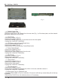
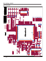
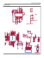
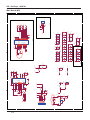
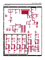
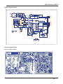
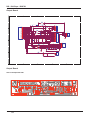
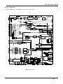
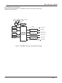
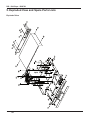
C.E.C BELSON/DPTO.TECNICO/BSA-3750/Ed.01
DVD - DivX Player - BSA3750
Table of Contents
1.Genernal Section
Cautions and Warnings
3
3
Precautions
3
Test Equipment / Jigs
4
Specifications
4
Disassembly Instructions
7
2.Servise and Special Functions
9
Software Upgrade
9
Initialization of the Set
9
3.Layout of PCBs and Circuit Diagrams
9
4.IC Block Diagrams
18
5.Exploded View and Spare Parts Lists
36
2
DVD - DivX Player - BSA3750
1. General Sections
Cautions and Warnings
Product Safety Notice
Parts marked with the symbol ! in the schematic diagram have critical
characteristics.
Use ONLY replacement parts recommended by the manufacturer. It
is recommended that the unit be operated from a suitable DC supply or
batteries during initial check out procedures.
Leakage Current Check/Resistance Check
Before returning the unit to the customer, make sure you make either (1) a leakage current check or
(2) a line to chassis resistance check. If the leakage current exceeds 0.5 milliamps, or if the resistance
from chassis to either side of the power cord is less than 240 K ohms, the unit is defective.
WARNING: DO NOT return the set to the customer until the problem or located is corrected.
Protection of Eyes from Laser Beam
To protect eyes from invisible laser beam during servicing
DO NOT LOOK AT THE LASER BEAM
Laser Caution
This Digital Video Disc Player employs a Laser System. To prevent direct exposure to the laser
beam, do not try to open the enclosure.
Visible laser radiation emits when open and interlocks are defeated.
Use of controls or adjustments or performance of procedures other than those specified herein may
result in hazardous radiation exposure. This CD Changer must be adjusted and repaired only by
qualified service personnel.
DO NOT STARE INTO BEAM.
Laser symbol:
THIS IS COMPACT DISC PLAYER IS CLASSIFIED AS A CLASS 1 LASER PRODUCT.
THE LASS 1 LASER PRODUCT LABEL IS LOCATED ON THE REAR EXTERIOR.
Precautions
1. ESD Precautions in Repairing
1.1 Do not apply excessive pressure on the mechanical parts (moving parts), including the Pickup
Block, as extremely high mechanical precision or required in these parts.
1.2 When soldering the microprocessor and signal processing IC’s, use a ceramic soldering iron or
a soldering iron whose metal part is grounded since they are not resistant to static electricity.
1.3 When removing the solder or soldering the laser shorting lands for the Pickup Block, use a
ceramic soldering iron or a soldering iron whose metal part is grounded since the laser diode or not
resistant to static electricity.
2. DVD Loading Unit Precautions when handling the Mechanism Block
2.1 Do not loosen any screws in the Pickup Block.
3
DVD - DivX Player - BSA3750
2.2 Do not adjust any screws in the Mechanism Block except for “Tilt Adjust Screws”, as they are
adjusted precisely at the factory.
2.3 Replacement of the Pickup Block is impossible. Always replace the Traverse Ass’y when the
Pickup Block needed to be replaced. Do not touch the lens or lens holder of the Pickup Block.
2.4 The Guide Rails of the Pickup Block are greased. Take care when handing.
2.5 When you try to slide the Pickup Block, do not press or pull it directly. Always turn the dive gears
with your fingers.
2.6 Be sure that the anti-slipping rubber on the turntable or clean. If there is dust or it is greasy, clean
the part with the liquid that contains 50% each of alcohol and water.
When removing the Mechanism P.C.B. Ass’y, you need to short-circuit the laser diode shorting
lands beforehand.
Test Equipment / Jigs
Variable isolating transfomer, Dual channel oscilloscope, Digital multimeter
Specification
1
2
3
4
5
Chassis
Laser concept
2 laser for DVD and VCD
Disc formats
DVD+R
DVD-R
DVD+RW
DVD-RW
CD-R
CD-RW
Yes
Yes
Yes
Yes
Yes
Yes
Media formats
DVD-Video
Audio CD
Video CD
S-Video CD
CD-ROM
Yes
Yes
VCD 1.0,1.1,2.0
Yes
DivX,MPEG4,MP3, JPEG, Kodak Picture CD,WMA
Player features
Parental control
Screen saver
Picture mode select
Video strobe
Video filter
File browser
Yes, numerical lock
Yes
Yes
Yes
Yes
DivX, MP3, JPEG, Kodak Picture CD,WMA
Player functions
Play/stop/pause
Yes/Yes/Yes
4
DVD - DivX Player - BSA3750
Next/previous(skip)
Fast forward/reverse
Random play
Program play
Last memory( resume)
Yes/Yes
Yes/Yes (DVD,MP3,WMA : 2X / 4X / 6X / 8X ,
VCD,CDDA:1X / 2X / 3X / 4X, DivX: 2X / 4X / 8X / 16X
)
DVD/VCD 2X/3X/4X,JPEG 1.5X/2X/1/2/1/4
YES/YES(DVD,VCD:1/2,1/4,1/8)
Yes
Yes/Yes
DVD: title -chapter-A/B;VCD,CD: A/B-repeat one-repeat
all
CDDA, MP3,WMA
CDDA,DVD,JPEG,MP3,WMA
Yes
Region Code
Region code
changed by request.
Zoom
Slow motion forward /reverse
Perfect still picture
Frame advance /reverse
Repeat CD /DVD
6
7
OSD
OSD style
OSD language
Subtitle Language
Welcome Logo and OSD background
8
Audio out
Digital Audio decoder
Digital Audio output
Analog Audio output
Audio D/A converter
Virtual surround Sound
Digital sound process
Frequency range DVD 48/96
kHz
Frequency range CD 44.1 kHz
Dynamic range 1 kHz
Crosstalk
Signal noise
9
Video out
Video D/A converter
Progressive Video out
PAL
standard
English, German, Dutch, French, Italian, Spanish, Portuguese
English, German, Dutch, French
Provided by Customer
Dolby digital AC-3, MPEG 2, PCM, MP3
Dolby digital AC-3, DTS, MPEG, PCM 48/96 KHz
Dolby Prologic II (down mix), Stereo; Dolby digital AC-3;
5.1CH
24 Bit/96kHz
Yes
Yes
4 Hz-22 kHz/ 4 Hz- 44 kHz
4 Hz-20 kHz
≥80 Db(weighted)
≥80 dB(weighted)
≥90 dB(weighted)
10 Bit / 54 MHz
PAL / NTSC
Yes, 625 lines / 50Hz / 4.43 MHz
5
DVD - DivX Player - BSA3750
NTSC
Norm converter ( PAL-NTSC,
NTSC-PAL)
Video resolution
Frequency response
Signal noise rate luminance
Signal noise rate chroma
10 Connections rear
Euro-AV
Cinch Video
Cinch Audio
S-Video ( Y-C)
Digital Audio out coaxial
Digital Audio out optical
progressive scan out
11 Power Supply
Power voltage
Max. power consumption
Power switch
Power supply plug
12 Cabinet
Dimensions in cm (W× H ×D)
net
Dimensions of carton in cm
(W× H ×D)
13 Design
Design
Cabinet keys
Logo
Label
Yes, 525 lines / 60 Hz / 3.58 MHz
Yes
525 lines
5MHz < -3 dB
>60 dB (weighted)
>60 dB unweighted
Yes, scart
Yes, 1× output
Yes, 6× output
Yes, 1× output
Yes, 1×
Yes, 1×
Yes, 3xoutput
AC 110-240V 50/60 Hz
Approx. max. 10W
Yes
Yes
Approx. 43.0×4.8×25.7
Aprrox. 47.1x10.8x36.8
mirror-like front panel as per the sample provided by Hualu
POWER ,PLAY, PAUSE, STOP, OPEN/CLOSE, PREV,
NEXT
ACCORDING TO REQUEST
Model no. label and production serial number label will be
sticked at rear panel
14 Remote Control
Type
Batteries
IR code
standard
Yes, 2×R03P AAA (no mercury)
standard
15 Display
Type
VFD
6
DVD - DivX Player - BSA3750
16 Packaging
1 set /carton
54 cartons/ slip-sheet
ACCORDING TO REQUEST
17 Loadability
For 20’ Container
For 40’ Container
For 40 HC Container
1296 sets
2592 sets
2880 sets
18 Supplied Accessories
Euro-AV cable (Scart-cable)
Power cord
Remote control
Batteries
Instruction Manual
Warranty info
Yes
Yes
Yes
Yes
ACCORDING TO REQUEST
Yes
19 Safely Conformity
CE
changed by request with payment
CE report is available for Hualu's model no.:DVD4360
Dissassembly Instructions
M
A
L
C
B
D
E
A
A
G
Fig. 1
F
F
G
Fig. 2
7
DVD - DivX Player - BSA3750
J
Fig.3
Fig. 4
Fig. 5
1. Cabinet Upper Part
- Undo the 8 screws A (Fig. 1)
- Bend the upper part of the cabinet from the rear side (Fig. 1) off the base plate, and then detach
the cabinet upper part from the unit.
2. Front Panel
- Undo the 2 screws J (Fig. 3)
- Undo the 2 screws F (Fig. 2)
- Undo the 2 locking lugs G (Fig. 2) and then remove the front panel.
- Unplug the connectors if necessary.
3. VFD Driver and Key Control Board Units
- Remove the front panel (Point 2)
- Undo the 4 screws I (Fig. 4)
- Remove the VFD Driver and Key Control Board units.
4. Power Supply Board
- Undo the 4 screws B (Fig. 2).
- Undo the 1 screw L (Fig. 1).
- Remove the Power Supply Board from the unit.
- Unplug the connectors if necessary.
5. Main Board
- Undo the 7 screws E (Fig. 2).
- Remove the main board.
- Unplug the connectors if necessary.
6. Output Board
- Undo the 2 screws M (Fig. 2)
- Undo the 4 screws C (Fig. 1).
- Remove the output board.
- Unplug the connectors if necessary.
7. Drive Mechanism
- Undo the 4 screws D (Fig. 2)
- Lift the drive mechanism at its back part, slide it to the rear, and then remove it.
- Unplug the connectors if necessary.
8. Opening the Tray of a Defective Unit
- Turn the toothed wheel H (Fig. 5) in direction of the arrow until the tray moves then pull out the tray
completely.
- Remove the DVD/CD from the defective drive unit if necessary.
8
DVD - DivX Player - BSA3750
2. Service and Special Functions
Software Upgrade
You can download the upgrade software “bank30.rom“ from Web using an Internet browser.
- Copy the “bank30.rom” on the drive of your PC.
- Create a software upgrade CD.
- Use only a new CD-R / CD-RW (not a erased one).
- Give the CD name of your choise (e.g. version and unit name).
- Burn the “bank30.rom“ on the CD-R / CD-RW.
- Insert the upgrade CD, the unit will be upgraded automatically.
- After upgrade, the disc tray will opened, remove the upgrade CD.
Attention: if a failure should occur during the software upgrade, it may happen that the
unit’s function and a restart of the upgrade function are no longer possible. If this should
be the case,
- Power off the unit with pressing ON/OFF button on the front panel (do not remove the upgrade
CD).
- During pressing still the NEXT button on the front panel, press down the ON/OFF button to power
on the unit, the unit will be upgraded automatically.
- After upgrade, the disc tray will opened, remove the upgrade CD.
Initialization of the Set
You can restore all the custom settings to the basic settings.
- Press SETUP button to open the main menu.
- Select the PREFERENCES line with 5or 6 and activate with OK button.
- Select the DEFAULTS line with 5or 6 and press OK button to confirm.
- Select the RESET with 4 and press OK button to reset the unit to its basic settings.
- Press SETUP to exit the menu.
3. Layout of Circuit Diagrams and PCBs
Main Board
9
1
2
3
4
RAS1#
RAS2#
DQM
DWE#
CAS#
RAS0#
CS0#
DOE#
DSCK
MA0
MA1
MA2
MA3
MA4
MA5
MA6
MA7
MA8
MA9
MA10
MA11
GND
R22
0
3 SVREF15
3 TRACK
3 SPINDLE
3 FOCUS
3 SLEGN
VCC
WC
SCL
SDA
15PF
C86
GND
R49
R41
24C01A/24C02
S0
S1
S2
GND
8
7
6
5
33
33
U5
GND
36
40
20
21
15
39
16
17
18
19
37
38
23
24
25
26
29
30
31
32
33
34
22
35
0.1U
560P
0.015U
CC30
47P
560P
CC33
0.1U
CC32
33P
33P
VSS
VSS
VSS
VSSQ
VSSQ
VSSQ
VSSQ
VCCQ
VCCQ
VCCQ
VCCQ
VCC
VCC
VCC
DQ0
DQ1
DQ2
DQ3
DQ4
DQ5
DQ6
DQ7
DQ8
DQ9
DQ10
DQ11
DQ12
DQ13
DQ14
DQ15
32/64MBIT SDRAM
28
41
54
6
12
46
52
3
9
43
49
1
14
27
2
4
5
7
8
10
11
13
42
44
45
47
48
50
51
53
GND
GND
GND
DB0
DB1
DB2
DB3
DB4
DB5
DB6
DB7
DB8
DB9
DB10
DB11
DB12
DB13
DB14
DB15
VCC33
3
1
2
3
0R
VCC
IR
VFD_CLK
VFD_CS
VFD_DAT
VCC
1
EM6353
2
VCC
GND
RESET
U7
V6300(open)
NC VDD 5
GND
NC RES 4
U6
RR8
OPEN
GND
27PF
C13
Y1
27M
R47
27PF
C14
CC17
6800P
AVSS_DS
AVSS_PL
XSPDOFTR1
XSFDO
XSFTROPI
AVDD3_PL
XSPLLFTR1
XSPLLFTR2
XSVREF0
XSAWRC
AVSS_DA
XSRFRPCTR
XSTRAY
AVDD3_DA
XSSPINDLE
XSFOCUS
XSSLEGP
XSSLEGN
XSTRACK
XSTESTDA
XSFGIN
XSPHOI
SXCSJ
XSDATA
XSCLK
XSDFCT
XSLDC
XSSPDON
VD33
VS33
XGPIO[9]
XGPIO[8]
XGPIO[7]
XGPIO[6]
XGPIO[5]
XGPIO[4]
EAUX03
EAUX02
EAUX01
EAUX00
VSS
VDD
AUX0
AUX1
AUX2/ HSYNC
AUX3/ VSYNC
AUX4
AUX5
AUX6
AUX7
RESET
VS33
RFGND
1000PF(OPEN)
C15
FB3
R48 0(OPEN)
3.3UH(OPEN)
GND
157
158
159
160
161
162
163
164
165
166
167
168
169
170
171
172
173
174
175
176
177
178
179
180
181
182
183
184
185
186
187
188
189
190
191
192
193
194
195
196
197
198
199
200
201
202
203
204
205
206
207
208
GND
100K
RESET#
RESET#
AUX4
XSCSJ
XSDATA
XSCLK
DEFCT
SLDC
SPDON
OPEN
OPEN
1K
33
33
33
6.8K
6.8K
5.1K
6.8K
6.8K
CC27
0.1U
TR1
TR2
CC22
0.1U
PLL33V
C
20K
RR7
CC16
68K
RR6
0.1U
DIN
CC14
R26
STANDBY
R29
VCC
IRDL
SCARTCTL2
R32
3 ZERO1
3 INSW
3 HOMESW
3 CLOSE
0.015U
RR24
RR25
RR23
RR20
RR21
10K
5.1K
CC18
C
CC19
C
CC21
0.047U
CC23
560P
RR26
RR27
RR28
RR16
RR17
1.2K
R
0.1U
CC13
3 DIN
RFGND
RF33V
DA
CC31
AUX4
0
0
R28
R33
33
33
33P 3 OUTSW
3 OPEN
SCARTCTL0 R34
4Mx16 SDRAM (9ns)
NC
NC
BA0
BA1
DQML
DQMH
WE
CAS
RAS
CS
CKE
CLK
A0
A1
A2
A3
A4
A5
A6
A7
A8
A9
A10
A11
RR14
RR12
CC24 CC25 CC26
TR2
TR1
CC35 CC36 CC37
0.015U
CC28
PLLGND
MOCTL
RFGND
R30
R31
R24
1K
SCARTCTL1
SCL
SDA
R23
1K
SCSJ
SDATA
SCLK
SVREF15
TRACK
SPINDLE
FOCUS
SLEGN
RFGND
3 CD_DVDCT
3 SCSJ
3 SDATA
VCC
3 SCLK
GND
CC20
1U
TESTAD
SPDON 3
SLDC 3
33K
SVREF15
RR13
SERIAL EEPROM
U3
3 MIRR
SPDON
SLDC
SDEFCT 3
XIN
XOUT
DCLK
DMA0
DMA1
DMA2
DMA3
8
7
6
5
CC10
1U
CC12
1U
4.7U
GND
R6
4.7K
R7
4.7K
led3
led4
SCARTCTL0
VFD_DAT
VFD_CS
VFD_CLK
GND
IR
GND
VD33_PLL
RWS/TDMFS
RBCK/TDMCLK
RSD/TDMDR
LD7
LD6
LD5
LD4
VD33
VS33
LD3
LD2
LD1
LD0
LOE
LWRLL
LCS3
VDD
VSS
LCS2
LCS1
LCS0
LA0
LA1
LA2
VD33
VS33
LA3
LA4
LA5
LA6
LA7
LA8
VDD
VSS
LA9
LA10
LA11
LA12
LA13
LA14
LA15
VD33
VS33
LA16
LA17
LA18
LA19
LA20
LA21
DQM
VD33
U1
ES66x8
HDR9-100
1
2
3
4
5
6
7
8
9
JJ6
104
103
102
101
100
99
98
97
96
95
94
93
92
91
90
89
88
87
86
85
84
83
82
81
80
79
78
77
76
75
74
73
72
71
70
69
68
67
66
65
64
63
62
61
60
59
58
57
56
55
54
53
R10
4.7K
GND
LA16
LA17
LA18
LA19
LA20
LA21
DQM
LA9
LA10
LA11
LA12
LA13
LA14
LA15
LA3
LA4
LA5
LA6
LA7
LA8
LA0
LA1
LA2
LCS2#
LD3
LD2
LD1
LD0
LOE#
WRLL#
LCS3#
LD7
LD6
LD5
LD4
VCC33
VCC33V
TP34LCS3#
TP32WRLL#
TP30LA21
TP28LA19
TP26LA17
TP24LA15
TP22LA13
TP20LA11
TP18LA9
TP16LA7
TP14LA5
TP12LA3
TP10LA1
TP8 LD7
TP6 LD5
TP4 LD3
TP2 LD1
VCC20
0 OHM
0 OHM
UDAC1
CDAC1
YDAC1
VDAC1
FDAC1
GNDV
LA0
LA1
LA2
LA3
LA4
LA5
LA6
LA7
LA8
LA9
LA10
LA11
LA12
LA13
LA14
LA15
LA16
LA17
LA18
LA19
LA20
LA21
RESET#
WRLL#
LOE#
LCS3#
LD0
LD1
LD2
LD3
LD4
LD5
LD6
LD7
R19
R20
VCC
R200
TP33LOE#
TP31RESET#
TP29LA20
TP27LA18
TP25LA16
TP23LA14
TP21LA12
TP19LA10
TP17LA8
TP15LA6
TP13LA4
TP11LA2
TP9 LA0
TP7 LD6
TP5 LD4
TP3 LD2
TP1 LD0
4.7k(open)
TWS
TBCK
LCS2#
LCS3#
LA19
LA18
LA8
LA7
LA6
LA5
LA4
LA3
LA2
WRLL#
RESET#
LA16
LA15
LA14
LA13
LA12
LA11
LA10
LA9
LA20
BAT54S
D5
BAT54S
D4
BAT54S
D3
BAT54S
D2
U2
1
2
3
4
5
6
7
8
9
10
11
12
13
14
15
16
17
18
19
20
21
22
23
24
VCC
VCC33
GNDV
R17
R18
R25
R27
open
0
CVBS
Y
V
U
CVBS
1.8UH
1.8UH
1.8UH
LCE#
LA1
LD0
LOE#
LD1
LD2
LD3
LD4
LD5
LD6
LA0
LD7
FDAC
VDAC
YDAC
CDAC
FLASHVCC
LA17
GNDV
C12
330PF
GNDV
C10
330PF
GNDV
C6
330PF
GNDV
C4
330PF
UDAC
CVBS
G
R
B
CVBS
CVBS + RGB
C2
330PF
GNDV
GND
1.8UH
Y
G
R
B
C
S-VIDEO + RGB
1.8UH
OPEN
0
A16
BYTE
GND
DQ15/A_1
DQ7
DQ14
DQ6
DQ13
DQ5
DQ12
DQ4
VCC
DQ11
DQ3
DQ10
DQ2
DQ9
DQ1
DQ8
DQ0
G
GND
E
A0
48
47
46
45
44
43
42
41
40
39
38
37
36
35
34
33
32
31
30
29
28
27
26
25
CVBS + YUV
FLASHVCC
GNDV
C11
330PF
GNDV
L5
C9
330PF
GNDV
L4
C5
330PF
GNDV
L3
C3
330PF
GNDV
L2
A15
A14
A13
A12
A11
A10
A9
A8
NC
NC
W
RP
VPP
DU/WP
NC
NC
A17
A7
A6
A5
A4
A3
A2
A1
75 OHM
R16
GNDV
75 OHM
R15
GNDV
75 OHM
R12
GNDV
75 OHM
R11
GNDV
C1
330PF
L1
CVBS + S-VIDEO
or CVBS + YUV
CVBS
Y
V
U
C
75 OHM
R5
VDAC
YDAC
CDAC
UDAC
5DAC
VIDEO OUTPUT TABLE
BAT54S
D1
VCCV GNDV
MULTI
Frequency
S-CHIP DEFAULT
DEFAULT
S-CHIP
4.5
114.75
4.25
121.5
NA
reserved
5
135
bypass 2 bypass
NA
7
3.75
101.25
4
108
121.5
4.5
4.25
114.75
128.25
reserved
4.75
NA
94.5
5.5
148.5
3.5
4
6
108
162
GNDV
PLL0
0
1
0
1
0
1
0
1
FB2
FERB
FB1
FERB
PLL1
0
0
1
1
0
0
1
1
VD33_PL1
RWS
RBCK
0.1U
GND
VCCV
PLL2
0
0
0
0
1
1
1
1
390
VCC33V
TSD2
TSD1
TSD0
TWS
SPDIF
TBCK
MCLK
0.1U
C8
0 OHM
GND
R13
R9
4.7K
R4
OPEN
VCC33
GND
R14
C7
R8
4.7K
R3
OPEN
GND
R2
OPEN
VCC33
3
VCC33
GND
R1
OPEN
Vibratto-II
1
2
3
4
MA0
MA1
MA2
MA3
DEFCT
CC8
10K
8
7
6
5
RFO
10x4
RN1
DMA4
DMA5
DMA6
DMA7
DMA8
DMA9
10x4
RN2
1
2
3
4
MA4
MA5
MA6
MA7
3 RFO
RR5
CC5
0.1U
VCC20
DMA11
CC6
4700P
CC7
C
CC9
C
CC11
4700P
TESTAD
DMA10
8
7
6
5
1
2
3
4
MA8
MA9
MA11
MA10
DIP
10x4
RN3
1
2
3
4
CAS#
CS0#
RAS0#
RAS1#
3 DIP
SVREF15
SVREF09
SVREF21
RR1
RR2
RR3
RR4
8
7
6
5
RAS2#
DOE#
DWE#
SBAD
FEI
CEI
TEI
RN4
1
2
3
4
3 SBAD
3 FEI
3 CEI
3 TEI
CC2
1000P
CC4
1000P
3.3K
3.3K
3.3K
3.3K
CLK SOURCE
DCLK INPUT
CRSTAL OSC
10x4
8
7
6
5
RFGND
MIRR
CC1
1000P
CC3
1000P
PLL3
1
0
SPDIF
TBCK
MCLK
DB0
DB1
DB2
10x4
RN5
4.7K
33
33
33
33
TSD2
DB3
DB4
DB5
DB6
DB7
DB15
DB14
R35
R36
R37
R38
R39
TSD1
TSD0
TWS
UDAC1
CDAC1
YDAC1
GNDV
VCC33V
VDAC1
FDAC1
RSET
COMP
VREF
VS33_PL2
156
155
154
153
152
151
150
149
148
147
146
145
144
143
142
141
140
139
138
137
136
135
134
133
132
131
130
129
128
127
126
125
124
123
122
121
120
119
118
117
116
115
114
113
112
111
110
109
108
107
106
105
XSDSSLV
XSRFIP
XSRFIN
XSIPIN
AVDD3_DS
XSIREF
XSVREF[15]
XSVREF[09]
XSVREF[21]
AVDD3_AD
XSRFRP
XSTEI
XSCEI
AVSS_AD
XSFEI
XSSBAD
XSTESTAD
XSTEXI
VDD
VSS
XSFLAG[3]
XSFLAG[2]
XSFLAG[1]
XSFLAG[0]
XSIP1
XSIP2
XSLG
XSWBL
XSWBLCLK
VS33
VD33
SPDIFIN
SPDIF/SEL_PLL3
TBCK
MCLK
TSD3
TSD2
VS33
TSD1/SEL_PLL1
TSD0/SEL_PLL0
TWS/SEL_PLL2
YUV0/UDAC
YUV2/CDAC
YUV5/YDAC
VS33_DA
VD33_DA
YUV6/VDAC
YUV7/FDAC
YUV4/RSET
YUV3/COMP
YUV1/VREF
VS33_PL
VD33
XIN
XOUT
DCLK
DMA0
DMA1
DMA2
DMA3
VS33
VD33
DMA4
DMA5
DMA6
DMA7
DMA8
DMA9
DMA10
VS33
VD33
DMA11
DCAS
DCS0
DCS1
DRAS0
DBANK0/ DRAS1
VSS
VDD
DBANK1/ DRAS2
DCKE/DOE/TDMTSC
DWE
DB0
DB1
DB2
VS33
VD33
DB3
DB4
DB5
DB6
DB7
DB15
DB14
VS33
VD33
DB13
DB12
DB11
DB10
DB9
DB8
DSCK
VS33
1
2
3
4
5
6
7
8
9
10
11
12
13
14
15
16
17
18
19
20
21
22
23
24
25
26
27
28
29
30
31
32
33
34
35
36
37
38
39
40
41
42
43
44
45
46
47
48
49
50
51
52
DB13
DB12
DB11
DB10
DB9
DB8
DSCK
2
2
2
2
2
1
1
1
1
1
3
3
3
3
10
M29W800DT
VCC33
DVD - DivX Player - BSA3750
Main Board (M1)
11
MGND
2 OPEN
CC75
MVCC
0.1U
LD-GND
DVD-LD
(N.C.)
HFM-Vcc
MPD
CD-LD
DVD-VR
CD-VR
(N.C.)
E
Vcc
Vc(Vref)
GND
F
B
A
RF
CD/DVD SW
D
C
TT+
F+
F-
DCLOAD+
SANYO-DV34
CN1
4
3
2
1
UU4
RIN
VREF
OUT2
BA6287F ROHM
FIN
VCC
VM
GND
5
6
7
8
MGND
F
DVD-D
DVD-A
DVDRF
CD_DVD
DVD-B
DVD-C
TRACKTRACK+
FOCUSFOCUS+
PVC
E
CDLDO
VR_DVD
VR_CD
DVDLDO
LL2
CDLDO
OUT1
24
23
22
21
20
19
18
17
16
15
14
13
12
11
10
9
8
7
6
5
4
3
2
1
LL1
DVDLDO
QQ1
2SB1132
FB (0805)
DVD-C
DVD-D
DVD-A
DVD-B
2SB1132
QQ2
MVCC
IN4148
1000P
CC66
10
10
CC59
1000P
IN4148
0.1U
CC46
CLOSE
CLOSE 2
RF50V
1
2
3
4
5
6
7
8
9
10
11
12
13
14
15
16
CD_DVDCT
6
5
4
3
2
1
2.0MM
6
5
4
3
2
1
JJ4
CC41
470P
CC43
470P
ES6603
MGND
LOAD-/DCMOLOAD+/DCMO+
SLED+
SLED-
2
DCLOAD+
DCLOAD-
10K
MGND
F
E
PVC
DVDLD
CDLD
DVDMDI
CDMDI
RR9
5
4
3
2
1
2.0MM
5
4
3
2
1
JJ3
CC47
820P
DVDFRP
DVDRFN
A2
B2
C2
D2
CP
CN
D
C
B
A
CD_D
CD_C
CD_B
CD_A
UU1
CC48
100U/16V
RF50V
RFGND
CC64
100U/16V
CC63
100U/16V
RFGND
CC50
680P
CC51
680P
CC52
680P
CC54
680P
CC55
100P
CC15
4700P
CC29
0.1UF
2 CD_DVDCT
DCLOAD-
0.1U
CC57
1
1
DD3
DVDMDI
CDMDI
FB (0805)
RR39
RR40
1
DD1
1
RFGND
DVDRF
2
3
3
RFGND
MGND
C
CC76
R
RR68
MVCC
OPEN
RR71
RFGND
QQ8
2N3904
10K
RR10
RF50V
RFGND
3
2
RF50V
64
63
62
61
60
59
58
57
56
55
54
53
52
51
50
49
RFDC
RFSIN
ATOP
ATON
AIN
AIP
VPA
RFAC
BYP
DIN
DIP
FNP
FNN
VNA
MEV
RX
CD_F
CD_E
VPB
VC
DVDLD
CDLD
DVDPD
CDPD
VNB
LDON
MIRR
MP
MB
MLPF
MIN
MEVO
48
47
46
45
44
43
42
41
40
39
38
37
36
35
34
33
CD_DVD
HOMESW 2
100K
RR11
0
RFGND
2
CC53
0.047U
CE
FE
TE
SBA
RFGND
QQ6
2N3904
18K
OUTSW 2
0
LINK
TP38
MIRR
RR15
RF50V
RR35
SVREF15
CC56 RF50V
0.1U
INSW 2
2
2SK3018
QQ5
VR_CD
RF50V
RFO 2
DIN 2
DIP 2
TP37
LINK-
SDEFCT 2
TP36
DEFCT
CEI 2
FEI 2
TEI 2
SBAD 2
SCSJ 2
SDATA 2
SCLK 2
RFGND
2
2SK3018
QQ7
VR_DVD
MIRR 2
SLDC 2
RFGND
SCSJ
SDATA
SCLK
CC49
0.1U
RFGND
RF33V
RF50V
CC45
0.01U
12K(1%)
MEVO
CC58
0.22U RF50V
CC60
CC61
160P
CC62
33000P
0.01U
SDEN
SDATA
SCLK
V33
LCP
LCN
MNTR
CE
FE
TE
PI
V25
V125
TPH
DFT
LINK
RR29
CC44
0.1U
RR73
17
18
19
20
21
22
23
24
25
26
27
28
29
30
31
32
1
3
1
CC40
0.1U
CC42
0.1U
3
1
3
1
CC38
0.1U
CC39
0.1U
TP35
MNTR
2 SLEGN
2 SVREF15
2 FOCUS
VCC
MGND
RR66
22K
RR64
1.5K
RR63
10K
LOAD-/DCMO-
MVCC
33
RR46
SVREF15
MGND
MGND
MVCC
FOCUS+
MGND
RR72
22K
RR70
1.5K
RR69
10K
RR59
RR61
FB
2
RR47
RR49
6
5
RF50V
RR65 1M
1(0805)
1(0805)
SLED+
SLED-
MGND
CC68
4700P
CC65
100P
12K
3.3K
47K
RR43
FOCUS-
FOCUS-
LL3
1
1K
LOAD+/DCMO+
CC85
0.1U
CC70
0.1U
RR50
33K
RR41
-
+
8
RFGND
4
VOFC+
VOFC-
VOSL+
VOSL-
PGND
PVCC1
VCC
VNFFC
VOSL
VINSL-
VINSL+
TL3472
7
VINTK
BIAS
STBY
MGND
RFGND
0.1U
CC77
RF50V
MOCTL
RR67
4.7K
MGND
VOTK+
VOTK-
VOLD+
VOLD-
PGND
VNFTK
PVCC2
PREGND
VINLD
CTKERR2
CTKERR1
RESET#
RR36
MVCC
CFCERR2
CFCERR1
VINFC
UU2
BA5954FP
UU3B
14
13
12
11
10
9
8
7
6
5
4
3
2
1
2 SPDON
GND
GND
29
30
RF50V
33K
47K
15
16
17
18
GND
RR60
RR62
CC72
0.1U
RFGND
CC73
100U/10V
MGND
+
SPINDLE 2
MGND
TRACK 2
1(0805) TRACK1(0805)
TRACK+
LOAD+/DCMO+
LOAD-/DCMO-
20
19
MVCC
TRACK-
21
22
23
CC67
100P
RR48
24
RR45
10K
25
RR42
DD2
IN4148
R
26
27
28
1
1K
MVCC RR38
DVD - DivX Player - BSA3750
Main Board (M2)
1
2
3
VCC33
3
3
Q20
8050
HEAD12-100
1
2
3
4
5
6
7
8
9
10
11
12
JJ7
TBCK
TWS
TSD0
MCLK
1
IN
3
Q21
8050
GND
3.3VB
OUT
33 OHM MCLK-
A
R70
250(1%)(open)
R69
412(1%)(open)
2
1
L6 1
GND
2
VCC33
B4
0.1UF
FB
33(open)
R205
33
GNDA
100UF
B2
VCCA
33(OPEN)
L7 1
R203
R202
VCCA
GNDA
2
FB
B26
100UF
VCC20
FB
-12V
L8 1
+12V
33
R204
TBCK
TWS
R53
33 OHM TSD0-
R52
Q2
AMS1117(open)
2
4
ADJ
1
2
1
1
2
TBCK
100U/25V
2
2
15
CC78
PLL33V
1U
CC83
RF33V
B
4.7k
LRCIN
BCKIN
DIN
ZER0
MCLK
LATI2S
SCKDSD
SDIDEM
MUTEB
MODE
CSBIWL
DGND
DVDD
R206
1
3
2
5
4
20
19
18
17
16
100U/16V
VCC33
CC82
LL5
FB
FB4
FB
TSD0-
TWS
ZERO
C91
27PF
VCC
C90
27PF
MCLK-
7
6
U8
WM8728
B
VCCA
VMID
VOUTR
VOUTL
VREFN
AGND
VREFP
AVDD
2
12
8
11
13
9
14
10
L10
FB
VCC
VCC
1
1
2
10UF
2
LL6
FB
1
100U/16V
CC80
LL4
FB
1
VCC33
C22
0.1UF
MVCC
RFGND
1U
CC81
RF50V
B27
47UF
VCC33V
GND
2
L9
FB (0805)
10UF
C87
C23
R
AVCM
0.1UF
0.1UF
L
C88
C89
open
B28
0.1UF
C
VCCA
B31
0.1UF
B15
0.1UF
B8
0.1UF
WM8746/da1196
B30
0.1UF
SDRAM
B14
0.1UF
ES60x8
B7
0.1UF
ZERO1
B32
0.1UF
B16
0.1UF
GND
10K(open)
8
12
13
14
9
11
1
B33
0.1UF
B17
0.1UF
B10
10UF
VCC
B34
0.1UF
B18
0.1UF
B11
0.1UF
GND
24C01
GNDA
D
GND
B36
10UF
B55
0.1UF
D
0.1UF
B37
B20
0.1UF
VCC
LRCLK2
MCLK
BCLK
LRCLK
DIN0
DIN1
DIN2
MODE
CAP
OUT2R
OUT2L
OUT1R
OUT1L
OUT0R
OUT0L
GR0
GR1
GR2
AGND1
AGND2
AVDD1
AVDD2
16
19
17
23
21
27
25
26
22
18
20
24
15
28
B22
0.1UF
B39
0.1UF
C28
R
L
B23
0.1UF
B40
0.1UF
B24
10UF
GND
GND
B41
0.1UF
KAR
B56
0.1UF
GNDA
B57
10UF
B43
0.1UF
GNDA
B53
10UF
B25
10UF
KAR
'normal_intlev = 1'
0.1UF(open)10UF(open)
C27
VCCA
WM8720(wm8726/da1132)
B42
0.1UF
VCCA
B21
0.1UF
B38
0.1UF
open
LATCH/12S
SCLK/IWL
SDIN/DM0
MUTE
DGND
DVDD
U9
DA1196/WM8746(open)
FLASHVCC
B35
0.1UF
B19
0.1UF
B12
10UF
10
MCLK2
TBCK
3
TWS
4
TSD05
TSD1 R60
33 OHM(open)6
33 OHM(open)7
TSD2 R61
1 R54
B9
0.1UF
TSD1
TSD2
Q1
2SC3327(open)
ZERO
ZERO1
VCCA
0.1UF(open)
B51
B44
B54
B50
B49
B48
0.1UF(open) 10UF(open) 10UF(open)
0.1UF(open)0.1UF(open)
B29
0.1UF
VCC33
B13
0.1UF
VCC33
B6
0.1UF
VCC20
C
3
12
2
A
+12V
C25
C21
C19
C18
C17
C16
AOUT0L
AOUT0R
VCC
open
GNDA
-12V
AOUT2R
10UF(open)
AOUT2L
10UF(open)
AOUT1R
10UF(open)
AOUT1L
10UF(open)
10UF
10UF
E
E
HEADER 6(open)
1
2
3
4
5
6
JP2
1
2
3
4
DVD - DivX Player - BSA3750
Main Board (M3)
1
2
3
4
AOUT2L
AOUT1L
AOUT1R
AOUT2R
AOUT0L
KAR
LED4
AOUT0R
KAR
1
R76
R88
C85
R111 18K(open)
13
A
1000PF
GNDA
3
6
5
2
GNDA
GNDA
100K(open)
1
1
7
7
1
GNDA
R123 18K
1
1
R140 18K
R138 3.3K
GNDA
R132 10K(open)
1
GNDA
9014(open)
Q16
Q14
9014(open)
1
C_OUT
10K9open)
R121 3.3K
R115
1
150PF(open)
-12VA
V-
V+
Ls_OUT
Rs_OUT
LFE_OUT
+12VA U14-2
OPA2134UA(open)
1
U14-1
OPA2134UA(open)
C83
22PF(open)
10(open)
470(open)
R128
-12VA
V-
V+
+12VA
150PF(open)
-12VA
V-
V+
+12VA U12-2
OPA2134UA(open)
150PF(open)
470(open)
1
U12-1
OPA2134UA(open)
150PF(open)
C46
C53
6
5
V-
-12VA
C38
22PF(open)
C76
R125
R131
R135
R127
1K(open)
GNDA
100K(open)
R117
10UF(open)
C80
VCCA
1000PF
C64
R114 10(open)
1000PF(open)
R137 11K
1
C78
GNDA
R109 3.3K(open)
C71
R120 11K
1
GNDA
1
1
10UF(open)
C73
GNDA
11K(open)
R108
GNDA
1
GNDA
1000PF(open)
C54
R104 18K(open)
1
18K(open)
3.3K(open)
R101 3.3K(open)
1
GNDA
R90
1
1
18K(open)
3.3K(open)
GNDA
1 R78
1
11K(open)
GNDA
1000PF(open)
C48
11K(open)
R87
GNDA
1000PF(open)
C39
11K(open)
R75
R100
1
1
GNDA
2
V+
+12VA
8
4
8
4
3
8
4
8
3
C77
2
5
6
1K(open)
1K(open)
R110
GNDA
V-
V+
-12VA
150PF
C84
1
+12VA
150PF
-12VA
V-
V+
1
B
7
10UF
1K
QUIET
GNDA
1K
1K
RS
GNDA
1
C81
22PF
1
C74
22PF
C63
22PF(open)
CC
C52
22PF(open)
SUB
C45
22PF(open)
LS
C36
22PF(open)
GNDA
R122
R139
1
1K
R129
R134
100K
1
1
R112
R116
100K
1
GNDA
0 OHM(open)
QUIET
GNDA
10UF
C72
GNDA
C79
1
R106
GNDA
0 OHM(open)
R96
Q11
2SC3327(open)
GNDA
C62
22PF(open)
1
1
GNDA
0 OHM(open)
R82
Q10
2SC3327(open)
GNDA
C51
22PF(open)
1
1
GNDA
0 OHM(open)
R72
Q4
2SC3327(open)
1
Q6
2SC3327(open)
GNDA
C44
22PF(open)
1
C35
22PF(open)
U15-2
OPA2134UA
+12VA U15-1
OPA2134UA
1
GNDA
1K(open)
R103
R105
1
R107
100K(open)
1
QUIET
GNDA
10UF(open)
C55
1K(open)
R95
GNDA
1K(open)
R89
1
R98
100K(open)
1
QUIET
GNDA
10UF(open)
C50
1K(open)
R81
GNDA
1K(open)
R85
100K(open)
1
QUIET
GNDA
10UF(open)
C43
1
R77
1K(open)
R71
R73
100K(open)
1
QUIET
GNDA
10UF(open)
C32
3
2
3
0 OHM
R113
GNDA
GNDA
0 OHM
R130
Q17
2SC3326
1
Q12
2SC3326
1
GNDA
D12
1
GNDA
GNDA
1
C82
22PF
FL
C75
22PF
FR
C65
0.1UF
C
R97
150
220uF/16V
C56
0.1UF
-12VA
D11
R79
150
R74
150
IN4148
C47
+12VA
RESET#
STANDBY
VCC33
-12V
+12V
1
C37
8550
GNDA
Q8
2N3906
R91
2K
D10
IN4148
1
1
VCC33
1
1
100K
R94
QUIET
Q7
2N3906
47
R84
-12VA
R201
4.7K(open)
R99
2K
1
C42
470uF/25V
-12VA
SCARTCTL1
LED3
SCARTCTL2
C67
0.1UF(open)
R142 1K
SCARTCTL1 1
LED3
R141 1K
1
R126 1K
SCARTCTL2 1
GNDA
1
C70
C68
C69
10UF(open) 10UF(open) 10UF
GNDA
C60
C59
C58
C61
0.1UF(open) 10UF(open) 10UF(open) 10UF
ZERO
GNDA
C66
0.1UF(open)
1
-12VA
GNDA
+12VA
220uF/16V
C40
2
220uF/16V
IN4148
R86
100K
3
1
8050
2
C57
0.1UF(open)
1
Q5
Q3
3
1
1
1
1
1
1
1
1
1
2
3
C
1
1
1
2
3
1
2
3
2
3
2
4
3
2
2
3
3
3
1
2
1
8
4
3904
Q18
2.2K
R136
2.2K
R133
+12V
GND
3904
1
R124 1K
1
2.2K
R118
Q15
VCC
2N3906
Q9
C41
GND
D
3904
Q19
R83
1
3
0V------CVBS
3V------RGB
BLANK
Q13
3906
75
R119
0.1UF
VCC
0V------TV
6V------AV 16:9
12V------AV 4:3
SWITCH
1
SPDIF
R80
10M
D
1
open
8
4
1
1
1
3
2
1
3 1
2
21
3
B
3
2
1M
4
IRDL
39NF(open)
C273
7404
U13B
1
VCC33
SWITCH
7404
U13C
6
C34
0.1UF
GND
2
R417
10K(open)
GND
SUB
GND
CC
GND
RS
GND
LS
GND
FR
GND
FL
GND
CVBS
OP
R93
91 OHM
COAX
7404
U13D
VCC
2
GND
Q35
8550(open)
FDAC
BLANK
GND
VCC
COAX
OP
GND
UDAC
YDAC
CDAC
GND
9
R415
100K(open)
VDAC
YDAC
CDAC
UDAC
GND
Q33
2N3904(open)
IN4148(open)
D26
2
1OK(open)
GND
R416
C33
10UF
R414
1M2(open)
5
1
GND
3
1
2
3
2
1
3
8
1
E
1
GND
E
0.1UF
C49
7404
U13F
7404
U13E
7404
U13A
AUX4
20PIN
1
2
3
4
5
6
7
8
9
10
11
12
13
14
15
16
17
18
19
20
21
22
23
24
25
26
27
28
29
30
JJ1
12
10
2
AUX4
C274
1NF(open)
33 OHM(open)
R422
GND
R418
10K(open)
VCC33
13
Q34
2N3904(open)
68 OHM
1
11
33 OHM
R92
R102
GND
1
3
1
A
1
2
3
4
DVD - DivX Player - BSA3750
Main Board (M4)
DVD - DivX Player - BSA3750
Main Board
View of Component Side
14
DVD - DivX Player - BSA3750
Power Supply Board
1
2
!
!
F601
C602
C6010.1u/250V
0.1u/250V
LC20-001
AC INPUT
!
Component_1
CY602
102(open)
CY601
102(open)
D601
1N4001
D602
1N4001
C607
472/1KV(OPEN)
R603
C603
68uF/400V
3.3M(OPEN)
D604
1N4001
C606
100nF
R610
4.7K
R609C605
6.8K470P
C
C604
560P(OPEN)
R630
10K
4
REG
3
RC
Drain
C608
+
472/1KV
56K(OPEN)
Q601
BC337-40(OPEN)
R612
120K/1W
VCC Source
6
2
GND
5
AUX
1
1
D615
C631
220nF
5.6u
C620
220u/25V
D613
100
D605
FR104
L605
5.6u
+ C618
220uF/25V
FR107
+
C625
220uF/25V
PC817
D610
0
L602
IN5822 C614
+
C627
1000uF/16V
R617
1K
R618
j602
0 OHM
RL205
Q603
BC327-40(open)
C622
470uF/25V
+
B
3.3K(open)
BC337-40(open) j601
0 ohm
C611
100nF
U603
TL431
D620
Q602
FR104(OPEN)
!
D618
RL205
D611
0 OHM
C
10u
+
2200uF/16V
C609
+ 10uF/50V
+12v
-12v
GNDA
VCCA
VCC
GND
GND
3.3V
SVCC
SGND
MGND
+9V
12 HEADER
L604
D614
FR157(open)
5.6u(open)
+ C619
C624 +
470uF/25V(open) 470uF/25V(open)
U602
!
D606
BZX79C16V
1
2
3
4
5
6
7
8
9
10
11
12
+ C615
2.2u/50V(open)
FR107(open)
R607
D607
FR104
10 OHM
222/2KV
220uF/25V
C616
D612
R631
CY604
L603
FR107
1(OPEN)
PSB
5VSB
GND
FLFL+
VEE
HEADER 6
JS601
C610
+ 10uF/50V R611
1K
R608
22K
1
2
3
4
5
6
C621
100uF/50V
FR107
R604 R605 R606
R601
75K
TEA1523P
JS602
BZX79C9V1
R619
33K
D616
D608
FR107
cadd601
560P(open)
1
D619
T601
8
R602
B
8
D
220uF/25V
+ C617
FR104
!
D603
1N4001
U601
CY603
7
D617
+
1 CON601
2
6
+
!
5
! ! !
FUSE601
T1.6AL/250V
1 CON602
2
POWER SW
4
+
!
D
3
R620
R616
5.6K
470(open)
R621
33K(open)
R615
5.1K
C623 +
470uF/25V(open)
Q604
BC337-40(open)
C630
100NF(open)
X601
X602
ZX601
A
A
open
1
2
3
4
5
6
7
8
Power Supply Board
View of component Side
15
DVD - DivX Player - BSA3750
Output Board
1
2
3
4
5
FB721
D
D
FERB
C720
22PF
R701
C701
220UF/16V
FB702
4 OHM
J701
FERB
FERB
SUB
GND
CC
GND
RS
GND
LS
GND
FR
GND
FL
GND
CVBS
YDAC
CDAC
UDAC
GND
VCC
COAX
OP
GND
UDAC
YDAC
CDAC
GND
SWITCH
BLANK
FDAC
C
W703
2
1
JS701
1
2
3
4
5
6
7
8
9
10
11
12
13
14
15
16
17
18
19
20
21
22
23
24
25
26
27
28
FB703
FERB
FERB
FERB
FERB
CVBS
GND
Y
C
1
2
3
8
9
GND
GND
GND
GND
GND
CVBS+SVIDEO
C704
1NF
FB705
FB706
C703
100PF
C702
22PF
FB704
7
6
4
5
J702
1
2
3
4
5
6
7
8
9
10
11
12
13
14
15
16
17
18
19
20
21
C705
1NF
FB707
FERB
FB709
FERB
20pin
C710
22PF(open)
C709
22PF
C708
100PF
C706
100PF
C707
22PF(open)
FB717
FERB
FB718
FERB
FB716
FB715
B
FERB
J704
AOR
AIR
AOL
AGND
BGND
AIL
B
SWITCH
GGND
CLKOUT
G
DATA
RGND
DATAGND
R
BLANK
VGND
BLANKGND
VOUT
VIN
SHIELD
1
2
3
4
5
8
SCART
J703
1
2
3
4
5
6
7
8
9
FERB
FB720
FERB
FERB
C716
1NF
C717
1NF
C718
1NF
C719
1NF
C711
1NF
C
VIDEO+COAX
FB719
FB713
GND
SIG
GND
Pr
Pb
Y
GND
SUB-WOOFER
CENTER
GND
R-SURROUND
L-SURROUND
GND
R
L
B
AUDIO
C712
1NF
FERB
22PF
C713
J705
FB714
FERB
C714
22PF
C715
0.1UF
1
VIN
2
VCC
3
GND
FIBER
A
A
5
Output Board
View of Component Side
16
4
3
2
1
DVD - DivX Player - BSA3750
Key Control and VFD Driver Board
6
5
4
3
2
1
F1
F1
NP
D
2
1
3
8
7
6
5
4
5G
4G
3G
2G
1G
NC
NC
NC
NC
NC
13
12
11
10
9
F2
F2
P16
P15
P14
P13
P12
P11
P10
P9
P8
P7
P6
P5
P4
P3
P2
P1
F1
23
24
25
26
27 VEE
28
29
30
31
32
33
29
28
27
26
25
24
23
22
21
20
19
18
17
16
15
14
32
31
F2
30
D
NC
U501
VFD_0504
GND
GND
KS3
KS2
KS1
VCC
4
OUT
GND
Vs
5
IR
GRID4
GRID3
GRID2
GRID1
VDD2
LED4
LED3
LED2
LED1
VSS2
OSC
R511
10K(OPEN)
34
35
36
37
38
39
40
41
42
43
44
VCC
LED3
C502
0.1uF
JP502
R502
47K
R503
470R(OPEN)
D501
UPD16312
R501
VEE
F2
F1
GND
VCC
VCC
1
2
3
4
5
6
E501
+ 16V100uF
LED(OPEN)
C
6PIN
11
10
9
8
7
6
5
4
3
2
1
1
2
3
VCC
SEG8
SEG7
SEG6/KS6
SEG5/KS5
SEG4/KS4
SEG3/KS3
SEG2/KS2
SEG1/KS1
VDD1
KEY4
KEY3
KEY2
KEY1
STB
CLK
VSS1
DIN
DOUT
SW4
SW3
SW2
SW1
U502
IR_1
C
SEG9
SEG10
SEG11
SEG12/GRID11
VEE
SEG13/GRID10
SEG14/GRID9
SEG15/GRID8
SEG16/GRID7
GRID6
GRID5
U503
22
21
20
19
18
17
16
15
14
13
12
10R
R510
10K
R509
10K
+ E502
6.3V47uF
JP501
DIN/OUT
STB
CLK
GND
IR
LED3
R504
4.7K
R505
1
2
3
4
5
6
7
7PIN
KS3
KS2
KS1
Din/out
STB
CLK
4.7K
R506
4.7K
D502
1N4148
B
R507
10K
D503
1N4148
D504
1N4148
SW501
SW502
SW503
STOP
PREV
NEXT
SW504
SW505
SW506
PAUSE
PLAY
OPEN/CLOSE
B
R508
10K
A
A
1
2
3
4
5
6
Key Control and VFD Driver Board
View of Component Side
17
DVD - DivX Player - BSA3750
4. IC Block Diagrams
ES6603
SCLK
V33
LCP
LCN
MNTR
CE
FE
TE
PI
V25
DFT
LINK
47 46
45
44
43
42
41
40
39
38
37 3 6 3 5 3 4
33
TPH
SDATA
48
V125
SDEN
ES6603 PINOUT
The figure below depicts the ES6603 device pinout. The pound symbol(#) indicates an active-low
signal.
RX
49
32
MEVO
MEV
50
31
MIN
VNA
51
30
MLPF
FNN
52
29
MB
FNP
53
28
MP
DIP
54
27
MIRR
DIN
55
26
LDON
BYP
56
25
VNB
RFAC
57
24
CDPD
VPA
58
23
DVDPD
AIP
59
22
CDLD
AIN
60
21
DVDLD
ATON
61
20
VC
ATOP
62
19
VPB
RFSIN
63
18
CD_E
RFDC
64
17
CD_F
9
10
11
12
13
14 15 16
C
B
A
CD_D
CD_C
ES6603 Device Pinout
18
CD_A
8
CD_B
7
D
6
CN
A2
5
CP
DVDRFN
4
D2
3
C2
2
B2
1
DVDRFP
ES6603S
DVD - DivX Player - BSA3750
ES6603 PIN DESCRIPTION
The table below lists the pin descriptions for the ES6603. The poundsymbol (#) indicates an active-low signal.
ES6603 Pin Descriptions List
Name
Pin Numbers
I/O
DVDRFP,
DVDRFN
1, 2
I
Differential RF signal attenuator inputs.
A2, B2, C2, D2
3:6
I
AC coupled photo detector interface inputs for the differential phase detector (DPD)
from the main beam photo matrix.
CP, CN
7, 8
ó
D, C, B, A
9:12
I
Photo detector interface inputs from the main beam photo matrix.
CD_D, CD_C,
CD_B, CD_A
13:16
I
CD photo detector interface inputs from the main beam photo matrix.
17, 18
I
CD photo detector interface inputs from the CD side beam photo detector; used for
CD tracking detection.
VPB
19
P
Servo block power supply.
VC
20
O
Reference voltage out (VPB/2). Output impedance is less than 50 .
DVDLD
21
O
DVD APC output; controls laser power for DVD.
CDLD
22
O
CD APC output; controls laser power for CD.
DVDPD
23
I
DVD APC input.
CDPD
24
I
CD APC input.
VNB
25
G
Servo block ground.
LDON
26
I
APC On/Off control. A high level activates LD output. (open is low)
MIRR
27
O
Mirror detect output.
28, 29
I
Mirror top and bottom hold pins.Connected to VPB pin 19 via capacitors.
30
I
Mirror low-pass filter pins. Connected to VPB pin 19 via a capacitor.
31
I
RF input signal for mirror. AC coupled inputs for the mirror detection circuit from
MEVO pin 32.
MEVO
32
O
RFDC bottom envelope out. Pull-In or bottom clamped RF envelope signal output
for mirror detection.
LINK
33
I,O
Linking Signal In/Mirror Monitor Out. In the linking area, the mirror and tracking
error outputs are disabled when this pin goes high. When the monitor output signal
is selected by the Control H register, mirror-related signals can be observed.
DFT
34
O
Defect output. When the Pull-In signal level is below the detection level, or when
the RF signal level is below the detection level, the DFT output goes high. The
defect output is selected by the serial port.
TPH
35
I
Pull-In top hold. Connected to VPB pin 19 via a capacitor.
V125
36
O
1.25V servo block reference voltage output.
V25
37
P
2.5V servo output reference power supply.
PI
38
O
Pull-In signal out. The summing signal output of A, B, C, D, or CD_A, CD_B, CD_C,
or CD_D. Reference to V25/3.
TE
39
O
Tracking error output reference to V125 pin 36.
FE
40
O
Focusing error output reference to V125 pin 36.
CD_F, CD_E
MP, MB
MLPF
MIN
Definition
Differential phase tracking low-pass filter pins. Connect CP to CN via capacitors.
19
DVD - DivX Player - BSA3750
ES6603 PIN DESCRIPTION
ES6603 Pin Descriptions List (Continued)
Name
Pin Numbers
I/O
Definition
CE
41
O
Center error output reference to V125 pin 36.
MNTR
42
O
Monitor out signal. Output is selectable by register settings.
43, 44
I
Lens shift offset cancellation low-pass filter pins. Connect LCN to LCP via a capacitor.
V33
45
P
3.3V output buffers power supply.
SCLK
46
I
Serial clock from ES66x8.
SDATA
47
I/O
SDEN
48
I
Serial data enable. Enabled by an active-high signal.
RX
49
I
Reference resistor. Connected to ground via a 12.0k , 1% resistor..
MEV
50
I
RFDC bottom envelope. Connected to VPA pin 58 via a capacitor.
VNA
51
G
RF block and serial port ground.
FNN, FNP
52, 53
O
Differential outputs of equalizer/filter.
DIP, DIN
54, 55
I
Differential analog inputs to the RF single-end output buffer and full wave rectifier.
BYP
56
I
AGC amplifier gain bypass. Tied to VPA via a capacitor.
RFAC
57
O
Single-ended RF output.
VPA
58
P
RF block and serial port power supply.
AIP, AIN
59, 60
I
Differential AGC amplifier inputs.
ATON, ATOP
61, 62
O
Differential attenuator outputs.
RFSIN
63
I
Single-ended RF signal attenuator input.
RFDC
64
O
Single-ended RF summing output.
LCN, LCP
20
Serial data I/O.
DVD - DivX Player - BSA3750
ES6603 DEVICE INTERFACES
The table below lists the device interfaces for the ES6603.
ES6603 Device Interfaces
Name
AGC Interface
Automatic Laser
Power Control (APC)
Interface
Pin Numbers
I/O
59, 60
I
Differential AGC amplifier inputs [AIP] and [AIN].
21
O
APC laser power control for DVD [DVDLD].
22
O
APC laser power control for CD [CDLD].
23
I
APC photo diode in for DVD [DVDPD].
24
I
APC photo diode in for CD [CDPD].
26
I
APC input on/off control [LDON].
3:6
CD/DVD Photo
Detector Interface
Embedded Servo DSP
Interface
Filtering and
Reference Voltage
Power and Ground
AGC and Filter
Interface
Definition
9:12
DVD differential phase detector matrix inputs [A2], [B2], [C2], and [D2].
I
DVD single-ended phase detector matrix inputs [A], [B], [C], and [D].
13:16
I
CD photo detector interface inputs [CD_A], [CD_B], [CD_C] and [CD_D].
17, 18
I
CD side beam photo detector tracking outputs [CD_E] and [CD_F].
26
I
APC input on/off control [LDON] from embedded servo DSP.
33
I/O
Linking signal and mirror monitor control I/O [LINK].
34
O
Defect output [DFT] to embedded servo DSP.
38
O
Pull-In signal [PI] to embedded servo DSP.
39
O
Tracking error [TE] to embedded servo DSP.
40
O
Focusing error [FE] to embedded servo DSP.
41
O
Center error [CE] to embedded servo DSP..
46
I
Serial clock [SCLK] from embedded servo DSP.
47
I/O
48
I
Serial data enable [SDEN] from embedded servo DSP.
7, 8
I
Differential phase tracking low-pass filters [CP] and [CN].
20
O
DC bias reference voltage [VC].
30
I
Mirror low-pass filter [MLPF].
36
O
Servo block reference voltage [V125].
43, 44
I
Lens shift offset cancellation low-pass filters [LCP] and [LCN].
64
O
Single-ended RF summing output reference [RFDC].
19
P
Servo block port power supply [VPB].
25
G
Servo block ground [VNB].
37
P
2.5V reference voltage servo output power supply [V25].
45
P
3.3V output buffers power supply [V33].
51
G
RF block and serial port ground [VNA].
58
P
RF block and serial port power supply [VPA].
Serial data I/O [SDATA] for embedded servo DSP.
1,2
I
Differential RF signal attenuator inputs [DVDRFP] and [DVDRFN].
52, 53
O
Differential normal filter outputs [FNP] and [FNN].
54, 55
I
Differential analog RF buffer inputs [DIP] and [DIN].
57
O
Single-ended RF output [RFAC].
63
I
Single-ended RF signal attenuator input [RFSIN].
61, 62
O
Differential attenuator outputs [ATOP] and ATON].
21
DVD - DivX Player - BSA3750
SYSTEM BLOCK DIAGRAM
A sample system block diagram featuring the ES6603 and
the ES66x8 Vibratto-II DVD processor with embedded
servo DSP is depicted in the figure below.
A:D,
A2:D2,
CDPD
DVDPD
CD_A:CD_F
ES6603
CD/DVD PICKUP
PHOTO DETECTOR
AND LASER POWER
AFE
CDLD
DVDLD
FE, CE,
TE, PI,
MEVO
MOTOR
CD/DVD
MOTOR DRIVER
FOCUS
LOAD
OPEN/CLOSE
SPINDLE
TRACK
ES6603/ES66x8 Block Diagram
22
LINK,
SDATA
LDON,
SCLK,
SDEN
ES66X8
DVD PROCESSOR
W/SERVO DSP
DVD - DivX Player - BSA3750
BLOCK DIAGRAM
The major subsystem of the ES6603 are shown in the figure below.
CDR b6
HLDEN
RFCR b3
14
AGC HOLD
CGR b1
OUTPUT INHIBIT
PROGRAMMABLE
EQUALIZER
FILTER
DIFFERENTIATOR
AGC
BIAS
RFAC
IMPUT
ATT
MUX
DIN
DVDRFN
DIP
FN P
DVDRFP
FN N
AIP
AIN
ATON
ATOP
FCCR b6-0
FBCR b6-0
AGC
CHARGE
FULL WAVE
RECTIFIER
PUMP
RFSIN
2
4
RFCR b5-4
INPUT IMP SEL
SIGR b7-4
ATT
2
BYP
AGCO
SSOUT
RFCR b7-6
SIGR b3
Clamp
RX
& Env
INPUT IMP SEL
INPUT SEL
2
CAR b1-0
Env/Clamp
B+D
w/LPF
A
A
2
Level
CAR b3-2
SIGDET
Tenvb
CCR b4-0
FE offset
DAC
5
GCA
MUX
CD_A
SUM
Amp.
w/LPF
B
GCA
GCA
w/LPF
C
A+C
Offset
cansel
LPF
+/- 4dB
4
FOCR b7-4
FS gain
GCA
B
+/- 6dB 4bit
70kHz
GCA
FE
4
5
FOCR b3-0
FO Gain
PIOR b4-0
PI offset
70kHz
PII
w/LPF
D
CD_B
GCA
Offset
cancel
LPF
SIGR b2-0
PI
12dB is added
@high gain mode
TOPHLD
(CDR b5=1)
C
TPH
COMP
CTCR b7
BCA DET
GCA
DFT
SEL
2
CBR b3-2
A+D
CD_C
GCA
D
2
Buff
CBR b1-0
CGR b0
OUTPUT INHIBIT
GCA
GCA
4
2
CBR b5-4
TE MASK sel
3
SIGR b2-0
12dB is added
@high gain mode
PDCR b3
CD/DVD
TOPHLD
Offset
cancel
(CDR b5=1)
4
CER b4-0
CE offset
PI
FE
(CDR b5=1)
TE
RESUM
MON
SEL
CE
GCA
V25
V25/3
+/- 4dB
GCA
3
3
PIOR b7-5
GCA
CDR b5
High gain
4
3
CFR b2-0
CE-ATT
TRCR2 b3-0
3B
RFCR b2-0
MNTR
V125
+-3dB
CD_F
CE
0-+8dB,4bit
TOPHLD
4D
SUM
GCA
6dB is added
@high gain mode
CD_E
LPF
ATT
Pol.sel
Buf(-12dB)
CFR b3
CEPOL
LCP
LCN
12dB is added
@high gain mode
CP
(CDR b5=1)
A2
Comp.
CN
EQ
GCA
B2
GCA
EQ
C2
GCA
EQ
D2
GCA
EQ
SUB
MUX
PHASE
DETECTOR
TE
GCA
TE
RST
3
6
TRCR b5-0
TR offset
CFR b4
CEFDB
TRCR2 b7
CD/DVD
PHASE
DETECTOR
Offset
cancel
LPF
PDCR b3
CFR b7-5
TR Gain
for TE,FE & CE output ref.
for PI output ref.
CP/CN
Low Imp
V25/3
V125
V25/2
CDR b2
VC
V25
3
3
VCI for servo input
TRCR b6
DPD COMP HYS ON
RFCR b2-0
TRCR2 b6-4
DPD EQ
AGCO
CCR b5
CDR b4
LD H/L
RFDC
SEL
CTCR b3-0
CO gain
B+C
CD_D
DAC
CTCR b5-4
MEVO SEL
CHR b7-6
Mirr Defect
Comp ATT
MRCR2 b7 -0
droop rate
control
MRCR b6-4
Mirr Comp
ATT Level
2
CDR b3
SDEN
3
APC SEL
DVD/CD
Btm Env
SERIAL PORT
REGISTER
2
TOP HLD
ATT
MUX
TOP ENV
ATT
PII
Dual APC
Tenvb
AGC BTM ENV
DVDPD
VC
VC
CONTROL
Signals
To each block
MUX
MUX
SDATA
SCLK
GCA
offset
V33 for Output buff
CDPD
V33
BTM HLD
MUX
Btm clamp
& clip
Vref
BTM ENV
MUX
CGR b5-4
Gain
CCR b7
DISK DET
MUX
CDR b7
LINKEN
VN A
VN B
VPB
VPA
MIRR
LIN K
MLPF
MP
MB
MIN
MEVO
MEV
D VDLD
C D LD
LDON
ES6603 Block Diagram
23
DVD - DivX Player - BSA3750
ES6688/6698
157
158
159
160
161
162
163
164
165
166
167
168
169
170
171
172
173
174
175
176
177
178
179
180
181
182
183
184
185
186
187
188
189
190
191
192
193
194
195
196
197
198
199
200
201
202
203
204
205
206
207
208
ES6688A
VD33
VID_XI
VID_XO
CLK
DMA0
DMA1
DMA2
DMA3
VS33
VD33
DMA4
DMA5
DMA6
DMA7
DMA8
DMA9
DMA10
VS33
VD33
DMA11
DCAS#
DCS0#
DCS1#
DRAS0#
DRAS1#
VSS
VDD
DRAS2#
DSCK_EN/DOE#
DWE#
DB0
DB1
DB2
VS33
VD33
DB3
DB4
DB5
DB6
DB7
DB15
DB14
VS33
VD33
DB13
DB12
DB11
DB10
DB9
DB8
DSCK
VS33
1
2
3
4
5
6
7
8
9
10
11
12
13
14
15
16
17
18
19
20
21
22
23
24
25
26
27
28
29
30
31
32
33
34
35
36
37
38
39
40
41
42
43
44
45
46
47
48
49
50
51
52
AVSS_DS
AVSS_PL
PDOFTR1
FDO
FTROPI
AVDD3_PL
PLLFTR1
PLLFTR2
VREF0
AWRC
AVSS_DA
RFRPCTR
TRAY
AVDD3_DA
SPINDLE
FOCUS
SLEGP
SLEGN
TRACK
TESTDA
FGIN
PHOI
SCSJ
SDATA
SCLK
DFCT
LDC
SPDON
VD33
VS33
GPIO9
GPIO8
GPIO7
GPIO6
GPIO5
GPIO4
EAUX3
EAUX2
EAUX1
EAUX0
VSS
VDD
I2CDATA/AUX0
I2C_CLK/AUX1
OW#/HSYNC#/AUX2
IOR#/VSYNC#/AUX3
C2PO/AUX4
AUX5
AUX6
IR/AUX7
RESET#
VS33
156
155
154
153
152
151
150
149
148
147
146
145
144
143
142
141
140
139
138
137
136
135
134
133
132
131
130
129
128
127
126
125
124
123
122
121
120
119
118
117
116
115
114
113
112
111
110
109
108
107
106
105
DSSLV
RFIP
RFIN
IPIN
AVDD3_DS
IREF
VREF15
VREF09
VREF21
AVDD3_AD
RFRP
TEI
CEI
AVSS_AD
FEI
SBAD
TESTAD
TEXI
VDD
VSS
FLAG3
FLAG2
FLAG1
FLAG0
IP1
IP2
LG
WBL
WBLCLK
VS33
VD33
SPDIF_IN
SPD_DOBM/SEL_PLL3
TBCK
MCLK
TSD3
TSD2
VS33
TSD1/SEL_PLL1
TSD0/SEL_PLL0
TWS/SEL_PLL2
UDAC/YUV0/PIXOUT0
CDAC/YUV2/PIXOUT2
YDAC/YUV5/PIXOUT5
VS33_DA
VD33_DA
VDAC/YUV6/PIXOUT6
FDAC/YUV7/PIXOUT7
RSET/YUV4/PIXOUT4
COMP/YUV3/PIXOUT3
VREF/YUV1/PIXOUT1
VS33_PL
The figure below depicts the ES6688/98 device pinout.
24
104
103
102
101
100
99
98
97
96
95
94
93
92
91
90
89
88
87
86
85
84
83
82
81
80
79
78
77
76
75
74
73
72
71
70
69
68
67
66
65
64
63
62
61
60
59
58
57
56
55
54
53
VD33_PL
RWS
RBCK
RSD
LD7
LD6
LD5
LD4
VD33
VS33
LD3
LD2
LD1
LD0
LOE#
LWRLL#
LCS3#
VDD
VSS
LCS2#
LCS1#
LCS0#/PIXOUT_CLK
LA0
LA1
LA2
VD33
VS33
LA3
LA4
LA5
LA6
LA7
LA8
VDD
VSS
LA9
LA10
LA11
LA12
LA13
LA14
LA15
VD33
VS33
LA16
LA17
LA18
LA19
LA20
LA21
DQM
VD33
DVD - DivX Player - BSA3750
ES6688/98 DEVICE INTERFACES
The table below lists the device interfaces for the ES6688/98.
ES6688A Pin Description
Names
Definitions
Pin Numbers
I/O
1, 10, 19, 35, 44,
53, 62, 79, 96, 126,
185
P
I/O power supply.
VID_XI
2
I
Crystal input.
VID_XO
3
O
Crystal output.
CLK
4
I
System clock.
5:8 11:17, 20
O
DRAM address bus.
9, 18, 34, 43, 52,
61, 78, 95, 119, 127,
186, 208
G
Ground for I/O power supply.
21
O
DRAM column address strobe (active-low).
22, 23
O
DRAM chip select (active-low).
24, 25, 28
O
DRAM row address strobe (active-low).
VSS
26, 70, 86, 137, 197
G
Ground for core power supply.
VDD
27, 71, 87, 138, 198
P
Core power supply.
O
DRAM clock enable output.
O
DRAM output enable (active-low).
30
O
DRAM write enable (active-low).
31:33, 36:42, 45:50
I/O
DRAM data bus.
DSCK
51
O
Output clock to DRAM.
DQM
54
O
Data input/output mask.
55:60, 63:69, 72:77,
80:82
O
RISC port address bus.
O
RISC port chip select (active-low).
O
CCIR656 output pixel clock.
84, 85, 88
O
RISC port chip select (active-low).
LWRLL#
89
O
RISC port low-byte write enable (active-low).
LOE#
90
O
RISC port output enable (active-low).
91:94, 97:100
I/O
RISC port data bus; (5V tolerant input).
RSD
101
I
Audio receive serial data; (5V tolerant input).
RBCK
102
I
Audio receive bit clock; (5V tolerant input).
RWS
103
I
Audio receive frame sync; (5V tolerant input).
VD33_PL
104
P
Power for PLL blocks.
VS33_PL
105
G
Ground for PLL blocks.
VD33
DMA[11:0]
VS33
DCAS#
DCS[1:0]#
DRAS[2:0]#
DSCK_EN
DOE#
DWE#
DB[15:0]
LA[21:0]
LCS0#
PIXOUT_CLK
LCS[3:1]#
LD[7:0]
29
83
25
DVD - DivX Player - BSA3750
ES6688A Pin Description (Continued)
Names
Pin Numbers
VREF
I/O
Definitions
I
Internal voltage reference to video DAC.
O
YUV pixel 1 output data.
PIXOUT1
O
CCIR656 output pixel 1.
COMP
I
Compensation input.
O
YUV pixel 3 output data.
PIXOUT3
O
CCIR656 output pixel 3.
RSET
I
DAC current adjustment resistor input.
O
YUV pixel 4 output data.
PIXOUT4
O
CCIR656 output pixel 4.
FDAC
O
Video DAC output. Refer to description and matrix for UDAC pin 115.
O
YUV pixel 7 output data.
PIXOUT7
O
CCIR656 output pixel 7.
VDAC
O
Video DAC output. Refer to description and matrix for UDAC pin 115.
O
YUV pixel 6 output data.
O
CCIR656 output pixel 6.
106
YUV1
YUV3
107
YUV4
108
YUV7
109
YUV6
110
PIXOUT6
VD33_DA
111
P
Power for I/O power supply for VDAC.
VS33_DA
112
G
Ground for I/O power supply for VDAC.
O
Video DAC output. Refer to description and matrix for UDAC pin 115.
O
YUV pixel 5 output data.
PIXOUT5
O
CCIR656 output pixel 5.
CDAC
O
Video DAC output. Refer to description and matrix for UDAC pin 115.
O
YUV pixel 2 output data.
O
CCIR656 output pixel 2.
YDAC
YUV5
113
114
YUV2
PIXOUT2
26
DVD - DivX Player - BSA3750
ES6688A Pin Description (Continued)
Names
Pin Numbers
UDAC
I/O
Definitions
O
Video DAC output.
115
Value
F DAC
(pin 109)
V DAC
(pin 110)
Y DAC
C DAC
U DAC
(pin 1130 (pin 114) (pin 115)
0
CVBS/Chroma
CVBS1
Y
C
N/A
1
CVBS/Chroma
CVBS1
Y
C
CVBS2
2
CVBS/Chroma
N/A
Y
C
N/A
3
CVBS/Chroma
CVBS1
N/A
N/A
CVBS2
4
CVBS/Chroma
CVBS1
N/A
N/A
N/A
5
CVBS/Chroma
CVBS1
Y
Pb
Pr
6
CVBS/Chroma
N/A
Y
Pb
Pr
7
N/A
SYNC
G
B
R
8
CVBS/Chroma
Chroma
Y
Pb
Pr
9
CVBS
CVBS1
G
B
R
10
CVBS
CVBS1
G
R
B
11
N/A
SYNC
G
R
B
12
CVBS/Chroma
N/A
Y
Pr
Pb
13
CVBS/Chroma
CVBS1
Y
Pr
Pb
14
Chroma
Y
G
R
B
F: CVBS/chroma signal for simultaneous mode.
Y: Luma component for YUV and Y/C processing.
C: Chrominance signal for Y/C processing.
U: Chrominance component signal for YUV mode.
V: Chrominance component signal for YUV mode.
YUV0
O
YUV pixel 0 output data.
PIXOUT0
O
CCIR656 output pixel 0.
TWS
O
Audio transmit frame sync output.
SEL_PLL2
I
System and DSCK output clock frequency selection is made at the rising edge of
RESET#. The matrix below lists the available clock frequencies and their
respective PLL bit settings. Strapped to VCC or ground via 4.7-k&!resistor; readonly during reset.
116
SEL_PLL2
SEL_PLL1
SEL_PLL0
Clock Type (MHz)
0
0
0
CLK ⋅ 4.5
0
0
1
CLK ⋅ 5.0
0
1
0
Bypass
0
1
1
CLK ⋅ 4.0
1
0
0
CLK ⋅ 4.25
1
0
1
CLK ⋅ 4.75
1
1
0
CLK ⋅ 5.5
1
1
1
CLK ⋅ 6.0
27
DVD - DivX Player - BSA3750
ES6688A Pin Description (Continued)
Names
Pin Numbers
I/O
Definitions
O
Audio transmit serial data port 0.
I
Refer to the description and matrix for SEL_PLL2, pin 116.
O
Audio transmit serial data port 1.
I
Refer to the description and matrix for SEL_PLL2, pin 116.
120, 121
O
Audio transmit serial data ports 2 and 3.
MCLK
122
I/O
Audio master clock for audio DAC.
TBCK
123
O
Audio transmit bit clock.
SPD_DOBM
O
S/PDIF output.
SEL_PLL3
I
Clock source select. Strapped to VCC or ground via 4.7-k&! resistor; read only
during reset.
TSD0
SEL_PLL0
TSD1
SEL_PLL1
TSD2, 3
117
118
124
SEL_PLL3
Clock Source
0
Crystal oscillator
1
CLK input
SPDIF_IN
125
I
S/PDIF input; (5V tolerant input).
WBLCLK
128
O
DVD-RAM wobble detector circuit clock source to preamp.
WBL
129
O
DVD-RAM wobble output.
LG
130
O
DVD-RAM land/groove flag.
IP2
131
I
DVD-RAM header position index 2.
IP1
132
I
DVD-RAM header position index 1.
133:136
O
To monitor servo status.
TEXI
139
I
High-speed tracking error input.
TESTAD
140
I
Test AD input.
SBAD
141
I
Sub-beam addition input signal.
FEI
142
I
Focus input error signal.
AVSS_AD
143
G
Analog ground for ADC block.
CEI
144
I
Center error input signal.
TEI
145
I
Tracking error input signal.
RFRP
146
I
RF ripple/envelope input signal.
AVDD3_AD
147
P
Analog power supply for ADC block.
VREF21
148
O
2.1V reference voltage.
VREF09
149
O
0.9V reference voltage.
VREF15
150
O
1.5V reference voltage.
IREF
151
I
Servo data PLL interface reference current generator. Connect a resistor
between this pin and ground to set reference current.
AVDD3_DS
152
P
Analog power supply for data slicer block.
FLAG[3:0]
28
DVD - DivX Player - BSA3750
ES6688A Pin Description (Continued)
Names
Pin Numbers
I/O
IPIN
153
I
Inverting input of data slicer.
RFIN
154
I
Analog RF signal input after passing through equalizer (minus).
RFIP
155
I
Analog RF signal input after passing through equalizer (plus).
DSSLV
156
O
Data slicer level output.
AVSS_DS
157
G
Analog ground for data slicer block.
AVSS_PL
158
G
Analog ground for data PLL block.
PDOFTR1
159
O
Servo data PLL phase detector filter pin number 1.
FDO
160
O
Servo data PLL output node of frequency detector charge pump.
FTROPI
161
I
Servo data PLL input node of loop filter OP circuit.
AVDD3_PL
162
P
Analog power supply for data PLL block.
PLLFTR1
163
I
Servo data PLL loop filter pin number 1.
PLLFTR2
164
I
Servo data PLL loop filter pin number 2.
VREF0
165
O
Servo data PLL reference voltage output.
AWRC
166
I/O
Auto wide range control VCO signal from/to AWRC DAC.
AVSS_DA
167
G
Analog ground for DAC part.
RFRPCTR
168
I/O
Central level of RFRP.
TRAY
169
O
Output voltage level for tray buffer IC.
AVDD3_DA
170
P
Analog power supply for DAC part.
SPINDLE
171
O
Output voltage level for spindle buffer IC.
FOCUS
172
O
Output voltage level for focus buffer IC.
SLEGP
173
O
Output voltage level for Sledge buffer IC (plus).
SLEGN
174
O
Output voltage level for Sledge buffer IC (minus).
TRACK
175
O
Output voltage level for tracking buffer IC.
TESTDA
176
O
Test DA output.
FGIN
177
I
Spindle hall sensor input.
PHOI
178
I
Sledge photo interrupt signal input.
SCSJ
179
O
Chip selection signal to RF chip (serial data enable).
SDATA
180
I/O
Data signal from/to RF chip.
SCLK
181
O
Serial clock source to RF chip .
DFCT
182
I
Defect flag input signal.
LDC
183
O
Laser diode on/off control output.
SPDON
184
O
Spindle power driver on/off control output.
187-189, 191
O
General-purpose open-collector output used for servo control; Pull up to VCC via
a 4.7-k&!resistor.
190, 192
I/O
General-purpose input/output used for servo control; (5V tolerant input).
GPIO9-7, 5
GPIO6, 4
Definitions
29
DVD - DivX Player - BSA3750
ES6688A Pin Description (Continued)
Names
Pin Numbers
I/O
Definitions
EAUX3
193
O
Extended auxilliary port with open-collector output used for servo control; Pull up
to VCC via a 4.7-k&!resistor.
194-196
I/O
Extended auxilliary ports; (5V tolerant input).
I/O
I2C data I/O; (5V tolerant input).
I/O
Auxiliary port (open collector); (5V tolerant input).
I/O
I2C clock I/O; (5V tolerant input).
I/O
Auxiliary port (open collector); (5V tolerant input).
O
I/O Write strobe (LCS1) (active-low).
I/O
Horizontal sync (active-low); (5V tolerant input).
AUX2
I/O
Auxiliary port; (5V tolerant input).
IOR#
O
I/O Read strobe (LCS1) (active-low).
I/O
Vertical sync (active-low); (5V tolerant input).
I/O
Auxiliary port; (5V tolerant input).
EAUX2-0
I2CDATA
AUX0
I C_CLK
199
2
AUX1
200
IOW#
HSYNC#
VSYNC#
201
202
AUX3
C2PO
203
AUX4
AUX5, 6
IR
204, 205
206
AUX7
RESET#
30
207
I
Error correction flag from CD; (5V tolerant input).
I/O
Auxiliary port; (5V tolerant input).
I/O
Auxiliary ports; (5V tolerant input).
I
I/O
I
Infrared remote control input; (5V tolerant input).
Auxiliary port; (5V tolerant input).
Reset input (active-low); (5V tolerant input).
DVD - DivX Player - BSA3750
ES6688A Device Interfaces
Name
Audio Port Interface
Auxiliary Port Interface
Clock Interface
and Reset
Display Interface
CCIR656 Output Port
Interface
EPROM/Flash ROM
and RISC Port
Interface
Pin Numbers
I/O
Definition
101
I
Audio receive serial data input (RSD); (5V tolerant input).
102
I
Audio receive bit clock input (RBCK); (5V tolerant input).
103
I
Audio receive frame sync input (RWS); (5V tolerant input).
116
O
Audio transmit frame sync output (TWS).
117, 118, 120,
121
O
Audio transmit serial data outputs (TSD[3:0]).
122
I/O
Audio DAC master clock (MCLK).
123
O
Audio transmit bit clock output (TBCK).
124
O
Sony/Philips Digital Interface audio output (SPD_DOBM).
125
I
Sony/Philips Digital Interface audio input (SPDIF_IN); (5V tolerant input).
193
O
Extended auxilliary ports (EAUX3).
194-196
I/O
Extended auxilliary ports (EAUX2-0); (5V tolerant input).
199, 200
I/O
Open collector auxilliary ports (AUX1, 0); (5V tolerant input).
201-206
I/O
Primary auxiliary port I/Os (AUX7-2); (5V tolerant input).
2
I
27-MHz crystal clock input (VID_XI).
3
O
27-MHz crystal clock output (VID_XO).
4
I
System clock (CLK).
29
O
DRAM clock enable output (DSCK_EN).
51
O
Output clock (DSCK) to video memory (DRAM).
116:118
I
Clock frequency select PLL outputs (SEL_PLL[2:0]).
207
I
Reset input (active-low) (RESET#); (5V tolerant input).
106:110, 113:115
O
Pixel data outputs (YUV[7:0]).
201
I/O
Horizontal sync (HSYNC#); (5V tolerant input).
202
I/O
Vertical sync (VSYNC#); (5V tolerant input).
106:110, 113:115
O
CCIR656 output pixels [7:0]; [PIXOUT[7:0]].
83
O
CCIR656 output pixel clock [PIXOUT_CLK].
55:60, 63:69,
72:77, 80:82
O
RISC port address bus (LA[21:0]) to EPROM or Flash memory.
83:85
O
RISC port chip select outputs (LCS[2:0]#) to EPROM or Flash memory.
89
O
RISC port low-byte write enable output (LWRLL#) to EPROM or Flash
memory.
90
O
RISC port output enable (LOE#) to EPROM and Flash memory.
91:94, 97:100
I/O
RISC port data bus (LD[7:0]) to EPROM or Flash memory; (5V tolerant
input).
31
DVD - DivX Player - BSA3750
ES6688A Device Interfaces (Continued)
Name
Filter and Reference
Voltage Interface
Front Panel
Display Interface
Pin Numbers
I/O
106
I
Video DAC reference voltage input (VREF).
107
I
Compensation input (COMP).
206
I
Infrared remote control input (IR); (5V tolerant input).
187-189, 191
O
General-purpose open collector output (GPIO9-7, 5); Pull up to VCC using
a 4.7-k&!resistor.
190, 192
I/O
General-purpose I/O (GPIO6, 4); (5V tolerant input).
199
I/O
I2C data I/O (I2C_DATA); (5V tolerant input).
200
I/O
I2C clock I/O (I2C_CLK); (5V tolerant input).
1, 10, 19, 35, 44,
53, 62, 79, 96,
126, 185
P
I/O power supply (VD33).
9, 18, 34, 43, 52,
61, 78, 95, 119,
127, 186, 208
G
I/O ground (VS33).
26, 70, 86, 137,
197
G
Ground for core power (VSS).
27, 71, 87, 138,
198
P
Core power supply (VDD).
104
P
Power supply for PLL block (VD33_PL).
105
G
Ground for PLL block (VS33_PL).
111
P
Power supply for video DAC (VD33_DA).
112
G
Ground for video DAC (VS33_DA).
143
G
Analog ground for ADC (AVSS_AD).
147
P
Analog power supply for ADC (AVDD3_AD).
152
P
Analog power supply for data slicer (AVDD3_DS).
157
G
Analog ground for data slicer (AVSS_DS).
158
G
Analog ground for data PLL (AVSS_PL).
162
P
Analog power supply for data PLL (AVDD3_PL).
167
G
Analog ground for DAC (AVSS_DA).
170
P
Analog power supply for DAC (AVDD3_DA).
203
I
C2PO error correction flag from CD (C2PO); (5V tolerant input).
153
I
Inverting input of data slicer (IPIN).
154
I
Analog RF signal input after passing through equalizer (minus) (RFIN).
155
I
Analog RF signal input after passing through equalizer (plus) (RFIP).
156
O
Data slicer level output (DSSLV).
General-Purpose
I2C Bus Interface
Power and Ground
Serial Port Interface
Servo Data Slicer
Interface
32
Definition
DVD - DivX Player - BSA3750
ES6688A Device Interfaces (Continued)
Name
Servo DAC Interface
Servo Comparator
Interface
Servo ADC Interface
Servo PLL Interface
Pin Numbers
I/O
Definition
166
I/O
Auto wide range control VCO signal from/to AWRC DAC (AWRC).
168
I/O
Central level of RFRP (RFRPCTR).
169
O
Output voltage level for tray buffer IC (TRAY).
171
O
Output voltage level for spindle buffer IC (SPINDLE).
172
O
Output voltage level for focus buffer IC (FOCUS).
173
O
Output voltage level for Sledge buffer IC (plus) (SLEGP).
174
O
Output voltage level for Sledge buffer IC (minus) (SLEGN).
175
O
Output voltage level for tracking buffer IC (TRACK).
176
O
Test DA output (TESTDA).
139
I
High-speed tracking error input (TEXI).
140
I
Test AD input (TESTAD).
141
I
Sub-beam addition input signal (SBAD).
142
I
Focus input error signal (FEI).
144
I
Center error input signal (CEI).
145
I
Tracking error input signal (TEI).
146
I
RF ripple/envelope input signal (RFRP).
148
O
2.1V reference voltage (VREF21).
149
O
0.9V reference voltage (VREF09).
150
I
1.5V reference voltage (VREF15).
151
I
Servo data PLL interface reference current generator. Connect a resistor
between this pin and ground to set reference current (IREF).
159
O
Servo data PLL phase detector filter pin number 1 (PDOFTR1).
160
O
Servo data PLL output node of frequency detector charge pump (FDO).
161
I
Servo data PLL input node of loop filter OP circuit (FTROPI).
163
I
Servo data PLL loop filter pin number 1 (PLLFTR1).
164
I
Servo data PLL loop filter pin number 2 (PLLFTR2).
165
O
Servo data PLL reference voltage output (VREF0).
33
DVD - DivX Player - BSA3750
ES6688A Device Interfaces (Continued)
Name
Servo Control and
Data Interface
Servo DVD-RAM
Interface
System Memory
Interface
Video DAC Interface
34
Pin Numbers
I/O
Definition
133:136
O
To monitor servo status (FLAG[3:0]).
177
I
Spindle hall sensor input (FGIN).
178
I
Sledge photo interrupt signal input (PHOI).
179
O
Chip selection signal to RF chip (serial data enable) (SCSJ).
180
I/O
Data signal from/to RF chip (SDATA).
181
O
Serial clock source to RF chip (SCLK).
182
I
Defect flag input signal (DFCT).
183
O
Laser diode on/off control output (LDC).
184
O
Spindle power driver on/off control output (SPDON).
187-189, 191
O
General-purpose open collector output used for servo control (GPIO9-7, 5);
Pull up to VCC using a 4.7-k&!resistor.
190, 192
I/O
General-purpose input/output used for servo control (GPIO6, 4);
(5V tolerant input).
128
O
DVD-RAM wobble detector circuit clock source to preamp (WBLCLK).
129
O
DVD-RAM wobble output (WBL).
130
O
DVD-RAM land/groove flag (LG).
131
I
DVD-RAM header position index 2 (IP2).
132
I
DVD-RAM header position index 1 (IP1).
5:8, 11:17, 20
O
DRAM address bus (DMA[11:0]).
21
O
Memory column address strobe output (DCAS#).
22, 23
O
DRAM chip select outputs (DCS[1:0]#).
24, 25, 28
O
Memory row address strobe output (DRAS[2:0]#).
29
O
Memory output enable (DOE#).
30
O
Memory write enable output (DWE#).
31:33, 36:42,
45:50
I/O
Memory data bus (DB[15:0]).
51
O
Output clock to DRAM (DSCK).
54
O
Memory data I/O mask output (DQM).
109
O
CVBS/chroma signal (FDAC) for simultaneous mode.
110
O
Composite component signal (VDAC) for YUV mode.
113
O
Luma component signal (YDAC) for YUV mode and Y/C processing.
114
O
Chrominance component signal (CDAC) for Y/C processing.
115
O
Chrominance component signal (UDAC) for YUV mode.
DVD - DivX Player - BSA3750
SYSTEM BLOCK DIAGRAM
A sample system block diagram for the ES66x8 Vibratto-II DVD player board design
is show in the figure below.
DVD/CD
Motor
OPU
Motor Driver
Video
ES6603
RF Amp
SDRAM
(8/16-MB)
EEPROM
ROM/Flash
ES6688A
Vibratto-II
TV Display
Audio DAC
Speakers
Audio ADC
Microphone In
S/PDIF
A/V Receiver
VFD Driver
VFD Panel
IR Remote
Figure 2 ES6688A Vibratto-II System Block Diagram
35
7
4
22
21
6
7
6
36
12
13
8
20
16
6
8
18
23
11
15
16
16
6
7
25
24
7
5
6
13
8 17
26
14
10
16
8
8
19
27
5
13
14
8
11
10
2
12
3
5
9
5
5
5
9
5
5
9
5
DVD - DivX Player - BSA3750
5. Exploded View and Spare Parts Lists
Exploded View
DVD - DivX Player - BSA3750
Spare Parts Lists
Structure Parts List
Note: 1. When replacing any of components, be sure to use only manufactures specified parts shown in the parts list.
2. Important safety notice: Components identified by “ ! “ mark have special characteristics important for safety.
Ref.
No.
PART NUMBER
1
2
3
4
5
6
7
8
9
10
11
12
13
14
15
16
17
18
19
20
21
JKM3350-1
JMZ0001A
JMZ0001B
JSB0002
JWV0005
JGR4360
JMK4350-2
JKA2302
JMN0002
JMN2301
JMN2302
JGM2301
JWV12P2.5A
JWJ30P1.0T80
JYP3350P-2
JGK4350-BSA
JMN3350
JWV7P2.5A
JWV6P2.5B
JMG3350
JQL0011D
22
23
24
25
26
27
28
29
30
31
32
33
34
35
36
DV34
KZG-D01
JWJ24P0.5T190
JWV6P2.0Y160
JWV5P2.0T140
JMG1313
JMR0002
BA2.6×8
FM3×6
PA3×8
PWB3×8
PWB3×8-B
PWM3×6
PWM3×8
PWM3×11
37 PWM3×15
Part Name & Description
Pcs
Top Cover
Thermoplastic tube
Thermoplastic tube
POWER Switch
Power wire ( 2P)
Rear side panel
Chassis
Foot
Clip
Stanchion
Stanchion
Power board Rubber
Connecting wire (12pin)
Flexible flat cable(30P)
Front Panel
Logo nameplate
Bracket
Connecting wire (7pin)
Connecting wire (6pin)
Foot rubber mat
adhesive tape (double side)
Optical pickup unit
Holder of mechanism
Flexible flat cable(24P)
Connecting wire (6 pin, pitch=2.0mm, L=160mm)
Connecting wire (5 pin, pitch=2.0mm, L=140mm)
Board Rubber
Mechanism mat
Screw
Screw
Screw
Screw
Screw
Screw
Screw
Screw
1
2
1
1
1
1
1
2
3
7
2
2
1
1
1
1
1
1
1
2
1
1
1
1
1
1
2
2
2
4
10
2
8
9
4
2
Screw
7
Remarks
37
DVD - DivX Player - BSA3750
Electric Parts List
Note:
1. When replacing any of components, be sure to use only manufactures specified parts shown in the parts list.
2. Important safety notice: Components identified by “!” mark have special characteristics important for safety.
3. This product uses a laser diode. Refer to caution statements.
4. Capacity valuse are in microfarads (µF) unless specified otherwise, P=Pico-farads (pF), F=Farads (F); Resistance
vallues are in ohms, unless specified otherwise, 1K=1,000(OHM),1M=1,000K(OHM).
POS.
NO
PART NUMBER
JEP4364A
JEP3353A
JEP4360P
JEP4361A
JEP4364A
JJB4364A-1
C701
ECA1CHG221
C702,C709,C714,C713,C720 HLT1HC220K05F3D
C703,C706,C708
HLT1HS101K05F3D
C715
HLS1HF104Z07F3D
DESCRIPTION
Output Board Module
Operate Board Module
Power Board Module
Decode Board Module
Output Board Module
PCB
Aluminum electrolytic capacitor 220uF
Capacitor,ceramic 22pF
Capacitor,ceramic 100pF
Capacitor,ceramic 100nF
Pcs Remarks
1
1
1
1
1
1
1
5
3
1
C711,C712,C704,C705,C716,
HLK1HB102K05F3D Capacitor,ceramic 1000pF
C717,C718,C719
8
FB702,FB703,FB704,FB705,
FB706,FB707,FB709,FB713
,FB714,FB721,W703,W704, EN9589
W705,FB717,FB718,FB719,
FB720
Ferrite bead
17
JS701
X701,X702
J701
J702
J703
J704
J705
JJS30P1.0S
VJR0978
ASW-03
CS-106
AV6-8.4-13/PB
AV4-8403A
TPK-TX178A
Connector 30P 1.0mm
Earthing strip
Terminal (CVBS+S-VIDEO)
Terminal (SCART)
Terminal (5.1 channel Audio)
Terminal (Coaxial + YPbPr)
Terminal (Optical)
1
2
1
1
1
1
1
W701,W702,W706,W707,
W708,W709,W710
Z-W6NL-H10
Jumper 10mm
7
ERD25TJ3R9B
JEP3353A
JJB3353A
Resistor 1/4W 3.9Ω ±5%
Operate Board Module
PCB
1
ECEA1AKA101-H5
HLS1HF104Z07F3D
JJU6P2.5A
JJU7P2.5A
1N4148
AT136BT-12DW
ERD25TJ100D
Aluminum electrolytic capacitor 100uF
Capacitor,ceramic 100nF
Connector 6P 2.5mm
Connector 7P 2.5mm
Diode
36KHz IR Receiver
Resistor 10Ω ±5%
R701
E501,E502
C502
JP502
JP501
D502,D503,D504
U502
R501
38
1
1
2
1
1
1
3
1
1
DVD - DivX Player - BSA3750
R502
ERD25TJ473D
Resistor 47K ±5%
1
R504,R505,R506,R507,R508,
R509,R510
ERD25TJ103D
Resistor 10K ±5%
7
Light Touch Button
VFD
VFD rubber mat
Jumper 5mm
Jumper 7.5mm
IC
Power Board Module
6
1
2
4
2
1
1
SW501,SW502,SW503,
SW504,SW505,SW506
U501
W502,W503,W505,W506
W501,W504
U503
EVQPAE05R
HNV05SS32
JMG2302
Z-W6NL-H5
Z-W6NL-H7.5
D16312
JEP4360P
JJB3302A
PCB
C609 C610
ECA1HHG100
Aluminum electrolytic capacitor 10uF
C627
ECA1CHG102
Aluminum electrolytic capacitor 1000uF
C614
ECA1CHG222
Aluminum electrolytic capacitor 2200uF
C616 C618 C620 C625 C617 ECA1EHG221
Aluminum electrolytic capacitor 220uF
C622
ECA1EHG471
Aluminum electrolytic capacitor 470uF
C621
ECA1HHG101
Aluminum electrolytic capacitor 100uF
C603
HPW680M2GN30
Aluminum electrolytic capacitor 68uF
C601 C602
AC275V-104K
Capacitor, 275V104
C605
HLK1HB471K05F3D Capacitor,ceramic 470pF
C606
HLS1HF104Z07F3D Capacitor,ceramic 100nF
C631 C611
HCM08051HY5V224ZB3 Capacitor,ceramic 220nF
C608
ECKA3A472MBP
Capacitor,ceramic 4.7nF
CY603
HJE222M12H3
Capacitor,ceramic 2.2nF
AC Connector 2P pitch=7.92mm
CON602
JJS0002
CON601
K2AA2B000004
AC inlet
D601 D602 D603 D604
1N4007-H02-1
Diode
D605 D607 D617
FR104-H02-1
Diode
D606
BZX55C16V
Zener diode
D608 D613 D615 D616
FR107-H02-1
Diode
D610
1N5822-M26
Diode
D618 D620
RL205-H14
Diode
D619
BZX55C9V1
Zener diode
F601
JLF0001
Choke
J603
Z-W6NL-H7.5
Jumper 7.5mm
1
2
1
1
5
1
1
1
2
1
1
2
1
1
1
1
4
3
1
4
1
2
1
1
1
J601 J602 J605 J607 J608,
CY604
JS601
JS602
L602
L603 L605
R601
R604 R605
6
1
1
1
2
1
2
Z-W6NL-H10
JJU12P2.5A
JJU6P2.5A
ELC10D100E
ELEAA5R6JA
ERD25TJ753B
ERD25TF1R0B
Jumper 10mm
Connector 12P 2.5mm
Connector 6P 2.5mm
Inductor 10uH
Inductor 5.6uH
Resistor 75K ±5%
Resistor 1Ω±5%
39
DVD - DivX Player - BSA3750
R607
R608
R609
R631
R610
R615
R616
R611 R617
R612
R619
R630
T601
U601
U602
U603
X601 X602
ZA601 ZA602
ERD25TJ101B
ERD25TJ223B
ERD25TJ682B
ERD25TJ100B
ERD25TJ472B
ERD25TF512B
ERD25TF532B
ERD25TJ102B
ERX2SJ563H
ERD25TJ333B
ERD25TJ103B
JTP2301
TEA1523P
H11A817C300
AZ431BZ-A
Resistor 100Ω±5%
Resistor 22K ±5%
Resistor 6.8K ±5%
Resistor 10Ω±5%
Resistor 4.7K ±5%
Resistor 5.1K ±1%
Resistor 5.3K ±1%
Resistor 1K ±5%
Resistor 56K ±5%
Resistor 33K ±5% 0.25W
Resistor 10K ±5% 0.25W
Transformer
IC
IC
IC
Earthing Strip
1
1
1
1
1
1
1
2
1
1
1
1
1
1
1
2
2
U3
QQ2,QQ1
UU2
UU4
D1,D2,D3,D4,D5
VJR0978
EYF52BC
JSF0002
HJE102M09H3
RMCC001-1
JEP4361A
24C01
2SB1115-T
BA5954
BA6287F
BAT54RSLT1
B2,B26,CC73
B27
ECA1AM101
ECA1AM470
SMT diode
Aluminum electrolytic capacitor 100uF
Aluminum electrolytic capacitor 47uF
CC48,CC63,CC64,CC78,CC80
ECA1CM101
ECA1CM221
Aluminum electrolytic capacitor 47uF
Aluminum electrolytic capacitor 220uF
5
3
Aluminum electrolytic capacitor 10uF
Aluminum electrolytic capacitor 100uF
Aluminum electrolytic capacitor 470uF
Aluminum electrolytic capacitor 4.7uF
SMT capacitor 100pF
SMT capacitor 0.01uF
SMT capacitor 1uF
SMT capacitor 15pF
SMT capacitor 150pF
28
1
1
1
3
2
5
1
6
FUSE601
CY601,CY602
ZX601
C37,C40,C47
B10,B12,C16,C17,B24,B25,
C33,B36,B57,C61,C70,C72,
C79,C18,C19,C21,C25,C28,
B44,B54,C59,C60,C68,C69,
C32,C43,C50,C55
CC82
C42
CC8
CC55,CC65,CC67
CC45,CC62
ECA1EM100
ECA1EM101
ECA1EM471
ECA1EM4R7
ECJ1VB1C101K
ECJ1VB1C103K
CC10,CC12,CC20,CC81,CC83 ECJ1VB1C105Z
C86
ECJ1VB1C150Z
C77,C84,C38,C46,C53,C64 ECJ1VB1C151Z
40
Fuse socket
Fuse
Capacitor, 1nF/400V
Earthing Strip
Decode Board Module
IC
SMT transistor
IC
IC
1
2
1
1
2
1
1
5
3
1
DVD - DivX Player - BSA3750
CC28,CC31,CC32
CC60
CC58
ECJ1VB1C153K
ECJ1VB1C161K
ECJ1VB1C224K
SMT capacitor 0.015uF
SMT capacitor 160pF
SMT capacitor 0.022uF
3
1
1
C1,C2,C3,C4,C5,C6,C9,C10,
ECJ1VB1C331Z
C11,C12,
SMT capacitor 330pF
10
CC61
CC6,CC11,CC15,CC68
CC53,CC21
CC17
CC47
CC41,CC43
CC23,CC30,CC33
CC50,CC51,CC52,CC54
SMT capacitor 0.033uF
SMT capacitor 470pF
SMT capacitor 0.047uF
SMT capacitor 680pF
SMT capacitor 820pF
SMT capacitor 470pF
SMT capacitor 560pF
SMT capacitor 680pF
1
4
2
1
1
2
3
4
C74,C75,C81,C82,C36,C35,C
ECJ1VC1H220J
44,C45,C52,C51,C62,C63
SMT capacitor 22pF
12
C14,C13
CC35,CC36,CC37
CC25
ECJ1VC1H240G
ECJ1VC1H330J
ECJ1VC1H470J
SMT capacitor 24pF
SMT capacitor 33pF
SMT capacitor 47pF
2
3
1
B4,B6,B7,B8,B9,B11,B13,B1
4,B15,B16,B17,B18,B19,B20
,B21,B22,B23,B28,CC29,B29
,B30,B31,B32,B33,C34,B34,
B35,B37,B38,B39,B40,C41
,B41,C49,B55,C56,B56,C65,
ECJ1VF1C104Z
CC5,C7,C8,CC13,CC14,CC
22,CC24,CC26,CC27,CC38,
CC39,CC40,CC42,CC44,CC46,
CC49,CC56,CC57,CC70,CC72,
CC75,CC77,CC85,c27,B48,B49
,B50,B51,C57,C58,C66,C67
SMT capacitor 0.1uF
70
CC1,CC2,CC3,CC4,CC59,C
C66,C78,C85,C39,C48,C54, ECUV1H102JCV
C71
SMT capacitor 1000pF
12
L1,L2,L3,L4,L5
ELJEA1R8KF
SMT inductor 1.8uH
5
U7
EM6353BX1SP3B4.4
IC
1
RR29,RR47
ERJ3EKF1202V
SMT resistor 12K 0.1W ±1%
2
,R123,R140,R78,R90,R104,
R111
ERJ3EKF1802V
ECJ1VB1C333K
ECJ1VB1C472K
ECJ1VB1C473K
ECJ1VB1C682K
ECJ1VB1C821Z
ECJ1VB1H471K
ECJ1VB1H561K
ECJ1VB1H681K
SMT resistor 18K 0.1W ±1%
R121,R138,R76,R88,R101,R
ERJ3EKF3301V
109
SMT resistor 3.3K 0.1W ±1%
R137,R120,R75,R87,R100,R
ERJ3EKF9101V
108
SMT resistor 9.1K 0.1W ±1%
R22,R27,R34,RR35,RR73,R1
4,R19,R20,R28,R130,R113,R ERJ3GEY0R00V
72,R82,R96,R106
RR40,RR39,R18
ERJ3GEYJ100V
6
6
6
15
SMT resistor 0Ω 0.1W
SMT resistor 10Ω 0.1W ±5%
3
41
DVD - DivX Player - BSA3750
RR8,R23,R24,RR36,RR50,R1
12,R122,R124,R126,R129,R1
ERJ3GEYJ102V
39,R141,R142,R71,R77,R81,
R89,R103,R95,R105,R110
SMT resistor 1K 0.1W ±5%
RR5,RR9,RR10,RR16,RR42,
ERJ3GEYJ103V
RR63,RR69, R54
SMT resistor 10K 0.1W ±5%
RR11,R47,R86,R94,R116,R1
ERJ3GEYJ104V
34,R73,R85,R98,R107
R83,RR65
R80
RR14
R74,R79,R97
RR70,RR64
RR15
R91,R99
RR7
R118,R133,R136
RR72,RR66,RR41,RR45
ERJ3GEYJ105V
ERJ3GEYJ106V
ERJ3GEYJ122V
ERJ3GEYJ151V
ERJ3GEYJ152V
ERJ3GEYJ183V
ERJ3GEYJ202V
ERJ3GEYJ203V
ERJ3GEYJ222V
ERJ3GEYJ223V
RR26,RR27,RR28,R30,R31,R
36,R37,R38,R39,R41,RR46,R ERJ3GEYJ330V
49,R52,R53,R92,R60,R61
RR1,RR2,RR3,RR4,RR49,
RR13
R13
R84
R6,R7,R8,R9,R10,R35,RR67
RR43,RR48
RR17,RR23
R102
RR20,RR21,RR24,RR25
RR6
R5,R11,R12,R15,R16,R119
R93
RR59,RR60,RR61,RR62
UU1
U1
RN1,RN2,RN3,RN4,RN5
Y1
U5
ERJ3GEYJ332V
ERJ3GEYJ333V
ERJ3GEYJ391V
ERJ3GEYJ470V
ERJ3GEYJ472V
ERJ3GEYJ473V
ERJ3GEYJ512V
ERJ3GEYJ680V
ERJ3GEYJ682V
ERJ3GEYJ683V
ERJ3GEYJ750V
ERJ3GEYJ910V
ERJ6GEYJ1R0V
ES6603S
ES6688FA
EXB38V100JV
CN1
HC49S27.000M
IS42S16400A-7T
JJB2401A-003
JJS24P0.5AL
JJ1
JJ7
JJ3
JJS30P1.0S
JJU12P2.5A
JJU5P2.0A
42
21
SMT resistor
SMT resistor
SMT resistor
SMT resistor
SMT resistor
SMT resistor
SMT resistor
SMT resistor
SMT resistor
SMT resistor
SMT resistor
100K 0.1W ±5%
1MΩ 0.1W ±5%
10MΩ 0.1W ±5%
1.2K 0.1W ±5%
150Ω 0.1W ±5%
1.5K 0.1W ±5%
18K 0.1W ±5%
2K 0.1W ±5%
20K 0.1W ±5%
2.2K 0.1W ±5%
22K 0.1W ±5%
8
10
2
1
1
3
2
1
2
1
3
4
17
SMT resistor 33Ω 0.1W ±5%
SMT resistor 3.3K 0.1W ±5%
SMT resistor 33K 0.1W ±5%
SMT resistor 390Ω 0.1W ±5%
SMT resistor 47Ω 0.1W ±5%
SMT resistor 4.7K 0.1W ±5%
SMT resistor 47K 0.1W ±5%
SMT resistor 5.1K 0.1W ±5%
SMT resistor 68Ω 0.1W ±5%
SMT resistor 6.8K 0.1W ±5%
SMT resistor 68K 0.1W ±5%
SMT resistor 75Ω 0.1W ±5%
SMT resistor 91Ω 0.1W ±5%
SMT resistor 1Ω 0.125W ±5%
IC
IC
SMT Resistor Array 10Ω ×4
Crystal Oscillator
SDRAM
PCB
Connector 24P 0.5mm
Connector 30P 1.0mm
Connector 12P 2.5mm
Connector 5P 2.0mm
5
1
1
1
7
2
2
1
4
1
6
1
4
1
1
5
1
1
1
1
1
1
1
DVD - DivX Player - BSA3750
JJ4
JJ6
JJU6P2.0A
JJU7P2.5A
FB1,FB2,FB4,LL1,LL2,L9,LL3
JLB0004
,LL4,LL5,LL6,L6,L7,L8
Connector 6P 2.0mm
Connector 7P 2.5mm
SMT ferrite bead
QQ6,QQ8,Q15,Q18,Q19
KST3904-MTF
SMT transistor
DD1,DD2,DD3,D10,D11,D12 LL4148-13
SMT transistor
U2
M29W800DT-70N1 FLASH
U15,U12,U14
OPA 4558
IC
U13
PC74HCTO4T
IC
Q7,Q8,Q9,Q13
SMD-2N3906
SMT transistor
SMT transistor
Q17,Q12,Q1,Q4,Q6,Q10,Q11 SMD-2SC3326
QQ7,QQ5
SMD-2SK3018
SMT transistor
SMD-8050
SMT transistor
Q3,Q20,Q21
SMD-8550
SMT transistor
Q5
UU3
TL3472
IC
U9
WM8746
IC
1
1
13
5
6
1
3
1
4
7
2
3
1
1
1
43
DVD - DivX Player - BSA3750
ACCESSORY PARTS LIST
Note:
1. When replacing any of components, be sure to use only manufactures specified parts shown in
the parts list.
2. Important safety notice: Components identified by “ ! “ mark have special characteristics important for safety.
Ref.
No.
1
2
3
4
5
6
7
8
9
10
11
12
13
14
PART NUMBER
R03P-AAA
JAK4360-BSA-1
JFX0003
RJA0055-1K
JPF0001
JQC4360-BSA
JQT4360-BSA-1
JQL0010P
CZT1002-J
JPF0002-1
JPG4360B-BSA
JPN3350A
JPN3350B
PRNC0020
44
Part Name & Description
Battery
Remote control
Scart cable
Power cable
Accessory bag
Guarantee
User Manual
Adhesive Tape
Adhesive Tape
Set bag
Packing case
Cushion (left)
Cushion (right)
Cushion (front)
Pcs
2
1
1
1
1
1
1
0.15
1.4
1
1/3
1
1
1
Remarks