1
RS3t Service Manual Volume 1 August 1998 U.S. Manual PN: 10P56980201 A-4 Size Manual PN: 10P56980211 10P56985101 10P56985111 EFisher-Rosemount Systems, Inc., 1987--1998. All rights reserved. Printed in the U.S.A. Components of the RS3 distributed process control system may be protected by U.S. patent Nos. 4,243,931; 4,370,257; 4,581,734. Other Patents Pending. RS3 is a mark of one or more of the Fisher-Rosemount group of companies. All other marks are property of their respective owners. The contents of this publication are presented for informational purposes only, and while every effort has been made to ensure their accuracy, they are not to be construed as warranties or guarantees, express or implied, regarding the products or services described herein or their use or applicability. We reserve the right to modify or improve the designs or specifications of such products without notice. Fisher-Rosemount Systems, Inc. 12000 Portland Avenue South Burnsville, Minnesota 55337 U.S.A. Telephone: TWX/Telex: FAX: (612) 895-2000 192177 (612) 895-2044 Comment Form RS3t Manuals Service Manual 10P569802x1 Please give us your feedback to help improve this manual. Never Rarely Sometimes Usually Always D configuring making changes or enhancements ______ ______ ______ ______ ______ ______ ______ ______ ______ ______ D operating the system ______ ______ ______ ______ ______ D troubleshooting D other __________________________ ______ ______ ______ ______ ______ ______ ______ ______ ______ ______ ______ ______ ______ ______ ______ 1. Do you actually use this manual when you are: D 2. Does this manual answer your questions? 3. What could be changed in this manual to make it more useful? Errors and Problems: Please note errors or problems in this manual, including chapter and page number of affected information, if applicable; or send a marked-up copy of the affected page(s). May we contact you about your comments? j Yes j No Name ______________________________________________ Company ______________________________________________ Phone ______________________________________________ Date ______________________________________________ Fisher-Rosemount FAX #: (612) 895-2044 Thank you! Name Place stamp here Company Address Fisher-Rosemount Systems, Inc. RS3 User Documentation Mail Station G30 12000 Portland Avenue South Burnsville, MN 55337 U.S.A. Seal with tape. SV: v RS3t Service Manual About This Manual The Service Manual provides information on service, calibration, maintenance, and troubleshooting RS3 hardware. The Service Manual provides a brief idea of the function of each device, along with details of cabling, LEDs, jumpers, and fuses. Installation planning data is covered in the Site Preparation and Installation Manual (SP). Devices are arranged in functional groups within the Service Manual. To quickly find specific information, use the Index. You can look up a device by name, part number, or the legend printed on the silkscreen. An abstract of the service data appears in the Service Quick Reference Guide (SQ), which is small enough to be readily portable. Factory Repair Items Parts of devices that are listed as replacement parts are permitted to be replaced in the field with the stated replacement part as designated in the user documentation. Any part of a device that is not listed as a replacement part is not to be replaced in the field, but must be returned to the factory for repair. Changes for This Release D D RS3: Service Manual Numerous corrections and minor revisions have been made throughout the manual. Information on the RS3 Millennium Package (RMP), the System Power Supply Unit, and the MPC5 Controller Processor with 4 Meg NV Memory has been incorporated into the manual. Information of the MAI16 and Loop Power Module has also been incorporated. About This Manual SV: vi Revision Level for This Manual RS3 Service Manual releases are independent of software releases. New equipment and information is added to the Service Manual in each release, and older material is updated. You should always use the latest version of the Service Manual. Refer to This Document: For This Software Version: All Title Service Manual Date Part Number August 1999 10P569802x1 NOTE: The “x” in the part number is 0 for US size (8-1/2 x 11 inches) or 1 for A-4 size. References to Other Manuals References to other RS3 user manuals list the manual, chapter, and sometimes the section, as shown below. Sample Entries: For ..., see CC: 3. Manual Title Chapter For ..., see CC: 1-1. Manual Title Chapter-Section Abbreviations of Manual Titles AL = Alarm Messages BA= ABC Batch CB= ControlBlock Configuration CC= Console Configuration DT = Disk and Tape Functions IO = I/O Block Configuration OP= Operator’s Guide OV= System Overview and Glossary PW= PeerWay Interfaces RB= Rosemount Basic Language RI = RNI Installation Guide RR= RNI Release Notes RP = RNI Programmer’s Reference Manual SP = Site Preparation and Installation SV = Service RS3: Service Manual About This Manual SV: vii Reference Documents Prerequisite Documents You should be familiar with the information in the following documents before using this manual: NOTE: The “x” in the part number is 0 for US size (8-1/2 x 11 inches) and 1 to 9 for A-4 size. System Overview Manual and Glossary Software Release Notes, Performance Series 1 1984-2640-21x0 10P56870106 Related Documents You may find the following documents helpful when using this manual: ABC Batch Software Manual 1984-2654-21x0 Alarm Messages Manual 1984-2657-19x1 ABC Batch Quick Reference Guide 1984-2818-1103 Configuration Quick Reference Guide 1984-2812-0808 Console Configuration Manual 1984-2643-21x0 ControlBlock Configuration Manual 1984-2646-21x0 I/O Block Configuration Manual 1984-2645-21x0 Operator’s Guide 1984-2647-19x1 PeerWay Interfaces Manual 1984-2650-21x0 Rosemount Basic Language Manual 1984-2653-21x0 RNI Programmer’s Reference Manual 1984-3356-03x1 RNI Installation Guide 1984-3357-02x5 RNI Release Notes 10P574830x1 Site Preparation and Installation Manual 10P569902x1 Service Quick Reference Guide 10P57000201 Software Discrepancies for Performance Series 1 10P56870304 Software Loading and Upgrade Procedure, Including Batch, Performance Series 1 10P56870206 User Manual Master Index RS3: Service Manual 1984-2641-21x0 About This Manual SV: viii RS3: Service Manual About This Manual Contents of Volume 1 Chapter 1: Power Section 1: AC Input . . . . . . . . . . . . . . . . . . . . . . . . . . . . . . . . . . . . . . . . . . . . . . . . . 1-1-1 AC Entrance Panel . . . . . . . . . . . . . . . . . . . . . . . . . . . . . . . . . . . . . . . . . . . . . . . . . . . . Single Feed AC Entrance Panel . . . . . . . . . . . . . . . . . . . . . . . . . . . . . . . . . . . . . . Dual Feed AC Entrance Panel . . . . . . . . . . . . . . . . . . . . . . . . . . . . . . . . . . . . . . . Dual Feed AC Entrance Panel Fuses . . . . . . . . . . . . . . . . . . . . . . . . . . . . . . . 1-1-1 1-1-3 1-1-4 1-1-5 Power Supplies . . . . . . . . . . . . . . . . . . . . . . . . . . . . . . . . . . . . . . . . . . . 1-2-1 AC/DC Power Supply (With Battery Backup) . . . . . . . . . . . . . . . . . . . . . . . . . . . . . . AC/DC Power Supply (With Battery Backup) Alarm Contacts . . . . . . . . . . . . . AC/DC Power Supply (With Battery Backup) LEDs and Controls . . . . . . . . . . AC/DC Power Supply (With Battery Backup) Fuses . . . . . . . . . . . . . . . . . . . . . Battery Charger Card . . . . . . . . . . . . . . . . . . . . . . . . . . . . . . . . . . . . . . . . . . . . . . . Battery Charger Card Jumpers and Test Points . . . . . . . . . . . . . . . . . . . . . . Battery Charger Card Fuses . . . . . . . . . . . . . . . . . . . . . . . . . . . . . . . . . . . . . . Battery Replacement . . . . . . . . . . . . . . . . . . . . . . . . . . . . . . . . . . . . . . . . . . . . . AC/DC Power Supply (Without Battery Backup) . . . . . . . . . . . . . . . . . . . . . . . . . . . AC/DC Power Supply (Without Battery Backup) Measuring Output Current . AC/DC Power Supply (Without Battery Backup) Alarm Contacts . . . . . . . . . AC/DC Power Supply (Without Battery Backup) LEDs and Fuses . . . . . . . . . MTCC Remote Power Supply . . . . . . . . . . . . . . . . . . . . . . . . . . . . . . . . . . . . . . . . . . . MTCC Remote Power Supply Jumper . . . . . . . . . . . . . . . . . . . . . . . . . . . . . . . . . MTCC Remote Power Supply Fuse . . . . . . . . . . . . . . . . . . . . . . . . . . . . . . . . . . . OI Remote Power Supply . . . . . . . . . . . . . . . . . . . . . . . . . . . . . . . . . . . . . . . . . . . . . . OI Remote Power Supply Fuse . . . . . . . . . . . . . . . . . . . . . . . . . . . . . . . . . . . . . . . DC/DC Power Supply . . . . . . . . . . . . . . . . . . . . . . . . . . . . . . . . . . . . . . . . . . . . . . DC/DC Power Supply Fuses . . . . . . . . . . . . . . . . . . . . . . . . . . . . . . . . . . . . . . . . . AC/DC Unregulated Power Supply . . . . . . . . . . . . . . . . . . . . . . . . . . . . . . . . . . . . . . . AC/DC Unregulated Power Supply Fuses . . . . . . . . . . . . . . . . . . . . . . . . . . . . . . Remote I/O Power Supply . . . . . . . . . . . . . . . . . . . . . . . . . . . . . . . . . . . . . . . . . . . . . 10P5503 for I/O Applications . . . . . . . . . . . . . . . . . . . . . . . . . . . . . . . . . . . . . . . . . 10P5503 Remote Power Supply Connector Pin-Out . . . . . . . . . . . . . . . . . . 10P5503 Remote Power Supply LEDs . . . . . . . . . . . . . . . . . . . . . . . . . . . . . 10P5503 Remote Power Supply Checking and Adjusting Output . . . . . . . 10P5503 Remote Power Supply Fuses . . . . . . . . . . . . . . . . . . . . . . . . . . . . . Remote Operator Interface Power Supply . . . . . . . . . . . . . . . . . . . . . . . . . . . . . . . . 10P5409 for Operator Interface Applications . . . . . . . . . . . . . . . . . . . . . . . . . . . 10P5409 Remote Power Supply Connector Pin-Out . . . . . . . . . . . . . . . . . . 1-2-2 1-2-6 1-2-7 1-2-8 1-2-9 1-2-11 1-2-12 1-2-12 1-2-13 1-2-15 1-2-16 1-2-16 1-2-18 1-2-18 1-2-19 1-2-20 1-2-22 1-2-23 1-2-25 1-2-26 1-2-27 1-2-28 1-2-30 1-2-31 1-2-31 1-2-31 1-2-31 1-2-32 1-2-33 1-2-34 Section 2: RS3: Service Manual Contents SV: x 10P5409 Remote Power Supply LEDs . . . . . . . . . . . . . . . . . . . . . . . . . . . . . 10P5409 Remote Power Supply Checking and Adjusting Output . . . . . . . 10P5409 Remote Power Supply Fuses . . . . . . . . . . . . . . . . . . . . . . . . . . . . . 10P5701 for Operator Interface Applications . . . . . . . . . . . . . . . . . . . . . . . . . . . 10P5756 for Operator Interface Applications . . . . . . . . . . . . . . . . . . . . . . . . . . . Distribution Blocks . . . . . . . . . . . . . . . . . . . . . . . . . . . . . . . . . . . . . . . . . . . . . . . . . . . . . Distribution Block Fuses . . . . . . . . . . . . . . . . . . . . . . . . . . . . . . . . . . . . . . . . . . . . . 1-2-34 1-2-34 1-2-34 1-2-35 1-2-36 1-2-37 1-2-37 System Power Supply Units .............................. 1-3-1 Physical Description . . . . . . . . . . . . . . . . . . . . . . . . . . . . . . . . . . . . . . . . . . . . . . . . Housing . . . . . . . . . . . . . . . . . . . . . . . . . . . . . . . . . . . . . . . . . . . . . . . . . . . . . . . . Power Supply Modules . . . . . . . . . . . . . . . . . . . . . . . . . . . . . . . . . . . . . . . . . . . Electrical Description . . . . . . . . . . . . . . . . . . . . . . . . . . . . . . . . . . . . . . . . . . . . . . . Planning . . . . . . . . . . . . . . . . . . . . . . . . . . . . . . . . . . . . . . . . . . . . . . . . . . . . . . . . . . . . . System Cabinet and AC Wiring . . . . . . . . . . . . . . . . . . . . . . . . . . . . . . . . . . . . . . . System Cabinet DC Power Configurations . . . . . . . . . . . . . . . . . . . . . . . . . . . . . Alarm Wiring . . . . . . . . . . . . . . . . . . . . . . . . . . . . . . . . . . . . . . . . . . . . . . . . . . . . Special Conditions . . . . . . . . . . . . . . . . . . . . . . . . . . . . . . . . . . . . . . . . . . . . . . . . . . Installation . . . . . . . . . . . . . . . . . . . . . . . . . . . . . . . . . . . . . . . . . . . . . . . . . . . . . . . . . . . Physical Installation . . . . . . . . . . . . . . . . . . . . . . . . . . . . . . . . . . . . . . . . . . . . . . . . . Installing a Housing in a Cabinet . . . . . . . . . . . . . . . . . . . . . . . . . . . . . . . . . . . Installing a Power Supply in a Housing . . . . . . . . . . . . . . . . . . . . . . . . . . . . . Using the Auxiliary AC Outputs . . . . . . . . . . . . . . . . . . . . . . . . . . . . . . . . . . . . . . . Maintenance . . . . . . . . . . . . . . . . . . . . . . . . . . . . . . . . . . . . . . . . . . . . . . . . . . . . . . . . . . General Maintenance . . . . . . . . . . . . . . . . . . . . . . . . . . . . . . . . . . . . . . . . . . . . . . . Replacing a Cooling Fan . . . . . . . . . . . . . . . . . . . . . . . . . . . . . . . . . . . . . . . . . . . . Replacing a Power Supply . . . . . . . . . . . . . . . . . . . . . . . . . . . . . . . . . . . . . . . . . . . Removing a Power Supply Housing from a System Cabinet . . . . . . . . . . . Installing a Housing in a Cabinet . . . . . . . . . . . . . . . . . . . . . . . . . . . . . . . . . . . Installing a Power Supply in a Housing . . . . . . . . . . . . . . . . . . . . . . . . . . . . . Removing a Power Supply from a Housing . . . . . . . . . . . . . . . . . . . . . . . . . . Specifications . . . . . . . . . . . . . . . . . . . . . . . . . . . . . . . . . . . . . . . . . . . . . . . . . . . . . . . . . 1-3-1 1-3-3 1-3-5 1-3-6 1-3-7 1-3-7 1-3-8 1-3-11 1-3-12 1-3-13 1-3-13 1-3-13 1-3-14 1-3-15 1-3-16 1-3-16 1-3-16 1-3-18 1-3-18 1-3-19 1-3-20 1-3-21 1-3-21 DC Power Distribution . . . . . . . . . . . . . . . . . . . . . . . . . . . . . . . . . . . . 1-4-1 DC Power Distribution Bus . . . . . . . . . . . . . . . . . . . . . . . . . . . . . . . . . . . . . . . . . . . . . DC Output Card . . . . . . . . . . . . . . . . . . . . . . . . . . . . . . . . . . . . . . . . . . . . . . . . . . . . . . . DC Output Card Fuses . . . . . . . . . . . . . . . . . . . . . . . . . . . . . . . . . . . . . . . . . . . . . . DC Distribution Cabling . . . . . . . . . . . . . . . . . . . . . . . . . . . . . . . . . . . . . . . . . . . . . . . . Standard DC Distribution Cabling . . . . . . . . . . . . . . . . . . . . . . . . . . . . . . . . . . . . . Redundant DC Power Distribution Cabling . . . . . . . . . . . . . . . . . . . . . . . . . . . . . DC Power Distribution System Color Codes . . . . . . . . . . . . . . . . . . . . . . . . . . . . 1-4-3 1-4-5 1-4-6 1-4-7 1-4-7 1-4-8 1-4-10 Section 5: Redundant Power . . . . . . . . . . . . . . . . . . . . . . . . . . . . . . . . . . . . . . . . 1-5-1 Chapter 2: PeerWay Section 1: Electrical PeerWay . . . . . . . . . . . . . . . . . . . . . . . . . . . . . . . . . . . . . . . 2-1-1 Twinax PeerWay Tap Boxes . . . . . . . . . . . . . . . . . . . . . . . . . . . . . . . . . . . . . . . . . . . . 2-1-3 Section 3: Section 4: RS3: Service Manual Contents SV: xi Section 2: Section 3: Chapter 3: PeerWay Tap Test Points . . . . . . . . . . . . . . . . . . . . . . . . . . . . . . . . . . . . . . . . . . . . PeerWay Tap Fuses . . . . . . . . . . . . . . . . . . . . . . . . . . . . . . . . . . . . . . . . . . . . . . . . Grounding an Electrical PeerWay . . . . . . . . . . . . . . . . . . . . . . . . . . . . . . . . . . . . . . . . Twinax PeerWay Cable . . . . . . . . . . . . . . . . . . . . . . . . . . . . . . . . . . . . . . . . . . . . . . . . Twinax PeerWay Cable Termination . . . . . . . . . . . . . . . . . . . . . . . . . . . . . . . . . . . Installing Twinaxial Connectors . . . . . . . . . . . . . . . . . . . . . . . . . . . . . . . . . . . . . . 2-1-6 2-1-6 2-1-7 2-1-9 2-1-11 2-1-12 Optical PeerWay . . . . . . . . . . . . . . . . . . . . . . . . . . . . . . . . . . . . . . . . . . 2-2-1 Optical Tap Box . . . . . . . . . . . . . . . . . . . . . . . . . . . . . . . . . . . . . . . . . . . . . . . . . . . . . . . Connecting Cables to an Optical Tap Box . . . . . . . . . . . . . . . . . . . . . . . . . . . . . . Electrical Tap Box . . . . . . . . . . . . . . . . . . . . . . . . . . . . . . . . . . . . . . . . . . . . . . . . . . . . . Optical Repeater/Attenuator . . . . . . . . . . . . . . . . . . . . . . . . . . . . . . . . . . . . . . . . . . . . Optical Repeater/Attenuator Jumpers and LEDs . . . . . . . . . . . . . . . . . . . . . . . . Star Coupler . . . . . . . . . . . . . . . . . . . . . . . . . . . . . . . . . . . . . . . . . . . . . . . . . . . . . . . . . . Grounding an Optical PeerWay . . . . . . . . . . . . . . . . . . . . . . . . . . . . . . . . . . . . . . . . . Fiber Optic Cable and Accessories . . . . . . . . . . . . . . . . . . . . . . . . . . . . . . . . . . . . . . Installing Fiber Optic Connectors . . . . . . . . . . . . . . . . . . . . . . . . . . . . . . . . . . . . . 2-2-3 2-2-5 2-2-6 2-2-8 2-2-8 2-2-9 2-2-10 2-2-13 2-2-13 Hybrid PeerWay . . . . . . . . . . . . . . . . . . . . . . . . . . . . . . . . . . . . . . . . . . 2-3-1 PeerWay Extender (PX) . . . . . . . . . . . . . . . . . . . . . . . . . . . . . . . . . . . . . . . . . . . . . . . . PX System Cabling . . . . . . . . . . . . . . . . . . . . . . . . . . . . . . . . . . . . . . . . . . . . . . . . . Twinax Cables . . . . . . . . . . . . . . . . . . . . . . . . . . . . . . . . . . . . . . . . . . . . . . . . . . Fiber Optic Cables . . . . . . . . . . . . . . . . . . . . . . . . . . . . . . . . . . . . . . . . . . . . . . . DC Power Cable . . . . . . . . . . . . . . . . . . . . . . . . . . . . . . . . . . . . . . . . . . . . . . . . Drop Cables . . . . . . . . . . . . . . . . . . . . . . . . . . . . . . . . . . . . . . . . . . . . . . . . . . . . Grounding the PX . . . . . . . . . . . . . . . . . . . . . . . . . . . . . . . . . . . . . . . . . . . . . . . . . . PX LEDs . . . . . . . . . . . . . . . . . . . . . . . . . . . . . . . . . . . . . . . . . . . . . . . . . . . . . . . . . . PX Switches . . . . . . . . . . . . . . . . . . . . . . . . . . . . . . . . . . . . . . . . . . . . . . . . . . . . . . . Fiber Optic Power Switch . . . . . . . . . . . . . . . . . . . . . . . . . . . . . . . . . . . . . . . . . Normal/Test Switches . . . . . . . . . . . . . . . . . . . . . . . . . . . . . . . . . . . . . . . . . . . . PX Fuses . . . . . . . . . . . . . . . . . . . . . . . . . . . . . . . . . . . . . . . . . . . . . . . . . . . . . . . . . 2-3-2 2-3-5 2-3-6 2-3-6 2-3-6 2-3-7 2-3-7 2-3-7 2-3-8 2-3-8 2-3-8 2-3-9 Consoles Section 1: Multitube and Hardened Command Consoles and System Manager Station . . . . . . . . . . . . . . . . . . . . . . . . . . . . . . . . . . . . . . . . . . . . 3-1-1 Multitube Command Console Keyboard Assemblies . . . . . . . . . . . . . . . . . . . . . . . . Multitube Command Console Keyboard Error Reporting . . . . . . . . . . . . . . . . . Configuration Keyboard and Enhanced Engineering Keyboard . . . . . . . . . . . Operator Keyboard . . . . . . . . . . . . . . . . . . . . . . . . . . . . . . . . . . . . . . . . . . . . . . . . . Main Keyboard . . . . . . . . . . . . . . . . . . . . . . . . . . . . . . . . . . . . . . . . . . . . . . . . . . . . . Trackball Keyboard Assembly . . . . . . . . . . . . . . . . . . . . . . . . . . . . . . . . . . . . . . . . Option Keyboard . . . . . . . . . . . . . . . . . . . . . . . . . . . . . . . . . . . . . . . . . . . . . . . . . . . Touchpad . . . . . . . . . . . . . . . . . . . . . . . . . . . . . . . . . . . . . . . . . . . . . . . . . . . . . . . . . Joystick . . . . . . . . . . . . . . . . . . . . . . . . . . . . . . . . . . . . . . . . . . . . . . . . . . . . . . . . . . 3-1-4 3-1-5 3-1-6 3-1-6 3-1-7 3-1-8 3-1-9 3-1-10 3-1-11 RS3: Service Manual Contents SV: xii Section 2: Section 3: Multitube Command Console Keyboard Electronics . . . . . . . . . . . . . . . . . . . . . . . . Keyboard Electronics Board . . . . . . . . . . . . . . . . . . . . . . . . . . . . . . . . . . . . . . . . . Trackball Keyboard Electronics Board . . . . . . . . . . . . . . . . . . . . . . . . . . . . . . . . . Touchpad Keyboard Electronics Board . . . . . . . . . . . . . . . . . . . . . . . . . . . . . . . . Multitube Command Console Keyboard Interface . . . . . . . . . . . . . . . . . . . . . . . . . . Password Keyboard Interface . . . . . . . . . . . . . . . . . . . . . . . . . . . . . . . . . . . . . . . . Standard Keyswitch Keyboard Interface . . . . . . . . . . . . . . . . . . . . . . . . . . . . . . . 10P50840004 1984--3222--0004 . . . . . . . . . . . . . . . . . . . . . . . . . . . . . . . . . . . . . . . . . . . . . . . . 1984--2889--0004 . . . . . . . . . . . . . . . . . . . . . . . . . . . . . . . . . . . . . . . . . . . . . . . . 1984--1978--000x . . . . . . . . . . . . . . . . . . . . . . . . . . . . . . . . . . . . . . . . . . . . . . . . Remote Keyswitch Keyboard Interface . . . . . . . . . . . . . . . . . . . . . . . . . . . . . . . . 1984--3222--1004 . . . . . . . . . . . . . . . . . . . . . . . . . . . . . . . . . . . . . . . . . . . . . . . . 1984--2889--1004 . . . . . . . . . . . . . . . . . . . . . . . . . . . . . . . . . . . . . . . . . . . . . . . . Keyboard Interface Access . . . . . . . . . . . . . . . . . . . . . . . . . . . . . . . . . . . . . . . . . . Keyboard Interface LEDs . . . . . . . . . . . . . . . . . . . . . . . . . . . . . . . . . . . . . . . . . . . . Keyboard Interface Jumper . . . . . . . . . . . . . . . . . . . . . . . . . . . . . . . . . . . . . . . . . . Keyboard Interface Fuses . . . . . . . . . . . . . . . . . . . . . . . . . . . . . . . . . . . . . . . . . . . Console CRTs . . . . . . . . . . . . . . . . . . . . . . . . . . . . . . . . . . . . . . . . . . . . . . . . . . . . . . . . ROS CRT: IIYAMA Vision Master . . . . . . . . . . . . . . . . . . . . . . . . . . . . . . . . . . . . . Multitube Command Console CRT: Hitachi HM--4721--D . . . . . . . . . . . . . . . . . Multitube Command Console CRT: ViewSonic 17GS . . . . . . . . . . . . . . . . . . . Multitube Command Console CRT: Mag Innovision . . . . . . . . . . . . . . . . . . . . . Multitube Command Console CRT: Sony . . . . . . . . . . . . . . . . . . . . . . . . . . . . . . Multitube Command Console CRT: Conrac 7122 and 7241 . . . . . . . . . . . . . . . Conrac 7241 CRT Scan Board Failures . . . . . . . . . . . . . . . . . . . . . . . . . . . . . Conrac 7241 CRT Scan Board Adjustments . . . . . . . . . . . . . . . . . . . . . . . . . Conrac 7241 CRT Black Video or Black Bars on Screen . . . . . . . . . . . . . . Conrac 7241 CRT Power-up Diagnostics Failures . . . . . . . . . . . . . . . . . . . . Multitube Command Console CRT: Barco CD 551 and ICD 551 . . . . . . . . . . . . . . 3-1-17 3-1-18 3-1-19 3-1-20 3-1-20 3-1-22 3-1-23 3-1-24 3-1-24 3-1-25 3-1-26 3-1-26 3-1-26 3-1-26 3-1-27 3-1-27 3-1-30 3-1-32 3-1-33 3-1-34 3-1-34 3-1-35 Pedestal Command Console and Basic Command Console . 3-2-1 Pedestal Command Console Keyboards . . . . . . . . . . . . . . . . . . . . . . . . . . . . . . . . . . Pedestal Command Console Loop Callup Keyboard . . . . . . . . . . . . . . . . . . . . . Pedestal Command Console Command Entry Keyboard . . . . . . . . . . . . . . . . Pedestal Command Console Configuration Keyboard . . . . . . . . . . . . . . . . . . . Pedestal Command Console Trackball Keyboard . . . . . . . . . . . . . . . . . . . . . . . Pedestal Command Console Rotating (Alphanumeric) Keyboard . . . . . . . . . Pedestal Command Console Keyswitch Assembly . . . . . . . . . . . . . . . . . . . . . Pedestal Command Console Keyboard Interface . . . . . . . . . . . . . . . . . . . . . . . . . . Pedestal Command Console CRT . . . . . . . . . . . . . . . . . . . . . . . . . . . . . . . . . . . . . . . Pedestal Command Console Disk Interface Card (SCSI) . . . . . . . . . . . . . . . . . . . Remote Command Console Power Supply . . . . . . . . . . . . . . . . . . . . . . . . . . . . . . . . Pedestal Command Console Printer Interface Card . . . . . . . . . . . . . . . . . . . . . . . . 3-2-3 3-2-4 3-2-4 3-2-4 3-2-4 3-2-5 3-2-5 3-2-6 3-2-8 3-2-11 3-2-11 3-2-11 MiniConsole . . . . . . . . . . . . . . . . . . . . . . . . . . . . . . . . . . . . . . . . . . . . . . 3-3-1 MiniConsole Keyboards . . . . . . . . . . . . . . . . . . . . . . . . . . . . . . . . . . . . . . . . . . . . . . . . 3-3-4 RS3: Service Manual 3-1-12 3-1-12 3-1-13 3-1-13 3-1-14 3-1-15 3-1-16 Contents SV: xiii Section 4: Section 5: MiniConsole Power Regulator Card . . . . . . . . . . . . . . . . . . . . . . . . . . . . . . . . . . . . . . MiniConsole PeerWay Interface Card . . . . . . . . . . . . . . . . . . . . . . . . . . . . . . . . . . . . MiniConsole OI Processor Card . . . . . . . . . . . . . . . . . . . . . . . . . . . . . . . . . . . . . . . . . Monochrome Video Generator . . . . . . . . . . . . . . . . . . . . . . . . . . . . . . . . . . . . . . . . . . Monochrome Video Generator LEDs . . . . . . . . . . . . . . . . . . . . . . . . . . . . . . . . . . Monochrome Video Generator Raster Test Button . . . . . . . . . . . . . . . . . . . . . . Monochrome Video Generator Fuse . . . . . . . . . . . . . . . . . . . . . . . . . . . . . . . . . . MiniConsole CRT . . . . . . . . . . . . . . . . . . . . . . . . . . . . . . . . . . . . . . . . . . . . . . . . . . . . . MiniConsole Printer Interface . . . . . . . . . . . . . . . . . . . . . . . . . . . . . . . . . . . . . . . . . . . MiniConsole Floppy Disk Drive . . . . . . . . . . . . . . . . . . . . . . . . . . . . . . . . . . . . . . . . . . MiniConsole Floppy Interface (SCSI) . . . . . . . . . . . . . . . . . . . . . . . . . . . . . . . . . . . . . MiniConsole Floppy Interface (SCSI) LEDs . . . . . . . . . . . . . . . . . . . . . . . . . . . . Floppy Disk Power Supply . . . . . . . . . . . . . . . . . . . . . . . . . . . . . . . . . . . . . . . . . . . . . . Floppy Disk Power Supply Fuses . . . . . . . . . . . . . . . . . . . . . . . . . . . . . . . . . . . . . Remote MiniConsole Power Supply . . . . . . . . . . . . . . . . . . . . . . . . . . . . . . . . . . . . . . 3-3-6 3-3-6 3-3-6 3-3-7 3-3-9 3-3-9 3-3-10 3-3-11 3-3-11 3-3-11 3-3-12 3-3-13 3-3-14 3-3-16 3-3-16 RS3 Operator Station . . . . . . . . . . . . . . . . . . . . . . . . . . . . . . . . . . . . . 3-4-1 RS3 Operator Workstation . . . . . . . . . . . . . . . . . . . . . . . . . . . . . . . . . . . . . . . . . . . . . . ROS CRTs . . . . . . . . . . . . . . . . . . . . . . . . . . . . . . . . . . . . . . . . . . . . . . . . . . . . . . . . ROS CRT: Hitachi HM--4721--D . . . . . . . . . . . . . . . . . . . . . . . . . . . . . . . . . . . . ROS CRT: Iiyama Vision Master . . . . . . . . . . . . . . . . . . . . . . . . . . . . . . . . . . ROS Operator Keyboard . . . . . . . . . . . . . . . . . . . . . . . . . . . . . . . . . . . . . . . . . . . . ROS Operator Keyboard Interface Circuit Board (10P56910001) . . . . . . . ROS Operator Keyboard Connections . . . . . . . . . . . . . . . . . . . . . . . . . . . . . . Ethernet Cable . . . . . . . . . . . . . . . . . . . . . . . . . . . . . . . . . . . . . . . . . . . . . . . . . . . . . . . . RS3 Network Interface (RNI) . . . . . . . . . . . . . . . . . . . . . . . . . . . . . . . . . . . . . . . . . . . Ethernet Hubs . . . . . . . . . . . . . . . . . . . . . . . . . . . . . . . . . . . . . . . . . . . . . . . . . . . . . . . . TP/8 Hub . . . . . . . . . . . . . . . . . . . . . . . . . . . . . . . . . . . . . . . . . . . . . . . . . . . . . . . FMS II Hubs . . . . . . . . . . . . . . . . . . . . . . . . . . . . . . . . . . . . . . . . . . . . . . . . . . . . Hub Accessories . . . . . . . . . . . . . . . . . . . . . . . . . . . . . . . . . . . . . . . . . . . . . . . . FMS II Network Management Module . . . . . . . . . . . . . . . . . . . . . . . . . . . . . . Transceiver Interface Modules . . . . . . . . . . . . . . . . . . . . . . . . . . . . . . . . . . . . Hub Specifications . . . . . . . . . . . . . . . . . . . . . . . . . . . . . . . . . . . . . . . . . . . . . . . Router . . . . . . . . . . . . . . . . . . . . . . . . . . . . . . . . . . . . . . . . . . . . . . . . . . . . . . . . . . . . . . . Uninterruptible Power Supply (UPS) . . . . . . . . . . . . . . . . . . . . . . . . . . . . . . . . . . . . . UPS Software Setup . . . . . . . . . . . . . . . . . . . . . . . . . . . . . . . . . . . . . . . . . . . . . . . . 3-4-2 3-4-3 3-4-3 3-4-3 3-4-4 3-4-6 3-4-7 3-4-8 3-4-9 3-4-11 3-4-11 3-4-12 3-4-13 3-4-13 3-4-14 3-4-14 3-4-15 3-4-16 3-4-17 Disk and Tape Drives . . . . . . . . . . . . . . . . . . . . . . . . . . . . . . . . . . . . . 3-5-1 Hard Disk Drive . . . . . . . . . . . . . . . . . . . . . . . . . . . . . . . . . . . . . . . . . . . . . . . . . . . . . . . Quantum QM32100 . . . . . . . . . . . . . . . . . . . . . . . . . . . . . . . . . . . . . . . . . . . . . . . . . Quantum Thunderbolt . . . . . . . . . . . . . . . . . . . . . . . . . . . . . . . . . . . . . . . . . . . . . . . IBM Deskstar 540 . . . . . . . . . . . . . . . . . . . . . . . . . . . . . . . . . . . . . . . . . . . . . . . . . . Quantum ProDrive LPS 270S . . . . . . . . . . . . . . . . . . . . . . . . . . . . . . . . . . . . . . . . Quantum ProDrive LPS 170S . . . . . . . . . . . . . . . . . . . . . . . . . . . . . . . . . . . . . . . . Quantum ProDriver LPS 105S 3.5-Inch 102 Meg Hard Disk . . . . . . . . . . . . . . Quantum ProDriver 80S 3.5-Inch 100 MB Hard Disk . . . . . . . . . . . . . . . . . . . . Quantum ProDriver Q280 5.25-Inch 100 MB Hard Disk . . . . . . . . . . . . . . . . . . 3-5-2 3-5-5 3-5-6 3-5-7 3-5-8 3-5-9 3-5-10 3-5-11 3-5-13 RS3: Service Manual Contents SV: xiv Section 6: Section 7: Quantum ProDriver Q540 5.25-Inch 40 MB Hard Disk . . . . . . . . . . . . . . . . . . Floppy Disk Drive . . . . . . . . . . . . . . . . . . . . . . . . . . . . . . . . . . . . . . . . . . . . . . . . . . . . . 3.5-Inch Floppy Disk Drive . . . . . . . . . . . . . . . . . . . . . . . . . . . . . . . . . . . . . . . . . . . 5.25-Inch Floppy Disk Drive . . . . . . . . . . . . . . . . . . . . . . . . . . . . . . . . . . . . . . . . . MiniConsole 5.25-Inch Floppy Disk Drive Jumpers . . . . . . . . . . . . . . . . . . . Magnetic Tape Drive . . . . . . . . . . . . . . . . . . . . . . . . . . . . . . . . . . . . . . . . . . . . . . . . . . . Magnetic Tape Drive Cabling and Grounding . . . . . . . . . . . . . . . . . . . . . . . . . . . Magnetic Tape Drive Jumper and Switches . . . . . . . . . . . . . . . . . . . . . . . . . . . . 3-5-15 3-5-16 3-5-16 3-5-18 3-5-20 3-5-23 3-5-24 3-5-25 Printers ................................................. 3-6-1 Fujitsu DL3800 Printer . . . . . . . . . . . . . . . . . . . . . . . . . . . . . . . . . . . . . . . . . . . . . . . . . Fujitsu DL3800 Printer Set Up . . . . . . . . . . . . . . . . . . . . . . . . . . . . . . . . . . . . . . . . Fujitsu DL3800 Printer Self Test . . . . . . . . . . . . . . . . . . . . . . . . . . . . . . . . . . . . . . Fujitsu DL4600 Printer . . . . . . . . . . . . . . . . . . . . . . . . . . . . . . . . . . . . . . . . . . . . . . . . . Fujitsu DL4600 Printer Set Up . . . . . . . . . . . . . . . . . . . . . . . . . . . . . . . . . . . . . . . . Fujitsu DL2600 Printer . . . . . . . . . . . . . . . . . . . . . . . . . . . . . . . . . . . . . . . . . . . . . . . . . Fujitsu DL2600 Printer Error Messages . . . . . . . . . . . . . . . . . . . . . . . . . . . . . . . . Fujitsu DL2600 Printer Paper Handling . . . . . . . . . . . . . . . . . . . . . . . . . . . . . . . . Fujitsu DL2600 Printer Set Up . . . . . . . . . . . . . . . . . . . . . . . . . . . . . . . . . . . . . . . . Fujitsu DL2600 Printer Self Test . . . . . . . . . . . . . . . . . . . . . . . . . . . . . . . . . . . . . . Fujitsu DL2600 Printer Functional Test . . . . . . . . . . . . . . . . . . . . . . . . . . . . . . . . Fujitsu DL2600 Printer Operation . . . . . . . . . . . . . . . . . . . . . . . . . . . . . . . . . . . . . Fujitsu DPL24C Printer . . . . . . . . . . . . . . . . . . . . . . . . . . . . . . . . . . . . . . . . . . . . . . . . . Fujitsu DPL24C Printer Switch Settings . . . . . . . . . . . . . . . . . . . . . . . . . . . . . . . Fujitsu DPL24C Printer Self Test . . . . . . . . . . . . . . . . . . . . . . . . . . . . . . . . . . . . . Fujitsu DPL24C Printer Vertical Alignment . . . . . . . . . . . . . . . . . . . . . . . . . . . . . Fujitsu DPL24C Printer Error Signals . . . . . . . . . . . . . . . . . . . . . . . . . . . . . . . . . Fujitsu DPL24C Printer Paper Handling . . . . . . . . . . . . . . . . . . . . . . . . . . . . . . . TI 810 Printer . . . . . . . . . . . . . . . . . . . . . . . . . . . . . . . . . . . . . . . . . . . . . . . . . . . . . . . . . TI 810 Printer Jumpers and Switches . . . . . . . . . . . . . . . . . . . . . . . . . . . . . . . . . TI 810 Printer Voltage Checks . . . . . . . . . . . . . . . . . . . . . . . . . . . . . . . . . . . . . . . . TI 810 Printer Modification for 30.5 Cm Paper . . . . . . . . . . . . . . . . . . . . . . . . . . TI 810 Printer Modification for Lowercase Printing . . . . . . . . . . . . . . . . . . . . . . TI 810 Printer Printing Half Page of Data . . . . . . . . . . . . . . . . . . . . . . . . . . . . . . 3-6-2 3-6-2 3-6-5 3-6-6 3-6-6 3-6-9 3-6-9 3-6-10 3-6-11 3-6-13 3-6-14 3-6-15 3-6-16 3-6-16 3-6-17 3-6-17 3-6-18 3-6-18 3-6-20 3-6-20 3-6-21 3-6-22 3-6-23 3-6-23 OI Card Cage . . . . . . . . . . . . . . . . . . . . . . . . . . . . . . . . . . . . . . . . . . . . . 3-7-1 Electronics Cabinet . . . . . . . . . . . . . . . . . . . . . . . . . . . . . . . . . . . . . . . . . . . . . . . . . . . System Manager Station . . . . . . . . . . . . . . . . . . . . . . . . . . . . . . . . . . . . . . . . . . . . Alarm Output Panel . . . . . . . . . . . . . . . . . . . . . . . . . . . . . . . . . . . . . . . . . . . . . . . . . . . Alarm Output Board . . . . . . . . . . . . . . . . . . . . . . . . . . . . . . . . . . . . . . . . . . . . . . . . OI Card Cage . . . . . . . . . . . . . . . . . . . . . . . . . . . . . . . . . . . . . . . . . . . . . . . . . . . . . . . . . OI Card Cage 10P52820001 . . . . . . . . . . . . . . . . . . . . . . . . . . . . . . . . . . . . . . . . . OI Card Cage 1984--0660--0001 . . . . . . . . . . . . . . . . . . . . . . . . . . . . . . . . . . . . . . PeerWay Interface . . . . . . . . . . . . . . . . . . . . . . . . . . . . . . . . . . . . . . . . . . . . . . . . . . . . PeerWay Interface LEDs and Test Points . . . . . . . . . . . . . . . . . . . . . . . . . . . . . PeerWay Interface Jumpers . . . . . . . . . . . . . . . . . . . . . . . . . . . . . . . . . . . . . . . . . OI Power Supply . . . . . . . . . . . . . . . . . . . . . . . . . . . . . . . . . . . . . . . . . . . . . . . . . . . . . . 3-7-2 3-7-4 3-7-5 3-7-5 3-7-7 3-7-10 3-7-14 3-7-15 3-7-17 3-7-18 3-7-20 RS3: Service Manual Contents SV: xv OI Power Supply LEDs and Test Points . . . . . . . . . . . . . . . . . . . . . . . . . . . . . . . OI Power Supply Jumpers . . . . . . . . . . . . . . . . . . . . . . . . . . . . . . . . . . . . . . . . . . . OI Power Supply Jumpers for a System Power Supply Unit . . . . . . . . . . . . . . OI Power Supply Fuses . . . . . . . . . . . . . . . . . . . . . . . . . . . . . . . . . . . . . . . . . . . . . OI Processor . . . . . . . . . . . . . . . . . . . . . . . . . . . . . . . . . . . . . . . . . . . . . . . . . . . . . . . . . OI Processor 68040 . . . . . . . . . . . . . . . . . . . . . . . . . . . . . . . . . . . . . . . . . . . . . . . . . . . OI Processor 68040 LEDs . . . . . . . . . . . . . . . . . . . . . . . . . . . . . . . . . . . . . . . . . . OI Processor 68040 Jumpers . . . . . . . . . . . . . . . . . . . . . . . . . . . . . . . . . . . . . . . . OI Processor 68040 Fuses . . . . . . . . . . . . . . . . . . . . . . . . . . . . . . . . . . . . . . . . . . OI Processor 68020 . . . . . . . . . . . . . . . . . . . . . . . . . . . . . . . . . . . . . . . . . . . . . . . . . . . OI Processor 68020 LEDs . . . . . . . . . . . . . . . . . . . . . . . . . . . . . . . . . . . . . . . . . . . OI Processor 68020 Jumpers . . . . . . . . . . . . . . . . . . . . . . . . . . . . . . . . . . . . . . . . OI Processor 68020 Fuses . . . . . . . . . . . . . . . . . . . . . . . . . . . . . . . . . . . . . . . . . . OI Processor 68000 . . . . . . . . . . . . . . . . . . . . . . . . . . . . . . . . . . . . . . . . . . . . . . . . . . . OI Processor 68000 LEDs . . . . . . . . . . . . . . . . . . . . . . . . . . . . . . . . . . . . . . . . . . . OI Processor 68000 Jumpers . . . . . . . . . . . . . . . . . . . . . . . . . . . . . . . . . . . . . . . . OI Processor 68000 Fuses . . . . . . . . . . . . . . . . . . . . . . . . . . . . . . . . . . . . . . . . . . Pixel Graphics Video Generator . . . . . . . . . . . . . . . . . . . . . . . . . . . . . . . . . . . . . . . . . Pixel Graphics Video Generator LEDs . . . . . . . . . . . . . . . . . . . . . . . . . . . . . . . . . Character Graphics Video Generator . . . . . . . . . . . . . . . . . . . . . . . . . . . . . . . . . . . . . Character Graphics Video Generator LEDs . . . . . . . . . . . . . . . . . . . . . . . . . . . . Character Graphics Video Generator Fuse . . . . . . . . . . . . . . . . . . . . . . . . . . . . . Printer Interface . . . . . . . . . . . . . . . . . . . . . . . . . . . . . . . . . . . . . . . . . . . . . . . . . . . . . . . Printer Interface LEDs . . . . . . . . . . . . . . . . . . . . . . . . . . . . . . . . . . . . . . . . . . . . . . Printer Interface Jumpers . . . . . . . . . . . . . . . . . . . . . . . . . . . . . . . . . . . . . . . . . . . . SCSI (Small Computer System Interface) . . . . . . . . . . . . . . . . . . . . . . . . . . . . . . . . SCSI LEDs . . . . . . . . . . . . . . . . . . . . . . . . . . . . . . . . . . . . . . . . . . . . . . . . . . . . . . . . SCSI Jumpers . . . . . . . . . . . . . . . . . . . . . . . . . . . . . . . . . . . . . . . . . . . . . . . . . . . . . 1984--3301--000x SCSI Board 2 . . . . . . . . . . . . . . . . . . . . . . . . . . . . . . . . . . . 1984--1140--0001 OI SCSI Host Adapter . . . . . . . . . . . . . . . . . . . . . . . . . . . . OI Nonvolatile Memory . . . . . . . . . . . . . . . . . . . . . . . . . . . . . . . . . . . . . . . . . . . . . . . . . OI Bubble Memory . . . . . . . . . . . . . . . . . . . . . . . . . . . . . . . . . . . . . . . . . . . . . . . . . . . . OI Bubble Memory LEDs . . . . . . . . . . . . . . . . . . . . . . . . . . . . . . . . . . . . . . . . . . . . OI Bubble Memory LED Sequences . . . . . . . . . . . . . . . . . . . . . . . . . . . . . . . . . . OI Bubble Memory Jumpers . . . . . . . . . . . . . . . . . . . . . . . . . . . . . . . . . . . . . . . . . OI NV RAM . . . . . . . . . . . . . . . . . . . . . . . . . . . . . . . . . . . . . . . . . . . . . . . . . . . . . . . . . . OI NV RAM LEDs and Test Points . . . . . . . . . . . . . . . . . . . . . . . . . . . . . . . . . . . . OI NV RAM LED Sequences . . . . . . . . . . . . . . . . . . . . . . . . . . . . . . . . . . . . . . . . . OI NV RAM Jumpers . . . . . . . . . . . . . . . . . . . . . . . . . . . . . . . . . . . . . . . . . . . . . . . OI NV RAM Battery Replacement . . . . . . . . . . . . . . . . . . . . . . . . . . . . . . . . . . . . RS3: Service Manual 3-7-22 3-7-23 3-7-23 3-7-24 3-7-25 3-7-27 3-7-29 3-7-29 3-7-29 3-7-30 3-7-32 3-7-33 3-7-33 3-7-34 3-7-36 3-7-37 3-7-38 3-7-39 3-7-41 3-7-42 3-7-44 3-7-45 3-7-46 3-7-49 3-7-51 3-7-52 3-7-55 3-7-56 3-7-56 3-7-58 3-7-60 3-7-62 3-7-65 3-7-66 3-7-67 3-7-69 3-7-74 3-7-77 3-7-78 3-7-81 Contents SV: xvi Chapter 4: ControlFiles Section 1: ControlFile Card Cage . . . . . . . . . . . . . . . . . . . . . . . . . . . . . . . . . . . . 4-1-1 ControlFile Jumpers . . . . . . . . . . . . . . . . . . . . . . . . . . . . . . . . . . . . . . . . . . . . . . . . . . . ControlFile Data Bus Terminators . . . . . . . . . . . . . . . . . . . . . . . . . . . . . . . . . . . . . . . . ControlFile Terminator II . . . . . . . . . . . . . . . . . . . . . . . . . . . . . . . . . . . . . . . . . . . . . ControlFile Terminator Boards . . . . . . . . . . . . . . . . . . . . . . . . . . . . . . . . . . . . . . . . 4-1-3 4-1-5 4-1-5 4-1-7 ControlFile Support Section . . . . . . . . . . . . . . . . . . . . . . . . . . . . . . 4-2-1 PeerWay Buffer . . . . . . . . . . . . . . . . . . . . . . . . . . . . . . . . . . . . . . . . . . . . . . . . . . . . . . . PeerWay Buffer LEDs and Test Points . . . . . . . . . . . . . . . . . . . . . . . . . . . . . . . . PeerWay Buffer Jumpers . . . . . . . . . . . . . . . . . . . . . . . . . . . . . . . . . . . . . . . . . . . . PeerWay Buffer Fuse . . . . . . . . . . . . . . . . . . . . . . . . . . . . . . . . . . . . . . . . . . . . . . . ControlFile 5 VDC Only Power Regulator . . . . . . . . . . . . . . . . . . . . . . . . . . . . . . . . . ControlFile 5 VDC Only Power Regulator LEDs and Test Points . . . . . . . . . . ControlFile 5 VDC Only Power Regulator Jumpers . . . . . . . . . . . . . . . . . . . . . ControlFile 5 VDC Only Power Regulator Fuse . . . . . . . . . . . . . . . . . . . . . . . . . ControlFile Power Regulator 5 VDC and 12 VDC . . . . . . . . . . . . . . . . . . . . . . . . . . ControlFile Power Regulator 5 VDC and 12 VDC LEDs and Test Points . . . . ControlFile Power Regulator 5 VDC and 12 VDC Jumpers . . . . . . . . . . . . . . . ControlFile Power Regulator 5 VDC and 12 VDC Fuses . . . . . . . . . . . . . . . . . Coordinator Processor (CP) . . . . . . . . . . . . . . . . . . . . . . . . . . . . . . . . . . . . . . . . . . . . CP-IV Circuit Description . . . . . . . . . . . . . . . . . . . . . . . . . . . . . . . . . . . . . . . . . . . CP-I and CP-II Circuit Description . . . . . . . . . . . . . . . . . . . . . . . . . . . . . . . . . . . . CP (Coordinator Processor) Redundancy . . . . . . . . . . . . . . . . . . . . . . . . . . . . . . CP LEDs, Test Points, and Enable/Disable Switch . . . . . . . . . . . . . . . . . . . . . . CP LED Sequences . . . . . . . . . . . . . . . . . . . . . . . . . . . . . . . . . . . . . . . . . . . . . CP Jumpers . . . . . . . . . . . . . . . . . . . . . . . . . . . . . . . . . . . . . . . . . . . . . . . . . . . . . . . CP-IV+ (10P50870004 and 1984--4164--0004) . . . . . . . . . . . . . . . . . . . . . . . CP-IV (1984--4064--000x) . . . . . . . . . . . . . . . . . . . . . . . . . . . . . . . . . . . . . . . . . CP-II (1984--1594--000x) . . . . . . . . . . . . . . . . . . . . . . . . . . . . . . . . . . . . . . . . . CP-I (1984--1448--0001 or 1984--1240--0001) . . . . . . . . . . . . . . . . . . . . . . . . CP Fuses . . . . . . . . . . . . . . . . . . . . . . . . . . . . . . . . . . . . . . . . . . . . . . . . . . . . . . . . . NV (Nonvolatile) Memory . . . . . . . . . . . . . . . . . . . . . . . . . . . . . . . . . . . . . . . . . . . . . . . RAM NV Memory . . . . . . . . . . . . . . . . . . . . . . . . . . . . . . . . . . . . . . . . . . . . . . . . . . . . . RAM NV Memory LEDs and Test Points . . . . . . . . . . . . . . . . . . . . . . . . . . . . . . . RAM NV Memory LED Sequences . . . . . . . . . . . . . . . . . . . . . . . . . . . . . . . . . . . RAM NV Memory Jumpers . . . . . . . . . . . . . . . . . . . . . . . . . . . . . . . . . . . . . . . . . . RAM NV Memory Battery Replacement . . . . . . . . . . . . . . . . . . . . . . . . . . . . . . . RAM NV Memory Fuse . . . . . . . . . . . . . . . . . . . . . . . . . . . . . . . . . . . . . . . . . . . . . NV Memory and Powering Down the ControlFile . . . . . . . . . . . . . . . . . . . . . . . Bubble NV Memory . . . . . . . . . . . . . . . . . . . . . . . . . . . . . . . . . . . . . . . . . . . . . . . . . . . . Bubble NV Memory: LEDs and Test Points . . . . . . . . . . . . . . . . . . . . . . . . . . . . . Bubble NV Memory Jumpers . . . . . . . . . . . . . . . . . . . . . . . . . . . . . . . . . . . . . . . . . Bubble NV Memory Fuses . . . . . . . . . . . . . . . . . . . . . . . . . . . . . . . . . . . . . . . . . . . 4-2-2 4-2-4 4-2-5 4-2-6 4-2-7 4-2-9 4-2-11 4-2-12 4-2-13 4-2-16 4-2-18 4-2-19 4-2-20 4-2-21 4-2-24 4-2-27 4-2-29 4-2-31 4-2-34 4-2-34 4-2-35 4-2-36 4-2-37 4-2-38 4-2-39 4-2-41 4-2-44 4-2-46 4-2-48 4-2-49 4-2-49 4-2-49 4-2-50 4-2-52 4-2-53 4-2-53 Section 2: RS3: Service Manual Contents SV: xvii Section 3: Controller Processors . . . . . . . . . . . . . . . . . . . . . . . . . . . . . . . . . . . . . 4-3-1 MPC (MultiPurpose Controller Processor) . . . . . . . . . . . . . . . . . . . . . . . . . . . . . . . . MPC5 Function . . . . . . . . . . . . . . . . . . . . . . . . . . . . . . . . . . . . . . . . . . . . . . . . . . . . MPC II Function . . . . . . . . . . . . . . . . . . . . . . . . . . . . . . . . . . . . . . . . . . . . . . . . . . . MPC I Function . . . . . . . . . . . . . . . . . . . . . . . . . . . . . . . . . . . . . . . . . . . . . . . . . . . . MPC LEDs . . . . . . . . . . . . . . . . . . . . . . . . . . . . . . . . . . . . . . . . . . . . . . . . . . . . . . . . MPC5 Jumpers . . . . . . . . . . . . . . . . . . . . . . . . . . . . . . . . . . . . . . . . . . . . . . . . . . . . MPC II Jumpers . . . . . . . . . . . . . . . . . . . . . . . . . . . . . . . . . . . . . . . . . . . . . . . . . . . . MPC I Jumpers . . . . . . . . . . . . . . . . . . . . . . . . . . . . . . . . . . . . . . . . . . . . . . . . . . . . MPC Fuses . . . . . . . . . . . . . . . . . . . . . . . . . . . . . . . . . . . . . . . . . . . . . . . . . . . . . . . MLC (MultiLoop Controller Processor) . . . . . . . . . . . . . . . . . . . . . . . . . . . . . . . . . . . . MLC Function . . . . . . . . . . . . . . . . . . . . . . . . . . . . . . . . . . . . . . . . . . . . . . . . . . . . . MLC LEDs . . . . . . . . . . . . . . . . . . . . . . . . . . . . . . . . . . . . . . . . . . . . . . . . . . . . . . . . MLC Jumpers . . . . . . . . . . . . . . . . . . . . . . . . . . . . . . . . . . . . . . . . . . . . . . . . . . . . . . MLC Fuses . . . . . . . . . . . . . . . . . . . . . . . . . . . . . . . . . . . . . . . . . . . . . . . . . . . . . . . . SSC (Single Strategy Controller Processor) . . . . . . . . . . . . . . . . . . . . . . . . . . . . . . . SSC LEDs . . . . . . . . . . . . . . . . . . . . . . . . . . . . . . . . . . . . . . . . . . . . . . . . . . . . . . . . SSC Jumpers . . . . . . . . . . . . . . . . . . . . . . . . . . . . . . . . . . . . . . . . . . . . . . . . . . . . . . SSC Fuses . . . . . . . . . . . . . . . . . . . . . . . . . . . . . . . . . . . . . . . . . . . . . . . . . . . . . . . . CC (Contact Controller Processor) . . . . . . . . . . . . . . . . . . . . . . . . . . . . . . . . . . . . . . . CC LEDs . . . . . . . . . . . . . . . . . . . . . . . . . . . . . . . . . . . . . . . . . . . . . . . . . . . . . . . . . . CC Fuse . . . . . . . . . . . . . . . . . . . . . . . . . . . . . . . . . . . . . . . . . . . . . . . . . . . . . . . . . . MUX (Multiplexer Controller Processor) PLC (Programmable Logic Controller Processor) . . . . . . . . . . . . . . . . . . . . . . . . . . MUX and PLC LEDs . . . . . . . . . . . . . . . . . . . . . . . . . . . . . . . . . . . . . . . . . . . . . . . . MUX and PLC Fuse . . . . . . . . . . . . . . . . . . . . . . . . . . . . . . . . . . . . . . . . . . . . . . . . Controller Processor LEDs . . . . . . . . . . . . . . . . . . . . . . . . . . . . . . . . . . . . . . . . . . . . . Controller Processor LED Sequence on Power Up . . . . . . . . . . . . . . . . . . . . . MPC, CC, MUX, and PLC Controller Processor LEDs . . . . . . . . . . . . . . . . . . . MultiLoop and Single Strategy Controller Processor LEDs . . . . . . . . . . . . . . . Controller Processor Enable/Disable Switch . . . . . . . . . . . . . . . . . . . . . . . . . . . . . . Controller Processor Jumpers . . . . . . . . . . . . . . . . . . . . . . . . . . . . . . . . . . . . . . . . . . . Controller Processor Redundancy . . . . . . . . . . . . . . . . . . . . . . . . . . . . . . . . . . . . . . . 4-3-2 4-3-5 4-3-7 4-3-10 4-3-12 4-3-12 4-3-15 4-3-18 4-3-19 4-3-20 4-3-21 4-3-24 4-3-24 4-3-24 4-3-25 4-3-26 4-3-26 4-3-27 4-3-28 4-3-29 4-3-29 RS3: Service Manual 4-3-30 4-3-30 4-3-31 4-3-32 4-3-32 4-3-33 4-3-35 4-3-36 4-3-37 4-3-39 Contents SV: xviii Contents of Volume 2 Chapter 5: Serial and Analog I/O Section 1: Analog Card Cage . . . . . . . . . . . . . . . . . . . . . . . . . . . . . . . . . . . . . . . . 5-1-1 Analog Card Cage . . . . . . . . . . . . . . . . . . . . . . . . . . . . . . . . . . . . . . . . . . . . . . . . . . . . . Analog Card Cage Address Label . . . . . . . . . . . . . . . . . . . . . . . . . . . . . . . . . . . . Communications Connect Card . . . . . . . . . . . . . . . . . . . . . . . . . . . . . . . . . . . . . . . . . Communications Connect Card III / IV / V . . . . . . . . . . . . . . . . . . . . . . . . . . . . . Communications Connect Card III / IV / V Communication Wiring . . . . . . Communications Connect Card III / IV / V Jumpers . . . . . . . . . . . . . . . . . . Communications Connect Card II . . . . . . . . . . . . . . . . . . . . . . . . . . . . . . . . . . . . . Communications Connect Card II Jumpers . . . . . . . . . . . . . . . . . . . . . . . . . Analog Transfer Card . . . . . . . . . . . . . . . . . . . . . . . . . . . . . . . . . . . . . . . . . . . . . . . Analog Transfer Card LEDs and Test Points . . . . . . . . . . . . . . . . . . . . . . . . Analog Transfer Card Fuse . . . . . . . . . . . . . . . . . . . . . . . . . . . . . . . . . . . . . . . Output Bypass Card (OBC) . . . . . . . . . . . . . . . . . . . . . . . . . . . . . . . . . . . . . . . . . . Output Bypass Card Operating Instructions . . . . . . . . . . . . . . . . . . . . . . . . . Output Bypass Card LEDs . . . . . . . . . . . . . . . . . . . . . . . . . . . . . . . . . . . . . . . . Output Bypass Card Fuses . . . . . . . . . . . . . . . . . . . . . . . . . . . . . . . . . . . . . . . Analog Card Cage Field Interface Cards . . . . . . . . . . . . . . . . . . . . . . . . . . . . . . . . . . Analog FIC . . . . . . . . . . . . . . . . . . . . . . . . . . . . . . . . . . . . . . . . . . . . . . . . . . . . . . . Analog FIC Redundancy . . . . . . . . . . . . . . . . . . . . . . . . . . . . . . . . . . . . . . . . . . Analog FIC LEDs . . . . . . . . . . . . . . . . . . . . . . . . . . . . . . . . . . . . . . . . . . . . . . . Analog FIC Jumpers . . . . . . . . . . . . . . . . . . . . . . . . . . . . . . . . . . . . . . . . . . . . Analog FIC Fuses . . . . . . . . . . . . . . . . . . . . . . . . . . . . . . . . . . . . . . . . . . . . . . . Analog FIC W/Smart Transmitter Daughterboard . . . . . . . . . . . . . . . . . . . . . . . Analog FIC W/Smart Transmitter Daughterboard LEDs . . . . . . . . . . . . . . . Analog FIC W/Smart Transmitter Daughterboard Jumpers . . . . . . . . . . . . Analog FIC W/Smart Transmitter Daughterboard Fuses . . . . . . . . . . . . . . Smart Transmitter Daughterboard Kit . . . . . . . . . . . . . . . . . . . . . . . . . . . . . . . . . Smart Transmitter Daughterboard Installation . . . . . . . . . . . . . . . . . . . . . . . Smart Transmitter Daughterboard LEDs . . . . . . . . . . . . . . . . . . . . . . . . . . . Pulse I/O FIC . . . . . . . . . . . . . . . . . . . . . . . . . . . . . . . . . . . . . . . . . . . . . . . . . . . . . . Pulse I/O FIC LEDs . . . . . . . . . . . . . . . . . . . . . . . . . . . . . . . . . . . . . . . . . . . . . . Pulse I/O FIC Jumpers . . . . . . . . . . . . . . . . . . . . . . . . . . . . . . . . . . . . . . . . . . . Pulse I/O FIC Fuses . . . . . . . . . . . . . . . . . . . . . . . . . . . . . . . . . . . . . . . . . . . . . Temperature Input FIC . . . . . . . . . . . . . . . . . . . . . . . . . . . . . . . . . . . . . . . . . . . . . Temperature Input FIC LEDs . . . . . . . . . . . . . . . . . . . . . . . . . . . . . . . . . . . . . . Temperature Input FIC Jumpers . . . . . . . . . . . . . . . . . . . . . . . . . . . . . . . . . . . Temperature Input FIC Fuses . . . . . . . . . . . . . . . . . . . . . . . . . . . . . . . . . . . . . 5-1-2 5-1-3 5-1-4 5-1-6 5-1-7 5-1-8 5-1-10 5-1-10 5-1-13 5-1-16 5-1-17 5-1-18 5-1-21 5-1-21 5-1-22 5-1-23 5-1-24 5-1-28 5-1-30 5-1-31 5-1-34 5-1-35 5-1-36 5-1-37 5-1-37 5-1-37 5-1-38 5-1-40 5-1-41 5-1-43 5-1-44 5-1-45 5-1-46 5-1-51 5-1-52 5-1-53 RS3: Service Manual Contents SV: xix Section 2: Section 3: Section 4: Analog Extender Card . . . . . . . . . . . . . . . . . . . . . . . . . . . . . . . . . . . . . . . . . . . . . . Analog Marshaling Panel . . . . . . . . . . . . . . . . . . . . . . . . . . . . . . . . . . . . . . . . . . . . . . . Cold Junction Compensator . . . . . . . . . . . . . . . . . . . . . . . . . . . . . . . . . . . . . . . . . . Marshaling Panel Auxiliary Terminal Block . . . . . . . . . . . . . . . . . . . . . . . . . . . . . 5-1-53 5-1-54 5-1-57 5-1-57 Contact Card Cage . . . . . . . . . . . . . . . . . . . . . . . . . . . . . . . . . . . . . . . 5-2-1 Contact Card Cage and Contact FlexTerm . . . . . . . . . . . . . . . . . . . . . . . . . . . . . . . . Contact Card Cage . . . . . . . . . . . . . . . . . . . . . . . . . . . . . . . . . . . . . . . . . . . . . . . . . Contact Card Cage FIC Addressing . . . . . . . . . . . . . . . . . . . . . . . . . . . . . . . Contact Card Cage Wiring . . . . . . . . . . . . . . . . . . . . . . . . . . . . . . . . . . . . . . . Contact FlexTerm . . . . . . . . . . . . . . . . . . . . . . . . . . . . . . . . . . . . . . . . . . . . . . . . . . Contact FlexTerm FIC Addressing . . . . . . . . . . . . . . . . . . . . . . . . . . . . . . . . . Contact FlexTerm Wiring . . . . . . . . . . . . . . . . . . . . . . . . . . . . . . . . . . . . . . . . . Contact Card Cage and Contact FlexTerm Jumpers . . . . . . . . . . . . . . . . . . . . Contact Card Cage and Contact FlexTerm Fuses . . . . . . . . . . . . . . . . . . . . Contact Termination Board . . . . . . . . . . . . . . . . . . . . . . . . . . . . . . . . . . . . . . . . . . . . . Contact Termination Board Wiring . . . . . . . . . . . . . . . . . . . . . . . . . . . . . . . . . . . . Contact Termination Board Fuses . . . . . . . . . . . . . . . . . . . . . . . . . . . . . . . . . . . . Contact Marshaling Panel . . . . . . . . . . . . . . . . . . . . . . . . . . . . . . . . . . . . . . . . . . . . . . Contact Marshaling Panel Wiring . . . . . . . . . . . . . . . . . . . . . . . . . . . . . . . . . . . . . Contact Marshaling Panel Fuses . . . . . . . . . . . . . . . . . . . . . . . . . . . . . . . . . . . . . Optical Isolator Modules . . . . . . . . . . . . . . . . . . . . . . . . . . . . . . . . . . . . . . . . . . . . . . . . Discrete Switch Panel . . . . . . . . . . . . . . . . . . . . . . . . . . . . . . . . . . . . . . . . . . . . . . . . . . Contact Field Interface Cards . . . . . . . . . . . . . . . . . . . . . . . . . . . . . . . . . . . . . . . . . . . Contact FIC LEDs . . . . . . . . . . . . . . . . . . . . . . . . . . . . . . . . . . . . . . . . . . . . . . . Contact FIC Jumpers . . . . . . . . . . . . . . . . . . . . . . . . . . . . . . . . . . . . . . . . . . . . Contact FIC Fuses . . . . . . . . . . . . . . . . . . . . . . . . . . . . . . . . . . . . . . . . . . . . . . Contact Card Cage and Contact FlexTerm Extender Card . . . . . . . . . . . . . . . . . . 5-2-2 5-2-4 5-2-5 5-2-6 5-2-7 5-2-8 5-2-8 5-2-10 5-2-12 5-2-13 5-2-14 5-2-15 5-2-16 5-2-17 5-2-19 5-2-20 5-2-22 5-2-23 5-2-25 5-2-26 5-2-27 5-2-28 Multiplexer FlexTerm Hardware . . . . . . . . . . . . . . . . . . . . . . . . . . . . 5-3-1 MUX FlexTerm . . . . . . . . . . . . . . . . . . . . . . . . . . . . . . . . . . . . . . . . . . . . . . . . . . . . . . . . MUX Power Regulator . . . . . . . . . . . . . . . . . . . . . . . . . . . . . . . . . . . . . . . . . . . . . . MUX Power Regulator LEDs . . . . . . . . . . . . . . . . . . . . . . . . . . . . . . . . . . . . . . MUX Communication Card . . . . . . . . . . . . . . . . . . . . . . . . . . . . . . . . . . . . . . . . . . MUX Marshaling Panels . . . . . . . . . . . . . . . . . . . . . . . . . . . . . . . . . . . . . . . . . . . . . . . . Voltage MUX Marshaling Panel . . . . . . . . . . . . . . . . . . . . . . . . . . . . . . . . . . . . . . . Current MUX Marshaling Panel . . . . . . . . . . . . . . . . . . . . . . . . . . . . . . . . . . . . . . . RTD MUX Marshaling Panel . . . . . . . . . . . . . . . . . . . . . . . . . . . . . . . . . . . . . . . . . MUX Front End Modules (FEMs) . . . . . . . . . . . . . . . . . . . . . . . . . . . . . . . . . . . . . . . . Thermocouple and Voltage FEM and Universal Voltage FEM . . . . . . . . . . . . . 5-3-2 5-3-4 5-3-5 5-3-5 5-3-7 5-3-7 5-3-9 5-3-10 5-3-14 5-3-16 PLC (Programmable Logic Controller) Hardware . . . . . . . . . . . . 5-4-1 PLC FlexTerm . . . . . . . . . . . . . . . . . . . . . . . . . . . . . . . . . . . . . . . . . . . . . . . . . . . . . . . . PLC FlexTerm Jumpers . . . . . . . . . . . . . . . . . . . . . . . . . . . . . . . . . . . . . . . . . . . . . PLC Redundancy . . . . . . . . . . . . . . . . . . . . . . . . . . . . . . . . . . . . . . . . . . . . . . . . . . . . . PLC Controller Processor Redundancy . . . . . . . . . . . . . . . . . . . . . . . . . . . . . . . . PLC Port I/O Card Redundancy . . . . . . . . . . . . . . . . . . . . . . . . . . . . . . . . . . . . . . 5-4-2 5-4-8 5-4-9 5-4-10 5-4-11 RS3: Service Manual Contents SV: xx Section 5: Port I/O Card . . . . . . . . . . . . . . . . . . . . . . . . . . . . . . . . . . . . . . . . . . . . . . . . . . . . . . . . . RS-422/RS-232 Port I/O Card . . . . . . . . . . . . . . . . . . . . . . . . . . . . . . . . . . . . . . . . RS-422/RS-232 Port I/O Card RS-232 Pin Assignments . . . . . . . . . . . . . . RS-422/RS-232 Port I/O Card LEDs . . . . . . . . . . . . . . . . . . . . . . . . . . . . . . . RS-422/RS-232 Port I/O Card Jumpers . . . . . . . . . . . . . . . . . . . . . . . . . . . . . RS-422/RS-232 Port I/O Card Fuse . . . . . . . . . . . . . . . . . . . . . . . . . . . . . . . . RS-422/RS-422 Port I/O Card . . . . . . . . . . . . . . . . . . . . . . . . . . . . . . . . . . . . . . . . RS-422/RS-422 Port I/O Card RS-422 Pin Assignments . . . . . . . . . . . . . . RS-422/RS-422 Port I/O Card LEDs . . . . . . . . . . . . . . . . . . . . . . . . . . . . . . . RS-422/RS-422 Port I/O Card Jumpers . . . . . . . . . . . . . . . . . . . . . . . . . . . . . RS-422/RS-422 Port I/O Card Fuse . . . . . . . . . . . . . . . . . . . . . . . . . . . . . . . . 5-4-13 5-4-13 5-4-15 5-4-16 5-4-17 5-4-19 5-4-20 5-4-22 5-4-22 5-4-23 5-4-24 MultiLoop and Single-Strategy FlexTerm Hardware . . . . . . . . . 5-5-1 MultiLoop FlexTerm . . . . . . . . . . . . . . . . . . . . . . . . . . . . . . . . . . . . . . . . . . . . . . . . . . . . Single-Strategy FlexTerm . . . . . . . . . . . . . . . . . . . . . . . . . . . . . . . . . . . . . . . . . . . . . . . Single-Strategy FlexTerm Analog Wiring . . . . . . . . . . . . . . . . . . . . . . . . . . . . . . . Single-Strategy FlexTerm Contact Wiring . . . . . . . . . . . . . . . . . . . . . . . . . . . . . . Single-Strategy FlexTerm Contact Fuses . . . . . . . . . . . . . . . . . . . . . . . . . . . . . . Analog Input FICs . . . . . . . . . . . . . . . . . . . . . . . . . . . . . . . . . . . . . . . . . . . . . . . . . . . . . Non-Isolated Analog Input FIC . . . . . . . . . . . . . . . . . . . . . . . . . . . . . . . . . . . . . . . Non-Isolated Analog Input FIC LEDs and Test Points . . . . . . . . . . . . . . . . . Non-Isolated Analog Input FIC Jumpers . . . . . . . . . . . . . . . . . . . . . . . . . . . . Non-Isolated Analog Input FIC Fuses . . . . . . . . . . . . . . . . . . . . . . . . . . . . . . Smart Transmitter FIC . . . . . . . . . . . . . . . . . . . . . . . . . . . . . . . . . . . . . . . . . . . . . . Smart Transmitter FIC LEDs and Test Points . . . . . . . . . . . . . . . . . . . . . . . . Smart Transmitter FIC Jumpers . . . . . . . . . . . . . . . . . . . . . . . . . . . . . . . . . . . . . . Smart Transmitter FIC Fuses . . . . . . . . . . . . . . . . . . . . . . . . . . . . . . . . . . . . . Isolated Analog Input FIC . . . . . . . . . . . . . . . . . . . . . . . . . . . . . . . . . . . . . . . . . . . . Isolated Analog Input FIC LEDs and Test Points . . . . . . . . . . . . . . . . . . . . Isolated Analog Input FIC Jumpers . . . . . . . . . . . . . . . . . . . . . . . . . . . . . . . . Isolated Analog Input FIC Fuses . . . . . . . . . . . . . . . . . . . . . . . . . . . . . . . . . . . Analog Input Field Wiring . . . . . . . . . . . . . . . . . . . . . . . . . . . . . . . . . . . . . . . . . . . Analog Output FICs . . . . . . . . . . . . . . . . . . . . . . . . . . . . . . . . . . . . . . . . . . . . . . . . . . . Non-Isolated Analog Output FIC . . . . . . . . . . . . . . . . . . . . . . . . . . . . . . . . . . . . . . Non-Isolated Analog Output FIC LEDs and Test Points . . . . . . . . . . . . . . . Non-Isolated Analog Output FIC Jumpers . . . . . . . . . . . . . . . . . . . . . . . . . . . Non-Isolated Analog Output FIC Fuses . . . . . . . . . . . . . . . . . . . . . . . . . . . . . Isolated Analog Output FIC . . . . . . . . . . . . . . . . . . . . . . . . . . . . . . . . . . . . . . . . . . Isolated Analog Output FIC LEDs and Test Points . . . . . . . . . . . . . . . . . . . Isolated Analog Output FIC Jumpers . . . . . . . . . . . . . . . . . . . . . . . . . . . . . . Isolated Analog Output FIC Fuses . . . . . . . . . . . . . . . . . . . . . . . . . . . . . . . . . Analog FIC Extender Card . . . . . . . . . . . . . . . . . . . . . . . . . . . . . . . . . . . . . . . . . . . Output Bypass Unit (OBU) . . . . . . . . . . . . . . . . . . . . . . . . . . . . . . . . . . . . . . . . . . . 5-5-2 5-5-4 5-5-5 5-5-5 5-5-6 5-5-7 5-5-8 5-5-10 5-5-11 5-5-12 5-5-13 5-5-13 5-5-14 5-5-14 5-5-15 5-5-16 5-5-17 5-5-18 5-5-19 5-5-20 5-5-21 5-5-24 5-5-25 5-5-26 5-5-27 5-5-29 5-5-30 5-5-32 5-5-33 5-5-34 RS3: Service Manual Contents SV: xxi Chapter 6: Multipoint I/O Section 1: Multipoint I/O Installation and System Wiring . . . . . . . . . . . . . . . 6-1-1 Multipoint I/O Addressing . . . . . . . . . . . . . . . . . . . . . . . . . . . . . . . . . . . . . . . . . . . . . . . Multipoint I/O Termination Panel Address Jumpers . . . . . . . . . . . . . . . . . . . . . . Multipoint I/O Scanning Rates . . . . . . . . . . . . . . . . . . . . . . . . . . . . . . . . . . . . . . . . . . Multipoint I/O FIM Redundancy and Online Replacement . . . . . . . . . . . . . . . . . . . Multipoint I/O FIM Online Replacement . . . . . . . . . . . . . . . . . . . . . . . . . . . . . . . . Multipoint I/O FIM Redundancy . . . . . . . . . . . . . . . . . . . . . . . . . . . . . . . . . . . . . . . Multipoint I/O Termination Panel Installation . . . . . . . . . . . . . . . . . . . . . . . . . . . . . . . Multipoint I/O Termination Panel Grounding . . . . . . . . . . . . . . . . . . . . . . . . . . . Multipoint I/O Termination Panel FIM Power Wiring . . . . . . . . . . . . . . . . . . . . . Multipoint I/O Termination Panel Communication Wiring . . . . . . . . . . . . . . . . . Multipoint I/O Termination Panel Communication Wiring: Online Replacement . . . . . . . . . . . . . . . . . . . . . . . . . . . . . . . . . . . . . . . . . . . . . Multipoint I/O Termination Panel Communication Wiring: Redundancy . . 6-1-4 6-1-4 6-1-5 6-1-6 6-1-6 6-1-6 6-1-8 6-1-8 6-1-8 6-1-10 Communication Devices . . . . . . . . . . . . . . . . . . . . . . . . . . . . . . . . . . 6-2-1 Remote Communications Termination Panel . . . . . . . . . . . . . . . . . . . . . . . . . . . . . . Remote Communications Termination Panel II . . . . . . . . . . . . . . . . . . . . . . . . . . Remote Communications Termination Panel II Installation . . . . . . . . . . . . . Remote Communications Termination Panel II Wiring . . . . . . . . . . . . . . . . . Remote Communications Termination Panel II Jumpers . . . . . . . . . . . . . . . Remote Communications Termination Panel I . . . . . . . . . . . . . . . . . . . . . . . . . . Remote Communications Termination Panel I Installation . . . . . . . . . . . . . Remote Communications Termination Panel I Wiring . . . . . . . . . . . . . . . . . Remote Communications Termination Panel I Jumpers . . . . . . . . . . . . . . . Fiber Optic I/O Converter . . . . . . . . . . . . . . . . . . . . . . . . . . . . . . . . . . . . . . . . . . . . . . . Fiber Optic I/O Converter Power Wiring . . . . . . . . . . . . . . . . . . . . . . . . . . . . . . . Fiber Optic I/O Converter Communications Wiring . . . . . . . . . . . . . . . . . . . . . . Fiber Optic I/O Converter Fiber Optic Link . . . . . . . . . . . . . . . . . . . . . . . . . . . . . Fiber Optic I/O Converter LEDs . . . . . . . . . . . . . . . . . . . . . . . . . . . . . . . . . . . . . . 6-2-2 6-2-4 6-2-6 6-2-6 6-2-8 6-2-9 6-2-9 6-2-9 6-2-10 6-2-11 6-2-14 6-2-15 6-2-15 6-2-16 Multipoint Discrete I/O (MDIO) . . . . . . . . . . . . . . . . . . . . . . . . . . . . . 6-3-1 Direct Discrete Termination Panels . . . . . . . . . . . . . . . . . . . . . . . . . . . . . . . . . . . . . . Direct Discrete Termination Panel II . . . . . . . . . . . . . . . . . . . . . . . . . . . . . . . . . . . Direct Discrete Termination Panel II Installation . . . . . . . . . . . . . . . . . . . . . . Direct Discrete Termination Panel II Field Wiring . . . . . . . . . . . . . . . . . . . . . Direct Discrete Termination Panel II Jumpers . . . . . . . . . . . . . . . . . . . . . . . . Direct Discrete Termination Panel II Fuses . . . . . . . . . . . . . . . . . . . . . . . . . . Direct Discrete Termination Panel . . . . . . . . . . . . . . . . . . . . . . . . . . . . . . . . . . . . . Direct Discrete Termination Panel Installation . . . . . . . . . . . . . . . . . . . . . . . Direct Discrete Termination Panel Field Wiring . . . . . . . . . . . . . . . . . . . . . . . Direct Discrete Termination Panel Jumpers . . . . . . . . . . . . . . . . . . . . . . . . . Direct Discrete Termination Panel Fuses . . . . . . . . . . . . . . . . . . . . . . . . . . . . Multi-FIM Discrete Termination Panel . . . . . . . . . . . . . . . . . . . . . . . . . . . . . . . . . . . . 6-3-3 6-3-4 6-3-8 6-3-9 6-3-10 6-3-13 6-3-14 6-3-16 6-3-16 6-3-21 6-3-22 6-3-23 Section 2: Section 3: RS3: Service Manual 6-1-10 6-1-11 Contents SV: xxii Section 4: Multi-FIM Discrete Termination Panel Label . . . . . . . . . . . . . . . . . . . . . . . . . . . . Multi-FIM Discrete Termination Panel Jumpers . . . . . . . . . . . . . . . . . . . . . . . . . Isolated Discrete Termination Panel . . . . . . . . . . . . . . . . . . . . . . . . . . . . . . . . . . . . . . Isolated Discrete Termination Panel Field Wiring . . . . . . . . . . . . . . . . . . . . . . . . Isolated Discrete Termination Panel Field Wiring Labels . . . . . . . . . . . . . . Isolated Discrete Termination Panel Field Wiring Output Points . . . . . . . . Isolated Discrete Termination Panel Field Wiring Input Points . . . . . . . . . . Isolated Discrete Termination Panel Solid State Relays . . . . . . . . . . . . . . . . . . Isolated Discrete Termination Panel Jumpers . . . . . . . . . . . . . . . . . . . . . . . . . . . Isolated Discrete Termination Panel Fuses . . . . . . . . . . . . . . . . . . . . . . . . . . . . . High Density Isolated Discrete Termination Panel . . . . . . . . . . . . . . . . . . . . . . . . . . High Density Isolated Discrete Termination Panel Field Wiring . . . . . . . . . . . . High Density Isolated Discrete Termination Panel Label . . . . . . . . . . . . . . . . . . High Density Isolated Discrete Termination Panel Jumpers . . . . . . . . . . . . . . . High Density Isolated Discrete Termination Panel Solid State Relays . . . . . . Discrete Field Interface Module (FIM) . . . . . . . . . . . . . . . . . . . . . . . . . . . . . . . . . . . . Discrete FIM Online Replacement . . . . . . . . . . . . . . . . . . . . . . . . . . . . . . . . . . . . Discrete FIM Redundancy . . . . . . . . . . . . . . . . . . . . . . . . . . . . . . . . . . . . . . . . . . . Discrete FIM Precision . . . . . . . . . . . . . . . . . . . . . . . . . . . . . . . . . . . . . . . . . . . . . . Discrete FIM LEDs . . . . . . . . . . . . . . . . . . . . . . . . . . . . . . . . . . . . . . . . . . . . . . . . . Discrete FIM LED Patterns . . . . . . . . . . . . . . . . . . . . . . . . . . . . . . . . . . . . . . . . . . 6-3-25 6-3-26 6-3-28 6-3-31 6-3-33 6-3-36 6-3-37 6-3-38 6-3-39 6-3-40 6-3-41 6-3-43 6-3-43 6-3-44 6-3-45 6-3-46 6-3-48 6-3-48 6-3-49 6-3-50 6-3-51 Multipoint Analog I/O (MAIO) . . . . . . . . . . . . . . . . . . . . . . . . . . . . . . 6-4-1 Multipoint Analog I/O Termination Panels . . . . . . . . . . . . . . . . . . . . . . . . . . . . . . . . . MAIO16 Termination Panel . . . . . . . . . . . . . . . . . . . . . . . . . . . . . . . . . . . . . . . . . . . . . MAIO16 Termination Panel Installation . . . . . . . . . . . . . . . . . . . . . . . . . . . . . . . . Checklist for CE Installation . . . . . . . . . . . . . . . . . . . . . . . . . . . . . . . . . . . . . . MAIO16 Termination Panel Loop Power . . . . . . . . . . . . . . . . . . . . . . . . . . . . . . . MAIO16 Termination Panel Field Wiring . . . . . . . . . . . . . . . . . . . . . . . . . . . . . . . Wire Landing . . . . . . . . . . . . . . . . . . . . . . . . . . . . . . . . . . . . . . . . . . . . . . . . . . . Shield Grounding . . . . . . . . . . . . . . . . . . . . . . . . . . . . . . . . . . . . . . . . . . . . . . . I/O Point Type Jumpers . . . . . . . . . . . . . . . . . . . . . . . . . . . . . . . . . . . . . . . . . . Output Point . . . . . . . . . . . . . . . . . . . . . . . . . . . . . . . . . . . . . . . . . . . . . . . . . . . System-Powered Input Point . . . . . . . . . . . . . . . . . . . . . . . . . . . . . . . . . . . . . Self-Powered Input Point with External Ground Reference . . . . . . . . . . . . Self-Powered Input Point with Ground Reference at Termination Panel . Marshaling Panel Cable . . . . . . . . . . . . . . . . . . . . . . . . . . . . . . . . . . . . . . . . . . MAIO16 Termination Panel Labels . . . . . . . . . . . . . . . . . . . . . . . . . . . . . . . . . . . . MAIO16 Termination Panel Jumpers . . . . . . . . . . . . . . . . . . . . . . . . . . . . . . . . . . MAIO16 Termination Panel Fuses . . . . . . . . . . . . . . . . . . . . . . . . . . . . . . . . . . . . MAIO Termination Panel . . . . . . . . . . . . . . . . . . . . . . . . . . . . . . . . . . . . . . . . . . . . . . . MAIO Termination Panel Installation . . . . . . . . . . . . . . . . . . . . . . . . . . . . . . . . . . MAIO Termination Panel Loop Power . . . . . . . . . . . . . . . . . . . . . . . . . . . . . . . . . MAIO Termination Panel Field Wiring . . . . . . . . . . . . . . . . . . . . . . . . . . . . . . . . . MAIO Termination Panel Field Wiring -- Output Points . . . . . . . . . . . . . . . . MAIO Termination Panel Field Wiring -- Input Points . . . . . . . . . . . . . . . . . MAIO Termination Panel labels . . . . . . . . . . . . . . . . . . . . . . . . . . . . . . . . . . . . . . . 6-4-2 6-4-4 6-4-7 6-4-7 6-4-7 6-4-9 6-4-9 6-4-10 6-4-10 6-4-11 6-4-12 6-4-13 6-4-14 6-4-15 6-4-15 6-4-16 6-4-16 6-4-17 6-4-19 6-4-19 6-4-20 6-4-21 6-4-22 6-4-25 RS3: Service Manual Contents SV: xxiii Section 5: Section 6: MAIO Termination Panel Jumpers . . . . . . . . . . . . . . . . . . . . . . . . . . . . . . . . . . . . MAIO Termination Panel Fuses . . . . . . . . . . . . . . . . . . . . . . . . . . . . . . . . . . . . . . MAI32 Termination Panel . . . . . . . . . . . . . . . . . . . . . . . . . . . . . . . . . . . . . . . . . . . . . . . MAI32 Termination Panel Installation . . . . . . . . . . . . . . . . . . . . . . . . . . . . . . . . . . MAI32 Termination Panel Loop Power . . . . . . . . . . . . . . . . . . . . . . . . . . . . . . . . . MAI32 Termination Panel Field Wiring . . . . . . . . . . . . . . . . . . . . . . . . . . . . . . . . . MAI32 Termination Panel labels . . . . . . . . . . . . . . . . . . . . . . . . . . . . . . . . . . . . . . MAI32 Termination Panel Jumpers . . . . . . . . . . . . . . . . . . . . . . . . . . . . . . . . . . . . MAI32 Termination Panel Fuses . . . . . . . . . . . . . . . . . . . . . . . . . . . . . . . . . . . . . . Loop Power Module (LPM) . . . . . . . . . . . . . . . . . . . . . . . . . . . . . . . . . . . . . . . . . . . . . Loop Power Module LEDs . . . . . . . . . . . . . . . . . . . . . . . . . . . . . . . . . . . . . . . . . . . Loop Power Module Fuses . . . . . . . . . . . . . . . . . . . . . . . . . . . . . . . . . . . . . . . . . . MAIO FIMs . . . . . . . . . . . . . . . . . . . . . . . . . . . . . . . . . . . . . . . . . . . . . . . . . . . . . . . . . . . Analog FIM Redundancy . . . . . . . . . . . . . . . . . . . . . . . . . . . . . . . . . . . . . . . . . . . . 16-Point Input FIMs . . . . . . . . . . . . . . . . . . . . . . . . . . . . . . . . . . . . . . . . . . . . . . . . . 16-Point Output FIMs . . . . . . . . . . . . . . . . . . . . . . . . . . . . . . . . . . . . . . . . . . . . . . . 32-Point Input FIM . . . . . . . . . . . . . . . . . . . . . . . . . . . . . . . . . . . . . . . . . . . . . . . . . . MAIO FIM LEDs . . . . . . . . . . . . . . . . . . . . . . . . . . . . . . . . . . . . . . . . . . . . . . . . . . . . . . MAIO FIM LED Patterns . . . . . . . . . . . . . . . . . . . . . . . . . . . . . . . . . . . . . . . . . . . . Single FIM Operation . . . . . . . . . . . . . . . . . . . . . . . . . . . . . . . . . . . . . . . . . . . . . . . Redundant FIM Operation . . . . . . . . . . . . . . . . . . . . . . . . . . . . . . . . . . . . . . . . . . . Failed FIM Indications . . . . . . . . . . . . . . . . . . . . . . . . . . . . . . . . . . . . . . . . . . . . . . . 6-4-27 6-4-28 6-4-29 6-4-32 6-4-32 6-4-33 6-4-33 6-4-35 6-4-38 6-4-39 6-4-41 6-4-41 6-4-42 6-4-43 6-4-44 6-4-46 6-4-48 6-4-49 6-4-50 6-4-50 6-4-50 6-4-51 Multipoint I/O Marshaling Panel . . . . . . . . . . . . . . . . . . . . . . . . . . . . 6-5-1 Standard Remote Termination Panel . . . . . . . . . . . . . . . . . . . . . . . . . . . . . . . . . . . . . 6-5-2 Intrinsic Safety (IS) . . . . . . . . . . . . . . . . . . . . . . . . . . . . . . . . . . . . . . . 6-6-1 Elcon Series 1000 IS Termination Panel . . . . . . . . . . . . . . . . . . . . . . . . . . . . . . . . . . Elcon Panel for Discrete Applications . . . . . . . . . . . . . . . . . . . . . . . . . . . . . . . . . Elcon Panel Discrete Cross Wiring . . . . . . . . . . . . . . . . . . . . . . . . . . . . . . . . . Elcon Discrete IS Barriers . . . . . . . . . . . . . . . . . . . . . . . . . . . . . . . . . . . . . . . . Elcon Panel for Analog Applications . . . . . . . . . . . . . . . . . . . . . . . . . . . . . . . . . . . Loop Power and Jumpers . . . . . . . . . . . . . . . . . . . . . . . . . . . . . . . . . . . . . . . . . Elcon Panel Analog Cross Wiring . . . . . . . . . . . . . . . . . . . . . . . . . . . . . . . . . . Elcon Analog IS Barriers . . . . . . . . . . . . . . . . . . . . . . . . . . . . . . . . . . . . . . . . . Elcon Panel Common Features . . . . . . . . . . . . . . . . . . . . . . . . . . . . . . . . . . . . . . DC Power . . . . . . . . . . . . . . . . . . . . . . . . . . . . . . . . . . . . . . . . . . . . . . . . . . . . . . Grounding . . . . . . . . . . . . . . . . . . . . . . . . . . . . . . . . . . . . . . . . . . . . . . . . . . . . . . Jumpers . . . . . . . . . . . . . . . . . . . . . . . . . . . . . . . . . . . . . . . . . . . . . . . . . . . . . . . . Fuses . . . . . . . . . . . . . . . . . . . . . . . . . . . . . . . . . . . . . . . . . . . . . . . . . . . . . . . . . . Keying . . . . . . . . . . . . . . . . . . . . . . . . . . . . . . . . . . . . . . . . . . . . . . . . . . . . . . . . . MTL IS Termination Panel for Discrete Applications . . . . . . . . . . . . . . . . . . . . . . . . Mapping I/O points to MTL Discrete Isolators . . . . . . . . . . . . . . . . . . . . . . . . DC Power . . . . . . . . . . . . . . . . . . . . . . . . . . . . . . . . . . . . . . . . . . . . . . . . . . . . . . Grounding . . . . . . . . . . . . . . . . . . . . . . . . . . . . . . . . . . . . . . . . . . . . . . . . . . . . . . Communication Wiring . . . . . . . . . . . . . . . . . . . . . . . . . . . . . . . . . . . . . . . . . . . Field Wiring . . . . . . . . . . . . . . . . . . . . . . . . . . . . . . . . . . . . . . . . . . . . . . . . . . . . . 6-6-3 6-6-6 6-6-7 6-6-8 6-6-9 6-6-10 6-6-10 6-6-11 6-6-12 6-6-12 6-6-12 6-6-12 6-6-12 6-6-13 6-6-14 6-6-18 6-6-19 6-6-19 6-6-19 6-6-19 RS3: Service Manual Contents SV: xxiv Labels . . . . . . . . . . . . . . . . . . . . . . . . . . . . . . . . . . . . . . . . . . . . . . . . . . . . . . . . . Fuses . . . . . . . . . . . . . . . . . . . . . . . . . . . . . . . . . . . . . . . . . . . . . . . . . . . . . . . . . . Line Fault Detection (LFD) . . . . . . . . . . . . . . . . . . . . . . . . . . . . . . . . . . . . . . . . MTL Discrete Isolators . . . . . . . . . . . . . . . . . . . . . . . . . . . . . . . . . . . . . . . . . . . Panel A Jumpers . . . . . . . . . . . . . . . . . . . . . . . . . . . . . . . . . . . . . . . . . . . . . . . . Panel B Jumpers . . . . . . . . . . . . . . . . . . . . . . . . . . . . . . . . . . . . . . . . . . . . . . . . MTL IS Termination Panel for Analog Applications . . . . . . . . . . . . . . . . . . . . . . . . . DC Power . . . . . . . . . . . . . . . . . . . . . . . . . . . . . . . . . . . . . . . . . . . . . . . . . . . . . . Grounding . . . . . . . . . . . . . . . . . . . . . . . . . . . . . . . . . . . . . . . . . . . . . . . . . . . . . . Communication Wiring . . . . . . . . . . . . . . . . . . . . . . . . . . . . . . . . . . . . . . . . . . . Field Wiring . . . . . . . . . . . . . . . . . . . . . . . . . . . . . . . . . . . . . . . . . . . . . . . . . . . . . Labels . . . . . . . . . . . . . . . . . . . . . . . . . . . . . . . . . . . . . . . . . . . . . . . . . . . . . . . . . Fuses . . . . . . . . . . . . . . . . . . . . . . . . . . . . . . . . . . . . . . . . . . . . . . . . . . . . . . . . . . MTL Analog Isolators . . . . . . . . . . . . . . . . . . . . . . . . . . . . . . . . . . . . . . . . . . . . . . . Jumpers . . . . . . . . . . . . . . . . . . . . . . . . . . . . . . . . . . . . . . . . . . . . . . . . . . . . . . . . . . 6-6-19 6-6-20 6-6-20 6-6-21 6-6-23 6-6-24 6-6-25 6-6-28 6-6-28 6-6-28 6-6-28 6-6-28 6-6-28 6-6-29 6-6-29 Chapter 7: PeerWay Interface Devices Section 1: System Resource Unit (SRU) . . . . . . . . . . . . . . . . . . . . . . . . . . . . . . 7-1-1 Section 2: Supervisory Computer Interface (SCI) . . . . . . . . . . . . . . . . . . . . . . 7-2-1 RS-232C Asynchronous Communications Protocol . . . . . . . . . . . . . . . . . . . . . . . . RS-422 Asynchronous Communications Protocol . . . . . . . . . . . . . . . . . . . . . . . . . RS-422 Asynchronous Protocol Cabling . . . . . . . . . . . . . . . . . . . . . . . . . . . . . . RS-422 X.25 Protocol . . . . . . . . . . . . . . . . . . . . . . . . . . . . . . . . . . . . . . . . . . . . . . . . . RS-422 X.25 Cabling . . . . . . . . . . . . . . . . . . . . . . . . . . . . . . . . . . . . . . . . . . . . . . . Checklist for CE Compliant Installation . . . . . . . . . . . . . . . . . . . . . . . . . . . . . . . . RS-422 X.25 Clocking . . . . . . . . . . . . . . . . . . . . . . . . . . . . . . . . . . . . . . . . . . . . . . OI NV Memory Card . . . . . . . . . . . . . . . . . . . . . . . . . . . . . . . . . . . . . . . . . . . . . . . . . . . EIA Options . . . . . . . . . . . . . . . . . . . . . . . . . . . . . . . . . . . . . . . . . . . . . . . . . . . . . . . . . . 7-2-3 7-2-6 7-2-8 7-2-9 7-2-11 7-2-12 7-2-13 7-2-14 7-2-15 Highway Interface Adapter (HIA) . . . . . . . . . . . . . . . . . . . . . . . . . . . 7-3-1 HIA Direct Connection of PeerWays . . . . . . . . . . . . . . . . . . . . . . . . . . . . . . . . . . . . . HIA Connection of PeerWays Using Modems . . . . . . . . . . . . . . . . . . . . . . . . . . . . . OI NV Memory Jumpering for the HIA . . . . . . . . . . . . . . . . . . . . . . . . . . . . . . . . . . . OI NV Memory Jumpering for HIA Direct Connection . . . . . . . . . . . . . . . . . . . . OI NV Memory Jumpering for HIA Connection Using Modems . . . . . . . . . . . . Checklist for CE Compliant Installation . . . . . . . . . . . . . . . . . . . . . . . . . . . . . . . . Configure HIA Screen . . . . . . . . . . . . . . . . . . . . . . . . . . . . . . . . . . . . . . . . . . . . . . . . . HIA Status Screen . . . . . . . . . . . . . . . . . . . . . . . . . . . . . . . . . . . . . . . . . . . . . . . . . . . . 7-3-3 7-3-5 7-3-7 7-3-7 7-3-7 7-3-8 7-3-9 7-3-11 VAX/PeerWay Interface . . . . . . . . . . . . . . . . . . . . . . . . . . . . . . . . . . . 7-4-1 QBI Hardware Kit for the MicroVAX II . . . . . . . . . . . . . . . . . . . . . . . . . . . . . . . . . . . . MicroVAX II -- PeerWay Marshaling Panel . . . . . . . . . . . . . . . . . . . . . . . . . . . . . QBI Hardware Kit for the VAX 3xxx and VAX 4xxx . . . . . . . . . . . . . . . . . . . . . . . . . 7-4-3 7-4-4 7-4-5 Section 3: Section 4: RS3: Service Manual Contents SV: xxv Section 5: Section 6: VAX 3xxx/VAX 4xxx -- PeerWay Marshaling Panel . . . . . . . . . . . . . . . . . . . . . . VAX QBUS Interface Marshaling Panel LEDs . . . . . . . . . . . . . . . . . . . . . . . . . . . . . VAX QBUS Interface Circuit Cards . . . . . . . . . . . . . . . . . . . . . . . . . . . . . . . . . . . . . . VAX QBUS Interface Board 1 (CPU Card) Jumpers . . . . . . . . . . . . . . . . . . . . . VAX QBUS Interface Board 2 (PeerWay Interface Card) Jumpers . . . . . . . . . VAX QBUS Interface Board 2 (PeerWay Interface Card) LEDs . . . . . . . . . . . 7-4-6 7-4-7 7-4-8 7-4-10 7-4-13 7-4-15 Diogenes Interface . . . . . . . . . . . . . . . . . . . . . . . . . . . . . . . . . . . . . . . . 7-5-1 OI NV Memory Card . . . . . . . . . . . . . . . . . . . . . . . . . . . . . . . . . . . . . . . . . . . . . . . . . . . Diogenes Interface Software . . . . . . . . . . . . . . . . . . . . . . . . . . . . . . . . . . . . . . . . . . . Diogenes Interface TI Communications Card . . . . . . . . . . . . . . . . . . . . . . . . . . . . . Diogenes Communication Convertor Box . . . . . . . . . . . . . . . . . . . . . . . . . . . . . . . . . 7-5-4 7-5-5 7-5-6 7-5-7 RS3 Network Interface (RNI) . . . . . . . . . . . . . . . . . . . . . . . . . . . . . . . 7-6-1 RNI PeerWay Node Label . . . . . . . . . . . . . . . . . . . . . . . . . . . . . . . . . . . . . . . . . . . . . . RNI System Cabling . . . . . . . . . . . . . . . . . . . . . . . . . . . . . . . . . . . . . . . . . . . . . . . . . . . Serial Port . . . . . . . . . . . . . . . . . . . . . . . . . . . . . . . . . . . . . . . . . . . . . . . . . . . . . . . . . . . . Boot Data . . . . . . . . . . . . . . . . . . . . . . . . . . . . . . . . . . . . . . . . . . . . . . . . . . . . . . . . . Crash Dumps . . . . . . . . . . . . . . . . . . . . . . . . . . . . . . . . . . . . . . . . . . . . . . . . . . . . . . RNI Fan . . . . . . . . . . . . . . . . . . . . . . . . . . . . . . . . . . . . . . . . . . . . . . . . . . . . . . . . . . . . . RNI LEDs and Reset Switch . . . . . . . . . . . . . . . . . . . . . . . . . . . . . . . . . . . . . . . . . . . . RNI Jumper . . . . . . . . . . . . . . . . . . . . . . . . . . . . . . . . . . . . . . . . . . . . . . . . . . . . . . . . . . RNI Fuse . . . . . . . . . . . . . . . . . . . . . . . . . . . . . . . . . . . . . . . . . . . . . . . . . . . . . . . . . . . . 7-6-3 7-6-4 7-6-6 7-6-6 7-6-6 7-6-7 7-6-8 7-6-9 7-6-10 Chapter 8: Calibration Section 1: Calibrating Serial I/O Field Interface Cards . . . . . . . . . . . . . . . . . 8-1-1 Serial I/O Analog Output Points . . . . . . . . . . . . . . . . . . . . . . . . . . . . . . . . . . . . . . . . . Checking Calibration of Serial I/O Analog Output Points . . . . . . . . . . . . . . . . . Calibrating Serial I/O Analog Output Points . . . . . . . . . . . . . . . . . . . . . . . . . . . . Serial I/O Analog Input Points . . . . . . . . . . . . . . . . . . . . . . . . . . . . . . . . . . . . . . . . . . . Checking Calibration of Serial I/O Analog Input Points . . . . . . . . . . . . . . . . . . Calibrating Serial I/O Analog Input Points . . . . . . . . . . . . . . . . . . . . . . . . . . . . . 8-1-2 8-1-3 8-1-4 8-1-5 8-1-6 8-1-7 Calibrating Temperature Input FICs . . . . . . . . . . . . . . . . . . . . . . . . 8-2-1 Temperature Input FIC Calibration Procedure . . . . . . . . . . . . . . . . . . . . . . . . . . . . . Thermocouple Sensor Calibration Verification . . . . . . . . . . . . . . . . . . . . . . . . . . . . Thermocouple Sensor Redundancy . . . . . . . . . . . . . . . . . . . . . . . . . . . . . . . . . . . . . 8-2-2 8-2-6 8-2-7 Calibrating Pulse Input FICs . . . . . . . . . . . . . . . . . . . . . . . . . . . . . . . 8-3-1 Pulse Input FICs Calibration Procedure . . . . . . . . . . . . . . . . . . . . . . . . . . . . . . . . . . 8-3-2 Calibrating MUX FEMs . . . . . . . . . . . . . . . . . . . . . . . . . . . . . . . . . . . . 8-4-1 Entering Calibration Constants for Multiplexer FEMs . . . . . . . . . . . . . . . . . . . . . . . Calibrating Voltage Input and Thermocouple FEMs . . . . . . . . . . . . . . . . . . . . . . . . Checking and Calibrating Voltage Input and Thermocouple FEMs . . . . . . . . . 8-4-2 8-4-3 8-4-5 Section 2: Section 3: Section 4: RS3: Service Manual Contents SV: xxvi Section 5: Section 6: Calibrating 4--20 mA FEMs . . . . . . . . . . . . . . . . . . . . . . . . . . . . . . . . . . . . . . . . . . . . . Checking and Calibrating the 4--20 mA FEM . . . . . . . . . . . . . . . . . . . . . . . . . . . Checking Calibration of RTD FEMs . . . . . . . . . . . . . . . . . . . . . . . . . . . . . . . . . . . . . . Checking RTD FEM Calibration . . . . . . . . . . . . . . . . . . . . . . . . . . . . . . . . . . . . . . 8-4-7 8-4-8 8-4-9 8-4-10 Calibrating Analog I/O Field Interface Cards . . . . . . . . . . . . . . . . 8-5-1 Analog I/O Output Points . . . . . . . . . . . . . . . . . . . . . . . . . . . . . . . . . . . . . . . . . . . . . . Checking Calibration of Analog I/O Output Points . . . . . . . . . . . . . . . . . . . . . . Calibrating Non-Isolated Analog I/O Output Points . . . . . . . . . . . . . . . . . . . . . . Calibrating Isolated Output FICs . . . . . . . . . . . . . . . . . . . . . . . . . . . . . . . . . . . . . Analog I/O Input Points . . . . . . . . . . . . . . . . . . . . . . . . . . . . . . . . . . . . . . . . . . . . . . . . Checking Calibration of Analog I/O Input Points . . . . . . . . . . . . . . . . . . . . . . . . Calibrating Analog I/O Input Points . . . . . . . . . . . . . . . . . . . . . . . . . . . . . . . . . . . Calibrating Analog I/O Input Points Setup Using Current Input . . . . . . . . . Calibrating Analog I/O Input Points Setup Using Voltage Input . . . . . . . . . Calibrating Analog I/O Input Points . . . . . . . . . . . . . . . . . . . . . . . . . . . . . . . . . 8-5-3 8-5-4 8-5-6 8-5-7 8-5-8 8-5-9 8-5-10 8-5-10 8-5-11 8-5-12 Calibrating Multipoint Analog I/O (MAIO) Output and Input Points . . . . . . . . . . . . . . . . . . . . . . . . . . . . . . . . . . . . . . . . . . . . . 8-6-1 Checking and Calibrating MAIO Output Points . . . . . . . . . . . . . . . . . . . . . . . . . . . . Checking and Calibrating MAIO Input Points . . . . . . . . . . . . . . . . . . . . . . . . . . . . . 8-6-1 8-6-4 Chapter 9: Maintenance Section 1: Scheduled Maintenance . . . . . . . . . . . . . . . . . . . . . . . . . . . . . . . . . . . 9-1-1 Cleaning Tape Drives . . . . . . . . . . . . . . . . . . . . . . . . . . . . . . . . . . . . . . . . . . . . . . . . . . Cleaning Floppy Disk Drives . . . . . . . . . . . . . . . . . . . . . . . . . . . . . . . . . . . . . . . . . . . . Cleaning the Trackball . . . . . . . . . . . . . . . . . . . . . . . . . . . . . . . . . . . . . . . . . . . . . . . . . Cleaning Console Fan Filters . . . . . . . . . . . . . . . . . . . . . . . . . . . . . . . . . . . . . . . . . . . Command Console Fan Filter . . . . . . . . . . . . . . . . . . . . . . . . . . . . . . . . . . . . . . . . Cleaning Cabinet Filters and Screens . . . . . . . . . . . . . . . . . . . . . . . . . . . . . . . . . . . . Cabinet Door Filter . . . . . . . . . . . . . . . . . . . . . . . . . . . . . . . . . . . . . . . . . . . . . . . . . Cabinet Fan Screen . . . . . . . . . . . . . . . . . . . . . . . . . . . . . . . . . . . . . . . . . . . . . . . . ControlFile Fan Filter . . . . . . . . . . . . . . . . . . . . . . . . . . . . . . . . . . . . . . . . . . . . . . . OI Card Cage, HIA, SCI, and SRU Fan Filter . . . . . . . . . . . . . . . . . . . . . . . . . . . Cleaning Cabinet Surfaces . . . . . . . . . . . . . . . . . . . . . . . . . . . . . . . . . . . . . . . . . . . . . Checking LEDs . . . . . . . . . . . . . . . . . . . . . . . . . . . . . . . . . . . . . . . . . . . . . . . . . . . . . . . Checking Active Hardware Alarms . . . . . . . . . . . . . . . . . . . . . . . . . . . . . . . . . . . . . . . Maintaining the CRT . . . . . . . . . . . . . . . . . . . . . . . . . . . . . . . . . . . . . . . . . . . . . . . . . . . Cleaning Glare Filter on a Command Console CRT . . . . . . . . . . . . . . . . . . . . . Degaussing a Command Console CRT . . . . . . . . . . . . . . . . . . . . . . . . . . . . . . . . Console Diagnostic Programs . . . . . . . . . . . . . . . . . . . . . . . . . . . . . . . . . . . . . . . . . . . Running Off-Line Diagnostics . . . . . . . . . . . . . . . . . . . . . . . . . . . . . . . . . . . . . . . . Checking Calibration . . . . . . . . . . . . . . . . . . . . . . . . . . . . . . . . . . . . . . . . . . . . . . . . . . . Checking Voltages . . . . . . . . . . . . . . . . . . . . . . . . . . . . . . . . . . . . . . . . . . . . . . . . . . . . 9-1-4 9-1-4 9-1-5 9-1-6 9-1-6 9-1-8 9-1-9 9-1-9 9-1-9 9-1-10 9-1-11 9-1-12 9-1-13 9-1-14 9-1-14 9-1-15 9-1-16 9-1-17 9-1-18 9-1-19 RS3: Service Manual Contents SV: xxvii Section 2: Section 3: ControlFile Power Regulator Card . . . . . . . . . . . . . . . . . . . . . . . . . . . . . . . . . . . . ControlFile Power Regulator Card Adjustment . . . . . . . . . . . . . . . . . . . . . . . . . . Operator Interface (OI) Power Regulator Card . . . . . . . . . . . . . . . . . . . . . . . . . . System Power Supply Units . . . . . . . . . . . . . . . . . . . . . . . . . . . . . . . . . . . . . . . . . Checking the AC/DC Power Supply Battery . . . . . . . . . . . . . . . . . . . . . . . . . . . . . . . Replacing the AC/DC Power Supply Battery . . . . . . . . . . . . . . . . . . . . . . . . . . . Checking Backup Cards in Redundant Pairs . . . . . . . . . . . . . . . . . . . . . . . . . . . . . . Checking Redundant Coordinator Processor Cards . . . . . . . . . . . . . . . . . . . . . Checking Redundant Controller Processor Cards . . . . . . . . . . . . . . . . . . . . . . . Removing and Installing Cards . . . . . . . . . . . . . . . . . . . . . . . . . . . . . . . . . . . . . . . . . . Cleaning Cards . . . . . . . . . . . . . . . . . . . . . . . . . . . . . . . . . . . . . . . . . . . . . . . . . . . . . . . Storing Cards . . . . . . . . . . . . . . . . . . . . . . . . . . . . . . . . . . . . . . . . . . . . . . . . . . . . . . . . . Cooling Fan (System Power Supply Units) . . . . . . . . . . . . . . . . . . . . . . . . . . . . . . . . 9-1-19 9-1-21 9-1-24 9-1-26 9-1-27 9-1-28 9-1-29 9-1-29 9-1-30 9-1-31 9-1-32 9-1-32 9-1-32 Parts Replacement . . . . . . . . . . . . . . . . . . . . . . . . . . . . . . . . . . . . . . . . 9-2-1 AC/DC Power Supply Battery and Charger Replacement . . . . . . . . . . . . . . . . . . . OI NV RAM Battery Replacement . . . . . . . . . . . . . . . . . . . . . . . . . . . . . . . . . . . . . . . Command and Basic Command Console Parts Replacement . . . . . . . . . . . . . . . Command Console Hard Disk Drive Removal . . . . . . . . . . . . . . . . . . . . . . . . . . Command Console Keyboard, Tape, or Floppy Disk Removal . . . . . . . . . . . . FlexTerm Replacement . . . . . . . . . . . . . . . . . . . . . . . . . . . . . . . . . . . . . . . . . . . . . . . . MultiLoop and Single-Strategy FlexTerm Replacement . . . . . . . . . . . . . . . . . . Contact FlexTerm Replacement . . . . . . . . . . . . . . . . . . . . . . . . . . . . . . . . . . . . . . 9-2-2 9-2-4 9-2-5 9-2-6 9-2-9 9-2-11 9-2-11 9-2-13 Recommended Tools . . . . . . . . . . . . . . . . . . . . . . . . . . . . . . . . . . . . . 9-3-1 Hand Tools . . . . . . . . . . . . . . . . . . . . . . . . . . . . . . . . . . . . . . . . . . . . . . . . . . . . . . . . . . . Electronics . . . . . . . . . . . . . . . . . . . . . . . . . . . . . . . . . . . . . . . . . . . . . . . . . . . . . . . . . . . Cleaning . . . . . . . . . . . . . . . . . . . . . . . . . . . . . . . . . . . . . . . . . . . . . . . . . . . . . . . . . . . . . PeerWay . . . . . . . . . . . . . . . . . . . . . . . . . . . . . . . . . . . . . . . . . . . . . . . . . . . . . . . . . . . . . Fiber Optics . . . . . . . . . . . . . . . . . . . . . . . . . . . . . . . . . . . . . . . . . . . . . . . . . . . . . . . . . . 9-3-1 9-3-2 9-3-2 9-3-3 9-3-3 Chapter 10: Troubleshooting Section 1: Troubleshooting the Power System . . . . . . . . . . . . . . . . . . . . . . . . 10-1-1 Section 2: Troubleshooting a PeerWay . . . . . . . . . . . . . . . . . . . . . . . . . . . . . . . 10-2-1 PeerWay Screens . . . . . . . . . . . . . . . . . . . . . . . . . . . . . . . . . . . . . . . . . . . . . . . . . . . . . Plant Status Screen . . . . . . . . . . . . . . . . . . . . . . . . . . . . . . . . . . . . . . . . . . . . . . . . PeerWay Performance Screen . . . . . . . . . . . . . . . . . . . . . . . . . . . . . . . . . . . . . . . PeerWay Overview Screen . . . . . . . . . . . . . . . . . . . . . . . . . . . . . . . . . . . . . . . . . . PeerWay Node Screen . . . . . . . . . . . . . . . . . . . . . . . . . . . . . . . . . . . . . . . . . . . . . . PeerWay Node Screen General Definitions . . . . . . . . . . . . . . . . . . . . . . . . . . . . Time Interval Controller (TIC) . . . . . . . . . . . . . . . . . . . . . . . . . . . . . . . . . . . . . TIC Master . . . . . . . . . . . . . . . . . . . . . . . . . . . . . . . . . . . . . . . . . . . . . . . . . . . . . Host . . . . . . . . . . . . . . . . . . . . . . . . . . . . . . . . . . . . . . . . . . . . . . . . . . . . . . . . . . . 10-2-1 10-2-2 10-2-3 10-2-9 10-2-12 10-2-13 10-2-13 10-2-13 10-2-14 RS3: Service Manual Contents SV: xxviii Section 3: Section 4: Section 5: Server . . . . . . . . . . . . . . . . . . . . . . . . . . . . . . . . . . . . . . . . . . . . . . . . . . . . . . . . . Broadcast Messages . . . . . . . . . . . . . . . . . . . . . . . . . . . . . . . . . . . . . . . . . . . . . Point-To-Point Messages . . . . . . . . . . . . . . . . . . . . . . . . . . . . . . . . . . . . . . . . . Socket . . . . . . . . . . . . . . . . . . . . . . . . . . . . . . . . . . . . . . . . . . . . . . . . . . . . . . . . . Buffer . . . . . . . . . . . . . . . . . . . . . . . . . . . . . . . . . . . . . . . . . . . . . . . . . . . . . . . . . . PeerWay Node Screen Field Definitions . . . . . . . . . . . . . . . . . . . . . . . . . . . . . . . PeerWay Node Screen Column 1 . . . . . . . . . . . . . . . . . . . . . . . . . . . . . . . . . . PeerWay Node Screen Columns 2 and 3 . . . . . . . . . . . . . . . . . . . . . . . . . . . PeerWay Node Screen Column 4 . . . . . . . . . . . . . . . . . . . . . . . . . . . . . . . . . . PeerWay Node Screen Column 5 . . . . . . . . . . . . . . . . . . . . . . . . . . . . . . . . . . PeerWay Node Screen Lower Part . . . . . . . . . . . . . . . . . . . . . . . . . . . . . . . . . Sample PeerWay Problems . . . . . . . . . . . . . . . . . . . . . . . . . . . . . . . . . . . . . . . . . . . . . PeerWay Fault Conditions . . . . . . . . . . . . . . . . . . . . . . . . . . . . . . . . . . . . . . . . . . . Detecting a PeerWay Fault . . . . . . . . . . . . . . . . . . . . . . . . . . . . . . . . . . . . . . . . . . Using the PeerWay Overview Screen . . . . . . . . . . . . . . . . . . . . . . . . . . . . . . . . . PeerWay Fault Diagnostics . . . . . . . . . . . . . . . . . . . . . . . . . . . . . . . . . . . . . . . . . . . . . Diagnosing a Console or SCI PeerWay Problem . . . . . . . . . . . . . . . . . . . . . . . . Diagnosing a ControlFile PeerWay Problem . . . . . . . . . . . . . . . . . . . . . . . . . . . With One ControlFile on the PeerWay . . . . . . . . . . . . . . . . . . . . . . . . . . . . . . With Multiple ControlFiles on the PeerWay . . . . . . . . . . . . . . . . . . . . . . . . . . PeerWay Cable Fault Diagnostics . . . . . . . . . . . . . . . . . . . . . . . . . . . . . . . . . . . . . . . Troubleshooting Twinax PeerWay Cables . . . . . . . . . . . . . . . . . . . . . . . . . . . . . . Troubleshooting Fiber Optic PeerWay Cables . . . . . . . . . . . . . . . . . . . . . . . . . . 10-2-14 10-2-14 10-2-14 10-2-14 10-2-15 10-2-15 10-2-15 10-2-19 10-2-21 10-2-23 10-2-25 10-2-29 10-2-30 10-2-31 10-2-33 10-2-35 10-2-36 10-2-37 10-2-37 10-2-39 10-2-40 10-2-41 10-2-42 Troubleshooting Consoles . . . . . . . . . . . . . . . . . . . . . . . . . . . . . . . . 10-3-1 General Console Troubleshooting Procedures . . . . . . . . . . . . . . . . . . . . . . . . . . . . . Console Power-Up Diagnostics . . . . . . . . . . . . . . . . . . . . . . . . . . . . . . . . . . . . . . . . . Console Off-Line Diagnostics . . . . . . . . . . . . . . . . . . . . . . . . . . . . . . . . . . . . . . . . . . . Memory Dump . . . . . . . . . . . . . . . . . . . . . . . . . . . . . . . . . . . . . . . . . . . . . . . . . . . . . . . . Automatic Controller Memory Dump Capture . . . . . . . . . . . . . . . . . . . . . . . . . . Other Commands . . . . . . . . . . . . . . . . . . . . . . . . . . . . . . . . . . . . . . . . . . . . . . . . . . Controller Memory Dump Recommendations . . . . . . . . . . . . . . . . . . . . . . . . . . . Memory View Screen . . . . . . . . . . . . . . . . . . . . . . . . . . . . . . . . . . . . . . . . . . . . . . . . . . Node Dump Screen . . . . . . . . . . . . . . . . . . . . . . . . . . . . . . . . . . . . . . . . . . . . . . . . . . . Menu Confidence Screen . . . . . . . . . . . . . . . . . . . . . . . . . . . . . . . . . . . . . . . . . . . . . . Keyboard Problems . . . . . . . . . . . . . . . . . . . . . . . . . . . . . . . . . . . . . . . . . . . . . . . . . . . CRT Problems . . . . . . . . . . . . . . . . . . . . . . . . . . . . . . . . . . . . . . . . . . . . . . . . . . . . . . . . Troubleshooting OI Card Cage Problems . . . . . . . . . . . . . . . . . . . . . . . . . . . . . . . . . 10-3-2 10-3-3 10-3-8 10-3-12 10-3-12 10-3-14 10-3-15 10-3-16 10-3-19 10-3-20 10-3-21 10-3-22 10-3-24 Troubleshooting ControlFiles . . . . . . . . . . . . . . . . . . . . . . . . . . . . . 10-4-1 ControlFile Status Screen . . . . . . . . . . . . . . . . . . . . . . . . . . . . . . . . . . . . . . . . . . . . . . Wipe Bubble Procedure . . . . . . . . . . . . . . . . . . . . . . . . . . . . . . . . . . . . . . . . . . . . . . . . 10-4-7 10-4-9 Troubleshooting Input/Output . . . . . . . . . . . . . . . . . . . . . . . . . . . . . 10-5-1 Restoring Redundant FICs . . . . . . . . . . . . . . . . . . . . . . . . . . . . . . . . . . . . . . . . . . . . . Troubleshooting Procedures for Serial Input/Output . . . . . . . . . . . . . . . . . . . . . . . . Troubleshooting Procedures for Analog Input/Output . . . . . . . . . . . . . . . . . . . . . . . 10-5-2 10-5-3 10-5-8 RS3: Service Manual Contents SV: xxix Field I/O Status Screen (FIC Status Screen) . . . . . . . . . . . . . . . . . . . . . . . . . . . . . . FIC Detail Screen . . . . . . . . . . . . . . . . . . . . . . . . . . . . . . . . . . . . . . . . . . . . . . . . . . . . . RBL Controller and Cards . . . . . . . . . . . . . . . . . . . . . . . . . . . . . . . . . . . . . . . . . . . . . . 10-5-13 10-5-18 10-5-21 Troubleshooting PeerWay Interface Devices . . . . . . . . . . . . . . . . 10-6-1 OI Bubble Memory Problems . . . . . . . . . . . . . . . . . . . . . . . . . . . . . . . . . . . . . . . . . . . 10-6-1 Appendix A: Fuses . . . . . . . . . . . . . . . . . . . . . . . . . . . . . . . . . . . . . . . . . . . . . . . . . . . . A-1 Appendix B: IEC and ISO Symbols . . . . . . . . . . . . . . . . . . . . . . . . . . . . . . . . . . . . . B-1 Appendix C: Acronyms and Abbreviations . . . . . . . . . . . . . . . . . . . . . . . . . . . . . . C-1 Section 6: Appendixes RS3: Service Manual Contents SV: xxx RS3: Service Manual Contents 10P56987101 10P56987111 RS3t Service Manual Chapter 1: Power Section 1: Section 2: RS3: Power AC Input . . . . . . . . . . . . . . . . . . . . . . . . . . . . . . . . . . . . . . . . . . . . . . . . . 1-1-1 AC Entrance Panel . . . . . . . . . . . . . . . . . . . . . . . . . . . . . . . . . . . . . . . . . . . . . . . . . . . . Single Feed AC Entrance Panel . . . . . . . . . . . . . . . . . . . . . . . . . . . . . . . . . . . . . . Dual Feed AC Entrance Panel . . . . . . . . . . . . . . . . . . . . . . . . . . . . . . . . . . . . . . . Dual Feed AC Entrance Panel Fuses . . . . . . . . . . . . . . . . . . . . . . . . . . . . . . . 1-1-1 1-1-3 1-1-4 1-1-5 Power Supplies . . . . . . . . . . . . . . . . . . . . . . . . . . . . . . . . . . . . . . . . . . . 1-2-1 AC/DC Power Supply (With Battery Backup) . . . . . . . . . . . . . . . . . . . . . . . . . . . . . . AC/DC Power Supply (With Battery Backup) Alarm Contacts . . . . . . . . . . . . . AC/DC Power Supply (With Battery Backup) LEDs and Controls . . . . . . . . . . AC/DC Power Supply (With Battery Backup) Fuses . . . . . . . . . . . . . . . . . . . . . Battery Charger Card . . . . . . . . . . . . . . . . . . . . . . . . . . . . . . . . . . . . . . . . . . . . . . . Battery Charger Card Jumpers and Test Points . . . . . . . . . . . . . . . . . . . . . . Battery Charger Card Fuses . . . . . . . . . . . . . . . . . . . . . . . . . . . . . . . . . . . . . . Battery Replacement . . . . . . . . . . . . . . . . . . . . . . . . . . . . . . . . . . . . . . . . . . . . . AC/DC Power Supply (Without Battery Backup) . . . . . . . . . . . . . . . . . . . . . . . . . . . AC/DC Power Supply (Without Battery Backup) Measuring Output Current . AC/DC Power Supply (Without Battery Backup) Alarm Contacts . . . . . . . . . AC/DC Power Supply (Without Battery Backup) LEDs and Fuses . . . . . . . . . MTCC Remote Power Supply . . . . . . . . . . . . . . . . . . . . . . . . . . . . . . . . . . . . . . . . . . . MTCC Remote Power Supply Jumper . . . . . . . . . . . . . . . . . . . . . . . . . . . . . . . . . MTCC Remote Power Supply Fuse . . . . . . . . . . . . . . . . . . . . . . . . . . . . . . . . . . . OI Remote Power Supply . . . . . . . . . . . . . . . . . . . . . . . . . . . . . . . . . . . . . . . . . . . . . . OI Remote Power Supply Fuse . . . . . . . . . . . . . . . . . . . . . . . . . . . . . . . . . . . . . . . DC/DC Power Supply . . . . . . . . . . . . . . . . . . . . . . . . . . . . . . . . . . . . . . . . . . . . . . DC/DC Power Supply Fuses . . . . . . . . . . . . . . . . . . . . . . . . . . . . . . . . . . . . . . . . . AC/DC Unregulated Power Supply . . . . . . . . . . . . . . . . . . . . . . . . . . . . . . . . . . . . . . . AC/DC Unregulated Power Supply Fuses . . . . . . . . . . . . . . . . . . . . . . . . . . . . . . Remote I/O Power Supply . . . . . . . . . . . . . . . . . . . . . . . . . . . . . . . . . . . . . . . . . . . . . 10P5503 for I/O Applications . . . . . . . . . . . . . . . . . . . . . . . . . . . . . . . . . . . . . . . . . 10P5503 Remote Power Supply Connector Pin-Out . . . . . . . . . . . . . . . . . . 10P5503 Remote Power Supply LEDs . . . . . . . . . . . . . . . . . . . . . . . . . . . . . 10P5503 Remote Power Supply Checking and Adjusting Output . . . . . . . 10P5503 Remote Power Supply Fuses . . . . . . . . . . . . . . . . . . . . . . . . . . . . . Remote Operator Interface Power Supply . . . . . . . . . . . . . . . . . . . . . . . . . . . . . . . . 10P5409 for Operator Interface Applications . . . . . . . . . . . . . . . . . . . . . . . . . . . 1-2-2 1-2-6 1-2-7 1-2-8 1-2-9 1-2-11 1-2-12 1-2-12 1-2-13 1-2-15 1-2-16 1-2-16 1-2-18 1-2-18 1-2-19 1-2-20 1-2-22 1-2-23 1-2-25 1-2-26 1-2-27 1-2-28 1-2-30 1-2-31 1-2-31 1-2-31 1-2-31 1-2-32 1-2-33 Contents SV: ii Section 3: Section 4: Section 5: RS3: Power 10P5409 Remote Power Supply Connector Pin-Out . . . . . . . . . . . . . . . . . . 10P5409 Remote Power Supply LEDs . . . . . . . . . . . . . . . . . . . . . . . . . . . . . 10P5409 Remote Power Supply Checking and Adjusting Output . . . . . . . 10P5409 Remote Power Supply Fuses . . . . . . . . . . . . . . . . . . . . . . . . . . . . . 10P5701 for Operator Interface Applications . . . . . . . . . . . . . . . . . . . . . . . . . . . 10P5756 for Operator Interface Applications . . . . . . . . . . . . . . . . . . . . . . . . . . . Distribution Blocks . . . . . . . . . . . . . . . . . . . . . . . . . . . . . . . . . . . . . . . . . . . . . . . . . . . . . Distribution Block Fuses . . . . . . . . . . . . . . . . . . . . . . . . . . . . . . . . . . . . . . . . . . . . . 1-2-34 1-2-34 1-2-34 1-2-34 1-2-35 1-2-36 1-2-37 1-2-37 System Power Supply Units .............................. 1-3-1 Physical Description . . . . . . . . . . . . . . . . . . . . . . . . . . . . . . . . . . . . . . . . . . . . . . . . Housing . . . . . . . . . . . . . . . . . . . . . . . . . . . . . . . . . . . . . . . . . . . . . . . . . . . . . . . . Power Supply Modules . . . . . . . . . . . . . . . . . . . . . . . . . . . . . . . . . . . . . . . . . . . Electrical Description . . . . . . . . . . . . . . . . . . . . . . . . . . . . . . . . . . . . . . . . . . . . . . . Planning . . . . . . . . . . . . . . . . . . . . . . . . . . . . . . . . . . . . . . . . . . . . . . . . . . . . . . . . . . . . . System Cabinet and AC Wiring . . . . . . . . . . . . . . . . . . . . . . . . . . . . . . . . . . . . . . . System Cabinet DC Power Configurations . . . . . . . . . . . . . . . . . . . . . . . . . . . . . Alarm Wiring . . . . . . . . . . . . . . . . . . . . . . . . . . . . . . . . . . . . . . . . . . . . . . . . . . . . Special Conditions . . . . . . . . . . . . . . . . . . . . . . . . . . . . . . . . . . . . . . . . . . . . . . . . . . Installation . . . . . . . . . . . . . . . . . . . . . . . . . . . . . . . . . . . . . . . . . . . . . . . . . . . . . . . . . . . Physical Installation . . . . . . . . . . . . . . . . . . . . . . . . . . . . . . . . . . . . . . . . . . . . . . . . . Installing a Housing in a Cabinet . . . . . . . . . . . . . . . . . . . . . . . . . . . . . . . . . . . Installing a Power Supply in a Housing . . . . . . . . . . . . . . . . . . . . . . . . . . . . . Using the Auxiliary AC Outputs . . . . . . . . . . . . . . . . . . . . . . . . . . . . . . . . . . . . . . . Maintenance . . . . . . . . . . . . . . . . . . . . . . . . . . . . . . . . . . . . . . . . . . . . . . . . . . . . . . . . . . General Maintenance . . . . . . . . . . . . . . . . . . . . . . . . . . . . . . . . . . . . . . . . . . . . . . . Replacing a Cooling Fan . . . . . . . . . . . . . . . . . . . . . . . . . . . . . . . . . . . . . . . . . . . . Replacing a Power Supply . . . . . . . . . . . . . . . . . . . . . . . . . . . . . . . . . . . . . . . . . . . Removing a Power Supply Housing from a System Cabinet . . . . . . . . . . . Installing a Housing in a Cabinet . . . . . . . . . . . . . . . . . . . . . . . . . . . . . . . . . . . Installing a Power Supply in a Housing . . . . . . . . . . . . . . . . . . . . . . . . . . . . . Removing a Power Supply from a Housing . . . . . . . . . . . . . . . . . . . . . . . . . . Specifications . . . . . . . . . . . . . . . . . . . . . . . . . . . . . . . . . . . . . . . . . . . . . . . . . . . . . . . . . 1-3-1 1-3-3 1-3-5 1-3-6 1-3-7 1-3-7 1-3-8 1-3-11 1-3-12 1-3-13 1-3-13 1-3-13 1-3-14 1-3-15 1-3-16 1-3-16 1-3-16 1-3-18 1-3-18 1-3-19 1-3-20 1-3-21 1-3-21 DC Power Distribution . . . . . . . . . . . . . . . . . . . . . . . . . . . . . . . . . . . . 1-4-1 DC Power Distribution Bus . . . . . . . . . . . . . . . . . . . . . . . . . . . . . . . . . . . . . . . . . . . . . DC Output Card . . . . . . . . . . . . . . . . . . . . . . . . . . . . . . . . . . . . . . . . . . . . . . . . . . . . . . . DC Output Card Fuses . . . . . . . . . . . . . . . . . . . . . . . . . . . . . . . . . . . . . . . . . . . . . . DC Distribution Cabling . . . . . . . . . . . . . . . . . . . . . . . . . . . . . . . . . . . . . . . . . . . . . . . . Standard DC Distribution Cabling . . . . . . . . . . . . . . . . . . . . . . . . . . . . . . . . . . . . . Redundant DC Power Distribution Cabling . . . . . . . . . . . . . . . . . . . . . . . . . . . . . DC Power Distribution System Color Codes . . . . . . . . . . . . . . . . . . . . . . . . . . . . 1-4-3 1-4-5 1-4-6 1-4-7 1-4-7 1-4-8 1-4-10 Redundant Power . . . . . . . . . . . . . . . . . . . . . . . . . . . . . . . . . . . . . . . . 1-5-1 Contents SV: iii List of Figures Figure RS3: Power Page 1.1.1 AC Distribution System . . . . . . . . . . . . . . . . . . . . . . . . . . . . . . . . . . . . . . . . 1-1-2 1.1.2 Single Feed AC Entrance Panel . . . . . . . . . . . . . . . . . . . . . . . . . . . . . . . . 1-1-3 1.1.3 Dual Feed AC Entrance Panel . . . . . . . . . . . . . . . . . . . . . . . . . . . . . . . . . . 1-1-4 1.2.1 AC/DC Power Supply (With Battery Backup) Front Panel . . . . . . . . . . 1-2-3 1.2.2 AC/DC Power Supply (With Battery Backup) Functional Diagram . . . . 1-2-5 1.2.3 Power Supply (With Battery Backup) Panel Features . . . . . . . . . . . . . . 1-2-7 1.2.4 Accessing the Battery Charger Card . . . . . . . . . . . . . . . . . . . . . . . . . . . . 1-2-10 1.2.5 Battery Charger Board Fuse and Jumper Locations . . . . . . . . . . . . . . . 1-2-11 1.2.6 Power Supply (Without Battery Backup) Front Panel . . . . . . . . . . . . . . 1-2-13 1.2.7 AC/DC Power Supply (Without Battery Backup) Functional Diagram . 1-2-15 1.2.8 Power Supply (Without Battery Backup) Panel Indicators . . . . . . . . . . 1-2-17 1.2.9 10P5645000x and 1984--3023--000x MTCC Remote Power Supply . . 1-2-18 1.2.10 OI Remote Power Supply Functional Diagram . . . . . . . . . . . . . . . . . . . . 1-2-21 1.2.11 DC/DC Power Supply Functional Diagram . . . . . . . . . . . . . . . . . . . . . . . 1-2-23 1.2.12 Redundant DC/DC Power Supply Functional Diagram . . . . . . . . . . . . . 1-2-24 1.2.13 AC/DC Unregulated Power Supply Functional Diagram . . . . . . . . . . . . 1-2-26 1.2.14 Typical Remote I/O Power Supply Assembly . . . . . . . . . . . . . . . . . . . . . 1-2-29 1.2.15 10P5503 Power Supply . . . . . . . . . . . . . . . . . . . . . . . . . . . . . . . . . . . . . . . . 1-2-30 1.2.16 10P5409 Power Supply . . . . . . . . . . . . . . . . . . . . . . . . . . . . . . . . . . . . . . . . 1-2-33 1.2.17 10P5701 Power Supply . . . . . . . . . . . . . . . . . . . . . . . . . . . . . . . . . . . . . . . . 1-2-35 1.2.18 10P5756 Power Supply . . . . . . . . . . . . . . . . . . . . . . . . . . . . . . . . . . . . . . . . 1-2-36 1.3.1 System Power Supply Unit with Two Power Modules Installed . . . . . . 1-3-2 1.3.2 System Power Supply Unit (Housing Only) . . . . . . . . . . . . . . . . . . . . . . . 1-3-3 1.3.3 DC Output and Alarm Connections . . . . . . . . . . . . . . . . . . . . . . . . . . . . . . 1-3-3 1.3.4 Input and Output Connectors and Auxiliary Output Circuit Breakers . . 1-3-4 1.3.5 Power Supply Module . . . . . . . . . . . . . . . . . . . . . . . . . . . . . . . . . . . . . . . . . 1-3-5 1.3.6 System Cabinet DC Output Terminals . . . . . . . . . . . . . . . . . . . . . . . . . . . 1-3-8 1.3.7 Standard DC Power Distribution for System Power Supply Units . . . . 1-3-10 1.3.8 Redundant DC Power Distribution System for System Power Supply Units . . . . . . . . . . . . . . . . . . . . . . . . . . . . . . . . . . . . . . . . . . . . . . . . . 1-3-11 1.3.9 Alarm Connections . . . . . . . . . . . . . . . . . . . . . . . . . . . . . . . . . . . . . . . . . . . . 1-3-11 1.3.10 Alarm Connection Example . . . . . . . . . . . . . . . . . . . . . . . . . . . . . . . . . . . . 1-3-12 1.3.11 Input and Auxiliary Output Connectors and Auxiliary Output Circuit Breakers . . . . . . . . . . . . . . . . . . . . . . . . . . . . . . . . . . . . . . . . . . . . . . 1-3-15 Contents SV: iv RS3: Power 1.3.12 Power Supply Housing AC Input and Auxiliary AC Output Schematic Diagram . . . . . . . . . . . . . . . . . . . . . . . . . . . . . . . . . . . . . . . . . . . 1-3-16 1.3.13 Replacing the Fan and Grill in a Power Supply . . . . . . . . . . . . . . . . . . . . 1-3-17 1.4.1 Standard DC Power Distribution System . . . . . . . . . . . . . . . . . . . . . . . . . 1-4-1 1.4.2 Redundant DC Power Distribution System . . . . . . . . . . . . . . . . . . . . . . . 1-4-2 1.4.3 DC Power Distribution Bus . . . . . . . . . . . . . . . . . . . . . . . . . . . . . . . . . . . . . 1-4-4 1.4.4 DC Distribution Bus and DC Output Card . . . . . . . . . . . . . . . . . . . . . . . . 1-4-5 1.4.5 Non-redundant DC Power Cable . . . . . . . . . . . . . . . . . . . . . . . . . . . . . . . . 1-4-7 1.4.6 Redundant DC Power Cable . . . . . . . . . . . . . . . . . . . . . . . . . . . . . . . . . . . 1-4-8 1.4.7 Dual DC Power Cables . . . . . . . . . . . . . . . . . . . . . . . . . . . . . . . . . . . . . . . . 1-4-9 1.5.1 Examples of Redundant System Power . . . . . . . . . . . . . . . . . . . . . . . . . . 1-5-1 1.5.2 Redundant AC Power and Load Sharing DC Power Supplies . . . . . . . 1-5-2 1.5.3 Redundant AC Power, Load Sharing DC Power Supplies, and Redundant Power Buses . . . . . . . . . . . . . . . . . . . . . . . . . . . . . . . . . . . . . . 1-5-2 Contents SV: v List of Tables Table RS3: Power Page 1.1.1 AC Input Wiring . . . . . . . . . . . . . . . . . . . . . . . . . . . . . . . . . . . . . . . . . . . . . . 1-1-1 1.1.2 Dual Feed AC Entrance Panel Fuses . . . . . . . . . . . . . . . . . . . . . . . . . . . . 1-1-5 1.2.1 AC/DC Power Supply (With Battery Backup) Parts Replacement . . . . 1-2-4 1.2.2. Power Supply (With Battery Backup) Indicators and Controls . . . . . . . 1-2-8 1.2.3 AC/DC Power Supply (With Battery Backup) Fuses . . . . . . . . . . . . . . . 1-2-8 1.2.4 Battery Charger Board Jumper Positions . . . . . . . . . . . . . . . . . . . . . . . . . 1-2-11 1.2.5 Battery Charger Card Test Points . . . . . . . . . . . . . . . . . . . . . . . . . . . . . . . 1-2-12 1.2.6 Battery Charger Card Fuses . . . . . . . . . . . . . . . . . . . . . . . . . . . . . . . . . . . 1-2-12 1.2.7 AC/DC Power Supply (Without Battery Backup) Parts Replacement . 1-2-14 1.2.8 Power Supply (Without Battery Backup) Indicators . . . . . . . . . . . . . . . . 1-2-17 1.2.9 10P5664000x AC/DC Power Supply (Without Battery Backup) Fuse . 1-2-17 1.2.10 MTCC Remote Power Supply Fuses . . . . . . . . . . . . . . . . . . . . . . . . . . . . 1-2-19 1.2.11 OI Remote Power Supply Fuse . . . . . . . . . . . . . . . . . . . . . . . . . . . . . . . . . 1-2-22 1.2.12 DC/DC Power Supply Specifications . . . . . . . . . . . . . . . . . . . . . . . . . . . . 1-2-24 1.2.13 DC/DC Power Supply Fuses . . . . . . . . . . . . . . . . . . . . . . . . . . . . . . . . . . . 1-2-25 1.2.14 AC/DC Unregulated Power Supply Specifications . . . . . . . . . . . . . . . . . 1-2-26 1.2.15 AC/DC Unregulated Power Supply Fuse . . . . . . . . . . . . . . . . . . . . . . . . . 1-2-27 1.2.16 10P5503 Remote Power Supply Connector Pin-Out .............. 1-2-31 1.2.17 10P5503 Remote Power Supply Fuse . . . . . . . . . . . . . . . . . . . . . . . . . . . 1-2-31 1.2.18 10P5409 Remote Power Supply Connector Pin-Out .............. 1-2-34 1.2.19 10P5409 Remote Power Supply Fuse . . . . . . . . . . . . . . . . . . . . . . . . . . . 1-2-34 1.2.20 Distribution Block Fuses . . . . . . . . . . . . . . . . . . . . . . . . . . . . . . . . . . . . . . . 1-2-37 1.3.1 System Power Supply Unit Specification . . . . . . . . . . . . . . . . . . . . . . . . 1-3-21 1.4.1 DC Output Card Fuses . . . . . . . . . . . . . . . . . . . . . . . . . . . . . . . . . . . . . . . . 1-4-6 1.4.2 Power Cable Plugs and Jacks . . . . . . . . . . . . . . . . . . . . . . . . . . . . . . . . . . 1-4-8 1.4.3 Standard Color Codes for Wiring and Test Points . . . . . . . . . . . . . . . . . 1-4-10 Contents SV: vi RS3: Power Contents SV: 1-1-1 Section 1: AC Input This section describes the AC power distribution system. AC Entrance Panel The AC Entrance Panel (10P5662000x and 1984--0303--000x) supplies AC power to the DC power supplies and distributes AC power to the fans in the cabinets. The AC entrance panel is designed as a single or dual feed entrance to use with one or two AC input power sources. NOTE: The System Power Supply Unit does not require an AC entrance panel. Table 1.1.1 shows the AC input wire connections. Figure 1.1.1 shows a functional diagram for the AC distribution system through the AC entrance panel. Table 1.1.1. AC Input Wiring Terminal 115 VAC Wiring 230 VAC Wiring L1 Hot Line 1 L2/N Neutral Line 2 Ground Ground CAUTION If the caution symbol shown on the left is present on the cabinet door (near the handle), then multiple mains supply circuits are located within the cabinet. Disconnect all mains supplies prior to servicing. CAUTION Use supply wires suitable for 115°C above surrounding ambient if input current exceeds 20 amperes. RS3: Power AC Input SV: 1-1-2 Output Lamp Input Lamp AC Line Filter Primary AC F1 F2 0.5 A 0.5 A Control Alarm Relay Contacts Secondary AC This section only on Dual AC Entrance Panels AC Lines to AC/DC Supplies and Fans Figure 1.1.1. AC Distribution System RS3: Power AC Input SV: 1-1-3 Single Feed AC Entrance Panel Power distribution for a single AC input panel includes an internal filter to reduce the incoming AC line noise. Three output breakers protect up to three AC/DC power supplies. The output breakers can also be used for AC cooling fans. Figure 1.1.2 shows a Single Feed AC Entrance Panel. The lamp labeled “INPUT” indicates AC input to the system. The lamps labeled “OUTPUT” indicate AC out of each of the three circuit breakers (10-amp for 230 VAC and 15-amp for 115 VAC). WARNING For personal safety, use a circuit breaker lockout device to ensure that an opened breaker is not accidentally closed while you are working on the line. Input Lamp Ä Ä AC Input Plastic Guard Ä Ä Ä Ä Ä Ä ON ON L1 AC Breaker Output Lamp Ä Ä Ä Ä ON L2/N Ä Ä Ä Ä Ä Ä Ä Ä Input Terminal Block AC Output AC Output AC Output Figure 1.1.2. Single Feed AC Entrance Panel RS3: Power AC Input SV: 1-1-4 Dual Feed AC Entrance Panel A Dual Feed AC Entrance Panel accepts AC from two independent sources. If the primary (upper) AC line drops out, the secondary (lower) AC line automatically switches in within 500 milliseconds. The 500 millisecond delay prevents arcing during switching if the two AC lines are out of phase. If primary AC power is restored, the relay switches back automatically from the secondary AC source to the primary AC source. Alarm output relay contacts indicate which AC line is being used. Note that this provides dual power sources but no duplication of circuit breakers, etc. Figure 1.1.3 shows a dual feed AC entrance panel. If fuse F1 or F2 is blown the associated “INPUT” lamp goes out, which indicates that power cannot be switched over from one AC line to the other. WARNING Dangerous AC voltage may be present even if the “AC IN” indicator is not lit. If the input fuse is blown, AC may still be present at the input terminal block. The lamps labeled “OUTPUT” indicate AC out of each of the three circuit breakers (10-amp for 230 VAC and 15-amp for 115 VAC). WARNING For personal safety, use a circuit breaker lockout device to ensure that an opened breaker is not accidentally closed while you working on the line. AC Input Terminal Block Primary AC Input Secondary AC Input Input Lamps ÄÄ Ä Ä Ä Ä ON ÄÄ Ä Ä Input Fuses AC Output Plastic Guard Output Lamp Alarm Output Terminal Block Ä Ä ON Ä Ä Ä Ä Ä Ä ON Ä Ä AC Breaker Common Normally Closed Normally Open Figure 1.1.3. Dual Feed AC Entrance Panel RS3: Power AC Input SV: 1-1-5 Dual Feed AC Entrance Panel Fuses The state of the Alarm Output is determined by which power input is being applied. The state of the Alarm Output under primary or secondary power is: Power Normally Open Contacts Normally Closed Contacts Primary closed open Secondary open closed Table 1.1.2 gives fuse data for the Dual Feed AC Entrance Panel. Table 1.1.2. Dual Feed AC Entrance Panel Fuses Fuse FRSI Part No. Bussman Part No. Littelfuse Part No. Characteristics F1 F2 C09140--0017 MDQ 1/2 -- -- 0.5 A 250 V Slow Blow RS3: Power AC Input SV: 1-1-6 RS3: Power AC Input SV: 1-2-1 Section 2: Power Supplies This section gives the hardware descriptions and functional diagrams for these power supplies: D AC/DC Power Supply (With Battery Backup) D AC/DC Power Supply (Without Battery Backup) D Multitube Command Console (MTCC) Remote Power Supply D OI Remote Power Supply D DC/DC Power Supply D AC/DC Unregulated Power Supply D Remote I/O Power Supply D Remote Power Supply D Distribution Blocks NOTE: Information on System Power Supply Units is in Section 3. RS3: Power Power Supplies SV: 1-2-2 AC/DC Power Supply (With Battery Backup) The AC/DC Power Supply (with battery backup) (10P5658000x, 1984--2298--000x and 1984--0298--000x) provide 30 volts DC to the DC bus. AC/DC power supplies are rack mounted in the console cabinet. The --2298 supply is an internal redesign of the --0298 supply; they are completely interchangeable. CAUTION The power supply unit is heavy, approximately 32 kg (70 lb). CAUTION The top surface of the power supply may be hot. Figure 1.2.1 shows the power supply front panel. Table 1.2.1 gives parts replacement data. RS3: Power Power Supplies SV: 1-2-3 OUTPUT CURRENT TEST BATT 30 FAULT NORM PS FAULT 3 BATT ON BATT FAULT OFF PS FAULT LINE RTN NEUT AC IN POS GND PS OUTPUT Figure 1.2.1. AC/DC Power Supply (With Battery Backup) Front Panel RS3: Power Power Supplies SV: 1-2-4 CAUTION Use only the following rechargeable sealed lead-acid batteries in the power supply. Always replace batteries in pairs. Do not mix batteries from different manufacturers. D Portalac PE 7.0--12R D Panasonic LCR 12V6.5BP Table 1.2.1. AC/DC Power Supply (With Battery Backup) Parts Replacement Part No. Replaces 10P5658000x 1984--0298--000x 1984--2298--000x 1984--0390--000x The 10P5658000x supply is CE-compliant 1984--2298--000x 1984--0298--000x Supplies are fully interchangeable with same voltage and frequency 1984--0298--000x 1984--2298--000x Supplies are fully interchangeable with same voltage and frequency 1984--2298--000x or 1984--0298--000x 1984--0390--000x Comment Either supply may replace a --0390 AC/DC Power Supply (Without Battery Backup) but the BATT switch must be turned OFF. NOTE: The PS FAULT alarm jumper (HD1) must be set to 2--3 because the --0390 contacts are Normally Closed (N.C.). Figure 1.2.2 shows the functional diagram. The AC/DC power supply uses a ferroresonant core transformer for partial regulation. The primary and secondary of the transformer have selectable taps for 50 or 60 Hz line frequency. The primary also has taps for 115 or 220 volts AC input. The third winding on the primary side is isolated and has a parallel capacitor. This provides transformer output voltage regulation by providing extra voltage to the circuit from the power stored in the resonant circuit. The third winding also inherently limits current. NOTE: Because the transformer is self-regulating, no other power conditioning should be necessary. Do not use an isolation transformer, voltage regulating power source, or uninterruptible power supply with a ferroresonant transformer as its output device unless it is rated at least 3 kVA for each standard AC/DC power supply it powers. Use of a smaller ferroresonant transformer can result in oscillations. An optional Battery Charger card in the power supply slowly charges the backup batteries, protects against momentary AC voltage drops, and contains contacts for external alarms if the output voltage drops below 26 volts DC. The Battery Charger card and batteries are not required for DC output from the power supply. A 10 segment LED display shows the current output of the power supply in 3-amp increments. RS3: Power Power Supplies SV: 1-2-5 30 VDC 22 A 176,000 UF 60 Cycle F2 30 A Output Current LEDs 25 Ohm Current Sense Turns ON Below 2 Amps 50 Cycle 115 V or 220 V Battery OFF Switch Control Circuits Control Circuitry 24 Hour Automatic Test + -- 30 27 24 21 18 15 9 6 3 Battery & DC Fail Alarm Contacts Battery Charger 16 A Battery Test Resistor DC Out Manual Test Pushbutton F1 50 A 12 V Battery 12 V Battery Battery Charger Card Figure 1.2.2. AC/DC Power Supply (With Battery Backup) Functional Diagram RS3: Power Power Supplies SV: 1-2-6 AC/DC Power Supply (With Battery Backup) Alarm Contacts The front panel provides two sets of terminals for battery fault and power supply fault alarm contacts. The cards are shipped with the contacts set to be normally open (N.O.). They may be changed to normally closed (N.C.) by changing jumper positions on the Battery Charger Card (1984--1283--000x). The appropriate contact will be closed (or opened) if the red BATT FAULT or PS FAULT LED is lighted. The supply will continue delivering power while the alarm condition is present. Figure 1.2.3 shows the alarm contacts. The alarm contacts are rated for switching a resistive load: RS3: Power D Maximum switching voltage: 100 VDC D Maximum switching current: 250 mA D Maximum current: 500 mA Power Supplies SV: 1-2-7 AC/DC Power Supply (With Battery Backup) LEDs and Controls The AC/DC power supply has power indicators and controls on the front panel. Figure 1.2.3 shows the location of the LEDs and controls. Table 1.2.3 shows the significance of each. CAUTION Under certain failure conditions, 30VDC can be present even though both LED indicators are off. Check all AC/DC power supplies for both red LED fault indications and equal output current indication. All the supplies on the same DC distribution system should show approximately the same current flow indications within 3 to 6 amps (1 to 2 segments on the LED indicator). Check each DC distribution system individually. OUTPUT Ä TEST CURRENT 30 BATT Battery Fault (Red LED) Battery Test Pushbutton FAULT NORM FAULT PS Power Supply Normal Indicator (Green LED) 3 BATT ON BATT FAULT Ä OFF PS FAULT Output Current Indicator (LED Bar Graph) Ä Power Supply Fault Indicator (Red LED) Battery ON/OFF Toggle Switch LINE RTN POS Ä NEUT AC IN PS OUTPUT GND Ä AC Input Indicator (Orange) Figure 1.2.3. Power Supply (With Battery Backup) Panel Features RS3: Power Power Supplies SV: 1-2-8 Table 1.2.2. Power Supply (With Battery Backup) Indicators and Controls Function Item BATT ON/OFF Toggle Switch Removes the battery backup circuit from the system when in OFF position. The Battery Test Pushbutton is used to manually enable the 16 amp, 5 second battery test. If battery voltage falls below 20 V during the test, the BATT FAULT LED lights and the battery alarm activates. BATT TEST Pushbutton NOTE: The battery cannot be tested until the system has been running for at least five minutes or until five minutes after the last battery test. AC IN Indicator (Orange) OUTPUT CURRENT (Bar Graph LED) (Red) PS FAULT LED (DS1) (Red) PS NORM LED (DS2) (Green) BATT FAULT LED (DS3) (Red) Indicates that AC input is present. This is a series of LEDs indicating the relative current being delivered to the DC distribution system by the AC/DC power supply. It indicates the load share provided by the power supply with a readout in 3 amp intervals. Power supplies should be within 1 to 2 LEDs of the others on the DC distribution system for proper load sharing. The 30 volt DC output dropped below 26 volts. The power supply alarm is actuated when this LED is on. The DC output voltage and battery status (if the battery is used with the header jumper enabled) is in normal working condition. The battery has failed the periodic load test. Approximately once every 24 hours the unit automatically tests the batteries under a 16 amp load for five seconds. If battery voltage drops below 20 volts DC (24 volts nominal), the BATT FAULT LED will light, the PS NORM LED will go out, and the battery fault alarm will activate. The battery fault alarm will also activate if the battery test fails. AC/DC Power Supply (With Battery Backup) Fuses The 10P5658000x power supply has two fuses (F1 and F2), and the 1984--0298--000x and 1984--2298--000x power supplies each have one fuse (F1) between the battery charger card and the batteries. Figure 1.2.4 shows the location of the fuse(s). Table 1.2.3 gives fuse data. There are additional fuses on the Battery Charger Card (1984--1283--000x). Table 1.2.3. AC/DC Power Supply (With Battery Backup) Fuses Fuse FRSI Part No. Bussman Part No. Littelfuse Part No. Characteristics F1 G50527--0004 ---- SLC50 50 A 300 V Time Delay F2 50P03980007 SC-30 ---- 30 A 300 V Time Delay RS3: Power Power Supplies SV: 1-2-9 Battery Charger Card The Battery Charger card (1984--1283--000x) contains a battery charging circuit, a battery test circuit, and a board current sense circuit. The card is marked “BATTERY CHARGER AND DISPLAY DRIVER/ALARM” on the printed wiring assembly (PWA). The battery charging circuit charges two 12 volt gel-cell batteries in series. Charge current is limited to 1/2 amp (average) with a nominal charge voltage of 27.6 volts. To prevent complete discharge and possible damage to the batteries, the Battery Charger card contains control circuitry to disconnect the battery if the battery voltage drops below 18 volts. If, during testing, the power supply voltage drops to 26.4 volts, the control circuitry turns on a red LED and Activates an alarm relay. The battery backup circuit can maintain the output load for approximately 30 seconds. The power supply output circuit and battery backup circuits are diode isolated from each other to prevent loading in case either circuit fails. The battery test circuit consists of a 100 Hz oscillator divided down to 24 hours and 5.12 seconds. Five minutes after power is applied, a test is performed on the batteries under a 16-amp load for 5.12 seconds. The test is automatically repeated every 24 hours. The test may also be initiated manually. If the battery voltage drops below 20 volts, a red LED lights and the alarm relay is activated. NOTE: A manually initiated battery test will not be permitted until approximately five minutes after power-up or after a previous manual test. - To Access the Battery Charger card (refer to Figure 1.2.4): 1. Remove the four screws securing cover A and remove cover A. 2. Remove the single screw securing cover B and open cover B. 3. Disconnect the batteries (plug G). 4. Push the upper edge of the Battery Charger circuit card C toward the rear of the power supply just enough to free it from the standoff. 5. Pull up the card slightly to free it from the card connector. 6. Disconnect cable D from connector J193. 7. Lift the card out of the power supply far enough to note the orientation of connectors J0 and J192 (E). On connector J0 the orange wire is nearest the large heat sink; on connector J192 the yellow wire is nearest T1. 8. Disconnect the cables. 9. Separate the two cards (F). 10. Position the jumpers as desired. RS3: Power Power Supplies SV: 1-2-10 CAUTION Use caution in removing and replacing boards in the power supply. Some boards are not keyed to prevent improper insertions. 11. Replace the card in the power supply by performing the above steps in reverse order. Jumpers J0 J192 T1 Battery Charger Circuit Card Battery F1 F2 Figure 1.2.4. Accessing the Battery Charger Card RS3: Power Power Supplies SV: 1-2-11 Battery Charger Card Jumpers and Test Points The Battery Charger card in the AC/DC power supply has three jumpers and three test points. Figure 1.2.5 shows the jumper and test point locations. HD3 TP1 TP2 TP3 R1 F1 R2 F2 HD1 HD2 Figure 1.2.5. Battery Charger Board Fuse and Jumper Locations Jumpers HD1 and HD2 determine the alarm contact condition for power supply and battery fault alarms. If the jumpers are in the “normally open” position, the contacts will be open for no alarm and closed for an alarm. Jumper HD3 controls use of the battery check circuitry and the BATT FAULT alarm contacts. When HD3 is in the 1--2 position, the battery is tested every 24 hours and the BATT FAULT alarm contacts are active. When HD3 is in the 2--3 position, no testing of the battery occurs, the BATT FAULT alarm contacts are not used, and the battery test pushbutton is inactive. Table 1.2.4 shows the jumper positions. Table 1.2.4. Battery Charger Board Jumper Positions Jumper Purpose HD1 Alarm contact for power supply fault 1--2 N.O. -- Contact is normally open 2--3 N.C. -- Contact is normally closed HD2 Alarm contact for battery fault 1--2 N.O. -- Contact is normally open 2--3 N.C. -- Contact is normally closed HD3 Battery connection RS3: Power Position 1--2 W BAT -- Test Battery every 24 hours 2--3 W/O BATT -- Do not test Battery Power Supplies SV: 1-2-12 NOTE: Any adjustments to the battery voltage must be made with the BATT switch in the OFF position. Table 1.2.5. Battery Charger Card Test Points Test Point Function TP1 Reference to ground TP2 Reference voltage 2.35 volts (adjusted by variable resistor R1) TP3 Battery voltage 27.6 volts (adjusted by variable resistor R2) Battery Charger Card Fuses Figure 1.2.4 shows the fuse locations. Table 1.2.6 gives fuse data for the Battery Charger card. Table 1.2.6. Battery Charger Card Fuses Fuse FRSI Part No. Bussman Part No. Littelfuse Part No. F1 G09140--0016 AGC 1/2 312.500 .5 A 250 V Quick Acting F2 G09140--0030 AGC 2 312002 2 A 250 V Quick Acting Characteristics Battery Replacement To replace the batteries on the Battery Charger card, 1. Turn the BATT switch to the OFF position 2. Remove the battery box 3. Install new batteries 4. Reinstall the battery box 5. Turn the BATT switch to the ON position. RS3: Power Power Supplies SV: 1-2-13 AC/DC Power Supply (Without Battery Backup) The AC/DC Power Supply without battery backup (10P5664000x and 1984--0390--000x) provides 30 volts DC to the DC bus. It is intended for systems that do not require battery backup. CAUTION The power supply unit is heavy, approximately 25 kg (55 pounds). CAUTION The top surface of the power supply may be hot. Figure 1.2.6 shows the power supply front panel. MEASURED VOLTAGE (Volts) POWER OUTPUT CURRENT (Amps) .01 3 .02 6 .03 9 .04 12 .05 15 .06 18 .07 21 + MEASURED VOLTAGE -- PS FAULT LINE RTN NEUT AC IN POS GND Cable From AC Distribution System PS OUTPUT DC Output Cables (Orange and Brown) Figure 1.2.6. Power Supply (Without Battery Backup) Front Panel RS3: Power Power Supplies SV: 1-2-14 Table 1.2.7 gives parts replacement data. This power supply can be used with a battery-backed power supply, provided the BATT switches are turned OFF. This power supply can replace a battery-backed supply ONLY if the battery is not being used, the BATT switch is turned off, and the PS FAULT alarm contacts (if used) are jumpered as Normally Closed (N.C.). Table 1.2.7. AC/DC Power Supply (Without Battery Backup) Parts Replacement Part No. 10P5664000x 1984--0390--000x Replaces Comment 10P5658000x 1984--0390--000x Power supplies are interchangeable only in systems that do not use batteries. The BATT switch on the replaced unit must be turned OFF. The PS FAULT contact (if used) must be jumpered as Normally Closed (N.C.). 1984--0298--000x or 1984--2298--000x Power supplies are interchangeable only in systems that do not use batteries. The BATT switch on the replaced unit must be turned OFF. The PS FAULT contact (if used) must be jumpered as Normally Closed (N.C.). NOTE: The 1984--0390--000x and 10P5664000x power supplies are rated at 20 amps, and the 1984--x298--000x and 10P5658000x power supplies are rated at 22 amps. If you replace a 22-amp supply with a 20-amp supply, make sure that the DC load does not exceed the rating of the replacement power supply. Figure 1.2.7 shows the functional diagram. The AC/DC power supply uses a ferroresonant core transformer for partial regulation. The transformer primary and secondary have selectable taps for 50 or 60 Hz line frequency. The primary also has taps for 115 or 220 volts AC input. The third winding on the primary side is isolated and has a parallel capacitor. This regulates transformer output voltage by providing extra voltage to the circuit from power stored in the resonant circuit. The third winding also inherently limits current. NOTE: Because the transformer is self-regulating, no other power conditioning is necessary. Do not use an isolation transformer, voltage regulating power source, or uninterruptible power supply with a ferroresonant transformer as its output device unless it is rated at least 3 kVA for each standard AC/DC power supply it powers. Use of a smaller ferroresonant transformer can result in oscillations. Output current is measured by measuring the voltage drop across a .0033 ohm precision resistor that is in series with the output. The POWER LED and the PS FAULT relay are on a replaceable board (1984--3442--0003) marked “POWER SUPPLY DISPLAY III” on the PWA. RS3: Power Power Supplies SV: 1-2-15 DC Out + F1 30 A 12.5 W 60 Cycle 12.5 W 170,000 UF 50 Cycle 115 V or 220 V J2--2 TB2--3 G POWER LED Display Board 1984--3442--0003 PS FAULT Alarm Contacts TB2--4 .0033 W TB2--2 DC Return -TB2--1 J2--1 MEASURED VOLTAGE Contacts 60 Cycle 50 Cycle Figure 1.2.7. AC/DC Power Supply (Without Battery Backup) Functional Diagram AC/DC Power Supply (Without Battery Backup) Measuring Output Current Output current is measured by reading the voltage drop across a .0033 ohm precision resistor in series with the output. TB2 contacts 1 and 2 provide access to the resistor. A table is provided on the front panel to assist in converting the measured voltage drop to output current. Steps in the table correspond to LED segments on the --2298, --0298, and 10P5658000x power supplies. The precise current output can be calculated from Ohm’s Law: E = I*R I = E/R = (Volts)/(Resistance) = (Volts)/ 0.0033 = 303 x Volts I = 303 x Voltage Reading RS3: Power Power Supplies SV: 1-2-16 AC/DC Power Supply (Without Battery Backup) Alarm Contacts The front panel provides a set of terminals for power supply fault alarm contacts (PS FAULT). These are normally closed (N.C.). The contact will be opened if the green PS NORM LED goes out. The supply continues to supply power when the alarm condition is active. The contacts are rated for switching a resistive load. Rating for 1984--0390--000x: D 200 Volts DC D 500 mA D 10 Watts Rating for 10P5664000x: D 100 Volts DC D 500 mA D 10 Watts NOTE: The PS FAULT contacts of the 1984--0390--000x and 10P5664000x power supplies are normally closed (N.C.). AC/DC Power Supply (Without Battery Backup) LEDs and Fuses The AC/DC power supply (without battery backup) has two indicators on the front to indicate status. Figure 1.2.8 shows the location of the lights. Table 1.2.8 shows the meaning of each light. Table 1.2.9 shows the power supply fuse. CAUTION Under certain failure conditions, 30 VDC may be present even though both LED indicators are off. Check all AC/DC power supplies for green LED normal indications and equal output current. All supplies on the same DC distribution system supply approximately the same current within 3 to 6 amps. Check each DC distribution system individually. RS3: Power Power Supplies SV: 1-2-17 MEASURED VOLTAGE (Volts) POWER OUTPUT CURRENT (Amps) .01 3 .02 6 .03 9 .04 12 .05 15 .06 18 .07 21 Power Supply Normal Indicator (Green LED) + MEASURED VOLTAGE -- PS FAULT LINE RTN NEUT AC IN POS AC Input Indicator (Orange) GND PS OUTPUT Figure 1.2.8. Power Supply (Without Battery Backup) Panel Indicators Table 1.2.8. Power Supply (Without Battery Backup) Indicators Function Item AC IN (Orange) Indicates that AC input is present. POWER (Green) Indicates that the DC output voltage is in normal working range. The power supply alarm is activated when this LED is off. Table 1.2.9. 10P5664000x AC/DC Power Supply (Without Battery Backup) Fuse Fuse FRSI Part No. Bussman Part No. Characteristics F1 50P03980007 SC-30 30 A 300 V Time Delay RS3: Power Power Supplies SV: 1-2-18 MTCC Remote Power Supply The Multitube Command Console (MTCC) Remote Power Supply (10P5645000x and 1984--3023--000x) is used when powering a MTCC from a remote location. A remote location is defined as being more than 200 feet from the AC/DC distribution panel. The MTCC Remote Power Supply is mounted inside the electronics cabinet of a MTCC. It receives AC power from an AC distribution switch assembly (1984--3004--000x) also mounted in the electronics cabinet. This power supply assembly consists of an electronics box and two attached cables. There are no batteries associated with this supply. Figure 1.2.9 shows the assembly. L1 Fuse F1 P803 with 1984--3023 P847 with 10P5645 L2/N Jumper 110/220 Volts (1984--3023 only) GND Figure 1.2.9. 10P5645000x and 1984--3023--000x MTCC Remote Power Supply MTCC Remote Power Supply Jumper On the 1984--3023--000x power supply, an internal jumper wire changes the input voltage from 110 volts to 220 volts. The jumper wire is in place for 110 volt input (--0001) and removed for 220 volt input (--0002). NOTE: The 10P5645000x power supply is autosensing for AC input voltage, and does not require a jumper. RS3: Power Power Supplies SV: 1-2-19 MTCC Remote Power Supply Fuse There is an internal fuse on the AC input. Table 1.2.10 gives fuse data. Table 1.2.10. MTCC Remote Power Supply Fuses Fuse FRSI Part No. Bussman Part No. Littelfuse Part No. Characteristics F1 power supply: 1984--3023--000x G09140--0064 GMC5 ---- 5 A 250 V Miniature F1 power supply: 10P5645000x G09140--0041 MTH5 312005 5 A 250 V 1-1/4 in. RS3: Power Power Supplies SV: 1-2-20 OI Remote Power Supply The OI (Operator Interface) Remote Power Supply (1984--1046--000x) is used when powering a Multitube Command Console, Command Console, or MiniConsole from a remote location. A remote location is defined as being more than 200 feet from the system. The OI remote power supply is either mounted inside the electronics cabinet of a Multitube Command Console, inside a Command Console pedestal, or standing alone when used with a MiniConsole. The OI Remote AC/DC power supply operates similarly to the system AC/DC power supply. Figure 1.2.10 shows a functional diagram of the power supply. The OI Remote AC/DC supply does not use an AC distribution panel, so a fan, filter, fuse, and circuit breaker have been added to the power supply itself. A 10 amp thermal type circuit breaker is used at the input. An optional Battery Charger card in the power supply slowly charges the backup batteries, protects against momentary AC voltage drops, and contains contacts for external alarms if a voltage drop occurs. The Battery Charger card and batteries are not required for DC output from the power supply. The Battery Charger card contains a battery charging circuit and a battery test circuit. The battery charging circuit charges two 12 volt gel-cell batteries in series. Charge current is limited to 1/2 amp (average) with a nominal charge voltage of 27.6 volts. To prevent complete discharge and possible damage to the batteries, the Battery Charger card contains control circuitry to disconnect the battery if the battery voltage drops below 18 volts. If, during testing, the power supply voltage drops to 26.4 volts, the control circuitry turns on a red LED and activates an alarm relay. The battery backup circuit can maintain the output load for approximately 30 seconds. The power supply output circuit and battery backup circuits are diode isolated from each other to prevent loading in case either circuit fails. The battery test circuit consists of a 100 Hz oscillator divided down to 24 hours and 5.12 seconds. Five minutes after power is applied, a test is performed on the batteries under a 16 amp load for 5.12 seconds. The test is automatically repeated every 24 hours or can be initiated manually. If the battery voltage drops below 20 volts, a red LED lights and the alarm relay is activated. NOTE: A manually initiated battery test will not be permitted until approximately five minutes after power-up or after a previous manual test. The OI Remote Power Supply is essentially identical to the AC/DC Power Supply (1984--2298--000x, 1984--0298--000x, or 10P5658000x) covered earlier in this section. RS3: Power Power Supplies SV: 1-2-21 115 OR 220 Volts, 50 or 60 HZ > > > 28VDC L1 DC Out AC/DC Power Supply L2/N Ground + -- Circuit Breaker Switch Battery OFF Switch Control Circuitry Battery & DC Fail Alarm Contacts Battery Charger 16 A Battery Test Resistor Control Circuitry 24 Hour Automatic Test Manual Test Pushbutton F1 12 V Battery 12 V Battery Battery Charger Card Figure 1.2.10. OI Remote Power Supply Functional Diagram RS3: Power Power Supplies SV: 1-2-22 OI Remote Power Supply Fuse The OI Remote Power Supply has a fuse between the battery charger card and the batteries. It is located on the partition panel, in front of the printed circuit board. Table 1.2.11 shows fuse data. Table 1.2.11. OI Remote Power Supply Fuse Fuse FRSI Part No. Bussman Part No. Littelfuse Part No. Characteristics F1 G50527--0004 ---- SLC50 50 A 300 V Time Delay RS3: Power Power Supplies SV: 1-2-23 DC/DC Power Supply The DC/DC Power Supply (1984--0393--000x) supplies power to remotely powered devices. The DC/DC supply receives 30 volts DC from the system power supplies and uses a 25 K Hz switching regulator to provide a 24 volts DC or 15 volts DC volt output to external devices. The output of the DC/DC power supply is preset at the factory. The output of the DC/DC power supply is wired in parallel to five pairs of terminal blocks. Each terminal block has positive and negative terminals. The positive terminal of each output is fused at 3 amps. Do not exceed the rated output current of the supply. Figure 1.2.11 shows a functional diagram for connecting a single DC/DC power supply. Output Terminal Block 30 VDC System Power RTN DC/DC Power Supply 24 or 15VDC RTN 3 Amps 3 Amps 3 Amps 3 Amps 3 Amps 10 9 8 7 6 5 4 3 2 1 Figure 1.2.11. DC/DC Power Supply Functional Diagram RS3: Power Power Supplies SV: 1-2-24 An optional power switching box can be used to create a redundant DC power supply. Figure 1.2.12 shows a functional diagram for connecting redundant DC/DC power supplies. Output Terminal Block 30 VDC System Power DC/DC Power Supply #1 RTN 30 VDC System Power RTN 24 VDC or 15 VDC Power Switch Box 3 Amps RTN 3 Amps 3 Amps DC/DC Power Supply #2 3 Amps 3 Amps 24 or 15 VDC 10 9 8 7 6 5 4 3 2 1 Figure 1.2.12. Redundant DC/DC Power Supply Functional Diagram Table 1.2.12 gives specifications for the DC/DC Power Supplies. Table 1.2.12. DC/DC Power Supply Specifications Parameter Specification Power supply type Switching regulator Temperature range 0o C to 50o C Input voltage 30 volts DC Input voltage range 10 volts DC to 60 volts DC Line regulation ± .5% with input voltage >15 volts Output voltage 1984--0393--0001: set @ 24 volts DC 1984--0393--0002: set @ 24 volts DC 1984--0393--0003: set @ 15 volts DC RS3: Power Output voltage range 4.4 volts DC to 30 volts DC Output current 0 to 12 amps Output ripple 50 millivolts (0--25K Hz) 150 millivolts (total) Power Supplies SV: 1-2-25 DC/DC Power Supply Fuses Table 1.2.13 shows fuse data for the DC/DC Power Supply. Table 1.2.13. DC/DC Power Supply Fuses Fuse FRSI Part No. Bussman Part No. Littelfuse Part No. Characteristics All G09140--0036 MDL 3 313003 3 A 250 V Slow Blow RS3: Power Power Supplies SV: 1-2-26 AC/DC Unregulated Power Supply The 1984--1089--000x AC/DC Unregulated Power Supply supplies power to a remote MiniConsole positioned more than 200 feet from the system 30 volt DC bus. Figure 1.2.13 shows a functional diagram for the AC/DC Unregulated Power Supply. The power supply input is protected by a 15 amp circuit breaker. The output of the power supply is fused at 10 amps. An overvoltage protection circuit in the AC/DC supply activates at voltages greater than 40 volts DC. Table 1.2.14 has specifications for the AC/DC unregulated power supply. 10 Amp Fuse AC IN Line Neutral Gnd 15 Amp Breaker Switch Line Neutral AC/DC Supply Over Voltage Protection Circuit 27.5 VDC Return Figure 1.2.13. AC/DC Unregulated Power Supply Functional Diagram Table 1.2.14. AC/DC Unregulated Power Supply Specifications Parameter Voltage Input Voltage Range Frequency Range Output Source RS3: Power Specification 1984--1089--0001: 115 volts AC 1984--1089--0002: 220 volts AC 1984--1089--0001: 104 to 127 volts AC 1984--1089--0002: 198 to 242 volts AC 47 to 63 Hz Nominal: 27.5 volts, 7.5 amps Power Supplies SV: 1-2-27 AC/DC Unregulated Power Supply Fuses Table 1.2.15 shows fuse data for the AC/DC Unregulated Power Supply. Table 1.2.15. AC/DC Unregulated Power Supply Fuse Fuse FRSI Part No. Bussman Part No. Littelfuse Part No. Characteristics F1 G01940--0046 AGC 10 311010 10 A 32 V Regular RS3: Power Power Supplies SV: 1-2-28 Remote I/O Power Supply The DIN rail mounted Remote I/O Power Supply can be used to supply DC power to distributed I/O termination panels mounted in I/O cabinets. The supply is assembled as required from these components: D Remote I/O Power Supply 10P55030001 230 VAC 10P55030002 115 VAC 1984--4302--0001 110 VAC 1984--4302--0002 220 VAC D AC Distribution Block 1984--4329--0001 (2 circuits) D DC Distribution Block 1984--4329--0002 (10 circuits) 1984--4329--0003 (1 circuit) D AC/DC Distribution Block 1984--4329--0004 (2 AC 10 DC circuits) D DC I/O Power Cable(s) 1984--4337--xxxx (Bus A cable) 1984--4433--xxxx (Bus B cable) D Fuse Label 1984--4350--000x D DIN Rail (optional) 1984--4309--0004 Figure 1.2.14 shows a typical assembly. RS3: Power Power Supplies SV: 1-2-29 DC Distribution Block AC Distribution Block Power Supply Figure 1.2.14. Typical Remote I/O Power Supply Assembly RS3: Power Power Supplies SV: 1-2-30 10P5503 for I/O Applications This configuration supplies power to I/O panels located away from the main system DC bus. Figure 1.2.15 shows the unit. P837 P838 1 6 5 ∆U1 P835 + -- P834 P836 2 3 No. 7 4 Description No. Description 1 Front view 5 Top view 2 Green LED 6 DC output: P837 (Orange) P838 (Brown) 3 Test socket for output voltage measurement 7 4 Potentiometer for output voltage adjustment AC input: P834 (Black) P835 (White) P836 (Green) +24 v Return L1 L2/N Ground Figure 1.2.15. 10P5503 Power Supply NOTE: A cooling fan assembly is required for the cabinet holding the power supply. RS3: Power Power Supplies SV: 1-2-31 10P5503 Remote Power Supply Connector Pin-Out A connector is used to mount the cables on the power supply. The pin-out of the connector is shown in Table 1.2.16. Table 1.2.16. 10P5503 Remote Power Supply Connector Pin-Out Description Pin 6 DC + output 14 DC return 16 Jumper to pin 32 (connects DC return to AC safety ground) 28 L1 AC line 1 30 L2/N AC line 2 (230 V) or neutral (115 V) 32 AC safety ground 10P5503 Remote Power Supply LEDs The power supply has one green LED that lights when the unit is operating normally. 10P5503 Remote Power Supply Checking and Adjusting Output Adjustment should not be required. Attach a voltmeter to the test jack to monitor the output voltage. Adjust the voltage (¦ 1 Volt) with the adjustment potentiometer (∆U1). 10P5503 Remote Power Supply Fuses Table 1.2.17 shows fuse data for the Remote Power Supply. Table 1.2.17. 10P5503 Remote Power Supply Fuse FRSI Part No. Wickman Part No. Schurter Part No. Characteristics ---- 19372K Series MST 250 3.15 A, 250 V Slow Blow, Plug-In RS3: Power Power Supplies SV: 1-2-32 Remote Operator Interface Power Supply The Remote Power Supply is available in these versions: D RS3: Power For Operator Interface products: — 230 VAC input 10P54090001, 3 — 115 VAC input 10P54090002, 4 — 110--230 VAC input 10P57010001 — 110--230 VAC input 10P57560001 Power Supplies SV: 1-2-33 10P5409 for Operator Interface Applications This configuration supplies power to OI card cages located away from the main system DC bus. Figure 1.2.16 shows the 10P54090003 and 4. 1 7 5 6 ∆U1 P846--1 + -- P846--2 P846--3 2 3 No. 8 4 Description No. Description 1 Front view 5 Top view 2 Green LED 6 Connector 3 Test socket for output voltage measurement 7 DC output cable (connector P981 goes to J907 PWRA on the OI Card Cage) 4 Potentiometer for output voltage adjustment 8 AC input: P846--1 (Black) L1 P846--2 (White) L2/N P846--3 (Green)Ground Figure 1.2.16. 10P5409 Power Supply The power supply can be mounted in a Suspended Cabinet (“7U”), a “11U”, or a “13U” enclosure using the Power Supply Mounting Bracket (10P53760001) which is part of the assembly. The bracket attaches to the drive mounting bracket. NOTE: A cooling fan assembly is required under the slot that holds the power supply. RS3: Power Power Supplies SV: 1-2-34 10P5409 Remote Power Supply Connector Pin-Out A connector is used to mount the cables on the power supply. The pin-out of the connector is shown in Table 1.2.18. Table 1.2.18. 10P5409 Remote Power Supply Connector Pin-Out Description Pin 6 DC + output 14 DC return 16 Jumper to pin 32 (connects DC return to AC safety ground) 28 L1 AC line 1 30 L2/N AC line 2 (230 V) or neutral (115 V) 32 AC safety ground 10P5409 Remote Power Supply LEDs The power supply has one green LED that lights when the unit is operating normally. 10P5409 Remote Power Supply Checking and Adjusting Output Adjustment should not be required. Attach a voltmeter to the test jack to monitor the output voltage. Adjust the voltage (¦ 1 Volt) with the adjustment potentiometer (∆U1). 10P5409 Remote Power Supply Fuses Table 1.2.19 shows fuse data for the Remote Power Supply. Table 1.2.19. 10P5409 Remote Power Supply Fuse FRSI Part No. Wickman Part No. Schurter Part No. Characteristics ---- 19372K Series MST 250 3.15 A, 250 V Slow Blow, Plug-In RS3: Power Power Supplies SV: 1-2-35 10P5701 for Operator Interface Applications This configuration supplies power to OI card cages located away from the main system DC bus. Figure 1.2.17 shows the unit. 1 2 No. 1 Description DC output (Orange) (Brown) +24 v Return No. 2 Description AC input: (Black) (White) (Green) L1 L2/N Ground Figure 1.2.17. 10P5701 Power Supply NOTE: A cooling fan assembly is required for the cabinet holding the power supply. RS3: Power Power Supplies SV: 1-2-36 10P5756 for Operator Interface Applications This configuration supplies power to OI card cages located away from the main system DC bus. Figure 1.2.18 shows the unit. 1 2 No. 1 Description DC output cable (connector P981 goes to J907 PWRA on the OI Card Cage) No. 2 Description AC input: P850--1 (Black) P850--2 (White) P850--3 (Green) L1 L2/N Ground Figure 1.2.18. 10P5756 Power Supply The power supply can be mounted in a Suspended Cabinet (“7U”), a “11U”, or a “13U” enclosure using the power supply mounting bracket, which is part of the assembly. The bracket attaches to the drive mounting bracket. NOTE: A cooling fan assembly is required under the slot that holds the power supply. RS3: Power Power Supplies SV: 1-2-37 Distribution Blocks The AC and DC distribution blocks have all like terminals jumpered together on the input side. Jumper the neutrals with an internal bar. The active terminals are jumpered with an external bridging jumper which must not be removed. The input side is marked with an “I”. CAUTION Input power must be connected to the input side of the distribution block. All circuits will be controlled by a single fuse if this is not done. Distribution Block Fuses Distribution block fuses are mounted inside the black fuse module at the top of the block. Each fuse module has a bulb that lights if the fuse is blown. The fuse module also acts as a disconnect switch, remove the fuse module to open the circuit. The fuse is reached by prying the fuse module cover open. Table 1.2.20 shows the factory installed fuse values. Table 1.2.20. Distribution Block Fuses Block Wickman P/N Littelfuse P/N FRSI P/N Characteristics AC Distribution Series 19197 Series 235 G53394--3000--1 3.0 amp 250 V CSA approved DC Distribution 10 Circuits Series 19197 Series 235 G53394--1000--1 1.0 amp 250 V CSA approved DC Distribution 1 Circuit Series 19197 Series 235 G53394--3000--1 3.0 amp 250 V CSA approved A label (1984--4350--000x) is provided to record the actual fuse sizes installed in the AC and DC distribution blocks. The label should be installed inside the I/O cabinet door or as close to the power supply as practical. Standard fuse sizes are listed on the label; be sure to record any changes from the standard. RS3: Power Power Supplies SV: 1-2-38 RS3: Power Power Supplies SV: 1-3-1 Section 3: System Power Supply Units The RS3 System Power Supply Unit is standard equipment in an RS3 Millennium Package (RMP). It is also standard equipment in most newer RS3 system cabinets. The RS3 System Power Supply Unit normally consists of two power supply modules (12P0238X012) and a housing (12P0236X012). This section describes physical and electrical descriptions of the System Power Supply Unit along with installation instructions and specifications. NOTE: The 12P0238X012 power supplies cannot be mixed with 10P5658-XXXX, 1984-2298-XXXX, 1984-0298-XXXX, 10P5664-XXXX, or 1984-0390-XXXX AC/DC power supplies on the same DC bus. Physical Description The RS3 System Power Supply Unit is installed in an RS3 system cabinet or an RMP cabinet, providing regulated DC power for equipment installed in the cabinets. The System Power Supply Unit does not require an AC entrance panel. The System Power Supply Unit with two power supply modules has a 2400-watt output capacity, with 74 amperes available, at 80% loading. A housing can contain either one or two 1200-watt power supply modules that provide DC power. If a housing contains only one power supply module, it should be installed in the right side of the housing (PS1 position). The housing contains input and output connectors, alarm connectors, and circuit breakers for the auxiliary outputs. All connections are on the front of the housing. Rear and side access to the housing are not required. Figure 1.3.1 shows a housing with two power supply modules installed. RS3: Power System Power Supply Units SV: 1-3-2 Blind-Mate Connector 446 mm (17.55 in.) Power Supply Housing 343 mm (13.50 in.) 38.1 mm. (1.5 in.) (Max) Current Monitor Test Points DC Outputs 483 mm (19.00 in.) Power Supply Fan Connector Fan AC Input (PS1) AUX AC Output 1 5.22 in. (133 mm) AC Input (PS2) Interlock and Alarm Contact Outputs Lock Power Supply 2 Auxiliary Power Power Output Supply 1 Switch Circuit LED Breaker Indicators and Current Monitor Test Points AUX AC Output 2 Figure 1.3.1. System Power Supply Unit with Two Power Modules Installed RS3: Power System Power Supply Units SV: 1-3-3 Housing Figure 1.3.2 shows the System Power Supply Unit housing (12P0236X012). The housing mounts on standard 483 mm (19-in.) EIA rails in an RS3 system cabinet. Rack height is 133 mm (5.25 in.) with a depth of 343 mm (13.5 in.) from the mounting flange. The housing supports two power supply modules and contains separate DC output terminals for each power supply. DC Output and Alarm Connections Blind-Mate Connectors Guide Rails AC Input and Auxiliary AC Output Connectors, Auxiliary AC Output Circuit Breakers Figure 1.3.2. System Power Supply Unit (Housing Only) Figure 1.3.3 shows the DC output block on the housing. The housing contains separate DC output terminals for each power supply module. The figure also shows the alarm connections on the housing. The alarm connections do not require wire terminating lugs. DC Output Block PS1 (RIGHT) + 26 VDC OUTPUT -- + 26 VDC OUTPUT -PS2 (LEFT) Alarm Connections PS2 PS1 Figure 1.3.3. DC Output and Alarm Connections RS3: Power System Power Supply Units SV: 1-3-4 Figure 1.3.4 shows the AC input connectors and the auxiliary AC output connectors and circuit breakers. CAUTION European installations require external switches or circuit breakers that break both the line and neutral connections of the AC inputs. (The circuit breakers provided for the auxiliary AC outputs are single-pole and break only the line side.) The housing includes terminal blocks for two AC input sources. This enables each power supply in a housing to be connected to a separate AC source. The chassis of the power supply housing is internally bonded to the ground terminal of each AC input terminal block. INPUT 1 is routed directly to PS1 (the power supply module on the right side of the housing), and is routed to AUXILIARY OUTPUT 1 through the AUX OUT 1 circuit breaker. INPUT 2 is routed directly to PS2 (the power supply module on the left side of the housing), and is routed to AUXILIARY OUTPUT 2 through the AUX OUT circuit breaker (see Figure 1.3.1 and Figure 1.3.4). Separate 5-position terminal blocks are provided on the front left hand side of the housing to access the alarm relay contacts and interlock for each power supply (see Figure 1.3.1, Figure 1.3.2, and Figure 1.3.3). Terminal blocks, circuit breakers, and all wiring connections are on the front of the housing. The housing does not require side or rear access. Auxiliary Output 1 Circuit Breaker Auxiliary Output 2 Circuit Breaker AC Input (PS1) AUX. OUT. 1 ON OFF 15 AMPS AUX. OUT. 2 ON PS1 (RIGHT) INPUT 1 85--264 VAC 50/60 Hz N AUXILIARY OUTPUT 1 N PS2 (LEFT) INPUT 2 85--264 VAC 50/60 Hz N L INPUT 1 L AUXILIARY OUTPUT 1 L INPUT 2 L OFF 15 AMPS AUXILIARY OUTPUT 2 N Auxiliary AC Output 1 AUXILIARY OUTPUT 2 AC Input (PS2) Auxiliary AC Output 2 Figure 1.3.4. Input and Output Connectors and Auxiliary Output Circuit Breakers RS3: Power System Power Supply Units SV: 1-3-5 Power Supply Modules Each power supply module (12P0238X012) has a brushless DC fan to provide cooling. Air flow is front to rear, and the rear of the power supply module and the housing are slotted to exhaust heat. Figure 1.3.5 shows a front view of a power supply module and a detail view of the label. The upper right corner of the label shows the rated output wattage of the power supply module. The additional information on the label includes the part number and the serial number. FRS 1200W CP6103X1-CA1 12P0238X012A S/N:1094--2327C Power Supply Fan Connector Label (Typical) Fan FAN LED Indicators and Current Monitor Test Points Power Switch DC AC -+ 1 VDC = 100% LOAD Lock Locking Pawl I O P O W E R L O C K Figure 1.3.5. Power Supply Module RS3: Power System Power Supply Units SV: 1-3-6 Electrical Description Each power supply module converts AC line voltage to the DC voltage required by the equipment and field instruments. The power supply module output is rated at 1200 watts. The switching power supplies have universal AC inputs with power factor correction and can operate over an input range of 85--264 VAC, 47--63 Hz without reconfiguration. However, this supply voltage will be passed through auxiliary output, so AC voltage ranges for auxiliary devices (cabinet fans) must be properly defined. The power supply module outputs are provided with overvoltage, overcurrent, and short circuit protection. A pair of isolated test jacks on the front of each power supply module enable monitoring of output current. Each power supply module has two front-mounted LEDs: D D The amber LED indicates that the power supply module’s AC input is energized. The green LED indicates that the DC output voltage is within tolerances. Each power supply module has an alarm relay that connects to a terminal block on the power supply housing. Alarm relays are energized during normal operation and de-energized if the DC output is out of tolerance or if the cooling fan fails. The alarm relay contacts are rated to 5 amperes at 250 VAC, or 5 amperes at 30 VDC, for a resistive load. A current-limited interlock loop (limited to 100 mA) is provided to allow connection of other external alarm circuits. See Alarm Wiring on page 1-3-11 for more information. The power supply housing includes separate AC input terminal blocks for each power supply module, enabling each power supply module in a housing to be connected to a separate AC source. Inputs from each terminal block are routed through a single-pole, 15-ampere circuit breaker to an auxiliary AC output terminal block that can be used to power auxiliary equipment such as cabinet fans. Individual power supply modules can be removed from the power supply housing and replaced without interrupting power to equipment that is redundantly powered. You must power up multiple power supply modules connected to the same DC Distribution Bus consecutively, all within approximately 2--3 seconds. If too much time elapses between the power-up of the first and last power supply modules, one or more of the modules may go into over-current mode, until together they are able to supply the load. RS3: Power System Power Supply Units SV: 1-3-7 Planning The system power supply housing fits on standard 483 mm (19 in.) EIA rails in front-access system cabinet assemblies and occupies three units of vertical rack space. Outline dimensions of the housing are shown in Figure 1.3.1. This section provides information on using System Power Supply Units in a typical RS3 system cabinet installation. System Cabinet and AC Wiring You will need to provide AC power to the system cabinets from an external circuit breaker panel, and wire the power leads to the AC input terminal blocks on the power supply housing. Use wire with insulation rated at least twice the working voltage of the circuit. Fisher-Rosemount Systems recommends that each 1200-watt power supply module be powered from a 30-ampere circuit breaker. In no case should a power supply module be powered from a circuit breaker larger than 30 amperes. Each power supply housing contains one or two power supply modules as shown in Figure 1.3.6. Terminal blocks are provided for two AC input sources. This enables each power supply module in the housing to be connected to a separate AC source. The chassis of the power supply housing is internally bonded to the ground terminal of each AC input terminal block. Inputs from each terminal block are routed through a single-pole, 15-ampere circuit breaker to a terminal block for use by auxiliary equipment such as fans. NOTE: The cabinet fans used with the RS3 System Power Supply Units are not autosensing. Depending on the AC input (110 VAC or 220 VAC), the correct fan must be specified according to the input voltage. AC power is supplied to the AC fan in the RS3 system cabinet from the auxiliary outputs on the RS3 System Power Supply Unit. (System cabinets use an AC fan. RMP cabinets use a DC fan.) RS3: Power System Power Supply Units SV: 1-3-8 2 Input 1 L + -- 26 VDC (PS1 Output) N 1 AUX Output 1 AUX Output 2 + -- 26 VDC (PS2 Output) L 2 N Input 2 Notes: 1 2 Rocker ON/OFF switch/circuit breaker for auxiliary AC outputs Input 1 and Input 2 shall be supplied from separate dedicated circuit breakers Figure 1.3.6. System Cabinet DC Output Terminals System Cabinet DC Power Configurations System Power Supply Units are intended to operate in an N+1 redundancy configuration. There should always be one extra power supply module connected to a DC bus to provide redundancy. Separate DC output terminals are provided for each power supply module on the front of the housing, as shown in Figure 1.3.6. Standard RS3 system cabinets are available with cable entry openings in both the top and bottom panels. The System Power Supply Unit and DC Distribution Bus can be mounted as appropriate for bottom cable entry or top cable entry. A typical system might have three cabinets, with three primary supplies and one redundant supply. The redundant supply is normally load sharing with the primary supplies. If a primary or redundant supply fails, there will be no power loss at the load. No. 8 AWG insulated wire, orange for 26V+ and brown for 26V--, is used to connect the System Power Supply Unit DC outputs to the DC Distribution Bus. Use either the 1-meter cable (10P58277001) or the 3-meter cable (10P58277003) to make this connection. Do not exceed 2.15 + 0.12 NSm (19+1 lbfSin) torque on the DC output terminals of the System Power Supply Unit. Use separate wire channels for high-voltage (110/220 VAC) lines and low-voltage (4--20 mA) signal lines to maintain as much separation as possible between voltage and signal wiring. A minimum of 203 mm (8 in.) is recommended. RS3: Power System Power Supply Units SV: 1-3-9 Jumpers on the ControlFile Power Regulator and OI Power Regulator must be set for 24 VDC, as follows: Regulator Header Position OI Power Regulator HD1 2--3 ControlFile Power Regulator HD1 1--2 Refer to the Site Preparation and Installation Manual (SP) for more information about system cabinet configurations, dimensions, grounding, etc. The DC power distribution system consists of a DC Distribution Bus (installed in the system cabinet), DC Output card (attached to the DC Distribution Bus), and various cables. Each DC Distribution Bus assembly within a system cabinet consists of three copper bus bars with a current-carrying capacity of 200 amperes. DC Distribution Bus assemblies can be daisy chained as required, using a Jumper Cable DC bus to DC bus (1984--0373--xxxx). Bus A is normally jumpered to bus B, giving a bus A/B. A standard, non-redundant, DC power distribution system consists of one or more System Power Supply Units feeding one or more DC Distribution Bus assemblies. Figure 1.3.7 shows a standard bus A/B operation. A DC Distribution Bus should have no more than two System Power Supply Units (four DC outputs) wired to it, redundant power supplies included. This applies to both redundant and non-redundant buses. NOTE: If a single System Power Supply Unit is used, the configuration should be the standard A/B distribution as shown in Figure 1.3.7. RS3: Power System Power Supply Units SV: 1-3-10 Bus A/B Power Supplies (up to 4) System Power Supply Unit 2 PS2 -- + System Power Supply Unit 1 PS1 -- PS2 + -- Bus A Return Bus Bus B + DC Bus to DC Bus Jumper PS1 -- + Bus A Return Bus Bus B Figure 1.3.7. Standard DC Power Distribution for System Power Supply Units Figure 1.3.8 represents a redundant DC power distribution configuration consisting of one System Power Supply Unit feeding bus A and another System Power Supply Unit feeding bus B. Buses A and B are not connected. Each bus (A and B) needs to have a separate redundant power supply module, so a total of two redundant power supply modules are needed for a redundant DC power distribution. (This would be a redundant bus/redundant power supply configuration, which meets the N+1 redundancy requirement.) The redundant bus configuration must have the same number of power supply modules on each bus. Four power supply modules (two Power Supply Units) is the maximum allowed for both buses. RS3: Power System Power Supply Units SV: 1-3-11 Bus A/B Power Supplies (up to 4) System Power Supply Unit 2 PS2 -- + System Power Supply Unit 1 PS1 -- + PS2 -- + DC Bus to DC Bus Jumper PS1 -- + Bus A Bus A Return Bus Return Bus Bus B Bus B Figure 1.3.8. Redundant DC Power Distribution System for System Power Supply Units Alarm Wiring Figure 1.3.9 shows the alarm connections on the housing. The housing contains separate alarm connections for each power supply module. The alarm and interlock terminal blocks connect to alarm relay contacts and interlocks in the power supply modules. The alarm terminal blocks do not require wire terminating lugs. ALARM DC output block PS1 (RIGHT) INTL. + 26 VDC OUTPUT -- + 26 VDC OUTPUT -- Alarm connections N.O. COM. N.C. PS2 PS1 PS2 (LEFT) ALARM INTL. PS2 PS1 N.O. COM. N.C. Alarm connection detail Note: The connections marked INTL are for alarm interlocks Figure 1.3.9. Alarm Connections RS3: Power System Power Supply Units SV: 1-3-12 To cause either power supply module relay to function as a combined alarms relay, connect any number of external alarm contacts that are closed during normal equipment operation in series and wire them across the interlock terminal connection of the power supply module. Refer to Figure 1.3.10 for an example. Internal to Power Supply INTL External to Power Supply Ext. Alm. 1 Ext. Alm. 2 +26V N.O. Connection made with no external alarms Com. N.C. To Alarm Contacts/ Power Circuits Alarm Relay Contacts Figure 1.3.10. Alarm Connection Example If the interlock connections of an installed power supply module are not connected to external alarm contacts, jumper the connections to enable the power supply module alarm relay to operate properly. To use only one combined alarm for a cabinet, wire the output alarm contacts for one power supply module into the interlock circuit of the other power supply module. Alarm relay contacts are rated to 250 VAC. Use wiring with insulation rated at least 300 Volts or twice the working voltage used for these circuits, whichever is higher. Use 2.07 mm@ (14 AWG) to 0.812 mm@ (18 AWG) wire for the connection. Special Conditions Ensure that all other devices are mounted above the Operator Interface (OI) electronics to ensure compliance with temperature requirements. The OI must be the lowest device mounted in a system cabinet. RS3: Power System Power Supply Units SV: 1-3-13 Installation The typical factory-prepared cabinet installation is shipped with the System Power Supply Unit mounted. However, this section provides installation procedures in the event you need to install a System Power Supply Unit. Physical Installation This subsection explains how to: D Install a power supply housing in a cabinet D Install a power supply module in a housing. Installing a Housing in a Cabinet Fisher-Rosemount Systems recommends that you install the housing first, without power supply modules; then install the power supply modules in the housing. NOTE: The System Power Supply Unit can weigh as much as 13.29 kg (29.3 lb) if two power supply modules are installed. The following procedure describes installation of a power supply housing in a system cabinet. 1. Place all external circuit breakers that control AC power inputs to the power supply housing in the OFF position. CAUTION The DC Distribution Bus and associated power cables may have DC power still applied if the load is backed up by a redundant power source located elsewhere. Personal injury and equipment damage can occur if a DC Distribution Bus or cable is accidentally shorted. Turn off any backup power sources. 2. Position the power supply housing on the EIA rails. Provide sufficient support to hold the housing in place until the flange-lock screws are installed and tightened. 3. Install the four M6 Phillips Screws with nylon splash (G12215-2006-0116) and M6 cage nuts (G53426-0601-0716) and tighten them until the housing is securely attached to the cabinet rails. RS3: Power System Power Supply Units SV: 1-3-14 4. Connect DC output and alarm wiring as required for your installation. 5. Connect the AC inputs to the input terminal blocks on the right side of the housing front panel. 6. Install power supply modules in the housing (see Installing a Power Supply in a Housing, following). 7. After following appropriate procedures for energizing circuits, place all circuit breakers that control cabinet AC power in the ON position. NOTE: Be sure to place the startup voltage jumpers on the OI and ControlFile power regulators in the 24 Volt position when using a System Power Supply Unit. Installing a Power Supply in a Housing The following procedure describes installation of a power supply module in the housing. 1. Ensure that the AC power switch on the front of the power supply module is in the off (O) position and that the locking pawl is in the horizontal position. 2. Align the power supply module with the guide rails in the housing. 3. Slide the power supply module into the housing, making sure that the bottom right edge of the power supply module engages the plastic guide rail in the housing. NOTE: If you are installing only one power supply module in a housing, install it in the right side of the housing. 4. Continue inserting the power supply module until the locking pawl reaches the stop. 5. Using a screwdriver, slowly turn the locking screw counterclockwise one quarter turn while observing the pawl to ensure that it freely rotates 90 degrees to the vertical position and engages the slot in the bottom of the housing. If the pawl does not rotate to the vertical position, move the power supply module in or out of the housing slightly to align the pawl with the slot in the housing. 6. Turn the locking screw approximately 10 additional turns counterclockwise until it stops, to fully seat the blind-mate connector. The remaining turns draw the power supply module into the housing and seat the blind-mate electrical connector. CAUTION Do not apply power to the power supply module until the blind-mate connector is fully seated. Failure to fully seat the connector may result in damage to the power supply module and power supply housing. RS3: Power System Power Supply Units SV: 1-3-15 Using the Auxiliary AC Outputs The power supply housing includes two auxiliary AC outputs that are independent of the power supply modules. Figure 1.3.11 shows the layout of the AC input and auxiliary output terminal blocks and circuit breakers. AC Input (PS1) Auxiliary Output 1 Circuit Breaker AUX. OUT. 1 ON OFF 15 AMPS Auxiliary Output 2 Circuit Breaker AUX. OUT. 2 ON PS1 (RIGHT) INPUT 1 85--264 VAC 50/60 Hz N AUXILIARY OUTPUT 1 N PS2 (LEFT) INPUT 2 85--264 VAC 50/60 Hz N L INPUT 1 Auxiliary AC Output 1 L AUXILIARY OUTPUT 1 L AC Input (PS2) INPUT 2 L OFF 15 AMPS AUXILIARY OUTPUT 2 N AUXILIARY OUTPUT 2 Auxiliary AC Output 2 Figure 1.3.11. Input and Auxiliary Output Connectors and Auxiliary Output Circuit Breakers Figure 1.3.12 shows a schematic diagram for one set of AC inputs and auxiliary AC outputs. Each housing has two identical circuits, one for each power supply module. Note that the circuit breakers on the housing control only the auxiliary AC outputs and do not control power to the power supply modules. Use wire with insulation rated for a minimum of twice the rated mains supply voltage that feeds the auxiliary circuit. RS3: Power System Power Supply Units SV: 1-3-16 To Power Supply Note: Each Housing Contains Two Circuits. Auxiliary AC Circuit Breaker 15A Terminal Block L N AC Input L N Auxiliary AC Output Figure 1.3.12. Power Supply Housing AC Input and Auxiliary AC Output Schematic Diagram Maintenance Maintenance requirements for the System Power Supply Unit are described in the following subsections. General Maintenance Each power supply module has test points for monitoring the current output. The test point voltages serve as an indicator and are not an absolute measure of a power supply module’s output. Replacing a Cooling Fan The only regular maintenance required for the System Power Supply Unit is replacing the cooling fans on the power supply modules. The recommended maintenance interval for replacing the fan is 3.5 years (42 months). For fan replacement, you will need a replacement fan kit (12P0239X012). RS3: Power System Power Supply Units SV: 1-3-17 CAUTION Fan replacement at recommended intervals is necessary because a fan failure causes the power supply module to shut down which may cause critical control equipment to lose power. To replace a cooling fan (see Figure 1.3.13): 1. Remove the power supply module from the housing to gain access to the plastic rivets that connect the fan to the power supply module. (See “Removing a Power Supply from a Housing.”) 2. Disconnect the fan power connector from the power supply module. 3. Using a small screwdriver or other suitable tool, pry the pin out of the plastic rivets at each corner of the fan and remove the fan. There are two sets of rivets: four that hold the fan to the power supply module and four that hold the fan grill to the fan. Because the fan and grill are removed as a unit, only the rivets that hold the fan to the power supply module must be removed. Power Supply Collar Pin Rivet (Typical 4 places) Fan power connector Fan Mounting Flange Rivet (Typical 4 places) Figure 1.3.13. Replacing the Fan and Grill in a Power Supply 4. Remove the fan from the power supply module. 5. Position the new fan on the power supply module. 6. At each fan mounting hole, insert a plastic collar until the lip of the collar seats on the fan. Use a new collar from the replacement fan kit. RS3: Power System Power Supply Units SV: 1-3-18 7. Press a plastic pin into the collar until it seats on the collar flange. This expands the collar to hold the fan to the power supply module. 8. Position the new grill from the replacement fan kit on the fan. 9. At each grill mounting hole, insert a plastic collar until the lip of the collar seats on the grill. Use a new collar from the replacement fan kit. 10. Press a plastic pin into the collar until it seats on the collar flange. This expands the collar to hold the grill to the fan. 11. Connect the fan power connector to the power supply module. 12. Install the power supply module in the housing following the steps in Installing a Power Supply in a Housing. Replacing a Power Supply To remove and replace a power supply module, follow the procedures below. The housing and power supply modules can be removed from a cabinet as a unit; however, removing the power supply modules from the housing first makes the housing lighter and easier to handle. NOTE: System Power Supply Units cannot be used in a redundant bus scheme with AC/DC power supplies. NOTE: Because of the wide variety of existing installations, it is not possible to include procedures for replacing an AC/DC power supply and AC entrance panel with a System Power Supply Unit. If your installation requires such a change, consult with your Fisher-Rosemount Systems representative or sales office for assistance. Removing a Power Supply Housing from a System Cabinet To remove a power supply housing from a system cabinet: 1. Place all external circuit breakers that control AC power inputs to the power supply housing in the OFF position. 2. After initiating an approved lockout procedure, disconnect the AC input or inputs from the terminal blocks on the right side of the housing and disconnect any wiring to auxiliary outputs. 3. Disconnect the DC outputs and alarm wiring from the terminals on the left side of the housing. Note that the DC power cables and associated cabinet bus bars could still be powered if the load is backed up by a redundant power source located elsewhere. The alarm wiring could also be powered by an external source. If in doubt, measure all terminals before disconnecting wiring. RS3: Power System Power Supply Units SV: 1-3-19 4. Remove the power supply modules from the housing, if desired: a. Make sure the AC power switch on the front of the power supply module is in the off (O) position. b. Using a screwdriver, turn the locking screw clockwise until the locking pawl rotates to the horizontal position. c. Using the handle on the front of the power supply module, pull the power supply module out of the housing. 5. Provide sufficient support for the housing to prevent it from dropping. (If the two power supply modules have not been removed from the housing, the System Power Supply Unit can weigh as much as 13.29 kg (29.3 lb).) 6. Remove the four M6 Phillips Screws and M6 cage nuts securing the power supply housing to the rails of the cabinet. Retain the screws and nuts for reinstallation of the power supply housing. CAUTION The DC Distribution Bus and associated power cables may have DC power still applied if the load is backed up by a redundant power source located elsewhere. Personal injury and equipment damage can occur if a DC Distribution Bus or cable is accidentally shorted. Turn off any backup power sources. Installing a Housing in a Cabinet Fisher-Rosemount Systems recommends that you install the housing first, without power supply modules, then install the power supply modules in the housing. The System Power Supply Unit can weigh as much as 13.29 kg (29.3 lb) if two power supply modules are installed. To install a power supply housing in a system cabinet: 1. Place all external circuit breakers that control AC power inputs to the power supply housing in the OFF position. CAUTION The DC Distribution Bus and associated power cables may have DC power still applied if the load is backed up by a redundant power source located elsewhere. Personal injury and equipment damage can occur if a DC Distribution Bus or cable is accidentally shorted. Turn off any backup power sources. 2. Position the power supply housing on the EIA rails. Provide sufficient support to hold the housing in place until the flange-lock screws are installed and tightened. RS3: Power System Power Supply Units SV: 1-3-20 3. Install the four M6 Phillips Screws and M6 cage nuts and tighten them until the housing is securely attached to the cabinet rails. 4. Connect DC output and alarm wiring as required for your installation. 5. Connect the AC inputs to the input terminal blocks on the right side of the housing front panel. 6. Install power supply modules in the housing if they are not already installed. (See Installing a Power Supply in a Housing, following.) 7. After following appropriate procedures for energizing circuits, place all circuit breakers that control cabinet AC power in the ON position . Installing a Power Supply in a Housing To install a power supply module in the housing: 1. Ensure that the AC power switch on the front of the power supply module is in the off (O) position and that the locking pawl is in the horizontal position. 2. Align the power supply module with the guide rails in the housing. 3. Slide the power supply module into the housing, making sure that the bottom right edge of the power supply module engages the plastic guide rail in the housing. NOTE: If you are installing only one power supply module in a housing, install it in the right side of the housing. 4. Continue inserting the power supply module until the locking pawl reaches the stop. 5. Using a screwdriver, slowly turn the locking screw counterclockwise one quarter turn while observing the pawl to ensure that it freely rotates 90 degrees to the vertical position and engages the slot in the bottom of the housing. If the pawl does not rotate to the vertical position, move the power supply module in or out of the housing slightly to align the pawl with the slot in the housing. 6. Turn the locking screw approximately 10 additional turns counterclockwise until it stops, to fully seat the blind-mate connector. The remaining turns draw the power supply module into the housing and seat the blind-mate electrical connector. CAUTION Do not apply power to the power supply module until the blind-mate connector is fully seated. Failure to fully seat the connector may result in damage to the power supply module and power supply housing. RS3: Power System Power Supply Units SV: 1-3-21 Removing a Power Supply from a Housing Individual power supply modules can be removed from a housing while the housing is installed in a cabinet or after the housing has been removed from a cabinet. To remove a power supply module from the housing: 1. Make sure the AC power switch on the front of the power supply module is in the off (O) position. 2. Using a screwdriver, turn the locking screw clockwise until the locking pawl rotates to the horizontal position. 3. Using the handle on the front of the power supply module, pull the power supply module out of the housing. Specifications Table 1.3.1 contains the specifications for the System Power Supply Unit. Table 1.3.1. System Power Supply Unit Specification Item Specification Input Voltage 85 to 264 VAC, 47 to 63 Hz, single phase line-to-neutral. Internally fused. Undervoltage protected. Input power indicators. Output Voltage 26.00 +/-- 1.00 VDC, isolated from chassis, internal OR-ing diodes. Output Power 1200 watts (46 amperes @ 26 VDC) at 60_C (140_F). Auxiliary Output Terminal blocks and circuit breakers for auxiliary AC output. Leakage Current 3.5 mA maximum at 240 VAC, 60 Hz input. Inrush Soft start, 50 A peak maximum for one cycle or less at 240 VAC. Power Factor 0.98 minimum at full load (meets EN 60555--2 harmonics limit). EMC Compliance Emissions: EN 50081--2 Immunity: EN 50082--2 Radiated Radio Frequency (RF), continuous wave, 20 to 1000 MHz at 35 V/m Radiated RF, 80% amplitude modulation of a 1 kHz sinewave, 20 to 1000 MHz at 35 V/m Radiated RF, pulsed with a 1 Hz square wave, 20 to 1000 MHz at 35 V/m Surge: Withstand ANSI/IEEE C62.41--1991 Category B3 transients (with output to remain within specified tolerance). RS3: Power System Power Supply Units SV: 1-3-22 Table 1.3.1. System Power Supply Unit Specification (continued) Item Specification Applicable Safety Standards CSA--C22.2 No. 234--M90 CSA--C22.2 No. 142--M1987 CSA--C22.2 No. 1010.1--92 EN 60950 including Clause 2.3 EN 61010--1 UL 1950 Agency Approvals NRTL/C certified, CE Alarm Relay Contacts rated at 5 A @ 30 VDC and 5 A @ 250 VAC. Test Jacks Monitor output current 0 to 100% of full load (0 to 1 VDC). Holdup Time 20 ms minimum, output to remain within 5% of nominal at full load. Parallel Operation Up to 4 power supply modules, current share within 10%. Overload Protection Overload and short circuit protection, automatic recovery. Thermal Protection Shutdown on overtemp, automatic reset. Overvoltage Protection Output protected at 105 to 110%. Reverse Voltage Protection Protected to load rating. Operating Temperature 0 to 70_C (32 to 158_F), rated wattage to 60_C (140_F), derating of 2.5%/_C above 60_C. Storage Temperature --67 to 185_F (--55 to 85_C). Relative Humidity 5% to 95% non-condensing. Airborne Contaminants Designed for operation in environmental conditions per ISA-S71.04-1985 gaseous corrosion level G2. Altitude Sea level to 2440 meters (8000 feet) without derating. Cooling Fan Brushless, DC. Reliability 200,000 hours MTBF minimum at 25_C (77_F). Mounting Rack mountable power supply housing with blind-mate connectors for power supply modules. Dimensions Overall housing: 483 mm (19 in.) wide x 133.4 mm (5.25 in.) high x 343 mm (13.5 in.) deep (from mounting flange). Weight Housing: 5.66 kg (12.5 lb). Power Supply Module: 3.81 kg (8.4 lb). RS3: Power System Power Supply Units SV: 1-4-1 Section 4: DC Power Distribution This section describes the DC power distribution system and the DC Output card. A standard, non-redundant, DC power distribution system consists of one or more AC/DC Power Supplies feeding one or more DC Distribution Bus assemblies as shown in Figure 1.4.1. Each DC Distribution Bus assembly consists of three 1 x 14 inch copper bus bars with a current carrying capacity of 200 amps. DC Distribution Bus assemblies may be daisy chained as required using DC Bus to DC Bus Jumper cables. Bus A is frequently jumpered to bus B giving bus A/B. 3 1 2 -- Bus A 1 x 14 Copper Bus Bars (200 Amp Max) DC Bus to DC Bus Jumper Bus A/B Power Supplies (Up to Six) + Bus A Return Bus Return Bus Bus B Bus B Figure 1.4.1. Standard DC Power Distribution System RS3: Power DC Power Distribution SV: 1-4-2 A redundant DC power distribution system consists of one set of AC/DC Power Supplies feeding the bus A and another set of AC/DC Power Supplies feeding the bus B as shown in Figure 1.4.2. Buses A and B are not connected. A3 Bus A Power Supplies (Up to six) A1 A2 -- DC Bus to DC Bus Jumper + Bus A Bus A Return Bus Return Bus Bus B Bus B -B3 B2 + B1 Bus B Power Supplies (Up to six) Figure 1.4.2. Redundant DC Power Distribution System RS3: Power DC Power Distribution SV: 1-4-3 DC Power Distribution Bus The DC Power Distribution Bus (1984--1144--000x) distributes power to consoles, ControlFiles, FlexTerms, card cages, and some field devices. Figure 1.4.3 shows a functional diagram of the DC Power Distribution Bus. Each AC/DC Power Supply is connected to the DC Power Distribution Bus by the “AC/DC Power Supply to DC Bus Cable” (1984--0283--00xx). The DC Power Distribution Bus consists of heavy copper terminals mounted directly on three bus bars, bus A, bus B, and the return bus. bus A, bus B, and the return bus run parallel to each other in a plastic channel. Bus B is intended for use with an optional redundant DC distribution system. The return bus is used to connect the DC return system to the chassis with a large wire connected from the bus bar to the chassis ground lug. This is the only connection point of the DC return system to ground. DC Power Distribution Bus assemblies may be daisy chained using the DC Bus to DC Bus Jumper Cable (1984--0373--00xx) or 2-gauge wire. The current limit is 180 amps. Each DC Power Distribution Bus assembly may hold up to six DC Output cards, which are used to supply power to individual card cages and devices. RS3: Power DC Power Distribution SV: 1-4-4 A3 A2 A1 -- + -+ -- Bus A Power Supplies A Power B Power Connector to Card Cage + DC OUTPUT CARD DC OUTPUT CARD Bus A F1 F1 DS1 DS1 Return Bus F2 F2 DS2 DS2 Bus B FUSE F1 FUSE F2 -B3 B2 10A X X 15A 20A FUSE F1 FUSE F2 10A X X 15A 20A + B1 Bus B Power Supplies Figure 1.4.3. DC Power Distribution Bus RS3: Power DC Power Distribution SV: 1-4-5 DC Output Card Power for system devices is tapped from the bus bars by mounting DC Output cards (1984--1264--000x) on the bus bars as shown in Figure 1.4.4. The card is marked “DC OUTPUT” on the PWA. Each DC Output card has a fuse and terminal for both bus A and bus B. An LED in parallel with each fuse lights to indicate a blown fuse. A fuse reference chart at the bottom of each output card indicates the proper size of fuse to be used in each position. A standard DC distribution system has buses A and B jumpered together to give bus A/B. Devices may take power from either the bus A or the bus B portion of the DC Output card. Up to 12 devices may be connected to a single DC Distribution Bus in standard configuration. A redundant DC distribution system has separate buses A and B. Up to six devices may be powered from a single DC Distribution Bus in the redundant configuration. Each device draws power from the bus A and the bus B portion of the DC Output card. Bus A and bus B fuses must be identical. DC Distribution Bus From DC Power Supplies Fuse 1 (Bus A) To Additional DC Distribution Buses PWA 01984--1264--0001 Bus A Bus A Return Bus A Power Bus B Power Bus B Return Fuse 2 (Bus B) Bus B DC Output Card Figure 1.4.4. DC Distribution Bus and DC Output Card RS3: Power DC Power Distribution SV: 1-4-6 DC Output Card Fuses Table 1.4.1 shows the DC Output card fuses for various hardware devices. Table 1.4.1. DC Output Card Fuses FRSI Part No. Bussman Part No. Littelfuse Part No. Characteristics Multitube Command ConsoleL 1 Tube G09140--0047 AGC 15 311015 15 A 32 V Regular Multitube Command ConsoleL 2 Tubes G09140--0061 ABC 20 314020 20 A 250 V Regular Multitube Command ConsoleL 3 Tubes G09140--0061 ABC 20 314020 20 A 250 V Regular Command Console G09140--0047 AGC 15 311015 15 A 32 V Regular MiniConsole G09140--0047 AGC 15 311015 15 A 32 V Regular ControlFile G09140--0061 ABC 20 314020 20 A 250 V Regular ControlFile Fan G09140--0046 AGC 10 311010 10 A 32 V Regular I/O Card Cage G09140--0047 AGC 15 311015 15 A 32 V Regular FlexTerm G09140--0046 AGC 10 311010 10 A 32 V Regular Highway Interface Adapter (HIA) G09140--0047 AGC 15 311015 15 A 32 V Regular Supervisory Computer Interface (SCI) G09140--0047 AGC 15 311015 15 A 32 V Regular System Manager Station (SMS) G09140--0047 AGC 15 311015 15 A 32 V Regular RS3 Network Interface (RNI) G09140--0046 AGC 10 311010 10 A 32 V Regular Multipoint I/O Term Panels G09140--0046 AGC 10 311010 10 A 32 V Regular Fiber Optic I/O Converter G09140--0046 AGC 10 311010 10 A 32 V Regular Device RS3: Power DC Power Distribution SV: 1-4-7 DC Distribution Cabling The DC power distribution system may be: D Standard, with bus A jumpered to bus B. D Redundant, with bus A and bus B independently powered. Standard DC Distribution Cabling The Bus A/B DC Power Distribution Cable (1984--0158--20xx) is used on the Analog Card Cage, and on the Analog, Contact, MUX, and PLC FlexTerms. This cable allows upgrade to redundant DC power without adding another cable. When using the Bus A/B DC Power Distribution Cable with a standard DC power system, attach it to the DC Output card as shown in Figure 1.4.5. Connection may be made to either the bus A or bus B portion of the card. The other portion of the card may be used for another device. NOTE: The Pxxx tags on the cable will not match the Jxxx tags on the DC Output card. A/B DC Distribution Power Cable Brown To Device Power Connectors A & B B U S A Orange Orange-Black B U S B Figure 1.4.5. Non-redundant DC Power Cable RS3: Power DC Power Distribution SV: 1-4-8 Redundant DC Power Distribution Cabling When using bus A/B DC Power Distribution Cable with a redundant DC power system, attach it to the DC Output card as shown in Figure 1.4.6. This applies to all devices in which a single power cable can carry the load. NOTE: The fuses in the sides of the output card of buses A and B must be identical. B U S Brown A To Device Power Connector B U S ORANGE B Orange-Black Figure 1.4.6. Redundant DC Power Cable NOTE: The Pxxx tags on the cable will not all match the Jxxx tags on the DC Output card. See Table 1.4.2 Table 1.4.2. Power Cable Plugs and Jacks RS3: Power Cable Plug Jack P233/4 J234 P235/6 J236 P237/8 J237 P239/40 J240 DC Power Distribution SV: 1-4-9 Bus A DC Power Distribution Cable (1984--0158--00xx) and bus B DC Power Distribution Cable (1984--0158--10xx) are used as dual power cables for the ControlFile, and the Multitube because a single redundant power cable (as in Figure 1.4.6.) cannot carry the load. They are connected to the DC Output card as shown in Figure 1.4.7. NOTE: The Pxxx tags on the cable will match the Jxxx tags on the DC Output card. To Device Power Connector A Brown Bus A Cable Orange B U S A B U S B Orange-Black To Device Power Connector B Bus B Cable Brown Figure 1.4.7. Dual DC Power Cables NOTE: The fuses in the sides of the output card of buses A and B must be identical. RS3: Power DC Power Distribution SV: 1-4-10 DC Power Distribution System Color Codes Table 1.4.3 shows the standard color codes used for DC wiring throughout the system. Table 1.4.3. Standard Color Codes for Wiring and Test Points Color Voltage Orange +30 VDC Brown Ground Return Red +12 VDC Blue --12 VDC Yellow +5 VDC Purple RS3: Power +9 VDC (Unregulated) NOTE: Violet is used for test points on the --2494 Analog Transfer Card White +5 V Relative Current Indication Green +12 V Relative Current Indication Gray Isolated Ground Return DC Power Distribution SV: 1-5-1 Section 5: Redundant Power This section shows different ways in which system power can be made redundant. Figure 1.5.1 shows examples of single and redundant system power. With single-source AC Power (no redundancy), if the AC power source fails, the system fails. With redundant AC Power, if one AC power source fails, the system relies on the second AC power source. Redundant AC Power Sources Single AC Power Source AC Input Panel AC Input Panel DC Power Supply DC Power Supply Bus A Return Bus A Return Bus B Bus B System Device System Device Single-Source AC Power Redundant AC Power Figure 1.5.1. Examples of Redundant System Power RS3: Power Redundant Power SV: 1-5-2 Figure 1.5.2 adds redundant power supplies. The DC power supplies share the load. If one DC power supply fails, the other DC supply assumes the load. Redundant AC Power Sources AC Input Panel DC Power Supply DC Power Supply Load Sharing DC Power Supplies Bus A Return Bus B System Device Figure 1.5.2. Redundant AC Power and Load Sharing DC Power Supplies Figure 1.5.3 adds redundant power supply buses in addition to giving redundant AC power, load sharing DC power supplies, and redundant power buses. Redundant AC power is fed to each AC input panel. Load sharing DC power supplies provide power to bus A and bus B. The system device is connected to redundant buses A and B. Redundant AC Power Sources AC Input Panel AC Input Panel DC Power Supply DC Power Supply DC Power Supply DC Power Supply Load Sharing DC Power Supplies Bus A Return Bus B Redundant Buses A and B System Device Figure 1.5.3. Redundant AC Power, Load Sharing DC Power Supplies, and Redundant Power Buses RS3: Power Redundant Power RS3t Service Manual Chapter 2: PeerWay Section 1: Section 2: Section 3: RS3: PeerWay Electrical PeerWay ..................................... 2-1-1 Twinax PeerWay Tap Boxes ......................................... PeerWay Tap Test Points . . . . . . . . . . . . . . . . . . . . . . . . . . . . . . . . . . . . . . . . . . . PeerWay Tap Fuses .............................................. Grounding an Electrical PeerWay . . . . . . . . . . . . . . . . . . . . . . . . . . . . . . . . . . . . . . . . Twinax PeerWay Cable .............................................. Twinax PeerWay Cable Termination ................................ Installing Twinaxial Connectors . . . . . . . . . . . . . . . . . . . . . . . . . . . . . . . . . . . . . . 2-1-3 2-1-6 2-1-6 2-1-7 2-1-9 2-1-11 2-1-12 Optical PeerWay . . . . . . . . . . . . . . . . . . . . . . . . . . . . . . . . . . . . . . . . . . 2-2-1 Optical Tap Box . . . . . . . . . . . . . . . . . . . . . . . . . . . . . . . . . . . . . . . . . . . . . . . . . . . . . . . Connecting Cables to an Optical Tap Box . . . . . . . . . . . . . . . . . . . . . . . . . . . . . Electrical Tap Box . . . . . . . . . . . . . . . . . . . . . . . . . . . . . . . . . . . . . . . . . . . . . . . . . . . . . Optical Repeater/Attenuator . . . . . . . . . . . . . . . . . . . . . . . . . . . . . . . . . . . . . . . . . . . . Optical Repeater/Attenuator Jumpers and LEDs .................... Star Coupler . . . . . . . . . . . . . . . . . . . . . . . . . . . . . . . . . . . . . . . . . . . . . . . . . . . . . . . . . . Grounding an Optical PeerWay ....................................... Fiber Optic Cable and Accessories . . . . . . . . . . . . . . . . . . . . . . . . . . . . . . . . . . . . . Installing Fiber Optic Connectors ................................... 2-2-3 2-2-5 2-2-6 2-2-8 2-2-8 2-2-9 2-2-10 2-2-13 2-2-13 Hybrid PeerWay ......................................... 2-3-1 PeerWay Extender (PX) . . . . . . . . . . . . . . . . . . . . . . . . . . . . . . . . . . . . . . . . . . . . . . . . PX System Cabling . . . . . . . . . . . . . . . . . . . . . . . . . . . . . . . . . . . . . . . . . . . . . . . . . Twinax Cables . . . . . . . . . . . . . . . . . . . . . . . . . . . . . . . . . . . . . . . . . . . . . . . . . . Fiber Optic Cables . . . . . . . . . . . . . . . . . . . . . . . . . . . . . . . . . . . . . . . . . . . . . . . DC Power Cable . . . . . . . . . . . . . . . . . . . . . . . . . . . . . . . . . . . . . . . . . . . . . . . . Drop Cables . . . . . . . . . . . . . . . . . . . . . . . . . . . . . . . . . . . . . . . . . . . . . . . . . . . . Grounding the PX . . . . . . . . . . . . . . . . . . . . . . . . . . . . . . . . . . . . . . . . . . . . . . . . . . PX LEDs . . . . . . . . . . . . . . . . . . . . . . . . . . . . . . . . . . . . . . . . . . . . . . . . . . . . . . . . . . PX Switches . . . . . . . . . . . . . . . . . . . . . . . . . . . . . . . . . . . . . . . . . . . . . . . . . . . . . . . Fiber Optic Power Switch . . . . . . . . . . . . . . . . . . . . . . . . . . . . . . . . . . . . . . . . . Normal/Test Switches . . . . . . . . . . . . . . . . . . . . . . . . . . . . . . . . . . . . . . . . . . . . PX Fuses . . . . . . . . . . . . . . . . . . . . . . . . . . . . . . . . . . . . . . . . . . . . . . . . . . . . . . . . . 2-3-2 2-3-5 2-3-6 2-3-6 2-3-6 2-3-7 2-3-7 2-3-7 2-3-8 2-3-8 2-3-8 2-3-9 Contents SV: ii List of Figures Figure RS3: PeerWay Page 2.1.1 PeerWay Tap Box Connection . . . . . . . . . . . . . . . . . . . . . . . . . . . . . . . . . . 2-1-1 2.1.2 Electrical PeerWay (A or B Side Only) . . . . . . . . . . . . . . . . . . . . . . . . . . . 2-1-2 2.1.3 PeerWay Tap Functional Diagram . . . . . . . . . . . . . . . . . . . . . . . . . . . . . . . 2-1-4 2.1.4 PeerWay Tap Test Points . . . . . . . . . . . . . . . . . . . . . . . . . . . . . . . . . . . . . . 2-1-6 2.1.5 Tap Boxes 10P52760001 and 10P52790001 . . . . . . . . . . . . . . . . . . . . . 2-1-7 2.1.6 PeerWay Tap Ground Jumper . . . . . . . . . . . . . . . . . . . . . . . . . . . . . . . . . . 2-1-8 2.1.7 PeerWay Tap Box Connection . . . . . . . . . . . . . . . . . . . . . . . . . . . . . . . . . . 2-1-10 2.1.8 Electrical PeerWay Termination . . . . . . . . . . . . . . . . . . . . . . . . . . . . . . . . . 2-1-11 2.1.9 Crimp-type Twinaxial Connector . . . . . . . . . . . . . . . . . . . . . . . . . . . . . . . . 2-1-12 2.1.1 0Solder-type Twinaxial Connector . . . . . . . . . . . . . . . . . . . . . . . . . . . . . . . 2-1-14 2.2.1 Optical PeerWay (A or B) . . . . . . . . . . . . . . . . . . . . . . . . . . . . . . . . . . . . . . 2-2-1 2.2.2 Optical PeerWay Components . . . . . . . . . . . . . . . . . . . . . . . . . . . . . . . . . . 2-2-2 2.2.3 Optical PeerWay Tap and Cable Tie Panel Assembly . . . . . . . . . . . . . . 2-2-3 2.2.4 Optical Tap Block Diagram . . . . . . . . . . . . . . . . . . . . . . . . . . . . . . . . . . . . . 2-2-4 2.2.5 Cable Connection to Optical Tap Box . . . . . . . . . . . . . . . . . . . . . . . . . . . . 2-2-5 2.2.6 Electrical Tap Box Set . . . . . . . . . . . . . . . . . . . . . . . . . . . . . . . . . . . . . . . . . 2-2-6 2.2.7 Electrical Tap Block Diagram . . . . . . . . . . . . . . . . . . . . . . . . . . . . . . . . . . . 2-2-7 2.2.8 Optical Repeater/Attenuator LED and Jumper Locations . . . . . . . . . . . 2-2-8 2.2.9 Star Coupler . . . . . . . . . . . . . . . . . . . . . . . . . . . . . . . . . . . . . . . . . . . . . . . . . 2-2-9 2.2.10 Optical PeerWay Grounding . . . . . . . . . . . . . . . . . . . . . . . . . . . . . . . . . . . . 2-2-10 2.2.11 Grounding the Optical Tap Box . . . . . . . . . . . . . . . . . . . . . . . . . . . . . . . . . 2-2-12 2.2.12 Fiber Optic Connector . . . . . . . . . . . . . . . . . . . . . . . . . . . . . . . . . . . . . . . . . 2-2-13 2.3.1 Sample Hybrid PeerWay . . . . . . . . . . . . . . . . . . . . . . . . . . . . . . . . . . . . . . . 2-3-1 2.3.2 PeerWay Extender Tap Box Assembly . . . . . . . . . . . . . . . . . . . . . . . . . . . 2-3-2 2.3.3 PeerWay Extender (PX) . . . . . . . . . . . . . . . . . . . . . . . . . . . . . . . . . . . . . . . 2-3-4 2.3.4 PX System Cabling . . . . . . . . . . . . . . . . . . . . . . . . . . . . . . . . . . . . . . . . . . . 2-3-5 Contents SV: iii List of Tables Table RS3: PeerWay Page 2.1.1 PeerWay Tap Box Parts Replacement . . . . . . . . . . . . . . . . . . . . . . . . . . 2-1-3 2.2.1 Optical Tap Box Replacement Data . . . . . . . . . . . . . . . . . . . . . . . . . . . . . 2-2-4 2.2.2 Electrical Tap Box Replacement Data . . . . . . . . . . . . . . . . . . . . . . . . . . . 2-2-7 2.2.3 Optical Repeater/Attenuator Jumper Settings . . . . . . . . . . . . . . . . . . . . . 2-2-8 2.3.1 PX Parts Replacement Data . . . . . . . . . . . . . . . . . . . . . . . . . . . . . . . . . . . 2-3-3 2.3.2 PX System Cabling Components .............................. 2-3-6 2.3.3 PX LEDs . . . . . . . . . . . . . . . . . . . . . . . . . . . . . . . . . . . . . . . . . . . . . . . . . . . . 2-3-7 2.3.4 Normal/Test Switch Settings . . . . . . . . . . . . . . . . . . . . . . . . . . . . . . . . . . . 2-3-8 2.3.5 PX Fuses 2-3-9 .................................................. Contents SV: iv RS3: PeerWay Contents SV: 2-1-1 Section 1: Electrical PeerWay This section describes hardware and shows functional diagrams for the electrical PeerWay. The electrical PeerWay includes twinax PeerWay cables and PeerWay taps. The PeerWay is fully redundant. Each PeerWay carries half the traffic and either one can carry the full load if the other fails. Two sets of twinax PeerWay cables and PeerWay Tap Boxes provide independent communication paths between the nodes. Figure 2.1.1 shows a PeerWay with two Tap Boxes and five nodes. Each node is attached to PeerWay A and PeerWay B through the Tap Box. If there are four or fewer nodes, twinax PeerWay cables are not required. All connections can be made at a single PeerWay Tap, as shown on the right hand side of Figure 2.1.1. PeerWay A Twinax Cable PeerWay B Twinax Cable A B A PeerWay Tap Box B PeerWay Drop Cable Node Node Node Node Node 1 2 3 4 5 Figure 2.1.1. PeerWay Tap Box Connection RS3: PeerWay Electrical PeerWay SV: 2-1-2 Figure 2.1.2 shows one side (A or B) of a typical electrical PeerWay. Up to 32 nodes may be attached to a PeerWay. Highway Interface Adaptors (HIA) may be used to connect multiple PeerWays. Console ControlFile PeerWay Tap Card Cages Console ControlFile Card Cages Twinax Cable Console PeerWay Tap Console ControlFile Card Cages Twinax Cable PeerWay Tap Figure 2.1.2. Electrical PeerWay (A or B Side Only) RS3: PeerWay Electrical PeerWay SV: 2-1-3 Twinax PeerWay Tap Boxes The PeerWay Tap Box is the connection between the electrical PeerWay and drop cables to ControlFiles, consoles, or other devices. These tap boxes are availible: D D D PeerWay A Tap Box — 10P52760001 CE Approved — 1984--0488--0001 PeerWay B Tap Box — 10P52790001 CE Approved — 1984--0489--0001 Mounting Plate 1984--0484--0002 One A and one B Tap Box are normally mounted on the mounting plate to make an assembly. They are marked “DATAWAY TAP A” and “DATAWAY TAP B” on the printed wiring assembly (PWA). Table 2.1.1. PeerWay Tap Box Parts Replacement Part Part No. Replaces Tap A 10P52760001 1984--0488--0001 1984--0488--0001 10P52760001 10P52790001 1984--0489--0001 1984--0489--0001 10P52790001 Tap B Comment All installations. Only in non-CE installations. All installations. Only in non-CE installations. Figure 2.1.3 shows a functional diagram of a PeerWay Tap Box. RS3: PeerWay Electrical PeerWay SV: 2-1-4 PeerWay Tap Box A 5V REG PEERWAY A TWINAX CABLE Unreg. +9 V ISO. 100 or 124 Ohm Terminator (4 Places) Local Loop Back Ready to Send (RTS) Watch dog Timer Transmit Data Receive Data Status F1 Section 1 Section 2 (Same as Section 1) Male Connector 4 Places PEERWAY B TWINAX CABLE Cable to Card Cage Section 3 (Same as Section 1) Section 4 (Same as Section 1) F2 GND Jumper HOLD 1 Meg Ohm PeerWay Tap Box B F1 Female Connector 4 Places F2 GND Jumper HOLD 1 Meg Ohm Figure 2.1.3. PeerWay Tap Functional Diagram RS3: PeerWay Electrical PeerWay SV: 2-1-5 Each PeerWay Tap Box has four identical circuits that connect to four different nodes (system devices). The four circuits are isolated from each other so that if one node fails, other nodes will not be affected. There are four connections from the tap boxes to system device drop cables. The A tap box uses male connectors; the B tap box uses female connectors. Each tap box has two fuses, F1 and F2. The fuses are in line with the PeerWay so a problem with either box is indicated by a communication failure on one line but not on the other. The PeerWay Tap is considered to be one drop on the PeerWay. Connections are made between two A tap boxes and two B tap boxes with twinax cable and a “T” connector. Buffers transmit and receive data to the different nodes. For power, an onboard 5 volt regulator is provided for each of the four nodes, with the unregulated 9 volts brought to each tap circuit from the originating node. Thus, each tap receives power from the node to which it is cabled. The PeerWay Tap connects to a PeerWay Buffer Card (in a ControlFile) or a PeerWay Interface Card (in a console) through a PeerWay Drop Cable. The Loopback circuit on the PeerWay Tap drives the local loopback relay. When the loopback relay is de-energized, data is not transmitted to the PeerWay. A transmit circuit on the tap takes the data transmitted from the node and changes it to transistor to transistor logic (TTL) and then to RS-422 for transmission on the PeerWay. The Ready To Send (RTS) circuit drives the RTS signal to enable the transmitter output. This circuit has a watchdog timer on its output to disable the loopback relay. This prevents a problem on the node from tying up the PeerWay. A feedback transmitter is used to tell the node that a time-out is in progress. The Receive circuit in the tap buffers data from the PeerWay to the node. Communications with the node are in RS-422 format. In a system with four nodes or less and in which a twinax is not needed for long communication distance, all connections can be made through the PeerWay Tap with 100 ohm terminators installed on all of the twinax connectors. RS3: PeerWay Electrical PeerWay SV: 2-1-6 PeerWay Tap Test Points To access the PeerWay Tap test points, loosen the four captive screws on the tap and turn the tap cover so that the board is visible. There are four sets of brown and yellow test points on each board. Each point is a 5 volt DC (4.75 -- 5.25) voltage regulator with power drawn from the node to which it is connected. Figure 2.1.4 shows the test point locations. TP3, 4 TP1, 2 TP5, 6 TP7, 8 Figure 2.1.4. PeerWay Tap Test Points PeerWay Tap Fuses The PeerWay Tap has two special fuses (F1, F2) soldered into the board. These fuses are not field replaceable. RS3: PeerWay Electrical PeerWay SV: 2-1-7 Grounding an Electrical PeerWay Each tap box assembly must be grounded by having the metal case connected to ground. The twinax PeerWay shield must be connected to ground at only one tap box set. The shield is grounded by having the screw at the “GROUND” position or the jumper at “GND” on the A and B boxes of the set. The tap nearest to the system ground point should be used to ground the PeerWay shield. - To ground the Twinax PeerWay Shield on Tap Boxes 10P52760001 and 10P52790001: GROUND Position PEERWAY DROP 1 PEERWAY DROP 2 PEERWAY DROP 3 OPEN Position PEERWAY DROP 4 Figure 2.1.5. Tap Boxes 10P52760001 and 10P52790001 1. Move the grounding screw from the “OPEN” to the “GROUND” position on tap boxes A and B. 2. To prevent a multiple ground of the Twinax PeerWay shield, check all other taps on the PeerWay to make sure that the grounding screws or jumpers are in the OPEN or HOLD position. 3. Check that no connector body can touch grounded metal. Grounding a connector body can lead to ground loops that are very hard to locate. RS3: PeerWay Electrical PeerWay SV: 2-1-8 - To ground the Twinax PeerWay Shield on Tap Boxes 1984--0488 and 1984--0489: Mounting Plate PeerWay Tap A PeerWay Tap B SHIELD SHIELD GND HOLD GND HOLD Figure 2.1.6. PeerWay Tap Ground Jumper 1. Remove the PeerWay Tap by loosening the four captive screws that secure it to the mounting plate. Refer to Figure 2.1.6. 2. Turn the Tap over to expose the circuit board. 3. Place the jumper in the GND (ground) position. 4. Reinstall the Tap on the mounting plate. 5. Repeat the procedure for the adjoining PeerWay tap B. 6. To prevent a multiple ground of the Twinax PeerWay shield, check all other taps on the PeerWay to make sure that the grounding screws or jumpers are in the OPEN or HOLD position. 7. Check that no connector body can touch grounded metal. Grounding a connector body can lead to ground loops that are very hard to locate. RS3: PeerWay Electrical PeerWay SV: 2-1-9 Twinax PeerWay Cable Twinax PeerWay cable provides the communication connection between electrical PeerWay nodes. The twinax PeerWay transmits messages serially at a rate of one million bits per second. As many as 32 system devices such as ControlFiles and consoles can be connected to the twinax PeerWay. The twinax PeerWay cable consists of a twisted pair of wires within an overall shield. The electrical specification is RS-422, a form of high speed data communication using two lines driven differentially between 5 volts and ground. The twinax shield is used to shield the data lines from outside electrical interference. Twinax PeerWay cables are used in pairs, called A and B. In order to identify the cables, the A cable should be color coded green and the B cable should be color coded blue. The cable connectors can be marked with a felt-tip marker. Corresponding A and B PeerWay tap boxes are marked with green and blue labels. T-style connectors are used to connect the twinax cable to the bulkhead connector on the PeerWay tap. Figure 2.1.7 shows the cable connections to a Tap Box. CAUTION The connector must have an insulating sleeve to prevent accidental grounding of the Twinax PeerWay shield. RS3: PeerWay Electrical PeerWay SV: 2-1-10 PeerWay A PeerWay B PeerWay A PeerWay B PEERWAY PEERWAY TAP TAP A B To Next PeerWay Tap Drop Cables Figure 2.1.7. PeerWay Tap Box Connection RS3: PeerWay Electrical PeerWay SV: 2-1-11 Twinax PeerWay Cable Termination Both ends of each standard (100 ohm) twinax PeerWay cable are equipped with a 100 ohm impedance terminator (1984--1065--0001). Extended length (124 ohm) cable is equipped with a 124 ohm impedance terminator (1984--1065--0002). The terminator eliminates noise and reflections on the cable. Figure 2.1.8 shows terminator connections. In a system with four nodes or less and in which a twinax cable is not needed, all connections can be made through a single PeerWay Tap with four 100 ohm terminators installed on the twinax connectors. Terminators PeerWay B PeerWay A PEERWAY TAP A PEERWAY TAP B Drop Cables Figure 2.1.8. Electrical PeerWay Termination RS3: PeerWay Electrical PeerWay SV: 2-1-12 Installing Twinaxial Connectors Two types of connectors are available: D D Crimp Type (100 ohm cable only) 1167--0016--0001 Solder Type (100 ohm cable) (124 ohm Beldin cable) (124 ohm Intercomm cable) G12885--0001 G12885--0006 G12885--0008 NOTE: An insulating sleeve should be placed over the metal barrel of the connector to prevent inadvertent grounding of the twinax shield. - To install a crimp-type twinaxial connector: 1. Strip the cable as shown in Figure 2.1.9. 2. Refer to the crimping instructions (AS047401) shipped with the connector for installation instructions. 3. Put an insulating sleeve over the connector. NOTE: A Connector Crimp Tool (1167--0016--0002) is required. A Crimp Tool Kit (1167--0016--0007) is available. The kit has 20 connectors and a crimp tool. 15.08 ± 0.4 mm (0.59 ± 0.016 in.) 9.53 ± 0.4 mm (0.38 ± 0.016 in.) 4.76 ± 0.4 mm (0.19 ± 0.016 in.) 7.14 ± 0.4 mm (0.28 ± 0.016 in.) 24.61 mm (ref) (0.97 in.) Figure 2.1.9. Crimp-type Twinaxial Connector RS3: PeerWay Electrical PeerWay SV: 2-1-13 - To install a solder-type twinaxial connector: 1. Place the wrench crimp nut on the cable. Refer to step A of Figure 2.1.10. 2. Strip the cable as shown and bend the braid outward to allow free entry of cone. 3. Push the cone under the braid until bottomed (step B). 4. Bend the long conductor outward and install the shield over the copper conductor. 5. Position the pin and solder in place. 6. Wrap the conductor between the shield ridges and solder (step C). Do not allow the solder to extend above ridges. 7. Bring the wrench crimp nut onto the tapered portion of the cone (step D). 8. Assemble the connector body over the cable assembly and engage with the wrench crimp nut. Hold the cable and the connector body stationary while tightening the nut. 9. Wrench tighten the nut to 4.5--5.5 NSm (40--50 in-lb) torque. 10. Put an insulating sleeve over the connector. RS3: PeerWay Electrical PeerWay SV: 2-1-14 16.6 mm (0.66 in.) Wrench Crimp Nut 6.35 mm (0.25 in.) A 6.35 mm (0.25 in.) Braid Copper Conductor B Shield Cone Pin Solder Cone C Solder Turn D Conductor Body Hold Figure 2.1.10. Solder-type Twinaxial Connector RS3: PeerWay Electrical PeerWay SV: 2-2-1 Section 2: Optical PeerWay This section gives hardware descriptions and functional diagrams for the optical PeerWay. The optical PeerWay uses fiber optic cable and provides complete electrical isolation between system components. An optical PeerWay uses a passive star architecture with a star coupler feeding up to eight optical fiber runs. Each optical fiber run terminates at an optical tap box. The optical fiber run may include repeaters and/or attenuators to adjust signal strength. Figure 2.2.1 shows an overview of an optical PeerWay. Console ControlFile Optical Tap Electrical Tap ControlFile Card Cages Console ControlFile Card Cages Optical Tap Optical Cable Star Coupler Console Card Cages Opto/Electrical Cable Drop Cable Console ControlFile Card Cages Optical Cable Optical Cable Repeater Optical Tap Attenuator Figure 2.2.1. Optical PeerWay (A or B) An optical tap box can support up to four directly connected devices. Additional devices may be connected to the optical tap box by daisy chaining up to three electrical tap boxes using special opto/electrical cables. Each electrical tap box may support up to four devices. Figure 2.2.2 shows one side (A or B) of an optical PeerWay. RS3: PeerWay Optical PeerWay SV: 2-2-2 Each side (A and B) of the optical PeerWay uses a dual fiber optic cable, one fiber for transmission and one for reception. The fiber optic cable carries messages serially at a rate of one million bits per second. A maximum of 32 system devices can be connected to an optical PeerWay. A Highway Interface Adaptor (HIA) can be used to connect two optical PeerWays or an optical and an electrical PeerWay. Star Coupler Fiber Optic Cable Fiber Optic Cable Optical Tap Optical Tap Fiber Optic Cable Fiber Optic Cable Optical Repeater Optical Tap Attenuator Opto/Electrical Cable Optical Tap Opto/Electrical Cable Electrical Tap Attenuator Electrical Tap Opto/Electrical Cable Electrical Tap (MAX 4 NODES) Figure 2.2.2. Optical PeerWay Components RS3: PeerWay Optical PeerWay SV: 2-2-3 Optical Tap Box The tap consists of a mounting plate and two Optical Tap Boxes: D PeerWay A ( 1984--3211--0001 or 1984--1191--0001) D PeerWay B ( 1984--3214--0001 or 1984--1192--0001) The Optical PeerWay Tap should always be used with a Fiber Optic Cable Tie Panel Assembly (1984--2231--0001) to securely dress and tie down fiber optic cables. The cable tie assembly mounts at the top of the Optical PeerWay Tap. Figure 2.2.3 shows the Optical PeerWay Tap and the Fiber Optic Cable Tie Panel Assembly. TR TR Fiber Optic Tap A Fiber Optic Tap B Optical Tap _X__ Electrical Tap____ Ground ____ Optical Tap _X__ Electrical Tap____ Ground ____ Figure 2.2.3. Optical PeerWay Tap and Cable Tie Panel Assembly RS3: PeerWay Optical PeerWay SV: 2-2-4 Up to three Electrical Tap Boxes may be daisy chained to an Optical Tap Box using special Opto/Electrical cables. Figure 2.2.4 shows the functional diagram of an Optical Tap Box. Test Timer PeerWay Drop 1 LED Watchdog PeerWay Drop 2 PeerWay Drop 3 Optical/ Electrical Interface PeerWay Drop 4 Fiber Optic Transmitter To Fiber Optic PeerWay Fiber Optic Receiver From Fiber Optic PeerWay DATA RTS +9V GND Electrical Interface to Other Tap Boxes Figure 2.2.4. Optical Tap Block Diagram The --3211 and --1191 parts are fully interchangeable. Similarly, the --3214 and --1192 parts are fully interchangeable as shown in Table 2.2.1. Table 2.2.1. Optical Tap Box Replacement Data RS3: PeerWay Part No. Replaces Comment 1984--3211--0001 1984--1191--0001 PeerWay A Optical Tap Box 1984--1191--0001 1984--3211--0001 PeerWay A Optical Tap Box 1984--3214--0001 1984--1192--0001 PeerWay B Optical Tap Box 1984--1192--0001 1984--3214--0001 PeerWay B Optical Tap Box Optical PeerWay SV: 2-2-5 Connecting Cables to an Optical Tap Box Figure 2.2.4 shows the fiber optic, opto/electric cable, and PeerWay drop cable connections to an optical tap box. D D Optical Tap Box “A” to Electrical Tap Box “A”, use Opto/Electric Cable (1984--1195--xxxx). Optical Tap Box “B” to Electrical Tap Box “B”, use Opto/Electric Cable (1984--1196--xxxx). The Optical Tap Box can be in the middle of the daisy chain if desired. Both electrical connectors may be used at the same time. Devices connect to the optical tap box with normal PeerWay drop cables. Fiber Cable to Star Coupler B Fiber Cable to Star Coupler A Opto/Electrical Cable to Electrical Tap Box A Opto/Electrical Cable to Electrical Tap Box B TR Fiber Optic Tap A TR Fiber Optic Tap B Optical Tap _X__ Electrical Tap____ Ground ____ Optical Tap _X__ Electrical Tap____ Ground ____ Standard PeerWay Drop Cables Figure 2.2.5. Cable Connection to Optical Tap Box RS3: PeerWay Optical PeerWay SV: 2-2-6 Electrical Tap Box The tap consists of a mounting plate and two Electrical Tap Boxes: D PeerWay A (1984--3211--0002 or 1984--1193--0002) D PeerWay B (1984--3214--0002 or 1984--1194--0002) Figure 2.2.6 shows the PeerWay Electrical Tap set. Figure 2.2.7 shows the functional diagram of an Electrical Tap Box. Optical Tap ___ Electrical Tap__X_ Ground ____ Optical Tap ___ Electrical Tap__X_ Ground ____ Figure 2.2.6. Electrical Tap Box Set RS3: PeerWay Optical PeerWay SV: 2-2-7 PeerWay Drop 1 Optical/Electrical Interface PeerWay Drop 2 TXD LLB RTS RXD CPLST +9VI IGND Electrical Interface to Optical Tap Box DATA RTS +9VI IGND PeerWay Drop 3 TXD = Data Transmit LLB = Local Loop Back RTS = Ready to Send RXD = Data Receive VI = Volts Isloated IGND = Isolated Ground PeerWay Drop 4 Figure 2.2.7. Electrical Tap Block Diagram Up to 3 Electrical Tap Boxes may be daisy chained to an Optical Tap Box using special Opto/Electrical cables. The maximum allowable length of the chain is 30 meters (100 feet). Devices are connected to the electrical tap box with normal PeerWay drop cables. Use Opto/Electric Cable (1984--1195--9999) to connect Electrical Tap Boxes “A”. Use Opto/Electric Cable (1984--1196--9999) to connect Electrical Tap Boxes “B”. The --3211 and --1193 parts are fully interchangeable. Similarly, the --3124 and --1194 parts are fully interchangeable as shown in Table 2.2.2 Table 2.2.2. Electrical Tap Box Replacement Data RS3: PeerWay Part No. Replaces Comment 1984--3211--0002 1984--1193--0001 PeerWay A Electrical Tap Box 1984--1193--0001 1984--3211--0002 PeerWay A Electrical Tap Box 1984--3214--0002 1984--1194--0001 PeerWay B Electrical Tap Box 1984--1194--0001 1984--3214--0002 PeerWay B Electrical Tap Box Optical PeerWay SV: 2-2-8 Optical Repeater/Attenuator The Optical Repeater/Attenuator (1984--2350--0002) is used to adjust signal levels in an optical PeerWay. It is marked “FIBER OPTIC REPEATER” on the PWA (1984--0514--000x). Optical Repeater/Attenuator Jumpers and LEDs Figure 2.2.8 shows the jumper and LED locations on the card within the Optical Repeater/Attenuator. Table 2.2.3 gives the jumper settings for normal and test operation. 1 2 3 HD1 T1 R1 LEDs DS7 1 2 3 LEDs DS1 -- DS6 HD2 T2 DS1 Hardware Good DS2 Hardware Bad DS3 +30V Fuse Blown DS4 FO TX1 Failed* DS5 FO TX2 Failed* DS6 Data 1 DS7 Data 2 R2 * FO = Fiber Optic Figure 2.2.8. Optical Repeater/Attenuator LED and Jumper Locations Table 2.2.3. Optical Repeater/Attenuator Jumper Settings RS3: PeerWay Jumper Normal Position Test Position HD1 1--2 2--3 HD2 1--2 2--3 Optical PeerWay SV: 2-2-9 Star Coupler The Star Coupler (1984--1198--000x) provides optical connection for up to eight fiber optic cable pairs (transmit and receive). The coupler is a passive device that connects the optical fibers to provide circuit continuity. Figure 2.2.9 shows the Star Coupler label and the eight fiber optic connectors. There are no serviceable parts in a Star Coupler. PEERWAY STAR “A“ ROSEMOUNT INC. P/N 1984--1198--0002 Made in USA REV ___ SER ___ Front View (with cover in place) Front View (with cover removed) Figure 2.2.9. Star Coupler RS3: PeerWay Optical PeerWay SV: 2-2-10 Grounding an Optical PeerWay Each fiber optic run from the star coupler must be grounded at one and only one tap box (optical or electrical). The tap should have low resistance to earth ground (preferably less than one ohm). Both tap box A and tap box B must be grounded. As an example, Figure 2.2.10 shows a fiber optic PeerWay. All of the shaded tap boxes are grounded. Star Coupler Shaded Taps Are Grounded Optical Tap Optical Tap Max 4 Nodes Opto/Electrical Cable Optical Tap Electrical Tap Electrical Tap Electrical Tap Figure 2.2.10. Optical PeerWay Grounding RS3: PeerWay Optical PeerWay SV: 2-2-11 - To ground an optical or electrical tap box: 1. Free the fiber optic tap A by loosening the four captive screws that secure it to the mounting plate. Refer to Figure 2.2.11. NOTE: Perform this procedure before connecting the fiber optic cables to the tap boxes. However, if the fiber optic cables are attached to the tap, do not turn the tap over. Move the tap away from the mounting plate just enough to move or check the jumper position. 2. Turn the tap over to expose the circuit board. 3. Place the jumper in the GND (ground) position. 4. Reinstall the tap on the mounting plate. 5. Repeat the procedure for the other PeerWay tap at this location. 6. To prevent multiple grounds, remove and check all other taps on the fiber optic connection to make sure that the jumpers are in the HOLD position. RS3: PeerWay Optical PeerWay SV: 2-2-12 TR Fiber Optic Tap A TR Fiber Optic Tap B Optical Tap ___ Electrical Tap__X_ Ground ____ Optical Tap ___ Electrical Tap__X_ Ground ____ Mounting Plate CAUTION: Do not turn the tap box over if the fiber optic cables are attached. Back side of Tap A HD 3 HD 3 HOLD NOTE: Set the jumpers in Tap A and Tap B the same way. GND Figure 2.2.11. Grounding the Optical Tap Box RS3: PeerWay Optical PeerWay SV: 2-2-13 Fiber Optic Cable and Accessories Each fiber optic cable has two separate fibers. One fiber is used to transmit data and one fiber is used to receive data. Fiber optic cables are used in pairs, called A and B. The A cable should be color coded green and the B cable should be color coded blue. The cable connectors can be marked with a felt-tip marker. Corresponding A and B tap boxes are marked with green and blue labels. The fiber optic cable is terminated with ST connectors that have less than 0.7 dB loss per connector. See the Site Preparation and Installation Manual (SP) for procedures to install fiber optic connectors. WARNING Use care when handling optical cables. The ends are subject to damage from chipping, dust, and dirt. The cable may be damaged if it is bent at too small a radius. Installing Fiber Optic Connectors A kit (1984--1189--0001) is available for splicing fiber optic cables. Refer to the instructions received with the kit for installing the fiber optic connector. Figure 2.2.12 shows the connector components. Straight Coupling Straight In Line Plug Plastic Cap Key Key Way Figure 2.2.12. Fiber Optic Connector RS3: PeerWay Optical PeerWay SV: 2-2-14 RS3: PeerWay Optical PeerWay SV: 2-3-1 Section 3: Hybrid PeerWay A hybrid PeerWay has electrical (twinax) segments and fiber optic segments. The PeerWay Extender (PX) allows creation of a hybrid PeerWay with both twinax and fiber optic segments. The PX transfers information between the twinax and the fiber optic segments and acts as a regenerative repeater. It also provides two standard PeerWay drops, which directly connect to the twinax segment. The PX is designed to be fully compatible with both twinax PeerWay products and fiber optic PeerWay products. A pair of Highway Interface Adapters (HIA) can be used to allow communications between a twinax and a fiber optic PeerWay, but the two PeerWays each retain their individual set of node numbers. Figure 2.3.1 shows insertion of a fiber optic link in a twinax PeerWay. The PXs are shown at the physical end of the twinax segments. Actually they can be located anywhere along the twinax run. 1 2 3 6 7 8 No. 5 4 Description 9 No. Description 1 Twinax PeerWay cable 6 DC power cable (18--36 VDC) 2 PeerWay Extender (PX) 7 Fiber Optic PeerWay cable 3 DC power cable (18--36 VDC) 8 Peerway Drop Cables to devices 4 PeerWay Extender (PX) 9 Peerway Drop Cables to devices 5 Twinax PeerWay cable Figure 2.3.1. Sample Hybrid PeerWay RS3: PeerWay Hybrid PeerWay SV: 2-3-2 PeerWay Extender (PX) A PeerWay Extender Tap Box Assembly consists of a PeerWay A PX (10P50930001), a PeerWay B PX (10P50960001), and a mounting plate (1984--0484--0002). FRSI recommends using a Fiber Optic Cable Tie Assembly (1984--2231--0001). A typical unit is shown in Figure 2.3.2. 1 S1 S2 XMT STATUS S1 S2 S3 HIGH LOW POWER POWER RECV S1 S2 STATUS S1 S2 NORMAL GROUND OPEN F.O. DISABLE F.O. DISABLE F.O. XMT TEST GND A B 18-- 36 VDC BARCODE PEERWAY DROP 1 PEERWAY DROP 2 GND A B RECV XMT S3 HIGH LOW POWER POWER RECV NORMAL F.O. DISABLE F.O. DISABLE F.O. XMT TEST PEERWAY A 2 XMT 18-- 36 VDC GROUND OPEN BARCODE PEERWAY B 3 PEERWAY DROP 1 PEERWAY DROP 2 RCV XMT 4 No. Description No. Description 1 Mounting Plate 3 PX for PeerWay B 2 PX for PeerWay A 4 Fiber Optic Cable Tie Assembly Figure 2.3.2. PeerWay Extender Tap Box Assembly RS3: PeerWay Hybrid PeerWay SV: 2-3-3 Table 2.3.1. PX Parts Replacement Data Part No. Replaces Name Tap A 10P52760001 Twinax Tap Box A Provides only two PeerWay drops. 10P50930001 1984--0488--0001 Twinax Tap Box A Provides only two PeerWay drops. 1984--3211--0001 Optical Tap Box A Provides only two PeerWay drops. Cannot connect to Electrical Tap Boxes. 1984--1191--0001 Optical Tap Box A Provides only two PeerWay drops. Cannot connect to Electrical Tap Boxes. Tap B 10P52760002 Twinax Tap Box B Provides only two PeerWay drops. 10P50960002 1984--0488--0002 Twinax Tap Box B Provides only two PeerWay drops. 1984--3211--0002 Optical Tap Box B Provides only two PeerWay drops. Cannot connect to Electrical Tap Boxes. 1984--1191--0002 Optical Tap Box B Provides only two PeerWay drops. Cannot connect to Electrical Tap Boxes. RS3: PeerWay Comment Hybrid PeerWay SV: 2-3-4 The parts of a PX are shown in Figure 2.3.3. 1 S1 2 S2 STATUS S1 S3 XMT 3 RECV HIGH POWER S2 LOW POWER 4 NORMAL GROUND OPEN F.O. DISABLE PEERWAY A F.O. DISABLE 5 6 BARCODE LABEL F.O. XMT TEST 7 GND 1 2 A B 3 4 18-- 36 VDC PEERWAY DROP 1 8 9 Description No. PEERWAY DROP 2 RECV 11 10 XMT 12 No. Description 1 Twinax Peerway Connector 7 Label showing effect of Normal/Test switches 2 Normal/Test switches S1 and S2 8 DC power connector 3 LEDs 9 PeerWay Drop 1 connector 4 Fiber Optic output power switch (S3) 10 PeerWay Drop 2 connector 5 Tap Box grounding screw position 11 Fiber Optic receiver 6 Tap Box non-grounded screw position 12 Fiber Optic transmitter Figure 2.3.3. PeerWay Extender (PX) RS3: PeerWay Hybrid PeerWay SV: 2-3-5 PX System Cabling The PeerWay Extender is cabled as shown in Figure 2.3.4. Table 2.3.2 identifies the parts. 2 5 1 S1 S2 XMT STATUS S1 S2 S1 S2 GND A B 18-- 36 VDC GROUND OPEN BARCODE PEERWAY DROP 2 4 GND A B RECV XMT S3 HIGH LOW POWER POWER RECV NORMAL GROUND OPEN F.O. DISABLE F.O. DISABLE F.O. XMT TEST PEERWAY A PEERWAY DROP 1 XMT STATUS S1 S2 NORMAL F.O. DISABLE F.O. DISABLE F.O. XMT TEST 3 S3 HIGH LOW POWER POWER RECV 18-- 36 VDC BARCODE PEERWAY B PEERWAY DROP 1 PEERWAY DROP 2 RECV XMT 6 5 7 9 8 Figure 2.3.4. PX System Cabling RS3: PeerWay Hybrid PeerWay SV: 2-3-6 Table 2.3.2. PX System Cabling Components Description No. No. Description 1 Peerway A Twinax connector and cable 6 PeerWay B fiber optic cables and connectors 2 Peerway B Twinax connector and cable 7 PeerWay A Drop Cable to device 3 DC power cable for PX A 8 PeerWay B Drop Cable to device 4 DC power cable for PX B 9 Device connected to the PeerWay 5 Peerway A fiber optic cables and connectors Twinax Cables Twinax cables are attached to the top of the unit by a “T” connector. Use a terminator if this tap box is at the end of the twinax run. If there are no twinax cables attached, you must put a terminator on the single twinax connector at the top of the unit. Use only one terminator. CAUTION The barrel of each twinax connector and terminator must be covered with an insulating sleeve to prevent inadvertent grounding of the twinax cable to the mounting plate. Fiber Optic Cables Fiber optic cables require strain relief near the connector. It is customary to leave about 3 meters (10 feet) of cable to allow replacement of the connector. FRSI recommends using Fiber Optic Cable Tie Assembly (1984--2231--0001). DC Power Cable A standard DC Bus to System Device cable (1984--0158--xxxx) can be used to connect system DC power to the tap box. Any other reliable source of DC in the range of 18 to 36 V can be used. A Mate N LockT connector (G11262--1004) is used. CAUTION The PX must be supplied with a reliable source of DC power. If the PX loses power, the PeerWay is broken into separate twinax segments at that point. RS3: PeerWay Hybrid PeerWay SV: 2-3-7 Drop Cables Sandard PeerWay Drop Cables (1984--0473--xxxx) are used to connect devices to the tap box. Tighten the connector captive screws at both ends of the cable run. NOTE: The PX can be powered through the Drop Cables but only if turning the devices off will not break the PeerWay by removing power from the PX. Grounding the PX Each tap box assembly must be grounded. Mounting the assembly in a properly grounded system cabinet grounds the assembly. If the assembly is mounted on a non-conducting surface, a ground wire must be run to the nearest system grounding point. One tap box set (and only one tap box set) in each twinax PeerWay segment must have the twinax shield connected to chassis ground. To make the connection at the PX tap box set, move the screw from the OPEN position to the GROUND position. Move the screws on both tap boxes A and B. To make the connection at another tap box set, set the “SHIELD” jumper to “GND” on both tap boxes A and B. A zero length twinax segment (a PX with no twinax attached) must have the screw set at GROUND on both A and B tap boxes. PX LEDs There are three LEDs as shown in Table 2.3.3. Table 2.3.3. PX LEDs LED RS3: PeerWay Meaning STATUS (Yellow) The PX is running and has adequate power applied. XMT (Yellow) Fiber Optic Transmit -- ON (flickering) when messages are being transmitted on the fiber optic channel. ON continuously indicates a stuck transmitter or transmitter in test mode. RECV (Yellow) Fiber Optic Receive -- ON (flickering) when messages are being received on the fiber optic channel. ON continuously indicates a stuck transmitter at the other end of the fiber or transmitter in test mode. Hybrid PeerWay SV: 2-3-8 PX Switches There are two sets of switches: S1 and S2 control the Normal/Test mode of operation; S3 controls the output power of the fiber optic transmitter. The switches are reached through holes in the faceplate. Fiber Optic Power Switch Switch S3 controls the power output of the fiber optic transmitter. At the HIGH POWER setting full transmitter power is output. At the LOW POWER setting the output is about 7 to 10 dB lower. This is used in place of an external attenuator. Normal/Test Switches The PeerWay Extender has three operating modes: normal, disabled, and test. The modes are controlled by switches S1 and S2. You must force PeerWay traffic to the other PeerWay before using either disable or test mode. Normal Mode: When S1 and S2 are both thrown to the right, normal operation results. Disabled Mode: When S1 and S2 differ, the twinax to fiber optic connection is turned off. Test Mode: When S1 and S2 are both thrown to the left, the fiber optic transmitter sends a 50% duty cycle signal on the fiber. The Receive LED on all tap boxes connected to this fiber should be ON. This verifies that both transmitter and receiver are functioning within specification. Table 2.3.4 shows all cases. Table 2.3.4. Normal/Test Switch Settings RS3: PeerWay S1 Position S2 Position Effect Right Right Normal Mode Right Left Disabled Left Right Disabled Left Left Fiber Optic Transmitter Test Mode Hybrid PeerWay SV: 2-3-9 PX Fuses Table 2.3.5 gives fuse data for the PX. Table 2.3.5. PX Fuses Fuse FRSI Part No. Littelfuse Part No. Schurter Part No. Characteristics F1, F2 G50382--0009 273.125 MSF 034.4210 1/8 A 125 V Plug-In F3 G50382--0019 273.001 MSF 034.4221 1 A 125 V Plug-In RS3: PeerWay Hybrid PeerWay SV: 2-3-10 RS3: PeerWay Hybrid PeerWay RS3t Service Manual Chapter 3: Consoles Section 1: Multitube and Hardened Command Consoles and System Manager Station . . . . . . . . . . . . . . . . . . . . . . . . . . . . . . Multitube Command Console Keyboard Assemblies . . . . . . . . . . . . . . . . . . . . . . . . Multitube Command Console Keyboard Error Reporting . . . . . . . . . . . . . . . . . Configuration Keyboard and Enhanced Engineering Keyboard . . . . . . . . . . . . Operator Keyboard . . . . . . . . . . . . . . . . . . . . . . . . . . . . . . . . . . . . . . . . . . . . . . . . . Main Keyboard . . . . . . . . . . . . . . . . . . . . . . . . . . . . . . . . . . . . . . . . . . . . . . . . . . . . . Trackball Keyboard Assembly . . . . . . . . . . . . . . . . . . . . . . . . . . . . . . . . . . . . . . . . Option Keyboard . . . . . . . . . . . . . . . . . . . . . . . . . . . . . . . . . . . . . . . . . . . . . . . . . . . Touchpad . . . . . . . . . . . . . . . . . . . . . . . . . . . . . . . . . . . . . . . . . . . . . . . . . . . . . . . . . Joystick . . . . . . . . . . . . . . . . . . . . . . . . . . . . . . . . . . . . . . . . . . . . . . . . . . . . . . . . . . . Multitube Command Console Keyboard Electronics . . . . . . . . . . . . . . . . . . . . . . . . Keyboard Electronics Board . . . . . . . . . . . . . . . . . . . . . . . . . . . . . . . . . . . . . . . . . Trackball Keyboard Electronics Board . . . . . . . . . . . . . . . . . . . . . . . . . . . . . . . . . Touchpad Keyboard Electronics Board . . . . . . . . . . . . . . . . . . . . . . . . . . . . . . . . Multitube Command Console Keyboard Interface . . . . . . . . . . . . . . . . . . . . . . . . . . Password Keyboard Interface . . . . . . . . . . . . . . . . . . . . . . . . . . . . . . . . . . . . . . . . Standard Keyswitch Keyboard Interface . . . . . . . . . . . . . . . . . . . . . . . . . . . . . . . 10P50840004 1984--3222--0004 . . . . . . . . . . . . . . . . . . . . . . . . . . . . . . . . . . . . . . . . . . . . . . . . 1984--2889--0004 . . . . . . . . . . . . . . . . . . . . . . . . . . . . . . . . . . . . . . . . . . . . . . . . 1984--1978--000x . . . . . . . . . . . . . . . . . . . . . . . . . . . . . . . . . . . . . . . . . . . . . . . . Remote Keyswitch Keyboard Interface . . . . . . . . . . . . . . . . . . . . . . . . . . . . . . . . 1984--3222--1004 . . . . . . . . . . . . . . . . . . . . . . . . . . . . . . . . . . . . . . . . . . . . . . . . 1984--2889--1004 . . . . . . . . . . . . . . . . . . . . . . . . . . . . . . . . . . . . . . . . . . . . . . . . Keyboard Interface Access . . . . . . . . . . . . . . . . . . . . . . . . . . . . . . . . . . . . . . . . . . Keyboard Interface LEDs . . . . . . . . . . . . . . . . . . . . . . . . . . . . . . . . . . . . . . . . . . . . Keyboard Interface Jumper . . . . . . . . . . . . . . . . . . . . . . . . . . . . . . . . . . . . . . . . . . Keyboard Interface Fuses . . . . . . . . . . . . . . . . . . . . . . . . . . . . . . . . . . . . . . . . . . . Console CRTs . . . . . . . . . . . . . . . . . . . . . . . . . . . . . . . . . . . . . . . . . . . . . . . . . . . . . . . . ROS CRT: IIYAMA Vision Master . . . . . . . . . . . . . . . . . . . . . . . . . . . . . . . . . . . . . Multitube Command Console CRT: Hitachi HM--4721--D . . . . . . . . . . . . . . . . . Multitube Command Console CRT: ViewSonic 17GS . . . . . . . . . . . . . . . . . . . Multitube Command Console CRT: Mag Innovision . . . . . . . . . . . . . . . . . . . . . Multitube Command Console CRT: Sony . . . . . . . . . . . . . . . . . . . . . . . . . . . . . . Multitube Command Console CRT: Conrac 7122 and 7241 . . . . . . . . . . . . . . . RS3: Consoles 3-1-1 3-1-4 3-1-5 3-1-6 3-1-6 3-1-7 3-1-8 3-1-9 3-1-10 3-1-11 3-1-12 3-1-12 3-1-13 3-1-13 3-1-14 3-1-15 3-1-16 3-1-17 3-1-18 3-1-19 3-1-20 3-1-20 3-1-22 3-1-23 3-1-24 3-1-24 3-1-25 3-1-26 3-1-26 3-1-26 3-1-26 3-1-27 3-1-27 3-1-30 Contents SV: ii Section 2: Section 3: Section 4: RS3: Consoles Conrac 7241 CRT Scan Board Failures . . . . . . . . . . . . . . . . . . . . . . . . . . . . . Conrac 7241 CRT Scan Board Adjustments . . . . . . . . . . . . . . . . . . . . . . . . . Conrac 7241 CRT Black Video or Black Bars on Screen . . . . . . . . . . . . . . Conrac 7241 CRT Power-up Diagnostics Failures . . . . . . . . . . . . . . . . . . . . Multitube Command Console CRT: Barco CD 551 and ICD 551 . . . . . . . . . . . . . . 3-1-32 3-1-33 3-1-34 3-1-34 3-1-35 Pedestal Command Console and Basic Command Console . 3-2-1 Pedestal Command Console Keyboards . . . . . . . . . . . . . . . . . . . . . . . . . . . . . . . . . . Pedestal Command Console Loop Callup Keyboard . . . . . . . . . . . . . . . . . . . . . Pedestal Command Console Command Entry Keyboard . . . . . . . . . . . . . . . . Pedestal Command Console Configuration Keyboard . . . . . . . . . . . . . . . . . . . Pedestal Command Console Trackball Keyboard . . . . . . . . . . . . . . . . . . . . . . . Pedestal Command Console Rotating (Alphanumeric) Keyboard . . . . . . . . . Pedestal Command Console Keyswitch Assembly . . . . . . . . . . . . . . . . . . . . . Pedestal Command Console Keyboard Interface . . . . . . . . . . . . . . . . . . . . . . . . . . Pedestal Command Console CRT . . . . . . . . . . . . . . . . . . . . . . . . . . . . . . . . . . . . . . . Pedestal Command Console Disk Interface Card (SCSI) . . . . . . . . . . . . . . . . . . . Remote Command Console Power Supply . . . . . . . . . . . . . . . . . . . . . . . . . . . . . . . . Pedestal Command Console Printer Interface Card . . . . . . . . . . . . . . . . . . . . . . . . 3-2-3 3-2-4 3-2-4 3-2-4 3-2-4 3-2-5 3-2-5 3-2-6 3-2-8 3-2-11 3-2-11 3-2-11 MiniConsole . . . . . . . . . . . . . . . . . . . . . . . . . . . . . . . . . . . . . . . . . . . . . . 3-3-1 MiniConsole Keyboards . . . . . . . . . . . . . . . . . . . . . . . . . . . . . . . . . . . . . . . . . . . . . . . . MiniConsole Power Regulator Card . . . . . . . . . . . . . . . . . . . . . . . . . . . . . . . . . . . . . . MiniConsole PeerWay Interface Card . . . . . . . . . . . . . . . . . . . . . . . . . . . . . . . . . . . . MiniConsole OI Processor Card . . . . . . . . . . . . . . . . . . . . . . . . . . . . . . . . . . . . . . . . . Monochrome Video Generator . . . . . . . . . . . . . . . . . . . . . . . . . . . . . . . . . . . . . . . . . . Monochrome Video Generator LEDs . . . . . . . . . . . . . . . . . . . . . . . . . . . . . . . . . . Monochrome Video Generator Raster Test Button . . . . . . . . . . . . . . . . . . . . . . Monochrome Video Generator Fuse . . . . . . . . . . . . . . . . . . . . . . . . . . . . . . . . . . MiniConsole CRT . . . . . . . . . . . . . . . . . . . . . . . . . . . . . . . . . . . . . . . . . . . . . . . . . . . . . MiniConsole Printer Interface . . . . . . . . . . . . . . . . . . . . . . . . . . . . . . . . . . . . . . . . . . . MiniConsole Floppy Disk Drive . . . . . . . . . . . . . . . . . . . . . . . . . . . . . . . . . . . . . . . . . . MiniConsole Floppy Interface (SCSI) . . . . . . . . . . . . . . . . . . . . . . . . . . . . . . . . . . . . . MiniConsole Floppy Interface (SCSI) LEDs . . . . . . . . . . . . . . . . . . . . . . . . . . . . Floppy Disk Power Supply . . . . . . . . . . . . . . . . . . . . . . . . . . . . . . . . . . . . . . . . . . . . . . Floppy Disk Power Supply Fuses . . . . . . . . . . . . . . . . . . . . . . . . . . . . . . . . . . . . . Remote MiniConsole Power Supply . . . . . . . . . . . . . . . . . . . . . . . . . . . . . . . . . . . . . . 3-3-4 3-3-6 3-3-6 3-3-6 3-3-7 3-3-9 3-3-9 3-3-10 3-3-11 3-3-11 3-3-11 3-3-12 3-3-13 3-3-14 3-3-16 3-3-16 RS3 Operator Station . . . . . . . . . . . . . . . . . . . . . . . . . . . . . . . . . . . . . 3-4-1 RS3 Operator Workstation . . . . . . . . . . . . . . . . . . . . . . . . . . . . . . . . . . . . . . . . . . . . . . ROS CRTs . . . . . . . . . . . . . . . . . . . . . . . . . . . . . . . . . . . . . . . . . . . . . . . . . . . . . . . . ROS CRT: Hitachi HM--4721--D . . . . . . . . . . . . . . . . . . . . . . . . . . . . . . . . . . . . ROS CRT: Iiyama Vision Master . . . . . . . . . . . . . . . . . . . . . . . . . . . . . . . . . . ROS Operator Keyboard . . . . . . . . . . . . . . . . . . . . . . . . . . . . . . . . . . . . . . . . . . . . ROS Operator Keyboard Interface Circuit Board (10P56910001) . . . . . . . ROS Operator Keyboard Connections . . . . . . . . . . . . . . . . . . . . . . . . . . . . . . Ethernet Cable . . . . . . . . . . . . . . . . . . . . . . . . . . . . . . . . . . . . . . . . . . . . . . . . . . . . . . . . 3-4-2 3-4-3 3-4-3 3-4-3 3-4-4 3-4-6 3-4-7 3-4-8 Contents SV: iii Section 5: Section 6: RS3: Consoles RS3 Network Interface (RNI) . . . . . . . . . . . . . . . . . . . . . . . . . . . . . . . . . . . . . . . . . . . Ethernet Hubs . . . . . . . . . . . . . . . . . . . . . . . . . . . . . . . . . . . . . . . . . . . . . . . . . . . . . . . . TP/8 Hub . . . . . . . . . . . . . . . . . . . . . . . . . . . . . . . . . . . . . . . . . . . . . . . . . . . . . . . FMS II Hubs . . . . . . . . . . . . . . . . . . . . . . . . . . . . . . . . . . . . . . . . . . . . . . . . . . . . Hub Accessories . . . . . . . . . . . . . . . . . . . . . . . . . . . . . . . . . . . . . . . . . . . . . . . . FMS II Network Management Module . . . . . . . . . . . . . . . . . . . . . . . . . . . . . . Transceiver Interface Modules . . . . . . . . . . . . . . . . . . . . . . . . . . . . . . . . . . . . Hub Specifications . . . . . . . . . . . . . . . . . . . . . . . . . . . . . . . . . . . . . . . . . . . . . . . Router . . . . . . . . . . . . . . . . . . . . . . . . . . . . . . . . . . . . . . . . . . . . . . . . . . . . . . . . . . . . . . . Uninterruptible Power Supply (UPS) . . . . . . . . . . . . . . . . . . . . . . . . . . . . . . . . . . . . . UPS Software Setup . . . . . . . . . . . . . . . . . . . . . . . . . . . . . . . . . . . . . . . . . . . . . . . . 3-4-9 3-4-11 3-4-11 3-4-12 3-4-13 3-4-13 3-4-14 3-4-14 3-4-15 3-4-16 3-4-17 Disk and Tape Drives . . . . . . . . . . . . . . . . . . . . . . . . . . . . . . . . . . . . . 3-5-1 Hard Disk Drive . . . . . . . . . . . . . . . . . . . . . . . . . . . . . . . . . . . . . . . . . . . . . . . . . . . . . . . Quantum QM32100 . . . . . . . . . . . . . . . . . . . . . . . . . . . . . . . . . . . . . . . . . . . . . . . . . Quantum Thunderbolt . . . . . . . . . . . . . . . . . . . . . . . . . . . . . . . . . . . . . . . . . . . . . . . IBM Deskstar 540 . . . . . . . . . . . . . . . . . . . . . . . . . . . . . . . . . . . . . . . . . . . . . . . . . . Quantum ProDrive LPS 270S . . . . . . . . . . . . . . . . . . . . . . . . . . . . . . . . . . . . . . . . Quantum ProDrive LPS 170S . . . . . . . . . . . . . . . . . . . . . . . . . . . . . . . . . . . . . . . . Quantum ProDriver LPS 105S 3.5-Inch 102 Meg Hard Disk . . . . . . . . . . . . . . Quantum ProDriver 80S 3.5-Inch 100 MB Hard Disk . . . . . . . . . . . . . . . . . . . . Quantum ProDriver Q280 5.25-Inch 100 MB Hard Disk . . . . . . . . . . . . . . . . . . Quantum ProDriver Q540 5.25-Inch 40 MB Hard Disk . . . . . . . . . . . . . . . . . . Floppy Disk Drive . . . . . . . . . . . . . . . . . . . . . . . . . . . . . . . . . . . . . . . . . . . . . . . . . . . . . 3.5-Inch Floppy Disk Drive . . . . . . . . . . . . . . . . . . . . . . . . . . . . . . . . . . . . . . . . . . . 5.25-Inch Floppy Disk Drive . . . . . . . . . . . . . . . . . . . . . . . . . . . . . . . . . . . . . . . . . MiniConsole 5.25-Inch Floppy Disk Drive Jumpers . . . . . . . . . . . . . . . . . . . Magnetic Tape Drive . . . . . . . . . . . . . . . . . . . . . . . . . . . . . . . . . . . . . . . . . . . . . . . . . . . Magnetic Tape Drive Cabling and Grounding . . . . . . . . . . . . . . . . . . . . . . . . . . . Magnetic Tape Drive Jumper and Switches . . . . . . . . . . . . . . . . . . . . . . . . . . . . 3-5-2 3-5-5 3-5-6 3-5-7 3-5-8 3-5-9 3-5-10 3-5-11 3-5-13 3-5-15 3-5-16 3-5-16 3-5-18 3-5-20 3-5-23 3-5-24 3-5-25 Printers ................................................. 3-6-1 Fujitsu DL3800 Printer . . . . . . . . . . . . . . . . . . . . . . . . . . . . . . . . . . . . . . . . . . . . . . . . . Fujitsu DL3800 Printer Set Up . . . . . . . . . . . . . . . . . . . . . . . . . . . . . . . . . . . . . . . . Fujitsu DL3800 Printer Self Test . . . . . . . . . . . . . . . . . . . . . . . . . . . . . . . . . . . . . . Fujitsu DL4600 Printer . . . . . . . . . . . . . . . . . . . . . . . . . . . . . . . . . . . . . . . . . . . . . . . . . Fujitsu DL4600 Printer Set Up . . . . . . . . . . . . . . . . . . . . . . . . . . . . . . . . . . . . . . . . Fujitsu DL2600 Printer . . . . . . . . . . . . . . . . . . . . . . . . . . . . . . . . . . . . . . . . . . . . . . . . . Fujitsu DL2600 Printer Error Messages . . . . . . . . . . . . . . . . . . . . . . . . . . . . . . . . Fujitsu DL2600 Printer Paper Handling . . . . . . . . . . . . . . . . . . . . . . . . . . . . . . . . Fujitsu DL2600 Printer Set Up . . . . . . . . . . . . . . . . . . . . . . . . . . . . . . . . . . . . . . . . Fujitsu DL2600 Printer Self Test . . . . . . . . . . . . . . . . . . . . . . . . . . . . . . . . . . . . . . Fujitsu DL2600 Printer Functional Test . . . . . . . . . . . . . . . . . . . . . . . . . . . . . . . . Fujitsu DL2600 Printer Operation . . . . . . . . . . . . . . . . . . . . . . . . . . . . . . . . . . . . . Fujitsu DPL24C Printer . . . . . . . . . . . . . . . . . . . . . . . . . . . . . . . . . . . . . . . . . . . . . . . . . Fujitsu DPL24C Printer Switch Settings . . . . . . . . . . . . . . . . . . . . . . . . . . . . . . . Fujitsu DPL24C Printer Self Test . . . . . . . . . . . . . . . . . . . . . . . . . . . . . . . . . . . . . 3-6-2 3-6-2 3-6-5 3-6-6 3-6-6 3-6-9 3-6-9 3-6-10 3-6-11 3-6-13 3-6-14 3-6-15 3-6-16 3-6-16 3-6-17 Contents SV: iv Section 7: RS3: Consoles Fujitsu DPL24C Printer Vertical Alignment . . . . . . . . . . . . . . . . . . . . . . . . . . . . . Fujitsu DPL24C Printer Error Signals . . . . . . . . . . . . . . . . . . . . . . . . . . . . . . . . . Fujitsu DPL24C Printer Paper Handling . . . . . . . . . . . . . . . . . . . . . . . . . . . . . . . TI 810 Printer . . . . . . . . . . . . . . . . . . . . . . . . . . . . . . . . . . . . . . . . . . . . . . . . . . . . . . . . . TI 810 Printer Jumpers and Switches . . . . . . . . . . . . . . . . . . . . . . . . . . . . . . . . . TI 810 Printer Voltage Checks . . . . . . . . . . . . . . . . . . . . . . . . . . . . . . . . . . . . . . . . TI 810 Printer Modification for 30.5 Cm Paper . . . . . . . . . . . . . . . . . . . . . . . . . . TI 810 Printer Modification for Lowercase Printing . . . . . . . . . . . . . . . . . . . . . . TI 810 Printer Printing Half Page of Data . . . . . . . . . . . . . . . . . . . . . . . . . . . . . . 3-6-17 3-6-18 3-6-18 3-6-20 3-6-20 3-6-21 3-6-22 3-6-23 3-6-23 OI Card Cage . . . . . . . . . . . . . . . . . . . . . . . . . . . . . . . . . . . . . . . . . . . . . 3-7-1 Electronics Cabinet . . . . . . . . . . . . . . . . . . . . . . . . . . . . . . . . . . . . . . . . . . . . . . . . . . . System Manager Station . . . . . . . . . . . . . . . . . . . . . . . . . . . . . . . . . . . . . . . . . . . . Alarm Output Panel . . . . . . . . . . . . . . . . . . . . . . . . . . . . . . . . . . . . . . . . . . . . . . . . . . . Alarm Output Board . . . . . . . . . . . . . . . . . . . . . . . . . . . . . . . . . . . . . . . . . . . . . . . . OI Card Cage . . . . . . . . . . . . . . . . . . . . . . . . . . . . . . . . . . . . . . . . . . . . . . . . . . . . . . . . . OI Card Cage 10P52820001 . . . . . . . . . . . . . . . . . . . . . . . . . . . . . . . . . . . . . . . . . OI Card Cage 1984--0660--0001 . . . . . . . . . . . . . . . . . . . . . . . . . . . . . . . . . . . . . . PeerWay Interface . . . . . . . . . . . . . . . . . . . . . . . . . . . . . . . . . . . . . . . . . . . . . . . . . . . . PeerWay Interface LEDs and Test Points . . . . . . . . . . . . . . . . . . . . . . . . . . . . . PeerWay Interface Jumpers . . . . . . . . . . . . . . . . . . . . . . . . . . . . . . . . . . . . . . . . . OI Power Supply . . . . . . . . . . . . . . . . . . . . . . . . . . . . . . . . . . . . . . . . . . . . . . . . . . . . . . OI Power Supply LEDs and Test Points . . . . . . . . . . . . . . . . . . . . . . . . . . . . . . . OI Power Supply Jumpers . . . . . . . . . . . . . . . . . . . . . . . . . . . . . . . . . . . . . . . . . . . OI Power Supply Jumpers for a System Power Supply Unit . . . . . . . . . . . . . . OI Power Supply Fuses . . . . . . . . . . . . . . . . . . . . . . . . . . . . . . . . . . . . . . . . . . . . . OI Processor . . . . . . . . . . . . . . . . . . . . . . . . . . . . . . . . . . . . . . . . . . . . . . . . . . . . . . . . . OI Processor 68040 . . . . . . . . . . . . . . . . . . . . . . . . . . . . . . . . . . . . . . . . . . . . . . . . . . . OI Processor 68040 LEDs . . . . . . . . . . . . . . . . . . . . . . . . . . . . . . . . . . . . . . . . . . OI Processor 68040 Jumpers . . . . . . . . . . . . . . . . . . . . . . . . . . . . . . . . . . . . . . . . OI Processor 68040 Fuses . . . . . . . . . . . . . . . . . . . . . . . . . . . . . . . . . . . . . . . . . . OI Processor 68020 . . . . . . . . . . . . . . . . . . . . . . . . . . . . . . . . . . . . . . . . . . . . . . . . . . . OI Processor 68020 LEDs . . . . . . . . . . . . . . . . . . . . . . . . . . . . . . . . . . . . . . . . . . . OI Processor 68020 Jumpers . . . . . . . . . . . . . . . . . . . . . . . . . . . . . . . . . . . . . . . . OI Processor 68020 Fuses . . . . . . . . . . . . . . . . . . . . . . . . . . . . . . . . . . . . . . . . . . OI Processor 68000 . . . . . . . . . . . . . . . . . . . . . . . . . . . . . . . . . . . . . . . . . . . . . . . . . . . OI Processor 68000 LEDs . . . . . . . . . . . . . . . . . . . . . . . . . . . . . . . . . . . . . . . . . . . OI Processor 68000 Jumpers . . . . . . . . . . . . . . . . . . . . . . . . . . . . . . . . . . . . . . . . OI Processor 68000 Fuses . . . . . . . . . . . . . . . . . . . . . . . . . . . . . . . . . . . . . . . . . . Pixel Graphics Video Generator . . . . . . . . . . . . . . . . . . . . . . . . . . . . . . . . . . . . . . . . . Pixel Graphics Video Generator LEDs . . . . . . . . . . . . . . . . . . . . . . . . . . . . . . . . . Character Graphics Video Generator . . . . . . . . . . . . . . . . . . . . . . . . . . . . . . . . . . . . . Character Graphics Video Generator LEDs . . . . . . . . . . . . . . . . . . . . . . . . . . . . Character Graphics Video Generator Fuse . . . . . . . . . . . . . . . . . . . . . . . . . . . . . Printer Interface . . . . . . . . . . . . . . . . . . . . . . . . . . . . . . . . . . . . . . . . . . . . . . . . . . . . . . . Printer Interface LEDs . . . . . . . . . . . . . . . . . . . . . . . . . . . . . . . . . . . . . . . . . . . . . . Printer Interface Jumpers . . . . . . . . . . . . . . . . . . . . . . . . . . . . . . . . . . . . . . . . . . . . 3-7-2 3-7-4 3-7-5 3-7-5 3-7-7 3-7-10 3-7-14 3-7-15 3-7-17 3-7-18 3-7-20 3-7-22 3-7-23 3-7-23 3-7-24 3-7-25 3-7-27 3-7-29 3-7-29 3-7-29 3-7-30 3-7-32 3-7-33 3-7-33 3-7-34 3-7-36 3-7-37 3-7-38 3-7-39 3-7-41 3-7-42 3-7-44 3-7-45 3-7-46 3-7-49 3-7-51 Contents SV: v SCSI (Small Computer System Interface) . . . . . . . . . . . . . . . . . . . . . . . . . . . . . . . . SCSI LEDs . . . . . . . . . . . . . . . . . . . . . . . . . . . . . . . . . . . . . . . . . . . . . . . . . . . . . . . . SCSI Jumpers . . . . . . . . . . . . . . . . . . . . . . . . . . . . . . . . . . . . . . . . . . . . . . . . . . . . . 1984--3301--000x SCSI Board 2 . . . . . . . . . . . . . . . . . . . . . . . . . . . . . . . . . . . 1984--1140--0001 OI SCSI Host Adapter . . . . . . . . . . . . . . . . . . . . . . . . . . . . OI Nonvolatile Memory . . . . . . . . . . . . . . . . . . . . . . . . . . . . . . . . . . . . . . . . . . . . . . . . . OI Bubble Memory . . . . . . . . . . . . . . . . . . . . . . . . . . . . . . . . . . . . . . . . . . . . . . . . . . . . OI Bubble Memory LEDs . . . . . . . . . . . . . . . . . . . . . . . . . . . . . . . . . . . . . . . . . . . . OI Bubble Memory LED Sequences . . . . . . . . . . . . . . . . . . . . . . . . . . . . . . . . . . OI Bubble Memory Jumpers . . . . . . . . . . . . . . . . . . . . . . . . . . . . . . . . . . . . . . . . . OI NV RAM . . . . . . . . . . . . . . . . . . . . . . . . . . . . . . . . . . . . . . . . . . . . . . . . . . . . . . . . . . OI NV RAM LEDs and Test Points . . . . . . . . . . . . . . . . . . . . . . . . . . . . . . . . . . . . OI NV RAM LED Sequences . . . . . . . . . . . . . . . . . . . . . . . . . . . . . . . . . . . . . . . . . OI NV RAM Jumpers . . . . . . . . . . . . . . . . . . . . . . . . . . . . . . . . . . . . . . . . . . . . . . . OI NV RAM Battery Replacement . . . . . . . . . . . . . . . . . . . . . . . . . . . . . . . . . . . . RS3: Consoles 3-7-52 3-7-55 3-7-56 3-7-56 3-7-58 3-7-60 3-7-62 3-7-65 3-7-66 3-7-67 3-7-69 3-7-74 3-7-77 3-7-78 3-7-81 Contents SV: vi List of Figures Figure RS3: Consoles Page 3.1.1 Multitube Command Console . . . . . . . . . . . . . . . . . . . . . . . . . . . . . . . . . . . 3-1-1 3.1.2 System Manager Station . . . . . . . . . . . . . . . . . . . . . . . . . . . . . . . . . . . . . . 3-1-2 3.1.3 Hardened Command Console (Doors Open) . . . . . . . . . . . . . . . . . . . . . 3-1-3 3.1.4 Typical 10P50842004 and 1984--3222--2004 Keyboard Interface Connections . . . . . . . . . . . . . . . . . . . . . . . . . . . . . . . . . . . . . . . . . . . . . . . . . 3-1-15 3.1.5 Typical 10P50840004 and 1984--3222--0004 Keyboard Interface Connections . . . . . . . . . . . . . . . . . . . . . . . . . . . . . . . . . . . . . . . . . . . . . . . . . 3-1-17 3.1.6 Typical 1984--2889--0004 Keyboard Interface Connections . . . . . . . . . 3-1-18 3.1.7 Typical 1984--1978--000x Keyboard Interface (Without Video Isolation) Connections . . . . . . . . . . . . . . . . . . . . . . . . . . . . . . . . . . . . . . . . . . . . . . . . . 3-1-19 3.1.8 Typical 1984--3222--1004 Remote Keyswitch Keyboard Interface Connections . . . . . . . . . . . . . . . . . . . . . . . . . . . . . . . . . . . . . . . . . . . . . . . . . 3-1-20 3.1.9 Typical 1984--3222--1004 Replacing 1984--2889--1004 . . . . . . . . . . . . . 3-1-21 3.1.10 Typical 1984--2889--1004 Remote Keyswitch Keyboard Interface Connections . . . . . . . . . . . . . . . . . . . . . . . . . . . . . . . . . . . . . . . . . . . . . . . . . 3-1-22 3.1.11 Removing the Console Keyboard Interface . . . . . . . . . . . . . . . . . . . . . . . 3-1-23 3.1.12 Cable Routing for 14-Inch Sony Monitor . . . . . . . . . . . . . . . . . . . . . . . . . 3-1-28 3.1.13 14-Inch Sony Monitor Adjustments . . . . . . . . . . . . . . . . . . . . . . . . . . . . . . 3-1-29 3.1.14 Conrac 7241 CRT Block Diagram . . . . . . . . . . . . . . . . . . . . . . . . . . . . . . . 3-1-30 3.1.15 Conrac 7241 CRT (Back View) . . . . . . . . . . . . . . . . . . . . . . . . . . . . . . . . . 3-1-31 3.1.16 Conrac 7241 Scan Board Adjustment Locations . . . . . . . . . . . . . . . . . . 3-1-34 3.1.17 Barco CD 551 CRT Block Diagram . . . . . . . . . . . . . . . . . . . . . . . . . . . . . . 3-1-35 3.1.18 Barco CD 551 CRT (Back View) . . . . . . . . . . . . . . . . . . . . . . . . . . . . . . . . 3-1-36 3.1.19 Barco CD 551 CRT (Input Panel) . . . . . . . . . . . . . . . . . . . . . . . . . . . . . . . 3-1-37 3.1.20 Barco CD 551 CRT Deflection Board . . . . . . . . . . . . . . . . . . . . . . . . . . . . 3-1-38 3.1.21 Barco CRT RGB Input/Output Amplifier and Remote Control . . . . . . . 3-1-39 3.1.22 Barco CRT Switched Mode and EHT Power Supply . . . . . . . . . . . . . . . 3-1-40 3.2.1 Pedestal Command Console . . . . . . . . . . . . . . . . . . . . . . . . . . . . . . . . . . . 3-2-1 3.2.2 Pedestal Command Console (Rear View) . . . . . . . . . . . . . . . . . . . . . . . . 3-2-2 3.2.3 Pedestal Command Console Keyboard Layout . . . . . . . . . . . . . . . . . . . 3-2-3 3.2.4 Basic and Pedestal Command Console Keyboard Interface (1984--1921--000x) . . . . . . . . . . . . . . . . . . . . . . . . . . . . . . . . . . . . . . . . . . . . 3-2-7 3.2.5 Conrac 7211 CRT Block Diagram . . . . . . . . . . . . . . . . . . . . . . . . . . . . . . . 3-2-8 3.2.6 Conrac 7211 CRT (Back View) . . . . . . . . . . . . . . . . . . . . . . . . . . . . . . . . . 3-2-9 3.3.1 MiniConsole . . . . . . . . . . . . . . . . . . . . . . . . . . . . . . . . . . . . . . . . . . . . . . . . . 3-3-2 Contents SV: vii RS3: Consoles 3.3.2 MiniConsole Block Diagram . . . . . . . . . . . . . . . . . . . . . . . . . . . . . . . . . . . . 3-3-3 3.3.3 MiniConsole Front Panel Keyboard Functional Diagram . . . . . . . . . . . . 3-3-5 3.3.4 Monochrome Video Generator Functional Diagram . . . . . . . . . . . . . . . . 3-3-8 3.3.5 Monochrome Video Generator LEDs . . . . . . . . . . . . . . . . . . . . . . . . . . . . 3-3-9 3.3.6 Monochrome Video Generator Fuse Location . . . . . . . . . . . . . . . . . . . . . 3-3-10 3.3.7 Floppy Interface (SCSI) . . . . . . . . . . . . . . . . . . . . . . . . . . . . . . . . . . . . . . . 3-3-12 3.3.8 Floppy Interface (SCSI) LEDs . . . . . . . . . . . . . . . . . . . . . . . . . . . . . . . . . . 3-3-13 3.3.9 MiniConsole Floppy Disk Drives (With 1984--1017--0001 Power Regulator Only) . . . . . . . . . . . . . . . . . . . . . . . . . . . . . . . . . . . . . . . . . . . . . . 3-3-14 3.3.10 Floppy Disk Power Supply Block Diagram (With 1984--1017--0001 Power Regulator Only) . . . . . . . . . . . . . . . . . . . 3-3-15 3.3.11 Floppy Disk Power Supply Fuse Location . . . . . . . . . . . . . . . . . . . . . . . . 3-3-16 3.4.1 RS3 Operator Station PC . . . . . . . . . . . . . . . . . . . . . . . . . . . . . . . . . . . . . . 3-4-2 3.4.2 Elevated Operator Keyboard Dimensions in Millimeters (Inches) . . . . 3-4-4 3.4.3 Operator Keyboard Dimensions in Millimeters (Inches) . . . . . . . . . . . . . 3-4-5 3.4.4 ROS Operator Keyboard Interface Card . . . . . . . . . . . . . . . . . . . . . . . . . 3-4-6 3.4.5 ROS Operator Keyboard Interface Connection . . . . . . . . . . . . . . . . . . . . 3-4-7 3.4.6 RS3 Network Interface . . . . . . . . . . . . . . . . . . . . . . . . . . . . . . . . . . . . . . . . 3-4-9 3.4.7 RNI Write-on Label . . . . . . . . . . . . . . . . . . . . . . . . . . . . . . . . . . . . . . . . . . . 3-4-10 3.5.1 Hard Disk Drive (Front View) . . . . . . . . . . . . . . . . . . . . . . . . . . . . . . . . . . . 3-5-4 3.5.2 1984--2780--000x ProDrive 80S Jumper Positions . . . . . . . . . . . . . . . . . 3-5-11 3.5.3 1984--2780--000x ProDrive 80S Drive Jumpers and Terminators . . . . 3-5-12 3.5.4 1984--2307--000x Quantum Q280 Drive Jumpers and Terminators . . . 3-5-14 3.5.5 1984--1928--000x 40 Meg Hard Drive Jumpers . . . . . . . . . . . . . . . . . . . . 3-5-15 3.5.6 1984--2837--000x 3.5-Inch Floppy Disk Drive Dip Switch Positions . . . 3-5-17 3.5.7 MiniConsole 5.25-Inch Floppy Disk Drives (Top View) . . . . . . . . . . . . . . 3-5-19 3.5.8 Pansonic JU475--4AEG 5.25-Inch Floppy Drive Jumper Positions . . . 3-5-20 3.5.9 Pansonic JU475--3AEG 5.25-Inch Floppy Drive Jumper Positions . . . 3-5-21 3.5.10 Pansonic JU475--2AEG 5.25-Inch Floppy Drive Jumper Positions . . . 3-5-22 3.5.11 Magnetic Tape Drive . . . . . . . . . . . . . . . . . . . . . . . . . . . . . . . . . . . . . . . . . . 3-5-24 3.5.12 Tandberg 5623 or 9245 (10P5685000x) Configuration Jumpers . . . . . 3-5-25 3.5.13 Viper 2150S (1984--3389--000x) and 2060S Tape Drive (1984--3289--000x) Jumper Block . . . . . . . . . . . . . . . . . . . . . . . . . . . . . . . 3-5-25 3.5.14 Scorpion 5945S Tape Drive (1984--1989--000x) Dip Switch Positions 3-5-25 3.5.15 Scorpion 5945C Tape Drive (1984--1927--000x) Dip Switch Positions 3-5-25 3.6.1 Fujitsu DL2600 Printer Control Panel . . . . . . . . . . . . . . . . . . . . . . . . . . . . 3-6-9 3.6.2 TI 810 Jumper Wire . . . . . . . . . . . . . . . . . . . . . . . . . . . . . . . . . . . . . . . . . . . 3-6-22 3.7.1 Standard Electronics Cabinet (Front View) . . . . . . . . . . . . . . . . . . . . . . . 3-7-2 3.7.2 Standard (non-EMC) Electronics Cabinet (Rear View) . . . . . . . . . . . . . 3-7-3 Contents SV: viii RS3: Consoles 3.7.3 System Manager Station . . . . . . . . . . . . . . . . . . . . . . . . . . . . . . . . . . . . . . 3-7-4 3.7.4 Alarm Output Panel . . . . . . . . . . . . . . . . . . . . . . . . . . . . . . . . . . . . . . . . . . . 3-7-5 3.7.5 Alarm Output Board Wiring . . . . . . . . . . . . . . . . . . . . . . . . . . . . . . . . . . . . 3-7-6 3.7.6 OI Card Cage (Front) . . . . . . . . . . . . . . . . . . . . . . . . . . . . . . . . . . . . . . . . . 3-7-7 3.7.7 Rear View of EMC OI Card Cage 10P52820001 . . . . . . . . . . . . . . . . . . 3-7-10 3.7.8 Alarm Circuit Wiring . . . . . . . . . . . . . . . . . . . . . . . . . . . . . . . . . . . . . . . . . . . 3-7-13 3.7.9 OI Card Cage 1984--0660--0001 (Back View) . . . . . . . . . . . . . . . . . . . . . 3-7-14 3.7.10 PeerWay Interface Functional Diagram . . . . . . . . . . . . . . . . . . . . . . . . . . 3-7-15 3.7.11 PeerWay Interface LEDs . . . . . . . . . . . . . . . . . . . . . . . . . . . . . . . . . . . . . . 3-7-17 3.7.12 PeerWay Interface Jumper Locations . . . . . . . . . . . . . . . . . . . . . . . . . . . . 3-7-18 3.7.13 Setting the Node Address Jumpers . . . . . . . . . . . . . . . . . . . . . . . . . . . . . 3-7-19 3.7.14 OI Power Supply Functional Diagram . . . . . . . . . . . . . . . . . . . . . . . . . . . . 3-7-20 3.7.15 OI Power Supply LEDs . . . . . . . . . . . . . . . . . . . . . . . . . . . . . . . . . . . . . . . . 3-7-22 3.7.16 1984--1137--000x OI Power Supply Fuse and Jumper Locations . . . . . 3-7-23 3.7.17 OI Processor 68040 Functional Diagram . . . . . . . . . . . . . . . . . . . . . . . . . 3-7-27 3.7.18 OI Processor 68040 LEDs . . . . . . . . . . . . . . . . . . . . . . . . . . . . . . . . . . . . . 3-7-29 3.7.19 OI Processor 68020 Functional Diagram . . . . . . . . . . . . . . . . . . . . . . . . . 3-7-30 3.7.20 OI Processor 68020 LEDs . . . . . . . . . . . . . . . . . . . . . . . . . . . . . . . . . . . . . 3-7-32 3.7.21 OI Processor 68020 Jumper Locations . . . . . . . . . . . . . . . . . . . . . . . . . . 3-7-33 3.7.22 OI Processor 68000 Functional Diagram . . . . . . . . . . . . . . . . . . . . . . . . . 3-7-35 3.7.23 OI Processor 68000 LEDs . . . . . . . . . . . . . . . . . . . . . . . . . . . . . . . . . . . . . 3-7-36 3.7.24 OI Processor 68000 Fuse and Jumper Location . . . . . . . . . . . . . . . . . . 3-7-37 3.7.25 Pixel Graphics Video Generator Functional Diagram . . . . . . . . . . . . . . . 3-7-39 3.7.26 Pixel Graphics Video Generator LEDs . . . . . . . . . . . . . . . . . . . . . . . . . . . 3-7-41 3.7.27 Character Graphics Video Generator Card Functional Diagram . . . . . 3-7-42 3.7.28 Character Graphics Video Generator LEDs . . . . . . . . . . . . . . . . . . . . . . . 3-7-44 3.7.29 Character Graphics Video Generator Fuse Location . . . . . . . . . . . . . . . 3-7-45 3.7.30 Printer Interface Functional Diagram . . . . . . . . . . . . . . . . . . . . . . . . . . . . 3-7-47 3.7.31 Printer Interface Card --0001, --0002 (Without RS-422 Interface) LEDs 3-7-49 3.7.32 Printer Interface Card --0003, --0004 (With RS-422 interface) LEDs . . 3-7-50 3.7.33 Printer Interface Jumper Locations . . . . . . . . . . . . . . . . . . . . . . . . . . . . . . 3-7-51 3.7.34 SCSI Board 2 Functional Diagram . . . . . . . . . . . . . . . . . . . . . . . . . . . . . . 3-7-53 3.7.35 OI SCSI Host Adapter Functional Diagram . . . . . . . . . . . . . . . . . . . . . . . 3-7-53 3.7.36 SCSI Card LEDs . . . . . . . . . . . . . . . . . . . . . . . . . . . . . . . . . . . . . . . . . . . . . 3-7-55 3.7.37 SCSI Board 2 (1984--3301--000x) Jumper Locations . . . . . . . . . . . . . . . 3-7-56 3.7.38 OI SCSI Host Adapter (1984--1140--0001) Jumper Locations . . . . . . . 3-7-58 3.7.39 OI Bubble Memory Block Diagram . . . . . . . . . . . . . . . . . . . . . . . . . . . . . . 3-7-63 Contents SV: ix RS3: Consoles 3.7.40 OI Bubble NV Memory LEDs . . . . . . . . . . . . . . . . . . . . . . . . . . . . . . . . . . . 3-7-65 3.7.41 OI Bubble Memory Jumpers . . . . . . . . . . . . . . . . . . . . . . . . . . . . . . . . . . . 3-7-67 3.7.42 OI NV RAM Memory Block Diagram . . . . . . . . . . . . . . . . . . . . . . . . . . . . . 3-7-70 3.7.43 RAM NV Memory Battery Control Circuit . . . . . . . . . . . . . . . . . . . . . . . . . 3-7-72 3.7.44 OI NV RAM LEDs . . . . . . . . . . . . . . . . . . . . . . . . . . . . . . . . . . . . . . . . . . . . 3-7-74 3.7.45 OI NV RAM Memory Test Points . . . . . . . . . . . . . . . . . . . . . . . . . . . . . . . . 3-7-75 3.7.46 OI NV RAM Memory Jumpers . . . . . . . . . . . . . . . . . . . . . . . . . . . . . . . . . . 3-7-78 Contents SV: x List of Tables Table RS3: Consoles Page 3.1.1 Multitube Command Console Keyboard Numbers . . . . . . . . . . . . . . . . . 3-1-5 3.1.2 Main Keyboard Parts Replacement . . . . . . . . . . . . . . . . . . . . . . . . . . . . . 3-1-7 3.1.3 Keyboard Electronics Board Jumper Positions for Use in Main Keyboard . . . . . . . . . . . . . . . . . . . . . . . . . . . . . . . . . . . . . . . . . . . . . . . . . . . . 3-1-7 3.1.4 Trackball Keyboard Parts Replacement . . . . . . . . . . . . . . . . . . . . . . . . . 3-1-8 3.1.5 Option Keyboard Electronics Board Parts Replacement . . . . . . . . . . . . 3-1-9 3.1.6 Keyboard Electronics Board Jumper Positions . . . . . . . . . . . . . . . . . . . . 3-1-9 3.1.7 Touchpad Replacement . . . . . . . . . . . . . . . . . . . . . . . . . . . . . . . . . . . . . . . 3-1-10 3.1.8 Joystick Parts Replacement . . . . . . . . . . . . . . . . . . . . . . . . . . . . . . . . . . . . 3-1-11 3.1.9 Keyboard Electronics Board Jumper Positions . . . . . . . . . . . . . . . . . . . . 3-1-12 3.1.10 Keyboard Electronics Board Parts Replacement . . . . . . . . . . . . . . . . . . 3-1-12 3.1.11 Trackball Electronics Board Replacement . . . . . . . . . . . . . . . . . . . . . . . . 3-1-13 3.1.12 Keyboard Interface Parts Replacement . . . . . . . . . . . . . . . . . . . . . . . . . . 3-1-14 3.1.13 Keyboard Interface LEDs . . . . . . . . . . . . . . . . . . . . . . . . . . . . . . . . . . . . . . 3-1-24 3.1.14 Keyboard Interface Jumper Setting . . . . . . . . . . . . . . . . . . . . . . . . . . . . . . 3-1-24 3.1.15 Keyboard Interface Fuses . . . . . . . . . . . . . . . . . . . . . . . . . . . . . . . . . . . . . 3-1-25 3.1.16 Adaptor Cables for Sony CRTs . . . . . . . . . . . . . . . . . . . . . . . . . . . . . . . . . 3-1-27 3.1.17 Sony Monitor Adjustments . . . . . . . . . . . . . . . . . . . . . . . . . . . . . . . . . . . . . 3-1-29 3.1.18 Conrac 7241 Components . . . . . . . . . . . . . . . . . . . . . . . . . . . . . . . . . . . . . 3-1-31 3.1.19 Conrac 7241 Low Voltage Regulator Test Points . . . . . . . . . . . . . . . . . . 3-1-32 3.1.20 Conrac 7241 Scan Board Adjustments . . . . . . . . . . . . . . . . . . . . . . . . . . 3-1-33 3.2.1 Command Console Key Map . . . . . . . . . . . . . . . . . . . . . . . . . . . . . . . . . . . 3-2-6 3.2.2 Keyboard Interface Parts Replacement . . . . . . . . . . . . . . . . . . . . . . . . . . 3-2-7 3.2.3 Conrac 7211 CRT Components . . . . . . . . . . . . . . . . . . . . . . . . . . . . . . . . 3-2-10 3.3.1 Monochrome Video Generator Fuse Data . . . . . . . . . . . . . . . . . . . . . . . . 3-3-10 3.3.2 Floppy Disk Power Supply Fuses . . . . . . . . . . . . . . . . . . . . . . . . . . . . . . . 3-3-16 3.4.1 Hub Specifications . . . . . . . . . . . . . . . . . . . . . . . . . . . . . . . . . . . . . . . . . . . . 3-4-14 3.4.2 Typical Power Consumption Examples ......................... 3-4-16 3.5.1 Hard Disk Drive Parts Replacement . . . . . . . . . . . . . . . . . . . . . . . . . . . . . 3-5-3 3.5.2 Hard Disk Drive DC Power Cable Assemblies . . . . . . . . . . . . . . . . . . . . 3-5-4 3.5.3 Cable 10P56840001 Inline Fuses . . . . . . . . . . . . . . . . . . . . . . . . . . . . . . . 3-5-4 3.5.4 10P58570001 Quantum Thunderbolt Drive Address Jumpers . . . . . . . 3-5-5 3.5.5 10P58050001 Quantum Thunderbolt Drive Address Jumpers . . . . . . . 3-5-6 Contents SV: xi RS3: Consoles 3.5.6 10P5665000x IBM Deskstar 540 Jumpers . . . . . . . . . . . . . . . . . . . . . . . 3-5-7 3.5.7 10P5280000x ProDrive LPS 270S Drive Address Jumpers . . . . . . . . . 3-5-8 3.5.8 1984--3100--000x ProDrive LPS 170S Drive Address Jumpers . . . . . . 3-5-9 3.5.9 1984--3100--000x Productive LPS 105S Drive Option Jumpers . . . . . . 3-5-10 3.5.10 1984--3100--000x ProDrive LPS 105S Drive Address Jumpers . . . . . . 3-5-10 3.5.11 1984--2780--000x ProDrive 80S Drive Option Jumpers . . . . . . . . . . . . . 3-5-11 3.5.12 1984--2780--000x Productive 80s Drive Address Jumpers . . . . . . . . . . 3-5-11 3.5.13 1984--2307--000x Q280 Version 1 Drive Option Jumpers . . . . . . . . . . 3-5-13 3.5.14 1984--2307--000x Q280 Version 2 Drive Option Jumpers . . . . . . . . . . . 3-5-13 3.5.15 1984--2307--000x Q280 Drive Address Jumpers . . . . . . . . . . . . . . . . . . 3-5-14 3.5.16 1984--1928--000x 40 Meg Drive Jumpers . . . . . . . . . . . . . . . . . . . . . . . . 3-5-15 3.5.17 1984--2837--000x 8-Bit Switch Setting . . . . . . . . . . . . . . . . . . . . . . . . . . . 3-5-16 3.5.18 1984--2837--000x 4-Bit Switch Setting . . . . . . . . . . . . . . . . . . . . . . . . . . . 3-5-17 3.5.19 5.25-Inch Floppy Disk Drive Parts Replacement . . . . . . . . . . . . . . . . . . 3-5-18 3.5.20 Magnetic Tape Drive Parts Replacement . . . . . . . . . . . . . . . . . . . . . . . . . 3-5-23 3.6.1 Printer Types ............................................... 3-6-1 3.6.2 Fujitsu DL3800 Printer MENU1 and MENU2 Options . . . . . . . . . . . . . . 3-6-4 3.6.3 Fujitsu DL3800 Printer HARDWARE Menu Options . . . . . . . . . . . . . . . 3-6-5 3.6.4 Fujitsu DL4600 Printer Setup: Menu 1 and 2 . . . . . . . . . . . . . . . . . . . . . 3-6-7 3.6.5. jitsu DL 4600 Printer Setup: Hardware Features . . . . . . . . . . . . . . . . . . 3-6-7 3.6.6 Fujitsu DL2600 Printer Paper Thickness . . . . . . . . . . . . . . . . . . . . . . . . . 3-6-10 3.6.7 Fujitsu DL2600 Printer Setup . . . . . . . . . . . . . . . . . . . . . . . . . . . . . . . . . . . 3-6-11 3.6.8 Fujitsu DL2600 Printer Setup . . . . . . . . . . . . . . . . . . . . . . . . . . . . . . . . . . . 3-6-12 3.6.9 Fujitsu DPL24C Printer Switch Settings . . . . . . . . . . . . . . . . . . . . . . . . . . 3-6-16 3.6.10 TI 810 Processor Board Jumpers .............................. 3-6-20 3.6.11 TI 810 Printer Motherboard Jumpers . . . . . . . . . . . . . . . . . . . . . . . . . . . . 3-6-20 3.6.12 T1 810 Printer Baud Rate (Pencil) Switches . . . . . . . . . . . . . . . . . . . . . . 3-6-21 3.6.13 TI 810 Printer Voltage Checks . . . . . . . . . . . . . . . . . . . . . . . . . . . . . . . . . . 3-6-21 3.7.1 Alarm Output Board Fuses . . . . . . . . . . . . . . . . . . . . . . . . . . . . . . . . . . . . . 3-7-6 3.7.2 OI Card Cage Parts Replacement . . . . . . . . . . . . . . . . . . . . . . . . . . . . . . 3-7-7 3.7.3 EMC OI Card Cage 10P52820001 Connectors and Fuses . . . . . . . . . 3-7-11 3.7.4 CE-Compliant Cables . . . . . . . . . . . . . . . . . . . . . . . . . . . . . . . . . . . . . . . . . 3-7-12 3.7.5 OI Card Cage 10P5282000x Fuses . . . . . . . . . . . . . . . . . . . . . . . . . . . . . 3-7-13 3.7.6 PeerWay Interface Jumper Values . . . . . . . . . . . . . . . . . . . . . . . . . . . . . . 3-7-18 3.7.7 OI Power Supply Parts Replacement . . . . . . . . . . . . . . . . . . . . . . . . . . . . 3-7-21 3.7.8 1984--1137--000x OI Power Supply Jumper Settings . . . . . . . . . . . . . . . 3-7-23 3.7.9 OI Jumper Settings for a System Power Supply Unit . . . . . . . . . . . . . . 3-7-23 Contents SV: xii RS3: Consoles 3.7.10 OI Power Supply Fuses . . . . . . . . . . . . . . . . . . . . . . . . . . . . . . . . . . . . . . . 3-7-24 3.7.11 OI Processor Replacement Data . . . . . . . . . . . . . . . . . . . . . . . . . . . . . . . . 3-7-26 3.7.12 OI Processor 68040 Jumper Positions . . . . . . . . . . . . . . . . . . . . . . . . . . . 3-7-29 3.7.13 OI Processor 68020 Jumper Positions . . . . . . . . . . . . . . . . . . . . . . . . . . . 3-7-33 3.7.14 OI Processor 68000 Jumper Positions . . . . . . . . . . . . . . . . . . . . . . . . . . . 3-7-37 3.7.15 OI Processor 68000 Fuses . . . . . . . . . . . . . . . . . . . . . . . . . . . . . . . . . . . . . 3-7-38 3.7.16 Character Graphics Video Generator Fuse . . . . . . . . . . . . . . . . . . . . . . . 3-7-45 3.7.17 Printer Interface Parts Replacement . . . . . . . . . . . . . . . . . . . . . . . . . . . . . 3-7-46 3.7.18 Printer Interface Jumper Placement . . . . . . . . . . . . . . . . . . . . . . . . . . . . . 3-7-51 3.7.19 SCSI Card Parts Replacement . . . . . . . . . . . . . . . . . . . . . . . . . . . . . . . . . 3-7-52 3.7.20 SCSI Board 2 (1984--3301--000x) ID Jumper Setting . . . . . . . . . . . . . . 3-7-56 3.7.21 SCSI Board 2 (1984--3301--000x) Bus Terminator Jumper Setting . . . 3-7-57 3.7.22 OI SCSI Host Adapter (1984--1140--000x) Device ID Jumper . . . . . . . 3-7-59 3.7.23 OI SCSI Host Adapter (1984--1140--000x) Address Jumpers . . . . . . . . 3-7-59 3.7.24 OI NV Memory Replacement Data . . . . . . . . . . . . . . . . . . . . . . . . . . . . . . 3-7-61 3.7.25 OI Bubble LED Sequences . . . . . . . . . . . . . . . . . . . . . . . . . . . . . . . . . . . . . 3-7-66 3.7.26 OI Bubble Jumper Values . . . . . . . . . . . . . . . . . . . . . . . . . . . . . . . . . . . . . . 3-7-68 3.7.27 OI NV RAM Memory Test Points . . . . . . . . . . . . . . . . . . . . . . . . . . . . . . . . 3-7-76 3.7.28 OI NV RAM LED Sequences . . . . . . . . . . . . . . . . . . . . . . . . . . . . . . . . . . . 3-7-77 3.7.29 OI NV RAM Jumper Values . . . . . . . . . . . . . . . . . . . . . . . . . . . . . . . . . . . . 3-7-79 Contents SV: 3-1-1 Section 1: Multitube and Hardened Command Consoles and System Manager Station This section covers the free standing operator interface portion of the Multitube Console, including the keyboards and CRT. The operator interface portion of the Hardened Command Console and System Manager Station is also covered here. The Hardened Command Console uses many of the same assemblies as the Multitube Console. The Operator Interface (console) Card Cage and electronics are covered in Section 6 of this chapter. Peripheral devices (disk, tape, and printer) are covered in Sections 4 and 5 of this chapter. Maintenance and troubleshooting of the console is covered in chapters 9 and 10. Figure 3.1.1 shows the Multitube Command Console operator interface. Figure 3.1.2 shows the System Manager Station. Figure 3.1.3 shows the interior of a Hardened Command Console. CRTs Keyswitch Operator Keyboard Keyboard Interface Option Keyboard Figure 3.1.1. Multitube Command Console RS3: Consoles Multitube and Hardened Command Consoles and System Manager Station SV: 3-1-2 3 1 5 2 4 6 Front Door Removed No. Description Panels Removed No. Description 1 PeerWay Tap 4 Keyboard/Video Interface (if internal mount) 2 Tape Drive 5 Power Supply (if present) 3 Disk Drive 6 OI Card Cage (door closed) Figure 3.1.2. System Manager Station RS3: Consoles Multitube and Hardened Command Consoles and System Manager Station SV: 3-1-3 Monitor CRT Power, Brightness, and Degauss Assembly Base Console Keyboard Interface Callup Button Keyboards (Optional) Operator Keyboard To Configuration Keyboard Joystick or Resistive Touch Pad Hard Disk Drive (Rear) Tape Drive or Floppy Disk (Front) AC/DC Power Supply With Battery Backup (optional) PeerWay Taps A & B Alarm Output Board Card Cage AC/DC Distribution Box * (optional) * The AC distribution box for the optional air conditioner must be supplied separately by the customer and must be on a different circuit than the circuit powering the CRT and card dage electronics. Figure 3.1.3. Hardened Command Console (Doors Open) RS3: Consoles Multitube and Hardened Command Consoles and System Manager Station SV: 3-1-4 Multitube Command Console Keyboard Assemblies The Multitube Console may have these keyboard assemblies: D D D Alphanumeric keyboard (PC or QWERTY style): — Configuration Keyboard or Engineering Keyboard — Enhanced Engineering Keyboard (Combines Operator and Engineering Keyboard functions) Operator Keyboard Assembly (also called the Main Keyboard) Option Keyboard Assembly (with up to 3 units of 32 configurable keys each) D Trackball Assembly D Touchpad Assembly (Hardened Command Console only) D Joystick (Hardened Command Console only) The Keyboard Interface card connects these keyboard assemblies to the console electronics. The Alarm Output Board provides console alarm signals as contact closures. See Section 5 of this chapter for details. RS3: Consoles Multitube and Hardened Command Consoles and System Manager Station SV: 3-1-5 Multitube Command Console Keyboard Error Reporting If a key is shorted or held down for more than 20 seconds, hardware alarm 090 will be issued. The message indicates the problem area by keyboard number (p) and key number (kkk): Board: Key <p:kkk> is bad Table 3.1.1 shows the keyboard number assignments for Multitube Command Console keyboards. Table 3.1.1. Multitube Command Console Keyboard Numbers RS3: Consoles Keyboard Number Keyboard 1 Configuration Keyboard (Alphanumeric Keyboard) 2 Trackball Keyboard 3 Operator Keyboard 4 Callup Option Keyboard 1 (Left) 5 Callup Option Keyboard 2 (Middle) 6 Callup Option Keyboard 3 (Right) Multitube and Hardened Command Consoles and System Manager Station SV: 3-1-6 Configuration Keyboard and Enhanced Engineering Keyboard The Configuration Keyboard (1984--1654--000x), also known as the “Engineering Keyboard”, is a PC compatible alphanumeric keyboard. The Enhanced Engineering Keyboard (1984--2386--000x) combines the functions of the Configuration Keyboard and the Operator Keyboard. NOTE: The Enhanced Engineering Keyboard requires software Version 15 or higher. There are no field replaceable parts in either keyboard. Upgrade kits are available to change --1654 keycaps to --2386 format. A Keycap Puller (1984--3017--000x) is available to assist in the keycap change operation. A new Keyboard Interface microprocessor or a new Keyboard Interface board may also be required for the upgrade. Operator Keyboard The Operator Keyboard comes in two versions: D Main Keyboard/Trackball (1984--1634--000x) D Main Keyboard/Trackball/Option (1984--2372--000x) Subassemblies are available to replace the keyboard tops for each of the three component keyboards. The subassemblies are without base or cable. Keyboard Electronics boards are also available. See the individual keyboard assemblies listed below for details. A single elevated base is standard issue. Separate bases for each subassembly are available for the Main, Trackball, and Option Keyboards. RS3: Consoles Multitube and Hardened Command Consoles and System Manager Station SV: 3-1-7 Main Keyboard The Main Keyboard is the flat panel, membrane key part of the Operator Keyboard assembly. The keyboard top may be replaced with the Main Keyboard Replacement Subassembly (1984--1695--000x). The subassembly has no base or cable. The Main Keyboard uses the Keyboard Electronics board (1984--2871--000x or 1984--1970--000x). They are completely interchangeable. NOTE: The same Keyboard Electronics board (with different jumper settings) is also used in the Option Keyboard. Table 3.1.2 gives parts replacement data. Table 3.1.2. Main Keyboard Parts Replacement Part Part No. Replaces Characteristics Keyboard Electronics 68HC05 1984--2871--000x 1984--1970--000x Keyboard Electronics boards are completely interchangeable Keyboard Electronics 1984--1970--000x 1984--2871--000x Keyboard Electronics boards are completely interchangeable Main Keyboard Replacement Subassembly 1984--1695--000x Keyboard top Without base or cable Jumpers HD1 through HD4 (or J1 through J4) on the Keyboard Electronics board must be set to indicate that the board is being used with the Main Keyboard. Jumper positions are shown in Table 3.1.3. NOTE: The table printed on some boards refers to HD1--HD4 as J1--J4. Table 3.1.3. Keyboard Electronics Board Jumper Positions for Use in Main Keyboard Board use HD1 (J1) HD2 (J2) HD3 (J3) HD4 (J4) Main Keyboard 1--2 1--2 2--3 2--3 RS3: Consoles Multitube and Hardened Command Consoles and System Manager Station SV: 3-1-8 Trackball Keyboard Assembly The Trackball Assembly (1984--1631--000x) is a part of the Operator Keyboard or of a free standing trackball keyboard. The Trackball top may be replaced with the Trackball Keyboard Replacement Subassembly. The subassembly is without base or cable. Two versions exist: D 10P5324000x CE compliant. For all consoles. D 1984--1693--000x For all except CE-compliant consoles. NOTE: For a CE-compliant console, be sure to replace CE-compliant parts only with CE-compliant parts. The Trackball Keyboard Replacement Subassembly includes a Trackball Keyboard Electronics Board. The trackball is contained in a small black box (1984--1653--000x). Two versions are available: --0003 for normal use and --0004 for severe environments. NOTE: Most trackball problems can be cured by cleaning the trackball. See Chapter 9, Maintenance, for instructions. Table 3.1.4 gives parts replacement data. Table 3.1.4. Trackball Keyboard Parts Replacement Part No. Name Replaces 10P5324000x Trackball Keyboard Replacement Subassembly 1984--1693--000x CE compliant. Useable in any console. Replaces the keyboard top only. Has no base or cable 1984--1693--000x Trackball Keyboard Replacement Subassembly 10P5324000x Not for a CE-compliant console. Replaces the keyboard top only. Has no base or cable 10P5285000x Keyboard Electronics Board 68HCC05 1984--1975--000x 1984--2662--000x CE compliant. Can replace any other keyboard electronics board 1984--2662--000x Keyboard Electronics Board 68HCC05 10P5285000x 1984--1975--000x Keyboard electronics boards are Interchangeable except for CE compliance 1984--1975--000x6 Keyboard Electronics Board 10P5285000x 1984--2662--000x Keyboard electronics boards are Interchangeable except for CE compliance 1984--1653--0003 Normal Trackball Trackball Trackball Replaces the “black box” containing the trackball 1984--1653--0004 Teflon Sealed Trackball Trackball -- The entire 1984--1631--0006 Keyboard Assembly must be replaced if the sealed trackball fails RS3: Consoles Characteristics Multitube and Hardened Command Consoles and System Manager Station SV: 3-1-9 Option Keyboard The Option Keyboard (1984--1632--000x), with 32 Callup Buttons, is a part of the Operator Keyboard or a free standing keyboard. The keyboard top may be replaced with the Option Keyboard Replacement Subassembly (1984--1694--000x). The subassembly is without base or cable. The Option Keyboard uses Keyboard Electronics board 1984--2871--000x or 1984--1970--000x. They are completely interchangeable. The same board (with different jumper settings) is also used in the Main Keyboard. Table 3.1.5 provides parts replacement data. NOTE: To maintain CE compliance, replace subassemblies only with subassemblies bearing the CE mark. Table 3.1.5. Option Keyboard Electronics Board Parts Replacement Part No. Replaces Name on PWA Characteristics 1984--2871--000x 1984--1970--000x KEYBOARD ELECTRONICS Keyboard Electronics boards are completely interchangeable 1984--1970--000x 1984--2871--000x KEYBOARD ELECTRONICS Keyboard Electronics boards are completely interchangeable Jumpers on the Keyboard Electronics board must be set to indicate that the board is being used with Option Keyboard 1, 2, or 3. Jumper positions are shown in Table 3.1.6. NOTE: The table printed on some boards refers to HD1--HD4 as J1--J4. Table 3.1.6. Keyboard Electronics Board Jumper Positions Usage HD1 (J1) HD2 (J2) HD3 (J3) HD4 (J4) Option Keyboard 1 1--2 1--2 1--2 2--3 Option Keyboard 2 1--2 1--2 2--3 1--2 Option Keyboard 3 1--2 1--2 1--2 1--2 RS3: Consoles Multitube and Hardened Command Consoles and System Manager Station SV: 3-1-10 Touchpad The Touchpad (1984--2844--000x or 1984--2321--000x) is used with the Hardened Command Console. It is marked “TOUCH PANEL” on the printed wiring assembly (PWA). The touchpad is sometimes called a “Scratchpad”. The touchpad is used in conjunction with a membrane keyboard (1984--2335--000x) and the Touchpad Keyboard Electronics Board (1984--1981--000x). NOTE: The touchpad is obsolete and should be replaced with a Joystick. Table 3.1.7 provides replacement data. Table 3.1.7. Touchpad Replacement Item Part No. Characteristics Touchpad 1984--2321--000x A Touchpad should be replaced with a Joystick upgrade kit. Touchpad 1984--2844--000x A Touchpad should be replaced with a Joystick upgrade kit. Touchpad Keyboard Electronics Board 1984--1981--000x A Touchpad Keyboard Electronics Board should be replaced with a Joystick upgrade kit. Keyboard, Cursor Control (Modified) 1984--2335--000x The membrane keyboard may be replaced with any dash number (--000x) keyboard assembly or with a Joystick upgrade kit. RS3: Consoles Multitube and Hardened Command Consoles and System Manager Station SV: 3-1-11 Joystick The Joystick (1984--3038--000x) is used with the Hardened Command Console. It replaces the Touchpad. Replacement requires use of a Joystick Upgrade Kit (1984--3040--000x). The upgrade kit contains a joystick, a new membrane keyboard, a Trackball Electronics Board, and miscellaneous hardware. The Trackball Electronics Board replaces the Touchpad Keyboard Electronics Board. The Joystick uses either the Trackball 68HC05 (10P5285000x or 1984--2662--000x) or the Trackball Keyboard (1984--1975--000x) keyboard electronics boards. They are completely interchangeable. The Joystick cannot be used in a CE-compliant console. The Joystick is used in conjunction with a membrane keyboard (1984--2335--000x). The keyboard dash number must be --0003 or higher. NOTE: The Joystick is sensitive to radio frequency interference in the 400--500 MHz range. For example, a walkie-talkie operated within one foot of the Joystick may cause the cursor to move across the screen. Table 3.1.8 provides replacement data. Table 3.1.8. Joystick Parts Replacement Item Part No. Replaces Joystick 1984--3038--000x Itself Joystick Upgrade Kit 1984--3040--000x 1984--2844--000x 1984--2321--000x Replaces the touchpad Trackball 68HC05 Keyboard Electronics Board 10P5285000x 1984--2662--000x 1984--1975--000x Keyboard electronics board CE compliant Trackball 68HC05 Keyboard Electronics Board 1984--2662--000x 10P5285000x 1984--1975--000x Keyboard electronics board Trackball Keyboard Electronics Board 1984--1975--000x 1984--2662--000x Keyboard electronics board RS3: Consoles Characteristics Multitube and Hardened Command Consoles and System Manager Station SV: 3-1-12 Multitube Command Console Keyboard Electronics The keyboard assemblies use these electronics boards: D Keyboard Electronics Board D Trackball Keyboard Electronics Board D Touchpad Keyboard Electronics Board Keyboard Electronics Board The Keyboard Electronics board (1984--2871--000x or 1984--1970--000x) is used in both the Main Keyboard and the Option Keyboard. Both are marked “KEYBOARD ELECTRONICS” on the PWA. They differ in the microprocessor used but they are completely interchangeable. Jumpers on the Keyboard Electronics board must be set to indicate whether the board is being used with the Main Keyboard or with Option Keyboard 1, 2, or 3. Jumper positions are shown in Table 3.1.9. The jumpers on 1984--1970--000x are concealed. The board must be removed for access to the jumpers. NOTE: The table printed on some boards refers to HD1--HD4 as J1--J4. Table 3.1.9. Keyboard Electronics Board Jumper Positions Usage HD1 (J1) HD2 (J2) HD3 (J3) HD4 (J4) Main Keyboard 1--2 1--2 2--3 2--3 Option Keyboard 1 1--2 1--2 1--2 2--3 Option Keyboard 2 1--2 1--2 2--3 1--2 Option Keyboard 3 1--2 1--2 1--2 1--2 Table 3.1.10 provides replacement data. Table 3.1.10. Keyboard Electronics Board Parts Replacement Item Part No. Replaces Characteristics Keyboard Electronics board 1984--2871--000x 1984--1970--000x Completely interchangeable Keyboard Electronics board 1984--1970--000x 1984--2871--000x Completely interchangeable RS3: Consoles Multitube and Hardened Command Consoles and System Manager Station SV: 3-1-13 Trackball Keyboard Electronics Board The Trackball Assembly and the Joystick use either: D 10P5285000x marked “TRACKBALL 68HC05” on the PWA D 1984--2662--000x marked “TRACKBALL 68HC05” on the PWA D 1984--1975--000x marked “TRACKBALL KEYBOARD” on the PWA. The boards are fully interchangeable except that only the 10P5285000x can be used in a CE-compliant console. Table 3.1.11 gives parts replacement data. Table 3.1.11. Trackball Electronics Board Replacement Name on PWA Part No. Replaces Characteristics TRACKBALL 68HC05 10P5285000x 1984--2662--000x 1984--1975--000x Boards are interchangeable except in CE-Complaint consoles TRACKBALL 68HC05 1984--2662--000x 10P5285000x 1984--1975--000x Boards are interchangeable except in CE-Complaint consoles TRACKBALL KEYBOARD 1984--1975--000x 10P5285000x 1984--2662--000x Boards are interchangeable except in CE-Complaint consoles Touchpad Keyboard Electronics Board The Touchpad Keyboard Electronics board (1984--1981--000x) is mounted behind the touchpad. It is marked “TOUCHPAD KEYBOARD” on the PWA. NOTE: If the Touchpad Keyboard Electronics board requires replacement, the touchpad should be replaced with a joystick. When a Touchpad is replaced by a Joystick, the Touchpad Keyboard Electronics board must be replaced with a Trackball Keyboard Electronics board. The replacement board is part of the Joystick upgrade kit (1984--3040--000x). RS3: Consoles Multitube and Hardened Command Consoles and System Manager Station SV: 3-1-14 Multitube Command Console Keyboard Interface The Keyboard Interface connects the keyboard assemblies to the console electronics. D D D Password Security Software: — 10P50842004 (CE-Compliant Console) — 1984--3222--2004 Standard Keyswitch: — 10P50840004 (CE-Compliant Console) — 1984--3222--0004 (also supports dual keyswitch option) — 1984--2889--0004 — 1984--1978--000x (without video isolation) Remote Keyswitch — 1984--3222--1004 — 1984--2889--1004 Table 3.1.12 shows parts replacement for the Keyboard Interface. Only CE-compliant boards can be used in CE-compliant consoles. Table 3.1.12. Keyboard Interface Parts Replacement Part No. Replaces 10P50842004 1984--3222--2004 CE-compliant console Password Security Software 1984--3222--2004 None Password Security Software 1984--3222--1004 1984--2889--1004 Remote Keyswitch (Uses 1984--3267--xxxx Remote Keyswitch Cable) 10P50840004 1984--3222--0004 CE-compliant console Standard Keyswitch only 1984--3222--0004 1984--2889--0004 1984--1978--000x Standard Keyswitch or Dual Keyswitch (Uses 1984--3223--xxx Dual Keyswitch Cable) 1984--2889--0004 1984--1978--000x Standard Keyswitch or Dual Keyswitch 1984--1978--000x None Standard Keyswitch No video isolation 1984--2889--1004 None Remote Keyswitch (with pigtail cable) RS3: Consoles Characteristics Multitube and Hardened Command Consoles and System Manager Station SV: 3-1-15 Password Keyboard Interface Keyboard Interfaces used with password security software have no keyswitch or connector for keyswitches. Keyboard Interface 10P50842004 is used with password security software in the Console. D D 10P50842004 marked “KEYBD INT./ VIDEO ISOLATOR” on the PWA, this card is CE Compliant 1984--3222--2004 marked “KEYBD INTERFACE/VIDEO ISOLATOR” on the PWA Figure 3.1.4 shows connections for these cards. RS-422 Video Input Keyboard RGB Cables Communications (Coaxial) Keyboard Power Cable Ground Cable Wire J942 Isolated Video Isolated Video Output Output RGB Cable RGB Cables (Twisted Pairs) (Coaxial) J494 J407 J495 J496 J497 J491 J492 J493 HD2 F1 DS3 DS1 DS2 J408 J409 J410 Trackball Keyboard Configuror Keyboard Operator Keyboard Figure 3.1.4. Typical 10P50842004 and 1984--3222--2004 Keyboard Interface Connections RS3: Consoles Multitube and Hardened Command Consoles and System Manager Station SV: 3-1-16 Standard Keyswitch Keyboard Interface The standard keyswitch function is provided with video isolation by: D 10P50840004 (CE compliant) D 1984--3222--0004 The dual keyswitch option is provided with video isolation by: D 1984--3222--0004 The standard keyswitch function is provided with video isolation by: D 1984--2889--0004 The standard keyswitch function is provided without video isolation by: D RS3: Consoles 1984--1978--000x Multitube and Hardened Command Consoles and System Manager Station SV: 3-1-17 10P50840004 1984--3222--0004 Keyboard Interface 10P50840004 is CE compliant. It does not support the dual keyswitch option. Keyboard Interface 1984--3222--0004 is used for standard keyswitch applications and for the dual keyswitch option. In the standard keyswitch application, there is a jumper wire in J414. In the dual keyswitch option, a 1984--3223--xxxx “Cable, Keyboard Interface to Dual Keyswitch”, is plugged into J414. This cable provides the dual keyswitch. Figure 3.1.5 shows the card and connections. Isolated Video Isolated Video Output Output RGB Cable RGB Cables (Twisted Pairs) (Coaxial) RS-422 Video Input Keyboard RGB Cables Communications (Coaxial) Keyboard Power Cable Ground Cable Wire J942 J494 J407 J495 J496 J497 J491 J492 J493 HD2 F1 DS3 DS1 J408 J409 J410 Keyswitch DS2 J411 J414 Trackball Keyboard Configuror Keyboard 1984--3223--xxxx Cable and Remote Keylock (--3222 only) Operator Keyboard Figure 3.1.5. Typical 10P50840004 and 1984--3222--0004 Keyboard Interface Connections RS3: Consoles Multitube and Hardened Command Consoles and System Manager Station SV: 3-1-18 1984--2889--0004 Keyboard Interface 1984--2889--0004 is used for standard keyswitch applications. The card provides video isolation. Figure 3.1.6 shows typical connections. Isolated Video Isolated Video Output Output RGB Cable RGB Cables (Twisted Pairs) (Coaxial) RS-422 Video Input Keyboard RGB Cables Communications (Coaxial) Keyboard Power Cable Ground Cable Wire J942 J494 J407 J495 J496 J497 J491 J492 J493 HD2 F1 DS3 DS1 J408 J409 J410 Keyswitch DS2 J411 Trackball Keyboard Configuror Keyboard Operator Keyboard Figure 3.1.6. Typical 1984--2889--0004 Keyboard Interface Connections RS3: Consoles Multitube and Hardened Command Consoles and System Manager Station SV: 3-1-19 1984--1978--000x Keyboard Interface 1984--1978--0004 is used for standard keyswitch applications. The card does not provide video isolation. Figure 3.1.7 shows typical connections. Keyboard Power Cable J412 F2 Keyboard Communications Cable Ground Wire J942 J407 DS2 HD2 DS1 GND F1 DS3 Keyswitch J408 J409 J411 J410 Option Keyboard Configuration Keyboard Top View Operator Keyboard Figure 3.1.7. Typical 1984--1978--000x Keyboard Interface (Without Video Isolation) Connections RS3: Consoles Multitube and Hardened Command Consoles and System Manager Station SV: 3-1-20 Remote Keyswitch Keyboard Interface The remote keyswitch option is supported by: D 1984--3222--1004 D 1984--2889--1004 1984--3222--1004 Keyboard Interface 1984--3222--1004 is used with the remote keyswitch option. No keyswitch is mounted on the card. A 1984--3267--xxxx, “Cable, Keyboard Interface to Remote Keylock”, plugs into J415 to provide the remote keyswitch. A wire jumper must be in J414. Figure 3.1.8 shows the normal connections. RS-422 Video Input Keyboard RGB Cables (Coaxial) Keyboard Communications Cable Power Cable Ground Wire J942 Isolated Video Isolated Video Output Output RGB Cable RGB Cables (Twisted Pairs) (Coaxial) J494 J407 J495 J496 J497 J491 J492 J493 HD2 F1 DS3 DS1 DS2 J408 J409 J415 J414 J410 Configuror Keyboard Trackball Keyboard 1984--3267--xxxx Cable and Remote Keylock Operator Keyboard Figure 3.1.8. Typical 1984--3222--1004 Remote Keyswitch Keyboard Interface Connections RS3: Consoles Multitube and Hardened Command Consoles and System Manager Station SV: 3-1-21 NOTE: When this card replaces 1984--2889--0004, a 1984--3297--xxxx “Cable, Keyboard Interface to Keyswitch Cable Assembly” is required. The adaptor cable plugs into J415 to replace the short cable soldered onto the --2889. The original 1984--3067--xxxx cable with keylock is plugged into the adaptor cable as shown in Figure 3.1.9. Keyswitch J408 J409 J410 J415 J411 Trackball Keyboard Configuror Keyboard Operator Keyboard 1984--3297--xxxx Adaptor Cable and 1984--3067--xxxx Remote Keylock Cable Figure 3.1.9. Typical 1984--3222--1004 Replacing 1984--2889--1004 RS3: Consoles Multitube and Hardened Command Consoles and System Manager Station SV: 3-1-22 1984--2889--1004 Keyboard Interface 1984--2889--1004 provides the remote keyswitch function with the aid of a short cable soldered into the J411 (keyswitch) position. A 1984--3067--xxxx “Cable, Keyboard Interface to Remote Keylock” is plugged into the socket on the short cable. Figure 3.1.10 shows this use. RS-422 Video Input Keyboard RGB Cables (Coaxial) Keyboard Communications Cable Ground Power Cable Wire J942 Isolated Video Isolated Video Output Output RGB Cable RGB Cables (Twisted Pairs) (Coaxial) J494 J407 J495 J496 J497 J491 J492 J493 HD2 F1 DS3 DS1 J410 DS2 J408 J409 Cable soldered to J411 position Trackball Keyboard Configuror Keyboard 1984--3067--xxxx Cable and Remote Keylock Operator Keyboard Figure 3.1.10. Typical 1984--2889--1004 Remote Keyswitch Keyboard Interface Connections RS3: Consoles Multitube and Hardened Command Consoles and System Manager Station SV: 3-1-23 Keyboard Interface Access - To access the Keyboard Interface card: 1. A portion of the connection cabling is typically routed through the legs of the Multitube Command Console table. To access the interior of the table legs, you must remove the table side panels. To remove a side panel, lift the panel up an inch or two, and then pull out. CAUTION The console Keyboard Interface contains electrostatic sensitive devices. Use a grounding wrist strap while working with the card. 2. Remove the console Keyboard Interface card from the monitor base by removing the two screws at the front of the console base and pulling out the assembly. Figure 3.1.11 shows the screw locations. Tabletop Remove screws and pull out Keyboard Interface Card Figure 3.1.11. Removing the Console Keyboard Interface RS3: Consoles Multitube and Hardened Command Consoles and System Manager Station SV: 3-1-24 Keyboard Interface LEDs The 10P5084x00x, 1984--3222--x00x and 1984--2889--000x Keyboard Interface cards have three LEDs. Table 3.1.13 shows their meanings. Table 3.1.13. Keyboard Interface LEDs LED Color Meaning DS1 Yellow Flashes when receiving data from the printer interface DS2 Yellow Flashes when sending data to the printer interface DS3 Red Fuse F1 is blown Keyboard Interface Jumper The 10P5084x00x, 1984--3222--x00x and 1984--2889--000x Keyboard Interface cards have one jumper that indicates the software revision level loaded in the console. 1984--3222--x00x also has a jumper wire in J414 unless the --0004 dual keyswitch option is installed. Table 3.1.14 gives the jumper settings. Table 3.1.14. Keyboard Interface Jumper Setting Jumper Position HD2 1--2 12.86¯ HD2 2--3 12.90 J414 Jumper wire J414 Dual keyswitch cable RS3: Consoles Function Console software is at revision 12.86 or lower Console software is at revision 12.90 or higher 1984--3222--0004 only Standard keyswitch application 1984--3222--0004 only Dual keyswitch application Multitube and Hardened Command Consoles and System Manager Station SV: 3-1-25 Keyboard Interface Fuses Table 3.1.15 provides fuse data for the Keyboard Interface cards. Table 3.1.15. Keyboard Interface Fuses Part No. Name on PWA Fuse FRSI Part No. Schurter Part No. Littelfuse Part No. Characteristics 10P5084x00x 1984--3222--000x 1984--2889--000x Keybd Interface/ Video Isolator F1 G50382--0021 MSF 034.4224 273002 2 A 125 V Plug-In 1984--1978--000x Console/ Keyboard Interface G50382--0021 MSF 034.4224 273002 2 A 125 V Plug-In RS3: Consoles F1 F2 Multitube and Hardened Command Consoles and System Manager Station SV: 3-1-26 Console CRTs The color CRT monitors that can be used with the Multitube Command Console include: D 17-inch IIYAMA Vision Master CRT D 21-inch Hitachi HM--4721--D CRT D 17-inch ViewSonic 17GS CRT D 15-inch Mag Innovision CRT D 14-inch Sony CRT D 19-inch Conrac 7241 CRT (Conrac 7122 in 220 volt version) D 20-inch Barco CD 551 and ICD 551 CRT ROS CRT: IIYAMA Vision Master The IIYAMA Vision Master CRT (55P0144x022) is a 17-inch color unit. The unit runs on either 115 or 220 VAC, 50 or 60 Hz (108--132 / 198--264 VAC auto selecting). Setup and controls are described in the user manual that accompanies the unit. Multitube Command Console CRT: Hitachi HM--4721--D The Hitachi HM--4721--D CRT (12P0373x032) is a 21-inch color unit that connects to the Keyboard Interface. This CRT requires video isolation provided by the keyboard interface card. The unit runs on either 115 or 220 VAC (100--120 / 200--240 VAC auto selecting). Setup and controls are described in the user manual that accompanies the unit. Multitube Command Console CRT: ViewSonic 17GS The ViewSonic 17GS CRT (10P56120001) is a 17-inch color unit that connects to the Keyboard Interface via a D-Sub connector and twisted pairs of wires. This CRT requires video isolation provided by the keyboard interface card. The unit runs on either 115 or 220 VAC (100--240 VAC auto selecting). Setup and controls are described in the user manual that accompanies the unit. RS3: Consoles Multitube and Hardened Command Consoles and System Manager Station SV: 3-1-27 Multitube Command Console CRT: Mag Innovision The Mag Innovision CRT (10P50660002) is a 15-inch color unit that connects to the Keyboard Interface via a D-Sub connector and twisted pairs of wires. This CRT requires video isolation provided by the keyboard interface card. This unit can replace any 14-inch Sony unit. The adapter cable is part of the assembly. The unit runs on either 115 or 220 VAC. Setup and controls are described in the user manual that accompanies the unit. If the unit goes out of adjustment, first try the Brightness and Contrast dials at the front. If this fails, you can restore the default settings by: 1. Open the hinged door in front. Check that the User-Preset switch is set to Preset. 2. Press the Recall/Program button. Multitube Command Console CRT: Sony The Sony CRT (1984--3286--000x, 1984--3246--000x, or 1984--2633--000x) is a 14-inch color unit that connects to the Keyboard Interface via a D-Sub connector and twisted pairs of wires. This CRT requires video isolation provided by the keyboard interface card. These models have been used. Each requires the use of an adapter cable, as shown in Table 3.1.16. All are interchangeable. Table 3.1.16. Adaptor Cables for Sony CRTs RS3: Consoles Part No. Model No. Adaptor Cable 1984--3286--000x CPD--1430 1984--3287--9500 1984--3246--000x CPD--1304S C--1404S 1984--3245--0001 1984--2633--000x CPD--1304 1984--3005--9030 Multitube and Hardened Command Consoles and System Manager Station SV: 3-1-28 Figure 3.1.12 shows typical wiring for the Sony CRT. Monitor (Rear) RGB Video Cable AC Power Connector Base AC IN IN RGB Monitor To 30 VDC AC Power Distribution Box Source RS-422 Keyboard Communications Interface Cable from Operator Interface Card Cage Red, Green, and Blue Input Cables from Operator Interface Card Cage Figure 3.1.12. Cable Routing for 14-Inch Sony Monitor RS3: Consoles Multitube and Hardened Command Consoles and System Manager Station SV: 3-1-29 The adjustments available on the side of the Sony CRT are shown in Figure 3.1.13 and in Table 3.1.17. Auto Size H Size H Shift V Size V Cent Figure 3.1.13. 14-Inch Sony Monitor Adjustments Table 3.1.17. Sony Monitor Adjustments Control AUTO SIZE Must be set to “ADJ” to enable use of the other controls. H Size (horizontal size) Used to adjust the horizontal size of the display. H Shift (horizontal shift) Used to adjust the center of the display horizontally. V Size (vertical size) V Cent (vertical center) RS3: Consoles Function Used to adjust the vertical size of the display. Used to adjust the center of the display vertically. Multitube and Hardened Command Consoles and System Manager Station SV: 3-1-30 Multitube Command Console CRT: Conrac 7122 and 7241 The model 7241 and 7122 19-inch color CRT (1984--1651--0027) is manufactured by Conrac Inc. 220 volt applications use model 7122. Figure 3.1.14 shows a block diagram of the CRT circuitry. See the Conrac 7241 User Guide (1984--1651--0013) and the Conrac 7241 Installation and Operation Manual (1984--1651--0006) for detailed information. The Conrac monitor has internal video isolation so that you can cable it directly from the OI Card Cage. The 7241 monitor uses RGB video signals with the Vertical and Horizontal sync superimposed on the Green video signal. The Video Processor removes the sync signals from the Green signal and passes them to the Scan Board. The Scan Board generates the Vertical and Horizontal drive signals to the CRT yokes. The High Voltage Module is monitored and controlled from the Scan Board. Control of High Voltage Shutdown is on the Scan Board. All the power that is needed by the complete CRT is developed and controlled by the Power Transformer and the Low Voltage Regulator Board. A separate 120 VAC input is required for the Conrac Monitor. Red Video Red Grn Blu BNC Board Inp Pwr Sel Blk Power Transformer Power Power CRT Blu Video Horz & Vert Sync Control Board AC Power Grn Video Video Processor Horz and Vert Coils Scan Board HV Shutdown ABL HV G2 Low Voltage Regulator Board HV Module Power G3 Focus 2nd Anode Power Figure 3.1.14. Conrac 7241 CRT Block Diagram RS3: Consoles Multitube and Hardened Command Consoles and System Manager Station SV: 3-1-31 Figure 3.1.15 shows the switches and connections at the rear of the monitor. Switch settings S1, S2, and S3 set up the input impedance for the RGB coaxial input. S4 and S5 are set up to use internal Vertical and Horizontal sync. S6 selects the raster size and S7 Lo, Hi or Med frequency. NOTE: This assumes use of Pixel Graphics. Ä Ä Switches S4 and S5 should be set to INTERNAL Switches S1, S2, and S3 should be set to 75 Ohm Ä Switch S7 should be set to HI Switch S6 should be set to position 2 ON/OFF switch MODEL RFI/EM R G × Ä × Ä B × × Ä × SN Ä Ä Ä Ä Ä Ä AC power Figure 3.1.15. Conrac 7241 CRT (Back View) Table 3.1.18 lists the FRSI part number for Conrac 7241 components. Table 3.1.18. Conrac 7241 Components Component FRSI Part Number Conrac Part Number Scan Board (Selectable) 1984--1651--0018 162885--77 BNC (Selectable) 1984--1651--0033 162938--74A Video Processor Board 1984--1651--0004 162838--72 High Voltage Module 1166--0524--0010 106513--6 Low Voltage Regulator Board 1984--1651--0007 162931--71 CRT Socket Board 1984--1651--0019 162921--72 Control Board 1984--1651--0020 162951--71 RS3: Consoles Multitube and Hardened Command Consoles and System Manager Station SV: 3-1-32 Conrac 7241 CRT Scan Board Failures In certain cases, a failure of the Scan board (1984--1651--0018) also causes a failure of the Low Voltage Regulator board (1984--1651--0007). NOTE: If you suspect that the Scan board is bad, always check the Low Voltage Regulator board before you replace the Scan board. Failure to do this can result in damage to the new Scan board. Table 3.1.19 shows the nominal voltages on the Low Voltage Regulator board. If any voltages are missing or are far from nominal, replace the Low Voltage Regulator board before you replace the Scan board. Also check for AC ripple. Table 3.1.19. Conrac 7241 Low Voltage Regulator Test Points RS3: Consoles Test Point Nominal Voltage 01 Ground 2 6.3 VDC 5.3--6.6 4 14.0 VDC 138--142 5 84 VDC 82.3--88.2 7 35 VDC 34.95--35.05 9 24 VDC 23.9--24.1 Range Multitube and Hardened Command Consoles and System Manager Station SV: 3-1-33 Conrac 7241 CRT Scan Board Adjustments Horizontal or vertical adjustments require the use of different pots on the Scan board (1984--1651--0018). Table 3.1.20 lists the adjustments on the Scan board and Figure 3.1.16 shows the pot location. Table 3.1.20. Conrac 7241 Scan Board Adjustments RS3: Consoles Adjustment Label Vertical Hold R195 Vertical Center R29 Vertical Height R190 Vertical Linearity R11 Horizontal Hold (Pixel Board) R168 Horizontal Hold (Character Board) R154 Horizontal Center R83 Horizontal Width (Pixel Board) R171 Horizontal Width (Character Board) R157 Side Pincushion R132 Static Phase R188 Multitube and Hardened Command Consoles and System Manager Station SV: 3-1-34 R190 R195 R29 R154 R157 R11 R168 R132 R83 R171 R188 Figure 3.1.16. Conrac 7241 Scan Board Adjustment Locations Conrac 7241 CRT Black Video or Black Bars on Screen If there are black bars across the screen or the top half of the screen is green and the bottom is black, adjust the synch gain pot. The synch gain pot (R301) is on the Video Processor board (1984--1651--0004). Turn the pot to a higher gain (clockwise) until the screen returns to normal. If this does not work, replace the Video Processor board. Conrac 7241 CRT Power-up Diagnostics Failures Failure of the Video Generator Color Test or the Synch Test during boot-up of a pixel graphics console is often due to a floating DC bus. It can also be caused by the switches on the BNC card not being set to 75 ohms. Prior to March 1988, remotely powered devices (such as MTCC, CC, and OI Electronics) were shipped without a ground wire to the DC RTN terminal of the AC/DC Remote Power Supply (1984--1046--000x). Install 12 gauge green insulated wire between the DC RTN lug of the power supply and the designated chassis ground connection on all remotely powered devices. RS3: Consoles Multitube and Hardened Command Consoles and System Manager Station SV: 3-1-35 Multitube Command Console CRT: Barco CD 551 and ICD 551 The Barco CD 551 CRT (1984--3065--000x) is a 20-inch color unit that connects to the Keyboard Interface via the RGB coaxial cables (1984--1691--0003). This CRT requires the video isolation provided by the 1984--2889--000x Keyboard Interface. Kits are available to allow replacement of a CONRAC monitor with a Barco monitor. Barco technical documentation is available: D CD 551 User Manual 1984--3065--0032 D CD 551 Service Manual 1984--3065--0034 Figure 3.1.17 shows the block diagram of the Barco CD 551 or 651 CRT. Control Panel Adj. Voltages R G B LED Drive Voltages RGB IN/OUT + Remote Control G1 G2 G3 CRT Socket UF VG3 VG2 VG1 HV 26 kV H/CS Pulse H&V + SYNC VS Pulse EHT EN Degauss Control Voltage CRT H.Pulse V.Pulse Switched Mode & EHT Power Supply Degauss Coils FIL HI +7 V + 17 V + 28 V + 88 V + 160 V -- 10 V +E +B Figure 3.1.17. Barco CD 551 CRT Block Diagram RS3: Consoles Multitube and Hardened Command Consoles and System Manager Station SV: 3-1-36 Figure 3.1.18 and Figure 3.1.19 show the rear view of the monitor with switches and connections for the input cables. SYNC must be set to INTERNAL. The three switches on the R, G, and B panels select the input impedance for the RGB coaxial cable (1984--1691--0003). These must be set to 75 ohms. NOTE: If two or three monitors are daisy chained on the line, the switches of the last monitor on the line must be set to 75 ohms. The others must be set to a high impedance. Connect the cables to the right-hand set of coaxial connectors on the input panel. The left-hand set of connectors can be used to daisy chain additional monitors. Brightness and contrast adjustments are also on the input panel. Label Label AC POWER Figure 3.1.18. Barco CD 551 CRT (Back View) RS3: Consoles Multitube and Hardened Command Consoles and System Manager Station SV: 3-1-37 REMOTE ON OFF CAL EXTERNAL × × SYNC HS/CS 75E INTERNAL × × VS × R × 75E × G × 75E × B × 75E Figure 3.1.19. Barco CD 551 CRT (Input Panel) RS3: Consoles Multitube and Hardened Command Consoles and System Manager Station SV: 3-1-38 Figure 3.1.20 shows the Deflection board. Adjustments on this board include: D horizontal D vertical D blanking D skew D clamping D scan selection Clamp Position J7 o o o o o J6J5 J4J3 L2 J13 . Horizontal Shift P15 Horizontal Linearity Scan Selection L Shift S.T.CL P6 P8 R . Horizontal Blanking B.P.CL J12 High Short High Long Low Short Low Long TP1 P9 Phase Fail LED indicates incorrect selection of deflection range P5 J11 Skew Vertical Clamp Width Horizontal Frequency P10 P11 P7 Vertical Blanking Factory adjusted for +7.5 Vu at pin 7 of U9 45--65 Hz 65--85 Hz P13 P4 P3 Horizontal P16 S1 Vertical Trapezium Amplitude Vertical P2 P1 Horizontal Shift Parabola P14 P12 Vertical Vertical Linearity Frequency Horizontal Amplitude TP2 Figure 3.1.20. Barco CD 551 CRT Deflection Board RS3: Consoles Multitube and Hardened Command Consoles and System Manager Station SV: 3-1-39 Figure 3.1.21 shows the Input/Output Amplifier and Remote Control board. P307 BLUE LOWLIGHTS TP303 P207 P107 GREEN RED LOWLIGHTS LOWLIGHTS TP203 TP302 TP103 TP202 S4 TP401 TP2 PICTURE BACKGROUND TP3 TP102 P1 P305 BLUE BIAS P205 GREEN BIAS P303 C211 P203 P204 BLUE GAIN BLUE FREQ. COMP. GREEN GREEN FREQ. RED GAIN COMP. GAIN C305 P301 TP301 P2 P105 RED BIAS C111 P103 P104 C311 P304 P302 C205 TP1 P202 C105 RED FREQ. COMP. S1 P102 POS. NEG. P101 P201 GREEN RED BLUE TRACKING TRACKING TRACKING TP201 TP101 Figure 3.1.21. Barco CRT RGB Input/Output Amplifier and Remote Control RS3: Consoles Multitube and Hardened Command Consoles and System Manager Station SV: 3-1-40 Figure 3.1.22 shows the power supply board. High long High short Low long Low short ........ .......... J7 J6 J5 J4 +A adj P1 P2 +E adj 115V 230V WARNING Sealed preset potentiometers! Do not adjust! Follow the adjustment procedure of the technical manual for service or repair! Beam Current Limiter P4 FUSE EHT limit P5 o Overload o P3 EHT adj P6 Figure 3.1.22. Barco CRT Switched Mode and EHT Power Supply RS3: Consoles Multitube and Hardened Command Consoles and System Manager Station SV: 3-2-1 Section 2: Pedestal Command Console and Basic Command Console This section covers the free standing operator interface portion of the Pedestal Command Console, and the Basic Command Console. The console card cage and electronics are covered in Section 6 of this chapter. Peripheral devices (disk, tape, and printer) are covered in Sections 4 and 5 of this chapter. Maintenance and troubleshooting of the console are covered in chapters 9 and 10. Figure 3.2.1 shows front and side views of the Pedestal Command Console. Figure 3.2.2 shows the back of the console with access covers removed. Front View Side View Figure 3.2.1. Pedestal Command Console RS3: Consoles Pedestal Command Console and Basic Command Console SV: 3-2-2 Hard Disk Drive 30 VDC Card Cage Power Circuit Breaker (AC outlets only) Pedestal Cover (removed) RS-232 Printer Output J346 PeerWay Tap A J349 (A) PeerWay Tap B J348 (B) 30 VDC Input J932 (A) Hardware Alarm 30 VDC Input J931 (B) Process Alarm Alarm Output Board AC Outlets Rear Column Panel (removed) Access Panel Cable Tray Cover Cable Tray Access Panel Access Panel Figure 3.2.2. Pedestal Command Console (Rear View) RS3: Consoles Pedestal Command Console and Basic Command Console SV: 3-2-3 Pedestal Command Console Keyboards The Pedestal Command Console keyboards are arranged as shown in Figure 3.2.3 They are: D Loop Callup Keyboard D Command Entry Keyboard D Configuration Keyboard D Trackball Keyboard D Rotating (Alphanumeric) Keyboard D Keyswitch Assembly Command Entry Keyboard Tape/Disk and Loop Callup Configuration Keyboard Trackball Keyboard Rotating Keyboard Figure 3.2.3. Pedestal Command Console Keyboard Layout RS3: Consoles Pedestal Command Console and Basic Command Console SV: 3-2-4 Pedestal Command Console Loop Callup Keyboard The Command Console Loop Callup Keyboard (1984--1915--000x) is marked “LOOP CALLUP (32 SWITCHES)” on the printed wiring assembly (PWA). There are no field replaceable parts. Pedestal Command Console Command Entry Keyboard The Command Console Command Entry Keyboard (1984--1731--000x or 1984--1934--000x) is marked “COMMAND ENTRY SWITCH MATRIX” on the PWA. There are no field replaceable parts. Pedestal Command Console Configuration Keyboard The Command Console Configuration Keyboard (1984--1776--000x) is marked “BLOCK CONFIGURATOR SWITCH MATRIX” on the PWA. There are no field replaceable parts. Pedestal Command Console Trackball Keyboard The Command Console Trackball Keyboard (1984--1779--000x) is marked “TRACKBALL SW MATRIX” on the PWA. There are no field replaceable parts. RS3: Consoles Pedestal Command Console and Basic Command Console SV: 3-2-5 Pedestal Command Console Rotating (Alphanumeric) Keyboard The Command Console Rotating (Alphanumeric) Keyboard (1984--1825--000x) is a single assembly, which includes the keyboard and brackets. There are no field replaceable parts. Pedestal Command Console Keyswitch Assembly The Command Console Keyswitch Assembly (1984--0657--000x) is a single assembly which includes the cable. There are no field replaceable parts. RS3: Consoles Pedestal Command Console and Basic Command Console SV: 3-2-6 Pedestal Command Console Keyboard Interface The Keyboard Interface (1984--1782--000x and 1984--1921--000x) is used in the Basic Command Console and the Pedestal Command Console to connect the keyboards with the console electronics. 1984--1782--000x is marked “OI KEYBOARD INTERFACE” on the PWA. 1984--1921--000x is marked “OS KEYBOARD INTERFACE” on the PWA. The Keyboard Interface is used to combine signals from all of the keyboard assemblies into one cable to the OI Processor Board. All communications to the OI Processor Board are in the RS-422 format. The console will report bad keys (shorted or excessive length keystroke) by the message “Keyboard Error X:YY” where X represents the keyboard number (always 1 on Pedestal Command Consoles) and YY represents the key. The alphanumeric keyboard is not reported. Table 3.2.1 shows the map of key numbers to keyboard. Table 3.2.1. Command Console Key Map Key Number Keyboard Part Number 1--26 32--63 Command Console Entry Keyboard 1984--1731--000x 64--68 Trackball and Cursor Control 1984--1779--000x 72--87 Block Configuration 1984--1776--000x 27--31 69--71 Not Used ---- NOTE: It is extremely important to verify proper connector orientation before applying power to the Command Console. Failure to do so may result in permanent damage to the Keyboard Interface circuitry. RS3: Consoles Pedestal Command Console and Basic Command Console SV: 3-2-7 Be sure to line up the colored stripe on the ribbon cable with the embossed triangle on the Keyboard Interface connector. Figure 3.2.4 shows the 1984--1921--000x Keyboard Interface and connections. Loop Callup Keyboard Trackball Keyboard Keyboard Interface Card J335 J344 Configuration Keyboard J336 J333 J339 J338 J334 J337 Cable installed with 1/2 twist Card Cage Motherboard Rotating Keyboard Command Entry Keyboard Figure 3.2.4. Basic and Pedestal Command Console Keyboard Interface (1984--1921--000x) Table 3.2.2 gives parts replacement data. Table 3.2.2. Keyboard Interface Parts Replacement RS3: Consoles Part No. Part Name on PWA Replaces 1984--1921--000x OS KEYBOARD INTERFACE 1984--1782--000x 1984--1782--000x OI KEYBOARD INTERFACE Pedestal Command Console and Basic Command Console SV: 3-2-8 Pedestal Command Console CRT The model 7211 19-Inch color CRT (1984--1872--000x) is a character based CRT manufactured by Conrac, Inc. It is used on both the Pedestal Command and the Basic Command Consoles. Figure 3.2.5 shows a block diagram of the CRT circuitry. See Section 7 of the Conrac 7211 maintenance manual (7900--0317--0023) for a complete diagram. Red Video RED GRN BLU BNC Board Video Processor 15.5 KHz Horizontal Scan Blu Video Horz & Vert Sync Power Transformer Power CRT (Character Based) Grn Video Horz And Vert Scan Scan Board Power H V Shutdown ABL Power G2 Rect and Filter Board Power Power Low Voltage Regulator Board High Voltage Module G3 Focus 2ND Anode Power Figure 3.2.5. Conrac 7211 CRT Block Diagram The 7211 monitor uses RGB video signals. The Vertical and Horizontal sync are superimposed on the Green video signal. The Video Processor removes the sync signals from the Green signal and passes them to the Scan Board. The Video Processor conditions the color video and passes them to the CRT Guns. The Scan Board generates the Vert and Horz drive signals to the CRT yokes. Control of High Voltage Shutdown is on the Scan Board. The High Voltage Module is monitored and controlled from the Scan Board. All the power that is needed by the complete CRT is developed and controlled by the Rectifier/Filter Board, and the Low Voltage Regulator Board. A separate 120 VAC input is required for the Conrac 7211 Monitor. RS3: Consoles Pedestal Command Console and Basic Command Console SV: 3-2-9 Figure 3.2.6 shows the connections to the CRT. Terminator switches must be in the 75-ohm position. B Ground Wire C H A N N E L OUT IN G OUT IN RGB Video Cables R A AC Power OUT IN Figure 3.2.6. Conrac 7211 CRT (Back View) RS3: Consoles Pedestal Command Console and Basic Command Console SV: 3-2-10 Table 3.2.3 lists the FRSI part numbers for components of the Conrac 7211 CRT. Table 3.2.3. Conrac 7211 CRT Components RS3: Consoles Component FRSI Part Number Scan Board (15.75 kHz) 1166--0524--0016 BNC (Differential) 1166--0524--0044 Video Processor Board (Differential) 1166--0524--0045 BNC (Single Ended) 1166--0524--0011 Replaced by 1166--0524--0044 Video Processor Board (Single Ended) 1166--0524--0012 Replaced by 1166--0524--0045 High Voltage Module 1166--0524--0010 Low Voltage Regulator Board 1166--0524--0015 CRT Socket Board 1166--0524--0013 Rectifier and Filter Board 1166--0524--0014 Control Board 1166--0524--0017 Comment Pedestal Command Console and Basic Command Console SV: 3-2-11 Pedestal Command Console Disk Interface Card (SCSI) The Pedestal Command Console uses the same Disk Interface card (1984--1140--000x) as the Multitube Console. See the discussion in this chapter, Section 6 (OI Card Cage) for details. Remote Command Console Power Supply The Remote Command Console Power Supply (1984--1046--000x) is described in Chapter 1, Section 2 (Power Supplies). Pedestal Command Console Printer Interface Card The Pedestal Command Console uses the same Printer Interface card (1984--1011--000x) as the Multitube Console. See the discussion in this chapter, Section 6 (OI Card Cage) for details. RS3: Consoles Pedestal Command Console and Basic Command Console SV: 3-2-12 RS3: Consoles Pedestal Command Console and Basic Command Console SV: 3-3-1 Section 3: MiniConsole This section covers the operator interface and electronics of the MiniConsole. Many cards of the MiniConsole are identical to those used in the Pedestal Command Console and Multitube Command Console. These will be described in Section 6 of this chapter “OI Card Cage”. This section covers the MiniConsole: D Block Diagram D Keyboards D Power Regulator card (see Section 6) D PeerWay Interface card (see Section 6) D OI Processor card 68000 (see Section 6) D Monochrome Video Generator card D Monochrome CRT D SCSI card (see Section 6) D Floppy Interface (I/F) Connect card D 5.25-Inch Floppy Disk Drive (Section 4, Disk and Tape Drives) D Floppy Disk Power Supply (Section 4, Disk and Tape Drives) D Remote Power Supply (see Chapter 1, Section 2, Power Supplies) Maintenance and troubleshooting are covered in chapters 9 and 10. Figure 3.3.1 shows front and rear views of the MiniConsole. Figure 3.3.2 gives a block diagram of the MiniConsole. RS3: Consoles MiniConsole SV: 3-3-2 Floppy Disk Drive CRT Processor Floppy Interface Printer Interface PeerWay Interface Video Generator Board Power Regulator Motherboard Keyboard Power Regulator, Floppy Disk Power Cable, Floppy Disk Remote Power Supply DC Floppy Power CRT Cable Connector Figure 3.3.1. MiniConsole RS3: Consoles MiniConsole SV: 3-3-3 68000 Processor mP RS-422 Data RAM RAM Callup Panel 5V Power Switch 30 V (A) > 30 V (B) > Return > Power Regulator Fan +12 Address 12 V Data Entry Keyboard 5V +9 (ISO) +5 Control 5V Data Disk Drive Interface Video Generator Upper RAM Buffer RAM Lower RAM 5V PeerWay Interface 12 V 5 V CRT Buffer RAM 30 V (A) 30 V (B) Printer Interface +12 Horz Vert Video 5V NVROM RS-422 PeerWay Tap B 5V TTL Disk Drive Unit Real Time Clock 12 V P.S. Printer Port RS-422 PeerWay Tap A > > Drive 1 Drive 2 RS-232 Printer Figure 3.3.2. MiniConsole Block Diagram RS3: Consoles MiniConsole SV: 3-3-4 MiniConsole Keyboards The MiniConsole keyboards provide operator interface with the console through the alphanumeric keyboard, loop control, loop callup keyboard, loop alarm LEDs, speaker, and keyboard switch. Figure 3.3.3 shows a functional diagram for a MiniConsole keyboard. All connections to the keyboard are made through a single cable from the console motherboard and driven by RS-422 signals from the processor. The loop control buttons are in a configuration similar to the Analog Panel Stations and are used to control the loop displayed on the CRT. The loop callup buttons are used to address any one loop in the system for display on the CRT. Each is configurable through the main operator keyboard. The Keyboard switch is used to limit configuration access in the system. An audio alarm generator is used to indicate alarm status in the system and has variable frequency and volume. The main keyboard has the standard alphanumeric keyboard and some special keyboards for screen control. All control of the front panel is handled by the Console Processor card via an extension of the bus through the cable. Bus buffers isolate the card from the rest of the system. The 12 loop control and 32 loop callup buttons are sensed by driving each of the 8 strobe lines low one at a time. The sense lines are pulled up to +5 V through pullup resistors. The strobe and sense lines form a matrix with a momentary contact switch at each intersection point. As a button is pushed, the sense line is pulled low. The microprocessor senses the line pulled low and knows which strobe line is activated at that point. Each intersection point is a different key. Each loop has a process alarm LED associated with it and is driven by a latch off the bus. There are 32 LEDs driven by these latches. The alphanumeric keyboard has its own microprocessor that handles all keyboard strobing and sensing. It outputs the ASCII character code for the key to the front panel circuitry, through a buffer, to the console bus. This keyboard is designed so that if any key fails closed, it will not cause all the keys to lock up. The microcomputer in the keyboard sends a periodic null character to indicate that it is still operating. If the console processor does not receive this character every 100 microseconds, it will send a reset command to the keyboard. The speaker has a 555 timer that provides an oscillator frequency. This output is divided through a programmable counter whose output frequency is controlled by the console bus, whose amplitude is controlled through several Field Effect Transistors (FETs). RS3: Consoles MiniConsole SV: 3-3-5 The keyswitch is sensed through 5 buffer lines for a Binary-Coded Decimal (BCD) weighted input to the processor. There are 32 different keys that can be used with the switch. Loop 1 Loop Alarm LED Latches through Key Switch Sense Loop 32 Typical 32 Momentary Pushbuttons for Callup Panel Strobe Latch Driver 12 Momentary Pushbuttons for Loop Control Strobe Sense Buffers Microprocessor Driven Operator Keyboard Speaker Drive Amp Alpha Keyboard Buffer Bus Buffers To MC Processors Figure 3.3.3. MiniConsole Front Panel Keyboard Functional Diagram RS3: Consoles MiniConsole SV: 3-3-6 MiniConsole Power Regulator Card The Power Regulator card (1984--1137--000x or 1984--1017--000x) is described in Section 5 of this Chapter. MiniConsole PeerWay Interface Card The PeerWay Interface card (1984--1045--000x) is described in Section 5 of this Chapter. MiniConsole OI Processor Card The OI (Operator Interface) Processor card (1984--2137--000x, 1984--2122--000x, 1984--2120--000x, 1984--2107--000x, or 1984--1061--000x) is described in Section 5 of this Chapter. RS3: Consoles MiniConsole SV: 3-3-7 Monochrome Video Generator The Monochrome Video Generator (1984--1002--000x) is used in the MiniConsole to generate the signals necessary to drive the 9-inch monochrome CRT. It is marked “MC VIDEO GENERATOR” on the printed wiring assembly (PWA). Figure 3.3.4 shows the functional diagram of a Monochrome Video Generator. The Video Generator can drive the CRT at varying brightness levels. The remote intensity can be controlled character by character or on a whole screen basis. This is done by data attributes stored along with each character and converted from digital to an analog bias in the video drive. The drives to the CRT are transistor to transistor logic (TTL) signals for the horizontal and vertical synch and analog signals for the video. The monochrome CRT screen is 80 characters wide and 24 lines high. There is a possible total of 1920 character spaces on one screen. The ASCII character designation and the attributes are stored in one of two memories on the Video Generator card. The CRT Controller reads data for two consecutive characters from the upper memory while the processor is writing data to the lower memory. Each character occupies two addresses in RAM memory. The first address contains the attributes for the character. Character attributes include normal or inverted video, blink, underline, and gray scale (brightness). A full screen update takes place 30 times a second. The CRT controller handles all CRT interface timing functions. The card also buffers the data to the microprocessor, and another circuit arbitrates access to RAM by the microprocessor and the CRT controller. The LED latch driver is driven from the processor card. It also enables the cursor from screen to screen; CRT display enable; and two DC relay drivers driven from software. These are to be used as alarm relay contacts. Fusing for the CRT is on the card, along with failed fuse LED indicators. NOTE: You can install the card in a cage, along with a Coordinator Processor, and a Power Regulator to determine if the card is good. RS3: Consoles MiniConsole SV: 3-3-8 Timer Horizontal SYNC To CRT Vertical SYNC CRT Control +12 V Test Button (Momentary Contact Switch) Blink +5 V Upper RAM Normal or Inverted Video Select Character ROM Memory Arbitration Lower RAM Buffer Analog Video Driver Video Out Alarm Output Latch To Processor Bus Parallel to Serial Shift Register Board Good Alarm Output Board Fault Figure 3.3.4. Monochrome Video Generator Functional Diagram RS3: Consoles MiniConsole SV: 3-3-9 Monochrome Video Generator LEDs The monochrome Video Generator card has LEDs to determine the card status. Figure 3.3.5 shows the LEDs for the Monochrome Video Generator card. LED G (DS1) Card good. No faults are detected on the video generator card. Controller processor lights DS1 when power up diagnostics are completed. (DS2) Card fault. DS2 lights if the video generator card does not pass power up diagnostics. (DS3) Indicates that fuse F1 is bad. F1 supplies 12 volts to the CRT MONITOR. R R Meaning Raster test button Figure 3.3.5. Monochrome Video Generator LEDs Monochrome Video Generator Raster Test Button A momentary ON pushbutton, called the Raster Test Button, forces a raster on the screen to help distinguish between a failed Video Generator card or a failed CRT. Figure 3.3.5 shows the location of the test button. RS3: Consoles MiniConsole SV: 3-3-10 Monochrome Video Generator Fuse The monochrome Video Generator card has a fuse in the 12 volt line to the CRT. Figure 3.3.6 shows the location of the fuse. Table 3.3.1 gives fuse data. F1 Figure 3.3.6. Monochrome Video Generator Fuse Location Table 3.3.1. Monochrome Video Generator Fuse Data Fuse FRSI Part No. Bussman Part No. Littelfuse Part No. Characteristics F1 G09140--0032 MDL 2 313002 2 A 250 V Slow Blow RS3: Consoles MiniConsole SV: 3-3-11 MiniConsole CRT The MiniConsole CRT (1984--0672--000x) is a green phosphor, 9-inch monitor. It requires 12 volts DC for power and TTL level signals for the horizontal and vertical signals. The video drive is analog and the intensity is remotely controlled by increasing or decreasing the drive amplitude to change the CRT brightness. The CRT will not accept composite video. There is one circuit card that has all components mounted except the CRT and yoke. MiniConsole Printer Interface The Printer Interface card (1984--1011--000x) is described in section 5 of this chapter. MiniConsole Floppy Disk Drive The MiniConsole 5.25-inch Floppy Disk Drive is described in this chapter, Section 5, “Disk and Tape Drives”. RS3: Consoles MiniConsole SV: 3-3-12 MiniConsole Floppy Interface (SCSI) The Floppy Interface (SCSI) (1984--1053--000x) is marked “OI MINI FLOPPY DISK CONTROLLER” on the PWA. The board controls the 5.25-iinch floppy disk drives used with the MiniConsole. The interface card provides interface and data buffering between the Processor and the Floppy Disk Drives. Figure 3.3.7 shows a block diagram of the card. This is an intelligent controller used to transfer data to and from the disk drives. The Processor tells the interface which drive, track and sector to use, whether to read or write, and the interface does the rest. Data to and from the drives is in the Non-Return to Zero (NRZ) format. The disk drives need +5 VDC and +12 VDC to operate. Both voltages are supplied from the console Power Regulator board. Older MiniConsoles that use the 1984--1017--000x Power Regulator also use the 1984--1050--000x Floppy Disk Power Supply for +12 VDC power. To 5.25-Inch Disk Drives +5 LED Latch To Motherboard Bus Buffers Bidirection Data BUS Buffers 8K x 8 Buffer Ram DMAC Disk Drive Controller NRZ Serial Data NRZ Data Read Control Lines Buffers System Clock Divider 16 MHz OSC Disk Drive Controller Support Logic Figure 3.3.7. Floppy Interface (SCSI) RS3: Consoles MiniConsole SV: 3-3-13 MiniConsole Floppy Interface (SCSI) LEDs Figure 3.3.8 shows the LEDs on the Floppy Interface board. G DS1 · Card Good. No faults are detected on the card. R DS2 · Card Fault. A fault has been detected on the Interface card. DS4 DS5 Y DS6 · Write Data. The Interface card is writing to one of the Disk Drives. Y DS7 · Head Load. The read/write head on a disk drive is in the loaded position. Y DS8 · Read Data. Data is being transmitted from the disk drive to the Interface card. Y DS9 · Ready. The disk drive is sending a signal that it is ready for use. Y DS10 · Drive Sel 1. Disk drive number 1 is doing an active command. Y DS11 · Drive Sel 2. Disk drive number 2 is doing an active command. Y DS12 · CMD Request. A request for data to or from the drives is awaiting execution. Y DS13 · CMD Active. The system is currently sending a command for data transfer. Y DS14 · Retry. System is doing rereads or rewrites because of incomplete data on the first try. Figure 3.3.8. Floppy Interface (SCSI) LEDs RS3: Consoles MiniConsole SV: 3-3-14 Floppy Disk Power Supply The Floppy Disk Power Supply (1984--1050--000x) provides 12 volt power to the drives and serves to connect the various cables. The card mounts on the top of the MiniConsole chassis and is connected to the console via one power cable, as shown in Figure 3.3.9. NOTE: Used only on MiniConsoles that use the 1984--1017--0001 Power Regulator card. Floppy Disk Power Supply Fan Status LED Disk Power Cables Regulator, input power cable Disk Data Cable Disk Drive Number 1 Disk Drive Number 2 Figure 3.3.9. MiniConsole Floppy Disk Drives (With 1984--1017--0001 Power Regulator Only) The Floppy Disk Power Supply regulates the 30 volt bus to provide the 12 volts needed to power the two disk drives. Figure 3.3.10 shows a block diagram of the card. No provisions are made to communicate the power fail status bits to the Console Processor. However, a front panel red/green LED is mounted on the disk drive assembly to indicate power good or bad. RS3: Consoles MiniConsole SV: 3-3-15 30 volts is provided through isolating diodes from the A and B supplies and is fused on the card. The power regulator is a flyback switching type that is capable of supplying 12 volts output throughout the full power input specification of 19 to 36 volts. The voltage to the regulator chip is pre-regulated to 14 volts through a simple zener transistor regulator. Two operational amplifiers are used for integrating and filtering the output voltage to the regulator for optimum voltage control. Current is limited to 3 amps and overvoltage protection is accomplished using an overvoltage protection chip driving an Silicon-Controlled Rectifier (SCR). A voltage comparator monitors the output voltage in comparison to a stable temperature compensated reference zener. It uses a single red/green LED to indicate if the output voltage is out of tolerance. This circuit is powered by +5 V and is independent of +12 V changes. If the LED goes out, the +5 V fuse has blown on the disk drive. Two power connectors are provided for the two disk drives. +5 From MC > +5 V DIsk Red/Green LED Return > 30 V (A) > 30 V (B) > > Return Return Voltage Comparator Circuit F2 12 V Regulator Over Voltage Protection and Current Limit +12 V Drive +5 V Disk +12 V +12 V Drive F1 Fan Power Return > Figure 3.3.10. Floppy Disk Power Supply Block Diagram (With 1984--1017--0001 Power Regulator Only) RS3: Consoles MiniConsole SV: 3-3-16 Floppy Disk Power Supply Fuses Figure 3.3.11 shows the location of the fuses on the Floppy Disk Power Supply. Table 3.3.2 gives fuse data. F1 F2 Figure 3.3.11. Floppy Disk Power Supply Fuse Location Table 3.3.2. Floppy Disk Power Supply Fuses Fuse FRSI Part No. Bussman Part No. Littelfuse Part No. Characteristics F1 G09140--0011 MDQ 1/4 313.250 1/4 A 250 V Slow Blow F2 G09140--0045 AGC 8 -- -- 8 A 250 V Regular Remote MiniConsole Power Supply The Remote MiniConsole Power Supply (1984--1089--000x) is described in Section 2 of Chapter 1. RS3: Consoles MiniConsole SV: 3-4-1 Section 4: RS3 Operator Station This section describes the RS3 Operator Station (ROS) hardware. It covers: RS3: Consoles D RS3 Operator Workstation D Operator Keyboard D Ethernet Cable D RS3 Network Interface (RNI) D Ethernet Hubs D Router D Uninterruptible Power Supply (UPS) RS3 Operator Station SV: 3-4-2 RS3 Operator Workstation The workstation (Figure 3.4.1) consists of a computer, keyboard, mouse, CRT, and speakers. The workstation (10P5627xxxx -- 166 MHz and 10P5693xxxx --200 MHz) can also have a tape drive, a printer, and an optional operator keyboard. The workstation personal computer is shipped with installation and service manuals provided by the PC manufacturer. Figure 3.4.1. RS3 Operator Station PC The workstation requires: D An AC power source for the PC, CRT, speakers, and printer D A hardware keylock device (supplied with the software) D A 10BaseT Ethernet cable to the hub or RNI D Uninterruptible power system (UPS) Two suitable uninterruptible power systems are: — Liebert Power Sure PS600--60 (NRTL) — Liebert Power Sure PS600--50 (CE) At least one workstation on the process network should have these peripheral devices: D D A tape drive for backup of all workstations on the process network A printer that can be used by any workstation on the process network The optional tape drive is a 3200 MB Travan. Refer to the tape drive user’s manual. The optional printer is a HP870Cxi Color Printer (10P55800004). This printer has an auto-sensing universal Power supply for 100--240 VAC, 50/60 Hz. The software printer driver is the HP560 driver in Windows NT. The printer cable number is 10P55800003. Refer to the printer user’s manual. RS3: Consoles RS3 Operator Station SV: 3-4-3 ROS CRTs The color CRT monitors that can be used with the RS3 Operator Station include: D 21-inch Hitachi HM--4721--D CRT D 17-inch Iiyama Vision Master CRT ROS CRT: Hitachi HM--4721--D The Hitachi HM--4721--D CRT (12P0373x032) is a 21-inch color unit. The unit runs on either 115 or 220 VAC, 50 or 60 Hz (100--120 / 200--240 VAC auto selecting). Setup and controls are described in the user manual that accompanies the unit. ROS CRT: Iiyama Vision Master The Iiyama Vision Master CRT (55P0144x022) is a 17-inch color unit. The unit runs on either 115 or 220 VAC, 50 or 60 Hz (108--132 / 198--264 VAC auto selecting). Setup and controls are described in the user manual that accompanies the unit. RS3: Consoles RS3 Operator Station SV: 3-4-4 ROS Operator Keyboard The RS3 Operator Station has a variety of keyboard options. Figure 3.4.2 shows the dimensions of the optional operator keyboard with a single option button panel. Up to three option button panels may be provided. OPTIONS 368 (14.5) Top View 490 (19.3) 56 (2.1) 97 (3.8) Side View Figure 3.4.2. Elevated Operator Keyboard Dimensions in Millimeters (Inches) RS3: Consoles RS3 Operator Station SV: 3-4-5 Figure 3.4.3 shows the dimensions of the operator keyboard with trackball. 181 (7.1) Top View 490 (19.3) 56 (2.1) 25 (1.0) 66 (2.6) Side View With Trackball 46 (1.8) Side View w/o Trackball Figure 3.4.3. Operator Keyboard Dimensions in Millimeters (Inches) RS3: Consoles RS3 Operator Station SV: 3-4-6 ROS Operator Keyboard Interface Circuit Board (10P56910001) CAUTION Observe normal electrostatic discharge (ESD) precautions when handling the keyboard interface circuit board. Observe the ESD precautions in your computer manual when installing the board in the computer. Interface card dip switch settings are shown in Figure 3.4.4. SW4 SW1 SW3 SW2 ON ON OFF OFF 1 2 3 4 5 Switch SW1 6 7 ON ON OFF OFF 1 2 3 4 Switch SW3 8 1 2 1 3 4 5 Switch SW2 2 3 4 Switch SW4 6 7 8 Figure 3.4.4. ROS Operator Keyboard Interface Card RS3: Consoles RS3 Operator Station SV: 3-4-7 ROS Operator Keyboard Connections The 9-pin D-sub connector end of interface cable 10P56700015 (Figure 3.4.5) is connected to the keyboard interface card serial port on the back of the PC. The 8-pin connector end of the interface cable is connected to the standard keyboard cable. ROS PC Interface Cable 10P56700015 Keyboard and Standard Cable P262: 9-Pin D-sub Connector (Connects to serial port of interface card on back of PC.) P261: 8-Pin Connector (Connects interface cable to standard keyboard cable) Figure 3.4.5. ROS Operator Keyboard Interface Connection RS3: Consoles RS3 Operator Station SV: 3-4-8 Ethernet Cable The RS3 process network uses 10BaseT cable. 10BaseT cable uses two pairs of 0.14 -- 0.34 mm2 (22 -- 26 AWG) wires, one pair to transmit and one to receive data signals. The wires in each pair are twisted together along the length of the cable. This allows segment lengths of up to 100 meters (328 feet). There are two additional pairs of wires in the cable that can be used for telephone or other use. The cable has an 8-pin RJ-45 connector at each end. D D Category 5 cable in plenum grades must be used Cables must be routed away from power lines or other sources of interference NOTE: For CE-compliant applications, shielded 10BaseT cable is required. Stranded-wire cable is suitable only for short runs where flexibility is required. Cable is available with color-coded jackets, with or without connectors. Standard cable (for use with a hub) has the connection wired straight through. Crossed cable is available with the transmit and receive cables crossed over for “null modem” connections. Crossover cable is used only when a workstation is connected directly to an RNI without a hub. RS3: Consoles RS3 Operator Station SV: 3-4-9 RS3 Network Interface (RNI) The RS3t Network Interface (RNI) (10P53330001) provides a connection between the PeerWay and an Ethernet Local Area Network. It is a node on the PeerWay and a host on the Ethernet. Software in the RNI provides a connection between PeerWay messages and Ethernet messages. Service issues are covered in the Service Manual (SV), Volume 2. The RNI (Figure 3.4.6) requires: D A DC power source (18--36 V) D An Ethernet 10BaseT cable to the hub or workstation D PeerWay Drop cables to the PeerWay Tap Box set All connections are made to the front of the RNI as shown below. PW A/B ERROR ETHERNET 10 BASE T HW GOOD PEERWAY B PEERWAY A CONSOLE / SERIAL 1 RESET SWITCH ETHERNET 18 -- 36 VDC INPUT POWER 10 BASE 2 HW BAD 1 2 3 TMSTR 4 Item No. COMM No. 5 6 Item 1 Ethernet 10BaseT connector 4 Ethernet 10Base2 connector (not used) 2 PeerWay B drop cable 5 Console/Serial connector (for field service use) 3 PeerWay A drop cable 6 DC power connector to RS3 DC power bus Figure 3.4.6. RS3 Network Interface RS3: Consoles RS3 Operator Station SV: 3-4-10 The write-on label (Figure 3.4.7) provides space to record the PeerWay Node address of the RNI, the Ethernet host name of the RNI, and which Ethernet port is in use. The MAC Address (machine address) will be filled out at the factory. This is the unique Ethernet address of the RNI. PEERWAY NODE E-NET HOST MAC ADDRESS E-NET 10 BASE T NUMBER E-NET 10 BASE 2 Figure 3.4.7. RNI Write-on Label RS3: Consoles RS3 Operator Station SV: 3-4-11 Ethernet Hubs A hub provides the common connection point for devices on the process network and a connection to the plant LAN. Fisher-Rosemount supports use of these hubs from the 3Com LinkBuilderT series: D D D TP/8 8-port Unmanaged TP Hub (10P55200001 -- 115V) FMS II 12-Port TP Hub (10P55200002 -- Autosensing power supply) FMS II 24-port TP Hub (10P55200003 -- Autosensing power supply) The hubs require a source of AC power. NOTE: The material below has been freely adapted from 3Com product literature. TP/8 Hub The LinkBuilder TP/8 (3C16180) is a basic twisted-pair hub offering cost-effective connectivity for small process networks. It does not support network management. The TP/8 Hub: D D RS3: Consoles Provides eight RJ-45 ports Can be connected to another TP/8 hub to provide fourteen RJ-45 ports D Provides one thin coaxial (BNC) port for backbone connections D Provides full compliance with IEEE 802.3 10BaseT standards D Has LED status indicators which make faults easy to identify D Has bandwidth utilization LEDs to show network utilization D Is powered by an external AC power adapter RS3 Operator Station SV: 3-4-12 FMS II Hubs The LinkBuilder FMS II (Flexible Media Stack) hub family provides the features needed for larger process networks. Up to eight hubs can be stacked as a single repeater. TP and fiber-optic hubs can be mixed in the stack. Options provide network management connections to the plant LAN. Two versions of LinkBuilder FMS II hubs are used: D 12-Port TP (3C16670A) 12 shielded RJ-45 TP connectors D 24-Port TP (3C16671A) 24 shielded RJ-45 TP connectors The FMS II hubs are equipped with a standard attachment unit interface (AUI) port and a slot for a plug-in Transceiver Interface Module. The 12-Port TP hub can use either the AUI port or the transceiver port, the 24-Port hub can use both. Each LinkBuilder FMS II hub includes LEDs for power status, packet reception, packet collision, network management, and hub ID. Each port has LEDs for partition and link status. All LinkBuilder FMS II hubs offer: D D D D D RS3: Consoles Simple Network Management Protocol (SNMP) management: Accepts optional network management modules. RMON Management: Standard Remote Monitoring (RMON) automates network management to reduce network traffic and errors. Built-in security: Easy-to-enable security features can be used to protect data and LAN resources. Media choices: You can create mixed-media stack with 12-port and 24-port RJ-45 twisted-pair hubs and 6-port ST fiber hubs. Backbone choices: Backbone links include a standard attachment unit interface (AUI) port, plus optional Transceiver Interface Modules for AUI, BNC coaxial, ST fiber, and twisted-pair connections. RS3 Operator Station SV: 3-4-13 LinkBuilder FMS II hubs are equipped with a number of simple-to-use features that help safeguard the network against security breaches. As part of the 3Com patented LAN Security Architecture, these security features come standard with the hubs: D D D D Need To Know: Protects sensitive data on the network by checking destination addresses on each packet and sending readable packets only to authorized nodes. Disconnect Unauthorized Device: If an unauthorized device attempts to log on, the hub automatically records and/or disables it and logs the event at the management station. Audit Log: Automatically tracks changes involving users and devices on the network, giving the manager a complete record. Multiple User Levels ensure that only authorized users have access to critical network functions. Passwords can be used to identify network managers. RMON support comes standard with FMS II hubs, and allows industry standard tracking, storing and analysis of network traffic, as well as powerful diagnostic capabilities. The RMON agent reduces the SNMP traffic over LAN and Wide Area network (WAN) connections, and improves response time on the SNMP workstation and reduces costs. SmartAgentsT enhance RMON by adding autocalibration of thresholds, actions, and events. Hub Accessories Accessories for the FMS II hub family allow addition of network management and additional connection configurations. They include: D FMS II Network Management Module D Transceiver Interface Modules These modules are not available from FRSI. FMS II Network Management Module The FMS II Network Management Module (3C16630) provides SNMP (Simple Network Management Protocol) capabilities for all hubs in the stack. Smart-Agent intelligent agents automatically gather and collate critical information and minimize network management traffic. The module fits internally and does not use any of the slots or connectors on the hub. The network management card has its own Ethernet and IP address. Only one network management card is needed in a stack of up to eight hubs. This module is not available from FRSI. RS3: Consoles RS3 Operator Station SV: 3-4-14 Transceiver Interface Modules A Transceiver Interface Module can be plugged into any FMS II hub to provide connections for fiber and coaxial cables. Available modules include: D Twisted pair (3C12063) one RJ-45 connector D BNC coaxial (3C1206--6) one BNC connector D ST fiber (3C1206--5) two ST connectors D Fan-Out (3C1206--4) one male AUI connector D AUI (3C1206--0) one female AUI connector These modules are not available from FRSI. The fiber-optic transceiver can be used to provide additional fiber optic ports on a fiber-optic hub or to provide a fiber-optic port on a twisted pair hub. Hub Specifications All hubs accept 115 or 230 VAC, 50 to 60 Hz. The FMS II hubs are autosensing. The TP/8 hub requires a power pack specified for voltage and frequency. They can operate over 0 to 50°C (32 to 122°F) with up to 90% humidity (noncondensing) and be stored in --22 to 60°C (--30 to 140°F) with 10% to 90% humidity (noncondensing). Hub specifications are listed in Table 3.4.1 Table 3.4.1. Hub Specifications Hub Dimensions Weight Power, Heat TP/8 20.1 x 2.7 x 11.1 cm (8 x 1 x 4.5 in.) 0.57 kg (1.25 lb) 6.5 W 22.2 BTU/hr FMS II 12-port TP 44 x 30.4 x 6.6 cm (17.5 x 9 x 1.66 in.) 2.6 kg 5.75 lb) 28 W 100 BTU/hr FMS II 24-port TP 44 x 30.4 x 6.6 cm (17.5 x 9 x 1.66 in.) 2.7 kg (6 lb) 36 W 123 BTU/hr RS3: Consoles RS3 Operator Station SV: 3-4-15 Router When connecting to a plant network, a router must be used to isolate your process network. Which to chose depends heavily on the nature of the plant network. Consult with your plant network administration or a knowledgeable networking service to select the proper connection mechanism for your installation. Consult Fisher-Rosemount Systems for the recommended router. CAUTION The process network must be isolated from the plant network with a router. If it is not isolated, a misbehaving device on the plant network could cause loss of control on the process network. Be sure to use the router’s controlled access list functionality to provide isolation from network traffic. RS3: Consoles RS3 Operator Station SV: 3-4-16 Uninterruptible Power Supply (UPS) The workstation must be powered from an uninterruptible power supply (UPS). Two suitable systems are the Liebert Power Sure PS600--60 (55P0566x012 -- NRTL) and the Liebert Power Sure PS600--50 (55P0567x012 -- CE). The UPS should be able to signal when primary power fails and when the battery is getting low. This signal is carried by cable to a dedicated serial port on a workstation computer. The NT operating system can be configured to warn users of power failure and to shut down the system when the UPS batteries are low. With the Liebert Power Sure PS600--60 (NRTL) or the Liebert Power Sure PS600--50, cable 10P56820001 (WIN--NEG--48A) is connected from COM2 on the PC to the communications port on the UPS. The UPS should be sized to operate the equipment for at least five minutes to allow for an orderly shutdown. The minimum volt-ampere rating for a UPS on a single workstation is 600 VA. Table 3.4.2 lists typical power consumption examples. Table 3.4.2. Typical Power Consumption Examples RS3: Consoles Item Typical Power Consumption (Watts) PC 200 17-Inch CRT 130 21-Inch CRT 250 Printer 12 TP/8 Hub 10 FMS II 12-Port Hub 28 FMS II 24-Port Hub 36 RS3 Operator Station SV: 3-4-17 UPS Software Setup Windows NT (under Control Panel) provides the UPS configuration software. In order to make changes to the UPS configuration you must be logged in as an NT Administrator. With the Liebert Power Sure PS600-- 60 (NRTL) or the Liebert Power Sure PS600-- 50, the following configuration should be set: D Select Uninterruptible Power Supply is installed on: COM2 Under UPS Configuration: D D D Select Power failure signal (select Negative for UPS Interface Voltages). Select Low battery signal: at least 2 minutes (select Negative for UPS Interface Voltages). Select Remote UPS Shutdown (select Positive for UPS Interface Voltages). Under UPS Service: D RS3: Consoles Set Time between power failure and initial warning message to 0 seconds. D Set Delay between warning messages to 30 seconds. D Click on OK. RS3 Operator Station SV: 3-4-18 RS3: Consoles RS3 Operator Station SV: 3-5-1 Section 5: Disk and Tape Drives This section covers the disk and tape devices used with consoles and PeerWay interface devices: RS3: Consoles D Hard disk drive (Winchester) D Floppy disk drive D Magnetic tape drive Disk and Tape Drives SV: 3-5-2 Hard Disk Drive Hard “Winchester” disks used with the Multitube Command Console, Pedestal Command Console, and System Resource Unit include: D 10P58570001 Quantum QM32100, 2.1 Gigabyte D 10P58050001 Quantum Thunderbolt, 540 Meg D 10P5665000x 3.5-inch IBM Deskstar 540 (540 Meg Unformatted) D D D D D D 10P52800002 3.5-inch Quantum ProDriver LPS 270S (270 Meg Unformatted) 1984--3500--000x 3.5-inch Quantum ProDriver LPS 170S (170 Meg Unformatted) 1984--3100--000x 3.5-inch Quantum ProDriver LPS 105S (102 Meg Formatted) 1984--2780--000x 3.5-inch Quantum ProDriver 80S (100 Meg Unformatted) 1984--2307--000x 5.25-inch Quantum Q280 (100 Meg Unformatted) 1984--1928--000x 5.25-inch Quantum Q540 (40 Meg) NOTE: The IBM Deskstar 540 and above requires minimum boot ROM and software versions. Table 3.5.1 gives parts replacement data. Figure 3.5.1 shows a typical hard disk drive. RS3: Consoles Disk and Tape Drives SV: 3-5-3 Table 3.5.1. Hard Disk Drive Parts Replacement Part No. RS3: Consoles Replaces Characteristics 10P58570001 3.5-inch disk Quantum QM32100 2.1 Gigabyte Formatted 10P58050001 3.5-inch disk Quantum Thunderbolt 540 Meg Formatted 10P5665000x 10P52800002 3.5-inch disk IBM Deskstar 540 540 Meg Formatted 10P52800002 1984--3500--000x 1984--3100--000x 3.5-inch disk Quantum ProDrive LPS 270S 270 Meg Built-in SCSI 1984--3500--000x 1984--3100--000x 3.5-inch disk Quantum ProDrive LPS 170S 170 Meg Built-in SCSI 1984--3100--000x 1984--2780--000x 1984--2307--000x 1984--1928--000x 3.5-inch disk Quantum ProDrive LPS 105S 102 Meg Formatted 1984--2780--000x 1984--2307--000x 1984--1928--000x 3.5-inch disk Quantum ProDrive 80S 100 Meg Unformatted, 84 Meg Formatted 1984--2307--000x 1984--1928--000x 5.25-inch disk Quantum Q280 100 Meg Unformatted, 80 Meg Formatted 1984--1928--000x Itself only 5.25-inch disk Quantum Q540 40 Meg Unformatted, 34 Meg Formatted Disk and Tape Drives SV: 3-5-4 Ä Ä Figure 3.5.1. Hard Disk Drive (Front View) Table 3.5.2 lists the DC power cable assemblies. Table 3.5.3 lists the specifications for cable 10P56840001 inline fuses. Table 3.5.2. Hard Disk Drive DC Power Cable Assemblies Part No. Replaces Characteristics 10P56840001 1054180001 CE Compliant with inline fuses. Required with IBM Deskstar drive 10P54180001 itself only EMC Compliant 10P56909901 1984-1630-9901 Non-CE Multitube SCSI/KVI Power Cable 10P56909902 1984-1630-9902 Non-CE Multitube SCSI/KVI Power Cable 52” 1984-1630-9901 itself only Non-CE Multitube Mem Power Cable 1984-1630-9902 itself only Non-CE Multitube Mem Power Cable 52” Table 3.5.3. Cable 10P56840001 Inline Fuses Fuse FRSI Part No. Bussman Part No. Littelfuse Part No. Characteristics Cable 10P56840001 F1 & F2 G01940--0046 AGC 10 311010 10 A 32 V Regular Rev A F1 & F2 G01940--0041 MTH 5 312005 5 A 250 V Regular Rev B RS3: Consoles Disk and Tape Drives SV: 3-5-5 Quantum QM32100 Table 3.5.4 shows values of the Quantum QM32100 jumpers. Table 3.5.4. 10P58570001 Quantum Thunderbolt Drive Address Jumpers Jumper Factory Setting A0 ON (Jumper) A1 OFF (No Jumper) A2 ON (Jumper) PK ON (Jumper) TE OFF (No Jumper) +LED ON (Jumper) Reserved ON (Jumper) Warning The metal frame of the disk drive must not make electrical contact with the mounting frame in the console. Use either the black coated mounting can or use mylar insulating pads between the drive and the yellow can. RS3: Consoles Disk and Tape Drives SV: 3-5-6 Quantum Thunderbolt Table 3.5.5 shows values of the Quantum Thunderbolt jumpers. Table 3.5.5. 10P58050001 Quantum Thunderbolt Drive Address Jumpers Jumper Factory Setting PO ON (Jumper) A0 ON (Jumper) A1 OFF (No Jumper) A2 ON (Jumper) Warning The metal frame of the disk drive must not make electrical contact with the mounting frame in the console. Use either the black coated mounting can or use mylar insulating pads between the drive and the yellow can. RS3: Consoles Disk and Tape Drives SV: 3-5-7 IBM Deskstar 540 Table 3.5.6 shows values of the IBM Deskstar 540 jumpers. Table 3.5.6. 10P5665000x IBM Deskstar 540 Jumpers Jumper Factory Setting 1 ON (Jumper) 2 OFF (No Jumper) 3 ON (Jumper) 4 OFF (No Jumper) 5 ON (Jumper) 6 ON (Jumper) 7 ON (Jumper) 8 OFF (No Jumper) 9 OFF (No Jumper) 10 OFF (No Jumper) 11 OFF (No Jumper) 12 OFF (No Jumper) Warning The metal frame of the disk drive must not make electrical contact with the mounting frame in the console. Use either the black coated mounting can or use mylar insulating pads between the drive and the yellow can. DC power cable 10P56840001 is required with the IBM Deskstar 540 drive. RS3: Consoles Disk and Tape Drives SV: 3-5-8 Quantum ProDrive LPS 270S Table 3.5.7 shows values of the Drive Address Jumpers. They set the drive to address 5. Table 3.5.7. 10P5280000x ProDrive LPS 270S Drive Address Jumpers Jumper Factory Setting A0 ON (Jumper) A1 OFF (No Jumper) A2 ON (Jumper) Warning The metal frame of the disk drive must not make electrical contact with the mounting frame in the console. Use either the black coated mounting can or use mylar insulating pads between the drive and the yellow can. RS3: Consoles Disk and Tape Drives SV: 3-5-9 Quantum ProDrive LPS 170S Table 3.5.8 shows values of the Drive Address Jumpers. They set the drive to address 5. Table 3.5.8. 1984--3100--000x ProDrive LPS 170S Drive Address Jumpers Jumper Factory Setting A0 ON (Jumper) A1 OFF (No Jumper) A2 ON (Jumper) Warning The metal frame of the disk drive must not make electrical contact with the mounting frame in the console. Use either the black coated mounting can or use mylar insulating pads between the drive and the yellow can. RS3: Consoles Disk and Tape Drives SV: 3-5-10 Quantum ProDriver LPS 105S 3.5-Inch 102 Meg Hard Disk Table 3.5.9 shows the factory setting of the 1984--3100--0001 Quantum ProDrive LPS 105S Drive Option jumpers. These jumpers should not be changed. Table 3.5.9. 1984--3100--000x Productive LPS 105S Drive Option Jumpers Jumper Purpose Factory Setting WS Wait Spin Option OFF (No Jumper) EP Enable Parity Option ON (Jumper) SS Self Seek Test Option OFF Table 3.5.10 shows values of the Drive Address Jumpers. They set the drive to address 5. Table 3.5.10. 1984--3100--000x ProDrive LPS 105S Drive Address Jumpers Jumper Factory Setting A0 ON (Jumper) A1 OFF (No Jumper) A2 ON (Jumper) Warning The metal frame of the disk drive must not make electrical contact with the mounting frame in the console. Use either the black coated mounting can or use mylar insulating pads between the drive and the yellow can. RS3: Consoles Disk and Tape Drives SV: 3-5-11 Quantum ProDriver 80S 3.5-Inch 100 MB Hard Disk Table 3.5.11 shows the factory setting of the 1984--2780--000x Quantum ProDrive 80S Drive Option jumpers. These jumpers should not be changed. Table 3.5.11. 1984--2780--000x ProDrive 80S Drive Option Jumpers Jumper Purpose Factory Setting WS Wait Spin Option OFF (No Jumper) EP Enable Parity Option ON (Jumper) SS Self Seek Test Option OFF Table 3.5.12 shows values of the Drive Address Jumpers. These should be set to drive address 5. Table 3.5.12. 1984--2780--000x Productive 80s Drive Address Jumpers Jumper Factory Setting A0 ON (Jumper) A1 OFF (No Jumper) A2 ON (Jumper) Warning The metal frame of the disk drive must not make electrical contact with the mounting frame in the console. Use either the black coated mounting can or use mylar insulating pads between the drive and the yellow can. Figure 3.5.2 shows the address jumper positions for a drive address of 5. Drive Address Jumpers (set to address = 5) A0 A1 A2 WS EP SS Figure 3.5.2. 1984--2780--000x ProDrive 80S Jumper Positions RS3: Consoles Disk and Tape Drives SV: 3-5-12 There are three small computer system interface (SCSI) terminating resistors that remain in place unless the drive is not the last unit on the SCSI bus. Figure 3.5.3 shows the location of jumpers and terminating resistors. CAUTION It is possible to put the logic cable on incorrectly even though it is keyed. The cable should be installed with pin 1 (red wire) on the end of the plug nearest to the center of the board. DC Power Pin 1 (red wire) SCSI Terminators SCSI Bus Cable Jumpers Figure 3.5.3. 1984--2780--000x ProDrive 80S Drive Jumpers and Terminators RS3: Consoles Disk and Tape Drives SV: 3-5-13 Quantum ProDriver Q280 5.25-Inch 100 MB Hard Disk The 1984--2307--000x Quantum ProDrive Q280 5.25-Inch 100 MB Hard Disk is a half-height unit with built in SCSI board. When formatted it holds 80 MB. There are two versions of the drive. Version 1: Table 3.5.13 shows the factory setting of the 1984--2307--000x Quantum ProDrive Q280 Version 1 Drive Option jumpers. These jumpers should not be changed. Table 3.5.13. 1984--2307--000x Q280 Version 1 Drive Option Jumpers Jumper Purpose Factory Setting WS Wait Spin Option OFF (No Jumper) EP Enable Parity Option ON (Jumper) SS Self Seek Test Option OFF R0 P1 OFF No function ON Version 2: Table 3.5.14 shows the factory setting of the 1984--2307--000x Quantum ProDrive Q280 Version 2 Drive Option jumpers. These jumpers should not be changed. Table 3.5.14. 1984--2307--000x Q280 Version 2 Drive Option Jumpers RS3: Consoles Jumper Purpose Factory Setting WS Wait Spin Option OFF (No Jumper) EP Enable Parity Option ON (Jumper) SS Self Seek Test Option OFF P1 No function ON P2 No function ON Disk and Tape Drives SV: 3-5-14 Table 3.5.15 shows values of the Drive Address Jumpers. Only address 5 is valid. Table 3.5.15. 1984--2307--000x Q280 Drive Address Jumpers Drive Address Jumper A0 Jumper A1 Jumper A2 0 OFF (No Jumper) OFF OFF 1 ON (Jumper) OFF OFF 2 OFF ON OFF 3 ON ON OFF 4 OFF OFF ON 5 ON OFF ON 6 OFF ON ON 7 ON ON ON There are three SCSI terminating resistors that remain in place unless the drive is not the last unit on the SCSI bus. Figure 3.5.4 shows the location of jumpers and terminating resistors. DC Power SCSI Bus Cable LED Jumpers SCSI Terminators Pin 1 Figure 3.5.4. 1984--2307--000x Quantum Q280 Drive Jumpers and Terminators RS3: Consoles Disk and Tape Drives SV: 3-5-15 Quantum ProDriver Q540 5.25-Inch 40 MB Hard Disk Table 3.5.16 shows jumper settings for the 1984--1928--000x 40 Meg “Winchester” Hard Drive. Table 3.5.16. 1984--1928--000x 40 Meg Drive Jumpers Jumper Setting A--B ON C--D No Jumper E--F No Jumper G--H No Jumper J--K ON DG No Jumper PAR ON A4 ON A2 No Jumper A1 ON Figure 3.5.5 shows the location and settings for jumpers on the 40 Meg hard disk. 1 Red trace on cable goes here (Pin 1) CAUTION Use extreme care when connecting the 50-pin connector. All pins must be connected properly. Jumpers 5 0 Hard Disk Drive Power SCSI Controller Power Figure 3.5.5. 1984--1928--000x 40 Meg Hard Drive Jumpers RS3: Consoles Disk and Tape Drives SV: 3-5-16 Floppy Disk Drive Two sizes of floppy disk drives are used: D 3.5-inch disk for Multitube Command Console D 5.25-inch disk for MiniConsole 3.5-Inch Floppy Disk Drive The 3.5-inch Floppy Disk Drive (1984--2837--000x) is used with the Multitube Command Console. The assembly includes the drive and a SCSI controller board. The SCSI address of the drive is fixed, as is the position of the drive on the SCSI bus. Therefore there is no requirement for address changes or terminators. The switch on the left side of the drive must be placed in the position nearest to the rear end of the drive unit. There are two factory set switches on the SCSI board assembly. These must be set as indicated in Table 3.5.17 and Table 3.5.18. Table 3.5.17. 1984--2837--000x 8-Bit Switch Setting RS3: Consoles Switch Position 1 OFF 2 OFF 3 OFF 4 OFF 5 ON 6 ON 7 ON 8 ON Disk and Tape Drives SV: 3-5-17 Table 3.5.18. 1984--2837--000x 4-Bit Switch Setting Switch Position 1 ON 2 ON 3 ON 4 OFF The switch settings are shown in Figure 3.5.6 This drive is always used at the same address and position on the SCSI bus. Thus there is no requirement for changing the drive address or bus termination. DC Power Connector SCSI Bus Cable Connector 8-Bit Switch Red trace on cable goes here (Pin 1) Drive Select Jumpers (None installed) 4-Bit Switch ·· ·· ·· ·· ON ON OFF OFF 1 2 3 4 5 8-Bit Switch 6 7 8 1 2 3 4 4-Bit Switch Figure 3.5.6. 1984--2837--000x 3.5-Inch Floppy Disk Drive Dip Switch Positions RS3: Consoles Disk and Tape Drives SV: 3-5-18 5.25-Inch Floppy Disk Drive The 5.25-inch Floppy Disk Drive (1984--1803--000x) is used with the MiniConsole. Three different drive models have been used: D Pansonic JU475--4AEG D Pansonic JU475--3AEG D Pansonic JU475--2AEG Jumpering differs for different drive models. See the heading, “MiniConsole 5.25-Inch Floppy Disk Drive Jumpers”, below for details. Table 3.5.19 gives parts replacement data. The replacement kit includes rubber U-channel spacers attached to the bottom of the drive between the mounting holes. These spacers must be in place to give the drive wheel clearance to turn and to insulate the drive from the mounting plate. Table 3.5.19. 5.25-Inch Floppy Disk Drive Parts Replacement Part No. Characteristics 1984--1803--000x Kit includes drive and mounting hardware Figure 3.5.7 shows cabling for two floppy disk drives that use the 1984--1754--000x Mini-Floppy Interface Card. The bus terminator (either resistor pack or jumper TM) must be removed from drive 2 in a two drive installation. The terminator must be installed in drive 1 (drive 1 is the last drive on the cable). The terminator must be installed for a single drive installation. RS3: Consoles Disk and Tape Drives SV: 3-5-19 30 VDC Mini-Floppy Interface Card Fan Regulator Input Power Cable 5 VDC Disk Power Cables Disk Data Cable and 12 VDC Disk Drive Number 1 Disk Data Cable Disk Drive Number 2 Figure 3.5.7. MiniConsole 5.25-Inch Floppy Disk Drives (Top View) RS3: Consoles Disk and Tape Drives SV: 3-5-20 MiniConsole 5.25-Inch Floppy Disk Drive Jumpers Jumpering depends on the particular drive model in hand. Pansonic JU475--4AEG: Figure 3.5.8 shows jumper positions. The drive select jumpers are marked DS1, DS2, DS3, and DS4. In a two drive installation, the left drive should be jumpered as drive DS1 and the right drive as DS2. Jumper TM must be installed in drive 1 and removed from drive 2. Jumper TM must be installed for a single drive installation. HS HL1 HM HL DA HA LA UA DC DO NDO RDY MS EX GX 1E MX AX BX DD TH 1M TM NH OF PH DS1DS2DS3DS4 RY ST Figure 3.5.8. Pansonic JU475--4AEG 5.25-Inch Floppy Drive Jumper Positions RS3: Consoles Disk and Tape Drives SV: 3-5-21 Pansonic JU475-- 3AEG: Figure 3.5.9 shows jumper positions. The drive select jumpers are marked 1, 2, 3, and 4. In a two drive installation, the left drive should be jumpered as drive 1 and the right drive as 2. Jumper TM must be installed in drive 1 and removed from drive 2. Jumper TM must be installed for a single drive installation. If the drive shows many checksum errors, try adding a standard RS3 jumper to MDB. This changes the Drive Ready option, which may correct the problem. NAX MDB BX MDA DA UA HA LA MS MM OP 1M TM 1 2 3 4 MX Figure 3.5.9. Pansonic JU475--3AEG 5.25-Inch Floppy Drive Jumper Positions RS3: Consoles Disk and Tape Drives SV: 3-5-22 Pansonic JU475--2AEG: Figure 3.5.10 shows jumper positions. The drive select jumpers are marked 1, 2, 3, and 4. In a two drive installation, the left drive should be jumpered as drive 1 and the right drive as 2. The resistor pack must be installed in drive 1 and removed from drive 2. The resistor pack must be installed for a single drive installation. MS MM HA OA DA UA DD IX SP CX BX 1M DO DC LR RD AX AT Resistor Pack MX DS 1 2 3 4 Figure 3.5.10. Pansonic JU475--2AEG 5.25-Inch Floppy Drive Jumper Positions RS3: Consoles Disk and Tape Drives SV: 3-5-23 Magnetic Tape Drive Magnetic Tape Drives used in the Multitube Command Console and the Pedestal Command Console are: D 10P5685000x Tandberg 5623 D 1984--3389--000x Viper 2150S D 1984--3289--000x Viper 2060S D 1984--1989--000x Scorpion 5945S D 1984--1927--000x Scorpion 5945C NOTE: The Viper 2150S and Tandberg 5623 can read tapes written by any of the other drives. None of the other drives can read a tape written by the Viper 2150S or Tandberg because they use a different, higher-density, tape data format. The Viper 2150S, Viper 2060S and Tandberg 5623 require minimum boot ROM and software versions. Figure 3.5.11 shows the magnetic tape drive assembly. Table 3.5.20 shows parts replacement data. CAUTION Use extreme care when connecting the 50 pin connector. All pins must be connected properly. Also be careful to route cables as they were originally routed. Table 3.5.20. Magnetic Tape Drive Parts Replacement Replaces Characteristics 10P5685000x 1984--3389--000x Tandberg tape drive with embedded SCSI controller. NOTE: The Tandberg can read tapes written by any of the drives below. Of the drives listed, only the Viper 2150S can read tapes written by the Tandberg. 1984--3389--000x 1984--3289--000x 1984--1989--000x 1984--1927--000x Viper 2150S tape drive with embedded SCSI controller. NOTE: The Viper 2150S can read tapes written by any of the drives below. The drives below CANNOT read tapes written by the Viper 2150S. 1984--3289--000x 1984--1989--000x 1984--1927--000x Viper 2060S tape drive with embedded SCSI controller 1984--1989--000x 1984--1927--000x Scorpion 5945S tape drive with embedded SCSI controller 1984--1927--000x None Part No. RS3: Consoles Scorpion 5945C tape drive with SCSI controller board Disk and Tape Drives SV: 3-5-24 Ä Ä Tape Drive (Front) Tape Drive (Rear) Figure 3.5.11. Magnetic Tape Drive Magnetic Tape Drive Cabling and Grounding In a Multitube console the magnetic tape drive must connect to one end of the SCSI bus, with the SCSI master O/I card cage 1 (SCSI address 0) in the middle of the bus. The SCSI address is set on the O/I SCSI Host Adapter board (1984--1140--000x). DC power for the tape drive comes from P981 (P956 on a Pedestal Console). This is the SCSI master O/I card cage DC power cable. The Scorpion 5945C SCSI board is powered from P982 (P955 on a Pedestal Console). NOTE: Be sure that pin 1 of the SCSI cable matches pin 1 of the tape drive connector. RS3: Consoles Disk and Tape Drives SV: 3-5-25 Magnetic Tape Drive Jumper and Switches Tandberg 5623 or 9245 Tape Drive: The 10P5685000x magnetic tape drive has a configuration jumper block. The jumpers must be set as indicated in Figure 3.5.12. OUT IN PARITY 2 1 0 TERMPWR Figure 3.5.12. Tandberg 5623 or 9245 (10P5685000x) Configuration Jumpers Viper 2150S and 2060S Tape Drive: The 1984--3389--000x and 1984--3289--000x Magnetic Tape Drives have a configuration jumper block. The jumpers must be set as indicated in Figure 3.5.13. BUFFER DISCONNECT SIZE (16K) SERIAL DIAGNOSTIC PARITY ENABLE OPERATION MODE CF2 CF1 CF0 BUFFER DISCONNECT SIZE (16K) ID2 ID1 ID0 SCSI ID Figure 3.5.13. Viper 2150S (1984--3389--000x) and 2060S Tape Drive (1984--3289--000x) Jumper Block Scorpion 5945S Tape Drive: The 1984--1989--000x Magnetic Tape Drive has no exposed jumpers or switches. A dip switch, located behind the black front cover, is set for the console tape drive (SCSI address 4). The switch settings should not be changed. Figure 3.5.13 shows the dip switch settings. · ON OFF · · 1 2 · · 3 4 5 · · · 6 7 8 Figure 3.5.14. Scorpion 5945S Tape Drive (1984--1989--000x) Dip Switch Positions Scorpion 5945C Tape Drive: The 1984--1927--000x Magnetic Tape Drive has an exposed jumper and switch assembly. These should not be changed from the factory settings shown in Figure 3.5.14. NOTE: The chip at position U2 on the SCSI controller board must be at revision level A08J or higher. ON OFF · 1 · 2 · 3 · 4 · 5 · · 6 7 · 8 E F Jumper in Position E--F Figure 3.5.15. Scorpion 5945C Tape Drive (1984--1927--000x) Dip Switch Positions RS3: Consoles Disk and Tape Drives SV: 3-5-26 RS3: Consoles Disk and Tape Drives SV: 3-6-1 Section 6: Printers Several printers are used. This section will cover the following: D Fujitsu DL3800 D Fujitsu DL4600 D Fujitsu DL2600 D Fujitsu DPL24 D TI 810 Table 3.6.1 gives a cross-reference between the model number (located on the back of the printer) and the printer type. Table 3.6.1. Printer Types RS3: Consoles Model No Printer Type M3389A Fujitsu DL3800 M3367A Fujitsu DL4600 M3345A DL2600 M3333C DPL24 Printers SV: 3-6-2 Fujitsu DL3800 Printer The Fujitsu DL3800 color printer (1984--3318--000x) runs at 300 characters per second (cps) (draft quality), and 100 cps (letter quality). It prints 10 characters per inch and 6 lines per inch. It should be operated at 4800 baud. The printer dimensions are: Height Width Depth Weight 130 mm (5.1 in.) 570 mm (22.4 in.) 330 mm (13.0 in.) 8.5 kg (18.7 lb) For further information see the Fujitsu DL3800 User’s Manual (1984--3318--0008) and the Fujitsu DL3800 Maintenance Manual (1984--3318--0011). The RS-232 serial port is located under a door on the right side of the unit. An internal cable trough is provided to lead the cable to the rear of the unit. The unit is delivered with the forms tractor in the rear position where it pushes paper that is fed from the rear. The tractor can be moved to the top position where it pulls paper that is fed from the rear or from the bottom. See the User’s Manual for the procedure on changing the forms tractor position. Fujitsu DL3800 Printer Set Up The set up menu parameters are displayed by printing them out and using the print carriage position to select the desired values. There is a red cursor line on the clear plastic print guide assembly. - To verify the setup: 1. Put the printer in setup mode: Put the printer off-line (press ONLINE until the ONLINE light goes out). Hold both the FONT and MENU buttons until the printer beeps. or Turn the printer off. Hold both the FONT and MENU buttons. Turn the printer on. The printer will beep. 2. The printer will print a header describing the setup procedure, a Help menu, and the <<FUNCTION>> menu. The red cursor on the print guide is positioned at the SAVE&END function. RS3: Consoles Printers SV: 3-6-3 3. Press LOCK to move the cursor to the LIST function. Press FONT to select it. The printer will print the list of options currently in memory. 4. Verify the options against Table 3.6.2 and Table 3.6.3. If any options require changing, use the set up procedure below. - To set up the Fujitsu DL3800 printer: 1. Have continuous form paper loaded. The setup procedure will require several sheets. 2. Put the printer in set up mode: Put the printer off-line (press ONLINE until the ONLINE light goes out). Press both the FONT and MENU buttons until the printer beeps. or Turn the printer off. Press both the FONT and MENU buttons. Turn the printer on. The printer will beep. 3. The printer will print a header describing the setup procedure, a Help menu, and the <<FUNCTION>> menu. The red cursor on the print guide is positioned at the SAVE&END function. 4. Press LOCK to move the cursor to the MENU1 function. Press FONT to select it. The printer will print the first item in the menu and the options for the item. 5. The cursor will stop at the option currently stored in memory. This option will have a short underline on the paper. Use LOCK to move the cursor to the desired option. 6. Use FONT to select the option. When an option is selected it is completely underlined. The next item in the menu is then printed. 7. Set MENU1 to the options shown in Table 3.6.2. RS3: Consoles Printers SV: 3-6-4 Table 3.6.2. Fujitsu DL3800 Printer MENU1 and MENU2 Options Item Option Item Option EMULATE DPL24+ TOP-MRG 1 LINE FONT COUR10 LANGUAGE PAGE 437 QUALITY DRAFT CHR-SET SET 2 PITCH 10 characters per inch (cpi) PRF-SKP NO SKIP LINE SP 6 lines per inch (lpi) WIDTH 13.6 IN CHAR-W NORMAL ZEROFNT NO-SLSH CHAR-H NORMAL DC3-CDE ENABLE ATTRIB NONE CR-CODE CR ONLY PAGE LG 11.0 IN LF-CODE LF ONLY COLOR AUTOSEL RGHTEND WRAP LFT-END 1 COLM 8. Press ONLINE to return to the <<FUNCTION>> menu. Press LOCK to position the cursor at MENU2. Press FONT to select MENU2. Set the options in MENU2 as shown in Table 3.6.2. 9. Press ONLINE to return to the <<FUNCTION>> menu. Press LOCK to position the cursor at HARDWARE and press FONT to select it. Set the options in the HARDWARE menu as shown in Table 3.6.3. RS3: Consoles Printers SV: 3-6-5 Table 3.6.3. Fujitsu DL3800 Printer HARDWARE Menu Options Item Option Item Option PPR-OUT CNTONLY INTRFCE SERIAL PRT-DIR BI-DIR FORMAT 8NONE1 BUZZER ON BAUE-RT 4800 WORD-LG 8 BIT PROTOCL XON/XOFF DSR IGNORE DUPLEX FULL BUFFER FEEDER 8KBYTE NOTE: Do not use a buffer size larger than 8 kilobytes REAR 10. Press ONLINE to return to the <<FUNCTION>> menu. Press LOCK to position the cursor at SAVE&END and press LOCK to select it. The configuration will be saved in memory. The printer will be in ONLINE mode, ready for use. 11. The printout serves as a record of the configuration. Selected options have full underlines. Options that were changed have a partial underline at the original value. Fujitsu DL3800 Printer Self Test The self test operation prints test pages containing the printer firmware version number, the resident emulations, and all of the characters in the currently selected set. Printing is in seven colors. - To initiate the Fujitsu DL3800 Printer self test: 1. Put the printer in setup mode. Select SELF-TST from the <<FUNCTION>> menu. 2. Pause printing by pressing FONT or MENU. Resume with FONT or MENU. 3. Press ONLINE to exit the self test. RS3: Consoles Printers SV: 3-6-6 Fujitsu DL4600 Printer The Fujitsu DL4600 color printer (1984--0543--000x) runs at 333 cps (draft quality), and 111 cps (letter quality). It prints 10 characters per inch and 6 lines per inch. It should be operated at 4800 baud. The printer dimensions are: Height Width Depth Weight 190 mm (7.5 in.) 582 mm (22.9 in.) 386 mm (15.2 in.) 18 kg (39.7 lb) Double and triple bin paper handling attachments are available from Fujitsu. For further information see the Fujitsu DL4600 User Manual (1984--0543--0009) and the Fujitsu DL4600 Maintenance Manual (1984--0543--0008). Fujitsu DL4600 Printer Set Up - To set up the Fujitsu DL4600 printer: 1. Press “NEXT DISPLAY” until “enter setup” appears in the display window. Press F1 so “Menu 1” appears in the display window. Scroll through the options and verify the settings in Table 3.6.4. Scroll with F2. Change options with F3. 2. Press F1 so “Menu 2” appears in the display window. Scroll through the options and verify the settings. Menu 2 must be identical to Menu 1. RS3: Consoles Printers SV: 3-6-7 Table 3.6.4. Fujitsu DL4600 Printer Setup: Menu 1 and 2 Menu Item Value Menu Item Value EMULATE DPL24C TOP-MRG 1 LINE FONT COUR10 LANGUAGE USA QUALITY DRAFT CHR-SET SET 2 PITCH 10 CPI PRT-SKIP NO-SKIP LINE SP 6 LPI WIDTH 13.6 IN CHAR-W NORMAL ZEROFNT NO-SLASH CHAR-H NORMAL DC3-CDE ENABLE ATTRIB NONE CR-CODE CR ONLY PAGE LG 11.0 IN LF-CODE LF ONLY COLOR AUTOSEL RGHTEND WRAP LFT-END 1 COLM =END= 3. Press F1 until “Hardware Features” appears in the display window. Scroll through the options and verify the settings in Table 3.6.5. Scroll with F2. Change options with F3. Table 3.6.5. Fujitsu DL 4600 Printer Setup: Hardware Features Menu Item Value Menu Item Value SensePE REAR FORMAT 8 NONE 1 PRT-DIR BI-DIR BAUD-RT 4800 BUZZER ON PROTOCOL XON/XOFF WORD-LG 8 BIT DSR IGNORE BUFFER 8 KBYTE NOTE: Do not use a buffer size larger than 8 kilobytes DUPLEX FULL FEEDER REAR =END= INTRFCE SERIAL RS3: Consoles Printers SV: 3-6-8 4. Press F1 until “Save” appears in the display window. Press F3 to save the configuration. 5. Press F1 until “Func LIST” appears. Press F3 to print the option lists. Verify the printed lists. 6. Press F1 until “Self Test” appears in the display window. Press F3 to start the test and press F2 to stop it after about 30 seconds. Press F1 to exit the self test. 7. Press the “ON LINE” button to resume normal operation. RS3: Consoles Printers SV: 3-6-9 Fujitsu DL2600 Printer The Fujitsu DL2600 color printer (1984--0533--000x) runs at 288 cps (draft quality), 96 characters per second (letter quality), and 8 inches per second (graphics). It prints 10 characters per inch and 6 lines per inch. It should be operated at 4800 Baud. See the Fujitsu Maintenance Manual (1984--0533--0021) for troubleshooting procedures and the User Manual (1984--0533--0022) for user information. Figure 3.6.1 shows the Fujitsu DL2600 printer Control Panel. Each key has three legends: one above the key, one on the key, and one below the key. Keys will be specified using the label appropriate for the action being performed. SETUP POWER EXT FUNCTION ONLINE FF SETUP LOAD ITEM LF MICRO LF SELECT RESET ALT Figure 3.6.1. Fujitsu DL2600 Printer Control Panel Fujitsu DL2600 Printer Error Messages There are four types of error messages that may be displayed on the printer control panel: 1. Operational 2. Paper handling 3. Serial interface 4. Memory RS3: Consoles Printers SV: 3-6-10 Fujitsu DL2600 Printer Paper Handling - To load the paper: 1. Pull the paper release lever towards the front of the printer. 2. Pull the paper bail lever toward the front of the printer. 3. Hold the ALT key and press LOAD. 4. Return the paper bail lever to the former position. - To adjust for paper thickness: 1. Set the paper thickness adjustment lever, located on the right side under the front cover, as indicated in Table 3.6.6. If the lever is set too low, the paper may be damaged at the edges, line feeding may be off, or the ribbon may come loose. If the lever is set too high, the printing may be light or characters may be missing. Table 3.6.6. Fujitsu DL2600 Printer Paper Thickness RS3: Consoles Paper Notch Single part, 10 pound 1 or 2 Two part 2 Three part 3 Four part 4 Ribbon removal D Printers SV: 3-6-11 Fujitsu DL2600 Printer Set Up - To set up the Fujitsu DL2600 printer: 1. Hold down ALT and then press SETUP. The display shows “SET-UP MODE” and then “FUNCTION: STYLE”. 2. Press ITEM to enter the “style” level. 3. Press SELECT to display each of the items listed in Table 3.6.7. When the correct item is displayed, press ITEM to enter it in memory. Table 3.6.7. Fujitsu DL2600 Printer Setup * Item Value Item Value EMULATE: DPL24C PAGE LG: 11.0 IN * CHR SET: SET 2 * TOP MRG: 1 LINE * LANGUAGE: USA * DC3-CDE: ENABLE GRPH LF: IBM GRH * AUTO CR: NO LFT END: 1 COLM * FONT: COUR10 * PPR OUT: DETECT * COLOR: AUTOSEL * LF-CODE: LF ONLY LINE SP: 6 LPI * BUZZER: ON * PRF SKP: NO * QUALITY: DRAFT OFFSET: 0* ATTRIB: NONE * CR-CODE: CR ONLY * CHAR SP: 10 CPI * PRT-DIR: BI-DIR * indicates a factory setting 4. Press FUNCTION until “FUNCTION: INTERFACE” is displayed. Press ITEM to enter the “function” level. RS3: Consoles Printers SV: 3-6-12 5. Press SELECT to display each of the items listed in Table 3.6.8. When the correct item is displayed, press ITEM to enter it in memory. Table 3.6.8. Fujitsu DL2600 Printer Setup Item Value Item Value TYPE: SERIAL PROTOCL: XON/XOFF WORD LG: 8 BIT DUPLEX: FULL FORMAT: 8NONE 1 CONTROL: 3 WIRE BAUD RT: 4800 6. Press FUNCTION until “FUNCTION SAVE” is displayed. Press ITEM to have the printer save the selected options in nonvolatile memory. 7. Press ONLINE to resume normal operation. RS3: Consoles Printers SV: 3-6-13 Fujitsu DL2600 Printer Self Test During the printer self test the following items are printed: D The current setups D The firmware revision level D - A series of complete character sets in alternating colors at the maximum paper width. To initiate the Fujitsu DL2600 printer self test: Either 1. Turn the power off. Hold the FUNCTION key down and turn the power on. or 2. a. Hold down ALT and press SETUP. b. Press FUNCTION until “FUNCTION: SELF TEST” is displayed. c. Press SELECT or ITEM to start the test. - To pause the test: 1. Press either ALT or SETUP. To resume, press the same button again. - To stop the test: Either 1. Turn the power off and then on. or 2. Press FUNCTION. Vertical alignment is set at the factory and should not require field adjustment. However, if the alignment is off, use the following procedure. RS3: Consoles Printers SV: 3-6-14 - To adjust Fujitsu DL2600 printer vertical alignment: 1. Load full width paper. 2. Turn the power off. Hold FF and LF and turn the power on. The display reads “VER:ALIGNMENT:0”. The printer prints a series of vertical lines. 3. If the lines are not aligned, press LF or FF until they are aligned. The display may range from --7 to +8. 4. When the lines are aligned, press RESET. The display will read “SAVING NOW!” and the alignment will be saved. Fujitsu DL2600 Printer Functional Test The functional test checks almost all printer features. First verify the operator interface setup and then run the functional test. NOTE: For software Version 11, verify that “PRINTER” is set to “FUJITSU”. - To run the functional test from a Command console: 1. Type CCC [ENTER] at the home position to display the “Configure Command Console” screen. Cursor to the printer entry area and verify that these settings are valid: - BAUD: 4800 FI YES L/PG 66 GRAPHICS YES To run the functional test from a MiniConsole: 1. Type CM [ENTER] to display the “Configure Minicon” screen. Cursor to the printer entry area and verify that these settings are valid: RS3: Consoles BAUD: 4800 FI YES L/PG 66 Printers SV: 3-6-15 - To perform a Fujitsu DL2600 printer functional test: 1. Take the printer off-line by pressing ONLINE. Press LF. The paper should advance one line. Hold LF. The paper should advance continuously. 2. Press FF. The paper should advance to the head of form. 3. Move the paper bail to the released position. Press RESET and FF together. The paper should unload. Pressing RESET and FF together should cause the paper to reload. 4. Press RESET and FF together. Release them and press LF. The paper should advance in a microstep for each depression of LF. 5. Return the printer to online status by pressing ONLINE. 6. Operate the printer from the system console. Fujitsu DL2600 Printer Operation - To operate the printer from a Command Console: 1. Place the cursor at home. Type [C] [C] [P] [ENTER] or use [NEXT OPTION] to scroll through options to “CONFIG COLOR PALETTE”. Press [ENTER]. 2. With the cursor at home, type [S] [G] and [ENTER]. The printer should print the “CONFIG COLOR PALETTE” screen. 3. Verify that the printed output is in color, that all characters are visible, and that the paper advanced one page. - To operate the printer from a MiniConsole: 1. Select the main menu screen by typing [M] [M] [ENTER]. Press [PRINT]. 2. Press [PRINT]. The printer should print the main menu screen. 3. Verify that the printout has all characters visible, and that the paper advanced one page. RS3: Consoles Printers SV: 3-6-16 Fujitsu DPL24C Printer The Fujitsu DPL24C color printer (1984--0510--000x) has graphics resolution of .001 x .001 inch with an 8-bit image mode. It prints at 240 characters per second (cps) (draft quality) and 80 cps (letter quality). Character spacing is 10 characters per inch, 136 characters per line. Line spacing is 6 lines per inch. See the Fujitsu DPL24C User Manual (1984--0510--0022) for user details. See the Fujitsu DPL24C Maintenance Manual (1984--0510--0021) for hardware details. Fujitsu DPL24C Printer Switch Settings The printer should be set to operate at 4800 Baud and 6 lines per inch. Table 3.6.9 shows the settings of the dip switches on the Printer Control Panel. “Don’t care” indicates switches that can be in either position. Table 3.6.9. Fujitsu DPL24C Printer Switch Settings Dip Switch 1 2 3 4 5 6 7 8 A ON OFF ON OFF OFF OFF OFF ON B ON ON OFF OFF OFF OFF OFF OFF C OFF OFF OFF OFF OFF OFF (Don’t care) (Don’t care) D ON ON ON ON OFF ON OFF OFF The Form Length switches should be set to 66 for 27.9 cm (U.S. 11-inch) paper and to 72 for 30.5 cm (12-inch) paper. NOTE: New switch settings will take effect after printer power has been cycled or the Reset button is pressed. RS3: Consoles Printers SV: 3-6-17 Fujitsu DPL24C Printer Self Test The self test prints the character set for each type style and each language, followed by a vertical line in each column. There are eight type styles and eight languages on the standard printer. - To initiate the printer self test: 1. Turn the power off. 2. Hold the self test (FF) switch down. 3. Turn the power on. The self test will begin. 4. Release the self test switch. 5. The self test will stop if: a. The reset button is pressed. b. The power is turned off c. The top cover is opened d. The printer runs out of paper. Fujitsu DPL24C Printer Vertical Alignment The Adjust switch is used to adjust the vertical alignment of the print columns. Due to mechanical inaccuracies of the carriage movement across the paper, an electrical adjustment is used to ensure that a character will print in exactly the same spot whether the printhead is moving left or right. The vertical alignment is factory set and should not require field adjustment. It can be modified by this procedure: - To check and modify the vertical alignment: 1. Initiate the printer self-test. When all character sets have been printed, a vertical line will be printed in each column. 2. Observe the vertical alignment and make adjustments as required with the Adjust switch. 3. Stop the self test by pressing the reset button, turning off the power, or opening the top cover. RS3: Consoles Printers SV: 3-6-18 Fujitsu DPL24C Printer Error Signals The error lamp lights and the buzzer sounds if the printer detects a communications problem or a circuit malfunction. 1. Communications Error A “?” is substituted for any character received with an error. 2. Circuit Malfunction Refer to the Fujitsu DPL24C Printer Maintenance Manual (1984--0510--0021), for troubleshooting procedures. Fujitsu DPL24C Printer Paper Handling The printer functions best with 20 pound, standard perforation paper. Micro perforation paper will often burst the perforations before the paper feeds through the printer, causing paper jams. Standard perforation paper of 15 pound weight should not be used. This paper lacks the body to reliably feed through the printer tractor mechanism. The paper thickness lever adjusts the spacing between the printhead and the platen to compensate for various paper thickness. It is located at the extreme right side, under the printer cover. It is marked from 1 to 9. Each graduation moves the printhead about .05 mm (.002 in.). One graduation corresponds roughly to one sheet of paper. NOTE: The lever should NOT be set to “1” for one thickness of paper. Follow the procedure below to adjust the paper thickness level properly. If the lever is set too low: D Paper may be damaged at the left and right margins. D Printing may smear as the paper is advanced. D Line feeding may be inaccurate. D The ribbon may come off of the guides or come loose during printing. If the setting is too high: D RS3: Consoles Printing may be light and/or characters may be missing. Printers SV: 3-6-19 - To adjust the paper thickness lever: 1. Move the lever to position 9 to move the printhead as far as possible from the platen. 2. Initiate the self test. Move the lever to a lower number until the print quality is as desired. 3. Stop the self test by pressing the reset button or turning off the power. Paper jams may be caused by: D Poor paper quality or improper thickness. D Improper adjustment of the paper thickness lever. D Scraps of paper in the feed path. D D - Misalignment of the box of paper that is feeding the printer. The box should sit directly beneath the printer infeed slot. Improper alignment of the paper catch basket. To clear a paper jam: 1. Turn off the power and open the front cover. 2. Note the setting of the paper thickness lever. Set the lever to 9 to give the maximum clearance between printhead and platen. 3. Place the printhead at either end of the line. 4. Carefully pull the jammed paper out of the printer. Rotate the platen knob to remove all scraps from beneath the platen. 5. Center the printhead and insert paper into the form tractors. Rotate the platen knob to feed the paper. 6. If the paper does not feed freely, use 4 or 5 sheets of paper (folded together) to push out any scraps remaining in the paper path. 7. When the paper feeds normally, return the paper release lever to the original setting and close the front cover. Turn the power on and operate. 8. If this does not clear the jam, remove the platen to access the feed mechanism. See the Fujitsu Maintenance Manual (1984--0510--0021), for the platen removal procedure. RS3: Consoles Printers SV: 3-6-20 TI 810 Printer The Texas Instruments 810 (1984--0317--000x) is a basic printer. See the Operator Manual (1984--0317--0005) for details. TI 810 Printer Jumpers and Switches Jumpers on the TI 810 Processor Board are set as shown in Table 3.6.10. Table 3.6.10. TI 810 Processor Board Jumpers Jumpers Setting E1--E2--E3 E2--E3 E4--E5--E6 E5--E6 E7--E8--E9 E8--E9 E10--E11--E12 E11--E12 E13--E14--E15 E13--E14 E16--E17--E18 E17--E18 E19--E20--E21 OPEN E22--E23--E24 OPEN Jumpers on the TI 810 Motherboard are set as shown in Table 3.6.11. Table 3.6.11. TI 810 Printer Motherboard Jumpers RS3: Consoles Jumpers Setting E1--E2 JUMPERED E3--E4 JUMPERED E11--E12--E13 E11--E12 Printers SV: 3-6-21 The seven dip switches (pencil switches) located under the access door are set as shown in Table 3.6.12. This sets the printer up for: D 4800 Baud D No Parity D No Automatic Linefeed D No Automatic Top of Form. NOTE: Printer power must be cycled on and off after you change any switches. Table 3.6.12. T1 810 Printer Baud Rate (Pencil) Switches Switch Setting Switch Setting 1 ON 5 OFF 2 OFF 6 ON 3 ON 7 ON 4 OFF TI 810 Printer Voltage Checks The test points and proper voltages are listed in Table 3.6.13. Table 3.6.13. TI 810 Printer Voltage Checks RS3: Consoles Test Point Voltage Tolerance E4 + 12 VDC ± .6 VDC E5 -- 12 VDC ± .6 VDC E6 + 8 VDC ± 1 VDC E7 -- 75 VDC ± 15 VDC E8 -- 5 VDC ± .25 VDC E9 +30 VDC ± 10 VDC E10 + 5 VDC ± .05 VDC Printers SV: 3-6-22 TI 810 Printer Modification for 30.5 Cm Paper The TI 810 Printer is designed to work with standard U.S. paper which is 11 inches long. It can be modified to use standard European 30.5 cm (12-inch) paper with the following procedure. NOTE: A special jumper wire is required. Order it from your normal FRSI parts source. - To modify the TI 810 Printer for 30.5 cm paper: 1. Turn the power off. 2. Remove the plastic paper cover and the access door. 3. Remove the five screws that hold the cover down: three in front and two in back. 4. Locate connector J7 (it may be marked as J16 on the motherboard), which is just behind and to the left of the paper drive motor. The cable connects the motherboard to the Auxiliary Control Panel. 5. Pull the cable off of the motherboard pins. 6. Insert the special jumper wire into the cable connector, as shown in Figure 3.6.2. 7. Reinsert the cable connector on the motherboard pins. 8. Replace the cover, paper cover, and access door. Turn the power on. 24 13 12 1 Figure 3.6.2. TI 810 Jumper Wire RS3: Consoles Printers SV: 3-6-23 TI 810 Printer Modification for Lowercase Printing The TI 810 printer can be modified to print lowercase characters while connected to the system. The modification does not affect operation of the printer with VDS-25 systems. A ROM (TI part number 1166--0505--0021) must be inserted at U67 (located at the top left hand side of the Printer Processor Board). The part may be obtained from Texas Instruments. TI 810 Printer Printing Half Page of Data If only about half a page is printed at a time, check to be sure that “DNB” is enabled on the Printer Processor Board. This “Data Terminal Not Busy” enables the terminal buffer control to stop data transfer from the console until the buffer is empty and ready for more data. TI service personnel may change the jumper or replace the Printer Processor Board with the jumper in the wrong location for operation with RS3. - To enable DNB: 1. Set jumpers E4-E5-E6 to E5-E6. RS3: Consoles Printers SV: 3-6-24 RS3: Consoles Printers SV: 3-7-1 Section 7: OI Card Cage This section covers the OI (Operator Interface) Card Cage (also called the Console Card Cage). The major components covered in this section are the: D Electronics Cabinet D Alarm Output Panel D OI Card Cage D PeerWay Interface D Power Regulator D OI Processor D Video Generator (Character Graphics) D Video Generator (Pixel Graphics) D Printer Interface D Small Computer System Interface (SCSI) D OI Nonvolatile Memory Bubble RAM The OI Card Cage is used with the: D Multitube Command Console (MTCC) D System Manager Station (SMS) D Command Console (CC) D Basic Command Console (BCC) D Hardened Command Console (HCC) D System Resource Unit (SRU) D Supervisory Computer Interface (SCI) D Highway Interface Adapter (HIA) D Diogenes Interface The operator interface portions of the console (keyboard, CRT, tape drive, and floppy disk drive) are covered in earlier sections of this chapter. Maintenance and troubleshooting are covered in chapters 9 and 10. RS3: Consoles OI Card Cage SV: 3-7-2 Electronics Cabinet The Electronics Cabinet houses one or more OI Card Cages, disks, and tape drives. The “Tower” and System Manager Station (SMS) versions house a single OI Card Cage. The standard version houses up to three OI Card Cages and power supplies. Figure 3.7.1 and Figure 3.7.2 show the front and rear view of a standard Electronics Cabinet. Configurations vary. Card Cage C Tape Drive or Floppy Disk Card Cage B Card Cage A Figure 3.7.1. Standard Electronics Cabinet (Front View) RS3: Consoles OI Card Cage SV: 3-7-3 3 2 1 Alarm Output Panel Alarm Output Board 0 Alarm Output Board 1 Alarm Output Board 2 RGB Video Cable Connections Card Cage C Hard Disk Drive(s) Card Cage B Card Cage A ON DC Distribution OFF Figure 3.7.2. Standard (non-EMC) Electronics Cabinet (Rear View) RS3: Consoles OI Card Cage SV: 3-7-4 System Manager Station The System Manager Station is a stand-alone, upright arrangement of the RS3 Operator Interface Console. The System Manager Station (SMS) is EMC-compliant. The SMS is shown in Figure 3.7.3. 3 1 5 2 4 6 Front Door Removed Description No. Panels Removed No. Description 1 PeerWay Tap 4 Keyboard/Video Interface (if internal mount) 2 Tape Drive 5 Power Supply (if present) 3 Disk Drive 6 OI Card Cage (door closed) Figure 3.7.3. System Manager Station RS3: Consoles OI Card Cage SV: 3-7-5 Alarm Output Panel The Alarm Output Panel supports up to three Alarm Output Boards and has an optional marshaling panel for up to three sets of RGB (red, green, blue) video cables between OI Card Cages and CRTs. Figure 3.7.4 shows the Alarm Output Panel. T1 P140 P141 P142 RED GREEN BLUE + OPTO 1 F1 1.5A -+ OPTO 2 F2 1.5A 1 2 3 4 J289 -- 2 Alarm signals from OI Interface Card Cage Figure 3.7.4. Alarm Output Panel NOTE: The Alarm Output Panel is optional with the 10P52820001 OI Card Cage. Alarm Output Board The 1984--0744--0005 Alarm Output Board mounts on the Alarm Output Panel. It is connected to the OI Card Cage alarm outputs and has optical isolation for two sets of alarm contacts. Figure 3.7.5 shows wiring for the Alarm Output Board. The optically isolated alarm circuits are rated for 5--40 VDC and up to 1 Amp. The alarm contacts are fused as shown in Table 3.7.1. CAUTION Do not power the alarm circuit with AC. Use of AC and AC rated optical isolators can result in problems that are very hard to locate. RS3: Consoles OI Card Cage SV: 3-7-6 Ó ROSEMOUNT INC. ALARM OUTPUT BOARD + TB1 + 1 + 2 -OPTO 2 PROCESS ALARM -- External Enunciator/ Alarm Relay OUTPUT External Enunciator/ Alarm Relay OUTPUT -- + -- OPTO 1 HARDWARE ALARM F1 1.5A DC Power Supply -- + F2 1.5A 1 2 3 4 J289 Alarm signals from OI Interface Card Cage Figure 3.7.5. Alarm Output Board Wiring Table 3.7.1. Alarm Output Board Fuses RS3: Consoles Fuse FRSI Part No. Bussman Part No. Characteristics F1 F2 G09140--0029 MDQ--1-1/2 1.5 A 250 V Slow Blow OI Card Cage SV: 3-7-7 OI Card Cage The OI (Operator Interface) Card Cage is also called the Console Card Cage. Figure 3.7.6 shows the front of the OI Card Cage. Table 3.7.2 shows parts replacement data. Video Generator PeerWay Interface Printer Interface SCSI Card Power Regulator Power Switch and Cable OI Processor Figure 3.7.6. OI Card Cage (Front) These versions are available: D OI Card Cage (EMC-compliant) 10P52820001 D OI Card Cage 1984--0660--000x Table 3.7.2. OI Card Cage Parts Replacement Part Number Replaces 10P52820001 1984--0660--000X 1984--0660--000X 10P52820001 Comments All installations except MiniConsole, Enhanced Command Console (ECC), and BCC. Supports single tube only. Only where EMC-compliance is not a requirement. The OI Card Cage motherboard is the central signal distribution point for all console lines. There are no active components or fuses on the motherboard. RS3: Consoles OI Card Cage SV: 3-7-8 The following are routed through the motherboard: RS3: Consoles D DC distribution bus D DC power switch D Dual PeerWay interface D Fan D CRT screen D Keyboards D Printer D Magnetic storage media (floppy disk or hard disk and tape) D Power Regulator D Video Generator D PeerWay Interface D Printer Interface D Nonvolatile Memory D Disk Drive or SCSI Interface D OI Processor OI Card Cage SV: 3-7-9 Circuit card components face to the left. The bottom 20 pins (component and solder side) are assigned individual functions according to the card slot. Pin numbering begins at the bottom and goes up. Because of this, cards are not interchangeable and are keyed to prevent incorrect slot insertion. Pins 21 through 60 (solder and component side) are common across the bus. They are: D +30 V A and B D 30 V return D +5 D +5 return D +12 V D +12 V return D Isolated 9 V A and B D Isolated 9 V return lines D Address bus (A0 through A15) D Data bus (D0 through D16) D RS3: Consoles Control bus -- Interrupt 1 through 6 -- Data Transfer Acknowledge (DTACK) -- Upper and Lower Data Strobe -- Read/Write -- System Clock -- Reset OI Card Cage SV: 3-7-10 OI Card Cage 10P52820001 The EMC-compliant OI Card Cage is built in a shielded enclosure with a door in front and a special filterboard (10P50450001) at the rear. Figure 3.7.7 shows the connectors and fuses on the rear of the OI Card Cage. Table 3.7.3 lists the OI Card Cage connectors and fuses. 8 9 10 KEYBOARD/SCSI POWER 11 7 12 6 13 5 14 4 15 3 16 17 18 2 19 20 1 21 Figure 3.7.7. Rear View of EMC OI Card Cage 10P52820001 RS3: Consoles OI Card Cage SV: 3-7-11 Table 3.7.3. EMC OI Card Cage 10P52820001 Connectors and Fuses No. Description No. Description 1 RS-422 Keyboard Interface cable connection (J086) 12 DC power A cable connection (J907) 2 SCSI cable (J088) 13 SCSI power cable connection (J933) 3 RS-232 printer cable connection (J085) 14 Power Switch cable connection (J906) 4 Process Alarm cable connection (TB2) 15 PeerWay A Drop Cable connection (J084) 5 Hardware Alarm cable connection (TB1) 16 Video BNC Output RED (J646) 6 Alarm Circuit fuses (F1, F2) 1.5 A max 17 Video Output cable connection to the BNC Breakout Panel (replacement use only) (J082) 7 Process Alarm Opto-2 (RL2) 18 Video BNC Output GRN (J647) 8 Hardware Alarm Opto-1 (RL1) 19 Video BNC Output BLU (J648) 9 Alarm Output cable connection to Alarm Output Panel (replacement use only) (J284) 20 PeerWay B Drop Cable connection (J083) 10 Keyboard/SCSI power cable connection (J920) 21 Fan cable connection (J919) 11 DC power B cable connection (optional) (J908) NOTE: The Alarm Output Panel is optional with the 10P52820001 OI Card Cage. RS3: Consoles OI Card Cage SV: 3-7-12 Follow these rules to ensure EMC (CE) compliance: 1. Use cables listed in Table 3.7.4, as required. 2. The Keyboard/Video Interface-to-CRT coaxial cable (1984--1691--0003) is approximately 1 meter (39 in.) long. Do not use a longer cable between the KVI and the CRT. 3. Use Keyboard/Video Interface 10P50840004 or 2004. 4. Use keyboards, trackball, printer, and CRT bearing the CE mark and install them in a control room environment. 5. Power the cage from a CE-approved power supply such as the system DC bus or a MARK I Remote Power Supply (10P5409000x). 6. The door at the front of the OI Card Cage must be closed for the unit to meet EMC specifications. Table 3.7.4. CE-Compliant Cables Cable Part Number Maximum Length PeerWay Drop Cable 1984--0473--00xx 15.2 meters (50 feet) DC Power Cable, bus to product 1984--0158--0xxx 61 meters (200 feet) DC Power Cable, remote power supply to product 1984--1083--00xx 15.2 meters (50 feet) DC Power Cable, local power supply to product 10P54100001 Standard Fan Power Cable (for use with remote power supply) 1984--1605--0009 Standard Fan Power “Y” Cable (for use with local power supply) 10P54190001 Standard Power Cable, disk and tape drive 10P56840001 Standard I/O Cable, disk and tape drive 1984--1895--9901 Standard Keyboard/Video Interface (KVI) Power Cable 1984--1628--0xxx 152.4 meters (500 feet) RGB Video Cable, coaxial, console to KVI 1984--1691--0xxx 152.4 meters (500 feet) RGB Video Cable, shielded, KVI to CRT 1984--1691--0003 1 meters (3 feet) KVI Communication Cable, shielded, OI Card Cage to KVI 10P52890xxx 152.4 meters (500 feet) Printer Communication Cable, shielded 10P530800xx 15.2 meters (50 feet) RS3: Consoles OI Card Cage SV: 3-7-13 The filterboard includes both Alarm Panel and Alarm Output Board functions. RGB video output is provided by J646--J648. The filterboard provides optical isolation for two sets of alarm contacts that connect to TB1 and TB2. Figure 3.7.8 shows wiring for the alarm circuits. The optical isolators are rated for 5 to 40 VDC maximum and up to 1.0 amp. The isolators are fused as shown in Table 3.7.1. DC Power Supply TB1 TB2 + -- External Enunciator/ Alarm Relay 1 + + -- -- + + -- -- Output 1 Output 2 External Enunciator/ Alarm Relay 2 Figure 3.7.8. Alarm Circuit Wiring CAUTION Do not power the alarm circuit with AC. Use of AC and AC-rated optical isolators can result in problems that are very hard to locate. Table 3.7.5. OI Card Cage 10P5282000x Fuses RS3: Consoles Fuse FRSI Part No. Bussman Part No. Characteristics F1 F2 G09140--0029 MDQ--1-1/2 1.5 A 250 V Slow Blow OI Card Cage SV: 3-7-14 OI Card Cage 1984--0660--0001 The 1984--0660--0001 OI Card Cage has an open chassis. Figure 3.7.9 shows the connector layout on the back of this OI Card Cage. 1 3 2 4 5 6 15 7 8 12 14 No. 13 Description 10 10 11 11 9 No. Description 1 RS-422 Keyboard Cable MTCC 9 30 VDC Fan Power red and black wires on older units. 2 Peerway A 10 CRT Color 3 Power 11 CRT Mono 4 Redundant 30 V Power Optional Bus B 12 PeerWay B 5 30 V Power (Bus A) 13 RS-232C Printer Cable 6 Connection for On/Off Switch 14 Tape, Disk or Floppy Drive on SCSI Bus 7 DC Power for Disk, Floppy and Tape Drives 15 Keyboard Cable (old units only) 8 5 VDC Power for Disk Drive, 30 VDC for Keyboard Interface Figure 3.7.9. OI Card Cage 1984--0660--0001 (Back View) RS3: Consoles OI Card Cage SV: 3-7-15 PeerWay Interface The PeerWay Interface (1984--1045--0003) transforms parallel data from the processor bus into synchronous serial data for transmission on the PeerWay. The PeerWay Interface also determines the PeerWay node address of the console and associated OI card cage. It is marked “MC PEERWAY” on the printed wiring assembly (PWA). Figure 3.7.10 shows a block diagram. Unregulated +9 V A Return Watch Dog Timer WD Status +5 V +5 V ADLC RTS XMT RCV Manchester Encoder/ Decoder A Bus Select B Bus Arbitration Optical Isolation Coupler Status Transmit A Receive A Status A DMAC Optical Isolation +5 V RAM A RS-422 Local Loop Back A RTS A LED Latch RS-422 Local Loop Back B RTS B Transmit B Receive B Status B B +5 V Node Address Jumpers Buffer Unregulated +9 V B Return RTN +9 V To Motherboard Bus RTN +9 V Figure 3.7.10. PeerWay Interface Functional Diagram RS3: Consoles OI Card Cage SV: 3-7-16 NOTE: The PeerWay node address must be an even number. The PeerWay node address is independent of SCSI device addresses used in the Card Cage. Bus buffers on the PeerWay Interface isolate the board synchronous bus for the Direct Memory Access Controller (DMAC), Advanced Data Link Controller (ADLC), Programmable Timer Module (PTM), write buffer, read buffer, RAM (2K X 8), and a software-driven LED latch. The RAM buffers transmissions for the PeerWay. The DMAC transfers data from buffer memory to and from the ADLC. The ADLC changes data from parallel to serial for transmission and from serial to parallel data for receiving. The PTM runs the bus access scheme, controlling timeout functions to allow other devices to access the bus at given times. The Manchester Encoder/Decoder (HD6409) encodes data for transmitting to Non-Return-to-Zero (NRZ) format. NRZ format encodes data and a synchronous clock in the same signal. Rising and falling edges of the transmitter signal keep the phase-lock loop oscillator in the receivers locked onto the transmitter clock frequency. Serial data is presented to the transmitter section of the card. The transmit and receive sections are connected to the PeerWay Tap by a cable that carries the following signals: D 9 volts unregulated DC D Transmit signal (RS-422) to PeerWay D RTS signal (RS-422) enables PeerWay Tap transmitter D Local Loop Back Signal (RS-422) enables online relay D D Status (RS-422) returns status of the local loop back (LLB) relay and watchdog timer Receive signal (RS-422) from PeerWay An analog watchdog timer monitors the RTS signal and disables the transmitter if the length of the transmission exceeds 67 milliseconds. A backup watchdog timer on the PeerWay Tap has the same function. Signals are isolated from chassis ground by special isolated voltages and optical isolators on the PeerWay Interface. TIL 155 OPTOs handle DC signals (RTS, LLB and STATUS), and high speed 6N137s OPTOs manage the transmit and receive signals. All signals are transmitted in RS-422 format, a differential signal transmission at TTL voltage levels. The two output lines of the transmitter are driven 180 degrees out of phase and a voltage comparator at the receive end changes the signal back to a single TTL line. Two 3-terminal voltage regulators are included to regulate the +9 V from the Power Regulator card down to +5 V. The 5 volt sources supply voltage to the A and B PeerWay isolated circuits. RS3: Consoles OI Card Cage SV: 3-7-17 PeerWay Interface LEDs and Test Points LEDs on the PeerWay Interface card indicate different status conditions. Figure 3.7.11 shows the LEDs. The test points are: D TP1 +5V Isolated DC for Tap A (Yellow) D TP2 A Return (Gray) D TP3 +5V Isolated DC for Tap B (Yellow) D TP4 B Return (Gray) G DS1 Card Good No faults are detected on the card. R DS2 Card Fault A fault is detected in the communication link. Y DS4 PW Tap ST A The timer in tap A has timed out. Y DS5 PW Tap ST B The timer in Tap B has timed out. Y DS6 RTS Ready to send generated from PeerWay Interface. Y DS7 Bus Active The PeerWay Interface is receiving data. Y DS8 A Active The Interface is using the A PeerWay. Y DS9 B Active The Interface is using the B PeerWay. Y DS10 CMD Active. Command active. The software is actively executing a command on the Interface Board. Figure 3.7.11. PeerWay Interface LEDs RS3: Consoles OI Card Cage SV: 3-7-18 PeerWay Interface Jumpers Four jumpers on the PeerWay Interface set the node address of the Console and the OI Card Cage. The sum of the jumper values plus 2 determines the node address, which can only be an even number. Figure 3.7.12 shows the PeerWay Interface jumper locations. Table 3.7.6 shows the jumper values. Figure 3.7.13 shows the jumper setting for a PeerWay node address of 16. The name of each jumper is marked at the right of the jumper. The least significant (LS) jumper is at the top and the most significant (MS) is at the bottom. A jumper has the listed value in the (1--2) position and a 0 value in the 2--3 position. Total the values and add 2 to get the node address. HD1 HD2 HD3 HD4 Figure 3.7.12. PeerWay Interface Jumper Locations Table 3.7.6. PeerWay Interface Jumper Values RS3: Consoles Jumper Value at 1--2 Value at 2--3 HD1 2 0 HD2 4 0 HD3 8 0 HD4 16 0 OI Card Cage SV: 3-7-19 HD PeerWay Address Jumpers 1 2 3 LS 1 1 2 HD1 at 1--2 = 2 3 2 HD2 at 1--2 = 4 1 2 3 3 HD3 at 1--2 = 8 1 2 Sum of Jumpers 3 4 MS HD4 at 2--3 = 0 Node Address = 14+2 = 16 Figure 3.7.13. Setting the Node Address Jumpers NOTE: Setting the jumper for use on a PeerWay other than PeerWay number 1 requires that you calculate the jumper setting: Jumper Setting = HN -- (P#--1)*32 Where: HN is the node number as shown on the CCC screen. P# is the PeerWay number. The result is the desired jumper setting value. RS3: Consoles OI Card Cage SV: 3-7-20 OI Power Supply The “OI POWER SUPPLY” (1984--1137--0001) regulates the incoming 30 VDC bus to +5 volts for the OI Card Cage circuitry, and to +12 volts for the CRT and the isolated supplies on the Printer Interface. See Figure 3.7.14 for an OI Power Supply functional diagram. The 1984-1017--000x “MINICON POWER REGULATOR” is replaced by the 1984--1137--0001 OI Power Supply. To Fan F2 9 V Unreg. A 30 V (A) F1 30 V (B) 5V Regulator with current limit and overvoltage protection 9 V Unreg. B 12 V Regulator with current limit and overvoltage protection 30 V (A) RTN 30 V (B) RTN Voltage Comparators +5 V +12 V 30 V (A) 30 V (B) Power Status Buffers +5 V RTN +12 V To Address and Data Bus Figure 3.7.14. OI Power Supply Functional Diagram Input power from power buses A and B is diode isolated and fed through two fuses, F1 and F2. F1 feeds the regulators and F2 feeds power to the DC fan. Each fuse has a red LED indicator. RS3: Consoles OI Card Cage SV: 3-7-21 The 30 VDC supply is applied to the 5 volt switching regulator circuit. This circuit supplies regulated 5 volts and unregulated 9 volts. A voltage sensing and integration network regulates the supply by referencing the oscillations of the 5 volt switching regulator. The regulator chip limits current. The circuit has an overvoltage protection circuit. If voltage goes above a set level, an SCR is turned on, the output is shorted, and fuse F1 is blown. The 12 volt regulator controls the state of the pass transistor as the buffer/integrator senses voltage changes. The regulator output is filtered and protected from over-voltage conditions. LEDs indicate supply status. Voltage comparators give a stable voltage source with a zener diode. If the output voltage of the supply goes above or below tolerance levels, the failure LED lights and the status bit to the processor card is set. LEDs indicate output voltage status. Table 3.7.7 shows parts replacement data. Model 1984--1137--0001 is used in any console. You can jumper the card for 30 VDC input or 24 VDC input. This card has higher current ratings for added current requirements. It has two unregulated +9 volt outputs (500 mA each) that are run to the PeerWay Interface for the isolated +5 volt regulators. When jumpered for 30 volt input, startup voltage is 26 volts and shutdown voltage is 14 volts. When jumpered for 24 volt input, startup voltage is 20 volts and shutdown voltage is 11.4 volts. Model 1984--1017--000x is an earlier version used in the MiniConsoles, Basic Command Consoles, and SCIs. Table 3.7.7. OI Power Supply Parts Replacement Part Number 1984--1137--0001 1984--1017--000x RS3: Consoles Replaces Characteristics Comment 1984--1017--0001 24 VDC or 30 VDC Input 12 V Output 3 Amps 5 V Output 20 Amps Replaces any 1984--1017--000x 30 VDC Input 12 V Output 2 Amps 5 V Output 11 Amps OI Card Cage SV: 3-7-22 OI Power Supply LEDs and Test Points The OI Power Supply has LEDs to monitor the voltages as shown in Figure 3.7.15. Power from power buses A and B is diode isolated and fed through fuses F1 and F2. An LED indicates if a fuse has opened. There are test points for the +5 volt (yellow-brown) and +12 volt (Red-Brown) supplies. Model 1984--1137--0001 has two sets of purple and gray test points for the 9-volt unregulated supplies that power the PeerWay Tap Boxes. NOTE: Read voltages at the PeerWay Tap Box; not at the card itself. To determine the card’s condition, install the card alone in the card cage and observe the LEDs. DS1 DS1=Card Good. Comparators are within tolerance. DS2 DS2=Card Fault. +5 V or +12 V comparator has sensed voltage out of tolerance. Y DS3 DS3=Fuse F1 is bad. (Regulator) Y DS4 DS4=Fuse F2 is bad. (Fan) Y DS6 DS6=+5 V Good. The +5 V comparator is within tolerance. Y DS7 DS7=+12 V Good. The +12 V comparator is within tolerance. Y DS8 DS8=+30 V Bus A Good. The 30 VDC power bus A is within tolerance. Y DS9 DS9=+30 V Bus B Good. The 30 VDC power bus B is within tolerance. G R Figure 3.7.15. OI Power Supply LEDs RS3: Consoles OI Card Cage SV: 3-7-23 OI Power Supply Jumpers The 1984--1137--0001 OI Power Supply may be jumpered for 30 VDC or 24 VDC input. Figure 3.7.16 shows jumper locations. Table 3.7.8 gives jumper positions for the two input voltages. F2 3 2 1 HD1 F1 Figure 3.7.16. 1984--1137--000x OI Power Supply Fuse and Jumper Locations Table 3.7.8. 1984--1137--000x OI Power Supply Jumper Settings Jumper HD1 Position Input Voltage 1--2 30 VDC 2--3 24 VDC OI Power Supply Jumpers for a System Power Supply Unit The power regulators for the ControlFile and OI card cage must be set to use 24 VDC. Jumpers on the ControlFile Power Regulator and OI Power Regulator must be set for 24 VDC as shown in Table 3.7.9. Table 3.7.9. OI Jumper Settings for a System Power Supply Unit Regulator RS3: Consoles Header Position OI Power Regulator (01984--1137--000x) HD1 2--3 ControlFile Power Regulator (01984--3505--000x) HD1 1--2 OI Card Cage SV: 3-7-24 OI Power Supply Fuses Figure 3.7.16 shows the locations of the OI Power Supply fuses. Table 3.7.10 shows fuse data. Table 3.7.10. OI Power Supply Fuses Card Fuse FRSI Part No. Bussman Part No. Littelfuse Part No. Characteristics 1984--1137--000x F1 G09140--0047 AGC 15 311015 15 A 32 V Regular F2 G09140--0023 MDQ 1 313001 1 A 250 V Slow Blow F1 G09140--0044 AGC 7-1/2 31107.5 7.5 A 32 V Regular F2 G09140--0023 MDQ 1 313001 1 A 250 V Slow Blow 1984--1017--000x RS3: Consoles OI Card Cage SV: 3-7-25 OI Processor The OI Processor family is offered in these groups: D D D OI 68040 — 10P5527001x marked “OI PROCESSOR V” — 1984--3202--00xx marked “OI PROCESSOR V” OI 68020 — 1984--1540--000x marked “OI PROCESSOR 68020 W/ASIC” — 1984--1161--0008 marked “OI PROCESSOR 68020” OI 68000 — 10P57140008 and 1984--2759--0008 marked “OI PROCESSOR III” — 1984--2137--0008 marked “OI PROCESSOR 1 MEG” — 1984--2122--0007 marked “OI PROCESSOR 1 MEG” — 1984--2120--0008 marked “OI PROCESSOR” — 1984--2107--0005 marked “OI PROCESSOR” — 1984--1061--0005 marked “OI PROCESSOR” Each group is described individually in this section. The OI Processor family is used in the: D Multitube Command Console (MTCC) D Command Console (CC) D MiniConsole (MC) D Basic Command Console (BCC) D Supervisory Computer Interface (SCI) D Highway Interface Adapter (HIA) D System Resource Unit (SRU) D Diogenes Interface. Table 3.7.11 lists the models, the RAM size, and the equipment when the part is applicable. NOTE: Some software versions require at least 1 Meg of memory. The OI Processor 68020 (1984--1540--000x or 1984--1161--000x) may replace any of the OI Processor cards listed below them, but new software and pixel graphics are required. RS3: Consoles OI Card Cage SV: 3-7-26 Table 3.7.11. OI Processor Replacement Data Part Number Replaces RAM Used In PWA Marked 10P55270011 -- 16 Meg SMS OI PROCESSOR V 10P55270010 1984--3202--0010 16 Meg MTCC OI PROCESSOR V 1984--3202--0010 1984--1540--0009 1984--1161--000x 16 Meg MTCC OI PROCESSOR V 1984--1540--0009 1984--1161--000x All below NOTE: Use of this processor requires pixel graphics and may require changing of software. 4 Meg MTCC OI PROCESSOR 68020 W/ASIC OI PROCESSOR 68020 2 Meg MC CC MTCC HIA SCI OI PROCESSOR III 2 Meg MC CC MTCC HIA SCI OI PROCESSOR III OI PROCESSOR 1 MEG 10P57140008 1984--2759--0008 1984--2759--0008 All below 1984--2137--0008 All below 1 Meg MC BCC CC MTCC HIA SCI 1984--2122--0007 All below 1 Meg BCC CC OI PROCESSOR 1 MEG 1/2 Meg MC BCC OI PROCESSOR 1/2 Meg MC BCC OI PROCESSOR 1/2 Meg MC BCC OI PROCESSOR 1984--2120--0008 1984--2107--0005 1984--1061--0005 RS3: Consoles 1984--2107--0005 1984--1061--0005 1984--1061--0005 OI Card Cage SV: 3-7-27 OI Processor 68040 OI Processor 68040 (1984--3202--0010, 10P55270010, and 10P55270011) is marked “OI PROCESSOR V” on the printed wiring assembly (PWA). It performs 68020 or 68000 OI processor functions but has more memory and is enhanced for increased performance. Replacing an older OI Processor with this card requires pixel graphics and may require new software. The major functional blocks of the card are the: D 68040 microprocessor D Clock, Watch Dog, and Interrupt Encoder D Main Memory Interface (MMI) Application Specific Integrated Circuit (ASIC) D Dynamic RAM (16 MB) D Erasable Programmable Read-Only Memory (EPROM) for the boot program (128KB) D Static Random Access Memory (SRAM) (512KB Zero Wait State) D Dual Universal Asynchronous Receiver/Transmitter (DUART) (Optional, for software debugging) D Buffered Motherboard Interface (BMI) for the 68000 motherboard bus D Hardware read and write latches Figure 3.7.17 shows the functional diagram for an OI Processor 68040. Clock and Watch Dog Interrupts EPROM 128KB SRAM 512KB DUART 32 Bit Address 68040 MicroProcessor 32 Bit Data Buffered Motherboard Interface Control DRAM 16MB MMI ASIC Read and Write Latches 68000 Motherboard Bus Figure 3.7.17. OI Processor 68040 Functional Diagram RS3: Consoles OI Card Cage SV: 3-7-28 The OI Processor 68040 runs at a clock rate of 50 and 25 MHz. The 68040 microprocessor runs internally at 50 MHz, and all external bus operations are timed by the 25 MHz clock. There are internal 2KB instruction and data caches. It has a full 32-bit data bus and address bus. Because the 68040 does not have dynamic bus sizing, the buffered motherboard interface communicates with the 16-bit Motherboard Bus. In the 68040 support circuitry, the watchdog timer generates a reset to the processor if the processor hangs up. The 68040 has 128KB of EPROM to store the boot program, the power up diagnostics, the PeerWay Boot program, and a debugging program. The Main Memory Interface (MMI) ASIC controls the Dynamic Random Access Memory (DRAM) and performs the Error Detection and Correction (EDAC) function. The dynamic RAM is 16 megabytes, arranged as 4 Meg x 32 plus 4 Meg x 7 for EDAC syndrome bits. The EDAC generates a 7-bit check word from a 32-bit data word to detect and correct all DRAM signal bit errors. A 512KB Fast Static RAM is used for code that must run faster than normal, such as interrupt routines. The 68040 uses the same motherboard as the 68000-based OI Processor Card. The Buffered Motherboard Interface (BMI) generates the 68000 compatible signals. The 68040 does not have the keyboard buffers found on the 68000 OI Processor cards. Keyboard communications are handled by the printer interface board. RS3: Consoles OI Card Cage SV: 3-7-29 OI Processor 68040 LEDs Figure 3.7.18 shows the OI Processor 68040 LEDs. G DS1 Card Good. No faults are detected on the card. R DS2 Card Fault. A fault has been detected on the Processor Card. Y DS6 Display Active. Processor is updating Video Generator RAM. Y DS7 Keyboard Active. Processor is operating on an instruction from a keyboard. Y DS8 Controller I/O. Processor is working on a data update from a Controller. Figure 3.7.18. OI Processor 68040 LEDs OI Processor 68040 Jumpers Table 3.7.12 shows the jumper settings. Table 3.7.12. OI Processor 68040 Jumper Positions Jumper Position 1--2 Position 2--3 HD1 Not used Hard wired HD2 Not used Hard wired HD3 PeerWay Boot Disk Boot (Normal) HD4 Not used Hard wired HD5 Not used Hard wired HD6 Not used Hard wired OI Processor 68040 Fuses The OI Processor 68040 has no fuses. RS3: Consoles OI Card Cage SV: 3-7-30 OI Processor 68020 The OI Processor 68020 (1984--1540--0009 and 1984--1161--0009) is used in consoles and System Resource Units (SRUs) requiring larger memory and faster processing than that provided by the 68000-based OI Processor. 1984--1540--0009 is marked “OI PROCESSOR 68020 W/ASIC” on the PWA. The daughterboard circuitry is contained in Application Specific Integrated Circuit (ASIC) chips. 1984--1161--0009 is marked “OI PROCESSOR 68020” on the PWA. This card has an attached daughterboard. The OI Processor 68020 performs 68000-based OI Processor functions, but has more memory and is enhanced for increased performance. Replacing an OI Processor with this card requires new software and pixel graphics. Figure 3.7.19 shows the functional diagram for an OI Processor 68020. Watch Dog Timer Reset LED Latch Bus Cont ASIC Cache Memory 16KB Fast Static RAM 112KB Address Data 68020 Microprocessor 68000 Buffers Control RAM Cont ASIC EDAC 32 BIT Dynamic RAM 4MB EPROM 64KB To Motherboard Bus Buffer Figure 3.7.19. OI Processor 68020 Functional Diagram RS3: Consoles OI Card Cage SV: 3-7-31 The major functional blocks of the card are: D 68020 microprocessor and support circuitry D EPROM for the boot program D Application Specific Integrated Circuit (ASIC) Bus Controller and ASIC RAM Controller D Dynamic RAM with error detection and correction circuitry D External cache memory D Fast Static RAM (zero wait-state memory) D Interface for the 68000 motherboard The OI Processor 68020 runs at a clock rate of 16 MHz. It has a full 32-bit data bus and address bus. The 68020 microprocessor has dynamic bus sizing, which allows the processor to interface to devices of any size from 8 to 32 bits, in 8-bit increments. The OI Processor 68020 has an internal 256 byte instruction cache memory to speed processing of tight loops. Also, to reduce the time to execute an instruction, the processor decouples the instruction execution portion from the instruction fetch portion, which enables the processor to execute an instruction while pre-fetching the next instruction. As part of the 68020 support circuitry, the watchdog timer generates a reset to the processor should the processor hang. LEDs are driven on the card by a latch to indicate card status. The OI Processor 68020 has 128K bytes of EPROM memory that is used to store the boot program, the power up diagnostics, the PeerWay Boot program, and a debugging program. The Bus Controller ASIC generates the control signals for the external cache memory, the Fast Static RAM memory, and the 68000 motherboard interface. The Bus Controller ASIC also generates the signals that are used by the processor to determine external bus size and transfer status of the current bus cycle. The RAM Controller ASIC generates all control signals for the EDAC (error detection and correction) circuitry and the dynamic RAM memory, and it multiplexes the addresses for the dynamic RAM memory. The dynamic RAM memory array is 1 megabyte by 32 bits, or 4 megabytes. The OI Processor Card 68020 uses 1 megabit by 1 bit dynamic RAM devices. The memory array requires a total of 39 parts: 32 parts for data and 7 parts for the check bits used in the EDAC. The error detection and correction (EDAC) circuitry contains a 32-bit EDAC. The EDAC generates a 7-bit check word from a 32-bit data word to detect and correct all signal bit errors in the dynamic RAM memory. RS3: Consoles OI Card Cage SV: 3-7-32 In addition to the internal cache memory on the 68020 processor, there is a 16K byte external cache memory and a 112K byte Fast Static RAM memory. The Fast Static RAM contains code that is required to run faster than normal, such as interrupt routines. The OI Processor 68020 uses the same motherboard as the 68000-based OI Processor Card. The required 68000 compatible signals are generated by the Bus Controller ASIC. The OI Processor 68020 does not have the keyboard buffers found on the 68000 OI Processor cards. Keyboard communications are handled through the printer interface board. OI Processor 68020 LEDs Figure 3.7.20 shows the OI Processor 68020 LEDs. G DS1 Card Good. No faults are detected on the card. R DS2 Card Fault. A fault has been detected on the Processor Card. Y DS6 Display Active. Processor is updating Video Generator RAM. Y DS7 Keyboard Active. Processor is operating on an instruction from a keyboard. Y DS8 Controller I/O. Processor is working on a data update from a Controller. Figure 3.7.20. OI Processor 68020 LEDs RS3: Consoles OI Card Cage SV: 3-7-33 OI Processor 68020 Jumpers Figure 3.7.21 shows the location of the movable jumpers on the 68020. Table 3.7.13 gives jumper positions. Jumpers HD1, HD2, and HD6 are hardwired. NOTE: Cards with Boot ROM 9.15 or greater automatically do a PeerWay boot after three failures to boot from disk. This is done even if HD3 is set to Disk Boot. HD3, 4, 5 HD1 HD2 HD3 HD4 HD5 HD6 Figure 3.7.21. OI Processor 68020 Jumper Locations Table 3.7.13. OI Processor 68020 Jumper Positions Jumper Position 1--2 Position 2--3 HD3 PeerWay Boot Disk Boot (Normal) HD4 Not used Factory set HD5 Not used Factory set OI Processor 68020 Fuses There are no fuses on the OI Processor 68020. RS3: Consoles OI Card Cage SV: 3-7-34 OI Processor 68000 The OI 68000 PWA can be marked: D “OI PROCESSOR III” D “OI PROCESSOR 1 MEG” D “OI PROCESSOR” The OI Processor 68000 controls these functions: D EPROM Memory timing D Dynamic RAM timing D Motherboard bus buffering D Reading Power Regulator Status bits D Screen RAM update D PeerWay communications D Disk operations D Printer D Reading Real-Time Clock D NVRAM update D Keyboard operation The OI Processor 68000 has five main circuits: D Microprocessor D RAM D ROM D Motherboard bus buffers D Keyboard buffers Figure 3.7.22 shows a functional diagram of the card. RS3: Consoles OI Card Cage SV: 3-7-35 Watch Dog Timer LED Latch Keyboard Buffers RS-422 To Loop Operation Panel, Data Entry Keyboard, and Callup Panel Reset Address Data 68000 Microprocessor Control Buffers To Motherboard Bus RAM EPROM MC = 1/2 Meg (Boot ROM) SCI = 1/2 Meg BCC & CC = 1 Meg MTCC = 1 Meg Figure 3.7.22. OI Processor 68000 Functional Diagram The microprocessor is a Motorola 68000 running at a clock rate of 12 MHz, which is provided by the onboard clock. The watchdog circuit provides two functions for the microprocessor: a low-level interrupt and a hardware reset. The microprocessor has approximately 67 milliseconds to respond to the watchdog low-level interrupt before the watchdog issues a reset signal to the microprocessor. LEDs are driven on the card by a software latch to indicate good/bad and card status. The Programmable Array Logic chips (PAL) provide address decoding for all individual circuits on the card. The card contains the dynamic RAM and the Error Detection and Correction (EDAC) control circuitry. The Dynamic Memory Controller does the required address multiplexing for the RAM chips and handles the refresh cycle. The dynamic RAM chips have separate pins for the read and write functions. A separate Read/Write select function provides the separation and data bus buffering. The EDAC Controller decodes the check bits that are stored along with the data bits. A 22-bit word is stored in dynamic RAM with 16 data bits and six check bits. If any single bit error is indicated by the EDAC check bits, the EDAC controller will automatically correct the error and rewrite the data into the dynamic RAM location. If any multiple bit errors are found, the EDAC will trigger a bus error, which causes the board to reset and indicate problems to the operator. One pair of EPROMs provides a program for power up diagnostics. They contain information necessary for downloading the operating program from a disk or tape. RS3: Consoles OI Card Cage SV: 3-7-36 The first 20 pins in each card slot are dedicated to I/O for that slot. Pins 1 through 20 of the OI Processor 68000 edge connector are for interface with the loop callup keyboard and remote callup panels using the RS-422 protocol. Fusing is provided for the +5 and +30 volt inputs. There are also address and data bus buffers for the motherboard bus lines that communicate to the cards in the card cage. OI Processor 68000 LEDs Figure 3.7.23 shows the OI Processor 68000 LEDs. G DS1 CARD GOOD. No faults are detected on the card. R D2S CARD FAULT. A fault has been detected on the Processor Card. R DS3 EXT LOOP SEL 30V FUSE. Fuse F1 is bad. R DS4 FUSE BLOWN. 5V Keyboard fuse blown. Y DS6 DISPLAY ACTIVE Y DS7 KEYBOARD ACTIVE Processor is operating on an instruction from a keyboard. Y DS8 CONTROLLER I/O Processor is updating Video Generator RAM. Processor is working on a data upgrade from a Controller. Figure 3.7.23. OI Processor 68000 LEDs RS3: Consoles OI Card Cage SV: 3-7-37 OI Processor 68000 Jumpers Figure 3.7.24 shows the location of the one movable OI Processor 68000 jumper. The 10P57140008/1984--2759--000x model has no movable jumpers. Table 3.7.14 shows jumper positions and effects for the OI Processor 68000. HD2 F1 F2 Figure 3.7.24. OI Processor 68000 Fuse and Jumper Location Table 3.7.14. OI Processor 68000 Jumper Positions RS3: Consoles Card Jumper HD2 Position 2--3 Jumper HD2 Position 1--2 1984--2759--0008 No movable Jumpers No movable Jumpers 1984--2137--0008 1984--2122--0007 1984--2120--0008 1984--2107--0005 1984--1061--0005 256K EPROM installed (Normal) 128K EPROM installed OI Card Cage SV: 3-7-38 OI Processor 68000 Fuses Figure 3.7.24 shows the fuse locations for the OI Processor 68000. Table 3.7.15 shows fuse data. NOTE: Fuses on the OI Processor 68000 III are in the same area, but are oriented vertically. Table 3.7.15. OI Processor 68000 Fuses Fuse FRSI Part No. Bussman Part No. Littelfuse Part No. Characteristics F1 G09140--0036 MDL--3 313003 3A 250 V Slow Blow F2 G09140--0041 MDL--5 312005 5 A 250 V Regular RS3: Consoles OI Card Cage SV: 3-7-39 Pixel Graphics Video Generator The Pixel Graphics Video Generator (10P58900001 or 1984--2503--0001) generates color video signals for the command console CRT. It is marked “OI GRAPHICS VIDEO GEN” on the PWA. It uses a 30.5 KHz horizontal scan rate. Figure 3.7.25 is a schematic diagram of the card. Memory Input Signals from Controller Processor Card 82786 Graphics Coprocessor Buffer Graphics Processor Display Processor Memory Controller Bus Interface Buffer D/A Converter Timer Red, Blue and Green Output Signals to CRT A/D Testing Alarm Output Latch Board Good Board Fault Alarm Output Figure 3.7.25. Pixel Graphics Video Generator Functional Diagram The inputs to the Pixel Graphics Video Generator include address lines and data lines from the Console Processor through the console motherboard. The input signals include the DTACK signal for synchronization, the SYSTEM CLOCK signal, and the RESET signal. RS3: Consoles OI Card Cage SV: 3-7-40 The output signals of the Pixel Graphics Video Generator include red, blue, and green color signals and alarm contact signals. The color signals are sent to the CRT monitor. The alarm contact signals are sent to the Alarm Output Panel. Video information goes out with the red, blue, and green color signals. In addition, the sync signal is superimposed on the green color signal. There are three major parts of the Pixel Graphics Video Generator: D the 82786 graphics coprocessor D the memory D the video output section The 82786 graphics coprocessor includes a graphics processor, a display processor, a memory controller, 1 Meg video RAM, and a bus interface unit. The 82786 graphics processor draws all geometric objects and characters with attributes such as color, texture, path, rotation, and proportional spacing. The display processor takes the bitmaps generated by the graphics processor or external processor, organizes the data, and displays the bitmaps as a window on the screen. The display processor generates and synchronizes the Horizontal Synch, Vertical Synch, and Blank signals to the CRT display. The console processor loads a character set into memory on power up. The bus interface unit controls communication between the 82786 coprocessor and the Console Processor. The memory array has a 2 Meg capacity (currently stuffed to 1 Meg). Sixteen bits of data can be accessed at one time, either by the coprocessor or by the console processor. The video output section includes three digital-to-analog converters (DACs) that convert the digital signal from the display processor into analog signals that drive the red, blue, and green electron guns. The 4-bit digital signal from the display processor defines the pixel color by pointing to an address in an array. Each address has 24 bits divided into 3 sets of 8 bits each. Each set of 8 bits defines color intensity for the red, blue, or green color signal. In the output section, a parallel interface unit drives the blanking signal, the LEDs, and the alarm contact; and tests the outputs. As part of the testing, the parallel interface unit takes the voltage comparators output and checks synch level, green level, red level, and blue level for frequency and amplitude. Output of the voltage comparators appears as horizontal red, blue, and green lines on the CRT during power up. There are two clocks on the Pixel Graphics Video Generator: a 25 MHz video clock and a 20 MHz processor clock. RS3: Consoles OI Card Cage SV: 3-7-41 Pixel Graphics Video Generator LEDs The Pixel Graphics Video Generator has LEDs to indicate status. Figure 3.7.26 shows the LEDs. G R DS1 (Green) No faults are detected on the card. DS1 lights when the OI Processor completes power up diagnostics. DS2 (Red) The Pixel Graphics Video Generator has a fault. DS8 (Yellow) The Graphics Processor on the Pixel Graphics Video Generator is executing commands. DS8 lights when the CRT screen is periodically updated. DS9 (Yellow) Y Y Y DS10 (Yellow) Y Y The specific area of memory where commands are stored is being used. When the Graphics Processor is finished executing commands, DS9 goes out and the command area can be accessed. The memory bus is in use. DS10 lights when the OI Processor is reading into or writing from the Pixel Graphics Video Generator memory. DS11 (Yellow) Text fields on the CRT screen are being updated. DS11 goes out after the fields are updated. DS12 (Yellow) Horizontal sync. Under normal operation, DS12 blinks at a regular rate. Figure 3.7.26. Pixel Graphics Video Generator LEDs RS3: Consoles OI Card Cage SV: 3-7-42 Character Graphics Video Generator The Character Graphics Video Generator card (1984--1064--0001) generates color video signals for the command console CRT. It is marked “OI COLOR VIDEO” on the PWA. It uses a 15.5 KHz horizontal scan rate. Figure 3.7.27 shows a functional diagram of the card. Control Logic CRT Controller B U F F E R Vertical and Horizontal Clock Signals Latch Character Memory Serial Latch Attribute Memory Latch Refresh Memory Timer Input Signals from Controller Processor Card. Alarm Output Alarm & LED Latch Board Good Board Fault Alarm Output D/A Red, Blue and Green signals to CRT Figure 3.7.27. Character Graphics Video Generator Card Functional Diagram Inputs to the Character Graphics Video Generator card include address lines and data lines from the Controller Processor card through the console motherboard. The input signals include the DTACK signal for synchronization, the SYSTEM CLOCK signal, and the RESET signal. The output signals of the Character Graphics Video Generator card include red, blue, and green color signals and alarm contact signals. Color signals are sent to the CRT monitor and alarm contact signals are sent to the alarm output panel. Video information goes out with the red, blue, and green color signals. In addition, the sync signal is superimposed on the green color signal. The horizontal and vertical clock signals for the CRT are created by the CRT controller, 68B45. The CRT controller sets horizontal and vertical timing for output signals and refresh memory addressing. RS3: Consoles OI Card Cage SV: 3-7-43 The RAM on the Character Graphics Video Generator card is divided into three sections: Refresh, Character, and Attribute. Refresh RAM output data is 16 bits wide, and gives data for each character location on the screen. Attribute and Character data load into RAM on power up. Attribute RAM provides a table for translations between color and pixel information. Character RAM contains the character font. The 8-bit output of the Character RAM is synchronized with the output from the Refresh RAM. This output contains two bits for each color, allowing 4 color intensities for each color. The video output section includes three digital-to-analog converters (DACs) that convert digital signals into analog signals to drive the red, blue, and green electron guns. The card has a momentary contact switch to drive the CRT gun in order to help determine if the CRT is working. External alarm contacts are driven from this card. This is the first board checked by the processor after it has run its own diagnostics. RS3: Consoles OI Card Cage SV: 3-7-44 Character Graphics Video Generator LEDs The Character Graphics Video Generator card has LEDs to indicate the card status. Figure 3.7.28 shows the LEDs. G R DS1 (Green) No faults are detected on the card. DS1 lights when the card completes power up diagnostics. DS2 (Red) Card fault. DS2 lights if the Video Generator Card fails power up diagnostics. DS3 (Red) Not used. DS6 (Yellow) Page 0 is active. Page 0 and page 1 store information for the CRT display. Depending on the amount of screen information, either DS6 or DS7 lights, or both DS6 and DS7 light. DS7 (Yellow) Page 1 is active. Page 0 and page 1 store information for the CRT display. Depending on the amount of screen information, either DS6 or DS7 lights, or both DS6 and DS7 light. DS8 (Yellow) Hardware alarm contact. The signal sent to light DS8 has also been sent to open or close the hardware alarm contact. DS9 (Yellow) Process alarm contact. The signal sent to light DS9 has also been sent to open or close the process alarm contact. DS10 (Yellow) Diagnostic routine is in progress during a power up procedure. DS11 (Yellow) Screen blank is active. On a normally functioning Character Graphics Video Generator Card, DS11 shows a slight but constant flicker. R Y Y Y Y Y Y Figure 3.7.28. Character Graphics Video Generator LEDs RS3: Consoles OI Card Cage SV: 3-7-45 Character Graphics Video Generator Fuse Figure 3.7.29 shows the location of the fuse on the Character Graphics Video Generator. Table 3.7.16 shows fuse data. F1 Figure 3.7.29. Character Graphics Video Generator Fuse Location Table 3.7.16. Character Graphics Video Generator Fuse Fuse FRSI Part No. Bussman Part No. Littelfuse Part No. Characteristics F1 G09140--0032 MDL--2 312002 2A 250 V slow blow RS3: Consoles OI Card Cage SV: 3-7-46 Printer Interface The Printer Interface card (1984--1011--0003) is marked “MINICONSOLE PRINTER INTERFACE” on the PWA. It has these functions: D D D D Real Time Clock (RTC) which keeps time for the system and is backed up by battery Battery backed RAM RS-232 Printer Interface which drives a printer capable of handling standard ASCII text RS-422 Interface for the Multitube Console The card is used in these components: D Multitube Command Console D Command Console D Basic Command Console D MiniConsole D Supervisory Computer Interface (SCI) Table 3.7.17 shows parts replacement data. Table 3.7.17. Printer Interface Parts Replacement Part No. Replaces 1984--1011--0001 1984--1011--0002 1984--1011--0003 1984--1011--0004 Characteristics No RS-422 Interface 1984--1011--0001 1984--1011--0002 RS-422 Interface for Multitube Consoles Figure 3.7.30 shows the functional diagram for the Printer Interface card. RS3: Consoles OI Card Cage SV: 3-7-47 Printer Serial Interface RS-422 to Keyboard + 12 V A D D R E D A T A C O +12 V RS-232 to Printer --12 V OPTO-Isolator LED Latch Keyboard Interface MTCC +5 V (ISO) +12 V ISO Power Regulator Isolated Supplies NVRAM --12 V ISO +5 V (ISO.) N T R S O S L +5V Battery Comparator Real Time Clock 17 Jan. 1986 16:22:31 3.6 VDC Battery Charger ON Battery Buffer OFF To Motherboard Bus Figure 3.7.30. Printer Interface Functional Diagram All operations of the Printer Interface card are handled by the Console Processor, so all data exchange on the bus is handled by the processor. LEDs are driven from a data latch to indicate card status. Another output from the latch is a software battery charge enable. The 8 MHz clock is divided down and distributed. The Programmable Array Logic (PAL) decodes the addressing for the various addressable devices on the card. A data buffer puts the battery status indications on the data bus for the processor. The card has 4 NVRAM chips to retain data if power is removed. Data to and from the EEROM is buffered for read and write. RS3: Consoles OI Card Cage SV: 3-7-48 NOTE: In current software revision levels, NVRAM is no longer used. The Printer Interface card contains the serial interface, which transfers the parallel data and the printer format RS-232 data. All data on and off the card are isolated by optical isolators. The consoles support any RS-232 serial communications printer that uses X-On/X-Off or data terminal ready (DTR) signals to indicate when the printer buffer is full. If the printer does not use X-On/X-Off or DTR, select a slower baud rate. Compatible printers should have eight bits, no parity, no automatic line feed and one stop bit. The real time clock (RTC) generates: D Seconds D Minutes D Hours D Day of the Week D Day of the Month D Month D Year (including Leap Year) The RTC is backed up by three Nicad battery cells. A jumper that disables power during shipping must be repositioned before the card is placed in service. While in service, the batteries are charged at a constant 7 mA rate. Data is buffered both in and out of the RTC. There is a port for the Keyboard Interface board to communicate with the console on this card. Only the Multitube consoles interface on this card; all others interface on the OI processor. RS3: Consoles OI Card Cage SV: 3-7-49 Printer Interface LEDs Printer Interface cards --0001 and --0002 (those without the RS-422 interface) have seven LEDs to indicate card status. Figure 3.7.31 shows the LEDs of cards --0001 and --0002. G DS1 R DS2 Card fault. A fault has been detected in the communication link. Y DS8 TXD. Indicates data being transmitted to the printer. Y DS9 Y DS10 NV Write. The nonvolatile RAM is being written. Y DS11 Clock. A one-second pulse that the RTC is running. Y DS12 Card good. No faults are detected on the card. CTS. Clear To Send. Printer is connected and ready to accept data. Software Clock. The internal software clock of the console is running. Figure 3.7.31. Printer Interface Card --0001, --0002 (Without RS-422 Interface) LEDs RS3: Consoles OI Card Cage SV: 3-7-50 Printer Interface cards --0003 and --0004 (those with the RS-422 interface) have nine LEDs to indicate card status. Figure 3.7.32 shows the LEDs of cards --0003 and --0004. G DS1 Card good. No faults are detected on the card. Card fault. A fault has been detected in the communication link. R DS2 Y DS6 Y DS7 Y DS8 Y DS9 Y DS10 Y DS11 Y DS12 TXD A. Indicates data is being transmitted to the keyboard. CTS A. Clear To Send. Keyboard is connected and ready to accept data. TXD B. Indicates data being transmitted to the printer. CTS B. Clear To Send. Printer is connected and ready to accept data. NV Write. The nonvolatile RAM is being written to. Clock. A one-second pulse that the RTC is running. Software Clock. Console’s internal software clock is running. Figure 3.7.32. Printer Interface Card --0003, --0004 (With RS-422 interface) LEDs RS3: Consoles OI Card Cage SV: 3-7-51 Printer Interface Jumpers Figure 3.7.33 shows the location of the battery jumper on the Printer Interface. Table 3.7.18 gives the jumper values. The Printer Interface battery jumper must be in the ON (1--2) position when the card is installed in a console, and in the OFF (2--3) position when the card is shipped or stored. The battery jumper is in the OFF position when the card is shipped from stock. All other jumpers are factory set and should not be moved. Clock Battery Jumper HD10 TEST CONFIGURATION Figure 3.7.33. Printer Interface Jumper Locations Table 3.7.18. Printer Interface Jumper Placement RS3: Consoles Jumper Position Function HD10 1--2 Clock battery connected (Operating position) 2--3 Clock battery disconnected (Storage position) HD1--HD6 M Configured as Modem (Normal position) HD7--HD9 N Test disabled (Normal position) OI Card Cage SV: 3-7-52 SCSI (Small Computer System Interface) The Small Computer System Interface (SCSI) card, in the OI Card Cage, provides the interface to hard disks, magnetic tape drives, floppy disks, optical disks, printers, and local area networks. These versions are in use: D D 1984--3301--0001 marked “SCSI BOARD 2” on the PWA. 1984--1140--0001 and --0004 marked “OI SCSI HOST ADAPTER” on the PWA. The SCSI card performs the following functions: D D D Allows alarm messages to be sent from console to console over the SCSI interface bus. Provides data transfer from mass storage devices (tapes and disks) to the OI Processor Card. Provides the host computer with peripheral device independence by translating SCSI commands into disk or tape commands. Table 3.7.19 shows parts replacement data. Table 3.7.19. SCSI Card Parts Replacement Part Number Replaces Characteristics 1984--3301--000x 1984--1140--0001 NOTE: You cannot mix --3301 and --1140 boards in a Multitube console. 1984--1140--0004 1984--1140--0001 Cannot be used with a --3301 board in a Multitube console. 1984--1140--0001 Itself only Cannot be used with a --3301 board in a Multitube console. Requires OI 68040 Processor with a minimum boot ROM of 10.08. NOTE: See the Software Release Notes for the current boot ROM to be used with your version of software. NOTE: With a disk-only console, SCSI termination is required. Use 1984--3301--0001 with the proper termination jumper settings (Table 3.7.21), or use 1984--1140--0003, which has termination resistors. RS3: Consoles OI Card Cage SV: 3-7-53 Figure 3.7.34 is the functional diagram of the SCSI Board 2. RAM 1 RAM 1 32K x 8 32K x 8 Bus Arbitration DMA Bus Buffers Bus Buffers To O/I Motherboard DMA Controller SCSI Controller To Hard Disk, Tape or Floppy Figure 3.7.34. SCSI Board 2 Functional Diagram Figure 3.7.35 shows a functional diagram of the OI SCSI Host Adapter. RAM 1 8K x 8 RAM 2 8K x 8 RAM 3 8K x 8 RAM 4 8K x 8 RAM 1 8K x 8 RAM 2 8K x 8 RAM 3 8K x 8 RAM 4 8K x 8 Bus Arbitration To O/I Motherboard DMA Bus Buffers To Hard Disk, Tape or Floppy Bus Buffers DMA Controller SCSI Controller SCSI Bus Buffers Figure 3.7.35. OI SCSI Host Adapter Functional Diagram RS3: Consoles OI Card Cage SV: 3-7-54 In a Multitube console, one of the Multitube Card Cages acts as the SCSI master. A 50-pin ribbon cable and a power cable with +5 VDC and +12 VDC lines connect the SCSI card to devices such as a disk or a tape drive. The SCSI card has two controllers: a direct memory access controller (DMAC) and a SCSI controller. Address, data, and timing lines are sent across the motherboard under the direction of the OI Processor card. The DMAC handles the data transfer between the SCSI card and static RAM. The DMAC transfers bytes of memory to or from sequential memory locations in 16-bit words. Data from the SCSI card in the Console Card cage goes on the SCSI bus. From the SCSI bus, information goes to a SCSI board mounted in the tape or disk drive. Each device on the SCSI bus has its own SCSI bus address. The disk and tape drives are considered separate from the console hardware although disk and tape drives are powered by the SCSI master. Each SCSI card has its own SCSI address and is to be considered an equal device. The synchronous bus has arbitration to assure that the two controllers, DMAC and SCSI, cannot be enabled at the same time. Bus arbitration occurs between the OI Processor card, SCSI controller and the DMAC. Either the SCSI controller or the DMAC may request control of the synchronous bus. When control is given to one device, another device cannot access the bus until the current request is completed. A decoder selects one of the static RAM chips used for buffer memory storage of messages to and from the SCSI mass storage devices. RS3: Consoles OI Card Cage SV: 3-7-55 SCSI LEDs Figure 3.7.36 shows the LEDs for the SCSI card. DS1 (Green) G R DS2 (Red) Y A fault has been detected on the card. DS2 lights when the card has failed power up diagnostics. DS6 (Yellow) SCSI bus is busy. DS6 is a hardware driven LED and will flicker under normal operation. DS7 (Yellow) Message or status information is being transferred on the SCSI bus. DS7 is driven by the target device and will flicker under normal operation. A steady ON indicates the bus is locked. DS8 (Yellow) Indicates data is being transferred to the tape or drive. DS8 is driven by a target device and will flicker under normal operation. A steady ON indicates the bus is locked. DS9 (Yellow) Indicates messages or commands are being transferred on the SCSI bus. DS9 is driven by a target device and will flicker under normal operation. A steady ON indicates the bus is locked. DS10 (Yellow) Direct memory access request. Indicates a data transfer between the disk or tape and SCSI Interface card. DS12 (Yellow) Hard disk access. A command is being issued to the hard disk. DS13 (Yellow) Indicates a command is being issued to the tape drive. DS13 will blink every second as the tape drive is monitored for tape insertion or removal. DS14 (Yellow) Indicates cache memory on the SCSI board is being accessed. The most recently used disk sectors are stored in cache memory. Y Y No faults are detected on the card. DS1 lights when the card has passed power up diagnostics. Y Y Y Y Y Figure 3.7.36. SCSI Card LEDs RS3: Consoles OI Card Cage SV: 3-7-56 SCSI Jumpers The boards differ in jumper usage. NOTE: The SCSI address is independent of the PeerWay node address of the console and card cage. 1984--3301--000x SCSI Board 2 This card has two sets of jumpers, one sets the SCSI ID and one enables or disables the bus active terminators. Figure 3.7.37 shows the jumper locations on the card. Table 3.7.20 shows the SCSI ID jumper settings. G R Y Y Y Y Y HD0 HD1 HD2 HD3 Y 1 2 3 Y Y Figure 3.7.37. SCSI Board 2 (1984--3301--000x) Jumper Locations Table 3.7.20. SCSI Board 2 (1984--3301--000x) ID Jumper Setting RS3: Consoles SCSI Device ID Put Jumper On Used For 0 HD0 Card Cage A 1 HD1 Card Cage B 2 HD2 Card Cage C OI Card Cage SV: 3-7-57 Bus termination is used only when the card is at the physical end of the bus and there is only one other terminated device on the bus. Table 3.7.21 shows the SCSI Bus Terminator jumper settings. NOTE: With a disk-only console, the bus termination jumper on this board must be enabled. Table 3.7.21. SCSI Board 2 (1984--3301--000x) Bus Terminator Jumper Setting RS3: Consoles HD3 Action 1--2 Enabled (Disk-only Console) 2--3 Disabled (Normal setting) OI Card Cage SV: 3-7-58 1984--1140--0001 OI SCSI Host Adapter This card has two sets of jumpers to select addressing. The SCSI DEVICE ID jumpers set the data bus to communicate by using the correct ID. SCSI BUS ID jumpers tell the SCSI controller communications chip its address. Figure 3.7.38 shows the jumper locations on the console SCSI card. Set both jumpers at address 2 if the card is installed in a Pedestal Command Console. NOTE: Both sets of jumpers must be set to the same address. G R SCSI BUS ID HD9 HD10 RN3 -- RN4 HD11 SCSI DEVICE ID RN5 -- RN6 HD1 HD2 0 1 HD3 HD4 2 3 HD5 4 HD6 HD7 HD8 5 6 7 3 2 1 Y Y Y Y Y Y Y Y Figure 3.7.38. OI SCSI Host Adapter (1984--1140--0001) Jumper Locations RS3: Consoles OI Card Cage SV: 3-7-59 Table 3.7.22 shows positions of the SCSI Device ID jumper. Note that only one jumper is used to specify the device address. Table 3.7.22. OI SCSI Host Adapter (1984--1140--000x) Device ID Jumper SCSI Device ID Put Jumper On Used For 0 HD1 Card Cage A 1 HD2 Card Cage B or Command Console 2 HD3 Card Cage C 3--7 HD4--HD8 These device IDs are not used in Console Card Cages Table 3.7.23 shows positions of the three SCSI card Address jumpers. Table 3.7.23. OI SCSI Host Adapter (1984--1140--000x) Address Jumpers SCSI Bus Address HD9 HD10 HD11 Used For 0 2--3 2--3 2--3 Card Cage A 1 2--3 2--3 1--2 Card Cage B or Command Console 2 2--3 1--2 2--3 Card Cage C 3 2--3 1--2 1--2 Not used 4 1--2 2--3 2--3 Not used 5 1--2 2--3 1--2 Not used 6 1--2 1--2 2--3 Not used 7 1--2 1--2 1--2 Not used RS3: Consoles OI Card Cage SV: 3-7-60 OI Nonvolatile Memory The OI Nonvolatile (NV) Memory is used in the Supervisory Computer Interface (SCI), Highway Interface Adapter (HIA), Rosemount Factory Interface (RFI), and the Diogenes Interface. There are two versions: D OI NV RAM using battery-backed RAM: — D 1984--1547--0001 marked “OI NV RAM” on the PWA. OI Bubble Memory using bubble memory modules: — 1984--1147--0001 marked “OI BUBBLE MEMORY” on the PWA. — 1984--1167--0002 marked “OI BUBBLE MEMORY SC” on the PWA. The card may be referred to by a name associated the unit using it, such as “HIA Bubble Memory”, and “SCI Bubble Memory”. The term “bubble” is often used for a RAM OI NV Memory. The OI Nonvolatile Memory provides: D D D D RS3: Consoles NV memory for the OI Processor. RS-232 communications interface to a host computer or other device RS-422 communications interface to a host computer or other device Real Time Clock (RTC) OI Card Cage SV: 3-7-61 Table 3.7.24 gives parts replacement data for the OI Nonvolatile Memory. The OI NV RAM has much higher data transfer rates between the OI Processor and the OI NV Memory, and may have a larger memory. There may be system restrictions on replacing a RAM card with a Bubble card. Table 3.7.24. OI NV Memory Replacement Data RS3: Consoles Part No. Replaces 1984--1547--0001 --0002 1984--1147--0001 1984--1167--0002 1984--1547--0003 --0004 1984--1147--0001 1984--1167--0002 1984--1167--0001 --0002 1984--1147--0001 1984--1147--0001 -- Characteristics 256K RAM 512K RAM --0001 has X.25 --0002 has X.25 disabled --0003 has X.25 --0004 has X.25 disabled 256K Bubble Memory --0001 has X.25 --0002 has X.25 disabled Original 256K Bubble Memory Does not have X.25 capability OI Card Cage SV: 3-7-62 OI Bubble Memory The OI Bubble Memory uses bubble memory modules for NV memory service. There are two part numbers: D D 1984--1147--0001 marked “OI BUBBLE MEMORY” on the PWA. 1984--1167--0002 marked “OI BUBBLE MEMORY SC” on the PWA. See Table 3.7.24 (OI NV Memory Replacement Data) for OI Bubble Memory replacement data. The OI Bubble Memory card is composed of: D Bus Arbitration control D Direct Memory Address (DMA) Controller D 8K x 8 Static RAM D Serial Communications Controller D Magnetic Bubble Memory D Real Time Clock D Read and Write Latches Figure 3.7.39 is a block diagram of the OI Bubble Memory card. RS3: Consoles OI Card Cage SV: 3-7-63 DMA Controller From MotherBoard Address Buffers Address Decode Synch Address Bus Serial Communication Controller Data Buffers and Latch RS-422 Interface Address Decodes Bus Arbitration Control To/From MotherBoard RS-422 Interface Memory 8K x 8 Static RAM Bubble Memory Chips LED Latch Write Latch Real Time Clock Read Latch Synch Data Bus Figure 3.7.39. OI Bubble Memory Block Diagram RS3: Consoles OI Card Cage SV: 3-7-64 Bus Arbitration Control arbitrates access between the OI Processor and the DMAC. The DMAC always has first access to the bus. The DMAC is used in data transfer with the Bubble Memory and the Serial Communication Controller because of their high data transfer rates. The Bubble Memory consists of bubble chips and control circuitry. There are two serial communications channels: D Channel A is an RS-422 communications port. D Channel B is an RS-232 port. Only one channel is used at a time. The choice is made by software from the Operator Console. Jumpers are used to configure the communications ports. The Baud rate on the communications channel is set by software. Other jumpers allow configuration as a terminal (clock supplied externally) or as a modem (this card supplies the clock) and to select a loopback test. The loopback jumpers connect transmit with receive data and request-to-send with clear-to-send signals. Three LEDs monitor each communications channel. The Real Time Clock supplies real time clock services for the OI Processor card. These include periodic interrupts, time and date keeping, and 50 bytes of battery backed RAM. The clock is backed up by a nicad battery and an associated charging circuit. The battery provides for continuation of the clock readings over power failures and for times when the card may be removed from the card cage. Jumpers are provided to disable the battery when the card will be unused for a period of more than a few hours. The 8K x 8 Static RAM is accessible by both the OI Processor and the DMA Controller. The Read Latch has a battery status line and provides for software differentiation between the two generations of OI Bubble Memory boards. The Write Latch is used for bubble memory testing. The LED Latch drives the status LEDs. RS3: Consoles OI Card Cage SV: 3-7-65 OI Bubble Memory LEDs Figure 3.7.40 shows the LEDs on the OI Bubble NV Memory. G R DS1 (Green) No faults are detected on the card. DS1 lights when the card has passed power up diagnostics. DS2 (Red) A fault has been detected on the card. DS2 lights when the card has failed power up diagnostics. DS6 (Yellow) TXD for RS-422 channel. Y DS7 (Yellow) RXD for RS-422 channel. Y DS8 (Yellow) CTS for RS-422 channel. Y DS9 (Yellow) RXD for RS-232 channel. Y DS10 (Yellow) CTS for RS-232 channel. Y DS11 (Yellow) TXD for RS-232 channel. DS12 (Yellow) Status LED 1: Operation: Program Access Power-up Test: Low order bit of test number. DS13 (Yellow) Status LED 2: Operation: Writing to the Bubble. Power-up Test: Middle bit of test number. DS14 (Yellow) Status LED 3: Operation: Reading from the Bubble. Power-up Test: High order bit of test number. Y Y Y Y Figure 3.7.40. OI Bubble NV Memory LEDs RS3: Consoles OI Card Cage SV: 3-7-66 OI Bubble Memory LED Sequences In normal operation, the green LED (DS1) is ON. DS6 through DS8 flash for RS-422 communications. DS9 through DS11 flash for RS-232 communications. DS12 through DS14 flash as reads and writes are made to the RAM. The boot sequence has the red LED (DS2) ON with the three yellow status LEDs (DS12, DS13, DS14) flashing. At the end of a successful power-up test, the green LED lights. If the power-up test fails, the red LED stays ON and the failed test will be displayed in the status LEDs as indicated in Table 3.7.25. Note that the status of DS12 is not usually significant. Table 3.7.25. OI Bubble LED Sequences RS3: Consoles Status LEDs (DS12, 13, 14) Failed Test ---OFF OFF Unable to initialize. ---OFF ON Write failure. ---ON OFF Read failure. ---ON ON Read or write failure. ON ON ON Both 30 VDC power supplies bad. OI Card Cage SV: 3-7-67 OI Bubble Memory Jumpers Figure 3.7.41 shows jumper locations on the OI Bubble Memory card. Table 3.7.26 gives jumper values. Set the jumper for the Real Time Clock battery (HD1) to OFF (2--3) if you remove the card for more than a few hours. The Board Address Decode jumper (HD19) is used to distinguish between two OI NV RAM cards inserted in the card cage at the same time. You must jumper one as “DOWNLOAD”, the other as “NORMAL” so data in the “NORMAL” card may be restored. See Chapter 10: Troubleshooting Consoles for the detailed restoration procedure. HD1 HD2 3 2 1 3 2 1 OFF ON BATT T N HD19 3 2 1 DOWNLOAD NORMAL HD13, 12, 11, 9, 8 HD17 3 2 1 T M T N HD10 1 2 3 1 2 3 1 2 3 1 2 3 HD7 HD21 HD6 HD5 HD15 T M 1 2 3 M T 1 2 3 HD16 HD18 321 CS2 SYNC CS1 SYNC HD4 HD3 HD20 Figure 3.7.41. OI Bubble Memory Jumpers RS3: Consoles OI Card Cage SV: 3-7-68 Table 3.7.26. OI Bubble Jumper Values Jumper Value Purpose HD1 (BATT) ON Real Time Clock battery connected OFF Real Time Clock battery disconnected T No longer used by software N No longer used by software 1--2 Bubble test (Factory use only) 2--3 Normal operation 1--2 Bubble test (Factory use only) 2--3 Normal operation 1--2 Bubble test (Factory use only) 2--3 Normal operation 1--2 Bubble test (Factory use only) 2--3 Normal operation N Normal Communications (RS-232) T Communications Loopback Test (RS-232) M Function as a Modem (RS-232) T Function as a Terminal (RS-232) HD14 -- Not Used HD15, 16, 17, 18 T Communications Loopback Test (RS-422) N Normal Communications (RS-422) DOWNLOAD Address this board as Secondary (See text) NORMAL Address this board as Primary (See text) M Function as a Modem (RS-422) T Function as a Terminal (RS-422) T Function as a Terminal (RS-422) M Function as a Modem (RS-422) HD2 (BOOT SWAP) HD3 (SYNC) HD4 (CS1) HD5 (SYNC) HD6 (CS2) HD7, HD10 HD8, 9, 11, 12, 13 HD19 HD20 HD21 RS3: Consoles OI Card Cage SV: 3-7-69 OI NV RAM The OI NV RAM uses battery backed RAM as the storage medium. This allows much faster data transfer between the OI NV RAM and the OI Processor and also provides an optional larger memory. The part number is 1984--1547--000x. It is marked “OI NV RAM” on the PWA. See Table 3.7.24 (OI NV Memory Replacement Data) for OI NV RAM parts replacement data. The OI NV RAM duplicates all OI Bubble Memory functions and is a fully qualified replacement for the bubble card. A RAM card reads and writes faster than the bubble card and may have twice the memory, so in some cases a bubble card cannot replace a RAM card. The OI NV RAM card consists of: D Bus Arbitration Control D DMA Controller D 8K x 8 Communication Static RAM buffer D Serial Communication Controller D Battery Backed Static RAM D Real Time Clock D Diagnostic Latches Figure 3.7.42 is a block diagram of the OI NV RAM. RS3: Consoles OI Card Cage SV: 3-7-70 DMA Controller From MotherBoard Address Buffers Address Decode Synch Address Bus Serial Communication Controller RS-422 Interface Address Decodes Memory 8K x 8 Static RAM Bus Arbitration Control To/From Mother Board RS-422 Interface LED Latch Data Buffers and Latch Write Latch Real Time Clock Read Latch Synch Data Bus From Mother Board To/From Mother Board Power Monitoring Circuit NVM Address Buffers NVM Address Bus NVM Data Buffers Battery Backed Static RAM 256KB or 512KB NVM Data Bus (16 bits) Figure 3.7.42. OI NV RAM Memory Block Diagram RS3: Consoles OI Card Cage SV: 3-7-71 Bus Arbitration Control: Most addresses are the same for the bubble and RAM cards. The OI processor senses the type of nonvolatile memory in use and adjusts addresses as required. Bus Arbitration Control arbitrates access between the OI processor and the DMAC. DMAC: The DMAC always has first access to the bus. The DMAC is used in data transfers between the Serial Communication Controller and the Communication Static RAM. This frees the OI processor for other tasks. 8K x 8 Communication Static RAM Buffer: The 8K x 8 Static RAM is accessible by the OI Processor. Diagnostic Latches: The Read Latch has battery status lines and configuration information. The Write Latch changes pages of the NV RAM and starts battery tests. The LED Latch drives the status LEDs. Serial Communication Controller: There are two serial communications channels: D Channel A is an RS-422 communications port. D Channel B is an RS-232 port. Only one channel may be used at a time. The choice is made from the Operator’s console (by software). Jumpers are used to configure the communications ports. The Baud rate on the communications channel is set by software. Other jumpers allow configuration as a terminal or as a modem. Jumpers are also used to select a loopback test. The loopback jumpers directly connect transmit with receive data and request-to-send with clear-to-send signals. Three LEDs monitor the activity of each communications channel. Real Time Clock: The Real Time Clock supplies real time clock services for the OI Processor card including time and date, periodic interrupts, and 50 bytes of battery backed RAM. The clock is backed up by the battery control circuit. The battery provides for continuation of the clock readings over power failures and for times when the card may be removed from the card cage. RS3: Consoles OI Card Cage SV: 3-7-72 Battery Backed RAM: The battery backed RAM (BRAM) consists of the RAM chips and required control and battery backup circuits. It is accessed only by the OI processor over a dedicated NVRAM bus. Figure 3.7.43 shows the battery control circuit. Power to BRAM BRAM Enable/Disable Signal Power Control Circuits +5 VDC Current Monitoring Signal Battery Voltage Check Battery Voltage (Isolated Supply) Diode Isolation Low Battery Test Low Battery Alarm to Read Latch Battery Test Points Battery Test Push Button Battery 1 Battery 2 Figure 3.7.43. RAM NV Memory Battery Control Circuit The battery control circuit monitors the +5 VDC supply and battery voltages. If the +5 VDC supply falls below the threshold value, the battery control circuit acts to preserve the contents of the BRAM: RS3: Consoles D Disables the BRAM, to prevent further reads or writes. D Resets the OI processor. D Supplies the BRAM with power from the batteries. OI Card Cage SV: 3-7-73 When the +5 VDC supply rises to the threshold level, the battery control circuit restores normal BRAM operation. The battery control circuit continuously monitors the unloaded voltage of each battery. If a battery voltage falls below the limit, a Low Battery Alarm is sent to the Read Latch. Once every 24 hours the OI Processor initiates a BRAM current draw test. The current used by the BRAM is measured and reported by the battery control circuit. This can be used to detect static electricity damage to BRAM cells or other abnormal BRAM power conditions. Damaged cells typically draw a much larger current than do normal cells. If a battery fails the test, a Low Battery Alarm is sent to the Read Latch. The OI Processor periodically accesses the Read Latch. If the Low Battery Alarm is active, the OI Processor lights the low battery LEDs. You can start the battery voltage test by hand with the momentary contact switch at the top of the card. The test points allow direct measurement of battery voltage. Two 3.6 V AA lithium batteries (chosen for long life and high reliability) are used. New batteries can keep RAM in continuous data retention mode for several years. Disable both batteries if OI NV Memory is not used for data retention and normal +5 VDC is not available. This prevents unnecessary battery discharge. Since RAM cells that have been damaged by static electricity discharge draw considerably more power than undamaged cells, it is possible that battery drain in the standby condition can be much higher than normal, with the resulting shortened battery life. An OI NV RAM that shows an abnormal BRAM current draw should be returned to the factory for repair. If one battery requires replacement, replace both batteries. Backup RAM data to disk before changing the batteries. Remove one battery at a time to allow the other battery to power the RAM. Replace the lower reading battery first. See Chapter 9, Maintenance , for the complete battery replacement procedure. RS3: Consoles OI Card Cage SV: 3-7-74 OI NV RAM LEDs and Test Points Figure 3.7.44 shows the LEDs on the OI NV RAM card. DS1 (Green) No faults are detected on the card. DS1 lights when the card has passed power up diagnostics. DS2 (Red) A fault has been detected on the card. DS2 lights when the card has failed power up diagnostics. DS4 (Yellow) Battery 1 is low. Replace both batteries (battery 1 first). DS5 (Yellow) Battery 2 is low. Replace both batteries (battery 2 first). Y DS6 (Yellow) TXD for RS-422 channel. Y DS7 (Yellow) RXD for RS-422 channel. Y DS8 (Yellow) CTS for RS-422 channel. Y DS9 (Yellow) RXD for RS-232 channel. Y DS10 (Yellow) CTS for RS-232 channel. Y DS11 (Yellow) TXD for RS-232 channel. G R Y Y Y DS12 (Yellow) Status LED 1: Operation: Program Access Power-up Test: Low order bit of test number. DS13 (Yellow) Status LED 2: Operation: Writing to the Bubble. Power-up Test: Middle bit of test number. DS14 (Yellow) Status LED 3: Operation: Reading from the Bubble. Power-up Test: High order bit of test number. Figure 3.7.44. OI NV RAM LEDs RS3: Consoles OI Card Cage SV: 3-7-75 Figure 3.7.45 shows test points and the Battery Load test switch on the OI NV RAM card. You can start the battery load test by hand by closing this switch momentarily. An alarm is issued if the battery fails the test. TP1 TP2 TP3 TP4 TP5 TP6 TP7 TP 8 TP 9 Battery Load Test Switch Battery 1 ON OFF Battery 2 TP 10 Figure 3.7.45. OI NV RAM Memory Test Points RS3: Consoles OI Card Cage SV: 3-7-76 Table 3.7.27 lists the name, color, and purpose of the test points. Table 3.7.27. OI NV RAM Memory Test Points RS3: Consoles Test Point Color Purpose TP1 +5V1 Yellow RS-422 isolated +5 V supply TP2 IG1 Gray RS-422 isolated ground TP3 +5V2 Yellow RS-232 isolated +5 V supply TP4 IG2 Gray RS-232 isolated ground TP5 +9V Purple Comparator supply TP6 B1C White Battery 1 current TP7 B2C Green Battery 2 current TP8 B1V White Battery 1 voltage TP9 B2V Green Battery 2 voltage TP10 GND Brown Logic ground OI Card Cage SV: 3-7-77 OI NV RAM LED Sequences In normal operation, the green LED is ON. DS6 through DS8 flash for RS-422 communications. DS9 through DS11 flash for RS-232 communications. DS12 through DS14 flash as reads and writes are made to the RAM. The boot sequence has the red LED (DS2) ON with the three yellow status LEDs (DS12, DS13, DS14) flashing. If a power-up test succeeds, the green LED lights. If the power-up test fails, the red LED will stay ON and the number of the failed test will be displayed in the status LEDs, as indicated in Table 3.7.28. Table 3.7.28. OI NV RAM LED Sequences RS3: Consoles Status LEDs (DS12, 13, 14) Failed Test OFF ON ON Failure in read/write tests of RAM. ON ON ON Bad program length, failed SCI image checksum, or both 30 VDC power supplies bad. OI Card Cage SV: 3-7-78 OI NV RAM Jumpers Figure 3.7.46 shows the location of the jumpers on the OI NV RAM card. Table 3.7.29 lists jumper values. PEERWAY BOOT BD ADDR DECODE PWAY NORM 2NDARY PRIMARY HD5 HD19 RTC PWR BATT&PS PSONLY NVM SIZE HD3 HD13, 12, 11, 9, 8 RS-232 Modem/Terminal (Remove for loopback test) HD21 L T R M M L T R HD20 R L M L R T L R HD7, 10 RS-232 Run Normal Loopback Test 512 KB 256 KB HD4 Battery 1 ON OFF HD1, 2 (Battery ON/OFF) HD20, 21 RS-422 Synchronous Modem/Terminal (Note Reversal) Battery 2 HD15, 16, 17, 18 RS-422 Loopback Test Run Normal Figure 3.7.46. OI NV RAM Memory Jumpers Battery Jumpers: Set battery jumpers (HD1 and HD2) to OFF when RAM battery is not needed. Jumper HD3 (RTCPWR) selects battery backup for the Real Time Clock. This jumper is hardwired. Modem or Terminal Jumpers: Jumpers HD8, 9, 11, 12, and 13 select RS-232 operation as either a Modem (M) or a Terminal (T). Set them all to the same value. NOTE: Remove jumpers HD8, 9, 11, 12, and 13 for the RS-232 local loopback test. Be sure to replace them correctly when the test is completed. RS3: Consoles OI Card Cage SV: 3-7-79 Jumpers HD20 and HD21 select RS-422 operation as either a Modem (M) or a Terminal (T). For X.25 (synchronous) operation both must be set to the same value. These jumpers are hardwired in cards ordered for non-X.25 (asynchronous) operation. NOTE: The “M” and “T” positions of HD20 and HD21 are reversed. Loopback Test Jumpers: Use jumpers marked “L” and “R” only for local loopback tests. Set them on Run Normal (“R”) for operating the card. HD7 and HD10 are used for RS-232. HD15, 16, 17, and 18 are used for RS-422 operation. NOTE: The Modem or Terminal jumpers must be removed for the RS-232 local loopback test. Be sure to replace them correctly when the test is completed. Board Address Decode Jumpers: The Board Address Decode jumper (HD19) distinguishes between two OI NV RAM cards inserted in the card cage at the same time. One must be jumpered as “PRIMARY”, the other as “2NDARY” (secondary). This is needed to restore bad data in the BRAM. The bad card is jumpered “PRIMARY”, and the known good card is jumpered “2NDARY”. When the card cage is powered up, the OI Processor boots from the secondary (good) card and begins operation. The operator can copy data to the primary (bad) card. PeerWay Boot Jumper: The PeerWay Boot jumper (HD5) is used to force a PeerWay boot. Set it to NORM for normal operation. To force a PeerWay boot, power down the card cage. Set the jumper to PWAY and restore cage power. The OI Processor will boot from the PeerWay. Power down again and return the jumper to NORM. Power up for normal operation. Table 3.7.29. OI NV RAM Jumper Values Jumper Value Purpose HD1 (BATT 1) ON Battery 1 Connected OFF Battery 1 Disconnected ON Battery 2 Connected OFF Battery 2 Disconnected HD2 (BATT 2) (continued on next page) RS3: Consoles OI Card Cage SV: 3-7-80 Table 3.7.29. OI NV RAM Jumper Values (continued) Jumper Value Purpose HD3 (RTCPWR) BAT&PS Hardwired PS ONLY ---- 512 KB Hardwired for number of RAM chips used 256 KB Hardwired for number of RAM chips used PWAY Force PeerWay boot NORM Normal operation R Run Normal Communications (RS-232) L Communications Loopback Test (RS-232) M Function as a Modem (RS-232) (Remove for Loopback Test) T Function as a Terminal (RS-232) (Remove for Loopback Test) L Communications Loopback Test (RS-422) R Run Normal Communications (RS-422) 2NDARY Address this board as Secondary (See text) PRIMARY Address this board as Primary (See text) M Function as a Modem (RS-422) T Function as a Terminal (RS-422) (Hardwired for non-X.25 operation) M Function as a Modem (RS-422) (Hardwired for non-X.25 operation) T Function as a Terminal (RS-422) HD4 (NVM SIZE) HD5 (PEERWAY BOOT) HD7, HD10 HD8, 9, 11, 12, 13 HD15, 16, 17, 18 HD19 (BD ADRR DECODE) HD20 HD21 RS3: Consoles OI Card Cage SV: 3-7-81 OI NV RAM Battery Replacement Replace the batteries at least once a year or if any Low Battery LEDs light. Replace both batteries, but disable them one at a time to allow the other to retain the RAM contents. Use only 3.6 volt lithium batteries (C52932--0002). NOTE: A disk backup should be made before the OI NV RAM card is removed for battery replacement. Follow recommended procedures in powering down the Operator Interface Card Cage. Use static protection whenever handling the OI RAM NV card. CAUTION If one battery is low, replace the low battery first to ensure data retention. - To replace the batteries: 1. Disable battery one by moving jumper HD1 to OFF. 2. Remove and replace battery one. 3. Enable battery one by moving jumper HD1 to ON. 4. Repeat for battery two, using jumper HD2. RS3: Consoles OI Card Cage SV: 3-7-82 RS3: Consoles OI Card Cage RS3t Service Manual Chapter 4: ControlFiles Section 1: Section 2: RS3: ControlFiles ControlFile Card Cage . . . . . . . . . . . . . . . . . . . . . . . . . . . . . . . . . . . . 4-1-1 ControlFile Jumpers . . . . . . . . . . . . . . . . . . . . . . . . . . . . . . . . . . . . . . . . . . . . . . . . . . . ControlFile Data Bus Terminators . . . . . . . . . . . . . . . . . . . . . . . . . . . . . . . . . . . . . . . . ControlFile Terminator II . . . . . . . . . . . . . . . . . . . . . . . . . . . . . . . . . . . . . . . . . . . . . ControlFile Terminator Boards . . . . . . . . . . . . . . . . . . . . . . . . . . . . . . . . . . . . . . . . 4-1-3 4-1-5 4-1-5 4-1-7 ControlFile Support Section ............................. 4-2-1 PeerWay Buffer . . . . . . . . . . . . . . . . . . . . . . . . . . . . . . . . . . . . . . . . . . . . . . . . . . . . . . PeerWay Buffer LEDs and Test Points .............................. PeerWay Buffer Jumpers . . . . . . . . . . . . . . . . . . . . . . . . . . . . . . . . . . . . . . . . . . PeerWay Buffer Fuse ............................................. ControlFile 5 VDC Only Power Regulator . . . . . . . . . . . . . . . . . . . . . . . . . . . . . . . . . ControlFile 5 VDC Only Power Regulator LEDs and Test Points . . . . . . . . . ControlFile 5 VDC Only Power Regulator Jumpers . . . . . . . . . . . . . . . . . . . . ControlFile 5 VDC Only Power Regulator Fuse . . . . . . . . . . . . . . . . . . . . . . . ControlFile Power Regulator 5 VDC and 12 VDC . . . . . . . . . . . . . . . . . . . . . . . . . . ControlFile Power Regulator 5 VDC and 12 VDC LEDs and Test Points . ControlFile Power Regulator 5 VDC and 12 VDC Jumpers ............. ControlFile Power Regulator 5 VDC and 12 VDC Fuses ............... Coordinator Processor (CP) . . . . . . . . . . . . . . . . . . . . . . . . . . . . . . . . . . . . . . . . . . . . CP-IV Circuit Description . . . . . . . . . . . . . . . . . . . . . . . . . . . . . . . . . . . . . . . . . . CP-I and CP-II Circuit Description . . . . . . . . . . . . . . . . . . . . . . . . . . . . . . . . . . . . CP (Coordinator Processor) Redundancy . . . . . . . . . . . . . . . . . . . . . . . . . . . . CP LEDs, Test Points, and Enable/Disable Switch ................... CP LED Sequences . . . . . . . . . . . . . . . . . . . . . . . . . . . . . . . . . . . . . . . . . . . . . CP Jumpers . . . . . . . . . . . . . . . . . . . . . . . . . . . . . . . . . . . . . . . . . . . . . . . . . . . . . . CP-IV+ (10P50870004 and 1984--4164--0004) . . . . . . . . . . . . . . . . . . . . . . . CP-IV (1984--4064--000x) . . . . . . . . . . . . . . . . . . . . . . . . . . . . . . . . . . . . . . . . . CP-II (1984--1594--000x) . . . . . . . . . . . . . . . . . . . . . . . . . . . . . . . . . . . . . . . . . CP-I (1984--1448--0001 or 1984--1240--0001) . . . . . . . . . . . . . . . . . . . . . . . . CP Fuses ....................................................... NV (Nonvolatile) Memory . . . . . . . . . . . . . . . . . . . . . . . . . . . . . . . . . . . . . . . . . . . . . . . RAM NV Memory . . . . . . . . . . . . . . . . . . . . . . . . . . . . . . . . . . . . . . . . . . . . . . . . . . . . RAM NV Memory LEDs and Test Points ........................... RAM NV Memory LED Sequences . . . . . . . . . . . . . . . . . . . . . . . . . . . . . . . . . . RAM NV Memory Jumpers ........................................ 4-2-2 4-2-4 4-2-5 4-2-6 4-2-7 4-2-9 4-2-11 4-2-12 4-2-13 4-2-16 4-2-18 4-2-19 4-2-20 4-2-21 4-2-24 4-2-27 4-2-29 4-2-31 4-2-34 4-2-34 4-2-35 4-2-36 4-2-37 4-2-38 4-2-39 4-2-41 4-2-44 4-2-46 4-2-48 Contents SV: ii Section 3: RS3: ControlFiles RAM NV Memory Battery Replacement ............................. RAM NV Memory Fuse ........................................... NV Memory and Powering Down the ControlFile . . . . . . . . . . . . . . . . . . . . . . . Bubble NV Memory . . . . . . . . . . . . . . . . . . . . . . . . . . . . . . . . . . . . . . . . . . . . . . . . . . . . Bubble NV Memory: LEDs and Test Points ......................... Bubble NV Memory Jumpers ...................................... Bubble NV Memory Fuses ........................................ 4-2-49 4-2-49 4-2-49 4-2-50 4-2-52 4-2-53 4-2-53 Controller Processors . . . . . . . . . . . . . . . . . . . . . . . . . . . . . . . . . . . . . 4-3-1 MPC (MultiPurpose Controller Processor) . . . . . . . . . . . . . . . . . . . . . . . . . . . . . . . . MPC5 Function . . . . . . . . . . . . . . . . . . . . . . . . . . . . . . . . . . . . . . . . . . . . . . . . . . . MPC II Function . . . . . . . . . . . . . . . . . . . . . . . . . . . . . . . . . . . . . . . . . . . . . . . . . . MPC I Function . . . . . . . . . . . . . . . . . . . . . . . . . . . . . . . . . . . . . . . . . . . . . . . . . . . MPC LEDs . . . . . . . . . . . . . . . . . . . . . . . . . . . . . . . . . . . . . . . . . . . . . . . . . . . . . . . . MPC5 Jumpers .................................................. MPC II Jumpers ................................................. MPC I Jumpers . . . . . . . . . . . . . . . . . . . . . . . . . . . . . . . . . . . . . . . . . . . . . . . . . . . . MPC Fuses ..................................................... MLC (MultiLoop Controller Processor) . . . . . . . . . . . . . . . . . . . . . . . . . . . . . . . . . . . . MLC Function . . . . . . . . . . . . . . . . . . . . . . . . . . . . . . . . . . . . . . . . . . . . . . . . . . . . MLC LEDs . . . . . . . . . . . . . . . . . . . . . . . . . . . . . . . . . . . . . . . . . . . . . . . . . . . . . . . . MLC Jumpers . . . . . . . . . . . . . . . . . . . . . . . . . . . . . . . . . . . . . . . . . . . . . . . . . . . . . . MLC Fuses . . . . . . . . . . . . . . . . . . . . . . . . . . . . . . . . . . . . . . . . . . . . . . . . . . . . . . SSC (Single Strategy Controller Processor) . . . . . . . . . . . . . . . . . . . . . . . . . . . . . . . SSC LEDs . . . . . . . . . . . . . . . . . . . . . . . . . . . . . . . . . . . . . . . . . . . . . . . . . . . . . . . . SSC Jumpers . . . . . . . . . . . . . . . . . . . . . . . . . . . . . . . . . . . . . . . . . . . . . . . . . . . . . . SSC Fuses . . . . . . . . . . . . . . . . . . . . . . . . . . . . . . . . . . . . . . . . . . . . . . . . . . . . . . CC (Contact Controller Processor) . . . . . . . . . . . . . . . . . . . . . . . . . . . . . . . . . . . . . . . CC LEDs . . . . . . . . . . . . . . . . . . . . . . . . . . . . . . . . . . . . . . . . . . . . . . . . . . . . . . . . . . CC Fuse ........................................................ MUX (Multiplexer Controller Processor) PLC (Programmable Logic Controller Processor) . . . . . . . . . . . . . . . . . . . . . . . . . . MUX and PLC LEDs . . . . . . . . . . . . . . . . . . . . . . . . . . . . . . . . . . . . . . . . . . . . . . . MUX and PLC Fuse ............................................. Controller Processor LEDs . . . . . . . . . . . . . . . . . . . . . . . . . . . . . . . . . . . . . . . . . . . . . Controller Processor LED Sequence on Power Up . . . . . . . . . . . . . . . . . . . . MPC, CC, MUX, and PLC Controller Processor LEDs ............. MultiLoop and Single Strategy Controller Processor LEDs ........... Controller Processor Enable/Disable Switch . . . . . . . . . . . . . . . . . . . . . . . . . . . . . . Controller Processor Jumpers . . . . . . . . . . . . . . . . . . . . . . . . . . . . . . . . . . . . . . . . . . . Controller Processor Redundancy . . . . . . . . . . . . . . . . . . . . . . . . . . . . . . . . . . . . . . . 4-3-2 4-3-5 4-3-7 4-3-10 4-3-12 4-3-12 4-3-15 4-3-18 4-3-19 4-3-20 4-3-21 4-3-24 4-3-24 4-3-24 4-3-25 4-3-26 4-3-26 4-3-27 4-3-28 4-3-29 4-3-29 4-3-30 4-3-30 4-3-31 4-3-32 4-3-32 4-3-33 4-3-35 4-3-36 4-3-37 4-3-39 Contents SV: iii List of Figures Figure RS3: ControlFiles Page 4.1.1. ControlFile Card Cage (Front) . . . . . . . . . . . . . . . . . . . . . . . . . . . . . . . . . . 4-1-1 4.1.2. ControlFile Motherboard Jumper Locations . . . . . . . . . . . . . . . . . . . . . . . 4-1-3 4.1.3. Setting the ControlFile Node Address Jumpers . . . . . . . . . . . . . . . . . . . 4-1-4 4.1.4. Setting the CE ControlFile (10P52960001) Node Address Jumpers . . 4-1-4 4.1.5. ControlFile Motherboard Terminator II Installation . . . . . . . . . . . . . . . . . 4-1-6 4.1.6. ControlFile Motherboard Terminator Board Installation . . . . . . . . . . . . . 4-1-8 4.2.1. ControlFile Card Cage (Front) . . . . . . . . . . . . . . . . . . . . . . . . . . . . . . . . . . 4-2-1 4.2.2. PeerWay Buffer Functional Diagram . . . . . . . . . . . . . . . . . . . . . . . . . . . . . 4-2-2 4.2.3. PeerWay Buffer LEDs . . . . . . . . . . . . . . . . . . . . . . . . . . . . . . . . . . . . . . . . . 4-2-4 4.2.4. PeerWay Buffer 1984--1502--000x Fuse and Jumper Locations . . . . . 4-2-5 4.2.5. ControlFile 5 VDC Only Power Regulator Functional Diagram . . . . . . . 4-2-8 4.2.6. ControlFile 5 VDC Only Power Regulator LEDs and Test Points . . . . . 4-2-10 4.2.7. ControlFile 5 VDC Only Power Regulator Jumper and Fuse Locations 4-2-11 4.2.8. ControlFile Power Regulator 5 VDC and 12 VDC Functional Diagram 4-2-15 4.2.9. ControlFile Power Regulator 5 VDC and 12 VDC LEDs and Test Points . . . . . . . . . . . . . . . . . . . . . . . . . . . . . . . . . . . . . . . . . . . . . . . . . . . 4-2-17 4.2.10. ControlFile Power Regulator 5 VDC and 12 VDC 1984--1505--000x Jumper and Fuse Locations . . . . . . . . . . . . 4-2-18 4.2.11. Coordinator Processor IV (CP-IV) Block Diagram . . . . . . . . . . . . . . . . . 4-2-22 4.2.12. CP-I and CP-II Coordinator Processor Functional Diagram . . . . . . . . . 4-2-25 4.2.13. Coordinator Processor LEDs and Test Points . . . . . . . . . . . . . . . . . . . . . 4-2-30 4.2.14. CP-IV and CP-IV+ Fuse and Jumper Locations . . . . . . . . . . . . . . . . . . . 4-2-35 4.2.15. CP-II Fuse and Jumper Locations . . . . . . . . . . . . . . . . . . . . . . . . . . . . . . . 4-2-36 4.2.16. CP-I Fuse and Jumper Locations . . . . . . . . . . . . . . . . . . . . . . . . . . . . . . . 4-2-37 4.2.17. RAM Nonvolatile Memory Block Diagram . . . . . . . . . . . . . . . . . . . . . . . . 4-2-42 4.2.18. RAM NV Memory Battery Control Circuit . . . . . . . . . . . . . . . . . . . . . . . . . 4-2-43 4.2.19. RAM NV Memory LEDs, Test Points, and Enable/Disable Switch . . . . 4-2-45 4.2.20. RAM NV Memory Fuse, Jumper, and Test Point Locations . . . . . . . . . 4-2-48 4.2.21. Bubble NV Memory Functional Diagram . . . . . . . . . . . . . . . . . . . . . . . . . 4-2-50 4.2.22. Bubble NV Memory LEDs and Test Points . . . . . . . . . . . . . . . . . . . . . . . 4-2-52 4.2.23. Bubble NV Memory Fuse Locations . . . . . . . . . . . . . . . . . . . . . . . . . . . . . 4-2-53 4.3.1. ControlFile Card Cage (Front) . . . . . . . . . . . . . . . . . . . . . . . . . . . . . . . . . . 4-3-1 4.3.2. MPC5 Functional Diagram . . . . . . . . . . . . . . . . . . . . . . . . . . . . . . . . . . . . . 4-3-5 Contents SV: iv RS3: ControlFiles 4.3.3. MPC II Functional Diagram . . . . . . . . . . . . . . . . . . . . . . . . . . . . . . . . . . . . 4-3-7 4.3.4. MPC I Functional Diagram . . . . . . . . . . . . . . . . . . . . . . . . . . . . . . . . . . . . . 4-3-10 4.3.5. MPC5 Fuse and Jumper Locations . . . . . . . . . . . . . . . . . . . . . . . . . . . . . . 4-3-12 4.3.6. MPC II Fuse and Jumper Locations . . . . . . . . . . . . . . . . . . . . . . . . . . . . . 4-3-15 4.3.7. MPC I Fuse Location . . . . . . . . . . . . . . . . . . . . . . . . . . . . . . . . . . . . . . . . . . 4-3-19 4.3.8. MultiLoop Controller Processor Functional Diagram . . . . . . . . . . . . . . . 4-3-23 4.3.9. MLC Fuse Locations . . . . . . . . . . . . . . . . . . . . . . . . . . . . . . . . . . . . . . . . . . 4-3-24 4.3.10. SSC Fuse Locations . . . . . . . . . . . . . . . . . . . . . . . . . . . . . . . . . . . . . . . . . . 4-3-27 4.3.11. Contact Controller Processor Fuse Location . . . . . . . . . . . . . . . . . . . . . . 4-3-29 4.3.12. MUX and PLC Fuse Location . . . . . . . . . . . . . . . . . . . . . . . . . . . . . . . . . . . 4-3-31 4.3.13. MPC, CC , MUX, and PLC Controller Processor LEDs and Test Points . . . . . . . . . . . . . . . . . . . . . . . . . . . . . . . . . . . . . . . . . . . . . . . . . . . 4-3-34 4.3.14. MultiLoop and Single-Strategy Controller Processor LEDs and Test Points . . . . . . . . . . . . . . . . . . . . . . . . . . . . . . . . . . . . . . . . . . . . . . . . . . . 4-3-35 4.3.15. Controller Processor Software and Communication Rate Jumper Locations . . . . . . . . . . . . . . . . . . . . . . . . . . . . . . . . . . . . . . . . . . . . . . . . . . . . 4-3-37 Contents SV: v List of Tables Table RS3: ControlFiles Page 4.1.1. Parts Replacement for the ControlFile Card Cage . . . . . . . . . . . . . . . . . 4-1-2 4.1.2. ControlFile Motherboard Jumper Values . . . . . . . . . . . . . . . . . . . . . . . . . 4-1-3 4.2.1. Parts Replacement for PeerWay Buffer . . . . . . . . . . . . . . . . . . . . . . . . . . 4-2-3 4.2.2. PeerWay Buffer 1984--1502--000x Jumper Positions . . . . . . . . . . . . . . . 4-2-5 4.2.3. PeerWay Buffer Fuse . . . . . . . . . . . . . . . . . . . . . . . . . . . . . . . . . . . . . . . . . 4-2-6 4.2.4. ControlFile 5 VDC Only Power Regulator Parts Replacement . . . . . . . 4-2-7 4.2.5. ControlFile 5 VDC Only Power Regulator Jumper Positions . . . . . . . . 4-2-11 4.2.6. ControlFile 5 VDC Only Power Regulator Fuse . . . . . . . . . . . . . . . . . . . 4-2-12 4.2.7. ControlFile Power Regulator 5 VDC and 12 VDC Parts Replacement 4-2-13 4.2.8. ControlFile Power Regulator 1984--1505--000x Jumper Positions . . . 4-2-19 4.2.9. ControlFile Power Regulator 5 VDC and 12 VDC Fuses . . . . . . . . . . . . 4-2-19 4.2.10. Coordinator Processors . . . . . . . . . . . . . . . . . . . . . . . . . . . . . . . . . . . . . . . 4-2-20 4.2.11. Coordinator Processor Parts Replacement . . . . . . . . . . . . . . . . . . . . . . . 4-2-21 4.2.12. CP Fault Indications: Green LED OFF, Red LED ON . . . . . . . . . . . . . . 4-2-32 4.2.13. CP Fault Indications: Green LED ON Then OFF, Red LED ON . . . . . 4-2-33 4.2.14. CP-IV+ Jumper Positions . . . . . . . . . . . . . . . . . . . . . . . . . . . . . . . . . . . . . 4-2-34 4.2.15. CP-IV Jumper Positions . . . . . . . . . . . . . . . . . . . . . . . . . . . . . . . . . . . . . . . 4-2-35 4.2.16. CP-II Software Jumper Positions . . . . . . . . . . . . . . . . . . . . . . . . . . . . . . . 4-2-36 4.2.17. CP-II Factory Set Jumpers . . . . . . . . . . . . . . . . . . . . . . . . . . . . . . . . . . . . . 4-2-36 4.2.18. CP-I Factory Set Jumpers . . . . . . . . . . . . . . . . . . . . . . . . . . . . . . . . . . . . . 4-2-37 4.2.19. CP Fuses . . . . . . . . . . . . . . . . . . . . . . . . . . . . . . . . . . . . . . . . . . . . . . . . . . . . 4-2-38 4.2.20. Nonvolatile Memory Cards . . . . . . . . . . . . . . . . . . . . . . . . . . . . . . . . . . . . . 4-2-39 4.2.21. Nonvolatile Memory Parts Replacement . . . . . . . . . . . . . . . . . . . . . . . . . 4-2-40 4.2.22. RAM NV Memory Retention . . . . . . . . . . . . . . . . . . . . . . . . . . . . . . . . . . . . 4-2-44 4.2.23. RAM NV Memory LED Sequences . . . . . . . . . . . . . . . . . . . . . . . . . . . . . . 4-2-47 4.2.24. RAM NV Memory Battery Jumper Positions . . . . . . . . . . . . . . . . . . . . . . 4-2-48 4.2.25. RAM NV Memory Jumper Positions . . . . . . . . . . . . . . . . . . . . . . . . . . . . . 4-2-48 4.2.26. RAM NV Memory Fuse Data . . . . . . . . . . . . . . . . . . . . . . . . . . . . . . . . . . . 4-2-49 4.2.27. Bubble NV Memory Fuses .................................... 4-2-53 4.3.1. MPC Communication Rates . . . . . . . . . . . . . . . . . . . . . . . . . . . . . . . . . . . 4-3-2 4.3.2. Controller Images and Associated Card Cages or FlexTerms . . . . . . . 4-3-3 4.3.3. MPC Parts Replacement . . . . . . . . . . . . . . . . . . . . . . . . . . . . . . . . . . . . . . 4-3-3 Contents SV: vi RS3: ControlFiles 4.3.4. MPC5 Jumper Label . . . . . . . . . . . . . . . . . . . . . . . . . . . . . . . . . . . . . . . . . . 4-3-13 4.3.5. ControlFile Status Screen Jumper Code (MPC5) . . . . . . . . . . . . . . . . . . 4-3-14 4.3.6. MPC II Jumper Label . . . . . . . . . . . . . . . . . . . . . . . . . . . . . . . . . . . . . . . . . . 4-3-16 4.3.7. ControlFile Status Screen Jumper Code (MPC2+) . . . . . . . . . . . . . . . . . 4-3-18 4.3.8. MPC I, MPC II, and MPC5 Fuses . . . . . . . . . . . . . . . . . . . . . . . . . . . . . . . 4-3-19 4.3.9. MLC Fuses . . . . . . . . . . . . . . . . . . . . . . . . . . . . . . . . . . . . . . . . . . . . . . . . . . 4-3-24 4.3.10. SSC Fuses . . . . . . . . . . . . . . . . . . . . . . . . . . . . . . . . . . . . . . . . . . . . . . . . . . 4-3-27 4.3.11. Contact Controller Processor Parts Replacement . . . . . . . . . . . . . . . . . 4-3-28 4.3.12. Contact Controller Processor Fuse . . . . . . . . . . . . . . . . . . . . . . . . . . . . . . 4-3-29 4.3.13. MUX and PLC Parts Replacement . . . . . . . . . . . . . . . . . . . . . . . . . . . . . . 4-3-30 4.3.14. MUX and PLC Fuse . . . . . . . . . . . . . . . . . . . . . . . . . . . . . . . . . . . . . . . . . . . 4-3-31 4.3.15. Controller Processor Fault Indications . . . . . . . . . . . . . . . . . . . . . . . . . . . 4-3-33 4.3.16. Image Jumper Positions (Not for MPC II or MPC5) . . . . . . . . . . . . . . . . 4-3-38 4.3.17. Image Jumper Positions for MLC and SS . . . . . . . . . . . . . . . . . . . . . . . . 4-3-38 4.3.18. Communications Jumper Positions (Not for MPC5) . . . . . . . . . . . . . . . . 4-3-38 Contents SV: 4-1-1 Section 1: ControlFile Card Cage These versions of the ControlFile Card Cage are in service: D ControlFile Card Cage (EMC compliant) 10P52960001 D ControlFile Card Cage (with blower) 1984--3048--000x D ControlFile Card Cage 1984--0023--000x NOTE: To retain EMC compliance in a 10P52960001 ControlFile, you must use the MPC II (10P50400006) or MPC5 (10P57520007) Controller Processor. Support Section A B C D E F G H CONTROLLER PROCESSOR CONTROLLER PROCESSOR CONTROLLER PROCESSOR CONTROLLER PROCESSOR CONTROLLER PROCESSOR CONTROLLER PROCESSOR CONTROLLER PROCESSOR CONTROLLER PROCESSOR NONVOLATILE MEMORY COORDINATOR PROCESSOR COORDINATOR PROCESSOR POWER REGULATOR POWER REGULATOR PEERWAY B PEERWAY A The ControlFile Card Cage houses the PeerWay Buffer, Power Regulator, Coordinator Processor, Nonvolatile Memory, and Controller Processor cards. A redundant pair of PeerWay Buffer cards is standard. One Power Regulator card and one Coordinator Processor card are standard, though each can be made redundant with the addition of another card. One Nonvolatile Memory card is standard. There is a slot for a second memory card but only one card can be enabled at a time. Up to eight Controller Processor cards can be configured, in any combination, including standalone units or as redundant pairs. Figure 4.1.1 shows the front of a ControlFile Card Cage. Controller Processor Cards Figure 4.1.1. ControlFile Card Cage (Front) RS3: ControlFiles ControlFile Card Cage SV: 4-1-2 The ControlFile motherboard interconnects the power and signals of all cards in the ControlFile Card Cage. Power and signal connections include: D DC power A and B D PeerWay Tap Boxes A and B D Cage alarm contacts D I/O Card Cage connectors D Plenum Fan Power (except --0023) The motherboard is a multilayer card. The inner layers carry power and ground and the outer layers carry the data, address, and control signals across the motherboard. The data, address, and control lines are fully redundant. Each line extends from one Coordinator Processor (CP) card to the Controllers. Coordinator Processor, Controller Processor, and Nonvolatile Memory cards have redundant buffering to isolate failures and prevent the failures from affecting the other cards. Redundant PeerWay Buffer cards each have their own bus. The dedicated Coordinator Processor bus is a 32-bit parallel bus that allows data transfer between redundant Coordinator Processor cards. There are two rows of connectors across the backplane of the motherboard: an upper and a lower. The upper row is used by the MultiPurpose Controller. Each Controller slot has a corresponding connector that allows connection to the Analog Card Cages and/or FlexTerms. The lower row is used by MultiLoop and Single-Strategy Controllers for the 1 to 5 V input signals, and the .5 to 2.5 V feedback signals from MultiLoop FlexTerms. Table 4.1.1 shows the parts replacement matrix. Table 4.1.1. Parts Replacement for the ControlFile Card Cage RS3: ControlFiles Part No. Replaces Characteristics 10P5296000x 1984--3048--000x 1984--0023--000x Provides EMC compliance (when used with MPC II [10P50400006] or MPC5 [10P57520007]) 1984--3048--000x 1984--0023--000x Has integral blower assembly ControlFile Card Cage SV: 4-1-3 ControlFile Jumpers Two groups of jumpers on the ControlFile indicate its node number address. The jumpers must be set to the same address. If they differ, the lowest node address will be used and a “PeerWay Jumpers Bad” alarm message will be issued. Figure 4.1.2 shows the jumper locations. The jumpers are on the back (solder side) of some motherboards and on the front (connector side) of others. Jumpers on the back are unmarked. Those on the front are marked HAA and HAB and are numbered as shown in Figure 4.1.3 and Figure 4.1.4. Table 4.1.2 gives jumper values. Figure 4.1.3 shows the Jumper setting to give a node address of 29. NOTE: The “H” and “L” positions are reversed when the jumpers are on the back of the motherboard. HAA HAB HL HL Figure 4.1.2. ControlFile Motherboard Jumper Locations Table 4.1.2. ControlFile Motherboard Jumper Values RS3: ControlFiles Jumper Value at H Value at L 5 16 0 4 8 0 3 4 0 2 2 0 1 1 0 ControlFile Card Cage SV: 4-1-4 HAA 5 HD5 at H = 16 4 HD2 at H = 8 3 HD3 at H = 4 2 HD4 at L = 0 1 HD4 at L = 0 H Sum of Jumpers = 28 + 1 Node Address = 29 L Figure 4.1.3. Setting the ControlFile Node Address Jumpers HAB HAA HAB HAA 5 H=16 5 5 4 H=8 4 4 H=16 5 H=8 4 3 H=4 3 3 H=4 3 2 H=2 2 2 H=2 2 H=1 +1 1 1 H L H L 1 H L 16 8 4 0 -----+1 H=1 1 H L +1 = 29 Figure 4.1.4. Setting the CE ControlFile (10P52960001) Node Address Jumpers RS3: ControlFiles ControlFile Card Cage SV: 4-1-5 ControlFile Data Bus Terminators The motherboard data bus is terminated with two Data Bus Terminators. Non-EMC ControlFile Card Cages (1984--3048--000x and 1984--0023--000x) use removable terminators. These terminators sometimes are dislodged when working with wiring. Replace them exactly as shown in the appropriate figure. NOTE: ControlFile 10P52960001 has the terminators built into the motherboard. The following versions are in use: D ControlFile Terminator II (1984--3270--0001) D ControlFile Terminator Board (Top) (1984--1231--0001) D ControlFile Terminator Board (Bottom) (1984--1243--0001) ControlFile Terminator II The ControlFile Terminator II (1984--3270--0001) is marked “CF TERMINATOR II” on the PWA. This board is used in both top and bottom positions. It must be installed as shown in Figure 4.1.5. NOTE: The board is installed with the component side inward. The holes in the board must be on the right side for both the top and the bottom board. The solder side is marked “UP” and “DOWN” to assist in orienting the board. RS3: ControlFiles ControlFile Card Cage SV: 4-1-6 J226 J224 SLOT H UPPER SLOT G UPPER Correctly installed terminators must match this figure exactly Must show 15 rows of pins here ControlFile Terminator II 1984--3270--0001 Must show 1 row of pins here 107 106 Figure 4.1.5. ControlFile Motherboard Terminator II Installation RS3: ControlFiles ControlFile Card Cage SV: 4-1-7 ControlFile Terminator Boards ControlFile Terminator Board (Top) (1984--1231--0001) is used in the top position. ControlFile Terminator Board (Bottom) (1984--1243--0001) goes in the lower position. It is marked “TERMINATOR CONTROLFILE BOTTOM” on the PWA. NOTE: Install the board with the component side inward. The pair of terminators must be installed as shown in Figure 4.1.6. RS3: ControlFiles ControlFile Card Cage SV: 4-1-8 J224 J226 SLOT H SLOT G UPPER UPPER Must show six rows of pins here Correctly installed terminators must match this figure exactly ControlFile Terminator 1984--1231--000x ControlFile Terminator 1984--1243--000x Must show 2 1/2 rows of pins here 107 106 Figure 4.1.6. ControlFile Motherboard Terminator Board Installation RS3: ControlFiles ControlFile Card Cage SV: 4-2-1 Section 2: ControlFile Support Section The ControlFile support section consists of: D PeerWay Buffer D 5 VDC Only Power Regulator D 5 VDC and 12 VDC Power Regulator D Coordinator Processor (CP) D Nonvolatile (NV) Memory D RAM Nonvolatile Memory D Bubble Nonvolatile Memory Support Section A B C D E F G H CONTROLLER PROCESSOR CONTROLLER PROCESSOR CONTROLLER PROCESSOR CONTROLLER PROCESSOR CONTROLLER PROCESSOR CONTROLLER PROCESSOR CONTROLLER PROCESSOR CONTROLLER PROCESSOR NONVOLITILE MEMORY COORDINATOR PROCESSOR COORDINATOR PROCESSOR POWER REGULATOR POWER REGULATOR PEERWAY B PEERWAY A The ControlFile Card Cage is covered in section 1 of this chapter. The Controller Processor cards are covered in section 3 of this chapter. Maintenance and troubleshooting are covered in chapters 9 and 10. Controller Processor Cards Figure 4.2.1. ControlFile Card Cage (Front) RS3: ControlFiles ControlFile Support Section SV: 4-2-2 PeerWay Buffer PeerWay Buffer cards (1984--1502--000x and 1984--1402--000x) communicate serial data and control signals between the Coordinator Processor and the PeerWay tap for transmission on the PeerWay. Two PeerWay Buffer cards are required for interface to the A and B PeerWays and each can communicate its data with either of the two Coordinator Processor cards. Figure 4.2.2 shows a functional diagram for a PeerWay Buffer card. +5 V Voltage Sense +5 V 30 V (A) Switching Regulator 30 V (B) +9 V Unregulated Unreg Isolated +5 V (ISO) 16MHz OSC T X Data RX Data To Coordinator Processor Clock RTS Manchester Encoder/ Decoder Buffer Local Loop Back Coupler Status Clear To Send Isolated Return +5 V (ISO) Optical Isolation Return TXD RXD To PeerWay Tap RTS LLB CPLST NoEnergy Detect Circuit Figure 4.2.2. PeerWay Buffer Functional Diagram RS3: ControlFiles ControlFile Support Section SV: 4-2-3 Data is buffered through a single buffer chip for isolation. An onboard 16 MHz clock and clock divider generate the necessary timing signals for data communication. A switching regulator provides +5 V with overvoltage protection for the card and is checked by comparators for voltage tolerance. The same transformer also generates isolated +9 V for isolation circuitry necessary for the PeerWay interface devices and tap card. A three-terminal +5 volt regulator supplies the proper isolated voltage to the optical isolators and the RS-422 transmitters and receivers. Transmit (TX) data goes from the buffer chip to the Manchester encoder/decoder. There, data is encoded with a 1 MHz clock signal, optically isolated, and then transferred to the tap by an RS-422 transmitter. The local loop back (LLB) signal used to drive the tap relay is transferred from the buffer to the tap through the optical isolators and the RS-422 transmitter. The Ready To Send (RTS) signal is first disabled by a power up reset flip-flop to ensure all circuitry is stable before the card is enabled to transmit on the PeerWay. Receive data is fed through an optical isolator to the Manchester encoder/decoder where data is separated from the clock signal. An internal phase locked loop synchronizes the cards’ internal clock with the receive signal clock. Both the clock signal and the data are buffered and sent to the Coordinator Processor card advanced data link controller (ADLC). The Clear-To-Send (CTS) signal is asserted by a counter to detect when data is present on the receive line. The CP line status (CPLST) is received, isolated, and fed directly to the Coordinator Processor card. CPLST provides several functions: D D TAP — Watchdog time-out (RTS active for too long) — Cable disconnected BUFFER — +5 VDC out of tolerance — Oscillator failed Table 4.2.1 shows parts replacement data for the card. Table 4.2.1. Parts Replacement for PeerWay Buffer Part No. Replaces Characteristics 1984--1502--000x 1984--1402--000x Marked “PEERWAY BUFFER” on the PWA 1984--1402--000x RS3: ControlFiles No name marked on the PWA ControlFile Support Section SV: 4-2-4 PeerWay Buffer LEDs and Test Points The PeerWay Buffer has LEDs to indicate card status. Figure 4.2.3 shows the LED indicators for the PeerWay Buffer. The two test points are shown in Figure 4.2.3. LEDS Y Y RTS (DS7) Request-To-Send signal active; Enables transmission on the PeerWay. TXD (DS6) Transmitting to the PeerWay. BUS ACTIVE (DS5) Card active: Data is being transmitted or received through the Coordinator Processor. +5 V FAULT (DS4) PeerWay buffer voltage comparators have sensed that the main regulator is out of operating tolerance (voltage is high or low). FUSE BLOWN (DS3) Replace Fuse F1 (Supplies power to the PeerWay Buffer Power Regulator). Y R R R G STATUS FAULT (DS2) STATUS GOOD (DS1) The status timer has timed out, indicating the RTS Signal has been enabled too long and the jabber-halt relay has opened. The RTS signal is forced OFF to keep the node from interfering with the PeerWay. The fault could be the status timer in the PeerWay Tap, the RTS signal on the Coordinator Processor, the Tap Board connection, or loss of the onboard clock, which is a PeerWay Buffer or Coordinator Processor problem. The timer on the PeerWay Tap is in its normal operating mode. Test Points for +5 VDC +5V (Yellow) 5 VDC test point. Return (Brown) 5 VDC return. Figure 4.2.3. PeerWay Buffer LEDs RS3: ControlFiles ControlFile Support Section SV: 4-2-5 PeerWay Buffer Jumpers Figure 4.2.4 shows the jumper locations for PeerWay Buffer card 1984--1502--000x. Card 1984--1402--000x has no jumpers. Jumpers should be moved only for a loop-back test. Table 4.2.2 shows the jumper positions. NOTE: The PeerWay node address of the ControlFile is set by jumpers on the ControlFile motherboard. HD2, HD3, HD4, HD5, HD8 HD6, HD7 F1 Figure 4.2.4. PeerWay Buffer 1984--1502--000x Fuse and Jumper Locations Table 4.2.2. PeerWay Buffer 1984--1502--000x Jumper Positions RS3: ControlFiles Jumper Signal Normal Loop Back Test HD1 Not used Not used Not used HD2 Receive Clock 2--3 1--2 HD3 Transmit Clock 2--3 1--2 HD4 Receive Data 2--3 1--2 HD5 Transmit Data 2--3 1--2 HD6 Ready to Send 2--3 1--2 HD7 BSL (Coupler Status) 2--3 1--2 HD8 Clear to Send 2--3 1--2 ControlFile Support Section SV: 4-2-6 PeerWay Buffer Fuse Figure 4.2.4 shows the PeerWay Buffer fuse location. Table 4.2.3 gives fuse data. Table 4.2.3. PeerWay Buffer Fuse RS3: ControlFiles Fuse FRSI Part No. Bussman Part No. Littelfuse Part No. Characteristics F1 G09149--0022 AGC 1 312001 1 A 250 V Quick Acting ControlFile Support Section SV: 4-2-7 ControlFile 5 VDC Only Power Regulator The ControlFile 5 VDC Only Power Regulator (1984--3505--000x) provides power to all cards in the ControlFile except the two PeerWay Buffers. The card is marked “CONTROLFILE POWER REGULATOR 5V ONLY” on the Printed Wiring Assembly (PWA). The ControlFile 5 VDC Only Power Regulator is used only in ControlFiles with RAM NV Memory (1984--2347--00xx). It does not supply +12 VDC and --12 VDC required to support Bubble NV Memory (1984--1598--000x, 1984--1483--000x, or 1984--1224--000x). CAUTION Disable the NV Memory and then the Coordinator Processor cards before removing any card (other than a PeerWay Buffer card) from the ControlFile. Failing to do so may cause a corrupted data transfer. A redundant Power Regulator is optional. If two Power Regulators are used, the one in the left slot becomes the master and controls the output of the one in the right slot (the slave). A ControlFile 5 VDC Only Power Regulator may be paired with a 5 VDC and 12 VDC Power Regulator in ControlFiles that use RAM NV Memory. Table 4.2.4 shows parts replacement data. Table 4.2.4. ControlFile 5 VDC Only Power Regulator Parts Replacement Part No. 1984--3505--000x Replaces Characteristics 1984--1505--000x Replaces these cards ONLY in ControlFiles that use NVRAM and MPC Processors. 1984--1432--000x CAUTION When inserting a Power Regulator card, push it partially in and pause to allow the capacitors to charge. The LED will blink once. Then seat the card firmly. Failure to allow the capacitors to charge can result in burned edge connector contacts. RS3: ControlFiles ControlFile Support Section SV: 4-2-8 The ControlFile 5 VDC Only Power Regulator has one output: D +5 volts with over voltage and current protection. Figure 4.2.5 is a functional diagram for the ControlFile 5 VDC Only Power Regulator. +5 V Bus Buffers Voltage Sense Comparators +12 V --12 V Input Voltage (B) DC Input (A) 24 V or 30 V Input Voltage (A) DC Input (B) 24 V or 30 V +5 V Current Sense +15 V Switching Regulator Master Current Over Voltage Sense Slave Voltage Adjust Input Slave Current Output Slave Voltage Adjust Output Slave Current Input Slave Voltage Adjust Input Figure 4.2.5. ControlFile 5 VDC Only Power Regulator Functional Diagram The 5 V output is used for all logic circuitry. The +5 volt power regulator is a buck type regulator. The input voltage is turned on and off at a 25 KHz rate with a pulse width that varies with the input voltage. Four parallel power field effect transistors (FET) are turned on by the switching regulator as the output sense determines the need for added current. To turn on the FETs, the gate voltage must be 10 volts above the input voltage rail. A transformer and DC restoring circuit is used to provide the required voltage. Power to the regulator is preregulated by a zener transistor combination. Load sharing is accomplished by the current sense from the regulator being fed into an error amplifier. The output of the amplifier is then used to raise or lower the output voltage of the slave card. The +12 V and --12 V status lines are tied to ground in order to indicate proper 12 VDC status to the Coordinator Processor. RS3: ControlFiles ControlFile Support Section SV: 4-2-9 The 5 VDC voltage output and both buses are monitored through a comparator for voltage tolerance. Each has a yellow LED to indicate that the power is good. If the +5 volt regulator fails, a red LED lights. In case of failure, all output lines are statused and buffered to the Coordinator Processor through the motherboard bus to generate alarms. ControlFile 5 VDC Only Power Regulator LEDs and Test Points The ControlFile 5 VDC Only Power Regulator has LEDs to indicate card status. Figure 4.2.6 shows the LEDs and test points for the Power Regulator. Test points are accessible from the top of the ControlFile. RS3: ControlFiles ControlFile Support Section SV: 4-2-10 LEDs +5 V POWER CHARGE (DS10) R Input capacitors are charging during card insertion with card cage power on. The proper procedure is to slowly insert the card into the ControlFile Motherboard connector (the LED will blink on briefly). INPUT B STATUS (DS9) Bus B (24 VDC or 30 VDC) from the DC distribution system is within operating tolerance. Normally OFF if only one DC bus is used. INPUT A STATUS (DS8) Bus A (24 VDC or 30 VDC) from the DC distribution system is within operating tolerance. R +5 V STATUS (DS5) The +5 VDC regulator is within operating tolerance. R CARD FAULT (DS4) The +5 VDC regulator section is out of operating tolerance. Replace the card. 5 V FUSE BLOWN (DS2) Replace Fuse F2 (Power to the +5 VDC Power Regulator). CARD GOOD (DS1) +5 VDC Supply is within operating tolerance. Does not include status of the DC buses. Y Y Y G Test Points BROWN Ground return YELLOW +5 VDC Regulator WHITE +5 V Relative current indication Figure 4.2.6. ControlFile 5 VDC Only Power Regulator LEDs and Test Points RS3: ControlFiles ControlFile Support Section SV: 4-2-11 ControlFile 5 VDC Only Power Regulator Jumpers The ControlFile 5 VDC Only Power Regulator may be jumpered for 30 VDC or 24 VDC input. It should be jumpered for 30 volt DC input unless it is necessary to use 24 VDC input to allow a +24 volt uninterruptible power supply source to tie in with a ControlFile. Figure 4.2.7 shows the jumper locations for the ControlFile 5 VDC Only Power Regulator. Table 4.2.5 shows the jumper positions. F2 HD1 Figure 4.2.7. ControlFile 5 VDC Only Power Regulator Jumper and Fuse Locations Table 4.2.5. ControlFile 5 VDC Only Power Regulator Jumper Positions Jumper HD1 Position 1--2 30 V Input 24 V Input RS3: ControlFiles Position 2--3 ON ON ControlFile Support Section SV: 4-2-12 ControlFile 5 VDC Only Power Regulator Fuse Figure 4.2.7 shows location of the ControlFile 5 VDC Only Power Regulator fuse. Table 4.2.6 gives the fuse value and part number. Table 4.2.6. ControlFile 5 VDC Only Power Regulator Fuse RS3: ControlFiles Fuse FRSI Part No. Bussman Part No. Littelfuse Part No. Characteristics F2 G09140--0061 ABC 20 314020 20 A 250 V Regular ControlFile Support Section SV: 4-2-13 ControlFile Power Regulator 5 VDC and 12 VDC The ControlFile Power Regulator 5 VDC and 12 VDC (1984--1505--000x and 1984--1432--000x) provides power to all cards in the ControlFile except the two PeerWay Buffer cards. The cards are marked “CONTROLFILE POWER REGULATOR” on the PWA. A redundant Power Regulator is optional. If two Power Regulators are used, the one in the left slot becomes the master and controls the output of the one in the right slot (the slave). The ControlFile Power Regulator 5 VDC and 12 VDC may be used in ControlFiles with either RAM NV Memory or Bubble NV Memory. The card may replace a 5 VDC Only Power Regulator in a ControlFile that has only RAM NV Memory. It may be used as a redundant card in either slot of a RAM NV Memory only ControlFile. Table 4.2.7 shows parts replacement data. Table 4.2.7. ControlFile Power Regulator 5 VDC and 12 VDC Parts Replacement Part No. 1984--1505--000x Replaces Characteristics 1984--1432--000x 1984--3505--000x 30 VDC or 24 VDC input selectable by jumper. 3 or 6 amp 12 VDC output selectable by jumper. ONLY in a ControlFile with NVRAM. CAUTION Disable the NV Memory and then the Coordinator Processor cards before removing any card (other than a PeerWay Buffer card) from the ControlFile. Failure to do so may result in a corrupted data transfer. The ControlFile Power Regulator 5 VDC and 12 VDC has three outputs: D +5 volts at 42 amps with over voltage and current protection. D +12 volts at 3 or 6 amps with over voltage and current protection. D --12 volts at 3 or 6 amps. Voltage regulation follows the +12 volt supply. CAUTION When inserting a Power Regulator card, push it in part way and pause to allow the capacitors to charge. The LED will blink once. Then seat the card firmly. Failure to allow the capacitors to charge can result in burned edge connector contacts. RS3: ControlFiles ControlFile Support Section SV: 4-2-14 Figure 4.2.8 is the functional diagram for the ControlFile Power Regulator 5 VDC and 12 VDC. The 5 V output is used for all logic circuitry and the +12 volt and --12 volt outputs are used for the analog circuits on the Single-Strategy and MultiLoop Controller Processor cards. The +12 volt output is also used for the Bubble Nonvolatile Memory. The +5 volt power regulator is a buck type regulator. The input voltage is turned on and off at a 25 kHz rate with a pulse width that varies with the input voltage. Four parallel power field effect transistors (FETs) are turned on by the switching regulator as the output sense determines the need for added current. To turn on the FETs, the gate voltage must be 10 volts above the input voltage rail. A transformer and DC restoring circuit is used to provide the required voltage. Power to the regulator is preregulated by a zener-transistor combination. Load sharing is accomplished by feeding the current sense from both regulators into an error amplifier. The output of the amplifier is then used to raise or lower the output voltage of the slave card. The +12 and --12 volt supplies are derived from the same transformer through a combination push-pull and flyback switching supply. The primary of the transformer has a pair of switching FETs on each leg that are driven 180 degrees out of phase. A voltage regulator produces an alternating current in the primary at 40 kHz. The regulator has power supplied through a pre-regulator circuit. The secondary of the transformer has a grounded center tap and a set of rectifiers to produce the +12 volt and --12 volt outputs. The output of the +12 volt is sensed and the input pulse width to the transformer is varied to control the output voltage. The card may be jumpered to provide either 3 amps or 6 amps at 12 volts. The current outputs of the +12 volt and --12 volt supplies are combined through an error amplifier and this output is compared to the current output of the supplies on the slave card. The voltage of the slave card is then adjusted to ensure that both Power Regulator cards share the load in the card cage. All voltage outputs and both buses are monitored through a comparator for voltage tolerance. Each has a yellow LED to indicate that the power is good. If the +5 volt, +12 volt, or --12 volt regulator fails, a red LED lights. In case of failure, all output lines are statused and buffered to the Coordinator Processor card through the motherboard bus to generate alarms. RS3: ControlFiles ControlFile Support Section SV: 4-2-15 +5 V Bus Buffers Voltage Sense Comparators +12 V --12 V Input Voltage (B) DC Input (A) Input Voltage (A) 24 or 30 V DC Input (B) +5 V 24 or 30 V Current Sense +15 V Switching Regulator Master Current Over Voltage Sense Slave Voltage Adjust Input Slave Current Output Slave Voltage Adjust Output Slave Current Input Slave Voltage Adjust Input +12 V Output +15 V +12 V Current Sense --12 V Current Sense Over Voltage Sense Slave Voltage Adjust Input Slave Current Output Slave Voltage Adjust Output Slave Current Output --12 V Output Switching Regulator Voltage Sense Slave Voltage Adjust Input Figure 4.2.8. ControlFile Power Regulator 5 VDC and 12 VDC Functional Diagram RS3: ControlFiles ControlFile Support Section SV: 4-2-16 ControlFile Power Regulator 5 VDC and 12 VDC LEDs and Test Points The ControlFile Power Regulator 5 VDC and 12 VDC has LEDs to indicate card status. Figure 4.2.9 shows the LEDs and test points. Test points are accessible from the top of the ControlFile. RS3: ControlFiles ControlFile Support Section SV: 4-2-17 LEDs +12 V POWER CHARGE (DS11) R R Y Y Y Y Y R R R G + 5 V POWER CHARGE (DS10) Input capacitors are charging during card insertion with card cage power on. The proper procedure is to slowly insert the card into the ControlFile Motherboard connector (+12 AND +5 V Power Charge LEDs will blink on briefly). Same as + 12 V Power Charge above. INPUT B STATUS (DS9) Bus B (24 VDC or 30 VDC) from the DC distribution system is within operating tolerance. Normally OFF if only one DC bus is used. INPUT A STATUS (DS8) Bus A (24 VDC or 30 VDC) from the DC distribution system is within operating tolerance. --12 V STATUS (DS7) The --12 VDC regulator is within operating tolerance. If HD2 is jumpered, DS7 is forced ON and --12 VDC is disabled. +12 V STATUS (DS6) The +12 VDC regulator is within operating tolerance. +5 V STATUS (DS5) The +5 VDC regulator is within operating tolerance. CARD FAULT (DS4) One of the regulator sections (+5, +12, --12 VDC) is out of operating tolerance. Replace the card. 12 V FUSE BLOWN (DS3) Replace Fuse F1 (± 12 VDC supply sections of the Power Regulator). 5 V FUSE BLOWN (DS2) Replace Fuse F2 (Power to the +5 VDC Power Regulator). CARD GOOD (DS1) +5, +12, and --12 VDC Supplies are within operating tolerance. Does not include status of the DC buses. BROWN Test Points Ground return BLUE --12 VDC Regulator YELLOW +5 VDC Regulator RED +12 VDC Regulator WHITE +5 V Relative current indication GREEN +12 V Relative current indication Figure 4.2.9. ControlFile Power Regulator 5 VDC and 12 VDC LEDs and Test Points RS3: ControlFiles ControlFile Support Section SV: 4-2-18 ControlFile Power Regulator 5 VDC and 12 VDC Jumpers Model 1984--1505--000x can be jumpered for 30 volt or 24 volt DC input. This Power Regulator card should be jumpered for the 30 volt DC input unless it is necessary to use the 24 volt DC input to allow a +24 volt uninterruptible power supply source to tie in with a ControlFile. The card can be jumpered to supply either 3 or 6 amps at 12 volts. Supplying 6 amps may put the --12 volt supply out of spec. Figure 4.2.10 shows the jumper locations for the 1984--1505--000x Power Regulator card. Table 4.2.8 shows the jumper positions. Jumpers HD2 and HD3 use a bar that connects all pins. The bar should be on HD2 for 6 amp output and on HD3 for 3 amp output. F2 HD5 HD1 HD2 HD3 F1 HD4 Figure 4.2.10. ControlFile Power Regulator 5 VDC and 12 VDC 1984--1505--000x Jumper and Fuse Locations RS3: ControlFiles ControlFile Support Section SV: 4-2-19 Table 4.2.8. ControlFile Power Regulator 1984--1505--000x Jumper Positions Jumper 30 V Input 24 V Input HD1 2--3 1--2 3 Amp Output 6 Amp Output HD2 Open Bar HD3 Bar Open HD4 1--2 2--3 HD5 1--2 2--3 ControlFile Power Regulator 5 VDC and 12 VDC Fuses Figure 4.2.10 shows the 5 VDC and 12 VDC ControlFile Power Regulator fuse locations. Table 4.2.9 gives the fuse values and part numbers. Table 4.2.9. ControlFile Power Regulator 5 VDC and 12 VDC Fuses RS3: ControlFiles Fuse FRSI Part No. Bussman Part No. Littelfuse Part No. Characteristics F1 (12 VDC) G09140--0044 AGC 7--1/2 31107.5 7.5 A 32 V Regular F2 (5 VDC) G09140--0061 ABC 20 314020 20 A 250 V Regular ControlFile Support Section SV: 4-2-20 Coordinator Processor (CP) The Coordinator Processor (CP) governs communications between Controller Processor cards and between the ControlFile and the PeerWay. The Coordinator Processor updates the nonvolatile memory database with current operating data and manages the downloading of program and operating data from nonvolatile memory to individual Controller Processors. When redundant Controller Processors are used, the Coordinator Processor determines which of the two is active and executes the actual exchange of control from one to another. The Coordinator Processor monitors status bits, PeerWay protocol, and communication with the (optional) redundant Coordinator Processor. The Coordinator Processor is responsible for: D Backing up Controller Processors D Loading Controller Processors D Controlling nonvolatile memory D Communications on the PeerWay D Communications between Controller Processors in the ControlFile D Maintaining Links D Running Batch Coordinator Processor models are shown in Table 4.2.10. Table 4.2.10. Coordinator Processors Model Part Number Name PWA Legend Comment CP5 10P57360007 Coordinator Processor 5 COORDINATOR PROCESSOR 5 EMC compliant CP-IV+ 10P5087000x Coordinator Processor IV+ COORDINATOR PROCESSOR IV+ EMC compliant CP-IV+ 1984--4164--000x Coordinator Processor IV+ COORDINATOR PROCESSOR IV+ CP-IV 1984--4064--000x Coordinator Processor IV COORDINATOR PROCESSOR IV CP-II 1984--1594--000x Coordinator Processor II COORDINATOR PROCESSOR II CP-I 1984--1448--000x 1984--1240--000x Coordinator Processor I COORDINATOR PROCESSOR RS3: ControlFiles ControlFile Support Section SV: 4-2-21 WARNING Disable the NV Memory and then the Coordinator Processor cards before removing any card (other than a PeerWay Buffer card) from the ControlFile. Failure to do so may result in a corrupted data transfer. Table 4.2.11 gives parts replacement data. Table 4.2.11. Coordinator Processor Parts Replacement Name Part No. CP5 10P57360007 CP-IV+ CP-IV+ 10P50870004 Replaces NOTE: For use with MPCII, MPC5, or a combination of MPCII and MPC5 1984--4164--000x 1984--4064--000x NOTE: For use with MPCI, MPCII, MPC5, or a combination of MPCI and MPCII 10P50870004 (except where EMC compliance is required) 1984--4064--000x 1984--4164--000x NOTE: For use with MPCI, MPCII, MPC5, or a combination of MPCI and MPCII 1984--4164--000x NOTE: For use with MPC II only Characteristics EMC compliant 68040 microprocessor EMC compliant 64 MHz oscillator; 4 Meg RAM; 68020 microprocessor 64 MHz oscillator; 4 Meg RAM; 68020 microprocessor 64 MHz oscillator; 4 Meg RAM; 68020 microprocessor CP-IV 1984--4064--000x CP-II 1984--1594--000x 1984--1448--000x 1984--1240--000x 48 MHz oscillator; 512K RAM CP-I 1984--1448--000x 1984--1240--000x 40 MHz Oscillator; 128K RAM CP-I 1984--1240--000x 40 MHz Oscillator; 128K RAM CP5 Circuit Description The versions of the CP5 perform all the functions of the CP-IV and CP-II but have increased processor speed. A MC68EC040 microprocessor is used. CP5 will work with MPC5 or MPC II processors. Figure 4.2.12 shows the functional diagram of a CP5 Coordinator Processor. RS3: ControlFiles ControlFile Support Section SV: 4-2-22 A PeerWay Buffers ADLC To PeerWay Buffer Board B PTM1 (S/W) Support Circuits 128 kB EPROM PTM2 (PeerWay) Synch ARB DMA 32 kB SRAM Synch Bus Address Bus 68EC040 Micro Processor ControlFile Motherboard Bus Buffers Data Bus Control Bus 4 Mbyte SRAM DUART 512 kB Fast SRAM ADLC = Advanced Data Link Controller ARB = Arbitration DMA = Direct Memory Access DUART = Dual Universal Asynchronous Receiver/Transmitter EPROM = Erasable Programmable Read-Only Memory SRAM = Static Random Access memory S/W = Software Synch = Synchronous Figure 4.2.11. Coordinator Processor 5 (CP5) Block Diagram RS3: ControlFiles ControlFile Support Section SV: 4-2-23 The MC68EC040 microprocessor has a 32-bit architecture and a 48 MHz clock rate. The microprocessor support circuits provide a watchdog timer, clock generation circuitry, and an interrupt encoder. The microprocessor can interface with devices from 8 bits to 32 bits wide. It has an internal 4 kB instruction and data caches that speed up tight loops. The clock generation circuits provide 48, 24, and 2 MHz clocks for timing. The 128 kB erasable programmable read-only memory (EPROM) provides the microprocessor boot program, power-up diagnostics, PeerWay boot program, and a debugger. The 512 kB zero wait state fast static random access memory (SRAM) is organized into 32-bit words to hold programs, such as interrupt routines, that must run as fast as possible. Four megabytes of static random access memory provides one megabyte of 32-bit working storage for the microprocessor. The synchronous bus provides a compatible interface between the microprocessor and the PeerWay for standard PeerWay communications. It also serves to interface the programmable timers (PTM), DMA controller, advanced data link controller (ADLC), and SRAM. Bus A arbitration circuit (ARB) controls access to the synchronous bus by either the DMA or the MC68EC040 microprocessor. Buffers provide an interface with the standard ControlFile motherboard bus. This allows communications between the MC68EC040 processor on the CP5 and the processors that are on other cards in the ControlFile. There is also a 16-bit data path for communication between two redundant CP boards. This interface is identical to that used on CP-I, CP-II, and CP-IV. CP-IV Circuit Description The versions of the CP-IV perform all the functions of the CP-II but have increased memory and processor speed. A MC68020 microprocessor is used. CP-IV+ will work with MPC I processors, MPC5 processors, or MPC II processors. CP-IV works only with MPC II processors. Figure 4.2.12 shows the functional diagram of a CP-IV Coordinator Processor. RS3: ControlFiles ControlFile Support Section SV: 4-2-24 A PeerWay Buffers ADLC To PeerWay Buffer Board B PTM1 (S/W) Support Circuits 128 kB EPROM PTM2 (PeerWay) Synch ARB DMA 32 kB SRAM Synch Bus Address Bus 68020 Micro Processor ControlFile Motherboard Bus Buffers Data Bus Control Bus RAMCON ASIC 4 Mbyte DRAM Buffers DUART 128 kB Fast SRAM 32-Bit EDAC ADLC = Advanced Data Link Controller ARB = Arbitration ASIC = Application Specific Integrated Circuit DMA = Direct Memory Access DRAM -- Dynamic Random Access Memory DUART = Dual Universal Asynchronous Receiver/Transmitter EDAC = Error Detection and Correction EPROM = Erasable Programmable Read-Only Memory SRAM = Static Random Access memory S/W = Software Synch = Synchronous Figure 4.2.12. Coordinator Processor IV (CP-IV) Block Diagram RS3: ControlFiles ControlFile Support Section SV: 4-2-25 The MC68020 microprocessor has a 32-bit architecture and a 16 MHz clock rate. The microprocessor support circuits provide a watchdog timer, clock generation circuitry, and an interrupt encoder. The microprocessor can interface with devices from 8 bits to 32 bits wide. It has an internal 256 byte instruction cache that speeds up tight loops. The clock generation circuits provide 32, 16, 8, 4, and 2 MHz clocks for timing. The 8 MHz clock is used for the PeerWay interface. The 128 kB erasable programmable read-only memory (EPROM) provides the microprocessor boot program, power-up diagnostics, PeerWay boot program, and a debugger. The 128 kB zero wait state fast static random access memory (SRAM) is organized into 32-bit words to hold programs, such as interrupt routines, that must run as fast as possible. Four megabytes of dynamic random access memory (DRAM) provides one megabyte of 32-bit working storage for the microprocessor. Thirty-nine bits are used, thirty-two for data and seven for the EDAC check bits. The Error Detection And Correction (EDAC) scheme corrects single bit errors and detects multiple bit errors. The RAMCON ASIC provides for all of the timing requirements of the dynamic RAM chips and the EDAC circuitry. The synchronous bus provides a compatible interface between the microprocessor and the PeerWay for standard PeerWay communications. It also serves to interface the programmable timers (PTM), DMA controller, advanced data link controller (ADLC), and SRAM. Bus A arbitration circuit (ARB) controls access to the synchronous bus by either the DMA or the MC68020 microprocessor. Buffers provide an interface with the standard ControlFile motherboard bus. This allows communications between the MC68020 processor on the CP-IV and the processors that are on other cards in the ControlFile. There is also a 16-bit data path for communication between two redundant CP boards. This interface is identical to that used on CP-I and CP-II. RS3: ControlFiles ControlFile Support Section SV: 4-2-26 CP-I and CP-II Circuit Description Figure 4.2.13 shows the functional diagram of a CP-I and CP-II Coordinator Processor. An on-card oscillator generates all timing required for card functions. The oscillator runs at either 40 MHz or 48 MHz, depending on the model used, and is divided down to various clock outputs distributed throughout the card. The processor is a 68000 series (16-bit) microprocessor. Interrupts are prioritized according to importance so the tasks are handled in a reasonable order. A watchdog timer requires periodic resetting by the healthy processor or it will reset the micro. Buffering is provided on the card to the ControlFile motherboard for either the left or right motherboard bus, depending on which slot is selected. An on-card bootstrap EPROM is provided that consists of two EPROMs arranged in 16-bit words. EPROMs store power-up diagnostics and the boot program required to download the operating program from nonvolatile memory to RAM or from the PeerWay by a PeerWay Boot procedure. NOTE: The PeerWay Boot procedure may not be supported by all combinations of hardware and software. The CP-I and CP-II Coordinator Processor contains dynamic RAM memory and error detection and correction (EDAC) control circuitry. The dynamic memory controller performs the required address multiplexing for the RAM chips and handles the refresh cycle. The dynamic RAM chips have separate pins for the read and write functions. A separate read/write select provides the separation and data bus buffering. The EDAC controller decodes the check bits that are stored along with the data bits. There are 16 data bits and six check bits. If any single bit is not as indicated by the EDAC check bits, the EDAC controller will automatically correct for the error and rewrite the data into the RAM location correctly. An alarm message is annunciated at the console to indicate a weak RAM bit. If multiple bit errors are found, the EDAC triggers a bus error also annunciated at the console. Each dynamic RAM (2600) chip is arranged in a 64K x 1 bit pattern. A word in memory is 16 bits (8 bits to a byte, 2 bytes to a word) and 128K bytes are mapped to a 64K x (16 + 6) bits EDAC. The positions of the node address jumpers are read into a buffer that stores the addresses. A second set of jumpers is configured identically for redundancy. RS3: ControlFiles ControlFile Support Section SV: 4-2-27 Cage Alarm Contacts Cage Alarm Watch Dog Timer Left Motherboard Bus Buffer Bootstrap ROM 8K Asynch Bus 16-Bit Data Bus LED Latch Reset 68000 Micro Processor ASYNC Bus Buffers Right Motherboard Bus Buffer Error Detection Correction Control Dynamic Refresh and Control RAM + 6 Bits EDC 128K or 512K Board Enable/Disable OSC DIV 40MHz or 48MHz To Bus A or B (Slot Selective) Buffer Buffer Motherboard Address Jumpers 1 MHz Reference SYNC Bus Buffer SYNC Arbitration Write Latch To Redundant CP Board Read Buffer From Redundant CP Board SYNC Bus (8 Data Bits) 2K x 8 (2) PTM DMAC ADLC ADLC = Advanced Data Link Controller ASYNC = Asynchronous DMAC = Direct Memory Access Controller LED = Light Emitting Diode OSC = Oscillation PTM = Programmable Timer Module RAM = Random Access Memory ROM = Read Only Memory SEL = Select SYNC = Synchronous A Buffer To PeerWay Buffer A B Buffer To PeerWay Buffer B SEL Figure 4.2.13. CP-I and CP-II Coordinator Processor Functional Diagram RS3: ControlFiles ControlFile Support Section SV: 4-2-28 The 68000 series microprocessor is an asynchronous device, operating on a 10 or 12MHz clock. The peripheral chips used on the Coordinator Processor, including the PTM, DMAC, and ADLC are synchronous devices, operating at a maximum of 2 MHz. These synchronous devices interface to the asynchronous bus through a separate internal synchronous bus. The synchronous bus is 8 bits wide, and interfaces to the processors’ lower 8 bits for the PeerWay buffer. Address and bidirectional data bus buffers transfer information to be communicated on the PeerWay into special buffer RAM. This RAM size is 4K x 8. Data is then transferred through the direct memory access controller (DMAC) to the advanced data link controller (ADLC) where the information is transformed to NRZ serial data. Data is then transferred to either the A or B PeerWay Buffer. The programmable timer modules (PTMs) are used for the bus access scheme that performs time-out functions. This allows other devices to access the bus at given times. RS3: ControlFiles ControlFile Support Section SV: 4-2-29 CP (Coordinator Processor) Redundancy Coordinator Processors (CP) are made redundant simply by adding a second unit. The CPs must be of the same type. One CP will become the primary processor; the other will be the secondary. Many events can cause a switch in roles between the primary and secondary CP. When a switch occurs, the secondary CP becomes primary and the primary becomes the secondary CP. The primary CP will allow the secondary CP access to the controllers once every minute to allow it to talk to all controllers. If the error statistics on the primary CP are worse than the secondary, the secondary CP will switch to the primary and an appropriate alarm will be generated. All errors and conditions that cause a CP switchover are prioritized. If both CPs have active error conditions, the one with the lowest priority error will act as primary. For instance, if the primary CP develops a weak RAM chip, the secondary will switch in as primary. If the new primary then develops a higher priority error, the CP with the weak RAM chip will take over again. Each CP has its own dedicated data bus to communicate with power supplies, nonvolatile memory, and all controllers. All cards, other than the CP and the PeerWay Buffers, have two sets of buffers for addresses and data. Thus, should an open or short happen on any card, the redundant CP can still operate unaffected. Although the two Coordinator Processor boards operate on different buses, they must still communicate with each other. A dedicated communications bus is provided to allow redundant Coordinator Processors to communicate directly with each other. Each Coordinator Processor has dedicated 16-bit wide read and write buffers that are used to transfer data between Coordinator Processors. The redundant Coordinator Processors also use the static RAM area in the NV Memory to exchange information. Messages from the primary CP are deposited in the nonvolatile memory. Then, while the primary CP is communicating with the controllers, the secondary CP accesses the nonvolatile memory, reads the message, and leaves its message for the primary CP. RS3: ControlFiles ControlFile Support Section SV: 4-2-30 The conditions that cause a CP switch are: D D D The operator performs a manual switch from the ControlFile Status screen. The primary CP no longer communicates with the backup CP. The primary CP communicates with the backup CP but has a higher priority error condition than the backup CP. CP error conditions, listed in decreasing priority, are: — Backplane data integrity error — PeerWay health — Primary CP cannot see all controllers — ROM checksum error — RAM EDAC error — Error in the watchdog timer circuit To prevent endless switching between CPs, no more than two nonmanual CP switches are allowed in a 5.5 minute period. The PeerWay Node screen will display the PeerWay statistics and errors for the primary CP. Pressing the [EXCHG] key will display the statistics and errors of the Redundant CP. A CP can be disabled by use of the Enable/Disable Switch. In order to troubleshoot, you may need to remove the cards from the ControlFile one at a time or move the other CP to the suspected faulty slot. RS3: ControlFiles ControlFile Support Section SV: 4-2-31 CP LEDs, Test Points, and Enable/Disable Switch The Coordinator Processor has LEDs to indicate card status. Figure 4.2.14 shows the CP LEDs and test points. The Enable/Disable Switch turns the CP on and off. The Enable/Disable Switch can be used as follows during operation: D D D If a primary CP (with redundant backup) is disabled, the primary CP goes out of service. The backup CP assumes control. If the Nonvolatile Memory is not present and enabled, some information will be lost when the primary CP goes out of service. Loss of information is critical with enhanced CP images such as $$CPBATxx or $$CPMAXxx. If a primary CP (with no backup) is disabled, all communications between CPs in the ControlFile and between the ControlFile and the PeerWay will halt. Processing will resume when the switch is enabled, but only after the CP passes power-up diagnostic tests and data is downloaded from the Nonvolatile Memory. If a redundant backup CP is disabled, the backup ceases to perform background tests and tells the primary CP that it is out of service. It can return to backup status after it passes power-up diagnostic tests and after data is downloaded from the Nonvolatile Memory. NOTE: If the CP switch is disabled and then quickly enabled, the CP may refuse to boot up. Wait for the red LED to come on before throwing the switch again. RS3: ControlFiles ControlFile Support Section SV: 4-2-32 LEDs TIC (DS10) Y Y Y Y Y CONT (DS9) Flashes at the beginning of a new time interval counter period (one tic is 1/4 second). The system operates on a 1/4 second data transfer rate for all PeerWay nodes (electrical drops). The Coordinator Processor is communicating with a Controller via the Motherboard. With redundant Coordinator Processors, this LED indicates which one is active. BUS A (DS8) The Coordinator Processor is using PeerWay A to transmit or receive data. BUS B (DS7) The Coordinator Processor is using PeerWay B to transmit or receive data. RTS PEERWAY (DS6) The Ready-To-Send signal is active and data should be transmitting on one of the two PeerWays. 5 V FUSE BLOWN (DS3) Replace Fuse F1 (supplies 5 VDC to the Coordinator Processor). CARD FAULT (DS2) A fault has been detected on the Coordinator Processor, or the Enable/Disable Switch is in the DISABLE position. If the switch is ENABLED and this LED is on, replace the Coordinator Processor. R R G ENABLE DISABLE CARD ENABLE (DS1) The Enable/Disable Switch is ENABLED and no hardware faults are detected on the Coordinator Processor. Enable/Disable Switch Test Points Yellow 5 V (± 0.1 V) Brown Ground Return Figure 4.2.14. Coordinator Processor LEDs and Test Points RS3: ControlFiles ControlFile Support Section SV: 4-2-33 CP LED Sequences Normal operation of the CP card is signified by the green LED being ON and the yellow LEDs flashing. The red LED will be ON when the Enable/Disable switch is in the Disable position or if a fault has been detected. The Coordinator Processor Power Up Sequence begins when the Enable/Disable switch is placed in the ENABLE position. For a successful power up test the red LED comes ON, the yellow LEDs cycle, the red LED goes OFF, and the green LED comes ON. A power up fault is indicated by the green LED lighting briefly, followed by the red LED turning ON. The yellow LEDs will cycle, stop briefly, and cycle again. The top four yellow LEDs are counting in hex from 1 to 15. The fault condition can be found by comparing the yellow LED pattern at the pause with those shown in Table 4.2.12 and Table 4.2.13. When the Coordinator Processor passes the power up diagnostics, it then requests a program load from the Nonvolatile Memory. If it cannot access the nonvolatile memory, all of the yellow LEDs will flash simultaneously approximately once per second. This indicates that the Coordinator Processor is waiting for a disk PeerWay boot. Check to see that the Nonvolatile Memory is enabled and properly seated. RS3: ControlFiles ControlFile Support Section SV: 4-2-34 Table 4.2.12. CP Fault Indications: Green LED OFF, Red LED ON Yellow LED Conditions RS3: ControlFiles Fault Condition OFF OFF OFF ON OFF 1. CPU Test fault OFF OFF ON OFF OFF 2. Boot ROM Checksum fault OFF OFF ON ON OFF 3. Vector Test fault OFF ON OFF OFF OFF 4. Watchdog Timer fault OFF ON OFF ON OFF 5. Nondestructive RAM OFF ON ON OFF OFF 6. Destructive RAM Test or EDAC fault OFF ON ON ON OFF 7. Synch Bus Test Level 1 & 2 and checks on interrupts ControlFile Support Section SV: 4-2-35 Table 4.2.13. CP Fault Indications: Green LED ON Then OFF, Red LED ON RS3: ControlFiles Yellow LED Conditions Fault Condition ON OFF OFF OFF OFF 1. Nonvolatile Memory write test failed before the PeerWay boot procedure was performed. The Nonvolatile Memory card should be replaced. ON OFF OFF ON OFF 2. No Nonvolatile Memory card is present or the Nonvolatile Memory card switch is in the DISABLE position. ON OFF ON OFF OFF 3. Checksum invalid after load. If the problem persists, a nonvolatile memory reload from disk may be necessary. ON OFF ON ON OFF 4. Uncorrectable error detected in CP card communications. The CP card should be replaced. ON ON OFF OFF OFF 5. Nonvolatile memory initialize failed. Nonvolatile Memory card problem. See Chapter 10, “Troubleshooting”. ON ON OFF ON OFF 6. Nonvolatile memory table checksum bad. Nonvolatile Memory card problem. See Chapter 10, “Troubleshooting”. ON ON ON OFF OFF 7. No program image stored in the nonvolatile memory. See Chapter 10, “Troubleshooting”. ON ON ON ON OFF 8. Nonvolatile Memory card hardware error on read. If the Nonvolatile Memory card was enabled, the card should be replaced. ControlFile Support Section SV: 4-2-36 CP Jumpers The Coordinator Processor variations are: D CP5 D CP-IV+ D CP-IV D CP-II D CP-I CP5 (10P57360007) CP5 may be used with MPC II and MPC5 Controller Processors. It does not have any jumpers. CP-IV+ (10P50870004 and 1984-- 4164-- 0004) CP-IV+ may be used with MPC I, MPC II, MPC5, CC, MLC, MUX, SSC, and PLC Controller Processors. It has one moveable jumper. Table 4.2.14 shows the jumper positions for CP-IV+. Table 4.2.14. CP-IV+ Jumper Positions RS3: ControlFiles Jumper Position Function HD3 to HD6 1--2 HD7 MPC II or MPC5 (1--2) Working with MPC II or MPC5 Controller Processors only (Factory Setting) OTHER (2--3) Working with a mix of MPC I, CC, MLC, MUX, SSC, and PLC Controller Processors. Factory set -- do not move ControlFile Support Section SV: 4-2-37 Figure 4.2.15 shows fuse and jumper locations. TP1, 2 HD 7 F1 Figure 4.2.15. CP-IV and CP-IV+ Fuse and Jumper Locations CP-IV (1984-- 4064-- 000x) CP-IV may be used only with MPC II Controller Processors. It has no field adjustable jumpers. Figure 4.2.15 shows fuse and jumper locations. Table 4.2.15 shows the jumper positions for CP-IV. HD1, HD2, and HD8 are hardwired. HD3 through HD6 are factory set to 1--2 and should not be moved. Table 4.2.15. CP-IV Jumper Positions RS3: ControlFiles Jumper Position HD3 to HD6 1--2 Function Factory set -- do not move ControlFile Support Section SV: 4-2-38 CP-II (1984--1594-- 000x) CP-II has Jumpers HD8 and HD16, which are adjustable for the basic $$CPxxxx operating program being loaded. The remainder of the jumpers are factory set and should not be moved. Figure 4.2.16 shows the jumper positions for CP-II. Table 4.2.16 shows the software jumper positions. Set the other jumpers as shown in Table 4.2.17. HD10 --15 HD2 TP1, 2 HD16 HD7 HD8 F1 HD5 Figure 4.2.16. CP-II Fuse and Jumper Locations Table 4.2.16. CP-II Software Jumper Positions Software Jumper HD8 Jumper HD16 $$CPBATxx 2--3 2--3 $$CPxx V9 1--2 1--2 $$CPMAXXxx V9 and above $$CPxx V11 and above 2--3 1--2 Table 4.2.17. CP-II Factory Set Jumpers RS3: ControlFiles Jumper Position HD2 2--3 HD5 1--2 HD7 1--2 HD10 through HD15 Open ControlFile Support Section SV: 4-2-39 CP-I (1984-- 1448-- 0001 or 1984-- 1240-- 0001) CP-I has no field adjustable jumpers. The jumpers are factory set and should not be moved. Jumpers HD2 and HD5 are set to 2--3. Jumper HD7 is set to 1--2. Figure 4.2.17 shows fuse and jumper locations. Table 4.2.18 shows the jumper positions. HD2 TP1, 2 HD7 F1 HD5 Figure 4.2.17. CP-I Fuse and Jumper Locations Table 4.2.18. CP-I Factory Set Jumpers RS3: ControlFiles Jumper Position HD2 2--3 HD5 2--3 HD7 1--2 ControlFile Support Section SV: 4-2-40 CP Fuses Figure 4.2.17 shows the fuse location. Table 4.2.19 gives fuse values for the Coordinator Processors. Table 4.2.19. CP Fuses Card Fuse FRSI Part No. Bussman Part No. Littelfuse Part No. Characteristics CP5 10P57360007 F1 G09140--0037 AGC 4 311004 4 A 32 V Regular CP-IV+ 10P50870004 1984--4164--0004 F1 G09140--0041 MTH 5 312005 5 A 250 V Regular CP-IV 1984--4064--0004 F1 G09140--0041 MTH 5 312005 5 A 250 V Regular CP-II 1984--1594--0001 F1 G09140--0039 AGC 5 311005 5 A 32 V Regular CP-I 1984--1448--0001 F1 G09140--0037 AGC 4 311004 4 A 32 V Regular CP-I 1984--1240--0001 F1 G09140--0037 AGC 4 311004 4 A 32 V Regular RS3: ControlFiles ControlFile Support Section SV: 4-2-41 NV (Nonvolatile) Memory The Nonvolatile Memory is available in two forms: Table 4.2.20. Nonvolatile Memory Cards Type Name Part No. RAM RAM Nonvolatile Memory 1984--2347--00xx NV MEMORY 1984--1598--0001 NV BUBBLE MEMORY 1984--1483--0001 NV BUBBLE MEMORY 1984--1224--000x NV BUBBLE MEMORY Bubble Bubble Nonvolatile Memory PWA Legend The two forms differ in speed, available memory size, and in the mechanism used to provide the nonvolatile memory. The RAM Nonvolatile Memory card uses battery-backed SRAM whereas the Bubble Nonvolatile Memory card uses Magnetic Bubble Memory (MBM) modules. The Nonvolatile Memory card is responsible for: D Storing the CP operating program. D Storing operating programs for each Controller. D Providing backup storage for the Plant Configuration. CAUTION Disable the NV Memory and then the Coordinator Processor cards before removing any card (other than a PeerWay Buffer card) from the ControlFile. Failure to do so may result in a corrupted data transfer. The Nonvolatile Memory is an extension of the memory on the Coordinator Processor. Nonvolatile memory is capable of storing data without power being applied, yet can be readily changed when power is applied. It stores the operating program and configuration data for the Coordinator Processor(s). There is also space for the configuration data of nine Controller Processors. This space consists of configurations for up to eight Controller Processors and one extra working file so that the last file is not deleted until a new one is completed. The data can be downloaded through the PeerWay from a disk or the card may be shipped with configuration data already loaded. A memory map for all data is stored in the nonvolatile memory header table in the nonvolatile memory. RS3: ControlFiles ControlFile Support Section SV: 4-2-42 Once the Coordinator Processor is through its startup diagnostics, it uses its boot ROM to download (read) the operating program from the Nonvolatile Memory. The Coordinator Processor then accesses the RAM on each Controller Processor in turn and downloads (writes) the operating and configuration program to each. Periodically the Coordinator Processor takes a snapshot of the configuration and dynamic data in each Controller Processor and transfers it to nonvolatile memory. As a result, if a power loss occurs, the Controller Processor can be restarted with accurate data. The Nonvolatile Memory has dual port buffers so it can be controlled by either Coordinator Processor card (if redundant Coordinator Processor cards are used). The card cage has two slots for nonvolatile memory cards. These are not intended for redundancy but are useful during troubleshooting and recovery from a “Nonvolatile Memory” or “Bubble Memory” fault. There are several versions of the Nonvolatile Memory card. Table 4.2.21 covers parts replacement data. NOTE: Only RAM NV Memory cards may be used in a ControlFile that uses the 5 V Only Power Regulator. Table 4.2.21. Nonvolatile Memory Parts Replacement Part No. Replaces Memory Board Marked 1984--2347--0041 ---- 4 Megabyte RAM NV MEMORY 1984--2347--0021 Any card below 2 Megabyte RAM NV MEMORY 1984--2347--0011 Any card below 1 Megabyte RAM NV MEMORY 1984--1598--0001 Any card below 1 Megabyte Bubble NV BUBBLE MEMORY 1984--1483--000x 1984--1224--000x 1/2 Megabyte Bubble NV BUBBLE MEMORY 1984--1224--000x ---- 1/2 Megabyte Bubble NV BUBBLE MEMORY RS3: ControlFiles ControlFile Support Section SV: 4-2-43 RAM NV Memory The RAM Nonvolatile memory uses a 16 MHz MC68000 microprocessor. All functions of the Bubble Nonvolatile Memory are duplicated by the microprocessor, which makes the RAM card a fully qualified replacement for the bubble card. The RAM card reads and writes at approximately twice the speed of the bubble card. Figure 4.2.18 shows a functional diagram of the RAM Nonvolatile Memory. Bus arbitration circuitry controls which ControlFile bus will be used for each transaction. Addresses sent by the Coordinator Processor are translated from those used with the bubble memory to those used with the RAM. This allows a RAM card to replace a bubble memory card. The MC68000 microprocessor simulates the actions of the bubble card. A 64K EPROM is used to hold the microprocessor boot and power-up diagnostic programs and holds the operating program of the NV Memory. A 64K program RAM supplies the microprocessor with program memory and working storage. A watchdog timer is provided to ensure against hangups of the microprocessor. CAUTION Disable the NV Memory and then the Coordinator Processor cards before removing any card (other than a PeerWay Buffer card) from the ControlFile. Failure to do so may result in a corrupted data transfer. RS3: ControlFiles ControlFile Support Section SV: 4-2-44 ControlFile Motherboard Bus A Bus B Dual Port Buffers Address Translation 64K Dual Port Memory Bus Arbitration Dual Port Buffers 64K EPROM (Boot & Power-Up Diagnostics) MC68000 Microprocessor 64K Program RAM (Microprocessor Memory) Programmable Interface/Timer BRAM Buffers BRAM Microprocessor Reset (From Battery Control Circuit) LEDs Enable/Disable Switch BRAM Power (From Battery Control Circuit) BRAM Enable/Disable Signal (From Battery Control Circuit) Figure 4.2.18. RAM Nonvolatile Memory Block Diagram Figure 4.2.19 shows the battery control circuit. The battery control circuit monitors the +5 VDC supply and the battery voltages. If the +5 VDC supply falls below the threshold value, the battery control circuit preserves the contents of the battery backed random access memory (BRAM): D RS3: ControlFiles Causes the microprocessor to issue an alarm to the Coordinator Processor. D Signals the microprocessor to halt reads and writes to the BRAM. D Disables the BRAM, to prevent further reads or writes. D Supplies the BRAM with power from the batteries. ControlFile Support Section SV: 4-2-45 Microprocessor Reset Signal +5 VDC (From ControlFile) Power to BRAM Power Control Circuits Current Monitoring Signal to Microprocessor Low Battery Alarm BRAM Enable/Disable Signal Battery Voltage (Isolated Supply) Diode Isolation Battery Voltage Check Low Battery LEDs Battery Test Points Battery 1 Battery 2 Figure 4.2.19. RAM NV Memory Battery Control Circuit When the +5 VDC supply raises to the threshold level, the battery control circuit acts to restore normal BRAM operation. The battery control circuit continuously monitors the voltage of each battery. If a battery voltage falls below the limit, a Low Battery Alarm is generated to the Coordinator Processor and the proper Low Battery LED is lighted. Test points are provided to allow direct measurement of battery voltage. The microprocessor initiates a BRAM current draw test once every 24 hours. The current used by the BRAM is measured and reported by the battery control circuit. This can be used to detect static electricity damage to BRAM cells or other abnormal BRAM power conditions. Damaged cells typically draw a much larger current than do normal cells. RS3: ControlFiles ControlFile Support Section SV: 4-2-46 Two 3.6 V AA size lithium batteries are used. The batteries were selected for their reliability and long life. New batteries can maintain the RAM in continuous data retention mode for approximately the times listed in Table 4.2.22. The batteries should be disabled if the RAM NV Memory is not being used for data retention and normal +5 VDC is not available. This prevents unnecessary discharge of the batteries. Table 4.2.22. RAM NV Memory Retention RAM Size Data Retention 1 Meg 4 years 2 Meg 2.5 years 4 Meg 1.25 years Because RAM cells that have been damaged by static electricity discharge draw considerably more power than undamaged cells, it is possible that battery drain in the standby condition can be much higher than normal. This can result in shortened battery life. A RAM NV Memory card that shows an abnormal BRAM current draw should be returned to the factory for repair. If a battery requires replacement, both batteries should be replaced and the battery manufacture date entered on the label area provided on the board. Remove one battery at a time to allow the other battery to power the RAM. It is recommended that a disk backup be made of the ControlFile static data prior to changing the batteries. A PeerWay boot of the Coordinator Processor will be required when a RAM NV Memory card is installed unless the RAM already contains the required software. A PeerWay boot will also be required if the RAM is somehow erased. RAM NV Memory LEDs and Test Points Figure 4.2.20 shows the LEDs Test Points, and the Enable/Disable Switch on the RAM Nonvolatile Memory. LED sequences are shown in the next paragraph. RS3: ControlFiles ControlFile Support Section SV: 4-2-47 Test Points Brown Ground Return Yellow +5 VDC Green Voltage of Battery # 2 White Voltage of Battery # 1 LEDS R BATTERY 2 LOW (DS10) Battery 2 voltage is low. Replace both batteries. (One at a time) BATTERY 1 LOW (DS9) Battery 1 voltage is low. Replace both batteries. (One at a time) R PROGRAM ACCESS (DS8) Y Y Y R The Coordinator Processor is accessing the main operating programs of a Controller Processor or itself. The CP is reading from Nonvolatile Memory to download data to a card, or is writing to the Nonvolatile Memory from the ControlFile. WRITE (DS7) The Nonvolatile Memory is being written to by the Coordinator Processor. READ (DS6) The Nonvolatile Memory is being read by the Coordinator Processor. R G +5 VDC BAD (DS3) ENABLE DISABLE CARD BAD (DS2) CARD GOOD (DS1) Replace Fuse F1. Enable/Disable switch is at DISABLE or the card failed power-up diagnostics. Card passed power-up diagnostics. Enable/Disable Switch The Enable/Disable Switch is read by the Coordinator Processor during operation. The result is that it knows when it can or cannot access the Nonvolatile Memory. Nonvolatile memory functions resume when the switch is enabled and the card has successfully passed power-up diagnostic tests. Figure 4.2.20. RAM NV Memory LEDs, Test Points, and Enable/Disable Switch RS3: ControlFiles ControlFile Support Section SV: 4-2-48 RAM NV Memory LED Sequences Normal operation of the RAM NV Memory is signified by the green LED being ON and the yellow LEDs flashing. The red “Card Bad” LED will be on when the Enable/Disable Switch is in the DISABLE position or if the card has failed power-up diagnostics. The RAM NV Memory power-up sequence begins when the battery control circuit detects restoration of +5 VDC. A power-up test sequence may take up to 1 minute and 40 seconds, depending on the memory size and the condition of the RAM. First the power-up diagnostics are performed and then a memory check is run. The red “Card Bad” LED will be ON during the power-up diagnostics. The yellow LEDs will flash as the tests are run. If the power-up tests fail, the red “Card Bad” LED will stay ON. The yellow status LEDs will flash as the power-up tests are run. A pattern will hold in the yellow LEDs for a second or two and then the sequence will repeat. The pattern indicates which power-up test failed. Table 4.2.23 shows the pattern and its meaning. The RAM is checked next. The red and green LEDs will flash alternately and all of the other LEDs will blink. A Cyclical Redundancy Check (CRC) is made on each block of RAM and the result is compared with a stored value. If the CRC check fails, the block of memory is cleared. When this memory scrubbing operation is completed, the red “Card Bad” LED will go OFF, the green LED will go ON, and the yellow LEDs will flash as the card performs its normal functions. If the red LED goes off and the yellow LEDs do not flash, the card has no images. Download new images. The yellow LEDs will flash and the card will run normally when the download is completed. A low battery is indicated by either of the two red “Battery Low” LEDs being ON. If the red “Card Bad” LED and the green LED are flashing alternately: D One battery is low. D BRAM chips have been swapped out due to a bad SRAM chip. D The current draw of the battery backed RAM is too high. Replace the batteries or the card as soon as is practical. RS3: ControlFiles ControlFile Support Section SV: 4-2-49 Table 4.2.23. RAM NV Memory LED Sequences Yellow LED Pattern OFF OFF Fault Condition: Red “Card Bad” LED ON Green LED OFF 0. MC68000 Microprocessor test OFF OFF OFF 1. EPROM checksum test ON OFF ON 2. Program & Dual Port ROM test OFF OFF ON 3. Watchdog Timeout test ON ON OFF 4. Not used OFF ON OFF 5. Interrupt test ON ON ON 6. Parallel Interface test OFF ON ON 7. Not used ON RS3: ControlFiles ControlFile Support Section SV: 4-2-50 RAM NV Memory Jumpers Figure 4.2.21 shows the location of the jumpers on the NV RAM card. Table 4.2.24 gives the battery jumper settings. The batteries should be disabled only if memory backup is not desired. Table 4.2.25 shows the other jumper locations. Jumper HD3 is factory set at 1--2 but is not presently used by the software. Test Points HD3 HD2 HD5 Battery Jumpers HD6 & HD7 HD4 F1 Batteries Figure 4.2.21. RAM NV Memory Fuse, Jumper, and Test Point Locations Table 4.2.24. RAM NV Memory Battery Jumper Positions Jumper Position Action HD6 1--2 Battery 2 enabled 2--3 Battery 2 disabled 1--2 Battery 1 enabled 2--3 Battery 1 disabled HD7 Table 4.2.25. RAM NV Memory Jumper Positions RS3: ControlFiles Card HD3 HD4 HD5 Characteristic 1984--2347--0011 1--2 1--2 1--2 Hard wired 1 Meg RAM 1984--2347--0021 1--2 2--3 1--2 Hard wired 2 Meg RAM 1984--2347--0041 Hard wired 2--3 Hard wired 2--3 Hard wired 4 Meg RAM ControlFile Support Section SV: 4-2-51 RAM NV Memory Battery Replacement The batteries should be replaced periodically or whenever one of the Low Battery LEDs lights. Replace both batteries but disable them one at a time to allow the other to retain the RAM contents. Use only 3.6 volt lithium batteries (G52932--0002). - To replace the batteries: NOTE: Backup to disk before you remove the NV memory card for battery replacement. Follow recommended procedures in powering down the ControlFile (see below). Use static protection whenever handling the NV RAM. CAUTION If one battery is low, replace the low battery first to ensure data retention. 1. Disable the battery by moving the jumper to 2--3 (“OFF”). Jumper HD7 is for battery one, HD6 is for battery two. 2. Remove and replace the battery. Mark the date of battery manufacture on the “BT1 DATECODE” label area. 3. Enable the battery by moving the jumper back to 1--2 (“ON”). 4. Repeat for battery two, using the other jumper. RAM NV Memory Fuse Figure 4.2.21 shows the location of the fuse on the RAM Nonvolatile Memory card. Table 4.2.26 gives fuse data. Table 4.2.26. RAM NV Memory Fuse Data Fuse FRSI Part No. Bussman Part No. Littelfuse Part No. Characteristics F1 G09140--0037 AGC 4 311004 4 A 32 V Regular NV Memory and Powering Down the ControlFile Perform the Disk Shutdown (DS) command before powering down the console. This will purge the cache and prevent possible loss of data. First disable the NV Memory card and then the primary and secondary Coordinator Processor cards by placing the ENABLE/DISABLE switches to the DISABLE position. The ControlFile cards can now be pulled. RS3: ControlFiles ControlFile Support Section SV: 4-2-52 When powering up the ControlFile, first enable the NV Memory card and then enable the primary and secondary Coordinator Processor cards. Bubble NV Memory The Bubble NV Memory uses Magnetic Bubble Memory (MBM) modules for data storage. Figure 4.2.22 shows the function diagram for a Bubble Nonvolatile Memory card. Nonvolatile Data & Control 1/2 Megabyte Capacity Upper 8 Bits 16K x 16 Static RAM Buffer Lower 8 Bits Buffer Buffer LED Latch Buffer DMAC Non Volatile Controller 1 Megabit 128K Bytes Control Circuit 1 Megabit 128K Bytes Control 1 Megabit 128K Circuit Bytes SYNC Bus Buffers Enable/Disable Switch 8 Bits Control Circuit Control 1 Megabit 128K Circuit Bytes 1 Megabyte Capacity ASYNC Bus Buffer A ASYNC Bus Buffer B Control Circuit 4 Megabit 512K Bytes Control Circuit 4 Megabit 512K Bytes Figure 4.2.22. Bubble NV Memory Functional Diagram The card is fused for +5 volts and +12 volts. The +12 volts is used for the magnetic bubble memory and control circuitry. Bus A arbitration circuit on the Bubble Nonvolatile Memory card determines which redundant motherboard port is accessing the card. The proper buffers are then enabled to transfer asynchronous data on the card. A LED latch is driven by the bus through a software driven latch to light the green, red, or yellow status LEDs. There is also a read buffer on the card that determines the state of the ENABLE/DISABLE toggle switch. RS3: ControlFiles ControlFile Support Section SV: 4-2-53 The data bus operating off the motherboard asynchronous bus is then buffered to a synchronous bus for data transfer to those devices that are used to transfer the data to and from the nonvolatile memory. There are four RAM chips used for buffering data to and from the nonvolatile memory. The buffer RAM size is 16K x 16. The direct memory access controller (DMAC) and Bubble Memory Controller circuitry are designed for 8 bit words so that a set of buffers multiplexes the 16-bit words into two successive 8 bit words for transfer to the DMAC. The DMAC transfers data between the Bubble Memory Controller and RAM. The bubble memory controller changes the parallel data to serial data and provides the needed timing for operation of the bubble memory support circuitry. The serial data is then transferred to the selected magnetic bubble memory (MBM) modules for storage. Each MBM module contains 5 support chips for the MBM. These chips format data, drive currents for the X and Y coils that move the magnetic bubbles within the MBM, and move the bubbles to storage. For the read cycle, the circuitry detects the bubbles, and formats and transfers the data back to the nonvolatile controller memory for serial to parallel data conversion. The ControlFile motherboard has two slots for Nonvolatile Memory cards. These are not intended for redundancy but are useful during troubleshooting and recovery from a nonvolatile memory fault. The MBM modules also contain error detection and correction (EDAC) circuitry for all data stored in the MBM. This EDAC circuitry is in the Formatter/Sense Amplifier (FSA). The error detection code used by the FSA is a 14 bit Fire code that is appended to each 256-bit block of data. The code is capable of correcting all single error bursts up to and including 5 bits in length. It takes four times as much current to write a bubble as it does to copy a bubble. Each MBM has a seed bubble that is used to copy from. Any time an address is to be written to it is copied from the seed bubble. If this seed bubble is corrupted through a card fault or an improper insertion or removal procedure, the Bubble Nonvolatile Memory must be returned. Contact your local FRSI service center for more information. Current bubble technology cannot produce perfect bubble matrices. To map around the faulty areas of the bubble the manufacturer has a boot program that identifies the bad areas of of each bubble in hexadecimal code. This information is stored in several locations in the MBM. If these locations should become corrupted, the Bubble Nonvolatile Memory card must be returned to the factory to be restored. RS3: ControlFiles ControlFile Support Section SV: 4-2-54 Bubble NV Memory: LEDs and Test Points Figure 4.2.23 shows the LEDs, Enable/Disable Switch, and test points for the Bubble Nonvolatile Memory cards. LEDS PROGRAM ACCESS (DS8) Y Y Y R R R G ENABLE DISABLE The Coordinator Processor is accessing the main operating programs of a Controller Processor or itself. The card is reading from Nonvolatile Memory to download data to a card, or is writing to the memory card from the disk drive. WRITE (DS7) The Nonvolatile Memory Card is being written to by the Coordinator Processor. READ (DS6) The Nonvolatile Memory Card is being read by the Coordinator Processor. 12 V FUSE BLOWN (DS4) Replace Fuse F2 (Supplies 12 VDC to the card). 5 V FUSE BLOWN (DS3) Replace Fuse F1 (Supplies 5 VDC to the card). A fault is detected on the Nonvolatile Memory or the Enable/Disable Switch is DISABLED. If the switch is ENABLED and this LED is ON, replace the card. CARD FAULT (DS2) CARD ENABLED (DS1) The Enable/Disable Switch is ENABLED and no hardware faults are detected on the NV Memory. Enable/Disable Switch The Enable/Disable Switch is read by the Coordinator Processor during operation. The result is that it knows when it can or cannot access the Nonvolatile Memory. Nonvolatile memory functions resume when the switch is enabled and the card has successfully passed power-up diagnostic tests. Test Points at Top of Card (Not on 1984--1224--000X) Yellow +5 V (± 0.1 V) Red +12 V (± 0.1 V) Brown Ground Return Figure 4.2.23. Bubble NV Memory LEDs and Test Points RS3: ControlFiles ControlFile Support Section SV: 4-2-55 Bubble NV Memory Jumpers Bubble Nonvolatile Memory jumpers are only for factory use and should not be changed. Changing the jumpers could cause the bubbles to become corrupted. Bubble NV Memory Fuses Figure 4.2.24 shows fuse locations. Table 4.2.27 gives fuse values for the Bubble NV Memory card. Test Points F1 F2 Figure 4.2.24. Bubble NV Memory Fuse Locations Table 4.2.27. Bubble NV Memory Fuses Card Fuse FRSI Part No. Bussman Part No. Littelfuse Part No. Characteristics 1984--1598--0001 F1 G09140--0060 MTH 4 312004 4 A 250 V Regular F2 G09140--0041 MTH 5 312005 5 A 250 V Regular F1 G09140--0060 MTH 4 312004 4 A 250 V Regular F2 G09140--0030 AGC 2 312002 2 A 250 V Quick Acting F1 G09140--0038 MDL 4 313004 4 A 250 V Slow Blow F2 G09140--0030 AGC 2 312002 2 A 250 V Quick Acting 1984--1483--000x 1984--1224--000x RS3: ControlFiles ControlFile Support Section SV: 4-2-56 RS3: ControlFiles ControlFile Support Section SV: 4-3-1 Section 3: Controller Processors Controller Processors include: D MultiPurpose (MPC) D MultiLoop (MLC) D Single-Strategy (SSC) D Contact (CC) D Multiplexer (MUX) D PLC Interface (PLC). CAUTION Support Section A B C D E F G H CONTROLLER PROCESSOR CONTROLLER PROCESSOR CONTROLLER PROCESSOR CONTROLLER PROCESSOR CONTROLLER PROCESSOR CONTROLLER PROCESSOR CONTROLLER PROCESSOR CONTROLLER PROCESSOR NONVOLITILE MEMORY COORDINATOR PROCESSOR COORDINATOR PROCESSOR POWER REGULATOR POWER REGULATOR PEERWAY B PEERWAY A Disable the NV Memory and then the Coordinator Processor cards before removing any card (other than a PeerWay Buffer card) from the ControlFile. Failure to do so may result in a corrupted data transfer. Controller Processor Cards Figure 4.3.1. ControlFile Card Cage (Front) RS3: ControlFiles Controller Processors SV: 4-3-2 MPC (MultiPurpose Controller Processor) The MultiPurpose Controller (MPC) Processor card replaces the Contact Controller Processor (CCP), Programmable Logic Controller (PLC), Controller Processor, and Multiplexer (MUX) Controller Processors. The current versions of the MPC follow: D D MultiPurpose Controller Processor 5, (MPC5) 10P57520007 Labeled “MPC5” on the printed wiring assembly (PWA). MultiPurpose Controller Processor II, (MPC II) 10P50400006 1984--4068--000x Labeled “MULTIPURPOSE CONTROLLER II” on the PWA. D MultiPurpose Controller Processor (MPC or MPC I) 1984--2500--000x Labeled “SERIAL PROCESSOR” on the PWA. The MPC5 has a 68020, 256-byte instruction cache, 24 MHz, 32-bit databus while the MPC II has a 68000, no cache, 16 MHz, 16-bit databus. The MPC5 also has hardware support for higher performance I/O communications including PLC connectivity. The MPC II performs all of the functions of the original MPC but has a faster clock and more memory. The MPC II Processor can be jumpered to accept different software images so that it can replace a Contact, a Multiplexer (MUX), or a PLC Controller Processor. It cannot replace a MultiLoop or a Single-Strategy Controller Processor. The MPC II can be configured with 1024 I/O points. They can be a mixture of analog and discrete points. An MPC can communicate with a variety of I/O or other interface devices via eight digital RS-422 communications lines. The communication rates are listed in Table 4.3.1. The Baud rate is set by a jumper for all MPCs except the MPC5 where it is set by software. Table 4.3.1. MPC Communication Rates MPC, MPC I, or MPC II MPC5 RS3 I/O 10.4K Baud 10.4K Baud MUX 9600 Baud 9600 Baud PLC 300--9600 Baud 300--19.2K Baud Interface Device RS3: ControlFiles Controller Processors SV: 4-3-3 The MPC supports the Controller images and associated Card Cages or FlexTerms listed in Table 4.3.2. The MPC cannot fully support these images or associated FlexTerms: D Single Strategy MultiLoop D AutoTuning MultiLoop Controller D Table 4.3.2. Controller Images and Associated Card Cages or FlexTerms MPC or MPC I MPC II MPC5 Analog I/O (Serial I/O, MAIO) n n n Contact n n Multiplexer n n n Programmable Logic Controller (PLC) n n n Rosemount Basic Language (RBLC) n n n Smart n n n Pulse n n n RTD/Thermocouple n n Discrete n n Table 4.3.3 shows parts replacement data. A change of MPC may require a software change. Table 4.3.3. MPC Parts Replacement Name Part No. Replaces MPC5 10P57520007 -- -- 10P50400006 1984--4068--000x 1984--2500--000x 1984--1494--000x 1984--1445--000x 1984--1374--000x Replaces MPC II, MPC, CC, PLC, and MUX Controller Processors. (Requires jumper setting) MPC II 1984--4068--000x 1984--2500--000x 1984--1494--000x 1984--1445--000x 1984--1374--000x Replaces MPC as well as CC, PLC, and MUX Controller Processors (Requires jumper setting) MPC 1984--2500--000x 1984--1494--000x Multiplexer (MUX) Controller Processor Programmable Logic Controller (PLC) Controller Processor 1984--1445--000x Contact Controller (CC) Controller Processor 1984--1374--000x Contact Controller (CC) Controller Processor MPC II RS3: ControlFiles Characteristics Controller Processors SV: 4-3-4 The MultiPurpose Controller can be installed in any slot A through H. When a MultiPurpose Controller is used in a redundant pair configuration, only slots AB, CD, EF, and GH can be used as redundant pairs. MultiPurpose Controllers can be used in redundant pairs if the image being run supports redundancy and the controllers are identical. Flat redundancy cables have two connectors at one end. These two connectors connect to the corresponding controller connectors on the ControlFile Motherboard. A redundant flat cable cannot be used on a nonredundant controller. Should a redundant flat cable be used on a nonredundant controller, the controller assumes it is redundant and clears the configuration for the adjacent slot. (This is true of MPC Controller Processors that are running the CC image.) Redundancy on Serial I/O card cages (both Analog and Contact) is handled differently. The redundant controllers are connected to the I/O cage by separate cables and redundancy jumpering is done at the I/O card cage(s). If the Controller Processor loses RS-485 communications with the Field Interface Card, the redundant controller will take over. Note that this will happen any time a Field Interface Card (FIC) is removed from a FlexTerm or I/O Card Cage. Hardware alarm code #19 will be generated when this occurs. Hardware alarms from the controllers are prioritized. If both controllers have active alarms, the controller with the lowest priority alarm will operate as primary. There are two rows of connectors across the backplane of the ControlFile motherboard, an upper and a lower. Only the upper row is used by the MultiPurpose Controller. Each Controller slot has a corresponding connector on the top row of connectors. This connector allows connection to the serial I/O Analog Card Cages and/or FlexTerms. RS3: ControlFiles Controller Processors SV: 4-3-5 MPC5 Function Figure 4.3.2 shows a functional diagram of the MultiPurpose Controller Processor 5 (MPC5). Dual Port and Memory Control Memory Control A and B Drivers Address 2 Megabyte Dual Port RAM CP Interface 32-Bit to 16-Bit Data Transceiver A and B Transceiver Data Dual Port Address Dual Port Data Driver Transceiver 8 Serial I/O Channels MC68EC020 (24 MHz) Address Programmable Timer Data Field Interface Debug DUART 128K x 8 Boot Flash Figure 4.3.2. MPC5 Functional Diagram RS3: ControlFiles Controller Processors SV: 4-3-6 The data from two redundant Coordinator Processors on separate redundant buses are selected and buffered on the card to isolate the two in case of a failure of either bus. These two buffers come together at the dual port bus that has 2 Megabytes of RAM. The remainder of the card is separated from the dual port bus. The Coordinator Processor must have unrestricted access to the RAM on the controller in order to permit it to download the operation and configuration data. After the data is downloaded, the Controller Processor limits the memory access of the Coordinator Processor to the area containing the dynamic and configuration data. The MC68HC020 microprocessor controls all the functions on the card and is monitored by the watchdog timer. If it is not reset periodically by the microprocessor, the watchdog timer toggles the reset line to the microprocessor, which forces a restart. All the LEDs are controlled by the LED latch, which includes the Card Enable (green), Card Fault (red), and three yellow status LEDs. The card ENABLE/DISABLE switch is read through a buffer to indicate to the processor when it should disable processing. During initial power up of the card, the microprocessor does diagnostics from data stored in programs loaded in the 128K x 8 FLASH. After the MPC5 has successfully completed the diagnostic tests, it informs the Coordinator Processor which IMAGE it is jumpered for and requests the operating program. The Controller, now executing its own internal program, will then request the Coordinator Processor to download any configuration data stored in the Nonvolatile Memory. Communication with up to eight Field Interface Cards is handled by the eight serial communication converters that transfer the parallel data from the card data bus to serial NRZ data. Each communication converter is capable of supporting one Field Interface Card communication line. The serial data from the communication chip at transistor to transistor logic (TTL) level is then converted to RS-422 and sent to the Field Interface Cards through the cables. Receive data is in a similar format. RS3: ControlFiles Controller Processors SV: 4-3-7 MPC II Function Figure 4.3.3 shows a functional diagram of the MultiPurpose Controller Processor II (MPC II). Dual Port and Memory Control A&B Drivers Driver RAS & CAS MUX Address 2 Megabyte Dual Port RAM CP Interface Read Driver A&B Transceiver Data In Data Out Driver Write Latch Memory Data Dual Port Address Dual Port Data EDAC Mode Reg Driver 29C60 EDAC Transceiver 8 Serial I/O Channels MC68HC000 (12 or 16 MHz) Address Programmable Timer Data Field Interface Debug DUART 64 k x 16 Boot EPROM Figure 4.3.3. MPC II Functional Diagram RS3: ControlFiles Controller Processors SV: 4-3-8 The MPC II can operate either as an MPC I or as an MPC II. The data from two redundant Coordinator Processors on separate redundant buses are selected and buffered on the card to isolate the two in case of a failure of either bus. These two buffers come together at the dual port bus that also has the 2 Megabyte dynamic RAM with EDAC. The remainder of the card is separated from the dual port bus because the Coordinator Processor must have restricted access to the dynamic RAM on the controller in order to permit it to download the operation and configuration data. After the data is downloaded, the Controller Processor limits the memory access of the Coordinator Processor to the area containing the dynamic and configuration data. The MPC II card contains dynamic RAM and EDAC control circuitry. The dynamic memory controller does the required address multiplexing for the RAM chips and handles the refresh cycle. The dynamic RAM chips have separate pins for the read and write function. A separate read/write select provides separation and data bus buffering. The EDAC controller decodes the check bits that are stored along with the data bits. A 16-bit word is used in conjunction with the 16-bit microprocessor. Six additional bits are used to store a pattern that can be decoded to indicate the exact bit pattern in the data word. If any single bit is not as indicated by the EDAC check bits, the EDAC Controller automatically corrects for the error and rewrites the data into the RAM location correctly. If any multiple bit errors are found, the EDAC will trigger a bus error to indicate problems to the operators station. RAM capacity is 2 Megabytes with 8 bits per byte and 2 bytes per word. An additional six bits associated with each word are the check bits. The clock oscillator is divided down to provide all the timing requirements of the microprocessor and the remainder of the support devices on the card. The system clock rate is selected by jumper as either 12 MHz (MPC I operation) or 16 MHz (MPC II operation). The MC68HC000 microprocessor controls all the functions on the card and is monitored by the watchdog timer. If it is not reset periodically by the microprocessor, the watchdog timer toggles the reset line to the microprocessor which forces a restart. All the LEDs are controlled by the LED latch, which includes the Card Enable (green), Card Fault (red), and three yellow status LEDs. The card ENABLE/DISABLE switch is read through a buffer to indicate to the processor when it should disable processing. During initial power up of the card, the microprocessor does diagnostics from data stored in programs loaded in the 64K x 16 EPROM. After the MultiPurpose Controller II has successfully completed the diagnostic tests, it informs the Coordinator Processor which IMAGE it is jumpered for and requests the operating program. The Controller, now executing its own internal program, will then request the Coordinator Processor to download any configuration data stored in the Nonvolatile Memory. RS3: ControlFiles Controller Processors SV: 4-3-9 Communication with up to eight Field Interface Card communication lines is handled by the four dual port serial communication converters that transfer the parallel data from the card data bus to serial NRZ data. Each communication converter is capable of supporting two Field Interface Card communication lines. The serial data from the communication chip at TTL level is then converted to RS-422 and sent to the Field Interface Cards through the cables. Receive data is in a similar format. RS3: ControlFiles Controller Processors SV: 4-3-10 MPC I Function Figure 4.3.4 shows a functional diagram for the MultiPurpose Controller Processor (MPC I). 40 MHz Osc Div Left Mother Board Bus Buffer Dual To Port Mother Bus Board Buses Control Right Mother Board Bus Buffer 68000 Microprocessor Watchdog Timer LED Latch Reset Dual Port Address Data Control Bus Error Detection Correction Control Buffer Address Data Control Bus Buffer Dynamic RAM Refresh & Control (Boot ROM) EPROM 8K x 16 NVRAM 2K x 8 Image Selection Jumpers 128K Dynamic RAM +6 BITS EDAC Dual Port Serial Comm Controllers Comm OSC (MUX & PLC) RS-422 Comm Lines to FlexTerms Figure 4.3.4. MPC I Functional Diagram The data from two Coordinator Processors on separate redundant buses is selected and buffered on the card to isolate the two in case of a failure of either bus. These two buffers come together at the dual port bus that also has the 64K x 22 dynamic RAM with Error Detection and Correction (EDAC). The remainder of the card is separated from the dual port bus because the Coordinator Processor card must have access to the dynamic RAM on the controller to permit it to download the operation and configuration data. After the data is downloaded, the Controller Processor limits the memory access of the Coordinator Processor to the area containing the dynamic and configuration data. RS3: ControlFiles Controller Processors SV: 4-3-11 The MPC card contains dynamic RAM and EDAC control circuitry. The dynamic memory controller does the required address multiplexing for the RAM chips and handles the refresh cycle. The dynamic RAM chips have separate pins for the read and write function. A separate read/write select provides separation and data bus buffering. The EDAC controller decodes the check bits that are stored along with the data bits. A 16-bit word is used in conjunction with the 16-bit microprocessor. Six additional bits are used to store a pattern that can be decoded to indicate the exact bit pattern in the data word. If any single bit is not as indicated by the EDAC check bits, the EDAC Controller automatically corrects for the error and rewrites the data into the RAM location correctly. If any multiple bit errors are found, the EDAC will trigger a bus error to indicate problems to the operator’s station. Each dynamic RAM chip is arranged in a 64K x 1 bit pattern. RAM capacity is 128K bytes, or 64K words, with 8 bits per byte and 2 bytes per word. There are six additional bits with each word as check bits. The 40 MHz clock oscillator is divided down to provide the timing requirements of the microprocessor and the remainder of the support devices on the card. The 68000 series microprocessor controls all the functions on the card and is monitored by the watchdog timer. If it is not reset periodically by the microprocessor, the watchdog timer toggles the reset line to the microprocessor which forces a restart. All the LEDs are controlled by the software driven LED latch, which includes the Card Enable (green), Card Fault (red), and three yellow status LEDs. The card ENABLE/DISABLE switch is read through a buffer to indicate to the processor when it should disable processing. During initial power up of the card, the microprocessor does diagnostics from data stored in programs loaded in the 8K x 16 EPROM. After the MultiPurpose Controller has successfully completed the diagnostic tests, it informs the Coordinator Processor which IMAGE it is jumpered for and requests the operating program. The controller, now executing its own internal program, will then request the Coordinator Processor to download any configuration data stored in the Nonvolatile Memory. Communication with up to eight Field Interface Cards is handled by the four dual port serial communication converters that transfer the parallel data from the card data bus to serial NRZ data. Each communication converter is capable of supporting two Field Interface Card communication lines. The serial data from the communication chip at TTL level is then converted to RS-485 and sent to the Field Interface Cards through the cables. Receive data is in a similar format. RS3: ControlFiles Controller Processors SV: 4-3-12 MPC LEDs The LEDs of all Controller Processor cards are essentially identical. See the LED description later in this section. MPC5 Jumpers MPC5 jumpers differ from those on the other Controller Processor cards. Figure 4.3.5 shows MPC5 jumper locations. Table 4.3.4 shows the MPC5 jumper label. HD8 HD7 HD6 HD9 HD5 HD4 F1 Figure 4.3.5. MPC5 Fuse and Jumper Locations RS3: ControlFiles Controller Processors SV: 4-3-13 Table 4.3.4. MPC5 Jumper Label 10P57520007 MPC5 JUMPER SETTINGS PROCESSOR FUNCTIONALITY IMAGE SELECT HD6 HD7 HD8 ADDITIONAL IMAGE #1 1--2 1--2 1--2 ADDITIONAL IMAGE #2 1--2 2--3 2--3 ADDITIONAL IMAGE #3 1--2 2--3 1--2 ADDITIONAL IMAGE #4 1--2 1--2 2--3 MPC5 IMAGE FUNCTIONALITY HD4 HD5 HD9 MPC+ 1--2 1--2 1--2 PLC+ 1--2 1--2 2--3 MUX+ 1--2 2--3 1--2 Image Select (HD6-- HD8): These jumpers select one of the images shown on the label under “Processor Type”. Four images are listed for MPC5 functionality. The actual image loaded depends on the system configuration. CAUTION No mixing of MPC IIs with MPC5s in a ControlFile is allowed. The ControlFile Status screen has a three-digit Jumper Code field that shows the placement of all jumpers. This code is shown when using an MPC5 image. Jumper position 1--2 is “1”, and 2--3 is “0”. The first digit is always “1”. The second digit reports the positions of HD6, HD7, and HD8 as an octal number (0--7), with HD6 as the high order bit. The third digit reports on HD4, HD5, and HD9. NOTE: With the MPC5, the I/O communication baud rate is set by software instead of by a hardware jumper (as done by the MPC II and MPC). The baud rate is set automatically when either the PLC+ or MUX+ image is selected. RS3: ControlFiles Controller Processors SV: 4-3-14 Table 4.3.5. ControlFile Status Screen Jumper Code (MPC5) Jumper Code Image Selection MPC5 Image Functionality 145 Additional Image #2 MUX5 146 Additional Image #2 PLC5 147 Additional Image #2 MPC5 155 Additional Image #3 MUX5 156 Additional Image #3 PLC5 157 Additional Image #3 MPC5 165 Additional Image #4 MUX5 166 Additional Image #4 PLC5 167 Additional Image #4 MPC5 175 Additional Image #1 MUX5 176 Additional Image #1 PLC5 177 Additional Image #1 MPC5 RS3: ControlFiles Controller Processors SV: 4-3-15 MPC II Jumpers MPC II jumpers differ from those on the other Controller Processor cards. Figure 4.3.6 shows MPC II jumper locations. Table 4.3.6 shows the MPC II jumper label. HD1 HD2 HD4 HD5 HD9 HD21 HD22 HD6 HD7 HD8 HD23 HD24 F1 Figure 4.3.6. MPC II Fuse and Jumper Locations RS3: ControlFiles Controller Processors SV: 4-3-16 Table 4.3.6. MPC II Jumper Label 01984-- 4086-- 0006 CONTROL PROCESSOR II JUMPER SETTINGS COMMUNICATION RATE HD21 HD22 HD23 HD24 FISHER-ROSEMOUNT 10.4K BAUD 2--3 2--3 2--3 2--3 1--2 1--2 1--2 1--2 INDUSTRY STANDARD PROCESSOR FUNCTIONALITY HD2 MPC HD2 MPC II 2--3 1--2 PROCESSOR TYPE PROCESSOR TYPE IMAGE SELECT HD6 HD7 HD8 IMAGE SELECT HD6 HD7 HD8 CONTACT 2--3 2--3 1--2 ADDITIONAL IMAGE #1 1--2 1--2 1--2 MULTIPLEXER 2--3 1--2 1--2 ADDITIONAL IMAGE #2 1--2 2--3 2--3 ADDITIONAL IMAGE #1 1--2 1--2 1--2 ADDITIONAL IMAGE #3 1--2 2--3 1--2 ADDITIONAL IMAGE #2 1--2 2--3 2--3 ADDITIONAL IMAGE #4 1--2 1--2 2--3 ADDITIONAL IMAGE #3 1--2 2--3 1--2 MPC2+ IMAGE FUNCTIONALITY HD4 HD5 HD9 ADDITIONAL IMAGE #4 1--2 1--2 2--3 MPC+ 1--2 1--2 1--2 PLC+ 1--2 1--2 2--3 MUX+ 1--2 2--3 1--2 01984--2572--0002 REV C RS3: ControlFiles Controller Processors SV: 4-3-17 Communication Rate (HD21--HD24): Select 10.4 K Baud speed for use with most FICs or the Industry Standard (9600 Baud) speed for special applications, specifically MUX and PLC. Processor functionality (HD2): This jumper controls the clock speed of the on-board computer chip. CAUTION HD2 must be set to agree with the image being loaded. Setting it for MPC functionality with an MPC II image (or vice versa) may result in operating problems. When MPC functionality is selected (HD2 set to 2--3), the clock runs at the MPC I card speed of 12 MHz. When MPC II functionality is selected (HD2 set to 1--2), the clock runs at the MPC II card speed of 16 MHz. Image Select (HD6-- HD8): These jumpers select one of the images shown on the label under “Processor Type”. Six images are listed for MPC I functionality and four for MPC II functionality. The actual image loaded depends on the system configuration. CAUTION Selecting an MPC I image with HD2 set for MPC II functionality (or the reverse) may result in operating problems. MPC2+ Image Functionality (HD4, HD5, HD9): These jumpers are read by an MPC II image to select one of the three MPC II functions. Normally a combination of Image Select and MPC2+ Image Functionality jumpers will be specified for MPC II operation. The ControlFile Status screen has a three-digit Jumper Code field that shows the placement of all jumpers except the Communication Rate jumpers (HD21--HD24). This code is shown when using an MPC II image. Jumper position 1--2 is “1” and 2--3 is “0”. The first digit reports the position of HD2. The second digit reports the positions of HD6, HD7, and HD8 as an octal number (0--7), with HD6 as the high order bit. The third digit reports on HD4, HD5, and HD9. If HD2 is set incorrectly for an MPC II Image, the code will start with “0” and be in red. Table 4.3.5 translates the Jumper Code. RS3: ControlFiles Controller Processors SV: 4-3-18 Table 4.3.7. ControlFile Status Screen Jumper Code (MPC2+) Jumper Code Processor Functionality Image Selection MPC2+ Image Functionality 0xx (Red) MPC I Jumper HD2 is set for MPC I functionality with an MPC II Image 145 MPC II Additional Image #2 MUX+ 146 MPC II Additional Image #2 PLC+ 147 MPC II Additional Image #2 MPC+ 155 MPC II Additional Image #3 MUX+ 156 MPC II Additional Image #3 PLC+ 157 MPC II Additional Image #3 MPC+ 165 MPC II Additional Image #4 MUX+ 166 MPC II Additional Image #4 PLC+ 167 MPC II Additional Image #4 MPC+ 175 MPC II Additional Image #1 MUX+ 176 MPC II Additional Image #1 PLC+ 177 MPC II Additional Image #1 MPC+ MPC I Jumpers MPC I jumpers are essentially identical to the other CP cards. See the jumper description at the end of this section for MPC I jumpers. RS3: ControlFiles Controller Processors SV: 4-3-19 MPC Fuses Table 4.3.8 gives fuse data for the MPC, MPC II, and the MPC5. Fuse locations are shown in Figure 4.3.5 (MPC5), Figure 4.3.6 (MPC II),and Figure 4.3.7 (MPC I). Table 4.3.8. MPC I, MPC II, and MPC5 Fuses Card Fuse FRSI Part No. Bussman Part No. Littelfuse Part No. Characteristics MPC5 10P57520007 F1 G09140--0034 AGC 3 312003 3 A 250 V Regular MPC II 10P50400006 1984--4068--000x F1 G09140--0041 MTH 5 312005 5 A 250 V Regular MPC I 1984--2500--000x F4 G09140--0041 MTH 5 312005 5 A 250 V Regular F4 Figure 4.3.7. MPC I Fuse Location RS3: ControlFiles Controller Processors SV: 4-3-20 MLC (MultiLoop Controller Processor) There are two MultiLoop Controller Processor (MLC) versions: D MLC (1984--1439--000x) Marked “MULTILOOP PROCESSOR” on the PWA D MLC (1984--1249--000x) Marked “MULTISTRATEGY PROCESSOR” on the PWA The MLC has eight RS-422 communication ports and 16 analog inputs. One MultiLoop FlexTerm is connected to the Controller Processor through two cables. The upper cable (connected from the top connector of the ControlFile card cage to the upper connector of the FlexTerm) carries the communications lines and analog feedback for eight output Field Interface Cards (FIC). The lower cable carries the analog inputs for the eight input ICs. Each output FIC requires one communication port and one analog input. Each input FIC requires one analog input. Any or all of the output FICs can be removed and input FICs can be put in their place to provide added flexibility in the FlexTerm. Output FICs cannot be placed in the lower eight dedicated input slots of the FlexTerm. Redundancy: The MultiLoop Controller can be installed in any slot A through H. When a MultiLoop Controller is used as a redundant pair, only slots AB, CD, EF, and GH can be used as redundant pairs. Flat and round cables are used for redundancy. Flat cables have two connectors at one end. These two connectors connect to the adjacent controller slots. For the round cable version, two short cables are connected from the two adjacent controller slots to a special connection board. The third connector on this board is used to connect to the FlexTerm. This connector board also has a jumper between pins 7 and 8 to indicate to the controller that it is redundant. It is important to note that a redundant flat cable cannot be used on a nonredundant controller for the upper connectors. Should a redundant flat cable be used on a nonredundant controller, the controller assumes it is redundant and clears out the configuration for the adjacent slot, because a redundancy indication for one controller is assumed for both. If the controller processor loses RS-422 communications with the FIC, the redundant controller will take over. Note that this will happen any time an FIC is removed from the FlexTerm. Also, if an Instrument High or Low alarm is generated on a redundant controller pair, the redundant controller will also take over, assuming that the A/D on the primary controller has failed. If the controller switchover was for one of these reasons, the alarm indication on the ControlFile Status Screen can be cleared by rebooting the redundant controller. RS3: ControlFiles Controller Processors SV: 4-3-21 Instrument HIGH and LOW alarms must be configured to ensure that the redundant controllers will switchover in case of a controller A/D fault. Hardware alarms from the controllers are prioritized. If both controllers have active alarms, the controller with the lowest priority alarm will take over as primary controller. MLC Function This circuit description refers only to the MultiLoop Controller and Single Strategy cards as shown in Figure 4.3.8. Nonvolatile RAM: The MultiLoop Processor and Single-Strategy cards contain a Nonvolatile RAM (2K X 8) that can be altered electrically and does not lose its data when power is lost. The NVRAM is used to store calibration data for the analog inputs and outputs. There are no calibration pots on the FICs. To calibrate the FICs, current is monitored at the FIC and the proper value is entered into the operators station. This value is compared with the current output or input and the calibration value is corrected. Each time the controller writes a new output or reads a new input, the controller automatically adjusts the value stored in the NVRAM. See Chapter 8, “Calibration”, for details. Because Multiplexer calibration constants are stored in an area of nonvolatile memory, contents should be reentered when the Nonvolatile Memory is replaced or changed. Calibration data for serial I/O points is stored in memory on the FICs. Analog Input: The MultiLoop Processor and Single-Strategy cards have an analog input section that performs the analog to digital (A/D) conversion. The analog input section is used for two purposes. The first is to bring in the 4--20 mA input and drop it across a precision 250 ohm resistor on the Input FIC. This voltage is then fed to the analog input of the MLC Card and digitized through the A/D section. The second is on a 4--20 mA output loop, which is dropped across a 125 ohm resistor on the output FIC. This voltage is fed to the MLC Card to be digitized and used as a verification that the output current is of the correct value. The MLC Card can correct the digital value communicated to the output FIC for up to a 5% error and will generate an alarm on any error greater. This can also indicate that no field current is going through the circuit (open loop). A precision zener is multiplexed into each A/D converter to check conversion accuracy. A programmable timer module (PTM) is used to measure the time periods required for the A/D conversion. A clock for these time periods is derived from the clock/divider circuit. A set of synchronous buffers is used to isolate the data bus for the PTM. The PTM is a synchronous device from the 68000 system asynchronous bus. RS3: ControlFiles Controller Processors SV: 4-3-22 Hybrids: There are four different hybrids used to process the analog input signals into the MLC Card. The first hybrid has input voltages fed in for differential buffering and filtering. The filtering is in two stages. The first filter only allows voltage ramp changes of less than an 18 Hz rate change through a single pole op-amp filter. This output is then fed into a two pole op-amp filter for further limiting to a 3.75 Hz rate change. A circuit gain of 1 to 1 is used and close tolerance resistors (laser trimmed) are specified to avoid losing accuracy in the system. This hybrid contains two identical isolated circuits that use +12 V and --12 V for power. The second hybrid is a multiplexer circuit that selects one of four inputs or the self check reference voltage to be routed to the A/D converter. Each hybrid contains two identical circuits to route signals to two A/D converters. Both use common control lines for switching. The signal switching is done by FET ICs that have a high off resistance and low on resistance. The third hybrid is the A/D converter integrator. The circuit makes up a dual slope integrator A/D that has a sample rate of 16 samples per second. Control signals from the Programmable Timer Module (PTM) turn on the input voltage to ramp up the charge on a capacitor to discharge to zero volts using the precision 5.5 V reference into the minus input of the op-amp. This type of A/D converter is unaffected by resistor and capacitor tolerances and value changes because of temperature variation. The fourth hybrid is the precision 5.5 volt reference generated by a special temperature-compensated IC with buffered output. Power Up Diagnostics: During initial power up of the card, the microprocessor does its primitive diagnostics from data stored in programs loaded in the EPROM. Once the Coordinator Processor has downloaded the operating program from the bubble memory, the operating system stored in RAM takes over. RS3: ControlFiles Controller Processors SV: 4-3-23 40 MHz Osc Div To Mother Board Buses Left Mother Board Bus Buffer Dual Port Bus Control Right Mother Board Bus Buffer Dual Port Address Data Control Bus 68000 MicroProcessor Reset Boot ROM EPROM 8K x 16 Buffer Address Data Control Bus Error Detection Correction Control LED Latch WatchDog Timer Dynamic RAM Refresh & Control SYNC Data Bus Buffer NVRAM 2K x 8 Control Address Bus Programmable Timer 128K Dynamic RAM +6 BITS EDAC Dual Port Serial Comm Controllers Programmable Timer SelfCheck Ref MUX Control 5.5 V Ref RS-422 Comm Lines to FlexTerms AD AD Multiplexer AD AD Multiplexer Filtering --+ --+ From FlexTerms: 1--5 Volt Analog Inputs or 5--2.5 Volt Feedback from Analog Outputs --+ --+ --+ --+ Figure 4.3.8. MultiLoop Controller Processor Functional Diagram RS3: ControlFiles Controller Processors SV: 4-3-24 MLC LEDs The LEDs of all Controller Processor cards are essentially identical. See the LED description later in this section. MLC Jumpers The jumpers of all Controller Processor cards (except MPC II) are essentially identical. See the jumper description later in this section. MLC Fuses Figure 4.3.9 shows the MLC fuse locations. Table 4.3.9 gives fuse data. F4 F2 F1 Figure 4.3.9. MLC Fuse Locations Table 4.3.9. MLC Fuses Fuse FRSI Part No. Bussman Part No. Littelfuse Part No. Characteristics F1 F2 G09140--0016 AGC 1/2 312.500 1/2 A 250 V Quick Acting F4 G09140--0041 MTH 5 312005 5 A 250V Regular RS3: ControlFiles Controller Processors SV: 4-3-25 SSC (Single Strategy Controller Processor) The Single-Strategy Controller Processor (SSC) is similar in function to the MultiLoop Controller discussed earlier in this section. See the MLC functional description for a summary of SSC processing. There are two models of SSC (1984--1442--000x and 1984--1371--000x). They are both marked “SINGLE STRATEGY PROCESSOR” on the PWA. One Single-Strategy FlexTerm is connected to the SSC through one cable. One Single-Strategy FlexTerm can contain FICs for two SSCs. The Single-Strategy Processor has three RS-422 communication ports and 6 analog inputs. Each Output FIC requires one communication port and one analog input. Each Input FIC requires one analog input. Each Contact FIC requires one communication port. The SSC can control four 4--20 mA inputs, two outputs, and six contact points. Three RS-422 communications ports are provided: two for the output FICs; and one for the contact FIC. Six analog inputs are also provided; two for the Output FICs, and four for the input FICs. Any or both of the output FICs can be removed and input FICs can be placed in the slots to provide added flexibility in the FlexTerm. Output FICs cannot be placed in the dedicated input slots. Communication to the two Output FICs and the Contact FIC is handled by the three dual port serial communication converters that transfer the parallel data from the data bus to serial RS-422 data. Analog Input: The Single-Strategy Processors have an analog input section that performs the analog to digital (A/D) conversion. The analog input section is used for two purposes. The first is to bring in the 4--20 mA input and drop it across a precision 250 ohm resistor on the Input FIC. This voltage is then fed to the analog input of the controller card and digitized through the A/D section. The second is on a 4--20 mA output loop. The loop current is dropped across a 125 ohm resistor on the Analog Output Field Interface card. This voltage is fed to the controller card to be digitized and used as a verification that the output current is of the correct value. The controller can correct the digital value communicated to the Analog Output FIC for up to a 5% error and will alarm on any error greater. This can also indicate that no field current is going through the circuit (open loop). Calibration: To calibrate the FICs, current is monitored at the FIC with an accurate device and the proper current is entered into the operator’s station. This current is compared with the current output or input and the calibration value is corrected. Each time the controller writes a new output or reads a new input, the controller automatically adjusts with the value stored in the NVRAM. RS3: ControlFiles Controller Processors SV: 4-3-26 Redundancy: The Single-Strategy Controller can be installed in any slot A through H. When a Single-Strategy Controller is used as a redundant pair, only slots AB, CD, EF, and GH can be used as redundant pairs. Flat and round cables are used for redundancy. Flat cables have two connectors at one end. These two connectors connect to the adjacent controller slots. For the round cable version, two short cables are connected from the two adjacent controller slots to a special connection board. The third connector on this board is used to connect to the FlexTerm. This connector board also has a jumper between pins 7 and 8 to indicate to the controller that it is redundant. It is important to note that a redundant flat cable cannot be used on a nonredundant controller for the upper connectors. Should a redundant flat cable be used on a nonredundant controller, the controller assumes it is redundant and clears out the configuration for the adjacent slot, because a redundancy indication for one controller is assumed for both. If the controller processor loses RS-422 communications with the FIC, the redundant controller will take over. Note that this will happen any time an FIC is removed from the FlexTerm. Also, if an Instrument High or Low alarm is generated on a redundant controller pair, the redundant controller will take over, assuming that the A/D on the primary controller has failed. If the controller switchover was for one of these reasons, the alarm indication on the ControlFile Status Screen can be cleared by rebooting the redundant controller. Instrument HIGH and LOW alarms must be configured before the redundant controllers will switchover in case of a controller A/D fault. Hardware alarms from the controllers are prioritized. If both controllers have active alarms, the controller with the lowest priority alarm will take over as primary controller. SSC LEDs The LEDs of all Controller Processor cards are essentially identical. See the LED description later in this section. SSC Jumpers The jumpers of all Controller Processor cards (except MPC II) are essentially identical. See the jumper description later in this section. RS3: ControlFiles Controller Processors SV: 4-3-27 SSC Fuses Figure 4.3.10 shows SSC fuse locations. Table 4.3.10 gives fuse data. F4 F2 F1 Figure 4.3.10. SSC Fuse Locations Table 4.3.10. SSC Fuses Card Fuse FRSI Part No. Bussman Part No. Littelfuse Part No. Characteristics 1984--1371--000x 1984--1442--000x F1 F2 G09140--0016 AGC 1/2 312.500 1/2 A 250 V Quick Acting F4 G09140--0041 MTH 5 312005 5 A 250V Regular RS3: ControlFiles Controller Processors SV: 4-3-28 CC (Contact Controller Processor) The Contact Controller Processor (CC) is superseded by the MultiPurpose (MPC) Controller Processor (1984--2500--000x). There are two CC models: D D 1984--1445--000x marked “CONTACT I/O PROCESSOR” on the PWA 1984--1374--000x marked “CONTACT PROCESSOR” on the PWA Table 4.3.11 shows parts replacement data. Table 4.3.11. Contact Controller Processor Parts Replacement Part No. Replaces Characteristics 1984--2500--000x 1984--1445--000x CONTACT PROCESSOR 1984--2500--000x 1984--1374--000x CONTACT I/O PROCESSOR The Contact Controller Processor has no analog circuitry, but it does have eight RS-422 communications ports communicating to two contact FICs in parallel. The Contact Processor can control two Contact FlexTerms, thus having a total of 96 contact modules with eight Contact FICs on each. Contact FICs monitor and control up to six optical isolator modules each. These modules can be AC or DC, in various voltage ranges. NOTE: This card and image will only work with a standard I/O contact FlexTerm. Communication: Communication with up to 16 Contact FICs is handled by the four dual port serial communication converters that transfer the parallel data from the data bus to serial RS-422 data. Redundancy: The Contact Controller can be installed in any slot A through H. When a Contact Controller is used as a Redundant pair, only slots AB, CD, EF, and GH can be used as redundant pairs. Flat and round cables are used for redundancy. Flat cables have two connectors at one end. These two connectors attach to the adjacent controller slots. For the round cable version, two short cables are connected from the two adjacent controller slots to a special connection board. The third connector on this board is used to attach to the FlexTerm. This connector board also has a jumper between pins 7 and 8 to indicate to the controller that it is redundant. RS3: ControlFiles Controller Processors SV: 4-3-29 It is important to note that a redundant flat cable cannot be used on a nonredundant controller for the upper connectors. Should a redundant flat cable be used on a nonredundant controller, the controller assumes it is redundant and clears out the configuration for the adjacent slot, because a redundancy indication for one controller is assumed for both. If the controller processor loses RS-422 communications with the FIC, the redundant controller will take over. Note that this will happen any time an FIC is removed from the FlexTerm. The alarm indication on the ControlFile Status Screen can be cleared by rebooting the redundant controller. Hardware alarms from the controllers are prioritized. If both controllers have active alarms, the controller with the lowest priority alarm will take over as primary controller. CC LEDs The LEDs of all Controller Processor cards are essentially identical. See the LED description later in this section. CC Fuse Figure 4.3.11 shows the location of the fuse on the Contact Controller Processor. Table 4.3.12 gives fuse data. F4 Figure 4.3.11. Contact Controller Processor Fuse Location Table 4.3.12. Contact Controller Processor Fuse Card Fuse FRSI Part No. Bussman Part No. Littelfuse Part No. Characteristics 1984--1374--000x 1984--1445--000x F4 G09140--0041 MTH 5 312005 5 A 250V Regular RS3: ControlFiles Controller Processors SV: 4-3-30 MUX (Multiplexer Controller Processor) PLC (Programmable Logic Controller Processor) The Multiplexer Controller Processor (MUX) and the Programmable Logic Controller Processor (PLC) use the same card: D 1984--1494--0001 marked “MULTIPLEXER PROCESSOR” on the PWA. It is superseded by the MultiPurpose Controller Processor (MPC) (1984--2500--0005). Table 4.3.13 shows parts replacement data. Table 4.3.13. MUX and PLC Parts Replacement Part No. Replaces Characteristics 1984--2500--0005 1984--1494--000x1 Multiplexer (MUX) or Programmable Logic Controller (PLC) The card has two full duplex RS-422 communications ports and no analog circuitry. MUX: As a MUX, the RS-422 ports are used to communicate with the Multiplexer FlexTerm. Each Multiplexer FlexTerm accommodates 100 inputs. An additional oscillator is used exclusively on the Multiplexer Processor to set up the 9600 Baud communication rate to the FlexTerm. The field inputs may be TCs, RTDs ,Voltage, and 4--20 mA. The Controller can scan all 100 inputs from the FlexTerm approximately once every 7 seconds. PLC: As a PLC, the RS-422 ports are used to communicate with the PLC FlexTerm. The PLC FlexTerm changes the RS-422 protocol to RS-232. The FlexTerm can support RS-422 communications to the PLC bus as well. The PLC communicates at 9600 baud with the FlexTerm. Redundancy: The MUX or PLC can be installed in any slot A through H. It cannot be made redundant either as a MUX or as a PLC. MUX and PLC LEDs The LEDs of all Controller Processor cards are essentially identical. See the LED description later in this section. RS3: ControlFiles Controller Processors SV: 4-3-31 MUX and PLC Fuse Figure 4.3.12 shows the location of the fuse on the card. Table 4.3.14 gives fuse data. F4 Figure 4.3.12. MUX and PLC Fuse Location Table 4.3.14. MUX and PLC Fuse Card Fuse FRSI Part No. Bussman Part No. Littelfuse Part No. Characteristics 1984--1494--000x F4 G09140--0041 MTH 5 312005 5 A 250V Regular RS3: ControlFiles Controller Processors SV: 4-3-32 Controller Processor LEDs The LED function of all Controller Processor cards is essentially identical. Some of the cards have two red LEDs at the top to indicate the condition of the + and -- 12 volt fuses. Controller Processor LED Sequence on Power Up When the Controller Processor switch is placed in the ENABLE position, the Power Up Diagnostics sequence begins. In case of a failure of any of the tests, the sequence stops and begins again. The sequence stops at the fault indication. The red LED (card fault) will remain on, and the green LED will not come on at all. This process will continue until the controller is replaced or the test finally passes. If the Controller Processor green LED (card enabled) lights and then goes out and the red LED comes back on, this indicates that the Controller Processor has passed the power-up diagnostics but the operating program has not been downloaded to the Coordinator Processor from the NV Memory. There may be a problem with the Coordinator Processor, NV Memory, configuration data, or else there may be no image present to be downloaded. If the green and the yellow LEDs come on for about one second and then the diagnostic cycle starts again, the Controller Processor is waiting for the image from the Coordinator Processor. There may be a problem with the Coordinator Processor or the NV Memory. If the alarm “Saved Configuration for Different Node” is generated, this indicates that the Controller Processor configuration image stored in the NV Memory is for a different node number and the Coordinator Processor will not allow the Controller Processor to start up with an incorrect image. A “Wipe Bubble” or “Kill Controller” command must be used to clear the configuration from the NV Memory before the controller will operate. If you wish to start up the Controller Processor, it is first necessary to clear the NV Memory image by using the “Wipe Bubble” command. This is done on the command console screen by typing: [W] [B] [=] [X] [Y] [ENTER] (X=Node, and Y=controller slot). Place the Controller Processor switch to DISABLE to clear the NV Memory. Place the Controller Processor switch to ENABLE to start properly with 100% free space. RS3: ControlFiles Controller Processors SV: 4-3-33 Table 4.3.15 shows the LED status for Controller Processor Faults. Table 4.3.15. Controller Processor Fault Indications Yellow LED Conditions OFF OFF Fault Condition CPU Test Fault ON OFF ON Boot ROM Checksum Fault OFF OFF ON Vector Test Fault ON ON OFF Watchdog Timer OFF ON OFF Nondestructive RAM ON ON ON Destructive RAM Test or EDAC Fault OFF ON ON Sync Bus Test Levels 1 & 2 and Checks on Interrupts ON MPC, CC, MUX, and PLC Controller Processor LEDs Figure 4.3.13 shows the LEDs, Enable Disable Switch, and test points for the MultiPurpose, Contact, Multiplexer, and PLC Controller Processor cards. RS3: ControlFiles Controller Processors SV: 4-3-34 LEDs Block Evaluation (DS8) CP Access (DS7) Y Y Interrupt (DS6) Y 5 V Fuse Blown (DS3) R R G The Coordinator Processor is accessing the Contact Processor’s RAM memory and transferring configuration and dynamic data to the NV Memory. If the Contact Processor loses memory, current data is quickly reloaded from NV Memory. The Contact Processor is resetting its watchdog timer to prevent timing out or to acknowledge the synchronizing clock pulse. Replace Fuse F4 (Supplies 5 VDC to the Contact Processor). Card Fault (DS2) A fault has been detected on the Contact Processor, or the ENABLE/DISABLE Switch is in the DISABLE position. If the switch is enabled and this LED is on, replace the Contact Processor. Card Enable (DS1) The ENABLE/DISABLE Switch is enabled and no hardware faults are detected on the Contact Processor. ENABLE DISABLE The microprocessor is evaluating an input or output block. With redundant Contact Processors, this LED indicates which card is active. ENABLE/DISABLE Switch Test Points Yellow Brown +5 V (± 0.1 V) Ground Return Figure 4.3.13. MPC, CC , MUX, and PLC Controller Processor LEDs and Test Points RS3: ControlFiles Controller Processors SV: 4-3-35 MultiLoop and Single Strategy Controller Processor LEDs Figure 4.3.14 shows LEDs, Enable/Disable switch, and test points for the MultiLoop and Single-Strategy Controller Processor cards. LEDs R 12 V Fuse Blown (DS10) Replace Fuse F1 (supplies --12 VDC to the card). +12 V Fuse Blown (DS9) Replace Fuse F2 (supplies +12 VDC to the card). Block Evaluation (DS8) The microprocessor is evaluating an input or output block. With redundant MultiLoop processors, this LED indicates which one is active. CP Access (DS7) The Coordinator Processor is accessing the MultiLoop Processor RAM Memory and transferring configuration and dynamic data to the NV Memory. If the MultiLoop Processor loses memory, current data is quickly reloaded from Nonvolatile Memory. Interrupt (DS6) The MultiLoop Processor is resetting its watchdog timer either to prevent timing out or to acknowledge the synchronizing clock pulse. R Y Y Y R R G 5 V Fuse Blown (DS3) Card Fault (DS2) ENABLE DISABLE Card Enable (DS1) Replace Fuse F4 (Supplies 5 VDC to the MultiLoop Processor). A fault has been detected on the MultiLoop Processor or the ENABLE/DISABLE Switch is in the disable position. If the switch is enabled and this LED is on, replace the MultiLoop Processor. The ENABLE/DISABLE Switch is enabled and no hardware faults are detected on the MultiLoop Processor. ENABLE/DISABLE Switch Test Points Yellow 5 V (± 0.1 V) Red 12 V (± 0.1 V) Brown Ground Return Figure 4.3.14. MultiLoop and Single-Strategy Controller Processor LEDs and Test Points RS3: ControlFiles Controller Processors SV: 4-3-36 Controller Processor Enable/Disable Switch The ENABLE/DISABLE switch can be used as follows during operation: D If the switch is disabled on the primary card with a redundant backup present, the primary card goes out of service. The backup card takes over processing, at which time the primary card can be removed. NOTE: Before removing the primary CP card, first disable the Nonvolatile Memory card and the secondary CP card. For more information on removing and installing cards, see SV: 9-1. D D RS3: ControlFiles If the switch is disabled on a redundant backup, the backup ceases to perform background tests and tells the Coordinator Processor that it is out of service. It can return to backup status after it passes power-up diagnostic tests and data is downloaded from the NV Memory. If the switch is disabled on a primary card with no backup present, all communication between this Controller Processor and the Coordinator Processor halts. Any links from this Controller Processor to another Controller Processor will not be serviced. Processing resumes when the switch is returned to ENABLE, but only after the card passes power-up diagnostic tests and data is downloaded from the NV Memory. Failure on one Controller Processor does not affect other Controller Processors or PeerWay communications. Controller Processors SV: 4-3-37 Controller Processor Jumpers Each Controller Processor has jumpers to determine hardware and software functions. Most jumpers are hardwired and should not be adjusted. Other jumpers can be adjusted. NOTE: MPC II and MPC5 jumpers differ from those used on the other Controller Processor cards. See pages 4-3-15 through 4-3-14 for more jumper information on MPC II and MPC5 cards. A Controller Processor must have the correct software image to communicate with the desired I/O, or to utilize special software programs. Software images are downloaded from the NV memory to the MPC card. The Controller Processor card is jumpered to receive specific images. Figure 4.3.15 shows the locations of the software Image and communication rate jumpers. Table 4.3.16 and Table 4.3.17 show the jumper positions. HD24 HD23 HD22 HD21 HD8 HD7 HD6 Figure 4.3.15. Controller Processor Software and Communication Rate Jumper Locations Standard images are included with the $$CPxxxx Plant Program file. Additional images are loaded from the console into the CP separately from the $$CPxxxx file. The first file loaded into the CP after the $$CPxxxx file is called additional image 1. The second file loaded into the CP after the $$CPxxxx field is additional image 2, and so on. The number of additional images available for a CP depends on the system configuration. The ControlFile Status screen shows the images loaded into a CP. The Jumper Code field is always blank for an MPC I or an MPC II operating as an MPC I. RS3: ControlFiles Controller Processors SV: 4-3-38 Table 4.3.16. Image Jumper Positions (Not for MPC II or MPC5) Image Jumper HD6 Jumper HD7 Jumper HD8 Contact 2--3 2--3 1--2 Multiplexer 2--3 1--2 1--2 Additional Image #1 1--2 1--2 1--2 Additional Image #2 1--2 2--3 2--3 Additional Image #3 1--2 2--3 1--2 Additional Image #4 1--2 1--2 2--3 Table 4.3.17. Image Jumper Positions for MLC and SS Image Jumper HD6 Jumper HD7 Jumper HD8 MLC (MultiLoop Controller) 2--3 2--3 2--3 SS (Single Strategy) 2--3 2--3 2--3 NOTE: A Controller Processor must be set to the proper communications (Baud) rate for the I/O in use. Table 4.3.18 shows the jumper settings for 10.4K baud communications and for industry standard communications. Table 4.3.18. Communications Jumper Positions (Not for MPC5) Jumper HD21 Jumper HD22 Jumper HD23 Jumper HD24 Fisher-Rosemount 10.4K Baud 2--3 2--3 2--3 2--3 Industry Standard (9600 Baud) 1--2 1--2 1--2 1--2 Communication Rate RS3: ControlFiles Controller Processors SV: 4-3-39 Controller Processor Redundancy Controller Processors may be used in redundant pairs with one being the primary, and the other the backup. A controller switch causes the roles to reverse: the primary takes up the backup function and the backup takes on the primary function. A controller switch can occur when: D D D The user performs a manual switch from the ControlFile Status screen. The primary Controller Processor no longer communicates with the backup Controller Processor. The primary Controller Processor communicates with the backup Controller Processor but has a higher priority error condition than the backup Controller Processor. Controller Processor error conditions, in priority order, are: — ROM checksum error — A/D problems (MLC and SS only) — FIC communication channel failure — FIC communication error — NVRAM write error — RAM EDAC error (MPC and MPC II only) — Image error (MPC5 only) — Analog high/low alarms (MLC and SS only) To prevent continuous Controller Processor switching, a mechanism limits switches to no more than three in a 5.5 minute period. Another mechanism limits switching due to consecutive instances of the same alarm. If a specific block alarm causes a controller switch, another instance of the same alarm during the next 10 seconds cannot cause another controller switch. The use of redundant Controller Processors requires the use of an additional cable and the setting of jumpers on the Comm Connect card, Contact FlexTerms, and the comm termination panels. NOTE: When a redundancy switch occurs with an MPC5 Controller Processor, the controller that was formerly primary will reboot and the Control File Status (CFS) screen will momentarily display the message “Redun Cont Missing” and a 1025 hardware alarm will be generated. This is an intentional change in system operation for the MPC5. RS3: ControlFiles Controller Processors SV: 4-3-40 RS3: ControlFiles Controller Processors SV: Index-1 RS3t Service Manual Index Numbers 1012 V0 0444 AA, 6-6-11 1022 A0 0242 AA, 6-6-11 1026 A0 0242 AA, 6-6-11 1032 H0 0242 AA, 6-6-11 1034 H0 0242 AA, 6-6-11 1072 D3 0510 AA, 6-6-11 1072 F3 0510 AA, 6-6-11 10P 5037000x, 6-6-14 50400006, 4-3-2 50450001, 3-7-10 5049000x, 6-6-14 50660002, 3-1-27 50840004, 3-1-14, 3-1-16, 3-1-17 50842004, 3-1-14, 3-1-15 5087000x, 4-2-20 50930001, 2-3-2 50960001, 2-3-2 5270 0001, 6-3-1, 6-3-3, 6-3-4 52790001, 2-1-3 5280000x, 3-5-2 52820001, 3-7-7, 3-7-10 5285000x, 3-1-13 52960001, 4-1-1 53190004, 6-4-48 5319000x, 6-4-29 5320000x, 5-4-2 5324000x, 3-1-8 5349000x, 6-4-29 5352 0006, 6-3-1, 6-3-46 53520006, 6-6-7 5355 0006, 6-3-1, 6-3-46 53910001, 7-6-7 54040004, 6-4-44, 6-6-10 5408 0004, 6-4-46 54080004, 6-6-10 5409000x, 1-2-32 54340xxx, 7-2-3 54440002, 5-1-24, 5-1-35 54470002, 5-1-41 54500005, 5-1-35 54530001, 5-1-4 54560001, 5-1-4 5477000x, 6-4-4 RS3: Service Manual 54850001, 5-4-20 5488 0001, 5-4-13 5503000x, 1-2-28 55270010, 3-7-27 55270011, 3-7-27 5590 xxxx, 5-1-4 56120001, 3-1-26 56450002, 1-2-28 5645000x, 1-2-18 5658000x, 1-2-2 5662000x, 1-1-1 5664000x, 1-2-13 5665000x, 3-5-2 56700015, 3-4-7 5685000x, 3-5-23 57070001, 6-4-39 57240002, 5-1-35 57520007, 4-3-2 57560001, 1-2-32 57700005, 6-4-44, 6-6-10 58050001, 3-5-2 58570001, 3-5-2 1166-0505--0021, 3-6-23 0524--0010, 3-1-31 0524--00xx, 3-2-10 1167-0016--0002, 2-1-12 0016--0006, 9-3-3 0016--0007, 2-1-12 0016--000x, 2-1-12 1216/CW--ROS4, 6-6-3 12P, 0373x032, 3-1-26, 3-4-3 1301/PZ, 6-6-3 16--Point Input FIMs, 6-4-44 16--Point Output FIMs, 6-4-46 1822 C0 0030 CC, 6-6-8 1842 C0 0030 CC, 6-6-8 1862 L0 0060 CC, 6-6-8 1872 L0 0060 WW, 6-6-8 1882 L0 0060 UU, 6-6-8 1882 L0 0060 WW, 6-6-8 1984-0023--000x, 4-1-1 0158--00xx, 1-4-9 0158--10xx, 1-4-9 0158--20xx, 1-4-7 Index SV: Index-2 0283--000x, 1-4-3 0298--000x, 1-2-2 0303--000x, 1-1-1 0317--000x, 3-6-20 0359--000X, 9-1-3 0360--000x, 5-2-22 0361--00xx, 5-2-22 0373--00xx, 1-4-3 0373--xxxx, 1-3-9 0390--000x, 1-2-13 0393--000x, 1-2-23 0484--0002, 2-1-3, 2-3-2 0488--000x, 2-1-3 0489--000x, 2-1-3 0498--0005, 6-3-28 0510--000x, 3-6-16 0514--000x, 2-2-8 0533--000x, 3-6-9 0543--000x, 3-6-6 0605--000x, 5-3-4 0607-0003, 5-3-16 0009, 5-3-16 000x, 5-3-14, 8-4-9 0620--000x, 5-3-2 0628--000x, 5-3-5 0657--000x, 3-2-5 0660--000x, 3-7-7, 3-7-14 0672--000x, 3-3-11 0744--000x, 3-7-5 1002--000x, 3-3-7 1011--000x, 3-7-46 1017--000x, 3-7-20 1045--000x, 3-7-15 1046--000x, 1-2-20 1050--000x, 3-3-14 1053--000x, 3-3-12 1064--000x, 3-7-42 1089--000x, 1-2-26 1129--000x, 5-5-34 1137--000x, 3-7-20 1140--000x, 3-7-52 1144--000x, 1-4-3 1147--000x, 3-7-60, 3-7-62 1161--000x, 3-7-30 1167--000x, 3-7-60, 3-7-62 1175--000x, 5-2-2, 5-2-7 1176--000x, 5-5-2 1189--0001, 2-2-13 1191--0001, 2-2-3 1192--0001, 2-2-3 1193--0002, 2-2-6 1194--0002, 2-2-6 1195--000x, 2-2-7 1195--xxxx, 2-2-5 1196--000x, 2-2-7 1196--xxxx, 2-2-5 1198--000x, 2-2-9 1224--000x, 4-2-39 1231--0001, 4-1-7 1240--000x, 4-2-20 RS3: Service Manual 1243--0001, 1249--000x, 1273--000x, 1274--000x, 1283--000x, 1288--000x, 1300--000x, 1304--000x, 1321--000x, 1325--000x, 1334--000x, 1336--000x, 1356--000x, 1362--000x, 1364--000x, 1371--000x, 1374--000x, 1394--000x, 1402--000x, 1432--000x, 1439--000x, 1442--000x, 1445--000x, 1448--000x, 1460--000x, 1463--000x, 1469--000x, 1483--000x, 1490--000x, 1494--000x, 1502--000x, 1505--000x, 1525--000x, 1540--000x, 1543--000x, 1547--000x, 1587--000x, 1594--000x, 1598--000x, 1631--000x, 1632--000x, 1634--000x, 1651--0006, 1651--0013, 1651--0027, 1651--00xx, 1653--000x, 1654--000x, 1693--000x, 1694--000x, 1695--000x, 1731--000x, 1754--000x, 1776--000x, 1779--000x, 1782--000x, 1803--000x, 1825--000x, 1872--000x, 1915--000x, 1921--000x, 4-1-7 4-3-20 5-5-21 1-4-5 1-2-9 5-2-13 5-5-4 5-2-23 5-2-12 5-5-15 5-5-27 5-2-2 5-5-5 5-5-33 5-2-28 4-3-25 4-3-28 5-5-8 4-2-2 4-2-13 4-3-20 4-3-25 4-3-28 4-2-20 5-2-23 5-5-8 5-5-27 4-2-39 5-5-21 4-3-30 4-2-2 4-2-13 5-5-27 3-7-30 5-1-57 3-7-60, 3-7-69 8-3-1 4-2-20 4-2-39 3-1-8 3-1-9 3-1-6 3-1-30 3-1-30 3-1-30 3-1-31 3-1-8, 9-1-5 3-1-6 3-1-8 3-1-9 3-1-7 3-2-4 3-5-18 3-2-4 3-2-4 3-2-6 3-5-18 3-2-5 3-2-8 3-2-4 3-2-6 Index SV: Index-3 1927--000x, 1928--000x, 1934--000x, 1970--000x, 1975--000x, 1978--0004, 1978--000x, 1981--000x, 1989--000x, 2154--000x, 2171--000x, 2231--0001, 2307--000x, 2321--000x, 2347--00xx, 2350--000x, 2372--000x, 2386--000x, 2402--000x, 2409--000x, 2412--000x, 2415--0001, 2441--000x, 2448--000x, 2456--000x, 2457--000x, 2458--000x, 2459--000x, 2461--000x, 2462--0001, 2466--000x, 2483--000x, 2491--000x, 2494--0001, 2497--000x, 2500--000x, 2503--000x, 2504--9002, 2507--0002, 2507--000x, 2510--0001, 2510--000x, 2512--000x, 2518--000x, 2519--000x, 2526--000x, 2530--0001, 2533--0001, 2533--000x, 2535--9901, 2543--000x, 2546--000x, 2551--000x, 2552--000x, 2576--000x, 2597--000x, 2616--000x, 2618--000x, 2622--0001, 2624--0001, 2627--0001, 3-5-23 3-5-2, 3-5-15 3-2-4 3-1-12 3-1-13 3-1-19 3-1-14, 3-1-16 3-1-13 3-5-23 9-1-4, 9-3-2 7-3-3 2-2-3, 2-3-2 3-5-2, 3-5-13 3-1-10 4-2-39 2-2-8 3-1-6 3-1-6 5-4-13 5-4-2 5-5-13 5-1-54 5-4-20 5-1-54 5-3-10 5-3-7 5-3-9 5-2-16 5-1-53 7-4-5 5-3-10 5-1-35 5-1-4 5-1-13 5-1-2 4-3-2 3-7-39 7-4-3, 7-4-5 7-4-3 7-4-8 7-4-3, 7-4-5 7-4-8 5-1-54 5-1-24 5-1-35 5-1-2 7-4-1 7-4-3 7-4-4 7-4-3, 7-4-5 5-1-4 5-1-41 5-1-18 6-2-2, 6-2-9 5-2-2, 5-2-4 5-1-2 5-1-57 5-1-57 7-4-5, 7-4-6 7-4-6 7-4-1 RS3: Service Manual 2628--x006, 2633--000x, 2662--000x, 2731--000x, 2780--000x, 2783--9045, 2837--000x, 2844--000x, 2859--00xx, 2871--000x, 2889--0004, 2889--1004, 2891--000x, 3004--000x, 3005--9030, 3017--000x, 3023--000x, 3028--000x, 3038--000x, 3040--000x, 3062--00xx, 3065--00xx, 3067--xxxx, 3100--000x, 3202--0010, 3211--0001, 3211--0002, 3214--0002, 3222--0004, 3222--1004, 3222--2004, 3223--xxxx, 3245--0001, 3246--000x, 3261--0002, 3267--xxxx, 3270--0001, 3278--000x, 3286--000x, 3287--9500, 3289--000x, 3301--000x, 3318--000x, 3389--000x, 3442--0003, 3500--000x, 3505--000x, 4064--000x, 4068--000x, 4080--000x, 4121--000x, 4124--000x, 4127--000x, 4164--000x, 4167--000x, 4186--00xx, 4195--000x, 4195--00xx, 4196--0001, 4196--000x, 4205--000x, 7-4-3, 7-4-5 3-1-27 3-1-13 5-1-46, 8-2-1 3-5-2, 3-5-11 5-1-4 3-5-16 3-1-10 7-3-6 3-1-12 3-1-14, 3-1-16, 3-1-18, 3-1-21 3-1-14, 3-1-22 9-1-4 1-2-18 3-1-27 3-1-6 1-2-18 4-1-1 3-1-11 3-1-11 5-3-3 3-1-35 3-1-22 3-5-2, 3-5-10 3-7-27 2-2-3 2-2-6 2-2-6 3-1-14, 3-1-16, 3-1-17 3-1-14, 3-1-20 3-1-14, 3-1-15 3-1-17 3-1-27 3-1-27 7-4-3, 7-4-5, 7-4-8 3-1-20 4-1-5 6-2-11 3-1-27 3-1-27 3-5-23 3-7-52 3-6-2 3-5-23 1-2-14 3-5-2 4-2-7 4-2-20 4-3-2 6-3-1, 6-3-46, 6-6-7 6-3-1, 6-3-28 6-3-1, 6-3-28 6-3-1, 6-3-3, 6-3-14 4-2-20 6-3-1, 6-3-41 6-3-28 6-3-18, 6-3-33 6-4-25 6-3-18 6-3-33 6-2-2, 6-2-6 Index SV: Index-4 4282--000x, 6-3-1, 6-3-23 4302--000x, 1-2-28 4309--0004, 1-2-28 4329--000x, 1-2-28 4344--000x, 6-3-1, 6-5-2 4350--000x, 1-2-28 4383--000x, 6-4-17 4398--000x, 6-4-39 4409--000x, 6-2-2, 6-2-9 4414--000x, 6-4-44 4418--000x, 6-4-46 4433--000x, 1-2-28 4438--000x, 7-6-3 3.5--inch floppy disk drive, 3-5-16 32--Point Input FIM, 6-4-48 3M Static Pad, 9-3-2 4--20 mA ANALOG INPUT FIELD INTERFACE MODULE, 6-4-44, 6-4-46 4--20 MA FEM, calibrating, 8-4-7 4--20 MUX MARSHALLING PANEL, 5-3-9 5 1/4--inch floppy disk drive, 3-5-18 50P, 0589 0103, 6-2-6, 6-2-15 551 Barco CRT, 3-1-35 55P 0144x022, 3-1-26, 3-4-3 0416X012, 9-1-3 601077, 6-6-3 68020 OI Processor, 3-7-30 68040 OI Processor, 3-7-27 70983--, 0039, 9-3-2 7122 Conrac CRT, 3-1-30 7211 Conrac CRT, 3-2-8 7241 Conrac CRT, 3-1-30 7900-0317--0023, 3-2-8 408--0001, 7-5-6 A A Bus DC Power Distribution Cable, 1-4-9 AC Distribution Block, 1-2-28 fuse, 1-2-37 AC distribution switch assembly, 1-2-18 AC Entrance Panel, 1-1-1 dual feed, 1-1-4 single feed, 1-1-3 AC input, 1-1-1 AC/DC Power Supply, 1-3-1 (with battery backup), 1-2-2 fuses, 1-2-8 LEDs, 1-2-7 (without battery backup), 1-2-13 measuring output current, 1-2-15 battery and charger replacement, 9-2-2 checking battery, 9-1-27 installing, 1-3-1 with battery backup, alarm contacts, 1-2-6 without battery backup alarm contacts, 1-2-16 RS3: Service Manual LEDs, 1-2-16 AC/DC Power Supply to DC Bus Cable, 1-4-3 AC/DC Unregulated Power Supply, 1-2-26 fuses, 1-2-27 active hardware alarms, checking, 9-1-13 alarm contacts, AC/DC Power Supply with battery backup, 1-2-6 without battery backup, 1-2-16 Alarm Output Board, 3-7-5 Alarm Output Panel, 3-7-5 alphanumeric keyboard, 3-1-6 Pedestal Command Console, 3-2-5 Analog Card Cage, 5-1-2 address label, 5-1-3 FICs, 5-1-23 hardware, 5-1-1 Analog Extender Card, 5-1-53 Analog FIC, 5-1-24 fuses, 5-1-34 jumpers, 5-1-31 LEDs, 5-1-30 redundancy, 5-1-28 Analog FIC Extender Card, 5-5-33 Analog FIC W/Smart Transmitter Daughterboard, 5-1-35 fuses, 5-1-37 jumpers, 5-1-37 LEDs, 5-1-36 Analog I/O, troubleshooting procedures, 10-5-8 ANALOG I/O CAGE MOTHERBOARD, 5-1-2 Analog I/O FIC, calibrating, 8-5-1 Analog Input FIC, 5-5-7 ANALOG INPUT NON--ISOLATED, 5-5-8 ANALOG MARSHALING PANEL, 5-3-7 Analog Marshaling Panel, 5-1-54 ANALOG MARSHALLING PANEL, 5-1-54 Analog Output FIC, 5-5-20 ANALOG OUTPUT ISOLATED, 5-5-27 ANALOG TRANSFER, 5-1-13 Analog Transfer Card, 5-1-13 fuse, 5-1-17 LEDs and test points, 5-1-16 Analog FIM, redundancy, 6-4-43 automatic, memory dump, 10-3-12 Auxiliary Terminal Block, 5-1-57 B B Bus DC Power Distribution Cable, 1-4-9 Balance Mode, 5-1-19 Barco CD 551 Service Manual, 3-1-35 User Manual, 3-1-35 Basic Command Console, 3-2-1, 3-2-2 parts replacement, 9-2-5 BATTERY CHARGER AND DISPLAY DRIVER/ALARM, 1-2-9 Battery Charger Card, 1-2-9 fuse, 1-2-12 jumpers and test points, 1-2-11 Index SV: Index-5 Battery Replacement, battery charger card, 1-2-12 battery replacement AC/DC Power Supply, 9-2-2 OI NV RAM, 3-7-81 OI NV RAM Card, 9-2-4 RAM NV Memory, 4-2-49 Black Box Cable Assembly, 7-3-5 Data Converter, 7-3-5 BLOCK CONFIGURATOR SWITCH MATRIX, 3-2-4 broadcast messages, 10-2-14 bubble. See NV Memory Bubble Nonvolatile Memory. See NV Memory, bubble Bubble NV Memory. See NV Memory, bubble Bus A/B DC Power Distribution Cable, 1-4-7 Bypass Mode, 5-1-19 C C 12243, 5-2-20, 6-3-38 1285, 2-1-12 12918, 9-1-3 52932--0002, 4-2-49 C--1404S, 3-1-27 C52932, --0002, 3-7-81 C53394--, 0250--0005, 5-1-55 cabinet, electronics, 3-7-2 cabinet door filter, cleaning, 9-1-9 cabinet fan screen, cleaning, 9-1-9 cabinet filter, cleaning, 9-1-8 cabinet surface, cleaning, 9-1-11 cable A Bus DC Power Distribution, 1-4-9 AC/DC Power Supply to DC Bus, 1-4-3 B Bus DC Power Distribution, 1-4-9 Bus A/B DC Power Distribution, 1-4-7 DC Bus to DC Bus, 1-4-3 DC Bus to DC Bus Jumper, 1-3-9 fiber optic, 2-2-13 Keyboard Interface to Dual Keyswitch, 3-1-17 Keyboard Interface to Keyswitch, 3-1-21 Keyboard Interface to Remote Keylock, 3-1-20, 3-1-22 Opto/Electric, 2-2-7 QBUS Board 1 to Board 2, 7-4-3, 7-4-5 QBUS Boards to MP, 7-4-3, 7-4-5 twinax PeerWay, 2-1-9 calibrating 4--20 MA FEM, 8-4-7 Analog I/O FIC, 8-5-1 Input Points, 8-5-8 Isolated Output Points, 8-5-7 Non--Isolated Output Points, 8-5-6 Output Points, 8-5-3, 8-6-1, 8-6-4 Multiplexer FEMs, 8-4-2 MUX FEM, 8-4-1 Pulse Input FIC, 8-3-1 RS3: Service Manual Serial I/O FIC, 8-1-1 Analog Input Points, 8-1-5 Analog Output Points, 8-1-2 Temperature Input FIC, 8-2-1 Thermocouple FEM, 8-4-3 Voltage Input FEM, 8-4-3 calibration, checking, 9-1-18 CC, 4-3-28 LEDs, 4-3-33 fuse, 4-3-29 CF TERMINATOR II, 4-1-5 Character Graphics Video Generator, 3-7-42 fuse, 3-7-45 LEDs, 3-7-44 checking 4--20 MA FEM, 8-4-8 AC/DC Power Supply battery, 9-1-27 active hardware alarms, 9-1-13 Analog I/O FIC Input Points, 8-5-9 Output Points, 8-5-4 Console Power Regulator Card voltages, 9-1-24 I/O calibration, 9-1-18 LEDs, 9-1-12 RTD FEM calibration, 8-4-9 Serial I/O FIC Analog Input Points, 8-1-6 Analog Output Points, 8-1-3 System Power Supply voltages, 9-1-26 Temperature Input FIC, 8-2-6 Thermocouple FEM, 8-4-5 Thermocouple Sensor calibration, 8-2-6 Voltage Input FEM, 8-4-5 voltages, 9-1-19 cleaner kit, tape drive, 9-1-4 cleaning cabinet door filter, 9-1-9 cabinet fan screen, 9-1-9 cabinet filters and screens, 9-1-8 cabinet surfaces, 9-1-11 Command Console Fan filter, 9-1-6 Command Console glare filter, 9-1-14 console fan filter, 9-1-6 ControlFile Fan Filter, 9-1-9 floppy disk drives, 9-1-4 OI Card Cage filter, 9-1-10 tape drives, 9-1-4 trackball, 9-1-5 Cold Junction Compensator, 5-1-57 color codes, DC wiring, 1-4-10 COMM TERM PNL II, 6-2-2 COMM TERMINATION PNL, 6-2-2 Command Console cleaning CRT, 9-1-14 degaussing CRT, 9-1-15 fan filter, 9-1-6 hard disk drive removal, 9-2-6 keyboard, tape, or floppy disk removal, 9-2-9 parts replacement, 9-2-5 Command Entry Keyboard, Pedestal Command Console, 3-2-4 Index SV: Index-6 COMMAND ENTRY SWITCH MATRIX, 3-2-4 Communication Card, MUX, 5-3-5 communication wiring, Multipoint I/O, 6-1-10 Communications Connect Card, 5-1-4 Communications Connect Card II, 5-1-4, 5-1-10 jumpers, 5-1-10 Communications Connect Card III, 5-1-4 Communications Connect Card III / IV / V, 5-1-6 communication wiring, 5-1-7 jumpers, 5-1-8 Communications Connect Card IV, 5-1-4 Communications Connect Card V, 5-1-4 COMMUNICATIONS CONNECT III, 5-1-4 COMMUNICATIONS CONNECT IV, 5-1-4 COMMUNICATIONS CONNECT V, 5-1-4 Communications FlexTerm, 5-4-2 Communications Register Unit, 7-5-6 Communications Termination Panel, 6-2-2 Configuration Keyboard, 3-1-6 Pedestal Command Console, 3-2-4 Configure HIA Screen, 7-3-9 connector fiber optic PeerWay, 2-2-13 twinaxial PeerWay, 2-1-12 Connector Crimp Tool, 2-1-12 Conrac 7122, 3-1-30 Conrac 7211 maintenance manual, 3-2-8 spare parts, 3-2-10 Conrac 7241, 3-1-30 components, 3-1-31 Installation and Operation Manual, 3-1-30 User Guide, 3-1-30 Conrac 7241 CRT black video or black bars, 3-1-34 power--up diagnostics failures, 3-1-34 Scan Board adjustments, 3-1-33 Scan Board failures, 3-1-32 Console, CRT, 3-1-26 console Basic Command, 3-2-1 diagnostic programs, 9-1-16 Hardened Command, 3-1-1 Memory Dump screen, 10-3-12 Multitube, 3-1-1 Off--Line Diagnostic screen, 10-3-8 off--line diagnostics, 9-1-17, 10-3-8 Pedestal, 3-2-1 power--up diagnostics, 10-3-3 troubleshooting procedures, 10-3-1 Console Card Cage. See OI Card Cage console node address, 3-7-18 Console Off--Line Diagnostics screen, 10-3-8 Contact Card Cage, 5-2-1, 5-2-2, 5-2-4 FIC addressing, 5-2-5 fuse, 5-2-12 jumpers, 5-2-10 wiring, 5-2-6 Contact Card Cage Extender Card, 5-2-28 Contact Controller Processor. See CC Contact FIC, 5-2-23 RS3: Service Manual fuses, 5-2-27 jumpers, 5-2-26 LEDs, 5-2-25 Contact Field Interface Card, 5-2-23 CONTACT FIELD TERMINATION, 5-2-13 Contact FlexTerm, 5-2-2, 5-2-7 FIC addressing, 5-2-8 fuse, 5-2-12 jumpers, 5-2-10 Motherboard, 5-2-7 replacement, 9-2-13 wiring, 5-2-8 Contact FlexTerm Extender Card, 5-2-28 Contact FlexTerm II, 5-2-7 CONTACT FLEXTERM MOTHERBOARD, 5-2-7 CONTACT FLEXTERM MOTHERBOARD II, 5-2-7 Contact I/O, 5-2-23 CONTACT I/O PROCESSOR, 4-3-28 Contact Marshaling Panel, 5-2-16 fuse, 5-2-19 wiring, 5-2-17 CONTACT PROCESSOR, 4-3-28 Contact Termination Board, 5-2-13 fuse, 5-2-15 wiring, 5-2-14 Contact Termination Panel, 5-5-5 fuses, 5-5-6 ControlFile, 4-2-1 5 V DC Only Power Regulator, 4-2-7 fuse, 4-2-12 jumpers, 4-2-11 LEDs and test points, 4-2-9 Card Cage, 4-1-1 jumpers, 4-1-3 Motherboard, Data Bus Terminators, 4-1-5 Power Regulator 5 and 12 V DC, 4-2-13 fuses, 4-2-19 jumpers, 4-2-18 LEDs and test points, 4-2-16 Support Section, 4-2-1 troubleshooting, 10-4-1 ControlFile fan filter, cleaning, 9-1-9 CONTROLFILE POWER REGULATOR, 4-2-13 CONTROLFILE POWER REGULATOR 5V ONLY, 4-2-7 ControlFile Power Regulator Card adjustment, 9-1-21 checking voltages, 9-1-19 ControlFile Status screen, 10-4-7 ControlFile Terminator Board, 4-1-7 ControlFile Terminator II, 4-1-5 Controller Processor, 4-3-1 Contact, 4-3-28 Enable/Disable Switch, 4-3-36 jumpers, 4-3-37 LED sequence on power up, 4-3-32 LEDs, 4-3-32 Multi--Loop, 4-3-20 MultiPurpose, 4-3-2 Single--Strategy, 4-3-25 MPC, 4-3-2 Index SV: Index-7 Multiplexer, 4-3-30 Programmable Logic Controller, 4-3-30 redundancy, 4-3-39 COORDINATOR PROCESSOR, 4-2-20 Coordinator Processor. See CP COORDINATOR PROCESSOR EXTENDER, 5-2-28 COORDINATOR PROCESSOR II, 4-2-20 COORDINATOR PROCESSOR IV, 4-2-20 COORDINATOR PROCESSOR IV+, 4-2-20 Cover Plate, DEC, 7-4-5 CP, 4-2-20 enable/disable switch, 4-2-29 fuses, 4-2-38 jumpers, 4-2-34 LED sequences, 4-2-31 LEDs, 4-2-29 redundancy, 4-2-27 test points, 4-2-29 CPI, 4-2-20 II, 4-2-20 IV, 4-2-20 IV+, 4-2-20 CP-I, 4-2-20 circuit description, 4-2-24 CP-II, 4-2-20 circuit description, 4-2-24 CP-IV, 4-2-20 circuit description, 4-2-21 CP-IV+, 4-2-20 CPD-1304, 3-1-27 1304S, 3-1-27 1430, 3-1-27 CPU Card, QBI, 7-4-3, 7-4-5 Crimp Tool Kit, 2-1-12 CRT Barco 20”, 3-1-35 Conrac 19”, 3-1-30 Console, 3-1-26 Hitachi 21”, 3-1-26 Iiama Vision Master 17”, 3-1-26 Mag Innovision 15”, 3-1-27 maintaining, 9-1-14 problems, 10-3-22 Sony 14”, 3-1-27 ViewSonic 17”, 3-1-26 Current MUX Marshaling Panel, 5-3-9 D Data Bus Terminators, 4-1-5 DATAWAY TAP A, 2-1-3 DATAWAY TAP B, 2-1-3 daughterboard, 5-1-36 DC color codes, 1-4-10 distribution cabling, 1-4-7 RS3: Service Manual output card, 1-4-5 power distribution, 1-4-1 power distribution bus, 1-4-3 DC Bus to DC Bus Jumper Cable, 1-4-3 DC Distribution Block, 1-2-28 fuse, 1-2-37 DC OUTPUT, 1-4-5 DC Output Card, 1-4-5 fuses, 1-4-6 DC Power Distribution Bus, 1-4-3 DC/DC Power Supply, 1-2-23 fuses, 1-2-25 degaussing, Command Console CRT, 9-1-15 Degaussing Coil, 9-3-2 diagnosing Console PeerWay problem, 10-2-36 ControlFile PeerWay problem, 10-2-37 multiple ControlFiles, 10-2-39 one ControlFile, 10-2-37 SCI PeerWay problem, 10-2-36 diagnostic programs, console, 9-1-16 Diogenes Communication Converter Box, 7-5-7 Interface, 7-5-1 Interface Software, 7-5-5 TI Communications Card, 7-5-6 Direct Discrete Termination Panel, 6-3-1, 6-3-3, 6-3-14 field wiring, 6-3-16 fuses, 6-3-22 input points, 6-3-20 installation, 6-3-16 jumpers, 6-3-21 labels, 6-3-18 output points, 6-3-20 Direct Discrete Termination Panel II, 6-3-1, 6-3-3, 6-3-4 field wiring, 6-3-9 fuse, 6-3-13 installation, 6-3-8 jumpers, 6-3-10 DIRECT DISCRETE TERMINATION PNL, 6-3-14 DISCRETE FIELD INTERFACE MODULE, 6-3-46 Discrete Field Interface Module (FIM), 6-3-1, 6-3-46 DISCRETE FIELD INTERFACE MODULE: HIGH SIDE SWITCH, 6-3-46 DISCRETE FIELD INTERFACE MODULE: LOW SIDE SWITCH, 6-3-46 Discrete FIM LED patterns, 6-3-51 LEDs, 6-3-50 online replacement, 6-3-48 precision, 6-3-49 redundancy, 6-3-48 Discrete I/O, 6-3-1, 6-3-2 Discrete Switch Panel, 5-2-22 Discrete Termination Panel Direct, 6-3-14 Direct II, 6-3-4 High Density Isolated, 6-3-41 Index SV: Index-8 Isolated, 6-3-28 Multi--FIM, 6-3-23 disk--only SCSI, 3-7-52, 3-7-57 distribution block AC, 1-2-28 DC, 1-2-28 Distribution Blocks, 1-2-37 Dual Feed AC Entrance Panel, 1-1-4 fuses, 1-1-5 dump memory, 10-3-12 automatic, 10-3-12 viewing, 10-3-16 DVM, 9-3-2 E EIA Options, SCI, 7-2-15 EIGHT LINE COMM CONNECT, 5-1-4 Elcon Intrinsically Safe Termination Panel, 6-6-3 Analog Applications, 6-6-9 Discrete Applications, 6-6-6 electrical PeerWay, 2-1-1 grounding, 2-1-7 termination, 2-1-11 Electrical Tap Box, 2-2-6 Electronics Cabinet, 3-7-2 Engineering Keyboard, 3-1-6 Enhanced Engineering Keyboard, 3-1-6 Ethernet cable, 3-4-8 hubs, 3-4-11 Extender Card Analog, 5-1-53 Analog FIC, 5-5-33 Contact Card Cage, 5-2-28 Contact FlexTerm, 5-2-28 MPC, 5-1-53 SIO, 5-1-53 F FEM, 5-3-14 Thermocouple, 5-3-16 Universal Voltage, 5-3-16 Voltage, 5-3-16 fiber optic cable and accessories, 2-2-13 Cable Tie Panel Assembly, 2-2-3 connector kit, 2-2-13 I/O Converter, 6-2-11 installing connectors, 2-2-13 Fiber Optic Cable Tie Panel Assembly, 2-2-3 Fiber Optic I/O Converter, 6-2-11 fiber optic PeerWay, troubleshooting cables, 10-2-42 Fiber Optic Power Meter, 9-3-3 RS3: Service Manual FIBER OPTIC REPEATER, 2-2-8 Fiber Optic Source meter, 9-3-3 FIC, 5-1-23, 5-5-1 4--20 MA, 5-1-24 4--20 mA W/Smart Daughterboard, 5-1-35 Analog, 5-1-24 Analog Input, 5-5-7 Analog Output, 5-5-20 Detail screen, 10-5-18 Field I/O Status screen, 10-5-13 Isolated Analog Input, 5-5-15 Isolated Analog Output, 5-5-27 Non--Isolated Analog Input, 5-5-8 Non--Isolated Analog Output, 5-5-21 Pulse I/O, 5-1-41 restoring redundant, 10-5-2 RTD/TC, 5-1-46 Smart Transmitter, 5-5-13 Status screen, 10-5-13 TC/RTD, 5-1-46 Temperature Input, 5-1-46 FIC 2--IN 1--OUT/COMM EXTENDER BD, 5-1-53 FIC 4--20 MA, 5-1-24 FIC Detail screen, 10-5-18 field definitions, 10-5-18 FIC NON--ISOLATED INPUT, 5-5-8 Field I/O Status screen, 10-5-13 Field Interface Card. See FIC Field Interface cards, 5-1-23 field wiring Direct Discrete Termination Panel, 6-3-16 High Density Isolated Discrete Termination Panel, 6-3-43 Isolated Discrete Termination Panel, 6-3-31 Remote Communications Termination Panel I, 6-2-9 Remote Communications Termination Panel II, 6-2-6 filter console fan, 9-1-6 replacement, 9-1-3 FIM, Discrete, 6-3-46 FIM Detail screen, 10-5-18 FIM Status screen, 10-5-13 FlexTerm MUX, 5-3-2 replacement, 9-2-11 floppy disk drive, 3-5-16 3 1/2 inch, 3-5-16 5 1/4--inch, 3-5-18 cleaning, 9-1-4 Floppy Disk Power Supply, 3-3-14 fuses, 3-3-16 Floppy Drive Cleaner Kit, 9-1-4 FMS II Hubs, 3-4-12 Front End Modules (FEMs), 5-3-14 Fujitsu DL2600, 3-6-9 DL3800, 3-6-2 DL4600, 3-6-6 DPL24C, 3-6-16 Index SV: Index-9 fuse CC, 4-3-29 MLC, 4-3-24 MPCI, 4-3-19 PLC, 4-3-31 SSC, 4-3-27 AC Distribution Block, 1-2-37 AC input, 1-1-5 AC/DC Unregulated Power Supply, 1-2-27 Analog FIC, 5-1-34 Analog FIC W/Smart Transmitter Daughterboard, 5-1-37 Analog Transfer Card, 5-1-17 Battery Charger Card, 1-2-12 Character Graphics Video Generator, 3-7-45 Contact Card Cage, 5-2-12 Contact FIC, 5-2-27 Contact FlexTerm, 5-2-12 Contact Marshaling Panel, 5-2-19 Contact Termination Board, 5-2-15 Contact Termination Panel, 5-5-6 ControlFile 5 V DC Only Power Regulator, 4-2-12 Power Regulator 5 and 12 V DC, 4-2-19 CP, 4-2-38 DC Distribution Block, 1-2-37 DC Output Card, 1-4-6 DC/DC Power Supply, 1-2-25 Direct Discrete Termination Panel, 6-3-22 Direct Discrete Termination Panel II, 6-3-13 Floppy Disk Power Supply, 3-3-16 Isolated Analog Input FIC, 5-5-18 Isolated Analog Output FIC, 5-5-32 Isolated Discrete Termination Panel, 6-3-40 Keyboard Interface, 3-1-25 MARK 1 Remote Power Supply, 1-2-31, 1-2-34 Monochrome Video Generator, 3-3-10 MPC, 4-3-19 MPCII, 4-3-19 MTCC Remote Power Supply, 1-2-19 MUX, 4-3-31 Non--Isolated Analog Input FIC, 5-5-12 Non--Isolated Analog Output FIC, 5-5-26 NV Memory bubble, 4-2-53 RAM, 4-2-49 OI Power Supply, 3-7-24 OI Processor 68000, 3-7-38 OI Processor 68020, 3-7-33 OI Processor 68040, 3-7-29 OI Remote Power Supply, 1-2-20 Output Bypass Card, 5-1-22 PeerWay Buffer, 4-2-6 PeerWay Tap, 2-1-6 Pulse I/O FIC, 5-1-45 PX, 2-3-9 RS422/RS232 Port I/O Card, 5-4-19 RS422/RS422 Port I/O Card, 5-4-24 Smart Transmitter FIC, 5-5-14 Temperature Input FIC, 5-1-53 fuse label, Remote I/O Power Supply, 1-2-28 RS3: Service Manual fuses AC/DC Power Supply, (with battery backup), 1-2-8 used in RS3 (list), A-1 G G, 53373--0103, 6-2-6, 6-2-15 Grant Continuity Card, 7-4-8 grounding electrical PeerWay, 2-1-7 Optical PeerWay, 2-2-10 tape drive, 3-5-24 H hard disk, hardware, 3-5-2 Hardened Command Console, 3-1-1 HIA Configure HIA Screen, 7-3-9 direct connection of PeerWays, 7-3-3 hardware, 7-3-1 HIA/Black Box Cable Assembly, 7-3-5 Link Cable, 7-3-3 modem, 7-3-5 OI NV Memory jumpering, 7-3-7 Status screen, 7-3-11 HIA Bubble Memory, 3-7-60 HIA Link Cable, 7-3-3 HIA Modem, 7-3-5 HIA Status screen, 7-3-11 HIA/Black Box Cable Assembly, 7-3-6 HIGH DENSITY ISOLATED DISCRETE TERMINATION PANEL, 6-3-41 High Density Isolated Discrete Termination Panel, 6-3-1, 6-3-41 field wiring, 6-3-43 jumpers, 6-3-44 label, 6-3-43 solid state relays, 6-3-45 Highway Interface Adapter. See HIA host, 10-2-14 hubs, 3-4-11 Hybrid PeerWay, 2-3-1, 2-3-2 I IAC5, 5-2-20, 6-3-38 IAC5A, 5-2-20, 6-3-38 IBM Deskstar, 3-5-2 IC454--187, 7-3-5 IDC5, 5-2-20, 6-3-38 IDC5-B, 6-3-38 F, 6-3-38 IDC5B, 5-2-20 Index SV: Index-10 Controller Processor, 4-3-37 CP, 4-2-34 Direct Discrete Termination Panel, 6-3-21 Direct Discrete Termination Panel II, 6-3-10 floppy disk drive 3.5--inch, 3-5-16 High Density Isolated Discrete Termination Panel, 6-3-44 Isolated Analog Input FIC, 5-5-17 Isolated Analog Output FIC, 5-5-30 Isolated Discrete Termination Panel, 6-3-39 Keyboard Electronics Board, 3-1-12 Keyboard Interface, 3-1-24 MiniConsole 5 1/4 inch floppy disk drive, 3-5-20 MPCII, 4-3-12, 4-3-15 MTCC Remote Power Supply, 1-2-18 Multi--FIM Discrete Termination Panel, 6-3-26 Non--Isolated Analog Input FIC, 5-5-11 Non--Isolated Analog Output FIC, 5-5-25 NV Memory bubble, 4-2-53 RAM, 4-2-48 OI Bubble Memory, 3-7-67 OI NV RAM, 3-7-78 OI Power Supply, 3-7-23 OI Processor 68000, 3-7-37 OI Processor 68020, 3-7-33 OI Processor 68040, 3-7-29 Optical Repeater/Attenuator, 2-2-8 PeerWay Buffer, 4-2-5 PeerWay Interface, 3-7-18 PLC FlexTerm, 5-4-8 Printer Interface, 3-7-51 Pulse I/O FIC, 5-1-44 Remote Communications Termination Panel I, 6-2-10 Remote Communications Termination Panel II, 6-2-8 RS422/RS232 Port I/O Card, 5-4-17 RS422/RS422 Port I/O Card, 5-4-23 SCSI, 3-7-56 Smart Transmitter FIC, 5-5-14 tape drive, 3-5-25 Temperature Input FIC, 5-1-52 VAX QBUS Interface Board 1, 7-4-10 VAX QBUS Interface Board 2, 7-4-13 IDC5F, 5-2-20 IDC5G, 6-3-38 IDC5N, 6-3-38 installing AC/DC Power Supply, 1-3-1 Remote Communications Terminal Panel II, 6-2-6 Remote Communications Termination Panel I, 6-2-9 Smart Transmitter Daughterboard, 5-1-37 INTERFACE RS422--RS232, 5-4-13 INTERFACE RS422--RS422, 5-4-20 Intrinsic Safety, 6-6-1, 6-6-2 Elcon IS Termination Panel, 6-6-3 MTL IS Termination Panels, 6-6-14, 6-6-25 IS. See Intrinsic Safety Isolated Analog Input FIC, 5-5-15 fuses, 5-5-18 jumpers, 5-5-17 LEDs and test points, 5-5-16 Isolated Analog Output FIC, 5-5-27, 5-5-30 fuses, 5-5-32 LEDs and Test Points, 5-5-29 Isolated Discrete Termination Panel, 6-3-1, 6-3-28 field wiring, 6-3-31 fuses, 6-3-40 input points, 6-3-37 jumpers, 6-3-39 labels, 6-3-33 output points, 6-3-36 solid state relays, 6-3-38 ISOLATED DISCRETE TERMINATION PANEL A, 6-3-28 ISOLATED DISCRETE TERMINATION PANEL B, 6-3-28 ISOLATED INPUT, 5-5-15 ISOLATED OUTPUT FIC, 5-5-27 ISOLATED OUTPUT FIC 0--20 MA, 5-5-27 J Joystick, 3-1-11 Upgrade Kit, 3-1-11 JU475-2AEG, 3-5-18 3AEG, 3-5-18 4AEG, 3-5-18 jumpers Analog FIC, 5-1-31 Analog FIC W/Smart Transmitter Daughterboard, 5-1-37 Battery Charger Card, 1-2-11 Communications Connect Card III / IV / V, 5-1-8 Contact Card Cage, 5-2-10 Contact FIC, 5-2-26 Contact FlexTerm, 5-2-10 ControlFile, 4-1-3 5 V DC Only Power Regulator, 4-2-11 Power Regulator 5 and 12 V DC, 4-2-18 RS3: Service Manual K KEYBD INT./ VIDEO ISOLATOR, 3-1-15 KEYBD INTERFACE/VIDEO ISOLATOR, 3-1-15 keyboard, problems, 10-3-21 KEYBOARD ELECTRONICS, 3-1-12 Keyboard Electronics Board, 3-1-12 jumpers, 3-1-12 Touchpad, 3-1-13 trackball, 3-1-13 Keyboard Interface access, 3-1-23 fuses, 3-1-25 jumper, 3-1-24 Index SV: Index-11 LEDs, 3-1-24 Multitube Command Console, 3-1-14 Pedestal Command Console, 3-2-6 Keycap Puller, 3-1-6 Keyswitch Assembly, Pedestal Command Console, 3-2-5 L LEDs Controller Processor, 4-3-32 MPC, 4-3-33 MUX, 4-3-33 PLC, 4-3-33 AC/DC Power Supply (with battery backup), 1-2-7 without battery backup, 1-2-16 Analog FIC, 5-1-30 Analog FIC W/Smart Transmitter Daughterboard, 5-1-36 Analog Transfer Card, 5-1-16 CC, 4-3-33 Character Graphics Video Generator, 3-7-44 checking, 9-1-12 Contact FIC, 5-2-25 ControlFile 5 and 12 V DC Power Regulator, 4-2-16 ControlFile 5V DC Power Regulator, 4-2-9 CP, 4-2-29 DC Output Card, 1-4-5 Discrete FIM, 6-3-50 Fiber Optic I/O Converter, 6-2-16 Isolated Analog Input FIC, 5-5-16 Isolated Analog Output FIC, 5-5-29 Keyboard Interface, 3-1-24 LPM, 6-4-41 MAIO FIM, 6-4-49 Mark 1 Remote Power Supply, 1-2-31, 1-2-34 MiniConsole Floppy Interface, 3-3-13 MLC, 4-3-35 Monochrome Video Generator, 3-3-9 MUX Power Regulator, 5-3-5 Non--Isolated Analog Input FIC, 5-5-10 Non--Isolated Analog Output FIC, 5-5-24 NV Memory bubble, 4-2-52 RAM, 4-2-44 OI Bubble Memory, 3-7-65 OI NV RAM, 3-7-74 OI Power supply, 3-7-22 OI Processor 68000, 3-7-36 OI Processor 68020, 3-7-32 OI Processor 68040, 3-7-29 Optical Repeater/Attenuator, 2-2-8 Output Bypass Card, 5-1-21 PeerWay Buffer, 4-2-4 Pixel Graphics Video Generator, 3-7-41 Printer Interface, 3-7-49 Pulse I/O FIC, 5-1-43 RS3: Service Manual PX, 2-3-7 RS422/RS232 Port I/O Card, 5-4-16 RS422/RS422 Port I/O Card, 5-4-22 SCSI, 3-7-55 Smart Transmitter Daughterboard, 5-1-40 Smart Transmitter FIC, 5-5-13 SSC, 4-3-35 Temperature Input FIC, 5-1-51 VAX QBUS Interface Board 2, 7-4-15 VAX QBUS Interface Marshaling Panel, 7-4-7 LFD. See Line Fault Detection Line Fault Detection, 6-6-20 Local Field Termination Board, 5-2-13 LOOP CALLUP (32 SWITCHES), 3-2-4 Loop Callup Keyboard, Pedestal Command Console, 3-2-4 Loop Power Module. See LPM LPM, 6-4-39 fuses, 6-4-41 LEDs, 6-4-41 LPS 105S, 3-5-2 LPS 170S, 3-5-2 LPS 270S, 3-5-2 M M9047, 7-4-8 Mag Innovision CRT, 3-1-27 magnetic tape drive, 3-5-23 cleaner kit, 9-1-4 MAI32 Termination Panel, 6-4-29 Main Keyboard, 3-1-7 jumpers, 3-1-7 Replacement Subassembly, 3-1-7 Main Keyboard/Trackball, 3-1-6 Main Keyboard/Trackball/Option, 3-1-6 maintaining, CRT, 9-1-14 maintenance, scheduled, 9-1-1 MAIO, 6-4-1 FIM LEDs, 6-4-49 FIMs, 6-4-42 termination panels, 6-4-2 MAIO TERMINATION PANEL, 6-4-17 MAIO Termination Panel, 6-4-17 MAIO16 TERMINATION PANEL, 6-4-4 MAIO16 Termination Panel, 6-4-4 MARK 1 Remote Power Supply, fuses, 1-2-31, 1-2-34 Marshaling Panel Analog, 5-1-54 Contact, 5-2-16 Current MUX, 5-3-9 MicroVAX/PeerWay Interface, 7-4-4 MPC, 5-1-54 RTD MUX, 5-3-10 Serial, 5-1-54 VAX 3xxx/VAX4xxx PeerWay, 7-4-6 Voltage MUX, 5-3-7 Marshaling Panel Auxiliary Terminal Block, 5-1-57 MC PEERWAY, 3-7-15 Index SV: Index-12 MC VIDEO GENERATOR, 3-3-7 MDIO, 6-3-1, 6-3-46 MDIO MTL IS Termination Panel, 6-6-14 MDIO--MTL I.S. ISOLATOR BARRIERS TERMINATION PANEL A, 6-6-14 MDIO--MTL I.S.. ISOLATOR BARRIERS TERMINATION PANEL B, 6-6-14 MDIOH, 6-3-1, 6-3-46 MDIOL, 6-3-1, 6-3-46 memory, dump, 10-3-12 automatic, 10-3-12 Memory Dump screen, 10-3-12 Memory View screen, 10-3-16 field definitions, 10-3-16 Menu Confidence screen, 10-3-20 messages broadcast, 10-2-14 point--to--point, 10-2-14 MicroVAX II, QBI Hardware Kit, 7-4-3 MicroVAX II -- PeerWay Marshaling Panel, 7-4-3 MicroVAX/PeerWay Interface Marshaling Panel, 7-4-4, 7-4-6 mini--floppy interface card, 3-5-18 MINICON POWER REGULATOR, 3-7-20 MiniConsole, 3-3-1 CRT, 3-3-11 Floppy Disk Drive, 3-3-11 floppy disk drive, jumpers, 3-5-20 Floppy Interface (SCSI), 3-3-12 keyboards, 3-3-4 OI Processor Card, 3-3-6 PeerWay Interface Card, 3-3-6 Power Regulator Card, 3-3-6 Printer Interface, 3-3-11 Remote Power Supply, 3-3-16 MINICONSOLE PRINTER INTERFACE, 3-7-46 MLC, 4-3-20 function, 4-3-21 LEDs, 4-3-32 fuses, 4-3-24 LEDs, 4-3-35 MODE Pushbutton, 5-1-19 Monochrome Video Generator, 3-3-7 fuse, 3-3-10 LEDs, 3-3-9 Raster Test Button, 3-3-9 MPC, 4-3-2 fuses, 4-3-19 LEDs, 4-3-33 MPC Analog Card Cage, 5-1-2 MPC Analog FIC, 5-1-24 MPC Contact Card Cage, 5-2-2 MPC Contact FlexTerm, 5-2-2 MPC CONTACT FLEXTERM MOTHERBOARD, 5-2-4 MPC Marshaling Panel, 5-1-54 MPC5, 4-3-2 MPCI, 4-3-2 function, 4-3-10 MPCII, 4-3-2 function, 4-3-5, 4-3-7 RS3: Service Manual jumpers, 4-3-12, 4-3-15 MTCC Remote Power Supply, 1-2-18 fuse, 1-2-19 jumper, 1-2-18 MTL 4014, 6-6-22 4021, 6-6-22 4023, 6-6-22 4025, 6-6-22 4041B, 6-6-29 4041P, 6-6-29 4045B, 6-6-29 4046P, 6-6-29 MTL IS Termination Panels, 6-6-14, 6-6-25 MULTI LOOP PROCESSOR, 4-3-20 MULTI STRATEGY PROCESSOR, 4-3-20 Multi--FIM Discrete Termination Panel, 6-3-1, 6-3-23 jumpers, 6-3-26 label, 6-3-25 MULTI--FIM TERMINATION PANEL, 6-3-23 Multi--Loop Controller Processor. See MLC Multi--Loop FlexTerm, 5-5-1 replacement, 9-2-11 MULTI--PURPOSE CONTROLLER II, 4-3-2 MULTI--STRATEGY MARSHALLING PANEL, 5-1-54, 5-3-10 MultiLoop FlexTerm, 5-5-2 Multiplexer Controller Processor. See MUX Multiplexer FEM, calibrating, 8-4-2 Multiplexer FlexTerm Hardware, 5-3-1 MULTIPLEXER PROCESSOR, 4-3-30 Multipoint Analog I/O. See MAIO Multipoint Discrete I/O. See MDIO Multipoint I/O address jumpers, 6-1-4 addressing, 6-1-4 communication wiring, 6-1-10 grounding, 6-1-8 installation, 6-1-1, 6-1-8 online replacement, 6-1-6 power wiring, 6-1-8 redundancy, 6-1-6 scanning rate, 6-1-5 system cabling, 6-1-1 MultiPurpose Controller Processor. See MPC MultiPurpose Controller Processor II, 4-3-2 Multitube Command Console, 3-1-1 CRT Barco CD 551 and ICD 551, 3-1-35 Hitachi 21”, 3-1-26 Iiyama 17”, 3-1-26 Mag Innovision, 3-1-27 Sony, 3-1-27 ViewSonic 17”, 3-1-26 keyboard assembly, 3-1-4 keyboard electronics, 3-1-12 keyboard error reporting, 3-1-5 Keyboard Interface, 3-1-14 Multitube Electronics Cabinet, 3-7-2 MUX, 4-3-30 Index SV: Index-13 Communication Card, 5-3-5 fuse, 4-3-31 LEDs, 4-3-33 Power Regulator, 5-3-4 MUX Cable Assembly, 200 Points, 5-3-3 MUX FEM, calibrating, 8-4-1 MUX FlexTerm, 5-3-2 MUX Front End Modules (FEMs), 5-3-14 MUX MARSH PANEL, 5-3-9 MUX Marshaling Panels, 5-3-7 MUX Power Regulator, 5-3-4 LEDs, 5-3-5 N node address, 3-7-18 Node Dump screen, 10-3-19 NON--ISO & ISO ANALOG OUTPUT/INPUT CARD EXTENDER, 5-5-33 NON--ISO ANALOG OUTPUT, 5-5-21 Non--Isolated Analog Input FIC, 5-5-8 fuses, 5-5-12 jumpers, 5-5-11 LEDs and test points, 5-5-10 Non--Isolated Analog Output FIC, 5-5-21 fuses, 5-5-26 jumpers, 5-5-25 LEDs and test points, 5-5-24 NON--ISOLATED OUTPUT, 5-5-21 Nonvolatile Memory. See NV Memory NV BUBBLE MEMORY, 4-2-39 NV MEMORY, 4-2-39 NV Memory, 4-2-39 bubble, 3-7-62, 4-2-50 fuses, 4-2-53 jumpers, 4-2-53 LEDs, 4-2-52 problems, 10-6-1 test points, 4-2-52 RAM, 3-7-69, 4-2-41 battery replacement, 4-2-49 fuse, 4-2-49 jumpers, 4-2-48 LED sequences, 4-2-46 LEDs, 4-2-44 test points, 4-2-44 NV RAM, OI, 3-7-69 O OAC5, 5-2-20, 6-3-38 OAC5-1, 5-2-20, 6-3-38 A, 5-2-20, 6-3-38 OAC5A5, 5-2-20, 6-3-38 OBC, 5-1-18 OBU, 5-5-34 RS3: Service Manual ODC5, 5-2-20, 6-3-38 ODC5A, 5-2-20, 6-3-38 ODC5RM , 6-3-38 OI BUBBLE MEMORY, 3-7-60, 3-7-62 OI Bubble Memory, 3-7-62 jumpers, 3-7-67 LED Sequences, 3-7-66 LEDs, 3-7-65 OI BUBBLE MEMORY SC, 3-7-60, 3-7-62 OI Card Cage, 3-7-1, 3-7-7, 3-7-14 cleaning filter, 9-1-10 EMC Compliant, 3-7-7, 3-7-10 troubleshooting, 10-3-24 OI COLOR VIDEO, 3-7-42 OI GRAPHICS VIDEO GEN, 3-7-39 OI KEYBOARD INTERFACE, 3-2-6 OI MINI FLOPPY DISK CONTROLLER, 3-3-12 OI Nonvolatile Memory, 3-7-60 OI NV RAM, 3-7-60, 3-7-69, 3-7-74 battery replacement, 3-7-81, 9-2-4 jumpers, 3-7-78 LED Sequences, 3-7-77 OI POWER SUPPLY, 3-7-20 OI Power Supply, 3-7-20 fuses, 3-7-24 jumpers, 3-7-23 LEDs and test points, 3-7-22 OI Processor, 3-7-25 OI Processor 68000, 3-7-34 fuses, 3-7-38 jumpers, 3-7-37 LEDs, 3-7-36 OI PROCESSOR 68020, 3-7-30 OI Processor 68020, 3-7-30 fuses, 3-7-33 jumpers, 3-7-33 LEDs, 3-7-32 OI PROCESSOR 68020 W/ASIC, 3-7-30 OI Processor 68040, 3-7-27 fuses, 3-7-29 jumpers, 3-7-29 LEDs, 3-7-29 OI PROCESSOR V, 3-7-27 OI Remote Power Supply, 1-2-20 fuse, 1-2-22 OI SCSI HOST ADAPTER, 3-7-52 online replacement Discrete FIM, 6-3-48 Multipoint I/O, 6-1-6 Operator Interface Card Cage. See OI Card Cage operator keyboard, 3-1-6 jumpers, 3-1-7 Optical Isolator Module Contact I/O, 5-2-20 Discrete I/O, 6-3-38 High Density Isolated Discrete Termination Panel, 6-3-45 Optical PeerWay, 2-2-1, 2-2-2 grounding, 2-2-10 Optical Repeater/Attenuator, 2-2-8 jumpers and LEDs, 2-2-8 Index SV: Index-14 Optical Tap Box, 2-2-3 connecting cables, 2-2-5 Option Keyboard, 3-1-9 jumpers, 3-1-9 Replacement Subassembly, 3-1-9 OPTO Isolator, 5-2-20 Opto/Electric cable, 2-2-5– 2-2-7 ORR5--1, 6-3-38 OS KEYBOARD INTERFACE, 3-2-6 Output Bypass Card, 5-1-18, 5-1-19 fuses, 5-1-22 LEDs, 5-1-21 operating instructions, 5-1-21 Output Bypass Unit, 5-5-34 P Pansonic JU474--2AEG, 3-5-18 JU475--3AEG, 3-5-18 JU475--4AEG, 3-5-18 parts replacement, 9-2-1 Password Keyboard Interface , 3-1-15 PC compatible keyboard, 3-1-6 Pedestal Command Console, 3-2-1 Alphanumeric Keyboard (Rotating), 3-2-5 Command Entry Keyboard, 3-2-4 Configuration Keyboard, 3-2-4 CRT, 3-2-8 Disk Interface Card (SCSI), 3-2-11 Keyboard Interface, 3-2-6 keyboards, 3-2-3 Keyswitch Assembly, 3-2-5 Loop Callup Keyboard, 3-2-4 Power Supply, 3-2-11 Printer Interface Card, 3-2-11 Trackball Keyboard, 3-2-4 PeerWay Backup Node screen, 10-2-12 cable fault diagnostics, 10-2-40 electrical, 2-1-1 fault conditions, 10-2-30 fault detection, 10-2-31 fault diagnostics, 10-2-35 hybrid, 2-3-1, 2-3-2 Node screen, 10-2-12 optical, 2-2-1 Overview screen, 10-2-9 Performance screen, 10-2-3 sample problems, 10-2-29 screens, 10-2-1 twinax, 2-1-1 PeerWay Backup Node screen, 10-2-12 field definitions, 10-2-12 PeerWay Buffer, 4-2-2 fuse, 4-2-6 jumpers, 4-2-5 LEDs and test points, 4-2-4 PeerWay Drop Cables, MicroVAX, 7-4-3, 7-4-5 RS3: Service Manual PeerWay Extender. See PX PeerWay Field Termination Kit, 9-3-3 PeerWay Interface, 3-7-15 jumpers, 3-7-18 LEDs and test points, 3-7-17 PeerWay Interface Card, QBI, 7-4-3, 7-4-5 PeerWay Interface Devices, troubleshooting, 10-6-1 PeerWay Node screen, 10-2-12 field definitions, 10-2-12 PeerWay Overview screen, 10-2-9 field definitions, 10-2-9 use in fault detection, 10-2-33 PeerWay Performance screen, 10-2-3 field definitions, 10-2-3 PeerWay Tap fuses, 2-1-6 test points, 2-1-6 Peripheral Devices, disk drives, 3-5-1 Pixel Graphics Video Generator, 3-7-39 LEDs, 3-7-41 Plant Status screen, 10-2-2 PLC, 4-3-30, 5-4-1 Fuse, 4-3-31 FlexTerm, 5-4-2 hardware, 5-4-1 Port I/O Card Redundancy, 5-4-11 redundancy, 5-4-9 PLC FlexTerm, 5-4-2 jumpers, 5-4-8 point--to--point messages, 10-2-14 Port I/O Card, 5-4-13 redundancy, 5-4-11 RS422/RS232, 5-4-13 RS422/RS422, 5-4-20 power, redundancy, 1-5-1 power regulator MUX, 5-3-4 OI, 3-7-20 Power Regulator Card 5 and 12 Volt DC, 4-2-13 5V DC Only, 4-2-7 checking voltages, 9-1-24 ControlFile, checking voltages, 9-1-19 Inserting, 4-2-7, 4-2-13 power supplies, 1-2-1 POWER SUPPLY DISPLAY III, 1-2-14 power wiring, Multipoint I/O, 6-1-8 printer, 3-6-1 DL2600 (Fujitsu), 3-6-9 DL3800 (Fujitsu), 3-6-2 DL4600 (Fujitsu), 3-6-6 DPL24C (Fujitsu), 3-6-16 TI 810, 3-6-20 printer interface, 3-7-46 jumpers, 3-7-51 LEDs, 3-7-49 ProDrive. See Quantum Programmable Logic Controller. See PLC PULSE I/O, 5-1-41 Pulse I/O FIC fuses, 5-1-45 Index SV: Index-15 jumpers, 5-1-44 LEDs, 5-1-43 Pulse Input FIC, calibrating, 8-3-1 PX, 2-3-2 Q QBI, 7-4-1, 7-4-2, 7-4-3 Hardware Kit, 7-4-1 QBUS Board 1, 7-4-3, 7-4-5, 7-4-8 QBUS Board 2, 7-4-3, 7-4-5, 7-4-8 QBUS TO PEERWAY INTERFACE I, 7-4-8 QBUS TO PEERWAY INTERFACE I+, 7-4-8 QBUS TO PEERWAY INTERFACE II, 7-4-8 Quantum 80S, 3-5-2, 3-5-11 LPS 105S, 3-5-10 Q250, 3-5-2 Q280, 3-5-2, 3-5-13 Q540, 3-5-15 Quantum QM32100, 3-5-2 Quantum Thunderbolt, 3-5-2 R RAM Nonvolatile Memory. See NV Memory, RAM RAM NV Memory. See NV Memory, RAM Raster Test Button, Monochrome Video Generator, 3-3-9 RBLC FlexTerm, 5-4-2 reactivity coupon, use, 1-3-5, 1-3-16, 1-3-18, 1-3-19, 1-3-20, 1-3-21 Recommended Resistance, 6-3-4 redundancy Analog FIC, 5-1-28 Analog FIM, 6-4-43 Controller Processor, 4-3-39 CP, 4-2-27 Discrete FIM, 6-3-48 Multipoint I/O, 6-1-6 PLC, 5-4-9 PLC Port I/O Card, 5-4-11 power, 1-5-1 Thermocouple Sensor, 8-2-7 Remote Communications Termination Panel, 6-2-2 Remote Communications Termination Panel I, 6-2-2, 6-2-9 installing, 6-2-9 jumpers, 6-2-10 Remote Communications Termination Panel II, 6-2-2– 6-2-4 field wiring, 6-2-6 installing, 6-2-6 jumpers, 6-2-8 Remote I/O Power Supply, 1-2-28 Remote Keyswitch, 3-1-20 Remote Power Supply, 1-2-32 RS3: Service Manual remote power supply I/O, 1-2-28 MTCC, 1-2-18 OI, 1-2-20 remote termination panel, standard, 6-5-2 Repeater/Attenuator, optical, 2-2-8 Resistance Temperature Detector, 5-3-16 restore operations, redundant FICs, 10-5-2 RNI, 3-4-9, 7-6-1, 7-6-2 Fan Assembly, 7-6-7 PeerWay Node Label, 7-6-3 ROS CRT Hitachi 21”, 3-4-3 Iiama Vision Master 17”, 3-4-3 ROS Hardware, 3-4-1 Rotating (Alphanumeric) Keyboard, Pedestal Command Console, 3-2-5 router, 3-4-15 RPQNA, 7-4-5 RS--232C pin assignments, 7-2-4 SCI cabling, 7-2-3 signal names, 7-2-3 RS--422 pin assignments, 7-2-7 SCI cabling, 7-2-6 X.25 cabling, 7-2-11 X.25 clocking, 7-2-13 X.25 protocol, 7-2-9 signal names, 7-2-6 RS3 Network Interface (RNI), 3-4-9 Operator Station, 3-4-2 RS3 Network Interface, 7-6-1, 7-6-2 RS422/RS232 Port I/O Card, 5-4-13 fuse, 5-4-19 jumpers, 5-4-17 LEDs, 5-4-16 RS232 pin assignments, 5-4-15 RS422/RS422 Port I/O Card fuse, 5-4-24 jumpers, 5-4-23 LEDs, 5-4-22 RS422 pin assignments, 5-4-22 RTD, 5-3-16 RTD FEM, checking calibration, 8-4-9 RTD MUX MARSHALLING PANEL, 5-3-10 Rush Brush, 9-3-2 S scheduled maintenance, 9-1-1 SCI (Supervisory Computer Interface) EIA options, 7-2-15 hardware, 7-2-1 SCI Bubble Memory, 3-7-60 Scorpion 5945C, 3-5-23 5945S, 3-5-23 Index SV: Index-16 Scratchpad, 3-1-10 screen Configure HIA, 7-3-9 ControlFile Status, 10-4-7 FIC Detail, 10-5-18 FIC Status, 10-5-13 Field I/O Status, 10-5-13 FIM Detail, 10-5-18 FIM Status, 10-5-13 HIA Status, 7-3-11 Memory Dump, 10-3-12 Memory View, 10-3-16 Menu Confidence, 10-3-20 Node Dump, 10-3-19 Off--Line Diagnostics, 10-3-8 PeerWay Backup Node, 10-2-12 PeerWay Node, 10-2-12 PeerWay Overview, 10-2-9 PeerWay Performance, 10-2-3 Plant Status, 10-2-2 Screwdrivers, 9-3-1 SCSI, 3-7-52 jumpers, 3-7-56 LEDs, 3-7-55 SCSI BOARD 2, 3-7-52 Serial I/O, troubleshooting procedures, 10-5-3 Serial I/O FIC, calibrating, 8-1-1 SERIAL MARSHALLING PANEL, 5-1-54 SERIAL PROCESSOR, 4-3-2 Server, 10-2-14 Single Feed AC Entrance Panel, 1-1-3 SINGLE STRATEGY PROCESSOR, 4-3-25 Single--Strategy Controller Processor. See SSC Single--Strategy FlexTerm, 5-5-1, 5-5-4 analog wiring, 5-5-5 contact wiring, 5-5-5 replacement, 9-2-11 SIO, RTD/TC, 5-1-46 Small Computer System Interface. See SCSI Smart Transmitter Daughterboard Analog FIC, 5-1-35 installation, 5-1-38 Kit, 5-1-37 LEDs, 5-1-40 Smart Transmitter FIC, 5-5-13 fuses, 5-5-14 jumpers, 5-5-14 LEDs and test points, 5-5-13 SMART TRANSMITTER OPTION, 5-1-37 SMART XMTR FIC, 5-5-13 Socket, 10-2-14 solid state relay High Density Isolated Discrete Termination Panel, 6-3-45 Isolated Discrete Termination Panel, 6-3-38 Sony 14” CRT, 3-1-27 SRU, hardware, 7-1-1 SSC, 4-3-25 fuses, 4-3-27 LEDs, 4-3-35 Standard Keyswitch Keyboard Interface , 3-1-16 RS3: Service Manual STANDARD REMOTE TERMINATION PANEL, 6-5-2 Standard Remote Termination Panel, 6-3-1, 6-5-2 Star Coupler, 2-2-9 static pad, 9-3-2 status bits analog, 10-5-13 contact, 10-5-13 discrete I/O, 10-5-13, 10-5-18 pulse, 10-5-13 Supervisory Computer Interface. See SCI System Manager Station, 3-1-1 electronics cabinet, 3-7-4 System Power Supply, checking voltages, 9-1-26 System Resource Unit. See SRU T Tandberg, 5623, 3-5-23 tape drive, 3-5-1, 3-5-23 cleaning, 9-1-4 grounding, 3-5-24 jumpers, 3-5-25 switches, 3-5-25 Tape Drive Head Cleaner, Refill Kit, 9-1-4 Tape Drive Head Cleaning Kit, 9-3-2 TC/RTD FIC, 5-1-46 Temperature Input FIC, 5-1-46 calibrating, 8-2-1 fuse, 5-1-53 jumpers, 5-1-52 LEDs, 5-1-51 Terminal Block, Marshaling Panel Auxiliary, 5-1-57 termination panel Direct Discrete, 6-3-14 Direct Discrete II, 6-3-4 Discrete High Density Isolated, 6-3-41 Discrete Multi--FIM, 6-3-23 Isolated Discrete, 6-3-28 Standard Remote, 6-5-2 TERMINATOR CONTROLFILE BOTTOM, 4-1-7 test points Analog Transfer Card, 5-1-16 Battery Charger Card, 1-2-11 ControlFile 5 and 12 V DC Power Regulator, 4-2-16 5 V DC Only Power Regulator, 4-2-9 CP, 4-2-29 Isolated Analog Input FIC, 5-5-16 Isolated Analog Output, 5-5-29 Non--Isolated Analog Input FIC, 5-5-10 Non--Isolated Analog Output FIC, 5-5-24 NV Memory bubble, 4-2-52 RAM, 4-2-44– 4-2-46 OI NV RAM, 3-7-74 PeerWay Buffer, 4-2-4 Smart Transmitter FIC, 5-5-13 Thermocouple and Voltage FEM, 5-3-16 Thermocouple FEM, calibrating, 8-4-3 Index SV: Index-17 thermocouple sensor, redundancy, 8-2-7 TI 810 printer, 3-6-20 TI 960B, 7-5-6 TI Communications Card, 7-5-6 TIC, definition, 10-2-13 TIC Master, 10-2-13 Time Interval Controller. See TIC tool kit, 9-3-1 tools, recommended, 9-3-1 TOUCH PANEL, 3-1-10 Touchpad, 3-1-10 TOUCHPAD KEYBOARD, 3-1-13 Touchpad Keyboard Electronics Board, 3-1-13 tower electronics cabinet, 3-7-2 TP/8 Hub, 3-4-11 TRACKBALL 68HC05, 3-1-13 Trackball Assembly, 3-1-8 TRACKBALL KEYBOARD, 3-1-13 Trackball Keyboard, 3-1-8 Assembly, 3-1-8 cleaning, 9-1-5 Pedestal Command Console, 3-2-4 replacement subassembly, 3-1-8 replacing trackball, 9-1-5 Trackball Keyboard Electronics Board, 3-1-13 TRACKBALL SW MATRIX, 3-2-4 troubleshooting Analog I/O, 10-5-8 consoles, 10-3-1 ControlFiles, 10-4-1 fiber optic PeerWay cables, 10-2-42 Input/Output, 10-5-1 OI Card Cage problems, 10-3-24 PeerWay, 10-2-1 PeerWay Interface Devices, 10-6-1 power system, 10-1-1 Serial I/O, 10-5-3 Twinax PeerWay cables, 10-2-41 Twinax PeerWay, 2-1-1 cable, 2-1-9 termination, 2-1-11 troubleshooting cables, 10-2-41 Twinax PeerWay Tap Boxes, 2-1-3 twinaxial connector crimp type, 2-1-12 solder type, 2-1-12 Universal Voltage FEM, 5-3-16 UPS, 3-4-16 V Vacuum Cleaner, 9-3-2 VAX QBUS Interface, 7-4-1 VAX QBUS Interface Board 1, jumpers, 7-4-10 VAX QBUS Interface Board 2 jumpers, 7-4-13 LEDs, 7-4-15 VAX QBUS Interface Marshalling Panel, LEDs, 7-4-7 Video Generator Character Graphics, 3-7-42 Monochrome, 3-3-7 Pixel Graphics, 3-7-39 Viper 2060S, 3-5-23 2150S, 3-5-23 Voltage Input FEM, calibrating, 8-4-3 Voltage MUX Marshaling Panel, 5-3-7 VOLTAGE MUX MARSHALLING PANEL, 5-3-7 W Winchester disk drive. See hard disk drive Wipe Bubble procedure, 10-4-9 wiring color codes, 1-4-10 X X.25 protocol, 7-2-9 SCI, 7-2-9 cabling, 7-2-11 clocking, 7-2-13 U Y uninterruptible power supply, 3-4-16 Y cable, 5-3-3 RS3: Service Manual Index SV: Index-18 RS3: Service Manual Index


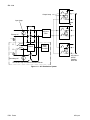

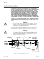
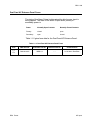


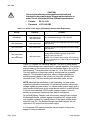
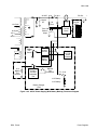


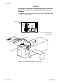
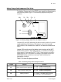

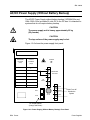


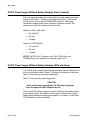
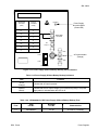
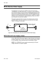
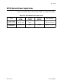

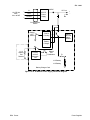
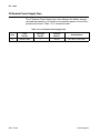


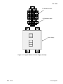


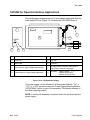

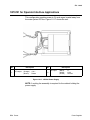
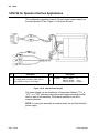
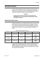


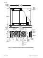
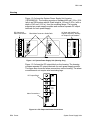
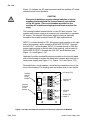

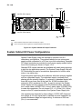


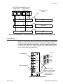
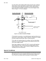


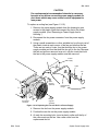


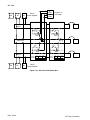
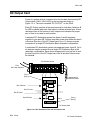
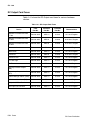

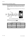

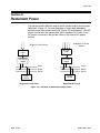


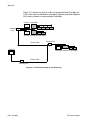

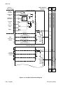


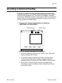
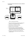
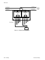


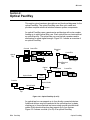


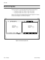
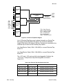

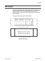
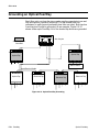


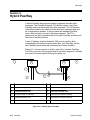
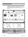

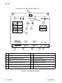
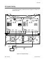


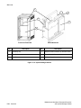
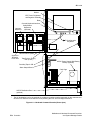


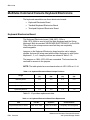

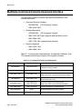
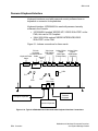


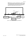
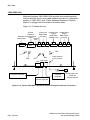
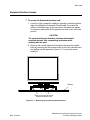

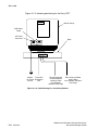
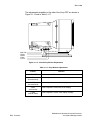
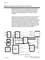

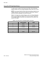

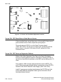


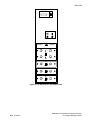

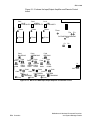
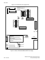
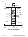
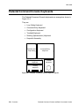
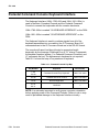
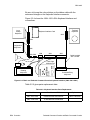


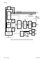


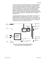


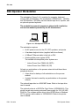
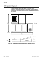
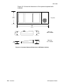
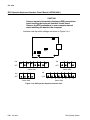
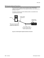

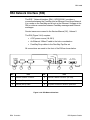


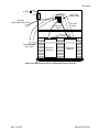


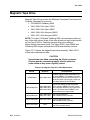

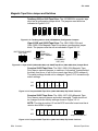


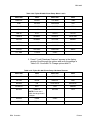


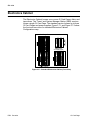
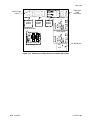

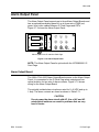

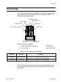


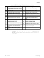


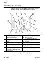


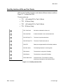

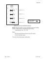
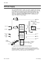
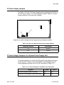


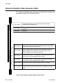


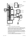

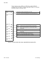


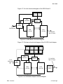


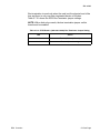
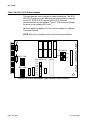


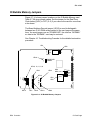
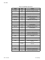
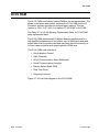


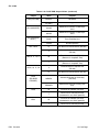


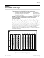

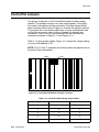
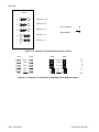
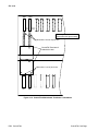


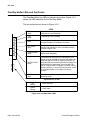
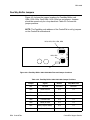
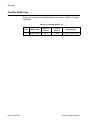


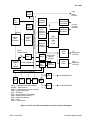


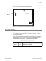
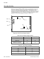
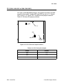

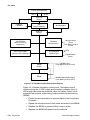

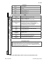


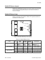

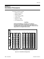

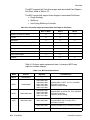


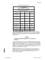


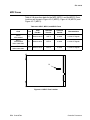


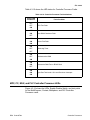


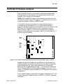


![[1 ] Oracle® Enterprise Manager](http://vs1.manualzilla.com/store/data/005669073_1-0396df232df5e560fdd03210f5126330-150x150.png)