1
i
Lock-’”
c.,, —
. .
---—“’. .
.<
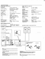
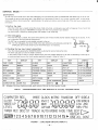
Service
Manual
Mini
Component
Contents
,
,-.
”
IL-- .+
‘
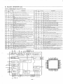
System
FILE NO.
DC
D30
(AU)
CODE
No.
PRODUCT
129 374
SPECIFICATION
... ... . ... ......
SYSTEM CONNECTION
. ... ..... .
OPERATING
THE RESET SWITCH
PARTS LIST(PACK & ACCESSORIES)
PARTS LIST(REMOCON)
. .. ......
....
. ...
. ...
..
... .
CD/ TUNER UNIT
TUNER ADJUSTMENT
. .. ..... ... ...
LASER BEAM SAFETY PRECAUTION
.
CD MECHANISM
REMOVAL
.... ... ..
CD SERVICE MODE
. .. ... ..... .. ..
CD ADJUSTMENT
.. .. .. .. ..... .. ..
PARTS LIST . . . . . . . . . . . . . . . . . . . . . .
EXPLODED VIEW(CABINET
& CHASSIS)
EXPLODED VIEW(CD MECHANISM)
. ..
PARTS LIST(CD MECHANISM)
.... . ..
IC BLOCK DIAGRAM
. .. .. ... .... . ..
LCD BLOCK DIAGRAM
. .. ..... .. . ..
CD VOLTAGE TABLE
.. .. .... ... .. .
SCHEMATIC
DIAGRAM(FRONT)
... .. .
CONNECTION
DIAGRAM
... .. .. .. . ..
SCHEMATIC
DIAGRAM
. .. .... . ..
WIRING DIAGRAM(CD)
. .. .... ... . ..
.
.
.
.
.
.
.
.
.
.
.
.
.
.
.
.
.
.
.
.
.
.
.
.
.
..il
. .
. .
. .
. .
.
.
.
.
.
.
.
.
.
.
.
.
.
.
.
.
.
.
.
.
.
.
.
.
.
.
.
.
.
.
.
.
.
.
.
.
.
.
.
.
.
.
.
.
.
.
.
.
.
.
.
.
.
.
.
.
.
.
.
.
.
.
.
.
.
.
.
.
.
.
.
.
.
.
.
.
.
.
.
.
.
.
.
.
.
.
.
.
.
.
.
.
.
.
.
.
.
.
.
.
.
.
.
.
.
.
.
.
.
1
2
2
2
3
4
5
9
12
14
17
18
19
20
26
27
30
32
34
36
1
05
SCHEMATIC’
DIAGRAM(TUNER)
. . . . . . . . . . . . . ..38
40
WIRING
DIAGRAM(TUNER
& FRONT)
..... ...
42
BLOCK DIAGRAM(CD)
. .. .. . . ... ... .... ....
DECK / AMPLIFIER
UNIT
DECK ADJUSTMENT
.. .. ... . . ... ... .... ...
EXPLODED
VIEW(CABINET
& CHASSIS)
PARTS LIST . . . . . . . . . . . . . . . . . . . . . . . . . . . . .
PARTS LIST(TAPE
MECHANISM)
.. .... ......
EXPLODED
VIEW(TAPE
MECHANISM)
... .....
IC BLOCK DIAGRAM
. ... .. . . . ... ... ... ....
LCD BLOCK DIAGRAM
. .. . . . . .... .. ... ....
SCHEMATIC
DIAGRAM(TAPE
DECK AMP)
....
WIRING
DIAGRAM(TAPE
DECK AMP) . . . . . . . .
SCHEMATIC
DIAGRAM(PRE-AMP)
.. ... ......
WIRING
DIAGRAM(PRE-AMP
& FRONT)
. .....
SCHEMATIC
DIAGRAM(SYSCON
& MAIN AMP)
WIRING
DIAGRAM(MAIN
AMP) . . . . . . . . . . . . . .
CONNECTION
DIAGRAM
. .. . . . ... .. ........
BLOCK DIAGRAM(TAPE
DECK & FRONT)
....
BLOCK DIAGRAM(PRE
& MAIN AMP) . . . . . . . .
SCHEMATIC
DIAGRAM(FRONT)
... . ...... ...
SCHEMATIC
DIAGRAM(TAPE
MECHANISM)
...
TAPE
43
45
46
52
53
54
59
60
62
64
66
68
70
72
74
75
76
77
‘Dolby” and the double-D symbol ~ are trademark of Dolby
Laboratories
Licensing Corporation. Dolby Noise Reduction
system is manufactured
under license from Dolby Laboratories
Licensing Corporation.
This Service manual
is consist of “RB-D30-,
‘SX-D30”,
“DC-D30CT”,
“DC-D30DA-.
REFERENCE
No.
SM580042
SPECIFICATION
CASSETTE DECK/AMPLIFIER
Cassette decks
Track system . . . . .
.
Frequency response . . . . . .
4-track,
Approx.
Amplifier
“
Output power . . . . . . . . . . .
Graphic equalizer . . . . . . . .
Spectrum analyzer . . . . . . .
Inputs . . . . . . . . . . . . . . . . . . .
CD player
Channels
................
Sampling frequency
... ..
Pick-up . . . . . . . . . . . . . . . . . .
Frequency response . . . . . .
Wow and flutter
........
General
Dimensions(approx.)
....
We@ht(approx.)
.........
120 sec. (C-60)
SUPER WOOFER OUT :600
SPEAKERS : B ohms
PHONES : 8 ohms
2-channel stereo
44.1 kHz
Optical 3-beam semiconductor
20-20,000
Hz
Below measurable limits
270 (W)
2.9 kg
SPEAKER SYSTEMS
Type . . . . . . . . . . . . . . . . . . . .
Unit used
...............
mV
x 178 (H) x 278(D)
laser
mm
2 way bass reflex
Woofer: 13 cm cone type
Tweeter: 5cm cone type
Power
General
Power requirements
.....
Power consumption . . . . . .
Dimensions(approx.)
.....
Weight(approx.)
.........
handling
capacity
.......
Nominal impedance
.....
.....
Dimensions(approx.)
Weight(approx.)
.........
AC: 230-240 V, 50 I-Iz
75 w
270(W) x 178(H) x 317(D)mm
5.2 kg
REMOTE CONTROLLER (R8-D30)
Power requirements
......
SYSTEM
stereo
27 W x 2 (at 8 ohms, 10% distortion)
7 band electronic
7 band
PHONO : 2.5 mV/50k ohms
VIDEO : 250 mV/50k ohms
.................
Dimensions(approx.)
2-channel
Chrome tapes: 40- 13,500 Hz
Normal tapes :4012,500 Hz
60dB(with DOLBY NR : ON)
().14~0 (WRMS)
Signal to noise ratio
.
wow and flutter
.
...
Fast forward /
rewind time
.... ..
outputs
TUNER/TIMER/CD
PLAYER UNIT
Tunes
FM : 87.5 -1 OB MHZ
Reception frequency
.....
AM : 531- 1701kHz
UNIT
......
DC : 3V
‘R031AAAIUM-458(W) x 18(D)
Battery x 2
x 186(H)mm
Max. 40W (peak)
8 ohms
178(W) x 356(H) x 220(D) mm
3.6 kg (Per sperker)
.. .
.’ .,. .”
Specification subject to change without notice.
. .. .
.. .
.
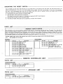
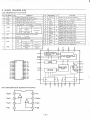
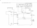
CONNECTION
R ch speaker
L ch speaker
b
l-==-
I
‘Urntab}e
[
,-,..
Ecrth cord
~
White
._ I
I*”
&cl
ships
I
R!si3
I
To connect,
push the middle of
the plug cnd Insert k until
To disconncd
it clicks.
(,~.j
1
CD
w
w
]
W&
w
playerflunerfilmer
Cacsette
To an AC outlet
dwkfAmplifier
Not=
Do not connecf
the mains
lead 10 an AC outlal
until all connections
have been made.
The system Is not disconnected
unplugged
from the mains unless the mains lead is
Headphones
from the AC outleL
Corm&
Speakers
When connecting
matched properly.
PHONES
the speakers,
Otherwise,
make sure that (+) and (-) polarities are
automatically
disconnected
kohms,
or for pr~ate
when
not supplied)
to the
listening. The speakers
headphones
are
are connected.
Note
wire with the stripe to the red terminal
other wire to the black terminal
(8 ohms 1010
socket for monitoring
the sound may appear to be lacking in the
bass range and in stability.
Connect the speaker
stereo headphones
(-).
(+) and the
Sefore
connecting
manual
provided
-1-
external
equipment,
your equipment.
please
refer to the Instruction
iii
.
OPERATING
This
THE
RESET
SWITCH
CD I TUNER and TAPE DECK/ PRE-AMPLIFIER unit is provided
tialize
the microprocessor
key input
is not
in the each units which
acknowledged
switch and initialize
even
the microprocessor
1).
Disconnect the AC power
2).
Keep the RESET switch depressed
(The backed
Reconnect the AC power
4).
Press the CD/TUNER,
PARTS
the
CD/ TUNER,
following
a reset switch on the rear panel. The reset switch serves to ini-
TAPE DECK and etc. operation
buttons
are
pressed,
press the
RESET
the step below.
cord from the power
up electrolytic
3).
when
with
controls the CD, TUNER, TAPE DECK and etc block. If the unit is to be serviced or
outlet.
for 60 seconds.
capacitor
is discharged
cord to the power
by keeping
the RESET switch depress.)
outlet.
TAPE DECK and etc. operations,
and check their
operation.
LIST
PRODUCT SAFETY NOTICE
.-.’.-.:.”:
Each precaution in this manual should be followed during servicing. Components identified with the IEC symbol ~ in the parts list
and the schematic diagram designate components in which safety can be of special significance. When replacing a component identified ~, use only the replacement
parts designated, or parts with the same ratings of resistance, wattage or voltage that are designated in the parts list in this manual. Leakage-current
or resistance measurements
must be made to determine that exposed parts
are acceptably insulated from the supply circuit before returning the product to the customer.
Regular type resistors and capacitors are not list. To know those values, refer to the schematic diagram.
CAUTION:
N.S.P
: Not available
as service parts.
PACKING
ACCESSORIES
Ref. No.
Part No.
.
....
614 244 4092
614 239 0726
614 239 0719
614-239
“1778
614 239 1765
614 239 1778
614 176 6027
614 176 6027
614 236 0132
614 176 3231
614
614
176
231
Ref. No.
Description
INNER CARTON
PAO, TOP
PAD, BOTTOM
SHEET, CT UNIT
SHEET,CO TRAY
SHEET,OA UNIT
INNER POLYE COVER,CT UNIT
INNER POLYE COVER,OA UNIT
POLY COVER,REMOCON
INNER POLYE COVER, INST &
ACCESSORY
INNER POLYE COVER,SCREW
LABEL,SAFETY,LASER
1039
6832
.
[
LIST
PARTS
REMOCON(RB-D30)
Ref. No.
Part No.
Description
614 243 8152
614 235 9433
ASSY,REMOCON
LID,BATTERY
LIST
PARTS
SPEAKER(SX-D30)
Ref. No.
Part No.
. .. . .
Description
614 246 2621
I
I
ASSY,CABINET,SPEAKER
I
I
-2-
Description
- Part No.
614”244
614 232
614,234
411 0B3
614 239
4115
6671
5511
9307
5288
INSTRUCTION MANUAL
ANTENNA,FM
LOOP ANTENNA,AM
SCR WOODRND 3.lX13,Ai
ANT
ASSY,CONNECTOR-P,19P,
CD/TUNER - DECK/AMPUNIT
i
-B.mm
mmmm.-mmm.-mmmmmm
ADJUSTMENT
-m
mm.mm.mm
TUNER /CD
PLAYER
FM to the frequency
of ceramic filter.
ss.-cc-.-#.-c-=zczesmszzssszz-s
UNIT
(TUNER)
● Use a plastic screwdriver
● Adjust the intermediate
for adjustment.
frequency
of
AM
and
SG RF Level : 75 ohm Open voltage dBIV
1. FM BAND
STEP
Antenna
ITEMS
:75 ohm Direct,
INPUT CONDITION
(mono) . f40k Hz (main) . f6.75k
MEASURE
INPUT
MEASURE
OUTPUT
TP211(H)
TP212(E)
FM Sweep
Generator
TP223(H)
TP224(E)
T2201
V CURVE Wave
Digital Voltmeter
TP202(H)
TP201(E)
L2104
------
Confirm
TP233(L)
TP234(R)
TP235(E)
L2102
L2103
IF
10.7 MHZ
FM Sweep
Generator
2
COVER
87.9 MHz
107.9 MHZ
..----
TRACKING
:1 kHz, Dev. : t 75kHz
TUNING
FREQUENCY
1
3
Modulation
OUTPUT CONDITION
--. -—
90.1 MHZ
FM SG
TP211(H)
VTVM
106.1 MHZ
(about 8dB)
TP212(E)
Oscilloscope
TP211 (H)
_ TP212(E)
PARTS
CT201
4
IF(OV)
98.1 MHz
FM SG
(66dB)
5
Vco
98:1 MHz
FM SG
(66d8)
TP211(H)
TP212(E)
Frequency
Counter
TP206(H)
TP207(E)
SVR23
6
SEPARATION
98.1 MHz
FM SG
TP211(H)
VTVM
..----
TP212(E)
Oscilloscope
TP233(L)
TP234(R)
TP235(E)
---—.
------
STEREO
SENSITIVITY
7
.-
2.
AM
STEP
(about
66d8)
FM SG
98.lMHz
-. .,.
BAND
ITEMS
1
COVER
2“
TRACKING
‘“ INPUT CONDI’
MEASURE
-----:
;
..
1400k Hz
SD
##19 KHzi50Hz
point.
INPUT
1000kHz
30%
LOOP
VTVM
ANT
Oscilloscope
AM SG
(about 80dB)
LOOP
ANT
.--—-
off
Confirm stereo indicator light
up within near the specification
Tuner Mode
: AUTO STEREO
.
PARTS
dBIV
STANDARDS
OUTPUT
--—-------
TP202(H)
TP201(E)
Voltmeter
(about 80dB)
...
...
to
RF Level : 75 ohm Open voltage
SG
CONDITION
MEASURE
Digital
;
AM”SG.’
: lkHz
Confirm
near the specification
*X : AdJust ‘in the m-odulation
,,. ,
OUTPUT
ON
,
530kHz1700kHz
; :6@kHz
3
Oio.osv
Antenna : IRE Loop, Modulation
TUNING”
FREQUENCY
~ 8.5V (about 6.6v)
Output : Maximum
Adjust to near
the I.H. F sensitivity
T2202
------
: suitable
1.O-1.3V
Digital Voltmeter
TP211(H)
# ‘ TP204 is no earth
STANDARDS
TP203(H)
~TP204(E)
Set to EXT(STEREO) TP212(E)
Hz(pilot)
TP233(L)
TP234(Rj
TP235(E)
I
“’ -----------
I
--—-
------
Confirm
1.1-1
Confirm
~ 8.5V (about 7.7v)
.5V
output : Maximum
Confirm to near
the effective sensitivity.
Confirm auto tuning stops at
within near the specification
SD : Station Detection
3.
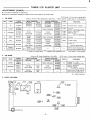
PARTS LOCATION
FM EXT.
ANT.(75CJ
TP212
TP202
‘F?
TP201
SVR 23
‘pm
FI
❑
Q
1
T2201
%%-\\
TP223
(R2227)
Tp203
(J427)
R
T2202
TP204
‘
(.)438) -?
,,,
,1,
818
‘k
,~!’
TP233 .
(J420)
q
AM LOOP ANT,
-3-
I
LASER BEAM SAFETY
....
PRECAUTIONS
(CD)
Do not look straight at the laser beam from the pickup and do
not point the beam at your fingers or any other part of your
body.
Note: The laser beam must never be allowed to enter the eyes
since this may damage the eyes.
Power must never be supplied to a pickup with a damaged laser
output part (objective
lens, etc.).
INVISIBLE
LASER
RADIATION
EXPOSURE
OUTPUT
TO
POWER
:
Structural
lever
mW
Interlock
has a disc chuck lever and top lid. This disc chuck
and top lid prevent
IS
BEAM
0.6
Safety
This model
DANGEROUS
MAX
to expose the laser beam for
CLASS
WAVELENGTH
\
:
LASER
1
users.
PRODUCT
790 nm
/
L
CAUTION - USE OF CONTROLS OR ADJUSTMENTS
OR PERFORMANCE
OF PROCEDURES OTHER THAN THOSE
SPECIFIED IN THE OPERATING INSTRUCTIONS MAY RESULT IN HAZARDOUS RADIATION EXPOSURE.
THE COMPACT DISC PIAYER
QUALIFIED PERSONNEL.
SHOULD
NOT BE ADJUSTED
for handling the pickup and semiconductors
(particularly the lCs)
lCS) may be
a. The pickup and semiconductors (particularly th
\ ~e of high
damaged if they come into contact with a sou
1. Precautions
voltage
.,
static
electricity.
Do not bring them,
contact with
or into the
vicinity of anything
charged with
high voltage
with
or
Do not
store
or repair
a high temperature,
high
dust
powerful
it
high humidity,
not
it to impact.
external
Actions
in any
pickup
location
fields
contains
brought
pressure to the
like these
is a single
adjusted.
bands
are
grounded
near
a
any
pickup
can cause the
or subject
printed
circuit
Note:
Under
no circumstances
grounded
without
Since static
part which
its adjustment
has been
points
very
and
set
any of the
be grounded.
instruments,
safeguard
the
metal
tools and
against
a grounded
part
leakage
of
a
lM:
grounding
bands be
1Ml resistance) since
a
in the clothes of the
repair
personnel
taken
to
not
to
allow
semiconductors
e. The
place
pickup,
to
3. Cleaning
the
clothes
(particularly
which
bag.
touch
will not be
care must be
the
pickup
and
the ICS).
is a single
integrated
part,
is kept
in a
Use this bag to convey the pickup from
[n order
another.
static which
to avoid
may occur when
sure that
damage
one
resulting
the pickup is removed
from
from
the
it is not placed on top of the bag.
the lens surface
a. Blow off dust on the
the
power
plug
may mark
Notes:
Cover the work
will be done with
c.Ground
parts, disconnect
being repaired.
b. All measuring
(with
bands, every
alcohol.
static during handling
replacing
from the unit
must be the
a resistor (with
lens using the kind of air brush which is
b. Remove stubborn dirt with
a. When
resistor
used for cameras.
screws must not be touched.
2. How to prevent
a
discharged by wearing grounding
bag, make
to occur.
integrated
Therefore,
through
resistance).
conductive
board to crack or malfunctioning
precisely
be
and precision
high magnetic
(Since the
must
PROPERLY
personnel must wear grounding bands around their
wrists to discharge static picked up by their bodies. These
been
objects.)
C.DO not apply Srong
d. The pickup
into
EXCEPT
doing so involves the risk of electric shocks.
of optical
it, therefore,
concentration.
magnet,
magnetized
has
BY ANYONE
d. Repair
static.
b. The pickup consists of a large number
parts.
therefore,
which
OR REP-AIRED
repair
bench where
electrically
the
must
the
work
repair
conductive
soldering
of electricity
equipment
iron
in
order
to
from the heater.
of cleaning
in isopropyl
fluid since it
use too much isopropyl alcohol:
the excess ma)
seep inside the pickup.
●The
lens
is held
Therefore,
more
in
place
when
force
by
a very
cleaning
by the
feeble
the
cotton
lens,
swab
supper
avo
applying
any
necessary
since this may bend the support spring out
shape.
-4-
type
the plastic lens.
● Do not
spring.
sheet.
a cotton swab dipped
Do not use any other
than
‘.
CD MECHANISM
REMOVAL
1) Preparations
1) Do not apply unnecessary force to the pickup when handling it.
Care should
be taken
not even to touch the lens or drive
circuit sections.
2) Do
not
apply
unnecessary
force
(do
not
Unnecessary force may break the teeth
3) In the descriptions which follow,
Pull or
onthetray
push it forcefully)
to
remove
the
disc tray
from
its inside
position.
gear (CM6).
the numbers in the parentheses
after
the parts are reference
numbers
in the exploded
views.
Refer to these views.
DISC TRAY REPLACEMENT
2) Removing and installing the disc tray
1) Remove the stop screw (Yl) of the disc tray (31). (~)
2) Pull the disc tray
(31) all the
way
forward
by turning
the
tray drive gear (CM12)
clockwise.
Note:
hold of the disc tray (31) and pull it
Do not take
SECOND TOOTH
OF TRAY MOVE GEAR
(@)
out by force.
3) Push the catch on the disc tray
bythearrow,
anddraw
4) To install the disc tray,
tionof
thearrowas
5) Align thedisc
Adjusting
6) Push the
(31)
outthe
in the direction
disc tray (31).
turn the
gear
far as it will go.
(CM12)
disc tray
(31)
7) Secure itwiththe
direc-
chassis (CM39).
move gear (CM3).
toward
the
with the tray drive gear (CM12)
in the
(@)
tray (31) with the mechanism
second tooth of thetray
shown
(@)
rear,
and
(@)
interlock
it
as shown in Fig.@ .
screw (Yl)which
was removed
in step 1).
-,
3)
Disassembling
the mechanism
(1) Removing the pickup block
1) Remove the disc tray (31).
the
section
entitled
(Refer
to steps 1), 2) and 3) of
“Removing
and
installing
the
disc
(@),
and
TRAY MOVE
GEAR (CM3)
TRAy GEAR (CM6)
tray.-)
2) Turn the tray drive gear
(CM 12) counterclockwise
move the pickup in the direction
of arrow
(@) as far as it
r.
.
*R
will go.
(CM23)
3) Remove the spring wire (CM44)
with tweezers.
4) Remove the screw (CM1 1), and also remove
gear (CM12)
and washer
(CM13).
(@)
the
tray
@
‘
5) Now remove the pick rack gears (CM16 and CM19).
Note:
It will
not
gears
(CM16
be possible to
and
CM19)
been moved all the way
remove
the
unless the
%’
pick
rack
pickup
has
in the direction
of arrow
(@).
6) The pickup
block can now
be removed
by taking
out the
screw (CM51) and spring coil (CM49).
Note:
If the timing
gear (CM23)
“X” in the figure
G———————
drive
(@)
is in the state shown by
on the right, put it in the state
shown by “O”.
-5-
&_’_’u
.::
“
MECHANISM
(2)
REIWIVAL
Replacing
and
lubricating
1) Pull out the two pickup
2) The pickup (CM52)
up rails (CM43)
3) When
two
the
the
pickup
rails (CM43)
from the chassis (CM50).
cam now be removed
have
pickup
been
has
taken
been
pickup rails (CM43)
once the two
SHAFT
pick-
“
r
h
out.
replaced,
cleanly
474B) around the entire
.
,M$q
(CD)
be sure to wipe
and apply
circumference
grease
/’
+s
the
, ..
/,
.- “
.’/7’
N
,.
(FLOIL G-
SHAFT
a
of the rails and along
FIX BY THE CEMEDINE #575
their entire
4) pass the
(CM52),
length.
two
pickup
insert them
rails
into
(CM43)
through
the chassis (CM50),
new
the
CM9
pickup
and fix them
in
a.
Notes:
applying
When
the
grease,
do
allow
not
any
grease to adhere to any other parts.
b.
If a part
(indicated
by the
dots in the
the chassis (CM50) is damaged
...
moving
or
inserting
the
two
figure)
0
0@
of
in the process of repickup
rails (CM43)
the chassis (CM50),
area
with
a cloth
ane),
and
bond
1) The
the”
loading/sled
chassis (CM39)
(CM38)
2) Mount
(CM39)
in alcohol
it together
(Cemedine #575).
, ..
.
(3) Replacing
dipped
(normal
.
hex-
CM50
BREAK
agent
..’,
motor
motor
can
the
0
(G-4746)
the damaged
using a bonding
loading/sled
once
wipe
FLOIL
0=
%
‘..
from or into
0
00
place at an angle of 45” as shown in the figure.
(CM38)
screw
be
(CM24)
“
removed
securing
“--’
-
from
SHAFT
the
the
motor
the
chassis
is removed.
the
new
Ioadinglsled
using the screw
motor
(CM38)
onto
(CM24).
(4) Checking the loading/sled motor’s operation
1) As shown in the figure, connect an ammeter and a DC power supply
to the
loading/sled
motor
(CM38),
and set the tray
open and end switches to the “off” [open] positions.
2) Check that
...
ping
3)
from
the
pickup
the
inner
(CM52)
ward
its outer
circumference
plied
from
DC power
the
The disc tray
a DC
4V
is housed
voltage
moves smoothly
circumference
when
of the
without
compact
stop
disc to.
a DC 0.6V voltage
is ap.
supply.
inside and the gear (CM9) slips when
is applied
from
the
DC power
supply.
Check that the ammeter indicates 120mA or more at this
time.
——
ATTACHMENT
OF MOTOR
l’”
Q
o
c
~ ,—. m }
,,
2 ‘ “ k ‘4
I
ANGLE
RED MARK
‘#T
m-
U,u
L-------.-
MECHANISM
REMOVAL
(CD)
Check points for CD mechanism
4)
assembly
and
(3) Installing
lubrication
1) Move
(1) Lubricating and mounting the tray slide
the base up/down
arrow
1) Apply grease (FLOIL G-474B) to the area indicated
by the di-
the base up/down
0,
and
set the
slide and timing
slide (CM14)
gears
at the
gear
in the direction
of the
positions shown
in the
figure.
agonal in the figure.
2) Insert the timing
2) When inserting the tray slide (CM15),
set the
position
gear (CM23),
and mount
it using the screw
where
(CM21).
it
is
installed
vis-a-vis the
base/tray
timing
gear
(CM20)
as
3) Turn the timing
gear (CM23)
counterclockwise.
shown in the figure.
9
TIMING
GEAR
BASE
UP/ DOWN
p@gg:$4
v
>——..
,..
SCREW (CM21)
.. .
4) Hook the gear tension spring (CM22)
gear
(CM23).
@
GEAR TENSION ,PRING
x
o
%
(2)
y:,:-?
FLOIL(G-474B)
onto the timing
.
~<
Installing the tray gear
1) Move the tray slide (CM 15) in the direction
2) Engage the
inner
gear
gear
section of the
of the
tray
gear
tray
(cM6)
of the arrow
slide (CM15)
at
the
with
center
—
o.
line,
the
as
shown in the figure.
3) Align the tray move gear (CM3) with
hole in the outer
gear of the
tray
the position (0)
gear
(CM6)
of the
‘~
and engage
o
the tray move gear (CM3), as shown in the figure.
I
TRAY
GEAR
II
GEAR CM3
s
.-
--
GEAR TENSION
x
--
--
SPRING (CM22)
, .,
MECHANISM
(4) Lubricating
REMOVAL
the
base
(CD)
(5)
lever
Apply grease (FLOIL G-474B)to
the >~area
Lubricating the pickup sled gear and clutch gear
1) ApplY grease (FLOIL G-474B) around the entire circumference
in the figure.
of the lower gear of the pickup sled gear (CM12),
in the figure
( %
2) Apply grease
as shown
area).
(G-333)
around
the entire
circumference
of the
outer ctutch gear (CM9).
3) Apply
grease
clutch
gear
(FLOIL
(CM9)
clutch gear
G-474B)
where
to
the
it makes
*
Part
contact
of the
with
the
outer
inner
(cM8).
PKKUP
SLED GEAR
F~+-cM12
.....
OUTER GEAR “-”h
I
I
.
(6)
Arranging
.
]’
.
—.
--
.\..
..—
..
and securing the leads
1) As shown in the figure,
set the
leads from the pickup (CM52)
ing/sled motor
securing the
(CM38)
leads with
pickup
and spindle motor
and sensor switch
the
(CM52)
lug (CM41),
(micro
at a position
(CM48)
on the
through
switch) (CM26)
check that
the
pickup
innermost
pin (a) of the
circumference
chassis (CM39).
by passing them
(CM52)
moves
of the compact
through
smoothly
point
Arrange
disc, and pass the
the leads from the load-
(b) in the chassis (CM39).
without
the
leads interfering
movement.
2) if no problems arise in the @ check, secure the points shown in the figure
using a bonding agent (Cemedine #575).
TO CN101
~BE
NOT SLACK
CD
PCB
m.
CU\HION
NOTE THE LUG PORTION
-8-
After
with
its
SERVICE
...
MODE
Specifications
To enter any service mode other than timer
This accesses the service mode entry state.
mode entry state is discontinued
after
debugging,
first simultaneously
press the OPEN/CLOSE and BAND keys on the CT unit.
Now press one of the buttons on the CT unit to enter
1 second elapses, the system will enter
a service mode.
As the service
a service mode only if the next key is pressed within
one second.
1. Confirm
the clock
. When the CLOCK key is pressed during the service mode entry state, a rectangular
of the oscillating frequency (1 .048576MHz)
. The clock output
2. Timer
is output
is stopped by pressing either
wave with
a frequency
of one- fourth that
from the micro processor’s port CLKOUT.
the POWER or SET CLEAR key.
debugging
When the FAST key is pressed, the current
time
advances one minute
and the seconds readout
changes to 55 seconds.
If the
key is held down the time advances continuously.
. The FAST key, a concealed
Note : For timer debugging,
key not actually
mounted
12k ohm
to the set.
the service mode entry state (entered
by simultaneously
pressin”g the
34
OPEN/CLOSE service mode entry key and the BAND key) is not necessary.
3. Checking the key input signal connections
. Enter this mode by pressing the ME MORY(TUNER) key during the service mode entry state.
. The entire
F
FAST KEY
+
L
—
LCD goes out once this mode is entered.
. In this mode, as keys on the CT unit (or remote
a one-to-one
control
unit) are pressed segments
basis come on (i.e. the lit portions gradually
KEY
DISPLAY
increase).
KEY
(Refer to Table
on the LCD corresponding
to each key on
1.)
DISPLAY
DISPLAY
KEY
TIME
CLOCK
REC
FUNCTION
DIGIT 3:
H
REPEAT
REPEAT
SLEEP
SLEEP
BAND
DIGIT 4:
H
STOP
ONE
TUNING
UP
SIDE A
PST UP
1 OF CALENDAR
CD MEMORY
PROG.
TUNING
DOWN
SIDE B
PST DOWN
2 OF CALENDAR
PLAY I PAUSE
>
WAKE
FMITUNE
3 OF CALENDAR
RANDOM
RANDOM
TIMER
TIMER
WIDE
4 OF CALENDAR
OPEN / CLOSE
ALL
SET I CLEAR
@
FW D
DISC
EDIT
EDIT
MEMORY
5 OF CALENDAR
BACK
TRACK
COMPUTER REC
COMP. REC
POWER
DIGIT
TIME
@
:
,,,
/ FADE
Releases the key checking
TABLE
mode
and
1 : CORRESPONDING
COMPUTERREC,
UP
returns
WAKE
the
KEYS AND
set
to
UP
MODE
2 : ~
the
normal
.:...
mode.
DISPLAYS IN THE KEY CHECKING
WIDE CLOCK INTRO RANDOM
MODE
OFF SIDEA
;;::u;–/–/f/Tllb
/-//–/;!-2 51/-/ /-/’/–//:/ ;;;;;B
/~//~/ LWAM-( /~//~/~/&/~/ MHz PM
LEVEL /~/d”/c
TIMERREC DiscST TRACK AUTO MONO FADETIMEEDIT
REPEAT
m123456789101112131415
~ONEALLCONT
P
FIGURE 1 : LCD( LIQUID
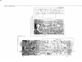
-9-
CRYSTAL DISPLAY )
,.
SERVICE
MODE
4. Checking LCD connections
- Enter this mode by pressing the OPEN/CLOSE key during the service mode
. The entire
LCD goes out once this mode
In this mode, one segment
of the
LCD
each time the OPEN/CLOSE key is pressed.
lights
. Press the SET/CLEAR key to exit this mode and return to the normal
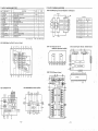
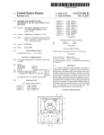
5. System connector
checking
state. (See note.)
entry
is entered.
mode.
mode
Enter this mode by pressing the BAND key during the service mode entry state.
Before entering
this mode, connect a jig at the beginning
of the system connector
cord as shown
in Figure 2
In this mode, check the signal connections
shown in Table 2 for the set’s CT unit and system connector
The results of the checking
appear
of connections
cord.
on the LCD as shown in Table 2.
Press the SET/CLEAR key to release the system connector
checking
mode and return to the normal
mode.
2.2k
. .
r
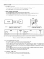
SYSTEM
CT UNIT
CON-
JIG
NECTOR CORD
~
.,
FIGURE 3-: CIRCUIT DIAGRAM OF THE
CONNECTOR CHECKING JIG
FIGURE 2 “:-CONNECTION ‘DURING THE SYSTEM
CONNECTOR--CHECKING MODE
--
.Sois
STATE
N.G. .“
,,-
GND
BUSY
TA-AF
DUB-IN
so
SCK
IR
KEY-O
“o”
--
DISPLAY
STATE
DISPLAY
BUSY is N.G.
4
SCK is N.G.
1
IR is N.G.
5
DUB-IN is N.G.
2
KEY-O is N.G.
6
AT-AF is N.G.
3
All OK
Note: : With the D series, the system connector
TABLE 2:
6. CD tracking
balance
adjusting
checking
mode cannot
be entered
when
the SCK(AD unit) connection
DISPLAYS DURING SYSTEM CONNECTOR
is defective.
CHECKING
mode
. Enter this mode by pressing the PLAY/PAUSE key during the service mode entry state.
. If the power
is off when this mode is entered,
. In this mode, the tracking
If the
PLAY key
Therefore,
balance adjustment
is pressed
the readout
in this state,
the power automatically
state (tracking
the
~racking
on the display at the time
servo
playing
comes on.
is off) is automatically
is turned
is begun
on
indicates
and
entered
after
playing
is begun
the initial
position
the tray is completely
at
the
present
closed.
position.
of the pickup (i.e. the position
of the limit switch).
. In this mode, the
tracking
balance adjustment
PLAY key in this state turns on the tracking
. Turning off the
7. CD operatiort
power
state can be entered
servo and causes playing to begin.
releases the CD tracking
display
by pressing the MEMORY
balance adjusting
mode.
mode
. Enter this mode by pressing the STOP key during the service mode entry state.
. If
the power
is off when this mode is entered,
the power
-1o-
automatically
comes on.
key during playing. Pressing the
SERVICE
MODE
. In this mode,
normally
when
CD function
displayed)
appear
. In this mode,
the calendar
track number
and calendar
while operations
are used, displays like those shown
in the LCD track number
numbers
shown
displays become
DISPLAY
I
in Table
4 come on when
fixed at their
is turned
nu
FOCUSsearch has been begun
Focus search has been begun
❑z
Waiting
current
II
for focusing
Is-l
CD operations
occurs in CD operations,
To release these fixed
6Z
TOC reading
is in progress
6-
TOC reading
has been completed
10
L-point access has been begun
II
L-point access (REV64 track jump)
12
L-point access (FWD64
13
L-point access (REV16 track jump)
Both CLV and tracking
are ON
qq
L-point access (FWD16
Is
L-point access (REV1 track jump)
16
L-point access has been completed
Focus search has been completed
20
Tray closing has begun
(success, failure)
Hn
Pausing has begun
Zz
direction)
is in progress
E3
Pause (REV16 track jump)
~~
Pick return (external
direction)
is in progress
z-
H~
❑s
HE
Pause (FWD16
Tray closing (pick return)
9U
Music acc”esshas begun
has been completed
an
Spindle braking
has bequn
Ell
Spindle braking
is in progress
g~
Pick return
is in progress
] Spindle braking
and pick return
have been
..
completed
~il
Fast forwarding
ql
Rewinding
~n
Plavina has beoun
51
Playing is in progress
~~
Playing is in progress (skip return
En
TOC reading
I
is in progress
is in progress
I TOC readin~
operation)
has been begun
I
is in proqress
TABLE
I
3 : DISPLAYS
DURING
the
Music access (high-speed
access has begun)
g~
Music access (high-speed
access is in progress)
93
Music access (high-speed
access has been completed)
9q
95
96
91
99
99
9-
Music access (high-speed
access has been completed)
Music access (high-speed
access has been completed)
Music access (REV64 track jump)
Music access (FWD64
Music access (FWD16
The focus was lost while the servo was on (during
playing,
the servo is on (during
6
The tray does not open completely.
7
The tray does not close completely.
etc.).
playing,
etc.).
TABLE 4 : DISPLAY OF CD ERRORS
-11-
track jump)
Music access (final stage)
disc startup.
The subcode is not input while
track jump)
Music access (REV16 track jump)
TOC cannot be read.
5
track jump)
91”
THE CD OPERATION
4
(success/failure)
Pause (trace)
Focusing is not possible in focus search.
The subcode is not input during
I
Pause (REV1 track jump)
STATE OF CD ERROR
NUMBER
E
time
track jump)
(internal
~
at which
track jump)
Pick return
Tray closing is in progress
I 3-
than
OPERATION
I
are ON
n-
21
different
displays, press the STOP key
] Both CLV and tracking
Spindle kick is in progress
I
an error
readouts.
DISPLAY
I
fi~
represent
off.
OPERATION
U1
:2
3 (which
are stopped.
. This mode is released when the power
I
in Table
display.
MODE
.. .
CD ADJUSTMENT
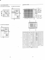
10K
Electrical Adjustment
So
far we
have
presented
explanations
regarding
compact
disc
notes prior to repair, handling the pick-up and
player handling,
disassembly of the
unit. Be sure
to
carefully
read
‘r;::D–A*’’O-’cO”
BAND PASS FILTER
these
instructions before making any adjustments.
Preparations
Measuring
for Adjustments
instruments,
(4) Oscillator (400 Hz, 300mV
tools and filter
(5) Frequency
(1) Test disc. : YEDS lB (Sony)
(2) Oscilloscope: SS5711 (IOMHZ
or Memoryscope
(3) Digital voltmeter
b. Use a 10:1
1.
.,
Initial
equipment
corresponds to that of the above
probe for observing
c. Test disc is subject change
(B) AC Voltage
1M ohm or more)
can be using the
produced
by other
Meter
manufactures
provided
that
the
performance
of that
listed models.
signals on the oscilloscope and stora9e
without
or more)
for adjustments
(7) Band Pass Filter
: DSS6521 (Storagescope)
Notes : a. The adjustments
equipment
(6) Screw drivers (non-metalic)
or dual phenomenon)
(Input impedance
RMS)
Counter (5MHz;
scoPe.
notice.
set
Set the SVR11 at its initial position of adjustment
controls as shown in figure
below.
SVRI 1
TP2 (FE)
SVR11
INITIAL SET
(MECHANICAL
SENTER)
TP3 (TE)
TP4 (GND)
TPI (RF)
..
2.
Tracking
Balance Adjustment
(SVRII)
5. Adjust
1. Connect the oscilloscope to TP3 (TE) and TP4 (GND.).
2. Turn on the power of the unit.
Insert
form
test disc.
press the
so that
ative to OV. (See figure
3. Play-back the test disc.
4. Continuously
SVR11
forward
search } }
or
“If
backward-
the
adjustment
motor (pick-up
search } } button to do it
the
TE (Tracking
of TP3 on the oscilloscope
motor),
become
inferior
Ov
Ov
TP3
SEARCH h
-SEARCH
-12-
run
away
playability.
TP 1
(RF)
(TE)
symmetrical
rel
right side)
is imperfect,
sending
Error) signal wave
is vertically
the
sled
..-
‘-*.
. ----
.,
.. ---- ..
.
.
,.. ,
, .?
. .
i
;. ...
CD ADJUSTMENT
2.
Other Adjustment
of Tracking
Balance
(SVR11)
~-=~-l’
“
1. Set the service mode(CD tracking balance adjusting mode).
Enter this
mode
by pressing the
the service mode
entry
state.
PLAY/PAUSE
key
during
TP1
(RF)
Pressing the PLAY / Pause key
in this state turns on the tracking
servo and causes playing
to begin. (See service mode)
2. Connect the oscilloscope to TP3 (TE) and TP4 (GND).
3. Adjust SVR1 1 so that
TP3 on the
the
oscilloscope
TE
(Traverse)
signal
is vertically
waveform
symmetrical
of
relative
Ov
TP3
to
(TE)
OV. Or may adjust SVR11 so that the DC voltage : (Peak
Hold Level) - (Bottom
OV. (See figure
Hold Level) of the
traverse
signal is
right side)
4. If it were not for obtain
waveform
at the right figure,
re-
peat item 2-1 -2-3.
3.
Focus Gain
1. Connect
through
Confirmation
the
storage
scope
to
TP2 (F.E
:
Focus
Error)
4. Set the
the Band pass filter. (See BPF Figure)
2. Turn on the power
5. Confirm
3. Play-back the test disc.
become weak the mechanical
MAIN
~
rms
Gain
PCB
oscillator
voltage
of
scope is 0.5V p-p,
to
400 Hz,
0.5V rms and
the resistor : 120k ohms.
the
F.E signal waveform
f 3db by through
BPF.
and can not playback the
OSCILLOSCOPE or STORAGESCOPE
.J e-.
BAND PASS FILTER
,,,.,I
DIM
-
74
TP2
(FE)
1.
=
I
1
Confirmation
1. Connect the storage scope to TP3 (T.E) through the Band
pass filter.
the
playability,
Iclol
=
Tracking
shock, inferior
120K
400Hz
4.
AF
..
AF OSCILLATOR
0.5;
so that
on the storage
is imperfect,
of
connect to pin 24 (IC101) through
of the unit.
‘If this CONFIRMATION
Disc.
output
4. Set the output of AF oscillator to 400 Hz, 0.5V rms and
(See BPF Figure).
2. Turn on the power
connect to pin 14( IC101) through
of the unit.
5. Confirm
3. playback the test disc.
‘If this CONFIRMATION
is imperfect,
storage
become weak the mechanical
AF OSCILLATOR
400Hz
0.5V rms
MAIN
shock, inferior
the voltage
playability,
BPF.
and can not playback the Disc.
OSCILLOSCOPE or STORAGESCOPE
BAND PASS FILTER
Iclol
PIN 14
resistor 47k ohms.
of T.E signal waveform
scope is 0.5V p-p, f 3db by through
PCB
47K
=
so that
TP3
(TE)
Iu ~ _E–
= .
on the
LIST
PARTS
PRODUCT SAFETY NOTICE
Each precaution in this manual should be followed during servicing. Components identified
with the IEC symbol A in the parts list
and the schematic diagram designate components in which safety can be of special significance. When replacing a component identior parts
with
the same ratings
of
resistance,
wattage
or voltage
that
are
desigfied ~, use only the replacement parts Clesignateci,
nated in the parts’ list in this manual. Leakage-current
or resistance measurements
must be made to determine that exposed parts
are acceptably insulated from the supply circuit before returning the product to the customer.
CAUTION:
N.S.P
Regular
type
resistors and capacitors are not list. To know
: Not avairable
those
values,
refer to the schematic
diagram.
as service parts.
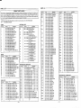
:ABINET
Ref. No.
-----.-,
.,..
1
2
3
4
5
6
7
8
9
10
11
Part
No.
614
614
614
614
614
614
614
614
614
614
614
238
239
244
239
239
239
239
239
239
239
239
:HASSIS
Ref.
Part
31
32
33
34
35
36
37
38
Ref. No.
Y1
T2
Y3
Y4
Y5
Y6
Y7
Ref.
ASSY,PANEL,FRONT
ASSY,CA81NET,TOP
PANEL,REAR
ASSY,CA81NET,BOTTOM
ESCUTCHEON,CDTRAY FRONT
BUTTON,TIMER ETC.
BUTTON,BAND ETC.
BUTTON,TUN,PRESET
BUTTON,CD
BUTTON,CD SKIP
BUTTON,CD OPEN/CLOSE
:
No.
FIXING
Description
9966
0924
4009
0931
1082
1136
1143
1150
1167
1174
1181
614
614
614
614
614
614
412
614
r-.~<:
No.
Description
238
1694
239
1228
239
1198
239
1204
239
1211
195 6978
003
1708
212 8343
’s-
TABLE,LOADING,CD
MOUNT-M,CD MECHA
BRACKET-E,TU
PCB
BRACKET-E,CD PCB
hfOUNT-E,TU PCB
RUBBER CUSHION,MECHA
FLOAT
FIX
SPECIAL
SCREW,MECHA
LABEL,LASER BEAM CAUTION
PARTS
Part
411
411
411
411
411
411
411
Description
No.
022
021
021
021
021
021
021
8408
1202
3107
1806
6405
6603
3503
SCR S-TPG PAN 2X8
SCR S-TPG BIN 2X8
SCR
SCR
SCR
SCR
SCR
S-TPG
S-TPG
S-TPG
S-TPG
S-TPG
BIN
BIN
2.6X8
2.6X1O
BIN 3X8
BIN 3X8
81N 3X1O
ELECTRIC PARTS
Ref. No.
51
Part No.
614
Description
243 1481
CORD,CD MECHA-MICON PCB
WNER P :.BOARDASSY
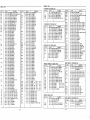
Ref. No.
71
C2304
C2458
CF201
CF202
CF204
CF205
Part
No.
Description
614,247
6S4 116
6561
5349
614
4Q3
117
080
1029
5000
4~3 106
614 231
6S.4 231
614 208
614 030
1603
0199
0199
9644
4787
ASSY,PCB,TUNER
MAIN
SHIELD PLATE,SYMBOL SIDE
SHIELD PLATE,PATTERN
SIDE
100V
POLYPRO 1000P J
NP-ELECT lU Q 50V
FILTER,1O.5MHZ,FM
FILTER,1O.5MHZ,FM
FILTER,450KHZ,AM
CERAMIC
FILTER,450KHZ
-14-
CN201
CN241
CT201
D2101
D2102
D2103
D2104
or
or
D2105
or
or
D2201
or
or
D2301
or
or
D2302
or
or
IC201
IC202
IC203
L2102
L2103
L2104
L2105
L2150
L2451
Q2101
or
Q2102
Q2103
or
Q2104
Q2105
Q2201
Q2202
or
Q2203
Q2301
or
Q2302
or
or
Q2351
or
or
Q2352
or
or
Q2451
or
Q2452
cm
No.
Description
Part No.
614
614
614
407
407
407
239
225
007
105
105
io5
407 007
407 012
407 012
407 007
401 012
407 012
407 007
407 012
407 012
407 007
407 012
407 012
407 007
407 012
407 012
409
195
409 016
409,066
614 229
614 229
614 239
614 028
614 241
614 028
405
114
405
114
405 012
405
114
405
114
405 012
405 012
405 018
405 012
405 020
405 001
405 012
405 020
405 067
405 078
405 000
405 067
405 078
405 000
405 067
405 078
405 000
405
114
405
114
405
114
405
114
1686
3502
6356
0100
0100
0100
9904
4406
5809
9904
4406
5809
9904
4406
5809
9904
4406
5809
9904
4406
5809
3108
9500
7600
0866
0873
7282
4058
1162
4256
8407
8506
5904
8407
8506
5904
5904
7902
2002
7204
7001
2002
7204
0800
2404
0904
0600
2404
0904
0800
2404
0904
1804
1903
1804
1903
TERMINAL,4P,ANT
PLUG,14P,T0 FRONT
TRIMMER,llPF,WH
VARAcTOR 01 SVC211-B-AL
VARACTOR
01 SVC211-B-AL
VARACTOR
DI SVC211-B-AL
DIODE
GMAO1
DIODE
1SS133
DIOOE
1SS176
DIODE
GMAO1
DIODE 1SS133
DIODE 1SS176
DIODE GMAO1
DIODE 1SS133
DIODE 1SS176
DIODE GMAO1
DIODE 1SS133
DIODE 1SS176
DIODE GMAO1
DIODE 1SS133
DIODE 1SS176
IC LA1265-AUD
IC LA3361
IC LM7001
TRANS,RF,FM
TRANS,RF,FM
TRANS,OSC,FM
FILTER,CHOKE,2.2UH,FM
TUNER,RF,AM
FILTER,CHOKE, 1OOUH,VDD
TR 2SK193-LL
TR 2SK193-ML
TR
TR
TR
TR
TR
TR
TR
TR
TR
TR
TR
TR
TR
TR
TR
TR
TR
TR
TR
TR
TR
TR
TR
TR
2SC1923-Y
2SK193-LL
2SK193-ML
2SC1923-Y
2SC1923-Y
2SC380TM-O
2SC1815-GR
2SC945A-K
2SA1015-GR
2SC1815-GR
2SC945A-K
RN2207
BN1A4P
DTA114YS
RN2207
BN1A4P
DTA114YS
RN2207
BN1A4P
DTA114YS
2SC1815(L)-GR
2SC1815(L)-Y
2SC1815(L)-GR
2SC1815(L)-Y
PARTS
LIST
Part No.
Ref. No.
Description
Ref. No.
Q2461
or
Q2701
or
Q2702
or
Q2801
405
405
405
405
405
405
405
012
020
012
020
016
016
012
2002
7204
2002
7204
2206
2305
2002
TR
TR
TR
TR
TR
TR
TR
or
Q2802
or
R2465
SVR23
405
405
405
020
016
016
7204
2206
2305
401
614
614
614
614
614
614
018
223
204
239
030
240
234
1209
1906
1901
7299
4114
1118
0486
TR 2SC945A-K
TR 2SC2878-A
TR 2SC2878-B
CARBON 33 JB l/4W
POTENTIOMETER,
1OK(B),VCO
SEMI-FIXED
V.R,1OK(B),VCO
TRANS,IF,FM
I.F.T,1O.7MHZ,FM
RESONATOR,7.2MHZ
RESONATOR,7.2MHZ
&
or
T2201
T2202
X2451
or
2SC1815-GR
2SC945A-K
2SC1815-GR
2SC945A-K
2SC2878-A
2SC2878-B
2SC1815-GR
or
;304
w
;305
I cm
;500
er
;;501
car
or
S1301
X1301
D MAIN
:D MICON
P.C.BOARD ASSY
Part No.
Ref. No.
72
C1301
614. 239
403
196
2065
9602
C1302
C1522
C1523
C1608
C1609
CN131
CN132
CN141
4Q3
403
403
403
403i
614
614
135
056
056
043
042
225
225
3302
7908
790B
3104
6205
6459
6381
614
614
614
407
40F
407
407’
40T
407
407
241
6143
243
3218
2395455
005
4505
013
7109
050
1801
053
5202
005
4505
013
7109
005
4505
%161
D1301
or
D1302
or
01303
or
D1304
or
407 013 7109
D1601
A
or
A
01602
or
D1603
or
D1604
or
D1605
or
IC103
IC107
IC108
IC109
L1301
L1501
L1502
Q1301
or
;i302
or
;:303
A
407004
407
012
40TO04
9105
3300
9105
A
A
A
A
A
40~
407’
407
407
407’
012
004
012
004
012
3300
9105
3300
9105
3300
40~
013
7109
40Z 005 4505
~
41C#
409
40%
40S
61A!
614?
61*
4E%
40%
405
146
189
040
039
028
212
212
006
006
002
Ref. No.
Description
1104
4203
1105
9204
4133
3171
3171
1806
1905
1305
4@S 011 85oO
405 011 8609
405 014 5209
405+ 006 1806
ASSY,PCB,
CO MICON
DL-ELECT
0.047F
Z 5.5V,FOR
MICON BACKUP
ELECT
1000U
M 6.3V
POLYESTER
1000P
K 50V
POLYESTER
1000P
K 50V
ELECT 2200U
M
16V,
FOR +9V
ELECT
1000U
M
16V,
FOR -9V
PLUG,13P,CO-FRONT
PLUG,6P,CD-FRONT
SOCKET,22P,CD-MECHA
SOCKET,22P,CD-MECHA
SOCKET,19P,CT-DA
UNIT
.
DIODE
DS442X
DIODE
1S2473
ZENER OIODE GZA3.9Z
ZENER DIODE
MTZ3.9B
DIODE
DS442X
DIOOE
1S2473
DIODE
DS442X,
FOR IR
DIODE 1S2473, FOR IR
D1ODE DSF1OC
OIODE
1SR35-200A
DIOOE
DSF1OC
DIODE
1SR35-200A
DIOOE
DSF1OC
DIODE
1SR35-200A
DIODE
DSF1OC
DIODE
1SR35-200A
DIODE
1S2473
DIODE
0S442X
IC UPD75116GF-F56-3BE
IC M5278005
IC NJM79L05A
Ic NJM7BL05A
FILTER,CHOKE,1OUH
INOUCTOR,FERITE,CD
INC)UCTOR,FERITE,CD
TR 2SA933S-R
TR 2SA933S-S
TR 2SAI048-Y
TR 2SC1740S-R
TR 2SC1740S-S
TR 2SC2458-GR
TR 2SA933S-R
33
Chllol
CN102
CN103
CN104 .
or
IclolIC102
IC104
IC105
1C106
or
Qlol
Q102,
Q103
006
002
011
Description
1905
1305
8500
405 011 8609
405
405
405
405
405
405
405
405
405
405
614
614
014
006
006
002
011
011
014
011
5209
1806
1905
1305
8500
8609
5209
85oO
014
221
229
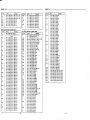
P.C.BOARD
5209
8327
3300
239
227
017
017
035
243
Description
2072
7935
3833
3B26
2061
3225
“-- 409 245-4802
~ 409 247 0000
409 248 8708
409.278 0109
409 241 5506
409
405
405
405
192
002
014
014
7109
030B
4509
4509
614’223 1906
614
614
614
614
614
614
‘RONTP.C.BOARD
Cti251
CN252
CN253
D2501
or
or
212502
or
or
1C251
L2501
LCD21
S2511
S2512
S2513
-%5-
TR 2SC2458-GR
SWITCH,TACT,RESET
RESONATOR,XTAL, 4.19MHZ
Part No.
614
614
614
614
614
- 614
2SA933S-S
2SA1048-Y
2SC1740S-R
2SC1740S-S
2SC2458-GR
2SA933S-R
2SA933S-S
2SA1048-Y
2SC1740S-R
2SC1740S-S
2SC2458-GR
2SC1740S-R
ASSY
SVRll
Ref. No.
TR
TR
TR
TR
TR
TR
TR
TR
TR
TR
TR
TR
011 B609 TR 2SC1740S-S
TP101
TP102
TP103
TP104
TP105
Xlol
74
OUT L-CP
OUT R-Ch
Part No.
405
405
405
227
227
227
227
227
236
6839
6839
6839
6839
6839
1B18
ASSY,PCB,CO MECHA
SOCKET,13P,FOR PICIUJP(FFC)
PLUG,4P,FOR MOTOR
PLUG,3P,FOR SWITCH
SOCKET,22P,T0 CD MICON(FFC)
SOCKET,22P,T0 CO MICON(FFC)
IC
IC
IC
IC
IC
LA921OM
LA6524
LC7866E
SM5870DS
XRA15218F
IC BA15218F
TR 2SA1037K-R
TR 2SC2412K-R
TR 2SC2412K-R
POTENTIOMETER”,
1OK(B),T.BAL
TERMINAL,TEST
POINT,RF
TERMINAL,TEST
POINT,FE
TERMINAL,TEST
POINT,TE
TERMINAL,TEST
POINT,GND
TERMINAL,TEST
POINT,PLL
RESONATOR,
16.93MHZ
ASSY
Description
Part No.
614
614
614
411
614
244
241
238
021
221
2265
9151
8037
3107
9133
614
614
407
407
407
407
407
407
410
221
226
013
013
005
013
013
005
146
9065
24BI
1701
7109
4505
1701
7109
4505
1203
614
614
614
614
614
028
238
220
220
220
4256
0284
5563
5563
5563
ASSY,PCB,FRONT
REFLECTOR,LCD
SHEET,LCO
SCR S-TPG BIN 2.6X8
SOCKET,13P,CD MICON
PCB
SOCKET,6P,CD
MICON PCB
SOCKET,14P,TUNER
PCB
DIODE
1S1588
DIODE
1S2473
DIODE
DS442X
DIODE
1S15B8
DIODE
1S2473
DIOOE
DS442X
IC UPD75306GF-225-3B9
FILTER,CHOKE,1OOUH
LCD(LIQUID
CRYSTAL
OISPLAY)
SWITCH,TACT,OPEN/CLOSE
SWITCH,TACT,PLAYI’PAUSE
SWITCH,TACT,STOP
I
m
I
I
.
<
I
I
.ncn.
*A*-a
NN,-.
nmDou.
rI-rx8sr
000000000
,,l!
,,
.
1,!!!
Dnm
Fr8
D
!!!!
mm
11,,,
.
..-I.
>
r..
$,,
n.>nm>
,,,
.
*
z
~
*
a
8 =.8
.-l
00
ma
nn
1-r
g
*
.
q
~
=
~
O
000 .
N-w
m...-
!,!
nmnn
.F
.*NN-
.
f,,,,,
.-..-*.-.
.
”A Ann
CJwooyy
Dna.
Dn.
xssszrr
-“m””
Oooaooooo
!!!!
,,,
-
-l.
Clrn’amyclmmmmm
.
nnnmnnnnnmn
0-00.00.00
NNWNNNNNNN
mJNNNNNf-.N
mmc+mmmmmmm
I.-.-l-”-.
-***---*-*
rrrl-rrl-l-rr
!!l!
1!!,,
.
.
.
.
.
.
--J-.4.-4-J
00000000000
.
+
rlrln AA1-ionn.
clct~o’a~yymmo
!,,,,!,!!
+
.-.,-t-.-”..
---l+.<-.
00000000000
N
I-
r-r-
rue-a.o.oo
IT C-lnnnnnnnnn
I-1-r
rvl-l-r
U..
?.JI.JNNNNN
NNru
.n.n.nmmmm
0.-”--a-A*--
-t4cmmJlw
-.
(
i
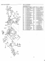
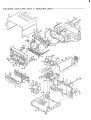
EXPLODED
VIEW (CD
MECHANISM)
PARTS
:D MEC
Ref. No.
CMO1
CM02
CM03
CM04
CM05
CM06
CM07
CM08
CM09
or
CM1O
CM1l
CM12
CM13
CM14
CM15
CM16
CM17
CM18
CM19
cp20
CM21” - ‘
CM22
CM23
CM24..
.
CM25
CM26
CM27
CM28
CM29
CM30
LIST (CD MECHANISM)
iNISM
(PM-DAD
Pan No.
411
411
614
411
411
614
411
614
614
614
412
411
614
412
614
614
614
412
614
614
614
412
614
614
411
614
614
614
411
614
614
119 8908
087 4704
224 2056
119 6908
087 4704
224 2049
152 4301
237 9172
23t
4194
243 6455
031 2104
152 4301
224 1998
045 4101
233 6311
224 2094
224 2018
031 2104
225 0684
224 2001
224 2032
031 2104
242 8665
237 8304
044.7205
016 9223
016 9223
202 5277
020 9603
224 1967
243 2594
:X22S/ SP)
Description
SCR S-TPG PAN 2X14, GEAR FIX
WASHER V 2X6 X0.4, GEAR FIX
GEAR TRAY MOVE
SCR S-TPG
PAN 2X14, GEAR FII
WASHER V 2X6 X0.4, GEAR FIX
GEAR, TRAY
SCR S-TPG
PAN PCS 1.7x6
ASSY, GEAR, CLUTCH
INNER
GEAR, CLUTCH OUTER
GEAR, CLUTCH OUTER
SPECIAL
SC REW, SLIOE
FIX
SCR S-TPG
PAN PCS 1.7x6
GEAR, PICK
SLED
SPECIAL
WASHER, PICK GEAR
SLIOE , BASE UP/OOWN
SLIOE, TRAY
GEAR, PICK
RACK UPPER
SPECIAL
SC REW, GEAR FIX
SPRING,
COMP, RACK BACK
GEAR, PICK
RACK LOWER
GEAR, BASE/TRAY
TIMING
SPECIAL
SCREW, GEAR FIX
SPRING,
TENS, GEAR TENSION
GEAR, TIMING
SCR PAN+SW 2X4 ,SLEO MOTOR
SWITCH, LIMIT
SWITCH, TRAY OPEN
SPRING
PLATE, CHUCKING
SCR S-TPG
BRZ+FLG
3x6
BRACKET-M,
CHUCKING
ASSY, PULLEY
Ref. No.
411
614
411
614
614
614
411
614
614
614
412
614
411
614
614
614
614
022
224
022
224
233
226
020
225
228
242
031
129
021
230
229
228
247
CM51
CM52
411
614
020
239
or
614
231
CM53
CM54
%55
or
CM56
CM57
I
–19-
7B07 ; SCR S-TPG PAN 2X6,6 RACXET
3176
BRACKET-M,
TRAY GUIOE(L)
7607
SCR S-TPG PAN ZX6,6RACKET
3183
BRACKET-M,
TRAY GUIDE(R)
6304
LEvER, BASE
5536
SPRING, COMP, BASE LEVER MOVE
9902
SCR S-TPG BRZ+FLG 3x8, LEvEF
4B20
ASSY, MOTOR , LOAOINGISLEO
5855
CHASSIS,
LOADING CHASSIS
6641
CHASSIS,
LOAOING CHASSIS
2i04
SPECIAL
SCREW, REINFORCEMENT
9136
LUG. WIRE DRESS
5705
SC R” S-TPG BIN 3x6, LuG FIX
0411
SHAFT, PICK RAIL
4529
SPRING, WI RE, PICK BACK
5064
SPRING, TENS,6ASE
PULL UP
1950
ASSY, CHASSIS, BASE CHASSIS,
WITH SPINOOLE
MOTOR + TURNTABLE, SERVICE
ONLY
98o3
SCR S-TPG BRZ+FLG 3x6
1303
PICXUP,
LASER, PLASTIC
,,SF-PIPS)
6047
PICKUP .LASER. ALMINUM
T
614 246
614 246
614 246
614246412 014
614 125
.
-18-
Description
Part No.
CM31
CM32
CM33
CM34
CM35
CM36
CM37
CM38
CM39
or
CM40
CM41
CM42
CM43
CM44
CM49
CM50
-.
2959
2966
2973
29B0
2800
6526
ASSY, CONNECTOR-S,4P,
SPINOLE/SLEO
MOTOR
ASSY, CONNECTOR-S,3P,
LIMIT/TRAY
OPEN SWITCH
SPECIAL
WASHER, GEAR FIX
CUSHION,
MOTOR LEAO FIX
ii
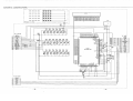
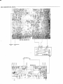
IC BLCMCK DIAGRAM
ICIO1 IJWI1OM
~ NO.
PIN NAME
FUNCTION
1/0
NC
Non Connection
2
VEE
-5V
E
IV Convert
4
I
No.
PIN NAME
41
Input (from
Photo
42
JP-
1
- Input
D;ocie E)
43
JP+
I
+ Input
diode
44
THLD
I
Hold
Tracking
5
FN
IV Converter
Input
45
TG L
1.
6
FCl
o
IV Converter
Output
46
TOFF
I
Error Ampl!fler
47
TES
o
Tracking
HFL
o
Detect
o
o
VREF2
I
9
VRE!=3
10
TEST
—
Tracking
Reference
Voltage
3
49
FZD
I
Test Input
50
FOCS
I
Input
51
CLV-
1
- Input
52
CLV +
I
+ Input
53
SLCO
o
54
—EFMO
i
EFMO (RF) Siqnal
55
Al
I
I EFMO (RF) Signal
56
VDD
57
PDO
I
+
58
PDO-
1
- Input
+ Input
1
- Input
of
of
Anti
Anti
Shock Detect
13
TPA -+
I
- Input
of
Tracking
14
TPA-
1
+ lnDut
of
Tracking
Pulse Amplifier
Shock Detect
Trackina
15
TPAO
o
TOFS
I
Input
17
THDS
I
Trackina
18
TO++
I
Add the Track Jump
for Tracking
Pulse Am Dlifier
Output
Offset
Servo Hold Switch
Track Jump
Pulse
Pulse Amplifier
19
JPO
20
SLEQ
I
21
TDO
o
Tracking
22
FDO
o
Focus Actuator
Actuator
FO-
1
Input
FSW
I
Focus Servo Switch
:or Focus Actuator
25
NC
26
FEAO
o
Focus Error Amplifier
?7
FE +
28
FD +
+ Incwt
I I I+
o
Input
1 I IInput
o
Amplifier
Output
of
Input
VCO Control
of
VCO Control
Vco
Amplifier
VCO Control
Amplifier
Amplifier
Output
output
Input
Clock
Coil Driver
63
LAS ER
I
Laser Control Signal
64
66/60
I
Select of DSP LC7866 / LC7860
Coil Driver
Output
Driver
I
of Low Pass Filter
Non Connection
65
NC
66
DF2
I
Input
for
Defect
Pulse width
Control
I
lnDut
for Defect
Pulse width
Control
O
I Defect
PH3
I
I
69
BH
1- I
70
PH
I
I
I
Track
Detect
Timing
Detect
Timing
I Focus Detect
Timing
I Ground
71
GND
72
RF SUM
o
RF SUM Amplifier
73
RFS-
0
IV Converter
74
LDO
o
Laser Diode ON
75
LDS
I
Input of Auto Laser Power Control
+ 5V
76
LDC
I
Input
Sled Servo Switch
77
VDD
Defect
78
FIN1
I
IV Convert
Input (From
Photo
Diode A+ C
79
FIN2
I
IV Convert
Input (From
Photo
Diode
80
VREFI
Spindle
Motor
Driver
Output
SLOO
34
SL-
1
- input
35
SL+
[
+ Input of Sled Motor
36
Vcc
37
SLSW
I
38
DEFO
o
-5V
LA6524 (Dual
CLV Error Amplifier
Slice Level Control
I
68
VEE
O
CLV Error Amplifier
of
I
Focus Actuator
33
I
of
LF1
of
32
2FREQ
I
o
DF1
SPDO
I
Vcoc
Vcoo
67
Motor
Focus Error Signal
CLK
Output
31
o
59
Focus Error Amcriifier
for Spindle
S Carve of
For Off the Focus Servo
I +5V
60
of
CLV Error Amplifier
Detect
61
Non Connection
I
Track Signal
62
Output
Serv
Servo
Output
Coil Driver
Coil Driver
23
ICI02
Output
Input for Sled Servo Equalizer
24
DRF
‘
Pulse Amplifier
16
o
Amplifier
Amplifier
‘ier
Error Signal
I
I
I
For Off the Tracking
48
ATSC
of Tracking
Gain Low
2
AT5C-
39
Voltage
Voltage
12
! 40
Input
Pulse Amp[lfier
Track Jump Pulse Arnc’
Reference
11
30 I sPo-
Output
Track Jump
of
of Output
IV Convert
TE&O
F)—
of
I
8
Photo
FUNCTION
Non Connection
1
7
Input (from
1/0
NC
F
I
291SP0
1
(Servo Signal Processor)
1
3
,.,.’-.
(CD)
Sled Motor
Input
of
Output
Sled Motor
Signal
Driver
Driver
Output
for VCO
I Focusina
Motor
Driver
Servo
ON : Hiah
& Actuator
Level
II
I
of
I
I
I Reference
Coil Driver)
OUT2 VEE IN1
IN2
-20-
IN3
IN4
VCC 0uT3
Auto
Laser Power
Control
,+5V
<
OUT1
Output
Output
OUT4
Vo!taqe
1
B+ D
i
IC BLOCK
1cI03
PIN
No.
1
2
3
a
5
6
7
8
9
..
lCJ
I
I
11
.IL
13
,A
I -R
ILIJ
!
I FB
j FA
RESET
x2
xl
.. -,,,/
I v Lti K
lv DECO
1 ., -,-7,
i
I v utL
I TU MUTE
Inlr
,“<
t
1-
I
>U
>UB
““,
I ro I
I P80
Do>
I r >J
I P92
m,-,.
1
P13/l NT3
P12/lNT2
Pll /lNT1
PIO/lNTO
PTH03
PTH02
PTHO 1
PTHCK)
TIO
Tl1
P23
P721PCL
-P21 /PTO1
P20 / PTOO
Po3/sl
?02
1s0
.—.
.-
NC
.36
NC
KEY3
37
i’8
CLOSE
CIK OLJT
;;
OPE~-”
‘-’
RWC
SQOUT
COIN
----t ffif
-y
1
nRF
-..
K
,
I ------Pnl
1
I OPN SW
IL18.
innt c!Af
,.”
NC
NC
NC
/<rK
1
pm
/ INITLI
.“-
..,.,
I P123
JL
53
54
55
56
57
SW DAC
SW BAND
SW PST
SWSD
Nc
P142
P141
P140
NC
20
co
$,nn
Vuu
!Jnn
I VI/u
59
60
PULL UP
NC
i P33
I P32
1
i; I SHIFT
KA I ATCU s,,
“-,
,--,
p:43
l?Lc
D2
1
“>=”
{C.
.
>,-.,.”
<innal
I Switch
,.. +LLII
I >ele
Detect!ol
n-+UC
I
.+;-,
LCLLIU,I
Ll >Iglldl
n,., .,-.
”e,
I
of Electricity
I
o
I
o
I
I
I
Deck
o
o
o
I
I
II
I
I
Siqnal
I
I
I
I
.
o
o
Interface
Interface
[Command
Latch]
[Sub Q Data]
Interface
[command
Interface
[Clock]
Siqnal
S,gnal
o
I
o
Data]
o
I
I
I
I
1
I
I
I
I
for Open End of CD Tray
for Limit of Pickup
ON /OFF Switch for Pre Niutinq
~., ,~.~ c.. --h for ~,gh s~eed Access
ulv~urr
3.”.’!(L
- .,, ,.. ,--,.. .
to Analoque
fro )m UN /u FI- >wi~ch f or DAC (Diqital
fro Im TU /BAND or FIM Switch for Remocon Function
frc lm PST UP or SCAN Switch for Remocon Function
frc Im S /D Series Switch
irurll
. 5V
Power supply to Pull Up Resistors
Not Used (Open)
DSP (Dicltal
‘nCO+
‘fi-+-fil
c,~nal
for
UHC
o
o
o
o
o
Converter)
I
I
II
,4
c.,
--!.,
,“pply
r“,
\Ulyl
LCIl
I P43
I DAC (Dlq,tal
DA 7
1 .
I --nAr
1
(nin,+~l
,U!
,.”,
I
II
Select Signal
Not Connection
!
o
I
o
,
I Select Signal
I Select Siqnal
Select Signal
I
-L
I
I
I
Control Siqnal of Tray Open
DSP (Digital Signal Processor)
DSP (Diqital Signal Processcr)
DIP
--- (Dinhal
\- ---- Sinnal
---- processor)
~<P
(~inltal
. ~,jal Processcr)
--,-, > . . . . $inr
nuc
1 -,
?
r.”
o
A,,.
I Infrared
Ray Receivinq (f?emocon)
I Key input Signal
Key Input Signal
Key Input Siqnal
Key Input Siqnal
Not Used (Open)
Not Used (Open)
Control Signal of Tray Cl
Clock
------- finnal..----for Arii~J!tm
----- . ent
I
1
.
o
S,gnal
,u, uu,>d)
,4
Not Used (Ground)
Not Used (Ground)
Not Used (Ground)
Not Used (Ground)
Select Siqnal from
.-, -.. c: ---,
..-_
NC
SW PRE
e,”,
,,,
.,>Vv
r-ii HL
ncD
I !.,.
C..,, +.l.
50
51
..
H,,
c
r.4k
01?7
r,c,2
P121
P120
P133
P132
P131
m,an
rd>u
c1
CJ-In+rql
._”!
..,”,!
Not Used (Open)
Not Used (Open)
“ “ \Lo
3eIect>ignal Tor– LLV
‘--nstant
1c.,..-,-——!..
—— Linear Veloc!ty) Gain
I Data Out to AD I wilcro
‘“’
~rocessc)r
(fl PD75512)
C7a. b n,. + +fin
I LIULK
UUL
w J
Micro Processor (IJPD7551 2)
I CD Tray Indicator LED
-.. –/..
.. . . ..
uaIa
UUK
10 juo
kolcro
r‘roces!or
(,~PD73508)
Clock Out to Su! 0 Ivllcro
‘-’
Processor
(,xPD73508)
Ground
Busy Siqnal In from Sub Micro Processor (~ PD73508)
I 8usy Signal In from AD Micro Processor (PPD75512)
I DSP (Diaital
Sianal Processor) Interface [Sub Q Request]
.—
I P82
Vss
KEY2
KEY1
KEYO
o
‘ c]f
Not Used (Ground)
Dubbing Signal
C,, me+; fim C;,.,, >1 for Tape
D7n
I
I
I
I
Ff,
nr-t, nn
“$,
,wu.
P72
P71
rY
o
o
Nl,-.+
I
SUB BUSY
AMP BUSY
WRO
31
32
33
34
35-
45
AC
-+”
47
48
49
I
I P60
I 07>
r,>
V5S
IR
.-
I P62
mr.
t-o I
P90
30
a?
[ Ybj
SUB SCK
25
26
27
28
29
1/0
-.
Signal
I Function Contrc IIB Signal
I Function Contrc II A slqnal
System Reset
X?al 0ut(4.19
hJHz)
X’tal In (4.19 Mt iz)
-..
.
1 uewctlon
>Ignal of the Stopp age Failure
I Detection
Signal Out of Voltage
Drop
-. .-–..-.
-.
>iqna I In of Voltaqe
Drop
I ue~ec~lon
I Control Signal c)f Tuner Muting
I P83
NC
,-,., /-.,.,
I LLv Ul+!lv
\ AMP SO
A&n D Crl,’
Jul\
II f+:wlr
I TRAY LED
I .,. - em
ah
-re,.
t
I P51
I P50
RESET
Xo
xl
---
AC
Fic
40
41
u?
I
P<>
--
Nc
DUB IN
L4
P40
P53
1
DESCRIPTION
Analogue
Mutinq
Control Signal of Power Suppiy for CD Circu N
Not Used (Open)
1 -.,
I LonTrol
t’4 I
I
FC
TA
21
7-I
c<
23
-.
I m..
4-
?7
-,6
PORT NAME
NAME
Ivlult
16
LU
I
SIGNAL
... ,7-
(CD)
(CD Micro Processor)
P CONT
NC
;;
18
19
DIAGRAM
uP1375116-F56
Analogue
to Analoque
4nalogue
fm
LU
.“
,
-21–
Converter)
Converter)
Converter)
o
o
S!gnal
Proce~sor)
lnterfaCe
Interface
Interface
!Data]
[Clock]
[Latch]
o
o
o
o
I
,..
IC BLOCK
ICI04
,
DIAGRAM
LC7866E (Digital
(CD)
Signal Processor)
PIN
DESCRIPTION
1
2
TFST1
I
AO
o
3
Al
1
4
PDO
o
I For
TEST.
Input
Ntirmal
from
lime
vCO
!S non
output
Phase comparbon
No
connection.
1/0
NAME
DESCRIPTION
31
srJF’2
o
Oulput
32
SMP1
o
for
33
LF(CLK
o
Output
34
srfl P
o
for
35
oFOUT
o
of
OUIPU1
of VCO
and
EFM
6
I
FRO
I
o
outwt
EFMO.
This
Positive
EFMO
7
o
This
throuqh
signal
output
signal
Inputting
use SLICE
S1 ICE LEVEL
signal
of
connection.
1
For
10
CLV +
o
Oulput
for
OISC
MOTOR
11
CLV-
0
Output
for
DISC
MOTOR
12
VIP
0
TEST.
Normal
rough
FOCS
0
Output
14
FST
—
FZO
0
Servo.
I
Focus
of $ignal
Sampling
with
& JP”.
Comply
FSEQ
-120
TOFF
21
TGL
22
THLO
23
+=
TEST3
s,gnal
use
SLICE LEVEL
It jump
with
0
PCK
Monitor
k
SYNC
0
counter
:
‘H-
For TEST. Normal
time
Z5
JP +
JF’”0
Comply
o
JP +
with
command
Itjump
& JP-.
27
oEMO
I
For
adjustment
28
TEsT4-
I
For
TEST.
29
EMPH
0
Output
~30
TESTA
is “H-
Fc,r TEST.
o
37
TES7B
38
TESTC
COCK
Colh
Rwc
DEMC
of
si$nal
$gnal
10 OAC.
Signal
of
Latch
S L/R
select.
S19na’
Hold
For
TEST.
Normal
time
,S non
connecl!
o
For TEST
Normal
time
,s non
connection.
on.
CO. ROM
with
CO.RO14
CONTROL.
41
C2FLCK
o
For
output
of s,onal
that
Con-ply
w]lh
CD. ROM
CONTROL.
42
C2F
o
For
output
of signal
that
Comply
with
CO-ROM
43
O(JUT
o
Output
44
SBSY
o
Synchronizing
signal
45
EFLG
o
For
monitor
46
Pw
o
SFSY
47
SFSY
o
eighth
Pulse.
48
SBCK
I
T, U, V,
(1.4, ?6,64)
49
FSX
o
Output
50
WF(Q
0
51
Rwc
I
“H-.
output
of
track
jump,
stop
the
Focus
FOCS..
For
Iead.in
11 oscillate
kick
prescribed
track
number
jump.
of
track
it osc,llate
kick
Pulse.
prescribed
number
of
track
(1,4,16,64).
from
EFM
during
signal
=
SYNC
of
in 1 frame)
of
of track jump,
it oxillate
kick
Pulse,
prescribed
number
of track (1,4716.64).
is non connection.
jump,
pre$crlbed
is non
it oscillate
number
process.
of
Sound
kick
track
on
Pu!se,
(1 ,4.16,64).
o
COIN
I
55
i
—
CQCK
RES
M/L
correction
send
s
1
of
sub.code
CL2CK.
RWC
on the
of
This
1614
0
16M
4M
o
4M
60
CONT
o
This
61
TESTS
I
For
62
Cs
I
Chip
.,4110
wlrl.~
$’l:i~
>
-22-
block.
c2,
$ingle,
double,
of sub.code
read
out
& frame.
the
Clock
sub.code
of
Oata
the
can
Output
output
output
TEST.
select
“H.
by Micro
time
at the
control
(16.9344
then
from
WRQ
SC20UT
Proce%or
Synchronizing
Supply
want
out
t!>en
CQCK
: Once
LRS first
do
il
It
the
let
command
data.
‘Ltime
: M /L
set the
“L-
at Serial
Control
from
Micro
Proce$$w,
at Serial
Control
from
Micro
l’roc?sw
M!!:)
(4.2336MHz)
can
control
Normal
time
Terminal.
Resi>lor
is non
This
: Pull
connection.
terminal
‘L-
: LC7866
is active
Down)
XIN
1
Connect(on
Terminal
of crystal
oscillation
(16.9344MHz)
xt)uT
o
Connectmn
Terminal
of crystal
oscillation
(16.9344MHz)
r
R, S
“H-.
by send
64
:2FCLK
:RSY
:2F
?OMOUT
of
P, 0,
(7.35KHz)
CRC check
read
w$th
Power
SQOUT
output
signal
63
)OUT
SERVO
COMMANOER
then
Q pass the
set
Turn
59
SBCK
by $end
Oata
58
Ct,
signal
external,
I
o
of
Synchronizing
at
LASER
sub-code
of
& W,
I
I
INTERFACE
to
cetect
57
OUT
is Synchronizing
(Internal
is H..
OIGITAL
command
function,
connection.
de-emphas,
SCJOUT
53
56
of
Oata
52
54
.JCOM
g=73
E
S!gnai
w!th
INTERPOLATION
MUTE
a
$elect,
o
CLV+
CLV-
URO SOOUT
M/L
& L/R
Comply
Et reset
1
PH SBCK
SL3SY SFSY
Latch
Comply
OEMOOULATION
,
of
that
SYFWZHRONIZATION
v/P
S,gnal
Sampling
EFMIN
EFM
to DAC.
for
...”
FSEC
select.
Hold
that
!t need
t,me
Of signal
of signal
production
time,
Normal
S!gnal
of signal
of track
time
& L / R select.
output
than
the
of
Normal
Latch
output
+ 5V
26
of
For
Oulput
.1
Signal
For
detected
Comply
with
command
JP + & ,P-. ,t jump
the
OAC.
o
of
(Latch
to
o
of
0
0
0
& L/R
CK2
slowly
the
truth)
Latch
ROM OUT
(4.3218MHz)
(FS of
of
40
UP wnh
the
& JP_. It jump
Signal
39
: Output
command
DACLK
36
1
JP +
I
of EFMO.
: Output”L.
command
DAC,
Hold
Sampling
Output
Ant,phase
I
JP +
19
time
Ome
‘H: Lens pull
—
If FZO generale,
Comply
4--
time
Servo
Phase control
13
TES
for
CONTROL.
CLV
17
of
CONTROL.
is non
I
TEST2
Anlighase
CONTROL.
Iimller.
This
EFMIN
HFL
LEVEL
l-2Vp.P
9
16
hmiter.
ampl)tude
8
15
amdnude
through
use
HF
to
Hold
signal.
Output
-.Neaative
wgnal
Sarnplhng
,n LA921O .(8.6436 MHz)
“i
C
BLOCK
.CI05
DIAGRAM
SM5870DS (D/A
(CD)
Converter)
-m
FUNCTION
Output
1
4
5
6
7
8
Terminal
Xvss
GND Terminal
CKSLN
Frequency
o
* CKO
Ii
12
PIN NAME
1/0
MOTEO
o
Route (OV)
14
Test
T
=4+
-1
Output
Output
of
L=
Test
DVOD
DFS2
Terminal
(OV)
Digital
VDD
Terminal
(5V)
VDD
Output
Analog
Terminal
Reset
1 (5V)
(+)
1 (OV)
of L-channel
(-)
Analog
VDD Terminal
2 (5V)
Analog
VDD Terminal
3 (5V)
rate (fs) Clock of Input Data
L = R-ch
Data
VDD Terminal
~
L=
of L-channel
GND Terminal
PWM Output
o
I
2
Normal,
GNU
o ‘ PWM
Bit Clock of Input
OFS1
H=
Reset
Detector
Mode
ATTN
DIN
Zero
Digital
Analog
Sample
nflnity
Clock
H = Normal,
NODN
LRCI
of
System
of XTI, CKO
Part,
Terminal
id}JCTION
i
RSTN
16
TSTN
H = L-ch
-iii
of Crystal
Select
Oscillation
No.
of Oscillation
I
:
I
On
De-Emphasis
Input Terminal
2E;i:3;)
De-Emphasis
48.OkHz
of Crystal
Route (5V)
of Oscillation
~~~
On
z
z
32.0k Hz
E
z
y
INFINITY
g$
z
z
ZERO
1-
/a.
FILTER OPERATIONAL &
ATTENTION OPERATIONAL
BLOCK
I
XTO
;0
‘-n
Xvss
CXStN
3
cxO
.4.-
TSTN
KU-6
5
xl
27.
xvUl
26.
AWXM
-Z5.
m
2A
AV?,S4
23.
RON
DvSS
22
AVCC13
21
avUx2
Cfsl
ffs2
wTEO
9
20
L~
10
19
AVSS
II
18
LO
12
17
A-l
13
RSTN
V] N-l
V]N+l
1
I
1
8
R
I
I
)Xvss
I
l-..-J-
XTO
1x11
1
)xvDD
1
+-
.,
.’, .:
“. ,
)AvOD4
Vcc
Fd
-+
2
4
)CKO
Amplifier)
I
3
—
0:: : ~
14
XRA15218F (Dual Operational
VOUT1
1
SHAPER“
OPERATIONAL
BLOCK
NOISE
L
PWM OATA
OSC BLOCK
C2VOD 16
R
)CKSLN
●
15
au=
7
8
L
TIMING
CONTROL
RSTN !4
ATTN
DIN
‘EE
1
LiW1
5CK1
ICIOG
28
7
VOUT
6
V] N-2
5
‘1N+2
2
-.
-23-
i
‘.
[C BLOCK
ICI07
DIAGRAM
M5278D05
(CD
(3 Terminal
& TUNER)
Voltage
ICI08
Regulator)
NJM79L05
(3-Terminal
Voltage
Regulator)
IW2JT
,
T
(
T
) INPuT
-’
WTWT
) OUTPUT
II
) GNO
. ..
.’.
.
ICI09
NJM78L05
(3-Terminal
IC201
Voltacje Regulator)
LA2165 (Tuner
IF System)
AM IF FM. IF
IN
I
,
T
T
T
(
-’
--$%-41
4’7 -
AM Rf
IN
,
RF
“.=.
..-.
Mlx
I
I
-.
I
<
II@@= ‘s’”’’”
I
AM RF
IN
,9
. .
--
.
.
AMIF
A
“ET
LEO
“’l’”
P
.
J
1
-.
Vco ~oi
INPUT LEvEL
ILFILTER I
Vcc
PHASE
C~PENSATOR
~
19kHz 7P
1
1’
lC203
Demodulator)
IC202 LA3361 (FM
CHARGE CAP
I
FORCt O
MONO
MPX
IM
c2&P&:TOR
~
“up’
A:, ‘::%0
SEPARATION
OUTPUT
L
‘cc
-24-
F?
(
X1P4
(
XM
(
FMIN
(
ANIN
(
LM7001 (PLL Frequency
Synthesizer)
)
PO!
IC BLOCK
DIAGRAM
(FRONT)
IC251 PPD75306GF-225-3B9
SIGNAL
PIN No.
1
5
6
7
8
9
10
11
12
13
14
15
16
17
18
19
20
21
22
23
24
25
26
27
I
28
t
?Cl
--?0
I
I
I
$
I
,
NC
NC
NC
COM
COM
COM
COM
BIAS
VLCO
VLC1
I VLC2
i STFP
.-.
I <T
O
1
2
3
S18
S19
S20
S21
S22
S23
S24/BPO
S25/BPl
S26/BP2
S271BP3
S28/BP4
S29/BP5
S30/BP6
S31 /BP7
COMO
COM1
COM2
COM3
BIAS
v, <~
v, r’,
i v, -.
I ..Purl
I >U
I r4z
I NC
Vss
ii
‘-’
i Do
-‘-- K)
\-.
ii
2Q
I MONO (S)
Nr
I P53
Don / lhl-rA
I ,
“”,,,.,-.
] SCK
I PO1 /SCK
I NC
al
I <1
P02/SO/SBO
I1 rmalcll<Rl
42
43
44
45
46
~ NC
I NC
NC
NC
WIDE
47
I Pcxl
----
I
!“-r-.
#”-.
I PIO/lNTO
t Pll /lNT1
P12/lNT2
P13/TIO
P2OIPTIOO
(f)
.-,
1P;;””
‘-
48
&a
-<
I MUTE
I P22/PCL
, RI I<v
r
1D>21nl17
49
50
I BUSY
I $0
I P23/BUZ
1 ------P?L-L/lC-nc[
--
-“~m
ii
ii
52
53
5a
55
--
S2
S3 (FM MUTE)
Vnn
56
57
58
59
60
61
62
48
63
64
65
t NC
..NC
NC
xl
x2
S4(12H/24H)
S5 (AM IF)
s6(D/s)
MUTE
MONO (D)
DO (D)
CLK {D)
L<,
.J”
L
P31 /SYNC
P32
P33
v..
I XT1
.. .
Crystal
Crystal
Crystal
Crystal
ACTIVE : HIGH LEVEL
-. .
Initial
Initial
-.
Set for User = Country
Set for User = Country
Select Signal
Pnwer
..”.
/ KRO
/KR1
I KR2
/ PCL
I KR3
I KR4
IKR5
LM7001 (For S Series)
LM7f)01
. . . . (For S Series)
-----
_--..
for FM Auto
~tjnnlv
I I<oA
.
.
.
.
.--..-,
(3SC
(Open
(Open
Mute
X’tal
OSC X’tal
ncil
Not Used (Open)
Non Connection
X’tal In (4.194304 MHz)
X’tal 0ut(4.194304
MHz)
Select Signal for CLOCK
Select Signal for AM IF
Select Signal
Tuner Mute
Compulsion
Data Signal
Data Signal
o
LCD
LCD
LCD
LCD
LCD
LCD
LCD
LCD
LCD
LCD
LCD
LCD
LCD
LCD
LCD
LCD
TUNER
o
o
o
OPEN
OPEN
OPEN
LCD
LCD
LCD
LCD
I
I
I
I
TUNER
TUNER
TUNER
v$~
LEVEL
TUNER
TUNER
A
TUNER
TUNER
V<$
MAIN ,uCON
v<<
MAIN pCON
V5<
v<<
v~~
v<<
TUNER
TUNER
TUNER
MAIN /JCON
MAIN ,uCON
o
o
o
o
I
I
I
(LOW)
LEVEL
LEVEL
or Ground)
Ground)
SET (Open) / NOT (V~$)
or
Terminal
Terminal
Main
Main
24H (Open)/
SET (Ope_n)/
SET (Open) /
ACTIVE
ACTIVE
for D & S Series
Siqnal
Monaural (For D Series)
from LM7001 (For D Series)
from LM7001 (For D Series)
-25-
for
for
Clock
Clock
12H (V$~)
NOT (V$<)
NOT (V$~)
: HIGH LEVEL
: HIGH LEVEL
1
I
I
I
I
I
o
o
o
o
o
1
I
I
I
v. .
v~$
+ <V
(Grn!,
,-
CONNECT
Display
Display
Display
Display
~ata
I Nnt
.
XT2
NC
xl
Xo
P60
P61
P62
P22
P63
P70
P71
Common of Liquid
Common of Liquid
Common
of Liquid
Common of Liquid
1/0
Display
Display
Display
Display
Display
Display
Display
Display
Display
Display
Display
Display
Display
Display
Display
Display
<innal
I M7CM
,., -,. from
.“,
,,-,
.,,
”.)1
(For S Series)
ACTIVE : HIGH
Compulsion
Monaural (For S Series)
Not Used (Ground)
Clock Signal In from Main Micro Processor (PPD651 17)
Not Used (Ground)
Data In from Main Micro Processor (PPD651 17)
Not Used (Ground)
Not Used (Ground)
Not Used (Ground)
Not Used (Ground)
Select $ional for AM $iqnal Type
(H IGH)/ Narrow
Wide
I Tllnpr
(Fnr
ACTIVE : HIGH
.- ..-. .PrIw
. . . Pr
. . .<innal.- .,.S Series)
I Tuner Mute Signal
ACTIVE : HIGH
Micro Process or (PPD651 17)
I Busy Signal Out to Main
f~v~crnal
Out to Main Micro Processor
(,,PD651
. ----.r —-- 17)
I Initial ----Spt for ---- ll~pr ---- = Cnl, ntrv
(OnOn
or--------Gro!lnrl) ,
.. . .
,-----
I
39
.
Crystal
Crystal
Crystal
Crystal
Crystal
Crystal
Crystal
Crystal
Crystal
Crystal
Crystal
Crystal
Crystal
Crystal
Crystal
Crystal
Ground
Data Signal from
Data Sional
from
.
40
..”
DESCRIPTION
of Liquid
of Liquid
of Liquid
of Liquid
of Liquid
of L!quid
of Liquid
of Liquid
Segment
of Liquid
Seqment of Liquid
Segment of Liquid
Segment of Liquid
Seqrnent of Liquid
Segment of Liquid
Segment of Liquid
Seqrnent of Liquid
Auto Tuning Signal
Not Used (Open)
Not Used (Open)
Not Used (Open)
Bias of Liquid Crystal Display
Power Supply for Drive of Liquid Crystal Display
Power Supply f‘or Orive of Liquid Crystal Display
I Pnwpr
-------- <I)nnlv
~r. ,. for
v.- ~riup
. ..- of Liquid Crystal Display
I .AM
./<bf Z (Vnn)/ 10kHz (V$$)
. . ‘iton
..-y -<oloctinn
.-..-...”..
1
KT <inmal
ACTIVE : LOW LEVEL
ACTWE : LOW LEVEL
I >u
>Iqnai
I Not Used (Ground)
I P43
V<5
P50
PSI
I P<?
---
!.s
Processor)
Seqment
Segment
Segment
Segment
Segment
Seqment
Segment
Seqment
I Pfll
CE (S)
CLK (SJ
Micro
PORT NAME
51
,
& LCD Driveing
S12
S13
S14
S15
S16
S17
32
33
34
35
J“
I
NAME
SEG12
SEG13
SEG14
SEG15
SEG16
SEG17
SEG18
SEG19
SEG20
SEG21
SEG22
SEG23
SEG24
SEG25
SEG26
SEG27
AUTO
2
3
4
(Tuner
I
o
I
o
I
I
I
o
o
o
o
I
TUNER
TUNER
TUNER
TUNER
TUNER
... ..
i
IC
BLOCK
I PIN No. I
DIAGRAM
SIGNAL
(FRONT)
PORT NAME
NAME
DESCRIPTION
I
I 1/0
I
CONNECT
!
66
67
68
69
70
71
72
73
74
75
76
77
78
79
80
P721KR6
P731KR7
RESET
CE (D)
PCON D
RESET
SEGO
SEG1
SEG2
SEG3
SEG4
SEG5
SEG6
SEG7
SEG8
SEG9
SEGICI
SEG11
E
from LM7001 (For D Series)
Data Signal
Tuner Power Siqnal (For D Series)
System Reset Signal
Segment of Liquid Crystal Display
$egment of Liquid Crystal Display
so
S1
S2
Segment
Segment
Seqment
Segment
Segment
Seqment
Segment
Seqment
Seqment
Segment
S3
S4
S5
S6
S7
S8
S9
Slo
Sll
E
of
of
of
of
of
of
of
of
of
of
Liquid
Liquid
Liquid
Liquid
Liquid
Liquid
Liquid
Liquid
Liquid
Liquid
Crystal
Crystal
Crystal
Crystal
Crystal
Crystal
Crystal
Crystal
Crystal
Crystal
ACTIVE
o
o
: HIGH LEVEL
Display
Display
Display
Display
Display
Display
Display
Display
Display
Display
TUNER
TUNER
RESET CIRCU)”
LCD
LCD
LCD
LCD
LCD
LCD
LCD
LCD
LCD
LCD
LCD
LCD
I PIT
huu
WIDE CLOCK INTRO RANDOM OFF SIDEA
COMPUTER RECA
SLEEP ‘–/–/j/j
/b
/-/
/–/
WAKE UP
/7/
——
LEVEL /1- /e/z’”c
-, /7
TIMER
REC DISC’ST
TRACK AUTO MONO FADETIMEEDITh
,----REPEAT~
lZIiH123456789101112131415~ONEALLCONT
..
. ....”
..
... .....
..-
\l---
NO.
1
Cora
COM.
2
.
—
COM. 3
COM. 4
NO.
—
—-----JI1
COM.
1
COM.
2
COM. 3
Corvl.
4
1
corm
ALL
ONE
REPEAT
17
INTRO
5b.c
Sg
2
13
14
15
F
18
6f
6g
6e
6d
3
12
11
10
9
19
6a
6b
6C
MONO
4
5
4
6
7
8
20
7f
7g
7e
7d
5
3
2
1
21
7a
7b
7C
FADE
6
SLEEP
REC
22
RANDM
7
8
WAKE
UP
TIMER
TIME
LEVEL
DISC
PROG.
23
8f
8g
8e
8d
Ih
la.e.f
1b.c
Id
24
8a
8b
8C
EDIT
2d
25
9f
9g
9e
9d
9b
9C
COMP.
REC
9
2f
2g
2e
10
2a
2b
2C
ST
26
9a
11
3$
3g
3e
3d
27
OFF
ON
KHz
IL?Piz
12
3a
3b
3C
TRACK
28
DISE A
DISE 8
AM
PM
13
4*
4g
4e
4d
29
COM.
...
14
4a
4b
4C
AUTO
30
15
WIDE
FM
MW
LW
31
16
CLOCK
1 (FM)
2 (FM)
AM
32
-26-
..
—
.
1
COM. 2
COM. 3
COM. Q
VOLTAGES
OF
IC (CD)
(Unit
IC101 LA921OM
MeasuringPin No.
1
Stop Mode
-----------Play Mode
Measuring
Pin
Stop
-----------Play
Mode
Measuring
Pin
Measuring
o
----Flue
0
_____
Flu<
0
_____
Flue
0
_____
Flue
49
50
51
0
_____
Flue
0
----Flue
65
o
-----
Mode
-----
o
66
67
0.4
-0.4
----Flue
Flue
1
I
2
I
Flue
Mode
0
_____
Flue
3
I
Flue
5
0
. _____
Flue
20
-----
Flu<
----Flue
0
36
7
6
0
_____
Flue
21
Flu<
35
0
----Flue
0
_____
Flu<
22
37
o
_____
Flu<
38
9
10
11
12
13
0
0
____
o
0
2.59
____
Flue
2.54
____
Flue
2.55
____
Flue
0
____
FIUC
24
25
____
23
Flu<
_____
Flue
8
0
_____
Flue
4.39
----Flue
0
_____
Flue
0
_____
Flue
0
---Flue
52
53
54
55
56
0
_____
F!uc
2.52
_____
Flue
2.49
_____
Flue
2.50
_____
Flue
5.0
_____
50
______
s. o
69
70
-05
. _____
Flue
-05
_____
Flue
68
-----
0
Flue
I
-71
4
5
I
Flue
I
Flue
o
o
6
7
Flu<
Flue
44
0
---- 0
____0
____0
Flu<
---
Ffuc
Flue
30
31
4.97
____
4.92
____
4.07
___
4.07
____
Flue
Flue
Flue
FhJc
Flue
59
60
61
62
63
2.51
____
Flue
2.54
____
Flu<
2.60
____
Flue
2.33
____
Flue
4.92
___
Flu<
74
75
-4.97
,____
Flue
9
1
. ._---
76
77
78
79
4.83
5.0
____
5.0
0
_____
Flue
0
___
Flu<
Flue
Flue:
10
I
Flue
32
47
Flue
4.82
_____
Flu<
Flu<
46
58
0
____0
0
____
Flue
45
3.92
____
FICJC
16
0
____
Ffuc
Flu<
Flue
70
2.43
43
----
29
____
Flue
0
o
----
8
I
Flue
____
Flu<
15
0
57
73
-0.5
_____
Flue
28
42
____
2.51
____
FICJC
72
0
0
____
27
0
____
Flue
41
5.0
71
_____
0
____
40
39
26
14
Volt)
-5.0
____
.5.0
48
64
0
----
o
80
0
____
o
Fluctuation
Flue
/cPD75116
MeasuringPin No.
1
Stop Mcde
-----------Play Mode
Measuring
-----
Pin No.
Stop Mode
-----------Play Mode
Measuring
Measuring
Stop
Play
PIN 39 :
Stop
Play
Mode
Mcde
Mode
ICI04
LC7866E
MeasuringPin No.
Stop Mode
-----------Play Mode
Measuring
Pin
Stop Mode
Play
Measuring
No.
Mode
Pin
No.
Measuring
Pin No.
Stop Mode
-----------Play Mode
Play Mode
Play
Pin No.
Mode
IC106 XRA15218F
MeasuringPin No.
Play
Mode
19
20
21
22
_____
0
_____
0
_____
0
_____
5.0
33
34
35
36
37
38
5.0
_____
5.0
0
______
0
49
50
51
o
_____
0
_____
0
.
.
TAPE & TUNER
.
.
WAIT
.
.
OPENING
I
.-
(o)
_____
[5. o)
52
53
_--,
0
_____
0
OTHER
PIN 5 :
PIN 23 :
TRAY
1
2
3
4
2.31
----Flue
2.34
---Flue
2.51
----Flue
17
18
19
20
2.s
_____
Flue
o
_____
flu<
34
Mode
Stop Mode
5
----
4.95
_____
Flue
35
6
____
0
24
25
26
27
28
29
30
____
4,7
____
4.8
____
____
0
5.0
5.0
43
44
45
46
47
____
____
5.0
____0
4.0
5.0
5.0
0
0
59
60
61
62
63
64
____
2.5
____
0
40
41
42
o
____
0
____
0
56
57
58
----
5.0
CO & PHONO
ON
THE
OISC
.
ON
THE
NO
.
.
EMPHASIS
ON
EMPHASIS
OFF
____
5.0
PIN
37
[0)
---5.0
:
9
10
11
TUNER,
=
OTHER
=
CLOSING THE TRAY
Stop
Mode
Mode
12
Flue
Flue
Flue
Flue
Flue
22
23
24
25
26
27
28
0
____
Flue
----0
Flue
____5.0
---- 0
---- 0
____0
____0
0
2.5
____
2.41
____
39
4.92
____
13
14
5.0
AV & CD
15
2,51
----
4,07
---
Flue
Flue
Flue
29
30
31
0
____
----5.0
---- 0
48
5.0
OTHER
Flue
38
o
5.0
---- 0
---
(5.0)
32
----
____
=
o
37
---
=
21
Fk
___
Mode
---- 2,52
____0
0
16
(0)
____
(4.8)
31
Mode
2.48
____
---- 0
----
15
---
Play
2.46
----
---- 0
14
Stop
Play
OISC
8
13
----
5.0
PIN 6 :
OTHER
7
-
---5.0
.
.
-----
0
4.97
_____
Flu<
36
Mcde
____
0
____
50
Stop Mode
Play
o
----Flue
____
Mode
2.5
____
5.0
----
55
5.0
Play
PIN 62 :
THE
[5.0)
_____
(o)
_____
12
____
5.0
o
____
Flue
39
Stop Mode
THE SYNCRO
OTHER
(0)
_____
[5.0)
o
11
____
4.7
9
----
23
54
10
____
2.5
8
_____
5.0
-----
Play
OTHER
1.25
___
16
----
4.07
Flue
32
---- 1.25
5.0
Flue
Flue
Flu<
Flue
Flue
5.0
Flue
40
41
42
43
44
45
46
47
FIUC
48
2.5
____
4.5
____
252
____
Flue
____
2.28
____
0
____
---2.5
____0
2.5
_____
Flue
2.5
_____
Flue
0
----Flue
25
.___-,
Flue
Flue
Flue
Flue
flu<
0(4. 5)
Flue
Flue
Flue
Flue
Flue
Flu<
49
50
51
52
53
54
55
56
57
58
59
60
61
62
63
Flue
_____
Flue
Flue
_____
Flue
Flue
,____
Flue
o
____
o
----5.0
4.48
____
____ 0
4.92
____
----Flue
----2.3?
4.93
____
---- 0
0
____
2.28
---
---- 2.47
5.0
Flu<
o
Flu<
Flue
Flu<
Flue
Flue
o
Flue
Fiuc
2.5
----FIUC
IC105 SM5870DS
MeasuringPin No.
Measuring
0
18
-----
7
6
(o)
----(5. o)
5.0
33
Stop Mode
-----------Play Mode
(o)
_____
[5.0)
17
4.07
_____
Flvc
----
5
(0)
_____
[5.0)
4.8
-----
Mode
-----
_____
0
Pin No.
NOTES :
PIN4 :
stop Mode
Play Mode
4
3
-----
-----
Stop Mode
--------_-_Play Mode
PIN 16 :
2
o
_____
o
Pin No.
Stop Mode
-----------Play Mode
--------
34
o
_____
Flue
Pin No.
Mode
Play
IC103
19
4.07
----Flue
IC102 LA6524
MeasuringPin No.
I
18
Pin No.
Stop Mode
-----------Play Mode
Stop
-----------Play
17
33
Stop Mode
-----------Play Mode
Measuring
0
_____
Flu<
No.
4
3
-5.0
----.5.0
No.
Mode
2
o
_____
o
:
-----
1.63
____
Flue
64
1
2
3
4
5
6
7
8
9
10
11
12
13
14
15
16
3.0
0
0
0
5.0
5.0
50
2.5
2.4
1.6
5.0
0
0
4.8
0
5.0
17
18
19
20
21
22
23
24
25
26
27
28
5.0
2.4
0
2.4
5.0
5.0
2.4
0
2.4
5.0
5.0
1.3
1
Flue
I
2
1.3
I
3
1.3
I
4
-5.0
I
5
13
6
I
1.3
I
7
I
Flu<
-27-
8
50
I
‘6
Z-
–-.
.
-.,
.
.
.
..
‘8
Z-
,.
.-
..
09
0
0
------
----90
-----0
8
-----3
05______
0
-------
-----
90
______
3
0
______
0
______
0
------
s
WQW
kd
------------------0
----->
+Qw
do,s
___________________
3
..-A
awe.
“Id
6u, m,ew
-----------------10510
00s10
.0.
Jol%’$. e’l
-----------------Et
-----
0s
------
CD
------
0s
------
05
------
s
90
------
05
------
0
------
90
------
3
>
0
0
------
0
------
9
05’
______
82
0
0
______
0s
______
Wow
o
.-----
.----—
apow
-------
)
_____
3
0
i.!d
------------------
8,
-------
------>
0
------
-----0
0
-------
>
_____
3
d0,5
-----------------3
awe.
VI,
6UI, ”W+W
-----------------Sm[o
o
*OSLO
05
------
-----
------
-----
0s
------
0
------
------
------
_______
>
>
_______
52
0
------
COLD
lGCIC)
Coc:o
o
.-----,
0
------
a
3
E?E:3
St
------
90
0
Oc
______
------
5Z
0{
______
-----9
3
______
)
e,
______
‘.
0.+ ,O,s!$. ?’1
9[
_____
0
______
3
-----
awn
)
23!0
Aw
------------------
0$
_____
a
wow
dols
__________________
●we.
3
-------
(WA
.,,
_____
1010
6uIJnwaw
--—---
0.
,ol~’~.ell
lJOISISNVLil
: wn}
[1
------
90
------
21
-----(N)
E
9s
-------
90
-----[0.9)
Z
0
o s-
St’
-----------
-----9s
------(1110) 1
0’
______
ape,”,
______
.-----
05------(1!70)
-----(?:),
c
._-’;__
(NI] C
~-(%
.0,s
-----------------(Lno)
i
awe.
“,,
6.:,0,,
+,,
-----------------‘9!),
0.
k10E31SNVEll 8 31 do
(ad
‘?;,
------------------,00.,
_;;_
.__;_
(c N’3)r
I
8?.>!
60, >1
0W3W
,.:sl
$..,,
S33V11OA
-------- ------ -------- .
-- —..
.,
—--—
.-
b
.,
,,
-&-
-.-------
-------------
------
—
----
-w
SR’
, ,,,
>
,;
.-
I
1%
I
I
I
0
m
i
I
I
u
u
)
y
z
7...; ;;; , , .-.....-.-.1
... . . . .. . . . . . . .
-n
0
w
In
w
g
c
o
I
c
r--nl
I
1-
o
0
m
m
=i
c
z
,,
.,. .
I
J.
1
1%
w
—-.
—
z_Will-
9
g
111
.“,,
II 14
,U,u
1
34
~rr
..
I
—..
__ p
I
--
1
—
r
,
T
. . —
——
-!
6
‘?j
.>
r-l-l& .
T-Ll “w
-.
*.
.0
y.
-.
111111111111111111
22
Ill
-.
WI NVHXN
,,
—
:
5
I
I
L
~
x
..>,
—--—
I
I
..
—— .
Ii”
—--1
:
I -.
—--—
!
...
.--J
(
1
In
m
1
ii
,.
I
L
—.—
.—
-—
.—
I
I
I
r----”---1
.—
i.
k
I
-—
!1
.—.
I
—
.,
.—
L
.—.
.—
I
—
I
.—
NKZ2
. ..
.—
1
ZO.o
LO?!2NU 15cz0
,.,
.—
.
,“
—
1
.
+
.,.
—
<
,’
I
%
1
I
m
m
I
i
D
C21M
,,
,’
—.
IIIIIIMIII
.,
i
I
—.. —
..—
,
_
L_.__
u
Wd
b
N03SAS
01
L!OSSXIOM
7VN91S lvLIclIa
dsa
?0121
I
,“
.
–.——-lllJ_llJ_l
IOln
.._.
:!
=-l-=
_.,
,!+,
,,
0,
-Ow,
, +s,,
<u,
, -mm
la
it
.
.,—
+*
g
II
—.. —
I
~111
dss
10131
1VN91S
..—
UA?I 10
tlosslmtl<l
I
.-
,?
m,
,*,
,.
.,
N,”
0!,
.,—
al
al
3
K1
En
al
gp-
(
irEr
H!3—
1NVH3JH
—.._
>
.:
I
w
I
N
i
,., .
ADJUSTMENT
4.
OF
DECK
& TORQUE
Torque Measurements
ITEM
Test cassette
TAKE-UP TORQUE
BACK TENSION
PLAY :TW211 l(FWD)
PLAY :TW211 l(FWD)
PLAY :TW2121
PLAY :TW2121
F. FWD/REW;
PLAY
5.
i
30-
(REV)
TW2231
REW:Torque
60gr.cm
F.FWD
70-
140gr.cm
REW
70-
140gr.cm
2.0-
TAPE TENSION
Driving power
(REV)
cassette:
TW-2412(FWD)
Gage
TW-2422(REV)
5. Ogr.cm
> 80g
Replacement of Head
.
Lead Connection Method of Rotary Head
1. Fix the leads from the head at the stem with
.-
the
rubber
adhesives.
..
,.
... ..
6.
Replacement of Motor and Belt
SHORT
LOWER 1
v EW (TAPE
DECK
& AMPLIFIER
UNIT)
33S l“d
01’dS’13X30S
33S l“d
01”d9’13X30S
31 t101VlI193U 01’dC’13X30S
21 U01V11193U 01’dC’13X30S
lVNIWti31
dS 01’d@’13X30S
(344) 1NOU4 01’dLl’13X20S
‘dt’S-Li0123NN02’
ASSV
ZHS 1NOU3 01’d9’SNlld
114S 1WOL14 01’d9”9fIld
“dWV-Y230 01’d6’5nld
9 “VH33W 01”d8’9n7d
V ‘VH33W
01’d8’Ylld
At”% W nOOOJ 1]373
ASC
w noozz
13313
ASC
W nOOZZ 13313
ASC
W nOOZZ 13313
“dWV-NIVW’ 83d’ASSVl
ucwd!maa
,
0CZ6
6LS9
tZZ
020
P19
ti19
91Z6 CZZ $’19
S5S9 Ozo *I9
6CZI OZO ti19
Ocso Ioz
PT9
Zroc
Stz
*19
LLSZ
L1O 919
6CLZ Ozz *19
LLZb
9CZ t’19
1160
8ZZ *I9
16S2 LIO t19
Zocc 9CI cob
Sott
Cso cob
Sotv
C’30 cob
Sott
rso cot
SIC9 9*Z *19
.ON Ved
ASSV ClW09”>d
13s3b1’13vl”
H211Ms
133NV3
1v38’HUIIVS
133NV3
1V38’H3111VS
8X .xOOI ‘iiOlSIS3LI
8X 1001 ‘u01SIS3U
8X YOOI’U01SIS3U
8X xOOI ‘II01S1S3LI
X-VS*63SZ
U1
L19-ST813SZ
tll
x-vSP62SZ
Lll
ii9-S1813SZ
81
X- VSb63SZ
81
Id5-s1813SZ
U1
X-VSP63SZ
tll
t19-s1812sz
Ml
X-VSb63SZ
Ml
89-S1813S2
81
Y-VSb63SZ
ill
L19-s18:3SZ
LI1
X-VSb63SZ
81
U9-S1813SZ
Vll
Y-vS963SZ
ILl
tJ!)-S18J3SZ
U
x-vst62SZ
LI1
85-S1812SZ
Lll
x- VSt62SZ
lil
LI!J-SJ812SZ
U1
x-vSP63SZ
U1
lJ9-S1813SZ
U1
x-vsb63SZ
U1
U9-S1812SZ
81
x-vS963SZ
81
IJ9-s1813SZ
81
x-vst63SZ
U1
b19-s1812sz
UJ
x-vSt63SZ
Ml
u9-S1812SZ
Ml
x-vSP63SZ
LL1
vKJ-S1813SZ
Ml
X- VSb63SZ
HI
~9-S18TJSZ
LI1
x-vSP63SZ
Ml
u9-S1813SZ
U
Z*11V8
nJ
I
–LbJO
OL8N3
JO
OS8N)
Z08N3
00SN3
Z6PN3
ZZCN>
IZCN)
ZOSN3
ZOON3
100N3
000s)
SZ6b3
S069)
L06P3
ZL
.ON .Jati
t131417dWWNlVU
Zlo
SO*
OZO SO*
ZIO sot
OZO SO*
ZIO SOb
OZO SO*
210 Soti
OZO SO*
ZTO SO*
OZO SOP
ZIO sot
OZO SOb
Zlo
SOP
OZO SO*
ZIO SOb
OZO SOb
ZTO sot
OZO SO*
ZIO sot
OZO SOti
ZIO sob
OZO SOP
ZIO SO*
OZO SO*
Zlo
sot
OZO SOt
ZIO SOb
OZO S09
Zlo
SO*
OZO SO*
ZIO sot
OZO SOb
ZIO SO*
SOI 50t
S10 SOV
Zooz
t’OZL
Zooz
bOZL
zOOZ
tOZL
zoo?
bOZL
zOOZ
vOZL
Zooz
bOZL
?00?
b’OZL
ZOOZ
bOZL
Zooz
bOZL
Zooz
bOZL
Zooz
$OZL
Zooz
b’OZL
Zooz
vOZL
2002
tOZL
Zooz
tOZL
Zooz
*OZL
Zooz
POZL
60@8
STZ
CZO
ZIO
60Z
81Z
602
812
OZO
ZIO
020
8Z86
L6Z8
91s?
969C
99P0
969C
b9b0
POZL
Zooz
tOZL
ON
Zocts
t19
b19
P19
t19
P19
*I9
*19
SO*
sot
SOP
do
TOTCS
JO
IS*V8
JO
OS*VU
Jo
IL9tb
JO
0L9bb
JO
o19ib
Jo
609t(l
JO
809tb
JO
L09t0
JO
909bb
JO
so9to
JO
t.09th
JO
lLStb
JO
OLS@b
JO
olstb
JO
60Skb
JO
80$vb
Jo
LOStb
do
90Sbb
JO
sostb
Jo
bOSt’o
do
60Ckb
ON
VP.j
-LP’11V8 81
S1*P131O
Ml
X-VSb6)SZ
U1
L19-S1813SZ
LI1
x-vSk63SZ
81
U9-S1813SZ
81
x-vSV62S2
tll
V19-S1813SZ
tll
Slbb1310
Ml
Z*11V8
Lll
Sltb1310
U1
Zbl IV8 &ll
X-VSb63SZ
ML
u9-S1813SZ
blL
S19)I21O
Ill
Zbllv’z
Lli
VdS-9-ZIOIOSZ
Lll
s-sc19Plosz
Ml
A-8b OlVSZ
U1
u-SCC6VSZ
LI1
S-SCC6VSZ
81
X-VSb63SZ
IIJ
n3-s1813sz
#l
X- VSb63SZ
ill
M5-S18T3SZ
b’~
81som
31
S8S)9V1
21
S8SP9V1
31
dVCS1621
31
sast9vl
21
ZZSL)l
31
S8St9Vl
31
31
S8Sb9Vl
s~sobna
31
31
S8SP9V1
n3N3i
38” 9z1bd 3oaIa
38”9Z1H
3aaIa
lL3N3i
81” SZ1H 3aoIa
U3N3i
89” SZ1H 3aaIa
ii3N3i
89” SZ1N 3aOI0
ti3N3i
ELtizsI
3aaI(
88s1s1
3aaI(
xz**so
3aaI(
Iovw9
3aaI(
ftIss
T 3aoIl
9L1ssT
3aaI(
TOVW9 3aaI(
tttssl
3a01(
911ss1
3aaIi
Iovw9
3aaI(
CCISST
3abIl
9fIss
T 3aa I{
911ss1
3aoIl
ttlssI
3a01(
IOVW9
3oaI(
9L1ss1
3aaI(
ctIssI
3oaI(
IOVW9
3aaI(
9f1sst
3aaI{
ccIssI
3ao]{
1ovw9
3aaxl
9fIssI
3aa11
mssl
3aaIl
Iovw5
3aaIl
VH33M
z133a’dP ‘9nl
(UA)1NOU3 01’dC’9nl
dS lX3’V31J’dI’13X30
IOZL
iOk8
vOZL
200Z
!OZL
2002
POZL
?002
60P8
hOZL
60t8
kOZL
POZL
Zooz
60t8
POZL
0090
S089
sort
9081
S061
$OZL
zoo?
tOZL
Zooz
80t6
606P
606t
60P0
606P
LOOP
606t
606t
80C6
606P
tOLL
10LL
80C9
VOL9
VOL9
601L
iOLl
SOSk
k066
90PP
60S’S
t066
90*?
608S
P066
90tt
608S
608S
90P9
t066
608S
90PP
9066
608S
90tti
P066
608S
90P*
t066
6TIZ
9?SZ
z9t S
.jaU
SOT
SLO
OZO
ZIO
OZO
Zlo
OZO
ZIO
SLO
SOI
SLO
SO I
OZO
Z!o
SLO
SO I
lZO
‘LCo
zoo
900
900
OZO
Zlo
OZO
ZIO
COO
810
810
CSO
810
880
910
810
COO
810
CSO
CSO
CSO
CSO
CSO
CIO
C1O
S00
LOO
Z1O
ZIO
LOO
ZIO
ZIO
LOO
Z1O
Z1O
ZIO
ZIO
LOO
ZTO
ZIO
LOO
ZIO
ZIO
LOO
ZIO
ZIO
LOO
LIO
LIO
6CZ
ON
SOP
SO?
SOt
sop
SOP
sob
SOP
SOP
sOt
SO*
SOb
SOP
SOP
sob
SO*
SOb
sot
SOP
sot
SOt
sO*
SOb
SOP
SOP
SOP
60t
60P
60t
60P
60b
60V
60*
60P
60k
60*
LOP
LOP
LOti
LOP
LOP
LOt
LOP
LOP
LOV
LOV
LOP’
LOt
LOti
LOP
LOV
LO*
LO*
LOt
109
LOV’
10$
LOV
LOV
LOP
LOb
LOb
LOb
LO*
10*
*I9
ti19
*19
ale.+
-917JO
80C*0
JO
LOC*b
JO
90cvb
JO
soctb
.!0
eocvb
JO
Cocbo
JO
zoctb
do
Iorvo
Jo
Z60t0
JO
JO
T60P0
JO
Zooto
JO
I 00P0
Z0821
11L31
60L)1
80131
90L31
SOLJI
tOL31
COL31
ZOL31
;OL31
Zostc
TOS*(
Oost(
Osb’b(
OSCP(
J1
1301A 9 0NOHd’V3Li’
“dWV-NIVW
NI
dP’13130S
01’d9”13X30S
“dnV NIVW Ol”dL’13X30S
“dWV-NIVW
01’d8’13X30S
“dWV-NIVW
01’dOI’13X30S
X3311 01’d6’9nld
AOS
AO’2
AOS
Aos
AC9
AC9
AC9
AC9
AOS
AOS
AOS
A09
AC9
AC9
AC9
At9
AC”9
.’
C
c
r
c
r
C
C
C
C
c
r
c
c
f19SO”0
nl”o
nl. o
m“o
m“o
U31S3A10d
t431S3A10d
L131S3A10d
U31S3A10d
lS3Alld-lW
nCCO”}
lS3A10d-lW
llLZ” O
lS3A10d-lW
ilZ80”0
lS3A10d-lW
I19SO”0
V131S3A70d
nt”o
t131S3A10d
m“o
831 S3A10d
m“o
U31S3A10d
m.o
lS3Alld-lW
P fICCO” O lS3A10d-lW
C flLZ” O
lS3A10d-lW
C flZ80”0 lS3A10d-LW
m noool
13373
“dWV-3Ud’93d’ASSV
uo!id!n$aa
1
09EC lZZ
LGO
LSO
LSO
S90
6FI
S90
S061
~061
S061
ZO08
0098
ooze
192
6CZ
6CZ
6CZ
LIO
Z90
ltt6
CIZL
OZZL
tbZL
L09Z
60Z9
ZO16
60Z9
S061
S061
9061
ZO08
0098
0028
6C1
Z90
LSO
LSO
L90
S90
6CJ
S90
*19
*19
P19
P19
*19
*19
cop
COP
COb
CO*
cob
C’Ob
cop
COt
COP
fOt
COP
CO*
CO*
CO*
cot
lCPN)
tItN3
CT*N3
21*N3
ll*NJ
IOCN3
SL9i’3
tL9*3
CL9t’3
ZL9t3
619t3
819b3
L19b3
1 919*)
9xC N18 fJdl-S u3S SOLS 120
ON9 ONOHd’ C Ml lnO t13HSVA
2oko 800
ON9 ONOHd-l
XOIXt
Z M3HSVPI
bOL8 S01
l“d’8Xt
I’IIE 9dl-S
143s ?096 120
VH33W’SZXC N18 KCdl-S u3S CO)* 860
tlXC 514+ZL18 9dl-S
tL3S Lot6 0?0
OIXC N18 5dl-S
L13S 101s IZo
OIXC N18 9dl-S
L13S Cosr lZO
8XC 913+ZL18
9dl-S
L13S Z066 020
8XC NIiZ 9dl-S
Ii3S
SO)9 Izo
9XC E113+ZUE
!3dl-S
n3S
C086 OZO
9081 IZO
u3S
l13S LOIC lZO
ON
01x9” Z N18 9dl-S
fJx9” Z N18 9dl-S
uo!?dp]saa
J<
1609(
J<
J(
910*(
ZO16 6C1 COP
Zocc SCI cob
I ZO06 6CZ t19
ON
I
dln
ASSV
Z8SZ
SLSZ
66SZ
1S61
SS61
*261
8*61
0S99
ItZ
ICZ
Trz
CtZ
CPZ
C)Z
CbZ
6CZ
Vied
919
P19
*19
P19
b19
919
69
89
J{
J(
J(
Czt
b19
t19
Czt
b19
v
w
1?
ON
CIA
ZIA
11A
OIA
60A
80A
LOA
90A
SOA
tOA
COA
ZOA
10A
.JW
9NIXI
b3‘NalM8
13S3Nd ‘NOllnE’
ASSV
u3Aad’Nalln8
0 3dV1’b13AOL3’
ASSV
V 3dV1’LL3Af33”
ASSV
Ss
tis
Fs
v
W
ill?.+
W011LN3’13N18V3’
ASSV
UV38’13NVd’ASSV
13 N19V)’ASSV
‘ 13NVd’ ASSV
Zs
1s
lNONJ
621
6ZT
6fZ
6CZ
6ZI
IZZ
1)2
6FZ
6CZ
t)z
80z
Tzz
IZZ
8CZ
8FZ
b19
tT9
*I9
)19
t19
b19
i19
*I9
b19
*T9
t19
*I9
b19
*I9
*19
t08Z COO
ZLLl
6Z1
OCOO 6tZ
CZOO 6CZ
OS*O 6CZ
CWO 6CZ
S0)0 6CZ
6601 6CZ
lQbO 6CZ
tLtO
6CZ
9100 6CZ
L9v0 6tZ
8686 ‘drz
1886 8CZ
VLQ6 8CZ
It6C
CZ90
SC66
ttZ
Otz
8CZ
tic
Cf
Zf
lf
or
6Z
8Z
LZ
9Z
Sz
tz
rz
22
12
ON
.~an
8J
LI
91
S1
tT
c1
zl
11
01
6
8
L
9
s
t
c
z
I
Zlb
P19 ~
P19
b’18
b18
$19
b19
b19
P19
*I9
*19
*I9
P19
P19
t19
*I9
)19
?19
L3N18V:
‘ltl1331
ON
ON
uo!%d!maa
.~au
SIZWd 1
Wci
SISSVH
S9
b9
Z9
19
9s
6L!Z b19
6CZ t19
806L 910
t’.C89 6CZ
1SS9 6CZ
910
CZO
ON
.ON
L9
99
IIN9 ONC)Hd”M3U3S lV133dS
aua3 3vcn3x14
AVld “NOllnE ‘ ASSV
33u’ Nallna’
Assv
8 1)3 C3’U3A31’8LINX
V 133 C3’bL3A31’LW3NX
33 NV1V8’AIJV101L’ 8ONX
NC13HJln2S3
NaI12Nn4’Nalln8
bT9
?19
3Lld-lNbtij
LIOH
91OM
J(
CIO*(
C086
6Z6Z
uo!]dpxaa
J1
11*
Ilt
Ilt
I1t
l~t
11)
IIt
11)
Ilt
11>
11?
IIk
llt
Iled
~
av31 SS3110’IL3XIJ
IL6t
93d NIVW’U3XIJ
tfSS
VNI”0131HS
tc90
XNIS 1V3H” W-13 YTVH8 6SS0
83d X330” 83X14
8SSS
83d X330’3-13X3VU8
6C8B
N3d0 3113 SSV2’3UIA
9NItidS
988Z
6890
N3d0 3113SSV2’3UIR
9NINdS
x14 LIV39 dWnO’W-lNnbh
C090
ti3dWn0
3113 SSV3’ASSV
UV39
6618
133 C3’SN31’9NIUdS
9096
i+ 1J3C3’U3A37
0668
1 123 C3” U3A31
C868
1166
8 3dVl ‘ 3113 SSV3’011’ASS%
V 3dV1’3113SSV3’1311’
ASSk ~ t066
uo!%d!asaa
ASSV ClMV09”Yd Li31Jl
(28tN3)0v3tI
“dS’S-U0133NN02’
(18 CN3)LIV3H
d
‘dS’S-lJ0133NN03’
ASSV
(T*tN3)0v3H
3
‘dZ’S-&10133NN03’
ASSV
(20 fN2)x330-NIvw
‘d6’S-L101J3NN03’
ASSV
(I OCN3)X230-3Ud
“d6’S-Lt0133NNb3’
ASSV
(200 N3)9”vH33w-NIvw
‘d8” S- L10133NN02’ASSV
(100N3)v”vH33wNxvw
‘ d’d’ S-tiO133NNO)’
ASSV
dS-lN084
‘dt’S-H0123NN02’
ASSV
J<
J(
Cb99
18CL
‘dC’S-M0133NN03’
ASSV
(343) NIVW-lNOHj’dLI’
0tL03
(J08.
IOU14)L13WJ3dS
‘VS” Z AOSZ 3SI14
XNIS
1V3H
N3wu04SNW1
H31VOd
(666114 )Li3hOd
‘VC9”0
AOSZ 3sn4
wx-3v’atia3
ti3mad
J<
J(
Zlotil
ON
VP,j
.JW
.!1
Ilom
.I1
JI
Olovl
I
16*N.
19t N.
ZtbN:
ON
.JaM
1awo2sn3 aql ox Zmpo)d
aql fw!um~al
a~o!aq L!n>j!> Alddns aq~ UJON,.. oammsu, Kmeldal>e
ale
sued pasodxa
Jeql eu!uuaiap
01 spew
aq 3$nu s$uauamseau
a]ue$s!saj
JO &uajm>a6eqeal
.!enueu
s!qi u! ]!!, sued aqi u! paleu
-6,sap a>e 3eqx a6e&jofi m a6eileM
.amev!sal
40 s6u!1eJ awes aql ql!r+ sved JO ‘paleu6!sap
sved zuaume!da>
aq! LIuO asn ‘Q? Pa))
-puap! Juauodwo>
e 6“!>eldaJ
uaqM
ame>!~m6!s
Ie!]ads JO aq ue> AJaJe$ q>iqm u! sluauodwo>
a~e.6! sap uwJ6e1p x]ewaq>s
aql pue
asq sped aqt u! w
Ioqwh 331 aql qJIM pa!y!luap! sxuauodwo> ‘6uIzAJas 6uyt’Ip pamollcq aq plnoqs Ienuetu s!q] u! uopnmajd qX3
33I1ON A134VS lonao~d
1S11
1S11 SIWld
SIHVd
PARTS
ARTS LIST
LIST
P.T PRIMARY P.C.BOARD ASSY
Ief.
No.
N871
N900
N911
N912
N913
N914
47.41
4900
r
4901
4902
4903
4904
4905
r
r
4911
r
r
4912
r
$913
$950
4951
1952
1953
iOOO
>005
)006
)007
8200
8201
202
300
301
,401
402
403
404
500
501
700
900
901
Part No.
614
614
614
614
614
614
407
b 407
A 407
A 407
A 407
A 407
Lh 407
407
407
407
407
407
407
407
407
407
407
407
407
407
407
407
407
407
407
407
407
407
407
407
407
407
401
407
401
407
407
407
407
407
407
407
407
407
407
407
407
407
407
407
A 614
A 614
1, 614
A 614
410
409
A 409
A 409
& 409
020 1222
239 5455
239 7176
239 7152
239 7145
241 9434
053 3208
077 7800
146 3306
012 3300
012 3300
012 3300
012 3300
012 4406
007 9904
012 5609
012 4406
007 9904
012 58o9
007 9904
012 4406
012 5809
053 3802
012 4406
007 9904
012 58o9
012 4406
007 9904
012 5809
012 44o6
007 9904
012 5809
012 44o6
007 9904
012 58o9
012 4408
007 9904
012 5809
012 44o6
007 9904
012 5809
012 4406
012 5809
007 9904
012 4406
012 5809
007 9904
053 63o8
012 4406
007 9904
012 5809
012 5809
007 9904
012 4406
053 6704
053 6704
203 7362
203 7362
121 5891
121 5891
150 96o8
275 5107
047 0200
027 1005
169 78o4
Ref. No.
Description
SOCKET,3P. TO P.T PRI
SOCKE7.19P,
T0 CO/TUNER
PLUG, 10P, TO PRE-AMP
PLUG,8P,
T0 PRE-AMP
PLUG, 7P. TO PRE-AMP
PLUG,6P,
T0 PRE-AMP
ZENER OIOOE
MTZ128
DIOOE R8V-402LF-A
OIOOE RBA-402LF-A
OIOOE ISR36-200A
OIOOE 1SR35-200A
OIOOE 1SR36-200A
D1OOE 1SR35-200A
OIOOE 1SS133
O1OOE GMAO1
DIOOE 1ss176
OIOOE 1SS133
OIOOE GMAO1
OIOOE 1SS176
OIOOE Gi4Aol
UNI1
or
or
IC903
Q4720
;;721
::740
Q4741
;;742
or
;i820
;;821
;1901
::90Z
or
Q4903
Q4904
Q4905
Q4906
OIOOE 1SS133
OIOOE 1SS176
ZENER D1OOE MTZ15C
DIOOE 1SS133
DIOOE 6MA01
OIOOE 1SS176
oIoOE
1SS133
O1OOE GMAO1
DIODE 1SS176
OIOOE 1SS133
OIOOE GMAO1
OIOOE 1SS176
OIOOE 1SS133
OIOOE 6MA01
OIOOE 1SS176
OIOOE 1SS133
OIOOE GMAO1
o1OOE 1SS176
oIOOE 1SS133
OIOOE 6MAOI
OIOOE 1SS176
OIODE 1SS133
OIOOE 1SS176
OIOOE 6MA01
OIOOE 1SS133
OIOOE 1SS176
O 100E GMAo 1
ZfNER OIOOE
MTZ5. 18
OIOOE 1SS133
oIoOE GMAO1
OIOOE 1ss176
OIOOE 1ss176
OIOOE G14A01
OIOOE 1ss133
2ENER OIOOE
MTZ5,6B
ZENER OIOOE
MTZ5.6B
HEAT SINK,
FOR IC900
HEAT SINK,
FOR IC903
HEAT SINK,
FOR Q4903
HEAT SINK, FOR Q4904
IC UP075516GF-412-369
IC 8A3826S
IC STK4132MK2
IC L780S12
IC NJ1478M05FA
;:001
;:003
;;004
;:005
;;006
;:007
~;ooa
;; Zoo
:;201
or
;:202
or
or
R4706
R4741
R4805
R4841
R4844
R4909
R4910
RA500
or
RA501
or
RA502
or
RA503
or
X5000
Part
A
409
No.
057
Ref.
Description
6407
Z?J409 026 85OO
~ 409 027 1005
405 016 2206
405 016 2305
405 016 2206
405 016 23o5
A 405 015 1606
405 012 2002
405 020 72o4
405 035 1600
405 107 8704
405 000 3400
405 016 2206
405 016 23o5
405 016 2206
405 016 23o5
405 012 2002
405 020 7204
405 012 2002
405 020 7204
h 405 077 9008
L?)405 078 8109
405 001 7209
405 012 2002
405 020 7204
405 035 t600
405 107 8704
405 001 0200
405 078 2909
405 001 0200
405 078 2909
405 001 0200
405 078 2909
405 001 1106
405 078 23o5
405 001 1108
405 076 2305
405 001 1108
405 078 2305
405 091 4201
405 075 7907
405 057 76o4
405 Ooz 1107
405 002 540Z
405 001 0200
405 078 2909
405 000 3103
401 008 7204
& 402 023 1703
401 008 7204
/k 40Z 023 1703
L?J402 023 1703
A, 402 065 070Z
d 402 065 070Z
614 217 1316
614 209 3641
614 209 3580
614 217 1288
614 217 1318
614 209 3641
614 209 3627
614 217 1301
614 215 55Z3
IC UPC78M05H
IC L78M05
IC L780S12
TR 2SC2878-A
TR 2SC2878-E!
TR 2SC2878-A
TR 2SC2878-8
TR 2SC2655-Y
TR 2SC1815-GR
TR 2SC945A-K
TR RN1211
7R BA1A4Z
TR DTC114TS
TR 2SC2878-A
TR 2SC2878-B
TR 2SC2876-A
TR 2SC2878-8
TR 2SC1815-GR
TR 2SC945A-K
TR 2SC1S.15-GR
TR 2SC945A-K
TR TIP29B
TR TIP32B
TR 2SA1OI5-Y
TR 2SC1815-GR
TR 2SC945A-K
TR RN12tt
TR BAIA4Z
TR RN1202
TR 6AIA4M
TR RN1202
TR BA1A4M
TR RN1202
TR BA1A4F4
TR RN2202
TR 0NlA4f4
TR RN2202
TR BN1A4M
TR Rf42202
TR BN1A4M
TR BN1L4Z
TR 0TA114TS
TR ZSA1175-FF
TR ZSA1046-GR
TR 2SA1175-EF
TR RN1202
TR 8A1A4M
TR 17TC114ES
2.2K
JB
l/Z!JI
CARBON
FUSIBLE
RES
100 Jl/4W
2.2K
J8
l/2u
CARBON
FUSIBLE
RES
100 Jl/4W
FuS16LE
RES
100 Jl/4W
FusIBLE
RES
33 JS
l/2w
FuSIBLE
RES
33 JS\ l/2ti
RESISTOR,
10K X6
RESISTOR,
IOK X6
RESISTOR,1OK
X3
RESISTOR,
10K X3
RESISTOR,
10K X6
RESISTOR,
10K X6
RESISTOR
.1OK X5
RESISTOR,
10K X5
RESONATOR,4
.19 MHHZ, IC500
& 614
lh
~
~
614
614
614
017
208
206
229
8203
4540
4540
0422
Part
I
05503
or
P.T SEC( NDARY
Ref.
No.
P. C. BOARD
Part
74
CN770
or
CN771
1CP51
ICP52
R4997
R4998
R4999
~
~
hi
~
~
614
614
614
614
614
614
402
402
402
No.
246
OZO
223
020
Z05
205
044
044
045
6339
6579
9230
1222
2921
29Z1
1607
1607
1507
05511
05512
05513
05514
05515
05516
IC551
LC051
Q5501
ASSY
Description
I
I ASSY, PCB, P. T-SEC
SOCKET,5P,
T0 MAIN-AMP.
SOCKET,5P,
T0 MAIN-AMP.
SOCKET,3P,
T0 MAIN-AMP.
lC PROTECTOR
ICP-N38
lC PROTECTOR
XCP-N38
RESISTOR
0.33
J- l/2u
RESISTOR
0.33
J- l/2w
RESISTOR
0.47
JlW
or
;;502
;:503
rt
or
REGULA1
Ref.
IR IC
No.
Part
75
CN750
or
1C902
/$
A
~
63
or
or
or
S5501
S5502
S5511
S5512
S5514
55515
S5516
S5517
S5518
S5519
vR551
P.C.BOARD ASSY
No.
Description
614
246
6346
614
020
6555
614
409
409
409
409
223
122
078
168
001
9216
6202
24o2
2107
7603
lAS5y,
pC8. REG. -IC
SOCXET,3P,
MAIN-AMP.
SOCKET,3P,
MAIN-AMP.
IC NJM7812FA
lC L7812ML
IC UPC7812HF
XC AN7812F
I
No.
Description
614
614
408
407
407
239
017
016
007
012
6193
3626
1200
9904
4406
408
408
408
40B
408
409
614
405
405
405
405
405
405
405
614
614
614
614
614
614
614
614
614
614
614
016
016
016
016
016
088
238
001
078
000
012
020
105
075
2Z0
22o
22o
220
220
22o
22o
220
220
22o
239
1002
1002
1002
1002
I JACK .PHONE
PLUG; 3P, T0 PRE-AMP.
LED SL2-1908-09-T2
OIOOE GNAOI
.STANO
1101
6209
3254
0200
2909
3103
2002
7204
7204
8409
564B
5648
5648
5648
5648
5648
5646
5648
5648
5648
7336
LEO SLZ-181C-15-T2,
PHON0
LEO SLZ-181C-15-T2,
TUNER
LEO SLZ-181C-15-T2
.TAPE
LEO SLZ-181C-15-T2,C0
LEO SLZ-381C-15-T2,0
SBASS
lC LC7582
LCO(LIQUIO
CRYSTAL OISPLAY]
TR RN1202
TR BA1A4U
TR 0TC114ES
TR 2SC1615-GR
TR 2SC945A-K
TR BAtL4Z
TR 0TC144TS
SWITCH, TACT, POWER
SWITCH, TACT, FUNCTION
SWITCH .TACT ,VOLU14E 00WN
SWITCH, TACT, VOLUNE UP
SWITCH,TACT.EQSWITCH, TACT, BASS EXPANOER
SWITCH, TACT, OISPLAY
SWITCH , TACT, FREQ/MEMO
SWITCH .TACT, PRESET
SWITCH .TACT, EQ+
VR, R01ARY,8ALANCE
r
‘RONT SWITCH 1 P.C.BOARD ASSY
SPEAKER “ERMINAL P.C.BOARD ASSY
Ref.
No.
Part
76
CN700
CN701
CN7&12
Ei4750
-
614
614
614
614
407
407
407
614
614
614
614
401
401
401
401
614
or
or
FCLP1
FCLP2
FCLP3
FCLP4
R4750
R4751
R4850
R4651
RY700
No.
246
238
017
020
012
007
012
208
208
208
206
010
009
010
009
242
Ref.
Description
6353
5111
2553
1239
4406
9904
5809
4540
4540
454o
454o
5908
5506
5908
5506
7767
ASSY, PCFJ ,5P TERMINAL
TERMINAL .4 P. SPEAKER
pLuG.4p,
To FRONT
SOCKET,4P,
T0 UAIN-AMP.
OIOOE
1sS133
DIOOE GMAO 1
OIOOE
1SS176
FUSE HOLDER .FOR FU701
FUSE HOLOER, FOR FU701
FUSE HOLOER, FOR FU801
FUSE HOLOER, FOR FU801
CARBON
5.6
J8
CARBON
330 JB
CARBON
5.6
JB
CARBON
330 J8
RELAY, SPEAKER
78
CN322
or
;:201
or
;:202
or
or
S3206
S3207
S3208
S3Z09
S321O
S3211
FRONT P.C.BOARD ASSY
Ref.
II
CN551
CN553
No.
Part
I
614
614
614
614
614
No.
243
241
238
241
017
Description
2334
I ASSY, PCB, FRONT
9151 REFLECTOR .LCD
8037
SHE ET. LCO
0752
SOCKET,17P.
TO MAIN-AMP.
3833
PLUG,4P.
TO 5P TERMINAL
I
Part
I
D3204
03205
[
77
No.
03203
lf2w
l/2w
l/2w
l/zw
I
No.
614
614
239
243
408
40B
408
407
013
013
008
103
407
405
405
405
405
405
405
614
614
614
614
103
000
001
078
000
001
078
240
22o
22o
22o
614
614
220
240
Description
9088
0903
lASSY.
pC73. FRONT sw t
~ASSY; CONNECTOFI-S,6P,
TO MAIN-AMP
2903
LEO SLZ-181C-09
-A-T1,
REC
3009
LED SLZ-181C-09-8-T1,
REC
48o6
LED SLP-381C-51-AB
.TAPE
A
4203
LEO SLP-181C-51-A,
TAPE B
4104 LEO SLP-181C-51-B,
TAPE B
0508 TR DTA114ES
1108 TR RN2202
2305 TR BN1A4M
0508 TR 0TA114ES
I1OB TR RN2202
23o5 TR BN1A4M
4539 SWITCH, TACT .A/B
5631 SW ITCH, TACT, OIR
5631 SWITCH , TACT ,DOLBY
5631 SWITCH, TACT, OUB
5631
SWITCH .TACT, REC MUTE
4539
SWITCH, TACT, REC
FRONT SWITCH 2 P.C.BOARD ASSY
I
I
–49-
B!
OIOOE 1SS133
407 007 9904 O1OOE GMAO1
407 012 4406 OIOOE 1SS133
408 016 1002 LEO SLZ-181C- 15-T2, V1OEO
or
r
~
-43-
No.
CN554
CN555
05501
05502
TERM; NAL’B;ARD,
AC-IN
FUSE HOLOER
FU999
FUSE HOLOER. FU999
INDUCTOR,
FERITE.
AC LINE
614
243
0697
ASSY’CON;ECTOR-S
408
013
3Z07
LEO
SLZ-381C-09
6P
-A- T1, FOW
,,
-ls
-
(13)xos’u.A
a3xx3-xM3s
(8) XOS’U”A
03 XI+-IIGS
(9) ZIOI’U’A 03 X13-IW3S
(LI)XOI’U”A
L13XX3-II!3S
(8) XOZ’U”A L13XIJ-IW3S
(Ll)X02’ll”A
03 X13-IH3S
(8)noz’M”
A a3xx4-xM3s
(8) XOZ” U”A a3xx4-xw3s
s-suut~asz
Ml
S-S89+IOSZ
tLl
S-SOt L13SZ
U1
X-vwmsz
Ml
U9-S1813SZ
Ml
d-CCfWSZ
Ml
L19-’3IOIVSZ
Ml
A-f2913sz
tll
)1-VS*63SZ
U1
WI-S1813SZ
IJl
tOZZNVl
81
WtlINV
U1
W*11N9
111
s3ttIvla
Ml
)OZINtl Ml
WIIVV
tll
Wt-nvs Ml
s3tt13ia
Ml
ztlIva
81
S19*I’31O
Ml
tOZINU
81
W?lIVV
81
WP11V8
81
s3*f131a
MI
tOZZNU
Ml
lttll NV B1
MtlIN9
Lll
S3**IV1O
Ml
tOZINIJ
tJl
W*lIVV
(I1
w*lIva
Ml
s3*t131a
w
bOZIN8
Lll
Wtllvv
Lll
w*lIva
Ml
s3ti*131a
tii
Z*lTVE
U1
sl*t131a
U1
8L0
000
SOI
SLO
100
COI
8L0
000
100
COT
@LO
000
Too
SOI
810
000
100
COI
8L0
000
SOI
*019
tOZL
60b8
80#0
9096
S00S
bO19
9otl
SOL6
LOIZ
Sozz
80*0
9096
soot
bOT9
QO*O
9096
Soot
PO19
902L
coo
Eoo
COO
coo
COO
COO
COO
COO
Cco
CCO
110
020
210
Soo
100
110
020
210
100
COI
8L0
000
100
tlz9
r1z9
C819
C819
0619
0619
0619
0619
S089
S089
6099
*OZL
2002
2002
100L
L061
*OZ1
2002
90s1
SOL6
1012
Sozz
Uoto
b19
*19
PT9
919
PJ9
P19
919
t19
sot
SOt
SOP
SO*
sot
SO*
sot
SOP
sot
sot
SO*
sot
S09
SO*
sot
LC8AS
9tklAS
SIXAS
!=IWAS
F,CUAS
ZCUAS
1 IXAS
OCtlAS
Ocmo
,
ot[tb
JO
JO
Corrb
JO
zofrb
Totxo
JO
00SXO
JO
do
JO
Igltb
Jo
9096 roI sot
SOOC
SO*
‘sot
SOP
’20P
SOP
SO*
SO?
SO*
sot
SO*
SO*
sot
SO*
SO*
SO*
SOt
sot
SOP
’30t
90P
sot
do
Jo
091C0
Jo
601F0
JO
AOS
AOS
JO
JO
801t0
Jo
bOZINLl
ill
n*lIvv
B1
UblIV’3
81
s3**13ia
u
tOZZNti
M1
Wbll NV Ml
WP11N8
Ml
s3tb Ivla
nl
tOZINLl
(I1
Wtllvv
U1
W*11V8
Lll
s3v*]31a
w
nnooot’
lxa~
xw
Hws”c’31tu3{
aua13naN]
HnoooT ‘831114
zHns8’7xa3
xn
Hwf”c’311u33’
na13naNx
Hnoooi ‘U3111J
ZHXS’Z’1103
XW
ZHXSSI”11C13
XW
3S0’SNVU1
VHOCC13dn
21
dVt?6ZIVX3
31
38990POdn
31
dS990t
Jl 31
8990tna
31
E990*31W
31
9*25X1
31
V9Cl ZIVH
3!
1V9C1ZIVH
31
XV31 SV18” XN1S 1V3H
msw
3aaIa
Iovw9
3aaxa
rftzsl
3aoIa
xzwsa
3aaxa
txtsst
3aoIa
Iovw9
3aaxa
rcIssI
3aaIa
IOVW9
3aaIa
cslssI
3oaIa
- “I ovw9 3aoIa
Cnsst
3aaIa
Jovw9
3oaIo
lnO 3dVl” dC’13XJOS
0V3H
d/U”dS’9nld
0V3H
d“dt ‘tlnld
13V3H 3’dZ’ !lSld
1333dS H91H. dZ’5nld
.dWV-NIVW
131”d6’9nld
.dHV-3tid
C1l’d6’9111d
X dOOSI
l131s3Alad
r ns~o”o
u31s3A7ad
31Vld
IZ131HS
dWV-X23Cl’83d’ASSV
uo!ad!m~
9090
9096
SOOC
*OT9
90CI
SOL6
LOTZ
Sozz
80)0
9096
SOOt
*019
Z91C
S89C
6LCt
ZtIt
Saslc
6Lci
L08C
Low
0829
S0?8
0061
S092
TOSE
90s6
006J
ZOL’Z
6021
TOIZ
Z6SC
909*
t066
6011
SOS*
90tt
b066
909}
b066
90bt
t066
90tt
t066
6*6S
09S2
S’ssz
6L?SZ
*80*
8LC6
f09Z
2111
92*Z
8601
66S9
100
COI
8L0
000
100
Col
8L0
000
Too
COI
8L0
000
620
012
820
620
012
820
620
620
122
Skt
tTZ
690
1S0
COO
LOZ
TZT
661
0/2
112
210
LOO
C1O
S00
210
LOO
ZTO
LOO
210
LOO
Z1O
LOO
Sro
LTO
LIO
110
910
6fZ
LIO
8s0
8s0
LII
6fZ
.ON
SOP
SOP
SOP
SO*
SO*
SOP
SOk
SOP
SOP
SOP
SOP
SOP
$19
t19
k19
t19
)19
*T9
tT9
)19
!19
60!
60F
609
60t
60t
60t
60t
60t
60t
t19
tot
LOk
LOk
LOk
LOt
LOP
fot
10b
LOt
LOV
LOt
LO*
t19
)19
)19
t19
*I9
tT9
*J9
cot
to)
t19
P19
Ved
JO
kssv awo9
JO
Yd Wl1311dWV )1
sJO
H3-03-l10f
I-13
a31
LOOO
H13-03-9oLI-13
a31
2066
HV-03-90LI-13
031
C086
H3-03-90f
I-12
a31
LOOO
HO-133 -90 L1-12
031
2066
HV-(13-90LT-13
031
C086
13-a3-9oLl-13
031
tOL6
la-a3-9oLr-73
a37
S096
lv-a3-9oLI-13
a37
90S6
H3-03-90L1-13
031
LOOO
H8-L13-90LI-13
1331 2066
HV-03-30LI-13
031
F086
H3-L13-90Ll-13
031
LOOO
H8-a3-9oLl-13
a31
2066
Hv-a3-90i
I-13
a31
t086
13-a2-9oLl-13
a31
tOL6
18-a3-9oLI-12
a31
S096
w-a2-9oLl-13
a31
90S6
H3-(33-90LI-13
031
LOOO
H8-03-90LI-13
L131 2066
HV-03-90LI-13
(331
C086
13-a3-9oLJ-13
031
tOL6
18-a3-9oLJ-13
031
S096
w-a3-9oll-13
031
90S6
H3-a3-9oLl-13
a31’
LOOO
Ha-a3-9oLI-13
a31
2066
Hv-a3-9oLI-13
031
C096
13-03-SOL1-12
a311 tOL6
la-a3-9oLI-13
031’
S096
lV-03-90LI-13
IZ31i 90S6
13-a3-9oLl-13
a311 tOL6
la-a3-9oit-13
031
S096
lv-a3-5oLI-13
a31~ 90S6
13-a3-9oLl-33
a31
tOL6
18-a3-9aLI-13
a31
S0S6
lV-03-90LI-13
(331
90S6
H3-(S3-90LT-13
L131 LOOO
H8-aJ-9oLI-13
031’
2066
HV-03-SOL1-13
a37 1 C086
H3-133-90L1-13
lZ31
LOOO
H8-a3-9ofl-73
a31
2066
Hv-a3-9oLI-13
a31
C086
H3-a3-3oft-13
a31
LOOO
H8-a3-9o11-13
031
2066
HV-03-90LI-13
031
C086
13-a3-9oLt-13
a31
toL6
3a-a3-9oLI-13
a31
S0S6
w-a3-9oLI-13
a31
90S6
tOL6
73-a3-9oLr-13
a31
19-02-30
L1-13
a31
S096
90S6
lv-a3-9ot1-13
031
lNall+
n, ‘dz Os.8a~n3NNa3CAssv
88*6
a31”i31d.
Assv
S606
JO
20
tolsb
Jo
Jo
do
ZOICO
Jo
do
JO
101CO
0S8F1
1C8C1
008tl
0SLC7
lCLC1
00LC1
Issrl
10SC1
Oocrl
SLC31
bLf31
Jo
do
do
ILE31
OLC31
JO
1SC31
10CSH
Jo
9olta
do
sol
ca
Jo
toxra
do
cotta
JO
zoIca
JO
IoIto
cLrN3
ZLCN3
1LSN3
IVXN3
COSN3
ZOCN3
10tN3
POSX3
COCC3
.,.
18
DN .Jan
uo!]d!nsw
a 3dVl
$S1
CSI
FSI
)S1
CSI
C91
CS1
FS1
FS1
kSl
CS1
CSI
tSl
CSI
6S1
C91
CS1
CSI
*S1
CSI
CSI
FS1
CS1
tSI
tSl
SS1
SS1
CSI
(XT
SS1
MI
FSJ
LXI
tS1
CSt
fSI
tSl
CSI
fSI
PSI
S31
FSI
)S1
Ml
CSI
CSI
CSI
CSt
SS1
CS1
CS1
2>2
6FZ
ON
LOt
LOV
LOt
LOt
10)
LO*
LOt
LOt
LOI
LOt
LOP
LO*
LOP
LOt
LOt
LO*
LOt
10t
LOt
LOt
LOt
LO#
LOt
LOt
LOP
LOt
LO)
LOt
(O*
LOt
LOV
LO*
LO*
LOt
LOt
LO*
LOt
LO)
LOt
LOP
LO*
LO*
LOt
LO*
LOt
10*
LOb
LO)
LOV
LOt
LO)
~
JO
JO
L9SS0
JO
JO
999s0
JO
JO
S9’390
Jo
Jo
*9SS0
JO
Jo
cessa
JO
JO
z9ssa
JO
JO
19ss0
JO
40
09ss0
JO
JO
6sssa
do
do
8sss0
do
JO
Lsssa
JO
JO
9sss0
h
Jo
~
Sssso
JO
i
i
JO
tsssa
JO
do
fsssa
JO
JO
2sss0
JO
JO
tsssa
t19
)19
Z9SN3
08
DN .JJ8
UQd
J
ASSV CX4VOE ).d (lH311
LOICb
)13VS
m)
a31
JO
73-a3-9olt-13
m3-a3-9ofr-13
lV-03-90LI-13
H3-03-!30LI-13
HE-f33-90Lt-13
HV-(13-90LT-13
13-03 -90 L1-13
19-a3-9oLI-13
do
JO
9oTro
Jo
do
Jo
Solro
Jo
031
031
a31
031
031
031
a37
a31
Volro
uo!ad!l>saa
0F4
kOL6 CSI
S096 SS1
90S6
tSI
LOOO PSI
2066 fSI
CO@6 CS1
bOL6 CSI
S096 tST
90S6 CST
.OM
.~an
LOP
LOk
LOb
LOP
LOt
LOb
LOb
LO*
LOP
&lPd
0:
~%:w
do
A3U.12V1’H311MS
MOJ.lJV1’HJ1lRS
dOIS. J3Vl.
H311AS
A3n’11-8-60-31f3
c-zls
a31
do
69SS0
JO
JO
A3u.; l-v-60
-318
I!04.11-8-60-318
uo!~d!,>s~
89SS0
.ON
-+
.jau
C-ZIS
F-ZIS
CL31
037
lr9s
IC9S
JC9S
90CC
022
022
022
C[o
t19
*19
t19
80,
I
LOZC C1O 80t
9otf
FIO eot
Sozlx
,02,s1
Cozcs
Zozcs
10ZCS
Jo
zozca
40
.ON .J8U
ON 21Pd
1S11 SlklVd
EXPLODED
\RTS LIST
VIEW (TAPE
DECK
MECHANISM)
PE DEI ( MECHANISM (1 bl-sF3J/sP)
ef. No.
101
Part No.
Ref. No,
Description
102
103
104
105
10.’
107
108
109
110
Ill
112
113
114
115
116
17
18
19
’20
21
22
23
,24
25
614
614
614
614
412
412
412
412
614
614
6;4
614
614
412
614
614
614
614
614
614
614
614
614
614
614
219
195
219
219
034
014
029
012
219
223
219
219
195
022
220
220
220
224
224
236
219
220
220
220
220
9657
9139
9671
9688
4709
3005
8200
7005
9596
8677
9954
9961
8644
0607
0001
1657
0261
5293
6309
5397
9617
0261
1664
0025
1268
,26
127
128
29
30
31
32
33
34
35
36
37
38
39
40
41
42
43
44
’45
46
47
48
49
50
51
52
53
54
55
56
57
58
59
50
61
62
53
64
65
614
614
614
614
614
614
614
614
614
614
614
614
614
614
614
614
614
614
614
614
614
614
614
614
614
614
614
614
614
614
614
614
614
412
6!4
614
614
4:2
614
614
219
219
219
219
220
219
219
229
220
220
220
220
220
220
220
220
220
220
219
222
222
220
220
232
220
220
220
220
219
220
220
220
220
012
220
220
226
031
221
219
9848
9831
9886
9693
1251
9695
9701
7520
1275
0070
0087
0162
0179
0247
0254
1190
0339
1626
9770
8968
8975
0146
1312
5414
0131
1688
1329
1183
9763
1633
0292
0308
4900
7609
0063
1336
5543
2005
8235
9932
ASSY. CHASSIS, TAPE DECK
SPRING PLATE, CASETTE PRES
ASSY. FLYWHEEL, REV, D2. O
ASSY. FLYWHEEL, NOR,02.2
SPECIAL WASHER, REV FW FIX
SPECIAL WASHER, NOR FW FIX
SPECIAL WASHER, REV OIL PRF
SPECIAL
WASHER, NOR OIL PRF
ASSY,COMMUTATE
MOTOR
8RACKET-E,
MOTOR
8ELT, SQUARE, A-MECHA
ORIVE
8ELT, S@ARE,8-MECHA
ORIVE
PULLEY,8ELT
OUMMY
SPECIAL
WASH ER, O. PULLEY
LEVER, PLAY GEAR
ASSY ,GEAR , PLAY CLUTCH
PIPE. PLAY SLIP
FIX
CUSHION, BELT TUTCH(8)
CUSHION, BELT TUTCH(Aj
SPRING .TENS. PLAY LEVER RSE1
GEAR, RELAY FIXEO
PIPE. GEAR FIX
ASSY. GEAR. TAKE UP MOVE
LEVER, TAKE UP MOVE B
SPRING, WIRE,8
MECHA REEL
CHANGE CLIC
GEAR, REEL RELAY
GEAR, REEL
REEL, RIGHT
REEL, LEFT
SPRING, COMP,8ACK
TENSION
L
ASSY, LEVER, PINCH, LEFT
ASSY, LEVER, PINCH, LIGHT
SPRING, WI RE, PINCH
LEFT
SPRING, WI RE, PINCH
RIGHT
LEVER, BRAKE R
LEVER,8RAKE
L
SLIOE, CN2JJR LOCK A
SLIOE,000R
LOCK 8
SLIOE, EJECT RELAY A
SLIOE, EJECT RELAY 8
SPRIXG, TENS. EJECT
RELAY
MAGNETIC
COIL, SOLENOIO
ASSY, PCB, MECHA
SHIELO, HEAO PCB
PCB ,P LEAO RELAY
PC8, R/P LEAO RELAY
LEVEii, O, SLIOE
LOCK
SPRING, WI RE, LOCK LEVER
LEVER, HEAO SLIOE
UP A
LEVER, HEAO SLIOE
UP 8
ASSY, SLIOE, HEAD
SPRING,’WIRE,
HEAD SLIOE
SPRIMG, TENS, HEAO SILEO
CON1
GUI OE, TAPE
ASSY, BRACKET -E, HEAD LOCATE
HEAD, R: C/PLAY
HEAO. PLAY
G: A?. HEAO ROTARY
SPECIAL
WASHER, HEAO THRUST
LEvER, SECTOR
SPRING, WI RE, HEAO CLIC
SORING, COMP, A21MUTH
COIL
SPECIAL
SC REW, AZIMUTH
BISS
SPRI!K, WI RE, HEAO SLIDE
GNO
LEVER .R/F
A
-52-
Part No.
w“
Description
TM66
TM67
TM68
Tt469
TM70
TM71
TM72
TM73
TM74
TM75
TM76
614
614
614
614
614
614
614
814
614
614
614
22o
219
220
219
220
220
223
220
220
229
229
0032
9855
0261
9879
0049
0066
8745
1299
0186
7508
7513
TM77
TM78
TM79
TM80
TM81
or
or
or
or
or
TM82
TM83
TM84
614
614
614
614
614
614
614
614
614
614
614
614
614
219
220
220
219
220
220
220
220
220
220
225
226
229
9718
1305
0209
9725
0346
0346
0346
0346
0348
0346
6916
6854
1313
TM85
TM86
614
614
228
228
5053
2311
LEVER .R/F 8
GEAR, R/F MOVE
PIPE, R/F MOVE GEAR FIX
GEAR, O. CAM
LEVER, MAIN
TRIGGER
LEvER, SUB TRIGGER
SLIOE.
ORIVE
SPRING,
WI RE, O. SLIOE
RESET
SLIOE,
A/8 MECHA CHANGE
SPRING,
TENS, CHANGE SLIOE
SPRING,
TENS, TRIGGER
INNER
FORCE
ASSY, SLIOE , HEAO CHANGE
SPRING .WIRE. CHANGE SLIOE
SLIOEJREEL
CHANGE NO. 1
ASSY, SLIOE,
REEL CHANGE NO.2
SWITCH,
LEAF, PACK1, SO03
SW ITCH, LEAF .PACK2,
SO04
SWITCH,
LEAF, CROM1, SO05
SW ITCH, LEAF, CROM2, SO06
SWITCH, LEAF, URFWO, SO07
SWITCH .LEAF, URREV, SO08
CUSHION ,RU88ER,
SILEN
CUSHION,
RF LEVER TOUTCH
CUSHION ,RUB8ER,0RIVE
SLIDE
WIRE STOPPER
CUSHION,
CUSHION,
MV6
~
%K%41%2+M50
RU88ER, H.S.
STOPPER
RF LEVER, SILE~
IXING PARTS FOR TAPE DECK MECHANISM
Ref. No.
Part No.
TYO1
TY02
TY03
TY04
TY05
TY06
TY07
411
411
411
411
411
411
411
102
021
044
021
022
124
018
Description
6300
6405
7205
0809
78o7
9204
6401
“APE DEI ( MECHANISM
Ref. No.
TM43
CNOOI
CNO02
CNO03
0001
or
Do02
or
0003
or
PHOO1
PHO02
lCPO1
QOO1
QO02
;;03
Sool
SO02
Svool
Part No.
&
d
SCR
SCR
SCR
SCR
SCR
SCR
SCR
SLIOE
PAN-FLG 2.6x2.8.
MOTOR
S-TPG
BIN 3x8,
8-MOTOR
PAN+SW 2X4,
SOLENO1O
S-TPG
81N 2X6
S-TPG
PAN 2X8, TAPE GUIO
PAN PCS 1.6x6,
HEAO FIX
PAN PCS 2X2,
REEL CH
NO.2
1 C.BOARD ASSY
Description
614
614
614
614
407
407
407
407
407
407
407
407
6:4
435
405
405
220
017
235
035
004
012
007
012
051
053
131
131
205
099
002
006
1626
3871
3646
4935
9i05
3300
9904
4406
6706
63o8
9900
9900
2884
0908
1107
1905
405
6!4
6;4
614
099
224
224
003
0908
2575
2575
6190
ASSY. PCB, MECHANISM
PLuG,8P, CNOO1, TAPE A
PLuG,8P. CN002, TAPE B
SOCKET,4P, CN003, T0 MOTOR
DIOOE OSF1OC
OIOOE
1SR35-200A
OIOOE
GMAO1
OIOOE
1ss133
ZENER OIOOE
GZS5. lY \
ZENER DIOOE
MTZ5. lB
PHOTO COUPLE
SPI-335-34-C
PHOTO COUPLE
SPI-335-34-C
IC PROTECTOR
ICP-N1O
TR 2S!3621-S
TR 2SA1048-GR
TR 2SA933S-S
TR 2SB621-S
SW ITCH, LEVER, PLAY
SWITCH, LEVER, STOP
SEMI -FIXEO
V, R,20K(B)
-?@-T3r’’%ilklo,,
.-
I
I
UJ
I
2
m
w
u
n
i
C BLOCK
N
DESCRIPTION
!/0
FOR IND
DOLBY RIP
C STOP
DuE lN/OUT
P MuTE
Fo.tiard
Ind, c.ator (LED; S,gnal
Oolb.{ Rec :Play Control S,qnal
CD Stop S,gnal
Dubb, ng IN IOUT Seleflfon
$$qnal
Play Mutrng $,gnal
cord Mut!ng S,gnal
\ Re[
1 .<.,
, ,.ecord Ind(c ator (LED) S,gnal
Not Used (VSS)
AD Ground
Not Used (VSS)
Not used (vDO)
Not Used (VDD)
Not used (VSS)
. . . . ..,,
,,n ,., ‘,. - ..,.
,..
, .. !>” r.>> ““-, ,” ,, ”!,, .-. ”.”,
I Volume Level DC OUT
o
o
o
o
o
70
R MUTE
o
71
REC INO
DISCO PARTY
A-VS5
PHONO OR VIDEO
MOTOR OR ELECT
REMOCON KEY
NC
BAND LEVEL IN
VOL LEVEL OC IN
AM1
o
o
72
73
74
75
76
77
78
79
80
IC
(AMPLIFIER)
SIGNAL NAME
No.
65
66
67
68
69
DIAGRAM
I
I
t
1
I
I
I
ACTIV
P OFF
L
H : REC
L
L
H
H
L
H
L
H
H
H
H
H
...
...
BLOCK
DIAGRAM (AMPLIFIER)
IC702. 802 BU40518 (3-input
8-Channel
Multiplexer
/ De-Multiplexer)
m Voo
I
3
l—————a
COM
mum+ TABLE
CONTROL
(N H4B)T
I
INPUTS
C
B
A
L LLLL
I LILILIH
m.) CHANNEL
4051
I
1
1
I
,1,1.1.
?
i” i”!
LHLL
I-i’
!
t
ACTIV : Active Level
I
I
1
8 Vss
L
I
I
0
I
LILIHIL
4
I
7 IVES
[
.
x :
DON’T
CARE
I
P OFF : Power Off T,me Level
IC501 BA3826S (Band Pass Filter for Spectrum Analyzer)
k:
I
IN
L
R IN
N.C
RO
GhO!
GN02
N.C
IC701.703.704
vEE
.7 06.709.710
.711
LA64S8S (Dual Operational
IC705 LC7522 (7-Segment
Electronic
Variable
Resistor)
Amplifier)
IF---J
,,.
-,
IC708 TC9153AP (Electronic Volume)
.
N.C
L
R
RESET
A
c
B
N.C
VO
WI
.-*
0s
IC700 STK4132MK11
IC5S1 LC7S82 (LCD Driver)
(AF Power
L-an
Amplifier)
iiiEREl-
t-ml
L-CM
WTWT
.KC
.VCC
a-c.
v~~ OUTP”l
-“~~
.Vcc
l-c.
R?
R%
5rlaAP
a-m
L-*
C* 0
INPUT
~::
-“cc
$.41 J,,NG
w
r&:
INPUT
L-a/r
-56-
1
L
,, .-ox*
-..’.
s
z no>
1 !N03
8V
88
Lv
L8
9V
98
f>
La
9>
9a
OIV
0!8
1iv
!18
8s
LS
9s
Ss
*S
:s
2s
Is
0s
L3
Ld
93
93
63
6a
114
014
63
8+
(dOd)●
(mow o
(Osla)●
OJNDS) e
113
013
63
63
113
OL!I
63
89
-6 S-
Sb
VW
H7
Zv
iv
Ob
6E
8E
LE
(Zztm
●
(
&
.
.
)
3mw
43S38d
MN A9700
93
59
141
‘--
‘-
29
24
::
I ‘We>
I
I
OE
6z
82
LZ
92
Sz
Vz
q
3
i9
>St
E9
9[
m
Sf
~~
-at
❑
av
II
Cz
Zz
Dd
‘j
la
V3
53
b>
za
‘8 S-
S1
*1
El
ZL
>1 Oov
[a
va
sa
Osk
z>
E>
bl
s>
il
01
6
8
L
09
is
\z
lV
9
mea
Oz
Zv
Zs
De
81
Ea
61
I ON I
z
m
bv
‘We>
1 “We>
s
b
~
-.
ON
lMLM
z
g-
0
i=o
..
—
10
--*~,.R.M-Fe...........
. . . . . . . . . . .
{_——.———
—~
11-IU41
.,
.
w
a
0
(z)
3
10A
ilw
—
—
—
—
;:;,,..
13S3Hd
m
I’w3 .
7WOA
msv-n
zzw
●
●
●
lSL
—
—
—
—
owa
●
X)OH ●
dOd ●
X9
ltiz
ML
OOb
0S1
3
09
loo~–’
-10
------
-co
-Vo
-s0
-9*O
-------1
---------9
---------9
------
--20
----
I_!l
+
mdm
=80
-50
-010
======
-9
------------11
3j3cJcl
<Vw
—.
P
Elv
‘
3
lA-1-J
1 -1-’
,.
.0}+
P
(Joaeln6a~
wnwmds)
(H3ZA7VNV
a6elloA
leUILUJal-E)
SOW8L1
106>
(JOle@aU
I
e6e\10A
(Wl1411dlW)
am
leUIUJal-S)
ZLSOSL1
WVU9VICI
E06
-006>1
X2019
al
,0,.,
1
I
II
,01
—
~, ,+&+%
.,.,.
i
–—
-ML!&4d !
I
c,,,,
,3353
1“
;. .,-
-?
[“m,
I;:L.
l--+=
I
1
I ‘“’ titikd
I
,
I ,--4
l.. I
1-
4
<,mm-—
r
I
-J I
I
I II
1<
w–~/--.-LJ%
.X
,.!,4
,
...
.L
I
I
0
w
.:
ii
mm>
b>
Soos
b>
mm
b>
LOOS
1
G 3,
~?
700S
9J
900s
L-%-J
800s
I
I
(LIXIt43)
[ZOON3)
H31411dWV H3WOd 01
I
w’-,
(1OCN3)
P-T
S 3d
lJ31dlWV-38d
01
,.
1
t
I
4-
t
—
II
—
—
I
I
,....... .,
I
u ‘Tiiiau
2!!!5
r].
U1
.,
.,
,,
—.—.
I ,,
$j ,
=L...
1111:1..J
---
w“
1
I
in
I
!9
I
e
w
I
I
I
m
m
!&u!
tZ
0
m
0
L
k-
II
l—.—.—
. ...........................--- .........,
r
,---------------;ZN
.................
—.—
2
L
—
%!
—
‘y
I
I
m
a
,’
u
I
u
0
1
CD
r
,(CNW.)
m P.RE-AMPLIFIER
PCB
r
(CN412)
I
(CNh)
——.,
(CN113)
(
I
E?
o
z
“
jo
I
—
L
I
I
1
I
-r,
U
.
r-.:,
~ ~,-
1
g
u
.....
c
(
c-
1
I
1
lx
m
v
IL
H,
a
w
2
L
z
5“
a
h
u
n
I
1
0
L-
L
II L-
I
I
a
I
N
r1
—..
-sL-
-bL
-
—
I
L. -. .-~
~~
.0..0..
— ---------–
Is
:!s=
‘
w.,
;
~
~
I
r
- ........................
; ~ ‘Ulm
.
~’
h,.
—..
—
.. —..
—..
—..
./’
J
(lNOW)
~.—.—
.——.
—.. —. ————..———
,
——
wvkmfla
.—. —___
noo7a
..
I
!
1
9
.?:.:.
*;:;y
1,
‘i
a%;
.... . .
Q
.,
,, .
.,K -,
.’
—
11~
1,1
11!
11111
,..
.
.
..”””
Z8SL37
1s531
““””,
3tld
wow
,, ,.,
<,
,,
dS
Wou i
~_:___-_.._J
-1
I
I
r.
I
u.