1
.c
om
SIEMENS
.E
lec
tri
ca
lP
ACCU/STA-pM MJ-3A
Regulator Control
··.nstructions
Operational Theory
Trouble Shooting
Acessories
ar
tM
an
ua
ls
Service Manual
ww
w
1
�.
$20.00
Siemens Energy & Automation, Inc.
Electrical Apparatus Division
P.O. Box 6289 Jackson, MS 39288-6289
444 Highway 49 South • Greenway Industrial Park. Richland, MS 39218. (601) 939-0550.
Fax (601) 932-9911
01 11hh07 ()1 ()
ww
w
.c
om
.E
lec
tri
ca
lP
ar
tM
an
ua
ls
SIEMENS
Siemens Energy & Automation, Inc.
Electrical Apparatus Division
P.O. Box 6289 Jackson, MS 39288-6289
444 Highway 49 South. Greenway Industrial Park. Richland, MS 39218. (601) 939-0550.
Fax (601) 932-9911
.c
om
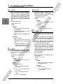
TABLE OF CONTENTS
Introduction
Purpose of Manual . . .
Organization of Manual .
Applicable Documents .
SECTION 1:
Generallnformation
ar
tM
an
ua
ls
Section - Page
-2
-2
-4
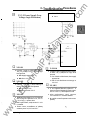
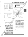
1 . 1 Safety Precautions when servicing MJ-3A
1 -2
1 .2 Recommended Troubleshooting Test Equipment
1-3
1 .2.1 Operational Simulator . .
1 .2.2 Oscilloscope . . . . . . .
1 .2.3 Analog and Digital Meters
1 .2.4 Signal Generator . . . . .
1 .2.5 Miscellaneous Tools & Accessories .
ca
lP
1 . 3 MJ-3A Troubleshooting Guidelines . . .
1 .3.1 General guidelines . .
1 .3.2 Soldering Techniques .
1 .3.3 Component Replacement
Integrated Circuits - Testing, Removal, I nstallation
Replacing Resistors . . . . . . . .
Replacing Capacitors . . . . . .
tri
.
1 -3
1 -3
1-4
1 -4
1 -4
1-5
1 -5
1-5
1- 6
1-6
1 -7
1-8
1 -8
1 .5 Handling of Static Sensitive Components . . . . . .
1 -8
1 . 6 Conversion Chart for Average, Rms, Peak, and Peak-to-peak Values
1 -9
ww
w
.E
lec
1 .4 Modifications and Repair for Printed Circuit Boards .
MJ-3A Regulator Control Service Manual
Contents - 1
.c
om
TABLE OF CONTENTS
SECTION 2: Configuring
2.1 Control Panel Board
. . . . . . . . . . . . . . . .
2-2
2. 1 . 1 Setting the 8 position DIP switch .
2. 1 .2 Setting the Basic Functions . . . .
2-2
2-2
2.2 Transformer Board
. .
2.3 Interface Option Board
I
ar
tM
an
ua
ls
I
&Calibrating the MJ-3A
2-3
2-3
2.3. 1 Data/Pak Current Display Settings
2.3.2 Setting Data/Pak Configuration . .
2-3
2-3
2.4 Setting the Accessory Functions . . . . . .
2-4
2.4. 1 Voltage Limit Control . . .
2.4.2 Voltage Reduction Control
2-4
2-4
I
SECTION 3:
MJ-3A Troubleshooting Procedures
3-2
3.2 MJ-3A Troubleshooting Strategy . . . . .
3-2
I
ca
lP
3.1 Bench Setup for MJ-3A Troubleshooting .
3.2.1 Summary . . . . . . . . . . . . . . . . . . . .
3.2.2 Definition of the Systematic, Logical Procedure
3-2
3-3
3.3 Determining Trouble Symptoms . . . . . . . . . . . . . . . . .
3-5
tri
3.3. 1 I nitial Settings of Operator and Simulator Controls
MJ-3A Control Settings . . .
MJ-3A J umper Connections
Initial Simulation Setup . . .
3.3.2 Fault Symptom Verification . .
3.4 Localizing Trouble to a Functioning Module or Sulrsystem
lec
·
3.4. 1 No apparent power to control panel.
3.4.2 No apparent P.T. sensing .
3.4.3 No apparent C.T. sensing
·
·
·
ww
w
.E
3.5 Isolating Trouble to a Circuit . . . . . . . .
Contents - 2
3-5
3-5
3-5
3-5
3-6
3 .5.1 Control Panel Board : Fault Verified or Suspected
3.5. 1 . 1 Current Transformer Interface . . . .
3.5. 1 .2 Potential & Utility Winding Interface
3.5. 1 .3 Neutralite Interface . . . . . . . . . .
3-1 9
3-20
3-22
3-24
·
3-27
·
3-28
3-30
3-3 1
3-32
·
·
·
MJ-3A Regulator Control Service Manual
.c
om
TABLE OF CONTENTS
3-33
3.5. 1 .4 Drag Hands Reset Interface .
3-34
3.5. 1 .5 Operations Counter Interface
3-35
3.5. 1 . 6 Raise / Lower Relay I nterface
3-3 6
3.5. 1 . 7 Power Supply (Low Voltage Rectification)
3-37
3.5. 1 .8 Power Supply ( Low Voltage Logic Reference)
3.5. 1 .9 Power Supply (Low Voltage AjD Reference)
3-38
3-39
3.5.1 . 1 0 Oscillator . . . . . . . . . . . . .
3.5. 1 . 1 1 Reset Circuit . . . . . . . . . . .
3-40
3-42
3.5. 1 . 1 2 P.T. Zero Cross Detection Circuit
. 3-44
. 3.5.1 . 1 3 P.T. Magnitude Input Circuit . . .
3-4 6
3.5. 1 . 1 4 CT. Zero Cross Detection Circuit
3-48
3.5. 1 . 1 5 CT. Magnitude Input Circuit .
3-50
3.5. 1 . 1 6 Relay Driver Circuits . . . . . .
3-52
3.5. 1 . 1 7 Circuit Ann unciation Logic . . .
3-54
3.5. 1 .1 8 Operator Setpoint Switch Logic
3-5 6
3. 5 . 2 Transformer Board Fault Verified or Suspected
3-57
3.5.2.1 Sensi ng Transformer T2 . . . .
3.5.2.2 Power Transformer T1 . . . . .
3-58
3-59
3.5.2.3 P.T. Zero Cross Transformer T4
. 3-60
3.5.2.4 CT. Transformer T3 . . . . . .
3-61
3.5.3 Interface Option Board : Fault Verified or Suspected .
3- 6 1
3.5.3.1 Oscillator/Microcomputer Modes . . . .
3- 62
3.5.3.2 Power Supply . . . . . . . . . . . . . .
3- 64
3.5.3.3 Microcomputer Memory Management .
3-6 6
3.5.3.4 Power Monitor Ci rcuits
3- 68
3.5.3.5 Reset Circuit . . . . . .
3.5.3. 6 Port 2 Arbitration Logic
3-70
3-70
3.5.3.7 Switch Decoding . . . .
3-70
3.5.3.8 Data/Pak Interface Logic
3-72
3.5.3.9 Control Panel Bus Arbitration
3-74
3.5.3. 1 0 Control Panel Communications Interface
3-7 6
3.5.4 Data/Pak Option Board : Fault Verified or Suspected
3-78
3.5.5 VLC (Voltage Li mit Control) Option Fault Verified or Suspected
0
3.5. 6 VRC (Voltage Reduction Control) Option Fault Verified or Suspected 3-8
·
ar
tM
an
ua
ls
·
·
·
·
·
·
·
·
·
·
·
·
·
·
·
·
·
·
·
·
·
·
·
·
·
·
·
·
·
ww
w
.E
lec
tri
c
alP
·
MJ-3A Regulator Control Service Manual
Contents - 3
.c
om
TABLE OF CONTENTS
SECTION 4:
MJ-3A: Detailed Theory of Operation
4-2
4.1 . 1 Top Level - Overview
4.1 .2 Top Level - Detailed .
4-2
4-2
4.2 Electrical I/O . . . . . . . . . . . . .
4-3
ar
tM
an
ua
ls
4. 1 MJ-3A System - Top Level . . . . . . .
4-3
4-3
4.2.1 Electrical I/O - Overview
4.2.2 Electrical I/O - Detailed .
4.2.2.1 Control Panel Board (Electrical Portion) .
4.2.2. 1 .1 PDS Connector . . . . . .
4.2.2.1 .2 Individual Circuits . . . . . . . . .
Current Transformer Interface . . . .
Potential & Utility Wi nding interface .
N EUTRALITE interface . . . . .
DRAG HANDS reset interface .
Operations Counter interface .
Raise I Lower Motor interface .
4.2.2.2 Transformer Board . . . . . . .
4.2.2.2.1 Power Transformer T1 . .
4.2.2.2.2 Potential Transformer T2
4.2.2.2.3 Current Transformer T3 .
4.2.2.2.4 PT Zero Cross Transformer T4
4-4
4-4
4-5
4-5
4-5
4-6
4-6
4-6
4-6
4-7
4-7
4-7
ca
lP
4-8
4-8
4-8
4.3 Control Panel PC Board (Electronic Portion) . . . . . . . . . . .
ww
w
.E
lec
tri
4.3. 1 Control Panel (Electronic) -Overview .
4-8
4.3.2 Control Panel (Electronic) -Detailed . . . . . .
4-9
4.3.2.1 Power Supply . . . . . . . . . . . .
4-9
4-9
Low Voltage Power Supply Rectification
Microcomputer Logic Voltage Reference .
. 4-1 0
. 4-1 0
Microcomputer AID Voltage Reference and Bias
4.3.2.2 68HC1 1 Microcomputer Support Circuits
. 4-1 0
Oscillator Support Circuit
. 4-1 1
System Mode Circuitry . . . . . . . .
. 4-1 1
System Reset Circuitry . . . . . . . . .
. 4-1 1
. 4-1 1
4.3.2.3 Microcomputer Interface Circuitry
. 4-1 1
Low Level Signal Conditioning . . . .
. 4-1 1
P.T. Signal Conditioning . . . .
p.T. Zero Cross Detection Circuit . . . . . . . . 4-12
P.T. Magnitude Input Circuit
.
.
4-13
C.T. Signal Conditioning . . . . . . . . . . . . . . . . . . 4-1 3
C.T. Zero Cross Detection Circuit
4-14
C.T. Magnitude Input Circuit
. . .
. . , . . 4-15
Contents 4
-
.
.
.
.
.
.
.
.
.
.
MJ-3A Regulator Control Service Manual
.c
om
TAB LE OF CONTENTS
.
4.4 Interface PC Board Option .
ca
lP
4.4. 1 Interface PC Board - Overview
4.4.2 Interface PC Board - Detailed .
4.4.2.1 8035 Microcomputer
4.4.2.2 Oscillator Circuit . . .
4.4.2.3 Power Supply . . . .
4.4.2.4 Microcomputer Memory Management .
Program Memory . . . . .
Data Memory . . . . . . . . .
4.4.2.5 Power Monitor Circuits . .
Power-Down STORE Function
Power-Up RECALL Function .
4.4.2. 6 Reset Circuit . . . . . .
4.4.2.7 Port 2 Arbitration Logic
Switch Decoding . . . . .
Data/Pak Interface Logic .
4.4.2.8 Control Panel Data/Pak Communications Logic
4.4.2.9 Control Panel Bus Arbitration . . . . . . .
4.4.2.1 0 Control Panel Communications Interface
·
4-1 6
4-1 6
4-1 7
4 -1 7
4 -1 7
4 -1 9
4-1 9
4-1 9
·
·
·
·
·
·
·
4-2 1
·
4-21
4-2 1
4-2 1
4-2 1
4-22
4-22
4-22
4-24
4-24
4-25
4-25
4-27
4-28
4-28
4-29
4-29
4-30
4-31
·
·
·
·
.
·
.
.
.
·
·
·
.
.
.
.
·
. . . . . . . . . .
·
4 -3 2
4.5.1 Data/Pak - Overview . . . .
4.5.2 Data/Pak Display - Detailed .
·
4-32
4-32
tri
4.5 Data/Pak Display Option
I
·
ar
tM
an
ua
ls
High Voltage Level Interface Circuits .
Relay Driver Circuits . . . .
User Interface Circuits . . . . . . . .
Circuit Annunciation Logic . .
Operator Setpoint Switch Logic
MJ-3A Detailed Theory of Operation
68HC1 1 RESEr Function .
SYST EM RESEr Logic .
·
. 4-34
4. 6. 1 VLC - Overview . .
4. 6.2 VLC - Detailed . . .
. 4 -3 4
. 4-34
lec
4. 6 Voltage Limit Control (VLC) Option
I
4.7 Voltage Reduction Control (VRC) Option .
ww
w
.E
I
4.7. 1 VRC - Overview . . . . . .
4.7.2 VRC - Detailed . . . . . .
MJ-3A Regulator Control Service Manual
. 4-3 6
. 4-3 6
. 4-3 6
Contents 5
-
.c
om
TABLE OF CONTENTS
Circuit Board layouts
ar
tM
an
ua
ls
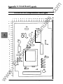
APPENDIX A:
MJ3A Control Panel with Options . . . . . . .
·
REF -2
APPEN DIX A 1 : Control Panel PC Board .
·
REF -3
APPEN DIX A2: Transformer Board . . .
·
REF -4
APPEN DIX A3: Interface PC Board
APPENDIX A4: Data/Pak Option
. .
. . REF -5
. . . . . . . . . . . . .
APPENDIX AS: VLC (Voltage Limit Control) Option
. . .
APPENDIX A 6: VRC (Voltage Red uction Control) Option
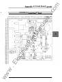
Block Diagrams
REF -8
MJ3A Control Panel Interconnection Block Diagram
REF -1 1
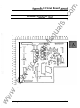
APPENDIX B.l : Control Panel PC Board .
REF -1 2
APPENDIX B.2: Transformer Board
REF -1 3
APPEN DIX B.3 : Interface PC Board .
REF -1 4
APPEN DIX B.4: Data/Pak Option . .
REF -1 5
APPEN DIX 8.5: VLC (Voltage Limit Control) Option .
REF -1 6
APPEN DIX B. 6: VRC (Voltage Reduction Control) Option
REF -1 7
tri
Schematic Diagrams
APPENDIX Cl (part 1 ): Control Panel PC Board (Electrical Portion) . .
REF -20
APPEN DIX Cl (part 2): Control Panel PC Board (Electronic Portion) . .
REF -2 1
APPENDIX C2: Transformer PC Board
REF -22
APPEN DIX C3: Interface PC Board Option . .
REF -23
.E
ww
w
Contents - 6
REF -7
REF -1 0
lec
APPENDIX C:
REF -6
MJ-3A Control Top Level Block Diagram
ca
lP
APPENDIX B:
·
APPENDIX C4: Data/Pak PC Board Option . . .
REF -24
APPENDIX C5: VLC (Voltage Limit Control) PC Board Option
REF -2 5
APPENDIX C6: VRC (Voltage Reduction Control) PC Board Option
REF -2 6
MJ-3A Regulator Control Service Manual
.c
om
TABLE OF CONTENTS
Parts List
ar
tM
an
ua
ls
APPENDIX D:
APPEN DIX D. 1 : Control Panel PC Board-(1 )
REF -28
APPEN DIX D. 1 : Control panel PC Board - (2)
REF -29
APPENDIX D. 1 : Control Panel PC Board - (3)
REF -30
APPENDIX D. 1 : Control Panel PC Board - (4)
REF -31
APPEN DIX D.2: Transformer PC Board . . . . . . . . . . . . . . . . . . . REF -32
APPENDIX D.3: Interface PC Board Option- (1 )
REF -33
APPENDIX D.3: Interface PC Board Option-(2)
REF -34
APPEN DIX D.3: Interface PC Board Option-(3)
APPENDIX D.4: Data/Pak PC Board Option . . . . . . . . . . . . . . .
REF -3 6
APPENDIX D.5: VLC (Voltage Limit Control ) PC Board Option . . . .
REF -37
APPENDIX D. 6: VRC (Voltage Reduction Control) PC Board Option
REF -38
.
Data/Pak Option .... Alert Codes
I
Al ert Code Definitions . . . . . . . . . . . . . . . . . . . . . . . . . . . REF -40
Troubleshooting with the Operational Simulator
tri
c
APPENDIX F:
. . . . . REF -35
alP
APPENDIX f:
. . . . . .
.Operational Simulator -Initial Setup . . . . . . . . . . . . . . .
REF -42
lec
Operational Simulator - Notes . . . . . . . . . . . . . . . . . . . . . . . REF -42
APPENDIX G:
Fault Symptoms Guidance
Fault Symptoms Lookup Chart . . . . . . . . . . . . . . . . . . . . . . . . . REF
.E
I
APPENDIX H:
Diagnostic Quick Reference
ww
w
Test Point Quick Reference Table . . . . . . . . . . . . . . . . . . . . . REF -48
MJ-3A Regulator Control Service Manual
Contents - 7
.c
om
ar
tM
an
ua
ls
TABLE OF CONTENTS
ww
w
.E
lec
tri
ca
lP
THIS PAGE BLANK INTENTIONALLY
Contents - 8
MJ-3A Regulator Control Service Manual
.c
om
ar
tM
an
ua
ls
Introduction
ww
w
.E
lec
tri
ca
lP
Introduction
MJ-3A Regulator Control Service Manual
Introdudion - 1
.c
om
Introduction
Purpose of Manual
ar
tM
an
ua
ls
The intent of this manual is to enable troubleshoot
ing and repair of the MJ-3A regulator control in the
most effective manner possible. Supplemental sec
tions provide detailed information regarding circuit
operation to provide detailed information at every
level. The systematic strategy used in this manual
provides procedures for analyzing trouble symp
toms, localizing faulty circuits, and isolating defec
tive components. This fault- finding strategy starts
with what you know - a symptom, and it takes you
through a step-by-step procedure of what to do and
how to do it . Using this approach, the fault can be
determined methodically to enable most efficient
troubleshooting.
Using this manual, you will be able to troubleshoot
the MJ-3A control with much greater efficiency and
a much better chance of success. Whether you are
interested in intricate details of the operation, with
the time to test and replace components at the
board level, or one who simply wants to get the
system fixed as soon as possible and desires to find
faults only at the mod ule level... this manual should
help you do the job well and quickly.
This manual is divided into four major sections
followed by a series of appendices. Each section and
appendix can be easily located by the large number
on the outside page column referencing it It is highly
recommended that you be aware of these sections
contents so the appropriate information can be
found quickly when needed. The most accessed
references are located in the appendices.
Sedion 1 provides information on safety precau
tions specific to the MJ-3A, recommendations for
test equipment, and a summary of troubleshooting
techniques. It is highly recommended that this sec
tion is read before any troubleshooting is attempted
regardless of your level of experience, because of
the variety of voltage levels present on the MJ-3A
control of which you must be aware.
tri
c
alP
To get the most out of this manual, you should know
how to read electronic circuit diagrams and be
familiar with the fundamentals of electricity, such as
Ohm's law, and some of the fundamental compo
nents of electronics, such as semiconductors. You
do not need mathematics, network theory, or any
other skills involved in original equipment design.
You should be able to read manufacturer's instruc
tions and use standard electronic test equipment,
such as the oscilloscope and the YOM. One of the
early steps used in the troubleshooting procedure is
to monitor operation of the circuit with various
pieces of test equipment Some recommendations
and techniques are provided to help assist in trou
bleshooting the MJ-3A, but the operator needs to
have at least a basic understanding of the equipment
he will use.
Organization of Manual
.E
lec
This manual supplements the Accu/Stat Instruction
manual (P/N 2 1 -1 1 5527-004) by providing MJ-3A
calibration and information on configuring MJ-3A
controls. When an MJ-3A is repaired, it may be
necessary to re-calibrate and/or re-configure the
control to the same level as when it was first in
stalled.
ww
w
To achieve maximum efficiency in troubleshooting
and repair of the MJ-3A control, it is extremely
important to understand the operation of the cir
cuitry. For this reason, an entire section of this
manual is devoted to explaining operational theory
at the circuit board level to provide an in-depth
understanding of the MJ-3A control. Although the
troubleshooting section provides a step by step
approach where an in-depth understanding is not
mandatory, maximum effectiveness at fault-finding
is attained by a better understanding the details of
the system.
Introdudion 2
-
Sedion 2 provides key switch setting configura
tions, as well as calibration procedures. This section
is used when troubleshooting to verify that the
system is properly configured as well as providing
information on re-cali brating after repairs have been
made.
Sedion 3 is a systematic and logical approach for
locating specific faults in the MJ-3A control by ob
serving the symptoms. This section ensures that
before any troubleshooting is begun, a strategy is
used which will enable you to pinpoint the faults
most effi ciently. Oscilloscope wave forms are pro
vided to verify proper performance at key nodal
points. This section is designed to provide the most
efficient techniques to trap faults quickly, regardless
of your level of understanding of MJ-3A circuit
operation.
Sedion 4 describes the entire circuit operation for
maximum troubleshooting effectiveness. Each cirMJ-3A Regulator Control Service Manual
.c
om
Introduction
cuit is individ ually described in detail. Reading this
section will provide a greater understanding of the
data observed in section 3 and provide the trouble
shooter with a greater insight of MJ-3A operation.
Appendix Sections This section contains the most
Appendix F: Troubleshooting using the Operational
Simulator. -This appendix is of interest only to those
who have a simulator. Throughout the trouble
shooting session in section 3, various tests require
excitation signals which must be directed into the
MJ-3A for observing circuit behavior. If you have
access to a simulator, the effort involved in each test
setup is greatly simplified. This section is referenced
by the troubleshooting section in section 3, and
steps you through the necessary configuration of the
simulator.
ar
tM
an
ua
ls
used references needed in all other sections in one
convenient place. Appendix A through Appendix D
are coded in such a manner that each level of the
appendix corresponds with the same level as an
other appendix. For example, if you were interested
in the transformer board, the transformer board
circuit layout is in Appendix A section "A2 ", the block
diagram is in Appendix B section "B2 ", the schematic
in Appendix C section "C2 " and the parts list in
Appendix D section " D2 ".
Appendix E : Alert Code Chart - Describes the mes- .
sage code if the optional Data/Pak is displaying one.
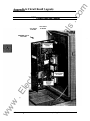
Appendix A: Circuit Board Layouts - The MJ-3A is
shown pictorially with all the available options refer
enced. The succeeding layouts depict each printed
circuit board individually with X & Y coordinates
labeled for component referencing.
8: Block Diagrams - This provides a top
level modular look at the MJ-3A main and secondary
subsystems. Referring to the block diagrams will
provide a better understanding of the schematics,
which follow in the next section.
ca
lP
Appendix
Appendix G: Fault Symptom Guidance - A com
prehensive listing of fault symptoms and references
in the manual to where they are add ressed. This
appendix provides a starting point for troubleshoot
ing when a fault symptom is known.
Appendix H: A quick reference for initial isolation
of problems. This appendix contains a lis of the 1 6
most primary test points and the pages where they
are referenced. Test points will appear on units sin
MJ303S 40000 and above.
Appendix C: Schematics - Provides detail at the
component level of each of the modules shown in
the block diagrams above.
Example: {20:A10} designates page
REF-� (Appendix e), x coordinate is
'a' and Y coordinate is lQ. Any circuit
discussed can be quickly tied to its loca
tion using this approach.
ww
w
.E
lec
tri
Appendix D: Components part list for each module
in the MJ-3A For convenience, each component
listed is identified by where it can be found on the
actual circuit board layout (Appendix A).
Note: All illustrations in this manual
which depict circuits are labeled with
location identifiers. After the name of a
circuit illustration will be a reference to
the appendix page where it can be found
with its X-V coordinates.
MJ-3A Regulator Control Service Manual
Introduction - 3
.c
om
ar
tM
an
ua
ls
Introduction
Applicable Documents
It is recommended you obtain the following docu
ments, as references are made to them throughout
this manual. Contact your local Siemens representa
tive.
Instruction
Siemens AccujStat MJ-3A
Manual (part number 2 1 -1 1 552 7 .Q04)
ca
lP
Siemens AccujStat MJ Series Regulator Control,
Operational Performance Evaluation (part number
2 1 -1 1 5527 .Q03)
ww
w
.E
lec
tri
Modification and Repair for Printed Boards and
Assemblies, (IPC-R-700B) Institute for Interconnect
ing and Packaging Electronic Circuits, available
from:
IP C
1717 Howard Street
Evan�on ILL, 60202
Introduction - 4
MJ-3A Regulator Control Service Manual
.c
om
-
General Information
ar
tM
an
ua
ls
1
ww
w
.E
lec
tri
ca
lP
SECTION 1:
General Informati'on
MJ-3A Regulator Control Service Manual
Page 1 - 1
-
General Information
•
As many different voltage levels are present in the
MJ-3A circuitry, you must exercise caution during
troubleshooting sessions. It is also necessary to
observe certain precautions during operation of the
electronic test equipment used during troubleshoot
ing. Some of the precautions are designed to pre
vent damage to the test equipment or to the circuit
where the troubleshootirig operation is being per
formed. Other precautions are to prevent injury to
the troubleshooter. Where applicable, special safety
precautions are noted throughout this manual.
•
1 . When troubleshooting, be especially
careful of areas where AC line voltages
will be present :
- the PDS connector
- the transformer board
- the lower half of the control
panel board
ca
lP
•
2. Be careful when using more than one
AC source at the test station as various
outlets may be wired to different phases.
•
•
•
•
•
•
•
.E
lec
tri
3. Many troubleshooting instruments are
housed in metal cases. These cases are
connected to the ground of the internal
circuit For proper operation, the ground
terminal of the test instrument should al
ways be connected to the ground of the
equipment being serviced. If you are test
ing the MJ-3A with it assembled, make
certain that the chassis of the MJ-3A being
serviced is NOT at ground. If there is any
doubt, connect the equipment being ser
viced to the power line through an isola
tion transformer.
ww
w
•
Page 1
4. Remember that troubleshooting equip
ment that operates at hazardous voltages
is always dangerous. Therefore, you
should familiarize yourself thoroughly
with the equipment being serviced before
troubleshooting it. bearing in mind that
high voltage may appear at unexpected
points in defective equipment Read ing
the operational theory (section 4) is rec
ommended prior to troubleshooting.
-
2
5. It is good practice to remove power
before connecting test leads to high-volt
age points. It is preferable to make all
troubleshooting connections with the
power removed. If this is impractical, be
especially careful to avoid accidental con
tact with equipment and objects that are
grounded. If you work with one hand
away from the equipment and stand on a
properly insulated floor, you will lessen
the danger of electric shock.
ar
tM
an
ua
ls
en
.c
om
1
•
•
6. Remember that leads with broken insu
lation pose the additional hazard of high
voltages appearing at exposed points
along the leads. Check test leads for
frayed or broken insulation before work
ing with them.
7. To lessen the danger of accidental
shock, disconnect test leads immediately
after the test is completed.
8. Remember that the risk of severe shock
is only one possible hazard. Even a minor
shock can place you in danger of more
serious risks, such causing you to touch a
source of higher voltage.
9. Guard continuously against injury and
do not work on hazardous circuits unless
another person is available to assist you in
case of accident
1 0. Even if you have had considerable
experience with test equipment used in
troubleshooting, always study the service
literature of any instrument with which
you are not thoroughly familiar.
1 1 . Use only shielded leads and probes.
Never allow your fingers to slip down to
the metal probe tip when the probe is in
contact with a hot circuit Be sure thatyou
do not short any terminals to ground
when you make voltage measurements. If
the probe should slip, for example, and
short out a voltage source, you could
damage one or more components.
1 2. Avoid vibration and rough treatment
Most electronic test equipment is deli
cate.
1 3. Study the circuit being serviced before
making any test connections. Try to match
the capabilities of the test instrument to
the circuit being serviced. It is recom-
MJ-3A Regulator Control Service Manual
mended that section 4 be read for an
understanding of operational theory.
General Information
1.2 .2 Osci lloscope
1 4. Do not remove components while the
unit is plugged in.
The oscilloscope is mandatory for any level of de
tailed troubleshooting. It may be possible to deter
mine trouble symptoms, and perhaps localize the
problem to a functioning module without one if your
only intent is to replace a de- fective module, but
anything more detailed dictates the use of one.
Beyond section 3.4, this manual assumes the avail
ability of one.
ar
tM
an
ua
ls
•
-
.c
om
1
1.2 Recommended
Troubleshooting Test
Equipment
The specifications of the oscilloscope are not critical,
but for maximum effectiveness , it is recommended
that the scope used have the following features:
•
•
digital storage (with full analog capabili
ties)
m i n i m u m of 1 00 M H z real-t i m e
bandwidth
•
dual channel, time delayed sweep
•
equipped with external trigger input
Use only low capacitance probes to ensure that
circuitry being analyzed is not loaded by the probes
such that the circuit operation is affected or the
measured waveform is distorted.
alP
This section discusses test equipment used in trou
bleshooting the MJ-3A control. It is absolutely essen
tial that you become thoroughly familiar with your
particular test instruments, which can only be gained
through actual practice. It is strongly recommended
that you establish a routi ne operating procedure or
sequence for each item of troubleshooting equip
ment This will save time and familiarize you with
the capabilities and li mitations of your particular
equipment, thus eliminating false conclusions
based on unknown operating conditions. This sec
tion highlights features desired in test equipment
used in MJ-3A troubleshooting.
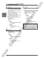
1.2.1 Operational Simulator
ww
w
.E
lec
tri
c
The operational simulator is available through Sie
mens. Section 3.2 describes the recommended MJ3A testing procedure which is divided into four
discrete phases. All of these phases, but most nota
bly phase 1 (Determining Trouble Symptoms) is best
performed with the use of an operational simulator.
As the MJ-3A to be repaired is no lon ger in service,
the use of the simulator is desirable to emulate the
problem reported by the operator so you can see it
first hand. The simulator contains all I/O signals
required to test the MJ-3A Without a simulator, you
are forced into providing your own excitation signals
to the MJ regulator control using other equipment,
which takes considerably more effort, and makes
fault detection considerably more complex than it
would be otherwise. If you do have access to a
simulator, Appendix F contains guidelines that will
help simplify the troubleshooting procedures in
section 3. If you do not have access to the simulator
then several observations described in section 3 will
not be possible as written. These will be obvious at
the appropriate time.
MJ-3A Regulator Control Service Manual
As an oscilloscope provides a means of visualizing
time varying voltages or signals, it is a perfect trou
bleshooting tool for the MJ-3A which has a basic
control function based on incoming time varying
signals. Because the heart of the MJ-3A is a micro
computer, the controlling waveforms can best be
viewed using the digital scope. Section 3 requires
the use of a scope to enable comparisons against
illustrated waveforms to provide fault detection in a
circuit
It is assumed that the troubleshooter has some
experience with the use of an oscilloscope, and this
manual will not attempt to teach the basics of
operating one.
Page 1
-
3
-
.c
om
1
General Information
1.2.3 Analog and Digital
Meters
ar
tM
an
ua
ls
The most obvious advantage of using the scope is
that it shows waveform, frequency and/or time
duration, and phase simultaneously with the voltage
being measured. If however, the only value required
when troubleshooting is voltage (or current), use the
meters because of its simplicity in readout as well as
its desired form of readout (rms or average). This
form of readout is desirable, for example, when
wanting to find the accuracy of the voltage and
current magnitude circuits on the control panel
board. At times, the meter is simply more conve
nient to use when reading AC/DC levels or checking
resistance.
For the testing of any power factor other than unity,
separate signal generators are required for voltage,
and current In this manner, any phase condition can
be simulated. At least one of the generators needs
to have a trigger input, and the other a sync output
to maintain the phase relationship between the two
signals. The generator needs to output both sinus
oidal and square waves with an amplitude of at least
5 volts, and be adjustable from 0 to 1 00 Hz
minimum.
You will need a high-input (1 M ohm or greater)
VOM (volt-ohm-meter), DVM (digital voltmeter), or
VTVM (vacuum tube voltmeter) to make resistance
and voltage tests.
1.2.5 Miscellaneous Tools
& Accessories
Soldering I ron
•
ca
lP
It is preferred that the voltmeter be a true rms
reading type, however, if the meter is one which
displays an average voltage with an rms correction
(as for most common dial point meters) itwill suffice.
Make certain that the generator has some form of
blocking capacitor to isolate the output circuit from
the DC voltages that may appear in the circuit If the
generator does not have a built in blocking capaci
tor, conned a .01 J.lfd capacitor between the
generator's output lead and the point of injection
into the circuit
Note: For convenience, a reference chart for con
verting rms, average, peak, and peak-to-peak volt
ages is provided at the end of this chapter in section
1 .6.
tri
1.2.4 Signal Generator
•
lec
Recommended if operational simulator
is NOT available.
.E
Note: Section 3 assumes the presence of a simula
tor, therefore references to simulator useage will be
impossible.
Used to emulate the voltage and current amplitude
and frequency signals the operational simulator
would normally provide.
ww
w
Two signal generators are required for optimum
testing.
As the basic function of the MJ-3A is to provide
control based on the incoming voltage and current
signals, these signals must be simulated to verify the
MJ-3A is functional.
Page 1
-
4
•
Solder
•
•
tip must be grounded and have a 1/8 inch
to 3/1 6 inch chisel point
preferably variable power from at least 25
to 75 watt
Rosin core with a 60:40 tin-lead content
DO NOT USE ACID CORE SOLDER
Hand Tools
•
•
•
•
•
•
Long nose pliers
Diagonal Cutters
Wire Strippers
1 /8 and 1 /4 inch blade screwdrivers
1 /1 6 inch hex Allen wrench
3/8 inch nut driver
Miscellaneous
•
•
•
•
•
•
•
•
•
Vacuum desoldering tool
Desoldering braid
utility knife
magnifying glass
Assortment of test leads and clips
DIP test clips
rosin flux remover aerosol spray
4 jumpers consisting of 2.5 to 3" of 20 to
26 gauge insulated wire with each end
stripped about 1 /4 inch
2 jumpers consisting of 2 to 2.5 1/ of 1 6 to
1 8 gauge insulated wire with each end
stripped about 1 /8 inch.
MJ-3A Regulator Control Service Manual
General Information
is installed backwards. I f the diode has a solid body,
the band is clearly defined. If the diode has a glass
body, do not mistake the colored end inside the
diode for the banded end. Look for a band painted
on the outside of the glass.
The printed circuit boards used in the MJ-3A are
sprayed with conformal coating, and as such acts as
an insulator. When probing the board for a signal,
ensure that you break thru the conformal coating
layer, otherwise the expected signal will not be
evident
ar
tM
an
ua
ls
1.3 MJ-3A Troubleshooting
Guidelines
-
.c
om
1
1. 3 .1 General guidelines
Follow the instructions in the troubleshooting sec
tion carefully. Read the entire step before you
perform each operation..
1. 3.2 Soldering Tech niques
Verify that the power is removed from the MJ-3A
when making repairs. This is very important to verify
because signal sources can be coming from more
than one power cord (signal generators, simulators).
Turn off EVERYTHING connected before making
repairs. Not only can you be injured by not doing
so, it is also possible to damage MJ-3A circuitry as
well as the test equipment itself.
A good solder connection will form an electrical
connection between two parts, such as a compo
nent lead and a circuit board foil. A bad solder
connection could prevent an otherwise well re
paired MJ-3A from operating properly. It is easy to
make a good solder connection if you follow a few
simple rules:
ca
lP
Do not under any circumstances insert or remove
any component; especially an IC or transistor with
the low voltage power supply energized. Doing so
can cause damage to the semiconductor material
due to transients. An IC is easily damaged if it
intermittently looses its ground potential.
•
•
tri
When injecting a signal into a circuit (from signal
generator), make sure there is a blocking capacitor
in the signal generator output to prevent circuit
damage. (see section 1 .2.4 under signal generators)
•
•
.E
lec
As troubleshooting will be conducted at the compo
nent level, defects will be located in circuits by
measuring and analyzing voltages at the elements
of active devices. This can be done with the circuit
operating and without disconnecting any parts.
Once located, the defective part can be discon
nected and tested or substituted, whichever is more
convenient
ww
w
Transistors can be tested using small voltage scales
to detect small differences in the emitter to base
junction. As it must be forward biased to get current
flow, in the PNP transistor the base must be more
negative than the emitter and in the NPN the base
must be more positive.
When you install a diode, always match the band
on the diode with the band mark on the circuit
board. The circuit will not work properly if a diode
MJ-3A Regulator Control Service Manual
•
Use the right type of soldering iron. A 25
to 75 watt pencil soldering iron with a 1 /8
inch or 1 /1 6 inch chisel tip works best
Use the lowest setting (2 5 watt) when
working with semiconductors.
Keep the soldering iron tip clean. Wipe it
often on a wet sponge or cloth; then
apply solder to the tip to give the entire
tip a wet look. This process (called tin
ning) will protect the tip and enable you
to make good connections. When solder
tends to "ball" or does not stick to the tip,
the tip needs to be cleaned and retinned.
Always use rosin core, radio-type solder
(60:40 tin-lead content) for all soldering.
When soldering component leads, push
the soldering tip against both the lead and
the circuit board foil. Heat BOTH for two
or three seconds. Apply solder to the
other side of the component Let the
heated lead and the circuit board foil melt
the solder. As the solder begins to melt,
allow it to flow around the connection.
Then remove the solder and iron and let
the connection cool. Cut off excess lead
lengths close to the connection.
After repair, carefully inspect the circuit
board for the following problems: unsol
dered connections, poor solder connecPage 1
-
5
-
.c
om
1
General Information
•
After any soldering repair, ensure that the
area repaired is cleaned with rosin- flux
remover.
locating and Repairing poor solder joints
1. 3 . 3 Component
Replacement
Re-apply conformal coating to any area of the board
which had been modified.
ar
tM
an
ua
ls
tions, solder bridges between foil pat
terns, protruding leads which could touch
together. A solder bridge may occur
when you make solder connections at
closely spaced foils. Therefore, after each
solder step, carefully inspect the foil for
solder bridges and remove any that may
have formed. To remove a solder bridge,
hold the circuit board foil-side down and
hold the soldering iron tip between the
two points that are bridged. The solder
will flow down the soldering iron tip to
clear the bridge.
TESTING IC'S:
For troubleshooting an IC, the most convenient way
is to test is in-circuit because the power source is
available and you do not have to unsolder the IC
As the MJ-3A uses double sided PCBs, it is difficult
to unsolder an IC without an expensive solder vac
uuming device. Without one, it is very easy to
damage the IC and/or circuit board traces.
You must measure the DC voltages applied at the
IC terminals to make sure that they are available and
correct If the voltages are absent or abnormal, this
is a good place for troubleshooting.
ca
lP
The low voltages in solid state equipment make
them vulnerable to poor solder joints (cold solder
joints). When there is no obvious cause for a low
voltage at some point in the circuit or there is an
abnormally high resistance, look for cold solder or
printed-circuit defects. Use a magnifying glass to
locate defects in printed wiring. Minor breaks in
printed wiring can sometimes be repaired by apply
ing solder at the break, however the entire board
should be replaced if there is more than one.
Integrated Circuits - Testing,
Removal, Installation
ww
w
.E
lec
tri
Cold solder joints can sometimes be found with an
ohmmeter. Remove all power. Connect the ohm
meter across two wires leading out of the suspected
cold solder joint, flex the circuit and note any change
in resistance. Look for resistance indications that
tend to drift when the ohmmeter is returned to a
particular scale. If a cold solder joint is suspected,
reheat the joint with the soldering iron, then recheck
the resistance.
Page 1
-
6
With the power sources established, the in-circuit IC
is tested by applying the appropriate input and
monitoring the output In some cases, it is not
necessary to inject an input because the normal
input is supplied by the circuits ahead of the I C
One drawback to testing an I C i n circuit i s that the
circuits before (input) and after (output) the IC may
be defective. This can lead you to believe that the
IC is bad. The fault finding techniques used in section
3.5 of providing key waveforms will aid you in such
an instance.
REMOVING IC's
As previously mentioned, without a vacuum de-so�
dering device, it is very difficult to remove a soldered
IC without damaging plated thru holes and the
circuit board traces, so use extreme caution. All the
printed circuit boards in the MJ-3A control panel use
double-sided PC boards, so solder must be removed
from both sides. Start by clipping all the IC pins going
into the IC body. Heat a pin on the foil side for about
3 seconds. While the solder at the pin is melted, use
the desoldering tool to force the molten solder from
the plated through hole. If you are unsuccessful,
then re-solder the pin and try again. Do the same for
every pin.
MJ-3A Regulator Control Service Manual
General Information
Replacing Resistors
Resistors are identified in the schematics
C), and parts list (appendix D). by their resistance
value. They are identified by a color code of four or
five color bands, where each color represents a
number. These colors are given in the steps in their
proper order (except the last band), which indicates
a resistor's tolerance. For convenience, the color
code and tolerance charts are provided in figure 1 -1
below and figure 1 -2 on the next page.
ar
tM
an
ua
ls
After the holes on the foil side look relatively clean,
using the desoldering braid, remove excess solder
from each of the circuit side IC pins while at the
same time trying to force the IC pin towards the
center of the hole. This step accomplishes two
purposes. First, it removes additional solder which
was not removed during the desoldering from the
foil side. Second, it detaches the pin from being
attached to the plated-thru hole.
-
.c
om
1
Use extreme caution not to damage traces on either
the top or bottom of the PC board in the process.
Also, when removing IC pins from the PCB holes,
be careful not to damage the plated thru hole itself.
If it is ever necessary to remove an IC from its socket,
use an IC puller or a small blade screw-driver. Push
the end of the IC puller or screwdriver blade be
tween the IC and the socket and carefully lift the IC
free. If any IC pins become bent, straighten them
carefully. When using a screw-driver to remove an
IC, be careful not to damage any PC board traces.
INSTALLING IC's:
Occasionally, a precision or power resistor may
have the value stamped on it The letter K,or M may
also be used at times to signify a decimal
point...K=1 000, M=1 ,OOO,OOO for multiplier.
Precision resistors may also be marked with a
J,G,F,D,C, or B as the last character. This indicates
the tolerance, and is per the chart below.
Take special care in installing any IC as they may be
damaged or destroyed if installed incorrectly.
tri
ca
lP
Make sure the pins are straight The pins on the lC's
may be bent out at an angle, so they do not easily
line up with the holes in the IC socket In the event
a pin gets bent out of alignment , bend it back
carefully. If it appears that the bend was severe
enough to possibly cause the pin to break when it
is inserted, apply a very thin coating of solder to it
to give it more structural stability. Do not use more
than a very thin coating, however, or the IC pin will
become too large to fit in the PC board hole.
ww
w
.E
lec
When you install integrated circuits, position them
so that the flat side is over the flat of the outline,on
the circuit board. Hold the IC in place while you turn
the board over. At first, solder only two pins at
diagonally opposite corners of the IC When the
solder cools, check to make sure the IC is tight
against the circuit board. If not, reheat the pins while
you press against the IC to reseat it Then solder the
remaining pins to the foil.
MJ-3A Regulator Control Service Manual
Figure 1-1: Resistance Color Code Chart
Page 1
-
7
-
.c
om
1
General Information
Replacing Capacitors
you install a polarized capacitor, always iden
the markings near the leads. One lead will have
positive (+) mark or a negative ( ) mark near it Be
sure to install the positive lead in the positive marked
hole or the negative lead in the negative-marked
hole. Be careful; as only one lead may be marked.
1.4 Modifications and Repair
for Printed Circuit Boards
ar
tM
an
ua
ls
-
Capacitors will be called out by their capaci-tance
value in JlF (microfarads), nf (nano-farads), or pF
(picofarads) and type: ceramic, Mylar® or any other
plastic material, electrcrlytic, etc. The last character
coded on the ca-pacitor refers to its tolerance, and
can be found in the tolerance chart shown in figure
1 -3.
This topic is beyond the scope of this manual, but is
very important to understand when using this man
ual. An excellent reference for PC board repair is
listed in the Introduction section under "Applicable
Documents".
1.5 Handling of Static
Sensitive Components
tri
c
alP
Static electricity is an electric charge at rest on a
surface. When the charge becomes sufficiently
large, an electrostatic discharge (ESD) takes place
when a charged person touches a part or a charged
part touches another conductive surface. People
can carry 1 000 to 5000 volts with-out ever feeling
the sensation of a discharge. The semiconductor
material used in compo-nents can be ESD sensitive
within this voltage range.
Figure 7-2: Resistor Tolerance Chart
OVER 1 0 pf
lec
1 0 pf OR LESS
.E
tive.
•
±0.25pf
ww
w
1. Treat all electronic parts and as
semblies as potentially static sensi
•
±O.lpf
±0.5pf
± 1 .0pf
±1%
±2.0pf
±2%
•
±3%
±5%
± 1 0%
±20%
Figure 1-3: Capacitor Tolerance Chart
Page 1 - 8
To avoid potential problems, proper handling pro
cedures of ESD sensitive components must be es.
tablished. The establishment of an ESD prevention
strategy should revolve around the following basic
guidelines:
•
Always handle ICs by the body, not by the
leads.
Keep all ICs in their original containers
until ready for use.
When handling ICs, it is highly recom
mended that you be grounded with a
wrist or heel strap through a 1 Meg ohm
resistor.
Do not slide ICs over any surfaces.
2. Handle all ESD sensitive parts and
assemblies at a statically safe work
station.
MJ-3A Regulator Control Service Manual
•
•
•
If possible, do the repair on a workbench
which provides both a grounded work
surface and a grounded floor mat (floor
mat should be grounded through a 1 M
ohm resistor)
Ground all metal equipment such as test
equipment, solder iron, stands and
fixtures.
ESO damage may be the cause ofa significant fraction
ofcostly electrical component failure. f50 protective
and preventative measures are fairly simple to imple
ment but won'tsucceed unless they are coupled with
continued static awareness.
Tie all grounded leads to a single common
ground.
When handling ICs you should avoid
clothing coming in contact with compo
nents and their assemblies.
3. Package parts properly for storage
and transportation.
•
Use antistatic tubes or conductive foam
to store or transport ICs.
Pack ICs securely to prevent motion
which can generate static.
1.6 Conversion Chart for
Average, Rms, Peak, and
Peak-topeak Values
Multiplying Factor to Get
ww
w
.E
lec
tri
GIVEN VALUE
ca
lP
•
General Information
ar
tM
an
ua
ls
•
-
.c
om
1
1 .414
2.0
0.637
0.32
2.828
0.354
Figure 1-4 Convert: Average, Rms, Peak, & Peak to Peak
MJ-3A Regulator Control Service Manual
Page 1
-
9
.c
om
-
General Information
ar
tM
an
ua
ls
1
ww
w
.E
lec
tri
ca
lP
THIS PAGE LEFT I NTENTIONALLY BLANK
Page 1 - 1 0
MJ-3A Regulator Control Service Manual
.c
om
-
Configuring & Calibrati ng the MJ-3A
ar
tM
an
ua
ls
2
ww
w
.E
lec
tri
ca
lP
SECTION 2: Configuring
&Calibrating the MJ-3A
MJ-3A Regulator Control Service Manual
Page 2 - 1
.c
om
2 - Configuring & Calibrati ng the MJ-3A
Switch 8 is to be closed for straight design single
2.1 Control Panel Board
2.1.2 Setting the Basic
Functions
ar
tM
an
ua
ls
2.1.1 Setting the 8 position
DIP switch
phase regulators and for all three-phase regulators.
Set this switch open for inverted design regulators.
(See appendix I of the Accu-jStat Instruction manual
for description of how to determine if a given
regulator is of the "straight" or "inverted" design,
based upon nameplate information.)
The AccujStat MJ-3A control must know certain
de-tails concerning desired operating mode, regula
tor design, and power system arrangements. This
information is programmed into the MJ-3A through
the 8 position DIP switch located at the lower part
of the slot found on the right side of the control. The
functions of each switch are as follows:
Opening Switch 1 advances the current 900 Set
closed for all single phase regulators. Set closed on
three phase regulators with single phase CT. Set
open on three phase regulators with phase to phase
connected CT's.
•
AccujStat MJ-3A control panels perform the basic
control functions as they are influenced by the
desired voltage level, voltage bandwidth, time delay
and line drop compensation settings. Settings are
accomplished via incremental switch points using
rotary switches on the face of the control. No
locking of the knobs is required.
For detailed information on the various settings, as
they pertain to the regulator they are controlling,
refer to the AccujStat Instruction Manual.
ca
lP
Closing Switch 2 will prevent any tap change if
current is less than 2 percent of the.c.T. Primary
rateing. To enable low current tap change, Switch 2
should be open.
With Switch 4 in the closed position, the control
tri
panel senses true RMS voltage and current In the
open position, the control will sense averaged de
rived RMS values, the same as sensed in previous
analog controls. Any difference in the values is
attributable to harmonic distortion. Factory setting
is closed.
lec
Switch 5 should be closed on regulators on wye
connected systems and should be open on reg-ul
ators on delta connected systems.
.E
Switch 6 should be closed on "lagging" regulators
on delta systems and should be open on "leading"
regulators on delta systems. Switch 6 has no effect
when switch 5 is set for a wye system . (See appendix
I I of the AccujStat Instruction manual for description
of how to determine the "leading" and "lagging"
regulators on an open delta system.)
ww
w
The relative polarity of the utility (tertiary) winding
and the current transformer must be established for
the MJ-3A Switch 7 shifts the current signal 1 80
degrees if open. The correct switch setting is estab
lished by examination of the utility winding diagram
and knowledge of the regulator design.
Page 2 - 2
MJ-3A Regulator Control Service Manual
.c
om
2 - Configuring & Calibrating the MJ-3A
2.2 Transformer Board
The transformer board also includes provisions for
three auxiliary connections. The troubleshooting
instructions in section 3 will inform you when to
install or remove these jumpers for testing pur
poses.)
Tap-change Inhibit The clo
sure of an external contact across the
AUTO INH terminals will prevent auto
matic (only) operation of the control. This
represents the highest level of command
in the priority of automatic operation.
Voltage Reduction Control
The closure of
an external contact across the VRC termi
nals will cause the regulator to to activate
one of two VRC modes by the percentage
which has been preset on the accessory
component (Refer to MJ-3A Instruction
Manual, {21 -1 1 5527-O04}, for more de
tails. The toggle switch on the component
must also have been set to REMOTE.
lec
tri
•
Automatic
The
nominal 200 mA secondary of the regula
tor CT is routed through these terminals.
These terminals are shorted at the factory
and must remain shorted except as they
are used to accommodate auxiliary appa
ratus, such as a current demand meter.
Current Transformer Secondary.
ww
w
.E
•
Controls equipped with Data/Pak accessory require
the correct CT ratio be input to the control to
provide the correct current display. This is accom
plished by properly setting the 5 position DIP switch
(SW5) located on the interface board.
Set the 5 position DIP switch in accordance with the
Figure 2-2 to provide a proper multiplier for the
current display on the Data/Pak. See nameplate of
the regulator for CT primary rating.
2.3.2 Setting Data/Pak
Configu ration
ca
lP
•
2 . 3 .1 Data/Pak Cu rrent
Display Settings
ar
tM
an
ua
ls
The sensing transformer provides a jumper t�rm! n�1
strip for compensating the regulator to which It IS
attached. As the MJ-3A to be troubleshot has al
ready been configured in the field for a particular
regulator it is not possible for this manual to de
scribe h �w the one you are currently using is
configured. A complete description on the �roce
dure for installing these jumpers can be found In the
instruction manual. (For troubleshooting purposes,
you will be instructed to configure the jum-pers for
specific tests.)
2.3 Interlace Option Board
MJ-3A Regulator Control Service Manual
Setting Integration TIme for Voltage, Current &
Power Factor:
Accu/Stat MJ-3A controls will display voltage, cur
rent and power factor as a time integrated readout
The time intervals selected can be set independently
of each other via three 4 position DIP switches
(SW6-Volts, SW7-Amps, SW8-Power Factor.
Position 4 on switches 6,7, and 8 relates to present
value parameters on the Data/Pak. Set closed for
instantaneous response. Set open for lagged re
sponse. If 4 is set open, integration periods will then
be selected by positions 1 ,2 and 3. (Factory set
closed)
Positions 1 ,2 and 3 select the integrating period for
drag hand parameters and the present value param
eters if position 4 is set open. (refer to figure 2-3)
Page 2 - 3
.c
om
2 - Configuring & Calibrating the MJ-3A
ar
tM
an
ua
ls
2.4 Setting the Accessory
Functions
2.4.1 Voltage Limit Control
Set the knobs to the maximum and minimum volt
ages to be held. Turning the VLC toggle switch off
deactivates any minimum/maximum settings on the
VLC
2.4.2 Voltage Reduction
Control
O=Open
ca
lP
C=Closed
Set the knob to the percent voltage reduction de
sired when activated. Place the toggle switch in
"remote" to have it activated via the VRC contacts
on the transformer board.
'This setting may be used for direct reading of CT sec
ondary current (in millamperes).
.E
lec
tri
Figure 2-2: Data/Pak Current Display Multiplier
(SW5).
ww
w
*
Factory set, SW6,SWB.
**
Factory set, SW7.
Figure 2-3: Data/Pak Display Intigration Time
Chart
Page 2 4
-
MJ-3A Regulator Control Service Manual
.c
om
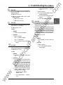
3 Troubleshooting Procedures
ar
tM
an
ua
ls
-
ww
w
.E
lec
tri
ca
lP
SECTION 3: MJ-3A
Troubleshooting
Procedures
MJ-3A Regulator Control Service Manual
Page 3 - 1
-
ar
tM
an
ua
ls
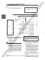
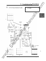
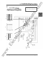
3.1 Bench Setup for MJ-3A
Troubleshooting
It is assumed that the MJ-3A is believed to be
and is removed from service. The remain
of this section assumes that the MJ-3A is at a
:u,r\rv l"\Ar,rh with the test equipment and tools which
recommended in section 1 .
riAlrArl-'\IA
The easiest way to troubleshoot the MJ-3A is to
disassemble i� removing all printed circuit boards.
Lay them out on your workbench in a way that the
control panel board cables attaches to the trans
former board, and the option modules (if available)
also connect to the control panel board. The oper
ational simulator (if available) should then be in close
enough proximity to the setup such that the PDS
connector from the control panel board mates to
the simulator.
lec
tri
....
Suggestion #2: Use the table of con
tents to locate specific sections which
.E
...
are referenced in the test procedur�s.
This is by far easier than trying to find a
section by randomly looking through the
pages.
Suggestion #3:
ww
w
The remainder of this
section assumes the availability of an
oscilloscope to monitor waveforms. If
one is not available, the DVM refer
enced in section 1 .3 can be used.
...
3.2 MJ-3A Troubleshooting
Strategy
3.2.1 Summa ry
The goal in troubleshooting the MJ-3A is to be most
efficient in locating and correcting a particular de
fect In order to do this, a logical step-by-step ap
proach is required.
STEP 1 : You must be able to use test equipment and
proper tools to repair defective circuitry. As a mini
mum for electronic repair, you must be able to use
the test equipment and tools mentioned in section
1 .2.
ca
lP
In the process of disassembling the MJ-3A, it is
necessary to remove the power and sensing fuses
which are attached to the control panel. For trouble
shooting purposes only, solder a jumper wire from
N 1 -N2 and M1-M2 to bypass the fuses. REMEMBER
TO DISCONNECT THE JUMPERS WHEN TROU
BLESHOOTI NG HAS BEEN COMPLETED!
Suggestion #1:
In the event the MJ3A unit you are troubleshooting does
NOT have an interface PCB ( Printed
Circuit Board) with a Data,tPak option BUT- you do have access to them, it is
highly recommended that you use them
for troubleshooting purposes. Using the
Data,tPak (which requires the interface
board to operate) makes troubleshoot
ing much easier.
Page 3 - 2
.c
om
3 Troubleshooting Procedures
STEP 2: You must become familiar with the opera
tion of the MJ-3A regulator control. This includes the
functions of all MJ-3A controls and adjustments and
how to manipulate them. It is difficult, if not impossi
ble, to check out an MJ-3A without knowing how to
set its controls. To do a truly first-rate job of deter
mining trouble symptoms, you must have a com
plete and thorough knowledge of the normal
operating characteristics of the MJ-3A In addition,
you must be able to determine the symptoms in
order to decide whether the equipment is perform
ing normally or abnormally when using the control
panel controls. This manual guides you along on a
step-by-step approach, but does require a basic
understanding of the system and its terminology. For
a better understanding of both, refer to Siemens
Accu/Stat Instruction Manual (PIN) 21 -1 1 5527004).
STEP 3: You should become familiar with the oper
ation of the MJ-3A at the circuit board level. Al
though this section will aid in fault-finding as much
as possible, it is strongly advised that you read
section 4 of this manual (operational theory), and
find out how each circuit works when operating
MJ-3A Regulator Control Service Manual
.c
om
3 Troubleshooting Procedures
-
•
•
•
•
1 ) determine trouble symptoms
mal job is not being done. This symptom-determin
ing phase involves noting both the normal and
abnormal performance indications, manipulating
the equipment's operational controls to gain further
information, and correlating the symptoms. At the
end of this phase, you will know that something is
wrong and have a fair idea of what the trouble is,
but you do not know just what area of the MJ-3A is
faulty. This is established in phase 2.
ar
tM
an
ua
ls
normally. In this way, you will know in detail how
the system should work. This will enable you to
better understand why a waveform you monitored
in a particular circuit deviates from the desired one
illustrated in this section, and thus better understand
the nature of the problem.
SUGGESTION: If time does not permit
you to read section 4 in its entirety, you
can proceed with step 3 until you find out
the malfunctioning module involved. At
this point read section 4 as it relates only
to that module.
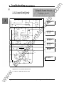
STEP 4: A systematic, logical procedure must be
instituted in order to locate the trouble. This is the
purpose of section 3. By following the systematic
approach, the trouble can be quickly located. Basi
cally there are four major approaches this manual
uses to troubleshoot the MJ-3A. They are:
2) localizing trouble to a functioning mod
ule
3) isolate the trouble to a circuit, and
4) locate the specific trouble, probably to
a specific part
PHASE 2: LOCALIZING TROUBLE TO A FUNC
TIONING MODULE OR SUBSYSTEM - The MJ-3A
regulator controls can be subdivided into modules
(circuit boards) that have a definite purpose or
function. Block diagrams of the MJ-3A (Appendix B)
show the functional relationship of all major sections
in the complete assembly and are the most logical
source of information to use when localizing trouble
to a functional module. Initially, the schematics will
be used only for referencing waveforms at key
areas. Actual component references will for the
most part, not be made during this phase. The MJ-3A
is divided into several functioning units consisting of
discrete circuit board assemblies with well defined
input/output functions. These are 1 ) control panel
PCBoard, (Printed Circuit Board), 2) transformer
PCBoard, 3) interface PCBoard, 4) OatajPak display
option PCBoard, 5) VLC option PCBoard, and 6)
VRC option PCBoard.
alP
STEP 5: You must be able to perform complete
It is assumed at this point. that the MJ-3A is rJPIIPV'p(J
to be defective and is removed from service.
nature of the problem is probably vaguely defined.
Be aware that it is always possible for an r.n.or.,�r.r
to report a trouble that is actually the result of
improper control settings. For this reason, it would
be desirable to determine first the nature of the
problem first-hand and verify the defective claims
made.
tri
c
checkout procedures on the repaired equipment
One major reason for the checkout is that there may
be more than one problem. Without the checkout,
you may have assumed that you have fixed the
problem, when in reality, you may have only fixed
part of it It is also possible that some initial problems
were masking others not yet found.
.E
lec
3.2.2 Defi nition of the
Systematic, Logical
Procedure
ww
w
The systematic approach discussed in step 4 is by
far the most complex step, and this is where the
emphasis is placed in this section. The four major
phases of MJ-3A troubleshooting are summarized
as follows:
PHASE 1 : DffiRMINING TROUBLE SYMPTOMS
- This phase involves determining what the MJ-3A is
supposed to do when it is operating normally and,
in recognizing improper operation when that norMJ-3A Regulator Control Service Manual
When simulating the operation of the MJ-3A, the
module most believed to need attention is often
found in phase 1 (determining trouble symptoms).
If that is the case, then you can proceed directly to
the verification of trouble relating to that module.
The completion of the determining trouble symp
toms step will not isolate the trouble to a defective
component; that comes later in the troubleshooting
process.
PHASE 3: ISOLATI NG TROUBLE TO A CIRCUIT After the trouble is localized to a single functional
unit, the next phase is to isolate the trouble to a
circuit in a faulty module. To do this, you consider
the signal paths in the circuitry that contain the
indicating instruments or other builtin aids that point
to abnormal performance (Le. band indicator LEOs,
Page 3 - 3
-
Section 3.3 is used for phase 1 , as it helps to
determine trouble symptoms. If the fault symptom
is obviously related to a specific circuit board, then
it will reference you to section 3.5 (phase 3 & 4)
directly (Isolating trouble to a circuit, and Locating
the specific trouble). If however, the fault is of a
broader nature, it may be necessary to first localize
the problem to a circuit board (module) first In
this case, you are directed to section 3.4 (phase
2) which will determine the circuit board, then lead
you to the specific circuit in section 3.5.
ar
tM
an
ua
ls
alert light, watchdog, Data/Pak}. By concentrating
on this circuiby and ignoring the circuits that pro
duce normal indications, you narrow down or iso
late the limits of the possible trouble. The isolating
step involves the use of test equipment such as
meters, oscilloscopes, and signal generators for sig
nal tracing and signal substitution in the suspected
faulty area By making the measurements and com
them against the illustrated readings and
valid educated estimates, you can systemat
logically isolate the trouble to a single
rl ollorl·;\/o module. Actual repair techniques and de
are not used until after the specific trouble is
located and verified. Observations are based on
indications of external test equipment used for signal
tracing or signal substitution, and the decisions re
late to whether these indications are normal or
abnormal, based on both your knowledge of how
the MJ-3A works and its resemblance to the pictured
waveform in the block diagram.
.c
om
3 Troubleshooting Procedures
You will be eventually led to section 3.5 which will
illustrate the circuit in question and provide a
procedure to verify its operation. Go to the circuit
mentioned first in the "Action" list If it appears
OK, then go down the list of each of the mentioned
circuits until the fault is found.
tri
c
alP
PHASE 4: LOCATI NG THE SPECIFIC TROUBLE Although this troubleshooting step refers only to
locating the specific trouble, it includes a final ana�
ysis of the complete procedure and the use of repair
techniques to remedy the trouble once it has been
located. The final analysis will enable you to deter
mine whether some other malfunction caused the
component to become faulty or whether the com
ponent located is the actual cause of the trouble. An
oscilloscope is used to observe waveforms and a
meter is used to measure voltages and make resis
tance and continuity checks in order to pinpoint the
defective component After the trouble is located, a
final analysis of the complete troubleshooting pro
cedure should be made to verify the trouble. The
trouble should be then be repaired, and the equip
ment checked out for proper operation.
ww
w
.E
lec
When making repairs, it is suggested that you use
only replacement parts obtained through Siemens
in order to ensure that they meet the high quality
levels initially designed into the MJ-3A.
Page 3 - 4
MJ-3A Regulator Control Service Manual
.c
om
3 Troubleshooting Procedu res
-
•
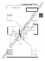
START OF TROUBLE
SYMPTOM ANAL YSIS:
Set Normal/External source switch on MJ
control to "normal".
ar
tM
an
ua
ls
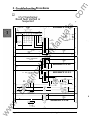
MJ-3A J umper Connections
•
3.3 Determining Trouble
Symptoms
3 . 3.1 Initial Settin gs of
Operator a nd Simulator
Controls
• To the six point terminal strip (TB2) on
the transformer board.
• Connect a jumper C2 to C.
• Be certain there is nm a jumper at "VRC"
or at "AUTO-I NH".
Set the controls to the settings listed below. Doing
so will ensure consistency with the routines fol
lowed in this manual. Reading the Siemens MJ
Operational Performance Evaluation, PIN 2 1 1 1552NXJ3, manual will be very helpful in under
standing the organization and approach used in the
troubleshooting section of this manual. This is espe
cially true with reference to the initial setup pro
ceedures and terminology. Also this manual
contains the same settings that will be used in the
troubleshooting section of this manual.
u;
•
•
ca
lP
3.3. 1 . 1
�
MJ-3A Control Settings
•
HeQ:
•
tri
(Refer to control overlay panel on MJ-3A)
•
•
•
Resistance volts = 0, polarity = '+'
•
Reactance volts = 0, polarity = '+'
ww
w
•
•
.
SW9, (the 8 position DIP switch), (starting
nearest bottom of PCBoard) =
'COCCCCOC', where C=closed and
O=open)
if Data/Pak is present, set to VOLTS
MJ-3A Regulator Control Service Manual
If Interface Option Board and Data/Pak
Option Board are both attached, set po
sition 4 on switches 6,7, and 8 on the
Interface Option Board CLOSED. This will
ensure instantaneous response settings
for voltage, current, and power factor
displayed on the Data/Pak option board.
If VRC (Voltage Reduction Control) op
tion is attached, turn toggle switch to OFF
position.
If VLC (Voltage Limit Control) option is
attached, turn toggle switch to OFF
position.
�oo:�
Voltage Level = 1 20V
Time Delay = 30 seconds
The presence or absence of a relay at RLY
1 position is not important at this time.
3.3.1 .2
Bandwidth = 6.0V
.E
•
Manual auto switch "off"
lec
•
On the 1 2 point terminal strip (TB1 )
the transformer board, connect a
between the P and P1 4 points
bottom points). This should be the on
jumper connected on that strip for
start of the test
»
H�
Initial Simulation Setup
Do you have an operational simulator?
• YES: Review Appendix F, set up simula
tor, then proceed to 3.3.2
• No: The MJ-3A should be proVided with
the following signals, as a minimum:
Line voltage potential (1 1 0 to 1 30
o
volts rms) at U2 and P2 inputs of
PDS connector.
No input to C2 input on PDS con
o
nector. When current flow is re
quired input must be applied.
Page 3 5
-
-
• YES: Go to 3.3.2.2
Note: Without a simulator you may not be
able to complete many observations and
operations directly. However you may be
able to improvise.
• NO:
>
VERIFY:
Control Panel Switch SW1 1 , (lower
left coner of control panel), is in
NORMAL position
Jumpers N 1 -N2 and M1 -M2 have
been added to control panel test
board as instructed.
Cables from connectors J2 and J3
are attached to transformer board
ar
tM
an
ua
ls
o
.c
om
3 Troubleshooting Procedures
o
3 . 3.2 Fault Symptom
Verification
o
o
o
Section 3.3.2 leads you through the necessary steps
to determine not only the faulty circuit board, but
in most instances what circuit sub-system is defec
tive as well. This procedure can be used as both an
initial fault verification, as well as a final inspection
once the board has been fixed to ensure fault
correction.
>
ca
lP
When this section is completed, one of two things
will be true:
2) a fault was verified which will be iso
lated in later sections if the failure mode
crosses more than one circuit board, or
can be determined immediately if iso
lated to one board.
lec
•
1 ) a fault was NOT verified because an
essential operating requirement was
overlooked, thus no fault exists or
tri
•
.E
(NOTE: Steps 3.3.2.1 thru 3.3.2.50 are reserved for
troubleshooting the Control Panel board, however
not all steps have been utilized.
ww
w
The purpose of the 'Watchdog" light on the MJ-3A
control panel is to determine if the panel is function
ing normally. Accordingly, this indicator will be the
basis of troubleshooting.
[;]
»
LED has not broken loose
o
ACTION:
o
If you do not know the specific fault or are unsure
that one exists, then proceed with this section. If you
are aware of a specific fault, then instead of starting
at the beginning of section 3.3.2, look up the fault
in Appendix G, which lists them alphabetically.
There you will find a section number that you can
go directly to in this manual.
PDS connector is attached to excita
tion source
Excitation power source to PDS con
nector is "on"
o
If an item of the verification process
caused the watchdog to begin flash
ing, then proceed to 3.3.2.2
If watchdog indicator light is still not
flashing after the verification pro
cess, then a trouble symptom has
been identified. The next step is to
localize the fault to a functioning
module ... Proceed to section 3.4. 1
3.3.2.2
»
Is reverse power flow light "off".
• YES: Go to 3.3.2.3
• NO:
> VERIFY:
o
>
The
CT
m ag n i tu d e
was
disconnected per initial setup in
3.3.1 and appendix F.
ACTION:
o
Press control panel reset button
(SW1 0). If light remains on, then
fault has been isolated to defective
control panel board. Refer to section
• 3.5. 1. 1 7 (Orcuit Annunciation
Logic )
• 3.5. 1. 1 1 (Reset Circuit)
3.3.2.1
Is the Control Panel Watchdog light flashing
at about a 6 8 Hz Rate?
Page 3 - 6
-
MJ-3A Regulator Control Service Manual
.c
om
3 Troubleshooting Procedu res
-
) VERIFY:
3.3.2.3
»
o
Is the alert light illuminated?
• YES: Go to section 3.3.2.4
o
• NO:
) VERIFY:
) AcnON:
The CT magnitude was discon
nected per initial setup in 3.3.1 and
appendix F
) AcnON:
o
o
• 3.5. 1. 1 8 (Operator Setpoint
Switch Logic)
• 3.5. 1. 13 (P. T. Magnitude Input
Orcuit)
• 3.5. 1 . 9 (Power Supply- low volt
age AID reference)
• 3.5. 1. 1 7 (Orcuit Annunciation
Logic )
• 3.5. 1. 14 (C T. Zero Cross Detec
tion Circuit)
3.3.2.6
»
• 3.5. 1. 12 (P. T. Zero Cross Detec
tion Circuit)
»
• NO:
) VERIFY:
o
Is voltage present at the voltmeter test ter
minals, on control panel?
) VERI FY:
Jumper +P P1 4 loose or not in
stalled on transformer board
lec
) AcnON:
o
A trouble symptom has been identi
fied. The next step is to localize the
fault to a functioning module .... pro
ceed to 3.4.2.
.E
3.3.2.5
»
at
M«::
Make necessary adjustments such that the
measured voltage (voltage level read from
the voltage test terminals or read from the
Data/Pak) is 3-4 volts less than the setting on
the voltage level switch.
ww
w
»
Refer to section
o
• Faulty Neutralite circuitry, see
3.5. 1.3
-
tri
o
PDS Connector is making good con
tact
) AcnON:
• YES: Go to 3.3.2.5
• NO:
Press the Neutralite lamp button (on the
simulator). Did the NEUTRALITE lamp glow?
• YES: Go to 3.3.2.7
ca
lP
• 3.5. 1. 1 1 (Reset Circuit)
Refer to section
• 3.5. 1. 1 7 (Orcuit Annunciation
Logic)
Press control panel reset button
(SW1 0 located on the right side of
and behind the control paneL). If
light remains on, then fault has been
isolated to defective control panel
board. Refer to section :
3.3.2.4
Pressing control panel reset button
(SW1 0) should illuminate this LED
while button is held in.
ar
tM
an
ua
ls
o
Control panel switch settings are per
instruction in section 3.3. 1
Is the "low" light illuminated?
• YES: Go to 3.3.2.6
• NO:
MJ-3A Regulator Control Service Manual
»
Press the operations counter button, (on
the simulator) and release it. Did the opera
tor counter activate and increment by a
count of two every time the circuit was
activated?
• YES: Go to 3.3.2.8
• NO:
) VERI FY:
o
PDS Connector is making good con
tact
) AcnON:
o
Refer to section
• 3.5. 1.5 (Operations Counter In
terface)
Page 3 - 7
-
3.3.2.8
»
Press the drag hands reset button (SW1 4)
on the lower control segment of the control
panel board. Is the drag hand reset light
illuminated while the button is held de
pressed or is 1 20V present at U 1 1 , (on the
PDS connector), when the simulator is not
present?
• YES: Go to 3.3.2.9
• NO:
• YES: Go to 3.3.2. 1 1
• NO:
) VERIFY:
o
Refer to section
o
»
Slowly turn the voltage level, (on the simu
lator), or voltage level switch such that the
measured voltage and the voltage setting
are within 1 .0 volt of each other
Is the "IN" band lamp on?
ca
lP
»
• YES: Go to 3.3.2. 1 0
• NO:
) VERIFY:
o
Pressing control panel reset button
should illuminate this LED while but
ton is held in.
Control panel switch settings are per
instructed in section 3.3.1
tri
o
lec
) ACTION:
o
Refer to section
• 3.5. 1. 1 7 (Orcuit Annunciation
Logic)
• 3.5. 1. 1 8 (Operator Setpoint
Switch Logic)
• 3.5. 1 . 13 (p. T. Magnitude Input
Orcuit)
• 3.5. 1.9 (Power Supply - low volt
age A/D reference)
3.3.2. 1 1
»
Nun
$',I
...
....
Place the MANUAL/AUTO toggle switch to
MANUAL. Toggle the TAP RAISE switch.
Did the 'J' light, (on the simulator), illumin
ate, or is 1 20V present at 'J', (on the PDS
connector), without the simulator
• YES: Go to 3.3.2. 1 2
• NO:
) VERIFY:
o
PDS Connector is making good con
tact
) ACTION:
o
Refer to section
• 3.5. 1.6 (Raise/Lower relay inter
face
.E
• 3.5. 1. 18 (Operator Setpoint
Switch Logic)
Refer to section
• 3.5. 1 . 1 7 (Orcuit Annunciation
Logic)
• 3.5. 1.4 (DRAG HANDS reset in
terface)
3.3.2.9
Pressing control panel reset button
should illuminate this LED while but
ton is held in .
Control panel switch settings are per
instructed in section 3.3. 1
) ACTION:
PDS Connector is making good con
tact
) ACTION:
o
Is the "HIGH" band lamp on?
o
> VERIFY:
o
»
measured voltage is 3-4 volts higher than the
switch setting
ar
tM
an
ua
ls
[;]
.c
om
3 Troubleshooting Procedures
• 3.5. 1. 13 (P. T. Magnitude Input
Orcuit)
ww
w
• 3.5. 1.9 (Power Supply - low volt
age A/D reference)
3.3.2.1 0
»
Slowly turn the voltage level, (on the simu
lator), or voltage level switch such that the
Page 3 - 8
MJ-3A Regulator Control Service Manual
.c
om
3 Troubleshooting Procedures
-
[;]
3.3.2.1 2
»
Toggle the TAP LOWER switch. Did the 'K'
light, (on the simulator), illuminate, or is
1 20V present at 'k', (on the PDS connector),
without the simulator?
o
o
• 3.5. 1 . 1 6 (Relay Driver Circuits)
Refer to section
3.3.2. 1 3
• 3.5. 1. 1 3 (P. T. Magnitude Input
Circuit)
Q
• YES: Go to 3.3. 2. 1 4
• NO:
»
»
n
Slowly turn the voltage level, or voltage level
switch such that the measured voltage is at
least 2 volts less than the voltage level set
ting.
Wait at least 30 seconds.
Is "J" light on?
• YES: Go to 3.3.2. 1 6
• NO: (next page)
o
) ArnON:
ca
lP
Switch #2 of Control Panel Configu
ration Switch SW9 is in open posi
tion per 3.3.1
Response timer is not set for more
than 30 seconds
Refer to section
tri
o
»
in
) VERIFY:
) VERIFY:
o
3.3.2.1 5
CD l ..n
Toggle the AUTO/MANUAL switch back to
AUTO. If "K" light is not on wait about 30
seconds. After thirty seconds, is "K" light on?
o
Refer to section
• 3.5. 1.6 (Raise/Lower Relay inter
face)
• 3.5. 1.6 (Raise/Lower relay inter
face
»
Voltage differential is not greater
than 1 . 5 volts
PDS Connector is making good con
tact
) ArnON:
o
o
ar
tM
an
ua
ls
) VERIFY:
Bandwidth setting is adjusted per
3.3. 1
) ArnON:
• YES: Go to 3.3.2. 1 3
• NO:
o
• 3.5. 1.6 (Raise/Lower Relay inter
face)
lec
• 3.5. 1. 1 6 (Relay Driver Circuits)
• 3.5. 1. 18 (Operator Setpoint
Switch Logic)
o
Switch #2 of Control Panel Configu
ration Switch SW9 is in "open" po
sition per 3.3.1
Response timer is not set for more
than 30 seconds ,
) ArnON:
o
Refer to section
• 3.5. 1.6 (Raise/Lower Relay inter
face)
• 3.5. 1. 1 6 (Relay Driver Circuits)
• 3.5. 1. 1 8 (Operator Setpoint
Switch Logic)
3.3.2. 1 4
Slowly turn the voltage level, or voltage level
switch such that the measured voltage is
within 1 .5 volts of the switch selling
.E
»
Did the HIGH light turn off? Did the IN
BAND light turn on? Is "K" light off?
ww
w
»
• YES: (to all three q uestions) Go to
3.3.2. 1 5
• NO:
) VERIFY:
MJ-3A Regulator Control Service Manual
Page 3 - 9
.c
om
3 Troubleshooting Procedures
-
3.3.2. 1 6
»
Slowly turn the voltage level, or voltage level
switch such that the measured voltage is
within 1 .5 volts of voltage level setting.
Connect the simulated current magnitude to
PDS terminal C2 in phase with the P.T.
magnitude by switching the power flow
switch to forward creating a forward power
flow.
Did ALERT light go out?
• NO:
o
o
Current level provided to C2 must
be greater than 2 mA.
PDS Connector is making good con
tact
• NO:
> VERIFY:
o
»
• IfAlert code indicates a C. T
problem., determine which mod
ule. Proceed to section 3.4. 1 .3.
»
tri
c
lec
• NO:
> VERIFY:
Using a scope that C.T. and P.T. are
out of phase
»
»
Put power flow i n IIforward" position. Close
position #2 of SW9, (the 8 position DIP
switch).
Slowly turn the voltage level, or voltage level
switch such that the measured voltage is at
least 4 volts lower than the voltage setting.
Wait for 1 light to illuminate (30 seconds),
then return the voltage level setting to within
1 .5 volts of the measured voltage.
"
.E
• 3.5. 1. 12 (P. T. Zero Cross Detec
tion Circuit)
ww
w
• 3.5. 1. 14 ( c. T. Zero Cross Detec
tion Circuit)
Page 3 - 1 0
"
Provide a low current (less than 2 mA.) on
terminal C2 by turning the current magni
tude potentiometer o n the s i m u l ator
counter-clockwise. This will cause the
ALERT light to illuminate. Ensure that the
measured voltage is at least 4 volts less than
the voltage setpoint
Wait 30 seconds.
Is it true that neither the "1 " light or the "K"
light came on?
• YES: Go to 3.3.2.20
• NO:
> VERIFY:
> ACTION:
Refer to section
Refer to section
3.3.2. 1 9
»
• YES: Go to 3.3.2 . 1 8
o
RPF light is illuminated, if not .. refer
to 3.3.2. 1 7
• 3.5. 1. 1 6 (Relay Driver Circuits)
Refer to section
Refer to section that Alert Code
Logic Refers you to. If due to C.T.,
then.....
Transfer power flow to reverse power flow.
After a 5 second delay, did the RPF light
come on?
o
Temporarily remove (or lower) the PDS
terminal P2 voltage by lowering the "L"
(load) variac on the simulator. Did the ob
served voltage stay the same?
• YES: Go to 3.3.2. 1 9
»
alP
o
»
There are still other alert codes set..
see Appendix E.
> ACTION:
o
3.3.2.1 8
> ACTION:
> VERIFY:
o
II
o
• YES: Go to 3.3.2. 1 7
»
11111 11'1
ar
tM
an
ua
ls
»
...
o
>
SW9 Position #2 of the 8 position
DIP switch is closed.
ACTION:
o
Refer to section
• 3.5. 1. 1 8 (Operator Setpoint
Switch Logic)
• 3.5. 1. 1 7 (Circuit Annunciation
Logic)
• 3.5. 1. 15 (CT magnitude)
MJ-3A Regulator Control Service Manual
.c
om
3 Troubleshooting Procedures
-
o
3.3.2.20
»
o
Re-open SW9 switch position #2 (of the 8
position DIP switch). Did the "J" light turn
on?
o
• YES: Go to 3.3.2.21
• NO:
>
The conditions per 3.3.2. 1 9 have
been met
Refer to section
3.3.2.21
»
Is a relay installed in RLY 1 of the transformer
board?
• NO:
ca
lP
Re-configure the jumpers on the 1 2 point
sensing transformer terminal strip:
• +PB to 20
• P1 4B to 20
• P1 4A to 2 5
VERIFY:
o
• +PA to 2 0
o
>
The correct jumper configuration
has been installed
That the RPF light is on
The switch #8 switch status is
"COCCCCOC" per 3.3.1
ACTION:
o
Refer to section
• 3.5.2. 1 (Sensing Transformer)
lec
tri
Remove the jumper which had been con
nected from P to P1 4. (This configuration
tests the sensing transformer by introducing
no correction for forward power flow, and
a minus 5 volt correction for reverse power
flow.)
Re-connect transformer board, and turn on
system power.
Verify power flow is in FWD mode. Apply
current magnitude at maximum level.
.E
»
>
o
3.3.2.22
»
Is there a 5 volt difference between the two
readings?
• YES: Go to 3.3.2.24
• NO: Go to 3.3.2.24
»
»
Put power flow to reverse setting. Using
voltmeter, measure and compare the volt
age between the test terminals and the in
coming voltage on PDS connector U2 to E.
Turn power OFF to all of the system.
• YES: Go to 3.3.2.22
»
3.3.2.23
»
• 3.5. 1. 1 8 (Operator Setpoint
Switch Logic)
»
Refer to section
• 3.5.2. 1 (Sensing Transformer)
AcnON:
o
> AcnON:
o
VERIFY:
o
That the RPF light is NOT on
The switch #8 switch status is
"COCCCCOC" per 3.3. 1
ar
tM
an
ua
ls
>
The correct jumper configuration
has been installed
Using the voltmeter, measure and compare
the voltage between the test terminals and
the incoming voltage on PDS connector P2
to E. Is it true that there is NO difference in
voltage?
ww
w
»
• YES: Go to 3.3.2.23
• NO:
>
VERIFY:
MJ-3A Regulator Control Service Manual
Page 3 - 1 1
-
[J
3.3.2.24
»
»
»
»
»
Turn OFF the power switch to the system. If
you m od ified any j u m per settings in
3.3.2.22, remove them now and replace the
jumper on P to P1 4.
Put a jumper across the AUTO - I N H termi
nals on the transformer board.
Turn the power switch back ON.
Wait at least 30 seconds. Are both the 1
and "K" lights off?
"
• NO:
Refer to section :
• 3.5.2.3 (P. T. Zero Cross Trans
former)
Open switch SW9 position #8 (of the 8
position DIP switch). Does reverse power
light illuminate after 5 seconds?
• YES: Go to 3.3.2.51
>
VERIFY:
o
o
c.T. is connected.
Alert light is not on.
> ACTION:
Refer to section :
• 3.5. 1. 1 8 (Operator Setpoint
Switch Logic)
(This concludes testing of the control panel
board. NOTE: When using the Data/Pak In
the following steps with the simulator, the
actual power factor reading on the
Da ta/Pak can vary slightly due to
component tolerances in the simulator.)
ca
lP
3.3.2.25
»
"
The AUTO-IN H jumper is providing
good continuity.
> ACTION:
o
»
Verify that current is in forward power flow
mode.
o
> VERIFY:
o
»
• NO:
Put voltage level switch to 1 06 volt setting.
Put power flow in forward mode.
• YES: Go to 3.3.2.25
3.3.2.26
ar
tM
an
ua
ls
[J
.c
om
3 Troubleshooting Procedures
Remove the AUTO-INH jumper. Does the
"K" light illuminate?
• YES: Go to 3.3.2.26
• NO:
VERIFY:
o
The AUTO-INH jumper is definitely
removed
tri
>
> ACTION:
Refer to section
lec
o
ww
w
.E
• 3.5.2.3 (P. T. Zero Cross Trans
former)
Page 3 - 1 2
MJ-3A Regulator Control Service Manual
.c
om
3 Troubleshooting Procedu res
-
- VRC Option Board ...... section
3. 5.6
3.3.2.51
• YES: Go to 3.3.2.52
• NO: Do you have either a VLC or VRC
option module?
• 3.5.3.9 (Control Panel Bus Arbi
tration)
o
YES: Go to 3.3.2.67
NO: Go to 3.3.2. 1 01
Is the I nterface Board Watchdog light flash
i ng at about a 6 8 Hz Rate?
-
• YES: go to 3.3.2.53
• NO:
>
>
VERI FY:
o
Cable is correctly attached.
Refer to section :
• 3.5.3.2 (Power Supply)
• 3.5.3. 1 (Oscillator)
3.3.2.53
alP
• 3.5.3.5 (Reset circuit/ watchdog
circuit)
Is the I nterface Board Transmit Light (back
side of MJ) flashing about every half-second?
>
Attach the voltmeter to the test leads. Rotate
the Operator calibration switch (on the side
panel) until the voltage on the Data/Pak and
the voltage measured at the test terminals
are the same (within 1 /8 [. 1 25] volts of each
other). Is the calibration LED illuminated?
• NO:
>
VERIFY:
o
The Data/Pak, is at the "volts" set
ting.
> ACTION:
o
Refer to section
• 3.5. 1. 1 8 (Operator Setpoint
Switch Logic)
VERIFY:
o
Conditions in 3.3.2.52 have been
met
lec
>
»
Set SW9 DIP switch (located on the control
panel board) to its initial starting conditions
(COCCCCOC).
tri
c
• YES: Go to 3.3.2.54
• NO:
3.3.2.54
• YES: Go to 3.3.2.55
ACTION:
o
• 3.5.3. 1 0.5 (XMIT LED circuit)
»
3.3.2.52
»
Refer to section :
• 3.5.3. 1 0 (Control Panel Commu
nications Interface)
o
»
o
Do you have both an interface module and
Data/Pak option?
ar
tM
an
ua
ls
»
ACTION:
Shut off power and disconnect
Data/Pak option board. Turn on
power. If 3.3.2.53 is now satisfied,
then problem exists with this mod
ule. If not, turn off power again and
replace the Data/Pak. Try the same
approach with the VRC and VLC
modules as well. If problem is tied to
option module, refer to trouble
shooting for that module:
ww
w
.E
o
- Data/Pak Option Board .. ,
section 3.5.4
- VLC Option Board ...... section
3.5.5
MJ-3A Regulator Control Service Manual
Page 3 - 1 3
-
g
3.3.2.57
3.3.2.55
»
Does the DataJPak appear to be operating
Correctly?
»
• YES: Go to 3.3.2.56
>
• NO:
VERIFY:
ar
tM
an
ua
ls
>
>
The cable from the interface board to
the DataJPak is correctly installed.
ACTION:
o
Refer to section
>
Set the following DIP switches on the inter
face board:
o
CT ratio switch (#5) to (CCOCC)
[set for 200A CT primary rating].
o
AMP SWITCH (#7), VOLT SWITCH
(#6), and PF SWITCH (#8) all are set
to (COCC).
Set power flow for "forward". Apply full
current magnitude.
ca
lP
»
Do COMP VOLTS and VOLTS display the
same value?
• YES: Go to 3.3.2.57
• NO:
VERIFY:
o
>
Control Panel Switches set in accor
dance with 3.3.1
tri
>
ACTION:
lec
• 3.5.3.7 (Interface Board Switch
Decoding)
ww
w
.E
• 3.5.4 (Data/Pak Option Board)
Page 3 - 1 4
o
DataJPak knobs are in correct set
tings
C.T. is attached.
ACTION:
o
Refer to section
• 3.5.3.7 (Interface Board Switch
Decoding)
3.3.2.56
»
VERIFY:
o
• 3.5.4 (Data/Pak Option Board)
»
'M
Does PF display a very high (slightly less than
.999) power factor, and does AMPS display
a reading greater than 1 50?
• YES: Go to 3.3.2.58
• NO:
>
15M
.c
om
3 Troubleshooting Procedures
• 3.5.4 (Data/Pak Option Board)
3.3.2.58
»
»
»
»
»
»
Fully rotate the CT (current magnitude po
tentiometer on the simulator) counter-clock
wise. Verify that the ALERT light illuminates.
Turn the DataJPak selector to the ALERT
position and verify the existence of the
code (should be "5000").
With the DataJPak selector set to amps,
rotate the current magnitude potentiometer
clockwise until a reading of 1 0r2 appears.
Turn the DataJPak selector to the ALERT
position and verify the existence of the
code (should be 1/1 000").
Press and release the reset button (SW3) on
the interface board.
Does the display momentarily read zero as
switch is released?
• YES: Go to 3.3.2.59
• NO:
>
VERIFY:
o
>
The reset button is SW3. The other
pushbutton is the DRAG HANDS
reset (SW4).
ACTION:
o
Refer to section
• 3.5.3.5 (Interface Board Reset
Circuit)
MJ-3A Regulator Control Service Manual
.c
om
3 Troubleshooting Procedu res
-
[]
o
3.3.2.59
»
»
> ACTION:
Are the values the same as those before you
shut off the power? While observing each
one of the readings again, press the
DatajPak Drag Hands reset button. Do at
least some of the values reset to another
value?
• NO:
>
VERIFY:
o
>
The DRAG HAND reset button is
SW4. The other pushbutton is the
RESET (SW3).
ACTION:
o
Refer to section
• 3.5.3.4 (Power Monitor Circuits)
• 3.5.3.3 (Microcomputer Mem
ory Management)
ca
lP
• 3.5.3. 7 (Interface Board Switch
Decoding)
• 3.5.4 (Data/Pak Option Board)
3.3.2.60
• 3.5.3. 7 (Interface Board Switch
Decoding)
3.3.2.61
»
»
Reset line drop adjustments RESISTANCE
VOLTS and REACTANCE VOLTS both back
to zero.
Set conditions for Forward Power Flow,
maximum current and lagging power factor.
Is the RPF LED off? Is the power factor about
. 700 to .800 lag?
• YES: Go to 3.3.2.62
• NO:
> VERIFY:
>
o
Power factor is lagging.
ACTION:
o Refer to section
• 3.5. 1 . 1 8 (Operator Setpoint
Switch Logic)
lec
tri
Disconnect current to C2 by turning the
power flow switch on the simulator to OFF.
Set the RESISTANCE VOLTS on the control
panel to 6 volts with the polarity switch in
the + position. Set the REACTANCE VOLTS
on the control panel to 8 volts with the
polarity switch in the + position. Turn the
DatajPak to COMP VOLTS.
(NOTE: Test procedures 6 1 thru 67 test for
the DIP switches on the control panel board
. It is much easier to test when using the
Interface & Data/Pak option modules.)
Adjust the voltage level setting such that the
setting is within 1 .5 volts of the measured
value. The IN-BAN D indicator LED will be
activated..
.E
»
• 3.5. 1 . 1 B (Operator Setpoint
Switch Logic)
Turn system off for 30 seconds, then turn it
back on.
• YES: Go to 3.3.2.60
»
o Refer to section
Record the readings for the LOW VOLT,
HIGH VOLT, MAX AMP, LEAD PF, and LAG
PF.
ar
tM
an
ua
ls
»
C.T. is attached.
»
»
Connect C2 with maximum current and for
ward power flow.
Is LOW indicator LED on? Does COMP
VOLTS read at least 1 volt less than the
measured input voltage?
ww
w
• YES: Go to 3.3.2.61
• NO:
> VERIFY:
MJ-3A Regulator Control Service Manual
Page 3 - 1 5
.c
om
3 Troubleshooting Procedures
-
3.3.2.62
»
3.3.2.65
Switch to reverse power flow mode. . Wait
at least 5 seconds. Is RPF light now on?
Does the power factor remain as i n
3.3.2.61 ?
»
• YES: Go to 3.3.2.66
• YES: Go to 3.3.2.63
• NO:
ar
tM
an
ua
ls
• NO:
> ACTION:
) VERIFY:
o Refer to section
o Control panel DIP switches are set
in accordance with 3.3.1
) ACTION:
o Refer to section
• 3.5. 1 . 1 8 (Operator Setpoint
Switch Logic)
• 3.5. 1 . 1 8 (Operator Setpoint
Switch Logic)
3.3.2.66
»
Open switch position #6. Is power factor
now .95 to .96 leading
• YES: Go to 3.3.2.67
3.3.2.63
»
Leaving switch #1 open, open switch posi
tion #5. Is power factor now .2 to .30
leading?
• NO:
Revert to Forward Power Flow. Wait 5 sec
onds for response. Set control panel DIP
switch, position #7 to the closed position....... .
(COCCCCCC). Is the RPF light on? Does the
power factor remain as in 3.3.2.61 ?
• NO:
) VERIFY:
ca
lP
• YES: Go to 3.3.2.64
o C o n trol panel D I P switch #8,
> ACTION:
o
Refer to section
• 3.5. 1 . 1 8 (Operator Setpoint
Switch Logic)
(NOTE: Test procedures 67 - 69 test the VRC
option, procedures 70 - 71 test the VLC
option, and procedures 72 73 test both. If
you do not have either of these option
modules, then proceed to 3.3.2. 1 0 1)
-
position 7 is firmly i n a closed posi
tion
> ACTION:
tri
o Refer to section
• 3.5. 1 . 1 8 (Operator Setpoint
Switch Logic)
»
lec
3.3.2.64
Set DIP switch position #1 open. Is power
factor now leading?
• YES: Go to 3.3.2.65
.E
• NO:
> ACTION:
o
Refer to section
ww
w
• 3.5. 1 . 1 8 (Operator Setpoint
Switch Logic)
Page 3 - 1 6
MJ-3A Regulator Control Service Manual
.c
om
3 Troubleshooting Procedures
-
-
3.3.2.67
»
»
1
3.3.2. 69
..
"WeI
»
Ensure that control panel board 8 position
DIP switch is set to its i nitial condition per
section 3.3. 1 (COCCCCOC).
Do you have a VRC option module?
»
»
• YES: Proceed
• YES: Go to 3.3.2.70
Set the voltage switch such that it is within
1 .5 volts of the measured voltage and the
in-band light illuminates.
• YES: Go to 3.3.2.68
• NO:
> VERIFY:
Refer to section :
Put VRC switch into REMOTE switch setting.
Does the "K" light immediately go off and
stay off when the transition is made?
• YES: Go to 3.3.2.69
• NO:
tri
> ACTION:
o
o
Refer to section
• 3.5.2.3 (P. T. Zero Cross Trans
former T4)
3.3.2.70
»
Refer to section
• YES: Turn toggle switch on VLC to ON
position. Go to 3.3.2.71 .
.�
3.3.2.71
»
»
Set the VLC UPPER volts to a setting less
than the actual voltage.
Do all band indicators extinguish them
selves? Does the "K" light illuminate im
mediately?
• YES: Go to 3.3.2.72
• NO:
> ACTION:
o
Refer to section
• 3.5.5 (VLC option)
• 3.5.6 (VRC Option)
ww
w
.E
lec
• 3.5.6 (VRC option)
Do you have a VLC option module?
• NO: Go to 3.3.2. 1 01
ca
lP
• 3.5.6 (VRC option)
3.3.2.68
The VRC contacts are shorting to
gether.
> ACTION:
Switch on VRC is in a detent position
> ACTION:
o
o
• 3.5.6 (VRC Option)
> VERI FY:
»
• NO:
Set the VRC switch to 5% setting. Turn on
VRC by putting the switch in a LOCAL set
ting. Does the "K" light illuminate as soon as
the VRC is activated without regard for time
delay setting?
o
'R
ar
tM
an
ua
ls
• NO: Go to 3.3.2.70
R
While the system is powered u p, momentar
ily touch the two VRC contacts on the trans
former board with a jumper wire, then
remove. Does the "K" light illuminate when
the jumper makes contact and immediately
go off when the jumper is removed?
MJ-3A Regulator Control Service Manual
Page 3 - 1 7
-
3.3.2.72
»
Turn both accessory toggle switches to OFF.
Set rotary VRC switch to 1 0%. Set VLC
LOWER to 1 1 5V, VLC UPPER to 1 25 volts.
Adjust voltage until Data/Pak reads about
1 20 volts. Turn on both VLC and VRC to
LOCAL setting. Is the "K" light on?
• YES: Go to 3.3.2.73
ACTION:
o Refer to section
• 3.5.5 (VLC option)
• 3.5.6 (VRC Option)
[;]
'&
3 .3.2.73
»
[;]
3.3.2.1 0 1
»
»
»
• NO:
>
(NOTE: Test procedures 74-1 00 are reserved
for future use )
8:
Phase 1 (Determining Trouble Symptoms)
has been concluded.
ar
tM
an
ua
ls
[;]
.c
om
3 Troubleshooting Procedures
Turn off power.
If you have not discovered a problem, it is
possible that the problems may have been
mis-reported due to the operator's mis-un
derstandings of how the system should op
erate. If you are convinced that there is a
problem, or want further verification, sec
tion 3.5 contains each circuit path and key
input! output signals.
Adjust the voltage such that the it goes
below 1 1 5 volts. Is the "J" light on?
• YES: Go to 3.3. 1 01
• NO:
>
ACTION:
o
Refer to section
• 3.5.5 (VLC option)
ww
w
.E
lec
tri
ca
lP
• 3.5.6 (VRC Option)
Page 3 - 1 8
MJ-3A Regulator Control Service Manual
.c
om
3 Troubleshooting Procedures
-
Due to the nature of how the transformer board is
electrically "daisy-chained" into the control panel
board, it is not immediately apparent where the
specific fault lies. This section helps to isolate faults
to not only the particular board, but also to the
particular circuit on the board as well.
ar
tM
an
ua
ls
3.4 Localizing Trouble to a
Functioning Module or
Sub-system
This section should be used only if directed specif
ically by another section. The fault will have been
identified in the "determining trouble symptoms" of
section 3.3, or a known fault would have been
looked up in the cross reference section of Appen
dix G.
This section will accomplish two purposes:
•
•
This section helps to determine when a problem is
related to the:
•
•
2) transformer board
it will provide clues of which circuits in
particular appear to be causing the prob
lem, and reference you to that appropri
ate circuit in section 3.5
Proceed with the suspected circuits, in the order
shown, until the actual circuit has been isolated.
3) electronic portion of the control panel
board
ww
w
.E
lec
tri
ca
lP
•
1 )electrical portion of the control panel
board
it will establish which circuit board is caus
ing the fault
MJ-3A Regulator Control Service Manual
Page 3 - 1 9
.c
om
3 Troubleshooting Procedures
-
Reference for test
instrument ground to be
Reference for test
instrument ground to be
made at connector
'0
20
SEC
30
20
:30
40
xE-3
SEC
tri
ca
lP
0
ar
tM
an
ua
ls
made at connector
lec
Figure 3-1 : No apparent power to control panel
[;]
3.4.1 No apparent power
.E
to control panel.
»
POSSIBLE CAUSES:
• Transformer board not receiving power
from electrical portion of control panel
board due to bad connection.
• Defective Electronic Section of control
panel board (i.e. watchdog annunciation
circuitry)
• PDS connector not receiving proper sig
nals:
ww
w
• Control panel board not receiving power
from transformer board due to bad con
nection
• Transformer board malfunctioning
Page 3 20
-
MJ-3A Regulator Control Service Manual
-
.c
om
3 Troubleshooting Procedures
o If waveform is still absent, go to
3.4. 1 . 5.
»
o If waveform appears, fault has been
Verify if the control panel board is receiving
AC power from the transformer board
[;]
»
If waveform appears, fault has been
isolated to defective control panel
board. Refer to section (circuit):
o
• 3.5. 1. 1 7 (circuit annunciation
logic)
• 3.5. 1. 1 1 (reset circuit)
Verify that the connector from transformer
board is not causing the problem
»
3.4.1 .6
Find out why PDS connector is not getting
power. It appears that either the excitation
source is turned off or is malfunctioning, and
this is beyond the scope of this manual.
tri
c
»
I
[;]
alP
• Connect a scope or DVM to pin 1 of
connector J3 as done in 3.4. 1 . 1 , but this
time at transformer board.
o
If waveform is still absent, go to
3.4. 1 .3.
o
If waveform appears, fault has been
isolated to defective connector, or
solder connection. Repair it and
continue with 3.3.2.1 .
3.4.1 .3
Verify that power is getting to the control
panel board
• 3.5. 1.2 (potential & utility wind
ing interface)
3.4.1 .2
»
1 .5
• Connect a scope or DVM to PDS con
nector inputs on the control panel board
between U2 and E (ground) signals.
o If waveform is still absent, go to
3.4. 1 .6
o If waveform appears, fault has been
isolated to defective control panel
board (electrical section). Refer to
section:
• 3.5. 1.8 (power supply logic refer
ence)
• 3.5. 1 . 1 0 (oscillator)
3
ar
tM
an
ua
ls
• Connect a scope or DVM from ground
to pin 1 of connector J3 as shown in
Figure 3. 1 .
o
If waveform is absent, go to 3.4. 1 .2
isolated to defective connector, or
solder connection. Repair it and
continue with 3.3.2. 1 .
Verify if the tran sformer board i s
malfu nctioni ng
lec
• Connect a scope or DVM to pin 4 of
connector J2 at the transformer board as
shown in Figure 3-1 .
o
If waveform is absent, go to 3.4. 1 .4.
o If waveform appears, fault has been
.E
isolated to defective transformer
board. Refer to section:
• 3.5.2. 1 (transformer board)
3.4.1 .4
..
..
Verify that the connector from control panel
board is not causing the problem
ww
w
»
• Connect a scope or DVM to pin 4 of
connector J2 as done in 3.4.1 .3, but this
time at the control panel board.
MJ-3A Regulator Control Service Manual
Page 3 - 21
-
.c
om
3 Troubleshooting Procedures
Reference for test
Reference for test
instrument ground to be
instrument ground to be
made at connector
tri
ca
lP
SEC
ar
tM
an
ua
ls
made at connector
lec
Figure 3-2: No apparent P. T. sensing
[;]
.E
3 .4.2 No app � rent P.T.
sensing
»
POSSIB LE CAUSES:
• Transformer board not receiving power
from electrical portion of control panel
board due to bad connection
• Defective Electronic Section of control
panel board (Le. P.T. magnitude cir
cuitry)
• PDS connector not receiving proper sig
nals.
ww
w
• Control panel board not receiving power
from transformer board due to bad con
nection
• Transformer board malfunctioning
Page 3 22
-
MJ-3A Regulator Control Service Manual
.c
om
3 Troubleshooting Procedu res
-
g
3.4.2. 1
• Connect a scope or DVM to pin 2 of
connector j2 as done in 3.4.1 .3, but this
time at the control panel board
..
» Verify if the control panel board is receiving
AC power from the transformer board
o If waveform is still absent, go to
3.4.2.5
• Connect a scope or DVM from ground
to pin 5 of connector j3 as shown in
Figure 3.2.
o If waveform is absent, go to 3.4.2.2
o If waveform appears, fault has been
ar
tM
an
ua
ls
isolated to defective connector, or
solder connection. Repair it and
continue with 3.3.2.4.
o If waveform appears, fault has been
3.4.2.5
isolated to defective control panel
board. Refer to section (circuit):
» Verify that power is getting to the control
panel board
• 3.5. 1 . 1 3 (P. T. Magnitude Input
Circuit)
[;]
3.4.2.2
• Connect a scope or DVM to PDS con
nector inputs on the control panel board
between P2 and E (ground) signals.
�:
o If waveform is still absent, go to
» Verify that the connector from transformer
board is not causing the problem
3.4.2.6
o If waveform appears, fault has been
isolated to defective control panel
board (electrical section). Refer to
section:
• 3.5. 1.2 (Potential & Utility Wind
ing Interface)
g
�
ca
lP
• Connect a scope or DVM to pin 5 of
connector j3 as done in 3.4.2. 1 , but this
time at transformer board.
o If waveform is still absent, go to
3.4.2.3.
o If waveform appears, fault has been
isolated to defective connector, or
solder connection. Repair it and
continue with 3.3.2.4.
3.4.2.3
» Veri fy if the transformer board i s
malfunctioning
3.4.2.6
n�N
» Find out why PDS connector is not getting
power. It appears that either the excitation
source is turned off or is malfunctioning, and
this is beyond the scope of this manual.
lec
tri
• Connect a scope or DVM to pin 2 of
connector j2 at the transformer board as
shown in Figure 3-2
o If waveform is absent, go to 3.4.2.4
o
If waveform appears, fault has been
isolated to defective transformer
board. Refer to section:
• 3.5.2. 1 (Transformer Board, Sens
ing Transformer)
3.4.2.4
.E
[;]
ww
w
» Verify that the connector from control panel
board is not causing the problem
MJ-3A Regulator Control Service Manual
Page 3 - 23
.c
om
3 Troubleshooting Procedures
-
Reference for test
instrument ground to be
made at connector
SEC
lec
tri
ca
lP
SEC
ar
tM
an
ua
ls
Reference for test
instrument ground to be
made at connector
.E
Figure 3-3: No apparent C T. sensing
3.4.3 No app arent C.T.
sensing
ww
w
» POSSIBLE CAUSES:
• Control panel board not receiving power
from transformer board due to bad con
nection
Page 3 24
-
• Transformer board malfunctioning (C C2 jumper missing or defective trans
former)
• Transformer board not receiving power
from electrical portion of control panel
board due to bad connection.
• Defective Electronic Section of control
panel board (Le. C.T. magnitude cir
cuitry)
• PDS connector not receiving proper sig
nals.
MJ-3A Regulator Control Service Manual
.c
om
3 Troubleshooting Procedures
-
g
3.4.3.1
» Verify if the control panel board is receiving
AC power from the transformer board
o
If waveform appears, fault has been
isolated to defective control panel
board. Refer to section (circuit):
• 3.5. 1. 15 (C T. Magnitude Input
Circuit)
[;]
3.4.3.2
» Verify that the connector from transformer
board is not causing the problem
• Connect a scope or DVM to pin 6 of
connector J3 as done in 3.4.3.1 , but this
time at transformer board.
o
If waveform is still absent, go to
3.4.3.3.
If waveform appears, fault has been
isolated to defective connector, or
solder connection. Repair it and
continue with 3.3.2.1 7.
ca
lP
o
o
o
If waveform is still absent, go to
3.4.3.5
If waveform appears, fault has been
isolated to defective connector, or
solder connection. Repair it and
continue with 3.3.2.1 7.
ar
tM
an
ua
ls
• Connect a scope or DVM from ground
to pin 6 of connector J3 as shown in
Figure 3.3.
o
If waveform is absent, go to 3.4.3.2
• Connect a scope or DVM to pin 5 of
connector J2 as done in 3.4. 1 .3, but this
time at the control panel board
3.4.3.3
» Verify if the tran sformer board i s
malfunctioning
3.4.3.5
» Verify that power is getting to the control
panel board
• Connect a scope or DVM to PDS con
nector inputs on the control panel board
board between C2 and E1 (ground) sig
nals.
o
o
If waveform is still absent, go to
3.4.3.6
If waveform appears, fault has been
isolated to defective control panel
board (electrical section). Refer to
section:
• 3.5. 1 . 1 (c.T. interface)
3.4.3.6
.....
» Find out why PDS connector is not getting
power. It appears that the excitation source
is turned off or may be malfunctioning,
which beyond the scope of this manual.
• Connect a scope or DVM to pin 5 of
connector J2 at the transformer board as
shown in Figure 3-3.
• 3.5.2.4(Transformer Board, AUX
C T. Transformer)
3.4.3.4
.E
g
lec
o
If waveform is absent, go to 3.4.3.4
If waveform appears, fault has been
isolated to defective transformer
board. Refer to section:
tri
o
ww
w
» Verify that the con nector from control panel
board is not causing the problem
MJ-3A Regulator Control Service Manual
Page 3 - 25
.c
om
3 Trou bleshooting Procedures
ar
tM
an
ua
ls
-
ww
w
.E
lec
tri
c
alP
THIS PAGE INTENTIONALLY BLANK.
Page 3 26
-
MJ-3A Regulator Control Service Manual
.c
om
3 Troubleshooting Procedures
-
ar
tM
an
ua
ls
3.5 Isolating Trouble to a
Circuit
Section 3.3 helped determine if there was a fault
based on operating characteristics. It has then led
you to here directly orvia section 3.4 where the fault
was narrowed down to a circuit board. Based on the
analysis of the fault found , you are guided to the
circuit most suspected of causing the fault
ww
w
.E
lec
tri
ca
lP
If after going through the procedure for the circuit
in which you are directed, you still do not find the
faulty component, go back to the area in section 3.3
and refer to the next suggested circuit
MJ-3A Regulator Control Service Manual
Page 3 27
-
.c
om
3 Troubleshooting Procedures
-
3 .5. 1 Control Panel Board:
Fau lt Verified or Suspected
�
U
P2
�
----<
F11 1
Q
fuI)
'C.l
CHASSIS I
SW1 1
"
M2
�
�
�
Ul1
1 �B-J
Ul0
I
SW1 2
@ ,
�
®"oo
I MAN
c;:: 470 0
R63 20K, .ow
DRAGHAND RESET
N/O ----L- c SW1 4
JP1 6
00
C12
O.lJLf
1 000V
I AUTO
�
�
J
A
2
C13
.E
K
I
r.
1
l
RLY 1 2
4 5
D lA 3A
3
0
MAN
K20
�
"' u
U7
�
/
-
1
K2 1
RLY 1 4
JP1 7 �
4 5
00
l A 3A
lec
I
'---
,I,
I
I
REFERENCE:
3.5.1 .2
I=b
EXT
-
00
SW1 3
RAISE
OFF
0
1
REFERENCE:
3.5. 1 . 4
REFERENCE:
3.5.1 .5
U6
-
3,-..
REFERENCE:
3.5. 1 .3
00
JP15
tri
0
I--
F3, 4A
HI
H2 crl6\9h
OPERATiON
'COUNTER
� 5;:0
J
YEL
-
REFERENCE:
3.5. 1 . 1
5
m";"t 4
0
I
( L2
INORM
K
NLT
!co)] REO
�O� BLK
I
WHT (0
F l , 4A
N
�
U),2
Ef? 1
1
( L1
NUKM
6
RLY 1 3
3*4
.
��
FL1 2
�
4
SLO BLO
n=>
v>
eI--�
10
5
2
TEST
ca
lP
I@
n
I
l� l�
� ;':> v,.lI1 >�
1
3
1
E
r-o
0
4
5
�
j@
I@
6
1
�
,@r'(£\
7
1
8
ar
tM
an
ua
ls
I
J2
REFERENCE:
3.5. 1 .6
2
LOWER
O . I /,f
Notes:
1 . All resistors are .25w, 5% unless otherwise noted.
ww
w
2.
All diodes are
Page 3 - 28
1 n4002 u nless otherwise noted.
MJ-3A Regulator Control Service Manual
.c
om
3 Troubleshooting Procedures
REF: 3.5.1 .7
JJ
� (4 ���
ll'�� J�� '�f v v ..
v""
r,OCj
I
....
r-r.
II
KtJ-: .1 •.'1 . I . 1.:S
REF: 3.5. 1 . 1 4
•
.�
C.I. NAG
..
itEr
�
4
"-"::1
�.���
v.
f
fU[T M
'Ol
g ,.'�
�'"
If':
�.
r.=;-'
,
ijl:)
�111,',.
ftNll
Ult
�
-'
�
�
�.u.�� .,
�(l).l�;T
Y 'J�
l
,"' 1C2,
,� �.
�
" 01'7 IJ�
.�
f'".!.
�.
:,,�
. �lc
jell
I!� �B;;
1 � 'b�
''''�
'
Ul
� "."
1
, _,
IIA':!
r""
02'1
>
PA3 •
�
! _�
a
...
lec
1
1
1
,
f� � �f� : � f�
!II I
' W '"T �1 �
! � -I i �
i : . ' � I�I �
1. ,
-
O 1 'lI' "
ww
w
.E
...Q l
.
.
�
r
•
c
, ;
- ","
�
cu',.
�
{-1�
�§
'f
"'L
{-}
C
•
LIo41Z4
, 1J
,. 1
",,
,1 � '�
r
� -
,..
C
....r LtD1A
L':1"--.J
.
.,..0.
"'"
4700 .... .
.
���
0.1111 1
�
1K
' 11 . _
�'"
�
"CYr' ,�
F!::L !'�"' �
�
D�
�
'i(,,5W
l.'IC
•
•
i ',l.
21l1lD'l'A
0
,
,
'
� U1,[J,t ,
•
,n:: 1 0
"
.,�
VJ..� j4
I
"
"
IT"
l
,
·
J
•
•
·
·
"r!¥.ll ,," !
·
J,tl,11!lij oo. ��
� - - - - - ----"
I
"':I � a
"""
III
�:'
3!
,
,
.,
��
>7
IIAC�� :;!tI
""")-- %'
�
..
'
"
'1I{UY
REF: 3.5. 1 . 1 6
g
):�
T
"' -
u!\ "IE: HT-:�
"'.'�
R
...
l�"."
"'"
I ·� 1';: ,, 1
� 1;:.,1 u�"."
,
.
'if-
,.., ,"'", .r '"
' . 4G11l
,021
-"it-
-
VtO:: IC
.':>. 1 . 1 1
�
>-[oo@-"
�J
I
�
�
....
",,
-
L
*' ,.r
REF: 3.5. 1 . 1 8
AM
101
" ��
•
�
U'
10il
�Cl���2��
I ��
I
1
I
!:�
,
I
�� �
�"' J 1 , lw-! �
4
�r� �f
! �<r"1apl
-
,
....01:"
...
..,. ."
.-�
Ktt:
"....7 '
,
"-
V"O:;C
�:!,:':t-:! ,; ,:
�
,
I
REF: 3.5.1 . 1 1
�k!C � �:r.�
Vat
o.W .....2.:! v
¥1iI�f
I
�
,
TP> �
�
h,, �j-s/
lJ.luf
C"
I
MI Se. REFERENCES
tri
c
Ktt: .1.5. 1 . 1 5
�-�
JPl
I
.. "
'loot
""
REF: 3.5. 1 . 1 2
�
AH!fr. ..
''1]' -�
REF: 3.5.1 .9
II
,
.JP11
JO<'
f -!" l:ow �f
I II
I
�
1'5
REF: 3.5. 1 .8
I
alP
�
_
>
v""
ar
tM
an
ua
ls
-
,
I
."
,�
"n aT 7
21
,.
,.
27
%0
1 0 '" :2
�
ltili �'�r� � J� a' � j��t\ , alfi�n ·" '
To
....[ Dn."Ul�
I • I " I I,-.",.
c r ,� c I I,... Ie I 'S��l. 'S[TTHQ
�:� a�
I�
I
MJ-3A Regulator Control Service Manual
_1 ,
�. C
...
'
�
i'
;3 ..
-. ,.,
"
'"
..
,
1
'f�trtN
...._or..
\oUN;[
,.,""'"
l.Ia:
\IIl.
.,
�1
11
...
YA
�,�
0.'
"'"
�
c.l<�P--c�
Page 3 29
-
-
D
8
J2
[;]
»
TEST REFERENCES:
• 3.4.1 .3
7
6
5
ca
lP
PDS
»
ar
tM
an
ua
ls
3.5. 1 . 1 Current Transformer
Interface
.c
om
3 Troubleshooting Procedures
3.5.1 . 1 . 1
Actual troubleshooting of C.T. circuitry is
performed at section 3.4.3.
tri
» If this section has led you to here, it has been
determined that this isolated section of the
circuitry is defective.
lec
» POSSIBLE CAUSES:
o Continuity is lacking between C2 of
the PDS and PIN 6 of J2 ... or...
o Continuity is lacking between E1 of
PDS and PIN 5 of J2
o PDS not tightened or making firm
contact
.E
o Cold solder joints on connector, or
ww
w
wire from PDS
Page 3 - 30
MJ-3A Regulator Control Service Manual '
D
3.5. 1 .2 Potential & Utility
Winding Interface
6
PDS
C2
r.......�
..
4
SWl l
1-4
.;...
...
_
_
.;;
6C) NORM
g
3.5.1 .2.1
tri
If you were led here due to a lack of P.T.
voltage in section 3.4.2, then the fault has
been isolated to this circuit
Ensure test jumpers are installed for both
points referenced by block #1 .
»
»
»
LfJ
yL2
BLK
3.5.1 .2.2
,
Verify continuity of fuse F2.
• I f F L 1 1 or FL 1 2 i s b lown, observe
MOV 1 1 , M OV 1 2 , M OV 1 3 , and
MOV1 4 for damage.
Ensure switch is in correct position, and
provides continuity between contacts.
Verify that RLY1 3 is operational. Verify con
tact continuity is maintained when contacts
close.
ww
w
.E
lec
»
5
ca
lP
U2
»
• 3.4. 1 .5, 3.4.2
TEST
El
g
TEST REFERENCES:
ar
tM
an
ua
ls
J2
»
.c
om
3 - Troubleshooting Procedures
MJ-3A Regulator Control Service Manual
Page 3 - 31
-
D
3.5. 1 .3 Neutralite Interface
»
TEST REFERENCES:
ar
tM
an
ua
ls
• 3.3.2.6
.c
om
3 Troubleshooting Procedures
TO J 2 - 4
PDS
N LT
»
3.5.1 .3.1
alP
g
u
When the N EUTRALITE is externally acti
vated:
tri
c
• If 1 20 VAC potential appears across
R1 1 , but NLT is not glowing, then re
place the neon light
ww
w
.E
lec
• With power off, test the resistance of
R63. Replace if resistance is larger than
about 2 1 K.
Page 3 - 32
MJ-3A Regulator Control Service Manual
-
»
3.5. 1 .4 Drag Hands Reset
Interface
TEST REFERENCES:
ar
tM
an
ua
ls
• 3.3.2.8
.c
om
3 Troubleshooting Procedures
TO J 2 - 4
PDS
D RAG HAN D
N/O
�---------------------o
»
3.5.1 .4.1
n
alP
[;]
W h e n the D RAG H A N D S R E S ET i s
activated:
C
SW 1 4
If DRAG HANDS reset appears defective,
first verify that voltage potential is at U 1 1
when button is pressed.
• If potential exists, then fault lies external
to PDS connector.
• If no potential exists, place jumper across
SW1 4 to verify switch integrity.
ww
w
.E
lec
tri
c
• The closure of the button results in
1 20VAC potential on terminal U 1 1 .
(Ground reference at E.)
»
R E S ET
MJ�3A Regulator Control Service Manual
Page 3 33
-
-
D
»
3.5. 1 . 5 Operations Counter
Interface
Cl 1
B
• 3.3.2.7
ar
tM
an
ua
ls
PDS
TEST REFERENCES:
.c
om
3 Troubleshooting Procedures
O . l ,uf ,
1 0 00V
O P ERATI O N
TO J 2 - 4
A
[;]
»
ca
lP
C O U NTER
[;]
3.5.1 .5.1
When an external request for operations
counter update is requested...
lec
tri
• The closure of the button results in
l 20VAC potential across points A and B.
The counter moves 1 /2 position on ap
plication of ground at U 1 0, and 1 /2 po
sition at removal of ground. (Counter will
advance one position [count of 2] with
application and removal of ground.)
»
3.5.1 .5.2
If counter appears defective, first verify
that voltage potential is between A & B
when button is pressed.
• If potential exists, and counter does not
update... replace counter.
• If counter needs replacing, look for any
sign of damage on Cl l . Replace it if any
sign exists.
ww
w
.E
• This can be simulated by jumpering Ul 0
with PDS connector E.
Page 3 - 34
MJ-3A Regulator Control Service Manual
.c
om
3 Troubleshooting Procedures
-
D
»
3.5. 1 .6 Raise / Lower Relay
Interface
• 3.3.2. 1 1 , 3.3.2.1 2, 3.3.2. 1 3,
3.3.2. 1 5
ar
tM
an
ua
ls
PDS
TEST REFERENCES:
JP 1 4
00
DO
I
AUTO
JP 1 7
00
K21
SW 1 3
lA
K20
�
3A
3
RAISE
OFF
3
O�______-4�_______
1
MAN
1
»
3.5.1 .6.1
If you were led here due to the lack of
proper "J" or "K" response:
• put SW1 2 in manual position, and test J
& K response.... (1 20 VAC with respect
to terminal E is at J or K with switch
SW1 3 held in appropriate position)
o
LOWER
» Verify contacts 4 & 5 of RLY1 2 close when
that relay activation is requested
• Replace relay if defective
3.5.1 .6.4
»
If operable, then go to 3.5. 1 .6.2
If inoperable, verify continuity of
JP1 4,JP1 5, JP1 6, J P1 7 and SW1 3
lec
3.5.1 .6.2
tri
o
»
0
3.5. 1 .6.3
ca
lP
[;]
C13
O. l J.tf
1 000V
U6
If J & K responses work manually
• verify the presence of jumpers; J P 1 4, 1 5,
1 6, and 1 7. See reference block 1 .
Verify contacts 4 & 5 close when RLY1 4
activation is requested
• Replace relay if defective
3.5.1 .6.5
»
Test resistance of R1 2 and R1 3. Replace if
not per rated value. Ensure C1 2 and C1 3 do
not appear damaged ... replace if necessary.
ww
w
.E
• with power turned off... verify that no
continuity exists at the following:
o
normally open contact, terminals 4
& 5 of RLY1 44....
MJ-3A Regulator Control Service Manual
Page 3 35
-
-
0.0
2.0
to
3.0
4.0
xE-3
\
TP 1 5
»
»
�
3.5 . 1 . 7. 1
TEST REFERENCES:
• 3.4. 1 , 3.3.2.1
+
alP
C27
3300,uf
Connect a scope o r DVM to location
pointed to by test points TP1 5, (VRECT).
(Ground reference at TPG.)
lec
[;]
+
tri
c
�
C37
3300 J1J
»
ar
tM
an
ua
ls
3.5. 1 . 7 Power Supply (Low
Voltage Rectification)
.c
om
3 Troubleshooting Procedures
Is there a rectified signal of about 1 3 to 1 8
V DC present at this point?
3.5. 1 . 7.2
• If signal is not present at test point TP1 5,
(VRECT), then replace bridge rectifier
BR1 1 .
• After repair, go to 3.5.1 .7.1 to verify
requirement is satisfied
.E
• YES: If the voltage level is observed at
TP1 5, (VRECT), then this test passes. Re
turn to next item in current checklist
ww
w
• NO: It was previously established that
AC voltage is present at location pointed
to by reference block #3 on preceeding
page. Verify before proceeding to sec
tion 3.5. 1 .7.2
o If AC is not present, then go back to
3 . 4. 1 . 1 , otherwise proceed to
3.5. 1 . 7.2
Page 3 - 36
MJ-3A Regulator Control Service Manual
.c
om
3 Troubleshooting Procedu res
-
» TEST REFERENCES:
3.5. 1 .8 Power Supply (Low
Voltage Logic Reference)
ar
tM
an
ua
ls
----- VRELAy
• 3.4. 1 . 1
TP3
/
SEC
.-------�
1-"'----41.------<___ • V L 0 GI C
R1 5
1 0K
26
Ul
68 H C 1 1
AS/STRA
[;]
ca
lP
_----4..:...:8:::.j V D D
3.5.1 .8.1
» Connect a scope or DVM from TPG to
TP3 [U1 , pin 48]. Is a 5 (+j- 5%) VDC logic
level present?
tri
• YES: Supply appears OK.
._----2
-3
--1 V SS
3.5.1 .8.4
» Connect scope or DVM from TPG to TP1 6.
Is there a 6 (+j-5%)volt DC logic level
present?
• Yes: If the 6 volt level exists, then supply
appears OK.
• NO: Go to 3.5. 1 .8.2
3.5.1 .8.2
n"C��
lec
'Qic
» Observe U1 1 , pin 1 [TP1 5, VRECT)]. Is
there a 1 3 to 1 8 VDC level present?
• YES: Go to 3.5. 1 .8.3
.E
• NO: Go to section 3.5. 1 . 7
3.5.1 .8.3
ww
w
» With signs of damage to U 1 1 or either the
filter or bypass capacitors C 1 6, C27 or
C37, of VRECT I replace them.
• No If 6 volt level does not exist go to
3. 5. 1 .8.5
g
3 .5 . 1 . 8 . 5
» If U 1 2 appears defective, replace it If
there are signs of damage to bypass capac
itors C1 7 or C2 1 , then replace as well.
» After replacem e n t, verify secti ons
3.5. 1 .8.41 and 3.5. 1 .8.4 are satisfied.
» Be careful to install capacitors with correct
polarity.
» After replacement, verify section 3.5.1 .8.1
is satisfied.
» Ensure correct re-installation of polarity
sensitive parts C1 6, C2 7 and C37 .
MJ-3A Regulator Control Service Manual
Page 3 - 37
.c
om
3 Troubleshooting Procedures
-
»
3.5. 1 .9 Power Supply (Low
Voltage AID Reference)
:5.0
4.0
xE-.3
0.0
\VRECT
VANALOG
'en
n
Connect a scope or DVM from TPG) to the
TP4 (U1 , pin 22). Is a 5 (+/-.2%)V DC logic
level present?
lec
»
3.5.1 .9.1
tri
[;]
• YES: If you were directed here from
section 3.4, return to next item in cur
rent checklist
.E
• NO: Go to 3.5. 1 .9.2
»
+5
to
2.0
SEC
3.0
4.0
""-3
Ul l
68HCl
=2�2 V R H
REF
���----____4r____
ca
lP
T C18
�lO�f
+
• 3.3.2.5, 3.3.1 .9, 3.3.1 . 1 0
ar
tM
an
ua
ls
2.0
SEC
TEST REFERENCES:
[;]
*eN:
3.5.1 .9.3
» If IC U1 3 or the bypass or filter capacitors
C1 8,C1 9, C20, or C22 appear damaged
then replace them . Be careful to install
capacitors at the correct polarity.
[;]
�n�nn
»
3.5.1 .9.4
�;cF��nrc
�
Observe test point TP1 5, (VRECT). Does a
+1 3 to +1 8 volt DC level appear here?
3.5.1 .9.2
• YES: Resistor R 1 4 is bad, replace it
Observe the input to U1 3, pin 2. Is there
a 1 3 to 1 8 VDC level present?
• NO:Go to 3.5. 1 .8
ww
w
• YES: Go to 3.5.1 .9.3
• NO: Go to section 3.5.1 .9.4
Page 3 - 38
MJ-3A Regulator Control Service Manual
.c
om
3 Troubleshooting Procedures
-
O PT I O NAL
3.5. 1 . 1 0 Oscillator /
Microcomputer Modes
»
4 . 9 1 52
X1 1
C14
1g
2
TEST REFERENCES:
o
TP 1 1
J----..+a--.i
ar
tM
an
ua
ls
• 3.4. 1 . 1
pf
29
30
XTAL
E XTAL
U1
TP2
200. 88ns
3 .92
Y
lOOns/DIY
IY/DIY
CHI
CHI
CHI
·
•
3.9K
�
Connect a scope with a low capacitance
probe from TPG to U1 pin 30 [TP1 1 ].
Does the clock frequency appear ? (clock
frequency is 4.91 52 MHZ)
• YES: If you were directed here from
section 3.3, or 3.4, then return to next
item in current checklist
tri
c
• NO: Go to 3.5.1 . 1 0.2.
Turn system off. With a DVM check for
short across X1 1 . If shorted locate origin.
Replace R30 and C1 4 if necessary.
Verify that X1 1 , R30, and C1 4 (C1 5 op
tional) are properly soldered and have con
tinuity.
.E
»
lec
»
An earlier step verified that the +5 volt logic
level was provided to U1 pin 48. If this is
not the case, go to 3.5. 1 .8.
»
g
Re-verify 3.5.1 . 1 0. 1 . If no frequency yet
appears, go to 3.5. 1 . 1 0.3.
3.5.1 . 1 0.3
,nnan-;:un'N �nn�nniCM;R=n�nn
ww
w
»
N'C�,;;nn�iCrc
MDDA
3.5. 1 . 1 0.4
»
»
Connect scope to TP1 .
Does a voltage level of 5 volts +j- 5% exist?
• YES: TP1 is functioning properly.
• NO: Verify with DVM that resistor R 1 8
has a resistence of 3.9K ohms, if not
replace resistor R 1 8.
3.5. 1 . 1 0.2
»
68HC 1 1
Note: Ifyou notice frequencies other then
fundamental appearing on the clock
signal, replace filter C14 and optionally
add C15.
alP
»
PER
P-P
25
[]
3.5. 1 .1 0.5
»
»
Connect scope to TP2.
Does a voltage level of 5 volts +j- 5% exist?
• YES: TP2 is functioning properly.
• NO: Verify with DVM that resistor R1 9
has a resistence of 3.9K ohms, if not
replace resistor R 1 9 and go to
3.5. 1 . 1 0.4.
'C'C';;l:l:
Replace crystal X1 1 . Re-verify 3.5. 1 . 1 0. 1 .
After replacement, verify that section
3.5. 1 .8.2 is satisfied. If not, replace micro
computer.
MJ-3A Regulator Control Service Manual
Page 3 - 39
»
»
3.5. 1 . 1 1 Reset Circuit
TEST REFERENCES:
.c
om
3 ,- Troubleshooting . Procedures
• 3.4. 1 . 1 , 3.3.2.2, 3.3.2.3
e f�
----.-----.-.----,---,
r-'C
o-:,
1 . 1 5 e + 1 -r--,----,-wr-:a:...Y:,-"'-T
1 . 1 3 e + 1 +-+--h,Dllf---+-+---If---o?o'k--+-+--I
1 . I D e + 1 +-+-,It--I'r-+-+----:JI--t'l-+-+--I
1. 0 B e + 1 +--++-+---+,<-+-+---f-1I--+-++-+-+-1
_
-
ar
tM
an
ua
ls
1 . 0 5 e + 1 +--11--+---+-'1+--++---1-+-.\1-+-1-1
1 . 0 3 e + 1 +--I--+---+-----tr-+I---1I--++-++--I
1 . 0 0 e + 1 flr-lt--I--+-+\-----il--+-B-H--I
-;;
9 . 7 5 e t O �H--+---+-+�--I--+-+-�-I
9 5 0 e + 0 +---'--'---+---'-"�-1
O . OOe+O
•
+ 5 REF
"""----�t--i
o,
���----+---��---.
g
ca
lP
C30
3.5.1 .1 1 . 1
�
» The 68HC1 1 is in a non-reset state when
operating normally. Accordingly, pin 39 of
the 68HC1 1 (TP9) should be high (5 VDC
potential), . Is this true?
lec
tri
• YES: If the watchdog is also flashing, (on
the i nterface option board [if so
equipped]), then the 68HC1 1 reset cir
cuit, and the system reset circuits ap
pear to be operati ng O K in the
non-reset state.
ww
w
.E
• NO: Go to 3.5. 1 .1 1 .2
Page 3 - 40
[;]
q
3.5.1 . 1 1 .2
» Depress manual reset button (SW1 0) on
side of control panel . Accordingly, pin 40
of 68HC1 1 (TP1 0 ) should go to a logic
low logic state (0 VDC potential).
• Yes: Go to 3.5.1 . 1 1 .3
• No: Failure of transition to a low logic
state on TP1 0, may be the result of the
IC U 1 4, quad comparator, being defec
tive or loss of continuity through R50,
R49, or reset switch SW1 0. First verify
with SW1 0 being depressed that U1 4,
pin 5 is less than 1 VDC.
o
o
Yes: Replace q uad comparator
U 1 4. This assumes that the analog
supply voltage at U 1 4, pin 3 and
the +5 Ref voltage at U 1 4,pins 4
and 6 are present If not repeat
secti o n s 3 . 5. 1 . 7, 3 . 5 . 1 .8 a n d
3 . 1 . 5.9.
No: Check resistors R50, R49, R48
, and R51 for proper continuity.
Replace as necessary. With SW1 0
depressed, the voltage at capacitor
+C34 should be at a logic low state.
MJ-3A· Regulator Control Service Manual
[;]
'"
Troubleshooting Procedures
[;]
3.5. 1 .1 1 .3
» The RESET line on the 68HCl l ,pin 39
pointed to by TP9, should transition to a
logic low state, delayed after the transition
of TPl 0 to a logic low state. This delay is
typically in the range of .25 to .5 seconds.
Is this true?
3.5. 1 . 1 1 .4
» When in a reset state, the external reset
signal ( at J l . pin 33) should be at a logic
high level (+5 VOC). Is this true?
• Yes: The system active reset circuits
appear to be operating properly. Pro
ceed to 3.5.1 . 1 1 .5 .
ar
tM
an
ua
ls
• Yes: Go to 3.5.1 . 1 1 .4
• No: Verify proper continuity of R33
and R3 1 , and that a sufficient supply
base bias of approximately (VLOGIC
+0.6 VOC) exists at Ql l . If not, replace
R33 or Ql l as appropriate.
• No: Verify quad comparator output
U 1 5, pin 7 is within 3 volts of the supply
voltage (typically 1 0 VOC). is This true?
o
o
Yes:
Verify proper continuity of
R66, and that a sufficient base bias
of approximately 0.6 VOC exists at
Q1 5. If not, replace R66 or Q1 5
as appropriate.
No:
g
Verify proper continuity of
R67,R36, R37, R35, and C29. Re
place as necessary. If component
continuity exists, verify voltage at
U 1 5, pin 6, (Inverting input), is
lower than U 1 5, pin 5, (non-invert
ing input). Is this true?
- Yes: Replace quad compara
ca
lP
tor U 1 5.
- No: Verify VLOGIC level at
.E
lec
tri
R36 and repeat section
3.5.1 . 1 1 .2.
ww
w
.c
om
3
MJ-3A Regulator Control Service Manual
::Q:
»
3.5. 1 . 1 1 .5
m:�1Q
This test verifies proper operation of the
loss of AC detection logic associated with
the reset logic. Improper operation could
result in a false reset state.
» with the control panel activated, verify
that a filtered, full wave rectified signal
appears at quad comparator U14, pin7 in
the range of 13 to 1 8 VDC. Is this truel
• Yes: This should force the output of
U 1 4, pin l to an off state. This is not
easily verified since a second U 1 4 out
put at pin 2 is logically ORed with the
pin 1 output If improper operation of
U 1 4, pin 1 is suspected, replace U 1 4.
• No: Verify continuity of diodes 021
and 022. If shorted or open, replace.
Verify continuity of R46. Replace if
defective.
» Remove AC power from control panel.
Verify that pin 40 of the 68HCl l (TP1 0)
immediately goes to a logic 10w(0 VOC)
active reset state. Is this true?
• Yes: Loss of AC detection logic ap
pears to be operating properly. Reset,
verification complete.
• No: Verify voltage at U 1 4, pin7 drops
to below +5 Ref at U 1 4, pin 6 within 2
60Hz cycles. If not, replace R.47. If
true, then replace quad comparator
U 1 4 and repeat section 3.5.1 .1 1 .
Page 3 - 41
.c
om
3 Troubleshooting Procedures
-
»
TEST REFERENCES:
• 3.3.2.3, 3.3.2.1 6, 3.3.2. 1 7
ar
tM
an
ua
ls
3.5. 1 . 1 2 P.T. Zero Cross
Detection Circuit
; .....!�i..... . .
o.e-.. .. ..
0.... . ...
Q.2o ...
0.0 ....
-0.2- ..... ... ;.....
o
SEC
JP
19
VLOGIC
R1 6
.3. 9 K
ca
lP
TO J 1
f---i.----i.--'''--t
01 1
1 N 4002
40
eo
SEC
eo
TP5
.3.9
-K----��
6
��
IC 1
VLOGIC
-co
«-3
U1
68HC 1 1
ww
w
.E
lec
tri
P.T. ZERO CROSS
20
4.
o
50
'00
SEC
Page 3 - 42
150
200
x'£-3
3.
o
20
SEC
MJ-3A Regulator Control Service Manual
.c
om
3 Troubleshooting Procedures
-
g
[;]
3.5.1 .1 2.1
»
Adjust voltage at voltage test terminals or
Data/Pak (if so equipped) for 1 20 V rms.
Observe test point TPS with a scope (with
ground reference attached at TPG). Is
there a 5 volt peak-to peak square wave at
the output of U 1 4?
• YES: P.T. zero circuitry appears OK. Go
to next item in checklist
• NO: Proper signal does not appear.
Look at input voltage from J Pl l to ver
ify the presence of about a 20V p-p
level as illustrated (reference block 1 ).
Does it appear?
o YES: Problem with P.T. zero cir
cu itry co nfirmed. Proceed to
3.5. 1 . 1 2.2
o NO: Verify that jumper JPl l is in
stalled. If this still does not correct
problem, then return to 3.4.2 as
voltage level at this point should
have been confirmed.
3.5.1 . 1 2.2
Observe U 1 4 pin 9 on scope and compare
to illustration, (reference block 2). Does
the waveform look similar?
• YES: Verify R1 7 is properly attached
and is connected to 5 VDC logic level.
If it appears OK, then U 1 4 is defective,
replace it
• NO: Resistor R20 and possibly R21
appear defective. Verify continuity and
replace as necessary..
Observe U 1 4, pin 8., (reference block 4),
Does waveform appear as illustrated with
a positive going level of about 600 milli
volts peak, and a negative going level of
about 300 millivolts peak?
ca
lP
»
»
ar
tM
an
ua
ls
»
3.5.1 . 1 2.3
• YES: Proceed to 3. 5. 1 . 1 2.3.
tri
• NO: Is the positive going potential
much greater than 700 millivolts peak
(Le. 1 .5 volts peak), or the negative
going potential much greater than 400
millivolts peak (Le. 900 millivolts
peak)?
lec
o If error is on positive level replace
ww
w
.E
diode 01 1 , if error is on negative
level replace diode 01 2.
MJ-3A Regulator Control Service Manual
Page 3 - 43
-
»
3.5. 1 . 1 3 P.T. Magnitude
I n put Circuit
TEST REFERENCES:
3.3.2. 1 0
ar
tM
an
ua
ls
• 3 . 3 . 2 . 5, 3 . 3 . 2 . 9,
3.3.2.1 4, 3.3.2. 1 6
.c
om
3 Trou bleshooting Procedures
4.
5.
SEC
JP1 2
TO J l - 2 2
ca
lP
U1
68H C 1 1
1 74ANO
�-4�__�____�
�
C24
O . O l.u f
.E
lec
tri
P . T.
ww
w
n
n
1.
2- ..
n. . ......... ...
�c
Page 3 - 44
0
r
3.
!
1:)
20
�c
30
40
><£-3
MJ-3A Regulator Control Service Manual
.c
om
3 Trou bleshooting Procedures
-
[;]
[;]
3.5.1 .1 3.1
»
Adjust voltage at voltage test terminals or
Data/Pak (if so equipped) for 1 2D V rms.
»
• Y E S : P.T. Magnitude circuitry con
firmed.
Observe test point TP6 with a scope (with
ground reference attached at TPG). Is there
a rectified voltage level of about 3.2 Volts
peak as shown?
• YES: P.T. magnitude circuitry appears
OK, proceed to next item in checklist
• NO: Proper signal does not appear.
Look at input voltage from JP1 2 to ver
ify the presence of the ac waveform as
illustrated, (reference block 1 ). Does it
appear?
o YES: Problem with P.T. magnitude
circuitry confirmed. Proceed to
3.5. 1 . 1 3.2
o NO: Verify that jumper JP1 2 is in
• NO: Go to 3.5. 1 . 1 3.5
3.5.1 .1 3.5
»
3.5.1 .1 3.2
»
»
alP
• NO: Replace RN1 1 .
»
A simple technique for determining the
true rms voltage of the rectified waveform
at AND using a standard true rms respond
ing 4 1 /2 digit DVM is given by the follow
ing:
• measure the ac rms voltage component
of AND
• square both values and sum, and finally
»
• take the square root of the squared
sums
This value is now directly related to the true
rms voltage at the VOLTAGE TEST termi
nals (see equation in section 4 ).
tri
c
3.5. 1 . 1 3.3
VOLTAGE ACCURACY:
• measure the dc rms component of AND
Observe U1 5, pin 1 3. Does illustrated (ref
erence block 6) waveform appear?
• YES: Proceed to 3.5. 1 .1 3.3
Either resistor R22 is open or diode D1 3 or
D1 4 is shorted. Determine if one is defec
tive. If they appear OK, then look for pos
sible cold solder joints or bad circuit traces.
3.5.1 .1 3.6
stalled. If this still does not correct
problem, replace RN 1 1 . If this
does not correct problem, then re
turn to 3.4.2 as voltage level at this
point should have been confirmed.
»
Observe waveform (reference block 4) at
cathode of D26 . Does waveform appear?
ar
tM
an
ua
ls
»
3.5. 1 . 1 3.4
Observe output U 1 5, pin 1 4. Does wave
form appear as illustrated (reference block
3) with a half wave rectified level of about
3.7 volts peak?
lec
• YES: Proceed to 3.5. 1 .1 3.4
ww
w
.E
• NO: Possible bad diode D26 or IC U1 5.
With power off, do continuity test on
D26. If bad replace it If OK, then sus
pect U 1 5.
MJ-3A Regulator Control Service Manual
Page 3 - 45
-
Troubleshooting Procedures
»
3.5. 1 . 1 4 C.T. Zero Cross
Detection Circuit
50
'r.:xJ
!50
200
• 3.3.2.3, 3.3.2. 1 7
JP1 3
U1
68HC 1 1
3.9K
ca
lP
C . T.
3.
SEC
x£-3
SEC
TO J l - 3 8
TEST REFERENCES:
ar
tM
an
ua
ls
4.
o
.c
om
3
.E
lec
tri
TP 7
3
--l I C 2
>1_�t--______7
1
ww
w
1.
o
50
,
>
0.
0.
:
n'
SEC
'OJ
Page 3 - 46
150
200
x'£-3
I
0.9 ....
a
.'" � .. , ....
20
<0
, . . " ,... ..
eo
SEC
2
eo
1Xl
x£-3
MJ-3A Reg.,lator Control Service Manual
.c
om
3 Troubleshooting Procedures
-
[;]
[;]
3.5. 1 . 1 4.1
»
»
Adjust current input for 200 mA.
Observe TP7 with a scope (with ground
reference attached at TPG). Is there a 5 volt
peak-to peak square wave at the output of
U 1 4?
Observe U14 pin 1 1 on scope and com
pare to illustration. Does the waveform
look similar?
• YES: Verify R23 is properly attached
and is connected to 5 VOC logic level.
If it appears OK, then U 1 4 is defective,
replace it
ar
tM
an
ua
ls
»
3.5. 1 . 1 4.3
• YES: C.T. zero cross circuitry appears
OK.
• NO: Proper signal does not appear.
Look at input voltage from JP1 3 to
verify the presence of about a 5.5 pop
level as illustrated, (reference block 1 ).
Does it appear?
o YES: Problem with C.T. zero cir
cu itry confirmed. Proceed to
3.5. 1 . 1 4.2
• NO: Resistor R25, and possibly R26
appear defective.
Verify continuity
and replace as necessary.
o NO: Verify that jumper JP1 3
is
installed. If this still does not correct
problem, then return to 3.4.2 as
level at this point should have been
confirmed.
3.5 .1 .1 4.2
�N:'Cr�n"C
R "C�n,**N"Cr�"C
..
Nne
Observe U1 4, pin 1 0. Does waveform
appear as illustrated, (reference block 4)
with a positive going level of about 600
millivolts peak, and a negative going level
of about 200 millivolts peak?
alP
»
• YES: Proceed to 3.5. 1 . 1 4. 3
tri
c
• NO: Is the positive going potential
much greater than 600 millivolts peak
(Le. 1 .5 volts peak), or the negative
going potential much greater than 400
m illivolts peak (Le. 700 millivolts
peak)?
o If error is on positive level replace
ww
w
.E
lec
diode 01 5, if error is on negative
level replace diode 01 6.
MJ-3A Regulator Control Service Manual
Page 3 - 47
.c
om
3 - Trou bleshooting Procedures
»
3.5. 1 . 1 5 C.T. Magnitude
Input Circuit
ar
tM
an
ua
ls
• 3.3.2.3, 3.3.2. 1 7
0
SEC
SEC
TO J l - 3 7 . J3- 6
AND
TEST REFERENCES:
JP1 3
5
1:)
15
20
x£-3
C.T.
1--.��__1:.8,..:
� C26
AN 1
O.01tLf
.E
lec
tri
MAG
ca
lP
U1
68HC 1 1
1.
ww
w
0
'0
20
SEC
Page 3 - 48
30
3.
40
x£-3
MJ-3A Regulator Control Service Manual
.c
om
3 Troubleshooting Procedures
-
g
3.5. 1 . 1 5.1
)}
Adjust CT. input for 200 mA. Adjust volt
age at voltage test terminals or Data/Pak (if
so equipped) for 1 20 V rms.
3.5. 1 . 1 5.4
»
• YES: CT. Magnitude circuitry con
firmed. Go to 3.5. 1 .1 5.5
Observe TP8 with a scope. Is there a
rectified voltage level of about 1 . 3 Volts
peak as shown?
• NO: Either resistor R29 is open or diode
0 1 9 or 0 1 8 is shorted. Determine if
either one is defective. If they appear
OK, then look for possible cold solder
jOints or bad circuit traces.
• YES: CT. magnitude circuitry appears
OK
• NO: Proper signal does not appear.
Look at input voltage from R28 to verify
the presence of the ac waveform as
illustrated, (reference block 1 ) . Does it
appear?
o YES: Problem with CT. magnitude
circuitry confirmed. Proceed to
3.5. 1 . 1 5.2
o NO: Verify that there is 2 volts rms
across resistor R28 or R27. If there
is not 2V, then R28 or R27 is sus
pected bad, as signal to this point
should have been confirmed in sec
tion 3.4.2.
)}
3.5.1 .1 5.2
Observe U 1 5 , pin 9. Does illustrated,
(reference block 6) waveform appear?
• YES: Proceed to 3.5.1 5.3
• NO: Replace RN1 2 or U 1 5.
)}
VOLTAGE ACCURACY AT AN1
A simple technique for determining the
true rms voltage of the rectified waveform
at AN1 using a standard true rms respond
ing 4 1 /2 digit DVM is given by the follow
ing:
• measure the dc rms component of AN 1
• measure the ac rms voltage component
of AN 1
3.5.1 .1 5.3
»
• take the square root of the squared
sums
This value is now directly related to the true
rms current circulating through the C2-C
terminals of the transformer board. (see
equation in section 4 ).
Observe output U1 5, pin 8. Does wave
form appear as illustrated , (reference block
3) with a half wave rectified level of about
1 .8 volts peak?
lec
)}
)}
tri
g
3.5. 1 . 1 5.5
• square both values and sum, and finally
ca
lP
g
Observe waveform at cathode of 01 7,
(reference block 5) . Does waveform ap
pear?
ar
tM
an
ua
ls
)}
[;]
l lU
• YES: Proceed to 3.5. 1 .1 5.4
ww
w
.E
• NO: Possible bad diode 0 1 7 or IC U1 5.
With power off, do continuity test on
01 7 If bad replace it If OK, then sus
pect U1 5.
MJ-3A Regulator Control Service Manual
Page 3 - 49
-
»
3.5. 1 . 1 6 Relay Driver Circuits
TEST REFERENCES:
.c
om
3 Troubleshooting Procedures
g
»
�
4�
5�________�
tri
c
P D3
alP
ar
tM
an
ua
ls
• 3.3.2. 1 3, 3 . 3 . 2 . 1 4, 3.3.2. 1 5
3 .. 3.2.1 8
3 .5.1 .1 6.1
Do you wish to verify that a relay is turned
OFF or ON?
lec
• OFF: Go to 3.5. 1 . 1 6.2
• ON: Go to 3.5.1 .1 6.3
3.5.1 . 1 6.2
»
»
VERIFICATION OF RELAY IN OFF STATE
Each of the three relays, RLY1 2, RLY1 3 and
RLY1 4 have a common side of the coil tied
to analog ground. Thus, when a relay is
de-activated (OFF), the other side of the
coil should also be at 0 volts. For verifica
tion purposes, this implies that the cath
odes (banded sides) of the associated
f1yback diodes must be at 0 volts if the relay
is to be OFF.
ww
w
Page 3 - 50
Is the cathode of the f1yback diode for the
relay in question at a ground potential
(TP1 2, TP1 3, & TP1 4)?
• YES: Verification of relay in OFF state
confirmed. This can be further verified
by ensuring that the normally open and
normally closed contacts are in force.
.E
»
Note: Normally open/normally closed
relay contact states should be verified with
relay de-energized. Contact welding may
occur, resulting in improper motor control
operation.
»
• NO: If the potential of the cathode was
near 6 volts, then the relay is activating.
If this is correct, then go to 3.5.1 . 1 6.3.
If this is incorrect, then continue.
The relay is energized either by the
68HC1 1 , or a fault exists, most likely, with
th e transistor d rivi n g i t( L e. Q 1 2 ,
Q1 3,Q1 4}.
MJ-3A Regulator Control Service Manual ·
.c
om
3 Troubleshooting Procedures
-
»
• YES:This is correct for an OFF state. If
relay is energized, then replace respec
tive defective transistor driver.
»
3.5.1 . 1 6.3
VERI FICATION OF RELAY IN ON STATE
» Each of the three relays, RLY1 2, RL 1 3 and
RL 1 4 have a common side of the coil tied
to analog ground. Thus, when a relay is
activated (ON), the other side of the coil
should be at 6 volts. For verification pur
poses, this impl ies that the cathodes
(banded sides) of the associated flyback
diodes must be at 6 volts if the relay is to
be ON
»
3.5.1 . 1 6.4
»
»
Is the cathode of the flyback diode for the
relay in question at 6 volts DC (TP1 2,
TP1 3, & TP1 4)
»
»
The relay is de-energized by the 68HCl l ,
or a fault exists, most likely with the transis
tor driving it (Q1 2, Q1 3, or Q1 4). Verify
the continuity of Rs2.
Is the respective port of the 68HCl l (PD3,
PD4 or PDs) low ( 0 volts)?
ww
w
• YES:This is as it should be for an ON
state. If relay is de-energized, then re
place respective transistor driver be
cause it is defective.
• NO: This is the wrong logic for an ON
condition. Either the 68HCl l is OK,
and the how it operates is misunder
stood, or the output port is defective. If
MJ-3A Regulator Control Service Manual
On the simulator turn the voltage magni
tude knob fully clockwise to create an
overvoltage situation. This should cause
the band indicator "high" light to come on.
Does the "K" light on the simulator come
on after 1 0 seconds?
• NO: Ensure that the above settings are
correct
3.5 . 1 . 1 6.5
»
»
Using a DVM or scope verify that a +5
volts + or - 5% exists on either side of RN1 3.
Does this voltage exist on both sides?
• YES: Proceed to 3.5. 1 . 1 6.6
• NO:
alP
lec
tri
c
• NO: If the potential of the cathode was
near 0 volts, then the relay is in an off
condition or no bias voltage exists.
(Verify continuity of Rs2.) If this is true,
then go to 3.5. 1 . 1 6.2. If this is incor
rect, then continue.
.E
»
Set the MJ-3A control panel Voltage Level
set to 1 20 V , the time delay setting at 1 0
seconds, and the bandwidth of 4.0 V
• YES: Goto 3.5. 1 . 1 6.5
• YES: Verification of relay in ON state is
confirmed. Further verifiy by ensuring
that the normally open and normally
closed contacts are the inverse. If the
relay is not energizing, then verify again
the 6 volt potential across the coil. If so,
then the relay is faulty... replace it
»
PREL I M I NARY SETU P FOR VERIFICA
TION OF AUTO INHIBIT FUNCTION.
ar
tM
an
ua
ls
• NO: This is the wrong logic for an OFF
condition. Either the 68HCl l is OK,
and the operation misunderstood, or
the output port is defective. If the latter
is the case, replace the 68HCl l micro
computer, Ul .
D
the latter is the case, replace 68HCl l
microcomputer.
Is the respective port of the 68HCl l (PD3,
PD4 or PDs) high ( 5 volts)?
o
o
Verify continuity thru RN1 3 pins 1
and 1 0. If none replace resistor
RN 1 3.
Go to sections 3.5.1 .7 and 3.5. 1 .8
3.5.1 . 1 6.6
»
»
»
VERIFICATION OF AUTO INHIBIT FUNC
TION.
Place a jumper across the transformer ter
minal strip terminals P and P1 4. The tap
lower light on the simulator should go out
indicating that the tap change has been
inhibited.
Does the "K" light go off when the jumper
is installed?
• YES: Tap inhibit circuit is OK.
• NO:
o
o
R e c h e c k s e tti n g s l i sted i n
3.5. 1 . 1 6.4 and start over.
With DVM check for a voltage
reading of 0 V on pin 8 of U l . (The
jumper is still installed.). If 0 volts
appears but "K" light is still on re
place the microprocessor.
Page 3 - 51
:.
»
TEST REFERENCES:
• 3.3.2.2, 3.3.2. 3, 3.3.2.5, 3.3.2.9
3.3.2.1 0, 3.3.2.1 7, 3.3.2.54
ar
tM
an
ua
ls
3.5. 1 . 1 7 Circuit Annunciation
Logic
1 0K
10
1
PA 7
PA6
PAS
PA4
2
3
4
S
V R ECT
LED 1 6
ww
w
.E
lec
PA3
ca
lP
PB6
9
tri
PB7
.c
om
3 Troubleshooting Procedures
Page 3 - 52
MJ-3A Regulator Control Service Manual
.c
om
3 Troubleshooting Procedures
-
g
[;]
3.5.1 . 1 7. 1
»
3.5.1 .1 7.3
»
D o you wish to verify that a LED i s turned
OFF or ON?
»
• OFF: Go to 3.5. 1 .1 7.2
[;]
3.5.1 .1 7.2
»
»
»
VERIFICATION OF LED IN OFF STATE
All of the seven LEDs , (LED 1 1 -LED 1 7)
have their anode side tied directly to the
VRECT volt supply. Thus, when one of these
LEDs is de-activated (OFF), the other side
of the LED (cathode side) should also be at
the appropriate logic high reference
(VRECT). For verification purposes, this im
plies that the output of U 1 8 of the associ
ated LED driver must be at a high state if
the LED is to be OFF.
»
• NO: If the potential of the driver output
was high ( ... 16 volts), then the LED is
being directed to deactivate. If you be
lieve this to be correct, then go to
3.5. 1 . 1 7.2. If you believe this to be
incorrect operation, then continue.The
LED is being told to illuminate due to
the 68HC1 1 directing it to do so, or else
a fault exists, most likely with the U1 8
output driving it or a defective LED .....
Is the U 1 8 driver output for the LED in
question at a logic high potential?
D
ca
lP
• NO: If the potential of the driver output
was low ('" 0 volts), then the LED is
being directed to activate. If you be
lieve this to be correct, then go to
3. 5. 1 . 1 7.3. If you believe this to be
incorrect operation, then continue.
3.5.1 .1 7.3.1
»
The LED is being told to illuminate by the
68HC1 1 , or else a fault exists, most likely
with the U1 8 output driving it
Is the respective port of the 68HC1 1 (PA3,
PA4,PA5, PA6, PA7, PB6 or PB7) at a logic
low (0 volts)?
lec
»
tri
3.5.1 .1 7.2.1
• YES:This is as it should be for an OFF
state. If LED is lit, then replace U 1 8
driver because it is defective.
»
len
un
n
n
�-=
Is the respective output port of the
68HC1 1 (PA3, PA4,PA5, PA6, PB7, and
PB8) at a logic high high (5 volts)?
• YES:This is as it should be for an ON
state. If LED is not illuminated, then
verify series resistor, (R38-R44), pullup
resistor network RN1 3, in question, or
replace U 18 driver because it is defec
tive.
NO: This is then the wrong logic for an ON
condition. Either the 68HC1 1 is OK, and
the logic of how it operates is misunder
stood, or the output port is defective. If the
latter is the case, replace 68HC1 1 micro
computer, U 1 .
.E
• NO: This is then the wrong logic for an
condition. Either the 68HC1 1 is OK,
and the logic of how it operates is
misunderstood, or the output port is
defective. If the latter is the case, re
Is the U 1 8 driver output for the LED in
question at a logic low (0 volt) potential?
• YES: Verification of LED in ON state
confirmed.
• YES: Verification of LED in OFF state
confirmed.
»
Each of the seven LEDs , (LED1 1 -LED1 7),
have their anode side tied directly to the
VRECT volt supply.
Thus, when one of
these LEDs is activated (ON), the other side
of the LED (cathode side) should be at 0
volts. For verification purposes, this implies
that the output of U 1 8 of the associated
LED driver must be at a low state
(0 volts) if the LED driver must be at a low
state (0 volts) if the LED is to be ON.
ar
tM
an
ua
ls
• ON: Go to 3.5. 1 .1 7.3
VERIFICATION OF LED I N ON STATE
ww
w
place 68HCl l microcomputer, U l .
MJ-3A Regulator Control Service Manual
Page 3 - 53
»
3.5. 1 . 1 8 Operator Setpoint
Switch Logic
S • , 0 e + 0 +-+-+-+-+-+-+-+-+-1--1
51
!
� ca
4 . 0 a e + 0 +-�-H-lHfl-+++-++-IJlI-t+-1-l
:;
I
1 . i t e +. H�+-tilll+-I-++-++-I!It-t+-1-l
8 • 0 Ie · 1
+1---*-+-tlJIt++++-I-HIIt!I-H-t--I
a . 0 a e + 0 -\---'----'--l--'-'--''---'-/
O .ODe+O
l .oOe·Z
Seconds
"-
Z . oOe·!
...a
_
D70
(aDS9
I"" D68
tJ��-'>-I"·""D�'-'jo766tt---,
...
��-<>-I"l!D6�D!! 5...eh
�
I
3 . 2 D e + 0 +-ft-+-t-!lltt+++-H-lHt-H-1--I
- 2 . 4 D e + a H�+-t-lHfl--I-++-++-IIII+--t+-1-l
5
'ill �r==-:;;;, '
4 . 8 D e + 0 +-�'AI'IIH1--l-fr=m�!-f"'t=I
_
• 3 . 3 . 2 . 5, 3 . 3 . 2 .9, 3 . 3 . 2 . 1 0
3 . 3 . 2 . 1 3, 3 . 3 . 2 . 1 5, 3 . 3 . 2. 1 9
3.3.2.60 thorough 3.3.2.66
ar
tM
an
ua
ls
6 . 4 a e + a -r-.--'W;-:I::...:Y:,.::e:..:f.,.=o:...:f.,::m'--r--'--'-""-'
TEST REFERENCES:
.c
om
3 ... Troubleshooting Procedures
I
�CHT/INVERTED !r111.."
:
IHL 3O'�
, Art
SHIFT ;5
YIA SELECT " �
TRUE RMS/AVERA�
PF
INHIBIT
.:r-i.,.
90' PHASE SHIFT
a.
",D.3,.
D60
002
DO'
1",-
5 . I I e + 0 -,.--.--=W-,=I--=-Y-,=e--=-f.;=.o..:..r-r.:-,--,--,---,
.J
_ '-- _
L
.059
D!18
�56
4 • 8 0 e + 0 +-+-+-+-+l-"""t--+-+-+--+---l
_
-;;
-
4 . 0 0 e + 0 +-+-+-+--1+-+-+--+--+-1--1
3 . 2 D e + 0 +-+-+-+-++-+-+-+-+-1--1
2 . 4 0 e t 0 +-+-+-+-++-+-+--+-+-1--1
1 . 6 0 e + D +-+-+-+-tt-t-t-HHH
8 • 0 0 e · 1 +-+-+-+-++-I-t--I---II--I
o • 0 0 e + 0 +-,.....�,....,.l-I�..w.+..,...,..j
•
•
0 0 e • 1 -\---'----'---'--+---''--/
L OOe·S
O . OO e + O
ca
lP
4
8
e .:...
1I ----,---,--;-:-r---,
v-Fr r-,
I-'0 ,5 • 6 D e + 0 .,..-;r"-, W,=f F-
4 . 8 0 e + 0 �lt=t=f=F=lF==1=1�o4#=!
-
3 . Z De+O
Z . 4 0 e + 0 +-ft-+-t--t--I---Ii-J-t-tt+-I
1 . , Oe + 0 +-ft-+--t--t--I---Ii-J-t-tt+-I
8 • 0 Oe · 1 +-ft-+--t-I--I--I-t-ll+-I
lec
�
tri
=
1
4 . 0 0 e + 0 +-If-+-t-t-H-I-t--tt+--1
a • 0 0 e + 0 +-f-+-+-I--I---I-4--l-<-<I+....J
· 8 . 0 D e · l +-L......1--.L-L..--+---'--'-----l
.E
O . D O e +O
S . OOe·]
Seconds
1 . 00e·Z
Y-r
e..:..
f;:o.:..
r r:. -,---r-�r-1
S • 6 I e + 0 'r-T--,II:..;I:",:
4 . 8 0 e + 0 -I-r--+-l--rrH-I-J."9h-rh--I--I
-;;
4 • 0 De + 0 ++-+--H-+f---I--I--II-lII-lll--+-l
\
3 . 2 De + 0 ++-+-t-+tH-I--1I-lH-tlt-l--l
Z . 4 0 e + 0 ++-+-t-+tH-I--1I-lH-tlt-l--I
ww
w
2
_
\
Page 3 - 54
00
€�
rf
� ��
�-*
�*
��
b�
�
��
��
��
� --------��
�
"'�
�-���
. ��
N-_
�
��
��
t��
MJ-3A Regulator Control Service Manual
3
.c
om
3 - Troubleshooting Procedures
(;]
3.5.1 . 1 8.1
» If you are here because of improper switch
actuation, or want to test any control panel
switch, continue.
(;]
»
(;]
3.5.1 .1 8.2
» For a detailed explanation of the ports , see
the theory of operation in section 4. For
testing purposes, we will only be con
cerned with the signals present
»
[J
» 6BHCl l port verification: Verify these sig
nals to test the 6BHCl l . The 6BHCl l is
possibly defective if any test fails.
STRB port test: Connect a scope to
the STRB port line, U l pin 2B, the
waveform should resemble the
illustration, ref. block 3.
o PROG port test: Connect a scope
to the PROG port line PB5, U l pin
1 1 , the waveform should resemble
the illustration, ref. block 4.
o
» Turn power OFF to system.
U s i n g i l l ustration 3 . 5 . 1 . 1 B, fi nd the
'common' for the switch in question . Put
the negative (-) black lead of an ohmmeter
to this common point
» Put the positive (+) red lead of the ohmme
ter on the anode side of the diode for the
binary switch position in question.
tri
o
lec
» Close the switch to test for continuity. If
none, try again on the cathode side of the
diode. If not evident on the anode side but
Control inputs to IC 'U 1 7'
l
INPUT SELECTS
'U1 7'enabled
0
0-0-0
0
0
0-0-1
1
0
0-1 -0
2
0
0-1 -1
3
0
1-0-0
4
0
1-0-1
5
0
1-1 -0
6
A2, Al, AO
.E
CHIP SELECT
INPUT
ww
w
Qutp: port
0
1
xxx
1 -1 -1
(don't care)
MJ-3A Regulator Control Service Manual
C o m p l ete b oth 3 . 5 . 1 . 1 B. 3 . 1 and
3.5. 1 . 1 B.3.2. The waveforms may not be
exactly like those illustrated, but they
should be similar. Activity appears on
these lines at least every 500 ms.....
3.5.1 .1 8.3.1
ca
lP
» Turn rotary switches to lowest settings,
compensation polarity switches to their
1/(-)" settings, and
dip switches to their
off(Open) positions..
o The rotary switches are binary en
coded. When counter-clockwise,
the switch is "OFF". In this setting,
there are no activated switch con
tacts. Each position increases the
binary count by a factor of '1 '. (ex
ample: When counterclockwise
and turned two positions clock
wise, the binary code would be
O-O-C-O, w h e re O = o p e n &
C=closed)
3.5. 1 . 1 8.3
» To understand which switch is activated
per a particular microcomputer address,
refer to the previous chart
» Switch testing: This test will verify the integ
rity of an individual switch.
»
Repeat for each dip switch position and
polarity switches, (SWB and SW7).
ar
tM
an
ua
ls
» Procedure 3.5. 1 .1 B.2 will test switche in
tegrity . Procedure 3.5. 1 . 1 B.3 will test the
6BHC l l , and support circuits.
was detected at the cathode, the diode is
bad... replace it If the continuity test fails
both times, the switch appears bad. If no
traces appear broken on the PC board,
replace the switch.
l::.:J
I/O address test Connect a scope
to the switch mux. address pins
PBO, PBl or PB2. The waveforms
should resemble the illustration,
ref. block 5.
3.5.1 . 1 8.3.2
» Support circuit test: Verify their signals to
test operation of switch mux U 1 7.
o
0
Switch address enable logic to multiplexer. Connect a scope to the
switch mux outputs, (YO-Y7),U1 7
pin 7, 9, 1 1 , 1 2, 1 3, 1 0, 1 4, and 1 5.
Waveforms should resemble the
illustration .
Replace U 1 7 if not seen, and
3.5. 1 .1 B.3.1 was successful.
7
none
Page 3 - 55
.c
om
3 - Troubleshooting Procedures
3 . 5.2 Transformer
Board Fault Verified or
Suspected
�"�- �-,
�
PI"
..p
ar
tM
an
ua
ls
-y
P.TSELECT
. SOURCE
�
REFE RENCE 3.5.2 . 1 .
TBI
��
Ie e � 1 0 CD 0 1 G @ @I@ @@ I
�,J
�4.
1
2
RlY,J_l�l�L,
b_.
[1 t t!J
-l""RD
l�
3
.
.1
C2
630V
O . 33#l-f
<120>
<E> 2
T2
-
AUX. P . T .
I on
..-
n=5/128
.
1
n=10/1J5
m
7
1
4
P.T. ZERO CROSS/ISO PO�ER
tri
n=12/ 1 1 5
I Err, AU'
lec
AUTO
TAPINHIBlT
MOV
HIlV 2
8
II
TB2
1
1
'-'0:::)
1
.E
.-F,
'::tMilv
3
I (v� (v�
ww
w
Page 3 - 56
I (cv c)
·
a
�t �
2
.' . Lc"�
I"
a
TB2
�ORTI
BAR NG
5
.
II
T 3
AUX. C.T.
n= l Il
I
I on
•
1
2
REFE RENCE 3.5.2.3.
"
IK
TB2
3
REFERENCE 3.5.2.2.
7
'RI'
R2
9
5
7
rL
1
6
1
4 )
r!l-
•
1
"
4
�
/' N.Pf ""
•
5
-
.
r
t-(" ,
.
9
_ _
*�vs
�
8
OPTIONAL
$ov.
5
I
I
1 /7
"
ca
lP
4
•
·
T1
PO�ER TRANsrORMER
r!J'
•
-
a .
20
1
1
I"'-" c"� 1 A �loo2
1 1 12
L
J3
r-
r�81:
$ov.
REFE RENCE 3.5.2.4.
4
10
9
12
11
6
7
--:-
A
MJ-3A Regulator Control Service Manual
.c
om
3 Troubleshooting Procedures
-
»
TEST REFERENCES:
• 3.4.2
�
J3
y-z:;oov
ar
tM
an
ua
ls
(OPTlONAl)
P.T. SIl\JRt:E
SELECT
J2
8
9
T2
AUX. P.T.
1 .n
n=5/128
2
ca
lP
3
1.
tri
SEC
»
Ensure that voltage on OatafPak display, or
or voltage test terminals is set for 1 20V rms.
Verify on scope or DVM (with ground
reference at J2-3) that the incoming AC
waveform (reference block 1 ) appears
going into transformer T2 primary on ter
minal J2-1 .
ww
w
.E
»
lec
3.5.2. 1 Sensing Transformer
T2
• YES: Verify that waveform at (refer
ence block 2) (ground reference at J33)
a p pears on seco n dary of
transformer.
MJ-3A Regulator Control Service Manual
5
3
2.
U
20
SEC
30
4O
><£-3
Note that secondary is 5/128 of the
primary. If waveform is there, transformer
is 0" if not there... rep/ace transformer
12.
»
• NO: Verify that jumper from +P to P1 4
is installed. Verify that power is entering
transformer board from control panel
board.. see section 3.4. 1 .
Verify that when RLY1 3 o n the control
panel board activates, the PT compensa
tion relay energizes. If it does not energize
when 6 volts appear across the coil, re
place Rly1 3. Verify flyback diode 01 is OK
also. If 6 volts does not appear across the
diode then replace 01 .
Page 3 57
-
-
»
TEST REFERENCES:
J2
-
T1
POVER TRANSFORMER
4
7
ar
tM
an
ua
ls
• 3.4. 1
n= LO/1I5
�
t"
I
. :�
1m
t.
T4
�
5
��V5
J3
r-
-L-
I
2
7
�
alP
�
.c
om
3 Troubleshooting Procedures
20
SEC
:50
40
x'£-3
lec
'0
tri
c
1.
3.5.2.2 Power Transformer T1
Ensure that voltage o n Data/Pak display or
on voltage test terminals is set for 1 20V
rms.
.E
»
» Verify on scope or DVM (with ground
reference at J2-7) that the incoming AC
voltage waveform (reference block 1 ) ap
pears going into transformer T1 primary on
terminal J2-4.
2.
0
1':1
20
SEC
30
40
)(£-3
Note that secondary is 10/1 15 of the
primary. If wa\leform is there, transformer
is OK.
• NO: Verify that contacts are touching
on connector. Look for broken solder
traces. Verify that power source exists
on the control panel board.
ww
w
• YES: Verify that waveform at (refer
ence block 2) (ground reference atJ 3-2)
appears on secondary of transformer.
Page 3 - 58
MJ-3A Regulator Control Service Manual
.c
om
3 Troubleshooting Procedures
-
»
TEST REFERENCES:
• 3.4.2.24, 3.4.4
1.
SEC
SEC
J2
P.T. ZERO CROSS/ISO POIJER
n=12/U5
ar
tM
an
ua
ls
2.
4
r---��----��
7
r-�------��
8 J-;---�Qd�---r�----�
t=;i!ef"--;:+--_-.J 12
alP
'---1"-----1 11
3.5.2.3 P.T. Zero Cross
Transformer T4
Verify on scope or DVM (with ground
reference at J2-7) that the incoming AC
waveform (reference block 1 ) appears
going into transformer T4 primary on ter
minal J2-4.
lec
»
Ensure that voltage on Data/Pak display, or
on voltage test terminals is set for 1 20V
rms.
tri
c
»
.E
• YES: Verify that (reference block 2)
(ground reference at J3-3) appears on
secondary of transformer. Note that
secondary is 1 2/1 1 5 of the primary. If
waveforms are there, transformer is
OK, if not ... replace transformer T4.
ww
w
• NO: Verify that contacts are touching
on connector. Look for broken solder
traces. Verify that power source exists
on the front panel board, and on trans
former T1 .
»
»
»
then verify the raw AC is entering BR1 . If it
is, yet there is no rectified output, replace
BR 1 ... otherwise continue.
AUTO-IN H opto-isolator verification: Ver
ify that terminal J3, pin l O is at +6 volt DC
potential (reference ground at OC 1 , (opto
Isolator 1 ), pin 4). When the TB2 "AUTO
INH" contacts are jumpered, 0 volts should
be seen at terminal 1 O. If it is still at +6 VDC'
then replace OC 1 .
VRC opto-isolator verification: Verify that
terminal J 3, pin 1 2 is at a +1 3 to +1 8 VDC
potential (reference ground at negative
end of C2 on control panel board). When
the TB2 "VRC" contacts are jumpered, the
+ 1 3 to + 1 8 volt DC level can be seen at
terminal 1 1 of J3. If not, then replace OC
2.
Verify that the rectifier for the opto-isola
tors is operating correctly. If + 20 volts DC
does not appear at the (+) output of BR 1 ,
MJ-3A Regulator Control Service Manual
Page 3 59
-
.c
om
3 Troubleshooting Procedures
-
»
TEST REFERENCES:
5
ar
tM
an
ua
ls
• 3.4.3
�____�.-__________________�8�
6 f------Ir---,
T 3
J3
�r-------�--.r--� 6
�r-------�---r--� 7
T 3
AUX. C.T.
t ,n
n=lIt
I
�
ca
lP
1
tri
SEC
Ensure that incoming current level is set for
200mA
Verify that the incoming AC waveform (ref
erence block 1 ) appears going into trans
former T3 primary on terminal J2-5.
.E
»
lec
3.5.2.4 C.T. Transformer T3
»
ww
w
• YES: Verify that (reference block 2)
waveform appears on secondary of
transformer.
Page 3 60
-
>--
>
(l - n - f- -D
\ : I
\ ! 1
· \ 1'_ 1- ;-1·· · · · ·
\ /i \[ I
\ I : \: I
····· \ri ---\1j - _ ·
:, \
\
o-yi
i
-2-� 6
_
__
I
Ii
2.
1J ' io ' ::sQ ' .o$O
""-,
Note: The secondary is the same
magnitude and the same phase as the
primary, (the same magnitude because the
transformer ratio is 1 to 1 and the same
phase because of the direction of current
flow as designated by the dot convention
as noted on the drawing.). The secondary
voltage in waveform illustrated, (reference
block 2}. lfwaveform is there, transformer
is OK, if not there... replace transformer
T3
•
• NO: Verify that contacts are touching
on connector. Look for broken solder
traces. Verify that power source exists
on the front panel board.
MJ-3A Regulator Control Service Manual
.c
om
3 Troubleshooting Procedures
-
ar
tM
an
ua
ls
3 . 5.3 I nterface Op tion
Board: Fault Verified or
Suspected
��
REFERENCE:
3.5.3.1
�-------'
ca
lP
REFERENCE:
3.5.3.5
REFERENCE:
3.5.3.7
.E
lec
tri
REFERENCE:
3.5.3.6
-
ww
w
<
I I I I I I I I I I I I I I
•
•
•
•
-
•
,
-
•
•
-
•
•
•
III
•
•
•
I I I
•
-
,
MJ-3A Regulator Control Service Manual
I I I I I I I I I I I I I I I I I I I I�
•
-
•
•
•
•
,
.
' .
I
•
,
•
,
•
I
• I •
REFERENCE:
....
....'"
.
3.5.3.1 0
Page 3 61
-
-
» TEST REFERENCES:
3.5.3. 1 Oscillator
ar
tM
an
ua
ls
• 3.3.2.52
.c
om
3 Troubleshooting Procedures
1
X T AL 2
\--3______
CJ
-
-
X TAll
-
r-
XTALl
3.93216
MH z
\--2______
D.2
SEC
Q.A.
ae
o.e
to
x£-6
1 20PF
- '- e 1 7
[;]
ca
lP
[;]
CD
3.5.3. 1 . 1
» Connect a scope with a low capacitance
probe to U1 pin 3 (reference block 1 )
(ground reference at negative end of capac
itor C2). Does the clock frequency appear
? (clock period is approximately 254 ns.)
lec
tri
• YES: If the crystal frequency is displayed
on the scope, then this requirement is
met If you were directed here from
section 3.3, or 3.4, then return to next
item in current checklist
» The microcomputer (U1 ) should have a +5
volt logic level provided on pin 40. If this
is not the case, go to 3.5.3.2.
» Turn off the system. Put an ohmmeter across
the crystal to ensure there is no short
» Verify that the crystal (XTAL 1 ), C1 6, and C1 7
are properly soldered and have continuity.
» Re-verify 3.5.3. 1 . 1 . If no frequency yet a,r
pears, go to 3.5.3. 1 .3.
[;]
3.5.3.2.3
» Replace XTAL 1 . Re-verify 3.5.3.1 . 1 . After re
placement, verify that section 3.5.3. 1 is sat
isfied. If not, replace microcomputer.
ww
w
.E
• NO: If clock frequency does not exist, go
to 3.5.3. 1 .2
3.5.3.1 .2
Page 3 62
-
MJ-3A Regulator Control Service Manual
.c
om
3 - Troubleshooting Procedures
»
3 .5.3. 2 Power Supply
TEST REFERENCES:
ar
tM
an
ua
ls
• 3.3.2.52
I
,
0
l4
---- + 6 V D C
Jl
+ 1 6 V DC
I
10/1-f
C3
�
eo
SEC
,
80
;
ro
x£-6
+ 5V D C
�
D1
alP
l5 1---___i.__
__
20
5 VOLT
l 3 1----e-"--1 RE G U L A T DR i-=
2___
U13
-__��____ VRAM
tri
c
3
lN58lB
+
SEC
�
��OO/1_ f �
4
l6 I---___iIII�--_II.__--����-�
.E
lec
l7
ww
w
1
2
:
o
�c
MJ�3A Regulator Control Service Manual
1XI
200
�c
300
40)
x£-6
Page 3 - 63
-
[;]
3.5.3.2.1
»
Connect a scope or DVM to reference block
4 (ground reference at negative end of C2).
There should be a 5 volt reference (minus the
diode 01 drop). Is logic level present?
.c
om
3 Troubleshooting Procedures
ar
tM
an
ua
ls
• YES: Verify also that voltage level exists at
reference block 3 waveform. If it is not
present, check that connector 11 is tight
Go to 3.5. 1 .8. If both reference blocks 3
and 4 exist, then verification is complete.
• NO: If voltage does NOT exist, go to
3.5.3.2.2
3.5.3.2.2
»
:-a
Observe the input to U1 3 (pin 1 ) (reference
block 1 ). Is there a 1 3 to 1 8 VDC level pres
ent?
• YES: Go to 3.5.3.2.3
• NO: The voltage must enter here from the
control panel board. Do not continue until
this is confirmed.
3.5.3.2.3
Verify that voltage waveform appears at refer
ence block 2. If it appeared here, but not at
reference block 4, then replace diode 01 .
ww
w
.E
lec
tri
»
IC U1 3 appears defective, replace it If there
are any signs of damage to any filter capaci
tors C1 , C2 or C3, t_l1en replace them as well.
Ensure that C2 an �C3 are inserted correctly,
as they are polarity sensitive.
ca
lP
»
Page 3 64
-
MJ-3A Regulator Control Service Manual
.c
om
3 - Troubleshooting Procedures
3.5.3.3 Microcomputer
Memory Management
13
ar
tM
an
ua
ls
!
105
2
SEC
20
SEC
-..
3
"
�i'+
"'
"'
.....
.
I ····· ,
"
o
n
150
o
200
xE-6
.E
/
ww
w
5
o
2
4
SEC
6
e
5
o ..
0.0 Q.2
SEC
-0
15
20
x-.:-6
9
I.
0.4
0.6
.••.....•.•.
DB
1.0
x'E-3
Xlll,
XTAll
i
BUSl0 j���")ia
r
x-':-6
7
········
..
P20-P23 1
n
8
. . .........
lec
4
SEC
1···.'.···· 1 · ··· '·1
...........
.........
xi:."
i! m
ca
lP
SEC
1Xl
50
tri
o
...........
Ji::>
[J" U1
L
MJ-3A Regulator Control Service Manual
:
!
6
m I
'
''';, I_
" " I:
..
OD
to
2.0
3.0
Page 3 - 65
4.0
xE-3
-
»
3.5.3.3.3
3.5.3.3.1
For a detailed explanation of 68HC1 1 ports,
see section 4 Theory of operation. It is im
portant that waveforms are similiar to those
illustrated. Section 3.5.3.3.2 will test the
68HC1 1 ports and section 3.5.3.3.3 the asso
ciated circuitry.
3.5.3.3.2
»
68HC1 1 port test: Check signals to ensure
proper 68HC1 1 operation. Replace 68HC1 1
if input voltage and clock references are good,
yet fails the following tests.
o BUS lines DBO thru DB7 are both
address and data lines, and forms a
synchronous bi-directional read/write
port Waveforms should be similiar to
ref. block 1 .o
ALE (address latch enable) port test:
This signal occurs once each cycle.
The negative edge strobes addresses
into external memory. Connect scope
to U1 pin 1 1 , the wave
form should resemble, ref. block 2.
o RU port test: This output strobe is
activated during a BUS read. When
low, it is used as a strobe to external
data memory. Connect a scope to U 1
pin 8. The waveform should resemble,
ref. block 3.
o WR: port test: This output strobe is
activated during a BUS write. When
low, it is used as a write strobe to
external data memory. Connect a
scope to U 1 pin 1 0. The waveform
should resemble, ref. block 4.
tri
ca
lP
»
Ground scope or DVM to TPG.
o PSm port test: This active low output
lec
»
68HC1 1 memory support test:
NOTE: Do not proceed with these tests
until section 3.5.3.3.2 is verified.
ar
tM
an
ua
ls
[;J
.c
om
3 Troubleshooting Procedures
»
»
»
»
To test the support circuitry, it is necessary
to have the correct 68HC1 1 output signals.
This section assumes they are correct
Observe US pins lines 01 -08. These ad
dress both data and program memory.
When clocked by ALE, and should resem
ble ref. block 7. If not, verify power supply
to IC US. ALE clock should have been
verified in 3.5.3.3.2. If no signals appear
here, but do appear on inputs, replace US.
Monitor U4 pin 1 5. This outputs data from
memory to the 68HC1 1 . If the line ap
pears "dead",verify inputs to U2, U3, and
U4. Verify that the CS signal is recieved.
If above conditions are met, but with no
output on the data lines ... replace appropri
ate IC (U2, U 3 or U4) Maximum input
should be +5 volts. If not, verify that resistor
network RN 1 is properly installed. Replace
if 5 volts cannot be attained.
The EA line was verified above to be in a
continually high state. Thus, the output of
U9, pin 1 2 should be low ... and force the
chip enable (� of U2, pin 1 8 low. Verify
this is so.
The Ill" and WI[ lines are connected to a
pair of inverters and a NOR gate. When
the output of the NOR gate (U8, pin 1 ) is
Iow a read or write occurs. Verify that the
output of U8 pin 1 resembles ref. block 9.
If not, then go to the inputs of U8 to verify
where signal is blocked. Replace either U8
or U9 if signal is blocked.
ww
w
.E
occurs during a fetch to external pro
gram memory. Connect scope to U1
pin 1 0. The waveform should resem
ble, ref. block 5.
o EA port test: Forces program memory
fetches to reference external memory.
This active high input SHOULD AL
WAYS BE HIGH. Connect scope to
U 1 pin 1 0. Verify the waveform you
see to that of the illustration , ref. block
6.
»
Page 3 66
-
MJ-3A Regulator Control Service Manual
.c
om
3 Troubleshooting Procedures
-
»
3.5.3.4 Power Monitor Circuits
0.0
to
2.0
3.0
• 3.3.2.59
ar
tM
an
ua
ls
1
Test References:
....0
x£-3
SEC
RESET
C 1 R CU I T
TO
-I-16VDC
VRAM
lec
tri
ca
lP
D25
.E
t--t-",",-""c=...r--J
TO
NOVRAM
ww
w
2
0.0
t.O
4
2.0
SEC
3.0
CD
to
2.0
SEC
MJ-3A Regulator Control Service Manual
3.0
4.0
x'E-3
0.0
Q.!5
to
2.0
xE-3
SEC
Page 3 67
-
-
(;]
3.5.3.4.4
3.5.3.4.1
»
Under normal operating conditions, are the
areas pointed to by reference block 4 at a
logic high as shown?
»
• NO: Go to 3.5.3.4.2
3.5.3.4.2
»
Comparator input pins monitor the 5 volt
logic reference and a derived reference of
roughly 8 volts (as illustrated by reference
block 2). If about 8 volts is not observed, then
verify components R1 3, R1 4, R1 5, and 022.
When the supply voltage is lost, the 1 6 volt
supply ramps downward while the 5 volt sup
ply remains constant, at least for some milli
seconds. When the input reference on U1 2,
pin 5, is less than 5 volts, then the output pin
#7 will be low. Ooes this happen?
»
»
Verify that resistors R1 7 thru R24 are OK.
When transistor Q4 is out of conduction
(during initial power-up), transistors Q3
and Q5 are conducting, which causes the
ERAM RECALL to go high, and pulse ex
tended via U 1 4. If either of these lines fail
to go to ground upon power-up, then re
place Q3 or Q5.
ca
lP
• YES: Go to 3.5.3.4.3
Transistor Q4 is biased on when there is
greater than .7 volts at the base. This only
happens if zener diode 023 conducts,
which requires 3.9 volts to do so. When
power is first applied to the system, the 5
volt supply ramps to about 4.6 volts when
Q4 first conducts. From that point, Q4
remains in conduction. If reference block
3 is not a logic low, then look at the base
voltage of Q4. If it is greater than . 7 volts,
then replace Q4. If it is not greater than . 7
volts, then ensure that 0 2 3 has a 3.9 volt
drop across it If it doesn't then verify resis
tors R26 and R1 6. If they are OK, replace
023.
ar
tM
an
ua
ls
• YES: There are no apparent problems with
the logic, but due to the fact that the circuit
is not activated until voltage is ramped u p
o r down, a problem could be hidden. I f
OatafPak circuit "drag hands" behavior ap
pears abnormal, then continue with proce
dure.
.c
om
3 Troubleshooting Procedures
• NO: If input references to U1 2 are there,
but output pin fails to go low during above
scenario, replace U 1 2.
3.5.3.4.3
*'
Ooes the ERAM STORE signal, U 1 4 (pin 9), go
low when output pin 7 from U1 2 is low?
tri
»
• YES: Go to 3.5.3.4.4
ww
w
.E
lec
• NO: Replace U 1 4.
Page 3 - 68
MJ-3A Regulator Control Service Manual
.c
om
3 Troubleshooting Procedures
-
»
TEST REFERENCES:
• 3.3.2.52, 3.3.2.53, 3.3.2.58
ar
tM
an
ua
ls
3.5.3.5 Reset Circuit
1
2
SEC
SEC
8748
8048
r-------��--+_--_,�� PIO
8035
+ 1 6VDC
alP
Ul
I �f
C7
To
Crcu;t Moo;tor
C;rcwt
.E
lec
tri
c
L-____�------�
ww
w
3
Q.2
4
0....
O.e.
os
to
SEC
MJ-3A Regulator Control Service Manual
SEC
Page 3 - 69
-
[;]
3.5.3.5.4
3.5.3.5.1
»
The microcomputer (U1 ) is in a non-reset state
when operating normally. Accordingly, pin 4
of U1 (reference block 2) should be high (5
voq, as illustrated. Is this true?
• NO: Go to 3.5.3.5.2
3.5.3.5.2
»
Place jumper across LE01 (short it out).
Does referen c e b l oc k 1 app ear as
illustrated?
• YES: Replace watchdog LED.
• NO: Verify that reference block 3 ap
pears at the base of Q1 . If not, replace
R5 or U 1 . If it does appear, check the
collector of Q1 . If no evident waveform
is apparent, then replace Q1 , if wave
form is there, then verify components
020, 021 , and C7.
ar
tM
an
ua
ls
• YES: If the watchdog is also flashing, (on
the interface option board), then the reset
circuit appears to be operating OK. Other
wise go to 3.5.3.5.2.
»
.c
om
3 Troubleshooting Procedures
The input of U 1 2, pin 3 should be about 1 volt
as illustrated by reference block 4. Verify this
is so.
• YES: Go to 3.5.3.5.3
• NO: If the voltage measured here is incor
rect, verify resistors R 1 0, R 1 1 , and R 1 2 are
correct values (color bands.)
3.5.3.5.3
»
Verify waveform on U 1 2 input pin 2 is per
reference block 1 .
ca
lP
• YES: Signals into U 1 2 are correct If output
signal (logic low) appears at U1 2, pin 1 ...
then reset circuit appears OK. If no signal
is observed at U1 2, pin 1 ... then replace
U1 2. lf U1 2, pin 1 is logic low, but the reset
input to U1 is not at +5 volts (reference
block 1 ), then replace U9.
ww
w
.E
lec
tri
• NO: Verify that pressing the reset button
SW3 causes this line to go low. If not do
continuity check on SW3 and replace if
necessary. Go to 3.5.3.5.4
Page 3 - 70
MJ-3A Regulator Control Service Manual
.c
om
3 Troubleshooting Procedures
-
»
3.5.3.6 Port 2 Arbitration Logic
TEST REFERENCES:
• 3.3.2.55 thru 3.3.2.60
[J
ar
tM
an
ua
ls
3.5.3.7 Switch Decoding
3.5.3.8 Data/Pak Interface
Logic
1
0.0
0.2
0.4
0.6
DB
2
1.0
8748
J5
8048
8035
P11
P13
P12
PlI
Ul
alP
IS
.E
lec
VAC2
tri
c
'---_t__r-----7.-j P24
�=-_+_+_t_-*-_t__+_t__t__HH_+_t_-*---H_+-*-·
----� P23
�=-_+_+-4--_t_+_�H_+-4----H�--_+_t_---:::_l P22
I-'=::-_+-*--_t_.-r--H-*----HI--_+_t_---� P21
f...O'-""--�----+-+-!---f�--___4I--+--t---_x_'''_I P20
ww
w
5
' I · ···
..
"
I
.....
0..0
SEC
MJ-3A Regulator Control Service Manual
4
3
,
to
2.0
SEC
3.0
i
4.0
SEC
Page 3 - 71
-
[;]
3.5.3.6.1
»
The portion of circuitry contained in this sec
tion is utilized in many circuits. The specific
portions of the port 2 arbitration logic which
is used by a specific circuit will be tested in
that specific circuit test procedure.
For a quick test of the logic for these circuits,
verify the waveforms as ill ustrated.
»
ity test fails each of the two tests, then
the switch appears bad. If no traces
appear broken on the PC board, re
place the switch.
3.5.3.7.3
»
ar
tM
an
ua
ls
»
• Control Panel Communications Interface
(3.5.3.1 0)
3.5.3.7.1
»
• If no activity appears on U 1 port lines,
then go to sections 3.5.3.1 and 3.5.3.2.
• Verify that U7 is enabled (reference
block 1 ), and that the mux output is
activated (any outputs of U7). Replace
U7 if inputs are detected, but there are
no outputs enabled.
I NTE RFACE BOARD SWITCH D E
COD I NG
»
If you were led here due to the lack of proper
switch actuation, or want to verify the integrity
of any control panel switch, the following
procedure will help to verify it
»
Procedure 3.5.3.7.2 will verify the integrity of
the switches, whereas procedure 3.5.3.7.3
will verify the microcomputer operation, and
support circuits.
ca
lP
D
3.5.3.7.2
»
»
A detailed test procedure for the DatafPak
is conducted in section 3.5.4. The specific
areas of the interface board which are
required for DatafPak operation will be
tested in that section.
For a detailed explanation of the DatafPak
operation, refer to section 4.
This circuit uses the same type decoder (U7)
as used on the control panel board. For a logic
table of the switches it selects, refer to section
3.5.1 . 1 8.
Switch continuity testing: This test will verify
the integrity of an individual switch.
lec
»
3.5.3.B.l
tri
»
• Put all switches to their "open" positions.
• Turn power OFF to system.
.E
• Looking at the illustration 3.5.3.7, deter
mine the 'common' for the questionable
switch. Put the negative (-) black lead of an
ohmmeter at this common point on the
appropriate pin of U7.
ww
w
• Put the positive (+) red lead of the ohmme
ter on the anode side of the diode for the
binary switch position in question.
• Close the switch to test for continuity. If it
is absent, try again on the cathode side of
the diode. If continuity was lacking on the
anode side but seen on the cathode, then
the diode is bad ... replace it If the continu-
Page 3 - 72
-
• Switch address enable logic to multi
plexer test Connect a scope to the mux
input,(Le. U7 pin 9). Verify the wave
form you see to that of the illustration
in reference block 1 waveform.
• Control Panel Bus Arbitration (3.5.3.9)
• DatafPak Option Board (3.5.4)
Support circuit test:
• (Refer to first note u nder 3.5.3.7.2 for
reference to decoder Ie)
For a through test of this circuitry, refer to the
following circuits:
• Switch Decoding (3.5.3.7)
.c
om
3 Troubleshooting Procedures
MJ-3A Regulator Control Service Manual
.c
om
3 Troubleshooting Procedures
-
»
3.5 . 3.9 Control Panel Bus
Arbitration
..
..
.,
27
••
..
1
3'
JI
��
3
o
20
40
60
SEC
80
'()Q
x£-3
Jl
V
8
• 3.3.2.53
�
-6vDe�
.
ar
tM
an
ua
ls
I"""3i"
TEST REFERENCES:
VlSOI
VlSDJ
VI"",
P27
VlDS<!
P"
P26
P22
P2I
PZl
P<O
""X IEH
DC
6 tNH
'c
ID
II
,
•
•
UUI
...,
3
"
•
3
ReSET
---
R£.SLT r-'
,
7
3�
.�
I�
•
"
PROt;
.�
s�
.
•
•
•
"'D4
VLe
J6
5
P2'
"23
"
"22
13
ID
P2I
JNV[EVS
2
J7
7
''''
,.
PI2
VRC
"
"'''"
-6
PI<
ID
P22
P2D
PI3
,.
P23
P23
p,.
•
I<
P>7
P"
�
r;-----
•
"20
7 •
8
" D4
•
[/03
"
1/02
15
''''
""'"
ca
lP
17
"'6VDC +--
V -�
SEC
2
27'
PR[]G
tri
'--
. ,
o
50
'1J()
150
14050
VII
tc
�
U6
•
10
<----..--!!.
12
lC!
D2
I3
T
'3
••
13 D
l
,
""
D3
.,
" DO
•
••
,,,
..
..SE'
CL DA DI
1000
�-�rr
u
�
TO
OMHUN)CATlIlNS
INrERRLf>l
CIRCUll
SOCKEl
.E
ww
w
4()76
10
rUTURE
6
MJ-3A Regulator Control Service Manual
,
11
SEC
SEC
2
•
31 1'IV
2CX)
x£-6
..
r�
�
,.
lec
3
5
]�C
·
4
5
SEC
SEC
Page 3 - 73
-
»
»
»
3.5.3.9.1
The portion of circuitry contained in this sec
tion is utilized in many circuits. The specific
portions of the control panel arbitration logic
which is used by a specific circuit will be
tested in that specific circuit test procedure.
ar
tM
an
ua
ls
!;]
.c
om
3 Troubleshooting Procedures
For a quick test of the logic for these circuits,
verify the waveforms as illustrated.
For a through test of this circuitry, refer to the
following circuits:
• Control Panel Communications Interface
(3.5.3.1 0)
• VlC (Voltage limit Control) (3.5.5)
ww
w
.E
lec
tri
ca
lP
• VRC (Voltage Reduction Control) (3. 5.6)
Page 3 - 74
MJ-3A Regulator Control Service Manual
.c
om
3 Troubleshooting Procedures
-
»
3.5.3. 1 0 Control Panel
Communications Interface
r--
11
-
PRIr.
...\0 ......
C
J
+
140�
5
14
JLJ
�
L-!!.
�
<--..!.
'----
DurpUT
14
SELECT LINE
IV
?
�
J3i "
14, ,,,
T
...
I · ···
...
1
S
!ll �
2
TO PCRT
:
1
0
SEC
I
""
xi="
BUS
1
�
·· ······ ·
w '� lRESEl
�
[
oor2---
c.NII
I CL
, - --'-
�
:
il
-
�
3
III DB
co
BII�
o
20
SEC
o
.:0
...
T +5VDC
0-
il
1
.............
i
lec
�
,0
SEC
o
.
xi="
1IP�1Ii
.E
+S:,OC
��
�.�
UI5
VIID
4
ww
w
12 D
10
VSS
6
tri
c
,--,
L��lj
4076
11 " U6
alP
OF UlO
1 J4 I
I r--I I BP20
I 24 II JPZl
I
9 ! : BP22
I
3
I
l l JPZ
I s3 ! lPRIJG
I
I I I ��
I 6II
I
II
I 8
I MuRE I
J3
�
I n 2n
6
9
TO
• 3.3.2.53
ar
tM
an
ua
ls
TO
FRIlNT PANEL
BUS
TEST REFERENCES:
8
14538
(1/2)
��:�I' ���:
UI5
(1/2)
+5�lDC
�
,,«
ISlT-I
II
+S:1nc
I
[XP
( 1/2)
SW2
Ul
-
�n
j
INTERRUPT
EXPAND
8022
--
2
-
OJpf
MJ-3A Regulator Control Service Manual
--,
-:l
Tn
J8
EXPANDED BUS
co
0
0
SEC
:0
40
Page 3 - 75
Troubleshooting Procedures
g
»
g
3.5.3.1 0.1
When the control panel communicates with
the interface board, it first sends a request for
a data buffer transfer on U6 (pin9). This wave
form is illustrated in reference block 3. Can
you see its presence on flip-flop U6?
• YES: Go to 3.5.3.4.2
• NO: If you do not see it at U6, but you
see it at U l l , pin 3 .... then replace U l l . If
you see it at U l l , but you don't see it at
Ul 0 (pin 1 3) [on page 3-86], then verify
that reference block 2 on same page
exists on U l 0 inputs 9,1 0 and 1 1 . Also
verify waveform on U l 0 (pin6) (reference
block 1 ). If seen at only Ul 0 inputs, then
replace U l o. If not, then verify good con
nection with control panel board.
g
»
3.5.3.1 0.2
The same request line in 3.5.3.4. 1 is also
routed to the 8035 on Tl (pin 39). Pulse
extended via U 1 5, the conditioned waveform
is per reference block 1 . Is this waveform
evident?
• YES:Go to 3.5.4.3
»
3.5.3.1 0.3
ca
lP
• NO:Replace U 1 5. Go back to 3.5.3. 1 0. 1
g
»
3.5.3.1 0.4
.c
om
-
Look for reference block 2 waveform at the
input to Ul (pin 6). This ensures that the
8035 will communicate with the control
panel board for the duration of the buffer
transfer. Is this waveform seen?
ar
tM
an
ua
ls
3
When actual data is sent from the control
panel board, the PROG line is pulsed 0 1 pin
2), per reference block 4 waveform. Is it there?
• YES:Go to 3.5.3.1 0.4
• NO:Check existence of waveform at
nodes between U l and the monostable
multivibrator U 1 5. Replace the compo
nent where the waveform is viewed as
an input, but not an output Replace
either R27, inverter U9, or U 1 5.
g
»
»
3.5.3.1 0.5
VERIFICATION OF COMMUNICATIONS
LED"XMIT LED2". (not shown on 3.5.3.1 0
illustration)
Is the LED2 flashing at a 2 Hz rate?
• YES: Verification of communication cir
cuit complete.
• NO: Monitor microcomputer Ul out
put (pin P1 4). Does a 1 /2 second
square wave alternati n g between
ground and 5 volts DC exist?
o YES: Monitor collector of transistor
Q2. If it is a steady state 5 volts,
then either R6 or Q2 is defective.
If the square wave appears here
too, then either LED2 or R7 is de
fective.
o N O : I f sections 3 . 5 . 1 0. 1 thru
3.5. 1 0.4 have been verified, yet
there is no output on P1 4, then
replace U l .
ww
w
.E
lec
tri
• NO:lf seen at input pin U l l , pin 5, then
replace Ul l . Otherwise verify that con
nector J2 is tight and providing the
. signal
from control panel board.
• YES: Go to 3.5.3.10.5
Page 3 - 76
MJ-3A Regulator Control Service Manual
.c
om
3 Troubleshooting Procedures
-
»
TEST REFERENCES:
3 . 5.4 Data/Pak Option
Board: Fault Verified or
Suspected
ar
tM
an
ua
ls
• 3.3.2.55, 3.3.2.57, 3.3.2.59
os
7
'\.Q
1.5
2D
xE-.3
ICH72 U<M)/CD22IG5
6
5
"
..
.. . . .
........
....
0.'0
.........
,PO
k'P26
XPZ7
H,..-....-I-__ -5V1lC
....•.....
:
4
0.20
..
0.30
SEC
0.40
28
L SWJ PIN 0..11
1 2 8 4 C
Z . Ail L O1nIf.S ARE INA1"B .
3. A. l I!ESIS1IJRS ARE 1/"fV. 5'1 .
,--------N OT E :
I
:
ON
EARUE�,�E����:.�.
I
I
1 "TlJ ue-.
TO Ul-J. DSPI- l lo �
TO DP)
I
1 10 U2-�
TO lIP1
I
TO DP2
lec
0.00
�,
tri
c
. .. . .
.. ........
i
alP
SEC
See 3.5.3.9,
.E
9
ww
w
3
0.0
Q.2
0.4
0.&
SEC
0.8
to
o
20
eo
eo
SEC
MJ-3A Regulator Control Service Manual
OJ
xE-.3
SEC
SEC
Page 3 - 77
.c
om
3 Troubleshooting Procedures
-
g
g
3.5.4. 1
» Verification data transmission to DatajPak
Data is directed to the Data/Pak from the
interface board via J 5 pins 1 0 thru 1 3 (P20
thru P23). Monitor each of these four lines to
verify port activity. reference block 7 pro
vides a sample snapshot of activity. Do you
verify this?
• YES: Verify that the PROG line (reference
block 4) is actively selecting the Data/Pak
for data transmission. Monitor also ad
dress and chip select lines 05 connector,
pins 3,4,5) for activity similar to reference
block 3 . Pin 1 5 should have similar activity
to indicate a proper data enable to U2. If
so, transmission to Data/Pak appears OK,
if not then see note below.
• NO: Check these same port lines on the
same pins as above, but look at the inter
face board instead. Verify that the connec
tor is tight. If data transmission fails to
materialize, refer to section 3.5.3.6.
3.5.4.2
» Verification of LED operation
tri
ca
lP
» Complete 3.5.4.1 before proceeding with this
section. Test LEDs by putting the switch into
the "PF" position. In this position, one of the
lights will be on, the other off. (The exact
sequence depends on the power flow of the
unit under test) The easiest way to test the
LEDs is to verify that one LED is lit, then
change to the opposite power factor and
verify that the opposite LED state is now true.
Does each light perform as described?
• YES: LED test operation complete.
lec
• NO: Did at least one LED illuminate?
o YES: Go to 3.5.4.2.1
o NO: IC U2 may be defective if neither
LED will light. If power factor is se
ww
w
.E
lected, and LCD is displaying the
power factor, yet neither pin 4 or 5 of
U2 is high, then replace U2. (Input to
transistors Q l and Q2 are high when
respective transistor is active.) If re
placement of IC does not solve prob
lem, then proceed to 3.5.4.2. 1
o 3.5.4.2. 1
If one of the ports is high, check the
collector of the appropriate transistor.
If it is high, then transistor suspected
bad, if low.. then suspected LED or
series resistor defective.
Page 3 - 78
,
» Verification of rotary switch operation
»
Monitor reference block 6 waveform to
verify that the switch is being selected by
the interface board.
» Monitor port 2 lines on each cathode
(banded ends) of the diodes D 1 thru D4).
If activity similar to reference block 7 does
NOT appear, diode is suspected to be
defective.
ar
tM
an
ua
ls
»
3.5.4.3
» Does the turning of the rotary switch to
each position cause different LCD mes
sages to appear?
• YES:(to all above checks) Switch is
probably OK. If you wish a more de
tailed test, refer to section below.
• NO: Monitor reference block 6 to ver
ify that the switch is being selected by
the interface board. If waveform is pres
ent, switch may be defective. If incor
rect readings occur, verify that diodes
D1 thru D4 are OK. Also...Verify the
switch in section 3.5.3. 7
3.5.4.4
..
» Verification of LCD driver and LCD oper
ation
» Put rotary switch into "volts" operation.
» Verify reference block 8 waveform exists
to determine that the LCD driver IC is
functioning properly (verifing internal oscil
lator operation). Does waveform exist
• YES: Verify that waveforms on refer
ence blocks 9, 1 0, and 1 1 appear at
points shown and also on the A thru G
segment drivers inputs of the LCD.
• Check that the waveforms on reference
blocks 3 and 4 exist to ensure that the
LCD is being properly addressed. If not,
go to section 3.5.3.6.
• Verify that waveforms at reference
blocks 1 and 2 are true for the DP1 ,
DP2, and DP3 inputs in the "volts" set
ting. If these signals are seen but refer
ence blocks 9, 1 0, and 1 1 are not, then
replace U3. If all the drive signals are
present to the LCD, but it does not light,
replace the LCD.
• NO: If it is not, first verify that the chip
is receiving proper voltage to pins 1 and
35. lf so, replace U1 . After replacement,
go back to 3.5.4.4
MJ-3A Regulator Control Service Manual
01c
� 0..
�I
�
::I
-
III
�
<
Q"
�
AI
::I
C
!..
'"
0
If
,
,
0
b
,
�
'"'f
.... '
sJ t " " " " , '
0
'"
s
In
'"
t
I
t
i
1
dj:,
"
:(
",
"L,
,,
1
"", :
,
'"
"" I
�
�
l
!S
��
'"
5 P24
11 P23
LO P22
9 P21
8 P20
lP
Cl
LO I'f
•
+6V DC
l.
lec
tri
•
�
ALL DIODES ARE IN4148 '
.E
ww
w
5;( ,
w
< n tn
0 .
ro
� _ U1
:::n
-' q
- <
ro
O r
o....:::; n
[[]
Q o<
(frO 0
c: !:t. ;:::;
(J')
O PJ
ro -n ro
Q. PJ r
ro c:
0.. ;:::;- 3
"'C ::J ()Q
_ .
_ .
,.....
.JJL
4076
+6VDC
ca
tO l D B
CL On 0
71 31 4
1 2 B 16 4 C
3, ALL RESISTORS ARE 1/4'W,
�
,
7 RESET
2,
�
,
" " " '' "
J6
2\
�
AI
0
'"
0
4 1 1101
L5
6
12
L4
0:
i-
tM
;0
..
p
�
ar
:II1I:I
D
'"
..
'"
.c
om
g
an
ua
ls
�
�
>
�
�
...
w
�
..
0
c
rr
t'D
en
:r
I
°,lop.r
C2
0
0
c::%'.
:l
rQ
""C
..
0
n
t'D
c..
C
..
�
'
t'D 4
en
,
,
,
,
.,
,
)
,
1
.c
om
3 Trou bleshooting Procedures
-
g
» See discussion of rotary switch binary en
coding logic in section 3.5. 1 . 1 8.
3.5.5.1
» Verification data transmission to VLC
• YES: Verify that the PROG line (reference
block 4) in 3.5.3. 1 0} is actively selecting
the VLC for data transmission, and that
reference block 3 waveform exists, to en
able the data going into U 1 .
• NO: Check these same port lines on the
same pins as above, but look at the inter
face board instead. Verify that the connec
tor is tight. If data transmission fails to
materialize, refer to section 3.5.3.6.
3.5.5.2
» Verification of LED operation
Monitor reference block 1 to verify that the
Upper VLC switch is being selected by the
interface board, do the same for reference
block 2 to verify the Lower VLC switch.
» Monitor port 2 lines (J 5 pins 8 thru 1 1 ) as
in 3.5.5.1 , but this time on each cathode
(banded ends) of the diodes 0 1 thru 0 1 O}.
If activity similar to waveform at reference
block 7 (from section 3.5.4) does NOT
appear, diode is suspected to be defective.
ar
tM
an
ua
ls
» Data is directed to the VLC from the interface
board via J6 pin 5 and 8 thru 1 1 (P20 thru
P24). Monitor each of these four lines to verify
port activity. reference block 7 (from section
3.5.4) provides a sample snapshot of activity.
Do you verify this?
»
tri
c
alP
» Complete 3.5.5.1 before proceeding with this
section, as it is assumed that VLC data trans
mission has been verified. LEOs can be tested
by putting the rotary switch into a voltage
level setting higher than the actual measured
voltage (lower limit LED active), or lower than
the actual measured voltage (upper limit LED
active). Doing so will ensure that one of the
lights will be on, the other off. The easiest way
to test the LEOs is to verify that one LED is lit,
then change to the voltage condition and
verify that the opposite LED state is now true.
Does each light perform as described?
• YES: Verification of LED operation com
plete.
• YES:(to all above checks} Switch is
probably OK. If you wish a more de
tailed test, refer to section below.
• NO: Monitor reference block 6 on con
nector of interface board to verify that
the switch is being selected by the in
terface board. If waveform is present,
switch may be defective. If incorrect
readings occur, verify that diodes 01
thru 04 are OK. Also...Verify the switch
in section 3.5.3.7
3.5.5.4
» Verification of toggle switch operation
• Follow same procedure as in 3.5.5.3.
Verify activity on J6, pin 6 for toggle
switch monitor.
g
3 . 5 . 5. 5
» Verification ofVLC being actively selected
• Ensure diode 01 1 is OK, otherwise the
control panel board will not recognize
the existence of the VLC option board
being installed.
ww
w
.E
lec
• NO: Did at least one LED illuminate?
o
YES: Go to 3.5.5.2.1
o
NO: IC U2 may be defective if neither
LED will light (Input to transistors Ql
and Q2 are high when respective tran
sistor is active.) If replacement of IC
does not solve problem, then proceed
to 3.5.5.2.1
o
3.5.5.2.1
If one of the ports is high, check the
collector of the appropriate transistor.
If it is high, then transistor suspected
bad, if low. .then suspected LED or
series resistor defective.
» Does the turning of the rotary switch to
each position cause different VLC activa
tion points to occur?
3.5.5.3
UUOlU:
..
» Verification of rotary switch operation
Page 3 - 80
MJ-3A Regulator Control Service Manual
.c
om
3 Troubleshooting Procedures
-
[;]
......
. '
1
•'...
.
.. '
. .... ..
"
..
0.0
1.0
� � • •, \II ,
2.0
SEC
3.0
4.0
:5.0
4.0
xE-3
�
-
to
2.0
-c
i
3
as
to
t5
2.Q
lec
0.0
tri
SEC
• 3.3. 2. 7 1 , 3.3.2.72, 3.3.2. 73
ca
lP
2
0.0
» TEST REFERENCES:
ar
tM
an
ua
ls
3 . 5.6 VRC (Voltage
Reduction Control) Option
Fault Verified or Suspected
ww
w
.E
SEC
MJ-3A Regulator Control Service Manual
Page 3 - 8 1
.c
om
3 Troubleshooting Procedures
-
[;]
section 3.5.4) does NOT appear, diode is
suspected to be defective.
3.5.6.1
» Verification data transmission to VRC
• YES: Verify that the PROG line [J7, pin 9)
(reference block 4 in 3.5.3.1 0) is actively
selecting the VRC for data transmission,
and that reference block 3 exists, to enable
the data going into U 1 .
• NO: Check these same port lines on the
same pins as above, but look at the inter
face board instead. Verify that the connec
tor is tight If data transmission fails to
materialize, refer to section 3.5.3.6.
3.5.6.2
» Verification of LED operation
alP
» Complete 3.5.6.1 before proceeding with this
section, as it is assumed that VRC data trans
mission has been verified. LED can be tested
by putting the toggle switch in a "local" set
ting... doing so will ensure that the light will be
on. Is it?
• YES: Verification of LED operation com
plete.
tri
c
• NO: IC U1 may be defective if LED will not
light (Input to transistor Q1 is high when
LED is active.) If replacement of IC does
not solve problem, then proceed to
3.5.6.2.1
3.5.6.2.1
If ports is high, check the collector of
the transistor. If it is high, then transis
tor suspected bad, if low.. then sus
p ected L E D or s e r i e s r e s i stor
defective.
lec
o
» Verification of rotary switch operation
» See discussion of rotary switch binary encod
ing logic in section 3.5. 1 .1 8.
ww
w
» Monitor 7 pin 1 1 , ref. block 1 to verify that
the VRC switch is selected by the interface
board.
Page 3 - 82
• NO: Monitor J 7 1 1 (reference block 1 )
on connector of interface board to ver
ify that the switch is being selected by
the interface board. If waveform is pres
ent, switch may be defective. If incor
rect readings occur, verify that diodes
D1 thru D4 are OK. Also... Verify the
switch in section 3.5.3.7
3.5.6.4
un
.. nn�
u
» Verification of toggle switch operation
• Put VRC switch in local position. Verify
continuity from U2, pin 5 to the anode
of D6. If switch closure does not pro
vide continuity, check diode and toggle
switch for faults. After test is made,
check continuity of toggle in the re
mote position. (verification of output
on U2, pin 6 will be made in 3.5.6.6)
3.5.6.5
» Verification of VRC being actively se
lected
• Ensure diode D5 is OK, if bad the con
trol panel board will not recognize the
VRC option board.
3.5.6.6
lected remotely
�rc
» Monitor port 2 lines (J 7 pins
3.5.6. 1 , but this time on
(banded ends) of the diodes
activity similar to reference
• YES:(to all above checks) Switch is
probably OK. For more detailed testing,
refer to section below.
» Verification of VRC being actively se
.E
3.5.6.3
» Does the turning of the rotary switch to
each position cause different control panel
LED band conditions to occur? (When VRC
is enabled with a high percentage dialed in,
w h i l e the con trol panel has a low
bandwidth setting and an in-band condi
tion, the VRC activation will immediately
upset the in-band condition.)
ar
tM
an
ua
ls
» Data is directed to the VRC from the interface
board via J 7 pins 4 thru 7 (P20 thru P23).
Monitor each of these four lines to verify port
activity. Reference block 7 (from section
3.5.4) provides a sample snapshot of activity.
Do you verify this?
'
4 thru 7) as in
each cathode
D1 thru D4). If
block 7 (from
• Short VRC terminals on the transformer
board. If waveform at U2 pin 4, refer
ence block 2 is present, and VRC will
not activate (LED illuminates) in "re
mote" position, yet it did in "local" posi
tion, replace U2. If ref. block 2 is not a
steady-state high when VRC contacts
are shorted, then go to 3.5.2.3.
MJ-3A Regulator Control Service Manual
.c
om
- MJ-3A: Detailed Theory of Operation
ar
tM
an
ua
ls
4
ww
w
.E
lec
tri
ca
lP
SECTION 4: MJ-3A:
Detailed Theory of
Operation
MJ-3A Regulator Control Service Manual
Page 4 - 1
Theory of Operation -
4. 1 MJ-3A System - Top Level
4. 1 . 1 Top Level - Overview
ar
tM
an
ua
ls
Each major topic will be discussed using the same
approach. It will start with a ''TOPIC'' OVERVIEW
by first referencing the pages for circuit board lay
outs (Appendix A) and block diagrams (Appendix
B). A review of the block diagram's logical structure
will present the basics of the modules operation.
.c
om
4 - MJ-3A: Detailed Theory of Operation
This will be followed by a more comprehensive
analysis of the circuitry that comprises that partic� lar
ule. For this detailed analysis, the appropriate
in Appendix C will be referenced. Ac
if you wish to leam only a functional
""" prVI PW, the "OVERVIEW" portion of each major
heading is all you need to read, however an exten
sive component level coverage requires reading the
"DETAILS" portion as well.
This "theory of operation" section is comprised of
the following sections:
•
Electrical I/O (encompasses Control
Panel Board [electrical section], and the
transformer board)
Control Panel PC Board (remaining elec
tronic portion)
Interface PC Board Option
.E
•
tri
•
MJ-3A System - Top Level
lec
•
•
•
ww
w
•
•
Appendix A, page REF-2
I Block Diagram:
• Appendix B, page REF-l 0
The MJ-3A regulator control in its minimum config
uration, consists of the control panel board, trans
former board, and PDS connector (See Appendix B,
pages REF-l 0,1 1 ).
The heart of the system is the control panel board
which directly or indirectly connects to everything
else. It includes an AjD input section to convert
analog system information from the instrument
transformers into a digital code which can be pro
cessed by the microcomputer. Digital information is
then used to calculate voltage, current, and power
factor. Calculated values are compared to the refer
ence values which have been selected by operator
settings on the control panel. Results of the compar
ison form the basis for output commands of the
control.
ca
lP
Every attempt has been made to structure this dis
cussion in a manner that allows each section pre
sented to "flow" directly into the next one. As a
result, it was necessary to divide the discussion of
the control panel PC board into "electrical" and
"electronic" sections, and insert the description of
the transformer board between them. The schemat
ics in Appendix C are consistent with this approach,
and in doing so provide for a clearer understanding
of the system. Other than this one exception, every
thing else will be discussed on a board by board
approach.
I Circuit Board Layout:
Data/Pak Option Module
Voltage Limit Control (VLC) Option Mod
ule
Voltage Reduction Control (VRC) Option
Module
Page 4 - 2
Optionally, the interface board can be added which
then permits attachment of the Data/Pak Display
Option, Voltage Limit Control Option (VLC), and
Voltage Reduction Control Option (VRC). Any or all
of the three options can be added, but as shown in
the top level and interconnection block diagrams
(page REF-l 0 and REF-l l ), the interface PC board
must first be added.
4. 1 .2 Top Level - Detailed
(A detailed discussion of the MJ-3A regulator control
at the top level will be limited to the mention of a
more detailed block diagram of the entire system,
this one showing the major interconnect lines [see
Appendix B, page 1 1 ]. For further details, refer to the
appropriate module which follows.)
MJ-3A Regulator Control Service Manual
.c
om
4 - MJ-3A: Detailed Theory of Operation
4.2.2 Electrical I/O Detailed
ar
tM
an
ua
ls
4.2 Electrical I/o
4. 2.1 Electrical I/O Overview
I Circuit Board Layout:
•
•
•
•
Control Panel Board (Electrical Portion) Appendix C, page REF-2D
-Wires to PDS
__
Control Panel Board - Appendix A, page
REF-3
_ Interface
Option Board
Control Panel
--"PC Board
Overview - Appendix B, page REF-1 1
Transformer
", PC Board
Control Panel Board - Appendix B, page
REF-1 2
•
Connedor
Connedor to
Transformer Board - Appendix A, page
REF-4
I Block Diagrams:
•
I Schematics:
Figure 4-1: MJ-3A Control-Rear View (shown wlo
options
•
Transformer board - App C, REF-2 1
The electrical ljO section consists of :
•
Control Panel Board (Electrical Portion)
•
Transformer Board
.E
lec
tri
c
alP
Transformer Board - Appendix B, page
REF-1 3
Because devices at different physical locations com
prise this particular discussion, block diagram page
REF-1 1 is referenced. The PDS connector serves as
the MJ-3A input/output connection with the regula
tor that it is controlling. It is here that all interconnec
tions to voltage and current transformers are made.
It is also via the PDS that the regulator receives the
actual tap raise/lower excitation from the controller,
and for drag hand reset The MJ-3A controller like
wise receives excitation from the regulator via this
connector for "Neutralite" indication and for updat
ing the operations counter.
ww
w
The transformer board is essentially an extension of
the control panel board, and that is how it is de
scribed in the discussion. Per REF-1 1 aQd REF-1 2,
incoming signals from the PDS connector (via the
control Panel PC board) are directed to the trans
former board from the voltage and current trans
formers at the regulator. These signals are applied
to the transformer board, then re-directed to the
electronic portion of the control panel board. The
transformer board provides for proper scaling, selec
tion, and isolation of the incoming voltage and
current signals.
MJ-3A Regulator Control Service Manual
Page 4 - 3
.c
om
4 - MJ-3A: Detailed Theory of Operation
Terminal 'El ' - Current transformer return. This .
4.2.2. 1 Control Panel Board
( Electrical Portion)
(Reference Appendix C, page REF-20).
point is physically tied to 'E' both by a shorting bar
on the PDS connector, as well as a shorting trace on
the control panel PCB.
Terminal 'U2' - Output from utility (tertiary) wind
ar
tM
an
ua
ls
ing. This voltage input provides the control panel AC
power source and the voltage phase reference for
extracting system power factor and power flow
information if...
•
the control panel External/Internal Power
switch SW1 1 is in the "NORMAL" posi
tion.
It will also provide the voltage reference excitation
for the potential transformer to the MJ-3A under
certain power flow and control panel configurations
when...
•
Figure 4-2: PDS Connector
4.2.2 . 1 . 1 PDS Connector
Terminal 'J' - To the RAISE motor winding. Voltage
to this terminal is either by automatic control, as
determined by the MJ-3A regulator, if the control
panel transfer switch SW1 2 is in the AUTO position,
or by manual control if the transfer switch SW1 2 is
in the MANUAL position AND the momentary
switch SW1 3 is in the RAISE position.
alP
The Control Panel Board interfaces with the outside
world via the PDS (polarized disconnect switch) and
is attached to the control panel board. The PDS
attaches to a stationary female section mounted at
the regulator. All electrical interfaces from the regu
lator to the MJ-3A are made via this connector
assembly. The electrical connections are (from left
to right):
relay RLY1 3 contact (pins 3 and 4) are
dosed.
Terminal 'U1 2' - Terminal from contact switch of
tri
c
regulator to indicate that tap changer is in neutral
position. This in turn activates the NEUTRALITE on
the control panel of the MJ-3A.
Terminal 'P2' - Output from potential (voltage)
lec
transformer winding. This voltage reference pro
vides the source for the regulating reference signal
to the MJ-3A if...
the control panel External/ Internal Power
switch SW1 1 is in the "NORMAL" posi
tion, AND
.E
•
•
relay RLY1 3 contact (pins 5 and 4) are
dosed.
Terminal 'C2' - Output from current transformer.
'K'
- To the LOWER motor winding.
Voltage to this terminal is either by automatic con
trol, as determined by the MJ-3A regulator, if the
control panel transfer switch SW1 2 is in the AUTO
position, or by manual control if both the transfer
switch SW1 2 is in the MANUAL position AND the
momentary switch SW1 3 is in the LOWER position.
Terminal
Terminal 'Ul 0' - Terminal from contact switch on
regulator which doses every other tap change. This
signal increments the operations counter located on
the MJ-3A control panel.
Terminal 'Ul l ' - Output signal to reset the position
indicator drag hands on the regulator. One drag
hand moves only in the raise direction with a pointer
and the other only in the lower direction with a
pointer. When the MJ-3A control panel "DRAG
HANDS RESET" SW1 4 is pressed, the momentary
voltage on contact U 1 1 forces the drag hands to
their present tap position setting.
ww
w
This input provides the reference to the MJ-3A for
determining the load current and its phase relation
ship to the voltage input within the power system.
Terminal 'E' - AC voltage common return.
Page 4 - 4
MJ-3A Regulator Control Service Manual
.c
om
4 - MJ-3A: Detailed Theory of Operation
4.2.2. 1 .2 Individual Circuits
ar
tM
an
ua
ls
Both the PDS connector and the transformer pri
maries, from the transformer board, connect directly
to the control panel PCB in the high voltage electri
cal portion ( lower section ) of the board. Only the
low voltage/current secondaries of the transformer
board interact directly with the control panel PCB
low voltage electronic section, which is electrically
isolated from the high voltage electrical portion.
The input current from the current transformer is
sent directly to the transformer board via connector
J2 (pins 5 and 6). The current is scaled and isolated
via a 1 : 1 isolation transformer T3 on the transformer
board. The secondary of the current transformer is
then routed to the low voltage portion of the MJ-3A
control panel board via J 3 (pins 6 and 7). Refer to
C.T. Magnitude description in next section for fur
ther details.
Potential & Utility Winding interface
Current Transformer Interface
6
J2
PDS
C2
ww
w
.E
lec
tri
ca
lP
E1
5
(Refer to figure 4-4.) The Potential Transformer sec
ondary and Utility Winding are interfaced to the
control panel board via the PDS connector,
nals P2 and U2 respectively. Fuse F1 & F2 provides
protection against P2 to U2 shorts resulting from
component failure (Le. contact welding and/or arc
ing). The P2 and U2 inputs are surge protected by
MOV1 1 & MOV1 3 and MOV1 2 & MOV1 4 respec
tively. When the External/Internal power switch
SW1 1 is in the 'EXT' position, the MJ-3A is powered
from the externally applied source on the EXTERNAL
SOURCE banana jacks on the MJ-3A control panel.
When SW1 1 is in the NORM position however, the
controller will be powered from the U2 input termi
nal.
MJ-3A Regulator Control Service Manual
Page 4 - 5
Operations Counter interface
N EUTRALITE interface
TO J2-4
PDS
POS
20K• .5W
R63
U
ar
tM
an
ua
ls
1 2H----O--....-+
...
ft-e---
This circuit provides a neon light (NLT) which glows
the contact switch of the regulator indicates
the tap changer is in the neutral position. Resis
R63 provides current limiting to the neon light
R 1 1 ensures the neon lamp will remain off
n the presence of high impedance leakage currents
that may be present at the U 1 2 terminal.
DRAG HANDS reset interface
Voltage appearing on terminal U 1 0, resulting from
the closure of the operations counter contact switch
within the regulator, increments the operations
counter located on the MJ-3A control panel every
other tap change. High frequency voltage spikes are
snubbed by capacitor C1 1 when the counter sole
noid de-activates. The operations counter is hard
wired to the control panel assembly at points 'A' and
'8' as shown in figure 4-7.
Raise / Lower Motor interface
TO J2-
PDS
C
..o
-L::.
/0
---.:.N::...
Ul)ol
U l H--<
DRAGHAND RESET
SW14
(Refer to figure 4-8.) The transfer switches SW1 2
and SW1 3, configure the manner in which the
RAISE(J)/LOWER(K) motor windings are activated.
When switch SW1 2 is in the manual position, the
RAISE (J) / LOWER (K) motor windings are activated
directly by the momentary action of switch SW1 3
in the 'tap raise' / 'tap lower' positions. When switch
SW1 2 is in the auto position, the RAISE (J) / LOWER
(K) motor Windings are controlled by MJ-3A relays
RLY1 2 and RLY 1 4, driven by the microcomputer. If
ca
lP
_
_
_
_
_
.c
om
4 - MJ-3A: Detailed Theory of Operation
tri
When pushbutton SW1 4 (physically mounted on
the control panel board) is pressed, voltage is ap
plied to the U 1 1 terminal, resulting in the resetting
of the remote position indicator drag hands.
PDS
lec
SW1 2
AUTO
4
6
JP1 6
on
.E
MAN
ww
w
I
I
Page 4 6
-
2
I
AUTO
00
3
0
MAN
O . l /-if
C1 3
JP 1 7
TO
J2 1
R LY 1 2
4
J20
3A
lA
3A
JP 1 4
on
U7
JP 1 5
5
lA
J2-4
U6
on
K21
SW 1 3
K20
�
3
RAI S E
2
OFF
1
0
LOW E R
1 000V
MJ-3A Regulator Control Service Manual
•
Power Transformer T1
•
Potential Transformer T2
•
Current Transformer T3
•
PT Zero-Cross Transformer T4
ar
tM
an
ua
ls
the microcomputer determines that th e RAISE(J)
motor winding should be activated, it will leave
RLY1 4 deactivated, and only activate RLY1 2. When
the LOWER(K) motor winding should be activated,
RLY1 4 is activated and RLY1 2 is deactivated. Jump
ers JP1 4 and JP1 5 must be installed to provide
voltage to power the RAISE(J)/LOWER(K) motor
windings. Connection points U6, U7, J20, J 2 1 , K20,
K21 , J and K, along with JP1 4 and JP1 5 may be used
for remote control of the motor circuit Resistor/ca
pacitor pairs R1 2/C1 2 and R1 3/C1 3 provide an RC
snubber for relay contact arc supression.
.c
om
4 - MJ-3A: Detailed Theory of Operation
4.2.2.2 Transformer Board
(Reference Appendix C, page REF-21 ).
ca
lP
The transformer board is mounted adjacent to the
MJ-3A control panel PCB in the MJ-3A assembly,
and like the PDS connector, interfaces directly with
the electrical portion of the control panel board. It
provides the control panel electronic section with
AC voltage and current references, signal isolation,
and contains configuration terminal blocks. Termi
nal block TB 1 is used to provide compensation for
regulators that do not provide a turns ratio of exactly
1 20 volts at rated voltage, which the MJ-3A requires.
An optional relay for providing different voltage
compensation under reverse power flow conditions
may also be included and is also configured using
this terminal strip. (Refer to Siemens MJ instruction
manual, publication part number 2 1-1 15527.()()4, for
configuration details). Terminal block TB2 provides
for three different functions:
tri
1 ) If the IIAUTO I NH" (automatic tap change inhibit)
terminals are jumpered, tap commands to relays
RLY1 4 and RLY1 2 from the control panel logic will
be inhibited. The jumper will, however, have no
effect when SW1 2 is in the MANUAL position.
2) The "VRC" contacts on TB2 allow the
Voltage Reduction Control module to be
activated by remote control when the
contacts are closed, proVided the VRC
option is installed, AN D the control
switch on the VRC option module is in
the "remote" mode.
ww
w
.E
lec
•
•
3) The C2 and C connection points on
TB2 allow for the series connection of
auxiliary current sensing apparatus to the
nominal 200 mA secondary of the regu
lator CT. These terminals are shorted at
the factory.
Four transformers provide voltage/current refer
ences to the control panel board:
MJ-3A Regulator Control Service Manual
4.2.2.2 . 1 Power Transformer T1
The power transformer provides the low voltage
power supply source for the MJ-3A control panel
controls. Excitation for the T1 primary (pins 1 and 4)
is obtained from the PDS U2 terminal, depending
on the position of the control panel External/Internal
power switch SW1 1 , as previously described. The
two T1 secondaries are connected in parallel to
provide maximum control panel output power (pins
6,5,8 and 7) at a turns ratio of 1 1 5:1 0. They are then
routed directly to the output connector J 3 (pins 1
and 2) where the control panel board receives a
nominal 1 0 VAC source, at a 1 1 5 VAC input, for
later rectification. T1 is a split bobbin coil design to
provide maximum isolation and to minimize RFI
coupling.
4.2 .2.2.2 Potential Transformer T2
The P.T. sensing transformer is fused by F2 and surge
protected by MOV1 1 & 1 3, both located on the
control panel PCB. Additional voltage surge protec
tion is provided by snubber C2 and R4 during P.T.
source select relay transitions. The Potential trans
former is configured via the jumpers on TB1 , men
tioned previously. The primary of T2 (pins 1 and 2)
is connected to the nominal 1 20 load side voltage
of the regulator via TB1 terminals +P and P1 4 when
the compensation relay RLY1 is not installed. The
reverse power flow TB1 compensation jumpers are
labeled +PA and P1 4A and +PB and P1 4B and are
active when the compensation relay is installed.
Transformer T2 secondary (pins 4 and 5) provides
the P.T. magnitude reference to the MJ-3A control
ler. The turns ratio of T2 is set at exactly 1 28:5.
Included in the T2 transformer design are correction
windings to compensate for P2 or U2 voltages not
at the reference value. Any deviation is calibrated
out at the factory when the MJ-3A controller is
attached to a particular regulator via a set of TB1
jumpers. The resolution of the compensation wind
ings at 1 20 volts is in 1 volt increments over a +/- 7
volt rms range, with the corrected P.T. voltage ap
pearing at the Volt Test terminals located on the
MJ-3A control panel. The voltages appearing at the
Page 4 - 7
I
.
JP1 1
TO
J1 - 1 9
V ANAL OG &---4a--...J
3 9K
���
.�
V LOG I C
.c
om
4 - MJ-3A: Detailed Theory of Operation
�
TP5
Ul
68 H C 1 1
6
�_� I C 1
01 1
1 N 4002
P.T.
Z E RO
C ROSS
ar
tM
an
ua
ls
__
__
__
__
012
1 00K
P.T. Zero Cross Detection Circuit
lec
tri
ca
lP
Zero crossing information is derived via scaling
transformer T4 (transformer board) for processing
by the microcomputer input line IC1 (pin 6). The P.T.
zero-cross signal is routed through current limiting
resistor R1 6, bipolar diode clamps 01 1 and 01 2,
and zero crossing comparator U 1 4. The diode
clamps (01 1 and 01 2) limit the maximum input
excursions applied to the U 1 4 comparator's input
to within +1 volt peak (01 1 ) and -o.s peak (01 2)
over the entire T4 output operating voltage range of
1 3 to 26 VAC. �iode 01 2 is a Schottky type to
ensure that the negative voltage excursions are
limited to a maximum of -0.5 volts. This is necessary
to guarantee proper operation (Le. no phase rever
sals) of comparator U1 4 in the presence of negative
input voltages below its negative power rail. This
clamping technique minimizes zero-cross phase
.
error resulting from the offset threshold uncertainty
of comparator U 1 4 by clamping the T4 output signal
without sacrificing its effective rate of change value
as it crosses zero.
ww
w
.E
The inherent high open loop gain of the voltage
comparator provides the necessary signal condition
ing to convert the relatively slow changing 60jSOHz
input signal into a square wave. This is required to
minimize the phase uncertainty as the input signal
crosses the zero voltage threshold. The square wave
output of the comparator is also more suitable for
the processing of phase information by the micro
computer.
difference between the IC1 rising edges is used to
derive the power system frequency by the 68HC 1 �
.
microcomputer. The rising edge was used to mini
mize component tolerance effects of R1 7, R20, and
R21 on the comparator zero-cross threshold which
is determined by the bias voltage on noninverting
input (pin 9) of U 1 4. With the output of the com
parator at ground, the bias hyteresis voltage at the
noninverting input is forced to the analog ground
reference or "zero" volts. When the output of the
comparator is high, resistors R20 and R2 1 form a
voltage divider with the VLOGIC supply reference.
This divider determines the resulting feedback volt
age at the non inverting input The resistor network
comprised of R20 and R2 1 connected to the non
inverting inputs provide positive feedback and the
necessary input threshold hysteresis. The actual
threshold voltage depends on the output state as
previously described. If the sine wave monito�ed on
the inverting input crosses the threshold In the
positive direction, the actual moment of transition
will be slightly delayed. There is a window of a
specified time from the moment the transition was
detected to when the comparator output actually
transitions. This window is the amount of hysterisis
in the circuit The advantage of adding hysteresis is
increased tolerance to noise voltages on the input
signal. Without hysteresis, these noise vol�ges
cause multiple switching to occur on slow Inp�t
transitions. It is desirable to set the total hysteresIs
voltage larger than the expected magnitude of
noise.
The rising edge of the comparator output (pin 1 4) is
used by the microcomputer's IC1 input (pin 6) as
the phase angle time reference for both power
factor and power flow derivation. Also, the time
Page 4 - 1 2
MJ-3A Regulator Control Service Manual
.c
om
4 - MJ-3A: Detailed Theory of Operation
TO J l -22
Ul
01 3
1 N 4002
01 4
1 N 4002
P.T. Magn itude I nput Circuit
TP6
7 AN O
1�
��____�
�
C24
O.O l,d
ar
tM
an
ua
ls
470 0
P.T.
r-__�
__
68H C 1 1
=
ww
w
.E
lec
tri
c
alP
The second P.T. analog processing path inputs the
scaled secondary voltage of T2 to obtain a signal
representing the magnitude of the regulator load
side input voltage. The P.T. signal is routed through
a precision, full-wave bridge rectifier composed of
U 1 5, RN l l and D26 viaJ3 (pin 5). The RN 1 1 resistor
pack has an internal relative resistance tolerance of
0.1 percent to maintain a uniform gain for positive
and negative input excursions over the entire oper
ating temperature range. The overall gain of the
absolute value rectifier is 0.5. Therefore, with the
given T2 turns ratio of 1 28:5, the peak output of the
absolute value rectifier should approach but not
exceed the maximum A/D input of 5 volts with a
maximum P.T. input of 1 80 volts rms. The output of
the rectifier is fed directly into the microcomputer's
AND (pin 1 7) analog input via a clamp network
consisting of diodes 01 3 and 01 4. The 68HC1 1 will
then calculate either an average derived or true rms
value of the incoming rectified voltage signal by very
rapidly sampling the waveform over a 50 msec
sampling period (i.e., three cycles at 60 Hz, two and
one-half cycles at 50 Hz). The decision to execute
either an average derived rms algorithm or a true
rms algorithm can be made via the 1.0. configuration
DIP switch, (SW9), position #4 (see section 2 for
configuration information). During the sample inter
val, the digitized analog magnitude samples are
either continuously integrated (summed) for the
average derived algorithm or a continuous sum-of
the- squares operation on the digitized analog sam
ples is performed over the 50 msec period for the
true rms algorithm. At the end of the sampling
period, the 68HC1 1 will contain a digital count that
is either directly proportional to the true average
value of the incoming P.T. magnitude or that is
directly proportional to the square of the true rms
value of the incoming P.T. magnitude for the aver
age derived or true rms algorithms respectively.
The rectified P.T. rms voltage at the 68HC1 1 's AjD
input AND is directly related to the voltage appear
ing at the control panel VOLTAGE TEST banana
jacks. The relationship between the two voltages is
given by the turns ratio of the T2 potential trans
former and the ful�wave rectifier gain (Le. VOLTAGE
TEST AND x 1 28/(5 x 0.5)). A simple technique
for determining the true rms voltage of the rectified
waveform at AND using a standard true rms re
sponding 4 1 /2 digit DVM is given by the following:
1 ) measure the dc rms voltage component of AND,
2) measure the ac rms voltage component of AND,
3) square both values and sum, and finally 4) take
the square root of the squared sums. This value is
now directly related to the true rms voltage at the
VOLTAGE TEST terminals as described by the above
relationship. Typical accuracies of 0.5% or better
should be observed over a 90 to 1 45 volt rms P.T.
input signal range.
MJ-3A Regulator Control Service Manual
Other components used in the P.T. magnitude signal
conditioning circuit serve to protect the microcom
puter from noise and transients. Bypass capacitor
C24 is used as a filter for high frequency noise on
the analog input AND and decoupling of the sam
ple/hold switching action within the 68HC1 1 AjD
section. Resistor R22 provides current limiting to the
68HC1 1 analog input port and diode clamps 01 3
and 0 1 4. Diode clamps prevent any voltage level
transients greater than 6.6 v and less than -0.6 volts
from appearing at the input of the 68HC1 1 .
CT. Signal Conditioning
The CT. signal conditioning circuitry consists of a
scaling and isolation transformer T3, zero-<:ross sig
nal and conditioning circuit, and a precision full
wave bridge rectifier. The CT. scaling transformer
receives excitation directly from the CT. signal as
previously described (refer to Transformer Board
theory of operation). The CT. signal conditioning
circuitry is designed to operate linearly over a C.T.
dynamic range of 2% to 320% of a nominal 200 mA
rms 50/60 Hz input
Page 4 - 1 3
.c
om
4 - MJ-3A: Detailed Theory of Operation
U1
C . T.
ZERO
C ROSS
68HC 1 1
3.9K
ar
tM
an
ua
ls
TO J l - 3 8
TP 7
1
3'--41..-___.__--7
:.....j I C 2
>c.::
3.9K
D15
1 N 4002
D16
1 N 4002
C.T. Zero Cross Detection Circuit
The rising edge of the U1 4 comparator output (pin
1 3) is used by the microcomputer's IC2 input (pin
7) to determine the phase angle time difference
from the P.T. voltage zero-cross rising edge time
reference applied to IC1 via U1 4 (pin 1 4). This
measured time difference is used for the basis of
both power factor and forward/reverse power flow
derivation. Similarly, the rising edge is used to mini
mize component tolerance effects of R23, R25 and
R26 on the comparator zero-cross threshold which
is determined by the bias voltage on noninverting
input (pin 1 1 ) of U 1 4. With the output of the
comparator at ground, the bias hyteresis voltage at
the noninverting input is forced to the analog
ground reference or "zero" volts. When the output
of the comparator is high, resistors R25 and R26
form a voltage divider with the VLOGIC supply
reference. This divider determines the resulting feed
back voltage at the noninverting input The resistor
network comprised of R25 and R26 connected to
the non inverting inputs provide positive feedback
and input hysteresis. The actual threshold voltage
depends on the output state as previously described
in the CT. zero cross description. Without hystere
sis, noise voltages may cause multiple switching to
occur on slow and low level CT. input transitions
(Le. less than 2% of CT. rating). It is desirable to set
the total hysteresis voltage larger than the expected
magnitude of noise. Capacitor C23 provides supply
decoupling at the U 1 4 power inputs (pins 3 and 1 2).
.E
lec
tri
ca
lP
In the zero cross signal path the scaled secondary
current from T3 is converted to a voltage via shunt
resistors R27 & R28. (Reference page REF-22, top
center). The CT. zero-cross signal is routed through
current limiting resistor R24, bipolar diode clamps
01 5 and 01 6, and zero crossing comparator U 1 4.
The diode clamps (01 5 and 0 1 6) limit the maxi
mum input excursions applied to the U 1 4
comparator's inverting input to within + 1 volt peak
(01 5) and -0.5 peak (01 6) over the entire CT.
output operating current range of 4 to 640 mA ac.
�iode 01 6 is a Schottky type to ensure that the
negative voltage excursions are limited to within 0.5
volts of the ground reference. This is necessary to
guarantee proper operation (Le. no phase reversals)
of comparator U 1 4 in the presence of negative
input voltages below its negative power rail. This
clamping technique minimizes zero-cross phase
error reSUlting from the offset threshold uncertainty
of comparator U 1 4 by clamping the CT. output
signal without sacrificing its effective rate of change
value as it crosses zero.
also more suitable for the processing of phase infor
mation by the microcomputer.
ww
w
The inherent high open loop gain of the voltage
comparator provides the necessary signal condition
ing to convert the relatively slow changing and low
level 60/50Hz CT. input signal into a square wave.
This is particularly necessary at very low levels of line
current in order to minimize the phase uncertainty
as the input signal crosses the zero current thresh
old. The square wave output of the comparator is
Page 4 - 1 4
MJ-3A Regulator Control Service Manual
.c
om
4 - MJ-3A: Detailed Theory of Operation
C.T. Magnitude Input Circuit
=
ar
tM
an
ua
ls
The second CT. analog processing path routes the
scaled secondary current of T3 into a precision
shunt resistor R27 & R28 where it is converted into
a voltage. The value of R28 was chosen to limit the
maximum input seen by the full-wave rectifier input
of U 1 5 at an input current level of 700 mA to within
20 volts (P-P). This voltage is then fed into a precision
full wave bridge rectifier, similar to the P.T. rectifier,
composed of RN1 2, U1 5, and 01 7. The reason an
active filter is used over a diode type rectifier is to
reduce the size requirements of the CT. when used
with the rectifier scheme. The problem with a
passive diode rectifier is that at low current levels a
significant portion of the CT. current may be
shunted through the magnetizing reactance of the
CT. due to the blocking effect of the diodes forward
voltage drop in the bridge circuit
circulating CT. current and the voltage appearing at
. 1 8) AN1 analog input is given by the
the U1 (pin
turns ratio of the T3 auxiliary CT. transformer, the
�urden resistor R28, and the full-wave rectifier gain
(I.e. C2-C AN1 /(1 Oohms x 0.5) ). A simple tech
nique for determining the true rms voltage of the
rectified waveform at AN 1 using a standard true rms
�esponding 4 1/2 digit DVM is given by the follow
Ing: 1 ) measure the dc rms voltage component of
AN1 , 2) measure the ac rms voltage component of
AN1 , 3) square both values and sum, and finally 4)
take the square root of the squared sums. This value
is now directly related to the true rms current circu
lating through the C2-C terminals by the described
relationship above. Typical accuracies of 0.5% or
better should be observed over a 4 mA to 640 mA
rms CT. input signal range.
alP
The output of the CT. rectifier is then fed into the
68HC1 1 's AN1 analog input through a clamping
network formed by R29 and diodes 0 1 8 and 01 9.
The 68HC1 1 will then obtain an average derived or
true rms value of the incoming rectified CT. voltage
signal in a fashion similar to that employed for the
rectified P.T. signal.
(Refer to P.T. circuit
descri ption).
Other components used in the CT. magnitude sig
nal conditioning circuit serve to protect the micr(?
computer from noise and transients. Bypass
capacitor C26 is used as a filter for high frequency
noise on the analog input AN1 and for decoupling
of the sample/hold switching action within the
68HC1 1 A/D section. Resistor R29 provides cur
r�nt limiting to the 68HC1 1 analog input port and
diode clamps 01 8 and 01 9. Diode clamps prevent
any voltage level transients greater than 6.6 v and
less than - 0.6 volts from appearing at the input of
the 68HC1 1 . Capacitor C25 provides supply decou
piing at the U1 5 power inputs (pins 4 and 1 1 ).
tri
c
The rectified CT. rms voltage at the 68HC1 1 's A/D
input AN1 is directly related to the current circulat
ing through the C2-C terminals (TB2) on the trans
former board. The relationship between the
TO J 1 - 3 7 , J 3 - 6
ww
w
.E
lec
AND JP 1 3
MJ-3A Regulator Control Service Manual
TP8
U1
68H C 1 1
r-���--_1�8� AN 1
�
C26
O . O lJ.l. f
Page 4 - 1 5
-
MJ-3A: Detailed Theory of Operation
High Voltage Level Interface Circuits
Relay Driver Circuits
PAO
U1
V LOGIC
�
9
C35
0 . 1 ,u f
TAP I N H I B IT
47
lec
68HC 1 1
8
tri
PD5
8
The P.T. select relay RLY1 3 coil voltage is brought
out to J3 (pins 8 & 9) . These pins go to the
transformer board where the P.T. compensation
relay (if installed) will also activate. This will correct
the sensing transformer for FOlWard and Reverse
power flow conditions. (Refer to Siemens Instruc
tion manual , PIN 2 1 -1 1 5527-00 1 , for further de
tails).
ca
lP
10
J3
ensure relay turn off when ports PD3, PD4, and PD5
are biased off. Diodes D25, D24, and D23 provide
relay coil voltage clamping when the relays are
de-energized. A separate relay coil ground return
path is incorporated to shunt the potentially high
circulating relay coil currents away from the more
sensitive digital and analog ground returns.
ar
tM
an
ua
ls
The "Motor Lower" ( RLY1 4), "Motor Raise"
(RLY1 2), and "P.T. Source" (RLY1 3) rel�ys are con
trolled by microcomputer ports PD3 (Pin 45), PD4
(pin 46) and PD5 (pin 47) respectively. Relays
RLY1 4, RLY1 2, and RLY1 3 all incorporate 1 50 ohm
coils and are powered via the +6VDC regulated
voltage source, (VRELAV). Each relay is driven from
P transistors Q1 4, Q1 3, and Q1 2, respectively,
n order to supply the current necessary to energize
Resistors R54, R55, and R56 provide the
base biasing to the transistors to ensure relay
on under a worst-case transistor gain. Resistors
R53, R57, and R58 provide the necessary biasing to
.c
om
4
.E
P D4
ww
w
PD3
Page 4 - 1 6
46
�
4�
5�________�
MJ-3A Regulator Control Service Manual
-
MJ-3A: Detailed Theory of Operation
1 0K
PB6
9
10
PA7
PA6
PA5
PA4
2
3
LE D 1 6
4
5
R44
1 K , . 5W
allow for VRC (voltage reduction control) and VLC
(voltage limit control) as well as communications to
the Data/Pak display option. All MJ-3A option inter
faces are implemented in CMOS to minimize load
ing on Ports B and C and to maintain a reasonable
margin of environmental noise immunity. The 47K
ohm pul�up is provided for Port C input bias require
ments, Additionally the use of pull-ups will be pro
vided on the option boards due to the increased
source current requirements and EMI/RFI suscepti
bility.
ca
lP
PA3
V R E CT
ar
tM
an
ua
ls
PB7
.c
om
4
User I nterlace Circuits
Circuit Annunciation Logic
lec
tri
A high current (500 mAl Darlington driver IC (U1 8)
is used as an interface between the 68HC1 1 Ports
(PA3 thru PB7) and LED1 1 through LED 1 2 respec
tively. Pullup resistors, from resistor network RN1 3,
connected on each of the input pins of U 1 8 ensure
that the associated Darlington driver will be biased
on (turning on the LEOs) when the microcomputer
port is turned off. Resistors R38 through R44 provide
the necessary current limiting for their associated
LEOs.
.E
Operator Setpoint Switch Logic
ww
w
Setpoint logic, local to the MJ-3A, is made via stan
dard control panel rotary switches, control panel
toggle switches, and by setpoint switches accessed
from the right side panel of the MJ-3A. These
setpoint / parameter switches are encoded via nine
switches SW1 through SW9 whose outputs are
diode isolated and wire ORed to Port C via diodes
027 through D63(Refer to section 2 for switch
definitions). These local on-board switches are indi
vidually addressed via a CMOS 3-t0-8 decoder U1 7
and Port B through software control. Bus expansion
is provided through the PCB edge connector "J1 " to
MJ-3A Regulator Control Service Manual
The following switches are individually scanned
when PB4, pin 1 7, is low. This enables (mux1 en
able) addressing switches local to the control panel
via the U 1 7 inputs AO,A1 , and A2 (pins 1 ,2, and 3).
The required output code from ports BO, B 1 , and B2
necessary to select a particular switch is listed adja
cent to the follOWing switch functions using the
convention (B2, B1 ,BO):
Standard CONTROL PANEL ACCESSED rotary and toggle
switches:
•
(0,0,0) Voltage Level Setting (SW1 )
•
(0,0,1 ) Time Delay (SW2)
•
(0,0,1 ) Bandwidth Setting (SW3)
Page 4 - 1 7
.c
om
Ul
PD2
POI
PDO
STRB
0
IRO
....,
tC
...
C1J
28
16
41
lP
r-- � tO o <o O tO O
0 0 0 0
8 7
_
_
O PTIONAL
�
I
5 4
3 2
1
91 1 0 1 1 2 1 3 1 4 1 5 1 6
SW16
I
€
_
l
I
II I
I
I
<0 ° <0 ° 111 ° 111 0
° 0 0 0
8 7 1 5 4
3 2
1
If) �
0
1I1 tl)
':! ..1l1 Il)
0
V
III
If)
°
(t )
( -)
I� I
16
�oIt: �I
w til
� w
.;:: til
�t5
w
� <i fU" -
t;:
� I
� til
>
f-I <iI b
� � � � tIl
I') W lt: I � «
2 0. 1 .1 til
�,,� �
« , 1 " <l w ,,-"'\
go � t l , � a.�S b
I w
. ')>-.f-.O::.J\"'.
�
till -
N
SW8
�
.", It::S
C
0
a.
,�
I
0 ' 0
8
'X'
0
SW9 9 1 0 1 1 1 2 1 3 1 4 1 5 1 6
J
_
,..,
to
00
0
N
ID "" 1.0 0'1 LJ) r-- LO
ca
f-
0
Ol
(�
°'V
SW6
4
2
C MP
a
C
1
IL I
SW7
�
.ik: 1t::S
°
0
a.
�'IMM,�
ar
:�;.
lec
tri
II
M
�
f-
ww
w
<
f-
"
<0
00
o
...... r-- (J) \0 " to III to
.E
f-
.-
• •
TxD
42
O - N l') v tIl <o r-u () () () () u u u
0. a. 0. 0.0. a. 0. a.
oN V
".1 1')
o
C1J
..c
I"'C
C2J
-
o
43
tM
PBO
.-
C1J
Tx ENABLE
11
PBS
12
PB4
13
PB3
14
PB2
1
5
PBl
C
tC
....,
44
(-)
00
'¢
'8
C
"
'¢
to
'<t
4
2
"� COMP
0
SWS
M
�
�
1/0
iRe
ADDRESS BIT
C
N
t') '¢
?
ADDRESS RIT
0
I
7
SW4
CO.,m
ALL ,M""
IN v
IC
I
2
Ie
I
§'
8
��
32
So
u
�r+VLOGIC
10K
.I.VLOGIC
!-3
�
�
�§
10K
0
U
..
0
..
1'1
C
6
L' �-
:;
01)
ell:
-<
G/
C','
-
�
�
10K
1/0
10
10
BIT 7
HI!
BIT S
BI
HI
QJ
25
26
27
28
29
4
2
-;;;
0..
"
30
'
31
v o ; o
0
0
8...J
e
..
4
ADDRESS BIT 1
ADDRESS RIT
II)
3
0
'¢
OP��:OR
�
8
.�G/
�
C
1'1
2
3
10 HII
10 Sf
10 HI
° "v ° III'<! o
0
0
16
2
MUX 1 ENABLE
1/0
34
1
PROG
1/0
'"Ii
36
STRB
1/0
,-!!.!.35
RxD
an
ua
ls
S8HC 1 1
t
•
IJ..!L-<
"
I ., n. l!...
1J
IL
t ? . Y3
l1
9
�
H
Y6
Y7
1C36
HC138
T
J=-j
8
-:..
CS3�
O . 1 IL
co
....
"'It
fa
1'1
I:\.
.c
om
ar
tM
an
ua
ls
4 - MJ-3A: Detailed Theory of Operation
•
. (0,1 ,0) "Resistance" Line Drop Compen
sation Switch (SW5) & Polarity switch,
(SW7),"R"
•
•
( 1 ,0,1 ) Operator N u l l rotary switch
(SW4).
(1 ,1 ,0) Optional features switch (SW1 6)
lec
•
(1 ,0,0) Configuration 1 0 switch (8 spst
DIP switch (SW8)
tri
•
.E
The following switches are individually scanned
when PB4 is high (which addresses remote switches
on option board) via the remote 3-t0-8 mux inputs
A,B, and C (pins 1 1 , 1 0, and 9). The required output
code from ports PBO, PB1 , and PB2 necessary to
select a particular switch is listed adjacent to the
following switch functions using the convention
(PB2,PB1 ,PBO):
REMOTELY ACCESSED option module switches:
•
( 1 ,0,1 ) VRC percentage switch
•
(0,0,1 ) Upper VLC limit control switch
•
(0,1 ,0) Lower VLC limit control switch
ww
w
MJ-3A Detailed Theory of Operation
68HCl l RESET Function
ca
lP
(0,1 ,1 0) "Reactance" Line Drop Compen
sation Switch, (SW6) and Polarity switch,
(SW8),"X".
SIDE PANEL ACCESS switches:
(1 ,0,0) toggle switches for VRC and VLC.
MJ-3A Regulator Control Service Manual
The 68HC1 1 microcontroller contains on chip logic
to automatically detect system RESET conditions.
The RESET pin on the 68HCl l provides an active
low bidirectional control signal to initialize the
mic�ocontroller to a known start-up state during
power-up or detection of a system failure. The
bidirectional RESET signal is significantly different
from RESET signals used in earlier microcontrollers
since it can be activated either from external RESET
logic or its internal RESET system.
Under normal operating conditions the RESET input
(pin 39) is held at a high 5vdc logic level by pull-up
resistor R34. Transistor Ql 5 provides an open col
lector input to allow either an external logic reset or
an internal self-generated 68HCl l reset Should an
internal 68HCl l reset condition occur, it will not
propagate to the board SYSTEM RESET on the
MJ-3A control panel at J l (pin 33). (For detailed
description of 68HCl l system RESET logic refer to
M68HCl l
Reference
Motorola
Manual
M68HCl l RMjAD).
Page 4 - 1 9
�YSTEM RESET Logic
necessary filtering for proper biasing of the ac de
tection threshold input at U 1 4 (pin 7) and estab
lishes the ac loss time constant The ac power loss
logic will typically issue a reset for loss of ac greater
than one cycle. The +5REF voltage applied to U 1 4
(pin 6) determines the loss of ac threshold level.
Resistor R32 provides necessary positive feedback
input threshold hysteresis. During ac power loss the
rectified voltage stored by C31 will discharge
through R47. When this voltage level decays below
the inverting input threshold on U 1 4 (pin 6), the
output of U 1 4 (pin 1 ) goes active low. This signal
then forms one of the three possible sources for
SYSTEM RESET and similarly is routed to the external
interrupt XI RQ input to the 68HC1 1 and reset delay
circuit
ar
tM
an
ua
ls
In conjunction with the internal RESET logic function
contained within the 68HC1 1 microcontroller, the
MJ-3A control panel also incorporates external reset
logic to provide a SYSTEM RESET function. The
SYSTEM RESET is comprised of three separate cir
cuit functions that contain logic for manual reset,
1055 of ac detection, and low operation voltage
detection. The outputs of these separate reset func
tions are effectively ORed together to form a com
posite active high SYSTEM RESET output at J1 (pin
3).
.c
om
4 - MJ-3A: Detailed Theory of Operation
The low voltage detection logic monitors the unreg
ulated dc supply voltage VRECT on the front panel
board. As previously described, this voltage is di
rectly related to the input ac source voltage applied
to the MJ-3A control panel via the PDS "U2" ac
input The unregulated supply voltage VRECT is fed
directly to R51 and C34. These components form
a power-up delay filter to allow stabilization of the
internal dc supply voltages during power-up prior to
releasing the microcontroller's RESET input Resis
tors R51 , R50, R49, and R62 establish the low
voltage detection threshold at the non- inverting
input to U 1 4 (pin 5). This threshold is compared the
+5REF voltage input threshold applied to the asso
ciated non-inverting U1 4 input (pin 4). Resistor R62
provides the necessary positive feedback for input
threshold hysteresis. When the input supply voltage
falls below the minimum threshold point (typically
lower than 80 vac), the output of the low voltage
detect comparator U 1 4 (pin 2) is forced to an active
low. As previously described, this output action
forms the third source for SYSTEM RESET. This same
logic also supports with the Manual Reset function.
When the input ac voltage at the PDS "U2" input
goes above the low voltage threshold point (typi
cally greater than 85 vac), the comparator output is
then forced to an active high state after the power
up delay established by R51 and C34. Note that the
low voltage power detect minimum/maximum
thresholds will fluctuate with the level of loading
place on the VRECT power supply. Specifically, if
any option modules are attached to the MJ-3A front
panel, the threshold voltage window will increase
slightly depending on the type and number of op
tion modules installed. Under worst case loading
the maximum power-up threshold should shift up
ward to no more than 90 vac (Le. the minimum
specified MJ-3A operating voltage).
ca
lP
resetting of the control logic is accommo
via the Manual RESET switch SW1 0 located
the side panel access. When SW1 0 is depressed
the operator, the voltage level applied to the
non-inverting input on comparator U 1 4 (pin 5) is
forced to a level below the inverting input (pin 4).
This action will force the output of U 1 4 (pin 2) low.
The output of U 1 4 (pin 2) is then routed to the
external interrupt request input XIRQ (pin 40) on the
microcontroller. This signal is then used by the
68HC1 1 to anticipate a SYSTEM RESET condition
and initiate reset "housekeeping" functions prior to
the RESET input (pin 39) going active low.
ww
w
.E
lec
tri
The delaying action between the external reset
request XIRQ and actual hardware reset is required
to allow sufficient time for the 68HC1 1 to perform
necessary "housekeeping" functions prior to a total
system shutdown. Typically functions include LED
indicator test and memory backup. The RESET delay
time constant is determined by R35 and C29. This
delay is set to approximately 0.5 seconds. The delay
circuit is formed by comparator U1 5 (pins 5,6,& 7),
R35, R36, R37, R67, and C29. It receives its input
from the external interrupt request XIRQ signal.
When the XIRQ signal goes active low, the inverting
input to U1 5 (pin 6) begins to decay from the
discharging action of C29 through R35. When the
inverting input (pin 6) drops below the non-inverting
input threshold (pin 5) on U1 5, the output of U 1 5
(pin 7) goes active high. This action then biases both
Q1 5 and Q1 1 on resulting in an active low RESET
signal applied at the 68HC1 1 (pin 39) and an active
high system RESET generated at J 1 (pin 33). Resis
tors R67, R36, and R3 7 determined the non- invert
ing voltage threshold with R67 providing necessary
input threshold hysteresis.
The ac power loss detection logic receives its raw
ac input via rectifier diodes D21 and D22 directly
from the MJ-3A power transformer secondary J3
(pins 1 & 2). This rectified input is routed through
R46 to C3 1 and R47. These components provide
Page 4 20
-
MJ-3A Regulator Control Service Manual
.c
om
4 - MJ-3A: Detailed Theory of Operation
4.4.2 I nterface PC Board Detailed
ar
tM
an
ua
ls
I Schematic:
•
Appendix C, page REF-23
4.4.2. 1 8035 Microcomputer
4.4 Interface PC Board
Option
I Circuit Board Layout:
•
Appendix A, page REF-5
I Block Diagram:
Appendix B, pages REF-1 4
tri
•
Data/Pak Display
Voltage Limit Control (VLC)
.E
•
lec
The interface board is so named because it inter
faces the control panel board with the option mod
ules:
•
•
Voltage Reduction Control (VRC)
As the interface board contains the necessary sup
port circuitry for the option modules, the interface
board option is required if ANY option modules are
used.
ww
w
The 8035 is configured in 40 pin Dual I n-Line Pack
age (DIP). It contains an 8 bit CPU (central process
ing unit), 64 bytes of RAM memory, 2 7 1/0 lines, an
internal 8 bit timer, and operates on a single 5 volt
power supply. The 8035 relies on external program
memory, whereas the 8048 has 1 K (1 024) bytes of
internal ROM (read-only-memory), and the 8748
has 1 K of internal EPROM (electrically programrna
ble ROM).
ca
lP
4.4.1 I nterface PC Board Overview
The interface board uses an Intel 8035 at the heart
of its system. Provisions on the interface board have
also been made to accommodate the 8748 and
8048 which are pin compatible to the 8035, but as
the greatest number of interface boards produced
use the 8035, the 8048/8748 will be referenced
only in specific instances.
MJ-3A Regulator Control Service Manual
The interface board uses the microcomputer in its
expanded mode to operate with external memory.
In this application, the program memory is stored in
EPROM (U2). System parameters are stored in a
special type of nonvolatile RAM called NOVRAM
(U3 and U4). This topic will be discussed in detail
under the "Microcompter Memory Management"
heading.
The bus port can operate in three different modes:
as a latched I/O port, as a bi-directional bus port, or
as a program memory address output when external
memory is used. The bus port lines are either active
high, active low, or high impedance (floating).
The lower half of Port 2 can be used in three different
ways: as an quasi bi-directional static port, as a port
expander, and to address external program mem
ory. In all cases, outputs are driven low by an active
device and driven high momentarily by an active
device and held high by a 50K resistor to 5 volts. The
port may contain latched I/O data prior to its use in
another mode without affecting operation of either.
If lower Port 2 (P20-P23) is used to output address
for an external program memory fetch, the I/O
information previously latched will be automatically
Page 4 - 21
l
X
T A L 2 1--'='3_______
X
T A L 1 1-'2
=-_
_
_
_----4.
=1-
C 1 E;
20 pP
--
I
4.4.2.3 Power Supply
The unregulated + 1 6VDC volt supply from the con
trol panel board is available at connector 11 on pins
1 2 and 1 3. The interface board locally regulates this
1 6 volt level for both a + 5 volt logic reference
(+5VDC) and for a 5 volt NOVRAM reference
(V RAM). This is accomplished via 5 volt regulator
U 1 3. Capacitors C1 and C2 provide filtering and
decoupling. Schottky diode D1 acts as a barrier to
isolate the 5 volt logic reference from the NOVRAM
reference, ensuring that the 5 volt logic reference
will not drain the NOVRAM reference voltage. The
storage capacitor C4 is large enough to provide an
adequate NOVRAM bias duration in the event of
power failure. At the microcomputer, C1 2 and C1 3
provide added decoupling and reduced noise sen
sitivity (refer to REF-23 (23:U36} for placement). C3
-provides decoupling of the 6 VDC supply on the
interface board.
ar
tM
an
ua
ls
XTALl
'c--= 3 . 9 3 2 1 6
II
-= M H z
.c
om
4 - MJ-3A: Detailed Theory of Operation
C17
20 pP
removed temporarily while address is present then
restored when the fetch is complete. However, if
the lower Port 2 is used to communicate to another
device in the expanded mode, previously latched
I/O information will be removed and not restored.
4.4.2.2 Oscillator Circuit
4.4.2.4 Microcomputer Mem
ory Management
ca
lP
The 8035 has a built-in crystal oscillator that requires
only the connection of a parallel resonant crystal for
operation. Internally, the 8035 divides the crystal
frequency by two to derive its basic cycle time. In
this application, the chosen crystal of 3.9321 6 MHz
yields an instruction cycle time of 3.75 microsec
onds.
tri
Capacitors C1 6 and C1 7 help to prevent the internal
clock oscillator from operating at any harmonics of
the crystal used. To accomplish this, two 20 pico
farad capacitors are connected from ground to both
leads of the crystal.
15
Jl
1
+6VDC
C3
1 0 IL f
.E
+ 16VDC
Ie
ww
w
13
Cl
220IL f
6V(MIN)
16
17
Program memory is accessed using the BUS (data
. bus) feature of the microcomputer. (If an
8048/8748 is used, then this feature is used to
expand program memory beyond 1 K.) In order to
get many functions on the 8035, yet keep the
package size small, some of the IC pins perform
multiple functions. The eight data bits and the eight
address bits are multiplexed to the same lines.
Accessing of external memory is accomplished in
the following steps:
lec
14
Program Memory
+5VDC
VRAM
c_
2200", f
{1 ) The contents of the 1 2 bit program counter will
be output to the data bus and the lower half of port
2. (2) Address latch enable (ALE) will indicate the
time at which the address is valid. The trailing edge
of ALE is used to latch the address externally via the
US octal latch. (3) Program Store Enable (PSEN)
indicates that an external instruction fetch is in
progress and serves to enable the external memory
device. (4) The data bus (BUS) reverts to input
(floating) mode and the microcomputer accepts its
8 bit contents as an instruction word.
More specifically, when accessing program mem
ory in step 1 , the memory address for U2 is output
on DBO thru DB7, which are directed to the inputs
Page 4 22
-
MJ-3A Regulator Control Service Manual
.c
om
4 - MJ-3A: Detailed Theory of Operation
While the address for the memory location to be
accessed is available on the outputs of US, they are
also made available to inputs AO thru A7 of U2. Both
J8
:
: 1]
Da3
:
'"
."
.m
'"
....
...
'"
'"
...
,..
.. n". ;;"Jlll "' �
J'
ca
lP
"'
-
U3 and U4 (the NOVRAMs) are disabled because
the RU and WR" pins are high, thus de-selecting
them. When the PSm line goes low (step 3), the
EPROM (U2) outputs are enabled. As SW1 is forced
in the external (EXl) position by R30, the EA line will
be high. All instruction fetches, including internal
addresses, will be forced to be external by activating
the EA pin (high level) of the 8035. Unless the
microcomputer used is an 8048/8748 where SW1
may be in the internal position (I NT), the EA pin will
always be pulled high (+5 volts). This high level on
ar
tM
an
ua
ls
of US for the lower 8 bits, and P20 thru P23 for the
higher 4 bits. When ALE (pin 1 1 ) goes high, the
outputs of US (Q1 thru Q8) follow the inputs, due
to latch enable, IT (pin 1 1 ), being forced high. When
ITgoes low in step 2, due to ALE going low, the data
at the US inputs (01 thru 08) will be retained at the
US outputs until ALE goes high again.
"'.
lec
tri
I
ww
w
.E
UI
lITAl2
!I
.
·'L
2716.
LO
74..c02
{�)
• _ _ _,
.I - �
�"_'"_ J
(1/2)
XUL I
MJ-3A Regulator Control Service Manual
"."
"32
I R'N2
"1l!ii""
..
..,
•
II
-
'�
Page 4 - 23
NOVRAM determines if either a read or write oper
ation is about to occur when the L5 line is enabled.
If a read operation should occur, the logic high on
the WR output of U2 will force the NOVRAMs in a
"read mode". If a write operation is to be performed,
a low logic level on the WR output will override the
pullup of RN2, and force the NOVRAMs into a
"write mode"."
ar
tM
an
ua
ls
the input of inverter U9 forces a low output through
R2B, thus enabling the chip select (CS) pin of U2.
Since U2 is now selected with the address on the
inputs and the outputs enabled, the appropriate
data is now available on outputs 00 through 07.
The output lines, when tri-stated, are pulled high by
resistor network RN1 . They are also routed to the
expander bus connector JB and the micro data bus
OBO thru OB7. When the PSm line goes active low,
the data bus reverts to the (floating) input mode, and
the output data from the EPROM U2 is treated as
input data at U 1 .
.c
om
4 - MJ-3A: Detailed Theory of Operation
As mentioned earlier, the lower half of Port 2 is used
address lines AB, A9, A1 0 and A1 1 . Although the
2 lines are used to output the most significant
of the program address during an external
memory fetch, the I/O information is still
output during certain portions of each machine
cycle. I/O information is always present on Port 2's
lower four bits at the rising edge of ALE and can be
sampled or latched at this time.
•
•
STORE: dump the contents of static RAM
into the E2 PROM array for safe keeping
when power is removed from the system
'" or
RECALL: dump the contents of a pre
viously saved E2 PROM array into static
RAM upon applying power to the system
The S lORE input, when low, will initiate the transfer
of the entire contents of the RAM array to the
E2PROM array internal to the NOVRAM. The WE
and RECALL inputs are inhibited during the store
cycle. The store operation will be completed in 1 0
ms or less. A store operation has priority over RAM
read/write operations. If 5TO"RE is asserted during a
read operation, the write will be immediately termi
nated and the store performed. The data at the RAM
address that was being written will be unknown in
both the RAM and E2PROM.
tri
c
alP
Switch SW2 is used to select the type of EPROM
installed, either a 271 6 (2 K) or 2732 (4K) device. If
resistor R29 is installed, a 2732 (4K) EPROM must
be used. The highest order address line A1 0 and A1 1
are decoded via NOR gate UB. If they were both
low, indicating that an address below 1 K is required,
then U2 would be disabled. This feature allows
program execution within the lower 1 K memory
bank (address OOOOH to 03FFH) to occur within
U 1 's program memory. Any program memory
"fetches" beyond the 1 K boundary (0400H to
OFFFH) would then be decoded via address lines
A1 0 and A 1 1 , thus enabling the external program
memory EPROM U2.
The purpose of the NOVRAM store/recall logic is
to
Memory
lec
Data
The actual logic which controls the store/recall logic
is discussed in the POWER MONITOR CIRCUITS,
which follows.
.E
In a fashion similar to the program memory address
decoding, the ALE signal is also used for de-multi
plexing of the data memory address lines AO
through A7.
The RECALL input, when low, will initiate the trans
fer of the entire contents of the E2PROM array to
the RAM array. The transfer of data will typically be
completed in 1 microsecond or less. An array recall
has priority over RAM read/write operations and will
terminate both operations when RECALL is as
serted. RECALL low will also inhibit the 5TO"RE input
ww
w
The operation of the interface board requires it to
remember OatafPak drag hand parameters. These
are low voltage, high voltage, maximum Amps,
leading power factor, and lagging power factor. This
is accomplished with the nonvolatile static RAM
(NOVRAM) comprised of ICs U3 and U4. When
ever a read or write to the NOVRAMs is required,
either the RrJ or WR drop low (respectively). Either
one will cause the output of the NOR gate UB, pin
1 to go low. This low logic enables the chip select
(CS) of the NOVRAMs. The WE input of the
Page 4 - 24
MJ-3A Regulator Control Service Manual
-
.c
om
4
MJ-3A: Detailed Theory of Operation
Power-U p RECALL Function
4.4.2.5 Power Monitor Cir
cuits
Purpose:
•
forces the reset line to the microcom
puter low (in reset state) until the voltage
rises to a safe operating level
ar
tM
an
ua
ls
The power monitor circuitry provides two basic
functions, "power-up" RECALL and the "power
down" STORE. Each of these functions has two
discrete purposes:
•
puts the NOVRAM into a RECALL state
when first applying power to the system.
Power-Down STORE Function
Purpose:
•
•
puts the reset line to the microcomputer
low (in reset state) when logic voltage
drops below a safe operating level
puts the NOVRAM into a STORE state
when powering down a system
POWER-DOWN STORE FUNCTION: The
down STORE function is activated by a logic
tcrlow falling edge transition at the B (pin 1 1 ) i
of the monostable multivibrator (U1 4). This
action will only occur when either the +5VDC logic
reference or +1 6VDC low voltage threshold detec
tion logic senses a low system voltage condition.
This forces the normally high Q! (ping) of the
multivibrator to go low for the duration determined
by C1 5 and R25 (1 ms), thereby triggering an auto
matic NOVRAM store operation via the ERAM
STORE output signal. The resulting pulse is at least
1 0 times the necessary pulse width required by the
NOVRAM for a store operation.
alP
10 RESET
C l � CU [ T
-+ 1 6VDC
VRA�
lec
tri
c
D25
VRAM
.E
ER�"
RECALL
VRIt<
ww
w
li2
MJ-3A Regulator Control Service Manual
�
9___
--,
L---...u.."",,---1
TO NDVRAM
Page 4 25
-
-
The power-up
RECALL function is triggered by a logic low-ta-high
rising edge transition at the A (pin 4) input of the
monostable multivibrator (U1 4). This trigger action
will only occur when both the +5VDC logic refer
ence and the + 1 6VDC low voltage detection logic
sense that power supply levels are within acceptable
operating limits. The actual timing for initiating a
power-up recall is determined by the monostable
multivibrator R23 and C1 4 combination (33 ms).
This timing sequence is initiated on the rising edge
trigger of input A (pin 4) which causes the Ql output
(pin 6) to go high for approximately 33 ms. This pulse
then inverted by Q6 and wired OR with Q5 to
the NOVRAM ERAM RECALL signal.
greater than the voltage level signal present at the
inverting input (pin 6). When the input voltage falls
below the minimum threshold point (typically lower
than 80 VAC at the PDS "U2" input), or power is
removed from the system, the 1 6 volt supply ramps
down, discharging Cl 0 rapidly through D22. This
results in the non-inverting input falling below the 5
volt reference of the inverting input When this
happens, the output of U 1 2 is forced low, causing
a high-to-low transition or a falling edge trigger to
occur on the monostable multivibrator B (pin 1 1 )
NOVRAM STORE input When the input voltage at
the PDS "U2" input goes above the maximum
threshold point (typically greater than 85 VAC), the
voltage appearing at the non-inverting comparator
input (pin 5) is greater than the +5VDC applied to
the non-inverting input This results in the compara
tor output pulled high via resistor R21 . It should be
noted that the low voltage detect minimum/maxi
mum thresholds will fluctuate slightly with the level
of loading placed on the +1 6VDC supply.
ar
tM
an
ua
ls
POWER-lJP RECAll FUNCTION·
.c
om
4 MJ-3A: Detailed Theory of Operation
Note that the power-down circuitry ties in physically
the reset circuit via isolation diodes D24 and D25.
a power-down condition has been sensed or
a RECALL action is active, the microcomputer is
momentarily held in a reset state via diode D25 or
D24.
The +5VDC logic reference threshold detection
logic consists of transistors Q3, Q4, and Q5, resis
tors R1 6, R1 7, R 1 9, R20, R26, zener diode D23, and
capacitor Cl l . When the system is initially powered
up, zener diode D23 is not conducting because its
voltage potential is less than 4.5 volts (formed by the
3.9 volt zener plus the emitter-base voltage of 0.6
volts). This biases transistor Q4 out of conduction
and transistors Q3 and Q5 in conduction via R1 7,
R 1 9 and R20, forcing the RECALL input to the
NOVRAM at ground. This action forces the
NOVRAM in a recall mode, thereby inhibiting any
STORE inputs during power-up. As the 5 volt supply
begins ramping above 4.5 volts, zener diode D23
will begin to conduct, biasing transistor Q4 into
conduction. This will turn offtransistor Q5, releasing
the RECALL line. ConverSely, when the +5VDC logic
supply falls below the 4.5 volt threshold, transistor
Q4 is biased off, thus forcing Q3 into conduction.
This results in a high-to-low edge trigger at the
multivibrator's B input, therefore activating a
NOVRAM STORE sequence as previously de
scribed. Capacitor Cl l reduces the response sensi
tivity of the circuit to any noise that may exist on the
+5VDC supply.
ca
lP
POWER MONITOR ClRCLJITS· The power moni
toring function is comprised of two discrete circuits,
the +5VDC logic reference detection and the
+1 6VDC low voltage threshold detection logic.
Each of these functions is implemented indepen
dently, with the outputs logically ORed at the two
inputs (A and B) of the monostable multivibrator
(U1 4). These two inputs are edge sensitive and, as
a result, will only respond to logic level transitions
when they occur.
ww
w
.E
lec
tri
The low voltage detection logic monitors the unreg
ulated +1 6VDC supply voltage. This voltage is di
rectly related to the input ac source voltage applied
via the PDS "U2" input The +1 6VDC low voltage
threshold detection logic consists of voltage compa
rator U 1 2, resistors R1 3, R1 4, R1 5, R1 8, R21 ,
Schottky diode D22, and capacitor Cl 0. The
+1 6VDC is fed directly to R1 3, Cl 0 and D22. These
components form a power-up delay filter to allow
stabilization of the internal dc supply voltages prior
to releasing the microcomputer from a RESET state. .
Diode D22 provides a rapid discharge path around .
R1 3 to allow quick response to decaying +1 6VDC
supply voltage. Resistors R1 3, R 1 4, R1 5 and R1 8
establish the low voltage detect threshold at the
non-inverting U1 2 input (pin 5) as compared to the
+5VDC voltage input applied to U1 2's inverting
input (pin 6). Resistor R 1 8 provides positive feed
back around the comparator and establishes the
hysteresis voltage window for the low voltage de
tection circuit Under normal operating system volt
age levels, the output of voltage comparator U1 2
(pin 7) will be high. This is a result of the voltage level
present on the non-inverting input (pin 5) being
Page 4 - 26
MJ-3A Regulator Control Service Manual
.c
om
4 - MJ-3A: Detailed Theory of Operation
causing the output of U 1 2 to go high. This level is
directed to the J8 bus for reset detection as well as
to the input of inverter U9. The output of U9 (pin
1 5) is then forced to a low logic level which will reset
the microcomputer. Should normal program execu
tion fail to reoccur, C7 will then recharge via R8 and
R9 to a potential higher than the positive input
threshold, thus allowing the watchdog to self-arm
itself and automatically r�initiate another reset
pulse. This action will continue indefinitely or until
normal program execution is reestablished.
4.4.2.6 Reset Circuit
ar
tM
an
ua
ls
The reset circuit consists of a watchdog charge
pump circuit (C7, CB, 020, 021 , Q 1 , R4, R5, LE01 ),
and a self-arming watchdog timer comprised of
voltage level comparator circuit (U1 2, U9, R8, R9,
R 1 0, R1 1 , R12, C9) which provides a simple and
reliable means of automatically resetting the micro
computer should it become "lost". Under normal
operating conditions, a 8 Hz square wave will ap
pear at the output of the 8035 (U1 ) P1 0 output (pin
2 7). This signal is directed to the base of transistor
Q 1 , turning it on. This periodic signal at the collector
of Q1 will maintain a voltage level at the negative
input of U 1 2 (pin 2) greater than the positive input
voltage threshold via the charge pumping action
through C7, C8, 020 and 02 1 . As a result, the
output of U1 2 will be forced to a low level. Should
the normal program execution flow become dis
rupted, the high voltage level stored on C7 will
discharge thru R8 below the positive threshold,
The watchdog LED flashes at the 8 Hz rate to visually
indicate that the microcomputer is operating
cessfully. It is turned "on" when Q1 conducts and
"off" when Q1 is biased off via P1 0.
The manual reset pushbutton forces the inverti
input to ground which in turn will reset the micro
computer, as previously described.
tri
c
+ l6 V D C
'w' A T CH D D G
LED l
C8
lec
L-____6-______�
.E
3
Ul2
3290
�
8 7 48
27
8048
PI0
8035
+5VDC
U9
8
H6V
15
XRESET
4
Ul
RESET
4049
020
021
ww
w
J8-3
alP
To
I �f
C7
To
CirCUit Monitor
C;rcuit
MJ-3A Regulator Control Service Manual
Page 4 27
-
4.4.2. 7 Port 2 Arbitration
Logic
Switch Decoding
tion inputs for the Data/Pak C.T. Ratio, Volts, Amps,
and Power Factor display functions. The Data/Pak
rotary switch informs the microcomputer of desired
display function. The SW4 pushbutton performs a
Data/Pak "Drag Hands" reset function, thereby
clearing previously saved min/max values in
NOVRAM. All these devices are selected by a
CMOS decoder (U 7). Port lines P1 1 , P1 2, P1 3 and
P1 7 determine which device has access to the Port
2 bus at the appropriate point in time. The switches
are time multiplexed into Port 2 and only one switch
device will be selected at a time, and no device will
be selected if the inhibit INH line is high.
ar
tM
an
ua
ls
As mentioned in the "8035 Microcomputer" head
ing, the lower half of Port 2 can be used in three
different ways: as an quasi bi-directional static port,
as a port expander, and to address external program
memory. The interface board logic utilizes all three
of these modes. Addressing external memory using
Port 2 was discussed previously in the "microcom
puter memory management" heading. This heading
with the other two modes which haven't as
been discussed. The first topic deals with decod
ing switch settings on the interface and Data/Pak
boards which use the Port 2 lines in their "quasi
bi-directional" mode. The second and third topics,
DataJPak interface logic and control panel commu
nications logic, respectively, use the "port expander
mode".
.c
om
4 - MJ-3A: Detailed Theory of Operation
The outputs of the switches are diode isolated and
wire ORed to Port 2 via isolation diodes D2 through
D1 9. When the appropriate switch address is se
lected via U7 outputs 0 through 7, the common to
the switch will be at ground potential. Any closed
switch will force the appropriate Port 2 (P20 thru
P27) line to which it is connected to ground poten
tial, otherwise, the line will be biased high via the
internal 50K pullups provided by the 8035. When
any switch is actively being processed, all other
devices are disabled, so the microcomputer "sees"
only the active selected device.
alP
DIP switches SW5, SW6, SW7 and SW8 are located
on the Interface PC board and serve as configura-
+� DC
7
43j1
4
�.
tri
c
::1 ;;; :g cg ::; :g g Q Q � Q
�
, 1-....j.!�
•
! _I_-+-I--++-+-+-H_+-+-I--+-+_+_H-44----Z -'-, l
L-_...JI!£.j
�l/�
� :)
15
--+-+-+--+--+-+-+-l-I-+-+---+-+-+-l-I-----"'-, 2
lS
H 1
5 1-��_I_-+-I--++-+-+-H_+-+---+-+_+_H---__2!..;
I--+":�""
;:=-I
�
6
ww
w
l
8748
804B
I... I-"
·____--'3<
�
C 51
3J
10
J
29
A IJ
28
.�
1 �6 12�
8035
PJ7
Pi)
PIZ
Pll
UL
��_+_I_-+-I--++-+-+-H_+-+---+-+_+_H-��-------�_4q p�G
""27
,.,2.
38
37
Page 4 - 28
__--------�
. 00
2
03
, ""
02
01
DI
•
3
TO J8
EXPANDER BUS
l
-4076
U6
00
'27
...
35
PO'
O'
P"
23
PZ2
22
PZI
.,
"'0
ICPZJ
.E
13
vss
IN
�_...Jl�
J�
lec
•
3
XPIlOC.
V[f�7
I.
V'D
D.
GN'
RESET
J-!�
FIgure 26: Port 2 Arb,tratIOn LogIC (23:h22)
MJ-3A Regulator Control Service Manual
-
.c
om
4
MJ-3A: Detailed Theory of Operation
Data/Pak Interlace logic
TO
FRONT PAt£l
BUS
The control panel DatafPak communications uti
lizes the "expanded mode" as well. Decoder U7
selects the D flip-flop U6 when DatafPak data is to
be transferred from the control panel board to the
interface board. When the microcomputer wants to
read the data on the Port 2 lines, a PROG pulse is
generated which enables the outputs of U6. The
data from U6 is then read into the 803 5 via P20 thru
P23.
ar
tM
an
ua
ls
The rotary switch on the DatafPak is decoded by
the method just described. However, the method of
both sending data to the DatafPak and enabling it
utilize the "port expander" method. The DatafPak
discussion will provide comprehensive details on
this topic.
4.4.2.8 Control Panel
Data/Pak Communications
Logic
t
...5 DC
14050
un
PI>OO
,
11
10
alP
'2
r - -.
J4
I
-1
21--...=
1+1.::.
I
1
m
,. '"
}-
OZ 5
01
00 3
OND •
,�" 00'
R£SEl J�
"' ''''
)1/011
"'22
...23
lec
I
I
I
I
I
I
I
I
I
I
I
I
13
•
OJ
tri
c
TO OUTPUT
SELECT LlNE
or UlO
D:J
I2
0Z
2
4076
U6
I SPRaG
BlIM
i+---. +5VDC
ww
w
.E
....'"
�SVDC
'6
VDo
3
J
CD 7
or
14538
U1S
<lIe)
MJ-3A Regulator Control Service Manual
[XP
5....2
<L/C!:>
8022
lNTERRUPT
EXPAND
'----=�Er J8
EXPANDED BUS
Page 4 - 29
-
.c
om
4
MJ-3A: Detailed Theory of Operation
board and are not to be confused with the port
designators for the 803 5. The portion of the control
panel bus which is used for arbitration are lines P20,
P21 , P22 and P23. These lines are directed to the
VRC module, VLC module, and also to Ul 1 which
is used for data communications from the control
panel to the interface board. It is the control panel
board which determines which device is active by
selecting the appropriate inputs on the decoder
U 1 0. A detailed explanation of the control panel
communications is in the next topic of discussion.
Later topics describing the VRC and VLC option
modules describe their operation in detail as well.
The 8035 is informed that data is available at U 6 via
interrupt circuitry. Data is then clocked into U6 via
the control panel 68HCl l PROG strobe. A detailed
explanation is given under the "Control Panel Com
munications I nterface" heading.
ar
tM
an
ua
ls
4.4.2.9 Control Panel Bus
Arbitration
The control panel bus consists of P20 thru P27 on
connector j 1 . These lines come directly from the
68HCl l microcomputer on the control panel
�
VtSD2
."
""
pe'
29
30
"
3
PZZ
PZZ
pel
PZl
� NUX
PZO
P20
(106
lEN
[/05
....6VDC
JI
•
7
B
Pl .
P"
P13
P'Z
16
· ,...
1l
•
•
""'"
.�
, F.. '
• C
10
tiM
""SET
Ul.
-40:)1
3�
2�
J�
PZ<
pe3
PZZ
PZ,
• [3
{NVEEVS
3 7 B
PZO
(/0"
1/03
VO?
PROG
ReS.ET
>5�
*
lec
ww
w
.E
2
L--
Page 4 - 30
""""
IS
VRC
JI
JZ
J7
7
•
5
,
B
"
13
•
3
-
VLC
"
10
•
B
•
JZ
15
·
,.
2
5
U11
L-.?
9
•
K::
•
10
" I "'"
J6
,
>6VDC+-r�
Dt C
>1,54050
1/01
tri
33
,.
R£SET 7
ca
lP
.
\/los.
PZ3
peJ
28
r--
P26
P26
27
>6VDC"--"::- �
pe7
pe7
24
.b
-
VIS[]I
Vtsm
,I "'IV
"r
4076
U6
01
00
" 00
z
03
02
l l OJ
,
vss
03
" 02
'2
IV
"
GNIl
CL
RES[T
DA DB
H 'I
I
I
TO
FUTURE
SOCKET
�
TO
ICOMMUN[CA
nONS
IN TERRUPT
CIRCUIT
MJ-3A Regulator Control Service Manual
.c
om
4 MJ-3A: Detailed Theory of Operation
-
ar
tM
an
ua
ls
4.4.2. 1 0 Control Panel
Communications Interface
ww
w
.E
lec
tri
ca
lP
The control panel address selection of (0,0,0) on
inputs A,B and C selects output ° (pin 1 3) on the
3-t0-8 decoder U 1 0. This occurs when a data buffer
transfer is requested from the control panel board.
It enables the transfer of data into the 0 flip-flop (U6)
via the 68HC1 1 PROG data strobe. It also interrupts
the 8035 microcomputer and alerts it to prepare for
a pending control panel data transfer via the 803 5
interrupt input (pin 6). The 8035 responds to this
interrupt by enabling the U6 0 latch outputs via its
I/O select 3-t0-8 decoder U7 output ° (pin 1 3). The
68HC1 1 PROG line is used to inform the 8035 that
data has been latched and is awaiting transfer via
the U1 T1 input (pin 39). The pulse width of the
68HC1 1 PROG data strobe line is lengthened by
monostable multivibrator U1 5 to 2 7 microseconds
to ensure capture of the data by the 8035 at the T1
input When actual data is sent from the control
panel board, the PROG line is pulsed to a logic low
(J 1 pin 2). This triggers the following events: first, the
data present at the 0 flip-flop inputs (DO thru 03) is
clocked into latch via the 68HC1 1 PROG strobe at
U6 (pin 7). Second, the 68HC1 1 PROG data strobe
(from the control panel) is routed to the 8035 to
ensure it acts on the data immediately. Third, the
latched data is then accessed via the Port 2 input
lines (Pl ° thru P1 3) by enabling the 0 latch outputs
(QO thru Q 3) via the 8035 PROG data strobe which
is controlled by the 8035 port arbitration logic. Each
data transfer sequence involves 62 transfers of 4-bit
data nibbles. Once the I/O channel is established by
interrupting the 8035 via its I NT input (pin 6), it
remains active until the entire transfer sequence has
been initiated. Should the data transfer become
disrupted, the U 1 4 monostable one-shot will time
out, releasing the 8035 interrupt input (pin 6),
thereby allOWing the 8035 to resume its normal
program operation.
MJ-3A Regulator Control Service Manual
Page 4 - 31
.c
om
4 - MJ-3A: Detailed Theory of Operation
4. 5.2 Data/Pak Display
Detailed
I Schematic:
ar
tM
an
ua
ls
4.5 Data/Pak Display Option
•
4. 5.1 Data/Pak - Overview
Circuit Board Layout:
•
Appendix A, page REF-6
Block Diagram :
•
Appendix B, pages REF-1 5
The DatafPak , located on the Mj-3A control panel,
provides a liquid crystal display readout of:
•
•
Present Voltage Reading
Compensated Voltage Reading - Reads
effect of voltage with line drop compen
sation factored in
Drag Hands - Digital readout that indi
cates lowest voltage, highest voltage,
maximum current, most leading power
factor, and most lagging power factor,
since last reset by operator
Alert - coded display that provides infor
mation to operator for limited self diag
nostics
ww
w
.E
•
The DatafPak option provides a visual indication of
key operating parameters. The heart of the DatafPak
module is the display driver IC (U1 ) which operates
the 4 digit liquid crystal display. This driver IC is a
version made for microcomputer interfacing, and
provides non-multiplexed operation of LCD dis
plays. It has 4 BCD data inputs (BO, B1 , B2 and B3),
two address lines (DS1 , DS2), and two chip select
lines (CS 1 , CS2).
The display driver section of U1 includes an oscilla
tor, a 7 stage binary divider, a backplane driver,
backplane slaving detector and logic, and 28 seg
ment drivers. The RC oscillator has a nominal oscil
lation frequency of 1 9 kHz with no external
components. The frequency is lowered slightly by
the addition of the external capacitor (C2) between
pin 36 and V+. The 1 9kHz (approximate) output of
the on-board oscillator is divided by a 7 stage binary
divider to generate the backplane frequency of 1 50
Hz. The backplane drive is simply an inverter whose
input is the output of the last driver. The backplane
output swings from ground to V+ with a 50% duty
cycle. The backplane has a low (200 ohm typical)
output resistance so that it can drive the capacitance
of large displays. The segment drivers are CMOS
inverters that swing between ground and V+ with
an output resistance of about 2 K ohms. The input
to the inverter is switched between two signals, so
that the segment driver output is the same as the
backplane when LCD segment is to be turned OFF,
and is BACKPLANE when the LCD segment is to be
turned ON. The segment and backplane drivers are
designed to have equal rise and fall times, so that
the average DC component across the LCD is less
than 25 millivolts.
ca
lP
•
Present Current Reading
tri
•
.
lec
•
Present power factor with LEOs to indi
cate leading or lagging power factor
Appendix C, page REF-24
Page 4 - 32
The operation of the DatafPak module was briefly
discussed in the discussion of the interface board
because it is from there that the module receives all
its instructions. The port 2 arbitrator circuit discussed
the scanning of switches using the decoder IC (U7).
Output 4 of this decoder selects the rotary switch
on the control of the DatafPak module (SW1 ) to
decide what function the user desires to be dis
played. When selected, Xlj04 on connector j5 (pin
MJ-3A Regulator Control Service Manual
-
.c
om
4
MJ-3A: Detailed Theory of Operation
9) is low. This effectively places the common of the
switch at ground potential as well as any lines whose
switches are closed. The switch reading is then
detected on the port 2 lines through isolation diodes
01 ,02,03, and 04 in the same manner as the DIP
switches on the interface board are read.
tri
c
alP
ar
tM
an
ua
ls
The 0 flip flop (U2) provides logic for additional
features on the Oata/Pak for both updating the
power factor LEOs and also for decimal point con
trol for the LCD. The outputs are never tri-stated in
this circuit because the output disable lines (pins 1
& 2) are tied to ground. The input disable is con
trolled by XI/02 on the J5 connector (pin 1 5).
Proper pull-up biasing is provided by resistor R3. This
input is enabled by the port2 bus arbitrator circuit
via output 2 of U7 on the interface board. Thus, only
when the 8035 on the interface board places the
appropriate output code, will the data lines be
enabled to U2. When a clock pulse is generated by
the PROG from the 8035, the data available is
clocked into U2 and accordingly sets the outputs.
Whether the PROG pulse strobes data into the 0
flip flop for LED / decimal point control, or to the
actual LCD depends entirely on which one is en
abled via XI/01 or Xlj02 when the PROG occurs.
This accordingly sets the outputs of the 0 latch QO
thru Q1 . Resistors R1 and R2 provide proper biasing
of transistors Q2 and Q1, which in turn, satisfy the
drive requirements of the status indicators LE02 and
LE01 . Resistors R4 and R5 provide the necessary
current limiting for the LED indicators to typically 1 5
mA. Capacitor C3 and C1 provide decoupling for
the +6VOC supply. R6 provides additional pull-up
biasing for the incoming RESET line.
ww
w
.E
lec
Control of the LCD decimal points OP1 , OP2, OP3
and COLON segments is accomplished via the
exclusive OR function of U3. Decimal point OP2
and COLON segments are forced off by driving
these segment inputs with a voltage in phase with
the LCD backplane. However, the ability to both
turn off or on decimal points OP1 and OP3 is
provided via exclusive OR gates in conjunction with
the 0 latch Q2 and Q3 outputs. When the Q2/Q3
outputs are at a high logic level, the outputs of the
associated XOR gates will be a waveform 1 80 de
grees out of phase with the LCD backplane (in
verted). This will bias "on" the decimal point
segments. Likewise, when the outputs of Q2/Q3
are latched low, the XOR gates will generate a
voltage in phase with the backplane waveform, thus
turning "off" the LCD segments. It is through this
action that all of the active LCD segments associated
with OSP1 are controlled.
MJ-3A Regulator Control Service Manual
Page 4 - 33
4.6. 1 VLC - Overview
Circuit Board Layout:
•
Appendix A, page REF-7
Block Diagram:
•
Appendix B, pages REF-1 6
panel microcomputer, via Port 1 , selects the specific
I/O device at the appropriate time by applying the
necessary binary code to the I/O select decoder
(U 1 0) inputs A,B, and C (pins 1 1 ,1 0,and 9). This
action will then activate the specified output of the
I/O decoder (Ul 0) which is then routed to the
proper I/O device. For the VLC module, four I/O
select outputs are used for control of the VLC
indicators and reading of the VLC switches.
ar
tM
an
ua
ls
4.6 Voltage Limit Control
(VLC) Option
.c
om
4 - MJ-3A: Detailed Theory of Operation
Similarly, the presence of the VLC module and its
activation via the ON/OFF switch (SW3) is sensed
using the 1/04 line on J6 (pin 6). When the VLC
module is attached to the J6 connector, diode Dl l
is used by the control panel microcomputer logic to
determine if a VLC module is present If a VLC
module has been attached, this will result in the Port
2 input P20 being pulled to a logic low level through
isolation diode Dl l when the 1/04 line is selected.
If the microcomputer logic does not sense the
presence of the VLC module via this mechanism,
the VLC option function will remain inactive, inde
pendent of the position of the VLC ON/OFF switch
(SW3). Once the microcomputer logic has deter
mined that the VLC module is present, it will then
test the Port 2 P2 1 input line for the position of the
VLC ON/OFF switch. If the switch is in the ON
position, then P2 1 will be pulled to a logic low level
via isolation diode D1 2 when the 1/04 line is acti
vated, as previously described. Otherwise, P21 will
remain pulled to a logic high when the switch is in
the OFF (open) position.
tri
ca
lP
The VLC option ensures that the voltage regulated
to by the MJ3A stays within a preset span. The VLC
hardware resides on an external PCB and interfaces
to the main control board via interface board con
nector J6. It includes both upper (SW1 ) and lower
(SW2) VLC set point switches along with their ass�
ciated upper (LED2) and lower (LED1 ) warning
indicators and the VLC ON/OFF switch (SW3). The
upper VLC set point range is from 1 20 to 1 35 volts
rms in one volt increments. The lower VLC set point
range is from 1 05 to 1 20 volts rms in one volt
increments. Both switches are binary encoded type
switches.
The VLC UPPER (SW1 ) and LOWER (SW2) switches
are enabled via the 1/01 and 1/02 lines, respec
tively. These lines are routed to the VLC module via
connector J6 (pins 4 and 1 5). The specific switch
information is read by the microcomputer by driving
their common switch inputs (pin C) to ground p�
tentiaJ (low) via the I/O select decoder (Ul 0). This
action will in turn force the associated Port 2 input
lines (P20 - P24) low through isolation diodes (Dl
thru D1 0) for any switch contact that is connected
to the switch common (pin C). Likewise, for any
switch contacts not shorted to the common pin the
associated Port 2 input will not be pulled low, but
will remain at a logic high. It is in this manner that
the switch positions are then decoded by reading
the resulting binary code via the Port 2 input lines
of the control panel microcomputer.
lec
4.6.2 VLC - Detailed
I Schematic:
.E
•
Appendix C, page REF-25
ww
w
As discussed briefly in the Operator Setpoint Switch
Logic section of the Control Panel PCB section, the
reading of the VLC setpoint switches and control of
the upperjlower limit LEDs are controlled via the
Control Panel PCB microcomputer (U 1 ) program
logic. The interface board 3-t0-8 decoder (U1 0) is
used to select each switch and the D latch (Ul ) on
the VLC module in the same manner as described
for the Control Panel setpoint switches. The control
Page 4 - 34
The D latch (U1 ) allows for control of the VLC
upper/lower LEDs. The two latched Ul outputs QO
(pin 3) and Q1 (pin 4) are used to turn off/on the
LOWER LIMIT and UPPER LIMIT LEDs respectively.
The outputs are always in an active logic state as a
result of the output enable lines QB (pin 2) and QA
(pin 1 ) being tied to their active state. The D latch
MJ-3A Regulator Control Service Manual
.c
om
4 - MJ-3A: Detailed Theory of Operation
ww
w
.E
lec
tri
ca
lP
ar
tM
an
ua
ls
inputs are enabled via th e 1/03 line routed from J 6
(pin 1 2) and attached to the D A (pin 9 ) latch enable
line. As previously described, 1/03 is controlled by
the control panel microcomputer Port 1 logic and is
enabled only at the appropriated time. Resistor R 1
provides the necessary pulkJp biasing for DA when
U 1 has been de-selected via 1/03. Once the D latch
has been selected, the desired LED on/off status
presented at the DO (pin 1 4) and D1 (pin 1 3) inputs
by the microcomputer is then clocked into the D
latch inputs via the clock pulse generated from the
PROG line of the control panel microcomputer. The
PROG pulse is routed from connector J6 (pin 1 4) to
the D latch clock input CL (pin 7). This accordingly
sets the outputs of the D latch QO and Q 1 . Resistors
R3 and R4 provide proper biasing of transistors Q2
and Q 1 , which in turn, satisfy the drive requirements
of the status indicators LED2 and LED 1 . Resistors R6
and R7 provide the necessary current limiting for the
LED indicators to typically 1 5 rnA. Capacitor C2 and
C1 provide decoupling for the +6VDC supply. Re
sistor R8 provides additional pull-up biasing for the
incoming RESET line.
MJ-3A Regulator Control Service Manual
Page 4 - 35
4. 7. 1 VRC - Overview
Circuit Board Layout:
•
Appendix A, page REF-8
Appendix B, pages REF-1 7
tri
c
I Operating Modes.
lec
Two operating modes are possible with the VRC on
an AccujStat MJ-3A.
.E
1 ) Activation (either by local switch or re
motely) for a period ot three seconds or
more, will cause the regulator to lower the
output voltage by, the preset percentage.
This reduction Will be maintained for as
long as VRC is activated.
ww
w
NOTE: This mode of operation is identical
to that of previous MJ series controls.
2) Activation with a switch closure, of less
ilian 3 seconds duration, causes the regula
tor to lower its output voltage by one-tflird
of the preset percentage. A second switch
closure of less than three seconds duration
causes voltage reduction to total two-thirds
-
4. 7.2 VRC - Detailed
•
Appendix C, page REF-26
As discussed briefly in the Operator Setpoint Switch
Logic section of the Control Panel PCB section, the
reading of the VRC setpoint switches and control of
the VRC status LED is controlled via the Control
Panel PCB microcomputer (Ul ) program logic. The
interface board 3-t0-8 decoder (U1 0) is used to
select the switch and the D latch (U l ) on the VRC
module in the same manner as described for the
Control Panel setpoint switches. The control panel
microcomputer via Port 1 selects the specific I/O
device at the appropriate point by applying the
necessary binary code to the I/O select decoder
(U l O) inputs A,B, and C (pins 1 1 , 1 O,and 9). This
action will then activate the specified output of the
I/O decoder (U 1 0) which is then routed to the
proper I/O device. For the VRC module, three I/O
select outputs are used for control of the VRC
indicator and reading of the VRC switches.
alP
The VRC is an optional feature that can be added to
the MJ-3A to allow for local or remote voltage
reduction control upon demand. The VRC hardware
resides on a PCB that connects to the interface
board via J 7. It incorporates a local/remote switch
function (SW2) for enabling either externally or
locally the VRC setpoints and a VRC status indicator
(LED1 ). The VRC set point range is selectable from
o to 1 0 percent in 1 percent increments and incor
porate a binary encoded type switch (SW1 ).
Page 4 36
The control can be activated locally for test or
remotely, as via a relay controlled by a SCADA
system connected to appropriate points on the rear
of the control. When activated, the command for
reduction is immediate, overriding the time delay set
on the basic control. An LED is illuminated when
the VRC is active.
I Schematic:
Block Diagram :
•
of the preset percentage. Closing the
switch ta third time for less than three sec
onds results in a voltage reduction of the
full preset percentage. The forth such clo
sure returns the control to zero reduction,
i.e. deactivating the VRC.
ar
tM
an
ua
ls
4. 7 Voltage Reduction
Control (VRC) Option
.c
om
4 - MJ-3A: Detailed Theory of Operation
The VRC setpoint switch (SW 1 ) is enabled via I/O
select line 1/05. This line is routed to the VRC
module via connector J7 (pin 1 1 ). The specific
switch information is read by the microcomputer by
driving the common switch input (pin C) to ground
potential (low) via the I/O select decoder (U 1 0), on
the interface board. This action will in turn force the
associated Port 2 input lines (P20 - P24) low through
isolation diodes (D1 thru D40) for any switch con
tact that is connected to the switch common (pin
C). Likewise, for any switch contacts not shorted to
the common pin the associated Port 2 input will not
be pulled low, but will remain at a logic high. It is in
this manner that the switch positions are then de
coded by reading the resulting binary code via the
Port 2 input lines of the control panel microcom
puter.
MJ-3A Regulator Control Service Manual
.c
om
4 - MJ-3A: Detailed Theory of Operation
Once the D latch has been selected, the desired LED
on/off status presented at DO (pin 1 4) by the micro
computer is then clocked into the D latch inputs via
the clock pulse generated from the PROG line of
the control panel microcomputer. The PROG pulse
is routed from connector J7 (pin 9) to the D latch
clock input CL (pin 7). This accordingly sets the
output of the D latch QO (pin 3). Resistor R5
provides proper biasing of transistor Q1 , which in
turn, satisfies the drive requirements of the status
indicator LED 1 . Resistor R7 provides the necessary
current limiting for the LED indicator to typically 1 5
mA Capacitors C1 and C4 provide decoupling for
the +6VDC supply. Resistor R8 provides additional
pull-up biasing for the incoming RESET line.
lec
tri
c
alP
ar
tM
an
ua
ls
Similarly, the presence of the VRC module and its
activation via the LOCAL/OFF/REMOTE switch
(SW2) is sensed using I/O select line 1/04 on J 7 (pin
1 3). When the VRC module is attached to the J 7
connector, th e presence of diode D 5 i s used by the
control panel microcomputer logic to determine if
a VRC module is present If a VRC module has been
attached, this will result in the Port 2 input P27 being
pulled to a logic low level through isolation diode
D5 when the 1/04 line is selected. If the microcom
puter logic does not sense the presence of the VRC
module via this mechanism, the VRC option func
tion will remain inactive, independent of the posi
tion of the VRC LOCAL/OFF/REMOTE switch
(SW2). Once the microcomputer logic has deter
mined that the VRC module is present, it will then
test the Port 2 P26 input line for the status of the
VRC LOCAL/OFF/REMOTE switch. If the switch is
in the LOCAL position, then P26 will be pulled to a
logic low level via isolation diode D6 when the 1/04
select line is activated, as previously described. If
SW2 is in the OFF (open) position, P26 will remain
pulled to a logic high when the switch status is read
by the microcomputer. When SW2 is placed in the
REMOTE position, OPTO-COUPLER (U2) will con
trol the sensed status of the REMOTE VRC input
located on the transformer board. (Refer to Trans
former Board section 4.2.2.2 for more detailed ex
planation of the remote VRC input) When the
REMOTE VRC inputs are shorted on the transformer
board, OPTO-COUPLER U2 is activated through
current limiting resistors R2 and R3 and filter capac
itor C3. Capacitor C2 provides additional ac filter
ing for older MJ transformer designs that did not
incorporate an on-board OPT()'COUPLER. When
activated, the OPTO-COUPLER's output Vo (pin 6)
will track its GND (pin 5) input Therefore, if the
OPTO-COUPLER has been activated via a remote
VRC input and the REMOTE/OFF/LOCAL switch is
in the REMOTE position, the Port 2 P26 input will
be pulled to a logic low level when the 1/04 input
is activated by the control panel microcomputer.
This will then alert the microcomputer logic that a
remote VRC signal has been sensed.
ww
w
.E
The D latch (U1 ) allows for control of the VRC status
LED. The latched U1 output QO (pin 3) is used to
turn off/on the VRC ENGAGED LED. The outputs
are always in an active logic state as a result of the
output enable lines QB (pin 2) and QA (pin 1 ) being
tied to their active state. The D latch inputs are
enabled via the 1/06 select line routed from J7 (pin
8) and attached to the DA (pin 9) latch enable line.
As previously described, 1/06 is controlled by the
control panel microcomputer Port 1 logic and is
enabled only at the appropriate time via the I/O
select decoder (U 1 0) located on the interface
board. Resistor R 1 provides the necessary pull-up
biasing for a logic high when U1 is de-selected.
MJ-3A Regulator Control Service Manual
Page 4 - 37
MJ-3A: Detailed Theory of Operation
.c
om
-
ar
tM
an
ua
ls
4
ww
w
.E
lec
tri
ca
lP
THIS PAGE LEFT BLANK INTENTIONALY
Page 4 - 38
MJ-3A Regulator Control Service Manual
.c
om
ar
tM
an
ua
ls
Appendix A: Circuit Board Layouts
alP
APPENDIX A:
ww
w
.E
lec
tri
c
Circuit Board Layouts
MJ-3A Regulator Control Service Manual
REF - l
VlC OPTION
PC BOARD
-.....
VRC OPTION
PC BOARD
ww
w
.E
lec
tri
ca
lP
DATA/PAK OPTION
PC BOARD
ar
tM
an
ua
ls
MJ3A control Panel with options
.c
om
Appendix A: Circu it Board layouts
REF - 2
MJ-3A Regulator Control Service Manual
.c
om
Appendix A: Circuit Board Layouts
APPENDIX A.l: Control Panel PC Board
J K L M N 0 P Q R S T U V W x Y Z AA B B C C DDEE
ar
tM
an
ua
ls
I
ww
w
.E
lec
tri
ca
lP
A B C D E F G H
MJ-3A Regulator Control Service Manual
REF - 3
.c
om
Appendix A: Circuit Board Layouts
APPENDIX A.2: Transfonner Board
2
4
5
6
7
9
11
12
13
15
17
�
18
!i?
�
:o S
D
M
a
...,
1
\D
-'
C
I
a
a
...
1
tri
�
2 8-2
3
lec
31
32--
33
ww
w
.E
34
REF - 4
3
3 637
3
4
4 1-
42
4 3-44
4 5--46
U V
4 74 8-
u
era
Q.
0::
!i!
��
(;')
Z
c
0::
C>
l
Pl
-'
��
c
g
... .
""") 1
:z:: R
1
� !t
W
Z:
w
(;,)
IZ
II<
D..
.�
��
QF
-c::r
..
�
� I::
d+
"MI
.,
"B
\I
��
II
£i!
sa
til
II!
De
-I-
+
-!;
�
rid
a
:D
..
II
01
DE
+
...
2 6-27
..
ca
lP
�
2 42�
�"
..
PO
1
II
E
16
23
T
..
i
14
2
ii
8
�
10
21
J K L M N 0 P Q R S
r- I -
8-
2
I
I I I I I I I I I I I I I I I I I I I I I I
3
19
G H
ar
tM
an
ua
ls
A B C D E F
a
I)
-0
l-
+
.
.
�
4
O�
�
!!!
•
..
UI
--
21
I
t3'
�
C>
....
i
'II)
It1
8
Q.
MJ-3A Regulator Control Service Manual
.c
om
Appendix A: Circu it Board Layouts
t
.
I
.
"
'
"
"
•
:]
•
I
,
•
•
•
I
L
•
t'· -'
'
� '�.
•
•
,
u
.. .
�
•
'�"
0
'
:-t
.E
If
,.
•
•
"
"
"
.
"
.
"
•
•
•
u
.
tri
•
Ul
"
lec
,
ta
B"
c..
•
•
�.
..
c=:J: ••
lt
ca
lP
•
W
ar
tM
an
ua
ls
APPENDIX A.3: Interface PC Board
c=>c• .
.
..
J ..
...
ww
w
I
MJ-3A Regulator Control Service Manual
REF - 5
.c
om
Appendix A: Circuit Board Layouts
,
I
•
•
•
•
,
A
•
,
•
•
•
•
•
•
•
C2
•
ODSP��
•
"
•
•
M
•
•
n
•
•
•
M
__
__
__
__
__
__
__
__
Ul
�
0 l 8 b LO
R
r,-r-
O
..
Q
••
-c=r
2
Q
0
tri
•
)
•
ca
lP
•
ar
tM
an
ua
ls
APPENDIX A.4: Data/Pak option
•
lec
•
¥
•
y
.E
z
•
•
ww
w
•
REf - 6
"----.,
S I.J 1
etp
1
+ .15
02 �
-tl
D�
0<4
03
.
I
.. �
-c::::J-c=r
R3
MJ-3A Regulator Control Service Manual
.c
om
Append ix A: Circuit Board Layouts
,
I
a
4
•
•
•
ar
tM
an
ua
ls
APPENDIX A.5: VlC (Voltage Limit Control) Option
•
,
•
t
O Ql
•
•
RjiII
I
LE01
•
•
•
L
•
•
•
•
C2
SW3
02
U1 0
3
DB
OU,
{
I
•
•
•
u
•
•
LE02
&0
o jill
D�
M
~
08
-c::n-c::n-en-c::n-
q
OQ2
CJ
R"I
tri
c
p
"
alP
•
-c::::r
•
O"l
OS
-c::n-c::n-c::IJ-c::n-
SW2
•
•
lec
T
•
SW 1
.,
•
.E
•
T
z
M
ww
w
•
06
-o::::J-c:::J-
Rl
I
MJ-3A Regulator Control Service Manual
-c::n-c:::J-
01
RS
Cl
+0
If6
REF - 7
.c
om
Appendix A: Circuit Board Layouts
APPENDIX A6: VRC (Voltage Reduction Control) Option
.
a
•
•
•
7
•
A
•
•
•
I
I
•
•
o
C2
•
It
U2
It
•
•
f
u
.,
x
I
o O R2
R3
ww
w
M
•
REF - 8
R;II
i5
;
I
,.
,.
17
tI
•
•
11
I'
•
Ql
O
C5
0
R5
-I
u-
Ul
-v-
..
I
,.
I
,.
SW2
-I
.E
•
U
----
lec
•
1I
I
06
D
C3
..
tri
,
,.
ca
lP
+0
L
•
CAl
LEOl O
,
•
ar
tM
an
ua
ls
,
r
SW l
J 7'
l
;i
�2
1.;i3
;��
O RB
81
-t
r
I-
r
r
t-
C1
I 0+
1
MJ-3A Regulator Control Service Manual
.c
om
alP
ar
tM
an
ua
ls
Appendix B: Block Diagrams
ww
w
.E
lec
tri
c
APPENDIX B:
Bl ock Diagrams
MJ-3A Regulator Control Service Manual
REF - 9
ww
w
.E
lec
the MJ3A)
tri
area represents the
configuration
ca
lP
ar
tM
an
ua
ls
MJ-3A control Top level BlOCk Diagram
.c
om
Appendix B: Block Diagrams
REF - l 0
MJ-3A Regulator Control Service Manual
K
<
RIof:s£ KlT1Jt
"'0 <
8
,
II
""
"
"
"
•y
"
•
..
20
��:;���r-o
"
P.'
22
•
�:���Qt4[Q
p.r.
..
.,
ll- iIlI"""
•
oor uSED)
"
"
,.
- l'II f'I . IIt "" "' CD
; !
;��
- ""' " ""
�a
iS g
cD
v " v v ,, " v
J2
�I
��
i I�
v v "
J3
3B
1I1 "' '' G Oo g :: !!I
�
i.
a lit .. � �
ti t; ; i
" "
3
..
.
v It' V
V 'V " V v
J3
�I
T RANS roRMER P C B
.
r
r
...
.E
n
w
•
...
�1 1�1�1 il�l� ;ltl1 ! :I� �I�
ww
""
TB2
I;�o 100� I G:� 1 5S�II- ��I<i �;I
�
· .
·
T
"
"
"
Il
"
AlA
"
J7�
,
3
·
·
•
r
,
,
·
"
r
VRC CNO"-'
"
"
Il
�
"
"
,
1Z
•
·
,
>-f---f. -0
,.
·
•
.c
om
->It'
t�B OPT I D�
..a
..
..'"
r
XI/Ii
'Jr.IT eM
,",VDC
"
,
so
..
..
"
J6
'''''
VL
.
''''.
.£so
*
� COPT
ION
B
...
..,
PO,
,"',
P
PR<L
" til
nrr.m, CN1I
0-6VDC
"fstT
,.
, J7
VR
'21
,.,
"co.
•
..,
'''' .
,"'.
\'ISOI
..
L>
"*
cptf T I O N
::::J
-
Ii
S
::::J
::::J
a
0
::::J
0:1
�
*
,
TBl
x
lec
tri
J2
.'"OVNLt
C<J<TROl PMlEL
,OJ....
3
T
·
"
,
11!l 8J1 0
"
"
,.
·
( IIl B)' 1
30
«-
•
T
110 8J1 i!
,
"
,
tlO 811 4
•
II
J5
DISPL
"OC,
"lI;
JQ/"
"
Il
·
tiC 8J1 S
"
�����RME:R R£1lMH
y
XI/II
"
•
,
...,
"
,
"
P.T
,.
*"
,
"'..
•
•
3
"
"
f'5Vllt
,
J 6 'I'""
2
r
.y
IImJ''''L o-.&J
•
•
•
INT ERFACE PCE
T
r
,y
12
TDUI.IR'I' CU1ILIT'fl
T
BJT I
,
"..
"
'----
�
",
.
"orr
,
•
PANEL
PCB
"
(/D .t.DDREts
7
F R ONT
,
.
.
•
C. J l
'"
•
[]!'ERA'JONS: aJUH'ltR
'o(]NIlIIiO
P1 <
r
.�
3
·
������a.I��
"' <
D <
...l
""'''' ..,rD. vr",,,,,
������
Ul2 <
C. <
te
'""'T""
'WINDlldi
UP I'{ISlflOt
FttSCT
uu <
Nt
3
als
<
.
ca
lP
J
�I
r,
,
·
an
u
[OtfIof.ClCII:
r---
J5
ar
tM
�awr
.,.
2
"
�
I 0j
i" A
R L 'i 1
-� ,
:J�
ti -
P. T . COMPo
REVERSE
PO'w'ER F L O \,!
OPT I O N
>
�
�
Q.
-.
><
=
• •
=
0
n
-
liE
IND1CATES O P TIONAL ACCESSORY
Dl
3
�
0
-.
�
""l
�
3
en
.c
om
Appendix B: Block Diagrams
ar
tM
an
ua
ls
APPENDIX B.l : Control Panel PC Boafd
Low Voltage
Rectification
,
,.
Oscillator
Circuitry
Power Supply
Logic Reference
�-----�
.._�
Reset Circuitry
Power Supply AID �___..
References
II'
ca
lP
II'
Potential Transformer
Zero Crossing
�
Reference
Microcomputer
(Motorola 68HCl l )
-....+.
tri
"
J ..
J
J
Relay Driver
Circuitry
.L-
_
_
----l
J
..
Annunciation
Logic
.E
lec
Potential Transformer
Magnitude Reference
ww
w
Current Transformer
Zero Crossing
Reference
REF - 1 2
Setpoint Switch
. Logic
Current Transformer
Magnitude Reference
MJ-3A Regulator Control Service Manual
.c
om
Appendix B: Block Diagrams
ar
tM
an
ua
ls
APPENDIX B.2: TranSfonner Board
Control Panel PC Board
Connector J3
ww
w
.E
lec
tri
c
alP
Connector J2
Jumper Block TB2
Rexerse Power
Flow �elay
Ophon
Auto Inhibit, VRC
Activate, Current Loop
MJ-3A Regulator Control Service Manual
Jumper Block TBl
Sense Transformer
J umper Selection
REF - 1 3
Data/Pak
Switch
Decode
Logic
..
Interface
t
Port 2
Oscillator
Circuitry
....
Arbitration
t
A IL
ar
tM
an
ua
ls
APPENDIX B.3: Interface PC Boara
.._� Reset Circuitry
... A
...
Control Panel
Communications
Power Monitor
Circuits
tri
VRC
Interface
lec
.q.
ca
lP
Microcomputer
(Intel 8035)
VLC
Interface
.c
om
Appendix B: Block Diagrams
...
.E
Control Panel
ww
w
Bus Arbitration
REF - 14
...
A ...
...
...
Memory
Management
MJ-3A Regulator Control Service Manual
.c
om
Appendix B: Block Diagrams
ar
tM
an
ua
ls
APPENDIX B.4: DatalPak Option
Interface PC Board
ww
w
.E
lec
tri
ca
lP
Connector J 5
MJ-3A Regulator Control Service Manual
REF - 1 5
ar
tM
an
ua
ls
APPENDIX 8.5: VLC (Voltage Limit Control) Option
.c
om
Appendix B: Block Diagrams
Interface PC Board
ca
lP
Connector j6
ww
w
.E
lec
tri
Connector j6
REF - 1 6
MJ-3A Regulator Control Service Manual
.c
om
App�ndix B�_Blo_�k Djagrams
ww
w
.E
lec
tri
ca
lP
ar
tM
an
ua
ls
APPENDIX B.6: VRC: (Voltage-Reduction-Control) Option
MJ-3A Regulator Control Service Manual
REF - 1 7
.c
om
B:
Block Dia.grams
ar
tM
an
ua
ls
Appendix
ww
w
.E
lec
tri
ca
lP
THIS PAGE LEFT BLANK I NTENTIONAlLY.
REF - 18
MJ-3A Regulator Control Service Manual ·
.c
om
ca
lP
ar
tM
an
ua
ls
Appendix C: Schematics
ww
w
.E
lec
tri
APPEND/X C:
Schematic Diagrams
MJ-3A Regulator Control Service Manual
REF - 1 9
.c
om
�\�
Appendix C: Schematics
}'.,,'
ar
tM
an
ua
ls
6
J2
PDS
C2
4
5
TEST
El
SW 1 1
RLY 1 3
tri
ca
lP
CF��59 F4��====�60
O. l l-d ,
REF - 20
LfJ
RED
BLK
1 L2
NORM
5
U
SW l 4
1 000V
OPERATION
lec
.E
J
ww
w
\
APPENDIX C.l (part 1 ): Control Panel PC Board (Electrical Portion)
COUNTER
SW 1 2
AUTO
4
JP l 6
00
JP1 4
00
U7
J2 1
JP 1 5
J20
IA
3A
lA
3A
00
U6
6
I
MAN
K2 1
AUTO
JP1 7
00
SW 1 3
K20
Q
I
3
RAISE
OFF
3
O�======�
.
�======o
1 LOWER
MAN
C13
O. I /Lf
1 000V
MJ-3A Regulator Control Service Manual
.c
om
Appendix C: Schematics
an
ua
ls
APPENDIX C.l (part 2): COl!trol Pam�1 P� Bo�rdn:leCtroni� Portion)
JI
19
v"""'
" ....
"
.. � I.H�
5[[ �E •
40
"
1l
I.
3!
�
t' �R[f
ar
tM
'l!i;1>---i 20
"AC2>---! ZI
lP
PT
1I1tc1
"ftEllY
11
n
V�
14
L1 il
,.....-j "
� U1 7
.
1 K ..SW
tri
ca
_17������������
�,
�1�--------------------------------------11__
p..
�
��
__
__
Pro "2
"
"""
J4
i�
RwD
;U;
� �IIL---------------------------------H-----��
P9A
�o
..
1,
ilJi"'T"tlillI:
lec
ffi) �IL---------------------------------H-----�����
� �I�
' ---------------------------------------it-------�����
� ��'41�
L-======================================4t======������
H1
m
8um]�[l2lt
n. u o. a.. a.. a. Q. o.
ww
,vlOOO
ddJJ
w
.E
�
I
I
I
er
IK """'"
________________________________
MJ-3A Regulator Control Service Manual
'
____-2OL
".
'"
I/O IJ1 7
I
i/O !;l1 2
II
n i 'a �l
I ..
WLTN:[
�NtNo'IOfU
;---t;:
1;
21
z:t
26
27
Z!I
l'l
':R)
31
L
�
liL�
"
REF - 2 1
ar
tM
an
ua
ls
APPENDIX C.2: TranSformer PC Boara
.c
om
Appendix C: Schematics
12
AUX, P,1,
1 ,n
0=5/128
rE
I
•
IIILVI to:..
I
L __
OPTIONAL
I
I
I
••
•
DI
,-
����-----------r--------�
ca
lP
4 �___________ _________��
7 r-r-----------------�_+�
m
$�5
��4r--------�--------�
8
9
1
2
P,T, ZERO CROSS/ISO POVER
.E
lec
tri
n=12/115
ww
w
-
REF - 22
MJ-3A Regulator Control Service Manual
.c
om
Appendix C: Schematics
ww
w
.E
lec
tri
c
alP
ar
tM
an
ua
ls
APPENDIX C3: Intelface PC Board Option
�
.
Cl
O
...
...
0
1t
-
,
,,
...
�
Z
O
L
O
MJ-3A Regulator Control Service Manual
·
"
·
:I
>
"
"
�
"
�
.
H
B
tl
t
S
!
·
�
1
1
1
8
1
8
REF - 23
12
13
14
15
17
16
13
12
II
10
D
XP23
XP22
XP21
XP20
D
D�
�� �
�
2
SIoII
DISP.
c
9
H
15
I
XI/02
E
Q)
.c
to)
tr:J
--
U
- ><
""C
C
Q)
<
U
><
-
0
z
UoI
Q.
Q.
-<
1.1
R 2
3.9K
N
0
6
p
4
3
5
0
XPROG
XP26
XI/OJ
2
u
V
1
'--
-.UL
DA
.r-=
22K
'"
-b
31
32
15
RSl
"
0 0 0,
3
4
2I
20
22
23
24
25
26
5
.. "
6
7
-
27
28
29
30
" '�
�
R 5
220.n.
L"E?
0 1
2N2222A
�
r
C3
° lO
.
+
CI
+5VDC
¥io /"
+5
8
9
--+
*"
�
U3
7
DC
14
10
4070
Bo B , Be B o
....lJ.L
3
I
i
B
DPI
DP2
�
,. f
1
I
7 34
' D4
G
E
Ie
I
- c
__
31
tn�
lliJfu3>.lk
-
13
U3
(,
U3
5
4070
4070
�
4 70
,1
36
OSC
V
I
:
A
�
2
�
:1 31 9 10 11 2930 2726 13 14 15 204 25 23 22 17 18 19 i?O 21
-DP3
DSPI
I' �3 I »
1�l e
--
-DP2
I' Ie
E Ie
I2
�
-0
I 't � 'it 't c I
2. ALL DIODES ARE IN4 1 48 .
1/4'"', 5% .
1
--
I
I
I
I
I
-
NOTES:
THESE GATES
-
I
BELO,", ARE USED ONLY ON
EARLY PRODUCTION DATA-PAK BOARDS
PIN, AI-201-216- 02-007
I
GRIGSBY
S,",lTCH
-DPI
I ' �I I e
1�le
il
-
1 - - - - - -
I
I
PIN OUT
3. ALL RESISTORS ARE
__
I
NOTES
1 . S,",I
U3
lOOp'
IIIJI]J]TTITII" 'IT.!" III "JIIIl
1 37 36 5 6
�
� COLON D
2
V+
C2
ICM7211(M)/CD22105
�
� BPI
P2
� DP3
,----
1
DC
G , E D C B A G f" E D e B A G F E D C B A G r E 0 C B A
-
2N2222A
P' - LAU
DSI
,2 BP
,--
Q., �
1
+5
27 28 29 30
DS2
---2d C S I
� CS2
0 2 0, CL
XP27
R
S
I
T T
8
14 1 3 12 11 2 I
9 VDD D O D , D e 03 0 . OA \Iss
16
lec
tri
�
�
3. 9K
.E
.....,
0 0
C
· ,
w
to)
--
0
I
R 3
22K
'"
K
ww
CI)
4
DC
.�' ' "
�. '''� J"
XI/04
14 XRESEl
�
+5
ar
tM
J5
ca
lP
c
19
an
u
A
B
18
als
,1
.c
om
10
4
2
TO U2-6
TO U2-5
L
_
TO UI - 3, DSPl-I
�
-12i , U3
4070
��
....£}, U3
-
5
(,
4070
TO DP 3
TO DPI
TO DP2
U3
4070
�
_- _
_
_
_
� 40
_
_
_
I
I
I
I
I
I
I
I
I
-.J
2
I
�
m
."
I
N
111
-
'-----
.c
om
"'C
"'C
rn
als
I CI
I0 �f
H
>
...l
�
4 2 1
UPPER VLC
C
I
$1,,1 1
+6VDC
D;
�1
D
� ������ �r�
...l
16
...l
4 2
SI"I2
LOI"IER VLC
C
8
1
�,
w
<.:J
4:
<.:J
z
w
D l�
-'r
0
<
$1,,1 3
\?
VLC
ON/OFF
u
--l
>
NOTES
.
1. ALL DIDOES ARE IN4148
2.
GRIGSBY
SI"IITCH
I y � � ti :t �
�
22K
+6fDC
T16
9 D A VDD
rD
-:- 71 3
.
3. ALL RESISTORS ARE 1/41,,1,
B
CL
Q
.''o':�
'"
m
14 13 12 11
0
...1!L
It
4076
4
(;I
R5
3.9K
R4
3.9K
R
I
QA
Vss 8
Z
o
+6VDC
an
u
1101
lI02
1104
lI03
PROG
4
15
6
12
14
8
...l
lec
tri
16
...l
ar
tM
� ����;� �r
-'
ca
lP
D l.,
.E
8
w
RESET
P24
P23
P22
P21
P20
7
5
11
10
9
ww
'J6
-:-
x
n
22K
UP� LIMIT
VI
..
+6V DC
�
270 ..n.
L?fu
N2222A
-:L08 LIMIT
(;1 2
Q I
-:-
L'@'
N2222A
t'I>
r-
�
270 ..n.
.1 C2
I
O.l ° M
3
�
Q
�
::J
57. .
>
tD
:l
c..
-.
><
n
• •
cr.
o
::J
rJl
n
::stD
3
�
n
en
.
10
.c
om
12
RESET
P26
P27
7 P23
6 P22
r-
�
:s
til
U
.-
Vl
U
• •
><
.-c
c
QJ
<
u
1:11::
;>
�
U
><
-
0
z
"isct
2
i
CI
+-r '"
8
1/06
9 PROG
IoU
Q.
Q.
<
L---
8
\CC GND 5
1 AC
3700
�
0.10 HCPL
R
w
QJ
..c
u
15
r-
+ 6V D C
...
'T'
R 2
S'vI2
��
-A
390 .n. J/ 3
3 1M'
390SL
3
"isd
ww
�
E
14
I
JC
lI04
,r
r-
4
+6VDC
AC
\/,
0
6
0
v
DC-
DC+
��,
10
ILf
lec
tri
c
13
4
2
VRC
S 'vI 1
.E
8
l I 05
11
,� ,' l
D6
VRC
R E M O T E- O F F - L OCAL
R E MO T E
OFF
L OC AL
+j-D C
an
u
��
8
�
D5
D2 D3 D4
r-�
22K
ar
tM
D1
ca
lP
5 P21
4 P20
it
�
C
"
als
3
'J7
9 DA
10 D
B
�
-=-
�
1
6
VDD
3
CL
13
14
Do Dl
--iLL
12 11
D2 D3
4076
Qo
3.9K
R 5
15
QB 2
RESET
QA �
Vss
��
r-�
2N2222A
Q I
-=-
NOTES
1 . A L L D J O D E S ARE l N 4 1 4 8 ' s
2.
I
3. ALL
4.
GRIGSBY
S'vIl T C H
� � C ';t 8
RE S I S TORS ARE 1 / 4 'v1, 5%
C 5 A D D E D T O L A T E R R E V I S I ONS.
0.10
. l c5
T
/.If
�
l:,
VUNGAGE D
L�
�
�
.�QI
III
e
c
0
U
..
0
"
-;
+ 6 V DC
-4
�
2 7 0 .n.
:
I
-=-
C4
0 . 1 0 /.If
�
QI
ell:
<
CO?
-
�
.c
om
alP
ar
tM
an
ua
ls
Appendix 0: Parts List
ww
w
.E
lec
tri
c
APPENDIX D:
Parts List
REF - 27
MJ-3A Regulator Control Service Manual
ww
w
.E
lec
tri
ca
lP
ar
tM
an
ua
ls
APPENDIX 0.1 : Control Panel PC Board{l)
.c
om
Appendix D: Parts List
MJ-3A Regulator Control Service Manual
REF - 28
.c
om
ww
w
.E
lec
tri
ca
lP
ar
tM
an
ua
ls
Appendix 0: Parts List
REF 29
-
MJ-3A Regulator Control Service Manual
APPENDIX 0.1 : Control Panel PC Board (3)
ww
w
.E
lec
tri
ca
lP
ar
tM
an
ua
ls
-
.c
om
Appendix D: Parts list
MJ-3A Regulator Control Service Manual
REF - 30
.c
om
Appendix 0: Parts list
APPENDIX 0.1 : Control Panel PC Board (4)
ww
w
.E
lec
tri
c
alP
ar
tM
an
ua
ls
-
.. = BOARD WITH RELAYS ON COMPONENT SIDE..
# BOARD WITH RELAYS ON SOLDER SIDE. BEGAN WITH SIN mj303S - 30000.
=
REF - 31
MJ-3A Regulator Control Service Manual
ww
w
.E
lec
tri
ca
lP
ar
tM
an
ua
ls
APPENDIX 0.2: Transfonner PC Board
.c
om
Appendix D: Paris List
REF - 32
MJ-3A Regulator Control Service Manual
.c
om
Appendix D: Parts list
RESISTOR
RESISTOR
RESISTOR
RESISTOR
RESISTOR
6
7
8
9
10
RESISTOR
RESISTOR
RESISTOR
RESISTOR
RESISTOR
11
12
13
14
15
RESISTOR
RESISTOR
RESISTOR
RESISTOR
RESISTOR
16
17
18
19
20
RESISTOR
RESISTOR
RESISTOR
RESISTOR
RESISTOR
1/4W, CARBON
1/4W, M.F.
1/4W, M.F.
1/4W, CARBON
1/4W, CARBON
Dl-RSC-ACN-l 07
Dl-RSF-ACH-289
o l-RSF-ACH-388
Dl-RSC-ACN.Q73
Dl-RSC-ACN-l 07
1/4W, CARBON
1/4W, CARBON
1/4W, CARBON
1/4W, CARBON
.. " ,.,.,. , ." , .. " " ,., 1/4W, CARBON
1/4W, CARBON
1/4W, CARBON
1/4W, M.F.
1/4W, M.F.
1/4W, M.F.
Dl-RSC-ACN-l 07
Dl-RSC-ACN.Q73
Dl-RSC-ACN-1 33
Dl-RSC-ACN.Q87
Dl-RSC-ACN-1 33
1/4W, CARBON
1/4W, CARBON
1/4W, CARBON
1/4W, CARBON
1/4W, CARBON
#Wi } / Dl-RSC-ACN.Q39
RESISTOR
RESISTOR
RESISTOR
RESISTOR
RESISTOR
21
22
23
24
25
Dl-RSC-ACN-1 33
Dl-RSC-ACN-122
Dl-RSF-ACH-33 1
Dl-RSF-ACH-331
Dl-RSF-ACH-388
Dl-RSC-ACN.Q73
Dl-RSC-ACN-129
Dl-RSC-ACN.Q97
Dl-RSC-ACN.Q97
•.• • ) u . • U ) 1/4W, CARBON
ca
lP
1
2
3
4
5
ar
tM
an
ua
ls
APPENDIX 0.3: Interface PC Board Option- (1)
,
Dl-RSC-ACN.Q87
Dl-RSC-ACN.Q97
Dl-RSC-ACN-1 33
Dl-RSC-ACN.Q87
Dl-RSC-ACN.Q97
1/4W, CARBON
" .... . :::. < > < 1/4W, CARBON
1/4W, CARBON
1/4W, CARBON
.cc.c.• ,•.
1/4W, CARBON
Dl-RSC-ACN.Q49
o l-RSO-AOO.QO 1
o l-RSO-AOO.QO 1
o l-RSO-AOO.QO 1
Dl-RSC-ACN.Q57
RES NElWORK
RES NElWORK
CAPACITOR
CAPACITOR
CAPACITOR
SIP
SIP
220 MFD, 25V
10 MFD, 25V
10 MFD, 25V
Dl-RSF-FCj.Q99
o l-RSF-FCj.Q99
o l-CRA-CT2-H22
Dl-CR2-CT1-Jl0
Dl-CR2-CT1-Jl0
CAPACITOR
CAPACITOR
CAPACITOR
CAPACITOR
CAPACITOR
2200 MFD, 25V
2700 PFD, 500V
0.1 MFD, SOV
1 .0 MFD, l ooV
1 .0 MFD, l ooV
41
42
43
44
45
CAPACITOR
CAPACITOR
CAPACITOR
CAPACITOR
CAPACITOR
1 MFD, 25VDC . ..
10 MFD, 25V .
0. 1 MFD, 25VDC •
0.1 MFD, 25VDC .
10 MFD, 25V
46
47
48
49
50
CAPACITOR
CAPACITOR
CAPACITOR
CAPACITOR
CAPACITOR
0.1 MFD, 50V
0. 1 MFD, 50V
20 PFD, 500V
20 PFD, 500V : :.
0.1 MFD, 25VDC .
ww
w
.E
36
37
38
39
40
lec
31
32
33
34
35 » p »
tri
RESISTOR
RESISTOR
RESISTOR
RESISTOR
RESISTOR
26
27
28
29
30
MJ-3A Regulator Control Service Manual
1/4W, CARBON
o l-CAA-CTO-G22
Dl-CRl-BTJ-N27
Dl -CRC-AW2-110
o l-CRF-BD6-K 10
Dl-CRF-BD6-Kl0
' /.
. .
A l-CRC-lHW-MOl
Dl-CR2-CT1-Jl0
A l-CDC-lHW-MOl
A l-CDC-lHW-MOl
Dl-CR2-CT1-Jl0
o l-CRC-AW2-l1 0
Dl-CRC-AW2-110
Dl-CDF-XEG-H02
Dl-CDF-XEG-H02
A l-CDC-lHW-MOl
REF - 33
CAPACITOR
CAPACITOR
CAPACITOR
CAPACITOR
DIODE
K
K
K
J
J
DIODE
DIODE
DIODE
DIODE
DIODE
61
62
63
64
65
I
I
I
H
H
DIODE
DIODE
DIODE
DIODE
DIODE
66
67
68
69
70
G
G
F
F
F
DIODE
DIODE
DIODE
DIODE
DIODE
71
72
73
74
75
E
E
E
I
J
76
77
78
79
80
M
H
I
I
M
81
82
83
84
85
N
M
M
I
H
ca
lP
D
L
C
D
N
DIODE
DIODE
DIODE
DIODE
DIODE
REF - 34
A 1-CDC-LHW-MOl
A 1-CDC-LHW-MOl
A 1-CDC-LHW-MOl
A 1-CDC-LHW-MOl
Dl-DDH-MQ.OO l
100 PIV, 0.2 AMP C>
100 PIV, 0.2 AMP >
100 PIV, 0.2 AMP (
100 PIV, 0.2 AMP ) ·.
100 PIV, 0.2 AMP •••••
100 PIV, 0.2 AMP
100 PIV, 0.2 AMP
100 PIV, 0.2 AMP
100 PIV, 0.2 AMP
100 PIV, 0.2 AMP
Dl-DDF-ABQ.OO l
Dl-DDF-ABQ.OO l
D 1-DDF-ABQ.OO 1
Dl-DDF-ABQ.OO l
Dl -DDF-ABQ.OO l
•.• .. .
100 PIV, 0.2 AMP
100 PIV, 0.2 AMP (
100 PIV, 0.2 AMP /
100 PIV, 0.2 AMP • • • • .
100 PIV, 0.2 AMP : . . ·.
•••••••.
100 PIV, 0.2 AMP .• ••:.
100 PIV, 0.2 AMP
100 PIV, 0.2 AMP
100 PIV, 0.2 AMP
100 PIV, 0.2 AMP
.
30 PIV, 1 AMP
3.9V, 5%
100 PIV, 0.2 AMP ............
100 PIV, 0.2 AMP ?
Dl-DDF-ABQ.OOl
Dl-DDF-ABQ.OO l
Dl -DDF-ABQ.OO l
Dl-DDF-ABQ.OO l
Dl-DDF-ABQ.OO l
.
Dl-DDF-ABQ.OOl
Dl-DDF-ABQ.OO l
Dl-DDF-ABQ.OOl
Dl-DDF-ABQ.OO l
Dl-DDF-ABQ.OO l
Dl-DDF-ABQ.OO l
Dl-DDF-ABQ.OO l
Dl-DDF-ABQ.OO l
Dl-DDF-ABQ.OO l
Dl-DDF-ABQ.OO l
Dl -DDH-MQ.OO l
Dl-DDZ-MQ.OO4
Dl-DDF-ABQ.OO l
Dl-DDF-ABQ.OO l
A 1-1 0Q.024-00 1
LED
TRANSISTOR
TRANSISTOR
TRANSISTOR
TRANSISTOR
A 1-1 0Q.024-001
Dl-TSS-NPA-OO l
Dl-TSS-NPA-OO l
D 1-TSS-NPA.QO 1
Dl-TSS-NPA.QOl
TRANSISTOR
TRANSISTOR
IC
IC
IC
D 1-TSS-N PA.QO 1
D 1-TSS-N PA.QO1
Dl-l0Q.024-03 1
Dl-10Q.02 1-51 2
D1-ICM-GCQ.OO2
0
0
D
IC
IC
IC
IC
IC
D
E
T
J
P
IC
IC
IC
IC
IC
E
H
0.1 MFD, 25VDC • .• • .
0.1 MFD, 25VDC • .•.•.
0.1 MFD, 25VDC •••
0.1 MFD, 25VDC
30 PIV, 1 AMP
tri
.E
L
ww
w
DIODE
DIODE
DIODE
DIODE
LED
lec
E
I
H
0
ar
tM
an
ua
ls
APPENDIX 0.3: Interface PC Board option- (2)
.c
om
Appendix D: Parts List
PROGRAMMED
64 x 4
64 x 4
5 VOLT
Dl-ICM-GCQ.OO2
D1-ICD-FCQ.OOl
Dl-ICD-MCQ.OOl
D1-ICL-FCQ.OO 1
D1-ICD-DCQ.OO2
D1-ICD-ECQ.OO 1
D1-ICM-FCQ.OO 1
D1-ICD-ECQ.OO2
Dl-ICL-BWQ.OOl
Dl-ICL-GXQ.OO3
MJ-3A Regulator Control Service Manual
.c
om
Appendix 0: Parts list
101
102
103
104
105
F
R
H
H
E
IC
IC
CRYSTAL
SWITCH
SWITCH
106
107
108
109
1 10
E
I
G
S
T
SWITCH
SWITCH
SWITCH
SWITCH
CABLE ASSY
111
112
113
114
115
V
C
C
HEADER
HEADER
HEADER
SOCKET
HEATSINK
NUT
LOCKWASHER <
MONOSTABLE
MONOSTABLE
3.93216 MHZ
SPDT
SPDT, RTANG
D1-ICD-JC().()()1
D1-ICD-JC(),()()1
D1-O'5-00000 3
D1-SWP-BOOO3O
D1-SWP-BOOOO5
5 POSITION
4 POSITION
4 POSITION
4 POSITION
D 1-SWD-RQO.OO3
D1-SWD-RQO.OO4
D1-SWD-RQO.OO4
D 1-SWD-RQO.OO4
D1-1<XW2 1-51 1
D1-CNM-S()(W04
D1-CNM-s()(wo4
D1-CNM-S()(W04
D 1-SKC-K()()'()()3
D1-HSH-POOO2O
#6-32
#6
00-631-1 33.Q40
00-655-01 7-018
ww
w
.E
lec
tri
ca
lP
116
117
ar
tM
an
ua
ls
APPENDIX D.3: Interface PC Board option- (3)
MJ-3A Regulator Control Service Manual
REF - 35
.c
om
Appendix D: Parts List
0
0
BB
l
N
RESISTOR
RESISTOR
RESISTOR
RESISTOR
RESISTOR
6
7
8
9
10
Z
C
I
l
Y
RESISTOR
CAPACITOR
CAPACITOR
CAPACITOR
DIODE
11
12
13
14
15
X
Y
Z
l
l
DIODE
DIODE
DIODE
lED
lED
16
17
18
19
20
I
l
P
l
U
DISPLAY
TRANSISTOR
TRANSISTOR
IC
IC
21
22
23
P
V
Z
IC
SWITCH
HEADER
1/4 W, CARBON
1/4 W, CARBON
1/4 W, CARBON
1/4 W, CARBON
1/4 W, CARBON
Dl-RSC-ACN-Q87
Dl-RSC-ACN-Q87
Dl-RSC-ACN-l05
Dl-RSC-ACN-Q57
Dl-RSC-ACN-Q57
1/4 W, CARBON
10 MFD, 25V
100 PFD, 500V
0.1 MFD, 63V
100 PIV, 0.2 AMP
D l-RSC-ACN-1 05
Dl-CR2-CT1-Jl0
Dl-CRl-BTJ-Pl0
Dl-CRF-BD2-l10
Dl-DDF-ABO-QOl
100 PlY, 0.2 AMP
100 PlY, 0.2 AMP
100 PlY, 0.2 AMP
Dl -DDF-ABO-QOl
Dl-DDF-ABO-QOl
Dl-DDF-ABO-oOl
Dl-l00-Q24-00 1
Dl-l00-Q24-00 1
4 DIGIT lCD
BCD
Dl-DSl-COO-QOl
Dl-TSS-NPA-QOl
Dl-TSS-NPA-QOl
Dl-ICD-CJO-QOl
Dl-ICD-MCO-QOl
Dl-ICD-DCO-QOl
Dl-l00-Q24-005
Dl-CNM-SOO-004
ww
w
.E
lec
tri
c
alP
1
2
3
4
5
ar
tM
an
ua
ls
APPENDIX 0.4: Data/Pak PC Board option
MJ-3A Regulator Control Service Manual
REF - 36
.c
om
Appendix 0: Parts List
Z
G
H
F
F
RESISTOR
RESISTOR
RESISTOR
RESISTOR
RESISTOR
6
7
8
9
10
Z
Y
C
X
J
RESISTOR
CAPACITOR
CAPACITOR
DIODE
DIODE
11
12
13
14
15
K
M
N
X
J
DIODE
DIODE
DIODE
DIODE
DIODE
16
17
18
19
20
L
M
N
I
I
DIODE
DIODE
DIODE
DIODE
DIODE
21
22
23
24
25
G
G
D
D
K
26
27
28
29
ca
lP
1
2
3
4
5
ar
tM
an
ua
ls
APPENDIX 0.5: VLC (Voltage Umit Control ) PC Boara Option
1/4 W, CARBON
1/4 W, CARBON
1/4 W, CARBON
1/4 W, CARBON
1/4 W, CARBON
Dl-RSC-ACN-l05
Dl-RSC-ACN-087
Dl-RSC-ACN-087
Dl-RSC-ACN-059
Dl-RSC-ACN-059
1/4 W, CARBON
10 MFD, 25V
0.1 MFD, 63V
100 PIV, 0.2 AMP
100 PIV, 0.2 AMP
Dl-RSC-ACN-l05
Dl-CR2-CT1-Jl0
Dl-CRF-BA2-L10
Dl-DDF-ABO-OO l
Dl-DDF-ABO-OO l
100 PIV, 0.2 AMP
100 PIV, 0.2 AMP
100 PIV, 0.2 AMP
100 PIV, 0.2 AMP
100 PIV, 0.2 AMP
Dl -DDF-ABO-OO l
Dl-DDF-ABO-OO l
Dl-DDF-ABO-OO l
D 1-DDF-ABO-OO 1
Dl-DDF-ABO-OO l
100 PIV, 0.2 AMP
100 PIV, 0.2 AMP
100 PIV, 0.2 AMP
100 PIV, 0.2 AMP
100 PIV, 0.2 AMP
Dl-DDF-ABO-OO l
Dl-DDF-ABO-OO l
Dl -DDF-ABO-OO l
Dl-DDF-ABO-OO l
Dl-DDF-ABO-OOl
LED
LED
TRANSISTOR
TRANSISTOR
IC
SWITCH
SWITCH
SWITCH
HEADER
V
Q
F
BCD
BCD
SPST
Dl-l00-024-009
Dl-l00-024-009
D 1-SWT-PO 1-001
Dl-CNM-SOO-OO4
ww
w
.E
lec
tri
AA
Dl-l00-024-00 1
Dl-l00-024-00 1
Dl-TSS.NPA-OO l
Dl-TSS.NPA-OO l
Dl -ICD-MCO-OOl
REF - 37
MJ-3A Regulator Control Service Manual
.c
om
Appendix D: Parts List
I
S
U
U
L
H
RESISTOR
RESISTOR
RESISTOR
RESISTOR
RESISTOR
6
7
8
9
10
M
Z
K
R
D
RESISTOR
CAPACITOR
CAPACITOR
CAPACITOR
CAPACITOR
11
12
13
14
'1 5
T
U
V
X
X
DIODE
DIODE
DIODE
DIODE
DIODE
16
17
18
19
20
N
H
G
M
N
DIODE
LED
TRANSISTOR
IC
IC
21
22
23
24
X
F
AA
SWITCH
SWITCH
HEADER
CAPACITOR
1/4 W, CARBON
1/4 W, CARBON
1/4 W, CARBON
1/4 W, CARBON
1/4 W, CARBON
Dl-RSC-ACN-l05
Dl-RSC-ACN-063
Dl-RSC-ACN-063
Dl-RSC-ACN-087
Dl-RSC-ACN-059
1/4 W, CARBON
10 MFD, 25V
10 MFD, 25V
0.1 MFD, 63V
0.1 MFD, 63V
Dl-RSC-ACN-l05
Dl-CR2-CT1-Jl0
Dl-CR2-CT1-Jl0
Dl-CRF-BD2-LOl
Dl-CRF-BD2-LOl
100 PIV, 0.2 AMP
100 PIV, 0.2 AMP
100 PIV, 0.2 AMP
100 PIV, 0.2 AMP
1 00 PIV, 0.2 AMP
D l-DDF-ABO-OO l
Dl-DDF-ABO-OO l
D l-DDF-ABO-OO l
Dl-DDF-ABO-OO l
Dl-DDF-ABO-OO l
;:;"",,,,,,,,,,'u·
:::::J:NI";I�,O:
100 PIV, 0.2 AMP
Dl-DDF-ABO-OO l
Dl-l00-024-00 1
Dl-TS5-NPA-OO l
Dl -ICD-MCO-OO l
Dl-IST-R()o'()()l
BCD
SPDT, CO
Dl-l00-024-00 7
Dl-SWT-P01-OO2
Dl-CNM-SOO-O4O
Dl-CRC-AW2-M 10
0.01 MFD 50V
ww
w
.E
lec
tri
J
ca
lP
1
2
3
4
5
ar
tM
an
ua
ls
APPENDIX D.6: VRC (Voltage Reduction Control) PC Boara Option
MJ-3A Regulator Control Service Manual
REF - 38
.c
om
ar
tM
an
ua
ls
Appendix E: Data/Pak Option .... Alert Codes
ca
lP
APPENDIX f:
D ata/Pak Option
ww
w
.E
lec
tri
.... Alert Codes
MJ-3A Regulator Control Service Manual
REF - 39
Alert Co(Je DeFinItions
-
I
I
I
I
-
81
-
80
83
� It>
81
80
83
I
I
look for the specific fault below. Appendix
G will gu ide you where to troubleshoot.
-
I
I
Bl�i\Y
82
81
80
83
82
81
/X/X/X/X/ /X/X/X/X/ /X/X/X/X/
lec
.E
ww
w
�"1��D
� R
80
'--
l
FAULTY VOLTAGE LEVEL SWITCH
'--
FAULTY TIME DELAY SWITCH
FAULTY BANDWlOTH SWITCH
FAULTY "R" COMPENSATION SWITCH
FAULTY "X" COMPENSATION SWITCH
FAULTY VRC SELECTOR SWITCH
FAULTY LOWER LIMIT SWITCH ON VLC
FAULTY UPPER LIMIT SWITCH ON VLC
( NOT USEO)
FAULTY MICROPROCESSOR PORT 'l
FAULTY MICROPROCESSOR PORT '2
LINE CURRENT >
__
_
_
_
__
_
_
_
_
_
_
_
_
_
_
_
_
_
_
350% OF
PRIMARY CT
L,NE CURRENT < 2% OF CT RATING
TAGE <
'--________________________n.... C.T.
REF - 40
DI
CHA A
��
tri
c
L...--t----:�-:-'--:�
82
I
I
-
alP
82
I
-
A�
� It>
83
I
I
I
-
ar
tM
an
ua
ls
I
I
-
.c
om
Appendix E: Data/Pak Option .... Alert Codes
64 VOLTS
OR P.T. PHASE INPUT
USEO)
MJ-3A Regulator Control Service Manual
.c
om
ar
tM
an
ua
ls
Appendix F:Trou bleshooting with the Simulator
alP
APPENDIX F:
ww
w
.E
lec
tri
c
Tro u bleshooti ng with th e
O perational Sim u lator
MJ-3A Regulator Control Service Manual
REF 41
-
.c
om
Appendix F: Troubleshooting with the Simulator
.Operational simulator - Initial Setup
ar
tM
an
ua
ls
If you are using a simulator for testing, set the
adjustments on it as follows:
•
Power Switch ·off"
•
S and L variacs at about 80% point
•
Power flow ·off"
•
High power factor
•
Straight regulator
•
SSPT ·off"
•
Current magnitude potentiometer fully
clockwise
ca
lP
operational simulator - Notes
For the duration of troubleshooting:
•
the Straight/Inverted switch will ALWAYS
be in a ·straight· position
tri
•
the SSPT switch will ALWAYS be ·off"
ww
w
.E
lec
During the testing process, you will often be asked
to provide a voltage differential between the mea
sured voltage and the voltage level setting. As the
simulator provides both source and load variacs, the
differential can be satisfied via these adjustments.
This would be the preferred method. (If the neither
simulator or variac were available, it would be nec
essary to provide a differential by raising / lowering
the voltage setpoint itself.) Although this would
work, adjusting the actual voltagejs much preferred,
as it better simulates actual operating conditions.
REF - 42
MJ-3A Regulator Control Service Manual
.c
om
ar
tM
an
ua
ls
Appendix G: Fault Symptoms Guidance
ww
w
.E
lec
tri
ca
lP
APPENDIX G:
Fault Symptoms
Guid ance
MJ-3A Regulator Control Service Manual
REF - 43
.c
om
Appendix G: Fault Symptoms Guidance
Fault Symptoms Lookup Chart
ar
tM
an
ua
ls
This appendix lists fault symptoms in alphabetical
order for quick identification. Locate the fault symp
tom experienced and proceed to the section and
page shown.
SECTlON:PAGE
Alert code message on Data/Pak:
o Faulty switch (voltage level, time delay, bandwidth, compensation).. .
3-55
o Faulty switch (VRC) Faulty switch (VLC upper, VLC lower).................
3-79,3-82
o Faulty microprocessor port ................................................................... .
3-45
o Line current problems...............................................................................
3-49
o Sensed voltage problems ........................................................................
3-42
o No C.T. or P.T. phase input. ....................................................................
alP
Automatic control does not operate, manual control only........................................
3-46
.
3-05
Circuits, control panel board fault suspected
o
Annunciation logic. ............................................................................ ..
_
3-48
o c.T. Zero Cross detection circuit .........................................................
3-46
o Current transformer interface ...............................................................
3-30
o D RAG HANDS reset interface ..............................................................
3-33
N EUTRALITE interface .........................................................................
3-32
tri
c
o C.T. Magnitude input circuit .................................................................
o
3-55
o Operations Counter interface ............................................................. ..
3-34
o Oscillator...................................................................................... .......... .
3-39
lec
o Operator setpoint switch logic ..............................................................
_
Potential & Utility winding interface.........................................................
3-3 1
o Power Supply (low voltage rectification) ................................................
3-36
o Power Supply (low voltage logic reference) ......................................... ..
3-37
o Power Supply (low voltage AjD reference)............................................. .
3-38
o P.T. Magnitude input circuit .................................................................... .
3-45
o P.T. Zero Cross detection circuit .............................................................
3-42
o Relay Driver Circuits ................................................................................
3-50
o Reset circuit ............................................................................................ .
3-40
o Raise/Lower relay interface......................................................................
3-35
ww
w
.E
o
REF - 44
3-52
MJ-3A Regulator Control Service Manual
.c
om
Appendix G: Fault Symptoms Guidance
SEC11 0 N:PAGE
Circuits, interface board fault suspected
o Data/Pak interface logic...........................................................................
3-70
ar
tM
an
ua
ls
.
o Control Panel Bus Arbitration .....................................................................
o Control Panel Communications Interface ..................................................
o Memory Management
o Oscillator
3-72
.
3H74
.
3�4
. . . . . . . . . . . . . . . . . . . . . . . . . . . . . . . . . . . . . . . . . . . . . . . .. . . . . . • . . . . . . . . . . . . . . . . . . . . . . .
3�1
. . . . . . . . . . .. . . . . . . . . . . . . . . . .. . . . . . . . . . . . . . . . . . . . . . . . . . . . . . . . .. . . . . . . . . . . . . . . . . . . . . . . . . . . . . . . . . . . . . .
o Port 2 Arbitration Logic ...........................................................................
o Power Monitor Circuits ...........................................................................
o Power Supply............................................................................................
o Reset Circuit ............................................................................................
o Switch Decoding .
3-70
.
3�6
.
3�2
.
3�8
.
3-70
. . . . . . . . . . . . . . . . . . . . . . . . . . . . . . . . . . . . . . . . . . . . . . . . . . . . . . . . . . . . . . . . . . . . . . . . . . . . . . . . . H• • •
Circuits, transformer board fault detected
o C.T. transformer T3 .
.
. . . . . . . . . . . . . . . . . . . . . . . . . . . . . . . . . . . .. . .
.
3�0
. . . . . . . .. . . . . . . . . . . . . . . . . . . . . . . . . . . . . . . . . .
o Power transformer Tl ..............................................................................
ca
lP
o P.T. transformer T4 ..................................................................................
3-58
.
3-59
.
o Sensing Transformer T2 ...........................................................................
3-57
.
Current does not appear to be sensed ........................................................................
Current is sensed incorrectly .......................................................................................
3-49
.
tri
Communications, option boards appear defective....................................................
Data/Pak not properly operating................................................................................
3-24
.
3-74
.
3-76
.
DRAG HANDS reset function does not operate ........................................................
3-33
N EUTRALITE does not operate ..................................................................................
3-32
lec
.
.
Operations counter does not operate. .......................................................................
3-34
.
Switches, control panel, do not operate correctly.......................................................
3-55
Switches, interface board, do not operate correctly..................................................
3-70
.
.
.E
Switches, (VLC, VRC, Data/Pak) do not operate correctly.........................................
Voltage not present at TEST TERMINALS..................................................................
Voltage is not correctly sensed ..................................................................................
3-79, 3-80
.
3-22
.
3-45
.
(VLC) Voltage Limit Control Option not operating properly .......................................
.
ww
w
(VRC) Voltage Reduction Control Option not operating properly .............................
Watchdog lite, control panel doesn't flash
.............................. ...........................•.•....
Watchdog lite, interface board panel doesn't flash...................................................
MJ-3A Regulator Control Service Manual
.
3-79
3-82
3-20
.
3�8
REF 45
-
.c
om
ar
tM
an
ua
ls
Appendix G; Fault �mptoms Guidance
ww
w
.E
lec
tri
ca
lP
PAGE LEFT BLANK INTENTIONALLY
REF 46
-
MJ-3A Regulator Contro(Se-.vice Manual
.c
om
ar
tM
an
ua
ls
Appendix H: Diagnostic Quick Reference
ca
lP
APPENDIX H:
Diagnostic Quick
ww
w
.E
lec
tri
Reference
MJ-3A Regulator Control Manual
Ref - 47
ar
tM
an
ua
ls
Test Point Quick Reference Table ·
.c
om
Appendix H: Diagnostic Quick Reference
ww
w
.E
lec
tri
ca
lP
The following table is appended for the convience of q u ickly determining the pri
mary test points and q u ickly locating the pages where these test points are men
tioned.
Ref - 48
MJ-3A Regulator Control Manual
w
ww
ca
lP
lec
tri
.E
ar
tM
als
an
u
.c
om
Siemens Energy & Automation
Electrical Apparatus Division
P.O. Box 6289 .
Jackson, MS 39288-6289
..
"
(601 ) 939-0550
ar
tM
an
ua
ls
SIEMENS
.c
om
.'
ACCUfSTAT, DATA/PAK and
NEUTRAUTE are trademarks of
Siemens Energy & Automation, Inc.
ww
w
.E
lec
tri
c
alP
The information in this manual is intended to assist personnel by providing information on the character
istics of equipment of this type. It does not relieve the user of responsibility to use sound engineering
'
practices in the maintenance of the particular equipment purchased.
If drawings or other supplementary instructions for specific applications are fOlWarded with the manual
or separately, they take precedence over any �nfljcting or ir.complete information in this manual.
I I