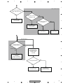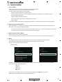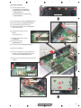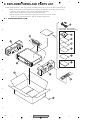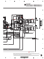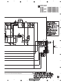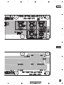
1
NETWORK AUDIO PLAYER /I STANDBY/ON STANDBY FUNCTION PURE AUDIO N-50 Hi-Bit32 ORDER NO. iPod/USB 5V 2.1A RRV4272 N-50 NETWORK AUDIO PLAYER N-50 N-50-K N-50-S N-30 N-30-K N-30-S THIS MANUAL IS APPLICABLE TO THE FOLLOWING MODEL(S) AND TYPE(S). Model Type Power Requirement N-50 CUXE AC 120V N-50-K SYXE8 AC 220V to 240V N-50-S SYXE8 AC 220V to 240V N-30 CUXE AC 120V N-30-K SYXE8 AC 220V to 240V N-30-S SYXE8 AC 220V to 240V Remarks PIONEER CORPORATION 1-1, Shin-ogura, Saiwai-ku, Kawasaki-shi, Kanagawa 212-0031, Japan PIONEER ELECTRONICS (USA) INC. P.O. Box 1760, Long Beach, CA 90801-1760, U.S.A. PIONEER EUROPE NV Haven 1087, Keetberglaan 1, 9120 Melsele, Belgium PIONEER ELECTRONICS ASIACENTRE PTE. LTD. 253 Alexandra Road, #04-01, Singapore 159936 PIONEER CORPORATION 2012 K-FZV FEB. 2012 Printed in Japan 1 2 3 4 SAFETY INFORMATION A This service manual is intended for qualified service technicians ; it is not meant for the casual do-ityourselfer. Qualified technicians have the necessary test equipment and tools, and have been trained to properly and safely repair complex products such as those covered by this manual. Improperly performed repairs can adversely affect the safety and reliability of the product and may void the warranty. If you are not qualified to perform the repair of this product properly and safely, you should not risk trying to do so and refer the repair to a qualified service technician. B WARNING This product contains lead in solder and certain electrical parts contain chemicals which are known to the state of California to cause cancer, birth defects or other reproductive harm. Health & Safety Code Section 25249.6 - Proposition 65 NOTICE (FOR CANADIAN MODEL ONLY) Fuse symbols (fast operating fuse) and/or be of identical designation. (slow operating fuse) on PCB indicate that replacement parts must REMARQUE (POUR MODÈLE CANADIEN SEULEMENT) Les symboles de fusible (fusible de type rapide) et/ou de remplacement doivent avoir la même désignation. C (fusible de type lent) sur CCI indiquent que les pièces (FOR USA MODEL ONLY) ANY MEASUREMENTS NOT WITHIN THE LIMITS OUTLINED ABOVE ARE INDICATIVE OF A POTENTIAL SHOCK HAZARD AND MUST BE CORRECTED BEFORE RETURNING THE APPLIANCE TO THE CUSTOMER. 1. SAFETY PRECAUTIONS The following check should be performed for the continued protection of the customer and service technician. LEAKAGE CURRENT CHECK 2. PRODUCT SAFETY NOTICE Measure leakage current to a known earth ground (water pipe, conduit, etc.) by connecting a leakage current tester such as Simpson Model 229-2 or equivalent between the earth ground and all exposed metal parts of the appliance (input/output terminals, screwheads, metal overlays, control shaft, etc.). Plug the AC line cord of the appliance directly into a 120V AC 60 Hz outlet and turn the AC power switch on. Any current measured must not exceed 0.5 mA. D Reading should Leakage not be above current 0.5 mA tester Device under test E Many electrical and mechanical parts in the appliance have special safety related characteristics. These are often not evident from visual inspection nor the protection afforded by them necessarily can be obtained by using replacement components rated for voltage, wattage, etc. Replacement parts which have these special safety characteristics are identified in this Service Manual. Electrical components having such features are identified by marking with a > on the schematics and on the parts list in this Service Manual. The use of a substitute replacement component which does not have the same safety characteristics as the PIONEER recommended replacement one, shown in the parts list in this Service Manual, may create shock, fire, or other hazards. Product Safety is continuously under review and new instructions are issued from time to time. For the latest information, always consult the current PIONEER Service Manual. A subscription to, or additional copies of, PIONEER Service Manual may be obtained at a nominal charge from PIONEER. Test all exposed metal surfaces Also test with plug reversed (Using AC adapter plug as required) Earth ground AC Leakage Test F 2 N-50 1 2 3 4 5 6 7 8 CONTENTS SAFETY INFORMATION.......................................................................................................................................................... 2 1. SERVICE PRECAUTIONS .................................................................................................................................................... 4 1.1 NOTES ON SOLDERING ............................................................................................................................................... 4 2. SPECIFICATIONS................................................................................................................................................................. 5 2.1 ACCESSORIES .............................................................................................................................................................. 5 2.2 SPECIFICATIONS .......................................................................................................................................................... 5 2.3 PLAYABLE FILE FORMATS ........................................................................................................................................... 6 3. BASIC ITEMS FOR SERVICE ............................................................................................................................................ 10 3.1 CHECK POINTS AFTER SERVICING ......................................................................................................................... 10 3.2 PCB LOCATIONS ......................................................................................................................................................... 11 3.3 JIGS LIST ..................................................................................................................................................................... 12 4. BLOCK DIAGRAM .............................................................................................................................................................. 14 4.1 OVERALL CONNECTION DIAGRAM (1/2) .................................................................................................................. 14 4.2 OVERALL CONNECTION DIAGRAM (2/2) .................................................................................................................. 16 4.3 BLOCK DIAGRAM ........................................................................................................................................................ 18 5. DIAGNOSIS ........................................................................................................................................................................ 20 5.1 TROUBLESHOOTING.................................................................................................................................................. 20 5.2 PROTECTION CIRCUIT ERROR DETECTION ........................................................................................................... 23 5.3 HOW TO CHECK THE IC COMMUNICATION ............................................................................................................. 24 5.4 IC INFORMATION ........................................................................................................................................................ 24 6. SERVICE MODE ................................................................................................................................................................. 25 6.1 SERVICE MODE .......................................................................................................................................................... 25 6.2 INITIAL SETTING ......................................................................................................................................................... 27 7. DISASSEMBLY ................................................................................................................................................................... 28 8. EACH SETTING AND ADJUSTMENT ................................................................................................................................ 34 8.1 FIRMWARE UPDATE ................................................................................................................................................... 34 8.2 HOW TO CHECK EACH TERMINAL............................................................................................................................ 37 9. EXPLODED VIEWS AND PARTS LIST............................................................................................................................... 40 9.1 PACKING SECTION ..................................................................................................................................................... 40 9.2 EXTERIOR SECTION .................................................................................................................................................. 42 10. SCHEMATIC DIAGRAM .................................................................................................................................................... 44 10.1 JACK ASSY ................................................................................................................................................................ 44 10.2 D-MAIN ASSY (1/5) .................................................................................................................................................... 46 10.3 D-MAIN ASSY (2/5) .................................................................................................................................................... 48 10.4 D-MAIN ASSY (3/5) .................................................................................................................................................... 50 10.5 D-MAIN ASSY (4/5) .................................................................................................................................................... 52 10.6 D-MAIN ASSY (5/5) .................................................................................................................................................... 54 10.7 DAC ASSY.................................................................................................................................................................. 56 10.8 LCD/KEY ASSY.......................................................................................................................................................... 58 10.9 LED ASSY, POWER SW ASSY, IR ASSY AND POWER LED ASSY ........................................................................ 60 10.10 USB ASSY................................................................................................................................................................ 62 10.11 STBY ASSY.............................................................................................................................................................. 64 10.12 CNT A ASSY AND CNT B ASSY ............................................................................................................................. 66 10.13 GUIDE 1, GUIDE 2(N-50, N-50-K/-S ONLY), GUIDE 3 AND GUIDE 4 ASSYS ....................................................... 68 11. PCB CONNECTION DIAGRAM ........................................................................................................................................ 70 11.1 JACK ASSY ................................................................................................................................................................ 70 11.2 D-MAIN ASSY ............................................................................................................................................................ 72 11.3 DAC ASSY.................................................................................................................................................................. 76 11.4 LCD/KEY ASSY.......................................................................................................................................................... 80 11.5 LED ASSY, POWER SW ASSY, IR ASSY AND POWER LED ASSY ........................................................................ 82 11.6 USB ASSY AND STBY ASSY .................................................................................................................................... 84 11.7 CNT A ASSY AND CNT B ASSY ............................................................................................................................... 88 11.8 GUIDE 1, GUIDE 2 (N-50, N-50-K/-S ONLY), GUIDE 3 AND GUIDE 4 ASSYS ........................................................ 90 12. PCB PARTS LIST.............................................................................................................................................................. 92 A B C D E F 3 N-50 5 6 7 8 1 2 3 4 1. SERVICE PRECAUTIONS 1.1 NOTES ON SOLDERING A • For environmental protection, lead-free solder is used on the printed circuit boards mounted in this unit. Be sure to use lead-free solder and a soldering iron that can meet specifications for use with lead-free solders for repairs accompanied by reworking of soldering. • Compared with conventional eutectic solders, lead-free solders have higher melting points, by approximately 40 ºC. Therefore, for lead-free soldering, the tip temperature of a soldering iron must be set to around 373 ºC in general, although the temperature depends on the heat capacity of the PC board on which reworking is required and the weight of the tip of the soldering iron. Do NOT use a soldering iron whose tip temperature cannot be controlled. B Compared with eutectic solders, lead-free solders have higher bond strengths but slower wetting times and higher melting temperatures (hard to melt/easy to harden). The following lead-free solders are available as service parts: • Parts numbers of lead-free solder: GYP1006 1.0 in dia. GYP1007 0.6 in dia. GYP1008 0.3 in dia. C D E F 4 N-50 1 2 3 4 5 6 7 8 2. SPECIFICATIONS 2.1 ACCESSORIES Remote control unit (8300764100010-IL) AC Power cord (N-50, N-30 :L068125130010-IL) (N-50-K/-S, N-30-K/-S :L068250160020-IL) Operating instructions (N-50, N-30 :5707000006130-IL) (N-50-K/-S, N-30-K/-S :5707000006140-IL) (N-50-K/-S, N-30-K/-S :6517000000450-IL) Audio cable (L063102020050-IL) Warranty card (N-50-K/-S, N-30-K/-S Safety sheet (N-50-K/-S, N-30-K/-S Caution sheet (N-50, N-30 (N-50-K/-S, N-30-K/-S AAA/R03 dry cell battery x 2 A :ARY7128) :5227000002330-IL) :5227000002270-IL) :5227000002280-IL) B 2.2 SPECIFICATIONS •Generalites •Digital audio output System. . . . . . . . . . . . . . . . . . . . .Network Audio Player Power requirements. . . . . . . . . . . . . . .AC 120 V, 60 Hz (N-50, N-30) Power requirements. . .AC 220 V to AC240V, 50/60 Hz (N-50-K/-S, N-30-K/-S) Coaxial digital output. . . . . . . . . . . . . . . . . . . . RCA jack Optical digital output . . . . . . . . . . . . . Optical digital jack •Digital audio input (N-50, N-50-K/-S only) Coaxial digital input . . . . . . . . . . . . . . . . . . . . RCA jack Optical digital input . . . . . . . . . . . . . . Optical digital jack USB type-B . . . . . . . . . . . . . . . . . . . . . . . . .USB 2.0 HS Power consumption N-50, N-50-K/-S . . . . . . . . . . . . . . . . . . . . . . . .34 W N-30, N-30-K/-S . . . . . . . . . . . . . . . . . . . . . . . .31 W Power consumption (In standby mode). . . . . . . . 0.3 W Weight (without package) N-50, N-50-K/-S . . . . . . . . . . . . . . . . .7.3 kg (16.1 lb) N-30, N-30-K/-S . . . . . . . . . . . . . . . . . . 5.0 kg (11 lb) Dimensions N-50, N-50-K/-S . . . . . .435 mm (W) x 99 mm (H) x 330 mm (D) (17 3/16 in. (W) x 3 15/16 in. (H) x 13 in. (D)) N-30, N-30-K/-S . . . . 435 mm (W) x 97.5 mm (H) x 330 mm (D) (17 3/16 in. (W) x 3 15/16 in. (H) x 13 in. (D)) Operating temperature. . . . . .. . . . . . . . +5 °C to +35 °C Operating humidity. . . . . . . . . . . . . . . . . . . 5 % to 85 % C Note • Specifications and the design are subject to possible modifications without notice, due to improvements. • This product is not designed for use in Japan. D •Network Ethernet interface. . . . . . . . . 10 BASE-T/100 BASE-TX DLNA. . . . . . . . . . . . . . . . . . . . . . . Ver 1.5 (DMP/DMR) E •Analog audio output Output level (During audio output) . . . . . . . . . . . . . . . . . . . . . . . . . . 2 V rms (1 kHz, 0 dB) Number of channels. . . . . . . . . . . . . . . . . . . . . . . . . . .2 Jack . . . . . . . . . . . . . . . . .. . . . . . . . . . . . . . . . . . . RCA Frequency response. . . . . . . . . . 4 Hz to 80 kHz –3 dB Signal-to-Noise Ratio 1 kHz, 0 dB, fs 192 kHz . . . .. . . . . . . . . . . . >111 dB Dynamic range 1 kHz, 0 dB, fs 192 kHz . . . . . . . . . . . . . . . >111 dB Total harmonic distortion 1 kHz, 0 dB, fs 192 kHz . . . . . . .. . . . . . . . .<0.002 % Channel separation 1 kHz, 0 dB, fs 192 kHz . . . . . . . . . . . . . . . >105 dB F 5 N-50 5 6 7 8 1 2 3 4 2.3 PLAYABLE FILE FORMATS This unit supports the following file formats. • A • • • B • Category Note that some file formats are not available for playback although they are listed as playable file formats. If an attempt is made to play files with unsupported formats, the sound may be intermittent or be accompanied by noise. In such cases, confirm that the file format is compatible with this unit. The compatibility of file formats varies depending on the type of server. Check with your server to ensure the compatibility of file formats supported by your server. Depending on the server, some file types not supported by this unit may be converted and output. For details, consult the server’s operating instructions. Internet radio playback may be affected by the Internet communications environment, and in this case playback may not be possible even with the file formats listed here Category Extension Stream Sampling 32kHz to frequency 48kHz (Internet Radio) — LPCM LPCM <*2> Quantizat 16bit ion bitrate (Internet Radio) 16bit, 24bit, 32bit (Digital In USB) Extension Stream Channel Sampling 32kHz to frequency 48kHz C .mp3 MPEG-1 Audio Layer-3 Channel 2ch Bitrate 8kbps to 320kbps 2ch Sampling 32 kHz to frequency 192kHz (Music Server) Quantizat 16bit ion bitrate MP3 <*1> 44.1 kHz, 48 kHz, 88.2 kHz, 96 kHz, 192 kHz (Digital In USB) WAV .wav 32kHz to 96kHz (USB) LPCM Quantizat 16bit, ion bitrate 20bit, 24bit VBR/CBR Supported/ Supported Channel D 2ch Sampling 32kHz to frequency 48kHz Quantizat 16bit ion bitrate WMA .wma WMA2/7/ Channel 8/9/10 Bitrate E 2ch 5kbps to 320kbps VBR/CBR Supported/ Supported F 6 N-50 1 2 3 4 5 Category 6 7 Extension Stream About network playback Sampling 32kHz to frequency 48kHz AAC .m4a .aac .3gp .3g2 The network playback function such as Internet Radio or Music Server of this unit uses the following technologies: Quantizat 16bit MPEG-4 ion bitrate AAC MPEG-4 Channel 2ch HE AAC (AAC Plus 16kbps to Bitrate v1/2) 320kbps Windows Media Player 11/Windows Media Player 12. Windows Media DRM Microsoft Windows Media Digital Rights Management (WMDRM) is a platform to protect and securely deliver content for playback on computers, portable devices and network devices. Music Server functions as a WMDRM 10 for networked devices. WMDRM protected content can only be played on media servers supporting WMDRM. Sampling 32 kHz to frequency 192kHz (Music Server) .flac Quantizat 16bit, 24bit ion bitrate Channel B Content owners use WMDRM technology to protect their intellectual property, including copyrights. This device uses WMDRM software to access WMDRM protected content. If the WMDRM soft ware fails to protect the content, content owners may ask Microsoft to revoke the software’s ability to use WMDRM to play or copy protected content. Revocation does not affect unprotected content. When you download licenses for protected content, you agree that Microsoft may include a revocation list with the licenses. Content owners may require you to upgrade WMDRM to access their content. If you decline an upgrade, you will not be able to access content that requires the upgrade. 32kHz to 96kHz (USB) FLAC A Windows Media Player VBR/CBR Supported/ Supported FLAC 8 2ch *1 “MPEG Layer-3 audio decoding technology licensed from Fraunhofer IIS and Thomson multimedia.” *2 Only streaming data from servers is concerned, so there is no extension. C This product is protected by certain intellectual property rights of Microsoft. Use or distribution of such technology outside of this product is prohibited without a license from Microsoft. D DLNA DLNA CERTIFIED® Audio Player E F 7 N-50 5 6 7 8 1 2 3 The Digital Living Network Alliance (DLNA) is a crossindustry organization of consumer electronics, computing industry and mobile device companies. Digital Living provides consumers with easy sharing of digital media through a wired or wireless network in the home. A FROM ACCESS TO OR USE OF CONTENT. NO ORAL OR WRITTEN INFORMATION OR ADVICE GIVEN BY PIONEER OR ITS CUSTOMER SERVICES REPRESENTATIVES WILL CREATE ANY SUCH WARRANTY. The DLNA certification logo makes it easy to find products that comply with the DLNA Interoperability Guidelines. This unit complies with DLNA Interoperability Guidelines v1.5. When a PC running DLNA server software or other DLNA compatible device is connected to this player, some setting changes of software or other devices may be required. Please refer to the operating instructions for the software or device for more information. DLNA ®, the DLNA Logo and DLNA CERTIFIED ® are B trademarks, service marks, or certification marks of the Digital Living Network Alliance. Content playable over a network • • • C • • Even when encoded in a compatible format, some files may not play correctly. Movie or Photo files cannot be played back. There are cases where you cannot listen to an Internet radio station even if the station can be selected from a list of radio stations. Some functions may not be supported depending on the server type or version used. Supported file formats vary by server. As such, files not supported by your server are not displayed on this unit. For more information check with the manufacturer of your server. N-50/N-30 only Disclaimer for Third Party Content ACCESS TO THIRD PARTY CONTENT SERVICES, INCLUDING ALL ASSOCIATED FEATURES AND FUNCTIONALITIES, IS PROVIDED “AS IS,” “AS AVAILABLE” AND AT THE USER’S OWN RISK, WITHOUT WARRANTY OF ANY KIND. PIONEER DISCLAIMS ALL WARRANTIES, EXPRESS OR IMPLIED, IN CONNECTION WITH ACCESS TO AND USE OF CONTENT SERVICES THROUGH THIS DEVICE, INCLUDING WITHOUT LIMITATION WARRANTIES OF MERCHANTABILITY, SATISFACTORY QUALITY, FITNESS FOR A PARTICULAR PURPOSE, AND NONINFRINGEMENT. PIONEER DOES NOT GUARANTEE, REPRESENT, OR WARRANT THAT CONTENT SERVICES WILL BE FREE FROM ERRORS, INTERRUPTION, LOSS, CORRUPTION, ATTACK, VIRUSES, INTERFERENCE, HACKING, OR OTHER SECURITY INTRUSION, AND PIONEER DISCLAIMS ANY LIABILITY IN CONNECTION WITH THE FOREGOING. PIONEER IS NOT LIABLE OR RESPONSIBLE FOR ANY LOSS OR DAMAGE ARISING D E 4 IN NO EVENT WILL PIONEER, ITS AFFILIATES, OR THEIR RESPECTIVE OFFICERS, DIRECTORS, OR EMPLOYEES BE LIABLE IN CONNECTION WITH YOUR USE OF THIRD PARTY CONTENT SERVICES THROUGH THIS DEVICE FOR PERSONAL INJURY OR SPECIAL, INCIDENTAL, INDIRECT OR CONSEQUENTIAL DAMAGES OF ANY KIND, INCLUDING WITHOUT LIMITATION DAMAGES FOR ATTORNEY’S FEES, LOST DATA OR LOST PROFITS, REGARDLESS OF THE THEORY OF LIABILITY AND WHETHER OR NOT ADVISED OF THE POSSIBILITY OF SUCH DAMAGES. IN NO EVENT WILL PIONEER ’S TOTAL LIABILITY TO YOU FOR ALL DAMAGES ARISING FROM THE USE OR INABILITY TO USE THIRD PARTY CONTENT SERVICES (OTHER THAN AS MAY BE REQUIRED BY LAW IN CASES INVOLVING PERSONAL INJURY) EXCEED $10.00. THE FOREGOING LIMITATIONS WILL APPLY EVEN IF THE ABOVE REMEDY FAILS OF ITS ESSENTIAL PURPOSE. IF ANY APPLICABLE AUTHORITY HOLDS ANY PORTION OF THIS SECTION TO BE UNENFORCEABLE, THEN LIABILITY WILL BE LIMITED TO THE MAXIMUM EXTENT PERMITTED BY APPLICABLE LAW. N-50/N-30 only Disclaimer for Third Party Content Access to content provided by third parties requires a high speed internet connection and may also require account registration and a paid substruction. Therd party content services may be changed, suspended, interrupted, or discontinued at any time without notice, and Pionner disclaims any liability in connection with such occurrences. Pionner does not represent or warrant that content services will continue to be provieded or available for a particular period of time, and any such warranty, express or implied, is disclaimed. N-50-K/-S, N-30-K/-S only About playback behavior over a network • • • • Playback may stall when the PC is switched off or any media files stored on it are deleted while playing content. If there are problems within the network environment (heavy network traffic, etc.) content may not be displayed or played properly (playback may be interrupted or stalled). For best performance, a 100BASE-TX connection between player and PC is recommended. If several clients are playing simultaneously, as the case may be, playback is interrupted or stalled. Depending on the security software installed on a connected PC and the setting of such software, network connection may be blocked. F 8 N-50 1 2 3 4 5 6 Pioneer is not responsible for any malfunction of the player and/or the Music Server features due to communication error/malfunctions associated with your network connection and/or your PC, or other connected equipment. Please contact your PC manufacturer or Internet service provider. Windows Media is either a registered trademark or trademark of Microsoft Corporation in the United States and/or other countries. This product includes technology owned by Microsoft Corporation and cannot be used or distributed without a license from Microsoft Licensing, Inc. Microsoft ®, Windows ®7, Windows ®Vista, Windows ®XP, Windows ®2000, Windows®Millennium Edition, Windows ®98, and WindowsNT ® are either registered trademarks or trademarks of Microsoft Corporation in the United States and/or other countries. 7 8 THIS SOFTWARE IS PROVIDED BY THE COPYRIGHT HOLDERS AND CONTRIBUTORS “AS IS” AND ANY EXPRESS OR IMPLIED WARRANTIES, INCLUDING, BUT NOT LIMITED TO, THE IMPLIED WARRANTIES OF MERCHANTABILITY AND FITNESS FOR A PARTICULAR PURPOSE ARE DISCLAIMED. IN NO EVENT SHALL THE FOUNDATION OR CONTRIBUTORS BE LIABLE FOR ANY DIRECT, INDIRECT, INCIDENTAL, SPECIAL, EXEMPLARY, OR CONSEQUENTIAL DAMAGES (INCLUDING, BUT NOT LIMITED TO, PROCUREMENT OF SUBSTITUTE GOODS OR SERVICES; LOSS OF USE, DATA, OR PROFITS; OR BUSINESS INTERRUPTION) HOWEVER CAUSED AND ON ANY THEORY OF LIABILITY, WHETHER IN CONTRACT, STRICT LIABILITY, OR TORT (INCLUDING NEGLIGENCE OR OTHERWISE) ARISING IN ANY WAY OUT OF THE USE OF THIS SOFTWARE, EVEN IF ADVISED OF THE POSSIBILITY OF SUCH DAMAGE. A B Authorizing this unit In order to be able to play with Music Server, this unit must be authorized. This happens automatically when the unit makes a connection over the network to the PC. If not, please authorize this unit manually on the PC. About iPod/iPhone/iPad The authorization (or permission) method for access varies depending on the type of server currently being connected. For more information on authorizing this unit, refer to the instruction manual of your server. aacPlus C The AAC decoder uses aacPlus developed by Coding Technologies D (www.codingtechnologies.com). “Made for iPod”, “Made for iPhone” and “Made for iPad” mean that an electronic accessory has been designed to connect specifically to iPod, iPhone or iPad, respectively, and has been certified by the developer to meet Apple performance standards. Apple is not responsible for the operation of this device or its compliance with safety and regulatory standards. Please note that the use of this accessory with iPod, iPhone, or iPad may affect wireless performance. Apple, AirPlay, the AirPlay logo, iPad, iPhone, iPod, iPod shuffle, iPod nano, iPod classic, iPod touch, iTunes and Mac are trademarks of Apple, Inc., registered in the U.S. and other countries. FLAC FLAC Decoder Copyright c 2000, 2001, 2002, 2003, 2004, 2005, 2006, 2007 Josh Coalson Redistribution and use in source and binary forms, with or without modification, are permitted provided that the following conditions are met: • • • Redistributions of source code must retain the above copyright notice, this list of conditions and the following disclaimer. Redistributions in binary form must reproduce the above copyright notice, this list of conditions and the following disclaimer in the documentation and/ or other materials provided with the distribution. Neither the name of the Xiph.org Foundation nor the names of its contributors may be used to endorse or promote products derived from this software without specific prior written permission. F 9 N-50 5 6 E 7 8 1 2 3 4 3. BASIC ITEMS FOR SERVICE 3.1 CHECK POINTS AFTER SERVICING A To keep the product quality after servicing, confirm recommended check points shown below. No. 1 2 3 B 4 Procedures Check points Confirm a firmware version at test mode. Should be the latest firmware version. If not, update the version. Confirm whether the customer complain has been solved. If the indicated complain is caused by a specific file format, replay a music file for test of the same format as target file. Confirm replay of a music file for test with the same format as corresponding file format at the front USB terminal. (Confirm music files with all file formats should be replayed.) Check the external package The customer complain must not be reappeared. No abnormalities should exist in screen displayed contents, audio and actions. No abnormalities should exist in actions such as audio, screen display, etc. No scratches or dirt on its appearance after receiving it for service. A music file for test with corresponding file format should be used after downloading from the service dedicated Web Site onto an USB memory, etc. See the table below for the items to be checked regarding audio. Item to be checked regarding audio Distortion C Noise Volume too low Volume too high Volume fluctuating Sound interrupted D E F 10 N-50 1 2 3 4 5 6 7 8 3.2 PCB LOCATIONS CNT B ASSY GUIDE 2 ASSY LED ASSY L N E A LCD/KEY ASSY GUIDE 4 ASSY USB ASSY POWER LED ASSY D P I H IR ASSY G B F POWER SW ASSY M GUIDE 1 ASSY C C A B K O J DAC ASSY JACK ASSY D-MAIN ASSY CNT A ASSY GUIDE 3 ASSY STBY ASSY D E F 11 N-50 5 6 7 8 1 NOTES: - A 2 3 Parts marked by “NSP” are generally unavailable because they are not in our Master Spare Parts List. The > mark found on some component parts indicates the importance of the safety factor of the part. Therefore, when replacing, be sure to use parts of identical designation. Mark No. Description Mark No. Description Part No. NSP LIST OF ASSEMBLIES B C 7025HU1102032-IL 702807138B010-IL 7028071381020-IL 7028071382030-IL 7028071383020-IL 7028071384010-IL 7028071385010-IL 7028071386010-IL 7028071387010-IL 7028071388010-IL 7028071389010-IL 1..TTL ASSY DAC(N-30-K/-S) 2..GUIDE 4 ASSY 2..DAC ASSY 2..STBY ASSY 2..LED ASSY 2..POWER LED ASSY 2..POWER SW ASSY 2..IR ASSY 2..GUIDE 3 ASSY 2..CNT B ASSY 2..GUIDE 1 ASSY 7025HU1102042-IL 702807138B010-IL 7028071381020-IL 7028071382040-IL 7028071383020-IL 7028071384010-IL 7028071385010-IL 7028071386010-IL 7028071387010-IL 7028071388010-IL 7028071389010-IL NSP 1..TTL ASSY JACK(N-50) 2..JACK ASSY 2..LCD/KEY ASSY 2..CNT A ASSY 7025HU1103043-IL 7028071391010-IL 7028071392010-IL 7028071393010-IL NSP 1..TTL ASSY JACK(N-50-K/-S) 2..JACK ASSY 2..LCD/KEY ASSY 2..CNT A ASSY 7025HU1103033-IL 7028071391010-IL 7028071392010-IL 7028071393010-IL NSP 1..TTL ASSY JACK(N-30) 2..JACK ASSY 2..LCD/KEY ASSY 2..CNT A ASSY 7025HU1102033-IL 7028071391020-IL 7028071392010-IL 7028071393010-IL NSP 1..TTL ASSY JACK(N-30-K/-S) 2..JACK ASSY 2..LCD/KEY ASSY 2..CNT A ASSY 7025HU1102043-IL 7028071391020-IL 7028071392010-IL 7028071393010-IL 1..TTL ASSY D-MAIN(N-50) 2..D-MAIN ASSY 7025HU1103040-IL 7028071361010-IL NSP 1..TTL ASSY D-MAIN(N-50-K/-S) 2..D-MAIN ASSY 7025HU1103030-IL 7028071361010-IL NSP 1.. TTL ASSY D-MAIN(N-30) 2..D-MAIN ASSY 7025HU1102030-IL 7028071361020-IL NSP 1..TTL ASSY D-MAIN(N-30-K/-S) 2..D-MAIN ASSY 7025HU1102040-IL 7028071361020-IL NSP 1..TTL ASSY USB(N-50) 2..USB ASSY 7025HU1103041-IL 7028071371010-IL NSP NSP 1..TTL ASSY USB(N-50-K/-S) 2..USB ASSY 7025HU1103031-IL 7028071371010-IL > NSP 1..TTL ASSY USB(N-30) 2..USB ASSY 7025HU1102031-IL 7028071371010-IL NSP 1..TTL ASSY USB(N-30-K/-S) 2..USB ASSY 7025HU1102041-IL 7028071371010-IL NSP 1..TTL ASSY DAC(N-50) 2..GUIDE 2 ASSY 2..GUIDE 4 ASSY 2..DAC ASSY 2..STBY ASSY 2..LED ASSY 2..POWER LED ASSY 2..POWER SW ASSY 2..IR ASSY 2..GUIDE 3 ASSY 2..CNT B ASSY 2..GUIDE 1 ASSY 7025HU1103042-IL 702807138A010-IL 702807138B010-IL 7028071381010-IL 7028071382010-IL 7028071383010-IL 7028071384010-IL 7028071385010-IL 7028071386010-IL 7028071387010-IL 7028071388010-IL 7028071389010-IL 1..TTL ASSY DAC(N-50-K/-S) 2..GUIDE 2 ASSY 2..GUIDE 4 ASSY 2..DAC ASSY 2..STBY ASSY 2..LED ASSY 2..POWER LED ASSY 2..POWER SW ASSY 2..IR ASSY 2..GUIDE 3 ASSY 2..CNT B ASSY 2..GUIDE 1 ASSY 7025HU1103032-IL 702807138A010-IL 702807138B010-IL 7028071381010-IL 7028071382020-IL 7028071383010-IL 7028071384010-IL 7028071385010-IL 7028071386010-IL 7028071387010-IL 7028071388010-IL 7028071389010-IL D NSP > E Part No. 1..TTL ASSY DAC(N-30) 2..GUIDE 4 ASSY 2..DAC ASSY 2..STBY ASSY 2..LED ASSY 2..POWER LED ASSY 2..POWER SW ASSY 2..IR ASSY 2..GUIDE 3 ASSY 2..CNT B ASSY 2..GUIDE 1 ASSY NSP > 4 > 3.3 JIGS LIST Name F Jig No. Remarks GGF1381 Service Remote Control Unit 12 Adjustment, Diagnosis N-50 1 2 3 4 5 6 7 8 A B C D E F 13 N-50 5 6 7 8 1 2 3 4 4. BLOCK DIAGRAM 4.1 OVERALL CONNECTION DIAGRAM (1/2) A A J B JACK ASSY (N-50, N-50-K/-S:702 (N-30, N-30-K/-S:702 STBY ASSY (N-50 :7028071382010-IL) (N-50-K/-S :7028071382020-IL) (N-30 :7028071382030-IL) (N-30-K/-S :7028071382040-IL) ! K C D N-50, N-50-K/-S only E F 14 N-50 1 2 3 4 CNT A AS (7028071 5 6 7 8 A Y 0-K/-S:7028071391010-IL) 0-K/-S:7028071391020-IL) B C DAC ASSY (N-50, N-50-K/-S:7028071381010-IL) (N-30, N-30-K/-S:7028071381020-IL) CNT A ASSY (7028071393010-IL) C D B ( B 1/5 - B 5/5 ) D-MAIN ASSY (1/2) (N-50, N-50-K/-S:7028071361010-IL) (N-30, N-30-K/-S:7028071361020-IL) E F When ordering service parts, be sure to refer to "EXPLODED VIEWS and PARTS LIST" or "PCB PARTS LIST". The > mark found on some component parts indicates the importance of the safety factor of the part. Therefore, when replacing, be sure to use parts of identical designation. 15 N-50 5 6 7 8 1 2 3 4 4.2 OVERALL CONNECTION DIAGRAM (2/2) A B ( B 1/5 - B 5/5 ) D-MAIN ASSY (2/2) (N-50, N-50-K/-S:7028071361010-IL) (N-30, N-30-K/-S:7028071361020-IL) M GUIDE 1 ASSY (7028071389010-IL) N GUIDE 2 ASSY (N-50, N-50-K/-S:702807138A010-IL) O GUIDE 3 ASSY (7028071387010-IL) P GUIDE 4 ASSY (702807138B010-IL) B C L D H CNT B ASSY (7028071388010-IL) G POWER LED ASSY (7028071384010-IL) IR ASSY (70280713 E Shield Case F F POWER SW ASSY (7028071385010-IL) E LED ASSY (N-50, N-50-K/-S:7028071383010-IL) (N-30, N-30-K/-S:7028071383020-IL) 16 I Direct connection(Chass N-50 1 2 3 USB (702 4 5 6 7 8 LCD/KEY ASSY (7028071392010-IL) A B D 10-IL) 20-IL) C D IR ASSY (7028071386010-IL) E I USB ASSY (7028071371010-IL) F nnection(ChassisShield Case) 17 N-50 5 6 7 8 1 2 3 4 4.3 BLOCK DIAGRAM E F A POWER SW ASSY I USB ASSY LED ASSY B D-MAIN ASSY H POWER LED ASSY B G IR ASSY LCD CONTROL D LCD/KEY ASSY SPI C D N-50, N-50-K/-S ONLY A E JACK ASSY N-50, N-50-K/-S ONLY F 18 N-50 1 2 3 4 5 6 7 8 A ASSY N-50, N-50-K/-S ONLY B N-30, N-30-K/-S ONLY N-30, N-30-K/-S ONLY J STBY ASSY C C DAC ASSY D N-50, N-50-K/-S ONLY E F 19 N-50 5 6 7 8 1 2 3 4 5. DIAGNOSIS 5.1 TROUBLESHOOTING A No sound comes out. Analog sound doesn’t come out. Digital sound comes out. NO Neither optical or coaxial digital sound comes out. NO No light comes out. YES NO YES YES Check the pattern between IC104 - IC101. IC104 (4, 10 pin) B Is the voltage about 3.3V? Check the pattern between IC104 - JACK102. NO YES Check the pattern between IC104 – L2513. Check the pattern between IC104 - IC2501. C No sound comes out in any function. NO No sound comes out for Music Server, Internet Radio, iPod or USB. NO A YES YES B Sound comes out for Music Server and Internet Radio, but no sound comes out for iPod and USB. D Sound comes out for iPod and USB, but no sound comes out for Music Server and Internet Radio. NO NO YES YES Check the patterns between JA1502 - IC1506 and around IC1506. Check the path between IC1504 - IC2501 (signal name: NWSPDIF). E No sound comes out for iPod . NO YES YES Check the pattern around IC1506. F 20 NO Is the signal detected in the land of R1649(NM)? Failure in IC1504 Check the path between IC1504 - USB ASSY. N-50 1 2 3 4 5 6 7 8 A A N-50, N-50-K/-S Only No sound comes out for BT Audio and Air Jam. NO YES No sound comes out for Digital In USB. Check the pattern around IC2509. NO YES No sound comes out for Digital In 1. Check the pattern around IC2503. B NO YES Check the pattern around IC103. Check the pattern around IC100. C B N-30, N-30-K/-S N-50, N-50-K/-S Only Sound comes out in the PURE AUDIO mode. N-50, N-50-K/-S NO D N-50, N-50-K/-S YES Check MCK_DAC, LRCK_DAC, DA_DAC and BCK_DAC of CN2502. Check the pattern between JA1502 - IC1506 and the pattern around IC1506. Is the signal detected? NO E YES Check around IC2505 and IC2506. Check DAC ASSY. F 21 N-50 5 6 7 8 1 2 3 4 No power comes on. A Even if the power cord is plugged in, the device is not put in a standby state. NO YES Check F202. Check F201. B Is it conducting? Is it conducting? NO YES NO CN205 (15~19 pin) YES CN205 (2~ 4 pin) Replace F202. Replace F201. C Is the voltage about 12V? Is the voltage about 5V? YES NO Is RLY201 operating? Check the path between CN205 - IC1001 (signal name:ACWP). YES Check STBY ASSY. (Around IC201, T201 and PC201) C1008 +side D Is the voltage about 3.3V? NO YES Check the transformer. NO Check the path between CN205 - IC1001 (signal name:ACRY, RYAC). YES E Check the connection between D-MAIN ASSY CNT-B ASSY - LED ASSY. Check around IC3001. F 22 N-50 1 NO 2 3 4 5 - BT error 5 Error 8 USB overcurrent Error 7 - AC Detection BT Module Over Current Detection WiFi Module Over Current Detect ion Front USB Over Current Detection 6 Front USB Over Voltage Detection Standby LED - - - - 1) Transit POW_USB_F(IC100122 pin) to Low. 2) Error is displayed at GUI, and the keys other than the Standby/On key become invalid. Immediately shut down. Overcurrent in the power supply to Front USB(iPod/iPhone/iPad/USB memory) is detected. The assumption is a failure in Module. XERR_USB_F (Main/IC1504-D2 pin) “L” detection Overcurrent in the power supply to Front USB(iPod/iPhone/iPad/USB memory) is detected. The assumption is a failure in DCDC Converter. XDDCERR_USB_F (Sub/IC1001-40 pin) “L” detection USB (0 to 255 displayed) - USB W ERR (0 to 255 displayed) 7 7 Input "ESC(A85F)" "TEST(A85E)" on the service remote controller (GGF1381). Since POW_USB_W remains in High to turn ON the power by ControlApp, the detection continues even after the transition to the high-speed startup Standby. When the detection is confirmed during the high-speed startup Standby, transit POW_USB_W to Low. After that, when the power is turned ON, POW_USB_W is set to High and after a lapse of 10 ms, the detection starts again. In the event of UART communication error with the BT module, BT error 5 is displayed. Remark This protection operation is intended for protection of the external Not returnable connection equipment against a Only releasing failure within the body. method The device is put in the unreturnable described below state in the event of an error. Power OFF Power ON effects a return. 1) Transit POW_USB_W (IC1001-6 pin) to Low. 2) Error is displayed at GUI (not displayed when the detection is confirmed during a high-speed Power OFF startup Standby), and the keys Power ON other than the Standby/On key effects a return. become invalid. Overcurrent in the power supply to WiFi Module (Wireless LAN Converter) is detected. The assumption is a failure in Module. XERR_USB_W (Sub/IC1001-3 pin) “L” detection BT OL (0 to 255 displayed) - 1) Mute On 2) Error display at GUI 3) Transit POW_BT(IC1504-W14 Power OFF pin) to Low, and the keys other Power ON than the Standby/On key effects a return. become invalid. Return processing Overcurrent in the power supply to BT Module is detected. The assumption is a failure in Module. XERR_BT (Main/IC1504-Y14 pin) "L" detection Processing after detection After detection, execute AC_OFF processing, and the power is turned OFF. Detection method The presence or absence of power supply is detected. At the same time, occurrence of AC instantaneous interruption is also detected. AC_DET (Sub/IC1001-81 pin) "H" detection LED Number of NGs display 6 [Releasing method for the power ON disabled state] GUI display Item 5 8 5.2 PROTECTION CIRCUIT ERROR DETECTION A B C N-50 8 D E F 23 1 2 3 4 5.3 HOW TO CHECK THE IC COMMUNICATION The Major IC (MainCPU, SubCPU, DSP, DIR, DAC, etc.) communications checking method A The communications status with each LSI can be checked as follows: Communications of MainCPUSubCPU In about one minute after the Power ON, the function screen appears. If the display is switched by change-over of functions, there is no problem in the communications. Communications of SubCPUDSP (N-50, N-50-K/-S only) In the event of DSP communications error, ”Error 9” is displayed on the LCD. If “Error 9” is not displayed, the communications have been established. Communications of SubCPUDIR Select DigitalIn1, and when the sound input to DigitalIn1 is output from Opt or Coax, the communications have been established. B 5.4 IC INFORMATION J040-22601-001-0S (POWER SWITCH) Block Diagram VCC Drain 2 6 7 8 Vstr 5 C Vcc VCC Idelay Vref OSC VBURL/VBURH VCC VCC good 8V/12V IFB 2.5 R FB 3 PWM Normal Burst R S Q LEB 250ns SoftStart Gate driver R Q ILIM 4 VSD D 1 GND VCC SQ LPF VOVP VOCP RQ TSD VCC good Pin Layout GND 1 8 Drain VCC 2 7 Drain FB 3 6 Drain ILIM 4 5 VSTR E Pin Definitions Pin No. 1 2 3 4 5 6,7,8 F 24 Pin Name GND VCC FB ILIM VSTR Drain Description Ground Power Supply Feedback Peak Current Limit Startup SenseFET Drain N-50 1 2 3 4 5 6 7 8 6. SERVICE MODE 6.1 SERVICE MODE 1. Service Mode A When the device is put in the Service Mode, the dedicated menu starts up. As long as the menu is open, the Service Mode is in operation. The items implemented by the menu are as follows: · Check of Versions for MainCPU / SubCPU / DSP · Check of Model Information (For which is SubCPU in operation, N-30(N-30-K/-S) or N-50(N-50-K/-S)?) · Check of Network Information · Update of USB for MainCPU / SubCPU · Check of the number of protection circuit detections and clear · Factory Setting B In the Service Mode, the protection circuit detection operates in the same way as during in the normal operation. 2. How to enter the Service Mode Enter "ESC(A85F)" "+10(A81F)" on the service remote controller GGF1381 while the power of the Main Unit is ON, and the menu for the Service Mode starts up. ∗ If any input from another remote controller is made between "ESC" and "+10", the Service Mode is not entered. The entry status of the "ESC" key is cleared at the time of Power OFF. 3. How to leave the Service Mode C When the menu is left, the Service Mode exits. The menu is left by switching of functions, Power OFF or the return key input on the top-end layer of the menu. 4. Menu The operation of the menu shall be conducted with the cursor keys of the product’s remote controller. Use the Enter key for selection of an item and use the Return key for return of one layer. The top menu is as shown in the screen below. [Display Screen] D Service Menu Service Menu System Information Factory Reset MainCPU Update Via USB SubCPU Update Via USB Error Information E In addition, menu operation by the Main Unit button is also capable if attached remote controller is not available. In that case, perform the following actions; : : : Enter : Return In some menu, it is unable to return to one hierarchy layer before with the [] button. In that case, please exit from the Service Mode once with function button, etc. F 25 N-50 5 6 7 8 1 2 3 4 4-1. System Information When the System Information is selected, the screen below is displayed. A [Display screen] DM860 software version System Information MainCPU Ver.: 0.001 uPD78F1166 software version SubCPU Ver.: 0.001 B DSP Ver.: 0.001 D810 software version (In the case of N-30, DSP is not equipped, 0000 is displayed.) Model: N-50 Model identified by the software System Information MAC Address: The upper [74:5e:1c] is fixed. MAC: 74:5e:1c:06:ab:2d IP Address: [0.0.0.0] when not connected to LAN IP : 192.168.0.1 C 4-2. MainCPU Update Via USB See the “8.1 FIRMWARE UPDATE”. 4-3. SubCPU Update Via USB See the “8.1 FIRMWARE UPDATE”. D 4-4. Error display for protection circuit, etc. When “Error Information” is selected on the ServiceMenu, the screen below is displayed. FrontUSB OverLoad detection number display USB OL : 000 USB W ERR : 000 BT OL : 001 Reset? WLAN power USB OverLoad detection number display BluetoothAdaptor OverLoad detection number display E [ENTER] Reset [RETURN] Return Press down the Enter key. Return to the ServiceMenu. [ENTER] Reset [RETURN] Return Return to the ServiceMenu. Execute the error count clear. After the execution, the screen is returned to the ServiceMenu. F 26 N-50 1 2 3 4 5 6 7 8 5. Factory Setting When the “Factory Reset” is selected on the ServiceMenu, the screen below is displayed. A Reset? [SETUP] Reset [RETURN] Cancel After the Factory Setting is executed the power is turned off. B Return to the ServiceMenu. 6.2 INITIAL SETTING Setting name SETUP system SOUND system SYSTEM NETWORK BT Initial value Setting range Intensity setting Display OFF setting Automatic Power Off High-Speed startup mode Language setting LEVEL3 Continuous display ON OFF English LEVEL3 / LEVEL2 /LEVEL1 Display OFF/Continuous display ON/OFF ON/OFF English, French, German, Dutch, Italian, Spanish, Russian, Japanese AutoSoundRetriever AutoLevelControl SoundRetriverAir Hi-bit32 PureAudio FUNCTION DHCP IP Address SubNetmask Gateway DNS 1 DNS 2 Proxy setting Proxy server Proxy port Favorite Parental lock setting Parental lock password Friendly Name PIN CODE OFF OFF OFF OFF OFF iPod ON 0.0.0.0 0.0.0.0 0.0.0.0 0.0.0.0 0.0.0.0 Don't Use (Null) (Null) 0 station OFF 0000 ∗1 0000 ON/OFF ON/OFF ON/OFF ON/OFF ON/OFF All functions ON/OFF 0.0.0.0 ~ ff.ff.ff.ff 0.0.0.0 ~ ff.ff.ff.ff 0.0.0.0 ~ ff.ff.ff.ff 0.0.0.0 ~ ff.ff.ff.ff 0.0.0.0 ~ ff.ff.ff.ff Don't Use/Use 128 characters 0 ~ ffff 20 station ON/OFF 0000 ~ 9999 C D E 0000 / 1234 / 8888 When the power cord is plugged off or the power is turned off by the STANDBY/ON switch of the Main Unit, the saving of the above setting values is not ensured. The display OFF setting becomes valid till the power is turned off. The function that was finally selected is saved at the time of transition to STANDBY. It cannot be saved by the STANDBY/ON switch of the Main Unit. ∗1: The Model Name shall be the initial value. “N-50” for the upper model, and “N-30” for the lower model. F ∗2: When the power is turned off by the STANDBY/ON switch of the Main Unit during the saving of settings in progress, the saving of the setting values is not ensured. 27 N-50 5 6 7 8 1 2 3 4 7. DISASSEMBLY A Note 1 : Even if the unit shown in the photos and illustrations in this manual may differ from your product, the procedures described here are common. Note 2 : As for the assembling, please perform assembling following to the opposite procedures of How to Disassemble. If any notes are existed, please follow those instructions. [1] Cabinet 1 (1) Remove the four screws. N-50/CUXE, N-50-K/SYXE8 N-30/CUXE, N-30-K/SYXE8: 1500040083B10-IL N-50-S/SYXE8, N-30-S/SYXE8: 1500040084B10-IL (2) Remove the five screws. (BBZ30P060FTB) ( B C ) ( 1 ) 2 2 2 1 2 Cabinet (3) Insert nails between the Cabinet and Back Chassis and pull the Cabinet backward horizontally. Set up some gap 1 2 3 Front Panel Insert nails Cabinet Back Chassis D (4) Take out Cabinet upward while spreading Rear Side Piece. Cabinet 4 E While spreading While spreading F 28 N-50 1 2 3 4 5 6 7 [2] Front Section 1 (1) Remove the five screws. N-50/CUXE, N-50-K/SYXE8 N-30/CUXE, N-30-K/SYXE8: BBZ30P080FTB N-50-S/SYXE8, N-30-S/SYXE8: BBZ30P080FNI ( x5 ) ( (2) (3) (4) (5) 8 A ) • Bottom view Remove the two screws. (BBZ30P080FTC) Remove the screw. (B020230063B10-IL) Cut the Binder. (N-50, N-50-K/-S) Release the cables from the PCB Binder. (N-50, N-50-K/-S) (6) Release the cables from the Binder. (N-50, N-50-K/-S) 2 POWER SW ASSY B 4 6 5 (7) Release the cables from the PCB Binder. (8) Remove the screw. (BBZ30P080FTC) (9) Loosen the screw. (BBZ30P080FTC) 3 GUIDE 2 ASSY GUIDE 2 ASSY C 12 (10) Cut the two Binders. Front Section (11) Insert a Screwdriver through the holes at left side of the Main Chassis and remove the three screws. (BBZ30P060FTC) (12) Unhook the two hooks and remove the Front Section. D 8 12 7 LCD/KEY ASSY 9 CNT B ASSY 10 E GUIDE 3 ASSY 11 x3 10 Main Chassis D-MAIN ASSY F 29 N-50 5 6 7 8 1 2 3 4 [3] Diagnosis A (1) Attach a Ground Cable from the IR ASSY with the screw. (B020230063B10-IL) (2) Attach a Ground Cable from the LED ASSY with the screw. (BBZ30P080FTC) Please use the screw hole near front to detach the Front Part. Ground Cable from the LED ASSY 2 the screw hole near front B 1 Ground Cable from the IR ASSY (3) Arrange the units as shown in the photo. C D (4) Connect the Shield on USB ASSY to the Main Chassis Ground. Note: Make the USB ASSY, IR ASSY not to touch with the Main Chassis for avoiding short circuited. USB ASSY IR ASSY E Main Chassis Shield USB ASSY Main Chassis F 30 N-50 1 2 3 4 5 6 7 8 Notes on assembling [1] Styling of cables A (1) FFC between the LCD/KEY ASSY and CNT B ASSY Make FFC not to touch with the LCD/KEY ASSY by folding the base of auxiliary plate located at the CNT B ASSY at a right angle. CNT B ASSY Detached B Folding right angled LCD/KEY ASSY (2) Secondary Side Cable of the Power Trans ( N-50/CUXE: 8200570300120-IL) N-50-K/SYXE8, N-50-S/SYXE8: 8200570300130-IL Put down the Cable not to touch with the Cabinet. ( ) Power Trans Detached C Secondary Side Cable of Power Trans (3) Primary Side Cable of the Power Trans ( N-50/CUXE: 8200570300120-IL) N-50-K/SYXE8, N-50-S/SYXE8: 8200570300130-IL Make some Cable extra length by pulling the Cable lightly toward the Power Trans side not to touch with the Cabinet after fixing the Cable with the PCB Binder of POWER SW ASSY. Securely fix the Cable with insulated the PCB Binder of GUIDE 4 ASSY not to touch with the Cabinet. ( ) Put down DAC ASSY D Fixing with Binder Power Trans Make the Cabinet not to touch with Fixing with PCB Binder Pull lightly POWER SW ASSY GUIDE 4 ASSY Primary Side Cable of Power Trans E Secondary Side Cable of Power Trans Extra length Fixing with PCB Binder [Case of N-30, N-30-K/-S] GUIDE 4 ASSY F 31 N-50 5 6 7 8 1 A B 2 3 (4) Secondary Side Cable of the Power Trans (N-50/CUXE: 8200660300120-IL) N-50-K/SYXE8, N-50-S/SYXE8: 8200660300130-IL (N-30/CUXE: 8200660300150-IL) N-30-K/SYXE8, N-30-S/SYXE8: 8200660300160-IL Fix the Secondary Side Cable of Power Trans with the PCB Binder of STBY ASSY not to touch with the Cable from USB ASSY. ( ) ( ) STBY ASSY Cable from the USB ASSY 4 Secondary Side Cable of Power Trans Detached Power Trans (5) Cable from the USB ASSY Fix the Cable from the USB ASSY with the PCB Binder of GUIDE 2 ASSY not to touch with the Primary Side Cable of Power Trans. ( N-50/CUXE: 8200570300120-IL) N-50-K/SYXE8, N-50-S/SYXE8: 8200570300130-IL ( 4 Detached Primary Side Cable of Power Trans 5 ) GUIDE 2 ASSY Put down Front C Cable from the USB ASSY (6) Cable from the USB ASSY Fix the Cable to the GUIDE 3 ASSY without sag with the two Binders not to touch the Shield Case of D-MAIN ASSY. 6 6 Detached GUIDE 3 ASSY Shield Case D-MAIN ASSY Front FFC D 4P Connector ASSY (7) 4P Connector ASSY from the LCD/KEY ASSY Fix the Cable at center with the PCB Binder of LCD/KEY ASSY not to touch with the 12P Connector ASSY from FFC and LED ASSY. 12P Connector ASSY 7 LCD/KEY ASSY Mostly center Front E (8) 12P connector ASSY Perform the styling of the Cable along the line with the Panel Frame (approximate the Cable to the Panel Frame as possible). (9) 4P Connector ASSY from the USB ASSY Put down the Cable apart from the Primary Side Cable of Power Trans and fix it with the Binder. However, the Cable from the USB ASSY should not to touch with the screw of Binder as well as the Main Chassis. F Front 32 12P Connector ASSY Panel Frame 8 Approximate Primary Side Cable of Power Trans Detached Detached 9 4P Connector ASSY Binder GUIDE 2 ASSY Screw Main Chassis N-50 1 2 3 4 5 6 7 (10) 3P Connector ASSY from the LED ASSY Fix with the PCB Binder of POWER SW ASSY by lowering the 3P Connector ASSY not to touch with the Cabinet. 3P Connector ASSY from the LED ASSY ) ( ) ( ) A Screw Heads 10 12 11 Detached POWER SW ASSY B POWER SW BRACKET (12) Primary Side Cable of the Power Trans (N-50/CUXE : 8200570300120-IL ) N-50-K/SYXE8, N-50-S/SYXE8 : 8200570300130-IL Fix the Cable on POWER SW ASSY with the Binder not to touch with the edge of POWER SW BRACKET. ( Main Chassis Side Piece GUIDE 1 ASSY (11) Primary Side Cable of the Power Trans N-50/CUXE : 8200660300120-IL : 8200570300120-IL N-50-K/SYXE8, N-50-S/SYXE8 : 8200660300130-IL : 8200570300130-IL (N-30/CUXE : 8200660300150-IL ) N-30-K/SYXE8, N-30-S/SYXE8 : 8200660300160-IL Fix the Cable on GUIDE 1 ASSY with the Binder not to touch with the Main Chassis Side Piece and the Screw Heads. ( 8 ) Primary Side Cable of Power Trans [Case of N-50, N-50-K/-S] C [2] Direction of Insulator Align the mark at under surface of Insulator with the direction of photo. ( N-50/CUXE, N-50-K/SYXE8 N-30/CUXE, N-30-K/SYXE8: 4000210391000-IL ) Insulator D [Case of N-30, N-30-K/-S] N-30-S/SYXE8: ( N-50-S/SYXE8, ) 4007210391000-IL E Insulator F 33 N-50 5 6 7 8 1 2 3 4 8. EACH SETTING AND ADJUSTMENT 8.1 FIRMWARE UPDATE A B 1. Save the update files for MAIN CPU (NAP12Main_***.bcd) and for SUB CPU (NAP12Sub_***.bcd) in the root folder of the USB Memory. * Do not put two or more update files in the root folder. Only one update file that is first found is recognized. 2. Plug the power cord into the receptacle and turn on the power. 3. Connect the USB Memory in which the update file has been stored to the Main Unit. 4. Press “ESC” “+10” from service remote controller GGF1381 and enter into the Service Mode. 5. Select “MainCPU Update via USB” or “SubCPU Update via USB” on the Menu Screen. 6. Press on the “ENTER” key on the Update Screen, and the update starts. 7. To update the Main CPU, DM860 automatically restarts and the software writing processing automatically starts up. When the update is successfully completed, the progress bar turns green and the restart automatically operates. 8. To update the Sub u-com, the Update of uPD78F1166 starts and the LED for the Main Unit flashes during the update processing. When the update is completed, the LED flashing stops, the LCD blacks out and the Main Unit goes into standby. 9. By “System Information” of “6.1 SERVICE MODE” menu, confirm that Main Ver and Sub Ver have been updated. Note: Do not plug off the power cord during the update processing. MAIN CPU Update Screen C Explanation Key operation FL display Time When “Update” is selected from the menu, this screen appears. On this screen, press the [ENTER], and the update starts. [ENTER] [RETURN] Updating in progress, don't unplug! [RETURN]: Returns to an immediately preceding screen. D For the error display after the [ENTER] key is pressed, see *1 in the detailed description. DM860 automatically restarts. [ENTER] OK [RETURN] C ancel Key invalid About 20 seconds E F 34 N-50 1 2 3 4 5 Explanation 6 7 Key operation 8 FL display Time A When the restart of DM860 is completed, the background is displayed for about 20 seconds. Key invalid About 20 seconds B After the restart, the software writing processing automatically starts up. Key invalid The status of writing is displayed by the progress bar. In increments of 20% C When the update is successfully completed, the progress bar turns green and the restart automatically operates. Key invalid D When the download fails, the progress bar turns red. In the case of failure, this state is continued. Plug off and on the power cord to return to a normal state. E The previous version starts up. In the case of a failure in data, the progress bar turns red. F 35 N-50 5 6 7 8 1 2 3 4 State of the Sub CPU Update Screen Explanation Key operation FL display Time A On this screen, press the [ENTER], and the update starts. [RETURN]: Returns to an immediately preceding screen. Updating in progress, don't unplug! [ENTER] [RETURN] [ENTER] B For the error display after the [ENTER] key is pressed, see *1 in the detailed description. Update of uPD78F1166 starts and “Updating in progress” is displayed. [RETURN] Key invalid About 5 minutes Updating in progress, don't unplug! The blue LED flashes during the updating processing. C When the update is completed, the LCD blacks out and the Main Unit goes into a standby state. D E If no update file exists in USB, the warning is displayed. File Not Found Press [Enter] to return to the menu and re-do. * If the USB Memory is not inserted, the warning is displayed. [ENTER] F 36 N-50 1 2 3 4 5 6 7 8 8.2 HOW TO CHECK EACH TERMINAL 1. Check of LAN terminal Directly connect PC and this device and conduct the setting below. Then, access to the set by Web Browser of PC. If the display as shown below appears, the LAN Terminal is in the normal state. A Setting for this device: 1. Turn the power ON. 2. Press “SETUP” and select Network Setting Connection Setting DHCP OFF. 3. Set as follows IP Address : 192.168.0.1 Subnet Mask : 255.255.255.0 Gateway Address : 0.0.0.0 NDS (1st) : 0.0.0.0 NDS (2nd) : 0.0.0.0 Proxy Setting : Not used 4. After the setting, press “RETURN” to leave the menu. B Setting for PC: 1. Press the “Start” button, “Setting” open “Control Panel”. 2. Open ”Network Connection”, double click “Local Area Connection”, and open the Local Area Connection status. 3. Press the “Property” button and open the Local Area Connection property. 4. Double click the Internet Protocol. C D E F 37 N-50 5 6 7 8 1 2 3 4 5. Set as shown below. A B C Start the Web Browser and enter http://192.168.0.1 for URL. When the screen as shown below appears, the terminal is in the normal state. D If this is displayed, the terminal state is normal. E 2. USB-B (Rear) Turn ON the Main Unit and connect to PC with a USB-B cable. Install the driver downloaded on Pioneer’s home page. When Pioneer USB Audio Device is displayed for the item of “Sound, Video and Game Controller” of the Device Manager of PC, the terminal state is normal. F 38 N-50 1 2 3 4 5 6 7 8 A B C D E F 39 N-50 5 6 7 8 1 2 3 4 9. EXPLODED VIEWS AND PARTS LIST NOTES: Parts marked by “NSP” are generally unavailable because they are not in our Master Spare Parts List. The > mark found on some component parts indicates the importance of the safety factor of the part. Therefore, when replacing, be sure to use parts of identical designation. - Screws adjacent to b mark on product are used for disassembly. - For the applying amount of lubricants or glue, follow the instructions in this manual. (In the case of no amount instructions, apply as you think it appropriate.) - A 9.1 PACKING SECTION N-50-K/SYXE8, N-50-S/SYXE8, N-30-K/SYXE8, N-30-S/SYXE8 only B C N-50/CUXE, N-30/CUXE only D E F 40 N-50 1 2 3 4 5 6 7 8 (1) PACKING SECTION PARTS LIST Mark No. 1 NSP 2 3 > 4 NSP 5 6 7 8 9 10 Description Part No. Remote Control Unit (AXD7641) 8300764100010-IL Warranty Card See Contrast table (2) Audio Cable L063102020050-IL AC Power Cord See Contrast table (2) Serial Label RRW-168 Caution Sheet Safety Sheet Quick Guide Operating Instructions (En, Fr) Operating Instructions (CD-ROM) (En,Fr,De,It,Es,NI,Ru) 11 Packing Case 12 Pad L/R 13 PE, Sheet A See Contrast table (2) See Contrast table (2) See Contrast table (2) See Contrast table (2) See Contrast table (2) See Contrast table (2) 6230213084000-IL 6327040059000-IL B (2) CONTRAST TABLE N-50/CUXE, N-50-K/-SYXE8, N-50-S/SYXE8, N-30/CUXE, N-30-K/-SYXE8 and N-30-S/SYXE8 are constructed the same except for the following: Mark No. NSP 2 > 4 6 7 8 9 Symbol and Description Warranty Card (*1) AC Power Cord Caution Sheet Safety Sheet Quick Guide N-50/CUXE N-50-K/-SYXE8 N-50-S/SYXE8 N-30/CUXE N-30-K/-SYXE8 N-30-S/SYXE8 Not used ARY7128 ARY7128 Not used ARY7128 ARY7128 L068125130010-IL L068250160020-IL L068250160020-IL L068125130010-IL L068250160020-IL L068250160020-IL 5227000002270-IL 5227000002280-IL 5227000002280-IL 5227000002270-IL 5227000002280-IL 5227000002280-IL Not used 5227000002330-IL 5227000002330-IL Not used 5227000002330-IL 5227000002330-IL Not used 5707000006140-IL 5707000006140-IL Not used 5707000006140-IL 5707000006140-IL Operating Instructions 5707000006130-IL Not used Not used 5707000006130-IL Not used C Not used (En, Fr) 10 Operating Instructions (CD-ROM) Not used 6517000000450-IL 6517000000450-IL Not used 6517000000450-IL 6517000000450-IL (En,Fr,De,It,Es,NI,Ru) 11 Packing Case 6007212010060-IL 6007212010050-IL 6007212010080-IL 6007212010010-IL 6007212010020-IL 6007212010070-IL (*1) : The Warranty card of CUXE models are included in the operating instructions. D E F 41 N-50 5 6 7 8 1 2 3 4 A CONTACT SIDE NON-CONTACT SIDE 9.2 EXTERIOR SECTION N-50, N-50-K/-S only A N-50, N-50-K/-S only B B A N-50, N-50-K/-S only M A A J O F K A´ C N-50, N-50-K/-S only B N-30, N-30-K/-S only P D B C H´ A B G C N F L H C E G N-50, N-50-K/-S only N-30, N-30-K/-S only N-50, N-50-K/-S only A´ H N-50, N-50-K/-S only D C I H J E J C F G ∗1 ∗1 ∗1 ∗2 ∗1 ∗1 E ∗1 ∗1 ∗1 ∗1 B I H´ D E I ∗1 ∗1 ∗2 D ∗1 N-50, N-50-K/-S only N-50, N-50-K/-S only ∗1, ∗2 : Cut from the Panel Frame. ∗2 : Cut before exchanging the Panel Frame. F 42 N-50 1 2 3 4 5 6 7 8 (1) EXTERIOR SECTION PARTS LIST Mark No. Mark No. Part No. Description Part No. D-MAIN ASSY USB ASSY GUIDE 2 ASSY DAC ASSY STBY ASSY See Contrast table (2) 7028071371010-IL See Contrast table (2) See Contrast table (2) See Contrast table (2) 26 27 28 29 30 6 7 8 9 10 LED ASSY POWER LED ASSY POWER SW ASSY IR ASSY GUIDE 3 ASSY See Contrast table (2) 7028071384010-IL 7028071385010-IL 7028071386010-IL 7028071387010-IL 31 32 33 34 35 Cushion (Foot) Cushion (SR Sheet) Cushion (LCD) Supporter Support PCB 4050211605000-IL See Contrast table (2) 4050213805000-IL 4070001601010-IL 4070211583000-IL 11 12 13 14 15 CNT B ASSY GUIDE 1 ASSY GUIDE 4 ASSY JACK ASSY LCD/KEY ASSY 7028071388010-IL 7028071389010-IL 702807138B010-IL See Contrast table (2) 7028071392010-IL 36 37 38 39 40 Binder Fastener Window Knob ASSY Screw 4330040343010-IL 4420040243010-IL 5077213233000-IL See Contrast table (2) ABZ30P080FTC 16 17 18 19 20 CNT A ASSY Power Trans Power Trans Socket, Power AC Display, LCD 7028071393010-IL See Contrast table (2) See Contrast table (2) G430040560021-IL K550240600010-IL 41 42 43 44 45 Screw Screw Screw Screw Screw, Tap Tite B020230063B10-IL BBZ30P060FTC See Contrast table (2) BBZ30P080FTC See Contrast table (2) 21 22 23 24 25 PIONEER Badge (AL) Sheet (Himelon) Cabinet Front Panel Back Chassis See Contrast table (2) 1210211749000-IL See Contrast table (2) See Contrast table (2) See Contrast table (2) 46 47 48 49 50 Screw Screw, Tap Tite Screw, Tap Tite Screw Screw B020030171B10-IL BBZ30P060FTB B020230083B10-IL B028940101B11-IL CBZ30P080FTB Screw Screw Serial Label Main Chassis 1500001206020-IL See Contrast table (2) RRW-168 3200214066000-IL 1 2 3 4 5 > > Description 51 52 NSP 53 NSP 54 Bottom Chassis Panel Frame Lens (Remocon) Lens (Standby) Insulator (PLS) See Contrast table (2) See Contrast table (2) See Contrast table (2) 3710210693000-IL See Contrast table (2) A B C (2) CONTRAST TABLE N-50/CUXE, N-50-K/-SYXE8, N-50-S/SYXE8, N-30/CUXE, N-30-K/-SYXE8 and N-30-S/SYXE8 are constructed the same except for the following: Mark No. 1 3 4 5 6 > > Symbol and Description D-MAIN ASSY GUIDE 2 ASSY DAC ASSY STBY ASSY LED ASSY N-50/CUXE N-50-K/-SYXE8 N-50-S/SYXE8 N-30/CUXE N-30-K/-SYXE8 N-30-S/SYXE8 7028071361010-IL 7028071361010-IL 7028071361010-IL 7028071361020-IL 7028071361020-IL 7028071361020-IL 702807138A010-IL702807138A010-IL702807138A010-IL Not used Not used Not used 7028071381010-IL 7028071381010-IL 7028071381010-IL 7028071381020-IL 7028071381020-IL 7028071381020-IL 7028071382010-IL 7028071382020-IL 7028071382020-IL 7028071382030-IL 7028071382040-IL 7028071382040-IL 7028071383010-IL 7028071383010-IL 7028071383010-IL 7028071383020-IL 7028071383020-IL 7028071383020-IL 14 JACK ASSY 17 Power Trans 18 Power Trans 21 PIONEER Badge (AL) 23 Cabinet 7028071391010-IL 7028071391010-IL 7028071391010-IL 7028071391020-IL 7028071391020-IL 7028071391020-IL 8200570300120-IL 8200570300130-IL 8200570300130-IL Not used Not used Not used 8200660300120-IL 8200660300130-IL 8200660300130-IL 8200660300150-IL 8200660300160-IL 8200660300160-IL PAN1376 BAM1004 VAM1124 PAN1376 BAM1004 VAM1124 3007211956010-IL 3007211956010-IL 3007211956000-IL 3007211956010-IL 3007211956010-IL 3007211956000-IL 24 25 26 27 28 Front Panel Back Chassis Bottom Chassis Panel Frame Lens (Remocon) 3067215358130-IL 3067215358100-IL 3067215358110-IL 3067215358010-IL 3067215358020-IL 3067215358000-IL 3207214076130-IL 3207214076120-IL 3207214076140-IL 3207214076010-IL 3207214076020-IL 3207214076030-IL 3207214086000-IL 3207214086000-IL 3207214086000-IL Not used Not used Not used 3210212191100-IL 3210212191100-IL 3217212191300-IL 3210212191100-IL 3210212191100-IL 3217212191300-IL 3710210683000-IL 3710210683000-IL 3710210683100-IL 3710210683000-IL 3710210683000-IL 3710210683100-IL 30 32 39 43 45 Insulator (PLS) Cushion (SR Sheet) Knob ASSY Screw Screw, Tap Tite 4000210391000-IL 4000210391000-IL 4007210391000-IL 4000210391000-IL 4000210391000-IL 4007210391000-IL 4050213795000-IL 4050213795000-IL 4050213795000-IL Not used Not used Not used 5088211391400-IL 5088211391400-IL 5088211391300-IL 5088211391400-IL 5088211391400-IL 5088211391300-IL BBZ30P080FTB BBZ30P080FTB BBZ30P080FNI BBZ30P080FTB BBZ30P080FTB BBZ30P080FNI B020030083B11-ILB020030083B11-ILB020030083B11-IL Not used Not used Not used 52 Screw 1500040083B10-IL1500040083B10-IL1500040084B10-IL1500040083B10-IL1500040083B10-IL1500040084B10-IL 43 N-50 5 D 6 7 8 E F 1 2 3 4 10. SCHEMATIC DIAGRAM 10.1 JACK ASSY A R157 R141 - R139 0 82K R121 100K 100K R114 100 0 R140 R138 C116 10/50 R118 100 R110 R134 0 8 ADAPTOR PORT C117 10/50 100 9 10 B 0 R112 R111 33P-CH 33P-CH C113 C112 11 12 13 14 15 16 17 18 CN103 ST-60-18P(50) 7 R113 100 R106 100 100 C111 100P-CH R120 - R119 - 1 2 3 C106 100P-CH 4 5 6 R107 C122 0 C124 0 BKT101 BRACKET SCREW C L104 BD121T N-50, N-50-K/-S only IC100 R161 47K 100 4 5 6 7 L105 BD121T 10 2 R117 R159 OPEN R158 OPEN - R154 75 PULSE TRANS C135 - R156 150 L107 0 C136 120pF/50V CH R116 C129 33 100N-K 3 BKT102 BRACKET SCREW A N-50 3 10 9 8 4 5 6 7 4 OPEN 47 330P-CH 10 F 2 47 R153 REAR PANEL 1 R132 GND 2 R122 - 44 - Vcc 100N-K 14 13 12 11 10 1 T101 R135 10N-K R131 L106 0 C133 RCA-107A SHIELD COAX_OUT FRONT SEPARATE TYPE C134 - - C132 JACK102 C131 R123 22P-CH C121 100N-K C103 JST2165 C137 R152 3 10 N-50, N-50-K/S : GOLD N-30, N-30-K/S : SILVER IC103 GND 3 TC74VHCU04FT 8 IC104 OPT_OUT E 2 IC101 1 9 TC74VHCU04FT GND 3.3V OUT - R127 14 13 12 11 10 1 IC101 C120 0 330P-CH - C108 R129 - Vcc 100N-K 100N-K C115 10N-K C128 C110 C109 C130 - - 0 - C101 FRONT SHIELD COMMON TYPE L100 OPEN RCA-117C(GOLD) 75 R101 R109 COAX_IN JACK101 C114 R124 22 R128 C102 JSR2165 D 2.2K 10 C119 R160 R162 3 47K 0 18P-CH R130 100 R151 2 R126 1 R125 OPT_IN 100N-K IN GND 3.3V R137 IC100 5 6 7 8 A JACK ASSY (N-50, N-50-K/-S: 7028071391010-IL) (N-30, N-30-K/-S: 7028071391020-IL) A 21 20 19 18 17 16 0 15 R147 R IN A BT GNDA L IN A BT GNDA V+5R0 BT 14 0 GNDA GNDA 13 R146 Tx BT/Rx U Rx BT/Tx U 12 10 V+5R0 BT GNDA NC 0 7 R149 GNDD SPDIF IN OPT GNDD SPDIF IN CAX V+3R3 D SPDIF OUT 4 6 0 5 R148 3 C127 C126 OPEN 10N-K 1 9 10 R145 ID BT XDET BT 8 10 10 11 10 R143 R144 C125 10N-K C118 OPEN R142 K CN104 2 V+3R3 D 10 C CP104 R150 B R136 OPEN R130 100 R133 D 0 C123 OPEN TC74VHCU04FT IC103 R129 - R152 - R132 47 E OPEN 47 R137 IC104 R153 TC74VHCU04FT R155 : Audio Signal Route OPEN When ordering service parts, be sure to refer to "EXPLODED VIEWS and PARTS LIST" or "PCB PARTS LIST". The > mark found on some component parts indicates the importance of the safety factor of the part. Therefore, when replacing, be sure to use parts of identical designation. : The power supply is shown with the marked box. A 45 N-50 5 6 7 8 F 1 46 2 3 1 2E 3 1C UMD2N 2 2B Q1002 2C 1B 6 1E 5 4 GNDD F B 1/5 N-50 4 TP1044 L1005 VTL1129-A V+3R3_STB 10 R1093 C1013 TP1045 AVREF0 P111/ANO1 P110/ANO0 39 P124/XT2 P16/EX30/TI01/TO01/INTP5 P123/XT1 P17/EX31/TI02/TO02 35 P56/EX14 P121/X1 P55/EX13 REGC P54/EX12 P52/EX10 P51/EX9 P50/EX8 C1040 VCH1234-A 30 29 51 52 8 R1097 1 2 10k R1164 R1165 R1159 1k 1k ID_BT KEY1 KEY2 XTL_DIR 4.7k R1043 C1031 NM 6 0.1u/16 C1012 7 3 4 100 R1182 47k XCS_DIR XDETBT XRST_LCD TP1064 NC 0.01u/25 P156/ANI14 P157/ANI15 AVSS 53 6 R1129 47k 100 TP1114 TEST TP1052 P53/EX11 P87/EX7 P30/INTP3/RTC1HZ EVDD1 P155/ANI13 54 55 56 57 58 100 R1126 59 5 R1127 100 R1027 100 R1056 60 61 R1128 47k 2 1 3 R1042 7 8 6 62 63 64 65 66 CLK_DDD XRST_DIR R1140 XREQ_DSP SIG_SEL_4 P86/EX6 IC1001 28 P41/TOOL1 100 P42/TI04/TO04 R1092 P43/xSCK01 27 P154/ANI12 P153/ANI11 P152/ANI10 P151/ANI9 P150/ANI8 P27/ANI7 P26/ANI6 P25/ANI5 P24/ANI4 P23/ANI3 P22/ANI2 P21/ANI1 47k 100 4 100 UPD78F1166AGF-GAS P85/EX5 P84/EX4 P83/EX3 P82/EX2 P81/EX1 P80/EX0 EVSS1 P05/CLKOUT P06/xWAIT P70/EX16/KR0 P71/EX17/KR1 P72/EX18/KR2 4 R1057 R1192 DO 26 25 24 23 22 21 20 19 18 17 16 15 100 3 R1143 100 R1045 5 100 XEN_DSP DO_DDD SK SIG_SEL_3 100 100 R1091 R1142 1 R1049 2 7 R1085 3 6 8 4 1 R1151 DO_DDD TP1062 4.7k R1041 NM R1193 TP1063 CS SIG_SEL_2 10 100 5 2 8 3 7 6 67 68 69 10 DI SIG_SEL_1 SIG_SEL_0 POW_NW POW_USB_F 100 R1107 P20/ANI0 P130 P131/TI06/TO06 P04/xSCK10/SCL1 100 R1152 R1098 IR_IN DI_DDD XEN_DSP TP1065 TP1043 POW_USB_B RYAC SIG_SEL_6 XRST_ADC P73/EX19/KR3 P74/EX20/KR4/INTP8 P75/EX21/KR5/INTP9 36 P57/EX15 P122/X2/EXCLK P76/EX22/KR6/INTP10 70 71 *R1140 NM DI_LCD PWM_LCD 2 TP1051 TP1067 XEN_LCD XCS_LCD 4 5 14 13 10 12 R1090 100 P03/SI10/RxD1/SDA1 10 100 R1120 DO_LCD CLK_LCD B 1 TP1050 TP1042 R1089 P40/TOOL0 TP1061 TP1049 U_COM IR_IN 37 FLMD0 P77/EX23/KR7/INTP11 xRESET HSYNC 11 10 R1189 R1153 0 10 GNDD SW_USB_F 100 R1138 10 100 73 72 100 GNDD R1139 P02/SO10/TxD1 P01/TO00 P00/TI00 R1154 75 74 100 R1156 10 VBUS_USB_DET NM 0DET_DAC UNLK_DIR P67/ASTB P66/xWR1 P65/xWR0 P145/TI07/TO07 R1026 R1155 INT_DIR 76 77 78 3 TP1047 TP1048 TP1041 9 100 8 99 EVSS0 VDD EVDD0 100 98 VSS R1137 97 P144/SO20/TxD2 N-50, N-50-K/-S: NM N-30, N-30-K/-S: 47k XAMUTE_SUB 1u/10 79 GNDD XCS_DAC 96 R1044 C1015 P64/xRD 95 7 0 6 94 100 N-50, N-50-K/-S:NM N-30, N-30-K/-S:47k R1060 R1030 1 93 2 0 100 R1113 8 92 7 91 0 TP1046 N-50, N-50-K/-S:100 N-30, N-30-K/-S:NM R1061 90 0 R1112 POW_USB_W 0 R1111 P44/SI01 XRST_DAC R1110 88 P45/SO01 P31/TI03/TO03/INTP4 87 P120/INTP0/EXLVI P47/INTP2 P46/INTP1/TI05/TO05 P143/SI20/RxD2/SDA2 47k R1173 3.3k R1174 V+3R3_STB 5 89 1 P63 0 2 8 4 R1109 7 86 3 0 3 4 R1108 6 85 6 84 5 80 10 R1088 XRST_NW 82 P140/PCLBUZ0/INTP6 P141/PCLBUZ1/INTP7 P142/xSCK20/SCL2 81 P60/SCL0 P61/SDA0 P62 REQ_NW 3 0 4 2 R1032 1 ACLKDET 83 NM GNDD 5 R1172 47k R1134 B 2/5 XERR_USB_W D 47k R1131 R1176 1 *R1178 47k 100 R1086 2 *R1047 *R1177 0 R1031 330p/50 C1050 47k R1175 3 8 *R1046 0.1u/16 C1014 R1187 R1028 100 7 100 R1037 4 6 SDA_USB_B GNDD R1185 ACWP 5 SCL_USB_B PWM_LED INT_USB_B 0DET_DAC5 47k IR_IN 1M POWERKEY R1181 47k R1029 GND XEN_LCD 10k R1180 47k DO_LCD 4 XRST_LCD 4 1 3 NC R1158 47k X1 GND2 GNDD R1168 47k X2 0 3 X1001 ASS7112-A GND1 NM BU4828F C1017 12p/50 2 0 CH R1033 R1034 4 C1016 12p/50 R1191 INT_USB_B GNDD FA-238 20MHz CL=10pF (EPSON) CH 1 POW_USB_W X1 R1184 47k R1160 47k X1002 XRST_DAC C XERR_USB_F 100u/16 C1048 NM GNDD X2 XERR_USB_W TP1066 R1171 NM 2 4.7k R1136 C1047 NM E 3 0 R1170 NM NM XRST_ADC 3 2 R1169 47k R1190 R1167 47k 2 DO_NW GNDD DO_DDD 2 XRST_DIR VDD R1166 47k VOUT R1157 47k B 2/5 - 5/5 IC1002 R1150 47k 1 HSYNC VTL1129-A L1001 XREQ_DSP V+3R3_ST R1141 47k 0 R1144 47k 0 R1118 ACLKDET 0 R1117 UNLK_DIR 7 R1116 R1135 47k 6 4.7k 5 0 INT_DIR R1038 C1038 47k R1132 0 4 R1115 4.7k R1040 C1037 1k R1039 TOOL1 3 C1010 100p/50 CN1003 NM R1035 TOOL0 0 MVG16VC100MF60TP FLMD0 2 R1114 ACH7337-1 RESET_IN 1 C1008 GND C1009 0.1u/16 RESET_OUT R1133 47k C1020 0.01u/25 R1036 100p/50 C1007 VDD NM 1 4 10.2 D-MAIN ASSY (1/5) A B 4/5 V+3R3_STB IC1003 VCC 8 7 GND NM 5 GNDD 50 AVREF1 49 P10/EX24/xSCK00 48 47 P12/EX26/SO00/TxD0 P11/EX25/Si00/RxD0 46 P13/EX27/TxD3 43 45 P14/EX28/RxD3 42 44 P15/EX29/RTCDIV/RTCCL 41 40 38 34 33 32 31 5 6 7 8 ASSY (1/5) B 1/5 D-MAIN (N-50, N-50-K/-S: 7028071361010-IL) A (N-30, N-30-K/-S: 7028071361020-IL) IR_IN IC1003 8 S V+3R3_STB VCC 7 K NM C1049 C1031 NM NC 6 I TEST L1007 VTL1129-A 5 O B 4 5 1B 2C KEY1 ID_BT KEY2 NM R1186 3 1C 1 2E GNDD 2 2B Q1001 UMD2N 1E 6 GND NM GNDD V+12V_USB 10k NM *R1024 1 N-30, N-30-K/-S:NM POWERKEY 8 7 6 NM R1053 R1055 1 R1097 2 3 4 100 AKM7206-1 B 2/5 N-50, N-50-K/-S:47k 5 CN1001 REM_NW3 R1159 1k R1164 R1182 47k R1165 1k NM R1119 *R1023 47k R1054 47k R1052 N-50, N-50-K/-S:NM GNDUSB R1082 0 LED0 N-30, N-30-K/-S:47k LED1 R1079 10 51 C1041 50 C1011 0.1u/16 C1051 1000p/50 49 R1096 48 R1121 C1043 TP1059 DO_NW DI_NW 10 TP1058 47k TP1057 R1059 47k 41 100 R1149 R1125 47k R1148 47k P15/EX29/RTCDIV/RTCCL 40 39 10 R1094 38 P57/EX15 37 R1147 36 R1146 P56/EX14 P55/EX13 P87/EX7 P30/INTP3/RTC1HZ EVDD1 5 4 100 6 3 R1050 7 2 TP1056 4 C1052 NM 100 R1051 100 0 KEY2 0 R1063 10 R1064 NM R1067 NM R1105 NM R1066 NM DO_LCD XRST_USB_B LED3 LED2 R1161 DI_LCD SDA_USB_B CLK_LCD SCL_USB_B 10 10 R1162 XCS_LCD 10 R1065 PWM_LCD 10 LED1 LED0 XRST_DSP TP1053 R1074 33 R4_LCD R1073 33 R2_LCD C1040 VCH1234-A 0.1u/16 C1012 R3_LCD R1072 33 R1_LCD R0_LCD G4_LCD R1071 33 R1093 100 100 100 100 100 G3_LCD 10 R1092 R1143 R1142 R1091 1 R1049 2 R1085 7 8 4 8 1 7 2 3 4 1 7 2 R1070 33 6 3 B4_LCD 5 4 B3_LCD 8 1 7 2 6 3 5 4 LED1 8 LED2 9 LED3 10 GNDD 11 PWM_LED 12 GNDD C REM 14 GNDD 15 V+5R0_STB 16 V+5R0_LCD 17 V+3R3_STB GNDD R1069 33 GNDD 20 KEY1 21 KEY2 22 XRST_LCD 23 DO_LCD 24 DI_LCD CLK_LCD 26 XCS_LCD 27 GNDD PWM_LCD 29 GNDD 30 R5_LCD 31 R4_LCD 32 R3_LCD 33 R1076 33 R1075 33 DE_LCD R1078 33 L CN702 R2_LCD 34 R1_LCD 35 R0_LCD 36 GNDD 37 G5_LCD 38 G4_LCD 39 G3_LCD 40 G2_LCD 41 G1_LCD D G0_LCD 43 GNDD 44 B5_LCD 45 B4_LCD 46 HSYNC_LCD PCLK_LCD 19 42 VSYNC_LCD R1106 TP1051 B3_LCD 47 B2_LCD 48 B1_LCD 49 B0_LCD 50 GNDD 51 VSYNC_LCD 52 HSYNC_LCD 53 DE_LCD NM R1077 33 54 GNDD 55 PCLK_LCD 56 GNDD E GNDD NW_LCD TP1050 TP1049 TP1048 5 8 B0_LCD TP1052 XREQ_DSP SIG_SEL_4 SIG_SEL_3 SIG_SEL_2 SIG_SEL_0 3 G1_LCD B1_LCD POW_NW 2 6 5 B2_LCD SIG_SEL_1 1 7 6 G0_LCD XEN_LCD 8 G2_LCD B5_LCD TP1047 LED0 7 28 R5_LCD G5_LCD TP1046 POWERKEY 6 25 R1068 XCS_DSP TP1054 R1062 KEY1 XRST_LCD POW_DSP TP1055 GNDUSB 5 18 GNDD XERR_USB_F CH V+12_USB 4 13 0 XDDCERR_USB_F 1 R1145 30 C1013 29 8 32 31 0.01u/25 28 P86/EX6 27 P85/EX5 NM 33 P53/EX11 P84/EX4 100 34 35 P54/EX12 SIG_SEL_5 R1095 10 P17/EX31/TI02/TO02 26 5 GNDUSB 3 V+3R3_DIS 0.1u/50 R1123 R1058 P16/EX30/TI01/TO01/INTP5 P83/EX3 3 C1042 0.1u/50 44 43 42 P13/EX27/TxD3 P82/EX2 CLK_NW C1033 10p/50 10 C1039 100 R1122 P14/EX28/RxD3 25 6 R1100 V+5R0_LCD R1124 45 P11/EX25/Si00/RxD0 24 2 0 0.1u/16 46 P12/EX26/SO00/TxD0 23 PWM_LED VTL1129-A L1002 TP1060 47k 1 7 R1101 47 AVREF1 P10/EX24/xSCK00 P52/EX10 P51/EX9 P50/EX8 V+5R0_STB CS_NW 100 NM C1032 AVREF0 P111/ANO1 P110/ANO0 LED3 R1188 P156/ANI14 P157/ANI15 AVSS 52 53 54 P155/ANI13 P154/ANI12 55 57 56 P153/ANI11 P152/ANI10 P151/ANI9 58 LED2 100u/16 8 V+12_USB 2 B 2/5 KN1001 CKF1089-A 1 GNDD F B 1/5 47 N-50 5 6 7 8 1 2 3 4 10.3 D-MAIN ASSY (2/5) A IC1501 45 M12L2561616A-5TG2K-K C1511 100p/50 C1512 0.1u/16 TP1527 IC1504 DM860 NWFDQ0 NWFDQ1 NWFDQ2 2 1 3 8 4 7 R1525 4.7k 6 XAMUTE_NW 2 1 8 R1533 47 3 NWSDQ12 NWSDQ9 4 7 4 6 3 5 5 2 6 5 7 4 6 1 3 7 8 47 R1534 47 1 2 8 NWSDQ11 NWSDQ10 NWSDQ6 NWSDQ8 NWSDQ5 NWSDQ7 NWSDQ4 NWSDQ3 NWSDQ2 NWSDQ1 NWSDQ0 NWSWE R1543 R1535 47 47 47 R1542 R1537 NM NWSCLK NWSCKE NWSCS NM 47 R1541 R1660 NM R1659 TP1529 NWSDQM1 47 R1539 NWSBA1 NWSDQM0 1 8 47 2 7 NWSBA0 3 6 NWSA12 NWSRAS NWSCAS 4 47 28 VSS1 R1540 VDD3 5 27 1 NWSA4 A4 R1538 47 A3 8 NWSA5 29 R1536 NWSA6 A5 A2 NWSA9 NWSA7 30 A6 NWSA11 NWSA8 31 NWSA8 NWSA3 26 A1 NWSA9 32 NWSA10 25 A7 2 NWSA2 A0 33 3 24 NWSA11 34 4 23 NWSA1 A8 7 NWSA0 R1528 NM 35 A9 A10/AP 6 A11 BA1 5 A12 BA0 NWSA7 22 NWSA12 R1531 47 21 V+3R3_NWVDD NWSCKE NWSA6 4.7k NWSA10 NWSCLK NWSA5 CS 20 NWSBA0 NWSBA1 NWSDQM1 36 19 R1527 0 37 1 CKE 8 CLK RAS 18 NWSCS R1517 38 CAS B 4/5 0.1u/16 39 UDQM WE 17 4.7k NWSDQ8 C1600 NM NC 16 R1526 NWSRAS C1516 40 LDQM C1510 NWSCAS 1000p/50 41 VSS2 VDD2 15 NWSWE 42 DQ8 DQ7 14 0.1u/16 C1515 NWSA4 13 43 3 C1509 NWSDQ9 DQ9 VDDQ3 VSSQ2 4 12 5 44 DQ6 C1508 0.01u/25 NWSDQ10 DQ10 R1658 DQ5 11 2 4 VSSQ3 10 7 3 5 NWSDQ11 C1514 330p/50 46 6 6 NWSDQ12 47 VDDQ2 0.1u/16 1000p/50 B DQ11 5 NWSDQ6 NWSDQ7 NWSDQM0 DQ12 DQ4 R1530 47 2 0.1u/16 48 DQ3 9 NWSA2 7 VDDQ4 VSSQ1 8 NWSA1 NWSDQ5 C1513 49 7 C1507 NWSDQ13 DQ13 6 1 1 4 R1516 47 The > There NWSDQ14 50 8 8 51 DQ2 C1506 330p/50 NWSDQ15 52 DQ14 DQ1 5 NWSA0 5 NWSDQ4 53 4 NWSA3 NWSDQ3 0.1u/16 2 3 3 2 6 VSSQ4 VDDQ1 4 7 NWSDQ2 VSS3 DQ15 3 7 NWSDQ1 C1505 R1524 47 1 DQ0 6 8 VDD1 5 2 NWSDQ0 54 1 CH R1515 47 C1517 MVG6.3VC220MF60TP C1504 100p/50 ACH7354-1 V+3R3_NWVDD C1503 0.1u/16 V+3R3_NWVDD 0 R1603 R1550 XRST_NW 10k R1552 R1553 10k R1554 10k C20 D20 E20 F20 TMS A2 A5 A8 A11 A19 B19 C19 D19 E19 F19 TDO TDI A1 A4 A7 A10 A18 B18 C18 D18 E18 F18 G18 RXD0 NRESET A0 A3 A6 A9 A12 A17 B17 C17 D17 E17 F17 G17 TXD1 RXD1 TXD0 R1546 NM 10k R1547 R1548 10k CLK_NW DI_NW DO_NW L20 M20 N20 P20 R20 T20 U20 A23 NCS1 MEMCLK NWE D2 D5 D8 D11 J19 K19 L19 M19 N19 P19 R19 T19 U19 A19 A22 NCS0 MEMCKE NOE D1 D4 D7 D10 J18 K18 L18 M18 N18 P18 R18 T18 U18 A18_DQM1 A21 NCS2 NCS3 NWAIT D0 D3 D6 D9 J17 K17 L17 M17 N17 P17 R17 T17 U17 FD2 FD1 FD0 H19 G19 A13_RAS A16_BA1 H18 A15_BA0 R1594 10k SPICLK VDD12_5 SPI_DOUT SPI_DIN H17 VDD33_12 VDD33_11 VDD12_10 VDD12_9 VDD33_8 VDD33_7 VDD12_6 D16 U16 SPI_NCS0 100 1 100 C1561 1u/10 C1562 330p/50 C1563 1u/10 C1564 1000p/50 10k V+3R3_NW C1565 0.1u/16 FALE C1566 100p/50 C16 SSMD7 C1567 0.1u/16 B16 SSMD6 C1568 10p/50 A16 SSMD5 R1551 C1635 100p/50 10k R1544 47 CS_NW R1578 K20 A20 A17_DQM0 R1545 CN1501 R1577 J20 H20 G20 A14_CAS R1556 10k 470 C B20 TCK C1634 100p/50 B 1/5, 3/5 - 5/5 2.7k GNDD U_COM 0.01u/25 C1522 NW A20 V+3R3_NWVDD 0 R1604 R1549 BTTX BTRX R1592 NM B 4/5 R1593 10k R1555 10k GNDD D15 A15 B15 C15 SSMD2 SSMD3 SSMD4 C1560 10p/50 SPI_NCS1 U15 VDD12_16 AKN7120-1 2 3 4 5 D14 A14 B14 C14 SSM_CMD SSMD0 SSMD1 C1559 0.1u/16 C1569 0.1u/16 U14 VDD33_4 VDD12_15 C1570 1000p/50 GNDD H13 J13 K13 L13 VSS_8 VSS_14 VSS_20 VSS_26 D13 A13 B13 C13 RFRXIP RFRXIN SSM_CLK VDD33_3 D12 A12 B12 C12 RFRXQP RFRXQN SSM_CP N13 M13 C1558 330p/50 VSS_38 VSS_32 U13 VDD33_16 C1557 0.1u/16 C1571 0.1u/16 VDD12_4 H12 J12 K12 L12 VSS_7 VSS_13 VSS_19 VSS_25 N12 M12 U12 VSS_37 VSS_31 VDD33_15 C1572 10p/50 H11 J11 K11 L11 VSS_6 VSS_12 VSS_18 VSS_24 D11 A11 B11 C11 RFCLKP RFCLKN SSM_WP VDD12_3 N11 M11 C1556 330p/50 VSS_36 VSS_30 U11 VDD12_14 R1591 10k C10 HIGHZ D10 C1573 0.1u/16 VDD33_2 H10 J10 K10 L10 VSS_5 VSS_11 VSS_17 VSS_23 C1555 0.1u/16 N10 M10 VSS_35 VSS_29 U10 VDD12_13 C1574 1000p/50 C1526 0.1u/16 VCH1234-A B10 NC_6 10k 10u/16 150u C1630 VDD12_17 R1590 A9 VSS_2 VDD33_1 TEST1 J9 VSS_10 U9 C1554 100p/50 VSS_34 VSS_28 VSS_22 VSS_16 N9 M9 L9 K9 H9 VSS_4 D9 C9 B9 NC_5 VDD33_14 1.5k R1612 A8 VDD33_18 B8 C8 RREF NC_7 J8 VSS_9 C1553 0.01u/25 U8 VDD33_13 VSS_33 VSS_27 VSS_21 VSS_15 N8 M8 L8 K8 H8 VSS_3 D8 VDD12_2 4.7k R1567 13k R1569 C1528 0.1u/16 C1575 0.1u/16 C1576 100p/50 10k C1524 NM 10k R1570 R1568 GNDD C1523 NM 150u VCH1234-A C1629 GNDD 10u/16 (2125) V+1R2_NWVDD NM C1604 L1505 ATL7010-A A10 V+3R3_NWVDD C1527 V+1R2_NW NM C1603 L1504 ATL7010-A (2125) V+3R3_NW C1525 D A7 VDD33_17 (F) XRST_NW A6 R1600 VSS_1 3k VPP VDD12_1 NRES12_REF U6 D6 C6 B6 NRES33_OUT U7 D7 C7 B7 NRES12_OUT LCD_D6 NC_11 NRES33_REF V+5R0_ST 0 R1687 GNDD USB_F+ CN1502 LCD_D10 1E R1676 0 UMD2N 1000p/50 C1636 GNDS USB_F- U5 C1552 100p/50 NC_10 C1551 0.1u/16 D5 C5 USB_ATST C1550 330p/50 NC_4 C1543 0.1u/16 B5 NC_2 4 C1542 1000p/50 A5 5 1B 3 1C C1541 0.1u/16 6 2C 2 2B V+5R0_USB E Q1503 1 2E POW_USB_F C1578 1000p/50 XERR_USB_F C1577 0.1u/16 XDDCERR_USB_F R1573 NM R1574 NM R1571 1.5k A4 B4 NC_1 NC_3 D4 C4 NC_9 USB_XTALI VDD33_5 VDD33_RTC U4 AV2_DATA2 AV2_CLK VDD12_12 VDD12_11 T4 R4 P4 N4 M4 VDD33_10 VDD33_9 VDD12_8 VDD12_7 VDD33_6 L4 K4 J4 H4 G4 F4 E4 VSS33_RTC LCD_D14 R1572 GNDD 2.7k AKM7143-1 10 R1681 A3 V+3R3_NW C1531 330p/50 NC_8 USB_XTALO AV2_DATA3 AV3_CLK R1613 47k 5 B1 USBDP K2 L2 M2 AOUT_RN VCO1 VCO0 VSS12_PLL VDD33_PLL VDD12_PLL AV2_CTRL0 AV1_DATA1 AV0_DATA0 U2 T2 R2 P2 N2 AV0_DATA3 VSS12_DCO VDD12_DCO M1 PDOUT0 AV2_DATA0 U1 AV2_CTRL1 AV1_DATA2 AV0_DATA1 AV0CLK T1 R1 P1 N1 L1 PDOUT1 K1 J1 H1 G1 F1 E1 VSS33_PLL AV2_DATA1 FA-238 24MHz CL=10pF (EPSON) 4 3 2 7 NM R1653 5 6 NM NWADAT 47k R1566 NM R1652 4 NM R1651 1 8 R1650 2 7 NWBCK NWMCLK 3 R1564 NM R1680 B 4/5 NWLRCK DSDL_NW NWLRCK 4 47k 1 2 7 6 3 R1666 6 5 4 47k NM R1665 NM R1662 DCLK_NW GNDD 3 NW_AU DSD_NW N-50 2 5 4.7k TP1524 R1684 REQ_NW B 1/5 ACLKDET ASS7113-1 8 47 47 47k R1518 R1657 R1664 2 GND1 1 GNDD 48 3 C1618 15p/50 1000p/50 C1609 10 R1601 3 1 POW_USB_W C1617 15p/50 R1616 GNDD XAPRST 2.2k (2125) C1544 2.2u/16 C1545 3 330p/50 X1501 4 GND2 GNDD NM C1607 1M DSDR_NW C1608 R1627 (2125) NM NM R1663 NM L1516 ATL7010-A 10u/16 (2125) MCLK_NW NM TP1528 EN C1610 V+5R0_ST C1538 10u/16 R1667 V+1R2_NW VTL1129-A (2125) C1539 0.1u/16 C1535 L1509 0.1u/16 C1620 0.1u/16 L1507 C1532 10u/16 XERR_USB_W C1540 10p/50 C1537 100p/50 C1536 0.1u/16 C1533 0.1u/16 L1508 C1534 330p/50 0 1000p/50 /OC VOUT GND VIN 2 BD2226G-TRB 4 5 IC1502 1 C1546 ! ACH7337-1 0.1u/16 C1547 C1548 0.1u/16 C1549 330p/50 C1579 100p/50 NM C1594 AKP7264-A J2 AOUT_RP C1606 R1579 OCP min:750mA VDD12_USB V+3R3_NW 0 4 D1 C1 VSS12_USB 100 R1588 RT2 XTALI USB_VBUSDRV NM R1649 D+ HSD+ VCC C1638 A1 USBDN GNDD 2 RT1 H2 XTALO G2 F2 E2 USBID R1661 1 3 USBVBUS USB_REXT VTL1129-A VTL1129-A NM R1648 NM GNDD 1 U3 T3 R3 AV1_DATA0 AV1_DATA3 AV0_DATA2 AV0_CTRL0 AV0_CTRL1 P3 N3 M3 L3 K3 AV0_CTRL2 AOUT_LN AOUT_LP NC_12 RTC_XOUT J3 H3 G3 F3 E3 RTC_XIN D2 C2 B2 VDD33_USB_2 C1621 2 SW_USB_F L1517 (2125) NM C1605 R1646 1 TC7USB31FK IC1508 330p/50 1 NC 2 HSD3 D4 GND C1637 NM 0.1u/16 NM C1624 R1645 3 OCP typ:1000mA B 2/5 D3 C3 B3 VSS33_USB_2 GNDD 0 8 U_COM NM C1625 B 1/5, 3/5 - 5/5 XDDCERR_USB_F POW_USB_F XERR_USB_F GNDD A2 VDD33_USB_1 R1688 R1647 NM CTF1703-A 4 6 7 JA1501 VTL1129-A L1519 7 0 NM C1622 NM C1623 R1683 6 OE NM 5 8 DC OUTPUT VSS33_USB_1 R1675 4 CP600 F L1506 VTL1129-A V+3R3_NWVDD 10 3 MVG16VC100MF60TP I 10 R1682 C1530 0.1u/16 R1679 2 C1529 10u/16 1 B 5 6 7 8 ASSY (2/5) B 2/5 D-MAIN (N-50, N-50-K/-S: 7028071361010-IL) A (N-30, N-30-K/-S: 7028071361020-IL) The > mark found on some component parts indicates the importance of the safety factor of the part. Therefore, when replacing, be sure to use parts of identical designation. V+3R3_NWVDD IC1505 H27U1G8F2 48 NC1 NC48 NC2 NC47 NC3 NC46 NC4 NC45 NC5 I/08 NC6 I/07 RY/BY I/06 RE I/05 CE NC40 NC10 NC39 NC11 NC38 VCC1 VCC2 VSS1 VSS2 NC14 NC35 NC15 NC34 CLE NC33 ALE I/04 WE I/03 WP I/02 2 47 3 46 7 NWFRB 8 36 C1518 0.1u/16 8 34 NM R1519 15 FD7 NWFWE 18 NWFWP 19 32 4.7k R1522 NM R1521 NWFDQ6 NC20 I/01 NC21 NC28 NC22 NC27 NC23 NC26 NC24 NC25 R1632 DE_LCD 75 R1633 R1634 C1553 0.01u/25 U8 VDD33_13 LCD_CTRL3 LCD_CTRL1 LCD_CTRL2 10k R1512 RMII_MDC RMII_RXDV C1601 NM L1501 VTL1129-A L1502 VTL1129-A AKN7114-1 2 2 C1602 NM 3 3 HSYNC_LCD TD+ 2 TD- 3 RD+ 4 TCT 5 RCT 6 RD- 7 NC 8 GNDC RT1 GNDS L1514 4.7u 25V GNDD 1 RT2 GNDS R1501 C1581 (2125) 0.01u/25 CCG1222-A C1583 25V 4.7u 44 C1598 10p/50 (F) (F) 49.9 49.9 R1583 (F) (F) 49.9 49.9 R1581 R1580 30 29 28 R1582 NM R1586 DLP11SN121SL2L CTF1703-A 11 C1599 0.022u/16 35 34 33 32 31 GND_FLAG 33 R1599 36 7 8 VSYNC_LCD 75 75 R1641 Y8 W8 V8 D GNDD NM GNDD RMII_TXD0 LCD_CLK LCD_CTRL0 MII_TXEN TXN JA1502 99TA-03188400023113(KSI-TWI) R1587 TP1525 PCLK_LCD 75 Y9 W9 V9 VDD33_14 V+3_PHYIO CCG1254-A-T U9 C1554 100p/50 TXP C1582 SCL_USB_B R1631 3 3 L1513 R1585 NM C1580 L1512 VTL1129-A TP1526 NM R1655 MII_TXD1 MII_TXD0 2 2 44 C1585 470p/50 C1584 100p/50 C1627 0.1u/16 0.01u/25 Y10 W10 V10 MII_TXER R1575 12k (D) (2125) R1654 U10 VDD33 9 16 V+3R3_NW NM R1607 330 (D) R1608 68 DLP11SN121SL2L CTF1703-A 11 RMII_TXEN SDA_USB_B VDD12_13 RXD0/MODE0 33 33 C1555 0.1u/16 17 5 V+3R3_NW C1628 0.1u/16 C1611 1000p/50 C1587 470p/50 CCG1222-A 5 6 4 TXCLK 4 7 3 RX_ER/RXD4 6 2 RXD1/MODE1 10 R1690 3 RMII_RXD0 RMII_RXER 22 RMII_TXD1 21 RMII_TXD0 7 8 C1595 MII_TXD3 MII_TXD2 MII_TXCLK 8 2 1 RXN 22u/16 VDD12_14 Y11 W11 V11 U11 B 4/5 R1509 1 R1511 RMII_RXD1 NM RXP VDDA3.3_1 RX_CLK/REGOFF C1556 330p/50 MII_RXD1 MII_RXD0 MII_RXCLK RXD2/MODE2 RX_DV VDD33_15 Y12 W12 V12 U12 VDD_CORE 15 RXD3/nINTSEL 18 0 EXRES1 VDDA3.3_2 IC1503 LAN8700C-AEZG CLKIN/XTAL1 R1689 R1605 C1557 0.1u/16 VDDA3.3_3 FDUPLEX/PHYAD3 XTAL2 10 RMII_PHYCLK XERR_BT SPEED100/PHYAD0 R1589 COL/RMII/CRS_DV 20 47k MII_RXD3 MII_RXD2 MII_RXER V+3R3_NWVDD Y13 W13 V13 U13 VDD33_16 LINK/PHYAD1 ACTIVITY/PHYAD2 13 C1558 330p/50 10 R1504 10k R1505 10k R1506 10k RMII_RXER RMII_RXD0 RMII_RXD1 11 MII_CRS MII_COL MII_RXDV LAN (10/100) R1584 CCG1254-A-T 10k 12 VDD12_15 C1597 22u/16 R1507 B 4/5 POW_BT R1606 Y14 W14 V14 U14 10 R1503 RMII_RXDV 10 C1559 0.1u/16 V+3R3_NW VTL1129-A VTL1129-A L1510 L1511 1.5k V+3R3_NW RMII_MDC R1596 10k RMII_MDIO RMII_PHYCLK R1513 33 MII_PHYCLK MII_MDIO MII_MDC 33 R1673 Y15 W15 V15 U15 VDD12_16 33 R1672 19 C1560 10p/50 R1576 R1508 10k NFCE0 1 NFWP 2 NFWE MDC 3 FALE C NWFALE NWFWE NWFWP NWFCE nINT/TX_ER/TXD4 Y16 TXD3 W16 TXD2 V16 27 U16 V+3_PHYIO 26 FCLE 25 NFRE XRSTPHY NFRB 1.5k FD0 RMII_MDIO FD1 CRS/PHYAD4 FD2 GNDD NWFRB NWFRE NWFCLE VDDIO 3_12 4.7k C1589 100p/50 Y17 RMII_TXEN W17 R1514 V17 33 U17 R1502 470 T17 R1510 R17 10k 17 C1502 0.01u/25 FD3 4 FD4 5 FD5 6 D9 nRST D6 MDIO D3 TX_EN D0 25 V+3R3_NWVDD R1529 37 Y18 TXD1 W18 TXD0 V18 24 U18 23 T18 10 R18 26 24 R1691 18 27 23 NWFDQ5 NWFDQ4 NWFDQ3 C1588 0.1u/16 FD6 RMII_TXD1 Y19 D14 25V W19 D12 4.7u V19 D10 C1590 0.1u/16 U19 D7 NWFDQ0 C1591 100p/50 T19 D4 NWFDQ1 29 CCG1254-A-T R19 NWFDQ2 30 28 21 22 19 D1 NWFDQ3 31 20 C1596 22u/16 D15 D13 D11 Y20 C1593 0.1u/16 C1501 (2125) CCG1222-A D8 D5 D2 W20 V20 U20 C1592 100p/50 T20 R20 20 33 16 14 7 6 4.7k R1520 35 14 17 NWFDQ4 37 13 NWFALE 41 38 12 NWFDQ7 NWFDQ5 39 NM 11 NWFCLE NWFDQ6 42 40 R1523 10 C1519 470p/50 1 2 R1532 47 3 1 4 R1533 47 5 8 7 6 5 5 6 7 9 NWFCE B NWFDQ7 43 330p/50 C1521 NWSDQ15 NWSDQ14 NWSDQ12 NWSDQ13 NWSDQ9 NWSDQ11 2 3 4 4 3 2 1 47 R1534 47 44 6 NWFRE 8 45 5 NWSDQ10 NWSDQ6 NWSDQ8 NWSDQ5 NWSDQ7 NWSDQ4 4 0.1u/16 C1520 NWFDQ0 NWFDQ1 NWFDQ2 1 NM V+3R3_NWVDD R1595 4 5 1 8 2 7 B5_LCD 3 6 G0_LCD 75 4 5 G1_LCD 1 8 G2_LCD 2 7 G3_LCD 3 6 G4_LCD 4 5 G5_LCD 75 R1639 Y2 W2 V2 AV2_DATA0 AV3_CTRL0 LCD_D17 AV4_DATA1 V+3R3_NW 47 R1561 NM R1680 NM 17 341S2164 IC1506 15 13 14 16 18 NC10 NC11 NC9 19 Q1501 POW_NW 1 2E R1642 0 6 2C 2 2B 5 1B 3 1C INB VCC INA R1644 NM 4 3 GND 12 11 1 2E R1685 1E UMD2N B 1/5 6 2C 2 2B REM_NW3 4 5 2 10 R1610 5 1B 3 1C 4 1E NM NM OUTY GNDD NM GNDD HSYNC R1677 10 NWSPDIF 3 4 NWSPDIF NWLRCK B 4/5 Q1502 B 4/5 F ACLKDET DSD_NW NM C1619 GNDD R1565 47k 5 6 2 7 2 1 1 8 8 7 6 47k R1566 4 5 R1653 NWADAT 3 NM NM NM R1651 R1650 R1652 NWMCLK NWBCK NWLRCK 2 NM 47k 3 R1564 4 1 8 7 6 5 B 4/5 C1626 1 SDA_AP SCL_AP GNDD V+3R3_NW IC1507 R1611 10 NW_AUDIO V+3R3_NW B 1/5 V+3R3_NW NM R1643 AV4_DATA0 AV3_DATA0 NC13 GNDD HSYNC_LCD AV3_CTRL1 10k R1614 AV2_DATA1 E R1624 NM R5_LCD Y1 W1 V1 10 R4_LCD 10k R1615 AV2_CTRL1 AV1_DATA2 ATA1 U1 T1 R1693 R1638 NW_LCD R1 R1692 10 75 R1640 75 P1 VSS NM R1623 NM L1518 NM AV2_CTRL0 AV1_DATA1 ATA0 U2 T2 R2 P2 R1621 0 R1622 NC7 R3_LCD NC6 5 VCC NC5 4 5 8 R2_LCD nRESET I2C_SCL/SPI_SIMO 9 R1_LCD 6 4 NC8 I2C_SDA/SPI_SOMI NC4 R0_LCD 7 3 NC12 20 8 2 NC2 NC3 1 MODE/SPI_nSS I2C_ADDR0/SPI_CLK C1633 NM LCD_D15 LCD_D16 NC1 3 L1515 VTL1129-A AV3_DATA1 R1626 NM (1608) XAPRST XRSTPHY 1 2 10 Y3 W3 V3 AV3_CLK 75 0 C1616 NM AV2_DATA3 AV1_DATA0 ATA3 R1620 C1612 NM R1637 LCD_D11 LCD_D12 LCD_D13 U3 T3 R3 P3 LCD_D14 Y4 W4 V4 R1618 4.7k 6 AV2_DATA2 AV2_CLK 2_12 U4 T4 R4 P4 LCD_D7 LCD_D8 LCD_D9 B4_LCD C1614 LCD_D10 B3_LCD Y5 W5 V5 B2_LCD R1636 0.1u/16 U5 LCD_D3 LCD_D4 LCD_D5 B1_LCD SCL_AP 6 SDA_AP 7 3 C1615 NM LCD_D6 Y6 W6 V6 B0_LCD 8 2 75 U6 R1635 1 LCD_D0 7 1k Y7 W7 LCD_D1 C1613 V7 LCD_D2 0.01u/25 U7 VPP B 2/5 49 N-50 5 6 7 8 1 2 3 4 10.4 D-MAIN ASSY (3/5) A *IC2001 54 1 2 *R2024 47 DSPDQ0 DSPDQ1 DSPDQ2 DSPDQ3 5 4 6 3 7 2 8 1 0.1u/16 DSPDQ7 *C2009 0.01u/25 51 50 5 DQ13 DQ2 4 6 3 7 2 VSSQ1 48 DQ3 DQ12 DQ4 DQ11 47 9 VDDQ2 VSSQ3 1 44 *C2026 13 DQ9 VSSQ2 CH 10p/50 DQ7 VDD2 DSPCS 19 DSPBA0 20 DSPBA1 21 DSPA10 22 DSPA0 23 DSPA1 24 DSPA2 25 DSPA3 26 8 1 DSPDQ14 DSPDQ13 DSPDQ12 CH 5 4 6 3 7 2 8 1 DSPDQ10 DSPDQ9 DSPDQ8 0.01u/25 NC2 39 /WE 18 *C2038 2 40 16 17 1000p/50 41 VSS2 LDQM *C2027 330p/50 DSPWE DSPRAS 42 3 7 DQ8 14 DSPCAS *C2037 VDDQ3 15 DSPDQM0 43 4 6 DSPDQ11 DQ10 DQ6 DSPDQ15 5 *R2032 47 45 DQ5 11 12 CH *C2036 0.1u/16 46 10 *C2025 0.1u/16 330p/50 VDDQ4 7 1000p/50 *C2035 49 6 8 5 *R2031 47 52 DQ14 DQ1 *C2010 8 B 53 VSSQ4 4 CH *R2025 47 DSPDQ6 VSS3 DQ15 3 VDDQ1 DSPDQ4 DSPDQ5 VDD1 DQ0 *C2008 *C2039 64M SDRAM *C2007 0.1u/16 ACH7354-1 *C2006 100p/50 MVG6.3VC220MF60TP V+3R3_D DSPDQM1 UDQM *R2028 38 /CAS CLK /RAS CKE DSPCLK 0 37 DSPCKE 36 /CS NC1 35 BA0 DSPA11 A11 34 BA1 A9 A10/AP A8 A0 A7 DSPA9 33 DSPA8 32 DSPA7 31 A1 DSPA6 A6 A2 30 DSPA5 29 DSPA4 A5 A3 A4 27 VDD3 28 VSS1 IS42S16400F-6TL-K 0.1u/16 CH*C2032 *C2033 100p/50 DSPDQM0 DSPWE DSPCAS 47 5 47 DSPDQ7 6 47 DSPDQ4 DSPDQ5 DSPDQ6 7 DSPDQ3 8 DSPDQ1 DSPDQ2 8 5 DSPDQ0 5 6 DSPDQ15 6 7 DSPDQ12 DSPDQ13 DSPDQ14 7 DSPDQ10 DSPDQ11 7 8 DSPDQ9 8 5 DSPDQ8 6 DSPCLK DSPDQM1 47 47 GNDD *R2048 *R2046 *R2040 *R2036 *R2043 4 3 2 47 1 4 3 2 47 1 4 47 *R2030 D810K013BZKB400 3 2 4 3 *R2029 *IC2002 C 1 47 2 1 *R2027 *R2026 *C2073 NM *C2074 CH NM *C2066 0.01u/25 *C2028 0.1u/16 CH *C2029 *C2067 330p/50 D21 K16 GP2_1 L16 GP0_15 M16 GP0_13 N16 GP0_11 P16 DVDD R16 VSS T16 A12 B15 DQM1 C15 D11 D15 D28 E15 D30 F15 D16 G15 D18 H15 D6 J15 SDWE K15 D23 L15 GP0_7 M15 GP0_5 N15 GP0_3 P15 GP0_1 R15 VSS T15 D26 A14 D25 B14 SDCLK C14 D10 D14 D27 E14 D29 F14 D31 G14 D17 H14 D19 J14 DQM0 K14 D22 L14 GP2_9 M14 GP0_14 N14 GP0_12 P14 GP0_10 R14 GP0_9 T14 D24 A13 DQM2 B13 SDCKE C13 D9 D13 D13 E13 D15 F13 D1 G13 D3 H13 D5 J13 D20 K13 CAS L13 GP2_3 M13 GP0_6 N13 GP0_4 P13 GP0_2 R13 GP0_0 T13 DQW3 A12 A11 B12 A9 C12 A8 D12 DVDD G12 CVDD H12 CVDD J12 DVDD M12 GP0_8 N12 GP2_8 P12 GP1_15 R12 GP2_0 T12 A7 A11 A6 B11 A5 C11 A4 D11 VSS E11 DVDD F11 CVDD G11 CVDD H11 DSPA10 DSPBA1 2 47 8 1 5 4 A3 A10 A2 B10 A1 C10 A0 D10 VSS E10 VSS F10 CVDD G10 CVDD H10 6 3*R2023 7 2 8 1 47 A10 A9 BA1 B9 BA0 C9 SDCS D9 DVDD E9 VSS F9 VSS G9 VSS H9 RAS A8 GP3_0 B8 GP3_1 C8 GP3_2 D8 DVDD E8 VSS F8 VSS G8 VSS H8 TP2047 *R2019 DSPRAS CH 3*R2022 7 *C2058 0.1u/16 DVDD L11 VSS M11 GP1_12 N11 GP1_11 P11 GP1_9 R11 GP1_8 T11 CVDD J10 CVDD K10 VSS L10 VSS M10 GP1_7 N10 GP1_6 P10 GP1_5 R10 GP1_4 T10 VSS J9 VSS K9 VSS L9 DVDD M9 GP1_3 N9 GP1_2 P9 GP1_1 R9 GP1_0 T9 47 VSS J8 VSS K8 VSS L8 GP1_10 N8 GP1_13 P8 GP1_14 R8 GP2_4 T8 GP2_7 R7 GP2_6 T7 CH DSPBA0 6 CVDD K11 *C2063 1000p/50 DSPCS CVDD J11 0.1u/16 DSPA3 DSPA2 L12 DVDD *C2062 DSPA1 4 *C2054 10p/50 D 47 1 5 *C2050 0.01u/25 2 8 K12 DVDD CH 3 *R2021 7 *C2055 6 *C2051 39p/50 DSPA6 DSPA0 F12 DVDD 330p/50 DSPA7 E12 DVDD CH 4 *C2044 0.01u/25 1 5 *C2078 DSPA5 NM 8 DSPA4 CH D7 J16 330p/50 *C2060 D4 H16 CH D2 G16 100p/50 2 D0 F16 NM *C2077 3 *R2020 47 7 D14 E16 CH 4 6 D12 D16 *C2079 DSPA11 5 VSS A15 D8 C16 NM DSPA9 DVDD B16 *C2047 DSPCKE DSPA8 CH 330p/50 VSS A16 M8 GP3_8 B6 GP3_9 C6 GP3_10 D6 VSS E6 CVDD F6 CVDD G6 CVDD H6 GP2_12 C5 GP2_13 D5 GP2_14 A4 GP2_15 B4 GP3_12 C4 AMUTE1 D4 E5 DVDD VSS L7 VSS M7 GP2_2 N7 GP2_5 P7 CVDD J6 CVDD K6 CVDD L6 VSS M6 GP2_10 N6 P6 SPI1_CLK/BOOT7 USB0_VDDA33 H5 DVDD G5 F5 DVDD R6 T6 *R208 SPI0_SOMI/BOOT0 SPI0_SIMO/BOOT1 EMU0 J5 CH *C2061 GP2_11 B5 CVDD K7 *C2059 0.1u/16 GP3_11 A5 CVDD J7 K5 DVDD 330p/50 GP3_7 A6 10p/50 CVDD H7 *C2052 CVDD G7 100p/50 RSV1 F7 *C2053 VSS E7 0.1u/16 *C2057 GP3_6 D7 CH GP3_5 C7 330p/50 *C2012 *C2004 V+3R3_DSP 0.1u/16 NM CH *C2002 CH *L2001 ATL7010-A GP3_4 B7 CH *C2048 V+1R2_DSP GP3_3 A7 *C2045 0.1u/16 TP2049 *C2014 10p/50 VCH1234-A-TRB @DUMMY TP2048 0.1u/16 *C2056 CH DVDD SPI0_CLK/BOOT2 SPI1_SOMI L5 DVDD DVDD M5 SPI1_SIMO N5 AXR1_6 M4 SPI0_SCS N4 P5 GP5_3/BOOT3 R5 V+3R3_D *C2005 10p/50 CH 0.1u/16 *C2003 *R20 *R2 *C2011 CH 330p/50 *C2013 *L2002 ATL7010-A E *R205 T5 GP4_15 E4 USB0_DP F4 NC H4 USB0_DM G4 XTRST J4 AFSX1 K4 AMUTE0 L4 SPI1_SCS P4 SPI1_ENA R4 AXR1_11 T4 *R20 VCH1234-A *R20 VSS A3 USB0_VDDA12 C3 VSS B3 USB0_VBUS D3 USB0_VDDA18 E3 NC F3 TCK H3 XRESET G3 TDO J3 ACLKX1 K3 AFSR1 L3 AXR1_7 M3 AXR1_10 N3 GP5_9 P3 GP5_8 R3 AXR1_0 T3 *C2064 330p/50 *C2065 V+3R3_D *CN2001 VSS B2 NC C2 USB0_ID D2 RSV2 B1 NC C1 PLL0_VDDA D1 VSS A2 OSCVSS E2 OSCIN F2 RTC_VSS G2 RTC_XO H2 TDI J2 AHCLKX1 K2 ACLKR1 L2 AXR1_8 M2 AXR1_4 N2 AXR1_2 P2 OSCOUT F1 RTC_CVDD G1 RTC_XI H1 TMS J1 GP7_14 K1 GP4_11 L1 AXR1_9 M1 AXR1_5 N1 AXR1_3 P1 *C2030 10k DSPTDO 0.1u/50 50 10 B 4/5 N-50 1 2 3 4 B 4/5 DIADAT DI_AUDIO DIBCK CH @DUMMY DILRCK DSP_AUDIO 2 X1 GND1 *R2054 *R2078 100 100 47 *R2049 *R2050 DSPADAT 33 68 47 47 *R2044 *R2045 *R2047 *R2039 10k *R2038 0 47 3 *R2034 0 X2 GND2 1 *C2046 12p/50 B 3/5 4 CH F 1M ASS7119*X2001 *C2043 15p/50 FA-238 20MHz CL=7pF (EPSON) *R2033 *R2037 470 *C2049 *L2006 VTL1129-A GNDD DSPLRCK DSPBCK DIMCLK DSPTMS 1 DSPEMU0 *R2041 DSPXTRST DSPTDO DSPTDI *R2042 DSPTMS TMS *L2003 VTL1129-A DSPXTRST 2 DSPTCK_RTN DSPTCK /TRST V+1R2_DSP DSPTDI 0.01u/25 3 CH 4 TDI (1608) *C2034 GND DVDD R1 *C2001 5 *R2035 47k 6 CH 7 GND PLL0_VSSA E1 DSPTCK_RTN 8 TDO V+3R3_D VSS A1 DSPTCK *C2042 10p/50 TCK_RET R2 AXR1_1 VSS T2 0.01u/25 GNDD DSPEMU0 0.1u/16 9 *C2041 10 TCK NM 11 EMU0 0.1u/16 CH 1000p/50 *C2031 *C2040 1u/10 EMU1 *R2017 10k NC 12 *R2018 NM VSS T1 5 6 7 8 ASSY (3/5) B 3/5 D-MAIN (N-50, N-50-K/-S: 7028071361010-IL) A B 1/5, 2/5, 4/5, 5/5 SIG_SEL_4 U_COM *C2076 0.1u/16 *C2075 330p/50 *IC2005 5 1 VCC INB 2 INA 3 *R2084 10 4 GND OUTY B *Q2001 DTC114YUA V+3R3_AD 10k *R2079 TC7SH08FUS1 XCS_DSP *C2070 330p/50 *C2071 0.01u/25 *L2005 VTL1129-A *IC2004 *R2072 DO_DDD 1 1G 2 1A 3 4 100 5 CLK_DDD *R2080 6 7 100 14 VCC 4G 1Y 4A 2G 4Y 2A 3G 2Y 3A GND 13 SIG_SEL_4 12 11 DI_DDD *R2081 10 100 9 8 3Y SIMO_DSP CLK_DSP SOMI_DSP TC74VHC126FK GNDD C *C2066 0.01u/25 *C2067 CH 330p/50 GP0_11 P16 DVDD R16 VSS T16 GP0_3 P15 GP0_1 R15 VSS T15 GP0_12 P14 GP0_10 R14 GP0_9 T14 GP0_4 P13 GP0_2 R13 GP0_0 T13 GP2_8 P12 GP1_15 R12 GP2_0 T12 GP1_11 P11 GP1_9 R11 GP1_8 T11 GP1_6 P10 GP1_5 R10 GP1_4 T10 GP1_2 P9 GP1_1 R9 GP1_0 T9 GP1_13 P8 GP1_14 R8 GP2_4 T8 GP2_5 P7 GP2_7 R7 GP2_6 T7 D V+3R3_D CLK_DSP 330p/50 *C2072 NM *R2061 47k *R2055 47 *R2067 *R2068 *R2065 NM 1k 1k V+3R3_D *R2070 *R2062 SPI1_CLK/BOOT7 P6 R6 GNDD 1k T6 10 *R2086 SPI0_SOMI/BOOT0 MO/BOOT1 SPI0_CLK/BOOT2 SPI1_SOMI P5 CLK_DSP *R2063 GP5_3/BOOT3 R5 47 *R2056 T5 SPI1_ENA R4 AXR1_11 T4 *R2085 NM NM *R2057 47 *R2058 *R2087 SPI1_SCS P4 47k *R2064 *R2069 47 10 GNDD SOMI_DSP SIMO_DSP V+3R3_D XEN_DSP XCS_DSP 47 *C2064 0.1u/16 R2 CH *C2069 CH 330p/50 *R2083 330p/50 *C2065 AXR1_2 P2 (2125) *C2068 0.1u/50 XREQ_DSP *R2060 47 47 AXR1_0 T3 47k *R2082 GP5_8 R3 VSS T2 47k AXR1_1 AXR1_3 P1 DVDD R1 VSS T1 *R2066 *R2059 GP5_9 P3 E 47k *IC2003 8 1 CS# SO/SIO1 2 VCC 7 HOLD# 3 WP# 4 GND 6 SCLK 5 SI/SIO0 MX25L1606EM2I-12G D-MAIN ASSY (3/5) CIRCUIT : N-50, N-50-K/-S ONLY XRST_DSP *R2054 10 GNDD 4/5 DIADAT F B 3/5 51 N-50 5 6 7 8 1 2 3 4 10.5 D-MAIN ASSY (4/5) A V+3R3_AD CH C2590 (D) C2591 10k R2585 0.1u/16 CAXSPDIF C2525 R2642 IPS0/RX4 NC_AVSS1 DIF0/RX5 3 37 38 39 2 R AVDD INT1 40 VSS3 VCOM 41 43 42 RX0 45 TEST1 2 INT0 OCSK0/CSN/CAD0 OCKS1/CCLK/SCL 31 XTI XTO IC2501 9 DAUX 10 6 3 *R2636 22 XPEE_D1 X2DAC_MCLK XPEE_D0 CM6631 *IC2503 NC2 X2ADC_SDIN XMDAC_SCLK XMADC_LRCK XMDAC_LRCK XMADC_MCLK XSCO 97 XHDA_BCLK XD0 XD1 24 23 XD7 XD6 21 20 22 XPWDN 19 GND1 XGPI_5 18 XGPI_4 XGPI_3 XGPI_2 15 17 16 XGPI_0 XGPI_1 14 13 12 GND0 VCC USBDP VCC3V0 9 10 11 GNDA_U20 8 7 VSS2 MCKO1 LRCK 0.1u/16 *C2577 330p/50 *C2649 100 100 R2568 DIRBCK SIG_SEL_3 *R2775 *R2774 V+3R3_USB 4.7u *L2511 25V (2125) *L2510 CCG1222-A *C2572 VTL1129-A 4 XPEE_A14 5 *C2574 0.1u/16 *C2573 330p/50 VTL1129-A OE 31 A10 30 A8 *R2711 *C2566 *C2565 *R2709 CE 29 A13 DQ7 A14 DQ6 NC1 DQ5 WE DQ4 VCC DQ3 NC2 VSS A16 DQ2 A15 DQ1 A12 DQ0 28 6 27 7 26 8 25 9 24 10 XPEE_A15 11 XPEE_A12 12 XPEE_A7 13 XPEE_A6 14 XPEE_A5 15 XPEE_A4 16 23 22 21 20 A7 A0 A6 A1 A5 A2 A4 A3 19 18 17 *X2503 1 *R2607 4 ST VCC GND OUT 1 4 ST VCC GND OUT 10k 3 *R2610 2 *C2683 10p/50 ASS7118-1 SG-310SCN 49.152MHz(EPSON) GNDD 3 GN ASS7117-1 SG-310SCN 45.158MHz(EPSON) N-50 2 SIG_SEL_1 USBADAT USBLRCK USBBCK USBMCLK (2125) CH CCG1222-A *C2576 GNDD 10 1 XPEE_A13 32 A11 A9 NM *R2710 10k GNDD 52 47 R2558 0.01u/25 C2526 C2522 330p/50 10p/50 C2523 ACH7330-1 INT_USB_B 10u/16 0.1u/16 0.1u/16 100p/50 (D) 12k *R2507 *C2582 100p/50 GNDD N-50, N-50-K/-S only 3 330p/50 0.1u/16 V+3R3_USB (2125) 2 B 4/5 XPEE_A8 0 *X2504 *R2609 JA2501 2 EN39LV010-70SIP GNDD F 4 3 2 1 *R2606 1M *R2602 0 NM NM *R2663 NM 22 @DUMMY CTF1703-A RT2 25V *C2575 C2684 RT1 *R2661 1 XPEE_A9 26 0 4.7u NM C2685 3 *IC2512 XPEE_A11 27 XPEE_WEN *L2520 GND1 @DUMMY 4 *R2664 AKP7272-1 2 22 4 *C2578 28 0 *R2660 3 470p/50 29 *C2682 10p/50 2 30 VTL1129-A *C2648 *L2515 XMADC_SDIN0 10 1 V+3R3_USB *C2665 GNDD 2 3 *C2583 1 1 X1 FLASH ROM *C2676 0.1u/16 *R2767 X2 *C2666 CH 0.1u/16 100p/50 *C2584 *R2662 NM GND2 100 *C2560 9p/50 NM *X2502 4 *C2559 9p/50 VBUS_USB_POW FA-238V 12MHz CL=8pF (EPSON) NM R2791 R2792 B 1/5 B 5/5 NM C2689 NM R2790 NM D2505 VBUS_USB_DET NM USBDM 99 VCCA_U20 98 XTEST ASS7116-1 TC GNDD VCC3V1 XSCI GNDD 7 31 XHDA_RST XHDA_SYNC XRST XRST_USB_B 6 XPEE_D0 *R2630 XMADC_SCLK VCC3V4 47k *R2731 41 1 32 XHDA_SDO XHDA_SDI 96 2 8 NM 33 XSEL_PWR *C2677 470p/50 *C2581 7 R2756 4 5 XPEE_D1 34 95 0 *R2706 0.1u/16 42 DIRBCK NM 35 XMDAC_MCLK 100 TP2507 *R2694 10 3 25 94 6 XPEE_D2 R2755 36 GNDHSRT *R2613 43 XPEE_D3 S1BCK 37 VCCHSRT USBMCLK 4 3 XPEE_D4 38 X2ADC_SCLK 5 *C2639 0.47u/16 *D2503 1SS355 2SA1576A(QR) *Q2505 100 *R2612 5 2 S1LRCK DIRLRCK XPEE_D5 XSPDIFO_0 X2ADC_LRCK 92 USBLRCK 44 XPEE_D6 X2ADC_MCLK NC1 6 TP2506 122*R2631 39 NC0 RREF NW 45 8 XPEE_D7 C2 1 40 X2DAC_SDOUT 93 2 C2 GND2 89 100 *R2611 USBBCK TP2505 3 7 XSPDIFI_0 XMDAC_SDOUT0 100k *R2730 4 6 46 XPEE_D3 91 Q2510 NM NM C2657 @DUMMY 22 5 47 XPEE_D4 90 Q2511 NM 0 R2996 TP2511 48 XPEE_D5 XPEE_RDN 88 100 24 100 R2569 23 100 R2570 DIRADAT R2566 9 SDTO DGND AK5358AET 8 *C2579 *C2675 0.1u/16 470p/50 51 52 53 56 54 55 XRSTO XSSDA XGPIO_1 49 XPEE_D7 84 *R2614 8 R2743 0 GNDD XGPIO_2 X2DAC_SCLK USBADAT 9 3A GND @DUMMY R2995 TP2510 50 XPEE_D2 87 TP2504 3G 2Y NM C2656 TP2508 TP2509 82 1 *R263583 10 2A TC74VHC126FK XGPIO_3 XPEE_WRN 4Y 0 4.7k 4.7k SDA_USB_B *R2618 *R2617 10 *R2615 SCL_USB_B *R2616 10 57 XSSCL XGPIO_6 58 XGPIO_7 XPEE_CEN 11 2G 22 86 R2793 C2524 C2520 0.1u/16 470p/50 C2521 (2125) 2.2u/10 C2588 C2587 0.1u/16 D2501 TP2542 TP2540 TP2539 TP2541 59 60 61 *R2703 4.7k 4.7k GND3 XGPIO_8 64 *R2704 XGPIO_9 8 65 22 7 66 63 XMSDA 6 67 XPEE_A0 XMSCL 5 68 XPEE_A2 7 8 69 62 XPEE_A4 1 *R2633 XPEE_A3 4 XPEE_A2 3 XPEE_A1 2 XPEE_A0 1*R2632 2 XPEE_A5 6 72 73 81 2 7 XPEE_WEN 8 XPEE_OEN 74 XPEE_A15 12 4A GNDD XPEE_D6 XPEE_A10 XPEE_A11 XPEE_A12 XPEE_A14 X2DAC_LRCK B 2/5 NM C2643 @DUMMY 13 4G 3Y *R2708 XPEE_A13 14 VCC *C2567 1u/10 80 1Y *C2568 79 4 1A 3 7 GNDD 0 85 E NM N-50, N-50-K/-S:NM *R2773 N-30, N-30-K/-S:10k *R2772 78 122 5 2 6 C2642 *R2608 GNDD 2 8 DIRLRCK DIRMCLK XPEE_CEN 77 7 1G @DUMMY R2994 XGPIO_4 XPEE_A15 C2640 0.1u/16 TC7SH08FUS1 330p/50 C2651 CH XPEE_A14 XGPIO_5 XPEE_A13 OUTY 10k 100 R2565 R2556 DIRBCK 47 R2564 DIRLRCK 47 100 R2563 11 12 10 LRCK SCLK MCLK VD AGND VA 7 5 AINL CKS1 4 3 6 13 14 DIF CKS2 PDN 15 16 CKS0 2 1 AINR IC2509 DAN202U CH C2558 1000p/50 D2502 ACH7354-1 MVG6.3VC220MF60TP C2557 0.1u/16 CH DAP202U R2697 10 4 GND VCC3V2 INA 3 3 XPEE_A1 XPEE_A12 2 BTRX 6 76 XPEE_A3 XPEE_A11 4 XPEE_A4 5 VCC 5 XPEE_A5 L2522 ATL7010-A VCC3V3 0 1 INB XPEE_A10 V+3R3_AD XPEE_A8 IC2519 XPEE_A9 R2698 22 *R2634 XPEE_A7 75 22 XDETBT ID_BT 70 CH GNDD CP105 XPEE_A6 *L2509 ATL7010-A *C2562 NM *C2678 V+3R3_USB 0 R2776 C2555 330p/50 C2556 C2641 0 R2700 XPEE_A6 R2699 XPEE_A7 21 4 20 ID_BT 1 5 0 *C2580 100p/50 XDET_BT D K GNDD BTTX 5 0 R2625 71 0 R2624 XPEE_A9 GNDBT *R2637 22 XPEE_A8 *R2638 22 0.1u/16 19 XERR_BT POW_BT CH 18 GNDAD 0 R2629 SIG_SEL_1 VTL1129-A L2505 0 /OC *C2563 17 4 EN 47u GNDA RxBT/Tx_U Tx_BT/Rx_U 3 V+3R3_AD R2993 R2992 330p/50 CH IC2508 0 @DUMMY 0 R2628 GND NM GNDD C2645 0.1u/16 C2517 4 C2644 R2991 *C2564 100p/50 0 16 2 @DUMMY C2516 *C2561 VCH1234-A R2623 15 VOUT NM 0 0.1u/16 14 0.1u/16 ATL7010-A L2517 R2622 R2649 5 VIN 13 GNDA B 2/5 IC2513 1 0 GNDA R_IN_A_BT BD2226G 330p/50 12 ! 100p/50 L_IN_A_BT 0 NM C2612 11 (1608) R2999 10 V+5R0_BT L2508 ATL7010-A 47k @DUMMY V+5R0_BT R2735 C2611 C2610 9 V+5R0_AD V+5R0_AD 7 GNDA @DUMMY OPTSPDIF *R2621 6 8 GNDA 0 R2998 5 NC NM C2659 CAXSPDIF *R2620 4 GNDAD 3 3 ACH7350-1 GNDD GNDBT N-50, N-50-K/-S:0 N-30, N-30-K/-S:NM MVG6.3VC47MD56TP SPDIF_IN_OPT 2 CH GNDD C2658 NM 25 Q2501 DTC114YUA 10p/50 @DUMMY 0 R2997 C2609 1000p/50 SPDIF_IN_CAX SPDIFOUT 10 C2608 V+3R3_D R2619 1 0.1u/16 V+3R3_D 10 C2527 AKM7106-A SPDIF_OUT R2562 NM CN2501 VCOM 10p/50 XRST_ADC C2617 C2618 C DIRMCLK NM L2513 26 SPDIFOUT 100p/50 C2551 22 DVDD VOUT/GP7 COUT/GP5 MCKO2 BICK SDTO 21 20 19 CH 0.1u/16 C2664 18 BOUT/GP4 16 17 NM C2663 0.1u/16 R2591 100 TX1/GP3 TVDD NC_DVSS1 TX0/GP2 14 15 13 C2549 ACH7354-1 MVG6.3VC220MF60TP CH R2590 C2550 330p/50 100p/50 0.1u/16 C2662 C2554 12 UOUT/GP6 27 XTL0 XTL1 VIN/GP0 11 V+3R3_AD @DUMMY 10p/50 28 P/SN 0 C2589 29 IPS1/IIC R 10 100 30 AK4118AEQ-TLB DIF2/RX7 8 R2990 R2641 PDN 7 R2 R2584 10 CM0/CDTO/CAD1 VSS1 GNDD 10 10 32 6 R2643 4 33 DIF1/RX6 10 35 CM1/CDTI/SDA TEST2 5 XTL_DIR 3 34 4 B 36 R2567 22 NC_AVSS2 1 NWSPDIF RX1 48 47 1 22 R2586 RX3 VSS4 RX2 B 2/5 U_COM 0.47u/16 OPTSPDIF R2587 *R2589 N-50, N-50-K/-S:10 N-30, N-30-K/-S:NM 44 *R2588 46 B 1/5 - 3/5, 5/5 330p/50 C2548 100p/50 C2547 0.1u/16 C2545 @DUMMY VCH1234-A-TRB CH 330p/50 C2546 L2507 ATL7010-A 3 4 5 6 7 ASSY (4/5) B 4/5 D-MAIN (N-50, N-50-K/-S: 7028071361010-IL) V+3R3_AD 25V 4.7u (2125) L2506 CCG1222-A C2528 C2529 0.1u/16 C2530 330p/50 VTL1129-A OE VDD GND OUT 3 2 B 2/5 NW_AUDIO 4 1 10k R2573 A (N-30, N-30-K/-S: 7028071361020-IL) X2501 R2572 8 100 NM 4 R2718 NM 5 NWBCK R2719 NM 6 R2720 NM 7 S3BCK 2Y NM 10 R2723 NM NWADAT 9 R2724 NM S3ADAT 3B NWLRCK A USB_B B NW N-50, N-50-K/-S:only S0LRCK 10 S3ADAT 14 4A 2A 2B GND 10 DSPLRCK *R2525 47 S1LRCK 11 *R2528 10 S0ADAT 10 *R2526 10 DSPADAT 9 *R2527 3A 3B 3Y 10 S2MCLK S1BCK USBLRCK USBBCK USBMCLK 10p/50 NM SELECT VCC 1A XST 3 1B 4 5 2B 7 5 S1BCK DIRBCK R2756 NM 4A 2G 4Y 2A 3G 2Y 7 GND 3A DSPBCK DSPADAT DSPLRCK 5 4 12 NM S1ADAT 10 R2672 NM DSDR_NW 9 R2673 NM S2ADAT 3A 2Y 3B 8 3Y 9 CN2502 2 R2597 UMD2N 4 1E 6 2C 5 1B R2593 10 DI_DDD R2592 10 CLK_DDD 1C 3 2B 2 2E 1 Q2509 SHL series 2200u/6.3v R2789 2.7k C2686 ACH7349-1 0 0DET_DAC5 R2594 R2595 10 XRST_DAC R2596 10 AMUTE 4 0DET_DAC DI_DAC 6 SCK_DAC 7 XCS_DAC 8 XRST_DAC 0 A8 *R2711 E_WEN *C2566 *C2565 NM *R2710 0 *R2709 A13 A14 DQ6 NC1 DQ5 WE DQ4 8 11 12 13 E_A6 14 E_A5 15 E_A4 16 XPEE_D7 28 XPEE_D6 27 XPEE_D5 26 XPEE_D4 25 XPEE_D3 10 R2599 NM S2BCK 10 R2600 NM C2680 R2786 NM Q2506 NM SIG_SEL_6 NC2 VSS A16 DQ2 A15 DQ1 A12 DQ0 A7 A0 A6 A1 A5 A2 A4 0 R2759 V+5R0_STB VTL1129-A L2529 GNDD 10 MCK_DAC 11 GNDD 12 LRCK_DAC 13 DA_DAC 14 BCK_DAC 15 GNDD 16 SIG_SEL_6 17 GNDD 18 GNDD 19 V+5R0_STB C CP500 E GNDD TWG-P19P-A1 (TAIKO) FRONT side GNDD 24 10 E_A7 29 DQ3 9 E_A12 XPEE_CEN DQ7 7 E_A15 XPEE_A10 30 CE 6 VCC XPEE_OEN 31 S2ADAT R2598 3300p/50 C2688 E_A14 5 32 OE A10 10 NM C2687 4 A9 10 C2681 22k R2787 E_A13 A11 R2601 S2LRCK NM XAMUTE_NW R2785 *C2569 NM 1u/10 *C2567 1u/10 *C2568 B 2/5 *IC2512 3 R2788 22k 9 2 100 GNDD 3 5 10 XCS_DAC S2MCLK Q2508 2SC4081(QR) REAR side GNDD 1 8 FLASH ROM 1 D BKP1120-A XAMUTE_SUB VTL1129-A L2528 GNDD E_A8 *R2658 S2LRCK SELECTOR 3Y E_A9 68 R2727 DSDL_NW NM R2674 R2738 GNDD GNDD R2758 TC74VHC126FK E_A11 NM C2690 NM C2691 XS1LRCK NM R2671 11 XRST_DAC GNDD 10 NM R2670 12 4Y Q2503 DTC114YUA V+5R0_STB TC7SH04FUS1 11 10 3 10 R2757 10k XZS1LRCK 6 13 GND N-50, N-50-K/-S:10k N-30, N-30-K/-S:NM 4G 6 3 1Y 7 3 4 NM OUTY D2504 R2755 1A INA 4 1SS355 DIRLRCK 2 NC 2 VCC R2675 13 4B 2A 6 14 4A 1Y V+3R3_AD 1 VCC 14 1G ACH7337-1 15 2 GNDD 8 NM NM C2673 C2671 IC2522 5 *R2539 S1LRCK 0.1u/16 2 C2674 IC2521 1 0.1u/50 16 DSP_AUDIO 1 B 3/5 VTL1129-A L2527 S1LRCK XS1LRCK XRST_DAC 10p/50 C2672 470p/50 NM L2530 CTF1379-A L2514 NM R2665 NM R2676 NM R2666 NM R2667 NM R2668 NM R2669 B 2/5 NM NM 0.1u/16 C2670 MVG16VC100MF60TP 1000p/50 C2622 C2626 GND SIG_SEL_3 *R2775 *R2774 S2BCK A DIR or USB_B or NW B DSP C2669 C2624 10 R2555 MCLK_NW GNDD V+3R3_AD NM L2516 NM IC2516 DCLK_NW N-50, N-50-K/-S:NM *R2773 N-30, N-30-K/-S:10k *R2772 R2657 GNDD S1MCLK NDD C2514 S0MCLK S0BCK S0MCLK SIG_SEL_5 C2625 1 SELECTOR V+3R3_AD 0 A DIR or USB_B or NW or DSP B DSD S1ADAT TC74VHC157FK VTL1129-A L2526 C2623 S1MCLK *R2524 12 4Y 2Y S0LRCK 13 4B 8 *R2529 10 DSD_NW 7 R2796 NM 6 47 OUTY NM NM 10 *R2523 IC2515 4 GND C2627 DSPBCK *R2522 S1BCK GND2 3 C2628 NM GNDD INA 5 CLK2 5 VCC 2 10 6 MCK R2743 0 XST 1Y VDD2 INB R2794 7 CLK1 GND1 4 LRCK 5 NC VDD1 3 BCK 4 10 R2520 S0BCK S1ADAT 1 8 ICLK 2 FD 1B NM *R2521 S1MCLK R2744 1 0 R2677 3 3Y TC74VHC126FK IC2523 GNDD 15 1A C R2795 ICS87002BM-05 VCC 2 8 GND 16 SELECT V+3R3_AD (1608) *IC2506 1 NM 6 R2518 8 S0MCLK S2MCLK 3A 7 SIG_SEL_4 SIG_SEL_3 9 0 R2678 10 3G VTL1129-A *L2502 NM 11 4Y 0.1u/16 330p/50 10p/50 2Y *C2506 *C2507 *C2509 2A 6 DTC114YUA Q2504 *C2508 2G 5 10k 12 4A MCK 13 4G 4 R2741 14 VCC LRCK 1Y BCK 1A 3 FD 1G 2 *R2543 GNDD V+3R3_AD N-50, N-50-K/-S only 0 *R2781 1 1 N-30, N-30-K/-S:0 N-50, N-50-K/-S:NM NM C2518 10p/50 C2519 47 R2558 CH IC2508 DIMCLK *R2537 10 NM S1LRCK GNDD VTL1129-A L2504 0.1u/16 330p/50 NM 8 3Y GNDD 7 DIRADAT 10k R2556 A USB_B (or NW) B DIR C2516 S0MCLK TC74VHC126FK S0ADAT SELECTOR C2517 R2740 DIRADAT TC74VHC157FK A 10 9 3A S1MCLK 47 S0ADAT 10 R2517 GND 5 R2516 9 3Y 2Y 4 10 3B 3G 7 DILRCK *R2536 10 2A 6 S0LRCK 11 4Y DIBCK S1BCK 3A 12 4A *R2534 10 S1ADAT BCK 2B 2Y 8 DIRLRCK 47 R2531 3 7 10 R2515 11 2 47 R2514 12 13 4G 5 S2ADAT R2513 13 4B 4Y 2A S0LRCK S0BCK 4A 1Y 6 6 S3LRCK 7 5 10 8 4 10 R2532 3 100 10 R2512 MCK R2510 R2511 14 LRCK 1B S0MCLK DIRBCK 2G S0BCK XST 1A S3BCK 1Y 4 S1BCK 3 1A 3 1 47 2 S2BCK R2509 S0ADAT 2 DIRMCLK VCC DIADAT 10 *R2535 15 B 3/5 14 1G (1608) 16 S1ADAT 2 FD 47 R2742 NM R2559 DIRBCK 47 *IC2507 VCC SELECT R2508 330p/50 1 1 S3MCLK 0.1u/16 *C2513 VTL1129-A L2501 NM 0.1u/16 330p/50 10p/50 C2502 C2503 VTL1129-A *L2503 *C2512 *C2515 V+3R3_AD V+3R3_AD V+3R3_AD DI_AUDIO GND EL_1 B GNDD IC2505 DIRLRCK NM USBADAT C2621 NWMCLK NWBCK 1 NWLRCK 2 R2728 NM SIG_SEL_0 DIRMCLK C2654 C2655 NM C2505 100 R2725 C2504 100 S3LRCK 11 USBLRCK SELECTOR 3 7 8 R2568 NM 4 6 S3LRCK R2567 NM R2722 3Y GND 5 24 100 R2569 NM R2721 12 3A 8 NWADAT DVDD VOUT/GP7 VSS2 MCKO1 LRCK 23 21 22 100 R2726 13 NM 26 25 R2570 C2551 2B 14 4B 4Y 2A S3BCK S3ADAT 100p/50 1Y NM R2729 S3MCLK 27 15 4A C2620 0.1u/50 10p/50 28 USBBCK R2717 USBBCK XRST_DIR DAUX MCKO2 BICK SDTO XST 100p/50 TP2502 R2583 10 16 VCC 1A 1B S3MCLK XTO 501 USBLRCK 3 DI_DDD C2589 29 2 NM NM XTI NM *R2716 SIG_SEL_4 100 *R2715 NWMCLK XZS1LRCK 30 USBMCLK DO_DDD PDN NM IC2520 SELECT 5 R2641 C2653 1 4 R2582 R2584 31 0 NM L2523 NM S2LRCK 10 CM1/CDTI/SDA 10 R2771 CLK_DDD 10 32 S3ADAT V+3R3_AD C2652 SIG_SEL_2 34 CM0/CDTO/CAD1 0 USBMCLK MCK XCS_DIR 0 R2770 LRCK INT_DIR 5 R2769 S3LRCK BCK UNLK_DIR 6 4 R2768 S3BCK FD 7 3 35 0 S3MCLK USBADAT 10k 2 36 33 EQ-TLB R2712 0.1u/16 37 38 39 40 VSS3 VCOM R AVDD INT1 INT0 SK0/CSN/CAD0 KS1/CCLK/SCL 8 10k R2713 C2590 (D) C2591 10k R2585 330p/50 C2525 0.47u/16 TP2501 TP2503 R2642 1 10k R2714 ASS7102-A GNDD 23 XPEE_D2 22 XPEE_D1 21 XPEE_D0 20 XPEE_A0 19 XPEE_A1 18 XPEE_A2 17 XPEE_A3 A3 : Audio Signal Route EN39LV010-70SIP F GNDD B 4/5 53 N-50 5 6 7 8 B 5/5 1 54 2 3 F The > mark found on some component parts indicates the importance of the safety factor of the part. Therefore, when replacing, be sure to use parts of identical designation. N-50 4 GNDD 4.7u GNDD 100p/50 *C3055 0.1u/16 *C3046 100p/50 G (2125) D4 5 D2 3 D3 4 *C3052 1 QHX D1 2 25V 0.1u/16 ACH7352 1 C3028 C3001 C3049 1000p/50 S C3002 V+3R3_ST *C3020 C3061 NM C3060 NM D3 4 10p/50 *C3016 CCG1222-A 10k *Q3011 2SC4081(QR) 4 G VIN D4 5 D2 3 NC 1 VSS 3 *R3159 4.7k D1 2 *C3015 5 *R3023 VOUT NM 2 R3026 1 @DUMMY 4.7u 25V 0.1u/50 C3234 C3065 330p/50 C3064 NM (3216) 1M R3031 (1608) C3066 (2125) 47u/10 CCG1233-A-T C3063 BXJ6.3VC220MF60TP CCG1222-A L3047 ON/OFF ATH7091 10k 100k *C3045 NM DTC114YUA Q3006 C3048 NM V+1R2_NW *R3010 *R3022 4.7k 0.1u/50 NM ! (3216) 10k CH R3273 0 L3027 *R3011 330p/50 5 6 7 8 ATH7091 10u NM *C3014 GNDD 10 C3237 9 FIN ! *C3017 R3025 4.7k GND 4 3 2 @DUMMY 100p/50 10 R3287 C3115 *R3158 470p/50 *C3047 R3282 330p/50 C3050 SW VIN BST 1 IC3001 BD9328 FB CH C3114 0.1u/16 NM (D) C3173 NM (D) NM R3116 10k R3271 (D) 7.5k R3106 NM R3105 7.5k 10p/50 C3172 AKP7278-1 3300p/50 C3101 CH C3102 R3272 R3107 10k COMP EN SS R3108 (2125) 1M V+1R2_NWVDD (3216) CH 330p/50 0.1u/50 ATL7010-A L3050 *R3152 C3106 C3105 22u/16 C3104 CCG1254-A-T (1608) 10 *C3018 CCG1222-A (2125) 1M (3216) CH NM L3028 @TEMP_CHRST (1608) (1608) R3117 NM R3122 0 C3175 R3495(2125) *C3143 NM NM 330p/50 C3119 (D) R3120 10k R3275 1 330p/50 (D) *C3177 (D) *R3278 47u/10 (2125) 0 R3276 V+5R0_ST 47u/10 0 C3118 NM NM CN3001 CCG1222-A ! CCG1233-A-T 10u *C3142 *L3046 CCG1222-A C3117 NM R3118 30k NM C3178 C3092 CH 3 25V 4.7u 4.7u 25V ! CCG1233-A-T NM C3174 (D) 1.2k R3119 R3274 0.022u/16 C3120 V+12V_DD *C3141 *R3157 10k 0.1u/50 C3235 C3116 FB COMP R3494(2125) *C3140 *R3155 10k V+3R3_NW 4.7u 25V 0.1u/50 BXJ6.3VC220MF60TP 330p/50 5 6 10p/50 R3496(2125) *R3279 NM *R3277 10 ! (D) NM *R3153 7.5k *C3176 7.5k *R3154 C3238 FIN CH C3121 R3299 NM (2125) 0 0.1u/50 *C3236 *C3239 3300p/50 *C3144 R3288 4 3 10u 330p/50 FB COMP SW GND L3039 10 6 5 0.1u/16 10p/50 V+3R3_NW (2125) FIN E *R3289 *C3150 4 CH EN SS 0.1u/16 NM @DUMMY VCH1234-A-TRB 0.1u/50 3 EN SS *R3156 SW 7 CH *C3149 *C3145 ! GND ATL7010-A 9 8 10 2 *L3052 BD9328 V+12V_DD *IC3029 C3126 VIN 1 7 8 R3121 BST 330p/50 9 IC3002 CH C3125 C3091 CH C3072 ACH7354-1 CH 2 CH *C3148 2 1 10 VIN BST V+3R3_NW 330p/50 ATL7010-A BD9328 L3051 0.1u/50 0.1u/50 V+5R0_ST *C3147 POW_DSP CH GNDD C3124 0 V+12V_D (1608) C3122 22u/16 POW_NW C3123 100uF/35V RVZ-35V101MG10U-R 22u/16 (1608) C3157 NM CH 10p/50 C3076 330p/50 C3075 10p/50 C3074 1000p/50 NM 100p/50 C3070 C3068 NM L3049 *C3146 NM CH @DUMMY CCG1254-A-T GNDD CCG1254-A-T GNDD C3156 CH C3152 ACH7355-1 NM C3151 100p/50 C3158 R3039 NM (2125) 220uF/6.3V MVG6.3VC220MF60TP NM R3161 NM (2125) R3029 2.2M (2125) 0 R3303 C3154 10p/50 C3155 330p/50 R3160 2.2M (2125) V+5R0_STB (3216) C3179 (1608) 0.1u/50 C3153 NM NM R3263 R3262 10 DTC114YUA Q3012 GNDD *C3180 (1608) NM NM C3193 C3192 ACWP 8 0.1u/50 NM NM C3203 NM 100uF/35V RVZ-35V101MG10U-R NM C3202 B 1/5 - 4/5 NM C3191 19 NM C3190 18 V+12_USB NM C3201 FRONT side 10 R3264 17 V+12_USB NM C3200 RYAC V+12_USB C3199 16 C3229 NM 15 V+12_D NM C3189 14 V+12_D NM C3188 GNDUSB NM 13 NM C3198 12 1M 11 GNDUSB NM GNDD GNDUSB NM C3187 10 NM C3197 GNDD NM R3280 9 (3216) ACWP NM C3183 AC_DET C3196 7 C3206 D 6 GNDD NM C3182 4 NM C3186 CN205 5 GNDD NM J GNDD NM C3181 3 V+5R0_STB NM C3185 C3184 2 V+5R0_STB C3195 ACRY NM C3194 B V+5R0_STB NM C3205 C3204 1 4 10.6 D-MAIN ASSY (5/5) A 127301119K2 (TAIKO) REAR side V+3R3_ST GNDD U_COM V+12V_USB GNDUSB C NETWORK POWER BLOCK RTQ040P02 Q3001 V+3R3_N 6 0.1u/16 GND GNDD GNDD V+3R3_HHH DSP POWER BLOCK RTQ040P02 *Q3003 S 6 *IC3011 S-1172B12-U5-TRB 5 6 7 8 ASSY (5/5) B 5/5 D-MAIN (N-50, N-50-K/-S: 7028071361010-IL) A (N-30, N-30-K/-S: 7028071361020-IL) USB_B & LCD/KEY POWER V+5R0_STB V+5R0_LCD L3054 R3302 NM S C3248 C3249 NM C3250 (2125) 0.1u/16 1000p/50 D3 4 22k R3297 0.1u/16 GNDD 1M R3031 (3216) (1608) C3138 NM C3139 NM R3300 NM NM (2125) L3053 R3301 NM (2125) 0.1u/16 C3232 NM C3233 C3134 0.1u/16 VTL1129-A R3281 C3136 ACH7352-1 S G L3043 MVG6.3VC100ME56TP 0.1u/16 10k B V+3R3_DIS 330p/50 R3148 4.7k 10 R3284 1000p/50 C3137 POW_USB_B D3 4 C3132 R3149 Q3010 DTC114YUA 6 D4 5 D2 3 C3135 NM GNDD VTL1129-A 1 D1 2 330p/50 330p/50 *L3042 RTQ040P02 Q3009 C3133 (2125) 47u/10 C3066 V+3R3_USB V+3R3_ST 4.7u 25V C3065 CCG1222-A C3064 CCG1233-A-T NM N-50, N-50-K/-S only C3063 BXJ6.3VC220MF60TP CH V+3R3_ST C3251 NM C3252 NM 1000p/50 C3253 6 D4 5 D2 3 G 10k VTL1129-A 1 D1 2 C3247 4.7k R3295 NM R3296 Q3016 2SC4081(QR) NM (D) C3173 R3272 (D) R3298 22k R3273 0 R3107 10k R3116 10k RTQ040P02 Q3015 GNDD NM Q3013 NM NM D3 4 S C3242 NM C3243 4/5 NM C3244 NM C3245 NM B 6 D4 5 D2 3 G NM C3240 R3291 VBUS_USB_POW C3241 NM R3290 1 D1 2 GNDD C V+12V_DD (2125) 4.7u 25V 100p/50 C3023 CCG1222-A C3030 4 5 VOUT VIN NC 1 ON/OFF V+3R3_AD CH VSS 3 10 10p/50 (2125) R3012 25V NM C3021 0.01u/25 C3025 4.7u CCG1222-A C3013 C3022 C3026 R3027 NM (3216) NM C3029 0.1u/16 3 NM 2 C3024 1 330p/50 NM C3042 NM F3001 2 NM C3041 NM C3043 C3230 C3044 NM ACH7355-1 470 100uF/35V RVZ-35V101MG10U-R 0.1u/16 R3283 MVG6.3VC100ME56TP 0.1u/16 NM C3049 C3028 S G ACH7352-1 C3001 D3 4 1000p/50 6 D4 5 D2 3 C3002 1 D1 2 L3023 2 R3493(2125) RTQ040P02 Q3001 ! IC3012 S-1170B33UC-OTS R3492 @DUMMY 25V (2125) NM 0 0 V+5R0_AD 3 100u/16 C3231 L3048 4.7u KIA7805API IC3031 OUT 1 IN GND ! @DUMMY V+3R3_NW GNDD C3060 NM C3061 NM GNDD GNDD D NM NM NM C3216 C3215 NM NM C3226 NM NM C3213 C3214 NM C3212 NM C3223 NM C3225 C3211 C3222 NM NM NM C3221 C3224 NM C3210 NM C3220 NM C3209 NM C3219 NM C3208 C3207 V+3R3_AD GNDD NM NM C3218 C3217 V+3R3_AD N-50, N-50-K/-S only GNDD DSP POWER BLOCK V+3R3_AD C3167 S (1608) NM NM C3228 C3227 E 0 NM 100p/50 *C3055 NM GNDAD *C3019 ACH7354-1 MVG6.3VC220MF60TP (2125) QHX NM 25V 4.7u 10p/50 *C3016 CCG1222-A 2 NC *C3015 VSS 3 GNDD 0 R3266 D3001 *C3020 4 VIN VOUT 5 1 ON/OFF NM @DUMMY R3265 GNDD V+1R2_DSP 10k *R3010 NM *R3011 (3216) (1608) (1608) *IC3011 S-1172B12-U5-TRB *C3014 NM C3165 0 R3499 *C3054 NM *C3046 0.1u/16 @DUMMY R3498 V+3R3_DSP 100p/50 G 10k Q3011 SC4081(QR) (1608) 0 (1608) D3 4 0 6 D4 5 D2 3 *R3021 1 D1 2 *C3052 R3023 *C3053 *C3045 NM RTQ040P02 *Q3003 NM 4010-210190-610-0S(INKEL) ANE7368-1 GND4 2 4 0 (1608) GND1 GND3 2 3 1 GND3 KN3001 C3170 R3497 GNDD 4 2 3 1 GND1 GND3 GND1 KN3002 KN3003 0 GNDD GND2 GND4 GND2 4 R3269 1 3 4010-210190-610-0S(INKEL) ANE7368-1 4010-210190-610-0S(INKEL) ANE7368-1 GND2 GND4 (1608) @DUMMY NM GNDD GNDD F GNDAD B 5/5 55 N-50 5 6 7 8 1 2 3 4 10.7 DAC ASSY A R601100K R589 0 R588 0 R587 0 0 R586 0 R584 B R585 0 CP500 R602100K GNDD GNDD AMUTE R564 0DET DAC DI DAC R569 0 R568 0 R567 0 R566 0 R565 0 R560 10 SCK DAC XCS DAC GNDD LRCK DAC DA DAC BCK DAC R563 10 R562 10 R561 10 R504 10 R604100K R503 10 R509 10K R502 10 R510 10K R501 10 10 R581 10 R582 10 R583 10 10 GNDD GNDD R621 0 R623 0 V+5R0_STB R622 0 R624 0 C594 C595 J564 OPEN R60010K 0 0 0 0 0 0 C593 L502 C592 R552 C R580 R500 GNDD NC J565 CN2502 MCK DAC GNDD R603100K OPEN B 4/5 XRST DAC 0 R59910K OPEN R594 OPEN R553 D R598 0 R556 R591 OPEN-3216 R597 330(2) FROM TRANS FOR ANALOG R592 OPEN-3216 E CP501 R593 OPEN F C 56 N-50 1 2 3 4 0 5 6 7 C R515 8 DAC ASSY (N-50, N-50-K/-S: 7028071381010-IL) (N-30, N-30-K/-S: 7028071381020-IL) A R5254.7K-F(M/F) B 3.6K-F(M/F) R523150-F(M/F) L R513 0 R537 OPEN R539 10K R542 0 JACK501 R520 150-F(M/F) R533 220 R512 R R554 220 R540 10 R519 R52622K R517 R532 10K 150-F(M/F) 4.7K-F(M/F) 3.6K-F(M/F) R555 10K R543 0 C JACK500 OPEN R624 10 220 R534 10K R536 0 R541 R5244.7K-F(M/F) 3.6K-F(M/F) R623 R538 220 150-F(M/F) R52722K R521 3.6K-F(M/F) 4.7K-F(M/F) R522 ANALOG OUT R535 R514 EN R518 OPEN D R556 R516 0 0 R595 OPEN-3216 R596 OPEN-3216 R605 OPEN-3216 E : Audio Signal Route F The > mark found on some component parts indicates the importance of the safety factor of the part. Therefore, when replacing, be sure to use parts of identical designation. C 57 N-50 5 6 7 8 1 2 3 4 10.8 LCD/KEY ASSY 10N-K 2 1 4 3 6 5 8 7 10 9 12 11 14 13 16 15 18 17 20 19 22 21 24 23 26 25 28 27 27(1/2) 32 31 30 29 R731 R725 2K2 R727 1K 34 R732 - D CSX SCL DE DOTCLK HSYNC VSYNC SDA LED-A+ LED-K1 LED-K2 LED-K3 LED-K4 IOVCC GND 33 C GND VCI RESX DB0/B0 DB1/B1 DB2/B2 DB3/B3 DB4/B4 DB5/B5 DB6/G0 DB7/G1 DB8/G2 DB9/G3 DB10/G4 DB11/G5 DB12/R0 DB13/R1 DB14/R2 DB15/R3 DB16/R4 DB17/R5 35 TO LCD MODULE B C703 C704 - 05002HR-H35J05(G) 35P SMT CN700 A C701 10N-K SW704 SW702 SW700 Q700 KRC103S FUNCTION R726 1K - C702 D700 - D701 R733 0 R734 0 F D 58 N-50 1 2 3 4 C700 10N-K SW703 SW701 E 5 6 7 8 D 39 38 37 36 35 34 33 32 31 30 29 28 27 26 25 24 23 22 21 20 19 18 17 16 B L C FPC701 12 13 14 15 R3 LCD R4 LCD R5 LCD GNDD 7 8 9 10 11 PWM LCD GNDD XCS LCD SCL LCD SDA LCD 4 5 6 NC XRST LCD NC KEY2 KEY1 GNDD 2 CN701 D 1.0-11S-39PW 39P 1 C701 10N-K SW704 A GNDD PCLK LCD GNDD DE LCD HSYNC LCD VSYNC LCD GNDD B0 LCD B1 LCD B2 LCD B3 LCD B4 LCD B5 LCD GNDD G0 LCD G1 LCD G2 LCD G3 LCD G4 LCD G5 LCD GNDD R0 LCD R1 LCD R2 LCD 3 R727 1K LCD/KEY ASSY (7028071392010-IL) FUNCTION R726 1K CN704 4P WIRE 3 1 2 C607 C705 C608 C706 4 - 10N-K - 10N-K C700 10N-K SW703 E GNDD GNDD V+3R3_STB V+5R0_STB L CP702 F D 59 N-50 5 6 7 8 1 2 3 4 10.9 LED ASSY, POWER SW ASSY, IR ASSY AND POWER LED ASSY A G IR ASSY (7028071386010-IL) H POWER LED ASSY (7028071384010-IL) E CP400 C CN400 B CP402 CN402 F POWER SW ASSY (7028071385010-IL) CP401 CN401 D E F E F G H 60 N-50 1 2 3 4 5 7 8 LED ASSY (N-50, N-50-K/-S: 7028071383010-IL) (N-30, N-30-K/-S: 7028071383020-IL) A CP402 E 6 B L CP701 CN400 CP405 C N-50, N-50-K/-S only CN401 D E F E 61 N-50 5 6 7 8 CP600 1 XDDCERR USB F 62 2 0 - 3 R616 22K-F IN OUT IN OUT 6 EN LIM 5 IC601 TPS2557 E F I N-50 4 R605 100-1005 Thermal Pad C605 C607 1 BST S 2 VIN E 3 R623 0 SW C 4 330P-J 100N-K C603 10000N-K-3216 R603 10M-2012 330P-J C609 L607 10UH 100N-K C621 C612 10000N-K-2012 C613 10000N-K-2012 L602 ATL7010-A R629 OPEN-1005 R608 10-2012 C602 10000N-K-3216 C626 330P-J C629 OPEN L601 ATL7010-A C608 100N-K R628 OPEN-1005 8 2 C628 OPEN L600 ATL7010-A 7 1 FAULT 3 D GND 4 C604 100P-J 100 ZD600 UDZ5.6B 4 3 2 3 R615 22K-F R631 R600 100N-K CH_GND1 C601 100N-K R602 560 1 L603 ATL7010-A C610 R630 R601 470 R607 0 4P CABLE CP601 B 1N-CH 8 USB F+ USB F7 GNDUSB R606 100-1005 6 GNDS GNDD 5 2 C611 NC POW USB F XERR USB F 4 V+12V USB GNDUSB C606 1N-CH CN1502 V+12V USB C600 1N-CH B 2/5 3 C 2 CP703 1 L 8P CABLE WITH SHIELD 1 4 10.10 USB ASSY A R614 Q600 KTC3875S 8K2-F R610 IC600 BD9329E GND T P F 5 6 7 8 I R614 8K2-F R610 USB ASSY (7028071371010-IL) B 470-F R613 A 1K IC600 BD9329EFJ 3 COMP 6 GND FB 5 OPEN 100N-K C614 C615 R612 R604 11K Thermal Pad C616 2N2-K 1K8-F 7 8 1 2 EN SW 4 R624 OPEN R625 OPEN R626 OPEN C D DIGITAL IN USB C625 OPEN 100N-K C624 6 JACK600 R621 OPEN 100N-K R620 OPEN 100P-J C623 OPEN D604 D603 OPEN 100N-K 5 3 0 4 0 R617 2 1 C622 100P-J R618 C620 C619 330/6.3 C617 330P-J SS VIN R629 OPEN-1005 C607 BST C605 R628 OPEN-1005 100N-K R623 0 D602 D601 C618 R622 R627 C627 OPEN OPEN E OPEN 0 0 OPEN CH_GND2 The > mark found on some component parts indicates the importance of the safety factor of the part. Therefore, when replacing, be sure to use parts of identical designation. F I 63 N-50 5 6 7 8 1 2 3 4 10.11 STBY ASSY A B CN201 ? ? ? ? CN202 C N-50, N-50-K/-S only CN203 D E CN204 The > mark found on some component Therefore, when replacing, be sure to us F J 64 N-50 1 2 3 4 5 6 7 J 8 STBY ASSY (N-50 : 7028071382010-IL) (N-50-K/-S : 7028071382020-IL) (N-30 : 7028071382030-IL) (N-30-K/-S : 7028071382040-IL) A B C CN205 B 5/5 D CN3001 E n some component parts indicates the importance of the safety factor of the part. acing, be sure to use parts of identical designation. F J 65 N-50 5 6 7 8 1 2 3 4 10.12 CNT A ASSY AND CNT B ASSY A CNT A ASSY (7028071393010-IL) L CNT B ASSY (7028071388010-IL) CP703 K I CP601 15 11 CP405 CP701 18 17 16 14 13 12 10 9 8 7 6 5 4 2 3 1 GNDA NC GNDD SPDIF IN OPT GNDD SPDIF IN CAX V+3R3 D V+3R3 D SPDIF OUT E B 4/5 CN2501 D CN704 CP702 21 Tx BT/Rx U Rx BT/Tx U GNDA GNDA R IN A BT GNDA L IN A BT GNDA V+5R0 BT V+5R0 BT 20 ID BT XDET BT 19 1 2 3 4 5 6 7 8 9 10 11 12 13 14 15 16 17 18 GNDA NC GNDD SPDIF IN OPT GNDD SPDIF IN CAX V+3R3 D V+3R3 D SPDIF OUT 19 CP104 C 20 A Tx BT/Rx U Rx BT/Tx U GNDA GNDA R IN A BT GNDA L IN A BT GNDA V+5R0 BT V+5R0 BT 21 ID BT XDET BT CP105 CN104 B D D CN701 FPC701 E F K L 66 N-50 1 2 3 4 5 6 7 8 A SY 388010-IL) B C B 1/5 D CN1001 CN702 E F L 67 N-50 5 6 7 8 1 2 3 4 10.13 GUIDE 1, GUIDE 2(N-50, N-50-K/-S ONLY), GUIDE 3 AND GUIDE 4 ASSYS A M GUIDE 1 ASSY (7028071389010-IL) O GUIDE 3 ASSY (7028071387010-IL) B N GUIDE 2 ASSY (N-50, N-50-K/-S: 702807138A010-IL) C P GUIDE 4 ASSY (702807138B010-IL) D E F M N O P M N O P 68 N-50 1 2 3 4 5 6 7 8 A B C D E F 69 N-50 5 6 7 8 1 2 3 4 11. PCB CONNECTION DIAGRAM 11.1 JACK ASSY A SIDE A A JACK ASSY B C CP104 K CN104 SIDE B D CP104 E F A 70 N-50 1 2 3 4 5 6 7 8 SIDE A A B C SIDE B D NOTE FOR PCB DIAGRAMS : 1. The parts mounted on this PCB include all necessary parts for several destinations. For further information for respective destinations, be sure to check with the schematic diagram. E 2. View point of PCB diagrams. Connector Capacitor SIDE A P.C.Board SIDE B Chip Part F A 71 N-50 5 6 7 8 1 2 3 4 11.2 D-MAIN ASSY IC3029 IC3001 IC3031 IC3002 IC3012 IC2002 IC3011 IC Q3009 Q3010 Q3001 Q2509 L3039 4 5 1 5 C3065 C3064 5 C3118 IC3001 8 4 1 5 1 8 IC3002 C3116 R3117 C1008 Q3001 Q3010 R1097 C1041 1 4 E R1045 1 R1085 10 1 C2545 X2501 Q3011 R1079 R1188 1 C2528 10 IC2 01 4 1 A 1 1 1 Q3015 5 5 1 15 E 5 5 E 1 E F 15 19 5 55 D2504 18 7020-07136-020-0S 1 56 Q2508 10 55 6.3V 3*17 PI 9.5 Q2509 L2529 2 CN2502 1 3*17 PI 9.5 CN2502 B C CP500 N-50 3 1 5 10 15 16 50 2200u 8 IC2 Q2506 C2686 5 1 IC2507 IC2 1 45 14 8 8 IC2506 1 7 14 1 10 1 C3018 IC2521 IC2523 R2543 10 R3011 5 10 5 1 1 1 5 16 Q2501 5 DIGITAL MAIN ASSY ANP7802-4 MAC ADDRESS R1069 10 R2020 R2021 R2022 R2023 Q3016 35 40 CN1001 3 8 5 1 5 1 7 C2039 14 1 1 R2025 R2024 R2728 IC2505 7 C3020 C3016 IC3011 4 1 1 1 1 R1072 IC2508 C3019 R2032 R2031 C2624 10 8 R1070 2 45 15 1 1 25 30 E E 1 40 16 C2004 IC2520 R1071 72 36 1 2 CN2001 1 X2001 1 R2030 1 R2036 1 5 R2040 Q1001 R2029 1 R3281 C2011 5 35 12 1 R3302 24 30 4 3 20 R3301 IC2004 25 15 1 R1060 5 10 CN1001 8 L2002 6 L CN702 IC2003 1 1 E 1 5 Q3003 1 C2068 L2507 IC2002 5 1 C3025 C3229 1 2 IC3012 1 C3023 CN1003 F3001 1 5 1 D 1 1 14 2 3 R1050 C1040 C1037 2 1 5 7 C3028 C3134 C3231 IC1002 1 1 E C3044 IC3031 1 C3042 3 5 Q30095 L1001 Q3006 20 3*17 PI 9.5 R3031 15 C3230 C3142 C3141 C3140 C3063 1 L3048 5 C C3122 L3051 L3050 1 4 1 1 R3289 L3027 5 L3052 R3303 C3146 1 IC3029 8 L3046 Q2501 Q2506 Q2508 1 B IC2501 IC2515 IC2516 Q3006 C3117 Q3003 Q3011 Q1001 Q3015 Q3016 1 Q 1 D-MAIN ASSY IC2523 1 B IC2521 IC1002 IC2004 IC2520 IC2505 IC2506 IC2003 IC2508 IC2507 1 SIDE A A 4 5 C3002 6 IC1002 IC2512 IC2509 C2004 IC2520 IC2505 IC2506 IC2523 7 IC2501 IC2515 IC2516 SIDE A IC2503 IC2513 IC2519 IC1508 8 A IC1504 IC1502 IC1506 IC1501 IC1505 IC1503 Q3012 Q2511 Q2510 Q2505 X2503 C2572 40 45 50 25 20 90 95 100 100 L1516 K CP105 CN2501 IC1502 1 5 C1596 15 10 20 1 1 R1533 7 JA1502 1 9 48 35 1 1 1 1 1 45 10 40 15 35 30 5 20 20 19 1 R1511 25 27 1 2 1 1 2 25 24 1 28 5 IC2516 5 36 30 IC1505 1 IC1501 15 10 8 E IC1503 1 5 R1637 R1635 R1638 R1636 1 54 R1509 10 15 R1532 1 1 8 I CP600 5 5 16 15 1 25 1 20 20 CN1501 IC1508 1 C1532 1 R1565 1 1 50 C1583 5 1 5 45 15 CN1502 C1546 1 C2624 5 6 10 IC1506 40 IC1504 16 1 IC2506 35 5 30 A 1 1 4 1 IC2523 D 6 Q1501 1 C1629 5 10 1 1 10 5 CN2501 20 21 10 5 5 IC2501 C1517 R1524 R1530 R1531 1 5 IC2515 8 3 5 1 15 1 8 C1544 X1501 4 R1666 5 1 4 1 20 1 C1630 C1525 L1504 15 C2545 3 JA1501 27 C1527 L1505 R1564 16 KN3003 1 15 35 45 20 30 40 48 8 15 JA2501 10 25 36 5 KN1001 CN1502 12 R2728 IC2505 10 1 Q2505 X2502 2 1 C2588 5 1 L2522 L2517 2 IC2519 16 15 1 1 D2501 IC2513 1 24 X2501 D2503 L2509 C2555 10 15 D2502 C2611 3*8 PI 9.5 1 5 7 16 C 1 C2549 16 [[ G ]] A30C5/C7 1 5 1 IC2509 IC2004 C2528 2 3 5 R1060 0-0S D2505 4 1 14 C2524 1 1 D3001 L2508 2 1 1 R2635 1 IC1002 3 1 R2634 4 1 R1045 1 E 1 4 C2561 1 1 43 E 1 E 1 3 Q2511 85 8 IC3002 1 C2649 20 15 5 80 2 B 1 IC2512 10 R2633 R2632 1 15 75 16 1 10 75 5 X2504 1 C2575 L2511 70 1 65 1 L3049 60 C3122 L3051 55 1 L3028 1 25 Q2510 35 25 32 30 L2510 30 50 R3029 C3072 KN3002 10E IC2503 L3047 1 R2630 1 R3299 R2631 1 15 2 Q3012 R3039 1 5 1 18 J CN205 1 19 CN3001 R3161 R3160 C3152 CN3001 Q1501 KN3001 LF 9.5 3 4 F B 73 N-50 5 6 7 8 1 2 3 4 SIDE B A IC1003 B IC D-MAIN ASSY IC IC1507 Q Q1002 Q3013 Q1503 Q1502 CN3001 6 5 7.GNDD 8.AC_DET 9.ACWP 10.GNDD 11.GNDD 12.GNDUSB 13.GNDUSB 14.GNDUSB 15.V+12_D 16.V+12_D 17.V+12_USB 18.V+12_USB 19.V+12_USB 5.GNDD 6.GNDD LF AWX 3.V+5R0_STB 4.V+5R0_STB B 1.ACRY 2.V+5R0_STB [[ G ]] A30C5/C7 4 3 IC1003 1 0 1 2 3 4 5 6 7 8 9 R1 80 R1088 80 75 70 1 0 1 2 3 0 1 A B C 5 0 1 1 R3300 Q3013 1 85 1 5 X1001 10.V+5R0_BT 12.GNDA 10 6 4 14.GNDA 16.GNDA 17.GNDA 19.Tx_BT/Rx_U 18.RxBT/Tx_U 20.XDET_BT 21.ID_BT 1 1 Q1503 R2642 CN2501 1 9.GNDA 11.V+5R0_BT 13.L_IN_A_BT CN1502 100 100 X1002 6.SPDIF_IN_OPT 8.NC 7.GNDD 15.R_IN_A_BT D 1 2.V+3R3_D 4.SPDIF_IN_CAX 95 1.SPDIF_OUT 3.V+3R3_D 5.GNDD 90 R1086 C C1535 C1529 1 C1538 1 R1566 1 1 R1515 Q1502 6 1 1 C1501 R1516 3 4 1 R1525 R1535 1 R1538 C1597 R1534 E 1 IC1507 5 C1582 5 DI DAC C1595 F B 74 N-50 1 2 L2 1.GNDD 2.GNDD 3.AMUTE 4.0DET_DAC 5 4 1 3 3 4 5 6 7 8 SIDE B A IC1003 IC1001 IC2005 IC2001 IC2522 Q1002 Q2001 Q2504 Q2503 17.V+12_USB 18.V+12_USB 19.V+12_USB Q1502 B 1 R1042 1 80 5 70 65 60 55 50 50 45 1 85 1.V+12_USB 2.GNDUSB 3.V+12_USB 4.GNDUSB 5.POWERKEY 6 40 90 95 100 35 1 IC1001 100 1 1 5 10 15 20 25 30 30 6 7.LED1 8.LED2 9.LED3 10.GNDD 11.PWM_LED 5 1 X1001 6.LED0 IC2005 1 3 4 E Q1002 Q2001 1 16.V+5R0_LCD 17.V+3R3_STB 18.GNDD 19.GNDD 20.KEY1 R2642 12.GNDD 13.REM 14.GNDD 15.V+5R0_STB L2001 50 45 40 5 10 15 20 25 E 1 Q1502 Q2504 6 IC2001 1 IC2522 5 1 21.KEY2 22.XRST_LCD 23.DO_LCD 24.DI_LCD 25.CLK_LCD 26.XCS_LCD 27.GNDD 28.PWM_LCD 29.GNDD 30.R5_LCD 31.R4_LCD 32.R3_LCD 33.R2_LCD 34.R1_LCD 35.R0_LCD 36.GNDD 37.G5_LCD 38.G4_LCD 39.G3_LCD 40.G2_LCD 41.G1_LCD 42.G0_LCD 43.GNDD 44.B5_LCD 27 D 45.B4_LCD 46.B3_LCD E L2530 1 R2677 47.B2_LCD 48.B1_LCD 49.B0_LCD 50.GNDD 51.VSYNC_LCD E 1 R2539 17.GNDD 18.GNDD 19.V+5R0_STB Q2503 5.DI_DAC 6.SCK_DAC 7.XCS_DAC 8.XRST_DAC 9.GNDD 10.MCK_DAC 11.GNDD 12.LRCK_DAC 13.DA_DAC 14.BCK_DAC 15.GNDD 16.SIG_SEL_6 1.GNDD 2.GNDD 3.AMUTE 4.0DET_DAC 4 35 54 3 30 2 C CN1001 75 1 80 52.HSYNC_LCD 53.DE_LCD 54.GNDD 55.PCLK_LCD 56.GNDD F CN2502 B 75 N-50 5 6 7 8 1 2 3 4 3 4 11.3 DAC ASSY SIDE A A C DAC ASSY B CN2502 CP500 B CP501 FROM TRANS (FOR ANALOG) C D E F C 76 N-50 1 2 5 6 7 8 SIDE A A B L C ANALOG OUT D R E F C 77 N-50 5 6 7 8 1 2 3 4 3 4 SIDE B A C DAC ASSY B C D E F C 78 N-50 1 2 5 6 7 8 SIDE B A CP500 B CP501 C D E F C 79 N-50 5 6 7 8 1 2 3 4 11.4 LCD/KEY ASSY SIDE A A D LCD/KEY ASSY L FPC701 CN701 CN704 L CP702 B C CN700 TO LCD MODULE SIDE B D CN704 CN700 E CN701 F D 80 N-50 1 2 3 4 5 6 7 8 SIDE A A B C SIDE B D E F D 81 N-50 5 6 7 8 1 2 3 4 11.5 LED ASSY, POWER SW ASSY, IR ASSY AND POWER LED ASSY SIDE A SIDE A A L CP701 LED ASSY CP405 E B CN401 CP402 CN400 F POWER SW ASSY CN402 C D G H IR ASSY POWER LED ASSY CP400 CP401 E F E F G H E F G H 82 N-50 1 2 3 4 5 6 7 8 SIDE B SIDE B A LED ASSY CP402 CN401 CP405 E B CN400 F POWER SW ASSY CN402 C D H G POWER LED ASSY CP401 IR ASSY CP400 E F E F G H E F G H 83 N-50 5 6 7 8 1 2 3 4 11.6 USB ASSY AND STBY ASSY SIDE A A I J USB ASSY STBY ASSY L CP703 TO POWE CP601 CN202 CP600 B CN1502 C CN204 FROM POWER TRANS B D E F I J 84 N-50 1 2 3 4 5 6 7 8 SIDE A A TO POWER TRANS CN202 CN203 FROM AC INLET CN201 (N-50, N-50-K/-S ONLY) B C D E CN205 B CN3001 F J 85 N-50 5 6 7 8 1 2 3 4 SIDE B A J STBY ASSY CN201 CN203 B C D E CN205 F J 86 N-50 1 2 3 4 CN202 5 6 7 8 SIDE B A I CN202 CP601 B CN204 C CP600 N203 USB ASSY D E F I 87 N-50 5 6 J 7 8 1 2 3 4 11.7 CNT A ASSY AND CNT B ASSY SIDE A SIDE A I CP601 E CP405 CNT B ASSY CP701 L CP703 C B CN2501 B CNT A ASSY CP105 A CP104 K CN104 A CP702 D CN704 FPC701 D CN701 CN702 B CN1001 D E F K L K L 88 N-50 1 2 3 4 5 6 7 8 SIDE B SIDE B A CN104 CNT A ASSY CP105 K L B C CNT B ASSY CP701 CP703 CN702 CP702 D FPC701 E F K L K L 89 N-50 5 6 7 8 1 2 3 4 11.8 GUIDE 1, GUIDE 2 (N-50, N-50-K/-S ONLY), GUIDE 3 AND GUIDE 4 ASSYS SIDE A SIDE A A M GUIDE 1 ASSY B N GUIDE 2 ASSY O GUIDE 3 ASSY P GUIDE 4 ASSY C D E F M N O P M N O P 90 N-50 1 2 3 4 5 6 7 8 SIDE B SIDE B A M GUIDE 1 ASSY B N GUIDE 2 ASSY C O GUIDE 3 ASSY D P GUIDE 4 ASSY E F M N O P M N O P 91 N-50 5 6 7 8 1 2 3 4 12. PCB PARTS LIST NOTES: Parts marked by “NSP” are generally unavailable because they are not in our Master Spare Parts List. The > mark found on some component parts indicates the importance of the safety factor of the part. Therefore, when replacing, be sure to use parts of identical designation. - When ordering resistors, first convert resistance values into code form as shown in the following examples. Ex.1 When there are 2 effective digits (any digit apart from 0), such as 560 ohm and 47 k ohm (tolerance is shown by J = 5%, and K = 10%). - A 560 Ω 47 kΩ 0.5 Ω 1Ω → → → → 56 × 101 → 561 ................................................................... RD1/4PU 5 473 ................................................................... RD1/4PU 4 47 × 103 → R50 ................................................................................................. RN2H R 5 1R0 ................................................................................................. RS1P 1 R 6 1 J 7 3 J 0 K 0 K Ex.2 When there are 3 effective digits (such as in high precision metal film resistors). 5.62 kΩ → B Mark No. Description 562 × 101 → 5621 ................................................................. RN1/4PC 5 6 2 1 F Mark No. Description Part No. NSP LIST OF ASSEMBLIES Part No. 1..TTL ASSY DAC(N-30) 2..GUIDE 4 ASSY 2..DAC ASSY 2..STBY ASSY 2..LED ASSY 2..POWER LED ASSY 2..POWER SW ASSY 2..IR ASSY 2..GUIDE 3 ASSY 2..CNT B ASSY 2..GUIDE 1 ASSY 7025HU1102032-IL 702807138B010-IL 7028071381020-IL 7028071382030-IL 7028071383020-IL 7028071384010-IL 7028071385010-IL 7028071386010-IL 7028071387010-IL 7028071388010-IL 7028071389010-IL 1..TTL ASSY DAC(N-30-K/-S) 2..GUIDE 4 ASSY 2..DAC ASSY 2..STBY ASSY 2..LED ASSY 2..POWER LED ASSY 2..POWER SW ASSY 2..IR ASSY 2..GUIDE 3 ASSY 2..CNT B ASSY 2..GUIDE 1 ASSY 7025HU1102042-IL 702807138B010-IL 7028071381020-IL 7028071382040-IL 7028071383020-IL 7028071384010-IL 7028071385010-IL 7028071386010-IL 7028071387010-IL 7028071388010-IL 7028071389010-IL NSP 1..TTL ASSY JACK(N-50) 2..JACK ASSY 2..LCD/KEY ASSY 2..CNT A ASSY 7025HU1103043-IL 7028071391010-IL 7028071392010-IL 7028071393010-IL NSP 1..TTL ASSY JACK(N-50-K/-S) 2..JACK ASSY 2..LCD/KEY ASSY 2..CNT A ASSY 7025HU1103033-IL 7028071391010-IL 7028071392010-IL 7028071393010-IL NSP 1..TTL ASSY JACK(N-30) 2..JACK ASSY 2..LCD/KEY ASSY 2..CNT A ASSY 7025HU1102033-IL 7028071391020-IL 7028071392010-IL 7028071393010-IL NSP 1..TTL ASSY JACK(N-30-K/-S) 2..JACK ASSY 2..LCD/KEY ASSY 2..CNT A ASSY 7025HU1102043-IL 7028071391020-IL 7028071392010-IL 7028071393010-IL NSP 1..TTL ASSY D-MAIN(N-50) 2..D-MAIN ASSY 7025HU1103040-IL 7028071361010-IL NSP 1..TTL ASSY D-MAIN(N-50-K/-S) 2..D-MAIN ASSY 7025HU1103030-IL 7028071361010-IL NSP 1.. TTL ASSY D-MAIN(N-30) 2..D-MAIN ASSY 7025HU1102030-IL 7028071361020-IL NSP 1..TTL ASSY D-MAIN(N-30-K/-S) 2..D-MAIN ASSY 7025HU1102040-IL 7028071361020-IL NSP 1..TTL ASSY USB(N-50) 2..USB ASSY 7025HU1103041-IL 7028071371010-IL NSP NSP 1..TTL ASSY USB(N-50-K/-S) 2..USB ASSY 7025HU1103031-IL 7028071371010-IL > NSP 1..TTL ASSY USB(N-30) 2..USB ASSY 7025HU1102031-IL 7028071371010-IL NSP 1..TTL ASSY USB(N-30-K/-S) 2..USB ASSY 7025HU1102041-IL 7028071371010-IL NSP 1..TTL ASSY DAC(N-50) 2..GUIDE 2 ASSY 2..GUIDE 4 ASSY 2..DAC ASSY 2..STBY ASSY 2..LED ASSY 2..POWER LED ASSY 2..POWER SW ASSY 2..IR ASSY 2..GUIDE 3 ASSY 2..CNT B ASSY 2..GUIDE 1 ASSY 7025HU1103042-IL 702807138A010-IL 702807138B010-IL 7028071381010-IL 7028071382010-IL 7028071383010-IL 7028071384010-IL 7028071385010-IL 7028071386010-IL 7028071387010-IL 7028071388010-IL 7028071389010-IL 1..TTL ASSY DAC(N-50-K/-S) 2..GUIDE 2 ASSY 2..GUIDE 4 ASSY 2..DAC ASSY 2..STBY ASSY 2..LED ASSY 2..POWER LED ASSY 2..POWER SW ASSY 2..IR ASSY 2..GUIDE 3 ASSY 2..CNT B ASSY 2..GUIDE 1 ASSY 7025HU1103032-IL 702807138A010-IL 702807138B010-IL 7028071381010-IL 7028071382020-IL 7028071383010-IL 7028071384010-IL 7028071385010-IL 7028071386010-IL 7028071387010-IL 7028071388010-IL 7028071389010-IL > C D > E NSP > F 92 N-50 1 2 3 4 5 A 6 7 8 JACK ASSY 7028071391010-IL and 7028071391020-IL are constructed the same except for the following: Mark Symbol and Description IC100 IC103 JA101 Ter,rca 1pin JA102 Pin Jack(1p) B 7028071391010-IL 7028071391020-IL E100216500010-IL TC74VHCU04FT G600117G03000-IL G600107AGF00Y-IL Not used Not used Not used G600107A0000Y-IL A D-MAIN ASSY 7028071361010-IL and 7028071361020-IL are constructed the same except for the following: 7028071361010-IL 7028071361020-IL IC2003 IC2004 IC2005 IC2503 IC2506 8952N50000010-IL TC74VHC126FK TC7SH08FUS1 CM6631-K TC74VHC157FK Not used Not used Not used Not used Not used IC2507 IC3011 IC3029 Q2001 Q2505 TC74VHC126FK S-1172B12-U5 BD9328EFJ J522011400020-IL 2SA1576A(QR) Not used Not used Not used Not used Not used Q3003 Q3011 L2001 Chip Bead L2002 Chip Bead L2509 Chip Bead RTQ040P02 2SC4081(QR) D340212561010-IL D340212561010-IL D340212561010-IL Not used Not used Not used Not used Not used L3046 Coil,inductor L3052 Chip Bead JA2501 Cn,plug Contact C2004 C2011 D310502061000-IL D340212561010-IL G480670680010-IL VCH1234 VCH1234 Not used Not used Not used Not used Not used C2039 C2561 C3019 C3140 D050221081550-IL VCH1234 D050221081550-IL VCH1234 Not used Not used Not used Not used Mark Symbol and Description B C D C DAC ASSY 7028071381010-IL and 7028071381020-IL are constructed the same except for the following: 7028071381010-IL 7028071381020-IL JA500 Ter,rca 1pin JA501 Ter,rca 1pin CN500 Cn.fpc 1.25mm CN501 Connector(3p) CN9500 Cn.fpc 1.25mm G600117G05000-IL G600117G06000-IL L131019100010-IL L102526700300-IL Not used G600117050000-IL G600117060000-IL Not used Not used L131019100010-IL CN9501 Connector(3p) Not used L102526700300-IL Mark E Symbol and Description E LED ASSY 7028071383010-IL and 7028071383020-IL are constructed the same except for the following: 7028071383010-IL 7028071383020-IL Q402 Q403 Q406 Q407 D402 J522010300210-IL J522010300210-IL J522010300210-IL J522010300210-IL K500036001420-IL Not used Not used Not used Not used Not used D403 K500036001420-IL Not used Mark Symbol and Description F 93 N-50 5 6 7 8 1 J A 2 3 STBY ASSY 7028071382010-IL, 7028071382020-IL, 7028071382030-IL and 7028071382040-IL are constructed the same except for the following: Mark Symbol and Description CN203 Cn.wafer 7.92mm Mark No. Description 7028071382010-IL 7028071382020-IL 7028071382030-IL 7028071382040-IL L108011430210-IL L108011430210-IL Not used Not used Mark No. Description Part No. JA 1502 JA 2501 CN 1001 CN 1501 CN 1502 A JACK ASSY SEMICONDUCTORS IC 100 IC 101 IC 103,104 B E100216500010-IL E100216500020-IL TC74VHCU04FT JA 101 JA 102 T 101 CN 103 CN 104 B TER,RCA 1PIN PIN JACK(1P) COIL,CHOKE CONNECTOR CN,WAFER G600117G03000-IL G600107AGF00Y-IL D300726100010-IL CKS5712 L109012522110-IL D > > > > E Part No. G4060RJ450120-IL G480670680010-IL L102125425610-IL L130100150550-IL L101200220810-IL L109012512110-IL L131019000010-IL L131019100010-IL CAPACITORS C C C C C 1008,1037,1041,1546 1040,1629,1630,2004 1517,2039,2549,2555 2011,2545,2561,3140 2624,3231 C 2686 C 3019,3072 C 3152,3230 D-MAIN ASSY SEMICONDUCTORS > JACK,MODULAR CN,PLUG CONTACT CN.WAFER 2.5MM CN.FPC 1.0MM CN.WAFER 2.0MM CN 2501 CN,WAFER CN 2502 CN.FPC 1.25MM CN 3001 CN.FPC 1.25MM MISCELLANEOUS C 4 IC IC IC IC IC 1001 1002 1502,2513 1503 1506 8952N30000020-IL BU4828F BD2226G LAN8700C-AEZG 341S2164 IC IC IC IC IC 1508 2003 2004,2507,2508,2521 2005,2519 2501 TC7USB31FK 8952N50000010-IL TC74VHC126FK TC7SH08FUS1 AK4118AEQ IC IC IC IC IC 2503 2505,2506 2509 2515 2522 CM6631 TC74VHC157FK AK5358AET ICS87002BM-05 TC7SH04FUS1 IC IC IC IC Q 3001,3002,3029 3011 3012 3031 1001,1002,1501,1503 BD9328EFJ S-1172B12-U5 S-1170B33UC-OTS J126780500110-IL UMD2N Q Q Q Q Q 2001,2501,2503,2504 2505 2508,3011,3016 2509 3001,3003,3009,3015 J522011400020-IL 2SA1576A 2SC4081 UMD2N RTQ040P02 Q D D D 3006,3010,3012 2501 2502 2504 J522011400020-IL DAP202U DAN202U 1SS355 C C C C C D340212561010-IL D340212561010-IL D340212561010-IL D310502061000-IL G480040400030-IL C 522-525 C 530,531 C 540-544 D050101083660-IL VCH1234 D050221081550-IL VCH1234 D050101083660-IL D040222081000-IL D050221081550-IL D050101085210-IL C DAC ASSY SEMICONDUCTORS > > > IC IC IC IC IC 502 503 504,505 506 507 J126780500550-IL AK4480EF J121458000020-IL KIA7815API KIA7915PI Q Q Q D D 501 502 505-508 500,501,509,510 502 J522010200210-IL J520010200210-IL J5232114K0010-IL K005041480030-IL K000013300520-IL D 505-508 K000400700010-IL MISCELLANEOUS JA 500 JA 501 CN 500 CN 501 TER,RCA 1PIN TER,RCA 1PIN CN.FPC 1.25MM CONNECTOR(3P) G600117G05000-IL G600117G06000-IL L131019100010-IL L102526700300-IL RESISTORS R 597 C060033166050-IL CAPACITORS MISCELLANEOUS F > L 1504,1505,1516,2001 CHIP BEAD L 2002,2507-2509,2517 CHIP BEAD L 2522,3050-3052 CHIP BEAD L 3027,3039,3046 COIL,INDUCTOR JA 1501 CN,PLUG CONTACT 94 503,504,506,507 505,513,517 511,512,515,516 518,545,549 519,520 D02010406C060-IL D040101084060-IL D02010406C060-IL D040102085030-IL D02039206C060-IL D02047106C060-IL D02033106C050-IL D02047306C060-IL N-50 1 2 3 4 5 Mark No. Description 6 7 Part No. Mark No. Description D LCD/KEY ASSY SEMICONDUCTORS J522010300210-IL IC IC Q D D 201 202 201 201 202-205 J040226010010-IL J126243118010-IL J5023198Y0000-IL K000013300520-IL K040000100010-IL > D D D D D 206 207 208 251,252 7251,7252 K050000015000-IL K000400700010-IL K125036000010-IL K005041480030-IL K047604000020-IL > D 9201,9203 D 9202 D 9251 TH 201 K06039R044520-IL K06006R844520-IL K06005R144520-IL F340315005510-IL MISCELLANEOUS S 700-704 SWITCH CN 700 CN.FPC 0.5MM CN 701 CN.FPC 1.0MM CN 704 CN,WIRE 2MM G180501000010-IL L136050020350-IL L130100113950-IL L002800042620-IL > > RESISTORS R 731 C060027065050-IL E LED ASSY SEMICONDUCTORS Q 401-404,406,407 D 401 D 402,403 J522010300210-IL K500032001160-IL K500036001420-IL CN.WAFER 2.0MM L101200100320-IL F POWER SW ASSY MISCELLANEOUS S 400 CN 402 SW,PUSH CN.WAFER 2.0MM G000122006060-IL L101200100320-IL B > > > > > L 201 COIL,LINE FILTER RY 201 RELAY T 201 TRANS,SWITCHING CN 201 CONNECTOR CN 202,203 CN.WAFER 7.92MM D320101405510-IL G680050102020-IL E060928705510-IL L108202000220-IL L108011430210-IL > CN 204 CONNECTOR CN 205 CN.FPC 1.25MM FU 201,202 FUSE GLASS TUBE 20MM PC 201 PHOTO,COUPLER L108202000220-IL L131019000010-IL N751501001160-IL K614817005510-IL C RESISTORS R 233 C060010465520-IL CAPACITORS G IR ASSY > > SEMICONDUCTORS IC 400 A MISCELLANEOUS MISCELLANEOUS CN 401 Part No. J STBY ASSY SEMICONDUCTORS Q 700 8 E940349003810-IL > C C C C C 202 205 207,232 210 211 D02147307H000-IL D04022008C070-IL D00815248H010-IL D040471081070-IL D00847127H010-IL D C 212 H POWER LED ASSY SEMICONDUCTORS Q 400 D 400 D00847127H010-IL K CNT A ASSY J522010300210-IL K500036001420-IL MISCELLANEOUS CN 104 CN 105 I USB ASSY SEMICONDUCTORS > > > IC IC Q D 600 601 600 600 COIL,INDUCTOR CN,PLUG CONTACT L109012512110-IL L109012522110-IL L CNT B ASSY BD9329EFJ J046255700010-IL J5223875Y0210-IL K06605R64P400-IL E MISCELLANEOUS CN 702 CN 8701 CN 9701 CN 9702 CN 9703 MISCELLANEOUS L 607 JA 600 CN,WAFER CN,WAFER D310804061000-IL G480040040040-IL CN.WAFER 2.5MM CN.FPC 1.0MM CN.WAFER 2.0MM CN.WAFER 2.0MM CN.WAFER 2.5MM L102225425610-IL L130100113950-IL L101200101220-IL L101200100420-IL L102526800400-IL M GUIDE 1 ASSY GUIDE 1 ASSY has no service parts. F 95 N-50 5 6 7 8 1 Mark No. Description 2 3 4 3 4 Part No. N GUIDE 2 ASSY A GUIDE 2 ASSY has no service parts. O GUIDE 3 ASSY GUIDE 3 ASSY has no service parts. P GUIDE 4 ASSY GUIDE 4 ASSY has no service parts. B C D E F 96 N-50 1 2