1
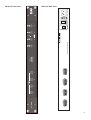
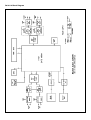
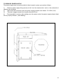
Operator’s &
Service manual
Model 8110
8 channel audio
display
BEL (Digital Audio) Ltd.
Invicta Works Elliott Road Bromley Kent BR2 9NT UK
Tel: +44 (0)20 8460 7299 Fax: +44 (0)20 8460 0499
Email: [email protected]
Web: www.bel-digital.com
CONTENTS
INTRODUCTION
FEATURES
OPERATION
Input Sensitivity
Delay Setting
To Set Delay Increments to NTSC
2
2
3
3
3
3
REAR PANEL CONNECTIONS
Cable Recommendation
EMC COMPLIANCE
SPECIFICATION
TROUBLESHOOTING
FRONT VIEW
REAR VIEW
BLOCK DIAGRAM
4
4
5
5
6
7
7
8
SERVICE INFORMATION (SETUP)
To Remove Power Supply
To Remove Main Printed Circuit Board
To Remove Filout Daughter Board
9
10
11
12
1
BEL 8110
8 Channel Audio Delay
INTRODUCTION
The cost effective Bel 8110 audio delay is designed specifically for synchronising audio to video in
post production areas where video delays result from the VT editing and video effects units etc. It
is intended for use where the video delay is known and is likely to be constant or when frequent
changes of delay are not required. The Bel 8110 may be used in a fixed location with each
channel dedicated to a specific item of video equipment. Independent A/D and D/A converters are
employed for each channel. Each stereo pair of delay lines is switchable in fields (PAL / NTSC) 0
to 15 (7.5 frames). An input level pre-set potentiometer, a signal-present and peak LED are fitted
for each stereo pair. The Bel 8110 user controls are recessed to prevent inadvertent operation.
Master signal bypass is effected by relays in the event of a power loss.
FEATURES
Refer to front and rear views of the Bel 8110 on pages 7/8 for control/connector positions.
The front panel has four "INPUT SENSITIVITY" controls with "Peak" and "-20db" LED
indicators above each control. These are used to set the correct operating signal level.
The delay settings for each channel are set by the four Rotary switches (16 position)
positioned on the left side of the front panel. Each position increases or decreases the set delay
by 1 field (PAL = 20ms) and the 0 (zero) position switches the channel to "BYPASS".
Maximum delay setting is therefore 15 FIELDS (7.5 frames).
The INPUT and OUTPUT connections are made via four 15 way FEMALE connectors on
the rear panel. Two for the INPUTS and two for the OUTPUTS. (Refer to PINOUT information on
Page 3.)
Also on the Rear panel is an EMI filter block (with IEC Power socket, fuse and ON/OFF
switch) and a voltage selector.
2
OPERATION
INPUT SENSITIVITY
To set the "INPUT SENSITIVITY" firstly set the "delay" switches to 1 FIELD DELAY and the
"INPUT SENSITIVITY" controls fully counter clockwise.
With a signal (1kHz SINEWAVE) of +6db at the input socket (channel 1 left) rotate the
"INPUT SENSITIVITY" control clockwise and either monitor or measure the signal at the OUTPUT
socket (channel 1 left) until it is +6db. (UNITY GAIN)
Repeat above for the other 3 channel pairs.
The LED indicators above each control show "signal present" (-20db) and "peak"
(0db).
Maximum signal output just before clipping into 600 W load is +15db. (Can be adjusted
internally) hence with a +6db input the headroom will be +9db.
DELAY SETTING
NOTE: An internal jumper is used to select either PAL or NTSC "field" increments. (See below)
The four Rotary switches (1 per channel pair) are used to set multiples of "field" delays (20m
/ PAL) or a "RELAY BYPASS".
The switches have sixteen positions and can be rotated in either clockwise or counter
clockwise directions with "click" positions 1-15 increasing or decreasing the delay by 1 field.
Position 1-15 in PAL SET MODE = 20-300 ms (1-15 fields)
Position 1-15 in NTSC SET MODE = 33-495 ms (1-15 fields)
Position 0 in both PAL / NTSC will put that channel pair into "BYPASS" connecting the
INPUTS directly to the OUTPUTS.
On Power off or Power fail the "BYPASS" will be initiated as above regardless of the delay
set switch position.
A "BYPASS" "hold" of approximately 1 second is initiated when the 8110 is powered "on", to
allow random data in the memory to be purged before "normal" operation. Switching to "BYPASS"
in normal operation will also have this "hold" time.
Set the other channel pairs as above.
TO SET DELAY INCREMENTS TO NTSC FIELD (33ms)
1) Power off and disconnect the power cable from the 8110.
2) Remove the cover plate
3) Locate LK1 on the DIGITAL PRINTED CIRCUIT BOARD. (See PCB layouts)
4) A small "jumper" link should be fitted to one of these pins if "PAL" was the previous setting
Remove this and locate across both link pins. (Shorting LK1)
5) Re-fit the cover plate and power cable.
6) Power on the 8110
7) Delay set increments will now be in steps of 33ms (1 field / NTSC)
3
REAR PANEL CONNECTIONS
INPUT CONNECTOR (15 WAY MIN "D" FEMALE) CH1/2
1 CH2 RIGHT IN 9 GND + CHASSIS
2 CH2 RIGHT IN +
10 GND + CHASSIS
3 CH2 LEFT IN 11 GND + CHASSIS
4 CH2 LEFT IN +
12 GND + CHASSIS
5 CH1 RIGHT IN 13 GND + CHASSIS
6 CH1 RIGHT IN +
14 GND + CHASSIS
7 CH1 LEFT IN 15 GND + CHASSIS
8 CH1 LEFT IN +
INPUT CONNECTOR (15 WAY MIN "D" FEMALE) CH3/4
1 CH4 RIGHT IN 9 GND + CHASSIS
2 CH4 RIGHT IN +
10 GND + CHASSIS
3 CH4 LEFT IN 11 GND + CHASSIS
4 CH4 LEFT IN +
12 GND + CHASSIS
5 CH3 RIGHT IN 13 GND + CHASSIS
6 CH3 RIGHT IN +
14 GND + CHASSIS
7 CH3 LEFT IN 15 GND + CHASSIS
8 CH3 LEFT IN +
OUTPUT CONNECTOR (15 WAY MIN "D" FEMALE) CH1/2
1 CH1 LEFT OUT +
9 GND
2 CH1 LEFT OUT 10 GND
3 CH1 RIGHT OUT +
11 GND
4 CH1 RIGHT OUT 12 GND
5 CH2 LEFT OUT +
13 GND
6 CH2 LEFT OUT 14 GND
7 CH2 RIGHT OUT +
15 GND
8 CH2 RIGHT OUT OUTPUT CONNECTOR (15 WAY MIN "D" FEMALE) CH3/4
1 CH3 LEFT OUT +
9 GND
2 CH3 LEFT OUT 10 GND
3 CH3 RIGHT OUT +
11 GND
4 CH3 RIGHT OUT 12 GND
5 CH4 LEFT OUT +
13 GND
6 CH4 LEFT OUT 14 GND
7 CH4 RIGHT OUT +
15 GND
8 CH4 RIGHT OUT (To "UNBALANCE" link GND and - at the Male connector)
It is recommended that; where possible, all cables be good quality screened twisted pair multiway
cables "BELDEN" or similar. Optimum performance is obtained using individual screened pairs
with a overall screen and separate ground returns.
Screened "MALE" 15 way connectors are essential.
4
EMC COMPLIANCE
The Bel 8110 was designed and tested to comply with the EMC directive numbers EN55103,
EN55022, EN55082-1 and EN60950 when used as directed.
CE
Please ensure that wherever possible a 1U space is provided above and below the Bel 8110 to
ensure that the unit is properly ventilated, unless forced air cooling is employed in the rack.
SPECIFICATION
Input Impedance
25K W Electronically balanced
Output Impedance
50 W Electronically balanced
Frequency Response
20-20kHz ± 1db
Input Dynamic Range
120 db
Signal To Noise Ratio
-95 db Typical
Distortion
less than .015% @ 1kHz / +6dbm
Nominal Input Level
+6db (+15db max.)
Nominal Output Level
+6db (+15db max.)
Conversion Accuracy
20 Bit Delta Sigma A/D
24 Bit Delta Sigma D/A
Sampling Rate
48kHz
Power Requirement
115/230VAC 50/60Hz
Power Consumption
35W max.
Dimensions
482w x 44h x 200d
Net Weight
5kg
5
TROUBLESHOOTING
The Bel 8110 is designed and constructed to ensure a long and fault free life but if a problem
does occur the following guidelines are provided.
The unit is constructed using two main printed circuit boards and four sub assembly boards.
The two main PCBÕs carry the digital processing (8110 digital) and analogue digital input output
systems (8110 analogue)
Four smaller PCBÕs carry :
1) The filter and output circuits (8110 filout) this board plugs into the connectors on the 8110
analogue board.
2) A system power supply PCB
3) Delay set switch PCB
4) LED indicator PCB
All of the printed circuit boards can be rapidly removed or replaced (see servicing section.)
If the outline fault finding suggestions which follow are unsuccessful, contact your Bel
distributor or the main Bel distributor, who will advise you and arrange for the unit to be repaired
or provide replacement PCBÕs.
Fault
"Dead" unit
Cause
Power supply
Distorted output
Headroom:
Input signal too high
Input sensitivity control
set too high
No delay on audio signal
"Delay-set" switch set
at 0 (BYPASS)
Input/output cables not
individually screened pairs.
Hum/noise, channel cross talk
Action
Check fuses in the IEC and
supply connectors then check
fuses and connectors on the
power supply
Check PPI indicators constant red indicator means
signal level "too high" reduce by adjusting input
sensitivity control
Set required "field" delay by
adjusting delay-set switch
Use "individually screened
pairs multiway cable
"BELDEN" or similar
6
INPUTS
3&4
INPUTS
1&2
1&2
OUTPUTS
3&4
OUTPUTS
BEL (DIGITAL AUDIO) LTD MADE IN THE EC
Model 8110 Serial
FUSE RATING 220/230V = 0.25A(a/s) 110/115V = 0.5A(a/s) 50/60Hz
230
Bel 8110 Front view
Bel 8110 Rear view
7
Bel 8110 Block Diagram
8
SET-UP INFORMATION - SERVICE
PRE-SET RESISTORS (equipment required - oscilloscope and db RMS level meter)
There are eight pre-set ten turn resistors and these are all located on the 8110 Filout PCB
daughter board.
These set the output level of the four stereo L/R outputs (eight channels)
RV1
RV2
RV3
RV4
RV5
RV6
RV7
RV8
Sets
Sets
Sets
Sets
Sets
Sets
Sets
Sets
output
output
output
output
output
output
output
output
level
level
level
level
level
level
level
level
of
of
of
of
of
of
of
of
CH3
CH3
CH4
CH4
CH1
CH1
CH2
CH2
RIGHT (monitor clipping at PL2/1)
LEFT (monitor clipping at PL2/2)
RIGHT (monitor clipping at PL2/5)
LEFT (monitor clipping at PL2/6)
RIGHT (monitor clipping at PL2/13)
LEFT (monitor clipping at PL2/14)
RIGHT (monitor clipping at PL2/9)
LEFT (monitor clipping at PL2/10)
TO SET PROCEED AS FOLLOWS
With +6db 1kHz SINEWAVE at CH1 LEFT INPUT, and a level meter and 600 W
CH1 LEFT OUTPUT.
1)
Locate PL2 on 8110 Filout PCB daughter board and monitor PIN 14.
oscilloscope)
2)
Increase "INPUT SENSITIVITY CONTROL" for CH1 until "clipping" just
monitored PIN.
3)
Adjust RV6 for +15db RMS on level meter.
4)
Move input signal and output monitor to CH1 RIGHT, repeat steps 1 and
OUTPUT (PL2 PIN13/RV5)
5)
Reduce level by adjusting CH1 input sensitivity until output is +6db RMS
3level meter.
6)
Check balance between CH1 LEFT and CH1 RIGHT and trim either RV5
balance.
7)
Repeat steps 1-6 for CH2, CH3 and CH4, monitoring and adjusting the
and Pre-sets listed above.
load connected to
(Using an
occurs at the
2 on CH1 RIGHT
on
or RV6 to
relevant PINS
9
TO REMOVE POWER SUPPLY
The power supply can be removed with all other boards in place, proceed as follows:1)
Remove power supply fixing screws (4 off) 3 on the chassis side 1 and on the underside of
chassis (see drawing).
2)
Disconnect all connectors from the power supply printed circuit board. PL1/PL2 (2 off)
3)
Tilt power supply towards the chassis side and lift out.
4)
Re-assemble in reverse order making sure the spacer under the power supply chassis heat
sink is properly located. (see drawing)
10
TO REMOVE MAIN PCBÕs (8110 DIGITAL AND 8110 ANALOGUE)
Power off Bel 8110 and disconnect IEC power plug from inlet socket.
1)
Remove cover screws (16) and cover.
2)
Remove 8 off Hex post fixings on analogue input/output sockets.
3)
Remove 7 off PCB fixing screws (see drawing).
4)
Remove power supply connector 8 PIN Molex (see drawing) and 2 off Ribbon connectors
(PL2 and PL3) from Digital PCB.
5)
Remove 5 off (socket screws) from underside of front fascia, 2 centre heat sink screws
(see drawing) and 4 larger PAN head front panel fascia fixing screws.
6)
Gently pull front panel including fascia forward and remove.
7)
Pull forward the 2 PCBÕs (8110 Digital and 8110 analogue) to disengage the 4x 15 way
"D" connectors from the rear panel and lift out (together with heat sink).
8)
Disconnect PL1/SK1 to separate boards.
Re-assemble in reverse order, pressing gently on the heat sink to allow location of fixing
screws.
11
TO REMOVE THE "FILOUT" DAUGHTER BOARD
1)
With the cover removed as in "To remove main PCBÕs" locate "filout" daughter board (see
PCB layout diagram)
2)
Grasp the PCB at both ends and pull gently and evenly upwards releasing the two plastic
pillars, which will remain in the mother board.
3)
Keep an even and gentle pull upwards until the PCB is released from the mother board
sockets. The PCB can now be lifted clear of the chassis.
4)
To refit the PCB, accurately locate the plugs on the PCB (daughter board) with the sockets
on the mother board making sure the pillars on the mother board locate in the holes on the PCB.
Gently push the plugs into the sockets keeping the board parallel to the mother board. When the
plastic pillars "click" in place the PCB is fitted correctly.
5)
Replace the cover plate.
12