Download Service manual Version 01.00
Transcript
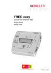
Semiautomatic defibrillator (PAD)
Service manual
Version 01.00
SCHILLER MEDICAL S.A.S
ZAE SUD
4, rue Louis pasteur
BP 90050
F-67162 WISSEMBOURG CEDEX
Téléphone : +33 (0) 3 88 63 36 00
Télécopie : +33 (0) 3 88 94 12 82
Internet : http://www.schiller-medical.com
E.mail : [email protected]
Part No. : 0-48-0049
FRED EASYPORT
Revision history
of the service manual
Version 01.00:
0-48-0019
April 2004
Page I
APRIL 2004
FRED EASYPORT
WARNING
This manual shall be considered to form an integral part of the device
described.
This technical manual is intended for qualified personnel and describes
the operating, maintenance and troubleshooting procedures for
FRED® EASYPORT.
Compliance with its content is a prerequisite for proper device
performance and for the safety of the patient and operator.
The manufacturer shall only be liable for the safety, reliability and
performance of the device if:
- assembly, extensions, adjustments, modifications or repairs are
performed by the manufacturer or by persons authorised by the
manufacturer.
- the electrical installation of the facility of use complies with the
requirements applicable in the country.
- the device is used in accordance with its instructions for use.
- the spare parts used are original parts from SCHILLER.
This manual describes the device at the time of printing.
The supply of this manual does not in any event constitute permission
or approval to modify or repair a device.
The manufacturer agrees to supply all the spare parts for a period of
ten years.
All rights reserved for the devices, circuits, processes and names
appearing in this manual.
The FRED EASY device shall be used as described in the User’s
Manual. The device may not be used for any purpose that has not been
specifically described in the manual, as such use could be hazardous.
0-48-0019
Page II
APRIL 2004
FRED EASYPORT
SAFETY INFORMATION
·
The product is marked as follows:
CE- 0459
in accordance with the requirements of Council Directive 93/42/EEC relating to medical
equipment, based on the essential requirements of annex I of the directive.
·
It fully meets the electromagnetic compatibility requirements of standard IEC 60601-1-2 / IEC
60601-2-4 “Electromagnetic compatibility of medical electrical devices”.
·
The device has undergone interference suppression in accordance with the requirements of
standard EN 50011, class B.
·
In order to optimise patient safety, electromagnetic compatibility, accurate measurement
indication and proper device performance, users are advised to use only original spare parts
supplied by SCHILLER. Any use of accessories other than original accessories shall be at the
exclusive risk of the user. The manufacturer shall not be liable for any damage due to the use of
incompatible accessories or consumable supplies.
·
The manufacturer shall only be liable for the safety, reliability and performance of the device if:
- assembly, configuration, modifications, extensions or repairs are made by personnel from
SCHILLER MEDICAL or personnel duly authorised by SCHILLER MEDICAL.
- the device is used in accordance with its instructions for use.
·
Any use of the device other than as described in the instructions for use shall be made at the
exclusive risk of the user.
·
This manual covers the device version and the safety standards applicable at the time of
printing. All rights reserved for the circuits, processes, names, software and devices appearing
in this manual.
·
The quality assurance system in use in the facilities of SCHILLER meets international standards
EN ISO 9001 and ISO 13485.
·
Unless otherwise agreed in writing by SCHILLER, no part of the manufacturer’s literature may be
duplicated or reproduced.
0-48-0019
Page III
APRIL 2004
FRED EASYPORT
Safety symbols used on the device
Danger! High voltage
Conventions used in the manual
G
Danger:
indicates an imminent hazard which, if not avoided, will result in
death or serious injury to the user (and/or others).
I
Caution:
Warning indicating conditions or actions that could lead to device
or software malfunctioning.
Note:
Useful information for more effective and
operation.
F
practical device
Additional information or explanation relating to the paragraphs
preceding the note.
Manufacturer:
SCHILLER MEDICAL
4, rue Louis Pasteur ZAE sud
F- 67 162 Wissembourg
Tel.
Fax
: **33 / (0) 3.88.63.36.00
: **33 / (0) 3.88.94.12.82
0-48-0019
Page IV
APRIL 2004
FRED EASYPORT
PRECAUTIONS WHILE TESTING THE DEVICE
While testing the FRED® EASYPORT defibrillator, the patient may only be simulated with fixed highvoltage and high-power resistors that are well insulated from the ground or earth. Poorly insulated
devices or devices with loose contacts or devices containing components such as spark arresters or
electronic flash lamps may never be used as they could irremediably destroy the device.
0-48-0019
Page V
APRIL 2004
FRED EASYPORT
SOMMAIRE
1.
Operation_________________________________________________________ 1-1
1.1
1.2
1.3
1.4
1.5
1.6
1.7
2.
Display and controls _____________________________________________________ 1-1
Battery and minicard. ____________________________________________________ 1-2
Explanation of symbols used ______________________________________________ 1-3
Device operation. _______________________________________________________ 1-4
Defibrillation procedure ___________________________________________________ 1-6
Recording (optional) _____________________________________________________ 1-8
Technical specifications __________________________________________________ 1-9
Testing and maintenance ____________________________________________ 2-1
2.1
2.2
2.3
2.4
2.5
Functional testing _______________________________________________________ 2-1
Test mode: ____________________________________________________________ 2-1
SAAD mode ___________________________________________________________ 2-2
Systematic checking before use ____________________________________________ 2-4
Cleaning and disinfection _________________________________________________ 2-4
3.
Troubleshooting____________________________________________________ 3-1
4.
Replacement of parts _______________________________________________ 4-4
4.1
4.2
4.3
4.4
4.5
4.6
5.
Device disassembly procedure _____________________________________________ 4-5
Working on the CPU circuit________________________________________________ 4-6
Working on the defibrillator circuit___________________________________________ 4-8
Replacing the HV capacitor________________________________________________ 4-9
Reassembling the device ________________________________________________ 4-10
Replacing parts ________________________________________________________ 4-10
Technical description of boards_______________________________________ 5-12
5.1 FRED® Easyport_______________________________________________________ 5-12
5.2 CPU, part no. 3.2627 ___________________________________________________ 5-13
5.3 Defibrillator board, part no. 3.2628 _________________________________________ 5-31
6.
Device modifications ________________________________________________ 6-1
6.1 Definition ______________________________________________________________ 6-1
6.2 CPU circuit ____________________________________________________________ 6-1
6.3 Defibrillator circuit _______________________________________________________ 6-1
7.
Diagrams and layout drawings ________________________________________ 7-1
7.1 CPU circuit 3.2627 ______________________________________________________ 7-1
7.2 Defibrillator circuit 3.2628 _________________________________________________ 7-3
0-48-0019
Page VI
APRIL 2004
Operation
1. Operation
This section briefly outlines the operating of the device. For more detailed information,
please refer to the User’s Manual.
1.1
1
2
3
4
5
6
Display and controls
Green
key to switch the device on and off (to stop supporting more than 3 seconds).
The yellow indicator lamp flashes as long as the electrodes are not in place.
Connection of adhesive electrodes
Display
Blue key to start analysing
Key for triggering the defibrillation shock
0-48-0049
Page 1-1
Avril 2004
Operation
1.2
7
8
9
Battery and minicard.
Battery 12 V
SD-Minicard protection.
SD-Minicard
0-48-0049
Page 1-2
Avril 2004
Operation
1.3
Explanation of symbols used
Symbols on the device or accessories
BF type signal input, protected from defibrillation
Caution! High voltage!
Expiry date for the use of defibrillation electrodes
Follow the instructions for use
Open the electrode packaging
Remove the protective film
Single use only. Do not reuse.
Do not fold the packaging
Storage temperature range
Symbols displayed on the screen
Number of shocks given since starting up
Battery weak (not flickering)
24%
Memorizing in progress with % progressively incremented with
the filling (not flickering)
99%
Almost full memory, threshold with 98% filling (flickering)
Problem memory card
Adult electrode detected
Child electrode detected
Time since the machine was started up (minutes and seconds)
0-48-0049
Page 1-3
Avril 2004
Operation
1.4
Device operation.
FRED® Easyport is programmed to operate in four different modes – the test mode followed by the
defibrillator mode, the SAAD mode for device configuration and the Standalone mode, used by
Manufacturing.
·
Test mode
When the device is powered by a cell, it runs a self test every time it is started up. If it does not find
any fault and is ready to operate, it switches to the Defibrillator mode.
·
Defibrillator mode (or Nominal mode)
When the device is powered by a cell and has passed the self tests, it switches to the defibrillator
mode. In this operating mode, the device performs the following operations:
- Resuscitation algorithm (ERC protocol).
- Saving of data throughout the procedure
- Monitoring of system and physiological parameters
Illustration of the screen in nominal mode
Date and time
15/01/04
16:54
24%
ECG trace
PRESS THE
GREEN BUTTON
Messages
·
SAAD (Setup, Acquisition, Adjustment, Downloading) mode
When the device is powered by an adapter unit connected to the FredCo software by means of the
serial link and is switched on, it goes into SAAD mode. This mode is used to:
- Set up and adjust the device
- View statistics
- View logs (events describing the use of the device)
- Download new software versions
·
Standalone mode (Manufacturing)
This mode is specific to the manufacturing department of Schiller and is used to test the CPU board
by itself. Connector P1 of the CPU board must be connected to the serial link of a test console and
pin 4 of P1 must be connected to the ground.
When the device is in Standalone mode, a message is displayed to inform the operator that the
device is not ready for defibrillation. Pressing the keys has no effect, including the On/Off button.
0-48-0049
Page 1-4
Avril 2004
Operation
Diagram of the operating modes
External power
+
Pin at ground
Power ON
External power
Battery power
STANDALONE Modus
TEST Modus
C.A.R.T. Modus
Test without errors
DEFIBRILLATOR Modus
In the Defibrillator mode (or nominal mode), FRED® Easyport is a cell-operated automated external
defibrillator that provides biphasic defibrillation waveforms.
Defibrillation is done by means of disposable adhesive electrodes through which the ECG signals required for
the analysis are also collected. Adhesive electrodes are available in child and adult versions. The device
recognises the type of electrode applied and selects the appropriate defibrillation energy levels accordingly.
When the electrodes are not connected, the device displays a message to inform the user that the electrodes
are not connected or are poorly connected and that they need to be connected to the device. The device
remains in that state as long as the electrode problem persists.
If the problem lasts for 30 seconds, the device guides the user to apply CPR.
After five minutes, the device goes off automatically to save power.
The fault is also reported by a second visual indicator, a LED located under the electrode connector. When
the fault is observed, the LED lights up to report it. Otherwise, the LED is off.
To use the device, the user is given visual and audio instructions (display and loudspeaker).
Power is supplied by disposable plug-in lithium cells. Their capacity is sufficient for
- 70 shocks at the maximum power value or
- five hours of monitoring (cyclical, 30 minutes on, 30 minutes off) or
- five years of standing by.
0-48-0049
Page 1-5
Avril 2004
Operation
1.5
Defibrillation procedure
All the stages are explained to the user through voice prompts and are displayed on the screen. When the
key is pressed, an introductory text asks the user to stick on the electrodes.
The introductory text is repeated till FRED® Easyport recognises that the adhesive electrodes have been
applied.
After that, FRED® Easyport asks the user to start an ECG analysis and not touch the patient.
Note
- With the signals from the database of the AHA (American Heart Association), FRED® Easyport
offers precise detection with 98.4 % sensitivity and 99.8% specificity.
- The device can be set up so that it automatically starts an ECG analysis.
During the analysis phase, the software controls the capacitor charge with an energy value equal to that of
the first shock. If the analysis program recognises a heart rate that calls for defibrillation, the device asks for a
shock.
The heart disorders that call for defibrillation are:
- ventricular fibrillation or
- ventricular tachycardia with a rate of over 180 bpm.
If the device recognises a heart rate that calls for defibrillation, defibrillation is only permitted if the patient has
been found earlier to have no pulse or show no signs of circulation.
A second analysis is triggered automatically with a preliminary capacitor charge to the energy value of the
first shock.
If the first defibrillation shock has no effect, the device automatically tops up the charge in the capacitor to the
energy required for a second shock.
A third analysis is triggered automatically with a preliminary capacitor charge to the energy value of the
second shock.
If the second defibrillation shock has no effect, the device automatically tops up the charge in the capacitor to
the energy required for a third shock.
Note
The energy values set by default as follows (the technical assistance department of Schiller
can set other default values).
Shock
Adult
Child
1
90 J
15 J
2
90 J
30 J
3
120 J
50 J
If the third shock has no effect, FRED® Easyport asks the user to alternately apply artificial respiration and
heart massage. After one minute, it will recommend a ECG analysis. Depending on the set-up, the new
analysis may be automatic.
After a successful defibrillation shock, FRED® Easyport asks the user to check the respiration and blood
circulation of the patient. If there are no signs of circulation, the device recommends the alternate application
of artificial respiration and heart message. If there are signs of circulation, the patient is to be laid on his or
her side.
0-48-0049
Page 1-6
Avril 2004
Operation
If the analysis program does not recognise a heart rate that calls for defibrillation:
- FRED® Easyport informs the user that no defibrillation shock is required, and
- asks the user to check respiration and signs of circulation
If there is no sign of circulation, FRED® Easyport asks the user to alternately apply artificial respiration and
heart massage. If there are signs of circulation, the user is asked to lay the patient on his or her side.
After a minute, FRED® Easyport will ask for an ECG analysis once again. Depending on the set-up, the new
analysis may be automatic.
The values below may be set up by the technical assistance department of Schiller:
- upon starting up: introductory text or immediate request to apply the adhesive electrodes
- voice volume
- energy levels of shocks 1, 2 and 3, with a distinction between adult and child values
- starting of the ECG analysis by pressing the keyboard or automatic
Procedure chart
0-48-0049
Page 1-7
Avril 2004
Operation
1.6
Recording (optional)
For information, the memory card can save:
- half an hour of ECG
- 500 events relating to the procedure (see overview opposite).
In the nominal operating mode, the device records different types of information throughout the procedure.
Recording starts when the device is powered up and runs in the nominal mode and stops when the device is
switched off.
24%
·
This symbol is displayed (steady display) and the
Saving in progress indicator.
percentage is incremented as the memory card is filled up.
·
This symbol flashes when the recording memory is
Memory almost full indicator.
almost full. That does not stop the ERC protocol. The limit at which the memory is almost full is 98 %.
·
Memory full or no card indicator. No memory symbol is displayed.
·
This symbol flashes when the
Indicator of a problem with the procedure recording memory.
recording memory is not accessible (write protected, hot insertion, electronic problem etc.). That
does not stop the ERC protocol.
99%
0-48-0049
Page 1-8
Avril 2004
Operation
1.7
Technical specifications
·
Form of the defibrillation pulse
- Biphasic impulse of defibrillation pulsated with compensation of patient impedance.
·
Standard energy settings::
- Adult (discharge in 50 Ω) : 90 -90 -120 J
- Child (automatic switch when child electrodes are connected) : 15 -30 -50 J
- The energy levels can be configured by the technical assistance department of Schiller if the standard
values need to be changed :
15 - 30 - 50 - 70 - 90 - 120 J (Adult)
15 - 30 - 50 - 70 (Child)
- Tolerance at 50 Ω: ± 3 J or ± 15 % (whichever is greater).
100
25 W
80
50 W
120 J
75 W
60
100 W
125 W
current (A)
40
20
0
150 W
200 W
-20
175 W
-40
0
1
2
3
4
5
6
7
8
9
time (ms)
·
Automatic charge control after a shock is recommended following an analysis
·
Patient resistance 30 to 200 Ω.
·
Charge duration, from the time a shock is recommended up to the time when the device is ready:
< 10 s
·
Cycle time between two shocks:
< 20 s
·
Indication that the devices is ready to deliver a shock: key
·
The shock is delivered with key
·
Internal safety discharge:
- after the self test phase of the defibrillator circuit
- if the CPU host selects a 0-J energy value
- if the PIC detects that the cell is low during the charge phase (UBATT £ 7,5V)
- if the energy stored during the hold phase does not match the energy selected
- when the device is switched off or when the cell is removed during operation
·
The shock is delivered
positions
·
BF type defibrillation electrode connector.
0-48-0049
goes on.
with single-use adhesive electrodes applied in the anterior / anterior-lateral
Page 1-9
Avril 2004
Operation
·
Defibrillation electrodes:
- Adult electrodes: Active area 50 cm²
- Child electrodes: Active area 15 cm²
- Electrode cable length: 1,20 m
·
VT / VF recognition:
- Shock recommendation: for VF and VT (VT > 180 bpm)
- Sensitivity: 98.4 %
Specificity: 99.8 %. These values have been found with the AHA database, which contains cases
of VF and VT with and without artefacts.
- Conditions required for ECG analysis:
Minimum amplitude for the signals used > 0.15 mV , signals of < 0.15 mV are considered to show
asystole.
- Definition:
Sensitivity: Correct detection of heart rates for which defibrillation shocks are recommended
Specificity: Correct detection of heart rates for which defibrillation shocks are not recommended
·
Display:
- LCD, 60 x 40 mm, high definition, with EL backlighting, display of text and icons
·
Recording of the use of the device (optional)
- ECG recording (half an hour)
- Event recording (500 events)
·
Capacité de la pile au lithium
- 70 chocs à puissance maximale ou
- Utilisation du moniteur pendant 4 heures (cyclique 30 minutes en marche, 30 min arrêté)
- 5 ans de veille.
Lithium battery capacity
- 70 shocks at the maximum power rating or
- Use of the monitor for four hours (cyclical, 30 minutes on, 30 minutes off)
- Five years standing by.
·
·
Environment conditions:
- Transport / storage:
Temperature - 20 to + 50 °C
Relative humidity of air 0 to 95 %, non condensing
Atmospheric pressure 500 - 1060 hPa
- Use:
Temperature 0 to + 50 °C
Relative humidity of air 0 to 95 %, non condensing
Atmospheric pressure 500 - 1060 hPa
·
Electromagnetic compatibility:
- The FRED easy® device only uses radio frequency range energy for its internal functions. It is treated
against interference in accordance with standard CISPR 11 class B
- The FRED easy® device can be subjected to the following interference without any adverse effect
on its functioning:
v electrostatic discharges of up to 8 kV.
v energy in the radio frequency range up to 20 V/m (80 - 2500 MHz, 5 Hz modulated).
v magnetic fields of 100 A/m, 50 Hz
·
Dimensions and weight:
- Width
- Depth
- Height
- Approximate weight
0-48-0049
: 126 mm
: 133 mm
: 35 mm
: 490 g (with battery)
Page 1-10
Avril 2004
Testing and maintenance
2. Testing and maintenance
This section describes the test and maintenance procedures recommended for pour FRED® Easyport.
2.1
Functional testing
Functional testing is performed by the automatic test function. In order to ensure that the device is operating
correctly, tests are conducted when it is switched on in the nominal mode (SAD mode).
2.2
Test mode:
Self tests are conducted automatically when the device is powered by the cell and is switched on by pressing
On/Off key. The operator does not see the tests. No message describing the tests is displayed when
the
the device is running them.
A starting up screen is displayed during the self test procedure with the following information:
SCHILLER
EASYPORT
Sw CPU : V01.00B1
Sw Defi : V01.00B1
Hw CPU : 3
Hw Defi : 5
Language : 16
19/01/04 15:54
!!! TESTING !!!
Language Code
1
English
10
Finnish
19
Turkish
28
Walloon
2
French
11
Russian
20
Japanese
29
Latvian
3
German
12
Chinese
21
Hebrew
30
Tahitian
4
Spanish
13
Korean
22
Bulgarian
31
Brazilian
5
Italian
14
Romanian
23
Arabic
32
Slovak
6
Dutch
15
USA
24
Czechoslovakian
33
Polish
7
Swedish
16
Austrian
25
Quebec French
8
Portuguese
17
Danish
26
Hungarian
9
Norwegian
18
Greek
27
Flemish
0-48-0049
Page 2-1
Avril 2004
Testing and maintenance
The tests cover the following functions:
1.
2.
3.
4.
5.
6.
7.
8.
Hardware number test
Acquisition system test: ECG & patient impedance
Defibrillator test: communication channel and defibrillation hardware module
Settings storage memory test
Real time device clock test
Cell voltage test. The cell voltage is tested by charging the capacitor
LCD display test
Voice prompt system test
Note
Failure to pass tests 1 – 4 disables the device, which indicates the failed test till it is
switched off.
Failure to pass tests 5 and 6 does not disable the device.
Simultaneous failure to pass tests 7 and 8 disables the device.
If the tests are passed or if the errors are not of the disabling type, the device goes into Defibrillator mode.
2.3
SAAD mode
This operating mode is used to set up the device, extract statistics or download software. The cell is replaced
by the adapter unit and the downloading unit connected to the FredCo software is to be used.
2.3.1
Setting up and adjustments
The configurable settings are:
·
·
·
·
·
·
·
·
·
·
·
·
·
Date and time + format + summer/winter time
Ø Date format: DD/MM/YYYY or MM/DD/YYYY or YYYY/MM/DD
Ø Time format: 12 or 24 hours
Defibrillation energy values
ECG display
Voice prompt volume level
Analyse button use
CPR phase
Motion detection
Language for the display and audio messages of the ERC protocol
Device serial number
Hardware version number
Shock counter (charge capacitor wear)
ERC 1 minute / 3 minute protocol selection
Device identification string
0-48-0049
Page 2-2
Avril 2004
Testing and maintenance
2.3.2
Statistics
The list of data stored below is not exhaustive and will develop to keep pace with needs:
·
·
·
·
·
·
·
·
Total device running time
Status of the mini SD card flash memory – card size, space occupied, number of events logged
Periodic test log (last 30 tests as a minimum): date, time, result, description of the error
Uncontrolled switching off (last 30 times as a minimum): cell low, electrode fault for more than 5
minutes – date and time
Number of charges per energy value
Number of shocks per energy value.
Total running time of the high-voltage converter
Etc.
The data cannot be erased by means of a device button. They may be erased by a command from the serial
link.
The data need to be made secure. In particular, they must not be destroyed when the device is switched off
suddenly because the cell is removed. The data are only saved when the device undergoes a controlled shutdown.
2.3.3
Downloading
The downloading function is used to upgrade the firmware in the device. The software provides the language.
To change languages, the firmware with the required language needs to be downloaded.
0-48-0049
Page 2-3
Avril 2004
Testing and maintenance
2.4
Systematic checking before use
Before each use, the device must undergo a visual inspection, including the cables, connectors and
electrodes.
If a fault or malfunctioning likely to harm the safety of the patient or the user is found, the device may not be
started up again before it is repaired.
Systematic inspection before each use
· Device housing check
· No mechanical damage
· No liquid penetration into the device
· Control button and connector check
2.5
Cleaning and disinfection
I
Important:
Switch off the device before cleaning. Remove the cell
before starting to clean the device in order to ensure that the
device does not start up accidentally. Before cleaning, also
disconnect the defibrillation electrode cables from the
device.
No liquid must enter into the device. If that does happen, the
device may not be used before it is checked by the aftersales service department.
Users are strongly advised against cleaning the devices or electrodes with agents such as
ether, acetone, esters or aromatic chemicals.
Never use phenol-based cleaners or cleaners containing peroxide derivatives to disinfect the
surfaces of the device housing.
·
Systematically dispose of the single-use electrodes immediately after use in order to ensure that
they are not reused by mistake (hospital waste).
·
Before cleaning the electrode cables, disconnect them from the device. Clean and disinfect
them by wiping them with a piece of gauze moistened with cleaner or disinfectant. Never
immerse the connectors in any liquid. Use any cleaning or disinfectant solution that is commonly
used in hospitals.
·
Proceed likewise with the device housing, with a cloth moistened with cleaner or disinfectant. No
liquid may enter the device during cleaning.
0-48-0049
Page 2-4
Avril 2004
Troubleshooting
3. Troubleshooting
This section describes how to locate failures if FRED® Easyport shows any signs of malfunctioning. If you
have trouble locating or correcting the fault, contact the after-sales service department of Schiller.
Precautions to be taken for troubleshooting
All tests with FRED® Easyport defibrillators shall be done exclusively with fixed resistors with high voltage
and power ratings to simulate the patient. The resistors shall be correctly insulated from the ground and the
earth. Any use of incorrectly insulated systems or systems with loose contacts or containing components
such as spark gaps or electronic flash lamps is strictly forbidden as that could irreversibly damage the device.
G
Danger:
ERROR
Before opening the device for work, FIRST MAKE SURE THAT THE
HV CAPACITOR HAS BEEN DISCHARGED FULLY.
OBSERVATION
POSSIBLE CAUSES
CORRECTIVE ACTION
1. Check button cell on
CPU (out of order or flat)
2. Check if F1 fault on
Defibrillator board
3. CPU board fault
4. Defibrillator board fault
1. Replace button cell
Electrodes not connected and LED under the
electrode connector off
1. Defibrillator board fault
2. CPU board fault
1. Replace defibrillator board
2. Replace CPU board
Electrodes connected to simulator with 50-ohm
impedance, but the LED stays on
1. Defibrillator board fault
2. CPU board fault
1. Replace defibrillator board
2. Replace CPU board
No voice prompts
1. Speaker fault
2. CPU board fault
1. Replace speaker
2. Replace CPU board
Orange Shock key will not light up
1. CPU board fault
1. Replace CPU board
No memory card recording
1. Memory card fault
2. CPU board fault
1. Replace memory card
2. Replace CPU board
Loss of date and time
1. Button cell fault
2. CPU board fault
1. Replace button cell
2. Replace CPU board
! ! ! TESTING ! ! ! Not displayed on the screen
0-48-0049
Page 3-1
2. Replace fuse
3. Replace CPU
4. Replace defibrillator board
Avril 2004
Troubleshooting
If any error is detected, FRED® Easyport will indicate the error code and the screen will be as shown below.
To identify the error, refer to the table below or use the FredCo software.
DEVICE OUT OF ORDER
ERROR
CODE
F
Note:
If an error message is displayed, note down the error number and
restart the device to make sure that the error is not due to an
isolated program error.
List of error messages
CODE
100-1
MESSAGE
Err: System
100-100
Err: ADC
100-101
Err: ADC selftest 1
100-102
Err: ADC selftest 2
100-103
Err: ADC selftest 3
100-200
100-201
Err: Defi
Err: Defi invalid Hard version
100-202
Err: Defi invalid Soft version
100-203
Err: Defi autotest precharge
100-204
Err: Defi reference voltage
100-205
Err: Defi ADC
100-206
Err: Defi charge transistor
100-207
Err: Defi security discharge
100-208
Err: Defi Eprom
POSSIBLE CAUSES
- CPU board problem
- Defi board problem
- ADC problem (U36) on
CPU board
- ADC problem (U36) on
CPU board
- ADC problem (U36) on
CPU board
- ADC problem (U36) on
CPU board
- Defi board problem
- Hardware version of Defi
board not compatible
- Software version of Defi
board not compatible
- µC problem (U9) on
Defi board
- Voltage reference problem
CORRECTIVE ACTION
- Replace CPU board
- Replace CPU board
- Replace CPU board
- Replace CPU board
- Replace CPU board
- Replace CPU board
- Replace Defi board
- Upgrade Defi board
hardware
- Upgrade Defi board
software
- Reload program
- Or replace Defi board
- Replace Defi board
at U7 of Defi board
0-48-0049
- µc problem (U9) on Defi
board
- Q6 problem on Defi
board
- Safety discharge circuit
problem on Defi board
(U6, R127, D17 - D19)
- µc problem (U9) on Defi
board
Page 3-2
- Reload program
- Or replace Defi board
- Replace Defi board
- Replace Defi board
- Reload program
- Or replace Defi board
Avril 2004
Troubleshooting
List of error messages
CODE
MESSAGE
POSSIBLE CAUSES
CORRECTIVE ACTION
100-209
Err: Defi shock button
- Shock button problem
- Or U8 problem
100-210
Err: Defi Com
100-211
100-212
Err: Defi Discharge HV reset
Err: Defi bad stored energy
100-213
Err: Defi discharge Hw defect
100-214
Err: Defi discharge bad energy
100-215
100-217
Err: Defi battery voltage
Err: Defi CPU
100-218
Err: Defi program integrity
100-220
Err: Defi charge circuit
100-221
Err: Defi problem IGBT
100-222
Err: Defi power supply
100-300
Err: LCD
100-400
Err: OKI
100-500
Err: Flash
100-501
Err: Read Flash
100-502
Err: Write flash
100-600
Err: RTC
100-700
Err: Hardware version
100-701
Err: Hw version invalid => 0
100-702
Err: Hw version invalid => 47
- µc problem (U9) on Defi
board
- Problem with HV circuit
- Problem with energy
stored on Defi board
- Problem with HV circuit
on Defi board
- Problem with discharge
energy on Defi board
- Problem with lithium cell
- µc problem (U9) on Defi
board
- µc problem (U9) on Defi
board
- HV generator problem
(U3) on Defi board
Problem with IGBT
module (U6) on Defi
board
- Problem with + 5 V
power supply
- Problem with LCD
management on CPU
board
- Problem with OKI (U26)
on CPU board
- Problem with Flash (U6)
on CPU board
- Problem with Flash
reading (U6) on CPU
board
- Problem with Flash
writing (U6) on CPU
board
- Problem with RTC
(U16) on CPU board
- Hard and software
version not compatible on
CPU board
- Problem on R81 of CPU
board
- Problem on R82 of CPU
board
- Check and replace Shock
button if needed
- Or replace Defi board
- Reload program
- Or replace Defi board
- Replace Defi board
- Replace Defi board
100-800
Err: Standalone mode
100-900
Err: ECG amplification chain
0-48-0049
- Problem with PB15 at
U1 of CPU board,
connected to the ground
- Problem with ECG
amplification chain on
Defi board or CPU board
Page 3-3
- Replace Defi board
- Replace Defi board
- Replace cell
- Reload program
- Or replace Defi r board
- Reload program
- Or replace Defi board
- Replace Defi board
- Replace Defi board
- Replace Defi board
- Or replace CPU board
- Replace CPU board
- Replace CPU board
- Replace CPU board
- Replace CPU board
- Replace CPU board
- Replace CPU board
- Load correct software
version
- Or Upgrade CPU board
- Check if R1 = 100 k on
CPU board
- Check R2 on CPU board; it
must adjust to the hardware
version.
- Check if LP1 is not shorted
- Or check if pin 4 of P1 is
not connected to the ground
- Replace CPU board
- And/or replace Defi board
Avril 2004
Replacement of parts
4. Replacement of parts
This section addresses the dismantling of FRED® Easyport for replacing defective parts. The warnings
below apply to all work on the components inside the device.
G
Danger:
FRED® Easyport is a defibrillator with an HV capacitor
capable of carrying fatal voltages. The device may only be
dismantled by specially authorised and trained personnel.
Before opening the device to work on it, MAKE SURE THAT
THE CAPACITOR HAS BEEN DISCHARGED
I
I
I
Important:
Before opening the device, take the cell out of its housing.
Important:
The device contains circuits sensitive to electrostatic
discharge. All work on FRED® Easyport shall be performed in
accordance with ESD rules. The work shall be performed on
an antistatic mat connected to the earth and the operator
shall wear an antistatic strap that is connected to the mat.
Remove the antistatic strap while working on the highvoltage part of the defibrillator.
Important:
Each defibrillator and CPU board has its own hardware
number. The list of permitted combinations (defibrillator and
CPU hardware number) is available from Schiller Medical.
The hardware version numbers are displayed when the
device is started up during the self test phase.
I
0-48-0049
Important:
Every time the device is opened, it must undergo an overall
test when it is closed.
4-4
Avril 2004
Replacement of parts
4.1
Device disassembly procedure
While disassembling the device, follow the instructions below:
1. Remove the lithium cell from its housing.
2. Disconnect the electrode cable.
3. Turn the device over (LCD screen down), take off the protective caps on the screws and
unscrew the six assembly screws of the upper and lower halves of the housing.
4. After removing the six screws, turn the device over once again (LCD screen toward you).
5. The upper half of the housing may now be pulled off gently. The electrode connections to
the left-hand side may offer some resistance.
6. Disconnect the flat cable connector.
Flat cable
Electrode
connections
0-48-0049
4-5
Avril 2004
Replacement of parts
4.2
Working on the CPU circuit
To remove the CPU, follow the instructions below:
1. Disconnect the speaker and take off the six screws shown by an arrow.
Disconnect
I
Important:
Do not lose the control button caps placed in the upper part.
2. The speaker is glued into its slot. If needed, prise it out with a screwdriver.
0-48-0049
4-6
Avril 2004
Replacement of parts
I
Important:
This circuit contains components sensitive to electrostatic
discharge. The operation above shall be performed in
accordance with ESD rules.
3. To replace the button cell, you will need to remove the shielding.
0-48-0049
4-7
Avril 2004
Replacement of parts
4.3
Working on the defibrillator circuit
To remove the defibrillator circuit:
1. Take off the six screws marked by an arrow.
2. Take off the bracket that holds the cell connector.
Bracket
I
0-48-0049
Important:
This circuit contains components sensitive to electrostatic
discharge. After disconnecting the PCB from the device,
follow ESD rules.
4-8
Avril 2004
Replacement of parts
4.4
Replacing the HV capacitor
G
Warning:
This operation concerns the HV capacitor, which may be
charged to a fatal voltage. Before any work, make sure that
the HV capacitor has been fully discharged. Never touch the
terminals of the HV capacitor directly. The HV capacitor may
only be replaced by specially authorised and trained
personnel.
The replacement of the HV capacitor is required very rarely, as the life of the capacitor is extremely
long. However, if needed, the HV capacitor may be replaced in accordance with the instructions
below:
IMPORTANT! FIRST CHECK IF THE HV CAPACITOR IS FULLY DISCHARGED!
1. Separate the two HV wires
F
After you remove the (fully discharged) HV capacitor from the lower part, short
its two terminals with conductive wire.
While replacing the HV capacitor, place it in its housing and then solder the cables, taking care to
follow the polarity. Also follow the cable path.
Make sure that nothing has been forgotten before restarting the device.
I
Important:
This operation concerns a key component of the HV part of
the device and may only be performed by specially
authorised personnel with training in FREDâ Easyport.
A test of the energy delivered is required.
0-48-0049
4-9
Avril 2004
Replacement of parts
4.5
Reassembling the device
Reverse the operations to reassemble the device.
1. Do not forget to connect the speaker to the CPU.
2. Take care while connecting the HV contacts.
4.6
Replacing parts
G
Warning:
Parts may only be replaced by personnel who have been
specially trained and authorised by Schiller.
Also, use only original Schiller replacement parts.
F
0-48-0049
Note:
While ordering a new part from Schiller, state the type of device and the
serial number provided under the device. Then specify the item code of
the part to be replaced.
4-10
Avril 2004
Replacement of parts
0-48-0049
4-11
Avril 2004
Technical description of boards
5. Technical description of boards
5.1
FRED® Easyport
General description of FRED® Easyport
FRED® Easyport is technically divided into two subassemblies:
·
The defibrillator board, which carries the various digital processing functions specific to the
defibrillator, analogue processing functions and the high-voltage circuit of the defibrillator.
·
The CPU board, which carries the various digital processing functions, storage, auxiliary power
supplies and control, monitoring and display systems.
The two boards communicate electrically with each other through a flat cable with a 26-pin connector
at its end (P2).
Control, monitoring, power supply, display and recording systems
The various control, monitoring and display systems of the CPU board are:
·
·
·
·
·
·
·
·
LCD screen that acts as the visual interface between FRED® Easyport and the user
On/Off key for switching the device on and off
Analyse key to start an analysis of the patient’s ECG signal
Shock key to deliver the defibrillation shock
Orange LEDs showing the Shock key and providing an added visual user interface
Electrode fault LED showing where the defibrillation electrodes are to be connected. It also shows
electrical circuit continuity.
A speaker to play the prompts intended for the user
A removable memory card of the mini SD card type for recording the ECG signal and procedure
events
Set-up and downloading accessory
·
A special unit that replaces the cell unit and has a mini DIN connector for a serial link with an external
PC is used to download programs and set up FRED® Easyport. During these operations, the device
is powered by an external power source through the same connector.
0-48-0049
5-12
Avril 2004
Technical description of boards
5.2
CPU, part no. 3.2627
The paragraphs below describe the different functions of the CPU board.
General description:
Figure Diagram 1, provides an overview of device functions.
The various subassemblies are represented in charts 2 to 7.
The pushbuttons and the LCD display module are directly soldered onto the CPU board.
The CPU board controls and monitors the following basic functions:
·
·
·
·
·
·
·
·
·
·
·
·
·
·
·
·
·
·
·
·
·
·
·
·
·
Main clock
Generation of intermediate clocks
Real time clock
Data bus amplification
Address bus amplification
SDRAM working memory
Flash memory (program, set-up data, incident log)
Power from the 26-pin P2 connector (for flat cable)
Auxiliary power supplies
3.3-V voltage supervisor (Coldfire power supply)
Monitoring of auxiliary voltages
Monitoring of power supply cell voltage
Device power on/off (On/Off key)
Start of analysis (Analyse key)
Recognition of electrode type (child/adult)
Delivery of defibrillation shock (Shock key)
RS232 serial links through connector P2 (26 pins)
Communication between Coldfire and defibrillator PIC
Mini SD Card memory card interface
LCD display interface
CPU hardware configuration
ADPCM decoder for voice prompts
Audio amplifier for voice prompts
Analogue to digital converter
ECG signal analogue processing
0-48-0049
5-13
Avril 2004
Technical description of boards
Description of subassemblies
Microcontroller
Figure Diagram 2 shows the MCU (microcontroller unit).
The MCU is built around a host microcontroller (U1) called Coldfire, the working RAM (U4 and U5) and the
Flash memory (U6).
Coldfire is controlled by a 40.96 MHz quartz clock.
Note: Configuration of Coldfire upon starting up.
Coldfire starts up as soon as signal PF_RESET/ (hardware reset from the voltage supervisor) appears and
generates signal –RST0 (reset generated by Coldfire and used by devices).
While activating -RST0, Coldfire reads entries BUSW0, BUSW1 and WSEL, which are used to set the
communication speeds with devices.
Signals WSEL, BUSW0 and BUSW1 are generated by means of U2.
Data bus amplification
The Coldfire data bus undergoes bidirectional amplification by U7.
With the exception of DRAM U4 and U5, all the other devices use amplified data bus B_D(16 - 31).
Signal -WE generated by Coldfire controls the direction of data transmission.
Signal -BD_CS (Buffered Data Chip Select) generated by programmable circuit U10 controls the activation of
U7.
Address bus amplification
The Coldfire address bus undergoes unidirectional amplification by means of U3. Only the eight low
addresses A(0 - 7) are amplified. With the exception of DRAM U4 and U5, all the other addressed peripherals
use amplified address bus BA(0 - 7).
Main clock
A 40.96 MHz quartz oscillator (U9) acts as the main clock (CPU_CLK) of Coldfire.
Generation of intermediate clocks and associated logical functions
A programmable logic circuit (U10) of the GAL22LV10 type is used to generate the secondary clocks and
other synchronisation signals from main clock CPU_CLK and asynchronous counter U8.
Secondary clock CLK4M096 is used by the ADPCM audio decoder.
Real time clock
Real time clock U16 is controlled by Coldfire through data bus B_D(16 - 31), address bus BA(0 - 7) and
control signals -CS3, -OE and -WE.
It performs the function of real-time clock/calendar and is controlled by 32.768 kHz quartz Q8.
This clock is powered by the backup cell (BT1) when the device is switched off. When the device is running,
U16 is powered by VCC = 3.3 V.
Note: software set-up data
The software set-up data of FRED® Easyport are saved in the dedicated areas of the Flash memory (U6).
0-48-0049
5-14
Avril 2004
Technical description of boards
Power supplies, On/Off, pushbuttons and LEDs
Figure Diagram 3 represents the following:
·
·
·
·
·
The various power supplies generated by the CPU board from voltage UBAT (12V lithium cell)
Voltage monitoring and Coldfire reset signal generation circuits
On/Off circuits
On/Off, Analyse and Shock pushbuttons
Shock and Electrode LEDs
UBAT comes from the defibrillator board and powers the CPU board via the 26-pin flat cable.
The secondary voltages generated are supplied to the defibrillator board by the same flat cable.
Power supplies
Voltage +3.3 VCC
The + 3.3 VCC power supply voltage is derived from the UBAT cell voltage by means of chopping
regulator U12, chopping transistors U13A and U13B, diode D4, induction coil L4 and capacitors C113
and C114.
The components make up a step-down regulator. The voltage is controlled by resistor R266.
Voltage +5 V
The +5 V power supply voltage is derived from the cell voltage by means of chopping regulator U11,
diode D2, induction coil L3 and capacitors C18, C111 and C116.
The components make up a step-down regulator. The voltage is controlled by dividing bridge R159,
R164.
Voltage +5 VOP
The +5 VOP voltage is +5 V filtered by L5, C19 and C112 and is particularly intended to supply power
to the operational amplifiers.
Voltage +17.5 V
The +17.5 V power supply voltage is derived from +5 V by means of a step-up chopping regulator
made up of U14, L7, D3 C82, C123, R162, R165, R166.
+ 3.3 V power supply voltage supervisor (minimum voltage)
The + 3.3 V power supply voltage supervisor is made up of circuit U18. It provides the RESET_PF pulse
when the device is started up and monitors the 3.3 V power supply voltage during operation. A drop below +3
V triggers a Coldfire reset pulse.
U_BAT_SWITCHED, + 3.3V, +5V, +17.5 V voltage supervisor
U17 resets the CPU if any over voltage is seen at the 3.3 V, 5 V or 17.5 V power supplies or if voltage
U_BAT_SWITCHED drops below 6.5 V.
Note:
0-48-0049
During normal operation, the cell voltage is monitored by Coldfire and by the PIC. If there is a
fault, an error message is generated and the user is informed if the cell voltage is too low to
correctly power FRED® Easyport.
The 6.5 V limit is therefore never reached in principle.
5-15
Avril 2004
Technical description of boards
On/Off key (S1): Starting up and shutting down
Pressing key S1 polarises the gate of transistor U15 through D11, R201 and R170 so as to make it conduct.
(U15 may be considered to be a main switch).
Line UBAT_SWITCHED switches to the cell voltage (U_BAT_FUSED_CPU).
U15 is then kept closed temporarily by Q2 through C84 and D12.
As soon as the Coldfire microcontroller has started, the device is kept operating by pulsed signal CMD_OFF
through C86, D12 and Q2.
Signal ON_OFF_KEY is used to see the status of key S1. If it is kept pressed in for a long time, the software
ceases to send a signal to CMD_OFF and the device goes off.
The device is shut down by pressing the ON_OFF key for more than 3 seconds.
Analyse key (S2): Starting an ECG analysis
An analysis is started by pressing key S2 when the device is on.
The signal is directly sent to the PIC microcontroller of the defibrillator board.
Coldfire is informed of any press of the key via the serial link from PIC to Coldfire.
Note: The Analyse key may also be read directly by Coldfire via latch U21 (see LCD interface)
Shock key (S3): Delivering a defibrillation shock
The command for giving a defibrillation shock is given by pressing key S3.
Pressing key S3 forces signal CHOC_KEY to zero.
The signal is transmitted directly to the PIC microcontroller of the defibrillator board.
Coldfire is informed of a press on the key via the serial link from PIC to Coldfire.
Note: The Shock key can also be read directly by Coldfire via latch U21 (see LCD interface)
Pressing the Shock key (S3) is only applied when it is lit up by two orange LEDs D15 and D26. The LEDs are
switched on by means of transistor Q3 and signal CMD_LED_CHOC generated by Coldfire.
Recognition of type of electrode
The type of electrode used (Child or Adult) is recognised by means of a reed contact REL1. The Child type
electrode connector has a permanent magnet that closes contact REL1 and forces signal TYPE_ELECTR to
the low logical status. The signal is sent to the microcontroller of the defibrillator.
Note: The connector of the Adult electrode does not have a permanent magnet.
Light emitting diodes (LEDs)
The device has 7 LEDs.
·
·
·
4 white LEDs are used to backlight the LCD
2 orange LEDs illuminate the Shock button when it is valid (Shock ready)
1 LED indicates electrode faults (patient not connected)
0-48-0049
5-16
Avril 2004
Technical description of boards
Serial links
Figure Diagram 4 represents the three serial links used by FRED® Easyport.
·
·
·
Serial link to an external PC
Serial link to the defibrillator board
SPI link to the Mini SD Card memory card
Serial communication with external PC
The serial link (RS232 protocol, TTL levels) through the battery connector (JP5) is used essentially for
operations involving upgrades of the device program and set-up. It enables communication between an
external PC and Coldfire. It operates at 115.2 kbauds.
A special adapting connector of the size of a battery unit, fitted with a mini DIN connector, is used to set up a
physical link between FRED® Easyport and the downloading device. Special software (FredCo) is required
for using the data from the serial link.
During the set-up and/or download operations, the device must also be powered by means of the connector.
Note:
Pin EXT_PWR is connected to U_BAT through the adapter unit.
It enables the software of FRED® Easyport to switch automatically to the set-up mode.
Serial communication between Coldfire and the PIC microcontroller of the defibrillator
Serial communication between Coldfire and the PIC microcontroller of the defibrillator takes place through a
serial link at 9600 bauds.
Signal TXD_DEFI from the defibrillator microcontroller is directly applied at the input of Coldfire. Signal
RXD_DEFI generated by Coldfire is sent to the microcontroller of the defibrillator by means of a voltage level
adaptation stage, which is made up of Q1 and Q5.
Serial communication between SPI and the mini SD card interface
The mini SD Card interface is made up of special connector, JP1, designed to accommodate memory cards.
During the procedure, the card is used to record the ECG signals and events of the procedure.
The mini SD card is controlled by Coldfire through signals SPI_CS3, QSPICLK, SPI_DATA_IN and
SPI_DATA_OUT.
Signals DET_PRESENT_SDCARD and WRITE_PROT_1 are status signals of the memory card, which
indicate mini SD card presence and write protection respectively.
The signals are active in the low logical state. The lines linked with JP1 are all protected by 220-W resistors.
The mini SD card power supply is protected by resistor R253.
0-48-0049
5-17
Avril 2004
Technical description of boards
LCD display
Figure Digram 5 represents the LCD interface of FRED® Easyport.
The LCD display is controlled by Coldfire by means of data bus B_D[24 - 31] and signals -CS1 and -CS4.
Data is written in the LCD registries by means of latch U23 and is controlled by signal LCD_WR generated by
latch U22.
Data are read from the LCD registries by means of latch U24 and is controlled by signal LCD_RD generated
by latch U22.
The other control signals (LCD_CS, LCD_RS, LCD_RES) are derived from the data bus by means of latch
U22.
The power for the logical functions of the LCD screen is provided by the 3.3 V power supply via R143.
A second power source, VLCD, is obtained from the 17.5 V power supply and linear regulator U24.
VLCD is temperature-compensated by thermistor R219, which offers optimum contrast regardless of the
ambient temperature.
All the logical links with the LCD screen are filtered by RC networks.
Back lighting is provided by 4 white LEDs controlled by latch U22, through Q4.
Hardware configuration
Some particular options may be put in place by solder spots (LP6 to LP10). The hardware configuration is
read by means of input latch U21.
Five entries of the latch are connected to VCC by pull-up resistors R151 to R155 and may be forced to zero.
Input latch U21 is controlled by Coldfire by means of the data bus B_D(24 - 31) and signals -CS1 and -OE via
logical door U20A.
Latch D21 also enables direct reading by Coldfire of the status of keys Analyse (S2) and Shock (S3).
Audio functions
Figure Diagram 6 represents the audio interface.
ADPCM decoder
The ADPCM decoder is controlled by Coldfire through data bus B_D[16 - 31] and status control signals CS2 ; -OE ; -WE ; BA0 ; -RST0 and OKI_FIFO_MID.
The decoder operating frequency is 4.096 MHz. It is achieved by the generation function of the intermediate
clocks that is built around U10. The ADPCM decoder (U26) output AOUTL provides an analogue signal is
applied to the audio amplification chain formed by U27A, U27B and U28.
Audio amplification
The audio amplifier is built around circuit U28. Pre-filtering is provided by U27B.
The audio signal is applied via a capacitive link (C34) to the power amplifier input, the output of which is
applied to the speaker. Power amplifier U28 may be put into standby mode by means of signal
POWER_DOWN_AUX/.
0-48-0049
5-18
Avril 2004
Technical description of boards
Analogue processing and analogue to digital converter
Figure Diagram 7 represents the analogue processing functions and analogue to digital conversion.
The ADC (U36) is controlled by Coldfire by means of data bus B_D[16 - 31], signals -CS5, -WE, -OE,
ADC_CSTART and clock CLK4M096.
Line -INT4/EOC informs Coldfire that conversion is completed and that the converted data are available.
The converter resolution is 10 bits and its voltage reference (VREF_2V5) is supplied by D20.
The ADC has eight multiplexed analogue inputs CH0 to CH7, which enable it to digitise the following signals:
CH0: ECG_ADC:
Analogue signal from the defibrillator board.
It carries information from the ECG with a bandwidth at -3 dB of 0.5 Hz - 23 Hz.
Before it is applied to the input of the ADC, signal ECG_ADC is conditioned by the
analogue processing function of the CPU board.
CH1: Z_ELEC_DEFI:
Analogue signal from the defibrillator board.
It carries information about patient impedance. Before it is applied to the
converter, signal Z_ELEC_DEFI is attenuated by two and filtered by dividing
bridge R74, R76 and C48.
CH2: DELTA_Z:
Analogue signal generated from Z_ELEC_DEFI by the filter built around U31A. It
carries information about impedance variation used for detecting motion.
CH3: CHK_BAT_CPU:
Signal used to measure the “instant” battery voltage.
CH4: CHK_BAT_CPU_F: Same signal as CHK_BAT_CPU, only filtered to eliminate the instant variations due
to brief current inrushes.
CH5: CHK_BAT_DEF:
Signal for controlling the voltage applied to the high-voltage (HV) converter on the
defibrillator board, when HV capacitor charging is under way.
CH6: CHK_EXT_PWR:
Signal used to determine if the software must start up in AED mode or in set-up
mode.
- If pin CHK_EXT_PWR (pin 15 of P2) or pin 2 of battery connector JP5 on the
defibrillator board is connected to U_BAT, the device starts up in set-up mode.
- If CHK_EXT_PWR is not connected, which means that a standard battery unit is
being used, the device starts in the AED mode.
Note:
Link U_BAT to CHK_EXT_PWR is made up of a special “battery” unit designed
for downloading.
CH7: (hardware version)
The voltage from a divider bridge is applied to input CH7. The value of resistor
R81 determines the hardware version of the CPU board.
0-48-0049
5-19
Avril 2004
Technical description of boards
ECG analogue signals
The defibrillator board provides two signals: ECG_DEFI and ECG_STIM
ECG_DEFI undergoes preliminary filtering on the defibrillator board. It is used to analyse the ECG but cannot
be used for extracting pacing pulses.
ECG_STIM is less filtered (for high frequencies) and is used for that purpose.
The operational amplifiers are powered between +5 V and GND, a virtual ground.
V_GND = +2 V is created by U34A.
Analogue processing of signal ECG_DEFI
The continuous component of analogue signal ECG_DEFI undergoes ultimate filtration, amplification and
offsetting before it is digitised by the ADC.
Signal ECG_DEFI is applied to analogue switch U29 which is responsible for opening the amplification chain
when a pacing pulse is detected. Such opening is controlled by signal INHIB_PACE/.
At the switch output, the signal is applied to follower U30A through a capacitive link made up of R167 and
C96, the object of which is to eliminate the continuous component of signal ECG_DEFI. U30B is an inverter
(gain = -1) and has no effect on the shape of the signal. The gain is adjusted by R160 and R203 around
U34B.
The continuous component is set to 1.25 V by R6 and R7 to be compatible with the input dynamics of the
ADC. C47 and C147 adjust the upper cut-off frequency.
Analogue processing of signal ECG_STIM
Pace information is extracted from signal ECG_DEFI by means of the amplification and filtration chain made
up of U32A, U32B and U31B.
The output of the amplification and filtration chain is applied to comparators U33A and U33B, which set off
the tripping of two monostable triggers U33A and U33B.
At the output of the monostable triggers, D19A, D27A and R146 form an OR gate through which the
recognition of a pacing pulse DETECT_PACE/ is sent to Coldfire.
In response, Coldfire sends to line BLOCK_PACE/ a low logical status for a definite time to shape signal
INH_PACE/, which is used to open the ECG amplification chain when a pacing pulse is detected.
Signal INH_PACE is also sent to the defibrillator board, where it is also used to open the amplification chain.
Signal INH_PACE_DETECT is used to block pace detection during the self test of the amplification chain.
Processing of other signals
Signals Z_ELEC_DEFI, DELTA_Z, UBAT_SWITCHED, CHK_BAT_DEF and CHK_EXT_PWR are filtered by
RC networks before they are applied to the input of the ADC converter.
0-48-0049
5-20
Avril 2004
Technical description of boards
Electromagnetic compatibility (EMC)
The CPU circuitry is enclosed in a metal housing that is connected at several points to the CAVE chip plan
that acts as the reference for EMC filtration.
The CAVE chip plan occupies an outer layer of the CPU PCB and therefore makes up a closed enclosure
with the metal housing.
All the CPU input and output signals are filtered by the RC and LC networks.
Description of port modules and labels
Port module and label
Description
A[0..20]
A10_PRECHG
ADC_CSTART
ANALYSE_KEY
Coldfire address bus
SDRAM control signal
ADC conversion starting
Signal resulting from the activation of the Shock key.
Active when low.
Amplified address bus
Synchronisation signal
Data bus buffer command signal
Amplified data bus
Signal of port BDM and JTAG.
Not involved in device operation
Signal of port BDM and JTAG.
Not involved in device operation
Amplification chain analogue switch opening command to remove the
pacing pulse
Active when low
Control signal of the transfer of data between the SDRAM and Coldfire
SDRAM control signal
Signal resulting from the activation of the Shock key
Active when low
Signal from the defibrillator board for measuring the voltage during the
charge
Signal for selecting the downloading and set-up mode
4.096 MHz secondary clock
40.96 MHz primary clock
Shock key LED control signal
Adhesive electrode input LED control signal
Pulsed signal generated by Coldfire
The device is shut down when this signal is absent
Bus made up of different CSs
Flash memory addressing (U6)
CONFIG and LCD latch addressing (U21 and U22)
ADPCM decoder addressing (U26)
RTC clock addressing (U16)
Addressing of data latches of LCD (U23 and U25)
ADC converter addressing (U36)
Not used / for future use
SDRAM memory addressing (U4 and U5).
Coldfire data bus.
Signals of port BDM and JTAG. Not involved in device operation.
Analogue signal of the patient impedance measurement used for
motion detection
Pacing pulse detection signal
Active when low.
Mini SD card presence detection signal
Active when low.
BA[0..7]
BCLKT
-BD_CS
B_D[16..31]
BDM_CPU_CLK
-BKPT
BLOCK_PACE/
-BS[0..3]
-CAS0
CHOC_KEY
CHK_BAT_DEF
CHK_EXT_PWR
CLK4M096
CPU_CLK
CMD_LED_CHOC
CMD_LED_ELECTRODE
CMD_OFF
-CS[0..7]
-CS0
-CS1
-CS2
-CS3
-CS4
-CS5
-CS6
-CS7
D[0..31]
DDATA[0..3]
DELTA_Z
DETECT_PACE/
DET_PRESENT_SDCARD
0-48-0049
5-21
Avril 2004
Technical description of boards
Port module and label
Description
DSCLK
Signal of port BDM and JTAG
Not involved in device operation
Signal of port BDM and JTAG
Not involved in device operation
Signal of port BDM and JTAG
Not involved in device operation
Signal of port BDM and JTAG
Not involved in device operation
ECG analogue signal applied to the ADC input
ECG analogue signal delivered by the defibrillator preamplifier
Filtered ECG signal for extracting pacing pulses
Flash memory status signal. Active when low.
SYNC FST signal inhibition
Control signal for opening the analogue switch of the amplification
chain while detecting a pacing pulse
Pacing pulse detection inhibition signal
Active when low
End of conversion signal indicating that the converted data are
available
Configuration signal of port BDM and JTAG.
Not involved in device operation
Signal generated by Coldfire to indicate that data are being read from
the data bus
Status signal of ADPCM decoder FIFO
Signal resulting from On/Off key activation
Reset signal generated by the voltage supervisor.
Active when low
Audio amplifier standby signal
Used to force the starting up of the CPU board via connector P2. Not
used during normal device operation.
Signals of port BDM and JTAG.
Not involved in device operation
SPI serial link clock signal
SDRAM control signal
Reset signal generated by Coldfire
Applied to the defibrillator microcontroller
For future extensions. Infrared link
Reset signal controlled by Coldfire
Active when low
Square signal generated by the real time clock and sent to Coldfire
RS232 serial communication between Coldfire and the defibrillator.
Signal generated by Coldfire
Serial link with an external PC (Set-up and downloading)
Signal available on the battery connector (JP5 on defibrillator board)
SDRAM address bank control signal
SDRAM bus clock
SDRAM bus clock control signal
Signal indicating that the min SD card is write protected.
Active when low.
SDRAM control signal.
Address CS3 selection signal of SPI serial link
Serial data of the SPI link read by Coldfire
Serial data of the SPI link generated by Coldfire
Synchronisation signal
Configuration signal of port BDM and JTAG.
Not involved in device operation
Recognition of Child/Adult electrode type
RS232 serial communication between Coldfire and the defibrillator.
Signal generated by the defibrillator microcontroller.
DSI
DSO
-DTEA
ECG_ADC
ECG_DEFI
ECG_STIM
-FLASH_BUSY
FST_INHIB
INH_PACE/
INH_PACE_DETECT/
-INT4
MTMOD
-OE
OKI_FIFO_MID
ON_OFF_KEY
PF_RESET/
POWER_DOWN_AUX/
-PROG ON
PST[0..3]
QSPICLK
-RAS0
RST_DEFI
REMOTE/
-RST0
RTC_WATCH_DOG/
RXD_DEFI
RXD_PC
SDBA0
SDCLK
SDCLKE
WRITE_PROT_1
-SDWE
SPI_CS3
SPI_DATA_IN
SPI_DATA_OUT
SYNC_FST
-TEST
TYPE_ELECTR
TXD_DEFI
0-48-0049
5-22
Avril 2004
Technical description of boards
Port module and label
Description
TXD_PC
Serial link with external PC (set-up and downloading)
Signal available on the battery connector.
Device power supply voltage (on connector P2).
Power supply voltage after the protective fuse.
Switched power supply voltage.
+2.5 V reference voltage
Signal generated by Coldfire to indicate that data are being written to
the data bus.
Signal representative of patient impedance.
+17.5 V auxiliary voltage
Used to command the IGBTs on the defibrillator board and the LCD.
+3.3 V auxiliary power supply voltage.
Mainly used by the digital part of the CPU PCB.
Auxiliary +5 V power supply voltage. Power supply of the analogue part
of the CPU and defibrillator.
Filtered +5 V power supply voltage
UBAT
UBAT_FUSED_CPU
UBAT_SWITCHED
VREF_2V5
-WE
Z_ELEC_DEFI
+17,5 V
+3,3 V
+5 V
+5 VOP
0-48-0049
5-23
Avril 2004
Technical description of boards
Diagram 1
General diagram
DEFIBRILLATOR CIRCUIT
CPU CIRCUIT
Conn.[P2]
Patient
Electrodes
Inputs
PATIENT 1
UBAT_CPU
UBAT_CPU
+17,5V
PATIENT 2
+17,5V
+3.3V
+5V
GND
+5V
GND
ANALYSE_KEY
CHOC_KEY
TYPE_ELECTR
UBAT
TXD_PC
RXD_PC
EXT_PWR
ADCPM decoder
audio amplifier
[Diagram 6]
LCD interface
JP3[1]
JP3[2]
[Diagram 5]
ANALYSE_KEY
CHOC_KEY
TYPE_ELECTR
RST_DEFI
RST_DEFI
TXD_DEFI
RXD_DEFI
TXD_DEFI
RXD_DEFI
TXD_PC
RXD_PC
GND
ECG / ADC
analogue processing
[Diagram 7]
SPEAKER
CPU - MCU
[Diagram 2]
TXD_PC
RXD_PC
INH_PACE/
INH_PACE/
ECG_DEFI
ECG_STIM
ECG_DEFI
ECG_STIM
Z_ELEC_DEFI
Z_ELEC_DEFI
CHK_BAT_DEF
EXT_PWR
CHK_BAT_DEF
EXT_PWR
JP1[1]
JP1[2]
JP1[3]
JP1[4]
JP1[5]
JP1[6]
JP1[7]
JP1[11]
JP1[12]
JP1[13]
Connector
Power
On / Off
pushbutton
[Diagram 3]
RS232 external PC and Defi board
SPI mini SD card
Serial communication
[Diagram 4]
Mini SD Card
conn. [JP1]
UBAT
TXD_PC
RXD_PC
GND
EXT_PWR
Cell unit
The subassemblies of the
CPU board have been
UBAT
TXD_PC
RXD_PC
GND
EXT_PWR
Set-up interface
described in diagrams 2 to 7
MINIDIN7
Set-up and
downloading
interface
Schema No. :
SCHILLER
PCB No.:
Date:
M E D I C A L
Art. No. :
Sheet
CPU - FRED EASY PORT - General diagram
Project :
Size:
0-48-0049
5-24
A3
Drawn by :
1 of 7
S . A . S.
4, rue Louis Pasteur
ZAE Sud BP50
67162 WISSEMBOURG CEDEX
APRIL 2004
Technical description of boards
Diagram 2
CPU - MCU
ColdFire - Memory - Clocks
Clocks
Logical functions
CPU_CLK
GAL22LV10
CLK4M096
Sheet 4/12
+3,3V
-BD_CS
-CS[0..7]
PF_RESET
COLDFIRE
CPU_CLK
Address
buffer
+3,3V
A[0..22} BA[0..7]
A[0..22]
A10PRECH
SDCLK
-BS[0..3]
SDCLKE
-SDWE
D[0..31]
-RAS0
-CAS0
SDBA0
Sheet 2/12
Bidirectional
data buffer
PF_RESET
R.T.C.
BA[0..7]
RTC_WATCHDOG
B_D[16..31]
-OE
-WE
-CS3
+3,3V
Sheet 6/12
D[0..31] B_D[16..31]
BUF_DATA_BUS
Buffered data bus
BUF_ADRS_BUS
Buffered address bus
SDRAM
memory
-RAS0
A10PRECHG
A[0..22]
-SDWE
SDCLK
-BS[0..3] SDCLKE
SBDA0
D[0..31]
-CAS0
+3,3V
Sheet 3/12
Flash memory
A[0..22]
BA[0..7]
B_D[16..31]
-FLASH_BUSY
RTC_WATCHDOG
-RSTO
-WE
-OE
-CS[0..7]
IO_BUS
+3,3V
RXD-TXD
-FLASH_BUSY
-BD_CS
-WE
+3,3V
Sheet 2/12
Sheet 3/12
-OE
-WE
-RSTO
-CS0
Sheet 3/12
+3,3V
CS_BUS
CS (Chip Select) bus
CTRL_BUS
Control bus (WR, OE, RSTO)
CLK_BUS
Clocks
IO_BUS
Miscellaneous in/outputs
SERIAL_BUS
RS232 serial links
PWR_BUS
Schema No. :
SCHILLER
PCB No.:
Date:
M E D I C A L
Art. No. :
Sheet 2 of 7
CPU - FRED EASY PORT - CPU - MCU
Project :
Size: A3
0-48-0049
5-25
Drawn by :
S . A . S.
4, rue Louis Pasteur
ZAE Sud BP50
67162 WISSEMBOURG CEDEX
APRIL 2004
Technical description of boards
Diagram 3
On/Off - Power supplies- Pushbuttons - LEDs
IO_BUS
PWR_BUS
Fuse EMC
filtering
UBAT_FUSED_CPU
UBAT_FUSED_CPU
UBAT_SWITCHED
CMD_OFF
UBAT
Power supplies
+ CR2032 + VREF
Main switch
Pushbuttons and LEDs
U15 (ON_OFF)
UBAT
UBAT_SWITCHED
UBAT_SWITCHED
+17,5V
+17,5V
ON_OFF_KEY
(-PROG ON)
+5V
CMD_LED_CHOC
CMD_LED_ELECTRODE
12 V cell
voltage
(via flat cable)
Power supply management
+ RESET management
+5V
+5VOP
Sheet 5/12
LED
Electrode
LED
Shock
ANALYSE_KEY
CHOC_KEY
Button
Button
ON_OFF
ANALYSE
Button
+3,3V
VREF_2V5
PF_RESET
To ColdFire
To latchs (LCD)
VREF_2V5
Sheet 9/12
TYPE_ELECTR
SHOCK
Sheet 7/12
PF_RESET
+3,3V
VbAux (CR2032)
Sheet 6/12
Sheet 6/12
Sheet 6/12
ANALYSE_KEY
CHOC_KEY
TYPE_ELECTR
To DEFI board
(flat cable)
[PWR_BUS]> contains the following power supplies :
+3,3 V
+5 V
+5 VOP
+17,5 V
ColdFire and device power supply (= Vcc)
Audio amplifier power supply
Filtered power supply for operational amplifiers
Power supply used on Defi board (IGBTs and HV converter control)
VbAux
Power supply to the real clock when the device is off
VREF_2V5 Voltage reference used by the ADC converter (36)
CPU - FRED EASY PORT - Power supplies - PBs
Project :
Size: A3
0-48-0049
5-26
Drawn by :
Schema No. :
WSM0005_SYN3
SCHILLER
M E D I C A L
PCB No.:
Date:
Art. No. :
Sheet 3 of 7
S . A . S.
4, rue Louis Pasteur
ZAE Sud BP50
67162 WISSEMBOURG CEDEX
APRIL 2004
Technical description of boards
Diagram 4
Serial communication
ColdFire <-> SPI
Mini SD Card
ColdFire <-> Defibrillator board
ColdFire <-> External PC (set-up)
SERIAL_BUS
RS232 links
Connector
Mini SD Card
IO_BUS
vers Latchs du module LCD
PWR_BUS
( TTL levels )
--> DEFI board
To battery connector
(Config / Téléchargement)
DET_PRESENT_SDCARD
RXD_DEFI
SPI_CS3
QSPICLK
TXD_DEFI
SPI_DATA_OUT
SPI_DATA_IN
CABLE PLAT vers carte DEFI
WRITE_PROTECT_1
RXD_PC
+3,3V
TXD_PC
Sheet 7/12
Sheet 7/12
--> DEFI board
To PIC microcontroller
(Communication with DEFI)
Schema No. :
SCHILLER
PCB No.:
Date:
M E D I C A L
Art. No. :
Sheet 4 of 7
CPU - FRED EASY PORT - Serial links
Project :
Size: A4
0-48-0049
5-27
Drawn by :
S . A . S.
4, rue Louis Pasteur
ZAE Sud BP50
67162 WISSEMBOURG CEDEX
APRIL 2004
Technical description of boards
Diagram 5
LCD interfaceand hardware configuration
Interface (latchs)
+3,3V
Regulation
PWR_BUS
+17,5V
LCD contrast
BUF_DATA_BUS
B_D[16..31]
CS_BUS
-CS[0..7]
PF_RESET
CTRL_BUS
-WE
-OE
SD Card connector
+3,3V
VLCD
VLCD
LCD_RES
LCD_RS/
LCD_CS/
PF_RESET
5 jumpers
for
hardware
configuration
L.C.D.
LCD_RES
LCD_RS
LCD_CS/
LCD_WR/
LCD_RD/
LCD_WR/
LCD_RD/
LCD_CDB[0..7]
CFG_LP6
CFG_LP7
CFG_LP8
CFG_LP9
CFG_LP10
LCD_CDB[0..7]
SET_BACKL
SET_BACKL
Backlight LEDs
Hardware
+5V
configuration
WRITE_PROT_1
LCD
+ Driver
Sheet 10/12
Sheet 10/12
Schema No. :
SCHILLER
PCB No.:
Date:
M E D I C A L
Art. No. :
Sheet 5 of 7
CPU - FRED EASY PORT - LCD Interface
Project :
Size: A4
0-48-0049
5-28
Drawn by :
S . A . S.
4, rue Louis Pasteur
ZAE Sud BP50
67162 WISSEMBOURG CEDEX
APRIL 2004
Technical description of boards
Diagram 6
ADPCM decoding - Audio amplification
ADPCM decoder
CS_BUS
-CS2
CTRL_BUS
-RSTO
-OE
-WE
IO_BUS
OKI_FIFO_MID
BUF_DATA_BUS
B_D[16..31]
BUF_ADRS_BUS
BA0
CLK_BUS
CLK4M096
AOUTL
Audio amplifier
Audio
AOUTL
To speaker (JP5)
To speaker
POWER_DOWN_AUX/
+5V
+3,3V
+5VOP
Sheet 11/12
Sheet 11/12
PWR_BUS
Schema No. :
SCHILLER
PCB No.:
Date:
M E D I C A L
Art. No. :
Sheet 6 of 7
CPU - FRED EASY PORT - Audio amplification
Project :
Size: A4
0-48-0049
5-29
Drawn by :
S . A . S.
4, rue Louis Pasteur
ZAE Sud BP50
67162 WISSEMBOURG CEDEX
APRIL 2004
Technical description of boards
Diagram 7
Analogue ECG processing - AD conversion
INH_PACE
ECG_DEFI
ECG_STIM
Pacing
detection (PACE)
ECG_STIM
INH_PACE/
DETECT_PACE/
INH_PACE_DETECT/
BLOCK_PACE/
To DEFI
via flat cable
+5VOP
ECG filtering
amplification
ECG_DEFI
INH_PACE/
VREF_2V5
+5VOP
ECG_ADC
To DEFI
via flat cable
AD converter
B_D[16..31]
BUF_DATA_BUS
ECG_ADC
-CS5
Sheet 8/12
CS_BUS
CLK4M096
Sheet 5/12
Z_ELEC_DEFI
CLK_BUS
-0E
CTRL_BUS
-WE
Motion detector
VREF_2V5
ADC_CSTART
+3,3V
Z_ELEC_DEFI
-INT4/EOC_ADC
I/O_BUS
Z_ELEC_DEFI
DELTA_Z
DELTA_Z
Sheet 9/12
EXT_PWR
CHK_BAT_DEF
PWR_BUS
CHK_EXT_PWR
Hardware
version set-up
VREF_2V5
CHK_HW_VERSION
Sheet 9/12
Battery
control (CPU)
CHK_BAT_CPU
UBAT_SWITCHED
Sheet 9/12CHK_BAT_CPU_F
CHK_BAT_DEF
CHK_BAT_CPU
CHK_BAT_CPU_F
Sheet 9/12
CHK_HW_VERSION
Schema No. :
SCHILLER
PCB No.:
Date:
M E D I C A L
Art. No. :
Sheet 7 of 7
CPU - FRED EASY PORT - Analogical - ADC
Project :
Size: A3
0-48-0049
5-30
Drawn by :
S . A . S.
4, rue Louis Pasteur
ZAE Sud BP50
67162 WISSEMBOURG CEDEX
APRIL 2004
Technical description of boards
5.3
Defibrillator board, part no. 3.2628
The lower part of FRED Easyport contains the housing for the Lithium MnO2 cell and the defibrillator
PCB.
The defibrillator PCB (part no. WSM0040_PCB) includes the following parts:
· ECG preamplifier
The ECG preamplifier acquires the ECG signal collected through the adhesive defibrillation
electrodes.
· Defibrillator control circuit
The defibrillator control circuit is responsible for controlling the charge of the HV capacitor and the
defibrillation shock.
· High-voltage circuit and HV capacitor
The high-voltage circuit charges and discharges the HV capacitor and measures the charging voltage
and the patient current during the defibrillation shock.
· IGBT control circuit
The IGBT control circuit controls the IGBT transistors of the high-voltage unit in order to generate a
patient impedance compensated pulsed biphasic waveform.
5.3.1
OPERATING OF THE DEFIBRILLATOR SECTION
GENERAL DESCRIPTION
The defibrillator circuit has four connectors:
· one connector (2 high-voltage contacts) for connecting the adhesive electrodes
· one connector (5 contacts) for connection with the lithium cell
· one connector (26 contacts) for connection with the CPU board
· one connector (5 contacts) for programming the µC of the defibrillator circuit
The power circuit of the defibrillator part that is used to charge the HV capacitor is directly powered
by the lithium cell protected by a fuse (voltage U_BAT_F_DEFI). The defibrillator control circuits and
the ECG preamplifier part are powered by +5 V voltage generated on the CPU board. The IGBT
control circuit is also powered by the +5 V voltage and by 17.5 V generated on the CPU board.
The voltage references used by the defibrillator part are generated locally in the defibrillator circuit.
The defibrillator function of FRED Easyport is a sequential circuit with six distinct phases:
1) Standby phase: phase during which FRED Easyport is powered and the defibrillator part is
standing by (no request for a charge).
2) Charge phase: phase during which the HV generator charges the HV capacitor (45 µF / 2.4KV).
The charge phase may be initiated by two distinct commands:
·
Preliminary charge command
·
Charge command
3) Preliminary charge completed: phase that follows the preliminary charge command, when the
selected energy value is reached. During this phase, the defibrillation shock is blocked.
4) Hold phase: phase that follows a Charge command when the selected energy is reached. This
phase lasts at least 20 seconds, during which time the HV capacitor remains charged. FRED
Easyport is ready to give a defibrillation shock.
5) Shock phase: this is the phase during which FRED Easyport gives the patient impedance
compensated pulsed biphasic defibrillation shock.
6) Safety discharge: this is the phase during which the energy stored in the HV capacitor is
discharged into a circuit internal to FRED Easyport.
0-48-0049
5-31
APRIL 2004
Technical description of boards
ECG PREAMPLIFIER
The preamplifier part performs the following functions:
· ECG signal acquisition
· ECG signal amplification and processing
· Acquisition circuit verification
· Patient impedance measurement
GENERAL DESCRIPTION:
On the defibrillator PCB, the ECG preamplifier is located close to RV1 under the upper metal
shielding. The ECG preamplifier part amplifies the ECG signal and measures the patient impedance.
The patient’s ECG signal is collected through the adhesive defibrillation electrodes. The amplified
ECG signal is transmitted in analogue form to the CPU board. The ECG preamplifier board supplies
two ECG signals, signal ECG_DEFI designed for analysing and recognising fibrillation and signal
ECG_STIM that is used to detect any pacing pulses. The ECG signals are analysed and interpreted
on the CPU board.
If pacing pulses are detected, the CPU board directly controls the ECG acquisition circuit of the ECG
preamplifier (signal INH_PACE). The ECG signal acquisition circuit test is controlled by the µC of the
defibrillator circuit (30 kHz signal), which injects a square signal with a 10-Hz frequency for 2 seconds
into the 30-kHz signal when FRED Easyport is switched on. That 10-Hz signal is used to check the
operating of the ECG signal acquisition circuit by the CPU board.
The ECG preamplifier part also measures patient impedance through the 30-kHz square signal. After
treatment, the signal corresponding to the value of the patient impedance is transmitted to the CPU
board in analogue form (signal Z_ELEC_DEFI). The signal is also used by the defibrillator control
circuit to permit the defibrillation shock only if the defibrillation electrodes are stuck correctly (signal
Z_ERROR).
DEFIBRILLATOR CONTROL CIRCUIT
The defibrillator control circuit performs the following functions:
· Defibrillator section self test
· Transfer of data by serial link to the CPU board
· HV capacitor charge control
· Measurement of the energy stored by the HV capacitor
· Triggering of the defibrillation shock if the shock key is pressed
· Control of the IGBT module to generate the patient impedance compensated pulse biphasic
waveform
· Determination of patient resistance during the defibrillation shock
· Safety discharge of the HV capacitor
GENERAL DESCRIPTION:
The defibrillator control circuit contains a microcontroller that performs all the functions described
above. When the device is powered up, the defibrillator control circuit runs a self test of the
defibrillator section. The defibrillator control circuit microcontroller transmits the data to the CPU
board by means of a serial link. During the AED protocol, the defibrillator control circuit
microcontroller checks if the Analyse key is pressed (signal ANALYSE_KEY) and transmits the
corresponding information through the serial link to the CPU board. If VF/VT is recognised by the
master microprocessor of the CPU board, it sends a request for a preliminary charge and the
selected energy value via the serial link. Before triggering the HV capacitor charge, the defibrillator
control circuit microcontroller checks the operating of the Charge transistor through signal
CHK_BAT_DEF. When the test is completed, the defibrillator control circuit generates the activation
signal of the Charge transistor (signal On_OFF_CONV). The IGBT responsible for the safety
discharge (S6, module IGBT) is activated continuously by signal DECH_INT. The microcontroller
validates the oscillator powering command by means of signal STOP_CHARGE. When the different
operations are performed, the HV capacitor charge is triggered by a pulse (signal START_CHARGE)
and the HV generator starts oscillating to self power the HV generator. While the HV capacitor is
being charged, the microcontroller measures the energy stored in the HV capacitor by means of
signal V_HV1. While the HV capacitor is being charged, IGBT S1 is blocked and S6 conducts
(making it possible to reference the potential of the upper branch of bridge H to the ground, in order
to ensure that the ECG signal collected by the adhesive defibrillation electrodes is stable). When the
0-48-0049
5-32
APRIL 2004
Technical description of boards
stored energy is equal to the selected energy, the microcontroller stops the HV generator (signal
STOP_CHARGE) and the defibrillator circuit switches to the preliminary charge completed stage,
where the defibrillation shock is blocked. During the preliminary charge completed phase, the
microcontroller measures the energy stored in the HV capacitor by means of signal V_HV2. If, during
the previous charging phase, the ECG signal analysed by the CPU board confirms VF/VT, the CPU
board sends a new charge request, to the defibrillator circuit this time. The defibrillator control circuit
activates the HT generator (signals ON_OFF_CONV and START_CHARGE) till the new selected
energy is reached. When the energy stored in the HV capacitor is equal to the energy selected, the
microcontroller stops the HV generator (signal STOP_CHARGE) and authorises the defibrillation
shock. The defibrillator is in the hold phase, during which the stored energy is measured by signal
V_HV2. During the hold phase, which may last 20 seconds at the most, pressing the Shock key
(signal CHOC_KEY) directly interconnected to the defibrillator circuit triggers the defibrillation shock
by means of two different signals. The first shock delivery signal is made up of the signal directly from
the Shock key (signal SHOCK_EN1). The second defibrillation shock triggering signal is signal
SHOCK_EN2 generated by the defibrillator control circuit microcontroller when the Shock key is
pressed. The signal duration is approximately 12 ms. The two signals above are used to validate the
control signals of the IGBT module for the two phases of the defibrillation shock. When a press on
the Shock key is taken into account, the microcontroller generates the first shock pulse after a 40-ms
delay (in order to ensure that IGBT S1 is conducting and S6 is correctly blocked). During the first
pulse, the microcontroller measures the defibrillation current by means of signal V_IPAT in order to
determine the patient impedance. When the patient impedance has been determined, the
microcontroller generates the waveform with a cyclical ratio adapted to the patient impedance, by
means of signals PH1_EN, PH1, PH2_EN and PH2. When the pulsed biphasic defibrillation pulse is
generated, the microcontroller blocks IGBT S1 and makes S6 conduct; the energy remaining in the
HV capacitor is not dissipated in the safety discharge circuit after the shock. During a
defibrillation shock, the microcontroller calculates the energy delivered and transmits that value and
the peak current and patient impedance to the CPU board.
HIGH VOLTAGE CIRCUIT
The high-voltage circuit part performs the following functions:
· Patient insulation from the high-voltage circuit
· Charging the HV capacitor to the set energy
· Measurement of the HV capacitor charge voltage
· Generation of the patient impedance compensated pulsed biphasic waveform
· Measurement of the peak value of the defibrillation current
· HV capacitor safety discharge
GENERAL DESCRIPTION:
The high voltage circuit insulates the patient from the high-voltage unit of the defibrillator by means of
IGBT S1 of the IGBT module. The defibrillator charge circuit is directly powered by the lithium cell via
the Charge transistor (signal ON_OFF_CONV). The HV capacitor is charged by the HV generator
(signal START_CHARGE). When the HV capacitor is being charged, IGBT S1 (patient insulation) is
blocked and IGBT S6 (safety discharge) is saturated. During the HV capacitor charge, the HV
capacitor charge voltage is measured by a voltage divider that supplies signal V_HV1. The signal is
used by the defibrillator control circuit to determine the energy stored in the HV capacitor. When the
energy stored in the HV capacitor is equal to the energy defined by the CPU board, the HV generator
is disabled, which stops the charge - signal STOP_CHARGE. When the defibrillator is in the hold
phase, the charge voltage is measured by a second voltage divider at the terminals of the HV
capacitor (signal V_HV2). During the charge and hold phases, the high-voltage circuit continues to
insulate the patient by blocking S1 and making S6 conduct. IGBT S1 is blocked by an optocoupler
(U21) and a photovoltaic cell (OPT1) controlled by signals IGBT_OFF and GENERAL_EN generated
by the microcontroller.
When the Shock key is pressed, the defibrillator control circuit generates signal SHOCK_EN2, which
in association with SHOCK_EN1 validates the defibrillation shock. When the defibrillation shock is
initiated, the microcontroller generates two signals PHASE1_EN and PHASE2_EN that validate
phases 1 and 2 respectively of the defibrillation shock. The two signals continuously activate the two
upper IGBTs (S2 and S3) of the bridge H throughout the duration of each respective phase by means
of two photovoltaic cells (OPT2 and OPT3). The pulsed biphasic waveform is chopped or generated
by the pulse trains of signals PHASE1_DECOUP and PHASE2_DECOUP which control the IGBTs
(S4 and S5) of the bridge H, which are referenced to the ground. With the first defibrillation waveform
0-48-0049
5-33
APRIL 2004
Technical description of boards
current pulse, the high-voltage circuit measures the value of the patient current (signal V_IPAT). This
information is used by the microcontroller to determine the patient impedance in order to control the
IGBT control circuit. All the control signals required to generate the pulsed biphasic waveform are
directly supplied by the microcontroller, which adapts the cyclical ratio of the pulses to the patient
impedance. The high-voltage circuit is also used for the safety discharge of the HV capacitor by
means of the IGBT module (IGBTs S1 and S6) and a power resistor. The safety discharge is only
possible when S1 and S6 conduct simultaneously. The IGBTs are controlled by the microcontroller.
The safety discharge may be initiated either directly by the defibrillator circuit microcontroller or by a
signal sent via the serial link by the CPU board.
IGBT CONTROL CIRCUIT
The IGBT control circuit performs the following functions:
· Blocking the IGBTs during the charge and hold phases (S6 conducts).
· Commanding the IGBTs to generate the patient impedance compensated pulsed biphasic
waveform during the defibrillation shock.
GENERAL DESCRIPTION:
The IGBT control circuit blocks the IGBTs (S1, S2, S3, S4 and S5) of the module and makes IGBT
S6 conduct during the charge, preliminary charge completed and hold phases in order to insulate the
patient. The gates of the IGBTS of the high voltage unit that are not referenced to the ground (S1, S2
and S3) are controlled by an optocoupler and photovoltaic cells. The IGBTs are controlled by signals
IGBT_OFF, GENERAL_EN, PHASE1_EN and PHASE2_EN. During the defibrillation shock phase,
the microcontroller directly generates the signals required to control the pulsed biphasic waveform
when the shock validation circuit is activated by signals SHOCK_EN1 and SCHOCK-EN2. Before
activating the IGBTs of bridge H, the microcontroller blocks IGBT S6 and makes S1 conduct. During
the defibrillation shock, the microcontroller controls the IGBTs to generate the patient impedance
compensated pulsed biphasic waveform. First of all (after S1 closes), IGBT S2 is activated
continuously by signal PHASE1_EN. After a small delay, IGBT S5 is controlled by signal
PHASE1_DECOUP as regards the pulses of phase1. During the first pulse, the microcontroller
determines the patient impedance and on the basis of the impedance, applies a constant cyclical
ratio to the chopping signal. After a set time following the first phase, IGBT S3 starts conducting
continuously (signal PHASE2_EN), and then IGBT S4 is controlled by signal PHASE2_DECOUP,
which leads to the pulses of phase 2. After the defibrillation shock, IGBT S1 is blocked when S6 is
saturated and the energy remaining after the shock remains stored in the HV capacitor.
FAULT DETECTION
GENERAL DESCRIPTION:
In order to detect any critical fault conditions due to technical faults, different circuits are monitored by
the microcontroller.
When the FRED Easyport device is powered up, the microcontroller runs a self test during which the
specific operating of the µC is checked by mean of the following tests:
· watchdog operating test
· internal memory test
· ADC test
· Shock button test
Besides, when the defibrillator part is operating, the microcontroller monitors the fault conditions
below:
· test of the operating of the Charge transistor when the charge is triggered
· test of the operating of the HV generator during the charge
· test of the operating of IGBT S1 during the charge
· test of the operating of IGBTs S2 or S3 during the shock
· test of the operating of IGBTs S4 or S5 during the shock
· safety discharge time greater than 15s
0-48-0049
5-34
APRIL 2004
Technical description of boards
Besides, the defibrillator circuit also includes a hardware circuit designed to detect off-range HV
capacitor charging voltage.
The different fault conditions above are all detected by the microcontroller, which then disables all the
outputs, runs a safety discharge and transmits an error message to the CPU board.
0-48-0049
5-35
APRIL 2004
Technical description of boards
5.3.2
TIME CHARTS
HV CAPACITOR CHARGE
CHARGE REQUEST 120J
ON_OFF_CONV
0
t
UBAT_F_DEFI
switched by Q6
+ UBATT
0
START_CHARGE
t
0
100 ms
t
signal
U3, p1
0
t
CHARGING
0
t
VDS Q9
switching
transistor
» 43 V
f = 60 kHz
+ UBATT
0
t
STOP_CHARGE
0
SHOCK
~2360V
HV capacitor
charge voltage
0
standby
Charge phase
Hold phase
tmax = 20s
IGBT S6
(VGE)
0
t
Wemm = 125 J
Press on Shock button
standby
t
205 ms
t
40 ms
t
IGBT S1
(VGE)
0
0-48-0049
165 ms
5-36
APRIL 2004
Technical description of boards
DEFIBRILLATION SHOCK
150 ms
40 ms
60 ms
1 ms
50 µs
SHOCK_EN1
DECH_INT
IGBT_OFF
GENERAL_EN
»500Hz,
50%
SHOCK_EN2
PH1_EN
PHASE1
PH2_EN
PHASE2
2,3 ms
0-48-0049
50 µs
5-37
1,5 ms
50 µs
» 700 µs
APRIL 2004
Technical description of boards
FRED EASY PORT, Defibrillator board
INH_PACE
ECG_DEFI
ECG_STIM
Z_ELEC_DEFI
INH_PACE
ECG_DEFI
ECG_STIM
Z_ELEC_DEFI
ECG
PREAMPLIFIER
+UBATT
PATIENT2
Vref_Supply
Vref_4.096
30KHZ
PATIENT1
Z_ERROR
Z_ERROR
PATIENT2
10
21
19
20
PATIENT1
JP1
U_BAT_F_DEFI
F1
1
2
3
2 AT
+17,5V
26
24
25
+5V
CHK_BAT_DEF
V_HV1
V_HV2
CHARGING
V_IPAT
11
12
13
14
22
NC
NC
TYPE_ELECTR
ANALYSE_KEY
CHOC_KEY
23
6
5
RST_DEFI
TXD_DEFI
RXD_DEFI
7
8
9
16
17
15
Vref_HVCONV
Connector
2
3
GENERAL_EN
IGBT_OFF
DEFIBRILLATOR PHASE2_EN
PHASE2_DECOUP
CONTROL
DECH_INT
CIRCUIT
4
5
EXT_PWR
RXD_PC
PATIENT2
GENERAL_EN
IGBT_OFF
PHASE1_EN
PHASE1_DECOUP
PHASE2_EN
PHASE2_DECOUP
DECH_INT
GENERAL_EN
U21
IGBT_OFF
PHASE1_EN
OPT 2
IGBT S1
IGBT S2
IGBT S5
PHASE1_DECOUP
PHASE2_EN
CSM 100
OPT 1
OPT 3
IGBT S3
TST_1
PHASE2_DECOUP
IGBT S4
V_CRTL_IGBT
DECH_INT
IGBT S6
IGBT CONTROL
TXD_PC
+UBATT
DEFAULT
DETECTION
CIRCUIT
V_CRTL_IGBT
V_CRTL_IGBT
TST_1
TST_1
Synoptique Easy Port 2 Defibrillator
Project : 100 FRED EASY PORT 2 PCB No.:
Art. No. : WSM0040A
Size: A3
Drawn by : RH/NF
0-48-0049
STERNUM
CIRCUIT
RST_DEFI
TXD_DEFI
RXD_DEFI
PHASE1_DECOUP
JP5
ON_OFF_CONV
START_CHARGE
STOP_CHARGE
HIGHT VOLTAGE
PHASE1_EN
Lithium Cell
APEX
Electrodes
Connector
Vref_HVCONV
TYPE_ELECTR
ANALYSE_KEY
CHOC_KEY
TXD_PC
RXD_PC
EXT_PWR
1
PATIENT1
+17,5V
ON_OFF_CONV
START_CHARGE
STOP_CHARGE
ON_OFF_CONV
START_CHARGE
STOP_CHARGE
Z_ERROR
U_BAT_F_DEFI
Vref_HVCONV
+17,5V
4
18
Vref_Supply
Vref_4.096
30KHZ
Vref_Supply
Vref_4.096
30KHZ
V_IPAT
CHARGING
V_HV2
V_HV1
CHK_BAT_DEF
CHK_BAT_DEF
V_HV1
V_HV2
CHARGING
V_IPAT
5-38
Schema No. :
WSM0040_SYN0
Date: 19/03/04
Sheet 1 of 1
SCHILLER
M E D I C A L
S . A . S.
4, rue Louis Pasteur
ZAE Sud BP50
67162 WISSEMBOURG CEDEX
APRIL 2004
Technical description of boards
R217
D17
D18
D19
H.V.
Converter
U_BAT_F_DEFI
40M
S1
H.V
Multiplier
R84
C91
470µF
S2
S3
TR1
GND
GND
R100
GND
R99
Q6
R81
PATIENT1
+17,5V
Q7
Defi
Electrodes
45µF
2,4KV
GND
S5
GND
GND
GND
R183
S4
R135
S6
R133
IGBT Module
R134
High Voltage
R132
H.V.
Generator
R184
PATIENT2
R121
0,005R
GND
IGBT Module
Control Signals
GND
V_CRTL_IGBT
to HOST CPU
RXD_DEFI
TXD_DEFI
Z_ERROR
Easy Port 2 Defibrillator - High Voltage Unit
Serial Communication
Project : 100 FRED EASY PORT 2 PCB No.:
Art. No. : WSM0040A
Size: A3
Drawn by : RH/NF
with HOST CPU
0-48-0049
INH_PACE
30KHZ
Z_ELEC_DEFI
IGBT S2, S3
Failure
Detection
Defibrillator
Control Unit
GND
R101
V_IPAT
Patient
Current
Measurement
ECG_STIM
Capacitor
Voltage
Measurement 1
ECG_DEFI
Capacitor
Voltage
Measurement 2
Defibrillator
Charging
Control
V_HV1
V_HV2
CHARGING
High Voltage
Generator
Control Signals
ECG Preamplifier
Patient Impedance
Measurement
GENERAL_EN
IGBT_OFF
DECH_INT
PHASE1_EN
PHASE1_DECOUP
PHASE2_EN
PHASE2_DECOUP
R122
GND
7
STOP_CHARGE
START_CHARGE
CHK_BAT_DEF
ON_OFF_CV
GND
R120
R119
CSM 100
5-39
Schema No. :
WSM0040_SYN1
Date: 22/03/04
Sheet 2 of 2
SCHILLER
M E D I C A L
S . A . S.
4, rue Louis Pasteur
ZAE Sud BP50
67162 WISSEMBOURG CEDEX
APRIL 2004
Device modifications
6. Device modifications
6.1
Definition
ECL:
The ECL is the two-digit revision number (PN) of the card
-P
: Card version number, which is incremented every time the card is rerouted.
-N
: Incremented with each modification on the card. N is reset to A when the P version
changes.
HARDWARE VERSION:
Digit incremented with each card change, which may be recognised by the software, as an
electronic system present on the cards makes it possible to adjust a resistor and define a voltage
limit that is converted by the device into a hardware version. There are 46 card possibilities (1 - 46).
On the CPU board, resistor R81 must be adjusted.
On the defibrillator board, resistor R163 must be adjusted.
6.2
6.3
CPU circuit
Part no.
ECL
3.2627
CA
Modifications
First manufactured card version
Hardware
Version: 1
R81 = 3.3 M
Defibrillator circuit
Part no.
ECL
3.2628
BA
0-48-0049
Modifications
First manufactured card version
6-1
Hardware
Version: 1
R164 = 3.3 M
Avril 2004
Layout drawings
7. Layout drawings
7.1
CPU circuit 3.2627
0-48-0049
7-1
Avril 2004
Diagrams and layout drawings
D2627CA
0-48-0049
7-2
Avril 2004
Layout drawings
7.2
Defibrillator circuit 3.2628
0-48-0049
7-3
Avril 2004
Diagrams and layout drawings
D2628BA
0-48-0049
7-4
Avril 2004


