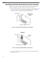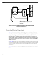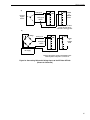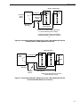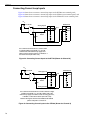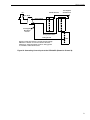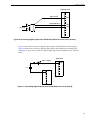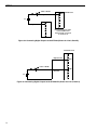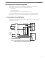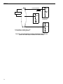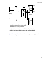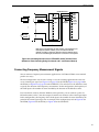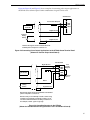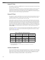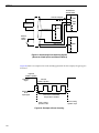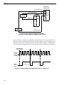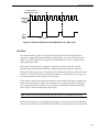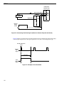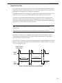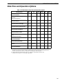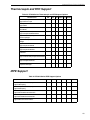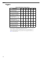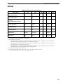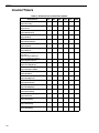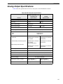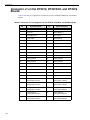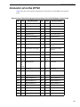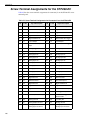
1
Title Page
UM-16866-V
DT3010 Series
User’s Manual
Copyright Page
Eighteenth Edition
May, 2010
Copyright © 2006 - 2010 by Data Translation, Inc.
All rights reserved.
Information furnished by Data Translation, Inc. is believed to be
accurate and reliable; however, no responsibility is assumed by
Data Translation, Inc. for its use; nor for any infringements of
patents or other rights of third parties which may result from its
use. No license is granted by implication or otherwise under any
patent rights of Data Translation, Inc.
Use, duplication, or disclosure by the United States Government
is subject to restrictions as set forth in subparagraph (c)(1)(ii) of
the Rights in Technical Data and Computer software clause at 48
C.F.R, 252.227-7013, or in subparagraph (c)(2) of the Commercial
Computer Software - Registered Rights clause at 48 C.F.R.,
52-227-19 as applicable. Data Translation, Inc., 100 Locke Drive,
Marlboro, MA 01752.
Data Translation, Inc.
100 Locke Drive
Marlboro, MA 01752-1192
(508) 481-3700
www.datatranslation.com
Fax: (508) 481-8620
E-mail: [email protected]
Data Translation® is a registered trademark of Data Translation,
Inc. DT-Open LayersTM, DT-Open Layers for .NET Class
LibraryTM, DataAcq SDKTM, Data Acquisition OMNI CDTM,
LV-LinkTM, and DTx-EZTM are trademarks of Data Translation, Inc.
All other brand and product names are trademarks or registered
trademarks of their respective companies.
FCC
Page
Radio and Television Interference
This equipment has been tested and found to comply with CISPR EN55022 Class A and
EN61000-6-1 requirements and also with the limits for a Class A digital device, pursuant to
Part 15 of the FCC Rules. These limits are designed to provide reasonable protection against
harmful interference when the equipment is operated in a commercial environment. This
equipment generates, uses, and can radiate radio frequency energy and, if not installed and
used in accordance with the instruction manual, may cause harmful interference to radio
communications. Operation of this equipment in a residential area is likely to cause harmful
interference, in which case the user will be required to correct the interference at his own
expense.
Changes or modifications to this equipment not expressly approved by Data Translation could
void your authority to operate the equipment under Part 15 of the FCC Rules.
Note: This product was verified to meet FCC requirements under test conditions that
included use of shielded cables and connectors between system components. It is important
that you use shielded cables and connectors to reduce the possibility of causing interference
to radio, television, and other electronic devices.
Canadian Department of Communications Statement
This digital apparatus does not exceed the Class A limits for radio noise emissions from
digital apparatus set out in the Radio Interference Regulations of the Canadian Department of
Communications.
Le présent appareil numérique n’émet pas de bruits radioélectriques dépassant les limites
applicables aux appareils numériques de la class A prescrites dans le Règlement sur le
brouillage radioélectrique édicté par le Ministère des Communications du Canada.
Table of Contents
Table of Contents
About this Manual . . . . . . . . . . . . . . . . . . . . . . . . . . . . . . . . . . . . . . . . . . . . . . . . . . . . . 11
Intended Audience. . . . . . . . . . . . . . . . . . . . . . . . . . . . . . . . . . . . . . . . . . . . . . . . . . . . . . . . . . . . 11
How this Manual is Organized . . . . . . . . . . . . . . . . . . . . . . . . . . . . . . . . . . . . . . . . . . . . . . . . . 11
Conventions Used in this Manual . . . . . . . . . . . . . . . . . . . . . . . . . . . . . . . . . . . . . . . . . . . . . . . 12
Related Information . . . . . . . . . . . . . . . . . . . . . . . . . . . . . . . . . . . . . . . . . . . . . . . . . . . . . . . . . . . 12
Where To Get Help. . . . . . . . . . . . . . . . . . . . . . . . . . . . . . . . . . . . . . . . . . . . . . . . . . . . . . . . . . . . 13
Chapter 1: Overview . . . . . . . . . . . . . . . . . . . . . . . . . . . . . . . . . . . . . . . . . . . . . . . . . . . 15
Features . . . . . . . . . . . . . . . . . . . . . . . . . . . . . . . . . . . . . . . . . . . . . . . . . . . . . . . . . . . . . . . . . . . . . 16
Supported Software . . . . . . . . . . . . . . . . . . . . . . . . . . . . . . . . . . . . . . . . . . . . . . . . . . . . . . . . . . 18
Accessories . . . . . . . . . . . . . . . . . . . . . . . . . . . . . . . . . . . . . . . . . . . . . . . . . . . . . . . . . . . . . . . . . . 19
Getting Started Procedure. . . . . . . . . . . . . . . . . . . . . . . . . . . . . . . . . . . . . . . . . . . . . . . . . . . . . . 21
Part 1: Getting Started . . . . . . . . . . . . . . . . . . . . . . . . . . . . . . . . . . . . . 23
Chapter 2: Installing the Board and Loading the Device Driver . . . . . . . . . . . . . . . . 25
Unpacking . . . . . . . . . . . . . . . . . . . . . . . . . . . . . . . . . . . . . . . . . . . . . . . . . . . . . . . . . . . . . . . . . . 27
Setting up the Computer . . . . . . . . . . . . . . . . . . . . . . . . . . . . . . . . . . . . . . . . . . . . . . . . . . . . . . . 28
Setting up Expansion Slots . . . . . . . . . . . . . . . . . . . . . . . . . . . . . . . . . . . . . . . . . . . . . . . . . . . . . 29
Removing the Board for Handling . . . . . . . . . . . . . . . . . . . . . . . . . . . . . . . . . . . . . . . . . . . . . . 30
Attaching the EP324 Cable (DT3010-268 Board Only) . . . . . . . . . . . . . . . . . . . . . . . . . . . . . . 31
Inserting the DT3010 Series Board into the Computer . . . . . . . . . . . . . . . . . . . . . . . . . . . . . 32
Loading the Device Driver . . . . . . . . . . . . . . . . . . . . . . . . . . . . . . . . . . . . . . . . . . . . . . . . . . . . . 34
Windows XP. . . . . . . . . . . . . . . . . . . . . . . . . . . . . . . . . . . . . . . . . . . . . . . . . . . . . . . . . . . . . . 34
Windows Vista . . . . . . . . . . . . . . . . . . . . . . . . . . . . . . . . . . . . . . . . . . . . . . . . . . . . . . . . . . . . 34
Windows 7 . . . . . . . . . . . . . . . . . . . . . . . . . . . . . . . . . . . . . . . . . . . . . . . . . . . . . . . . . . . . . . . 35
Chapter 3: Attaching and Configuring a Screw Terminal Panel . . . . . . . . . . . . . . . . 37
Attaching a Screw Terminal Panel . . . . . . . . . . . . . . . . . . . . . . . . . . . . . . . . . . . . . . . . . . . . . . . 39
Attaching the DT740 Screw Terminal Panel . . . . . . . . . . . . . . . . . . . . . . . . . . . . . . . . . . . 39
Attaching the STP268 Screw Terminal Panel . . . . . . . . . . . . . . . . . . . . . . . . . . . . . . . . . . 39
Attaching the STP268-EC Screw Terminal Panel . . . . . . . . . . . . . . . . . . . . . . . . . . . . . . . 40
Attaching to the DT3010-268 or DT3010/32-268 Board . . . . . . . . . . . . . . . . . . . . . 42
Attaching a 5B Series Backplane . . . . . . . . . . . . . . . . . . . . . . . . . . . . . . . . . . . . . . . . 42
Attaching a 7B Series Backplane . . . . . . . . . . . . . . . . . . . . . . . . . . . . . . . . . . . . . . . . . 43
Attaching a PB16H Opto-22 Backplane . . . . . . . . . . . . . . . . . . . . . . . . . . . . . . . . . . 43
Configuring a Screw Terminal Panel. . . . . . . . . . . . . . . . . . . . . . . . . . . . . . . . . . . . . . . . . . . . . 44
Configuring the DT740 Screw Terminal Panel . . . . . . . . . . . . . . . . . . . . . . . . . . . . . . . . . 44
Configuring Jumper W1 - Common Ground Sense . . . . . . . . . . . . . . . . . . . . . . . . 44
Configuring Resistors R1 to R16 - Bias Return . . . . . . . . . . . . . . . . . . . . . . . . . . . . 45
5
Contents
Configuring Resistors R17 to R32 - Current Shunt . . . . . . . . . . . . . . . . . . . . . . . . . 45
Configuring the STP268 Screw Terminal Panel . . . . . . . . . . . . . . . . . . . . . . . . . . . . . . . . 45
Configuring Jumper W1 - Common Ground Sense . . . . . . . . . . . . . . . . . . . . . . . . 46
Configuring Resistors R1 to R16 - Bias Return . . . . . . . . . . . . . . . . . . . . . . . . . . . . 46
Configuring Resistors R17 to R32 - Current Shunt . . . . . . . . . . . . . . . . . . . . . . . . . 47
Configuring the STP268-EC Screw Terminal Panel . . . . . . . . . . . . . . . . . . . . . . . . . . . . . 47
Chapter 4: Wiring Signals . . . . . . . . . . . . . . . . . . . . . . . . . . . . . . . . . . . . . . . . . . . . . . . 49
Preparing to Wire to a Screw Terminal Panel. . . . . . . . . . . . . . . . . . . . . . . . . . . . . . . . . . . . . . 51
Wiring Recommendations . . . . . . . . . . . . . . . . . . . . . . . . . . . . . . . . . . . . . . . . . . . . . . . . . . 51
Using 5B or 7B Series Signal Conditioning Modules . . . . . . . . . . . . . . . . . . . . . . . . . . . 51
Screw Terminal Assignments . . . . . . . . . . . . . . . . . . . . . . . . . . . . . . . . . . . . . . . . . . . . . . . . . . . 53
DT740 Screw Terminal Assignments . . . . . . . . . . . . . . . . . . . . . . . . . . . . . . . . . . . . . . . . . 53
STP268 Screw Terminal Assignments . . . . . . . . . . . . . . . . . . . . . . . . . . . . . . . . . . . . . . . . 56
STP268-EC Screw Terminal Assignments . . . . . . . . . . . . . . . . . . . . . . . . . . . . . . . . . . . . . 59
Connecting Analog Input Signals . . . . . . . . . . . . . . . . . . . . . . . . . . . . . . . . . . . . . . . . . . . . . . . 63
Connecting Single-Ended Voltage Inputs . . . . . . . . . . . . . . . . . . . . . . . . . . . . . . . . . . . . . 63
Connecting Pseudo-Differential Voltage Inputs . . . . . . . . . . . . . . . . . . . . . . . . . . . . . . . 65
Connecting Differential Voltage Inputs . . . . . . . . . . . . . . . . . . . . . . . . . . . . . . . . . . . . . . 66
Connecting Current Loop Inputs . . . . . . . . . . . . . . . . . . . . . . . . . . . . . . . . . . . . . . . . . . . . 70
Connecting Analog Output Signals . . . . . . . . . . . . . . . . . . . . . . . . . . . . . . . . . . . . . . . . . . . . . 72
Connecting Digital I/O Signals . . . . . . . . . . . . . . . . . . . . . . . . . . . . . . . . . . . . . . . . . . . . . . . . . 74
Connecting Counter/Timer Signals . . . . . . . . . . . . . . . . . . . . . . . . . . . . . . . . . . . . . . . . . . . . . 77
Connecting Event Counting Signals . . . . . . . . . . . . . . . . . . . . . . . . . . . . . . . . . . . . . . . . . 77
Connecting Frequency Measurement Signals . . . . . . . . . . . . . . . . . . . . . . . . . . . . . . . . . 83
Connecting Pulse Output Signals . . . . . . . . . . . . . . . . . . . . . . . . . . . . . . . . . . . . . . . . . . . 85
Chapter 5: Verifying the Operation of a DT3010 Series Board . . . . . . . . . . . . . . . . . 91
Running the Quick DataAcq Application . . . . . . . . . . . . . . . . . . . . . . . . . . . . . . . . . . . . . . . . 93
Testing Single-Value Analog Input . . . . . . . . . . . . . . . . . . . . . . . . . . . . . . . . . . . . . . . . . . . . . . 94
Testing Single-Value Analog Output . . . . . . . . . . . . . . . . . . . . . . . . . . . . . . . . . . . . . . . . . . . . 95
Testing Continuous Analog Input . . . . . . . . . . . . . . . . . . . . . . . . . . . . . . . . . . . . . . . . . . . . . . 96
Testing Single-Value Digital Input . . . . . . . . . . . . . . . . . . . . . . . . . . . . . . . . . . . . . . . . . . . . . . 97
Testing Single-Value Digital Output . . . . . . . . . . . . . . . . . . . . . . . . . . . . . . . . . . . . . . . . . . . . . 98
Testing Frequency Measurement . . . . . . . . . . . . . . . . . . . . . . . . . . . . . . . . . . . . . . . . . . . . . . . 99
Testing Pulse Output . . . . . . . . . . . . . . . . . . . . . . . . . . . . . . . . . . . . . . . . . . . . . . . . . . . . . . . . . 100
Part 2: Using Your Board . . . . . . . . . . . . . . . . . . . . . . . . . . . . . . . . . . 101
Chapter 6: Principles of Operation . . . . . . . . . . . . . . . . . . . . . . . . . . . . . . . . . . . . . . 103
Analog Input Features . . . . . . . . . . . . . . . . . . . . . . . . . . . . . . . . . . . . . . . . . . . . . . . . . . . . . . . . 105
Analog Input Resolution . . . . . . . . . . . . . . . . . . . . . . . . . . . . . . . . . . . . . . . . . . . . . . . . . . 105
Analog Input Channels . . . . . . . . . . . . . . . . . . . . . . . . . . . . . . . . . . . . . . . . . . . . . . . . . . . 105
6
Contents
Specifying a Single Channel . . . . . . . . . . . . . . . . . . . . . . . . . . . . . . . . . . . . . . . . . . . 105
Specifying One or More Channels . . . . . . . . . . . . . . . . . . . . . . . . . . . . . . . . . . . . . . 106
Specifying Digital Input Lines in the Analog Input Channel List . . . . . . . . 106
Performing Dynamic Digital Output Operations . . . . . . . . . . . . . . . . . . . . . . 106
Input Ranges and Gains . . . . . . . . . . . . . . . . . . . . . . . . . . . . . . . . . . . . . . . . . . . . . . . . . . 107
A/D Sample Clock Sources . . . . . . . . . . . . . . . . . . . . . . . . . . . . . . . . . . . . . . . . . . . . . . . 108
Internal A/D Sample Clock . . . . . . . . . . . . . . . . . . . . . . . . . . . . . . . . . . . . . . . . . . . 109
External A/D Sample Clock . . . . . . . . . . . . . . . . . . . . . . . . . . . . . . . . . . . . . . . . . . . 109
Analog Input Conversion Modes . . . . . . . . . . . . . . . . . . . . . . . . . . . . . . . . . . . . . . . . . . 110
Continuously-Paced Scan Mode . . . . . . . . . . . . . . . . . . . . . . . . . . . . . . . . . . . . . . . 110
Triggered Scan Mode . . . . . . . . . . . . . . . . . . . . . . . . . . . . . . . . . . . . . . . . . . . . . . . . . 111
Software-Retriggered Scan Mode . . . . . . . . . . . . . . . . . . . . . . . . . . . . . . . . . . . 111
Externally-Retriggered Scan Mode . . . . . . . . . . . . . . . . . . . . . . . . . . . . . . . . . . 112
Triggers . . . . . . . . . . . . . . . . . . . . . . . . . . . . . . . . . . . . . . . . . . . . . . . . . . . . . . . . . . . . . . . . . 113
Trigger Sources . . . . . . . . . . . . . . . . . . . . . . . . . . . . . . . . . . . . . . . . . . . . . . . . . . . . . . 113
Software Trigger . . . . . . . . . . . . . . . . . . . . . . . . . . . . . . . . . . . . . . . . . . . . . . . . . . 113
External Digital (TTL) Trigger . . . . . . . . . . . . . . . . . . . . . . . . . . . . . . . . . . . . . . 114
Analog Threshold Trigger . . . . . . . . . . . . . . . . . . . . . . . . . . . . . . . . . . . . . . . . . . 114
Trigger Acquisition Modes . . . . . . . . . . . . . . . . . . . . . . . . . . . . . . . . . . . . . . . . . . . . 115
Post-Trigger Acquisition . . . . . . . . . . . . . . . . . . . . . . . . . . . . . . . . . . . . . . . . . . . 115
Pre-Trigger Acquisition . . . . . . . . . . . . . . . . . . . . . . . . . . . . . . . . . . . . . . . . . . . . 116
About-Trigger Acquisition . . . . . . . . . . . . . . . . . . . . . . . . . . . . . . . . . . . . . . . . . 118
Data Format and Transfer . . . . . . . . . . . . . . . . . . . . . . . . . . . . . . . . . . . . . . . . . . . . . . . . . 119
Error Conditions . . . . . . . . . . . . . . . . . . . . . . . . . . . . . . . . . . . . . . . . . . . . . . . . . . . . . . . . . 120
Analog Output Features . . . . . . . . . . . . . . . . . . . . . . . . . . . . . . . . . . . . . . . . . . . . . . . . . . . . . . 122
Analog Output Resolution . . . . . . . . . . . . . . . . . . . . . . . . . . . . . . . . . . . . . . . . . . . . . . . . 122
Analog Output Channels . . . . . . . . . . . . . . . . . . . . . . . . . . . . . . . . . . . . . . . . . . . . . . . . . 122
Specifying a Single Channel . . . . . . . . . . . . . . . . . . . . . . . . . . . . . . . . . . . . . . . . . . . 122
Specifying One or More Channels . . . . . . . . . . . . . . . . . . . . . . . . . . . . . . . . . . . . . . 123
Output Ranges and Gains . . . . . . . . . . . . . . . . . . . . . . . . . . . . . . . . . . . . . . . . . . . . . . . . . 123
D/A Output Clock Sources . . . . . . . . . . . . . . . . . . . . . . . . . . . . . . . . . . . . . . . . . . . . . . . 123
Internal D/A Output Clock . . . . . . . . . . . . . . . . . . . . . . . . . . . . . . . . . . . . . . . . . . . 123
External D/A Output Clock . . . . . . . . . . . . . . . . . . . . . . . . . . . . . . . . . . . . . . . . . . . 124
Trigger Sources . . . . . . . . . . . . . . . . . . . . . . . . . . . . . . . . . . . . . . . . . . . . . . . . . . . . . . . . . . 124
Software Trigger . . . . . . . . . . . . . . . . . . . . . . . . . . . . . . . . . . . . . . . . . . . . . . . . . . . . . 124
External Digital (TTL) Trigger . . . . . . . . . . . . . . . . . . . . . . . . . . . . . . . . . . . . . . . . . 124
Analog Threshold Trigger . . . . . . . . . . . . . . . . . . . . . . . . . . . . . . . . . . . . . . . . . . . . . 125
Analog Output Conversion Modes . . . . . . . . . . . . . . . . . . . . . . . . . . . . . . . . . . . . . . . . . 125
Continuously-Paced Analog Output . . . . . . . . . . . . . . . . . . . . . . . . . . . . . . . . . . . 126
Waveform Generation . . . . . . . . . . . . . . . . . . . . . . . . . . . . . . . . . . . . . . . . . . . . . . . . 127
Data Format and Transfer . . . . . . . . . . . . . . . . . . . . . . . . . . . . . . . . . . . . . . . . . . . . . . . . . 127
Error Conditions . . . . . . . . . . . . . . . . . . . . . . . . . . . . . . . . . . . . . . . . . . . . . . . . . . . . . . . . . 128
7
Contents
Digital I/O Features . . . . . . . . . . . . . . . . . . . . . . . . . . . . . . . . . . . . . . . . . . . . . . . . . . . . . . . . . 129
Digital I/O Lines . . . . . . . . . . . . . . . . . . . . . . . . . . . . . . . . . . . . . . . . . . . . . . . . . . . . . . . . 129
Digital I/O Resolution . . . . . . . . . . . . . . . . . . . . . . . . . . . . . . . . . . . . . . . . . . . . . . . . . . . . 129
Digital I/O Operation Modes . . . . . . . . . . . . . . . . . . . . . . . . . . . . . . . . . . . . . . . . . . . . . . 129
Counter/Timer Features . . . . . . . . . . . . . . . . . . . . . . . . . . . . . . . . . . . . . . . . . . . . . . . . . . . . . . 131
Units . . . . . . . . . . . . . . . . . . . . . . . . . . . . . . . . . . . . . . . . . . . . . . . . . . . . . . . . . . . . . . . . . . . 131
C/T Clock Sources . . . . . . . . . . . . . . . . . . . . . . . . . . . . . . . . . . . . . . . . . . . . . . . . . . . . . . . 131
Internal C/T Clock . . . . . . . . . . . . . . . . . . . . . . . . . . . . . . . . . . . . . . . . . . . . . . . . . . . 132
External C/T Clock . . . . . . . . . . . . . . . . . . . . . . . . . . . . . . . . . . . . . . . . . . . . . . . . . . 132
Internally Cascaded Clock . . . . . . . . . . . . . . . . . . . . . . . . . . . . . . . . . . . . . . . . . . . . 132
Gate Types . . . . . . . . . . . . . . . . . . . . . . . . . . . . . . . . . . . . . . . . . . . . . . . . . . . . . . . . . . . . . . 133
Pulse Output Types and Duty Cycles . . . . . . . . . . . . . . . . . . . . . . . . . . . . . . . . . . . . . . . 134
Counter/Timer Operation Modes . . . . . . . . . . . . . . . . . . . . . . . . . . . . . . . . . . . . . . . . . . 135
Event Counting . . . . . . . . . . . . . . . . . . . . . . . . . . . . . . . . . . . . . . . . . . . . . . . . . . . . . 135
Frequency Measurement . . . . . . . . . . . . . . . . . . . . . . . . . . . . . . . . . . . . . . . . . . . . . . 137
Rate Generation . . . . . . . . . . . . . . . . . . . . . . . . . . . . . . . . . . . . . . . . . . . . . . . . . . . . . 139
One-Shot . . . . . . . . . . . . . . . . . . . . . . . . . . . . . . . . . . . . . . . . . . . . . . . . . . . . . . . . . . . 141
Repetitive One-Shot . . . . . . . . . . . . . . . . . . . . . . . . . . . . . . . . . . . . . . . . . . . . . . . . . . 143
Synchronizing A/D and D/A Subsystems . . . . . . . . . . . . . . . . . . . . . . . . . . . . . . . . . . . . . . 144
Synchronizing the Triggers . . . . . . . . . . . . . . . . . . . . . . . . . . . . . . . . . . . . . . . . . . . . . . . . 144
Synchronizing the Clocks. . . . . . . . . . . . . . . . . . . . . . . . . . . . . . . . . . . . . . . . . . . . . . . . . . 145
Chapter 7: Supported Device Driver Capabilities. . . . . . . . . . . . . . . . . . . . . . . . . . . 147
Data Flow and Operation Options. . . . . . . . . . . . . . . . . . . . . . . . . . . . . . . . . . . . . . . . . . . . . . 149
Buffering . . . . . . . . . . . . . . . . . . . . . . . . . . . . . . . . . . . . . . . . . . . . . . . . . . . . . . . . . . . . . . . . . . . 150
Triggered Scan Mode . . . . . . . . . . . . . . . . . . . . . . . . . . . . . . . . . . . . . . . . . . . . . . . . . . . . . . . . . 150
Data Encoding. . . . . . . . . . . . . . . . . . . . . . . . . . . . . . . . . . . . . . . . . . . . . . . . . . . . . . . . . . . . . . . 151
Channels . . . . . . . . . . . . . . . . . . . . . . . . . . . . . . . . . . . . . . . . . . . . . . . . . . . . . . . . . . . . . . . . . . . 151
Gain . . . . . . . . . . . . . . . . . . . . . . . . . . . . . . . . . . . . . . . . . . . . . . . . . . . . . . . . . . . . . . . . . . . . . . . 152
Ranges . . . . . . . . . . . . . . . . . . . . . . . . . . . . . . . . . . . . . . . . . . . . . . . . . . . . . . . . . . . . . . . . . . . . . 152
Resolution . . . . . . . . . . . . . . . . . . . . . . . . . . . . . . . . . . . . . . . . . . . . . . . . . . . . . . . . . . . . . . . . . . 152
Thermocouple and RTD Support. . . . . . . . . . . . . . . . . . . . . . . . . . . . . . . . . . . . . . . . . . . . . . . 153
IEPE Support. . . . . . . . . . . . . . . . . . . . . . . . . . . . . . . . . . . . . . . . . . . . . . . . . . . . . . . . . . . . . . . . 153
Triggers . . . . . . . . . . . . . . . . . . . . . . . . . . . . . . . . . . . . . . . . . . . . . . . . . . . . . . . . . . . . . . . . . . . . 154
Clocks . . . . . . . . . . . . . . . . . . . . . . . . . . . . . . . . . . . . . . . . . . . . . . . . . . . . . . . . . . . . . . . . . . . . . . 155
Counter/Timers . . . . . . . . . . . . . . . . . . . . . . . . . . . . . . . . . . . . . . . . . . . . . . . . . . . . . . . . . . . . . 156
Chapter 8: Calibration . . . . . . . . . . . . . . . . . . . . . . . . . . . . . . . . . . . . . . . . . . . . . . . . . 159
Calibrating the Analog Input Subsystem . . . . . . . . . . . . . . . . . . . . . . . . . . . . . . . . . . . . . . . 161
Choosing a Calibration Reference. . . . . . . . . . . . . . . . . . . . . . . . . . . . . . . . . . . . . . . . . . . 161
Configuring for the Internal Reference . . . . . . . . . . . . . . . . . . . . . . . . . . . . . . . . . . 161
Configuring for an External Reference . . . . . . . . . . . . . . . . . . . . . . . . . . . . . . . . . . 162
8
Contents
Using the DT3010 Calibration Utility . . . . . . . . . . . . . . . . . . . . . . . . . . . . . . . . . . . . . . . 163
Using the Auto-Calibration Procedure . . . . . . . . . . . . . . . . . . . . . . . . . . . . . . . . . . 163
Using the Manual Calibration Procedure . . . . . . . . . . . . . . . . . . . . . . . . . . . . . . . . 164
Calibrating the PGH Zero Setting . . . . . . . . . . . . . . . . . . . . . . . . . . . . . . . . . . . . . . . 165
Using the DT3016 Calibration Utility . . . . . . . . . . . . . . . . . . . . . . . . . . . . . . . . . . . . . . . 166
Using the Auto-Calibration Procedure . . . . . . . . . . . . . . . . . . . . . . . . . . . . . . . . . . 166
Calibrating the PGH Zero Setting . . . . . . . . . . . . . . . . . . . . . . . . . . . . . . . . . . . . . . . 168
Calibrating the Analog Output Subsystem . . . . . . . . . . . . . . . . . . . . . . . . . . . . . . . . . . . . . . 169
Choosing a Calibration Meter . . . . . . . . . . . . . . . . . . . . . . . . . . . . . . . . . . . . . . . . . . . . . . 169
Configuring for the Internal ADC . . . . . . . . . . . . . . . . . . . . . . . . . . . . . . . . . . . . . . 169
Configuring for an External Meter . . . . . . . . . . . . . . . . . . . . . . . . . . . . . . . . . . . . . . 170
Using the DT3010 Calibration Utility. . . . . . . . . . . . . . . . . . . . . . . . . . . . . . . . . . . . . . . . 171
Using the DT3016 Calibration Utility. . . . . . . . . . . . . . . . . . . . . . . . . . . . . . . . . . . . . . . . 173
Chapter 9: Troubleshooting . . . . . . . . . . . . . . . . . . . . . . . . . . . . . . . . . . . . . . . . . . . . 175
General Checklist . . . . . . . . . . . . . . . . . . . . . . . . . . . . . . . . . . . . . . . . . . . . . . . . . . . . . . . . . . . . 176
Technical Support . . . . . . . . . . . . . . . . . . . . . . . . . . . . . . . . . . . . . . . . . . . . . . . . . . . . . . . . . . . 178
If Your Board Needs Factory Service . . . . . . . . . . . . . . . . . . . . . . . . . . . . . . . . . . . . . . . . . . . 179
Appendix A: Specifications . . . . . . . . . . . . . . . . . . . . . . . . . . . . . . . . . . . . . . . . . . . . 181
Analog Input Specifications . . . . . . . . . . . . . . . . . . . . . . . . . . . . . . . . . . . . . . . . . . . . . . . . . . . 182
Analog Output Specifications. . . . . . . . . . . . . . . . . . . . . . . . . . . . . . . . . . . . . . . . . . . . . . . . . . 185
Digital I/O Specifications . . . . . . . . . . . . . . . . . . . . . . . . . . . . . . . . . . . . . . . . . . . . . . . . . . . . . 187
Counter/Timer Specifications . . . . . . . . . . . . . . . . . . . . . . . . . . . . . . . . . . . . . . . . . . . . . . . . . 188
Power, Physical, and Environmental Specifications . . . . . . . . . . . . . . . . . . . . . . . . . . . . . . . 189
Connector Specifications . . . . . . . . . . . . . . . . . . . . . . . . . . . . . . . . . . . . . . . . . . . . . . . . . . . . . . 190
Regulatory Specifications . . . . . . . . . . . . . . . . . . . . . . . . . . . . . . . . . . . . . . . . . . . . . . . . . . . . . 191
Appendix B: Connector Pin Assignments . . . . . . . . . . . . . . . . . . . . . . . . . . . . . . . . 193
Connector J1 on the DT3010, DT3010/32, and DT3016 Boards . . . . . . . . . . . . . . . . . . . . . . 194
Connector J2 on the DT3010, DT3010/32, and DT3016 Boards . . . . . . . . . . . . . . . . . . . . . . 196
Connector J1 on the DT3010-268 and DT3010/32-268 Board. . . . . . . . . . . . . . . . . . . . . . . . 198
Connector J2 on the DT3010-268 and DT3010/32-268 Board. . . . . . . . . . . . . . . . . . . . . . . . 200
Connector J1 on the DT740 . . . . . . . . . . . . . . . . . . . . . . . . . . . . . . . . . . . . . . . . . . . . . . . . . . . . 202
Connector J2 on the DT740 . . . . . . . . . . . . . . . . . . . . . . . . . . . . . . . . . . . . . . . . . . . . . . . . . . . . 203
Screw Terminal Assignments for the STP268. . . . . . . . . . . . . . . . . . . . . . . . . . . . . . . . . . . . . 205
Screw Terminal Assignments for the STP268-EC . . . . . . . . . . . . . . . . . . . . . . . . . . . . . . . . . 208
9
Contents
Appendix C: Using Your Own Screw Terminal Panel . . . . . . . . . . . . . . . . . . . . . . . 213
Analog Inputs . . . . . . . . . . . . . . . . . . . . . . . . . . . . . . . . . . . . . . . . . . . . . . . . . . . . . . . . . . . . . . . 215
Single-Ended Inputs . . . . . . . . . . . . . . . . . . . . . . . . . . . . . . . . . . . . . . . . . . . . . . . . . . . . . . 215
Pseudo-Differential Inputs. . . . . . . . . . . . . . . . . . . . . . . . . . . . . . . . . . . . . . . . . . . . . . . . . 215
Differential Inputs . . . . . . . . . . . . . . . . . . . . . . . . . . . . . . . . . . . . . . . . . . . . . . . . . . . . . . . . 216
Analog Outputs . . . . . . . . . . . . . . . . . . . . . . . . . . . . . . . . . . . . . . . . . . . . . . . . . . . . . . . . . . . . . 217
Digital Inputs and Counter/Timer Inputs . . . . . . . . . . . . . . . . . . . . . . . . . . . . . . . . . . . . . . . 218
Digital Outputs . . . . . . . . . . . . . . . . . . . . . . . . . . . . . . . . . . . . . . . . . . . . . . . . . . . . . . . . . . . . . . 219
Cabling Information . . . . . . . . . . . . . . . . . . . . . . . . . . . . . . . . . . . . . . . . . . . . . . . . . . . . . . . . . 220
Index . . . . . . . . . . . . . . . . . . . . . . . . . . . . . . . . . . . . . . . . . . . . . . . . . . . . . . . . . . . . . . . 221
10
About this Manual
This manual describes how to set up and install the following components:
• DT3010 Series software
• DT3010 Series board
• DT3010 Series Device Driver
• DT740, STP268, or STP268-EC screw terminal panel
It describes how to wire signals to the board and how to verify the board’s operation using the
Quick DataAcq application.
This manual also describes the features of the DT3010, DT3010-268, DT3010/32,
DT3010/32-268, and DT3016 boards (collectively referred to as the DT3010 Series), the
capabilities of the DT3010 Series Device Driver, and how to program the DT3010 Series boards
using the DT-Open Layers for .NET Class Library™ software. Troubleshooting and calibration
information is also provided.
Note: For information on checking system requirements, installing the software, and
viewing the documentation, refer to the README file on the OMNI CD.
For more information on the class library, refer to the DT-Open Layers for .NET Class Library
User’s Manual. If you are using the DataAcq SDK or a software application to program your
device, refer to the documentation for that software for more information.
Intended Audience
This document is intended for engineers, scientists, technicians, or others responsible for
using and/or programming the DT3010 Series boards for data acquisition operations in
Microsoft® Windows® XP, Windows Vista®, or Windows 7. It is assumed that you have some
familiarity with data acquisition principles, and that you understand your application.
How this Manual is Organized
This manual is organized as follows:
• Chapter 1, “Overview,” describes the major features of the board, as well as the supported
software and accessories for the board, and provides an overview of the getting started
procedure.
• Chapter 2, “Installing the Board and Loading the Device Driver,” describes how to install
the DT3010 Series board and load the DT3010 Series Device Driver.
• Chapter 3, “Attaching and Configuring a Screw Terminal Panel,” describes how to attach
the DT740, STP268, or STP268-EC screw terminal panel to a DT3010 Series board and how
to configure the screw terminal panel for use with a DT3010 Series board.
11
About this Manual
• Chapter 4, “Wiring Signals,” describes how to wire signals to a DT3010 Series board using
the DT740, STP268, or STP268-EC.
• Chapter 5, “Verifying the Operation of a DT3010 Series Board,” describes how to verify
the operation of a DT3010 Series board with the Quick DataAcq application
• Chapter 6, “Principles of Operation,” describes all of the board’s features and how to use
them in your application.
• Chapter 7, “Supported Device Driver Capabilities,” lists the data acquisition subsystems
and the associated features accessible using the DT3010 Series Device Driver.
• Chapter 8, “Calibration,” describes how to calibrate the analog
I/O circuitry of the board.
• Chapter 9, “Troubleshooting,” provides information that you can use to resolve problems
with the board and the device driver, should they occur.
• Appendix A, “Specifications,” lists the specifications of the board.
• Appendix B, “Connector Pin Assignments,” shows the pin assignments for the connectors
on the board and for the DT740, STP268, and STP268-EC screw terminal panels.
• Appendix C, “Using Your Own Screw Terminal Panel,” describes additional
considerations to keep in mind when designing your own screw terminal panel for use
with a DT3010 Series board.
• An index completes this manual.
Conventions Used in this Manual
The following conventions are used in this manual:
• Notes provide useful information or information that requires special emphasis, cautions
provide information to help you avoid losing data or damaging your equipment, and
warnings provide information to help you avoid catastrophic damage to yourself or your
equipment.
• Items that you select or type are shown in bold.
Related Information
Refer to the following documents for more information on using the DT3010 Series board:
• Measure Foundry Manual (UM-19298) and online help. These documents describe how to
use Measure Foundry™ to build drag-and-drop test and measurement applications for
Data Translation® data acquisition devices.
• DT-Open Layers for .NET User’s Manual (UM-22161). For programmers who are
developing their own application programs using Visual C# or Visual Basic .NET, this
manual describes how to use the DT-Open Layers for .NET Class Library to access the
capabilities of Data Translation data acquisition devices.
• DataAcq SDK User’s Manual (UM-18326). For programmers who are developing their own
application programs using the Microsoft C compiler, this manual describes how to use
the DT-Open Layers DataAcq SDKTM to access the capabilities of Data Translation data
acquisition boards. This manual is provided on the Data Acquisition OMNI CD.
12
About this Manual
• DTx-EZ Getting Started Manual (UM-15428). This manual, available from Data Translation,
describes how to use the ActiveX controls provided in DTx-EZTM to access the capabilities
of Data Translation data acquisition boards in Microsoft® Visual BasicTM or Visual C++.
• LV-Link Online Help. This help file describes how to use LV-Link™ with the LabVIEW™
graphical programming language to access the capabilities of Data Translation data
acquisition devices.
• PCI Specification: PCI Local Bus Specification, PCI Special Interest Group, Portland, OR.
(Revision 2.1, June 1, 1995).
• Microsoft Windows XP, Windows Vista, or Windows 7 documentation.
Where To Get Help
Should you run into problems installing or using a DT3010 Series board, our Technical
Support Department is available to provide prompt, technical assistance. Refer to Chapter 9
starting on page 175 for more information. If you are outside the U.S. or Canada, call your
local distributor, whose number is listed on our web site (www.datatranslation.com).
13
About this Manual
14
1
Overview
Features . . . . . . . . . . . . . . . . . . . . . . . . . . . . . . . . . . . . . . . . . . . . . . . . . . . . . . . . . . . . . . . . . . . . . 16
Supported Software . . . . . . . . . . . . . . . . . . . . . . . . . . . . . . . . . . . . . . . . . . . . . . . . . . . . . . . . . . . 18
Accessories . . . . . . . . . . . . . . . . . . . . . . . . . . . . . . . . . . . . . . . . . . . . . . . . . . . . . . . . . . . . . . . . . . 19
Getting Started Procedure. . . . . . . . . . . . . . . . . . . . . . . . . . . . . . . . . . . . . . . . . . . . . . . . . . . . . . 21
15
Chapter 1
Features
The DT3010 Series consists of the following high-speed, multifunction board types for the PCI
bus: DT3010, DT3010-268, DT3010/32, DT3010/32-268, and DT3016. These board types differ
in analog I/O resolution, output FIFO (first-in, first-out buffer) size, throughput, and
connectors as shown in Table 1.
Table 1: Differences Among DT3010 Series Boards
Analog I/O
Resolution
Output
FIFO
A/D Throughputa
D/A Throughputb
DT3010
12 bits
4K
1.25 MSamples/s
200 kSamples/s
one 50-pin, one 68-pin
DT3010-268
12 bits
4K
1.25 MSamples/s
200 kSamples/s
two 68-pin
DT3010/32
12 bits
32K
1.25 MSamples/s
200 kSamples/s
one 50-pin, one 68-pin
DT3010/32-268
12 bits
32K
1.25 MSamples/s
200 kSamples/s
two 68-pin
DT3016
16 bits
4K
250 kSamples/s
100 kSamples/s
one 50-pin, one 68-pin
Board
Connectors
a. This throughput is for a single analog input channel.
b. This throughput is for full-scale ranges.
All DT3010 Series boards share the following major features:
Analog Inputs
32 single-ended or 16 differential
Analog Outputs
2, ±10 V output range
Digital I/O Lines
16
Counter/Timers
4
• Programmable bipolar (±10 V) and unipolar (0 to 10 V) input ranges with gains of 1, 2, 4,
and 8
• Continuously-paced and triggered scan capability
• A 1024-location channel list that supports sampling analog input channels at the same or
different gains in sequential or random order
• Up to 256 scans per trigger for a total of 262,144 samples per trigger
• PCI bus mastering for data transfers
• Pre-, post-, and about-trigger acquisition modes to acquire data relative to an external
event using computer memory
• Internal and external clock sources; one external clock input for the analog input
subsystem and one external clock input for the analog output subsystem
• Analog threshold triggering using either an external analog input or one of the analog
input channels; a separate DAC sets the trigger level (8-bit resolution, fixed hysteresis)
16
Overview
• Digital TTL triggering; one external hardware TTL input for the analog input subsystem
and one external hardware TTL input for the analog output subsystem
• Simultaneous analog input and analog output operations running at full speed
• Software calibration of the analog input and output subsystems
• Two 8-bit digital ports programmable as inputs or outputs on a per-port basis; digital
inputs can be included as part of the analog input channel list to correlate the timing of
analog and digital events; digital outputs can drive external solid-state relays
• Two dynamic, high-speed digital output lines; useful for synchronizing and controlling
external equipment, these dynamic digital output lines are programmable as part of the
analog input subsystem using the DataAcq SDK
• Programmable gate types
• Programmable pulse output polarities (output types) and duty cycles
• A/D Sample Clock Output and A/D Trigger Output signals, useful for synchronizing and
controlling external equipment
For a discussion of these features in detail, refer to Chapter 6 starting on page 103.
17
Chapter 1
Supported Software
The following software is available for use with the DT3010 Series boards and on the Data
Acquisition OMNI CD:
• DT3010 Series Device Driver – The device driver is installed automatically when you
install the software from the Data Acquisition OMNI CD. You need the device driver to
use the DT3010 Series board with any of the supported software packages or utilities
• The Quick DataAcq application – This application provides a quick way to get a DT3010
Series board up and running. Using the Quick DataAcq application, you can verify the
features of the board, display data on the screen, and save data to disk.
• The quickDAQ application – An evaluation version of this .NET application is included
on the Data Acquisition OMNI CD. quickDAQ lets you acquire analog data from all
devices supported by DT-Open Layers for .NET software at high speed, plot it during
acquisition, analyze it, and/or save it to disk for later analysis.
• DT3010 and DT3016 Calibration Utilities – The DT3010 Calibration Utility allows you to
calibrate the analog input and analog output subsystems of the DT3010, DT3010-268,
DT3010/32, and DT3010/32-268 boards. The DT3016 Calibration Utility allows you to
calibrate the analog input and analog output subsystems of the DT3016 boards. Refer to
Chapter 8 starting on page 159 for more information on these utilities.
• Measure Foundry – An evaluation version of this software is included on the Data
Acquisition OMNI CD. Measure Foundry is drag-and-drop test and measurement
application builder designed to give you top performance with ease-of-use development.
Order the full development version of this software package to develop your own
application using real hardware.
• DT-Open Layers for .NET Class Library – Use this class library if you want to use Visual
C# or Visual Basic for .NET to develop your own application software for a DT3010 Series
board using Visual Studio 2003 or Visual Studio 2005; the class library complies with the
DT-Open Layers standard.
• DataAcq SDK – Use the Data Acq SDK if you want to use Visual Studio 6.0 and Microsoft
C or C++ to develop your own application software for a DT3010 Series board using
Windows XP, Windows Vista, or Windows 7; the DataAcq SDK complies with the
DT-Open Layers standard.
• DTx-EZ – DTx-EZ provides ActiveX controls, which allow you to access the capabilities of
the DT3010 Series boards using Microsoft Visual Basic or Visual C++; DTx-EZ complies
with the DT-Open Layers standard.
• DAQ Adaptor for MATLAB – Data Translation’s DAQ Adaptor provides an interface
between the MATLAB Data Acquisition (DAQ) subsystem from The MathWorks and Data
Translation’s DT-Open Layers architecture.
• LV-Link – An evaluation version of this software is included on the Data Acquisition
OMNI CD. Use LV-Link if you want to use the LabVIEW graphical programming
language to access the capabilities of the DT3010 Series boards.
Refer to the Data Translation web site (www.datatranslation.com) for more information on the
appropriate software package for your application.
18
Overview
Accessories
The following optional accessories are available for DT3010 Series boards:
• DT740 screw terminal panel – Screw terminal panel with two connectors to
accommodate the analog I/O, digital I/O, and counter/timer signals provided by the
DT3010, DT3010/32, and DT3016 boards.
• EP307 cable – A 1-meter, twisted-pair, shielded cable that connects the 50-pin analog I/O
connector (J1) on the DT3010, DT3010/32, and DT3016 boards to the J1 connector on the
DT740 screw terminal panel.
• EP308 cable – A 1-meter, twisted-pair, shielded cable that connects the 68-pin digital I/O
connector (J2) on the DT3010, DT3010/32, and DT3016 boards to the J2 connector on the
DT740 screw terminal panel.
• STP268 screw terminal panel – Screw terminal panel with one 68-pin connector to access
the signals provided by one of the connectors on the DT3010-268 or DT3010/32-268 board.
If you want to access all of the functionality of the DT3010-268 or DT3010/32-268 at the
same time, you need two STP268 screw terminal panels.
• STP268-EC screw terminal panel – Screw terminal panel with two 26-pin connectors for
attaching to 5B or 7B Series signal conditioning backplanes, one 50-pin connector for
attaching to the Opto-22 PB16H backplane, and one 68-pin connector for attaching to the
DT3010-268 or DT3010/32-268 board.
• EP324 cable – A 1 1/2-inch ribbon cable that connects to the 68-pin digital I/O connector
(J2) on the DT3010-268 or DT3010/32-268 board; the other end of this cable provides a
68-pin connector and face plate for connection to an EP325 cable. This cable is shipped
with each DT3010-268 or DT3010/32-268 board.
• EP325 cable – A, 6-foot, SCSI-3 cable that connects the STP268 or STP268-EC screw
terminal panel to connector J1 on the DT3010-268 board.
• 5B01 or 5B08 backplane and 5B Series modules – The 5B01 is a 16-channel backplane; the
5B08 is an 8-channel backplane. Both backplanes accept 5B modules for signal
conditioning applications, including measuring thermocouples, RTDs, voltage input,
current input, strain gage input, and frequency input.
To use the 5B series backplanes and modules with the STP268-EC, you need the following
additional accessories available from Data Translation:
− AC1315 cable – A 2-foot cable with a 26-pin connector on each end that connects a 5B
Series signal conditioning backplane to connector J2 on the STP268-EC screw terminal
panel.
− PWR-977 power supply – A 5 V, 3 A power supply for powering the 5B Series
backplanes.
• 7BP16-1, 7BP08-1, or 7BP04-1 backplane and 7B Series
modules – The 7BP16-1 is a 16-channel backplane, the 7BP08-1 is an 8-channel backplane,
and the 7BP04-1 is a 4-channel backplane. All three backplanes accept 7B modules for
signal conditioning applications, including measuring thermocouples, RTDs, voltage
input, current input, strain gage input, and frequency input.
To use the 7B series backplanes and modules with the STP268-EC, you need the following
additional accessories available from Data Translation:
19
Chapter 1
− AC1315 – A 2-foot, 26-pin female to 26-pin female cable that connects a 7B Series
backplane to the AC1393 cable.
− AC1393 – A 6-inch, 26-pin male to 25-pin female adapter cable that connects a 7B
Series backplane to the AC1315 cable; the AC1315 cable then connects to a STP268-EC
screw terminal panel.
− HES14-21 power supply – A linear ac/dc power supply that provides +24 Vdc for
powering 7B Series backplanes.
• Opto-22 PB16H – The PB16H is a digital backplane that connects to the STP268-EC screw
terminal panel to access the digital I/O signals.
You need the 2.4-meter, 50-pin EP035 ribbon cable to connect the PB16H backplane to the
STP268-EC screw terminal panel.
20
Overview
Getting Started Procedure
The flow diagram shown in Figure 1 illustrates the steps needed to get started using a DT3010
Series board. This diagram is repeated in each getting started chapter; the shaded area in the
diagram shows you where you are in the getting started procedure.
Install the Board and Load the Device
Driver (see Chapter 2 starting on page 25)
Attach and Configure the Screw Terminal
Panel (see Chapter 3 starting on page 37)
Wire Signals
(see Chapter 4 starting on page 49)
Verify the Operation of the Board
(see Chapter 5 starting on page 91)
Figure 1: Getting Started Flow Diagram
21
Chapter 1
22
Part 1: Getting Started
2
Installing the Board and Loading the
Device Driver
Unpacking . . . . . . . . . . . . . . . . . . . . . . . . . . . . . . . . . . . . . . . . . . . . . . . . . . . . . . . . . . . . . . . . . . . 27
Unpacking . . . . . . . . . . . . . . . . . . . . . . . . . . . . . . . . . . . . . . . . . . . . . . . . . . . . . . . . . . . . . . . . . . . 27
Setting up Expansion Slots . . . . . . . . . . . . . . . . . . . . . . . . . . . . . . . . . . . . . . . . . . . . . . . . . . . . . 29
Removing the Board for Handling . . . . . . . . . . . . . . . . . . . . . . . . . . . . . . . . . . . . . . . . . . . . . . 30
Attaching the EP324 Cable (DT3010-268 Board Only) . . . . . . . . . . . . . . . . . . . . . . . . . . . . . . 31
Inserting the DT3010 Series Board into the Computer . . . . . . . . . . . . . . . . . . . . . . . . . . . . . . 32
Loading the Device Driver . . . . . . . . . . . . . . . . . . . . . . . . . . . . . . . . . . . . . . . . . . . . . . . . . . . . . 34
25
Chapter 2
Install the Board and Load the Device
Driver (this chapter)
Attach and Configure the Screw Terminal
Panel (see Chapter 3 starting on page 37)
Wire Signals
(see Chapter 4 starting on page 49)
Verify the Operation of the Board
(see Chapter 5 starting on page 91)
Note: All DT3010 Series boards are factory-calibrated and require no further adjustment
prior to installation. If you are using the DT3010 Series board and decide later to recalibrate it,
refer to Chapter 8 for instructions.
26
Installing the Board and Loading the Device Driver
Unpacking
Open the shipping box and remove the wrapped DT3010 Series board.
CAUTION:
Keep the board in its protective antistatic bag until you are ready to
install it; this minimizes the likelihood of electrostatic damage.
Verify that the following items are present:
• DT3010 Series data acquisition board
• Data Acquisition OMNI CD
If an item is missing or damaged, contact Data Translation. If you are in the United States, call
the Customer Service Department at (508) 481-3700, ext. 1323. An application engineer will
guide you through the appropriate steps for replacing missing or damaged items. If you are
located outside the United States, call your local distributor, listed on Data Translation’s web
site (www.datatranslation.com).
27
Chapter 2
Setting up the Computer
CAUTION:
To prevent electrostatic damage that can occur when handling
electronic equipment, use a ground strap or similar device when
performing this installation procedure.
To set up the computer, do the following:
1. Install the software from the Data Acquisition OMNI CD or Data Translation web site.
Note: If you are using Windows 7, you must install the device driver before installing the
board in the computer.
2. Turn off the computer.
3. Turn off all peripherals (printer, modem, monitor, and so on) connected to the computer.
4. Unplug the computer and all peripherals.
5. Remove the cover from you computer. Refer to your computer’s user’s manual for
instructions.
28
Installing the Board and Loading the Device Driver
Setting up Expansion Slots
Once you have set up the computer, set up the expansion slots as follows:
1. Select a 32-bit or 64-bit PCI expansion slot.
PCI slots are shorter than ISA or EISA slots and are usually white or ivory. Commonly,
three PCI slots (one of which may be a shared ISA/PCI slot) are available. If an ISA board
exists in the shared slot, you cannot use the slot for a PCI board; if a PCI board exists in the
shared slot, you cannot use the slot for an ISA board.
Note: If you are using a DT3010-268 board with an STP268 screw terminal panel, the
expansion slot to the left of the slot you just selected must be available for the EP324 cable
and faceplate (it can be either a PCI or ISA slot). Refer to page 32 for more information.
2. Remove the cover plates from the selected expansion slots. Retain the screws that held
them in place; you will use them later to install the board.
29
Chapter 2
Removing the Board for Handling
To remove the board for handling, follow these steps:
1. Discharge any static electricity by holding the wrapped board in one hand while placing
your other hand firmly on a metal portion of the computer chassis.
2. Carefully remove the antistatic packing material from the board. (It is recommended that
you save the original packing material in the unlikely event that your board requires
servicing in the future.)
3. Hold the board by its edges and do not touch any of the components on the board.
30
Installing the Board and Loading the Device Driver
Attaching the EP324 Cable (DT3010-268 Board Only)
If you are using a DT3010-268 board and want to access the dynamic digital outputs, digital
I/O port B, or counter/timers 2 and 3 of the board, you need to use the STP268 screw terminal
panel and the EP324 cable that is shipped with the board.
Attach the end of the EP324 that does not have the face plate to connector J2 on the
DT3010-268 board, as shown in Figure 2.
Connector J2
EP324 ribbon cable
with face plate
Figure 2: Attaching the EP324 Cable to the DT3010-268 Board
Refer to page 39 for information on attaching the STP268 screw terminal panel.
31
Chapter 2
Inserting the DT3010 Series Board into the Computer
Once you have set up the expansion slots and connected the EP324 cable to the board (if
needed), do the following to insert the DT3010 Series board into the computer:
1. Position the board so that the cable connectors are facing the rear of the computer. Figure
3 shows an example of inserting a DT3010, DT3010/32, DT3010/32-268, and DT3016
board. Figure 4 shows an example of inserting a DT3010-268 board.
Rear of Computer
DT3010, DT3010/32,
DT3010/32-268, or
DT3016
PCI Expansion Slot Bus Connector
Figure 3: Inserting the DT3010 Series Board in the Computer
EP324 Cable and
Face Plate
Rear of Computer
DT3010-268
Board
PCI Expansion Slot Bus Connector
Figure 4: Inserting the DT3010-268 Board in the Computer
2. Carefully lower the board into the PCI expansion slot using the card guide to properly
align the board in the slot.
32
Installing the Board and Loading the Device Driver
3. When the bottom of the board contacts the bus connector, gently press down on the board
until it clicks into place.
CAUTION:
Do not force the board into place. Moving the board from side to side
during installation may damage the bus connector. If you encounter
resistance when inserting the board, remove the board and try again.
4. Secure the board in place at the rear panel of the system unit using the screw removed
from the slot cover.
5. If you are installing a DT3010-268 board, secure the face plate of the EP324 cable into the
appropriate slot.
6. Reinstall the cover of the computer. Refer to your computer’s user’s manual for
instructions.
7. Power up the computer, and follow the steps in the next section.
33
Chapter 2
Loading the Device Driver
To load the DT3010 Series device driver in:
• Windows XP, follow the steps on page 34.
• Windows Vista, follow the steps on page 34.
• Windows 7, follow the steps on page 35.
Windows XP
Once you have installed the DT3010 Series driver from the Data Acquisition OMNI CD,
installed a DT3010 Series board, and powered up the host computer, the New Hardware
Found dialog box appears. Do the following to load the device driver in Windows XP:
1. Click Next.
2. Click Search for a suitable driver for my device (recommended).
3. Click Specify a location, and click Next.
4. Browse to Windows\Inf\DT3010.Inf, and then click Open.
5. Click OK.
6. Click Next.
The files are copied.
7. Click Finish.
8. Open the Control Panel.
9. Double-click the Open Layers Control Panel icon.
10. Select the DT3010 Series board to configure, and then click Advanced.
By default, the prompt “Handles Overloaded Bus?” is checked.
11. If you are using an Optiplex computer or experience timing problems with your DT3010
Series board, uncheck this box.
12. When you are finished, click Close.
Once you have finished loading the device driver, perform the steps in Chapter 3 to attach and
configure the screw terminal panel and/or signal conditioning backplane.
Windows Vista
Once you have installed the DT3010 Series driver from the Data Acquisition OMNI CD,
installed a DT3010 Series board, and powered up the host computer, the New Hardware
Found dialog box appears. Do the following to load the device driver in Windows Vista:
1. Click Locate and install driver software (recommended).
The popup message "Windows needs your permission to continue" appears.
2. Click Continue.
The Windows Security dialog box appears.
34
Installing the Board and Loading the Device Driver
3. Click Install this driver software anyway.
The driver files are installed.
4. Open the Control Panel.
5. Double-click the Open Layers Control Panel icon.
6. Select the DT3010 Series board to configure, and then click Advanced.
By default, the prompt “Handles Overloaded Bus?” is checked.
7. If you are using an Optiplex computer or experience timing problems with your DT3010
Series board, uncheck this box.
8. When you are finished, click Close.
Once you have finished loading the device driver, perform the steps in Chapter 3 to attach and
configure the screw terminal panel and/or signal conditioning backplane.
Windows 7
Once you have installed the software from the Data Acquisition OMNI CD, installed a DT3010
Series board, and powered up the host computer, the hardware is found automatically.
Perform the following steps to configure the device driver:
1. Open the Control Panel.
2. Double-click the Open Layers Control Panel icon.
3. Select the DT3010 Series board to configure, and then click Advanced.
By default, the prompt “Handles Overloaded Bus?” is checked.
4. If you are using an Optiplex computer or experience timing problems with your DT3010
Series board, uncheck this box.
5. When you are finished, click Close.
Once you have finished loading the device driver, perform the steps in Chapter 3 to attach and
configure the screw terminal panel and/or signal conditioning backplane.
35
Chapter 2
36
3
Attaching and Configuring a Screw
Terminal Panel
Attaching a Screw Terminal Panel . . . . . . . . . . . . . . . . . . . . . . . . . . . . . . . . . . . . . . . . . . . . . . . 39
Configuring a Screw Terminal Panel. . . . . . . . . . . . . . . . . . . . . . . . . . . . . . . . . . . . . . . . . . . . . 44
37
Chapter 3
Install the Board and Load the Device
Driver (see Chapter 2 starting on page 25)
Attach and Configure the Screw Terminal
Panel (this chapter)
Wire Signals
(see Chapter 4 starting on page 49)
Verify the Operation of the Board
(see Chapter 5 starting on page 91)
38
Attaching and Configuring a Screw Terminal Panel
Attaching a Screw Terminal Panel
If you are using the DT3010, DT3010/32, or DT3016 board, you first need to attach the DT740
screw terminal panel to the board before you can wire signals.
If you are using the DT3010-268 or DT3010/32-268 board, you first need to attach the STP268
or STP268-EC screw terminal panel to the board before you can wire signals.
This section describes how to attach the DT740, STP268, or STP268-EC screw terminal panels
to the appropriate DT3010 Series board.
Attaching the DT740 Screw Terminal Panel
The DT740 screw terminal panel is provided for DT3010, DT3010/32, and DT3016 boards.
Connector J1 on the screw terminal panel brings out all of the analog signals from connector J1
on the board; cable EP307 connects connector J1 on the screw terminal panel to the DT3010,
DT3010/32, or DT3016 board. Connector J2 on the screw terminal panel brings out all of the
digital and counter/timer signals from connector J2 on the board; cable EP308 connects
connector J2 on the screw terminal panel to the DT3010, DT3010/32, or DT3016 board.
Figure 5 illustrates how to attach the DT740 screw terminal panel to the DT3010, DT3010/32,
DT3016, or DT3016 board.
Analog I/O
Connector (J1)
DT3010, DT3010/32, or
DT3016 Board
EP307 Cable
EP308 Cable
J1
DT740 Screw
Terminal Panel
J2
Digital I/O
Connector (J2)
Figure 5: Attaching the DT740 Screw Terminal Panel to the DT3010, DT3010/32, or DT3016 Board
Attaching the STP268 Screw Terminal Panel
The STP268 screw terminal panel is provided for accessing the signals of the DT3010-268 or
DT3010/32-268 board. If you are using both connector J1 on the DT3010-268 or
DT3010/32-268 board, which allows access to most of the functionality of the board, and
connector J2 on the DT3010-268 or DT3010/32-268 board, which allows access to the dynamic
digital outputs, digital I/O port B, and counter/timers 2 and 3 of the board, you need two
STP268 screw terminal panels.
39
Chapter 3
The EP325 cable, which is provided as an option for the STP268 screw terminal panel, attaches
the STP268 to either connector J1 or to the free end of cable EP324, which is attached to
connector J2 (refer to Chapter 2 for more information on attaching the EP324 cable to
connector J2).
Figure 6 illustrates how to attach STP268 screw terminal panels to the DT3010-268 or
DT3010/32-268 board.
Connector J1
DT3010-268 or
DT3010/32-268
Board
Connector J2
EP325 Cables
J1
STP268 Screw
Terminal Panel
EP324 Cable
J1
STP268 Screw
Terminal Panel
Figure 6: Attaching STP268 Screw Terminal Panels to the DT3010-268 or DT3010/32-268 Board
Attaching the STP268-EC Screw Terminal Panel
Only the STP268-EC screw terminal panel supports Analog Devices 5B Series backplanes, 7B
Series backplanes, and the AC1324 screw terminal panel, as well as the Opto-22 PB16H digital
I/O backplane. The STP268-EC provides the following four connectors:
• Connector J1 −Attaches to the 68-pin connector of the DT3010-268.
• Connector J2 −Supports the PB16H digital I/O backplane. The PB16H supports eight
digital I/O lines.
• Connectors J3 and J4 −Supports 5B and 7B Series backplanes or an AC1324 screw terminal
panel for analog input connections.
Figure 7 shows the location of these connectors on the STP268-EC screw terminal panel.
40
Attaching and Configuring a Screw Terminal Panel
J1, 68-Pin Connector
35
15
1
34
68
21
55
20
49
48
Jumpers
14
54
W4
W1
J4, 26-Pin Connector
W3
J3, 26-Pin Connector
W2
J2, 50-Pin Connector
Figure 7: STP268-EC Screw Terminal Panel
Specific 5B and 7B Series backplanes that are supported include the following:
− 5B01 – a16-channel backplane for 5B Series signal conditioning modules
− 5B08 – an 8-channel backplane for 5B Series signal conditioning modules
− 7BP16-1 – a 16-channel backplane for 7B Series signal conditioning modules
− 7BP08-1 – an 8-channel backplane for 7B Series signal conditioning modules
− 7BP04-1– a 4-channel backplane for 7B Series signal conditioning modules
This section describes how to connect the STP268-EC screw terminal panel to the DT3010-268
board, and how connect a 5B or 7B Series backplane, and/or a PB16H Opto-22 backplane to
the STP268-EC screw terminal panel.
41
Chapter 3
Attaching to the DT3010-268 or DT3010/32-268 Board
The EP325 cable, which is available as an accessory to the STP268-EC screw terminal panel,
attaches connector J1 on the STP268-EC to connector J1 on the DT3010-268 or DT3010/32-268
board.
Figure 8 illustrates how to attach an STP268-EC screw terminal panel to the DT3010-268 or
DT3010/32-268 board.
Connector J1
EP325 Cable
DT3010-268 or
DT3010/32-268
Board
J1
STP268-EC
Screw Terminal
Panel
Figure 8: Attaching an STP268-EC Screw Terminal Panel to the DT3010-268 or DT3010/32-268 Board
Attaching a 5B Series Backplane
To connect a 5B Series signal conditioning backplane to the STP268-EC screw terminal panel,
refer to Figure 9 while completing the steps that follow:
DT3010-268 or
DT3010/32-268
Board
J1 Connector
J3 or J4 Connector
5B01 or 5B08
STP268-EC
EP325
Cable
AC1315
Cable
PWR-977
Power Supply
To wall outlet
Figure 9: Connecting the 5B Series Backplane to the STP268-EC Screw Terminal Panel
1. Plug one end of an AC1315 cable into the J3 or J4 connector of the STP268-EC screw
terminal panel.
2. Plug the other end of the AC1315 cable into the 26-pin connector on the 5B Series
backplane.
3. Connect power supply PWR-977 to the +5 V and power ground screw terminals on the 5B
Series backplane and to the wall outlet.
42
Attaching and Configuring a Screw Terminal Panel
Attaching a 7B Series Backplane
To connect a 7B Series signal conditioning backplane to the STP268-EC screw terminal panel,
refer to Figure 10 while completing the steps that follow:
DT3010-268 or
DT3010/32-268
Board
J3 or J4 Connector
J1 Connector
AC1393
Adapter Cable
7B Series
Backplane
STP268-EC
EP325
Cable
AC1315
Cable
Figure 10: Connecting the 7B Series Backplane to the STP268-EC Screw Terminal Panel
1. Plug one end of an AC1315 cable into the J3 or J4 connector of the STP268-EC screw
terminal panel.
2. Plug the other end of the AC1315 cable into the 26-pin connector of the AC1393 adapter
cable; then, attach the 25-pin connector of the AC1393 adapter cable to the 7B Series
backplane.
3. Connect power supply HES14-21 to the V+A and COM screw terminals on the 7B Series
backplane and to the wall outlet.
Attaching a PB16H Opto-22 Backplane
To connect a PB16H Opto-22 backplane to an STP268-EC screw terminal panel, do the
following:
1. Plug one end of an EP035 cable into the J2 connector of the
STP268-EC screw terminal panel.
2. Plug the other end of the EP035 cable into the 50-pin connector on the PB16H Opto-22
backplane, as shown in Figure 11.
DT3010
Board
J1 Connector
J2 Connector
PB16H Opto-22
Backplane
STP268-EC
EP325
Cable
EP035 50-Pin
Ribbon Cable
Figure 11: Connecting the PB16H Opto-22 Backplane to the STP268-EC Screw Terminal Panel
43
Chapter 3
Configuring a Screw Terminal Panel
This section describes how to locate and configure the jumpers and resistors on the DT740 or
STP268 screw terminal panel for use with a DT3010 Series board.
Configuring the DT740 Screw Terminal Panel
Figure 12 shows the layout of the DT740 screw terminal panel, and shows the location of the
jumper and resistors.
Jumper and
Resistors
1
9
17
25
33
41
49
8
16
24
32
40
48
56
W1
R1 to R16
R17 to R32
J1
CTR CTR
57
65
J2
Trig
73
GND
81
DIO
89
DIO
97
Shield
105
80
88
96
104
112
Gnd 0
Clk 0
Out 0
Gate 0
Gnd 1
Clk 1
Out 1
Gate 1
64
72
Figure 12: Layout of the DT740 Screw Terminal Panel
Configuring Jumper W1 - Common Ground Sense
When shipped from the factory, jumper W1 connects the low side of the input amplifier (Amp
Low) on the DT3010, DT3010/32, DT3010/32-268, or DT3016 board to analog ground.
When using pseudo-differential analog inputs, remove jumper W1 and connect Amp Low to a
remote common-mode voltage to reject offset voltages common to all 32 input channels. Refer
to page 65 for an example of using jumper W1.
44
Attaching and Configuring a Screw Terminal Panel
Configuring Resistors R1 to R16 - Bias Return
Resistor locations R1 to R16 connect the low side of analog input channels to analog ground.
These resistor locations are typically used when connecting differential inputs to analog input
channels 0 to 15, where R1 corresponds to analog input channel 0, and R16 corresponds to
analog input channel 15.
The high side of the corresponding analog input channels returns the source input impedance
through the bias return resistors to the low side of the channels, and then to analog ground.
Typical resistor values are 1 kΩ to 100 kΩ depending on the application. Refer to page 66 for an
example of using bias return resistors.
Configuring Resistors R17 to R32 - Current Shunt
Resistor locations R17 to R32 are typically used to convert current to voltage on channels 0 to
15, where R17 corresponds to analog input channel 0, and R32 corresponds to analog input
channel 15.
These resistor locations connect the high side to the low side of the corresponding channels,
thereby acting as shunts. If, for example, you add a 250 Ω resistor to location R17, and connect
a 4 to 20 mA current loop input to channel 0, the input range is converted to 1 to 5 V. Note that,
depending on your application, you may need to use resistors R1 to R16 with resistors R17 to
R32 for proper operation. Refer to page 70 for an example of using current shunt resistors.
Configuring the STP268 Screw Terminal Panel
Figure 13 shows the layout of the STP268 screw terminal panel, including the location of
jumper W1 and the resistors.
45
Chapter 3
Jumper and
Resistors
R1
to
R16
1
16
17
32
R17
to
R32
W1
J1
33
40
41
52
55
68
Figure 13: Layout of the STP268 Screw Terminal Panel
Configuring Jumper W1 - Common Ground Sense
When shipped from the factory, jumper W1 connects the low side of the input amplifier (Amp
Low) on the DT3010-268 or DT3010/32-268 board to analog ground.
When using pseudo-differential analog inputs, remove jumper W1 and connect Amp Low to a
remote common-mode voltage to reject offset voltages common to all 32 input channels. Refer
to page 65 for an example of using jumper W1.
Configuring Resistors R1 to R16 - Bias Return
Resistor locations R1 to R16 connect the low side of analog input channels to analog ground.
These resistor locations are typically used when connecting differential inputs to analog input
channels 0 to 15, where R1 corresponds to analog input channel 0, and R16 corresponds to
analog input channel 15.
The high side of the corresponding analog input channels returns the source input impedance
through the bias return resistors to the low side of the channels, and then to analog ground.
Typical resistor values are 1 kΩ to 100 kΩ depending on the application. Refer to page 66 for an
example of using bias return resistors.
46
Attaching and Configuring a Screw Terminal Panel
Configuring Resistors R17 to R32 - Current Shunt
Resistor locations R17 to R32 are typically used to convert current to voltage on channels 0 to
15, where R17 corresponds to analog input channel 0, and R32 corresponds to analog input
channel 15.
These resistor locations connect the high side to the low side of the corresponding channels,
thereby acting as shunts. If, for example, you add a 250 Ω resistor to location R17, and connect
a 4 to 20 mA current loop input to channel 0, the input range is converted to 1 to 5 V. Note that,
depending on your application, you may need to use resistors R1 to R16 with resistors R17 to
R32 for proper operation. Refer to page 70 for an example of using current shunt resistors.
Configuring the STP268-EC Screw Terminal Panel
This section describes how to configure an STP268-EC screw terminal panel for use with
analog output modules on the 5B01 and 7BP16-1 signal conditioning backplanes.
Note: You cannot use analog output modules on the 5B08, 7BP04-1, or 7BP08-1 backplane.
By default, the 5B01 and 7BP16-1 backplanes map to single-ended analog input channels 0 to
15. However, you can use channels 14 and 15 on the 5B01 or 7BP16-1 backplane as analog
output channels 0 and 1.
You can determine how channels 14 and 15 are used on the 5B01 and 7BP16-1 backplanes
using jumpers on the STP268-EC screw terminal panel.
To use channels 14 and 15 on the 5B01 or 7BP16 backplane as analog inputs, remove jumpers
W1 through W4 on the STP268-EC screw terminal panel.
To use channel 14 on the 5B01 or 7BP16 backplane as analog output channel 0, install jumper
W1 (DAC0 Ground) and W2 (DAC0) on the STP268-EC screw terminal panel.
To use channel 15 on the 5B01 or 7BP16 backplane as analog output channel 1, install jumpers
W3 (DAC1) and W4 (DAC1 Ground) on the STP268-EC screw terminal panel.
Refer to Figure 13 on page 46 for the location of jumpers W1 through W4.
For example, assume that you are using a 5B01 with the DT3010-268 and that you want to use
analog output channels 0 and 1. In this case, ensure that you wire DAC0 signals to channel 14
and DAC1 signals to channel 15 on the 5B01 backplane. Then, install jumpers W1 through W4
on the STP268-EC screw terminal panel.
47
Chapter 3
48
4
Wiring Signals
Preparing to Wire to a Screw Terminal Panel. . . . . . . . . . . . . . . . . . . . . . . . . . . . . . . . . . . . . . 51
Screw Terminal Assignments . . . . . . . . . . . . . . . . . . . . . . . . . . . . . . . . . . . . . . . . . . . . . . . . . . . 53
Connecting Analog Input Signals . . . . . . . . . . . . . . . . . . . . . . . . . . . . . . . . . . . . . . . . . . . . . . . 63
Connecting Analog Output Signals. . . . . . . . . . . . . . . . . . . . . . . . . . . . . . . . . . . . . . . . . . . . . . 72
Connecting Digital I/O Signals . . . . . . . . . . . . . . . . . . . . . . . . . . . . . . . . . . . . . . . . . . . . . . . . . 74
Connecting Counter/Timer Signals . . . . . . . . . . . . . . . . . . . . . . . . . . . . . . . . . . . . . . . . . . . . . 77
49
Chapter 4
Install the Board and Load the Device
Driver (see Chapter 2 starting on page 25)
Attach and Configure the Screw Terminal
Panel (see Chapter 3 starting on page 37)
Wire Signals
(this chapter)
Verify the Operation of the Board
(see Chapter 5 starting on page 91)
50
Wiring Signals
Preparing to Wire to a Screw Terminal Panel
This section describes wiring recommendations when connecting signals to a DT3010 board
and screw terminal panel.
Wiring Recommendations
• Follow standard ESD procedures when wiring signals to the board.
• Use individually shielded twisted-pair wire (size 14 to 26 AWG) when using a DT3010
Series board in highly noisy electrical environments.
• Separate power and signal lines by using physically different wiring paths or conduits.
• To avoid noise, do not locate the screw terminal panel and cabling next to sources that
produce high electro-magnetic fields, such as large electric motors, power lines, solenoids,
and electric arcs, unless the signals are enclosed in a mumetal shield.
• On the DT740 screw terminal panel, we recommend that you connect the shields as
follows:
− Connect the analog shield to screw terminals TB35 and TB36, and to TB51 through
TB56.
− Connect the digital shield to screw terminals TB105 and TB108.
− Connect the analog and digital shields to one end only.
• When first installing the board, we recommend that you do the following:
− Wire a function generator or a known voltage source to analog input channel 0 (use the
differential configuration).
− Wire an oscilloscope or voltage meter to analog output channel 0.
− Wire a digital input to digital I/O Port A.
− Wire a external clock or scope to counter/timer channel 0.
− If you have not done so already, install the DT3010 Series software.
− Run the Quick DataAcq application (described in Chapter 5 starting on page 91) to
verify that the board is operating properly.
− Once you have determined that the board is operating properly, wire the signals
according to your application’s requirements.
Using 5B or 7B Series Signal Conditioning Modules
When using a DT3010-268 or DT3010/32-268 with an STP268-EC screw terminal panel and a
5B or 7B Series signal conditioning backplane and modules, keep the following considerations
in mind:
• The 7BP04-1 backplane maps to single-ended analog input channels 0 to 3.
• The 5B08 and 7BP08-1 backplanes map to single-ended analog input channels 0 to 7.
51
Chapter 4
• By default, the 5B01 and 7BP16-1 backplanes map to single-ended analog input channels 0
to 15. However, you can use channels 14 and 15 on the 5B01 or 7BP16-1 backplane as
analog output channels 0 and 1 by configuring jumpers on the STP268-EC. Refer to
Chapter 3 starting on page 37 for more information on configuring these jumpers.
• Install jumper W3 on the 5B Series backplane to connect Amp Low to Analog Ground on
the backplane.
• 5B and 7B Series thermocouple modules provide their own CJC and return a voltage that
already compensates for CJC. Therefore, when using 5B or 7B Series modules, you do not
have to compensate for offsets.
• The output of many 5B modules is ±5 V. The output of many 7B modules is 0 to 10 V.
Ensure that you select an input range that matches the output of the 5B or 7B modules that
you are using. For example, if you are using 5B modules that have an output of ±5 V, use a
bipolar input range and a gain of 2 on the DT9800-EC Series function module.
• Connect all unused inputs to analog common. Reading an open channel can cause settling
problems on the next valid channel.
Refer to the data sheets and user’s manuals for the 5B and 7B Series for detailed information
on using the backplanes and modules, including how to configure jumpers on the backplane,
install modules, wire signals to the modules, and connect power to the backplanes.
52
Wiring Signals
Screw Terminal Assignments
This section describes the screw terminal assignments for the DT740, STP268, and STP268-EC
screw terminal panels.
DT740 Screw Terminal Assignments
Screw terminals TB1 to TB56 on the DT740 screw terminal panel correspond to the analog I/O
channels from the DT3010, DT3010/32, and DT3016 boards. Screw terminals TB57 to TB112 on
the DT740 screw terminal panel correspond to the digital I/O signals from the DT3010,
DT3010/32, and DT3016 boards.
Screw terminals TB37 (+15 V) and TB39 (−15 V) on the DT740 screw terminal panel are
available for low-current signal conditioning applications. The supply on the DT3010,
DT3010/32, and DT3016 boards is current-limited through a 10 Ω resistor and is specified for a
maximum load current of ±3 mA.
Screw terminal TB49 (+5.0 V reference) on the DT740 screw terminal panel is also
current-limited through a 10 Ω resistor and is provided for applications that require a
reference less than 1 mA.
Screw terminal TB112 (+5 V output) on the DT740 screw terminal panel is current-limited
through a series 10 Ω resistor and supports loads up to 100 mA. Note that you must take the
drop (current [I] multiplied by resistance [R]) across the series 10 Ω resistor (1 V at 100 mA)
into consideration.
To provide maximum signal integrity, screw terminals TB35, TB36, and TB51 to TB56 on the
DT740 screw terminal panel have been reserved for external shield connections from the J1
connector. Screw terminals TB105 and TB108 on the DT740 screw terminal panel have been
reserved for external shield connections from the J2 connector. In addition, multiple ground
connections have been allocated for all the digital and clock signals for proper shielding and
current capacity.
Note: If you are connecting a high-speed clock to the DT740, it is recommended that you
connect the return to the adjacent ground screw terminal.
Table 2 lists the screw terminal assignments for connector J1 on the DT740 screw terminal
panel; Table 3 lists the screw terminal assignments for connector J2 on the DT740 screw
terminal panel.
53
Chapter 4
Table 2: Screw Terminal Assignments for Connector J1
on the DT740 Screw Terminal Panel
54
TB
J1 Pin
1
25
3
Signal Description
TB
J1 Pin
Signal Description
Analog Input 00
2
50
Analog Input 08/00 Return
24
Analog Input 01
4
49
Analog Input 09/01 Return
5
23
Analog Input 02
6
48
Analog Input 10/02 Return
7
22
Analog Input 03
8
47
Analog Input 11/03 Return
9
21
Analog Input 04
10
46
Analog Input 12/04 Return
11
20
Analog Input 05
12
45
Analog Input 13/05 Return
13
19
Analog Input 06
14
44
Analog Input 14/06 Return
15
18
Analog Input 07
16
43
Analog Input 15/07 Return
17
17
Analog Input 16/08
18
42
Analog Input 24/08 Return
19
16
Analog Input 17/09
20
41
Analog Input 25/09 Return
21
15
Analog Input 18/10
22
40
Analog Input 26/10 Return
23
14
Analog Input 19/11
24
39
Analog Input 27/11 Return
25
13
Analog Input 20/12
26
38
Analog Input 28/12 Return
27
12
Analog Input 21/13
28
37
Analog Input 29/13 Return
29
11
Analog Input 22/14
30
36
Analog Input 30/14 Return
31
10
Analog Input 23/15
32
35
Analog Input 31/15 Return
33
9
Amp Low
34
34
Analog Ground
35
8
Analog Shield Ground
36
33
Analog Shield Ground
37
7
+15 V Output
38
32
Power Ground
39
6
−15 V Output
40
31
Reserved
41
5
Analog Output 0+
42
30
Analog Output 0 Return
43
4
Analog Output 1+
44
29
Analog Output 1 Return
45
3
Reserved
46
28
Reserved
47
2
Reserved
48
27
Reserved
49
1
+5 V Reference Out
50
26
Analog Ground
51
-
Analog Shield Ground
52
-
Analog Shield Ground
53
-
Analog Shield Ground
54
-
Analog Shield Ground
55
-
Analog Shield Ground
56
-
Analog Shield Ground
Wiring Signals
Table 3: Screw Terminal Assignments for Connector J2
on the DT740 Screw Terminal Panel
TB
J2 Pin
Signal Description
TB
J2 Pin
SIgnal Description
57
51, 52
Digital Ground
58
17
User Clock Input 0
59
16
User Counter Output 0
60
50
External Gate 0
61
49
Digital Ground
62
15
User Clock Input 1
63
14
User Counter Output 1
64
48
External Gate 1
65
47
Digital Ground
66
13
User Clock Input 2
67
12
User Counter Output 2
68
46
External Gate 2
69
45
Digital Ground
70
11
User Clock Input 3
71
10
User Counter Output 3
72
44
External Gate 3
73
43
Digital Ground
74
9
External D/A Sample Clock
In
75
8
External D/A TTL Trigger
76
7
External A/D Sample Clock
In
77
6
External A/D TTL Trigger
78
5
A/D Trigger Out
79
4
A/D Sample Clock Out
80
3
Reserved
81
23,
28, 42
Digital Ground
82
39, 41,
57, 62
Digital Ground
83
18,
38,
40,
63, 64
Digital Ground
84
65
Reserved
85
31
Reserved
86
37
Reserved
87
30
Dynamic Digital Output 0
88
29
Dynamic Digital Output 1
89
27
Digital I/O Bank A 0
90
26
Digital I/O Bank A 1
91
25
Digital I/O Bank A 2
92
24
Digital I/O Bank A 3
93
61
Digital I/O Bank A 4
94
60
Digital I/O Bank A 5
95
59
Digital I/O Bank A 6
96
58
Digital I/O Bank A 7
97
22
Digital I/O Bank B 0
98
21
Digital I/O Bank B 1
99
20
Digital I/O Bank B 2
100
19
Digital I/O Bank B 3
101
56
Digital I/O Bank B 4
102
55
Digital I/O Bank B 5
103
54
Digital I/O Bank B 6
104
53
Digital I/O Bank B 7
105
33
Digital Shield Ground
106
68
Analog Ground
107
34
Analog Trigger
108
67
Digital Shield Ground
109
32
Reserved
110
66
Reserved
111
35, 36
Digital Ground
112
1, 2
+5 V Out
55
Chapter 4
STP268 Screw Terminal Assignments
Screw terminals on the STP268 screw terminal panel are available for low-current signal
conditioning applications. The supply on the DT3010-268 and DT3010/32-268 boards is
current-limited through a 10 Ω resistor and is specified for a maximum load current of ±3 mA.
The +5.0 V reference on the STP268 screw terminal panel is also current-limited through a 10 Ω
resistor and is provided for applications that require a reference less than 1 mA.
The +5 V output signal on the STP268 screw terminal panel is current-limited through a series
10 Ω resistor and supports loads up to 100 mA. Note that you must take the drop (current [I]
multiplied by resistance [R]) across the series 10 Ω resistor (1 V at 100 mA) into consideration.
Note: If you are connecting a high-speed clock to the STP268, we recommend that you
connect the return to the adjacent ground screw terminal.
Table 4 lists the screw terminal assignments on the STP268 screw terminal panel for connector
J1 of the DT3010-268 and DT3010/32-268 boards; Table 5 lists the screw terminal assignments
on the STP268 screw terminal panel for connector J2 of the DT3010-268 and DT3010/32-268
boards.
Table 4: Screw Terminal Assignments for Connector J1 on the STP268
TB
56
J1
Pin
Signal Description
TB
J1
Pin
Signal Description
1
34
Analog Input 00
2
68
Analog Input 08/
Analog Input 00 Return
3
33
Analog Input 01
4
67
Analog Input 09/
Analog Input 01 Return
5
32
Analog Input 02
6
66
Analog In 10/
Analog Input 02 Return
7
31
Analog Input 03
8
65
Analog In 11/
Analog Input 03 Return
9
30
Analog Input 04
10
64
Analog In 12/
Analog Input 04 Return
11
29
Analog Input 05
12
63
Analog In 13/
Analog Input 05 Return
13
28
Analog Input 06
14
62
Analog In 14/
Analog Input 06 Return
15
27
Analog Input 07
16
61
Analog In 15/
Analog Input 07 Return
17
26
Analog Input 16
18
60
Analog In 24/
Analog Input 16 Return
Wiring Signals
Table 4: Screw Terminal Assignments for Connector J1 on the STP268 (cont.)
J1
Pin
TB
Signal Description
J1
Pin
TB
Signal Description
19
25
Analog In 17
20
59
Analog In 25/
Analog Input 17 Return
21
24
Analog In 18
22
58
Analog In 26/
Analog Input 18 Return
23
23
Analog In 19
24
57
Analog In 27/
Analog Input 19 Return
25
22
Analog In 20
26
56
Analog In 28/
Analog Input 20 Return
27
21
Analog In 21
28
55
Analog In 29/
Analog Input 21 Return
29
20
Analog In 22
30
54
Analog In 30/
Analog Input 22 Return
31
19
Analog In 23
32
53
Analog In 31/
Analog Input 23 Return
33
18
Amp Low
34
49
Analog Ground
35
11
+15 V Output
36
45
Power Ground
37
12
−15 V Output
38
46
A/D Trigger Output
39
15
Analog Trigger
40
52
Analog Ground
41
17
Analog Output 0+
42
51
Analog Output Ground
43
16
Analog Output 1+
44
50
+5 Volts_Ref Output
45
10
External D/A TTL Trigger
46
44
External D/A Clock Input
47
47
A/D Sample Clock Output
48
13
External A/D Sample Clock
Input
49
14
External A/D TTL Trigger
50
48
External A/D Trigger and
Clock Enable
51
35
Digital Ground
52
1
+5 V Output
53
39
Digital Ground
54
5
User Clock Input 0
55
3
User Counter Output 0
56
37
External Gate 0
57
4
Digital Ground
58
38
User Clock Input 1
59
2
User Counter Output 1
60
36
External Gate 1
61
9
Digital I/O Bank A0
62
8
Digital I/O Bank A1
63
7
Digital I/O Bank A2
64
6
Digital I/O Bank A3
65
43
Digital I/O Bank A4
66
42
Digital I/O Bank A5
67
41
Digital I/O Bank A6
68
40
Digital I/O Bank A7
57
Chapter 4
Table 5: Screw Terminal Assignments for Connector J2 on the STP268
TB
58
J2
Pin
Signal Description
TB
J2
Pin
Signal Description
1
–
Reserved
2
–
Reserved
3
–
Reserved
4
–
Reserved
5
–
Reserved
6
–
Reserved
7
–
Reserved
8
–
Reserved
9
–
Reserved
10
–
Reserved
11
–
Reserved
12
–
Reserved
13
–
Reserved
14
–
Reserved
15
–
Reserved
16
–
Reserved
17
–
Reserved
18
–
Reserved
19
–
Reserved
20
–
Reserved
21
–
Reserved
22
–
Reserved
23
–
Reserved
24
–
Reserved
25
–
Reserved
26
–
Reserved
27
–
Reserved
28
–
Reserved
29
–
Reserved
30
–
Reserved
31
–
Reserved
32
–
Reserved
33
–
Reserved
34
–
Reserved
35
–
Reserved
36
–
Reserved
37
–
Reserved
38
–
Reserved
39
–
Reserved
40
–
Reserved
41
–
Reserved
42
–
Reserved
43
–
Reserved
44
–
Reserved
45
–
Reserved
46
–
Reserved
47
–
Reserved
48
13
Dynamic Digital Output 0
49
14
Dynamic Digital Output 1
50
4, 35,
39
Digital Ground
51
4, 35,
39
Digital Ground
52
1
+5 V Output
53
4, 35,
39
Digital Ground
54
5
User Clock Input 2
55
3
User Counter Output 2
56
37
External Gate 2
Wiring Signals
Table 5: Screw Terminal Assignments for Connector J2 on the STP268 (cont.)
J2
Pin
TB
Signal Description
J2
Pin
TB
Signal Description
57
4, 35,
39
Digital Ground
58
38
User Clock Input 3
59
2
User Counter Output 3
60
36
External Gate 3
61
9
Digital I/O Bank B0
62
8
Digital I/O Bank B1
63
7
Digital I/O Bank B2
64
6
Digital I/O Bank B3
65
43
Digital I/O Bank B4
66
42
Digital I/O Bank B5
67
41
Digital I/O Bank B6
68
40
Digital I/O Bank B7
STP268-EC Screw Terminal Assignments
The STP268-EC screw terminal provides connector J1 for attaching to the DT3010-268 or
DT3010/32-268 board, connector J2 for attaching to an Opto-22 backplane, and connectors J3
and J4 for attaching to 5B and/or 7B backplanes.
Table 6 lists the screw terminal assignments for connector J1 on the STP268-EC screw terminal
panel.
Table 6: Screw Terminal Assignments for Connector J1 on the STP268-EC
J1
Pin
TB
Signal Description
J1
Pin
TB
Signal Description
1
1
+5 V Output
2
2
User Counter Output 1
3
3
User Counter Output 0
4
4
Digital Ground
5
5
User Clock Input 0
6
6
Digital I/O Bank A3
7
7
Digital I/O Bank A2
8
8
Digital I/O Bank A1
9
9
Digital I/O Bank A0
10
10
External D/A TTL Trigger
11
11
+15 V Output
12
12
−15 V Output
13
13
External A/D Sample Input
14
14
External A/D TTL Trigger
15
15
Analog Trigger
16
16
Analog Output 1+
17
17
Analog Output 0+
18
18
Amp Low
19
19
Analog Input 23
20
20
Analog Input 22
21
21
Analog Input 21
22
22
Analog Input 20
23
23
Analog Input 19
24
24
Analog Input 18
25
25
Analog Input 17
26
26
Analog Input 16
27
27
Analog Input 07
28
28
Analog Input 06
29
29
Analog Input 05
30
30
Analog Input 04
59
Chapter 4
Table 6: Screw Terminal Assignments for Connector J1 on the STP268-EC (cont.)
TB
60
J1
Pin
Signal Description
TB
J1
Pin
Signal Description
31
31
Analog Input 03
32
32
Analog Input 02
33
33
Analog Input 01
34
34
Analog Input 00
35
35
Digital Ground
36
36
External Gate 1
37
37
External Gate 0
38
38
User Clock Input 1
39
39
Digital Ground
40
40
Digital I/O Bank A7
41
41
Digital I/O Bank A6
42
42
Digital I/O Bank A5
43
43
Digital I/O Bank A4
44
44
External D/A Clock Input
45
45
Power Ground
46
46
A/D Trigger Output
47
47
A/D Sample Clock Output
48
48
External A/D Trigger and Clock
Enable
49
49
Analog Ground
50
50
+5 V Ref_Out
51
51
Analog Output Ground
52
52
Analog Ground
53
53
Analog Input 31/
Analog Input 23 Return
54
54
Analog Input 30/
Analog Input 22 Return
55
55
Analog Input 29/
Analog Input 21 Return
56
56
Analog Input 28/
Analog Input 20 Return
57
57
Analog Input 27/
Analog Input 19 Return
58
58
Analog Input 26/
Analog Input 18 Return
59
59
Analog Input 25/
Analog Input 17 Return
60
60
Analog Input 24/
Analog Input 16 Return
61
61
Analog Input 15/
Analog Input 07 Return
62
62
Analog Input 14/
Analog Input 06 Return
63
63
Analog Input 13/
Analog Input 05 Return
64
64
Analog Input 12/
Analog Input 04 Return
65
65
Analog Input 11/
Analog Input 03 Return
66
66
Analog Input 10/
Analog Input 02 Return
67
67
Analog Input 09/
Analog Input 01 Return
68
68
Analog Input 08/
Analog Input 00 Return
Wiring Signals
Table 7 lists the screw terminal assignments for connector J2 on the STP268-EC screw terminal
panel.
Table 7: Screw Terminal Assignments for Connector J2 on the STP268-EC
TB
J2 Pin
6
41
8
Signal Description
TB
J2 Pin
Signal Description
Digital I/O 3
7
43
Digital I/O 2
45
Digital I/O 1
9
47
Digital I/O 0
40
33
Digital I/O 7
41
35
Digital I/O 6
42
37
Digital I/O 5
43
39
Digital I/O 4
Table 8 lists the screw terminal assignments for connector J3 on the STP268-EC screw terminal
panel.
Table 8: Screw Terminal Assignments for Connector J3 on the STP268-EC
TB
J3 Pin
16
22
18
SIgnal Description
TB
J3 Pin
Signal Description
DAC1_OUTa
17
20
DAC0_OUTb
25
Amp Low
−
26
Not Connected
27
23
Analog Input 07
28
19
Analog Input 06
29
17
Analog Input 05
30
13
Analog Input 04
31
11
Analog Input 03
32
7
Analog Input 02
33
5
Analog Input 01
34
1
Analog Input 00
51
21, 24
Analog Groundc
52
3, 6, 9,
12, 15,
18, 21,
24
Analog Ground
61
22
Analog Input 15d
Analog Input 07 Return
62
20
Analog Input 14e/
Analog Input 06 Return
63
16
Analog Input 13/
Analog Input 05 Return
64
14
Analog Input 12/
Analog Input 04 Return
65
10
Analog Input 11/
Analog Input 03 Return
66
8
Analog Input 10/
Analog Input 02 Return
67
4
Analog Input 09/
Analog Input 01 Return
68
2
Analog Input 08/
Analog Input 00 Return
a. Jumper W3 must be installed on the STP268-EC. If this jumper is not installed, this signal is not
available through this connector.
b. Jumper W2 must be installed on the STP268-EC. If this jumper is not installed, this signal is not
available through this connector.
c. Jumper W1 must be installed on the STP268-EC for DAC0 Ground; jumper W4 must be
installed on the STP268-EC for DAC1 Ground. If these jumpers are not installed, this signal is
not available through this connector.
d. If jumper W3 is installed on the STP268-EC, this signal is not available through this connector.
e. If jumper W2 is installed on the STP268-EC, this signal is not available through this connector.
61
Chapter 4
Table 9 lists the screw terminal assignments for connector J4 on the STP268-EC screw terminal
panel.
Table 9: Screw Terminal Assignments for Connector J4 on the STP268-EC
62
TB
J4 Pin
19
23
21
SIgnal Description
TB
J4 Pin
SIgnal Description
Analog Input 23
20
19
Analog Input 22
17
Analog Input 21
22
13
Analog Input 20
23
11
Analog Input 19
24
7
Analog Input 18
25
5
Analog Input 17
26
1
Analog Input 16
52
3, 6, 9,
12, 15,
18, 21,
24
Analog Ground
53
22
Analog Input 31
Analog Input 23 Return
54
20
Analog Input 30
Analog Input 22 Return
55
16
Analog Input 29
Analog Input 21 Return
56
14
Analog Input 28
Analog Input 20 Return
57
10
Analog Input 27
Analog Input 19 Return
58
8
Analog Input 26
Analog Input 18 Return
59
4
Analog Input 25
Analog Input 17 Return
60
2
Analog Input 24
Analog Input 16 Return
−
25
Not Connected
−
26
Not Connected
Wiring Signals
Connecting Analog Input Signals
The DT740, STP268, and STP268-EC screw terminal panels support both voltage and current
loop inputs. You can connect analog input voltage signals to the screw terminal panels in the
following configurations:
• Single-ended – Choose this configuration when you want to measure high-level signals,
noise is not significant, the source of the input is close to the screw terminal panel, and all
the input signals are referred to the same common ground. When you choose the
single-ended configuration, all 32 analog input channels are available.
• Pseudo-Differential – Choose this configuration when noise or common-mode voltage
(the difference between the ground potentials of the signal source and the ground of the
screw terminal panel or between the grounds of other signals) exists and the differential
configuration is not suitable for your application. This option provides less noise rejection
than the differential configuration; however, all 32 analog input channels are available.
• Differential – Choose this configuration when you want to measure low-level signals
(less than 1 V), you are using an A/D converter with high resolution (greater than 12 bits),
noise is a significant part of the signal, or common-mode voltage exists. When you choose
the differential configuration, 16 analog input channels are available.
Note: We recommend that you connect all unused analog input channels to analog ground.
This section describes how to connect single-ended, pseudo-differential, and differential
voltage inputs, as well as current loop inputs to the screw terminal panels.
Connecting Single-Ended Voltage Inputs
Figure 14 shows how to connect single-ended voltage inputs to the DT740 or STP268 screw
terminal panel.
63
Chapter 4
DT740 or STP268 Panel
Signal Source
−
−
+
Jumper W1
Installed
(Amp Low)
TB33
Vsource
0
Analog In 0
+
Analog In 1
Vsource
1
TB34
TB1
TB2
TB3
W1
Analog Ground
Note that the signals shown for the
STP268 screw terminal panel
correspond to connector J1.
Figure 14: Connecting Single-Ended Voltage Inputs to the DT740 or STP268
(Shown for Channels 0 and 1)
Figure 15 shows how to connect single-ended voltage inputs to the STP268-EC screw terminal
panel.
Signal Source
−
−
Vsource
0
Vsource
1
+
STP268-EC Panel
Analog In 0
+
TB34
TB33
Analog In 1
TB52
Analog Ground
Figure 15: Connecting Single-Ended Voltage Inputs to the STP268-EC
(Shown for Channels 0 and 1)
64
Wiring Signals
Connecting Pseudo-Differential Voltage Inputs
Figure 16 shows how to connect pseudo-differential voltage inputs to the DT740 or STP268
screw terminal panel.
DT740 or STP268 Panel
Signal Source
− Vsource +
0
−
Analog In 1
Vsource
1
TB33
Analog In 0
+
TB1
TB2
TB3
TB34
*
Remove Jumper W1 to use Amp
Low as a remote ground sense.
VCM
Analog Ground
*Make this connection as close to Vsources as possible to
reduce ground loop errors.
Vcm is the common-mode voltage for all 32 analog inputs.
Note that the signals shown for the STP268 screw
terminal panel correspond to connector J1.
Figure 16: Connecting Pseudo-Differential Voltage Inputs to the DT740 or STP268
(Shown for Channels 0 and 1)
Figure 17 shows how to connect pseudo-differential voltage inputs to the STP268-EC screw
terminal panel.
65
Chapter 4
STP268-EC Panel
Signal Source
−
−
Vsource
0
Vsource
1
+
TB18
Analog In 0
+
TB34
TB33
Analog In 1
TB52
*
Amp Low
VCM
Analog Ground
*Make this connection as close to Vsources as
possible to reduce ground loop errors.
Vcm is the common-mode voltage for all 32
analog inputs.
Figure 17: Connecting Pseudo-Differential Voltage Inputs to the STP268-EC
(Shown for Channels 0 and 1)
Connecting Differential Voltage Inputs
Figure 18A illustrates how to connect a floating signal source to the DT740 or STP268 screw
terminal panel using differential inputs. (A floating signal source is a voltage source that has
no connection with earth ground.) For floating signal sources, you need to provide a bias
return path by adding resistors R1 to R16 for channels 0 to 15, respectively.
If the input signal is +10 V, then the common-mode voltage could be 1 V. Theoretically, the
resistor value (Rb) should be 1 V divided by the input bias current (20 nA) or 50 mΩ. However,
when you add noise from external sources to the high impedance, a resistor value of 100 Ω to
100 kΩ is more practical.
In Figure 18B, the signal source itself provides the bias return path; therefore, you do not need
to use bias return resistors. Rs is the signal source resistance while Rv is the resistance required
to balance the bridge. Note that the negative side of the bridge supply must be returned to
analog ground.
Figure 19 illustrates how to connect a floating signal source to the STP268-EC screw terminal
panel.
66
Wiring Signals
A)
+
Floating
Signal
Source
TB1
TB2
Analog In 0
TB34
Rs
Analog In 0
Return
−
DT740
or
STP268
Panel
R1
Analog Ground
You can use resistor R1 to
connect the low side of
channel 0 to analog ground.
B)
Bridge
TB1
TB2
Analog In 0
Rv
Analog In 0
Return
Rs
TB34
DT740
or
STP268
Panel
−
+
DC Supply
Analog Ground
Note that the signals shown for the STP268 screw
terminal panel correspond to connector J1.
Figure 18: Connecting Differential Voltage Inputs to the DT740 or STP268
(Shown for Channel 0)
67
Chapter 4
STP268-EC Panel
A)
+
Floating
Signal
Source
Analog In 0
TB34
TB68
Rs
Analog In 0
Return
−
TB52
UserSupplied
Resistor
Analog Ground
Supply a bias return resistor to
connect the low side of channel
0 to analog ground.
B)
Bridge
TB34
Rv
TB68
Analog In 0
TB52
Rs
−
+
DC Supply
Analog In 0 Return
Analog Ground
Figure 19: Connecting Differential Voltage Inputs to the STP268-EC
(Shown for Channel 0)
Note that since they measure the difference between the signals at the high (+) and low (−)
inputs, differential connections usually cancel any common-mode voltages, leaving only the
signal. However, if you are using a grounded signal source and ground loop problems arise,
connect the differential signals to the DT740 or STP268 screw terminal panel as shown in
Figure 20, or to the STP268-EC as shown in Figure 21.
Make sure that the low side of the signal (−) is connected to ground at the signal source, not at
the screw terminal panel, and do not tie the two grounds together.
68
Wiring Signals
DT740 or STP268 Panel
+
Grounded
Signal
Source
TB1
TB2
Analog In 0
TB34
Es
Analog In 0
Return
−
Signal Source
Ground Vg1
R1
Analog Ground
Resistor R1 should be installed for bias return
in case the external ground is floating.
Note that the signals shown for the STP268
screw terminal panel correspond to connector
J1.
Figure 20: Connecting Differential Voltage Inputs from a Grounded Signal Source
to the DT740 or STP268 (Shown for Channel 0)
STP268-EC Panel
Grounded
Signal
Source
Es
+
Analog In 0
TB34
TB68
TB52
−
Signal Source
Ground Vg1
Analog In 0 Return
UserSupplied
Resistor
Analog Ground
Supply a bias return resistor in case the
external ground is floating.
Figure 21: Connecting Differential Voltage Inputs from a Grounded Signal Source
to the STP268-EC (Shown for Channel 0)
69
Chapter 4
Connecting Current Loop Inputs
Figure 22 shows how to connect a current loop input to the DT740 screw terminal panel,
Figure 23 shows how to connect a current loop input to the STP268 screw terminal panel, and
Figure 24 shows how to connect a current loop input to the STP268-EC screw terminal panel.
+VCC
DT740 Panel
4 to 20 mA
Analog Input 0
TB1
R17
+
TB2
-
TB50
TB51
Analog Input 0
Return
R1
Analog Ground
Analog Shield
Use current shunt resistor R17 to convert current
to voltage; 250 Ω for 4 to 20 mA = 1 to 5 V. The
common side of the external loop supply must
either connect to analog ground or, if needed, to a
bias return resistor (R1 in this case).
Figure 22: Connecting Current Inputs to the DT740 (Shown for Channel 0)
+VCC
STP268 Panel
4 to 20 mA
Analog Input 0
TB1
R17
+
TB34
TB2
Analog Input 0
Return
R1
Analog Ground
Use current shunt resistor R17 to convert current to voltage;
250 Ω for 4 to 20 mA = 1 to 5 V. The common side of the
external loop supply must either connect to analog ground or,
if needed, to a bias return resistor (R1 in this case).
Note that the signals shown for the STP268 screw terminal
panel correspond to connector J1.
Figure 23: Connecting Current Inputs to the STP268 (Shown for Channel 0)
70
Wiring Signals
STP268-EC Panel
+VCC
User-Supplied
Shunt Resistor
4 to 20 mA
TB34
+
TB68
Analog Input 0
-
User-Supplied
Bias Return
Resistor
Analog Input 0 Return
Analog Ground
TB52
Supply a current shunt resistor to convert current to voltage;
250 Ω for 4 to 20 mA = 1 to 5 V. The common side of the
external loop supply must either connect to analog ground
or, if needed, to a bias return resistor.
Figure 24: Connecting Current Inputs to the STP268-EC (Shown for Channel 0)
71
Chapter 4
Connecting Analog Output Signals
Figure 25 shows how to connect analog output voltage signals to the DT740 screw terminal
panel, Figure 26 shows how to connect analog output voltage signals to the STP268 screw
terminal panel, and Figure 27 shows how to connect analog output voltage signals to the
STP268-EC screw terminal panel.
DT740 Panel
Analog Output 0
TB41
TB42
Load
TB51
Analog Output 0
Return
Analog Shield
Figure 25: Connecting Analog Output Voltages to the DT740 (Shown for Channel 0)
STP268 Panel
Analog Output 0
TB41
TB42
Load
TB34
Analog Output
Return
Analog Ground
Note that the signals shown for the STP268 screw
terminal panel correspond to connector J1.
Figure 26: Connecting Analog Output Voltages to the STP268 (Shown for Channel 0)
72
Wiring Signals
STP268-EC Panel
Load
Analog Output 0
TB17
TB51
Analog Ground
Figure 27: Connecting Analog Output Voltages to the STP268-EC (Shown for Channel 0)
73
Chapter 4
Connecting Digital I/O Signals
Figure 28 shows how to connect digital input signals to the DT740 screw terminal panel,
Figure 29 shows how to connect digital input signals to the STP268 screw terminal panel, and
Figure 30 shows how to connect digital input signals to the STP268-EC screw terminal panel.
DT740 Panel
Digital I/O Bank A 0
TTL Inputs
Digital I/O Bank A 1
Digital Shield
TB89
TB90
TB105
Figure 28: Connecting Digital Inputs to the DT740 (Shown for Lines 0 and 1, Bank A)
STP268 Panel
Digital I/O Bank A 0
TTL Inputs
Digital I/O Bank A 1
Digital Ground
TB61
TB62
TB51
Note that the signals shown for the STP268 screw
terminal panel correspond to connector J1.
Figure 29: Connecting Digital Inputs to the STP268 (Shown for Lines 0 and 1, Bank A)
74
Wiring Signals
STP268-EC Panel
Digital Ground
TB4
Digital I/O Bank A 1
TTL Inputs
Digital I/O Bank A 0
TB8
TB9
Figure 30: Connecting Digital Inputs to the STP268-EC (Shown for Lines 0 and 1, Bank A)
Figure 31 shows how to connect a digital output signal to the DT740 screw terminal panel,
Figure 32 shows how to connect a digital output signal to the STP268 screw terminal panel,
and Figure 33 shows how to connect a digital output signal to the STP268-EC screw terminal
panel.
DT740 Panel
0 Out = LED On
500
Ω
TB97
Digital I/O Bank B 0
+
5V
TB81
Digital Ground
Figure 31: Connecting Digital Outputs to the DT740 (Shown for Line 0, Bank B)
75
Chapter 4
0 Out = LED On
500
TB61
Ω
STP268 Panel
Digital I/O Bank B 0
+
5V
TB51
Digital Ground
Note that the signals shown
for the STP268 screw
terminal panel correspond
to connector J2.
Figure 32: Connecting Digital Outputs to the STP268 (Shown for Line 0, Bank B)
STP268-EC Panel
Digital Ground
TB4
0 Out = LED On
500
+
Ω
Digital I/O
Bank A 0
TB9
5V
-
Figure 33: Connecting Digital Outputs to the STP268-EC (Shown for Line 0, Bank A)
76
Wiring Signals
Connecting Counter/Timer Signals
The DT3010 Series boards with the DT740, STP268, or STP268-EC screw terminal panel
provide counter/timers that you can use for the following operations:
• Event counting
• Frequency measurement
• Pulse output (rate generation, one-shot, and repetitive one-shot)
This section describes how to connect counter/timer signals to perform these operations.
Refer to Chapter 6 starting on page 103 for more information on using the counter/timers.
Connecting Event Counting Signals
Figure 34, Figure 35, and Figure 36 show examples of connecting event counting signals to the
DT740 screw terminal panel.
User Clock Input 0
TB58
TB60
TB61
Signal Source
Digital Ground
TB83
DT740
Panel
External
Gating
Switch
Gate 0
Digital Ground
TB108
Digital Shield
In this example, rising clock edges are
counted while the gate is active.
Figure 34: Connecting Event Counting Applications to the DT740
(Shown for Clock Input 0 and an External Gate 0)
77
Chapter 4
User Clock Input 0
TB58
TB60
TB61
Signal Source
Digital Ground
TB83
DT740 Panel
Digital Shield
TB108
In this example, a software gate is used
to start the event counting operation.
Figure 35: Connecting Event Counting Applications to the DT740
(Shown for Clock Input 0 without an External Gate)
78
Wiring Signals
User Clock Input 0
TB58
TB59
Gate 0
Signal Source
TB60
TB61
TB62
Digital Ground
TB83 Gate 1
External
Gating
Switch
User
Counter
Output 0
TB64
User Clock
Input 1
DT740 Panel
Digital Ground
TB108
Digital Shield
Note that you can also internally cascade counters using
software; if you internally cascade the counters, you do not
have to make the external cascading connections. Note also
that this example shows the use of an external gate;
however, this connection is not required.
Figure 36: Cascading Counters on a DT740 Screw Terminal Panel
(Shown for Event Counting Using Counters 0 and 1 and External Gate 0)
Figure 37, Figure 38, and Figure 39 show examples of connecting event counting signals to the
STP268 screw terminal panel.
79
Chapter 4
STP268 Panel
User Clock Input 0
TB54
TB56
TB57
Signal Source
Digital Ground
External
Gating
Switch
Gate 0
Digital Ground
Note that the signals shown for the STP268 screw terminal
panel correspond to connector J1. In this example, rising
clock edges are counted while the gate is active.
Figure 37: Connecting Event Counting Applications to the STP268
(Shown for Clock Input 0 and External Gate 0)
STP268 Panel
User Clock Input 0
Signal
Source
TB54
TB57
Digital Ground
Note that the signals shown for the STP268 screw
terminal panel correspond to connector J1.
Figure 38: Connecting Event Counting Applications to the STP268
(Shown for Clock Input 0 without an External Gate)
80
Wiring Signals
STP268 Panel
User Clock Input 0
TB54
TB55
Signal Source
Gate 0
TB56
TB57
TB58
Gate 1
External
Gating
Switch
User
Counter
Output 0
TB60
User Clock
Input 1
Digital Ground
Note that the signals shown for the STP268 screw terminal panel
correspond to connector J1.
Note that you can internally cascade counters using software; if you
internally cascade the counters, you do not have to make the
external cascading connections. Note also that this example shows
the use of an external gate; however, this connection is not required.
Figure 39: Cascading Counters on an STP268 Screw Terminal Panel
(Shown for Event Counting Using Counters 0 and 1 and External Gate 0)
Figure 40, Figure 41, and Figure 42 show examples of connecting event counting signals to the
STP268-EC screw terminal panel.
81
Chapter 4
STP268-EC Panel
TB35
Digital Ground
Signal
Source
User Clock Input 0
TB37
TB4
TB5
External
Gating
Switch
Digital Ground
Gate 0
In this example, rising clock edges are counted
while the gate is active.
Figure 40: Connecting Event Counting Applications to the STP268-EC
(Shown for Clock Input 0 and External Gate 0)
STP268-EC Panel
Digital Ground
TB4
TB5
Signal
Source
User Clock Input 0
Figure 41: Connecting Event Counting Applications to the STP268-EC
(Shown for Clock Input 0 without an External Gate)
82
Wiring Signals
STP268-EC Panel
Gate 1
Digital Ground
TB3
Signal
Source
TB4
User Clock Input 0
TB5
User
Clock
Output 0
TB35
TB36
TB37
TB38
User
Clock
Input 1
External
Gating
Switch
Digital Ground
Gate 0
Note that you can internally cascade counters using software; if you
internally cascade the counters, you do not have to make the
external cascading connections. Note also that this example shows
the use of an external gate; however, this connection is not required.
Figure 42: Cascading Counters on an STP268-EC Screw Terminal Panel
(Shown for Event Counting Using Counters 0 and 1 and External Gate 0)
Connecting Frequency Measurement Signals
You can connect a frequency measurement application to a DT740 or STP268 screw terminal
panel in two ways.
The first configuration uses the same wiring as an event counting application that does not
use an external gate signal (see Figure 35 on page 78 for the DT740, Figure 38 on page 80 for
the STP268, or Figure 41 on page 82 for the STP268-EC). The software uses the Windows timer
to specify the duration of the frequency measurement. In this configuration, the frequency of
the clock input is the number of counts divided by the duration of the Windows timer.
If you need more accuracy than the Windows timer provides, you can connect a pulse of a
known duration (such as a one-shot output of another user counter) to the external gate input.
In this configuration, the frequency of the clock input is the number of counts divided by the
period of the external gate input. For an example of this configuration, refer to Figure 43 for
the DT740, Figure 44 for the STP268, or Figure 45 for the STP268-EC.
83
Chapter 4
DT740 Panel
User Clock Input 0
TB58
Gate 0
TB60
TB61
Signal Source
Digital Ground
TB63
TB83
User
Counter
Output 1
TB108
Digital Shield
Figure 43: Connecting Frequency Measurement Applications to the DT740 Screw Terminal Panel
(Shown for Clock Input 0 and External Gate 0)
STP268 Panel
User Clock Input 0
Gate 0
Signal Source
Digital Ground
TB54
TB56
TB57
TB59
User
Counter
Output 1
Note that the signals shown for the STP268 screw
terminal panel correspond to connector J1.
Figure 44: Connecting Frequency Measurement Applications to the STP268 Screw Terminal Panel
(Shown for Clock Input 0 and External Gate 0)
84
Wiring Signals
STP268-EC Panel
Digital Ground
TB2
User Clock
Output 1
TB37
Signal
Source
TB4
Gate 0
TB5
User Clock Input 0
Figure 45: Connecting Frequency Measurement Applications to the STP268-EC Screw Terminal
Panel (Shown for Clock Input 0 and External Gate 0)
Connecting Pulse Output Signals
Figure 46, Figure 47, and Figure 48 show examples of connecting pulse output applications to
the DT740 screw terminal panel. Other combinations of signals can be used.
User Counter Output 0
TB59
TB60
TB61
Heater
Controller
Digital Ground
TB83
DT740 Panel
External
Gating
Switch
Gate 0
Digital Ground
Digital Shield
TB108
Figure 46: Connecting Pulse Output Applications to the DT740 Screw Terminal Panel
(Shown for Counter Output 0 and Gate 0)
85
Chapter 4
Digital Ground
User Clock Input 0
TB57
TB58
TB59
User
Counter
Output 0
TB60
TB61
Signal Source
TB62
External
Gating
Switch
User Clock
Input 1
DT740 Panel
Gate 0
Digital Ground
Digital Shield
TB108
Note that you can also internally cascade counters using
software; if you internally cascade the counters, you do
not have to make the external cascading connections. In
this example, counter 1 gate is logic high.
Figure 47: Cascading Counters to the DT740
(Shown for Rate Generation Using Counters 0 and 1 and External Gate 0)
Digital Ground
User Clock Input 0
TB57
TB58
User
Counter
Output 0
TB59
Signal Source
TB61
TB62
One-Shot
Trigger
Digital Ground
Gate 1
Digital Shield
TB64
User Clock
Input 1
DT740 Panel
TB108
Figure 48: Cascading Counters for the DT740
(Shown for One-Shot Using Counters 0 and 1 and External Gate 1)
86
Wiring Signals
Figure 49, Figure 50, and Figure 51 show examples of connecting pulse output applications to
the STP268 screw terminal panel. Other combinations of signals can be used.
STP268 Panel
User Counter Output 0
TB55
TB56
TB57
Heater
Controller
Digital Ground
External
Gating
Switch
Gate 0
Digital Ground
Note that the signals shown for the STP268 screw
terminal panel correspond to connector J1.
Figure 49: Connecting Pulse Output Applications to the STP268 Screw Terminal Panel
(Shown for Counter Output 0 and Gate 0)
STP268 Panel
Digital Ground
User Clock Input 0
TB53
TB54
TB55
User
Counter
Output 0
TB56
TB57
Signal Source
TB58
User Clock
Input 1
Gate 0
External
Gating
Switch
Digital Ground
Note that the signals shown for the STP268 screw terminal
panel correspond to connector J1.
Note also that you can internally cascade counters using
software; if you internally cascade the counters, you do
not have to make the external cascading connections. In
this example, counter 1 gate is logic high.
Figure 50: Cascading Counters to the STP268
(Shown for Rate Generation Using Counters 0 and 1 and External Gate 0)
87
Chapter 4
STP268 Panel
Digital Ground
TB53
TB54
User Clock Input 0
User
Counter
Output 0
TB55
Signal Source
TB57
TB58
One-Shot
Trigger
TB60
Digital Ground
User Clock
Input 1
Gate 1
Note that the signals shown for the STP268 screw
terminal panel correspond to connector J1.
Figure 51: Cascading Counters for the STP268
(Shown for One-Shot Using Counters 0 and 1 and External Gate 1)
Figure 52, Figure 53, and Figure 54 show examples of connecting pulse output applications to
the STP268-EC screw terminal panel. Other combinations of signals can be used.
STP268-EC Panel
TB35
User Counter Output 0
TB3
TB4
Heater
Controller
TB37
Digital Ground
External
Gating
Switch
Digital Ground
Gate 0
Figure 52: Connecting Pulse Output Applications to the STP268-EC Screw Terminal Panel
(Shown for Counter Output 0 and Gate 0)
88
Wiring Signals
STP268-EC Panel
TB35
Digital Ground
TB3
Signal
Source
TB4
User Clock Input 0
TB5
User
Clock
Output 0
TB37
TB38
User
Clock
Input 1
External
Gating
Switch
Digital Ground
Gate 0
Figure 53: Cascading Counters to the STP268-EC
(Shown for Rate Generation Using Counters 0 and 1 and External Gate 0)
STP268-EC Panel
TB35
Digital Ground
TB36
TB3
Signal
Source
TB4
User Clock Input 0
TB5
User
Clock
Output 0
TB38
User
Clock
Input 1
One-Shot
Trigger
Digital Ground
Gate 1
Figure 54: Cascading Counters for the STP268-EC
(Shown for One-Shot Using Counters 0 and 1 and External Gate 1)
89
Chapter 4
90
5
Verifying the Operation of a
DT3010 Series Board
Running the Quick DataAcq Application. . . . . . . . . . . . . . . . . . . . . . . . . . . . . . . . . . . . . . . . . 93
Testing Single-Value Analog Input . . . . . . . . . . . . . . . . . . . . . . . . . . . . . . . . . . . . . . . . . . . . . . 94
Testing Single-Value Analog Output . . . . . . . . . . . . . . . . . . . . . . . . . . . . . . . . . . . . . . . . . . . . . 95
Testing Continuous Analog Input . . . . . . . . . . . . . . . . . . . . . . . . . . . . . . . . . . . . . . . . . . . . . . . 96
Testing Single-Value Digital Input . . . . . . . . . . . . . . . . . . . . . . . . . . . . . . . . . . . . . . . . . . . . . . . 97
Testing Single-Value Digital Output . . . . . . . . . . . . . . . . . . . . . . . . . . . . . . . . . . . . . . . . . . . . . 98
Testing Frequency Measurement . . . . . . . . . . . . . . . . . . . . . . . . . . . . . . . . . . . . . . . . . . . . . . . . 99
Testing Pulse Output . . . . . . . . . . . . . . . . . . . . . . . . . . . . . . . . . . . . . . . . . . . . . . . . . . . . . . . . . 100
91
Chapter 5
Install the Board and Load the Device
Driver (see Chapter 2 starting on page 25)
Attach and Configure the Screw Terminal
Panel (see Chapter 3 starting on page 37)
Wire Signals
(see Chapter 4 starting on page 49)
Verify the Operation of the Board
(this chapter)
You can verify the operation of a DT3010 Series board using the Quick DataAcq application.
Quick DataAcq allows you to do the following:
• Acquire data from a single analog input channel or digital input port
• Acquire data continuously from one or more analog input channels using an oscilloscope,
strip chart, or Fast Fourier Transform (FFT) view
• Measure the frequency of events
• Output data from a single analog output channel or digital output port
• Output pulses either continuously or as a one-shot
• Save the input data to disk
This chapter describes how to install and run the Quick DataAcq application.
92
Verifying the Operation of a DT3010 Series Board
Running the Quick DataAcq Application
The Quick DataAcq application is installed automatically when you install the driver
software.
To run the Quick DataAcq application, do the following:
1. If you have not already done so, power up your computer and any attached peripherals.
2. Click Start from the Task Bar.
3. Browse to Programs|Data Translation, Inc| DT-Open Layers for
Win32|QuickDataAcq.
The main menu appears.
Note: The Quick DataAcq application allows you to verify basic operations on the board;
however, it may not support all of the board’s features.
For information on each of the features provided, use the online help for the Quick DataAcq
application by pressing F1 from any view or selecting the Help menu. If the system has
trouble finding the help file, navigate to C:\Program Files\Data Translation\Win32\
dtdataacq.hlp, where C: is the letter of your hard disk drive.
93
Chapter 5
Testing Single-Value Analog Input
To verify that the board can read a single analog input value, do the following:
1. Connect a voltage source, such as a function generator, to analog input channel 0
(differential mode) on the DT3010 Series board. Refer to page 66 for an example of how to
connect a differential analog input.
2. In the Quick DataAcq application, choose Single Analog Input from the Acquisition
menu.
3. Select the appropriate DT3010 Series board from the Board list box.
4. In the Channel list box, select analog input channel 0.
5. In the Range list box, select the range for the channel.
The default is ±10 V.
6. Select Differential.
7. Click Get to acquire a single value from analog input channel 0.
The application displays the value on the screen in both text and graphical form.
94
Verifying the Operation of a DT3010 Series Board
Testing Single-Value Analog Output
To verify that the board can output a single analog output value, do the following:
1. Connect an oscilloscope or voltmeter to DAC0 on the board. Refer to page 72 for an
example of how to connect analog output signals.
2. In the Quick DataAcq application, choose Single Analog Output from the Control menu.
3. Select the appropriate DT3010 Series board from the Board list box.
4. In the Channel list box, select analog output channel 0.
5. In the Range list box, select the output range of DAC0.
The default is ±10 V.
6. Enter an output value, or use the slider to select a value to output from DAC0.
7. Click Send to output a single value from DAC0.
The application displays the output value on the screen in both text and graphical form.
95
Chapter 5
Testing Continuous Analog Input
To verify that the board can perform a continuous analog input operation, do the following:
1. Connect known voltage sources, such as the outputs of a function generator, to analog
input channels 0 and 1 on the DT3010 Series board (using the differential configuration).
Refer to page 66 for an example of how to connect a differential analog input.
2. In the Quick DataAcq application, choose Scope from the Acquisition menu.
3. Select the appropriate DT3010 Series board from the Board list box.
4. In the Sec/Div list box, select the number of seconds per division (.1 to .00001) for the
display.
5. In the Channels list box, select analog input channel 1, and then click Add to add the
channel to the channel list.
Channel 0 is automatically added to the channel list.
6. Click Config from the Toolbar.
7. From the Config menu, select ChannelType, and then select Differential.
8. From the Config menu, select Range, and then select Bipolar or Unipolar depending on
the configuration of your board.
The default is Bipolar.
9. From the Scope view, double-click the input range of the channel to change the input
range of the board (±10 V, ±5 V, ±2.5 V, ±1.25 V for bipolar ranges or 0 to 10 V, 0 to 5 V, 0 to
2.5 V or 0 to 1.25 V for unipolar ranges).
The default is ±10 V. Note that the display changes to reflect the selected range for all the analog
input channels on the board.
10. In the Trigger box, select Auto to acquire data continuously from the specified channels or
Manual to acquire a burst of data from the specified channels.
11. Click Start from the Toolbar to start the continuous analog input operation.
The application displays the values acquired from each channel in a unique color on the oscilloscope
view.
12. Click Stop from the Toolbar to stop the operation.
96
Verifying the Operation of a DT3010 Series Board
Testing Single-Value Digital Input
To verify that the board can read a single digital input value, do the following:
1. Connect a digital input to digital input line 0 of port A on the DT3010 Series board. Refer
to page 74 for an example of how to connect a digital input.
2. In the Quick DataAcq application, choose Digital Input from the Acquisition menu.
3. Select the appropriate DT3010 Series board from the Board list box.
4. Select digital input port A by clicking Port A.
5. Click Get.
The application displays the value of each digital input line in port A on the screen in both text and
graphical form.
97
Chapter 5
Testing Single-Value Digital Output
To verify that the board can output a single digital output value, do the following:
1. Connect a digital output to digital output line 0 of port B on the DT3010 Series board.
Refer to page 74 for an example of how to connect a digital output.
2. In the Quick DataAcq application, choose Digital Output from the Control menu.
3. Select the appropriate DT3010 Series board from the Board list box.
4. Select digital output port B by clicking Port B.
5. Click the appropriate bits to select the digital output lines to write to. If the bit is selected,
a high-level signal is output to the digital output line; if the bit is not selected, a low-level
signal is output to the digital output line. Optionally, you can enter an output value in the
Hex text box.
6. Click Send.
The application displays the value of each digital output line of digital port B on the screen in both
text and graphical form.
98
Verifying the Operation of a DT3010 Series Board
Testing Frequency Measurement
To verify that the board can perform a frequency measurement operation, do the following:
1. Wire an external clock source to counter/timer 0 on the DT3010 Series board. Refer to
page 83 for an example of how to connect a an external clock for a frequency
measurement operation.
Note: The Quick DataAcq application works only with counter/timer 0.
2. In the Quick DataAcq application, choose Frequency Counter from the Acquisition
menu.
3. Select the appropriate DT3010 Series board from the Board list box.
4. In the Count Duration text box, enter the number of seconds during which events will be
counted.
5. Click Start to start the frequency measurement operation.
The operation automatically stops after the number of seconds you specified has elapsed, and the
application displays the frequency on the screen.
If you want to stop the frequency measurement operation when it is in progress, click Stop.
99
Chapter 5
Testing Pulse Output
To verify that the board can perform a pulse output operation, do the following:
1. Connect a scope to counter/timer 0 on the DT3010 Series board. Refer to page 85 for an
example of how to connect a scope (a pulse output) to counter/timer 0.
Note: The Quick DataAcq application works only with counter/timer 0.
2. In the Quick DataAcq application, choose Pulse Generator from the Control menu.
3. Select the appropriate DT3010 Series board from the Board list box.
4. Select either Continuous to output a continuous pulse stream or One Shot to output one
pulse.
5. Select either Low-to-high to output a rising-edge pulse (the high portion of the total pulse
output period is the active portion of the signal) or High-to-low to output a falling-edge
pulse (the low portion of the total pulse output period is the active portion of the signal).
6. Enter a percentage or use the slider to select a percentage for the pulse width. The pulse
width determines the duty cycle of the pulse.
7. Click Start to generate the pulse(s).
The application displays the results both in text and graphical form.
8. Click Stop to stop a continuous pulse output operation. One-shot pulse output operations
stop automatically.
100
Part 2: Using Your Board
6
Principles of Operation
Analog Input Features . . . . . . . . . . . . . . . . . . . . . . . . . . . . . . . . . . . . . . . . . . . . . . . . . . . . . . . . 105
Analog Output Features . . . . . . . . . . . . . . . . . . . . . . . . . . . . . . . . . . . . . . . . . . . . . . . . . . . . . . 122
Digital I/O Features. . . . . . . . . . . . . . . . . . . . . . . . . . . . . . . . . . . . . . . . . . . . . . . . . . . . . . . . . . 129
Counter/Timer Features . . . . . . . . . . . . . . . . . . . . . . . . . . . . . . . . . . . . . . . . . . . . . . . . . . . . . . 131
Synchronizing A/D and D/A Subsystems . . . . . . . . . . . . . . . . . . . . . . . . . . . . . . . . . . . . . . 144
103
Chapter 6
This chapter describes the analog input, analog output, digital I/O, counter/timer, and
synchronous features of the DT3010 Series boards. To frame the discussions, refer to the block
diagram shown in Figure 55. Note that bold entries indicate signals you can access.
Ext A/D Clock
Ext A/D TTL Trig
Ext D/A Clock
Ext D/A TTL Trig
A/D Trig
Trigger/Clock
Logic
A/D Trig
A/D Counter,
24-bits
A/D Clk
D/A Counter
24-bit
D/A Clk
20 MHz Clock
A/D Clk Out
1 K Entry
CGL FIFO
CGL Reg.
Channel
Parameter
Reg.
TScan Counter
24-bit
Analog Trigger
A/D Trig Out
Buffer
A/D Clk
Ext Analog Trigger
Output FIFO*
Analog In
Ch. Sel
32 Channel Mux
Gain Sel
Gain Amp
(1, 2, 4, 8)
A/D Clk
Output FIFO
Counter
12- or 16-bit Analog Out 1
DAC**
12- or 16-bit ADC**
D/A Clk
MUX
8-bit
DAC
12- or 16-bit Analog Out 0
DAC**
DIO Bank B
[7:0]
Bidirectional
8-bit Latch
DIO Ports
Input Sel
Ch. Sel
Gain Sel
Input Sel
Compare
1 kSample
Input FIFO
Analog Trigger
DIO Bank A
[7:0]
Bidirectional
8-bit Latch
Tristate Buffers
20
MHz
Clk
4 User
Counter/
Timers,
16-bit ea.
User Clk [3:0]
User Gate [3:0]
User Out [3:0]
PCI Bus Interface
PCI Bus
*The DT3010, DT3010-268, and DT3016 have a 4 kSample output FIFO; the
DT3010/32 and DT3010/32-268 have a 32 kSample output FIFO.**Only the
DT3016 has a 16-bit ADC and 16-bit DACs.
Figure 55: Block Diagram of the DT3010 Series Boards
104
Principles of Operation
Analog Input Features
This section describes the features of the analog input (A/D) subsystem, including the
following:
• Analog input resolution
• Analog input channels
• Input ranges and gains
• A/D sample clock sources
• Analog input conversion modes
• Trigger sources and trigger acquisition modes
• Data formats and transfer
• Error conditions
Analog Input Resolution
DT3010, DT3010-268, DT3010/32, and DT3010/32-268 boards have a fixed analog input
resolution of 12 bits. The DT3016 board has a fixed resolution of 16 bits. The analog input
resolution cannot be changed in software.
Analog Input Channels
DT3010 Series boards support 32 single-ended or pseudo-differential analog input channels,
or 16 differential analog input channels. Refer to Chapter 4 starting on page 49 for a
description of how to wire these signals. Use software to specify the channel type.
Note: For pseudo-differential inputs, specify single-ended in software; in this case, how you
wire these signals determines the configuration.
DT3010 Series boards can acquire data from a single analog input channel or from a group of
analog input channels. Channels are numbered 0 to 31 for single-ended and
pseudo-differential inputs, and 0 to 15 for differential inputs. The following subsections
describe how to specify the channels.
Specifying a Single Channel
The simplest way to acquire data from a single channel is to specify the channel for a
single-value analog input operation using software; refer to page 110 for more information on
single-value operations.
105
Chapter 6
Specifying One or More Channels
DT3010 Series boards can read data from one or more analog input channels using an analog
input channel list. You can group the channels in the list sequentially (either starting with 0 or
with any other analog input channel), or randomly. You can also specify a single channel or
the same channel more than once in the list.
Using software, specify the channels in the order you want to sample them. The analog input
channel list corresponds to the channel List FIFO on the board. You can enter up to 1,024
entries. The channels are read in order (using continuously- paced scan mode or triggered
scan mode) from the first entry to the last entry in the channel list. The board can read the
channels in the channel list up to 256 times per trigger (for a total of 262,144 samples per
trigger) using triggered scan mode. Refer to page 110 for more information on the supported
conversion modes.
Note: If you select an analog input channel as the analog threshold trigger source, the
channel used for this trigger source must be the first channel specified in the analog input
channel list; refer to page 114 for more information on this trigger source.
If you wish, you can also use software to inhibit data collection from channels in the channel
list. This feature is useful if you want to discard acquired values from specific entries in the
channel list. You can enable or disable inhibition for each entry in the analog input channel
list. If enabled, the value is discarded after the channel is read; if disabled, the value is not
discarded after the channel is read.
Specifying Digital Input Lines in the Analog Input Channel List
In addition to the analog input channels, you can read the 16 digital I/O lines (Bank A 0 to 7
and Bank B 0 to 7) of the DT3010 Series boards using the analog input channel list. This feature
is particularly useful when you want to correlate the timing of analog and digital events.
To read these 16 digital I/O lines, specify channel 32 in the analog input channel list. You can
enter channel 32 anywhere in the list and can enter it more than once, if desired.
This channel is treated like any other channel in the analog input channel list; therefore, all the
clocking, triggering, and conversion modes supported for analog input channels are
supported for these digital I/O lines, if you specify them in this manner.
Performing Dynamic Digital Output Operations
Note: This feature is supported in the DataAcq SDK. It is not supported in the DT-Open
Layers for .NET Class Library.
Using software, you can enable a synchronous dynamic digital output operation for the A/D
subsystem. This feature is particularly useful for synchronizing and controlling external
equipment.
106
Principles of Operation
Two dynamic digital output lines are provided: 0 and 1. These lines are set to a value of 0 on
power up; a reset does not affect the values of the dynamic digital output lines. Note that these
lines are provided in addition to the other 16 digital I/O lines; see page 129 for more
information on the digital I/O features.
Using software, specify the values to write to the dynamic digital output lines using the
analog input channel list. As each entry in the analog input channel list is read, the
corresponding value you specified is output to the dynamic digital output lines.
For DT3010 Series boards, you can specify the following values for the dynamic digital output
lines: 0 (00 in binary format), 1 (01 in binary format), 2 (10 in binary format), or 3 (11 in binary
format), where a value of 1 means that the line goes high and a value of 0 means that the line
goes low. Each bit in binary format corresponds to the value to write to the dynamic digital
output line. For example, a value of 1 (01 in binary format) means that a value of 1 is output to
dynamic digital output line 0 and value of 0 is output to dynamic output line 1. Similarly, a
value of 2 (10 in binary format) means that a value of 0 is output to dynamic digital output line
0 and value of 1 is output to dynamic output line 1.
For example, assume that the analog input channel list contains channels 5, 6, 7, 8; that
dynamic digital output operations are enabled; and that the values to write to the dynamic
digital output lines are 2, 0, 1, 3. Figure 56 shows this configuration.
Channel List
Dynamic Digital
Values
Dynamic Digital
Outputs
Line 1 Line 0
5
2
1
0
6
0
0
0
7
1
0
1
8
3
1
1
Figure 56: An Example Using Dynamic Digital Outputs
As analog input channel 5 is read, 1 is output to dynamic digital output line 1, and 0 is output
to dynamic output line 0 (since 2 in binary format is 10). As analog input channel 6 is read, 0 is
output to both dynamic digital output lines. As analog input channel 7 is read, 0 is output to
dynamic digital output line 1, and 1 is output to dynamic output line 0 (since 1 in binary
format is 01). As analog input channel 8 is read, 1 is written to both dynamic digital output
lines.
Input Ranges and Gains
Each channel on the DT3010 Series board can measure unipolar and bipolar analog input
signals. A unipolar signal is always positive (0 to 10 V on DT3010 Series boards), while a
bipolar signal extends between the negative and positive peak values (±10 V on DT3010 Series
boards).
107
Chapter 6
Through software, specify the range as 0 to 10 V for unipolar signals or −10 V to +10 V for
bipolar signals. Note that the range applies to the entire analog input subsystem, not to a
specific channel.
DT3010 Series boards also provide gains 1, 2, 4, and 8, which are programmable per channel.
Table 10 lists the effective ranges supported by DT3010 Series boards using these gains.
Table 10: Gains and Effective Ranges
Gain
Unipolar Analog
Input Range
Bipolar Analog
Input Range
1
0 to 10 V
±10 V
2
0 to 5 V
±5 V
4
0 to 2.5 V
±2.5 V
8
0 to 1.25 V
±1.25 V
For each channel, choose the gain that has the smallest effective range that includes the signal
you want to measure. For example, if the range of your analog input signal is ±1.5 V, specify a
range of −10 V to +10 V for the board and use a gain of 4 for the channel; the effective input
range for this channel is then ±2.5 V, which provides the best sampling accuracy for that
channel.
The simplest way to specify gain for a single channel is to specify the gain for a single-value
analog input operation using software; refer to page 110 for more information on single-value
operations.
If you are using an analog input channel list, you can use software to specify the gain for each
analog input channel entry in the analog input channel list.
Note: For analog input channel 32 (the 16 digital I/O channels) in the channel list, specify a
gain of 1.
A/D Sample Clock Sources
DT3010 Series boards provide two clock sources for pacing analog input operations in
continuous mode:
• An internal A/D sample clock that uses the 24-bit A/D Counter on the board
• An external A/D sample clock that you can connect to the screw terminal panel
The A/D sample clock paces the acquisition of each channel in the channel list; this clock is
also called the A/D pacer clock.
108
Principles of Operation
Note: If you enter digital I/O channel 32 in the channel list, the A/D sample clock (internal
or external) also paces the acquisition of the 16 digital input lines.
The following subsections describe the internal and external A/D sample clocks in more
detail.
Internal A/D Sample Clock
The internal A/D sample clock uses a 20 MHz time base. Conversions start on the falling edge
of the counter output; the output pulse is active low.
Using software, specify the clock source as internal and the clock frequency at which to pace
the operation. The minimum frequency supported is 1.2 Hz (1.2 Samples/s). For the DT3010,
DT3010-268, DT3010/32, and DT3010/32-268 boards, the maximum frequency supported is
1.25 MHz (1.25 MSamples/s). For the DT3016 board, the maximum frequency supported is
250 kHz (250 kSamples/s).
According to sampling theory (Nyquist Theorem), specify a frequency that is at least twice as
fast as the input’s highest frequency component. For example, to accurately sample a 20 kHz
signal, specify a sampling frequency of at least 40 kHz. Doing so avoids an error condition
called aliasing, in which high frequency input components erroneously appear as lower
frequencies after sampling.
Note: You can access the output signal from the A/D sample clock using screw terminal 79
on the DT740 screw terminal panel, or screw terminal 47 on the STP268 screw terminal panel
(attached to connector J1) or STP268-EC screw terminal panel.
External A/D Sample Clock
The external A/D sample clock is useful when you want to pace acquisitions at rates not
available with the internal A/D sample clock or when you want to pace at uneven intervals.
Connect an external A/D sample clock to screw terminal 76 on the DT740 screw terminal
panel, screw terminal 48 on the STP268 screw terminal panel (attached to connector J1), or
screw terminal 13 on the STP268-EC screw terminal panel. Conversions start on the falling
edge of the external A/D sample clock input signal.
Using software, specify the clock source as external. For DT3010 Series boards, the clock
frequency is always equal to the frequency of the external A/D sample clock input signal that
you connect to the board through the screw terminal panel.
109
Chapter 6
Note: The DT3010-268 board only provides an External A/D Trigger and Clock Enable
signal. This signal is pulled high on the DT3010-268 board by a 22 kΩ resistor. You can use
this signal to enable or disable the external digital trigger and the external A/D sample clock.
A high signal enables both the external digital trigger and the external A/D sample clock,
while a low signal disables both the external digital trigger and the external A/D sample
clock.
Analog Input Conversion Modes
DT3010 Series boards support the following conversion modes:
• Single-value operations are the simplest to use but offer the least flexibility and efficiency.
Use software to specify the range, gain, and analog input channel (among other
parameters); acquire the data from that channel; and convert the result. The data is
returned immediately. For a single-value operation, you cannot specify a clock source,
trigger source, trigger acquisition mode, scan mode, or buffer.
Single-value operations stop automatically when finished; you cannot stop a single-value
operation.
• Scan mode takes full advantage of the capabilities of the DT3010 Series boards. In a scan,
you can specify a channel list, clock source, trigger source, trigger acquisition mode, scan
mode, and buffer. Two scan modes are supported: continuously-paced scan mode and
triggered scan mode (often called burst mode). These modes are described in the
following subsections.
Using software, you can stop a scan mode operation by performing either an orderly stop
or an abrupt stop. In an orderly stop, the board finishes acquiring the specified number of
samples, stops all subsequent acquisition, and transfers the acquired data to host memory;
all subsequent triggers or retriggers are ignored. In an abrupt stop, the board stops
acquiring samples immediately; the acquired data is not transferred to host memory, but
all subsequent triggers or retriggers are ignored.
Continuously-Paced Scan Mode
Use continuously-paced scan mode if you want to accurately control the period between
conversions of individual channels in a scan.
When it detects an initial trigger, the board cycles through the channel list, acquiring and
converting the value for each entry in the channel list; this process is defined as the scan. The
board then wraps to the start of the channel list and repeats the process continuously until
either the allocated buffers are filled or you stop the operation. Refer to page 119 for more
information on buffers.
The conversion rate is determined by the frequency of the A/D sample clock; refer to page 108
for more information on the A/D sample clock. The sample rate, which is the rate at which a
single entry in the channel list is sampled, is determined by the frequency of the A/D sample
clock divided by the number of entries in the channel list.
110
Principles of Operation
To select continuously-paced scan mode, use software to specify the dataflow as Continuous,
ContinuousPreTrigger, or Continuous PrePostTrigger; refer to page 115 for more information
about these trigger acquisition modes.
The initial trigger source depends on the trigger acquisition mode selected; refer to page 113
for more information on the supported trigger acquisition modes and trigger sources.
Note: An A/D Trigger Out signal is provided for your use. This signal is high when the
A/D subsystem is waiting for a trigger and low when a trigger occurs. In continuously-paced
scan mode, this signal goes low when the trigger occurs and stays low until you stop the
operation.
Triggered Scan Mode
DT3010 Series boards support two triggered scan modes: software-retriggered and
externally-retriggered. These modes are described in the following subsections.
Software-Retriggered Scan Mode
Use software-retriggered scan mode if you want to accurately control both the period between
conversions of individual channels in a scan and the period between each scan. This mode is
useful when synchronizing or controlling external equipment, or when acquiring a buffer of
data on each trigger or retrigger. Using this mode, you can acquire up to 262,144 samples per
trigger (256 times per trigger x 1024-location channel list).
When it detects an initial trigger, the board scans the channel list a specified number of times
(up to 256), then waits for an software retrigger to occur. When the board detects an software
retrigger, the board scans the channel list the specified number of times, then waits for another
software retrigger to occur. The process repeats continuously until either the allocated buffers
are filled or you stop the operation; refer to page 119 for more information on buffers.
The sample rate is determined by the frequency of the A/D sample clock divided by the
number of entries in the channel list; refer to page 108 for more information on the A/D
sample clock. The conversion rate of each scan is determined by the frequency of the
Triggered Scan Counter, a 24-bit counter with a 20 MHz clock located on the board.
Using software, specify the retrigger frequency. The minimum retrigger frequency is 1.2 Hz.
For DT3010, DT3010-268, DT3010/32, and DT3010/32-268 boards, the maximum retrigger
frequency is 357.14 kHz (357.14 kSamples/s); for DT3016 boards, the maximum retrigger
frequency is 166.67 kHz (166.666 kSamples/s).
Specify the retrigger frequency as follows:
Min. Retrigger = # of CGL entries x # of CGLs per trigger + 2 μs
Period
A/D sample clock frequency
Max. Retrigger =
1
Frequency
Min. Retrigger Period
111
Chapter 6
For example, if you are using 512 channels in the channel list, scanning the channel list 256
times every trigger or retrigger, and using an A/D sample clock with a frequency of 1 MHz,
set the maximum retrigger frequency to 7.62 Hz, since
7.62 Hz =
1
( 512 * 256) +2 μs
1 MHz
To select software-retriggered scan mode, use software to specify the following parameters:
• The dataflow as Continuous, ContinuousPreTrigger, or ContinuousPrePostTrigger,
• Triggered scan mode usage as enabled.
• The retrigger source as Software.
• The number of times to scan per trigger or retrigger (also called the multiscan count).
• The frequency of the Triggered Scan Counter.
The initial trigger source depends on the trigger acquisition mode selected; refer to page 113
for more information on the supported trigger acquisition modes and trigger sources.
Note: An A/D Trigger Out signal is provided for your use. This signal is high when the
A/D subsystem is waiting for a trigger and low when a trigger occurs. In
software-retriggered scan mode, this signal stays low until the desired number of samples
have been acquired, then goes high until the software retrigger is generated.
Externally-Retriggered Scan Mode
Use externally-retriggered scan mode if you want to accurately control the period between
conversions of individual channels and retrigger the scan based on an external event. Like
software-retriggered scan mode, this mode allows you to acquire 262,144 samples per trigger
(256 times per trigger x 1024-location channel list).
Note: Use externally-retriggered scan mode with continuous post-trigger acquisitions only;
refer to page 115 for more information on post-trigger acquisitions.
When it detects an initial trigger (post-trigger source only), the board scans the channel list up
to 256 times, then waits for an external retrigger to occur. Specify any supported post-trigger
source as the initial trigger. For the retrigger, specify either an external digital (TTL) trigger.
When the retrigger occurs, the board scans the channel list the specified number of times, then
waits for another external retrigger to occur. The process repeats continuously until either the
allocated buffers are filled or you stop the operation; refer to page 119 for more information on
buffers.
112
Principles of Operation
The conversion rate of each channel is determined by the frequency of the A/D sample clock;
refer to page 108 for more information on the A/D sample clock. The conversion rate of each
scan is determined by the period between external retriggers; therefore, it cannot be accurately
controlled. The board ignores external triggers that occur while it is acquiring data. Only
external retrigger events that occur when the board is waiting for a retrigger are detected and
acted on.
To select externally-retriggered scan mode, use software to specify the following parameters:
• The dataflow as Continuous.
• Triggered scan mode as enabled.
• The retrigger source as an external digital (TTL) trigger.
• The number of times to scan per trigger or retrigger (also called the multiscan count).
Notes: If you are using an external trigger source as the initial trigger and want to retrigger
externally, specify the same trigger source as the retrigger. For example, if you are using an
external digital (TTL) trigger as the initial trigger, specify the external digital (TTL) trigger as
the retrigger.
An A/D Trigger Out signal is provided for your use. This signal is high when the A/D
subsystem is waiting for a trigger and low when a trigger occurs. In externally-retriggered
scan mode, this signal stays goes low when the trigger occurs and stays low until the desired
number of samples have been acquired, then goes high until the external retrigger is
generated.
Triggers
A trigger is an event that occurs based on a specified set of conditions. DT3010 Series boards
support a number of trigger sources and trigger acquisition modes, described in the following
subsections.
Trigger Sources
DT3010 Series boards support the following trigger sources:
• Software trigger
• External digital (TTL) trigger
• Analog threshold trigger
This subsection describes these trigger sources in more detail.
Software Trigger
A software trigger event occurs when you start the analog input operation (the computer
issues a write to the board to begin conversions). Specify the software trigger source in
software.
113
Chapter 6
External Digital (TTL) Trigger
For analog input operations, an external digital trigger event occurs when the DT3010 Series
board detects either a rising or falling edge on the External A/D TTL Trigger input signal
connected to screw terminal 77 on the DT740 screw terminal panel, screw terminal 49 on the
STP268 screw terminal panel (attached to connector J1), or screw terminal 14 on the
STP268-EC screw terminal panel. The trigger signal is TTL-compatible.
Using software, specify the trigger source as an external, positive digital (TTL) trigger for a
rising-edge digital trigger (OL_TRG_EXTERN for DataAcq SDK users) or an external,
negative digital (TTL) trigger for a falling-edge digital trigger (OL_TRG_EXTRA for DataAcq
SDK users).
Note: The DT3010-268 board provides an External A/D Trigger and Clock Enable signal.
You can use this signal to enable or disable the external digital trigger and the external A/D
sample clock. The External A/D Trigger and Clock Enable signal is pulled high on the
DT3010-268 by a 22 kΩ resistor.
A high signal enables both the external digital trigger and the external A/D sample clock,
while a low signal disables both the external digital trigger and the external A/D sample
clock.
Analog Threshold Trigger
For analog input operations, an analog trigger event occurs when the DT3010 Series detects a
transition from above a threshold level to below a threshold level (falling edge), or a transition
from below a threshold level to above a threshold level (rising edge). The following analog
threshold trigger sources are available:
• External Analog Trigger input signal – This trigger source is supported by the DataAcq
SDK; it is not supported by the DT-Open Layers Class Library.
Connect an external analog trigger signal to screw terminal 107 on the DT740 screw
terminal panel, screw terminal 39 on the STP268 screw terminal panel (attached to
connector J1), or screw terminal 15 on the STP268-EC screw terminal panel.
Using software, specify the trigger source as either a rising-edge (OL_TRG_EXTRA+1 for
DataAcq SDK users) or falling-edge analog threshold trigger (OL_TRG_EXTRA+2 for
DataAcq SDK users).
• One of the analog input channels after gain is applied (also called the output of the
programmable gain amplifier (PGA). Using software, specify the trigger source as either a
positive threshold trigger or negative threshold trigger.
Using software, specify the analog input channel used as the analog threshold trigger as
the first channel in the channel list; refer to page 106 for more information.
On DT3010 Series boards, the threshold level is set using a dedicated 8-bit DAC (the second
D/A subsystem). The hysteresis is fixed at 50 mV. Using software, program the threshold level
by writing a voltage value to this DAC; this value can range from –10 V to +10 V.
114
Principles of Operation
Note: If you are using an analog threshold trigger to trigger both the A/D and the D/A
subsystems, ensure that you use the same analog trigger type for both subsystems (either
external or one of the analog input channels). The polarity of the triggers, however, can be
different.
Trigger Acquisition Modes
DT3010 Series boards can acquire data in post-trigger mode, pre-trigger mode, or
about-trigger mode. These trigger acquisition modes are described in more detail in the
following subsections.
Post-Trigger Acquisition
Use post-trigger acquisition mode when you want to acquire data when a post-trigger or
retrigger, if using triggered scan mode, occurs.
Using software, specify the following parameters:
• The dataflow as Continuous.
• The trigger source to start the post-trigger acquisition (the post-trigger source) as any of
the supported trigger sources.
Refer to page 110 for more information on the supported conversion modes; refer to page 113
for information on the supported trigger sources.
Post-trigger acquisition starts when the board detects the post-trigger event and stops when
the specified number of post-trigger samples has been acquired or when you stop the
operation.
If you are using triggered scan mode, the board continues to acquire post-trigger data using
the specified retrigger source to clock the operation. Refer to page 111 for more information on
triggered scan mode.
Figure 57 illustrates continuous post-trigger mode using a channel list with three entries:
channel 0, channel 1, and channel 2. Triggered scan mode is disabled. In this example,
post-trigger analog input data is acquired on each clock pulse of the A/D sample clock. The
board wraps to the beginning of the channel list and repeats continuously
(continuously-paced scan mode).
Chan 0 Chan 2 Chan 0 Chan 2 Chan 0 Chan 2 Chan 0 Chan 2
Chan 1
Chan 1
Chan 1
Chan 1
A/D
Sample
Clock
Post-trigger event occurs
Post-trigger data
acquired continuously
Figure 57: Continuous Post-Trigger Mode without Triggered Scan
115
Chapter 6
Figure 58 illustrates the same example using triggered scan mode (either a software or
external retrigger source). The multiscan count is 2 indicating that the channel list will be
scanned twice per trigger or retrigger. In this example, post-trigger analog input data is
acquired on each clock pulse of the A/D sample clock until the channel list has been scanned
twice; then, the board waits for the retrigger event. When the retrigger event occurs, the board
scans the channel list twice more, acquiring data on each pulse of the A/D sample clock. The
process repeats continuously with every specified retrigger event.
Chan 2 Chan 0 Chan 2
Chan 0
Chan 1
Chan 1
Chan 0 Chan 2 Chan 0 Chan 2
Chan 1
Chan 1
A/D
Sample
Clock
Post-trigger event occurs;
post-trigger data acquired
for two scans of the CGL.
Board waits for
retrigger event.
Retrigger event occurs;
post-trigger data acquired for
two scans of the channel list.
Figure 58: Continuous Post-Trigger Mode with Triggered Scan
Pre-Trigger Acquisition
Use pre-trigger acquisition mode when you want to acquire data before a specific external
event occurs.
Using software, specify the following parameters:
• The dataflow as ContinuousPreTrigger.
• The pre-trigger source as Software.
• The post-trigger source as the external digital (TTL) trigger or the external analog
threshold trigger.
• If you are using triggered scan mode, the retrigger source as the software retrigger.
Refer to page 110 for more information on the supported conversion modes; refer to page 113
for information on the supported trigger sources.
Note: When using pre-trigger acquisition, you cannot use an external retrigger in triggered
scan mode; refer to page 111 for more information on triggered scan mode.
Pre-trigger acquisition starts when you start the operation and stops when the board detects
the selected post-trigger source, indicating that the first post-trigger sample was acquired (this
sample is ignored).
116
Principles of Operation
If you are using software-retriggered scan mode and the post-trigger event has not occurred,
the board continues to acquire pre-trigger data using the Triggered Scan Counter to clock the
operation. When the post-trigger event occurs, the operation stops. Refer to page 111 for more
information on software-retriggered scan mode.
Figure 59 illustrates continuous pre-trigger mode using a channel list of three entries: channel
0, channel 1, and channel 2. In this example, pre-trigger analog input data is acquired on each
clock pulse of the A/D sample clock. The board wraps to the beginning of the channel list and
the acquisition repeats continuously until the post-trigger event occurs. When the post-trigger
event occurs, acquisition stops.
Chan 0 Chan 2 Chan 0 Chan 2 Chan 0
Chan 1
Chan 1
A/D
Sample
Clock
Pre-trigger data acquired
Pre-trigger event occurs
Acquisition stops
Post-trigger event occurs
Figure 59: Continuous Pre-Trigger Mode
Figure 60 illustrates the same example using software-retriggered triggered scan mode. The
multiscan count is 2 indicating that the channel list will be scanned twice per trigger or
retrigger. In this example, pre-trigger analog input data is acquired on each clock pulse of the
A/D sample clock until the channel list has been scanned twice; then, the board waits for the
software retrigger event. When the software retrigger occurs, the process repeats. The process
stops when the post-trigger event occurs.
Chan 0 Chan 2 Chan 0 Chan 2
Chan 1
Chan 1
Chan 0 Chan 2 Chan 0
Chan 1
A/D
Sample
Clock
Pre-trigger event occurs;
pre-trigger data is
acquired for two scans of
the channel list.
Board waits for
retrigger event.
Retrigger event occurs;
pre-trigger data is
acquired until
post-trigger event
occurs.
Post-trigger even
occurs; acquisitio
stops.
Figure 60: Continuous Pre-Trigger Mode with Triggered Scan
117
Chapter 6
About-Trigger Acquisition
Use about-trigger acquisition mode when you want to acquire data both before and after a
specific external event occurs. This operation is equivalent to doing both a pre-trigger and a
post-trigger acquisition.
Using software, specify the following parameters:
• The dataflow as ContinuousPrePostTrigger.
• The pre-trigger source as Software.
• The post-trigger source as the external digital (TTL) trigger or the external analog
threshold trigger.
• If you are using triggered scan mode, the retrigger source as Software.
Refer to page 110 for more information on the supported conversion modes; refer to page 113
for information on the supported trigger sources.
Note: When using about-trigger acquisition, you cannot use an external retrigger in
triggered scan mode; refer to page 111 for more information on triggered scan mode.
The about-trigger acquisition starts when you start the operation. When the board detects the
selected post-trigger event, the board stops acquiring pre-trigger data and starts acquiring
post-trigger data.
If you are using software-retriggered scan mode and the post-trigger event has not occurred,
the board continues to acquire pre-trigger data using the Triggered Scan Counter to clock the
operation. If, however, the post-trigger event has occurred, the board continues to acquire
post-trigger data using the Triggered Scan Counter to clock the operation.
The about-trigger operation stops when the specified number of post-trigger samples has
been acquired or when you stop the operation. Refer to page 111 for more information on
software-retriggered scan mode.
Figure 61 illustrates continuous about-trigger mode using a channel list of two entries:
channel 0 and channel 1. In this example, pre-trigger analog input data is acquired on each
clock pulse of the A/D sample clock, scanning the channel list continuously, until the
post-trigger event occurs. When the post-trigger event occurs, post-trigger analog input data
is acquired continuously on each clock pulse of the A/D sample clock.
118
Principles of Operation
Chan 0 Chan 0
Chan 0 Chan 0
Chan 0 Chan 0
Chan 1
Chan 1
Chan 1
Chan 1
Chan 1
Chan 1
A/D
Sample
Clock
...
Post-trigger data acquired
Pre-trigger data acquired
Pre-trigger event occurs
Post-trigger event occurs
Figure 61: Continuous About-Trigger Mode
Figure 62 illustrates the same example using software-retriggered triggered scan mode. The
multiscan count is 2 indicating that the channel list will be scanned twice per trigger or
retrigger. In this example, pre-trigger analog input data is acquired on each clock pulse of the
A/D sample clock for two scans; then, the board waits for the software retrigger event. When
the software retrigger occurs, the board begins acquiring pre-trigger data until the post-trigger
event occurs. Then, the board finishes scanning the channel list the specified number of times,
but acquires the data as post-trigger samples. On all subsequent software retriggers,
post-trigger data is acquired.
Chan 0 Chan 0
Chan 1
Chan 1
Chan 0 Chan 0
Chan 1
Chan 1
Chan 0
Chan 1
A/D
Sample
Clock
Pre-trigger event
occurs;
pre-trigger data is
acquired for 2 scans of
the channel list.
Re-trigger event
occurs; pre-trigger
data is acquired until
post-trigger occurs.
Post-trigger event
occurs; post-trigger
data is acquired until
the end of the number
of scans.
Re-trigger event
occurs;
post-trigger
data is acquired
for 2 scans of
the channel list.
Figure 62: Continuous About-Trigger Mode with Triggered Scan
Data Format and Transfer
To represent unipolar signals, DT3010 Series boards use straight binary data encoding, such as
000 (for 12-bit boards) or 0000 (for 16-bit boards) to represent 0 V, and FFFh (for 12-bit boards)
or FFFFh (for 16-bit boards) to represent full-scale. To represent bipolar signals, DT3010 Series
boards use offset binary data encoding, such as 000 (for 12-bit boards) or 0000 (for 16-bit
boards) to represent negative full-scale, and FFFh (for 12-bit boards) or FFFFh (for 16-bit
boards) to represent positive full-scale. Use software to specify the data encoding as binary.
The ADC outputs FFFh (for 12-bit boards) or FFFFh (for 16-bit boards) for above-range
signals, and 000 (for 12-bit boards) or 0000 (for 16-bit boards) for below-range signals.
119
Chapter 6
The board packs two input samples (an even and an odd sample) into each transfer to the host
computer. Samples corresponding to entries 0, 2, 4, and so on, in the channel list are
considered even samples; samples corresponding to entries 1, 3, 5, and so on, in the channel
list are considered odd samples.
Using flags internally, the board determines whether the acquired samples are pre-trigger or
post-trigger samples. These flags are not transferred to the host computer. The host computer
can read the register on the board to determine where the post-trigger data starts. Note that
the host computer cannot read data directly from the board; the data must be transferred to
the host computer.
Using PCI bus mastering, the board transfers the analog input data to a 256 KB circular buffer,
which is dedicated to the hardware, in the host computer. The board treats this buffer as two
consecutive 128 KB blocks of memory.
Note: When you stop an analog input operation, a final block of 32 samples is transferred
even if less data is required. The host software ignores the extra samples.
The DT3010 Series Device Driver accesses the hardware circular buffer to fill user buffers that
you allocate in software. It is recommended that you allocate a minimum of two buffers for
analog input operations and add them to the subsystem queue using software. Data is written
to the queued input buffers continuously; when no more empty buffers are available on the
queue, the operation stops. The data is gap-free.
Error Conditions
DT3010 Series boards can report the following analog input error conditions to the host
computer:
• A/D Over Sample – Indicates that the A/D sample clock rate is too fast. This error is
reported if a new A/D sample clock pulse occurs while the ADC is busy performing a
conversion from the previous A/D sample clock pulse. The host computer can clear this
error. To avoid this error, use a slower sampling rate.
• Input FIFO Overflow – Indicates that the analog input data is not being transferred fast
enough from the Input FIFO across the PCI bus to the host computer. This error is
reported when the Input FIFO becomes full; the board cannot get access to the PCI bus
fast enough. The host computer can clear this error, but the error will continue to be
generated if the Input FIFO is still full. To avoid this error, close other applications that
may be running while you are acquiring data. If this has no effect, try using a computer
with a faster processor or reduce the sampling rate.
• Host Block Overflow – Indicates that the host computer is not handling data from the
board fast enough. This error is reported if the board completes the transfer of a block of
input data to the circular buffer in the host computer before the host computer has
finished reading the last block of data. The host computer can clear this error. If you
encounter this error, try allocating more buffers or larger buffers.
120
Principles of Operation
If any of these error conditions occurs, the board stops acquiring and transferring data to the
host computer.
Note: DT-Open Layers reports any of these errors as an overrun message.
121
Chapter 6
Analog Output Features
Two analog output (D/A) subsystems are provided on DT3010 Series boards. The first D/A
subsystem contains the majority of analog output features. The second is dedicated to
threshold triggering only (refer to page 125 for more information on analog threshold
triggering).
This section describes the following features of the first D/A subsystem:
• Analog output resolution
• Analog output channels
• Output ranges and gains
• Output filters
• D/A output clock sources
• Trigger sources
• Analog output conversion modes
• Data formats and transfer
• Error conditions
Analog Output Resolution
DT3010, DT3010-268, DT3010/32, and DT3010/32-268 boards have a fixed analog output
resolution of 12 bits. The DT3016 board has a fixed analog output resolution of 16 bits. The
analog output resolution cannot be changed in software.
Analog Output Channels
DT3010 Series boards support two differential analog output channels (DAC0 and DAC1).
Use software to specify the channel type. Refer to Chapter 4 starting on page 49 for
information on how to wire analog output signals to the board using the screw terminal panel.
Within each DAC, the digital data is double buffered to prevent spurious outputs, then output
as an analog signal. Both DACs power up to a value of 0 V ±10 mV. Note that resetting the
board does not clear the values in the DACs.
DT3010 Series boards can output data from a single analog output channel or from two analog
output channels. The following subsections describe how to specify the channels.
Specifying a Single Channel
The simplest way to output data to a single analog output channel is to specify the channel for
a single-value analog output operation using software; refer to page 125 for more information
on single-value operations.
You can also specify a single analog output channel using an analog output channel list,
described in the next section.
122
Principles of Operation
Specifying One or More Channels
You can specify one or two analog output channels in the analog output channel list, either
starting with DAC 0 or with DAC 1.
Values are output simultaneously to the entries in the channel list.
Output Ranges and Gains
Each DAC on the DT3010 Series board can output bipolar analog output signals in the range
of ±10 V.
Through software, specify the range for the entire analog output subsystem as −10 V to +10 V,
and the gain for each DAC as 1.
If you are using a single-value operation, specify a gain of 1; refer to page 125 for more
information on single-value operations.
If you are using an analog output channel list, the subsystem defaults to a gain of 1 for each
channel; therefore, you do not have to specify the gain.
D/A Output Clock Sources
DT3010 Series boards provide two clock sources for pacing the output of each channel in the
analog output channel list:
• An internal D/A output clock that uses the 24-bit D/A Counter on the board.
• An external D/A output clock that you can connect to the screw terminal panel.
The following subsections describe the internal and external D/A output clocks in more
detail.
Internal D/A Output Clock
The internal D/A output clock uses a 20 MHz time base. Conversions start on the falling edge
of the counter output; the output pulse is active low.
Through software, specify the clock source as internal and the clock frequency at which to
pace the analog output operation.
The minimum frequency supported is 1.2 Hz (1.2 Samples/s). For DT3010, DT3010-268,
DT3010/32, and DT3010/32-268 boards, the maximum frequency supported is 500 kHz
(500 kSamples/s) with 100 mV steps or 200 kHz (200 kSamples/s) with full-scale steps. For
DT3016 boards, the maximum frequency supported is 200 kHz (200 kSamples/s) with 100 mV
steps or 100 kHz (100 kSamples/s) with full-scale steps. See page 125 for more information on
these conversion modes.
123
Chapter 6
External D/A Output Clock
The external D/A output clock is useful when you want to pace analog output operations at
rates not available with the internal D/A output clock, if you want to pace at uneven intervals,
or if you want to start pacing when an external event occurs.
Connect an external D/A output clock to screw terminal 74 on the DT740 screw terminal
panel, screw terminal 46 on the STP268 screw terminal panel (attached to connector J1), or
screw terminal 44 on the STP268-EC screw terminal panel. Conversions start on the falling
edge of the external D/A output clock signal.
Using software, specify the clock source as external. For DT3010 Series boards, the clock
frequency is always equal to the frequency of the external D/A output clock input signal that
you connect to the board through the screw terminal panel.
Trigger Sources
A trigger is an event that occurs based on a specified set of conditions. DT3010 Series boards
support the following trigger sources for analog output operations:
• Software trigger
• External digital (TTL) trigger
• Analog threshold trigger
This subsection describes these trigger sources in more detail.
Software Trigger
A software trigger event occurs when you start the analog output operation (the computer
issues a write to the board to begin conversions). Specify the software trigger source in
software.
External Digital (TTL) Trigger
For analog output operations, an external digital trigger event occurs when the DT3010 Series
board detects either a rising or falling edge on the External D/A TTL Trigger input signal
connected to screw terminal 75 on the DT740 screw terminal panel, screw terminal 45 on the
STP268 screw terminal panel (attached to connector J1), or screw terminal 10 on the
STP268-EC screw terminal panel. The trigger signal is TTL-compatible.
Using software, specify the trigger source as either an external, positive digital (TTL) trigger
for a rising-edge digital trigger (OL_TRG_EXTERN for DataAcq SDK users) or an external,
negative digital (TTL) trigger for a falling-edge digital trigger (OL_TRG_EXTRA for DataAcq
SDK users).
124
Principles of Operation
Analog Threshold Trigger
For analog output operations, an analog trigger event occurs when the DT3010 Series board
detects a transition from above a threshold level to below a threshold level (falling edge), or a
transition from below a threshold level to above a threshold level (rising edge). The following
analog threshold trigger sources are available:
• External Analog Trigger input signal – This trigger source is supported by the DataAcq
SDK; it is not supported by the DT-Open Layers Class Library.
Connect an external analog signal to screw terminal 107 on the DT740 screw terminal
panel, screw terminal 39 on the STP268 screw terminal panel (attached to connector J1), or
screw terminal 15 on the STP268-EC screw terminal panel. Using software, specify the
trigger source as either a rising-edge (OL_TRG_EXTRA+1 for DataAcq SDK users) or
falling-edge analog threshold trigger (OL_TRG_EXTRA+2 for DataAcq SDK users).
• One of the analog input channels after gain is applied. Using software, specify the trigger
source as either a positive threshold trigger or a negative threshold trigger.
Using software, specify the analog input channel used as the analog threshold trigger as
the first channel in the analog input channel list; refer to page 106 for more information.
On DT3010 Series boards, the threshold level is set using a dedicated 8-bit DAC (the
second D/A subsystem); the hysteresis is fixed at 50 mV. Using software, program the
threshold level by writing a voltage value to the DAC of the second analog output
subsystem; this value can range from −10 V to +10 V.
Note: If you are using an analog threshold trigger to trigger both the A/D and the D/A
subsystems, ensure that you use the same analog trigger type for both subsystems (either
external or one of the analog input channels). The polarity of the triggers, however, can be
different.
Analog Output Conversion Modes
DT3010 Series boards support the following conversion modes:
• Single-value operations are the simplest to use but offer the least flexibility and efficiency.
Use software to specify the range, gain, and analog output channel (among other
parameters), and output the data from that channel. For a single-value operation, you
cannot specify a clock source, trigger source, or buffer.
Single-value operations stop automatically when finished; you cannot stop a single-value
operation.
• Continuous analog output operations take full advantage of the capabilities of the
DT3010 Series boards. In this mode, you can specify an analog input channel list, clock
source, trigger source, buffer, and buffer wrap mode. Two continuous analog output
operations are supported: continuously-paced and waveform generation mode. These
modes are described in the following subsections.
125
Chapter 6
To stop a continuously-paced analog output operation, you can stop sending data to the
board, letting the board stop when it runs out of data, or you can perform either an
orderly stop or an abrupt stop using software. In an orderly stop, the board finishes
outputting the specified number of samples, then stops; all subsequent triggers are
ignored. In an abrupt stop, the board stops outputting samples immediately; all
subsequent triggers are ignored.
Continuously-Paced Analog Output
Use continuously-paced analog output mode if you want to accurately control the period
between conversions of individual analog output channels in the analog output channel list.
The host computer transfers digital values to write to the DACs from allocated circular buffers
in computer memory to the output FIFO on the board. DT3010, DT3010-268, and DT3016
boards have a 4 kSample output FIFO; DT3010/32 and DT3010/32-268 boards have a 32
kSample output FIFO for demanding analog output operations. Use software to allocate the
number of buffers and to specify the values. It is recommended that you allocate a minimum
of two buffers.
When it detects a trigger, the board outputs the values in the output FIFO to the DACs at the
same time. Even samples (0, 2, 4, and so on) are written to entry 0 in the channel list; odd
samples (1, 3, 5, and so on) are written to entry 1 in the channel list. The operation repeats
continuously until no more buffers are on the subsystem queue or you stop the operation.
Refer to page 127 for more information on buffers.
Ensure that the host computer transfers data to the output FIFO fast enough so that the output
FIFO does not empty completely; otherwise, an output FIFO underrun error results. Note that
the output FIFO counter increments each time the host loads a value into the output FIFO and
decrements each time the DAC reads a value from the output FIFO; the counter is reset to 0
when the output FIFO is reset. To avoid the output FIFO underrun error in
continuously-paced mode, the host computer can read the output FIFO counter to determine
how many samples remain in the output FIFO, and transfer more data before the output FIFO
empties.
The conversion rate is determined by the frequency of the D/A output clock. For DT3010,
DT3010-268, DT3010/32, and DT3010/32-268 boards, the maximum throughput rate in this
mode is 500 kHz (500 kSamples/s) in 100 mV steps or 200 kHz (200 kSamples/s) in full-scale
steps. For DT3016 boards, the maximum throughput rate in this mode is 200 kHz
(200 kSamples/s) in 100 mV steps or 100 kHz (100 kSamples/s) in full-scale steps. Note that
rate is system-dependent. Refer to page 123 for more information on the D/A output clock.
To select continuously-paced analog output mode, use software to specify the following
parameters:
• Set the dataflow as Continuous.
• Set WrapSingleBuffer to False to use multiple buffers. A minimum of two buffers is
recommended.
• Set the trigger source as any of the supported trigger sources. Refer to page 124 for more
information on the supported trigger sources.
126
Principles of Operation
Waveform Generation
Use waveform generation mode if you want to output waveforms repetitively.
Before this process can begin, the host computer must transfer the entire waveform pattern to
output to the DACs from a single buffer allocated in computer memory into the output FIFO
on the board. Use software to allocate a single buffer and to specify the waveform pattern.
For the DT3010, DT3010-268, and DT3016 boards, if you are using a single DAC, the waveform
pattern can range from 2 to 4,096 samples; if you are using two DACs, the waveform pattern
can range from 2 to 2,048 samples. For the DT3010/32 and DT3010/32-268 boards, if you are
using a single DAC, the waveform pattern can range from 2 to 32,768 samples; if you are using
two DACs, the waveform pattern can range from 2 to 16,384 samples. Specify both DACs in
the analog output channel list.
When it detects a trigger, the board cycles through the analog output channel list, converting
and outputting the specified waveform for the specified DACs. When the output FIFO
empties, the board issues a retransmit pulse to the output FIFO. This allows the board to
output the same pattern continuously to the DACs without having to reload the output FIFOs.
The buffer wrap mode must be single in this mode; refer to page 127 for more information on
buffers.
The conversion rate is determined by the frequency of the D/A output clock. For DT3010,
DT3010-268, DT3010/32, and DT3010/32-268 boards, the maximum throughput rate in this
mode is 500 kHz (500 kSamples/s) in 100 mV steps or 200 kHz (200 kSamples/s) in full-scale
steps. For DT3016 boards, the maximum throughput rate in this mode is 200 kHz
(200 kSamples/s) in 100 mV steps or 100 kHz (100 kSamples/s) in full-scale steps. Refer to
page 123 for more information on the D/A output clock.
To select waveform generation mode, use software to specify the following parameters:
• Set the dataflow to Continuous.
• Set WrapSingleBuffer to True to use a single buffer.
• Set the trigger source to any of the supported trigger sources. Refer to page 124 for more
information on the supported trigger sources.
Data Format and Transfer
Data from the host computer must use offset binary data encoding for analog output signals,
such as 000 (for 12-bit boards) or 0000 (for 16-bit boards) to represent −10 V, and FFFh (for
12-bit boards) or FFFFh (for 16-bit boards) to represent +10 V. Using software, specify the data
encoding as binary.
The host computer transfers data as 32-bit words from one or more allocated circular buffers
in computer memory to the output FIFO on the board. DT3010 Series boards act as PCI slaves
to the host computer when performing analog output operations.
127
Chapter 6
The host computer must pack two output samples (an even and an odd sample) into each
transfer to the DT3010 Series board. The even sample is written to the output FIFO first,
followed by the odd sample. If the analog output channel list contains two DACs, the even
samples (0, 2, 4, and so on) are written to channel entry 0 in the analog output channel list; the
odd samples (1, 3, 5, and so on) are written to channel entry 1 in the analog output channel list.
If the analog output channel list contains one DAC, all the samples are written to the DAC,
alternating between even and odd samples.
Note that for continuously-paced analog output operations, the data from the circular buffers
in host computer memory can wrap multiple times. Data is output from each of the buffers on
the queue; when no more buffers are on the queue, the operation stops.
In waveform generation mode, the data from a single circular buffer is written once to the
output FIFO on the board (wrap mode is single); the board then continuously outputs the
data. That is, once all the data in the buffer is written to the output FIFO on the board, the host
computer is finished transferring data; the board recycles the data in the output FIFO without
using the bandwidth of the PCI bus or host processor, and the process repeats continuously
until you stop the operation.
Error Conditions
DT3010 Series boards can report an output FIFO underflow error to the host computer. This
error indicates that the analog output data was not being transferred fast enough across the
PCI bus from the host computer to the output FIFO on the board.
If the D/A output clock occurs while the output FIFO is empty, an error is not reported since
the most likely cause is that the host computer has no more data to output; in this case, the last
value received from the host computer is output by the specified DACs continuously until the
board is powered down or new data becomes available. If, however, the host does an
additional write to the output FIFO (after the D/A output clock occurred while the output
FIFO was empty), the data is written to the DACs and the output FIFO Underflow error is
reported. This error has no effect on board operation; the host computer can clear this error.
To avoid this error, ensure that the host computer provides data to the output FIFO faster than
the DACs are converting the data. You can read the value of the output FIFO counter to
determine how many samples are in the output FIFO.
If this error condition occurs, the host computer stops transferring data to the board and the
board continues to output the last data transferred to it by the host computer.
128
Principles of Operation
Digital I/O Features
This section describes the following features of the digital I/O subsystem:
• Digital I/O lines
• Digital I/O resolution
• Digital I/O operation modes
Digital I/O Lines
DT3010 Series boards support 16 digital I/O lines through the digital input (DIN) and output
(DOUT) subsystems; both subsystems use the same digital I/O lines. These lines are divided
into two banks of eight: Bank A, lines 0 to 7; and Bank B, lines 0 to 7. You can use each bank as
either an input port or an output port; all eight lines within a bank have the same
configuration. For example, if you use Bank A as an input port (port 0), lines 0 to 7 of Bank A
are configured as inputs. Likewise, if you use Bank B as an output port (port 1), lines 0 to 7 of
Bank B are configured as outputs.
Specify the digital I/O line to read or write in a single-value digital
I/O operation; refer to page 129 for more information on single-value operations.
A digital line is high if its value is 1; a digital line is low if its value is 0.
On power up or reset, no digital data is output from the board.
Digital I/O Resolution
Using software, specify the number of banks to read by specifying the resolution as 8 (for
eight lines) or 16 (for 16 lines). If you specify a resolution of 8, two digital I/O subsystems are
available. Element 0 (the first subsystem) corresponds to the Bank A, lines 0 to 7. Element 1
(the second subsystem) corresponds to Bank B, lines 0 to 7. If you specify a resolution of 16,
one subsystem is available.
Note: When the resolution is 16, digital I/O lines 0 to 7 of Bank B are represented as bits 8 to
15 of the digital value.
Digital I/O Operation Modes
DT3010 Series boards support the following digital I/O operation modes:
• Single-value operations are the simplest to use but offer the least flexibility and efficiency.
Use software to specify the digital I/O line, and a gain of 1 (the gain is ignored). Data is
then read from or written to the digital I/O line. For a single-value operation, you cannot
specify a clock or trigger source.
Single-value operations stop automatically when finished; you cannot stop a single-value
operation.
129
Chapter 6
• Continuous digital input takes full advantage of the capabilities of the DT3010 Series
boards. In this mode, you enter all 16 digital input lines as channel 32 of the analog input
channel list using software. This mode is programmed through the A/D subsystem.
Using this mode, you can specify a clock source, scan mode, trigger source, trigger
acquisition mode, and buffer for the digital input operation. Refer to page 106 for more
information on specifying digital input lines for a continuous digital input operation.
• Dynamic digital output (supported by the DataAcq SDK only) is useful for synchronizing
and controlling external equipment and allows you to output data to two dynamic digital
output lines each time an analog input value is acquired. This mode is programmed
through the A/D subsystem; refer to page 106 for more information.
130
Principles of Operation
Counter/Timer Features
The counter/timer circuitry on the board provides the clocking circuitry used by the A/D and
D/A subsystems as well as several user counter/timer features. This section describes the
following user counter/timer features:
• Units
• C/T clock sources
• Gate types
• Pulse types and duty cycles
• Counter/timer operation modes
Units
DT3010 Series boards support four user 16-bit counter/timer units (called counters); counters
are numbered 0, 1, 2, and 3.
Each counter accepts a clock input signal and gate input signal and outputs a clock output
signal (also called a pulse output signal), as shown in Figure 63.
Clock Input SIgnal
(internal, external, or
internally cascaded)
Counter
Pulse Output Signal
Gate Input Signal
(software or external
input)
Figure 63: Counter/Timer Channel
Each counter corresponds to a counter/timer (C/T) subsystem. To specify the counter to use
in software, specify the appropriate C/T subsystem. For example, counter 0 corresponds to
C/T subsystem element 0; counter 3 corresponds to C/T subsystem element 3.
C/T Clock Sources
The following clock sources are available for the user counters:
• Internal C/T clock
• External C/T clock
• Internally cascaded clock
Refer to the following subsections for more information on these clock sources.
131
Chapter 6
Internal C/T Clock
The internal C/T clock uses a 20 MHz time base. Counter/timer operations start on the rising
edge of the clock input signal.
Through software, specify the clock source as internal and the frequency at which to pace the
counter/timer operation (this is the frequency of the clock output signal). The maximum
frequency that you can specify for the clock output signal is 10 MHz. The minimum frequency
that you can specify for the clock output signal is 305.18 Hz.
External C/T Clock
The external C/T clock is useful when you want to pace counter/timer operations at rates not
available with the internal C/T clock or if you want to pace at uneven intervals. The rising
edge of the external C/T clock input signal is the active edge.
Using software, specify the clock source as external and the clock divider used to determine
the frequency at which to pace the operation (this is the frequency of the clock output signal).
The minimum clock divider that you can specify is 2.0; the maximum clock divider that you
can specify is 65,536. For example, if you supply an external C/T clock with a frequency of 5
MHz and specify a clock divider of 5, the resulting frequency of the external C/T clock output
signal is 1 MHz. The resulting frequency of the external C/T clock output signal must not
exceed 2.5 MHz.
Connect the external C/T clock to the board through the DT740, STP268, or STP268-EC screw
terminal panel. Table 11 lists the screw terminals that correspond to the external C/T clock
signals of each counter/timer.
Table 11: External C/T Clock Input Signals
Counter/Timer
Screw Terminal
on the DT740
Screw Terminal
on the STP268
Screw Terminal
on STP268-EC
0
TB58
TB54a
TB5
1
TB62
TB58a
TB38
2
TB66
TB54b
–c
3
TB70
TB58b
−c
a. STP268 must be attached to connector J1.
b. STP268 must be attached to connector J2.
c. To access counter/timers 2 or 3, connect an STP268 screw terminal panel to connector J2
on the DT3010-268 board.
Internally Cascaded Clock
You can also internally route the clock output signal from one user counter to the clock input
signal of the next user counter to internally cascade the counters. In this way, you can create a
32-bit counter without externally connecting two counters together. DT3010 Series boards
support software cascading on counters 0 and 1, 1 and 2, and 2 and 3.
132
Principles of Operation
Specify internal cascade mode in software. The rising edge of the clock input signal is active.
Through software, specify the clock source as internal and the frequency at which to pace the
counter/timer operation (this is the frequency of the clock output signal). The maximum
frequency that you can specify for the clock output signal is 10 MHz. For a 32-bit cascaded
counter, the minimum frequency that you can specify for the clock output signal is 0.00465 Hz,
which corresponds to a rate of once every 215 seconds.
Note: In software, specify the clock input and gate input for the first counter in the cascaded
pair. For example, if counters 1 and 2 are cascaded, specify the clock input and gate input for
counter 1.
Gate Types
The active edge or level of the gate input to the counter enables counter/timer operations. The
operation starts when the clock input signal is received. DT3010 Series boards provide the
following gate input types:
• None – A software command enables any specified counter/timer operation immediately
after execution. This gate type is useful for all counter/timer modes.
• Logic-low level external gate input – Enables a counter/timer operation when the
external gate signal is low, and disables the counter/timer operation when the external
gate signal is high. Note that this gate type is used only for event counting, frequency
measurement, and rate generation; refer to page 135 for more information on these modes.
• Logic-high level external gate input – Enables a counter/timer operation when the
external gate signal is high, and disables a counter/timer operation when the external
gate signal is low. Note that this gate type is used only for event counting, frequency
measurement, and rate generation; refer to page 135 for more information on these modes.
• Falling-edge external gate input – Enables a counter/timer operation on the transition
from the high level to the low level (falling edge). In software, this is called a low-edge
gate type. Note that this gate type is used only for one-shot and repetitive one-shot mode;
refer to page 143 for information on these modes.
• Rising-edge external gate input – Enables a counter/timer operation on the transition
from the low level to the high level (rising edge). In software, this is called a high-edge
gate type. Note that this gate type is used only for one-shot and repetitive one-shot mode;
refer to page 143 for information on these modes.
Specify that gate type in software.
Table 12 lists the screw terminals that correspond to the gate input signals of each
counter/timer.
133
Chapter 6
Table 12: Gate Input Signals
Counter/Timer
Screw Terminal on
the DT740
Screw Terminal on
the STP268
Screw Terminal
on STP268-EC
0
TB60
TB56a
TB37
1
TB64
TB60a
TB36
2
TB68
TB56b
–c
3
TB72
TB60b
–
a. STP268 must be attached to connector J1.
b. STP268 must be attached to connector J2.
c. To access counter/timers 2 or 3, connect an STP268 screw terminal panel to connector J2 on
the DT3010-268 board.
Pulse Output Types and Duty Cycles
The DT3010 Series boards can output pulses from each counter/timer. Table 13 lists the screw
terminals that correspond to the pulse output signals of each counter/timer.
Table 13: Pulse Output Signals
Counter/Timer
Screw Terminal
on the DT740
Screw Terminal on
the STP268
Screw Terminal
on STP268-EC
0
TB59
TB55a
TB3
1
TB63
TB59a
TB2
2
TB67
TB55b
–c
3
TB71
TB59b
–c
a. STP268 must be attached to connector J1.
b. STP268 must be attached to connector J2.
c. To access counter/timers 2 or 3, connect an STP268 screw terminal panel to connector J2 on
the DT3010-268 board.
DT3010 Series boards support the following pulse output types on the clock output signal:
• High-to-low transitions – The low portion of the total pulse output period is the active
portion of the counter/timer clock output signal.
• Low-to-high transitions – The high portion of the total pulse output period is the active
portion of the counter/timer pulse output signal.
You specify the pulse output type in software.
The duty cycle (or pulse width) indicates the percentage of the total pulse output period that is
active. A duty cycle of 50, then, indicates that half of the total pulse is low and half of the total
pulse output is high. You specify the duty cycle in software.
134
Principles of Operation
Figure 64 illustrates a low-to-high pulse with a duty cycle of approximately 30%.
Active Pulse Width
high pulse
low pulse
Total Pulse Period
Figure 64: Example of a Low-to-High Pulse Output Type
Counter/Timer Operation Modes
DT3010 Series boards support the following counter/timer operation modes:
• Event counting
• Frequency measurement
• Rate generation
• One-shot
• Repetitive one-shot
The following subsections describe these modes in more detail.
Event Counting
Use event counting mode to count events from the counter’s associated clock input source.
If you are using one counter, you can count a maximum of 65,536 events before the counter
rolls over to 0 and starts counting again. If you are using a cascaded 32-bit counter, you can
count a maximum of 4,294,967,296 events before the counter rolls over to 0 and starts counting
again.
In event counting mode, use an external C/T clock source; refer to page 132 for more
information on the external C/T clock source.
Using software, specify the counter/timer mode as event counting (count), the C/T clock
source as external, and the gate type that enables the operation. Refer to page 134 for
information on gates.
Ensure that the signals are wired appropriately. Figure 65 shows one example of connecting an
event counting application. This example uses the DT740 screw terminal panel and user
counter 0; rising clock edges are counted while the gate is active.
135
Chapter 6
DT740 Screw
Terminal Panel
User Clock Input 0
TB58
TB60
TB61
Signal Source
Digital Ground
External
Gating
Switch
TB83
Gate 0
Digital Ground
TB108
Digital Shield
Figure 65: Connecting Event Counting Signals
(Shown for Clock Input 0 and External Gate 0)
Figure 66 shows an example of an event counting operation. In this example, the gate type is
low level.
high level
disables operation
Gate Input
Signal
External C/T
Clock
Input Signal
low level
enables operation
3 events are counted while
the operation is enabled
event counting
operation starts
Figure 66: Example of Event Counting
136
event counting
operation stops
Principles of Operation
Frequency Measurement
Use frequency measurement mode to measure the frequency of the signal from counter’s
associated clock input source over a specified duration. In this mode, use an external C/T
clock source; refer to page 131 for more information on the external C/T clock source.
One way to perform a frequency measurement is to use the same wiring as an event counting
application that does not use an external gate signal, as shown in Figure 67.
DT740 Screw
Terminal Panel
User Clock Input 0
TB58
Signal Source
Digital Ground
TB83
Digital Shield
TB108
Figure 67: Connecting Frequency Measurement Signals without
an External Gate Input (Shown for Clock Input 0)
In this configuration, use software to specify the counter/timer mode as frequency
measurement or event counting, and the duration of the Windows timer over which to
measure the frequency. (The Windows timer uses a resolution of 1 ms.) In this configuration,
frequency is determined using the following equation:
Frequency Measurement =
Number of Events
Duration of the Windows Timer
If you need more accuracy than the Windows timer provides, you can connect a pulse of a
known duration (such as a one-shot output of another user counter) to the external gate input,
as shown in Figure 68.
137
Chapter 6
DT740 Screw
Terminal Panel
User Clock Input 0
TB58
Gate 0
TB60
TB61
Signal Source
Digital Ground
TB63
TB83
User
Counter
Output 1
Figure 68: Connecting Frequency Measurement Signals
(Shown for Clock Input 0 and External Gate 0)
In this configuration, use software to set up the counter/timers as follows:
1. Set up one of the counter/timers for one-shot mode, specifying the clock source, clock
frequency, gate type, and type of output pulse (high or low).
2. Set up the counter/timer that will measure the frequency for event counting mode,
specifying the clock source to count, and the gate type (this should match the pulse output
type of the counter/timer set up for one-shot mode).
3. Start both counters (events are not counted until the active period of the one-shot pulse is
generated).
4. Read the number of events counted. (Allow enough time to ensure that the active period
of the one-shot occurred and that events have been counted.)
5. Determine the measurement period using the following equation:
Measurement period =
1
* Active Pulse Width
Clock Frequency
6. Determine the frequency of the clock input signal using the following equation:
Frequency Measurement =
Number of Events
Measurement Period
Figure 69 shows an example of a frequency measurement operation. In this example, three
events are counted during a duration of 300 ms. The frequency, then, is 10 Hz, since 10 Hz =
3/(.3 s).
138
Principles of Operation
3 Events Counted
External C/T
Clock
Input Signal
Duration over which the
frequency is measured = 300 ms
frequency measurement
starts
frequency
measurement stops
Figure 69: Example of Frequency Measurement
Rate Generation
Use rate generation mode to generate a continuous pulse output signal from the counter; this
mode is sometimes referred to as continuous pulse output or pulse train output. You can use
this pulse output signal as an external clock to pace other operations, such as analog input,
analog output, or other counter/timer operations.
While the pulse output operation is enabled, the counter outputs a pulse of the specified type
and frequency continuously. As soon as the operation is disabled, rate generation stops.
The period of the output pulse is determined by the clock input signal and the external clock
divider. If you are using one counter (not cascaded), you can output pulses using a maximum
frequency of 10 MHz (this is the frequency of the clock output signal). In rate generation
mode, either the internal or external C/T clock input source is appropriate depending on your
application; refer to page 131 for more information on the C/T clock source.
Using software, specify the counter/timer mode as rate generation (rate), the C/T clock
source as either internal or external, the polarity of the output pulses (high-to-low transitions
or low-to-high transitions), the duty cycle of the output pulses, and the gate type that enables
the operation. Refer to page 134 for more information on pulse output signals and to page 133
for more information on gate types.
Ensure that the signals are wired appropriately. Figure 70 shows one example of connecting a
pulse output operation. This example uses the DT740 screw terminal panel, user counter 0,
and a software gate type.
139
Chapter 6
DT740 Screw
Terminal Panel
User Counter Input 0
User Counter Output 0
TB59
Heater
Controller
TB61
Digital Ground
Signal
Source
TB83
Digital Ground
Figure 70: Connecting Rate Generation Signals
(Shown for Counter Output 0; a Software Gate is Used)
Figure 71 shows an example of an enabled rate generation operation using an external C/T
clock source with an input frequency of 4 kHz, a clock divider of 4, a low-to-high pulse type,
and a duty cycle of 75%. (The gate type does not matter for this example.) A 1 kHz square
wave is the generated output. Figure 72 shows the same example using a duty cycle of 25%.
Rate Generation
Operation Starts
External C/T
Clock
Input Signal
(4 kHz)
Pulse
Output
Signal
75% duty cycle
Figure 71: Example of Rate Generation Mode with a 75% Duty Cycle
140
Principles of Operation
Continuous Pulse
Output Operation Starts
External C/T
Clock
Input Signal
(4 kHz)
Pulse
Output
Signal
25% duty cycle
Figure 72: Example of Rate Generation Mode with a 25% Duty Cycle
One-Shot
Use one-shot mode to generate a single pulse output signal from the counter when the
operation is triggered (determined by the gate input signal). You can use this pulse output
signal as an external digital (TTL) trigger to start other operations, such as analog input or
analog output operations.
When the one-shot operation is triggered, a single pulse is output; then, the one-shot
operation stops. All subsequent clock input signals and gate input signals are ignored.
The period of the output pulse is determined by the clock input signal. In one-shot mode, the
internal C/T clock source is more useful than an external C/T clock source; refer to page 131
for more information on the internal C/T clock source.
Using software, specify the counter/timer mode as one-shot, the clock source as internal, the
polarity of the output pulse (high-to-low transition or low-to-high transition), and the gate
type to trigger the operation. Refer to page 134 for more information on pulse output types
and to page 133 for more information on gate types.
Note: In the case of a one-shot operation, the pulse width is set to 100% automatically.
Ensure that the signals are wired appropriately. Figure 73 shows one example of connecting a
pulse output operation. This example uses the DT740 screw terminal panel and user counter 0.
141
Chapter 6
DT740 Screw
Terminal Panel
User Counter Output 0
Heater
Controller
Digital Ground
TB59
TB60
TB61
TB83
External
Gating
Switch
Gate 0
Digital Ground
Figure 73: Connecting One-Shot Signals (Shown for Counter Output 0 and Gate 0)
Figure 74 shows an example of a one-shot operation using an external gate input (rising edge),
a clock output frequency of 1 kHz (pulse period of 1 ms), and a low-to-high pulse type.
One-Shot Operation
Starts
External
Gate
Signal
1 ms period
100% duty cycle
Pulse
Output
Signal
Figure 74: Example of One-Shot Mode
142
Principles of Operation
Repetitive One-Shot
Use repetitive one-shot mode to generate a pulse output signal each time the board detects a
trigger (determined by the gate input signal). You can use this mode to clean up a poor clock
input signal by changing its pulse width, then outputting it.
In repetitive one-shot mode, the internal C/T clock source is more useful than an external C/T
clock source; refer to page 131 for more information on the internal C/T clock source.
Use software to specify the counter/timer mode as repetitive one-shot, the polarity of the
output pulses (high-to-low transitions or low-to-high transitions), the C/T clock source, and
the gate type to trigger the operation. Refer to page 134 for more information on pulse output
types and to page 133 for more information on gates.
Note: In the case of a repetitive one-shot operation, the pulse width is set to 100%
automatically.
Triggers that occur while the pulse is being output are not detected by the board.
When the one-shot operation is triggered (determined by the gate input signal), a pulse is
output. When the board detects the next trigger, another pulse is output. This operation
continues until you stop the operation.
Figure 75 shows an example of a repetitive one-shot operation using the DT740 screw terminal
panel, an external gate (rising edge), a clock output frequency of 1 kHz (one pulse every 1 ms),
and a low-to-high pulse type.
Repetitive One-Shot
Operation Starts
External
Gate
Signal
Pulse
Output
Signal
1 ms period
1 ms period
100% duty cycle
100% duty cycle
100% duty
cycle
Figure 75: Example of Repetitive One-Shot Mode
143
Chapter 6
Synchronizing A/D and D/A Subsystems
You can synchronize the operation of the A/D and D/A subsystems providing that they are
not performing single-value operations. Refer to page 110 and page 125 for more information
on single-value operations.
You can synchronize the A/D and D/A subsystems in two ways: by synchronizing the
triggers and by synchronizing the clocks. This section describes these two methods.
Synchronizing the Triggers
You can synchronize the triggers of the A/D and D/A subsystems as follows:
• Software trigger – Using software, specify the trigger source for the A/D and D/A
subsystems as the software trigger. Then, using software, allocate a simultaneous start list,
put the A/D and D/A subsystems on the simultaneous start list, prestart the subsystems,
and start the subsystems. When started, both subsystems are triggered simultaneously.
• External digital (TTL) trigger – Using software, specify the trigger source for the A/D
and D/A subsystems as the external digital (TTL) trigger. Then, wire an external digital
TTL trigger to both the A/D subsystem and the D/A subsystem. Using software, allocate
a simultaneous start list, put the A/D and D/A subsystems on the simultaneous start list,
prestart the subsystems, then start the subsystems. When started, both subsystems are
triggered simultaneously when the external digital event occurs.
• External Analog threshold trigger – This option is supported only when using the
DataAcq SDK; it is not supported using the DT-Open Layers for .NET Class Library.
Using software, specify the trigger source for the A/D and D/A subsystems as the
external analog threshold trigger. Then, wire an external analog threshold trigger to the
screw terminal panel. Using software, allocate a simultaneous start list, put the A/D and
D/A subsystems on the simultaneous start list, prestart the subsystems, then start the
subsystems. When started, both subsystems are triggered simultaneously when the
external analog event occurs.
• One of the analog input channels – Using software, specify the trigger source for the
A/D and D/A subsystems as one of the analog input channels. Then, wire an external
analog threshold trigger to one of the 32 or 16 analog input channels (depending on the
channel type specified). Using software, allocate a simultaneous start list, put the A/D
and D/A subsystems on the simultaneous start list, prestart the subsystems, then start the
subsystems. When started, both subsystems are triggered simultaneously when the
external analog event occurs on the specified analog input channel.
144
Principles of Operation
Synchronizing the Clocks
You can synchronize the clocks of the A/D and D/A subsystems as follows:
• Internal Sample Clocks – Using software, specify the clock source as the internal A/D
sample clock for the A/D subsystem and the internal D/A output clock for the D/A
subsystem. Specify the same frequency for both internal clock sources. Then, specify the
trigger source for the A/D and D/A subsystems as the software trigger. When started,
both subsystems are triggered and clocked simultaneously.
• External Sample Clocks – Using software, specify the clock source as the external A/D
sample clock for the A/D subsystem and as the external D/A output clock for the D/A
subsystem. Then, wire an external sample clock to both the A/D subsystem and the D/A
subsystem. Then, specify a synchronous trigger source for the A/D and D/A subsystems
(refer to page 144). When started, both subsystems are triggered and clocked
simultaneously.
145
Chapter 6
146
7
Supported Device Driver Capabilities
Data Flow and Operation Options. . . . . . . . . . . . . . . . . . . . . . . . . . . . . . . . . . . . . . . . . . . . . . 149
Buffering . . . . . . . . . . . . . . . . . . . . . . . . . . . . . . . . . . . . . . . . . . . . . . . . . . . . . . . . . . . . . . . . . . . 150
Triggered Scan Mode . . . . . . . . . . . . . . . . . . . . . . . . . . . . . . . . . . . . . . . . . . . . . . . . . . . . . . . . . 150
Gain . . . . . . . . . . . . . . . . . . . . . . . . . . . . . . . . . . . . . . . . . . . . . . . . . . . . . . . . . . . . . . . . . . . . . . . 152
Channels . . . . . . . . . . . . . . . . . . . . . . . . . . . . . . . . . . . . . . . . . . . . . . . . . . . . . . . . . . . . . . . . . . . 151
Ranges . . . . . . . . . . . . . . . . . . . . . . . . . . . . . . . . . . . . . . . . . . . . . . . . . . . . . . . . . . . . . . . . . . . . . 152
Resolution . . . . . . . . . . . . . . . . . . . . . . . . . . . . . . . . . . . . . . . . . . . . . . . . . . . . . . . . . . . . . . . . . . 152
Thermocouple and RTD Support. . . . . . . . . . . . . . . . . . . . . . . . . . . . . . . . . . . . . . . . . . . . . . . 153
IEPE Support. . . . . . . . . . . . . . . . . . . . . . . . . . . . . . . . . . . . . . . . . . . . . . . . . . . . . . . . . . . . . . . . 153
Triggers . . . . . . . . . . . . . . . . . . . . . . . . . . . . . . . . . . . . . . . . . . . . . . . . . . . . . . . . . . . . . . . . . . . . 154
Clocks . . . . . . . . . . . . . . . . . . . . . . . . . . . . . . . . . . . . . . . . . . . . . . . . . . . . . . . . . . . . . . . . . . . . . . 155
Counter/Timers . . . . . . . . . . . . . . . . . . . . . . . . . . . . . . . . . . . . . . . . . . . . . . . . . . . . . . . . . . . . . 156
147
Chapter 7
The DT3010 Series Device Driver provides support for the analog input (A/D), analog output
(D/A), digital input (DIN), digital output (DOUT), and counter/timer (C/T) subsystems. For
information on how to configure the device driver, refer to page 34.
Table 14: DT3010 Series Subsystems
DT3010 Series
Total Subsystems on Board
A/D
1
D/A
2a
DIN
2b
DOUT
2b
C/T
4
QUAD
0
a. The second D/A subsystem has limited capabilities and is used for threshold triggering
only. It has an output range of ±10 V.
b. DIN and DOUT subsystems use the same DIO lines.
The tables in this chapter summarize the features available for use with the DT-Open Layers
for .NET Class Library and the DT3010 Series boards. The DT-Open Layers for .NET Class
Library provides properties that return support information for specified subsystem
capabilities.
The first row in each table lists the subsystem types. The first column in each table lists all
possible subsystem capabilities. A description of each capability is followed by the property
used to describe that capability in the DT-Open Layers for .NET Class Library.
Note: Blank fields represent unsupported options.
For more information, refer to the description of these properties in the DT-Open Layers for
.NET Class Library online help or DT-Open Layers for .NET Class Library User’s Manual.
148
Supported Device Driver Capabilities
Data Flow and Operation Options
Table 15: DT3010 Series Data Flow and Operation Options
DT3010 Series
Single-Value Operation Support
SupportsSingleValue
A/D
D/A
DIN
Yes
Yes
Yes
Continuous Operation Support
SupportsContinuous
Yes
Yes
Yesa
Continuous Operation until Trigger
SupportsContinuousPreTrigger
Yes
DOUT
C/T
QUAD
Yes
Simultaneous Single-Value Output
Operations
SupportsSetSingleValues
Yes
Continuous Operation before & after Trigger
SupportsContinuousPrePostTrigger
Yes
Waveform Operations Using FIFO Only
SupportsWaveformModeOnly
Simultaneous Start List Support
SupportsSimultaneousStart
Yes
Yes
Supports Programmable Synchronization
Modes
SupportsSynchronization
Synchronization Modes
SynchronizationMode
Interrupt Support
SupportsInterruptOnChange
Output FIFO Size
FifoSize
4 kSample or
32 kSampleb
Auto-Calibrate Support
SupportsAutoCalibrate
a. All 16 bits of the DIO lines are assigned to A/D input channel 32. While the DIN subsystem itself is
incapable of continuous operation, continuous DIN operation can be performed by specifying channel
32 in the channel-gain list of the A/D subsystem and starting the A/D subsystem.
b. DT3010, DT3010-268, and DT3016 boards have a 4 kSample output FIFO; DT3010/32 and
DT3010/32-268 boards have a 32 kSample output FIFO.
149
Chapter 7
Buffering
Table 16: DT3010 Series Buffering Options
DT3010 Series
Buffer Support
SupportsBuffering
A/D
D/A
Yes
DOUT
C/T
QUAD
Yes
Single Buffer Wrap Mode Support
SupportsWrapSingle
Inprocess Buffer Flush Support
SupportsInProcessFlush
DIN
Yes
Yesa
a. The data from the DT3010 board is transferred to the host in 64 byte segments; therefore, the
number of valid samples that can be moved is always a multiple of 64. If the application
moves data from the buffer before the module has transferred 64 samples to the host, the
resulting buffer will contain 0 samples. Your application program must deal with these
situations when flushing an inprocess buffer.
Triggered Scan Mode
Table 17: DT3010 Series Triggered Scan Mode Options
DT3010 Series
Triggered Scan Support
SupportsTriggeredScan
A/D
D/A
DIN
DOUT
C/T
QUAD
Yes
Maximum Number of CGL Scans per Trigger
MaxMultiScanCount
256a
0
0
0
0
0
Maximum Retrigger Frequency
MaxRetriggerFreq
357.14 kHz,
166.67 kHz,
or 250 kHzb 0
0
0
0
0
Minimum Retrigger Frequency
MinRetriggerFreq
1.2 Hzc
0
0
0
0
0
a. The channel list depth of 1024 entries in conjunction with a multiscan count of 256 provides an
effective channel list depth of up to 256K entries.
b. For DT3016 boards, the maximum retrigger frequency is 166.666 kHz. For DT3010, DT3010-268,
DT3010/32, DT3010/32-268 boards, the maximum retrigger frequency is 357.14 kHz. The
maximum retrigger frequency is based on the number of samples per trigger as follows:
Min. Retrigger = # of CGL entries x # of CGLs per trigger + 2 μs
Period
A/D sample clock frequency
Max. Retrigger =
1
Frequency
Min. Retrigger Period
c. The value of 1.2 Hz assumes the minimum number of samples is 1.
150
Supported Device Driver Capabilities
Data Encoding
Table 18: DT3010 Series Data Encoding Options
DT3010 Series
Binary Encoding Support
SupportsBinaryEncoding
A/D
Yes
D/A
Yes
DIN
Yes
DOUT
Yes
C/T
QUAD
Yes
Twos Complement Support
SupportsTwosCompEncoding
Returns Floating-Point Values
ReturnsFloats
Channels
Table 19: DT3010 Series Channel Options
DT3010 Series
A/D
Number of Channels
NumberOfChannels
33a
SE Support
SupportsSingleEnded
Yes
SE Channels
MaxSingleEndedChannels
D/A
DIN
DOUT
C/T
QUAD
2
1
1
0
0
32
0
0
0
0
0
DI Support
SupportsDifferential
Yes
Yes
Yes
Yes
DI Channels
MaxDifferentialChannels
16
2
1
1
0
0
Maximum Channel-Gain List Depth
CGLDepth
1024
2
1b
1a
0
0
Simultaneous Sample-and-Hold Support
SupportsSimultaneousSampleHold
Channel-List Inhibit
SupportsChannelListInhibit
Yes
a. Channels 0 to 31 are provided for analog input; channel 32 reads all 16 bits from the DIN
subsystem.
b. All 16 bits of the DIO lines are assigned to A/D input channel 32. While the DIN subsystem
itself is incapable of continuous operation, continuous DIN operation can be performed by
specifying channel 32 in the channel-gain list of the A/D subsystem and starting the A/D
subsystem.
151
Chapter 7
Gain
Table 20: DT3010 Series Gain Options
DT3010 Series
A/D
D/A
DIN
DOUT
Programmable Gain Support
SupportsProgrammableGain
Yes
Number of Gains
NumberOfSupportedGains
4
1
1
1
Gains Available
SupportedGains
1, 2, 4, 8 1
1
1
C/T
0
QUAD
0
Ranges
Table 21: DT3010 Series Range Options
DT3010 Series
A/D
D/A
Number of Voltage Ranges
NumberOfRanges
2
1
Available Ranges
SupportedVoltageRanges
±10 V,
0 to 10 V
±10 V
DIN
0
DOUT
0
C/T
0
QUAD
0
Current Output Support
SupportsCurrentOutput
Resolution
Table 22: DT3010 Series Resolution Options
DT3010 Series
A/D
D/A
Software Programmable Resolution
SupportsSoftwareResolution
DIN
DOUT
Yes
Yes
C/T
Number of Resolutions
NumberOfResolutions
1a
1a
2b
2b
1
Available Resolutions
SupportedResolutions
12 or 16a
12 or 16a
8, 16b
8, 16b
16c
QUAD
0
a. For the DT3010, DT3010-268, DT3010/32, DT3010/32-268 boards, the resolution is 12 bits; for the
DT3016 board, the resolution is 16 bits.
b. When configured for 16 bits of resolution, element 0 uses DIO bits 15 to 0 (Banks A and B). When
configured for 8 bits of resolution, element 0 uses bits 7 to 0 (Bank A), and element 1 uses bits 15 to 8
(Bank B).
c. You can also internally route the clock output signal from one user counter to the clock input signal
of the next user counter to internally cascade the counters. In this way, you can create a 32-bit counter
without externally connecting two counters together.
152
Supported Device Driver Capabilities
Thermocouple and RTD Support
Table 23: DT3010 Series Thermocouple and RTD Support Options
DT3010 Series
A/D
D/A
DIN DOUT C/T QUAD
Thermocouple Support
SupportsThernocouple
RTD Support
SupportsRTD
Resistance Support
ReturnsOhms
Voltage Converted to Temperature in Hardware
SupportsTemperatureDataInStream
Supported Thermocouple Types
ThermocoupleType
Supported RTD Types
RTDType
Supports CJC Source Internally in Hardware
SupportsCjcSourceInternal
Supports CJC Channel
SupportsCjcSourceChannel
Available CJC Channels
CjcChannel
Supports Interleaved CJC Values in Data Stream
SupportsInterleavedCjcTemperaturesInStream
Supports Programmable Filters
SupportsTemperatureFilters
Programmable Filter Types
TemperatureFilterType
IEPE Support
Table 24: DT3010 Series IEPE Support Options
DT3010 Series
A/D
D/A
DIN
DOUT
C/T
QUAD
Software Programmable AC Coupling
SupportsACCoupling
Software Programmable DC Coupling
SupportsDCCoupling
Software Programmable External Excitation Current Source
SupportsExternalExcitationCurrent Src
Software Programmable Internal Excitation Current Source
SupportsInternalExcitationCurrentSrc
Available Excitation Current Source Values
SupportedExcitationCurrentValues
153
Chapter 7
Triggers
Table 25: DT3010 Series Trigger Options
DT3010 Series
A/D
D/A
DIN
DOUT
C/T
Software Trigger Support
SupportsSoftwareTrigger
Yes
Yes
Yes
External Positive TTL Trigger Support
SupportsPosExternalTTLTrigger
Yes
Yes
Yes
External Negative TTL Trigger Support
SupportsNegExternalTTLTrigger
Yesa
Yesa
Positive Threshold Trigger Support
SupportsPosThresholdTrigger
Yesb
Yesb
Negative Threshold Trigger Support
SupportsNegThresholdTrigger
Yesb
Yesb
QUAD
External Positive TTL Trigger Support for
Single-Value Operations
SupportsSvPosExternalTTLTrigger
External Negative TTL Trigger Support
for Single-Value Operations
SupportsSvNegExternalTTLTrigger
Digital Event Trigger Support
SupportsDigitalEventTrigger
a. For SDK users, specify OL_TRG_EXTRA for the olDaSetTrigger function.
b. Threshold triggers are supported for post-trigger acquisition only.
If you are using an analog threshold trigger for both A/D and D/A subsystems, both triggers
must by of the same type (that is, either both must be from an analog input channel or
external analog threshold). However, the polarities of the two triggers can be different. See
page 113 for more information.
154
Supported Device Driver Capabilities
Clocks
Table 26: DT3010 Series Clock Options
DT3010 Series
A/D
D/A
DIN
DOUT
C/T
QUAD
Internal Clock Support
SupportsInternalClock
Yes
Yes
Yes
External Clock Support
SupportsExternalClock
Yes
Yes
Yes
Base Clock Frequency
BaseClockFrequency
20 MHz
20 MHz
0
0
20 MHz
0
Maximum Clock Divider
MaxExtClockDivider
1.0
1.0
1.0
1.0
65536
0
Minimum Clock Divider
MinExtClockDivider
1.0
1.0
1.0
1.0
2.0
0
Maximum Frequency
MaxFrequency
1.25 MHz, 250 kHz,
or 500 kHza
500 kHz, 200 kHz,
or 100 kHzb
0
0
10 MHzc
0
Minimum Frequency
MinFrequency
1.2 Hz
1.2 Hz
0
0
0.005 Hzd
0
Simultaneous Input/Output on a Single
Clock Signal
SupportsSimultaneousClocking
a. For DT3010, DT3010-268, DT3010/32, DT3010/32-268 boards, the maximum A/D throughput is 1.25 MSamples/s. For
the DT3016, the maximum throughput is 250 kSamples/s.
b. Three conditions are possible:
• 200 kHz per DAC (for the DT3010, DT3010-268, DT3010/32, and DT3010/32-268) or 100 kHz per DAC (for the DT3016)
with full-scale steps in continuously-paced or waveform generation mode.
•
500 kHz per DAC (for the DT3010, DT3010-268, DT3010/32, and DT3010/32-268) or 200 kHz per DAC (for the DT3016)
with 100 mV steps in waveform generation mode.
•
500 kHz per DAC (for the DT3010, DT3010-268, DT3010/32, and DT3010/32-268) or 200 kHz per DAC (for the DT3016)
with 100 mV steps in continuously-paced mode (system-dependent).
c. If using cascaded timers, this value is 5 MHz.
d. Any two adjacent counter/timers, such as (1,2) or (2,3) or (3,4), can be cascaded in software.
If not using cascaded timers, this value is approximately 305.18 Hz.
155
Chapter 7
Counter/Timers
Table 27: DT3010 Series Counter/Timer Options
DT3010 Series
A/D
D/A
DIN
DOUT
C/T
Cascading Support
SupportsCascading
Yes
Event Count Mode Support
SupportsCount
Yes
Generate Rate Mode Support
SupportsRateGenerate
Yes
One-Shot Mode Support
SupportsOneShot
Yes
Repetitive One-Shot Mode Support
SupportsOneShotRepeat
Yes
Up/Down Counting Mode Support
SupportsUpDown
Edge-to-Edge Measurement Mode Support
SupportsMeasure
Continuous Edge-to-Edge Measurement
Mode Support
SupportsContinuousMeasure
High to Low Output Pulse Support
SupportsHighToLowPulse
Yes
Low to High Output Pulse Support
SupportsLowToHighPulse
Yes
Variable Pulse Width Support
SupportsVariablePulseWidth
Yesa
None (internal) Gate Type Support
SupportsGateNone
Yes
High Level Gate Type Support
SupportsGateHighLevel
Yesb
Low Level Gate Type Support
SupportsGateLowLevel
Yesb
High Edge Gate Type Support
SupportsGateHighEdge
Yesb
Low Edge Gate Type Support
SupportsGateLowEdge
Yesb
Level Change Gate Type Support
SupportsGateLevel
Clock-Falling Edge Type
SupportsClockFalling
Clock-Rising Edge Type
SupportsClockRising
Gate-Falling Edge Type
SupportsGateFalling
156
QUAD
Supported Device Driver Capabilities
Table 27: DT3010 Series Counter/Timer Options (cont.)
DT3010 Series
A/D
D/A
DIN
DOUT
C/T
QUAD
Gate-Rising Edge Type
SupportsGateRising
Interrupt-Driven Operations
SupportsInterrupt
a. For one-shot and repetitive one-shot operations, the pulse width is set automatically to 100%.
b. High-edge and low-edge are supported for one-shot and repetitive one-shot modes. High-level
and low-level are supported for event counting and rate generation modes.
157
Chapter 7
158
8
Calibration
Calibrating the Analog Input Subsystem . . . . . . . . . . . . . . . . . . . . . . . . . . . . . . . . . . . . . . . . 161
Calibrating the Analog Output Subsystem . . . . . . . . . . . . . . . . . . . . . . . . . . . . . . . . . . . . . . 169
159
Chapter 8
The DT3010 Series boards are calibrated at the factory and should not require calibration for
initial use. We recommend that you check and, if necessary, readjust the calibration of the
analog input and analog output circuitry on the DT3010 Series boards every six months.
The DT3010 Calibration Utility is provided for calibrating the DT3010, DT3010-268,
DT3010/32, and DT3010/32-268 boards. The DT3016 Calibration Utility is provided for
calibrating the DT3016 board.
Note: Ensure that you installed the DT3010 Series Device Driver prior to using the DT3010
or DT3016 Calibration Utility. Refer to Chapter 2 starting on page 25 for more information on
loading the device driver.
This chapter describes how to calibrate the analog input and output subsystems of DT3010
Series boards using the DT3010 and DT3016 calibration utilities.
160
Calibration
Calibrating the Analog Input Subsystem
This section describes how to configure the DT740, STP268, or STP268-EC screw terminal
panel for an internal or external reference, and how to use the DT3010 and DT3016 calibration
utilities to calibrate the analog input subsystem of the board.
Choosing a Calibration Reference
To calibrate the analog input circuitry, you can use either of the following references:
• The internal +5 V reference on the DT3010 Series board.
Using the +5 V reference on the board allows you to calibrate the analog input circuitry
quickly without using external equipment; the accuracy of the calibration is
approximately 0.05%.
• An external +9.3750 V reference (precision voltage source).
Using an external +9.3750 V reference provides an accuracy of approximately ±1 LSB.
This section describes how to configure for an internal or external reference. If you are using
STP268, it must be attached to connector J1 in all the steps below.
Configuring for the Internal Reference
To calibrate the analog input circuitry using the internal +5 V reference, do the following:
1. Connect Analog In 0 to +5 V Reference Out.
Signal
DT740 Screw
Terminal
STP268 Screw
Terminal on J1
STP268-EC
Screw Terminal
Analog Input 0
TB1
TB1
TB34
+5 V Reference
TB49
TB44
TB50
2. Connect Analog In 0 Return to Analog Ground.
Signal
DT740 Screw
Terminal
STP268 Screw
Terminal on J1
STP268-EC
Screw Terminal
Analog Input 0 Return
TB2
TB2
TB68
Analog Ground
TB34
TB34
TB52
161
Chapter 8
3. Connect Analog In 1 to Analog In 1 Return and Analog Ground.
Signal
DT740 Screw
Terminal
STP268 Screw
Terminal on J1
STP268-EC
Screw Terminal
Analog Input 1
TB2
TB2
TB33
Analog Input 1 Return
TB4
TB4
TB67
Analog Ground
TB34
TB34
TB52
For the DT3010, DT3010-268, DT3010/32, or DT3010/32-268 board, follow the instructions on
page 163. For the DT3016 board, follow the instructions on page 166.
Configuring for an External Reference
To calibrate the analog input circuitry using an external +9.3750 V reference, do the following:
1. Connect Analog In 0 to the positive side of the precision voltage source.
Signal
Analog Input 0
DT740 Screw
Terminal
TB1
STP268 Screw
Terminal on J1
STP268-EC
Screw Terminal
TB1
TB34
2. Connect Analog In 0 Return to the negative side of the precision voltage source.
Signal
Analog Input 0 Return
DT740 Screw
Terminal
TB2
STP268 Screw
Terminal on J1
STP268-EC
Screw Terminal
TB2
TB68
3. Connect Analog In 0 Return to Analog Ground.
Signal
162
DT740 Screw
Terminal
STP268 Screw
Terminal on J1
STP268-EC
Screw Terminal
Analog Input 0 Return
TB2
TB2
TB68
Analog Ground
TB34
TB34
TB52
Calibration
4. Connect Analog In 1 and Analog In 1 Return to Analog Ground.
Signal
DT740 Screw
Terminal
STP268 Screw
Terminal on J1
STP268-EC
Screw Terminal
Analog Input 1
TB3
TB1
TB33
Analog Input 1 Return
TB4
TB4
TB67
Analog Ground
TB34
TB34
TB52
For the DT3010, DT3010-268, DT3010/32, or DT3010/32-268 board, follow the instructions on
page 163. For the DT3016 and DT3016 boards, follow the instructions on page 166.
Using the DT3010 Calibration Utility
Note: After switching the power on, allow 15 minutes for the board to warm up before
calibrating the analog I/O subsystems.
1. Click Start from the Task Bar.
2. Browse to Programs|Data Translation, Inc| Calibration|DT3010 Calibration Utility.
The main menu appears.
Once the DT3010 Calibration Utility is running and you have connected the required
calibration signals to the DT740, STP268, or STP268-EC screw terminal panel, you can
calibrate the analog input circuitry of the DT3010, DT3010-268, DT3010/32, or DT3010/32-268
board either automatically or manually; auto-calibration is the easiest to use and is the
recommended calibration method.
This section describes these calibration methods.
Using the Auto-Calibration Procedure
Auto-calibration is the easiest to use and is the recommended calibration method.
Note: If you want to manually calibrate the bipolar and unipolar ranges instead of
auto-calibrating them, refer to “Using the Manual Calibration Procedure” on page 164.
To calibrate the analog input subsystem, do the following:
1. From the main menu of the DT3010 Calibration Utility, click Configure, and then Board.
163
Chapter 8
2. Select the name of the DT3010, DT3010-268, DT3010/32, or DT3010/32-268 board to
configure from the combo box, and then click OK.
3. From the main menu of the DT3010 Calibration Utility, click Calibrate, and then A/D.
4. In the Reference Source box, select the reference that you are using (Internal or External;
Internal is the default).
5. In the Auto Calibration box, click Go.
The bipolar (zero and full-scale) and unipolar (zero and full-scale) ranges are automatically
calibrated, and the calibration values are displayed. The bipolar readings should be within 0.0049
V; the unipolar readings should be within 0.0024 V.
6. Click OK.
7. In the Range box, select PGH Zero.
8. If the displayed value is not 0.0000 V (within 0.0049 V), continue with “Calibrating the
PGH Zero Setting,” on page 165; otherwise, click Quit when you are finished calibrating
the analog input circuitry.
Once you have finished this procedure, continue with “Calibrating the Analog Output
Subsystem” on page 169.
Note: If you are not satisfied with the analog input calibration, you can load the factory
default settings stored in the EEPROM by clicking Restore in the Factory Settings box.
Using the Manual Calibration Procedure
If you want to manually calibrate the analog input circuitry instead of auto-calibrating it, do
the following:
1. From the main menu of the DT3010 Calibration Utility, click Configure, and then Board.
2. Select the name of the DT3010, DT3010-268, DT3010/32, or DT3010/32-268 board to
configure from the combo box, and then click OK.
3. From the main menu of the DT3010 Calibration Utility, click Calibrate.
4. Click A/D.
5. In the Reference Source box, select the reference that you are using (Internal or External;
Internal is the default).
6. In the Range box, select Bipolar, and then Zero.
7. Click the increment or decrement arrows in the Manual Adjustment box until the display
reads 0.0000 V (within 0.0049 V).
8. In the Range box, select Bipolar, and then +FS (for full-scale).
9. Click the increment or decrement arrows in the Manual Adjustment box until the display
reads 5 V with the internal reference or +9.3750 V with the external reference (within
0.0049 V).
10. In the Range box, select Unipolar, and then Zero.
164
Calibration
11. Click the increment or decrement arrows in the Manual Adjustment box until the display
reads just above 0 V, then use the decrement arrow until the first value of 0 V is displayed
(within 0.0024 V).
12. In the Range box, select Unipolar, and then +FS (for full-scale).
13. Click the increment or decrement arrows in the Manual Adjustment box until the display
reads 5 V with the internal reference or +9.3750 V with the external reference (within
0.0024 V).
14. In the Range box, select PGH Zero.
15. If the displayed value is not 0.0000 V (within 0.0049 V), perform the procedure in the next;
otherwise, click Quit when you are finished calibrating the analog input circuitry.
Once you have finished this procedure, continue with “Calibrating the Analog Output
Subsystem” on page 169.
Note: If you are not satisfied with the analog input calibration, you can load the factory
default settings stored in the EEPROM by clicking Restore in the Factory Settings box.
Calibrating the PGH Zero Setting
PGH Zero is a factory-calibrated setting and, generally, should not need adjustment. However,
if you select PGH Zero in the Range box and a value other than 0.0000 V is displayed, do the
following to calibrate this setting:
1. In the Range box, select PGH Zero.
2. Physically adjust potentiometer R2 (labelled PGZ) on the DT3010/32 or DT3010/32-268
board until the display reads 0.0000 V (within 0.0049 V for the DT3010, DT3010/32, and
DT3010/32-268). Figure 76 shows the location of this potentiometer.
Potentiometer for PGH Zero (PGZ)
R2
Figure 76: Location of Potentiometer R2 on the DT3010, DT3010-268, DT3010/32, and
DT3010/32-268 Boards
165
Chapter 8
Note: If you have a version of the board without the -PBF (lead-free) designator, this
potentiometer is labelled R4.
3. Click Quit when you are finished.
Once you have finished this procedure, continue with “Calibrating the Analog Output
Subsystem” on page 169.
Using the DT3016 Calibration Utility
Note: After switching the power on, allow 15 minutes for the board to warm up before
calibrating the analog I/O subsystems.
To start the DT3016 Calibration Utility, do the following:
1. Click Start from the Task Bar.
2. Browse to Programs|Data Translation, Inc| Calibration|DT3016 Calibration Utility.
The main menu appears.
Once the DT3016 Calibration Utility is running and you have connected the required
calibration signals to the DT740 screw terminal panel, you can calibrate the analog input
circuitry of the DT3016 board either automatically or manually; auto-calibration is the easiest
to use and is the recommended calibration method.
This section describes these calibration methods.
Using the Auto-Calibration Procedure
Auto-calibration is the easiest to use and is the recommended calibration method.
Note: If you want to manually calibrate the bipolar and unipolar ranges instead of
auto-calibrating them, refer to “Using the Manual Calibration Procedure” on page 167.
To calibrate the analog input subsystem, do the following:
1. From the main menu of the DT3016 Calibration Utility, click Configure, and then Board.
2. Select the name of the DT3016 board to configure from the combo box, and then click OK.
3. From the main menu of the DT3016 Calibration Utility, click Calibrate, and then A/D.
4. In the Reference Source box, select the reference that you are using (Internal or External;
Internal is the default).
166
Calibration
5. In the Auto Calibration box, click Go.
The bipolar (zero and full-scale) and unipolar (zero and full-scale) ranges are automatically
calibrated, and the calibration values are displayed. The bipolar readings should be within 0.001 V;
the unipolar readings should be within 0.0005 V.
6. Click OK.
7. In the Range box, select PGH Zero.
8. If the displayed value is not 0.0000 V (within 0.001 V), continue with “Calibrating the
PGH Zero Setting” on page 168; otherwise, click Quit when you are finished calibrating
the analog input circuitry.
Once you have finished this procedure, continue with “Calibrating the Analog Output
Subsystem” on page 169.
Note: If you are not satisfied with the analog input calibration, you can load the factory
default settings stored in the EEPROM by clicking Restore in the Factory Settings box.
Using the Manual Calibration Procedure
If you want to manually calibrate the analog input circuitry instead of auto-calibrating it, do
the following:
1. From the main menu of the DT3016 Calibration Utility, click Configure, and then Board.
2. Select the name of the DT3016 board to configure from the combo box, and then click OK.
3. From the main menu of the DT3016 Calibration Utility, click Calibrate.
4. Click A/D.
5. In the Reference Source box, select the reference that you are using (Internal or External;
Internal is the default).
6.
In the Range box, select Bipolar, and then Zero.
7. Click the increment or decrement arrows in the Manual Adjustment box until the display
reads 0.0000 V (within 0.001 V).
8. In the Range box, select Bipolar, and then +FS (for full-scale).
9. Click the increment or decrement arrows in the Manual Adjustment box until the display
reads 5 V with the internal reference or +9.3750 V with the external reference (within
0.001 V).
10. In the Range box, select Unipolar, and then +FS (for full-scale).
11. Click the increment or decrement arrows in the Manual Adjustment box until the display
reads 5 V with the internal reference or +9.3750 V with the external reference (within
0.0005 V).
12. In the Range box, select Unipolar, and then Zero.
13. Click the increment or decrement arrows in the Manual Adjustment box until the display
reads just above 0 V, then use the decrement arrow until the first value of 0 V is displayed
(within 0.0005 V).
167
Chapter 8
14. In the Range box, select PGH Zero.
15. If the displayed value is not 0.0000 V (within 0.001 V), perform the procedure in the next
section; otherwise, click Quit when you are finished calibrating the analog input circuitry.
Once you have finished this procedure, continue with “Calibrating the Analog Output
Subsystem” on page 169.
Note: If you are not satisfied with the analog input calibration, you can load the factory
default settings stored in the EEPROM by clicking Restore in the Factory Settings box.
Calibrating the PGH Zero Setting
PGH Zero is a factory-calibrated setting and, generally, should not need adjustment. However,
if you select PGH Zero in the Range box and a value other than 0.0000 V is displayed, do the
following to calibrate this setting:
1. In the Range box, select PGH Zero.
2. Physically adjust potentiometer R2 (labelled PGZ) on the DT3016 board until the display
reads 0.0000 V (0.001 V). Figure 77 shows the location of this potentiometer.
Potentiometer for PGH Zero (PGZ)
R2
Figure 77: Location of Potentiometer R2 on the DT3016 Board
3. Click Quit when you are finished.
Once you have finished this procedure, continue with the next section.
168
Calibration
Calibrating the Analog Output Subsystem
This section describes how to configure the DT740, STP268, or STP268-EC screw terminal
panel for an internal or external meter, and how to use the DT3010 and DT3016 calibration
utilities to calibrate the analog output subsystems of the board.
Choosing a Calibration Meter
To calibrate the analog output circuitry, you can use either of the following meters:
• The internal A/D converter (ADC) on the DT3010 Series board.
Using the board’s ADC as an input to the analog output circuitry allows you to calibrate
the analog output circuitry quickly without using external equipment.
• An external precision meter.
The following sections describe how to configure for calibration using either of the supported
meters. If you are using STP268, it must be attached to connector J1 in all the steps below.
Configuring for the Internal ADC
To calibrate DAC0 using the internal ADC, do the following:
1. Connect Analog Out 0+ (TB41) to Analog In 2 (TB5).
Signal
DT740 Screw
Terminal
STP268 Screw
Terminal on J1
STP268-EC
Screw Terminal
Analog Output 0+
TB41
TB41
TB17
Analog Input 2
TB5
TB5
TB32
2. Connect Analog Out Return to Analog In 2 Return.
Signal
DT740 Screw
Terminal
STP268 Screw
Terminal on J1
STP268-EC
Screw Terminal
Analog Output Return
TB42
TB42
TB51
Analog Input 2 Return
TB6
TB6
TB66
169
Chapter 8
To calibrate DAC1 using the internal ADC, do the following:
1. Connect Analog Out 1+ to Analog In 3.
Signal
DT740 Screw
Terminal
STP268 Screw
Terminal on J1
STP268-EC
Screw Terminal
Analog Output 1+
TB43
TB43
TB16
Analog Input 3
TB7
TB7
TB31
2. Connect Analog Out Return to Analog In 3 Return.
Signal
DT740 Screw
Terminal
STP268 Screw
Terminal on J1
STP268-EC
Screw Terminal
Analog Output 1+ Return
TB44
TB42
TB51
Analog Input 3 Return
TB8
TB8
TB65
For the DT3010, DT3010-268, DT3010/32, DT3010/32-268 board, follow the instructions on
page 171. For the DT3016 board, follow the instructions on page 173.
Configuring for an External Meter
To calibrate DAC0 using an external voltage meter, do the following:
1. Connect Analog Out 0+ to the positive side of the precision voltage meter.
Signal
Analog Output 0+
DT740 Screw
Terminal
TB41
STP268 Screw
Terminal on J1
STP268-EC
Screw Terminal
TB41
TB17
2. Connect Analog Out 0 Return to the negative side of the precision voltage meter.
Signal
Analog Output 0 Return
170
DT740 Screw
Terminal
TB42
STP268 Screw
Terminal on J1
STP268-EC
Screw Terminal
TB42
TB51
Calibration
To calibrate DAC1 using an external voltage meter, do the following:
1. Connect Analog Out 1+ to the positive side of the precision voltage meter.
Signal
Analog Output 1+
DT740 Screw
Terminal
TB43
STP268 Screw
Terminal on J1
STP268-EC
Screw Terminal
TB43
TB16
2. Connect Analog Out 1 Return (TB44) to the negative side of the precision voltage meter.
Signal
Analog Output 1+ Return
DT740 Screw
Terminal
TB44
STP268 Screw
Terminal on J1
STP268-EC
Screw Terminal
TB42
TB51
For the DT3010, DT3010-268, DT3010/32, or DT3010/32-268 board, follow the instructions on
page 171. For the DT3016 board, follow the instructions on page 173.
Using the DT3010 Calibration Utility
Once the DT3010 Calibration Utility is running and you have connected the required
calibration signals to the DT740, STP268, or STP268-EC screw terminal panel, do the following
to calibrate the analog output subsystem on the DT3010, DT3010-268, DT3010/32, or
DT3010/32-268 board:
1. From the main menu of the DT3010 Calibration Utility, click Configure, and then Board.
2. Select the name of the DT3010, DT3010-268, DT3010/32, DT3010/32-268 board to
configure from the combo box, and then click OK.
3. From the main menu of the DT3010 Calibration Utility, click Calibrate, and then D/A.
4. In the Meter Selection box, select the meter that you are using (Internal or External;
Internal is the default).
5. In the Mode box, select Calibrate.
6. In the D/A box, select DAC 0.
7. In the Voltages box, select –9.3750.
8. Physically adjust potentiometer R15 (labelled 0Z) on the DT3010, DT3010-268,
DT3010/32, or DT3010/32-268 board until the display reads –9.3750 V (within 0.001 V).
Figure 78 shows the location of this potentiometer.
171
Chapter 8
Potentiometers for the DACs
R14 - 0G
R12 -1G
R13 - R15 0Z
1Z
Figure 78: Location of Potentiometers R12 to R15 on the DT3010, DT3010-268, DT3010/32,
and DT3010/32-268
9. In the Voltages box, select +9.3750.
10. Physically adjust potentiometer R14 (labelled 0G) on the DT3010, DT3010-268,
DT3010/32, or DT3010/32-268 board until the display reads +9.3750 V (within 0.001 V).
Figure 78 shows the location of this potentiometer.
11. In the D/A box, select DAC 1.
12. In the Voltages box, select –9.3750.
13. Physically adjust potentiometer R13 (labelled 1Z) on the DT3010, DT3010-268,
DT3010/32, or DT3010/32-268 board until the display reads –9.3750 V (within 0.001 V).
Figure 78 shows the location of this potentiometer.
14. In the Voltages box, select +9.3750.
15. Physically adjust potentiometer R12 (labelled 1G) on the DT3010, DT3010-268,
DT3010/32, or DT3010/32-268 board until the display reads +9.3750 V (within 0.001 V).
Figure 78 shows the location of this potentiometer.
Note: If you want to check the values for intermediate ranges, select Display Values in
the Mode box and select any of the available ranges; the range is then displayed. You
cannot calibrate intermediate ranges.
16. Click Quit when you are finished calibrating the analog output circuitry.
Once you have finished this procedure, the analog output circuitry is calibrated. To close the
DT3010 Calibration Utility, click the close box in the upper, right corner of the window.
172
Calibration
Using the DT3016 Calibration Utility
Once the DT3016 Calibration Utility is running and you have connected the required
calibration signals to the DT740 screw terminal panel, do the following to calibrate the analog
output subsystem on the DT3016 board:
1. From the main menu of the DT3016 Calibration Utility, click Configure, and then Board.
2. Select the name of the DT3016 board to configure from the combo box, and then click OK.
3. From the main menu of the DT3016 Calibration Utility, click Calibrate, and then D/A.
4. In the Meter Selection box, select the meter that you are using (Internal or External;
Internal is the default).
5. In the Mode box, select Calibrate.
6. In the D/A box, select DAC 0.
7. In the Voltages box, select –9.3750.
8. Physically adjust potentiometer R15 (labelled 0Z) on the DT3016 board until the display
reads –9.3750 V (within 0.001 V). Figure 79 shows the location of this potentiometer.
Potentiometers for the DACs
R14 - 0G
R12 -1G
R13 - R15 0Z
1Z
Figure 79: Location of Potentiometers R12 to R15 on the DT3016 Board
9. In the Voltages box, select +9.3750.
10. Physically adjust potentiometer R14 (labelled 0G) on the DT3016 board until the display
reads +9.3750 V (within 0.001 V). Figure 79 shows the location of this potentiometer.
11. In the D/A box, select DAC 1.
12. In the Voltages box, select –9.3750.
13. Physically adjust potentiometer R13 (labelled 1Z) on the DT3016 board until the display
reads –9.3750 V (within 0.001 V). Figure 79 shows the location of this potentiometer.
14. In the Voltages box, select +9.3750.
15. Physically adjust potentiometer R12 (labelled 1G) on the DT3016 board until the display
reads +9.3750 V (within 0.001 V). Figure 79 shows the location of this potentiometer.
173
Chapter 8
Note: If you want to check the values for intermediate ranges, select Display Values in
the Mode box and select any of the available ranges; the range is then displayed. You
cannot calibrate intermediate ranges.
16. Click Quit when you are finished calibrating the analog output circuitry.
Once you have finished this procedure, the analog output circuitry is calibrated. To close the
DT3016 Calibration Utility, click the close box in the upper, right corner of the window.
174
9
Troubleshooting
General Checklist . . . . . . . . . . . . . . . . . . . . . . . . . . . . . . . . . . . . . . . . . . . . . . . . . . . . . . . . . . . . 176
Technical Support . . . . . . . . . . . . . . . . . . . . . . . . . . . . . . . . . . . . . . . . . . . . . . . . . . . . . . . . . . . 178
If Your Board Needs Factory Service. . . . . . . . . . . . . . . . . . . . . . . . . . . . . . . . . . . . . . . . . . . . 179
175
Chapter 9
General Checklist
Should you experience problems using the DT3010 Series board, follow these steps:
1. Read all the documentation provided for your product. Make sure that you have added
any “Read This First” information to your manual and that you have used this
information.
2. Check the OMNI CD for any README files and ensure that you have used the latest
installation and configuration information available.
3. Check that your system meets the requirements stated in
the README file on the OMNI CD.
4. Check that you have installed your hardware properly using the instructions in Chapter 2.
5. Check that you have installed and configured the device driver properly using the
instructions in Chapter 2.
6. Search the DT Knowledgebase in the Support section of the Data Translation web site (at
www.datatranslation.com) for an answer to your problem.
If you still experience problems, try using the information in Table 28 to isolate and solve the
problem. If you cannot identify the problem, refer to page 178.
Table 28: Troubleshooting Problems
Symptom
Board does not
respond.
Intermittent
operation.
Data appears to
be invalid.
176
Possible Cause
Possible Solution
The board configuration is
incorrect.
Check the configuration of your device driver to
ensure that the board name and type are correct.
The board is incorrectly aligned in
a PCI expansion slot.
Check that the slot in which your DT3010 Series
board is located is a PCI slot and that the board is
correctly seated in the slot.
The board is damaged.
Contact Data Translation for technical support; refer
to page 178.
Loose connections or vibrations
exist.
Check your wiring and tighten any loose connections
or cushion vibration sources.
The board is overheating.
Check environmental and ambient temperature;
consult the board’s specifications on page 189 of this
manual and the documentation provided by your
computer manufacturer for more information.
Electrical noise exists.
Check your wiring and either provide better shielding
or reroute unshielded wiring.
An open connection exists.
Check your wiring and fix any open connections.
A transducer is not connected to
the channel being read.
Check the transducer connections.
The board is set up for differential
inputs while the transducers are
wired as single-ended inputs or
vice versa.
Check your wiring and ensure that what you specify
in software matches your hardware configuration.
Troubleshooting
Table 28: Troubleshooting Problems (cont.)
Symptom
Computer does
not boot.
System lockup.
Possible Cause
Possible Solution
Board is not seated properly.
Check that the slot in which your DT3010 Series
board is located is a PCI slot, that the board is
correctly seated in the slot, and that the board is
secured in the slot with a screw.
The power supply of the computer
is too small to handle all the
system resources.
Check the power requirements of your system
resources and, if needed, get a larger power supply;
consult the board’s specifications on page 189 of this
manual.
Board is not seated properly.
Check that the slot in which your DT3010 Series
board is located is a PCI slot, that the board is
correctly seated in the slot, and that the board is
secured in the slot with a screw.
177
Chapter 9
Technical Support
If you have difficulty using a DT3010 Series board, Data Translation’s Technical Support
Department is available to provide technical assistance.
To request technical support, go to our web site at http://www.datatranslation.com and click
on the Support link.
When requesting technical support, be prepared to provide the following information:
• Your product serial number
• The hardware/software product you need help on
• The version of the OMNI CD you are using
• Your contract number, if applicable
If you are located outside the USA, contact your local distributor; see our web site
(www.datatranslation.com) for the name and telephone number of your nearest distributor.
178
Troubleshooting
If Your Board Needs Factory Service
If your board must be returned to Data Translation, do the following:
1. Record the board’s serial number, and then contact the Customer Service Department at
(508) 481-3700, ext. 1323 (if you are in the USA) and obtain a Return Material
Authorization (RMA).
If you are located outside the USA, call your local distributor for authorization and
shipping instructions; see our web site (www.datatranslation.com) for the name and
telephone number of your nearest distributor. All return shipments to Data Translation
must be marked with the correct RMA number to ensure proper processing.
2. Using the original packing materials, if available, package the module as follows:
− Wrap the board in an electrically conductive plastic material. Handle with ground
protection. A static discharge can destroy components on the module.
− Place in a secure shipping container.
3. Return the board to the following address, making sure the RMA number is visible on the
outside of the box.
Customer Service Dept.
Data Translation, Inc.
100 Locke Drive
Marlboro, MA 01752-1192
179
Chapter 9
180
A
Specifications
Analog Input Specifications . . . . . . . . . . . . . . . . . . . . . . . . . . . . . . . . . . . . . . . . . . . . . . . . . . . 182
Analog Output Specifications. . . . . . . . . . . . . . . . . . . . . . . . . . . . . . . . . . . . . . . . . . . . . . . . . . 185
Digital I/O Specifications . . . . . . . . . . . . . . . . . . . . . . . . . . . . . . . . . . . . . . . . . . . . . . . . . . . . . 187
Counter/Timer Specifications . . . . . . . . . . . . . . . . . . . . . . . . . . . . . . . . . . . . . . . . . . . . . . . . . 188
Power, Physical, and Environmental Specifications . . . . . . . . . . . . . . . . . . . . . . . . . . . . . . . 189
Connector Specifications . . . . . . . . . . . . . . . . . . . . . . . . . . . . . . . . . . . . . . . . . . . . . . . . . . . . . . 190
Regulatory Specifications . . . . . . . . . . . . . . . . . . . . . . . . . . . . . . . . . . . . . . . . . . . . . . . . . . . . . 191
181
Appendix A
Analog Input Specifications
Table 29 lists the specifications for the A/D subsystem on the DT3010 Series boards.
Table 29: A/D Subsystem Specifications
Feature
DT3010, DT3010-268, DT3010/32,
and DT3010/32-268
Specifications
Number of analog input channels
Single-ended/
pseudo-differential:
Differential:
32
16
Number of gains
Resolution
4 (1, 2, 4, 8)
12 bits
16 bits
Data encoding
Bipolar:
Unipolar:
Offset binary
Binary
System accuracy
(full-scale)
Gain = 1:
Gain = 2:
Gain = 4:
Gain = 8:
0.03%
0.04%
0.05%
0.05%
0.01%
0.02%
0.02%
0.03%
Nonlinearity (integral)
±1.0 LSB
±2.0 LSB
Differential linearity
±0.75 LSB (no missing codes)
Range
Bipolar:
Unipolar:
Drift
Zero:
Gain:
±10 V
0 to 10 V
±30 μV + (+15 μV * Gain)/° C
±30 ppm/° C
Input impedancea
Off:
On (Differential):
On (Single-ended):
±20 μV + (+10 μV * Gain)/° C
±25 ppm/° C
100 MΩ, 10 pF
100 MΩ, 100 pF
100 MΩ, 200 pF
Input bias current
±20 nA
Common mode voltage
±11 V maximum (operational)
Maximum input voltage
±20 V maximum (protection)
A/D converter noise
0.3 LSB rms
0.5 LSB rms
15.0 μV rms + (20 μV rms * gain)
20.0 pA rms (current)
Amplifier input noise
182
DT3016
Specifications
Channel-to-channel offset
±40.0 μV
±30.0 μV
Channel acquisition time
1 μs to 0.05%
4 μs to 0.01%
Specifications
Table 29: A/D Subsystem Specifications (cont.)
Feature
DT3010, DT3010-268, DT3010/32,
and DT3010/32-268
Specifications
DT3016
Specifications
0.8 μs
4.0 μs
11.7 bits typical (1 MS/s aggregate
rate)
14.4 bits typical (at
150 kS/s aggregate rate)
10 kHz sine wave, 2 channels:
11.6 bits typical (1 MS/s aggregate
rate)
14.2 bits typical (at
150 kS/s aggregate rate)
sine wave, 2 channels:
11.5 bits typical (1 MS/s aggregate
rate with sine wave of 40 kHz)
13.5 bits typical (at 150 kS/s aggregate rate
with sine wave of 20 kHz)
–71 dB typical (at 1.25 MS/s rate)
–82 dB typical (at 250 kS/s rate)
A/D conversion time
Effective number of bits @
1 kHz sine wave, 2 channels:
Total Harmonic Distortion @
1 kHz input
−80 dB @ 1 kHz
Channel crosstalk
Data throughput
Single channel:
Multiple channel
(scan):
1.25 MSamples/s, 0.03% accuracy
250 kSamples/s, 0.01% accuracy
1.0 MSamples/s, 0.05% accuracy;
750 kSamples/s, 0.03% accuracy
200 kSamples/s, 0.03% accuracy;
150 kSamples/s, 0.01% accuracy
Schmitt trigger, falling-edge
sensitive
1 HCT14 (TTL)
2.0 V minimum
0.8 V maximum
0.4 V (minimum);
1.5 V (maximum)
1.0 μA
–1.0 μA
100 ns (high); 150 ns (low)
1.25 MHz
22 kΩ resistor pullup to 5 V for the
DT3010-268; for all other boards,
33 Ω series resistor
Schmitt trigger, falling-edge sensitive
1 HCT14 (TTL)
2.0 V minimum
0.8 V maximum
0.4 V (minimum);
1.5 V (maximum)
1.0 μA
–1.0 μA
100 ns (high); 150 ns (low)
200 kHz
33 Ω series resistor
External A/D sample clockb
Input type:
Input load:
High-level input voltage:
Low-level input voltage:
Hysteresis:
High-level input current:
Low-level input current:
Minimum pulse width:
Maximum frequency:
Termination:
External A/D digital (TTL)
triggerb
Input type:
Input load:
High-level input voltage:
Low-level input voltage:
Hysteresis:
High-level input current:
Low-level input current:
Minimum pulse width:
Termination:
Schmitt trigger, falling-edge sensitive
1 HCT14 (TTL)
2.0 V minimum
0.8 V maximum
0.4 V (minimum); 1.5 V (maximum)
1.0 μA
–1.0 μA
100 ns (high); 100 ns (low)
22 kΩ resistor pullup to 5 V for the DT3010-268;
for all other boards, 33 Ω series resistor
183
Appendix A
Table 29: A/D Subsystem Specifications (cont.)
Feature
External analog trigger
Input type:
Threshold voltage:
Threshold range:
Threshold resolution:
Hysteresis:
Input impedance:
Maximum input voltage:
Minimum pulse width:
A/D sample clock output signal
Output driver:
Output driver high voltage:
Output driver low voltage:
Termination:
A/D trigger output signal
Output driver:
Output driver high voltage:
Output driver low voltage:
Termination:
Dynamic Digital Output
Channels
Number of channels:
Output driver:
Output driver high voltage:
Output driver low voltage:
Termination:
DT3010, DT3010-268, DT3010/32,
and DT3010/32-268
Specifications
DT3016
Specifications
Threshold sensitive
Programmable
–10 V to +10 V (includes TTL)
8 bits/78 mV per LSB
50 mV typical
12 kΩ/20 pF typical
±20 V
100 ns (high); 100 ns (low)
TTL
2.0 V minimum (IOH = –15 mA);
2.4 V minimum (IOH = –3 mA)
0.5 V maximum (IOL = 24 mA);
0.4 V maximum (IOL = 12 mA)
22 Ω series resistor for the DT3010-268; for all other boards, 33 Ω series resistor
TTL
2.0 V minimum (IOH = –15 mA);
2.4 V minimum (IOH = –3 mA)
0.5 V maximum (IOL = 24 mA);
0.4 V maximum (IOL = 12 mA)
22 Ω series resistor for the DT3010-268; for all other boards, 33 Ω series resistor
2
TTL
2.0 V minimum (IOH = –15 mA);
2.4 V minimum (IOH = –3 mA)
0.5 V maximum (IOL = 24 mA);
0.4 V maximum (IOL = 12 mA)
22 Ω series resistor for the DT3010-268; for all other boards, 33 Ω series resistor
a. The input capacitance is isolated with a 330 Ω resistor to prevent typical amplifiers from oscillating with capacitive loading.
b. The DT3010-268 board provides an External A/D Trigger and Clock Enable signal. This signal is pulled high on the DT3010-268 board
by a 22 kΩ resistor. A high signal enables both the external digital trigger and the external A/D sample clock, while a low signal
disables both the external digital trigger and the external A/D sample clock.
184
Specifications
Analog Output Specifications
Table 30 lists the specifications for the D/A subsystem on the DT3010 Series boards.
Table 30: D/A Subsystem Specifications
Feature
DT3010, DT3010/32, and
DT3010/32-268
Specifications
Number of analog output channels
DT3016
Specifications
2 (voltage output)
Resolution
12 bits
Data encoding (input)
Offset binary
Nonlinearity (integral)
±1.0 LSB
Differential linearity
16 bits
±4.0 LSB
±0.75 LSB (monotonic to 15 bits)
Output range
±10 V (bipolar)
Error
Zero:
Gain:
Adjustable to 0
Adjustable to 0
Throughput
Full scale:
100 mV Step, continuously paced:
200 kSamples/s maximum
per channel
100 kSamples/s maximum
per channel
500 kSamples/s maximum
per channel
(system-dependent)
200 kSamples/s maximum
per channel
500 kSamples/s maximum
per channel
200 kSamples/s maximum
per channel
100 mV Step, waveform mode:
Current output
±5 mA maximum load
0.1 Ω maximum
Output impedance
0.004 μF (no oscillators)
Capacitive drive capability
Protection
Short circuit to Analog Common
Power-on voltage
0 V ±10 mV maximum
Settling time to 0.01% of FSR
5 μs, 20 V step;
2.0 μs, 100 mV step
10 μs, 20 V step;
5.0 μs, 100 mV step
Slew rate
10 V/ μs
5 V/ μs
185
Appendix A
Table 30: D/A Subsystem Specifications (cont.)
Feature
External D/A sample clock
Input type:
Input load:
High-level input voltage:
Low-level input voltage:
Hysteresis:
High-level input current:
Low-level input current:
Minimum pulse width:
Maximum frequency:
Termination:
External D/A digital (TTL) trigger
Input type:
Input load:
High-level input voltage:
Low-level input voltage:
Hysteresis:
High-level input current:
Low-level input current:
Minimum pulse width:
Termination:
186
DT3010, DT3010/32, and
DT3010/32-268
Specifications
Schmitt trigger, falling-edge
sensitive
1 HCT14 (TTL)
2.0 V minimum
0.8 V maximum
0.4 V (minimum);
1.5 V (maximum)
1.0 μA
–1.0 μA
200 ns (high); 150 ns (low)
500 kHz
22 kΩ resistor pullup to 5 V
for the DT3010-268; for all
other boards, 33 Ω series
resistor
DT3016
Specifications
Schmitt trigger,
falling-edge sensitive
1 HCT14 (TTL)
2.0 V minimum
0.8 V maximum
0.4 V (minimum);
1.5 V (maximum)
1.0 μA
–1.0 μA
200 ns (high); 150 ns (low)
200 kHz
33 Ω series resistor
Schmitt trigger, edge sensitive
1 HCT14 (TTL)
2.0 V minimum
0.8 V maximum
0.4 V (minimum); 1.5 V (maximum)
1.0 μA
–1.0 μA
100 ns (high); 100 ns (low)
22 kΩ resistor pullup to 5 V for the DT3010-268; for all
other boards, 33 Ω series resistor
Specifications
Digital I/O Specifications
Table 31 lists the specifications for the DIN/DOUT subsystems on the DT3010 Series boards.
Table 31: DIN/DOUT Subsystem Specifications
Feature
DT3010, DT3010/32, and
DT3016
Specifications
DT3010/32-268
Specifications
Number of lines
16 (bidirectional)
Number of ports
2 (8 bits each)
Termination
Inputs
Input type:
Input load:
High-level input voltage:
Low-level input voltage:
High-level input current:
Low-level input current:
Outputs
Output driver:
Output driver high voltage:
Output driver low voltage:
47 kΩ resistor pullup to +3.3 V;
33 Ω series resistor
22 kΩ resistor pullup to +5 V;
22 Ω series resistor
Level sensitive
1 TTL, 1 TTL
2.0 V minimum
0.8 V maximum
20 μA
−0.2 mA
TTL
2.0 V minimum (IOH = –15 mA);
2.4 V minimum (IOH = –3 mA)
0.5 V maximum (IOL = 24 mA);
0.4 V maximum (IOL = 12 mA)
187
Appendix A
Counter/Timer Specifications
Table 32 lists the specifications for the C/T subsystems on the DT3010 Series boards.
Table 32: C/T Subsystem Specifications
Feature
Number of counter/timers
Clock Inputs
Input type:
Input load:
High-level input voltage:
Low-level input voltage:
Hysteresis:
High-level input current:
Low-level input current:
Minimum pulse width:
Maximum frequency:
Termination:
Gate Inputs
Input type:
Input load:
High-level input voltage:
Low-level input voltage:
Hysteresis:
High-level input current:
Low-level input current:
Minimum pulse width:
Maximum frequency:
Termination:
Counter Outputs
Output driver:
Output driver high voltage:
Output driver low voltage:
Termination:
188
Specifications
4
Schmitt trigger, rising-edge sensitive
1 HCT14 (TTL)
2.0 V minimum
0.8 V maximum
0.4 V (minimum); 1.5 V (maximum)
1.0 μA
–1.0 μA
100 ns (high); 100 ns (low)
5.0 MHz
22 kΩ resistor pullup to +5 V for the DT3010-268;
for all other boards, 33 Ω series resistor
Schmitt trigger, level sensitive
1 HCT14 (TTL)
2.0 V minimum
0.8 V maximum
0.4 V (minimum); 1.5 V (maximum)
1.0 μA
–1.0 μA
100 ns (high); 100 ns (low)
5.0 MHz
22 kΩ resistor pullup to +5 V for the DT3010-268;
for all other boards, 33 Ω series resistor
TTL
2.0 V minimum (IOH = –15 mA);
2.4 V minimum (IOH = –3 mA)
0.5 V maximum (IOL = 24 mA);
0.4 V maximum (IOL = 12 mA)
22 Ω series resistor for the DT3010-268;
for all other boards, 33 Ω series resistor
Specifications
Power, Physical, and Environmental Specifications
Table 33 lists the power, physical, and environmental specifications for the DT3010 Series
boards.
Table 33: Power, Physical, and Environmental Specifications
Feature
Specifications
Power
+5 V (±0.25 V)
−5 V
+12 V
−12 V
±15 V Output (J1, pins 6 and 7)
1.5 A nominal
not used
0.12 A nominal
0.1 A nominal
±10 mA nominal
Physical
Dimensions:
Weight:
8.5 inches (length) by 4.2 inches (width)
5.95 ounces (170 grams)
Environmental
Operating temperature range:
Storage temperature range:
Relative humidity:
0° C to 70° C
–25° C to 85° C
To 95%, noncondensing
189
Appendix A
Connector Specifications
Table 34 lists the connector specifications for the DT3010, DT3010/32, DT3010/32-268, and
DT3016 boards and corresponding cables.
Table 34: Connector Specifications for the DT3010, DT3010/32, DT3010/32-268, and DT3016
Feature
Specifications
50-Pin Connector
Plug for cable:
Cable shell kit:
Cable wire:
Receptacle for board:
Latching posts:
AMP/Tyco 5787131-1
AMP/Tyco 787133-1
AMP/Tyco 57506-1
AMP/Tyco 6658751-1
AMP/Tyco 787003-3 (bag of 200)
68-Pin Connector
Plug for cable:
Cable shell kit:
Cable wire:
Receptacle for board:
Latching posts:
AMP/Tyco 5787131-3
AMP/Tyco 787229-1
AMP/Tyco 57508-1
Molex 71430-0101
AMP/Tyco 787003-3 (bag of 200)
EP307
Amp/Tyco 1-636326-1
EP308
Amp/Tyco 1-636327-1
Table 35 lists the connector specifications for the DT3010-268 board and corresponding cables.
Table 35: Connector Specifications for the DT3010-268 Board
Feature
68-Pin Connector
Receptacles for EP324:
2 Screwlocks for EP324:
6 foot DB68 male to DB68 male (EP325):
Receptacle for board:
2 Screwlocks for board:
Header for board:
190
Specifications
Ribbon: AMP/Tyco 3-111196-4
D-Sub: AMP/Tyco 5-749877-7
AMP/Tyco 750644-1
AMP/Tyco 621885-2
AMP/Tyco 5787170-7
AMP/Tyco 750644-1
AMP/Tyco 6-104068-8
EP307
Amp/Tyco 1-636326-1
EP308
Amp/Tyco 1-636327-1
Specifications
Regulatory Specifications
Table 36 lists the regulatory specifications for the DT3010 Series boards.
Table 36: Regulatory Specifications
Feature
Specifications
Emissions (EMI)
FCC Part 15,
EN55022:1994 + A1:1995 + A2:1997
VCCI, AS/NZS 3548
Class A
Immunity
EN61000-6-1:2001
RoHS (EU Directive 2002/95/EG)
Compliant (as of July 1st, 2006)
191
Appendix A
192
B
Connector Pin Assignments
Connector J1 on the DT3010, DT3010/32, and DT3016 Boards . . . . . . . . . . . . . . . . . . . . . . 194
Connector J2 on the DT3010, DT3010/32, and DT3016 Boards . . . . . . . . . . . . . . . . . . . . . . 196
Connector J1 on the DT3010-268 and DT3010/32-268 Board. . . . . . . . . . . . . . . . . . . . . . . . 198
Connector J2 on the DT3010-268 and DT3010/32-268 Board. . . . . . . . . . . . . . . . . . . . . . . . 200
Connector J1 on the DT740 . . . . . . . . . . . . . . . . . . . . . . . . . . . . . . . . . . . . . . . . . . . . . . . . . . . . 202
Connector J2 on the DT740 . . . . . . . . . . . . . . . . . . . . . . . . . . . . . . . . . . . . . . . . . . . . . . . . . . . . 203
Screw Terminal Assignments for the STP268. . . . . . . . . . . . . . . . . . . . . . . . . . . . . . . . . . . . . 205
Screw Terminal Assignments for the STP268-EC . . . . . . . . . . . . . . . . . . . . . . . . . . . . . . . . . 208
193
Appendix B
Connector J1 on the DT3010, DT3010/32, and DT3016
Boards
Table 37 lists the pin assignments of connector J1 on the DT3010, DT3010/32, and DT3016
boards.
Table 37: Connector J1 Pin Assignments on the DT3010, DT3010/32, and DT3016 Boards
Pin
194
Signal Description
Pin
Signal Description
1
+5 V Ref_Out
2
Reserved
3
Reserved
4
Analog Output 1+
5
Analog Output 0+
6
−15 V output
7
+15 V output
8
Shield Ground
9
Amp Low
10
Analog Input 23/15
11
Analog Input 22/14
12
Analog Input 21/13
13
Analog Input 20/12
14
Analog Input 19/11
15
Analog Input 18/10
16
Analog Input 17/09
17
Analog Input 16/08
18
Analog Input 07
19
Analog Input 06
20
Analog Input 05
21
Analog Input 04
22
Analog Input 03
23
Analog Input 02
24
Analog Input 01
25
Analog Input 00
26
Analog Ground
27
Reserved
28
Reserved
29
Analog Output 1 Return
30
Analog Output 0 Return
31
Reserved
32
Power Ground
33
Shield Ground
34
Analog Ground
35
Analog Input 31/
Analog Input 15 Return
36
Analog Input 30/
Analog Input 14 Return
37
Analog Input 29/
Analog Input 13 Return
38
Analog Input 28/
Analog Input 12 Return
39
Analog Input 27/
Analog Input 11 Return
40
Analog Input 26/
Analog Input 10 Return
41
Analog Input 25/
Analog Input 09 Return
42
Analog Input 24/
Analog Input 08 Return
43
Analog Input 15/
Analog Input 07 Return
44
Analog Input 14/
Analog Input 06 Return
Connector Pin Assignments
Table 37: Connector J1 Pin Assignments on the DT3010, DT3010/32, and DT3016 Boards (cont.)
Pin
Signal Description
Pin
Signal Description
45
Analog Input 13/
Analog Input 05 Return
46
Analog Input 12/
Analog Input 04 Return
47
Analog Input 11/
Analog Input 03 Return
48
Analog Input 10/
Analog Input 02 Return
49
Analog Input 09/
Analog Input 01 Return
50
Analog Input 08/
Analog Input 00 Return
195
Appendix B
Connector J2 on the DT3010, DT3010/32, and DT3016
Boards
Table 38 lists the pin assignments of connector J2 on the DT3010, DT3010/32, and DT3016
boards.
Table 38: Connector J2 Pin Assignments on the DT3010, DT3010/32, and DT3016 Boards
Pin
196
Signal Description
Pin
Signal Description
1
+ 5 V Output
2
+ 5 V Output
3
Reserved
4
A/D Sample Clock Output
5
A/D Trigger Output
6
External A/D TTL Trigger
7
External A/D Sample Clock
Input
8
External D/A TTL Trigger
9
External D/A Clock Input
10
User Counter Output 3
11
User Clock Input 3
12
User Counter Output 2
13
User Clock Input 2
14
User Counter Output 1
15
User Clock Input 1
16
User Counter Output 0
17
User Clock Input 0
18
Digital Ground
19
Digital I/O Bank B 3
20
Digital I/O Bank B 2
21
Digital I/O Bank B 1
22
Digital I/O Bank B 0
23
Digital Ground
24
Digital I/O Bank A 3
25
Digital I/O Bank A 2
26
Digital I/O Bank A 1
27
Digital I/O Bank A 0
28
Digital Ground
29
Dynamic Digital Output 1
30
Dynamic Digital Output 0
31
Reserved
32
Reserved
33
Shield Ground
34
Analog Trigger
35
Digital Ground
36
Digital Ground
37
Reserved
38
Digital Ground
39
Digital Ground
40
Digital Ground
41
Digital Ground
42
Digital Ground
43
Digital Ground
44
External Gate 3
45
Digital Ground
46
External Gate 2
47
Digital Ground
48
External Gate 1
49
Digital Ground
50
External Gate 0
51
Digital Ground
52
Digital Ground
53
Digital I/O Bank B 7
54
Digital I/O Bank B 6
Connector Pin Assignments
Table 38: Connector J2 Pin Assignments on the DT3010, DT3010/32, and DT3016 Boards (cont.)
Pin
Signal Description
Pin
Signal Description
55
Digital I/O Bank B 5
56
Digital I/O Bank B 4
57
Digital Ground
58
Digital I/O Bank A 7
59
Digital I/O Bank A 6
60
Digital I/O Bank A 5
61
Digital I/O Bank A 4
62
Digital Ground
63
Digital Ground
64
Digital Ground
65
Reserved
66
Reserved
67
Shield Ground
68
Analog Trigger Return
197
Appendix B
Connector J1 on the DT3010-268 and DT3010/32-268
Board
Table 39 lists the pin assignments of connector J1 on the DT3010-268 and DT3010/32-268
board.
Table 39: Connector J1 Pin Assignments on the DT3010-268 and DT3010/32-268 Board
Pin
198
Signal Description
Pin
Signal Description
1
+5 V Output
2
User Counter Output 1
3
User Counter Output 0
4
Digital Ground
5
User Clock Input 0
6
Digital I/O Bank A3
7
Digital I/O Bank A2
8
Digital I/O Bank A1
9
Digital I/O Bank A0
10
External D/A TTL Trigger
11
+15 V Output
12
−15 V Output
13
External A/D Sample Input
14
External A/D TTL Trigger
15
Analog Trigger
16
Analog Output 1+
17
Analog Output 0+
18
Amp Low
19
Analog Input 23/
Analog Input 15 Return
20
Analog Input 22/
Analog Input 14 Return
21
Analog Input 21/
Analog Input 13 Return
22
Analog Input 20/
Analog Input 12 Return
23
Analog Input 19/
Analog Input 11 Return
24
Analog Input 18/
Analog Input 10 Return
25
Analog Input 17/
Analog Input 09 Return
26
Analog Input 16/
Analog Input 08 Return
27
Analog Input 07
28
Analog Input 06
29
Analog Input 05
30
Analog Input 04
31
Analog Input 03
32
Analog Input 02
33
Analog Input 01
34
Analog Input 00
35
Digital Ground
36
External Gate 1
37
External Gate 0
38
User Clock Input 1
39
Digital Ground
40
Digital I/O Bank A7
41
Digital I/O Bank A6
42
Digital I/O Bank A5
43
Digital I/O Bank A4
44
External D/A Clock Input
45
Power Ground
46
A/D Trigger Output
47
A/D Sample Clock Output
48
External A/D Trigger and
Clock Enable
49
Analog Ground
50
+5 V Ref_Out
Connector Pin Assignments
Table 39: Connector J1 Pin Assignments on the DT3010-268 and DT3010/32-268 Board (cont.)
Pin
Signal Description
Pin
Signal Description
51
Analog Output 0 Ground
52
Analog Ground
53
Analog Input 31/
Analog Input 23 Return
54
Analog Input 30/
Analog Input 22 Return
55
Analog Input 29/
Analog Input 21 Return
56
Analog Input 28/
Analog Input 20 Return
57
Analog Input 27/
Analog Input 19 Return
58
Analog Input 26/
Analog Input 18 Return
59
Analog Input 25/
Analog Input 17 Return
60
Analog Input 24/
Analog Input 16 Return
61
Analog Input 15/
Analog Input 07 Return
62
Analog Input 14/
Analog Input 06 Return
63
Analog Input 13/
Analog Input 05 Return
64
Analog Input 12/
Analog Input 04 Return
65
Analog Input 11/
Analog Input 03 Return
66
Analog Input 10/
Analog Input 02 Return
67
Analog Input 09/
Analog Input 01 Return
68
Analog Input 08/
Analog Input 00 Return
199
Appendix B
Connector J2 on the DT3010-268 and DT3010/32-268
Board
Table 40 lists the pin assignments of connector J2 on the DT3010-268 and DT3010/32-268
board.
Table 40: Connector J2 Pin Assignments on the DT3010-268 and DT3010/32-268 Board
Pin
200
Signal Description
Pin
Signal Description
1
+5 V Output
2
User Counter Output 3
3
User Counter Output 2
4
Digital Ground
5
User Clock Input 2
6
Digital I/O Bank B3
7
Digital I/O Bank B2
8
Digital I/O Bank B1
9
Digital I/O Bank B0
10
Reserved
11
Reserved
12
Reserved
13
Dynamic Digital Output 0
14
Dynamic Digital Output 1
15
Reserved
16
Reserved
17
Reserved
18
Reserved
19
Reserved
20
Reserved
21
Reserved
22
Reserved
23
Reserved
24
Reserved
25
Reserved
26
Reserved
27
Reserved
28
Reserved
29
Reserved
30
Reserved
31
Reserved
32
Reserved
33
Reserved
34
Reserved
35
Digital Ground
36
External Gate 3
37
External Gate 2
38
User Clock Input 3
39
Digital Ground
40
Digital I/O Bank B7
41
Digital I/O Bank B6
42
Digital I/O Bank B5
43
Digital I/O Bank B4
44
Reserved
45
Reserved
46
Reserved
47
Reserved
48
Digital Ground
49
Reserved
50
Reserved
51
Reserved
52
Reserved
53
Reserved
54
Reserved
Connector Pin Assignments
Table 40: Connector J2 Pin Assignments on the DT3010-268 and DT3010/32-268 Board (cont.)
Pin
Signal Description
Pin
Signal Description
55
Reserved
56
Reserved
57
Reserved
58
Reserved
59
Reserved
60
Reserved
61
Reserved
62
Reserved
63
Reserved
64
Reserved
65
Reserved
66
Reserved
67
Reserved
68
Reserved
201
Appendix B
Connector J1 on the DT740
Table 41 lists the screw terminal assignments for connector J1 on the DT740 screw terminal
panel.
Table 41: Pin Assignments for Connector J1 on the DT740
202
TB
J1 Pin
1
25
3
Signal Description
TB
J1 Pin
Signal Description
Analog Input 00
2
50
Analog Input 08/00 Return
24
Analog Input 01
4
49
Analog Input 09/01 Return
5
23
Analog Input 02
6
48
Analog Input 10/02 Return
7
22
Analog Input 03
8
47
Analog Input 11/03 Return
9
21
Analog Input 04
10
46
Analog Input 12/04 Return
11
20
Analog Input 05
12
45
Analog Input 13/05 Return
13
19
Analog Input 06
14
44
Analog Input 14/06 Return
15
18
Analog Input 07
16
43
Analog Input 15/07 Return
17
17
Analog Input 16/08
18
42
Analog Input 24/08 Return
19
16
Analog Input 17/09
20
41
Analog Input 25/09 Return
21
15
Analog Input 18/10
22
40
Analog Input 26/10 Return
23
14
Analog Input 19/11
24
39
Analog Input 27/11 Return
25
13
Analog Input 20/12
26
38
Analog Input 28/12 Return
27
12
Analog Input 21/13
28
37
Analog Input 29/13 Return
29
11
Analog Input 22/14
30
36
Analog Input 30/14 Return
31
10
Analog Input 23/15
32
35
Analog Input 31/15 Return
33
9
Amp Low
34
34
Analog Ground
35
8
Analog Shield Ground
36
33
Analog Shield Ground
37
7
+15 V Output
38
32
Power Ground
39
6
−15 V Output
40
31
Reserved
41
5
Analog Output 0+
42
30
Analog Output 0 Return
43
4
Analog Output 1+
44
29
Analog Output 1 Return
45
3
Reserved
46
28
Reserved
47
2
Reserved
48
27
Reserved
49
1
+5 V Reference Out
50
26
Analog Ground
51
-
Analog Shield Ground
52
-
Analog Shield Ground
53
-
Analog Shield Ground
54
-
Analog Shield Ground
55
-
Analog Shield Ground
56
-
Analog Shield Ground
Connector Pin Assignments
Connector J2 on the DT740
Table 42 lists the screw terminal assignments for connector J2 on the DT740 screw terminal
panel.
Table 42: Screw Terminal Assignments for Connector J2 on the DT740 Screw Terminal Panel
TB
J2 Pin
Signal Description
TB
J2 Pin
Signal Description
57
51, 52
Digital Ground
58
17
User Clock Input 0
59
16
User Counter Output 0
60
50
External Gate 0
61
49
Digital Ground
62
15
User Clock Input 1
63
14
User Counter Output 1
64
48
External Gate 1
65
47
Digital Ground
66
13
User Clock Input 2
67
12
User Counter Output 2
68
46
External Gate 2
69
45
Digital Ground
70
11
User Clock Input 3
71
10
User Counter Output 3
72
44
External Gate 3
73
43
Digital Ground
74
9
External D/A Sample
Clock In
75
8
External D/A TTL Trigger
76
7
External A/D Sample
Clock In
77
6
External A/D TTL Trigger
78
5
A/D Trigger Out
79
4
A/D Sample Clock Out
80
3
Reserved
81
23,
28, 42
Digital Ground
82
39, 41,
57, 62
Digital Ground
83
18,
38,
40,
63, 64
Digital Ground
84
65
Reserved
85
31
Reserved
86
37
Reserved
87
30
Dynamic Digital Output 0
88
29
Dynamic Digital Output
1
89
27
Digital I/O Bank A 0
90
26
Digital I/O Bank A 1
91
25
Digital I/O Bank A 2
92
24
Digital I/O Bank A 3
93
61
Digital I/O Bank A 4
94
60
Digital I/O Bank A 5
95
59
Digital I/O Bank A 6
96
58
Digital I/O Bank A 7
97
22
Digital I/O Bank B 0
98
21
Digital I/O Bank B 1
99
20
Digital I/O Bank B 2
100
19
Digital I/O Bank B 3
101
56
Digital I/O Bank B 4
102
55
Digital I/O Bank B 5
103
54
Digital I/O Bank B 6
104
53
Digital I/O Bank B 7
203
Appendix B
Table 42: Screw Terminal Assignments for Connector J2 on the DT740 Screw Terminal Panel (cont.)
204
TB
J2 Pin
Signal Description
TB
J2 Pin
Signal Description
105
33
Digital Shield Ground
106
68
Analog Ground
107
34
Analog Trigger
108
67
Digital Shield Ground
109
32
Reserved
110
66
Reserved
111
35, 36
Digital Ground
112
1, 2
+5 V Out
Connector Pin Assignments
Screw Terminal Assignments for the STP268
Table 43 lists the screw terminal assignments for the STP268 screw terminal panel attached to
connector J1 on the DT3010-286.
Table 43: Screw Terminal Assignments for the STP268 Attached to Connector J1
TB
J1 Pin
1
34
3
Signal Description
TB
J1 Pin
Signal Description
Analog Input 00
2
68
Analog Input 08/
Analog Input 00 Return
33
Analog Input 01
4
67
Analog Input 09/
Analog Input 01 Return
5
32
Analog Input 02
6
66
Analog Input 10/
Analog Input 02 Return
7
31
Analog Input 03
8
65
Analog Input 11/
Analog Input 03 Return
9
30
Analog Input 04
10
64
Analog Input 12/
Analog Input 04 Return
11
29
Analog Input 05
12
63
Analog Input 13/
Analog Input 05 Return
13
28
Analog Input 06
14
62
Analog Input 14/
Analog Input 06 Return
15
27
Analog Input 07
16
61
Analog Input 15/
Analog Input 07 Return
17
26
Analog Input 16
18
60
Analog Input 24/
Analog Input 16 Return
19
25
Analog Input 17
20
59
Analog Input 25/
Analog Input 17 Return
21
24
Analog Input 18
22
58
Analog Input 26/
Analog Input 18 Return
23
23
Analog Input 19
24
57
Analog Input 27/
Analog Input 19 Return
25
22
Analog Input 20
26
56
Analog Input 28/
Analog Input 20 Return
27
21
Analog Input 21
28
55
Analog Input 29/
Analog Input 21 Return
29
20
Analog Input 22
30
54
Analog Input 30/
Analog Input 22 Return
31
19
Analog Input 23
32
53
Analog Input 31/
Analog Input 23 Return
33
18
Amp Low
34
49
Analog Ground
35
11
+15 V Output
36
45
Power Ground
37
12
−15 V Output
38
46
A/D Trigger Output
205
Appendix B
Table 43: Screw Terminal Assignments for the STP268 Attached to Connector J1 (cont.)
TB
J1 Pin
39
15
41
Signal Description
TB
J1 Pin
Signal Description
Analog Trigger
40
52
Analog Ground
17
Analog Output 0+
42
51
Analog Output Ground
43
16
Analog Output 1+
44
50
+5 Volts_Ref Output
45
10
External D/A TTL
Trigger
46
44
External D/A Clock Input
47
47
A/D Sample Clock
Output
48
13
External A/D Sample
Clock Input
49
14
External A/D TTL
Trigger
50
48
External A/D Trigger and
Clock Enable
51
35
Digital Ground
52
1
+5 V Output
53
39
Digital Ground
54
5
User Clock Input 0
55
3
User Counter Output 0
56
37
External Gate 0
57
4
Digital Ground
58
38
User Clock Input 1
59
2
User Counter Output 1
60
36
External Gate 1
61
9
Digital I/O Bank A0
62
8
Digital I/O Bank A1
63
7
Digital I/O Bank A2
64
6
Digital I/O Bank A3
65
43
Digital I/O Bank A4
66
42
Digital I/O Bank A5
67
41
Digital I/O Bank A6
68
40
Digital I/O Bank A7
Table 44 lists the screw terminal assignments for connector J2 on the STP268 screw terminal
panel.
Table 44: Screw Terminal Assignments for the STP268 Attached to Connector J2
206
TB
J2 Pin
1
−
3
SIgnal Description
TB
J2 Pin
Signal Description
Reserved
2
−
Reserved
−
Reserved
4
−
Reserved
5
−
Reserved
6
−
Reserved
7
−
Reserved
8
−
Reserved
9
−
Reserved
10
−
Reserved
11
−
Reserved
12
−
Reserved
13
−
Reserved
14
−
Reserved
15
−
Reserved
16
−
Reserved
17
−
Reserved
18
−
Reserved
Connector Pin Assignments
Table 44: Screw Terminal Assignments for the STP268 Attached to Connector J2 (cont.)
TB
J2 Pin
19
−
21
SIgnal Description
TB
J2 Pin
Signal Description
Reserved
20
−
Reserved
−
Reserved
22
−
Reserved
23
−
Reserved
24
−
Reserved
25
−
Reserved
26
−
Reserved
27
−
Reserved
28
−
Reserved
29
−
Reserved
30
−
Reserved
31
−
Reserved
32
−
Reserved
33
−
Reserved
34
−
Reserved
35
−
Reserved
36
−
Reserved
37
−
Reserved
38
−
Reserved
39
−
Reserved
40
−
Reserved
41
−
Reserved
42
−
Reserved
43
−
Reserved
44
−
Reserved
45
−
Reserved
46
−
Reserved
47
−
Reserved
48
13
Dynamic Digital Output 0
49
14
Dynamic Digital
Output 1
50
4, 35,
39
Digital Ground
51
4, 35,
39
Digital Ground
52
1
+5 V Output
53
4, 35,
39
Digital Ground
54
5
User Clock Input 2
55
3
User Counter Output 2
56
37
External Gate 2
57
4, 35,
39
Digital Ground
58
38
User Clock Input 3
59
2
User Counter Output 3
60
36
External Gate 3
61
9
Digital I/O Bank B0
62
8
Digital I/O Bank B1
63
7
Digital I/O Bank B2
64
6
Digital I/O Bank B3
65
43
Digital I/O Bank B4
66
42
Digital I/O Bank B5
67
41
Digital I/O Bank B6
68
40
Digital I/O Bank B7
207
Appendix B
Screw Terminal Assignments for the STP268-EC
Table 45 lists the screw terminal assignments for connector J1 on the STP268-EC screw
terminal panel.
Table 45: Screw Terminal Assignments for Connector J1 on the STP268-EC
208
TB
J1 Pin
1
1
3
Signal Description
TB
J1 Pin
Signal Description
+5 V Output
2
2
User Counter Output 1
3
User Counter Output 0
4
4
Digital Ground
5
5
User Clock Input 0
6
6
Digital I/O Bank A3
7
7
Digital I/O Bank A2
8
8
Digital I/O Bank A1
9
9
Digital I/O Bank A0
10
10
External D/A TTL Trigger
11
11
+15 V Output
12
12
−15 V Output
13
13
External A/D Sample
Input
14
14
External A/D TTL Trigger
15
15
Analog Trigger
16
16
Analog Output 1+
17
17
Analog Output 0+
18
18
Amp Low
19
19
Analog Input 23
20
20
Analog Input 22
21
21
Analog Input 21
22
22
Analog Input 20/
23
23
Analog Input 19
24
24
Analog Input 18
25
25
Analog Input 17
26
26
Analog Input 16
27
27
Analog Input 07
28
28
Analog Input 06
29
29
Analog Input 05
30
30
Analog Input 04
31
31
Analog Input 03
32
32
Analog Input 02
33
33
Analog Input 01
34
34
Analog Input 00
35
35
Digital Ground
36
36
External Gate 1
37
37
External Gate 0
38
38
User Clock Input 1
39
39
Digital Ground
40
40
Digital I/O Bank A7
41
41
Digital I/O Bank A6
42
42
Digital I/O Bank A5
43
43
Digital I/O Bank A4
44
44
External D/A Clock Input
45
45
Power Ground
46
46
A/D Trigger Output
47
47
A/D Sample Clock Output
48
48
External A/D Trigger and
Clock Enable
49
49
Analog Ground
50
50
+5 V Ref_Out
51
51
Analog Output Ground
52
52
Analog Ground
53
53
Analog Input 31/
Analog Input 23 Return
54
54
Analog Input 30/
Analog Input 22 Return
Connector Pin Assignments
Table 45: Screw Terminal Assignments for Connector J1 on the STP268-EC (cont.)
TB
J1 Pin
55
55
57
Signal Description
TB
J1 Pin
Signal Description
Analog Input 29/
Analog Input 21 Return
56
56
Analog Input 28/
Analog Input 20 Return
57
Analog Input 27/
Analog Input 19 Return
58
58
Analog Input 26/
Analog Input 18 Return
59
59
Analog Input 25/
Analog Input 17 Return
60
60
Analog Input 24/
Analog Input 16 Return
61
61
Analog Input 15/
Analog Input 07 Return
62
62
Analog Input 14/
Analog Input 06 Return
63
63
Analog Input 13/
Analog Input 05 Return
64
64
Analog Input 12/
Analog Input 04 Return
65
65
Analog Input 11/
Analog Input 03 Return
66
66
Analog Input 10/
Analog Input 02 Return
67
67
Analog Input 09/
Analog Input 01 Return
68
68
Analog Input 08/
Analog Input 00 Return
Table 46 lists the screw terminal assignments for connector J2 on the STP268-EC screw
terminal panel.
Table 46: Screw Terminal Assignments for Connector J2 on the STP268-EC
TB
J2 Pin
6
41
8
Signal Description
TB
J2 Pin
Signal Description
Digital I/O 3
7
43
Digital I/O 2
45
Digital I/O 1
9
47
Digital I/O 0
40
33
Digital I/O 7
41
35
Digital I/O 6
42
37
Digital I/O 5
43
39
Digital I/O 4
Table 47 lists the screw terminal assignments for connector J3 on the STP268-EC screw
terminal panel.
Table 47: Screw Terminal Assignments for Connector J3 on the STP268-EC
TB
J3 Pin
16
22
18
SIgnal Description
TB
J3 Pin
Signal Description
DAC1_OUTa
17
20
DAC0_OUTb
25
Amp Low
−
26
Not Connected
27
23
Analog Input 07
28
19
Analog Input 06
29
17
Analog Input 05
30
13
Analog Input 04
31
11
Analog Input 03
32
7
Analog Input 02
33
5
Analog Input 01
34
1
Analog Input 00
209
Appendix B
Table 47: Screw Terminal Assignments for Connector J3 on the STP268-EC (cont.)
TB
J3 Pin
51
21, 24
61
SIgnal Description
TB
J3 Pin
Signal Description
Analog Groundc
52
3, 6, 9,
12, 15,
18, 21,
24
Analog Ground
22
Analog Input 15d
Analog Input 07 Return
62
20
Analog Input 14e/
Analog Input 06 Return
63
16
Analog Input 13/
Analog Input 05 Return
64
14
Analog Input 12/
Analog Input 04 Return
65
10
Analog Input 11/
Analog Input 03 Return
66
8
Analog Input 10/
Analog Input 02 Return
67
4
Analog Input 09/
Analog Input 01 Return
68
2
Analog Input 08/
Analog Input 00 Return
a. Jumper W3 must be installed on the STP268-EC. If this jumper is not installed, this signal is not
available through this connector.
b. Jumper W2 must be installed on the STP268-EC. If this jumper is not installed, this signal is not
available through this connector.
c. Jumper W1 must be installed on the STP268-EC for DAC0 Ground; jumper W4 must be
installed on the STP268-EC for DAC1 Ground. If these jumpers are not installed, this signal is
not available through this connector.
d. If jumper W3 is installed on the STP268-EC, this signal is not available through this connector.
e. If jumper W2 is installed on the STP268-EC, this signal is not available through this connector.
Table 48 lists the screw terminal assignments for connector J4 on the STP268-EC screw
terminal panel.
Table 48: Screw Terminal Assignments for Connector J4 on the STP268-EC
210
TB
J4 Pin
19
23
21
SIgnal Description
TB
J4 Pin
SIgnal Description
Analog Input 23
20
19
Analog Input 22
17
Analog Input 21
22
13
Analog Input 20
23
11
Analog Input 19
24
7
Analog Input 18
25
5
Analog Input 17
26
1
Analog Input 16
52
3, 6, 9,
12, 15,
18, 21,
24
Analog Ground
53
22
Analog Input 31
Analog Input 23 Return
54
20
Analog Input 30
Analog Input 22 Return
55
16
Analog Input 29
Analog Input 21 Return
56
14
Analog Input 28
Analog Input 20 Return
57
10
Analog Input 27
Analog Input 19 Return
Connector Pin Assignments
Table 48: Screw Terminal Assignments for Connector J4 on the STP268-EC (cont.)
TB
J4 Pin
SIgnal Description
TB
J4 Pin
58
SIgnal Description
8
Analog Input 26
Analog Input 18 Return
59
4
Analog Input 25
Analog Input 17 Return
60
2
Analog Input 24
Analog Input 16 Return
−
25
Not Connected
−
26
Not Connected
211
Appendix B
212
C
Using Your Own Screw Terminal Panel
Analog Inputs . . . . . . . . . . . . . . . . . . . . . . . . . . . . . . . . . . . . . . . . . . . . . . . . . . . . . . . . . . . . . . . 215
Analog Outputs . . . . . . . . . . . . . . . . . . . . . . . . . . . . . . . . . . . . . . . . . . . . . . . . . . . . . . . . . . . . . 217
Digital Inputs and Counter/Timer Inputs . . . . . . . . . . . . . . . . . . . . . . . . . . . . . . . . . . . . . . . 218
Digital Outputs . . . . . . . . . . . . . . . . . . . . . . . . . . . . . . . . . . . . . . . . . . . . . . . . . . . . . . . . . . . . . . 219
Cabling Information. . . . . . . . . . . . . . . . . . . . . . . . . . . . . . . . . . . . . . . . . . . . . . . . . . . . . . . . . . 220
213
Appendix C
Data acquisition boards can perform only as well as the input connections and signal integrity
you provide. If you choose not to use the DT740, STP268, or STP268-EC screw terminal panel,
considerations must be given as to how the signals interact in the real world as well as how
they interact with each other.
This appendix describes additional considerations to keep in mind when designing your own
screw terminal panel for use with a DT3010 Series board.
214
Using Your Own Screw Terminal Panel
Analog Inputs
Typical data acquisition boards have three different types of analog input configurations that
you can use:
• Single-ended
• Pseudo-differential
• Differential
Single-Ended Inputs
With single-ended inputs, you have the maximum number of inputs but have the worst-case
noise immunity without external signal conditioning.
The major problem with this configuration it that you need a common ground between the
external inputs and the data acquisition board. Even with conditioning, consideration must be
given to the cable length and how the cable is routed. If the cable is over 3 feet, you must
consider the ringing and cross-talk in the cable. A typical cable has 30 pF per foot of
capacitance. If the source impedance is 1,000 Ω and the cable is 3 feet, then the cross talk based
on the source impedance is 1,000 Ω x (30 pF x 3 ft) = 90 ns.
This seems negligible, but when you consider that it requires nine time constants to settle
within 0.01%, the cross-talk becomes almost 10% of the time required to settle when switching
channels at 100 kHz.
Coupling must also be considered when adjacent channels have high-speed signals, especially
if these signals are TTL-type with high-speed edges.
Pseudo-Differential Inputs
Pseudo-differential inputs allow one common-mode voltage for all single-ended inputs. With
this type of connection, the low side of the instrumentation amplifier is used to sense an
external common-mode voltage. For example, if you have a signal-conditioning rack, the
AMP LOW signal connects to the analog common of the external rack.
The pseudo-differential configuration allows you to use the maximum number of input
channels, while placing an impedance between the external ground and the data acquisition
ground or analog common. Even if it is 100 Ω, this impedance provides the bias return
currents for the inputs and causes only 10 mA of current to flow with a ground potential
difference of 1 V. (The input bias current is typically in milliamperes.) This is usually
manageable by the common-mode range of the instrumentation amplifier and analog ground
system. Consider the problems with 1 Ω of impedance between 1 V of potential difference. The
resulting 1 A of current causes many problems in the analog signal integrity.
If it is provided and not used, ensure that you connect AMP LOW to the analog common of
the data acquisition board or to ground when running in single-ended mode.
215
Appendix C
Differential Inputs
Differential inputs offer the maximum noise rejection at the expense of half your total channel
count. For the best results, shielded twisted pairs are a must. The shield must connect at one
end so that ground currents do not travel over the shield. In low-level voltage applications,
differential inputs reduce problems not only due to electrostatic and magnetic noise, but due
to cross-talk and thermal errors.
One problem to consider with differential inputs is the bias current error. The differential
impedance is usually hundreds of megaohms. With a very small bias current multiplied by
this high input impedance, the voltage produced is out of the common-mode input range of
the instrumentation amplifier.
An external resistor must be provided to return this bias current to the analog common of the
data acquisition board. This resistor is typically in the order of 1 kΩ to 100 kΩ from the input
low side to analog common. Alternatively, the external common can be returned through a 10
Ω to 100 kΩ resistor to analog common (it cannot be 0 Ω due to ground currents).
216
Using Your Own Screw Terminal Panel
Analog Outputs
Most data acquisition boards have a minimum of two analog output channels, with a
resolution of 12 to 16 bits (even though the accuracy may be less).
On all Data Translation boards, we ensure that the analog outputs do not break into a high
frequency oscillation with high capacitance loads that may be experienced with long cables.
Typically, the analog outputs drive 1,000 pF without degradation and bandwidth-limit with
higher capacitive loads.
The grounds of most boards are optimized for analog inputs at the expense of some logic or
high-frequency noise on the analog outputs. This is because the analog and digital grounds of
the board are connected at the ADC’s input.
The analog outputs are brought out as a high and a low signal, but the low side is the analog
ground at the DAC’s output buffer. To remove the high-frequency noise and smooth the glitch
energy on the analog outputs, you can install a 15 kHz RC filter on the output, a 100 Ω resistor
in series with the output, and a 0.1 μF capacitor between the output side of the 100 Ω resistor
and output low.
217
Appendix C
Digital Inputs and Counter/Timer Inputs
TTL-type inputs must have current limiting so that circuitry is not damaged when power is
removed. On all Data Translation PCI boards, current limiting is used to prevent damage in
this fault condition.
On high-speed clock inputs, a ground that is located in the connector next to the clock must be
connected as a twisted pair with the high-speed clock input.
218
Using Your Own Screw Terminal Panel
Digital Outputs
If you are using the high drive capability of any of the PCI boards, ensure that the load is
returned to the digital ground provided in the connector next to the outputs.
If just eight of the digital outputs are switching 16 mA per output, then 128 mA of current
flows. To minimize problems with ringing, loading, and EMI, a 33 Ω resistor (22 series Ω
resistor on the DT3010-268 board only) is used in series with all digital outputs. You must
consider this resistor if you are matching cable impedance to the far end.
219
Appendix C
Cabling Information
If you are building your own screw terminal panel and/or cable, refer to Appendix A for
connector specifications.
220
Index
Index
Numerics
5B01 backplane 19
attaching 42
considerations when connecting signals 51
5B08 backplane 19
attaching 42
considerations when connecting signals 51
7BP04-1 backplane 19
attaching 43
considerations when connecting signals 51
7BP08-1 backplane 19
attaching 43
considerations when connecting signals 51
7BP16-1 backplane 19
attaching 43
considerations when connecting signals 51
A
A/D Over Sample error 120
A/D sample clock 108
external 109
internal 109
A/D subsystem 105
specifications 182
A/D Trigger Out signal 111, 112, 113
about-trigger acquisition mode 118, 149
abrupt stop
analog input 110
analog output 126
AC1315 cable 19, 20, 42, 43
AC1393 adapter cable 43
AC1393 cable 20
accessories 19
acquisition modes
about-trigger 118
post-trigger 115
pre-trigger 116
aliasing 109
analog input channel configuration
differential 63
pseudo-differential 63
single-ended 63
analog input features 105
A/D sample clock 108
calibrating 161
channel list 106
channels 105
continuous operations 110
conversion modes 110
data format 119
error conditions 120
gains 107
input ranges 107
resolution 105
single-value operations 110
specifications 182
trigger acquisition modes 115
trigger sources 113
analog output features 122
calibrating 169
channel list 123
channels 122
continuous operations 125
conversion modes 125
D/A output clock 123
data format and transfer 127
error conditions 128
gains 123
output ranges 123
resolution 122
single-value operations 125
specifications 185
trigger sources 124
analog threshold trigger 114, 125, 144
analog input channel 114, 125, 144
external 114, 125
application wiring
connecting analog outputs 72
connecting counter/timer signals 77
connecting current loop analog inputs 70
connecting differential analog inputs 66
connecting digital I/O signals 74
connecting event counting signals 77, 83
connecting externally cascaded counter/timers
86, 88, 89
connecting pseudo-differential analog inputs 65
connecting pulse output signals 85
connecting single-ended analog inputs 63
attaching backplanes 40
attaching the DT740 39
attaching the STP268 39
attaching the STP268-EC 40
221
Index
B
banks (digital I/O) 129
base clock frequency 155
BaseClockFrequency 155
bias return resistors
DT740 45
STP268 46
binary data encoding 151
bipolar signals 107
block diagram 104
buffers 126, 127, 150
inprocess flush 150
single wrap mode 150
bus mastering, PCI 120
bus slave, PCI 127
C
C/C++ programs 18
C/T clock sources 131
cascaded C/T clock 132
external C/T clock 132
internal C/T clock 132
C/T subsystem 131
specifications 188
cables
AC1315 19, 20, 42, 43
AC1393 20
AC1393 adapter 43
EP035 20, 43
EP307 19
EP308 19
EP324 19
EP325 19
cabling information 220
calibrating the board 18
analog input subsystem 161
analog output subsystem 169
running the utility 163, 166
cascading counters 132, 156
externally 86, 88, 89
CGLDepth 151
channel list
analog input 106
analog output 123
channel type
differential 105, 151
pseudo-differential 105
single-ended 105, 151
channel-gain list 106
depth 151
222
Channel-Gain List FIFO 106
channel-list inhibit 151
channels
analog input 105
analog output 122
counter/timer 131
digital I/O 129
number of 151
circular buffer 126, 127
CJC, on 5B Series modules 52
clock sources
external A/D sample clock 109
external C/T clock 132
external D/A output clock 124
internal A/D sample clock 109
internal C/T clock 132
internal D/A output clock 123
internal retrigger clock 111
internally cascaded C/T clock 132
clocks
base frequency 155
external 155
internal 155
maximum external clock divider 155
maximum throughput 155
minimum external clock divider 155
minimum throughput 155
common ground sense
DT740 44
STP268 46
configuring the DT740 screw terminal panel 44
configuring the STP268 screw terminal panel 45
configuring the STP268-EC screw terminal panel 47
connecting signals
analog outputs 72
counter/timer signals 77
current loop analog inputs 70
differential analog inputs 66
digital I/O signals 74
event counting signals 77, 83
externally cascaded counter/timers 86, 88, 89
pseudo-differential analog inputs 65
pulse output signals 85
single-ended analog inputs 63
connector J1 pin assignments
DT3010 Series boards 194, 198, 200
DT740 screw terminal panel 54, 202
STP268 screw terminal panel 56, 205
STP268-EC screw terminal panel 59, 208
connector J2 pin assignments
DT3010 Series boards 196
Index
DT740 screw terminal panel 55, 203
STP268 screw terminal panel 58, 206
STP268-EC screw terminal panel 61, 209
connector J3 pin assignments, STP268-EC screw
terminal panel 61, 209
connector J4 pin assignments, STP268-EC screw
terminal panel 62, 210
connector specifications 190
continuous analog input
about-trigger 149
continuously-paced scan mode 110
externally-retriggered scan mode 112
post-trigger 149
pre-trigger 149
software-retriggered scan mode 111
continuous analog output 149
continuously-paced analog output 126
waveform generation mode 127
continuous counter/timer 149
continuous digital input 149
continuous operations
about-trigger analog input 118
counter/timer 139
post-trigger analog input 115
pre-trigger analog input 116
conversion modes 110
continuous analog output 125
continuously-paced scan mode 110
dynamic digital output 130
externally-retriggered scan mode 112
single-value analog input 110
single-value analog output 125
software-retriggered scan mode 111
conversion rate 110, 111, 113
counter/timer 131
C/T clock sources 131
cascading 156
cascading internally 132
channels 151
clock sources 155
duty cycle 134
event counting 156
gate types 133
high-edge gate type 156
high-level gate type 156
high-to-low output pulse 156
internal gate type 156
low-edge gate type 156
low-level gate type 156
low-to-high output pulse 156
one-shot mode 156
operation modes 135
pulse output types 134
rate generation mode 156
repetitive one-shot mode 156
specifications 188
units 131
variable pulse width 156
when using your own screw terminal panel 218
counting events 135
current loop inputs 70
current shunt resistors
DT740 45
STP268 47
customer service 179
D
D/A output clocks
external 124
internal 123
D/A subsystem 122
specifications 185
DAQ Adaptor for MATLAB 18
data encoding 151
analog input 119
analog output 127
data flow modes
continuous about-trigger 149
continuous C/T 149
continuous digital input 149
continuous post-trigger 149
continuous pre-trigger 149
single-value 149
data format
analog input 119
analog output 127
data transfer
analog input 119
analog output 127
DataAcq SDK 18
description of the functional subsystems
A/D 105
C/T 131
D/A 122
DIN and DOUT 129
device driver 18
differential channels 151
differential inputs 63
digital event trigger 154
digital I/O features 129
lines 106, 129
223
Index
operation modes 129
resolution 129
specifications 187
when using your own screw terminal panel 218,
219
digital trigger
analog input 114
analog output 124
DIN subsystem 129
specifications 187
DOUT subsystem 129
specifications 187
DT3010 Series Device Driver 18
DT740 19
attaching 39
configuring 44
jumper W1 44
layout 44
resistors R1 to R16 45
resistors R17 to R32 45
DT-Open Layers for .NET Class Library 18
DTx-EZ 18
duty cycle 134
dynamic digital output 106, 130
E
edge gate type
high 133
low 133
encoding data
analog input 119
analog output 127
environmental specifications 189
EP035 20
EP035 cable 43
EP307 cable 19
EP308 cable 19
EP324 cable 19
EP325 cable 19
errors, hardware
analog input 120
analog output 128
event counting 77, 83, 135, 156
expansion slot selection 29
external analog trigger 114, 125
external clock 155
A/D sample 109
C/T 132
D/A output 124
224
external clock divider
maximum 155
minimum 155
external digital trigger
analog input 114
analog output 124
external negative digital trigger 154
external positive digital trigger 154
externally-retriggered scan mode 112
F
factory service 179
falling-edge gate 133
features 16
analog input 105
analog output 122
counter/timer 131
digital I/O 129
formatting data
analog input 119
analog output 127
frequency
base clock 155
external A/D sample clock 109
external C/T clock 132
internal A/D clock 155
internal A/D sample clock 109, 155
internal C/T clock 132, 155
internal D/A output clock 123
internal retrigger clock 111, 150
frequency measurement 77, 83, 137
G
gain
actual available 152
analog input 107
analog output 123
number of 152
programmable 152
gate type 133
falling edge 133
high-edge 156
high-level 156
internal 156
logic-high level 133
logic-low level 133
low-edge 156
low-level 156
none (software) 133
Index
rising edge 133
generating continuous pulses 139
H
help, online 93
HES14-21 power supply 20
high-edge gate type 133, 156
high-level gate type 156
high-to-low pulse output 134
Host Block Overflow error 120
hysteresis 114, 125
I
inhibiting data from channels 106
inprocess buffers 150
input configuration
differential analog 63
pseudo-differential analog 63
single-ended analog 63
Input FIFO Overflow error 120
input ranges 107
inserting the board 32
internal clock 155
A/D sample 109
C/T 132
cascaded C/T 132
D/A output 123
internal gate type 156
internal retrigger clock 111
J
J1 connector pin assignments
DT3010 Series boards 194, 198, 200
DT740 screw terminal panel 54, 202
STP268 screw terminal panel 56, 205
STP268-EC screw terminal panel 59, 208
J2 connector pin assignments
DT3010 Series boards 196
DT740 screw terminal panel 55, 203
STP268 screw terminal panel 58, 206
STP268-EC screw terminal panel 61, 209
J3 connector pin assignments, STP268-EC screw
terminal panel 61, 209
J4 connector pin assignments, STP268-EC screw
terminal panel 62, 210
jumper W1
DT740 44
STP268 46
STP268-EC 47
jumper W2, STP268-EC 47
jumper W3
5B Series backplanes 52
STP268-EC 47
jumper W4, STP268-EC 47
L
LabVIEW 18
layout
DT740 44
STP268 45, 46
STP268-EC 41
level gate type
high 133
low 133
lines, digital I/O 106, 129
loading the device driver
Windows 7 35
Windows Vista 34
Windows XP 34
logic-high level gate type 133
logic-low level gate type 133
low-edge gate type 133, 156
low-level gate type 156
low-to-high pulse output 134
LV-Link 18
M
MaxDifferentialChannels 151
MaxExtClockDivider 155
MaxFrequency 155
MaxMultiScanCount 150
MaxRetriggerFreq 150
MaxSingleEndedChannels 151
Measure Foundry 18
measuring frequency 137
MinExtClockDivider 155
MinFrequency 155
MinRetriggerFreq 150
N
negative threshold trigger 154
number of
differential channels 151
gains 152
I/O channels 151
resolutions 152
225
Index
scans per trigger 150
single-ended channels 151
voltage ranges 152
NumberOfChannels 151
NumberOfRanges 152
NumberOfResolutions 152
NumberOfSupportedGains 152
Nyquist Theorem 109
O
one-shot mode 141
one-shot pulse output 156
online help 93
operation modes
continuous digital input 130
continuously-paced scan mode 110
event counting 135
externally-retriggered scan mode 112
frequency measurement 137
one-shot pulse output 141
rate generation 139
repetitive one-shot pulse output 143
single-value analog input 110
single-value analog output 125
single-value digital I/O 129
software-retriggered scan mode 111
waveform generation 127
Opto-22 backplane 40
attaching 43
PB16H 20
orderly stop
analog input 110
analog output 126
output clock sources
external D/A output clock 124
internal D/A output clock 123
output FIFO 16, 126, 127
output FIFO counter 126
output FIFO underflow error 128
output pulses 156
output ranges 123
outputting pulses
continuously 139
one-shot 141
repetitive one-shot 143
P
PB16H Opto-22 backplane 20, 40
attaching 43
226
PCI bus master 120
PCI bus slave 127
physical specifications 189
pin assignments
DT3010 Series J1 connector 194, 198, 200
DT3010 Series J2 connector 196
DT740 screw terminal panel J1 connector 54, 202
DT740 screw terminal panel J2 connector 55, 203
STP268 screw terminal panel J1 connector 56, 205
STP268 screw terminal panel J2 connector 58, 206
STP268-EC screw terminal panel J1 connector 59,
208
STP268-EC screw terminal panel J2 connector 61,
209
STP268-EC screw terminal panel J3 connector 61,
209
STP268-EC screw terminal panel J4 connector 62,
210
ports 129
positive threshold trigger 154
post-trigger acquisition mode 115, 149
power specifications 189
power supply
HES14-21 20
PWR-977 19
pre-trigger acquisition mode 116, 149
pseudo-differential inputs 63
pulse output
duty cycle 134
one-shot 141
rate generation 139
repetitive one-shot 143
types 134
pulse train output 139
pulse width 134
PWR-977 power supply 19
Q
Quick DataAcq 18
continuous analog input operations 96
frequency measurement operations 99
pulse output operations 100
running 93
single-value analog input operations 94
single-value analog output operations 95
single-value digital input operations 97
single-value digital output operations 98
quickDAQ 18
Index
R
ranges
analog input 107
analog output 123
number of 152
rate generation 156
removing the board 30
repetitive one-shot mode 143
repetitive one-shot pulse output 156
resistors
R1 to R16 45, 46
R17 to R32 45, 47
resolution
analog input 105
analog output 122
available 152
digital I/O 129
number of 152
programmable 152
retrigger 112
retrigger clock 111
frequency 111, 150
retriggered scan mode
externally 112
software 111
returning boards to the factory 179
rising-edge gate 133
RMA 179
running the Quick DataAcq application 93
S
sample clock
external A/D 109
internal A/D 109
sample rate 110
scan mode
externally retriggered 112
software-retriggered 111
screw terminal panel 19
SDK 18
selecting expansion slots 29
setting up the computer 27
signal conditioning backplanes
7BP04-1 19
7BP08-1 19
simultaneous start list 149
single buffer wrap mode 150
single-ended channels 151
number of 151
single-ended inputs 63
single-value operations 149
analog input 110
analog output 125
digital I/O 129
slot selection 29
software packages 18
software supported 18
software trigger 154
analog input 113
analog output 124
software-triggered scan mode 111
specifications 181
analog input 182
analog output 185
connector 190
counter/timer 188
digital I/O 187
environmental 189
physical 189
power 189
regulatory 191
specifying a single channel
analog input 105
analog output 122
digital I/O 129
specifying one or more channels
analog input 106
analog output 123
digital I/O 106
stopping an operation
analog input 110
analog output 126
STP268 19, 46
attaching 39
configuring 45
jumper W1 46
layout 46
resistors R1 to R16 46
resistors R17 to R32 47
STP268-EC 19
attaching 40
configuring 47
jumpers W1 through W4 47
layout 41
subsystem descriptions
A/D 105
C/T 131
D/A 122
DIN and DOUT 129
SupportedGains 152
SupportedResolutions 152
227
Index
SupportedVoltageRanges 152
SupportsBinaryEncoding 151
SupportsBuffering 150
SupportsCascading 156
SupportsChannelListInhibit 151
SupportsContinuous 149
SupportsContinuousPrePostTrigger 149
SupportsContinuousPreTrigger 149
SupportsCount 156
SupportsDifferential 151
SupportsDigitalEventTrigger 154
SupportsExternalClock 155
SupportsGateHighEdge 156
SupportsGateHighLevel 156
SupportsGateLowEdge 156
SupportsGateLowLevel 156
SupportsGateNone 156
SupportsHighToLowPulse 156
SupportsInProcessFlush 150
SupportsInternalClock 155
SupportsLowToHighPulse 156
SupportsNegExternalTTLTrigger 154
SupportsNegThresholdTrigger 154
SupportsOneShot 156
SupportsOneShotRepeat 156
SupportsPosExternalTTLTrigger 154
SupportsPosThresholdTrigger 154
SupportsProgrammableGain 152
SupportsRateGenerate 156
SupportsSimultaneousStart 149
SupportsSingleEnded 151
SupportsSingleValue 149
SupportsSoftwareResolution 152
SupportsSoftwareTrigger 154
SupportsTriggeredScan 150
SupportsVariablePulseWidth 156
SupportsWrapSingle 150
T
technical support 178
threshold level 114, 125
threshold trigger
analog input channel 114, 125, 144
external 114, 125
negative 154
positive 154
throughput
maximum 155
minimum 155
228
transferring data
analog input 119
analog output 126, 127
trigger acquisition modes
about-trigger 118
post-trigger 115
pre-trigger 116
trigger sources
analog input channel 114, 125, 144
analog threshold trigger 114, 125
external digital (TTL) trigger 114, 124
software trigger 113, 124
triggered scan 111, 150
number of scans per trigger 150
retrigger frequency 150
Triggered Scan Counter 111
triggers
external negative digital 154
external positive digital 154
negative analog threshold 154
positive analog threshold 154
software 154
troubleshooting
procedure 176
technical support 178
troubleshooting table 176
TTL trigger
analog input 114
analog output 124
U
unipolar signals 107
units, counter/timer 131
unpacking 27
using your own screw terminal panel 213
V
variable pulse width 156
Visual Basic for .NET programs 18
Visual Basic programs 18
Visual C# programs 18
Visual C++ programs 18
voltage ranges 152
number of 152
Index
W
W1 jumper
DT740 44
STP268 46
STP268-EC 47
W2 jumper, STP268-EC 47
W3 jumper
5B Series backplanes 52
STP268-EC 47
W4 jumper, STP268-EC 47
waveform generation mode 127
waveform pattern 127
Windows 7, loading the device driver 35
Windows Vista, loading the device driver 34
Windows XP, loading the device driver 34
wiring recommendations, when using your own
screw terminal panel 213
wiring signals
analog outputs 72
counter/timer signals 77
current loop analog inputs 70
differential analog inputs 66
digital I/O signals 74
event counting signals 77, 83
externally cascaded counter/timers 86, 88, 89
pseudo-differential analog inputs 65
pulse output signals 85
single-ended analog inputs 63
writing programs in
C/C++ 18
Visual Basic 18
Visual Basic .NET 18
Visual C# 18
Visual C++ 18
229
Index
230