1
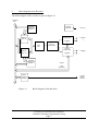
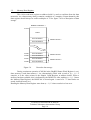
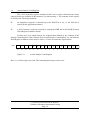
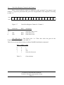
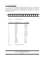
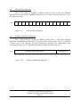
User manual TUeDACS/1
X-t and X-Y Recorder
BLN 2000-06 UM
May 2000
Eindhoven University of Technology
Department of Physics
Physical & Technical Laboratory Automation Group
Authors:
Version:
Date:
R. Smeets
1.0
13-09-2000
Hardware design:
G. Harkema
General guidelines for programming TUeDACS interfaces
1.
After a TUeDACS interface is started or enabled, by setting the start bit (STR bit),
enable bit (ENA bit) or the combined start/enable bit (STR/ENA bit) in the PhyBUS
Status Word Register at interface subaddress 0x00, do not change any interface
settings by changing the contents of write-only or read/write registers, as this may
result in erroneous interface operation. Settings can be safely changed before starting
or enabling the interface, i.e. when the DONE-bit in the PhyBUS Status Word
Register at subaddress 0x00 is set.
2.
If a specific TUeDACS interface must be programmed to use interrupts, follow these
guidelines:
3.
!
if the TUeDACS interface has a start bit (STR bit) in the PhyBUS Status
Word Register at interface subaddress 0x00, the STR bit and the IE bit must
be set at the same time.
!
if the TUeDACS interface has an enable bit (ENA bit) in the PhyBUS
Status Word Register at interface subaddress 0x00, first set the ENA bit in
the PhyBUS Status Word Register, then set the Interrupt Enable bit (IE bit)
in the PhyBUS Status Word Register. Do not set the ENA bit and the IE bit
at the same time, as this will result in a PhyBUS interrupt that is not caused
by an ‘interface operation completed’ event.
!
if the TUeDACS interface has a combination of a start bit and an enable bit
(STR/ENA bit) in the PhyBUS Status Word Register at interface subaddress
0x00, the function of the STR/ENA bit (start interface or enable interface)
depends on a software-selectable interface-specific operating mode. In this
case, the STR/ENA bit and the IE bit must be set at the same time (this does
not depend on the selected operating mode, i.e. whether the STR/ENA bit is
used as a start bit or as an enable bit).
Do not remove or insert a TUeDACS interface if the TUeDACS system crate is
powered, as this may result in damage to TUeDACS interfaces and/or to the system
crate.
TUeDACS/1 Recorder BLN 2000-06
Technical Laboratory Automation Group
Page 1
TUeDACS/1 Recorder BLN 2000-06
Technical Laboratory Automation Group
Page 2
Table of contents
page
1.
Introduction . . . . . . . . . . . . . . . . . . . . . . . . . . . . . . . . . . . . . . . . . . . . . . . . . . . . . . . . 5
2.
Block diagram of the Recorder . . . . . . . . . . . . . . . . . . . . . . . . . . . . . . . . . . . . . . . . . 7
2.1
Block diagram and description of the analog front end . . . . . . . . . . . . . . . . 8
3.
Recorder programming model . . . . . . . . . . . . . . . . . . . . . . . . . . . . . . . . . . . . . . . . . . 9
3.1
PhyBUS Status Word Register . . . . . . . . . . . . . . . . . . . . . . . . . . . . . . . . . 11
3.2
Memory Data Register . . . . . . . . . . . . . . . . . . . . . . . . . . . . . . . . . . . . . . . . 16
3.3
Sample Count Register . . . . . . . . . . . . . . . . . . . . . . . . . . . . . . . . . . . . . . . 18
3.4
Actual Sample Count Register . . . . . . . . . . . . . . . . . . . . . . . . . . . . . . . . . 19
3.5
Offset Register Channel 0 and Channel 1 . . . . . . . . . . . . . . . . . . . . . . . . . 20
3.6
Gain Select Register Channel 0 and Channel 1 . . . . . . . . . . . . . . . . . . . . . 21
3.7
Clock Select Register . . . . . . . . . . . . . . . . . . . . . . . . . . . . . . . . . . . . . . . . . 22
3.8
Interrupt Select Register . . . . . . . . . . . . . . . . . . . . . . . . . . . . . . . . . . . . . . 23
3.9
Interface Identification Register . . . . . . . . . . . . . . . . . . . . . . . . . . . . . . . . 23
4.
Recorder signal description . . . . . . . . . . . . . . . . . . . . . . . . . . . . . . . . . . . . . . . . . . .
4.1
Analog inputs . . . . . . . . . . . . . . . . . . . . . . . . . . . . . . . . . . . . . . . . . . . . . . .
4.2
Start input (START IN) . . . . . . . . . . . . . . . . . . . . . . . . . . . . . . . . . . . . . . .
4.3
External power supply input . . . . . . . . . . . . . . . . . . . . . . . . . . . . . . . . . . .
4.4
Serial Highway connector . . . . . . . . . . . . . . . . . . . . . . . . . . . . . . . . . . . . .
5.
LED indicators on the recorder . . . . . . . . . . . . . . . . . . . . . . . . . . . . . . . . . . . . . . . . 27
TUeDACS/1 Recorder BLN 2000-06
Technical Laboratory Automation Group
Page 3
25
25
25
25
25
TUeDACS/1 Recorder BLN 2000-06
Technical Laboratory Automation Group
Page 4
1.
Introduction
The TUeDACS/1 X-t and X-Y Recorder unit is the advanced equivalent of a paper
chart recorder. An X-t chart recorder records an analog signal as a function of time; an X-Y
recorder records an analog signal as a function of another analog signal.
The TUeDACS/1 Recorder unit consists of two analog input channels which are
both sampled (in parallel) with a software selectable clock frequency.
If the recorder is used as the equivalent of an X-t or an X-Y recorder, 2 analog input
signals are recorded as a function of time. Analog input data of both channels is sampled at
equidistant time intervals and is converted by a 16-bit ADC. Converted data of both channels
is stored in an interleaved buffer memory.
Whether the recorded data represents X-t data or X-Y data, is only determined by the
application and the graphical representation of the acquired data. In the case of X-Y
recording, the time is stored implicitly (determined by the selected clock frequency), but is
discarded when representing the data from the data memories.
The TUeDACS/1 Recorder communicates with the host computer by means of the
PhyDAS Serial Highway protocol.
TUeDACS/1 Recorder BLN 2000-06
Technical Laboratory Automation Group
Page 5
The main features of the TUeDACS/1 Recorder are:
!
two analog input channels
!
16-bit resolution
!
differential inputs
!
input range -10 volt .. +10 volt
!
Programmable Gain Amplifier with software selectable gains of 1, 10 and
100
!
data is buffered in interleaved memories (each memory capable of storing
8k samples), guaranteeing uninterrupted recording of input data
!
a constant DC offset voltage in the range from -10 volt .. +10 volt can be
added to or subtracted from the input signal by means of an offset DAC in
order to increase the dynamic recording range.
!
offset is controlled with a 16-bit DAC (305 µV resolution)
!
input impedance app. 2 MOhm
!
on-board clock source, providing a number of fixed software-selectable
sample clock frequencies in the range 100 µsec .. 100 sec.
!
external start input
TUeDACS/1 Recorder BLN 2000-06
Technical Laboratory Automation Group
Page 6
2.
Block diagram of the Recorder
The block diagram of the recorder is given in figure 2.1.
INTERNAL
BUS
ADDRESS
GENERATOR
MEMORY 0
TRIGGER
CONTROL
ANALOG
FRONT-END
MEMORY 0
(8K x 16)
CHANNEL
0
16-BIT
ADC
START IN
+ CHANNEL
0
-
ANALOG
MULTIPLEXER
ANALOG
FRONT-END
MEMORY 1
(8K x 16)
CHANNEL
1
ADDRESS
GENERATOR
MEMORY 1
+ CHANNEL
1
-
OFFSET
GAIN
SELECTION
SERIAL
HIGHWAY
CONTROL
Figure 2.1
PHYBUS
SERIAL
HIGHWAY
Block diagram of the Recorder
TUeDACS/1 Recorder BLN 2000-06
Technical Laboratory Automation Group
Page 7
2.1
Block diagram and description of the analog front end
The block diagram of the analog front-end for each channel is given in figure 2.2.
+
U
IN
A
+
1x
f
-
+
-
PROGRAMMABLE
GAIN
AMPLIFIER
UOUT
16-BIT
DAC
OFFSET
REGISTER
Figure 2.2
GAIN
SELECT
REGISTER
Block diagram of the analog front-end
The analog front-end of each channel consists of a first-order low-pass filter for
removing undesired high-frequency components from the input signal. The cut-off frequency
of this filter can be tailored to the customers specification. The default cut-off frequency for
this filter is 10 kHz. The output of the low-pass filter is followed by a unity gain buffer
amplifier.
To the output signal of this buffer amplifier, a DC offset voltage is added (or
subtracted) by means of a 16-bit offset DAC. Adding or subtracting a DC offset voltage is
useful when recording relatively low-level signals with a large DC offset component: the
offset voltage compensates the DC component, after which the resulting signal can be
amplified by the programmable gain amplifier, without the risk of signal clipping. The offset
voltage is set with the Offset Register, and is in the range from -10 volt to + 10 volt.
The resulting output signal is followed by a Programmable Gain Amplifier (PGA).
The gain of the PGA can be set to 1, 10 or 100 with the Gain Select Register.
TUeDACS/1 Recorder BLN 2000-06
Technical Laboratory Automation Group
Page 8
3.
Recorder programming model
The TUeDACS/1 Recorder programming model consist of 2 parts:
!
the functional programming model of the recorder, see figure 3.1.
!
the programming model of the Serial Highway Protocol communication unit, see
figure 3.2. This programming model is identical for every TUeDACS/1 module, as
this part handles the communication with the host computer. These registers need
not be programmed by the user, and are not described in this manual. See report
BLN 98-18 UM for a detailed description of these registers.
0x000
PHYBUS STATUS WORD REGISTER
R/W
0x001
MEMORY DATA REGISTER
R/W
0x002
SAMPLE COUNT REGISTER
R/W
0x003
ACTUAL SAMPLE COUNT REGISTER
RO
0x004
OFFSET REGISTER CHANNEL 0
R/W
0x005
GAIN SELECT REGISTER CHANNEL 0
R/W
0x006
OFFSET REGISTER CHANNEL 1
R/W
0x007
GAIN SELECT REGISTER CHANNEL 1
R/W
0x008
CLOCK SELECT REGISTER
R/W
0x00E
INTERRUPT SELECT REGISTER
R/W
0x00F
INTERFACE IDENTIFICATION REGISTER
RO
0x009
0x00D
0x010
0xF7F
Figure 3.1
Recorder programming model
TUeDACS/1 Recorder BLN 2000-06
Technical Laboratory Automation Group
Page 9
0xF80
SHP PHYBUS STATUS WORD REGISTER
R/W
0xF81
SHP LAST ADDRESS REGISTER
RO
0xF82
SHP LAST WORD DATA REGISTER
R/W
0xF84
SHP LAST LONGWORD DATA REGISTER (HI)
R/W
0xF85
SHP LAST LONGWORD DATA REGISTER (LO)
R/W
0xF8E
SHP INTERRUPT SELECT REGISTER
R/W
0xF8F
SHP INTERFACE IDENTIFICATION REGISTER
RO
0xF83
0xF86
0xF8D
0xF90
0xFFF
Figure 3.2
Serial Highway Protocol communications programming model
TUeDACS/1 Recorder BLN 2000-06
Technical Laboratory Automation Group
Page 10
3.1
PhyBUS Status Word Register
This 16-bit read/write register at address 0x000 controls the general operation of the
recorder.
0x000
ERR
IMF
X
X
X
X
X
15
14
13
12
11
10
9
BUSY DONE
8
7
IE
RST
ESS
X
6
5
4
3
Figure 3.3
PhyBUS Status Word Register
bit
mnemonic
R/W
description
15
14
13..9
8
7
6
5
4
3
2
1
0
ERR
IMF
BUSY
DONE
IE
RST
ESS
FMR
CMS
STR/ENA
RO
RO
RO
RO
R/W
WO
R/W
WO
R/W
R/W
ERRor
Interleaved Memory Full
not used, reads as zero
BUSY
DONE
Interrupt Enable
ReSeT
External Start Select
not used, reads as zero
Forced Memory Read
Continuous Mode Select
STaRt/ENAble operation
FMR CMS
2
1
STR/
ENA
0
ERR (bit 15): ERRor. This read-only bit indicates that an error has occurred. The
only error that can occur is that the interleaved memories are both full, which is indicated by
the IMF bit. When the ERR bit is set, the DONE bit is set and the BUSY bit is cleared:
recorder operation stops.
The ERR bit is cleared when setting the RST bit or when issuing a software PhyBUS
initialisation command.
TUeDACS/1 Recorder BLN 2000-06
Technical Laboratory Automation Group
Page 11
IMF (bit 14): Interleaved Memory Full. If this read-only bit is set, both data
memories 0 and 1 are full and no new data can be stored. This situation occurs if the host
processor fails to read data from the Memory Data Register after the DONE bit has been set.
The IMF bit can only be set if the continuous sample mode is selected, i.e. if the CMS bit is
set. If the single sample mode is selected, i.e. if the CMS bit is cleared, the IMF bit is always
cleared. See the description of the CMS bit.
The IMF bit is cleared when setting the RST bit or when issuing a software PhyBUS
initialisation command.
BUSY (bit 8): BUSY. The BUSY bit is always cleared if:
!
single sample mode is selected (the CMS bit is cleared), or
!
continuous sample mode is selected (the CMS bit is set) AND the ENA bit is set
AND the ESS bit is cleared, i.e. no external start signal is used.
The BUSY bit can only be set when the continuous sample mode is selected (the
CMS bit is set) AND the ENA bit is set, AND the ESS bit is set (i.e. an external start signal
applied to the START IN input is used). If this condition is met, the BUSY bit is set on the
first low-to-high transition of the external start signal. This indicates that the recorder has
been started by an external event.
The BUSY bit is always cleared if the STR/ENA bit is cleared. The BUSY bit is
cleared when setting the RST bit or when issuing a software PhyBUS initialisation command.
TUeDACS/1 Recorder BLN 2000-06
Technical Laboratory Automation Group
Page 12
DONE (bit 7): DONE. The timing of the DONE bit depends on the selected mode as
defined by the CMS bit:
!
single sample mode (CMS bit is cleared):
the DONE bit is cleared when setting the STR bit. The DONE bit remains cleared
during AD-conversion of both channels (a sample block). When AD-conversion has
completed, the DONE bit is set, and data of both channels (a sample block) can be
read from the Memory Data Register at address 0x001. Setting the STR-bit before
data is read, starts a new AD-conversion on both channels and overwrites the current
data.
!
continuous sample mode (CMS bit is set):
the DONE bit is cleared when setting the ENA bit. The DONE bit is set, when data
memory 0 or data memory 1 contains the number of sample blocks as defined by the
contents of the Sample Count Register at address 0x002. This indicates that data is
available and can be read from the Memory Data Register at address 0x001. After all
data has been read, the DONE bit is cleared.
Stopping the recorder by clearing the ENA bit does not immediately set the
DONE bit, as the current conversion of both channels will be completed first. When
this conversion has completed, the DONE bit is set.
The DONE bit is set when setting the RST bit or when issuing a software PhyBUS
initialisation command.
IE (bit 6): Interrupt Enable. If this bit is set, a PhyBUS interrupt is generated when
the DONE bit is set. If the IE bit is cleared, no PhyBUS interrupt can be generated.
The IE bit is cleared when setting the RST bit or when issuing a software PhyBUS
initialisation command.
NOTE: make sure that the IE bit is set after the STR/ENA bit has been set, otherwise
a PhyBUS interrupt will occur immediately (because the DONE bit has not been cleared yet).
RST (bit 5): ReSeT. Setting this bit initializes the recorder, sets the DONE bit and
clears the ERR bit, IMF bit and BUSY bit. All other bits remain unchanged. Note that the
contents of all other registers are NOT changed when setting the RST bit !
Setting the RST bit is a one-time command. This bit need not be cleared.
TUeDACS/1 Recorder BLN 2000-06
Technical Laboratory Automation Group
Page 13
ESS (bit 4): External Start Select. Setting this bit selects the START IN input for
starting the recorder. If the both the ESS bit, CMS bit and ENA bit have been set, a low-tohigh transition on this input starts the recorder.
FMR (bit 2): Forced Memory Read. Setting this write-only bit forces the recorder to
switch data storage from data memory 0 to data memory 1 (or vice versa), before data
memory 0 (or data memory 1) has been completely filled with the specified number of sample
blocks as defined by the Sample Count Register.
Setting the FMR bit allows data to become available at software-defined moments. If
a conversion is in progress, i.e. when input values from both input channels are being
acquired, setting the FMR bit results in an actual switch to occur when the conversion for
both channels has completed. When switching occurs, the DONE bit is set, indicating that
data can be read from the Memory Data Register at address 0x001. The Actual Sample Count
Register at address 0x003 holds the number of sample blocks (each block consisting of 2 data
words) that can be read from the Memory Data Register.
CMS (bit 1): Continuous Mode Select. Setting this bit selects continuous recorder
operation. In this mode, the recorder is enabled by setting the ENA bit. Data of both input
channels is acquired and stored in the interleaved data memories. The rate at which data is
acquired is defined by the contents of the Clock Select Register at address 0x008. When an
interleaved memory is full (indicated by the DONE bit, which is set), data must me be read by
reading the Memory Data Register at address 0x001. The recorder is stopped by clearing the
ENA bit.
Clearing the CMS bit selects single sample mode operation. In this mode, setting the
STR bit starts one AD conversion on both channels, and stores the data of both channels in
the memory. The data can be read by reading the Memory Data Register at address 0x001.
TUeDACS/1 Recorder BLN 2000-06
Technical Laboratory Automation Group
Page 14
STR/ENA (bit 0): StaRt recorder or ENAble recorder. The function of this bit
depends on the selected acquisition mode, defined by the CMS bit:
!
single sample mode operation selected (CMS bit is cleared): when setting the STR
bit, each input channel is sampled once, and the AD-converted value of each channel
is stored in data memory 0. When conversion completes, data memory 0 contains
one sample block, consisting of a total of 2 samples. Data can be read from the
Memory Data Register at address 0x001.
The STR/ENA bit functions as a StaRt bit: setting this bit immediately
starts one conversion for each channel.
!
continuous mode selected (CMS bit is set): after setting the ENA bit, the recorder
samples each channel, and the AD-converted value of each channel is stored in a
data memory. The frequency at which each channel is sampled, is defined by the
contents of the Clock Select Register at address 0x008. When the specified number
of sample blocks is stored, the DONE bit is set, indicating that data must be read
from a data memory. Data is read using the Memory Data Register at address 0x001.
After all data is read, the DONE bit is cleared again. While data is being read from a
data memory, acquisition continues and incoming data is stored in ‘the other’ data
memory.
The STR/ENA bit functions as an ENAble bit: setting this bit immediately
enables the recorder for storing a number of sample blocks. If the ESS bit is cleared,
recording starts immediately as described above. If the ESS bit is set, an external
start signal must be applied to the START IN input: a low-to-high transition on this
input starts the recorder.
Clearing the ENA bit aborts data acquisition in an orderly fashion: if a
conversion (of both channels) is in progress, i.e. when input values from both
channels are being acquired, recorder operation stops when the conversion for these
channels has completed.
The STR/ENA bit is cleared when setting the RST bit or when issuing a software PhyBUS
initialisation command.
TUeDACS/1 Recorder BLN 2000-06
Technical Laboratory Automation Group
Page 15
3.2
Memory Data Register
This 16-bit read/write register at address 0x001 is used to read data from the data
memories. As a data memory always contains a multiple of 2 samples (2 input channels), this
data register should always be read in multiples of 2. See figure 3.4 for a description of data
storage.
MEMORY 0 /MEMORY 1
0x1FFF
EMPTY
DATA CHANNEL 1
DATA CHANNEL 0
0x0003
DATA CHANNEL 1
0x0002
DATA CHANNEL 0
0x0001
DATA CHANNEL 1
0x0000
DATA CHANNEL 0
Figure 3.4
SAMPLE BLOCK n
SAMPLE BLOCK 1
SAMPLE BLOCK 0
Recorder data storage
During continuous operation (CMS bit in the PhyBUS Status Word Register is set),
data memory 0 and data memory 1 are (alternatingly) filled with a total of (n + 1) * 2
samples; n is the value written to the Sample Count Register at address 0x002. When a
memory has data available, this is indicated by the DONE bit. After reading (n + 1) * 2 times
the Memory Data Register, the DONE bit is cleared again. A total of n + 1 data blocks are
stored, indexed from 0 to n.
Reading the Memory Data Register more than (n + 1) * 2 times results in a bus error.
TUeDACS/1 Recorder BLN 2000-06
Technical Laboratory Automation Group
Page 16
During single sample operation (CMS bit in the PhyBUS Status Word Register is
cleared), one sample of each channel is acquired and stored in data memory 0. After both
samples have been stored , the DONE bit is set. The Memory Data Register can now be read
2 times. Reading the Memory Data Register returns the data from one sample block in the
following sequence:
1.
2.
input channel 0
input channel 1
Reading the Memory Data Register more than 2 times results in a bus error.
The Memory Data Register can also be used to test the internal memory address
generators and data memories 0 and 1. This memory test is enabled if the the ENA bit in the
PhyBUS Status Word Register is cleared. After setting the RST bit, the internal address
generators for data memories 0 and 1 are cleared. Writing data to the Memory Data Register
stores this data in the data memories: first, data memory 0 is written. If data memory 0 is full,
memory 1 is written next. The number of sample blocks (each block consisting of 2 words) to
be written to the Memory Data Register in order to fill a memory, must be equal to the
number of sample blocks as defined by the contents of the Sample Count Register at address
0x002. Next, the memory contents can be verified by reading the Memory Data Register and
comparing the data with the expected data.
TUeDACS/1 Recorder BLN 2000-06
Technical Laboratory Automation Group
Page 17
3.3
Sample Count Register
This 16-bit read/write register at address 0x002 is used to determine the number of
sample blocks to be stored in the interleaved memory if continuous recorder operation is
selected (CMS bit in the PhyBUS Status Word Register is set). One sample block always
contains 2 samples: one sample from each input channel.
0x002
X
X
X
X
15
14
13
12
Figure 3.5
SC11 SC10 SC9
11
10
9
SC8
SC7
SC6
SC5
SC4
SC3
SC2
SC1
SC0
8
7
6
5
4
3
2
1
0
Sample Count Register
Bits 11..0 of this register are used. Bits 15..12 always read as zero, writing these bits
has no effect.
If Nregister is the value written to the Sample Count Register, the actual number of
sample blocks Nsample blocks is given by:
Nsample blocks = Nregister + 1
As the recorder has a memory size of 8K words (both data memory 0 and data
memory 1), the maximum number of sample blocks in one memory is (8 x 1024) / 2 = 4096.
The value written to the Sample Count Register must be in the range 0..4095. Writing a value
outside this range results in undefined recorder operation.
The contents of the Sample Count Register is discarded if the CMS bit in the PhyBUS Status
Word Register is cleared.
Writing the Sample Count Register if the DONE bit is cleared (i.e. the recorder has
been enabled), results in a bus error. The Sample Count Register is cleared when issuing a
software PhyBUS initialisation command.
TUeDACS/1 Recorder BLN 2000-06
Technical Laboratory Automation Group
Page 18
3.4
Actual Sample Count Register
This 16-bit read-only register at address 0x003 can be read to determine how many
sample blocks are available in data memory 0 or data memory 1. The contents of this register
is useful in the following situations:
!
an acquisition sequence is aborted before the DONE bit is set, i.e. the ENA bit is
cleared by the application software,
!
a forced memory read has occurred by setting the FMR bit in the PhyBUS Status
Word Register at address 0x000.
In both cases, less sample blocks are acquired than defined by the contents of the
Sample Count Register. If the contents of the Actual Sample Count Register is n, the Memory
Data Register at address 0x001 must be read n * 2 times to obtain the acquired data.
0x003
X
X
X
X
ASC
11
ASC
10
ASC
9
ASC
8
ASC
7
ASC
6
ASC
5
ASC
4
ASC
3
ASC
2
ASC
1
ASC
0
15
14
13
12
11
10
9
8
7
6
5
4
3
2
1
0
Figure 3.6
Actual Sample Count Register
Bits 11..0 of this register are used. The remaining bits always read as zero.
TUeDACS/1 Recorder BLN 2000-06
Technical Laboratory Automation Group
Page 19
3.5
Offset Register Channel 0 and Channel 1
These 16-bit read/write registers at addresses 0x004 and 0x006 (for channel 0 and
channel 1, respectively) determine the DC offset voltage that is added to or subtracted from
the analog input signal, using the offset DAC. See also figure 2.2.
Adding or subtracting a DC offset is useful when recording small signals with a
large DC offset component: the offset voltage compensates the DC component, after which
the resulting signal can be amplified by the programmable gain amplifier, without the risk of
signal clipping.
The data in the Offset Registers represents 2's complement DAC data for the voltage
range of -10 volt .. +10 volt, see table 3.1.
offset voltage
dec
hex
binary
+9.99969
.
.
+0.00031
+0.00000
-0.00031
.
.
-9.99969
-10.0000
+32767
0x7FFF
0111 1111 1111 1111
+1
0
-1
0x0001
0x0000
0xFFFF
0000 0000 0000 0001
0000 0000 0000 0000
1111 1111 1111 1111
-32767
-32768
0x8001
0x8000
1000 0000 0000 0001
1000 0000 0000 0000
Table 3.1
2's complement offset DAC coding
TUeDACS/1 Recorder BLN 2000-06
Technical Laboratory Automation Group
Page 20
3.6
Gain Select Register Channel 0 and Channel 1
These 16-bit read/write registers at addresses 0x005 and 0x007 (for channel 0 and
channel 1, respectively) determine the gain of the Programmable Gain Amplifiers according
to table 3.2.
0x005
0x007
X
X
X
X
X
X
X
X
X
X
X
X
X
X
GS1
GS0
15
14
13
12
11
10
9
8
7
6
5
4
3
2
1
0
Figure 3.7
Gain Select Register Channel 0 / Channel 1
bit
mnemonic
R/W
description
15..2
1
0
GS1
GS0
R/W
R/W
not used, reads as zero
Gain Select, bit 1
Gain Select, bit 0
GS1..GS0 (bit 1): Gain Select, bits 1..0. These bits select the gain for the
Programmable Gain Amplifier, see table 3.2.
These bits are cleared when issuing a software PhyBUS initialisation command.
GS1
GS0
gain
0
0
1
1
0
1
0
1
1
10
100
reserved, do not use
Table 3.2
Gain selection
TUeDACS/1 Recorder BLN 2000-06
Technical Laboratory Automation Group
Page 21
3.7
Clock Select Register
The Clock Select Register selects the sample frequency for the recorder in the
continuous mode, i.e. if the CMS bit in the PhyBUS Status Word Register is set. If the CMS
bit is cleared, the value contained in the Clock Select Register is discarded. The Clock Select
Register must be programmed with a value in the range 0..18. The values 19..31 are reserved
and should not be used!
0x008
X
X
X
X
X
X
X
X
X
X
X
CS4
CS3
CS2
CS1
CS0
15
14
13
12
11
10
9
8
7
6
5
4
3
2
1
0
Figure 3.8
Clock Select Register
CS3..CS0
sample frequency
clock period
0
1
2
3
4
5
6
7
8
9
10
11
12
13
14
15
16
17
18
10 kHz
5 kHz
2 kHz
1 kHz
500 Hz
200 Hz
100 Hz
50 Hz
20 Hz
10 Hz
5 Hz
2 Hz
1 Hz
0.5 Hz
0.2 Hz
0.1 Hz
0.05 Hz
0.02 Hz
0.01 Hz
100 µsec
200 µsec
500 µsec
1 msec
2 msec
5 msec
10 msec
20 msec
50 msec
100 msec
200 msec
500 msec
1 sec
2 sec
5 sec
10 sec
20 sec
50 sec
100 sec
Table 3.3
Clock frequency selection
TUeDACS/1 Recorder BLN 2000-06
Technical Laboratory Automation Group
Page 22
3.8
Interrupt Select Register
This 16-bit read/write register at address 0x00e is used to select the PhyBUS
interrupt bit for the recorder. PhyBUS interrupt bits 15..0 can be selected. Only bits 3..0 of
this register are used.
0x00E
X
X
X
X
X
X
X
X
X
X
X
X
IS3
IS2
IS1
IS0
15
14
13
12
11
10
9
8
7
6
5
4
3
2
1
0
Figure 3.9
3.9
Interrupt Select Register
Interface Identification Register
This 16-bit read-only register at address 0x00f holds a value that uniquely
determines the PhyBUS interface type. The lower 4 bits of this register (bits 0..3) hold the
revision code of the interface. For the TUeDACS/1 Recorder, the identification code
contained in bits 15..4 is 70 (decimal). Writing this register results in a bus error.
0x00F
INTERFACE IDENTIFICATION CODE
15
14
13
Figure 3.10
12
11
10
9
8
7
REVISION CODE
6
5
Interface Identification Register
TUeDACS/1 Recorder BLN 2000-06
Technical Laboratory Automation Group
Page 23
4
3
2
1
0
TUeDACS/1 Recorder BLN 2000-06
Technical Laboratory Automation Group
Page 24
4.
Recorder signal description
4.1
Analog inputs
The analog ADC recorder inputs for channel 0 and 1 are located on the front panel and have
the following specifications:
!
!
!
!
!
4.2
available through isolated BNC connectors
differential inputs
differential input voltage range -10 volt .. +10 volt
input impedance app. 2 MOhm
protected for input voltages in the range of -40 volt .. +40 volt
Start input (START IN)
The start input START IN is located on the front panel and is used to start the recorder if the
continuous sample mode is selected, i.e. if the CMS bit in the PhyBUS Status Word Register
at address 0x000 is set. The START IN input has the following specifications:
!
!
!
!
!
!
!
4.3
available through isolated BNC connector
Schmitt trigger input
input impedance 50 ohm
minimum input pulse width: 15 ns
TTL compatible signal levels
positive edge-triggered
not protected against overvoltages
External power supply input
The external power supply input for the recorder is located on the rear panel of the recorder.
The recorder must be powered by a 9 volt, 500 mA DC adapter.
4.4
Serial Highway connector
The Serial Highway connector is located on the rear panel of the recorder.
TUeDACS/1 Recorder BLN 2000-06
Technical Laboratory Automation Group
Page 25
TUeDACS/1 Recorder BLN 2000-06
Technical Laboratory Automation Group
Page 26
5.
LED indicators on the recorder
The following LED indicators are located on the front panel of the recorder:
MEM0
this LED illuminates if memory 0 contains data
MEM1
this LED illuminates if memory 1 contains data
BUSY
this LED reflects the state of the BUSY bit in the PhyBUS Status Word
Register at address 0x000. See section 3.1 for a description of this bit.
MC
SHP Master Clock. This LED illuminates if the recorder receives a clock
signal from the Serial Highway master.
SC
SHP Slave Clock. This LED illuminates if the recorder transmits a clock
signal to the Serial Highway master.
TUeDACS/1 Recorder BLN 2000-06
Technical Laboratory Automation Group
Page 27