1
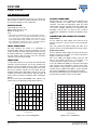
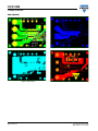
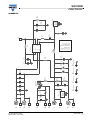
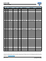
SiC413DB
Vishay Siliconix
SiC413 Reference Board User's Manual
4 A, 26 V Integrated Synchronous Buck Regulator
THE CHIP
FEATURES
PRODUCT SUMMARY
Input Voltage Range
4.75 V to 26 V
Output Voltage Range
0.6 V to 13.2 V
Operating Frequency
500 kHz
Continuous Output Current
4A
Peak Efficiency
93 %
Highside/Lowside RDS_ON
35 mΩ/19 mΩ
Package
SO-8
DESCRIPTION
The SiC413 is an integrated, dc-to-dc power conversion
solution with built-in PWM-optimized high- and low-side
n-channel MOSFETs and advanced PWM controller. The
SiC413 provides a quick and easy to use POL voltage
regulation solution for a wide range of applications. Vishay
Siliconix proprietary packaging technology is used to
optimize the power stage and minimize power losses
associated with parasitic impedances and switching delays.
The co-packaged Gen III TrenchFET power MOSFETs
deliver higher efficiency than lateral DMOS monolithic
solutions.
•
•
•
•
•
•
•
•
•
•
•
4.75 V to 26 V input voltage range
Integrated PWM controller and Gen III trench MOSFETs
Built-in bootstrap diode
500 kHz fixed switching frequency
Internal soft start
Break-before-make operation
Integrated current sense
Cycle by cycle overcurrent protection
Output over voltage protection
Thermal shutdown
Quick and easy single chip converter
• SO-8 package
APPLICATIONS
•
•
•
•
•
•
LCD TV, set-top box and DVD player
Desktop PC and server
Add-in graphic board
Memory, FPGA and µP device power supplies
Point of load dc-to-dc conversion
Telecom and networking equipment
REFERENCE BOARD PHOTOS
Figure 1. Top of the PCB
Document Number: 65172
S09-1350-Rev. A, 20-Jul-09
Figure 2. Bottom of the PCB
www.vishay.com
1
SiC413DB
Vishay Siliconix
THE REFERENCE BOARD
This reference board allows the end user to evaluate the
SiC413 chip for its features and all functionalities. It can also
be a reference design for a user’s application.
SPECIFICATION
Input voltage (V): 4.75 to 24
Output voltage (V): 0.6 to 12.0
Output current (A): 0 to 4
Notes:
• This board is, by default, preset to 3.3 V output with 12 V input
• This board can be set to any output voltage between 0.6 V and
12 V, and any input voltage between 4.75 V and 24 V. For a
specific input/output voltage combination, the values of inductor
and compensation network may need to be modified and the
output capacitors may need an increase or decrease.
INPUT CAPACITORS
The input capacitors are chosen as a combination of
electrolytic and ceramics so that the capacitance, the rms
current, the ESR, the input voltage ripple and the cost can
be all fairly satisfied. For a combination of high voltage input
and low voltage output (low duty cycle), the electrolytic
capacitors (C1) may not be required.
INDUCTORS
If off-the-shelf inductors are to be used, then their DCR and
saturation current parameters are the key besides their
inductance values. The DCR causes an I2R loss, which will
decrease the system efficiency and generate heat on the
board. The saturation current has to be higher than the
maximum output current plus ripple current. In over current
condition the inductor current may be drastically high. All
these need to be put into consideration when selecting the
inductor.
On this board Vishay IHLP4040DZ series inductors are
used to meet cost requirement and get better efficiency.
OUTPUT CAPACITORS
Voltage, ESR, rms current capability and capacitance are
essential elements to consider when choosing output
capacitors. The ESR and capacitance affect the output
voltage ripple, transient response and system stability. The
rms current capability determines the capacitor power
dissipation and life time. To meet all the 4 element
requirements, combination of ceramics and tantalum can be
used.
CONNECTION AND SIGNAL/TEST POINTS
Power sockets
VIN (J1), GND (J3): Input voltage source with VIN to be
positive. Connect to a 4.75 V to 24 V source that powers
SiC413.
VOUT (J9), GND (J13): Output voltage with VOUT to be
positive. Connect to a load that draws less than 4 A current.
Signal and test leads
VIN (J2), GND (J5): Intput voltage sense pins with VIN to be
positive. Connect to a volt meter or an oscilloscope probe if
display or waveform is needed.
VOUT (J11), GND (J14): Output voltage sense pins with
VOUT to be positive. Connect to a volt meter or an
oscilloscope probe if display or waveform is needed.
VCTRL (J6), LDTRG (J8), GND (J7): Load step control signal
input. Connect VCTRL and GND to a power source, VEXT,
which supplies enough voltage to generate the load step
needed. Connect LDTRG and GND to a pulse generater
that creates the MOSFET on/off signal for the load step.
EN: SiC413 enable signal input. To enable the system leave
this point open, otherwise connect it to any GND.
0.3
100
90
80
70
0.1
Efficiency (%)
Output Voltage Variation (%)
0.2
0
- 0.1
60
50
40
30
20
- 0.2
10
- 0.3
0.0
0.5
1.0
1.5
2.0
2.5
3.0
3.5
Load Current (A)
Figure 3. 12 V - 3.3 V Load Regulation
www.vishay.com
2
4.0
0
0.0
0.5
1.0
1.5
2.0
2.5
3.0
3.5
4.0
Load Current (A)
Figure 4. 12 V - 3.3 V Efficiency
Document Number: 65172
S09-1350-Rev. A, 20-Jul-09
SiC413DB
Vishay Siliconix
SET UP LOAD STEP
The hardware to test transient response is included in the
board, which allows users to see how the transient response
performs. The setup steps are:
1. Decide what load step is wanted, then based on the
output voltage calculate the external voltage VEXT that
will be connected between VCTRL and GND. For
example, a load step of 2 A between 0.5 A (I1) and 2.5 A
(I2) is required and the output voltage is 3.3 V. VEXT =
VO - (I2 - I1) * 3.01 Ω = VO - (2.5 A - 0.5 A) * 3.01 Ω =
- 2.72 V. Preset a DC source voltage to VEXT = 2.72 V
(current capability around 1 A) and connect it to the
board with positive side to GND and negative side to
VCTRL (if VEXT is a positive value, then connect the DC
source positive to VCTRL and negative to GND).
2. Preset a waveform from a function generator using the
following parameters and set its output to OFF (refer to
the specific function generator manual for its setup):
Shape: square
Freqency: 50 Hz or whatever is required
Duty cycle: 1 % to 2 % or whatever is required
Amplitude: -12 V low level and + 10 V high level
Rising time and falling time: 1 µs or whatever is
required.
3. Connect the function generator output positive to
LDTRG and negative to GND.
4. Preset the current of an electronic load to I1 and turn it
on.
5. Set up an oscilloscope using the following parameters.
Channel 1 for probing output voltage: AC coupled,
20 mV/div to 50 mV/div, 100 mV offset, or whatever is
required .
Channel 2 for probling the current on the 3.01 Ω
resistor (R2) (needs to be an isolated probe): DC
coupled, 3 V/div (corresponds to 1 A/div) for IO < 2.5 A or
5 V/div (corresponds to 1.661 A/div) for IO > 2.5 A.
Time base: 100 µs/div
Bandwidth: 20 MHz
6. Connect oscilloscope channel 1 probe positive to VOUT
(J11) and negative to GND (J14), and channel 2 probe
positive to VOUT (J11) and negative to Q1 DRAIN.
7. Turn on the system power. Output voltage should be
shown on the electronic load with current of I1.
8. Turn on the power source for VEXT.
9. Set the function generator output to be ON. The transient
response waveforms should be seen on the oscilloscope.
10. If needed, re-adjust the trigger waveform’s rising and
falling time on the function generator so that the current
slew rate is satisfied (the current slew rate can be seen
on oscilloscope channel 2 waveform by setting the time
base to 1 µs or 500 ns).
11. To change load step, decrease or increase the value of
VEXT.
12. To cease transient response test, simply set the function
generator output to off, turn off the power source for
VEXT, and then shut down the system power.
CHANGE OUTPUT VOLTAGE
If, at any time, different output voltage is needed, then
simply change the value of R9 based on the following
formula:
R9 = R7/(VO/VREF - 1) = 10K/(VO/0.6 - 1)
COMP
Output Voltage
Inductor Current IL
Figure 5. An Example of Load Step Waveforms
Document Number: 65172
S09-1350-Rev. A, 20-Jul-09
www.vishay.com
3
SiC413DB
Vishay Siliconix
PCB LAYOUT
Figure 6. Top
Figure 7. Inner Layer 1
www.vishay.com
4
Figure 8. Inner Layer 2
Figure 9. Bottom Layer
Document Number: 65172
S09-1350-Rev. A, 20-Jul-09
1
J6
VCTL
J14
VO_GND
J13
VO_GND
J11
VO
1
1
1
J8
LDTRG
J9
VO
1
J7
GND
1
1
C11
22 µF
1
1
1
J5
VIN_GND
J3
VIN_GND
J2
VIN
VO
V
1
1
1
R9
2K21
R7
10K
R2
3R01
C4
10 µF
1
C16
C
C15
3.3 nF
Si4812BDY
Q1
C3
10 µF
M2
Mounting Hole
C2
10 µF
M1
Mounting Hole
1
C130.1 µF
R3
100K
+ C1
150 µF
J12
VO Check Pin
C12
22 µF
VIN
1
1
C7
4.7 µF
1
1
M4
Mounting Hole
C20
10 µF
R11
20K
C8
0.1 µF
C19
C17
C18
100 µF 100 µF 100 µF
+
+
+
C6
0.01 µF
M3
Mounting Hole
C5
0.1 µF
R9
open
12K
10K
6K65
4K99
3K16
2K21
1K37
523R
GND
VIN
VREG
FB
U1SiC413
L1
4.7 µH
5
6
7
8
VO
0.6 V
1.100 V
1.200 V
1.502 V
1.802 V
2.499 V
3.315 V
4.980 V
12.072 V
VSW
BOOT
EN
COMP
R1
100K
4
3
2
1
EN
J4
EN
1
1
GND
GND
GND
GND
5
4
3
2
C21
C
R8
R
C14
0.1 µF
R5
0R
VSW 1
C9
100 pF
V
J10
VSW Check Pin
R6
3K01
C10
10 nF
GND
GND
GND
GND
Document Number: 65172
S09-1350-Rev. A, 20-Jul-09
2
3
4
5
J1
VIN
R10
750K
SiC413DB
Vishay Siliconix
SCHEMATIC
www.vishay.com
5
SiC413DB
Vishay Siliconix
BILL OF MATERIAL
Item
Qty
Reference
Value
Voltage
PCB Footprint
Part Number
Manufacturer
1
1
C1
150 µF
35 V
D8X11.5-D0.6X3.5
EEU-FM1V151
Panasonic
2
3
C2, C3, C4
10 µF
25 V
SM/C_1210
TMK325B7106MN-T
Taiyo Yuden
3
4
C5, C8, C13, C14
0.1 µF
50 V
SM/C_0603
VJ0603Y104KXACW1BC
Vishay
4
1
C6
0.01 µF
50 V
SM/C_0402
VJ0402Y103KXACW1BC
Vishay
5
1
C7
4.7 µF
10 V
SM/C_0805
LMK212B7475KG-T
Murata/Taiyo Yuden
6
1
C9
100 pF
50 V
SM/C_0603
VJ0603Y101KXACW1BC
Vishay
7
1
C10
10 nF
50 V
SM/C_0603
VJ0603Y103KXACW1BC
Vishay
8
2
C11, C12
22 µF
16 V
SM/C_1210
GRM32ER71C226ME18L
TAIYO YUDEN
9
1
C15
3.3 nF
50 V
SM/C_0603
VJ0603Y332KXACW1BC
Vishay
10
2
C16, C21
Not populated
50 V
SM/C_0603
11
3
C17, C18, C19
100 µF
20 V
595D-D
595D107X9020D2T
12
1
C20
10 µF
16 V
13
1
J1
VIN
14
1
J2
15
1
J3
Vishay
Vishay
SM/C_1206
C3216X7R1C106M
TDK
SOLDER-BANANA
575-6
Keystone
VIN
Probe Hook
1540-2
Keystone
VIN_GND
SOLDER-BANANA
575-6
Keystone
16
1
J4
EN
Probe Hook
1540-2
Keystone
17
1
J5
VIN_GND
Probe Hook
1540-2
Keystone
18
1
J6
VCTL
Probe Hook
1540-2
Keystone
19
1
J7
GND
Probe Hook
1540-2
Keystone
20
1
J8
LDTRG
Probe Hook
1540-2
Keystone
21
1
J9
VO
SOLDER-BANANA
575-6
Keystone
22
1
J10
VSW check pin
LECROY PROBE PIN
PK007-015
LeCroy
23
1
J11
VO
Probe Hook
1540-2
Keystone
24
1
J12
Vo check pin
LECROY PROBE PIN
PK007-015
LeCroy
25
1
J13
VO_GND
SOLDER-BANANA
575-6
Keystone
26
1
J14
VO_GND
Probe Hook
1540-2
Keystone
27
1
L1
4.7 µH
IHLP4040
IHLP4040DZER4R7M01
Vishay
28
4
M1, M2, M3, M4
Mounting hole
29
1
Q1
Si4812BDY
30
2
R1,R3
31
1
R2
32
1
R5
0R
50 V
SM/C_0603
CRCW06030000FKEA
Vishay
33
1
R6
3K01
50 V
SM/C_0603
CRCW06033K01FKEA
Vishay
CRCW060310K0FKEA
Vishay
STACKING SPACER
8834
Keystone
30 V
SO-8
Si4812BDY
Vishay
100K
50 V
SM/C_0603
CRCW0603100KFKEA
Vishay
3R01
200 V
C_2512
CRCW25123R01FKTA
Vishay
34
1
R7
10K
50 V
SM/C_0603
35
1
R8
R
50 V
SM/C_0603
Vishay
36
1
R9
2K21
50 V
SM/C_0603
CRCW06032K21FKEA
Vishay
37
1
R10
750K
50 V
SM/C_0603
CRCW0603750KFKEA
Vishay
38
1
R11
20K
50 V
SM/C_0603
CRCW060320K0FKEA
Vishay
39
1
U1
SiC413
SO-8
SiC413
Vishay
Vishay Siliconix maintains worldwide manufacturing capability. Products may be manufactured at one of several qualified locations. Reliability data for Silicon
Technology and Package Reliability represent a composite of all qualified locations. For related documents such as package/tape drawings, part marking, and
reliability data, see www.vishay.com/ppg?65172.
www.vishay.com
6
Document Number: 65172
S09-1350-Rev. A, 20-Jul-09