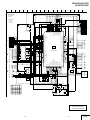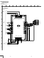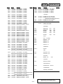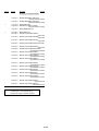
1
RDR-HX520/HX525/HX720/HX722/
HX725/HX727/HX920/HX925
RMT-D230P/D231P
SERVICE MANUAL
AEP Model
RDR-HX520/HX720/HX722/HX725/
HX727/HX920/HX925
UK Model
RDR-HX520/HX525/
HX720/HX725
for RDR-HX520/HX720/HX722/
HX725/HX727/HX920/HX925
for RDR-HX525/HX725
for RDR-HX525/HX725/HX727/HX925
Photo: RDR-HX525
SPECIFICATIONS
System
Inputs and outputs
General
Laser: Semiconductor laser
LINE 2 OUT
(AUDIO): Phono jack/2 Vrms/10 kilohms
(VIDEO): Phono jack/1.0 Vp-p
(S VIDEO): 4-pin mini DIN/Y: 1.0 Vp-p,
C: 0.3 Vp-p (PAL)
Power requirements: 220-240 V AC, 50/
60 Hz
Power consumption:
Channel coverage:
PAL (B/G, D/K, I)
VHF: E2 to E12, R1 to R12, Italian A
to H, Ireland A to J, South Africa 4 to
13
UHF: E21 to E69, R21 to R69, B21 to
B69
CATV: S01 to S05, S1 to S20
HYPER: S21 to S41
SECAM (L) (for French RDR-HX520/
HX725/HX727/HX920 and RDRHX925 models only)
VHF: F2 to F10
UHF: F21 to F69
CATV: France B to Q
HYPER: S21 to S41
The above channel coverage merely ensures
the channel reception within these ranges. It
does not guarantee the ability to receive
signals in all circumstances. For details, see
“Receivable channels”
Video reception: Frequency synthesizer
system
Audio reception: Split carrier system
Aerial out: 75-ohm asymmetrical aerial
socket
Timer: Clock: Quartz locked/Timer
indication: 24-hour cycle (digital)/Power
back-up duration: 1 hour
Video recording format: MPEG-2,
MPEG-1
Audio recording format/applicable bit
rate: Dolby Digital 2 ch
256 kbps/128 kbps (in EP and SLP
mode)
LINE 2 IN
(AUDIO): Phono jack/2 Vrms/more than
22 kilohms
(VIDEO): Phono jack/1.0 Vp-p
(S VIDEO): 4-pin mini DIN/Y: 1.0 Vp-p,
C: 0.3 Vp-p (PAL)
LINE 1 – TV: 21-pin
CVBS IN/OUT
S-Video/RGB OUT (upstream)
LINE 3/DECODER: 21-pin
CVBS IN/OUT
S-Video/RGB IN
(RGB signal cannot be recorded, except
with French RDR-HX520/HX725/HX727/
HX920 and RDR-HX925 models.)
S-Video OUT (downstream)
Decoder
DV IN: 4-pin/i.LINK S100
DIGITAL OUT (COAXIAL): Phono jack/
0.5 Vp-p/75 ohms
COMPONENT VIDEO OUT
(Y, PB/CB, PR/CR):
Phono jack/Y: 1.0 Vp-p, PB/CB: 0.7 Vp-p,
PR/CR: 0.7 Vp-p
G-LINK: mini jack
(for French RDR-HX525/HX725/HX727
and RDR-HX725 models only)
RDR-HX520/HX525: 42 W
RDR-HX720/HX722/HX725/HX727/
HX920/HX925: 44 W
Dimensions (approx.):
430 × 65 × 328 mm (width/height/
depth) incl. projecting parts
Hard disk drive capacity:
RDR-HX520/HX525: 80 GB
RDR-HX720/HX722/HX725/
HX727: 160 GB
RDR-HX920/HX925: 250 GB
Mass (approx.): 4.2 kg
Operating temperature: 5ºC to 35ºC
Operating humidity: 25% to 80%
Supplied accessories:
Mains lead (1)
Aerial cable (1)
Remote commander (remote) (1)
Set top box controller (1)
(for French RDR-HX525/HX725/
HX727/HX925 models only)
R6 (size AA) batteries (2)
Specifications and design are subject to
change without notice.
Compatible colour systems
This recorder is designed to record using the
PAL colour system and play back using the
PAL or NTSC colour systems.
For French RDR-HX520/HX725/HX727/
HX920 and RDR-HX925 models only
The signals of the SECAM colour system can
be received or recorded but played back in the
PAL colour system only. Recording of video
sources based on other colour systems cannot
be guaranteed.
DVD RECORDER
WARNING!!
WHEN SERVICING, DO NOT APPROACH THE LASER EXIT WITH
THE EYE TOO CLOSELY. IN CASE IT IS NECESSARY TO
CONFIRM LASER BEAM EMISSION, BE SURE TO OBSERVE
FROM A DISTANCE OF MORE THAN 25 cm FROM THE SURFACE
OF THE OBJECTIVE LENS ON THE OPTICAL PICK-UP BLOCK.
CAUTION:
The use of optical instrument with this product will increase eye
hazard.
CAUTION
Use of controls or adjustments or performance of procedures
other than those specified herein may result in hazardous radiation
exposure.
SAFETY-RELATED COMPONENT WARNING!!
Unleaded solder
Boards requiring use of unleaded solder are printed with the leadfree mark (LF) indicating the solder contains no lead.
(Caution: Some printed circuit boards may not come printed with
the lead free mark due to their particular size.)
: LEAD FREE MARK
Unleaded solder has the following characteristics.
• Unleaded solder melts at a temperature about 40°C higher than
ordinary solder.
Ordinary soldering irons can be used but the iron tip has to be
applied to the solder joint for a slightly longer time.
Soldering irons using a temperature regulator should be set to
about 350°C.
Caution: The printed pattern (copper foil) may peel away if the
heated tip is applied for too long, so be careful!
• Strong viscosity
Unleaded solder is more viscous (sticky, less prone to flow) than
ordinary solder so use caution not to let solder bridges occur such
as on IC pins, etc.
• Usable with ordinary solder
It is best to use only unleaded solder but unleaded solder may
also be added to ordinary solder.
COMPONENTS IDENTIFIED BY MARK 0 OR DOTTED LINE WITH
MARK 0 ON THE SCHEMATIC DIAGRAMS AND IN THE PARTS
LIST ARE CRITICAL TO SAFE OPERATION. REPLACE THESE
COMPONENTS WITH SONY PARTS WHOSE PART NUMBERS
APPEAR AS SHOWN IN THIS MANUAL OR IN SUPPLEMENTS
PUBLISHED BY SONY.
SAFETY CHECK-OUT
After correcting the original service problem, perform the following
safety checks before releasing the set to the customer.
1.
2.
3.
Check the area of your repair for unsoldered or poorly-soldered
connections. Check the entire board surface for solder splashes
and bridges.
Check the interboard wiring to ensure that no wires are
"pinched" or contact high-wattage resistors.
Look for unauthorized replacement parts, particularly
transistors, that were installed during a previous repair. Point
them out to the customer and recommend their replacement.
4.
Look for parts which, through functioning, show obvious signs
of deterioration. Point them out to the customer and
recommend their replacement.
5. Check the B+ voltage to see it is at the values specified.
6. Flexible Circuit Board Repairing
• Keep the temperature of the soldering iron around 270˚C
during repairing.
• Do not touch the soldering iron on the same conductor of the
circuit board (within 3 times).
• Be careful not to apply force on the conductor when soldering
or unsoldering.
—2—
TABLE OF CONTENTS
SERVICE NOTE
1.
DISK REMOVAL PROCEDURE IF THE TRAY
CANNOT BE EJECTED (FORCED EJECTION) ············ 5
1.
GENERAL
WARNING ············································································ 1-1
Precautions ············································································· 1-1
Quick Guide to Disc Types ···················································· 1-2
Hookups and Settings ································································ 1-3
Hooking Up the Recorder ······················································ 1-3
Step 1: Connecting the Aerial Cable ······································ 1-3
Step 2: Connecting the Video Cords ······································ 1-3
Step 3: Connecting the Audio Cords ····································· 1-3
Step 4: Connecting the Mains Lead ······································· 1-4
Step 5: Preparing the Remote ················································ 1-4
Step 6: Easy Setup ································································· 1-5
Connecting a VCR or Similar Device ···································· 1-5
Connecting to a Satellite or Digital Tuner ····························· 1-5
Connecting a PAY-TV/Canal Plus Analogue Decoder ·········· 1-6
Eight Basic Operations — Getting to Know Your DVD
Recorder ···················································································· 1-6
1. Inserting a Disc ·································································· 1-6
2. Recording a Programme ···················································· 1-6
3. Playing the Recorded Programme (Title List) ··················· 1-7
4. Displaying the Playing/Remaining Time and Play
Information ········································································ 1-7
5. Changing the Name of a Recorded Programme ················ 1-8
6. Labelling and Protecting a Disc ········································· 1-8
7. Playing the Disc on Other DVD Equipment (Finalise) ····· 1-9
8. Reformatting a disc ···························································· 1-9
Timer Recording ······································································ 1-10
Before Recording ································································· 1-10
Timer Recording (Standard/ShowView) ······························ 1-10
Checking/Changing/Cancelling Timer Settings
(Timer List) ·········································································· 1-11
Recording From Connected Equipment ······························ 1-12
Playback ·················································································· 1-13
Playing ················································································· 1-13
Searching for a Title/Chapter/Track, etc. ····························· 1-14
Playing MP3 Audio Tracks, JPEG Image Files, or DivX®
Video Files ······································································· 1-14
Erasing and Editing ································································· 1-15
Before Editing ······································································ 1-15
Erasing and Editing a Title ·················································· 1-16
Creating and Editing a Playlist ············································ 1-16
Dubbing (HDD y DVD) ······················································ 1-17
Before Dubbing ··································································· 1-17
Dubbing ··············································································· 1-18
DV Dubbing ············································································ 1-19
Before DV Dubbing ····························································· 1-19
Recording an Entire DV Format Tape (One Touch
Dubbing) ·············································································· 1-19
Program Edit ········································································ 1-20
Settings and Adjustments ························································ 1-20
Aerial Reception and Language Settings (Basic) ················ 1-20
Video Settings (Video) ························································· 1-22
Audio Settings (Audio) ························································ 1-22
Recording Settings (Recording) ·········································· 1-23
Disc Settings (DVD) ···························································· 1-23
Remote Control Settings/Factory Settings (Others) ············ 1-24
Easy Setup (Resetting the Recorder) ··································· 1-24
Additional Information ···························································· 1-24
Troubleshooting ··································································· 1-24
Self-diagnosis Function (When letters/numbers appear in the
display) ············································································· 1-26
Notes About This Recorder ················································· 1-26
Specifications ······································································· 1-26
About i.LINK ······································································· 1-26
Guide to Parts and Controls ················································· 1-27
Language Code List ····························································· 1-28
Area Code ············································································ 1-28
2.
DISASSEMBLY
2-1.
2-2.
2-3.
2-4.
2-5.
2-6.
2-7.
2-8.
2-9.
2-10.
2-11.
CASE BLOCK ASSEMBLY ·········································· 2-2
TRAY COVER ASSEMBLY ·········································· 2-2
FRONT PANEL SECTION ············································· 2-3
FR-240 BOARD, FL-159 BOARD ································· 2-3
HDD ················································································ 2-4
DVD DRIVE ··································································· 2-4
AV-103 BOARD ······························································ 2-5
POWER SUPPLY BLOCK ············································· 2-6
RD-060 BOARD ····························································· 2-7
D.C. FAN ········································································· 2-7
CIRCUIT BOARDS LOCATION ··································· 2-8
3.
BLOCK DIAGRAMS
3-1.
3-2.
3-3.
3-4.
OVERALL BLOCK DIAGRAM ···································· 3-1
AV-103 BLOCK DIAGRAM ·········································· 3-3
RD-060 BLOCK DIAGRAM ·········································· 3-5
POWER BLOCK DIAGRAM ········································· 3-7
4.
SCHEMATIC DIAGRAMS
4-1. FRAME SCHEMATIC DIAGRAM ································ 4-1
4-2. SCHEMATIC DIAGRAMS ············································ 4-3
WAVEFORMS ································································ 4-4
• AV-103 (1/8) (POWER)
SCHEMATIC DIAGRAM ······························ 4-5
• AV-103 (2/8) (AUDIO IN)
SCHEMATIC DIAGRAM ······························ 4-7
• AV-103 (3/8) (AUDIO OUT)
SCHEMATIC DIAGRAM ······························ 4-9
• AV-103 (4/8) (TUNER)
SCHEMATIC DIAGRAM ···························· 4-11
• AV-103 (5/8) (IT CONTROLLER)
SCHEMATIC DIAGRAM ···························· 4-13
• AV-103 (6/8) (VIDEO IN/OUT)
SCHEMATIC DIAGRAM ···························· 4-15
• AV-103 (7/8) (EURO)
SCHEMATIC DIAGRAM ···························· 4-17
• AV-103 (8/8) (IR-CNT)
SCHEMATIC DIAGRAM ···························· 4-19
• FL-159 (FL DRIVER, LINE2 IN, POWER SW)
SCHEMATIC DIAGRAM ···························· 4-21
• FR-240 (DV, REMOCON RECEIVER,
FUNCTION SW, LED)
SCHEMATIC DIAGRAM ···························· 4-23
• RD-060 (1/7) (RISM3)
SCHEMATIC DIAGRAM ···························· 4-25
• RD-060 (2/7) (HDD DRIVE)
SCHEMATIC DIAGRAM ···························· 4-27
• RD-060 (3/7) (V DEC)
SCHEMATIC DIAGRAM ···························· 4-29
• RD-060 (4/7) (FLASH ROM, SUPER AND)
SCHEMATIC DIAGRAM ···························· 4-31
• RD-060 (5/7) (AV-CN/POWER)
SCHEMATIC DIAGRAM ···························· 4-33
• RD-060 (6/7) (DV-PHY)
SCHEMATIC DIAGRAM ···························· 4-35
• RD-060 (7/7) (PLL/AUDIO-AD-DA)
SCHEMATIC DIAGRAM ···························· 4-37
—3—
SWITCHING REGULATOR (SRV-1858EK)
SCHEMATIC DIAGRAM ···························· 4-39
4-3. PRINTED WIRING BOARDS
• RD-060 (RISM3, VDEC, A/V INTERFACE,
AUDIO DAC/ADC)
PRINTED WIRING BOARD ······················· 4-41
5.
IC PIN FUNCTION DESCRIPTION
5-1. IT CONTROL IC
(IC603: M306H5MG-A13FP, M306H5MC-C33FP,
M306H5FGFP (AV-103 BOARD)) ································· 5-1
5-2. MAIN CONTROL IC
(IC103: R8A34012BG (RD-060 BOARD)) ···················· 5-4
6.
SERVICE MODE
6-1.
6-2.
6-3.
6-4.
6-5.
Check Item ······································································ 6-1
Screen Transition in the Service Mode ···························· 6-2
Items and Description of Service Mode Menu ················ 6-3
Device Check Menu (Diagnostic Test) ···························· 6-3
Hard Disk Check Menu ··················································· 6-4
7.
ADJUSTMENT
7-1. Video System Adjustment ··············································· 7-1
8.
REPAIR PARTS LIST
8-1. EXPLODED VIEWS
8-1-1. OVERALL SECTION ····················································· 8-1
8-1-2. CHASSIS SECTION ······················································· 8-2
8-2. ELECTRICAL PARTS LIST ·········································· 8-3
—4—
SERVICE NOTE
1. DISK REMOVAL PROCEDURE IF THE TRAY CANNOT BE EJECTED (FORCED EJECTION)
1.
2.
Remove the case block assembly.
Insert the stiff wire in the hole and eject the tray.
Hole
Stiff wire
Open the tray
NOTES DURING THE FORCED EJECTION
1. If the forced ejection is executed while a blank disc media (DVD±RW, ±R) exists on the tray
• Insert a DVD-ROM (DVD test disc, DVD software available on the market, or the like) in the tray and then close the tray.
Note1: If you close the tray while it is empty, ejection of the tray becomes impossible.
Note2: If you close the tray with a CD disc inserted in it, the CD can be ejected. However, if you close the tray while it is empty, there can be a case that
ejection of the tray becomes impossible.
Note3: Even if you replace the DVD drive unit while the tray remains under the state as described above, the situation cannot be improved.
2. If the tray cannot be ejected while the disc is not inserted
• Execute the forced ejection.
• Insert a DVD-ROM (DVD test disc, DVD software available on the market, or the like) on the tray and try to close the tray.
(There are cases that it recovers the trouble.)
3. Contents of forcedly ejected blank disc media (DVD±RW, ±R) can be damaged. (There can be a case that initialization is also impossible.)
—5—
MEMO
—6—
This section is extracted from instruction manual.
(RDR-HX520/HX720/HX722/HX920 :
2-672-836-E1(1))
SECTION 1
GENERAL
Precautions
WARNING
To reduce the risk of fire or electric
shock, do not expose this apparatus
to rain or moisture.
To avoid electrical shock, do not
open the cabinet. Refer servicing to
qualified personnel only.
The mains lead must be changed
only at a qualified service shop.
This appliance is classified as a
CLASS 1 LASER product. The
CLASS 1 LASER PRODUCT
MARKING is located on the laser
protective housing inside the
enclosure.
• This unit operates on 220 –
240 V AC, 50/60 Hz. Check that
the unit’s operating voltage is
identical with your local power
supply.
• To prevent fire or shock hazard,
do not place objects filled with
liquids, such as vases, on the
apparatus.
• Install this system so that the
mains lead can be unplugged
from the wall socket
immediately in the event of
trouble.
SHOWVIEW is a registered
trademark of Gemstar
Development Corporation. The
SHOWVIEW system is manufactured
under licence from Gemstar
Development Corporation.
CAUTION
The use of optical instruments with
this product will increase eye
hazard. As the laser beam used in
this DVD recorder is harmful to
eyes, do not attempt to disassemble
the cabinet.
Refer servicing to qualified
personnel only.
This label is located on the laser
protective housing inside the
enclosure.
Disposal of Old Electrical
& Electronic Equipment
(Applicable in the
European Union and
other European countries
with separate collection
systems)
This symbol on the product or on
its packaging indicates that this
product shall not be treated as
household waste. Instead it shall be
handed over to the applicable
collection point for the recycling of
electrical and electronic
equipment. By ensuring this
product is disposed of correctly,
you will help prevent potential
negative consequences for the
environment and human health,
which could otherwise be caused
by inappropriate waste handling of
this product. The recycling of
materials will help to conserve
natural resources. For more
detailed information about
recycling of this product, please
contact your local Civic Office,
your household waste disposal
service or the shop where you
purchased the product.
RDR-HX520/HX525/HX720/HX722/
HX725/HX727/HX920/HX925
Precautions
• Do not attempt to replace or
upgrade the hard disk by
yourself, as this may result in
malfunction.
This equipment has been tested
and found to comply with the
limits set out in the EMC
Directive using a connection
cable shorter than 3 metres.
If the hard disk drive should
malfunction, you cannot recover
lost data. The hard disk drive is
only a temporary storage space.
On safety
About repairing the hard
disk drive
Should any solid object or liquid
fall into the cabinet, unplug the
recorder and have it checked by
qualified personnel before
operating it any further.
• The contents of the hard disk
drive may be checked in case
of repair or inspection during a
malfunction or modification.
However, the contents will not
be backed up or saved by
Sony.
• If the hard disk needs to be
formatted or replaced, it will
be done at the discretion of
Sony. All contents of the hard
disk drive will be erased,
including contents that violate
copyright laws.
About the hard disk drive
The hard disk has a high storage
density, which enables long
recording durations and quick
access to the written data.
However, it can easily be
damaged by shock, vibration or
dust, and should be kept away
from magnets. To avoid losing
important data, observe the
following precautions.
• Do not apply a strong shock to
the recorder.
• Do not place the recorder in a
location subject to mechanical
vibrations or in an unstable
location.
• Do not place the recorder on
top of a hot surface, such as a
VCR or amplifier (receiver).
• Do not use the recorder in a
place subject to extreme
changes in temperature
(temperature gradient less than
10 °C/hour).
• Do not move the recorder with
its mains lead connected.
• Do not disconnect the mains
lead while the power is on.
• When disconnecting the mains
lead, turn off the power and
make sure that the hard disk
drive is not operating (the
clock is displayed in the front
panel display and all recording
or dubbing has stopped).
• Do not move the recorder for
one minute after you have
unplugged the mains lead.
On power sources
• The recorder is not
disconnected from the AC
power source (mains) as long
as it is connected to the wall
outlet, even if the recorder
itself has been turned off.
• If you are not going to use the
recorder for a long time, be
sure to disconnect the recorder
from the wall outlet. To
disconnect the AC power cord
(mains lead), grasp the plug
itself; never pull the cord.
• Before disconnecting the AC
power cord (mains lead),
check that the recorder’s hard
disk is not operating
(recording or dubbing) on the
front panel display.
On placement
Copyrights
• Place the recorder in a location
with adequate ventilation to
prevent heat build-up in the
recorder.
• Do not place the recorder on a
soft surface such as a rug that
might block the ventilation
holes.
• Do not place the recorder in a
confined space such as a
bookshelf or similar unit.
• Do not place the recorder in a
location near heat sources, or
in a place subject to direct
sunlight, excessive dust, or
mechanical shock.
• Do not place the recorder in an
inclined position. It is
designed to be operated in a
horizontal position only.
• Keep the recorder and discs
away from equipment with
strong magnets, such as
microwave ovens, or large
loudspeakers.
• Do not place heavy objects on
the recorder.
• Television programmes, films,
video tapes, discs, and other
materials may be copyrighted.
Unauthorized recording of
such material may be contrary
to the provisions of the
copyright laws. Also, use of
this recorder with cable
television transmission may
require authorization from the
cable television transmitter
and/or programme owner.
• This product incorporates
copyright protection
technology that is protected by
U.S. patents and other
intellectual property rights.
Use of this copyright
protection technology must be
authorized by Macrovision,
and is intended for home and
other limited viewing uses
only unless otherwise
authorized by Macrovision.
Reverse engineering or
disassembly is prohibited.
Copy guard function
On recording
Make trial recordings before
making the actual recording.
On compensation for lost
recordings
Sony is not liable and will not
compensate for any lost
recordings or relevant losses,
including when recordings are
not made due to reasons
including recorder failure, or
when the contents of a recording
are lost or damaged as a result of
recorder failure or repair
undertaken to the recorder. Sony
will not restore, recover, or
replicate the recorded contents
under any circumstances.
Since the recorder has a copy
guard function, programmes
received through an external
tuner (not supplied) may contain
copy protection signals (copy
guard function) and as such may
not be recordable, depending on
the type of signal.
IMPORTANT NOTICE
Caution: This recorder is
capable of holding a still
video image or on-screen
display image on your
television screen
indefinitely. If you leave the
still video image or onscreen display image
displayed on your TV for an
extended period of time you
risk permanent damage to
your television screen.
Plasma display panels and
projection televisions are
especially susceptible to this.
If you have any questions or
problems concerning your
recorder, please consult your
nearest Sony dealer.
,continued
2
About this manual
Check your model name
The instructions in this
manual are for 4 models:
RDR-HX520, RDR-HX720,
RDR-HX722, and RDRHX920. Check your model
name by looking at the front
panel of the recorder.
• In this manual, the internal
hard disk drive is written as
“HDD,” and “disc” is used as a
general reference for the HDD,
DVDs, or CDs unless
otherwise specified by the text
or illustrations.
• Icons, such as DVD , listed
at the top of each explanation
indicate what kind of media
can be used with the function
being explained.
• Instructions in this manual
describe the controls on the
remote. You can also use the
controls on the recorder if they
have the same or similar
names as those on the remote.
• The on-screen display
illustrations used in this
manual may not match the
graphics displayed on your TV
screen.
• The explanations regarding
DVDs in this manual refer to
DVDs created on this recorder.
The explanations do not apply
to DVDs that are created on
other recorders and played
back on this recorder.
4
1-1
3
Usable disc versions (as of March 2006)
Quick Guide to Disc Types
• 8x-speed or slower DVD+RWs
• 6x-speed or slower DVD-RWs (Ver.1.1,
Ver.1.2 with CPRM*2)
• 16x-speed or slower DVD+Rs
• 16x-speed or slower DVD-Rs (Ver.2.0,
Ver.2.1 with CPRM*2)
• 8x-speed or slower DVD+R DL (Double
Layer) discs
Recordable and playable discs
Icon used in
this manual
Formatting
(new discs)
Compatibility with other DVD
players (finalising)
Hard disk drive
(internal)
HDD
Formatting
unnecessary
Dub HDD contents to a DVD
to play on other DVD players
DVD+RW
+RW
Automatically
formatted in
+VR mode
(DVD+RW
VIDEO)
Playable on DVD+RW
compatible players
(automatically finalised)
VR
mode
-RWVR
Playable only on VR mode
Format in VR
compatible players
mode (page 27)
(finalisation unnecessary)
Video
mode
-RWVideo
Format in
Video mode
(page 27)
Playable on most DVD
players (finalisation
necessary) (page 36)
+R
Automatically
formatted in
+VR mode
(DVD+R
VIDEO)
Playable on most DVD
players (finalisation
necessary) (page 36)
VR
mode
-RVR
Format in VR
mode
(page 27)*1
Formatting is
performed
using the “Disc
Information”
display.
Playable only on DVD-R in
VR mode compatible players
(finalisation necessary)
(page 36)
Video
mode
-RVideo
Automatically
formatted in
Video mode
Playable on most DVD
players (finalisation
necessary) (page 36)
Type
Disc Logo
“DVD+RW,” “DVD-RW,” “DVD+R,” “DVD+R
DL,” and “DVD-R” are trademarks.
*1
When an unformatted DVD-R is inserted into
this recorder, it is automatically formatted in
Video mode. To format a new DVD-R in VR
mode, format using the “Disc Information”
display (page 27).
*2
CPRM (Content Protection for Recordable
Media) is a coding technology that protects
copyrights for images.
Discs that cannot be recorded on
DVDRW
DVD+R
DVD+R DL
DVD-R
• 8 cm discs
• DVD-R DL (Dual Layer) discs
,continued
8
Maximum recordable number of titles
Playable discs
Type
Disc Logo
Icon used in
this manual
DVD VIDEO
Discs such as movies that can be
purchased or rented
This recorder also recognizes DVD-R
Dual Layer (Video mode) discs as DVD
Video compatible discs.
DVD
VIDEO CD
DATA DVD
—
DATA DVD
DVD+RWs/DVD+Rs/DVD-RWs/
DVD-Rs/DVD-ROMs containing
either JPEG image files or DivX video
files
DATA CD
—
DATA CD
CD-ROMs/CD-Rs/CD-RWs
containing either MP3 audio tracks,
JPEG image files or DivX video files
8 cm DVD+RW/
DVD-RW/DVD-R
—
—
8 cm DVD+RW, DVD-RW, and
DVD-R recorded with a DVD video
camera
(Still images recorded with a DVD
video camera cannot be played.)
“DVD VIDEO” and “CD” are trademarks.
DivX, DivX Certified, and associated logos are
trademarks of DivX, Inc. and are used under
license.
DivX® is a video file compression technology,
developed by DivX, Inc.
Discs that cannot be played
HDD
300
DVD-RW/DVD-R
99
DVD+RW/DVD+R
49
DVD+R DL
49
Note on playback operations of DVD
VIDEOs/VIDEO CDs
Some playback operations of DVD VIDEOs/
VIDEO CDs may be intentionally set by
software producers. Since this recorder plays
DVD VIDEOs/VIDEO CDs according to the
disc contents the software producers
designed, some playback features may not be
available. See the instructions supplied with
the DVD VIDEOs/VIDEO CDs.
Music CDs or CD-Rs/CD-RWs in
music CD format
CD
Number of titles*
* The maximum length for one title is eight hours.
VIDEO CDs or CD-Rs/CD-RWs in
VIDEO CD/Super VIDEO CD format
VCD
CD
Characteristics
Disc
Region code (DVD VIDEO only)
Your recorder has a region code printed on
the rear of the unit and will only play DVD
VIDEOs (playback only) labelled with
identical region codes. This system is used to
protect copyrights.
DVD VIDEOs labelled ALL will also play
on this recorder.
If you try to play any other DVD VIDEO, the
message “Playback prohibited by region
code.” will appear on the TV screen.
Depending on the DVD VIDEO, no region
code indication may be labelled even though
playing the DVD VIDEO is prohibited by
area restrictions.
•
•
•
•
DVD Audio discs
DVD-RAMs
HD layer on Super Audio CDs
DVD VIDEOs with a different region code
(page 11).
• DVDs that were recorded on a different
recorder and not correctly finalised.
Region code
9
Note on DualDiscs
A DualDisc is a two sided disc product which
mates DVD recorded material on one side
with digital audio material on the other side.
However, since the audio material side does
not conform to the Compact Disc (CD)
standard, playback on this product is not
guaranteed.
b Notes
• Some DVD+RWs/DVD+Rs, DVD-RWs/DVDRs, or CD-RWs/CD-Rs cannot be played on this
recorder due to the recording quality or physical
condition of the disc, or the characteristics of the
recording device and authoring software. The
disc will not play if it has not been correctly
finalised. For more information, see the operating
instructions for the recording device.
• You cannot mix VR mode and Video mode on the
same DVD-RW. To change the disc’s format,
reformat the disc (page 38). Note that the disc’s
contents will be erased after reformatting.
• You cannot shorten the time required for
recording even with high-speed discs.
• It is recommended that you use discs with “For
Video” printed on their packaging.
• You cannot add new recordings to DVD+Rs,
DVD-Rs, or DVD-RWs (Video mode) that
contain recordings made on other DVD
equipment.
• In some cases, you may not be able to add new
recordings to DVD+RWs that contain recordings
made on other DVD equipment. If you do add a
new recording, note that this recorder will rewrite
the DVD menu.
• You cannot edit recordings on DVD+RWs,
DVD-RWs (Video mode), DVD+Rs, or DVD-Rs
that are made on other DVD equipment.
• If the disc contains PC data unrecognizable by
this recorder, the data may be erased.
• You may not be able to record on some
recordable discs, depending on the disc.
Music discs encoded with copyright
protection technologies
This product is designed to play back discs
that conform to the Compact Disc (CD)
standard.
Recently, various music discs encoded with
copyright protection technologies are being
marketed by some record companies. Please
be aware that among those discs, there are
some that do not conform to the CD standard
and may not be playable by this product.
• PHOTO CDs
• CD-ROMs/CD-Rs/CD-RWs that are
recorded in a format different from the
formats mentioned in the table above.
• Data part of CD-Extras
• DVD-ROMs/DVD+RWs/DVD-RWs/
DVD+Rs/DVD-Rs that do not contain
DVD Video, DivX video or JPEG image
files.
10
11
1-2
Step 2: Connecting the Video Cords
Hookups and Settings
Select one of the following patterns, A through D, according to the input jack on your TV
monitor, projector, or AV amplifier (receiver). This will enable you to view pictures.
Hooking Up the Recorder
B
INPUT
VIDEO
•
•
•
•
•
See “Specifications” (page 106) for a list of supplied accessories.
Plug in cords securely to prevent unwanted noise.
Refer to the instructions supplied with the components to be connected.
You cannot connect this recorder to a TV that does not have a SCART or video input jack.
Be sure to disconnect the mains lead of each component before connecting.
A
Audio/video cord
(not supplied)
b Notes
L
AUDIO
Hookups and Settings
Follow steps 1 through 6 to hook up and adjust the settings of the recorder. Do not connect the
mains lead until you reach “Step 4: Connecting the Mains Lead” on page 16.
TV
R
TV, projector, or AV
amplifier (receiver)
Step 1: Connecting the Aerial Cable
SCART cord
(not supplied)
(yellow)
to LINE 2 OUT (VIDEO)
to i LINE 1 – TV
Connect the aerial cable by following the steps below.
(blue)
(red)
to LINE 2 OUT (S VIDEO)
(green)
DVD recorder
to AERIAL IN
DVD recorder
D
COMPONENT
VIDEO IN
C
to
COMPONENT
VIDEO OUT
INPUT
Y
PB/CB
S VIDEO
PR/CR
S-video cord
(not supplied)
TV, projector, or AV
amplifier (receiver)
Component
video cord
(not supplied)
(green)
(blue)
(red)
TV, projector, or AV
amplifier (receiver)
: Signal flow
TV
to AERIAL OUT
A SCART input jack
When you set “Easy Setup - Line1 Output” to
“S Video” or “RGB” (page 20), use a
SCART cord that conforms to the selected
signal.
Aerial cable (supplied)
: Signal flow
B Video input jack
1
Disconnect the aerial cable from your TV, and connect it to AERIAL IN on the rear
panel of the recorder.
2
Connect AERIAL OUT of the recorder to the aerial input of your TV using the supplied
aerial cable.
You will enjoy standard quality images.
C S VIDEO input jack
You will enjoy high quality images.
D Component video input jacks (Y, PB/CB,
PR/CR)
You will enjoy accurate colour reproduction
and high quality images.
If your TV accepts progressive 525p/625p
format signals, you must use this connection
and set “Component Out” in the “Video”
setup to “On” (page 88). Then set
“Progressive Output” of the “Video Output”
to “On” in the “Video” setup to send
progressive video signals. For details, see
“Progressive Output” on page 88.
,continued
12
When playing “wide screen” images
Some recorded images may not fit your TV
screen. To change the picture size, see
page 88.
If you are connecting to a VCR
b Notes
• Do not connect more than one type of video cord
between the recorder and your TV at the same
time.
• When you connect the recorder to your TV via the
SCART jacks, the TV’s input source is set to the
recorder automatically when you start playback.
If necessary, press TV t to return the input to
the TV.
• For correct SMARTLINK connection, you will
need a SCART cord that has the full 21 pins.
Refer to your TV’s instruction manual as well for
this connection.
• If you connect this recorder to a TV with
SMARTLINK, set “Easy Setup - Line1 Output”
to “Video.”
About the SMARTLINK
features (for SCART
connections only)
If the connected TV (or other connected
equipment such as a set top box) complies
with SMARTLINK, NexTView Link*3,
MEGALOGIC*1, EASYLINK*2,
CINEMALINK*2, Q-Link*3, EURO VIEW
LINK*4, or T-V LINK*5, you can enjoy the
following SMARTLINK features.
• Preset Download
You can download the tuner preset data
from your TV to this recorder, and tune the
recorder according to that data in “Easy
Setup.” This greatly simplifies the “Easy
Setup” procedure. Be careful not to
disconnect the cables or exit the “Easy
Setup” function during this procedure
(page 20).
• TV Direct Rec
You can easily record what you are
watching on your TV (page 28).
• One Touch Play
You can turn on the recorder and TV, set the
TV’s input to the recorder, and start
playback with one touch of the H (play)
button (page 53).
Step 3: Connecting the Audio Cords
Select one of the following patterns, A or B, according to the input jack on your TV monitor,
projector, or AV amplifier (receiver). This will enable you to listen to sound.
[Speakers]
[Speakers]
Rear (L)
A
Rear (R)
AV amplifier (receiver)
with a decoder
Front (L)
Front (R)
Centre
Subwoofer
Hookups and Settings
Connect your VCR to the LINE 3/
DECODER jack on the recorder (page 21).
• One Touch Menu
You can turn on the recorder and TV, set the
TV to the recorder’s programme position,
and display the Title List menu with one
touch of the TITLE LIST button (page 53).
• One Touch Timer
You can turn on the recorder and TV, set the
TV to the recorder’s programme position,
and display the timer programming menu
with one touch of the TIMER button
(page 44).
• Automatic Power Off
The recorder will turn off automatically if
the recorder is not used after you turn off
the TV.
• NexTView Download
You can easily set the timer by using the
NexTView Download function on your TV.
See your TV’s instruction manual.
13
to coaxial digital input
Coaxial digital cord (not supplied)
to DIGITAL OUT (COAXIAL)
*1
“MEGALOGIC” is a registered trademark of
Grundig Corporation.
“EASYLINK” and “CINEMALINK” are
trademarks of Philips Corporation.
*3
“Q-Link” and “NexTView Link” are trademarks
of Panasonic Corporation.
*4 “EURO VIEW LINK” is a trademark of Toshiba
Corporation.
*5 “T-V LINK” is a trademark of JVC Corporation.
*2
DVD recorder
to LINE 2 OUT (R-AUDIO-L)
z Hint
SMARTLINK also works with TVs or other
equipment having EPG Timer Control, EPG Title
Download, and Now Recording functions. For
details, refer to the operating instructions supplied
with your TV or other equipment.
INPUT
(white)
Audio/video cord
(not supplied)
B
VIDEO
(yellow)
L
b Notes
• The SMARTLINK features are available only
when “Video” is selected in “Line1 Output.”
• The SMARTLINK features are not available
while the power is off when “Power save
standby” is set to “On” (page 96).
• Not all TVs respond to the functions above.
(red)
(white)
AUDIO
R
(yellow)*
(red)
TV, projector, or AV
amplifier (receiver)
: Signal flow
* The yellow plug is used for video signals (page 13).
A Digital audio input jack
If your AV amplifier (receiver) has a Dolby*1
Digital, DTS*2, or MPEG audio decoder and
a digital input jack, use this connection. You
can enjoy Dolby Digital (5.1ch), DTS
(5.1ch), and MPEG audio (5.1ch) surround
effects.
B Audio L/R (left/right) input jacks
This connection will use your TV’s or stereo
amplifier’s (receiver’s) two speakers for
sound.
z Hint
For correct speaker location, see the operating
instructions supplied with the connected
components.
,continued
14
1-3
15
*1 Manufactured
under license from Dolby
Laboratories.
“Dolby” and the double-D symbol are
trademarks of Dolby Laboratories.
*2 “DTS” and “DTS Digital Out” are trademarks of
Digital Theater Systems, Inc.
Step 4: Connecting the
Mains Lead
Step 5: Preparing the
Remote
Connect the supplied mains lead to the AC IN
terminal of the recorder. Then plug the
recorder and TV mains leads (power cords)
into the mains. After you connect the mains
lead, you must wait for a short while
before operating the recorder. You can
operate the recorder once the front panel
display lights up and the recorder enters
standby mode.
If you connect additional equipment to this
recorder (page 21), be sure to connect the
mains lead after all connections are complete.
You can control the recorder using the
supplied remote. Insert two R6 (size AA)
batteries by matching the 3 and # ends on
the batteries to the markings inside the
battery compartment. When using the
remote, point it at the remote sensor
on the
recorder.
Controlling TVs with the
remote
You can adjust the remote’s signal to control
your TV.
b Notes
• Depending on the connected unit, you may not be
able to control your TV with some or all of the
buttons below.
• If you enter a new code number, the code number
previously entered will be erased.
• When you replace the batteries of the remote, the
code number may be reset to the default setting.
Set the appropriate code number again.
Number
buttons
TV/DVD
~ AC IN
1
to AC IN
b Notes
• If the supplied remote interferes your other Sony
DVD recorder or player, change the command
mode number for this recorder (page 18).
• Use the batteries correctly to avoid possible
leakage and corrosion. Should leakage occur, do
not touch the liquid with bare hands. Observe the
following:
– Do not use a new battery with an old battery, or
batteries of different manufacturers.
– Do not attempt to recharge the batteries.
– If you do not intend to use the remote for an
extended period of time, remove the batteries.
– If battery leakage occurs, wipe out any liquid
inside the battery compartment, and insert new
batteries.
• Do not expose the remote sensor (marked
on
the front panel) to strong light, such as direct
sunlight or a lighting apparatus. The recorder may
not respond to the remote.
2
to mains
TV 2 +/–
TV [/1
TV t
TV PROG
+/–
1
Hold down the TV [/1 button located
at the bottom of the remote.
Do not press the [/1 button at the top of
the remote.
,continued
16
2
With the TV [/1 button pressed down,
enter the TV’s manufacturer code
using the number buttons.
For instance, to enter “09,” press “0” then
“9.” After you enter the last number,
release the TV [/1 button.
If more than one code number is listed,
try entering them one at a time until you
find the one that works with your TV.
Manufacturer
Code number
Sony
01 (default)
Hitachi
24
JVC
33
Panasonic
17, 49
Philips
06, 08
Samsung
71
Sanyo
25
Thomson
43
Toshiba
38
4
If you have a Sony DVD player
or more than one Sony DVD
recorder
If the supplied remote interferes with your
other Sony DVD recorder or player, set the
command mode number for this recorder and
the supplied remote to one that differs from
the other Sony DVD recorder or player after
you have completed “Step 6: Easy Setup.”
The default command mode setting for this
recorder and the supplied remote is DVD3.
5
Select “Command Mode,” and press
ENTER.
Number
buttons
6
M/m,
ENTER
Operations
TV [/1
Turns your TV on or
off
TV 2 (volume)
+/–
Adjusts the volume
of your TV
TV PROG +/–
Selects the
programme position
on your TV
2
Switches your TV’s
input source
3
1
Changing programme positions
of the recorder using the
remote
Number
buttons
SYSTEM
MENU
Buttons
If the Command Mode for the recorder has
not been changed, set the Command Mode
for the remote to the default setting of
DVD3. If the Command Mode for the
remote is changed to DVD1 or DVD2, you
will be unable to operate this recorder.
You can change programme positions of the
recorder using the number buttons.
7
The remote performs the following:
TV t
Select “Others,” and press ENTER.
17
Hookups and Settings
Code numbers of controllable TVs
Hookups and Settings
b Notes
• Do not connect your TV’s audio output jacks to
the LINE IN (R-AUDIO-L) jacks at the same
time. This will cause unwanted noise to come
from your TV’s speakers.
• With connection B, do not connect the LINE IN
(R-AUDIO-L) and LINE 2 OUT (R-AUDIO-L)
jacks to your TV’s audio output jacks at the same
time. This will cause unwanted noise to come
from your TV’s speakers.
• With connection A, after you have completed the
connection, make the appropriate settings under
“Easy Setup - Audio Connection” (page 20).
Otherwise, no sound or a loud noise will come
from your speakers.
Select a Command Mode (DVD1,
DVD2, or DVD3), and press ENTER.
Set the Command Mode for the remote
so it matches the Command Mode for
the recorder you set above.
Follow the steps below to set the
Command Mode on the remote.
1 Hold down ENTER.
2 While holding down ENTER, enter
the Command Mode code number
using the number buttons.
Check that “Easy Setup” (page 20)
has been finished. If “Easy Setup” has
not been finished, first perform “Easy
Setup.”
ENTER
Example: for channel 50
Press “5,” “0,” then press ENTER.
Command Mode Code number
Press SYSTEM MENU.
The System Menu appears.
Select “SETUP,” and press ENTER.
DVD1
number button 1
DVD2
number button 2
DVD3
number button 3
3 Hold down both the number and
ENTER buttons at the same time for
more than three seconds.
To operate the TV/DVD button
(for SCART connections only)
The TV/DVD button switches between the
recorder and the last input source selected on
the TV. Point your remote at the recorder
when using this button.
When you connect the recorder to the TV via
the SCART jacks, the input source for the TV
is set to the recorder automatically when you
start playback. To watch another source,
press the TV/DVD button to switch the TV’s
input source.
To check the Command Mode for the
recorder
Press x on the recorder when the recorder is
turned off. The Command Mode for the
recorder appears in the front panel display.
18
19
1-4
Easy Setup - Clock
The recorder will automatically search
for a clock signal. If a clock signal cannot
be found, set the clock manually using
</M/m/,, and press ENTER.
Step 6: Easy Setup
Make the basic adjustments by following the
on-screen instructions in “Easy Setup.”
Connecting a VCR or Similar Device
[/1
Connecting to the LINE 3/DECODER jack
Easy Setup - Component Out
If you are using the COMPONENT
VIDEO OUT jack, select “On.”
</M/m/,,
ENTER
O RETURN
1
Turn on the recorder and your TV.
Then switch the input selector on your
TV so that the signal from the recorder
appears on your TV screen.
SCART cord (not supplied)
to SCART input
to i LINE 3/DECODER
Follow the on-screen instructions to
make the following settings.
3
Easy Setup - OSD
Select a language for the on-screen
displays.
to i LINE 1 – TV
DVD recorder
Easy Setup - Audio Connection
If you connected an AV amplifier
(receiver) using a coaxial cord, select
“Yes : DIGITAL OUT” and set the
digital output signal (page 91).
Press ENTER.
TV
VCR
Easy Setup - Line1 Output
To output video signals, select “Video.”
To output S video signals, select “S
Video.”
To output RGB signals, select “RGB.”
Select “Video” to enjoy the
SMARTLINK features.
• If you set “Easy Setup - Component
Out” to “On,” you cannot select
“RGB.”
• If you set “Easy Setup - Line3 Input” to
“Yes,” you cannot select “S Video.”
The initial settings message appears.
• If this message does not appear, select
“Easy Setup” from “SETUP” in the
System Menu (“Settings and
Adjustments” on page 83).
2
Connect a VCR or similar recording device to the LINE 3/DECODER jack of this recorder.
Easy Setup - Line3 Input
If you plan to connect a decoder such as
a PAY-TV/Canal Plus analogue decoder
to the LINE 3/DECODER jack, select
“Yes.”
TV [/1
b Notes
• Pictures containing copy protection signals that prohibit any copying cannot be recorded.
• If you pass the recorder signals through a VCR, you may not receive a clear image on your TV screen.
DVD recorder
Press ENTER when “Finish” appears.
“Easy Setup” is finished.
VCR
TV
Be sure to connect your VCR to the DVD recorder and to your TV in the order shown below. To watch
video tapes, watch the tapes through a second line input on your TV.
Line input 1
To return to the previous step
Easy Setup - Tuner System
Select your country/region or language.
The programme position order will be set
according to the country/region you set.
To set the programme positions
manually, see page 83.
• If you live in a French speaking country
that is not listed on the display, select
“ELSE - English.”
VCR
Press O RETURN.
TV
DVD recorder
Line input 2
z Hints
• If your AV amplifier (receiver) has an MPEG
audio decoder, set “MPEG” to “MPEG”
(page 91).
• If you want to run “Easy Setup” again, select
“Easy Setup” from “SETUP” in the System Menu
(page 97).
• The SMARTLINK features are not available for devices connected via the DVD recorder’s LINE 3/
DECODER jack.
• When you record to a VCR from this DVD recorder, do not switch the input source to TV by pressing the
TV/DVD button on the remote.
• If you disconnect the recorder’s mains lead, you will not be able to view the signals from the connected
VCR.
,continued
20
Connecting to the LINE 2 IN jacks on the front panel
VIDEO
AUDIO
L
R
Satellite tuner,
CanalSat, etc.
TV
Hookups and Settings
Connect a satellite or digital tuner to this recorder using the LINE 3/DECODER jack.
Disconnect the recorder’s mains lead from the mains when connecting the tuner.
To use the Synchro-Rec function, see below. Do NOT set “Line3 Input” of the “Scart Setting”
to “Decoder” in the “Video” setup when making this connection.
VCR, etc.
OUTPUT
21
Connecting to a Satellite or Digital Tuner
Connect a VCR or similar recording device to the LINE 2 IN jacks of this recorder. If the
equipment has an S-video jack, you can use an S-video cord instead of an audio/video cord.
S VIDEO
Hookups and Settings
After disconnecting the recorder’s mains lead from the mains, connect a VCR or similar
recording device to the LINE IN jacks of this recorder.
Use the DV IN jack on the front panel if the equipment has a DV output jack (i.LINK jack)
(page 77).
For details, refer to the instruction manual supplied with the connected equipment.
To record on this recorder, see “Recording from connected equipment without a timer” on
page 51.
Easy Setup - TV Type (page 88)
If you have a wide-screen TV, select
“16:9.” If you have a standard TV, select
either “4:3 Letter Box” (shrink to fit) or
“4:3 Pan Scan” (stretch to fit). This will
determine how “wide-screen” images are
displayed on your TV.
to SCART input
S-video cord
(not supplied)
SCART cord (not supplied)
Audio/video cord
(not supplied)
to i LINE 3/DECODER
to i LINE 1 – TV
to LINE 2 IN
DVD recorder
: Signal flow
DVD recorder
z Hint
When the connected equipment outputs only monaural sound, connect to just the L(MONO) and VIDEO
input jacks on the front of the recorder. Do not connect the R input jack.
b Notes
• Do not connect the yellow LINE IN (VIDEO) jack when using an S-video cord.
• Do not connect the output jack of this recorder to another equipment’s input jack with the other
equipment’s output jack connected to the input jack of this recorder. This may cause noise (feedback).
• Do not connect more than one type of video cord between the recorder and your TV at the same time.
If the satellite tuner can output RGB
signals
If you want to use the Synchro Rec
function
This recorder accepts RGB signals. If the
satellite tuner can output RGB signals,
connect the TV SCART connector on the
satellite tuner to the LINE 3/DECODER jack,
and set “Line3 Input” of “Scart Setting” to
“Video/RGB” in the “Video” setup
(page 89). Note that this connection and
setup disable the SMARTLINK function. If
you want to use the SMARTLINK function
with a compatible set top box, see the
instructions supplied with the set top box.
This connection is necessary to use the
Synchro-Recording function. See
“Recording from connected equipment with a
timer (Synchro Rec)” on page 49.
Set “Line3 Input” of “Scart Setting” in the
“Video” setup (page 89) according to the
specifications of your satellite tuner. See your
satellite tuner’s instructions for more
information.
If you are using a B Sky B tuner, be sure to
connect the tuner’s VCR SCART jack to the
LINE 3/DECODER jack. Then set “Line3
Input” of “Scart Setting” according to the
specifications of the VCR SCART jack on
your satellite tuner.
b Notes
• Synchro-Recording does not work with some
tuners. For details, see the tuner’s operating
instructions.
• If you disconnect the recorder’s mains lead, you
will not be able to view the signals from the
connected tuner.
22
23
1-5
Setting PAY-TV/Canal Plus
analogue programme positions
Connecting a PAY-TV/Canal Plus Analogue Decoder
To watch or record PAY-TV/Canal Plus
analogue programmes, set your recorder to
receive the programme positions using the
on-screen display.
In order to set the programme positions
correctly, be sure to follow all of the steps
below.
Connecting a decoder
TV
PAY-TV/Canal Plus
analogue decoder
Number
buttons
Aerial cable (supplied)
to AERIAL IN
SCART cord
(not supplied)
Press M/m to select “Video” or “RGB”
for “Line1 Output,” “Decoder” for
“Line3 Input,” and “Video” for “Line3
Output,” and press ENTER.
The “Video” setup display appears again.
SYSTEM
MENU
to SCART input
5
Select “Scart Setting,” and press
ENTER.
Hookups and Settings
You can watch or record PAY-TV/Canal Plus analogue decoder programmes if you connect a
decoder (not supplied) to the recorder. Disconnect the recorder’s mains lead from the mains
when connecting the decoder. Note that when you set “Line3 Input” to “Decoder” in step 5 of
“Setting PAY-TV/Canal Plus analogue programme positions” (page 25), you will not be able
to select “L3” because Line 3 will become a dedicated line for the decoder.
4
6
Press O RETURN to return the cursor
to the left column.
7
Select “Basic,” and press ENTER.
8
Select “Channel Setting,” and press
ENTER.
9
Press M/m to select the desired
programme position, and press
ENTER.
</M/m/,,
ENTER
SCART cord
(not supplied)
O RETURN
to AERIAL OUT
to i LINE 1 – TV
to i LINE 3/DECODER
1
Press SYSTEM MENU.
The System Menu appears.
2
Select “SETUP,” and press ENTER.
3
Select “Video,” and press ENTER.
DVD recorder
,continued
24
10 Select “System” using </,.
Eight Basic Operations
— Getting to Know Your DVD Recorder
1. Inserting a Disc
+RW
-RVideo
DVD
VCD
+R
-RVR
CD
DATA DVD
DATA CD
system, BG, DK, I, or L.
Z (open/
close)
“L” is only available with French RDRHX520 and RDR-HX920 models. To
receive broadcasts in France, select “L.”
DVD
2. Recording a
Programme
HDD
+RW
-RVR
-RVideo
-RWVR -RWVideo
+R
This section introduces the basic operation to
record a current TV programme to the hard
disk (HDD) or to a disc (DVD). For an
explanation of how to make timer recordings,
see page 40.
12 Select “Channel” using </,.
HDD
DVD
PROG +/–
TV/DVD
1
2
Press DVD.
Press Z (open/close), and place a
disc on the disc tray.
DISPLAY
13 Select the PAY-TV/Canal Plus
analogue programme position using
M/m or number buttons.
14 Select “PAY-TV/ CANAL+” using </
z REC
,.
x REC
STOP
Recording/playing side facing down
3
Press Z (open/close) to close the disc
tray.
Wait until “LOAD” disappears from the
front panel display.
Unused DVDs are formatted
automatically.
• For DVD-RW discs
DVD-RWs are formatted in the
recording format (VR mode or Video
mode) set by “Format DVD-RW” in
the “DVD” setup.
15 Select “On” using M/m, and press
ENTER.
To return to the previous step
Press O RETURN.
• For DVD-R discs
DVD-Rs are automatically formatted in
Video mode. To format an unused
DVD-R in VR mode, format the disc
using the “Disc Information” display
(page 38) before you make a
recording.
If the disc is recordable on this recorder,
you can manually re-format the disc to
make a blank disc (page 38).
b Note
If you disconnect the recorder’s mains lead, you
will not be able to view the signals from the
connected decoder.
REC MODE
TV t
1
Press HDD or DVD.
If you want to record to a DVD, insert a
recordable DVD.
2
3
Press PROG +/– to select the
programme position or input source
you want to record.
Press REC MODE repeatedly to select
the recording mode.
Each time you press the button, the
display on the TV screen changes as
follows:
For more details about the recording
mode, see page 40.
,continued
26
1-6
Eight Basic Operations — Getting to Know Your DVD Recorder
11 Press M/m to select an available TV
-RWVR -RWVideo
25
27
4
Press z REC.
Recording starts.
Recording stops automatically after 8
hours of continuous recording or when
the HDD or DVD is full.
To stop recording
To watch another TV programme while
recording
If your TV is connected to the i LINE 1 –
TV jack, set your TV to the TV input using
the TV/DVD button and select the
programme you want to watch. If your TV is
connected to the LINE 2 OUT or
COMPONENT VIDEO OUT jacks, set the
TV to TV input using the TV t button
(page 17).
3. Playing the Recorded
Programme (Title List)
HDD
+RW
-RVR
-RVideo
b Note
If “TV” appears in the front panel display, you
cannot turn off the TV or change the programme
position during TV Direct Rec. To turn off the
function, set “TV Direct Rec” to “Off” in the
“Recording” setup (page 93).
+R
To play a recorded title, select the title from
the Title List.
HDD
Checking the disc status while
recording
m
DVD
Extended Title List
You can check the recording information
such as recording time or disc type.
TITLE LIST
Press DISPLAY during recording.
</M/m/,,
ENTER
OPTIONS
The recording information appears.
TV Direct Rec
If you are using the SMARTLINK
connection, you can easily record what you
are watching on your TV.
When the TV is turned on, press z REC. The
recorder automatically turns on and starts
recording what you are watching on the TV.
-RWVR -RWVideo
Title List with Thumbnail Images
(Example: DVD+RW)
/
mc
CM
x
A Disc type/format
B Recording status
C Recording mode
1
D Recording time
2
About the Teletext function
Press TITLE LIST.
To show the extended Title List, press
OPTIONS to select “Display List,” and
press ENTER.
Some broadcast systems ensure a Teletext
service* in which the complete programmes
and their data (title, date, programme
position, recording start time etc.) are stored
day by day. When recording a programme,
the recorder automatically takes the
programme name from the Teletext pages
and stores it as the title name. For details, see
“Auto Programme Title Labelling (TV Guide
Page)” on page 86.
Note that the Teletext information will not
appear on your TV screen. To view the
Teletext information on your TV screen,
press TV/DVD on the remote to switch the
input source to your TV (page 17).
Displays the media type, HDD or DVD.
Also displays the title type (Original or
Playlist) for HDD or DVD-RW/DVD-R
(VR mode) disc titles.
B Disc space (remainder/total)
Press HDD or DVD.
If you select DVD, insert a DVD (see “1.
Inserting a Disc” on page 27).
Playback starts automatically depending
on the disc.
Press DISPLAY to turn off the display.
A Disc type:
C Title information:
Displays the title number, title name, and
recording date. Title size is shown in the
Thumbnail title list.
z (red): Indicates that the title is
currently being recorded.
: Indicates that the title is currently
being dubbed.
: Indicates the protected title.
“NEW” (or N): Indicates that the title is
newly recorded (not played back) (HDD
only).
: Indicates titles containing “CopyOnce” copy protection signals (HDD
only) (page 73).
D Scroll bar:
Appears when all of the titles do not fit
on the list. To view the hidden titles,
press M/m.
E Title’s thumbnail picture:
The still images for each title are
displayed.
* not available in some areas
,continued
28
3
Select a title, and press ENTER.
To change the title order (Sort)
To turn off the Title List
The sub-menu appears.
The sub-menu displays options
applicable only to the selected item. The
displayed options differ depending upon
the model, situation, and disc type.
While the Title List menu is turned on, press
OPTIONS to select “Sort Titles.” Press M/m
to select the item, and press ENTER.
Press TITLE LIST.
4
Order
Sorted
By Date
In order of when the titles
were recorded. The title that is
recorded most recently is
listed at the top.
By Title
In alphabetical order.
By Number
In order of recorded title
number.
Unseen Title
(HDD only)
In order of when the titles
were recorded. The title that is
recorded most recently and
has not been played is listed at
the top. Playlist titles are not
displayed.
Select “Play,” and press ENTER.
Playback starts from the selected title.
To stop playback
Press x (stop).
To scroll the list display by page (Page
mode)
Press
/
while the list display is turned
on. Each time you press
/
, the entire
Title List changes to the next/previous page
of titles.
About the Title List for HDD/DVD-RWs/
DVD-Rs (VR mode)
You can switch the Title List to show
Original or Playlist titles.
While the Title List menu is turned on, press
</,.
z Hints
• After recording, the first scene of the recording
(the title) is automatically set as the thumbnail
picture.
• You can select “TITLE LIST” from the System
Menu.
b Notes
• The title names may not appear for DVDs created
on other DVD recorders.
• It may take a few seconds for the thumbnail
pictures to be displayed.
• After editing, the title thumbnail picture may
change to the first scene of the recording (title).
• After dubbing, the title thumbnail picture set on
the source recording is cancelled.
4. Displaying the
Playing/Remaining Time
and Play Information
HDD
+RW
-RVR
-RVideo
-RWVR -RWVideo
DVD
VCD
+R
CD
DATA DVD DATA CD
You can check the playing time and
remaining time of the current title, chapter,
track, or disc. Also, you can check the disc
name recorded on the DVD/CD.
To change a title thumbnail picture
(Thumbnail) (HDD/DVD-RW/DVD-R in VR
mode only)
DISPLAY
You can select a favourite scene for the
thumbnail picture shown in the Title List
menu.
29
ENTER
OPTIONS
1
Press TITLE LIST.
Press </, to switch the Title Lists, if
necessary.
TIME/TEXT
2
Select a title, and press ENTER.
The sub-menu appears.
Press DISPLAY.
3
Select “Set Thumbnail,” and press
ENTER.
The display for setting the thumbnail
point appears and the title starts to play.
4
While watching the playback picture,
press m/M to select the scene you
want to set for a thumbnail picture, and
press ENTER.
Playback pauses.
5
Press ENTER if the scene is correct.
If the scene is incorrect, press c/C to
select the scene you want to set for a
thumbnail picture, and press ENTER.
The display asks for confirmation.
• To change the thumbnail, press M.
6
Select “OK,” and press ENTER.
The scene is set for the title’s thumbnail
picture.
Eight Basic Operations — Getting to Know Your DVD Recorder
Sub-menu
Eight Basic Operations — Getting to Know Your DVD Recorder
Press x REC STOP.
Note that it may take a few seconds for
recorder to stop recording.
b Notes
• After pressing z REC, it may take a short while
to start recording.
• You cannot change the recording mode while
recording.
• If there is a power failure, the programme you are
recording may be erased.
• You cannot watch a PAY-TV/Canal Plus
programme while recording another PAY-TV/
Canal Plus programme.
• To use the TV Direct Rec function, you must first
correctly set the recorder’s clock.
The displays differ depending on the disc
type or playing status.
A Title number/name
(Shows either track number, track
name, scene number, or file name for
CDs, VIDEO CDs, DATA DVDs, or
DATA CDs.)
,continued
30
1-7
31
B Available functions for DVD VIDEOs
(
angle/
audio/
subtitle,
etc.), or playback data for DATA
DVDs and DATA CDs
C The current selected function or audio
setting (appears only temporarily)
Example: Dolby Digital 5.1 ch
Example: When playing a CD
Track playing time and the current track/index
number
m
Remaining time of the current track
Checking the remaining disc
space
Playing time of the disc
You can check the remaining disc space
using the “Disc Information” display.
Remaining time of the disc
1
m
m
m
b Note
CD text (when available)
Playing time of MP3 audio tracks may not be
displayed correctly.
Example: When playing an MP3 audio track
See “1. Inserting a Disc” on page 27.
2
Playing time and number of the current track
Front (L/R) +
Centre
LFE (Low Frequency
Effect)
D The current selected angle
E Disc type*1/format (page 8)
F Title type (only appears for Playlists)
G Play mode
H Recording mode (page 40)
Current album number
Example: When viewing a JPEG image
Current file number and total number of files in the
current album
You can view the playing or time information
displayed on the front panel display.
m
Press TIME/TEXT repeatedly.
Current album number and total number of
albums
The displays differ depending on the disc
type or playing status.
Example: When playing a DivX video file
Example: When playing a DVD
Current file number and playing time of the current
file
J Title number (chapter number*3)
(page 58)
(Shows either track number, scene
number, album number*3, or file
number for CDs, VIDEO CDs, DATA
DVDs, or DATA CDs.)
K Album name appears for DATA DVDs
or DATA CDs.
For CDs with CD text, press TIME/
TEXT.
L Playing time (remaining time*3)
“Remainder” (approximate)
• The remaining recording time in each
of the recording modes
• Disc space bar
• Remaining disc space/total disc space
m
Playing time and number of the
current title
I Playing status bar*2
Press OPTIONS to select “Disc
Information,” and press ENTER.
The “Disc Information” display appears.
Available settings differ depending on
the disc type.
Example: When a DVD+RW is inserted.
m
Checking the playing/
remaining time
Insert a disc.
Current album number
b Notes
• The recorder can only display the first level of a
CD’s text, such as the disc name.
• The letters or symbols that cannot be displayed
are replaced with “*.”
• Playing time of MP3 audio tracks may not be
displayed correctly.
Remaining time of the current title
Eight Basic Operations — Getting to Know Your DVD Recorder
Rear (L/R)
z Hints
• If “DTS” is set to “Off” in the “Audio” setup, the
DTS track selection option will not appear on the
screen even if the disc contains DTS tracks
(page 91).
• When “Auto Display” is set to “On” (default) in
the “Video” setup (page 90), information
automatically appears on the screen when the
recorder is operated.
z Hint
To increase disc space, see “To open up disc space”
(page 64).
Playing time and number of the
current chapter
Remaining time of the current chapter
*1
Displays Super VIDEO CDs as “SVCD,” DATA
CDs as “CD” and DATA DVDs as “DVD.”
*2
Does not appear with VIDEO CDs, DATA
DVDs, and DATA CDs.
*3 Displayed when you press TIME/TEXT
repeatedly.
Example: When playing a VIDEO CD
Playing time and number of the current
scene or track
32
33
To use the number buttons
Example: Input Title Name
5. Changing the Name of
a Recorded Programme
HDD
+RW
-RVR
-RVideo
-RWVR -RWVideo
You can also use the number buttons to enter
characters. Refer to the number next to each
row of letters on your TV screen.
1
+R
Number
buttons
INPUT
SELECT
The type of characters will change
according to the language you select in
“Easy Setup.” Some languages allow you
to enter an accent mark.
To enter a letter with an accent mark,
select an accent followed by the letter.
Example: Select “ ` ” and then “a” to
enter “à.”
To insert a space, select “Space.”
6
2
Press ENTER and select the next
character.
3
Select “Finish” and press ENTER.
You can execute options effective for the
entire disc using the “Disc Information”
display.
z Hint
You can switch between “A” (upper-case), “a”
(lower-case), or “Symbol” by pressing INPUT
SELECT.
Repeat steps 4 and 5 to enter the
remaining characters.
</M/m/,,
ENTER
OPTIONS
Input row
TITLE LIST
</M/m/,,
ENTER
Labelling a disc
+RW
1
2
Press TITLE LIST.
Select a title, and press ENTER.
The sub-menu appears.
3
Select “Title Name,” and press
ENTER.
The display for entering characters
appears.
4
Press </M/m/, to move the cursor
to the right of the display and select
“A” (upper-case), “a” (lower-case),
or “Symbol,” and press ENTER.
7
-RWVR -RWVideo
+R
-RVR
-RVideo
To erase a character, move the cursor to
the right of the character at the input row.
Select “Back” and press ENTER.
To insert a character, move the cursor to
the right of the point where you want to
insert the character. Select the character
and press ENTER.
To erase all of the characters, select
“Clear All” and press ENTER.
1
Eight Basic Operations — Getting to Know Your DVD Recorder
You can label a DVD, title, or programme by
entering characters. You can enter up to 64
characters for a title or disc name, but the
actual number of characters displayed in the
menus such as the Title List will vary. The
steps below explain how to change the name
of the recorded programme.
In step 5 above, press a number button
repeatedly to select a character.
Example:
Press the number 3 button once to enter
“D.”
Press the number 3 button three times to
enter “F.”
6. Labelling and
Protecting a Disc
Insert a disc.
See “1. Inserting a Disc” on page 27.
2
Press OPTIONS to select “Disc
Information,” and press ENTER.
The “Disc Information” display appears.
Available settings differ depending on
the disc type.
Example: When the inserted disc is a
DVD+RW.
Select “Finish,” and press ENTER.
To cancel the setting, select “Cancel.”
The characters for the selected type are
displayed.
5
Press </M/m/, to select the
character you want to enter, and press
ENTER.
3
The selected character appears at the top
of the display.
Select “Disc Name,” and press
ENTER.
Enter the disc name in the “Input Disc
Name” display (page 34).
,continued
34
1-8
35
b Note
You can enter up to 64 characters for a DVD’s disc
name. The disc name may not appear when the disc
is played on other DVD equipment.
Protecting a disc
-RWVR
-RVR
+R
7. Playing the Disc on
Other DVD Equipment
(Finalise)
+RW
-RWVR -RWVideo
+R
-RVideo
See “1. Inserting a Disc” on page 27.
2
Press OPTIONS to select “Disc
Information,” and press ENTER.
The “Disc Information” display appears.
Available settings differ depending on
the disc type.
Example: When the inserted disc is a
DVD-RW (VR mode).
1
Insert a disc.
See “1. Inserting a Disc” on page 27.
Press OPTIONS to select “Disc
Information,” and press ENTER.
The “Disc Information” display appears.
Finalising is necessary when you play discs
recorded with this recorder on other DVD
equipment.
When you finalise a DVD+RW, DVD-RW
(Video mode), DVD+R, or DVD-R (Video
mode), a DVD menu will be automatically
created, which can be displayed on other
DVD equipment.
Before finalising, check the differences
between the disc types in the table below.
3
Select “Finalise,” and press ENTER.
The display shows the approximate time
required for finalising and asks for
confirmation.
</M/m/,,
ENTER
OPTIONS
Differences between the disc types
+RW
A
“On”/“Off”: Indicates whether
protection is set (DVD-RW/DVDR in VR mode only)
-RWVR
B “Protect Disc”
3
Select “Protect Disc,” and press
ENTER.
4
Select “Protect,” and press ENTER.
-RWVideo
To cancel the protection
Select “Unprotected” in step 4.
z Hint
You can set protection for individual titles
(page 64).
-RVR
Discs are automatically finalised
when removed from the recorder.
However, you may need to finalise
the disc for certain DVD
equipment, or if the recording time
is short. You can edit or record on
the disc even after finalising.
Finalising the disc using Z
(open/close) button
1
2
Press Z (open/close).
The display shows the approximate time
required for finalising and asks for
confirmation.
For DVD+RWs, the recorder
automatically starts finalising the disc.
After finalising, the disc will be ejected
automatically.
Finalising is necessary when
playing on any equipment other
than this recorder.
After finalising, you cannot edit or
record on the disc. If you want to
record on it again, unfinalise
(page 38) or reformat the disc
(page 38). However, if you
reformat the disc, all recorded
contents will be erased.
3
Select “OK,” and press ENTER.
The recorder starts finalising the disc.
Make a recording.
See “2. Recording a Programme” on
page 27.
Finalising is unnecessary when
playing a disc on VR format
compatible equipment.
Even if your other DVD equipment
is VR format compatible, you may
need to finalise the disc, especially
if the recording time is short. You
can edit or record on the disc even
after finalising.
4
z Hint
You can check whether the disc has been finalised
or not. If you cannot select “Finalise” in step 3
above, the disc has already been finalised.
b Notes
• Depending on the condition of the disc,
recording, or the DVD equipment, discs may not
play even if the discs are finalised.
• The recorder may not be able to finalise the disc
if it was recorded on another recorder.
Select “OK,” and press ENTER.
The recorder starts finalising the disc.
After finalising, the disc will be ejected
automatically.
Finalising is necessary. The disc
can be played only on equipment
that supports DVD-R in VR mode.
After finalising you cannot edit or
record on the disc using this
recorder.
,continued
36
Unfinalising a disc
-RWVR -RWVideo
+RW
-RWVR -RWVideo
b Note
On this model, 1 GB (read “gigabyte”) is equivalent
to 1 billion bytes. The larger the number, the larger
the disc space.
New discs are automatically formatted when
inserted. If necessary, you can manually reformat a DVD+RW or DVD-RW disc to
make a blank disc. For DVD-RWs, you can
select a recording format (VR mode or Video
mode) according to your needs (page 63).
Eight Basic Operations — Getting to Know Your DVD Recorder
For DVD-RWs (VR mode)
If you cannot record or edit on a DVD-RW
(VR mode) that has been finalised with other
DVD equipment, unfinalise the disc.
b Note
The recorder is not able to unfinalise DVD-RWs
(Video mode) that have been finalised on another
recorder.
1
Insert a disc.
See “1. Inserting a Disc” on page 27.
2
</M/m/,,
ENTER
OPTIONS
Press OPTIONS to select “Disc
Information,” and press ENTER.
The “Disc Information” display appears.
3
Select “Unfinalise,” and press
ENTER.
The recorder starts unfinalising the disc.
Unfinalising may take several minutes.
1
37
z Hint
By reformatting, you can change the recording
format on DVD-RWs, or record again on DVDRWs that have been finalised.
8. Reformatting a disc
For DVD-RWs (Video mode)
DVD-RWs (Video mode) that have been
finalised to prohibit additional recording or
editing can be unfinalised to allow further
recording or editing.
Eight Basic Operations — Getting to Know Your DVD Recorder
Insert a disc.
Finalising the disc using “Disc
Information” display
2
Z (open/
close)
-RVR
-RVideo
1
Finalising is necessary when
playing on any equipment other
than this recorder.
After finalising, you cannot edit or
record on the disc.
Insert a disc.
See “1. Inserting a Disc” on page 27.
2
Press OPTIONS to select “Disc
Information,” and press ENTER.
Example: When a DVD+RW is inserted.
3
4
Select “Format,” and press ENTER.
Select “OK,” and press ENTER.
For DVD-RWs and unrecorded DVD-Rs
(Video mode), select “VR” or “Video,”
and press ENTER.
All contents on the disc are erased.
38
39
1-9
Press REC MODE repeatedly to switch the
recording modes.
Timer Recording
Before Recording
Before you start recording…
z Hint
Timer recordings will be made regardless whether
or not the recorder is turned on. You can turn off the
recorder without affecting the recording even after
recording starts.
b Note
To play a recorded disc on other DVD equipment,
finalise the disc (page 36).
Recording mode
Like the standard ×3 recording modes of
video tapes, you can select the desired
recording mode using the REC MODE
button.
Recording modes with higher quality provide
a more beautiful recording, but the large data
volume also results in a shorter recording
time.
Conversely, a longer duration provides a
longer recording time, but the lower data
volume results in a coarser picture quality.
The recorder automatically receives and
records stereo and bilingual programmes
based on the ZWEITON system or the
NICAM system.
The HDD and a DVD-RW (VR mode) or
DVD-R (VR mode) can record both main and
sub sounds. You can switch between main
and sub when playing the disc. For the HDD,
you can select the sound track before
recording. Select “Main,” “Sub,” or
“Main+Sub” in “Bilingual Recording” of the
“HDD Rec. Settings” in the “Recording”
setup (page 92).
A DVD+RW, DVD-RW (Video mode),
DVD+R, or DVD-R (Video mode) can
record only one sound track (main or sub) at
a time. Select the sound track using the Setup
Display before recording starts. Set
“Bilingual Recording” of the “DVD Rec.
Settings” to “Main” (default) or “Sub” in the
“Recording” setup (page 93).
Approx. recording time
(hours)
Recording
mode
HDD
DVD*
RDR- RDR- RDRHX520 HX720/ HX920
HX722
HQ+ (High 8
quality)
20
33
–
R
13
32
53
1
HSP R
19
46
77
1 hr.
30 min.
SP
(Standard
mode)
26
61
102
2
LSP r
33
77
127
2 hr.
30 min.
ESP r
39
93
153
3
LP
r
53
124
205
4
EP
r
79
187
308
6
249
410
8
HQ
SLP (Long 106
duration)
Unrecordable pictures
Pictures with copy protection cannot be
recorded on this recorder.
When the recorder receives a copy guard
signal, the recorder continues to record but
only a blank, grey coloured screen will be
recorded.
Copy control Recordable discs
signals
Copy-Free
HDD
+RW
-RWVR
-RWVideo
+R
-RVR
Timer Recording
• Check that the disc has enough available
space for the recording (page 33). For the
HDD, DVD+RWs, and DVD-RWs, you
can free up disc space by erasing titles
(page 64).
• Adjust the recording picture quality and
picture size if necessary (page 46).
Recording stereo and bilingual
programmes
To select the HQ+ mode, set “HQ Setting” of
the “HDD Rec. Settings” to “HQ+” in the
“Recording” setup (page 93). “HQ+” records
pictures in higher quality than HQ on the
HDD. Note that HQ+ plus appears as HQ in
the front panel display and the on screen
displays.
-RVideo
Copy-Once
HDD
-RWVR (CPRM*)
-RVR
Copy-Never
(CPRM*)
None (a blank screen is
recorded)
* The recorded disc can be played only on CPRM
compatible equipment (page 8).
ZWEITON (German stereo) system
When a stereo based programme is received,
“Stereo” appears.
When a bilingual ZWEITON based
programme is received, “Main,” “Sub,” or
“Main/Sub” appears.
NICAM system
* The recording time for DVD+R DL (Double
Layer) discs is as follows:
HQ: 1 hour 48 minutes
HSP: 2 hours 42 minutes
SP: 3 hours 37 minutes
LSP: 4 hours 31 minutes
ESP: 5 hours 25 minutes
LP: 7 hours 14 minutes
EP: 10 hours 51 minutes
SLP: 14 hours 28 minutes
When a stereo or bilingual NICAM based
programme is received, “NICAM” appears in
the front panel display.
To record a NICAM programme, be sure to
set “Audio” of “Channel Setting” in the
“Basic” setup to “NICAM” (default). If the
sound is not clear when listening to NICAM
broadcasts, set “Audio” to “Standard” (see
“Channel Setting” on page 83).
b Notes
• The maximum continuous recording time for a
single title is eight hours.
• Situations below may cause slight inaccuracies
with the recording time.
– Recording a programme with poor reception, or
a programme or video source of low picture
quality
– Recording on a disc that has already been edited
– Recording only a still picture or just sound
z Hint
You can select the audio (main or sub) while
recording bilingual programmes using the AUDIO
button. This does not affect the recorded sound.
40
41
Timer Recording
(Standard/ShowView)
HDD
+RW
-RVR
-RVideo
-RWVR -RWVideo
4
Press TIMER.
+R
Setting the timer manually
(Standard)
TIMER
</M/m/,,
ENTER
OPTIONS
Select “OK,” and press ENTER.
Auto Title Erase (HDD only)
The “TIMER LIST” display (page 47)
appears. The TIMER REC indicator
lights up on the front panel and the
recorder is ready to start recording.
Unlike a VCR, there is no need to turn off
the recorder before the timer recording
starts.
If there is not enough space for a timer
recording, the recorder automatically erases
old titles recorded on the HDD. The oldest,
played title is erased. Set “Auto Title Erase”
of the “Timer Settings” to “On” in the
“Recording” setup (page 93). Protected titles
are not erased.
If the timer settings overlap
To stop recording during timer recording
2
Press M/m to select the “Day and
Time” or “Mode” row. Then press
ENTER.
Press x REC STOP.
Note that it may take a few seconds for the
recorder to stop recording.
3
Select an item using </, and
adjust using M/m. Then press ENTER.
About the PDC/VPS function
PDC/VPS signals are transmitted with TV
programmes in some broadcast systems.
These signals ensure that timer recordings are
made regardless of any broadcast delays,
early starts, or broadcast interruptions.
To make additional changes to items in
different rows, return to step 2. The
adjustable items are listed below.
“Day and Time”:
Sets the date, start time, and stop time,
and selects the programme position or
input source.
The date item changes as follows:
Today y …… y Sat 28.10 (30 days
later) y Sun (every Sunday) y ……
y Sat (every Saturday) y Mon - Fri
(Monday to Friday) y Mon - Sat
(Monday to Saturday) y Daily y
Today
“Mode”:
Selects the recording mode (page 40).
“Media”:
Selects the media, HDD or DVD.
“PDC/VPS”:
Sets the PDC/VPS function. See “About
the PDC/VPS function” below.
“Extend Time”:
Sets the duration in increments of 10
minutes, for a maximum of 60 minutes
when a timer recording is in progress. If
the programme set to be recorded daily or
weekly is extended, the manually
extended time set here will be added to
the subsequent timer recording times.
Note that when “PDC/VPS” is set to
“On,” you cannot make the “Extend
Time” setting.
• If you make a mistake, select the item
and change the setting.
To use the PDC/VPS function
Set “PDC/VPS” to “On” in step 3 above.
When you turn on this function, the recorder
starts scanning the channels before the timer
recording starts. If you are watching TV
when scanning starts, a message will appear
on the TV screen. If you want to watch TV,
switch to your TV’s tuner or turn off the
PDC/VPS channel scan function.
Note that if you turn off the PDC/VPS
channel scan function, the timer recording
will not start.
To temporarily turn off PDC/VPS channel
scan
Press OPTIONS and select “PDC/VPS Scan
Off.”
To ensure that the PDC/VPS function works
properly, turn off the recorder before the
timer recording starts. This will
automatically turn on the PDC/VPS channel
scan function while the recorder remains off.
Overlapped timer settings are shown as
follows.
Timer Recording
You can set the timer for a total of 40
programmes (8 programmes when using the
PDC/VPS function), up to 30 days in
advance.
There are two methods to set the timer: the
standard method and ShowView method.
• Standard: Set the date, time, and
programme position of the programme
manually.
• ShowView: Enter the ShowView
programming number designated for each
TV programme (page 44).
x REC
STOP
1
To store the setting as shown, select “OK.”
The programme that does not have a
mark next to it has priority and the
overlapped programmes start recording only
after the first programme has finished.
To cancel the overlapped setting, select
“Cancel.”
To confirm, change, or cancel a timer
recording
See “Checking/Changing/Cancelling Timer
Settings (Timer List)” on page 47.
To extend the recording duration time
while recording
1
Press OPTIONS during recording to
select “Extend Rec,” and press ENTER.
2
Press M/m to select the duration time.
You can set the duration in increments of
10 minutes, for a maximum of 60
minutes.
3
Select “OK” and press ENTER.
Rec Mode Adjust
If there is not enough available disc space for
the recording, the recorder automatically
adjusts the recording mode to enable the
entire programme to be recorded. Set “Rec
Mode Adjust” of the “Timer Settings” to
“On” in the “Recording” setup (page 93).
,continued
42
1-10
43
One Touch Timer
If you use the SMARTLINK connection, you
can easily display the timer programming
menu.
When the TV is turned on or in standby
mode, press TIMER. The recorder
automatically turns on and the TV’s input is
switched to the recorder. The Timer
programming menu appears.
b Notes
• If a message indicating that the disc is full appears
on the screen, change the disc, or make available
space for the recording (HDD/DVD+RW/DVDRW only) (page 65).
• Check that the clock is correctly set before setting
the timer recording. If not, the timer recording
cannot be made.
To record a satellite programme, turn on the
satellite tuner and select the satellite programme
you want to record. Leave the satellite tuner
turned on until the recorder finishes recording. If
you connect equipment with a timer function, you
can use the Synchro Rec function (page 49).
• Even if the timer is set for the same daily or
weekly programme, the timer recording cannot be
made if it overlaps with a programme that has
priority. “
” will appear next to the overlapped
setting in the Timer List. Check the priority order
of the settings.
• Even if the timer is set, timer recordings cannot be
made while recording a programme that has
priority.
• The Rec Mode Adjust function only works with a
timer recording and the PDC/VPS function set to
off. It does not function with Quick Timer or
Synchro Rec. In addition, the Rec Mode Adjust
function does not work when recording to the
HDD while “Auto Title Erase” of the “Timer
Settings” is set to “On” in the “Recording” setup.
• The beginning of some recordings may not be
made when using the PDC/VPS function.
• You cannot extend the recording duration time
when “PDC/VPS” is set to “On.”
Press the number buttons to enter the
ShowView programming number, and
press ENTER.
The date, start and stop times,
programme position, recording mode,
etc. setting appear.
• If you make a mistake before pressing
ENTER, press </, and re-enter the
correct number.
The ShowView system is a feature that
simplifies setting the timer. Just enter the
ShowView programming number listed in
the TV programme guide. The date, time, and
programme position of that programme are
set automatically.
Check that the programme positions are
correctly set in “Channel Setting” in the
“Basic” setup (page 83).
Using the Quick Timer function
You can set the recorder to record in 30
minute increments.
Press z REC repeatedly to set the
duration.
Each press advances the time in 30 minute
increments. The maximum duration is six
hours.
(normal recording)
Number
buttons
• If you want to change the setting, press
</, to select the item and press M/m
to change the setting.
• If you want to re-enter the ShowView
programming number, select
“ShowView No.,” and press ENTER.
Then re-enter the ShowView
programming number.
TIMER
</M/m/,,
ENTER
4
Select “OK,” and press ENTER.
The TIMER REC indicator lights up on
the front panel, and the recorder is ready
to start recording.
z REC
x REC
STOP
Timer Recording
z Hint
If you are recording to the HDD or a DVD-RW (VR
mode) at a recording mode that is SP or lower and
is a 2x speed or higher disc, you can play the title as
it is being recorded by selecting the programme title
on the Title List (page 57).
3
Recording TV programmes
using the ShowView system
The time counter decreases minute by minute
to 0:00, then the recorder stops recording (the
power does not turn off). Even if you turn off
the recorder during recording, the recorder
continues to record until the time counter
runs out.
Note that the Quick Timer function does not
work if “TV Direct Rec” is set to “On” in the
“Recording” setup (page 93).
To cancel the Quick Timer
Press z REC repeatedly until the counter
appears in the front panel display. The
recorder returns to normal recording mode.
To stop recording during timer recording
1
Press x REC STOP.
Note that it may take a few seconds for the
recorder to stop recording.
Press TIMER.
If the timer settings overlap
See page 43.
To extend the recording duration time
while recording
See page 43.
2
Select “ShowView No.” using M/m,
and press ENTER.
To confirm, change, or cancel a timer
recording
See “Checking/Changing/Cancelling Timer
Settings (Timer List)” on page 47.
z Hint
The Rec Mode Adjust function also works with this
timer method (page 43).
,continued
44
You can adjust the recording picture quality
and picture size.
OPTIONS
2
Before recording starts, press
OPTIONS to select “Rec Settings,”
and press ENTER.
The adjustment display appears.
“Rec NR” (noise reduction): Reduces
noise contained in the video signal.
Example: Rec NR
“Rec Mode”:
Selects the recording mode for the
desired recording time and picture
quality. For more information, see
“Recording mode” on page 40.
3
HDD
+RW
-RVR
-RVideo
-RWVR -RWVideo
+R
You can check, change, or cancel timer
settings using the Timer List.
Creating chapters in a title
The recorder can automatically divide a
recording (a title) into chapters by inserting
chapter marks at approximately 6 minute
intervals during recording. To disable this
function, set “Auto Chapter” in the
“Recording” setup to “Off” (page 93).
When recording to the HDD, a DVD-R (VR
mode) or a DVD-RW (VR mode), you can
insert and erase chapter marks manually
(page 67).
b Note
“Rec Video Equalizer”: Adjusts the
picture in greater detail.
Press M/m to select the item you want to
adjust, then press ENTER.
• Contrast: Changes the contrast.
• Brightness: Changes the overall
brightness.
• Colour: Makes the colours deeper or
lighter.
Select the item you want to adjust,
and press ENTER.
Checking/Changing/
Cancelling Timer
Settings (Timer List)
When dubbing (page 71), the chapter marks in the
dubbing source are not retained in the dubbed title.
Timer Recording
</M/m/,,
ENTER
1
b Notes
• If one programme contains two picture sizes, the
selected size is recorded. However, if the 16:9
signal cannot be recorded as 16:9, it is recorded as
4:3.
• When playing a 16:9 size picture recorded as 4:3,
the image is fixed to 4:3 Letter Box regardless of
the setting in “TV Type” of “Video” setup
(page 88).
• Remnants of images may appear on your screen
when using “Rec NR.”
• “Rec Video Equalizer” does not affect the input
of the DV IN jack and does not work with RGB
signals.
“HDD Rec. Picture Size”/“DVD Rec.
Picture Size”:
Sets the picture size of the programme to
be recorded.
• 4:3 (default): Sets the picture size to
4:3.
• 16:9: Sets the picture size to 16:9 (wide
mode).
• Auto (HDD only): Automatically
selects the actual picture size.
“DVD Rec. Picture Size” works with
DVD-RWs/DVD-Rs (Video mode)
when the recording mode is set to HQ,
HSP, SP, LSP, or ESP. For all other
recording modes, the screen size is fixed
at “4:3.”
For DVD-Rs/DVD-RWs (VR mode), the
actual picture size is recorded regardless
of the setting. For example, if a 16:9 size
picture is received, the disc records the
picture as 16:9 even if “DVD Rec.
Picture Size” is set to “4:3.”
For DVD+RWs/DVD+Rs, the screen
size is fixed at “4:3.”
Adjusting the recording picture
quality and size
45
TIMER LIST
</M/m/,,
ENTER
O RETURN
/
1
Press TIMER LIST.
The Timer List appears.
Adjust the setting using </M/m/,,
and press ENTER.
Timer information displays the recording
date, time, recording mode, etc.
:
Indicates that the setting is overlapped by
another setting.
z (red):
Indicates the setting is currently being
recorded.
:
Indicates that the timer recording cannot
be recorded as set, such as for a timer
recording that cannot be recorded in the
selected Rec mode.
The default setting is underlined.
“Rec NR”: (weak) Off 1 ~ 2 ~ 3
(strong)
“Rec Video Equalizer”:
• Contrast: (weak) –3 ~ 0 ~ 3 (strong)
• Brightness: (dark) –3 ~ 0 ~ 3 (bright)
• Colour: (light) –3 ~ 0 ~ 3 (deep)
Repeat steps 2 and 3 to adjust any other
items.
,continued
46
1-11
47
:
Indicates the setting is being recorded to
the HDD.
:
Indicates the setting is being recorded to
a DVD.
To scroll the list display by page (Page
mode)
“Check Overlap”:
Checks for overlapped settings.
The timer setting without the
mark
has priority over the other settings.
Press
/
while the list display is turned
/
, the entire
on. Each time you press
Timer List changes to the next/previous page
of timer settings.
When all of the timer settings do not fit
on the list, the scroll bar appears.
To view the hidden timer settings, press
M/m.
Select the timer setting you want to
check/change/cancel, and press
ENTER.
Select one of the options, and press
ENTER.
“Modify”:
Changes the timer setting.
Select an item using </, and adjust
using M/m. Select “OK,” and press
ENTER.
+RW
-RVR
-RVideo
-RWVR -RWVideo
+R
Press TIMER LIST or O RETURN.
z Hint
While recording, you cannot modify the timer
setting for the current recording, but you can extend
the duration of the recording time (page 43).
Select “Close” to return to the Timer List.
To change or cancel the setting, repeat
steps 2 and 3 above.
HDD
When the timer settings overlap
The programme that starts first has priority
and the second programme starts recording
only after the first programme has finished.
will be cut off
When the recordings start at the same
time
The programme that is set last has priority. In
this example, timer setting B is set after A, so
the first part of timer setting A will not be
recorded.
DVD
INPUT
SELECT
b Notes
• When “PDC/VPS” is set to “On” for one or more
timer recordings, the start times may change in
the event of a broadcast delay or early start.
• Even if the timer is set, timer recordings cannot be
made while recording a programme that has
priority.
• Even if the timer is set for the same daily or
weekly programme, the timer recording cannot be
made if it overlaps with a programme that has
priority. “
” will appear next to the overlapped
setting in the Timer List. Check the priority order
of the settings.
The sub-menu appears.
3
HDD
To turn off the Timer List
Timer Recording
2
Recording From
Connected Equipment
</M/m/,,
ENTER
OPTIONS
z REC
x REC
STOP
REC MODE
cz
SYNCHRO
REC
Recording from connected
equipment with a timer
(Synchro Rec)
“Erase”:
Erases the timer setting. Select “OK,”
and press ENTER.
You can set the recorder to automatically
record programmes from connected
equipment that has a timer function (such as
a satellite tuner). Connect the equipment to
the LINE 3/DECODER jack of the recorder
(page 23).
When the connected equipment turns on, the
recorder starts recording a programme from
the LINE 3/DECODER jack.
When the end time of one recording and
the start time of another are the same
After finishing the previous recording, the
other recording may be delayed.
1
Before recording, select HDD or DVD.
If you select DVD, insert a recordable
DVD (see “1. Inserting a Disc” on
page 27).
2
Set “Synchro Rec” to “Record to
HDD” or “Record to DVD” in the
“Recording” setup (page 93).
,continued
48
3
Press INPUT SELECT repeatedly to
select “L3.”
4
Select the desired audio signal when
recording a bilingual programme to
the HDD or DVD-RWs/DVD-Rs (VR
mode).
5
Press REC MODE repeatedly to select
the recording mode.
For details about the recording mode, see
page 40.
6
7
Set the timer on the connected
equipment to the time of the
programme you want to record, and
turn it off.
Press c z SYNCHRO REC.
The SYNCHRO REC indicator lights up
on the front panel. The recorder is ready
to start Synchro-Recording.
The recorder automatically starts
recording when it receives an input
signal from the connected equipment.
The recorder stops recording when the
connected equipment turns off.
Recording from connected
equipment without a timer
You can record from a connected VCR or
similar device. To connect a VCR or similar
device, see “Connecting a VCR or Similar
Device” on page 21. Use the DV IN jack on
the front panel if the equipment has a DV
output jack (i.LINK jack).
1
2
3
First
programme
To cancel Synchro Rec
Second
programme
Press c z SYNCHRO REC.
The SYNCHRO REC indicator on the
recorder turns off.
If you connect a digital video camera with
a DV IN jack
See “DV Dubbing” on page 77 for an
explanation of how to record from the DV IN
jack.
Press INPUT SELECT to select an input
source according to the connection
you made.
Select the desired audio signal when
recording a bilingual programme to
the HDD or DVD-RWs/DVD-Rs (VR
mode).
z Hint
You can adjust the settings for the recording picture
before recording. See “Adjusting the recording
picture quality and size” on page 46.
b Notes
• When recording a video game image, the screen
may not be clear.
• Any programme that contains a Copy-Never copy
guard signal cannot be recorded. The recorder
continues to record, but a blank screen will be
recorded.
Press OPTIONS to select “Line Audio
Input,” and press ENTER. Then select
“Bilingual,” and press ENTER.
For details about bilingual recording, see
page 41.
To stop recording
Press x REC STOP or c z SYNCHRO
REC.
The connected equipment starts playback
and the playback image is recorded by
this recorder.
To stop recording, press x REC STOP
on this recorder.
If you select DVD, insert a recordable
DVD (see “1. Inserting a Disc” on
page 27).
The front panel display changes as
follows:
Regardless of whether or not the programme
is a Synchro Rec programme, the programme
that starts first has priority and the second
programme starts recording only after the
first programme has finished.
Press the pause (or play) button on the
connected equipment to cancel the
playback pause status.
Press HDD or DVD.
programme
position
If the timer settings of a SynchroRecording and another timer recording
overlap
7
Timer Recording
Press OPTIONS to select “Line Audio
Input,” and press ENTER. Then select
“Bilingual,” and press ENTER.
For details about bilingual recording, see
page 41.
b Notes
• The recorder starts recording only after detecting
a video signal from the connected equipment. The
beginning of the programme may not be recorded
regardless of whether or not the recorder’s power
is on or off.
• During Synchro-Recording, other operations,
such as normal recording, cannot be performed.
• To use the connected equipment while the
recorder is standing by for Synchro-Recording,
cancel Synchro-Recording by pressing c z
SYNCHRO REC. Be sure to turn off the
connected equipment and press c z SYNCHRO
REC to reset Synchro-Recording before the timer
recording starts.
• The Synchro Rec function does not work when
“Line3 Input” of “Scart Setting” is set to
“Decoder” in the “Video” setup (page 89).
• The Synchro Rec function does not work with
some tuners. For details, see the tuner’s operating
instructions.
• While the recorder is standing by for SynchroRecording, the Auto Clock Set function (page 87)
does not work.
• To use the Synchro Rec function, you must first
set the recorder’s clock correctly.
49
4
Press REC MODE repeatedly to select
the recording mode.
For details about the recording mode, see
page 40.
will be cut off
5
6
Insert the source tape into the
connected equipment and set to
playback pause.
Press z REC.
This recorder starts recording.
50
51
1-12
3
4
+RW
-RVR
-RVideo
To resume playback from the point where
you stopped (Resume Play)
When you press H again after you stop
playback, the recorder resumes playback
from the point where you pressed x.
To start from the beginning, press OPTIONS
to select “Play Beginning,” and press
ENTER. Playback starts from the beginning
of the title/track/scene.
Select “Play,” and press ENTER.
Playback starts from the selected title.
Playing
HDD
Select the title, and press ENTER.
The sub-menu appears.
Playback
-RWVR -RWVideo
DVD
VCD
To use the DVD’s Menu
+R
DATA DVD DATA CD
HDD
Z
DVD
To play VIDEO CDs with PBC functions
PROG +/–
Number
buttons
AUDIO
TOP MENU
MENU
SUBTITLE
TITLE LIST
</M/m/,,
ENTER
OPTIONS
/
>
.
H
X
The point where you stopped playing is
cleared when:
– you open the disc tray (except for HDD).
– you play another title (except for HDD).
– you switch the Title List menu to Original
or Playlist (HDD/DVD-RWs/DVD-Rs in
VR mode only).
– you edit the title after stopping playback.
– you change the settings on the recorder.
– you turn off the recorder (VIDEO CD/CD/
DATA DVD/DATA CD only).
– you make a recording (except for HDD/
DVD-RWs/DVD-Rs in VR mode).
– you disconnect the mains lead.
x
PBC (Playback Control) allows you to play
VIDEO CDs interactively using the menu on
your TV screen.
When you start playing a VIDEO CD with
PBC functions, the menu appears.
Select an item using the number buttons and
press ENTER. Then, follow the instructions
in the menu (press H when “Press
SELECT” appears).
The PBC function of Super VIDEO CDs does
not work with this recorder. Super VIDEO
CDs are played in continuous play mode
only.
b Note
You cannot resume playback during TV Pause.
To play restricted DVDs (Parental Control)
To change the angles
1
Press HDD or DVD.
• If you select DVD, insert a disc (see “1.
Inserting a Disc” on page 27).
• If you insert a DVD VIDEO, VIDEO
CD, or CD, press H. Playback starts.
2
Press TITLE LIST.
For details about the Title List, see “3.
Playing the Recorded Programme (Title
List)” on page 29.
Example: DVD+RW
If you play a restricted DVD, the message
“Do you want to temporarily change the
Parental Control level to * ?” appears on your
TV screen.
If various angles (multi-angles) for a scene
are recorded on the disc, “
” appears in
the front panel display. Press OPTIONS
during playback to select “Change Angle,”
and press ENTER.
1
Select “OK” and press ENTER.
The display for entering your password
appears.
Press x.
2
Enter your four-digit password using the
number buttons.
To playback quickly with sound (Scan
Audio)
3
When you press M during playback of a
title recorded in the HDD, you can play
quickly with dialogue or sound (“x1.3”
appears).
No sound is output when you press M two
or more times to change search speed.
Press ENTER to select “OK.”
The recorder starts playback.
To register or change the password, see
“Parental Control (DVD VIDEO only)” on
page 94.
To stop playback
You can lock the disc tray to prevent children
from ejecting the disc.
When the recorder is turned on, hold down x
until “LOCKED” appears in the front panel
display. The Z (open/close) button does not
work while the Child Lock is set.
To unlock the disc tray, hold down x until
“UNLOCKED” appears in the front panel
display when the recorder is turned on.
One Touch Play
If you use the SMARTLINK connection, you
can easily start playing.
Press H. The recorder and your TV
automatically turn on and the TV’s input is
switched to the recorder. Playback starts
automatically.
One Touch Menu
If you use the SMARTLINK connection, you
can easily display the Title List.
Press TITLE LIST. The recorder and your
TV automatically turn on and the TV’s input
is switched to the recorder. The Title List
appears.
z Hints
• You can also use the H button in step 3
(page 52) to start playback.
• Even if you select “Factory Setup” in the
“Others” setup (page 96), the Child Lock remains
set.
,continued
52
b Notes
• Angles and subtitles cannot be changed with titles
recorded on this recorder.
• Slideshows made with a DVD camcorder can
only be played. Other play functions, such as fast
forward, cannot be used.
Playback options
To check the position of the buttons below, see the illustration on page 52.
For MP3, JPEG, or DivX operations, see “Playing MP3 Audio Tracks, JPEG Image Files, or
DivX® Video Files” on page 59.
Operations
AUDIO
Selects one of the audio tracks recorded on the disc when pressed
repeatedly in normal playback mode.
-RVR
DVD
CD
VCD
HDD -RWVR
VCD
SUBTITLE
CD
-RVR : Selects the main or sub sound.
: Selects stereo or monaural audio tracks.
Selects a subtitle language when pressed repeatedly.
DVD
/
(instant replay/
instant advance)
HDD
+RW
-RWVR
-RWVideo
+R
-RVR
-RVideo
DVD
. (previous)/> (next)
(fast reverse/fast forward)
Replays the scene/briefly fast forwards the scene.
Notes on playing DVDs with a DTS sound
track
DTS audio signals are output only through the
DIGITAL OUT (COAXIAL) jack.
When you play a DVD with DTS sound tracks, set
“DTS” to “On” in the “Audio” setup (page 91).
Goes to the beginning of the previous/next title/chapter/scene/
track.
For the HDD, you cannot go to the beginning of the previous/
next title.
3
Fast reverses/fast forwards the disc when pressed during
playback.
Search speed changes as follows:
Adjusting the picture quality
fast reverse fast forward
m1 T t 1M*1
m2 T T t t 2M
*2
m3 T T T t t t 3M*2
When you press and hold the button, fast forward/fast reverse
continues at the selected speed until you release the button.
*1
HDD
+RW
-RWVideo
+R
-RVideo
DVD
-RWVR
+RW
-RVR
-RVideo
+R
VCD DATA DVD *
-RWVR -RWVideo
DVD
DATA CD *
* DivX video file only
1
When you press M once during playback of a title recorded in
the HDD, you can play quickly with sound (“x1.3” appears).
and 3M are only available for the HDD and DVDs.
*2 m 3
(slow, freeze frame)
HDD
Plays in slow motion when pressed for more than one second in
pause mode.
Plays one frame at a time when pressed briefly in pause mode.
Press OPTIONS during playback to
select “Video Settings,” and press
ENTER.
Select an item, and press ENTER.
The adjustment display appears.
“FNR” (frame noise reduction):
Reduces noise contained in the
luminance element of the video signal.
“BNR” (block noise reduction):
Reduces “block noise” or mosaic like
patterns in the picture.
“MNR” (mosquito noise reduction):
Reduces the faint noise appearing around
the outlines of the images. The noise
reduction effects are automatically
adjusted within each setting range
according to the video bit rate and other
factors.
“Sharpness”:
Sharpens the outlines of the images.
“PB Video Equalizer” (Playback video
equalizer):
Adjusts the picture in greater detail.
Select an item and press ENTER.
• Contrast: changes the contrast.
• Brightness: changes the overall
brightness.
• Colour: makes the colours deeper or
lighter.
• Hue: changes the colour balance.
• When playing DTS-encoded CDs, excessive
noise will be heard from the analogue stereo
jacks. To avoid possible damage to the audio
system, the consumer should take proper
precautions when the analogue stereo jacks of the
recorder are connected to an amplification
system. To enjoy DTS Digital Surround™
playback, an external DTS decoder must be
connected to the DIGITAL OUT jack of the
recorder.
• Set the sound to “Stereo” using the AUDIO
button when you play DTS sound tracks on a CD
(page 54).
DVD : Selects the language.
53
Playback
HDD -RWVR
2
Notes on playing DTS sound tracks on a
CD
Buttons
Playback
When you play a DVD VIDEO, or a finalised
DVD+RW, DVD-RW (Video mode),
DVD+R, or DVD-R (Video mode), you can
display the disc’s menu by pressing TOP
MENU or MENU.
CD
To lock the disc tray (Child Lock)
Press </, to adjust the setting, and
press ENTER.
The default settings are underlined.
“FNR”: (weak) Off 1
2 3 (strong)
“BNR”: (weak) Off 1
2 3 (strong)
“MNR”: (weak) Off 1 2 3 (strong)
“Sharpness”*: (weak) Off 1
2 3
(strong)
“PB Video Equalizer”:
• Contrast: (weak) –3 ~ 0 ~ 3 (strong)
• Brightness: (dark) –3 ~ 0 ~ 3 (bright)
• Colour: (light) –3 ~ 0 ~ 3 (deep)
• Hue: (red) –3 ~ 0 ~ 3 (green)
Repeat steps 2 and 3 to adjust any other
items.
* “1” softens the outlines of the images. “2”
enhances the outlines and “3” enhances them
more than “2.”
-RVR
VCD *
* Playback direction only
X (pause)
Pauses playback.
To resume normal playback, press H.
,continued
54
1-13
55
Pausing a TV Broadcast (TV
Pause)
Playing from the beginning of
the programme you are
recording (Chasing Playback)
You can pause a current TV broadcast, and
then continue watching the programme at a
later time. This is useful when you receive an
unexpected phone call or visitor while
watching TV.
1
HDD
While viewing a TV broadcast with
this recorder, press X.
Press OPTIONS while recording to select
“Chasing Playback,” and press ENTER.
The picture pauses. You can pause the
picture for up to three hours.
Playback starts from the beginning of the
programme you are recording.
When you fast forward to the point that you
are recording, Chasing Playback returns to
normal playback.
Adjusting the delay between
the picture and sound (AV
SYNC)
HDD
+RW
-RVR
-RVideo
-RWVR -RWVideo
DVD
+R
VCD DATA DVD
b Notes
• For DVD-RWs (VR mode), this function does not
work when recording:
– on a 1x-speed DVD-RW.
– in the HQ or HSP recording mode.
• The DVD’s picture on your TV screen freezes for
a few seconds when you fast forward/fast reverse
or instant replay/advance the recording.
• Chasing Playback is possible from one minute or
more after recording starts.
• Even if you fast forward the recorded programme,
there will always be a time difference of about
one minute or more between the recorded
programme and the current TV broadcast.
DATA CD
1
Press OPTIONS during playback to
select “Audio Settings,” and press
ENTER.
2
Select “AV SYNC”, and press ENTER.
“AV SYNC”:
When the video is delayed, this function
delays the audio for synchronization with
the video (0 to 120 milliseconds). Larger
numbers indicate a longer audio delay for
synchronization with the video. When
dubbing to a VCR or other video
recording equipment, be sure to return
this setting to 0 ms (default).
3
-RWVR
“Chasing Playback” allows you to view the
recorded part of a programme while the
recording is being made. You do not need to
wait until the recording finishes.
Press </, to adjust the setting, and
press ENTER.
TV pause
2
Press X or H again to resume
watching the programme.
b Notes
• Paused titles are not saved to the HDD.
• This function is cancelled when:
– x (stop) is pressed.
– PROG +/– is pressed.
– DVD is pressed.
– Z (open/close) is pressed.
– TITLE LIST is pressed.
– INPUT SELECT is pressed.
– the recorder is turned off.
– a timer recording or Synchro-Recording is
started.
– the PDC/VPS function is “On” and channel
scan is started.
– DV dubbing or regular dubbing is started.
• It may take one minute or more to resume
playback of the paused programme.
• Even if you fast forward the recorded programme,
there will always be a time difference of about
one minute or more between the recorded
programme and the current TV broadcast.
Playing a previous recording
while making another
(Simultaneous Rec and Play)
HDD
+RW
-RVR
-RVideo
-RWVR -RWVideo
DVD
VCD
+R
CD
DATA DVD DATA CD
“Simultaneous Rec and Play” allows you to
view a previously recorded programme while
recording programmes. Playback continues
even if a timer recording starts. Use this
function as follows:
• While recording to the HDD:
Play another title on the HDD.
Play a previously recorded programme on a
DVD by pressing DVD.
• While recording to a DVD:
Play a previously recorded programme on
the HDD by pressing HDD.
• While recording to a DVD-RW (VR
mode)*1:
Play another title on the same DVD-RW
(VR mode) disc.*2
*1
Simultaneous Rec and Play function does not
work when you record:
– on a 1x-speed DVD-RW.
–in the HQ or HSP recording mode.
*2
Picture noise may appear depending upon the
condition of the recording, or when playing a
title recorded in the HQ or HSP recording mode.
The picture freezes for a few seconds when you
use fast forward/fast reverse or instant replay/
advance.
You can also play a DVD VIDEO, VIDEO
CD, Super VIDEO CD, CD, DATA DVD, or
DATA CD while recording on the HDD.
Example: Play another title on the HDD
while recording to the HDD.
1
While recording, press TITLE LIST to
display the HDD Title List.
2
Select the title you want to play, and
press ENTER.
3
Select “Play” from the sub-menu, and
press ENTER.
Playback starts from the selected title.
,continued
56
Example: Play a DVD while recording to
the HDD.
57
Example: Title Search
Searching for a Title/
Chapter/Track, etc.
While recording, press DVD and insert
the DVD into the recorder.
2
Press TITLE LIST to display the DVD
Title List.
HDD
+RW
3
Select the title you want to play, and
press ENTER.
-RVR
-RVideo
DATA DVD DATA CD
4
Select “Play” from the sub-menu, and
press ENTER.
Playback starts from the selected title.
-RWVR -RWVideo
DVD
VCD
The number in parentheses indicates the
total number of titles, tracks, etc.
+R
CD
2
You can search a disc by title, chapter, scene
or track. As titles and tracks are assigned
individual numbers, select the title or track by
entering its number. You can also search for
a scene using the time code.
Press the number buttons to select the
number of the title, chapter, track,
time code, etc., you want.
For example: Time Search
To find a scene at 2 hours, 10 minutes,
and 20 seconds, enter “21020.”
If you make a mistake, select another
number.
3
Number
buttons
Playing MP3 Audio
Tracks, JPEG Image
Files, or DivX® Video
Files
DATA DVD DATA CD
You can play MP3 audio tracks, JPEG image
files, and DivX video files on DATA CDs
(CD-ROMs/CD-Rs/CD-RWs) or JPEG
image files and DivX video files on DATA
DVDs (DVD-ROMs/DVD+RWs/DVD+Rs/
DVD-RWs/DVD-Rs).
Playback
1
b Note
You cannot play a DVD, DivX video or VIDEO
CD recorded in the NTSC colour system while
recording on the HDD. When playing a DivX video
or VIDEO CD, be sure to set “Colour System” to
“PAL” in the “Video” setup (page 90).
Playback
b Notes
• If the outlines of the images on your screen
become blurred, set “BNR” and/or “MNR” to
“Off.”
• Depending on the disc or the scene being played,
the above BNR, MNR, or FNR effects may be
hard to discern. And, these functions may not
work with some screen sizes.
• When using the “Sharpness” function, noise
found in the title may become more apparent. In
this case, it is recommended that you use the BNR
function with the “Sharpness” function. If the
condition still does not improve, set the
“Sharpness” level to “Off.”
Press ENTER.
The recorder starts playback from the
selected number.
b Note
“Title Search” is not applicable to the HDD.
AUDIO
SUBTITLE
ENTER
DISPLAY
OPTIONS
1
/
.
m
H
TIME/
TEXT
Press OPTIONS during playback to
select a search method, and press
ENTER.
“Title Search” (for DVDs)
“Chapter Search” (for HDD/DVDs)
“Track Search” (for CDs/DATA CDs)
“Search” (for VIDEO CDs)
“Album Search” (for DATA DVDs/
DATA CDs)
“Time Search” (for HDD/DVDs/DATA
DVDs*/DATA CDs*): Searches for a
starting point by entering the time code.
1
</M/m/,,
ENTER
OPTIONS
>
x
X
Insert a disc.
See “1. Inserting a Disc” on page 27.
* DivX video file only
“File Search” (for DATA DVDs/DATA
CDs)
The display for entering the number
appears.
,continued
58
1-14
59
2
To rotate a picture
For MP3 discs, playback starts from the
first MP3 audio track on the disc.
For JPEG files, a slideshow of the
pictures on the disc begins.
For DivX video files, playback starts
from the first DivX video file on the disc.
If the disc contains MP3 audio tracks,
JPEG image files, and DivX video files,
only the DivX video files are played back
when H is pressed.
If the disc contains MP3 audio tracks and
JPEG image files, only the JPEG image
files are played back when H is
pressed.
Press OPTIONS while the JPEG image is
displayed to select “Rotate Right” or “Rotate
Left,” and press ENTER.
To stop playback or slideshow
Press x.
To pause playback or slideshow
Press X.
To play the beginning of the MP3 audio
track or DivX video file
Press OPTIONS to select “Play Beginning,”
and press ENTER.
To fast forward or fast reverse an MP3
audio track or DivX video file
Press m/M during playback.
To go to the next or previous MP3 audio
track, JPEG image file or DivX video file
Press . or > during playback. If you
repeatedly press . or >, you will go to
the next or previous album. (Except JPEG
image file)
z Hints
• Press AUDIO to switch between stereo or
monaural audio tracks when playing MP3 audio
tracks.
• You can change the audio track when playing
MP3 or MPEG audio of DivX video files using
the AUDIO button.
• You can display subtitles when playing DivX
video files using the SUBTITLE button.
• You can rotate a JPEG image using the </,
buttons when the image is displayed.
• Press DISPLAY repeatedly to show information
about the JPEG album or image on your TV
screen. Then press TIME/TEXT to toggle
between the current selected image number and
album number.
b Notes
• Some JPEG files, especially files of three million
pixels or more, may lengthen the slideshow
interval.
• Rotated JPEG images will not be saved when you
switch to another folder.
• Images larger than 720 × 480 will be reduced to
720 × 480 when displayed.
• The following images are not displayed:
– progressive JPEG image files
– greyscale JPEG image files
– 4:1:1 JPEG image files
• When you attempt to play a broken file or a file
that does not satisfy the play conditions,
appears but the recorder cannot play the file.
• The recorder cannot play a DivX video file of size
more than 720 (width) × 576 (height)/4 GB.
About MP3 audio tracks, JPEG
image files, and DivX video
files
MP3 audio tracks, JPEG image
files, or DivX video files that
the recorder can play
MP3 is an audio compression technology that
satisfies certain ISO/MPEG regulations.
JPEG is an image compression technology.
You can play MP3 (MPEG1 Audio Layer 3)
format audio tracks and JPEG image files on
DATA CDs (CD-ROMs/CD-Rs/CD-RWs)
or JPEG image files on DATA DVDs (DVDROMs/DVD+RWs/DVD+Rs/DVD-RWs/
DVD-Rs).
DATA CDs must be recorded according to
ISO9660 Level 1, Level 2 or Joliet format for
the recorder to recognize the MP3 tracks.
DivX® is a video file compression
technology, developed by DivX, Inc. This
product is an official DivX® Certified
product. You can play DATA CDs and
DATA DVDs that contain DivX video files.
You can also play discs recorded in
MultiSession/Border.
See the instructions supplied with the disc
drives and the recording software (not
supplied) for details on the recording format.
The recorder can play the following tracks
and files:
– MP3 audio tracks with the extension
“.mp3.”
– JPEG image files with the extension “.jpeg”
or “.jpg.”
– JPEG image files that conform to the DCF*
image file format.
– DivX video file with the extension “.avi” or
“.divx.”
Note on MultiSession/Border discs
If audio tracks and images in Music CD
format or Video CD format are recorded in
the first session/border, only the first session/
border will be played back.
b Note
The recorder may not be able to play some DATA
CDs/DATA DVDs created in the Packet Write
format.
To play DivX video file in slow motion/one
frame at a time (Playback direction only)
Playback
Press H.
* “Design rule for Camera File system”: Image
standards for digital cameras regulated by JEITA
(Japan Electronics and Information Technology
Industries Association).
b Notes
• The recorder will play any data with the extension
“.mp3,” “.jpeg,” “.jpg,” “.avi,” or “.divx” even if
they are not in MP3, JPEG, or DivX format.
Playing these data may generate a loud noise
which could damage your speaker system.
• The recorder does not conform to audio tracks in
mp3PRO format.
• The recorder may not play a DivX video file
when the file has been combined from two or
more DivX video files.
• Depending on the disc, normal playback may not
be possible. For example, the picture may be
unclear, playback may not appear smooth, the
sound may skip, and so on.
• Depending on the disc, playback may take some
time to start.
• Some files cannot be played.
• The letters that cannot be displayed are replaced
with “*.”
Press y/C in pause mode.
To go to the next or previous album
(Except for DivX video files)
Press
/
during playback or slideshow.
To display the registration code for this
recorder
Select “Registration Code” in the “Others”
setup (page 96).
,continued
60
z Hints
• If you add numbers (01, 02, 03, etc.) to the front
of the track/file names when you store the tracks
(or files) in a disc, the tracks and files will be
played in that order.
• Since a disc with many trees takes longer to start
playback, it is recommended that you create
albums with no more than two trees.
About playback order of
albums, tracks, and files
Albums play in the following order:
Structure of disc contents
Tree 1
Tree 2
Tree 3
Tree 4
Tree 5
Before Editing
This recorder offers various edit options for
various disc types.
b Notes
b Notes
• You may lose the edited contents if you remove
the disc or a timer recording starts while editing.
• DVD discs created by DVD video cameras
cannot be edited on this recorder.
• If a message appears and indicates that the disc’s
control information is full, erase or edit
unnecessary titles.
• When editing a DVD+R or DVD-R, finish all
editing before finalising the disc. You cannot edit
a finalised disc.
HDD
Edit features
MP3 audio track/
JPEG image file/
DivX video file
When you insert a DATA CD/DATA DVD
and press H, the numbered tracks (or files)
are played sequentially, from 1 through 7.
For JPEG image files, press
to go to the
next album. (For instance, when you want to
go from 1 to 2.) Any sub-albums/tracks (or
files) contained within a currently selected
album take priority over the next album in the
same tree. (Example: C contains D so 4 is
played before 5.)
-RWVR
+RW
-RVR
-RWVideo
Original
title
Playlist
title
Erasing and Editing
Album
Erasing and Editing
• Depending on the software you use to create the
DATA DVD/DATA CD, the playback order may
differ from the above illustration.
• No more than a total of 999 individual folders can
be played. (Folders that do not contain JPEG/
MP3/DivX files are counted as well.)
• No more than a total of 999 folders and 9999 files
can be played. (Files other than JPEG/MP3/DivX
files, and folders that do not contain JPEG/MP3/
DivX files are counted as well.)
• No more than 999 folders and files can be
recognized in a single folder. (Folders that do not
contain JPEG/MP3/DivX files are counted as
well.)
• Proceeding to the next or another album may take
some time.
• This recorder supports MP3 audio bit rates up to
320 kbps.
ROOT
61
+R
Original
title
Playlist
title
Erase (page 64)
Yes
Yes
Yes
Yes
Yes
Protect (page 64)
Yes
Yes
Yes
No
Yes
-RVideo
Title Name (page 64)
Yes
Yes
Yes
Yes
Yes
A-B Erase (page 65)
Yes
Yes
Yes
Yes
Yes*
Erase Titles (page 65)
Yes
Yes
Yes
Yes
Yes
Divide (page 66)
Yes
Yes
No
Yes
No
Set Thumbnail (page 64)
Yes
Yes
Yes
Yes
No
Chapter mark (page 67)
Yes
Yes
Yes
Yes
No
Create a Playlist (page 67)
Yes
No
Yes
No
No
Make a Playlist (page 69)
Yes
No
Yes
No
No
Change Order (page 69)
No
No
No
Yes
No
Combine (page 70)
No
Yes
No
Yes
No
* DVD+RW only
,continued
62
1-15
63
To open up disc space
To open up disc space on a DVD+RW or
DVD-RW (Video mode), erase the title with
the largest number in the title list.
“Set Thumbnail”: Changes the title’s
thumbnail picture that appears in the
Title List (page 30).
“Make a Playlist”: Adds the entire title to
the Playlist title as one scene (page 69).
Erasing and Editing a
Title
Largest title number
HDD
+RW
-RVR
-RVideo
-RWVR -RWVideo
z Hints
• You can erase multiple titles at one time
(page 65).
• You can automatically erase titles that have
already played (page 93).
• You can label or re-label DVDs (page 35).
b Note
</M/m/,,
ENTER
OPTIONS
O RETURN
HDD
+RW
-RVR
-RVideo
1
CM
2
Select “OK” and press ENTER.
The titles are erased.
To erase all titles on the disc
You can reformat the HDD, DVD+RW, or
DVD-RW to make the disc or drive blank.
To format the HDD, see “Format” on
page 96.
To format a DVD+RW or DVD-RW disc, see
“8. Reformatting a disc” on page 38.
Erasing a section of a title
(A-B Erase)
HDD
Press TITLE LIST.
+RW
-RWVR
-RVR
You can select a section (scene) in a title and
erase it. Note that erasing scenes in a title
cannot be undone.
1
Press OPTIONS to select “Erase
Titles,” and press ENTER.
After step 2 of “Erasing and Editing a
Title,” select “A-B Erase” and press
ENTER.
The display for setting point A appears.
The title starts to play.
• To return to the beginning of the title,
press X and then press ..
The display for selecting titles to be
erased appears.
Press TITLE LIST.
For HDD titles or DVD-RWs/DVD-Rs
in VR mode, press </, to switch the
Title Lists, if necessary.
2
+R
For HDD titles or DVD-RWs/DVD-Rs
in VR mode, press </, to switch the
Title Lists, if necessary.
X
1
-RWVR -RWVideo
You can select and erase more than one title
at one time using the OPTIONS menu.
>
.
mc
You can display the Playlist titles in the Title
List (Playlist), or the original titles in the Title
List (Original). To switch the two Title Lists,
press </, while a Title List is displayed.
To create and edit a Playlist, see page 67.
Erasing multiple titles (Erase
Titles)
CHAPTER
MARK
ERASE
TITLE LIST
CHAPTER
MARK
6
Erasing and Editing
To switch between the Playlist and Title
List
DVD-RW/DVD-R (VR mode) playlist titles cannot
be protected.
When you finish selecting titles,
select “OK,” and press ENTER.
The list of the titles to be erased appears
for confirmation.
• To change the selection, select
“Change,” and repeat from step 3.
+R
This section explains the basic edit functions.
Note that editing is irreversible. To edit the
HDD or DVD-RWs/DVD-Rs (VR mode)
without changing the original recordings,
create a Playlist title (page 67).
For the HDD and DVD-RWs (VR mode),
you can erase any title.
For DVD-Rs and DVD+Rs, the available disc
space does not increase even if you erase
titles.
See “Erasing and Editing a Title” on page 64
or “Erasing multiple titles (Erase Titles)” on
page 65.
5
Select a title, and press ENTER.
The sub-menu appears.
3
Select an option, and press ENTER.
You can make the following edits to the
title.
“Erase”: Erases the selected title. Select
“OK” when asked for confirmation.
“Protect”: Protects the title. “ ” appears
next to the protected title.
“Title Name”: Allows you to enter or reenter a title name (page 34).
“A-B Erase”: Erases a section of the title
(page 65).
“Divide”: Divides a title into two titles
(page 66).
3
Select a title, and press ENTER.
A check mark appears in the check box
next to the selected title.
• To clear the check mark, press ENTER
again.
• To clear all of check marks, select
“Reset.”
4
Playback point
2
Select point A using m/M, and
press ENTER.
Playback pauses.
Repeat step 3 to select all of the titles
you want to erase.
,continued
64
3
Press ENTER if point A is correct.
If point A is incorrect, select point A
using c/C, and press ENTER. The
display for setting point B appears.
4
Select point B using m/M, and
press ENTER.
Playback pauses.
5
Press ENTER if point B is correct.
6
Creating chapters manually
HDD
-RVR
*
-RVR
If you want to dub a long title to a disc but do
not want to reduce the picture quality, divide
the title into two shorter titles. Note that
dividing a title cannot be undone.
You can manually insert a chapter mark at
any point you like during playback or
recording.
* Only playlist titles can be divided for DVD-RWs/
DVD-Rs (VR mode).
Press CHAPTER MARK at the point where
you want to divide the title into chapters.
1
Each time you press the button, “Marking ...”
appears on the screen and the scenes to the
left and right of the mark become separate
chapters.
Press TITLE LIST.
Press </, to switch the Title Lists, if
necessary.
2
Select a title, and press ENTER.
The sub-menu appears.
3
To erase chapter marks
Select “Divide,” and press ENTER.
You can combine two chapters by erasing the
chapter mark during playback.
Press ./> to search for a chapter
number, and while displaying the chapter
containing the chapter mark you want to
erase, press CHAPTER MARK ERASE.
The current chapter combines with the
previous chapter.
The display for setting the dividing point
appears, and the title starts to play.
• To return to the beginning of the title,
press X and then press ..
Select “OK,” and press ENTER.
The scene is erased. The display for
setting point A appears.
• To continue, go to step 2.
• To finish, select “Quit.”
b Notes
• When dubbing, any chapter marks you enter will
be erased.
• To insert a chapter mark manually during
recording, set “Auto Chapter” to “Off” in the
“Recording” setup.
z Hint
A chapter mark is inserted after the scene was
erased. The chapter mark divides the title into
separate chapters on either side of the mark.
b Notes
• Images or sound may be momentarily interrupted
at the point where you erase a section of a title.
• Sections shorter than five seconds may not be
erased.
• For DVD+RWs, the erased section may be
slightly different from the points you selected.
-RWVR
4
5
Select the dividing point by pressing
m/M, and press ENTER.
HDD -RWVR
-RVR
Playlist edit allows you to edit or re-edit
without changing the actual recordings. You
can create up to 97 Playlist titles.
Example: You have recorded the final few
matches of a football tournament on a DVDRW/DVD-R (VR mode). You want to create
a digest with the goal scenes and other
highlights, but you also want to keep the
original recording.
Original
Playlist
In this case, you can compile highlight scenes
as a Playlist title. You can even rearrange the
scene order within the Playlist title.
The Playlist title calls up data from the
original titles for playback. When an original
title is used for a Playlist title, the original
title cannot be edited and erased.
Playback pauses.
b Note
Press ENTER if the dividing point is
correct.
Playlist titles containing titles recorded with the
“Copy-Once” copy protection signal cannot be
dubbed or moved (page 73).
If the dividing point is incorrect, select
the dividing point using c/C, and
press ENTER. The display asks for
confirmation.
• To change the dividing point, press M.
6
Creating and Editing a
Playlist
Erasing and Editing
If point B is incorrect, select point B
using c/C, and press ENTER. The
display asks for confirmation.
• To reset point A, press M and
O RETURN, and go to step 2.
• To reset point B, press M and repeat
step 4.
• To preview the title without scenes to
be erased, select “Preview” (except for
DVD+RWs).
Dividing a title (Divide)
HDD -RWVR *
65
Select “OK,” and press ENTER.
The title is divided in two.
z Hint
After a title is divided, the title name prior to
division is assigned to both the first and second
parts.
,continued
66
1-16
67
1
Press TITLE LIST.
7
If the Title List (Original) appears, press
<.
2
Press OPTIONS to select “Create a
Playlist,” and press ENTER.
Select the OUT point using m/M,
and press ENTER.
z Hint
When a Playlist title is created, the IN and OUT
points will become chapter marks, and each scene
will become a chapter.
Playback pauses.
8
Press ENTER if the OUT point is
correct.
b Note
The picture may pause when the edited scene is
played.
If the OUT point is incorrect, select the
OUT point using c/C, and press
ENTER.
The selected scene is added to the scene
list.
• To add more scenes, go to step 5.
9
When you finish adding scenes, press
m.
Select “Select,” and press ENTER.
1
Press TITLE LIST. If the Title List
(Playlist) appears, press ,.
2
Select the title and press ENTER.
The sub-menu appears.
3
Select “Make a Playlist,” and press
ENTER.
The selected title is added to the Title List
(Playlist).
The title name is the same as the Original
title name.
To play the Playlist title
4
Select the title you want to include in
the Playlist title, and press ENTER.
The display for setting the start point (IN)
appears. The title starts to play.
• To return to the beginning of the title,
press X and then press ..
1
A Total duration of the selected
scene
Press TITLE LIST. If the Title List
(Original) appears, press <.
2
Select a title, and press ENTER.
The sub-menu appears.
B Total number of scenes
3
Select “Play,” and press ENTER.
C Selected scene
10 Select the scene you want to re-edit,
-RWVR
-RVR
You can change the Playlist title order within
the Title List (Playlist).
1
Press TITLE LIST.
If the Title List (Original) appears, press
<.
2
Press OPTIONS to select “Change
Order,” and press ENTER.
3
Select the title you want to move, and
press ENTER.
4
Select a new location for the title
using M/m, and press ENTER.
Erasing and Editing
3
To add the entire title to the Playlist title
as one scene (Make a Playlist)
Moving a Playlist title (Change
Order)
The title moves to the new location.
• To move more titles, go to step 3.
• To finish, select “Quit,” and press
ENTER.
and press ENTER.
5
Select the IN point using m/M,
and press ENTER.
Playback pauses.
6
Press ENTER if the IN point is correct.
If the IN point is incorrect, select the IN
point using c/C, and press ENTER.
The display for setting the end point
(OUT) appears.
The sub-menu appears.
“Move”: Changes the scene order using
</, and press ENTER.
“Erase”: Erases the scene. When asked
for confirmation, select “OK.”
• To add more scenes, press M and go to
step 5.
• To add more scenes from another title,
select “Select” and go to step 4.
• To preview all of the captured scenes in
the listed order, select “Preview.”
11 When you finish editing the scene list,
select “OK,” and press ENTER.
The title of the created Playlist is added
to the Title List (Playlist). The title name
is the title name of the first scene.
,continued
68
Combining multiple Playlist
titles (Combine)
HDD -RWVR
1
-RVR
Press TITLE LIST.
If the Title List (Original) menu appears,
press <.
2
Press OPTIONS to select “Combine,”
and press ENTER.
The display for selecting titles appears.
3
Select a title, and press ENTER.
b Notes
z Hint
After titles are combined, the title name is the title
name of the first title prior to combination.
Dubbing (HDD y DVD)
b Note
When the number of chapters in the title to be
combined exceeds the limit, the chapters at the end
are combined into a single chapter.
Before Dubbing
Dividing a Playlist title (Divide)
HDD -RWVR
You can divide a Playlist title. For operations,
see page 66.
-RVideo
-RWVR -RWVideo
+R
Before you start…
• You cannot record both the main and sub
sound on DVD+RWs, DVD-RWs (Video
mode), DVD+Rs, or DVD-Rs (Video
mode). For bilingual programmes, set
“Bilingual Recording” of “DVD Rec.
Settings” to either “Main” (default) or
“Sub” in the “Recording” setup (page 93).
• The chapter marks in the dubbing source
are not retained in the dubbed title. When
“Auto Chapter” is set to “On” in the
“Recording” setup, chapter marks are
automatically inserted at approximately
6 minute intervals.
Select “OK,” and press ENTER.
• You cannot make a recording while dubbing.
• To play a dubbed disc on other DVD equipment,
finalise the disc (page 36).
• You cannot dub from DVD VIDEOs to the HDD.
• Thumbnails that you have set for the originally
recorded title (page 30) will not be retained in the
dubbed title.
• When dubbing to a DVD+R DL disc, the video
may be momentarily interrupted at the point
where the layers switch.
About “Dub Mode”
With this recorder, the recording mode for
dubbing is displayed as “Dub Mode.” Three
dubbing methods are available: High-speed
Dubbing, Original Dubbing, and Rec Mode
Conversion Dubbing. Read the following and
select according to the required time, disc
space, and picture quality.
Dubbing at high-speed (High-speed
Dubbing)
HDD , +RW / -RWVR / -RWVideo /
/ -RVR / -RVideo
+R
Dubbing (HDD y DVD)
Repeat step 3 to select all of the titles
you want to combine.
The list of titles to be combined appears.
To change the selection, select “Change”
and go to step 3.
6
+RW
-RVR
If you want to record from a digital video
camera connected to the DV IN jack, see
“DV Dubbing” on page 77. To record from
equipment connected to the LINE IN jacks,
see “Recording from connected equipment
without a timer” on page 51.
To cancel all of the selections, select
“Reset.”
5
HDD
In this section, “dubbing” refers to “copying
a recorded title on the internal hard disk drive
(HDD) to another disc, or vice versa.” You
can select to dub one title at a time (Title
Dubbing – see “Dubbing a single title (Title
Dubbing)” on page 74), or multiple titles all
at once (Multiple Title Dubbing – see
“Dubbing multiple titles (Dub Selected
Titles)” on page 75).
Before you start, read the following
precautions, which are common to both
dubbing methods.
-RVR
A number indicating the order in which
you selected the title appears.
To cancel the selection, press ENTER
again.
4
69
Allows you to dub what you have stored in
the HDD to a high-speed DVD (8x-speed
DVD+RWs/6x-speed DVD-RWs/16x-speed
DVD+Rs/16x-speed DVD-Rs, or slower
versions of each disc type), without changing
the recording mode.
Set “Dub Mode” to “Fast” in the steps of
“Dubbing a single title (Title Dubbing)”
(page 74) or “Dubbing multiple titles (Dub
Selected Titles)” (page 75).
When dubbing multiple titles, you can select
“Fast” if there are one or more titles that can
be dubbed at high speed in the selected titles.
However, titles that cannot be dubbed at high
speed are dubbed in the Original Dubbing
mode.
The minimum required time is as follows
(approximate).
z Hints
• When you dub a Playlist title, it is recorded as an
Original title.
• When dubbed from a DVD to the HDD, the
picture size and the sound types originally
recorded are retained.
Select “OK,” and press ENTER.
The titles are combined.
,continued
70
1-17
71
Speed*2 6x
6x
High- HighRec. speed speed
mode DVD- DVD+
RW
RW
8x
8x
2.4x
High- High- DVD+R
speed speed (Double
DVD-R DVD+R Layer)
HQ
Approx. Approx. Approx. Approx. Approx.
10 min. 10 min. 8 min. 8 min. 25 min.
HSP
Approx. Approx. Approx. Approx. Approx.
6 min. 6 min. 5 min. 5 min. 16 min.
40 sec. 40 sec.
40 sec.
Approx. Approx. Approx. Approx. Approx.
5 min. 5 min. 3 min. 3 min. 12 min.
45 sec. 45 sec. 30 sec.
LSP
Approx. Approx. Approx. Approx. Approx.
4 min. 4 min. 3 min. 3 min. 10 min.
ESP
Approx. Approx. Approx. Approx. Approx.
3 min. 3 min. 2 min. 2 min. 8 min.
20 sec. 20 sec. 30 sec. 30 sec. 20 sec.
Approx. Approx. Approx. Approx. Approx.
2 min. 2 min. 2 min. 2 min. 6 min.
30 sec. 30 sec.
15 sec.
LP
EP
Approx. Approx. Approx. Approx. Approx.
1 min. 60
1 min. 60
60
40 sec. min.*3 15 sec. min.*3 min.*3
SLP
Approx. Approx. Approx. Approx. Approx.
1 min. 60
56 sec. 60
60
15 sec. min.*3
min.*3 min.*3
*1
The values in the above table are for reference
only. Actual times for dubbing also require time
for creating disc’s control information and other
data.
*2
This is the maximum recording speed of this
recorder. The recording speed cannot exceed the
value indicated in the above table even when
using discs that support higher recording speeds.
In addition, depending on the disc condition, the
recorder may be unable to record at the
maximum recording speed indicated in the table.
*3
High-speed dubbing is not available when
dubbing titles recorded in EP and SLP mode to
DVD+RWs and DVD+Rs.
Rec Mode Conversion Dubbing
HDD n +RW / -RWVR / -RWVideo /
/ -RVR / -RVideo
+R
Allows you to dub from the HDD to a DVD
or vice versa, in a dubbing mode that differs
from the original recordings. For example,
when you dub an HQ title (data size is large)
in SP mode, you can reduce the data size,
saving more titles using less space.
Select a mode different from the original
recording in “Dub Mode” in the steps of
“Dubbing a single title (Title Dubbing)”
(page 74) or “Dubbing multiple titles (Dub
Selected Titles)” (page 75). When dubbing
multiple titles, all of the selected titles will be
recorded in same recording mode.
z Hint
Dubbing in the recording mode of the source title
smoothes out the “seams” that are left over from
editing.
Original Dubbing
HDD n +RW / -RWVR / -RWVideo /
/ -RVR / -RVideo
+R
b Notes
• For a title whose picture size (16:9 or 4:3) is
mixed:
– When dubbed from the HDD to DVD-RWs/
DVD-Rs (Video mode), the picture size is
determined by the setting in “DVD Rec. Picture
Size” (page 46).
– When dubbed from the HDD to DVD-RWs/
DVD-Rs (Video mode) in LP, EP or SLP mode,
the picture size is always 4:3.
– When dubbed from HDD to DVD+RW or
DVD+R, the picture size is always 4:3.
• The picture quality will not improve even if a title
is converted to a recording mode of better picture
quality.
Original Dubbing allows you to make smooth
dubbings by de-emphasizing the “seams” that
are left over from editing. In this case, the
recording mode is set to the same recording
mode that the source title was recorded in.
To set the “Dub Mode” to “Original,” you
must make your selection from the “Dub
Selected Titles” display (page 75).
Note that you cannot select “Original” when
using the Dubbing method explained in
“Dubbing a single title (Title Dubbing)”
(page 74).
Dubbing restriction
You cannot dub movies and other DVD
VIDEOs to the HDD. Also, when dubbing
from a DVD to the HDD, a grey, blank screen
will be recorded for scenes that contain a
copy protection signal.
Copy
protection
signals
Copy-Free
(No copy
protection
signal)
Dubbing
HDD
Copy-Once
HDD
,
,
+RW
-RWVR
-RWVideo
+R
-RVR
-RVideo
-RWVR
-RVR
*
*
* CPRM-compatible DVD-RWs/DVD-Rs (VR
mode) only
CPRM (Content Protection for Recordable
Media) is a coding technology that protects
copyrights for images.
Move
HDD , -RWVR / -RVR
Dubbing (HDD y DVD)
SP
b Notes
• High-speed Dubbing is not available for the
following titles:
– Titles recorded in HQ+.
– Titles that contain both main and sub sounds
(except DVD-RWs/DVD-Rs (VR mode)).
– Titles recorded in mixed picture size (4:3 and
16:9 etc.) (except DVD-RWs/DVD-Rs (VR
mode)).
– Dubbing from DVD to HDD
– Dubbing 16:9 size title from HDD to
DVD+RW/DVD+R
– When dubbing a title with a picture size of 16:9
recorded in LP, EP, or SLP mode to a DVD-RW
or DVD-R in Video mode.
• When dubbed to a DVD-RW (Video mode)/
DVD+RW/DVD+R/DVD-R (Video mode), the
“seams” that are left over from editing may
remain on the disc. If you edit a title, use the
Original Dubbing or Rec Mode Conversion
Dubbing method. This will smooth out the
“seams.”
,
Required times for High-speed Dubbing from
HDD to DVD (for 60-minute programme)*1
Titles containing “Copy-Once” copy
protection signals can be moved only from
HDD to DVD-RW/DVD-R (VR mode)*
(after the title is moved, the original title in
the HDD is erased). The “Move” function is
performed using the same procedure as
dubbing (page 74). Titles containing “CopyOnce” copy protection signals are indicated
with
.
b Notes
b Note
If the recording mode of the dubbing source title is
unknown when dubbing from a DVD to the HDD,
“Dub Mode” is automatically set to “SP” in the
“Dub Selected Titles” display (page 75).
• The following titles in the HDD cannot be moved.
– Protected titles
– Playlist titles
– Original titles referenced from the playlist
• When dubbing (Move) is stopped partway, no
part of the title will be moved to the dubbing
target. However, note that this will decrease the
free disc space for DVD+Rs/DVD-Rs.
• Even if you erase a scene that contains a copy
protection signal, the recording restrictions on
that title are retained.
* CPRM-compatible DVD-RWs/DVD-Rs (VR
mode) only.
72
73
6
7
Dubbing
HDD
+RW
-RVR
-RVideo
-RWVR -RWVideo
+R
2
Insert the DVD that you are going to
dub to or from.
Select “Start,” and press ENTER.
The remaining time of dubbing appears
in the front panel display.
1
Insert the DVD that you are going to
dub to or from.
2
6
Press HDD or DVD to select the
source.
7
3
Press HDD or DVD to select the
source.
Press TITLE LIST.
4
Select a title, and press ENTER.
Press </, to switch the Title Lists, if
necessary.
The sub-menu appears.
Select “Dubbing,” and press ENTER.
4
To automatically adjust the dubbing mode
If there is not enough available space on the
target disc, the recorder automatically selects
a dubbing mode with lower picture quality
according to the available space. If there is
insufficient disc space in the selected
dubbing mode, the following display appears
after step 8.
5
Press OPTIONS to select “Dub
Selected Titles,” and press ENTER.
To stop dubbing
This is displayed in red when the size
exceeds the available space on the
dubbing target media.
B Direction of dubbing
C Available space on the disc to be
dubbed (approximate)
D Information about the title to be
dubbed
E Dubbing mode and the space that
remains after dubbing
(approximate)
Select “OK,” and press ENTER.
8
Select a dubbing mode using M/m.
Fast*
Original
* From the HDD to a DVD only.
Appears when available for the title
(page 71).
9
Select “Start,” and press ENTER.
The remaining time of dubbing appears
in the front panel display.
To automatically adjust the dubbing mode
Select “OK” and go to step 8.
To manually select another dubbing mode,
select “Cancel,” and go to step 7.
A Size of the title (approximate)
Repeat step 5 to select all of the titles
you want to dub.
The display for selecting the dubbing
mode appears.
Select titles in the order you want to
dub, and press ENTER.
The titles are numbered in the selected
order.
• To cancel the selection, press ENTER
again.
• To cancel all of the selections, select
“Reset.”
The display for selecting the dubbing
mode appears.
If a title with
(page 73) is selected
in the title list, a confirmation display is
displayed.
To “Move,” select “OK.”
F Order of dubbing
Press TITLE LIST.
Press </, to switch the Title Lists, if
necessary.
: Indicates titles containing
“Copy-Once” copy protection
signals (page 73). When you select
a title with
, the display asks
for confirmation. To “Move,”
select “OK.”
Dubbing (HDD y DVD)
3
5
A maximum of 30 selected titles can be
dubbed at once.
* From the HDD to a DVD only.
Appears when High-speed Dubbing is
available for the title (page 71).
8
E
Dubbing multiple titles (Dub
Selected Titles)
Select a dubbing mode using M/m.
Fast*
Dubbing a single title (Title
Dubbing)
1
Select “Dub Mode.”
A Total size of the selected titles
Press OPTIONS to select “Stop Dubbing,”
and press ENTER. When asked for
confirmation, select “OK,” and press
ENTER.
When dubbing (Move) is stopped partway,
no part of the title will be moved to the
dubbing target. However, note that this will
decrease the free disc space for DVD+Rs/
DVD-Rs.
If there is not enough available space on the
target disc, the recorder automatically selects
a dubbing mode with lower picture quality
according to the available space. The same
dubbing mode is set for all of the titles. If disc
space is insufficient for the selected dubbing
mode, the following display appears after
step 9 of “Dubbing multiple titles (Dub
Selected Titles)” on page 75.
This is displayed in red when the size
exceeds the available space on the
dubbing target media.
B Direction of dubbing
C Available space on the disc to be
dubbed (approximate)
D “PL”: Indicates a Playlist title.
z Hint
You can turn off the recorder during dubbing. The
recorder completes dubbing even after being turned
off.
Select “OK” and go to step 9.
To manually select another dubbing mode,
select “Cancel,” and go to step 8.
,continued
74
1-18
75
b Notes
To stop dubbing
Press OPTIONS to select “Stop Dubbing,”
and press ENTER. When asked for
confirmation, select “OK,” and press
ENTER.
When dubbing (Move) is stopped partway,
no part of the title will be moved to the
dubbing target. However, note that this will
decrease the free disc space for DVD+Rs/
DVD-Rs.
DV Dubbing
Before DV Dubbing
This section explains dubbing with a digital
video camera via the DV IN jack on the front
panel. If you want to dub by way of the LINE
IN jacks, see “Recording from connected
equipment without a timer” on page 51.
The DV IN jack on this recorder conforms to
the i.LINK standard.
Follow the instructions in “Preparing for DV
dubbing,” and then move on to the section on
dubbing. For more information about
i.LINK, see “About i.LINK” on page 107.
z Hint
You can turn off the recorder during dubbing. The
recorder completes dubbing even after being turned
off.
• You cannot make a recording while DV dubbing.
• The DV IN jack is for input only. It will not
output signals.
• You cannot use the DV IN jack when:
– signal input to the DV IN jack on the front panel
or recorder operation cannot be performed
correctly when using a digital video camera
(see “About i.LINK” on page 107). Connect the
camera to the LINE IN jack and follow the
instructions of “Recording from connected
equipment without a timer” on page 51.
– the input signal is not in DVC-SD format. Do
not connect a MICRO MV format digital video
camera even if it has an i.LINK jack.
– the images on the tape contain copy protection
signals, which limit recording.
• If you want to play the disc on other DVD
equipment, finalise the disc (page 36).
Hookups
Preparing for DV dubbing
DVD recorder
DV Dubbing
You can connect a digital video camera to the
DV IN jack on the recorder to record or edit
from a DV/Digital8 format tape. Operation is
straightforward because the recorder will fast
forward and rewind the tape for you – you do
not need to operate your digital video camera.
Do the following to start using the “DV Edit”
functions of this recorder.
See the instruction manual supplied with the
digital video camera as well before
connecting.
to DV IN
i.LINK cable (not supplied)
z Hint
If you plan to do additional editing on a disc after
the initial dub, use the DV IN jack and record on a
DVD-RW/DVD-R (VR mode) or HDD.
DV output
Digital video camera
: Signal flow
1
Press HDD or DVD to select the
recording destination.
If you select DVD, insert a disc (see “1.
Inserting a Disc” on page 27).
2
Insert the source DV/Digital8 format
tape into your digital video camera.
For the recorder to record or edit, your
digital video camera must be set to video
playback mode.
,continued
76
3
Press INPUT SELECT on the remote
repeatedly to select “DV.”
The front panel display changes as
follows:
programme
position
4
Press REC MODE on the remote
repeatedly to select the recording
mode.
The recording mode changes as follows:
For details about the recording mode, see
page 40.
Press OPTIONS on the remote to
select “DV Audio Input,” and press
ENTER. Then, select the setting for the
audio input.
“Stereo1” (default): Records original
sound only. Normally select this when
dubbing a DV format tape.
“Mix”: Records both stereo 1 and 2.
“Stereo2”: Records additional audio
only.
Select “Mix” or “Stereo2” only if you
have added a second audio channel when
recording with your digital video camera.
You are ready to start dubbing. Select
one of the dubbing methods on the
following pages.
6
b Notes
Recording an Entire DV
Format Tape (One Touch
Dubbing)
HDD
+RW
-RVR
-RVideo
-RWVR -RWVideo
• When a blank space between the recordings on
the tape continues for more than five minutes,
One Touch Dubbing ends automatically.
• The recorder records a blank for five minutes
before it stops dubbing. To stop the blank
recording, press x REC STOP.
+R
You can record the entire contents of a DV/
Digital8 format tape onto a disc with a single
press of the ONE-TOUCH DUB button on
the recorder. The recorder controls the digital
video camera for the whole process, and
completes the recording.
How chapters are created
The contents dubbed to the HDD or DVD
become a single title. When “Auto Chapter”
is set to “On” in the “Recording” setup, this
title is divided into chapters. When dubbing
to the HDD or a DVD-RW/DVD-R (VR
mode), each shooting session on the tape
becomes a chapter on the disc. For other
discs, the recorder divides the title into
chapters at approximately 6 minute intervals.
DV Dubbing
5
b Notes
• You cannot connect more than one piece of
digital video equipment to the recorder.
• You cannot control the recorder using another
device or another recorder of the same model.
• You cannot record date, time, or the contents of
the cassette memory onto the disc.
• If you record from a DV/Digital8 format tape that
is recorded in multiple sound tracks, such as a
tape with multiple sampling frequencies (48 kHz,
44.1 kHz, or 32 kHz), no sound or an unnatural
sound will be output when playing back the
sampling frequency switch point on the disc.
• In order to use this recorder’s “Auto Chapter”
setting (page 79, 80), be sure to correctly set the
clock on your digital video camera before
shooting.
• The recorded picture may be momentarily
affected or the start and end points of a
programme may be different from what you have
set if the source DV/Digital8 format tape is in any
of the following conditions. In this case, see
“Recording from connected equipment without a
timer” (page 51).
– There is a blank space in the recorded portion of
the tape.
– The tape’s time code is not sequential.
– If the picture size or the recording mode on the
tape being dubbed changes.
77
Follow steps 1 to 6 of “Preparing for DV
dubbing” on page 77, and press ONETOUCH DUB on the recorder.
The recorder rewinds the tape and then starts
recording the tape contents.
When the recording is finished, the recorder
rewinds the tape in the digital video camera.
Adjust the dubbing picture quality and
size.
To stop during recording
Press x REC STOP.
Note that it may take a few seconds for the
recorder to stop recording.
Before dubbing starts, press OPTIONS
to select “Rec Settings,” and adjust the
recording settings (page 46).
z Hints
• If you set “Finalise Disc” of “One Touch
Dubbing” to “Auto” in the “DVD” setup
(page 95), the recorded disc (except DVD-RW
(VR mode)) will automatically be finalised after
recording is finished.
• You can play back a previously recorded title on
the HDD while One Touch Dubbing is in
progress.
z Hint
You can turn off the recorder during dubbing. The
recorder completes dubbing even after being turned
off.
78
79
1-19
1
Program Edit
HDD
+RW
-RVR
-RVideo
-RWVR -RWVideo
+R
2
7
Follow steps 1 to 6 of “Preparing for
DV dubbing” on page 77, and press
SYSTEM MENU.
10 When you finish editing the scene list,
select “OK,” and press ENTER.
If the OUT point is incorrect, select the
OUT point using c/C, and press
ENTER.
The selected scene is added to the scene
information block.
• To add more scenes, go to step 4.
Select “DV EDIT,” and press ENTER.
The display asks if you want to start
selecting scenes.
You can select scenes from a DV/Digital8
format tape, and then automatically record
selected scenes to the HDD or a DVD.
Press ENTER if the OUT point is
correct.
8
To use this function, do the following:
The display for entering the title name
appears. To enter a new name, select
“Enter,” and follow the explanations on
page 34.
When you finish adding scenes, press
m.
The scene list is displayed.
Connect your digital video camera and
prepare for recording
m
11 Select “OK,” and press ENTER.
• If you have previously saved a
programme, the display asks if you
want to edit an existing programme or
to create a new programme. To resume
editing the existing programme, select
“Saved Data,” and go to step 9.
3
The title name is fixed, and the display
asks if you want to start recording.
To change the disc media, select “Media”
and press M/m. To change the dubbing
mode, select “Dub Mode” and press M/
m.
Select “Start,” and press ENTER.
The display for setting the IN point (start
of the scene) appears.
The scene starts to play.
B Total number of scenes
Dub the selected scenes
After you have selected the scenes, the
recorder will fast forward and rewind the tape
automatically and record the scenes to the
HDD or a DVD.
How chapters are created
The contents dubbed to the HDD or DVD
become a single title. When “Auto Chapter”
is set to “On” in the “Recording” setup, this
title is divided into chapters. When dubbing
to the HDD or a DVD-RW/DVD-R (VR
mode), each shooting session on the tape and
each selected scene becomes a chapter on the
disc. For other discs, the recorder divides the
title into chapters at approximately 6 minute
intervals.
Data capacity required for the dubbing.
This is displayed in red when the size
exceeds the available space on the
dubbing target media.
A Total duration of the programme
DV Dubbing
Select and edit the scenes you want to dub
Using the recorder’s remote control, fast
forward or rewind the tape to select the
scenes. At this point, the selected scenes are
not copied to the disc. The recorder only
remembers the IN and OUT points of the
scenes that you selected for dubbing. You can
also erase or change the order of the scenes.
m
C Scene information block
9
4
The sub-menu appears.
“Move”: Changes the scene order using
</, and ENTER.
“Erase”: Erases the scene. When asked
for confirmation, select “OK.”
“Preview”: Plays the selected scene.
• To add more scenes, press M and go to
step 4.
Select the IN point using m/M,
and press ENTER.
Playback pauses.
5
Select the scene information block
you want to edit using </,, and
press ENTER.
Press ENTER if the IN point is correct.
The recorder starts recording the tape
contents as programmed.
To stop during recording
If the IN point is incorrect, select the IN
point using c/C, and press ENTER.
The display for setting the OUT point
(end of the scene) appears.
6
12 Select “Start,” and press ENTER.
Press x REC STOP.
Note that it may take a few seconds for the
recorder to stop recording.
Select the OUT point using m/M,
and press ENTER.
Playback pauses.
,continued
80
To automatically adjust the dubbing mode
If there is not enough available space on the
target disc, the recorder automatically selects
a dubbing mode with lower picture quality
according to the available space. The same
dubbing mode is set for all of the titles. If disc
space is insufficient for the selected dubbing
mode, the following display appears after
step 12.
1
Select “Channel Setting” in “Basic,” and
press ENTER.
2
Press M/m to select the programme
position, and press ENTER.
3
Select the item you want to change using
</,, and change the settings using M/
m and press ENTER.
4
To preset another programme position,
repeat from step 2.
81
Settings and Adjustments
Aerial Reception and
Language Settings
(Basic)
The “Basic” setup helps you to make tuner,
clock, and programme position settings for
the recorder.
1
2
3
Select “OK” and go to step 12.
If you do not want to change the dubbing
mode, select “Cancel.” However, note that
dubbing will end before the programme is
finished.
Press SYSTEM MENU while the
recorder is in stop mode.
Select “SETUP,” and press ENTER.
Select “Basic,” and press ENTER.
b Notes
• If you set the beginning of the tape as the IN point
and the end point as the OUT point, the IN and
OUT points may move slightly during dubbing.
• You cannot set a scene to be shorter than one
second.
Channel Setting
Presets programme positions manually.
If some programme positions could not be set
using the “Easy Setup” function, you can set
them manually.
If there is no sound or if the picture is
distorted, the wrong tuner system may have
been preset during “Easy Setup.” Set the
correct tuner system manually in the steps
below.
Settings and Adjustments
The options for “Basic” appear. The
default settings are underlined.
To turn off the display, press SYSTEM
MENU repeatedly.
System
Select an available TV system (page 84).
BG
Select this when in West
European countries, except
those listed in “Receivable
channels” on page 84.
DK
Select this when in East
European countries.
I
Select this when in Great
Britain/Ireland.
L*
Select this when in France.
* “L” is only available with French RDR-HX520
and RDR-HX920 models.
,continued
82
1-20
83
Channel
AFT
Press M/m repeatedly until the programme
position you want is displayed.
The programme positions are scanned in the
order shown in the table below.
• If you know the number of the programme
position you want, press the number
buttons. For example, for programme
position 5, first press “0” and then press
“5.”
• To disable a programme position, enter
“00.” The disabled programme positions
will be skipped when you press PROG +/–.
• To select a cable or satellite programme
position, press M/m until the programme
position you want is displayed.
Select “On” to turn on AFT.
On
Off
Turns on the Auto Fine
Tuning function.
Normally, select this.
Allows you to adjust the
pictures manually.
• If the Auto Fine Tuning function does not
work effectively, select “Off” and press ,.
Press M/m to obtain a clearer picture, and
press <.
Receivable channels
TV system
Name
Changes or enters a new station name (up to
5 characters). The recorder must receive
programme position information (for
instance, SMARTLINK information) for
station names to appear automatically.
Tuning the French CATV channels
This recorder can scan the CATV channels B
to Q and the HYPER frequency channels S21
to S41. On the Channel Set menu, the
channels are indicated as S1 to S44. For
example, channel B is indicated by Channel
Set number S1, and channel Q is indicated by
Channel Set number S23 (see the table
below). If the CATV channel you want to
preset is indicated by its frequency (for
example, 152.75 MHz), refer to the table
below to find the corresponding channel
number.
Channel coverage
BG (West European E2 – E12 VHF
Countries, except
Italia A – H VHF
those listed below)
E21 – E69 UHF
S1 – S20 CATV
S01 – S05 CATV
DK (East European
Countries)
R1 – R12 VHF
R21 – R69 UHF
S1 – S20 CATV
S21 – S41 HYPER
To enter characters, see page 34.
PAY-TV/ CANAL+
Sets the PAY-TV/Canal Plus channels.
For details, see page 25.
S01 – S05 CATV
I (Great Britain/
Ireland)
Audio
Select “NICAM” or “Standard.”
NICAM
Normally, select this.
Standard
Select this if the sound from
NICAM broadcasts is not
clear.
L* (France)
Channel
Set
number
Receivable
Frequency
range (MHz)
B
S1
116.75–124.75
C
S2
124.75–132.75
D
S3
132.75–140.75
D
S4
140.75–148.75
E
S5
148.75–156.75
F
S6
156.75–164.75
F
S7
164.75–172.75
G
S8
172.75–180.75
H
S9
180.75–188.75
H
S10
188.75–196.75
I
S11
196.75–204.75
J
S12
204.75–212.75
South Africa 4 – 13
VHF
J
S13
212.75–220.75
K
S14
220.75–228.75
B21 – B69 UHF
L
S15
228.75–236.75
S1 – S20 CATV
L
S16
236.75–244.75
S21 – S41 HYPER
M
S17
244.75–252.75
S01 – S05 CATV
N
S18
252.75–260.75
F2 – F10 VHF
N
S19
260.75–268.75
F21 – F69 UHF
O
S20
268.75–276.75
B – Q CATV
P
S21
276.75–284.75
S21 – S41 HYPER
P
S22
284.75–292.75
Ireland A – J VHF
* “L” is only available with French RDR-HX520
and RDR-HX920 models. To receive broadcasts
in France, select “L.”
Q
S23
292.75–300.75
S21
S24
299.25–307.25
S22
S25
307.25–315.25
S23
S26
315.25–323.25
S24
S27
323.25–331.25
Channel
Set
number
Receivable
Frequency
range (MHz)
S25
S28
331.25–339.25
S26
S29
339.25–347.25
S27
S30
347.25–355.25
S28
S31
355.25–363.25
S29
S32
363.25–371.25
S30
S33
371.25–379.25
S31
S34
379.25–387.25
S32
S35
387.25–395.25
S33
S36
395.25–403.25
S34
S37
403.25–411.25
S35
S38
411.25–419.25
S36
S39
419.25–427.25
S37
S40
427.25–435.25
S38
S41
435.25–443.25
S39
S42
443.25–451.25
S40
S43
451.25–459.25
S41
S44
459.25–467.25
Channel Sort
After the programme positions have been set,
you can change the order of each programme
position in the display list.
1
Select “Channel Sort” in “Basic,” and
press ENTER.
2
Press M/m to select the row containing
the programme position you want to
move, and press ENTER.
• To display other pages for programme
positions 4 to 99, press M/m repeatedly.
,continued
84
3
4
5
Press M/m until the selected programme
position row moves to the desired
programme position.
The selected programme position is
inserted at the new programme position.
2
Press ENTER to confirm the setting.
b Notes
• In step 4 above, enter “000” if you do not want to
use the TV guide page number for automatic
labelling. The recorder will instead store a default
title name (programme position, start time - stop
time).
• Refer to the Teletext information on your TV
screen to obtain the TV guide page number with
programme titles and their start times.
• If the Teletext TV guide has a page which always
shows the programmes for the current day, this
page should be input for all days.
• If you start recording more than three minutes
before the programme is scheduled to start, the
correct label information may not be transferred.
• Note that this function may not work correctly
with programmes broadcast from some stations.
• If the broadcast system updates the Teletext
information at the moment recording starts, the
title label may not correspond to the recorded
programme. In this case, you may have to
manually enter the correct title (page 34).
Select the programme position for which
you want to set or change the TV guide
page using PROG +/– or number buttons.
• The TV guide page numbers (Example:
P301) appear automatically when the
recorder detects them.
• If no page numbers are detected (P000),
you have to set the appropriate TV
guide page number manually.
To change the programme position of
another station, repeat from step 2.
Auto Programme Title Labelling
(TV Guide Page)
* Not available in some areas.
1
Clock
Auto Adjust
3
4
Select “TV Guide Page” in “Basic,” and
press ENTER.
The TV Guide Page menu appears.
5
z Hint
If you set “Auto Adjust” to “On,” the Auto Clock
Set function is activated whenever the recorder is
turned off.
b Note
The Auto Clock Set function does not work while
the recorder is standing by for Synchro-Recording.
To set the clock manually
If the Auto Clock Set function did not set the
clock correctly for your local area, try another
station for the Auto Clock Set function or set
the clock manually.
1
Select “Clock” in “Basic,” and press
ENTER.
2
Select “Auto Adjust,” and press ENTER.
3
4
Select “Off,” and press ENTER.
5
Press M/m to set the day, and press ,.
Set the month, year, hour, and minutes in
sequence. Press </, to select the item
to be set, then press M/m to set the
numbers. The day of the week is set
automatically.
Turns on the Auto Clock Set function when a
programme position in your local area
broadcasts a time signal.
Select the TV guide page number you
want to modify, and press ENTER.
Press the number buttons or </M/m/,
to enter the TV guide page number, and
press ENTER to confirm the setting.
• If you make a mistake, re-enter the
correct number.
• To return to the original settings, press
O RETURN.
1
Select “Clock” in “Basic,” and press
ENTER.
2
Select “Auto Adjust,” and press ENTER.
3
4
Select “On,” and press ,.
Press M/m repeatedly until the
programme position of the station that
carries a time signal appears, and press
ENTER.
To set or change another TV guide page
number, repeat steps 3 and 4 above.
• If the recorder does not receive a time
signal from any station, “Auto Adjust”
returns to “Off” automatically and the
menu for setting the clock manually
appears on the screen.
86
Select “Present Time,” and press
ENTER.
To change the numbers, press < to
return to the item to be changed, and
press M/m.
6
z Hint
To view Teletext information on your TV screen
during a broadcast, switch to your TV’s tuner by
pressing TV/DVD.
85
Settings and Adjustments
Some broadcast systems provide a Teletext
service* in which complete programmes and
their data (title, date, programme position,
recording start time, etc.) are stored day by
day. A TV guide page corresponds to each
day of the week. When recording a
programme, the recorder automatically takes
the programme name from the Teletext pages
and stores it as the title name. The TV guide
page numbers depend entirely on the
broadcast itself and may be subject to change.
If so, you may have to set those TV guide
page numbers manually in the TV Guide
Page menu.
Settings and Adjustments
S21 – S41 HYPER
Corresponding
channel
Corresponding
channel
Press ENTER to start the clock.
OSD (On-Screen Display)
Switches the display language on the screen.
87
1-21
Progressive Mode
DVD software can be divided into two types:
film based software and video based
software. Video based software is derived
from TV and displays images at 25 frames/50
fields (30 frames/60 fields) per second. Film
based software is derived from film and
displays images at 24 frames per second.
Some DVD software contains both Video
and Film.
In order for these images to appear natural on
your screen when output in progressive mode
(50 or 60 frames per second), the progressive
video signal needs to be converted to match
the type of DVD software that you are
watching.
You can fine-tune the progressive 525p/625p
video signal that is output when you set
“Progressive Output” to “On.”
Note that you must connect to a progressive
format TV using the COMPONENT VIDEO
OUT jacks (page 13).
16:9
Video Settings (Video)
Video settings will adjust items related to the
image, such as size and colour.
Choose the settings according to the type of
TV, tuner, or decoder connected to the DVD
recorder.
4:3 Letter Box
4:3 Pan Scan
1
Press SYSTEM MENU while the
recorder is in stop mode.
2
3
Select “SETUP,” and press ENTER.
Select “Video,” and press ENTER.
The “Video” setup appears with the
following options. The default settings
are underlined.
b Note
Depending on the disc, “4:3 Letter Box” may be
selected automatically instead of “4:3 Pan Scan” or
vice versa.
Component Out
Selects whether or not to output video signals
from the COMPONENT VIDEO OUT jacks.
Off
Video Output
TV Type
Sets the picture size when playing back a title
recorded from 16:9 size video (page 46) or a
16:9 size commercial DVD video.
Select the playback picture size according to
the type of connected TV (wide-screen/wide
mode TV or conventional 4:3 screen TV).
16:9
4:3 Letter
Box
4:3 Pan
Scan
Select this when connecting
to a wide-screen TV or TV
with a wide mode function.
Select this when connecting
to a 4:3 screen TV. Displays a
wide picture with bands on
the upper and lower portions
of the screen.
Select this when connecting
to a 4:3 screen TV.
Automatically displays a
wide picture on the entire
screen and cuts off the
portions that do not fit.
Auto
Outputs the component video
signals. Select this when you
want to view progressive
signals.
Outputs no signals.
Video
b Notes
• When you set “Line1 Output” to “RGB,” you
cannot set “Component Out” to “On.”
• When you connect the recorder to a monitor or
projector via only the COMPONENT VIDEO
OUT jacks, do not select “Off.” If you select
“Off” in this case, the picture may not appear.
1
2
Select “On,” and press ENTER.
The display asks for confirmation.
3
Select “Start,” and press ENTER.
The video switches to a progressive
signal for 5 seconds.
4
Video/
RGB
Inputs video signals or RGB
signals.
Decoder
Select this when connecting
to a PAY-TV/Canal Plus
analogue decoder. If you
connect to a cable box/
satellite receiver such as
CanalSat, do not select this
option.
S Video
Inputs S-video signals.
b Note
Fixes the conversion mode to
the mode for Video-based
software.
Input signals are recorded in video mode when
“Video/RGB” is selected (only French RDRHX520 and RDR-HX920 models can record in
video or RGB).
Scart Setting
Sets the method of inputting/outputting
signals from the SCART jacks on the rear
panel of the recorder. Select an option for
each of the items below according to the
combination of jacks and methods that you
are going to use.
Select “Progressive Output,” and press
ENTER.
Line3 Input
Selects a method of inputting video signals
for the LINE 3/DECODER jack. The picture
will not be clear if this setting does not match
the type of video input signal.
Automatically detects the
software type (Film-based or
Video-based) and selects the
appropriate conversion mode.
Normally select this position.
b Note
When picture noise appears after you set the
recorder to progressive format, hold down x, and
press PROGRAM – (minus) on the unit.
Progressive Output
If your TV accepts progressive (525p/625p)
format signals, set “Progressive Output” to
“On.” You will enjoy accurate colour
reproduction and high quality images.
• If your TV does not accept S-video or RGB
signals, no picture appears on the TV screen even
if you select “S Video” or “RGB.” See the
instructions supplied with your TV.
• You cannot select “RGB” when “Component
Out” above is set to “On.”
• SMARTLINK is available only when “Video” is
selected.
Line3 Output
Selects a method of outputting video signals
for the LINE 3/DECODER jack.
Video
Outputs video signals.
S Video
Outputs S-video signals.
Pause Mode (HDD/DVDs only)
Selects the picture quality in pause mode.
Auto
The picture, including
subjects that move
dynamically, is output with
no jitter. Normally select this
position.
Frame
The picture, including
subjects that do not move
dynamically, is output in high
resolution.
Line1 Output
Selects a method of outputting video signals
for the LINE 1 – TV jack.
If video signal appears OK, select “Yes,”
and press ENTER.
If picture is distorted, select “No,” and
press ENTER.
RGB
Outputs RGB signals.
Video
Outputs video signals.
S Video
Outputs S-video signals.
,continued
88
Colour System
Selects the colour system when playing
VIDEO CDs (including Super VIDEO CDs)/
DivX video files.
PAL
Plays a disc in PAL colour
system.
NTSC
Plays a disc in NTSC colour
system.
Auto Display
On
Off
Automatically displays
information on the screen
when the recorder is turned
on, etc.
Audio Connection
Audio Settings (Audio)
The following setup items switch the method
of outputting audio signals when you connect
a component such as an amplifier (receiver)
with a digital input jack.
For connection details, see “Step 3:
Connecting the Audio Cords” on page 15.
Select “Dolby Digital,” “MPEG,” “DTS,”
and “48kHz/96kHz PCM” after setting
“Digital Out” to “On.”
The “Audio” setup allows you to adjust the
sound according to the playback and
connection conditions.
1
2
3
Press SYSTEM MENU while the
recorder is in stop mode.
If you connect a component that does not
accept the selected audio signal, a loud noise
(or no sound) will come out from the
speakers, and may affect your ears or cause
speaker damage.
Select “SETUP,” and press ENTER.
Select “Audio,” and press ENTER.
The “Audio” setup appears with the
following options. The default settings
are underlined.
1
Displays information only
when DISPLAY is pressed.
Select “Audio Connection” in “Audio,”
and press ENTER.
PCM
Select this when the recorder
is connected to an audio
component without a built-in
MPEG decoder. If you play
MPEG audio sound tracks,
the recorder outputs stereo
signals via the DIGITAL
OUT (COAXIAL) jack.
MPEG
Select this when the recorder
is connected to an audio
component with a built-in
MPEG decoder.
• DTS (DVD VIDEOs only)
Selects whether or not to output DTS signals.
On
Select this when the recorder
is connected to an audio
component with a built-in
DTS decoder.
Off
Select this when the recorder
is connected to an audio
component without a built-in
DTS decoder.
Turns on the screen saver
function.
Off
Turns off the function.
If the playback sound is distorted, set this
item to “On.” The recorder reduces the audio
output level.
This function affects the output of the
following jacks:
– LINE 2 OUT R-AUDIO-L jacks
– LINE 1 – TV jack
– LINE 3/DECODER jack
On
Off
3
4
Select this when the playback
sound from the speakers is
distorted.
Select “Digital Out,” and press ENTER.
On
Normally select this
position.
Off
The influence of the
digital circuit upon the
analogue circuit is
minimal.
Select “On,” and press ENTER.
• 48kHz/96kHz PCM (DVD VIDEOs only)
Selects the sampling frequency of the audio
signal.
48kHz/
16bit
The audio signals of DVD
VIDEOs are converted to 48
kHz/16 bit and output.
96kHz/
24bit
All signals containing
96 kHz/24 bit are output
without conversion.
However, the signals are
output at 48 kHz/16 bit if
copyright-protected signals
are contained.
Set the digital output signal.
• Dolby Digital (HDD/DVDs only)
Selects the type of Dolby Digital signal.
Normally select this position.
D-PCM
Dolby
Digital
Select this when the recorder
is connected to an audio
component lacking a built-in
Dolby Digital decoder. The
surround effects of output
signals are determined by the
“Downmix” setting item in
the “Audio” setup.
b Note
“48kHz/96kHz PCM” setting has no effect when
audio signals are output from the LINE 2 OUT (RAUDIO-L) jacks or LINE 1 – TV/LINE 3/
DECODER jack. If the sampling frequency is
96kHz, signals are simply converted to analogue
signals and output.
Select this when the recorder
is connected to an audio
component with a built-in
Dolby Digital decoder.
,continued
90
1-22
Settings and Adjustments
On
2
Audio ATT (attenuation)
89
• MPEG (DVD VIDEOs only)
Selects the type of MPEG audio signal.
Screen Saver
The screen saver image appears when you do
not use the recorder for more than 10 minutes
while an on-screen display, such as the
System Menu, is displayed on your TV
screen. The screen saver image helps prevent
your display device from becoming damaged
(ghosting).
Settings and Adjustments
On
b Notes
91
Audio DRC (Dynamic Range Control)
(DVDs only)
Selects the dynamic range (difference
between soft and loud sounds) setting when
playing a DVD that conforms to Audio DRC.
This affects the output from the following
jacks:
– LINE 2 OUT R-AUDIO-L jacks
– LINE 1 – TV jack
– LINE 3/DECODER jack
– DIGITAL OUT (COAXIAL) jack only
when “Dolby Digital” is set to “D-PCM”
(page 91).
Standard
Normally select this position.
TV Mode
Makes low sounds clear even
if you turn the volume down.
Wide
Range
Gives you the feeling of
being at a live performance.
HQ Setting
Selects the HQ mode used for recording on
the HDD (page 40).
Recording Settings
(Recording)
The “Recording” setup allows you to adjust
recording settings.
1
Press SYSTEM MENU while the
recorder is in stop mode.
2
3
Select “SETUP,” and press ENTER.
Select “Recording,” and press
ENTER.
The “Recording” setup appears with the
following options. The default settings
are underlined.
Normally select this position.
Multi-channel audio signals
are output to two channels for
enjoying surround sounds.
Normal
Multi-channel audio signals
are downmixed to two
channels for use with your
stereo.
Records in higher quality
(approximate 15 Mbps).
Record to
HDD
Records to the HDD.
HQ
Records in the standard HQ
mode.
Record to
DVD
Records to DVDs.
DVD Rec. Settings
Auto Chapter
Selects whether to automatically divide a
recording (a title) into chapters during
recording or dubbing.
Main
Sub
Records the main sound for
the bilingual programme.
Records the sub sound for the
bilingual programme.
Timer Settings
Rec Mode Adjust
On
Automatically adjusts the
recording mode to enable the
entire programme to be
recorded (page 43).
Off
Turns off the function.
HDD Rec. Settings
Bilingual Recording
Selects the sound to be recorded on the HDD.
Main
Records the main sound for
the bilingual programme.
Sub
Records the sub sound for the
bilingual programme.
Main+Sub
Records the main and sub
sounds for the bilingual
programme.
On
Inserts chapter marks at
approximately 6 minute
intervals.
Off
No chapter mark is inserted.
b Notes
• The actual chapter mark interval may vary
depending on the amount of information
contained in the video to be recorded.
• Chapter marks are automatically inserted where
the recordings start on the tape when “Auto
Chapter” is set to “On” during DV dubbing to the
HDD or a DVD-RW/DVD-R (VR mode).
Settings and Adjustments
Dolby
Surround
HQ+
Bilingual Recording (for all recordable
discs except DVD-RWs/DVD-Rs in VR mode)
Selects the sound to be recorded on the
recordable disc. This setting is not necessary
when recording on DVD-RWs/DVD-Rs (VR
mode) that record both the main and sub
sounds.
Downmix (DVDs only)
Switches the method for mixing down to two
channels when you play a DVD which has
rear sound elements (channels) or is recorded
in Dolby Digital format. For details on the
rear signal components, see “4. Displaying
the Playing/Remaining Time and Play
Information” on page 31. This function
affects the output of the following jacks:
– LINE 2 OUT R-AUDIO-L jacks
– LINE 1 – TV jack
– LINE 3/DECODER jack
– DIGITAL OUT (COAXIAL) jack when
“Dolby Digital” is set to “D-PCM”
(page 91).
Synchro Rec
Selects the recording destination used for
Synchro-Recording (page 49).
Auto Title Erase (HDD only)
On
Automatically erases old
titles recorded on the HDD
(page 43).
Off
Turns off the function.
TV Direct Rec (HDD/DVD+RW/DVD-RW/
DVD+R/DVD-R only)
b Note
If you set the recording mode to be changed while
dubbing from a DVD to the HDD, the sound
recorded in the source (DVD) is applied regardless
of this setting.
On
Allows you to easily record
what you are watching on the
TV using SMARTLINK.
Off
Turns off the TV Direct Rec
function.
92
93
5
• When you have already registered a
password, the display for entering the
password appears.
Disc Settings (DVD)
Select “Level,” and press ENTER.
The selection items for “Level” are
displayed.
The “DVD” setup allows you to adjust
parental control, language and other DVD
related settings.
1
2
3
b Note
If you select a language in “DVD Menu,”
“Subtitle,” or “Audio” that is not recorded on the
DVD VIDEO, one of the recorded languages will
be automatically selected.
Press SYSTEM MENU while the
recorder is in stop mode.
Select “SETUP,” and press ENTER.
2
Select “DVD,” and press ENTER.
The lower the value, the stricter the
limitation.
Discs rated higher than the selected level
will be restricted.
Enter your four-digit password using the
number buttons, then select “OK” and
press ENTER.
The “DVD” setup appears with the
following options. The default settings
are underlined.
6
3
b Notes
• If you forget your password, you will have to
reset it by selecting “Parental Control” of
“Factory Setup” in the “Others” setup (page 96).
• When you play discs which do not have the
Parental Control function, playback cannot be
limited on this recorder.
• Depending on the disc, you may be asked to
change the Parental Control level while playing
the disc. In this case, enter your password, then
change the level.
4
Select a geographic area as the playback
limitation level, and press ENTER.
The area is selected.
• When you select “Others,” press the
number buttons to select and enter an
area code in the table (page 112). Then
select “OK” and press ENTER.
Format DVD-RW (DVD-RW only)
The recorder automatically starts formatting
in VR mode or Video mode, whichever is
selected below, when a new, unformatted
DVD-RW is inserted.
VR
Automatically formats the
disc in VR mode.
Video
Automatically formats the
disc in Video mode.
One Touch Dubbing
Displays the following options for the One
Touch Dub function.
Finalise Disc (for all recordable discs
except DVD-RW in VR mode)
Selects whether or not to finalise the disc
automatically following One Touch Dubbing
(page 79).
Auto
Automatically finalises the
disc following One Touch
Dubbing.
Manual
Allows you to finalise the
disc manually.
Settings and Adjustments
Select “Standard,” and press ENTER.
The selection items for “Standard” are
displayed.
Playback of some DVD VIDEOs can be
limited according to a predetermined level,
such as the age of the users. Scenes may be
blocked or replaced with different scenes.
Select “Parental Control” in “DVD,” and
press ENTER.
• If you have not entered a password, the
display for registering a new password
appears.
Select the level, and press ENTER.
The Parental Control setting is complete.
To cancel the Parental Control setting for
the disc, set “Level” to “Off” in step 6.
To change the password, select
“Password” in step 3, and press ENTER.
When the display for registering a
password appears, enter a new four-digit
password using the number buttons, then
select “OK” and press ENTER.
Parental Control (DVD VIDEO only)
1
z Hint
If you select “Others” in “DVD Menu,” “Subtitle,”
or “Audio,” select and enter a language code from
“Language Code List” on page 112 using the
number buttons.
Language (DVD VIDEO only)
DVD Menu
Switches the language for the DVD menu.
Audio
Switches the language of the sound track.
When you select “Original,” the language
given priority in the disc is selected.
Subtitle
Switches the language of the subtitles
recorded on the disc.
When you select “Audio Follow,” the subtitle
language changes according to the language
you selected for the sound track.
94
95
1-23
Remote Control Settings/
Factory Settings (Others)
The “Others” setup allows you to set up other
operational settings.
1
Press SYSTEM MENU while the
recorder is in stop mode.
2
3
Select “SETUP,” and press ENTER.
Select “Others,” and press ENTER.
The “Others” setup appears with the
following options. The default settings
are underlined.
b Notes
• Power Save mode does not function when there is
a timer setting with “PDC/VPS” set to “On” in the
Timer List, even if “Power save standby” is set to
“On.”
• The SMARTLINK features are not available
while the power is off when “Power save
standby” is set to “On.”
• To reduce the number of times that the fan turns
on automatically, set “Power save standby” to
“On.”
Easy Setup
(Resetting the Recorder)
1
Press SYSTEM MENU while the
recorder is in stop mode.
Command Mode
2
3
Select “SETUP,” and press ENTER.
4
5
Select “Start.”
Select this to run the “Easy Setup”
programme.
Changes the Command Mode of the recorder
if other DVD equipment is assigned the same
Command Mode. For details, see “If you
have a Sony DVD player or more than one
Sony DVD recorder” on page 18.
Select “Easy Setup,” and press
ENTER.
Registration Code
Factory Setup
Allows you to select the setup settings by
group, and return them to their default
settings. Note that all of your previous
settings will be lost.
Dimmer
Adjusts the lighting of the front panel display.
Normal
Bright lighting.
Save
Power
Low lighting. Turns off the
lighting when the power is
off.
1
Select “Factory Setup” in “Others,” and
press , or ENTER.
The display for selecting a group of
settings appears.
2
Select the group of settings you want to
return to default from “Basic,” “Video,”
“Audio,” “Recording,” “DVD,”
“Others,” “Parental Control,” and “All,”
and press , or ENTER.
3
Select “Start,” and press ENTER.
The selected settings return to their
default settings.
4
Press ENTER when “Finish” appears.
Power save standby
Selects whether this recorder is in power save
mode when the power is off (standby).
On
Sets to power save mode.
Normally, select this.
Off
Does not set to power save
mode.
Settings and Adjustments
Displays the registration code of DivX video
files for this recorder.
For more information, go to http://
www.divx.com/vod on the Internet.
Follow the instructions for “Easy
Setup” (page 20) from step 2.
Format
You can erase all titles recorded on the HDD.
97
96
Additional Information
Troubleshooting
If you experience any of the following
difficulties while using the recorder, use this
troubleshooting guide to help remedy the
problem before requesting repairs. Should
any problem persist, consult your nearest
Sony dealer.
Power
The power does not turn on.
, Check that the mains lead is connected
securely.
Picture
There is no picture.
,
,
,
,
Re-connect all connecting cords securely.
The connecting cords are damaged.
Check the connection to your TV (page 12).
Switch the input selector on your TV (such
as to “VCR”) so that the signal from the
recorder appears on the TV screen.
Check that “Scart Setting” in the “Video”
setup is set to the appropriate item that
conforms to your system (page 89).
If you connect the recorder to your TV via
only the COMPONENT VIDEO OUT
jacks, set “Component Out” in the “Video”
setup to “On” (page 88).
This recorder cannot record NTSC signals.
When playing a double-layer DVD, the
video and audio may be momentarily
interrupted at the point where the layers
switch.
TV channels cannot be changed.
The picture is black and white.
, If the picture output signal from your
recorder passes through your VCR to get to
your TV, or if you are connected to a
combination TV/VIDEO player, the copyprotection signal applied to some DVD
programmes could affect picture quality. If
you still experience this problem even when
you connect your recorder directly to your
TV, try connecting your recorder to your
TV’s S VIDEO input.
, You have set the recorder to progressive
format even though your TV cannot accept
the progressive signal. In this case, hold
down x, and press PROGRAM – (minus)
on the unit.
, Even if your TV is compatible with
progressive format (525p/625p) signals, the
image may be affected when you set the
recorder to progressive format. In this case,
hold down x, and press PROGRAM –
(minus) on the unit and the recorder is set to
normal (interlace) format.
, You are playing a DVD recorded in a colour
system that is different from your TV.
, Noise may appear in the pictures recorded
on the HDD, which is due to the
characteristics of HDD, and is not a
malfunction.
, When playing a double-layer DVD, the
video and audio may be momentarily
interrupted at the point where the layers
switch.
, The channel is disabled (page 84).
, A timer recording started, which changed
the channels.
, Check that “Line1 Output” of the “Scart
Setting” in the “Video” setup is set to the
appropriate item that conforms to your
system (page 89).
, If you are using a SCART cord, be sure to
use one that is fully wired (21 pins).
The picture from equipment connected to
the recorder’s input jack does not appear
on the screen.
, If the equipment is connected to the
LINE 1 – TV jack, select “L1” in the front
panel display by pressing PROG +/– or
INPUT SELECT.
If the equipment is connected to the LINE 2
IN jacks, select “L2” in the front panel
display by pressing PROG +/– or INPUT
SELECT.
If the equipment is connected to the LINE
3/DECODER jack, select “L3” in the front
panel display by pressing PROG +/– or
INPUT SELECT.
If the equipment is connected to the DV IN
jack, (this is usually for a digital video
camera connection), select “DV” in the
front panel display by pressing INPUT
SELECT.
The playback picture or TV programme
from the equipment connected through the
recorder is distorted.
, If the playback picture output from a DVD
player, VCR, or tuner goes through your
recorder before reaching your TV, the copyprotection signal applied to some
programmes could affect picture quality.
Disconnect the playback equipment in
question and connect it directly to your TV.
TV programme reception does not fill the
screen.
, Set the channel manually in “Channel
Setting” in the “Basic” setup (page 83).
, Select the correct source using the INPUT
SELECT button, or select a channel of any
TV programme using the PROG +/–
buttons.
The picture does not fill the screen.
, Set “TV Type” of the “Video Output” in the
“Video” setup in accordance with the
screen size of your TV (page 88).
The picture does not fill the screen, even
though the picture size is set in “TV Type”
of the “Video Output” in the “Video”
setup.
TV programme pictures are distorted.
, Reorient the TV aerial.
, Adjust the picture (see the TV’s instruction
manual).
, Place the recorder and TV farther apart.
, Place the TV and any bunched aerial cables
farther apart.
, The aerial cable is connected to the
AERIAL OUT jack on the recorder.
Connect the cable to the AERIAL IN jack.
Sound
There is no sound.
, Re-connect all connections securely.
, The connecting cord is damaged.
, The input source setting on the amplifier or
the connection to the amplifier is incorrect.
, The recorder is in reverse play, fastforward, slow motion, or pause mode.
, If the audio signal does not come through
the DIGITAL OUT (COAXIAL) jack,
check the “Audio Connection” settings in
the “Audio” setup (page 90).
, The recorder supports only MP3 audio and
MPEG audio for DivX video files. Press
AUDIO and select MP3 audio or MPEG
audio.
Sound distortion occurs.
, Set “Audio ATT” in the “Audio” setup to
“On” (page 90).
Sound is noisy.
, When playing a CD with DTS sound tracks,
noise will come from the LINE 2 OUT RAUDIO-L jacks, LINE 1 – TV jack, or
LINE 3/DECODER jack (page 55).
Additional Information
,
,
,
,
Picture noise appears.
The sound volume is low.
, The sound volume is low on some DVDs.
The sound volume may improve if you set
“Audio DRC” in the “Audio” setup to “TV
Mode” (page 92).
, Set “Audio ATT” in the “Audio” setup to
“Off” (page 90).
, The picture size of the title is fixed.
,continued
98
1-24
99
The recorder does not start playback from
the beginning.
, When recording from connected
equipment, set “Line Audio Input” in
OPTIONS menu to “Bilingual” (page 51).
, Multilingual tracks (main and sub) cannot
be recorded on DVD+RWs, DVD-RWs
(Video mode), DVD+Rs, or DVD-Rs
(Video mode). To record the language, set
“Bilingual Recording” of the “DVD Rec.
Settings” in the “Recording” setup to
“Main” or “Sub” before recording
(page 93). To record both the main and sub
sounds, record on DVD-RWs/DVD-Rs
(VR mode).
, Any discs other than the HDD or DVDRWs/DVD-Rs (VR mode) cannot be used
for recording both main and sub sounds. To
record on the HDD, set “Bilingual
Recording” of the “HDD Rec. Settings” in
the “Recording” setup to “Main+Sub”
(page 92).
, If you have connected an AV amplifier to
the DIGITAL OUT (COAXIAL) jack and
want to change the audio track for HDD/
DVD-RWs/DVD-Rs (VR mode) during
playback, set “Dolby Digital” of the “Audio
Connection” in the “Audio” setup to “DPCM” (page 91).
, Resume play was activated (page 53).
, You have inserted a DVD whose Title menu
or DVD menu automatically appears on the
TV screen when it is first inserted. Use the
menu to start playback.
Playback
The recorder does not play any type of disc
(except HDD).
, The disc is upside down. Insert the disc with
the labelled side facing up.
, The disc is not correctly inserted.
, Moisture has condensed inside the recorder.
In this case, if the recorder is on, leave it on
(if it is off, leave it off) for about an hour
until the moisture evaporates.
, If the disc was recorded on another recorder
and was not finalised (page 36), the
recorder cannot play the disc.
The angles cannot be changed.
, Multi-angles are not recorded on the DVD
VIDEO being played.
, You are trying to change the angles when
“
” does not appear on the TV screen
(page 52).
, The DVD VIDEO prohibits changing
angles.
, Try changing the angle using the DVD
VIDEO’s menu.
, The angles cannot be changed for the titles
recorded on this recorder.
, The angles cannot be changed during slow
motion playback or when playback is
paused.
The recorder starts playing automatically.
, The DVD VIDEO features an auto
playback function.
Playback stops automatically.
, If the DVD has an auto pause signal, the
recorder stops playback at the auto pause
signal.
The DivX video files do not play.
, The file is not created in DivX format.
, The file has an extension other than “.avi”
or “.divx.”
, The DATA CD (DivX video)/DATA DVD
(DivX video) is not created in a DivX
format that conforms to ISO 9660 Level 1/
Level 2 or Joliet.
, The DivX video file is larger than 720
(width) × 576 (height).
Some functions such as Stop, Search, or
Slow-motion Play cannot be performed.
, Depending on the DVD, you may not be
able to do some of the operations above. See
the instruction manual supplied with the
disc.
The language for the sound track cannot
be changed.
, Multilingual tracks are not recorded on the
DVD being played.
, The DVD VIDEO prohibits the changing of
the language for the sound track.
, Try changing the language using the DVD
VIDEO’s menu.
The MP3 audio tracks do not play.
, The MP3 audio tracks are not recorded in a
format that the recorder can play (page 59).
The JPEG image files do not play.
, The JPEG image files are not recorded in a
format that the recorder can play (page 59).
, Progressive JPEG images cannot be played.
The subtitle language cannot be changed
or turned off.
, Multilingual subtitles are not recorded on
the DVD VIDEO.
, The DVD VIDEO prohibits changing of the
subtitles.
, Try changing the subtitle using the DVD
VIDEO’s menu.
, The subtitles cannot be changed for the
titles recorded on this recorder.
TV Pause does not work.
, You are recording to the HDD or the HDD
is full.
Recording/Timer recording/
Editing
The programme position cannot be
changed from the programme position you
are recording.
, Set the TV’s input source to “TV.”
Recording does not start immediately
after you press z REC.
, Operate the recorder only after “LOAD,”
“FORMAT,” or “INFOWRITE” disappears
from the front panel display.
Nothing was recorded even though you set
the timer setting correctly.
, There was a power failure during recording.
, The recorder’s internal clock stopped due to
a power failure that lasted for more than 1
hour. Reset the clock (page 87).
, The channel was disabled after the timer
recording was set. See “Channel Setting”
on page 83.
, Disconnect the mains lead from the mains,
and connect it again.
, “PDC/VPS Scan Off” was selected in the
OPTIONS menu (page 43).
, The programme contains copy protection
signals that restrict copying.
, Other timer setting overlapped the timer
setting (page 48).
, There is no DVD inside the recorder.
, There is not enough disc space for the
recording.
, The recorder was in the process of dubbing
(HDDyDVD).
, The recorder was in the process of DV
Dubbing.
Recording does not stop immediately
after you press x REC STOP.
, It will take a few seconds for the recorder to
input disc data before recording can stop.
,continued
100
Recording does not stop after you press
x.
, Press x REC STOP.
Timer recording is not complete or did not
start from the beginning.
, There was a power failure during recording.
If the power recovers when there is a timer
recording, the recorder resumes recording.
Should the power failure continue for more
than 1 hour, reset the clock (page 87).
, Other timer setting overlapped the timer
setting (page 48).
, Disc space was not enough.
, The PDC/VPS function is working.
Contents previously recorded were
erased.
Recording from the equipment
with a timer
Display
Nothing was recorded even though you set
the Synchro-Rec setting correctly.
, You forgot to turn off the connected
equipment. Turn off the connected
equipment and set the recorder to SynchroRec standby mode (page 49).
, The recorder was not set to the SynchroRecording standby mode. Press
c z SYNCHRO REC to have the recorder
stand by for recording. Make sure the
SYNCHRO REC indicator lights up on the
front panel (page 49).
, The equipment is not connected to the LINE
3/DECODER jack of the recorder.
, The recorder is connected to the TV output
jack of the connected equipment.
, Set the clock again (page 87).
, The clock stopped due to a power failure
that lasted for more than 1 hour. Reset the
clock (page 87).
, Restart the recorder. Press down [/1 on the
recorder for more than ten seconds until
“WELCOME” appears in the front panel
display.
, When static electricity, etc., causes the
recorder to operate abnormally, turn off the
recorder and wait until the clock appears in
the front panel display. Then, unplug the
recorder and after leaving it off for a while,
plug it in again.
The recording mode indication is
incorrect.
, When the recording or dubbing is less than
three minutes, the recording mode
indication may be displayed incorrectly.
The actual recording itself is correctly made
in the selected recording mode.
, After playing titles recorded in EP and SLP
mode, the recording mode indication may
change depending on the recorded
programme.
, The timer setting for the connected
equipment overlapped the recorder’s timer
setting (page 50).
, There was a power failure during the
recording.
The clock does not appear in the front
panel display when the recorder is turned
off.
The PDC/VPS function does not operate.
, Check that the clock and date are set
correctly.
, Check that the PDC/VPS time you set is the
correct one (there might be a mistake in the
TV programme guide). If the broadcast you
wanted to record did not send the good
PDC/VPS information, the recorder will not
start recording.
, If the reception is poor, the PDC/VPS signal
might be altered and the recorder might not
start recording.
, “PDC/VPS Scan Off” is selected (page 43).
The recorder does not operate properly.
, The disc does not have enough space.
, Insert a recordable disc inside the recorder.
, The inserted DVD is protected (page 36).
Synchro-Recording does not complete.
The recorder automatically starts
recording when the satellite receiver is
turned on.
, “Dimmer” in the “Others” setup is set to
“Save Power” (page 96).
, The Synchro-Rec function was activated.
Turn off the satellite receiver and cancel the
Synchro-Rec function (page 49).
Others
The clock has stopped.
The TIMER REC indicator is flashing.
101
Five numbers or letters are displayed in
the front panel display.
, The self-diagnosis function was activated
(see the table on page 104).
The disc tray does not open after you press
Z (open/close).
, It may take a few seconds for the disc tray
to open after you have recorded or edited a
DVD. This is because the recorder is adding
disc data to the disc.
The disc tray does not open and
“LOCKED” appears in the front panel
display.
, The disc tray is locked. Cancel the Child
Lock (page 53).
Additional Information
, Data that is not playable on this recorder but
was recorded on a DVD with a PC will be
erased from the disc when the disc is
inserted.
, “Auto Title Erase” of the “Timer Settings”
in the “Recording” setup is set to “On”
(page 93).
Additional Information
An alternate audio track cannot be
recorded or played.
Remote control
The remote does not function.
Dubbing
, Batteries are weak.
, The remote is too far from the recorder.
, The remote’s manufacturer code returned to
the default setting when you replaced the
batteries. Reset the code (page 17).
, The remote is not pointed at the remote
sensor on the recorder.
, Different command modes are set for the
recorder and remote. Set the same
command mode (page 18). The default
command mode setting for this recorder and
the supplied remote is DVD3.
, Press x (stop) on the unit while the
recorder is turned off to check the current
command mode.
You dubbed a title, but the title did not
appear in the HDD Title List.
, The title contained a copy protection signal,
so it was moved (page 73).
High-speed dubbing is not possible.
, The title cannot be dubbed at high-speed
(page 72). Even if A-B erasure is performed
so that a title does not contain mixed picture
sizes, it is still treated as a title with mixed
picture sizes.
The disc tray does not open and “TRAY
LOCKED” appears in the front panel
display.
, Contact your Sony dealer or local
authorized Sony service facility.
,continued
102
1-25
103
The disc tray does not open and you
cannot remove the disc after you press Z
(open/close).
, Turn off the recorder. Once the clock
appears in the front panel display,
disconnect the mains lead. (If the recorder
does not turn off or if the clock does not
appear in the front panel display, disconnect
the mains lead anyway.) Connect the mains
lead again while pressing down A on the
recorder, and release the button when the
disc tray opens. Then, keep [/1 on the
recorder pressed for about ten seconds until
“WELCOME” appears in the front panel
display.
“RECOVERY” appears in the front panel
display.
, The recorder’s recovery function was
activated when the recorder was turned on
because the power was turned off or failed
during recording. Leave the recorder on
until “RECOVERY” disappears from the
front panel display.
, The hard disk error occurred. Press down
[/1 on the recorder for ten seconds until
“WELCOME” appears in the front panel
display. If this does not resolve the problem,
format the recorder’s HDD by pressing
down the HDD button on the recorder for
more than ten seconds until “FORMAT”
appears in the front panel display. Note that
all the contents recorded on the HDD will
be erased. If this does not fix the problem,
contact your nearest Sony dealer.
“FAN ERROR” appears in the front panel
display.
, Check that the vent on the rear of the
recorder is not blocked. Then, immediately
disconnect the mains lead. Leave the
recorder off for a while, then re-connect the
mains lead, and press [/1 on the recorder.
Notes About This
Recorder
, While the recorder is adjusting the clock for
the Auto Clock Set function or scanning the
programme positions for the PDC/VPS
function, operational noises (such as the
internal fan) may be heard, even when the
power is off. This is not a malfunction.
, To reduce the number of times that the fan
turns on automatically, set “Power save
standby” to “On” in the “Others” setup
(page 96).
On operation
• If the recorder is brought directly from a
cold to a warm location, or is placed in a
very damp room, moisture may condense
on the lenses inside the recorder. Should
this occur, the recorder may not operate
properly. In this case, if the recorder is on,
leave it on (if it is off, leave it off) for about
an hour until the moisture evaporates.
• When you move the recorder, take out any
discs. If you don’t, the disc may be
damaged.
Self-diagnosis Function
(When letters/numbers
appear in the display)
Do not turn up the volume while listening to
a section with very low level inputs or no
audio signals. If you do, the speakers may be
damaged when a peak level section is played.
On cleaning
Clean the cabinet, panel, and controls with a
soft cloth slightly moistened with a mild
detergent solution. Do not use any type of
abrasive pad, scouring powder or solvent
such as alcohol or benzine.
First three
Cause and/or corrective
characters of action
the service
number
There is a problem in the
HDD.
, Contact your nearest
Sony dealer or local
authorized service
facility.
The DVD is dirty.
, Clean the disc with a soft
cloth.
C 31
The DVD/CD is not inserted
correctly.
, Re-insert the disc
correctly.
• Do not expose the disc to direct sunlight or
heat sources such as hot air ducts, or leave
it in a car parked in direct sunlight as the
temperature may rise considerably inside
the car.
• After playing, store the disc in its case.
• Clean the disc with a cleaning cloth. Wipe
the disc from the centre out.
On adjusting volume
When the self-diagnosis function is activated
to prevent the recorder from malfunctioning,
a five-character service number (e.g., C 13
00) with a combination of a letter and four
numbers appears in the front panel display. In
this case, check the following table.
C 13
• To keep the disc clean, handle the disc by its
edge. Do not touch the surface. Dust,
fingerprints, or scratches on the disc may
cause it to malfunction.
About repairing the hard disk drive
• Do not use solvents such as benzine,
thinner, commercially available cleaners, or
anti-static spray intended for vinyl LPs.
• Do not use the following discs.
– A disc that has a non-standard shape (e.g.,
card, heart).
– A disc with a label or sticker on it.
– A disc that has cellophane tape or sticker
adhesive on it.
• It may be necessary to access data stored on
the hard disk for testing purposes; there is
no intention to copy or store the data, titles
or any other information.
• If replacement or initialization (format) is
required, the hard disk will be formatted at
our discretion. In this case, please note that
all of the contents recorded there will be
erased (including any data found to violate
copyright law).
Additional Information
“HDD ERROR” appears in the front panel
display.
Notes about the discs
Mechanical sound is heard when the
recorder is off.
On cleaning discs, disc/lens cleaners
Do not use a commercially available
cleaning disc or disc/lens cleaner (wet or
spray type). These may cause the recorder
to malfunction.
E XX
To prevent a malfunction, the
(xx is a number) recorder has performed the
self-diagnosis function.
, Contact your nearest
Sony dealer or local
authorized Sony service
facility and give the fivecharacter service number.
Example: E 61 10
104
105
Inputs and outputs
Specifications
System
Laser: Semiconductor laser
Channel coverage:
PAL (B/G, D/K, I)
VHF: E2 to E12, R1 to R12, Italian A
to H, Ireland A to J, South Africa 4 to
13
UHF: E21 to E69, R21 to R69, B21 to
B69
CATV: S01 to S05, S1 to S20
HYPER: S21 to S41
SECAM (L) (for French RDR-HX520
and RDR-HX920 models only)
VHF: F2 to F10
UHF: F21 to F69
CATV: France B to Q
HYPER: S21 to S41
Video reception: Frequency synthesizer
system
Audio reception: Split carrier system
Aerial out: 75-ohm asymmetrical aerial
socket
Timer: Clock: Quartz locked/Timer
indication: 24-hour cycle (digital)/Power
back-up duration: 1 hour
Video recording format: MPEG-2,
MPEG-1
Audio recording format/applicable bit
rate: Dolby Digital 2 ch
256 kbps/128 kbps (in EP and SLP
mode)
Specifications and design are subject to
change without notice.
LINE 2 IN
(AUDIO): Phono jack/2 Vrms/more than
Compatible colour systems
22 kilohms
(VIDEO): Phono jack/1.0 Vp-p
(S VIDEO): 4-pin mini DIN/Y: 1.0 Vp-p,
C: 0.3 Vp-p (PAL)
LINE 1 – TV: 21-pin
CVBS IN/OUT
S-Video/RGB OUT (upstream)
LINE 3/DECODER: 21-pin
CVBS IN/OUT
S-Video/RGB IN
(RGB signals cannot be recorded, except
with French RDR-HX520 and RDRHX920 models.)
S-Video OUT (downstream)
Decoder
DV IN: 4-pin/i.LINK S100
DIGITAL OUT (COAXIAL): Phono jack/
0.5 Vp-p/75 ohms
This recorder is designed to record using the
PAL colour system and play back using the
PAL or NTSC colour systems.
For French RDR-HX520 and RDR-HX920
models only
The signals of the SECAM colour system can
be received or recorded but played back in the
PAL colour system only. Recording of video
sources based on other colour systems cannot
be guaranteed.
About i.LINK
The DV IN jack on this recorder is i.LINKcompliant for digital video cameras. This
section describes the i.LINK standard and its
features.
COMPONENT VIDEO OUT
(Y, PB/CB, PR/CR):
Phono jack/Y: 1.0 Vp-p, PB/CB: 0.7 Vp-p,
PR/CR: 0.7 Vp-p
What is i.LINK?
i.LINK is a digital serial interface for
handling digital video, digital audio and other
data in two directions between equipment
having the i.LINK jack, and for controlling
other equipment.
i.LINK-compatible equipment can be
connected by a single i.LINK cable. Possible
applications are operations and data
transactions with various digital AV
equipment. When two or more i.LINKcompatible equipment are connected to this
recorder in a daisy chain, operations and data
transactions are possible with not only the
equipment that this recorder is connected to
but also with other devices via the directly
connected equipment.
Note, however, that the method of operation
sometimes varies according to the
characteristics and specifications of the
equipment to be connected, and that
operations and data transactions are
sometimes not possible on some connected
equipment.
General
Power requirements: 220-240 V AC, 50/
60 Hz
Power consumption:
RDR-HX520: 42 W
RDR-HX720/HX722/HX920: 44 W
Dimensions (approx.):
430 × 65 × 328 mm (width/height/
depth) incl. projecting parts
Hard disk drive capacity:
RDR-HX520: 80 GB
RDR-HX720/HX722: 160 GB
RDR-HX920: 250 GB
Mass (approx.): 4.2 kg
Operating temperature: 5ºC to 35ºC
Operating humidity: 25% to 80%
b Note
Normally, only one piece of equipment can be
connected to this recorder by the i.LINK cable (DV
connecting cable). When connecting this recorder
to i.LINK-compatible equipment having two or
more i.LINK jacks (DV jacks), see the instruction
manual of the equipment to be connected.
About the name “i.LINK”
i.LINK is a more familiar term for IEEE 1394
data transport bus proposed by SONY, and is
a trademark approved by many corporations.
IEEE 1394 is an international standard
standardized by the Institute of Electrical and
Electronics Engineers.
i.LINK baud rate
i.LINK’s maximum baud rate varies
according to the equipment. Three maximum
baud rates are defined:
S100 (approx. 100 Mbps*)
S200 (approx. 200 Mbps)
S400 (approx. 400 Mbps)
The baud rate is listed under “Specifications”
in the instruction manual of each equipment.
It is also indicated near the i.LINK jack on
some equipment.
The maximum baud rate of equipment on
which it is not indicated such as this unit is
“S100.”
When units are connected to equipment
having a different maximum baud rate, the
baud rate sometimes differs from the
indicated baud rate.
* What is Mbps?
Mbps stands for megabits per second, or the
amount of data that can be sent or received in one
second. For example, a baud rate of 100 Mbps
means that 100 megabits of data can be sent in
one second.
,continued
106
1-26
Additional Information
The above channel coverage merely ensures
the channel reception within these ranges. It
does not guarantee the ability to receive
signals in all circumstances. For details, see
“Receivable channels” (page 84).
Supplied accessories:
Mains lead (1)
Aerial cable (1)
Remote commander (remote) (1)
R6 (size AA) batteries (2)
LINE 2 OUT
(AUDIO): Phono jack/2 Vrms/10 kilohms
(VIDEO): Phono jack/1.0 Vp-p
(S VIDEO): 4-pin mini DIN/Y: 1.0 Vp-p,
C: 0.3 Vp-p (PAL)
107
i.LINK functions on this
recorder
Guide to Parts and Controls
For more information, see the pages in parentheses.
For details on how to dub when this recorder
is connected to other video equipment having
DV jacks, see page 77.
The DV jack on this recorder can only input
DVC-SD signals. It cannot output signals.
The DV jack will not accept MICRO MV
signals from equipment such as a MICRO
MV digital video camera with an i.LINK
jack.
For further precautions, see the notes on
page 77.
For details on precautions when connecting
this recorder, also see the instruction manuals
for the equipment to be connected.
Remote
J TV/DVD button (17)
K TOP MENU button (52)
1
2
3
4
5
6
7
8
9
0
M SYSTEM MENU button (80, 83)
TITLE LIST button (29, 52, 64)
TIMER button (42, 44)
N TIMER LIST button (47)
O DISPLAY button (31)
Required i.LINK cable
P </M/m/,/ENTER button (20)
Use the Sony i.LINK 4-pin-to-4-pin cable
(during DV dubbing).
i.LINK and
L CHAPTER MARK button (67)
CHAPTER MARK ERASE button
(67)
Q O RETURN button (47)
R OPTIONS button (38)
are trademarks.
(instant replay)/
(instant
advance) buttons (29, 59)
T ./> (previous/next) buttons
(54)
U mc / CM (search/slow/
freeze frame) buttons (54)
V H (play) button (52)
X (pause) button (54)
x (stop) button (52)
A HDD button (27)
DVD button (27)
B [/1 (on/standby) button (20)
C Z (open/close) button (27)
D PROG (programme) +/– buttons (27)
The + button has a tactile dot*.
E Number buttons (44, 58)
The number 5 button has a tactile dot*.
F INPUT SELECT button (51, 77)
G AUDIO button (54)
The AUDIO button has a tactile dot*.
H SUBTITLE button (54)
I MENU button (52)
The H button has a tactile dot*.
W TIME/TEXT button (31)
X z REC button (27)
x REC STOP button (27)
c z SYNCHRO REC button (49)
REC MODE button (27)
Y TV 2 (volume) +/– buttons (17)
Z TV [/1 (on/standby) button (17)
wj TV PROG (programme) +/– buttons
(17)
The + button has a tactile dot*.
wk TV t button (17)
* Use the tactile dot as a reference when operating
the recorder.
,continued
108
Front panel
B Front panel display (111)
C Disc tray (27)
D A (open/close) button (27)
E TIMER REC indicator (42)
SYNCHRO REC indicator (49)
F H (play) button (52)
G x (stop) button (52)
(remote sensor) (17)
I z REC button (27)
J x REC STOP button (27)
SMARTLINK
DVD NICAM
VCD TV
A HDD/DVD indicators
Displays the selected media and the
playing/recording status.
K HDD button/indicator (27)
DVD button/indicator (27)
L
DVD
• Clock
• Programme position
• TV Direct Rec indication (27):
“TV” appears in the right most two
digits.
B Dubbing direction indicator
DV IN jack (77)
M ONE-TOUCH DUB button (79)
N PROGRAM +/– buttons (27)
The + button has a tactile dot*.
C SMARTLINK indicator (14)
E NICAM indicator (41)
D Displays the following:
F TV indicator (27)
• Playing time/remaining time
• Current title/chapter/track/index
number
• Recording time/recording mode
O INPUT SELECT button (49, 77)
P REC MODE button (27)
Q LINE 2 IN (S VIDEO/VIDEO/
L(MONO) AUDIO R) jacks (22)
G Disc type*
H
(angle) indicator (52)
* Displays DATA CDs as “CD.”
z Hint
You can turn off the front panel display when the recorder is turned off by setting “Dimmer” to “Save
Power” in the “Others” setup (page 96).
* Use the tactile dot as a reference when operating
the recorder.
Rear panel
A AERIAL IN/OUT jacks (12)
B DIGITAL OUT (COAXIAL) jack (15)
110
Additional Information
H
109
Front panel display
HDD
A [/1 (on/standby) button (20)
Additional Information
S
E COMPONENT VIDEO OUT (Y, PB/
CB, PR/CR) jacks (13)
C LINE 2 OUT (R-AUDIO-L/VIDEO)
jacks (13, 15)
F LINE 3/DECODER jack (13)
D LINE 2 OUT (S VIDEO) jack (13)
H LINE 1 – TV jack (13)
G AC IN terminal (16)
111
1-27
Language Code List
For details, see page 95.
The language spellings conform to the ISO 639: 1988 (E/F) standard.
Code Language
Code Language
Code Language
Code Language
1027
1028
1032
1039
1044
1045
1051
1052
1053
1057
1059
1060
1061
1066
1183
1186
1194
1196
1203
1209
1217
1226
1229
1233
1235
1239
1245
1248
1253
1254
1257
1261
1269
1283
1287
1297
1298
1299
1300
1301
1305
1307
1311
1313
1326
1327
1332
1334
Irish
Scots Gaelic
Galician
Guarani
Gujarati
Hausa
Hindi
Croatian
Hungarian
Armenian
Interlingua
Interlingue
Inupiak
Indonesian
Icelandic
Italian
Hebrew
Japanese
Yiddish
Javanese
Georgian
Kazakh
Greenlandic
Cambodian
Kannada
Korean
Kashmiri
Kurdish
Kirghiz
Latin
Lingala
Laothian
Lithuanian
Latvian;
Lettish
1345 Malagasy
1347
1349
1350
1352
1353
1356
1357
1358
1363
1365
1369
1376
1379
1393
1403
1408
1417
1428
1435
1507
1508
1509
1511
1512
1513
1514
1515
1516
1517
1521
1525
1527
1528
1529
1531
1532
1534
1535
1538
1539
1540
1543
1557
1564
1572
1581
1587
1613
1632
1665
1684
1697
Code Area
Code Area
Code Area
Code Area
2044
2047
2046
2057
2070
2079
2090
2092
2115
2165
2174
2109
2248
2238
2254
2276
2304
2363
2362
2376
2390
2379
2427
2424
2436
2489
2501
2149
2499
2086
2528
2184
1067
1070
1079
1093
1097
1103
1105
1109
1130
1142
1144
1145
1149
1150
1151
1157
1165
1166
1171
1174
1181
Afar
Abkhazian
Afrikaans
Amharic
Arabic
Assamese
Aymara
Azerbaijani
Bashkir
Byelorussian
Bulgarian
Bihari
Bislama
Bengali;
Bangla
Tibetan
Breton
Catalan
Corsican
Czech
Welsh
Danish
German
Bhutani
Greek
English
Esperanto
Spanish
Estonian
Basque
Persian
Finnish
Fiji
Faroese
French
Frisian
1436
1463
1481
1482
1483
1489
1491
1495
1498
1501
1502
1503
1505
1506
Maori
Macedonian
Malayalam
Mongolian
Moldavian
Marathi
Malay
Maltese
Burmese
Nauru
Nepali
Dutch
Norwegian
Occitan
(Afan)Oromo
Oriya
Punjabi
Polish
Pashto;
Pushto
Portuguese
Quechua
RhaetoRomance
Kirundi
Romanian
Russian
Kinyarwanda
Sanskrit
Sindhi
Sangho
SerboCroatian
Singhalese
Slovak
Slovenian
Samoan
Shona
Somali
Albanian
Serbian
Siswati
Sesotho
Sundanese
Swedish
Swahili
Tamil
Telugu
Tajik
Thai
Tigrinya
Turkmen
Tagalog
Setswana
Tonga
Turkish
Tsonga
Tatar
Twi
Ukrainian
Urdu
Uzbek
Vietnamese
Volap k
Wolof
Xhosa
Yoruba
Chinese
Zulu
1703 Not specified
Area Code
For details, see page 94.
Argentina
Australia
Austria
Belgium
Brazil
Canada
Chile
China
Denmark
Finland
France
Germany
India
Indonesia
Italy
Japan
Korea
Malaysia
Mexico
Netherlands
New Zealand
Norway
Pakistan
Philippines
Portugal
Russia
Singapore
Spain
Sweden
Switzerland
Thailand
United
Kingdom
112
1-28E
SECTION 2
DISASSEMBLY
RDR-HX520/HX525/HX720/HX722/
HX725/HX727/HX920/HX925
NOTE: The following flow chart shows the disassembly procedure.
Set
Case block
assembly
(Page 2-2)
Tray cover assembly
(Page 2-2)
Front panel section
(Page 2-3)
HDD
(Page 2-4)
DVD drive
(Page 2-4)
FR-240 board,
FL-159 board
(Page 2-3)
Power supply block
(Page 2-6)
AV-103 board
(Page 2-5)
2-1
RD-060 board
(Page 2-6)
D.C. fan
(Page 2-7)
NOTE: Follow the disassembly procedure in the numerical order given.
2-1. CASE BLOCK ASSEMBLY
2 Three tapping screws
(+BV 3 x 8)
3 Case block assembly
1 Two tapping screws
2-2. TRAY COVER ASSEMBLY
Hole
3 Two claws
1 The stiff wire
4 Tray cover assembly
2 Open the tray
2-2
2-3. FRONT PANEL SECTION
1 Four claws
2 Three claws
3 Front panel section
2-4. FR-240 BOARD, FL-159 BOARD
3 Connector
(CN3101)
9 FL-159 board
7 Three tapping screws
(+BV 3 x 8)
(CN3102)
(CN3001)
1 Flexible flat cable
(FAR-004) (CN3003)
2 Connector
(CN3005)
8 FL cover
4 Flexible flat cable
(FLR-007)
5 Three tapping screws
(+BV 3 x 8)
6 FR-240 board
2-3
2-5. HDD
4 Four screws
(HDD damper screw)
5 Tapping screw
(+BV 3 x 8)
qs Lead
qa Four tapping screws
(6-3UNCX5)
q; Harness
(PH077)
7 Two dampers
8
9 Connector
qd HDD bracket
6 Two dampers
2 Connector
(CN1)
3 Connector
qf HDD
1 The wire pin that holds
the harness is set up.
2-6. DVD DRIVE
4 Four tapping screws
(+BV 3 x 8)
6 Two Non-HALOGENE tapes
2 Connector
(CN2)
7 Flexible flat cable
(FRD-010)
9 DVD drive
5 Remove the DVD section
in the direction of the arrow.
8 Harness (PD-138)
3 Flexible flat cable
(FRD-010) (CN101)
1 The wire pin that holds
the harness is set up.
2-4
2-7. AV-103 BOARD
2 Connector
(CN103)
1 The wire pin that holds
the harness is set up.
3 The wire pin that holds
the harness is set up.
4 Connector
(CN701)
6 Flexible flat cable
(FAR-004) (CN602)
qd Panel rear,
D.C fan
5 The wire pin that holds
the harness is set up.
qa Eight tapping screws
(+BV 3 x 10)
qf Five tapping screws
(+BV 3 x 8)
7 Connector
(CN3)
8 Connector
(CN601)
qs Screw
(+B 3 x 3)
qf Remove the AV-103 board
in the direction of the arrow.
9 Flexible flat cable
(FRA-003) (CN501)
q; Flexible flat cable
(FRA-005) (CN502)
2-5
2-8. POWER SUPPLY BLOCK
4 Four tapping screws
(+BV 3 x 8)
5 Remove the Power supply block
in the direction of the arrow.
3 Tapping screw
(+BV 3 x 10)
2 Connector
(CN3)
1 Connector
(CN2)
2-9. RD-060 BOARD
9 Four tapping screws
(+BV 3 x 8)
q; RD-060 board
4 Flexible flat cable
(FRA-003) (CN604)
8 Connector
(CN203)
3 Flexible flat cable
(FRA-005) (CN603)
2 Flexible flat cable
(FRA-004) (CN602)
7 Flexible flat cable
(FRD-010) (CN101)
5 Connector
(CN701)
6 Connector
(CN601)
2-6
1 The wire pin that holds
the harness is set up.
2-10. D.C. FAN
4 Remove the D.C. fan
in the direction of the arrow.
2 Connector
(CN103)
3 Two tapping screws
(+BV 3 x 10)
1 The wire pin that holds
the harness is set up.
2-7
2-11. CIRCUIT BOARDS LOCATION
Power supply block
AV-103 board
FL-159 board
RD-060 board
FR-240 board
2-8E
RDR-HX520/HX525/HX720/HX722/
HX725/HX727/HX920/HX925
SECTION 3
BLOCK DIAGRAMS
3-1. OVERALL BLOCK DIAGRAM
J702
C
AV-103 BOARD
LINE 2 OUT
Y
Y
C
S VIDEO
IC702
TU401
AERIAL
VIDEO
AUDIO L
AUDIO R
VIDEO AMP SELECTOR
J703
TU VIDEO
TUNER
V,C,Y
COMDONGNT VIDEO OUT
Y - CB - CR
TUDV
IN
Y,CB,CR
OUT
RECVY,RECCCR
IC1401
AUDIO
J301
EURO MSP
SIF
6
X1401
18.432MHz
TU SCL,TU SDA
DIGITAL OUT
COAXIAL
RD-060 BOARD
Y,C,Y/G,CR/R,CB/B
IDE D0-D15
RECVY,RECCCR
IC803
FL-159
BOARD (1/2)
J3001
LINE 2 IN
2
VIDEO
SELECTOR
DVD
UNIT
ADE A0-A4
Y,R/C
7
Y,C,Y/G,CR/R,CB/B
AT2 DATA[0-15]
Y2
IC201
SPDIFO
Y
C2
C
12
S VIDEO
HDD
UNIT
IC302
V2
VIDEO
DDATA[0-31]
DAL,DAR
AUDIO L
AOUT L +/-,AOUT R +/-
L2
AIN L +/-,AIN R +/-
(MONO)
TUL,TUR
R2
AUDIO R
AODATAI
IC803
ADATAO
2
AUDIO
ADC/DAC
MUTING
IC802
HT +/HR +/-
HDD DRIVE
DADRS[0-12]
6
768FSCHG
384FS48K
IC105,106
256Mbit
DDR
10
AUDIO
SELECTOR
6
DAL,DAR
IC202,203
UNSW4V
AMP
IC606
IC103
RESET
RISM3
20
OUT
V1
CN802
LINE1-TV
SCLK[0],RX[O]
IC605
AND GATE
AVLINK
HDATA[0-15]
RISMSTATUS2
V/Y OUT
IC501
XSYSRST
FLASH MEMORY
(128Mbit)
L1,R1
L1,R1 OUT
1
IC604
20
XPAMUTE
R.G.B
CN801
LINE3/DECODE
TX[0]
3
AND GATE
TU SCL,TU SDA
V3
9
V/Y,C OUT
IC502
IC605
L3,R3
SUPER AND
MEMORY
(128Mbit)
2
X801
27MHz
REAL TIME
CLOCK
IC802
PLL
HADRS[6-31]
FSEL
HCS[0]
3
VMCLK
A768 FS48K
A768 FS441K
L3,R3 OUT
1
PHYDO[0-7]
X603
32,76kHz
IC604
EEP ROM
FR-240 BOARD (1/2)
IC606
IC3002
RESET
REMOTE COMMANDER RECEIVER
AVLINK
BUFFER
FUNCTION
KEY
HDD,DVD
TIMER REC
SYNCHRO REC
IC301
IC603
5V
VIDEO
DECODER
IT CONTROL
UNSW6V
CLOCK.SYNC
IC701
*1
PHY
IC601
P FAIL DET
IC3001
24,576MHz
LED DRIVE
4
4
SW5V
UNSW4V
POWER
X602
10MHz
UNSW3V
D101
4
FLUORESCENT
INDICATOR TUBE
IC3101
SWITCHING REGULATOR
(SRV-1855EK)
FLD DRIVE
FR-159 BOARD (2/2)
D101
RECT
TPA+/-,TPB+/-
SW12V
FL-240 BOARD (2/2)
AC IN
UNSW4V
4
1
IC1102
2
G LINK
SW5V
UNSW12V
UNSW12V
UNSW-8V
UNSW-8V
*2
F101
UNSW6V
UNSW6V
IC1103
POWER
REGULATOR
16MHz
*1 HX520:AEP3/HX725:AEP3/HX727:AEP3/HX920/HX925
*2 HX525/HX725/HX727/HX925
FAN
3-1
DV IN
3-2
RDR-HX520/HX525/HX720/HX722/
HX725/HX727/HX920/HX925
3-2. AV-103 BLOCK DIAGRAM
C
V
Q709
CB/B
Q710
43 MONO IN
6
Q1401,1402
SIF
7
2 ANA IN+
SCL
9
12 SCL
TU L
SC1 OUT L 31
TU SCL
TU SDA
C/Cr
SYNCIN
CVIN1
AUDIO R
Y
CB
CR
RECVY
2
J703
COMDONGNT VIDEO OUT
CR - CB - Y
RECCCR
6
Q313
VSYNC
VSYNC OUT 65
47 CVBS2
X1401
18.432MHz
XTAL OUT 6
Q405,407
AGC
CONT
Y/CVBS
20 Cr IN
J702
FSW
SYNCRO DET
VDET2 OUT 75
57 Y2
XP VMUTE
MUTE 19
36 C2
L3G
L3B
TU SCL
SCLOCK 70
TU G MAX
TU AUTOP
21
19
17
15
13
TU SDA
SDATA 71
11
9
TU AFT
AFT 16
7
5
3
CVBS/YOUT 14
R/C 18
L3RC
47 SDA
ALL MUTE 41
G 20
L3G
LINE 2 IN
12 TU CVBS
VIN 1
CN3005
Y
C
2
4
4
1
1
Y2 IN
C2 IN
RIN
40 AUX R/C
BI
AUDIO L
(MONO)
6
8
8
10
10
BLANKING IN
R2 IN
FUNCTION SW IN
CN701
AUDIO R
SWITCH
51 FB
L1 FB OUT 50
31 FS2
CVBS/YOUT 36
Y
2 ENC Y
R/C OUT 28
4 ENC C
G OUT 29
6 ENC R
B OUT 30
8 ENC G
C OUT AUX 34
10 ENC B
FS AUX 3
C
CR/R
Y/G
CB/B
ASW2
ASW3
ASW4
ASW6
20
5
18
6
17
27
26
24
23
V/Y OUT3
Q309,310
UNSW12V
MUTING
XITRST5
13
ITSCK5
V/Y OUT1
R/C OUT
Q305,309,311
G OUT
POWER MUTE
SWITCH
12
ITREQ5
11
19
16
15
11
CN905
10
LINE 1-TV
8
7
6
3
2
1
1
20
41
40
37
36
32
29
LINE 3/DECODE
28
27
24
23
1
22
RECB
(SEE PAGE 3-5)
RECVY
RECCCR
TO/FROM
RD-060 BOARD
(CN604)
C
Y
CB/B
(SEE PAGE 3-5)
Y/G
CR/R
Note : CN501 is 21 Pin : *1
CN501 is 13 Pin : *2
6
NISE TX
3
NISE RX
2
DIAG
CN502
*1
AOUTL+
AOUTLAINLAINL+
AINR+
AINR-
ITSCK5
TO/FROM
RD-060 BOARD
CN603
ITSEQ5
(SEE PAGE 3-5)
XITRST5
ITSDO5
7
D304
AOUTR+
ITSDI5
Q306,308,312
POWER MUTE
SWITCH
AOUTR-
9
8
CO
SPDIFO
10
1
1
2
RISM STATUS5-1
RISM STATUS5-2
*1 HX520:AEP3/HX725:AEP3/HX727
*2 HX520:AEP1,2,UK/HX525/HX720/HX722
RISM RTS 0
TX 2
RX 2
DIAG
XRMUTE
FROM
RD-060 BOARD
XLMUTE
(SEE PAGE 3-5)
FOR CHECK
1
V IN 1
DIAG
20
RECG
ITSDI5
11 13 15 17 21 23
20
TO/FROM
RD-060 BOARD
(CN602)
RECR
ITSDO5
D303
BO
FS L1 5
ASW5
14
21
3
COMPARATOR
BLANKING OUT
XP AMUTE
IC803
VIDEO
SELECTOR
2
IC302
CVBS/YOUT 32
FL-159
BOARD
(1/2)
7
DA-L
42 AUX G
V2 IN
L2 IN
PARALLEL 7
CN501
1
DA-R
44 AUX B
GIN
6
FSW 52
FSW
Q807,808
38 AUX CVBS/Y
S2 SW
VIDEO
EU INT
ASW1
S VIDEO
2
VIN 3
L3B
B 22
INT 45
24 L1 CVBS/Y
DIGITAL OUT
FSW
CN501
AUOUTL
TU SDA
J3001
1
46 SCL
AUOUTR
TU SCL
COAXIAL
HDET
L3RC
DY AD
L3RC
AGC 11
16 C-Y IN
SYNC SEP
VDET1 OUT 68
XTAL IN 5
13 SDA
SDA 10
SLICE OUT 80
18 Cb IN
Q711
CR/R
14 S-Y IN
TU R
SC1 OUT R 30
R
Q702,705
V/Y OUT 1
2
3
BLANKING OUT
6
7
8
9 10 11
CEVISCK5
Y/G
CR
R/C OUT
IC802
G OUT
AV LINK
ASW1 3
AUDIO
SELECTOR
FUNCTION SW OUT
IC605
ASW2 4
BO/CI
A(L) IN 1
RIAL TIME CLOCK
ASW3 7
A(L) OUT 1
A(R) IN 1
TU L
V/Y OUT 3
L2 IN
R IN
G IN
R2 IN
FUNCTION SW IN
BI
28 SCL2
IT SOUT 38
29 SDA2
IT SW 39
ASW6 16
CLKOUT 3
FS L1 IN 27
13 L2 L IN
FS AUX IN 30
14 L2 R IN
AD L OUT 18
25 L1 R IN
A(L) OUT 3
A(R) IN 3
A(R) OUT
A(R) IN3
XVDCC 7
11 XRESET
XINTR 10
17
12
7
2
XINT2
13
IC603
AINLX603
32,76kHz
AD R OUT 17
XCIN
1
IT CONTROL
28 AUX R IN
6
FS L1 OUT 19
FUNCTION SW OUT
L1 R OUT 22 A(R) OUT1
DA L
DA R
5 DA L IN
L1 L OUT 23
6 DA R IN
AUX R OUT 31
AUX L OUT 32
A(L) OUT1
A(R) OUT3
A(L) OUT3
ITSDO5
ITSCK5
IT SCLK 40
RISM RTS0
MONITOR 41
RISM STATUS1 45
OND0
1
EEP SDA
66
5 SDA
EEP SCL
67
6 SCL
XEEP WP
68
7 WP
XOUT
12
XIN
14
IC604
EEPR011
AINR-
3
29 AUX L IN
ITSDI5
TH601
AMP
26 L1 L IN
A(R) IN1
A(L) IN3
IC202
6
9
ITREQ5
IT REQ 18
RISM STATUS2 23
SCL 4
5
A(L) IN1
BI/CO
A(L) IN 3
CNVSS
SDA 5
2 TU R IN
BLANKING IN
8
ASW5 15
1 TU L IN
TU R
53 XCE
ASW4 8
A(R) OUT 1
V IN 3
TU SLC
AUDIO OUT
Cb OUT 23
11 C IN
M2
EURO MSP
Q708
AUDIO L
SH RXD2
IC1401
OUT
Y
VIDEO
L
TU SDA
VIDEO 17
IN
TU VIDEO
TU DV
V
CB
Cr OUT 21
Q707
C
S VIDEO
G
Y
C-Y OUT 25
49 CVBS3
TU401
AERIAL
Q401,403
VIDEO
BUFFER
Y
38 C3
V2 IN
LINE 2 OUT
C
CNVSS
59 Y3
C2 IN
Y
G
S-Y OUT 27
45 CVBS1
Y2 IN
J702
Y
C
C OUT 29
SH TXD2
CVBS OUT 31
TX
WIDE SELI 37
VIDEO AMP
SELECTOR
RX
IC702
XIT PST
AV-103 BOARD
5
7
109 SYNCIN
AINL+
X602
10MHz
113 CVIN 1
2
1
AINR+
VSYNC
80 SYNC V1
3
IC203
52 HDET 1
AMP
IC606
58 SYNCRO DET
RESET
61 XP VMUTE
IT XRST
EU INT
20
2 INA
82 XINT3
OUT 4
XITRST5
1 INB
FSW
100 AN3
IC601
56 XP AMUTE
P FAIL DET
UNSW6V
Q611-Q615
HX525/HX725/HX727/HX925
27 AVLINK OUT
AVLINK
BUFFER
IC1102
3
TU AUTOP
AVLINK IN
84 AUTO PRESET
P FAIL
51
LED STB 94
LED XRESET 93
CN1102
7
6
NOT USE
5
4
3
104 TU G MAX
SH RXD2
30 RXD1
SH TXD2
X1101
16MHz
29 TXD1
XCE
9 XCOUT
CNVSS
10 XRESET
Q1104
4
G LINK
1
2
IR INT
IDU 33
TA3IN 21
26 RXD1
24 W
116 TU AFT1
XIN 13
7 CNVSS
XIR RST
IC1103
J1101
XOUT 11
CLKS1 28
CLK1 27
IR INT
IR BUSY
STB RXD
STB TXD
IR BUSY
STB RXD
STB TXD
RESET 5V
FLD DATA
2
4
FLD CLK
6
74 BS BST CONT
DIMMER
21
73 BS BIT SW
FLD STB
95
KEY0
96
42 TXD
77
RESET15V
*2
3-3
SIRCSIN
92 S2SW
43 RXD
3-4
1 VOUT VDD 2
KEY1
97
KEY2
98
11
SIRCS
9
DATA
6
DIM
CLK
DIM
4
CLK
10
DATA
8
12
13
14
15
CN602
LED STB
LED RST
SIRCS
LED DIM
LED CK
FLD STB
TO/FROM
FR-240 BOARD
(CN3003)
KEY0
(SEE PAGE 3-6)
LED DT
KEY1
KEY2
RDR-HX520/HX525/HX720/HX722/
HX725/HX727/HX920/HX925
3-3. RD-060 BLOCK DIAGRAM
FR-240 BOARD
RD-060 BOARD
FR-159 BOARD(2/2)
5V
*2
1 VOUT
RECVY
RECCCR
CN604
Q607
1
3
AE3
RECCR
AE5
YIN
AT1DATA0
IDE D0-D15
CIN
TO/FROM
AV-103 BOARD
(CN501)
(SEE PAGE 3-4)
Y
CB/B
Y/G
CR/R
COUT
Q601
5
7
9
Q602
YOUT
Q603
BOUT
AE9
YOUT
AD8
BOUT
C6,C7
AT1 ADRO,ADR1
ADR2,CSO,CS1
ADE A0-A4
D6,D7
IDE RST
IDE DREQ
AT1DMARQ B4
GOUT
AD6
ROUT
Y/G
CB/B
Y
TO/FROM
AV-103 BOARD
CN501
(SEE PAGE 3-4)
C
RECCCR
RECVY
RECB
RECG
RECR
FSW
FLD STB
38
DVD
1
UNIT
LED CK
25
IDE IORDY
TO/FROM
AV-103 BOARD
(CN602)
27
IDE DACK
29
IDE INT
AT1INTRQ A5
CR/R
35
LED STB
LED RST
(SEE PAGE 3-4)
4
3
6
9
STB
SG1 14
8
4
5
7
DIN
SG16 29
2
7
8
CLK
6
8
DATA
P3 1
9
CLK
P4 2
5
10 XSTB
P1 12
7
11 XCLR
P2 13
Q3002
HDD
D3004
D3005
5V
ND3001
FLD
GR1 31
GR12 42
DVD
D3003
TIMER REC
Q3001
D3002
SYNCHRD REC
31
IC3001
CN101
21
FLD DRIVE
REMOTE COMMANDER
RECIEVER
10
23
IDE R
AT1DMACK B5
SIRCS
21
IDE W
AT1DIOR D5
AT1IORDY C5
33
LED DAT
B6
AT1DIOW A4
AE7
ROUT
Q605
13
COUT
AT1RESET E2
GOUT
Q604
11
AD10
IC3101
IC3002
18
AT1DATA15
C
VCC 2
3
RECVY
Q606
LED DRIVE
19
Y2
17
REC656I0
52-50
16 VI 3A
REC656[1-7]
AT2DATA[0]
47-43
15
Y9
13
7
VI 2A
HS
11
9
REC656H
72
VS
73
DATACLK
40
7
1
VI 1B
SCL
28
5
8
VI 2B
SDA
29
REC656V
R656CLKI
SDCL[0]
SDA[0]
AC13
REC656H
AB13
REC656V
AE15
R656CLKI
L21
CDCL0
K25
SDA0
17 VI 3B
3
35 FSS
1
RESETB
XEYSRST
34
CN602
IC103
*1
AT2DATA[15]
AT2RESET
AT2CS 1
M1
E1
AT2CS 0
F4
AT2ADR 2
F3
AT2ADR 1
F1
AT2ADR 0
F2
AT2TNTRQ
G4
AT2DMACK
G3
AT2IORDY
G2
AT2DIOR
G1
AT2DIOW
H4
AT2DMARQ
H3
H DD0
1-3
5-7
10-15
61-64
AT2DATA[0-15]
REC656I7
H DD15
16
AT2CS[1]
AT2CS[0]
AT2ADR[2]
AT2ADR[1]
AT2ADR[0]
AT2TNTRQ
AT2DMACK
AT2IORDY
AT2DIOR
AT2DIOW
AT2DMARQ
H RESET N
2
HTHR-
RX M 28
AT2RESET
LED DIM
HT+
TX P 32
TX M 31
HR+
RX P 27
KEY 0
3
HDD
KEY 1
4
UNIT
KEY 2
12
1
3
CN3001
2
CN3102
1
5
S3012-S3014
47
H CS N1
48
H CS N0
49
H DA 2
50
H DA 1
51
H DA 0
IC201
53
H INTRQ
HDD DRIVE
54
H DMACK
55
H IORDY
58
H DIOR N
3
59
H DIOW N
4
60
H DMARQ
CN203
DVD, HDD,
INPUT SELECT
S3006-S3009
OPEN/CLOSE, CH+
CH-, REC MODE
TPA+
2
RSTN 17
1
3
TPB-
2
TPB+
5
PLAY, REC STOP,
REC, STOP, DUB
4
TPA-
S3101
POWER
S3001-S3005
CN3004
DV IN
1
CN3005
IC803
AUDIO ADC/DAC
AINLAINL+
AINR+
AINR-
AOUTRAOUTR+
AOUTL+
AOUTL-
25 AINL-
1
2
24 AINL+
4
26 AINR+
5
IC701
16 AOUTR-
8
15 AOUTR+
DACLR 9
17 AOUTL+
ZFLANL 4
18 AOUTL-
CL 2
768FSCHG
384FS48K
11 DACMC
N4 ADATAO
ALRCKO
RTS[1]
SCLK[1]
DI 1
TX[1]
CE 28
RX[1]
ABCKO
DACBCK 10
7 ADCMC
T1 AOLRCKI
ADATAO
DACD 12
7
P4 AOBCKI
AOLRCKI
ALCLR 5
10
P3 AODATAI
AOBCKI
ADCBC 6
27 AINR-
11
AODATAI
CDCD 8
PHY
PHYDIO 0
PHYDIO[0-7]
PHYDIO 7
PHYSCLK
PHYCTL 0
W3
Y1
PHYCTL 1
V4
P2 LRCKO
PHYLPS
W2
A23
RTS1
PHYLREQ
U1
C19
ACLKI
B21
TX1
C24
RX1
R3 BCKO
PHYSCLK
PHYCTL 0
LF701
TPA1P 46
2
TPA1N 45
3
D7
TPB1P 44
4
2 SCLK
TPB1N 43
8,9
11,12
14,15
17,18
D0
PHYCTL 1
6 CTL1
PHYLPS
59 LPS
PHYLREQ
5
TPB-
X701
27,576MHz
XI 23
63 LREQ
TPATPB+
CN701
XO 22
5 CTL0
TPA+
RESET B 35
DDATAO
DDATA[0-31]
ZFLANR 3
DDATA31
*2
*1
DADRS0
XLMUTE
XRMUTE
(SEE PAGE 3-4)
DDQS0
11 4Y
RISM STATUS1 20
IT-REQ5
17
RISM RTS0
22
IT-XRST5
15
IT-SIN5
18
IT-SCLK5
16
RISM STATUS2
21
TX[0]
4A 12
D19
TXO
DDM0
C8 HDACKO
3B 10
3 1Y
ITREQ
1A 1
IC105,IC106
DDM[0-3]
2,4,5,7
RISMSTATUS1
3A 9
DDQS[0-3]
U24,U21
T21,U23
DDM3
4B 13
8 3Y
V25,U22
U25,T22
DDQS3
AND GATE
19
DBA[0,1]
AE21,AD20
DBA0,DBA1
IC604
IT-SOUT5
DADRS12
DDAT[16-31]
R1 SPDIFO
14
DDAT[0-15]
DADRS[0-12]
SPDIFO
TO/FROM
AV-103 BOARD
C20
8,10,11,13
8,10,11,13
54,56,57,59
60,62,63,65 DQ15
CTSO
6 2Y
2A 4
A24
28-32
35-42
RTSO
A0
A12
26,27 BA0.1
16,51 LDQS,UDQS
RX[2]
DIAG
25
26
27
20,47 LDM,UDM
TX2
RX2
IC606
CTS2
RESET
UNSW 4V
CN603
1 OUT
VDD 2
R2 VCLKI
1 1A
1Y 3
60,62,63,65
XWE 21
28-32
35-42
XCAS 22
DQ15
A0
A12
XRAS 23
2B 5
TX[2]
DQ0
2,4,5,7
54,56,57,59
1B 2
RTS[0]
256Mbit DDR
DQ0
XSYSRST
AE13
RESET
D23
RXO
DCLKNO
AE24
DCLKO
AD24
DCS
AD22
DRAS
AE23
DCAS
AD23
DWE
AC23
XWE 21
XCAS 22
XRAS 23
26,27
BA0,1
CK 45
16,51
LDSS,UDQ3
CK 45
XCK 46
20,47
LDM,UDM
XCK 46
CS 24
CS 24
2 1B
2Y 6
4 2A
RX[0]
H7-H10
H22-H24
HDATA0
G6,8-10
C25
5 2B
9 3A
3Y 8
F7
E22-E25
SCLK[0]
B20
SCLKO
E10-E7
F22,24,25
10 3B
4Y 11
12 4A
RISMSTATUS2
C10
HCS5
HDATA15
HADRS[19]
D24,25
HADRS[20]
13 4B
B9
IC605
INT2
L23
AND GATE
HOE
B8
HWS0
A7
NAND CS
INT[2]
HDATA[0-15]
HCS2
IC802
H25
FSEL 6
X801
27MHz
FSEL
384FS48K 9
768FSCHG 13
HOE
HWS[0]
HADRS6
A10-A17
768FS48K 7
768FS441K 11
REF27M3 16
A768FS48K
N2 AMCLK1
A768FS441K
R4 AMCLK2
HADRS30
D11-D15
VMCLK
D22
VMCLK
A22
TX2
C11-C16
IC501
FLASH MEMORY
(128Mbit)
E4 R/R
K9 RE
E3 WE
35-42
44-51
DQ0-DQ15
1-12
HADRS[6-30]
A0-A24
18-26
34 XOE
13 XWE
HCS0 C9
TO
AV-103 BOARD
(SEE PAGE 3-4)
XRMUTE
XLMUTE
C22
RX2
D18
CTS2
*1 HX520:AEP3/HX725:AEP3/HX727:AEP3/HX920/HX925
*2 HX520:AEP1,2,UK/HX525/HX720/HX722/HX725:AEP1,UK/HX727:AEP1
54,56,31
B11-B16
4 X2 OUT
J3 CLE
K3 ALE
K10 CE
F4 DSE
HADRS[19,20]
PLL
3 X1 IN
I/O1-I/O16
D7,9,10
G23-G25
IC502
SUPER AND
MEMORY
(128Mbit)
14 XRESET
HCS[0]
32 XCE
1
XSYSRST
2
CN601
3-5
3-6
RDR-HX520/HX525/HX720/HX722/
HX725/HX727/HX920/HX925
3-4. POWER BLOCK DIAGRAM
SWITCHING REGULATOR
(SRV-1858EK)
RD-060 BOARD
IC601
1V REG
F101
T3.15A
D101
MAIN RECT
L
AC IN
T101
SWITCHING
TRANSFORMER
L602
SW 5V
D301
D304
P301 2A
UNSW 3V
VDEC 3.3V
N
IC101
SW12V
1
OSC
Q302
12V REG
D303
2
GND
3
IC301
Q303
SW
PROTECT
D106 L104
SW5V
4
CN2
2
3
L501
D501
1
IN
D107
2
OUT
SW5V
4
IC502
4
VR501
CN3
EN
6
1
9
DVD
UNIT
L201
IC501
P502 2A
6
SHUNT REGULATOR
P201 3.15A
10
3.4V REG
4 VIN
SW3.4V
VOUT 5
CONT
HDD
UNIT
3
IC202
IC701
IC201
1.8V REG
DV INTERFACE
SW5V
IC606
UNSW6V
RESET
HDD DRIVE
5 VIN
7
L601
P602
SUPER AND
MEMORY
(256Mbit)
FLASH MEMORY
(128Mbit)
IC602
CN601
IC502
IC501
5
P CONT
9
D201
SW1V
UN8W12V
2
8
5V REG
6V ADJ
PC301
PHOTO COUPLER
GND
SW 3
4
SW12V
1
L103
L601
4 VIN
3
UNSW 4V
Q301
12V REG
L301
VOUT 4
L202
L201
UNSW4V
12
P601 2A
14 UNSW-8V
PCONT
15
D601
D502
IC604
IC802
IC803
AND GATE
PLL
AUDIO
ADC/DAC
TU401
5V
AV-103 BOARD
5V
1
14
L405
UNSW12V
SW5V
2
L406
IC401
TU5V REG
8
L401
6
4 VIN
7
PCONT
UNSW3V
SW5V
UNSW4V
UDEC3.3V
1 VIN
VOUT 5
4
2 OSC
3
12
UNSW-8V
14
PCONT
15
1 VIN
VOUT
L403
TU PCONT
6
D101
3
L1401
SW5V-S
IC1401
IC302
IC202,203
EURO MSP
AUDIO AMP
AUDIO AMP
3.3V REG
5 VIN
RISM3
1
512Mbit DDRAM
Q303
5
IC102
Q302
UNSW-8V-A
VCC 2
IC1102
IC1103
IR CONTROL
COMPARATOR
IC108
8 VIN
VOUT 1
CONT
5
VA PCONT
HX520 : AEP3/HX725 : AEP3/
HX727 : AEP3/HX920/HX925
CN502
SWA5V
IT CONTROL
2
ADJ
CTL
3
2
4
83 47 86 49 50 48 55
IC104
TU5V REG
CN103
FL PCONT
FAN CONT
VA PCONT
3
IC605
IC606
IC604
REAL TIME
CLOCK
RESET
EEPROM
96 90
1
SWA5V
UN5V
5
FOR CHECK
5
7
FR/SIRCS 5V
12
CN603
CN601
L601
FAN CONT
FAN HI
2 VCC
UNSW5V-I
VO 4
Q101
3
IC601
FAN DET
P FAIL
DETECT
J301
VCC
VOUT 4
CONT
FAN HI
VI
PCONT
TU PCONT
1
1 VO
5 VIN
KEY0
OUT 4
CTL
INSEL PCONT
5 IN
FAN DET
UNSW6V A
FAN REG
3.3V REG
IC603
FAN SPEED
IC107
L102
L101
IC109
16
IC303
TU5V REG
1
SW3.4V
2.5V REG
VA PCONT
1
SW1V
SWA-8V
Q301
CLT
DIGITAL
OUT
IC105
IC106
IC103
VOUT 4
CONT
SWA12V
4
PS103
GND
L303
IC101
HX525/HX725/HX727/HX925
Q304
UNSW12V-A
3.3V REG
FAN DET
3
L301
9
3 VO
FAN OUT
L302
2
PCONT
CN102
FAN
VIDEO DECODER
1.8V REG
CONT
UNSW4V 10
IC301
IC302
TU30V REG
9
UNSW6V
HX520 : AEP3/HX725 : AEP3/
HX727 : AEP3/HX920/HX925
AND GATE
L404
IC402
D1401
IC605
30V
12
Q616
Q601-Q605
Q606,607
VIDEO BUFFER
BUFFER
HX520 : AEP3/HX725 : AEP3/
HX727 : AEP3/HX920/HX925
CN604
6
FL POW
L603
13
PS602
CN602
Q601
PS102
2
UNSW6V-I
IC802
IC803
AUDIO
SELECTOR
VIDEO
SELECTOR
FR-240 BOARD
IC801
Q715
UNSW5V-V
5V REG
L803
8
4 VOUT
VIN 6
IC702
BUFFER
IC3001
LED DRIVE
IC3001
FLD DRIVER
CN3102
FL POW 6V
13
Q707-711
IC3002
REMOTE COMMANDER
RECEIVER
FR 5V
11
9
INSEL PCONT
IC701
VIDEO5V
CN501
Q716
FR-159 BOARD
KEY 0
3
CN3003
-50
REG
UNSW-8V-V
D703
D704
VIDE0 AMP
SELECTOR
L701
5
VEE
D801
8
1
1
8
2
Q3101,3102
OSC
1
4
D3101-D3111
7
6
VOUT 6
5
POWER
3-8E
9
T3101
DC/DC CONVERTER
TRANSFORMER
ND3001
52 F2
8
CONT
1
3-7
10
3
L702-L704
2
3
CN3001
-3.3V REG
Q801
6
D3112
1 F1
FLUORESCENT
INDICATOR TUBE
N
O
SATA-HDD
10
9
Y2 IN
8
AN GND
7
C2 IN
6
AN GND
5
V2 IN
4
AU GND
3
L2 IN
2
AU GND
1
R2 IN
CN3101
SATA
8P
4-1
CN3102
RH-054
HARNESS
l=300
10P
FLD_CS
6
LED_DT
5
IT_GND
4
FR_6V
3
IT_GND
2
FL_POW_6V
1
KEY0
8
1
KEY0
LED_CK
7
2
LED_CK
8P
3
FLD_CS
4
LED_DT
5
IT_GND
6
FR_6V
7
IT_GND
8
FL_POW_6V
CN3001
8
9
10
11
12
13
14
15
LED_DT
SIRCS_6V
SIRCS
FR_6V
LED_DIM
FL_POW_6V
IT_GND
IT_GND
5
7
4
6
FLD_CS
LED_CK
LED_STB
TPBGND
5
6
17
16
15
GND_V
Y
11
10
9
8
RECCCR
GND_V
RECVY
GND_V
20
21
22
RISM_STATUS1
RISM_STATUS2
RISM_STATUS3
25
26
27
TX(2)
RX(2)
DIAG
24
19
IT-SOUT
DGND
18
IT-SIN
23
17
IT-REQ
DGND
16
11
AOUTL-
15
10
AOUTL+
IT-SCLK
9
AUGND
IT-XRST
8
AOUTR+
14
7
AOUTR-
SPDIFO
6
13
5
AUGND
SPD_GND
4
AINR-
12
3
AUGND
AINR+
1
FSW
2
2
GND_V
1
3
RECR
AINL+
4
GND_V
AINL-
5
RECG
SWA5V
CN603
6
GND_V
7
12
GND_V
RECB/CSYNC
13
C
14
18
VIDEO5V
19
Y/G
CB/B
20
GND_V
21
13
RECVY
CR/R
12
GND_V
GND_V
11
RECCCR
CN602 *
9
10
C
GND_V
CR/R
GND_V
Y/G
1
2
3
GND_V
RECG
GND_V
RECR
GND_V
FSW
AINLAINL+
AUGND
AINR+
AINRAUGND
AOUTRAOUTR+
AUGND
AOUTL+
18
19
20
21
27
26
25
24
23
22
21
20
19
18
IT-XRST
IT-SCLK
IT-SOUT
FL_POW
LED_DIM
3
4
LED_DT
LED_RST
LED_CK
LED_STB
FLD_STB
KEY0
KEY1
KEY2
10
11
12
13
14
15
SIRCS_6V
9
SIRCS
7
8
6
FR_6V
IT_GND
2
5
IT_GND
1
RX(2)
DIAG
TX(2)
1
2
CN602
DGND
3
DGND
RISM STATUS 3
4
5
RISM STATUS 2
6
7
CN502
RISM STATUS 1
IT-SIN
9
8
10
IT-REQ
SPDIFO
12
11
13
* CN501
* CN501
SPD_GND
SWA5V
14
15
16
AOUTL-
RECB
17
17
GND_V
16
VIDEO5V
8
RECVY
Y
7
GND_V
GND_V
6
15
CB/B
5
RECCCR
GND_V
4
14
Y/G
3
13
GND_V
2
GND_V
CR/R
1
12
RECVY
C
GND_V
11
RECCCR
13
10
GND_V
12
9
C
VIDEO5V
8
11
Y
7
9
GND_V
6
10
CB/B
5
GND_V
PCONT
9
4
GND
8
15P
27P
21P
13P
15
LED_RST
3
TPB+
4
7
Y
FFC 1.0mm
l=50
2
TPA-
3
6
FRA-005
FFC 1.0mm
l=50
1
TPA+
2
6P
27P
5
FRA-004
KEY0
GND
1
* CN701
IDE_A3(CS1)
40 GND
DASP
38
39
IDE_A4(CS0)
37
4
CB/B
GND_V
VDEC3.3V
GND
7
6 UNSW3V
5
14
KEY1
N.C
21P
3
Y/G
GND_V
8
2
VIDEO5V
1
CR/R
9
GND_V
8
GND
P-CONT
CN604 *
7
13
KEY2
IDE_IORDY
28
IDE_A2
IDE_A3(CS1)
12
CN3003
40 GND
6
40
27
IDE_A4(CS0)
DGND
GND
DASP
5
39
36
38
TPB+
39
IDE_A0
37
IDE_A3(CS1)
38
35
IDE_A4(CS0)
37
4
DASP
SATA
34 SATA_RST
IDE_A2
IDE_A1
IDE_A0
36
IDE_HD16
35
36
33
35
32
IDE_A0
IDE_A2
IDE_INT
IDE_A1
34 SATA_RST
31
IDE_HD16
33
34
30 GND
IDE_INT
32
33
29 IDE_DACK
31
32
26 GND
31
IDE_A1
IDE_R
IDE_INT
IDE_HD16
25
30 GND
24 GND
29 IDE_DACK
30
FFC 1.0mm
l=50
IDE_W
29
22 GND
N.C
IDE_DACK
GND
FRA-003
23
IDE_IORDY
28
IDE_DREQ
27
28
21
26 GND
27
N.C
N.C
20
23
IDE_DREQ
IDE_D15
21
IDE_D0
20
19 GND
19 GND
20
18
19
N.C
17
GND
IDE_D13
18
IDE_D14
18
IDE_D1
IDE_D1
IDE_D15
IDE_D13
IDE_D1
16
IDE_D0
IDE_D2
14
15
IDE_D14
17
IDE_D12
13
14
14
16
17
12
13
IDE_D2
15
16
12
IDE_D13
13
15
IDE_D14
IDE_D0
IDE_D12
IDE_D2
IDE_D12
IDE_D3
IDE_D3
11
12
11
11
IDE_D3
IDE_D11
IDE_D11
10
IDE_D4
10
IDE_D4
IDE_D10
9
10
9
IDE_D5
IDE_D10
7
8
7
IDE_D5
IDE_D9
IDE_D5
IDE_D9
IDE_D6
6
7
IDE_D8
5
6
6
8
9
IDE_D11
8
GND
IDE_D6
IDE_D7
4
5
GND
B TO B
5
3
IDE_D8
40P
13P
ATA1 DRIVE
4 UNSW4V
15 PCONT
6
14 UNSW-8V
15
5
13 GND
14
4
13
PCNT
UNSW3V
9P
GND
UNSW-8V
UNSW4V
CN102
SW5V
SW5V
12 UNSW4V
3
11 UNSW4V
12
2 XLMUTE
11
UNSW4V
VDEC3.3V
HARNESS
l=150
1 XRMUTE
UNSW4V
3
SW5V
9
2
10 UNSW4V
1
10
SW5V
UNSW4V
XLMUTE
8
IDE_D8
SATA_RST
8
4
25
26
N.C
SW5V
40P
24
7 UNSW6V
IDE_D7
IDE_R
25
IDE_IORDY
GND
6 UNSW6V
7
IDE_RST
GND
GND
5
6
* CN202
GND
4
5
GND
23
4
XRMUTE
5V
4
4P
CN101
3
22
IDE_W
GND
2
GND
3
GND
21
2 UNSW12V
3
HR+
IDE_DREQ
1 UNSW18V
2
7
IDE_D10
1
GND
6
IDE_D4
UNSW18V
UNSW12V
HR-
3
4
IDE_D6
IDE_D9
GND
5
IDE_D7
3
1
L
CN101
FAN_DET
GND
K
2
FAN_OUT
2
HT-
J
2
IDE_RST
1
HT+
DVDDRIVE
1
AU GND
4
GND
1
L2 IN
9
3
IDE_RST
AN GND
8
2
40P
V2 IN
7
GND
GND
3
FAN
9P
GND
2
10
CN601
PD-138
AN GND
6
1
H
GND
GND
UNSW6V
UNSW6V
9
C2 IN
5
FCI59334-002
12V
1
SW5V
4
* CN203
HARNESS
l=290
FFC 0.5mm
l=220
PH-077
FRD-004
3
4
2
GND
5V
1
GND
10P
11
TPA-
7
GND
I
12V
E
AN GND
10
3
6
HR+
G
4P
B
Y2 IN
3
9
TPB+
5
HR-
HARNESS
l=405
S2 SW
2
8
2
4
GND
5V
4
FA-117
1
7
TPB-
3
HT-
GND
3
D
6
1
2
HT+
GND
2
POWER
5
DGND
6P
1
GND
12V
1
F
4
15P
CN3005
4
C
3
1-831-413-11/-21
3
5V
2
FFC 1.0mm
l=120
2
GND
1
FLR-007
1
GND
M
12V
SECTION 4
SCHEMATIC DIAGRAMS AND PRINTED WIRING BOARDS
RDR-HX520/HX525/HX720/HX722/
HX725/HX727/HX920/HX925
4-1. FRAME SCHEMATIC DIAGRAM
16
17
18
A
CN701
R2 IN
CN103
AV-103
15P
FAR-004
FFC 1.0mm
l=230
IDE_D15
22 GND
IDE_W
RD-060
24 GND
IDE_R
ATA2 HDD
RF-117
HARNESS
l=90
FR-240
S2 SW
P
FL-159
4-2
FRAME SCHEMATIC DIAGRAM
RDR-HX520/HX525/HX720/HX722/
HX725/HX727/HX920/HX925
4-2. SCHEMATIC DIAGRAMS
WAVEFORMS
THIS NOTE IS COMMON FOR SCHEMATIC DIAGRAMS
(In addition to this, the necessary note is printed in each block)
AV-103 BOARD
(For schematic diagrams)
• All capacitors are in µF unless otherwise noted. pF : µµF.
50V or less are not indicated except for electrolytics and
tantalums.
• All resistors are in ohms, 1/4 W (Chip resistors : 1 /10 W) un-less
otherwise specified.
kΩ=1000Ω, MΩ=1000kΩ.
• Caution when replacing chip parts.
New parts must be attached after removal of chip.
Be careful not to heat the minus side of tantalum capacitor, because it is damaged by the heat.
• All variable and adjustable resistors have characteristic curve B,
unless otherwise noted.
• 2 : non flammable resistor
• 5 : fusible resistor
• C : panel designation
•
f
: internal component.
• C : adjustment for repair.
• U : B+ Line
• V : B– Line
• Circled numbers refer to waveforms.
• Voltages are dc between measurement point.
• Readings are taken with a color-bar signals on DVD reference
disc.
• Readings are taken with a digital multimeter (DC 10MW).
• Voltage variations may be noted due to normal production tolerances.
1 X1401
Note :
RD-060 BOARD
7 J703
COMPONENT PB
1 X201
3.5 Vp-p
1.7 Vp-p
54.3 ns
40 ns
1.0 Vp-p
H
8 J703
2 X602
100 ns
2 X301
2.0 Vp-p
4.6 Vp-p
1.0 Vp-p
H
3 X603
The components identified by mark 0 or dotted
line with mark 0 are critical for safety.
Replace only with part number specified.
COMPONENT PR
9 J703
69.8 ns
3 X701
S-VIDEO Y
1.2 Vp-p
30.5 µs
1.7 Vp-p
4.0 Vp-p
H
40.7 ns
When indicating parts by reference number, please include
the board name.
4 J702
S-VIDEO C
q; CN805 ql, r;
4 X801
1.3 Vp-p
H
H
2.0 Vp-p
2.0 Vp-p
37 ns
5 J702
S-VIDEO Y
H
qa X1101
1.7 Vp-p
5.1 Vp-p
62.5 ns
6 J702 VIDEO
1.0 Vp-p
H
WAVEFORMS
AV-103/RD-060
4-3
4-4
RDR-HX520/HX525/HX720/HX722/
HX725/HX727/HX920/HX925
2
1
3
4
5
6
7
8
9
10
11
AV-103 BOARD(1/8)
POWER
A
0
NO MARK:REC/PB MODE
-REF.NO.: SERIES-
(HX525/HX725/HX727/HX925)
CN101
15P
UNSW5V-V
JL101
UNSW18V
1
UNSW12V
2
TO
SWITCHING
REGULATOR
CN3
3
GND
4
GND
5
UNSW6V
6
UNSW6V
7
SW5V
8
SW5V
9
(PAGE 4-40)
C
UNSW4V
10
UNSW4V
11
UNSW4V
12
GND
13
UNSW-8V
14
PCONT
15
GND-V
R135
0
B+
JL103
GND
B+
R160
0
JL102
B
PS102
0.63A
R137
0
JL104
2
TO(7/8)
UNSW-8V-A
GND-A
XRMUTE
XLMUTE
3
TO(3/8)
VA_PCONT
4
TO(3/8,5/8)
5
TO(5/8)
6
TO(4/8)
GND-V
B+
R140
0
JL106
JL108
TO(6/8)
UNSW-8V-V
JL105
JL107
1
UNSW-8V-V
B+
R154
0
0
R111
10k
PS103
0.63A
B+
JL109
R142 0
JL110
JL112
JL111
JL113
UNSW6V-A
UNSW12V-A
UNSW12V-A
UNSW6V-A
PCONT
FAN_DET
FAN_HI
FAN_CONT
JL116
IC102
(PAGE 4-33)
VDEC3.3V
5
UNSW3V
6
JL128
JL129
C124
470u
10V
7
B+
GND
8
D101
EC21QS03L-TE12L
PCONT
9
GND
JL130
LP102
LP104
1.3
LP106
R146
0
GND
1
1
2
ADJ
6
VO
5
R148
0
GND
4
UNSW5V-I
UNSW6V-T
3
4
(HX525/HX725/HX727/HX925)
5
JL114
R114
15k
± 0.5%
C120
1u
B
25V
C119
1u
B
25V
C118
0.01u
B
R115
8200
± 0.5%
1.2
JL120
7
TO(8/8)
8
TO(2/8)
GND-I
B+
R120
0
0.5
Q101
MUN2213T1
SWITCH
GND-I
R121
39k
± 0.5%
0.1
B+
GND-T
B+
R113
120k
± 0.5%
C106
10u
6.3V
5.2
5.8
4
5.1
3
R122
12k
± 0.5%
C114
1u
B
10V
(HX520: AEP3/HX725: AEP3/H727: AEP3
/HX920/HX925)
Note :
4-5
GND-V
GND-T
VCC
GND
2
CTL
GND
3
IC107
TK11100CSCB-G
GND
SENSE
GND
2
C105
1u
10V
LP101
IC104
TK73400AU3G0L-C
C123
47u
25V
F
UNSW6V-I
SW5V-S
1
JL127
3.3
4
VO
UNSW4V
JL126
3.3
3
5
VCC
SW5V
JL125
6
CTL
2
7
4.3
XLMUTE
8
5.0
TO
RD-060
BOARD(5/7)
CN601
IC102
SI-3033KS-TL
E
1
R145
0
6
JL124
XRMUTE
UNSW5V REG
7.8
B+
R101
0
9P
FAN DRIVE
R144
0
GND-I
VDEC 3.3V REG
CN102
IC104
VO
3
C117
100p
NP
GND
D
JL121
IC107
1.3
2
11.9
FAN_DET
ADJ
1
GND
FAN_OUT
5.8
3P
VI
CN103
CTL
DC FAN
4-6
The components identified by mark 0 or dotted
line with mark 0 are critical for safety.
Replace only with part number specified.
POWER
AV-103 (1/8)
RDR-HX520/HX525/HX720/HX722/
HX725/HX727/HX920/HX925
2
1
3
5
6
7
8
9
10
NO MARK:REC/PB MODE
AV-103 BOARD(2/8)
A
4
AUDIO IN
C213
10u
C
10V
R223
10k
± 0.5%
R218
22k
± 0.5%
CN502
27P
27
AINL-
26
AINL+
25
AUGND
24
AINR+
23
AINR-
22
AUGND
21
AOUTR-
20
AOUTR+
19
AUGND
18
AOUTL+
17
AOUTL-
16
SWA5V
15
SPD_GND
14
SPDIFO
XITRST5
13
XITRST5
EU-AU-OUT-R
R227
4700
± 0.5%
R226
4700
± 0.5%
TO(7/8)
EU-AU-OUT-L
IC202
IC203
EQ
AMP
B-
B-
C214
10u
C
10V
AOUTR-
SWA-8V
AOUTL-
AOUTL-
C
3
1
C209
0.1u
B
SPDIFO
0
-7.3
0
2
4
3
2
AOUTL-
1
B+
C211
0.1u
B
C210
0.1u
B
SPDIFO
C212
0.1u
B
VCC
VCC
SPDIFO
10
AOUTL+
VEE
AOUTL+
AOUTL+
4
IC203
NJM4558M-TE2
IC202
NJM4558M-TE2
AOUTR+
AOUTR+
0
-7.3
AOUTRAOUTR-
C217
47p
50V
VEE
B
AOUTR+
0
9
11
TO(3/8)
5
6
7
8
5
6
7
D
11.9
0
0
11.9
0
0
B+
B+
SWA12V
B+
R224
4700
± 0.5%
SWA5V
R219
22k
± 0.5%
E
C215
10u
C
10V
R225
4700
± 0.5%
R222
10k
± 0.5%
12
ITSCK5
11
ITREQ5
ITSDI5
10
ITSDI5
ITSDO5
9
ITSDO5
RISM_STATUS5_1
8
RISM STATUS 5_1
RISM_STATUS5_2
7
RISM STATUS 5_2
RISM_RTS_0
6
RISM_RTS_0
5
DGND
4
DGND
NISE_TX
3
TX(2)
NISE_RX
2
RX(2)
DIAG
1
DIAG
C216
10u
C
10V
B+
SPD_GND
AUDIO IN
AV-103 (2/8)
4-7
(PAGE 4-34)
8
TO(5/8)
C218
47p
50V
ITSCK5
ITREQ5
TO
RD-060
BOARD
(5/7)
CN603
4-8
AUGND
8
GND-I
12
TO(1/8)
TO(3/8
6/8,7/8)
RDR-HX520/HX525/HX720/HX722/
HX725/HX727/HX920/HX925
2
1
3
4
AV-103 BOARD(3/8)
A
6
5
7
9
8
10
11
12
13
14
15
NO MARK:REC/PB MODE
AUDIO OUT
R310
5100
± 0.5%
R342, R344, R362
4.7k 100k xx
xx
xx 4.7k
R320
2200
AOUTRR311
5100
± 0.5%
HX520: AEP3/HX725: AEP3/HX727: AEP3/HX920/HX925
HX520: AEP1.2,UK/HX525/HX720/HX722/HX725: AEP1,UK/HX727: AEP1
R323
5600
± 0.5%
C313
560p
AOUTR+
R317
C310 2200
150p
IC302
LINE OUT
0
R326
470
B-
B-
4
3
2
Q310
2SD2704K-T146
MUTE
1
C319
0.1u
B
0
R330
47k
R342
*
SWA12V
5
1.3
AUOUTR
*
C327
220p
FB301
13 TO(6/8)
*
R331
47k
C320
0.1u
B
B-
SWA-8V
R344
R362
B+
10 TO(2/8)
R355
470
-7.2
IC302
C
NJM4558M-TE2
-7.3
1.3
B
C316
47u
25V
C314
180p
1.3
R314
5600
± 0.5%
6
1.3
7
0
-7.2
8
0
B+
12.0
R340
4700
Q309
2SD2704K-T146
MUTE
C326
220p
R353
470
AUOUTL
FB302
R343
100k
DA-L
14 TO(7/8)
SPD_GND
DA-R
D
SPDIFO
C315
180p
C311
150p
R312
5100
± 0.5%
R315
5600
± 0.5%
R327
470
C317
47u
25V
R316
2200
AOUTL+
R313
5100
± 0.5%
AOUTL-
C312
560p
12 TO(2/8,6/8,7/8)
AUGND
R318 R321
2200 ±5600
0.5%
E
B+
SWA5V
B+
B+
IC303
R366
1k
5V REG
B+
F
B+
B+
B+
11.9
11.9
R346
1k
UNSW12V-A
11.3
Q304
2SB1561T100Q
12V SWITCH
R309
5600
3 TO(1/8)
D301
BAS16-03W
Q303
MSD601-RST1
SWITCH
-7.1
R304
220k
-6.6
B-
G
-7.3
UNSW-8V-A
C301
47u
25V
XLMUTE
R305
10k
XRMUTE
5.0
4 TO(1/8,5/8)
Q301
MUN2111T1
SWITCH
VA_PCONT
5.0
-7.3
R308
47k
Q311
MSB709-RT1
9.5
R334
10k
C304
100u
16V
-7.2
5.0
B-
2.8
R335
47k
D303
BAS16-03W
Q305
MUN2213T1
R345
1k
C337
0.1u
B
Q313
MSD601-RST1
DIGITAL OUT
R350
68
DIGITAL OUT
4
5
1.8
R347
1k
R365
100k
9.4
0.1
-6.6
5
9.5
R338
10k
R332
10k
-7.3
Q302
2SD1781K-T146-QR
-8V SWITCH
IC303
S-T111B50MC-OHJTFG
5.8
C321
1u
B
GND-A
5.0
J301
Q305,Q307,Q311
MUTE CONTROL
Q307
DTC124TKA-T146
R307
10k
C306
22u
25V
2.5
UNSW6V-A
R348
220
C324
1u
B
10V
COAXIAL
4
C325
100p
3
GND
2
VCC
1
1
2
D IN
3
3.0
C307
0.22u
B
R364
33k
C308 C309
0.1u 47u
B
25V
R306
10k
Q305,Q307,Q311
MUTE CONTROL
H
Q312
BC857CE6327
-7.2
9.5
C322
1u
B
XP_AMUTE
R336
10k
R339
10k
9.4
R333
10k
0.1
Q306
BCR148-E3627
I
2.8
D303
BAS16-03W
C318
220u
16V
9.5
R337
47k
Q308
DTC124TKA-T146
18 TO(5/8)
(HX520: AEP3/HX725: AEP3/HX727: AEP3/HX920/HX925)
4-9
4-10
AUDIO OUT
AV-103 (3/8)
RDR-HX520/HX525/HX720/HX722/
HX725/HX727/HX920/HX925
4
6
5
7
9
8
10
11
AV-103 BOARD(4/8)
13
10 11 12
C401
47u
25V
C
R409
1k
C407
10u
50V
R418
100k
4.6
L405
10uH
D1401 BAS16-03W
1.5
TU_AUTOP
TU_G_MAX
15 TO(5/8,
B+
0.1
TU_AUTOP
TU_G_MAX
JL406
SONY(EURO)
VIDEO
R422
100
R423 R1406
0
100
TU_AUTOP
L406
10uH
B+
AUTO
PRESET
R414
100k
TU_PCONT
E
1.9
TU_AFT
TU_AFT
14 TO(5/8)
R415
27k
AFT
C456
0.001u
C408
0.1u
B
16V
C1408
1u
B
10V
Q407
MUN2213T1
TU_AFT
TU_G_MAX
Q405
BC847CE6327
AGC
R410
100
JL418
C416
0.1u
B
C414
47u
25V
1.9
JL404
JL419
JL417
R1418
0
C415
100u
16V
C410
10u
50V
C453
0.001u
B+
R428
470 JL414
R429
470
JL415
C409
0.1u
B
50V
C449
10p
50V
C454
0.001u
C455
22p
C405
0.1u
B
50V
R1417
0
B+
L404
10uH
JL408
L402
10uH
R420
100
32.3
JL413
V-OUT
JL412
5
33.6
DK
R1416
2200
GND
V-IN
4
R475
0
2W
JL411
6
4.2
OSC
1
T1
2
B
4.6
GND
14 15 16 17
IC401
TK11819MTL
L403
1mH
JL401
3
L401
10uH
30V
NC
9
5V
8
AGC
7
SDA
6
30V REG
B+
16
R1419
0
1
SCL
NC
AS
NC
5V
IC401
NC
OUT
GND
AERIAL
NO MARK:REC/PB MODE
15
IN
TUNER
D
14
(TUNER)
TU401
0
A
12
SIF
3
AUDIO OUT
2
1
TU_SCL
6/8,7/8)
TU_SDA
16 TO(7/8)
TU_R
TU_L
Q1402
MSD601-RST1
SIF AMP
R1402
1500
2.0
C1409 C1410
0.1u
10u
B
50V
1.4
C1412 R1410
0.1u
2200
B
C1411
3.3u
50V
4.0
-we3.7
43
42
41
40
39
38
37
36
35
34
SC1_IN_R
SC1_IN_L
NC
NC
NC
AGNDC
AHVSS
CAPL_M
2.3
44
VREFTOP
2.6
B+
C1414
10u
50V
MONO_IN
Q1401
MSB709-RT1
2.3
R1407
680
R1401
1k
JL1404
F
R1411
2200
2.1
4.6
JL1402
B+
AVSS
TUDV
10
ADR_SEL
11
STANDBYQ
Q403
MSD601-RT1
BUFFER
J
TP
TP_CO
DVSUP
DVSS
TP
RESETQ
12
13
14
15
16
17
18
19
20
21
22
R411
100
0.6
TU_VIDEO
B+
R405
1k
L1401
10uH
R1408
100
R1409
100
4-11
D1400
BAS16-03W
B+
R1412
120k
C1413
0.1u
B
C1402
0.1u
B
Note :
TUNER
NC
JL1405
R407
1k
C1401
47u
25V
AV-103 (4/8)
3.9
4.6
R412
100
1.2
JL1403
17 TO(6/8)
NC
0.6
4.6
Q401
BC847CE6327
JL403 BUFFER
TP
1.2
TP
4.6
JL402
DACM_R
2.3 JL1407
C1419
1u
B
C1418
1u
B
R1403
1k
TP
C1453
1u
B
4.6
SDA
4.6
VOUT
R1452
100k
± 0.5%
R1454
39k
± 0.5%
DACM_L
VREF2
4.6
C452
0.1u
R1453
270k
± 0.5%
NC
4.6
C1452
0.1u
B
16V
1.2
VREF1
IC1401
MSP3417G-QG-B8V3
SCL
I
5.1
33
1
32
9
2
5.7
IC402
PQ1MX55M2SPQ
R1451
1k
1608
3
1
31
GND
D_CTR_I/O_00
5
SC1_OUT_R
30
8
D_CTR_I/O_1
B+
EURO MSP
29
7
TP
4
VIN
H
GND-T
X1401
18.432MHz
2.3 JL1406
28
6
2.1
XTAL_OUT
UNSW6V-T
CONT
06 TO(1/8)
C1404
2p
50V
C1405
2p
50V
SC1_OUT_L
27
5
2.2
XTAL_IN
B+
IC1401
C1417
0.1u
B
26
4
TESTN
5V REG
B+
C1407
56p
50V
NC
4.6
25
2
3
1.5
ANA_IN-
C1403
56p
50V
IC402
AHVSUP
24
1
AVSUP
1.5
ANA_IN+
ADJ
G
C1416
47u
25V
4.6
23
C1406
0.1u
B
JL1401
SIF AMP
4-12
C1415
0.22u
B
The components identified by mark 0 or dotted
line with mark 0 are critical for safety.
Replace only with part number specified.
RDR-HX520/HX525/HX720/HX722/
HX725/HX727/HX920/HX925
2
3
4
5
6
7
AV-103 BOARD(5/8)
9
10
11
12
K
HX520: AEP3/
HX525/
HX725: AEP1, UK/ HX920
HX727: AEP1
HX520: AEP1,2, UK/
HX720/HX722
R648
0
0
XX
XX
R650
10k
10k
XX
XX
R652
100
100
XX
XX
R654
100
100
XX
C623
0.1u
B
16V
C624
47p
50V
XX
XX
10k
10k
10k
10k
XX
XX
R682
XX
10k
XX
10k
R683
10k
XX
10k
LED_STB
S2SW
R5.1/P0 R670 10k
R679
JL630
*
5.1
5.1
5.1
0.1
JL667
5.0
JL631
JL681
VA_PCONT
TU_AUTOP
TU_G_MAX
JL643
TU_AFT
JL644
5.1
RESET5V
R648
0
INSEL_2
INSEL_3
JL659
0
TU_PCONT
INSEL_1
JL653
JL660
LED_RST
LED_CK
11
LED_STB
12
FLD_STB
13
KEY0
14
KEY1
15
KEY2
(PAGE 4-24)
VA_PCONT
04 TO(1/8,
3/8)
TU_AUTOP
TU_G_MAX
14 TO(4/8)
TU_AFT
TU_PCONT
INSEL_1
(NOT USE)
INSEL_2
INSEL_3
C639
0.1u
B
16V
JL661
5.1
SYNCRO_DET
5.1
JL663
5.1
S2SW
R692
2200
R693
2200
R685
100
R686
100
5.1
JL664
INSEL_PCONT
JL665
CVIN1
JL632
0
JL633
0
JL634
0
JL635
SVREF
INSEL_2
INSEL_1
INSEL_3
5.1
SYNCIN
HDET
VSYNC
XP_VMUTE
SYNCRO_DET
S2SW
INSEL_PCONT
CVIN1
SVREF
09 TO(6/8)
SYNCIN
HDET
VSYNC
R1624
10k
5.1
0
XP_AMUTE
IC604
S-24CS04AFJ-TB-G
18 TO(3/8)
4
C642
47u
16V
8
7
5.1
WP
NC
5.1
SCL
NC
5.1
SDA
VSS
XP_VMUTE
FSW
EURO_INT
20 TO(6/8,7/8)
FSW
EURO_INT
21 TO(7/8)
AVLINK
5.1
(HX525/HX725/HX727/HX925)
IC604
RESET5V
EEPROM
XP_VMUTE
6
C641
0.1u
16V B
VCC
NC
5
P43
(SYNCHRO_DETT)
XP_AMUTE
JL654
R608
10k
0.3
JL658
KEY2
VSYNC
JL642
SYNCRO_DET
5.1
5.1
XP_AMUTE
INSEL_PCONT
0
JL666
5.0
HDET R666 0
R668
0
*
JL629
R661
100
JL628
0
5.1
0
JL680
EURO_INT
R1628
100k
R646
10k
*
P06(AREA6T)
P07(AREA5T)
P05(FL_PCONTt)
P04(FR_PCONTt)
P03(S2SWT)
P01(LED_STBt)
P02(LED_XRESETt)
AN7(KEY0T)
P00(FLD_STBt)
AN6(KEY1T)
AN5(KEY2T)
AN4(KEY3T)
AN2(TU_AFT_2T)
AN3(BS_C/N_DETT)
AN1(TU_G_MAX_2T)
VREF
AVCC
START
P97(TEST3_CONTt)
TEST2
SVREF
SYNCIN
AVSS
R699
10k
R1603
10k
RESET5V
IR_INT
22 TO(8/8)
R671
B+
100k
Q612
MSB709-RT1
Q613
MSD601-RST1
5.1
R1621
33k
R1609
150k
4.6
5.1
4.5
4.5
2.6
Q611
MUN2211T1
STB_TXD
Q611-615
AV LINK
4.6
0
XX
R672
R679
JL679
KEY1
9
10
TO
FR-240
BOARD
CN3003
D608
BAS16-03W
C622
47p
50V
5.1
REF.
LED_RST
KEY0
KEY1
FLD_STB
KEY2
C631
5.1 0.001u B 50V
C632
5.1 0.1u B 16V
C633
5.1 0.1u B
16V
C634
5.1 0.1u B 16V
4.9 0.1uC635
B 16V
R665
5.1
100
R667
5.1
100
0
0
0
R655
100
R651
100
5.1
5.1
5.1
JL638
5.1
VDD3
CVIN1
VSS3
C626
0.1u
B
16V
C621
0.1u
B
16V
FAN_HI
C620
47p
50V
FAN_CONT
J
R639
2200
R623
0
C619
0.01u
B
25V
JL678
KEY0
LED_DT
R611
10k
R637
510
FLD_STB
SIRCS_5V
8
R664
100
PCONT
POWER FAIL
C627
0.1u
B
16V
R642
2200
IC601
JL677
SIRCS
7
TU_PCONT
1.9
JL639
JL636
RISM_STATUS5_1
C607
47u
16V
JL676
LED_STB
FR_5V
6
TU_AUTOP
5.1
R643
10k
JL617
C604
0.1u
B
16V
FLD_CLK
LED_DIM
5
STB_RXD
R645
10k
C656
0.1u
B
16V
JL675
FL_POW
4
IR_BUSY
TH601
MODEL HX725: AEP3/
HX727: AEP3/
HX925
P42
(AREA0T)
LED_RST
3
*
R669
10k
L601
47uH
GND-V
5.0
0.9
JL619
R650
B+
JL610
UNSW5V-I
GND-I
TEST3
1
2
3
4
B+
JL609
R619
10k
B+
RISM_RTS_0
L602
47uH
N.C.
4
C601
0.01u
B
JL662
GND
5.7
UNSW6V-I
JL626
VDD
N.C.
5
1
B+
05 TO(1/8)
VOUT
2
*
3
IC601
S-80852CNMC-B9DT2G
FAN_HI
FAN_HI
P41(AREA1T)
JL674
IT_GND
VA_PCONT
0.1
30 31 32 33 34 35 36 37 38 39 40 41 42 43 44 45 46 47 48 49 50 51 52 53 54 55 56 57 58
FAN_CONT
FAN_CONT
H
C618
47u
16V
FAN_DET
FAN_DET
SDA2(TU_SDA_1)
R620
10k
PCONT
PCONT
SCL2(TU_SCL_1)
P40(XP_VMUTEt)
JL637
5.0
1
R638
0
TA1OUT(AVLINK_OUT t)
FLD_DATA
15P
IT_GND
2
JL652
2
TU_SDA
4.6
P37(INSEL_3t)
P73()
ITSDI5
6/8,7/8)
TU_SCL
4.5
P36(INSEL1t)
P74(V-SYNC_OUTt)
VSS2
15 TO(4/8,
R635
100
R636
100
CN602
1
5.1
3
G
0
R615
4700
R616
4700
P35(INSEL2t)
P75()
JL673
JL672
B+
59 60 61 62 63 64 65 66 67 68 69 70 71 72 73 74 75 76 77 78 79 80 81 82 83 84 85 86 87
JL657
CLOCK GEN
P34(INSEL6t)
P44
(SLICE_V_SWt)
IC605
P33(EEP_SDA)
P76(RISM_STATUS2 t)
P46
(INSEL_PCONTt)
P45(XP_AMUTE)
JL616
C652
0.1u
B
TA3IN(JUST_CLK_2T)
P47(HDET_2T)
JL614 JL615
P32(EEP_SCL)
TA4OUT(DIMMERt)
_CE
R610
100
P31(XEEP_WP)
P81(IT_XRSTt)
P51(HDET_1T)
0.1
RISM_STATUS5_2
VCC2
_INT0(SLICET)
P52(P_FAILT)
JL613
VSS
P30(INSEL4t)
_INT1(IT_REQT)
P53(FAN_SPEEDt)
R630
100
P27(INSEL5t)
IC603
M306H5MC-C33FP HX520/HX720/HX722/HX920
M306H5MG-A13FP HX525/HX725/HX727/HX925
_INT2(INT_RTCT)
P54(FAN_ONOFFt)
5.1
_NMI
P55(FAN_DETT)
5.1
DIMMER
P26(BS_BIT_SWT)
P56(PCONTt)
15
13
14
R1625
10k
1.2
NISE_RX
NISE_RX
0.3
P24(BS_COR_DETT)
P25(BS_BST_CONTt)
VCC1
ITSCK5
NISE_TX
CIN
VSS
0
R614
10k
R1610
100
5.1
5.1
R628
470
R629
0
ITREQ5
IT CONTROLLER
P23(BS_CONV_CONTt)
P57/CLKOUT(CLKOUTt)
NISE_TX
XINTR
XVDCC
3
X603
32.76kHz
5.1
XIN
ITSDO5
DIAG
8
DIAG
0.5
R627
10k
IC603
P60(RISM_STATUS1 T)
7
5.1
XITRST5
2
C655 C651
0.1u 1000u
B
10V
0.2
C617
0.1u
16V B
VSS
P61(RISM_STATUS3 T)
NC
5.1
C614
4p
CH
50V
XOUT
SCL0(TU_SCL_2/RXDT)
NC
C657
0.1u
B
16V
*
P22(BS_DEC_SWt)
_RESET
R644
R4.7/P0.1
100
R647
R0/P4.4
470
R649
4.9
100
R1629 JL623
4.4
470
R652 JL640
5.1
*
R654 JL641 4.9
*
JL624
R1630
0
470 JL625
ITREQ5
SDA
R1626
1k
1.8
R626
0
X602
10MHz
P21(BS_PCONTt)
P64(MONITORt)
ITREQ5
OSCOUT
12
4
5
6
ITSCK5
ITSCK5
SCL
4.6
ITSDI5
ITSDI5
11 TO(2/8)
OSCIN
5.1
11
ITSDO5
NC
CLKOUT
4.5
ITSDO5
10
RISM_RTS_0
RISM_RTS_0
VDD
VSB
9
2
JL656 R2.6/B1.8
RISM_STATUS5_2
RISM_STATUS5_2
3
RISM_STATUS5_1
RISM_STATUS5_1
R609
100k
5.1
P20(BS_VOL_DETT)
XCOUT
CLK1(IT_SCLK)
VCC
NC
XCIN
RXD1(IT_SIN)
R2051S03-E2-F
IC605
5.1
TXD1(IT_SOUT)
ITSCK5
C613
4p
CH
50V
JL684
R633
100
M1
JL608
C616
0.1u
B
16V
TEST1
ITSDO5
_INT5(SYNC_V_1T)
0
ITSDI5
JL607
CNVSS
SLICEON
2.6
JL606
JL655
F
ANEX1
(TU_AFT1 T )
JL605
_INT4(SYNC_V_2T)
BYTE
0.3
11
0
2.6
CEVISCK5
R624
100
JL604
_INT3(NC)
CLK3(FLD_CLKt)
VDD2
10
0
LP4
SH_RXD2
5.1
R621 10k
P10
(AREA4T)
P11(VA_PCONTt)
P14(TU_PCONTt)
5.1
9
SIRCS
R683
*
P13(AUTO_PRESET_1t)
1.2
8
R681
10k
P12(TU_PCONT_2t)
JL621
M2
SH_TXD2
B+
SIN3(FLD_INt)
LP3
7
FLD_CLK
R604
47k
JL603
SOUT3(FLD_DATA t)
1.7
CNVSS
JL602
R632
100
LP2
6
0
R617
10k
R613
10k
JL620
XIT_RST
R1638
100
JL601
JSTIN(JUST_CLK/AVLINK_INT)
5
5
0
6
UN5V
FLD_DATA
5.1
R631
100
RMTIN(SIRCSINT)
7
4
R622
10k
ANEX0(ONDOT)
8
3
JL612
1
E
RX
IT_GND
5.1
SIRCS
JL670
JL671
9
2
19
JL669
DIMMER
R672
*
29 28 27 26 25 24 23 22 21 20 19 18 17 16 15 14 13 12 11 10
TX
R618
15k
± 0.5%
4.2
DIAG
JL682 R1637 100
NISE_TX
JL683
NISE_RX
16
(FOR
CHECK)
C615
0.1u
B
16V
R1636
100
D
18
JL668
116 115 114 113 112 111 110 109 108 107 106 105 104 103 102 101 100 99 98 97 96 95 94 93 92 91 90 89 88
Q601
MUN2213T1
SWITCH
1
1.7
1.8
5.1
1.7
1.2 JL622
R1633
1k
C
R697
10k
R698
10k R656
1k
R658
100
R659
100
R660
100
R662
100
R663
100
JL611
0.1
DIAG
17
R682
*
5.0
11P
16
R674
10k
R675
10k
R676
10k
R677
10k
R678
100k
B+
Q616
2SB1197K-T-146-R
FR6V SWITCH
1.5
R606
10k
AN0(TU_G_MAX_1T)
C650
0.1u
B
5.7
C646
680p
B
SDA0(TU_SDA_2/TXDt)
B+
C625
0.1u
B
16V
C629
0.1u
B
16V
C628
C630
0.47u 0.47u
B
B
10V
10V
R1632
10k
0
PS602
0.63A
FSW
TU_G_MAX
SVREF
SYNCIN
CVIN1
R1627
0
5.7
CN601
15
B+
TU_AFT
NO MARK:REC/PB MODE
R :REC MODE
P :PB MODE
* :Cannot be measured
B
14
B+
IT CONTROLLER
-REF.NO.: SERIES-
I
13
JL627
A
8
FAN_DET
1
5.1
R1613
22k
Q614
MSD601-RST1
4.8
0
0
R1602
10k
XX
R1604
10k
R1601
10k
C649
0.1u
B
16V
R1614
10k
Q615
MSD601-RST1
Note :
4-13
4-14
The components identified by mark 0 or dotted
line with mark 0 are critical for safety.
Replace only with part number specified.
IT CONTROLLER
AV-103 (5/8)
RDR-HX520/HX525/HX720/HX722/
HX725/HX727/HX920/HX925
For Schematic Diagram
• Refer to page 4-4 for waveforms.
2
1
3
4
5
6
7
8
9
10
11
12
13
14
15
16
17
18
19
AV-103 BOARD(6/8)
VIDEO IN/OUT
A
NO MARK:REC/PB MODE
R :REC MODE
P :PB MODE
-REF.NO.: SERIESC
C
Y
Y
Y/G
Y/G
CB/B
CB/B
CR/R
CR/R
23 TO(7/8)
L3B
L3B
B
L3G
L3G
L3RC
L3RC
VY_AD
C706
0.1u
B
AU2INL
C707
0.1u
B
AU2INR
R736
22
C
Y
1.6
9
10
11
GND_V
12
RECVY
13
GND_V
14
RECB
TO
RD-060
BOARD(5/7)
CN602
(PAGE 4-33)
I
GND_V
16
RECG
17
GND_V
18
RECR
19
GND_V
20
FSW
21
Y
R738 1.3
22
L3B
L3G
Q709
MSD601-RST1
1
2
3
4
5
6
7
8
9
R785
0
2W
0.7
D704
1SR154-400TE-25
IC701
TK72233CMCL-G
22uH
JL750
L704
10uH
JL751
3
R716
100k
B-
-5.8
VEE
GND
VEE
-1.2
C701
47u
25V
-3.3
CONT
-5.8
5.1
K
VOUT
6
2.9
R1735
470
0.1
2
5V SWITCH
CR/R
1
4.3
Q715
2SB1197K-T-146-R
1 TO(1/8)
3.2
5.0
1.5
5.0
1.8
2.5
1.5
1.2
1.5
5.0
5.0
0
-3.3
0
2
1
C751
0.1u
B
1.3
Q711
MSD601-RST1
C714
47u
25V
C715
0.1u
B
C718
0.1u
B
C774
1u
B
C730
22u
25V
C733
C734
0.1u
0.1u
B
B
C772
0.1u
B
C735
0.1u
B
C738
0.1u
B
C740
0.1u
B
C744
47u
25V
1
9
2
8
R791
0
2W
0.7
B-
C717
47u
25V
4-16
J703
COMPONENT
VIDEO OUT
P R/
CR
JL749
C775
47u
25V
4-15
2
C745
47u
25V
CN501
AV-103 (6/8)
1
JL714
C728
1u
B
13P: EXCEPT HX520: AEP3/HX725: AEP3/HX727: AEP3/HX920/HX925
21P: HX520: AEP3/HX725: AEP3/HX727: AEP3/HX920/HX925
VIDEO IN/OUT
2
JL748
GND-V
Q716
MUN2213T1
SWITCH
1
7
NP
C703
0.01u
B
5
JL733
B+
R753
2200
4
S VIDEO
2
1
R780
75
10 11 12 13 14 15 16 17 18 19 20
LINE2
OUT
JL732
D715
STZ6.8N-T146
D728
STZ6.8N-T146
R744
22
C716
47u
25V
D724
STZ6.8N-T146
D714
STZ6.8N-T146
VCC(C)
Cb
VCC(CVBS)
CVBS1
2.5VREGFIL
CVBS2
4VREGFIL
ADR
CVBS3
CVBS4
C5
C750
0.1u
B
2
0.7
5.0
R715
47k
5
R1736
10k
0.4
1
R752
2200
B-
4
L701
5.0
5.1
B+
C749
0.1u
B
1.3
VIDEO
JL728
JL731
D721
STZ6.8N-T146
C762
0.1u
B
0.4
6
R779
75
B+
5.0
R742 1.3
22
UNSW5V-V
JL715
RECVY
CB/B
UNSW-8V-V
C748
0.1u
B
RECCCR
Q710
MSD601-RST1
-3.3V REG
XP_VMUTE
J
-0.1
L
JL726
R776
75
JL747
C721
47u
25V
R751
2200
Cr OUT
5.0
R
AUDIO
R772
10k
C720
47u
25V
5.0
R740 1.3
22
D703
1SR154-400TE-25
R1710
0
B+
Y/G
L3RC
IC701
20 TO(5/8,7/8)
L702
10uH
0.7
R750
2200
FSW
1.5
VCC-
SLICE OUT
B+
L703
10uH
5.0
Q708
MSD601-RST1
RECVY
15
1.5
AGC CTL
R749
2200
BRECCCR
GND(CVBS)
Cb OUT
1.3
H
C
GND_V
RECCCR
B+
VCC+
AGC IN
0.7
8
C
5.0
Y/CVBS/Cy/Cb OUT2
5.0
VIDEO5V
CVBS5
C-Y OUT
1.3
(PAGE 4-33)
1.5
OFFSET CTL2
VDET2FIL
0.4
C747
0.1u
B
D732
STZ6.8N-T146
7
VDET2 OUT
J702
JL724
D731
STZ6.8N-T146
6
Y
5.0
S-Y OUT
1
R1709
0
D702
STZ6.8N-T146
GND_V
CB/B
2.8
2.0
GND
VDET2 IN
-3.3
AUOUTR
R1707
0
C746
0.1u
B
3.2
R1717
75
R1716
75
R747
75
5
C722
10u
50V
C_SYNC2 OUT
21 22 23 24 25 26 27 28 29 30 31 32 33 34 35 36 37 38 39 40
CB/B
0.8
C OUT
1
13 TO(3/8)
2
Y
TO
RD-060
BOARD(5/7)
CN604
4
C726
1u
B
GND(I2C)
3.2
JL754
2
G
G
3
GND_V
0.3
Q707
MSD601-RST1
Y/G
VCC+
0
Cr IN
Y/G
CR/R
VCCCVBS OUT
MUTE
2
0
IC702
LA73036M-TBA-E
SDATA
AUOUTL
3.2
C
1
0
R761
4700
VIDEO IN/OUT
SCLOCK
C752
0.1u
B
G
CR/R
GND_V
R1720
10k
Q707-711
BUFFER
VCC(I2C)
GND(C)
3.2
JL753
0.7
*
Cr
IC702
VDET1 OUT
5.1
CN501
VDET1 IN
Cb IN
4.6
TU_SDA
D SEL
0.7
4.5
TU_SCL
7/8)
C2
C_SYNC OUT
VCC-
5.0
C725
0.1u
B
WIDE SEL1
V_SYNC OUT
C-Y IN
5.0
GND(SYNC-SEP)
-3.3
4.4
C3
VCC+
R1719
10k
Y5
0.5
4.5
R755
1k
C4
5.0
JL752
HDET
15 TO(4/8,5/8,
12 TO(2/8,7/8)
C743
0.1u
B
WIDE SEL2
S-Y IN
R702 0
C724
0.1u B 5.0
VSYNC
F
AUGND
C742
0.1u
B
VDET1FIL
GND
SYNCRO_DET
1.5
Y4
0.5
R760
10k
3.1
OFFSET CTL1
1.5
C723
0.1u
B
C IN
Q705
BC857CE6327
VCC+
D701
BAS16-03W
0.7
R714
680k
0.7
JL701
R713
10k
± 0.5%
C704
0.1u
B
R729
22k
CVBS IN
INSEL_PCONT
R733
0
5.0
C709
0.1u
B
C702
0.1u
B
C739
0.1u
B
60 59 58 57 56 55 54 53 52 51 50 49 48 47 46 45 44 43 42 41
C713
47u
16V
R728
39k
1.9
2.6
-2.6
SVREF
C705
1u
B
JL712
VCC-
R712
33k
± 0.5%
R1714
470
R726
470
R719
1600
± 0.5%
1.7
17 TO(4/8)
R1738
0
Cy
CVIN1
SYNCIN
19 TO(5/8)
R705
0
R1715
0
C737
0.1u
B
B+
VCC(Y)
S2SW
C736
0.1u
B
TU_VIDEO
C741
0.1u
B
B+
GND
D
E
R718
6800
± 0.5%
5.0
JL711
C729
0.1u
B
C/Cr OUT
10
C731 C732 C719
0.1u 0.1u 0.1u
B
B
B
C727
0.1u
B
Q702
BC847CE6327
Q702,705
SLICE
JL710
2.7
R2 IN
JL708
JL709
-3.3
9
1.5
8
Y2
L2 IN
AU GND
C708
0.1u
B
C712
0.1u B
GND(Y)
7
AGCFIL2
AU GND
C711
0.1u
B
JL707
CVBS/Cb OUT
6
1.4
V2 IN
JL705
JL706
1.5
5
S1/S2 DET
4
C753
0.1u
B
JL704
GND
C2 IN
AN GND
C710
0.1u
B
JL703
JL755
3
5.0
AN GND
Y3
(PAGE 4-21)
2
VCC(SYNC-SEP)
TO
FL-159
BOARD
CN3101
1
Y2 IN
Y/CVBS/Cy/Cb OUT
C
JL702
S2 SW
AGCFIL1
10P
80 79 78 77 76 75 74 73 72 71 70 69 68 67 66 65 64 63 62 61
CN701
P B/
CB
Y
RDR-HX520/HX525/HX720/HX722/
HX725/HX727/HX920/HX925
For Schematic Diagram
• Refer to page 4-4 for waveforms.
2
1
4
3
6
5
8
7
9
10
11
12
13
14
15
17
16
18
JL801
A
TU_SDA
JL803
AV-103 BOARD(7/8)
H
B+
12
R1801
0
FB810
0uH
FB811
0uH
AUGND
B-
TO(2/8,
6/8)
C805
1u
B
R819
100
B+
DA-R
AU2INR
R802
100k
R803
100k
AU2INL
R805
100k
R806
100k
R807
100k
0
0
ASW4
C817
0.1u
B
R808
100k
5.0
0
0
C818
0.1u
B
C809
1u
B
R827
100
3
0
0.2
ASW3
C807
1u
B
J
2
1
R822
100
R823
100
R825
100
7
TO(3/8)
DA-L
5
ASW2
14
4
0
R4.9
P0.2
R0
P4.6
6
ASW1
8
TU_R
9
TO(4/8)
0
R835
100k
R836
100k
4.9
0
0
ASW5
0
ASW6
0
4-17
AUX_L_OUT
TU_L_IN
AUX_R_OUT
TU_R_IN
FS_AUX_IN
ASW1
AUX_L_IN
ASW2
AUX_R_IN
DA_L_IN
FS_L1_IN
DA_R_IN
L1_L_IN
ASW3
L1_R_IN
ASW4
GND
-5V
L1_L_OUT
L4_L_IN
L1_R_OUT
L4_R_IN
+12V
+5V
FS_AUX_OUT
L2_L_IN
FS_L1_OUT
L2_R_IN
AD_L_OUT
ASW5
AD_R_OUT
ASW6
17 18 19 20 21 22 23 24 25 26 27 28 29 30 31 32
R820
100
R821
100
TU_L
16 15 14 13 12 11 10
TUDV
0
C843
1u
B
0
0.3
0
R860
100
R889
100k
1
2
3
D809
STZ6.8N-T146
2
1
3
FB814
0uH
2
1
D811
STZ6.8N-T146
2
1
FB819
0
IC802
0
C863
1u
B
10V
JL811
JL810
42
JL813
JL814
JL815
JL812
40
V/Y_OUT
41
39
GND(E)
38
GND(E)
17
JL816
37
BLANKING_IN
BLANKING_OUT
16
JL817
36
R/C_OUT
15
35
GND(E)
14
34
R_IN
GND(E)
13
JL818
33
N.C.
JL819
12
32
G_OUT
31
AVLINK
11
JL820
10
30
GND(E)
9
JL821
29
FUNCTION_SW_IN
FUNCTION_SW_OUT
8
JL822
28
27
BI/CO
BO/CI
GND(E)
V_IN
GND(E)
21
V_IN
20
JL827
V/Y_OUT
19
JL828
GND(E)
18
JL829
JL830
JL832
GND(E)
GND(E)
JL833
JL834
N.C.
G_IN
GND(E)
A(L)IN
AVLINK
JL835
JL836
D825
UDZSTE-176.2B
3
3
0uH
D812
STZ6.8N-T146
R898
470
R0.3
P4.5
JL837
C854
100p 50V
D810
STZ6.8N-T146
R863
100
0
LINE1-TV
C853
100p 50V
C844
1u
B
R888
100k
D808
STZ6.8N-T146
LINE3/
DECODER
D816
UDZSTE-176.2B
D817
UDZSTE-1713B
FB812
0uH
FB813
0uH
IC802
BD3826FS
16
D821
NNCD3.9F-T1
FB808
0uH
FB809
0uH
L3B
JL838
R873
0
L3G
JL839
L3RC
JL842
VY_AD
JL840
FB824
0uH
C839
100p
CN805
R852
75
ASW1
ASW2
ASW3
ASW4
ASW5
ASW6
C866 C865
47u 0.1u
B
25V
16V
42P
C838
0.1u
B
JL841
R887
0
R886
0
R843
0
B+
C836
0.1u
B
GND-V
C813
100u
10V
A(L)IN
2.8
1.3
R4.9
P0.2
0.6
0.6
R0
P4.7
4.9
0.6
0
24
7
D828
UDZSTE-176.2B
D824
STZ6.8N-T146
B+
C816
0.1u
B
G
0.2
R837
0
R838
0
0.6
14
JL823
R897
470
UNSW12V-A
L803
47uH
JL824
0uH
FB818
C862
1u
B
10V
Q807
RJK005N03-T146
SWITCH
6
JL809
D820
STZ6.8N-T146
26
JL806
D807
STZ6.8N-T146
FB817
0uH
GND(E)
R870
75
C850
220p
GND(E)
JL808
C846
220p
3
5
JL805
R878
0
R842
1M 0.1
2
1
GND(A)
R869
75
0.5
FB816
0uH
C849
220p
25
R875
100k
JL807
C845
220p
JL825
R874
100k
24
C861
1u
B
10V
0.1
D819
STZ6.8N-T146
JL826
JL804
D806
STZ6.8N-T146
23
R866
75
R867
100k
2
FB815 0uH
R896 470
Q808
DTA114TKA-T146
SWITCH
0.6
GND(A)
0.6
R868
75
3
22
0.6
2
1
0.5
C841
* 47u
25V
R859
100k
0.6
3
D805
NNCD3.9F-T1
4
26
R862
100k
2
1
A(L)OUT
25
0
D804
NNCD3.9F-T1
A(L)OUT
23
1.5
FB807
0uH
C856
100p
50V
3
22
C840
0.1u
B
C855
100p
50V
A(R)IN
21
4.9
3
A(R)OUT
20
0.6
R865
75
2
1
A(R)IN
19
C867
0.1u
B 16V
3
D803
STZ6.8N-T146
A(R)OUT
18
L1_C
17
ADR
16
L1_CVBS/Y
15
ASW1
UNSW6V-A
B
C804
1u
B
10V
FS1
G
ASW5
ASW2
TU_CVBS
R/C_OUT_to_L1
AVCC1
ASW6
G_OUT_to_L1
R/C
9
10
B_OUT_to_L1
ENC_B
AGND1
0
VREF
ASW3
C824
0.1u
B
R804
2200
FS2
CVBS/Y_OUT_to_INPUT_AD
1.8
-4.9
39
38
37
CVBS/Y_OUT_to_L1
R864
68
1
2
2
IC803
BH7626KS2
ENC_G
33
PARALLEL1
32
AVCC2
31
C_OUT_to_AUX
34
EURO VIDEO IN/OUT
ENC_R
1.5
D802
STZ6.8N-T146
D814
UDZSTE-176.2B
D815
UDZSTE-1713B
FB805
0uH
FB806
0uH
R861
75
D818
NNCD3.9F-T1
FB801
0uH
FB802
0uH
1
FSL1
AGND2
1.3
35
CVBS/Y_OUT_to_AUX
IC803
36
TEST1
FB803
0uH
FB804
0uH
C842
0.1u
B
C830
100p
GND(E)
1.3
ALL_MUTE
AUX_R/C
AUX_CVBS/Y
FS_AUX
ENC_C
21 TO(5/8)
JL831
R854
75
1.4
4.9
AUX_G
INT
SCL
DVCC1
1.9
4.6
4.6
SDA
1.3
1.9
C834
0.1u B
C829
0.1u
B
C828
0.1u
B
DVCC2
ENC_CVBS
FB
R872
0
ENC_Y
ASW4
0
11
C825
100u
10V 1.6
12
C823
0.1u
B
-5.6
TO(1/8)
40
DGND1
1.8
13
-7.3
D801
UDZSTE-175.6B
41
2.0
CB/B
02
42
30
Y/G
Q801
MSB709-RT1
SWITCH
F
43
29
2
3
7
C822
0.1u
B
AU2INL
UNSW-8V-V
44
0.1
8
VY_AD
AU2INL
45
DGND2
1.6
AU2INR
AU2INR
46
28
CR/R
L3RC
VY_AD
5
C821
0.1u
B
R839
10k
L3G
L3RC
47
2.8
6
L3B
L3B
L3G
48
R871
0
27
C
Y/G
CB/B
TO(6/8)
E
C819
0.1u
B
4
CR/R
CB/B
49
EURO_INT
AVLINK
0.3
C
Y/G
50
R858
75
1.8
Y
CR/R
51
4.9
C833
47u
25V
C820
0.1u
B
Y
23
1
FSW
52
L1_FB_OUT
C
0
C826
47u
25V
0
B+
B+
C
C835
0.1u
B
C803
10u
50V
0
B+
R841
100
R844
75
VOUT
R840
220
4
3
NP
C801
0.01u
B
Y
C832
0.1u
B
R845
75
5V REG
B
5.0
1.4
6
GND
5
1
2
GND
VIN
C837
0.1u
B
IC801
5.8
VCONT
6/8)
B+
IC801
TK11250CMCL-G
5.8
AUX_B
C802
10u
50V
1.3
D
20 TO(5/8,
FSW
NO MARK:REC/PB MODE
R :REC MODE
P :PB MODE
K
5/8,6/8)
EURO
-REF.NO.: SERIES-
I
12 TO(4/8,
TU_SCL
JL802
R876
100k
C847
220p
FB820
0uH
C851
220p
C848
220p
C852
220p
D822
STZ6.8N-T146
2
1
3
EURO AUDIO IN/OUT
R877
100k
0
0
11.9
JL843
C827
0.1u
B
C864
1u
B
10V
B+
FB821
0uH
R899
470
R0.5
P11.3
R879
0
D813
STZ6.8N-T146
D823
STZ6.8N-T146
D827
STZ6.8N-T146
FB822
0uH
0
EU-AU-OUT-L
0
R828
100
EU-AU-OUT-R
C810
1u
B
4-18
09 TO(2/8)
EURO
AV-103 (7/8)
RDR-HX520/HX525/HX720/HX722/
HX725/HX727/HX920/HX925
For Schematic Diagram
• Refer to page 4-4 for waveforms.
2
1
3
4
6
5
7
9
8
10
11
12
AV-103 BOARD(8/8) (RDR-HX525/HX725/HX727/HX925)
IR-CNT
M30263M6A-1547U5
D
0
0
0
0
0
0
E
P8.5/
NMI/SD
P8.4INT2/
ZP
P8.3/INT1
P8.2/INT0
P8.1TA4IN
/U
P8.0/TA4IN
/U
P7.7/TA3IN
42
41
39
38
37
36
33
35
34
P1.7/INT5/
IDU
32
31
P7.0/TxD1/SDA2/
TA0OUT/CTS1/
RTS1/CLKS1
P7.1/RxD2/SCL2
/TA0IN/CLK1
P7.2/CLK2/
TA1OUT/V/RxD1
P7.3/CTS2/RTS2
/TA1IN/V/TxD1
P7.4/TA2OUT
/W
P7.5TA2IN/W
P7.6/TA3OUT
0
0
0
22
0
0
IR_INT
0
4.9
R1139
10k
4.9
R1140
10k
4.9
R1141
10k
JL902
STB_RXD
JL901
5.1
STB_TXD
0
IC1103
0
0
0
R1105
1k
R1142
0
Q1104
2SB1561T100Q
SWITCH
B+
NAND
JL903
0
0
JL904
Vcc
B
4.9
3
R1148
150
4.9
R1106
2200
0
A
V
GND
0
R1110 4.9
1k
IC1103
SN74AHC1G00DCKR
R1143
0
B+
C1104
470p
B
R1132
150
4.9
R1107
150
B+
SW5V-S
F
C1103
1u
B
1608
GND-I
7
R1111
1k
IR-CNT
4-19
R1115
0
R1120
1k
JL913
JL914
JL915
G-LINK
GND-T
AV-103 (8/8)
D1103
STZ6.8N-T146
J1101
R1146
0
TO(1/8)
TO(5/8)
0
30
P6.5/CLK1
P6.7/TxD1
0
JL912
P6.4/CTS1/RTS1/
CTS0/CLKS1
P6.6/RxD1
IR_BUSY
0
2
0
VCC
P1.6/INT4/
IDW
R1144
1k
0
29
4.9
XIN
P1.5/INT3/
ADTRG/IDV
0
28
C1111
0.1u
B
2.3
VSS
P10.7/AN7/
KI3
27
X1101
16MHz
XOUT
P10.6/AN6/
KI2
26
C1109
15p
2.4
RESET
P10.5/AN5/
KI1
25
5.1
R1108
680
P8.6/XCOUT
P10.4/AN4/KI0
24
11
C1110
15p
40
1
2
3
4
5
6
7
8
P8.7/XCIN
0
8
P10.3/AN3
23
N.C
JL911
9
7
0
R1103
1k
10
SH_RXD2
JL910
CNVss
11
6
0
P9.0/TB0IN/
AN30/CLKOUT
12
5
JL909
0
13
XCE
SH_TXD2
JL908
R1133
4700
R1134
4700
P9.1/TB1/
AN31
14
4
R1116
100k
15
CNVss
JL907
16
3
17
2
18
C
UN5V
XIR_RST
0
JL906
19
(FOR CHECK)
1
P10.2/AN2
22
JL905
IR_GND
AVcc
B+
20
8P
VREF
21
CN1102
P10.0/AN0
4.9
R1147
4700
B
AVss
0
R1101
1k
P10.1/AN1
5
IC1102
IR I/F
4
IC1102
NO MARK:REC/PB MODE
1
A
RESET5V
4-20
RDR-HX520/HX525/HX720/HX722/
HX725/HX727/HX920/HX925
2
1
3
4
5
6
7
9
8
13
14
15
16
3
G
D3104
STZ6.8N-T146
R3104
0
2W
JL3106
2
1
3
JL3107
JL3108
2
JL3109
R3105
0 2W
F2
IC
P1
P2
IC
P3
P4
IC
P5
IC
P6
P7
IC
P8
IC
P9
IC
P10
P11
IC
P12
IC
P14
P15
IC
P16
P13
JL3168
JL3167
SEG1
JL3157
JL3156
SEG2
SEG5
SEG4 JL3153
JL3154
SEG3
JL3155
JL3152
JL3151
JL3150
JL3149
SEG6
JL3148
SEG7
JL3147
JL3146
GRD9
SEG8
JL3145
JL3144
SEG9
GRD8
GRD7
SEG11 JL3141
SEG10 JL3142
JL3143
GRD6
GRD4
GRD5
JL3140
JL3139
SEG12
GRD3
JL3138
SEG13
GRD2
JL3137
JL3136
SEG14
JL3135
SEG15
JL3133
JL3134
GR9
GR8
GR7
GR6
GR5
GR4
SG13
CLK
SG12
STB
SG11
K1
SG10
GRD11
GRD12
C3121
150p
CH
SEG16
SEG15
SEG14
SEG13
SEG12
SEG11
SEG10
SG9
SG8
SG7
K2
23 24 25 26 27 28 29 30 31 32 33
SG14
DIN
Y2 IN
8
AN GND
7
C2 IN
6
AN GND
5
V2 IN
4
AU GND
3
L2 IN
2
AU GND
1
R2 IN
TO
AV-103
BOARD(6/8)
CN701
12 13 14 15 16 17 18 19 20 21 22
B+
SEG9
9
SEG8
C3117
0.01u
B
16V
S2 SW
SEG7
JL3105
Y
R3102
75
SG15
DOUT
SEG6
C
1
SG16
OSC
SEG5
G
JL3104
D3103
STZ6.8N-T146
VEE
PT6315
IC3101
LED4
GRD10
10P
JL3101
10
GR12
GR11
LED3
SEG1
CN3101
2
FL DRIVER
LED2
VSS
1
D3102
STZ6.8N-T146 3
JL3103
LINE2 IN
11 10
R3123
0
JL3102
F
9
FLSTB
R3124
0
S VIDEO
8
LECK
IC3101
SG6
6
7
LEDT
LED1
SG5
JL3129
5
R3116
100k
D
R3101
75
SEG16
GRD1
3
B+
4
B+
R3103
0
2W
IC
IC
GRD12
1
2
JL3127
JL3128
J3101
JL3132
JL3131
JL3130
JL3125
GRD11
JL3124
GRD10
JL3123
GRD9
JL3122
JL3121
GRD8
R3115
27k
GR10
SG4
9
C3120
150p
CH
JL3126
SEG4
5
GR3
8
JL3111
SG3
6
D3109
1SS355TE-17
Q3102
2SC2411K-T-146-CR
SEG3
7
5.6
44 43 42 41 40 39 38 37 36 35 34
GR2
4
D3108
1SS355TE-17
52
C3116
0.01u
B
16V
C3115
0.1u
B
50V
2012
SG2
1
C3114
22u
50V
SEG2
10
3
C3113
0.1u
B
50V
2012
GR1
2
B+
JL3110
D3111
1SS355TE-17
SG1
0
T3101
DC/DC CONVERTER
TRANSFORMER
VDD
5.6
VDD
0
VSS
C3106
100u
16V
D3110
1SS355TE-17
Q3101
2SC2411K-T-146-CR
C3110
0.0068u
200V
E
12G
11G
10G
IC
9G
8G
IC
7G
IC
5G
4G
IC
3G
2G
6G
JL3120
JL3119
GRD7
JL3118
GRD6
JL3117
JL3116
10 11 12 13 14 15 16 17 18 19 20 21 22 23 24 25 26 27 28 29 30 31 32 33 34 35 36 37 38 39 40 41 42 43 44 45 46 47 48
GRD5
JL3115
9
GRD4
JL3114
JL3112
8
B+
R3111
3300
C
7
GRD2
Q3101,Q3102
OSC
L3101
100uH
D3112
MM3Z6V2ST1
:Voltage measurement of
the CSP IC and
the Transistors with
mark,is not possible.
GRD1
NO MARK:REC/PB MODE
B
6
5
JL3113
1
GRD3
F1
1G
FL-159 BOARD
FL DRIVER,LINE2 IN,POWER SW
C3118
0.1u
B
(PAGE 4-15)
B+
VIDEO
G
12
(FLUORESCENT TUBE DISPLAY)
ND3101
A
11
10
R3108
75
1
R3109
0 2W
AUDIO L
3
D3105
STZ6.8N-T146
2
CN3102
8P
JL3158
AUDIO R
FB3101
LECK
FB3102
D3106
3
STZ6.8N-T146
2
1
D3107
STZ6.8N-T146
B+
1
3
FLSTB
JL3160
LEDT
JL3161
JL3162
JL3163
2
POWER
H
C3103
220p
50V
B+
JL3159
S3101
JL3164
JL3165
8
KEY0
7
LED_CK
6
FLD_STB
5
LED_DT
4
IT_GND
TO
FR-240
BOARD
CN3001
(PAGE 4-23)
3
FR_5V
2
IT_GND
1
FL_POW_6V
R3114
220k
C3104
220p
50V
R3113
220k
I
4-21
4-22
FL DRIVER, LINE2 IN, POWER SW
FL-159
RDR-HX520/HX525/HX720/HX722/
HX725/HX727/HX920/HX925
2
1
3
4
6
5
7
8
10
9
11
13
12
14
15
FR-240 BOARD
DV,REMOCON RECEIVER,FUNCTION SW,LED
A
B+
NO MARK:REC/PB MODE
B+
R3005
2200
R3003
0
IC3001
B
5
FR_5V
6
IT_GND
7
FL_POW_6V
1
2
JL3012
LEDT
JL3013
JL3005
B+
JL3006
JL3014
JL3007
JL3015
JL3008
P2
P1
P5
XCLR
VSS
XSTB
P6
CLK
P7
DATA
P8
10 11 12 13 14
4
IT_GND
FLSTB
JL3004
JL3011
SYNCHRO REC
VDD
5.1
5.1
JL3016
D3004
EB3804X-TP-J555K
R3006
220
R3009
56
HDD
HDD
5.1
LERST
5.1
LESTB
5.1
LECK
0
LEDT
C3002
0.1u
B
16V
8
D3002
SLR-332VRT32
5.1
9
LED_DT
JL3003
DVD
3
3
LECK
4
FLD_STB
JL3002
5
2
0.4
P3
5.1
P4
8
(PAGE 4-22)
LED_CK
6
TO
FL-159 BOARD
CN3102
1
JL3010
7
C
KEY0
HDD
B+
R3008
0
Q3001
BCR133E6327
SWITCH
IC3001
BU2050F-E2
JL3001
Q3002
BC857CE6327
SWITCH
4.4
5.1
C3001
0.01u
B
16V
8P
R3004
4700
5.0
LED DRIVER
CN3001
5.1
0
LEDIM
R3007
220
D3005
SLI-343YCT32WST
R3010
150
DVD
D3003
SLR-332VRT32
DVD
TIMER REC
D
CN3003
15P
JL3029
JL3030
B+
B+
LEDIM
B+
B+
JL3031
JL3032
JL3033
JL3034
JL3035
LEDT
JL3036
LERST
JL3037
LECK
JL3038
E
LESTB
JL3039
FLSTB
JL3040
JL3041
JL3042
F
DV IN
R3001
0
2W
2012
JL3043
CN3005
CN3004 4P
6P
JL3022
JL3023
TPB-
1
TPB+
2
TPA-
3
TPA+
4
JL3024
JL3025
JL3026
JL3027
6
DGND
5
TPB-
4
TPB+
3
TPA-
2
TPA+
1
DGND
TO
RD-060
BOARD(6/7)
CN701
S3006
OPEN/CLOSE
(PAGE 4-36)
S3007
S3001
G
PLAY
S3002
IC3002
R3013
2200
± 0.5%
R3014
2200
R3018
2200
S3012
CH+
DVD
S3008
R3019
2200
S3013
R3023
2200
S3014
R3024
2200
CHHDD
REC_STOP
REMOTO CONTROL
RECEIVER
S3003
R3015
3300
S3009
R3020
3300
REC_MODE
IC3002
GP1UM28XK0SF
REC
INPUT_SELECT
VCC
GND
H
VOUT
S3004
1
2
3
S3005
B+
5.1
R3016
5600
STOP
R3017
8200
DUB
5.1
R3012
0
C3004
0.01u
B
16V
I
DV, REMOCON RECEIVER, FUNCTION SW, LED
FR-240
4-23
4-24
15
IT_GND
14
IT_GND
13
FL_POW_6V
12
LED_DIM
11
FR_5V
10
SIRCS
9
SIRCS_5V
8
LED_DT
7
LED_RST
6
LED_CK
5
LED_STB
4
FLD_STB
3
KEY0
2
KEY1
1
KEY2
TO
AV-103
BOARD(5/8)
CN602
(PAGE 4-14)
RDR-HX520/HX525/HX720/HX722/
HX725/HX727/HX920/HX925
For Schematic Diagram
• Refer to page 4-41 for printed wiring board.
JL133
JL134
JL135
JL136
JL137
JL132
JL138
RTS[0]
RTS[0]
ITREQ
ITREQ
SCLK[0]
SCLK[0]
TX[0]
TX[0]
H
RB155
0
A15
C14
RB156
0
A14
C13
RB157
0
A13
B12
RB158
0
D12
B11
RB159
0
R1043
0
P-CONT
R1030
10k
1
2
4
3
6
5
7
8
C102
0.01u
B
RB185
10k
1
2
4
3
6
5
7
8
HWS[0]
HOE
D11
JL139
R1044
22
R1045
22
R1046
22
R1047
22
RB186
10k
HCS[0]
RISMSTATUS1
JL108
C101
0.22u
B
40P
C103
0.22u
B
C107
0.1u
B
R113
1k
C1036
1u
B
C1032
0.1u
B
DADRS[12]
DADRS[11]
DADRS[10]
DADRS[9]
DADRS[8]
DADRS[7]
DADRS[6]
DADRS[5]
DADRS[4]
DADRS[3]
DADRS[2]
DADRS[1]
DADRS[0]
1
GND
2
IDE_D7
3
IDE_D8
4
IDE_D6
5
JL1028
JL1029
IDE_D9
6
JL1030
IDE_D5
7
IDE_D10
8
JL1031
JL1032
IDE_D4
9
JL1033
IDE_D11
10
JL1034
IDE_D3
11
IDE_D12
12
IDE_D2
13
IDE_D13
14
JL1035
JL1036
15
IDE_D14
16
JL1039
JL1040
IDE_D0
17
IDE_D15
18
GND
19
JL1041
N.C
20
IDE_DREQ
21
22
23
GND
24
IDE_R
25
GND
26
IDE_IORDY
27
C141
0.1u
B
C138
0.1u
B
RB106
68
1
3
5
7
2
4
6
8
RB102
100
IDE_DACK
29
GND
30
8
6
4
2
R1009
1k
IDE_HD16
32
IDE_A1
33
N.C
34
IDE_A0
35
8
6
4
2
RB108
68
SCLK[1]
VMCLK
7
5
3
1
RB104
100
JL1048
IDE_A2
36
IDE_A4(CS0)
37
JL1052
JL1053
IDE_A3(CS1)
38
DASP
39
GND
40
JL1054
R1001
0
R1002
0
R1003
0
R1004
0
R1005
0
R1006
0
R1007
0
R1008
0
RB109
68
R106
100
R130
0
R107
0
R131
22
R108
0
R132
22
R109
100
R133
0
RB160
47k
RB161
47k
RB162 RB163
47k
47k
R134
22
R111
100
R135
0
R112
0
R136
33
2
4
6
8
1
3
5
7
RB105
0
RB110
33
*
R1053
XX
10K
R1056
10K
XX
AE10
AB11
AA12
AA11
AE8
C155
FB106 0.1u
0uH
B
AC9
AC10
AD9
AB10
AA10
R162
1500
AD7
AB9
C157
0.1u
B
AD10
AA9
R163
1500
AE6
AA8
AC6
R166
150
± 0.5%
R164
22
± 0.5%
AB6
AC5
AE5
AB7
AD5
AE4
AC7
AD4
AD3
R168
150
± 0.5%
R170
150
± 0.5%
AA6
AC4
AE3
AD2
AB4
AA5
Y5
W5
C172 0.1u
C173 0.1u
V5
U5
AA4
Y4
RECCR
AC1
AB1
AA2
W4
AA1
Y2
AA3
Y3
W3
U1
Y1
V4
W2
V3
U4
W1
V2
U3
V1
U2
T4
R2
L101
10uH
FB107
0uH
DRAS1
DBA1[0]
DBA1[1]
DADR[10]
DADR[0]
DADR[1]
DADR[2]
DADR[3]
R1067
0
RB118
33
DDT2[23]
DDT2[22]
DDT2[21]
DDT2[20]
RB119
33
B
B
DDATA[19]
DDATA[18]
DDATA[17]
DDATA[16]
TRST
TCK
RB120
33
TO(2/7,3/7,4/7,5/7,6/7)
DDATA[11]
DDATA[10]
DDATA[9]
DDATA[8]
PHYSCLK
PHYLREQ
PHYCTL[0]
PHYCTL[1]
PHYLPS
PHYDIO[0]
PHYDIO[1]
PHYDIO[2]
PHYDIO[3]
PHYDIO[4]
PHYDIO[5]
PHYDIO[6]
PHYDIO[7]
N2
C195
0.1u
B
DDT2[2]
DDT2[4]
DDT2[5]
DDT2[7]
DDT2[6]
DDT2[5]
DDT2[4]
C196
0.1u
B
DDT2[7]
C197
0.1u
B
DDQS1[0]
R172
22
RB123
33
DDT2[3]
DDT2[2]
DDT2[1]
DDT2[0]
RB124
33
R15
DDM1[0]
DCAS1
DRAS1
C1035
0.01u
B
DCS1
IC109
3
2
1
3.3V REG
DBA1[0]
DBA1[1]
DADR[10]
DADR[0]
DADR[1]
5
DADR[2]
B+
C1034
0.22u
B
C1033
0.22u
B
REC656I[6]
REC656I[7]
4
REC656V
REC656H
REC656CLKI
SDA[0]
SDCL[0]
BOUT
VMCLK
GOUT
ROUT
YOUT
COUT
AT2INTRQ
RECCR
AT2RESET
RECVY
AT2DIOR
AT2DIOW
PHYDIO[0]
AT2DMARQ
PHYDIO[1]
PHYDIO[2]
5
RB144
68
AT2DATA[5]
AT2DATA[10]
AT2DATA[4]
AT2DATA[11]
RB145
68
AT2DATA[3]
AT2DATA[12]
AT2DATA[2]
AT2DATA[13]
RB146
68
AT2DATA[1]
AT2DATA[14]
AT2DATA[0]
AT2DATA[15]
1
2
3
4
5
6
VSSQ
VDDQ
7
DQ3
DQ12
DQ4
DQ11
VSSQ
DQ10
VDDQ
DQ5
VDD
DQ0
VDDQ
DQ1
DQ2
VSSQ
DQ3
DQ4
DQ11
VDDQ
VSSQ
DQ5
DQ10
DQ6
DQ9
VSSQ
VDDQ
DQ7
DQ8
NC
NC
VDDQ
VSSQ
LDQS
UDQS
NC
NC
VDD
VREF
NC
VSS
LDM
UDM
WE
CK
CAS
CK
RAS
CKE
CS
NC
NC
A12
BA0
A11
BA1
A9
A10/AP
A8
A0
A7
A1
A6
A2
A5
A3
A4
VDD
VSS
DDT2[30]
DDT2[29]
B+
DDT2[28]
DDT2[27]
C1008
0.1u
B
DDT2[26]
DDT2[25]
DDT2[24]
R191
4700 ± 0.5%
C1012
0.1u
B
DDQS1[3]
C1009
0.1u B
R175
22
R190
4700
± 0.5%
C1013
0.1u B
DDM1[3]
R182
220
R180
10k
DADR[12]
DADR[11]
DADR[9]
DADR[8]
DADR[7]
DADR[6]
DADR[5]
DADR[4]
IC106
HY5DU121622CTP-JDR
B+
VSS
DQ6
DQ15
VSSQ
DQ14
DQ13
VDDQ
DQ12
DQ9
VSSQ
VDDQ
DQ7
DQ8
NC
NC
VDDQ
VSSQ
LDQS
UDQS
NC
NC
VDD
VREF
NC
VSS
LDM
UDM
WE
CK
CAS
CK
RAS
CKE
CS
NC
NC
A12
BA0
A11
BA1
A9
A10/AP
A8
A0
A7
A1
A6
A2
A5
A3
A4
VDD
VSS
DDT2[15]
DDT2[14]
DDT2[13]
DDT2[12]
DDT2[11]
C1010
0.1u
B
DDT2[10]
DDT2[9]
DDT2[8]
R193
4700
± 0.5%
C1014
0.1u
B
DDQS1[1]
R173
22
C1011
0.1u
B
R192
4700
± 0.5%
C1015
0.1u B
DDM1[1]
R183
220
B+
R181
10k
DADR[12]
DADR[11]
DADR[9]
DADR[8]
DADR[7]
DADR[6]
DADR[5]
DADR[4]
512Mbit DDR
REC656I[0]
REC656I[1]
REC656I[2]
REC656I[3]
REC656I[4]
REC656I[5]
REC656I[6]
7
TO(3/7)
8
TO(5/7)
9
TO(6/7)
REC656I[7]
REC656V
REC656H
REC656CLKI
SDA[0]
SDCL[0]
BOUT
GOUT
ROUT
YOUT
COUT
RECCR
RECVY
SPDIFO
AT2DMACK
RB143
68
DQ13
IC106
REC656I[0]
REC656I[5]
TO
(7/7)
DQ2
DDT2[31]
C199
0.1u
B
SCLK[1]
AT2DATA[7]
AT2DATA[8]
AT2DATA[6]
AT2DATA[9]
C198
0.1u
B
DWE1
R14
DQ14
R1062 0
RB122
33
DDATA[3]
DDATA[2]
DDATA[1]
DDATA[0]
C194
0.1u
B
DDT2[6]
DDT2[11]
DDT2[10]
DDT2[9]
DDT2[8]
DDATA[7]
DDATA[6]
DDATA[5]
DDATA[4]
A768FS441K
A768FS48K
R4
DDT2[15]
DDT2[14]
DDT2[13]
DDT2[12]
VSSQ
DQ1
C193
0.1u
B
DDT2[0]
DDT2[3]
RB121
33
C1029
10u
B
6.3V
R1063
0
DDT2[1]
DDT2[19]
DDT2[18]
DDT2[17]
DDT2[16]
DDATA[15]
DDATA[14]
DDATA[13]
DDATA[12]
C177
10u
B
6.3V
DWE1
DDT2[27]
DDT2[26]
DDT2[25]
DDT2[24]
DDATA[23]
DDATA[22]
DDATA[21]
DDATA[20]
RECVY
B+
L102
10uH
DDM1[2]
C192
0.1u
B
DCAS1
DDT2[31]
DDT2[30]
DDT2[29]
DDT2[28]
DDATA[27]
DDATA[26]
DDATA[25]
DDATA[24]
REC656I[4]
AT2IORDY
R1011
5600
R174
22
DDQS1[3]
RB117
33
C174
0.1u
B
TDI
JL131
JL121
JL179
JL180
JL181
JL182
JL183
JL184
JL185
JL186
JL187
JL188
JL1002
JL1003
JL1004
JL1005
JL1006
JL1007
JL1008
JL1009
JL1010
JL1011
JL1012
JL1013
JL1014
DDQS1[2]
DDQS1[2]
DRAS1
DCS1
DBA1[0]
DBA1[1]
DDATA[31]
DDATA[30]
DDATA[29]
DDATA[28]
AC3
AB2
DDQS1[1]
C191
0.1u
B
DWE1
DCAS1
DRAS
DCS
DBA[0]
DBA[1]
FB110
0uH
AC2
AD1
R1065
0
DDQS1[0]
RB116
33
AB3
AE1
DDT2[23]
RB115
33
R169
150
± 0.5%
R167
150
± 0.5%
R165
22
± 0.5%
C166 0.1u B
C167 0.1u B
C168 0.1u B
C175 0.1u B
C176
0.1u B
C169 0.1u B
C170 0.1u B
C171 0.1u B
AE2
AB5
R1061 0
DDM1[0]
DDM1[1]
DDM1[2]
DDM1[3]
DWE
DCAS
YOUT
COUT
C159 0.1u B
C160 0.1u B
C161 0.1u B
C162 0.1u B
C163 0.1u B
C164 0.1u B
C165 0.1u B
AA7
DDT2[22]
DADR[0]
DADR[1]
DADR[2]
DADR[3]
DCS1
BOUT
GOUT
ROUT
C158
0.1u B
AB8
AE9
DDT2[21]
RB114
33
C156
0.1u B
AE7
AC8
C190
0.1u
B
DQ15
VDDQ
8
1
3
5
7
DDM[0]
DDM[1]
DDM[2]
DDM[3]
C154
0.1u
B
AD8
AD6
DDT2[20]
DQ0
34 35 36 37 38 39 40 41 42 43 44 45 46 47 48 49 50 51 52 53 54 55 56 57 58 59 60 61 62 63 64 65 66
AC11
DDT2[19]
R1064
0
C153
0.1u
B
REC656I[3]
AT2ADR[1]
R1010
10k
6
8
7
6
GND
5
1
2
3
4
1
3
5
7
2
4
6
8
AA20
AC15
AD14
AB14
AE20
AC16
AB15
AC20
AD11
DDQS[3]
REC656I[2]
RTS[1]
JL1049
JL1051
DDQS[2]
DDQS[1]
REC656I[1]
FSEL
A768FS48K
A768FS441K
ALRCKO
ABCKO
ADATAO
A0LRCKI
RX[1]
RTS[1]
RB103
100
R110
0
JL1050
R1039
10k
R1051
1k
TX[1]
RX[1]
JL1047
31
JL118
RB113
33
R161
0
R1012
0
R128
0
R160
0
DDT2[18]
B+
A0DATAI
AT2CS[1]
AT2CS[0]
AT2ADR[2]
AT2ADR[0]
TX[1]
7
5
3
1
JL1046
IDE_INT
JL178
C147
0.1u
B
JL1045
28
AE12
AE11
RB112
33
1
2
4
3
6
5
7
8
C189
0.1u
B
DDT2[17]
DADR[3]
A0BCKI
RB107
68
JL1044
CSEL
DDQS[0]
AC12
AB12
DADR[6]
DADR[5]
DADR[4]
DADR[10]
DADRS[0]
DADRS[1]
DADRS[2]
DADRS[3]
TMS
B+
FSEL
A768FS48K
A768FS441K
RB142
0
JL1043
P
AD17
AE19
AD18
AB17
AC19
AC18
AA18
AB18
AD19
AB20
AC21
AE24
AE22
AA19
AB21
AC22
AE25
AD21
AD24
AE23
AB22
JL159
JL160
JL161
JL162
JL163
JL164
JL165
JL166
JL147
JL148
RB101
100
JL1042
GND
IDE_W
AA14
AD12
RB111
33
1
3
5
7
C152
0.1u
B
4
C145
0.1u
B
R137
47k
R138
47k
R139
47k
R140
47k
R141
47k
R142
47k
1
3
5
7
2
4
6
8
R114
10k
IDE_D1
AD13
B+
JL1037
JL1038
AE15
AE13
AA13
R149
68
C144
0.1u
B
C139 C140
0.1u 0.1u
B
B
R129
33
R105
0
JL1026
AC14
AE14
2
4
6
8
R148
22
C146
0.1u
B
C143
0.1u
B
AE21
AD22
AD20
T21
AC24
AC23
AA22
AD23
AB23
U24
U21
AD25
V25
U25
T22
U23
U22
Y25
V21
M22
W24
V22
M23
W23
T23
P22
N22
P23
N23
R21
P25
N24
P21
P24
N25
N21
Y23
W21
R24
R25
Y22
V23
W22
W25
AA23
AA21
V24
Y24
Y21
AA25
R22
AC25
AB25
AA24
T24
M21
AB24
L25
C134
0.1u
B
R115
5600
IDE_RST
R196
1k
DWE
DRAS
DCAS
DBA[1]
DBA[0]
DCS
DDQS[3]
DDQS[2]
DDQS[1]
DDQS[0]
DDM[3]
DDM[2]
DDM[1]
DDM[0]
C137
0.1u
B
C132
0.1u
B
DDATA[0]
DDATA[1]
DDATA[2]
DDATA[3]
DDATA[4]
DDATA[5]
DDATA[6]
DDATA[7]
DDATA[8]
DDATA[9]
DDATA[10]
DDATA[11]
DDATA[12]
DDATA[13]
DDATA[14]
DDATA[15]
DDATA[16]
DDATA[17]
DDATA[18]
DDATA[19]
DDATA[20]
DDATA[21]
DDATA[22]
DDATA[23]
DDATA[24]
DDATA[25]
DDATA[26]
DDATA[27]
DDATA[28]
DDATA[29]
DDATA[30]
DDATA[31]
JL115
CL115
JL124
C129
0.1u
B
JL146
M24
T25
L23
L24
K23
R23
K22
J24
J25
H25
J22
L22
C133
0.1u
B
R116
4700
C110 C127 C125 C126
0.1u 47u 47u 100u
4V
10V 10V
B
AE16
AD15
DADR[11]
DADR[9]
DADR[8]
DADR[7]
DADRS[6] 2
DADRS[5] 4
DADRS[4] 6
DADRS[10] 8
REC656V
REC656H
REC656I[7]
REC656I[6]
REC656I[5]
REC656I[4]
REC656I[3]
REC656I[2]
REC656I[1]
REC656I[0]
REC656CLKI
R104
0
JL1025
JL1027
O
R147
22
SDA[0]
FSEL
JL111
JL112
CL116
C4
B+
B+
FB112
0uH
GND
DVD
UNIT
*
R1053
B+
FB103
0uH
UNSW3V
N
R1054
10k
*
NOISE
CONT
R1056
FB111
0uH
SW3.4V
M
C8
IC103
R8A34012BG
B+
4
SW1V
L
E8
E9
UNSW4V
CN101
E10
C122
0.1u
B
C123
0.1u
B
A7
A6
3.3V REG
FB101
0uH
K
C9
JL141
JL142
JL198
IC101
VOUT
5
A9
R1055
10k
3
GND
2
VIN
IC101
TK11133CSCL-G
1
B10
B9
C121
0.1u
B
JL109
JL110
J
D16
D15
JL140
TO(5/7)
B19
C15
NAND_CS
3
B18
A17
RB154
0
RISMSTATUS2
I
A18
23
512Mbit DDR
34 35 36 37 38 39 40 41 42 43 44 45 46 47 48 49 50 51 52 53 54 55 56 57 58 59 60 61 62 63 64 65 66
E16
RISM3
AE17
AD16
DADR[12]
R171
DADRS[11] 2 33 1
3
DADRS[9] 4
5
DADRS[8] 6
7
8
DADRS[7]
9
RX[0]
D17
E15
R1042
0
RX[0]
B20
IC103
AC17
AE18
DADRS[12]
VSS
33 32 31 30 29 28 27 26 25 24 23 22 21 20 19 18 17 16 15 14 13 12 11 10
C119
0.1u
B
C120
0.1u
B
G
HADRS[6]
HADRS[7]
HADRS[8]
HADRS[9]
HADRS[10]
HADRS[11]
HADRS[12]
HADRS[13]
HADRS[14]
HADRS[15]
HADRS[16]
HADRS[17]
HADRS[18]
HADRS[19]
HADRS[20]
HADRS[21]
HADRS[22]
HADRS[23]
HADRS[24]
HADRS[25]
HADRS[26]
HADRS[27]
HADRS[28]
HADRS[29]
HADRS[30]
JL1001
JL191
E17
C118
0.1u
B
RB184
10k
RB175
10k
D18
AC13
EXCEPT
HX520: AEP3/
HX725: AEP3/
HX727: AEP3/
HX920/HX925
C151
0.1u
B
JL120
JL167
JL168
JL169
JL170
JL171
JL172
JL173
JL174
JL175
JL176
JL177
JL130
DDT2[16]
RB170
47k
VDD
1
JL104
JL114
AB13
RB169
47k
RB168
47k
C1028
1u
B
2
C117
0.1u
B
C20
AA16
AB16
C1038
68u
16V
3
SCLK[0]
SCLK[1]
JL128
JL126
22
IC105
IC105
HY5DU121622CTP-JDR
C188
0.1u
B
4
CTS[2]
B22
R145
47k
F
A24
C150
0.1u
B
CONT
9
5
JL103
C22
AA15
CN
B+
6
ITREQ
A22
D23
AB19
AA17
NC
VIN
7
R198
22
VDD25
VSS
VDD
VDD33
PXCLK
REC656V
REC656H
REC656I7
REC656I6
REC656I5
REC656I4
REC656I3
REC656I2
REC656I1
REC656I0
R656CLKI
RESET
TMS
VSS
VDD
TESTMOD7
TESTMOD6
TESTMOD5
TESTMOD4
TESTMOD3
TESTMOD2
TESTMOD1
TESTMOD0
VSS
VDD
VDD33
VSSADA10
VDDDDA10
VSSDDA10B
VSSADA10
VCCADA10
BOUT(PD2)
GOUT(PD1)
ROUT(PD0)
REXT2
VSSDDA10A
VSSADA10
VCCADA10
VCCADA10
YOUT(PD4)
COUT(PD3)
REXT1
VSSAAD10B
VSSDAD10
VSSAAD10B
VRMB
VR0B
VRPB
CIN(VINB1)
VCCAAD10B
VCCAAD10B
VCCAAD10A
VCCDAD10
NC
VSSAAD10A
VSSAAD10A
VRMA
VR0A
VRPA
YIN(VINA2)
CVBSIN(VINA1)
VCCAAD10A
VDD33
VDD
VSS
VDD33
VDD
TRST
TCK
TDO
TDI
EVENT1
EVENT0
TRDATA7
TRDATA6
TRDATA5
TRDATA4
TRDATA3
TRDATA2
TRDATA1
TRDATA0
TRSYNC
TRCLK
PHYSCLK
PHYLREQ
PHYCTL0
PHYCTL1
PHYLPS
PHYDIO0
PHYDIO1
PHYDIO2
PHYDIO3
PHYDIO4
PHYDIO5
PHYDIO6
PHYDIO7
VCLKI
AMCLK2
AMCLK1
VSS
VSS
C149
0.1u
B
NC
GND
8
RX[0]
RX[1]
C1037
0.01u
B
C1006
0.01u
B
16V
R1035
0
NC
9
TX[2]
JL1024
33 32 31 30 29 28 27 26 25 24 23 22 21 20 19 18 17 16 15 14 13 12 11 10
JL102
JL199
1
3
5
7
JL101
1
3
5
7
D19
1
3
5
7
B24
JL122
JL189
JL105
JL116
JL123
JL190
JL107
JL117
RX[2]
RTS[0]
RTS[1]
B25
JL125
21
IC108
MM1762FHBE
VOUT
IC109
TK11133CSCL-G
R103
0
B+
B+
A25
R197
0
CONT
H23
20
REG
C109
220u C124
4V
1u
6.6X5.5
B
VIN
F25
G24
RB152
0
19
IC108
C148
0.1u
B
GND
F24
C142
0.1u
B
NOISE
E24
RB151
0
18
XSYSRST
VOUT
F22
RB150
0
17
B+
B+
D24
VDD
E20 VDD
VDD33
E21 VDD33
VSS
J23 DBI
CSYNC
F23 TEST
HDATA15
E22 HDATA14
HDATA13
E23 HDATA12
HDATA11
D25 HDATA10
HDATA9
E25 HDATA8
HDATA7
G23 HDATA6
HDATA5
H22 HDATA4
HDATA3
G25 HDATA2
HDATA1
H24 HDATA0
DVDD
B23 DVSS
AHVDD
C23 AHVSS
PCO
D22 VMCLK
TX0
B21 TX1
TX2
D20 TX3
RX0
C24 RX1
RX2
D21 RX3
RTS0
A23 RTS1
RTS2
C21 RTS3
CTS0
A21 CTS1
CTS2
C18 CTS3
SCLK0
C19 SCLK1
SCLK2
A20 SCLK3
VDD33
E18 VDD
VDD
E13 VDD
VSS
E14 VSS
MSDATA0
C17 MSDATA1
MSDATA2
A19 MSDATA3
MSCLK
B17 MSBS
MSINS
C16 HADRS6
HADRS7
B16 HADRS8
HADRS9
A16 HADRS10
HADRS11
B15 HADRS12
HADRS13
D14 HADRS14
HADRS15
B14 HADRS16
HADRS17
D13 HADRS18
HADRS19
B13 HADRS20
HADRS21
A12 HADRS22
HADRS23
C12 HADRS24
HADRS25
A11 HADRS26
HADRS27
C11 HADRS28
HADRS29
A10 HADRS30
HADRS31
C10 HCS5
HCS4
D10 HCS3
HCS2
A8 HCS1
HCS0
D9 HWS1
HWS0
B8 HOE
VDD
E12 VDD33
VDD33
E11 VSS
VSS
B7 HDACK1
HDACK0
D8 HDREQ1
HDREQ0
16
R1068
100
JL158
C25
RB149
0
15
R146
4700
± 0.5%
JL195
JL196
JL197
JL154
JL155
JL156
JL157
G22
C136
0.1u
B
C135
0.1u
B
14
C1031
0.1u B
C1030
0.1u
B
JL192
JL193
JL194
E19
C115
0.1u
B
C116
0.1u
B
RB181
10k
TO(4/7,
5/7)
JL143
JL144
JL129
JL145
JL119
JL1015
J21
C114
0.1u
B
R123
10k
K24
G21
RB183
10k
2
4
6
8
2
4
6
8
2
4
6
8
2
4
6
8
F21
K21
H21
1
3
5
7
1
3
5
7
1
3
5
7
1
3
5
7
2
4
6
8
2
4
6
8
2
4
6
8
RB182
10k
VMCLK
TX[0]
TX[1]
2
C128
0.1u
B
B+
C111
0.1u
B
C112
0.1u
B
C113
0.1u
B
HDATA[15]
HDATA[14]
HDATA[13]
HDATA[12]
HDATA[11]
HDATA[10]
HDATA[9]
HDATA[8]
HDATA[7]
HDATA[6]
HDATA[5]
HDATA[4]
HDATA[3]
HDATA[2]
HDATA[1]
HDATA[0]
E
7
5
3
1
C131
0.1u
B
13
R143
4700
± 0.5%
R1060
0
C130
0.1u
B
K25
EEPROM
8
6
4
2
7
5
3
1
12
R1066
0
M25
R125
2200
IC102
DBI
INT[2]
D
B+
8
7
6
R1037
4700
8
6
4
2
11
JL149
JL150
JL151
JL152
JL153
JL127
C
R1041
47
C104
0.01u
B
HADRS[6]
HADRS[7]
HADRS[8]
HADRS[9]
HADRS[10]
HADRS[11]
HADRS[12]
HADRS[13]
HADRS[14]
HADRS[15]
HADRS[16]
HADRS[17]
HADRS[18]
HADRS[19]
HADRS[20]
HADRS[21]
HADRS[22]
HADRS[23]
HADRS[24]
HADRS[25]
HADRS[26]
HADRS[27]
HADRS[28]
HADRS[29]
HADRS[30]
NAND_CS
HCS[0]
HWS[0]
HOE
HADRS[6]
HADRS[7]
HADRS[8]
HADRS[9]
HADRS[10]
HADRS[11]
HADRS[12]
HADRS[13]
HADRS[14]
HADRS[15]
HADRS[16]
HADRS[17]
HADRS[18]
HADRS[19]
HADRS[20]
HADRS[21]
HADRS[22]
HADRS[23]
HADRS[24]
HADRS[25]
HADRS[26]
HADRS[27]
HADRS[28]
HADRS[29]
HADRS[30]
NAND_CS
HCS[0]
HWS[0]
HOE
10
VDD
VSS
VSS
SDCL1
SDCL0
SDA1
SDA0
INT8
FSEL(INT7)
INT6
INT5
INT4
WP(INT3)
INT2
INT1
INT0
HWAIT
VSS
VSS
VDD25
VDD25
VDD25
VDD
DDATA0
DDATA1
DDATA2
DDATA3
DDATA4
DDATA5
DDATA6
DDATA7
DDATA8
DDATA9
DDATA10
DDATA11
DDATA12
DDATA13
DDATA14
DDATA15
DDATA16
DDATA17
DDATA18
DDATA19
DDATA20
DDATA21
DDATA22
DDATA23
DDATA24
DDATA25
DDATA26
DDATA27
DDATA28
DDATA29
DDATA30
DDATA31
VSS
VSS
VDD25
VDD25
VDD
DDQS3
DDQS2
DDQS1
DDQS0
DDM3
DDM2
DDM1
DDM0
VSS
VSS
VDD25
VDD25
DWE
DRAS
DCAS
DBA1
DBA0
DCS
DVREF
DCLKNO
DCLKO
VSS
VDD25
DADRS12
DADRS11
DADRS10
DADRS9
DADRS8
DADRS7
DADRS6
DADRS5
DADRS4
DADRS3
DADRS2
DADRS1
DADRS0
REC656O7
REC656O6
REC656O5
REC656O4
REC656O3
REC656O2
REC656O1
REC656O0
VSS
VDD
TO(4/7)
SDA
9
AT1DATA15
A3 AT1DATA14
AT1DATA13
A2 AT1DATA12
A1
AT1DATA11
C2 AT1DATA10
D2
AT1DATA9
E4 AT1DATA8
E3
AT1DATA7
D1 AT1DATA6
C1
AT1DATA5
B1 AT1DATA4
B2
AT1DATA3
D3 AT1DATA2
B3
AT1DATA1
D4 AT1DATA0
B4
AT1DMARQ
B5 AT1DMACK
A4
AT1DIOW
D5 AT1DIOR
E2
AT1RESET
A5 AT1INTRQ
C5
AT1IORDY
B6 AT1ADR2
D6
AT1ADR1
C6 AT1ADR0
D7
AT1CS1
C7 AT1CS0
E7
VDD
E6 VSS
E5
VDD
F5 VSS
H2
AT2DATA15
J4 AT2DATA14
J2
AT2DATA13
K4 AT2DATA12
K2
AT2DATA11
L4 AT2DATA10
L2
AT2DATA9
M4 AT2DATA8
M3
AT2DATA7
L1 AT2DATA6
L3
AT2DATA5
K1 AT2DATA4
K3
AT2DATA3
J1 AT2DATA2
J3
AT2DATA1
H1 AT2DATA0
H3
AT2DMARQ
G3 AT2DMACK
H4
AT2DIOW
G1 AT2DIOR
M1
AT2RESET
G4 AT2INTRQ
G2
AT2IORDY
F3 AT2ADR2
F1
AT2ADR1
F2 AT2ADR0
E1
AT2CS1
F4 AT2CS0
VDD33
G5
H5 VDD
J5
VSS
K5 VDD
L5
VDD33
M5 VSS
P3
A0DATAI
P4 A0BCKI
T1
A0LRCKI
P1 ADCCLKO
A1DATAI
N1
M2 A1BCKI
A1LRCKI
N3
N4 ADATAO
BCKO
R3
P2 LRCKO
DACCLKO
T2
T3 SPDIFI
SPDIFO
R1
N5 VDD
VDD33
P5
R5 VDD
VSS
T5
L11 VSS
VSS
L12
L13 VSS
VSS
L14
L15 VSS
VSS
M11
M12 VSS
VSS
M13
M14 VSS
VSS
M15
N11 VSS
VSS
N12
N13 VSS
VSS
N14
N15 VSS
VSS
P11
P12 VSS
VSS
P13
P14 VSS
VSS
P15
R11 VSS
VSS
R12
R13 VSS
1
SCL
VSS
R127
2200
R1040
47
B+
:Voltage measurement of
the CSP IC and
the Transistors with
mark,is not possible.
NC
5
TCK
1
TRST
TCK
2
TRST
NO MARK:REC/PB MODE
R :REC MODE
P :PB MODE
WP
NC
3
TMS
VCC
NC
4
TMS
TDI
-REF.NO.: SERIES-
B
TDI
8
R126
2200
R124
2200
IC102
BR24L32FJ-WE2
RISM3
7
L21
RD-060 BOARD(1/7)
A
6
SDCL[0]
5
C3
4
RB180
10k
3
RB179
10k
2
1
TO
(2/7)
PHYDIO[3]
PHYDIO[4]
PHYDIO[5]
PHYDIO[6]
PHYDIO[7]
PHYLPS
PHYSCLK
PHYLREQ
PHYCTL[0]
PHYCTL[1]
PHYDIO[0]
PHYDIO[1]
PHYDIO[2]
PHYDIO[3]
PHYDIO[4]
PHYDIO[5]
PHYDIO[6]
PHYDIO[7]
PHYLPS
PHYSCLK
PHYLREQ
PHYCTL[0]
PHYCTL[1]
HX520:AEP1,2,3/HX720:AEP2/HX722/HX920
HX520:UK/HX525/HX720:UK/HX725/HX727/HX925
4-25
4-26
RISM3
RD-060 (1/7)
RDR-HX520/HX525/HX720/HX722/
HX725/HX727/HX920/HX925
For Schematic Diagram
• Refer to page 4-41 for printed wiring board.
2
1
3
4
5
6
7
8
9
10
11
12
13
14
15
16
RD-060 BOARD(2/7)
AT2INTRQ
AT2ADR[1]
AT2ADR[0]
AT2ADR[2]
AT2CS[0]
2
4
6
8
1
3
5
7
RB223
82
H_DA2
T0
R270
1k
R272
1k
R274
10k
HT+
3
HT-
4
GND
5
HR-
6
HR+
7
GND
C232
0.01u
B
16V
H_RESET_N
UAI
3.3V
CL203
C220
0.01u
B
C230
0.01u
B
16V
C231
0.01u
B
16V
H_DA0
H_DA1
H_IOCS16_N
H_INTRQ
H_DMACK_N
VDD
H_IORDY
GND
T1
JL204
GND
2
17 18 19 20 21 22 23 24 25 26 27 28 29 30 31 32
B+
SA_A0
SA_A2
C234
0.01u
B
16V
SA_CS0
SA_CS1
C235
0.01u
B
16V
B+
C236
0.01u
B
16V
R243
1k
AT2CS[1]
H_DIOR_N
H_DMARQ
T2
H_DD7
C218
0.01u
B
C219
0.01u
B
1
R276
1k
C224
0.01u
B
16V
H_DIOW_N
H_DD0
H_DD8
RST_N
T3
JL203
R269
1k
SA_A1
H_DD6
CN203
C217
0.01u
B
JL202
R265
10k
R267
1k
R231
82
T4
C215
0.1u
B
R261
10k
SA_INT
H_DD9
C214
0.1u
B
TX_P
R229
22
T5
VSS2
SA_DACK
H_DD5
TX_M
R228
82
T6
VAA2
SA_IORDY
SA_XRST
H_DD10
RX_M
R227
22
SA_D7
T7
RX_P
SA_IOR
VDD
VDD
ISET
R226
82
SA_D8
GND
IC201
88SA8040-TBC1C000
VSS1
SA_IOW
HDD DRIVE
GND
SA_CS1
G
C203
0.01u
B
C204
12p
C205
12p
R248
12k
± 0.5%
R249
100
± 0.5%
R250
0
AT2DMACK
R225
82
R233
1k
AT2IORDY
SA_D6
JL201
AT2DIOR
SA_D9
SA_DREQ
UAI
33 34 35 36 37 38 39 40 41 42 43 44 45 46 47 48
1
2
SA_D5
AT2DIOW
F
C202
0.1u
B
VDDIO
H_DD4
VAA1
05 TO(1/7)
AT2DMARQ
H_DD11
XTLOUT
SA_D10
R224
22
H_DD15
H_DD1
SA_D15
AT2DATA[15]
E
3
SA_D0
IC201
H_DD3
SA_CS0
R246
1M
D
RB222
68
SA_D4
SA_D14
UAO
VDDIO
XTLIN/OSC
AT2DATA[0]
8
6
4
2
7
5
3
1
SA_D11
H_PDIAG_N
H_DD12
ATAIOSEL
AT2DATA[1]
SA_D3
SA_D1
H_CS_N1
R247
1k
AT2DATA[13]
AT2DATA[14]
SA_D2
SA_D13
C201
0.1u
B
H_CS_N0
H_DD2
X201
25MHz
RB221
68
SA_D12
SA_D12
R258
1k
H_DD13
CNFG2
AT2DATA[2]
SA_D2
CNFG1
AT2DATA[12]
SA_D13
SA_D3
4
AT2DATA[3]
8
6
4
2
7
5
3
1
SA_D4
SA_D11
5
AT2DATA[11]
RB220
68
SA_D10
6
C
8
6
4
2
7
5
3
1
7
AT2DATA[4]
64 63 62 61 60 59 58 57 56 55 54 53 52 51 50 49
SA_D5
8
AT2DATA[10]
SA_D6
SA_D9
AT2DATA[9]
AT2DATA[5]
SA_D8
H_DD14
RB219
68
SA_D7
9
AT2DATA[6]
8
6
4
2
7
5
3
1
16 15 14 13 12 11 10
AT2DATA[8]
R237
0
1608
B+
R240
1k
AT2DATA[7]
SA_XRST
R238
1k
B
CNFG0
R223
82
AT2RESET
CL201 UAO
C210
0.1u
B
CL202
SA_A2
SA_A0
SA_A1
SA_INT
SA_DACK
SA_IORDY
SA_IOR
SA_IOW
SA_DREQ
SA_D0
SA_D15
SA_D1
NO MARK:REC/PB MODE
R :REC MODE
P :PB MODE
SA_D14
HDD DRIVE
A
C206
0.01u
B
R252
0
C207
0.1u
B
C208
0.1u
B
C237
0.1u
B
10V
R245
470
C209
1u
B
R282
0
H
XSYSRST
B+
FB201
0uH
06 TO(1/7,3/7,4/7,
5/7,6/7)
B+
SW3.4V
L201
10uH
B+
B+
VOUT
VIN
CONT
5
3
2
1
IC202
R279
0
4
GND
C233
0.22u
B
6.3V
N.C
C223
10u
B
6.3V
2012
I
IC202
S-T111B18MC-OGDTFG
L202
10uH
J
HDD DRIVE
RD-060 (2/7)
C222
10u
B
6.3V
2012
10 TO(5/7)
1.8V REG
GND
4-27
4-28
HDD
UNIT
RDR-HX520/HX525/HX720/HX722/
HX725/HX727/HX920/HX925
For Schematic Diagram
• Refer to page 4-41 for printed wiring board.
2
1
3
4
6
5
7
10
11
12
13
14
REC656V
R315
22
R317
22
RD-060 BOARD(3/7) (RDR-HX520:AEP3/HX725:AEP3/HX727:AEP3/HX920/HX925)
V DEC
REC656H
C331
9p
C333
0.1u
B
R323
2200
C328
0.1u
B
NO MARK:REC/PB MODE
R :REC MODE
P :PB MODE
* R322
2200
R337
10k
R336
10k
A
9
8
REC656I[0]
C335
0.1u
B
REC656I[1]
B+
REC656I[2]
REC656I[3]
REC656I[4]
JL306
JL305
JL303
B+
JL302
R314
100k
R313
0
C316
0.1u
B
JL301
B
X301
B+
14.31818MHz
* C330
9p
REC656I[5]
RECVY_V
C322
0.1u
B
IOVDD
IOGND
C5/GPIO
IOGND
A18VDD_REF
IOVDD
A18GND_REF
Y5
CH3_A18VDD
Y6
CH3_A18GND
Y7
VI_3A
Y8
VI_3B
Y9
VI_3C
DGND
CH3_A33GND
R316
100
R318
100
L303
10uH
1.8V REG
C327
0.1u
B
4
VOUT
3
VOUT
2
7
GND
NOISE
VIN
1
5
6
STBY
4-29
TO(1/7)
REC656I[7]
REC656CLKI
REC656H
REC656V
SDA[0]
SDCL[0]
C336
0.1u
B
JL307
JL308
REC656I[0]
REC656I[1]
REC656I[2]
RB301
22
C337
0.1u
B
REC656I[3]
REC656I[4]
REC656I[5]
REC656I[6]
RB302
22
REC656I[7]
C338
0.1u
B
C329
0.1u
B
C332
0.1u
B
R328
10k
C334
0.1u
B
XSYSRST
C340
0.01uB
R325
06
TO(1/7,2/7,
4/7,5/7,6/7)
*
HX520:AEP3/HX725:AEP3/HX727:AEP3/HX920
L302
10uH
R338
0
R325
0
B+
C302
10u
B
6.3V
07
REC656I[6]
B+
IC302
BH18MA3WHFV-TR
GND
REC656I[5]
B+
GND
C339
0.01u
B
REC656I[4]
REC656CLKI
C305
10u
B
6.3V
SDA[0]
IC302
G
REC656I[3]
R329
0
B+
C303
10u
B
6.3V
C301
10u
B
6.3V
REC656I[2]
21 22 23 24 25 26 27 28 29 30 31 32 33 34 35 36 37 38 39 40
B+
L301
10uH
REC656I[1]
DATACLK
IOGND
IOVDD
DVDD
GLCO/I2CA
CH3_A33VDD
41 42 43 44 45 46 47 48 49 50 51 52 53 54 55 56 57 58 59 60
C4/GPIO/TDO
C3/GPIO/TDI
DVDD
C2/GPIO/TCK
DGND
C1/GPIO/TRST
FID/GPIO
C0/GPIO/JTMS
HS/CS/GPIO
XTAL1
VS/VBLK/GPIO
XTAL2
PLL_A18VDD
PLL_A18GND
CH2_A18VDD
VDEC3.3V
H
Y4
SDCL[0]
JL304
F
IC301
TVP5146M2PFP
CH2_A18GND
AVID/GPIO/FC
B+
Y3
FSS/GPIO
C326
0.1u
B
V DEC
VI_2C
RESETB
R308
0
C315
0.1u
B
Y1
Y2
DGND
C312
100p
C321
0.1u
B
IC301
VI_2B
PWDN
R307
22
VI_2A
INTREQ
E
Y0
DVDD
R306
22
TO(5/7)
DVDD
SDCL[0]
11
C320
0.1u
B
C325
0.1u
B
DGND
CH2_A33GND
SDA
C311
100p
C324
0.1u
B
C9/GPIO/FSO
CH2_A33VDD
SCL
C314
0.1u
B
C6/GPIO/RED
CH1_A33VDD
TMS
C310
100p
C319
0.1u
B
9
R305
22
20 19 18 17 16 15 14 13 12 11 10
D
REC656V
SDA[0]
C8/GPIO/BLUE
NSUB
8
7
R304
22
REC656H
C7/GPIO/GREEN
CH4_A18VDD
C318
0.1u
B
REC656CLKI
CH1_A33GND
VI_4A
3
4
C323
0.1u
B
REC656I[7]
VI_1C
CH4_A18GND
C309
100p
5
FSW
C313
0.1u
B
6
C308
100p
RECR
CH1_A18VDD
VI_1A
2
RECG
VI_1B
CH4_A33VDD
1
RECB
CH4_A33GND
C
CH1_A18GND
C317
0.1u
B
R303
22
REC656I[6]
80 79 78 77 76 75 74 73 72 71 70 69 68 67 66 65 64 63 62 61
R312
0
RECCR_V
REC656I[0]
B+
C304
10u
B
6.3V
* R325
XX
100
0
HX520:AEP1,2,UK/HX525/HX720/HX722/HX725:AEP1,UK/HX727:AEP1
HX520:AEP3/HX725:AEP3/HX727:AEP3/HX920
HX925
4-30
V DEC
RD-060 (3/7)
RDR-HX520/HX525/HX720/HX722/
HX725/HX727/HX920/HX925
For Schematic Diagram
• Refer to page 4-41 for printed wiring board.
2
1
4
3
5
6
7
8
9
10
11
12
13
15
14
16
HMS[0]
A
HMS[0]
TMS
RD-060 BOARD(4/7)
TMS
TDI
FLASH ROM,SUPER AND
TDI
DBI
DBI
NAND_CS
NO MARK:REC/PB MODE
NAND_CS
HOE
HOE
HCS[0]
:Voltage measurement of the CSP IC
and the Transistors with
mark,is
not possible.
HCS[0]
INT[2]
INT[2]
HDATA[0]
HDATA[0]
HDATA[1]
B
HDATA[1]
HDATA[2]
HDATA[2]
HDATA[3]
HDATA[3]
HDATA[4]
HDATA[4]
HDATA[5]
HDATA[5]
8
6
4
2
HDATA[6]
HDATA[7]
HDATA[15]
HDATA[14]
HDATA[13]
HDATA[12]
HDATA[11]
HDATA[9]
HDATA[8]
HDATA[7]
HDATA[6]
HDATA[5]
HDATA[4]
HDATA[3]
HDATA[2]
HDATA[1]
HDATA[10]
C
RB501
22k
7
5
3
1
HDATA[0]
TMS
TDI
DBI
HDATA[6]
HDATA[7]
HDATA[8]
HDATA[8]
HDATA[9]
HDATA[9]
HDATA[10]
C504
0.1u
B
B+
HDATA[10]
HDATA[11]
HDATA[11]
HDATA[12]
HDATA[12]
HDATA[13]
B+
E10 D7
E9
E7 G10 G8 H10 H8
F9
F8
G7 F10 D9 D10 E8
F7
IC502
G9 G6 H9 H7 H11 J11 J10 J9
HDATA[15]
DU
DU
DU
DU
I/O1
I/O2
I/O3
I/O4
I/O5
I/O6
I/O7
I/O8
DU
VCC
DU
DU
I/O9
I/O10
I/O11
I/O12
I/O13
I/O14
I/O15
HDATA[14]
HDATA[15]
256M FLASH MEMORY
I/O16
HDATA[13]
HDATA[14]
TCK
R535
D
5600
TRST
C8
DU
J6
HDATA[5]
C7
DU
DU
K6
HDATA[12]
F6
PRE
DU
H5
HDATA[4]
DU
DU
J5
DU
IC501
HN29V128A0ABP-5E
DU
K5
C6
DU
DU
J4
DU
DU
DU
DU
DU
DU
DU
DU
CLE
DU
J2
J3
K2
FL501
B+
B+
D503
RB551V-30TE-17
GND
C501
10u
B
6.3V
C502
0.1u
B
C505
0.1u
B
R554
0
HDATA[2]
HDATA[0]
HDATA[9]
HDATA[1]
HDATA[8]
RB502
0
1
2
4
3
6
5
7
8
2
4
6
8
1
3
5
7
RB503
0
R522
0
VSS
3.4
BYTE
2.0
A16
NC
0
A24
RY/BY
3.4
WP/ACC
0.6
A21
3.4
RESET
3.4
WE
1.6
A20
0.4
A19
1.4
A8
2.1
A9
0.6
A10
2.8
A11
2.5
A12
1.4
A13
2.1
A14
0.5
A15
0.1
A22
0
A23
HADRS[25]
HADRS[24]
HADRS[23]
HADRS[13]
HADRS[12]
R560
0
HADRS[9]
JL532
R549
0
HADRS[10]
HADRS[11]
HADRS[22]
HADRS[21]
HADRS[20]
HADRS[19]
HADRS[18]
HADRS[17]
HADRS[16]
HADRS[15]
HADRS[8]
HADRS[7]
R507
0
HADRS[6]
R548
0
R505
0
SW3.4V
R555
0
HADRS[26]
R533
0
DU
G2 G3 G4 G5 H2 H3 H4
R551
0
HDATA[10]
HMS[0]
DU
F5
DU
F4
DU
F3
DU
E4
DU
E3
WP
DU
E2
R506
10k
DSE
D2 D3
DU
VSS
DU
C3
R/B
DU
C2
WE
DU
B2
DU
DU
B1
DU
DU
A2
DU
DU
A1
R556
0
HDATA[3]
R517
0
L2 M1 M2 K3
ALE
HDATA[11]
L1
DU
K4
D6
DU
E5
DU
R552
0
10 11 12 13 14 15 16 17 18 19 20 21 22 23 24 25 26 27 28
H6
HDATA[13]
DU
R557
0
C508
10u
B
6.3V
HADRS[14]
R561
0
XSYSRST
I
INT[2]
R504
4700
02 TO(1/7,5/7)
RX[2]
TX[2]
R513
10k
B+
R519
10k
R518
10k
RD-060 (4/7)
4-31
06 TO(1/7,2/7,3/7,5/7,6/7)
CTS[2]
B+
FLASH ROM, SUPER AND
01 TO(1/7)
HADRS[27]
9
D8
MRES
VSS
R547
0
R553
0
HADRS[28]
8
J7
K7
HDATA[6]
DU
SUPER AND 128M bit
B+
10 TO(5/7)
HDATA[7]
HDATA[14]
DU
DU
H
HDATA[15]
E6
VSS
R558
0
VSS
3.0
OE
1.0
DQ0
0.5
DQ8
1.6
DQ1
1.4
DQ9
1.8
DQ2
0.6
DQ10
1.2
DQ3
0.3
DQ11
3.4
VCC
0.2
DQ4
1.2
DQ12
1.6
DQ5
1.6
DQ13
1.4
DQ6
0.7
DQ14
0.4
DQ7
0.4
DQ15/A-1
7
DU
IC501
DU
JL531
HADRS[29]
6
DU
HOE
R525
0
5
RE
R523
10k
JL530
NAND_CS
NC
3.1
A1
3.1
A2
1.2
A3
1.9
A4
0.9
A5
1.4
A6
1.6
A7
0.2
A17
0.2
A18
4
DU
HCS[0]
R516
0
R546
0
NC
NC
3.2
A0
3.0
CE
3
CE
3.4
VIO
2
DU
DU
HADRS[30]
1
DU
5600
IC502
S29GL256N90TFIR20
56 55 54 53 52 51 50 49 48 47 46 45 44 43 42 41 40 39 38 37 36 35 34 33 32 31 30 29
DU
K9 K10 M11 L11 M12 L12 K11
DU
R524
0
J8
DU
C506
0.1u
B
K8
DU
DU
D5
G
DU
C5
F
DU
D4
JL501
DU
C4
E
C9 A12 A11 B12 B11 C10 C11 D11 E11 F11 G11
R532
4-32
RDR-HX520/HX525/HX720/HX722/
HX725/HX727/HX920/HX925
For Schematic Diagram
• Refer to page 4-41 for printed wiring board.
2
1
3
4
5
6
7
8
9
10
11
12
13
14
15
RD-060 BOARD(5/7)
AV-CN/POWER
EXCEPT HX520:AEP3/HX725:AEP3/HX727:AEP3/HX920/HX925
CN604
Y/G
10
GND_V
R614
680
R615
0
R605
120
9
CB/B
8
GND_V
7
Y
TO
AV-103
BOARD(6/8)
CN501
6
VIDEO5V
(PAGE 4-15)
C
4
GND_V
1
YOUT
0.6
Q602
MSB709-RT1
C
R617
680
1.3
5.0
GND_V
RECVY
21
CR/R
20
GND_V
0
B+
0
TX[0]
0
RISMSTATUS1
R655
RTS[0]
0
21P
0
R644
0
VCC
3A
3Y
1B
AOUTR-
JL633
AOUTR+
R643
0
0
4A
1Y
C620
220p
B
50V
AOUTL+
3.0
4Y
2A
2B
JL635
JL636
SWA5V
B+ FB606
R645
0
4.5
2Y
JL634
AOUTL-
3.0
3B
0
AINR-
0
4B
0
ITREQ
JL631
JL632
BUFFER
0
1A
AINR+
0mH
JL637
JL638
19
Y/G
18
GND_V
17
CB/B
JL640
16
GND_V
JL641
15
Y
JL642
14
VIDEO5V
13
C
12
GND_V
11
RECCCR
10
GND_V
9
RECVY
8
GND_V
7
RECB/CSYNC
6
GND_V
5
RECG
4
GND_V
3
RECR
2
GND_V
1
FSW
RB601
100kx4
GND
R646
0
JL639
GOUT
RISMSTATUS2
R656
0
0.6
Q605
MSB709-RT1
0.1
R640
0
0
4.9
R651
0
TO
AV-103
BOARD(1/8)
CN102
R652
100
(PAGE 4-5)
RECVY
1
4
2
TX[0]
0.1
3B
Q607
MSB709-RT1
BUFFER
JL619
XRMUTE
1
2B
R639
0
0.1
2Y
RB602
10kx4
0
GND
XLMUTE
2
SW5V
3
UNSW4V
4
VDEC3.3V
5
UNSW3V
6
GND
7
GND
8
P-CONT
9
B+
JL625
FB604
AOUTL-
12
SWA5V
13
SPD_GND
14
SPDIFO
15
IT-XRST5
16
IT-SCLK5
17
IT-REQ5
18
IT-SIN5
19
IT-SOUT5
20
RISM_STATUS1
21
RISM_STATUS2
22
RISM-RTS[0]
23
DGND
24
DGND
25
TX(2)
26
RX(2)
27
DIAG
TO
AV-103
BOARD(2/8)
CN502
(PAGE 4-8)
02 TO(1/7,4/7)
06 TO(1/7,2/7,
3/5,4/7,6/7)
RISMSTATUS1
RTS[0]
ITREQ
ITREQ
RISMSTATUS2
RX[0]
RISMSTATUS2
RX[0]
SCLK[0]
SCLK[0]
03 TO(1/7)
P-CONT
B+
UNSW4V
0uH
UNSW3V
FB602
0uH
B+
JL623
JL621
B+
FB603
0uH
FB605
0uH
JL620
SW1V
B+
SW3.4V
L602
4.7uH
JL626
C622
0.1u
B
C619
0.1u
B
IC601
MP2105DJ-LF-Z
C610
47u
10V
4
C618
0.1u
B
5.0.
SW
VIN
L601
4.7uH
JL602
4.6
1.1
GND
1V REG
C601
0.01u
B
16V
C602
10u
B
6.3V
C603
10u
B
6.3V
3.4
R635
4700
4.8
4
5
3
2
1
1.2
IC602
3.4V REG
GND
RECB
RECG
RECR
FSW
VDEC3.3V
R627
10k
± 0.5%
I
R623
120k
± 0.5%
IC601
R624
160k
± 0.5%
5
EN
FB
1
4.8
0.6
GND
R628
0
JL603
B+
C617
0.1u
B
HX520:AEP3/HX725:AEP3/HX727:AEP3/HX920/HX925
AOUTL+
11
XLMUTE
JL624
JL622
RTS[0]
XRMUTE
JL618
AUGND
10
TX[0]
RISMSTATUS1
R626
18k
± 0.5%
R650
470
2A
VOUT
Q606
MSB709-RT1
BUFFER
9P
AOUTR+
9
XSYSRST
R638
0
3.4
4Y
RX[0]
CN601
AOUTR-
8
5.1
1Y
IC602
PQ1MX55M2SPQ
R649
100
C623
10u
6.3V
B
AUGND
7
3
RECCR
AINR-
6
3.4
1B
4A
R641
0
L603
10uH
AINR+
5
RX[2]
VDEC3.3V
R648
0
1A
4B
2
R647
470
H
3Y
3.2
SCLK[0]
G
3A
4.9
SPDIFO
AUGND
4
TX[2]
2
4
6
8
ROUT
F
0.1
SW/BUFFER
HX520:AEP3/HX725:AEP3/HX727:AEP3/HX920/HX925
VCC
AINL+
3
CTS[2]
R661
0
1
3
5
7
1.3
3.4
ADJ
R611
120
IC605
JL649
R642
100k
IC605
SN74LV08APWR
B+
JL648
B+
RESET
2
1
FSW
R620
0
IC606
C615
0.1u
B
10V
JL647
C621
0.01u
B
16V
R625
0
27P
AINL-
2
RECR
R621
680
IC606
S-80828CNNB-B8NT2G
3
RECG
JL645
JL646
VIN
Q604
MSB709-RT1
E
JL644
4.6
4
0.6
VDD
GND
BOUT
NC
5
RECB
OUT
6
RECVY_V
3.4
VSS
CONT
1.3
R609
120
C616
0.001u
B 50V
7
R619
0
(PAGE 4-15)
3
RECCR_V
C614
0.1u
B
10V
10 11 12 13 14
R618
680
JL643
9
08 TO(1/7)
TO
AV-103
BOARD(6/8)
CN501
8
D
0.6
Q603
MSB709-RT1
CN603
1
TO(7/7)
IC604
IC604
SN74HCT08APWR
JL630
1
3
5
7
R616
0
R607
120
12
RECCCR
CN602
JL629
AGND
1.3
2
JL628
AINL+
5
3
XLMUTE
JL627
1
Q601-605
BUFFER
XRMUTE
AINL-
2
B
11
3
Q601
MSB709-RT1
0.6
XLMUTE
4
COUT
GND_V
5
1.3
XRMUTE
12
2
4
6
8
R603
120
CR/R
6
R613
0
13P
13
7
R612
680
10 11 12 13 14
NO MARK:REC/PB MODE
9
-REF.NO.:10000 SERIES-
8
A
R658
1k
RECCR_V
RECVY_V
C605
XX
B
6.3V
C606
10u
B
6.3V
C607
10u
B
6.3V
C611
1u
B
10V
C609
47u
10V
RECB
RECG
RECR
11 TO(3/7)
FSW
VDEC3.3V
RECCR_V
RECVY_V
J
4-33
4-34
AV-CN/POWER
RD-060 (5/7)
RDR-HX520/HX525/HX720/HX722/
HX725/HX727/HX920/HX925
For Schematic Diagram
• Refer to page 4-41 for printed wiring board.
2
1
4
3
5
87
6
9
10
11
RD-060 BOARD(6/7)
A
DV-PHY
TO
06 (1/7,2/7,3/7
XSYSRST
4/7,5/7)
PHYLPS
PHYLREQ
C705
0.01u
B
R733
33
B
R709
100
R705
10k
R713
10k
B+
* CL701
B+
C710
0.01u
B
8
6
4
2
C703
0.01u
B
RB702
47
PHYDIO[4]
PHYDIO[5]
PHYDIO[6]
PHYDIO[7]
8
6
4
2
7
5
3
1
AGND
CTL1
DGND
D0
D1
IC701
DV INVERFACE
TpA1n
TpB1p
TpB1n
AGND
TpBIAS0
IC701
UPD72852AGB-8EU-A
AVDD
DVDD
TpA0p
D2
TpA0n
D3
TpB0p
DGND
TpBOn
D4
AGND
D5
RI1
DGND
AGND
8
CL711
CL703
2
7
CL712
CL704
3
6
CL713
CL705
4
5
CL714
JL706
JL707
JL708
C713
0.01u
B
C714
0.01u
B
16V
C716
270p
CH
R723
5100
± 0.5%
R717
9100
± 0.5%
C715
1u
B
10V
CPS
AVDD
CMC
IC(AL)
PC2
PC1
PC0
AVDD
AGND
XI
XO
DGND
DVDD
SUS/RES
D7
D6
17 18 19 20 21 22 23 24 25 26 27 28 29 30 31 32
R701
0
2W
R714
10k
R710
10k
R711
10k
R712
10k
B+
LF701
0uH
1
CL702
RB701
47
E
C712
0.01u
B
R718
56
± 0.5%
R719
56
± 0.5%
*R721
56
± 0.5%
R722
* 56
± 0.5%
DIRECT
AGND
IC(AL)
AVDD
AGND
DVDD
RESETB
DGND
LPS
LKON
SPD
DVDD
TEST
2
3
1
7
5
3
1
CTL0
33 34 35 36 37 38 39 40 41 42 43 44 45 46 47 48
PHYDIO[0]
PHYDIO[1]
PHYDIO[2]
PHYDIO[3]
DVDD
16 15 14 13 12 11 10
D
4
RB703
47
AVDD
TpA1p
5
7
5
3
1
TpBIAS1
IC(DL)
6
PHYCTL[0]
PHYCTL[1]
8
6
4
2
C702
0.01u
B
CN701
SCLK
7
PHYSCLK
8
09 TO(1/7)
DGND
9
C
R703
100
LREQ
DGND
64 63 62 61 60 59 58 57 56 55 54 53 52 51 50 49
B+
R706
1k
F
C704
0.01u
B
FL702
C708
0.01u
B
X701
24.576MHz
B+
SW3.4V
10 TO(5/7)
GND
C706
9p
C701
10u
B
6.3V
C711
0.01u
B
R715
10k
C707
9p
G
DV-PHY
RD-060 (6/7)
4-35
4-36
6
GND
5
TPB-
4
TPB+
3
TPA-
2
TPA+
1
GND
6P
TO
FR-240 BOARD
CN3005
(PAGE 4-23)
RDR-HX520/HX525/HX720/HX722/
HX725/HX727/HX920/HX925
For Schematic Diagram
• Refer to page 4-4 for waveforms.
• Refer to page 4-41 for printed wiring board.
2
R817
33
3.4
VDD
1.8
REF27M3
GND
1.5
X1_IN
1.5
X2_OUT
REF27M1
3.4
FSEL
1.6
768FS48K
GND
REF27M2
3.4
VDD
1.7
768FSCHG
GND
1.7
768FS441K
3.4
VDD
1.7
384FS48K
9
IC802
R823
15
PLL
10 11 12 13 14 15 16
1
A768FS48K
B
3
2
X801
27MHz
FSEL
6
REF27M1
4
1
R816
47
R821
2200
5
NO MARK:REC/PB MODE
C806
0.01u
B
C807
15p
CH
C808
15p
CH
7
PLL/AUDIO-AD-DA
87
6
IC802
ICS650G-42LFT
RD-060 BOARD(7/7)
(NOT USE)
5
8
A
4
3
JL802
C810
0.01u
B
R825
68
R826
33
C811
0.01u
B
9
1
R827
100
FL801
B+
B+
C803
10u
B
A768FS441K
HX520:AEP3/HX725:AEP3/
HX727:AEP3/HX920/HX925
C
VMCLK
R812
10k
XLMUTE
RTS[1]
R811
10k
XRMUTE
RX[1]
A0DATAI
8
ALRCKO
10
04 TO(1/7)
9
ADATAO
C804
10u
B
6.3V
10 TO(5/7)
13
SW3.4V
B+
C805
0.1u
B
14
F
12
11
ABCKO
28
27
26
25
AINL-
AINL+
2.5
24
AVDD
5.0
REFP
5.0
ADCMC
1.3
VMID
2.5
REFN
AGND
AOUTL2.5
AOUTL+
2.5
DVDD
AOUTR2.5
DGND
AOUTR+
2.5
ADCD
1.7
DACLR
1.7
DACBCK
1.7
DACMC
1.3
DACD
3.4
AINL+
B+
SWA5V
12 TO(5/7)
22
7
E
ADCBC
1.7
AINL2.5
21
A0BCKI
ADCLR
1.7
AINR+
20
6
A0LRCKI
ZFLANL
1.7
AINR+
2.5
19
4
A768FS441K
5
A768FS441K
ZFLANR
2.8
AINR-
18
A768FS48K
A768FS48K
AINR2.5
AUDIO ADC/DAC
17
3
FSEL
FSEL
CL
0
IC803
CE
3.4
16
2
SCLK[1]
DI
3.4
15
1
3.4
TX[1]
D
EXCEPT
HX520:AEP3/HX725:AEP3/
HX727:AEP3/HX920/HX925
23
IC803
WM8590GEDS/RV
R836
0
02 TO(1/5)
C816
0.22u
B
C817
47u
10V
AOUTLR839
0
AOUTL+
R840
0
AOUTRR841
0
AOUTR+
R842
0
GND
AGND
C809
0.01u
B
4-37
C812
0.22u
B
C813
10u
16V
4-38
PLL/AUDIO-AD-DA
RD-060 (7/7)
RDR-HX520/HX525/HX720/HX722/
HX725/HX727/HX920/HX925
SWITCHING REGULATOR
(SRV-1858EK)
C112
680P
250V
D101
S1WBA60B
RECT
IC301
T101
SWITCHING TRANSFORMER
C106
1000P
1kV
C105
120u
400V
C107
22P
500V
C102
0.1u
250V
R111
100k
1W
R113
22 1/2W
D301
S3L20U
D104
P6KE220
C301
1000P
1kV
C113
100P
1kV
R102
220
1/2W
Z102
DSP-501N
C104
100P
250V
L101
LFT
C501
3900u
10V
L104
R501
1k
Q303
2SJ599
12V REG
R307
10k
VR501
4.7k
1
R504
22k
Q303
DTC114EKA
SWITCH
IN
OUT
C601
100u
25V
R601
3.3k
3
2
N
C108
10u
50V
L103
L
CN101
2P
AC IN
C109
47u
35V
SRV-1858EK
4-39
SW 5V
1
SW 12V
2
GND
3
GND
4
SW 5V
HDD
UNIT
R507
0
R506
1k
C602
150u
25V
C510
2.2u
25V
C505
10u
50V
L502
0uH
P201
3.15A
C603
2.2u
25V
P601
2A
IC501
IC502
SHUNT
REGULATOR
5V REG
CN3 15P
R508
220
D502
ISS355
1
GND
2
UNSW 12V
3
GND
4
GND
5
GND
6
UNSW 6V
TO
AV-103 BOARD (1/8)
CN101
7
UNSW 6V
(SEE PAGE 4-5)
8
SW 5V
9
SW 5V
10
UNSW 4V
11
UNSW 4V
12
UNSW 4V
13
GND
14
UNSW -8V
15
PCONT
C114
680P
250V
D107
MTZJ7.5B
SWITCHING REGULATOR
4
VDD
UNIT
PC101
PS2561AL1
PHOTO COUPLER
R112
47
C110
0.1u
GND
C504
150u
25V
C503
150u
25V
Z101
S10K300
F101
T3.15A/250V
GND
3
4
C202
100u
16V
L601
10uH
2
IC502
PQ05RD21
R505
18k
R201
3.3k
SW 12V
R308
2.2k
C307
10u
50V
L201
10uH
C201
3900u
10V
1
CN2 4P
C304
100u
16V
P502 2A
D201
FCQ06A06
P602
5A
R304
82k
D303
SF5LC20U
C502
0.1u
IC501
TL431CLP
C101
0.1u
250V
CN1 4P
R305
12k
R503
1k
D601
D1NL20U
R303
22k
6V ADJ
R502
100
D106
D1NL20U
R101
2.2M
1/2W
Q301
2SJ438
12V REG
IC301
M5237ML
L501
3.7uH
OSC
R105
10
R302
270
P301
2A
D304
11EQS06
R306
22k
D501
FCQ06A06
IC101
C103
100P
250V
R301
680
C303
47u
35V
D302
MTZJT-22B
IC101
MIP-2E5
L102
LFT
R309
10K
C302
470u
35V
D105
SARS01
PROTECT
L301
3.7uH
Note :
4-40
The components identified by mark 0 or dotted
line with mark 0 are critical for safety.
Replace only with part number specified.
16
R275
R273
C231
C230
R267
C229
C228
R261
FB201
E
1
R249 R248
C225
R252
C215 C214
48
CL202
CL203
2
4-41
CL201
64
R224
60
R226
R253
49
R229
R251
R225
R227
R228
R236
R237
R231
A12
B12
A11
B11
C508
A2
B2
A1
B1
RB219
3
C11
D11
E11
IC501
F11
G11
H11
J11
K11
C10
D10
E10
F10
G10
H10
J10
K10
C9
D9
E9
F9
G9
H9
J9
K9
C8
D8
E8
F8
G8
H8
J8
K8
C7
D7
E7
F7
G7
H7
J7
K7
C6
D6
E6
F6
G6
H6
J6
K6
C5
D5
E5
F5
G5
H5
J5
K5
C4
D4
E4
F4
G4
H4
J4
K4
C3
D3
E3
F3
G3
H3
J3
K3
C2
D2
E2
G2
H2
J2
K2
R513 R503
R518 R519
R512
7
CN501
L12
M12
L11
M11
R547
L2
M2
L1
M1
R558
R553
C505
R515
R508
1
R525
R538
R540
RB110
R544
R545
R543
4
R131
P2
P1
M2
M1
R1009
CL104
U3
U2
U1
T3
T2
T1
CL114
RB150
R524
R523
4 1
5
25
35
40
AE3
AE2
45
50
C174
C1033
C175
C176
R1008
R1003
RB151
17
R710
R711
R712
R715
R716
2
S501
32
R521
R533
RB701
RB702
16
25
33
40
FL701
75
IC801 43 2 51
R815
C703
C702
10
5
60
IC701
55
48
49
C712
C710
R717
R723 R721 R719
C714
C715
C716
R718
R722
CL704 CL702
CL705 CL703
LF701
6
36
7
1
C107
FB103
C701
FL103
S601
R837
C801 C820
95 99
16
85
9
R622
1
4
1-867-082-
4-42
R526
R527
RB176
65
100
R821
2
3
R838
C817
C807
90
5
C818
IC802
C806
R817
C127
C809
8
80
FL801
FB101
C1029
R827
C803
R826
R830
R825
R823
C802
RV102
70
FB110
FL101
C1035
L101
R165
R642
55
60
C1034
R1051
5
4
1 2 3
R611
R164
R648
C623
C808
C616
CN506
AE1
IC109
30
RB178
AD1
AD2
AD3
R339
20
RB143
AC1
AC2
Q604
C125
RB144
AB2
AB1
AA2
RB177
AC3
AB3
AA3
AA1
R607
R649
L603
15
Y2
Y3
Y1
AE4
AE5
RV101
R625
1 5
W2
W1
V2
V1
AD4
AD5
R609
Q606
R651
C615
10
W3
V3
AC4
AB4
AA4
AC5
R170
R168
R166
R167
R169
R605
R603
C306
L304
C620
2
RB145
R159
R137 CL103
R139
C110
RB146
R2
R1
Y4
AB5
AA5
AE6
AE7
AE8
AE9
AE10
AE11
AE12
AE13
AE14
AE15
AE16
AE17
AE18
AE19
AE20
AE21
AE22
AE23
RB115
R640
R639
R652
Q607
R638
1
14
27
R713 C713 C705 R705
P3
N3
N2
N1
M3
W4
V4
Y5
AD6
AD7
AD8
AD9
AD10
AD11
AD12
AD13
AD14
AD15
AD16
AD17
AD18
AD19
AD20
AD21
AD22
AD23
AE25
AE24
15
CL701
L2
K2
K1
R3
L3
L1
K3
U4
T4
W5
V5
AC6
AD25
AD24
26
R703
J2
J3
J1
R1002
R1005
R1001
R706
G1
U5
T5
AB6
AC7
AB8
AB7
AC8
AC9
AC10
AC11
AA6
AA9
AA7
AB9
AA10
AC12
AC13
AC14
AC15
AC16
AC17
AC18
AC19
AC20
AC21
AA8
AB11
AB10
AA11
AB12
AB16
AA12
AB17
AA17
AA16
AB15
AB18
AA18
AB14
AB19
AB13
AB20
AA20
AA19
AA13
AB21
AA14
AC22
AB22
AA22
AA21
AA15
AC23
AB23
AA23
AC25
AB24
AC24
AB25
AA25
AA24
C177
C708 C704
RB167
G2
RB142
H3
H2
H1
G3
R138
C706
F2
E2
E1
RB106
F3
F1
E3
R4
P4
N4
M4
L4
K4
R5
P5
N5
M5
L5
K5
R11
P11
N11
M11
L11
Y21
Y22
Y23
CL102
CL101
X701
RB166
RB107
D1
D2
D3
J4
J5
R12
P12
N12
M12
L12
Y25
Y24
R162
R163
RB165
C2
C3
C1
H4
G4
F4
E4
H5
G5
F5
E5
R14
R13
P14
P13
M14
M13
W22
W21
V22
W23
V23
V21
W25
W24
V25
V24
R620
R621
R610
L102
RB164
RB108
B3
B2
B1
A3
A2
E8
E7
E6
R15
P15
N15
N14
N13
M15
U22
U21
T22
U23
T23
T21
U25
U24
T25
T24
C813
C711
RB155
A1
D4
D5
C5
C4
D6
D8
E9
E10
E11
R22
R21
L14
L15
IC103
P22
P21
N22
N21
M22
M21
R23
L13
L22
L21
K22
K21
P23
N23
M23
R25
R24
R617
R606
Q605
20
R709
RB159
C6
D7
D9
C9
C7
D10
C10
C8
D11
C11
E12
E13
E14
E15
E16
E17
E18
E19
E20
J22
J21
P24
N24
R619
R618
C707
RB158
R616
RB109
B9
A9
D12
D13
D14
D15
D16
D17
D18
D19
D20
H22
H21
G22
G21
F22
F21
E22
E21
L23
K23
P25
N25
M25
M24
Q603
R132
B10
A10
C12
C13
C14
C15
C16
C17
C18
C19
C20
D22
D21
J23
K24
C194
R133
B11
A11
B4
B12
A12
A4
B13
A13
B5
B14
A14
A5
B15
A15
B6
B16
A16
B8
B17
A17
B7
B18
A18
A8
B19
A19
A6
B20
A20
C22
C21
H23
G23
F23
E23
L25
L24
K25
R647
R714
R516
A7
B21
D23
J25
J24
RB168
R1046
B22
C23
H25
C1032
CN603
R702
RB149
5
FL702
RB171
RB157
10
R534
RB172
RB156
28
4
20
IC102
R1069
R1070
2
15
1
RB173
RB154
R608
R136
R135
R134
RB174
RB175
R604
R1043
RB182 R198
10
1
5
RB113
5
RB221
RB116
R615
R614
IC502
R188
8
H24
RB169
29
FB108
RB152
G25
1
R613
R612
35
C1008
G24
R602
40
C104
A21
66
A22
60
CL116
F25
IC105
CL115
F24
C184
E24
1
C302
1
55
5
E25
FL105
Q602
8
45
RB170
45
FB109
C188
B23
C1012
R190 C1009
R194
RB124
FL104
1
5
IC201
R128
Q601
1
40
10
C304
50
20
C189
C339
654
56
5
C190
L302
C506
R1066
C1003 C1027
C1010
D24
IC106
A23
55
66
13
21
IC503
33
50
5
D25
C187
C25
RB123
7
8
R641
R650
CL627
C507
4
10
C191
CL401
R522
25
15
60
123
R546
RB220
R126
C24
20
C1011
1
7
B25
C192
10
15
R1042
C1013
RB139 C1020 R191
C1014
R192
R195
2
IC302
B24
45
55
C195
5
R517
16
50
R338
20
12
R510
32
R404
A25
25
15
5
A24
40
C1015
R193
R127
R125
RB122
1
R506
R507
17
20
C196
RB180
C193
C1036
CN403
C502 R504 R505
30
45
C197
RB121
C198
5
RB179
40
10
RB120
C199
15
CN604
R509
C218
C217
25
C116
C180
RB119
R197
20
RB117
C181
RB118
30
FL102
L602
10
2
R511
C205 R247
C219
CN602
D502
R281
R658
1
R502
RB136
FB111
IC108
23
2
FL501
C204
R656
D503
FB112
C126
4
5
C124 C1037
R196
9
1
R501
34
24
•
C501
1
8
C1028
R105
2
R1040
R1041
1
RD-060 BOARD (SIDE A)
RB222
C1038
5
C609
C210
15
2
A
C610
RB223
CN101
10
CN601
R259
L202
33
R258
R181
34
R180
C1001
25
20
33
R189
B
RB133
R1059
R1058
35
30
9
C232
5
1
RB130
C1002
39
40
C109
C1026
IC104
4
5
RB127
40
39
R659
R223
C224
IC107
9
C1023
C1007
35
C607
R276
C1039
R179
4
R1061 8
R279
C222
C1005
R280
C223
1
X201
C226
D
9
30
C605
R246
7
8
C220
6
L201
5
IC202
4
25
L601
C209
3
C227
20
8
R274
R272
R270
R268
R266
R264
R262
R260
2
3 2 1
4
5
R1062
C206
C207
C208
1
10
C1004
R250
FB202
8
CN203
C233
2
CN202
B
C
+
15
B
+
C606
B
5
+
1
RDR-HX520/HX525/HX720/HX722/
HX725/HX727/HX920/HX925
4-3. PRINTED WIRING BOARDS
: Uses unleaded solder.
RD-060 BOARD (SIDE A)
IC605
C621
IC606
X801
C819
CN101
CN601
CN603
CN604
CN701
B-1
A-1
A-4
A-3
E-5
D503
D-3
IC103
IC105
IC106
IC108
IC109
IC501
IC502
IC605
IC606
IC701
IC802
C-3
C-2
B-2
A-1
B-4
D-3
D-4
A-5
A-5
D-5
B-5
Q601
Q602
Q603
Q604
Q605
Q606
B-3
B-4
B-4
B-4
B-4
A-3
R529
R1006
R1007
R1011
R1010
RB703
1
64
C709
R559
CL713 CL711
CL714 CL712
R701
CN701
1
34
5
RISM3, VDEC, A/V INTERFACE, AUDIO DAC/ADC
RD-060
RDR-HX520/HX525/HX720/HX722/
HX725/HX727/HX920/HX925
C618
FB602
FL604
C617 FB604
1
IC602
4
3
5
2
R627
RB403
R433
JL603
C601
R402
R401
R434
R403
C331
RB404
C303
L301
R431
C330
X301
R335
R337
R315
R624
R172
C182
JL1048
R183
R173
RB114
R114
JL231
R186
R182
JL202 JL204
JL203
R548
R245
C237
D
JL201
1-867-082-
5
RISM3, VDEC, A/V INTERFACE, AUDIO DAC/ADC
RD-060
4-43
4
3
2
1
4-44E
C
R234 C234
RB503
C235 R239
C236
R241
C203
R243
R242
R240
R238
R233
R263
R265
R269
R271
R551
C510
R561
R539
JL532
R282
R560
R554
C202
R550
R557
R556
R549
C201
JL531
JL530
C509
JL206 JL210 JL214 JL218 JL222
JL208 JL212 JL216 JL220
C115
R536
JL501
R537
RB502
JL708
JL706
R552
R555
JL108
C504
R1056
R130
JL707
R1057
JL205 JL209 JL213 JL217 JL221 JL224 JL226
RB140
R184
R175
RB137
C1021
C1018
R1065
C1024
R122
RB134
JL229 JL232
JL223 JL225 JL227
JL228
JL230
JL233
RB126
JL207 JL211 JL215 JL219
RB105
C1016
RB129
C179
R1064
C186
RB132
C183
R174
R160
C1017
RB141
RB138
R1012
JL1050
JL1051
JL1052
JL1053
JL1049
JL1047
JL1046
R111
R110
RB135
RB104
R187
R185
R1063
C185
C1019
R1067
R143
C1030
R1037
C1022
B
R106
RB125
C1025 C178
R146
C1031
R144
R1060
R147
RB128
R148
R161
C113 R124
C112
C117
C118
R1044
R1045
C133
C123
RB131
R129
C134
C138
RB102
RB103
R112
R334
R336
C408
RB406
C148
C150
C151
C142
C155
C157
C156
C154
C153
R1039
C152
C160
C162
C165
C122
C120
RB163
JL541
R104
R103
JL542
C602
R435
R171
JL130
C163
C161
C170 C167
C166
C164
JL1014
RB160
JL550 JL543 JL551
JL549
JL1013
C140 C141
JL506 JL507 JL504 JL513
JL544 JL552 JL545
R626
JL145
RB162
JL514 JL515 JL516 JL517
JL1005
JL1011
JL1012
R140
JL1002
RB161
JL518 JL519 JL520 JL509
JL553 JL546 JL554
R317
R411
JL168
JL1019 JL1016
JL1022 JL1018
RB112 RB111
R1036
JL1023 JL1020 JL1017
FB107
R733
R1068 JL1021
RB148
C146
JL121
C1006 RB147
JL1003
JL166 JL162 JL161
JL184
FB106
C168
JL1009 JL1008
JL164
JL160
C169
R151
JL1010
JL178
R152
JL1004
JL163
C149
C158
JL157
C159
JL1006
R1035 JL159
C135
C171
R149
C136
C172
R150
JL1007
R145
C137
R142 JL118 JL165 JL120
JL158
JL155 C173
R141
C130
C131
JL1024
R156
C147
RB186
R158
JL193
C145
JL143
JL195
JL115
JL154 C144
JL149
C129
JL117 C132
JL156
RB185
R154 JL197
JL124
RB181 JL144
RB183
JL147
JL196
JL146
JL129
JL112
JL111
C128
JL150
JL148
C139 C121
JL116
JL127 JL151
C114
JL153
C119
R1048
JL119
JL152
C111
JL1015
R1047
JL138
JL198
JL128
JL190 JL125
JL104 JL134
RB184
JL102
R1030
JL142
JL132 JL191
R1055 JL109
JL126
JL107
JL114 JL135
R1052 JL110
JL136 JL103 JL105 JL101
JL141
R1053
JL140
JL133
JL137
JL189 JL199
JL139
R1054
R1004
RB501
R535
JL547 JL555 JL548
JL167
RB405
A
C603
R628
RB302 RB301
JL180
JL568
C301
C305
C328 C316
R314 R313
61
C336
C337
C338
60
C611
JL414 JL413
JL410
24
JL621
5
4
1 2 3
R635
JL1042
C624
JL1036
IC601
R116
JL1034
R109
JL1037
JL1035
JL1045
JL602
R115
JL1026
JL1044
R108
JL1043
JL1028
JL1041 JL1038JL1031
R107
JL1025
JL1030 JL1027 JL1029
JL1040
JL1054
JL1032
JL1039
JL1033
RB101
55
RB401
JL626
R623
50
20
FB605
FL605
JL623
C622
C619
45
RB402
JL402
JL401
R432
41
13
1
IC404
JL405 JL404
JL403
JL411
JL412
JL172
JL171
JL170
JL169
40
R329
R302
C313
C317
R309
C318
R303
R304
R305
R310
C320
65
12
JL416
5
JL176
JL175
JL174
JL173
R328
R327
70
JL409 JL407
JL408 JL406
JL622
R323
R322
JL304
R809
R810
R807
R808
R811
R812
R836
IC301
35
R308 C340
JL177
C102
JL508 JL505 JL510 JL511
JL512
30
IC101 51 2 43
JL569
JL182JL183
JL571
JL567
JL187 JL185 JL188
JL131 JL181
JL179
JL186
JL556
JL521 JL522
75
C143
C101
R320
R325
80
R123
JL557
JL194 JL192
R532
JL527 JL526 JL528
JL524 JL525 JL523
R833
JL563
JL561JL559
R530
JL572
JL573 JL533
R528
JL570
JL529
C804
R326
C103
R113
JL564
JL539 JL562
JL537 JL538 JL536 JL560
R531 JL558
JL534 JL535
R831
8
5
JL566 JL565
JL540
R321
4
JL803
IC804
C810
JL802
R835
1
C811
R816
1
C333
R316
R318
5
FB603
L303
R312
C307
JL306
C335
JL305
JL303
JL302 JL301
14
10
25
C329
10
C805
JL801
C321
C311
21
15
C308
JL308
JL307
R333
R332
R331
R330
IC803
1
C323
15
20
FL603
JL625
C309
C319
C325 C324
JL618
JL624
C314
C823
R311
C326
C322
C327
20
28
R306 C310
C315
C812
JL629
R307
C312
R839
R840
R841
R842
JL635
JL634 JL632 JL633
C332
JL648 JL647
JL649
JL627 JL628
C334
JL646
C816
JL643
JL645
JL631 JL630
JL642 JL639
R644
R646
8
R655
JL619
C821 C822
14
1
JL122
JL620
JL636
JL638
R660 R661
7
RB602
C614
IC604
R662
R643
JL640
JL644 JL641 JL1001
: Uses unleaded solder.
JL637
FB606
RB601
JL123
B-5
B-1
A-2
A-5
A-4
R645
IC101
IC601
IC602
IC604
IC803
C824
RD-060 BOARD (SIDE B)
•
FL602
RD-060 BOARD (SIDE B)
E
16
34
RDR-HX520/HX525/HX720/HX722/
HX725/HX727/HX920/HX925
SECTION 5
IC PIN FUNCTION DESCRIPTION
5-1. IT CONTROL IC
(IC603: M306H5MG-A13FP, M306H5MC-C33FP, M306H5FGFP (AV-103 BOARD))
Pin No.
Pin Name
I/O
Function
1
ONDO
I
Detection of board temperature
2
3
SIRCSIN
AVLINK-IN
I
I
Input of remote control signal
Input of AV LINK scart signal
4
5
FLD_DATA
FLD_IN
O
I
Output of FLD data signal
Fixed at “L”
6
7
FLD_CLK
BYTE
O
I
Output of FLD clock signal
Fixed at “L”
8
9
CNVSS
XCIN
I
I
Connected to GND when the flash is overwritten is VCC
Input of sub-clock signal (32.768KHz)
10
11
XCOUT
_RESET
O
I
Not used
Input of system reset signal input
12
13
XOUT
VSS
O
—
Output of main-clock signal (10MHz)
Digital GND
14
15
XIN
VCC1
I
—
Input of main-clock signal (10MHz)
Power supply input (Digital 5.0V)
16
17
_NMI
INT_RTC
I
I
Fixed at “H”
Input of RTC INT signal from Real Time Clock
18
19
_IT_REQ
SLICE
I
I
Input of communication request signal with system controller
Input of slicer operation detection from 37 pin
20
21
IT_XRST
DIMMER
O
O
Output communication reset signal with RISM 3
Output of LED power supply switch
22
23
JUST_CLK_2
RISM_STATUS2
O
O
Not used
Output of communication status 2 signal with system controller
24
25
P75
P74
O
O
Not used
Not used
26
27
P73
AVLINK-OUT
O
O
Not used
Output of AV LINK signal
28
29
TU_SCL_1
TU_SDA_1
O
O
Output of IIC clock signal
Input/output IIC data signal
30
31
VSS2
LP2
—
O
Analog GND
Output of filter signal 2 (for Fsc)
32
33
LP3
LP4
O
O
Output of filter signal 3 (forVPS)
Output of filter signal 4 (for PDC)
34
35
VDD2
TEST1
—
—
Power supply input (Analog 5V)
Fixed at “L”
36
37
M1
SLICEON
—
O
Fixed at “L”
Output of slicer operation detection
38
39
IT_SOUT
IT_SIN
O
I
Output of serial TXD 1 signal with system controller
Input of serial RXD 1 signal with system controller
40
41
IT_SCLK
MONITOR
O
I
Output of serial CLK 1 signal with system controller
Input of RTS signal with system controller
42
43
TXD
RXD
O
O
44
45
RISM_STATUS3
RISM_STATUS1
O
I
Not used
Input of communication status 1 signal with system controller
46
47
CLKOUT
PCONT
—
O
Digital GND
Output of switch system power control signal
48
49
FAN_DET
FAN_ONOFF
I
O
Input of fan stopping detect signal
Output of fan on/off signal (“H”:fan on)
50
FAN_SPEED
O
Output of fan direction speed switching signal (“H”:high speed)
5-1
Pin No.
Pin Name
I/O
51
52
P_FAIL
HDET_1
I
I
Input of UNSW6V power off detection signal
Detection of IN SEL output video signal
Function
53
54
CE
HDET_2
I
O
Fixed at “L” (when the flash is overwritten is VCC)
Not used
55
56
INSEL_PCONT
XP_AMUTE
O
O
Output of IC’s power supply signal (“H”:INSEL)
Output of muting signal for audio
57
58
SLICE_V_SW
SYNCHRO_DET
O
—
Not used
Detection of selection signal from component video signal
59
60
AREA0
AREA1
I
I
Fixed at “L”
Fixed at “H”
61
62
XP_VMUTE
INSEL_3
O
O
Output of muting signal for video
Not used
63
64
INSEL1
INSEL2
O
O
Not used
Not used
65
66
INSEL6
EEP_SDA
O
O
Not used
Output of IIC data signal with EEPROM
67
68
EEP_SCL
XEEP_WP
O
O
Output of IIC clock signal with EEPROM
Output of IIC writing protect signal with EEPROM
69
70
VCC2
INSEL4
—
O
Power supply input (Digital 5V)
Not used
71
72
VSS
INSEL5
—
O
Digital GND
Not used
73
74
BS_BIT_SW
BS_BST_CONT
O
O
Output of busy signal for IR control IC
Output of INT signal for IR control IC
75
76
BS_COR_DET
BS_CONV_CONT
O
O
Not used
Not used
77
78
BS_DEC_SW
BS_PCONT
O
O
Output of reset signal for IR control IC
Not used
79
80
BS_VOL_DET
SYNC_V_1
O
I
Not used
Input of vertical synchronous signal
81
82
SYNC_V_2
NC
I
I
Fixed at “L”
Input of sacrt IC’s interpolate signal
83
84
TU_PCONT_1
AUTO_PRESET_1
O
O
Output of tuner power supply control signal (“H”:Power on)
Output of RF gain control signal
85
86
TU_PCONT2
VA_PCONT
O
O
Not used
Output of power control signal for audio/video
87
88
AREA4
AREA5
I
I
Fixed at “H” or “L”. Input of area detection signal
Fixed at “L” or “H”. Input of area detection signal
89
90
AREA6
FL_PCONT
I
O
Fixed at “H” or “L”. Input of area detection signal
Output of FLD grid power on signal
91
92
FR_PCONT
S2SW
O
I
Not used
Detection of line 2 S-video signal
93
94
LED_XRESET
LED_STB
O
O
Output of reset signal for LED and FLD driver
Output of strove signal for LED driver
95
96
FLD_CS
KEY0
O
I
Output of FLD driver strove signal
Input of switching signal 0
97
98
KEY1
KEY2
I
I
Input of switching signal 1
Input of switching signal 2
99
100
KEY3
FSW
I
I
Fixed at “H”
Input of blanking signal for EURO scart
101
102
TU_AFT_2
TU_G_MAX_2
I
I
Fixed at “L”
Fixed at “L”
103
AVSS
—
Analog GND
5-2
Pin No.
Pin Name
I/O
104
105
TU_G_MAX_1
VREF
I
I
Input of tuner gain signal
Power supply input (Analog 5V)
Function
106
107
AVCC
TEST3_CONT
—
O
Power supply input (Analog 5V)
Not used
108
109
START
SYNCIN
I
I
Input of oscillation selection signal
Input composite video signal
110
111
SVREF
TEST2
I
I
When slice the vertical synchronous signal input slice power
Fixed at GND
112
113
VDD3
CVIN1
—
I
Power supply input (Analog 5V)
Input of component video signal
114
115
VSS3
TEST3
—
I
Analog GND
Fixed at “L”
116
TU_AFT1
I
Input of tuner ATF control signal
5-3
5-2. MAIN CONTROL IC (IC103: R8A34012BG (RD-060 BOARD))
Pin No.
Pin Name
I/O
A1
A2
AT1DATA[11]
AT1DATA[12]
I/O
I/O
Input/output of data 11 for DVD
Input/output of data 12 for DVD
Function
A3
A4
AT1DATA[14]
AT1DIOW
I/O
O
Input/output of data 14
Output of DVD write signal
A5
A6
AT1INTRQ
HDREQ[0]
I
—
Input of IRQ signal
Fixed at “L”
A7
A8
HWS[0]
HCS[1]
O
—
Output of write strove signal 0
Fixed at “H”
A9
A10
HCS[4]
HADRS[30]
—
O
Fixed at “H”
Output of address 30
A11
A12
HADRS[26]
HADRS[22]
O
O
Output of address 26
Output of address 22
A13
A14
HADRS[21]
HADRS[17]
O
O
Output of address 21
Output of address 17
A15
A16
HADRS[13]
HADRS[10]
O
O
Output of address 13
Output of address 10
A17
A18
HADRS[7]
MSDATA[0]
O
—
Output of address 7
Fixed at “L”
A19
A20
MSDATA[3]
SCLK[3]
—
—
Fixed at “L”
Not usedd
A21
A22
CTS[1]
TX[2]
—
O
Fixed at “H”
Output of UART(CSIO)/GPIO
A23
A24
RTS[1]
RTS[0]
O
O
Output of UART(CSIO)/GPIO
Output of UART(CSIO)/GPIO
A25
AA1
DVDD
TRDATA[1]
O
Power supply input (Digital 1.0V)
Not used
AA2
AA3
TRDATA[3]
TRSYNC
O
O
Not used
Not used
AA4
AA5
EVENT[0]
VDD33
O
—
Not used
Power supply input (Digital 3.4V)
AA6
AA7
VRMA
VRMB
—
—
Fixed at “L”
Fixed at “L”
AA8
AA9
VSSDAD10
RREF1(REXT1)
—
Analog GND
Fixed at “L”
AA10
AA11
REF2(REXT2)
VDD33
—
—
Fixed at “L”
Power supply input (Digital 3.4V)
AA12
AA13
VDD
VSS
—
Power supply input (Digital 1.0V)
Digital GND
AA14
AA15
VDD
VSS
—
Power supply input (Digital 1.0V)
Digital GND
AA16
AA17
VDD33
VDD
—
—
Power supply input (Digital 3.4V)
Power supply input (Digital 1.0V)
AA18
AA19
DADRS[3]
DADRS[10]
O
O
Output of address 3 for SDRAM
Output of address 10 for SDRAM
AA20
AA21
VDD
DDATA[8]
—
I/O
Power supply input (Digital 1.0V)
Input/output of data 8 for SDRAM
AA22
AA23
VDD25
DDATA[10]
—
I/O
Power supply input (Digital 2.5V)
Input/output of data 10 for SDRAM
AA24
AA25
DDATA[3]
DDATA[4]
I/O
I/O
Input/output of data 3 for SDRAM
Input/output of data 4 for SDRAM
AB1
AB2
TRDATA[4]
TRDATA[7]
O
O
Not used
Not used
AB3
TRST
I
Fixed at “L”
5-4
Pin No.
Pin Name
I/O
AB4
AB5
VCCAAD10A
VROA
—
—
Power supply input (Analog 3.3V)(ADC)
Fixed at “L”
Function
AB6
AB7
VROB
VCCAAD10B
—
—
Fixed at “L”
Power supply input (Analog 3.3V)(ADC)
AB8
AB9
VCCADA10
VCCADA10
—
—
Power supply input (Analog 3.3V)(DAC)
Power supply input (Analog 3.3V)(DAC)
AB10
AB11
VCCADA10
VSS
—
Power supply input (Analog 3.3V)(DAC)
Digital GND
AB12
AB13
TESTMOD[5]
REC656V
O
I
Fixed at “L”
Input of vertical synchronization signal
AB14
AB15
REC656O[1]
REC656O[3]
O
O
Not used
Not used
AB16
AB17
PXCLK
REC656O[7]
O
O
Not used
Not used
AB18
AB19
DADRS[5]
VDD25
O
—
Output of address 5 for SDRAM
Power supply input (Digital 2.5V)(I/O)
AB20
AB21
DADRS[7]
DADRS[9]
O
O
Output of address 7 for SDRAM
Output of address 9 for SDRAM
AB22
AB23
DADRS[12]
VSS
O
Output of address 12 for SDRAM
Digital GND
AB24
AB25
DDATA[1]
DDATA[2]
I/O
I/O
Input/output of data 1 for SDRAM
Input/output of data 2 for SDRAM
AC1
AC2
TRDATA[5]
TCK
O
I
Not used
Fixed at “L”
AC3
AC4
TDO
VRPA
O
—
Not used
Fixed at “L”
AC5
AC6
VRPB
VSSAAD10B
—
Fixed at “L”
Analog GND
AC7
AC8
VCCDAD10
VSSDDA10A
—
Power supply input (Digital 3.3V)(ADC)
Digital GND
AC9
AC10
VDDDDA10
VSSDDA10B
—
—
Power supply input (Digital 1.0V)
Digital GND
AC11
AC12
TESTMOD[1]
TESTMOD[6]
O
O
Digital GND
Digital GND
AC13
AC14
REC656H
REC656I[1]
I
I
Input of horizontal synchronization signal
Input of digital video signal [1]
AC15
AC16
REC656O[2]
REC656O[4]
O
O
Not used
Not used
AC17
AC18
REC656I[7]
DADRS[4]
I
O
Input of digital video signal [7]
Output of address 4 for SDRAM
AC19
AC21
DADRS[6]
DADRS[8]
O
O
Output of address 6 for SDRAM
Output of address 8 for SDRAM
AC20
AC22
VSS
DADRS[11]
O
Digital GND
Output of address 11 for SDRAM
AC23
AC24
DWE
VDD25
O
—
Output of write enable signal
Power supply input (Digital 2.5V)
AC25
AD1
DDATA[0]
EVENT[1]
I/O
O
Input/output of data 0 for SDRAM
Not used
AD2
AD3
VINA1
VSSAAD10A
I
AD4
AD5
NC
VCCAAD10B
—
Not used
Power supply input (Analog 3.3V)(DAC)
AD6
ROUT(PD0)
O
Output of analog video signal (red)
Input of analog video (CVBS)
Analog GND
5-5
Pin No.
Pin Name
I/O
AD7
AD8
VSSADA10
BOUT(PD2)
—
O
Analog GND
Output of analog video signal (blue)
Function
AD9
AD10
VSSADA10
COUT(PD3)
—
O
Analog GND
Output of analog video signal (chroma)
AD11
AD12
TESTMOD[2]
TESTMOD[7]
O
O
Digital GND
Digital GND
AD13
AD14
TMS
REC656O[0]
I
O
Input of SDI-ICE/JTAG TMS
Not used
AD15
AD16
REC656I[2]
REC656I[4]
I
I
Input of digital video signal [2]
Input of digital video signal [4]
AD17
AD18
REC656O[5]
REC656O[6]
O
O
Not used
Not used
AD19
AD20
DADRS[1]
DBA[1]
O
Output of address 1 for SDRAM
Output of bank address 1 for SDRAM
AD21
AD22
VDD25
DCS
—
O
Power supply input (Analog 2.5V)
Output of chip select signal
AD23
AD24
DCAS
DCLKO
O
O
Output of CAS signal for SDRAM
Output of clock signal
AD25
AE1
VSS
TD1
I
Digital GND
Not used
AE2
AE3
VSSAAD10A
VINA2
I
Analog GND
Input of analog video signal (Y)
AE4
AE5
VCCAAD10A
CIN (VINB1)
—
I
Power supply input (Analog 3.3V)(DAC)
Input of analog video signal (C)
AE6
AE7
VSSAAD10B
GOUT(PD1)
O
Analog GND
Output of analog video signal (green)
AE8
AE9
VSSADA10
YOUT(PD4)
—
O
Analog GND (DAC)
Output of analog video signal (Y)
AE10
AE11
TESTMOD[0]
TESTMOD[3]
O
O
Digital GND
Digital GND
AE12
AE13
TESTMOD[4]
RESET
O
I
Digital GND
Input of hardware reset signal
AE14
AE15
REC656I[0]
R656CLKI
I
I
Input of digital video signal [0]
Input of clock signal
AE16
AE17
REC656I[3]
REC656I[5]
I
I
Input of digital video signal [3]
Input of digital video signal [5]
AE18
AE19
REC656I[6]
DADRS[2]
I
O
Input of digital video signal [6]
Output of address 2 for SDRAM
AE20
AE21
DADRS[0]
DBA[0]
O
O
Output of address 0 for SDRAM
Output of bank address 0 for SDRAM
AE22
AE23
VSS
DRAS
O
Digital GND
Output of RAS signal for SDRAM
AE24
AE25
DCLKNO
DVREF
O
I
Output of negative clock signal
Input of reference voltage
B1
B2
AT1DATA[4]
AT1DATA[3]
I/O
I/O
Input/output of data 4 for DVD
Input/output of data 3 for DVD
B3
B4
AT1DATA[1]
AT1DMAREQ
I/O
I
Input/output of data 1 for DVD
Input of request signal from DMA
B5
B6
AT1DMACK
AT1ADR[2]
O
O
Input of ACK signal from DMA
Output of devise address 2 for DVD
B7
B8
HDACK[1]
HOE
—
O
Fixed at “H”
Output of output enable signal
B9
HCS[2]
O
Output of chip select signal/GPIO 2
5-6
Pin No.
Pin Name
I/O
B10
B11
HADRS[31]
HADRS[27]
O
O
Output of address 31
Output of address 27
Function
B12
B13
HADRS[23]
HADRS[20]
O
O
Output of address 23
Output of address 20
B14
B15
HADRS[16]
HADRS[12]
O
O
Output of address 16
Output of address 12
B16
B17
HADRS[8]
MSBS
O
—
Output of address 8
Fixed at “L”
B18
B19
MSDATA[2]
MSCLK
—
—
Fixed at “L”
Fixed at “L”
B20
B21
SCLK[0]
TX[1]
O
O
Output of UART(CSIO)/GPIO
Output of UART(CSIO)/GPIO
B22
B23
RTS[2]
DVSS
—
Fixed at “H”
Digital GND
B24
B25
PCO
AHVDD
O
Not used
Power supply input (Analog 3.3V)
C1
C2
AT1DATA[5]
AT1DATA[10]
I/O
I/O
Input/output of data 5 for DVD
Input/output of data 10 for DVD
C3
C4
AT1DATA[13]
AT1DATA[15]
I/O
I/O
Input/output of data 13 for DVD
Input/output of data 15 for DVD
C5
C6
AT1IORDY
AT1ADR[0]
I
O
Input of I/O ready signal
Output of devise address 0 for DVD
C7
C8
AT1CS[0]
HDACK[0]
O
—
Output of chip select signal 0 for DVD
Output of transfer acknowledge signal/GPIO 0
C9
C10
HCS[0]
HCS[5]
O
—
Output of chip select signal 0
Output of chip select signal/GPIO 5
C11
C12
HADRS[28]
HADRS[24]
O
O
Output of address 28
Output of address 24
C13
C14
HADRS[19]
HADRS[15]
O
O
Output of address 19
Output of address 15
C15
C16
HADRS[11]
HADRS[6]
O
O
Output of address 11
Output of address 6
C17
C18
MSDATA[1]
CTS[3]
—
—
Fixed at “L”
Not used
C19
C20
SCLK[1]
CTS[0]
O
O
Output of UART(CSIO)/GPIO
Output of UART(CSIO)/GPIO
C21
C22
RTS[3]
RX[2]
—
O
Not used
Output of UART(CSIO)/GPIO
C23
C24
AHVSS
RX[1]
O
Digital GND
Output of UART(CSIO)/GPIO
C25
D1
HDATA[15]
AT1DATA[6]
—
I/O
Input/output of data 15
Input/output of data 6
D2
D3
AT1DATA[9]
AT1DATA[2]
I/O
I/O
Input/output of data 9 for DVD
Input/output of data 2 for DVD
D4
D5
AT1DATA[0]
AT1DIOR
I/O
O
Input/output of data 0
Output of I/O read signal
D6
D7
AT1ADR[1]
AT1CS[1]
O
O
Output of devise address 1 for DVD
Output of chip select signal 1 for DVD
D8
D9
HDREQ[1]
HWS[1]
—
O
Fixed at “L”
Fixed at “H”
D10
D11
HCS[3]
HADRS[29]
—
O
Fixed at “H”
Output of address 29
D12
HADRS[25]
O
Output of address 25
5-7
Pin No.
Pin Name
I/O
D13
D14
HADRS[18]
HADRS[14]
O
O
Output of address 18
Output of address 14
Function
D15
D16
HADRS[9]
MSINS
O
—
Output of address 9
Fixed at “L”
D17
D18
SCLK[2]
CTS[2]
—
O
Fixed at “H”
Output of UART(CSIO)/GPIO
D19
D20
TX[0]
TX[3]
O
O
Output of UART(CSIO)/GPIO
Fixed at “H”
D21
D22
RX[3]
VMCLK
O
I
Fixed at “H”
Input of 27MHz system clock
D23
D24
RX[0]
HDATA[13]
O
—
Output of UART(CSIO)/GPIO
Input/output of data 13
D25
E1
HDATA[10]
AT2CS[1]
—
O
Input/output of data 10
Output of chip select signal for HDD driver
E2
E3
AT1RESET
AT1DATA[7]
O
I/O
Output of reset signal
Input/output of data 7 for DVD
E4
E5
AT1DATA[8]
VDD
I/O
—
Input/output of data 8 for DVD
Power supply input (Digital 1.0V)
E6
E7
VSS
VDD
—
Digital GND
Power supply input (Digital 1.0V)
E8
E9
VDD33
VSS
—
Power supply input (Digital 3.3V)
Digital GND
E10
E11
VDD
VSS
—
Power supply input (Digital 1.0V)
Digital GND
E12
E13
VDD33
VDD
—
—
Power supply input (Digital 3.3V)
Power supply input (Digital 1.0V)
E14
E15
VSS
VDD
—
Digital GND
Power supply input (Digital 1.0V)
E16
E17
VSS
VDD33
—
Digital GND
Power supply input (Digital 3.3V)
E18
E19
VDD
VSS
—
Power supply input (Digital 1.0V)
Digital GND
E20
E21
VDD
VDD33
—
—
Power supply input (Digital 1.0V)
Power supply input (Digital 3.3V)
E22
E22
HDATA[4]
HDATA[14]
I/O
I/O
Input/output of data 4
Input/output of data 14
E23
E24
HDATA[12]
HDATA[9]
I/O
I/O
Input/output of data 12
Input/output of data 9
E25
F1
HDATA[8]
AT2ADR[1]
I/O
O
Input/output of data 8
Output of device address 1 for HDD driver
F2
F3
AT2ADR[0]
AT2ADR[2]
O
O
Output of device address 0 for HDD driver
Output of device address 2 for HDD driver
F4
F5
AT2CS[0]
VSS
O
Output of chip select signal for HDD driver
Digital GND
F21
F22
VDD
HDATA[11]
—
I/O
Power supply input (Digital 1.0V)
Input/output of data 11
F23
F24
TEST
HDATA[7]
—
I/O
Fixed at GND
Input/output of data 7
F25
G1
HDATA[5]
AT2DIOR
I/O
O
Input/output of data 5
Output of I/O read signal
G2
G3
AT2IORDY
AT2DMACK
I
O
Input of I/O ready signal
Output of ACK signal from DMA
G4
AT2INTRQ
I
Input of IRQ signal
5-8
Pin No.
Pin Name
I/O
G5
G21
VDD33
VSS
—
Power supply input (Digital 3.3V)
Digital GND
Function
G22
G23
CSYNC
HDATA[6]
—
—
Fixed at “H”
Input/output of data 6
G24
G25
HDATA[3]
HDATA[2]
—
—
Input/output of data 3
Input/output of data 2
H1
H2
AT2DATA[0]
AT2DATA[15]
I/O
I/O
Input/output of data 0 for HDD driver
Input/output of data 15 for HDD driver
H3
H4
AT2DMAREQ
AT2DIOW
I
O
Input of request signal from DMA
Output of I/O write signal
H5
H21
VDD
VDD
—
—
Power supply input (Digital 1.0V)
Power supply input (Digital 1.0V)
H22
H23
HDATA[4]
HDATA[1]
—
—
Input/output of data 4
Input/output of data 1
H24
H25
HDATA[0]
INT[7]
—
O
Input/output of data 0
Output of interrupt request/GPIO
J1
J2
AT2DATA[2]
AT2DATA[13]
I/O
I/O
Input/output of data 2 for HDD driver
Input/output of data 13 for HDD driver
J3
J4
AT2DATA[1]
AT2DATA[14]
I/O
I/O
Input/output of data 1 for HDD driver
Input/output of data 14 for HDD driver
J5
J21
VSS
VDD33
—
Digital GND
Power supply input (Digital 3.3V)
J22
J23
INT[8]
DBI
—
I
Not used
Input of SDI-ICE/JTAG TRST
J24
J25
INT[6]
INT[5]
—
—
Fixed at “H”
Fixed at “H”
K1
K2
AT2DATA[4]
AT2DATA[11]
I/O
I/O
Input/output of data 4 for HDD driver
Input/output of data 11 for HDD driver
K3
K4
AT2DATA[3]
AT2DATA[12]
—
I/O
Input/output of data 3 for HDD driver
Input/output of data 12 for HDD driver
K5
K21
VDD
VSS
—
Power supply input (Digital 1.0V)
Digital GND
K22
K23
INT4
WP(INT3)
K24
K25
SDA[1]
SDA[0]
—
—
Fixed at “H”
Fixed at “H”
L1
L2
AT2DATA[6]
AT2DATA[9]
I/O
—
Input/output of data 6 for HDD driver
Input/output of data 9 for HDD driver
L3
L4
AT2DATA[5]
AT2DATA[10]
—
I/O
Input/output of data 5 for HDD driver
Input/output of data 10 for HDD driver
L5
L11
VDD33
VSS
—
Power supply input (Digital 3.3V)
Digital GND
L12
L13
VSS
VSS
Digital GND
Digital GND
L14
L15
VSS
VSS
Digital GND
Digital GND
L21
L22
SDCL[0]
SDCL[1]
—
—
Fixed at “H”
Fixed at “H”
L23
L24
INT[2]
INT[1]
I
—
Input of interrupt request/GPIO
Fixed at “H”
L25
M1
INT[0]
AT2RESET
—
O
Fixed at “H”
Output of reset signal
M2
A1BCKI
I
Fixed at “H”
Fixed at “H”
Fixed at “H”
5-9
Pin No.
Pin Name
I/O
M3
M4
AT2DATA[7]
AT2DATA[8]
I/O
I/O
Function
M5
M11
VSS
VSS
Digital GND
Digital GND
M12
M13
VSS
VSS
Digital GND
Digital GND
M14
M15
VSS
VSS
Digital GND
Digital GND
M21
M22
VDD
DDATA[30]
—
I/O
Power supply input (Digital 1.0V)
Input/output of data 30 for SDRAM
M23
M24
DDATA[31]
VDD25
I/O
—
Input/output of data 31 for SDRAM
Power supply input (Digital 2.5V)
M25
N
HWAIT
VDD
—
—
Fixed at “H”
Power supply input (Digital 1.0V)
N1
N2
A1DDATAI
AMCLK1
I
I
Fixed at “H”
Input of audio master clock (36.864MHz)
N3
N4
A1LRCKI
ADATAO
I
O
Fixed at “H”
Output of digital audio signal
N5
N11
VDD
VSS
—
Power supply input (Digital 1.0V)
Digital GND
N12
N13
VSS
VSS
Digital GND
Digital GND
N14
N15
VSS
VSS
Digital GND
Digital GND
N21
N22
DDATA[21]
DDATA[28]
I/O
I/O
Input/output of data 21 for SDRAM
Input/output of data 28 for SDRAM
N23
N24
DDATA[29]
DDATA[22]
I/O
I/O
Input/output of data 29 for SDRAM
Input/output of data 22 for SDRAM
N25
P1
DDATA[23]
ADCCLKI
I/O
O
Input/output of data 23 for SDRAM
Not used
P2
P3
LRCKO
A0DATAI
O
I
Output of audio L/R clock signal
Output of digital audio signal
P4
P5
A0BCKI
VDD
I
—
Input of audio bit clock signal
Power supply input (Digital 3.3V)
P11
P12
VSS
VSS
Digital GND
Digital GND
P13
P14
VSS
VSS
Digital GND
Digital GND
P15
P21
VSS
DDATA[18]
I/O
Digital GND
Input/output of data 18 for SDRAM
P22
P23
DDATA[26]
DDATA[27]
I/O
I/O
Input/output of data 26 for SDRAM
Input/output of data 27 for SDRAM
P24
P25
DDATA[19]
DDATA[20]
I/O
I/O
Input/output of data 19 for SDRAM
Input/output of data 20 for SDRAM
R1
R2
SPDIFO
VCLKI
O
I
Input of digital audio signal
Input of clock signal (27MHz) (Video decoder)
R3
R4
BCKO
AMCLK2
O
I
Output of audio bit clock signal
Input of audio master clock (33.8688MHz)
R5
R11
VDD
VSS
—
Power supply input (Digital 1.0V)
Digital GND
R12
R13
VSS
VSS
Digital GND
Digital GND
R14
VSS
Digital GND
Input/output of data 7 for HDD driver
Input/output of data 8 for HDD driver
5-10
Pin No.
Pin Name
R15
R21
VSS
DDATA[25]
I/O
R22
R23
VDD25
VSS
—
Power supply input (Digital 2.5V)
Digital GND
R24
R25
DDATA[16]
DDATA[17]
I/O
I/O
Input/output of data 16 for SDRAM
Input/output of data 17 for SDRAM
T1
T2
A0LRCKI
DACCLKO
I
O
Input of audio L/R clock signal
Not used
T3
T4
SPDIFI
PHYDIO[7]
I
I/O
Fixed at “H”
Input/output of data 7 for PHY
T5
T21
VSS
DDM[2]
O
Digital GND
Output of data mask signal 2 for SDRAM
T22
T23
DDQS[3]
DDATA[24]
I
I/O
Output of data strobe signal 3 for SDRAM
Input/output of data 24 for SDRAM
T24
T25
VDD25
VSS
—
Power supply input (Digital 2.5V)
Digital GND
U1
U2
PHYLREQ
PHYDIO[6]
O
—
Input/output of data 6 for PHY
U3
U4
PHYDIO[4]
PHYDIO[1]
—
—
Input/output of data 4 for PHY
Input/output of data 1 for PHY
U5
U21
VDD
DDM[1]
—
O
Power supply input (Digital 1.0V)
Output of data mask signal 1 for SDRAM
U22
U23
DDQS[1]
DDM[3]
O
O
Output of data strobe signal 1 for SDRAM
Output of data mask signal 3 for SDRAM
U24
U25
DDM[0]
DDQS[2]
O
O
Output of data mask signal 0 for SDRAM
Output of data strobe signal 2 for SDRAM
V1
V2
PHYDIO[5]
PHYDIO[3]
I/O
I/O
Input/output of data 5 for PHY
Input/output of data 3 for PHY
V3
V4
PHYDIO[0]
PHYCTL[1]
I/O
O
Input/output of data 0 for PHY
Not used
V5
V21
VDD33
VDD
—
—
Power supply input (Analog 3.3V)(DAC)
Power supply input (Digital 1.0V)
V22
V23
VDD25
DDATA[15]
—
I/O
Power supply input (Digital 2.5V)
Input/output of data 15 for SDRAM
V24
V25
DDATA[7]
DDQS[0]
I/O
—
Input/output of data 7 for SDRAM
Output of data strobe signal 0
W1
W2
PHYDIO[2]
PHYLPS
I/O
O
Input/output of data 2 for PHY
W3
W4
PHYSCLK
TRDATA[2]
I
O
Input of clock signal
Not used
W5
W21
VSS
DDATA[14]
I/O
Digital GND
Input/output of data 14 for SDRAM
W22
W23
DDATA[13]
VSS
I/O
Input/output of data 13 for SDRAM
Digital GND
W24
W25
VDD25
DDATA[6]
—
—
Power supply input (Digital 2.5V)
Input/output data 6 for SDRAM
Y1
Y2
PHYCTL[0]
TRDATA[0]
O
O
Not used
Y3
Y4
TRCLK
TRDATA[6]
O
O
Not used
Not used
Y5
Y21
VDD
DDATA[9]
—
I/O
Power supply input (Digital 1.0V)
Input/output of data 9 for SDRAM
Y22
DDATA[11]
I/O
Input/output of data 11 for SDRAM
I/O
Function
Digital GND
Input/output of data 25 for SDRAM
5-11
Pin No.
Pin Name
I/O
Y23
Y24
DDATA[12]
DDATA[5]
I/O
I/O
Y25
VSS
Function
Input/output of data 12 for SDRAM
Input/output of data 5 for SDRAM
Digital GND
5-12E
SECTION 6
SERVICE MODE
RDR-HX520/HX525/HX720/HX722/
HX725/HX727/HX920/HX925
This is the diagnostics to locate cause of fault.
The diagnostics can be executed using the remote commander and a monitor.
To enter the service mode, connect the VIDEO OUT connector of the main unit to the monitor. While pressing the “A” (Open/Close) button
and the “G” (PLAY) button at the same time, connect the AC power cord to the power outlet. (Keep pressing the above buttons until a
message, “WELCOME” appears on the display panel of the main unit.)
While the diagnostics is in progress, either “OK” or “NG” appears on the monitor screen to enable the judgment whether the respective
devices or the peripheral are normal or have any abnormality.
When an abnormality is detected, the diagnostics is stopped at that moment and you can select to keep running the diagnostics or to stop it.
6-1. Check Item
Checking item
EEPROM
VIDEO DEC
DDR
DDR
IC name
IC M24C32-WMN6T
IC TVP5147M1PFP
IC K4H511638C-UCB3T
IC K4H511638C-UCB3T
When NG is displayed as the result of the DEVICE TEST, the IC or
its peripheral is defective.
REF
IC102
IC301
IC105
IC106
All parts are mounted on the RD-060 board.
For IC301, only AEP3 is used.
6-1
6-2.
Screen Transition in the Service Mode
MAIN MENU
<1>
~
<< MAIN MENU >>
1) Version No.
2) Display Color
3) Total Tme
9) HDD MODE
<RETURN>
MODEL
***
SYSCON Version [***]
HDD Serial ID [***]
HDD Sony ID [***]
Verifying version number of the respective software of the main
unit
<< Version No. >>
MODEL MRX1534EC
Region Code [*]
SYSCON Version [***]
ITcon Version [***]
Drive Version [***]
< RETURN >
<2>
Setting ON/OFF of the PAL 100% white signal output
<< Display Color >>
1) White Signal ON
2) White Signal OFF
< RETURN >
<3>
Reading the accumulative operating hours of the drive
• Total power-on hours
• Total DVD playback hours
• Total DVD recording hours
* Display format: aa hours ff minutes
<< Total Tme >>
1) Total [Power ON]
2) Total [DVD Playback]
3) Total [DVD Recording]
< RETURN >
<4>
Displaying the error history in the past in the error code
* Maximum 20 errors can be displayed.
<< Error History >>
3) ....................................
2) ....................................
1) ....................................
< RETURN >
[Up] or [Down]
<5>
Displaying history of the buttons pressed in the past.
* Pressed buttons for 400 commands at a maximum can be stored.
<< Command History >>
3) ....................................
2) ....................................
1) ....................................
< RETURN >
[Up] or [Down]
Clearing the Error History and the Command History
<< History Clear >>
<6>
Execute History Clear?
< RETURN >
Yes
<7>
<< Factory Set up >
1) NOR Factory Set up
2) S-AND Factory Set up
3) HDD Data Factory Set up
No
Returning the Set Ups of various functions to default
< RETURN >
<8>
< RETURN >
<9>
< RETURN >
< 10 >
< RETURN >
Diagnostic checks in the Service Mode
<< Device Check >
1) EEPROM Check
2) Super AND Check
3) Video Dec Device Check
4) ODR Data Check
5) IT Setting
<< HDD >>
1) Indcate ID
2) Performance Check
3) Write ID
4) Format
5) Factory Check
6) Write Registration Code
<< G-code OSD Setting Menu >>
1) G-CODE
2) Show View
3) Video Plus
4) VCR Plus+
6-2
6-3.
1)
2)
3)
4)
5)
6)
7)
8)
9)
0)
6-4.
1)
2)
3)
4)
5)
Items and Description of Service Mode Menu
When the key “1” is pressed down, the monitor display moves
to the Version No. check menu screen.
When the key “2” is pressed down, the monitor display moves
to the Display Color check menu screen.
When the key “3” is pressed down, the monitor display moves
to the Total Time check menu screen.
When the key “4”is pressed down, the monitor display moves
to the Error History check menu screen.
When the key “5” is pressed down, the monitor display moves
to the Command History check menu screen.
When the key “6” is pressed down, the monitor display moves
to the History Clear check menu screen.
When the key “7” is pressed down, the monitor display moves
to the Factory Set Up check menu screen.
When the key “8” is pressed down, the monitor display moves
to the hard disk check menu screen.
When the key “9” is pressed down, the monitor display moves
to the hard disk check menu screen.
When the key “0” is pressed down, the monitor display moves
to the G-code Setting menu screen.
<< MAIN MENU >>
1) Version No.
2) Display Color
3) Total Time
4) Error History
5) Command History
6) History Clear
7) Factory Set Up
8) Device Check
9) HDD MODE
0) G-code Setting
MODEL
SYSCON Version [
HDD Serial ID [
]
Sony ID [
]
*** ]
***
***
***
Device Check Menu (Diagnostic Test)
When the key “1” is pressed down, the EEPROM device check
will be executed. (The EEPROM device is checked whether it
is mounted or not, and the I2C communication between Rism3
(IC103) and EEPROM is checked.)
Key “2” is not used.
When the key “3” is pressed down, the Video Dec device check
will be executed. (The Video Dec device is checked whether it
is mounted or not, and the I2C communication between Rism3
(IC103) and Video Dec is checked.) ( It is used for the AEP3
destination only.
When the key “4” is pressed down, the DDR Data device check
will be executed. (The DDR device is checked whether it is
mounted or not, and the electrical signal connection between
Rism3 (IC103) and DDR device is checked.)
When the key “5” is pressed down, IC603 of the AV board will
be patched.
(Never press the key “5” unless otherwise specified.)
<< Device check >>
1) EEPROM Check
t Not used
2) Super AND Check
3) Video Dec Device Check t It is used for the AEP3
destination only.
4) DDR Date Check
5) IT Setting
Check result display: IC105 check result/IC106 check result
Display Message
DATA OK/OK
Meaning of Display
Both IC105 and IC106 are OK.
DATA OK/NG
DATA NG/OK
IC105: OK, IC106: NG
(NG: No Good)
IC105: NG, IC106: OK
DATA NG/NG
Both IC105 and IC106 are NG.
6-3
6-5.
1)
2)
3)
4)
5)
6)
7)
Hard Disk Check Menu
<< HDD MODE >>
1) Indicate ID
2) Peformance Check
3) Write ID
4) Format
5) Factory Check
6) Write Registration Code
When the key “1” is pressed down, the ID check will be
executed as shown below.
Indicate ID
: HDD information read-out
MODEL
: Model name of the product
Serial No.
: HDD serial No.
Model No.
: HDD model No.
F/W Rev
: HDD software version
When the key “2” is pressed down, Performance Check will be
executed as shown below.
Performance Check: Power ON/OFF test and Read/Verify of
all tracks
When the key “3” is pressed down, Write ID will be executed
as shown below.
Write ID: NOR Flash HDD information write
When the key “4” is pressed down, Format will be executed as
shown below.
Format
: Full erase of HDD
When the key “5” is pressed down, Factory Check will be
executed as shown below.
Factory Check: Aging test in the same way as in the factory.
When the key “6” is pressed down, the Write Registration Code
will be executed as shown below.
Write Registration Code: Writing the DIVX Registration Code
When the “RETURN” key is pressed down, the monitor display
will return to the menu screen.
6-4E
SECTION 7
ADJUSTMENT
7-1.
2. S-Video Output S-Y Check
<Purpose>
This check confirms that the S-video Y-signal output has the rated
amplitude. If it adjusted incorrectly, the playback video signal will
not be displayed corrected even when the S-video cable is connected.
Mode
PLAY
Video System Adjustment
Preparing for Adjustment
1. Equipments
• Oscilloscope
• Reference Disk
HLX-507 (PAL single layer disc) J-6090-077-A
HLX-506 (PAL dual layer disc) J-6090-078-A
1. Video Output Level Check
<Purpose>
This check is made to satisfy the PAL signal standard, If it is adjusted
incorrectly, brightness will be too bright or too dark.
Mode
PLAY
Signal
Test point
Color bars
Output (VIDEO) connector
(terminated in 75Ω)
Instrument
Specification
Oscilloscope
1.0 V± 0.07 p-p
RDR-HX520/HX525/HX720/HX722/
HX725/HX727/HX920/HX925
Signal
Test point
Color bars
S-VIDEO OUTPUT (S-Y) connector
(terminated in 75Ω)
Instrument
Specification
Oscilloscope
1.0 V±0.07 p-p
Check method:
1) Insert the PAL reference disc and play back the 100% color
bars.
2) Confirm that the video level is 1.0 V±0.07 Vp-p.
1.0 ± 0.07Vp-p
Check method:
1) Insert the PAL reference disc and play back the 100% color
bars.
2) Confirm that the video level is 1.0 V±0.07 Vp-p.
Fig. 7-2.
1.0 ±0.07 Vp-p
Fig. 7-1
7-1
3. S-Video Output S-C Check
<Purpose>
This check confirms that the S-video output S-C conforms to the
PAL standard. If it adjusted incorrectly, the playback color will not
be too dark or too thin.
Mode
PLAY
Signal
Test point
Instrument
Specification
5. Component Video Output B-Y Check
<Purpose>
This check confirms that the B-Y signal of the component video
conforms to the PAL standard. If this signal level is not correct,
color of the video signal will have different color when the
COMPONENT connector output signal is connected to a projector
having COMPONENT input.
Mode
PLAY
Color bars
S-VIDEO OUTPUT (S-C) connector
(terminated in 75Ω)
Oscilloscope
300 mV±30 mVp-p
Check method:
1) Insert the PAL reference disc and play back the 100% color
bars.
2) Confirm that the burst signal level is 300 mV±30 mVp-p.
Signal
Test point
Color bars
D1/D2 VIDEO OUTPUT connector
pin-7 (terminated in 75Ω)
Instrument
Specification
Oscilloscope
700 mV±50 mVp-p
Check method:
1) Insert the PAL reference disc and play back the 100% color
bars.
2) Confirm that the burst signal level is 700 mV±50 mVp-p.
300 ± 30 mVp-p
700 ± 50 mVp-p
Fig. 7-3.
4. Component Video Output Y Check
<Purpose>
This check confirms that the component Y signal output has the
rated amplitude. If this signal level is not correct, brightness of the
video signal will not be too dark or too thin when the COMPONENT
connector output signal is connected to a projector having
COMPONENT input.
Mode
PLAY
Signal
Test point
Color bars
D1/D2 VIDEO OUTPUT connector
pin-ql (terminated in 75Ω)
Instrument
Specification
Oscilloscope
1.0 V±0.07Vp-p
Fig. 7-5.
6. Component Video Output R-Y Check
<Purpose>
This check confirms that the R-Y signal of the component video
conforms to the PAL standard. If this signal level is not correct,
color of the video signal will have different color when the
COMPONENT connector output signal is connected to a projector
having COMPONENT input.
Mode
PLAY
Check method:
1) Insert the PAL reference disc and play back the 100% color
bars.
2) Confirm that the Y signal level is 1.0 V±0.07 Vp-p.
Signal
Test point
Color bars
D1/D2 VIDEO OUTPUT connector
pin-qg (terminated in 75Ω)
Instrument
Specification
Oscilloscope
700 mV±50 mVp-p
Check method:
1) Insert the PAL reference disc and play back the 100% color
bars.
2) Confirm that the burst signal level is 700 mV±50 mVp-p.
1.0 ± 0.07Vp-p
700 ± 50 mVp-p
Fig. 7-4.
Fig. 7-6
7-2E
RDR-HX520/HX525/HX720/HX722/
SECTION 8
HX725/HX727/HX920/HX925
REPAIR PARTS LIST
8-1. EXPLODED VIEWS
NOTE:
• -XX, -X mean standardized parts, so they may
have some differences from the original one.
• Items marked “*” are not stocked since they
are seldom required for routine service. Some
delay should be anticipated when ordering these
items.
•
•
The mechanical parts with no reference number
in the exploded views are not supplied.
Color Indication of Appearance Parts
Example:
KNOB, BALANCE (WHITE) . . . (RED)
↑
↑
Parts Color Cabinet’s Color
8-1-1. OVERALL SECTION
The components identified by mark 0 or
dotted line with mark 0 are critical for safety.
Replace only with part number specified.
5
10
9
11
not
supplied
12
9
8
5
7
4
not
supplied
6
5
Chasiss setion
2
3
1
Ref. No.
1
Part No.
Description
Remarks
3
2-658-528-21 WINDOW (R)
(HX520/HX525/HX720/HX722/HX725/HX727)
2-658-528-41 WINDOW (R) (HX920/HX925)
2-658-529-01 WINDOW (L) (HX920/HX925)
2-658-529-21 WINDOW (L)
(HX520/HX525/HX720/HX722/HX725/HX727)
X-2108-947-1 PANEL ASSY, FRONT (BLACK) (HX725)
3
3
3
3
3
X-2108-948-1
X-2108-949-1
X-2108-950-1
X-2108-951-1
X-2108-952-1
PANEL ASSY, FRONT (SILVER) (HX720:AEP)
PANEL ASSY, FRONT (SILVER) (HX525)
PANEL ASSY, FRONT (SILVER) (HX725:UK)
PANEL ASSY, FRONT (SILVER) (HX520:AEP)
PANEL ASSY, FRONT (SILVER) (HX727)
3
3
3
3
3
X-2109-931-1
X-2109-932-1
X-2108-953-1
X-2108-954-1
X-2108-955-1
PANEL ASSY, FRONT (SILVER) (HX520:UK)
PANEL ASSY, FRONT (SILVER) (HX720:UK)
PANEL ASSY, FRONT (BLACK) (HX720:AEP)
PANEL ASSY, FRONT (SILVER) (HX925)
PANEL ASSY, FRONT (SILVER) (HX920)
3
3
X-2108-956-1 PANEL ASSY, FRONT (SILVER) (HX722)
X-2108-962-1 PANEL ASSY, FRONT (SILVER) (HX725:AEP)
1
2
2
Ref. No.
Part No.
Description
4
4
5
* 6
7
3-066-225-11
3-066-225-01
3-077-331-01
1-831-413-11
X-2108-963-1
SONY BADGE (5-A) (SILVER)
SONY BADGE (5-A) (BLACK)
+BV3 (3-CR)
CABLE, FLEXIBLE FLAT (FLR-007)
COVER ASSY, TRAY
8
8
9
9
10
10
11
11
12
8-1
Remarks
X-2108-958-1 ASSY, WINDOW (TRAY)
(HX525/HX720/HX722/HX725/HX727)
X-2108-959-1 ASSY, WINDOW (TRAY) (HX920/HX925)
3-070-883-31 SCREW, TAPPING (BLACK)
3-070-883-41 SCREW, TAPPING (SILVER)
A-1176-233-A CASE BLOCK ASSY (SILVER) (SERVICE USE)
A-1176-321-A CASE BLOCK ASSY (BLACK) (SERVICE USE)
1-479-557-11 REMOTE COMMANDER (RMT-D231P)
(HX525/HX725/HX727/HX925)
1-479-558-11 REMOTE COMMANDER (RMT-D230P)
(HX520/HX720/HX722/HX920)
2-658-476-01 COVER, BATTERY
8-1-2. CHASSIS SECTION
52
not
supplied
59
58
61 61
60
61
57
57
56
not
supplied
61
56
52
54
not
supplied
63
not
53 supplied
52
62
64
52
55
not
supplied
65
TU401
not
supplied
51
not
supplied
not
supplied
not
supplied
Ref. No.
Part No.
Description
51
51
51
51
51
A-1183-523-A
A-1183-524-A
A-1183-525-A
A-1183-526-A
A-1183-527-A
RD-060 BOARD, COMPLETE (HX520:AEP1,2)
RD-060 BOARD, COMPLETE (HX525)
RD-060 BOARD, COMPLETE (HX520:AEP3)
RD-060 BOARD, COMPLETE (HX725:AEP1)
RD-060 BOARD, COMPLETE (HX725:UK)
51
51
51
51
51
A-1183-528-A
A-1183-530-A
A-1183-531-A
A-1183-532-A
A-1185-667-A
RD-060 BOARD, COMPLETE (HX727:AEP1)
RD-060 BOARD, COMPLETE (HX725:AEP3)
RD-060 BOARD, COMPLETE (HX925)
RD-060 BOARD, COMPLETE (HX920)
RD-060 BOARD, COMPLETE (HX720:AEP2)
51
51
51
51
52
A-1185-668-A
A-1194-638-A
A-1194-639-A
A-1194-640-A
3-077-331-01
RD-060 BOARD, COMPLETE (HX722)
RD-060 BOARD, COMPLETE (HX520:UK)
RD-060 BOARD, COMPLETE (HX720:UK)
RD-060 BOARD, COMPLETE (HX727:AEP3)
+BV3 (3-CR)
* 53
* 54
Remarks
Ref. No.
Part No.
* 54
1-831-511-11 CABLE, FLEXIBLE FLAT (FRA-004)
(HX520:AEP3/HX725:AEP3/HX920/HX925)
3-087-675-01 6-32UNCX5
3-089-380-01 DAMPER
2-159-920-01 SCREW, HDD DAMPER
1-797-413-11 DRIVE, DVD DRW-V35A
55
56
57
0 58
1-831-411-11 CABLE, FLEXIBLE FLAT (FRA-005)
1-831-410-11 CABLE, FLEXIBLE FLAT (FRA-003)
(HX520:AEP1,2,UK/HX525/HX720/
HX722/HX725:AEP1,UK/HX727)
Description
Remarks
59
59
59
60
61
A-1192-736-A
A-1192-748-A
A-1192-749-A
1-832-951-12
3-077-331-31
HDD(SATA-160GB) ASSY (720/722/725/727)
HDD(SATA-80GB) ASSY (520/525)
HDD(SATA-250GB) ASSY (920/925)
CABLE, FLEXIBLE FLAT (FRD-010)
+BV3 (3-CR)
62
63
* 64
0 65
0 TU401
3-088-023-01
1-787-290-21
1-831-414-11
1-468-961-11
8-597-558-00
+B3 (3-CR)
FAN, D.C
CABLE, FLEXIBLE FLAT (FAR-004)
POWER SUPPLY BLOCK
TUNER, FSS BTF-DC441
(HX520:AEP1,2,UK/HX525/HX720/HX722/
HX725:AEP1,UK/HX727:AEP1)
0 TU401
8-597-559-00 TUNER, FSS BTF-DF441
(HX520:AEP3/HX725:AEP3/HX727:AEP3/HX920/HX925)
Note :
8-2
The components identified by mark 0 or dotted
line with mark 0 are critical for safety.
Replace only with part number specified.
AV-103
8-2. ELECTRICAL PARTS LIST
NOTE:
• Due to standardization, replacements in the
parts list may be different from the parts
specified in the diagrams or the components
used on the set.
• -XX, -X mean standardized parts, so they may
have some difference from the original one.
• Items marked “*” are not stocked since they
are seldom required for routine service. Some
delay should be anticipated when ordering these
items.
• CAPACITORS:
uF: µF
Ref. No.
•
•
•
Part No.
Description
Not supplied
AV-103 BOARD, COMPLETE
**********************
RESISTORS
All resistors are in ohms.
METAL: metal-film resistor
METAL OXIDE: Metal Oxide-film resistor
F: nonflammable
COILS
uH: µH
SEMICONDUCTORS
In each case, u: µ, for example:
uA...: µA... , uPA... , µPA... ,
uPB... , µPB... , uPC... , µPC... ,
uPD..., µPD...
Remarks
Ref. No.
< CAPACITOR >
C105
C114
C117
C118
1-109-982-11 CERAMIC CHIP 1uF
10%
10V
(HX520:AEP3/HX725:AEP3/HX727:AEP3/HX920/HX925)
1-137-710-11 CERAMIC CHIP 10uF
20%
6.3V
(HX520:AEP3/HX725:AEP3/HX727:AEP3/HX920/HX925)
1-165-908-11 CERAMIC CHIP 1uF
10%
10V
1-162-927-11 CERAMIC CHIP 100PF
5%
50V
1-162-970-11 CERAMIC CHIP 0.01uF
10%
25V
C119
C120
C123
C124
C209
1-100-591-91
1-100-591-91
1-126-947-11
1-128-396-11
1-107-826-11
CERAMIC CHIP
CERAMIC CHIP
ELECT
ELECT CHIP
CERAMIC CHIP
1uF
1uF
47uF
470uF
0.1uF
10%
10%
20%
20%
10%
25V
25V
35V
10V
16V
C210
C211
C212
C213
C214
1-107-826-11
1-107-826-11
1-107-826-11
1-100-966-91
1-100-966-91
CERAMIC CHIP
CERAMIC CHIP
CERAMIC CHIP
CERAMIC CHIP
CERAMIC CHIP
0.1uF
0.1uF
0.1uF
10uF
10uF
10%
10%
10%
20%
20%
16V
16V
16V
10V
10V
C215
C216
C217
C218
C301
1-100-966-91
1-100-966-91
1-162-923-11
1-162-923-11
1-126-947-11
CERAMIC CHIP
CERAMIC CHIP
CERAMIC CHIP
CERAMIC CHIP
ELECT
10uF
10uF
47PF
47PF
47uF
20%
20%
5%
5%
20%
10V
10V
50V
50V
35V
C304
C306
C307
C308
C309
1-126-933-11
1-104-662-91
1-115-467-11
1-107-826-11
1-126-947-11
ELECT
ELECT
CERAMIC CHIP
CERAMIC CHIP
ELECT
100uF
22uF
0.22uF
0.1uF
47uF
20%
20%
10%
10%
20%
16V
25V
10V
16V
35V
C310
C311
C312
C313
C314
1-164-217-11
1-164-217-11
1-164-739-11
1-164-739-11
1-164-218-11
CERAMIC CHIP
CERAMIC CHIP
CERAMIC CHIP
CERAMIC CHIP
CERAMIC CHIP
150PF
150PF
560PF
560PF
180PF
5%
5%
5%
5%
5%
50V
50V
50V
50V
50V
C315
C316
C317
C318
C319
1-164-218-11
1-126-947-11
1-126-947-11
1-126-934-11
1-107-826-11
CERAMIC CHIP
ELECT
ELECT
ELECT
CERAMIC CHIP
180PF
47uF
47uF
220uF
0.1uF
5%
20%
20%
20%
10%
50V
35V
35V
16V
16V
C320
C321
C322
1-107-826-11 CERAMIC CHIP 0.1uF
10%
16V
1-165-908-11 CERAMIC CHIP 1uF
10%
10V
1-165-908-11 CERAMIC CHIP 1uF
10%
10V
(HX520:AEP3/HX725:AEP3/HX727:AEP3/HX920/HX925)
1-165-908-11 CERAMIC CHIP 1uF
10%
10V
1-162-927-11 CERAMIC CHIP 100PF
5%
50V
C106
C324
C325
8-3
When indicating parts by reference number,
please include the board name.
The components identified by mark 0 or
dotted line with mark 0 are critical for safety.
Replace only with part number specified.
Part No.
Description
Remarks
C326
C327
C337
C401
C405
1-164-230-11
1-164-230-11
1-107-826-11
1-126-947-11
1-115-339-11
CERAMIC CHIP
CERAMIC CHIP
CERAMIC CHIP
ELECT
CERAMIC CHIP
220PF
220PF
0.1uF
47uF
0.1uF
5%
5%
10%
20%
10%
50V
50V
16V
35V
50V
C407
C408
C409
C410
C414
1-126-964-11
1-107-826-11
1-115-339-11
1-126-964-11
1-126-947-11
ELECT
CERAMIC CHIP
CERAMIC CHIP
ELECT
ELECT
10uF
0.1uF
0.1uF
10uF
47uF
20%
10%
10%
20%
20%
50V
16V
50V
50V
35V
C415
C416
C449
C452
C453
1-126-933-11
1-107-826-11
1-162-915-11
1-107-826-11
1-115-416-11
ELECT
CERAMIC CHIP
CERAMIC CHIP
CERAMIC CHIP
CERAMIC CHIP
100uF
0.1uF
10PF
0.1uF
0.001uF
20%
10%
0.5PF
10%
5%
16V
16V
50V
16V
25V
C454
C455
C456
C601
C604
1-115-416-11
1-162-919-11
1-115-416-11
1-162-970-11
1-107-826-11
CERAMIC CHIP
CERAMIC CHIP
CERAMIC CHIP
CERAMIC CHIP
CERAMIC CHIP
0.001uF
22PF
0.001uF
0.01uF
0.1uF
5%
5%
5%
10%
10%
25V
50V
25V
25V
16V
C607
C613
C614
C615
C616
1-126-947-11
1-162-909-11
1-162-909-11
1-107-826-11
1-107-826-11
ELECT
CERAMIC CHIP
CERAMIC CHIP
CERAMIC CHIP
CERAMIC CHIP
47uF
4PF
4PF
0.1uF
0.1uF
20%
0.25PF
0.25PF
10%
10%
35V
50V
50V
16V
16V
C617
C618
C619
C620
C621
1-107-826-11
1-126-947-11
1-162-970-11
1-162-923-11
1-107-826-11
CERAMIC CHIP
ELECT
CERAMIC CHIP
CERAMIC CHIP
CERAMIC CHIP
0.1uF
47uF
0.01uF
47PF
0.1uF
10%
20%
10%
5%
10%
16V
35V
25V
50V
16V
C622
C623
C624
C625
C626
1-162-923-11
1-107-826-11
1-162-923-11
1-107-826-11
1-107-826-11
CERAMIC CHIP
CERAMIC CHIP
CERAMIC CHIP
CERAMIC CHIP
CERAMIC CHIP
47PF
0.1uF
47PF
0.1uF
0.1uF
5%
10%
5%
10%
10%
50V
16V
50V
16V
16V
C627
C628
C629
C630
C631
1-107-826-11
1-125-891-11
1-107-826-11
1-125-891-11
1-162-964-11
CERAMIC CHIP
CERAMIC CHIP
CERAMIC CHIP
CERAMIC CHIP
CERAMIC CHIP
0.1uF
0.47uF
0.1uF
0.47uF
0.001uF
10%
10%
10%
10%
10%
16V
10V
16V
10V
50V
C632
C633
C634
C635
C639
1-107-826-11
1-107-826-11
1-107-826-11
1-107-826-11
1-107-826-11
CERAMIC CHIP
CERAMIC CHIP
CERAMIC CHIP
CERAMIC CHIP
CERAMIC CHIP
0.1uF
0.1uF
0.1uF
0.1uF
0.1uF
10%
10%
10%
10%
10%
16V
16V
16V
16V
16V
AV-103
Ref. No.
Part No.
Description
Part No.
Description
C641
C642
C646
C649
C650
1-107-826-11
1-126-947-11
1-162-963-11
1-107-826-11
1-107-826-11
CERAMIC CHIP
ELECT
CERAMIC CHIP
CERAMIC CHIP
CERAMIC CHIP
0.1uF
47uF
680PF
0.1uF
0.1uF
10%
20%
10%
10%
10%
16V
35V
50V
16V
16V
Remarks
Ref. No.
C751
C752
C753
C762
C772
1-107-826-11
1-107-826-11
1-107-826-11
1-107-826-11
1-107-826-11
CERAMIC CHIP
CERAMIC CHIP
CERAMIC CHIP
CERAMIC CHIP
CERAMIC CHIP
0.1uF
0.1uF
0.1uF
0.1uF
0.1uF
10%
10%
10%
10%
10%
16V
16V
16V
16V
16V
C651
C652
C655
C656
C657
1-126-926-11
1-107-826-11
1-107-826-11
1-107-826-11
1-107-826-11
ELECT
CERAMIC CHIP
CERAMIC CHIP
CERAMIC CHIP
CERAMIC CHIP
1000uF
0.1uF
0.1uF
0.1uF
0.1uF
20%
10%
10%
10%
10%
10V
16V
16V
16V
16V
C774
C775
C801
C802
C803
1-165-908-11
1-126-947-11
1-107-726-91
1-126-964-11
1-126-964-11
CERAMIC CHIP
ELECT
CERAMIC CHIP
ELECT
ELECT
1uF
47uF
0.01uF
10uF
10uF
10%
20%
10%
20%
20%
10V
35V
16V
50V
50V
C701
C702
C703
C704
C705
1-126-947-11
1-107-826-11
1-107-726-91
1-107-826-11
1-125-837-91
ELECT
CERAMIC CHIP
CERAMIC CHIP
CERAMIC CHIP
CERAMIC CHIP
47uF
0.1uF
0.01uF
0.1uF
1uF
20%
10%
10%
10%
10%
35V
16V
16V
16V
6.3V
C804
C805
C807
C809
C810
1-165-908-11
1-165-908-11
1-165-908-11
1-165-908-11
1-165-908-11
CERAMIC CHIP
CERAMIC CHIP
CERAMIC CHIP
CERAMIC CHIP
CERAMIC CHIP
1uF
1uF
1uF
1uF
1uF
10%
10%
10%
10%
10%
10V
10V
10V
10V
10V
C706
C707
C708
C709
C710
1-107-826-11
1-107-826-11
1-107-826-11
1-107-826-11
1-107-826-11
CERAMIC CHIP
CERAMIC CHIP
CERAMIC CHIP
CERAMIC CHIP
CERAMIC CHIP
0.1uF
0.1uF
0.1uF
0.1uF
0.1uF
10%
10%
10%
10%
10%
16V
16V
16V
16V
16V
C813
C816
C817
C818
C819
1-104-658-91
1-107-826-11
1-107-826-11
1-107-826-11
1-107-826-11
ELECT
CERAMIC CHIP
CERAMIC CHIP
CERAMIC CHIP
CERAMIC CHIP
100uF
0.1uF
0.1uF
0.1uF
0.1uF
20%
10%
10%
10%
10%
10V
16V
16V
16V
16V
C711
C712
C713
C714
C715
1-107-826-11
1-107-826-11
1-107-696-91
1-126-947-11
1-107-826-11
CERAMIC CHIP
CERAMIC CHIP
ELECT
ELECT
CERAMIC CHIP
0.1uF
0.1uF
47uF
47uF
0.1uF
10%
10%
20%
20%
10%
16V
16V
16V
35V
16V
C820
C821
C822
C823
C824
1-107-826-11
1-107-826-11
1-107-826-11
1-107-826-11
1-107-826-11
CERAMIC CHIP
CERAMIC CHIP
CERAMIC CHIP
CERAMIC CHIP
CERAMIC CHIP
0.1uF
0.1uF
0.1uF
0.1uF
0.1uF
10%
10%
10%
10%
10%
16V
16V
16V
16V
16V
C716
C717
C718
C719
C720
1-126-947-11
1-126-947-11
1-107-826-11
1-107-826-11
1-126-947-11
ELECT
ELECT
CERAMIC CHIP
CERAMIC CHIP
ELECT
47uF
47uF
0.1uF
0.1uF
47uF
20%
20%
10%
10%
20%
35V
35V
16V
16V
35V
C825
C826
C827
C828
C829
1-104-658-91
1-126-947-11
1-107-826-11
1-107-826-11
1-107-826-11
ELECT
ELECT
CERAMIC CHIP
CERAMIC CHIP
CERAMIC CHIP
100uF
47uF
0.1uF
0.1uF
0.1uF
20%
20%
10%
10%
10%
10V
35V
16V
16V
16V
C721
C722
C723
C724
C725
1-126-947-11
1-126-964-11
1-107-826-11
1-107-826-11
1-107-826-11
ELECT
ELECT
CERAMIC CHIP
CERAMIC CHIP
CERAMIC CHIP
47uF
10uF
0.1uF
0.1uF
0.1uF
20%
20%
10%
10%
10%
35V
50V
16V
16V
16V
C830
C832
C833
C834
C835
1-162-927-11
1-107-826-11
1-126-947-11
1-107-826-11
1-107-826-11
CERAMIC CHIP
CERAMIC CHIP
ELECT
CERAMIC CHIP
CERAMIC CHIP
100PF
0.1uF
47uF
0.1uF
0.1uF
5%
10%
20%
10%
10%
50V
16V
35V
16V
16V
C726
C727
C728
C729
C730
1-125-837-91
1-107-826-11
1-125-837-91
1-107-826-11
1-104-662-91
CERAMIC CHIP
CERAMIC CHIP
CERAMIC CHIP
CERAMIC CHIP
ELECT
1uF
0.1uF
1uF
0.1uF
22uF
10%
10%
10%
10%
20%
6.3V
16V
6.3V
16V
25V
C836
C837
C838
C839
C840
1-107-826-11
1-107-826-11
1-107-826-11
1-162-927-11
1-107-826-11
CERAMIC CHIP
CERAMIC CHIP
CERAMIC CHIP
CERAMIC CHIP
CERAMIC CHIP
0.1uF
0.1uF
0.1uF
100PF
0.1uF
10%
10%
10%
5%
10%
16V
16V
16V
50V
16V
C731
C732
C733
C734
C735
1-107-826-11
1-107-826-11
1-107-826-11
1-107-826-11
1-107-826-11
CERAMIC CHIP
CERAMIC CHIP
CERAMIC CHIP
CERAMIC CHIP
CERAMIC CHIP
0.1uF
0.1uF
0.1uF
0.1uF
0.1uF
10%
10%
10%
10%
10%
16V
16V
16V
16V
16V
C841
C842
C843
C844
C845
1-126-947-11
1-107-826-11
1-165-908-11
1-165-908-11
1-164-230-11
ELECT
CERAMIC CHIP
CERAMIC CHIP
CERAMIC CHIP
CERAMIC CHIP
47uF
0.1uF
1uF
1uF
220PF
20%
10%
10%
10%
5%
35V
16V
10V
10V
50V
C736
C737
C738
C739
C740
1-107-826-11
1-107-826-11
1-107-826-11
1-107-826-11
1-107-826-11
CERAMIC CHIP
CERAMIC CHIP
CERAMIC CHIP
CERAMIC CHIP
CERAMIC CHIP
0.1uF
0.1uF
0.1uF
0.1uF
0.1uF
10%
10%
10%
10%
10%
16V
16V
16V
16V
16V
C846
C847
C848
C849
C850
1-164-230-11
1-164-230-11
1-164-230-11
1-164-230-11
1-164-230-11
CERAMIC CHIP
CERAMIC CHIP
CERAMIC CHIP
CERAMIC CHIP
CERAMIC CHIP
220PF
220PF
220PF
220PF
220PF
5%
5%
5%
5%
5%
50V
50V
50V
50V
50V
C741
C742
C743
C744
C745
1-107-826-11
1-107-826-11
1-107-826-11
1-126-947-11
1-126-947-11
CERAMIC CHIP
CERAMIC CHIP
CERAMIC CHIP
ELECT
ELECT
0.1uF
0.1uF
0.1uF
47uF
47uF
10%
10%
10%
20%
20%
16V
16V
16V
35V
35V
C851
C852
C853
C854
C855
1-164-230-11
1-164-230-11
1-162-927-11
1-162-927-11
1-162-927-11
CERAMIC CHIP
CERAMIC CHIP
CERAMIC CHIP
CERAMIC CHIP
CERAMIC CHIP
220PF
220PF
100PF
100PF
100PF
5%
5%
5%
5%
5%
50V
50V
50V
50V
50V
C746
C747
C748
C749
C750
1-107-826-11
1-107-826-11
1-107-826-11
1-107-826-11
1-107-826-11
CERAMIC CHIP
CERAMIC CHIP
CERAMIC CHIP
CERAMIC CHIP
CERAMIC CHIP
0.1uF
0.1uF
0.1uF
0.1uF
0.1uF
10%
10%
10%
10%
10%
16V
16V
16V
16V
16V
C856
C861
C862
C863
C864
1-162-927-11
1-165-908-11
1-165-908-11
1-165-908-11
1-165-908-11
CERAMIC CHIP
CERAMIC CHIP
CERAMIC CHIP
CERAMIC CHIP
CERAMIC CHIP
100PF
1uF
1uF
1uF
1uF
5%
10%
10%
10%
10%
50V
10V
10V
10V
10V
8-4
Remarks
AV-103
Ref. No.
C865
C866
C867
C1103
C1104
C1109
Part No.
Description
1-107-826-11
1-126-947-11
1-107-826-11
1-125-837-91
CERAMIC CHIP
ELECT
CERAMIC CHIP
CERAMIC CHIP
Remarks
Ref. No.
Part No.
Description
0.1uF
10%
16V
47uF
20%
35V
0.1uF
10%
16V
1uF
10%
6.3V
(HX525/HX725/HX727/HX925)
1-162-962-11 CERAMIC CHIP 470PF
10%
50V
(HX525/HX725/HX727/HX925)
D732
D801
D802
D803
D804
8-719-067-40
8-719-069-55
8-719-067-40
8-719-067-40
6-501-486-01
DIODE
DIODE
DIODE
DIODE
DIODE
STZ6.8N-T146
UDZSTE-175.6B
STZ6.8N-T146
STZ6.8N-T146
NNCD3.9F-T1B
D805
D806
D807
D808
D809
6-501-486-01
8-719-067-40
8-719-067-40
8-719-067-40
8-719-067-40
DIODE
DIODE
DIODE
DIODE
DIODE
NNCD3.9F-T1B
STZ6.8N-T146
STZ6.8N-T146
STZ6.8N-T146
STZ6.8N-T146
D810
D811
D812
D813
D814
8-719-067-40
8-719-067-40
8-719-067-40
8-719-067-40
8-719-069-56
DIODE
DIODE
DIODE
DIODE
DIODE
STZ6.8N-T146
STZ6.8N-T146
STZ6.8N-T146
STZ6.8N-T146
UDZSTE-176.2B
D815
D816
D817
D818
D819
8-719-083-63
8-719-069-56
8-719-083-63
6-501-486-01
8-719-067-40
DIODE
DIODE
DIODE
DIODE
DIODE
UDZSTE-1713B
UDZSTE-176.2B
UDZSTE-1713B
NNCD3.9F-T1B
STZ6.8N-T146
D820
D821
D822
D823
D824
8-719-067-40
6-501-486-01
8-719-067-40
8-719-067-40
8-719-067-40
DIODE
DIODE
DIODE
DIODE
DIODE
STZ6.8N-T146
NNCD3.9F-T1B
STZ6.8N-T146
STZ6.8N-T146
STZ6.8N-T146
D825
D827
D828
D1103
8-719-069-56
8-719-067-40
8-719-069-56
8-719-067-40
DIODE
DIODE
DIODE
DIODE
C1401
C1402
15PF
5%
50V
(HX525/HX725/HX727/HX925)
1-162-917-11 CERAMIC CHIP 15PF
5%
50V
(HX525/HX725/HX727/HX925)
1-107-826-11 CERAMIC CHIP 0.1uF
10%
16V
(HX525/HX725/HX727/HX925)
1-126-947-11 ELECT
47uF
20%
35V
1-107-826-11 CERAMIC CHIP 0.1uF
10%
16V
C1403
C1404
C1405
C1406
C1407
1-162-924-11
1-162-907-11
1-162-907-11
1-107-826-11
1-162-924-11
CERAMIC CHIP
CERAMIC CHIP
CERAMIC CHIP
CERAMIC CHIP
CERAMIC CHIP
56PF
2PF
2PF
0.1uF
56PF
5%
0.25PF
0.25PF
10%
5%
50V
50V
50V
16V
50V
C1408
C1409
C1410
C1411
C1412
1-165-908-11
1-107-826-11
1-126-964-11
1-126-962-11
1-107-826-11
CERAMIC CHIP
CERAMIC CHIP
ELECT
ELECT
CERAMIC CHIP
1uF
0.1uF
10uF
3.3uF
0.1uF
10%
10%
20%
20%
10%
10V
16V
50V
50V
16V
C1413
C1414
C1415
C1416
C1417
1-107-826-11
1-126-964-11
1-127-715-91
1-126-947-11
1-107-826-11
CERAMIC CHIP
ELECT
CERAMIC CHIP
ELECT
CERAMIC CHIP
0.1uF
10uF
0.22uF
47uF
0.1uF
10%
20%
10%
20%
10%
16V
50V
16V
35V
16V
C1418
C1419
C1452
C1453
1-165-908-11
1-165-908-11
1-107-826-11
1-165-908-11
CERAMIC CHIP
CERAMIC CHIP
CERAMIC CHIP
CERAMIC CHIP
1uF
1uF
0.1uF
1uF
10%
10%
10%
10%
10V
10V
16V
10V
C1110
C1111
1-162-917-11 CERAMIC CHIP
D1400
UDZSTE-176.2B
STZ6.8N-T146
UDZSTE-176.2B
STZ6.8N-T146
(HX525/HX725/HX727/HX925)
6-501-115-01 DIODE BAS16-03W
D1401
6-501-115-01 DIODE BAS16-03W
< FERRITE BEAD >
< CONNECTOR >
CN101
CN103
* CN601
CN602
* CN701
1-815-458-21
1-794-509-11
1-764-643-21
1-774-767-51
1-770-468-21
CONNECTOR, BOARD TO BOARD 15P
PIN, CONNECTOR (PC BOARD) 3P
PIN, CONNECTOR (SMD) 11P
CONNECTOR, FFC/FPC 15P
PIN, CONNECTOR (PC BOARD) 10P
* CN1102 1-691-591-11 PIN, CONNECTOR (1.5MM) (SMD) 8P
(HX525/HX725/HX727/HX925)
< DIODE >
D101
D301
D303
D304
D608
8-719-073-34 DIODE EC21QS03L-TE12L
6-501-115-01 DIODE BAS16-03W
6-501-115-01 DIODE BAS16-03W
6-501-115-01 DIODE BAS16-03W
(HX520:AEP3/HX725:AEP3/HX727:AEP3/HX920/HX925)
6-501-115-01 DIODE BAS16-03W
D701
D702
D703
D704
D714
6-501-115-01
8-719-067-40
8-719-053-18
8-719-053-18
8-719-067-40
DIODE
DIODE
DIODE
DIODE
DIODE
BAS16-03W
STZ6.8N-T146
1SR154-400TE-25
1SR154-400TE-25
STZ6.8N-T146
D715
D721
D724
D728
D731
8-719-067-40
8-719-067-40
8-719-067-40
8-719-067-40
8-719-067-40
DIODE
DIODE
DIODE
DIODE
DIODE
STZ6.8N-T146
STZ6.8N-T146
STZ6.8N-T146
STZ6.8N-T146
STZ6.8N-T146
8-5
Remarks
FB301
FB302
FB801
FB802
FB803
1-414-228-11
1-414-228-11
1-500-283-11
1-469-876-11
1-469-796-21
INDUCTOR, FERRITE BEAD
INDUCTOR, FERRITE BEAD
INDUCTOR, FERRITE BEAD
INDUCTOR, FERRITE BEAD
FERRITE, CHIP
FB804
FB805
FB806
FB807
FB808
1-469-796-21
1-469-796-21
1-469-796-21
1-469-796-21
1-500-283-11
FERRITE, CHIP
FERRITE, CHIP
FERRITE, CHIP
FERRITE, CHIP
INDUCTOR, FERRITE BEAD
FB809
FB810
FB811
FB812
FB813
1-469-876-11
1-469-796-21
1-469-796-21
1-469-796-21
1-469-796-21
INDUCTOR, FERRITE BEAD
FERRITE, CHIP
FERRITE, CHIP
FERRITE, CHIP
FERRITE, CHIP
FB814
FB815
FB816
FB817
FB818
1-469-796-21
1-414-228-11
1-414-228-11
1-414-228-11
1-414-228-11
FERRITE, CHIP
INDUCTOR, FERRITE BEAD
INDUCTOR, FERRITE BEAD
INDUCTOR, FERRITE BEAD
INDUCTOR, FERRITE BEAD
FB819
FB820
FB821
FB822
FB824
1-414-228-11
1-414-228-11
1-414-228-11
1-414-228-11
1-469-796-21
INDUCTOR, FERRITE BEAD
INDUCTOR, FERRITE BEAD
INDUCTOR, FERRITE BEAD
INDUCTOR, FERRITE BEAD
FERRITE, CHIP
AV-103
Ref. No.
Part No.
Description
Remarks
Ref. No.
Part No.
Description
< IC >
IC102
IC104
IC107
IC202
IC203
6-702-889-01 IC SI-3033KS-TL
(HX520:AEP3/HX725:AEP3/HX727:AEP3/HX920/HX925)
6-708-913-01 IC TK73400AU3G0L-C
6-707-208-01 IC TK11100CSCB-G
8-759-100-96 IC uPC4558G2
8-759-100-96 IC uPC4558G2
IC302
IC303
IC401
IC402
IC601
8-759-100-96
6-705-313-01
8-749-925-00
6-706-237-01
6-706-673-01
IC603
* IC604
* IC605
IC701
6-806-620-01 IC M306H5MG-A13FP
(HX525/HX725/HX727/HX925)
6-806-673-01 IC M306H5MC-C33FP
(HX520/HX720/HX722/HX920)
6-708-842-01 IC S-24CS04AFJ-TB-G
6-708-948-01 IC R2051S03-E2-F
6-708-957-01 IC TK72233CMCL-G
* IC702
IC801
IC802
IC803
IC1102
6-708-890-01
6-705-338-01
6-708-892-01
6-708-887-01
6-806-080-01
IC
IC
IC
IC
IC
uPC4558G2
S-T111B50MC-OHJTFG
TK11819MTL
PQ1MX55M2SPQ
S-80852CNMC-B9DT2G
Q101
Q301
Q302
Q303
Q304
8-729-421-19
8-729-424-08
8-729-921-80
6-550-286-01
8-729-045-17
Q305
Q306
6-551-199-01 TRANSISTOR
BCR148-E6327
6-551-199-01 TRANSISTOR
BCR148-E6327
(HX520:AEP3/HX725:AEP3/HX727:AEP3/HX920/HX925)
8-729-027-53 TRANSISTOR
DTC124TKA-T146
8-729-027-53 TRANSISTOR
DTC124TKA-T146
(HX520:AEP3/HX725:AEP3/HX727:AEP3/HX920/HX925)
6-551-287-01 TRANSISTOR
2SD2704K-T146
Q307
Q308
Q309
IC603
IC1103
IC1401
IC
IC
IC
IC
IC
Remarks
< TRANSISTOR >
LA73036M-TBA-E
TK11250CMCL-G
BD3826FS
BH7626KS2
M30263M6A-703FP
(HX525/HX725/HX727/HX925)
8-759-649-43 IC SN74AHC1G00DCKR
(HX525/HX725/HX727/HX925)
6-702-714-01 IC MSP3417G-QG-B8V3
Q310
Q311
Q312
TRANSISTOR
TRANSISTOR
TRANSISTOR
TRANSISTOR
TRANSISTOR
UN2213
UN2111
2SD1781K-T146-QR
BC847CE6327
2SB1561T100Q
Q313
Q401
6-551-287-01 TRANSISTOR
2SD2704K-T146
6-550-280-01 TRANSISTOR
BC857CE6327
6-550-280-01 TRANSISTOR
BC857CE6327
(HX520:AEP3/HX725:AEP3/HX727:AEP3/HX920/HX925)
6-550-286-01 TRANSISTOR
BC847CE6327
6-550-286-01 TRANSISTOR
BC847CE6327
Q403
Q405
Q407
Q601
Q611
8-729-010-25
6-550-286-01
6-551-199-01
6-551-199-01
8-729-421-22
TRANSISTOR
TRANSISTOR
TRANSISTOR
TRANSISTOR
TRANSISTOR
MSD601-RT1
BC847CE6327
BCR148-E6327
BCR148-E6327
UN2211
Q612
Q613
Q614
Q615
Q616
6-550-280-01
6-550-286-01
6-550-286-01
6-550-286-01
8-729-904-87
TRANSISTOR
TRANSISTOR
TRANSISTOR
TRANSISTOR
TRANSISTOR
BC857CE6327
BC847CE6327
BC847CE6327
BC847CE6327
2SB1197K-R
Q702
Q705
Q707
Q708
Q709
6-550-286-01
6-550-280-01
6-550-286-01
6-550-286-01
6-550-286-01
TRANSISTOR
TRANSISTOR
TRANSISTOR
TRANSISTOR
TRANSISTOR
BC847CE6327
BC857CE6327
BC847CE6327
BC847CE6327
BC847CE6327
Q710
Q711
Q715
Q716
Q801
6-550-286-01
6-550-286-01
8-729-904-87
6-551-199-01
6-550-280-01
TRANSISTOR
TRANSISTOR
TRANSISTOR
TRANSISTOR
TRANSISTOR
BC847CE6327
BC847CE6327
2SB1197K-R
BCR148-E6327
BC857CE6327
Q807
Q808
Q1104
6-550-683-01 TRANSISTOR
8-729-027-24 TRANSISTOR
8-729-045-17 TRANSISTOR
Q1401
Q1402
6-550-280-01 TRANSISTOR
6-550-286-01 TRANSISTOR
< JACK >
J702
J703
J1101
1-818-363-11 JACK BLOCK, PIN (LINE2 OUT)
1-818-063-11 JACK, PIN (3P) (COMPONENT VIDEO OUT)
1-764-188-31 JACK (SMALL TYPE) (DIA. 3.5) (G-LINK)
(HX525/HX725/HX727/HX925)
< COIL >
L401
L402
L403
L404
L405
1-414-856-11
1-469-967-21
1-414-858-31
1-414-856-11
1-414-856-11
INDUCTOR
INDUCTOR
INDUCTOR
INDUCTOR
INDUCTOR
10uH
10uH
1mH
10uH
10uH
L406
L601
L602
L701
L702
1-414-856-11
1-412-533-21
1-412-533-21
1-412-060-11
1-469-967-21
INDUCTOR
INDUCTOR
INDUCTOR
INDUCTOR
INDUCTOR
10uH
47uH
47uH
22uH
10uH
L703
L704
L803
L1401
1-469-967-21
1-469-967-21
1-414-743-21
1-414-856-11
INDUCTOR
INDUCTOR
INDUCTOR
INDUCTOR
10uH
10uH
47uH
10uH
RJK005N03-T146
DTA114TKA-T146
2SB1561T100Q
(HX525/HX725/HX727/HX925)
BC857CE6327
BC847CE6327
< RESISTOR >
< IC LINK >
0 PS102
0 PS103
0 PS602
1-576-570-21 FUSE, MICRO (1608 TYPE)
1-576-570-21 FUSE, MICRO (1608 TYPE)
1-576-570-21 FUSE, MICRO (1608 TYPE)
R101
R111
R113
R114
R115
1-216-295-91
1-216-833-11
1-218-897-11
1-218-875-11
1-218-869-11
SHORT CHIP
METAL CHIP
METAL CHIP
METAL CHIP
METAL CHIP
0
10K
120K
15K
8.2K
R120
R121
R122
R135
R137
1-216-864-11
1-218-885-11
1-218-873-11
1-216-295-91
1-216-295-91
SHORT CHIP
METAL CHIP
METAL CHIP
SHORT CHIP
SHORT CHIP
0
39K
12K
0
0
Note :
8-6
5%
0.5%
0.5%
0.5%
1/10W
1/10W
1/10W
1/10W
0.5%
0.5%
1/10W
1/10W
The components identified by mark 0 or dotted
line with mark 0 are critical for safety.
Replace only with part number specified.
AV-103
Ref. No.
Part No.
Description
R140
R142
R144
R145
R146
1-216-295-91
1-216-295-91
1-216-295-91
1-216-295-91
1-216-295-91
SHORT CHIP
SHORT CHIP
SHORT CHIP
SHORT CHIP
SHORT CHIP
R148
R154
R160
1-216-295-91 SHORT CHIP
1-216-295-91 SHORT CHIP
1-216-864-11 SHORT CHIP
R218
R219
1-218-879-11 METAL CHIP
1-218-879-11 METAL CHIP
R222
R223
R224
R225
R226
1-218-871-11
1-218-871-11
1-218-863-11
1-218-863-11
1-218-863-11
METAL CHIP
METAL CHIP
METAL CHIP
METAL CHIP
METAL CHIP
10K
10K
4.7K
4.7K
4.7K
0.5%
0.5%
0.5%
0.5%
0.5%
R227
R304
R305
R306
R307
1-218-863-11
1-216-849-11
1-216-833-11
1-216-833-11
1-216-833-11
METAL CHIP
METAL CHIP
METAL CHIP
METAL CHIP
METAL CHIP
4.7K
220K
10K
10K
10K
R308
R309
R310
R311
R312
1-216-841-11
1-216-830-11
1-218-864-11
1-218-864-11
1-218-864-11
METAL CHIP
METAL CHIP
METAL CHIP
METAL CHIP
METAL CHIP
R313
R314
R315
R316
R317
1-218-864-11
1-218-865-11
1-218-865-11
1-216-825-11
1-216-825-11
R318
R320
R321
R323
R326
1-216-825-11
1-216-825-11
1-218-865-11
1-218-865-11
1-216-817-11
R327
R330
R331
R332
R333
1-216-817-11 METAL CHIP
470
5%
1/10W
1-216-841-11 METAL CHIP
47K
5%
1/10W
1-216-841-11 METAL CHIP
47K
5%
1/10W
1-216-833-11 METAL CHIP
10K
5%
1/10W
1-216-833-11 METAL CHIP
10K
5%
1/10W
(HX520:AEP3/HX725:AEP3/HX727:AEP3/HX920/HX925)
R334
R335
R336
1-216-833-11 METAL CHIP
10K
5%
1/10W
1-216-841-11 METAL CHIP
47K
5%
1/10W
1-216-833-11 METAL CHIP
10K
5%
1/10W
(HX520:AEP3/HX725:AEP3/HX727:AEP3/HX920/HX925)
1-216-841-11 METAL CHIP
47K
5%
1/10W
(HX520:AEP3/HX725:AEP3/HX727:AEP3/HX920/HX925)
1-216-833-11 METAL CHIP
10K
5%
1/10W
R337
R338
R339
R340
R342
R343
R344
R345
R346
R347
R348
R350
Remarks
Ref. No.
0
0
0
0
0
R353
R355
R362
Description
Remarks
R364
R365
R366
R405
R407
R409
R410
1-216-821-11
1-216-821-11
1-216-821-11
1-216-821-11
1-216-809-11
METAL CHIP
METAL CHIP
METAL CHIP
METAL CHIP
METAL CHIP
1K
1K
1K
1K
100
5%
5%
5%
5%
5%
1/10W
1/10W
1/10W
1/10W
1/10W
1/10W
1/10W
1/10W
1/10W
1/10W
R411
R412
R414
R415
R418
1-216-809-11
1-216-809-11
1-216-845-11
1-216-838-11
1-216-845-11
METAL CHIP
METAL CHIP
METAL CHIP
METAL CHIP
METAL CHIP
100
100
100K
27K
100K
5%
5%
5%
5%
5%
1/10W
1/10W
1/10W
1/10W
1/10W
0.5%
5%
5%
5%
5%
1/10W
1/10W
1/10W
1/10W
1/10W
R420
R422
R423
R428
R429
1-216-809-11
1-216-809-11
1-216-864-11
1-216-817-11
1-216-817-11
METAL CHIP
METAL CHIP
SHORT CHIP
METAL CHIP
METAL CHIP
100
100
0
470
470
5%
5%
1/10W
1/10W
5%
5%
1/10W
1/10W
47K
5.6K
5.1K
5.1K
5.1K
5%
5%
0.5%
0.5%
0.5%
1/10W
1/10W
1/10W
1/10W
1/10W
R475
R604
R606
R608
R609
1-216-864-11
1-216-841-11
1-216-833-11
1-216-833-11
1-216-845-11
SHORT CHIP
METAL CHIP
METAL CHIP
METAL CHIP
METAL CHIP
0
47K
10K
10K
100K
5%
5%
5%
5%
1/10W
1/10W
1/10W
1/10W
METAL CHIP
METAL CHIP
METAL CHIP
METAL CHIP
METAL CHIP
5.1K
5.6K
5.6K
2.2K
2.2K
0.5%
0.5%
0.5%
5%
5%
1/10W
1/10W
1/10W
1/10W
1/10W
R610
R611
R613
R614
R615
1-216-809-11
1-216-833-11
1-216-833-11
1-216-833-11
1-216-829-11
METAL CHIP
METAL CHIP
METAL CHIP
METAL CHIP
METAL CHIP
100
10K
10K
10K
4.7K
5%
5%
5%
5%
5%
1/10W
1/10W
1/10W
1/10W
1/10W
METAL CHIP
METAL CHIP
METAL CHIP
METAL CHIP
METAL CHIP
2.2K
2.2K
5.6K
5.6K
470
5%
5%
0.5%
0.5%
5%
1/10W
1/10W
1/10W
1/10W
1/10W
R616
R617
R618
R619
R620
1-216-829-11
1-216-833-11
1-218-875-11
1-216-833-11
1-216-833-11
METAL CHIP
METAL CHIP
METAL CHIP
METAL CHIP
METAL CHIP
4.7K
10K
15K
10K
10K
5%
5%
0.5%
5%
5%
1/10W
1/10W
1/10W
1/10W
1/10W
R621
R622
R623
R624
R626
1-216-833-11
1-216-833-11
1-216-864-11
1-216-809-11
1-216-864-11
METAL CHIP
METAL CHIP
SHORT CHIP
METAL CHIP
SHORT CHIP
10K
10K
0
100
0
5%
5%
1/10W
1/10W
5%
1/10W
R627
R628
R629
R630
R631
1-216-833-11
1-216-817-11
1-216-864-11
1-216-809-11
1-216-809-11
METAL CHIP
METAL CHIP
SHORT CHIP
METAL CHIP
METAL CHIP
10K
470
0
100
100
5%
5%
1/10W
1/10W
5%
5%
1/10W
1/10W
R632
R633
R635
R636
R637
1-216-809-11
1-216-809-11
1-216-809-11
1-216-809-11
1-218-289-11
METAL CHIP
METAL CHIP
METAL CHIP
METAL CHIP
METAL CHIP
100
100
100
100
510
5%
5%
5%
5%
5%
1/10W
1/10W
1/10W
1/10W
1/10W
R638
R639
R642
R643
R644
1-216-864-11
1-216-825-11
1-216-825-11
1-216-833-11
1-216-809-11
SHORT CHIP
METAL CHIP
METAL CHIP
METAL CHIP
METAL CHIP
0
2.2K
2.2K
10K
100
5%
5%
5%
5%
1/10W
1/10W
1/10W
1/10W
0
0
0
(HX525/HX725/HX727/HX925)
22K
0.5% 1/10W
22K
0.5% 1/10W
1-216-833-11 METAL CHIP
10K
5%
1/10W
(HX520:AEP3/HX725:AEP3/HX727:AEP3/HX920/HX925)
1-216-829-11 METAL CHIP
4.7K
5%
1/10W
1-216-829-11 METAL CHIP
4.7K
5%
1/10W
(HX520:AEP3/HX725:AEP3/HX727:AEP3/HX920/HX925)
1-216-845-11 METAL CHIP
100K
5%
1/10W
1-216-845-11 METAL CHIP
100K
5%
1/10W
(HX520:AEP3/HX725:AEP3/HX727:AEP3/HX920/HX925)
1-216-821-11
1-216-821-11
1-216-821-11
1-216-813-11
1-216-807-11
Part No.
1-216-817-11 METAL CHIP
470
5%
1/10W
1-216-817-11 METAL CHIP
470
5%
1/10W
1-216-829-11 METAL CHIP
4.7K
5%
1/10W
(EXCEPT HX520:AEP3/HX725:AEP3/HX727:AEP3/HX920/HX925)
1-216-839-11 METAL CHIP
33K
5%
1/10W
1-216-845-11 METAL CHIP
100K
5%
1/10W
METAL CHIP
METAL CHIP
METAL CHIP
METAL CHIP
METAL CHIP
1K
1K
1K
220
68
5%
5%
5%
5%
5%
1/10W
1/10W
1/10W
1/10W
1/10W
8-7
AV-103
Ref. No.
Part No.
Description
R645
R646
R647
R648
1-216-833-11
1-216-833-11
1-216-817-11
1-216-864-11
METAL CHIP
METAL CHIP
METAL CHIP
SHORT CHIP
R649
1-216-809-11 METAL CHIP
R650
1-216-833-11 METAL CHIP
R651
R652
1-216-809-11 METAL CHIP
1-216-809-11 METAL CHIP
R654
1-216-809-11 METAL CHIP
R655
1-216-809-11 METAL CHIP
R656
R658
R659
R660
R661
1-216-821-11
1-216-809-11
1-216-809-11
1-216-809-11
1-216-809-11
METAL CHIP
METAL CHIP
METAL CHIP
METAL CHIP
METAL CHIP
1K
100
100
100
100
5%
5%
5%
5%
5%
1/10W
1/10W
1/10W
1/10W
1/10W
R662
R663
R664
R665
R666
1-216-809-11
1-216-809-11
1-216-809-11
1-216-809-11
1-216-864-11
METAL CHIP
METAL CHIP
METAL CHIP
METAL CHIP
SHORT CHIP
100
100
100
100
0
5%
5%
5%
5%
1/10W
1/10W
1/10W
1/10W
R667
R668
R669
R670
R671
1-216-809-11
1-216-864-11
1-216-833-11
1-216-833-11
1-216-845-11
METAL CHIP
SHORT CHIP
METAL CHIP
METAL CHIP
METAL CHIP
100
0
10K
10K
100K
5%
1/10W
5%
5%
5%
1/10W
1/10W
1/10W
R672
1-216-833-11 METAL CHIP
R674
R675
R676
R677
1-216-833-11
1-216-833-11
1-216-833-11
1-218-871-11
R678
R679
1-216-845-11 METAL CHIP
1-216-833-11 METAL CHIP
R681
R682
R683
METAL CHIP
METAL CHIP
METAL CHIP
METAL CHIP
Remarks
Ref. No.
Part No.
Description
10K
5%
1/10W
10K
5%
1/10W
470
5%
1/10W
0
(HX525/HX725/HX727/HX925)
100
5%
1/10W
R719
R726
R728
R729
R733
1-218-852-11
1-216-817-11
1-216-840-11
1-216-837-11
1-216-864-11
METAL CHIP
METAL CHIP
METAL CHIP
METAL CHIP
SHORT CHIP
1.6K
470
39K
22K
0
0.5%
5%
5%
5%
1/10W
1/10W
1/10W
1/10W
R736
R738
R740
R742
R744
1-216-801-11
1-216-801-11
1-216-801-11
1-216-801-11
1-216-801-11
METAL CHIP
METAL CHIP
METAL CHIP
METAL CHIP
METAL CHIP
22
22
22
22
22
5%
5%
5%
5%
5%
1/10W
1/10W
1/10W
1/10W
1/10W
R747
R749
R750
R751
R752
1-218-285-11
1-216-825-11
1-216-825-11
1-216-825-11
1-216-825-11
METAL CHIP
METAL CHIP
METAL CHIP
METAL CHIP
METAL CHIP
75
2.2K
2.2K
2.2K
2.2K
5%
5%
5%
5%
5%
1/10W
1/10W
1/10W
1/10W
1/10W
R753
R755
R760
R761
R772
1-216-825-11
1-216-821-11
1-216-833-11
1-216-829-11
1-216-833-11
METAL CHIP
METAL CHIP
METAL CHIP
METAL CHIP
METAL CHIP
2.2K
1K
10K
4.7K
10K
5%
5%
5%
5%
5%
1/10W
1/10W
1/10W
1/10W
1/10W
R776
R779
R780
R785
R791
1-218-285-11
1-218-285-11
1-218-285-11
1-216-864-11
1-216-864-11
METAL CHIP
METAL CHIP
METAL CHIP
SHORT CHIP
SHORT CHIP
75
75
75
0
0
5%
5%
5%
1/10W
1/10W
1/10W
R802
R803
R804
R805
R806
1-216-845-11
1-216-845-11
1-216-825-11
1-216-845-11
1-216-845-11
METAL CHIP
METAL CHIP
METAL CHIP
METAL CHIP
METAL CHIP
100K
100K
2.2K
100K
100K
5%
5%
5%
5%
5%
1/10W
1/10W
1/10W
1/10W
1/10W
R807
R808
R819
R820
R821
1-216-845-11
1-216-845-11
1-216-809-11
1-216-809-11
1-216-809-11
METAL CHIP
METAL CHIP
METAL CHIP
METAL CHIP
METAL CHIP
100K
100K
100
100
100
5%
5%
5%
5%
5%
1/10W
1/10W
1/10W
1/10W
1/10W
R822
R823
R825
R827
R828
1-216-809-11
1-216-809-11
1-216-809-11
1-216-809-11
1-216-809-11
METAL CHIP
METAL CHIP
METAL CHIP
METAL CHIP
METAL CHIP
100
100
100
100
100
5%
5%
5%
5%
5%
1/10W
1/10W
1/10W
1/10W
1/10W
R835
R836
R837
R838
R839
1-216-845-11
1-216-845-11
1-216-864-11
1-216-864-11
1-216-833-11
METAL CHIP
METAL CHIP
SHORT CHIP
SHORT CHIP
METAL CHIP
100K
100K
0
0
10K
5%
5%
1/10W
1/10W
5%
1/10W
R840
R841
R842
R843
R844
1-216-813-11
1-216-809-11
1-216-857-11
1-216-864-11
1-218-285-11
METAL CHIP
METAL CHIP
METAL CHIP
SHORT CHIP
METAL CHIP
220
100
1M
0
75
5%
5%
5%
1/10W
1/10W
1/10W
5%
1/10W
R845
R852
R854
R858
R859
1-218-285-11
1-218-285-11
1-218-285-11
1-218-285-11
1-216-845-11
METAL CHIP
METAL CHIP
METAL CHIP
METAL CHIP
METAL CHIP
75
75
75
75
100K
5%
5%
5%
5%
5%
1/10W
1/10W
1/10W
1/10W
1/10W
R860
R861
R862
R863
R864
1-216-809-11
1-218-285-11
1-216-845-11
1-216-809-11
1-216-807-11
METAL CHIP
METAL CHIP
METAL CHIP
METAL CHIP
METAL CHIP
100
75
100K
100
68
5%
5%
5%
5%
5%
1/10W
1/10W
1/10W
1/10W
1/10W
10K
5%
1/10W
(HX525/HX725/HX727/HX925)
100
5%
1/10W
100
5%
1/10W
(HX525/HX725/HX727/HX925)
100
5%
1/10W
(HX525/HX725/HX727/HX925)
100
5%
1/10W
10K
5%
1/10W
(HX520/HX720/HX722/HX920)
10K
5%
1/10W
10K
5%
1/10W
10K
5%
1/10W
10K
0.5% 1/10W
100K
5%
1/10W
10K
5%
1/10W
(HX525/HX725/HX727/HX925)
1-216-833-11 METAL CHIP
10K
5%
1/10W
1-216-833-11 METAL CHIP
10K
5%
1/10W
(EXCEPT HX520:AEP3/HX725:AEP3/HX727:AEP3/HX920/HX925)
1-216-833-11 METAL CHIP
10K
5%
1/10W
(HX520:AEP3/HX725:AEP3/HX727:AEP3/HX920/HX925)
R685
R686
R692
R693
R697
1-216-809-11
1-216-809-11
1-216-825-11
1-216-825-11
1-216-833-11
METAL CHIP
METAL CHIP
METAL CHIP
METAL CHIP
METAL CHIP
100
100
2.2K
2.2K
10K
5%
5%
5%
5%
5%
1/10W
1/10W
1/10W
1/10W
1/10W
R698
R699
R702
R705
R712
1-216-833-11
1-216-833-11
1-216-864-11
1-216-864-11
1-218-883-11
METAL CHIP
METAL CHIP
SHORT CHIP
SHORT CHIP
METAL CHIP
10K
10K
0
0
33K
5%
5%
1/10W
1/10W
0.5%
1/10W
R713
R714
R715
R716
R718
1-218-871-11
1-216-855-11
1-216-841-11
1-216-845-11
1-218-867-11
METAL CHIP
METAL CHIP
METAL CHIP
METAL CHIP
METAL CHIP
10K
680K
47K
100K
6.8K
0.5%
5%
5%
5%
0.5%
1/10W
1/10W
1/10W
1/10W
1/10W
8-8
Remarks
AV-103
Ref. No.
Part No.
Description
R865
R866
R867
R868
R869
1-218-285-11
1-218-285-11
1-216-845-11
1-218-285-11
1-218-285-11
METAL CHIP
METAL CHIP
METAL CHIP
METAL CHIP
METAL CHIP
75
75
100K
75
75
5%
5%
5%
5%
5%
1/10W
1/10W
1/10W
1/10W
1/10W
R1142
1-216-864-11 SHORT CHIP
R1143
1-216-864-11 SHORT CHIP
R1144
1-216-821-11 METAL CHIP
R870
R871
R872
R873
R874
1-218-285-11
1-216-864-11
1-216-864-11
1-216-864-11
1-216-845-11
METAL CHIP
SHORT CHIP
SHORT CHIP
SHORT CHIP
METAL CHIP
75
0
0
0
100K
5%
1/10W
R1146
R1147
1-216-864-11 SHORT CHIP
1-216-829-11 METAL CHIP
5%
1/10W
R1148
1-216-029-00 RES-CHIP
R875
R876
R877
R878
R879
1-216-845-11
1-216-845-11
1-216-845-11
1-216-295-91
1-216-295-91
METAL CHIP
METAL CHIP
METAL CHIP
SHORT CHIP
SHORT CHIP
100K
100K
100K
0
0
5%
5%
5%
1/10W
1/10W
1/10W
R1401
R1402
R1403
R1406
1-216-821-11
1-216-823-11
1-216-821-11
1-216-809-11
METAL CHIP
METAL CHIP
METAL CHIP
METAL CHIP
R886
R887
R888
R889
R896
1-216-864-11
1-216-864-11
1-216-845-11
1-216-845-11
1-216-817-11
SHORT CHIP
SHORT CHIP
METAL CHIP
METAL CHIP
METAL CHIP
0
0
100K
100K
470
R1407
R1408
R1409
R1410
R1411
1-216-819-11
1-216-809-11
1-216-809-11
1-216-825-11
1-216-825-11
METAL CHIP
METAL CHIP
METAL CHIP
METAL CHIP
METAL CHIP
680
100
100
2.2K
2.2K
5%
5%
5%
5%
5%
1/10W
1/10W
1/10W
1/10W
1/10W
R897
R898
R899
R1101
1-216-817-11
1-216-817-11
1-216-817-11
1-216-821-11
METAL CHIP
METAL CHIP
METAL CHIP
METAL CHIP
R1412
R1416
R1417
R1418
R1419
1-216-846-11
1-216-825-11
1-216-864-11
1-216-864-11
1-216-864-11
METAL CHIP
METAL CHIP
SHORT CHIP
SHORT CHIP
SHORT CHIP
120K
2.2K
0
0
0
5%
5%
1/10W
1/10W
R1103
1-216-821-11 METAL CHIP
R1105
1-216-821-11 METAL CHIP
R1451
R1452
R1453
R1454
R1601
1-216-821-11
1-218-895-11
1-218-905-11
1-218-885-11
1-216-833-11
METAL CHIP
METAL CHIP
METAL CHIP
METAL CHIP
METAL CHIP
1K
100K
270K
39K
10K
5%
0.5%
0.5%
0.5%
5%
1/10W
1/10W
1/10W
1/10W
1/10W
R1106
1-216-825-11 METAL CHIP
R1107
1-216-029-00 RES-CHIP
R1108
1-216-819-11 METAL CHIP
R1602
R1603
R1604
R1609
R1610
1-216-833-11
1-216-833-11
1-216-833-11
1-216-847-11
1-216-809-11
METAL CHIP
METAL CHIP
METAL CHIP
METAL CHIP
METAL CHIP
10K
10K
10K
150K
100
5%
5%
5%
5%
5%
1/10W
1/10W
1/10W
1/10W
1/10W
R1110
1-216-821-11 METAL CHIP
R1613
R1614
R1621
R1624
R1625
1-216-837-11
1-216-833-11
1-216-839-11
1-216-833-11
1-216-833-11
METAL CHIP
METAL CHIP
METAL CHIP
METAL CHIP
METAL CHIP
22K
10K
33K
10K
10K
5%
5%
5%
5%
5%
1/10W
1/10W
1/10W
1/10W
1/10W
R1626
R1627
R1628
R1629
R1630
1-216-821-11
1-216-864-11
1-216-845-11
1-216-817-11
1-216-817-11
METAL CHIP
SHORT CHIP
METAL CHIP
METAL CHIP
METAL CHIP
1K
0
100K
470
470
5%
1/10W
5%
5%
5%
1/10W
1/10W
1/10W
R1632
R1633
R1636
R1637
R1638
1-216-833-11
1-216-821-11
1-216-809-11
1-216-809-11
1-216-809-11
METAL CHIP
METAL CHIP
METAL CHIP
METAL CHIP
METAL CHIP
10K
1K
100
100
100
5%
5%
5%
5%
5%
1/10W
1/10W
1/10W
1/10W
1/10W
R1707
R1709
R1710
R1714
R1715
1-216-295-91
1-216-295-91
1-216-864-11
1-216-817-11
1-216-864-11
SHORT CHIP
SHORT CHIP
SHORT CHIP
METAL CHIP
SHORT CHIP
0
0
0
470
0
5%
1/10W
R1716
R1717
R1719
R1720
R1735
1-218-285-11
1-218-285-11
1-216-833-11
1-216-833-11
1-216-817-11
METAL CHIP
METAL CHIP
METAL CHIP
METAL CHIP
METAL CHIP
75
75
10K
10K
470
5%
5%
5%
5%
5%
1/10W
1/10W
1/10W
1/10W
1/10W
R1111
1-216-821-11 METAL CHIP
R1115
1-216-864-11 SHORT CHIP
R1116
1-216-845-11 METAL CHIP
R1120
1-216-821-11 METAL CHIP
R1132
1-216-029-00 RES-CHIP
R1133
1-216-829-11 METAL CHIP
R1134
1-216-829-11 METAL CHIP
R1139
1-216-833-11 METAL CHIP
R1140
1-216-833-11 METAL CHIP
R1141
1-216-833-11 METAL CHIP
Remarks
5%
5%
5%
Ref. No.
1/10W
1/10W
1/10W
470
5%
1/10W
470
5%
1/10W
470
5%
1/10W
1K
5%
1/10W
(HX525/HX725/HX727/HX925)
1K
5%
1/10W
(HX525/HX725/HX727/HX925)
1K
5%
1/10W
(HX525/HX725/HX727/HX925)
2.2K
5%
1/10W
(HX525/HX725/HX727/HX925)
150
5%
1/10W
(HX525/HX725/HX727/HX925)
680
5%
1/10W
(HX525/HX725/HX727/HX925)
1K
5%
1/10W
(HX525/HX725/HX727/HX925)
1K
5%
1/10W
(HX525/HX725/HX727/HX925)
0
(HX525/HX725/HX727/HX925)
100K
5%
1/10W
(HX525/HX725/HX727/HX925)
1K
5%
1/10W
(HX525/HX725/HX727/HX925)
150
5%
1/10W
(HX525/HX725/HX727/HX925)
4.7K
5%
1/10W
(HX525/HX725/HX727/HX925)
4.7K
5%
1/10W
(HX525/HX725/HX727/HX925)
10K
5%
1/10W
(HX525/HX725/HX727/HX925)
10K
5%
1/10W
(HX525/HX725/HX727/HX925)
10K
5%
1/10W
(HX525/HX725/HX727/HX925)
8-9
Part No.
Description
Remarks
0
(HX525/HX725/HX727/HX925)
0
(HX525/HX725/HX727/HX925)
1K
5%
1/10W
(HX525/HX725/HX727/HX925)
0
4.7K
5%
1/10W
(HX525/HX725/HX727/HX925)
150
5%
1/10W
(HX525/HX725/HX727/HX925)
1K
5%
1/10W
1.5K
5%
1/10W
1K
5%
1/10W
100
5%
1/10W
AV-103
Ref. No.
R1736
R1738
R1801
FL-159
Part No.
FR-240
Description
1-216-833-11 METAL CHIP
1-216-864-11 SHORT CHIP
1-216-864-11 SHORT CHIP
Remarks
10K
0
0
5%
Ref. No.
Part No.
Description
1/10W
IC3101
8-759-643-83 IC uPD16315GB-3BS
< JACK >
< THERMISTOR >
TH601
J3101
1-803-384-11 THERMISTOR (1608)
1-780-049-11 TERMINAL BOARD (S TERMINAL+3P)
< TUNER UNIT >
0 TU401
0 TU401
Remarks
< IC >
< COIL >
L3101
8-597-558-00 TUNER, FSS BTF-DC441
(EXCEPT HX520:AEP3/HX725:AEP3/HX727:AEP3/HX920/HX925)
8-597-559-00 TUNER, FSS BTF-DF441
(HX520:AEP3/HX725:AEP3/HX727:AEP3/HX920/HX925)
1-412-537-31 INDUCTOR
100uH
< FLUORESCENT INDICATOR TUBE >
* ND3101 1-519-849-21 INDICATOR TUBE, FLUORESCENT
< VIBRATOR >
< TRANSISTOR >
* X602
* X603
X1101
1-813-700-21 VIBRATOR, CRYSTAL (10MHz)
1-813-698-11 VIBRATOR, CRYSTAL (32.76KHz)
1-781-589-21 VIBRATOR, CRYSTAL (16MHz)
(HX525/HX725/HX727/HX925)
* X1401 1-813-713-31 VIBRATOR, CRYSTAL (18.432MHZ)
************************************************************
Not supplied
Q3101
Q3102
8-729-901-88 TRANSISTOR
8-729-901-88 TRANSISTOR
2SC2411K-CR
2SC2411K-CR
< RESISTOR >
FL-159 BOARD, COMPLETE
**********************
< CAPACITOR >
R3101
R3102
R3103
R3104
R3105
1-218-285-11
1-218-285-11
1-216-864-11
1-216-864-11
1-216-864-11
METAL CHIP
METAL CHIP
SHORT CHIP
SHORT CHIP
SHORT CHIP
75
75
0
0
0
5%
5%
1/10W
1/10W
5%
1/10W
5%
5%
5%
1/10W
1/10W
1/10W
5%
5%
1/10W
1/10W
C3103
C3104
C3106
C3110
C3113
1-164-230-11
1-164-230-11
1-125-972-91
1-106-363-00
1-115-339-11
CERAMIC CHIP
CERAMIC CHIP
ELECT
MYLAR
CERAMIC CHIP
220PF
220PF
100uF
0.0068uF
0.1uF
5%
5%
20%
5%
10%
50V
50V
16V
200V
50V
R3108
R3109
R3111
R3113
R3114
1-218-285-11
1-216-864-11
1-216-827-11
1-216-849-11
1-216-849-11
METAL CHIP
SHORT CHIP
METAL CHIP
METAL CHIP
METAL CHIP
75
0
3.3K
220K
220K
C3114
C3115
C3116
C3117
C3118
1-128-131-11
1-115-339-11
1-107-726-91
1-107-726-91
1-115-339-11
ELECT
CERAMIC CHIP
CERAMIC CHIP
CERAMIC CHIP
CERAMIC CHIP
22uF
0.1uF
0.01uF
0.01uF
0.1uF
20%
10%
10%
10%
10%
50V
50V
16V
16V
50V
R3115
R3116
R3123
R3124
1-216-838-11
1-216-845-11
1-216-295-91
1-216-295-91
METAL CHIP
METAL CHIP
SHORT CHIP
SHORT CHIP
27K
100K
0
0
C3120
C3121
1-164-217-11 CERAMIC CHIP
1-164-217-11 CERAMIC CHIP
150PF
150PF
5%
5%
50V
50V
< SWITCH >
S3101
1-771-410-21 SWITCH, TACTILE (POWER)
< TRANSFORMER >
< CONNECTOR >
CN3101 1-774-729-21 PIN, CONNECTOR (PC BOARD) 10P
* T3101 1-445-017-11 TRANSFORMER, DC-DC CONVERTER
************************************************************
< DIODE >
Not supplied
D3102
D3103
D3104
D3105
D3106
8-719-067-40
8-719-067-40
8-719-067-40
8-719-067-40
8-719-067-40
DIODE
DIODE
DIODE
DIODE
DIODE
STZ6.8N-T146
STZ6.8N-T146
STZ6.8N-T146
STZ6.8N-T146
STZ6.8N-T146
D3107
D3108
D3109
D3110
D3111
8-719-067-40
8-719-988-61
8-719-988-61
8-719-988-61
8-719-988-61
DIODE
DIODE
DIODE
DIODE
DIODE
STZ6.8N-T146
1SS355TE-17
1SS355TE-17
1SS355TE-17
1SS355TE-17
D3112
8-719-056-82 DIODE UDZ-TE-17-6.2B
FR-240 BOARD, COMPLETE
**********************
< CAPACITOR >
C3001
C3002
C3004
1-107-726-91 CERAMIC CHIP
1-107-826-11 CERAMIC CHIP
1-107-726-91 CERAMIC CHIP
0.01uF
0.1uF
0.01uF
10%
10%
10%
16V
16V
16V
< CONNECTOR >
CN3003 1-815-383-11 CONNECTOR, FPC/FFC 15P
CN3004 1-785-828-21 CONNECTOR, SQUARE TYPE 4P (DV IN)
CN3005 1-573-806-21 PIN, CONNECTOR (1.5MM) (SMD) 6P
< FERRITE BEAD >
< DIODE >
FB3101 1-414-228-11 INDUCTOR, FERRITE BEAD
FB3102 1-414-228-11 INDUCTOR, FERRITE BEAD
D3002
D3003
D3004
D3005
8-719-077-79
8-719-077-79
6-500-176-01
8-719-084-27
Note :
8-10
DIODE
DIODE
DIODE
DIODE
SLR-332VRT32 (SYNCHRO REC)
SLR-332VRT32 (TIMER REC)
EB3804X-TP-J555K (HDD)
SLI-343YCT32WST (DVD)
The components identified by mark 0 or dotted
line with mark 0 are critical for safety.
Replace only with part number specified.
FR-240
Ref. No.
Part No.
Description
Remarks
Ref. No.
< IC >
IC3001
* IC3002
6-706-783-01 IC BU2050F-E2
6-600-500-01 IC GP1UM28XK0SF
< TRANSISTOR >
Q3001
Q3002
8-729-421-22 TRANSISTOR
6-550-280-01 TRANSISTOR
UN2211
BC857CE6327
< RESISTOR >
R3001
R3003
R3004
R3005
R3006
1-216-295-91
1-216-864-11
1-216-829-11
1-216-825-11
1-216-813-11
SHORT CHIP
SHORT CHIP
METAL CHIP
METAL CHIP
METAL CHIP
0
0
4.7K
2.2K
220
R3007
R3008
R3009
R3010
R3012
1-216-813-11
1-216-864-11
1-216-806-11
1-216-811-11
1-216-864-11
METAL CHIP
SHORT CHIP
METAL CHIP
METAL CHIP
SHORT CHIP
220
0
56
150
0
R3013
R3014
R3015
R3016
R3017
1-218-855-11
1-216-825-11
1-216-827-11
1-216-830-11
1-216-832-11
METAL CHIP
METAL CHIP
METAL CHIP
METAL CHIP
METAL CHIP
R3018
R3019
R3020
R3023
R3024
1-216-825-11
1-216-825-11
1-216-827-11
1-216-825-11
1-216-825-11
METAL CHIP
METAL CHIP
METAL CHIP
METAL CHIP
METAL CHIP
5%
5%
5%
1/10W
1/10W
1/10W
5%
1/10W
5%
5%
1/10W
1/10W
2.2K
2.2K
3.3K
5.6K
8.2K
0.5%
5%
5%
5%
5%
2.2K
2.2K
3.3K
2.2K
2.2K
5%
5%
5%
5%
5%
1-771-410-21
1-771-410-21
1-771-410-21
1-771-410-21
1-771-410-21
SWITCH, TACTILE (PLAY)
SWITCH, TACTILE (REC STOP)
SWITCH, TACTILE (REC)
SWITCH, TACTILE (STOP)
SWITCH, TACTILE (DUB)
S3006
S3007
S3008
S3009
S3012
1-771-410-21
1-771-410-21
1-771-410-21
1-771-410-21
1-771-410-21
SWITCH, TACTILE (OPEN/CLOSE)
SWITCH, TACTILE (CH +)
SWITCH, TACTILE (CH -)
SWITCH, TACTILE (REC MODE)
SWITCH, TACTILE (DVD)
Part No.
Description
A-1183-523-A
A-1183-524-A
A-1183-525-A
A-1183-526-A
A-1183-527-A
A-1183-528-A
A-1183-530-A
A-1183-531-A
A-1183-532-A
A-1185-667-A
A-1185-668-A
A-1194-638-A
A-1194-639-A
A-1194-640-A
RD-060 BOARD, COMPLETE (HX520:AEP1,2)
RD-060 BOARD, COMPLETE (HX525)
RD-060 BOARD, COMPLETE (HX520:AEP3)
RD-060 BOARD, COMPLETE (HX725:AEP1)
RD-060 BOARD, COMPLETE (HX725:UK)
RD-060 BOARD, COMPLETE (HX727:AEP1)
RD-060 BOARD, COMPLETE (HX725:AEP3)
RD-060 BOARD, COMPLETE (HX925)
RD-060 BOARD, COMPLETE (HX920)
RD-060 BOARD, COMPLETE (HX720:AEP2)
RD-060 BOARD, COMPLETE (HX722)
RD-060 BOARD, COMPLETE (HX520:UK)
RD-060 BOARD, COMPLETE (HX720:UK)
RD-060 BOARD, COMPLETE (HX727:AEP3)
***********************
Remarks
< CAPACITOR >
C101
C102
C103
C104
C107
1-127-715-91
1-164-943-81
1-165-887-91
1-164-943-81
1-125-777-11
CERAMIC CHIP
CERAMIC CHIP
CERAMIC CHIP
CERAMIC CHIP
CERAMIC CHIP
0.22uF
0.01uF
0.22uF
0.01uF
0.1uF
10%
10%
10%
10%
10%
16V
16V
6.3V
16V
10V
1/10W
1/10W
1/10W
1/10W
1/10W
C109
C110
C111
C112
C113
1-126-246-11
1-125-777-11
1-125-777-11
1-125-777-11
1-125-777-11
ELECT CHIP
CERAMIC CHIP
CERAMIC CHIP
CERAMIC CHIP
CERAMIC CHIP
220uF
0.1uF
0.1uF
0.1uF
0.1uF
20%
10%
10%
10%
10%
4V
10V
10V
10V
10V
1/10W
1/10W
1/10W
1/10W
1/10W
C114
C115
C116
C117
C118
1-125-777-11
1-125-777-11
1-125-777-11
1-125-777-11
1-125-777-11
CERAMIC CHIP
CERAMIC CHIP
CERAMIC CHIP
CERAMIC CHIP
CERAMIC CHIP
0.1uF
0.1uF
0.1uF
0.1uF
0.1uF
10%
10%
10%
10%
10%
10V
10V
10V
10V
10V
C119
C120
C121
C122
C123
1-125-777-11
1-125-777-11
1-125-777-11
1-125-777-11
1-125-777-11
CERAMIC CHIP
CERAMIC CHIP
CERAMIC CHIP
CERAMIC CHIP
CERAMIC CHIP
0.1uF
0.1uF
0.1uF
0.1uF
0.1uF
10%
10%
10%
10%
10%
10V
10V
10V
10V
10V
C124
C125
C126
C127
C128
1-165-908-11
1-128-994-21
1-126-209-11
1-128-994-21
1-125-777-11
CERAMIC CHIP
ELECT CHIP
ELECT CHIP
ELECT CHIP
CERAMIC CHIP
1uF
47uF
100uF
47uF
0.1uF
10%
20%
20%
20%
10%
10V
10V
4V
10V
10V
C129
C130
C131
C132
C133
1-125-777-11
1-125-777-11
1-125-777-11
1-125-777-11
1-125-777-11
CERAMIC CHIP
CERAMIC CHIP
CERAMIC CHIP
CERAMIC CHIP
CERAMIC CHIP
0.1uF
0.1uF
0.1uF
0.1uF
0.1uF
10%
10%
10%
10%
10%
10V
10V
10V
10V
10V
C134
C135
C136
C137
C138
1-125-777-11
1-125-777-11
1-125-777-11
1-125-777-11
1-125-777-11
CERAMIC CHIP
CERAMIC CHIP
CERAMIC CHIP
CERAMIC CHIP
CERAMIC CHIP
0.1uF
0.1uF
0.1uF
0.1uF
0.1uF
10%
10%
10%
10%
10%
10V
10V
10V
10V
10V
C139
C140
C141
C142
C143
1-125-777-11
1-125-777-11
1-125-777-11
1-125-777-11
1-125-777-11
CERAMIC CHIP
CERAMIC CHIP
CERAMIC CHIP
CERAMIC CHIP
CERAMIC CHIP
0.1uF
0.1uF
0.1uF
0.1uF
0.1uF
10%
10%
10%
10%
10%
10V
10V
10V
10V
10V
C144
C145
C146
C147
C148
1-125-777-11
1-125-777-11
1-125-777-11
1-125-777-11
1-125-777-11
CERAMIC CHIP
CERAMIC CHIP
CERAMIC CHIP
CERAMIC CHIP
CERAMIC CHIP
0.1uF
0.1uF
0.1uF
0.1uF
0.1uF
10%
10%
10%
10%
10%
10V
10V
10V
10V
10V
< SWITCH >
S3001
S3002
S3003
S3004
S3005
RD-060
S3013 1-771-410-21 SWITCH, TACTILE (HDD)
S3014 1-771-410-21 SWITCH, TACTILE (INPUT SELECT)
************************************************************
8-11
RD-060
Ref. No.
Part No.
Description
Part No.
Description
C149
C150
C151
C152
C153
1-125-777-11
1-125-777-11
1-125-777-11
1-125-777-11
1-125-777-11
CERAMIC CHIP
CERAMIC CHIP
CERAMIC CHIP
CERAMIC CHIP
CERAMIC CHIP
0.1uF
0.1uF
0.1uF
0.1uF
0.1uF
10%
10%
10%
10%
10%
10V
10V
10V
10V
10V
Remarks
Ref. No.
C230
C231
C232
C233
C234
1-164-943-81
1-164-943-81
1-164-943-81
1-165-887-91
1-164-943-81
CERAMIC CHIP
CERAMIC CHIP
CERAMIC CHIP
CERAMIC CHIP
CERAMIC CHIP
C154
C155
C156
C157
C158
1-125-777-11
1-125-777-11
1-125-777-11
1-125-777-11
1-125-777-11
CERAMIC CHIP
CERAMIC CHIP
CERAMIC CHIP
CERAMIC CHIP
CERAMIC CHIP
0.1uF
0.1uF
0.1uF
0.1uF
0.1uF
10%
10%
10%
10%
10%
10V
10V
10V
10V
10V
C235
C236
C237
C301
C159
C160
C161
C162
C163
1-125-777-11
1-125-777-11
1-125-777-11
1-125-777-11
1-125-777-11
CERAMIC CHIP
CERAMIC CHIP
CERAMIC CHIP
CERAMIC CHIP
CERAMIC CHIP
0.1uF
0.1uF
0.1uF
0.1uF
0.1uF
10%
10%
10%
10%
10%
10V
10V
10V
10V
10V
1-164-943-81 CERAMIC CHIP 0.01uF
10%
16V
1-164-943-81 CERAMIC CHIP 0.01uF
10%
16V
1-125-777-11 CERAMIC CHIP 0.1uF
10%
10V
1-137-710-11 CERAMIC CHIP 10uF
20%
6.3V
(HX520:AEP3/HX725:AEP3/HX727:AEP3/HX920/HX925)
1-137-710-11 CERAMIC CHIP 10uF
20%
6.3V
(HX520:AEP3/HX725:AEP3/HX727:AEP3/HX920/HX925)
C164
C165
C166
C167
C168
1-125-777-11
1-125-777-11
1-125-777-11
1-125-777-11
1-125-777-11
CERAMIC CHIP
CERAMIC CHIP
CERAMIC CHIP
CERAMIC CHIP
CERAMIC CHIP
0.1uF
0.1uF
0.1uF
0.1uF
0.1uF
10%
10%
10%
10%
10%
10V
10V
10V
10V
10V
C169
C170
C171
C172
C173
1-125-777-11
1-125-777-11
1-125-777-11
1-125-777-11
1-125-777-11
CERAMIC CHIP
CERAMIC CHIP
CERAMIC CHIP
CERAMIC CHIP
CERAMIC CHIP
0.1uF
0.1uF
0.1uF
0.1uF
0.1uF
10%
10%
10%
10%
10%
10V
10V
10V
10V
10V
C174
C175
C176
C177
C188
1-125-777-11
1-125-777-11
1-125-777-11
1-137-710-11
1-125-777-11
CERAMIC CHIP
CERAMIC CHIP
CERAMIC CHIP
CERAMIC CHIP
CERAMIC CHIP
0.1uF
0.1uF
0.1uF
10uF
0.1uF
10%
10%
10%
20%
10%
10V
10V
10V
6.3V
10V
C189
C190
C191
C192
C193
1-125-777-11
1-125-777-11
1-125-777-11
1-125-777-11
1-125-777-11
CERAMIC CHIP
CERAMIC CHIP
CERAMIC CHIP
CERAMIC CHIP
CERAMIC CHIP
0.1uF
0.1uF
0.1uF
0.1uF
0.1uF
10%
10%
10%
10%
10%
10V
10V
10V
10V
10V
C315
C194
C195
C196
C197
C198
1-125-777-11
1-125-777-11
1-125-777-11
1-125-777-11
1-125-777-11
CERAMIC CHIP
CERAMIC CHIP
CERAMIC CHIP
CERAMIC CHIP
CERAMIC CHIP
0.1uF
0.1uF
0.1uF
0.1uF
0.1uF
10%
10%
10%
10%
10%
10V
10V
10V
10V
10V
C318
C199
C201
C202
C203
C204
1-125-777-11
1-125-777-11
1-125-777-11
1-164-943-81
1-164-852-11
CERAMIC CHIP
CERAMIC CHIP
CERAMIC CHIP
CERAMIC CHIP
CERAMIC CHIP
0.1uF
0.1uF
0.1uF
0.01uF
12PF
10%
10%
10%
10%
5%
10V
10V
10V
16V
50V
C205
C206
C207
C208
C209
1-164-852-11
1-164-943-81
1-125-777-11
1-125-777-11
1-125-837-91
CERAMIC CHIP
CERAMIC CHIP
CERAMIC CHIP
CERAMIC CHIP
CERAMIC CHIP
12PF
0.01uF
0.1uF
0.1uF
1uF
5%
10%
10%
10%
10%
50V
16V
10V
10V
6.3V
C210
C214
C215
C217
C218
1-125-777-11
1-125-777-11
1-125-777-11
1-164-943-81
1-164-943-81
CERAMIC CHIP
CERAMIC CHIP
CERAMIC CHIP
CERAMIC CHIP
CERAMIC CHIP
0.1uF
0.1uF
0.1uF
0.01uF
0.01uF
10%
10%
10%
10%
10%
10V
10V
10V
16V
16V
C326
C219
C220
C222
C223
C224
1-164-943-81
1-164-943-81
1-137-710-11
1-137-710-11
1-164-943-81
CERAMIC CHIP
CERAMIC CHIP
CERAMIC CHIP
CERAMIC CHIP
CERAMIC CHIP
0.01uF
0.01uF
10uF
10uF
0.01uF
10%
10%
20%
20%
10%
16V
16V
6.3V
6.3V
16V
C329
C302
C303
C304
C305
C308
C309
C310
C311
C312
C313
C314
C316
C317
C319
C320
C321
C322
C323
C324
C325
C327
C328
8-12
Remarks
0.01uF
0.01uF
0.01uF
0.22uF
0.01uF
10%
10%
10%
10%
10%
16V
16V
16V
6.3V
16V
1-137-710-11 CERAMIC CHIP 10uF
20%
6.3V
(HX520:AEP3/HX725:AEP3/HX727:AEP3/HX920/HX925)
1-137-710-11 CERAMIC CHIP 10uF
20%
6.3V
(HX520:AEP3/HX725:AEP3/HX727:AEP3/HX920/HX925)
1-137-710-11 CERAMIC CHIP 10uF
20%
6.3V
(HX520:AEP3/HX725:AEP3/HX727:AEP3/HX920/HX925)
1-164-874-11 CERAMIC CHIP 100PF
5%
50V
(HX520:AEP3/HX725:AEP3/HX727:AEP3/HX920/HX925)
1-164-874-11 CERAMIC CHIP 100PF
5%
50V
(HX520:AEP3/HX725:AEP3/HX727:AEP3/HX920/HX925)
1-164-874-11 CERAMIC CHIP 100PF
5%
50V
(HX520:AEP3/HX725:AEP3/HX727:AEP3/HX920/HX925)
1-164-874-11 CERAMIC CHIP 100PF
5%
50V
(HX520:AEP3/HX725:AEP3/HX727:AEP3/HX920/HX925)
1-164-874-11 CERAMIC CHIP 100PF
5%
50V
(HX520:AEP3/HX725:AEP3/HX727:AEP3/HX920/HX925)
1-125-777-11 CERAMIC CHIP 0.1uF
10%
10V
(HX520:AEP3/HX725:AEP3/HX727:AEP3/HX920/HX925)
1-125-777-11 CERAMIC CHIP 0.1uF
10%
10V
(HX520:AEP3/HX725:AEP3/HX727:AEP3/HX920/HX925)
1-125-777-11 CERAMIC CHIP 0.1uF
10%
10V
(HX520:AEP3/HX725:AEP3/HX727:AEP3/HX920/HX925)
1-125-777-11 CERAMIC CHIP 0.1uF
10%
10V
(HX520:AEP3/HX725:AEP3/HX727:AEP3/HX920/HX925)
1-125-777-11 CERAMIC CHIP 0.1uF
10%
10V
(HX520:AEP3/HX725:AEP3/HX727:AEP3/HX920/HX925)
1-125-777-11 CERAMIC CHIP 0.1uF
10%
10V
(HX520:AEP3/HX725:AEP3/HX727:AEP3/HX920/HX925)
1-125-777-11 CERAMIC CHIP 0.1uF
10%
10V
(HX520:AEP3/HX725:AEP3/HX727:AEP3/HX920/HX925)
1-125-777-11 CERAMIC CHIP 0.1uF
10%
10V
(HX520:AEP3/HX725:AEP3/HX727:AEP3/HX920/HX925)
1-125-777-11 CERAMIC CHIP 0.1uF
10%
10V
(HX520:AEP3/HX725:AEP3/HX727:AEP3/HX920/HX925)
1-125-777-11 CERAMIC CHIP 0.1uF
10%
10V
(HX520:AEP3/HX725:AEP3/HX727:AEP3/HX920/HX925)
1-125-777-11 CERAMIC CHIP 0.1uF
10%
10V
(HX520:AEP3/HX725:AEP3/HX727:AEP3/HX920/HX925)
1-125-777-11 CERAMIC CHIP 0.1uF
10%
10V
(HX520:AEP3/HX725:AEP3/HX727:AEP3/HX920/HX925)
1-125-777-11 CERAMIC CHIP 0.1uF
10%
10V
(HX520:AEP3/HX725:AEP3/HX727:AEP3/HX920/HX925)
1-125-777-11 CERAMIC CHIP 0.1uF
10%
10V
(HX520:AEP3/HX725:AEP3/HX727:AEP3/HX920/HX925)
1-125-777-11 CERAMIC CHIP 0.1uF
10%
10V
(HX520:AEP3/HX725:AEP3/HX727:AEP3/HX920/HX925)
1-125-777-11 CERAMIC CHIP 0.1uF
10%
10V
(HX520:AEP3/HX725:AEP3/HX727:AEP3/HX920/HX925)
1-125-777-11 CERAMIC CHIP 0.1uF
10%
10V
(HX520:AEP3/HX725:AEP3/HX727:AEP3/HX920/HX925)
RD-060
Ref. No.
C330
C331
C332
C333
C334
C335
C336
C337
C338
C339
C340
Part No.
Remarks
Ref. No.
Part No.
Description
1-164-849-11 CERAMIC CHIP 9PF
0.5PF 50V
(HX520:AEP3/HX725:AEP3/HX727:AEP3/HX920/HX925)
1-164-849-11 CERAMIC CHIP 9PF
0.5PF 50V
(HX520:AEP3/HX725:AEP3/HX727:AEP3/HX920/HX925)
1-125-777-11 CERAMIC CHIP 0.1uF
10%
10V
(HX520:AEP3/HX725:AEP3/HX727:AEP3/HX920/HX925)
1-125-777-11 CERAMIC CHIP 0.1uF
10%
10V
(HX520:AEP3/HX725:AEP3/HX727:AEP3/HX920/HX925)
1-125-777-11 CERAMIC CHIP 0.1uF
10%
10V
(HX520:AEP3/HX725:AEP3/HX727:AEP3/HX920/HX925)
Description
C805
C806
C807
C808
C809
1-125-777-11
1-164-943-81
1-164-854-11
1-164-854-11
1-164-943-81
CERAMIC CHIP
CERAMIC CHIP
CERAMIC CHIP
CERAMIC CHIP
CERAMIC CHIP
0.1uF
0.01uF
15PF
15PF
0.01uF
10%
10%
5%
5%
10%
10V
16V
50V
50V
16V
C810
C811
C812
C813
C816
1-164-943-81
1-164-943-81
1-165-887-91
1-124-779-00
1-165-887-91
CERAMIC CHIP
CERAMIC CHIP
CERAMIC CHIP
ELECT CHIP
CERAMIC CHIP
0.01uF
0.01uF
0.22uF
10uF
0.22uF
10%
10%
10%
20%
10%
16V
16V
6.3V
16V
6.3V
C817
C1006
C1008
C1009
C1010
1-128-994-21
1-164-943-81
1-125-777-11
1-125-777-11
1-125-777-11
ELECT CHIP
CERAMIC CHIP
CERAMIC CHIP
CERAMIC CHIP
CERAMIC CHIP
47uF
0.01uF
0.1uF
0.1uF
0.1uF
20%
10%
10%
10%
10%
10V
16V
10V
10V
10V
C1011
C1012
C1013
C1014
C1015
1-125-777-11
1-125-777-11
1-125-777-11
1-125-777-11
1-125-777-11
CERAMIC CHIP
CERAMIC CHIP
CERAMIC CHIP
CERAMIC CHIP
CERAMIC CHIP
0.1uF
0.1uF
0.1uF
0.1uF
0.1uF
10%
10%
10%
10%
10%
10V
10V
10V
10V
10V
C1028
C1029
C1030
C1031
C1032
1-165-908-11
1-137-710-11
1-125-777-11
1-125-777-11
1-125-777-11
CERAMIC CHIP
CERAMIC CHIP
CERAMIC CHIP
CERAMIC CHIP
CERAMIC CHIP
1uF
10uF
0.1uF
0.1uF
0.1uF
10%
20%
10%
10%
10%
10V
6.3V
10V
10V
10V
C1033
C1034
C1035
C1036
C1037
1-127-715-91
1-165-887-91
1-164-943-81
1-165-908-11
1-164-943-81
CERAMIC CHIP
CERAMIC CHIP
CERAMIC CHIP
CERAMIC CHIP
CERAMIC CHIP
0.22uF
0.22uF
0.01uF
1uF
0.01uF
10%
10%
10%
10%
10%
16V
6.3V
16V
10V
16V
68uF
20%
16V
1-125-777-11 CERAMIC CHIP 0.1uF
10%
10V
(HX520:AEP3/HX725:AEP3/HX727:AEP3/HX920/HX925)
1-125-777-11 CERAMIC CHIP 0.1uF
10%
10V
(HX520:AEP3/HX725:AEP3/HX727:AEP3/HX920/HX925)
1-125-777-11 CERAMIC CHIP 0.1uF
10%
10V
(HX520:AEP3/HX725:AEP3/HX727:AEP3/HX920/HX925)
1-125-777-11 CERAMIC CHIP 0.1uF
10%
10V
(HX520:AEP3/HX725:AEP3/HX727:AEP3/HX920/HX925)
1-164-943-81 CERAMIC CHIP 0.01uF
10%
16V
(HX520:AEP3/HX725:AEP3/HX727:AEP3/HX920/HX925)
C501
C502
C505
C506
1-164-943-81 CERAMIC CHIP 0.01uF
10%
16V
(HX520:AEP3/HX725:AEP3/HX727:AEP3/HX920)
1-137-710-11 CERAMIC CHIP 10uF
20%
6.3V
1-125-777-11 CERAMIC CHIP 0.1uF
10%
10V
1-125-777-11 CERAMIC CHIP 0.1uF
10%
10V
1-125-777-11 CERAMIC CHIP 0.1uF
10%
10V
C601
C602
C603
C606
C607
1-164-943-81
1-137-710-11
1-137-710-11
1-137-710-11
1-137-710-11
CERAMIC CHIP
CERAMIC CHIP
CERAMIC CHIP
CERAMIC CHIP
CERAMIC CHIP
0.01uF
10uF
10uF
10uF
10uF
10%
20%
20%
20%
20%
16V
6.3V
6.3V
6.3V
6.3V
C609
C610
C611
C614
C615
1-128-994-21
1-128-994-21
1-165-908-11
1-125-777-11
1-125-777-11
ELECT CHIP
ELECT CHIP
CERAMIC CHIP
CERAMIC CHIP
CERAMIC CHIP
47uF
47uF
1uF
0.1uF
0.1uF
20%
20%
10%
10%
10%
10V
10V
10V
10V
10V
C616
C617
C618
C619
C620
1-164-937-11
1-125-777-11
1-125-777-11
1-125-777-11
1-162-960-11
CERAMIC CHIP
CERAMIC CHIP
CERAMIC CHIP
CERAMIC CHIP
CERAMIC CHIP
0.001uF
0.1uF
0.1uF
0.1uF
220PF
10%
10%
10%
10%
10%
50V
10V
10V
10V
50V
C621
C622
C623
C701
C702
1-164-943-81 CERAMIC CHIP 0.01uF
10%
16V
1-125-777-11 CERAMIC CHIP 0.1uF
10%
10V
1-137-710-11 CERAMIC CHIP 10uF
20%
6.3V
(HX520:AEP3/HX725:AEP3/HX727:AEP3/HX920/HX925)
1-137-710-11 CERAMIC CHIP 10uF
20%
6.3V
1-164-943-81 CERAMIC CHIP 0.01uF
10%
16V
C703
C704
C705
C706
C707
1-164-943-81
1-164-943-81
1-164-943-81
1-164-849-11
1-164-849-11
CERAMIC CHIP
CERAMIC CHIP
CERAMIC CHIP
CERAMIC CHIP
CERAMIC CHIP
0.01uF
0.01uF
0.01uF
9PF
9PF
10%
10%
10%
0.5PF
0.5PF
16V
16V
16V
50V
50V
C708
C710
C711
C712
C713
1-164-943-81
1-164-943-81
1-164-943-81
1-164-943-81
1-164-943-81
CERAMIC CHIP
CERAMIC CHIP
CERAMIC CHIP
CERAMIC CHIP
CERAMIC CHIP
0.01uF
0.01uF
0.01uF
0.01uF
0.01uF
10%
10%
10%
10%
10%
16V
16V
16V
16V
16V
C714
C715
C716
C803
C804
1-164-943-81
1-125-837-91
1-112-001-81
1-137-710-11
1-137-710-11
CERAMIC CHIP
CERAMIC CHIP
CERAMIC CHIP
CERAMIC CHIP
CERAMIC CHIP
0.01uF
1uF
270PF
10uF
10uF
10%
10%
5%
20%
20%
16V
6.3V
50V
6.3V
6.3V
* C1038
1-112-833-11 ELECT CHIP
Remarks
< CONNECTOR >
CN101
CN601
CN701
1-818-857-51 CONNECTOR, FFC/FPC 40P
1-816-339-21 CONNECTOR, BOARD TO BOARD 9P
1-573-806-21 PIN, CONNECTOR (1.5MM) (SMD) 6P
< FERRITE BEAD >
FB101
FB103
FB106
FB107
FB110
1-400-794-21
1-400-794-21
1-469-670-21
1-469-670-21
1-469-670-21
EMI FERRITE (SMD) (1608)
EMI FERRITE (SMD) (1608)
FERRITE, EMI (SMD) (2012)
FERRITE, EMI (SMD) (2012)
FERRITE, EMI (SMD) (2012)
FB111
FB112
FB602
FB603
FB604
1-400-794-21
1-400-794-21
1-400-794-21
1-400-794-21
1-400-794-21
EMI FERRITE (SMD) (1608)
EMI FERRITE (SMD) (1608)
EMI FERRITE (SMD) (1608)
EMI FERRITE (SMD) (1608)
EMI FERRITE (SMD) (1608)
FB605
FB606
1-400-794-21 EMI FERRITE (SMD) (1608)
1-469-084-21 FERRITE
0mH
< FLUORESCENT INDICATOR >
FL501
FL702
FL801
8-13
1-234-867-11 FILTER, EMI REMOVAL (SMD)
1-234-867-11 FILTER, EMI REMOVAL (SMD)
1-234-867-11 FILTER, EMI REMOVAL (SMD)
RD-060
Ref. No.
Part No.
Description
Remarks
Ref. No.
< IC >
IC101
IC102
IC103
IC105
IC106
6-702-302-01
6-704-573-01
6-708-896-01
6-708-305-01
6-708-305-01
IC
IC
IC
IC
IC
TK11133CSCL-G
M24C32-WMN6T (B)
R8A34012BG
K4H511638C-UCB3T
K4H511638C-UCB3T
IC108
IC109
IC201
IC202
* IC301
6-708-935-01
6-702-302-01
6-806-103-01
6-705-311-01
6-708-848-01
IC
IC
IC
IC
IC
MM1762FHBE
TK11133CSCL-G
88SA8040-TBC1C000
S-T111B18MC-OGDTFG
TVP5146M2PFP
(HX520:AEP3/HX725:AEP3/HX920/HX925)
IC302
* IC502
IC601
IC602
IC604
6-708-882-01 IC BH18MA3WHFV-TR
(HX520:AEP3/HX725:AEP3/HX920/HX925)
6-708-924-01 IC S29GL256N90TFIR20
6-708-889-01 IC MP2105DJ-LF-Z
6-706-237-01 IC PQ1MX55M2SPQ
8-759-660-23 IC SN74HCT08APWR
IC605
IC606
IC701
* IC802
IC803
8-759-548-99
6-703-224-01
6-706-365-01
6-708-929-01
6-708-888-01
IC
IC
IC
IC
IC
SN74LV08APWR
S-80828CNNB-B8NT2G
uPD72852AGB-8EU-A
ICS650G-42LFT
WM8590GEDS/RV
< COIL >
L101
L102
L201
L202
L301
1-469-555-21 INDUCTOR
10uH
1-469-555-21 INDUCTOR
10uH
1-469-555-21 INDUCTOR
10uH
1-469-555-21 INDUCTOR
10uH
1-469-555-21 INDUCTOR
10uH
(HX520:AEP3/HX725:AEP3/HX727:AEP3/HX920/HX925)
L302
1-469-555-21 INDUCTOR
10uH
(HX520:AEP3/HX725:AEP3/HX727:AEP3/HX920/HX925)
1-469-555-21 INDUCTOR
10uH
(HX520:AEP3/HX725:AEP3/HX727:AEP3/HX920/HX925)
1-419-630-21 INDUCTOR
4.7uH
1-400-073-21 INDUCTOR
4.7uH
1-469-555-21 INDUCTOR
10uH
(HX520:AEP3/HX725:AEP3/HX727:AEP3/HX920/HX925)
L303
L601
L602
L603
< LINE FILTER >
LF701
1-400-476-11 COMMON MODE CHOKE COIL
< TRANSISTOR >
Q601
Q602
Q603
Q604
Q605
6-550-280-01
6-550-280-01
6-550-280-01
6-550-280-01
6-550-280-01
Q606
6-550-280-01 TRANSISTOR
BC857CE6327
(HX520:AEP3/HX725:AEP3/HX727:AEP3/HX920/HX925)
6-550-280-01 TRANSISTOR
BC857CE6327
(HX520:AEP3/HX725:AEP3/HX727:AEP3/HX920/HX925)
Q607
TRANSISTOR
TRANSISTOR
TRANSISTOR
TRANSISTOR
TRANSISTOR
BC857CE6327
BC857CE6327
BC857CE6327
BC857CE6327
BC857CE6327
< RESISTOR >
R103
R104
R105
R106
R107
1-218-990-81
1-218-990-81
1-218-990-81
1-218-941-81
1-218-990-81
SHORT CHIP
SHORT CHIP
SHORT CHIP
RES-CHIP
SHORT CHIP
0
0
0
100
0
5%
1/16W
8-14
Part No.
Description
R108
R109
R110
R111
R112
1-218-990-81
1-218-941-81
1-218-990-81
1-218-941-81
1-218-990-81
SHORT CHIP
RES-CHIP
SHORT CHIP
RES-CHIP
SHORT CHIP
0
100
0
100
0
Remarks
R113
R114
R115
R116
R123
1-218-953-11
1-218-965-11
1-218-962-11
1-218-961-11
1-218-965-11
RES-CHIP
RES-CHIP
RES-CHIP
RES-CHIP
RES-CHIP
R124
R125
R126
R127
R128
1-218-957-11
1-218-957-11
1-218-957-11
1-218-957-11
1-218-990-81
R129
R130
R131
R132
R133
5%
1/16W
5%
1/16W
1K
10K
5.6K
4.7K
10K
5%
5%
5%
5%
5%
1/16W
1/16W
1/16W
1/16W
1/16W
RES-CHIP
RES-CHIP
RES-CHIP
RES-CHIP
SHORT CHIP
2.2K
2.2K
2.2K
2.2K
0
5%
5%
5%
5%
1/16W
1/16W
1/16W
1/16W
1-218-935-11
1-218-990-81
1-218-933-11
1-218-933-11
1-218-990-81
RES-CHIP
SHORT CHIP
RES-CHIP
RES-CHIP
SHORT CHIP
33
0
22
22
0
5%
1/16W
5%
5%
1/16W
1/16W
R134
R135
R136
R137
R138
1-218-933-11
1-218-990-81
1-218-935-11
1-218-973-11
1-218-973-11
RES-CHIP
SHORT CHIP
RES-CHIP
RES-CHIP
RES-CHIP
22
0
33
47K
47K
5%
1/16W
5%
5%
5%
1/16W
1/16W
1/16W
R139
R140
R141
R142
R143
1-218-973-11
1-218-973-11
1-218-973-11
1-218-973-11
1-208-699-11
RES-CHIP
RES-CHIP
RES-CHIP
RES-CHIP
METAL CHIP
47K
47K
47K
47K
4.7K
5%
5%
5%
5%
0.5%
1/16W
1/16W
1/16W
1/16W
1/16W
R145
R146
R147
R148
R149
1-218-973-11
1-208-699-11
1-218-933-11
1-218-933-11
1-218-939-11
RES-CHIP
METAL CHIP
RES-CHIP
RES-CHIP
RES-CHIP
47K
4.7K
22
22
68
5%
0.5%
5%
5%
5%
1/16W
1/16W
1/16W
1/16W
1/16W
R160
R161
R162
R163
R164
1-218-990-81
1-218-990-81
1-218-851-11
1-218-851-11
1-211-977-11
SHORT CHIP
SHORT CHIP
METAL CHIP
METAL CHIP
METAL CHIP
0
0
1.5K
1.5K
22
0.5%
0.5%
0.5%
1/10W
1/10W
1/10W
R165
R166
R167
R168
R169
1-211-977-11
1-218-827-11
1-218-827-11
1-218-827-11
1-218-827-11
METAL CHIP
METAL CHIP
METAL CHIP
METAL CHIP
METAL CHIP
22
150
150
150
150
0.5%
0.5%
0.5%
0.5%
0.5%
1/10W
1/10W
1/10W
1/10W
1/10W
R170
R171
R172
R173
R174
1-218-827-11
1-218-935-11
1-218-933-11
1-218-933-11
1-218-933-11
METAL CHIP
RES-CHIP
RES-CHIP
RES-CHIP
RES-CHIP
150
33
22
22
22
0.5%
5%
5%
5%
5%
1/10W
1/16W
1/16W
1/16W
1/16W
R175
R180
R181
R182
R183
1-218-933-11
1-218-965-11
1-218-965-11
1-218-945-11
1-218-945-11
RES-CHIP
RES-CHIP
RES-CHIP
RES-CHIP
RES-CHIP
22
10K
10K
220
220
5%
5%
5%
5%
5%
1/16W
1/16W
1/16W
1/16W
1/16W
R190
R191
R192
R193
R196
1-208-699-11
1-208-699-11
1-208-699-11
1-208-699-11
1-218-953-11
METAL CHIP
METAL CHIP
METAL CHIP
METAL CHIP
RES-CHIP
4.7K
4.7K
4.7K
4.7K
1K
0.5%
0.5%
0.5%
0.5%
5%
1/16W
1/16W
1/16W
1/16W
1/16W
RD-060
Ref. No.
Part No.
Description
R197
R198
R223
R224
R225
1-216-864-11
1-218-933-11
1-218-940-11
1-218-933-11
1-218-940-11
SHORT CHIP
RES-CHIP
RES-CHIP
RES-CHIP
RES-CHIP
0
22
82
22
82
5%
5%
5%
5%
1/16W
1/16W
1/16W
1/16W
R226
R227
R228
R229
R231
1-218-940-11
1-218-933-11
1-218-940-11
1-218-933-11
1-218-940-11
RES-CHIP
RES-CHIP
RES-CHIP
RES-CHIP
RES-CHIP
82
22
82
22
82
5%
5%
5%
5%
5%
1/16W
1/16W
1/16W
1/16W
1/16W
R325
R233
R237
R238
R240
R243
1-218-953-11
1-216-864-11
1-218-953-11
1-218-953-11
1-218-953-11
RES-CHIP
SHORT CHIP
RES-CHIP
RES-CHIP
RES-CHIP
1K
0
1K
1K
1K
5%
1/16W
R329
5%
5%
5%
1/16W
1/16W
1/16W
R336
R245
R246
R247
R248
R249
1-218-949-11
1-218-989-11
1-218-953-11
1-208-709-11
1-218-941-11
RES-CHIP
RES-CHIP
RES-CHIP
METAL CHIP
RES-CHIP
470
1M
1K
12K
100
5%
5%
5%
0.5%
5%
1/16W
1/16W
1/16W
1/16W
1/16W
R338
R250
R252
R258
R261
R265
1-216-864-11
1-216-864-11
1-218-953-11
1-218-965-11
1-218-965-11
SHORT CHIP
SHORT CHIP
RES-CHIP
RES-CHIP
RES-CHIP
0
0
1K
10K
10K
5%
5%
5%
1/16W
1/16W
1/16W
R267
R269
R270
R272
R274
1-218-953-11
1-218-953-11
1-218-953-11
1-218-953-11
1-218-965-11
RES-CHIP
RES-CHIP
RES-CHIP
RES-CHIP
RES-CHIP
1K
1K
1K
1K
10K
5%
5%
5%
5%
5%
1/16W
1/16W
1/16W
1/16W
1/16W
R276
R279
R282
R303
1-218-953-11 RES-CHIP
1K
5%
1/16W
1-218-990-81 SHORT CHIP
0
1-218-990-81 SHORT CHIP
0
1-218-933-11 RES-CHIP
22
5%
1/16W
(HX520:AEP3/HX725:AEP3/HX727:AEP3/HX920/HX925)
1-218-933-11 RES-CHIP
22
5%
1/16W
(HX520:AEP3/HX725:AEP3/HX727:AEP3/HX920/HX925)
R304
R305
R306
R307
R308
R312
R313
R314
R315
R316
R317
Remarks
Ref. No.
R318
R322
R323
R325
R328
R337
Description
Remarks
1-218-965-11 RES-CHIP
10K
5%
1/16W
(HX520:AEP3/HX725:AEP3/HX727:AEP3/HX920/HX925)
1-218-990-81 SHORT CHIP
0
(HX520:AEP3/HX725:AEP3/HX727:AEP3/HX920/HX925)
1-218-965-11 RES-CHIP
10K
5%
1/16W
(HX520:AEP3/HX725:AEP3/HX727:AEP3/HX920/HX925)
1-218-965-11 RES-CHIP
10K
5%
1/16W
(HX520:AEP3/HX725:AEP3/HX727:AEP3/HX920/HX925)
1-218-990-81 SHORT CHIP
0
(HX520:AEP3/HX725:AEP3/HX727:AEP3/HX920/HX925)
R504
R513
R518
R519
R522
1-218-961-11
1-218-965-11
1-218-965-11
1-218-965-11
1-216-864-11
RES-CHIP
RES-CHIP
RES-CHIP
RES-CHIP
SHORT CHIP
4.7K
10K
10K
10K
0
5%
5%
5%
5%
1/16W
1/16W
1/16W
1/16W
R523
R524
R525
R532
R533
1-218-965-11
1-218-990-81
1-218-990-81
1-218-962-11
1-218-990-81
RES-CHIP
SHORT CHIP
SHORT CHIP
RES-CHIP
SHORT CHIP
10K
0
0
5.6K
0
5%
1/16W
5%
1/16W
R535
R547
R549
R551
R552
1-218-962-11
1-218-990-81
1-218-990-81
1-218-990-81
1-218-990-81
RES-CHIP
SHORT CHIP
SHORT CHIP
SHORT CHIP
SHORT CHIP
5.6K
0
0
0
0
5%
1/16W
R553
R554
R555
R556
R557
1-218-990-81
1-218-990-81
1-218-990-81
1-218-990-81
1-218-990-81
SHORT CHIP
SHORT CHIP
SHORT CHIP
SHORT CHIP
SHORT CHIP
0
0
0
0
0
R558
R560
R603
R605
R607
1-218-990-81
1-218-990-81
1-218-942-11
1-218-942-11
1-218-942-11
SHORT CHIP
SHORT CHIP
RES-CHIP
RES-CHIP
RES-CHIP
0
0
120
120
120
5%
5%
5%
1/16W
1/16W
1/16W
R609
R611
R612
R613
R614
1-218-942-11
1-218-942-11
1-218-951-11
1-218-990-81
1-218-951-11
RES-CHIP
RES-CHIP
RES-CHIP
SHORT CHIP
RES-CHIP
120
120
680
0
680
5%
5%
5%
1/16W
1/16W
1/16W
5%
1/16W
R615
R616
R617
R618
R619
1-218-990-81
1-218-990-81
1-218-951-11
1-218-951-11
1-218-990-81
SHORT CHIP
SHORT CHIP
RES-CHIP
RES-CHIP
SHORT CHIP
0
0
680
680
0
5%
5%
1/16W
1/16W
R620
R621
R623
* R624
R625
1-218-990-81
1-218-951-11
1-218-978-11
1-208-940-81
1-218-990-81
SHORT CHIP
RES-CHIP
RES-CHIP
METAL CHIP
SHORT CHIP
0
680
120K
160K
0
5%
5%
0.5%
1/16W
1/16W
1/16W
1-218-933-11 RES-CHIP
22
5%
1/16W
(HX520:AEP3/HX725:AEP3/HX727:AEP3/HX920/HX925)
1-218-933-11 RES-CHIP
22
5%
1/16W
(HX520:AEP3/HX725:AEP3/HX727:AEP3/HX920/HX925)
1-218-933-11 RES-CHIP
22
5%
1/16W
(HX520:AEP3/HX725:AEP3/HX727:AEP3/HX920/HX925)
1-218-990-81 SHORT CHIP
0
(HX520:AEP3/HX725:AEP3/HX727:AEP3/HX920/HX925)
1-218-990-81 SHORT CHIP
0
(HX520:AEP3/HX725:AEP3/HX727:AEP3/HX920/HX925)
1-218-990-81 SHORT CHIP
0
(HX520:AEP3/HX725:AEP3/HX727:AEP3/HX920/HX925)
1-218-977-11 RES-CHIP
100K
5%
1/16W
(HX520:AEP3/HX725:AEP3/HX727:AEP3/HX920/HX925)
1-218-933-11 RES-CHIP
22
5%
1/16W
(HX520:AEP3/HX725:AEP3/HX727:AEP3/HX920/HX925)
1-218-941-81 RES-CHIP
100
5%
1/16W
(HX520:AEP3/HX725:AEP3/HX727:AEP3/HX920/HX925)
1-218-933-11 RES-CHIP
22
5%
1/16W
(HX520:AEP3/HX725:AEP3/HX727:AEP3/HX920/HX925)
Part No.
1-218-941-81 RES-CHIP
100
5%
1/16W
(HX520:AEP3/HX725:AEP3/HX727:AEP3/HX920/HX925)
1-218-957-11 RES-CHIP
2.2K
5%
1/16W
(HX520:AEP3/HX725:AEP3/HX727:AEP3/HX920/HX925)
1-218-957-11 RES-CHIP
2.2K
5%
1/16W
(HX520:AEP3/HX725:AEP3/HX727:AEP3/HX920/HX925)
1-218-941-81 RES-CHIP
100
5%
1/16W
(HX520:AEP3/HX725:AEP3/HX727:AEP3/HX920)
1-218-990-81 SHORT CHIP
0 (HX925)
8-15
RD-060
Ref. No.
Part No.
Description
R626
R627
R628
R635
R638
1-208-713-11
1-208-911-11
1-216-295-91
1-218-961-11
1-218-990-81
METAL CHIP
METAL CHIP
SHORT CHIP
RES-CHIP
SHORT CHIP
18K
10K
0
4.7K
0
R639
R640
R641
R642
R643
1-218-990-81
1-218-990-81
1-218-990-81
1-218-977-11
1-218-990-81
SHORT CHIP
SHORT CHIP
SHORT CHIP
RES-CHIP
SHORT CHIP
0
0
0
100K
0
R644
R645
R646
R647
1-218-990-81 SHORT CHIP
0
1-218-990-81 SHORT CHIP
0
1-218-990-81 SHORT CHIP
0
1-218-949-11 RES-CHIP
470
5%
1/16W
(HX520:AEP3/HX725:AEP3/HX727:AEP3/HX920/HX925)
1-218-990-81 SHORT CHIP
0
(EXCEPT HX520:AEP3/HX725:AEP3/HX727:AEP3/HX920/HX925)
R648
R649
Remarks
0.5%
0.5%
1/16W
1/16W
5%
1/16W
5%
R836
1/16W
R655
1-218-941-81 RES-CHIP
100
5%
1/16W
(HX520:AEP3/HX725:AEP3/HX727:AEP3/HX920/HX925)
1-218-949-11 RES-CHIP
470
5%
1/16W
(HX520:AEP3/HX725:AEP3/HX727:AEP3/HX920/HX925)
1-218-990-81 SHORT CHIP
0
(EXCEPT HX520:AEP3/HX725:AEP3/HX727:AEP3/HX920/HX925)
1-218-941-81 RES-CHIP
100
5%
1/16W
(HX520:AEP3/HX725:AEP3/HX727:AEP3/HX920/HX925)
1-218-990-81 SHORT CHIP
0
R656
R658
R661
R701
R703
1-216-295-91
1-216-821-11
1-218-990-81
1-216-864-11
1-218-941-81
SHORT CHIP
METAL CHIP
SHORT CHIP
SHORT CHIP
RES-CHIP
0
1K
0
0
100
R705
R706
R709
R710
R711
1-218-965-11
1-218-953-11
1-218-941-81
1-218-965-11
1-218-965-11
RES-CHIP
RES-CHIP
RES-CHIP
RES-CHIP
RES-CHIP
R712
R713
R714
R715
R717
1-218-965-11
1-218-965-11
1-218-965-11
1-218-965-11
1-208-910-11
R718
R719
R721
R722
R723
1-218-938-11
1-218-938-11
1-218-938-11
1-218-938-11
1-218-864-11
R733
R811
R812
R816
R817
1-218-935-11 RES-CHIP
33
5%
1/16W
1-218-965-11 RES-CHIP
10K
5%
1/16W
(HX520:AEP3/HX725:AEP3/HX727:AEP3/HX920/HX925)
1-218-965-11 RES-CHIP
10K
5%
1/16W
1-218-937-11 RES-CHIP
47
5%
1/16W
1-218-935-11 RES-CHIP
33
5%
1/16W
R821
R823
R825
R826
R827
1-218-957-11
1-218-931-11
1-218-939-11
1-218-935-11
1-218-941-81
R650
R651
R652
5%
1/10W
5%
1/16W
10K
1K
100
10K
10K
5%
5%
5%
5%
5%
1/16W
1/16W
1/16W
1/16W
1/16W
RES-CHIP
RES-CHIP
RES-CHIP
RES-CHIP
METAL CHIP
10K
10K
10K
10K
9.1K
5%
5%
5%
5%
0.5%
1/16W
1/16W
1/16W
1/16W
1/16W
RES-CHIP
RES-CHIP
RES-CHIP
RES-CHIP
METAL CHIP
56
56
56
56
5.1K
5%
5%
5%
5%
0.5%
1/16W
1/16W
1/16W
1/16W
1/10W
RES-CHIP
RES-CHIP
RES-CHIP
RES-CHIP
RES-CHIP
2.2K
15
68
33
100
5%
5%
5%
5%
5%
Ref. No.
8-16
Description
Remarks
R839
R840
R841
R842
R1001
R1002
R1003
R1004
R1005
1-218-990-81
1-218-990-81
1-218-990-81
1-218-990-81
1-218-990-81
SHORT CHIP
SHORT CHIP
SHORT CHIP
SHORT CHIP
SHORT CHIP
0
0
0
0
0
R1006
R1007
R1008
R1009
R1010
1-218-990-81
1-218-990-81
1-218-990-81
1-218-953-11
1-218-965-11
SHORT CHIP
SHORT CHIP
SHORT CHIP
RES-CHIP
RES-CHIP
0
0
0
1K
10K
R1011
R1012
R1030
R1035
R1037
1-218-962-11
1-218-990-81
1-218-965-11
1-218-990-81
1-218-961-11
RES-CHIP
SHORT CHIP
RES-CHIP
SHORT CHIP
RES-CHIP
5.6K
0
10K
0
4.7K
R1039
R1040
R1041
R1042
R1043
1-218-965-11
1-218-937-11
1-218-937-11
1-218-990-81
1-218-990-81
RES-CHIP
RES-CHIP
RES-CHIP
SHORT CHIP
SHORT CHIP
R1044
R1045
R1046
R1047
R1051
1-218-933-11
1-218-933-11
1-218-933-11
1-218-933-11
1-218-953-11
RES-CHIP
RES-CHIP
RES-CHIP
RES-CHIP
RES-CHIP
R1053
R1060
1-218-965-11 RES-CHIP
10K
5%
1/16W
(HX520:UK/HX525/HX720:UK/HX725/HX727/HX925)
1-218-965-11 RES-CHIP
10K
5%
1/16W
1-218-965-11 RES-CHIP
10K
5%
1/16W
1-218-965-11 RES-CHIP
10K
5%
1/16W
(HX520:AEP1,2,3/HX720:AEP2/HX722/HX920)
1-218-990-81 SHORT CHIP
0
R1061
R1062
R1063
R1064
R1065
1-218-990-81
1-218-990-81
1-218-990-81
1-218-990-81
1-218-990-81
R1066
R1067
R1068
1-218-990-81 SHORT CHIP
1-218-990-81 SHORT CHIP
1-218-941-81 RES-CHIP
R1054
R1055
R1056
1/16W
1/16W
1/16W
1/16W
1/16W
Part No.
1-218-990-81 SHORT CHIP
0
(EXCEPT HX520:AEP3/HX725:AEP3/HX727:AEP3/HX920/HX925)
1-218-990-81 SHORT CHIP
0
1-218-990-81 SHORT CHIP
0
1-218-990-81 SHORT CHIP
0
1-218-990-81 SHORT CHIP
0
SHORT CHIP
SHORT CHIP
SHORT CHIP
SHORT CHIP
SHORT CHIP
5%
5%
1/16W
1/16W
5%
1/16W
5%
1/16W
5%
1/16W
10K
47
47
0
0
5%
5%
5%
1/16W
1/16W
1/16W
22
22
22
22
1K
5%
5%
5%
5%
5%
1/16W
1/16W
1/16W
1/16W
1/16W
0
0
0
0
0
0
0
100
5%
< COMPOSITION CIRCUIT BLOCK >
RB101
RB102
RB103
RB104
RB105
1-234-372-11
1-234-372-11
1-234-372-11
1-234-372-11
1-234-400-21
RES, NETWORK 100 (1005X4)
RES, NETWORK 100 (1005X4)
RES, NETWORK 100 (1005X4)
RES, NETWORK 100 (1005X4)
CONDUCTOR, NETWORK (2010X4)
RB106
RB107
RB108
RB109
RB110
1-234-702-11
1-234-702-11
1-234-702-11
1-234-702-11
1-242-963-21
RES, NETWORK
RES, NETWORK
RES, NETWORK
RES, NETWORK
RES, NETWORK
68 (1005X4)
68 (1005X4)
68 (1005X4)
68 (1005X4)
33 (1005X4)
1/16W
RD-060
Ref. No.
Part No.
Description
RB111
RB112
RB113
RB114
RB115
1-242-963-21
1-242-963-21
1-242-963-21
1-242-963-21
1-242-963-21
RES, NETWORK
RES, NETWORK
RES, NETWORK
RES, NETWORK
RES, NETWORK
33 (1005X4)
33 (1005X4)
33 (1005X4)
33 (1005X4)
33 (1005X4)
Remarks
RB116
RB117
RB118
RB119
RB120
1-242-963-21
1-242-963-21
1-242-963-21
1-242-963-21
1-242-963-21
RES, NETWORK
RES, NETWORK
RES, NETWORK
RES, NETWORK
RES, NETWORK
33 (1005X4)
33 (1005X4)
33 (1005X4)
33 (1005X4)
33 (1005X4)
RB121
RB122
RB123
RB124
RB142
1-242-963-21
1-242-963-21
1-242-963-21
1-242-963-21
1-234-400-21
RES, NETWORK 33 (1005X4)
RES, NETWORK 33 (1005X4)
RES, NETWORK 33 (1005X4)
RES, NETWORK 33 (1005X4)
CONDUCTOR, NETWORK (2010X4)
RB143
RB144
RB145
RB146
RB149
1-234-702-11
1-234-702-11
1-234-702-11
1-234-702-11
1-234-400-21
RES, NETWORK 68 (1005X4)
RES, NETWORK 68 (1005X4)
RES, NETWORK 68 (1005X4)
RES, NETWORK 68 (1005X4)
CONDUCTOR, NETWORK (2010X4)
RB150
RB151
RB152
RB154
RB155
1-234-400-21
1-234-400-21
1-234-400-21
1-234-400-21
1-234-400-21
CONDUCTOR, NETWORK
CONDUCTOR, NETWORK
CONDUCTOR, NETWORK
CONDUCTOR, NETWORK
CONDUCTOR, NETWORK
RB156
RB157
RB158
RB159
RB160
1-234-400-21
1-234-400-21
1-234-400-21
1-234-400-21
1-234-380-21
CONDUCTOR, NETWORK (2010X4)
CONDUCTOR, NETWORK (2010X4)
CONDUCTOR, NETWORK (2010X4)
CONDUCTOR, NETWORK (2010X4)
RES, NETWORK 47K (1005X4)
RB161
RB162
RB163
RB168
Ref. No.
RB601
RB602
RB701
RB702
RB703
POWER BLOCK
Part No.
Description
1-234-381-21
1-234-378-21
1-234-371-21
1-234-371-21
1-234-371-21
RES, NETWORK
RES, NETWORK
RES, NETWORK
RES, NETWORK
RES, NETWORK
Remarks
100K (1005X4)
10K (1005X4)
47 (1005X4)
47 (1005X4)
47 (1005X4)
< VIBRATOR >
X201
X301
1-813-210-11 VIBRATOR, CRYSTAL (NX5032GA)
1-781-940-41 VIBRATOR, CRYSTAL (14.318MHz)
(HX520:AEP3/HX725:AEP3/HX920/HX925)
* X701
1-813-695-11 VIBRATOR, CRYSTAL (24.576MHz)
X801
1-781-867-21 VIBRATOR, CRYSTAL (27MHz)
************************************************************
0
1-468-961-11 POWER SUPPLY BLOCK
*******************
<CAPACITOR>
(2010X4)
(2010X4)
(2010X4)
(2010X4)
(2010X4)
0 C101
0 C102
0 C103
0 C104
0 C112
METALLIZED
METALLIZED
CERAMIC
CERAMIC
CERAMIC
0.1uF
0.1uF
100pF
100pF
680pF
250V
250V
250V
250V
250V
0 C114
CERAMIC
680pF
250V
<FUSE>
0 F101
0 P201
0 P301
0 P502
0 P601
FUSE T3.15A/250V
CHIP,FUSE 3.15A
CHIP,FUSE 2A
CHIP,FUSE 2A
CHIP,FUSE 2A
1-234-380-21 RES, NETWORK 47K (1005X4)
1-234-380-21 RES, NETWORK 47K (1005X4)
1-234-380-21 RES, NETWORK 47K (1005X4)
1-234-380-21 RES, NETWORK 47K (1005X4)
(EXCEPT HX520:AEP3/HX725:AEP3/HX727:AEP3/HX920/HX925)
1-234-380-21 RES, NETWORK 47K (1005X4)
(EXCEPT HX520:AEP3/HX725:AEP3/HX727:AEP3/HX920/HX925)
0 P602
CHIP,FUSE 5A
0 L101
0 L102
RB175
RB179
RB180
RB181
1-234-380-21 RES, NETWORK 47K (1005X4)
(EXCEPT HX520:AEP3/HX725:AEP3/HX727:AEP3/HX920/HX925)
1-234-378-21 RES, NETWORK 10K (1005X4)
1-234-378-21 RES, NETWORK 10K (1005X4)
1-234-378-21 RES, NETWORK 10K (1005X4)
1-234-378-21 RES, NETWORK 10K (1005X4)
RB182
RB183
RB184
RB185
RB186
1-234-378-21
1-234-378-21
1-234-378-21
1-234-378-21
1-234-378-21
RES, NETWORK
RES, NETWORK
RES, NETWORK
RES, NETWORK
RES, NETWORK
RB219
RB220
RB221
RB222
RB223
1-234-702-11
1-234-702-11
1-234-702-11
1-234-702-11
1-242-962-21
RES, NETWORK 68 (1005X4)
RES, NETWORK 68 (1005X4)
RES, NETWORK 68 (1005X4)
RES, NETWORK 68 (1005X4)
RES, NETWORK 82X4 (1005)
RB301
1-234-370-21 RES, NETWORK 22 (1005X4)
(HX520:AEP3/HX725:AEP3/HX727:AEP3/HX920/HX925)
1-234-370-21 RES, NETWORK 22 (1005X4)
(HX520:AEP3/HX725:AEP3/HX727:AEP3/HX920/HX925)
1-234-379-21 RES, NETWORK 22K (1005X4)
1-234-400-21 CONDUCTOR, NETWORK (2010X4)
1-234-400-21 CONDUCTOR, NETWORK (2010X4)
RB169
RB170
RB302
RB501
RB502
RB503
10K (1005X4)
10K (1005X4)
10K (1005X4)
10K (1005X4)
10K (1005X4)
<CONNECTOR>
0 CN101
AC-INLET
<COIL>
LINE FILTER
LINE FILTER
0.4A
0.4A
<RESISTOR>
0 R101
CARBON
220
1/2W
<VARISTOR>
0 Z101
VARISTOR S10K300
<PHOTO COUPLER>
0 PC101
PHOTO COUPLER PS2561AL
<TRANSFORMER>
0 T101
SWITCHING TRANSFORMER
***********************************************************
Note :
8-17
The components identified by mark 0 or dotted
line with mark 0 are critical for safety.
Replace only with part number specified.
Ref. No.
Part No.
Description
Remarks
ACCESSORY & PACKING MATERIALS
******************************
0
0
1-479-557-11 REMOTE COMMANDER (RMT-D231P)
(HX525/HX725/HX727/HX925)
1-479-558-11 REMOTE COMMANDER (RMT-D230P)
(HX520/HX720/HX722/HX920)
1-575-131-82 CORD, POWER (AEP)
1-759-586-22 CONTROLLER, VIDEO (AV MOUSE)
(HX525/HX725/HX727/HX925)
1-696-593-11 CORD, CONNECTION (PAL)
1-827-946-21 CORD, POWER (UK)
2-672-836-11 MANUAL, INSTRUCTION (FRENCH)
(HX520:AEP)
2-672-836-21 MANUAL, INSTRUCTION (GERMAN)
(HX520:AEP)
2-672-836-31 MANUAL, INSTRUCTION (ITALIAN)
(HX520:AEP)
2-672-836-41 MANUAL, INSTRUCTION (DUTCH)(HX520:AEP)
2-672-836-51 MANUAL, INSTRUCTION (SPANISH)
(HX520:AEP)
2-672-836-61 MANUAL, INSTRUCTION (PORTUGUESE)
(HX720:AEP/HX722/HX920)
2-672-836-71 MANUAL, INSTRUCTION (DANISH)
(HX720:AEP/HX722/HX920)
2-672-836-81 MANUAL, INSTRUCTION (SWEDISH)
(HX720:AEP/HX722/HX920)
2-672-836-91 MANUAL, INSTRUCTION (FINNISH)
(HX720:AEP/HX722/HX920)
2-672-837-11 MANUAL, INSTRUCTION (FRENCH)
(HX725:AEP/HX727/HX925)
2-672-837-21 MANUAL, INSTRUCTION (GERMAN)
(HX725:AEP/HX727/HX925)
2-672-837-31 MANUAL, INSTRUCTION (ITALIAN)
(HX725:AEP/HX727/HX925)
2-672-837-41 MANUAL, INSTRUCTION (DUTCH)
(HX725:AEP/HX727/HX925)
2-672-837-51 MANUAL, INSTRUCTION (SPANISH)
(HX725:AEP/HX727/HX925)
2-672-838-11 MANUAL, INSTRUCTION (ENGLISH)
(HX525/HX725:UK)
2-686-263-11 MANUAL, INSTRUCTION (ENGLISH)
(HX520:UK/HX720:UK)
************************************************************
Note :
The components identified by mark 0 or dotted
line with mark 0 are critical for safety.
Replace only with part number specified.
8-18E
RDR-HX520/HX525/HX720/HX722/
HX725/HX727/HX920/HX925
Sony Corporation
9-883-909-11
Home Electronics Network Company
— 132 —
2006C1600-1
©2006.03
Published by Quality Assurance Dept.