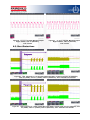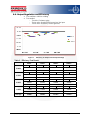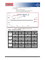
1
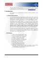
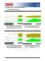
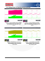
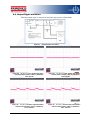
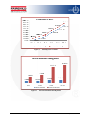
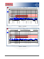
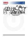
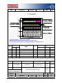
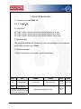
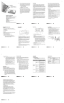
User Guide for FEBFSL206MRN_H428v1 Evaluation Board Integrated Controller FSL206MRN 5W Auxiliary Power Supply Featured Fairchild Product: FSL206MRN Direct questions or comments about this evaluation board to: “Worldwide Direct Support” Fairchild Semiconductor.com © 2011 Fairchild Semiconductor Corporation 1 FEBFSL206MRN_H428v1 • Rev. 1.0.1 Table of Contents 1. Introduction ............................................................................................................................... 3 1.1. General Description ........................................................................................................... 3 1.2. Features .............................................................................................................................. 3 2. Specifications ............................................................................................................................ 4 3. Photographs............................................................................................................................... 5 4. PCB Layout ............................................................................................................................... 6 5. Test Conditions ......................................................................................................................... 7 6. Performance of Evaluation Board ............................................................................................. 8 6.1. Startup Performance........................................................................................................... 8 6.2. Normal Operation .............................................................................................................. 9 6.3. Voltage Stress of Secondary Diode and Drain ................................................................ 10 6.4. Output Ripple and Noise.................................................................................................. 11 6.5. Short Protections .............................................................................................................. 12 6.6. Brown-In and Brownout Protection ................................................................................. 14 6.7. Temperature Measurement .............................................................................................. 14 6.8. Output Regulation and Efficiency ................................................................................... 15 6.9. Standby Power Consumption........................................................................................... 17 6.10. EMI Measurement ......................................................................................................... 19 7. Schematic ................................................................................................................................ 21 8. Transformer Specification ...................................................................................................... 22 9. Bill of Materials ...................................................................................................................... 26 10. Revision History ..................................................................................................................... 27 © 2011 Fairchild Semiconductor Corporation 2 FEBFSL206MRN_H428v1 • Rev. 1.0.1 This user guide supports the evaluation kit for the FSL206MR. It should be used in conjunction with the FSL206MR datasheet as well as Fairchild’s application notes and technical support team. Please visit Fairchild’s website at www.fairchildsemi.com. 1. Introduction This document is an engineering report describing measured performance of the FSL206MR. 1.1. General Description The FSL206MR integrated Pulse Width Modulator (PWM) and SenseFET is specifically designed for high-performance offline Switched-Mode Power Supplies (SMPS) with minimal external components. This device is an integrated high-voltage power regulator that combines an avalanche-rugged SenseFET with a current mode PWM control block. The integrated PWM controller includes: 7.8V regulator for no bias winding, UnderVoltage Lockout (UVLO) protection, Leading-Edge Blanking (LEB), an optimized gate turn-on/turn-off driver, EMI attenuator, Thermal Shutdown (TSD) protection, temperature-compensated precision current sources for loop compensation, and faultprotection circuitry. Protections include Overload Protection (OLP), Over-Voltage Protection (OVP), Abnormal Over-Current Protection (AOCP), and Line Under-Voltage Protection (LUVP). During startup, the FSL206MR offers good soft-start performance. The internal high-voltage startup switch and the Burst-Mode operation with very low operating current reduce the power loss in Standby Mode. As a result, it is possible to reach power loss of 150mW with no-bias winding and 25mW with bias winding at noload condition when the input voltage is 265VAC. 1.2. Features Internal Avalanche Rugged SenseFET: 650V Precision Fixed Operating Frequency: 67kHz No-Load <150mW at 265VAC without Bias Winding; <25mW with Bias Winding No Need for Auxiliary Bias Winding Frequency Modulation for Attenuating EMI Line Under-Voltage Protection (LUVP) Pulse-by-Pulse Current Limiting Low Under-Voltage Lockout (UVLO) Ultra-Low Operating Current: 300µA Built-In Soft-Start and Startup Circuit Protections: Overload Protection (OLP), Over-Voltage Protection (OVP), Thermal Shutdown (TSD), Abnormal Over-Current Protection (AOCP) Auto-Restart Mode for All Protections © 2011 Fairchild Semiconductor Corporation 3 FEBFSL206MRN_H428v1 • Rev. 1.0.1 VSTR 5 VCC 2 Internal VCC Good Bias Drain 6,7,8 7.8V HVREG 7V/8V VREF VCC VREF IFB IDELAY OSC VBURL/VBURH with EMI Attenuator S Q 4.5R PWM VFB 3 LS 4 Line Sense H if VLS>2V L if VLS<1.5V R Q R Gate Driver LEB 2V/1.5V VFB Soft-Start VSD RSENSE 1 GND LUVP VCC S OLP OVP VOVP VAOCP Q HVREG Off TSD R Q VCC Good TSD Figure 1. Internal Block Diagram 2. Specifications Table 1. Evaluation Board Specifications Fairchild Device FSL206MR Input Voltage Range 90 ~ 265 VAC Frequency 60Hz Maximum Output Power 5W Output Full-Load Condition 5V / 1A © 2011 Fairchild Semiconductor Corporation 4 FEBFSL206MRN_H428v1 • Rev. 1.0.1 3. Photographs Figure 2. Figure 3. © 2011 Fairchild Semiconductor Corporation Top View (Dimension 64 x 33[mm2]) Bottom View (Dimension 64 x 33[mm2]) 5 FEBFSL206MRN_H428v1 • Rev. 1.0.1 4. PCB Layout Figure 4. Figure 5. Figure 6. © 2011 Fairchild Semiconductor Corporation 6 Top Overlay Bottom Overlay Bottom Layer FEBFSL206MRN_H428v1 • Rev. 1.0.1 5. Test Conditions Evaluation Board # FEBFSL206MRN_H428 Evaluation Board Ver. 1.0 Test Date August 18, 2010 Test Equipment AC Source: 6800 Series Electronic Load: Chroma 63030 Oscilloscope: LeCroy 24Xs-A Power Meter: Yokogawa WT210 Test Items 1. Startup Performance 2. Normal Operation 3. Voltage Stress of Secondary Diode and Drain 4. Output Ripple and noise 5. Short Protections 6. Brown-in and Brownout Protection 7. Temperature Measurement 8. Output Regulation and Efficiency 9. Standby Power Consumption 10. Conducted EMI Measurement © 2011 Fairchild Semiconductor Corporation 7 FEBFSL206MRN_H428v1 • Rev. 1.0.1 6. Performance of Evaluation Board 6.1. Startup Performance Figure 7. Startup Time (AC Input to VCC UVLO HIGH) = 114ms, 90VAC and Full-Load Condition (CH1: VDS (200V/div), CH2: VFB (2V/div), CH3: VCC (10V/div), CH4: IDS (200mA/div), Time: 20ms/div Figure 8. Soft-Start, 90VAC and Full-Load Condition (CH1: VDS (200V/div), CH2: VFB (2V/div), CH3: VCC (10V/div), CH4: IDS (200mA/div), Time: 2ms/div Figure 9. Startup Time (AC Input to VCC UVLO HIGH) = 114ms, 265VAC and Full-Load Condition, (CH1: VDS (200V/div), CH2: VFB (2V/div), CH3: VCC (10V/div), CH4: IDS (200mA/div), Time: 20ms/div Figure 10. Soft-Start, 265VAC and Full-Load Condition, (CH1: VDS (200V/div), CH2: VFB (2V/div), CH3: VCC (10V/div), CH4: IDS (200mA/div), Time: 2ms/div © 2011 Fairchild Semiconductor Corporation 8 FEBFSL206MRN_H428v1 • Rev. 1.0.1 6.2. Normal Operation Figure 11. Full-Load Condition, 90VAC, (CH1: VDS (200V/div), CH2: VFB (2V/div), CH3: VCC (10V/div), CH4: IDS (500mA/div), Time: 10µs/div Figure 12. Full-Load Condition, 265VAC, (CH1: VDS (200V/div), CH2: VFB (2V/div), CH3: VCC (10V/div), CH4: IDS (500mA/div), Time: 10µs/div Figure 13. No-Load Condition, 90VAC, (CH1: VDS (200V/div), CH2: VFB (2V/div), CH3: VCC (10V/div), CH4: IDS (200mA/div), Time: 10ms/div Figure 14. No-Load Condition, 90VAC, (CH1: VDS (200V/div), CH2: VFB (2V/div), CH3: VCC (10V/div), CH4: IDS (200mA/div), Time: 50µs/div Figure 15. No-Load Condition, 265VAC, (CH1: VDS (200V/div), CH2: VFB (2V/div), CH3: VCC (10V/div), CH4: IDS (200mA/div), Time: 10ms/div Figure 16. No-Load Condition, 265VAC, (CH1: VDS (200V/div), CH2: VFB (2V/div), CH3: VCC (10V/div), CH4: IDS (200mA/div), Time: 50µs/div © 2011 Fairchild Semiconductor Corporation 9 FEBFSL206MRN_H428v1 • Rev. 1.0.1 6.3. Voltage Stress of Secondary Diode and Drain Figure 17. VDIODE.MAX at Startup=35.8V, 5V Output Diode with 265VAC & Full-Load Condition, CH2: VDIODE (10V/div), CH4: IDS (200mA/div), Time: 2ms/div Figure 18. VDIODE.MAX at Normal = 35.7V, 5V Output Diode with 265VAC & Full-Load Condition, CH2: VDIODE (10V/div), CH4: IDS (200mA/div), Time: 5µs/div Figure 19. VDS.MAX at Startup = 540V, Drain Voltage with 265VAC & Full-Load Condition, CH2: VDS (200V/div), CH4 :IDS (200mA/div), Time: 2ms/div © 2011 Fairchild Semiconductor Corporation Figure 20. VDS.MAX at Normal = 514V, Drain Voltage with 265VAC & Full-Load Condition, CH2: VDS (200V/div), CH4 :IDS (200mA/div), Time: 2ms/div & 5µs/div 10 FEBFSL206MRN_H428v1 • Rev. 1.0.1 6.4. Output Ripple and Noise Maximum output ripple is measured at maximum output power in Burst Mode. Figure 21. Recommended Test Setup Figure 22. VO_RIPPLE = 7.4mV, Output with 90VAC and Full-Load Condition, CH2: VO (20mV/div), Time: 5µs/div Figure 23. VO_RIPPLE = 7.8mV, Output with 265VAC and Full-Load Condition, CH2: VO (20mV/div), Time: 5µs/div Figure 24. VO_RIPPLE = 24.2mV, Output with 90VAC and No-Load Condition, CH2: VO (20mV/div), Time: 10ms/div Figure 25. VO_RIPPLE = 26.6mV, Output with 265VAC and No-Load Condition, CH2: VO (20mV/div), Time: 10ms/div © 2011 Fairchild Semiconductor Corporation 11 FEBFSL206MRN_H428v1 • Rev. 1.0.1 Figure 27. VO_RIPPLE = 64.8mV, Maximum Output Ripple at 265VAC, CH2: VO (20mV/div), Time: 1ms/div Figure 26. VO_RIPPLE = 47.8mV, Maximum Output Ripple at 90VAC, CH2: VO (20mV/div), Time: 1ms/div 6.5. Short Protections Figure 28. OLP Triggered: VFB = 5.10V, Output Short with 90VAC and Full-Load, CH1: VDS (200V/div), CH2: VFB (2V/div), CH3: VCC (10V/div), CH4: IDS (500mA/div), Time: 100ms/div and 10ms/div Figure 29. OLP Triggered: VFB = 5.08V, Output Short with 265VAC and Full-Load, CH1: VDS (200V/div), CH2: VFB (2V/div), CH3: VCC (10V/div), CH4: IDS (500mA/div), Time: 100ms/div and 10ms/div © 2011 Fairchild Semiconductor Corporation 12 FEBFSL206MRN_H428v1 • Rev. 1.0.1 Figure 30. OLP Triggered: VFB = 5.10V, Opto-Coupler Second Short (Open-Loop Test), with 90VAC and FullLoad, CH1: VDS (200V/div), CH2: VFB (2V/div), CH3: VCC (10V/div), CH4: IDS (500mA/div), Time: 500ms/div and 20ms/div Figure 31. OVP Triggered: VCC = 24.1V, Opto-Coupler Second Short (Open-Loop Test), with 265VAC and Full-Load, CH1: VDS (200V/div), CH2: VFB (2V/div), CH3: VCC (10V/div), CH4: IDS (500mA/div), Time: 500ms/div and 20ms/div © 2011 Fairchild Semiconductor Corporation 13 FEBFSL206MRN_H428v1 • Rev. 1.0.1 6.6. Brown-In and Brownout Protection Figure 1. Brown-In 65VAC and Full-Load Condition, CH1: VIN (50V/div), CH2: VFB (2V/div), CH3: VCC (10V/div), CH4: IDS (200mA/div), Time: 200ms/div Figure 2. Brown-out 58VAC and Full-Load Condition, CH1: VIN (50V/div), CH2: VFB (2V/div), CH3: VCC (10V/div), CH4: IDS (200mA/div), Time: 200ms/div 6.7. Temperature Measurement Table 2. Temperature Test Result Input Voltage Temperature 90VAC 110VAC 230VAC 265VAC IC 44.0°C 43.3°C 44.6°C 46.2°C DIODE 56.8°C 56.8°C 57.7°C 58.2°C Transformer 49.7°C 49.8°C 51.6°C 52.6°C 24.4°C 24.4°C 24.4°C 24.4°C Room Temperature © 2011 Fairchild Semiconductor Corporation 14 FEBFSL206MRN_H428v1 • Rev. 1.0.1 6.8. Output Regulation and Efficiency Test condition: with bias winding Test method: Test after 15 minutes aging Test in order: from high line input to low line input Test in order: from heavy load to light load - Figure 3. Efficiency vs Output Load and Input Voltage Table 3. Efficiency Test Result 90VAC 5.023V 5.00W 1.000A 5.022V 1.000A 6.908W 72.93% 74.25% 73.84% 72.70% 0.750A 5.025V 0.750A 5.024V 0.750A 5.024V 0.750A 5.119W 5.075W 5.209W 5.273W 73.64% 74.26% 72.34% 71.46% 0.500A 3.402W 73.88% Average 5.022V 6.801W 5.028V 1.25W 1.000A 265VAC 6.765W 5.027V 2.50W 5.023V 230VAC 6.887W 5.026V 3.75W 1.000A 110VAC 0.250A 5.027V 0.500A 3.416W 73.58% 5.028V 0.250A 5.026V 0.500A 3.566W 0.500A 3.676W 70.47% 5.028V 5.026V 68.36% 0.250A 5.028V 0.250A 1.754W 1.745W 1.822W 1.855W 71.66% 72.03% 68.99%T 67.76% 73.03% 73.53% 71.41% 70.07% © 2011 Fairchild Semiconductor Corporation 15 FEBFSL206MRN_H428v1 • Rev. 1.0.1 Test condition: Without bias winding (removing R12) Test method: - Test after 15 minutes aging - Test in order: from high line input to low line input - Test in order: from heavy load to light load Figure 4. Table 4. Efficiency Test Result 90VAC 5.023V 5.00W Average 1.000A 5.023V 1.000A 265VAC 5.023V 1.000A 6.901W 7.074W 7.213W 72.79% 71.01% 69.64% 0.750A 5.025V 0.750A 5.024V 0.750A 5.024V 0.750A 5.216W 5.186W 5.396W 5.489W 72.25% 72.67% 69.83% 68.65% 0.500A 5.026V 0.500A 5.025V 0.500A 5.025V 0.500A 3.488W 3.522W 3.788W 3.909W 72.05% 71.35% 66.33% 64.27% 5.028V 1.25W 5.023V 230VAC 71.75% 5.026V 2.50W 1.000A 110VAC 7.001W 5.025V 3.75W Efficiency vs Output Load and Input Voltage 0.250A 5.028V 0.250A 5.028V 0.250A 5.028V 0.250A 1.817W 1.826W 1.962W 2.002W 69.18% 68.84% 64.07% 62.79% 71.31% 71.41% 67.81% 66.34% © 2011 Fairchild Semiconductor Corporation 16 FEBFSL206MRN_H428v1 • Rev. 1.0.1 6.9. Standby Power Consumption Table 5. With Bias Winding Condition 90VAC 110VAC 230VAC 265VAC No Load 12mW 13mW 19mW 24mW 10mA 94mW 94mW 102mW 107mW 20mA 172mW 169mW 182mW 191mW 50mA 386mW 384mW 409mW 420mW 70mA 520mW 523mW 552mW 569mW 100mA 729mW 729mW 772mW 786mW Table 6. Without Bias Winding Condition 90VAC 110VAC 230VAC 265VAC No Load 46mW 56mW 114mW 134mW 10mA 128mW 135mW 202mW 224mW 20mA 207mW 215mW 283mW 306mW 50mA 428mW 436mW 513mW 540mW 70mA 566mW 576mW 664mW 687mW 100mA 775mW 787mW 881mW 908mW © 2011 Fairchild Semiconductor Corporation 17 FEBFSL206MRN_H428v1 • Rev. 1.0.1 Figure 5. Figure 6. © 2011 Fairchild Semiconductor Corporation Standby Power at 230VAC No-Load Condition Standby Power 18 FEBFSL206MRN_H428v1 • Rev. 1.0.1 6.10. EMI Measurement Att dBµV 1 100 10 RBW MT PREAMP dB 9 kHz 1 ms OFF MHz Marker 1 [T1 ] 55.22 dBµV 150.000000000 kHz 10 MHz 90 1 PK MAXH 80 2 AV MAXH TDF 70 EN55022Q 1 60 PRN EN55022A 50 6DB 40 30 20 10 0 150 Date: kHz 11.NOV.2010 30 15:28:09 Figure 7. Att dBµV 1 100 MHz 10 L1 at 230VAC RBW MT PREAMP dB 9 kHz 20 ms OFF MHz Marker [T1 ] 31.66 dBµV 150.000000000 kHz 10 1 MHz 90 1 PK MAXH 80 2 AV MAXH TDF 70 EN55022Q 60 PRN EN55022A 50 6DB 40 1 30 20 10 0 150 Date: kHz 11.NOV.2010 30 15:26:29 Figure 8. © 2011 Fairchild Semiconductor Corporation MHz 19 N at 230VAC FEBFSL206MRN_H428v1 • Rev. 1.0.1 Att dBµV 1 100 10 RBW MT PREAMP dB 9 kHz 1 ms OFF MHz Marker 1 [T1 ] 32.81 dBµV 150.000000000 kHz 10 MHz 90 1 PK MAXH 80 2 AV MAXH TDF 70 EN55022Q 60 PRN EN55022A 50 6DB 40 1 30 20 10 0 150 Date: kHz 11.NOV.2010 30 15:33:27 Figure 9. Att dBµV 1 100 MHz 10 L1 at 110VAC RBW MT PREAMP dB 9 kHz 1 ms OFF MHz Marker 1 [T1 ] 33.22 dBµV 150.000000000 kHz 10 MHz 90 1 PK MAXH 80 2 AV MAXH TDF 70 EN55022Q 60 PRN EN55022A 50 6DB 40 1 30 20 10 0 150 Date: kHz 11.NOV.2010 30 15:30:40 Figure 10. © 2011 Fairchild Semiconductor Corporation MHz 20 N at 110VAC FEBFSL206MRN_H428v1 • Rev. 1.0.1 7. Schematic Figure 11. © 2011 Fairchild Semiconductor Corporation 21 Schematic FEBFSL206MRN_H428v1 • Rev. 1.0.1 8. Transformer Specification Customer - DATE 08/12/2010 Version A P/N: TRN-0299 Page 1/4 1.DIMENSION 1. Pin3.6.7.removed 2. wire shield: 2UEW 0.15*1, pin 1 3. Add 14mm insulation tape *4 turns to fix core and bobbin. UNIT m/m DRAWN CHECK TITLE TRANS TEL (02)29450588 Ci wun Chen Guo long Huang IDENT N O. TRN-0299 FAX (02)29447647 No.26-1, Lane 128, Sec. 2, Singnan Rd., Jhonghe City, Taipei County 235, Taiwan (R.O.C.) Customer © 2011 Fairchild Semiconductor Corporation SEN HUEI INDUSTRIAL CO.,LTD. - DWG N O. P/N: 22 TRN-0299 FEBFSL206MRN_H428v1 • Rev. 1.0.1 DATE 08/12/2010 Version A Page 2/4 2. Schematic: 1. 2. 3. When W3 is winding, it must winds one layers. W4 layer wire size can be smaller if there is no area for 20 turns. if there is extra area when W4 is winding, please fill the area with barrier tape. NO TERMINAL WIRE TS INSULATION S F TS W1 2 1 2UEW 0.2*1 140 2 W2 1 - 2UEW 0.15*1 45 3 W3 8 10 TEX-E 0.55*1 9 3 W4 5 4 2UEW 0.25*1 20 3 CORE ROUNDING TAPE BARRIER Pri S 2mm 3 UNIT m/m DRAWN CHECK TITLE TRANS TEL (02)29450588 Ci wun Chen Guo long Huang IDENT N O. TRN-0299 FAX (02)29447647 No.26-1, Lane 128, Sec. 2, Singnan Rd., Jhonghe City, Taipei County 235, Taiwan (R.O.C.) Customer DATE SEN HUEI INDUSTRIAL CO.,LTD. 08/12/2010 © 2011 Fairchild Semiconductor Corporation Version 23 A DWG N O. P/N: TRN-0299 Page 3/4 FEBFSL206MRN_H428v1 • Rev. 1.0.1 3. Electrical Specification 3.1 inductance test: at 67KHz ,1V P(2-1): 1.4mH ±7% 3.2 Hi-pot test: AC 3.0KV / 60Hz / 5mA hi-pot for one minute between pri to sec. AC 1.5KV / 60Hz / 5mA hi-pot for one minute between pri to core. AC 1.5KV / 60Hz / 5mA hi-pot for one minute between sec to core. 3.3 insulation test: The insulation resistance is between pri to sec and windings to core measured by DC 500V, must be over 100MΩ. 3.4 Terminal strength: 1.0Kg on terminals for 30 seconds, test the breakdown. UNIT m/m DRAWN CHECK TITLE TRANS TEL (02)29450588 Ci wun Chen Guo long Huang IDENT N O. TRN-0299 FAX (02)29447647 No.26-1, Lane 128, Sec. 2, Singnan Rd., Jhonghe City, Taipei County 235, Taiwan (R.O.C.) © 2011 Fairchild Semiconductor Corporation SEN HUEI INDUSTRIAL CO.,LTD. 24 DWG N O. FEBFSL206MRN_H428v1 • Rev. 1.0.1 Customer DATE 08/12/2010 Version A P/N: TRN-0299 Page 4/4 4. Materials List COMPONENT MAT’L MANUFACTURE FILE NO. 1.Bobbin Phenolic 94V-0,T373J,150°C EE-16.(TF-1613) Chang Chun plastics co. ltd. E59481(S) 2.Core PC-40,BH2,2E6 3C85,NC-2H, Ferrite core EE-16 TDK,Tokin.Tomita.Philip.Nicera. UEWE 130°C ℃ Tai-I electric wire &cable Co Ltd. E85640 (S) UEW-2 130°C Jung Shing wire Co Ltd. E174837 UEW-B 130°C Chuen Yih wire Co Ltd. E154709(S) TEX-E 105°C / 120°C Furukawa electric Co Ltd. E206440 BC-346A 180°C John C Dolph Co Ltd. E51047 (M) 468-2FC 130°C Ripley resin engineering co inc. E81777 (N) 31CT 130°C Nitto denk CORP. E34833 (M) Polyester 3M #1350(b) 130°C Minnesota mining &MFG Co Ltd. CTI material groupⅡ E17385 (N) 6.Tube Teflon tube TFL 150V,200°C Great holding industrial Co Ltd. E156256 (S) 7.Terminals Tin coatedCopper wire Will for special wire CORP. 8.Shield Copper foil Hitachi cable lid. (copper foil: 0.025t x7mm) 3.Wire 4.Varnish 5.Tape t=0.064mm UNIT m/m DRAWN CHECK TITLE TRANS TEL (02)29450588 Ci wun Chen Guo long Huang IDENT N O. TRN-0299 FAX (02)29447647 DWG N O. I1613 No.26-1, Lane 128, Sec. 2, Singnan Rd., Jhonghe City, Taipei County 235, Taiwan (R.O.C.) © 2011 Fairchild Semiconductor Corporation SEN HUEI INDUSTRIAL CO.,LTD. 25 FEBFSL206MRN_H428v1 • Rev. 1.0.1 9. Bill of Materials Component Qty. Part No. Manufacturer Reference Chip Resistor 0805 0Ω ±5% 1 R12 Chip Resistor 0805 47Ω ±5% 2 R20, R21 Chip Resistor 0805 510Ω ±5% 1 R25 Chip Resistor 0805 20KΩ ±1% 2 R31, R32 Chip Resistor 0805 453KΩ ±1% 1 R18 Chip Resistor 1206 3K3Ω ±5% 1 R28 Chip Resistor 1206 30KΩ ±1% 1 R30 Chip Resistor 1206 120KΩ ±1% 2 R11, R11A Chip Resistor 1206 10MΩ ±1% 2 R1, R3 Ceramic Capacitor 472P 1KV +80/-20% 1 C19 0805 MLCC X7R ±10% 102P 100V 1 C21 0805 MLCC X7R ±10% 104P 50V 2 C2, C14 0805 MLCC X7R ±10% 223P 50V 1 C3 1206 MLCC X7R ±10% 104P 50V 1 C24 Electrolytic Capacitor 10µH 400V 105°C 2 KM SAMXON C1, C1A Electrolytic Capacitor 22µH 50V 105°C 1 LHK JACKCON C20 Electrolytic Capacitor 680µH 10V 105°C 2 GF SAMXON C22, C25 Y1 Capacitor 102P 250V ±20% 1 Inductor DR6X8 5µH 1 TRN0216 C23 SEN HUEI L4 Fixed Inductor 2.2μH ±10% 1 EC36-2R2K SYNTON L1 Fixed Inductor 330μH ±10% 1 EC36-331K SYNTON L2 Transformer EE-16-H 1.4mH 1 TRN0299 SEN HUEI TX1 Diode 1A/1000V DO-41 1 1N4007 TAPING D11 CP D12 Fast Diode 1A/1000V DO-41 1 FR107 Diode DO-210AD 5A/40V 1 SB540 SMD Bridge 0.5A/600V SOIC-4 1 MB6S D2 Fairchild Semiconductor BD1 REGULATOR KA431L ±0.5% 1 Fairchild Semiconductor U6 IC FOD817B SMDIP-B 1 Fairchild Semiconductor U3 IC SMPS Power Switch 1 FSL206MRN Fairchild Semiconductor U1 FUSE GLASS 250V2A Fast Blow 1 3.6*10mm SLEEK F1 Varistor 7ψ470V 1 PCB PLM0049 REV1 1 © 2011 Fairchild Semiconductor Corporation VZ1 26 FEBFSL206MRN_H428v1 • Rev. 1.0.1 10. Revision History Rev. Date 1.0.0 1.0.1 Description Change User Guide EVB number from FEB428_001 to FEBFSL206MRN_H428v1 3/6/12 Formatting & Editing pass by Tech Docs prior to posting WARNING AND DISCLAIMER Replace components on the Evaluation Board only with those parts shown on the parts list (or Bill of Materials) in the Users’ Guide. Contact an authorized Fairchild representative with any questions. This board is intended to be used by certified professionals, in a lab environment, following proper safety procedures. Use at your own risk. The Evaluation board (or kit) is for demonstration purposes only and neither the Board nor this User’s Guide constitute a sales contract or create any kind of warranty, whether express or implied, as to the applications or products involved. Fairchild warrantees that its products meet Fairchild’s published specifications, but does not guarantee that its products work in any specific application. Fairchild reserves the right to make changes without notice to any products described herein to improve reliability, function, or design. Either the applicable sales contract signed by Fairchild and Buyer or, if no contract exists, Fairchild’s standard Terms and Conditions on the back of Fairchild invoices, govern the terms of sale of the products described herein. DISCLAIMER FAIRCHILD SEMICONDUCTOR RESERVES THE RIGHT TO MAKE CHANGES WITHOUT FURTHER NOTICE TO ANY PRODUCTS HEREIN TO IMPROVE RELIABILITY, FUNCTION, OR DESIGN. FAIRCHILD DOES NOT ASSUME ANY LIABILITY ARISING OUT OF THE APPLICATION OR USE OF ANY PRODUCT OR CIRCUIT DESCRIBED HEREIN; NEITHER DOES IT CONVEY ANY LICENSE UNDER ITS PATENT RIGHTS, NOR THE RIGHTS OF OTHERS. LIFE SUPPORT POLICY FAIRCHILD’S PRODUCTS ARE NOT AUTHORIZED FOR USE AS CRITICAL COMPONENTS IN LIFE SUPPORT DEVICES OR SYSTEMS WITHOUT THE EXPRESS WRITTEN APPROVAL OF THE PRESIDENT OF FAIRCHILD SEMICONDUCTOR CORPORATION. As used Life support devices or systems are devices or systems which, (a) are intended for surgical implant into the body, or (b) support or sustain life, or (c) whose failure to perform when properly used in accordance with instructions for use provided in the labeling, can be reasonably expected to result in significant injury to the user. herein:1. 2. A critical component is any component of a life support device or system whose failure to perform can be reasonably expected to cause the failure of the life support device or system, or to affect its safety or effectiveness. ANTI-COUNTERFEITING POLICY Fairchild Semiconductor Corporation's Anti-Counterfeiting Policy. Fairchild's Anti-Counterfeiting Policy is also stated on our external website, www.fairchildsemi.com, under Sales Support. Counterfeiting of semiconductor parts is a growing problem in the industry. All manufacturers of semiconductor products are experiencing counterfeiting of their parts. Customers who inadvertently purchase counterfeit parts experience many problems such as loss of brand reputation, substandard performance, failed applications, and increased cost of production and manufacturing delays. Fairchild is taking strong measures to protect ourselves and our customers from the proliferation of counterfeit parts. Fairchild strongly encourages customers to purchase Fairchild parts either directly from Fairchild or from Authorized Fairchild Distributors who are listed by country on our web page cited above. Products customers buy either from Fairchild directly or from Authorized Fairchild Distributors are genuine parts, have full traceability, meet Fairchild's quality standards for handling and storage and provide access to Fairchild's full range of up-to-date technical and product information. Fairchild and our Authorized Distributors will stand behind all warranties and will appropriately address any warranty issues that may arise. Fairchild will not provide any warranty coverage or other assistance for parts bought from Unauthorized Sources. Fairchild is committed to combat this global problem and encourage our customers to do their part in stopping this practice by buying direct or from authorized distributors. EXPORT COMPLIANCE STATEMENT These commodities, technology, or software were exported from the United States in accordance with the Export Administration Regulations for the ultimate destination listed on the commercial invoice. Diversion contrary to U.S. law is prohibited. U.S. origin products and products made with U.S. origin technology are subject to U.S Re-export laws. In the event of re-export, the user will be responsible to ensure the appropriate U.S. export regulations are followed. © 2011 Fairchild Semiconductor Corporation 27 FEBFSL206MRN_H428v1 • Rev. 1.0.1