1
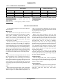
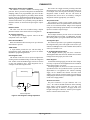
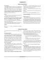
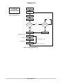
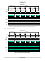
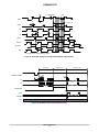
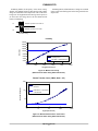
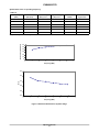
EVBUM2257/D
Full Frame Image Sensors
Evaluation Board
User's Manual
http://onsemi.com
Introduction
EVAL BOARD USER’S MANUAL
The Full Frame Evaluation Board provides a powerful
platform to quickly and easily evaluate a number of
ON Semiconductor Full Frame Image Sensors in
a prototype imaging system. The Evaluation Kit also serves
as a useful reference design that will save considerable time
and cost in the development of a product prototype.
The programmable logic architecture, bias supplies, clock
drivers and analog signal processing chain can be readily
used, with application specific modifications, in a camera
production design.
The Evaluation Board is designed to be flexible, and has
the ability to operate many different Full Frame image
sensors at different operating frequencies. Consult
ON Semiconductor to obtain information for optimizing the
reference design to operate a specific image sensor at
a specific operating frequency.
Overview
The Full Frame Evaluation Board serves as a complete,
self-contained, CCD image acquisition sub-system.
The user simply applies power, and an IMAGE_AQUIRE
TTL pulse to begin capturing digital images. Differential
TTL frame grabber sync pulses (Frame, Pixel and Line rate)
are provided to facilitate easy connection to a frame grabber.
In the still capture mode, application of the
IMAGE_ACQUIRE signal results in flushing of the CCD,
then integration, then clocking out of a full frame of image
data. In free-run mode, an acquisition signal is not needed;
the board is free running and continuous frames of 12 bit
information stream out.
12 Bit Output
Image_Acquire
CCD Reference
Evaluation Board
Figure 1. Block Diagram (Overview)
SPECIFICATIONS
Inputs
Maximum Data Rate:
6 MHz
Resolution:
12 Bits
Frame Rate:
Depends on Data Rate, CCD Array Size,
and Integration Time
Serial Clock:
PGA Gain Range:
PGA Gain Resolution:
Offset Range:
Offset Resolution:
Temperature Range Board:
Temperature Range CCD:
Outputs
D[11..0]:
Frame Grabber Syncs:
Integration Sync:
© Semiconductor Components Industries, LLC, 2014
September, 2014 − Rev. 2
Differential TTL
Differential TTL
TTL
1
10 MHz Maximum
1X to 6X
256 Steps
−100 mV to +100 mV
256 Steps
0 – 70°C
−50 to +70°C Typical
Publication Order Number:
EVBUM2257/D
EVBUM2257/D
Table 1. POWER SUPPLY REQUIREMENTS
Typical Current
Switching Power Supply
Power Supplies
Supply
Minimum
Nominal
Maximum
Disabled
Enabled
+5 V
+4.9 V
+5 V
+5.1 V
1000 mA
1500 mA
+18 V
+17 V
+18 V
+20 V
120 mA
−
−18 V
−20 V
−18 V
−13 V
100 mA
−
Electrons per A/D count − 29.2 @ 5 MHz, 2.5X Gain setting
(Assuming on-chip CCD amplifier gain CCD of
10 mV/electron).
RMS Dark Noise − 1.9 LSB typical @ 5 MHz, 2.5X Gain
setting.
System Noise Floor − 56 electrons @ 5 MHz, 2.5X Gain
setting (Assuming on-chip CCD amplifier gain of
10 mV/electron).
ARCHITECTURE OVERVIEW
a three wire serial interface. Additionally, if the user chooses
to adjust the AD9816’s register settings, the PLD2 controls
the programming of these registers.
A complete Block Diagram of the Evaluation Board is
shown in Figure 3.
Master Clock
The Master Clock runs at eight times the Pixel clock
frequency. The maximum pixel clock frequency is 6 MHz,
which yields a maximum system clock frequency of
48 MHz. For slower Pixel clock frequencies, decrease the
master clock frequency. The Default setting of the
evaluation board is a 40 MHz system clock, with a pixel
clock frequency of 5 MHz.
The KAF−4301 is an exception to this. It provides pixel
frequencies of 2.5 MHz and 1.25 MHz by dividing the
40 MHz master clock by 16 and 32. The pixel frequency is
selected using SW2. This is an 8-position switch that usually
selects a CCD binning mode (See section Binning Modes).
The KAF−4301 timing program does not support binning at
this time and, instead, uses this switch to select the pixel rate
(See Table 8). The pixel rate is 1.25 MHz when SW2 is set
to position 0 and 2.5 MHz when set in any other position.
CCD Clock Drivers
Elantec clock drivers, designed to drive the large
capacitance loads presented by the clock gates of the CCD,
are used to generate the horizontal and vertical clocks.
The Elantec drivers accept TTL inputs, and level shift to the
required peak-to-peak voltage swing of the CCD clocks.
The peak-to-peak swing of the clocks is adjustable.
The outputs of the drivers are AC coupled, providing
adjustable offset of the clocks from the negative rail to the
positive rail. Using a separate IC for each vertical clock (V1,
V2), a maximum 4 amp output drive current per vertical
clock channel is available. A single IC is used to drive H1,
and H2, giving a maximum 2 A output drive current per
Horizontal clock channel.
The reset clock driver utilizes two fast switching
transistors, designed for a fast switching input signal with
a narrow pulse width. The peak-to-peak voltage swing and
the offset voltage are adjustable.
PLD1
PLD1 contains the Clocking State Machine that controls
the operational flow of the evaluation board (Figure 4).
PLD1 generates the CCD clock timing, A/D converter
timing and frame grabber sync signals. The PLD1 controls
the image line and frame length [dependent upon the CCD
switch settings], as well as the horizontal and vertical CCD
clock timing [dependent upon the binning mode BIN switch
settings.]
CCD Bias Voltages
CCD bias voltages (VRD, VOG, VLG) are supplied by
filtered outputs of adjustable potentiometers. Fixed CCD
bias voltages (LOD, VSS, GUARD) are supplied by filtered
outputs of voltage dividers.
CCD Image Sensor
This evaluation board supports the following Full Frame
CCD image sensors: KAF−0261, KAF−0402, KAF−1001,
KAF−1603, KAF−3200, KAF−6303, KAF−16801,
and KAF−4301.
PLD2
PLD2 controls the integration timing, which is dependent
upon the INT switch settings. PLD2 also programs the
AD9816’s registers to a default condition upon power up via
http://onsemi.com
2
EVBUM2257/D
A/D Converter Analog Devices AD9816
The circuit is set to toggle at 100 Hz, providing a fixed unit
integration time of 10 ms. The actual integration time is set
to a multiple of the unit integration time using an internal
integration counter in PLD2. The user can choose an
integration time from 10 ms to 10 seconds by setting the
integration switches appropriately (See Table 9).
The AD9816 is a 12 bit, 6 MSPS CCD analog signal
processor. The IC provides an integrated correlated double
sampling (CDS), 8 bit programmable gain, and 8 bit DC
offset adjust. Timing signals are provided by PLD1. Default
register values are downloaded from PLD2 upon power up.
Alternate programming of its registers can be achieved via
external serial interface or by manually setting the address
and data switches on the board and pressing the capture
button.
J6 Input Connector
This connector is used to input control signals to the
evaluation board. This is an optional feature; all control lines
can be set via on-board switches. Images can be acquired
using the on-board image capture button. No external digital
inputs are needed to acquire images.
Emitter Follower
The video out of the CCD is buffered using a bipolar
junction transistor in the emitter follower configuration.
J4 Output Connector
AC Coupling Capacitor
A 1200 pF input coupling capacitor removes the DC
component of the video signal.
The J4 output connector provides 12 bits of video data in
RS422 differential TTL format. J4, additionally, provides
three frame grabber sync signals in differential TTL format.
Power On Clear/Reset
J7 Integration Sync
Resets and initializes the board on power up or when the
Reset button in pressed.
This connector provides a sync signal that is high during
the integration time period. The signal can be used to sync
a shutter or LED light source to the evaluation board, and can
source up to 80 mA at 5 V.
JTAG Header
A 10-pin header provides the user with the ability to
reprogram the Altera 7000S PLDs in system via Altera’s
ByteBlaster programming hardware.
J1, J2 Imager Board Connectors
CCD Daughter Boards plug into these connectors.
The daughter boards route the clock and bias traces from the
timing board to the proper pins of the CCD.
Unit Integration Time
The amount of time the CCD is exposed to light before
clocking out the accumulated charge is called the integration
time. An RC circuit and Schmitt trigger inverter are used to
set the unit integration time. Total integration time is
a multiple of the unit integration time.
Altera Timing
Power Supplies
An onboard switching supply provides all of the voltages
necessary to operate the CCD Digital Reference Evaluation
Board, from a single +5 V source.
Switching supplies can, however, be a source of low-level
asynchronous noise. If asynchronous noise is present and
objectionable in an application, the internal switching
supply can be disabled and external low-noise linear
supplies can be used to power the board. The procedure for
configuring the board to accept external supplies is detailed
Under Power Supply Modes
Integrate
J5 Power Connector
RPOT
The power connector is a 5-pin connector with +5 V,
+18 V, −18 V and two AGND connections. If the switching
power supply is used to generate the +15 V and −10 V
supplies, then only an external +5 V supply needs to be
brought in through J5. Otherwise, all three power supplies
must be connected to the board via J5.
C1
Set Unit Integration
Figure 2. Unit Integration Timing Adjustment
http://onsemi.com
3
EVBUM2257/D
BOARD REQUIREMENTS
Power Supply
INTEGRATE − A signal provided to allow the user to
synchronize the strobing of LED illuminators or opening of
a shutter, during the integration period.
FRAME (±)* − Differential TTL Frame grabber vertical
sync signal.
LINE (±)* − Differential TTL Frame grabber horizontal
sync signal.
PIX (±)* − Differential TTL Frame grabber pixel sync
The board requires only a single +5 V, 1.5 Amp or greater
power supply to operate. An on board switching power
supply generates the necessary +15 V, 120 mA and –10 V,
120 mA power supplies from the 5 V input. Although
extensive filtering is done on board, the power supplied to
the board must be quiet and stable in order to achieve the best
possible performance. (See Power Supply Modes, for an
alternative way to power the board.)
*These sync signals can be modified if necessary to accommodate
different Frame Grabbers.
Inputs
In the Free-Run mode, the evaluation board requires no
input signals to begin acquiring images.
In Still mode, the evaluation board will acquire a single
image on the falling edge of the Image_Acquire control line.
This can be accomplished via the push button (S4) or,
remotely, by utilizing the Image_Acquire control line.
See Section Still/Free-Run Modes for more information
on Still and Free-Run modes.
See Sections Line/Switches Modes and AD_IN/EX
Modes for information on additional optional inputs.
JTAG Programming
Altera 7000S In System Programmable (ISP) PLD’s are
used on this board. A ten-pin header (J8) is provided to allow
for the programming of these PLD’s. Since these parts are
re-programmable, custom digital logic can be implemented
for timing and mode adjustments or additions. Any custom
implementation can be made quickly and easily to via the
JTAG programming interface provided by this connector.
Outputs
D[11..0] (±) − 12 bits of Differential TTL Digital
information
CONFIGURATION MODES
accomplished by either pressing the on-board acquire button
(S4) or, remotely, bringing the Image_Acquire line low and
then back high. The detection of the falling edge of this
signal starts the image acquisition process.
The still mode acquisition process is as follows:
1. The CCD is flushed of all accumulated charge.
2. The CCD is exposed to light during the integration
time.
3. The image is clocked out of the CCD. The system
then waits for the next Image_Acquire signal.
The following modes of operation are available to the
user:
Line/Switches Modes
The Line/Switches Jumper (SW5) selects whether some
of the board settings will be controlled externally through
the J6 connector (Line), or via the on-board switches
(Switches). If this switch is set to Line, then the integration
time and the binning mode must be set remotely via digital
I/O. The still/free-run mode switch (SW3, 3-position
switch) can also be set externally when the Line mode is
selected. Set SW3 to the middle position if it is desired to
control this line externally.
In the Free-Run mode, the system will continuously
capture images and clock them out. No flushing is done, as
the clocking out of the previous image serves this same
purpose.
See Figure 4 for the Clocking State Machine Diagram.
Still/Free-Run Modes
The “Still/Free-Run” switch (SW3) is a three-position
switch that selects whether the board will operate in the still
mode, or a free-running mode.
If SW3 is placed in the middle position (“LINE”),
the image capture mode is determined by the voltage on the
STILL/FREE-RUN pin on the input connector (J6−27).
Setting this line LOW selects the free-run mode, and setting
it HIGH selects the still mode.
In still mode, the Image_Acquire control line must be
strobed in order to acquire a single image. This is
AD_IN/EX Modes
The board comes with an Analog Devices AD9816 12 bit
A/D converter on board. This A/D has several features, such
as multiple configurations, programmable gain, and offset
registers which require initialization and/or programming
on power up. The programming of these registers is done via
a three wire serial interface.
http://onsemi.com
4
EVBUM2257/D
EXT
Frame Grabber Diagnostic Modes
A three wire serial interface is provided on the J6
connector of the board, and the AD9816 registers can be
controlled remotely via these when the A/D_IN/EX Jumper
(SW4) is set to EXT. See Figure 5 for AD9816 serial timing
diagrams and information.
When set to ENABLE, the Sync_Test_Enable switch
(SW12) tri-states the 12-bit output bus out of the A/D
converter, and enables the output of either the pixel number
or the line number onto the output bus, depending on how the
Sync_Test_pix/line Jumper is set (SW11). This provides
a diagnostic test to make certain the Frame Grabber is
synchronized correctly with the board.
The line counter in PLD1 is a binary up-counter, therefore
the line count that is output to the output bus will increment
sequentially (0, 1, 2, 3, 4, 5...) until the last line in the frame.
The pixel counter in PLD1 is a gray code up counter,
therefore the pixel count that is output to the output bus will
increment in gray code transition counts (0, 1, 3, 2, 6, 7, 5,
4...) until the last pixel in the line.
INT
If it is not desired to control the programming of the A/D’s
registers remotely, set Jumper SW4 to INT. PLD2 contains
a state machine that serially loads in the following default
values to these registers upon power up.
A/D Default Register Settings:
No. of channels:
1
Mode:
CDS Mode
Input Span:
3V
Channel Selected: Green
Red PGA Gain*:
1
Green PGA Gain: 1
Blue PGA Gain*: 1
Red Offset*:
0 mv
Green Offset:
0 mv
Blue Offset*:
0 mv
Power Supply Modes
Power can be supplied to the board in one of two ways:
Switching Power Supply
The board comes supplied with a 500 kHz switching
power supply (Linear Technologies LT1372). If it is desired
to utilize the on-board switching supply, the board should be
configured as follows:
1. Connect a 5 V, 1.5 A or greater lab supply to the J5
power connector.
2. Install Jumper 6 and Jumper 4.
3. Remove Jumper 7 and Jumper 5.
4. Set Jumper 1 to the ON position.
*Although the Red and Blue channels are not used, these registers
are still initialized to these default settings.
Adjustments
Adjustments can be made to the A/D registers during
operation of the board by utilizing the DATA dipswitch
(SW10), the ADDRESS switch (SW9), and the
Image_Acquire control line. After setting SW9 to the
desired Address, and SW10 to the desired Data, send an
Image_Acquire signal either by pressing the
Image_Acquire button or remotely via the J6 connector
control line. This will load the new value into PLD2 and
a state machine inside the PLD will then serial load the new
data into the A/D’s register. This is true whether or not the
board is running in Still or Free Run Mode. (See Figure 5 for
more information on the AD9816 registers.)
External Supply Operation
To disable the on-board switching supply and operate
using external supplies:
1. Remove Jumpers 4 and 6;
2. Install Jumpers 5 and 7;
3. Move Jumper 1 to the “OFF” position to disable
the switching power supply;
4. Connect +18 V, −18 V, and +5 V to power input
connector J5.
Functionality
The switching supply generates +15 V and –10 V supply
“islands”. The same is true for the +15 V and –10 V
regulators on the board. Jumpers 4 and 6 connect the
switcher supplies to the +15 V, −10 V power plane.
Jumpers 5 and 7 connect the regulated outputs to the +15 V,
−10 V power plane. Jumper 1 either enables or disables the
LT1372 Switcher.
CCD Modes
The CCD Select switch (SW1) setting determines the line
and frame length timing.
This switch is pre-set at ON Semiconductor. (See Table 5)
Binning Modes
The BIN Select switch (SW2) setting determines the
Binning mode operation. (Table 6)
Integration Modes
The INT Select switches (SW6, SW7) settings determine
the Integration Time.
SW6 is the Coarse Adjust. SW7 is the Fine Adjust.
(Table 9)
http://onsemi.com
5
EVBUM2257/D
CCD IMAGER BOARDS
LOD/GUARD:
VSUB:
VSS:
Each CCD has an imager board. The imager boards route
the bias voltage traces from the timing board through
connectors J1 and J2 to the appropriate pins on the device.
The imager boards contain the Horizontal and Reset clock
driver ICs as well as the emitter-follower circuit that buffers
and drives the video signal down to the timing board.
+10 V
0V
0 to +2.1 V
NOTE: The VSS bias voltage is set by the inclusion of up to three
series diodes on the imager board. Therefore 0 V is achieved
by shorting across all three diode positions. This bias is
preset at the factory depending on the appropriate CCD
specification.
Adjustments
Fixed Bias Voltages
Variable Bias Voltages (see Table 2)
Fixed Voltages:
VDD:
+15 V
Table 2. VARIABLE BIAS VOLTAGES
Variable Voltage (Note 1)
Function
Adjustment Potentiometer
VOG
R12
VRD
R11
VLG
R13
V_PP
(Vertical clk Peak to Peak Swing )
R17
VCLK
(Vertical clk Level Adjust)
R67
H_PP
(Horizontal clk Peak to Peak Swing )
R64 (Imager Board)
HCLK
(Horizontal clk Level Adjust)
R14 (Imager Board)
R_PP
(Reset clk Peak to Peak Swing)
R18 (Imager Board)
RCLK
(Reset clk Level Adjust)
R27 (Imager Board)
1. These voltages are optimized for the particular KAF Series image sensor being used and are fixed at the factory according to the image
sensor specification. Adjustments should not be made to them without consulting ON Semiconductor.
Output Selection for Sensors with Two Outputs
To select the low gain output, Vout1:
Set J3 to the VID1 position:
The KAF−1001, KAF−0261, and KAF−4301 sensors
have two video outputs. The outputs have different gain and
one of them is selected depending on the application.
The imager daughter boards for these sensors have two
jumpers that must be set correctly to enable the desired
output.
To select the high gain output, Vout2:
Set J3 to the VID2 position:
J4
Bias
J3
Set the two jumpers on J4 as follows:
NOTE:
J4
H21
H2
H22
Bias
http://onsemi.com
6
H21
Bias
2
Bias
2
Set the two jumpers on J4 as follows:
H2
VID
VID
J3
H22
1
1
The schematic for the KAF−1001 imager daughter board
contains an error. The library element for the imager
indicates that pin 5 is Vout1 and pin 12 is Vout2. These are
incorrect and are reversed in that part of the schematic.
However, the labeling on the imager board is correct. Only
the pin labeling on the schematic is incorrect.
EVBUM2257/D
TIMING
Fixed Timing
SAMPLE (Binning Modes)
A/D Clock (Binning Modes)
See Timing Diagram 1 − Figure 6
See Timing Diagram 3 − Figure 14
H1, H2
Variable Timing
V1, V2 (Binning Modes)
RESET (Binning Modes)
CLAMP (Binning Modes)
NOTE:
Not available with the KAF−16801 and KAF−4301 image
sensors.
OTHER PARAMETERS
Fixed Parameters
Frame Length: (Depends on CCD mode)
Vwidth: (Depends on pixel frequency, 64 pixel counts wide)
Unit Integration: The integration clock frequency is set by
a RC circuit of R6 and C6 and is adjusted to 100 Hz at the
factory, creating a unit integration time of 10 ms. By
adjusting R6, the unit integration time can be varied.
Because all of the integration time settings in Table 9 are
multiples of this unit integration time, the values would need
to be recalculated for any new unit integration time.
Flush Duration: (4000 lines)
Variable Parameters
Pixel frequency:The pixel frequency is 1/8 the master clock.
The maximum pixel frequency is 6 MHz. To run the board
at a slower pixel rate one must decrease the system clock
frequency; being mindful of the 1/8 relationship. (e.g. for
a 4 MHz pixel rate, use a 32 MHz system clock)
Line Length: (Depends on CCD mode)
FIGURES, TABLES, TIMING DIAGRAMS, AND PERFORMANCE DATA
J5
Unit Integration Time
+5V
+15V
LT1372
Switching
Supply
+5V
−10V
7414
+18V
J8
R
1K
C
VDD
10 pin JTAG
Header
VRD
J1
24 position connector
10uF
−18V
Power_on_clear
J6
34 pos
Vclks Driver
CCD Daughter Board
Altera
7000S
PLD 2
Capture Button
Hclks Driver
CCD
Sensor
Rclk Driver
8 bit
Line
Drivers
VCC
Still/Free−
Run
Int[5..0]
Bin[2..0]
Emitter
Follower
Altera
7000S
PLD 1
J2
24 position connector
Guard
8 bit
Line
Drivers
VOG
40 Mhz
Clock
VSS, VLG
VSUB
1200 pF
VCC
SW1
J4 (40 pos Connecter)
Switch_CCD[3..0]
CDSCLK1
Video in
CDSCLK2
SW2
AD9816
ADCCLK
Switch_Bin[2..0]
12 Bits
Line/Switches
SW3
VCC
Pixclk
Frame
Line
SCLK
SDATA
SLOAD
Switch_Int[5..0]
SW4
2X
Octal
Latch
J7
A/D_in/ex
(LED/Shutter Sync)
Figure 3. System Block Diagram
http://onsemi.com
7
4X
Diff
TTL
Line
Drivers
EVBUM2257/D
Power ON
CLOCKING
STATE MACHINE
CLEAR_ALL
CLOCK = EIGHTH CLOCK
SET−UP
RESET = POWER ON CLEAR
INITIALIZE
STILL/FREE−
RUN?
NO
STILL
IMAGE
ACQUIRE?
FREE−RUN
YES
INTEGRATION
FLUSH
INTEGRATION_DONE
V_TRANSFER
V_ENABLE
H_TRANSFER
V_XFER_DONE = LOW
H_XFER_DONE
LINE_CHECK
V_XFER_DONE = HIGH
Figure 4. Clocking State Machine
http://onsemi.com
8
EVBUM2257/D
Table 3.
Address
Register
0
Configuration Register
Function
Default Programming
Bit 7 MSB
Test Mode Bit
Always 0
0
Bit 6
Test Mode Bit
Always 0
0
Bit 5
CDS Mode Bit
High for CDS
1
Low for SHA Mode
1
Bit 4
Input Span
High for 3 V
1
Bit 3
Input Span
High for 1.5 V
0
Bit 2
Channel Mode
High for 3 Channel
0
Bit 1
Channel Mode
High for I Channel
1
Bit 0
Test Mode Bit
Always 0
0
1
MUX Register
Bit 7
Test Mode Bit
Always 0
0
Bit 6
Channel Sequence
High for BGR
0
Bit 5
Channel Sequence
High for RGB
0
Bit 4
Channel Select
High for Red
0
Bit 3
Channel Select
High for Green
1
Bit 2
Channel Select
High for Blue
0
Bit 1
Test Mode Bit
Always 0
0
Bit 0
Test Mode Bit
Always 1
1
2
Red PGA Register
1X to 6X (Note 2)
0 (1X)
3
Green PGA Register
1X to 6X (Note 2)
0 (1X)
4
Blue PGA Register
1X to 6X (Note 2)
0 (1X)
5
Red Offset Register
−100 mV to 100 mV (Note 3)
0 (0 mV)
6
Green Offset Register
−100 mV to 100 mV (Note 3)
0 (0 mV)
7
Blue Offset Register
−100 mV to 100 mV (Note 3)
0 (0 mV)
2. PGA Gain = 1 + (gain code/ 51.2)
3. 01111111 = +100 mV, 00000000 = 0 mV, 11111111 = −100 mV
R/W*
A2
A0
D7
SLOAD
SDATA
SCLK
3 Wire Serial Interface Timing
* R/W Low for Write, High for Read
Figure 5. AND9816 Register Configuration
http://onsemi.com
9
D0
EVBUM2257/D
Table 4. BOARD SWITCHES, INPUTS, OUTPUTS
SWITCHES
Line/Switches
Select Where Control of Modes Comes from
Switch_Int[5..0]
Integration Timing Control Lines (See Table 9)
Switch_Bin[2..0]
Binning Mode Control Lines (See Table 6 and Table 7)
Switch_CCD[3..0]
Device Select (See Table 5)
Still/Free-Run
Selects Mode of Operation
A/D_in/ex
Select How A/D Programming is Controlled
Sync_test_pix/line
Select Frame Grabber Diagnostic to be Performed
Sync_test_enable
Enable/Disable Frame Grabber Sync Test
INPUTS
System_clk
8X Pixel Clock (48 MHz Maximum)
integrate_clk
Unit Integration Time clock
Image_Acquire
Still Mode Image Acquisition Command Line, OR,
Capture Button Input
Int[5..0]
Integration Timing Control Lines
Bin[2..0]
Binning Mode Control Lines
Serial Clock
For A/D Use
Serial Data
For A/D Use
Serial Load
For A/D Use
JTAG Header
10-pin Header for ISP
OUTPUTS
Dout[11..0] (±)
FRAME (±)
12 Bits Differential TTL Digital information
Differential TTL Frame Grabber Frame Sync Signal
LINE (±)
Differential TTL Frame Grabber Line Sync Signal
PIX (±)
Differential TTL Frame Grabber Pixel Sync Signal
INTEGRATE
Active high signal indicates when in integration state. Can be used to sync LED’s or shutter with this state.
Table 5. CCD MODES
CCD Switch Setting
CCD
Pixels/Line
Lines/Frame
0*
Test Mode 0 or KAF−16801
100
2
1
Test Mode 1
1500
1200
2
Test Mode 2
10
4
3
Test Mode 3
1500
1200
4
Test Mode 4
2300
2150
5
KAF−1603
1700
1100
6
KAF−6303
3300
2150
7
KAF−0402
1000
650
8
KAF−3200
2300
1600
9
KAF−1001
1200
1150
A
KAF−0261
700
650
B
KAF−16801
4300
4200
C
KAF−4301
2300
2200
NOTE:
In order to operate the KAF−16801 sensor using the KAF Series CCD Digital Reference Evaluation Board, the board is configured
with a unique PLD program. This is the switch setting for the KAF−16801 for that case. When the board is configured for the
KAF−16801, this mode will produce 4300 pixels per line and 4200 lines per frame. For all the other sensors, this is a test mode as
described in the table.
http://onsemi.com
10
EVBUM2257/D
Table 6. BINNING MODES
NOTE:
Bin Switch Setting
Binning Mode
1
1x1 (No Binning)
2
2x2
3
3x3
4
4x4
5
5x5
6
6x6
7
8x8
0
10x10
Binning Mode is not included in the timing program for the KAF−16801 and KAF−4301 image sensors.
Table 7. BINNING MODES WHEN CONFIGURED FOR USE WITH KAF−16801
NOTE:
Bin Switch (SW2) Setting
Binning Mode
1
1x1 (No Binning)
2
1x1 (No Binning)
3
1x1 (No Binning)
4
1x1 (No Binning)
5
1x1 (No Binning)
6
1x1 (No Binning)
7
1x1 (No Binning)
0
1x1 (No Binning)
In order to operate the KAF−16801 sensor using the KAF Series CCD Digital Reference Evaluation Board, the board is configured
with a unique PLD program. That PLD program does not support binning modes other than 1x1 (normal full resolution readout).
Table 8. KAF−4301 SW2 PIXEL RATE SETTINGS
KAF−4301E SW2 Setting
Pixel Rate
0
1.25 MHz
1…7
2.5 MHz
Table 9. INTEGRATION TIME MODES
SW7 Switch Setting
(Coarse)
INT 5−3 Switch
(Coarse)
Integration Time
(Seconds)
0
0
0
1
1
1
2
10
2
3
11
3
4
100
4
5
101
5
6
110
7
7
111
9
SW6 Switch Setting
(Fine)
INT 2−0 Switch Setting
(Fine)
Integration Time
(ms)
0
0
0 (Note 4)
1
1
20
2
10
50
3
11
100
4
100
200
5
101
300
6
110
500
7
111
800
4. If both SW7 and SW6 are set to zero, the integration time is set to 10 ms.
http://onsemi.com
11
EVBUM2257/D
Vdark+Voffset
Vsat
Vpix
Video
1t
1 count = 8t
Reset
H1
8t
H2
1t
Clamp
3t
Sample
4t
A/D Clock
3t
PIX
t = 1/system clock (Default Setting = 200ns)
Figure 6. Pixel Rate Timing
NOTE:
The KAF−4301 implements 16t = 1pixel and 32t = 1 pixel modes instead of the 8t = 1pixel timing. This provides pixel frequencies
of 2.5 MHz and 1.25 MHz.
http://onsemi.com
12
EVBUM2257/D
Integration Time
64 t
64 t
64 t
5t
V1
V2
LINE*
140t
2t
12t
50t
FRAME*
25t
H1
222t
H2
R
Clamp
Sample
A/D clk
PIX*
t = 1/system clock (Default Setting = 200ns)
Figure 7. Line Rate Timing for KAF−0261, 0402, 1001
NOTE:
The line rate timing for the KAF−4301 is similar to this with the addition of an overlap period in the vertical clock timing. Consult
the current specification for the KAF−4301 for details.
Integration Time
100 t
V2
100 t
100 t
4t
V1
LINE*
248t
2t
FRAME*
50t
25t
H2
329t
H1
R
Clamp
Sample
A/D clk
PIX*
t = 1/system clock (Default Setting = 200ns)
Figure 8. Line Rate Timing for KAF−16801 Sensors
http://onsemi.com
13
EVBUM2257/D
Frame Timing
Integration Time
tReadout
1 Frame = N Lines
V2
V1
Line
0
1
N−1
N
LINE*
FRAME*
H2
H1
R
Clamp
Sample
A/D clk
PIX*
Figure 9. Frame Rate Timing for the KAF−0261, 0402, 1001, 1603, 4301, 6303, 16801
NOTE:
Default Frame Grabber Settings
Frame Timing
tReadout
Integration Time
1 Frame = N Lines
V2
V1
Line
0
1
LINE*
FRAME*
H2
H1
R
Clamp
Sample
A/D clk
PIX*
Figure 10. Frame Timing for the KAF−3200 Sensor
http://onsemi.com
14
N−1
N
EVBUM2257/D
Vdark+Voffset
Vsat
Vpix
Video
1t
1 count = 8t
Reset
H2
8t
H1
1t
Clamp
3t
Sample
4t
A/D Clock
3t
PIX
t = 1/system clock (Default Setting = 200ns)
Figure 11. Pixel Rate Timing for the KAF−3200 and KAF−16801 Sensors
Flush Timing
IMAGE ACQUIRE
CCD Readout Time
Integration Time
T = 128t
5t
5t
V1
66t**
Line 0
V2
4000 T
INTEGRATE
LINE*
7t
FRAME*
PIX*
Figure 12. Still Mode: Flush and Integration Timing
http://onsemi.com
15
Line N
EVBUM2257/D
CCD Readout Time
CCD Readout Time
Integration Time
Frame N
1 Frame = N Lines
Frame N+1
1 Frame = N Lines
INTEGRATE
5t
Line N
Line N−1
V1
Line 0
V2
Line 1
3t
LINE*
7t
FRAME*
PIX*
Figure 13. Free Run Mode: Integration Timing
NOTES:
t = 1/system clock (Default Setting = 200 ns)
Default Frame Grabber Settings
Vpixbinned
Video
1 count = 8 * (bin mode) * t
1t
Reset
H1
8t
H2
1t
Clamp
3t
Sample
4t
A/D Clock
3t
PIX
Pixel Rate Timing
t = 1/system clock (Default Setting = 200ns)
Figure 14. Binning Mode Timing (2x2 Binning Shown)
http://onsemi.com
16
EVBUM2257/D
In Binning Modes, the Frequency of the Reset, Clamp,
Sample, A/D, and PIX clocks are decreased in order to allow
charge to accumulate on the output node of the CCD before
being reset. See Application Note Binning Mode Operation
for Full Frame CCD Image Sensors for more details on Full
Frame CCD Binning.
V1
Number of pulses = bin mode +1
V2
Number of pulses = bin mode
In Binning Modes, additional lines of charge are summed
in the CCD’s horizontal register before being clocked to the
output node.
Line Rate Timing
Linearity
180000
160000
Electrons
140000
120000
100000
80000
60000
Linearity Curve
40000
Full Well = 115000 Electrons
20000
0
0
2000
4000
6000
8000
10000
Integration Time (ms)
Figure 15. Measured Linearity
(Measurements Taken Using KAF−1600 Sensor)
Photon Transfer Curve (5 MHz, Gain = 2.5)
1000
Noise (A/D Counts)
Slope = El/ADU = 29.2
electrons
100
Noise Floor = 1.92 Counts
= 56 electrons
10
1
1
10
100
1000
Signal (A/D Counts)
Figure 16. Measured Performance: Noise Floor
(Measurements Taken Using KAF−1600 Sensor)
http://onsemi.com
17
10000
EVBUM2257/D
System Noise Floor vs. Operating Frequency
Table 10.
Frequency
(MHz)
Noise Floor
(Electrons)
Dynamic Range
(Bits) (Note 5)
Dynamic Range
(dB) (Note 5)
El/ADU
System Gain
1
40
11.49
69.17
29.2
2.5X
2
48
11.23
67.59
29.2
2.5X
3
50
11.17
67.23
29.2
2.5X
4
54
11.06
66.57
29.2
2.5X
5
56
11
66.25
29.2
2.5X
6
58
10.95
65.95
29.2
2.5X
Noise Floor (Electrons)
5. Dynamic Range Calculated using KAF−1600 Sensor, Full Well = 115000 Electrons Measured
60
50
40
30
20
10
0
0
1
2
3
4
5
6
7
Frequency (MHz)
12.0
11.6
Bits
11.2
10.8
10.4
10.0
0
1
2
3
4
5
Frequency (MHz)
Figure 17. Measured Performance: Dynamic Range
http://onsemi.com
18
6
7
EVBUM2257/D
Linearity of Programmable Analog Gain
800
A/D Units
600
400
200
0
0
15
30
45
60
75
90 105 120 135 150 165 180 195 210 225 240 255
Programmable Gain Code
PGA Gain
Measured Gain
7
6
5
4
3
2
1
0
0
15
30
45
60
75
90
105 120 135 150 165 180 195 210 225 240 255
Programmable Gain Code
Incremental Gain
1.1
1.05
Ideal Delta = 1.019
1
Measured
0.95
0.9
0
15 30
45
60 75
90 105 120 135 150 165 180 195 210 225 240 255
Programmable Gain Code
Figure 18. Measured Performance: A/D Programmable Gain
http://onsemi.com
19
EVBUM2257/D
Connector Pinouts
Table 11. IMAGER BOARD CONNECTORS J1, J2
Connector
Pin
Assignment
Connector
Pin
J1
1
N.C.
J2
1
Assignment
VSUB
J1
2
VSUB
J2
2
RESET
J1
3
N.C.
J2
3
VSUB
J1
4
VSUB
J2
4
N.C.
J1
5
N.C.
J2
5
VSUB
J1
6
VSUB
J2
6
N.C.
J1
7
VLG
J2
7
VSUB
J1
8
VSUB
J2
8
N.C.
J1
9
N.C.
J2
9
VSUB
J1
10
VSUB
J2
10
N.C.
J1
11
VDD
J2
11
VSUB
J1
12
VSUB
J2
12
H2
J1
13
VDD
J2
13
VSUB
J1
14
VSUB
J2
14
H1
J1
15
N.C.
J2
15
VSUB
J1
16
VSUB
J2
16
Video
J1
17
LOD/GUARD
J2
17
VSUB
J1
18
VSUB
J2
18
VOG
J1
19
N.C.
J2
19
VSUB
J1
20
VSUB
J2
20
VRD
J1
21
N.C.
J2
21
VSUB
J1
22
VSUB
J2
22
V2
J1
23
Neg 10 V trace
J2
23
VSUB
J1
24
VSUB
J2
24
V1
Table 12. INPUT CONNECTOR J6
Pin
Assignment
Pin
Assignment
1
INT0
2
GND
3
INT2
4
GND
5
INT3
6
GND
7
INT5
8
GND
9
IMAGE_ACQUIRE
10
GND
11
BIN0
12
GND
13
BIN1
14
GND
15
SCLOCK
16
GND
17
INT1
18
GND
19
SLOAD
20
GND
21
INT4
22
GND
23
BIN2
24
GND
25
SDATA
26
GND
27
STILL/FREE−RUN
28
GND
29
N.C.
30
GND
31
N.C.
32
GND
33
N.C.
34
GND
http://onsemi.com
20
EVBUM2257/D
Table 13. OUTPUT CONNECTOR J4
Connector
Pin
Assignment
Comment
J4
1
DIG0+
RS422
J4
2
DIG0−
RS422
J4
3
DIG1+
RS422
J4
4
DIG1−
RS422
J4
5
GND
J4
6
DIG2+
RS422
J4
7
DIG2−
RS422
J4
8
DIG3+
RS422
J4
9
DIG3−
RS422
J4
10
GND
J4
11
DIG4+
RS422
J4
12
DIG4−
RS422
J4
13
DIG5+
RS422
J4
14
DIG5−
RS422
J4
15
GND
J4
16
DIG6+
RS422
J4
17
DIG6−
RS422
J4
18
DIG7+
RS422
J4
19
DIG7−
RS422
J4
20
GND
J4
21
DIG8+
RS422
J4
22
DIG8−
RS422
J4
23
DIG9+
RS422
J4
24
DIG9−
RS422
J4
25
GND
J4
26
DIG10+
RS422
J4
27
DIG10−
RS422
J4
28
DIG11+
RS422
J4
29
DIG11−
RS422
J4
30
GND
J4
31
FRAME+
RS422
J4
32
FRAME−
RS422
J4
33
LINE+
RS422
J4
34
LINE−
RS422
J4
35
GND
J4
36
PIX+
RS422
J4
37
PIX−
RS422
J4
38
N.C.
J4
39
N.C.
J4
40
N.C.
http://onsemi.com
21
EVBUM2257/D
Table 14. INTEGRATE SYNC CONNECTOR J7
Connector
Pin
Assignment
Comment
J7
1
Integrate
TTL
J7
2
GND
Table 15. POWER CONNECTOR J5
Connector
Pin
Assignment
J5
1
+18 V
J5
2
SUPPLY GND
J5
3
−18 V
J5
4
SUPPLY GND
J5
5
+5 V
Connector
Pin
Assignment
J8
1
TCK
J8
2
GND
J8
3
TDO
J8
4
+5 V
J8
5
TMS
J8
6
N.C.
J8
7
N.C.
J8
8
N.C.
J8
9
TDI
J8
10
GND
Table 16. JTAG CONNECTOR J8
http://onsemi.com
22
EVBUM2257/D
WARNINGS AND ADVISORIES
Board during the reprogramming of the Altera PLD, damage
to the Imager Board will occur.
Purchasers of a ON Semiconductor Evaluation Board Kit
may, at their discretion, make changes to the Timing
Generator Board firmware. ON Semiconductor can only
support firmware developed by, and supplied by,
ON Semiconductor. Changes to the firmware are at the risk
of the customer.
ON Semiconductor is not responsible for customer
damage to the Timing Board or Imager Board electronics.
The customer assumes responsibility and care must be taken
when probing, modifying, or integrating the
ON Semiconductor Evaluation Board Kits.
When programming the Timing Board, the Imager Board
must be disconnected from the Timing Board before power
is applied. If the Imager Board is connected to the Timing
ORDERING INFORMATION
ON Semiconductor reserves the right to change any
information contained herein without notice. All
information furnished by ON Semiconductor is believed to
be accurate.
Please address all inquiries and purchase orders to:
Truesense Imaging, Inc.
1964 Lake Avenue
Rochester, New York 14615
Phone: (585) 784−5500
E-mail: [email protected]
REFERENCES
[1] KAF−0261, KAF−0402, KAF−1001, KAF−1603,
KAF−3200, KAF−6303, KAF−16801, and
KAF−4301 Device Specifications
[2] Full Frame Evaluation Kit Schematics
[3] Analog Devices AD9816 Product Data Sheet
ON Semiconductor and the
are registered trademarks of Semiconductor Components Industries, LLC (SCILLC) or its subsidiaries in the United States and/or other countries.
SCILLC owns the rights to a number of patents, trademarks, copyrights, trade secrets, and other intellectual property. A listing of SCILLC’s product/patent coverage may be accessed
at www.onsemi.com/site/pdf/Patent−Marking.pdf. SCILLC reserves the right to make changes without further notice to any products herein. SCILLC makes no warranty, representation
or guarantee regarding the suitability of its products for any particular purpose, nor does SCILLC assume any liability arising out of the application or use of any product or circuit, and
specifically disclaims any and all liability, including without limitation special, consequential or incidental damages. “Typical” parameters which may be provided in SCILLC data sheets
and/or specifications can and do vary in different applications and actual performance may vary over time. All operating parameters, including “Typicals” must be validated for each
customer application by customer’s technical experts. SCILLC does not convey any license under its patent rights nor the rights of others. SCILLC products are not designed, intended,
or authorized for use as components in systems intended for surgical implant into the body, or other applications intended to support or sustain life, or for any other application in which
the failure of the SCILLC product could create a situation where personal injury or death may occur. Should Buyer purchase or use SCILLC products for any such unintended or
unauthorized application, Buyer shall indemnify and hold SCILLC and its officers, employees, subsidiaries, affiliates, and distributors harmless against all claims, costs, damages, and
expenses, and reasonable attorney fees arising out of, directly or indirectly, any claim of personal injury or death associated with such unintended or unauthorized use, even if such claim
alleges that SCILLC was negligent regarding the design or manufacture of the part. SCILLC is an Equal Opportunity/Affirmative Action Employer. This literature is subject to all applicable
copyright laws and is not for resale in any manner.
PUBLICATION ORDERING INFORMATION
LITERATURE FULFILLMENT:
Literature Distribution Center for ON Semiconductor
P.O. Box 5163, Denver, Colorado 80217 USA
Phone: 303−675−2175 or 800−344−3860 Toll Free USA/Canada
Fax: 303−675−2176 or 800−344−3867 Toll Free USA/Canada
Email: [email protected]
N. American Technical Support: 800−282−9855 Toll Free
USA/Canada
Europe, Middle East and Africa Technical Support:
Phone: 421 33 790 2910
Japan Customer Focus Center
Phone: 81−3−5817−1050
http://onsemi.com
23
ON Semiconductor Website: www.onsemi.com
Order Literature: http://www.onsemi.com/orderlit
For additional information, please contact your local
Sales Representative
EVBUM2257/D