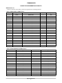
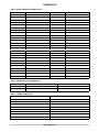
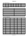
1
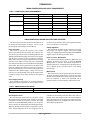
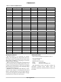
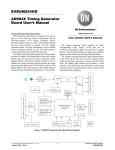
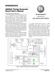
EVBUM2252/D
ADS-93X Timing Generator
Board User's Manual
Timing Generator Board Description
http://onsemi.com
This Timing Generator Board is designed to be part of a
two−board set, used in conjunction with an
ON Semiconductor CCD Imager Evaluation Board.
ON Semiconductor offers a variety of CCD Imager Boards
that have been designed to operate with this Timing
Generator Board. For more information on the available
Imager Evaluation Boards, see the ON Semiconductor
contact information at the end of this document.
The Timing Generator Board generates the timing signals
necessary to operate Truesense Imaging Imager Boards, and
also provides the power required by these Imager Boards via
the board interface connector (J4). In addition, the Timing
Generator Board performs the signal processing and
digitization of the analog output from the Imager Board. The
analog output of the Imager Board is connected to the
Timing Generator Board via coaxial cable.
EVAL BOARD USER’S MANUAL
The Timing Generator Board contains an Altera
Programmable Logic Device (PLD) that can be
In−System−Programmed (ISP) with code that is imager
specific. This provides flexibility to operate many different
Imager Boards with the same Timing Generator Board.
The Timing Generator Board has a digital Input interface
to the Altera device that can be used to support various
modes of operation depending on imager specific Altera
code.
SMB
+12V
REGULATOR
LINE
RECIEVER
OP AMP
CDS
CLAMP
OP AMP
LPF
OP AMP
ADS-93x
16 BIT A/D
16 bits
LVDS
DRIVERS
-12V
REGULATOR
SAMPLE
FRAME
GRABBER
TIMING
BOARD INTERFACE CONNECTOR
CLAMP
LVDS
DRIVERS
TIMING GENERATOR
ALTERA 7000S
ISP PLD
DIGITAL
INPUT
BUFFERS
DIO INPUT CONN
VIN
100 PIN SCSI OUTPUT CONN
CCD VIDEO PROCESSING CHAIN
JUMPERS
POWER CONNECTOR
BOARD
RESET
BUTTON
MASTER
CLOCK
UNIT
INT
CLOCK
INT
SYNC
JTAG
ISP
HEADER
Figure 1. Generator Board Block Diagram
© Semiconductor Components Industries, LLC, 2014
August, 2014 − Rev. 2
1
Publication Order Number:
EVBUM2252/D
EVBUM2252/D
TIMING GENERATOR BOARD INPUT REQUIREMENTS
Table 1. POWER SUPPLY INPUT REQUIREMENTS
Power Supplies
Minimum
+5 V Supply
4.9
Typical
Maximum
5
5.1
Units
V
500
−5 V Supply
−5.1
mA
−5
−4.9
V
150
VPLUS Supply
18
mA
20
24
V
25
VMINUS Supply
−21
mA
−20
−18
V
15
mA
TIMING GENERATOR BOARD ARCHITECTURE OVERVIEW
For best noise performance, linear power supplies should be
used to provide power to the boards.
The following sections describe the functional blocks of
the Timing Generator Board. See Figure 1 for an overall
block diagram of the Timing Generator Board.
Voltage Regulators
The operational amplifiers in the CCD video processing
chain require ±12 V power supplies. These power supply
voltages are regulated down from the VPLUS and VMINUS
supplies input to the Timing Generator Board.
Power Connector
This connector provides the necessary power supply
inputs to the Timing Generator Board. The connector also
provides the power needed by the CCD Imager Boards. The
Timing Generator Board simply routes these power supplies
from the power connector to the board interface connector.
Table 1 shows the power supply requirements for the timing
generator board. This is not the total power requirement
since this board is always used in conjunction with an image
sensor board. The current requirements for the image sensor
board are contained in its manual, and need to be added to
the values listed in Table 1 to arrive at the total system power
requirement. The “VPLUS Supply” voltage value can vary
from 20 to 24 volts depending on the specific imager board.
Consult the image sensor board manual for the required
value.
Power−On Clear / Board Reset
The Altera Programmable Logic Device (PLD) resets and
initializes the board on power-up, or when the BOARD
RESET button in pressed. The default configuration is
defined separately for each particular CCD Image Sensor,
and is detailed in the associated Altera Code Timing
Specification.
Master Clock
The master clock is used to generate the pixel rate clocks.
The pixel rate timing signals operate at a frequency that is
divided down from the master clock frequency. The exact
pixel rate frequency is Altera code dependent, but is
typically equal to 1/16 the frequency of the master clock.
Power Supply Filtering
Power supplied to the board is de−coupled and filtered
with ferrite beads and capacitors in order to suppress noise.
Table 2. TIMING BOARD CLOCK RATES
Timing Board PN
Master Clock
Pixel Clock (Max)
3E8290
48 MHz
3 MHz
Unit Integration Clock
controlled by the Timing Generator Board and will be a
multiple of this unit integration time. The actual integration
time is dependent on how the integration control lines on the
digital input connector are configured, as well as on how the
Altera PLD is programmed.
The unit integration clock is used as a means for varying
the integration time. The clock circuit consists of a 555 timer
configured to oscillate at a frequency of 100 Hz. The output
of this circuit, the INTEGRATE_CLK, has a 10 ms period,
which is used by the Altera PLD as the unit integration time.
When the Timing Generator Board is configured to operate
in the internal integration mode, the integration time is
http://onsemi.com
2
EVBUM2252/D
Integration Sync Output Connector
Timing Generator PLD
This output provides a signal that is high during the
integration time period. This signal can be used to
synchronize an external shutter or LED light source with the
integration time period.
The Programmable Logic Device (PLD) is an Altera
7000S series part. This device is In System Programmable
(ISP) via a 10-pin JTAG header located on the board. In this
way, the Altera device is programmed with imager specific
code to operate the Imager Board to which the Timing
Generator Board will be connected.
The Timing Generator PLD controls the overall flow of
the evaluation board operation. The PLD outputs include the
CCD clocks signals, analog processing timing signals, and
Frame Grabber synchronization signals.
Digital Input Connector (Remote Digital Input Control)
The digital input connector can be used to input control
signals to the evaluation board. These control signals can be
used to adjust the operating mode of the evaluation board.
The functions of the digital inputs depend on what code the
Altera device is programmed with. This is an optional
feature. No external digital inputs are required for board
operation.
The digital input control lines to the board are buffered.
The input pins to the buffer IC’s are weakly held low by pull
down resistors to GND. Therefore, with no digital inputs, the
default level of the Timing Generator Board control lines is
all zeros.
A three wire serial interface is also provided on the input
connector. This interface consists of three lines, a serial
clock, serial data, and a serial load signal. The serial
interface is provided as an alternate way to adjust the
operating condition of the Timing Generator Board if the
Altera device is programmed with code to support this
feature.
LVDS Drivers
Timing signals are sent to the Imager Board via the board
interface connector using Low Voltage Differential
Signaling (LVDS) drivers. LVDS combines high-speed
connectivity with low noise and low power.
Board Interface Connector
This 80-pin connector provides both the timing signals
and the necessary power to the CCD Imager Boards from the
Timing Generator Board.
CCD Video Processing Chain
The CCD video signal from the Imager Board is input to
the Timing Generator Board via the SMB coaxial connector.
The coaxial cable is terminated with a resistor and is then
buffered by a receiver op-amp with a gain of 1.25. Next the
video signal is clamped to ground, effectively performing
the first half of the correlated double sampling (CDS)
function. Finally the video signal is passed through a low
pass filter before being input to the 16-bit A/D converter.
The A/D sample signal completes the CDS function and
converts the signal to digital information.
Jumpers
There are four jumpers on the board that can be used to
adjust the operating mode of the Timing Generator Board.
The functions of the jumpers depend on how the Altera
device is programmed, and is detailed in the associated
Altera Code Timing Specification.
JTAG Header
ADS−93X 16−Bit A/D Convertor
This 10-pin header provides the user with the ability to
reprogram the Altera PLD in place via Altera’s
BYTEBLASTER programming hardware.
The Timing Generator Board supports the 16 bit
ADS-93X family of convertors offered by Datel Inc.
There are several variants in the ADS-93X family. The
Timing Generator Board is populated differently depending
on which convertor is being used.
Table 3. TIMING BOARD CONFIGURATION OPTIONS
Timing Board PN
Datel A/D PN
Sampling Rate
Bit Depth
Channels
3E8290
ADS−933MC
3 MSPS
16
1
Output Connector
differential format. The connector also provides the three
necessary PCI-1424 frame grabber synchronization signals
in LVDS differential format.
The output connector interfaces directly to the National
Instruments PCI-1424 framegrabber. The output connector
provides a single channel of 16 bit output data in LVDS
http://onsemi.com
3
EVBUM2252/D
CONNECTOR ASSIGNMENTS AND PINOUTS
SMB Connector J5
J5 allows connection of the VOUT_CCD video signal from the CCD Imager Boards.
Table 4. DIGITAL INPUT CONNECTOR J4
Pin
Assignment
Function
Pin
Assignment
1
SDATA
SERIAL PORT
2
GND
3
SCLOCK
SERIAL PORT
4
GND
5
SLOAD
SERIAL PORT
6
GND
7
DIO15
Altera Code Dependent
8
GND
9
DIO14
Altera Code Dependent
10
GND
11
DIO13
Altera Code Dependent
12
GND
13
DIO12
Altera Code Dependent
14
GND
15
DIO11
Altera Code Dependent
16
GND
17
DIO10
Altera Code Dependent
18
GND
19
DIO9
Altera Code Dependent
20
GND
21
DIO8
Altera Code Dependent
22
GND
23
DIO7
Altera Code Dependent
24
GND
25
DIO6
Altera Code Dependent
26
GND
27
DIO5
Altera Code Dependent
28
GND
29
DIO4
Altera Code Dependent
30
GND
31
DIO3
Altera Code Dependent
32
GND
33
DIO2
Altera Code Dependent
34
GND
35
DIO1
Altera Code Dependent
36
GND
37
DIO0
Altera Code Dependent
38
GND
39
NO CONNECT
N/A
40
GND
Table 5. BOARD INTERFACE CONNECTOR J3
Pin
Assignment
Pin
1
N.C.
2
N.C.
3
AGND
4
AGND
5
TIMING_OUT11+
6
TIMING_OUT11−
7
AGND
8
AGND
9
TIMING_OUT10+
10
TIMING_OUT10−
11
AGND
12
AGND
13
TIMING_OUT9+
14
TIMING_OUT9−
15
AGND
16
AGND
17
TIMING_OUT8+
18
TIMING_OUT8−
19
AGND
20
AGND
21
TIMING_OUT7+
22
TIMING_OUT7−
23
AGND
24
AGND
25
TIMING_OUT6+
26
TIMING_OUT6−
27
AGND
28
AGND
29
TIMING_OUT5+
30
TIMING_OUT5−
http://onsemi.com
4
Assignment
EVBUM2252/D
Table 5. BOARD INTERFACE CONNECTOR J3
Pin
Assignment
Pin
Assignment
31
AGND
32
AGND
33
TIMING_OUT4+
34
TIMING_OUT4−
35
AGND
36
AGND
37
TIMING_OUT3+
38
TIMING_OUT3−
39
AGND
40
AGND
41
TIMING_OUT2+
42
TIMING_OUT2−
43
AGND
44
AGND
45
TIMING_OUT1+
46
TIMING_OUT1−
47
N.C.
48
N.C.
49
AGND
50
AGND
51
N.C.
52
N.C.
53
VMINUS_MTR
54
VMINUS_MTR
55
N.C.
56
N.C.
57
AGND
58
AGND
59
TIMING_OUT0+
60
TIMING_OUT0−
61
−5 V_MTR
62
−5 V_MTR
63
N.C.
64
N.C.
65
AGND
66
AGND
67
N.C.
68
N.C.
69
+5 V_MTR
70
+5 V_MTR
71
N.C.
72
N.C.
73
AGND
74
AGND
75
N.C.
76
N.C.
77
VPLUS_MTR
78
VPLUS_MTR
79
N.C.
80
N.C.
Table 6. INTEGRATE SYNC CONNECTOR J1
Pin
Assignment
Function
1
INTEGRATE
Signal is High during Integration Time Period
2
AGND
Ground
Table 7. POWER CONNECTOR J2
Pin
Assignment
1
VMINUS
2
AGND
3
VPLUS
4
AGND
5
−5 V_MTR
6
AGND
7
+5 V_MTR
8
AGND
http://onsemi.com
5
EVBUM2252/D
Table 8. JUMPER SELECTS P[4..1]
Jumper
Pin
Assignment
Pin
Assignment
Pin
Assignment
Function
P1
1
VCC
2
JMP0
3
AGND
Altera Code Dependent
P2
1
VCC
2
JMP1
3
AGND
Altera Code Dependent
P3
1
VCC
2
JMP2
3
AGND
Altera Code Dependent
P4
1
VCC
2
JMP3
3
AGND
Altera Code Dependent
Table 9. JTAG CONNECTOR P5
Pin
Assignment
1
TCK
2
AGND
3
TDO
4
+5 V_MTR
5
TMS
6
N.C.
7
N.C.
8
N.C.
9
TDI
10
AGND
Table 10. OUTPUT CONNECTOR J6
Pin
Assignment
Signal Level
Pin
Assignment
Signal Level
1
AOUT0+
LVDS
2
AOUT0−
LVDS
3
AOUT1+
LVDS
4
AOUT1−
LVDS
5
AOUT2+
LVDS
6
AOUT2−
LVDS
7
AOUT3+
LVDS
8
AOUT3−
LVDS
9
AOUT4+
LVDS
10
AOUT4−
LVDS
11
AOUT5+
LVDS
12
AOUT5−
LVDS
13
AOUT6+
LVDS
14
AOUT6−
LVDS
15
AOUT7+
LVDS
16
AOUT7−
LVDS
17
AOUT8+
LVDS
18
AOUT8−
LVDS
19
AOUT9+
LVDS
20
AOUT9−
LVDS
21
AOUT10+
LVDS
22
AOUT10−
LVDS
23
AOUT11+
LVDS
24
AOUT11−
LVDS
25
AOUT12+
LVDS
26
AOUT12−
LVDS
27
AOUT13+
LVDS
28
AOUT13−
LVDS
29
AOUT14+
LVDS
30
AOUT14−
LVDS
31
AOUT15+
LVDS
32
AOUT15−
LVDS
33
N.C.
34
N.C.
35
N.C.
36
N.C.
37
N.C.
38
N.C.
39
N.C.
40
N.C.
41
FRAME+
42
FRAME−
43
LINE+
44
LINE−
http://onsemi.com
6
EVBUM2252/D
Table 10. OUTPUT CONNECTOR J6
Pin
Assignment
45
Signal Level
Pin
Assignment
N.C.
46
N.C.
47
N.C.
48
N.C.
49
PIXEL+
50
PIXEL−
51
N.C.
52
N.C.
53
N.C.
54
N.C.
55
N.C.
56
N.C.
57
N.C.
58
N.C.
59
N.C.
60
N.C.
61
N.C.
62
N.C.
63
N.C.
64
N.C.
65
N.C.
66
N.C.
67
N.C.
68
N.C.
69
N.C.
70
N.C.
71
N.C.
72
N.C.
73
N.C.
74
N.C.
75
N.C.
76
N.C.
77
N.C.
78
N.C.
79
N.C.
80
N.C.
81
N.C.
82
N.C.
83
N.C.
84
N.C.
85
N.C.
86
N.C.
87
N.C.
88
N.C.
89
N.C.
90
N.C.
91
N.C.
92
N.C.
93
N.C.
94
N.C.
95
N.C.
96
N.C.
97
N.C.
98
N.C.
99
AGND
100
AGND
Warnings and Advisories
Signal Level
Ordering Information
ON Semiconductor is not responsible for customer
damage to the Timing Board or Imager Board electronics.
The customer assumes responsibility and care must be taken
when probing, modifying, or integrating the Truesense
Imaging Evaluation Board Kits.
When programming the Timing Board, the Imager Board
must be disconnected from the Timing Board before power
is applied. If the Imager Board is connected to the Timing
Board during the reprogramming of the Altera PLD, damage
to the Imager Board will occur.
Purchasers of a an Evaluation Board Kit may, at their
discretion, make changes to the Timing Generator Board
firmware. ON Semiconductor can only support firmware
developed by, and supplied by, ON Semiconductor. Changes
to the firmware are at the risk of the customer.
Please address all inquiries and purchase orders to:
Truesense Imaging, Inc.
1964 Lake Avenue
Rochester, New York 14615
Phone:
(585) 784−5500
E−mail:
[email protected]
ON Semiconductor reserves the right to change any
information contained herein without notice. All
information furnished by ON Semiconductor is believed to
be accurate.
http://onsemi.com
7
EVBUM2252/D
ON Semiconductor and the
are registered trademarks of Semiconductor Components Industries, LLC (SCILLC) or its subsidiaries in the United States and/or other countries.
SCILLC owns the rights to a number of patents, trademarks, copyrights, trade secrets, and other intellectual property. A listing of SCILLC’s product/patent coverage may be accessed
at www.onsemi.com/site/pdf/Patent−Marking.pdf. SCILLC reserves the right to make changes without further notice to any products herein. SCILLC makes no warranty, representation
or guarantee regarding the suitability of its products for any particular purpose, nor does SCILLC assume any liability arising out of the application or use of any product or circuit, and
specifically disclaims any and all liability, including without limitation special, consequential or incidental damages. “Typical” parameters which may be provided in SCILLC data sheets
and/or specifications can and do vary in different applications and actual performance may vary over time. All operating parameters, including “Typicals” must be validated for each
customer application by customer’s technical experts. SCILLC does not convey any license under its patent rights nor the rights of others. SCILLC products are not designed, intended,
or authorized for use as components in systems intended for surgical implant into the body, or other applications intended to support or sustain life, or for any other application in which
the failure of the SCILLC product could create a situation where personal injury or death may occur. Should Buyer purchase or use SCILLC products for any such unintended or
unauthorized application, Buyer shall indemnify and hold SCILLC and its officers, employees, subsidiaries, affiliates, and distributors harmless against all claims, costs, damages, and
expenses, and reasonable attorney fees arising out of, directly or indirectly, any claim of personal injury or death associated with such unintended or unauthorized use, even if such claim
alleges that SCILLC was negligent regarding the design or manufacture of the part. SCILLC is an Equal Opportunity/Affirmative Action Employer. This literature is subject to all applicable
copyright laws and is not for resale in any manner.
PUBLICATION ORDERING INFORMATION
LITERATURE FULFILLMENT:
Literature Distribution Center for ON Semiconductor
P.O. Box 5163, Denver, Colorado 80217 USA
Phone: 303−675−2175 or 800−344−3860 Toll Free USA/Canada
Fax: 303−675−2176 or 800−344−3867 Toll Free USA/Canada
Email: [email protected]
N. American Technical Support: 800−282−9855 Toll Free
USA/Canada
Europe, Middle East and Africa Technical Support:
Phone: 421 33 790 2910
Japan Customer Focus Center
Phone: 81−3−5817−1050
http://onsemi.com
8
ON Semiconductor Website: www.onsemi.com
Order Literature: http://www.onsemi.com/orderlit
For additional information, please contact your local
Sales Representative
EVBUM2252/D