1
MCF5272UM/D
3/2002
REV 2
MCF5272 ColdFire® Integrated
Microprocessor User’s Manual
HOW TO REACH US:
USA/EUROPE/LOCATIONS NOT LISTED:
Motorola Literature Distribution;
P.O. Box 5405, Denver, Colorado 80217
1-303-675-2140 or 1-800-441-2447
JAPAN:
Motorola Japan Ltd.;
SPS, Technical Information Center,
3-20-1, Minami-Azabu Minato-ku,
Tokyo 106-8573 Japan
81-3-3440-3569
Information in this document is provided solely to enable system and software implementers to use
ASIA/PACIFIC:
Motorola products. There are no express or implied copyright licenses granted hereunder to design
Motorola Semiconductors H.K. Ltd.;
Silicon Harbour Centre, 2 Dai King Street,
Tai Po Industrial Estate, Tai Po, N.T., Hong Kong
852-26668334
or fabricate any integrated circuits or integrated circuits based on the information in this document.
TECHNICAL INFORMATION CENTER:
use of any product or circuit, and specifically disclaims any and all liability, including without
1-800-521-6274
limitation consequential or incidental damages. “Typical” parameters which may be provided in
HOME PAGE:
Motorola reserves the right to make changes without further notice to any products herein.
Motorola makes no warranty, representation or guarantee regarding the suitability of its products
for any particular purpose, nor does Motorola assume any liability arising out of the application or
Motorola data sheets and/or specifications can and do vary in different applications and actual
performance may vary over time. All operating parameters, including “Typicals” must be validated
http://www.motorola.com/semiconductors
for each customer application by customer’s technical experts. Motorola does not convey any
DOCUMENT COMMENTS:
license under its patent rights nor the rights of others. Motorola products are not designed,
FAX (512) 933-2625,
Attn: TECD Applications Engineering
intended, or authorized for use as components in systems intended for surgical implant into the
body, or other applications intended to support or sustain life, or for any other application in which
the failure of the Motorola product could create a situation where personal injury or death may
occur. Should Buyer purchase or use Motorola products for any such unintended or unauthorized
application, Buyer shall indemnify and hold Motorola and its officers, employees, subsidiaries,
affiliates, and distributors harmless against all claims, costs, damages, and expenses, and
reasonable attorney fees arising out of, directly or indirectly, any claim of personal injury or death
associated with such unintended or unauthorized use, even if such claim alleges that Motorola was
negligent regarding the design or manufacture of the part.
Motorola and the Stylized M Logo are registered in the U.S. Patent and Trademark Office.
digital dna is a trademark of Motorola, Inc. All other product or service names are the property
of their respective owners. Motorola, Inc. is an Equal Opportunity/Affirmative Action Employer.
© Motorola, Inc. 2002
Overview
1
ColdFire Core
2
Hardware Multiply/Accumulate (MAC) Unit
3
Local Memory
4
Debug Support
5
System Integration Module (SIM)
6
Interrupt Controller
7
Chip-Select Module
8
SDRAM Controller
9
DMA Controller Module
10
Ethernet Module
11
Universal Serial Bus (USB)
12
Physical Layer Interface Controller (PLIC)
13
Queued Serial Peripheral Interface (QSPI) Module
14
Timer Module
15
UART Modules
16
General-Purpose I/O Module
17
Pulse-Width Modulation (PWM) Module
18
Signal Descriptions
19
Bus Operation
20
IEEE 1149.1 Test Access Port (JTAG)
21
Mechanical Data
22
Electrical Characteristics
23
Appendix A: List of Memory Maps
A
Appendix B: Buffering and Impedence Matching
B
Index
IND
B
GLO
IND
1
Overview
2
ColdFire Core
3
Hardware Multiply/Accumulate (MAC) Unit
4
Local Memory
5
Debug Support
6
System Integration Module (SIM)
7
Interrupt Controller
8
Chip-Select Module
9
SDRAM Controller
10
DMA Controller Module
11
Ethernet Module
12
Universal Serial Bus (USB)
13
Physical Layer Interface Controller (PLIC)
14
Queued Serial Peripheral Interface (QSPI) Module
15
Timer Module
16
UART Modules
17
General-Purpose I/O Module
18
Pulse-Width Modulation (PWM) Module
19
Signal Descriptions
20
Bus Operation
21
IEEE 1149.1 Test Access Port (JTAG)
22
Mechanical Data
23
Electrical Characteristics
A
Appendix A: List of Memory Maps
B
Appendix B: Buffering and Impedence Matching
IND
Index
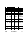
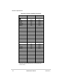
CONTENTS
Paragraph
Number
Title
Page
Number
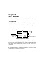
Chapter 1
Overview
1.1
1.2
1.2.1
1.2.2
1.2.2.1
1.2.2.2
1.2.2.3
1.2.2.4
1.2.2.5
1.2.2.6
1.2.3
1.2.4
1.2.5
1.3
1.3.1
1.4
1.4.1
1.4.2
1.4.3
1.4.4
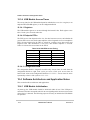
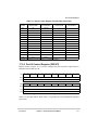
MCF5272 Key Features......................................................................................
MCF5272 Architecture .......................................................................................
Version 2 ColdFire Core.................................................................................
System Integration Module (SIM)..................................................................
External Bus Interface ................................................................................
Chip Select and Wait State Generation ......................................................
System Configuration and Protection .........................................................
Power Management ....................................................................................
Parallel Input/Output Ports .........................................................................
Interrupt Inputs ...........................................................................................
UART Module ................................................................................................
Timer Module .................................................................................................
Test Access Port..............................................................................................
System Design ...................................................................................................
System Bus Configuration ..............................................................................
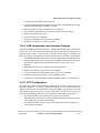
MCF5272-Specific Features ...............................................................................
Physical Layer Interface Controller (PLIC)....................................................
Pulse-Width Modulation (PWM) Unit ...........................................................
Queued Serial Peripheral Interface (QSPI).....................................................
Universal Serial Bus (USB) Module ..............................................................
1-1
1-4
1-4
1-5
1-5
1-5
1-5
1-6
1-6
1-6
1-6
1-7
1-7
1-7
1-7
1-8
1-8
1-8
1-8
1-9
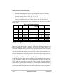
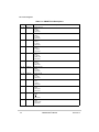
Chapter 2
ColdFire Core
2.1
2.1.1
2.1.1.1
2.1.1.2
2.1.1.2.1
2.1.1.2.2
2.1.1.2.3
2.1.2
MOTOROLA
Features and Enhancements................................................................................
Decoupled Pipelines .......................................................................................
Instruction Fetch Pipeline (IFP)..................................................................
Operand Execution Pipeline (OEP) ............................................................
Illegal Opcode Handling.........................................................................
Hardware Multiply/Accumulate (MAC) Unit ........................................
Hardware Divide Unit.............................................................................
Debug Module Enhancements ........................................................................
Contents
2-1
2-1
2-2
2-3
2-3
2-3
2-4
2-4
v
CONTENTS
Paragraph
Number
2.2
2.2.1
2.2.1.1
2.2.1.2
2.2.1.3
2.2.1.4
2.2.1.5
2.2.1.6
2.2.2
2.2.2.1
2.2.2.2
2.2.2.3
2.2.2.4
2.2.2.5
2.2.2.6
2.2.2.7
2.3
2.4
2.4.1
2.4.2
2.5
2.6
2.6.1
2.7
2.7.1
2.7.2
2.7.3
2.7.4
2.7.5
2.8
2.8.1
2.8.2
Title
Page
Number
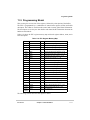
Programming Model ........................................................................................... 2-5
User Programming Model .............................................................................. 2-6
Data Registers (D0–D7) ............................................................................. 2-6
Address Registers (A0–A6) ........................................................................ 2-6
Stack Pointer (A7, SP) ................................................................................ 2-7
Program Counter (PC) ................................................................................ 2-7
Condition Code Register (CCR) ................................................................. 2-7
MAC Programming Model......................................................................... 2-8
Supervisor Programming Model..................................................................... 2-8
Status Register (SR).................................................................................... 2-8
Vector Base Register (VBR) ...................................................................... 2-9
Cache Control Register (CACR) ................................................................ 2-9
Access Control Registers (ACR0–ACR1)................................................ 2-10
ROM Base Address Register (ROMBAR) ............................................... 2-10
RAM Base Address Register (RAMBAR) ............................................... 2-10
Module Base Address Register (MBAR) ................................................. 2-10
Integer Data Formats......................................................................................... 2-10
Organization of Data in Registers..................................................................... 2-10
Organization of Integer Data Formats in Registers ...................................... 2-11
Organization of Integer Data Formats in Memory ....................................... 2-12
Addressing Mode Summary ............................................................................. 2-12
Instruction Set Summary................................................................................... 2-13
Instruction Set Summary .............................................................................. 2-16
Instruction Timing ............................................................................................ 2-19
MOVE Instruction Execution Times ............................................................ 2-20
Execution Timings—One-Operand Instructions .......................................... 2-22
Execution Timings—Two-Operand Instructions.......................................... 2-23
Miscellaneous Instruction Execution Times................................................. 2-24
Branch Instruction Execution Times ............................................................ 2-25
Exception Processing Overview ....................................................................... 2-26
Exception Stack Frame Definition................................................................ 2-28
Processor Exceptions .................................................................................... 2-29
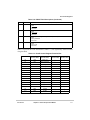
Chapter 3
Hardware Multiply/Accumulate (MAC) Unit
3.1
3.1.1
3.1.2
3.1.3
3.1.4
3.2
vi
Overview.............................................................................................................
MAC Programming Model.............................................................................
General Operation...........................................................................................
MAC Instruction Set Summary ......................................................................
Data Representation........................................................................................
MAC Instruction Execution Timings..................................................................
MCF5272 User’s Manual
3-1
3-2
3-3
3-4
3-5
3-5
MOTOROLA
CONTENTS
Paragraph
Number
Title
Page
Number
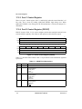
Chapter 4
Local Memory
4.1
4.2
4.3
4.3.1
4.3.2
4.3.2.1
4.3.2.2
4.3.2.3
4.4
4.4.1
4.4.2
4.4.2.1
4.4.2.2
4.5
4.5.1
4.5.2
4.5.2.1
4.5.2.2
4.5.2.3
4.5.2.3.1
4.5.2.3.2
4.5.2.4
4.5.2.5
4.5.3
4.5.3.1
4.5.3.2
Interactions between Local Memory Modules ................................................... 4-1
Local Memory Registers..................................................................................... 4-2
SRAM Overview ................................................................................................ 4-2
SRAM Operation ............................................................................................ 4-2
SRAM Programming Model........................................................................... 4-2
SRAM Base Address Register (RAMBAR)............................................... 4-3
SRAM Initialization.................................................................................... 4-4
Programming RAMBAR for Power Management ..................................... 4-5
ROM Overview................................................................................................... 4-5
ROM Operation .............................................................................................. 4-5
ROM Programming Model............................................................................. 4-6
ROM Base Address Register (ROMBAR) ................................................. 4-6
Programming ROMBAR for Power Management ..................................... 4-7
Instruction Cache Overview ............................................................................... 4-7
Instruction Cache Physical Organization........................................................ 4-7
Instruction Cache Operation ........................................................................... 4-9
Interaction with Other Modules.................................................................. 4-9
Cache Coherency and Invalidation ............................................................. 4-9
Caching Modes ........................................................................................... 4-9
Cacheable Accesses .............................................................................. 4-10
Cache-Inhibited Accesses..................................................................... 4-10
Reset ......................................................................................................... 4-11
Cache Miss Fetch Algorithm/Line Fills ................................................... 4-11
Instruction Cache Programming Model........................................................ 4-12
Cache Control Register (CACR) .............................................................. 4-13
Access Control Registers (ACR0 and ACR1) .......................................... 4-15
Chapter 5
Debug Support
5.1
5.2
5.3
5.3.1
5.4
5.4.1
5.4.2
5.4.3
5.4.4
MOTOROLA
Overview.............................................................................................................
Signal Description...............................................................................................
Real-Time Trace Support....................................................................................
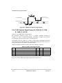
Begin Execution of Taken Branch (PST = 0x5) .............................................
Programming Model ...........................................................................................
Revision A Shared Debug Resources .............................................................
Address Attribute Trigger Register (AATR) ..................................................
Address Breakpoint Registers (ABLR, ABHR) .............................................
Configuration/Status Register (CSR)..............................................................
Contents
5-1
5-2
5-2
5-4
5-5
5-7
5-7
5-8
5-9
vii
CONTENTS
Paragraph
Number
5.4.5
5.4.6
5.4.7
5.5
5.5.1
5.5.2
5.5.2.1
5.5.2.2
5.5.3
5.5.3.1
5.5.3.1.1
5.5.3.2
5.5.3.3
5.5.3.3.1
5.5.3.3.2
5.5.3.3.3
5.5.3.3.4
5.5.3.3.5
5.5.3.3.6
5.5.3.3.7
5.5.3.3.8
5.5.3.3.9
5.5.3.3.10
5.5.3.3.11
5.5.3.3.12
5.6
5.6.1
5.6.1.1
5.6.2
5.7
5.7.1
5.7.2
5.8
Title
Page
Number
Data Breakpoint/Mask Registers (DBR, DBMR).........................................
Program Counter Breakpoint/Mask Registers (PBR, PBMR)......................
Trigger Definition Register (TDR) ...............................................................
Background Debug Mode (BDM) ....................................................................
CPU Halt.......................................................................................................
BDM Serial Interface....................................................................................
Receive Packet Format .............................................................................
Transmit Packet Format............................................................................
BDM Command Set......................................................................................
ColdFire BDM Command Format............................................................
Extension Words as Required...............................................................
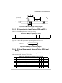
Command Sequence Diagrams.................................................................
Command Set Descriptions ......................................................................
Read A/D Register (rareg/rdreg) ..........................................................
Write A/D Register (wareg/wdreg) ......................................................
Read Memory Location (read)..............................................................
Write Memory Location (write) ...........................................................
Dump Memory Block (dump) ..............................................................
Fill Memory Block (fill) .......................................................................
Resume Execution (go) ........................................................................
No Operation (nop)...............................................................................
Read Control Register (rcreg)...............................................................
Write Control Register (wcreg) ............................................................
Read Debug Module Register (rdmreg) ...............................................
Write Debug Module Register (wdmreg) .............................................
Real-Time Debug Support ................................................................................
Theory of Operation......................................................................................
Emulator Mode .........................................................................................
Concurrent BDM and Processor Operation ..................................................
Processor Status, DDATA Definition...............................................................
User Instruction Set ......................................................................................
Supervisor Instruction Set.............................................................................
Motorola-Recommended BDM Pinout.............................................................
5-11
5-12
5-13
5-15
5-15
5-16
5-17
5-18
5-18
5-19
5-20
5-20
5-22
5-22
5-23
5-23
5-25
5-26
5-28
5-30
5-30
5-31
5-32
5-32
5-33
5-34
5-34
5-36
5-36
5-37
5-37
5-41
5-42
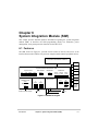
Chapter 6
System Integration Module (SIM)
6.1
6.2
6.2.1
6.2.2
6.2.3
viii
Features ...............................................................................................................
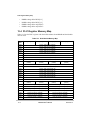
Programming Model ...........................................................................................
SIM Register Memory Map............................................................................
Module Base Address Register (MBAR) .......................................................
System Configuration Register (SCR)............................................................
MCF5272 User’s Manual
6-1
6-3
6-3
6-4
6-5
MOTOROLA
CONTENTS
Paragraph
Number
6.2.4
6.2.5
6.2.6
6.2.7
6.2.8
6.2.8.1
6.2.8.2
6.2.8.3
6.2.8.4
Title
Page
Number
System Protection Register (SPR) .................................................................. 6-6
Power Management Register (PMR).............................................................. 6-7
Activate Low-Power Register (ALPR)......................................................... 6-10
Device Identification Register (DIR)............................................................ 6-11
Software Watchdog Timer............................................................................ 6-12
Watchdog Reset Reference Register (WRRR) ......................................... 6-13
Watchdog Interrupt Reference Register (WIRR) ..................................... 6-13
Watchdog Counter Register (WCR) ......................................................... 6-14
Watchdog Event Register (WER)............................................................. 6-14
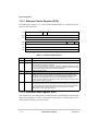
Chapter 7
Interrupt Controller
7.1
7.2
7.2.1
7.2.2
7.2.2.1
7.2.2.2
7.2.2.3
7.2.2.4
7.2.3
7.2.4
7.2.5
7.2.6
Overview.............................................................................................................
Interrupt Controller Registers .............................................................................
Interrupt Controller Registers .........................................................................
Interrupt Control Registers (ICR1–ICR4) ......................................................
Interrupt Control Register 1 (ICR1) ...........................................................
Interrupt Control Register 2 (ICR2) ...........................................................
Interrupt Control Register 3 (ICR3) ...........................................................
Interrupt Control Register 4 (ICR4) ...........................................................
Interrupt Source Register (ISR) ......................................................................
Programmable Interrupt Transition Register (PITR)......................................
Programmable Interrupt Wakeup Register (PIWR)........................................
Programmable Interrupt Vector Register (PIVR) ...........................................
7-1
7-2
7-3
7-4
7-4
7-5
7-5
7-6
7-6
7-7
7-7
7-8
Chapter 8
Chip Select Module
8.1
8.1.1
8.1.2
8.1.3
8.2
8.2.1
8.2.2
Overview.............................................................................................................
Features...........................................................................................................
Chip Select Usage...........................................................................................
Boot CS0 Operation........................................................................................
Chip Select Registers ..........................................................................................
Chip Select Base Registers (CSBR0–CSBR7) ...............................................
Chip Select Option Registers (CSOR0–CSOR7) ...........................................
8-1
8-1
8-1
8-2
8-2
8-3
8-5
Chapter 9
SDRAM Controller
9.1
9.2
MOTOROLA
Overview............................................................................................................. 9-1
SDRAM Controller Signals ................................................................................ 9-1
Contents
ix
CONTENTS
Paragraph
Number
9.3
9.4
9.5
9.5.1
9.5.2
9.6
9.7
9.8
9.9
9.10
9.10.1
9.10.2
9.10.3
Title
Page
Number
Interface to SDRAM Devices ............................................................................. 9-4
SDRAM Banks, Page Hits, and Page Misses ..................................................... 9-6
SDRAM Registers .............................................................................................. 9-6
SDRAM Configuration Register (SDCR) ...................................................... 9-6
SDRAM Timing Register (SDTR) ................................................................. 9-8
Auto Initialization ............................................................................................... 9-9
Power-Down and Self-Refresh ........................................................................... 9-9
Performance ...................................................................................................... 9-10
Solving Timing Issues with SDCR[INV] ......................................................... 9-13
SDRAM Interface ............................................................................................. 9-15
SDRAM Read Accesses ............................................................................... 9-16
SDRAM Write Accesses .............................................................................. 9-18
SDRAM Refresh Timing .............................................................................. 9-20
Chapter 10
DMA Controller
10.1
10.2
10.3
10.3.1
10.3.2
10.3.3
10.3.4
10.3.5
DMA Data Transfer Types ...............................................................................
DMA Address Modes .......................................................................................
DMA Controller Registers................................................................................
DMA Mode Register (DMR)........................................................................
DMA Interrupt Register (DIR) .....................................................................
DMA Source Address Register (DSAR) ......................................................
DMA Destination Address Register (DDAR) ..............................................
DMA Byte Count Register (DBCR).............................................................
10-1
10-2
10-2
10-2
10-4
10-5
10-6
10-6
Chapter 11
Ethernet Module
11.1
11.1.1
11.2
11.3
11.4
11.4.1
11.4.2
11.4.3
11.4.4
11.4.5
11.4.6
11.4.7
11.4.8
x
Overview...........................................................................................................
Features.........................................................................................................
Module Operation .............................................................................................
Transceiver Connection ....................................................................................
FEC Frame Transmission .................................................................................
FEC Frame Reception...................................................................................
CAM Interface ..............................................................................................
Ethernet Address Recognition ......................................................................
Hash Table Algorithm ..................................................................................
Interpacket Gap Time ...................................................................................
Collision Handling........................................................................................
Internal and External Loopback....................................................................
Ethernet Error-Handling Procedure ..............................................................
MCF5272 User’s Manual
11-1
11-1
11-2
11-3
11-4
11-5
11-7
11-7
11-8
11-9
11-9
11-9
11-9
MOTOROLA
CONTENTS
Paragraph
Number
11.4.8.1
11.4.8.2
11.5
11.5.1
11.5.2
11.5.3
11.5.4
11.5.5
11.5.6
11.5.7
11.5.8
11.5.9
11.5.10
11.5.11
11.5.12
11.5.13
11.5.14
11.5.15
11.5.16
11.5.16.1
11.5.17
11.5.18
11.5.19
11.5.20
11.5.21
11.5.22
11.5.22.1
11.5.23
11.5.24
11.5.24.1
11.6
11.6.1
11.6.1.1
11.6.1.2
11.7
Title
Page
Number
Transmission Errors................................................................................
Reception Errors .....................................................................................
Programming Model .......................................................................................
Ethernet Control Register (ECR)................................................................
Interrupt Event Register (EIR)....................................................................
Interrupt Mask Register (EIMR).................................................................
Interrupt Vector Status Register (IVSR).....................................................
Receive Descriptor Active Register (RDAR).............................................
Transmit Descriptor Active Register (TDAR)............................................
MII Management Frame Register (MMFR) ...............................................
MII Speed Control Register (MSCR) .........................................................
FIFO Receive Bound Register (FRBR) ......................................................
FIFO Receive Start Register (FRSR)..........................................................
Transmit FIFO Watermark (TFWR)...........................................................
FIFO Transmit Start Register (TFSR) ........................................................
Receive Control Register (RCR) ................................................................
Maximum Frame Length Register (MFLR) ...............................................
Transmit Control Register (TCR) ...............................................................
RAM Perfect Match Address Low (MALR) ..............................................
RAM Perfect Match Address High (MAUR) .........................................
Hash Table High (HTUR)...........................................................................
Hash Table Low (HTLR)............................................................................
Pointer-to-Receive Descriptor Ring (ERDSR) ...........................................
Pointer-to-Transmit Descriptor Ring (ETDSR)..........................................
Receive Buffer Size Register (EMRBR) ....................................................
Initialization Sequence................................................................................
Hardware Initialization ...........................................................................
User Initialization (Prior to Asserting ETHER_EN) ..................................
FEC Initialization........................................................................................
User Initialization (after setting ETHER_EN) .......................................
Buffer Descriptors...........................................................................................
FEC Buffer Descriptor Tables ....................................................................
Ethernet Receive Buffer Descriptor (RxBD)..........................................
Ethernet Transmit Buffer Descriptor ......................................................
Differences between MCF5272 FEC and MPC860T FEC.............................
11-10
11-10
11-11
11-12
11-12
11-13
11-14
11-15
11-16
11-17
11-18
11-19
11-20
11-21
11-22
11-22
11-23
11-24
11-25
11-26
11-27
11-27
11-28
11-28
11-29
11-30
11-30
11-30
11-31
11-31
11-32
11-32
11-33
11-34
11-36
Chapter 12
Universal Serial Bus (USB)
12.1
12.2
12.2.1
MOTOROLA
Introduction....................................................................................................... 12-1
Module Operation ............................................................................................. 12-3
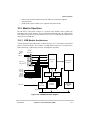
USB Module Architecture ............................................................................ 12-3
Contents
xi
CONTENTS
Paragraph
Number
12.2.1.1
12.2.1.2
12.2.1.3
12.2.1.4
12.2.1.5
12.3
12.3.1
12.3.2
12.3.2.1
12.3.2.2
12.3.2.3
12.3.2.4
12.3.2.5
12.3.2.6
12.3.2.7
12.3.2.8
12.3.2.9
12.3.2.10
12.3.2.11
12.3.2.12
12.3.2.13
12.3.2.14
12.3.2.15
12.3.2.16
12.3.2.17
12.3.2.18
12.3.2.19
12.3.3
12.3.3.1
12.3.3.2
12.3.4
12.3.4.1
12.3.4.2
12.3.4.3
12.4
12.4.1
12.4.2
12.4.3
12.4.4
12.4.4.1
12.4.4.1.1
12.4.4.1.2
xii
Title
Page
Number
USB Transceiver Interface ....................................................................... 12-4
Clock Generator........................................................................................ 12-4
USB Control Logic ................................................................................... 12-4
Endpoint Controllers................................................................................. 12-5
USB Request Processor ............................................................................ 12-5
Register Description and Programming Model ................................................ 12-7
USB Memory Map........................................................................................ 12-7
Register Descriptions.................................................................................... 12-9
USB Frame Number Register (FNR) ....................................................... 12-9
USB Frame Number Match Register (FNMR)......................................... 12-9
USB Real-Time Frame Monitor Register (RFMR) ................................ 12-10
USB Real-Time Frame Monitor Match Register (RFMMR) ................. 12-10
USB Function Address Register (FAR) ................................................. 12-11
USB Alternate Settings Register (ASR) ................................................. 12-11
USB Device Request Data 1 and 2 Registers (DRR1/ 2) ....................... 12-12
USB Specification Number Register (SPECR) ...................................... 12-13
USB Endpoint 0 Status Register (EP0SR).............................................. 12-13
USB Endpoint 0 IN Configuration Register (IEP0CFG) ....................... 12-14
USB Endpoint 0 OUT Configuration Register (OEP0CFG) .................. 12-15
USB Endpoint 1–7 Configuration Register (EPnCFG) .......................... 12-16
USB Endpoint 0 Control Register (EP0CTL) ........................................ 12-16
USB Endpoint 1–7 Control Register (EPnCTL) .................................... 12-19
USB Endpoint 0 Interrupt Mask (EP0IMR) and General/Endpoint 0
Interrupt Registers (EP0ISR).............................................................. 12-20
USB Endpoints 1–7 Status / Interrupt Registers (EPnISR) .................... 12-23
USB Endpoint 1–7 Interrupt Mask Registers (EPnIMR) ....................... 12-24
USB Endpoint 0–7 Data Registers (EPnDR).......................................... 12-25
USB Endpoint 0–7 Data Present Registers (EPnDPR)........................... 12-25
Configuration RAM.................................................................................... 12-26
Configuration RAM Content .................................................................. 12-26
USB Device Configuration Example...................................................... 12-27
USB Module Access Times........................................................................ 12-28
Registers ................................................................................................. 12-28
Endpoint FIFOs ...................................................................................... 12-28
Configuration RAM................................................................................ 12-28
Software Architecture and Application Notes ................................................ 12-28
USB Module Initialization.......................................................................... 12-28
USB Configuration and Interface Changes ................................................ 12-29
FIFO Configuration .................................................................................... 12-29
Data Flow.................................................................................................... 12-30
Control, Bulk, and Interrupt Endpoints .................................................. 12-30
IN Endpoints....................................................................................... 12-31
OUT Endpoints................................................................................... 12-31
MCF5272 User’s Manual
MOTOROLA
CONTENTS
Paragraph
Number
12.4.4.2
12.4.4.2.1
12.4.4.2.2
12.4.5
12.4.6
12.4.7
12.5
12.5.1
12.5.2
12.5.3
Title
Page
Number
Isochronous Endpoints............................................................................
IN Endpoints.......................................................................................
OUT Endpoints...................................................................................
Class- and Vendor-Specific Request Operation .........................................
remote wakeup and resume Operation........................................................
Endpoint Halt Feature.................................................................................
Line Interface ..................................................................................................
Attachment Detection .................................................................................
PCB Layout Recommendations..................................................................
Recommended USB Protection Circuit ......................................................
12-31
12-32
12-32
12-32
12-33
12-33
12-34
12-34
12-34
12-35
Chapter 13
Physical Layer Interface Controller (PLIC)
13.1
13.2
13.2.1
13.2.2
13.2.3
13.2.3.1
13.2.3.2
13.2.3.3
13.2.3.4
13.2.3.5
13.2.4
13.2.4.1
13.2.4.2
13.2.4.3
13.2.5
13.2.5.1
13.2.5.2
13.2.5.3
13.3
13.3.1
13.3.2
13.3.3
13.4
13.5
13.5.1
13.5.2
13.5.3
13.5.4
MOTOROLA
Introduction....................................................................................................... 13-1
GCI/IDL Block ................................................................................................. 13-3
GCI/IDL B- and D-Channel Receive Data Registers ................................... 13-3
GCI/IDL B- and D-Channel Transmit Data Registers.................................. 13-4
GCI/IDL B- and D-Channel Bit Alignment ................................................. 13-5
B-Channel Unencoded Data ..................................................................... 13-5
B-Channel HDLC Encoded Data.............................................................. 13-6
D-Channel HDLC Encoded Data ............................................................. 13-7
D-Channel Unencoded Data ..................................................................... 13-7
GCI/IDL D-Channel Contention ............................................................. 13-8
GCI/IDL Looping Modes ............................................................................. 13-8
Automatic Echo Mode .............................................................................. 13-9
Local Loopback Mode .............................................................................. 13-9
Remote Loopback Mode........................................................................... 13-9
GCI/IDL Interrupts ..................................................................................... 13-10
GCI/IDL Periodic Frame Interrupt ......................................................... 13-10
GCI Aperiodic Status Interrupt.............................................................. 13-10
Interrupt Control ..................................................................................... 13-11
PLIC Timing Generator .................................................................................. 13-11
Clock Synthesis........................................................................................... 13-11
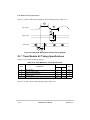
Super Frame Sync Generation .................................................................... 13-12
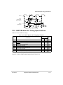
Frame Sync Synthesis................................................................................. 13-13
PLIC Register Memory Map .......................................................................... 13-14
PLIC Registers ................................................................................................ 13-15
B1 Data Receive Registers (P0B1RR–P3B1RR) ....................................... 13-15
B2 Data Receive Registers (P0B2RR–P3B2RR) ....................................... 13-16
D Data Receive Registers (P0DRR–P3DRR)............................................. 13-16
B1 Data Transmit Registers (P0B1TR–P3B1TR) ...................................... 13-17
Contents
xiii
CONTENTS
Paragraph
Number
13.5.5
13.5.6
13.5.7
13.5.8
13.5.9
13.5.10
13.5.11
13.5.12
13.5.13
13.5.14
13.5.15
13.5.16
13.5.17
13.5.18
13.5.19
13.5.20
13.5.21
13.5.22
13.6
13.6.1
13.6.2
13.6.2.1
13.6.2.2
13.6.3
13.6.4
13.6.5
Title
Page
Number
B2 Data Transmit Registers (P0B2TR–P3B2TR) ......................................
D Data Transmit Registers (P0DTR–P3DTR)............................................
Port Configuration Registers (P0CR–P3CR)..............................................
Loopback Control Register (PLCR) ...........................................................
Interrupt Configuration Registers (P0ICR–P3ICR)....................................
Periodic Status Registers (P0PSR–P3PSR) ................................................
Aperiodic Status Register (PASR)..............................................................
GCI Monitor Channel Receive Registers (P0GMR–P3GMR) ...................
GCI Monitor Channel Transmit Registers (P0GMT–P3GMT)..................
GCI Monitor Channel Transmit Abort Register (PGMTA) ......................
GCI Monitor Channel Transmit Status Register (PGMTS)........................
GCI C/I Channel Receive Registers (P0GCIR–P3GCIR) ..........................
GCI C/I Channel Transmit Registers (P0GCIT–P3GCIT) .........................
GCI C/I Channel Transmit Status Register (PGCITSR) ............................
D-Channel Status Register (PDCSR) .........................................................
D-Channel Request Register (PDRQR)......................................................
Sync Delay Registers (P0SDR–P3SDR) ....................................................
Clock Select Register (PCSR) ....................................................................
Application Examples.....................................................................................
Introduction.................................................................................................
PLIC Initialization ......................................................................................
Port Configuration Example ...................................................................
Interrupt Configuration Example............................................................
Example 1: ISDN SOHO PBX with Ports 0, 1, 2, and 3 ............................
Example 2: ISDN SOHO PBX with Ports 1, 2, and 3 ................................
Example 3: Two-Line Remote Access with Ports 0 and 1 .........................
13-17
13-18
13-19
13-20
13-21
13-22
13-24
13-24
13-25
13-26
13-27
13-28
13-29
13-29
13-30
13-31
13-32
13-32
13-33
13-33
13-34
13-34
13-35
13-36
13-39
13-40
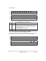
Chapter 14
Queued Serial Peripheral Interface (QSPI) Module
14.1
14.2
14.3
14.3.1
14.3.2
14.4
14.4.1
14.4.1.1
14.4.1.2
14.4.1.3
14.4.2
14.4.3
xiv
Overview...........................................................................................................
Features .............................................................................................................
Module Description ..........................................................................................
Interface and Pins..........................................................................................
Internal Bus Interface....................................................................................
Operation...........................................................................................................
QSPI RAM....................................................................................................
Receive RAM ...........................................................................................
Transmit RAM..........................................................................................
Command RAM........................................................................................
Baud Rate Selection......................................................................................
Transfer Delays.............................................................................................
MCF5272 User’s Manual
14-1
14-1
14-1
14-2
14-3
14-3
14-4
14-5
14-6
14-6
14-6
14-7
MOTOROLA
CONTENTS
Paragraph
Number
14.4.4
14.4.5
14.5
14.5.1
14.5.2
14.5.3
14.5.4
14.5.5
14.5.6
14.5.7
14.5.8
Title
Page
Number
Transfer Length............................................................................................. 14-8
Data Transfer ................................................................................................ 14-8
Programming Model ......................................................................................... 14-9
QSPI Mode Register (QMR) ........................................................................ 14-9
QSPI Delay Register (QDLYR) ................................................................. 14-11
QSPI Wrap Register (QWR)....................................................................... 14-12
QSPI Interrupt Register (QIR).................................................................... 14-12
QSPI Address Register (QAR) ................................................................... 14-14
QSPI Data Register (QDR)......................................................................... 14-14
Command RAM Registers (QCR0–QCR15).............................................. 14-14
Programming Example ............................................................................... 14-15
Chapter 15
Timer Module
15.1
15.2
15.3
15.3.1
15.3.2
15.3.3
15.3.4
15.3.5
Overview...........................................................................................................
Timer Operation................................................................................................
General-Purpose Timer Registers .....................................................................
Timer Mode Registers (TMR0–TMR3) .......................................................
Timer Reference Registers (TRR0–TRR3) ..................................................
Timer Capture Registers (TCAP0–TCAP3) .................................................
Timer Counters (TCN0–TCN3)....................................................................
Timer Event Registers (TER0–TER3)..........................................................
15-1
15-2
15-3
15-3
15-4
15-5
15-5
15-5
Chapter 16
UART Modules
16.1
16.2
16.3
16.3.1
16.3.2
16.3.3
16.3.4
16.3.5
16.3.6
16.3.7
16.3.8
16.3.9
16.3.10
16.3.11
16.3.12
MOTOROLA
Overview........................................................................................................... 16-1
Serial Module Overview ................................................................................... 16-2
Register Descriptions ........................................................................................ 16-3
UART Mode Registers 1 (UMR1n).............................................................. 16-5
UART Mode Register 2 (UMR2n) ............................................................... 16-6
UART Status Registers (USRn) ................................................................... 16-7
UART Clock-Select Registers (UCSRn)...................................................... 16-8
UART Command Registers (UCRn) ............................................................ 16-9
UART Receiver Buffers (URBn) ............................................................... 16-11
UART Transmitter Buffers (UTBn) ........................................................... 16-11
UART Input Port Change Registers (UIPCRn).......................................... 16-12
UART Auxiliary Control Registers (UACRn) ........................................... 16-12
UART Interrupt Status/Mask Registers (UISRn/UIMRn).......................... 16-13
UART Divider Upper/Lower Registers (UDUn/UDLn) ............................ 16-14
UART Autobaud Registers (UABUn/UABLn).......................................... 16-15
Contents
xv
CONTENTS
Paragraph
Number
16.3.13
16.3.14
16.3.15
16.3.16
16.3.17
16.4
16.5
16.5.1
16.5.1.1
16.5.1.2
16.5.1.2.1
16.5.1.2.2
16.5.1.2.3
16.5.2
16.5.2.1
16.5.2.2
16.5.2.3
16.5.2.4
16.5.3
16.5.3.1
16.5.3.2
16.5.3.3
16.5.4
16.5.5
16.5.5.1
16.5.5.2
16.5.5.3
16.5.6
16.5.6.1
Title
Page
Number
UART Transmitter FIFO Registers (UTFn) ...............................................
UART Receiver FIFO Registers (URFn) ...................................................
UART Fractional Precision Divider Control Registers (UFPDn) ..............
UART Input Port Registers (UIPn) ............................................................
UART Output Port Command Registers (UOP1n/UOP0n) .......................
UART Module Signal Definitions ..................................................................
Operation.........................................................................................................
Transmitter/Receiver Clock Source............................................................
Programmable Divider............................................................................
Calculating Baud Rates...........................................................................
CLKIN Baud Rates.............................................................................
External Clock ....................................................................................
Autobaud Detection ............................................................................
Transmitter and Receiver Operating Modes...............................................
Transmitting ...........................................................................................
Receiver ..................................................................................................
Transmitter FIFO ....................................................................................
Receiver FIFO .......................................................................................
Looping Modes ...........................................................................................
Automatic Echo Mode ............................................................................
Local Loop-Back Mode ..........................................................................
Remote Loop-Back Mode.......................................................................
Multidrop Mode..........................................................................................
Bus Operation .............................................................................................
Read Cycles ............................................................................................
Write Cycles ...........................................................................................
Interrupt Acknowledge Cycles ...............................................................
Programming ..............................................................................................
UART Module Initialization Sequence ..................................................
16-15
16-16
16-17
16-18
16-18
16-19
16-20
16-20
16-20
16-21
16-21
16-22
16-22
16-23
16-23
16-25
16-26
16-26
16-28
16-28
16-28
16-29
16-29
16-31
16-31
16-31
16-31
16-31
16-32
Chapter 17
General Purpose I/O Module
17.1
17.2
17.2.1
17.2.2
17.2.3
17.2.4
17.3
17.3.1
17.3.2
xvi
Overview........................................................................................................... 17-1
Port Control Registers....................................................................................... 17-2
Port A Control Register (PACNT)................................................................ 17-2
Port B Control Register (PBCNT) ................................................................ 17-5
Port C Control Register................................................................................. 17-8
Port D Control Register (PDCNT)................................................................ 17-8
Data Direction Registers ................................................................................... 17-9
Port A Data Direction Register (PADDR).................................................. 17-10
Port B Data Direction Register (PBDDR) .................................................. 17-10
MCF5272 User’s Manual
MOTOROLA
CONTENTS
Paragraph
Number
17.3.3
17.4
17.4.1
Title
Page
Number
Port C Data Direction Register (PCDDR) .................................................. 17-11
Port Data Registers ......................................................................................... 17-11
Port Data Register (PxDAT)....................................................................... 17-11
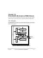
Chapter 18
Pulse Width Modulation (PWM) Module
18.1
18.2
18.3
18.3.1
18.3.2
Overview...........................................................................................................
PWM Operation ................................................................................................
PWM Programming Model...............................................................................
PWM Control Register (PWCRn) ................................................................
PWM Width Register (PWWDn) .................................................................
18-1
18-2
18-2
18-3
18-4
Chapter 19
Signal Descriptions
19.1
19.2
19.3
19.4
19.4.1
19.5
19.6
19.6.1
19.6.2
19.6.3
19.6.4
19.6.5
19.6.6
19.6.7
19.6.8
19.6.9
19.6.10
19.6.11
19.6.12
19.6.13
19.7
19.7.1
19.7.2
19.7.3
19.7.4
19.8
MOTOROLA
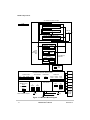
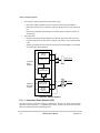
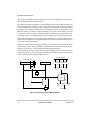
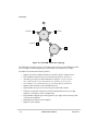
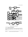
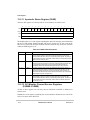
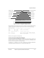
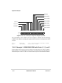
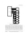
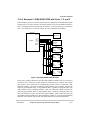
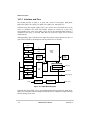
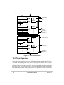
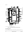
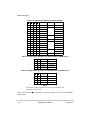
MCF5272 Block Diagram with Signal Interfaces ............................................ 19-1
Signal List ......................................................................................................... 19-2
Address Bus (A[22:0]/SDA[13:0]) ................................................................. 19-18
Data Bus (D[31:0]) ......................................................................................... 19-18
Dynamic Data Bus Sizing........................................................................... 19-18
Chip Selects (CS7/SDCS, CS[6:0]) ................................................................ 19-19
Bus Control Signals ........................................................................................ 19-19
Output Enable/Read (OE/RD) .................................................................... 19-19
Byte Strobes (BS[3:0])................................................................................ 19-19
Read/Write (R/W)....................................................................................... 19-21
Transfer Acknowledge (TA/PB5)............................................................... 19-21
Hi-Z............................................................................................................. 19-21
Bypass......................................................................................................... 19-22
SDRAM Row Address Strobe (RAS0)....................................................... 19-22
SDRAM Column Address Strobe (CAS0) ................................................. 19-22
SDRAM Clock (SDCLK)........................................................................... 19-22
SDRAM Write Enable (SDWE) ................................................................. 19-22
SDRAM Clock Enable (SDCLKE) ............................................................ 19-22
SDRAM Bank Selects (SDBA[1:0]) .......................................................... 19-22
SDRAM Row Address 10 (A10)/A10 Precharge (A10_PRECHG)........... 19-22
CPU Clock and Reset Signals......................................................................... 19-22
RSTI............................................................................................................ 19-22
DRESETEN ................................................................................................ 19-23
CPU External Clock (CLKIN).................................................................... 19-23
Reset Output (RSTO).................................................................................. 19-23
Interrupt Request Inputs (INT[6:1])................................................................ 19-23
Contents
xvii
CONTENTS
Paragraph
Number
19.9
19.10
19.10.1
19.10.2
19.10.3
19.10.4
19.10.5
19.11
19.11.1
19.11.2
19.11.3
19.11.4
19.11.5
19.11.6
19.11.7
19.11.8
19.11.9
19.11.10
19.12
19.12.1
19.12.2
19.12.3
19.12.4
19.13
19.13.1
19.13.2
19.13.3
19.13.4
19.13.5
19.13.6
19.13.7
19.13.8
19.13.9
19.13.10
19.13.11
19.13.12
19.13.13
19.13.14
19.14
19.15
19.15.1
19.15.2
19.15.3
xviii
Title
Page
Number
General-Purpose I/O (GPIO) Ports .................................................................
UART0 Module Signals and PB[4:0] .............................................................
Transmit Serial Data Output (URT0_TxD/PB0) ........................................
Receive Serial Data Input (URT0_RxD/PB1) ............................................
Clear-to-Send (URT0_CTS/PB2) ...............................................................
Request to Send (URT0_RTS/PB3) ............................................................
Clock (URT0_CLK/PB4) ...........................................................................
USB Module Signals and PA[6:0]..................................................................
USB Transmit Serial Data Output (USB_TP/PA0)....................................
USB Receive Serial Data Input (USB_RP/PA1)........................................
USB Receive Data Negative (USB_RN/PA2)............................................
USB Transmit Data Negative (USB_TN/PA3) ..........................................
USB Suspend Driver (USB_SUSP/PA4) ...................................................
USB Transmitter Output Enable (USB_TxEN/PA5) .................................
USB Rx Data Output (USB_RxD/PA6) .....................................................
USB_D+ and USB_D-................................................................................
USB_CLK...................................................................................................
INT1/USB Wake-on-Ring (USB_WOR) ...................................................
Timer Module Signals.....................................................................................
Timer Input 0 (TIN0)..................................................................................
Timer Output (TOUT0)/PB7 ......................................................................
Timer Input 1 (TIN1)/PWM Mode Output 2 (PWM_OUT2) ....................
Timer Output 1 (TOUT1)/PWM Mode Output 1 (PWM_OUT1)..............
Ethernet Module Signals.................................................................................
Transmit Clock (E_TxCLK).......................................................................
Transmit Data (E_TxD0) ............................................................................
Collision (E_COL)......................................................................................
Receive Data Valid (E_RxDV)...................................................................
Receive Clock (E_RxCLK) ........................................................................
Receive Data (E_RxD0) .............................................................................
Transmit Enable (E_TxEN) ........................................................................
Transmit Data (E_TxD[3:1]/PB[10:8]) ......................................................
Receive Data (E_RxD[3:1]/PB[13:11])......................................................
Receive Error (E_RxER/PB14) ..................................................................
Management Data Clock (E_MDC/PB15) .................................................
Management Data (E_MDIO) ....................................................................
Transmit Error (E_TxER)...........................................................................
Carrier Receive Sense (E_CRS) .................................................................
PWM Module Signals (PWM_OUT0–PWM_OUT2]) ..................................
Queued Serial Peripheral Interface (QSPI) Signals ........................................
QSPI Synchronous Serial Data Output (QSPI_Dout/WSEL).....................
QSPI Synchronous Serial Data Input (QSPI_Din) .....................................
QSPI Serial Clock (QSPI_CLK/BUSW1)..................................................
MCF5272 User’s Manual
19-23
19-24
19-24
19-24
19-24
19-25
19-25
19-25
19-25
19-25
19-25
19-25
19-25
19-26
19-26
19-26
19-26
19-26
19-27
19-27
19-27
19-27
19-27
19-27
19-27
19-27
19-28
19-28
19-28
19-28
19-28
19-28
19-28
19-29
19-29
19-29
19-29
19-29
19-29
19-30
19-30
19-30
19-30
MOTOROLA
CONTENTS
Paragraph
Number
19.15.4
19.15.5
19.15.6
19.15.7
19.16
19.16.1
19.16.1.1
19.16.1.2
19.16.1.3
19.16.1.4
19.16.1.5
19.16.1.6
19.16.1.7
19.16.1.8
19.16.1.9
19.16.2
19.16.2.1
19.16.2.2
19.16.2.3
19.16.2.4
19.16.2.5
19.16.2.6
19.16.3
19.16.3.1
19.16.3.2
19.16.3.3
19.16.3.4
19.17
19.17.1
19.17.2
19.17.3
19.17.4
19.17.5
19.17.6
19.17.7
19.17.8
19.17.9
19.17.10
19.18
19.19
MOTOROLA
Title
Page
Number
Synchronous Peripheral Chip Select 0 (QSPI_CS0/BUSW0)....................
Synchronous Peripheral Chip Select 1 (QSPI_CS1/PA11) ........................
Synchronous Peripheral Chip Select 2 (QSPI_CS2/URT1_CTS) ..............
Synchronous Peripheral Chip Select 3 (PA7/DOUT3/QSPI_CS3)............
Physical Layer Interface Controller TDM Ports and UART 1 .......................
GCI/IDL TDM Port 0. ................................................................................
Frame Sync (FSR0/FSC0/PA8)..............................................................
D-Channel Grant (DGNT0/PA9)............................................................
Data Clock (DCL0/URT1_CLK) ...........................................................
Serial Data Input (DIN0/URT1_RxD)....................................................
UART1 CTS (URT1_CTS/QSPI_CS2) .................................................
UART1 RTS (URT1_RTS/INT5)...........................................................
Serial Data Output (DOUT0/URT1_TxD) .............................................
D-Channel Request(DREQ0/PA10) .......................................................
QSPI Chip Select 1 (QSPI_CS1/PA11)..................................................
GCI/IDL TDM Port 1 .................................................................................
GCI/IDL Data Clock (DCL1/GDCL1_OUT).........................................
GCI/IDL Data Out (DOUT1) .................................................................
GCI/IDL Data In (DIN1) ........................................................................
GCI/IDL Frame Sync (FSC1/FSR1/DFSC1) .........................................
D-Channel Request (DREQ1/PA14) ......................................................
D-Channel Grant (DGNT1_INT6/PA15_INT6) ....................................
GCI/IDL TDM Ports 2 and 3......................................................................
GCI/IDL Delayed Frame Sync 2 (DFSC2/PA12) ..................................
GCI/IDL Delayed Frame Sync 3 (DFSC3/PA13) ..................................
QSPI_CS3, Port 3 GCI/IDL Data Out 3, PA7
(PA7/DOUT3/QSPI_CS3)..................................................................
INT4 and Port 3 GCI/IDL Data In (INT4/DIN3) ...................................
JTAG Test Access Port and BDM Debug Port...............................................
Test Clock (TCK/PSTCLK) .......................................................................
Test Mode Select and Force Breakpoint (TMS/BKPT)..............................
Test and Debug Data Out (TDO/DSO).......................................................
Test and Debug Data In (TDI/DSI) ............................................................
JTAG TRST and BDM Data Clock (TRST/DSCLK) ................................
Motorola Test Mode Select (MTMOD)......................................................
Debug Transfer Error Acknowledge (TEA) ...............................................
Processor Status Outputs (PST[3:0]) ..........................................................
Debug Data (DDATA[3:0])........................................................................
Device Test Enable (TEST)........................................................................
Operating Mode Configuration Pins...............................................................
Power Supply Pins ..........................................................................................
Contents
19-30
19-31
19-31
19-31
19-31
19-31
19-31
19-32
19-32
19-32
19-32
19-32
19-32
19-33
19-33
19-33
19-33
19-33
19-34
19-34
19-34
19-34
19-34
19-35
19-35
19-35
19-36
19-36
19-36
19-36
19-37
19-37
19-37
19-37
19-37
19-37
19-38
19-38
19-38
19-39
xix
CONTENTS
Paragraph
Number
Title
Page
Number
Chapter 20
Bus Operation
20.1
20.2
20.2.1
20.2.2
20.2.3
20.2.4
20.2.5
20.3
20.4
20.5
20.5.1
20.6
20.6.1
20.6.2
20.7
20.8
20.9
20.10
20.11
20.12
20.12.1
20.12.2
20.12.3
20.12.4
Features ............................................................................................................. 20-1
Bus and Control Signals.................................................................................... 20-1
Address Bus (A[22:0]).................................................................................. 20-2
Data Bus (D[31:0]) ....................................................................................... 20-2
Read/Write (R/W)......................................................................................... 20-2
Transfer Acknowledge (TA)......................................................................... 20-3
Transfer Error Acknowledge (TEA)............................................................. 20-3
Bus Exception: Double Bus Fault..................................................................... 20-4
Bus Characteristics............................................................................................ 20-4
Data Transfer Mechanism................................................................................. 20-4
Bus Sizing ..................................................................................................... 20-5
External Bus Interface Types............................................................................ 20-8
Interface for FLASH/SRAM Devices with Byte Strobes............................. 20-8
Interface for FLASH/SRAM Devices without Byte Strobes...................... 20-13
Burst Data Transfers ....................................................................................... 20-18
Misaligned Operands ...................................................................................... 20-18
Interrupt Cycles............................................................................................... 20-19
Bus Errors ....................................................................................................... 20-20
Bus Arbitration................................................................................................ 20-22
Reset Operation............................................................................................... 20-22
Master Reset ............................................................................................... 20-23
Normal Reset .............................................................................................. 20-24
Software Watchdog Timer Reset Operation............................................... 20-25
Soft Reset Operation................................................................................... 20-26
Chapter 21
IEEE 1149.1 Test Access Port (JTAG)
21.1
21.2
21.3
21.4
21.5
21.6
21.7
xx
Overview...........................................................................................................
JTAG Test Access Port and BDM Debug Port.................................................
TAP Controller..................................................................................................
Boundary Scan Register....................................................................................
Instruction Register...........................................................................................
Restrictions .......................................................................................................
Non-IEEE 1149.1 Operation.............................................................................
MCF5272 User’s Manual
21-1
21-2
21-3
21-4
21-7
21-8
21-9
MOTOROLA
CONTENTS
Paragraph
Number
Title
Page
Number
Chapter 22
Mechanical Data
22.1
22.2
Pinout ................................................................................................................ 22-1
Package Dimensions ......................................................................................... 22-2
Chapter 23
Electrical Characteristics
23.1
23.1.1
23.1.2
23.1.3
23.2
23.2.1
23.3
23.3.1
23.3.2
23.3.3
23.4
23.5
23.6
23.6.1
23.6.2
23.6.3
23.6.4
23.7
23.8
23.9
23.10
23.11
23.12
23.13
23.14
Maximum Ratings............................................................................................. 23-1
Supply, Input Voltage, and Storage Temperature......................................... 23-1
Operating Temperature ................................................................................. 23-2
Resistance ..................................................................................................... 23-2
DC Electrical Specifications ............................................................................. 23-3
Output Driver Capability and Loading ......................................................... 23-3
AC Electrical Specifications ............................................................................. 23-5
Clock Input and Output Timing Specifications ............................................ 23-5
Processor Bus Input Timing Specifications.................................................. 23-6
Processor Bus Output Timing Specifications ............................................... 23-7
Debug AC Timing Specifications................................................................... 23-12
SDRAM Interface Timing Specifications....................................................... 23-13
Fast Ethernet AC Timing Specifications ........................................................ 23-15
MII Receive Signal Timing (E_RxD[3:0], E_RxDV, E_RxER, and
E_RxCLK).............................................................................................. 23-15
MII Transmit Signal Timing (E_TxD[3:0], E_TxEN, E_TxER,
E_TxCLK) .............................................................................................. 23-16
MII Async Inputs Signal Timing (CRS and COL) ..................................... 23-17
MII Serial Management Channel Timing (MDIO and MDC).................... 23-17
Timer Module AC Timing Specifications ...................................................... 23-18
UART Modules AC Timing Specifications.................................................... 23-19
PLIC Module: IDL and GCI Interface Timing Specifications ....................... 23-20
General-Purpose I/O Port AC Timing Specifications..................................... 23-25
USB Interface AC Timing Specifications....................................................... 23-25
IEEE 1149.1 (JTAG) AC Timing Specifications ........................................... 23-26
QSPI Electrical Specifications........................................................................ 23-27
PWM Electrical Specifications ....................................................................... 23-28
Appendix A
List of Memory Maps
A.1
MOTOROLA
List of Memory Map Tables .............................................................................. A-1
Contents
xxi
CONTENTS
Paragraph
Number
Title
Page
Number
Appendix B
Buffering and Impedance Matching
Index
xxii
MCF5272 User’s Manual
MOTOROLA
ILLUSTRATIONS
Figure
Number
1-1
2-1
2-2
2-3
2-4
2-5
2-6
2-7
2-8
2-9
2-10
3-1
3-2
4-1
4-2
4-3
4-4
4-5
5-1
5-2
5-3
5-4
5-5
5-6
5-7
5-8
5-9
5-10
5-11
5-12
5-13
5-14
5-15
5-16
5-18
5-17
Title
Page
Number
MCF5272 Block Diagram............................................................................................. 1-2
ColdFire Pipeline .......................................................................................................... 2-2
ColdFire Multiply-Accumulate Functionality Diagram ............................................... 2-4
ColdFire Programming Model...................................................................................... 2-6
Condition Code Register (CCR) ................................................................................... 2-7
Status Register (SR)...................................................................................................... 2-9
Vector Base Register (VBR)......................................................................................... 2-9
Organization of Integer Data Formats in Data Registers............................................ 2-11
Organization of Integer Data Formats in Address Registers ...................................... 2-11
Memory Operand Addressing..................................................................................... 2-12
Exception Stack Frame Form...................................................................................... 2-28
ColdFire MAC Multiplication and Accumulation........................................................ 3-2
MAC Programming Model ........................................................................................... 3-2
SRAM Base Address Register (RAMBAR) ................................................................. 4-3
ROM Base Address Register (ROMBAR) .................................................................. 4-6
Instruction Cache Block Diagram................................................................................. 4-8
Cache Control Register (CACR) ................................................................................ 4-13
Access Control Register Format (ACRn) ................................................................... 4-15
Processor/Debug Module Interface............................................................................... 5-1
PSTCLK Timing........................................................................................................... 5-2
Example JMP Instruction Output on PST/DDATA...................................................... 5-5
Debug Programming Model ......................................................................................... 5-6
Address Attribute Trigger Register (AATR) ................................................................ 5-7
Address Breakpoint Registers (ABLR, ABHR) ........................................................... 5-9
Configuration/Status Register (CSR).......................................................................... 5-10
Data Breakpoint/Mask Registers (DBR and DBMR)................................................. 5-12
Program Counter Breakpoint Register (PBR)............................................................. 5-13
Program Counter Breakpoint Mask Register (PBMR) ............................................... 5-13
Trigger Definition Register (TDR) ............................................................................. 5-14
BDM Serial Interface Timing ..................................................................................... 5-17
Receive BDM Packet.................................................................................................. 5-17
Transmit BDM Packet ................................................................................................ 5-18
BDM Command Format ............................................................................................. 5-20
Command Sequence Diagram..................................................................................... 5-21
RAREG/RDREG Command Sequence............................................................................ 5-22
RAREG/RDREG Command Format ............................................................................... 5-22
MOTOROLA
Illustrations
xxiii
ILLUSTRATIONS
Figure
Page
Title
Number
Number
5-20
WAREG/WDREG Command Sequence .......................................................................... 5-23
WAREG/WDREG Command Format.............................................................................. 5-23
5-19
READ Command Sequence.......................................................................................... 5-24
5-22
READ Command/Result Formats................................................................................. 5-24
5-21
WRITE Command Format ............................................................................................ 5-25
5-23
WRITE Command Sequence ........................................................................................ 5-26
5-24
DUMP Command/Result Formats ............................................................................... 5-27
5-25
DUMP Command Sequence ......................................................................................... 5-28
5-26
FILL Command Sequence............................................................................................ 5-29
5-28
FILL Command Format............................................................................................... 5-29
5-27
GO Command Sequence.............................................................................................. 5-30
5-30
NOP Command Sequence ............................................................................................ 5-30
5-32
GO Command Format.................................................................................................. 5-30
5-29
NOP Command Format................................................................................................ 5-30
5-31
RCREG Command Sequence........................................................................................ 5-31
5-34
RCREG Command/Result Formats............................................................................... 5-31
5-33
WCREG Command Sequence ....................................................................................... 5-32
5-36
WCREG Command/Result Formats.............................................................................. 5-32
5-35
RDMREG Command Sequence..................................................................................... 5-33
5-38
RDMREG BDM Command/Result Formats .................................................................. 5-33
5-37
WDMREG BDM Command Format.............................................................................. 5-33
5-39
WDMREG Command Sequence .................................................................................... 5-34
5-40
5-41
Recommended BDM Connector................................................................................. 5-42
6-1
SIM Block Diagram...................................................................................................... 6-1
6-2
Module Base Address Register (MBAR) ..................................................................... 6-4
6-3
System Configuration Register (SCR).......................................................................... 6-5
6-4
System Protection Register (SPR) ................................................................................ 6-6
6-5
Power Management Register (PMR) ............................................................................ 6-8
6-6
Activate Low-Power Register (ALPR)....................................................................... 6-10
6-7
Device Identification Register (DIR).......................................................................... 6-12
6-8
Watchdog Reset Reference Register (WRRR) ........................................................... 6-13
6-9
Watchdog Interrupt Reference Register (WIRR) ....................................................... 6-13
6-10
Watchdog Counter Register (WCR) ........................................................................... 6-14
6-11
Watchdog Event Register (WER)............................................................................... 6-14
7-1
Interrupt Controller Block Diagram.............................................................................. 7-2
7-2
Interrupt Control Register 1 (ICR1).............................................................................. 7-4
7-3
Interrupt Control Register 2 (ICR2).............................................................................. 7-5
7-4
Interrupt Control Register 3 (ICR3).............................................................................. 7-5
7-5
Interrupt Control Register 4(ICR4)............................................................................... 7-6
7-6
Interrupt Source Register (ISR) .................................................................................... 7-6
7-7
Programmable Interrupt Transition Register (PITR).................................................... 7-7
7-8
Programmable Interrupt Wakeup Register (PIWR)...................................................... 7-8
7-9
Programmable Interrupt Vector Register (PIVR) ......................................................... 7-9
xxiv
MCF5272 User’s Manual
MOTOROLA
ILLUSTRATIONS
Figure
Number
8-1
8-2
9-1
9-2
9-3
9-4
9-5
9-6
9-7
9-8
9-9
9-10
9-11
9-12
9-13
9-14
9-15
10-1
10-2
10-3
10-4
10-5
11-1
11-2
11-3
11-4
11-5
11-6
11-7
11-8
11-9
11-10
11-11
11-12
11-13
11-14
11-15
11-16
11-17
11-18
11-19
11-20
11-21
Title
Page
Number
Chip Select Base Registers (CSBRn) ........................................................................... 8-3
Chip Select Option Registers (CSORn)....................................................................... 8-5
SDRAM Controller Signals .......................................................................................... 9-2
54-Pin TSOP SDRAM Pin Definition .......................................................................... 9-3
SDRAM Configuration Register (SDCR) .................................................................... 9-6
SDRAM Timing Register (SDTR) ............................................................................... 9-8
Example Setup Time Violation on SDRAM Data Input during Write....................... 9-13
Timing Refinement with Inverted SDCLK................................................................. 9-13
Timing Refinement with True CAS Latency and Inverted SDCLK........................... 9-14
Timing Refinement with Effective CAS Latency....................................................... 9-14
SDRAM Burst Read, 32-Bit Port, Page Miss, Access = 9-1-1-1 ............................... 9-17
SDRAM Burst Read, 32-Bit Port, Page Hit, Access = 5-1-1-1 .................................. 9-18
SDRAM Burst Write, 32-Bit Port, Page Miss, Access = 7-1-1-1 .............................. 9-19
SDRAM Burst Write, 32-Bit Port, Page Hit, Access = 3-1-1-1 ................................. 9-20
SDRAM Refresh Cycle............................................................................................... 9-21
Enter SDRAM Self-Refresh Mode ............................................................................. 9-22
Exit SDRAM Self-Refresh Mode ............................................................................... 9-23
DMA Mode Register (DMR)...................................................................................... 10-2
DMA Interrupt Register (DIR) ................................................................................... 10-4
DMA Source Address Register (DSAR) .................................................................... 10-6
DMA Destination Address Register (DDAR) ............................................................ 10-6
DMA Byte Count Register (DBCR) ........................................................................... 10-6
Ethernet Block Diagram ............................................................................................. 11-2
Fast Ethernet Module Block Diagram ........................................................................ 11-2
Ethernet Frame Format ............................................................................................... 11-4
Ethernet Address Recognition Flowchart ................................................................... 11-8
Ethernet Control Register (ECR) .............................................................................. 11-12
EIMR Register ......................................................................................................... 11-14
Interrupt Vector Status Register (IVSR)................................................................... 11-14
RDAR Register ......................................................................................................... 11-15
TDAR Register ......................................................................................................... 11-16
MII Management Frame Register (MMFR) ............................................................. 11-17
MII Speed Control Register (MSCR) ...................................................................... 11-18
FIFO Receive Bound Register (FRBR) ................................................................... 11-20
FIFO Receive Start Register (FRSR)....................................................................... 11-20
Transmit FIFO Watermark (TFWR)........................................................................ 11-21
FIFO Transmit Start Register (TFSR) ...................................................................... 11-22
Receive Control Register (RCR) .............................................................................. 11-23
Maximum Frame Length Register (MFLR) ............................................................. 11-24
Transmit Control Register (TCR) ............................................................................. 11-25
RAM Perfect Match Address Low (MALR) ............................................................ 11-26
RAM Perfect Match Address High (MAUR) ........................................................... 11-26
Hash Table High (HTUR)........................................................................................ 11-27
MOTOROLA
Illustrations
xxv
ILLUSTRATIONS
Figure
Page
Title
Number
Number
11-22
Hash Table Low (HTLR)......................................................................................... 11-27
11-23 Pointer to Receive Descriptor Ring (ERDSR).......................................................... 11-28
11-24 Pointer to Transmit Descriptor Ring (ETDSR) ........................................................ 11-29
11-25 Receive Buffer Size (EMRBR)................................................................................. 11-29
11-26 Receive Buffer Descriptor (RxBD) .......................................................................... 11-33
11-27
Transmit Buffer Descriptor (TxBD) ........................................................................ 11-34
12-1
The USB “tiered star” topology.................................................................................. 12-2
12-2
USB Module Block Diagram...................................................................................... 12-3
12-3
USB Frame Number Register (FNR).......................................................................... 12-9
12-4
USB Frame Number Match Register (FNMR)........................................................... 12-9
12-5
USB Real-Time Frame Monitor Register (RFMR) .................................................. 12-10
12-6
USB Real-Time Frame Monitor Match Register (RFMMR) ................................... 12-11
12-7
USB Function Address Register (FAR).................................................................... 12-11
12-8
USB Alternate Settings Register (ASR) ................................................................... 12-12
12-9
USB Device Request Data 1 Register (DRR1)......................................................... 12-12
12-10 USB Device Request Data 2 Register (DRR2)......................................................... 12-13
12-11 USB Specification Number Register (SPECR) ........................................................ 12-13
12-12 USB Endpoint 0 Status Register (EP0SR)................................................................ 12-14
12-13 USB Endpoint 0 IN Configuration Register (IEP0CFG).......................................... 12-15
12-14 USB Endpoint 0 OUT Configuration Register ......................................................... 12-15
12-15 USB Endpoint 1–7 Configuration Register .............................................................. 12-16
12-16 USB Endpoint 0 Control Register (EP0CTL)........................................................... 12-16
12-17 USB Endpoint 1-7 Control Register (EPnCTL) ....................................................... 12-19
12-18 USB Endpoint 0 Interrupt Mask (EP0IMR) and General/Endpoint 0
Interrupt Registers (EP0ISR) .................................................................................... 12-21
12-19 USB Endpoints 1–7 Interrupt Status Registers (EPnISR) ........................................ 12-23
12-20 USB Endpoint 1-7 Interrupt Mask Registers (EPnIMR) .......................................... 12-24
12-22 USB Endpoint 0-7 Data Present Registers (EPnDPR) ............................................. 12-25
12-21 USB Endpoint 0-7 Data Registers (EPnDR) ............................................................ 12-25
12-23 Example USB Configuration Descriptor Structure................................................... 12-27
12-24 Recommended USB Line Interface .......................................................................... 12-34
12-25 USB Protection Circuit ............................................................................................. 12-36
13-1
PLIC System Diagram ................................................................................................ 13-2
13-2
GCI/IDL Receive Data Flow ...................................................................................... 13-3
13-3
GCI/IDL B-Channel Receive Data Register Demultiplexing..................................... 13-4
13-4
GCI/IDL Transmit Data Flow..................................................................................... 13-4
13-5
GCI/IDL B Data Transmit Register Multiplexing ...................................................... 13-5
13-6
B-Channel Unencoded and HDLC Encoded Data...................................................... 13-6
13-7
D-Channel HDLC Encoded and Unencoded Data...................................................... 13-7
13-8
D-Channel Contention ................................................................................................ 13-8
13-9
GCI/IDL Loopback Mode........................................................................................... 13-9
13-10 Periodic Frame Interrupt ........................................................................................... 13-10
13-11 PLIC Internal Timing Signal Routing....................................................................... 13-13
xxvi
MCF5272 User’s Manual
MOTOROLA
ILLUSTRATIONS
Figure
Number
13-12
13-13
13-14
13-15
13-16
13-17
13-18
13-19
13-20
13-21
13-22
13-23
13-24
13-25
13-26
13-27
13-28
13-29
13-30
13-31
13-32
13-33
13-34
13-35
13-36
13-37
13-38
13-39
13-40
13-41
13-42
14-1
14-2
14-3
14-4
14-5
14-6
14-7
14-8
14-9
14-10
15-1
15-2
Title
Page
Number
PLIC Clock Generator .............................................................................................. 13-13
B1 Receive Data Registers P0B1RR–P3B1RR ........................................................ 13-16
B2 Receive Data Registers P0B2RR – P3B2RR ...................................................... 13-16
D Receive Data Registers P0DRR–P3DRR ............................................................. 13-17
B1 Transmit Data Registers P0B1TR–P3B1TR ....................................................... 13-17
B2 Transmit Data Registers P0B2TR–P3B2TR ....................................................... 13-18
D Transmit Data Registers P0DTR–P3DTR ............................................................ 13-18
Port Configuration Registers (P0CR–P3CR)............................................................ 13-19
Loopback Control Register (PLCR) ......................................................................... 13-20
Interrupt Configuration Registers (P0ICR–P3ICR).................................................. 13-21
Periodic Status Registers (P0PSR–P3PSR) .............................................................. 13-22
Aperiodic Status Register (PASR)............................................................................ 13-24
GCI Monitor Channel Receive Registers (P0GMR–P3GMR) ................................. 13-25
GCI Monitor Channel Transmit Registers (P0GMT–P3GMT) ................................ 13-26
GCI Monitor Channel Transmit Abort Register (PGMTA) ..................................... 13-26
GCI Monitor Channel Transmit Status Register (PGMTS)...................................... 13-27
GCI C/I Channel Receive Registers (P0GCIR–P3GCIR) ........................................ 13-28
GCI C/I Channel Transmit Registers (P0GCIT–P3GCIT) ....................................... 13-29
GCI C/I Channel Transmit Status Register (PGCITSR)........................................... 13-30
D-Channel Status Register (PDCSR)........................................................................ 13-30
D-Channel Request Registers (PDRQR) .................................................................. 13-31
Sync Delay Registers (P0SDR–P3SDR) .................................................................. 13-32
Clock Select Register (PCSR) .................................................................................. 13-33
Port 1 Configuration Register (P1CR)...................................................................... 13-35
Port 1 Interrupt Configuration Register (P1ICR)...................................................... 13-36
ISDN SOHO PABX Example .................................................................................. 13-37
Standard IDL2 10-Bit Mode ..................................................................................... 13-38
ISDN SOHO PABX Example .................................................................................. 13-39
Standard IDL2 10-bit mode. ..................................................................................... 13-40
Two-Line Remote Access......................................................................................... 13-41
Standard IDL2 8-Bit mode........................................................................................ 13-41
QSPI Block Diagram .................................................................................................. 14-2
QSPI RAM Model ...................................................................................................... 14-5
QSPI Mode Register (QMR) ...................................................................................... 14-9
QSPI Clocking and Data Transfer Example ............................................................. 14-11
QSPI Delay Register (QDLYR)................................................................................ 14-11
QSPI Wrap Register (QWR)..................................................................................... 14-12
QSPI Interrupt Register (QIR) .................................................................................. 14-12
QSPI Address Register ............................................................................................. 14-14
QSPI Data Register ................................................................................................... 14-14
Command RAM Registers (QCR0–QCR15)............................................................ 14-15
Timer Block Diagram ................................................................................................. 15-2
Timer Mode Registers (TMR0–TMR3)...................................................................... 15-3
MOTOROLA
Illustrations
xxvii
ILLUSTRATIONS
Figure
Page
Title
Number
Number
15-3
Timer Reference Registers (TRR0–TRR3) ................................................................ 15-4
15-4
Timer Capture Registers (TCAP0–TCAP3) ............................................................... 15-5
15-5
Timer Counter (TCN0–TCN3) ................................................................................... 15-5
15-6
Timer Event Registers (TER0–TER3)........................................................................ 15-5
16-1
Simplified Block Diagram .......................................................................................... 16-1
16-2
UART Mode Registers 1 (UMR1n)............................................................................ 16-5
16-3
UART Mode Register 2 (UMR2n) ............................................................................. 16-6
16-4
UART Status Registers (USRn).................................................................................. 16-7
16-5
UART Clock-Select Registers (UCSRn) .................................................................... 16-9
16-6
UART Command Registers (UCRn) .......................................................................... 16-9
16-7
UART Receiver Buffer (URBn) ............................................................................... 16-11
16-8
UART Transmitter Buffers (UTBn) ......................................................................... 16-12
16-9
UART Input Port Change Registers (UIPCRn) ........................................................ 16-12
16-10 UART Auxiliary Control Registers (UACRn) ......................................................... 16-13
16-11 UART Interrupt Status/Mask Registers (UISRn/UIMRn)........................................ 16-13
16-12 UART Divider Upper Registers (UDUn) ................................................................. 16-14
16-13 UART Divider Lower Registers (UDLn) ................................................................. 16-15
16-14 UART Autobaud Upper Registers (UABUn) ........................................................... 16-15
16-15 UART Autobaud Lower Registers (UABLn) ........................................................... 16-15
16-16 UART Transmitter FIFO Registers (UTFn) ............................................................. 16-16
16-17 UART Receiver FIFO Registers (URFn) ................................................................. 16-16
16-18 UART Fractional Precision Divider Control Registers (UFPDn) ............................ 16-17
16-19 UART Input Port Registers (UIPn)........................................................................... 16-18
16-20 UART Output Port Command Registers (UOP1/UOP0).......................................... 16-18
16-21 UART Block Diagram Showing External and Internal Interface Signals ................ 16-19
16-22 UART/RS-232 Interface ........................................................................................... 16-20
16-23 Clocking Source Diagram......................................................................................... 16-21
16-24 Transmitter and Receiver Functional Diagram......................................................... 16-23
16-25
Transmitter Timing .................................................................................................. 16-24
16-26 Receiver Timing........................................................................................................ 16-25
16-27 Automatic Echo ........................................................................................................ 16-28
16-28 Local Loop-Back ...................................................................................................... 16-28
16-29 Remote Loop-Back ................................................................................................... 16-29
16-30 Multidrop Mode Timing Diagram ............................................................................ 16-30
16-31 UART Mode Programming Flowchart ..................................................................... 16-32
17-1
Port A Control Register (PACNT).............................................................................. 17-3
17-2
Port B Control Register (PBCNT) .............................................................................. 17-5
17-3
Port D Control Register (PDCNT).............................................................................. 17-8
17-4
Port A Data Direction Register (PADDR)................................................................ 17-10
17-5
Port B Data Direction Register (PBDDR) ................................................................ 17-10
17-6
Port C Data Direction Register (PCDDR) ................................................................ 17-11
17-7
Port x Data Register (PADAT, PBDAT, and PCDAT) ............................................ 17-11
18-1
PWM Block Diagram (3 Identical Modules).............................................................. 18-1
xxviii
MCF5272 User’s Manual
MOTOROLA
ILLUSTRATIONS
Figure
Number
18-2
18-3
18-4
19-1
20-1
20-2
20-3
20-4
20-5
20-6
20-7
20-8
20-9
20-10
20-11
20-12
20-13
20-14
20-15
20-16
20-17
20-18
20-19
20-20
20-21
20-22
20-23
20-24
21-1
21-2
21-3
21-4
21-5
21-6
21-7
21-8
22-1
22-2
23-1
23-2
23-3
Title
Page
Number
PWM Control Registers (PWCRn)............................................................................. 18-3
PWM Width Register (PWWDn) ............................................................................... 18-4
PWM Waveform Examples (PWCRn[EN] = 1)......................................................... 18-5
MCF5272 Block Diagram with Signal Interfaces ...................................................... 19-2
Internal Operand Representation ................................................................................ 20-5
MCF5272 Interface to Various Port Sizes .................................................................. 20-6
Longword Read; EBI = 00; 32-Bit Port; Internal Termination .................................. 20-9
Word Write; EBI = 00; 16-/32-Bit Port; Internal Termination................................. 20-10
Longword Read with Address Setup; EBI = 00; 32-Bit Port; Internal Termination 20-10
Longword Write with Address Setup; EBI = 00; 32-Bit Port; Internal Termination 20-11
Longword Read with Address Hold; EBI = 00; 32-Bit Port; Internal Termination . 20-11
Longword Write with Address Hold; EBI = 00; 32-Bit Port; Internal Termination 20-12
Longword Read; EBI = 00; 32-Bit Port; Terminated by TA with One Wait State .. 20-12
Longword Read; EBI=11; 32-Bit Port; Internal Termination .................................. 20-13
Word Write; EBI=11; 16/32-Bit Port; Internal Termination .................................... 20-14
Read with Address Setup; EBI=11; 32-Bit Port; Internal Termination.................... 20-15
Longword Write with Address Setup; EBI=11; 32-Bit Port; Internal Termination . 20-15
Read with Address Hold; EBI=11; 32-Bit Port; Internal Termination ..................... 20-16
Longword Write with Address Hold; EBI=11; 32-Bit Port; Internal Termination .. 20-16
Longword Read with Address Setup and Address Hold; EBI = 11; 32-Bit Port,
Internal Termination ................................................................................................. 20-17
Longword Write with Address Setup and Address Hold; EBI = 11; 32-Bit Port,
Internal Termination ................................................................................................. 20-17
Example of a Misaligned Longword Transfer .......................................................... 20-19
Example of a Misaligned Word Transfer.................................................................. 20-19
Longword Write Access To 32-Bit Port Terminated with TEA Timing .................. 20-21
Master Reset Timing................................................................................................. 20-23
Normal Reset Timing................................................................................................ 20-24
Software Watchdog Timer Reset Timing ................................................................. 20-25
Soft Reset Timing ..................................................................................................... 20-27
Test Access Port Block Diagram ................................................................................ 21-2
TAP Controller State Machine.................................................................................... 21-4
Output Cell (O.Cell) (BC–1)....................................................................................... 21-5
Input Cell (I.Cell). Observe only (BC–4) ................................................................... 21-5
Output Control Cell (En.Cell) (BC–4)........................................................................ 21-6
Bidirectional Cell (IO.Cell) (BC–6) ........................................................................... 21-6
General Arrangement for Bidirectional Pins .............................................................. 21-7
Bypass Register........................................................................................................... 21-8
MCF5272 Pinout (196 MAPBGA)............................................................................. 22-1
196 MAPBGA Package Dimensions (Case No. 1128A-01) ...................................... 22-2
Clock Input Timing Diagram...................................................................................... 23-5
General Input Timing Requirements .......................................................................... 23-7
Read/Write SRAM Bus Timing.................................................................................. 23-9
MOTOROLA
Illustrations
xxix
ILLUSTRATIONS
Figure
Page
Title
Number
Number
23-4
SRAM Bus Cycle Terminated by TA....................................................................... 23-10
23-5
SRAM Bus Cycle Terminated by TEA .................................................................... 23-11
23-6
Reset and Mode Select/HIZ Configuration Timing.................................................. 23-11
23-7
Real-Time Trace AC Timing .................................................................................... 23-12
23-8
BDM Serial Port AC Timing .................................................................................... 23-12
23-9
SDRAM Signal Timing ............................................................................................ 23-14
23-10 SDRAM Self-Refresh Cycle Timing ........................................................................ 23-15
23-11 MII Receive Signal Timing Diagram ....................................................................... 23-16
23-12 MII Transmit Signal Timing Diagram...................................................................... 23-17
23-13 MII Async Inputs Timing Diagram .......................................................................... 23-17
23-14 MII Serial Management Channel Timing Diagram .................................................. 23-18
23-15 Timer Timing ............................................................................................................ 23-19
23-16 UART Timing........................................................................................................... 23-20
23-17 IDL Master Timing ................................................................................................... 23-21
23-18 IDL Slave Timing ..................................................................................................... 23-22
23-19 GCI Slave Mode Timing........................................................................................... 23-23
23-20 GCI Master Mode Timing ........................................................................................ 23-24
23-21 General-Purpose I/O Port Timing............................................................................. 23-25
23-22 USB Interface Timing............................................................................................... 23-26
23-23 IEEE 1149.1 (JTAG) Timing.................................................................................... 23-27
23-24 QSPI Timing ............................................................................................................. 23-28
23-25 PWM Timing ............................................................................................................ 23-29
B-1
Buffering and Termination ...........................................................................................B-2
xxx
MCF5272 User’s Manual
MOTOROLA
TABLES
Table
Number
2-1
2-2
2-3
2-4
2-5
2-6
2-7
2-8
2-9
2-10
2-11
2-12
2-13
2-14
2-15
2-16
2-17
2-18
2-19
2-20
2-21
3-1
4-1
4-2
4-3
4-4
4-5
4-6
4-7
4-8
4-9
5-1
5-2
5-3
5-4
5-5
Title
Page
Number
CCR Field Descriptions ............................................................................................... 2-7
MOVEC Register Map ................................................................................................. 2-8
Status Field Descriptions .............................................................................................. 2-9
Integer Data Formats................................................................................................... 2-10
ColdFire Effective Addressing Modes....................................................................... 2-13
Notational Conventions ............................................................................................. 2-14
User-Mode Instruction Set Summary ......................................................................... 2-16
Supervisor-Mode Instruction Set Summary............................................................... 2-19
Misaligned Operand References ................................................................................ 2-20
Move Byte and Word Execution Times...................................................................... 2-21
Move Long Execution Times..................................................................................... 2-21
Move Execution Times .............................................................................................. 2-22
One-Operand Instruction Execution Times ................................................................ 2-22
Two-Operand Instruction Execution Times................................................................ 2-23
Miscellaneous Instruction Execution Times............................................................... 2-24
General Branch Instruction Execution Times............................................................. 2-25
Bcc Instruction Execution Times............................................................................... 2-26
Exception Vector Assignments................................................................................... 2-27
Format Field Encoding ............................................................................................... 2-28
Fault Status Encodings................................................................................................ 2-28
MCF5272 Exceptions ................................................................................................. 2-29
MAC Instruction Summary........................................................................................... 3-4
Memory Map of Instruction Cache Registers............................................................... 4-2
RAMBAR Field Description ........................................................................................ 4-3
Examples of Typical RAMBAR Settings ..................................................................... 4-5
ROMBAR Field Description ........................................................................................ 4-6
Examples of Typical ROMBAR Settings ..................................................................... 4-7
Instruction Cache Operation as Defined by CACR[CENB,CEIB]............................. 4-12
Memory Map of Instruction Cache Registers............................................................. 4-13
CACR Field Descriptions ........................................................................................... 4-13
ACRn Field Descriptions............................................................................................ 4-15
Debug Module Signals.................................................................................................. 5-2
Processor Status Encoding............................................................................................ 5-3
BDM/Breakpoint Registers........................................................................................... 5-6
Rev. A Shared BDM/Breakpoint Hardware ................................................................. 5-7
AATR Field Descriptions ............................................................................................. 5-8
MOTOROLA
Tables
xxxi
TABLES
Table
Number
5-6
5-7
5-8
5-9
5-10
5-11
5-12
5-13
5-14
5-15
5-16
5-17
5-18
5-19
5-20
5-21
5-22
5-23
6-1
6-2
6-3
6-4
6-5
6-6
6-7
6-8
6-9
6-10
6-11
7-1
7-2
7-3
7-4
7-5
7-6
7-7
7-8
8-1
8-2
8-3
8-4
8-5
9-1
xxxii
Title
Page
Number
ABLR Field Description ............................................................................................... 5-9
ABHR Field Description............................................................................................... 5-9
CSR Field Descriptions............................................................................................... 5-10
DBR Field Descriptions.............................................................................................. 5-12
DBMR Field Descriptions .......................................................................................... 5-12
Access Size and Operand Data Location .................................................................... 5-12
PBR Field Descriptions............................................................................................... 5-13
PBMR Field Descriptions ........................................................................................... 5-13
TDR Field Descriptions .............................................................................................. 5-14
Receive BDM Packet Field Description ..................................................................... 5-18
Transmit BDM Packet Field Description ................................................................... 5-18
BDM Command Summary ......................................................................................... 5-19
BDM Field Descriptions ............................................................................................. 5-20
Control Register Map.................................................................................................. 5-31
Definition of DRc Encoding—Read........................................................................... 5-33
DDATA[3:0]/CSR[BSTAT] Breakpoint Response.................................................... 5-34
PST/DDATA Specification for User-Mode Instructions............................................ 5-37
PST/DDATA Specification for Supervisor-Mode Instructions.................................. 5-41
SIM Registers................................................................................................................ 6-3
MBAR Field Descriptions ........................................................................................... 6-5
SCR Field Descriptions................................................................................................. 6-5
SPR Field Descriptions ................................................................................................. 6-7
PMR Field Descriptions................................................................................................ 6-8
USB and USART Power Down Modes ...................................................................... 6-10
Exiting Sleep and Stop Modes.................................................................................... 6-11
DIR Field Descriptions ............................................................................................... 6-12
WRRR Field Descriptions .......................................................................................... 6-13
WIRR Field Descriptions............................................................................................ 6-13
WER Field Descriptions ............................................................................................. 6-14
Interrupt Controller Registers ....................................................................................... 7-2
Interrupt and Power Management Register Mnemonics .............................................. 7-3
ICR Field Descriptions ................................................................................................. 7-5
ISR Field Descriptions.................................................................................................. 7-7
PITR Field Descriptions ............................................................................................... 7-7
PIWR Field Descriptions .............................................................................................. 7-8
PIVR Field Descriptions ............................................................................................... 7-9
MCF5272 Interrupt Vector Table ................................................................................. 7-9
CSCR and CSOR Values after Reset............................................................................ 8-2
CSBRn Field Descriptions............................................................................................ 8-3
Output Read/Write Strobe Levels versus Chip Select EBI Code ................................. 8-4
Chip Select Memory Address Decoding Priority ......................................................... 8-5
CSORn Field Descriptions............................................................................................ 8-5
SDRAM Controller Signal Descriptions ...................................................................... 9-2
MCF5272 User’s Manual
MOTOROLA
TABLES
Table
Number
9-2
9-3
9-4
9-5
9-6
9-7
9-8
9-9
9-10
9-11
9-12
9-13
10-1
10-2
10-3
11-1
11-2
11-3
11-4
11-5
11-6
11-7
11-8
11-9
11-10
11-11
11-12
11-13
11-14
11-15
11-16
11-17
11-18
11-19
11-20
11-21
11-22
11-23
11-24
11-25
11-26
Title
Page
Number
Connecting BS[3:0] to DQMx ...................................................................................... 9-4
Configurations for 16-Bit Data Bus.............................................................................. 9-4
Configurations for 32-Bit Data Bus.............................................................................. 9-4
Internal Address Multiplexing (16-Bit Data Bus) ........................................................ 9-5
Internal Address Multiplexing (32-Bit Data Bus) ........................................................ 9-5
SDCR Field Descriptions.............................................................................................. 9-7
SDTR Field Descriptions.............................................................................................. 9-8
SDRAM Controller Performance, 32-Bit Port, (RCD = 0, RP = 1) or
(RCD = 1, RP = 0) ...................................................................................................... 9-10
SDRAM Controller Performance, 32–Bit Port, (RCD = 0, RP = 0)........................... 9-11
SDRAM Controller Performance (RCD = 1, RP = 1), 16-Bit Port ............................ 9-11
SDRAM Controller Performance, 16-Bit Port, (RCD=0, RP=1) or
(RCD=1, RP = 0) ........................................................................................................ 9-12
SDRAM Controller Performance, 16-Bit Port, (RCD=0, RP=0) ............................... 9-12
DMA Data Transfer Matrix ........................................................................................ 10-1
DMR Field Descriptions ............................................................................................. 10-3
DIR Field Descriptions ............................................................................................... 10-4
MII Mode .................................................................................................................... 11-3
Seven-Wire Mode Configuration................................................................................ 11-4
Ethernet Address Recognition .................................................................................... 11-7
Transmission Errors .................................................................................................. 11-10
Reception Errors ....................................................................................................... 11-10
FEC Register Memory Map...................................................................................... 11-11
ECR Field Descriptions ............................................................................................ 11-12
EIR Field Descriptions.............................................................................................. 11-13
EIMR Register Field Descriptions............................................................................ 11-14
IVSR Field Descriptions ........................................................................................... 11-15
RDAR Register Field Descriptions........................................................................... 11-16
TDAR Field Descriptions ......................................................................................... 11-16
MMFR Field Descriptions ........................................................................................ 11-17
MSCR Field Descriptions ......................................................................................... 11-19
Programming Examples for MSCR Register............................................................ 11-19
FRBR Field Descriptions.......................................................................................... 11-20
FRSR Field Descriptions .......................................................................................... 11-21
TFWR Field Descriptions ......................................................................................... 11-21
TFSR Field Descriptions........................................................................................... 11-22
RCR Field Descriptions ............................................................................................ 11-23
MFLR Field Descriptions ......................................................................................... 11-24
TCR Field Descriptions ............................................................................................ 11-25
MALR Field Descriptions......................................................................................... 11-26
MAUR Field Descriptions ........................................................................................ 11-26
HTUR Field Descriptions ......................................................................................... 11-27
HTLR Field Descriptions.......................................................................................... 11-28
MOTOROLA
Tables
xxxiii
TABLES
Table
Number
11-27
11-28
11-29
11-30
11-31
11-32
11-33
11-34
11-35
12-1
12-2
12-3
12-4
12-5
12-6
12-7
12-8
12-9
12-10
12-11
12-12
12-13
12-14
12-15
12-16
12-17
12-18
12-19
12-20
13-1
13-2
13-3
13-4
13-5
13-6
13-7
13-8
13-9
13-10
13-11
13-12
13-13
13-14
xxxiv
Title
Page
Number
ERDSR Field Descriptions ....................................................................................... 11-28
ETDSR Field Descriptions ....................................................................................... 11-29
EMRBR Field Descriptions ...................................................................................... 11-30
Hardware Initialization ............................................................................................. 11-30
ETHER_EN = 0 ........................................................................................................ 11-30
User Initialization Process (before ETHER_EN) ..................................................... 11-31
User Initialization (after ETHER_EN) ..................................................................... 11-31
RxBD Field Descriptions.......................................................................................... 11-33
TxBD Field Descriptions .......................................................................................... 11-35
USB Device Requests ................................................................................................. 12-6
USB Memory Map...................................................................................................... 12-7
FNR Field Descriptions .............................................................................................. 12-9
FNMR Field Descriptions......................................................................................... 12-10
RFMR Field Descriptions ......................................................................................... 12-10
RFMMR Field Descriptions ..................................................................................... 12-11
FAR Field Descriptions ............................................................................................ 12-11
ASR Field Descriptions ............................................................................................ 12-12
SPECR Field Descriptions........................................................................................ 12-13
EP0SR Field Descriptions......................................................................................... 12-14
IEP0CFG Field Descriptions .................................................................................... 12-15
EP0CTL Field Descriptions...................................................................................... 12-17
EPnCTL Field Descriptions...................................................................................... 12-19
EP0IMR and EP0ISR Field Descriptions ................................................................. 12-21
EPnISR Field Descriptions ....................................................................................... 12-23
EPnIMR Field Descriptions...................................................................................... 12-24
EPnDR Field Descriptions........................................................................................ 12-25
EPnDPR Field Descriptions...................................................................................... 12-26
USB FIFO Access Timing ........................................................................................ 12-28
Example FIFO Setup................................................................................................. 12-30
PLIC Module Memory Map ..................................................................................... 13-14
P0CR–P3CR Field Descriptions ............................................................................... 13-19
PLCR Field Description............................................................................................ 13-21
P0ICR–P3ICR Field Descriptions ............................................................................ 13-21
P0PSR–P3PSR Field Descriptions ........................................................................... 13-23
PASR Field Descriptions .......................................................................................... 13-24
P0GMR–P3GMR Field Descriptions ....................................................................... 13-25
P0GMT–P3GMT Field Descriptions........................................................................ 13-26
PGMTA Field Descriptions ...................................................................................... 13-27
PGMTS Field Descriptions....................................................................................... 13-27
P0GCIR–P3GCIR Field Descriptions....................................................................... 13-28
P0GCIT–P3GCIT Field Descriptions ....................................................................... 13-29
PGCITSR Field Descriptions.................................................................................... 13-30
PDCSR Field Descriptions ....................................................................................... 13-30
MCF5272 User’s Manual
MOTOROLA
TABLES
Table
Number
13-15
13-16
13-17
14-1
14-2
14-3
14-4
14-5
14-6
14-7
15-1
15-2
16-1
16-2
16-3
16-4
16-5
16-6
16-7
16-8
16-9
16-10
16-11
16-12
16-13
16-14
16-15
16-16
16-17
17-1
17-2
17-3
17-4
17-5
17-6
17-7
17-8
17-9
18-1
18-2
18-3
19-1
19-2
Title
Page
Number
PDRQR Field Descriptions....................................................................................... 13-31
P0SDR–P3SDR Field Descriptions .......................................................................... 13-32
PCSR Field Descriptions .......................................................................................... 13-33
QSPI Input and Output Signals and Functions ........................................................... 14-3
QSPI_CLK Frequency as Function of CPU Clock and Baud Rate ............................ 14-7
QMR Field Descriptions ........................................................................................... 14-10
QDLYR Field Descriptions ...................................................................................... 14-11
QWR Field Descriptions........................................................................................... 14-12
QIR Field Descriptions ............................................................................................. 14-13
QCR0–QCR15 Field Descriptions............................................................................ 14-15
TMRn Field Descriptions ........................................................................................... 15-4
TERn Field Descriptions............................................................................................. 15-6
UART Module Programming Model.......................................................................... 16-3
UMR1n Field Descriptions ......................................................................................... 16-5
UMR2n Field Descriptions ......................................................................................... 16-7
USRn Field Descriptions ............................................................................................ 16-8
UCSRn Field Descriptions.......................................................................................... 16-9
UCRn Field Descriptions.......................................................................................... 16-10
UIPCRn Field Descriptions ...................................................................................... 16-12
UACRn Field Descriptions ....................................................................................... 16-13
UISRn/UIMRn Field Descriptions ........................................................................... 16-14
UTFn Field Descriptions........................................................................................... 16-16
URFn Field Descriptions .......................................................................................... 16-17
UFPDn Field Descriptions........................................................................................ 16-17
UIPn Field Descriptions............................................................................................ 16-18
UOP1/UOP0 Field Descriptions ............................................................................... 16-18
UART Module Signals ............................................................................................. 16-19
Transmitter FIFO Status Bits .................................................................................... 16-26
Receiver FIFO Status Bits ........................................................................................ 16-27
GPIO Signal Multiplexing .......................................................................................... 17-1
GPIO Port Register Memory Map .............................................................................. 17-2
PACNT Field Descriptions ......................................................................................... 17-3
Port A Control Register Function Bits........................................................................ 17-4
PBCNT Field Descriptions ......................................................................................... 17-6
Port B Control Register Function Bits ........................................................................ 17-7
PDCNT Field Descriptions ......................................................................................... 17-8
Port D Control Register Function Bits........................................................................ 17-9
PADDR Field Descriptions....................................................................................... 17-10
PWM Module Memory Map ...................................................................................... 18-2
PWCRn Field Descriptions......................................................................................... 18-3
PWWDn Field Descriptions ....................................................................................... 18-4
Signal Descriptions Sorted by Function ..................................................................... 19-3
Signal Name and Description by Pin Number.......................................................... 19-10
MOTOROLA
Tables
xxxv
TABLES
Table
Number
19-3
19-4
19-5
19-6
19-7
19-8
19-9
19-10
20-1
20-2
20-3
20-4
20-5
20-6
20-7
21-1
21-2
23-1
23-2
23-3
23-4
23-5
23-6
23-7
23-8
23-9
23-10
23-11
23-12
23-13
23-14
23-15
23-16
23-17
23-18
23-19
23-20
23-21
23-22
23-23
23-24
23-25
A-1
xxxvi
Title
Page
Number
Byte Strobe Operation for 32-Bit Data Bus.............................................................. 19-20
Byte Strobe Operation for 16-Bit Data Bus—SRAM Cycles.................................. 19-20
Byte Strobe Operation for 16-Bit Data Bus—SDRAM Cycles............................... 19-20
Connecting BS[3:0] to DQMx .................................................................................. 19-21
Processor Status Encoding........................................................................................ 19-38
MCF5272 Bus Width Selection ................................................................................ 19-39
MCF5272 CS0 Memory Bus Width Selection ......................................................... 19-39
MCF5272 High Impedance Mode Selection ............................................................ 19-39
ColdFire Bus Signal Summary .................................................................................. 20-1
Chip Select Memory Address Decoding Priority ....................................................... 20-4
Byte Strobe Operation for 32-Bit Data Bus................................................................ 20-6
Byte Strobe Operation for 16-Bit Data Bus—SRAM Cycles.................................... 20-7
Byte Strobe Operation for 16-Bit Data Bus—SDRAM Cycles................................. 20-7
Data Bus Requirement for Read/Write Cycles ........................................................... 20-8
External Bus Interface Codes for CSBRs ................................................................... 20-8
JTAG Signals .............................................................................................................. 21-3
Instructions.................................................................................................................. 21-7
Maximum Supply, Input Voltage and Storage Temperature ...................................... 23-1
Operating Temperature ............................................................................................... 23-2
Thermal Resistance..................................................................................................... 23-2
DC Electrical Specifications ...................................................................................... 23-3
I/O Driver Capability .................................................................................................. 23-3
Clock Input and Output Timing Specifications .......................................................... 23-5
Processor Bus Input Timing Specifications................................................................ 23-6
Processor Bus Output Timing Specifications ............................................................. 23-8
Debug AC Timing Specification .............................................................................. 23-12
SDRAM Interface Timing Specifications................................................................. 23-13
MII Receive Signal Timing ...................................................................................... 23-15
MII Transmit Signal Timing..................................................................................... 23-16
MII Async Inputs Signal Timing .............................................................................. 23-17
MII Serial Management Channel Timing ................................................................. 23-17
Timer Module AC Timing Specifications ................................................................ 23-18
UART Modules AC Timing Specifications.............................................................. 23-19
IDL Master Mode Timing, PLIC Ports 1, 2, and 3 ................................................... 23-20
IDL Slave Mode Timing, PLIC Ports 0–3 ................................................................ 23-21
GCI Slave Mode Timing, PLIC Ports 0–3................................................................ 23-22
GCI Master Mode Timing, PLIC PORTs 1, 2, 3 ...................................................... 23-23
General-Purpose I/O Port AC Timing Specifications............................................... 23-25
USB Interface AC Timing Specifications................................................................. 23-25
IEEE 1149.1 (JTAG) AC Timing Specifications ..................................................... 23-26
QSPI Modules AC Timing Specifications................................................................ 23-28
PWM Modules AC Timing Specifications ............................................................... 23-28
On-Chip Module Base Address Offsets from MBAR ................................................. A-1
MCF5272 User’s Manual
MOTOROLA
TABLES
Table
Number
A-2
A-3
A-4
A-5
A-6
A-7
A-8
A-9
A-10
A-11
A-12
A-13
A-14
A-15
A-16
Title
Page
Number
CPU Space Registers Memory Map ............................................................................ A-2
On-Chip Peripherals and Configuration Registers Memory Map ............................... A-2
Interrupt Control Register Memory Map..................................................................... A-2
Chip Select Register Memory Map.............................................................................. A-3
GPIO Port Register Memory Map ............................................................................... A-3
QSPI Module Memory Map ........................................................................................ A-4
PWM Module Memory Map ....................................................................................... A-4
DMA Module Memory Map........................................................................................ A-4
UART0 Module Memory Map .................................................................................... A-4
UART1 Module Memory Map .................................................................................... A-6
SDRAM Controller Memory Map............................................................................... A-7
Timer Module Memory Map ....................................................................................... A-7
PLIC Module Memory Map ........................................................................................ A-7
Ethernet Module Memory Map ................................................................................... A-9
USB Module Memory Map ....................................................................................... A-10
MOTOROLA
Tables
xxxvii
TABLES
Table
Number
xxxviii
Title
Page
Number
MCF5272 User’s Manual
MOTOROLA
About This Book
The primary objective of this user’s manual is to define the functionality of the MCF5272
processors for use by software and hardware developers.
The information in this book is subject to change without notice, as described in the
disclaimers on the title page of this book. As with any technical documentation, it is the
readers’ responsibility to be sure he is using the most recent version of the documentation.
To locate any published errata or updates for this document, refer to the world-wide web at
http://www.motorola.com/coldfire.
Audience
This manual is intended for system software and hardware developers and applications
programmers who want to develop products with the MCF5272. It is assumed that the
reader understands operating systems, microprocessor system design, basic principles of
software and hardware, and basic details of the ColdFire® architecture.
Organization
Following is a summary and brief description of the major sections of this manual:
•
Chapter 1, “Overview,” includes general descriptions of the modules and features
incorporated in the MCF5272, focussing in particular on new features.
•
Chapter 2, “ColdFire Core,” provides an overview of the microprocessor core of the
MCF5272. The chapter describes the organization of the Version 2 (V2) ColdFire
5200 processor core and an overview of the program-visible registers (the
programming model) as they are implemented on the MCF5272. It also includes a
full description of exception handling and a table of instruction timings.
•
Chapter 3, “Hardware Multiply/Accumulate (MAC) Unit,” describes the MCF5272
multiply/accumulate unit, which executes integer multiply, multiply-accumulate,
and miscellaneous register instructions. The MAC is integrated into the operand
execution pipeline (OEP).
•
Chapter 4, “Local Memory.” This chapter describes the MCF5272 implementation
of the ColdFire V2 local memory specification. It consists of three major sections,
as follows.
MOTOROLA
About This Book
xxxix
Organization
— Section 4.3, “SRAM Overview,” describes the MCF5272 on-chip static RAM
(SRAM) implementation. It covers general operations, configuration, and
initialization. It also provides information and examples of how to minimize
power consumption when using the SRAM.
•
xl
— Section 4.4, “ROM Overview,” describes the MCF5272 on-chip static ROM.
The ROM module contains tabular data that the ColdFire core can access in a
single cycle.
— Section 4.5, “Instruction Cache Overview,” describes the MCF5272 cache
implementation, including organization, configuration, and coherency. It
describes cache operations and how the cache interacts with other memory
structures.
Chapter 5, “Debug Support,” describes the Revision A hardware debug support in
the MCF5272.
•
Chapter 6, “System Integration Module (SIM),” describes the SIM programming
model, bus arbitration, power management, and system-protection functions for the
MCF5272.
•
Chapter 7, “Interrupt Controller,” describes operation of the interrupt controller
portion of the SIM. Includes descriptions of the registers in the interrupt controller
memory map and the interrupt priority scheme.
•
Chapter 8, “Chip Select Module,” describes the MCF5272 chip-select
implementation, including the operation and programming model, which includes
the chip-select address, mask, and control registers.
•
Chapter 9, “SDRAM Controller,” describes configuration and operation of the
synchronous DRAM controller component of the SIM, including a general
description of signals involved in SDRAM operations. It provides interface
information for memory configurations using most common SDRAM devices for
both 16- and 32-bit-wide data buses. The chapter concludes with signal timing
diagrams.
•
Chapter 10, “DMA Controller,” provides an overview of the MCF5272’s
one-channel DMA controller intended for memory-to-memory block data transfers.
This chapter describes in detail its signals, registers, and operating modes.
•
Chapter 11, “Ethernet Module,” describes the MCF5272 fast Ethernet media access
controller (MAC). This chapter begins with a feature-set overview, a functional
block diagram, and transceiver connection information for both MII and seven-wire
serial interfaces. The chapter concludes with detailed descriptions of operation and
the programming model.
•
Chapter 12, “Universal Serial Bus (USB),” provides an overview of the USB module
of the MCF5272, including detailed operation information and the USB
programming model. Connection examples and circuit board layout considerations
are also provided.
MCF5272 User’s Manual
MOTOROLA
Organization
The USB Specification, Revision 1.1 is a recommended supplement to this chapter.
It can be downloaded from http://www.usb.org. Chapter 2 of this specification,
Terms and Abbreviations, provides definitions of many of the words found here.
•
Chapter 13, “Physical Layer Interface Controller (PLIC),” provides detailed
information about the MCF5272’s physical layer interface controller, a module
intended to support ISDN applications. The chapter begins with a description of
operation and a series of related block diagrams starting with a high-level overview.
Each successive diagram depicts progressively more internal detail. The chapter
then describes timing generation and the programming model and concludes with
three application examples.
•
Chapter 14, “Queued Serial Peripheral Interface (QSPI) Module,” provides a
feature-set overview and description of operation, including details of the QSPI’s
internal RAM organization. The chapter concludes with the programming model
and a timing diagram.
•
Chapter 15, “Timer Module,” describes configuration and operation of the four
general-purpose timer modules, timer 0, 1, 2 and 3.
•
Chapter 16, “UART Modules,” describes the use of the universal
asynchronous/synchronous receiver/transmitters (UARTs) implemented on the
MCF5272, including example register values for typical configurations.
•
Chapter 17, “General Purpose I/O Module,” describes the operation and
programming model of the three general purpose I/O (GPIO) ports on the
MCF5272. The chapter details pin assignment, direction-control, and data registers.
•
Chapter 18, “Pulse Width Modulation (PWM) Module,” describes the configuration
and operation of the pulse width modulation (PWM) module. It includes a block
diagram, programming model, and timing diagram.
•
Chapter 19, “Signal Descriptions,” provides a listing and brief description of all the
MCF5272 signals. Specifically, it shows which are inputs or outputs, how they are
multiplexed, and the state of each signal at reset. The first listing is organized by
function, with signals appearing alphabetically within each functional group. This is
followed by a second listing sorted by pin number.
•
Chapter 20, “w Bus Operation,” describes the functioning of the bus for
data-transfer operations, error conditions, bus arbitration, and reset operations. It
includes detailed timing diagrams showing signal interaction. Operation of the bus
is defined for transfers initiated by the MCF5272 as a bus master. The MCF5272
does not support external bus masters. Note that Chapter 9, “SDRAM Controller,”
describes DRAM cycles.
MOTOROLA
About This Book
xli
Suggested Reading
•
Chapter 21, “IEEE 1149.1 Test Access Port (JTAG),” describes configuration and
operation of the MCF5272 Joint Test Action Group (JTAG) implementation. It
describes those items required by the IEEE 1149.1 standard and provides additional
information specific to the MCF5272. For internal details and sample applications,
see the IEEE 1149.1 document.
•
Chapter 22, “Mechanical Data,” provides a functional pin listing and package
diagram for the MCF5272.
•
Chapter 23, “Electrical Characteristics,” describes AC and DC electrical
specifications and thermal characteristics for the MCF5272. Because additional
speeds may have become available since the publication of this book, consult
Motorola’s ColdFire web page, http://www.motorola.com/coldfire, to confirm that
this is the latest information.
This manual includes the following two appendixes:
•
Appendix A, “List of Memory Maps,” provides the entire address-map for
MCF5272 memory-mapped registers.
•
Appendix B, “Buffering and Impedance Matching,” provides some suggestions
regarding interface circuitry between the MCF5272 and SDRAMs.
This manual also includes an index.
Suggested Reading
This section lists additional reading that provides background for the information in this
manual as well as general information about the ColdFire architecture.
General Information
The following documentation provides useful information about the ColdFire architecture
and computer architecture in general:
ColdFire Documentation
The ColdFire documentation is available from the sources listed on the back cover of this
manual. Document order numbers are included in parentheses for ease in ordering.
•
ColdFire Programmers Reference Manual, R1.0 (MCF5200PRM/AD)
•
User’s manuals—These books provide details about individual ColdFire
implementations and are intended to be used in conjunction with The ColdFire
Programmers Reference Manual. These include the following:
— ColdFire MCF5102 User’s Manual (MCF5102UM/AD)
— ColdFire MCF5202 User’s Manual (MCF5202UM/AD)
— ColdFire MCF5204 User’s Manual (MCF5204UM/AD)
— ColdFire MCF5206 User’s Manual (MCF5206EUM/AD)
xlii
MCF5272 User’s Manual
MOTOROLA
Conventions
— ColdFire MCF5206E User’s Manual (MCF5206EUM/AD)
— ColdFire MCF5307 User’s Manual (MCF5307UM/AD)
•
•
— ColdFire MCF5407 User’s Manual (MCF5407UM/AD)
ColdFire Programmers Reference Manual, R1.0 (MCF5200PRM/AD)
Using Microprocessors and Microcomputers: The Motorola Family, William C.
Wray, Ross Bannatyne, Joseph D. Greenfield
Additional literature on ColdFire implementations is being released as new processors
become available. For a current list of ColdFire documentation, refer to the World Wide
Web at http://www.motorola.com/ColdFire/.
Conventions
This document uses the following notational conventions:
MNEMONICS
In text, instruction mnemonics are shown in uppercase.
mnemonics
In code and tables, instruction mnemonics are shown in lowercase.
italics
0x0
Italics indicate variable command parameters.
Book titles in text are set in italics.
Prefix to denote hexadecimal number
0b0
Prefix to denote binary number
REG[FIELD]
Abbreviations for registers are shown in uppercase. Specific bits,
fields, or ranges appear in brackets. For example, RAMBAR[BA]
identifies the base address field in the RAM base address register.
nibble
A 4-bit data unit
byte
An 8-bit data unit
word
A 16-bit data unit1
longword
A 32-bit data unit
x
In some contexts, such as signal encodings, x indicates a don’t care.
n
Used to express an undefined numerical value
¬
NOT logical operator
&
AND logical operator
|
OR logical operator
1The
only exceptions to this appear in the discussion of serial communication modules that support variable-length data transmission units. To simplify the discussion these units are referred to as words regardless
of length.
MOTOROLA
About This Book
xliii
Acronyms and Abbreviations
Acronyms and Abbreviations
Table i lists acronyms and abbreviations used in this document.
Table i. Acronyms and Abbreviated Terms
Term
ADC
ALU
Analog-to-digital conversion
Arithmetic logic unit
AVEC
Autovector
BDM
Background debug mode
BIST
Built-in self test
BSDL
Boundary-scan description language
CODEC
DAC
Code/decode
Digital-to-analog conversion
DMA
Direct memory access
DSP
Digital signal processing
EA
Effective address
EDO
Extended data output (DRAM)
FIFO
First-in, first-out
GPIO
General-purpose I/O
I2C
Inter-integrated circuit
IEEE
Institute for Electrical and Electronics Engineers
IFP
Instruction fetch pipeline
IPL
Interrupt priority level
JEDEC
JTAG
Joint Electron Device Engineering Council
Joint Test Action Group
LIFO
Last-in, first-out
LRU
Least recently used
LSB
Least-significant byte
lsb
MAC
MBAR
Least-significant bit
Multiply accumulate unit, also Media access controller
Memory base address register
MSB
Most-significant byte
msb
Most-significant bit
Mux
Multiplex
NOP
No operation
OEP
xliv
Meaning
Operand execution pipeline
PC
Program counter
PCLK
Processor clock
MCF5272 User’s Manual
MOTOROLA
Terminology Conventions
Table i. Acronyms and Abbreviated Terms (Continued)
Term
Meaning
PLIC
Physical layer interface controller
PLL
Phase-locked loop
PLRU
Pseudo least recently used
POR
Power-on reset
PQFP
Plastic quad flat pack
PWM
Pulse width modulation
QSPI
Queued serial peripheral interface
RISC
Reduced instruction set computing
Rx
Receive
SIM
System integration module
SOF
Start of frame
TAP
Test access port
TTL
Tx
Transistor transistor logic
Transmit
UART
Universal asynchronous/synchronous receiver transmitter
USB
Universal serial bus
Terminology Conventions
Table ii shows terminology conventions used throughout this document.
Table ii. Notational Conventions
Instruction
Operand Syntax
Opcode Wildcard
cc
Logical condition (example: NE for not equal)
Register Specifications
An
Ay,Ax
Any address register n (example: A3 is address register 3)
Source and destination address registers, respectively
Dn
Any data register n (example: D5 is data register 5)
Dy,Dx
Source and destination data registers, respectively
Rc
Any control register (example VBR is the vector base register)
Rm
MAC registers (ACC, MAC, MASK)
Rn
Any address or data register
Rw
Destination register w (used for MAC instructions only)
Ry,Rx
Xi
MOTOROLA
Any source and destination registers, respectively
index register i (can be an address or data register: Ai, Di)
About This Book
xlv
Terminology Conventions
Table ii. Notational Conventions (Continued)
Instruction
Operand Syntax
Register Names
ACC
MAC accumulator register
CCR
Condition code register (lower byte of SR)
MACSR
MAC status register
MASK
MAC mask register
PC
Program counter
SR
Status register
Port Name
DDATA
PST
Debug data port
Processor status port
Miscellaneous Operands
#<data>
<ea>
<ea>y,<ea>x
<label>
<list>
Immediate data following the 16-bit operation word of the instruction
Effective address
Source and destination effective addresses, respectively
Assembly language program label
List of registers for MOVEM instruction (example: D3–D0)
<shift>
Shift operation: shift left (<<), shift right (>>)
<size>
Operand data size: byte (B), word (W), longword (L)
bc
Both instruction and data caches
dc
Data cache
ic
Instruction cache
# <vector>
<>
<xxx>
Identifies the 4-bit vector number for trap instructions
identifies an indirect data address referencing memory
identifies an absolute address referencing memory
dn
Signal displacement value, n bits wide (example: d16 is a 16-bit displacement)
SF
Scale factor (x1, x2, x4 for indexed addressing mode, <<1n>> for MAC operations)
Operations
xlvi
+
Arithmetic addition or postincrement indicator
–
Arithmetic subtraction or predecrement indicator
x
Arithmetic multiplication
MCF5272 User’s Manual
MOTOROLA
Terminology Conventions
Table ii. Notational Conventions (Continued)
Instruction
Operand Syntax
/
Arithmetic division
~
Invert; operand is logically complemented
&
Logical AND
|
Logical OR
^
Logical exclusive OR
<<
Shift left (example: D0 << 3 is shift D0 left 3 bits)
>>
Shift right (example: D0 >> 3 is shift D0 right 3 bits)
→
Source operand is moved to destination operand
←→
Two operands are exchanged
sign-extended
All bits of the upper portion are made equal to the high-order bit of the lower portion
If <condition>
then
<operations>
else
<operations>
Test the condition. If true, the operations after ‘then’ are performed. If the condition is false and the
optional ‘else’ clause is present, the operations after ‘else’ are performed. If the condition is false
and else is omitted, the instruction performs no operation. Refer to the Bcc instruction description
as an example.
Subfields and Qualifiers
{}
Optional operation
()
Identifies an indirect address
dn
Displacement value, n-bits wide (example: d16 is a 16-bit displacement)
Address
Calculated effective address (pointer)
Bit
Bit selection (example: Bit 3 of D0)
lsb
Least significant bit (example: lsb of D0)
LSB
Least significant byte
LSW
Least significant word
msb
Most significant bit
MSB
Most significant byte
MSW
Most significant word
Condition Code Register Bit Names
C
Carry
N
Negative
V
Overflow
X
Extend
Z
Zero
MOTOROLA
About This Book
xlvii
Terminology Conventions
Register Identifiers
Register identifiers in this user’s manual were changed from names used in early versions
of the manual released under non-disclosure agreement (NDA). Because a significant
amount of collateral documentation, such as source code, was developed using the old
register names, Table iii through Table xvi list the new register names and mnemonics as
they should appear in the data book, along with the old ones. Identifiers that have changed
are displayed in boldface type. Those that have not changed are marked “no change” in the
‘New Mnemonic’ column.
Table iii. On-Chip Peripherals and Configuration Registers Memory Map
MBAR
Offset
Register Name
Old Mnemonic
New
Mnemonic
0x0000
Module Base Address Register, Read Only
MBAR
No change
0x0004
System Configuration Register
SCR
No change
0x0006
System Protection Register
SPR
No change
0x0008
Power Management Register
PMR
No change
0x000E
Activate Low Power Register
ALPR
No change
0x0010
Device Identification Register
DIR
No change
Table iv. Interrupt Control Register Memory Map
MBAR
Offset
Register Name
Old Mnemonic
New
Mnemonic
0x0020
Interrupt Control Register 1
ICR1
No change
0x0024
Interrupt Control Register 2
ICR2
No change
0x0028
Interrupt Control Register 3
ICR3
No change
0x002C
Interrupt Control Register 4
ICR4
No change
0x0030
Interrupt Source Register
ISR
No change
0x0034
Programmable Interrupt Transition Register
PITR
No change
0x0038
Programmable Interrupt Wakeup Register
PIWR
No change
0x003F
Programmable Interrupt Vector Register
PIVR
No change
Table v. Chip Select Register Memory Map
MBAR
Offset
Register Name
Old Mnemonic
New
Mnemonic
0x0040
CS Base Register 0
CSBR0
No change
0x0044
CS Option Register 0
CSOR0
No change
0x0048
CS Base Register 1
CSBR1
No change
0x004C
CS Option Register 1
CSOR1
No change
0x0050
CS Base Register 2
CSBR2
No change
xlviii
MCF5272 User’s Manual
MOTOROLA
Terminology Conventions
Table v. Chip Select Register Memory Map (Continued)
MBAR
Offset
Register Name
Old Mnemonic
New
Mnemonic
0x0054
CS Option Register 2
CSOR2
No change
0x0058
CS Base Register 3
CSBR3
No change
0x005C
CS Option Register 3
CSOR3
No change
0x0060
CS Base Register 4
CSBR4
No change
0x0064
CS Option Register 4
CSOR4
No change
0x0068
CS Base Register 5
CSBR5
No change
0x006C
CS Option Register 5
CSOR5
No change
0x0070
CS Base Register 6
CSBR6
No change
0x0074
CS Option Register 6
CSOR6
No change
0x0078
CS Base Register 7
CSBR7
No change
0x007C
CS Option Register 7
CSOR7
No change
Table vi. GPIO Port Register Memory Map
MBAR
Offset
Register Name
Old Mnemonic
New
Mnemonic
0x0080
Port A Control Register
PACNT
0x0084
Port A Data Direction Register
PADDR
No change
No change
0x0086
Port A Data Register
PADAT
No change
0x0088
Port B Control Register
PBCNT
No change
0x008C
Port B Data Direction Register
PBDDR
No change
0x008E
Port B Data Register
PBDAT
No change
0x0094
Port C Data Direction Register
PCDDR
No change
0x0096
Port C Data Register
PCDAT
No change
0x0098
Port D Control Register
PDCNT
No change
Table vii. QSPI Module Memory Map
MBAR
Offset
Register Name
Old Mnemonic
New
Mnemonic
0x00A0
QSPI Mode Register
SPMODE
QMR
0x00A4
QSPI Delay Register
SPDELAY
QDLYR
0x00A8
QSPI Wrap Register
SPWRAP
QWR
0x00AC
QSPI Interrupt Register
SPINT
QIR
0x00B0
QSPI Address Register
SPADDR
QAR
0x00B4
QSPI Data Register
SPDATA
QDR
MOTOROLA
About This Book
xlix
Terminology Conventions
Table viii. PWM Module Memory Map
MBAR
Offset
Register Name
Old Mnemonic
New
Mnemonic
0x00C0
PWM Control Register 0
PWMCR1
PWCR0
0x00C4
PWM Control Register 1
PWMCR2
PWCR1
0x00C8
PWM Control Register 2
PWMCR3
PWCR2
0x00D0
PWM Pulse Width Register 0
PWMWD1
PWWD0
0x00D4
PWM Pulse Width Register 1
PWMWD2
PWWD1
0x00D8
PWM Pulse Width Register 2
PWMWD3
PWWD2
Table ix. DMA Module Memory Map
MBAR
Offset
Register Name
Old Mnemonic
DCMR
New
Mnemonic
0x00E0
DMA Mode Register
No change
0x00E6
DMA Interrupt Register
DCIR
No change
0x00E8
DMA Byte Count Register
DBCR
No change
0x00EC
DMA Source Address Register
DSAR
No change
0x00F0
DMA Destination Address Register
DDAR
No change
Table x. UART0 Module Memory Map
MBAR
Offset
Register Name
Old Mnemonic
New
Mnemonic
0x0100
UART0 Mode Register 1/2
U1MR1/U1MR2
U0MR1/U0MR2
0x0104
UART0 Status
U1SR
U0SR
0x0104
UART0 Clock Select Register
U1CSR
U0CSR
0x0108
UART0 Command Register
U1CR
U0CR
0x010C
UART0 Receive Buffer
U1RxB
U0RxB
0x010C
UART0 Transmit Buffer
U1TxB
U0TxB
0x0110
UART0 CTS Change Register
U1CCR
U0CCR
0x0110
UART0 Auxiliary Control Register
U1ACR
U0ACR
0x0114
UART0 Interrupt Status Register
U1ISR
U0ISR
0x0114
UART0 Interrupt Mask Register
U1IMR
U0IMR
0x0118
UART0 Baud Prescaler MSB
U1BG1
U0BG1
0x011C
UART0 Baud Prescaler LSB
U1BG2
U0BG2
0x0120
UART0 AutoBaud MSB Register
U1ABR1
U0ABR1
0x0124
UART0 AutoBaud LSB Register
U1ABR2
U0ABR2
0x0128
UART0 TxFIFO Control/Status Register
U1TxFCSR
U0TxFCSR
0x012C
UART0 RxFIFO Control/Status Register
U1RxFCSR
U0RxFCSR
l
MCF5272 User’s Manual
MOTOROLA
Terminology Conventions
Table x. UART0 Module Memory Map (Continued)
MBAR
Offset
Register Name
Old Mnemonic
New
Mnemonic
0x0134
UART0 CTS Unlatched Input
U1IP
U0IP
0x0138
UART0 RTS O/P Bit Set Command Register
U1OP1
U0OP1
0x013C
UART0 RTS O/P Bit Reset Command Register
U1OP0
U0OP0
Table xi. UART1 Module Memory Map
MBAR
Offset
Register Name
Old Mnemonic
New
Mnemonic
0x0140
UART1 Mode Register 1/2
U2MR1/U2MR2
U1MR1/U1MR2
0x0144
UART1 Status
U2SR
U1SR
0x0144
UART1 Clock Select Register
U2CSR
U1CSR
0x0148
UART1 Command Register
U2CR
U1CR
0x014C
UART1 Receive Buffer
U2RxB
U1RxB
0x014C
UART1 Transmit Buffer
U2TxB
U1TxB
0x0150
UART1 CTS Change Register
U2CCR
U1CCR
0x0150
UART1 Auxiliary Control Register
U2ACR
U1ACR
0x0154
UART1 Interrupt Status Register
U2ISR
U1ISR
0x0154
UART1 Interrupt Mask Register
U2IMR
U1IMR
0x0158
UART1 Baud Prescaler MSB
U2BG1
U1BG1
0x015C
UART1 Baud Prescaler LSB
U2BG2
U1BG2
0x0160
UART1 AutoBaud MSB Register
U2ABR1
U1ABR1
0x0164
UART1 AutoBaud LSB Register
U2ABR2
U1ABR2
0x0168
UART1 TxFIFO Control/Status Register
U2TxFCSR
U1TxFCSR
0x016C
UART1 RxFIFO Control/Status Register
U2RxFCSR
U1RxFCSR
0x0174
UART1 CTS Unlatched Input
U2IP
U1IP
0x0178
UART1 RTS O/P Bit Set Command Register
U2OP1
U1OP1
0x017C
UART1 RTS O/P Bit Reset Command Register
U2OP0
U1OP0
Table xii. SDRAM Controller Memory Map
MBAR
Offset
Register Name
Old Mnemonic
New
Mnemonic
0x0182
SDRAM Configuration Register
SDCCR
SDCR
0x0186
SDRAM Timing Register
SDCTR
SDTR
MOTOROLA
About This Book
li
Terminology Conventions
Table xiii. Timer Module Memory Map
MBAR
Offset
Register Name
Old Mnemonic
New
Mnemonic
0x0200
Timer 0 Mode Register
TMR1
TMR0
0x0204
Timer 0 Reference Register
TRR1
TRR0
0x0208
Timer 0 Capture Register
TCR1
TCAP0
0x020C
Timer 0 Counter Register
TCN1
TCN0
0x0210
Timer 0 Event Register
TER1
TER0
0x0220
Timer 1 Mode Register
TMR2
TMR1
0x0224
Timer 1 Reference Register
TRR2
TRR1
0x0228
Timer 1 Capture Register
TCR2
TCAP1
0x022C
Timer 1 Counter Register
TCN2
TCN1
0x0230
Timer 1 Event Register
TER2
TER1
0x0240
Timer 2 Mode Register
TMR3
TMR2
0x0244
Timer 2 Reference Register
TRR3
TRR2
0x0248
Timer 2 Capture Register
TCR3
TCAP2
0x024C
Timer 2 Counter Register
TCN3
TCN2
0x0250
Timer 2 Event Register
TER3
TER2
0x0260
Timer 3 Mode Register
TMR4
TMR3
0x0264
Timer 3 Reference Register
TRR4
TRR3
0x0268
Timer 3 Capture Register
TCR4
TCAP3
0x026C
Timer 3 Counter Register
TCN4
TCN3
0x0270
Timer 3 Event Register
TER4
TER3
0x0280
Watchdog Reset Reference Register
WRRR
No change
0x0284
Watchdog Interrupt Reference Register
WIRR
No change
0x0288
Watchdog Counter Register
WCR
No change
0x028C
Watchdog Event Register
WER
No change
Table xiv. PLIC Module Memory Map
MBAR
Offset
Register Name
Old Mnemonic
New
Mnemonic
0x0300
Port0 B1 Data Receive
PLRB10
P0B1RR
0x0304
Port1 B1 Data Receive
PLRB11
P1B1RR
0x0308
Port2 B1 Data Receive
PLRB12
P2B1RR
0x030C
Port3 B1 Data Receive
PLRB13
P3B1RR
0x0310
Port0 B2 Data Receive
PLRB20
P0B2RR
0x0314
Port1 B2 Data Receive
PLRB21
P1B2RR
0x0318
Port2 B2 Data Receive
PLRB22
P2B2RR
lii
MCF5272 User’s Manual
MOTOROLA
Terminology Conventions
Table xiv. PLIC Module Memory Map (Continued)
MBAR
Offset
Register Name
Old Mnemonic
New
Mnemonic
0x031C
Port3 B2 Data Receive
PLRB23
P3B2RR
0x0320
Port0-3 D Data Receive
PLRD0
PLRD1
PLRD2
PLRD3
P0DRR
P1DRR
P2DRR
P3DRR
0x0328
Port0 B1 Data Transmit
PLTB10
P0B1TR
0x032C
Port1 B1 Data Transmit
PLTB11
P1B1TR
0x0330
Port2 B1 Data Transmit
PLTB12
P2B1TR
0x0334
Port3 B1 Data Transmit
PLTB13
P3B1TR
0x0338
Port0 B2 Data Transmit
PLTB20
P0B2TR
0x033C
Port1 B2 Data Transmit
PLTB21
P1B2TR
0x0340
Port2 B2 Data Transmit
PLTB22
P2B2TR
0x0344
Port3 B2 Data Transmit
PLTB23
P3B2TR
0x0348
Port0-3 D Data Transmit
PLTD0
PLTD1
PLTD2
PLTD3
P0DTR
P1DTR
P2DTR
P3DTR
0x0350
Port0-1 GCI/IDL Configuration Register
PLCR0
PLCR1
P0CR
P1CR
0x0354
Port2-3 GCI/IDL Configuration Register
PLCR2
PLCR3
P2CR
P3CR
0x0358
Port0-1 Interrupt Configuration Register
PLICR0
PLICR1
P0ICR
P1ICR
0x035C
Port2-3 Interrupt Configuration Register
PLICR2
PLICR3
P2ICR
P3ICR
0x0360
Port0-1 GCI Monitor RX
PLGMR0
PLGMR1
P0GMR
P1GMR
0x0364
Port2-3 GCI Monitor RX
PLGMR2
PLGMR3
P2GMR
P3GMR
0x0368
Port0-1 GCI Monitor TX
PLGMT0
PLGMT1
P0GMT
P1GMT
0x036C
Port2-3 GCI Monitor TX
PLGMT2
PLGMT3
P2GMT
P3GMT
0x0370
GCI Monitor TX Status
GCI Monitor TX abort
PLGMTS
PLGMTA
PGMTS
PGMTA
0x0374
Port0-3 GCI C/I RX
PLGCIR0
PLGCIR1
PLGCIR2
PLGCIR3
P0GCIR
P1GCIR
P2GCIR
P3GCIR
0x0378
Port0-3 GCI C/I TX
PLGCIT0
PLGCIT1
PLGCIT2
PLGCIT3
P0GCIT
P1GCIT
P2GCIT
P3GCIT
MOTOROLA
About This Book
liii
Terminology Conventions
Table xiv. PLIC Module Memory Map (Continued)
MBAR
Offset
Register Name
Old Mnemonic
New
Mnemonic
0x037C
GCI C/I TX Status
PGCITSR
No change
0x0384
Port0-1 Periodic Status
PLPSR0
PLPSR1
P0PSR
P1PSR
0x0388
Port2-3 Periodic Status
PLPSR2
PLPSR3
P2PSR
P3PSR
0x038C
Aperiodic Interrupt Status Register;
Loop back Control
PLASR
PLLCR
PASR
PLCR
0x0392
D Channel Request
PLDRQ
PDRQR
0x0394
Port0-1 Sync Delay
PLSD0
PLSD1
P0SDR
P1SDR
0x0398
Port2-3 Sync Delay
PLSD2
PLSD3
P2SDR
P3SDR
0x039C
Clock Select
PLCKSEL
PCSR
Table xv. Ethernet Module Memory Map
MBAR
Offset
Register Name
Old Mnemonic
New
Mnemonic
0x0840
Ethernet Control Register
ECNTRL
ECR
0x0844
Ethernet Interrupt Event Register
IEVENT
EIR
0x0848
Ethernet Interrupt Mask Register
IMASK
EIMR
0x084C
Ethernet Interrupt Vector Status
IVEC
IVSR
0x0850
Ethernet Rx Ring Updated Flag
R_DES_ACTIVE
RDAR
0x0854
Ethernet Tx Ring Updated Flag
X_DES_ACTIVE
TDAR
0x0880
Ethernet MII Data Register
MII_DATA
MMFR
0x0884
Ethernet MII Speed Register
MII_SPEED
MSCR
0x08CC
Ethernet Receive Bound Register
R_BOUND
FRBR
0x08D0
Ethernet Rx FIFO Start Address
R_FSTART
FRSR
0x08E4
Transmit FIFO Watermark
X_WMRK
TFWR
0x08EC
Ethernet Tx FIFO Start Address
X_FSTART
TFSR
0x0944
Ethernet Rx Control Register
R_CNTRL
RCR
0x0948
Maximum Frame Length Register
MAX_FRM_LEN
MFLR
0x0984
Ethernet Tx Control Register
X_CNTRL
TCR
0x0C00
Ethernet Address (Lower)
ADDR_LOW
MALR
0x0C04
Ethernet Address (Upper)
ADDR_HIGH
MAUR
0x0C08
Ethernet Hash Table (Upper)
HASH_TABLE_HIGH
HTUR
0x0C0C
Ethernet Hash Table (Lower)
HASH_TABLE_LOW
HTLR
0x0C10
Ethernet Rx Descriptor Ring
R_DES_START
ERDSR
liv
MCF5272 User’s Manual
MOTOROLA
Terminology Conventions
Table xv. Ethernet Module Memory Map (Continued)
MBAR
Offset
Register Name
Old Mnemonic
New
Mnemonic
0x0C14
Ethernet Tx Descriptor Rin
X_DES_START
ETDSR
0x0C18
Ethernet Rx Buffer Size
R_BUFF_SIZE
EMRBR
0x0C40
–
0x0DFF
FIFO RAM
E_FIFO
EFIFO
Table xvi. USB Module Memory Map
MBAR
Offset
0x1002
Register Name
Old Mnemonic
New
Mnemonic
USB Frame Number Register
USBFNR
FNR
0x1006
USB Frame Number Match Register
USBFNMR
FNMR
0x100A
USB Real-time Frame Monitor Register
USBRTFMR
RFMR
0x100E
USB Real-time Frame Monitor Match Register
USBRTFMMR
RFMMR
0x1013
USB Function Address Register
USBFAR
FAR
0x1014
USB Alternate Setting Register
USBASR
ASR
0x1018
USB Device Request Data1 Register
USBDRR1
DRR1
0x101C
USB Device Request Data2 Register
USBDRR2
DRR2
0x1022
USB Specification Number Register
USBSPECR
SPECR
0x1026
USB Endpoint 0 Status Register
USBEPSR0
EP0SR
0x1028
USB Endpoint 0 IN Config Register
USBEPICFG0
IEP0CFG
0x102C
USB Endpoint 0 OUT Config Register
USBEPOCFG0
OEP0CFG
0x1030
USB Endpoint 1 Configuration Register
USBEPCFG1
EP1CFG
0x1034
USB Endpoint 2 Configuration Register
USBEPCFG2
EP2CFG
0x1038
USB Endpoint 3 Configuration Register
USBEPCFG3
EP3CFG
0x103C
USB Endpoint 4 Configuration Register
USBEPCFG4
EP4CFG
0x1040
USB Endpoint 5 Configuration Register
USBEPCFG5
EP5CFG
0x1044
USB Endpoint 6 Configuration Register
USBEPCFG6
EP6CFG
0x1048
USB Endpoint 7 Configuration Register
USBEPCFG7
EP7CFG
0x104C
USB Endpoint 0 Control Register
USBEPCTL0
EP0CTL
0x1052
USB Endpoint 1 Control Register
USBEPCTL1
EP1CTL
0x1056
USB Endpoint 2 Control Register
USBEPCTL2
EP2CTL
0x105A
USB Endpoint 3 Control Register
USBEPCTL3
EP3CTL
0x105E
USB Endpoint 4 Control Register
USBEPCTL4
EP4CTL
0x1062
USB Endpoint 5 Control Register
USBEPCTL5
EP5CTL
0x1066
USB Endpoint 6 Control Register
USBEPCTL6
EP6CTL
0x106A
USB Endpoint 7 Control Register
USBEPCTL7
EP7CTL
MOTOROLA
About This Book
lv
Terminology Conventions
Table xvi. USB Module Memory Map (Continued)
MBAR
Offset
Register Name
Old Mnemonic
New
Mnemonic
0x106C
USB General/Endpoint 0 Interrupt Status Register
USBEPISR0
EP0ISR
0x1072
USB Endpoint 1 Interrupt Status Register
USBEPISR1
EP1ISR
0x1076
USB Endpoint 2 Interrupt Status Register
USBEPISR2
EP2ISR
0x107A
USB Endpoint 3 Interrupt Status Register
USBEPISR3
EP3ISR
0x107E
USB Endpoint 4 Interrupt Status Register
USBEPISR4
EP4ISR
0x1082
USB Endpoint 5 Interrupt Status Register
USBEPISR5
EP5ISR
0x1086
USB Endpoint 6 Interrupt Status Register
USBEPISR6
EP6ISR
0x108A
USB Endpoint 7 Interrupt Status Register
USBEPISR7
EP7ISR
0x108C
USB Endpoint 0 Interrupt Mask Register
USBEPIMR0
EP0IMR
0x1092
USB Endpoint 1 Interrupt Mask Register
USBEPIMR1
EP1IMR
0x1096
USB Endpoint 2 Interrupt Mask Register
USBEPIMR2
EP2IMR
0x109A
USB Endpoint 3 Interrupt Mask Register
USBEPIMR3
EP3IMR
0x109E
USB Endpoint 4 Interrupt Mask Register
USBEPIMR4
EP4IMR
0x10A2
USB Endpoint 5 Interrupt Mask Register
USBEPIMR5
EP5IMR
0x10A6
USB Endpoint 6 Interrupt Mask Register
USBEPIMR6
EP6IMR
0x10AA
USB Endpoint 7 Interrupt Mask Register
USBEPIMR7
EP7IMR
0x10AC
USB Endpoint 0 Data Register
USBEPDAT0
EP0DR
0x10B0
USB Endpoint 1 Data Register
USBEPDAT1
EP1DR
0x10B4
USB Endpoint 2 Data Register
USBEPDAT2
EP2DR
0x10B8
USB Endpoint 3 Data Register
USBEPDAT3
EP3DR
0x10BC
USB Endpoint 4 Data Register
USBEPDAT4
EP4DR
0x10C0
USB Endpoint 5 Data Register
USBEPDAT5
EP5DR
0x10C4
USB Endpoint 6 Data Register
USBEPDAT6
EP6DR
0x10C8
USB Endpoint 7 Data Register
USBEPDAT7
EP7DR
0x10CE
USB Endpoint 0 Data Present Register
USBEPDP0
EP0DPR
0x10D2
USB Endpoint 1 Data Present Register
USBEPDP1
EP1DPR
0x10D6
USB Endpoint 2 Data Present Register
USBEPDP2
EP2DPR
0x10DA
USB Endpoint 3 Data Present Register
USBEPDP3
EP3DPR
0x10DE
USB Endpoint 4 Data Present Register
USBEPDP4
EP4DPR
0x10E2
USB Endpoint 5 Data Present Register
USBEPDP5
EP5DPR
0x10E6
USB Endpoint 6 Data Present Register
USBEPDP6
EP6DPR
0x10EA
USB Endpoint 7 Data Present Register
USBEPDP7
EP7DPR
USB_CFG_RAM
No change
0x1400– USB Configuration RAM, 1 K Bytes
0x17FF
lvi
MCF5272 User’s Manual
MOTOROLA
Terminology Conventions
NOTE:
The MBAR Offset column corresponds to the tables found in
Appendix A, “List of Memory Maps.” 16- and/or 8-bit wide
registers may be offset by 0, 1, 2, or 3 bytes from the offset
address shown above. Refer to the appropriate discussions in
this document for actual positioning of 16- or 8-bit registers in
a 32-bit long word.
MOTOROLA
About This Book
lvii
Terminology Conventions
lviii
MCF5272 User’s Manual
MOTOROLA
Chapter 1
Overview
This chapter provides an overview of the MCF5272 microprocessor features, including the
major functional components.
1.1 MCF5272 Key Features
A block diagram of the MCF5272 is shown in Figure 1-1. The main features are as follows:
•
•
•
•
Static Version 2 ColdFire variable-length RISC processor
— 32-bit address and data path on-chip
— 66-MHz processor core and bus frequency
— Sixteen general-purpose 32-bit data and address registers
— Multiply-accumulate unit (MAC) for DSP and fast multiply operations
On-chip memories
— 4-Kbyte SRAM on CPU internal bus
— 16-Kbyte ROM on CPU internal bus
— 1-Kbyte instruction cache
Power management
— Fully-static operation with processor sleep and whole-chip stop modes
— Very rapid response to interrupts from the low-power sleep mode (wake-up
feature)
— Clock enable/disable for each peripheral when not used
— Software-controlled disable of external clock input for virtually zero power
consumption (low-power stop mode)
Two universal asynchronous/synchronous receiver transmitters (UARTs)
— Full-duplex operation
— Based on MC68681 dual-UART (DUART) programming model
— Flexible baud rate generator
— Modem control signals available (CTS and RTS)
— Processor interrupt and wake-up capability
— Enhanced Tx, Rx FIFOs, 24 bytes each
MOTOROLA
Chapter 1. Overview
1-1
MCF5272 Key Features
V2 ColdFire Processor Complex
Instruction Unit
JTAG
IFP
Instruction Address Generation
Instruction Fetch
FIFO Instruction Buffer (3 X 32)
D[31:0]
OEP
Decode, Select, Operand Fetch
Address Generation, Execute
Local Memory
SRAM Controller
4-Kbyte
RAMBAR
SRAM
ROM Controller
16-Kbyte
ROM
Local
Memory
Instruction
Bus
ROMBAR
Instruction Cache
Controller
ACR0
ACR1
Local Memory
Data Bus
CACR
1-Kbyte
Cache
31
0
4-Entry
Store
Buffer
PLIC
SYSTEM INTEGRATION MODULE (SIM)
System Control
SCR
PMR
WRRR
WCR
SPR
ALPR
WIRR
WER
Base Address
Identification
MBAR
DIR
QSPI
Parallel Port
PACNT– PADDR–
PDCNT PCDDR
PADR–
PCDR
DMA
USB
SDRAM Controller
Chip Select Module
SDRAM Control
SDCR
External
Bus Interface
Interrupt Controller
4 ICRs
8
CSORs
ISR
8
CSBRs
PITR
SDRAM Timer
PIWR
SDTR
PIVR
8
DRAM Controller Outputs
CS[7:0]
32-Bit Data Bus
32-Bit Address Bus
6
INT[6:1]
PWM
Ethernet
Two UARTs
Four
GeneralPurpose
Timers
Control Signals
Figure 1-1. MCF5272 Block Diagram
1-2
MCF5272 User’s Manual
MOTOROLA
MCF5272 Key Features
•
•
•
•
•
•
Ethernet Module
— 10 baseT capability, half- or full-duplex
— 100 baseT capability, half duplex and limited throughput full-duplex (MCF5272)
— On-chip transmit and receive FIFOs
— Off-chip flexible buffer descriptor rings
— Media-independent interface (MII)
Universal serial bus (USB) module
— 12 Mbps (full-speed)
— Fully compatible with USB 1.1 specifications
— Eight endpoints (control, bulk, interrupt Rx, isochronous)
— Endpoint FIFOs
— Selectable on-chip analog interface
External memory interface
— External glueless 8, 16, and 32-bit SRAM and ROM interface bus
— SDRAM controller supports 16–256 Mbit devices
— External bus configurable for 16 or 32 bits width for SDRAM
— Glueless interface to SRAM devices with or without byte strobe inputs
— Programmable wait state generator
Queued serial peripheral interface (QSPI)
— Full-duplex, three-wire synchronous transfer
— Up to four chip selects available
— Master operation
— Programmable master bit rates
— Up to 16 preprogrammed transfers
Timer module
— 4x16-bit general-purpose multi-mode timer
– Input capture and output compare pins for timers 1 and 2
– Programmable prescaler
— 15-nS resolution at 66-MHz clock frequency
— Software watchdog timer
— Software watchdog can generate interrupt before reset
— Processor interrupt for each timer
Pulse width modulation (PWM) unit
— Three identical channels
— Independent prescaler TAP point
— Period/duty range variable
MOTOROLA
Chapter 1. Overview
1-3
MCF5272 Architecture
•
•
•
•
•
•
•
System integration module (SIM)
— System configuration including internal and external address mapping
— System protection by hardware watchdog
— Versatile programmable chip select signals with wait state generation logic
— Up to three 16-bit parallel input/output ports
— Latchable interrupt inputs with programmable priority and edge triggering
— Programmable interrupt vectors for on-chip peripherals
Physical layer interface controller (PLIC)
— Allows connection using general circuit interface (GCI) or interchip digital link
(IDL) physical layer protocols for 2B + D data
— Three physical interfaces
— Four time-division multiplex (TDM) ports
IEEE 1149.1 boundary-scan test access port (JTAG) for board-level testing
Operating voltage: 3.3 V ±0.3 V
Operating temperature: 0°–70°C
Operating frequency: DC to 66 MHz, from external CMOS oscillator
Compact ultra low-profile 196 ball-molded plastic ball-grid array package (PGBA)
1.2 MCF5272 Architecture
This section briefly describes the MCF5272 core, SIM, UART, and timer modules, and test
access port.
1.2.1 Version 2 ColdFire Core
Based on the concept of variable-length RISC technology, ColdFire combines the
simplicity of conventional 32-bit RISC architectures with a memory-saving,
variable-length instruction set. The main features of the MCF5272 core are as follows:
•
•
•
•
•
•
•
•
•
•
1-4
32-bit address bus directly addresses up to 4 Gbytes of address space
32-bit data bus
Variable-length RISC
Optimized instruction set for high-level language constructs
Sixteen general-purpose 32-bit data and address registers
MAC unit for DSP applications
Supervisor/user modes for system protection
Vector base register to relocate exception-vector table
Special core interfacing signals for integrated memories
Full debug support
MCF5272 User’s Manual
MOTOROLA
MCF5272 Architecture
The Version 2 ColdFire core has a 32-bit address bus and a 32-bit data bus. The address bus
allows direct addressing of up to 4 Gbytes. It supports misaligned data accesses and a bus
arbitration unit for multiple bus masters.
The Version 2 ColdFire supports an enhanced subset of the 68000 instruction set. The MAC
provides new instructions for DSP applications; otherwise, Version 2 ColdFire user code
runs unchanged on 68020, 68030, 68040, and 68060 processors. The removed instructions
include BCD, bit field, logical rotate, decrement and branch, integer division, and integer
multiply with a 64-bit result. Also, four indirect addressing modes have been eliminated.
The ColdFire 2 core incorporates a complete debug module that provides real-time trace,
background debug mode, and real-time debug support.
1.2.2 System Integration Module (SIM)
The MCF5272 SIM provides the external bus interface for the ColdFire 2 architecture. It
also eliminates most or all of the glue logic that typically supports the microprocessor and
its interface with the peripheral and memory system. The SIM provides programmable
circuits to perform address-decoding and chip selects, wait-state insertion, interrupt
handling, clock generation, discrete I/O, and power management features.
1.2.2.1 External Bus Interface
The external bus interface (EBI) handles the transfer of information between the internal
core and memory, peripherals, or other processing elements in the external address space.
1.2.2.2 Chip Select and Wait State Generation
Programmable chip select outputs provide signals to enable external memory and
peripheral circuits, providing all handshaking and timing signals for automatic wait-state
insertion and data bus sizing.
Base memory address and block size are programmable, with some restrictions. For
example, the starting address must be on a boundary that is a multiple of the block size.
Each chip select is general purpose; however, any one of the chip selects can be
programmed to provide read and write enable signals suitable for use with most popular
static RAMs and peripherals. Data bus width (8-bit, 16-bit, or 32-bit) is programmable on
all chip selects, and further decoding is available for protection from user mode access or
read-only access.
1.2.2.3 System Configuration and Protection
The SIM provides configuration registers that allow general system functions to be
controlled and monitored. For example, all on-chip registers can be relocated as a block by
programming a module base address, power management modes can be selected, and the
source of the most recent RESET or BERR can be checked. The hardware watchdog
features can be enabled or disabled, and the bus time-out period can be programmed.
MOTOROLA
Chapter 1. Overview
1-5
MCF5272 Architecture
A software watchdog timer is also provided for system protection. If programmed, the
timer causes a reset to the MCF5272 if it is not refreshed periodically by software.
1.2.2.4 Power Management
The sleep and stop power management modes reduce power consumption by allowing
software to shut down the core, peripherals, or the whole device during inactive periods. To
reduce power consumption further, software can individually disable internal clocks to the
on-chip peripheral modules. The power-saving modes are described as follows:
•
•
Sleep mode uses interrupt control logic to allow any interrupt condition to wake the
processor. As the MCF5272 is fully static, sleep mode is simply the disabling of the
core’s clock after the current instruction completes. An interrupt from any internal
or external source causes on-chip power management logic to reenable the core’s
clock; execution resumes with the next instruction. This allows rapid return from
power-down state as compared to a dynamic implementation that must perform
power-on reset processing before software can handle the interrupt request. If
interrupts are enabled at the appropriate priority level, program control passes to the
relevant interrupt service routine.
Stop mode is entered by the disabling of the external clock input and is achieved by
software setting a bit in a control register. Program execution stops after the current
instruction. In stop mode, neither the core nor peripherals are active. The MCF5272
consumes very little power in this mode. To resume normal operation, the external
interrupts cause the power management logic to re-enable the external clock input.
The MCF5272 resumes program execution from where it entered stop mode (if no
interrupt are pending), or starts interrupt exception processing if interrupts are
pending.
1.2.2.5 Parallel Input/Output Ports
The MCF5272 has up to three 16-bit general-purpose parallel ports, each line of which can
be programmed as either an input or output. Some port lines have dedicated pins and others
are shared with other MCF5272 functions. Some outputs have high drive current capability.
1.2.2.6 Interrupt Inputs
The MCF5272 has flexible latched interrupt inputs each of which can generate a separate,
maskable interrupt with programmable interrupt priority level and triggering edge (falling
or rising). Each interrupt has its own interrupt vector.
1.2.3 UART Module
The MCF5272 has two full-duplex UART modules with an on-chip baud rate generator
providing both standard and non-standard baud rates up to 5 Mbps. The module is
functionally equivalent to the MC68681 DUART with enhanced features including 24-byte
Tx and Rx FIFOs. Data formats can be 5, 6, 7, or 8 bits with even, odd, or no parity and up
1-6
MCF5272 User’s Manual
MOTOROLA
System Design
to 2 stop bits in 1/16-bit increments. Receive and transmit FIFOs minimize CPU service
calls. A wide variety of error detection and maskable interrupt capability is provided.
Using a programmable prescaler or an external source, the MCF5272 system clock
supports various baud rates. Modem support is provided with request-to-send (RTS) and
clear-to-send (CTS) lines available externally. Full-duplex autoecho loopback, local
loopback, and remote loopback modes can be selected.
The UART can be programmed to interrupt or wake-up the CPU on various normal or
abnormal events. To reduce power consumption, the UART can be disabled by software if
not in use.
1.2.4 Timer Module
The timer module contains five timers arranged in two submodules. One submodule
contains a programmable software watchdog timer. The other contains four independent,
identical general-purpose timer units, each containing a free-running 16-bit timer for use in
various modes, including capturing the timer value with an external event, counting
external events, or triggering an external signal or interrupting the CPU when the timer
reaches a set value. Each unit has an 8-bit prescaler for deriving the clock input frequency
from the system clock or external clock input. The output pin associated with each timer
has programmable modes.
To reduce power consumption, the timer module can be disabled by software.
1.2.5 Test Access Port
For system diagnostics and manufacturing testing, the MCF5272 includes user-accessible
test logic that complies with the IEEE 1149.1 standard for boundary scan testing, often
referred to as JTAG (Joint Test Action Group). The IEEE 1149.1 Standard provides more
information.
1.3 System Design
This section presents issues to consider when designing with the MCF5272. It describes
differences between the MCF5272 (core and peripherals) and various other standard
components that are replaced by moving to an integrated device like the MCF5272.
1.3.1 System Bus Configuration
The MCF5272 has flexibility in its system bus interfacing due to the dynamic bus sizing
feature in which 32-,16-, and 8-bit data bus sizes are programmable on a per-chip select
basis. The programmable nature of the strobe signals (including OE/RD, R/W, BS[3:0], and
CSn) should ensure that external decode logic is minimal or nonexistent. Configuration
software is required upon power-on reset before chip-selected devices can be used, except
MOTOROLA
Chapter 1. Overview
1-7
MCF5272-Specific Features
for chip select 0 (CS0), which is active after power-on reset until programmed otherwise.
BUSW1 and BUSW0 select the initial data bus width for CS0 only. A wake-up from sleep
mode or a restart from stop mode does not require reconfiguration of the chip select
registers or other system configuration registers.
1.4 MCF5272-Specific Features
This section describes features peculiar to the MCF5272.
1.4.1 Physical Layer Interface Controller (PLIC)
The physical layer interface controller (PLIC) allows the MCF5272 to connect at a physical
level with external CODECs and other peripheral devices that use either the general circuit
interface (GCI), or interchip digital link (IDL), physical layer protocols. This module is
primarily intended to facilitate designs that include ISDN interfaces.
1.4.2 Pulse-Width Modulation (PWM) Unit
The PWM unit is intended for use in control applications. With a suitable low-pass filter, it
can be used as a digital-to-analog converter. This module generates a synchronous series of
pulses. The duty cycle of the pulses is under software control.
Its main features include the following:
•
•
•
•
Double-buffered width register
Variable-divide prescale
Three identical, independent PWM modules
Byte-wide width register provides programmable control of duty cycle.
The PWM implements a simple free-running counter with a width register and comparator
such that the output is cleared when the counter exceeds the value of the width register.
When the counter wraps around, its value is not greater than the width register value, and
the output is set high. With a suitable low-pass filter, the PWM can be used as a
digital-to-analog converter.
1.4.3 Queued Serial Peripheral Interface (QSPI)
The QSPI module provides a serial peripheral interface with queued transfer capability. It
supports up to 16 stacked transfers at a time, making CPU intervention between transfers
unnecessary. Transfer RAMs in the QSPI are indirectly accessible using address and data
registers. Functionality is similar to the QSPI portion of the QSM (queued serial module)
implemented in the MC68332.
1-8
MCF5272 User’s Manual
MOTOROLA
MCF5272-Specific Features
The QSPI has the following features:
•
•
•
•
•
•
•
Programmable queue to support up to 16 transfers without user intervention
Supports transfer sizes of 8 to 16 bits in 1-bit increments
Four peripheral chip-select lines for control of up to 15 devices
Baud rates from 129.4 Kbps to 33 Mbps at 66 MHz.
Programmable delays before and after transfers
Programmable clock phase and polarity
Supports wrap-around mode for continuous transfers
1.4.4 Universal Serial Bus (USB) Module
The USB controller on the MCF5272 supports device mode data communications with a
USB host (typically a PC). One host and up to 127 attached peripherals share USB
bandwidth through a host-scheduled, token-based protocol. The USB uses a tiered star
topology with a hub at the center of each star. Each wire segment is a point-to-point
connection between the host connector and a peripheral connector.
MOTOROLA
Chapter 1. Overview
1-9
MCF5272-Specific Features
1-10
MCF5272 User’s Manual
MOTOROLA
Chapter 2
ColdFire Core
This chapter provides an overview of the microprocessor core of the MCF5272. The
chapter describes the V2 programming model as it is implemented on the MCF5272. It also
includes a full description of exception handling, data formats, an instruction set summary,
and a table of instruction timings.
2.1 Features and Enhancements
The MCF5272 is the most highly-integrated V2 standard product, containing a variety of
communications and general-purpose peripherals. The V2 core was designed to maximize
code density and performance while minimizing die area.
The following list summarizes MCF5272 features:
•
•
•
•
•
•
•
•
•
Variable-length RISC Version 2 microprocessor core
Two independent, decoupled pipelines—two-stage instruction fetch pipeline (IFP)
and two-stage operand execution pipeline (OEP)
Three longword FIFO buffer provides decoupling between the pipelines
32-bit internal address bus supporting 4 Gbytes of linear address space
32-bit data bus
16 user-accessible, 32-bit-wide, general-purpose registers
Supervisor/user modes for system protection
Vector base register to relocate exception-vector table
Optimized for high-level language constructs
2.1.1 Decoupled Pipelines
The IFP prefetches instructions. The OEP decodes instructions, fetches required operands,
then executes the specified function. The two independent, decoupled pipeline structures
maximize performance while minimizing core size. Pipeline stages are shown in Figure 2-1
and are summarized as follows:
MOTOROLA
Chapter 2. ColdFire Core
2-1
Features and Enhancements
•
•
Two-stage IFP (plus optional instruction buffer stage)
— Instruction address generation (IAG) calculates the next prefetch address.
— Instruction fetch cycle (IC) initiates prefetch on the processor’s local instruction
bus.
— Instruction buffer (IB) optional stage uses FIFO queue to minimize effects of
fetch latency.
Two-stage OEP
— Decode, select/operand fetch (DSOC) decodes the instruction and selects the
required components for the effective address calculation, or the operand fetch
cycle.
— Address generation/execute (AGEX) calculates the operand address, or performs
the execution of the instruction.
IAG
Instruction
Address
Generation
IC
Instruction
Fetch Cycle
IB
FIFO
Instruction Buffer
DSOC
Decode & Select,
Operand Fetch
AGEX
Address
Generation,
Execute
Address [31:0]
Instruction
Fetch
Pipeline
Data[31:0]
Operand
Execution
Pipeline
Figure 2-1. ColdFire Pipeline
2.1.1.1 Instruction Fetch Pipeline (IFP)
The IFP generates instruction addresses and fetches. Because the fetch and execution
pipelines are decoupled by a 3 longword FIFO buffer, the IFP can prefetch instructions
before the OEP needs them, minimizing stalls.
2-2
MCF5272 User’s Manual
MOTOROLA
Features and Enhancements
2.1.1.2 Operand Execution Pipeline (OEP)
The OEP is a two-stage pipeline featuring a traditional RISC datapath with a register file
feeding an arithmetic/logic unit (ALU). For simple register-to-register instructions, the first
stage of the OEP performs the instruction decode and fetching of the required register
operands (OC), while the actual instruction execution is performed in the second stage
(EX).
For memory-to-register instructions, the instruction is effectively staged through the OEP
twice in the following way:
•
•
•
•
The instruction is decoded and the components of the operand address are selected
(DS).
The operand address is generated using the execute engine (AG).
The memory operand is fetched while any register operand is simultaneously
fetched (OC).
The instruction is executed (EX).
For register-to-memory operations, the stage functions (DS/OC, AG/EX) are effectively
performed simultaneously allowing single-cycle execution. For read-modify-write
instructions, the pipeline effectively combines a memory-to-register operation with a store
operation.
2.1.1.2.1 Illegal Opcode Handling
On Version 2 ColdFire implementations, only some illegal opcodes (0x0000 and 0x4AFC)
are decoded and generate an illegal instruction exception. Additionally, attempting to
execute an illegal line A or line F opcode generates unique exception types. If any other
unsupported opcode is executed, the resulting operation is undefined.
2.1.1.2.2 Hardware Multiply/Accumulate (MAC) Unit
The MAC is an optional unit in Version 2 that provides hardware support for a limited set
of digital signal processing (DSP) operations used in embedded code, while supporting the
integer multiply instructions in the ColdFire microprocessor family. The MAC features a
three-stage execution pipeline, optimized for 16 x 16 multiplies. It is tightly coupled to the
OEP, which can issue a 16 x 16 multiply with a 32-bit accumulation plus fetch a 32-bit
operand in a single cycle. A 32 x 32 multiply with a 32-bit accumulation requires three
cycles before the next instruction can be issued.
Figure 2-2 shows basic functionality of the MAC. A full set of instructions are provided for
signed and unsigned integers plus signed, fixed-point fractional input operands.
MOTOROLA
Chapter 2. ColdFire Core
2-3
Features and Enhancements
Operand Y
Operand X
X
Shift 0,1,-1
+/-
Accumulator
Figure 2-2. ColdFire Multiply-Accumulate Functionality Diagram
The MAC provides functionality in the following three related areas, which are described
in detail in Chapter 3, “Hardware Multiply/Accumulate (MAC) Unit.”
•
•
•
Signed and unsigned integer multiplies
Multiply-accumulate operations with signed and unsigned fractional operands
Miscellaneous register operations
2.1.1.2.3 Hardware Divide Unit
The hardware divide unit performs the following integer division operations:
•
•
•
32-bit operand/16-bit operand producing a 16-bit quotient and a 16-bit remainder
32-bit operand/32-bit operand producing a 32-bit quotient
32-bit operand/32-bit operand producing a 32-bit remainder
2.1.2 Debug Module Enhancements
The ColdFire processor core debug interface supports system integration in conjunction
with low-cost development tools. Real-time trace and debug information can be accessed
through a standard interface, which allows the processor and system to be debugged at full
speed without costly in-circuit emulators. On-chip breakpoint resources include the
following:
•
•
•
2-4
Configuration/status register (CSR)
Bus attributes and mask register (AATR)
Breakpoint registers. These can be used to define triggers combining address, data,
and PC conditions in single- or dual-level definitions. They include the following:
— PC breakpoint register (PBR)
— PC breakpoint mask register (PBMR)
MCF5272 User’s Manual
MOTOROLA
Programming Model
•
•
— Data operand address breakpoint registers (ABHR/ABLR)
— Data breakpoint register (DBR)
Data breakpoint mask register (DBMR)
Trigger definition register (TDR) can be programmed to generate a processor halt or
initiate a debug interrupt exception.
These registers can be accessed through the dedicated debug serial communication channel,
or from the processor’s supervisor programming model, using the WDEBUG instruction.
2.2 Programming Model
The MCF5272 programming model consists of three instruction and register groups—user,
MAC (also user-mode), and supervisor, shown in Figure 2-2. User mode programs are
restricted to user and MAC instructions and programming models. Supervisor-mode
system software can reference all user-mode and MAC instructions and registers and
additional supervisor instructions and control registers. The user or supervisor
programming model is selected based on SR[S]. The following sections describe the
registers in the user, MAC, and supervisor programming models.
MOTOROLA
Chapter 2. ColdFire Core
2-5
Programming Model
31
0
Data registers
A0
A1
A2
A3
A4
A5
A6
A7
PC
CCR
Address registers
MACSR
ACC
MASK
MAC status register
MAC accumulator
MAC mask register
SR
VBR
CACR
ACR0
ACR1
ROMBAR
RAMBAR
MBAR
Status register
Vector base register
Cache control register
Access control register 0
Access control register 1
ROM base address register
RAM base address register
Module base address register
0
User Registers
31
D0
D1
D2
D3
D4
D5
D6
D7
31
Stack pointer
Program counter
Condition code register
0
15
Supervisor
Registers
31
19
(CCR)
Must be zeros
Figure 2-3. ColdFire Programming Model
2.2.1 User Programming Model
As Figure 2-3 shows, the user programming model consists of the following registers:
•
•
•
16 general-purpose 32-bit registers, D0–D7 and A0–A7
32-bit program counter
8-bit condition code register
2.2.1.1 Data Registers (D0–D7)
Registers D0–D7 are used as data registers for bit, byte (8-bit), word (16-bit), and longword
(32-bit) operations. They may also be used as index registers.
2.2.1.2 Address Registers (A0–A6)
The address registers (A0–A6) can be used as software stack pointers, index registers, or
base address registers and may be used for word and longword operations.
2-6
MCF5272 User’s Manual
MOTOROLA
Programming Model
2.2.1.3 Stack Pointer (A7, SP)
The processor core supports a single hardware stack pointer (A7) used during stacking for
subroutine calls, returns, and exception handling. The stack pointer is implicitly referenced
by certain operations and can be explicitly referenced by any instruction specifying an
address register. The initial value of A7 is loaded from the reset exception vector, address
0x0000. The same register is used for user and supervisor modes, and may be used for word
and longword operations.
A subroutine call saves the program counter (PC) on the stack and the return restores the
PC from the stack. The PC and the status register (SR) are saved on the stack during
exception and interrupt processing. The return from exception instruction restores SR and
PC values from the stack.
2.2.1.4 Program Counter (PC)
The PC holds the address of the executing instruction. For sequential instructions, the
processor automatically increments PC. When program flow changes, the PC is updated
with the target instruction. For some instructions, the PC specifies the base address for
PC-relative operand addressing modes.
2.2.1.5 Condition Code Register (CCR)
The CCR, Figure 2-4, occupies SR[7–0], as shown in Figure 2-3. CCR[4–0] are indicator
flags based on results generated by arithmetic operations.
7
6
5
Field
—
Reset
000
R/W
R
4
3
2
1
0
X
N
Z
V
C
R/W
R/W
R/W
R/W
Undefined
R/W
Figure 2-4. Condition Code Register (CCR)
CCR fields are described in Table 2-1.
Table 2-1. CCR Field Descriptions
Bits
Name
7–5
—
Reserved, should be cleared.
4
X
Extend condition code bit. Assigned the value of the carry bit for arithmetic operations; otherwise not
affected or set to a specified result. Also used as an input operand for multiple-precision arithmetic.
3
N
Negative condition code bit. Set if the msb of the result is set; otherwise cleared.
2
Z
Zero condition code bit. Set if the result equals zero; otherwise cleared.
1
V
Overflow condition code bit. Set if an arithmetic overflow occurs, implying that the result cannot be
represented in the operand size; otherwise cleared.
0
C
Carry condition code bit. Set if a carry-out of the data operand msb occurs for an addition or if a
borrow occurs in a subtraction; otherwise cleared.
MOTOROLA
Description
Chapter 2. ColdFire Core
2-7
Programming Model
2.2.1.6 MAC Programming Model
Figure 2-3 shows the registers in the MAC portion of the user programming model. These
registers are described as follows:
•
•
•
Accumulator (ACC)—This 32-bit, read/write, general-purpose register is used to
accumulate the results of MAC operations.
Mask register (MASK)—This 16-bit general-purpose register provides an optional
address mask for MAC instructions that fetch operands from memory. It is useful in
the implementation of circular queues in operand memory.
MAC status register (MACSR)—This 8-bit register defines configuration of the
MAC unit and contains indicator flags affected by MAC instructions. Unless noted
otherwise, MACSR indicator flag settings are based on the final result, that is, the
result of the final operation involving the product and accumulator.
2.2.2 Supervisor Programming Model
The MCF5272 supervisor programming model is shown in Figure 2-3. Typically, system
programmers use the supervisor programming model to implement operating system
functions and provide memory and I/O control. The supervisor programming model
provides access to the user registers and additional supervisor registers, which include the
upper byte of the status register (SR), the vector base register (VBR), and registers for
configuring attributes of the address space connected to the Version 2 processor core. Most
supervisor-mode registers are accessed by using the MOVEC instruction with the control
register definitions in Table 2-2.
Table 2-2. MOVEC Register Map
Rc[11–0]
Register Definition
0x002
Cache control register (CACR)
0x004
Access control register 0 (ACR0)
0x005
Access control register 1 (ACR1)
0x801
Vector base register (VBR)
0xC00
ROM base address register
0xC04
RAM base address register (RAMBAR)
0xC0F
Module base address register (MBAR)
2.2.2.1 Status Register (SR)
The SR stores the processor status, the interrupt priority mask, and other control bits.
Supervisor software can read or write the entire SR; user software can read or write only
SR[7–0], described in Section 2.2.1.5, “Condition Code Register (CCR).” The control bits
indicate processor states—trace mode (T), supervisor or user mode (S), and master or
interrupt state (M). SR is set to 0x27xx after reset.
2-8
MCF5272 User’s Manual
MOTOROLA
Programming Model
15
8
7
0
System Byte
Field
T
Reset
0
—
R/W R/W
S
M
Condition Code Register (CCR)
—
I
—
X
N
Z
V
C
0
1
0
0
111
000
—
—
—
—
—
R
R/W
R/W
R
R/W
R
R/W
R/W
R/W
R/W
R/W
Figure 2-5. Status Register (SR)
Table 2-3 describes SR fields.
Table 2-3. Status Field Descriptions
Bits
Name
Description
15
T
Trace enable. When T is set, the processor performs a trace exception after every instruction.
13
S
Supervisor/user state. Indicates whether the processor is in supervisor or user mode
0 User mode
1 Supervisor mode
12
M
Master/interrupt state. Cleared by an interrupt exception. It can be set by software during execution
of the RTE or move to SR instructions so the OS can emulate an interrupt stack pointer.
10–8
I
Interrupt priority mask. Defines the current interrupt priority. Interrupt requests are inhibited for all
priority levels less than or equal to the current priority, except the edge-sensitive level-7 request,
which cannot be masked.
7–0
CCR
Condition code register. See Table 2-4.
2.2.2.2 Vector Base Register (VBR)
The VBR holds the base address of the exception vector table in memory. The displacement
of an exception vector is added to the value in this register to access the vector table.
VBR[19–0] are not implemented and are assumed to be zero, forcing the vector table to be
aligned on a 0-modulo-1-Mbyte boundary.
31
Field
20 19
0
Exception vector table base address
Reset
—
0000_0000_0000_0000_0000_0000_0000_0000
R/W Written from a BDM serial command or from the CPU using the MOVEC instruction. VBR can be read from
the debug module only. The upper 12 bits are returned, the low-order 20 bits are undefined.
Rc[11–0]
0x801
Figure 2-6. Vector Base Register (VBR)
2.2.2.3 Cache Control Register (CACR)
The CACR controls operation of both the instruction and data cache memory. It includes
bits for enabling, freezing, and invalidating cache contents. It also includes bits for defining
the default cache mode and write-protect fields. See Section 4.5.3.1, “Cache Control
Register (CACR).”
MOTOROLA
Chapter 2. ColdFire Core
2-9
Integer Data Formats
2.2.2.4 Access Control Registers (ACR0–ACR1)
The access control registers (ACR0–ACR1) define attributes for two user-defined memory
regions. Attributes include definition of cache mode, write protect and buffer write enables.
See Section 4.5.3.2, “Access Control Registers (ACR0 and ACR1).”
2.2.2.5 ROM Base Address Register (ROMBAR)
The ROMBAR base address register determines the base address of the internal ROM
module and indicates the types of references mapped to it. The ROMBAR includes a base
address, write-protect bit, address space mask bits, and an enable. Note that the MCF5272
ROM contains data for the HDLC module and is not user programmable. See
Section 4.4.2.1, “ROM Base Address Register (ROMBAR).”
2.2.2.6 RAM Base Address Register (RAMBAR)
The RAMBAR register determines the base address location of the internal SRAM module
and indicates the types of references mapped to it. The RAMBAR includes a base address,
write-protect bit, address space mask bits, and an enable. The RAM base address must be
aligned on a 0-modulo-4-Kbyte boundary. See Section 4.3.2.1, “SRAM Base Address
Register (RAMBAR).”
2.2.2.7 Module Base Address Register (MBAR)
The module base address register (MBAR) defines the logical base address for the
memory-mapped space containing the control registers for the on-chip peripherals. See
Section 6.2.2, “Module Base Address Register (MBAR).”
2.3 Integer Data Formats
Table 2-4 lists the integer operand data formats. Integer operands can reside in registers,
memory, or instructions. The operand size for each instruction is either explicitly encoded
in the instruction or implicitly defined by the instruction operation.
Table 2-4. Integer Data Formats
Operand Data Format
Size
Bit
1 bit
Byte integer
8 bits
Word integer
16 bits
Longword integer
32 bits
2.4 Organization of Data in Registers
The following sections describe data organization within the data, address, and control
registers.
2-10
MCF5272 User’s Manual
MOTOROLA
Organization of Data in Registers
2.4.1 Organization of Integer Data Formats in Registers
Figure 2-7 shows the integer format for data registers. Each integer data register is 32 bits
wide. Byte and word operands occupy the lower 8- and 16-bit portions of integer data
registers, respectively. Longword operands occupy the entire 32 bits of integer data
registers. A data register that is either a source or destination operand only uses or changes
the appropriate lower 8 or 16 bits in byte or word operations, respectively. The remaining
high-order portion does not change. The least significant bit (lsb) of all integer sizes is zero,
the most-significant bit (msb) of a longword integer is 31, the msb of a word integer is 15,
and the msb of a byte integer is 7.
31
30
1
0
msb
lsb
31
8
Not used
31
31
6
1
0
msb Low order byte
16
Not used
msb
7
15
msb
14
lsb
1
Byte (8 bits)
0
Lower order word
30
Bit (0 ≤ bit number ≤ 31)
lsb
1
Word (16 bits)
0
Longword
lsb
Longword (32 bits)
Figure 2-7. Organization of Integer Data Formats in Data Registers
The instruction set encodings do not allow the use of address registers for byte-sized
operands. When an address register is a source operand, either the low-order word or the
entire longword operand is used, depending on the operation size. Word-length source
operands are sign-extended to 32 bits and then used in the operation with an address register
destination. When an address register is a destination, the entire register is affected,
regardless of the operation size. Figure 2-8 shows integer formats for address registers.
31
16
Sign-Extended
15
0
16-Bit Address Operand
31
0
Full 32-Bit Address Operand
Figure 2-8. Organization of Integer Data Formats in Address Registers
The size of control registers varies according to function. Some have undefined bits
reserved for future definition by Motorola. Those particular bits read as zeros and must be
written as zeros for future compatibility.
All operations to the SR and CCR are word-size operations. For all CCR operations, the
upper byte is read as all zeros and is ignored when written, regardless of privilege mode.
MOTOROLA
Chapter 2. ColdFire Core
2-11
Addressing Mode Summary
2.4.2 Organization of Integer Data Formats in Memory
All ColdFire processors use a big-endian addressing scheme. The byte-addressable
organization of memory allows lower addresses to correspond to higher order bytes. The
address N of a longword data item corresponds to the address of the high-order word. The
lower order word is located at address N + 2. The address N of a word data item corresponds
to the address of the high-order byte. The lower order byte is located at address N + 1. This
organization is shown in Figure 2-9.
31
24 23
16 15
8
7
0
Longword 0x0000_0000
Word 0x0000_0000
Byte 0x0000_0000
Word 0x0000_0002
Byte 0x0000_0001
Byte 0x0000_0002
Byte 0x0000_0003
Longword 0x0000_0004
Word 0x0000_0004
Byte 0x0000_0004
Word 0x0000_0006
Byte 0x0000_0005
Byte 0x0000_0006
Byte 0x0000_0007
.
.
.
Longword 0xFFFF_FFFC
Word 0xFFFF_FFFC
Byte 0xFFFF_FFFC
Word 0xFFFF_FFFE
Byte 0xFFFF_FFFD
Byte 0xFFFF_FFFE
Byte 0xFFFF_FFFF
Figure 2-9. Memory Operand Addressing
2.5 Addressing Mode Summary
Addressing modes are categorized by how they are used. Data addressing modes refer to
data operands. Memory addressing modes refer to memory operands. Alterable addressing
modes refer to alterable (writable) data operands. Control addressing modes refer to
memory operands without an associated size.
These categories sometimes combine to form more restrictive categories. Two combined
classifications are alterable memory (both alterable and memory) and data alterable (both
alterable and data). Twelve of the most commonly used effective addressing modes from
the M68000 Family are available on ColdFire microprocessors. Table 2-5 summarizes
these modes and their categories.
2-12
MCF5272 User’s Manual
MOTOROLA
Instruction Set Summary
Table 2-5. ColdFire Effective Addressing Modes
Addressing Modes
Mode
Field
Reg.
Field
Dn
An
000
001
(An)
(An)+
–(An)
(d16, An)
Syntax
Category
Data
Memory
Control
Alterable
reg. no.
reg. no.
X
—
—
—
—
—
X
X
010
011
100
101
reg. no.
reg. no.
reg. no.
reg. no.
X
X
X
X
X
X
X
X
X
—
—
X
X
X
X
X
(d8, An,
Xi*SF)
110
reg. no.
X
X
X
X
Program counter indirect
with displacement
(d16, PC)
111
010
X
X
X
—
Program counter indirect
with scaled index
8-bit displacement
(d8, PC,
Xi*SF)
111
011
X
X
X
—
Absolute data addressing
Short
Long
(xxx).W
(xxx).L
111
111
000
001
X
X
X
X
X
X
—
—
Immediate
#<xxx>
111
100
X
X
—
—
Register direct
Data
Address
Register indirect
Address
Address with
Postincrement
Address with
Predecrement
Address with
Displacement
Address register indirect with
scaled index
8-bit displacement
2.6 Instruction Set Summary
The ColdFire instruction set is a simplified version of the M68000 instruction set. The
removed instructions include BCD, bit field, logical rotate, decrement and branch, and
integer multiply with a 64-bit result. Nine new MAC instructions have been added.
Table 2-6 lists notational conventions used throughout this manual.
MOTOROLA
Chapter 2. ColdFire Core
2-13
Instruction Set Summary
Table 2-6. Notational Conventions
Instruction
Operand Syntax
Opcode Wildcard
cc
Logical condition (example: NE for not equal)
Register Specifications
An
Ay,Ax
Any address register n (example: A3 is address register 3)
Source and destination address registers, respectively
Dn
Any data register n (example: D5 is data register 5)
Dy,Dx
Source and destination data registers, respectively
Rc
Any control register (example VBR is the vector base register)
Rm
MAC registers (ACC, MAC, MASK)
Rn
Any address or data register
Rw
Destination register w (used for MAC instructions only)
Ry,Rx
Xi
Any source and destination registers, respectively
index register i (can be an address or data register: Ai, Di)
Register Names
ACC
MAC accumulator register
CCR
Condition code register (lower byte of SR)
MACSR
MAC status register
MASK
MAC mask register
PC
Program counter
SR
Status register
Port Names
DDATA
PST
Debug data port
Processor status port
Miscellaneous Operands
#<data>
<ea>
<ea>y,<ea>x
<label>
<list>
Effective address
Source and destination effective addresses, respectively
Assembly language program label
List of registers for MOVEM instruction (example: D3–D0)
<shift>
Shift operation: shift left (<<), shift right (>>)
<size>
Operand data size: byte (B), word (W), longword (L)
bc
# <vector>
<>
<xxx>
2-14
Immediate data following the 16-bit operation word of the instruction
Instruction cache
Identifies the 4-bit vector number for trap instructions
identifies an indirect data address referencing memory
identifies an absolute address referencing memory
MCF5272 User’s Manual
MOTOROLA
Instruction Set Summary
Table 2-6. Notational Conventions (Continued)
Instruction
Operand Syntax
dn
Signal displacement value, n bits wide (example: d16 is a 16-bit displacement)
SF
Scale factor (x1, x2, x4 for indexed addressing mode, <<1n>> for MAC operations)
Operations
+
Arithmetic addition or postincrement indicator
–
Arithmetic subtraction or predecrement indicator
x
Arithmetic multiplication
/
Arithmetic division
~
Invert; operand is logically complemented
&
Logical AND
|
Logical OR
^
Logical exclusive OR
<<
Shift left (example: D0 << 3 is shift D0 left 3 bits)
>>
Shift right (example: D0 >> 3 is shift D0 right 3 bits)
→
Source operand is moved to destination operand
←→
Two operands are exchanged
sign-extended
All bits of the upper portion are made equal to the high-order bit of the lower portion
If <condition>
then
<operations>
else
<operations>
Test the condition. If the condition is true, the operations in the then clause are performed. If the
condition is false and the optional else clause is present, the operations in the else clause are
performed. If the condition is false and the else clause is omitted, the instruction performs no
operation. Refer to the Bcc instruction description as an example.
Subfields and Qualifiers
{}
Optional operation
()
Identifies an indirect address
dn
Displacement value, n-bits wide (example: d16 is a 16-bit displacement)
Address
Bit
lsb
Calculated effective address (pointer)
Bit selection (example: Bit 3 of D0)
Least significant bit (example: lsb of D0)
LSB
Least significant byte
LSW
Least significant word
msb
Most significant bit
MSB
Most significant byte
MSW
Most significant word
MOTOROLA
Chapter 2. ColdFire Core
2-15
Instruction Set Summary
Table 2-6. Notational Conventions (Continued)
Instruction
Operand Syntax
Condition Code Register Bit Names
C
Carry
N
Negative
V
Overflow
X
Extend
Z
Zero
2.6.1 Instruction Set Summary
Table 2-7 lists implemented user-mode instructions by opcode.
Table 2-7. User-Mode Instruction Set Summary
Instruction
Operand Syntax
Operand Size
Operation
ADD
Dy,<ea>x
<ea>y,Dx
.L
.L
Source + destination → destination
ADDA
<ea>y,Ax
.L
Source + destination → destination
ADDI
#<data>,Dx
.L
Immediate data + destination → destination
ADDQ
#<data>,<ea>x
.L
Immediate data + destination → destination
ADDX
Dy,Dx
.L
Source + destination + X → destination
AND
Dy,<ea>x
<ea>y,Dx
.L
.L
Source & destination → destination
ANDI
#<data>,Dx
.L
Immediate data & destination → destination
ASL
Dy,Dx
#<data>,Dx
.L
.L
X/C ← (Dx << Dy) ← 0
X/C ← (Dx << #<data>) ← 0
ASR
Dy,Dx
#<data>,Dx
.L
.L
MSB → (Dx >> Dy) → X/C
MSB → (Dx >> #<data>) → X/C
Bcc
<label>
.B,.W
If condition true, then PC + 2 + dn → PC
BCHG
Dy,<ea>x
#<data>,<ea-1>x
.B,.L
.B,.L
~(<bit number> of destination) → Z,
Bit of destination
BCLR
Dy,<ea>x
#<data>,<ea-1>x
.B,.L
.B,.L
~(<bit number> of destination) → Z;
0 → bit of destination
BRA
<label>
.B,.W
PC + 2 + dn → PC
BSET
Dy,<ea>x
#<data>,<ea-1>x
.B,.L
.B,.L
~(<bit number> of destination) → Z;
1→ bit of destination
BSR
<label>
.B,.W
SP – 4 → SP; next sequential PC→ (SP); PC + 2 + dn → PC
BTST
Dy,<ea>x
#<data>,<ea-1>x
.B,.L
.B,.L
~(<bit number> of destination) → Z
CLR
<ea>y,Dx
.B,.W,.L
0 → destination
CMP
<ea>y,Ax
.L
Destination – source
2-16
MCF5272 User’s Manual
MOTOROLA
Instruction Set Summary
Table 2-7. User-Mode Instruction Set Summary (Continued)
Instruction
Operand Syntax
Operand Size
Operation
CMPA
<ea>y,Dx
.L
Destination – source
CMPI
<ea>y,Dx
.L
Destination – immediate data
DIVS
<ea-1>y,Dx
<ea>y,Dx
.W
.L
Dx /<ea>y → Dx {16-bit remainder; 16-bit quotient}
Dx /<ea>y → Dx {32-bit quotient}
Signed operation
DIVU
<ea-1>y,Dx
Dy,<ea>x
.W
.L
Dx /<ea>y → Dx {16-bit remainder; 16-bit quotient}
Dx /<ea>y → Dx {32-bit quotient}
Unsigned operation
EOR
Dy,<ea>x
.L
Source ^ destination → destination
EORI
#<data>,Dx
.L
Immediate data ^ destination → destination
EXT
#<data>,Dx
.B →.W
.W →.L
Sign-extended destination → destination
EXTB
Dx
.B →.L
Sign-extended destination → destination
HALT1
None
Unsized
Enter halted state
JMP
<ea-3>y
Unsized
Address of <ea> → PC
JSR
<ea-3>y
Unsized
SP – 4 → SP; next sequential PC → (SP); <ea> → PC
LEA
<ea-3>y,Ax
.L
<ea> → Ax
LINK
Ax,#<d16>
.W
SP – 4 → SP; Ax → (SP); SP → Ax; SP + d16 → SP
LSL
Dy,Dx
#<data>,Dx
.L
.L
X/C ← (Dx << Dy) ← 0
X/C ← (Dx << #<data>) ← 0
LSR
Dy,Dx
#<data>,Dx
.L
.L
0 → (Dx >> Dy) → X/C
0 → (Dx >> #<data>) → X/C
MAC
Ry,RxSF
.L + (.W × .W) → .L
.L + (.L × .L) → .L
ACC + (Ry × Rx){<< 1 | >> 1} → ACC
ACC + (Ry × Rx){<< 1 | >> 1} → ACC; (<ea>y{&MASK}) →
Rw
MACL
Ry,RxSF,<ea-1>y,Rw
.L + (.W × .W) → .L, .L
.L + (.L × .L) → .L, .L
ACC + (Ry × Rx){<< 1 | >> 1} → ACC
ACC + (Ry × Rx){<< 1 | >> 1} → ACC; (<ea-1>y{&MASK})
→ Rw
MOVE
<ea>y,<ea>x
.B,.W,.L
<ea>y → <ea>x
MOVE from
MAC
MASK,Rx
ACC,Rx
MACSR,Rx
.L
Rm → Rx
MACSR,CCR
.L
MACSR → CCR
Ry,ACC
Ry,MACSR
Ry,MASK
.L
Ry → Rm
#<data>,ACC
#<data>,MACSR
#<data>,MASK
.L
#<data> → Rm
MOVE from
CCR
CCR,Dx
.W
CCR → Dx
MOVE to
CCR
Dy,CCR
#<data>,CCR
.B
Dy → CCR
#<data> → CCR
MOVE to
MAC
MOTOROLA
Chapter 2. ColdFire Core
2-17
Instruction Set Summary
Table 2-7. User-Mode Instruction Set Summary (Continued)
Instruction
Operand Syntax
Operand Size
Operation
MOVEA
<ea>y,Ax
.W,.L → .L
Source → destination
MOVEM
#<list>,<ea-2>x
<ea-2>y,#<list>
.L
.L
Listed registers → destination
Source → listed registers
MOVEQ
#<data>,Dx
.B → .L
Sign-extended immediate data → destination
MSAC
Ry,RxSF
.L - (.W × .W) → .L
.L - (.L × .L) → .L
ACC – (Ry × Rx){<< 1 | >> 1} → ACC
MSACL
Ry,RxSF,<ea-1>y,Rw
.L - (.W × .W) → .L, .L
.L - (.L × .L) → .L, .L
ACC – (Ry × Rx){<< 1 | >> 1} → ACC;
(<ea-1>y{&MASK}) → Rw
MULS
<ea>y,Dx
.W X .W → .L
.L X .L → .L
Source × destination → destination
Signed operation
MULU
<ea>y,Dx
.W X .W → .L
.L X .L → .L
Source × destination → destination
Unsigned operation
NEG
Dx
.L
0 – destination → destination
NEGX
Dx
.L
0 – destination – X → destination
NOP
none
Unsized
Synchronize pipelines; PC + 2 → PC
NOT
Dx
.L
~ Destination → destination
OR
<ea>y,Dx
Dy,<ea>x
.L
Source | destination → destination
ORI
#<data>,Dx
.L
Immediate data | destination → destination
PEA
<ea-3>y
.L
SP – 4 → SP; Address of <ea> → (SP)
PULSE
none
Unsized
Set PST= 0x4
REMS
<ea-1>,Dx
.L
Dx/<ea>y → Dw {32-bit remainder}
Signed operation
REMU
<ea-1>,Dx
.L
Dx/<ea>y → Dw {32-bit remainder}
Unsigned operation
RTS
none
Unsized
(SP) → PC; SP + 4 → SP
Scc
Dx
.B
If condition true, then 1s destination;
Else 0s → destination
SUB
<ea>y,Dx
Dy,<ea>x
.L
.L
Destination – source → destination
SUBA
<ea>y,Ax
.L
Destination – source → destination
SUBI
#<data>,Dx
.L
Destination – immediate data → destination
SUBQ
#<data>,<ea>x
.L
Destination – immediate data → destination
SUBX
Dy,Dx
.L
Destination – source – X → destination
SWAP
Dx
.W
MSW of Dx ←→ LSW of Dx
TRAP
#<vector>
Unsized
SP – 4 → SP;PC → (SP);
SP – 2 → SP;SR → (SP);
SP – 2 → SP; format → (SP);
Vector address → PC
2-18
MCF5272 User’s Manual
MOTOROLA
Instruction Timing
Table 2-7. User-Mode Instruction Set Summary (Continued)
Instruction
Operand Syntax
Operand Size
Operation
TRAPF
None
#<data>
TST
<ea>y
.B,.W,.L
Set condition codes
UNLK
Ax
Unsized
Ax →SP; (SP) → Ax; SP + 4 → SP
WDDATA
<ea>y
.B,.W,.L
<ea>y →DDATA port
1
Unsized
.W
.L
PC + 2 → PC
PC + 4 → PC
PC + 6 → PC
By default the HALT instruction is a supervisor-mode instruction; however, it can be configured to allow user-mode
execution by setting CSR[UHE].
Table 2-8 describes supervisor-mode instructions.
Table 2-8. Supervisor-Mode Instruction Set Summary
Instruction
Operand Syntax
Operand Size
Operation
CPUSHL
(bc),(Ax)
Unsized
Invalidate instruction cache line
HALT1
none
Unsized
Enter halted state
MOVE from SR
SR, Dx
.W
SR → Dx
MOVE to SR
Dy,SR
.W
Source → SR
#<data>,SR
MOVEC
Ry,Rc
.L
Ry → Rc
Rc
Register Definition
0x002
0x004
0x005
0x801
0xC00
0xC04
0xC0F
Cache control register (CACR)
Access control register 0 (ACR0)
Access control register 1 (ACR1)
Vector base register (VBR)
ROM base address register (ROMBAR)
RAM base address register (RAMBAR)
Module base address register (MBAR)
RTE
None
Unsized
(SP+2) → SR; SP+4 → SP; (SP) → PC; SP + formatfield SP
STOP
#<data>
.W
Immediate data → SR; enter stopped state
WDEBUG
<ea-2>y
.L
<ea-2>y → debug module
1
The HALT instruction can be configured to allow user-mode execution by setting CSR[UHE].
2.7 Instruction Timing
The timing data presented in this section assumes the following:
•
•
The OEP is loaded with the opword and all required extension words at the
beginning of each instruction execution. This implies that the OEP spends no time
waiting for the IFP to supply opwords and/or extension words.
The OEP experiences no sequence-related pipeline stalls. For the MCF5272,the
most common example of this type of stall involves consecutive store operations,
excluding the MOVEM instruction. For all store operations (except MOVEM),
MOTOROLA
Chapter 2. ColdFire Core
2-19
Instruction Timing
certain hardware resources within the processor are marked as busy for two clock
cycles after the final DSOC cycle of the store instruction. If a subsequent store
instruction is encountered within this two-cycle window, it is stalled until the
resource again becomes available. Thus, the maximum pipeline stall involving
consecutive store operations is two cycles.
The OEP can complete all memory accesses without memory causing any stall
conditions. Thus, timing details in this section assume an infinite zero-wait state
memory attached to the core.
All operand data accesses are assumed to be aligned on the same byte boundary as
the operand size:
— 16-bit operands aligned on 0-modulo-2 addresses
— 32-bit operands aligned on 0-modulo-4 addresses
Operands that do not meet these guidelines are misaligned. Table 2-9 shows how the
core decomposes a misaligned operand reference into a series of aligned accesses.
•
•
Table 2-9. Misaligned Operand References
1
Additional C(R/W) 1
A[1:0]
Size
Bus Operations
x1
Word
Byte, Byte
2(1/0) if read
1(0/1) if write
x1
Long
Byte, Word, Byte
3(2/0) if read
2(0/2) if write
10
Long
Word, Word
2(1/0) if read
1(0/1) if write
Each timing entry is presented as C(r/w), described as follows:
C is the number of processor clock cycles, including all applicable operand fetches and writes, as
well as all internal core cycles required to complete the instruction execution.
r/w is the number of operand reads (r) and writes (w) required by the instruction. An operation
performing a read-modify write function is denoted as (1/1).
2.7.1 MOVE Instruction Execution Times
The execution times for the MOVE.{B,W,L} instructions are shown in the next tables.
Table 2-12 shows the timing for the other generic move operations.
NOTE:
For all tables in this section, the execution time of any
instruction using the PC-relative effective addressing modes is
equivalent to the time using comparable An-relative mode.
ET with {<ea> = (d16,PC)}
ET with {<ea> = (d8,PC,Xi*SF)}
equals ET with {<ea> = (d16,An)}
equals ET with {<ea> = (d8,An,Xi*SF)}
The nomenclature “(xxx).wl” refers to both forms of absolute
addressing, (xxx).w and (xxx).l.
2-20
MCF5272 User’s Manual
MOTOROLA
Instruction Timing
Table 2-10 lists execution times for MOVE.{B,W} instructions.
Table 2-10. Move Byte and Word Execution Times
Destination
Source
Rx
(Ax)
(Ax)+
-(Ax)
(d16,Ax)
(d8,Ax,Xi*SF)
(xxx).wl
Dy
1(0/0)
1(0/1)
1(0/1)
1(0/1)
1(0/1)
2(0/1)
1(0/1)
Ay
1(0/0)
1(0/1)
1(0/1)
1(0/1)
1(0/1)
2(0/1)
1(0/1)
(Ay)
3(1/0)
3(1/1)
3(1/1)
3(1/1)
3(1/1)
4(1/1)
3(1/1)
(Ay)+
3(1/0)
3(1/1)
3(1/1)
3(1/1)
3(1/1)
4(1/1)
3(1/1)
-(Ay)
3(1/0)
31/1)
3(1/1)
3(1/1)
3(1/1)
4(1/1)
3(1/1)
(d16,Ay)
3(1/0)
3(1/1)
3(1/1)
3(1/1)
3(1/1)
—
—
(d8,Ay,Xi*SF)
4(1/0)
4(1/1)
4(1/1)
4(1/1)
—
—
—
(xxx).w
3(1/0)
3(1/1)
3(1/1)
3(1/1)
—
—
—
—
(xxx).l
3(1/0)
3(1/1)
3(1/1)
3(1/1)
—
—
(d16,PC)
3(1/0)
3(1/1)
3(1/1)
3(1/1)
3(1/1)
—
—
(d8,PC,Xi*SF)
4(1/0)
4(1/1)
4(1/1)
4(1/1)
—
—
—
#<xxx>
1(0/0)
3(0/1)
3(0/1)
3(0/1)
—
—
—
Table 2-11 lists timings for MOVE.L.
Table 2-11. Move Long Execution Times
Destination
Source
Rx
(Ax)
(Ax)+
-(Ax)
(d16,Ax)
(d8,Ax,Xi*SF)
(xxx).wl
Dy
1(0/0)
1(0/1)
1(0/1)
1(0/1)
1(0/1)
2(0/1)
1(0/1)
Ay
1(0/0)
1(0/1)
1(0/1)
1(0/1)
1(0/1)
2(0/1)
1(0/1)
(Ay)
2(1/0)
2(1/1)
2(1/1)
2(1/1)
2(1/1)
3(1/1)
2(1/1)
(Ay)+
2(1/0)
2(1/1)
2(1/1)
2(1/1)
2(1/1)
3(1/1)
2(1/1)
-(Ay)
2(1/0)
2(1/1)
2(1/1)
2(1/1)
2(1/1)
3(1/1)
2(1/1)
(d16,Ay)
2(1/0)
2(1/1)
2(1/1)
2(1/1)
2(1/1)
—
—
(d8,Ay,Xi*SF)
3(1/0)
3(1/1)
3(1/1)
3(1/1)
—
—
—
(xxx).w
2(1/0)
2(1/1)
2(1/1)
2(1/1)
—
—
—
(xxx).l
2(1/0)
2(1/1)
2(1/1)
2(1/1)
—
—
—
(d16,PC)
2(1/0)
2(1/1)
2(1/1)
2(1/1)
2(1/1)
—
—
(d8,PC,Xi*SF)
3(1/0)
3(1/1)
3(1/1)
3(1/1)
—
—
—
#<xxx>
1(0/0)
2(0/1)
2(0/1)
2(0/1)
—
—
—
Table 2-12 gives execution times for MOVE.L instructions accessing program-visible
registers of the MAC unit, along with other MOVE.L timings. Execution times for moving
contents of the ACC or MACSR into a destination location represent the best-case scenario
when the store instruction is executed and no load, MAC, or MSAC instructions are in the
MOTOROLA
Chapter 2. ColdFire Core
2-21
Instruction Timing
MAC execution pipeline. In general, these store operations require only one cycle for
execution, but if they are preceded immediately by a load, MAC, or MSAC instruction, the
MAC pipeline depth is exposed and execution time is three cycles.
Table 2-12. Move Execution Times
Effective Address
Opcode
<ea>
Rn
(An)
(An)+
-(An)
(d16,An)
(d8,An,Xi*SF)
(xxx).wl
#<xxx>
move.l
<ea>,ACC
1(0/0)
—
—
—
—
—
—
1(0/0)
move.l
<ea>,MACSR
2(0/0)
—
—
—
—
—
—
2(0/0)
move.l
<ea>,MASK
1(0/0)
—
—
—
—
—
—
1(0/0)
move.l
ACC,Rx
1(0/0)
—
—
—
—
—
—
—
move.l
MACSR,CCR
1(0/0)
—
—
—
—
—
—
—
move.l
MACSR,Rx
1(0/0)
—
—
—
—
—
—
—
move.l
MASK,Rx
1(0/0)
—
—
—
—
—
—
—
2.7.2 Execution Timings—One-Operand Instructions
Table 2-13 shows standard timings for single-operand instructions.
Table 2-13. One-Operand Instruction Execution Times
Effective Address
Opcode
<ea>
Rn
(An)
(An)+
-(An)
(d16,An)
(d8,An,Xi*SF)
(xxx).wl
#xxx
clr.b
<ea>
1(0/0)
1(0/1)
1(0/1)
1(0/1)
1(0/1)
2(0/1)
1(0/1)
—
clr.w
<ea>
1(0/0)
1(0/1)
1(0/1)
1(0/1)
1(0/1)
2(0/1)
1(0/1)
—
clr.l
<ea>
1(0/0)
1(0/1)
1(0/1)
1(0/1)
1(0/1)
2(0/1)
1(0/1)
—
ext.w
Dx
1(0/0)
—
—
—
—
—
—
—
—
ext.l
Dx
1(0/0)
—
—
—
—
—
—
extb.l
Dx
1(0/0)
—
—
—
—
—
—
—
neg.l
Dx
1(0/0)
—
—
—
—
—
—
—
negx.l
Dx
1(0/0)
—
—
—
—
—
—
—
not.l
Dx
1(0/0)
—
—
—
—
—
—
—
—
scc
Dx
1(0/0)
—
—
—
—
—
—
swap
Dx
1(0/0)
—
—
—
—
—
—
—
tst.b
<ea>
1(0/0)
3(1/0)
3(1/0)
3(1/0)
3(1/0)
4(1/0)
3(1/0)
1(0/0)
tst.w
<ea>
1(0/0)
3(1/0)
3(1/0)
3(1/0)
3(1/0)
4(1/0)
3(1/0)
1(0/0)
tst.l
<ea>
1(0/0)
2(1/0)
2(1/0)
2(1/0)
2(1/0)
3(1/0)
2(1/0)
1(0/0)
2-22
MCF5272 User’s Manual
MOTOROLA
Instruction Timing
2.7.3 Execution Timings—Two-Operand Instructions
Table 2-14 shows standard timings for two-operand instructions.
Table 2-14. Two-Operand Instruction Execution Times
Effective Address
Opcode
<ea>
Rn
(An)
(An)+
-(An)
(d16,An)
(d8,An,Xi*SF)
(xxx).wl
#<xxx>
1(0/0)
add.l
<ea>,Rx
1(0/0)
3(1/0)
3(1/0)
3(1/0)
3(1/0)
4(1/0)
3(1/0)
add.l
Dy,<ea>
—
3(1/1)
3(1/1)
3(1/1)
3(1/1)
4(1/1)
3(1/1)
—
addi.l
#imm,Dx
1(0/0)
—
—
—
—
—
—
—
addq.l
#imm,<ea>
1(0/0)
3(1/1)
3(1/1)
3(1/1)
3(1/1)
4(1/1)
3(1/1)
—
addx.l
Dy,Dx
1(0/0)
—
—
—
—
—
—
—
and.l
<ea>,Rx
1(0/0)
3(1/0)
3(1/0)
3(1/0)
3(1/0)
4(1/0)
3(1/0)
1(0/0)
and.l
Dy,<ea>
—
3(1/1)
3(1/1)
3(1/1)
3(1/1)
4(1/1)
3(1/1)
—
andi.l
#imm,Dx
1(0/0)
—
—
—
—
—
—
—
asl.l
<ea>,Dx
1(0/0)
—
—
—
—
—
—
1(0/0)
asr.l
<ea>,Dx
1(0/0)
—
—
—
—
—
—
1(0/0)
bchg
Dy,<ea>
2(0/0)
4(1/1)
4(1/1)
4(1/1)
4(1/1)
5(1/1)
4(1/1)
—
bchg
#imm,<ea>
2(0/0)
4(1/1)
4(1/1)
4(1/1)
4(1/1)
—
—
—
bclr
Dy,<ea>
2(0/0)
4(1/1)
4(1/1)
4(1/1)
4(1/1)
5(1/1)
4(1/1)
—
bclr
#imm,<ea>
2(0/0)
4(1/1)
4(1/1)
4(1/1)
4(1/1)
—
—
—
bset
Dy,<ea>
2(0/0)
4(1/1)
4(1/1)
4(1/1)
4(1/1)
5(1/1)
4(1/1)
—
bset
#imm,<ea>
2(0/0)
4(1/1)
4(1/1)
4(1/1)
4(1/1)
—
—
—
btst
Dy,<ea>
1(0/0)
3(1/0)
3(1/0)
3(1/0)
3(1/0)
4(1/0)
3(1/0)
—
btst
#imm,<ea>
1(0/0)
3(1/0)
3(1/0)
3(1/0)
3(1/0)
—
—
—
cmp.l
<ea>,Rx
1(0/0)
3(1/0)
3(1/0)
3(1/0)
3(1/0)
4(1/0)
3(1/0)
1(0/0)
cmpi.l
#imm,Dx
1(0/0)
—
—
—
—
—
—
—
divs.w
<ea>,Dx
20(0/0)
23(1/0)
23(1/0)
23(1/0)
23(1/0)
24(1/0)
23(1/0)
20(0/0)
divu.w
<ea>,Dx
20(0/0)
23(1/0)
23(1/0)
23(1/0)
23(1/0)
24(1/0)
23(1/0)
20(0/0)
divs.l
<ea>,Dx
35(0/0)
38(1/0)
38(1/0)
38(1/0)
38(1/0)
—
—
—
divu.l
<ea>,Dx
35(0/0)
38(1/0)
38(1/0)
38(1/0)
38(1/0)
—
—
—
eor.l
Dy,<ea>
1(0/0)
3(1/1)
3(1/1)
3(1/1)
3(1/1)
4(1/1)
3(1/1)
—
eori.l
#imm,Dx
1(0/0)
—
—
—
—
—
—
—
lea
<ea>,Ax
—
1(0/0)
—
—
1(0/0)
2(0/0)
1(0/0)
—
lsl.l
<ea>,Dx
1(0/0)
—
—
—
—
—
—
1(0/0)
lsr.l
<ea>,Dx
1(0/0)
—
—
—
—
—
—
1(0/0)
mac.w
Ry,Rx
1(0/0)
—
—
—
—
—
—
—
mac.l
Ry,Rx
3(0/0)
—
—
—
—
—
—
—
msac.w
Ry,Rx
1(0/0)
—
—
—
—
—
—
—
MOTOROLA
Chapter 2. ColdFire Core
2-23
Instruction Timing
Table 2-14. Two-Operand Instruction Execution Times (Continued)
Effective Address
Opcode
<ea>
Rn
(An)
(An)+
-(An)
(d16,An)
(d8,An,Xi*SF)
(xxx).wl
#<xxx>
msac.l
Ry,Rx
3(0/0)
—
—
—
—
—
—
—
mac.w
Ry,Rx,ea,Rw
—
3(1/0)
3(1/0)
3(1/0)
3(1/0)
—
—
—
mac.l
Ry,Rx,ea,Rw
—
5(1/0)
5(1/0)
5(1/0)
5(1/0)
—
—
—
moveq
#imm,Dx
—
—
—
—
—
—
—
1(0/0)
msac.w
Ry,Rx,ea,Rw
—
3(1/0)
3(1/0)
3(1/0)
3(1/0)
—
—
—
msac.l
Ry,Rx,ea,Rw
—
5(1/0)
5(1/0)
5(1/0)
5(1/0)
—
—
—
muls.w
<ea>,Dx
4(0/0)
6(1/0)
6(1/0)
6(1/0)
6(1/0)
7(1/0)
6(1/0)
4(0/0)
mulu.w
<ea>,Dx
4(0/0)
6(1/0)
6(1/0)
6(1/0)
6(1/0)
8(1/0)
6(1/0)
4(0/0)
muls.l
<ea>,Dx
6(0/0)
8(1/0)
8(1/0)
8(1/0)
8(1/0)
—
—
—
mulu.l
<ea>,Dx
6(0/0)
8(1/0)
8(1/0)
8(1/0)
8(1/0)
—
—
—
or.l
<ea>,Rx
1(0/0)
3(1/0)
3(1/0)
3(1/0)
3(1/0)
4(1/0)
3(1/0)
1(0/0)
or.l
Dy,<ea>
—
3(1/1)
3(1/1)
3(1/1)
3(1/1)
4(1/1)
3(1/1)
—
or.l
#imm,Dx
1(0/0)
—
—
—
—
—
—
—
rems.l
<ea>,Dx
35(0/0)
38(1/0)
38(1/0)
38(1/0)
38(1/0)
—
—
—
remu.l
<ea>,Dx
35(0/0)
38(1/0)
38(1/0)
38(1/0)
38(1/0)
—
—
—
sub.l
<ea>,Rx
1(0/0)
3(1/0)
3(1/0)
3(1/0)
3(1/0)
4(1/0)
3(1/0)
1(0/0)
sub.l
Dy,<ea>
—
3(1/1)
3(1/1)
3(1/1)
3(1/1)
4(1/1)
3(1/1)
—
subi.l
#imm,Dx
1(0/0)
—
—
—
—
—
—
—
subq.l
#imm,<ea>
1(0/0)
3(1/1)
3(1/1)
3(1/1)
3(1/1)
4(1/1)
3(1/1)
—
subx.l
Dy,Dx
1(0/0)
—
—
—
—
—
—
—
2.7.4 Miscellaneous Instruction Execution Times
Table 2-15 lists timings for miscellaneous instructions.
Table 2-15. Miscellaneous Instruction Execution Times
Effective Address
Opcode
<ea>
Rn
(An)
(An)+
-(An)
(d16,An)
(d8,An,Xi*SF)
(xxx).wl
#<xxx>
cpushl
(Ax)
—
11(0/1)
—
—
—
—
—
—
link.w
Ay,#imm
2(0/1)
—
—
—
—
—
—
—
move.w
CCR,Dx
1(0/0)
—
—
—
—
—
—
—
move.w
<ea>,CCR
1(0/0)
—
—
—
—
—
—
1(0/0)
move.w
SR,Dx
1(0/0)
—
—
—
—
—
—
—
move.w
<ea>,SR
7(0/0)
—
—
—
—
—
—
7(0/0)
movec
Ry,Rc
9(0/1)
—
—
—
—
—
—
—
2-24
MCF5272 User’s Manual
MOTOROLA
Instruction Timing
Table 2-15. Miscellaneous Instruction Execution Times (Continued)
Effective Address
Opcode
movem.l
1
movem.l
<ea>
Rn
(An)
(An)+
-(An)
(d16,An)
(d8,An,Xi*SF)
(xxx).wl
#<xxx>
<ea>,&list
—
1+n(n/0)
—
—
1+n(n/0)
—
—
—
&list,<ea>
—
1+n(0/n)
—
—
1+n(0/n)
—
—
—
3(0/0)
—
—
—
—
—
—
—
—
2(0/1)
—
—
2(0/1)2
3(0/1)3
2(0/1)
—
nop
pea
<ea>
pulse
1(0/0)
—
—
—
—
—
—
—
stop
#imm
—
—
—
—
—
—
—
3(0/0)4
trap
#imm
—
—
—
—
—
—
—
15(1/2)
trapf
1(0/0)
—
—
—
—
—
—
—
trapf.w
1(0/0)
—
—
—
—
—
—
—
trapf.l
1(0/0)
—
—
—
—
—
—
—
unlk
Ax
2(1/0)
—
—
—
—
—
—
—
wddata.l
<ea>
—
3(1/0)
3(1/0)
3(1/0)
3(1/0)
4(1/0)
3(1/0)
—
wdebug.l
<ea>
—
5(2/0)
—
—
5(2/0)
—
—
—
1
n is the number of registers moved by the MOVEM opcode.
2 PEA execution times are the same for (d16,PC).
3 PEA execution times are the same for (d8,PC,Xi*SF).
4 The execution time for STOP is the time required until the processor begins sampling continuously for interrupts.
2.7.5 Branch Instruction Execution Times
Table 2-16 shows general branch instruction timing.
Table 2-16. General Branch Instruction Execution Times
Effective Address
Opcode
<ea>
bra
bsr
jmp
<ea>
jsr
<ea>
Rn
(An)
(An)+
-(An)
(d16,An)
(d8,An,Xi*SF)
(xxx).wl
#<xxx>
—
—
—
—
2(0/1)
—
—
—
—
—
—
—
3(0/1)
—
—
—
—
3(0/0)
—
—
3(0/0)
4(0/0)
3(0/0)
—
—
3(0/1)
—
—
3(0/1)
4(0/1)
3(0/1)
—
rte
—
—
10(2/0)
—
—
—
—
—
rts
—
—
5(1/0)
—
—
—
—
—
Table 2-17 shows timing for Bcc instructions.
MOTOROLA
Chapter 2. ColdFire Core
2-25
Exception Processing Overview
Table 2-17. Bcc Instruction Execution Times
Opcode
Forward Taken
Forward Not
Taken
Backward Taken
Backward Not
Taken
bcc
3(0/0)
1(0/0)
2(0/0)
3(0/0)
2.8 Exception Processing Overview
Exception processing for ColdFire processors is streamlined for performance. Differences
from previous M68000 Family processors include the following:
•
•
•
•
A simplified exception vector table
Reduced relocation capabilities using the vector base register
A single exception stack frame format
Use of a single, self-aligning system stack pointer
ColdFire processors use an instruction restart exception model but require more software
support to recover from certain access errors. See Table 2-18 for details.
Exception processing can be defined as the time from the detection of the fault condition
until the fetch of the first handler instruction has been initiated. It is comprised of the
following four major steps:
1. The processor makes an internal copy of the SR and then enters supervisor mode by
setting SR[S] and disabling trace mode by clearing SR[T]. The occurrence of an
interrupt exception also forces SR[M] to be cleared and the interrupt priority mask
to be set to the level of the current interrupt request.
2. The processor determines the exception vector number. For all faults except
interrupts, the processor performs this calculation based on the exception type. For
interrupts, the processor performs an interrupt-acknowledge (IACK) bus cycle to
obtain the vector number from a peripheral device. The IACK cycle is mapped to a
special acknowledge address space with the interrupt level encoded in the address.
3. The processor saves the current context by creating an exception stack frame on the
system stack. ColdFire processors support a single stack pointer in the A7 address
register; therefore, there is no notion of separate supervisor and user stack pointers.
As a result, the exception stack frame is created at a 0-modulo-4 address on the top
of the current system stack. Additionally, the processor uses a simplified
fixed-length stack frame for all exceptions. The exception type determines whether
the program counter in the exception stack frame defines the address of the faulting
instruction (fault) or of the next instruction to be executed (next).
4. The processor acquires the address of the first instruction of the exception handler.
The exception vector table is aligned on a 1-Mbyte boundary. This instruction
address is obtained by fetching a value from the table at the address defined in the
vector base register. The index into the exception table is calculated as
2-26
MCF5272 User’s Manual
MOTOROLA
Exception Processing Overview
4 x vector_number. When the index value is generated, the vector table contents
determine the address of the first instruction of the desired handler. After the fetch
of the first opcode of the handler is initiated, exception processing terminates and
normal instruction processing continues in the handler.
ColdFire processors support a 1024-byte vector table aligned on any 1-Mbyte address
boundary; see Table 2-18. The table contains 256 exception vectors where the first 64 are
defined by Motorola; the remaining 192 are user-defined interrupt vectors.
Table 2-18. Exception Vector Assignments
Vector Numbers
Vector Offset (Hex)
Stacked Program Counter 1
0
000
—
Initial stack pointer
1
004
—
Initial program counter
1
Assignment
2
008
Fault
Access error
3
00C
Fault
Address error
4
010
Fault
Illegal instruction
5
014
Fault
6–7
018–01C
—
8
020
Fault
Privilege violation
9
024
Next
Trace
10
028
Fault
Unimplemented line-a opcode
11
02C
Fault
Unimplemented line-f opcode
12
030
Next
Debug interrupt
13
034
—
14
038
Fault
Format error
15
03C
Next
Uninitialized interrupt
16–23
040–05C
—
24
060
Next
Spurious interrupt
25–31
064–07C
Next
Level 1–7 autovectored interrupts
32–47
080–0BC
Next
48–60
0C0–0F0
—
61
0F4
Fault
62–63
0F8–0FC
—
64–255
100–3FC
Next
Divide by zero
Reserved
Reserved
Reserved
Trap #0–15 instructions
Reserved
Unsupported instruction
Reserved
User-defined interrupts
The term ‘fault’ refers to the PC of the instruction that caused the exception. The term ‘next’ refers to the PC
of the instruction that immediately follows the instruction that caused the fault.
ColdFire processors inhibit sampling for interrupts during the first instruction of all
exception handlers. This allows any handler to effectively disable interrupts, if necessary,
by raising the interrupt mask level contained in the status register.
MOTOROLA
Chapter 2. ColdFire Core
2-27
Exception Processing Overview
2.8.1 Exception Stack Frame Definition
The exception stack frame is shown in Figure 2-10. The first longword of the exception
stack frame contains the 16-bit format/vector word (F/V) and the 16-bit status register. The
second longword contains the 32-bit program counter address.
31
A7→
28
Format
27
26
25
FS[3–2]
+ 0x04
18
Vector[7–0]
17
16
15
0
FS[1–0]
Status Register
Program Counter [31–0]
Figure 2-10. Exception Stack Frame Form
The 16-bit format/vector word contains three unique fields:
•
Format field—This 4-bit field at the top of the system stack is always written with a
value of {4,5,6,7} by the processor indicating a 2-longword frame format. See
Table 2-19. This field records any longword misalignment of the stack pointer that
may have existed when the exception occurred.
Table 2-19. Format Field Encoding
•
Original A7 at Time of
Exception, Bits 1–0
A7 at First Instruction of
Handler
Format Field Bits
31–28
00
Original A[7–8]
0100
01
Original A[7–9]
0101
10
Original A[7–10]
0110
11
Original A[7–11]
0111
Fault status field—The 4-bit field, FS[3–0], at the top of the system stack is defined
for access and address errors along with interrupted debug service routines. See
Table 2-20.
Table 2-20. Fault Status Encodings
FS[3–0]
0000-001x
0100
0101–011x
Reserved
Error on instruction fetch
Reserved
1000
Error on operand write
1001
Attempted write to write-protected space
101x
Reserved
1100
Error on operand read
1101–111x
2-28
Definition
Reserved
MCF5272 User’s Manual
MOTOROLA
Exception Processing Overview
•
Vector number—This 8-bit field, vector[7–0], defines the exception type. It is
calculated by the processor for internal faults and is supplied by the peripheral for
interrupts. See Table 2-18.
2.8.2 Processor Exceptions
Table 2-21 describes MCF5272 exceptions.
Table 2-21. MCF5272 Exceptions
Exception
Description
Access Error
Caused by an error when accessing memory. For an access error on an instruction fetch, the
processor postpones the error reporting until the instruction at the faulted reference is executed.
Thus, faults that occur during instruction prefetches that are followed by a change of instruction flow
do not generate an exception. When the processor attempts to execute an instruction with a faulted
opword or extension word, the access error is signaled, and the instruction is aborted. For this type of
exception, the programming model is not altered by the faulted instruction.
If an access error occurs on an operand read, the processor immediately aborts the current
instruction execution and initiates exception processing. In this case, any address register changes
caused by the auto-addressing modes, (An)+ and -(An), have already occurred. In addition, if an
access error occurs during the execution of a MOVEM instruction loading from memory, registers
updated before the fault occurs contain the memory operand.
Due to the processor pipeline implementation, a write cycle may be decoupled from the execution of
the instruction causing the write. Thus, if an access error occurs on an operand write, the signaling of
the error is imprecise. Accordingly, the PC contained in the exception stack frame represents the
location in the program when the access error is signaled, not necessarily the instruction causing the
fault. All programming model updates associated with the write instruction are complete. The NOP
instruction can be used to help identify write access errors. A NOP is not executed until all previous
operations, including any pending writes are complete. Thus if any previous write terminates with an
access error, it is guaranteed to be reported on the NOP.
Address
Error
Caused by an attempted execution transferring control to an odd instruction address (that is, if bit 0 of
the target address is set), an attempted use of a word-sized index register (Xi.w) or a scale factor of
8 on an indexed effective addressing mode, or attempted execution of an instruction with a full-format
indexed addressing mode.
Illegal
Instruction
On Version 2 ColdFire implementations, only some illegal opcodes (0x0000 and 0x4AFC) are
decoded and generate an illegal instruction exception. Additionally, attempting to execute an illegal
line A or line F opcode generates unique exception types: vectors 10 and 11, respectively. If any
other nonsupported opcode is executed, the resulting operation is undefined.
ColdFire processors do not provide illegal instruction detection on extension words of any instruction,
including MOVEC. Attempting to execute an instruction with an illegal extension word causes
undefined results.
Divide by
Zero
Attempted division by zero causes an exception (vector 5, offset = 0x014) except when the PC points
to the faulting instruction (DIVU, DIVS, REMU, REMS).
Privilege
Violation
Caused by attempted execution of a supervisor mode instruction while in user mode. The ColdFire
Programmer’s Reference Manual lists supervisor- and user-mode instructions.
MOTOROLA
Chapter 2. ColdFire Core
2-29
Exception Processing Overview
Table 2-21. MCF5272 Exceptions (Continued)
Exception
Description
Trace
Exception
ColdFire processors provide instruction-by-instruction tracing. While the processor is in trace mode
(SR[T] = 1), instruction completion signals a trace exception. This allows a debugger to monitor
program execution.
The only exception to this definition is the STOP instruction. If the processor is in trace mode, the
instruction before the STOP executes and then generates a trace exception. In the exception stack
frame, the PC points to the STOP opcode. When the trace handler is exited, the STOP instruction is
executed, loading the SR with the immediate operand from the instruction. The processor then
generates a trace exception. The PC in the exception stack frame points to the instruction after
STOP, and the SR reflects the just-loaded value.
If the processor is not in trace mode and executes a STOP instruction where the immediate operand
sets the trace bit in the SR, hardware loads the SR and generates a trace exception. The PC in the
exception stack frame points to the instruction after STOP, and the SR reflects the just-loaded value.
Because ColdFire processors do not support hardware stacking of multiple exceptions, it is the
responsibility of the operating system to check for trace mode after processing other exception types.
As an example, consider a TRAP instruction executing in trace mode. The processor initiates the
TRAP exception and passes control to the corresponding handler. If the system requires that a trace
exception be processed, the TRAP exception handler must check for this condition (SR[15] in the
exception stack frame asserted) and pass control to the trace handler before returning from the
original exception.
Debug
Interrupt
Caused by a hardware breakpoint register trigger. Rather than generating an IACK cycle, the
processor internally calculates the vector number (12). Additionally, the M bit and the interrupt priority
mask fields of the SR are unaffected by the interrupt. See Section 2.2.2.1, “Status Register (SR).”
RTE and
Format Error
Exceptions
When an RTE instruction executes, the processor first examines the 4-bit format field to validate the
frame type. For a ColdFire processor, any attempted execution of an RTE where the format is not
equal to {4,5,6,7} generates a format error. The exception stack frame for the format error is created
without disturbing the original exception frame and the stacked PC points to RTE.The selection of the
format value provides limited debug support for porting code from M68000 applications. On M68000
Family processors, the SR was at the top of the stack. Bit 30 of the longword addressed by the
system stack pointer is typically zero; so, attempting an RTE using this old format generates a format
error on a ColdFire processor.
If the format field defines a valid type, the processor does the following:
1 Reloads the SR operand.
2 Fetches the second longword operand.
3 Adjusts the stack pointer by adding the format value to the auto-incremented address after the first
longword fetch.
4 Transfers control to the instruction address defined by the second longword operand in the stack
frame.
TRAP
2-30
Executing TRAP always forces an exception and is useful for implementing system calls. The trap
instruction may be used to change from user to supervisor mode.
MCF5272 User’s Manual
MOTOROLA
Exception Processing Overview
Table 2-21. MCF5272 Exceptions (Continued)
Exception
Description
Interrupt
Exception
Interrupt exception processing, with interrupt recognition and vector fetching, includes uninitialized
and spurious interrupts as well as those where the requesting device supplies the 8-bit interrupt
vector.
Reset
Exception
Asserting the reset input signal (RSTI) causes a reset exception. Reset has the highest exception
priority; it provides for system initialization and recovery from catastrophic failure. When assertion of
RSTI is recognized, current processing is aborted and cannot be recovered. The reset exception
places the processor in supervisor mode by setting SR[S] and disables tracing by clearing SR[T].
This exception also clears SR[M] and sets the processor’s interrupt priority mask in the SR to the
highest level (level 7). Next, the VBR is initialized to 0x0000_0000. Configuration registers controlling
the operation of all processor-local memories (cache and RAM modules on the MCF5272) are
invalidated, disabling the memories.
Note: Other implementation-specific supervisor registers are also affected. Refer to each of the
modules in this manual for details on these registers.
If the processor is not halted and it has ownership of the bus, it initiates the reset exception by
performing two longword read bus cycles. The longword at address 0 is loaded into the stack pointer
and the longword at address 4 is loaded into the PC. After the initial instruction is fetched from
memory, program execution begins at the address in the PC. If an access error or address error
occurs before the first instruction executes, the processor enters the fault-on-fault halted state.
If a ColdFire processor encounters any type of fault during the exception processing of
another fault, the processor immediately halts execution with the catastrophic fault-on-fault
condition. A reset is required to force the processor to exit this halted state.
MOTOROLA
Chapter 2. ColdFire Core
2-31
Exception Processing Overview
2-32
MCF5272 User’s Manual
MOTOROLA
Chapter 3
Hardware Multiply/Accumulate (MAC)
Unit
This chapter describes the MCF5272 multiply/accumulate (MAC) unit, which executes
integer multiply, multiply-accumulate, and miscellaneous register instructions. The MAC
is integrated into the operand execution pipeline (OEP).
3.1 Overview
The MAC unit provides hardware support for a limited set of digital signal processing
(DSP) operations used in embedded code, while supporting the integer multiply
instructions in the ColdFire microprocessor family.
The MAC unit provides signal processing capabilities for the MCF5272 in a variety of
applications including digital audio and servo control. Integrated as an execution unit in the
processor’s OEP, the MAC unit implements a three-stage arithmetic pipeline optimized for
16 x 16 multiplies. Both 16- and 32-bit input operands are supported by this design in
addition to a full set of extensions for signed and unsigned integers plus signed, fixed-point
fractional input operands.
The MAC unit provides functionality in three related areas:
•
•
•
Signed and unsigned integer multiplies
Multiply-accumulate operations supporting signed, unsigned, and signed fractional
operands
Miscellaneous register operations
Each of the three areas of support is addressed in detail in the succeeding sections. Logic
that supports this functionality is contained in a MAC module, as shown in Figure 3-1.
The MAC unit is tightly coupled to the OEP and features a three-stage execution pipeline.
To minimize silicon costs, the ColdFire MAC is optimized for 16 x 16 multiply
instructions. The OEP can issue a 16 x 16 multiply with a 32-bit accumulation and fetch a
32-bit operand in the same cycle. A 32 x 32 multiply with a 32-bit accumulation takes three
cycles before the next instruction can be issued. Figure 3-1 shows the basic functionality of
the ColdFire MAC. A full set of instructions is provided for signed and unsigned integers
plus signed, fixed-point, fractional input operands.
MOTOROLA
Chapter 3. Hardware Multiply/Accumulate (MAC) Unit
3-1
Overview
Operand Y
Operand X
X
Shift 0,1,-1
+/-
Accumulator
Figure 3-1. ColdFire MAC Multiplication and Accumulation
The MAC unit is an extension of the basic multiplier found on most microprocessors. It can
perform operations native to signal processing algorithms in an acceptable number of
cycles, given the application constraints. For example, small digital filters can tolerate some
variance in the execution time of the algorithm; larger, more complicated algorithms such
as orthogonal transforms may have more demanding speed requirements exceeding the
scope of any processor architecture and requiring a fully developed DSP implementation.
The M68000 architecture was not designed for high-speed signal processing, and a large
DSP engine would be excessive in an embedded environment. In striking a middle ground
between speed, size, and functionality, the ColdFire MAC unit is optimized for a small set
of operations that involve multiplication and cumulative additions. Specifically, the
multiplier array is optimized for single-cycle, 16 x 16 multiplies producing a 32-bit result,
with a possible accumulation cycle following. This is common in a large portion of signal
processing applications. In addition, the ColdFire core architecture has been modified to
allow for an operand fetch in parallel with a multiply, increasing overall performance for
certain DSP operations.
3.1.1 MAC Programming Model
Figure 3-2 shows the registers in the MAC portion of the user programming model.
31
0
MACSR
ACC
MASK
MAC status register
MAC accumulator
MAC mask register
Figure 3-2. MAC Programming Model
3-2
MCF5272 User’s Manual
MOTOROLA
Overview
These registers are described as follows:
•
•
•
Accumulator (ACC)—This 32-bit, read/write, general-purpose register is used to
accumulate the results of MAC operations.
Mask register (MASK)—This 16-bit general-purpose register provides an optional
address mask for MAC instructions that fetch operands from memory. It is useful in
the implementation of circular queues in operand memory.
MAC status register (MACSR)—This 8-bit register defines configuration of the
MAC unit and contains indicator flags affected by MAC instructions. Unless noted
otherwise, the setting of MACSR indicator flags is based on the final result, that is,
the result of the final operation involving the product and accumulator.
3.1.2 General Operation
The MAC unit supports the ColdFire integer multiply instructions (MULS and MULU) and
provides additional functionality for multiply-accumulate operations. The added MAC
instructions to the ColdFire ISA provide for the multiplication of two numbers, followed
by the addition or subtraction of this number to or from the value contained in the
accumulator. The product may be optionally shifted left or right one bit before the addition
or subtraction takes place. Hardware support for saturation arithmetic may be enabled to
minimize software overhead when dealing with potential overflow conditions using signed
or unsigned operands.
These MAC operations treat the operands as one of the following formats:
•
•
•
Signed integers
Unsigned integers
Signed, fixed-point, fractional numbers
To maintain compactness, the MAC module is optimized for 16-bit multiplications. Two
16-bit operands produce a 32-bit product. Longword operations are performed by reusing
the 16-bit multiplier array at the expense of a small amount of extra control logic. Again,
the product of two 32-bit operands is a 32-bit result. For longword integer operations, only
the least significant 32 bits of the product are calculated. For fractional operations, the
entire 63-bit product is calculated and then either truncated or rounded to a 32-bit result
using the round-to-nearest (even) method.
Because the multiplier array is implemented in a 3-stage pipeline, MAC instructions can
have an effective issue rate of one clock for word operations, three for longword integer
operations, and four for 32-bit fractional operations. Arithmetic operations use
register-based input operands, and summed values are stored internally in the accumulator.
Thus, an additional MOVE instruction is necessary to store data in a general-purpose
register. MAC instructions can choose the upper or lower word of a register as the input,
which helps filtering operations in which one data register is loaded with input data and
another is loaded with coefficient data. Two 16-bit MAC operations can be performed
without fetching additional operands between instructions by alternating the word choice
during the calculations.
MOTOROLA
Chapter 3. Hardware Multiply/Accumulate (MAC) Unit
3-3
Overview
The need to move large amounts of data quickly can limit throughput in DSP engines.
However, data can be moved efficiently by using the MOVEM instruction, which
automatically generates line-sized burst references and is ideal for filling registers quickly
with input data, filter coefficients, and output data. Loading an operand from memory into
a register during a MAC operation makes some DSP operations, especially filtering and
convolution, more manageable.
The MACSR has a 4-bit operational mode field and three condition flags. The operational
mode bits control the overflow/saturation mode, whether operands are signed or unsigned,
whether operands are treated as integers or fractions, and how rounding is performed.
Negative, zero and overflow flags are also provided.
The three program-visible MAC registers, a 32-bit accumulator (ACC), the MAC mask
register (MASK), and MACSR, are described in Section 3.1.1, “MAC Programming
Model.”
3.1.3 MAC Instruction Set Summary
The MAC unit supports the integer multiply operations defined by the baseline ColdFire
architecture, as well as the new multiply-accumulate instructions. Table 3-1 summarizes
the MAC unit instruction set.
Table 3-1. MAC Instruction Summary
Instruction
Mnemonic
Description
Multiply Signed
MULS <ea>y,Dx
Multiplies two signed operands yielding a signed result
Multiply Unsigned
MULU <ea>y,Dx
Multiplies two unsigned operands yielding an unsigned result
Multiply Accumulate
MAC Ry,RxSF
MSAC Ry,RxSF
Multiplies two operands, then adds or subtracts the product
to/from the accumulator
Multiply Accumulate
with Load
MAC Ry,RxSF,Rw
MSAC Ry,RxSF,Rw
Multiplies two operands, then adds or subtracts the product
to/from the accumulator while loading a register with the
memory operand
Load Accumulator
MOV.L {Ry,#imm},ACC
Loads the accumulator with a 32-bit operand
Store Accumulator
MOV.L ACC,Rx
Writes the contents of the accumulator to a register
Load MACSR
MOV.L {Ry,#imm},MACSR Writes a value to the MACSR
Store MACSR
MOV.L MACSR,Rx
Writes the contents of MACSR to a register
Store MACSR to CCR
MOV.L MACSR,CCR
Writes the contents of MACSR to the processor’s CCR register
Load MASK
MOV.L {Ry,#imm},MASK
Writes a value to MASK
Store MASK
MOV.L MASK,Rx
Writes the contents of MASK to a register
3-4
MCF5272 User’s Manual
MOTOROLA
MAC Instruction Execution Timings
3.1.4 Data Representation
The MAC unit supports three basic operand types:
•
•
•
Two’s complement signed integer: In this format, an N-bit operand represents a
number within the range -2(N-1) < operand < 2(N-1) - 1. The binary point is to the right
of the least significant bit.
Two’s complement unsigned integer: In this format, an N-bit operand represents a
number within the range 0 < operand < 2N - 1. The binary point is to the right of the
least significant bit.
Two’s complement, signed fractional: In an N-bit number, the first bit is the sign bit.
The remaining bits signify the first N-1 bits after the binary point. Given an N-bit
number, aN-1aN-2aN-3... a2a1a0, its value is given by the following formula:
N–2
+
∑2
(i + 1 – N)
⋅ ai
i=0
This format can represent numbers in the range -1 < operand < 1 - 2(N-1).
For words and longwords, the greatest negative number that can be represented is -1,
whose internal representation is 0x8000 and 0x0x8000_0000, respectively. The
most positive word is 0x7FFF or (1 - 2-15); the most positive longword is
0x7FFF_FFFF or (1 - 2-31).
3.2 MAC Instruction Execution Timings
For information on MAC instruction execution timings, refer to Section 2.7, “Instruction
Timing.”
MOTOROLA
Chapter 3. Hardware Multiply/Accumulate (MAC) Unit
3-5
MAC Instruction Execution Timings
3-6
MCF5272 User’s Manual
MOTOROLA
Chapter 4
Local Memory
This chapter describes the MCF5272 implementation of the ColdFire Version 2 core local
memory specification. It consists of the following sections.
•
•
Section 4.3, “SRAM Overview,” and Section 4.4, “ROM Overview,” describe the
on-chip static RAM (SRAM) and ROM implementations. These chapters cover
general operations, configuration, and initialization. They also provide information
and examples showing how to minimize power consumption when using the ROM
and SRAM.
Section 4.5, “Instruction Cache Overview,” describes the cache implementation,
including organization, configuration, and coherency. It describes cache operations
and how the cache interfaces with other memory structures.
4.1 Interactions between Local Memory Modules
Depending on configuration information, instruction fetches and data read accesses may be
sent simultaneously to the SRAM, ROM, and cache controllers. This approach is required
because the controllers are memory-mapped devices and the hit/miss determination is made
concurrently with the read data access. Power dissipation can be minimized by configuring
the ROM and SRAM base address registers (ROMBAR and RAMBAR) to mask unused
address spaces whenever possible.
If the access address is mapped into the region defined by the SRAM (and this region is not
masked), it provides the data back to the processor and any cache or ROM data is discarded.
If the access address does not hit the SRAM, but is mapped into the region defined by the
ROM (and this region is not masked), the ROM provides the data back to the processor and
any cache data is discarded. Accesses from the SRAM and ROM modules are never cached.
The complete definition of the processor’s local bus priority scheme for read references is
as follows:
if (SRAM “hits”)
SRAM supplies data to the processor
if (ROM “hits”)
ROM supplies data to the processor
else if (cache “hits”)
cache supplies data to the processor
else system memory reference to access data
MOTOROLA
Chapter 4. Local Memory
4-1
Local Memory Registers
4.2 Local Memory Registers
Table 4-1 lists the local memory registers. Note the following:
•
•
Addresses not assigned to the register and undefined register bits are reserved. Write
accesses to these bits have no effect; read accesses return zeros.
The reset value column indicates the register initial value at reset. Uninitialized
fields may contain random values after reset.
Table 4-1. Memory Map of Instruction Cache Registers
Address (using MOVEC)
Name
Width
0x002
CACR
32
Cache control register
Description
Reset Value
0x0000
0x004
ACR0
32
Access control register 0
0x0000
0x005
ACR1
32
Access control register 1
0x0000
0xC00
ROMBAR
32
ROM base address register
0xC04
RAMBAR
32
SRAM base address register Uninitialized (except V = 0)
Uninitialized (except V = 0)
4.3 SRAM Overview
The SRAM module has the following features:
•
•
•
•
•
4-Kbyte SRAM, organized as 1K x 32 bits
Single-cycle access
Physically located on the ColdFire core's high-speed local bus
Byte, word, longword address capabilities
Programmable memory mapping
4.3.1 SRAM Operation
The SRAM module provides a general-purpose memory block the ColdFire core can access
in a single cycle. The location of the memory block can be set to any 4-Kbyte address
boundary within the 4-Gbyte address space. The memory is ideal for storing critical code
or data structures or for use as the system stack. Because the SRAM module is physically
connected to the processor's high-speed local bus, it can quickly service core-initiated
accesses or memory-referencing commands from the debug module.
Section 4.1, “Interactions between Local Memory Modules,” describes priorities when an
access address hits multiple local memory resources.
4.3.2 SRAM Programming Model
The MCF5272 implements the SRAM base address register (RAMBAR), shown in
Figure 4-1 and described in the following section.
4-2
MCF5272 User’s Manual
MOTOROLA
SRAM Overview
4.3.2.1 SRAM Base Address Register (RAMBAR)
RAMBAR determines the base address location of the internal SRAM module, as well as
the definition of the types of accesses allowed for it.
•
•
RAMBAR is a 32-bit write-only supervisor control register. It is accessed in the
CPU address space via the MOVEC instruction with an Rc encoding of 0xC04.
RAMBAR can be read or written in background debug mode (BDM). At system
reset, the V bit is cleared and the remaining bits are uninitialized. To access the
SRAM module, RAMBAR must be written with the appropriate base address after
system reset.
The SRAM base address register (RAMBAR) can be accessed only in supervisor
mode using the MOVEC instruction with an Rc value of 0xC04.
31
Field
12 11
BA
9
—
Reset
8
WP
7
6
—
5
4
3
2
1
0
C/I SC SD UC UD V
—
R/W
0
W for CPU; R/W for debug
Address
CPU space + 0xC04
Figure 4-1. SRAM Base Address Register (RAMBAR)
RAMBAR fields are described in Table 4-2.
Table 4-2. RAMBAR Field Description
Bits
Name
31–12
BA
Base address. SRAM module base address. The SRAM module occupies a 4-Kbyte space
defined by BA. SRAM can reside on any 4-Kbyte boundary in the 4-Gbyte address space.
11–9
—
Reserved, should be cleared.
8
WP
7–6
—
MOTOROLA
Description
Write protect. Controls read/write properties of the SRAM.
0 Allows read and write accesses to the SRAM module.
1 Allows only read accesses to the SRAM module. Any attempted write reference generates an
access error exception to the ColdFire processor core.
Reserved, should be cleared.
Chapter 4. Local Memory
4-3
SRAM Overview
Table 4-2. RAMBAR Field Description (Continued)
Bits
Name
Description
5–1
C/I,
SC,
SD,
UC,
UD
Address space masks (ASn). These fields allow certain types of accesses to be masked, or
inhibited from accessing the SRAM module. These bits are useful for power management as
described in Section 4.3.2.3, “Programming RAMBAR for Power Management.” In particular, C/I is
typically set.
The address space mask bits are follows:
C/I = CPU space/interrupt acknowledge cycle mask. Note that C/I must be set if BA = 0.
SC = Supervisor code address space mask
SD = Supervisor data address space mask
UC = User code address space mask
UD = User data address space mask
For each ASn bit:
0 An access to the SRAM module can occur for this address space
1 Disable this address space from the SRAM module. References to this address space cannot
access the SRAM module and are processed like other non-SRAM references.
0
V
Valid. Enables/disables the SRAM module. V is cleared at reset.
0 RAMBAR contents are not valid.
1 RAMBAR contents are valid.
The mapping of a given access into the SRAM uses the following algorithm to determine
if the access hits in the memory:
if (RAMBAR[0] = 1)
if (requested address[31:12] = RAMBAR[31:12])
if (address space mask of the requested type = 0)
Access is mapped to the SRAM module
if (access = read)
Read the SRAM and return the data
if (access = write)
if (RAMBAR[8] = 0)
Write the data into the SRAM
else Signal a write-protect access error
4.3.2.2 SRAM Initialization
After a hardware reset, the contents of the SRAM module are undefined. The valid bit of
RAMBAR is cleared, disabling the module. If the SRAM needs to be initialized with
instructions or data, the following steps should be performed:
1. Load RAMBAR, mapping the SRAM module to the desired location.
2. Read the source data and write it to the SRAM. Various instructions support this
function, including memory-to-memory MOVE instructions and the MOVEM
opcode. The MOVEM instruction is optimized to generate line-sized burst fetches
on 0-modulo-16 addresses, so this opcode generally provides the best performance.
3. After data is loaded into the SRAM, it may be appropriate to load a revised value
into RAMBAR with new write-protect and address space mask attributes. These
attributes consist of the write-protect and address-space mask fields.
The ColdFire processor or an external BDM emulator using the debug module can perform
this initialization.
4-4
MCF5272 User’s Manual
MOTOROLA
ROM Overview
4.3.2.3 Programming RAMBAR for Power Management
Depending on the configuration defined by RAMBAR, instruction fetch accesses can be
sent to the SRAM module, ROM module, and instruction cache simultaneously. If the
access is mapped to the SRAM module, it sources the read data, discarding the instruction
cache access. If the SRAM is used only for data operands, setting RAMBAR[SC,UC]
lowers power dissipation by disabling the SRAM during all instruction fetches.
Additionally, if the SRAM holds only instructions, setting RAMBAR[SD,UD] reduces
power dissipation.
Consider the examples on Table 4-3 of typical RAMBAR settings:
Table 4-3. Examples of Typical RAMBAR Settings
Data Contained in SRAM RAMBAR[7–0]
Instructions only
0x2B
Data only
0x35
Both instructions and data
0x21
ROMBAR can be configured similarly, as described in Section 4.4.2.2, “Programming
ROMBAR for Power Management.”
4.4 ROM Overview
The ROM modules has the following features:
•
•
•
•
•
•
•
16-Kbyte ROM, organized as 4K x 32 bits
Contains data tables for soft HDLC (high-level data link control)
The ROM contents are not customizeable
Single-cycle access
Physically located on ColdFire core's high-speed local bus
Byte, word, longword address capabilities
Programmable memory mapping
4.4.1 ROM Operation
The ROM module contains tabular data that the ColdFire core can access in a single cycle.
The ROM can be located on any 16-Kbyte address boundary in the 4-Gbyte address space.
Section 4.1, “Interactions between Local Memory Modules,” describes priorities when a
fetch address hits multiple local memory resources.
MOTOROLA
Chapter 4. Local Memory
4-5
ROM Overview
4.4.2 ROM Programming Model
The MCF5272 implements the ROM base address register (ROMBAR), shown in
Figure 4-2 and described in the following section.
4.4.2.1 ROM Base Address Register (ROMBAR)
ROMBAR determines the base address location of the internal ROM module, as well as the
definition of the allowable access types. ROMBAR can be accessed in supervisor mode
using the MOVEC instruction with an Rc value of 0xC00. It can also be read when the
processor is in background debug mode (BDM). To access the ROM module, ROMBAR
should be initialized with the appropriate base address.
31
Field
14
BA
Reset
13
8
—
—
R/W
7
6
5
4
3
2
1
0
—
C/I SC SD UC UD
V
00
—
— —
0
—
—
W for CPU; R/W for debug
Address
CPU space + 0xC00
Figure 4-2. ROM Base Address Register (ROMBAR)
ROMBAR fields are described in Table 4-4.
Table 4-4. ROMBAR Field Description
Bits
Name
Description
31–14
BA
Base address. Defines the ROM module base address. ROM can reside on any 4-Kbyte boundary
in the 4-Gbyte address space.
13–6
—
5–1
C/I,
SC,
SD,
UC,
UD
0
V
4-6
Reserved, should be cleared.
Address space masks (ASn). Allows specific address spaces to be enabled or disabled, placing
internal modules in a specific address space. If an address space is disabled, an access to the
register in that address space becomes an external bus access, and the module resource is not
accessed. These bits are useful for power management as described in Section 4.4.2.2,
“Programming ROMBAR for Power Management.” In particular, C/I is typically set.
The address space mask bits are follows:
C/I = CPU space/interrupt acknowledge cycle mask. Note that C/I must be set if BA = 0.
SC = Supervisor code address space mask
SD = Supervisor data address space mask
UC = User code address space mask
UD = User data address space mask
For each ASn bit:
0 An access to the ROM module can occur for this address space
1 Disable this address space from the ROM module. References to this address space cannot
access the ROM module and are processed like other non-ROM references.
Valid. Indicates whether ROMBAR contents are valid. The BA value is not used and the ROM
module is not accessible until V is set.
0 Contents of ROMBAR are not valid.
1 Contents of ROMBAR are valid.
MCF5272 User’s Manual
MOTOROLA
Instruction Cache Overview
4.4.2.2 Programming ROMBAR for Power Management
Depending on the ROMBAR configuration, memory accesses can be sent to the ROM
module and the cache simultaneously. If an access hits both, the ROM module sources read
data and the instruction cache access is discarded. Because the ROM contains only for data,
setting ROMBAR[SC,UC] lowers power dissipation by disabling the ROM during
instruction fetches.
Table 4-5 shows typical ROMBAR settings:
Table 4-5. Examples of Typical ROMBAR Settings
Data Contained In ROM
ROMBAR[7–0]
Instructions only
0x2B
Data only
0x35
Both instructions and data
0x21
RAMBAR can be configured similarly, as described in Section 4.3.2.3, “Programming
RAMBAR for Power Management.”
4.5 Instruction Cache Overview
The features of the instruction cache are as follows:
•
•
•
•
•
•
1-Kbyte direct-mapped cache
Single-cycle access on cache hits
Physically located on ColdFire core's high-speed local bus
Nonblocking design to maximize performance
16-byte line-fill buffer
Configurable cache miss-fetch algorithm
4.5.1 Instruction Cache Physical Organization
The instruction cache, Figure 4-3, is a direct-mapped single-cycle memory, organized as 64
lines, each containing 16 bytes. Memory consists of a 64-entry tag array (containing
addresses and a valid bit) and a 1-Kbyte instruction data array, organized as 64 x 128 bits.
The two memory arrays are accessed in parallel: bits 9–4 of the instruction fetch address
provide the index into the tag array; bits 9–2 address the data array. The tag array outputs
the address mapped to the given cache location along with the valid bit for the line. This
address field is compared to bits 31–10 of the instruction fetch address from the local bus
to determine if a cache hit in the memory array has occurred. If the desired address is
mapped into the cache memory, the output of the data array is driven onto the ColdFire
core's local data bus completing the access in a single cycle.
MOTOROLA
Chapter 4. Local Memory
4-7
Instruction Cache Overview
The tag array maintains a single valid bit per line entry. Accordingly, only entire 16-byte
lines are loaded into the instruction cache.
The instruction cache also contains a 16-byte fill buffer that provides temporary storage for
the last line fetched in response to a cache miss. With each instruction fetch, the contents
of the line-fill buffer are examined. Thus, each instruction fetch address examines both the
tag memory array and the line-fill buffer to see if the desired address is mapped into either
hardware resource. A cache hit in either the memory array or the line-fill buffer is serviced
in a single cycle. Because the line-fill buffer maintains valid bits on a longword basis, hits
in the buffer can be serviced immediately without waiting for the entire line to be fetched.
If the referenced address is not contained in the memory array or the line-fill buffer, the
instruction cache initiates the required external fetch operation. In most situations, this is a
16-byte line-sized burst reference.
Hardware is nonblocking, meaning the ColdFire core's local bus is released after the initial
access of a miss. Thus, the cache, SRAM, or ROM module can service subsequent requests
while the rest of the line is being fetched and loaded into the fill buffer.
Generally, longword references are used for sequential fetches. If the processor branches to
an odd word address, a word-sized fetch is generated. The memory array of the instruction
cache is enabled only if CACR[CENB] is asserted.
External Data[31:0]
31
Local Address Bus
9 43 21 0
31
4
Line Buffer Data Storage
Buffer
Address
Line
MUX
=
31
0
0
Fill Hit
Data
9
Tag
0
63
Valid
31
31
MUX
=
Local Data Bus
Tag Hit
Figure 4-3. Instruction Cache Block Diagram
4-8
MCF5272 User’s Manual
MOTOROLA
Instruction Cache Overview
4.5.2 Instruction Cache Operation
The instruction cache is physically connected to the ColdFire core's local bus, allowing it
to service all instruction fetches from the ColdFire core and certain memory fetches
initiated by the debug module. Typically, the debug module's memory references appear as
supervisor data accesses but the unit can be programmed to generate user-mode accesses
and/or instruction fetches. The instruction cache processes any instruction fetch access in
the normal manner.
4.5.2.1 Interaction with Other Modules
Because both the instruction cache and high-speed SRAM module are connected to the
ColdFire core's local data bus, certain user-defined configurations can result in
simultaneous instruction fetch processing.
If the referenced address is mapped into the SRAM module, that module services the
request in a single cycle. In this case, data accessed from the instruction cache is discarded
without generating external memory references. If the address is not mapped into SRAM
space, the instruction cache handles the request in the normal fashion.
4.5.2.2 Cache Coherency and Invalidation
The instruction cache does not monitor ColdFire core data references for accesses to cached
instructions. Therefore, software must maintain cache coherency by invalidating the
appropriate cache entries after modifying code segments.
Cache invalidation can be performed in the two following ways:
•
•
Setting CACR[CINVA] forces the entire instruction cache to be marked as invalid.
The invalidation operation requires 64 cycles because the cache sequences through
the entire tag array, clearing a single location each cycle. Any subsequent instruction
fetch accesses are postponed until the invalidation sequence is complete.
The privileged CPUSHL instruction can invalidate a single cache line. When this
instruction is executed, the cache entry defined by bits 9–4 of the source address
register is invalidated, provided CACR[CDPI] is cleared.
These invalidation operations can be initiated from the ColdFire core or the debug module.
4.5.2.3 Caching Modes
For every memory reference generated by the processor or debug module, a set of effective
attributes is determined based on the address and the ACRs. Caching modes determine how
the cache handles an access. An access can be cacheable or cache-inhibited. For normal
accesses, the ACRn[CM] bit corresponding to the address of the access specifies the
caching mode. If an address does not match an ACR, the default caching mode is defined
by CACR[DCM]. The specific algorithm is as follows:
MOTOROLA
Chapter 4. Local Memory
4-9
Instruction Cache Overview
if (address == ACR0-address including mask)
effective attributes = ACR0 attributes
else if (address == ACR1-address including mask)
effective attributes = ACR1 attributes
else effective attributes = CACR default attributes
Addresses matching an ACR can also be write-protected using ACR[WP].
Reset disables the cache and clears all CACR bits. Reset does not automatically invalidate
cache entries; they must be invalidated through software.
The ACRs allow CACR defaults to be overridden. In addition, some instructions (for
example, CPUSHL) and processor core operations perform accesses that have an implicit
caching mode associated with them. The following sections discuss the different caching
accesses and their associated cache modes.
4.5.2.3.1 Cacheable Accesses
If ACRn[CM] or the default field of the CACR indicates the access is cacheable, a read
access is read from the cache if matching data is found. Otherwise, the data is read from
memory and the cache is updated. When a line is being read from memory, the longword
in the line that contains the core-requested data is loaded first and the requested data is
given immediately to the processor, without waiting for the three remaining longwords to
reach the cache.
4.5.2.3.2 Cache-Inhibited Accesses
Memory regions can be designated as cache-inhibited, which is useful for memory
containing targets such as I/O devices and shared data structures in multiprocessing
systems. Do not cache memory-mapped registers (for example, registers shown with an
MBAR offset). If the corresponding ACRn[CM] or CACR[DCM] indicates cache-inhibited
the access is cache-inhibited. The caching operation is identical for both cache-inhibited
modes, which differ only regarding recovery from an external bus error.
In determining whether a memory location is cacheable or cache-inhibited, the CPU checks
memory-control registers using the following priority:
1.
2.
3.
4.
5.
RAMBAR
ROMBAR
ACR0
ACR1
If an access does not hit in RAMBAR, ROMBAR, or the ACRs, the default is
provided for all accesses in CACR.
Cache-inhibited write accesses bypass the cache and a corresponding external write is
performed. Cache-inhibited reads bypass the cache and are performed on the external bus,
except when all of the following conditions are true:
4-10
MCF5272 User’s Manual
MOTOROLA
Instruction Cache Overview
•
•
•
The cache-inhibited fill-buffer bit, CACR[CEIB], is set.
The access is an instruction read.
The access is normal (that is, TT = 0).
In this case, a fetched line is stored in the fill buffer and remains valid there; the cache can
service additional read accesses from this buffer until another fill occurs or a
cache-invalidate-all operation occurs.
If ACRn[CM] indicates cache-inhibited, the controller bypasses the cache and performs an
external transfer. To ensure the consistency of cached data, execute a CPUSHL instruction
or set CACR[CINVA] to invalidate the entire cache before switching cache modes.
CPU space-register accesses, such as MOVEC, are treated as cache-inhibited.
4.5.2.4 Reset
A hardware reset clears the CACR disabling the instruction cache.
NOTE:
Tag array contents are not affected by reset. Accordingly,
system startup code must explicitly invalidate the cache by
setting CACR[CINVA] before the cache can be enabled.
4.5.2.5 Cache Miss Fetch Algorithm/Line Fills
As discussed in Section 4.5.1, “Instruction Cache Physical Organization,” the instruction
cache hardware includes a 16-byte line-fill buffer for providing temporary storage for the
last fetched instruction.
With the cache enabled as defined by CACR[CENB], a cacheable instruction fetch that
misses in both the tag memory and the line-fill buffer generates an external fetch. The size
of the external fetch is determined by the value contained in CACR[CLNF] and the miss
address. Table 4-8 shows the relationships between the CLNF bits, the miss address, and
the size of the external fetch.
Depending on the run-time characteristics of the application and the memory response
speed, overall performance may be increased by programming CLNF to values {00, 01}.
For all cases of a line-sized fetch, the critical longword defined by miss address bits 3–2 is
accessed first followed by the remaining three longwords that are accessed by incrementing
the longword address in 0-modulo-16 increments, as shown below:
if miss address[3:2] =
fetch sequence
if miss address[3:2] =
fetch sequence
if miss address[3:2] =
fetch sequence
if miss address[3:2] =
fetch sequence
MOTOROLA
00
= {0x0,
01
= {0x4,
10
= {0x8,
11
= {0xC,
0x4, 0x8, 0xC}
0x8, 0xC, 0x0}
0xC, 0x0, 0x4}
0x0, 0x4, 0x0x8}
Chapter 4. Local Memory
4-11
Instruction Cache Overview
When an external fetch is initiated and data is loaded into the line-fill buffer, the instruction
cache maintains a special most-recently-used indicator that tracks the contents of the fill
buffer versus its corresponding cache location. At the time of the miss, the hardware
indicator is set, marking the fill buffer as most recently used. If a subsequent access occurs
to the cache location defined by bits 9–4 of the fill buffer address, the data in the cache
memory array is now most-recently used, so the hardware indicator is cleared. In all cases,
the indicator defines whether the contents of the line-fill buffer or the cache memory data
array are most recently used. If the entire line is present at the time of the next cache miss,
the line-fill buffer contents are written into the cache memory array and the fill buffer data
is still most recently used compared to the cache memory array.
The fill buffer can also be used as temporary storage for line-sized bursts of non-cacheable
references under control of CACR[CEIB]. With this bit set, a noncacheable instruction
fetch is processed as defined by Table 4-6. For this condition, the fill buffer is loaded and
subsequent references can hit in the buffer, but the data is never loaded into the cache
memory array.
Table 4-6 shows the relationship between CENB, CEIB, and the type of instruction fetch.
Table 4-6. Instruction Cache Operation as Defined by CACR[CENB,CEIB]
CACR[CENB,CEIB] Type of Fetch
Description
00
N/A
Instruction cache and line-fill buffer are disabled; fetches are word or
longword in size.
01
N/A
Instruction cache is disabled but because the line-fill buffer is enabled,
CACR[CLNF] defines fetch size and instructions can be bursted into the
line-fill buffer.
1X
Cacheable
Cache is enabled; CACR[CLNF] defines fetch size and line-fill buffer contents
can be written into the cache memory array.
10
Noncacheable Cache is enabled but the linefill buffer is disabled; fetches are either word or
longword and are not loaded into the line-fill buffer.
11
Noncacheable Cache and line buffer are enabled; CACR[CLNF] defines fetch size; fetches
are loaded into the line-fill buffer but never into the cache memory array.
4.5.3 Instruction Cache Programming Model
Three supervisor registers define the operation of the instruction cache and local bus
controller: the cache control register (CACR) and two access control registers (ACR0,
ACR1). Table 4-7 shows the memory map of the CACR and ACRs. These registers have the
following characteristics:
•
•
4-12
The CACR and ACRs can be accessed only in supervisor mode using the MOVEC
instruction with an Rc value of 0x002 (CACR), 0x004 (ACR0), and 0x005 (ACR1).
Addresses not assigned to the registers and undefined register bits are reserved for
future expansion. Write accesses to these reserved address spaces and reserved
register bits have no effect; read accesses return zeros.
MCF5272 User’s Manual
MOTOROLA
Instruction Cache Overview
•
•
The reset value column indicates the initial value of the register at reset.
Uninitialized fields may contain random values after reset.
The access column indicates whether the corresponding register can be read, written
or both. Attempts to read a write-only register cause zeros to be returned. Attempts
to write to a read-only register are ignored.
Table 4-7. Memory Map of Instruction Cache Registers
Address (using MOVEC)
Name Width
Description
Reset Value
0x002
CACR
32
Cache control register
0x0000
0x004
ACR0
32
Access control register 0
0x0000
0x005
ACR1
32
Access control register 1
0x0000
4.5.3.1 Cache Control Register (CACR)
The CACR controls operation of the instruction cache. It provides a set of default memory
access attributes for when a reference address does not map into spaces defined by the
ACRs. The supervisor-level CACR is accessed in the CPU address space using the MOVEC
instruction with an Rc encoding of 0x002. The CACR can be read or written when the
processor is in background debug mode (BDM).
31
30
Field CENB
29
—
28
27
26
CDPI CFRZ
25
—
Reset
24
23
16
CINVA
—
0000_0000_0000_0000
R/W
Write (R/W by debug module)
15
10
Field
—
9
8
7
CEIB DCM DBWE
Reset
6
—
5
4
DWP
2
—
1
0
CLNF
0000_0000_0000_0000
R/W
Write (R/W by debug module)
Rc
0x002
Figure 4-4. Cache Control Register (CACR)
Table 4-8 describes CACR fields.
Table 4-8. CACR Field Descriptions
Bits
Name
31
CENB
30–29
—
Reserved, should be cleared.
28
CDPI
Disable CPUSHL invalidation.
0 Cache disabled
1 Cache enabled
MOTOROLA
Description
Enable cache.
0 Cache disabled. The cache is not operational, but data and tags are preserved.
1 Cache enabled.
Chapter 4. Local Memory
4-13
Instruction Cache Overview
Table 4-8. CACR Field Descriptions (Continued)
Bits
Name
27
CFRZ
Description
Cache freeze. Allows the user to freeze the contents of the cache. When CFRZ is asserted line
fetches can be initiated and loaded into the line-fill buffer, but a valid cache entry can not be
overwritten. If a given cache location is invalid, the contents of the line-fill buffer can be written
into the memory array while CFRZ is asserted.
0 Normal operation
1 Freeze valid cache lines
26–25
—
24
CINVA
23–11
—
10
CEIB
Default noncacheable fill buffer. Determines if the fill buffer can store noncacheable accesses
0 Fill buffer not used to store noncacheable instruction accesses (16 or 32 bits).
1 Fill buffer used to store noncacheable accesses. The fill buffer is used only for normal (TT = 0)
instruction reads of a noncacheable region. Instructions are loaded into the fill buffer by a burst
access (same as a line fill). They stay in the buffer until they are displaced, so subsequent
accesses may not appear on the external bus.
Note that this feature can cause a coherency problem for self-modifying code. If CEIB = 1 and a
cache-inhibited access uses the fill buffer, instructions remain valid in the fill buffer until a
cache-invalidate-all instruction, another cache-inhibited burst, or a miss that initiates a fill.
9
DCM
Default cache mode. See Section 4.5.2.3, “Caching Modes.”
0 Default cacheable
1 Default noncacheable
8
DBWE
7–6
—
5
DWP
4–2
—
4-14
Reserved, should be cleared.
Cache invalidate all. Writing a 1 to this bit initiates entire cache invalidation. Note the caches are
not cleared on power-up or normal reset.
0 No invalidation is performed.
1 Initiate invalidation of the entire cache. The cache controller sequentially clears V in all sets.
Subsequent accesses stall until invalidation finishes, at which point, CINVA is automatically
cleared. This operation takes 64 clock cycles.
Reserved, should be cleared.
Default buffered write enable. Defines the default value for enabling buffered writes. Generally,
enabled buffered writes provide higher system performance but recovery from access errors can
be more difficult. For the ColdFire CPU, reporting access errors on operand writes is always
imprecise and enabling buffered writes simply further decouples the write instruction from the
signaling of the fault
0 Termination of an operand write cycle on the processor's local bus is delayed until the external
bus cycle completes.
1 A local bus write cycle is terminated immediately and the operation buffered in the bus
controller. Operand write cycles are effectively decoupled between the processor's local bus
and the external bus.
Reserved, should be cleared.
Default write protect.
0 Read and write accesses permitted
1 Write accesses not permitted
Reserved, should be cleared.
MCF5272 User’s Manual
MOTOROLA
Instruction Cache Overview
Table 4-8. CACR Field Descriptions (Continued)
Bits
Name
1–0
CLNF
Description
Control longword fetch. Controls the size of the memory request the cache issues to the bus
controller for different initial line access offsets.
Longword Address Bits
CLNF
00
00
01
10
11
Line
Line
Line
Longword
01
Line
Line
1x
Line
Line
Longword Longword
Line
Line
4.5.3.2 Access Control Registers (ACR0 and ACR1)
The ACRs define memory reference attributes for two memory regions (one per ACR).
These attributes affect every memory reference using the ACRs or the set of default
attributes contained in the CACR. ACRs are examined for each memory reference not
mapped to the SRAM or ROM module. The supervisor-level ACRs are accessed in the CPU
address space using the MOVEC instruction with an Rc encoding of 0x004 and 0x005.
ACRs can be read and written in BDM mode.
31
24
Field
BA
23
16
BAM
Reset
15
EN
14
13
12
SM
7
—
6
5
CM BWE
4
3
—
2
1 0
WP —
0000_0000_0000_0000
R/W
Write (R/W by debug module)
Rc
ACR0: 0x004; ACR1: 0x005
Figure 4-5. Access Control Register Format (ACRn)
Table 4-9 describes ACRn fields.
I
Table 4-9. ACRn Field Descriptions
Bits
Name
31–24
BA
23–16
BAM
15
EN
MOTOROLA
Description
Base address. Compared with A[31:24]. Eligible addresses that match are assigned the access
control attributes of this register.
Base address mask. Setting a BAM bit masks the corresponding BA bit. Setting low-order BAM bits
can define contiguous regions exceeding 16 Mbytes. BAM can define multiple noncontiguous
regions.
Enable. Enables or disables the other ACRn bits.
0 Access control attributes disabled
1 Access control attributes enabled
Chapter 4. Local Memory
4-15
Instruction Cache Overview
Table 4-9. ACRn Field Descriptions (Continued)
Bits
Name
14–13
SM
Supervisor mode. Specifies whether only user or supervisor accesses are allowed in this address
range or if the type of access is a don’t care.
00 Match addresses only in user mode
01 Match addresses only in supervisor mode
1x Execute cache matching on all accesses
12–7
—
Reserved; should be cleared.
6
CM
Cache mode. Defines whether the memory access is cacheable or noncacheable.
0 Caching enabled
1 Caching disabled
5
BWE
4–3
—
2
WP
1–0
—
4-16
Description
Buffered write enable. Generally, the enabling of buffered writes provides higher system
performance but recovery from access errors may be more difficult. For the ColdFire CPU, reporting
access errors on operand writes is always imprecise; enabling buffered writes further decouples the
write instruction from the signaling of the fault.
0 Termination of an operand write cycle on the processor's local bus is delayed until the external
bus cycle is completed.
1 A write cycle on the local bus is terminated immediately and the operation is then buffered in the
bus controller. In this mode, operand write cycles are effectively decoupled between the
processor's local bus and the external bus.
Reserved, should be cleared.
Write protect. Selects the write privilege of the memory region.
0 Read and write accesses permitted
1 Write accesses not permitted
Reserved, should be cleared.
MCF5272 User’s Manual
MOTOROLA
Chapter 5
Debug Support
This chapter describes the Revision A enhanced hardware debug support in the MCF5272.
5.1 Overview
The debug module is shown in Figure 5-1.
High-speed
local bus
ColdFire CPU Core
Debug Module
Control
BKPT
Trace Port
PST[3:0], DDATA[3:0]
PSTCLK
Communication Port
DSCLK, DSI, DSO
Figure 5-1. Processor/Debug Module Interface
Debug support is divided into three areas:
•
•
•
Real-time trace support—The ability to determine the dynamic execution path
through an application is fundamental for debugging. The ColdFire solution
implements an 8-bit parallel output bus that reports processor execution status and
data to an external emulator system. See Section 5.3, “Real-Time Trace Support.”
Background debug mode (BDM)—Provides low-level debugging in the ColdFire
processor complex. In BDM, the processor complex is halted and a variety of
commands can be sent to the processor to access memory and registers. The external
emulator uses a three-pin, serial, full-duplex channel. See Section 5.5, “Background
Debug Mode (BDM),” and Section 5.4, “Programming Model.”
Real-time debug support—BDM requires the processor to be halted, which many
real-time embedded applications cannot do. Debug interrupts let real-time systems
execute a unique service routine that can quickly save the contents of key registers
and variables and return the system to normal operation. External development
systems can access saved data because the hardware supports concurrent operation
of the processor and BDM-initiated commands. See Section 5.6, “Real-Time Debug
Support.”
MOTOROLA
Chapter 5. Debug Support
5-1
Signal Description
5.2 Signal Description
Table 5-1 describes debug module signals. All ColdFire debug signals are unidirectional
and related to a rising edge of the processor core’s clock signal. The standard 26-pin debug
connector is shown in Section 5.8, “Motorola-Recommended BDM Pinout.”
Table 5-1. Debug Module Signals
Signal
Description
Development Serial
Clock (DSCLK)
Internally synchronized input. (The logic level on DSCLK is validated if it has the same value on
two consecutive rising CLKIN edges.) Clocks the serial communication port to the debug
module during packet transfers. Maximum frequency is 1/5 the processor status clock
(PSTCLK) speed. At the synchronized rising edge of DSCLK, the data input on DSI is sampled
and DSO changes state.
Development Serial
Input (DSI)
Internally synchronized input that provides data input for the serial communication port to the
debug module.
Development Serial
Output (DSO)
Provides serial output communication for debug module responses. DSO is registered
internally.
Breakpoint (BKPT)
Input used to request a manual breakpoint. Assertion of BKPT puts the processor into a halted
state after the current instruction completes. Halt status is reflected on processor status signals
(PST[3:0]) as the value 0xF.
Processor Status
Clock (PSTCLK)
Delayed version of the processor clock. Its rising edge appears in the center of valid PST and
DDATA output. See Figure 5-2. PSTCLK indicates when the development system should
sample PST and DDATA values.
Debug Data
(DDATA[3:0])
These output signals display the register breakpoint status as a default, or optionally, captured
address and operand values. The capturing of data values is controlled by the setting of the
CSR. Additionally, execution of the WDDATA instruction by the processor captures operands
which are displayed on DDATA. These signals are updated each processor cycle.
Processor Status
(PST[3:0])
These output signals report the processor status. Table 5-2 shows the encoding of these
signals. These outputs indicate the current status of the processor pipeline and, as a result, are
not related to the current bus transfer. The PST value is updated each processor cycle.
Figure 5-2 shows PSTCLK timing with respect to PST and DDATA.
PSTCLK
PST or DDATA
Figure 5-2. PSTCLK Timing
5.3 Real-Time Trace Support
Real-time trace, which defines the dynamic execution path, is a fundamental debug
function. The ColdFire solution is to include a parallel output port providing encoded
processor status and data to an external development system. This port is partitioned into
two 4-bit nibbles: one nibble allows the processor to transmit processor status, (PST), and
the other allows operand data to be displayed (debug data, DDATA). The processor status
5-2
MCF5272 User’s Manual
MOTOROLA
Real-Time Trace Support
may not be related to the current bus transfer.
External development systems can use PST outputs with an external image of the program
to completely track the dynamic execution path. This tracking is complicated by any
change in flow, especially when branch target address calculation is based on the contents
of a program-visible register (variant addressing). DDATA outputs can be configured to
display the target address of such instructions in sequential nibble increments across
multiple processor clock cycles, as described in Section 5.3.1, “Begin Execution of Taken
Branch (PST = 0x5).” Two 32-bit storage elements form a FIFO buffer connecting the
processor’s high-speed local bus to the external development system through PST[3:0] and
DDATA[3:0]. The buffer captures branch target addresses and certain data values for
eventual display on the DDATA port, one nibble at a time starting with the least significant
bit (lsb).
Execution speed is affected only when both storage elements contain valid data to be
dumped to the DDATA port. The core stalls until one FIFO entry is available.
Table 5-2 shows the encoding of these signals.
Table 5-2. Processor Status Encoding
PST[3:0]
Definition
Hex
Binary
0x0
0000
Continue execution. Many instructions execute in one processor cycle. If an instruction requires more
clock cycles, subsequent clock cycles are indicated by driving PST outputs with this encoding.
0x1
0001
Begin execution of one instruction. For most instructions, this encoding signals the first clock cycle of
an instruction’s execution. Certain change-of-flow opcodes, plus the PULSE and WDDATA instructions,
generate different encodings.
0x2
0010
Reserved
0x3
0011
Entry into user-mode. Signaled after execution of the instruction that caused the ColdFire processor to
enter user mode.
0x4
0100
Begin execution of PULSE and WDDATA instructions. PULSE defines logic analyzer triggers for debug
and/or performance analysis. WDDATA lets the core write any operand (byte, word, or longword)
directly to the DDATA port, independent of debug module configuration. When WDDATA is executed, a
value of 0x4 is signaled on the PST port, followed by the appropriate marker, and then the data transfer
on the DDATA port. Transfer length depends on the WDDATA operand size.
0x5
0101
Begin execution of taken branch. For some opcodes, a branch target address may be displayed on
DDATA depending on the CSR settings. CSR also controls the number of address bytes displayed,
indicated by the PST marker value preceding the DDATA nibble that begins the data output. See
Section 5.3.1, “Begin Execution of Taken Branch (PST = 0x5).”
0x6
0110
Reserved
0x7
0111
Begin execution of return from exception (RTE) instruction.
0x8–
0xB
1000–
1011
Indicates the number of bytes to be displayed on the DDATA port on subsequent clock cycles. The
value is driven onto the PST port one PSTCLK cycle before the data is displayed on DDATA.
0x8 Begin 1-byte transfer on DDATA.
0x9 Begin 2-byte transfer on DDATA.
0xA Begin 3-byte transfer on DDATA.
0xB Begin 4-byte transfer on DDATA.
MOTOROLA
Chapter 5. Debug Support
5-3
Real-Time Trace Support
Table 5-2. Processor Status Encoding (Continued)
PST[3:0]
Definition
Hex
Binary
0xC
1100
Exception processing. Exceptions that enter emulation mode (debug interrupt or optionally trace)
generate a different encoding, as described below. Because the 0xC encoding defines a multiple-cycle
mode, PST outputs are driven with 0xC until exception processing completes.
0xD
1101
Entry into emulator mode. Displayed during emulation mode (debug interrupt or optionally trace).
Because this encoding defines a multiple-cycle mode, PST outputs are driven with 0xD until exception
processing completes.
0xE
1110
Processor is stopped. Appears in multiple-cycle format when the MCF5272 executes a STOP
instruction. The ColdFire processor remains stopped until an interrupt occurs, thus PST outputs
display 0xE until the stopped mode is exited.
0xF
1111
Processor is halted. Because this encoding defines a multiple-cycle mode, the PST outputs display
0xF until the processor is restarted or reset. (see Section 5.5.1, “CPU Halt”)
5.3.1 Begin Execution of Taken Branch (PST = 0x5)
PST is 0x5 when a taken branch is executed. For some opcodes, a branch target address may
be displayed on DDATA depending on the CSR settings. CSR also controls the number of
address bytes displayed, which is indicated by the PST marker value immediately
preceding the DDATA nibble that begins the data output.
Bytes are displayed in least-to-most-significant order. The processor captures only those
target addresses associated with taken branches which use a variant addressing mode, that
is, RTE and RTS instructions, JMP and JSR instructions using address register indirect or
indexed addressing modes, and all exception vectors.
The simplest example of a branch instruction using a variant address is the compiled code
for a C language case statement. Typically, the evaluation of this statement uses the variable
of an expression as an index into a table of offsets, where each offset points to a unique case
within the structure. For such change-of-flow operations, the MCF5272 uses the debug pins
to output the following sequence of information on successive processor clock cycles:
1. Use PST (0x5) to identify that a taken branch was executed.
2. Using the PST pins, optionally signal the target address to be displayed sequentially
on the DDATA pins. Encodings 0x9–0xB identify the number of bytes displayed.
3. The new target address is optionally available on subsequent cycles using the
DDATA port. The number of bytes of the target address displayed on this port is
configurable (2, 3, or 4 bytes).
Another example of a variant branch instruction would be a JMP (A0) instruction. Figure
shows when the PST and DDATA outputs that indicate when a JMP (A0) executed,
assuming the CSR was programmed to display the lower 2 bytes of an address.
5-4
MCF5272 User’s Manual
MOTOROLA
Programming Model
PSTCLK
PST
0x5
0x9
default
default
default
default
DDATA
0x0
0x0
A[3:0]
A[7:4]
A[11:8]
A[15:12]
Figure 5-3. Example JMP Instruction Output on PST/DDATA
PST of 0x5 indicates a taken branch and the marker value 0x9 indicates a 2-byte address.
Thus, the subsequent 4 nibbles of DDATA display the lower 2 bytes of address register A0
in least-to-most-significant nibble order. The PST output after the JMP instruction
completes depends on the target instruction. The PST can continue with the next instruction
before the address has completely displayed on DDATA because of the DDATA FIFO. If
the FIFO is full and the next instruction has captured values to display on DDATA, the
pipeline stalls (PST = 0x0) until space is available in the FIFO.
5.4 Programming Model
In addition to the existing BDM commands that provide access to the processor’s registers
and the memory subsystem, the debug module contains nine registers to support the
required functionality. These registers are also accessible from the processor’s supervisor
programming model by executing the WDEBUG instruction (write only). Thus, the
breakpoint hardware in the debug module can be read or written by the external
development system using the debug serial interface or by the operating system running on
the processor core. Software is responsible for guaranteeing that accesses to these resources
are serialized and logically consistent. Hardware provides a locking mechanism in the CSR
to allow the external development system to disable any attempted writes by the processor
to the breakpoint registers (setting CSR[IPW]). BDM commands must not be issued if the
MCF5272 is using the WDEBUG instruction to access debug module registers or the
resulting behavior is undefined.
These registers, shown in Figure 5-4, are treated as 32-bit quantities, regardless of the
number of implemented bits.
MOTOROLA
Chapter 5. Debug Support
5-5
Programming Model
31
15
31
15
7
0
31
15
0
31
15
0
31
15
31
AATR
Address attribute trigger register
ABLR
ABHR
Address low breakpoint register
Address high breakpoint register
CSR
Configuration/status register
DBR
DBMR
Data breakpoint register
Data breakpoint mask register
PBR
PBMR
PC breakpoint register
PC breakpoint mask register
TDR
Trigger definition register
0
0
15
0
Note: Each debug register is accessed as a 32-bit register; shaded fields above are not used (don’t care).
All debug control registers are writable from the external development system or the CPU via the
WDEBUG instruction.
CSR is write-only from the programming model. It can be read or written through the BDM port using the
RDMREG and WDMREG commands.
Figure 5-4. Debug Programming Model
These registers are accessed through the BDM port by new BDM commands, WDMREG and
RDMREG, described in Section 5.5.3.3, “Command Set Descriptions.” These commands
contain a 5-bit field, DRc, that specifies the register, as shown in Table 5-3.
Table 5-3. BDM/Breakpoint Registers
DRc[4–0]
0x00
0x01–0x05
Register Name
Configuration/status register
Abbreviation
Initial State
Page
CSR
0x0000_0000
p. 5-9
—
—
—
Reserved
0x06
Address attribute trigger register
AATR
0x0000_0005
p. 5-7
0x07
Trigger definition register
TDR
0x0000_0000
p. 5-13
0x08
Program counter breakpoint register
PBR
—
p. 5-12
0x09
Program counter breakpoint mask register
PBMR
—
p. 5-12
—
—
—
p. 5-8
0x0A–0x0B Reserved
5-6
0x0C
Address breakpoint high register
ABHR
—
0x0D
Address breakpoint low register
ABLR
—
p. 5-8
0x0E
Data breakpoint register
DBR
—
p. 5-11
0x0F
Data breakpoint mask register
DBMR
—
p. 5-11
MCF5272 User’s Manual
MOTOROLA
Programming Model
NOTE:
Debug control registers can be written by the external
development system or the CPU through the WDEBUG
instruction.
CSR is write-only from the programming model. It can be read
or written through the BDM port using the RDMREG and
WDMREG commands.
5.4.1 Revision A Shared Debug Resources
In the Revision A implementation of the debug module, certain hardware structures are
shared between BDM and breakpoint functionality as shown in Table 5-4.
Table 5-4. Rev. A Shared BDM/Breakpoint Hardware
Register
BDM Function
AATR
Breakpoint Function
Bus attributes for all memory commands
Attributes for address breakpoint
ABHR
Address for all memory commands
Address for address breakpoint
DBR
Data for all BDM write commands
Data for data breakpoint
Thus, loading a register to perform a specific function that shares hardware resources is
destructive to the shared function. For example, a BDM command to access memory
overwrites an address breakpoint in ABHR. A BDM write command overwrites the data
breakpoint in DBR.
5.4.2 Address Attribute Trigger Register (AATR)
The address attribute trigger register (AATR), Figure 5-5, defines address attributes and a
mask to be matched in the trigger. The register value is compared with address attribute
signals from the processor’s local high-speed bus, as defined by the setting of the trigger
definition register (TDR).
15
Field RM
14
13
SZM
12
11
10
TTM
8
7
TMM
Reset
R
6
5
SZ
4
3
TT
2
0
TM
0000_0000_0000_0101
R/W Write only. AATR is accessible in supervisor mode as debug control register 0x06 using the WDEBUG
instruction and through the BDM port using the WDMREG command.
DRc[4–0]
0x06
Figure 5-5. Address Attribute Trigger Register (AATR)
Table 5-5 describes AATR fields.
MOTOROLA
Chapter 5. Debug Support
5-7
Programming Model
Table 5-5. AATR Field Descriptions
Bits
Name
Description
15
RM
Read/write mask. Setting RM masks R in address comparisons.
14–13
SZM
Size mask. Setting an SZM bit masks the corresponding SZ bit in address comparisons.
12–11
TTM
Transfer type mask. Setting a TTM bit masks the corresponding TT bit in address comparisons.
10–8
TMM
Transfer modifier mask. Setting a TMM bit masks the corresponding TM bit in address comparisons.
7
R
Read/write. R is compared with the R/W signal of the processor’s local bus.
6–5
SZ
Size. Compared to the processor’s local bus size signals.
00 Longword
01 Byte
10 Word
11 Reserved
4–3
TT
Transfer type. Compared with the local bus transfer type signals.
00 Normal processor access
01 Reserved
10 Emulator mode access
11 Acknowledge/CPU space access
These bits also define the TT encoding for BDM memory commands. In this case, the 01 encoding
indicates an external or DMA access (for backward compatibility). These bits affect the TM bits.
2–0
TM
Transfer modifier. Compared with the local bus transfer modifier signals, which give supplemental
information for each transfer type.
TT = 00 (normal mode):
000 Explicit cache line push
001 User data access
010 User code access
011 Reserved
100 Reserved
101 Supervisor data access
110 Supervisor code access
111 Reserved
TT = 10 (emulator mode):
0xx–100 Reserved
101 Emulator mode data access
110 Emulator mode code access
111 Reserved
TT = 11 (acknowledge/CPU space transfers):
000 CPU space access
001–111 Interrupt acknowledge levels 1–7
These bits also define the TM encoding for BDM memory commands (for backward compatibility).
5.4.3 Address Breakpoint Registers (ABLR, ABHR)
The address breakpoint low and high registers (ABLR, ABHR), Figure 5-6, define regions
in the processor’s data address space that can be used as part of the trigger. These register
values are compared with the address for each transfer on the processor’s high-speed local
bus. The trigger definition register (TDR) identifies the trigger as one of three cases:
1. identically the value in ABLR
2. inside the range bound by ABLR and ABHR inclusive
3. outside that same range
5-8
MCF5272 User’s Manual
MOTOROLA
Programming Model
31
0
Field
Address
Reset
—
R/W Write only. ABHR is accessible in supervisor mode as debug control register 0x0C using the WDEBUG
instruction and via the BDM port using the RDMREG and WDMREG commands.
ABLR is accessible in supervisor mode as debug control register 0x0D using the WDEBUG instruction and
via the BDM port using the WDMREG command.
DRc[4–0]
0x0D (ABLR); 0x0C (ABHR)
Figure 5-6. Address Breakpoint Registers (ABLR, ABHR)
Table 5-6 describes ABLR fields.
Table 5-6. ABLR Field Description
Bits
Name
Description
31–0
Address
Low address. Holds the 32-bit address marking the lower bound of the address breakpoint range.
Breakpoints for specific addresses are programmed into ABLR.
Table 5-7 describes ABHR fields.
Table 5-7. ABHR Field Description
Bits
Name
Description
31–0 Address High address. Holds the 32-bit address marking the upper bound of the address breakpoint range.
5.4.4 Configuration/Status Register (CSR)
The configuration/status register (CSR) defines the debug configuration for the processor
and memory subsystem and contains status information from the breakpoint logic. CSR is
write-only from the programming model. It can be read from and written to through the
BDM port. CSR is accessible in supervisor mode as debug control register 0x00 using the
WDEBUG instruction and through the BDM port using the RDMREG and WDMREG
commands.
MOTOROLA
Chapter 5. Debug Support
5-9
Programming Model
31
28
27
26
24
23
20
BSTAT
Reset
0000
0
0
0
0
0000
R/W1
R
R
R
R
R
R
10
9
15
14
13
Field MAP TRC EMU
Reset
0
R/W R/W
FOF TRG HALT BKPT
12
11
19
HRL
8
17
—
0
16
IPW
0
0
—
0
R/W
7
6
5
4
DDC
UHE
BTB
—1
NPL
IPI
SSM
—
3
0
0
0
00
0
00
0
0
0
0
0000
R/W
R/W
R/W
R/W
R/W
R
R/W
R/W
R/W
—
DRc[4–0]
1
25
Field
0x00
Bit 7 is reserved for Motorola use and must be written as a zero.
Figure 5-7. Configuration/Status Register (CSR)
Table 5-8 describes CSR fields.
Table 5-8. CSR Field Descriptions
Bit
31–28
Name
Description
BSTAT Breakpoint status. Provides read-only status information concerning hardware breakpoints. BSTAT
is cleared by a TDR write or by a CSR read when either a level-2 breakpoint is triggered or a
level-1 breakpoint is triggered and the level-2 breakpoint is disabled.
0000 No breakpoints enabled
0001 Waiting for level-1 breakpoint
0010 Level-1 breakpoint triggered
0101 Waiting for level-2 breakpoint
0110 Level-2 breakpoint triggered
27
FOF
Fault-on-fault. If FOF is set, a catastrophic halt occurred and forced entry into BDM. FOF is cleared
whenever CSR is read.
26
TRG
Hardware breakpoint trigger. If TRG is set, a hardware breakpoint halted the processor core and
forced entry into BDM. Reset, the debug GO command, or reading CSR clear TRG.
25
HALT
Processor halt. If HALT is set, the processor executed a HALT and forced entry into BDM. Reset,
the debug GO command, or reading CSR clear HALT.
24
BKPT
Breakpoint assert. If BKPT is set, BKPT was asserted, forcing the processor into BDM. Reset, the
debug GO command, or reading CSR clear BKPT.
23–20
HRL
Hardware revision level. Indicates the level of debug module functionality. An emulator could use
this information to identify the level of functionality supported.
0000 Initial debug functionality (Revision A) (this is the only valid value for the MCF5272)
19–17
—
16
IPW
Inhibit processor writes. Setting IPW inhibits processor-initiated writes to the debug module’s
programming model registers. IPW can be modified only by commands from the external
development system.
15
MAP
Force processor references in emulator mode.
0 All emulator-mode references are mapped into supervisor code and data spaces.
1 The processor maps all references while in emulator mode to a special address space, TT = 10,
TM = 101 or 110.
14
TRC
Force emulation mode on trace exception. If TRC = 1, the processor enters emulator mode when a
trace exception occurs. If TRC=0, the processor enters supervisor mode.
5-10
Reserved, should be cleared.
MCF5272 User’s Manual
MOTOROLA
Programming Model
Table 5-8. CSR Field Descriptions (Continued)
Bit
Name
Description
13
EMU
Force emulation mode. If EMU = 1, the processor begins executing in emulator mode. See
Section 5.6.1.1, “Emulator Mode.”
12–11
DDC
Debug data control. Controls operand data capture for DDATA, which displays the number of bytes
defined by the operand reference size before the actual data; byte displays 8 bits, word displays 16
bits, and long displays 32 bits (one nibble at a time across multiple clock cycles). See Table 5-2.
00 No operand data is displayed.
01 Capture all write data.
10 Capture all read data.
11 Capture all read and write data.
10
UHE
User halt enable. Selects the CPU privilege level required to execute the HALT instruction.
0 HALT is a supervisor-only instruction.
1 HALT is a supervisor/user instruction.
9–8
BTB
Branch target bytes. Defines the number of bytes of branch target address DDATA displays.
00 0 bytes
01 Lower 2 bytes of the target address
10 Lower 3 bytes of the target address
11 Entire 4-byte target address
See Section 5.3.1, “Begin Execution of Taken Branch (PST = 0x5).”
7
—
6
NPL
Reserved, should be cleared.
5
IPI
Ignore pending interrupts.
1 Core ignores any pending interrupt requests signalled while in single-instruction-step mode.
0 Core services any pending interrupt requests that were signalled while in single-step mode.
4
SSM
Single-step mode. Setting SSM puts the processor in single-step mode.
0 Normal mode.
1 Single-step mode. The processor halts after execution of each instruction. While halted, any
BDM command can be executed. On receipt of the GO command, the processor executes the
next instruction and halts again. This process continues until SSM is cleared.
3–0
—
Non- mode. Determines whether the core operates in pipelined or mode or not.
0 Pipelined mode
1 Nonpipelined mode. The processor effectively executes one instruction at a time with no overlap.
This adds at least 5 cycles to the execution time of each instruction. Given an average execution
latency of 1.6, throughput in non-pipeline mode would be 6.6, approximately 25% or less of
pipelined performance.
Regardless of the NPL state, a triggered PC breakpoint is always reported before the triggering
instruction executes. In normal pipeline operation, the occurrence of an address and/or data
breakpoint trigger is imprecise. In non-pipeline mode, triggers are always reported before the next
instruction begins execution and trigger reporting can be considered precise.
An address or data breakpoint should always occur before the next instruction begins execution.
Therefore the occurrence of the address/data breakpoints should be guaranteed.
Reserved, should be cleared.
5.4.5 Data Breakpoint/Mask Registers (DBR, DBMR)
The data breakpoint register (DBR), Figure 5-8, specify data patterns used as part of the
trigger into debug mode. DBR bits are masked by setting corresponding DBMR bits, as
defined in TDR.
MOTOROLA
Chapter 5. Debug Support
5-11
Programming Model
31
0
Field
Data (DBR); Mask (DBMR)
Reset
Uninitialized
R/W DBR is accessible in supervisor mode as debug control register 0x0E, using the WDEBUG instruction and
through the BDM port using the RDMREG and WDMREG commands.
DBMR is accessible in supervisor mode as debug control register 0x0F,using the WDEBUG instruction and
via the BDM port using the WDMREG command.
DRc[4–0]
0x0E (DBR), 0x0F (DBMR)
Figure 5-8. Data Breakpoint/Mask Registers (DBR and DBMR)
Table 5-9 describes DBR fields.
Table 5-9. DBR Field Descriptions
Bits
Name
Description
31–0
Data
Data breakpoint value. Contains the value to be compared with the data value from the processor’s
local bus as a breakpoint trigger.
Table 5-10 describes DBMR fields.
Table 5-10. DBMR Field Descriptions
Bits
Name
Description
31–0
Mask
Data breakpoint mask. The 32-bit mask for the data breakpoint trigger. Clearing a DBR bit allows
the corresponding DBR bit to be compared to the appropriate bit of the processor’s local data bus.
Setting a DBMR bit causes that bit to be ignored.
The DBR supports both aligned and misaligned references. Table 5-11 shows relationships
between processor address, access size, and location within the 32-bit data bus.
Table 5-11. Access Size and Operand Data Location
A[1:0]
Access Size
Operand Location
00
Byte
D[31:24]
01
Byte
D[23:16]
10
Byte
D[15:8]
11
Byte
D[7:0]
0x
Word
D[31:16]
1x
Word
D[15:0]
xx
Longword
D[31:0]
5.4.6 Program Counter Breakpoint/Mask Registers
(PBR, PBMR)
The PC breakpoint register (PBR) defines an instruction address for use as part of the
trigger. This register’s contents are compared with the processor’s program counter register
5-12
MCF5272 User’s Manual
MOTOROLA
Programming Model
when TDR is configured appropriately. PBR bits are masked by setting corresponding
PBMR bits. Results are compared with the processor’s program counter register, as defined
in TDR. Figure 5-9 shows the PC breakpoint register.
31
0
Field
Program Counter
Reset
—
R/W Write. PC breakpoint register is accessible in supervisor mode using the WDEBUG instruction and through
the BDM port using the RDMREG and WDMREG commands using values shown in Section 5.5.3.3, “Command
Set Descriptions.”
DRc[4–0]
0x08
Figure 5-9. Program Counter Breakpoint Register (PBR)
Table 5-12 describes PBR fields.
Table 5-12. PBR Field Descriptions
Bits
Name
Description
31–0 Address PC breakpoint address. The 32-bit address to be compared with the PC as a breakpoint trigger.
Figure 5-9 shows PBMR.
31
0
Field
Mask
Reset
—
R/W
Write. PBMR is accessible in supervisor mode as debug control register 0x09 using the WDEBUG
instruction and via the BDM port using the wdmreg command.
DRc[4–0]
0x09
Figure 5-10. Program Counter Breakpoint Mask Register (PBMR)
Table 5-13 describes PBMR fields.
Table 5-13. PBMR Field Descriptions
Bits
Name
31–0
Mask
Description
PC breakpoint mask. A zero in a bit position causes the corresponding PBR bit to be compared to
the appropriate PC bit. Set PBMR bits cause PBR bits to be ignored.
5.4.7 Trigger Definition Register (TDR)
The TDR, shown in Table 5-11, configures the operation of the hardware breakpoint logic
that corresponds with the ABHR/ABLR/AATR, PBR/PBMR, and DBR/DBMR registers
within the debug module. The TDR controls the actions taken under the defined conditions.
Breakpoint logic may be configured as a one- or two-level trigger. TDR[31–16] define the
second-level trigger and bits 15–0 define the first-level trigger.
MOTOROLA
Chapter 5. Debug Support
5-13
Programming Model
NOTE:
The debug module has no hardware interlocks, so to prevent
spurious breakpoint triggers while the breakpoint registers are
being loaded, disable TDR (by clearing TDR[29,13])before
defining triggers.
A write to TDR clears the CSR trigger status bits, CSR[BSTAT].
Second-Level Trigger
31
Field
30
TRC
29
EBL
28
27
26
25
24
23
22
EDLW EDWL EDWU EDLL EDLM EDUM EDUU
Reset
21
20
DI
EAI
19
18
17
EAR EAL EPC
16
PCI
0000_0000_0000_0000
First-Level Trigger
15
Field
14
—
13
EBL
12
11
10
9
8
7
6
EDLW EDWL EDWU EDLL EDLM EDUM EDUU
Reset
5
4
DI
EAI
3
2
1
EAR EAL EPC
0
PCI
0000_0000_0000_0000
R/W Write only. Accessible in supervisor mode as debug control register 0x07 using the WDEBUG instruction and
through the BDM port using the WDMREG command.
DRc[4–0]
0x07
Figure 5-11. Trigger Definition Register (TDR)
Table 5-14 describes TDR fields.
Table 5-14. TDR Field Descriptions
Bits
Name
Description
31–30
TRC
Trigger response control. Determines how the processor responds to a completed trigger condition.
The trigger response is always displayed on DDATA.
00 Display on DDATA only
01 Processor halt
10 Debug interrupt
11 Reserved
15–14
—
29/13
EBL
Reserved, should be cleared.
Enable breakpoint. Global enable for the breakpoint trigger. Setting TDR[EBL] enables a breakpoint
trigger. Clearing it disables all breakpoints at that level.
28–22
12–6
EDx
Setting an EDx bit enables the corresponding data breakpoint condition based on the size and
placement on the processor’s local data bus. Clearing all EDx bits disables data breakpoints.
28/12
EDLW
Data longword. Entire processor’s local data bus.
27/11
EDWL
Lower data word.
26/10
EDWU Upper data word.
25/9
EDLL
Lower lower data byte. Low-order byte of the low-order word.
24/8
EDLM
Lower middle data byte. High-order byte of the low-order word.
23/7
EDUM
Upper middle data byte. Low-order byte of the high-order word.
22/6
EDUU
Upper upper data byte. High-order byte of the high-order word.
5-14
MCF5272 User’s Manual
MOTOROLA
Background Debug Mode (BDM)
Table 5-14. TDR Field Descriptions (Continued)
Bits
Name
21/5
DI
20–18/
4–2
EAx
Description
Data breakpoint invert. Provides a way to invert the logical sense of all the data breakpoint
comparators. This can develop a trigger based on the occurrence of a data value other than the
DBR contents.
Enable address bits. Setting an EA bit enables the corresponding address breakpoint. Clearing all
three bits disables the breakpoint.
20/4
EAI
Enable address breakpoint inverted. Breakpoint is based outside the range between
ABLR and ABHR.
19/3
EAR
Enable address breakpoint range. The breakpoint is based on the inclusive range defined
by ABLR and ABHR.
18/2
EAL
Enable address breakpoint low. The breakpoint is based on the address in the ABLR.
17/1
EPC
Enable PC breakpoint. If set, this bit enables the PC breakpoint.
16/0
PCI
Breakpoint invert. If set, this bit allows execution outside a given region as defined by PBR and
PBMR to enable a trigger. If cleared, the PC breakpoint is defined within the region defined by PBR
and PBMR.
5.5 Background Debug Mode (BDM)
The ColdFire Family implements a low-level system debugger in the microprocessor
hardware. Communication with the development system is handled through a dedicated,
high-speed serial command interface. The ColdFire architecture implements the BDM
controller in a dedicated hardware module. Although some BDM operations, such as CPU
register accesses, require the CPU to be halted, other BDM commands, such as memory
accesses, can be executed while the processor is running.
5.5.1 CPU Halt
Although most BDM operations can occur in parallel with CPU operations, unrestricted
BDM operation requires the CPU to be halted. The sources that can cause the CPU to halt
are listed below in order of priority:
1. A catastrophic fault-on-fault condition automatically halts the processor.
2. A hardware breakpoint can be configured to generate a pending halt condition
similar to the assertion of BKPT. This type of halt is always first made pending in
the processor. Next, the processor samples for pending halt and interrupt conditions
once per instruction. When a pending condition is asserted, the processor halts
execution at the next sample point. See Section 5.6.1, “Theory of Operation.”
3. The execution of a HALT instruction immediately suspends execution. Attempting
to execute HALT in user mode while CSR[UHE] = 0 generates a privilege violation
exception. If CSR[UHE] = 1, HALT can be executed in user mode. After HALT
executes, the processor can be restarted by serial shifting a GO command into the
debug module. Execution continues at the instruction after HALT.
MOTOROLA
Chapter 5. Debug Support
5-15
Background Debug Mode (BDM)
4. The assertion of the BKPT input is treated as a pseudo-interrupt; that is, the halt
condition is postponed until the processor core samples for halts/interrupts. The
processor samples for these conditions once during the execution of each
instruction. If there is a pending halt condition at the sample time, the processor
suspends execution and enters the halted state.
The assertion of BKPT should be considered in the following two special cases:
•
•
After the system reset signal is negated, the processor waits for 16 processor clock
cycles before beginning reset exception processing. If the BKPT input is asserted
within eight cycles after RSTI is negated, the processor enters the halt state,
signaling halt status (0xF) on the PST outputs. While the processor is in this state,
all resources accessible through the debug module can be referenced. This is the
only chance to force the processor into emulation mode through CSR[EMU].
After system initialization, the processor’s response to the GO command depends on
the set of BDM commands performed while it is halted for a breakpoint.
Specifically, if the PC register was loaded, the GO command causes the processor to
exit halted state and pass control to the instruction address in the PC, bypassing
normal reset exception processing. If the PC was not loaded, the GO command
causes the processor to exit halted state and continue reset exception processing.
The ColdFire architecture also handles a special case of BKPT being asserted while
the processor is stopped by execution of the STOP instruction. For this case, the
processor exits the stopped mode and enters the halted state, at which point, all BDM
commands may be exercised. When restarted, the processor continues by executing
the next sequential instruction, that is, the instruction following the STOP opcode.
CSR[27–24] indicates the halt source, showing the highest priority source for multiple halt
conditions.
5.5.2 BDM Serial Interface
When the CPU is halted and PST reflects the halt status, the development system can send
unrestricted commands to the debug module. The debug module implements a synchronous
protocol using two inputs (DSCLK and DSI) and one output (DSO), where DSO is
specified as a delay relative to the rising edge of the processor clock. See Table 5-1. The
development system serves as the serial communication channel master and must generate
DSCLK.
The serial channel operates at a frequency from DC to 1/5 of the PSTCLK frequency. The
channel uses full-duplex mode, where data is sent and received simultaneously by both
master and slave devices. The transmission consists of 17-bit packets composed of a
status/control bit and a 16-bit data word. As shown in Figure , all state transitions are
enabled on a rising edge of the PSTCLK clock when DSCLK is high; that is, DSI is
sampled and DSO is driven.
5-16
MCF5272 User’s Manual
MOTOROLA
Background Debug Mode (BDM)
C1
C2
C3
C4
PSTCLK
DSCLK
DSI
BDM State
Machine
DSO
Current
Next
Current State
Next State
Past
Current
Figure 5-12. BDM Serial Interface Timing
DSCLK and DSI are synchronized inputs. DSCLK acts as a pseudo clock enable and is
sampled on the rising edge of the processor CLK as well as the DSI. DSO is delayed from
the DSCLK-enabled CLK rising edge (registered after a BDM state machine state change).
All events in the debug module’s serial state machine are based on the processor clock
rising edge. DSCLK must also be sampled low (on a positive edge of CLK) between each
bit exchange. The MSB is transferred first. Because DSO changes state based on an
internally-recognized rising edge of DSCLK, DSDO cannot be used to indicate the start of
a serial transfer. The development system must count clock cycles in a given transfer.
C1–C4 are described as follows:
•
•
•
•
C1—First synchronization cycle for DSI (DSCLK is high).
C2—Second synchronization cycle for DSI (DSCLK is high).
C3—BDM state machine changes state depending upon DSI and whether the entire
input data transfer has been transmitted.
C4—DSO changes to next value.
NOTE:
A not-ready response can be ignored except during a
memory-referencing cycle. Otherwise, the debug module can
accept a new serial transfer after 32 processor clock periods.
5.5.2.1 Receive Packet Format
The basic receive packet, Figure 5-13, consists of 16 data bits and 1 status bit.
16
15
S
0
Data Field [15:0]
Figure 5-13. Receive BDM Packet
Table 5-15 describes receive BDM packet fields.
MOTOROLA
Chapter 5. Debug Support
5-17
Background Debug Mode (BDM)
Table 5-15. Receive BDM Packet Field Description
Bits
Name
16
S
15–0
Data
Description
Status. Indicates the status of CPU-generated messages listed below. The not-ready response can
be ignored unless a memory-referencing cycle is in progress. Otherwise, the debug module can
accept a new serial transfer after 32 processor clock periods.
S Data
Message
0 xxxx
Valid data transfer
0 0xFFFF Status OK
1 0x0000
Not ready with response; come again
1 0x0001
Error—Terminated bus cycle; data invalid
1 0xFFFF Illegal command
Data. Contains the message to be sent from the debug module to the development system. The
response message is always a single word, with the data field encoded as shown above.
5.5.2.2 Transmit Packet Format
The basic transmit packet, Figure 5-14, consists of 16 data bits and 1 control bit.
16
15
0
C
D[15:0]
Figure 5-14. Transmit BDM Packet
Table 5-16 describes transmit BDM packet fields.
Table 5-16. Transmit BDM Packet Field Description
Bits
Name
16
C
15–0
Data
Description
Control. This bit is reserved. Command and data transfers initiated by the development system
should clear C.
Contains the data to be sent from the development system to the debug module.
5.5.3 BDM Command Set
Table 5-17 summarizes the BDM command set. Subsequent paragraphs contain detailed
descriptions of each command. Issuing a BDM command when the processor is accessing
debug module registers using the WDEBUG instruction causes undefined behavior.
5-18
MCF5272 User’s Manual
MOTOROLA
Background Debug Mode (BDM)
Table 5-17. BDM Command Summary
Command
Mnemonic
Read A/D
register
RAREG/
Write A/D
register
WAREG/
Read
memory
location
Description
CPU
State1
Section
Command
(Hex)
Read the selected address or data register and
return the results through the serial interface.
Halted
5.5.3.3.1 0x218 {A/D,
Reg[2:0]}
Write the data operand to the specified address or
data register.
Halted
5.5.3.3.2 0x208 {A/D,
Reg[2:0]}
READ
Read the data at the memory location specified by
the longword address.
Steal
5.5.3.3.3 0x1900—byte
0x1940—word
0x1980—lword
Write
memory
location
WRITE
Write the operand data to the memory location
specified by the longword address.
Steal
5.5.3.3.4 0x1800—byte
0x1840—word
0x1880—lword
Dump
memory
block
DUMP
Used with READ to dump large blocks of memory.
An initial READ is executed to set up the starting
address of the block and to retrieve the first result.
A DUMP command retrieves subsequent operands.
Steal
5.5.3.3.5 0x1D00—byte
0x1D40—word
0x1D80—lword
Fill memory
block
FILL
Used with WRITE to fill large blocks of memory. An
initial WRITE is executed to set up the starting
address of the block and to supply the first operand.
A FILL command writes subsequent operands.
Steal
5.5.3.3.6 0x1C00—byte
0x1C40—word
0x1C80—lword
Resume
execution
GO
The pipeline is flushed and refilled before resuming
instruction execution at the current PC.
Halted
5.5.3.3.7 0x0C00
No operation NOP
Perform no operation; may be used as a null
command.
Parallel
5.5.3.3.8 0x0000
Read control RCREG
register
Read the system control register.
Halted
5.5.3.3.9 0x2980
Write control WCREG
register
Write the operand data to the system control
register.
Halted
5.5.3.3.10 0x2880
Read debug
module
register
RDMREG
Read the debug module register.
Parallel
5.5.3.3.11 0x2D {0x42
DRc[4:0]}
Write debug
module
register
WDMREG
Write the operand data to the debug module
register.
Parallel
5.5.3.3.12 0x2C {0x42
DRc[4:0]}
RDREG
WDREG
1
General command effect and/or requirements on CPU operation:
- Halted. The CPU must be halted to perform this command.
- Steal. Command generates bus cycles that can be interleaved with bus accesses.
- Parallel. Command is executed in parallel with CPU activity.
2 0x4 is a three-bit field.
Unassigned command opcodes are reserved by Motorola. All unused command formats
within any revision level perform a NOP and return the illegal command response.
5.5.3.1 ColdFire BDM Command Format
All ColdFire Family BDM commands include a 16-bit operation word followed by an
optional set of one or more extension words, as shown in Figure 5-15.
MOTOROLA
Chapter 5. Debug Support
5-19
Background Debug Mode (BDM)
15
10
Operation
9
8
0
R/W
7
6
5
4
3
Op Size
0
0
A/D
2
0
Register
Extension Word(s)
Figure 5-15. BDM Command Format
Table 5-18 describes BDM fields.
Table 5-18. BDM Field Descriptions
Bit
15–10
Name
Description
Operation Specifies the command. These values are listed in Table 5-17.
9
0
8
R/W
7–6
Operand
Size
Reserved
Direction of operand transfer.
0 Data is written to the CPU or to memory from the development system.
1 The transfer is from the CPU to the development system.
Operand data size for sized operations. Addresses are expressed as 32-bit absolute values.
Note that a command performing a byte-sized memory read leaves the upper 8 bits of the
response data undefined. Referenced data is returned in the lower 8 bits of the response.
Operand Size Bit Values
00 Byte
8 bits
01 Word
16 bits
10 Longword
32 bits
11 Reserved
—
5–4
00
Reserved
3
A/D
Address/data. Determines whether the register field specifies a data or address register.
0 Indicates a data register.
1 Indicates an address register.
2–0
Register
Contains the register number in commands that operate on processor registers.
5.5.3.1.1 Extension Words as Required
Some commands require extension words for addresses and/or immediate data. Addresses
require two extension words because only absolute long addressing is permitted. Longword
accesses are forcibly longword-aligned and word accesses are forcibly word-aligned.
Immediate data can be 1 or 2 words long. Byte and word data each requires a single
extension word and longword data requires two extension words.
Operands and addresses are transferred most-significant word first. In the following
descriptions of the BDM command set, the optional set of extension words is defined as
address, data, or operand data.
5.5.3.2 Command Sequence Diagrams
The command sequence diagram in Figure 5-16 shows serial bus traffic for commands.
Each bubble represents a 17-bit bus transfer. The top half of each bubble indicates the data
the development system sends to the debug module; the bottom half indicates the debug
module’s response to the previous development system commands. Command and result
transactions overlap to minimize latency.
5-20
MCF5272 User’s Manual
MOTOROLA
Background Debug Mode (BDM)
COMMANDS TRANSMITTED TO THE DEBUG MODULE
COMMAND CODE TRANSMITTED DURING THIS CYCLE
HIGH-ORDER 16 BITS OF MEMORY ADDRESS
LOW-ORDER 16 BITS OF MEMORY ADDRESS
NONSERIAL-RELATED ACTIVITY
SEQUENCE TAKEN IF
OPERATION HAS NOT
COMPLETED
READ (LONG)
???
MS ADDR
"NOT READY"
LS ADDR
"NOT READY"
XXX
"ILLEGAL"
NEXT CMD
"NOT READY"
READ
MEMORY
LOCATION
XXX
"NOT READY"
NEXT
COMMAND
CODE
XXXXX
XXX
MS RESULT
NEXT CMD
LS RESULT
XXX
BERR
NEXT CMD
"NOT READY"
DATA UNUSED FROM
THIS TRANSFER
SEQUENCE TAKEN IF
ILLEGAL COMMAND
IS RECEIVED BY DEBUG MODULE
RESULTS FROM PREVIOUS COMMAND
SEQUENCE TAKEN IF BUS
ERROR OCCURS ON
MEMORY ACCESS
HIGH- AND LOW-ORDER
16 BITS OF RESULT
RESPONSES FROM THE DEBUG MODULE
Figure 5-16. Command Sequence Diagram
The sequence is as follows:
•
•
In cycle 1, the development system command is issued (READ in this example). The
debug module responds with either the low-order results of the previous command
or a command complete status of the previous command, if no results are required.
In cycle 2, the development system supplies the high-order 16 address bits. The
debug module returns a not-ready response unless the received command is decoded
as unimplemented, which is indicated by the illegal command encoding. If this
occurs, the development system should retransmit the command.
NOTE:
A not-ready response can be ignored except during a
memory-referencing cycle. Otherwise, the debug module can
accept a new serial transfer after 32 processor clock periods.
•
•
In cycle 3, the development system supplies the low-order 16 address bits. The
debug module always returns a not-ready response.
At the completion of cycle 3, the debug module initiates a memory read operation.
Any serial transfers that begin during a memory access return a not-ready response.
MOTOROLA
Chapter 5. Debug Support
5-21
Background Debug Mode (BDM)
•
Results are returned in the two serial transfer cycles after the memory access
completes. For any command performing a byte-sized memory read operation, the
upper 8 bits of the response data are undefined and the referenced data is returned in
the lower 8 bits. The next command’s opcode is sent to the debug module during the
final transfer. If a memory or register access is terminated with a bus error, the error
status (S = 1, DATA = 0x0001) is returned instead of result data.
5.5.3.3 Command Set Descriptions
The following sections describe the commands summarized in Table 5-17.
NOTE:
The BDM status bit (S) is 0 for normally completed
commands; S = 1 for illegal commands, not-ready responses,
and transfers with bus-errors. Section 5.5.2, “BDM Serial
Interface,” describes the receive packet format.
Motorola reserves unassigned command opcodes for future expansion. Unused command
formats in any revision level perform a NOP and return an illegal command response.
5.5.3.3.1 Read A/D Register (RAREG/RDREG)
Read the selected address or data register and return the 32-bit result. A bus error response
is returned if the CPU core is not halted.
Command/Result Formats:
15
Command
12
11
8
0x2
7
0x1
Result
4
0x8
3
A/D
2
0
Register
D[31:16]
D[15:0]
Figure 5-17. RAREG/RDREG Command Format
Command Sequence:
RAREG/RDREG
???
XXX
MS RESULT
XXX
BERR
NEXT CMD
LS RESULT
NEXT CMD
"NOT READY"
Figure 5-18. RAREG/RDREG Command Sequence
Operand Data:
None
Result Data:
The contents of the selected register are returned as a longword
value, most-significant word first.
5-22
MCF5272 User’s Manual
MOTOROLA
Background Debug Mode (BDM)
5.5.3.3.2 Write A/D Register (WAREG/WDREG)
The operand longword data is written to the specified address or data register. A write alters
all 32 register bits. A bus error response is returned if the CPU core is not halted.
Command Format:
15
12
11
0x2
8
7
0x0
4
0x8
3
2
A/D
0
Register
D[31:16]
D[15:0]
Figure 5-19. WAREG/WDREG Command Format
Command Sequence
WDREG/WAREG
???
MS DATA
"NOT READY"
XXX
BERR
LS DATA
"NOT READY"
NEXT CMD
"CMD COMPLETE"
NEXT CMD
"NOT READY"
Figure 5-20. WAREG/WDREG Command Sequence
Operand Data
Longword data is written into the specified address or data register.
The data is supplied most-significant word first.
Result Data
Command complete status is indicated by returning 0xFFFF (with S
cleared) when the register write is complete.
5.5.3.3.3 Read Memory Location (READ)
Read data at the longword address. Address space is defined by BAAR[TT,TM]. Hardware
forces low-order address bits to zeros for word and longword accesses to ensure that word
addresses are word-aligned and longword addresses are longword-aligned.
MOTOROLA
Chapter 5. Debug Support
5-23
Background Debug Mode (BDM)
Command/Result Formats:
15
12
Byte
11
8
0x1
7
0x9
4
3
0x0
Command
0
0x0
A[31:16]
A[15:0]
Result
Word
X
X
Command
X
X
X
X
0x1
X
X
0x9
D[7:0]
0x4
0x0
0x8
0x0
A[31:16]
A[15:0]
Result
D[15:0]
Longword Command
0x1
0x9
A[31:16]
A[15:0]
Result
D[31:16]
D[15:0]
Figure 5-21. READ Command/Result Formats
Command Sequence:
READ (B/W)
???
MS ADDR
"NOT READY"
LS ADDR
"NOT READY"
READ
MEMORY
LOCATION
XXX
"NOT READY"
XXXCMD
NEXT
RESULT
XXX
BERR
READ (LONG)
???
MS ADDR
"NOT READY"
LS ADDR
"NOT READY"
READ
MEMORY
LOCATION
NEXT CMD
"NOT READY"
XXX
"NOT READY"
XXX
XXX
MS RESULT
XXX
BERR
NEXT CMD
LS RESULT
NEXT CMD
"NOT READY"
Figure 5-22. READ Command Sequence
Operand Data
The only operand is the longword address of the requested location.
Result Data
Word results return 16 bits of data; longword results return 32. Bytes
are returned in the LSB of a word result, the upper byte is undefined.
0x0001 (S = 1) is returned if a bus error occurs.
5-24
MCF5272 User’s Manual
MOTOROLA
Background Debug Mode (BDM)
5.5.3.3.4 Write Memory Location (WRITE)
Write data to the memory location specified by the longword address. The address space is
defined by BAAR[TT,TM]. Hardware forces low-order address bits to zeros for word and
longword accesses to ensure that word addresses are word-aligned and longword addresses
are longword-aligned.
Command Formats:
15
12
Byte
11
8
0x1
7
0x8
4
0x0
3
1
0x0
A[31:16]
A[15:0]
X
Word
X
X
0x1
X
X
X
X
X
0x8
D[7:0]
0x4
0x0
0x8
0x0
A[31:16]
A[15:0]
D[15:0]
Longword
0x1
0x8
A[31:16]
A[15:0]
D[31:16]
D[15:0]
Figure 5-23. WRITE Command Format
MOTOROLA
Chapter 5. Debug Support
5-25
Background Debug Mode (BDM)
Command Sequence:
WRITE (B/W)
???
MS ADDR
"NOT READY"
LS ADDR
"NOT READY"
DATA
"NOT READY"
WRITE
MEMORY
LOCATION
XXX
"NOT READY"
XXX CMD
NEXT
"CMD COMPLETE"
XXX
BERR
NEXT CMD
"NOT READY"
WRITE (LONG)
???
MS ADDR
"NOT READY"
LS ADDR
"NOT READY"
MS DATA
"NOT READY"
LS DATA
"NOT READY"
WRITE
MEMORY
LOCATION
XXX
"NOT READY"
XXX CMD
NEXT
"CMD COMPLETE"
XXX
BERR
NEXT CMD
"NOT READY"
Figure 5-24. WRITE Command Sequence
Operand Data
This two-operand instruction requires a longword absolute address
that specifies a location to which the data operand is to be written.
Byte data is sent as a 16-bit word, justified in the LSB; 16- and 32-bit
operands are sent as 16 and 32 bits, respectively
Result Data
Command complete status is indicated by returning 0xFFFF (with S
cleared) when the register write is complete. A value of 0x0001 (with
S set) is returned if a bus error occurs.
5.5.3.3.5 Dump Memory Block (DUMP)
is used with the READ command to access large blocks of memory. An initial READ
is executed to set up the starting address of the block and to retrieve the first result. If an
initial READ is not executed before the first DUMP, an illegal command response is returned.
The DUMP command retrieves subsequent operands. The initial address is incremented by
the operand size (1, 2, or 4) and saved in a temporary register. Subsequent DUMP commands
use this address, perform the memory read, increment it by the current operand size, and
store the updated address in the temporary register.
DUMP
5-26
MCF5272 User’s Manual
MOTOROLA
Background Debug Mode (BDM)
NOTE:
DUMP does not check for a valid address; it is a valid command
only when preceded by NOP, READ, or another DUMP command.
Otherwise, an illegal command response is returned. NOP can
be used for intercommand padding without corrupting the
address pointer.
The size field is examined each time a DUMP command is processed, allowing the operand
size to be dynamically altered.
Command/Result Formats:
15
Byte
Command
Result
Word
Command
12
11
X
X
8
0x1
X
X
0xD
X
0x1
X
4
3
0x0
X
X
0xD
Result
Longword Command
7
0
0x0
D[7:0]
0x4
0x0
0x8
0x0
D[15:0]
0x1
0xD
Result
D[31:16]
D[15:0]
Figure 5-25.
MOTOROLA
DUMP
Command/Result Formats
Chapter 5. Debug Support
5-27
Background Debug Mode (BDM)
Command Sequence:
READ
MEMORY
LOCATION
DUMP (B/W)
???
XXX
"NOT READY"
NEXT CMD
RESULT
XXX
"ILLEGAL"
NEXT CMD
"NOT READY"
READ
MEMORY
LOCATION
DUMP (LONG)
???
XXX
BERR
XXX
"NOT READY"
NEXT CMD
MS RESULT
XXX
"ILLEGAL"
NEXT CMD
"NOT READY"
NEXT CMD
"NOT READY"
XXX
BERR
NEXT CMD
LS RESULT
NEXT CMD
"NOT READY"
Figure 5-26. DUMP Command Sequence
Operand Data:
None
Result Data:
Requested data is returned as either a word or longword. Byte data is
returned in the least-significant byte of a word result. Word results
return 16 bits of significant data; longword results return 32 bits. A
value of 0x0001 (with S set) is returned if a bus error occurs.
5.5.3.3.6 Fill Memory Block (FILL)
A FILL command is used with the WRITE command to access large blocks of memory. An
initial WRITE is executed to set up the starting address of the block and to supply the first
operand. The FILL command writes subsequent operands. The initial address is incremented
by the operand size (1, 2, or 4) and saved in a temporary register after the memory write.
Subsequent FILL commands use this address, perform the write, increment it by the current
operand size, and store the updated address in the temporary register.
If an initial WRITE is not executed preceding the first FILL command, the illegal command
response is returned.
NOTE:
The FILL command does not check for a valid address—FILL is
a valid command only when preceded by another FILL, a NOP,
or a WRITE command. Otherwise, an illegal command response
is returned. The NOP command can be used for intercommand
padding without corrupting the address pointer.
The size field is examined each time a FILL command is processed, allowing the operand
size to be altered dynamically.
5-28
MCF5272 User’s Manual
MOTOROLA
Background Debug Mode (BDM)
Command Formats:
15
Byte
12
11
X
X
8
0x1
X
X
Word
7
0xC
X
0x1
X
4
3
0x0
X
0
0x0
X
D[7:0]
0xC
0x4
0x0
0x8
0x0
D[15:0]
Longword
0x1
0xC
D[31:16]
D[15:0]
Figure 5-27.
FILL
Command Format
Command Sequence:
FILL
(LONG)
FILL
(B/W)
???
MS DATA
"NOT READY"
LS DATA
"NOT READY"
XXX
"ILLEGAL"
NEXT CMD
"NOT READY"
WRITE
MEMORY
LOCATION
XXX
"NOT READY"
NEXT CMD
"CMD COMPLETE"
XXX
BERR
FILL (LONG)
(B/W)
FILL
???
DATA
"NOT READY"
WRITE
MEMORY
LOCATION
XXX
"ILLEGAL"
NEXT CMD
"NOT READY"
NEXT CMD
"NOT READY"
XXX
"NOT READY"
NEXT CMD
"CMD COMPLETE"
XXX
BERR
NEXT CMD
"NOT READY"
Figure 5-28. FILL Command Sequence
Operand Data:
A single operand is data to be written to the memory location. Byte
data is sent as a 16-bit word, justified in the least-significant byte; 16and 32-bit operands are sent as 16 and 32 bits, respectively.
Result Data:
Command complete status (0xFFFF) is returned when the register
write is complete. A value of 0x0001 (with S set) is returned if a bus
error occurs.
MOTOROLA
Chapter 5. Debug Support
5-29
Background Debug Mode (BDM)
5.5.3.3.7 Resume Execution (GO)
The pipeline is flushed and refilled before normal instruction execution resumes.
Prefetching begins at the current address in the PC and at the current privilege level. If any
register (such as the PC or SR) is altered by a BDM command while the processor is halted,
the updated value is used when prefetching resumes. If a GO command is issued and the
CPU is not halted, the command is ignored.
15
12
11
8
0x0
7
0xC
4
3
0x0
0
0x0
Figure 5-29. GO Command Format
Command Sequence:
GO
???
NEXT CMD
"CMD COMPLETE"
Figure 5-30. GO Command Sequence
Operand Data:
None
Result Data:
The command-complete response (0xFFFF) is returned during the
next shift operation.
5.5.3.3.8 No Operation (NOP)
NOP
performs no operation and may be used as a null command where required.
Command Formats:
15
12
11
8
0x0
0x0
7
4
0x0
3
0
0x0
Figure 5-31. NOP Command Format
Command Sequence:
NOP
???
NEXT CMD
"CMD COMPLETE
Figure 5-32. NOP Command Sequence
Operand Data:
None
Result Data:
The command-complete response, 0xFFFF (with S cleared), is
returned during the next shift operation.
5-30
MCF5272 User’s Manual
MOTOROLA
Background Debug Mode (BDM)
5.5.3.3.9 Read Control Register (RCREG)
Read the selected control register and return the 32-bit result. Accesses to the
processor/memory control registers are always 32 bits wide, regardless of register width.
The second and third words of the command form a 32-bit address, which the debug
module uses to generate a special bus cycle to access the specified control register. The
12-bit Rc field is the same as that used by the MOVEC instruction.
Command/Result Formats:
15
Command
12
11
8
7
4
3
0
0x2
0x9
0x8
0x0
0x0
0x0
0x0
0x0
0x0
Rc
Result
D[31:16]
D[15:0]
Figure 5-33. RCREG Command/Result Formats
Rc encoding:
Table 5-19. Control Register Map
Rc
Register Definition
Rc
Register Definition
0x002
Cache control register (CACR)
0x806
MAC accumulator (ACC)
0x004
Access control register 0 (ACR0)
0x80E
Status register (SR)
0x005
Access control register 1 (ACR1)
0x80F
Program register (PC)
0x801
Vector base register (VBR)
0xC04
RAM base address register (RAMBAR)
0x804
MAC status register (MACSR)
0xC0F
Module base address (MBAR)
0x805
MAC mask register (MASK)
Command Sequence:
RCREG
???
MS ADDR
EXT
WORD
"NOT READY"
MS ADDR
EXT
WORD
"NOT READY"
READ
CONTROL
MEMORY
REGISTER
LOCATION
XXX
"NOT READY"
XXX
MS RESULT
NEXT CMD
LS RESULT
XXX
BERR
NEXT CMD
"NOT READY"
Figure 5-34. RCREG Command Sequence
Operand Data:
The only operand is the 32-bit Rc control register select field.
Result Data:
Control register contents are returned as a longword,
most-significant word first. The implemented portion of registers
smaller than 32 bits is guaranteed correct; other bits are undefined.
MOTOROLA
Chapter 5. Debug Support
5-31
Background Debug Mode (BDM)
5.5.3.3.10 Write Control Register (WCREG)
The operand (longword) data is written to the specified control register. The write alters all
32 register bits.
Command/Result Formats:
15
Command
12
11
8
7
4
3
0
0x2
0x8
0x8
0x0
0x0
0x0
0x0
0x0
0x0
Rc
Result
D[31:16]
D[15:0]
Figure 5-35. WCREG Command/Result Formats
Command Sequence:
WCREG
???
MS ADDR
EXT
WORD
"NOT READY"
MS ADDR
EXT
WORD
"NOT READY"
MS DATA
"NOT READY"
LS DATA
"NOT READY"
WRITE
WRITE
CONTROL
MEMORY
REGISTER
LOCATION
XXX
"NOT READY"
XXX CMD
NEXT
"CMD COMPLETE"
XXX
BERR
NEXT CMD
"NOT READY"
Figure 5-36. WCREG Command Sequence
Operand Data:
This instruction requires two longword operands. The first selects the
register to which the operand data is to be written; the second
contains the data.
Result Data:
Successful write operations return 0xFFFF. Bus errors on the write
cycle are indicated by the setting of bit 16 in the status message and
by a data pattern of 0x0001.
5.5.3.3.11 Read Debug Module Register (RDMREG)
Read the selected debug module register and return the 32-bit result. The only valid register
selection for the RDMREG command is CSR (DRc = 0x00). Note that this read of the CSR
clears CSR[FOF, TRG, HALT, BKPT]; as well as the trigger status bits (CSR[BSTAT]) if
either a level-2 breakpoint has been triggered or a level-1 breakpoint has been triggered and
no level-2 breakpoint has been enabled.
5-32
MCF5272 User’s Manual
MOTOROLA
Background Debug Mode (BDM)
Command/Result Formats:
15
12
Command
11
0x2
8
7
5
0xD
4
0
100
Result
DRc
D[31:16]
D[15:0]
Figure 5-37.
RDMREG BDM
Command/Result Formats
Table 5-20 shows the definition of DRc encoding.
Table 5-20. Definition of DRc Encoding—Read
DRc[4:0]
Debug Register Definition
Mnemonic
Initial State
Page
0x00
Configuration/Status
CSR
0x0
p. 5-9
0x01–0x1F
Reserved
—
—
—
Command Sequence:
RDMREG
???
XXX
MS RESULT
NEXT CMD
LS RESULT
XXX
"ILLEGAL"
NEXT CMD
"NOT READY"
Figure 5-38. RDMREG Command Sequence
Operand Data:
None
Result Data:
The contents of the selected debug register are returned as a
longword value. The data is returned most-significant word first.
5.5.3.3.12 Write Debug Module Register (WDMREG)
The operand (longword) data is written to the specified debug module register. All 32 bits
of the register are altered by the write. DSCLK must be inactive while the debug module
register writes from the CPU accesses are performed using the WDEBUG instruction.
Command Format:
Figure 5-39. WDMREG BDM Command Format
15
12
0x2
11
8
7
0xC
5
100
4
0
DRc
D[31:16]
D[15:0]
Table 5-3 shows the definition of the DRc write encoding.
MOTOROLA
Chapter 5. Debug Support
5-33
Real-Time Debug Support
Command Sequence:
WDMREG
???
MS DATA
"NOT READY"
LS DATA
"NOT READY"
XXX
"ILLEGAL"
NEXT CMD
"NOT READY"
NEXT CMD
"CMD COMPLETE"
Figure 5-40. WDMREG Command Sequence
Operand Data:
Longword data is written into the specified debug register. The data
is supplied most-significant word first.
Result Data:
Command complete status (0xFFFF) is returned when register write
is complete.
5.6 Real-Time Debug Support
The ColdFire Family provides support debugging real-time applications. For these types of
embedded systems, the processor must continue to operate during debug. The foundation
of this area of debug support is that while the processor cannot be halted to allow
debugging, the system can generally tolerate small intrusions into the real-time operation.
The debug module provides three types of breakpoints—PC with mask, operand address
range, and data with mask. These breakpoints can be configured into one- or two-level
triggers with the exact trigger response also programmable. The debug module
programming model can be written from either the external development system using the
debug serial interface or from the processor’s supervisor programming model using the
WDEBUG instruction. Only CSR is readable using the external development system.
5.6.1 Theory of Operation
Breakpoint hardware can be configured to respond to triggers in several ways. The response
desired is programmed into TDR. As shown in Table 5-21, when a breakpoint is triggered,
an indication (CSR[BSTAT]) is provided on the DDATA output port when it is not
displaying captured processor status, operands, or branch addresses.
Table 5-21. DDATA[3:0]/CSR[BSTAT] Breakpoint Response
DDATA[3:0]/CSR[BSTAT] 1
1
5-34
Breakpoint Status
0000/0000
No breakpoints enabled
0010/0001
Waiting for level-1 breakpoint
0100/0010
Level-1 breakpoint triggered
1010/0101
Waiting for level-2 breakpoint
1100/0110
Level-2 breakpoint triggered
Encodings not shown are reserved for future use.
MCF5272 User’s Manual
MOTOROLA
Real-Time Debug Support
The breakpoint status is also posted in CSR. Note that CSR[BSTAT] is cleared by a CSR
read when either a level-2 breakpoint is triggered or a level-1 breakpoint is triggered and a
level-2 breakpoint is not enabled. Status is also cleared by writing to TDR.
BDM instructions use the appropriate registers to load and configure breakpoints. As the
system operates, a breakpoint trigger generates the response defined in TDR.
PC breakpoints are treated in a precise manner—exception recognition and processing are
initiated before the excepting instruction is executed. All other breakpoint events are
recognized on the processor’s local bus, but are made pending to the processor and sampled
like other interrupt conditions. As a result, these interrupts are imprecise.
In systems that tolerate the processor being halted, a BDM-entry can be used. With
TDR[TRC] = 01, a breakpoint trigger causes the core to halt (PST = 0xF).
If the processor core cannot be halted, the debug interrupt can be used. With this
configuration, TDR[TRC] = 10, the breakpoint trigger becomes a debug interrupt to the
processor, which is treated higher than the nonmaskable level-7 interrupt request. As with
all interrupts, it is made pending until the processor reaches a sample point, which occurs
once per instruction. Again, the hardware forces the PC breakpoint to occur before the
targeted instruction executes. This is possible because the PC breakpoint is enabled when
interrupt sampling occurs. For address and data breakpoints, reporting is considered
imprecise because several instructions may execute after the triggering address or data is
detected.
As soon as the debug interrupt is recognized, the processor aborts execution and initiates
exception processing. This event is signaled externally by the assertion of a unique PST
value (PST = 0xD) for multiple cycles. The core enters emulator mode when exception
processing begins. After the standard 8-byte exception stack is created, the processor
fetches a unique exception vector, 12, from the vector table.
Execution continues at the instruction address in the vector corresponding to the breakpoint
triggered. All interrupts are ignored while the processor is in emulator mode. The debug
interrupt handler can use supervisor instructions to save the necessary context such as the
state of all program-visible registers into a reserved memory area.
When debug interrupt operations complete, the RTE instruction executes and the processor
exits emulator mode. After the debug interrupt handler completes execution, the external
development system can use BDM commands to read the reserved memory locations.
If a hardware breakpoint such as a PC trigger is left unmodified by the debug interrupt
service routine, another debug interrupt is generated after the completion of the RTE
instruction.
MOTOROLA
Chapter 5. Debug Support
5-35
Real-Time Debug Support
5.6.1.1 Emulator Mode
Emulator mode is used to facilitate non-intrusive emulator functionality. This mode can be
entered in three different ways:
•
•
•
Setting CSR[EMU] forces the processor into emulator mode. EMU is examined
only if RSTI is negated and the processor begins reset exception processing. It can
be set while the processor is halted before reset exception processing begins. See
Section 5.5.1, “CPU Halt.”
A debug interrupt always puts the processor in emulation mode when debug
interrupt exception processing begins.
Setting CSR[TRC] forces the processor into emulation mode when trace exception
processing begins.
While operating in emulation mode, the processor exhibits the following properties:
•
•
All interrupts are ignored, including level-7 interrupts.
If CSR[MAP] = 1, all caching of memory and the SRAM module are disabled. All
memory accesses are forced into a specially mapped address space signaled by
TT = 0x2, TM = 0x5 or 0x6. This includes stack frame writes and the vector fetch
for the exception that forced entry into this mode.
The RTE instruction exits emulation mode. The processor status output port provides a
unique encoding for emulator mode entry (0xD) and exit (0x7).
5.6.2 Concurrent BDM and Processor Operation
The debug module supports concurrent operation of both the processor and most BDM
commands. BDM commands may be executed while the processor is running, except those
following operations that access processor/memory registers:
•
•
Read/write address and data registers
Read/write control registers
For BDM commands that access memory, the debug module requests the processor’s local
bus. The processor responds by stalling the instruction fetch pipeline and waiting for
current bus activity to complete before freeing the local bus for the debug module to
perform its access. After the debug module bus cycle, the processor reclaims the bus.
Breakpoint registers must be carefully configured in a development system if the processor
is executing. The debug module contains no hardware interlocks, so TDR should be
disabled while breakpoint registers are loaded, after which TDR can be written to define the
exact trigger. This prevents spurious breakpoint triggers.
Because there are no hardware interlocks in the debug unit, no BDM operations are allowed
while the CPU is writing the debug’s registers (DSCLK must be inactive).
5-36
MCF5272 User’s Manual
MOTOROLA
Processor Status, DDATA Definition
Note that the debug module requires the use of the internal bus to perform BDM
commands. In Revision A, if the processor is executing a tight loop that is contained within
a single aligned longword, the processor may never grant the internal bus to the debug
module, for example:
align4
label1: nop
bra.b label1
or
align4
label2: bra.w label2
The processor grants the internal bus if these loops are forced across two longwords.
5.7 Processor Status, DDATA Definition
This section specifies the ColdFire processor and debug module’s generation of the
processor status (PST) and debug data (DDATA) output on an instruction basis. In general,
the PST/DDATA output for an instruction is defined as follows:
PST = 0x1, {PST = [0x89B], DDATA= operand}
where the {...} definition is optional operand information defined by the setting of the CSR.
The CSR provides capabilities to display operands based on reference type (read, write, or
both). A PST value {0x8, 0x9, or 0xB} identifies the size and presence of valid data to
follow on the DDATA output {1, 2, or 4 bytes}. Additionally, for certain change-of-flow
branch instructions, CSR[BTB] provides the capability to display the target instruction
address on the DDATA output {2, 3, or 4 bytes} using a PST value of {0x9, 0xA, or 0xB}.
5.7.1 User Instruction Set
Table 5-22 shows the PST/DDATA specification for user-mode instructions. Rn represents
any {Dn, An} register. In this definition, the ‘y’ suffix generally denotes the source and ‘x’
denotes the destination operand. For a given instruction, the optional operand data is
displayed only for those effective addresses referencing memory.The ‘DD’ nomenclature
refers to the DDATA outputs.
Table 5-22. PST/DDATA Specification for User-Mode Instructions
Instruction
Operand Syntax
PST/DDATA
add.l
<ea>y,Rx
PST = 0x1, {PST = 0xB, DD = source operand}
add.l
Dy,<ea>x
PST = 0x1, {PST = 0xB, DD = source}, {PST = 0xB, DD = destination}
addi.l
#imm,Dx
PST = 0x1
addq.l
#imm,<ea>x
addx.l
Dy,Dx
and.l
<ea>y,Dx
MOTOROLA
PST = 0x1, {PST = 0xB, DD = source}, {PST = 0xB, DD = destination}
PST = 0x1
PST = 0x1, {PST = 0xB, DD = source operand}
Chapter 5. Debug Support
5-37
Processor Status, DDATA Definition
Table 5-22. PST/DDATA Specification for User-Mode Instructions (Continued)
Instruction
Operand Syntax
and.l
Dy,<ea>x
PST = 0x1, {PST = 0xB, DD = source}, {PST = 0xB, DD = destination}
andi.l
#imm,Dx
PST = 0x1
asl.l
{Dy,#imm},Dx
PST = 0x1
asr.l
{Dy,#imm},Dx
bcc.{b,w}
PST = 0x1
if taken, then PST = 0x5, else PST = 0x1
bchg
#imm,<ea>x
PST = 0x1, {PST = 0x8, DD = source}, {PST = 0x8, DD = destination}
bchg
Dy,<ea>x
PST = 0x1, {PST = 0x8, DD = source}, {PST = 0x8, DD = destination}
bclr
#imm,<ea>x
PST = 0x1, {PST = 0x8, DD = source}, {PST = 0x8, DD = destination}
bclr
Dy,<ea>x
PST = 0x1, {PST = 0x8, DD = source}, {PST = 0x8, DD = destination}
bra.{b,w}
PST = 0x5
bset
#imm,<ea>x
PST = 0x1, {PST = 0x8, DD = source}, {PST = 0x8, DD = destination}
bset
Dy,<ea>x
PST = 0x1, {PST = 0x8, DD = source}, {PST = 0x8, DD = destination}
bsr.{b,w}
5-38
PST/DDATA
PST = 0x5, {PST = 0xB, DD = destination operand}
btst
#imm,<ea>x
PST = 0x1, {PST = 0x8, DD = source operand}
btst
Dy,<ea>x
PST = 0x1, {PST = 0x8, DD = source operand}
clr.b
<ea>x
PST = 0x1, {PST = 0x8, DD = destination operand}
clr.l
<ea>x
PST = 0x1, {PST = 0xB, DD = destination operand}
PST = 0x1, {PST = 0x9, DD = destination operand}
clr.w
<ea>x
cmp.l
<ea>y,Rx
PST = 0x1, {PST = 0xB, DD = source operand}
cmpi.l
#imm,Dx
PST = 0x1
divs.l
<ea>y,Dx
PST = 0x1, {PST = 0xB, DD = source operand}
divs.w
<ea>y,Dx
PST = 0x1, {PST = 0x9, DD = source operand}
divu.l
<ea>y,Dx
PST = 0x1, {PST = 0xB, DD = source operand}
divu.w
<ea>y,Dx
PST = 0x1, {PST = 0x9, DD = source operand}
eor.l
Dy,<ea>x
PST = 0x1, {PST = 0xB, DD = source}, {PST = 0xB, DD = destination}
eori.l
#imm,Dx
PST = 0x1
ext.l
Dx
PST = 0x1
ext.w
Dx
PST = 0x1
extb.l
Dx
PST = 0x1
jmp
<ea>x
PST = 0x5, {PST = [0x9AB], DD = target address} 1
jsr
<ea>x
PST = 0x5, {PST = [0x9AB], DD = target address},
{PST = 0xB , DD = destination operand}1
lea
<ea>y,Ax
PST = 0x1
link.w
Ay,#imm
PST = 0x1, {PST = 0xB, DD = destination operand}
lsl.l
{Dy,#imm},Dx
PST = 0x1
lsr.l
{Dy,#imm},Dx
PST = 0x1
MCF5272 User’s Manual
MOTOROLA
Processor Status, DDATA Definition
Table 5-22. PST/DDATA Specification for User-Mode Instructions (Continued)
Instruction
Operand Syntax
mac.l
PST = 0x1
mac.l
Ry,Rx
mac.l
Ry,Rx,ea,Rw
mac.w
mac.w
PST/DDATA
PST = 0x1
PST = 0x1, {PST = 0xB, DD = source operand}
PST = 0x1
Ry,Rx
PST = 0x1
mac.w
Ry,Rx,ea,Rw
PST = 0x1, {PST = 0xB, DD = source operand}
move.b
<ea>y,<ea>x
PST = 0x1, {PST = 0x8, DD = source}, {PST = 0x8, DD = destination}
move.l
<ea>y,<ea>x
move.l
<ea>y,ACC
PST = 0x1
move.l
<ea>y,MACSR
PST = 0x1
move.l
<ea>y,MASK
PST = 0x1
move.l
ACC,Rx
PST = 0x1
move.l
MACSR,CCR
PST = 0x1
move.l
MACSR,Rx
PST = 0x1
move.l
MASK,Rx
PST = 0x1
move.w
<ea>y,<ea>x
move.w
CCR,Dx
PST = 0x1, {PST = 0xB, DD = source}, {PST = 0xB, DD = destination}
PST = 0x1, {PST = 0x9, DD = source}, {PST = 0x9, DD = destination}
PST = 0x1
move.w
{Dy,#imm},CCR
movem.l
#list,<ea>x
PST = 0x1, {PST = 0xB, DD = destination},... 2
PST = 0x1
movem.l
<ea>y,#list
PST = 0x1, {PST = 0xB, DD = source},... 2
moveq
#imm,Dx
PST = 0x1
msac.l
Ry,Rx
PST = 0x1
msac.l
Ry,Rx,ea,Rw
msac.w
Ry,Rx
PST = 0x1, {PST = 0xB, DD = source}, {PST = 0xB, DD = destination}
msac.w
Ry,Rx,ea,Rw
muls.l
<ea>y,Dx
PST = 0x1, {PST = 0xB, DD = source operand}
muls.w
<ea>y,Dx
PST = 0x1, {PST = 0x9, DD = source operand}
PST = 0x1
PST = 0x1, {PST = 0xB, DD = source}, {PST = 0xB, DD = destination}
mulu.l
<ea>y,Dx
PST = 0x1, {PST = 0xB, DD = source operand}
mulu.w
<ea>y,Dx
PST = 0x1, {PST = 0x9, DD = source operand}
neg.l
Dx
negx.l
Dx
nop
PST = 0x1
PST = 0x1
PST = 0x1
not.l
Dx
or.l
<ea>y,Dx
PST = 0x1, {PST = 0xB, DD = source operand}
or.l
Dy,<ea>x
PST = 0x1, {PST = 0xB, DD = source}, {PST = 0xB, DD = destination}
ori.l
#imm,Dx
PST = 0x1
MOTOROLA
PST = 0x1
Chapter 5. Debug Support
5-39
Processor Status, DDATA Definition
Table 5-22. PST/DDATA Specification for User-Mode Instructions (Continued)
Instruction
Operand Syntax
pea
<ea>y
pulse
PST/DDATA
PST = 0x1, {PST = 0xB, DD = destination operand}
PST = 0x4
rems.l
<ea>y,Dx:Dw
remu.l
<ea>y,Dx:Dw
rts
PST = 0x1, {PST = 0xB, DD = source operand}
PST = 0x1, {PST = 0xB, DD = source operand}
PST = 0x1, {PST = 0xB, DD = source operand},
PST = 0x5, {PST = [0x9AB], DD = target address}
scc
Dx
sub.l
<ea>y,Rx
PST = 0x1
PST = 0x1, {PST = 0xB, DD = source operand}
sub.l
Dy,<ea>x
PST = 0x1, {PST = 0xB, DD = source}, {PST = 0xB, DD = destination}
subi.l
#imm,Dx
PST = 0x1
subq.l
#imm,<ea>x
subx.l
Dy,Dx
PST = 0x1
swap
Dx
PST = 0x1
trap
#imm
PST = 0x13
trapf
PST = 0x1, {PST = 0xB, DD = source}, {PST = 0xB, DD = destination}
PST = 0x1
tst.b
<ea>x
PST = 0x1, {PST = 0x8, DD = source operand}
tst.l
<ea>x
PST = 0x1, {PST = 0xB, DD = source operand}
tst.w
<ea>x
PST = 0x1, {PST = 0x9, DD = source operand}
unlk
Ax
wddata.b
<ea>y
PST = 0x1, {PST = 0xB, DD = destination operand}
PST = 0x4, {PST = 0x8, DD = source operand
wddata.l
<ea>y
PST = 0x4, {PST = 0xB, DD = source operand
wddata.w
<ea>y
PST = 0x4, {PST = 0x9, DD = source operand
1
For JMP and JSR instructions, the optional target instruction address is displayed only for those effective
address fields defining variant addressing modes. This includes the following <ea>x values: (An), (d16,An),
(d8,An,Xi), (d8,PC,Xi).
2 For Move Multiple instructions (MOVEM), the processor automatically generates line-sized transfers if the
operand address reaches a 0-modulo-16 boundary and there are four or more registers to be transferred. For
these line-sized transfers, the operand data is never captured nor displayed, regardless of the CSR value.
The automatic line-sized burst transfers are provided to maximize performance during these sequential
memory access operations.
3 During normal exception processing, the PST output is driven to a 0xC indicating the exception processing
state. The exception stack write operands, as well as the vector read and target address of the exception
handler may also be displayed.
Exception Processing PST = 0xC, {PST
{PST
{PST
PST = 0x5, {PST
=
=
=
=
0xB,DD = destination},
0xB,DD = destination},
0xB,DD = source},
[0x9AB],DD = target}
//
//
//
//
stack frame
stack frame
vector read
handler PC
The PST/DDATA specification for the reset exception is shown below:
Exception Processing PST = 0xC,
PST = 0x5, {PST = [0x9AB],DD = target}
5-40
MCF5272 User’s Manual
// handler PC
MOTOROLA
Processor Status, DDATA Definition
The initial references at address 0 and 4 are never captured nor displayed since these
accesses are treated as instruction fetches.
For all types of exception processing, the PST = 0xC value is driven at all times, unless the
PST output is needed for one of the optional marker values or for the taken branch indicator
(0x5).
5.7.2 Supervisor Instruction Set
The supervisor instruction set has complete access to the user mode instructions plus the
opcodes shown below. The PST/DDATA specification for these opcodes is shown in
Table 5-23.
Table 5-23. PST/DDATA Specification for Supervisor-Mode Instructions
Instruction
Operand Syntax
PST/DDATA
cpushl
PST = 0x1
halt
PST = 0x1,
PST = 0xF
move.w
SR,Dx
move.w
{Dy,#imm},SR
movec
Ry,Rc
rte
PST = 0x1
PST = 0x1, {PST = 0x3}
PST = 0x1
PST = 0x7, {PST = 0xB, DD = source operand}, {PST = 3},{ PST =0xB,
DD =source operand},
PST = 0x5, {[PST = 0x9AB], DD = target address}
stop
#imm
PST = 0x1,
PST = 0xE
wdebug
<ea>y
PST = 0x1, {PST = 0xB, DD = source, PST = 0xB, DD = source}
The move-to-SR and RTE instructions include an optional PST = 0x3 value, indicating an
entry into user mode. Additionally, if the execution of a RTE instruction returns the
processor to emulator mode, a multiple-cycle status of 0xD is signaled.
Similar to the exception processing mode, the stopped state (PST = 0xE) and the halted
state (PST = 0xF) display this status throughout the entire time the ColdFire processor is in
the given mode.
MOTOROLA
Chapter 5. Debug Support
5-41
Motorola-Recommended BDM Pinout
5.8 Motorola-Recommended BDM Pinout
The ColdFire BDM connector, Figure 5-41, is a 26-pin Berg connector arranged 2 x 13.
Figure 5-41. Recommended BDM Connector
Developer reserved 1
1
2
BKPT
GND
3
4
DSCLK
GND
5
6
Developer reserved 1
RESET
7
8
DSI
Pad-Voltage2
9
10
DSO
GND
11
12
PST3
PST2
13
14
PST1
PST0
15
16
DDATA3
DDATA2
17
18
DDATA1
DDATA0
19
20
GND
Motorola reserved
21
22
Motorola reserved
GND
23
24
PSTCLK
Core-Voltage
25
26
TEA
1Pins reserved for BDM
2Supplied by target
5-42
developer use.
MCF5272 User’s Manual
MOTOROLA
Chapter 6
System Integration Module (SIM)
This chapter provides detailed operation information regarding the system integration
module (SIM). It describes the SIM programming model, bus arbitration, power
management, and system-protection functions for the MCF5272.
6.1 Features
The SIM, shown in Figure 6-1, provides overall control of the bus and serves as the
interface between the ColdFire core processor complex and the internal peripheral devices.
V2 COLDFIRE PROCESSOR COMPLEX
PLIC
QSPI
SYSTEM INTEGRATION MODULE (SIM)
DMA
System Control
SCR
PMR
WRRR
WCR
SPR
ALPR
WIRR
WER
Base Address
Identification
MBAR
DIR
Parallel Port
PACNT– PADDR–
PDCNT PCDDR
PADR–
PCDR
USB
PWM
SDRAM Controller
Chip Select Module
SDRAM Control
SDCR
External
Bus Interface
Interrupt Controller
4 ICRs
8
CSORs
ISR
8
CSBRs
PITR
SDRAM Timer
PIWR
SDTR
PIVR
8
DRAM Controller Outputs
CS[7:0]
32-Bit Data Bus
32-Bit Address Bus
Ethernet
Two UARTs
Four
GeneralPurpose
Timers
6
INT[6:1]
Control Signals
Figure 6-1. SIM Block Diagram
MOTOROLA
Chapter 6. System Integration Module (SIM)
6-1
Features
The following is a list of the key SIM features:
•
•
•
•
•
•
•
6-2
Module base address register (MBAR)
— Base address location of all internal peripherals, SIM resources, and
memory-mapped registers
— Address space masking to internal peripherals and SIM resources
Interrupt controller
— Programmable interrupt level (1–7) for internal peripheral interrupts
— Up to six external interrupt request inputs
— See Chapter 7, “Interrupt Controller.”
Chip select module
— Eight dedicated programmable chip selects
— Address masking for memory block sizes from 4 Kbytes to 2 Gbytes
— Programmable wait states and port sizes
— Programmable address setup
— Programmable address hold for read and write
— SDRAM controller interface supported with CS7/SDCS
See Chapter 8, “Chip Select Module.”
System protection
— Hardware watchdog timer. See Section 6.2.3, “System Configuration Register
(SCR).”
— Software watchdog timer. See Section 6.2.8, “Software Watchdog Timer
Pin assignment register (PAR) configures the parallel port. See Section 6.2.3,
“System Configuration Register (SCR).”
Power management
— Individual control for each on-chip peripheral
— Choice of low-power modes
See Section 6.2.5, “Power Management Register (PMR).”
Bus arbitration
— Configure arbitration for internal bus among ColdFire core, Ethernet controller,
and DMA controller. See Section 6.2.3, “System Configuration Register (SCR).”
MCF5272 User’s Manual
MOTOROLA
Programming Model
6.2 Programming Model
The following sections describe the registers incorporated into the SIM.
6.2.1 SIM Register Memory Map
Table 6-1 shows the memory map for the SIM registers. The internal registers in the SIM
are memory-mapped registers offset from the MBAR address pointer defined in
MBAR[BA]. This supervisor-level register is described in Section 6.2.2, “Module Base
Address Register (MBAR).” Because SIM registers depend on the base address defined in
MBAR[BA], MBAR must be programmed before SIM registers can be accessed.
Table 6-1. SIM Registers
MBAR
Offset
0x000
0x004
0x008
0x00C
[31:24]
[23:16]
[15:8]
[7:0]
Module base address register (MBAR), after initialization [p. 6-4]
System configuration register (SCR) [p. 6-5]
System protection register (SPR) [p. 6-6]
Power management register (PMR) [p. 6-7]
Reserved
Active low power register (ALPR) [p. 6-10]
0x010
Device identification register (DIR) [p. 6-11]
0x014–
0x01C
Reserved
Interrupt Controller Registers
0x020
Interrupt control register 1 (ICR1) [p. 7-4]
0x024
Interrupt control register 2 (ICR2) [p. 7-5]
0x028
Interrupt control register 3 (ICR3) [p. 7-5]
0x02C
Interrupt control register 4 (ICR4) [p. 7-6]
0x030
Interrupt source register (ISR) [p. 7-6]
0x034
Programmable interrupt transition register (PITR) [p. 7-7]
0x038
Programmable interrupt wakeup register (PIWR) [p. 7-7]
0x03C
Reserved
Programmable interrupt
vector register (PIVR)
[p. 7-8]
Software Watchdog Registers
0x280
Watchdog reset reference register (WRRR)
[p. 6-13]
Reserved
0x284
Watchdog interrupt reference register (WIRR)
[p. 6-13]
Reserved
0x288
Watchdog counter register (WCR) [p. 6-14]
Reserved
0x28C
Watchdog event register (WER) [p. 6-14]
Reserved
MOTOROLA
Chapter 6. System Integration Module (SIM)
6-3
Programming Model
6.2.2 Module Base Address Register (MBAR)
The supervisor-level MBAR, Figure 6-2, specifies the base address and allowable access
types for all internal peripherals. It is written with a MOVEC instruction using the CPU
address 0xC0F. (See the ColdFire Family Programmer’s Reference Manual.) MBAR can
be read or written through the debug module as a read/write register, as described in.” Once
MBAR has been initialized, it can be read and written in supervisor mode at the address
programmed into the base address (BA) field.
The valid bit, MBAR[V], is cleared at system reset to prevent incorrect references before
MBAR is written; other MBAR bits are uninitialized at reset. To access internal peripherals,
write MBAR with the appropriate base address (BA) and set MBAR[V] after system reset.
All internal peripheral registers occupy a single relocatable memory block along 64-Kbyte
boundaries. If MBAR[V] is set, MBAR[BA] is compared to the upper 16 bits of the full
32-bit internal address to determine if an internal peripheral is being accessed. MBAR
masks specific address spaces using the address space fields. Attempts to access a masked
address space generate an external bus access.
Addresses hitting overlapping memory spaces take the following priority:
1. SRAM, ROM, and cache
2. MBAR
3. Chip select
Thus, if an overlapping address hits in the SRAM, ROM, or cache, the SIM will not
generate a bus cycle, either externally or to an on-chip peripheral.
NOTE:
The MBAR region must be mapped to non-cacheable space.
Attribute Mask Bits
31
Field
16 15
BA
Reset
R/W
Address
5
—
4
3
2
1
0
SC SD UC UD V
Undefined
0
W initially through MOVEC; R/W after initialization in supervisor mode
CPU + 0x0C0F initially; MBAR+0x000 after initialization
Figure 6-2. Module Base Address Register (MBAR)
Table 6-2 describes MBAR fields.
6-4
MCF5272 User’s Manual
MOTOROLA
Programming Model
Table 6-2. MBAR Field Descriptions
Bits
Field
31–16
BA
Description
Base address. Defines the base address for a 64-Kbyte address range.
15–5
—
Reserved, should be cleared.
4
SC
Setting masks supervisor code space in MBAR address range
3
SD
Setting masks supervisor data space in MBAR address range
2
UC
Setting masks user code space in MBAR address range
1
UD
Setting masks user data space in MBAR address range
0
V
Valid. Determines whether MBAR settings are valid.
0 MBAR contents are invalid.
1 MBAR contents are valid.
The following example shows how to set the MBAR to location 0x1000_0000 using the D0
register. Setting MBAR[V] validates the MBAR location. This example assumes all
accesses are valid:
move.1 #0x10000001,DO
movec DO,MBAR
6.2.3 System Configuration Register (SCR)
The system configuration register (SCR), Figure 6-3, provides information and control for
a variety of system features.
15
14
Field 1
0
RSTSRC
Reset 1
0
seeTable 6-3
R/W
13
12
11
9
—
8
7
6
Priority
AR
SoftRST
5
4
—
3
BusLock
2
0
HWR
0000_1000_0111
R/W; except for RSTSRC[1:0], which are read only
Address
MBAR + 0x004
Figure 6-3. System Configuration Register (SCR)
Table 6-3 describes SCR fields.
Table 6-3. SCR Field Descriptions
Bits
Field
15-14
—
Description
Reserved. Bit 15 always reads as a 1, bit 14 as a 0. Writing to these bits has no effect.
13–12 RSTSRC Reset source. Indicates the source of the last device reset.
00 Reserved
01 RSTI asserted, DRESETEN not asserted
10 Software watchdog
11 RSTI and DRESETEN asserted
11–9
—
MOTOROLA
Reserved, should be cleared.
Chapter 6. System Integration Module (SIM)
6-5
Programming Model
Table 6-3. SCR Field Descriptions (Continued)
Bits
Field
8
Priority
7
AR
Assume request. Selects the bus mastership scheme.
0 Current bus master relinquishes the bus after the current bus cycle.
1 Assume current bus master wants the bus for the next bus cycle and include it in the arbitration
process. If AR is set and the current bus master has a higher priority than other requesting
masters but is not requesting the bus for the next cycle, there is a 1 clock dead cycle before the
arbiter can reassign the bus to the next highest priority master.
6
SoftRST
Writing a one to this bit resets the on-chip peripherals, excluding the chip select module, interrupt
controller module, GPIO module, and SDRAM controller, and asserts RSTO. The CPU is not
reset. The reset remains asserted for 128 clock cycles. This bit is automatically cleared on
negation of the reset.
5–4
—
3
BusLock
2–0
HWR
Description
Selects the bus arbiter priority scheme.
0 Ethernet has highest priority, DMA has next highest priority, CPU has lowest priority.
1 CPU has highest priority, DMA has next highest priority, Ethernet has lowest priority.
This bit should be cleared if the Ethernet module is enabled.
Reserved, should be cleared.
Locks the ownership of the bus.
0 Ownership of the bus is determined by arbitration.
1 Current bus master retains ownership of the bus indefinitely.
Hardware watchdog reference. Determines how many clocks to wait before timing out a bus
cycle when SPR[HWTEN] is set. The value programmed should be longer than the response
time of the slowest external peripheral in the system.
000 128
001 256
010 512
011 1024
100 2048
101 4096
110 8192
111 16384
6.2.4 System Protection Register (SPR)
The system protection register (SPR), Figure 6-4, provides information about bus cycles
that have generated error conditions. These error conditions can optionally generate an
access error exception by using the enable bits.
Field
15
14
13
12
11
10
9
8
ADC
WPV
SMV
PE
HWT
RPV
EXT
SUV
Reset
0000_0000
R/W
R/W
7
Field ADCEN
Reset
R/W
Address
6
5
4
3
2
1
0
WPVEN
SMVEN
PEEN
HWTEN
RPVEN
EXTEN
SUVEN
0000_1011
R/W
MBAR + 0x006
Figure 6-4. System Protection Register (SPR)
6-6
MCF5272 User’s Manual
MOTOROLA
Programming Model
Table 6-4 describes SPR fields.
Table 6-4. SPR Field Descriptions
Bits
Fields
Description
15, 7
ADC,
ADCEN
Address decode conflict. This bit is set when an address matches against two chip selects. If
ADCEN is also set, the bus cycle is terminated with an access error exception.
14, 6
WPV,
WPVEN
Write protect violation. This bit is set when a write access is attempted to an area for which the
chip select is set to read only. If WPVEN is also set, the bus cycle is terminated with an access
error exception.
13, 5
SMV,
SMVEN
Stopped module violation. This bit is set when an access is attempted to an on-chip peripheral
whose clock has been stopped. If SMVEN is also set, the bus cycle is terminated with an access
error exception.
12, 4 PE, PEEN Peripheral error. This bit is set when an access to an on-chip peripheral is terminated with a
transfer error. If PEEN is also set, the bus cycle is terminated with an access error exception.
11, 3
HWT,
HWTEN
Hardware watchdog timeout. This bit is set when the hardware watchdog timer has reached its
programmed timeout value. If HWTEN is also set, the bus cycle is terminated with an access
error exception.
10, 2
RPV,
RPVEN
Read protect violation. This bit is set when a read access is attempted to an area for which the
chip select is set to write only. If RPVEN is also set, the bus cycle is terminated with an access
error exception.
9, 1
EXT,
EXTEN
External transfer error. This bit is set when an external transfer error is reported to the SIM on
TEA. If EXTEN is also set, the bus cycle is terminated with an access error exception.
8, 0
SUV,
SUVEN
Supervisor/user violation. This bit is set when a user mode access is attempted to an area for
which the chip select is set to supervisor only. If SUVEN is also set, the bus cycle is terminated
with an access error exception.
6.2.5 Power Management Register (PMR)
The power management register (PMR), Figure 6-5, is used to control the various
low-power options including low-power sleep, low-power stop, and powering down
individual on-chip modules.
MOTOROLA
Chapter 6. System Integration Module (SIM)
6-7
Programming Model
31
30
27
Field BDMPDN
—
Reset
26
25
24
ENETPDN
PLIPDN
DRAMPDN
17
16
0000_0000
R/W
R/W, Supervisor mode only
23
22
21
20
19
18
Field DMAPDN PWMPDN QSPIPDN TIMERPDN GPIOPDN USBPDN UART1PDN UART0PDN
Reset
0000_0000
R/W
R/W, Supervisor mode only
15
11
Field
—
Reset
10
9
8
USBWK
UART1WK
UART0WK
0000_0000
R/W
R/W, Supervisor mode only
7
Field
6
—
5
4
MOS
SLPEN
Reset
3
0
—
0000_0000
R/W
R/W, Supervisor mode only
Address
MBAR+0x008
Figure 6-5. Power Management Register (PMR)
Table 6-5 describes PMR fields.
Table 6-5. PMR Field Descriptions
Bits
Field
31
BDMPDN
30–27
—
26
ENETPDN
25
PLIPDN
24
DRAMPDN
23
DMAPDN
DMA controller power-down enable. Controls the clocking to the DMA controller module.
0 Clock enabled.
1 Clock disabled.
22
PWMPDN
PWM power-down enable. Controls the clocking to the PWM module.
0 Clock enabled.
1 Clock disabled.
6-8
Description
Debug power-down enable. Controls the clocking to the debug module.
0 Clock enabled.
1 Clock disabled.
Reserved, should be cleared.
Ethernet power-down enable. Controls the clocking to the ethernet module.
0 Clock enabled.
1 Clock disabled.
PLIC power-down enable. Controls the clocking to the PLIC module.
0 Clock enabled.
1 Clock disabled.
DRAM controller power-down enable. Controls the clocking to the DRAM controller module.
0 Clock enabled.
1 Clock disabled.
MCF5272 User’s Manual
MOTOROLA
Programming Model
Table 6-5. PMR Field Descriptions (Continued)
Bits
Field
21
QSPIPDN
20
Description
QSPI power-down enable. Controls the clocking to the QSPI module.
0 Clock enabled.
1 Clock disabled.
TIMERPDN Timer power-down enable. Controls the clocking to the timer module.
0 Clock enabled.
1 Clock disabled.
19
GPIOPDN
Parallel port power-down enable. Controls the clocking to the parallel port module.
0 Clock enabled.
1 Clock disabled.
18
USBPDN
USB power-down enable. Controls the clocking to the USB module. Clocking to the USB
module may be turned on by USD_D+ or INT1/USB_WOR, at which time this bit is
automatically cleared.
0 Clock enabled.
1 Clock disabled.
17
UART1PDN UART1 power-down enable. Controls the clocking to the UART1 module. Clocking to the
UART1 module may be restored when a change in signal level is detected on UART1RxD, at
which time this bit is automatically cleared.
0 Clock enabled.
1 Clock disabled.
16
UART0PDN UART0 power-down enable. Controls the clocking to the UART0 module. Clocking to the
UART0 module may be restored when a change in signal level is detected on UART0RxD, at
which time this bit is automatically cleared.
0 Clock enabled.
1 Clock disabled.
15-11
—
10
USBWK
USB wakeup enable. Allows clocking to the USB module to be restored when a change in
signal level is detected on USD_D+ or INT1/USB_WOR. See Table 6-6 for a description of the
interaction between the PDN and WK bits.
0 Wakeup disabled.
1 Wakeup enabled. USBPDN must also be set.
9
UART1WK
UART1 wakeup enable. Allows clocking to the UART1 module to be restored when a change in
signal level is detected on UART1RxD. See Table 6-6 for a description of the interaction
between the PDN and WK bits.
0 Wakeup disabled.
1 Wakeup enabled. UART1PDN must also be set.
8
UART0WK
UART0 wakeup enable. Allows clocking to the UART0 module to be restored when a change in
signal level is detected on UART0RxD. See Table 6-6 for a description of the interaction
between the PDN and WK bits.
0 Wakeup disabled.
1 Wakeup enabled. UART0PDN must also be set.
7-6
—
5
MOS
MOTOROLA
Reserved, should be cleared.
Reserved, should be cleared.
Main oscillator stop. Allows the MCF5272 to be put into stop mode, in which internal clocking is
stopped to the entire processor. To enter stop mode, the user must write to the ALPR and then
execute a STOP instruction. See Section 6.2.6, “Activate Low-Power Register (ALPR).” It is not
necessary to put any on-chip modules in power down mode. After setting this bit, a write
access must be made to the ALPR register to actually enter stop mode. D[31:0] are driven low,
and other bus signals are negated. Stop mode is exited when an interrupt is detected on one
the external interrupt pins, INT[6:1].
0 Stop mode disabled.
1 Stop mode enabled.
Chapter 6. System Integration Module (SIM)
6-9
Programming Model
Table 6-5. PMR Field Descriptions (Continued)
Bits
Field
Description
4
SLPEN
Sleep enable. Allows the MCF5272 to be put into sleep mode in which internal clocking to the
CPU is disabled.To enter sleep mode, the user must write to the ALPR and then execute a
STOP instruction. See Section 6.2.6, “Activate Low-Power Register (ALPR).” Individual
modules may have clocking disabled through the appropriate PDN bits. After SLPEN is set, a
write access must be made to ALPR to actually enter sleep mode. D[31:0] are driven low, and
other bus signals are negated. Sleep mode is exited when an interrupt is detected from an
on-chip peripheral or one of the external interrupt pins, INT[6:1].
0 Sleep mode disabled.
1 Sleep mode enabled.
3-0
—
Reserved, should be cleared.
Table 6-6 details the interaction between the PDN and WK bits for the USB and USART
modules.
Table 6-6. USB and USART Power Down Modes
PDN WK
Description
0
X
Module powered up and operating normally.
1
0
Module in power down and can only be reactivated by clearing PDN.
1
1
Module in power down and can be reactivated by clearing PDN or detecting signal on the receive pins.
6.2.6 Activate Low-Power Register (ALPR)
ALPR, Figure 6-6, is used to put the MCF5272 into a low power mode (sleep or stop). A
low-power mode is activated by a write access with any data to ALPR followed by a STOP
instruction.
15
0
Field
ALPHR
Reset
0000_0000_0000_0000
R/W
Address
Write only
MBAR + 0x00E
Figure 6-6. Activate Low-Power Register (ALPR)
The sequence to enter sleep mode is as follows:
1. Set power down and wakeup enable bits in the PMR as desired; set PMR[SLPEN].
2. Set the CPU interrupt priority level in the status register (SR). Interrupts below this
level do not reactivate the CPU. Note that any interrupt will cause the processor to
exit low-power mode, but only unmasked interrupts will cause the processor to
resume operation.
3. Perform a write access with any data to ALPR.
4. Execute the STOP instruction. This must be the next instruction executed after the
write to the ALPR.
6-10
MCF5272 User’s Manual
MOTOROLA
Programming Model
Sleep mode is exited by an interrupt request from by either an external device or an on-chip
peripheral as detailed in Table 6-7.
The sequence to enter stop mode is:
1. Set PMR[MOS]; clear PMR[SLPEN].
2. Set the CPU interrupt priority level in the status register (SR). Interrupts below this
level do not reactivate the CPU.
3. Perform a write access with any data to ALPR.
4. Execute the STOP instruction. This must be the next instruction executed after the
write to the ALPR.
Stop mode is exited by an interrupt request from an external device as detailed in Table 6-7.
Table 6-7. Exiting Sleep and Stop Modes
Interrupt Source
Exit Sleep
Exit Stop USB Wake-on-Ring
Interrupts, INT6–INT2
Yes
Yes
No
Interrupt, INT1
Yes
Yes
Yes
USART1, USART2
Yes, interrupt and Rx signal change
No
No
QSPI
Yes
No
No
USB
Yes, interrupt and Rx signal change
No
No
PLIC
Yes, interrupt
No
No
General purpose I/O
No
No
No
General purpose timers
Yes, interrupt
No
No
Ethernet
Yes, interrupt
No
No
DMA controller
Yes, interrupt
No
No
PWM
No
No
No
Hardware watchdog timer No
No
No
Software watchdog timer
No
No
Yes, interrupt
6.2.7 Device Identification Register (DIR)
The DIR, Figure 6-7, contains a value representing the identification mark for the
MCF5272 device. This register contains the same value as the JTAG IDCODE register. The
version number field will change if a new revision of the MCF5272 is created.
MOTOROLA
Chapter 6. System Integration Module (SIM)
6-11
Programming Model
31
28 27
22 21
12 11
1
0
Field
Version
Number
Design Center
Device Number
JEDEC ID
—
Value
0010
forK75N
0100_01
00_0000_0011
0000_0001_110
1
R/W
Read only
Address
MBAR+0x010
Figure 6-7. Device Identification Register (DIR)
Table 6-8 describes the DIR fields.
Table 6-8. DIR Field Descriptions
Bits
Description
31–28
Version number. Indicates the revision number of the MCF5272.
27–22
Design center. Indicates the ColdFire design center
21–12
Device number. Indicates an MCF5272
11–1
Indicates the reduced JEDEC ID for Motorola. Joint Electron Device Engineering Council (JEDEC)
Publication 106-A and Chapter 11 of the IEEE Standard 1149.1 give more information on this field.
6.2.8 Software Watchdog Timer
The software watchdog timer prevents system lockup should the software become trapped
in loops with no controlled exit. The software watchdog timer can be enabled or disabled
through WRRR[EN]. If enabled, the watchdog timer requires the periodic execution of a
software watchdog servicing sequence. If this periodic servicing action does not occur, the
timer counts until it reaches the reset timeout value, resulting in a hardware reset with
RSTO driven low for 16 clocks. SCR[RSTSRC] is updated to indicate that the software
watchdog caused the reset.
If an interrupt timeout value is programmed in WIRR, and this value is reached prior to the
reset timeout value, WER[WIE] is set and a maskable interrupt is issued at the level defined
by ICR4[SWTOIPL].
The software watchdog consists of a 15-bit counter with a 15-bit prescaler. It counts up to
a maximum of 32768, with a resolution of 32768 clock periods. Thus, at 66 MHz, the
resolution of the watchdog is 0.5 msec, with a maximum timeout period of 32768 * 32768
= 230 clock periods or 16.267 S.
Timeout = (WRRR +1) * 32768 clocks
6-12
MCF5272 User’s Manual
MOTOROLA
Programming Model
6.2.8.1 Watchdog Reset Reference Register (WRRR)
The watchdog reset reference register (WRRR), Figure 6-8, contains the reference value for
the software watchdog timeout causing a reset.
15
1
Field
REF
Reset
0
EN
1111_1111_1111_1110
R/W
R/W
Address
MBAR + 0x280
Figure 6-8. Watchdog Reset Reference Register (WRRR)
Table 6-9 describes WRRR fields.
Table 6-9. WRRR Field Descriptions
Bits
Field
Description
15–1
REF
Reference value. This field determines the reset timeout value.Reset initializes this register to 0xFFFE,
disabling the watchdog timer and setting it to the maximum timeout value.
0
EN
Enable watchdog. When enabled, software should periodically write to WCR to avoid reaching the
reset reference value.
0 Watchdog timer disabled.
1 Watchdog timer enabled.
6.2.8.2 Watchdog Interrupt Reference Register (WIRR)
The watchdog interrupt reference register (WIRR), Figure 6-9, contains the reference value
for the software watchdog timeout causing an interrupt.
15
1
Field
REF
Reset
0
IEN
1111_1111_1111_1110
R/W
R/W
Address
MBAR + 0x284
Figure 6-9. Watchdog Interrupt Reference Register (WIRR)
Table 6-10 describes WIRR fields.
Table 6-10. WIRR Field Descriptions
Bits
Field
15-1
REF
Reference value. Contains the reference value for the watchdog timeout causing an interrupt.
0
IEN
Enable interrupt. When enabled, software should periodically write to WCR to avoid reaching the
interrupt reference value.
0 Disable interrupt.
1 Enable interrupt upon reaching interrupt reference value. If IEN is set when WER[WIE] = 1, an
immediate interrupt occurs.
MOTOROLA
Description
Chapter 6. System Integration Module (SIM)
6-13
Programming Model
6.2.8.3 Watchdog Counter Register (WCR)
The WCR, Figure 6-10, contains the 16 most significant bits of the software watchdog
counter. Writing any value to WCR resets the counter and prescaler and should be executed
on a regular basis if the watchdog is enabled.
15
0
Field
COUNT
Reset
0000_0000_0000_0000
R/W
R/W
Address
MBAR + 0x288
Figure 6-10. Watchdog Counter Register (WCR)
6.2.8.4 Watchdog Event Register (WER)
The WER, Figure 6-11, reports when the watchdog timer reaches the WIRR value.
15
1
Field
—
Reset
0
WIE
0000_0000_0000_0000
R/W
R/W
Address
MBAR + 0x28C
Figure 6-11. Watchdog Event Register (WER)
Table 6-11 describes WER fields.
Table 6-11. WER Field Descriptions
Bits
Field
15–1
—
0
WIE
6-14
Description
Reserved, should be cleared.
Watchdog interrupt event.
0 WIRR value has not been reached.
1 WIRR value has been reached.
WIE is cleared by writing a 1 to it. The timer does not negate the interrupt request to the interrupt
controller until WIE is cleared. WIE is set regardless of the state of WIRR[IEN]; however, an interrupt is
not asserted to the controller unless WIRR[IEN] = 1.
MCF5272 User’s Manual
MOTOROLA
Chapter 7
Interrupt Controller
This chapter describes the operation of the interrupt controller portion of the system
integration module (SIM). It includes descriptions of the registers in the interrupt controller
memory map and the interrupt priority scheme.
7.1 Overview
The SIM provides a centralized interrupt controller for all MCF5272 interrupt sources,
which consist of the following:
•
•
•
•
•
•
•
•
•
External interrupts INT[6:1]
Timer modules
UART modules
PLIC module
USB module
DMA module
Ethernet module
QSPI module
Software watchdog timer (SWT)
Figure 7-1 is a block diagram of the interrupt controller.
MOTOROLA
Chapter 7. Interrupt Controller
7-1
Interrupt Controller Registers
PLIC
QSPI
SYSTEM INTEGRATION MODULE (SIM)
DMA
USB
Software
Watchdog
Interrupt Controller
4 ICRs
Ethernet
ISR
Two UARTs
PITR
PIWR
Four
GeneralPurpose
Timers
PIVR
6
INT[1:6]
Figure 7-1. Interrupt Controller Block Diagram
The SIM provides the following registers for managing interrupts:
•
•
•
•
•
Four interrupt control registers (ICR1–ICR4), which are used to assign interrupt
levels to the interrupt sources.
The interrupt source register (ISR) allows reading the instantaneous value of each
interrupt source.
The programmable interrupt transition register (PITR) specifies the triggering
transition of the external interrupt inputs.
The programmable interrupt wakeup register (PIWR) specifies which interrupt
sources can reactivate the CPU from low-power sleep or stop mode.
The programmable interrupt vector register (PIVR) specifies which vector number
is returned in response to an interrupt acknowledge cycle.
7.2 Interrupt Controller Registers
The interrupt controller register portion of the SIM memory map is shown in Table 7-1.
Table 7-1. Interrupt Controller Registers
MBAR
Offset
[31:24]
[23:16]
[15:8]
0x020
Interrupt control register 1 (ICR1) [p. 7-4]
0x024
Interrupt control register 2 (ICR2) [p. 7-5]
0x028
Interrupt control register 3 (ICR3) [p. 7-5]
0x02C
Interrupt control register 4 (ICR4) [p. 7-6]
7-2
MCF5272 User’s Manual
[7:0]
MOTOROLA
Interrupt Controller Registers
Table 7-1. Interrupt Controller Registers (Continued)
0x030
Interrupt source register (ISR) [p. 7-6]
0x034
Programmable interrupt transition register (PITR) [p. 7-7]
0x038
Programmable interrupt wakeup register (PIWR) [p. 7-8]
0x03C
Reserved
Programmable interrupt
vector register (PIVR)
[p. 7-8]
All external interrupt inputs are edge sensitive, with the active edge being programmable
through PITR. An interrupt must remain asserted for at least three consecutive rising edges
of CPU_ExtCLK to be considered valid. The priority level of each interrupt source is
programmed through the ICRs.
The MCF5272 does not support auto-vectored interrupts. Interrupt service routines for all
interrupts should have vectors in the user-defined interrupt region of the vector table
(vectors 64–255). The location of these vectors is programmable through the PIVR. For
more information on the servicing of interrupts, see Chapter 2, “ColdFire Core.” Pending
interrupts from external sources (INT[6:1]) can be cleared using the ICRs.
For an interrupt to be successfully processed, stack RAM must be available. A
programmable chip select is often used for the RAM, in which case, the RAM is not
immediately available at startup. Thus, no interrupts are recognized until PIVR is
initialized. The RAM chip select and system stack should be set up before this initialization.
If more than one interrupt source has the same interrupt priority level (IPL), the interrupt
controller daisy chains the interrupts with the priority order following the bit placement in
the PIWR, with INT1 having the highest priority and SWTO having the lowest priority, as
shown in Figure 7-8.
7.2.1 Interrupt Controller Registers
This section describes the registers associated with the interrupt controller. Table 7-2 gives
the nomenclature used for the interrupt and power management registers.
Table 7-2. Interrupt and Power Management Register Mnemonics
Mnemonic or Portion Thereof
Description
INT1, INT2, INT3, INT4, INT5, INT6
External interrupt signals 1–6.
TMR0, TMR1, TMR2, TMR3
Timers 3–0 from timer module
USB0, USB1, USB2, USB3, USB4, USB5,
USB6, USB7
USB endpoint 0–7
UART1, UART2
UART1, UART2 modules
PLIP
PLIC 2-KHz periodic interrupt, 2B+D data
PLIA
PLIC asynchronous and maintenance channels interrupt
DMA
DMA controller interrupt
MOTOROLA
Chapter 7. Interrupt Controller
7-3
Interrupt Controller Registers
Table 7-2. Interrupt and Power Management Register Mnemonics (Continued)
Mnemonic or Portion Thereof
Description
ETx
Ethernet module transmit data interrupt
ERx
Ethernet module receive data interrupt
ENTC
Ethernet module non-time-critical interrupt
QSPI
Queued serial peripheral interface
IPL2, IPL1, IPL0
Interrupt priority level bits 2–0
PI
Pending interrupt
PDN
Power down enable
WK
Wakeup enable
SWTO
Software watchdog timer time out
7.2.2 Interrupt Control Registers (ICR1–ICR4)
ICR1–ICR4 are used to configure interrupts from various on- and off-chip sources. When
read, the data is the last value written to the register with the exception of the PI bits, which
are transitory functions. These registers can be accessed as 8-, 16-, or 32-bit registers. An
8- or 16-bit write leaves the remaining bits intact. To avoid altering other IPL fields when
resetting interrupts generated by INT[6:1], read the required byte, word, or longword from
the appropriate ICR, AND.B/W/L its value with a mask whose IPL bits are all 1 and whose
PI bits are 1 for those sources whose PI bit is to be reset and 0 for those sources whose PI
bit is to be left unchanged.
7.2.2.1 Interrupt Control Register 1 (ICR1)
ICR1, Figure 7-2, is used to configure interrupts from various on- and off-chip sources.
31
30
Field INT1PI
28
INT1IPL
27
26
INT2PI
24
INT2IPL
Reset
23
22
INT3PI
20
INT3IPL
19
18
INT4PI
16
INT4IPL
0000_0000_0000_0000
15
Field TMR0PI
14
12
TMR0IPL
11
TMR1PI
Reset
10
8
TMR1IPL
7
TMR2PI
6
4
TMR2IPL
3
TMR3PI
2
0
TMR3IPL
0000_0000_0000_0000
R/W
R/W
Addr
MBAR + 0x020
Figure 7-2. Interrupt Control Register 1 (ICR1)
Table 7-3 describes ICR1 fields.
7-4
MCF5272 User’s Manual
MOTOROLA
Interrupt Controller Registers
Table 7-3. ICR Field Descriptions
Bits
Name
Description
31, 27,
23, 19,
15, 11,
7, 3
PI
Pending interrupt. Writing a 1 enables the value for the corresponding IPL field to be set. Note:
for external interrupts only, writing a one to this bit clears the corresponding interrupt latch.
The external interrupt must be toggled before another interrupt is latched. For all on-chip
interrupt sources, this bit is cleared when the interrupt is cleared in the module registers.
0 No interrupt pending
1 An interrupt is pending.
30–28,
26–24,
22–20,
18–16,
14-12,
10–8,
6–4, 2–0
IPL
Interrupt priority level. Specifies the IPL for the corresponding interrupt source. This field can
be changed only when a 1 is simultaneously written to the corresponding PI bit.
000 The corresponding INT source is inhibited and cannot generate interrupts. The state of
the signal can still be read in the ISR.
001–111The corresponding INT source is enabled and generates an interrupt with the
indicated priority level.
7.2.2.2 Interrupt Control Register 2 (ICR2)
ICR2, Figure 7-3, is used to configure interrupts from various on-chip sources.
31
Field UART1PI
30
28
UART11IPL
27
UART2PI
26
24
UART2IPL
Reset
23
22
PLIPPI
20
PLIPIPL
19
18
PLIAPI
16
PLIAIPL
0000_0000_0000_0000
15
Field USB0PI
14
12
USB0IPL
11
USB1PI
10
8
USB1IPL
Reset
7
6
USB2PI
4
USB2IPL
3
2
USB3PI
0
USB3IPL
0000_0000_0000_0000
R/W
R/W
Addr
MBAR + 0x024
Figure 7-3. Interrupt Control Register 2 (ICR2)
Table 7-3 describes ICR2 fields.
7.2.2.3 Interrupt Control Register 3 (ICR3)
ICR3, Figure 7-4, is used to configure interrupts from various on-chip sources.
31
Field USB4PI
30
28
USB41IPL
27
USB5PI
26
Reset
23
22
USB6PI
20
USB6IPL
19
18
USB7PI
16
USB7IPL
0000_0000_0000_0000
15
Field
24
USB5IPL
DMAPI
Reset
14
12
DMAIPL
11
ERXPI
10
8
ERXIPL
7
6
ETXPI
4
ETXIPL
3
ENTCPI
2
0
ENTCIPL
0000_0000_0000_0000
R/W
R/W
Addr
MBAR + 0x028
Figure 7-4. Interrupt Control Register 3 (ICR3)
MOTOROLA
Chapter 7. Interrupt Controller
7-5
Interrupt Controller Registers
Table 7-3 describes ICR3 fields.
7.2.2.4 Interrupt Control Register 4 (ICR4)
ICR4, Figure 7-5, is used to configure interrupts from various on-chip sources.
31
Field
30
QSPIPI
28
QSPIIPL
27
26
INT5PI
24
INT5IPL
Reset
23
22
INT6PI
20
19
INT6IPL
SWTOPI
18
16
SWTOIPL
0000_0000_0000_0000
15
0
Field
—
Reset
0000_0000_0000_0000
R/W
R/W
Addr
MBAR + 0x02C
Figure 7-5. Interrupt Control Register 4(ICR4)
Table 7-3 describes ICR4 fields.
7.2.3 Interrupt Source Register (ISR)
The interrupt source register (ISR), Figure 7-6, is used to read the instantaneous value of
all interrupt sources, both internal and external. Note that the register bits give the value of
the interrupt source prior to input synchronization or polarity correction.
Field
31
30
29
28
27
26
25
24
INT1
INT2
INT3
INT4
TMR0
TMR1
TMR2
TMR3
Reset
XXXX_1111
R/W
Field
Read only
23
22
21
20
19
18
17
16
UART1
UART2
PLI_P
PLI_A
USB0
USB1
USB2
USB3
Reset
1111_1111
R/W
Read only
Field
15
14
13
12
11
10
9
8
USB4
USB5
USB6
USB7
DMA
ERx
ETx
ENTC
Reset
1111_1111
R/W
Read only
Field
Reset
R/W
Address
7
6
5
4
QSPI
INT5
INT6
SWTO
3
0
—
1XX1_0000
Read only
MBAR+0x030
Figure 7-6. Interrupt Source Register (ISR)
7-6
MCF5272 User’s Manual
MOTOROLA
Interrupt Controller Registers
Table 7-4 describes ISR fields.
Table 7-4. ISR Field Descriptions
Bits
Field
Description
31–4
—
0 Interrupt source is high.
1 Interrupt source is low.
3–0
—
Reserved, should be cleared.
7.2.4 Programmable Interrupt Transition Register (PITR)
The programmable interrupt transition register (PITR), Figure 7-7, specifies the triggering
(either high-to-low or low-to-high) on each of the external interrupt inputs.
31
30
29
28
27
16
Field INT1 INT2 INT3 INT4
—
Reset
0000_0000_0000_0000
15
7
Field
5
INT5 INT6
—
Reset
6
4
0
—
0000_0000_0000_0000
R/W
R/W
Addr
MBAR + 0x034
Figure 7-7. Programmable Interrupt Transition Register (PITR)
Table 7-5 describes PITR fields.
Table 7-5. PITR Field Descriptions
Bits
Name
Description
31–28,
6, 5
—
0 Triggering edge of external interrupt input is high-to-low (negative edge triggered).
1 Triggering edge of external interrupt input is low -to-high (positive edge triggered).
27–7,
4–0
—
Reserved, should be cleared.
7.2.5 Programmable Interrupt Wakeup Register (PIWR)
The programmable interrupt wakeup register (PIWR), Figure 7-8, is used to specify which
interrupt sources are capable of causing the CPU to wake up from low-power SLEEP or
STOP modes when their source is active. All sources are disabled on reset. Note that only
the external interrupt pins INT[6:1] can wake up the CPU from STOP mode.
If more than one interrupt source has the same interrupt priority level (IPL) programmed in
the ICRs, the interrupt controller daisy chains the interrupts with the priority order
following the bit placement in the PIWR, with INT1 having the highest priority and SWTO
having the lowest priority as shown in Figure 7-8.
MOTOROLA
Chapter 7. Interrupt Controller
7-7
Interrupt Controller Registers
Field
31
30
29
28
27
26
25
24
INT1
INT2
INT3
INT4
TMR0
TMR1
TMR2
TMR3
Reset
1111_1111
R/W
Field
R/W
23
22
21
20
19
18
17
16
UART1
UART2
PLI_P
PLI_A
USB0
USB1
USB2
USB3
Reset
1111_1111
R/W
R/W
Field
15
14
13
12
11
10
9
8
USB4
USB5
USB6
USB7
DMA
ERx
ETx
ENTC
Reset
1111_1111
R/W
R/W
Field
7
6
5
4
QSPI
INT5
INT6
SWTO
Reset
3
0
—
1111_0000
R/W
R/W
Address
MBAR+0x038
Figure 7-8. Programmable Interrupt Wakeup Register (PIWR)
Table 7-6 describes PIWR fields.
Table 7-6. PIWR Field Descriptions
Bits
Field
Description
31–4
—
0 Interrupt cannot wake up the CPU when interrupt source is active.
1 Interrupt wakes up the CPU from low-power modes.
3–0
—
Reserved, should be cleared.
7.2.6 Programmable Interrupt Vector Register (PIVR)
The programmable interrupt vector register (PIVR), Figure 7-9, specifies the vector
numbers the interrupt controller returns in response to interrupt acknowledge cycles for the
various peripherals and discrete interrupt sources.
Pending interrupts are presented to the processor core in order of priority from highest to
lowest. The core responds to an interrupt request by initiating an interrupt acknowledge
cycle to receive a vector number, which allows the core to locate the interrupt’s service
routine. The interrupt controller is able to identify the source of the highest priority
interrupt that is being acknowledged and provide the interrupt vector to the core. The three
most significant bits of the interrupt vector are programmed by the user in the PIVR. The
lower five bits are provided by the interrupt controller, depending on the source, as shown
in Table 7-7.
7-8
MCF5272 User’s Manual
MOTOROLA
Interrupt Controller Registers
If the core initiates an interrupt acknowledge cycle prior to the PIVR being programmed,
the interrupt controller returns the uninitialized interrupt vector (0x0F). If the core initiates
an interrupt acknowledge cycle after the PIVR has been initialized, but there is no interrupt
pending, the interrupt controller returns the user a spurious interrupt vector (0xxxx0_0000).
Because the interrupt controller responds to all interrupt acknowledges, a bus error situation
cannot occur during an interrupt-acknowledge cycle.
7
Field
5
4
0
IV
—
Reset
0000_1111
R/W
R/W
Address
MBAR + 0x03F
Figure 7-9. Programmable Interrupt Vector Register (PIVR)
Table 7-7 describes PIVR fields.
Table 7-7. PIVR Field Descriptions
Bits
Field
Description
7-5
IV
These bits provide the high three bits of the interrupt vector for interrupt acknowledge cycles from all
sources. To conform to the core interrupt vector allocation, these bits should be set equal to or greater
than 010. See Table 2-3.
4-0
—
Reserved, should be cleared.
Table 7-8 lists the values for the five least significant bits of the interrupt vector. The vector
numbers shown assume PIVR[IV]=0b010. If another value of PIVR[IV] is used, the vector
numbers would change accordingly.
Table 7-8. MCF5272 Interrupt Vector Table
Vector Number
Bits 4–0
Source
64
00000
Reserved
User Spurious Interrupt
65
00001
INT1
External Interrupt Input 1
66
00010
INT2
External Interrupt Input 2
67
00011
INT3
External Interrupt Input 3
68
00100
INT4
External Interrupt Input 4
69
00101
TMR0
Timer 0
70
00110
TMR1
Timer 1
71
00111
TMR2
Timer 2
72
01000
TMR3
Timer 3
73
01001
UART1
UART 1
74
01010
UART2
UART 2
75
01011
PLIP
PLIC 2KHz Periodic
MOTOROLA
Chapter 7. Interrupt Controller
Function
7-9
Interrupt Controller Registers
Table 7-8. MCF5272 Interrupt Vector Table (Continued)
Vector Number
Bits 4–0
76
77
7-10
Source
Function
01100
PLIA
PLIC Asynchronous
01101
USB0
USB Endpoint 0
78
01110
USB1
USB Endpoint 1
79
01111
USB2
USB Endpoint 2
80
10000
USB3
USB Endpoint 3
81
10001
USB4
USB Endpoint 4
82
10010
USB5
USB Endpoint 5
83
10011
USB6
USB Endpoint 6
84
10100
USB7
USB Endpoint 7
85
10101
DMA
DMA Controller
86
10110
ERx
Ethernet Receiver
87
10111
ETx
Ethernet Transmitter
88
11000
ENTC
Ethernet Module Non-time-critical
89
11001
QSPI
Queued Serial Peripheral Interface
90
11010
INT5
External Interrupt Input 5
91
11011
INT6
External Interrupt Input 6
92
11100
SWTO
Software Watchdog Timer Timeout
93
11101
Reserved
Reserved
94
11110
Reserved
Reserved
95
11111
Reserved
Reserved
MCF5272 User’s Manual
MOTOROLA
Chapter 8
Chip Select Module
This chapter describes the chip select module, including the chip select registers, the
configuration and behavior of the chip select signals, and the global chip select functions.
8.1 Overview
The chip select module provides user-programmable control of the eight chip select and
four byte strobe outputs. This subsection describes the operation and programming model
of the chip select registers, including the chip select base and option registers.
8.1.1 Features
The following list summarizes the key chip select features:
•
•
•
•
•
•
•
Eight dedicated programmable chip selects
Address masking for memory block sizes from 4 Kbytes to 2 Gbytes
Programmable wait states and port sizes
Programmable address setup
Programmable address hold for read and write
SDRAM controller interface supported with CS7/SDCS
Global chip select functionality
8.1.2 Chip Select Usage
Each of the eight chip selects, CS0–CS7, is configurable for external SRAM, ROM, and
peripherals. CS0 is used to access external boot ROM and is enabled after a reset. The data
bus width of the external ROM must be configured at reset by having appropriate pull-down
resistors on QSPI_CLK/BUSW1 and QSPI_CS0/BUSW0. At reset these two signals
replace the bus width field in the chip select 0 base register (CSBR0[BW]).
CS7 must be used for enabling an external SDRAM array. In this mode, it is referred to as
SDCS.
MOTOROLA
Chapter 8. Chip Select Module
8-1
Chip Select Registers
NOTE:
A detailed description of each bus access type supported by the
MCF5272 device is given in Chapter 20, “w Bus Operation.”
8.1.3 Boot CS0 Operation
CS0 is enabled after reset and is used to access boot ROM. The memory port width of CS0
is defined by the state of QSPI_CLK/BUSW1 and QSPI_CS0/BUSW0. These two bits
should be configured to define the width of the boot ROM connected to CS0, as described
in Section 19.18, “Operating Mode Configuration Pins.”
8.2 Chip Select Registers
Each chip select is controlled through two 32-bit registers. The chip select base registers
(CSBR0–CSBR7) are used to enable the chip select and to configure the base address, port
size, bus interface type, and address space. The chip select option registers
(CSOR0–CSOR7) are used to configure the address mask, additional setup/hold, extended
burst capability, wait states, and read/write access.
Table 8-1. CSCR and CSOR Values after Reset
Offset
Name
Chip Select Register
+ 0x040
CSBR0 CS base register 0
0x0000_0x011
+ 0x044
CSOR0 CS option register 0
0xFFFF_F078
+ 0x048
CSBR1 CS base register 1
0xFFFF_F078
+ 0x050
CSBR2 CS base register 2
0x0000_2300
+ 0x054
CSOR2 CS option register 2
0xFFFF_F078
+ 0x058
CSBR3 CS base register 3
0x0000_3300
0xFFFF_F078
+ 0x060
CSBR4 CS base register 4
0x0000_4300
+ 0x064
CSOR4 CS option register 4
0xFFFF_F078
+ 0x068
CSBR5 CS base register 5
+ 0x06C CSOR5 CS option register 5
0x0000_5300
0xFFFF_F078
+ 0x070
CSBR6 CS base register 6
0x0000_6300
+ 0x074
CSOR6 CS option register 6
0xFFFF_F078
+ 0x078
CSBR7 CS base register 7
0x0000_7700
+ 0x07C CSOR7 CS option register 7
8-2
0x0000_1300
+ 0x04C CSOR1 CS option register 1
+ 0x05C CSOR3 CS option register 3
1
Reset
0xFFFF_F078
The nibble shown as x resets as 00xx, where the undefined bits represent
the BW field. QSPI_CS0/BUSW0 and QSPI_CLK/BUSW1 program the
bus width for CS0 at reset
MCF5272 User’s Manual
MOTOROLA
Chip Select Registers
8.2.1 Chip Select Base Registers (CSBR0–CSBR7)
The CSBRs, Figure 8-1, provide a model internal bus cycle against which to match actual
bus cycles to determine whether a specific chip select should assert. A bus cycle in a specific
chip select register causes the assertion of the corresponding external chip select.
31
12 11
Field
BA
10
EBI
9
8
BW
7
SUPER
6
5
4
TT
2
TM
1
0
CTM ENABLE
CSBR0: 0x0000_0x011; CSBR1: 0x0000_1300; CSBR2: 0x0000_2300; CSBR3: 0x0000_3300;
CSBR4: 0x0000_4300; CSBR5: 0x0000_5300; CSBR6: 0x0000_6300; CSBR7: 0x0000_7700
Reset
R/W
R/W
Addr
0x040 (CSBR0); 0x048 (CSBR1); 0x050 (CSBR2); 0x058 (CSBR3);
0x060 (CSBR4); 0x068 (CSBR5); 0x070 (CSBR6); 0x078 (CSBR7)
Figure 8-1. Chip Select Base Registers (CSBRn)
Table 8-2 describes CSBRn fields.
Table 8-2. CSBRn Field Descriptions
Bits
Name
31–12
BA
Base address. The starting address of the memory space covered by the chip select. BA is
compared with bits 31–12 of the access to determine whether the current bus cycle is intended
for this chip select. Any combination of BA bits can be masked in the associated CSOR.
11–10
EBI
External bus interface modes. These modes are used to multiplex outputs and determine timing
of the appropriate bus interface module onto the device pins.
00 16-/32-bit SRAM/ROM. For 16-/32-bit wide memory devices with byte strobe inputs.
CSBR0[EBI] = 00 at reset. Affects all chip selects.
01 SDRAM. One physical bank of SDRAM consisting of 16–256 Mbit devices. CSOR7[WS] must
be set to 0x1F. Affects only CS7/SDCS.
10 Reserved
11 Use SRAM/ROM timing for 8-bit devices without byte strobe inputs.
9–8
BW
Bus width. Determines data bus size of the memory-mapped resource for all chip selects except
CS0. It is assumed that boot code for the processor is accessed through the global chip select
CS0, so the initial bus width for this chip select must be configured at reset. QSPI_CS0/BUSW0
and QSPI_CLK/BUSW1 are used to program the bus width for CS0 at reset.
00 Longword (32 bits)
01 Byte (8 bits)
10 Word (16 bits)
11 Cache line (32 bits)
7
SUPER
Supervisor mode.
0 Bus cycle may be in user or supervisor mode (neglecting conditions imposed by setting CTM).
1 The chip select asserts a match only if the transfer modifier indicates a supervisor mode
access. A user access matching BA causes an access error.
SUPER, CTM, TT, and TM are used to restrict bus access. For example, if TT and TM indicate a
user data access and SUPER and CTM are both set, no accesses can occur.
6–5
TT
Transfer type. TT and TM may be used to further qualify the address match. If CTM is set, TT and
TM must match the access types for the chip select to assert. See the description of TM.
MOTOROLA
Description
Chapter 8. Chip Select Module
8-3
Chip Select Registers
Table 8-2. CSBRn Field Descriptions (Continued)
Bits
Name
4–2
TM
1
CTM
0
Description
Transfer modifier. Operates with TT to determine the access type.
TT
TM
Function
0x
000
Reserved
0x
001
User data access
0x
010
User instruction access
0x
011–100 Reserved
0x
101
Supervisor data access
0x
110
Supervisor instruction access
0x
111
Reserved
10
000–100 Reserved
10
101
Emulator mode data access
10
110
Emulator mode instruction access
10
111
Reserved
11
000
CPU space access
11
001
Interrupt acknowledge level 1
11
010
Interrupt acknowledge level 2
11
011
Interrupt acknowledge level 3
11
100
Interrupt acknowledge level 4
11
101
Interrupt acknowledge level 5
11
110
Interrupt acknowledge level 6
11
111
Interrupt acknowledge level 7
Compare TM. Enables comparison between the access type and the TM and TT bits.
0 TT and TM register bits do not affect address match.
1 TT and TM register bits must match the access type for an address match to occur.
ENABLE Enable. Disables/enables the chip select. When disabled, the chip select is never asserted,
regardless of the address on the internal bus. ENABLE is 0 at reset, except CS0 which is 1.
0 Chip select is disabled, no matches can occur and chip select output cannot assert.
1 Chip select is enabled, bus cycles are compared against register contents.
Table 8-3 describes the interaction between CSBRn[EBI], OE/RD, R/W, and SDWE.
Table 8-3. Output Read/Write Strobe Levels versus Chip Select EBI Code
EBI
EBI Function
00
SRAM, ROM
01
11
SDRAM
SRAM, ROM
Access Type
OE/RD
R/W
SDWE
Write
High
Low
High
Read
Low
High
High
Write
High
High
Low
Read
High
High
High
Write
High
Low
High
Read
Low
High
High
NOTE:
The MCF5272 compares the address for the current bus
transfer with the address and mask bits in the CSBRs and
CSORs looking for a match. The priority is listed in Table 8-4
(from highest priority to lowest priority):
8-4
MCF5272 User’s Manual
MOTOROLA
Chip Select Registers
Table 8-4. Chip Select Memory Address Decoding Priority
Priority
Chip Select
Highest
Chip select 0
Chip select 1
Chip select 2
Chip select 3
Chip select 4
Chip select 5
Chip select 6
Lowest
Chip select 7
8.2.2 Chip Select Option Registers (CSOR0–CSOR7)
CSOR0–CSOR7, Figure 8-2, are used to configure the address mask, additional setup/hold,
extended burst capability, wait states, and read/write access.
31
12
Field
BAM
11
10
9
8
ASET WRAH RDAH EXTBURST
Reset
7
6
—
2
WS
1
0
RW
MRW
0xFFFF_F078
R/W
R/W
Addr
0x044 (CSOR0); 0x04C (CSOR1); 0x054 (CSOR2); 0x05C (CSOR3);
0x064 (CSOR4); 0x06C (CSOR5); 0x074 (CSOR6); 0x07C (CSOR7)
Figure 8-2. Chip Select Option Registers (CSORn)
Table 8-5 describes CSORn fields.
Table 8-5. CSORn Field Descriptions
Name
Name
31–12
BAM
Address mask. Masks equivalent CSOR[BA] bits. The BAM setting chooses which BA bits to
compare with the corresponding address bit to determine a match.
0 Mask address bit
1 Compare address bit
11
ASET
Address setup enable. Controls assertion of chip select with respect to assertion of a valid
address that hits in the chip select address space.
0 Assert chip select on the rising edge of CLK that address is asserted.
1 Delay assertion of chip select for one CLK cycle after address is asserted. During write
transfers, both chip select and R/W are delayed by 1 clock cycle.
R/W asserts 1 clock cycle after assertion of the chip select.
10
WRAH
Controls the address, data, and attribute hold time after the termination, internal or external
with TA, of a write cycle that hits in the chip select address space.
0 Do not hold address, data, and attribute signals an extra cycle after chip select and R/W
negate on writes.
1 Hold address, data, and attribute signals an extra cycle after CSx and R/W negate on writes.
MOTOROLA
Description
Chapter 8. Chip Select Module
8-5
Chip Select Registers
Table 8-5. CSORn Field Descriptions (Continued)
Name
Name
Description
9
RDAH
Controls the address and attribute hold time after the termination, internal or external with TA,
of a read cycle that hits in the chip select address space.
0 Do not hold address and attribute signals an extra cycle after chip select negates on reads.
1 Hold address and attribute signals an extra cycle after chip select negate on reads.
8
EXTBURST Enable extended burst. Valid only for CS7. Reserved bit for CS[0:5]. EXTBURST should be 1
when external SDRAM is configured for a data bus narrower than the width programmed for
the MCF5272. EBI must be set for SDRAM and the BW must be set to the data bus width of
the external SDRAM array.
Example: If the MCF5272 external physical data bus width is 32 or 16 bits but the external
SDRAM is 16 bits wide, EXTBURST must be set and BW must be 10 (word) for SDCS.
0 Extended bursts are not enabled.
1 Extended bursts are enabled.
7
—
6–2
WS
Wait state generator. Specifies the number of wait states (in system clocks) needed before the
SIM generates an internal transfer acknowledge signal to terminate the access.
0x00 No wait states
0x01 1 wait state
...
0x1E 30 wait states
0x1F External access
For example, WS = 0x0A introduces a 10-clock wait before the bus cycle terminates; 0x1F
indicates a source external to the chip select module terminates the access.
For SRAM and ROM accesses EBI codes 00 or 11 and WS = 0x1F, TA must be driven from an
external source to terminate the bus cycle, otherwise the on-chip bus timeout monitor issues a
bus error exception.
For SRAM and ROM accesses with EBI = 00 or 11 and WS = 0x00–0x1E, the chip select
module terminates the bus cycle after the programmed number of system clocks.
For SDRAM accesses with SDCS, EBI = 01, and WS = 0x1F, bus cycles are terminated under
control of the SDRAM controller.
The CSOR0[WS] reset default is 0x1E. The default for all other CSORs is 0x00.
Caution: Never drive TA as an input to terminate SDRAM peripheral accesses.
1
RW
RW and MRW determine whether the selected memory region is read only or write only.
0 Read only
1 Write only
0
MRW
8-6
Reserved, should be cleared.
MRW must be set for value of RW be taken into consideration.
0 Memory covered by chip select is read/write. The memory covered by the chip select is
neither read nor write protected.
1 RW determines whether memory covered by chip select is read only or write only. A conflict
causes either a read or write protect violation.
MCF5272 User’s Manual
MOTOROLA
Chapter 9
SDRAM Controller
This chapter describes configuration and operation of the synchronous DRAM controller
component of the SIM including a general description of signals involved in SDRAM
operations. It provides interface information for memory configurations using most
common SDRAM devices for both 16- and 32-bit wide data buses. The chapter concludes
with signal timing diagrams.
9.1 Overview
The MCF5272 incorporates an SDRAM controller, whose main features are as follows:
•
•
•
•
•
•
•
•
•
•
•
Glueless interface to a variety of JEDEC-compliant SDRAM devices.
MCF5272 data bus width of 16 or 32 bits to SDRAM memory array
16- to 256-Mbit device support
Dedicated bank address pins to provide pin out compatibility for different SDRAM
sizes with a single printed circuit board layout
Page size from 256–1024 column address locations
6-1-1-1 timing for burst-read; 3-1-1-1 timing for burst-write accesses (assuming a
page hit at 66 MHz)
CAS latencies of 1 and 2
Up to four concurrently activated banks
SDRAM power down and self refresh
Refresh timer prescaler supports system clock down to 5 MHz maintaining a
15.6-µS refresh cycle
Auto initialization of SDRAM
9.2 SDRAM Controller Signals
The SDRAM controller provides all required signals for glueless interfacing to a variety of
JEDEC-compliant SDRAM devices. RAS/CAS address multiplexing and the SDRAM pin
A10 auto-precharge function is software configurable for different page sizes. To maintain
refresh capability without conflicting with concurrent accesses on the address and data
buses, RAS0, CAS0, SDWE, SDBA[0:1], SDCLKE, A10_PRECHG, and the SDRAM
bank selects are dedicated SDRAM signals.
MOTOROLA
Chapter 9. SDRAM Controller
9-1
SDRAM Controller Signals
Figure 9-1 shows the SDRAM controller signal configuration.
SDRAM Controller
Internal 32-Bit Address Bus
1
1
1
1
4
2
1
1
1
Address Multiplexer
8
10
2
SDRAMCS/CS7
RAS0
CAS0
SDWE
BS[3:0]
SDBA[1:0]
SDCLKE
SDCLK
A10_PRECHG
A[22:15]
A[11:2]/SDA[9:0]
A[14:13/SDA[12:11]
Dynamic Bus Sizer
32
D[31:0]
Figure 9-1. SDRAM Controller Signals
Table 9-1 describes SDRAM controller signals.
Table 9-1. SDRAM Controller Signal Descriptions
Signal
Description
A10_PRECHG
A10 precharge strobe. A precharge cycle occurs only after a page miss. During precharge, the
SDRAM writes the designated on-chip RAM page buffer back into the SDRAM array.
Precharge latency is set in SDTR[RP]. The reset value is 2 cycles, RP = 01.
BS[3:0]
For SDRAM devices, these outputs should be connected to individual DQM signals. During
SDRAM accesses, these signals indicate a byte transfer between SDRAM and the MCF5272
when asserted. Note that most SDRAMs associate DQM3 with the MSB, in which case BS3
should be connected to the SDRAM's DQM3 input, and so forth.
CAS0
DRESETEN
RAS0
9-2
SDRAM column address strobe output
DRESETEN is asserted to indicate that the SDRAM controller is to be reset whenever RSTI
asserts. If DRESETEN is negated, RSTI does not affect the SDRAM controller, which
continues to refresh external memory. This is useful for debug situations where a reset of the
device is required without losing data located in SDRAM. DRESETEN is normally tied high or
low depending on system requirements. It should never be tied to RSTI or RSTO.
SDRAM row address strobe output
SDA[13:0]/
A[22:0]
Fourteen address signals are multiplexed to form SDRAM_ADR[13:0], which are used for
connecting to SDRAM devices as large as 256 Mbits. SDRAM can be configured for 16- or
32-bit wide interface to the MCF5272 data bus. For an SDRAM array with a 32-bit data bus,
SDRAM address signals are multiplexed starting with A2. For a 16-bit data bus, address
signals are multiplexed starting with A1.
SDBA[1:0]
SDRAM controller bank address select outputs. Assigned to internal high-order address
signals by programming SDCR[BALOC]. This allows using SDRAM devices of different sizes
without changing the board layout. See Table 9-7.
MCF5272 User’s Manual
MOTOROLA
SDRAM Controller Signals
Table 9-1. SDRAM Controller Signal Descriptions (Continued)
Signal
Description
SDCLK
SDRAM (bus) clock (same frequency as CPU clock). This dedicated output reduces setup and
hold time uncertainty due to process and temperature variations. SDCLK is disabled for
SDRAM power-down mode.
SDCLKE
SDRAM clock enable
SDRAMCS/CS7
SDWE
SDRAM chip select/CS7. The SDRAM is assigned to CS7 (SDRAMCS) of the device chip
select module.
SDRAM write enable
Figure 9-2 is the pinout of a 16-bit SDRAM in a 54-pin TSOP (thin, small-outline package)
package. Size can vary from 16–256 Mbits.
64 Mbit
128 Mbit
256 Mbit
VDD
DQ0
VDD
DQ1
DQ2
GND
DQ3
DQ4
VDD
DQ5
DQ6
GND
DQ7
VDD
DQML
R/W
CAS
RAS
CS
BA0
BA1
A10
A0
A1
A2
A3
VDD
VDD
DQ0
VDD
DQ1
DQ2
GND
DQ3
DQ4
VDD
DQ5
DQ6
GND
DQ7
VDD
DQML
R/W
CAS
RAS
CS
BA0
BA1
A10
A0
A1
A2
A3
VDD
VDD
DQ0
VDD
DQ1
DQ2
GND
DQ3
DQ4
VDD
DQ5
DQ6
GND
DQ7
VDD
DQML
R/W
CAS
RAS
CS
BA0
BA1
A10
A0
A1
A2
A3
VDD
1
2
3
4
5
6
7
8
9
10
11
12
13
14
15
16
17
18
19
20
21
22
23
24
25
26
27
54
53
52
51
50
49
48
47
46
45
44
43
42
41
40
39
38
37
36
35
34
33
32
31
30
29
28
GND
DQ15
GND
DQ14
DQ13
VDD
DQ12
DQ11
GND
DQ10
DQ9
VDD
DQ8
GND
NC
DQMH
CLK
CKE
A12
A11
A9
A8
A7
A6
A5
A4
GND
GND
DQ15
GND
DQ14
DQ13
VDD
DQ12
DQ11
GND
DQ10
DQ9
VDD
DQ8
GND
NC
DQMH
CLK
CKE
A12
A11
A9
A8
A7
A6
A5
A4
GND
GND
DQ15
GND
DQ14
DQ13
VDD
DQ12
DQ11
GND
DQ10
DQ9
VDD
DQ8
GND
NC
DQMH
CLK
CKE
A12
A11
A9
A8
A7
A6
A5
A4
GND
Figure 9-2. 54-Pin TSOP SDRAM Pin Definition
MOTOROLA
Chapter 9. SDRAM Controller
9-3
Interface to SDRAM Devices
Table 9-2 shows how BS[3:0] should be connected to DQMx for 16- and 32-bit SDRAM
configurations.
Table 9-2. Connecting BS[3:0] to DQMx
5272
SDRAM
Data Signals
16 Bit 32 Bit
16 Bit
32 Bit (2 x 16) 32 Bit (1 x 32)
BS3
BS3
DQMH
DQMH
DQM3
D[31:24]
BS2
BS2
DQML
NC
BS1
NC
DQML
DQM2
D[23:16]
DQMH
DQM1
D[15:8]
NC
BS0
NC
DQML
DQM0
D[7:0]
9.3 Interface to SDRAM Devices
The following tables describes possible memory configurations using most common
SDRAM devices for 16- and 32-bit wide data buses.
Table 9-3. Configurations for 16-Bit Data Bus
8-Bit
16-Bit
Parameter
16 Mbits
Number of devices
64 Mbits
16 Mbits
64 Mbits
2
Total size
4 Mbytes
16 Mbytes
1 Kbyte
1 Kbyte
Total page size
Number of banks
Refresh count in 64 mS
128 Mbits
256 Mbits
16 Mbytes
32 Mbytes
1 Kbyte
1 Kbyte
1
2 Mbytes
8 Mbytes
512 Kbytes 512 Kbytes
2
4
2
4
4
4
4K
4K
4K
4K
4K
8K
Table 9-4. Configurations for 32-Bit Data Bus
8-Bit
16-Bit
32-Bit
Parameter
16 Mbits
Number of devices
64Mbits
16 Mbits
64 Mbits
4
128 Mbits
256 Mbits
64 Mbits
2
128 Mbits
1
Total size
8 Mbytes
32 Mbytes
4 Mbytes
16 Mbytes
32 Mbytes
64 Mbytes
8 Mbytes
16 Mbytes
Total page size
2 Kbytes
2 Kbytes
1 Kbyte
1 Kbyte
2 Kbytes
2 Kbytes
1 Kbyte
1 Kbyte
2
4
2
4
4
4
4
4
4K
4K
4K
4K
4K
8K
4K
8K
Number of banks
Refresh count in 64 mS
A device’s data bus width affects its connection to SDRAM address pins. A device can be
configured for external data bus width of 16 or 32 bits by appropriate configuration of the
WSEL signal during reset. See Section 19.18, “Operating Mode Configuration Pins.” The
following tables describe address pin connections and internal address multiplexing.
9-4
MCF5272 User’s Manual
MOTOROLA
Interface to SDRAM Devices
Table 9-5. Internal Address Multiplexing (16-Bit Data Bus)
8-Bit
16-Bit
Device Pin
SDRAM Pin
16 Mbits
64 Mbits
16 Mbits
64 Mbits
128 Mbits
256 Mbits
A1
A0
A1/A10
A1/A10
A1/A9
A1/A9
A1/A10
A1/A10
A2
A1
A2/A11
A2/A11
A2/A10
A2/A10
A2/A11
A2/A11
A3
A2
A3/A12
A3/A12
A3/A11
A3/A11
A3/A12
A3/A12
A4
A3
A4/A13
A4/A13
A4/A12
A4/A12
A4/A13
A4/A13
A5
A4
A5/A14
A5/A14
A5/A13
A5/A13
A5/A14
A5/A14
A6
A5
A6/A15
A6/A15
A6/A14
A6/A14
A6/A15
A6/A15
A7
A6
A7/A16
A7/A16
A7/A15
A7/A15
A7/A16
A7/A16
A8
A7
A8/A17
A8/A17
A8/A16
A8/A16
A8/A17
A8/A17
A9
A8
A9/A18
A9/A18
A17
A17
A9/A18
A9/A18
A10
A9
A19
A19
A18
A18
A19
A19
A10_PRECHG
A10/AP
A20
A20
A19
A19
A20
A20
A12
A11
A20
A21
A13
A12
SDBA0
BA0
SDBA1
BA1
A21
A21
A22
A21
A22
A20
A23
A21
A22
A23
A22
A23
A24
Table 9-6. Internal Address Multiplexing (32-Bit Data Bus)
8-Bit
Device Pin
16-Bit
32-Bit
SDRAM Pin
16 Mbits 64 Mbits 16 Mbits 64 Mbits 128 Mbits 256 Mbits 64 Mbits 128 Mbits
A2
A0
A2/A11
A2/A11
A2/A10
A2/A10
A2/A11
A2/A11
A2/A10
A2/A10
A3
A1
A3/A12
A3/A12
A3/A11
A3/A11
A3/A12
A3/A12
A3/A11
A3/A11
A4
A2
A4/A13
A4/A13
A4/A12
A4/A12
A4/A13
A4/A13
A4/A12
A4/A12
A5
A3
A5/A14
A5/A14
A5/A13
A5/A13
A5/A14
A5/A14
A5/A13
A5/A13
A6
A4
A6/A15
A6/A15
A6/A14
A6/A14
A6/A15
A6/A15
A6/A14
A6/A14
A7
A5
A7/A16
A7/A16
A7/A15
A7/A15
A7/A16
A7/A16
A7/A15
A7/A15
A8
A6
A8/A17
A8/A17
A8/A16
A8/A16
A8/A17
A8/A17
A8/A16
A8/A16
A9/A18
A9/A17
A9/A17
A9/A18
A9/A18
A9/A17
A9/A17
A18
A18
A10/A19
A10/A19
A18
A18
A20
A19
A19
A20
A20
A19
A19
A21
A20
A20
A9
A7
A9/A18
A10
A8
A10/A19 A10/A19
A11
A9
A20
A10_PRECHG
A10/AP
A21
A13
A11
A14
A12
SDBA0
BA0
SDBA1
BA1
MOTOROLA
A22
A20
A21
A21
A21
A22
A22
A20
A22
A23
A24
A21
A22
A23
A24
A25
A22
A23
A21
A23
A22
A23
A24
A21
Chapter 9. SDRAM Controller
9-5
SDRAM Banks, Page Hits, and Page Misses
9.4 SDRAM Banks, Page Hits, and Page Misses
SDRAMs can have up to four banks addressed by SDBA1 and SDBA0. The two uppermost
address lines of the memory space are mapped to SDBA1 and SDBA0. Specific address
lines mapped depend on the size of the SDRAM array and are defined in the SDCR.
Each of the four bank address registers holds the page address (lower bits of row address)
of an activated page. Each bank can have one open page. A device with two banks can have
two open pages. A device with four banks can have four open pages.
The lower addresses of the row address are compared against the page address register
content. If it does not match, the SDRAM controller precharges the open page on the
accessed bank and activates the new required page. After this, the SDRAM controller
executes the READ or WRITE command. Concurrently, the page address register of the bank
is updated. This is called a page miss.
After a bank is activated, it remains activated until the next page access causing a page miss.
A precharge of a deactivated bank is allowed and simply ignored by the SDRAM.
If a memory access is to an open page only the READ or WRITE command is issued to the
SDRAM. This is called a page hit.
In two-page SDRAMs, banks 2 and 3 are invalid and must not be addressed. To avoid
address aliasing, the user should restrict the chip select address range to the space available
in the SDRAMs.
9.5 SDRAM Registers
The SDRAM configuration register (SDCR) and the SDRAM timing register (SDTR) are
described in the following sections. Note that SDRAM provides a mode register that is not
part of the SDRAM controller memory model. The SDRAM mode register is automatically
configured during initialization.
9.5.1 SDRAM Configuration Register (SDCR)
SDCR is used to configure the SDRAM controller address multiplexers for the type of
SDRAM devices used on the system board.
15
14
13
12
11
10
8
7
6
5
4
Write
—
MCAS
—
BALOC
GSL
—
REG
Reset
0
00
00
001
0
00
0
R/W
Addr
3
2
1
INV SLEEP ACT
1
Read/Write
0
0
Read-only
0
INIT
0
R/W
MBAR + 0x0182
Figure 9-3. SDRAM Configuration Register (SDCR)
9-6
MCF5272 User’s Manual
MOTOROLA
SDRAM Registers
Table 9-7 describes SDCR fields.
Table 9-7. SDCR Field Descriptions
Bits
Name
15
—
14–13
MCAS
12–11
10–8
—
Description
Reserved, should be cleared.
Maximum CAS address. Determines which device address output carries the column address
msb. For example, if the SDRAM device has eight column addresses and the data bus is
configured for 32 bits, the column address appears on A[9:2], so the maximum column address is
A9. The lsb of the row address is therefore taken from internal address signal A10 and is used by
the SDRAM controller to control address multiplexing.
00 A7
01 A8
10 A9
11 A10
Reserved, should be cleared.
BALOC Bank address location. Determines the internal addresses that become SDRAM bank addresses.
SDBA1
SDBA0
000
Reserved
001
A21
A20
010
A22
A21
011
A23
A22
100
A24
A23
101
A25
A24
110
Reserved
111
Reserved
7
GSL
6–5
—
4
REG
Register read data for 66 MHz. Writing a 1 to REG enables pipeline mode for read data access. It
forces the SDRAM controller to register the read data, adding one wait state to single-read
accesses and to the first word read during a burst. REG must be 1 for clock frequencies above
48 MHz to meet input setup timing for data input (See electrical characteristics timing SD16). The
description of INV shows how REG and INV interact.
3
INV
Invert clock. Inverts SDRAM clock output for timing refinement.
If REG = 0
0 Do not add wait state for read accesses.
1 Shift SDCLK edge 180o
If REG = 1
0 Add wait state for read accesses, all frequencies
1 Invalid, do not use.
2
Go to sleep. Setting GSL powers down the SDRAM and puts it into auto-refresh mode.
Reserved, should be cleared.
SLEEP SLEEP mode. This read-only status bit goes high when setting SDCR[GSL] has taken effect and
the SDRAM is powered down. SLEEP is cleared when SDRAM is in auto-refresh mode.
1
ACT
Active. This read-only status bit goes high when the SDRAM controller completes its initialization.
ACT is cleared by writing to SDCR.
0
INIT
Initialization enable. Setting INIT enables initialization of the SDRAM based on other SDCR bit
values. Initialization starts after the first dummy write access to the SDRAM. CSOR7, CSBR7, and
SDTR must be configured before setting INIT.
CAUTION: CSOR7[WAITST] must equal 0x1F when CS7/SDCS is configured for SDRAM.
MOTOROLA
Chapter 9. SDRAM Controller
9-7
SDRAM Registers
9.5.2 SDRAM Timing Register (SDTR)
The SDTR is used to configure SDRAM controller refresh counters for the type of SDRAM
devices used and the number of clocks required for each type of SDRAM access. The reset
value is 0x2115. For lower CPU clock frequencies, precharge and activate times can be
reduced to eliminate up to 2 clock cycles from the read and write accesses. Consult the data
sheets of the SDRAMs being considered.
15
10
9
8
7
6
5
4
3
2
1
0
Write
RTP
RC
—
RP
RCD
CLT
Reset
0010_00
01
00
01
01
01
R/W
R/W
Addr
MBAR + 0x0186
Figure 9-4. SDRAM Timing Register (SDTR)
Table 9-8 describes SDTR fields.
Table 9-8. SDTR Field Descriptions
Bits
Name
15–10
RTP
9–8
Description
Refresh timer prescaler. Determines the number of clock cycles x 16 between refreshes. The
following table describes different recommended prescaler settings for different clock frequencies
including a margin of 1.2 µS. Recommended values are as follows:
RTP
15.6 µs = 1/f*RTP*16
System Clock
111101
61
66 MHz
101011
43
48 MHz
011101
29
33 MHz
010110
22
25 MHz
000100
4
5 MHz (emulator)
RC
Refresh count. Indicates the number of clock cycles spent in refresh state (RC + 5). Refresh occurs
during the first of these clock cycles; the rest of the time is the delay that must occur before the
SDRAM is ready to do anything else.
00 5 cycles
01 6 cycles (default)
10 7 cycles
11 8 cycles
7–6
—
Reserved, should be cleared.
5–4
RP
Precharge time. Specifies number of clock cycles taken for a precharge (RP + 1).
00 1 cycle
01 2 cycles (default)
10 3 cycles
11 4 cycles
9-8
MCF5272 User’s Manual
MOTOROLA
Auto Initialization
Table 9-8. SDTR Field Descriptions (Continued)
Bits
Name
Description
3–2
RCD
RAS-to-CAS delay. The reset value is 1, requiring 2 clock cycles for SDRAM activation.
00 1 cycle
01 2 cycles (default)
10 3 cycles
11 4 cycles
1–0
CLT
CAS latency. Specifies the delay programmed into the SDRAM mode register during initialization,
indicating the time between a READ command being issued to the SDRAM and data appearing on
the pins. The SDRAM controller uses this value to sequence its state machine during read
operations. CLT cannot be changed after the mode register is written.
00 Reserved
01 2-cycle CAS latency (default)
1x Reserved
9.6 Auto Initialization
Each SDRAM requires an initialization sequence before it can be accessed. After power up,
the SDRAM requires a certain time (100 µS) before it can accept the first command of the
initialization procedure. After this time, one PRECHARGE ALL command and eight REFRESH
commands are required. After initialization, an INITIATE LOAD REGISTER SET command is
executed, which writes the SDRAM configuration into the SDRAM device mode register.
SDRAM mode register data is transferred on the address signals, so all SDRAM devices
are configured simultaneously.
Initialization is enabled by setting SDCR[INIT] and performing a dummy write to the
SDRAM address space. The SDRAM controller executes the required PRECHARGE and
REFRESH commands and automatically loads the mode register, which configures the
SDRAM as follows:
•
•
SDRAM internal burst is always disabled.
CAS latency is defined by SDTR[CLT].
SDCR[ACT] is set after initialization.
9.7 Power-Down and Self-Refresh
The SDRAM can be powered down by setting SDCR[GSL]. The SDRAM controller
executes the required power-down command sequence to ensure self-refresh during power
down. The SDRAM controller completes the current memory access then automatically
issues the following commands to force the SDRAM into sleep mode:
PRECHARGE ALL BANKS
NOP
AUTO REFRESH COMMAND
MOTOROLA
Chapter 9. SDRAM Controller
9-9
Performance
In self-refresh mode, SDRAM devices can refresh themselves without an external clock.
After power-down completes, SDCR[SLEEP] is set, the SDRAM clock output is driven
high, and SDCLKE is driven low.
To wake up the SDRAMs, SDCR[GSL] must be cleared. SDCR[SLEEP] remains set while
the SDRAM is exiting sleep mode and is cleared when the SDRAM completes the correct
sequence to exit sleep mode.
9.8 Performance
The maximum performance of the SDRAM controller is determined by the required
number of cycles for page activation and precharge. The read access is influenced by the
CAS latency. All SDRAM accesses are in page mode. The following table shows the
number of required cycles including all dead cycles for each type of read/write SDRAM
access. It assumes default timing configuration using an at least PC100-compliant SDRAM
device at 66 MHz. Page miss latency includes the cycles to precharge the last open page
and activate the new page before the read/write access. There are no precharge cycles when
an address hits an open page.
In Table 9-9, the timing configuration is RTP = 61, RC = negligible, RCD = 0 (or 1), RP = 1
(or 0), and CLT = 1.
Table 9-9. SDRAM Controller Performance, 32-Bit Port, (RCD = 0, RP = 1) or
(RCD = 1, RP = 0)
Number of System Clock Cycles
SDRAM Access
REG = 0, INV = 0
Single-beat read
Single-beat write
Burst read
Burst write
REG = 1, INV = 0
Page miss
8
9
Page hit
5
6
Page miss
6
6
Page hit
3
3
Page miss
8-1-1-1 = 11
9-1-1-1 = 12
Page hit
5-1-1-1 = 8
6-1-1-1 = 9
Page miss
6-1-1-1 = 9
6-1-1-1 = 9
Page hit
3-1-1-1 = 6
3-1-1-1 = 6
In Table 9-10, the timing configuration is RTP = 61, RC = negligible, RCD = 0, RP = 0, and
CLT = 1.
9-10
MCF5272 User’s Manual
MOTOROLA
Performance
Table 9-10. SDRAM Controller Performance, 32–Bit Port, (RCD = 0, RP = 0)
Number of System Clock Cycles
SDRAM Access
Single-beat read
Single-beat write
REG = 0, INV = 0
REG = 1, INV = 0
Page miss
7
8
Page hit
5
6
Page miss
5
5
Page hit
Burst read
Burst write
3
3
Page miss
7-1-1-1 = 10
8-1-1-1 = 11
Page hit
5-1-1-1 = 8
6-1-1-1 = 9
Page miss
5-1-1-1 = 8
5-1-1-1 = 8
Page hit
3-1-1-1 = 6
3-1-1-1 = 6
In Table 9-11, the timing configuration is RTP = 61, RC = negligible, RCD = 1, RP = 1, and
CLT = 1.
Table 9-11. SDRAM Controller Performance (RCD = 1, RP = 1), 16-Bit Port
Number of System Clock Cycles
SDRAM Access
REG = 0, INV = 0
Single-beat read
Single-beat
longword read
Single-beat write
REG = 1, INV = 0
Page miss
9
10
Page hit
5
6
Page miss
9-1
10-1
Page hit
5-1
6-1
Page miss
7
7
Page hit
3
3
Single-beat
longword write
Page miss
7-1
7-1
Page hit
3-1
3-1
Burst read
Page miss
9-1-1-1-1-1-1-1 = 16 10-1-1-1-1-1-1-1 = 17
Page hit
5-1-1-1-1-1-1-1 = 12 6-1-1-1-1-1-1-1 = 13
Page miss
7-1-1-1-1-1-1-1 = 14 7-1-1-1-1-1-1-1 = 14
Page hit
3-1-1-1-1-1-1-1 = 10 3-1-1-1-1-1-1-1 = 10
Burst write
In Table 9-12, the timing configuration is RTP = 61, RC = negligible, RCD = 0 (or 1),
RP = 1 (or 0), and CLT = 1.
MOTOROLA
Chapter 9. SDRAM Controller
9-11
Performance
Table 9-12. SDRAM Controller Performance, 16-Bit Port, (RCD=0, RP=1)
or (RCD=1, RP = 0)
Number of System Clock Cycles
SDRAM Access
REG = 0, INV = 0
Single-beat read
Single-beat longword read
Single-beat write
REG = 1, INV = 0
Page miss 8
9
Page hit
6
5
Page miss 8-1
9-1
Page hit
6-1
5-1
Page miss 6
6
Page hit
3
3
Single-beat longword write Page miss 6-1
Page hit
Burst read
6-1
3-1
3-1
Page miss 8-1-1-1-1-1-1-1 = 15 9-1-1-1-1-1-1-1 = 16
Page hit
Burst write
5-1-1-1-1-1-1-1 = 12 6-1-1-1-1-1-1-1 = 13
Page miss 6-1-1-1-1-1-1-1 = 13 6-1-1-1-1-1-1-1 = 13
Page hit
3-1-1-1-1-1-1-1 = 10 3-1-1-1-1-1-1-1 = 10
In Table 9-12, the timing configuration is RTP = 61, RC = negligible, RCD = 0, RP = 0, and
CLT = 1.
Table 9-13. SDRAM Controller Performance, 16-Bit Port, (RCD=0, RP=0)
Number of System Clock Cycles
SDRAM Access
REG = 0, INV = 0
Single-beat
read
Page miss
7
8
Page hit
5
6
Single-beat
longword read
Page miss
7-1
8-1
Page hit
5-1
6-1
Single-beat
write
Page miss
5
5
Page hit
3
3
Single-beat
longword write
Page miss
5-1
5-1
Page hit
3-1
3-1
Burst read
Page miss
7-1-1-1-1-1-1-1 = 14 8-1-1-1-1-1-1-1 = 15
Page hit
5-1-1-1-1-1-1-1 = 12 6-1-1-1-1-1-1-1 = 13
Burst write
9-12
REG = 1, INV = 0
Page miss
5-1-1-1-1-1-1-1 = 12 5-1-1-1-1-1-1-1 = 12
Page hit
3-1-1-1-1-1-1-1 = 10 3-1-1-1-1-1-1-1 = 10
MCF5272 User’s Manual
MOTOROLA
Solving Timing Issues with SDCR[INV]
9.9 Solving Timing Issues with SDCR[INV]
When some SDRAM devices (such as 4 x 8 bit wide SDRAMs) are used, the SDCLK and
other control signals are more loaded than data signals. In normal MCF5272 operation, the
write data and all other control signals change with the positive edge of SDCLK. Large
capacitive loads on SDCLK can cause long delays on SDCLK, possibly causing SDRAM
hold-time violations during writes. The clock may arrive at the same time as the write data.
The write data setup time to SDCLK edge may not meet device requirements at the
SDRAM. This timing issue cannot be solved by reducing the SDCLK frequency. SDCLK
must be delayed further to meet setup/hold margin on the SDRAM data input. Setting INV
provides a 180° phase shift and moves the positive clock edge far beyond the data edge.
Internal CLK
Data bus
Data setup delay
SDCLK
External delay of SDCLK
Figure 9-5. Example Setup Time Violation on SDRAM Data Input during Write
As Figure 9-6 shows timing relationships between SDCLK and the remaining data and
control signals can be refined by setting SDCR[INV], which inverts the SDRAM clock.
SDCR[REG] must always be cleared when SDCR[INV] is set.
.
Internal CLK
Data bus
Data setup delay
SDCLK
Shifted delay of SDCLK
Figure 9-6. Timing Refinement with Inverted SDCLK
NOTE:
If the delay difference between the fastest data signal and the
slowest control signal exceeds half of the clock cycle time, the
clock shift can cause hold-time violations on control signals.
MOTOROLA
Chapter 9. SDRAM Controller
9-13
Solving Timing Issues with SDCR[INV]
The incoming data setup time should be inspected during reads. The active clock edge event
of SDCLK now precedes the MCF5272 internal active clock edge event when (REG = 0).
This behavior is frequency dependent. The two following scenarios are possible:
•
•
High-speed timing refinement with true CAS latency. See Figure 9-7.
Low-speed timing refinement with reduced effective CAS latency.
If the delay between shifted SDCLK and following internal system clock edge is shorter
than the read access time of the SDRAM, data is sampled with the true CAS latency.
CASL = 2
Internal CLK
SDCLK
Data
SDRAM read access time
Delay SDCLK to CLK
Shifted delay of SDCLK
TSDCLK_to_CLK - Tacc < 0 => true CAS latency
Figure 9-7. Timing Refinement with True CAS Latency and Inverted SDCLK
Selecting a system clock frequency low enough that the SDCLK-to-CLK delay is long
compared to the SDRAM read access time reduces effective CAS latency by 1 cycle.
CASL = 1
Internal CLK
SDCLK
Data
Delay SDCLK to CLK
SDRAM read access time
Shifted delay of SDCLK
TSDCLK_to_CLK - Tacc > 0 => effective CAS latency reduced by 1
Figure 9-8. Timing Refinement with Effective CAS Latency
9-14
MCF5272 User’s Manual
MOTOROLA
SDRAM Interface
NOTE:
When reduced effective CAS latency is used, the SDRAM is
still programmed with true CAS latency. The SDRAM
controller state machine must be reprogrammed for the
reduced CAS latency. SDRAM initialization software
programs the CAS latency of 2 and transfers it into the
SDRAM mode register. After SDRAM initialization is
confirmed, initialization software should change SDTR[CLT]
to CAS latency 1 but should not reinitialize the SDRAM. The
SDRAM controller state machine now runs with CAS latency
1 and SDRAMs run with CAS latency 2, which increases
bandwidth on the SDRAM bank and improves performance.
9.10 SDRAM Interface
Setting CSBRn[EBI] to 0b01 enables chip select CS7 for use with one physical bank of
SDRAM. In this case, CS7 becomes SDCS. The SDRAM memory array may have a 32- or
16-bit data bus width; an 8-bit width is not supported. An array may consist of SDRAM
devices with 8, 16, or 32 bits data bus width. Each SDRAM device can have from 16–256
Mbits.
The interface to the SDRAM devices is glueless. The following control signals are
dedicated to SDRAM: SDCS, SDWE, A10_PRECHG, SDCLK, SDCLKE, RAS0, CAS0,
and SDBA[1:0].
If SDRAM EBI mode is used, CSOR7[WAITST] should be programmed for 0x1F to
ensure that the internal bus cycle termination signal is sourced from the SDRAM controller
and not the chip select module.
NOTE:
The SDRAM shares address and data signals with external
memory and peripherals. Due to stringent SDRAM timing
requirements, it is strongly recommended to buffer the address,
byte strobe, and data buses between the MCF5272 and
non-SDRAM memory and peripherals. Never buffer signals to
the SDRAMs. See Appendix C for details on how to buffer
external memory and peripherals in a system using SDRAM.
The controller allows single-beat read/write accesses and the following burst accesses:
•
16-byte cache line read bursts from 32-bit wide SDRAM with access times of
n-1-1-1. The value of n depends on read, write, page miss, page hit, etc. The enable
extended bursts bit in chip select option register 7 (CSOR7[EXTBURST]) must be
cleared, CSBR7[EBI] must be set for SDRAM, and CSBR7[BW] must be set for a
16-byte cache line width.
MOTOROLA
Chapter 9. SDRAM Controller
9-15
SDRAM Interface
•
•
16-byte cache line read bursts from 16-bit wide SDRAM with access times of
n-1-1-1-1-1-1-1. CSOR7[EXTBURST] must be set, CSBR7[EBI] must be set for
SDRAM, and CSBR7[BW] must be set for 16 bits.
16-byte read or write bursts during Ethernet DMA transfers to/from SDRAM with
access times of n-1-1-1 or n-1-1-1-1-1-1-1 depending on 32 or 16 bit SDRAM port
width as described in the previous two paragraphs.
These SDRAM accesses are shown in Figure 9-9 through Figure 9-15. The SDRAM
supports a low-power, self-refreshing sleep mode as shown in Figure 9-14 and Figure 9-15.
It is also possible to turn off the SDRAM controller completely using the power
management control register in the SIM.
Figures show burst read and burst writes, with a page miss and a page hit for each case. A
single-cycle read or write is identical to the first access of a burst. In normal operation the
SDRAM controller refreshes the SDRAM.
As these examples show, SDCLKE is normally high and SDCLK is always active.
SDCLKE can be forced to 0 and SDCLK can be shut off by putting the SDRAM controller
into power down or self-refresh mode.
9.10.1 SDRAM Read Accesses
The read examples, Figure 9-9 and Figure 9-10, show a CAS latency of 2, SDCR[REG] = 0
and SDCR[INV] = 1.
In T1, the ColdFire core issues the address. This cycle is internal to the device and always
occurs. In T2, the SDRAM controller determines if there is a page miss or hit. This cycle is
internal to the device and always occurs.
Because Figure 9-9 shows a page miss, the PRECHARGE command (T3) and the following
cycle occur. During precharge the SDRAM writes the designated on-chip RAM page buffer
back into the SDRAM array. The number of cycles for a precharge is set by programming
SDTR[RP]. The default after reset is two cycles. The activate new page cycle that follows
(T5) is required to open a new page due to the page miss. Cycle T6 is a wait state for
SDRAM activation command. It is added due to default value of 0b01 in SDTR[RCD]. For
lower clock speed systems the RCD value could be written as 00 and this clock cycle can
be removed. Consult the data sheets of the SDRAM devices being used.
9-16
MCF5272 User’s Manual
MOTOROLA
SDRAM Interface
T0
SDCLK
T1
T2
T3
T4
CF2 Core Page Precharge
Issue Hit or Old Page
Address Miss?
T5
T6
Activate
New Page
T7
(7)
T8
Read
1
T9
Read
2
T10
Read
3
T11
T12
T13
Read
4
SDCLKE
SDADR[13:0]
Row
10_PRECHG
Row
SDBA[1:0]
Bank x
Col
Bank y
Col
Col
Col
Data
Data
Bank y
CASL = 2
D[31:0]
Data
Data
SDCS
RAS0
CAS0
SDWE
BS[3:0]
Figure 9-9. SDRAM Burst Read, 32-Bit Port, Page Miss, Access = 9-1-1-1
Figure 9-10 shows a similar burst read that hits the page. As in the page-miss example, the
SDRAM controller takes a clock cycle (T2) to determine whether the access is a hit or a
miss. Because it is a hit, the burst operation follows immediately.
MOTOROLA
Chapter 9. SDRAM Controller
9-17
SDRAM Interface
T0
SDCLK
T1
CF2 Core
Issue
Address
T2
Page
Hit or
Miss?
T3
T4
Read
1
T5
Read
2
T6
Read
3
T7
T8
T9
Read
4
SDCLKE
SDADR[13:0]
Col
Col
Col
Col
Data
Data
A10_PRECHG
SDBA[1:0]
Bank
SDCS
RAS0
CAS0
SDWE
BS[3:0]
D[31:0]
Data
Data
Figure 9-10. SDRAM Burst Read, 32-Bit Port, Page Hit, Access = 5-1-1-1
9.10.2 SDRAM Write Accesses
Like the read operations, shown in Figure 9-9 and Figure 9-10, the write operations require
one cycle to issue the address (T1) and another (T2) to determine whether the access is page
hit or miss. In the burst-write, page-miss example, shown in Figure 9-11, after the SDRAM
determines that this is a page miss (T2), the precharge old page (T3) and activate new page
cycles (T5) are required. Cycle T6 is a wait state for SDRAM activation command as it is
in Figure 9-9.
9-18
MCF5272 User’s Manual
MOTOROLA
SDRAM Interface
T0
SDCLK
T1
CF2 Core
Issue
Address
T2
Page
Hit or
Miss?
T3
T4
Precharge
Old Page
T5
T6
Activate
New Page
T7
T8
Write
1
T9
T10
Write
3
Write
2
T1
Write
4
SDCLKE
SDADR[13:0]
Row
A10_PRECHG
Row
SDBA[1:0]
Bank x
Col
Bank y
Col
Col
Col
Data
Data
Bank y
SDCS
RAS0
CAS0
SDWE
BS[3:0]
Data
D[31:0]
Data
Figure 9-11. SDRAM Burst Write, 32-Bit Port, Page Miss, Access = 7-1-1-1
In the burst-write, page-hit example, shown in Figure 9-12, after the SDRAM controller
determines that the access is a page hit in T2, the burst transfer begins in T3.
MOTOROLA
Chapter 9. SDRAM Controller
9-19
SDRAM Interface
T0
T1
T2
T3
T4
T5
T6
T7
T8
SDCLK
CF2 Core
Issue
Address
Page
Hit or
Miss?
Write
1
Write
2
Write
3
Write
4
SDCLKE
SDADR[13:0]
Col
Col
Col
Col
Data
Data
A10_PRECHG
SDBA[1:0]
Bank
SDCS
RAS0
CAS0
SDWE
BS[3:0]
Data
D[31:0]
Data
Figure 9-12. SDRAM Burst Write, 32-Bit Port, Page Hit, Access = 3-1-1-1
9.10.3 SDRAM Refresh Timing
Figure 9-13 shows refresh-cycle timing. As in Figure 9-14, during a PRECHARGE ALL
command (T1), the SDRAM writes all of its on-chip RAM page buffers into the SDRAM
array. SDTR[RP] determines the number of dead cycles after a precharge. Note that self
refresh occurs during T3. In refresh state, SDRAM cannot accept any other command.
9-20
MCF5272 User’s Manual
MOTOROLA
SDRAM Interface
T0
T1
T2
T3
T4
T5
T6
T7
T8
T9
SDCLK
Precharge
All Banks
NOP
Next Command
Auto
Refresh
tRC
SDCLKE
(H)
SDADR[13:0]
A10_PRECHG
SDBA[1:0]
SDCS
RAS0
CAS0
SDWE
Figure 9-13. SDRAM Refresh Cycle
Figure 9-14 shows the timing for entering SDRAM self-refresh mode. During a
PRECHARGE ALL command (T1), the SDRAM writes all of its on-chip RAM page buffers
back into the SDRAM array. The SDTR[RP] value determines the number of dead cycles
after a precharge. Note that auto refresh occurs in T3. SDTR[RC] determines the number
of clock cycles the SDRAM remains in refresh state, during which time it cannot accept
other commands.
MOTOROLA
Chapter 9. SDRAM Controller
9-21
SDRAM Interface
Internal Clock
T0
T1
T2
T3
T4
T5
T6
T7
T8
T9
T10
T11
T12
T13
SDCLK
PrechargeNOP
All Banks
Self
Refresh
SDCR[SLEEP]
SDCLKE
SDADR[13:0]
A10_PRECHG
SDBA[1:0]
SDCS
RAS0
CAS0
SDWE
Figure 9-14. Enter SDRAM Self-Refresh Mode
Figure 9-15 shows the timing for exiting SDRAM self-refresh mode. Note that
SDCR[GSL] is sampled on the rising edge of the internal clock. If it is 0, as it is here,
SDRAM controller signals become active on the following negative clock edge.
9-22
MCF5272 User’s Manual
MOTOROLA
SDRAM Interface
Internal Clock
T0
T1
T2
T3
T4
T5
T6
T7
T8
SDCLK
NOP
NOP
NOP
NOP
NOP
NOP
NOP
SDCR[GSL]
SDCR[SLEEP]
SDCLKE
SDADR[13:0]
A10_PRECHG
SDBA[1:0]
SDCS
RAS0
CAS0
SDWE
Figure 9-15. Exit SDRAM Self-Refresh Mode
MOTOROLA
Chapter 9. SDRAM Controller
9-23
SDRAM Interface
9-24
MCF5272 User’s Manual
MOTOROLA
Chapter 10
DMA Controller
The MCF5272 has a one-channel DMA controller that supports memory-to-memory DMA
transfers that can be used for block data moves. This chapter describes in detail its signals,
registers, and operating modes.
10.1 DMA Data Transfer Types
A source and destination address must be specified for any dual-address DMA transfer.
These addresses can have different data transfer types, but there is always a read from the
source address followed by a write to the destination address. On the MCF5272, sources
and destinations can be SDRAM, external SRAM, or on-chip peripheral in any
combination.
NOTE:
Memory-to-memory DMA transfers run to completion if the
assume request bit in the system configuration register,
SCR[AR], is set. This generally prevents the CPU from
recognizing interrupts and blocks bus accesses by other
on-chip bus masters. It is best not to enable SCR[AR] when the
DMA controller is in use. When AR = 0, the DMA controller
allows the CPU and Ethernet controller to obtain bus access.
Table 10-1. DMA Data Transfer Matrix
Source or Destination Address
Transfer Type
SDRAM External SRAM On-Chip Peripheral
Byte (8 bits)
Yes
Yes
Yes
Word (16 bits)
Yes
Yes
Yes
Longword (32 bits)
Yes
Yes
Yes
Burst (4 x longword)
Yes
No
No
Note that transfers to on-chip peripherals are limited by the transfer type supported by a
specific peripheral.
MOTOROLA
Chapter 10. DMA Controller
10-1
DMA Address Modes
10.2 DMA Address Modes
The DMA address mode determines how the address output by the channel is updated after
a transfer to be ready for the next transfer. The two following modes are supported:
•
•
Static address mode—The address remains unchanged after the transfer completes.
This mode should be used when the source or destination address is the FIFO data
port of an on-chip peripheral.
Increment address mode—In increment address mode, the address is incremented at
the end of the transfer by the number of bytes transferred. This mode should be used
when a source or destination address is in external memory.
10.3 DMA Controller Registers
The MCF5272 DMA controller supports a single DMA channel which can be used for
memory-to-memory transfers.
10.3.1 DMA Mode Register (DMR)
The DMR controls various operation modes, principally the request and addressing modes.
Fields include the transfer size and modifier, transfer direction, channel enable and reset.
31
Field RESET
30
29
20 19
EN
—
Reset
18 17
RQM
16
—
0000_0000_0000_0000
R/W
R/W
15
14
13
12
10
9
8
Field
—
DSTM
DSTT
DSTS
Reset
0
01
1_00
01
7
6
5
—
—
SRCM
SRCT
SRCS
0
0
1
1_01
01
R/W
R/W
Addr
MBAR + 0x00E0
4
2 1
0
Figure 10-1. DMA Mode Register (DMR)
Table 10-2 describes DMR fields.
10-2
MCF5272 User’s Manual
MOTOROLA
DMA Controller Registers
Table 10-2. DMR Field Descriptions
Bits
31
Name
Description
RESET Reset. Writing a 1 to this location causes the DMA controller to reset to a condition where no
transfers are taking place. EN is cleared, preventing new transfers.
30
EN
Enable. Controls whether the DMA channel is enabled to perform transfers.
0 DMA transfers are disabled.
1 DMA transfers are enabled. The DMA controller can respond to requests from the peripheral or
generates internal requests in dual address mode, so long as the conditions described under
the DMA interrupt flags (see Section 10.3.2, “DMA Interrupt Register (DIR)”) do not prevent
transfers from going ahead.
29–20
—
Reserved, should be cleared.
19–18
RQM
17–15
—
14–13
DSTM
Destination addressing mode for the channel.
00 Static address mode
01 Increment address mode
1x Reserved, do not use.
12–10
DSTT
Destination addressing type. Used internal to the MCF5272 to qualify the address bits. This value
should be compatible with the CSCRn[TM] value used for external RAM or peripheral device
access.
000 Reserved
001 User data access
010 User code access
011–100 Reserved
101 Supervisor data access
110 Supervisor code access
111 Reserved
9–8
DSTS
Destination data transfer type. The DMA controller buffers data from the source address data
fetches until there are enough bytes to perform a destination data write of the size programmed in
these bits. Thus it is possible to configure source accesses to be byte type and destination
addresses to be line burst type. In this case 16 individual byte reads are performed followed by an
indivisible burst write of four longwords. Longword or line bursts are the most efficient data
transfers.
Request mode. Determines the request mode of the channel. This must be 11.
00–10 Reserved, do not use.
11 Dual address request mode. Both the DMA source and DMA destination are memory
addresses. The MCF5272 supports only dual-address request mode.
Reserved, should be cleared.
DSTS
Data Transfer Type
00
Longword
4
01
Byte
1
10
Word
2
11
16-byte line burst
16. Valid only for SDRAM.
7
—
Reserved, should be cleared.
6
—
Reserved, should be cleared.
5
SRCM
MOTOROLA
Address Incremented by
Source addressing mode of the channel.
0 Static address mode
1 Increment address mode
Chapter 10. DMA Controller
10-3
DMA Controller Registers
Table 10-2. DMR Field Descriptions (Continued)
Bits
Name
Description
4–2
SRCT
Source addressing type. Used internal to the MCF5272 to qualify the address bits. The value
should be compatible with the CSCRn[TM] value used for external RAM or peripheral device
access.
000 Reserved
001 User data access
010 User code access
011 Reserved
100 Reserved
101 Supervisor data access
110 Supervisor code access
111 Reserved
1–0
SRCS
Source data transfer type. Determines the amount of data the DMA controller fetches and buffers
data from the source address. When there are enough bytes to perform a destination data write of
the size programmed in DSTS, the data is written to the destination address. Thus source
accesses can be longword type and destination addresses can be line burst type. In this case, 4
longword reads are performed followed by an indivisible burst write of 4 longwords.
The most efficient data transfer method is to use longword or line burst transfer types.
SRCS
Data Transfer Type
Address Incremented by
00
Longword
4
01
Byte
1
10
Word
2
11
16-byte line burst
16. Valid only for SDRAM.
10.3.2 DMA Interrupt Register (DIR)
The DIR, Figure 10-2, contains status bits and their corresponding interrupt enables.
15
13
Field
—
12
11
INVEN ASCEN
10
—
Reset
9
8
7
TEEN TCEN
5
—
4
3
2
1
0
INV
ASC
—
TE
TC
0000_0000_0000_0000
R/W
R/W
Addr
MBAR + 0x00E6
Figure 10-2. DMA Interrupt Register (DIR)
Table 10-3 describes DIR fields.
Table 10-3. DIR Field Descriptions
Bits
Name
15–13
—
12
INVEN
10-4
Description
Reserved, should be cleared.
Invalid combination interrupt enable.
0 INV interrupt is disabled.
1 INV interrupt is enabled.
MCF5272 User’s Manual
MOTOROLA
DMA Controller Registers
Table 10-3. DIR Field Descriptions (Continued)
Bits
11
Name
Description
ASCEN Address sequence complete interrupt enable.
0 ASC interrupt is disabled.
1 ASC interrupt is enabled.
10
—
Reserved, should be cleared.
9
TEEN
Transfer error interrupt enable.
0 TE interrupt is disabled.
1 TE interrupt is enabled.
8
TCEN
Transfer complete interrupt enable.
0 TC interrupt is disabled.
1 TC interrupt is enabled.
7–5
—
4
INV
Reserved, should be cleared.
Invalid combination.
0 No invalid combination detected.
1 An invalid combination of request and address modes is programmed into the mode register.
INV remains set until it is cleared by writing a 1 to it or by a hardware reset. Writing a 0 has no
effect. No further transfers can take place when this bit is set.
3
ASC
Address sequence complete.
0 Address sequence is not complete.
1 The address sequence is complete. This occurs when the byte counter decrements to 0.
Corresponds to DMA complete. ASC remains set until it is cleared by writing a 1 to its location
or by a hardware reset. Writing a 0 has no effect. No further transfers can take place when ASC
is set. It is important to ensure that the combination of source address, destination address, and
transfer sizes ensures that the byte counter always decrements to 0.
2
—
Reserved, should be cleared.
1
TE
Transfer error.
0 No transfer error.
1 A DMA data transfer terminated with an error such as an internally generated bus error. This
generally occurs when the address is not decoded successfully by an on-chip peripheral or by a
chip select register. TE remains set until it is cleared by writing a 1 to its location or by a
hardware reset. Writing 0 has no effect. No further transfers can take place when TE is set.
0
TC
Transfer complete.
1 A data transfer completed successful. The bit is cleared when DMA module is reset. Writing a 0
to this location has no effect. This bit is available to show that the DMA transfers have started.
Otherwise it is not essential to monitor the status of this bit.
10.3.3 DMA Source Address Register (DSAR)
The DSAR provides a 32-bit address, which the DMA controller drives onto the internal
address bus for all of the channel’s read accesses. The address value is altered after each
read access according to the addressing mode.
MOTOROLA
Chapter 10. DMA Controller
10-5
DMA Controller Registers
31
0
Field
SRCADR
Reset
0000_0000_0000_0000_0000_0000_0000_0000
R/W
R/W
Addr
MBAR + 0x00EC
Figure 10-3. DMA Source Address Register (DSAR)
10.3.4 DMA Destination Address Register (DDAR)
The DDAR provides a 32-bit address that the DMA controller drives onto the internal
address bus for all of the channel’s write accesses. The address is altered after each write
access according to the addressing mode.
31
0
Field
DESTADR
Reset
0000_0000_0000_0000_0000_0000_0000_0000
R/W
R/W
Addr
MBAR + 0x00F0
Figure 10-4. DMA Destination Address Register (DDAR)
10.3.5 DMA Byte Count Register (DBCR)
The DBCR is initially loaded with the number of bytes to be transferred during the DMA.
After each transfer, the DBCR decrements by the number of bytes transferred. DIR[ASC]
is set when the byte counter reaches zero. The user must ensure that the bytes remaining to
be transferred and the transfer size are such that the byte counter decrements to zero or
wraps around without setting the ASC flag.
31
Field
Reset
24 23
0
—
BYTCNT
R/W
R/W
0000_0000_0000_0000_0000_0000_0000_0000
Addr
MBAR + 0x00E8
Figure 10-5. DMA Byte Count Register (DBCR)
10-6
MCF5272 User’s Manual
MOTOROLA
Chapter 11
Ethernet Module
This chapter begins with a feature-set overview, a functional block diagram, and transceiver
connection information for both MII and seven-wire serial interfaces. The chapter
concludes with detailed descriptions of operation and the programming model.
11.1 Overview
The MCF5272’s integrated fast Ethernet media access controller (MAC) performs the full
set of IEEE 802.3/Ethernet CSMA/CD media access control and channel interface
functions. It requires an external interface adaptor and transceiver function to complete the
interface to the media.
11.1.1 Features
The fast Ethernet controller (FEC) incorporates the following features:
•
•
•
•
•
•
Full compliance with the IEEE 802.3 standard
Support for three different physical interfaces:
— 100 Mbps 802.3 media independent interface (MII)
— 10 Mbps 802.3 MII
— 10 Mbps seven-wire interface
Half-duplex 100-Mbps operation at system clock frequency ≥ 50 MHz
448 bytes total on-chip transmit and receive FIFO memory to support a range of bus
latencies
Note: the total FIFO size is 448 bytes. It is not intended to hold entire frames but
only to compensate for external bus latency. The FIFO can be partitioned on any
32-bit boundary between receive and transmit, for example, 32 x 56 receive and
32 x 56 transmit.
Retransmission from transmit FIFO following a collision, no processor bus used
Automatic internal flushing of the receive FIFO for runts and collisions with no
processor bus use
MOTOROLA
Chapter 11. Ethernet Module
11-1
Module Operation
11.2 Module Operation
The FEC is implemented using a combination of hardware and microcode. Figure 11-1
shows a functional block diagram of this module.
Random No.
Slot Time
and Defer
Counter
Control
Registers
RCLK
Clock
Generator
Peripheral Bus
TCLK
Internal Clocks
REJECT
Receiver
Control
Unit
Rstrt
CD = RENA
Rx
Data
FIFO
Tx
Data
FIFO
RTS = TENA
Transmitter
Control
Unit
CD = RENA
CTS = CLSN
CTS = CLSN
Shifter
RXD
TXD
Shifter
Figure 11-1. Ethernet Block Diagram
Figure 11-2 shows a fast Ethernet module.
Internal Bus Interface
Bus
Controller
RAM
FIFO
Controller
Dedicated DMA/
Descriptor Access
RAM I/F
Descriptor
Controller
CSRs
MII
E_MDC
E_MDIO
Receive
Transmit
E_RxCLK
E_RxDV
E_RxD[3:0]
E_RxER
E_TxCLK
E_TxEN
E_TxD[3:0]
E_TxER
E_CRS,E_COL
Figure 11-2. Fast Ethernet Module Block Diagram
11-2
MCF5272 User’s Manual
MOTOROLA
Transceiver Connection
The descriptor controller opens and closes the buffer descriptors. The DMA controller
manages the data transfer. As soon as the DMA channel is initialized, it begins transferring
data. An on-board RAM acts as both a transmit and receive FIFO, and also provides scratch
memory for the FEC.
The RAM is the focal point of all data flow in the FEC. The RAM is divided into three
sections: transmit FIFO, receive FIFO, and descriptor controller memory. User data flows
to or from the DMA unit from or to the receive/transmit FIFOs. Transmit data flows from
the transmit FIFO into the transmit block. Receive data flows from the receive block into
the receive FIFO.
The user controls the FEC by writing into control registers located in each block. The
control and status registers (CSRs) provide global control (for example, Ethernet reset and
enable) and interrupt handling. The MII block provides a serial channel for the FEC and
external physical layer device to pass control and status information.
The descriptor controller manages data flow in both transmit and receive directions. It is
programmed with microcode to open and close buffer descriptors, control the transmit
collision recovery process, and filter received frame addresses.
The descriptor controller accesses both the transmit and receive descriptor rings through the
descriptor access block. The descriptor access block acts as a dedicated single channel
DMA that either reads a descriptor in external user memory or writes an updated descriptor
back into user memory.
11.3 Transceiver Connection
The FEC supports both an MII interface for 10/100 Mbps Ethernet and a seven-wire serial
interface for 10 Mbps Ethernet. The interface mode is selected by RCR[MII_MODE]. In
MII mode, the 802.3 standard defines and the FEC module supports 18 signals. These are
shown in Table 11-1.
Table 11-1. MII Mode
Signal Description
MCF5272 Pin
Transmit clock
E_TxCLK
Transmit enable
E_TxEN
Transmit data
E_TxD[3:0]
Transmit error
E_TxER
Collision
E_COL
Carrier sense
E_CRS
Receive clock
E_RxCLK
Receive enable
MOTOROLA
E_RxDV
Receive data
E_RxD[3:0]
Receive error
E_RxER
Chapter 11. Ethernet Module
11-3
FEC Frame Transmission
Table 11-1. MII Mode (Continued)
Signal Description
MCF5272 Pin
Management channel clock
E_MDC
Management channel serial data
E_MDIO
The serial mode interface operates in what is generally referred to as AMD mode. The
MCF5272 configuration for seven-wire serial mode connections to the external transceiver
are shown in Table 11-2.
Table 11-2. Seven-Wire Mode Configuration
Signal Description
MCF5272 Pin
Transmit clock
E_TxCLK
Transmit enable
E_TxEN
Transmit data
E_TxD[0]
Collision
E_COL
Receive clock
E_RxCLK
Receive enable
E_RxDV
Receive data
E_RxD[0]
Unused, configure as PB14
E_RxER
Unused input, tie to ground
E_CRS
Unused, configure as PB[13:11]
E_RxD[3:1]
Unused output, ignore
E_TxER
Unused, configure as PB[10:8]
E_TxD[3:1]
Unused, configure as PB15
E_MDC
Input after reset, connect to ground
E_MDIO
11.4 FEC Frame Transmission
Figure 11-3 shows the Ethernet frame format.
Stored in Receive Buffer
Stored in Transmit Buffer
Preamble
7 Bytes
Start Frame
Delimiter
Destination
Address
Source
Address
Type/
Length
Data
1 Byte
6 Bytes
6 Bytes
2 Bytes
46–1500 Bytes
(Pads)
Frame Check
Sequence
4 Bytes
NOTE: Short Tx frames are padded automatically by the MCF5272
Figure 11-3. Ethernet Frame Format
The Ethernet transmitter is designed to work with almost no host intervention. As soon as
the driver enables the FEC transmitter by setting ECR[ETHER_EN] and TDAR[24], the
FEC fetches the first transmit buffer descriptor (TxBD). If the user has a frame ready to
11-4
MCF5272 User’s Manual
MOTOROLA
FEC Frame Transmission
transmit, DMA of the transmit data buffer(s) begins immediately. A collision window (512
bits) of transmit data is sent as a DMA to the transmit FIFO before off-chip transmission
begins.
When the transmit FIFO contains 512 bits of data, the FEC asserts E_TxEN and starts
transmitting the preamble sequence, the start-of-frame delimiter, and then the frame data.
However, if the line is busy, the controller defers the transmission (carrier sense is active).
Before transmitting, the controller waits for carrier sense to become inactive. When carrier
sense goes inactive, the controller waits to verify that it stays inactive for 60 bit times. If so,
the transmission begins after waiting an additional 36 bit times (96 bit times after carrier
sense originally went inactive).
If a collision occurs during the transmit frame, the FEC follows the specified backoff
procedures and attempts to retransmit the frame until the retry limit is reached. The FEC
stores the first 64 bytes of the transmit frame in internal RAM, so they need not be retrieved
from system memory in case of a collision. This improves external bus use and reduces
latency whenever the backoff process results in an immediate retransmission.
See Figure 11-27 on page 11-34 for the following discussion. When the end of the last
transmit buffer in the current frame is reached, the 32-bit frame check sum is appended (if
TxBD[TC] is set) and transmission is disabled (E_TxEN is negated). Following the
transmission of the check sum, the FEC writes the frame status bits into the buffer
descriptor and clears the ready bit. When the end of the current BD is reached but it is not
the last buffer in the frame, then only the ready bit is cleared. Short frames are automatically
padded by the transmit logic.
If the transmit frame length exceeds the value programmed in the maximum frame length
register, the BABT interrupt is asserted. However, the entire frame is transmitted and is not
truncated. See Section 11.5.14, “Maximum Frame Length Register (MFLR).”
Both buffer and frame interrupts may be generated as determined by the EIMR register
settings.
Setting the graceful transmit stop bit, TCR[GTS], pauses transmission. The FEC
transmitter stops immediately if no transmission is in progress. Otherwise it continues
transmission until the current frame finishes normally or terminates with a collision. When
TCR[GTS] is cleared, the FEC resumes transmission with the next frame.
The FEC transmits bytes lsb first.
11.4.1 FEC Frame Reception
The FEC receiver is designed to work with almost no intervention from the host and can
perform address recognition, CRC, short frame checking, and maximum frame length
checking.
MOTOROLA
Chapter 11. Ethernet Module
11-5
FEC Frame Transmission
When the FEC receiver is enabled by setting ECR[ETHER_EN] and RDAR[24] it
immediately starts processing receive frames. Received frame processing proceeds as
follows:
•
•
•
•
•
•
•
•
When E_RxDV asserts, the receiver first checks for a valid header comprised of a
preamble and start-of-frame delimiter (PA/SDF).
If the PA/SFD is valid, it is stripped off and the frame processed further by the
receiver. If a valid PA/SFD is not found, the frame is ignored.
In serial mode, the first 16 bit times of E_RxD0 following assertion of E_RxDV
(RENA) are ignored.
After the first 16 bit times, the data sequence is checked for alternating I/0.
If a 11 or 00 data sequence is detected during bit times 17 to 21, the remainder of the
frame is ignored.
After bit time 21, the data sequence is monitored for a valid start-of-frame delimiter
(SFD) of 11. If a 00 is detected, the frame is rejected. When a 11 is detected, the
PA/SFD sequence is complete.
In MII mode, the receiver checks for at least one byte matching the SFD. Zero or
more PA bytes may occur, but if a 00 bit sequence is detected before the SFD byte,
the frame is ignored.
After the first 8 bytes of the frame have been passed to the receive FIFO, the FEC
performs address recognition on the frame.
As soon as a collision window (512 bits) of data is received, and if address recognition has
not rejected the frame, the FEC starts transferring the incoming frame to the receive buffer
descriptor’s (RxBD’s) associated data buffer. If the frame is a runt (due to collision) or is
rejected by address recognition, no receive buffers are filled. Thus, no collision frames are
presented to the user except late collisions, which indicate serious LAN problems. When
the data buffer has been filled, the FEC clears RxBD[E] and generates an RXB interrupt (if
RBIEN is asserted in EIMR register). If the incoming frame exceeds the length of the data
buffer, the FEC fetches the next RxBD in the table and, if it is empty, continues transferring
the rest of the frame to this BD’s associated data buffer.
The RxBD length is determined in the R_BUFF_SIZE value in the EMRBR register. The
user should program R_BUFF_SIZE to be at least 128 bytes. R_BUFF_SIZE must be
quad-word (16-byte) aligned.
During reception, the FEC checks for a frame that is either too short or too long. When the
frame ends (carrier sense is negated), the receive CRC field is checked and written to the
data buffer. The data length written to the last BD in the Ethernet frame is the length of the
entire frame. Frames shorter than 64 bytes are discarded automatically with no system bus
impact.
When the receive frame is complete, the FEC sets RxBD[L], writes the other frame status
bits into the RxBD and clears RxBD[E]. The FEC next generates a maskable interrupt
11-6
MCF5272 User’s Manual
MOTOROLA
FEC Frame Transmission
(EIR[RFINT], maskable by EIMR[RFIEN]), indicating that a frame has been received and
is in memory. The FEC then waits for a new frame. The FEC receives serial data lsb first.
11.4.2 CAM Interface
In addition to the FEC address recognition logic, an external CAM may be used for frame
reject with no additional pins other than those in the MII interface. This CAM interface is
documented in an application note titled “Using Motorola’s Fast Static RAM CAMs with
the MPC860T’s Media Independent Interface,” located at the following URL:
http://www.mot.com/SPS/RISC/netcomm/aesop/mpc8XX/860/860tcam.pdf.
11.4.3 Ethernet Address Recognition
The FEC filters the received frames based on the type of destination media access controller
address (hardware address). There are three destination address (DA) types:
•
•
•
Individual (unicast)
Group (multicast)
Broadcast (all-ones group address)
The difference between an individual address and a group address is determined by the I/G
bit in the destination address field. A flowchart for address recognition on received frames
is illustrated in Figure 11-4 and summarized in Table 11-3.
.
Table 11-3. Ethernet Address Recognition
Destination
Address Type
FEC Address Processing
individual
The FEC compares the destination address field of the received frame with the 48-bit MAC address
programmed into MALR and MAUR.
group
The FEC determines whether or not the group address is a broadcast address. If not broadcast, a
hash table lookup is performed using the 64-entry hash table defined in HTLR and HTUR.
broadcast
The frame is accepted unconditionally.
In promiscuous mode (PROM = 1 in RCR), the FEC receives all of the incoming frames
regardless of their address. In this mode, the destination address lookup is still performed
and RxBD[MISS] is set accordingly. If address recognition did not achieve a match, the
frame is received with RxBD[MISS] set. If address recognition achieves a match, the frame
is received without setting RxBD[MISS].
MOTOROLA
Chapter 11. Ethernet Module
11-7
FEC Frame Transmission
Check Address
I
I/G Address
?
G
True
Broadcast
Address
?
False
True
Hash Match
?
Receive Frame
Receive Frame
False
False
Perfect Match
?
True
Receive Frame
True (RCR[PROM] = 1)
Promiscuous
Mode
?
False
(RCR[PROM] = 0)
Receive Frame
Set Miss Bit
Discard Frame
Figure 11-4. Ethernet Address Recognition Flowchart
11.4.4 Hash Table Algorithm
The hash table process used in the group hash filtering operates as follows. When a frame
with the destination address I/G bit set is received by the FEC, the 48-bit destination media
access control (MAC) address is mapped into one of 64 bins, which are represented by 64
bits stored in HTLR and HTUR. This is performed by passing the 48-bit MAC address
through the on-chip 32-bit CRC generator and selecting 6 bits of the CRC-encoded result
to generate a number between 0 and 63. Bit 31 of the CRC result selects HTUR (bit 31 =
1) or HTLR (bit 31 = 0). Bits 30–26 of the CRC result select the bit within the selected
register. If the CRC generator selects a bit that is set in the hash table, the frame is accepted;
otherwise, it is rejected. The result is that if eight group addresses are stored in the hash
table and random group addresses are received, the hash table prevents roughly 56/64 (or
87.5%) of the group address frames from reaching memory. Those that do reach memory
must be further filtered by the processor to determine if they truly contain one of the eight
preferred addresses.
11-8
MCF5272 User’s Manual
MOTOROLA
FEC Frame Transmission
The effectiveness of the hash table declines as the number of addresses increases.
The hash table registers must be initialized by the user. The CRC32 polynomial to use in
computing the hash is as follows:
X 32 + X 26 + X 23 + X 22 + X 16 + X 12 + X 11 + X 10 + X 8 + X 7 + X 5 + X 4 + X 2 + X + 1
11.4.5 Interpacket Gap Time
The minimum interpacket gap time for back-to-back transmission is 96 bit times. After
completing a transmission or after the backoff algorithm completes, the transmitter waits
for carrier sense to negate before starting its interpacket gap time counter. Frame
transmission may begin 96 bit times after carrier sense is negated if it stays negated for at
least 60 bit times. If carrier sense asserts during the last 36 bit times, it is ignored and a
collision will occur.
The receiver receives back-to-back frames separated by at least 28 bit times. If an
interpacket gap between receive frames is less than 28 bit times, the following frame may
be discarded by the receiver.
11.4.6 Collision Handling
If a collision occurs during transmission, the FEC continues transmitting for at least 32 bit
times, sending a JAM pattern of 32 ones. The JAM pattern follows the preamble sequence
if the collision occurs during preamble.
If a collision occurs within 64 byte times, the retry process is initiated. The transmitter waits
a random number of slot times. A slot time is 512 bit times. If a collision occurs after 64
byte times, no retransmission is performed and the end-of-frame buffer is closed with an
LC error indication.
11.4.7 Internal and External Loopback
Both internal and external loopback are supported by the FEC. In loopback mode, both of
the FIFOs are used and the FEC actually operates in a full-duplex fashion. Both internal
and external loopback are configured using combinations of RCR[LOOP].
For internal loopback, set LOOP and clear DRT. E_TxEN and E_TxER cannot assert
during internal loopback.
For external loopback, clear LOOP, set DRT, and configure the external transceiver for
loopback.
11.4.8 Ethernet Error-Handling Procedure
The FEC reports frame reception and transmission error conditions through the buffer
descriptors and the EIR register.
MOTOROLA
Chapter 11. Ethernet Module
11-9
FEC Frame Transmission
11.4.8.1 Transmission Errors
Transmission errors are defined in Table 11-4.
Table 11-4. Transmission Errors
Error
Description
Transmitter
Underrun
The FEC sends 32 bits that ensure a CRC error and stops transmitting. All remaining buffers for
that frame are then flushed and closed, with the UN bit set in the last TxBD for that frame. The FEC
continues to the next TxBD and begins transmitting the next frame.
Carrier Sense
Lost during
Frame
Transmission
When this error occurs and no collision is detected in the frame, the FEC sets the CSL bit in the last
TxBD for this frame. The frame is sent normally. No retries are performed as a result of this error.
The CSL bit is not set if TCR[FDEN] = 1, regardless of the state of CRS.
Retransmission When this error occurs, the FEC terminates transmission. All remaining buffers for that frame are
Attempts Limit then flushed and closed, with the RL bit set in the last TxBD for that frame. The FEC then continues
Expired
to the next TxBD and begins sending the next frame.
1
Late Collision1
The FEC stops sending. All remaining buffers for that frame are then flushed and closed, with the
LC bit set in the last TxBD for that frame. The FEC then continues to the next TxBD and begins
sending the next frame.
Heartbeat
Some transceivers have a self-test feature called heartbeat or signal-quality error. To signify a good
self-test, the transceiver indicates a collision within 20 clocks after the FEC sends a frame. This
heartbeat condition does not imply a real collision, but that the transceiver seems to be functioning
properly.
If TCR[HBC] is set and the heartbeat condition is not detected by the FEC after a frame
transmission, then a heartbeat error occurs. When this error occurs, the FEC closes the buffer, sets
the HB bit in the Tx BD, and generates the HBERR interrupt if it is enabled.
The definition of what constitutes a late collision is hard-wired in the FEC.
11.4.8.2 Reception Errors
Table 11-5 describes reception errors.
Table 11-5. Reception Errors
Error
Description
Overrun Error The FEC maintains an internal FIFO for receiving data. If a receiver FIFO overrun occurs, the FEC
closes the buffer and sets RxBD[OV].
Non-Octet
The FEC handles up to seven dribbling bits when the receive frame terminates non-octet aligned and
Error
it checks the CRC of the frame on the last octet boundary. If there is a CRC error, the frame non-octet
(Dribbling Bits) aligned (NO) error is reported in the RxBD. If there is no CRC error, no error is reported.
CRC Error
When a CRC error occurs with no dribbling bits, the FEC closes the buffer and sets RxBD[CR]. CRC
checking cannot be disabled, but the CRC error can be ignored if checking is not required.
Frame Length When the receive frame length exceeds R_HASH[MAX_FRAME_LENGTH], EIR[BABR] is set
Violation
indicating babbling receive error, and the LG bit in the end of frame RxBD is set.
Note: Receive frames exceeding 2047 bytes are truncated.
11-10
MCF5272 User’s Manual
MOTOROLA
Programming Model
11.5 Programming Model
This section gives an overview of the registers, followed by a description of the buffers.
The FEC is programmed by a combination of control/status registers (CSRs) and buffer
descriptors. The CSRs are used for mode control and to extract global status information.
The descriptors are used to pass data buffers and related buffer information between the
hardware and software.
Table 11-6 shows the FEC register memory map with each register address, name, and a
brief description.
Table 11-6. FEC Register Memory Map
Offset
Name
Width
Description
0x840
ECR
32
Ethernet control register, [p. 11-12]
0x844
EIR
32
Interrupt event register, [p. 11-13]
0x848
EIMR
32
Interrupt mask register, [p. 11-14]
0x84C
IVSR
32
Interrupt vector status register, [p. 11-14]
0x850
RDAR
32
Receive descriptor active register, [p. 11-15]
0x854
TDAR
32
Transmit descriptor active register, [p. 11-16]
0x880
MMFR
32
MII management frame register, [p. 11-17]
0x884
MSCR
32
MII speed control register, [p. 11-18]
0x8CC
FRBR
32
FIFO receive bound register, [p. 11-20]
0x8D0
FRSR
32
FIFO receive start register, [p. 11-20]
0x8EC
TFSR
32
FIFO transmit start register, [p. 11-22]
0x8E4
TFWR
32
Transmit FIFO watermark, [p. 11-21]
0x944
RCR
32
Receive control register, [p. 11-23]
0x948
MFLR
32
Maximum frame length register, [p. 11-24]
0x984
TCR
32
Transmit control register, [p. 11-25]
0xC00
MALR
32
Lower 32-bits of MAC address
0xC04
MAUR
32
Upper 16-bits of MAC address
0xC08
HTUR
32
Upper 32-bits of hash table, [p. 11-27]
0xC0C
HTLR
32
Lower 32-bits of hash table, [p. 11-27]
0xC10
ERDSR
32
Pointer to receive descriptor ring, [p. 11-28]
0xC14
ETDSR
32
Pointer to transmit descriptor ring, [p. 11-29]
0xC18
EMRBR
32
Maximum receive buffer size, [p. 11-29]
EFIFO
32
FIFO RAM space
0xC40 0xDFF
The following sections describe each register in detail.
MOTOROLA
Chapter 11. Ethernet Module
11-11
Programming Model
11.5.1 Ethernet Control Register (ECR)
The ECR register, Figure 11-5, is used to enable/disable the FEC. It is written by the user
and cleared at system reset.
31
26
Field
—
Reset
25
24
16
TX_RT
—
0000_0000_0000_0000
R/W
Read/write
15
2
Field
—
Reset
1
0
ETHER_EN RESET
0000_0000_0000_0000
R/W
Read/write
Addr
MBAR + 0x840
Figure 11-5. Ethernet Control Register (ECR)
Table 11-7. ECR Field Descriptions
Bits
Name
31–26
—
25
TX_RT
24–2
1
0
—
Description
Reserved, should be cleared.
Transmit retime.
0 Normal operation, seven-wire serial mode.
1 The transmit output signals (E_TxD[3:0], E_TxEN, and E_TxER) are delayed by one-half
of a E_TxCLK period. This bit should be set to provide compatibility with transceivers that
have hold time requirements that exceed the MII specification.
Reserved, should be cleared.
ETHER_EN Ethernet enable. When this bit is set, the FEC is enabled, and reception and transmission is
possible. When this bit is cleared, reception is immediately stopped and transmission is
stopped after a bad CRC is appended to any frame currently being transmitted. The buffer
descriptor(s) for an aborted transmit frame are not updated following deassertion of
ETHER_EN. When ETHER_EN is deasserted, the DMA, buffer descriptor, and FIFO control
logic are reset, including FIFO pointers.
RESET
Ethernet controller reset. When this bit is set, the equivalent of a hardware reset is
performed but it is local to the FEC. ETHER_EN is cleared and all other FEC registers take
their reset values. Also, any transmission/reception currently in progress is abruptly aborted.
This bit is automatically cleared by hardware once the reset sequence is complete
(approximately 16 clock cycles after being set).
11.5.2 Interrupt Event Register (EIR)
An event that sets a bit in EIR generates an interrupt if the corresponding bit in the interrupt
mask register (EIMR) is set. Bits in the interrupt event register are cleared when a one is
written to them. Writing a zero has no effect.
11-12
MCF5272 User’s Manual
MOTOROLA
Programming Model
31
30
29
28
Field HBERR BABR BABT GRA
Reset
27
26
25
24
TXF
TXB
RXF
RXB
23
22
21
MII EBERR UMINT
20
16
—
0000_0000_0000_0000
R/W
Read/write
15
0
Field
—
Reset
0000_0000_0000_0000
R/W
Read/write
Addr
MBAR + 0x844
Table 11-8. EIR Field Descriptions
Bits
Name
Description
31
HBERR
Heartbeat error. A heartbeat was not detected within the heartbeat window following a
transmission.
30
BABR
Babbling receive error. A frame was received with length in excess of MAX_FL bytes.
29
BABT
Babbling transmit error. The transmitted frame length has exceeded MAX_FL bytes. This
condition is usually caused by a frame that is too long being placed into the transmit data
buffer(s). Truncation does not occur.
28
GRA
Graceful stop complete. A graceful stop, which was initiated by setting X_CTRL[GTS], is now
complete. This bit is set as soon as the transmitter has finished transmitting any frame that
was in progress when GTS was set.
27
TXF
Transmit frame interrupt. A frame has been transmitted and that the last corresponding buffer
descriptor has been updated.
26
TXB
Transmit buffer interrupt. A transmit buffer descriptor has been updated.
25
RXF
Receive frame interrupt. A frame has been received and the last corresponding buffer
descriptor has been updated.
24
RXB
Receive buffer interrupt. A receive buffer descriptor has been updated.
23
MII
22
EBERR
FEC bus error. A bus error occurred when the FEC was accessing an internal bus.
MII interrupt. The MII has completed the data transfer requested.
21
UMINT
Unmasked interrupt status. An interrupt is currently being asserted to the interrupt controller.
This bit is not maskable.
20–0
—
Reserved, should be cleared.
11.5.3 Interrupt Mask Register (EIMR)
The EIMR register provides control over which possible interrupt events are allowed to
actually cause an interrupt.This register is cleared upon a hardware reset.
MOTOROLA
Chapter 11. Ethernet Module
11-13
Programming Model
31
30
29
28
Field HBERR BABR BABT GRA
27
26
25
24
23
22
TXF
TXB
RXF
RXB
MII
EBERR
Reset
21
16
—
0000_0000_0000_0000
R/W
Read/write
15
0
Field
—
Reset
0000_0000_0000_0000
R/W
Read/write
Addr
MBAR + 0x848
Figure 11-6. EIMR Register
Table 11-9. EIMR Register Field Descriptions
Bits
Name
Description
31–22
See
Figure 11-6
Interrupt mask. Each bit corresponds to an interrupt source defined by the EIR register.
The corresponding EIMR bit determines whether an interrupt condition can generate an
interrupt. At every clock, the EIR samples the signal generated by the interrupting
source. The corresponding EIR bit reflects the state of the interrupt signal even if the
corresponding EIMR bit is set.
0 The corresponding interrupt source is not masked .
1 The corresponding interrupt source is masked.
21–0
—
Reserved, should be cleared.
11.5.4 Interrupt Vector Status Register (IVSR)
The IVSR register gives status indicating the class of interrupt being generated by the FEC.
Interrupt level control is provided in the interrupt control registers of the SIMBC.
31
16
Field
—
Reset
0000_0000_0000_0000
R/W
Read Only
15
Field
Reset
4
—
3
2
IVEC
1
0
—
0000_0000_0000_0000
R/W
Read Only
Addr
MBAR + 0x84C
Figure 11-7. Interrupt Vector Status Register (IVSR)
11-14
MCF5272 User’s Manual
MOTOROLA
Programming Model
Table 11-10. IVSR Field Descriptions
Bit
Name
31–4
—
3–2
IVEC
1–0
—
Description
Reserved, should be cleared.
Interrupt vector. IVEC gives the highest outstanding priority FEC interrupt. The bit field
meanings (from low priority to high priority) are as follows:
00 No pending FEC interrupt
01 Non-time critical interrupt (All interrupts except TXB, TXF, RXB, and RXF.)
10 Transmit interrupt
11 Receive interrupt
Reserved, should be cleared.
11.5.5 Receive Descriptor Active Register (RDAR)
The RDAR register, Figure 11-8, is a command register that should be written by the user
to indicate that the receive descriptor ring has been updated (empty receive buffers have
been produced by the driver with the E bit set).
The R_DES_ACTIVE bit is set whenever the register is written. This is independent of the
data actually written by the user. When set, the FEC polls the receive descriptor ring and
processes receive frames (provided ETHER_EN is also set). As soon as the FEC polls a
receive descriptor whose E bit is not set, it clears the R_DES_ACTIVE bit and stops polling
the receive descriptor ring.
The RDAR register is cleared at reset and when ETHER_EN is cleared.
31
Field
25
—
Reset
24
23
R_DES_ACTIVE
16
—
0000_0000_0000_0000
R/W
Read/Write
15
0
Field
—
Reset
0000_0000_0000_0000
R/W
Read/Write
Addr
MBAR + 0x850
Figure 11-8. RDAR Register
MOTOROLA
Chapter 11. Ethernet Module
11-15
Programming Model
Table 11-11 describes the RDAR fields.
Table 11-11. RDAR Register Field Descriptions
Bit
Name
31–25
—
24
R_DES_ACTIVE
23–0
—
Description
Reserved, should be cleared.
Set when this register is written, regardless of the value written. Cleared by the FEC
whenever no additional empty descriptors remain in the receive ring.
Reserved, should be cleared.
11.5.6 Transmit Descriptor Active Register (TDAR)
The TDAR register, Figure 11-9, is a command register which should be set by the user to
indicate that the transmit descriptor ring has been updated, that is, transmit buffers have
been defined by the driver with the ready bit set in the buffer descriptor.
The X_DES_ACTIVE bit is set whenever the register is written. This is independent of the
data actually written by the user. When TDAR is set, the FEC polls the transmit descriptor
ring and processes transmit frames (provided ETHER_EN is also set). As soon as the FEC
polls a transmit descriptor whose ready bit is not set, it clears the X_DES_ACTIVE bit and
stops polling the transmit descriptor ring.
The TDAR register is cleared at reset and when ETHER_EN is cleared. Figure 11-9
describes this register.
31
25
Field
—
Reset
24
23
X_DES_ACTIVE
16
—
0000_0000_0000_0000
R/W
Read/Write
15
0
Field
—
Reset
0000_0000_0000_0000
R/W
Read/Write
Addr
MBAR +0x854
Figure 11-9. TDAR Register
Table 11-12 describes the TDAR fields.
Table 11-12. TDAR Field Descriptions
Bits
Name
31–25
—
24
X_DES_ACTIVE
23–0
—
11-16
Description
Reserved, should be cleared.
Set to one when this register is written, regardless of the value written. Cleared by
the FEC whenever no additional ready descriptors remain in the transmit ring.
Reserved, should be cleared.
MCF5272 User’s Manual
MOTOROLA
Programming Model
11.5.7 MII Management Frame Register (MMFR)
The MMFR register, Figure 11-10, is used to communicate with the attached MII
compatible PHY device(s), providing read/write access to their MII registers. Performing
a write to the MMFR register causes a management frame to be sourced, unless the MSCR
register has been programmed to 0. In the case of writing to MMFR when MSCR = 0, if the
MSCR register is then written to a non-zero value, an MII frame is generated with the data
previously written to MMFR. This allows MMFR and MSCR to be programmed in either
order if MSCR is currently zero.
31
Field
30
ST
29
28
OP
27
23
22
PA
18
17
RA
Reset
Undefined
R/W
Read/Write
16
TA
15
0
Field
DATA
Reset
Undefined
R/W
Read/Write
Addr
MBAR + 0x880
Figure 11-10. MII Management Frame Register (MMFR)
Table 11-13 describes the MMFR fields.
Table 11-13. MMFR Field Descriptions
Bits
Name
Description
31–30
ST
Start of frame delimiter. Must be programmed to 01 for a valid MII management frame
29–28
OP
Operation code. This field must be programmed to 10 (read) or 01(write) to generate a valid
MII management frame. A value of 11 produces a read frame operation while a value of 00
produces a write frame operation, but these frames are not MII-compliant.
27–23
PA
PHY address. Specifies one of up to 32 attached PHY devices
22–18
RA
Register address. Specifies one of up to 32 registers within the specified PHY device
17–16
TA
Turn around. Must be programmed to 10 to generate a valid MII management frame.
15–0
DATA
Management frame data. Field for data to be written to or read from PHY register
To perform a read or write operation on the MII management interface, the MMFR register
is written by the user. To generate a valid read or write management frame, the ST field must
be written with a 01 pattern, the OP field must be written with a 01 (management register
write frame) or 10 (management register read frame), and the TA field must be written with
a 10. If other patterns are written to these fields, a frame is generated but will not comply
with the IEEE 802.3 MII definition. OP field = 1x produces a read-frame operation, while
OP = 0x produces a write-frame operation.
MOTOROLA
Chapter 11. Ethernet Module
11-17
Programming Model
To generate an 802.3-compliant MII management interface write frame (write to a PHY
register), the user must write {01 01 PHYAD REGAD 10 DATA} to the MMFR register.
Writing this pattern causes the control logic to shift out the data in the MMFR register
following a preamble generated by the control state machine. The contents of MMFR are
altered as the contents are serially shifted, and are unpredictable if read by the user. Once
the write management frame operation completes, the MII interrupt is generated. At this
time, the contents of the MMFR register match the original value written.
To generate an MII management interface read frame (read a PHY register), the user must
write {01 10 PHYAD REGAD 10 XXXX} to MMFR (the contents of the DATA field are
a don’t care). Writing this pattern causes the control logic to shift out the data in the MMFR
register following a preamble generated by the control state machine.The contents of the
MMFR register are altered as the contents are serially shifted, and are unpredictable if read
by the user. Once the read management frame operation completes, the MII interrupt is
generated. At this time the contents of the MMFR register matches the original value
written except for the DATA field, whose contents are replaced by the value read from the
PHY register.
If the MMFR register is written while frame generation is in progress, the frame contents
are altered. Software should use the MII interrupt to avoid writing to the MMFR register
while frame generation is in progress.
11.5.8 MII Speed Control Register (MSCR)
The MSCR register, Figure 11-11, provides control of the MII clock (E_MDC pin)
frequency, allows dropping the preamble on the MII management frame and provides
observability (intended for manufacturing test) of an internal counter used in generating the
E_MDC clock signal.
31
16
Field
—
Reset
0000_0000_0000_0000
R/W
Read/Write
15
8
7
6
1
0
Field
—
DIS_PREAMBLE
MII_SPEED
—
Reset
0000_0000
0
000_000
0
R/W
Read/Write
Addr
MBAR + 0x884
Figure 11-11. MII Speed Control Register (MSCR)
Table 11-14 describes the MSCR fields.
11-18
MCF5272 User’s Manual
MOTOROLA
Programming Model
Table 11-14. MSCR Field Descriptions
Bits
Name
Description
31–8
—
7
DIS_PREAMBLE
Disable preamble. Asserting this bit causes the preamble of 32 consecutive 1’s not to
be prepended to the MII management frame. The MII standard allows the preamble
to be dropped if the attached PHY device(s) do not require it.
6–1
MII_SPEED
MII frequency divider. MII_SPEED controls the frequency of the MII management
interface clock (E_MDC) relative to system clock. A value of 0 in this field turns off the
E_MDC and leaves it in low-voltage state. Any non-zero value results in an E_MDC
frequency given by the following formula:
MDC_FREQUENCY = system frequency / (4 * MII_SPEED)
0
—
Reserved, should be cleared.
Reserved, should be cleared.
The MII_SPEED field must be programmed with a value to provide an E_MDC frequency
of less than or equal to 2.5 MHz to be compliant with the IEEE MII specification. The
MII_SPEED must be set to a non-zero value in order to source a read or write management
frame. After the management frame is complete, the MSCR register may optionally be set
to zero to turn off the E_MDC. The E_MDC generated will have a 50% duty cycle except
when MII_SPEED is changed during operation. Change will take effect following either a
rising or falling edge of E_MDC.
If the system clock is 50 MHz, programming this register to 0x0000_000A results in an
E_MDC frequency of 25 MHz * 1/10 = 2.5 MHz. Table 11-15 shows optimum values for
MII_SPEED as a function of system clock frequency.
Table 11-15. Programming Examples for MSCR Register
System Clock Frequency
[MII_SPEED]
E_MDC frequency
25 MHz
0x3
2.08 MHz
33 MHz
0x4
2.06 MHz
50 MHz
0x5
2.5 MHz
66 MHz
0x7
2.36 MHz
11.5.9 FIFO Receive Bound Register (FRBR)
FRBR is a read-only register used to determine the upper address boundary of the FIFO
RAM. Drivers can use this value, along with the registers FRSR and TFSR, to appropriately
divide the available FIFO RAM between the transmit and receive data paths. The value in
this register must be added to MBAR + 0x800 to determine the absolute address.
MOTOROLA
Chapter 11. Ethernet Module
11-19
Programming Model
31
16
Field
—
Reset
0000_0000_0000_0000
R/W
Read only
15
11
Field
—
Reset
0000_0
10
2
1
0
R_BOUND
—
110_0000_00
00
R/W
Read only
Addr
MBAR + 0x884
Figure 11-12. FIFO Receive Bound Register (FRBR)
Table 11-16 describes the FRBR fields.
Table 11-16. FRBR Field Descriptions
Bits
Name
31–11
—
10–2
R_BOUND
1–0
—
Description
Reserved, should be cleared.
End of FIFO RAM. This field contains the ending address of the FIFO RAM, exclusive.
Reserved, should be cleared.
11.5.10 FIFO Receive Start Register (FRSR)
The FRSR register, Figure 11-13, is programmed by the user to indicate the starting address
of the receive FIFO. FRSR marks the boundary between the transmit and receive FIFOs.
The transmit FIFO uses addresses from TFSR to FRSR - 4. The receive FIFO uses
addresses from FRSR to FRBR - 4. The value in this register must be added to MBAR +
0x800 to determine the absolute address.
FRSR needs to be written only to change the default value.
31
16
Field
—
Reset
0000_0000_0000_0000
R/W
Read/Write
15
11
10
9
2
1
0
Field
—
1
R_FSTART
—
Reset
0000_0
1
01_0000_00
00
R/W
Read/Write
Addr
MBAR + 0x8D0
Figure 11-13. FIFO Receive Start Register (FRSR)
11-20
MCF5272 User’s Manual
MOTOROLA
Programming Model
Table 11-17 describes the FRSR fields.
Table 11-17. FRSR Field Descriptions
Bits
Name
Description
31–11
—
Reserved, should be cleared.
Reserved, should be set.
10
1
9–2
R_FSTART
1–0
—
Receive FIFO starting address. Address of first receive FIFO location. Acts as delimiter
between receive and transmit FIFOs.
Reserved, should be cleared.
11.5.11 Transmit FIFO Watermark (TFWR)
The TFWR register, shown in Figure 11-14, controls the amount of data required in the
transmit FIFO before transmission of a frame can begin. Setting TFWR to larger values
reduces the risk of transmit FIFO underrun due to system bus latency.
31
16
Field
—
Reset
0000_0000_0000_0000
R/W
Read/Write
15
2
1
0
Field
—
X_WMRK
Reset
0000_0000_0000_00
00
R/W
Read/Write
Addr
MBAR + 0x8E4
Figure 11-14. Transmit FIFO Watermark (TFWR)
Table 11-18 describes the TFWR fields.
Table 11-18. TFWR Field Descriptions
Bits
Name
31–2
—
1–0
X_WMRK
MOTOROLA
Description
Reserved, should be cleared.
Transmit FIFO watermark. Frame transmission begins when the number of bytes
selected by this field are written into the transmit FIFO, if an end of frame has been
written to the FIFO, or if the FIFO is full before the selected number of bytes are
written. The options are:
0X 64 bytes written to transmit FIFO
10 128 bytes written to transmit FIFO
11 192 bytes written to transmit FIFO
Chapter 11. Ethernet Module
11-21
Programming Model
11.5.12 FIFO Transmit Start Register (TFSR)
The TFSR register, Figure 11-15, can be programmed by the user to indicate the starting
address of the transmit FIFO. Usually there is no need to program TFSR. For optimal RAM
allocation, do not program TFSR to a value less than its reset value. The value in this
register must be added to MBAR + 0x800 to determine the absolute address.
The TFSR register is reset to the first available RAM address.
31
16
Field
—
Reset
0000_0000_0000_0000
R/W
Read/Write
15
11
10
9
2
1
0
Field
—
1
X_FSTART
—
Reset
0000_0
1
0001_1000
00
R/W
Read/Write
Addr
MBAR + 0x8EC
Figure 11-15. FIFO Transmit Start Register (TFSR)
Table 11-19 describes the TFSR fields.
Table 11-19. TFSR Field Descriptions
Bits
Name
31–11
—
Reserved, should be cleared.
—
Reserved, should be set.
10
9–2
1–0
Description
X_FSTART Transmit FIFO starting address. Address of first transmit FIFO location.
—
Reserved, should be cleared.
11.5.13 Receive Control Register (RCR)
The RCR register, Figure 11-16, controls the operational mode of the receive block.
11-22
MCF5272 User’s Manual
MOTOROLA
Programming Model
31
16
Field
—
Reset
0000_0000_0000_0000
R/W
Read/Write
15
4
—
Field
Reset
3
2
1
0
PROM MII_MODE DRT LOOP
0000_0000_0000_0000
R/W
Read/Write
Addr
MBAR + 0x944
Figure 11-16. Receive Control Register (RCR)
Table 11-20 describes the RCR fields.
Table 11-20. RCR Field Descriptions
Bits
Name
31–4
—
3
PROM
2
MII_MODE
1
DRT
0
LOOP
Description
Reserved, should be cleared.
Promiscuous mode. All frames are accepted regardless of address matching.
MII mode enable. Selects the external interface mode. Setting this bit to one
selects MII mode, setting this bit equal to zero selects seven-wire mode (used
only for serial 10 Mbps). This bit controls the interface mode for both transmit and
receive blocks.
Disable receive on transmit
0 Receive path operates independently of transmit (use for full duplex or to
monitor transmit activity in half-duplex mode).
1 Disable reception of frames while transmitting (normally used for half-duplex
mode).
Internal loopback. If set, transmitted frames are looped back internal to the FEC
and the transmit output signals are not asserted. The system clock is substituted
for the E_TxCLK when LOOP is asserted. DRT must be set to zero when
asserting LOOP.
11.5.14 Maximum Frame Length Register (MFLR)
As shown in Figure 11-17, the MFLR register serves two purposes. Bits 10–0 provide the
user R/W MAX_FL field. The MAX_FL field allows the user to program the maximum
legal-size frame. Frames larger than this size cause the BABT interrupt (transmit frames)
or BABR interrupt and receive buffer descriptor LG bit to be asserted (receive frames).
Frames exceeding the MAX_FL are not truncated.
Bits 31–24 provide an eight-bit read-only field that provides address recognition
information from the receive block about the frame currently being received by the FEC.
MOTOROLA
Chapter 11. Ethernet Module
11-23
Programming Model
31
30
29
Field BRDCAST MULTCAST
24
23
16
HASH
Reset
—
0000_0000_0000_0000
R/W
Read/Write
15
11
10
0
Field
—
MAX_FL
Reset
0000_0
101_1110_1110
R/W
Read/Write
Addr
MBAR + 0x948
Figure 11-17. Maximum Frame Length Register (MFLR)
Table 11-21 describes the MFLR fields.
Table 11-21. MFLR Field Descriptions
Bits
Name
Description
31
BRDCAST
Broadcast address received. Set if the current receive frame contained a destination
address of all ones (the broadcast address). Cleared if the current receive frame does not
correspond to a broadcast address.
30
MULTCAST Multicast address received. Set if the current receive frame contained a multi-cast
destination address (the least significant bit of the DA was set). Cleared if the current
receive frame does not correspond to a multi-cast address.
29–24
HASH
23–11
—
10–0
MAX_FL
Current hash value. Corresponds to the hash value of the current receive frame’s
destination address. The hash value is a 6-bit field extracted from the least significant
portion of the CRC register.
Reserved, should be cleared.
Maximum frame length. Length is measured starting at DA and includes the CRC at the
end of the frame. Transmit frames longer than MAX_FL cause the BABT interrupt to occur.
Receive frames longer than MAX_FL cause the BABR interrupt to occur and set the LG bit
in the end-of-frame buffer descriptor. Frames exceeding the MAX_FL are not truncated.
Transmit frames are never truncated, but receive frames are truncated at 2k-1 bytes. The
MAX_FL field resets to 1518 decimal and can be programmed either smaller or larger (up
to 2k-1). The recommended default value to be programmed by the user is 1518 or 1522 (if
VLAN Tags are supported).
11.5.15 Transmit Control Register (TCR)
The TCR register, Figure 11-18, controls the operational mode of the transmit block
11-24
MCF5272 User’s Manual
MOTOROLA
Programming Model
31
16
Field
—
Reset
0000_0000_0000_0000
R/W
Read/Write
15
3
—
Field
Reset
2
1
0
FDEN HBC GTS
0000_0000_0000_0000
R/W
Read/Write
Addr
MBAR + 0x984
Figure 11-18. Transmit Control Register (TCR)
Table 11-22 describes the TCR fields.
Table 11-22. TCR Field Descriptions
Bits
Name
Description
31–3
—
2
FDEN
1
HBC
Heartbeat control. If set, the heartbeat check is performed following end of transmission and
the HB bit in the status register is set if the collision input does not assert within the heartbeat
window. This bit should be modified only when ETHER_EN is deasserted.
0
GTS
Graceful transmit stop. When this bit is set, the MAC stops transmission after any current
frame is complete and the GRA interrupt in the INTR_EVENT register is asserted. If frame
transmission is not currently underway, the GRA interrupt is asserted immediately. Once
transmission is complete, a restart is accomplished by clearing the GTS bit. The next frame in
the transmit FIFO is then transmitted. If an early collision occurs during transmission when
GTS = 1, transmission stops after the collision. The frame is transmitted again once GTS is
cleared. Note that there may be old frames in the transmit FIFO that are transmitted when
GTS is reasserted. To avoid this, deassert ETHER_EN following the GRA interrupt.
Reserved, should be cleared.
Full duplex enable. If set, frames are transmitted independent of carrier sense and collision
inputs. This bit should only be modified when ETHER_EN is deasserted.
11.5.16 RAM Perfect Match Address Low (MALR)
The MALR register contains the lower 32 bits of the 48 bit MAC address used in the
address recognition process to compare with the Destination Address field of the receive
frames.
This register, shown in Figure 11-19, is not reset and must be initialized by the user prior
to operation.
MOTOROLA
Chapter 11. Ethernet Module
11-25
Programming Model
31
16
Field
ADDR_LOW
Reset
Undefined
R/W
Read/Write
15
0
ADDR_LOW
Field
Reset
Undefined
R/W
Read/Write
Addr
MBAR + 0xC00
Figure 11-19. RAM Perfect Match Address Low (MALR)
Table 11-23. MALR Field Descriptions
Bits
Name
Description
31–0
ADDR_LOW
Bytes 0 (bits 31–24), 1 (bits 23–16), 2 (bits 15:8), and 3 (bits 7–0) of the 6-byte address.
11.5.16.1 RAM Perfect Match Address High (MAUR)
The MAUR register contains bytes 4 and 5 of the 48-bit MAC address used in the address
recognition process to compare with the destination address field of the receive frames.
Byte 0 is the first byte transmitted on the network at the start of the frame.
This register is not reset and must be initialized by the user prior to operation. See
Figure 11-20.
31
16
Field
ADDR_HIGH
Reset
Undefined
R/W
Read/Write
15
0
Field
ADDR_HIGH
Reset
0000_0000_0000_0000
R/W
Read/Write
Addr
MBAR + 0xC04
Figure 11-20. RAM Perfect Match Address High (MAUR)
Table 11-24. MAUR Field Descriptions
Bits
31–0
11-26
Name
Description
ADDR_HIGH Bytes 4 (bits 31–24) and 5 (bits 23–16) of the 6-byte address.
MCF5272 User’s Manual
MOTOROLA
Programming Model
11.5.17 Hash Table High (HTUR)
The HTUR register, Figure 11-21, contains the upper 32 bits of the 64-bit hash table used
in the address recognition process for receive frames with a multicast address.
This register is not reset and must be initialized by the user prior to operation.
31
16
Field
HASH_HIGH
Reset
Undefined
R/W
Read/Write
15
0
HASH_HIGH
Field
Reset
Undefined
R/W
Read/Write
Addr
MBAR + 0xC08
Figure 11-21. Hash Table High (HTUR)
Table 11-25. HTUR Field Descriptions
Bits
Name
31–0
HASH_HIGH
Description
The HTUR register contains the upper 32 bits of the 64-bit hash table used in the
address recognition process for receive frames with a multicast address.
Bit 31 of HTUR contains hash index bit 63.
Bit 0 of HTUR contains hash index bit 32.
11.5.18 Hash Table Low (HTLR)
The HTLR register, Figure 11-22, contains the lower 32 bits of the 64-bit hash table used
in the address recognition process for receive frames with a multicast address.
This register is not reset and must be initialized by the user prior to operation.
31
16
Field
HASH_LOW
Reset
Undefined
R/W
Read/Write
15
Field
0
HASH_LOW
Reset
Undefined
R/W
Read/Write
Addr
MBAR + 0xC0C
Figure 11-22. Hash Table Low (HTLR)
MOTOROLA
Chapter 11. Ethernet Module
11-27
Programming Model
Table 11-26. HTLR Field Descriptions
Bits
Name
Description
31–0
HASH_LOW
The HTLR register contains the lower 32 bits of the 64-bit hash table used in the
address recognition process for receive frames with a multicast address.
Bit 31 of HTLR contains hash index bit 31.
Bit 0 of HTLR contains hash index bit 0.
11.5.19 Pointer-to-Receive Descriptor Ring (ERDSR)
This register, Figure 11-23, provides a pointer to the start of the circular receive buffer
descriptor queue in external memory. This pointer must be long-word aligned. However, it
is recommended it be aligned on a 16-byte boundary (address evenly divisible by 16) in
order to improve bus utilization. Bits 1 and 0 should be written to 0 by the user. Non-zero
values in these two bit positions are ignored by the hardware.
This register is not reset and must be initialized by the user prior to operation.
31
16
Field
R_DES_START
Reset
Undefined
R/W
Read/Write
15
2
Field
R_DES_START
Reset
Undefined
R/W
Read/Write
Addr
MBAR + 0xC10
1
0
0
0
Figure 11-23. Pointer to Receive Descriptor Ring (ERDSR)
Table 11-27. ERDSR Field Descriptions
Bits
Name
31–2
R_DES_START
1–0
—
Description
Pointer to start of receive buffer descriptor queue.
Reserved, should be cleared.
11.5.20 Pointer-to-Transmit Descriptor Ring (ETDSR)
This register provides a pointer to the start of the circular transmit buffer descriptor queue
in external memory. This pointer must be long-word aligned. However, it is recommended
it be aligned on a 16 byte boundary (address evenly divisible by 16) in order to improve bus
utilization. Bits 1 and 0 should be set to 0 by the user. Non-zero values in these two bit
positions are ignored by the hardware.
This register is not reset and must be initialized by the user prior to operation.
11-28
MCF5272 User’s Manual
MOTOROLA
Programming Model
31
16
Field
X_DES_START
Reset
Undefined
R/W
Read/Write
15
2
Field
X_DES_START
Reset
Undefined
R/W
Read/Write
Addr
MBAR + 0xC14
1
0
0
0
Figure 11-24. Pointer to Transmit Descriptor Ring (ETDSR)
Table 11-28. ETDSR Field Descriptions
Bits
Name
31–2
X_DES_START
1–0
—
Description
Pointer to start of transmit buffer descriptor queue.
Reserved, should be cleared.
11.5.21 Receive Buffer Size Register (EMRBR)
The EMRBR register dictates the maximum size of all receive buffers. Note that because
receive frames are truncated at 2k-1 bytes, only bits 10–4 are used. This value should take
into consideration that the receive CRC is always written into the last receive buffer. To
allow one maximum size frame per buffer, R_BUFF_SIZE must be set to MAX_FL or
larger. The R_BUFF_SIZE must be evenly divisible by 16. To insure this, bits 3–0 are
forced low. To minimize bus utilization (descriptor fetches), it is recommended that
R_BUFF_SIZE be at least 256 bytes.
This register, Figure 11-25, is not reset and must be initialized by the user prior to
operation.
31
16
Field
—
Reset
0000_0000_0000_0000
R/W
Read/Write
15
11
Field
—
Reset
0000_0
10
4
R_BUFF_SIZE
3
0
—
0000
R/W
Read/Write
Addr
MBAR + 0xC18
Figure 11-25. Receive Buffer Size (EMRBR)
MOTOROLA
Chapter 11. Ethernet Module
11-29
Programming Model
Table 11-29. EMRBR Field Descriptions
Bits
Name
Description
31–11
—
10–4
R_BUFF_SIZE
3–0
—
Reserved, should be cleared.
Receive buffer size.
Reserved, should be cleared.
11.5.22 Initialization Sequence
This section describes which registers and RAM locations are reset due to hardware reset,
which are reset due to the FEC reset, and what locations the user must initialize before
enabling the FEC.
As soon as the FEC is initialized and enabled, it operates autonomously. Typically, the
driver writes only to RDAR, TDAR, and EIR during operation.
11.5.22.1 Hardware Initialization
In the FEC, hardware resets only those registers that generate interrupts to the MCF5272
processor or cause conflict on bidirectional buses. The registers are reset due to a hardware
reset.
Table 11-30. Hardware Initialization
User/System
Register/Machine
Reset Value
User
ECR
Cleared
EIR
Cleared
EIMR
Cleared
System
MSCR
Cleared
MII State Machine
Prevent conflict on MMFR
Other registers reset whenever the ETHER_EN bit is cleared. Clearing ETHER_EN
immediately stops all DMA and transmit activity after a bad CRC is sent, as shown in
Table 11-31
Table 11-31. ETHER_EN = 0
System
User
Location
Effect
DMA block
All DMA activity is terminated
XMIT block
Transmission is Aborted
RDAR
Cleared
TDAR
Cleared
11.5.23 User Initialization (Prior to Asserting ETHER_EN)
The user must initialize portions the FEC prior to setting the ETHER_EN bit. The exact
11-30
MCF5272 User’s Manual
MOTOROLA
Programming Model
values depend on the particular application. The sequence is similar to the procedure
defined in Table 11-32.
Table 11-32. User Initialization Process (before ETHER_EN)
Step
Description
1
Set EIMR
2
Clear EIR
3
Set IVSR (define ILEVEL)
4
Set FRSR (optional)
5
Set TFSR (optional)
6
Set MAUR and MALR
7
Set HTUR and HTLR
8
Set EMRBR
9
Set ERDSR
10
Set ETDSR
11
Set RCR
12
Set TCR
13
Set MSCR (optional)
14
Initialize (Empty) TxBD
15
Initialize (Empty) RxBD
11.5.24 FEC Initialization
In the FEC, the descriptor control machine initializes a few registers whenever
ETHER_EN control is asserted. The transmit and receive FIFO pointers are reset,
transmit backoff random number is initialized, and the transmit and receive blocks
activated. After the FEC initialization sequence is complete, the hardware is ready
operation, waiting for RDAR and TDAR to be asserted by the user.
the
the
are
for
11.5.24.1 User Initialization (after setting ETHER_EN)
The user initializes portions of the FEC after setting ETHER_EN. The exact values depend
on the particular application. The sequence probably resembles the steps shown in
Table 11-33, though these could also be done before asserting ETHER_EN.
Table 11-33. User Initialization (after ETHER_EN)
MOTOROLA
Step
Description
1
Fill Receive Descriptor Ring with Empty Buffers
2
Set RDAR
Chapter 11. Ethernet Module
11-31
Buffer Descriptors
11.6 Buffer Descriptors
Data associated with the FEC controller is stored in buffers, which are referenced by buffer
descriptors (BDs) organized as tables in the dual-port RAM. These tables have the same
basic configuration as those used by the USB.
The BD table allows users to define separate buffers for transmission and reception. Each
table forms a circular queue, or ring. The FEC uses status and control fields in the BDs to
inform the core that the buffers have been serviced, to confirm reception and transmission
events, or to indicate error conditions.
11.6.1 FEC Buffer Descriptor Tables
The data for the fast Ethernet frames must reside in memory external to the FEC. The data
for a frame is placed in one or more buffers. Each buffer has a pointer to it in a buffer
descriptor (BD). In addition to pointing to the buffer, the BD contains the current state of
the buffer. To permit maximum user flexibility, the BDs are also located in external
memory.
Software defines buffers by allocating/initializing memory and initializing buffer
descriptors. Setting the RxBD[E] or TxBD[R] produces the buffer. Software writing to
either TDAR or RDAR tells the FEC that a buffer has been placed in external memory for
the transmit or receive data traffic, respectively. The hardware reads the BDs and processes
the buffers after they have been defined. After the data DMA is complete and the BDs have
been written by the DMA engine, RxBD[E] or TxBD[R] are cleared by hardware to
indicate that the buffer has been processed. Software may poll the BDs to detect when the
buffers have been processed or may rely on the buffer/frame interrupts.
The ETHER_EN signal operates as a reset to the BD/DMA logic. When ETHER_EN is
negated, the DMA engine BD pointers are reset to point to the starting transmit and receive
BDs. The buffer descriptors are not initialized by hardware during reset. At least one
transmit and receive BD must be initialized by software (write 0x0000_0000 to the most
significant word of buffer descriptor) before the ETHER_EN bit is set.
The BDs are organized in two separate rings, one for receive buffers and one for transmit
buffers. ERDSR defines the starting address of the receive BDs and ETDSR the same for
the transmit BDs. The last buffer descriptor in each ring is defined by the wrap (W) bit.
When set, W indicates that the next descriptor in the ring is at the location pointed to by
ERDSR and ETDSR for the receive and transmit rings, respectively. Buffers descriptor
rings must start on a double-word boundary.
The format of the transmit and receive buffer descriptors are given in Figure 11-26 and
Figure 11-27.
11-32
MCF5272 User’s Manual
MOTOROLA
Buffer Descriptors
11.6.1.1 Ethernet Receive Buffer Descriptor (RxBD)
In the RxBD, the user initializes the E and W bits in the first word and the pointer in the
second word. When the buffer has been sent as a DMA, the FEC will modify the E, L, M,
LG, NO, SH, CR, and OV bits and write the length of the used portion of the buffer in the
first word. The M, LG, NO, SH, CR, and OV bits in the first word of the buffer descriptor
are modified by the FEC only when the L bit is set.
+0
15
14
13
12
11
E
RO1
W
RO2
L
10
9
—
8
7
6
5
4
3
2
1
0
M
BC
MC
LG
NO
SH
CR
OV
TR
+2
DATA LENGTH
+4
Rx Data Buffer Pointer A[31–16]
+6
Rx Data Buffer Pointer A[15–0]
Figure 11-26. Receive Buffer Descriptor (RxBD)
The first word of the RxBD contains control and status bits. Its format is detailed below.
Table 11-34. RxBD Field Descriptions
Bits
Name
Description
15
E
Empty. Written by the FEC (= 0) and user (= 1).
0 The data buffer associated with this BD has been filled with received data, or data reception
has been aborted due to an error condition. The status and length fields have been updated as
required.
1 The data buffer associated with this BD is empty, or reception is currently in progress.
14
RO1
Receive software ownership. This field is reserved for use by software. This read/write bit is not
modified by hardware, nor does its value affect hardware.
13
W
12
RO2
11
L
Last in frame. Written by the FEC.
0 =The buffer is not the last in a frame.
1 =The buffer is the last in a frame.
10–9
—
Reserved, should be cleared.
8
M
Miss. Written by the FEC. This bit is set by the FEC for frames that were accepted in
promiscuous mode, but were flagged as a miss by the internal address recognition. Thus, while
in promiscuous mode, the user can use the M-bit to quickly determine whether the frame was
destined to this station. Valid only if the L-bit and the PROM bit are set.
0 The frame was received because of an address recognition hit.
1 The frame was received because of promiscuous mode.
7
BC
Broadcast. Written by the FEC. Will be set if DA is broadcast. (FF-FF-FF-FF-FF-FF)
6
MC
Mulitcast. Written by the FEC. Is set if DA is multicast and not BC.
5
LG
Rx frame length violation. Written by the FEC. A frame length greater than MAX_FL was
recognized. Frames exceeding 2047 bytes are truncated to prevent wrapping hardware length
counters. Valid only if the L-bit is set.
MOTOROLA
Wrap. Written by the user.
0 =The next buffer descriptor is found in the consecutive location.
1 =The next buffer descriptor is found at the location defined in ERDSR.
Receive software ownership. Reserved for use by software. This read/write bit is not modified
by hardware, nor does its value affect hardware.
Chapter 11. Ethernet Module
11-33
Buffer Descriptors
Table 11-34. RxBD Field Descriptions (Continued)
Bits
Name
Description
4
NO
Rx non-octet-aligned frame. Written by the FEC. A frame that contained a number of bits not
divisible by 8 was received, and the CRC check that occurred at the preceding byte boundary
generated an error. Valid only if the L-bit is set. If this bit is set, the CR bit is not set.
3
SH
Short frame. Written by the FEC. A frame length that was less than the minimum defined for
this channel was recognized. The FEC does not support SH and this bit is always cleared.
2
CR
Rx CRC error. Written by the FEC. Contains a CRC error and is an integral number of octets in
length. Valid only if the L-bit is set.
1
OV
Overrun. Written by the FEC. A receive FIFO overrun occurred during frame reception. If this
bit is set, the other status bits, M, LG, NO, SH, CR, and CL, lose their normal meaning and are
zero. Valid only if the L-bit is set.
0
TR
Truncated receive frame. Written by the FEC. Set if the receive frame is truncated. Frames
greater than or equal to 2048 bytes are truncated.
Offset
+2
Data Written by the FEC. Data length is the number of octets written by the FEC into this BD’s data
Length buffer if L = 0 (the value is equal to EMRBR), or the length of the frame including CRC if L = 1.
It is written by the FEC once as the BD is closed.
Offset
+4
Rx Buffer Written by the user. The receive buffer pointer, which always points to the first location of the
Pointer associated data buffer, must always be evenly divisible by 16. The buffer must reside in
memory external to the FEC.
NOTE:
Anytime the software driver sets an E bit in a receive
descriptor, the driver should immediately write to RDAR.
11.6.1.2 Ethernet Transmit Buffer Descriptor
Data is presented to the FEC for transmission by arranging it in buffers referenced by the
channel’s TxBDs. The FEC confirms transmission or indicates error conditions using the
BDs to inform the host that the buffers have been serviced. In the TxBD, the user initializes
the R, W, L, and TC bits and the length (in bytes) in the first word and the buffer pointer in
the second words.
If L = 0, then the FEC sets the R bit to 0 in the first word of the BD when the buffer is sent
as a DMA. Status bits are not modified.
If L = 1, then the FEC sets the R bit to 0 and will modify the DEF, HB, LC, RL, RC, UN,
and CSL status bits in the first word of the BD after the buffer is sent as a DMA, and frame
transmission is complete.
+0
15
14
13
12
11
10
9
8
7
6
R
TO1
W
TO2
L
TC
DEF
HB
LC
RL
+2
DATA LENGTH
+4
Tx Data Buffer Pointer A[31–16]
+6
Tx Data Buffer Pointer A[15–0]
5
2
RC
1
0
UN
CSL
Figure 11-27. Transmit Buffer Descriptor (TxBD)
11-34
MCF5272 User’s Manual
MOTOROLA
Buffer Descriptors
The TxBD fields are detailed in Table 11-35.
Table 11-35. TxBD Field Descriptions
Bits
Name
Description
15
R
Ready. Written by the FEC (= 0) and user (= 1).
0 The data buffer associated with this BD is not ready for transmission. The user is free to
manipulate this BD or its associated data buffer. The FEC clears this bit after the buffer has
been transmitted or after an error condition is encountered.
1 The data buffer, which has been prepared for transmission by the user, has not been
transmitted or is currently being transmitted. No fields of this BD may be written by the user
once this bit is set.
14
TO1
13
W
12
TO2
11
L
10
TC
9
DEF
Defer indication. Written by the FEC and is only valid if L = 1. The FEC had to defer while
trying to transmit a frame. This bit is not set if a collision occurs during transmission.
8
HB
Heartbeat error. Written by the FEC and is valid only if L = 1. The collision input was not
asserted within the heartbeat window following the completion of transmission. Cannot be
set unless the HBC bit is set in the TCR register.
7
LC
Late collision. Written by the FEC and is only valid if L = 1. A collision has occurred after 56
data bytes are transmitted. The FEC terminates the transmission.
6
RL
Retransmission limit. Written by the FEC and is only valid if L = 1. The transmitter has
failed retry limit + 1 attempts to successfully transmit a message due to repeated collisions
on the medium.
5–2
RC
Retry count. Written by the FEC and is valid only if L = 1. These four bits indicate the
number of retries required before this frame is successfully transmitted. If RC = 0, then the
frame was transmitted correctly the first time. If RC = 15, then the frame was transmitted
successfully while the retry count was at its maximum value. If RL is set, then RC has no
meaning.
1
UN
Underrun. Written by the FEC and is only valid if L = 1. The FEC encountered a transmit
FIFO underrun while transmitting one or more of the data buffers associated with this
frame. When transmit FIFO underrun occurs, transmission of the frame stops, and an
incorrect CRC is appended. The remaining buffer(s) associated with this frame are sent as
a DMA and dumped by the transmit logic.
0
CSL
Carrier sense lost. Written by the FEC and is valid only if L = 1. Carrier sense dropped out
or never asserted during transmission of a frame without collision.
MOTOROLA
Transmit software ownership bit.Reserved for use by software. This read/write bit is not
modified by hardware, nor does its value affect hardware.
Wrap. Written by the user.
0 The next buffer descriptor is found in the consecutive location.
1 The next buffer descriptor is found at the location defined in ETDSR.
Transmit software ownership bit. Reserved for use by software. This read/write bit is not
modified by hardware, nor does its value affect hardware.
Last in frame. Written by the user.
0 The buffer is not the last in the transmit frame.
1 The buffer is the last in the transmit frame.
Tx CRC. Written by the user and is only valid if L = 1.
0 End transmission immediately after the last data byte.
1 Transmit the CRC sequence after the last data byte.
Chapter 11. Ethernet Module
11-35
Differences between MCF5272 FEC and MPC860T FEC
Table 11-35. TxBD Field Descriptions (Continued)
Bits
Name
Description
-
Data Length
Written by the user. Data length is the number of octets the FEC should transmit from this
BD’s data buffer. It is never modified by the FEC. Bits [10–0] are used by the DMA engine;
bits [15–11] are ignored.
-
Tx Buffer Pointer Written by the user. The transmit buffer pointer, which contains the address of the
associated data buffer, may be even or odd. The buffer must reside in memory external to
the FEC. This value is never modified by the FEC.
An underrun occurs when, during transmit, the transmit FIFO empties before the end of the
frame. Then, a bad CRC is appended to the partially transmitted data. In addition, the UN
bit is set in the last BD for the current frame. This situation can occur if the FEC cannot
access an internal bus, or if the next BD in the frame is not available.
NOTE:
Anytime the software driver sets an R bit in a transmit
descriptor, the driver should immediately write to TDAR.
11.7 Differences between MCF5272 FEC and
MPC860T FEC
The MCF5272 features the same FEC as the MPC860T with a few differences. The
following list pertains to the MCF5272.
•
•
•
•
•
Limited throughput full-duplex 100 Mbps operation. External bus use is the limiting
factor.
Only big-endian mode is supported for buffer descriptors and buffers.
Separate interrupt vectors for Rx, Tx and non-time critical interrupts
Interrupt priority is set in the interrupt controller
The formula for calculating E_MDC clock frequency differs between MCF5272 and
MPC860T:
— MCF5272: E_MDC_FREQUENCY= system frequency / (4 * MII_SPEED)
— MPC860T: E_MDC_FREQUENCY= system frequency / (2 * MII_SPEED)
NOTE:
MCF5272 ethernet controller signal names are generally
identical to those used in the MPC860T, except for a prefix of
‘E_’. For example, MDC in the MPC860T corresponds to
E_MDC in the MCF5272.
11-36
MCF5272 User’s Manual
MOTOROLA
Chapter 12
Universal Serial Bus (USB)
This chapter provides an overview of the USB module of the MCF5272, including detailed
operation information and the USB programming model. Connection examples and circuit
board layout considerations are also provided.
The USB Specification, Revision 1.1 is a recommended supplement to this chapter. It can
be downloaded from http://www.usb.org. Chapter 2 of this specification, Terms and
Abbreviations, provides definitions of many of the terms found here.
NOTE:
Unless otherwise stated, all mention of the USB specification
refers to revision 1.1.
12.1 Introduction
The universal serial bus (USB) is an industry-standard extension to the PC architecture. The
USB controller on the MCF5272 supports device mode data communication between itself
and a USB host device, typically a PC. One host and up to 127 attached peripherals share
USB bandwidth through a host-scheduled, token-based protocol. The USB uses a tiered star
topology with a hub at the center of each star, as shown in Figure 12-1. Each wire segment
is a point-to-point connection between the host A connector and a peripheral B connector.
MOTOROLA
Chapter 12. Universal Serial Bus (USB)
12-1
Introduction
A
B
Peripheral
B Peripheral
B
A
A
Hub
A
Peripheral
A
B
B
Hub
A
B
A
B
Figure 12-1. The USB “tiered star” topology.
The USB cables contain four wires, two for data and two for power. The USB full-speed bit
rate is 12 Mbps. A limited-capability, low-speed mode is also defined at 1.5 Mbps.
The MCF5272 includes the following features:
•
•
•
•
•
•
•
•
•
12-2
Supports full-speed 12-Mbps USB devices and low-speed 1.5-Mbps devices
Full compliance with the Universal Serial Bus Specification, Revision 1.1
Automatic processing of USB standard device requests: CLEAR_FEATURE,
GET_CONFIGURATION, GET_DESCRIPTOR, GET_INTERFACE, GET_STATUS,
SET_ADDRESS, SET_CONFIGURATION, SET_FEATURE, and SET_INTERFACE
Supports either internal or external USB transceiver
Programmable 512-byte receive and 512-byte transmit FIFO buffers
USB device controller with protocol control and administration for up to eight
endpoints, 16 interfaces, and 16 configurations
Programmable endpoint types with support for up to eight control, interrupt, bulk,
or isochronous endpoints
Independent interrupts for each endpoint
Supports remote wakeup
MCF5272 User’s Manual
MOTOROLA
Module Operation
•
•
Detects start-of-frame and missed start-of-frame for isochronous endpoint
synchronization
Notification of start-of-frame, reset, suspend, and resume events
12.2 Module Operation
The MCF5272 USB system consists of a protocol state machine which controls the
transmitter and receiver modules. The state machine implements only the USB function
state diagram. The MCF5272 USB controller can serve as a USB function endpoint, but
cannot serve as a USB host.
12.2.1 USB Module Architecture
A block diagram of the USB module is shown in Figure 12-2. The module is partitioned
into five functional blocks. These blocks are USB internal transceiver, clock generator,
USB control logic, USB request processor, and endpoint controllers.
To USB
Cable
Internal
Transceiver
USB_DUSB_D+
USB Control
Logic
USB_VDD
USB_GND
USB_TP
USB_TxEN
USB_TN
USB_RP
USB_RN
USB_RxD
USB_Susp
512-Byte
OUT FIFO
USB Request
Processor
512-Byte
IN FIFO
External Transceiver
Interface
USB_ExtCLK
Clock
Generator
Endpoint
Controllers
1024-Byte
Configuration
RAM
System Clock
Internal Bus
Figure 12-2. USB Module Block Diagram
MOTOROLA
Chapter 12. Universal Serial Bus (USB)
12-3
Module Operation
12.2.1.1 USB Transceiver Interface
The USB module supports either an internal or external USB transceiver. USB_D+ and
USB_D- drive USB cable D+ and D- lines, respectively. With additional external protection
circuitry (see 12.5.3, “Recommended USB Protection Circuit”), equipment can be built that
complies with Universal Serial Bus Specification, Rev. 1.1. Transceiver performance
specifications are described in the Chapter 7 of the Universal Serial Bus Specification. See
note on page , [p. 12-1].
When the internal transceiver is selected, (USBEPCTL0[AFEEN] is cleared), the driven
outputs can be observed by using the parallel port A if these pins are configured for USB,
using the PACNT register, 17.2.1, “Port A Control Register (PACNT)”.
The USB module has separate power pins for the internal transceiver.
NOTE:
USB_GND should always be grounded.
However, to reduce power consumption, USB_VDD may be left unconnected if either of
the following is true:
•
•
The USB module is not used.
An external transceiver is used.
12.2.1.2 Clock Generator
The USB module requires two clock inputs; the system clock and a 48-MHz data clock. The
data clock source is selectable between the USB_ExtCLK pin or the system clock. The
clock generator automatically uses the external clock as the data clock if it detects the
presence of a clock signal on the USB_CLK pin during system reset. This automatic
selection can be overridden by setting bit USBEPCTL0[CLK_SEL], Section 12.3.2.13. If
a clock signal is not present on USB_CLK, the clock generator uses the system clock.
NOTE:
In all cases, the system clock must be at least 24-MHz for the
USB module to function properly. If the system clock is used
for the USB data clock, the system clock frequency must be
48-MHz.
12.2.1.3 USB Control Logic
The control logic performs the following functions:
•
12-4
For transmitted data:
— Packet creation
— Parallel-to-serial conversion
— CRC generation
MCF5272 User’s Manual
MOTOROLA
Module Operation
•
•
— NRZI encoding
— Bit stuffing
For received data:
— Sync detection
— Packet identification
— End-of-packet detection
— Serial-to-parallel conversion
— CRC validation
— NRZI decoding
— Bit unstuffing
For error detection:
— Bad CRC
— Timeout waiting for end-of-packet
— Bit stuffing violations
12.2.1.4 Endpoint Controllers
The MCF5272 has eight independent endpoint controllers that manage data transfer
between the on-chip CPU and the USB host for each endpoint. These controllers provide
event notification to the user and manage the IN and OUT FIFO dual-port RAM buffers.
The USB endpoint configuration registers (USBEPOCFGn or USBEPICFGn) are used to
configure each endpoint to support either control, interrupt, bulk, or isochronous transfers.
USB always uses endpoint 0 as a control pipe, so it must be configured for control transfer
mode. Additional control pipes can be provided by other endpoints.
A total of 1024 bytes of dual-port RAM are available for transmit and receive FIFO buffers.
This RAM is partitioned to provide 512 bytes for each direction. The user is responsible for
configuring the FIFO for each endpoint. This configuration is flexible within the following
constraints:
•
•
•
FIFO size must be an integral power of 2
FIFO size must be at least twice the maximum packet size
FIFO starting address must be aligned on a boundary defined by the FIFO size.
For example, an endpoint with a maximum packet size of 32 bytes can have a FIFO size of
64, 128, or 256 bytes and a starting address of 0, 64, 128, 192, 256, etc.
12.2.1.5 USB Request Processor
The MCF5272 USB request processor automatically processes all of the USB standard
requests listed in Table 12-1 except for SYNC_FRAME and the optional SET_DESCRIPTOR
request. The SYNC_FRAME request is passed to the user as a vendor-specific request. The
MOTOROLA
Chapter 12. Universal Serial Bus (USB)
12-5
Module Operation
USB module responds with a request error when the SET_DESCRIPTOR request is issued.
These standard requests are defined in Chapter 9 of the USB Specification. See beginning
of Page 12-1.
Table 12-1. USB Device Requests
Device Request
USB Request Processor Action
clear_feature
Request processor clears the feature specified by the feature selector parameter. Currently,
remote wakeup and endpoint halt are the only features defined by the USB specification. If
the feature to be cleared is remote wakeup, the USB block disables the remote wakeup
functionality. If the feature to be cleared is endpoint halt, the request processor activates the
selected endpoint. The user is notified when the remote wakeup is disabled or an endpoint
halt is cleared.
get_configuration
Returns the current configuration as set by a previous SET_CONFIGURATION request. No user
notification is provided. No user action required.
get_descriptor
Reads the specified device or configuration descriptor from the configuration RAM and
transfers it to the host. Requests for a configuration descriptor returns all of the descriptors
associated with a given configuration including interface, endpoint, and class-specific
descriptors. This request fails if the configuration RAM has not been initialized. No user
notification is provided.
The optional requests for string descriptors are not handled automatically by the request
processor. GET_DESCRIPTOR requests for string descriptors are passed to the user as a
vendor specific request. The string descriptors must be stored in external memory and not
the configuration RAM.
get_interface
Returns the selected alternate setting for the specified interface. No user notification is
provided.
get_status
Returns the current status of the specified device, endpoint or interface. No user notification
is provided, no user action required.
set_address
Loads the specified address into USBFAR. The control logic begins responding to the new
address once the status stage of the request completes successfully. No user notification is
provided unless debug mode is enabled.
set_configuration
Reads the configuration RAM. If the configuration is cleared, the USB module is placed into
the unconfigured state. If a valid configuration is selected, the appropriate endpoint
controllers are activated. An invalid configuration number or error in the configuration
descriptor causes the USB module to return a STALL response to the host. The user is
notified when this request completes successfully and must initialize the active endpoint
controllers.
set_descriptor
Not supported. Returns request error.
set_feature
Sets the specified feature. Remote wakeup and endpoint halt are the only features defined in
the USB Specification, Revision 1.0. If the specified feature is remote wakeup, the USB
enables the remote wakeup functionality. If the specified feature is endpoint halt, the USB
request processor halts the selected endpoint. A halted endpoint returns a STALL response
to any requests.
set_interface
Allows the host to select an alternate setting for the specified interface. If a valid alternate
setting is selected, the appropriate endpoint controllers are activated. The user is notified
upon successful completion of this request and must reinitialize the affected endpoint
controllers.
NOTE: The user must read the descriptor structure to determine which endpoints correspond
to a given interface.
sync_frame
Passed to the user as a vendor specific request.
12-6
MCF5272 User’s Manual
MOTOROLA
Register Description and Programming Model
12.3 Register Description and Programming Model
This section contains a detailed description of each register and its specific function.
12.3.1 USB Memory Map
The operation of the USB is controlled by writing control bytes into the appropriate
registers. Table 12-2 is a memory map for USB registers. All of the registers are longword
aligned even though they are not all 32 bits wide.
Table 12-2. USB Memory Map
Offset
[31:24]
[23:16]
[15:8]
[7:0]
0x1000
Reserved
0x1004
Reserved
USB Frame Number Match Register (FNMR)
0x1008
Reserved
USB Real-time Frame Monitor Register (RFMR)
0x100C
Reserved
USB Real-time Frame Monitor Match Register
(RFMMR)
0x1010
USB Frame Number Register (FNR)
Reserved
USB Function Address
Register (FAR)
0x1014
USB Alternate Setting Register (ASR)
0x1018
USB Device Request Data1 Register (DRR1)
0x101C
USB Device Request Data2 Register (DRR2)
0x1020
Reserved
USB Specification Number Register (SPECR)
0x1024
Reserved
USB Endpoint 0 Status Register (EP0SR)
0x1028
USB Endpoint 0 IN Config Register (IEP0CFG)
0x102C
USB Endpoint 0 OUT Config Register (OEP0CFG)
0x1030
USB Endpoint 1 Configuration Register (EP1CFG)
0x1034
USB Endpoint 2 Configuration Register (EP2CFG)
0x1038
USB Endpoint 3 Configuration Register (EP3CFG)
0x103C
USB Endpoint 4 Configuration Register (EP4CFG)
0x1040
USB Endpoint 5 Configuration Register (EP5CFG)
0x1044
USB Endpoint 6 Configuration Register (EP6CFG)
0x1048
USB Endpoint 7 Configuration Register (EP7CFG)
0x104C
USB Endpoint 0 Control Register (EP0CTL)
0x1050
Reserved
USB Endpoint 1 Control Register (EP1CTL)
0x1054
Reserved
USB Endpoint 2 Control Register (EP2CTL)
0x1058
Reserved
USB Endpoint 3 Control Register (EP3CTL)
0x105C
Reserved
USB Endpoint 4 Control Register (EP4CTL)
0x1060
Reserved
USB Endpoint 5 Control Register (EP5CTL)
0x1064
Reserved
USB Endpoint 6 Control Register (EP6CTL)
MOTOROLA
Chapter 12. Universal Serial Bus (USB)
12-7
Register Description and Programming Model
Table 12-2. USB Memory Map (Continued)
Offset
0x1068
0x106C
[31:24]
[23:16]
Reserved
[15:8]
[7:0]
USB Endpoint 7 Control Register (EP7CTL)
USB General/Endpoint 0 Interrupt Status Register (EP0ISR)
0x1070
Reserved
USB Endpoint 1 Interrupt Status Register (EP1ISR)
0x1074
Reserved
USB Endpoint 2 Interrupt Status Register (EP2ISR)
0x1078
Reserved
USB Endpoint 3 Interrupt Status Register (EP3ISR)
0x107C
Reserved
USB Endpoint 4 Interrupt Status Register (EP4ISR)
0x1080
Reserved
USB Endpoint 5 Interrupt Status Register (EP5ISR)
0x1084
Reserved
USB Endpoint 6 Interrupt Status Register (EP6ISR)
0x1088
Reserved
USB Endpoint 7 Interrupt Status Register (EP7ISR)
0x108C
USB Endpoint 0 Interrupt Mask Register (EP0IMR)
0x1090
Reserved
USB Endpoint 1 Interrupt Mask Register (EP1IMR)
0x1094
Reserved
USB Endpoint 2 Interrupt Mask Register (EP2IMR)
USB Endpoint 3 Interrupt Mask Register (EP3IMR)
0x1098
Reserved
0x109C
Reserved
USB Endpoint 4 Interrupt Mask Register (EP4IMR)
0x10A0
Reserved
USB Endpoint 5 Interrupt Mask Register (EP5IMR)
0x10A4
Reserved
USB Endpoint 6 Interrupt Mask Register (EP6IMR)
0x10A8
Reserved
USB Endpoint 7 Interrupt Mask Register (EP7IMR)
0x10AC
USB Endpoint 0 Data Register (EP0DR)
0x10B0
USB Endpoint 1 Data Register (EP1DR)
0x10B4
USB Endpoint 2 Data Register (EP2DR)
0x10B8
USB Endpoint 3 Data Register (EP3DR)
0x10BC
USB Endpoint 4 Data Register (EP4DR)
0x10C0
USB Endpoint 5 Data Register (EP5DR)
0x10C4
USB Endpoint 6 Data Register (EP6DR)
0x10C8
USB Endpoint 7 Data Register (EP7DR)
0x10CC
Reserved
USB Endpoint 0 Data Present Register (EP0DPR)
0x10D0
Reserved
USB Endpoint 1 Data Present Register (EP1DPR)
0x10D4
Reserved
USB Endpoint 2 Data Present Register (EP2DPR)
0x10D8
Reserved
USB Endpoint 3 Data Present Register (EP3DPR)
0x10DC
Reserved
USB Endpoint 4 Data Present Register (EP4DPR)
0x10E0
Reserved
USB Endpoint 5 Data Present Register (EP5DPR)
0x10E4
Reserved
USB Endpoint 6 Data Present Register (EP6DPR)
0x10E8
Reserved
USB Endpoint 7 Data Present Register (EP7DPR)
0x1400
–
0x17FF
12-8
USB Configuration RAM, 1 K Bytes
MCF5272 User’s Manual
MOTOROLA
Register Description and Programming Model
12.3.2 Register Descriptions
The following are detailed register diagrams and field descriptions.
12.3.2.1 USB Frame Number Register (FNR)
Once every 1 ms, the USB host issues a start-of-frame packet containing a frame number. The FNR
register captures this frame number. Figure 12-3 shows the FNR.
15
Field
11
10
0
—
FRM
Reset
0000_0000_0000_0000
R/W
Read
Addr
MBAR + 0x1002
Figure 12-3. USB Frame Number Register (FNR)
Table 12-3 describes FNR fields.
Table 12-3. FNR Field Descriptions
Bits
Name
15–11
—
10–0
FRM
Description
Reserved, should be cleared.
USB frame number. Contains the current USB frame number. FRM is updated with the new frame
number each time the device successfully receives a start-of-frame (SOF) packet from the USB
host. The new frame number is contained in the SOF packet.
12.3.2.2 USB Frame Number Match Register (FNMR)
FNMR is used to signal, via the FRM_MAT interrupt, when a particular frame number is
issued by the USB host. To avoid a false match during intermediate states of a byte write
operation to the FNMR, Figure 12-4, byte accesses to this register are not supported and
cause an access error.
15
Field
11
10
0
—
FRM_MAT
Reset
0000_0000_0000_0000
R/W
R/W
Addr
MBAR + 0x1006
Figure 12-4. USB Frame Number Match Register (FNMR)
Table 12-4 describes FNMR fields.
MOTOROLA
Chapter 12. Universal Serial Bus (USB)
12-9
Register Description and Programming Model
Table 12-4. FNMR Field Descriptions
Bits
Name
15–11
—
10–0
Description
Reserved, should be cleared
FRM_MAT Frame number match value. Contains the USB frame number match value. When the FNR
value equals the value in the register, a FRM_MAT interrupt is generated.
12.3.2.3 USB Real-Time Frame Monitor Register (RFMR)
The value in the RFMR can be used to determine approximately how much time has
elapsed since the USB host sent its last start-of-frame packet.
Because the hardware does not guarantee that any of the bit values are stable during the read
access:
•
•
only the higher-order bits should be used
the returned data should always be de-glitched by verifying that the same value is
seen on the higher-order bits for two consecutive read cycles.
Figure 12-5 shows the USB real-time frame monitor register.
15
Field
14
13
0
RTFM
—
Reset
0000_0000_0000_0000
R/W
Read
Addr
MBAR + 0x100A
Figure 12-5. USB Real-Time Frame Monitor Register (RFMR)
Table 12-5 lists field descriptions for the USB real-time frame monitor register.
Table 12-5. RFMR Field Descriptions
Bits
Name
15–14
—
13–0
Description
Reserved, should be cleared.
RTFM Real-time frame count. Contains the current USB frame counter value. The counter is
incremented one time for every USB bit time and is reset when a SOF packet from the
host is detected or an artificial start of frame (ASOF) interrupt is generated.
12.3.2.4 USB Real-Time Frame Monitor Match Register (RFMMR)
To avoid intermediate false values in the real-time frame monitor match register,
Figure 12-6, byte accesses are not supported and cause an access error.
12-10
MCF5272 User’s Manual
MOTOROLA
Register Description and Programming Model
15
Field
14
13
0
—
RTFM_MAT
Reset
0011_1111_1111_1111
R/W
R/W
Addr
MBAR + 0x100E
Figure 12-6. USB Real-Time Frame Monitor Match Register (RFMMR)
Table 12-6 lists field descriptions for the USB real-time frame monitor match register.
Table 12-6. RFMMR Field Descriptions
BIts
Name
15–14
13–0
Description
—
Reserved, should be cleared
RTFM_MAT Real-time frame monitor match. Contains the real-time frame monitor match value. When
the RFMR value equals the value in the register, an ASOF interrupt is generated. The
value programmed in this register should not be less than 0x2EE0--the nominal period
between SOF packets.
12.3.2.5 USB Function Address Register (FAR)
Figure 12-7 shows the USB function address register (FAR). If EP0CTL[DEBUG] is set,
EP0CTL[DEV_CFG] also reflects any change in FAR. If DEBUG is zero, the MCF5272
USB controller is not notified if the function address changes. This value is for information
only.
7
Field
6
—
0
FAD
Reset
0000_0000
R/W
Read
Addr
MBAR + 0x1013
Figure 12-7. USB Function Address Register (FAR)
Table 12-7 gives the USB function address register field descriptions.
Table 12-7. FAR Field Descriptions
Bits
Name
7
—
6–0
FAD
Description
Reserved, should be cleared
USB function address. This field holds the USB address of the device. The USB module writes
this field with the USB address assigned to the device with a SET_ADDRESS device request.
12.3.2.6 USB Alternate Settings Register (ASR)
Defines which of several possible interfaces is currently active.
MOTOROLA
Chapter 12. Universal Serial Bus (USB)
12-11
Register Description and Programming Model
Figure 12-8 shows the USB alternate settings register. The configuration descriptors must
be read by the user in order to determine which interfaces are currently valid.
31
30
Field IF15_AS
29
28
IF14_AS
27
26
IF13_AS
Reset
25
23
22
IF11_AS
21
20
IF10_AS
19
18
IF9_AS
17
16
IF8_AS
0000_0000_0000_0000
R/W
Read
15
Field
24
IF12_AS
14
IF7_AS
13
12
IF6_AS
11
10
IF5_AS
Reset
9
8
IF4_AS
7
6
IF3_AS
5
4
IF2_AS
3
2
IF1_AS
1
0
IF0_AS
0000_0000_0000_0000
R/W
Read
Addr
MBAR + 0x1014
Figure 12-8. USB Alternate Settings Register (ASR)
Table 12-8 lists field descriptions for the USB alternate settings register.
Table 12-8. ASR Field Descriptions
Bits
31–0
Name
Description
IFn_AS USB alternate settings for interface n. This field indicates which alternate setting is active
for each interface.
00 Alternate Setting 0
01 Alternate Setting 1
10 Alternate Setting 2
11 Alternate Setting 3
12.3.2.7 USB Device Request Data 1 and 2 Registers (DRR1/ 2)
The device request data registers, Figure 12-9 and Figure 12-10, are used to notify the user
that an optional standard, class-specific, or vendor-specific request has been received and
to pass the request type and parameters to the application. The fields in DRR1 and DRR2
are defined in Chapter 9 of the USB Specification. See top of page, [p. 12-1].
31
16
Field
wValue
Reset
0000_0000_0000_0000
R/W
Read
15
Field
Reset
8
7
bRequest
0
bmRequestType
0000_0000_0000_0000
R/W
Read
Addr
MBAR + 0x1018
Figure 12-9. USB Device Request Data 1 Register (DRR1)
12-12
MCF5272 User’s Manual
MOTOROLA
Register Description and Programming Model
31
16
Field
wLength
Reset
0000_0000_0000_0000
R/W
Read
15
0
Field
wIndex
Reset
0000_0000_0000_0000
R/W
Read
Addr
MBAR + 0x101C
Figure 12-10. USB Device Request Data 2 Register (DRR2)
12.3.2.8 USB Specification Number Register (SPECR)
Figure 12-11 shows the USB specification number register.
15
4
Field
Reset
3
0
MRN
SPEC
0001_0001_0000_0001
R/W
Read
Addr
MBAR + 0x1022
Figure 12-11. USB Specification Number Register (SPECR)
Table 12-9 lists field descriptions for the USB specification number register.
Table 12-9. SPECR Field Descriptions
Bits
Name
15–4
SPEC USB specification release number. This field identifies the release of the USB
Specification that the device complies with. The USB Specification Release Number is in
binary-coded decimal (BCD) format.
Descriptions
3–0
MRN
Module revision number.
12.3.2.9 USB Endpoint 0 Status Register (EP0SR)
Figure 12-12 shows the USB endpoint 0 status register. Only written via the standard
SET_CONFIGURATION request by the host.
MOTOROLA
Chapter 12. Universal Serial Bus (USB)
12-13
Register Description and Programming Model
15
Field
12
CONFIG
Reset
11
10
3
WAKE_ST
—
2
1
HALT_ST DIR
0
—
0000_0000_0000_0001
R/W
Read
Addr
MBAR + 0x1026
Figure 12-12. USB Endpoint 0 Status Register (EP0SR)
Table 12-10 lists field descriptions the USB endpoint 0 status register.
Table 12-10. EP0SR Field Descriptions
Bits
Name
15–12
CONFIG
11
Descriptions
Current configuration number. Indicates which configuration is active. Receiving a
SET_CONFIGURATION USB standard device request sets the active configuration. A
configuration setting of 0 means that the device is unconfigured. Valid only when
EPISR0[DEV_CFG] is set
WAKE_ST Remote wakeup status. Indicates whether the USB module has been enabled to
generate remote wakeup resume signaling.
1 Enabled. The USB host has issued the SET_FEATURE request with the Remote
wakeup feature selector set.
0 Disabled. The USB host has issued the CLEAR_FEATURE request with the remote
wakeup feature selector set, or has not set this feature since a USB or system reset
has occurred.
10–3
—
Reserved, should be cleared.
2
HALT_ST
Current endpoint 0 halt status. Indicates whether endpoint 0 is currently halted or active.
Endpoint 0 is halted if there is an error processing a request. A halt is cleared
automatically by a SETUP packet.
1 Endpoint 0 halted
0 Endpoint 0 active
1
DIR
Current endpoint 0 direction. Indicates whether endpoint 0 is currently accessed as an IN
or OUT endpoint.
1 The endpoint is configured as an IN endpoint
0 The endpoint is configured as an OUT endpoint
0
—
Reserved, should be cleared.
12.3.2.10 USB Endpoint 0 IN Configuration Register (IEP0CFG)
Figure 12-13 shows the USB Endpoint 0 IN configuration (IEP0CFG) register.
12-14
MCF5272 User’s Manual
MOTOROLA
Register Description and Programming Model
31
22
Field
21
MAX_PACKET
Reset
20
—
16
FIFO_SIZE
0000_0000_0000_0000
R/W
R/W
15
11
Field
FIFO_SIZE
10
9
0
—
Reset
FIFO_ADDR
0000_0000_0000_0000
R/W
R/W
Addr
MBAR + 0x1028
Figure 12-13. USB Endpoint 0 IN Configuration Register (IEP0CFG)
Table 12-11 lists field descriptions for the IEP0CFG register. Only longword writes are
allowed. The maximum packet size for endpoint 0 is eight bytes. Writing to the register
resets the FIFO. Any data in the FIFO are discarded, and the associated EPnDP register is
also reset.
Table 12-11. IEP0CFG Field Descriptions
Bits
Name
Descriptions
31–22 MAX_PACKET Maximum packet size. Must be written with the maximum packet size defined in the device
descriptor for endpoint 0 or the endpoint descriptors for other endpoints.
21
—
20–11
FIFO_SIZE
Reserved, should be cleared.
10
—
9–0
FIFO_ADDR
Size of the FIFO. Sets the depth of the FIFO buffer for the endpoint. The FIFO size must be
a power of 2. For non-isochronous endpoints, the FIFO size must be at least two times the
maximum packet size.
Reserved, should be cleared.
Starting address in the FIFO buffer memory for the endpoint’s FIFO. Reading this field
returns the current write pointer for IN endpoints or the read pointer for OUT endpoints for
the FIFO.
12.3.2.11 USB Endpoint 0 OUT Configuration Register (OEP0CFG)
Figure 12-14 shows the USB endpoint 0 OUT configuration register.
31
22
Field
MAX_PACKET
Reset
21
20
—
16
FIFO_SIZE
0000_0000_0000_0000
R/W
R/W
15
Field
Reset
11
FIFO_SIZE
10
9
0
—
FIFO_ADDR
0000_0000_0000_0000
R/W
R/W
Addr
MBAR + 0x102C
Figure 12-14. USB Endpoint 0 OUT Configuration Register
MOTOROLA
Chapter 12. Universal Serial Bus (USB)
12-15
Register Description and Programming Model
See Table 12-11 for a description of the fields.
12.3.2.12 USB Endpoint 1–7 Configuration Register (EPnCFG)
Figure 12-15 shows the USB endpoint 1–7 configuration register.
31
22
Field
MAX_PACKET
Reset
21
20
16
—
FIFO_SIZE
0000_0000_0000_0000
R/W
R/W
15
10
Field
FIFO_SIZE
9
0
—
Reset
FIFO_ADDR
0000_0000_0000_0000
R/W
R/W
Addr
MBAR + 0x1030, 0x1034, 0x1038, 0x103C, 0x1040, 0x1044, 0x1048
Figure 12-15. USB Endpoint 1–7 Configuration Register
See Table 12-11 for a description of the fields.
12.3.2.13 USB Endpoint 0 Control Register (EP0CTL)
Figure 12-16 shows the USB endpoint 0 control register. provides both module level and
endpoint 0 specific control (bits 0-9) functions.
31
23
Field
—
Reset
0000_0000
R/W
R/W
22
19
Field
—
Reset
14
13
12
CLK_SEL
RESUME
AFE_EN
WOR_LVL
WOR_EN
10
9
8
11
BUS_PWR USB_EN CFG_RAM_VAL CMD_ERR CMD_OVER
0000_0000
R/W
Reset
16
R/W
15
Reset
Field
17
0000_0000
R/W
Field
18
DEBUG
R/W
7
6
CRC_ERR
—
5
4
3
OUT_LVL
2
IN_LVL
1
0
IN_DONE
—
0000_0000
R/W
R/W
Addr
MBAR + 0x104C
Figure 12-16. USB Endpoint 0 Control Register (EP0CTL)
12-16
MCF5272 User’s Manual
MOTOROLA
Register Description and Programming Model
Table 12-12 lists field descriptions for the USB endpoint 0 control register.
Table 12-12. EP0CTL Field Descriptions
Bits
Name
31–19
—
18
DEBUG
17
WOR_LVL
Wake-on-ring level select. Selects the active level of INT1 for the wake-on-ring function.
0 Wake-on-ring function is invoked when INT1 pin is 0.
1 Wake-on-ring function is invoked when INT1 pin is 1.
16
WOR_EN
Wake-on-ring enable. Generates a RESUME when the active level is detected on INT1
pin.
0 Wake-on-ring function disabled
1 Wake-on-ring function enabled
Note: the wake-on-ring function generates a RESUME only if the USB module is enabled
for remote wakeup by the host, for example, WAKE_ST = 1, and is suspended.
15
CLK_SEL
Clock source selection. Overrides the clock source for the USB module. If the
USB_ExtCLK pin is selected after reset, setting this bit forces the USB module to use the
internal system clock.
0 Clock is retrieved from the clock selected at reset.
1 Clock is retrieved from the internal system clock.
Note: the selected clock must have a frequency of 48 MHz.
14
RESUME
Generates RESUME condition. Used to exit the SUSPEND state. The USB control logic
ensures the forced resume duration is greater than 10 ms. This command bit is write-only
and always returns 0 when read.
0 Default
1 Generate RESUME condition (force data lines to K state)
Note: this command generates a RESUME only if the USB is both suspended and
enabled for remote wakeup by the host, that is, USBEPSR0[WAKE_ST] = 1.
13
AFE_EN
External USB analog front-end enable. Used to select the internal or external USB
analog front end (AFE). The internal AFE is selected by default.
0 The USB internal AFE is powered up and the external transceiver interface is disabled.
The driven outputs can be observed on the parallel port A signals if they are configured
for USB.
1 The USB internal AFE is powered down and the external transceiver interface is
enabled. The internal transceiver outputs, (USBH and USBL), are high impedance.
12
BUS_PWR
11
USB_EN
MOTOROLA
Description
Reserved, should be cleared.
Debug mode. Enters debug mode. Debug mode enables CRC error generation and
notification of a change of address.
0 Normal operation
1 Enable debug mode functions
Select bus-powered mode. Used to select between bus-powered and self-powered
mode. This bit only affects the response to a GET_STATUS device request. This bit
should be set according to the current configuration.
0 Self-powered mode
1 Bus-powered mode
Enables and disables the USB control logic. Has no effect on USB register values. When
cleared, the outputs are high impedance, preventing any response to the host. This bit
should be set after USB module registers are initialized and the descriptors are copied
into the configuration RAM.
0 Disable USB module
1 Enable USB module
Chapter 12. Universal Serial Bus (USB)
12-17
Register Description and Programming Model
Table 12-12. EP0CTL Field Descriptions (Continued)
Bits
10
Name
Description
CFG_RAM_VAL Enable USB configuration RAM. Notifies the USB module that the user has loaded the
configuration RAM. Must be set in order for the USB module to process the USB
standard device requests that access the configuration RAM. These requests are
GET_DESCRIPTOR, SET_CONFIGURATION, and SET_INTERFACE. When this bit is set,
accesses to the configuration RAM cause an access error.
0 Configuration RAM invalid
1 Configuration RAM valid
9
CMD_ERR
Command error for device request interface. Used to indicate to the endpoint controller
that an error has been encountered during class or vendor specific device request or
SYNCH_FRAME command processing. This command bit is write only and always
returns 0 when read.
Result of Request
CMD_OVER
CMD_ERR
Processed device request successfully
1
0
Error processing the request
1
1
Busy processing the request
0
X
Note: CMD_OVER and CMD_ERR have to be written simultaneously. The CMD_OVER
and CMD_ERR bits control the status stage response for vendor and class specific
requests.
8
CMD_OVER
Command over for device request interface. Used to indicate to the endpoint controller
that processing of a class or vendor specific device request or SYNCH_FRAME
command has been completed by the user. This command bit is write only and always
returns 0 when read.
Note: CMD_OVER and CMD_ERR have to be written simultaneously. The CMD_OVER
and CMD_ERR bits control the status stage response for vendor and class specific
requests.
7
CRC_ERR
CRC error generation enable. This bit enables CRC error generation for debug and test
purpose. In order to use this feature, the DEBUG bit must be set. Enabling this bit causes
a CRC error on the next data packet transmitted. The CRC_ERR bit must be set again in
order to generate another CRC error. This bit only applies to IN transfers. This command
bit is write-only and always returns 0 when read.
1 CRC error generation if DEBUG = 1
0 default value
6
—
5–4
OUT_LVL
3–2
IN_LVL
12-18
Reserved, should be cleared.
Endpoint 0 OUT FIFO level for interrupt. This field selects the FIFO level to generate an
OUT_LVL interrupt. The OUT_LVL interrupt is generated when the FIFO fills above the
selected level.
00 FIFO 25% Full
01 FIFO 50% Full
10 FIFO 75% Full
11 FIFO 100% Full
Endpoint 0 IN FIFO level for interrupt. This field selects the FIFO level to generate an
IN_LVL interrupt. The IN_LVL interrupt is generated when the FIFO falls below the
selected level.
00 FIFO 25% Empty
01 FIFO 50% Empty
10 FIFO 75% Empty
11 FIFO 100% Empty
MCF5272 User’s Manual
MOTOROLA
Register Description and Programming Model
Table 12-12. EP0CTL Field Descriptions (Continued)
Bits
Name
Description
1
IN_DONE
This bit controls the USB's response to IN tokens from the host. This bit is set at Reset
and must be cleared by software when the last byte of a transfer has been written to the
IN-FIFO. This bit is then subsequently set by the USB core when an end of transfer (EOT)
event occurs indicating that the transfer has been completed. An end of transfer (EOT)
event is indicated by one of the following:
a) An IN packet is transmitted that contains less than the maximum number of bytes
defined at endpoint configuration.
b) A zero length IN packet is transmitted. This occurs when the previously transmitted
IN packet was full, and no more data remains in the IN-FIFO. Hence a single zero
length packet must be sent to indicate EOT.
0 CPU has completed writing to the IN-FIFO and transfer is in progress. The USB
module will send any amount of data in the FIFO or a zero-length packet when the
FIFO is empty.
1 Transfer completed or CPU Busy writing transfer into the IN-FIFO. The USB module
will only send maximum size packets or NAK responses if the FIFO contains less than
a maximum size packet. This bit is set at Reset and on an EOT event.
0
—
Reserved, should be cleared.
12.3.2.14 USB Endpoint 1–7 Control Register (EPnCTL)
Figure 12-17 shows the USB endpoint 1–7 control register.
15
8
Field
—
Reset
0000_0000
R/W
R/W
7
6
5
Field CRC_ERR ISO_MODE
4
3
—
Reset
2
FIFO_LVL
1
0
IN_DONE
STALL
0000_0004
R/W
R/W
Addr
MBAR + 0x1052, 0x1056, 0x105A, 0x105E, 0x1062, 0x1066, 0x106A
Figure 12-17. USB Endpoint 1-7 Control Register (EPnCTL)
Table 12-13 lists the field descriptions for the USB endpoint 1–7 control register.
Table 12-13. EPnCTL Field Descriptions
Bits
Name
15–8
—
7
Description
Reserved, should be cleared.
CRC_ERR CRC error generation enable. Enables CRC error generation for debug and test purposes. To
use this feature, the DEBUG bit must be set. Enabling this bit causes a CRC error on the next
non-zero-length data packet transmitted. The CRC_ERR bit must be set again in order to
generate another CRC error. This bit is only valid for IN endpoints. This command bit is write
only and always returns 0 when read.
0 Default Value
1 CRC error generation if DEBUG = 1
MOTOROLA
Chapter 12. Universal Serial Bus (USB)
12-19
Register Description and Programming Model
Table 12-13. EPnCTL Field Descriptions
Bits
6
Name
Description
ISO_MODE Isochronous transfer mode. This bit must be set when the endpoint is configured for
isochronous mode.
0 Non-isochronous transfer mode
1 Isochronous transfer mode
5–4
—
3–2
FIFO_LVL
Reserved, should be cleared.
Endpoint n FIFO level for interrupt. This field selects the FIFO level to generate a FIFO_LVL
interrupt. The FIFO_LVL interrupt is generated when the FIFO fills above (OUT) or falls below
(IN) the selected level.
IN FIFO
OUT FIFO
00
FIFO 25% empty FIFO 25% full
01
FIFO 50% empty FIFO 50% full
10
FIFO 75% empty FIFO 75% full
11
FIFO empty
FIFO full
1
IN_DONE
This bit controls the USB's response to IN tokens from the host. Set at Reset and on an EOT
event and must be cleared by software when the last byte of a transfer has been written to the
IN-FIFO. This bit is then subsequently set by the USB core when an end of transfer (EOT)
event occurs, indicating that the transfer has been completed. An end of transfer (EOT) event
is indicated by one of the following:
a) An IN packet is transmitted that contains less than the maximum number of bytes
defined at endpoint configuration.
b) A zero length IN packet is transmitted. This occurs when the previously transmitted IN
packet was full, and no more data remains in the IN-FIFO. Hence a single zero length
packet must be sent to indicate EOT.
0 CPU has completed writing to the IN-FIFO and transfer is in progress. The USB module
sends all the data in the FIFO, or a zero-length packet when the FIFO is empty.
1 Transfer completed or CPU is busy writing to the IN-FIFO. The USB module only sends
maximum-sized packets or NAK responses if the FIFO contains less data than the maximum
packet size.
0
STALL
Force STALL response. Causes the endpoint to return a STALL handshake when polled by
either IN or OUT token by the USB host controller. The STALL handshake causes the endpoint
to be halted. The STALL bit is not valid for isochronous endpoints. This command bit is
write-only and always returns 0 when read.
0 Default
1 Send STALL handshake
12.3.2.15 USB Endpoint 0 Interrupt Mask (EP0IMR) and
General/Endpoint 0 Interrupt Registers (EP0ISR)
Figure 12-18 shows the USB endpoint 0 interrupt mask and general/endpoint 0 interrupt
registers.
12-20
MCF5272 User’s Manual
MOTOROLA
Register Description and Programming Model
31
24
Field
—
Reset
0000_0000
R/W
R/W
23
17
Field
—
Reset
16
DEV_CFG
0000_0000
R/W
R/W
15
Field VEND_REQ
14
13
12
11
10
9
8
FRM_MAT
ASOF
SOF
WAKE_CHG
RESUME
SUSPEND
RESET
Reset
0000_0000
R/W
R/W
7
Field OUT_EOT
6
5
4
3
2
1
0
OUT_EOP
OUT_LVL
IN_EOT
IN_EOP
UNHALT
HALT
IN_LVL
Reset
0000_0000
R/W
R/W
Addr
MBAR + 0x108C (EP0IMR); MBAR + 0x106C (EP0ISR)
Figure 12-18. USB Endpoint 0 Interrupt Mask (EP0IMR) and General/Endpoint 0
Interrupt Registers (EP0ISR)
NOTE:
Interrupt bits are reset by writing a 1 to the specified bits.
Writing 0 has no effect.
Table 12-14 lists field descriptions for the USB endpoint 0 interrupt mask and
general/endpoint 0 interrupt registers.
Table 12-14. EP0IMR and EP0ISR Field Descriptions
Bits
Name
Description
31–17
—
16
DEV_CFG
Device configuration change interrupt. Set when a device configuration change has been
received. The USB standard device requests SET_CONFIGURATION and
SET_INTERFACE generate a DEV_CFG interrupt. Any IN or OUT packets to the active
endpoints cause a NAK response to the host while this bit is set in order to allow the user
to initialize the endpoints’ FIFO’s. Note that if one of these requests is done repeatedly
and therefore the registers don’t change, a DEV_CFG interrupt is still generated. If debug
mode is enabled, a change in FAR also generates an interrupt.
0 No interrupt pending
1 Device configuration change received
15
VEND_REQ
Class or vendor specific request received. Set when a class- or vendor-specific request is
received. When the application detects assertion of VEND_REQ interrupt, it should begin
reading DRR1 and DRR2.
0 No interrupt pending
1 Class or vendor specific request received
MOTOROLA
Reserved, should be cleared.
Chapter 12. Universal Serial Bus (USB)
12-21
Register Description and Programming Model
Table 12-14. EP0IMR and EP0ISR Field Descriptions (Continued)
Bits
Name
Description
14
FRM_MAT
Frame number match. Set when the USB frame number matches the value written to the
FNMR register.
0 No interrupt pending
1 Frame number match
13
ASOF
12
SOF
11
WAKE_CHG
10
RESUME
Resume. Set when the USB block is in the suspend state and detects resume signaling
on the USB data lines. User-initiated resume signaling also causes the RESUME
interrupt to be asserted.
0 No interrupt pending
1 USB resume signal detected
9
SUSPEND
Suspend. Set when the USB module detects a suspend state on the USB data lines. The
USB suspends when the bus is idle for at least 3 ms.
0 No interrupt pending
1 USB suspend state detected
8
RESET
USB Reset. Set when the USB module detects a USB reset. A USB reset is caused by a
single-ended zero (SE0) greater than 2.5 µs. A USB reset has no effect on the registers
written by the user.
0 No interrupt pending
1 USB reset signal detected
7
OUT_EOT
End of transfer. Set when the end of a transfer has been reached for OUT FIFO. An
OUT_EOT is generated when a packet with a size less than the maximum packet size or
the first zero-length packet following maximum size packets is received. The EPDP0 must
be read before clearing this interrupt in order to determine the number of bytes of
remaining data in the FIFO for the last transfer. Any packets received from the host cause
a NAK response until the OUT_EOT interrupt is cleared.
0 No interrupt pending
1 Transfer completed
6
OUT_EOP
End of packet. Set when a packet is successfully received for endpoint 0 OUT.
0 No interrupt pending
1 OUT packet received successfully
5
OUT_LVL
OUT FIFO threshold level. Indicates that the FIFO level has risen above the level set in
the EPCTL0 register.
0 No interrupt pending
1 OUT FIFO threshold level reached
4
IN_EOT
End of transfer. This bit is set when the end of a transfer has been reached for an IN
endpoint. An EOT interrupt is generated when a packet with a size less than the
maximum packet size or the first zero-length packet following maximum size packets is
sent.
0 No interrupt pending
1 Transfer completed
12-22
Artificial start of frame detected. Set when an artificial SOF is generated. The ASOF is
used to notify the user that a SOF packet was not detected as expected.
0 No interrupt pending
1 Artificial SOF generated
Start of frame (SOF) detected. Set when a SOF packet is detected.
0 No interrupt pending
1 SOF detected
Remote wakeup status change interrupt. Indicates that a change has occurred in the
EPSR0[WAKE_ST].
0 No interrupt pending
1 Remote wakeup status bit has changed
MCF5272 User’s Manual
MOTOROLA
Register Description and Programming Model
Table 12-14. EP0IMR and EP0ISR Field Descriptions (Continued)
Bits
Name
Description
3
IN_EOP
End of packet. This bit is set when a packet has been sent successfully for endpoint 0 IN.
0 No interrupt pending
1 IN packet sent successfully
2
UNHALT
Unhalt. This bit is set when the endpoint 0 HALT_ST bit is cleared by a SETUP packet or
USB reset.
0 No interrupt pending
1 Endpoint halt cleared
1
HALT
Halt. This bit is set when the endpoint 0 HALT_ST bit is set due to a STALL response to
the host.
0 No interrupt pending
1 Endpoint halted
0
IN_LVL
IN FIFO threshold level. This bit indicates that the FIFO level has fallen below the level
set in the EPCTL0 register.
0 No interrupt pending
1 IN FIFO threshold level reached
12.3.2.16 USB Endpoints 1–7 Status / Interrupt Registers (EPnISR)
Figure 12-19 shows the USB endpoints 1-7 status/interrupt registers.
15
14
13
12
Field HALT_ST DIR PRES
Reset
5
—
4
3
2
1
0
EOT EOP UNHALT HALT FIFO_LVL
0000_0000_0000_0000
R/W
Interrupt bits are cleared by writing a 1 to the specified bits. Bits 13–15 are read-only status bits.
Addr
MBAR + 0x1072, 0x1076, 0x107A, 0x107E, 0x1082, 0x1086, 0x108A
Figure 12-19. USB Endpoints 1–7 Interrupt Status Registers (EPnISR)
Table 12-15 lists field descriptions for the USB endpoints 1–7 interrupt status registers.
Table 12-15. EPnISR Field Descriptions
Bits
Name
15
HALT_ST
14
DIR
13
PRES
12–5
—
MOTOROLA
Description
Current status of endpoint n. This bit indicates whether endpoint n is currently halted or
active. HALT_ST is set due to a SET_FEATURE request with the endpoint halt feature
selector set or a STALL response to an IN or OUT packet. HALT_ST is cleared by a
CLEAR_FEATURE request with the endpoint halt feature selector set.
0 Endpoint n active
1 Endpoint n halted
Current direction of endpoint n. This bit indicates whether endpoint n is currently
configured as an IN or OUT endpoint.
0 Endpoint n configured as an OUT endpoint
1 Endpoint n configured as an IN endpoint
Endpoint n present. This bit indicates whether or not endpoint n is present in the current
configuration.
0 Endpoint n absent
1 Endpoint n present
Reserved, should be cleared.
Chapter 12. Universal Serial Bus (USB)
12-23
Register Description and Programming Model
Table 12-15. EPnISR Field Descriptions (Continued)
Bits
Name
Description
4
EOT
End of transfer interrupt. Set when the end of a transfer has been reached. An EOT
interrupt is generated when a packet with a size less than the maximum packet size or
the first zero-length packet following maximum size packets is sent or received. For OUT
endpoints, the EPDPn must be read before clearing this interrupt in order to determine
the number of bytes of remaining data in the FIFO for the last transfer. For OUT
endpoints, any packets received from the host cause a NAK response until the EOT
interrupt is cleared. For IN endpoints, the user must wait until the EOT interrupt is set
before writing the next transfer to the FIFO.
0 No interrupt pending
1 Transfer completed
3
EOP
End of packet interrupt. Set when a packet is successfully sent or received on endpoint n.
0 No interrupt pending
1 Packet sent or received successfully
2
UNHALT
1
HALT
0
Endpoint unhalt interrupt. Set when the endpoint n HALT_ST bit is cleared.
0 No interrupt pending
1 Endpoint n unhalted
Endpoint halt interrupt. Set when the endpoint n HALT_ST bit is set.
0 No interrupt pending
1 Endpoint n halted
FIFO_LVL FIFO threshold level reached interrupt. Indicates that the FIFO level has risen above or
fallen below the level set in the EPCTLn register for OUT or IN endpoints, respectively.
0 No interrupt pending
1 FIFO threshold level reached
12.3.2.17 USB Endpoint 1–7 Interrupt Mask Registers (EPnIMR)
Figure 12-20 shows the USB endpoint 1–7 interrupt mask register.
15
5
Field
—
Reset
4
3
2
1
0
EOT_EN EOP_EN UNHALT_EN HALT_EN FIFO_LVL_EN
0000_0000_0000_0000
R/W
R/W
Addr
MBAR + 0x1092, 0x1096, 0x109A, 0x109E, 0x10A2, 0x10A6, 0x10AA
Figure 12-20. USB Endpoint 1-7 Interrupt Mask Registers (EPnIMR)
Table 3-16 lists field descriptions for the USB endpoint 1–7 interrupt mask register.
Table 12-16. EPnIMR Field Descriptions
Bits
Name
15–5
—
4–0
12-24
Description
Reserved, should be cleared.
Interrupt mask. These bits are set when the user wants to activate the interrupt source for
the specific bit. Refer to Table 12-15 for a description of each interrupt source.
1 Interrupt Enabled
0 Interrupt Disabled
MCF5272 User’s Manual
MOTOROLA
Register Description and Programming Model
12.3.2.18 USB Endpoint 0–7 Data Registers (EPnDR)
Figure 12-22 shows the USB endpoint 0-7 data registers.
31
16
Field
DATA
Reset
0000_0000_0000_0000
R/W
R/W
15
0
Field
DATA
Reset
0000_0000_0000_0000
R/W
R/W
Addr
MBAR + 0x10AC, 0x10B0, 0x10B4, 0x10B8, 0x10BC, 0x10C0, 0x10C4, 0x10C8
Figure 12-21. USB Endpoint 0-7 Data Registers (EPnDR)
Table 12-17 lists field descriptions for the USB endpoint 0–7 data registers.
Table 12-17. EPnDR Field Descriptions.
Bits
Name
31–0
DATA
Description
The EPnDR registers allow data to be written to/from each endpoint’s FIFO. For IN
endpoints, the registers are write-only and writing to a full FIFO is ignored. For OUT
endpoints, the registers are read-only, and reading from an empty FIFO returns
undefined data. These registers can be accessed using 8-, 16-, or 32-bit accesses in
order to read/write 1, 2, or 4 bytes from/to the FIFO at one time.
12.3.2.19 USB Endpoint 0–7 Data Present Registers (EPnDPR)
Figure 12-23 shows the USB endpoint 0-7 data present registers. used to coordinate user
access to FIFO with external devices to prevent data loss (overwrite) says how much free
space is still available. Gives amount of data just received.
15
9
Field
8
0
—
Reset
DATA_PRES
0000_0000_0000_0000
R/W
Read
Addr
MBAR + 0x10CE, 0x10D2, 0x10D6, 0x10DA, 0x10DE, 0x10E2, 0x10E6, 0x10EA
Figure 12-22. USB Endpoint 0-7 Data Present Registers (EPnDPR)
MOTOROLA
Chapter 12. Universal Serial Bus (USB)
12-25
Register Description and Programming Model
Table 12-18 describes EPDPn fields.
Table 12-18. EPnDPR Field Descriptions
Bits
15–9
8–0
Name
—
Description
Reserved, should be cleared.
DATA_PRES Endpoint n data present. This field reflects the number of bytes in the endpoint’s FIFO.
This field is updated when the user writes to or reads from the FIFO and when the control
logic accesses the FIFO. For non-isochronous endpoints, the FIFO level is only updated
when a complete packet is received or transmitted without any errors. This occurs
synchronously with an EOP interrupt. For isochronous endpoints, the FIFO level is
updated by the control logic in real-time rather than only after the transfer of a complete
packet.
Note: for non-isochronous OUT endpoints, this field is frozen while an EOT interrupt is
pending in order to allow the user to determine the number of bytes to read for the last
transfer. For endpoint 0, EPDP0 monitors the OUT FIFO only.
12.3.3 Configuration RAM
The USB module supports up to 1 KByte of USB descriptors. The configuration RAM
begins at address MBAR + 0x1400 and is longword accessible only.
EPCTL0[CFG_RAM_VAL] must be cleared to access the configuration RAM, otherwise
an access error results.
12.3.3.1 Configuration RAM Content
The USB host must configure a device before that device’s function can be used. The host
configures the device by first reading the descriptors for the device. The descriptors must
follow the format described in Chapter 9 of the USB specification and any relevant class
specification.
NOTE:
The USB descriptors use little endian format for word and
longword fields. The MCF5272 uses big endian format for
words and longwords. The user must make sure that any word
or longword fields are stored in the correct byte order.
A device may support multiple configurations. Within any one configuration, the device
may support multiple interfaces. An interface consists of a set of endpoints that presents to
the host a single feature or function of the device. An interface within a configuration may
have alternate settings that redefine the characteristics of the associated endpoints. All
devices must provide a device descriptor and at least one configuration, interface and
endpoint descriptor. Each configuration must have at least one interface and one endpoint
descriptor. Only one configuration is effective at any time, but several interfaces and their
related endpoints may be operational at the same time. Only one setting for a particular
interface is effective at any time.
12-26
MCF5272 User’s Manual
MOTOROLA
Register Description and Programming Model
12.3.3.2 USB Device Configuration Example
The example descriptor structure in Figure 12-23 shows a device with three different
configurations. Refer to Chapter 9 of the USB Specification for information on the contents
of each descriptor.
Device
Descriptor
Configuration #1
Descriptor
Interface #0
Descriptor
Endpoint #1
Descriptor
Endpoint #2
Descriptor
Configuration #2
Descriptor
Configuration #3
Descriptor
Interface #1
Descriptor
Interface #0
Descriptor
Interface #0
Descriptor
Endpoint #3
Descriptor
Endpoint #1
Descriptor
Endpoint #1
Descriptor
Endpoint #2
Descriptor
Figure 12-23. Example USB Configuration Descriptor Structure
This example is described in the configuration RAM sequence shown below. The device
descriptor begins at address MBAR + 0x1400. Each descriptor must immediately follow
the previous descriptor without any empty locations between them.
1. Device Descriptor
2. Configuration #1 Descriptor
3. Interface #0 Descriptor
4. Endpoint #1 Descriptor
5. Endpoint #2 Descriptor
6. Interface #1 Descriptor
7. Endpoint #3 Descriptor
8. Configuration #2 Descriptor
9. Interface #0 Descriptor
10. Endpoint #1 Descriptor
11. Configuration #3 Descriptor
12. Interface #0 Descriptor
13. Endpoint #1 Descriptor
14. Endpoint #2 Descriptor
MOTOROLA
Chapter 12. Universal Serial Bus (USB)
12-27
Software Architecture and Application Notes
12.3.4 USB Module Access Times
The access times for the USB module depend on whether the access is to a register, to an
endpoint FIFO (EPnDR register), or to the configuration RAM.
12.3.4.1 Registers
The USB module registers are accessed through the internal S-bus. Each register access
takes 3 clock cycles for reads and writes.
12.3.4.2 Endpoint FIFOs
The FIFO access time depends on the size, the time between accesses, and whether the
previous FIFO access was for the same endpoint. After a longword access to an endpoint’s
FIFO, the next longword in the FIFO is cached for a quicker access time on the next
longword read. This mechanism is reset every time another endpoint is accessed.
Table 12-19 shows the access times for the FIFOs.
Table 12-19. USB FIFO Access Timing
Access Type
Read
Write
Byte
5
4
Word
6
4
Long (back to back)
8-4-6-6-6-6...
4-6-6-6-6-6...
Long (1 clock gap)
8-3-5-5-5-5...
4-5-5-5-5-5...
Long (2 clock gap)
8-3-4-4-4-4...
4-4-4-4-4-4...
Long (3+ clock gap)
8-3-3-3-3-3...
4-4-4-4-4-4...
12.3.4.3 Configuration RAM
The configuration RAM is longword accessible only. Access times for reads from the
configuration RAM are eight clock cycles per access. Clock cycle access times for
back-to-back writes to the configuration RAM are 3-5-5-5-5-5... Access times for writes
separated by at least 1 clock cycle are 3-3-3-3-3-3…
12.4 Software Architecture and Application Notes
This section describes architecture and applications.
12.4.1 USB Module Initialization
At power-up, the USB module should be initialized within 20 ms if the USB port is
connected. This time corresponds to the 10 ms reset signaling and 10 ms reset recovery time
when a device is detected. The following steps are necessary to initialize the USB module
for operation:
12-28
MCF5272 User’s Manual
MOTOROLA
Software Architecture and Application Notes
1. Clear EP0CTL[CFG_RAM_VAL,USB_EN].
2. Load the configuration RAM with the descriptors from external ROM. The starting
configuration RAM address is MBAR + 0x1400.
3. Select the internal or external USB transceiver in EPC0TL.
4. Write IEP0CFG and OEP0CFG to initialize the EP0 IN and OUT FIFOs.
5. Initialize the EP0 interrupt vectors.
6. Clear all interrupt bits in EP0ISR.
7. Enable the desired EP0 interrupt sources in EP0IMR.
8. Set EP0CTL[USB_EN, CFG_RAM_VALID].
12.4.2 USB Configuration and Interface Changes
Although the USB module handles the SET_CONFIGURATION and SET_INTERFACE
requests, the user is still required to perform some initialization when the configuration or
alternate settings change. A configuration or alternate setting change is signaled by the
DEV_CFG interrupt. The following steps are required to service the DEV_CFG interrupt.
1. Read EPSR0 and ASR to determine the current configuration and alternate settings.
2. Read the endpoint descriptors for the current configuration and alternate settings to
determine the endpoint type and maximum packet size for all of the active
endpoints.
3. Write EPnCFG for all active endpoints to initialize the FIFOs.
4. Initialize the interrupt vectors for the active endpoints.
5. Clear all interrupt bits in the EPnISR registers for all active endpoints.
6. Enable the desired interrupt sources in the EPnIMR registers.
7. Clear the DEV_CFG interrupt bit to allow the USB module to access the FIFOs.
12.4.3 FIFO Configuration
The USB module allows a very flexible FIFO configuration. The FIFO configuration is very
application dependent. The FIFO configuration depends on the current configuration
number, alternate setting for each interface, and each endpoint’s type and packet size. The
USB module contains two separate 512-byte FIFO spaces: one for IN and one for OUT
endpoints. The following guidelines must be adhered to when configuring the FIFO’s:
•
•
The MAX_PACKET field in the EPnCFG registers must match the
wMaxPacketSize field in the corresponding endpoint descriptor. An incorrect setting
causes USB errors and unexpected interrupts.
EPnCFG[FIFO_SIZE] must be a power of 2 and must be at least two packets for
non-isochronous endpoints.
MOTOROLA
Chapter 12. Universal Serial Bus (USB)
12-29
Software Architecture and Application Notes
•
•
The FIFO_ADDR field in the EPnCFG registers must be aligned to a boundary
defined by the FIFO_SIZE field. For example, a FIFO with a size equal to 64 bytes
can have a starting address of 0, 64, 128, 192, 256, etc.
The FIFO space for an endpoint defined by FIFO_SIZE and FIFO_ADDR must not
overlap with the FIFO space for any other endpoint with the same direction.
An example FIFO configuration with a variety of endpoint types and packet sizes is shown
in Table 12-20.
Table 12-20. Example FIFO Setup
Endpoint
Number
Endpoint
Direction
Endpoint
Type
Max Packet
Size
FIFO Size
FIFO Starting
Address
EPnCFG
Value
0
IN
Control
8
32
480
0x020101C0
0
OUT
Control
8
32
384
0x02010180
1
IN
Interrupt
17
64
384
0x04420180
2
IN
Bulk
64
128
256
0x10040100
3
OUT
Bulk
32
128
256
0x08040100
4
IN
Isochronous
5
32
448
0x014101C0
5
OUT
Isochronous
5
32
416
0x014101A0
6
IN
Isochronous
300
256
0
0x4B080000
7
OUT
Isochronous
300
256
0
0x4B080000
12.4.4 Data Flow
The handling of the data flow to and from each endpoint can be divided between
isochronous and non-isochronous endpoints. Isochronous endpoints are designed to
transfer streaming data which is continuous and real-time in creation, delivery, and
consumption. The timely delivery of isochronous data is ensured at the expense of potential
transient losses in the data stream. In other words, any error in electrical transmission in not
corrected by hardware mechanisms such as retries. An example of streaming data is voice.
The other endpoint types transfer message based, or bursted data where integrity of the data
is more important than timely delivery.
12.4.4.1 Control, Bulk, and Interrupt Endpoints
The data flow for control, bulk, and interrupt endpoints can be handled the same way for all
3 types of endpoints. Control, bulk, and interrupt endpoints all support guaranteed data
delivery. If the host detects an error during the read of a packet from an IN endpoint, it
requests that the packet be resent from the device. The USB FIFO mechanism takes care of
this without interrupting the CPU. In a similar fashion, the USB FIFO mechanism keeps a
received packet from being read by the user until the control logic validates the packet for
transmission errors.
12-30
MCF5272 User’s Manual
MOTOROLA
Software Architecture and Application Notes
12.4.4.1.1 IN Endpoints
The following example demonstrates how to transmit a transfer on an IN endpoint:
1.
2.
3.
4.
5.
6.
7.
8.
Wait until the last transfer is complete (an EOT interrupt has occurred).
Write data to the FIFO to fill it.
Wait for EOP interrupt or poll EOP bit.
Read EPnDP to determine the number of bytes that can be written to the FIFO.
Normally, only one packet should be written unless the software does not service the
EOP immediately.
Write data to the FIFO to fill it or until all of the data for the transfer has been
written.
Repeat steps 5–7 until all of the data for the transfer has been written to the FIFO.
Clear EPnCTL[IN_DONE].
Wait for the EOT interrupt or poll the EOT bit. The user can now begin processing
the next transfer.
12.4.4.1.2 OUT Endpoints
The following example demonstrates how to handle a received transfer on an OUT
endpoint:
1.
2.
3.
4.
5.
Wait for the EOP interrupt or poll the EOP bit.
Read EPnDP to determine number of bytes in the FIFO.
Read the indicated number of bytes of data from the FIFO into a buffer.
Repeat steps 1–3 until EOT is set.
When EOT is set, the transfer is complete. While EOT is set, the FIFO is locked and
any packets sent for the next transfer cause a NAK response.
6. Read EPnDP to determine the number of bytes in the FIFO if any for the last transfer.
The EOT bit can be cleared once this register has been read.
7. Read the indicated number of bytes of data from the FIFO into a buffer.
8. The user can now process the received transfer.
12.4.4.2 Isochronous Endpoints
The data flow for isochronous endpoints must be handled differently than the data flow for
non-isochronous endpoints. Data on isochronous endpoints is generally streaming data.
Therefore, there is no concept of transfers and EOT. In addition, isochronous endpoints
differ from other endpoint types in two distinct ways. Isochronous endpoints support packet
sizes up to 1023 bytes and isochronous packets are never resent. In order to support the
large packet sizes, the FIFO size can be less than two times the packet size and the EPDPn
registers are updated in real-time, not just at the end of a packet as with other endpoint
types. If the packet size is larger than the FIFO size, the FIFO level interrupt must be used.
MOTOROLA
Chapter 12. Universal Serial Bus (USB)
12-31
Software Architecture and Application Notes
Isochronous packets are guaranteed to occur once per USB frame. The SOF and ASOF
interrupts are provided in order for the user to synchronize the data flow with the USB. The
SOF interrupt occurs every 1 ms provided the USB is active. The ASOF interrupt is
generated if the USB module fails to detect a SOF packet within the set timeout period.
It is strongly recommended that interrupts be used rather than polling for isochronous
endpoints as isochronous endpoints do not have any error detection or flow-control
mechanisms. If the packet size is larger than the FIFO size, using interrupts is required.
12.4.4.2.1 IN Endpoints
The user should write one packet of data to the IN FIFO per frame. If an ASOF interrupt
occurs, the user may wish to insert additional data in the data stream if the data for the frame
is lost. The following example demonstrates how to handle an isochronous IN packet each
frame with a packet size larger than the FIFO size:
1.
2.
3.
4.
5.
6.
Wait for the SOF interrupt for synchronization.
Write data to the FIFO until filled.
Wait for FIFO_LVL interrupt.
Read EPnDP to determine the number of bytes that can be written to the FIFO.
Write data to the FIFO to fill it or until all of the data for the packet has been written.
Repeat steps 3–5 until the entire packet has been written to the FIFO.
12.4.4.2.2 OUT Endpoints
The user should read one packet of data from the OUT FIFO per frame. If an ASOF
interrupt occurs, the user may wish to discard the data for the frame. The following example
demonstrates how to handle an isochronous OUT packet each frame with a packet size
larger than the FIFO size:
1. Wait for SOF interrupt for synchronization. The user may want to track that a packet
is received for every frame.
2. Wait for the FIFO_LVL interrupt.
3. Read EPDPn to determine number of bytes in the FIFO.
4. Read data the indicated number of bytes from the FIFO.
5. Repeat steps 2–4 until entire packet is received.
6. Wait for EOP or SOF interrupt and read any remaining data in the FIFO.
7. An EOT interrupt indicates a short or zero-length packet.
12.4.5 Class- and Vendor-Specific Request Operation
The class- and vendor-specific requests are specific to a particular device class or vendor,
and are not processed by the USB request processor. When the USB module receives a class
or vendor request, the parameters for the request are written to the DRR1 and DRR2
12-32
MCF5272 User’s Manual
MOTOROLA
Software Architecture and Application Notes
registers and the user is notified of the request with the VEND_REQ interrupt. The user
must take the following step to process a class or vendor request:
1. Read DRR1 and DRR2 to determine the request type.
2. If the request has a data stage, the EP0 FIFO should be read or written with the
number of bytes as defined in the DRR2[wLength]. Refer to for more details on
accessing the FIFOs.
3. When the user has finished processing the request, EP0CTL[CMD_OVER] must be
set to signal completion of the request. [CMD_ERR] must also be set
simultaneously if an error was encountered while processing the request.
12.4.6 REMOTE WAKEUP and RESUME Operation
The MCF5272 supports USB RESUME initiated from three different sources. Two of the
sources are for remote wakeup capability. The three different resume mechanisms are listed
below:
•
•
•
The user sets EP0CTL[RESUME]. The USB module responds to this only if the
USB is in the suspended state and EP0SR[WAKE_ST] is set. The ColdFire core
must be running to write E0PCTL. To meet USB timing specifications, the
RESUME bit must not be set until two milliseconds have elapsed since the USB
module entered suspend state.
The wake-on-ring INT1 interrupt pin is at the active level defined in EP0CTL. The
USB module responds to the INT1 pin only if the wake-on-ring function is enabled,
the USB is in the suspended state and EP0SR[WAKE_ST] is set. The ColdFire core
may be powered down, and the resume signaling wakes up the ColdFire core. The
wake-on-ring function must not be enabled until two milliseconds have elapsed
since the USB module entered the suspend state in order to meet USB specification
timing requirements.
The USB module detects any activity on the USB, which may be normal bus activity,
resume signaling, or reset signaling. The ColdFire core may be powered down, and
the resume signaling wakes up the ColdFire core.
12.4.7 Endpoint Halt Feature
USB has the ability to halt endpoints due to errors. The user is notified when an endpoint
is halted and when the halt is cleared. When an endpoint is halted, the user should abort the
current transfer and reinitialize the FIFO for the endpoint. An endpoint can be halted for a
variety of reasons.
•
•
•
SET_FEATURE
request with the endpoint halt feature selector set.
EPnCTL[STALL] is set by the user. This bit should be set only when there is a
critical error on the endpoint.
On control endpoints, an error processing a request.
MOTOROLA
Chapter 12. Universal Serial Bus (USB)
12-33
Line Interface
A halted endpoint can be cleared in several different ways:
•
•
•
•
CLEAR_FEATURE
request with the endpoint halt feature selector set.
A USB reset signal.
A SET_CONFIGURATION or SET_INTERFACE request.
On control endpoints, a SETUP token for the next request.
12.5 Line Interface
The recommended line interface is shown in Figure 12-24. The transistor used to control
the 1.5–kΩ pull-up resistor is optional.
3.3 V
1kΩ
GP I/O pin
100Ω
MCF5272
Vbus
1.5kΩ±5%
USB_D+
D+
33Ω
USB_D-
D–
USB
Series B
Receptacle
33Ω
GND
Figure 12-24. Recommended USB Line Interface
12.5.1 Attachment Detection
The USB specification requires that a pull-up resistor must be placed on the D+ signal for
the upstream hub to detect attachment of a full-speed device. The user may optionally want
to control the attach/detach detection by software instead of only at power on and off. With
software control of the pull-up resistor, the user has unlimited time to initialize the USB
module. The software controlled pull-up resistor can be implemented with only a few
discrete components. The recommended circuit for implementing software control of the
pull-up resistor is shown in Figure 12-24.
12.5.2 PCB Layout Recommendations
The device has input protection on all pins and may source or sink a limited amount of
current without damage.
12-34
MCF5272 User’s Manual
MOTOROLA
Line Interface
The most important considerations for PCB layout deal with noise: noise on the power
supply, noise generated by the digital circuitry on the device, and noise resulting from
coupling digital signals into the analog signals. The best PCB layout methods to prevent
noise–induced problems are as follows:
•
•
•
•
•
•
•
Keep digital signals as far away from analog signals (D+ and D-) as possible.
Use short, low inductance traces for the analog circuitry to reduce inductive,
capacitive, and radio frequency noise sensitivities.
Use short, low inductance traces for digital circuitry to reduce inductive, capacitive,
and radio frequency radiated noise.
Bypass capacitors should be connected between the Vdd and GND pairs with
minimal trace length. These capacitors help supply the instantaneous currents of the
digital circuitry, in addition to decoupling the noise that may be generated by other
sections of the device or other circuitry on the power supply.
Use short, wide, low inductance traces to connect all of the GND pins together and,
with a single trace, connect all of the GND pins to the power supply ground. This
helps to reduce voltage spikes in the ground circuit caused by high-speed digital
current spikes. Suppressing these voltage spikes on the integrated circuit is the
reason for multiple GND leads. A PCB with a ground plane connecting all of the
digital and analog GND pins together is the optimal ground configuration,
producing the lowest resistance and inductance in the ground circuit.
Use short, wide, low inductance traces to connect all of the Vdd power supply pins
together and, with a single trace, connect all of the Vdd pins to the 3.3V power
supply. Connecting all of the digital and analog Vdd pins to the power plane would
be the optimal power distribution method for a multi-layer PCB with a power plane.
The 48-MHz oscillator must be located as close as possible to the chip package. This
is required to minimize parasitic capacitance between crystal traces and ground.
12.5.3 Recommended USB Protection Circuit
Figure 12-25 shows the recommended external ESD protection circuit for the USB.
MOTOROLA
Chapter 12. Universal Serial Bus (USB)
12-35
Line Interface
+3.3V
+3.3V
Schottky Diode
2 x MMBD301LT1
1.5K
330
USB Port
1
33
D–
2
3
D+
33
22pF
22pF
4
Zener Diode
BZX84C3V3LT1
0.1uF
Figure 12-25. USB Protection Circuit
12-36
MCF5272 User’s Manual
MOTOROLA
Chapter 13
Physical Layer Interface Controller
(PLIC)
This chapter provides detailed information about the MCF5272’s physical layer interface
controller (PLIC), a module intended to support ISDN applications. The chapter begins
with a description of operation and a series of related block diagrams starting with a
high-level overview. Each successive diagram depicts progressively more internal detail.
The chapter then describes timing generation, the programming model, and concludes with
three application examples.
The reader is assumed to have a basic familiarity with ISDN technology and terminology.
A glossary containing many ISDN terms can be found on the web at the following URL:
http://www.tribecatech.com/isdnterm.htm.
13.1 Introduction
The physical layer interface controller (PLIC) allows the MCF5272 to connect at a physical
level with external CODECs (coder/decoder) and other peripheral devices that use either
the general circuit interface (GCI) or interchip digital link (IDL) physical layer protocols.
This module is primarily intended to facilitate designs that include ISDN (integrated
services digital network) interfaces.
The MCF5272 has four dedicated physical layer interface ports for connecting to external
ISDN transceivers, codecs, and other peripherals. There are three sets of pins for these
interfaces. Port 0 has its own dedicated set of pins. Ports 1, 2, and 3 share a set of pins.
Port 3 can also be configured to use a dedicated pin set. Ports 1, 2, and 3 always share the
same data clock (DCL).
When the ports are operated in slave mode, the PLIC can support a DCL frequency of
4.096 MHz and frame sync frequency (FSC/FSR) of 8 KHz. When in master mode, DCL
should be no greater than one-twentieth of the CPU clock (CLKIN), with a maximum
FSC/FSR of 8 KHz.
This chapter is written from the perspective of connecting to an ISDN transceiver with
8-KHz frame sync. The MCF5272 PLIC has four ports, port 0 – port 3, connected through
three pin sets, numbered 0, 1, and 3. A port can service, read, or write any 2B + D channel.
As shown in Figure 13-1, port 0 connects through pin set 0, and ports 1 and 2 both connect
MOTOROLA
Chapter 13. Physical Layer Interface Controller (PLIC)
13-1
Introduction
through set 1. port 3 can use either pin set 1 or 3. Pin set 3 consists of data in and data out.
Data clock and frame sync are common to pin set 1 and 3. In the case of set 1, which
connects multiple ports, separate delayed frame sync generators are provided for each port
which distinguish each port’s active time slots. See Section 13.6, “Application Examples”
for further information.
Figure 13-1 illustrates the basic PLIC system.
Pin Set 0
Pin Set 1
PA8/FSC0/FSR0, PA9/DGNT0,
DCL0/URT1_CLK, DIN0/URT1_RxD,
DOUT0/URT1_TxD, PA10/DREQ0
FSC1/FSR1/DFSC1,
DCL1/GDCL1_OUT, PA14,
PA15_INT6/DGNT1_INT6, DOUT1, DIN1
Pin Set 3
PA7/QSPI_CS3/DOUT3,
DIN3/INT4
DIN3
DOUT
Pin Set 1 Mux
Timing
Gen
Port 0
GCI/IDL
32
Timing
Generator
Timing
Gen
Pin Set 3
Mux
Port 1
GCI/IDL
Port 2
GCI/IDL
Port 3
GCI/IDL
32
32
32
Timing
Gen
Internal Interface Registers
Internal Bus
Figure 13-1. PLIC System Diagram
The four ports have the following timing and connectivity features:
•
•
13-2
Port 0: Connects through pin set 0. Operates as a slave-only port; that is, an external
device must source frame sync clock/frame sync receive (FSC/FSR) and data clock
(DCL). These pins are unidirectional inputs. Din0 and Dout0 are dedicated pins for
port 0.
Port 1: Connects through pin set 1. Operates as a master or slave port. In slave mode
an external device must source FSC/FSR and DCL. In master mode, DCL1 and
FSC1/FSR1 are outputs. These signals are in turn derived from the DCL0 and
FSC/FSR from port 0. For port 1 to function in master mode, port 0 must be enabled
with an external transceiver sourcing DCL and FSC/FSR. The physical interface
pins Din1 and Dout1 serve ports 1, 2, and 3.
MCF5272 User’s Manual
MOTOROLA
GCI/IDL Block
•
•
Port 2: Connects through pin set 1. Operates as a slave-only port. Port 2 shares a data
clock with port 1: DCL1 when port 1 is in slave mode or GDCL when port 1 is in
master mode. A delayed frame sync, DFSC2, derived from FSC1, is connected to
the DFSC2 output and fed to the port 2 IDL/GCI block. Users can synchronize the
port 2 IDL/GCI block with an offset frame sync, (offset with respect to the port 1
GCI/IDL block), by programming the port 2 sync delay register, P2SDR.
Port 3: Connects through pin set 1 or 3. Operates as a slave-only port. Port 3 shares
a data clock with port 1: DCL1 when port 1 is in slave mode, or GDCL, when port 1
is in master mode. A delayed frame sync, DFSC3, is derived from FSC1 and is fed
to the port 3 IDL/GCI block. Programming the port 3 sync delay register, P3SDR,
allows it to be synchronized with an offset frame sync (offset with respect to the
port 1 GCI/IDL block). Port 3 can also have dedicated data in and data out pins,
DIN3 and DOUT3 of pin set 3 (see Section 13.5.7, “Port Configuration Registers
(P0CR–P3CR)”). This allows the MCF5272 to connect to ISDN NT1s that have a
common frame sync and clock, but two sets of serial data-in and data-out pins.
The MCF5272 PLIC provides two sets of D-channel arbitration control pins:
•
•
DREQ0 and DGNT0 for pin set 0
DREQ1 and DGNT1 for pin set 1
Because pin set 1 connects ports 1, 2, and 3, these ports do not have D-channel arbitration
control signals.
13.2 GCI/IDL Block
This section describes the GCI/IDL block.
13.2.1 GCI/IDL B- and D-Channel Receive Data Registers
DCL
DIN
Demultiplexing
Circuitry
B1 Shift Register
B2 Shift Register
D Shift Register
B1 Channel
B2 Channel
D Channel
32
32
8
Internal Bus
Figure 13-2. GCI/IDL Receive Data Flow
MOTOROLA
Chapter 13. Physical Layer Interface Controller (PLIC)
13-3
GCI/IDL Block
The maximum data rate received for each GCI/IDL port is 144 Kbps: the sum of two
64-Kbps B channels and one 16-Kbps D-channel. Frames of B1 and B2 channels are packed
together to form longwords (32 bits). Frames of D-channels are packed together to form
bytes. For channels B and D, this requires CPU service at a 2-KHz rate, because it requires
four frames to fill the 32-bit B-channel register and the 8-bit D-channel register.
The CPU should service the B1 and B2 registers once every 500 µS. Overrun conditions
can be avoided only if the CPU services these registers in a timely manner.
The MCF5272 has 4 GCI/IDL interfaces. Thus the theoretical maximum is twelve 32-bit
data registers to be read. For most applications the typical number is less.
Figure 13-3 shows the shift register, shadow register, internal bus register, and multiplexor
for each B receive channel.
After reset, the B- and D-channel shift registers and shadow registers are initialized to all
ones.
Shift Register (B1 or B2)
DIN
64 Kbps
8 bits
8-KHz Rate
DEMUX
START
Shadow Register
END
8 bits
8 bits
8 bits
8 bits
2-KHz transfer and interrupt
32
B1, B2, Receive
32 bits
Data Register
32
Internal Bus
Figure 13-3. GCI/IDL B-Channel Receive Data Register Demultiplexing
13.2.2 GCI/IDL B- and D-Channel Transmit Data Registers
DCL
B1 Shift Register
B2 Shift Register
D Shift Register
B1
B2
D
Dout
32
32
Multiplexing
Circuitry
8
Internal Bus
Figure 13-4. GCI/IDL Transmit Data Flow
13-4
MCF5272 User’s Manual
MOTOROLA
GCI/IDL Block
The maximum transmission rate for each GCI/IDL port is 144 Kbps: the sum of two
64-Kbps B channels and one 16-Kbps D-channel. Frames of B1, B2, and D-channels are
packed together in a similar way to the receive side.
Because the reception and transmission of information on the GCI/IDL interface is
deterministic, a common interrupt is generated at the 2-KHz rate. It is expected that a
common interrupt service routine services the transmit and receive registers.
After reset, the B- and D-channel shift registers and shadow registers are initialized to all
ones.
Shift Register
8 bits
8-KHz Rate
MUX
START
Shadow Register
END
8 bits
8 bits
8 bits
32
B1, B2 Transmit
Data Register
8 bits
2-KHz transfer and interrupt
32 bits
32
Internal Bus
Figure 13-5. GCI/IDL B Data Transmit Register Multiplexing
13.2.3 GCI/IDL B- and D-Channel Bit Alignment
Unencoded voice is normally presented on the physical line most significant bit first (left
aligned). See the MC145484 data sheet for an example. Accordingly, the MCF5272
normally assumes incoming data are left-aligned.
However, this convention is reversed when the data stream is HDLC (high-level data link
control) encoded. HDLC-stuffing and unstuffing are done by counting bits from the lsb. The
look-up table in the software HDLC on this device transmits the lsb first.
13.2.3.1 B-Channel Unencoded Data
Because unencoded voice data appears on the physical interface most significant bit (msb)
first, the msb is left aligned in the transmit and receive shift register; that is, the first bit of
B-channel received data is aligned in the msb position as shown in Figure 13-6.
The CPU uses longword (32-bit) registers (like P0B1RR) to communicate B-channel data
to/from the PLIC. These registers are loaded by concatenating four of the 8-bit/8-KHz
frames. The four frames are aligned sequentially as shown in Figure 13-6, with the first
MOTOROLA
Chapter 13. Physical Layer Interface Controller (PLIC)
13-5
GCI/IDL Block
frame in the most significant byte (MSB) position, and the fourth frame taking the least
significant byte (LSB) position. See Section 13.5.1, “B1 Data Receive Registers
(P0B1RR–P3B1RR),”
or
Section 13.5.5,
“B2
Data
Transmit
Registers
(P0B2TR–P3B2TR),” for more information about some of these registers.
.
DCL
FSR
Unencoded
Din/Dout
B7 B6 B5 B4 B3 B2 B1 B0 B7 B6 B5 B4 B3 B2 B1 B0 D0 D1
B 7 B 6 B5 B 4 B 3 B 2
B0 B1 B2 B3 B4 B5 B6 B7 B0 B1 B2 B3 B4 B5 B6 B7 D0 D1
B 0 B 1 B2 B 3 B 4 B 5
HDLC
Encoded
Din/Dout
B1
D
B2
Frame 0
Frame 1
32-bit B1/B2 Receive/Transmit Registers, PnB1RR, PnB2RR, PnB1TR, PnB2TR
B7 B6 B5 B4 B3 B2 B1 B0 B7 B6 B5 B4 B3 B2 B1 B0 B7 B6 B5 B4 B3 B2 B1 B0 B7 B6 B5 B4 B3 B2 B1 B0
Frame 0
Frame 1
Frame 2
Frame 3
Figure 13-6. B-Channel Unencoded and HDLC Encoded Data
13.2.3.2 B-Channel HDLC Encoded Data
When the incoming B channels contain HDLC encoded data they are presented on the
physical line least significant bit (lsb) first. The Soft HDLC expects the first bit received to
be aligned in the lsb position of a byte, with the last bit received aligned in the msb position.
Because the presentation of HDLC encoded data on the physical interface is lsb (least
significant bit) first for B1 and B2 the lsb is right-aligned in the transmit and receive shift
register, that is, the first bit of the B-channel received is aligned in the lsb position through
to the last received bit of a byte that is aligned in the msb position.
The ordering of the bytes over four frames within the longword register is as for unencoded
data; that is, the first frame is aligned in the MSB through to the fourth frame, which is
aligned in the LSB position. See Figure 13-6.
13-6
MCF5272 User’s Manual
MOTOROLA
GCI/IDL Block
13.2.3.3 D-Channel HDLC Encoded Data
When the incoming D channels contain HDLC-encoded data, they are presented on the
physical line lsb first. The Soft HDLC expects the first bit received to be aligned in the lsb
position of a byte, with the last bit received aligned in the msb position.
Because the presentation of HDLC encoded data on the physical interface is lsb first, the
lsb is right-aligned in the transmit and receive shift register.
A D-channel byte is formed by concatenating two D bits from each of four frames. This
data is also right-aligned in the D-channel receive register as shown in Figure 13-7.
DCL
FSR
Frame 1
Frame 0
Frame 3
Frame 2
HDLC
Encoded
Din/Dout
D0 D1
D2 D3
D4 D5
D6 D7
D7 D6
D5 D4
D3 D2
D1 D0
Unencoded
Din/Dout
8-Bit D-Channel Receive/Transmit Register, RD, TD
D7
Frame
D6
3
D5
D4
2
D3
D2
1
D1
D0
0
Figure 13-7. D-Channel HDLC Encoded and Unencoded Data.
13.2.3.4 D-Channel Unencoded Data
As with the B channel, a mechanism is provided to support incoming D channels containing
unencoded data, even though as of this document’s publication date, no communication
protocols using unencoded D-channel data are known.
As with unencoded (PCM encoded) B-channel data, it is assumed unencoded D-channel
information is presented on the physical line msb first. The msb is left-aligned in the
transmit and receive shift register, that is, the first bit received is aligned in the msb position
through to the last received bit of a byte that is aligned in the lsb position.
A D-channel byte is formed by concatenating two D bits from each frame over four
consecutive frames as shown in Figure 13-7. These 8 bits are also left-aligned in the
MOTOROLA
Chapter 13. Physical Layer Interface Controller (PLIC)
13-7
GCI/IDL Block
D-channel receive register, that is, the first two D-channel bits from the first frame go into
the two msbs, B7 and B6, the next two D-channel bits from the second frame in B5 and B4,
and so on, until the last two D-channel bits in the fourth frame are aligned in B1 and B0.
13.2.3.5 GCI/IDL D-Channel Contention
Typically, when the CPU wants to transmit a D-channel packet, it starts the HDLC framer.
In IDL mode, when the CPU can start sending data from the prepared HDLC frame to the
D-channel transmit register, it asserts DREQ by setting the appropriate DRQ bit in the
PDRQR register. The D-channel controller hardware looks for a valid DGRANT back from
the layer 1 transceiver and, assuming DREQ is also valid, begins transmitting the
D-channel packet. PDCSR[DGn] reflects the value of the dedicated DGRANT pin. Refer
to the MC145574 data sheet for SCIT mode information.
In GCI mode the only D-channel contention control is provided by PnCR[G/S],
Section 13.5.7, “Port Configuration Registers (P0CR–P3CR).” Provided the PLIC operates
in SCIT mode, PDCSR[DGn], Section 13.5.19, “D-Channel Status Register (PDCSR),” is
defined by the state of PnCR[G/S], and is used to control D-channel transmission along
with PDRQR[DRQn], Section 13.5.20, “D-Channel Request Register (PDRQR).” In GCI
mode, the PLIC ports do not support any other form of D-channel contention such as the
indirect mode found on the Motorola MC145574. In GCI mode, the DGRANT pin function
found in IDL mode is disabled and the pin can be defined for other functions. Please note
that the D-channel periodic interrupts in both the receive and transmit direction are not
disabled even though the shift register is disabled by DREQ, DGRANT, and
PDRQR[DCNTIn] (Section 13.5.20, “D-Channel Request Register (PDRQR)”)
configuration.
An override mechanism for D-channel contention control is provided through the
D-channel ignore DCNTI bit.
Figure 13-8 illustrates this functionality:
DGRANT
DREQ
DCNTI
Shift Register Enable
Figure 13-8. D-Channel Contention
13.2.4 GCI/IDL Looping Modes
The PLIC ports can be configured to operate in various looping modes as shown in
Figure 13-9. These modes are useful for local and remote system diagnostic functions.
13-8
MCF5272 User’s Manual
MOTOROLA
GCI/IDL Block
The loopback modes are independent signal loopbacks for the respective ports. These
loopbacks allow for the echoing of local or remote information. In auto-echo or
remote-loopback modes there is no time switching or time slot assignment function. All
data received on Din is transmitted on Dout during the same time slot. Similarly, in
local-loopback mode, the information transmitted on the Dout pin is echoed back on Din
during the same time slot.
The PLIC transmitter and receiver should both be disabled when switching between modes.
13.2.4.1 Automatic Echo Mode
The port automatically retransmits the received data on a bit-by-bit basis in this mode. The
local CPU-to-receiver communication continues normally, but the CPU-to-transmitter link
is disabled. While in this mode, received data is clocked on the receiver clock and
retransmitted on transmit Dout pin.
13.2.4.2 Local Loopback Mode
TxData is internally connected to RxData in this mode. This mode is useful for testing the
operation of a local port by sending data to the transmitter and checking data assembled by
the receiver. In this manner, correct channel operations can be assured. Also, both
transmitter and CPU-to-receiver communications continue normally in this mode. While in
this mode, the receive Din pin is ignored, the transmit Dout is held marking, and the
receiver is clocked by the transmitter clock.
13.2.4.3 Remote Loopback Mode
The channel automatically transmits received data on the transmit Dout pin on a bit-by-bit
basis in this mode. The local CPU-to-transmitter link is disabled. This mode is useful in
testing receiver and transmitter operation of a remote channel. While in this mode, the
receiver clock is used for the transmitter.
Rx
Rx
Din
Disabled
Din
CPU
CPU
Disabled
Tx
Disabled
Tx
Dout
(a) Automatic Echo
Disabled
Dout
(b) Local Loopback
Disabled
Rx
Disabled
Din
CPU
Disabled
Tx
Disabled
Dout
(c) Remote Loopback
Figure 13-9. GCI/IDL Loopback Mode
MOTOROLA
Chapter 13. Physical Layer Interface Controller (PLIC)
13-9
GCI/IDL Block
13.2.5 GCI/IDL Interrupts
The PLIC module generates two interrupts—the periodic frame interrupt and the aperiodic
status interrupt.
13.2.5.1 GCI/IDL Periodic Frame Interrupt
The frame interrupt is a periodic 2-KHz interrupt as shown in Figure 13-10. This is the
normal interrupt rate for servicing the incoming and outgoing B and D channels. This
service routine must execute in a timely manner. Each of the B- and D-channel transmit and
receive registers should be written and read prior to the next 2-KHz interrupt for underrun
or overrun conditions to be prevented.
Note that only the active, that is enabled, B- and D-channel receive and transmit registers
need to be read and written. B and D channels which are not active need not have their
receive and transmit registers read and written.
500 µs
125 µs
Slot 0
Slot 1
Slot 2
Slot 3
Frame n
Slot 0
Slot 1
Slot 2
Slot 3
Frame n + 1
2-KHz interrupt
2-KHz interrupt
Interrupt service routine
Interrupt service routine
Read Frame n -1 (B&D)
Write Frame n + 1 (B&D)
Read Frame n (B&D)
Write Frame n + 2 (B&D)
Slot 0
Slot 1
Slot 2
Frame n + 2
2-KHz interrupt
Interrupt service routine
Read Frame n + 1 (B&D)
Write Frame n + 3 (B&D)
Figure 13-10. Periodic Frame Interrupt
It should be clear from Figure 13-10 that due to the double buffering through the PLIC
shadow register, frame (n) is written to the PLIC transmit register during the interrupt
service routine of the previous frame, frame (n-1). Similarly on the receive side, frame (n)
is read from the PLIC receive register during the interrupt service routine of the following
frame, frame (n + 2). Figure 13-10 shows that the minimum delay through the PLIC, when
not in loopback mode, is two 2-KHz frames, or 1 mS.
13.2.5.2 GCI Aperiodic Status Interrupt
The aperiodic status interrupt is an interrupt which is driven by a number of conditions. The
CPU services this interrupt by reading the aperiodic status register, ASR, and by reading or
writing the relevant C/I or monitor channel register or registers which have generated this
interrupt. Once read, the interrupt is cleared. Each port and individual interrupts within each
port is maskable. The following conditions for each of the ports can trigger this interrupt:
13-10
MCF5272 User’s Manual
MOTOROLA
PLIC Timing Generator
•
•
•
•
Monitor channel receive: ASR defines which port or ports have generated a monitor
channel receive interrupt. The interrupt service routine must then read the
appropriate GMR register or registers to clear the monitor channel receive interrupt.
Monitor channel transmit: ASR defines which port or ports have generated a monitor
channel transmit interrupt. The interrupt service routine must then read the
appropriate GMT register or registers to clear the monitor channel transmit interrupt.
C/I channel receive: ASR defines which port or ports have generated a C/I channel
receive interrupt. The interrupt service routine must then read the appropriate GCIR
register or registers to clear the C/I channel receive interrupt.
C/I channel transmit: ASR defines which port or ports have generated a C/I channel
transmit interrupt. The interrupt service routine must then read the appropriate GCIT
register or registers to clear the C/I channel transmit interrupt.
13.2.5.3 Interrupt Control
There are a number of control mechanisms for the periodic and aperiodic interrupts on the
PLIC.
•
•
•
Clearing the ON/OFF bit in the port configuration register, Section 13.5.7, “Port
Configuration Registers (P0CR–P3CR),” turns the port off and masks all periodic
and aperiodic interrupts for the affected port.
Clearing the enable bits, ENB1 or ENB2, in the port configuration register masks the
periodic transmit and receive interrupts associated with the respective B1 or B2
channel.
Specific interrupt enables are provided in each port’s ICR. This includes a port
interrupt enable, IE, which masks all periodic and aperiodic interrupts. In addition,
there are interrupt enables for specific conditions. These are listed in Section 13.5.9,
“Interrupt Configuration Registers (P0ICR–P3ICR).”
13.3 PLIC Timing Generator
13.3.1 Clock Synthesis
The PLIC clock generator employs a completely digital, synchronous design which can be
used to synthesize a new clock by multiplying an incoming reference clock. This clock
generator is not a PLL—it has no VCO or phase comparator.
The frequency multiplication factor is always an integral power of two between 2 and 256
inclusive. The amount of phase jitter exhibited by the synthesized clock increases as the
synthesized clock frequency approaches CLKIN’s frequency. As a general guide, the
maximum generated DCL should be no greater than one-twentieth of CLKIN’s frequency.
Therefore, given a CLKIN of 66 MHz, the maximum frequency which can be synthesized
with acceptable jitter is approximately 3.3 MHz.
MOTOROLA
Chapter 13. Physical Layer Interface Controller (PLIC)
13-11
PLIC Timing Generator
The clock generator uses a 14-bit counter to divide CLKIN. This limits the reference
clock’s minimum frequency to CLKIN divided by 16,384.
To summarize these two points:
•
•
Synthesized clock x 20 < CLKIN
Reference clock > CLKIN / 16,384
(Recommended)
(Required)
The control of the clock generator block is provided through the PCSR register detailed in
Section 13.5.22, “Clock Select Register (PCSR).”
The process is illustrated by this example. Suppose the following:
•
•
•
CPU clock = 66 MHz
Reference clock = 64 KHz
Synthesized clock = 1.024 MHz
The appropriate reference clock is selected by programming PLCLKSEL[CKI1, CKI0],
Section 13.5.22, “Clock Select Register (PCSR).” The multiplication factor is 16
(1.024 MHz / 64 KHz) and is specified by PLCLKSEL[CMULT0-2]. The division ratio
between the synthesized clock (GDCL), 1.024 MHz, and the synthesized frame sync
(Gen_FSC) must be set. (A Gen_FSC of 8 KHz is assumed). This division ratio is selected
by means of FDIV[2-0]. Finally, the clock generation block should be taken out of bypass
by setting PCSR[NBP].
The above settings can be made by a single write of the 16-bit value 0x802B to PCSR.
The following restrictions should be observed when using the clock generator module:
•
•
The smallest multiplication factor is 2.
CLKIN should be significantly greater than (> 20 times) the synthesized clock.
Figure 13-11 and Figure 13-12 show the connectivity and relationship of the timing signals
within the PLIC block.
13.3.2 Super Frame Sync Generation
Figure 13-11 shows the generation of the 2-KHz super frame sync. The choice of either
FSC0 or FSC1 is possible using P1CR[FSM]. This allows either the port 0 or port 1 timing
to be used to generate the 2-KHz super frame sync interrupt. The SFSC block then divides
this accordingly. When P1CR[FSM] is set, FSC1 is the source of the super frame sync. In
case P1CR[MS] is 0 (that is, port 1 is in slave mode), the interrupt is ultimately driven by
an external source. In case the M/S bit is 1 (that is, port 1 is in master mode), FSC1
ultimately comes from port 0.
13-12
MCF5272 User’s Manual
MOTOROLA
PLIC Timing Generator
FSC0
SFSC Gen
FSC1
2-KHz to CPU
P0CR[M2-M0]
P1CR[FSM]
P0SDR[15:0]
DFSC0
Prog Delay 0
Pin
Mux 0
DCL0/URT1_CLK
Pin
Mux 1
DCL1/GDCL1_OUT
PA8/FSC0/FSR0
P1SDR[15:0]
Port 0
GCI/IDL
DCL0
DFSC0
Prog Delay 1
Port 1
GCI/IDL
DFSC1
FSC1/FSR1/DFSC1
DCL1
FSC1
P2SDR[15:0]
P1CR[M/S]
Port 2
GCI/IDL
DCL1
DFSC2
Prog Delay 2
DFSC2
P3SDR[15:0]
Port 3
GCI/IDL
DCL1
DFSC3
Prog Delay 3
DFSC3
Figure 13-11. PLIC Internal Timing Signal Routing
GDCL
DCL0/URT1_CLK
PA8/FSC0/FSR0
Mux
O192K
CKI[1:0]
Multiply
Block
Divider
Block
CMULT[2:0]
FDIV[2:0]
Gen_FSC
Figure 13-12. PLIC Clock Generator
13.3.3 Frame Sync Synthesis
Figure 13-11 illustrates the relationships between the various frame sync clocks. DFSC1 is
generated through programmable delay 1 referenced to DFSC0. DFSC2 and DFSC3 are
generated through programmable delays 2 and 3 referenced to DFSC1. Note well the
following:
MOTOROLA
Chapter 13. Physical Layer Interface Controller (PLIC)
13-13
PLIC Register Memory Map
•
•
•
•
P0SDR settings affect DFSC[0–3]
P1SDR settings affect DFSC[1–3]
P2SDR settings affect only DFSC2
P3SDR settings affect only DFSC3
13.4 PLIC Register Memory Map
Table 13-1 lists the PLIC registers with their offset address from MBAR and their default
value on reset.
Table 13-1. PLIC Module Memory Map
MBAR
Offset
[31:24]
[23:16]
[15:8]
0x0300
Port0 B1 Data Receive (P0B1RR)
0x0304
Port1 B1 Data Receive (P1B1RR)
0x0308
Port2 B1 Data Receive (P2B1RR)
0x030C
Port3 B1 Data Receive (P3B1RR)
0x0310
Port0 B2 Data Receive (P0B2RR)
0x0314
Port1 B2 Data Receive (P1B2RR)
0x0318
Port2 B2 Data Receive (P2B2RR)
0x031C
0x0320
Port3 B2 Data Receive (P3B2RR)
Port0 D Data Receive
(P0DRR)
Port1 D Data Receive
(P1DRR)
Port2 D Data Receive
(P2DRR)
0x0328
Port0 B1 Data Transmit (P0B1TR)
0x032C
Port1 B1 Data Transmit (P1B1TR)
0x0330
Port2 B1 Data Transmit (P2B1TR)
0x0334
Port3 B1 Data Transmit (P3B1TR)
0x0338
Port0 B2 Data Transmit (P0B2TR)
0x033C
Port1 B2 Data Transmit (P1B2TR)
0x0340
Port2 B2 Data Transmit (P2B2TR)
0x0344
0x0348
[7:0]
Port3 D Data Receive
(P3DRR)
Port3 B2 Data Transmit (P3B2TR)
Port0 D Data Transmit
(P0DTR)
Port1 D Data Transmit
(P1DTR)
Port2 D Data Transmit
(P2DTR)
Port3 D Data Transmit
(P3DTR)
0x0350
Port0 GCI/IDL Configuration register (P0CR)
0x0354
Port2 GCI/IDL Configuration register (P2CR)
Port3 GCI/IDL Configuration register (P3CR)
0x0358
Port0 Interrupt Configuration register (P0ICR)
Port1 Interrupt Configuration register (P1ICR)
0x035C
Port2 Interrupt Configuration register (P2ICR)
Port3 Interrupt Configuration register (P3ICR)
0x0360
Port0 GCI monitor Rx (P0GMR)
Port1 GCI monitor Rx (P1GMR)
0x0364
Port2 GCI monitor Rx (P2GMR)
Port3 GCI monitor Rx (P3GMR)
0x0368
Port0 GCI monitor Tx (P0GMT)
Port1 GCI monitor Tx (P1GMT)
13-14
Port1 GCI/IDL Configuration register (P1CR)
MCF5272 User’s Manual
MOTOROLA
PLIC Registers
Table 13-1. PLIC Module Memory Map (Continued)
MBAR
Offset
0x036C
[31:24]
[23:16]
Port2 GCI monitor Tx (P2GMT)
[15:8]
[7:0]
Port3 GCI monitor Tx (P3GMT)
0x0370
Reserved
GCI monitor Tx status
(PGMTS)
GCI monitor Tx abort
(PGMTA)
Reserved
0x0374
Port0 GCI C/I Rx
(P0GCIR)
Port1 GCI C/I Rx
(P1GCIR)
Port2 GCI C/I Rx
(P2GCIR)
Port3 GCI C/I Rx
(P3GCIR)
0x0378
Port0 GCI C/I Tx
(P0GCIT)
Port1 GCI C/I Tx
(P1GCIT)
Port2 GCI C/I Tx
(P2GCIT)
Port3 GCI C/I Tx
(P3GCIT)
0x037C
Reserved
GCI C/I Tx Status
(PGCITSR)
0x0383
Reserved
GCI C/I D-Channel
Status (PDCSR)
0x0384
Port0 periodic status (P0PSR)
0x0388
Port2 periodic status (P2PSR)
0x038C
Aperiodic Interrupt status register (PASR)
0x0390
Port1 periodic status (P1PSR)
Port3 periodic status (P3PSR)
Reserved
Loop back Control
(PLCR)
Reserved
D-Channel Request (PDRQR)
0x0394
Port0 Sync Delay (P0SDR)
Port1 Sync Delay (P1SDR)
0x0398
Port2 Sync Delay (P2SDR)
Port3 Sync Delay (P3SDR)
0x039C
Reserved
Clock Select (PCSR)
13.5 PLIC Registers
Any bits in the following registers marked 0 have no function. When the register is a
read/write register, these bits should be cleared.
Some registers are described that control more than one port. In these cases, parentheses
indicates to which port the control bits relate; for example, LM0(0) is the LM0 bit for
port 0.
13.5.1 B1 Data Receive Registers (P0B1RR–P3B1RR)
All bits in these registers are read only and are set on hardware or software reset.
The PnB1RRs contain the last four frames of data received on channel B1. (P0B1RR is the
B1 channel data for port 0, P1B1RR is B1 for port 1, and so on.) The data are packed from
the least significant byte (LSB), up to the most significant byte (MSB).
These registers are aligned on longword boundaries from MBAR + 0x300 for P0B1RR to
MBAR + 0x30C for P3B1RR. See Section 13.2.3, “GCI/IDL B- and D-Channel Bit
Alignment,” for the frame and bit alignment within the 32-bit word.
MOTOROLA
Chapter 13. Physical Layer Interface Controller (PLIC)
13-15
PLIC Registers
31
24
Field
Frame 0
Reset
1111_1111
R/W
23
16
Frame 1
1111_1111
Read Only
15
8
Field
Frame 2
Reset
1111_1111
7
0
Frame 3
1111_1111
R/W
Read Only
Addr
MBAR + 0x300 (P0B1RR); 0x304 (P1B1RR); 0x308 (P2B1RR); 0x30C (P3B1RR)
Figure 13-13. B1 Receive Data Registers P0B1RR–P3B1RR
13.5.2 B2 Data Receive Registers (P0B2RR–P3B2RR)
All bits in these registers are read only and are set on hardware or software reset.
The PnB2RR registers contain the last four frames of data received on channel B2.
(P0B2RR is the B2 channel data for port 0, P1B2RR is B2 for port 1, and so on.) The data
are packed from LSB to MSB.
These registers are aligned on long-word boundaries from MBAR + 0x310 for P0B2RR to
MBAR + 0x31C for P3B2RR. See Section 13.2.3, “GCI/IDL B- and D-Channel Bit
Alignment,” for the frame and bit alignment within the 32-bit word.
Figure 13-14 shows the B2 receive data registers.
31
24
Field
Frame 0
Reset
1111_1111
R/W
23
16
Frame 1
1111_1111
Read Only
15
8
Field
Frame 2
Reset
1111_1111
7
0
Frame 3
1111_1111
R/W
Read Only
Addr
MBAR + 0x310 (P0B2RR); 0x314 (P1B2RR); 0x318 (P2B2RR); 0x31C (P3B2RR)
Figure 13-14. B2 Receive Data Registers P0B2RR – P3B2RR
13.5.3 D Data Receive Registers (P0DRR–P3DRR)
All bits in these registers are read-only and are set on hardware or software reset.
The PnDRR registers contain the last four frames of D-channel receive data packed from
the least significant bit, (lsb), to the most significant bit, (msb), for each of the four physical
ports on the MCF5272. P0DRR is the D-channel byte for port 0, P1DRR the D channel for
port 1, and so on.
13-16
MCF5272 User’s Manual
MOTOROLA
PLIC Registers
Each of the four byte-addressable registers, P0DRR-P3DRR, are packed to form one 32-bit
register, PnDRR, located at MBAR + 0x320. P0DRR is located in the MSB of the PnDRR
register, P3DRR is located in the LSB of the PnDRR register.
31
24
Field
P0DRR
Reset
1111_1111
R/W
23
16
P1DRR
1111_1111
Read Only
15
8
Field
P2DRR
Reset
1111_1111
7
0
P3DRR
1111_1111
R/W
Read Only
Addr
MBAR + 0x320 (P0DRR); 0x321 (P1DRR); 0x322 (P2DRR); 0x323 (P3DRR)
Figure 13-15. D Receive Data Registers P0DRR–P3DRR
13.5.4 B1 Data Transmit Registers (P0B1TR–P3B1TR)
All bits in these registers are read/write and are set on hardware or software reset.
The PnB1TR registers contain four frames of transmit data for channel B1. (P0B1TR is the
B1 channel transmit data for port 0, P1B1TR is B1 transmit for port 1, and so on.) The data
are packed from LSB to MSB.
These registers are aligned on long-word boundaries from MBAR + 0x328 for P0B1TR to
MBAR + 0x334 for P3B1TR. See Section 13.2.3, “GCI/IDL B- and D-Channel Bit
Alignment,” for the frame and bit alignment within the 32-bit word.
31
24
Field
Frame 0
Reset
1111_1111
R/W
23
16
Frame 1
1111_1111
Read/Write
15
8
Field
Frame 2
Reset
1111_1111
7
0
Frame 3
1111_1111
R/W
Read/Write
Addr
MBAR + 0x328 (P0B1TR); 0x32C (P1B1TR); 0x330 (P2B1TR); 0x334 (P3B1TR)
Figure 13-16. B1 Transmit Data Registers P0B1TR–P3B1TR
13.5.5 B2 Data Transmit Registers (P0B2TR–P3B2TR)
All bits in these registers are read/write and are set on hardware or software reset.
The PnB2TR registers contain four frames of transmit data for port n of channel B2.
(P0B2TR is the B2 channel transmit data for port 0, P1B2TR is B2 transmit for port 1, and
so on.) The data are packed from LSB to MSB.
MOTOROLA
Chapter 13. Physical Layer Interface Controller (PLIC)
13-17
PLIC Registers
These registers are aligned on long-word boundaries from MBAR + 0x338 for P0B2TR to
MBAR + 0x344 for P3B2TR. Please refer to Section 13.2.3, “GCI/IDL B- and D-Channel
Bit Alignment” for the frame and bit alignment within the 32-bit word.
31
24
Field
Frame0
Reset
1111_1111
R/W
23
16
Frame1
1111_1111
Read/Write
15
8
Field
Frame2
Reset
1111_1111
7
0
Frame3
1111_1111
R/W
Read/Write
Addr
MBAR + 0x338 (P0B2TR); 0x33C (P1B2TR); 0x340 (P2B2TR); 0x344 (P3B2TR)
Figure 13-17. B2 Transmit Data Registers P0B2TR–P3B2TR
13.5.6 D Data Transmit Registers (P0DTR–P3DTR)
All bits in these registers are read/write and are set on hardware or software reset.
The PLTD registers contain four frames of D-channel transmit data, packed from lsb to
msb, for each of the four physical ports on the MCF5272. P0DTR is the D-channel byte for
port 0, P1DTR the D channel for port 1, and so on.
The four byte-addressable 8-bit registers, P0DTR–P3DTR, are packed to form one 32-bit
register, PLTD. PLTD is aligned on a long-word boundary at MBAR + 0x348 and can be
read as a single 32-bit register. P0DTR is located in the MSB of the PLTD register, P3DTR
is located in the LSB of the PLTD register.
31
24
Field
P0DTR
Reset
1111_1111
R/W
23
16
P1DTR
1111_1111
Read/Write
15
8
Field
P2DTR
Reset
1111_1111
7
0
P3DTR
1111_1111
R/W
Read/Write
Addr
MBAR + 0x348 (P0DTR); 0x349 (P1DTR); 0x34A (P2DTR); 0x34B (P3DTR)
Figure 13-18. D Transmit Data Registers P0DTR–P3DTR
13-18
MCF5272 User’s Manual
MOTOROLA
PLIC Registers
13.5.7 Port Configuration Registers (P0CR–P3CR)
15
14
P0CR ON/OFF
12
M
10
9
8
7
6
5
4
G/S
—
ACT
—
—
—
—
SHB2 SHB1 ENB2
ENB1
M/S G/S FSM ACT
—
—
—
—
SHB2 SHB1 ENB2
ENB1
—
—
—
—
SHB2 SHB1 ENB2
ENB1
DMX —
—
—
SHB2 SHB1 ENB2
ENB1
P1CR ON/OFF
—
P2CR ON/OFF
—
—
—
—
—
P3CR ON/OFF
—
—
—
—
—
Reset
M
11
—
—
—
—
—
3
2
1
0
0000_0000_0000_0000
R/W
Read/Write
Addr
MBAR + 0x350 (P0CR); 0x352 (P1CR); 0x354 (P2CR); 0x356 (P3CR)
Figure 13-19. Port Configuration Registers (P0CR–P3CR)
PnCR are registers containing configuration information for each of the four ports on the
MCF5272.
All bits in these registers are read/write and are cleared on hardware or software reset.
Table 13-2. P0CR–P3CR Field Descriptions
Bits
15
Name
Description
ON/OFF 0 Port is off and in a steady state condition. In this state, the B and D channels on the transmit side
are high impedance when in GCI/IDL. The receive registers are all set. In IDL and GCI modes
with the port in this state, all periodic and aperiodic interrupts associated with the port are
disabled.
1 Switches on the port for operation in the configured mode.
14–12
M
Mode. Selects between various modes of operation as described below. Note: bit 14 is relevant to
port 0 only. The IDL modes on the PLIC only support short frame sync.
Port 1-3 Port 0
000 IDL8
IDL8
001 IDL10
IDL10
010 GCI
GCI
011 Reserved Reserved
10x Reserved Reserved
11x Reserved Reserved
11
M/S
Master/Slave. Defines the direction of the DCL1 and FSC1 pins.
0 DCL1 and FSC1 are inputs and are sourced from an external master. Note: This bit is relevant to
port 1 only, as port 0 is always in slave mode.
1 enables DCL1 and FSC1 to be outputs, that is, the MCF5272 drives DCL1 and FSC1.
10
G/S
GCI/SCIT.
0 The normal mode of GCI is used (i.e. no D-channel contention control).
1 Selects SCIT mode of operation for the GCI interfaces.
9
FSM
Frame Sync Master.
0 Default reset value. 2-KHz interrupt is generated from port 0.
1 Port 1 FSC/FSR is used to generate the 2-KHz interrupt.
MOTOROLA
Chapter 13. Physical Layer Interface Controller (PLIC)
13-19
PLIC Registers
Table 13-2. P0CR–P3CR Field Descriptions (Continued)
Bits
Name
Description
8
ACT
GCI Activation.
0 Default reset value.
1 Causes Dout to transition to a logic low for the respective port. This bit is only operational when
the port is in GCI mode. Setting the ACT bit in any other mode has no effect. It is the responsibility
of the CPU to clear the ACT bit when normal operation on Dout is required. This bit is intended to
be used to request activation from the upstream DCL/FSC driver. Periodic interrupts commence as
soon as the upstream device generates DCL, provided the appropriate interrupts, such as IE,
B1RIE, and so on, are enabled for the port.
7
DMX
Data multiplex.
0 port 3 Dout and Din are multiplexed onto Dout1 and Din1.
1 enables port 3 Dout and Din to be connected to dedicated output and input pins, DOUT3 and
DIN3.
3
SHB2
B2 channel shift direction.
0 B2 channel data is received/transmitted msb first. The msb-first convention is often used for
communication with PCM CODECs and converters.
1 B2 channel data is received/transmitted lsb first. The lsb-first convention is used when the data is
to be HDLC encoded.
2
SHB1
B1 channel shift direction. See SHB2.
1
ENB2
Enable B2 data channel.
0 The B2 channel is disabled and all periodic interrupts in both receive and transmit directions are
disabled. The behavior of Din and Dout in this state is shown below.
Mode
Din
Dout
IDL
All 1s
High Impedance
GCI
Operational (data on
Din visible)
Open drain
1 Enables the B2 data channel for the respective port.
0
ENB1
Enable B1 data channel. See ENB2.
13.5.8 Loopback Control Register (PLCR)
All bits in this register are cleared on hardware or software reset.
The PLCR is an 8-bit register containing the configuration information for all four ports on
the MCF5272.
7
Field
6
LM3
5
4
3
LM2
2
LM1
Reset
0000_0000
R/W
Read/Write
Addr
MBAR + 0x38F
1
0
LM0
Figure 13-20. Loopback Control Register (PLCR)
13-20
MCF5272 User’s Manual
MOTOROLA
PLIC Registers
Table 13-3. PLCR Field Description
Bits
Name
Description
7-6
LM3
Loopback mode control, port 3.
00 Normal
01 Auto-echo
10 Local Loopback
11 Remote Loopback
5-4
LM2
Loopback mode control, port 2. See LM3.
3-2
LM1
Loopback mode control, port 1. See LM3.
1-0
LM0
Loopback mode control, port 0. See LM3.
NOTE:
In loopback mode, the respective port must be enabled (using
PnCR[ON/OFF]) along with the B1 and B2 channels (using
PnCR[ENB1, ENB2]) and the D channel (using
PDRQR[DCNTI] when in IDL mode, for instance). Also, if
more than one of ports 1, 2, or 3 are programmed in loopback
mode, it is necessary to program the appropriate frame sync
function using the sync delay registers discussed in
Section 13.5.21, “Sync Delay Registers (P0SDR–P3SDR).”
13.5.9 Interrupt Configuration Registers (P0ICR–P3ICR)
All bits in these registers are read/write and are cleared on hardware or software reset.
15
14
PLCIR0–3 IE
12
—
Reset
11
10
9
8
GCR GCT GMR GMT
7
6
—
5
4
3
2
1
0
DTIE B2TIE B1TIE DRIE B2RIE B1RIE
0000_0000_0000_0000
R/W
Read/Write
Addr
MBAR + 0x0358 (P0ICR); 0x035A (P1ICR); 0x035C (P2ICR); 0x035E (P3ICR)
Figure 13-21. Interrupt Configuration Registers (P0ICR–P3ICR)
The PnICR registers contain interrupt configuration bits for each of the four ports on the
MCF5272.
Table 13-4. P0ICR–P3ICR Field Descriptions
Bits
Name
15
IE
Interrupt enable. Allows the port to generate interrupts to the CPU. When cleared, the IE bit
masks all periodic and aperiodic interrupts associated with the respective port.
14–12
—
Reserved, should be cleared.
11
GCR
MOTOROLA
Description
Interrupt enable for the C/I channel receive.
0 Interrupt masked
1 Interrupt enabled. When set, an interrupt is enabled which occurs when the corresponding
GCR status bit is set.
Chapter 13. Physical Layer Interface Controller (PLIC)
13-21
PLIC Registers
Table 13-4. P0ICR–P3ICR Field Descriptions (Continued)
Bits
Name
Description
10
GCT
C/I channel transmit Interrupt enable.
0 Interrupt masked
1 Interrupt enabled.
9
GMR
Interrupt enable for the monitor channel receive.
0 Interrupt masked
1 Interrupt enabled.
8
GMT
Interrupt enable for the monitor channel transmit.
0 Interrupt masked
1 Interrupt enabled.
7–6
—
5
DTIE
D transmit interrupt enable.
0 Interrupt masked
1 Interrupt enabled.Interrupt occurs when the corresponding PnPSR[DTDE] or PnPSR[DTUE]
is set.
4
B2TIE
B2 transmit interrupt enable.
0 Interrupt masked
1 Interrupt enabled. Interrupt occurs when the corresponding PnPSR[B2TDE] or
PnPSR[B2TUE] is set.
3
B1TIE
B1 transmit interrupt enable.
0 Interrupt masked
1 Interrupt enabled. Interrupt occurs when the corresponding PnPSR[B1TDE] or
PnPSR[B1TUE] is set.
2
DRIE
D receive interrupt enable.
0 Interrupt masked
1 Interrupt enabled. Interrupt occurs when the corresponding PnPSR[DRDF] or
PnPSR[DROE] is set.
1
B2RIE
B2 receive interrupt enable.
0 Interrupt masked
1 Interrupt enabled. Interrupt occurs when the corresponding PnPSR[B2RDF] or
PnPSR[B2ROE] is set.
0
B1RIE
B1 receive interrupt enable.
0 Interrupt masked
1 Interrupt enabled.Interrupt occurs when the corresponding PnPSR[B1RDF] or
PnPSR[B1ROE] is set.
Reserved, should be cleared.
13.5.10 Periodic Status Registers (P0PSR–P3PSR)
All bits in these registers are read only and are set on hardware or software reset.
15
P0PSR–3
Reset
12
—
11
10
9
8
7
6
5
4
3
2
1
0
DTUE B2TUE B1TUE DROE B2ROE B1ROE DTDE B2TDE B1TDE DRDF B2RDE B1RDF
0000_0000_0000_0000
R/W
Read Only
Addr
MBAR + 0x384 (P0PSR); 0x386 (P1PSR); 0x388 (P2PSR); 0x38A (P3PSR)
Figure 13-22. Periodic Status Registers (P0PSR–P3PSR)
13-22
MCF5272 User’s Manual
MOTOROLA
PLIC Registers
PnPSR are 16-bit registers containing the interrupt status information for the B- and
D-channel transmit and receive registers for each of the four ports on the MCF5272.
Table 13-5. P0PSR–P3PSR Field Descriptions
Bits
Name
15–12
—
11
DTUE
D data transmit underrun error. This bit is set when the data in the PLTD transmit data
register for the respective port was transferred to the transmit shadow register, which was
already empty indicated by DTDE. DTUE is automatically cleared, when the PnPSR
register has been read by the CPU.
10
B2TUE
B2 data transmit underrun error. This bit is set when the data in the PnB2TR transmit data
register for the respective port was transferred to the transmit shadow register, which was
already empty indicated by B2TDE. B2TUE is automatically cleared when the PnPSR
register has been read by the CPU.
9
B1TUE
B1 data transmit underrun error. This bit is set when the data in the PnB1TR transmit data
register for the respective port was transferred to the transmit shadow register, which was
already empty indicated by B1TDE. B1TUE is automatically cleared when the PnPSR
register has been read by the CPU.
8
DROE
D-Channel data receive overrun error. This bit is set when the data in the D receive
shadow register for the respective port has been transferred to the receive data register
PnDRR, which was already full indicated by DRDF. DROE is automatically cleared when
the PnPSR register has been read by the CPU.
7
B2ROE
B2 data receive overrun error. This bit is set when the data in the B2 receive shadow
register for the respective port has been transferred to the receive data register PnB2RR,
which was already full indicated by B2RDF. B2ROE is automatically cleared when the
PnPSR register has been read by the CPU.
6
B1ROE
B1 data receive overrun error. This bit is set when the data in the B1 receive shadow
register for the respective port has been transferred to the receive data register PnB1RR,
which was already full indicated by B1RDF. B1ROE is automatically cleared when the
PnPSR register has been read by the CPU. Note: Overrun and Underrun conditions are
caused by the B and/or D-channel receive or transmit data registers not being read or
written prior to a 2-KHz super frame arriving.
5
DTDE
D data transmit data empty. This bit is set when the data in the PLTD transmit data register
for the respective port has been transferred to the transmit shadow register. This bit is
cleared when the CPU writes data to PLTD.
4
B2TDE
B2 data transmit data empty. This bit is set when the data in the PnB2TR transmit data
register for the respective port has been transferred to the transmit shadow register. This
bit is cleared when the CPU writes data to PnB2TR.
3
B1TDE
B1 data transmit data empty. This bit is set when the data in the PnB1TR transmit data
register for the respective port has been transferred to the transmit shadow register. This
bit is cleared when the CPU writes data to PnB1TR.
2
DRDF
D receive data full. This bit indicates that the D receive data register for the respective port
is full. DRDF is cleared when the CPU reads the receive data register PnDRR.
1
B2RDF
B2 receive data full. This bit indicates that the B2 receive data register for the respective
port is full. B2RDF is cleared when the CPU reads the receive data register PnB2RR.
0
B1RDF
B1 receive data full. This bit indicates that the B1 receive data register for the respective
port is full. B1RDF is cleared when the CPU reads the receive data register PnB2RR.
MOTOROLA
Description
Reserved, should be cleared.
Chapter 13. Physical Layer Interface Controller (PLIC)
13-23
PLIC Registers
13.5.11 Aperiodic Status Register (PASR)
All bits in this register are read only and are set on hardware or software reset.
15
14
13
12
11
10
9
8
7
6
5
4
3
2
1
0
Field GCR GCT GMR GMT GCR GCT GMR GMT GCR GCT GMR GMT GCR GCT GMR GMT
3
3
3
3
2
2
2
2
1
1
1
1
0
0
0
0
Reset
0000_0000_0000_0000
R/W
Read Only
Addr
MBAR + 0x38C
Figure 13-23. Aperiodic Status Register (PASR)
The PASR register is a 16-bit register containing the aperiodic interrupt status information
for the C/I and monitor channel transmit and receive registers for all four ports on the
MCF5272. An aperiodic interrupt condition remains asserted as long as any one of the bits
within the PASR register is set.
Table 13-6. PASR Field Descriptions
Bits
Name
Description
15, 11, 7, 3
GCRn
GCI C/I received. When set, this bit indicates that valid new data has been written to
a GCI C/I receive register. An interrupt is queued when this bit is set if the GCR
interrupt enable bit has been set in the corresponding PnICR register. The GCR bit
and associated interrupt are automatically cleared when the corresponding PnGCIR
register has been read by the CPU.
14, 10, 6, 2
GCTn
GCI C/I transmitted. When set, this bit indicates that a C/I register is empty. An
interrupt is queued when this bit is set if the GCT interrupt enable bit has been set in
the corresponding PnICR register. The GCT bit and associated interrupt are
automatically cleared when the PGCITSR register has been read by the CPU.
13, 9, 5, 1
GMRn
GCI monitor received. When set, this bit indicates that data has been written to a
monitor channel receive register. An interrupt is queued when this bit is set if the
GMR interrupt enable bit has been set in the corresponding PnICR register. The
GMR bit and associated interrupt are automatically cleared when the corresponding
PnGMR register has been read by the CPU.
12, 8, 4, 0
GMTn
GCI monitor transmitted. When set, this bit indicates that the monitor channel
transmit register is empty. An interrupt is queued when this bit is set if the GMT
interrupt enable bit has been set in the corresponding PnICR register. The GMT bit
and associated interrupt are automatically cleared when the PGMTS register has
been read by the CPU.
13.5.12 GCI Monitor Channel Receive Registers
(P0GMR–P3GMR)
All bits in these registers are read only and are initialized to 0x00FF on hardware or
software reset.
PnGMR are 16-bit registers containing the received monitor channel bits for each of the
four receive ports on the MCF5272.
13-24
MCF5272 User’s Manual
MOTOROLA
PLIC Registers
A byte of monitor channel data received on a certain port is put into an associated register
using the format shown in Figure 13-24. A maskable interrupt is generated when a byte is
written into any of these four registers.
15
11
Field
—
Reset
10
9
8
EOM
AB
MC
7
0
M
0000_0000_1111_1111
R/W
Read Only
Addr
MBAR + 0x360 (P0GMR); 0x362 (P1GMR); 0x364 (P2GMR); 0x366 (P3GMR)
Figure 13-24. GCI Monitor Channel Receive Registers (P0GMR–P3GMR)
Table 13-7. P0GMR–P3GMR Field Descriptions
Bits
Name
15–11
—
Description
10
EOM
9
AB
Abort.
0 Default at reset.
1 Indicates that the GCI controller has recognized an abort condition and is
acknowledging the abort. It is automatically cleared by the CPU when the
PnGMR register has been read.
8
MC
Monitor change.
0 Default at reset.
1 Indicates to the CPU that the monitor channel data byte written to the respective
PnGMR register has changed and that the data is available for processing.
Automatically cleared by the CPU when the PnGMR register has been read.
Clearing this bit by reading this register also clears the aperiodic GMR interrupt.
7–0
M
Reserved, should be cleared.
End of message.
0 Default at reset.
1 Indicates to the CPU that an end-of-message condition has been recognized on
the E bit. EOM is automatically cleared when the PnGMR register has been read
by the CPU.
Monitor channel data byte.
13.5.13 GCI Monitor Channel Transmit Registers
(P0GMT–P3GMT)
All bits in these registers are read/write and are cleared on hardware or software reset.
The PnGMT registers are 16 bit register containing the control and monitor channel bits to
be transmitted for each of the four ports on the MCF5272.
A byte of monitor channel data to be transmitted on a certain port is put into an associated
register using the format shown in Figure 13-25. A maskable interrupt is generated when
this byte of data has been successfully transmitted.
MOTOROLA
Chapter 13. Physical Layer Interface Controller (PLIC)
13-25
PLIC Registers
15
10
Field
—
Reset
9
8
L
R
7
0
M
0000_0000_0000_0000
R/W
Read/Write
Addr
MBAR + 0x368 (P0GMT); 0x36A (P1GMT); 0x36C (P2GMT); 0x36E (P3GMT)
Figure 13-25. GCI Monitor Channel Transmit Registers (P0GMT–P3GMT)
Table 13-8. P0GMT–P3GMT Field Descriptions
Bits
Name
15–10
—
Reserved, should be cleared.
Description
9
L
Last.
0 Default reset value
1 Set by the CPU. Indicates to the monitor channel controller to transmit the end of message signal
on the E bit. Both PnGMT[L] and PnGMT[R] must be set for the monitor channel controller to send
the end of message signal. PnGMT[M7:0] are ignored and 0xFF is sent with the end of message
condition necessitating sending the monitor channel information using PnGMT[R] to control the
monitor channel transmitter, followed at the end of the frame by setting PnGMT[L] and PnGMT[R].
The L bit is automatically cleared by the GCI controller.
8
R
Ready.
0 Default reset value.
1 Set by the CPU. Indicate to the monitor channel controller that a byte of data is ready for
transmission. Automatically cleared by the GCI controller when it generates a transmit
acknowledge (ACK bit in PGMTS register) or when the L bit is reset.
7–0
M
Monitor channel data byte. Written by the CPU when a byte is ready for transmission.
13.5.14 GCI Monitor Channel Transmit Abort Register
(PGMTA)
All bits in this register are read/write and are cleared on hardware or software reset.
The PGMTA register contains the abort control bits for each of the four ports on the
MCF5272 for the transmit monitor channel.
Field
7
6
5
4
AR3
AR2
AR1
AR0
3
Reset
0000_0000
R/W
Read/Write
Addr
MBAR + 0x372
0
—
Figure 13-26. GCI Monitor Channel Transmit Abort Register (PGMTA)
13-26
MCF5272 User’s Manual
MOTOROLA
PLIC Registers
Table 13-9. PGMTA Field Descriptions
Bits Name
Description
7
AR3
Abort request, port 3.
0 Default reset value.
1 Set by the CPU, this bit causes the monitor channel controller to transmit the end of message signal
on the E bit. Automatically cleared by the monitor channel controller on receiving an abort, that is,
when PGMTS[AB] is set.
6
AR2
Abort request, port 2. See AR3.
5
AR1
Abort request, port 1. See AR3.
4
AR0
Abort request, port 0. See AR3.
3–0
—
Reserved, should be cleared.
13.5.15 GCI Monitor Channel Transmit Status Register
(PGMTS)
All bits in this register are read only and are cleared on hardware or software reset.
The PGMTS register contains the monitor channel status bits for each of the four transmit
ports on the MCF5272.
Field
7
6
5
4
3
2
1
0
ACK3
ACK2
ACK1
ACK0
AB3
AB2
AB1
AB0
Reset
0000_0000
R/W
Read Only
Addr
MBAR + 0x371
Figure 13-27. GCI Monitor Channel Transmit Status Register (PGMTS)
Table 13-10. PGMTS Field Descriptions
Bits Name
Description
7
ACK3 Acknowledge, port 3.
0 Default reset value.
1 Indicates to the CPU that the GCI controller has transmitted the previous monitor channel
information. Automatically cleared by the CPU reading the register. The clearing of this bit by reading
this register also clears the aperiodic GMT interrupt.
6
ACK2 Acknowledge, port 2. See ACK3.
5
ACK1 Acknowledge, port 1. See ACK3.
4
ACK0 Acknowledge, port 0. See ACK3.
3
AB3
Abort, port 3.
0 Default reset value.
1 Indicates to the CPU that the GCI controller has aborted the current message. This bit is
automatically cleared by the CPU reading the register. When the GCI controller sets this bit, it also
clears the AR bit in the PGMTA register, the ACK bit in the GMTS register, and the L and R bits in the
PnGMT register.
2
AB2
Abort, port 2. See AB3.
MOTOROLA
Chapter 13. Physical Layer Interface Controller (PLIC)
13-27
PLIC Registers
Table 13-10. PGMTS Field Descriptions
Bits Name
Description
1
AB1
Abort, port 1. See AB3.
0
AB0
Abort, port 0. See AB3.
13.5.16 GCI C/I Channel Receive Registers
(P0GCIR–P3GCIR)
All bits in these registers are read only and are cleared on hardware or software reset.
The PnGCIR registers contain the received C/I bits for one of each of the four ports on the
MCF5272.
31
Field
29
—
Chan
28
27
26
25
24
F
C3
C2
C1
C0
23
21
—
P0GCIR
20
19
18
17
16
F
C3
C2
C1
C0
P1GCIR
Reset
0000_0000_0000_0000
R/W
Read Only
15
Field
13
—
Chan
12
11
10
9
8
F
C3
C2
C1
C0
7
5
—
P2GCIR
Reset
4
3
2
1
0
F
C3
C2
C1
C0
P3GCIR
0000_0000_0000_0000
R/W
Read Only
Addr
MBAR + 0x374 (P0GCIR), 0x375 (P1GCIR), 0x376 (P2GCIR), 0x377 (P3GCIR)
Figure 13-28. GCI C/I Channel Receive Registers (P0GCIR–P3GCIR)
Table 13-11. P0GCIR–P3GCIR Field Descriptions
Bits
Name
31–29, 23–21,
15–13, 7–5
—
Reserved, should be cleared.
28, 20, 12, 4
F
Full. This bit is set by the C/I channel controller to indicate to the CPU that new C/I
channel data has been received and is available for processing. It is automatically cleared
by a CPU read. The clearing of this bit by reading this register also clears the aperiodic
GCR interrupt.
27–24, 19–16,
11–8, 3–0
13-28
Description
C3–C0 C/I bits. These four bits are received on the GCI or SCIT channel 0. When a change in the
C/I data value is received in two successive frames, it is interpreted as being valid and is
passed on to the CPU, via this register. A maskable interrupt is generated when data is
written into any of the four available positions.
MCF5272 User’s Manual
MOTOROLA
PLIC Registers
13.5.17 GCI C/I Channel Transmit Registers
(P0GCIT–P3GCIT)
All bits in these registers are read/write and are cleared on hardware or software reset.
The PnGCIT registers are 8-bit registers containing the monitor channel bits to be
transmitted for each of the four ports on the MCF5272.
31
Field
29
—
Chan
28
27
26
25
24
R
C3
C2
C1
C0
23
21
—
P0GCIT
20
19
18
17
16
R
C3
C2
C1
C0
P1GCIT
Reset
0000_0000_0000_0000
R/W
Read/Write
15
Field
13
—
Chan
12
11
10
9
8
R
C3
C2
C1
C0
7
5
—
P2GCIT
Reset
4
3
2
1
0
R
C3
C2
C1
C0
P3GCIT
0000_0000_0000_0000
R/W
Read/Write
Addr
MBAR + 0x378 (P0GCIT), 0x379 (P1GCIT), 0x37A (P3GCIT), 0x37B (P4GCIT)
Figure 13-29. GCI C/I Channel Transmit Registers (P0GCIT–P3GCIT)
Table 13-12. P0GCIT–P3GCIT Field Descriptions
Bits
Name
31–29, 23–21,
15–13, 7–5
—
Reserved, should be cleared.
28, 20, 12, 4
R
Ready. This bit is set, by the CPU to indicate to the C/I channel controller that data is ready
for transmission. The transition of this bit from a 0 to a 1 starts the C/I state machine which
responds with the ACK bit once transmission of two successive C/I words is complete.
This bit is automatically cleared by the GCI controller when it generates a transmit
acknowledge (ACK bit in PGCITSR register). The clearing of this bit by reading this
register also clears the aperiodic GCT interrupt.
27–24, 19–16,
11–8, 3–0
Description
C3–C0 C/I bits. The CPU writes C/I data to be transmitted, on the GCI or SCIT channel 0, into
these positions. The CPU must ensure that this data is not overwritten before it has been
transmitted the required minimum amount of times, that is, so any change is detected and
confirmed by a receiver. A maskable interrupt is generated when this data has been
successfully transmitted
13.5.18 GCI C/I Channel Transmit Status Register
(PGCITSR)
All bits in this register are read only and are cleared on hardware or software reset.
The PGCITSR register is an 8-bit register containing the C/I channel status bits for each of
the four transmit ports on the MCF5272.
MOTOROLA
Chapter 13. Physical Layer Interface Controller (PLIC)
13-29
PLIC Registers
7
4
Field
—
Reset
3
2
1
0
ACK3
ACK2
ACK1
ACK0
0000_0000
R/W
Read Only
Addr
MBAR + 0x37F
Figure 13-30. GCI C/I Channel Transmit Status Register (PGCITSR)
Table 13-13. PGCITSR Field Descriptions
Bits
Name
7–4
—
Description
3
ACK3
Acknowledge, port 3.
0 Default reset value.
1 Set by the C/I channel controller to indicate that the previous C/I data has
been transmitted in two successive C/I words. The ACK bit is automatically
cleared by the CPU when the PGCITSR register has been read.
2
ACK2
Acknowledge, port 2. See ACK3.
1
ACK1
Acknowledge, port 1. See ACK3.
0
ACK0
Acknowledge, port 0. See ACK3.
Reserved, should be cleared.
13.5.19 D-Channel Status Register (PDCSR)
All bits in this register are read only and are cleared on hardware or software reset. The
register is also cleared after a read operation.
The PDCSR register contains the D-channel status bits for all four ports on the MCF5272.
7
Field
6
—
5
4
3
2
1
0
DG1
DG0
DC3
DC2
DC1
DC0
Reset
0000_0000
R/W
Read Only
Addr
MBAR + 0x383
Figure 13-31. D-Channel Status Register (PDCSR)
Table 13-14. PDCSR Field Descriptions
Bits
Name
7–6
—
5
DG1
13-30
Description
Reserved, should be cleared.
D-channel grant, port 1.
0 Default reset value.
1 In IDL mode, indicates the status of DGRANT. When the external DGNT has a logic 1,
the corresponding DG1/DG0 bit is set. In GCI mode, DG1 and DG0 reflects the
inverted value of the SCIT bit. The significance of this bit is the same in IDL or GCI
mode, that is, in IDL mode when the DG bit is set, the D channel is granted. In GCI
mode when the DG bit is set, this corresponds to the GO condition. In both cases the D
channel is granted and communication may commence.
MCF5272 User’s Manual
MOTOROLA
PLIC Registers
Table 13-14. PDCSR Field Descriptions
Bits
Name
Description
4
DG0
D-channel grant, port 0. See DG1.
3
DC3
D-channel change, port 3.
0 Default reset value.
1 Indicates that a value other than 0xFF (all ones) exists the D-channel receive register.
2
DC2
D-channel change, port 2. See DC3.
1
DC1
D-channel change, port 1. See DC3.
0
DC0
D-channel change, port 0. See DC3.
13.5.20 D-Channel Request Register (PDRQR)
All bits in this read/write register are cleared on hardware or software reset.
The PDRQR register contains D-channel control bits for all four ports on the MCF5272.
15
Field
12
—
11
10
9
8
7
SHDD(1) DCNTI(1) SHDD(0) DCNTI(0)
Reset
2
—
1
0
DRQ
0000_0000_0000_0000
R/W
Read/Write
Addr
MBAR + 0x392
Figure 13-32. D-Channel Request Registers (PDRQR)
Table 13-15. PDRQR Field Descriptions
Bits
Name
15–12
—
11, 9
SHDD
D-channel shift direction.
0 D-channel data is msb first. The first bit received is assumed to be the most
significant bit and is loaded into the msb position of the D-channel receive register
for the respective port. SHDD(1) configures the shift direction for ports 1, 2 and 3,
SHDD(0) configures the shift direction for port 0.
1 D-channel data is lsb first for the D channel. The first bit received is assumed to be
the least significant bit and is loaded into the lsb position of the D-channel receive
register for the respective port.
10, 8
DCNTI
D-channel control ignore. Allows the D-Channel contention function to be ignored.
00 contention active on both ports
01 ignore contention on port 0
10 ignore contention on port 1
11 ignore contention on both ports
7–2
—
1–0
DRQ
MOTOROLA
Description
Reserved, should be cleared.
Reserved, should be cleared.
The value written to these bits is driven onto the DREQ pins associated with port 0
and port 1. When set, a logic high, 1, is driven on to the corresponding pin.
Chapter 13. Physical Layer Interface Controller (PLIC)
13-31
PLIC Registers
13.5.21 Sync Delay Registers (P0SDR–P3SDR)
All bits in these registers are read/write and are cleared on hardware or software reset.
The PnSDR registers contain the frame sync delay bits for each of the four ports on the
MCF5272.
15
14
13
Field FSW1 FSW0
Reset
10
9
0
—
SD
0000_0000_0000_0000
R/W
Read/Write
Addr
MBAR + 0x394 (P0SDR); 0x396 (P1SDR); 0x398 (P2SDR); 0x39A (P3SDR)
Figure 13-33. Sync Delay Registers (P0SDR–P3SDR)
Table 13-16. P0SDR–P3SDR Field Descriptions
Bits
Name
15–14
FSW[1–0]
Description
Frame sync width. Sets the width, in clock cycles, of the output frame sync pulse.
00 Frame sync width = 1
01 Frame sync width = 2
10 Frame sync width = 8
11 Frame sync width = 16
13–10
—
Reserved, should be cleared.
9–0
SD
Sync delay. Range: 0–1023. Sets the delay, in DCL clock cycles, for DFSC3–DFSC0. The
delay period should be doubled in GCI mode because GCI has two clock cycles per data bit.
See Section 13.3, “PLIC Timing Generator,” for further information.
NOTE:
If a sync delay value of 0 is specified, that is,
PnSDR[SD] = 0x000, then the programmable delay block is
transparent. When bypassed, the input frame sync passes
directly to the output, making the frame-sync-width function
defined by PnSDR[FSW] unavailable.
The 8-bit frame-sync-width should not be confused with long
frame sync mode. The PLIC only supports short frame sync in
IDL8 and IDL10 bit modes for interfacing to external
transceivers.
13.5.22 Clock Select Register (PCSR)
All bits in this register are read/write and are cleared on hardware or software reset.
PCSR controls the PLIC clock generation block. Please refer to Section 13.3, “PLIC
Timing Generator,” for certain restrictions on the use of the clock generation block.
13-32
MCF5272 User’s Manual
MOTOROLA
Application Examples
15
14
8
Field NBP
—
7
6
5
CKI
Reset
3
2
FDIV
0
CMULT
0000_0000_0000_0000
R/W
Read/Write
Addr
MBAR + 0x39E
Figure 13-34. Clock Select Register (PCSR)
Table 13-17. PCSR Field Descriptions
Bits
Name
Description
15
NBP
Non-bypass mode select for the clock generation module.
0 The clock generation module is bypassed. Gen_FSC and GDCL are connected
to FSC0 and DCL0.
1 Selects non-bypassed mode. Gen_FSC and GDCL are synthesized from the
incoming FSC0 or DCL0.
14–8
—
7–6
CKI
Reserved, should be cleared.
5–3
FDIV
2–0
CMULT
Clock select Input. Selects the source clock for the clock generation block.
00 DCL0
01 FSC0
1x Reserved
FSC divide. Sets the divide ratio between GDCL and Gen_FSC.
000 ÷4
001 ÷8
010 ÷16
011 ÷32
100 ÷64
101 ÷128
110 ÷192
111 ÷256
Clock multiplication ratio. Sets the ratio of the reference clock frequency to the
GDCL frequency.
000 x 2
001 x 4
010 x 8
011 x 16
100 x 23
101 x 64
110 x 128
111 x 256
13.6 Application Examples
This section provides examples for applications.
13.6.1 Introduction
The following section describes the initialization of the PLIC ports and gives three
application examples demonstrating the connection of multiple transceivers or CODECs to
the PLIC module.
MOTOROLA
Chapter 13. Physical Layer Interface Controller (PLIC)
13-33
Application Examples
13.6.2 PLIC Initialization
The ports on the PLIC module of the MCF5272 require a number of registers to be
configured after power-on reset and prior to use. The following are the steps necessary for
initializing the ports.
The port configuration registers, PnCR, and the interrupt configuration register, PnICR,
must be initialized before using any port.
13.6.2.1 Port Configuration Example
•
•
•
•
•
•
•
•
•
Specify which ports are active.
Specify the operational modes, IDL8, IDL10, and so on, for the active ports,
PnCR[M].
If GCI mode is specified in PnCR[M], select whether GCI SCIT mode is to be used,
PnCR[G/S]
If port 1 is used, program whether the 2-KHz frame interrupt is to be derived from
port 0 or port 1, PnCR[FSM].
If port 1 is used, program whether it receives as inputs DCL and FSC or whether it
drives these signals as outputs.
If the port is in GCI mode, the PnCR[ACT] bit may be set if GCI Activation should
be requested.
If port 3 is used, program the PnCR[DMX] bit if this port is routed through physical
interface 3 (DIN3/DOUT3).
Program the shift direction for the B1 and B2 channels, PnCR[SHB1–SHB2], to
specify msb or lsb first.
Program PnCR[ENB1–ENB2] to specify whether B1 or B2 is enabled at
initialization.
The following example shows a basic configuration of port 1, assuming the following:
•
•
•
•
13-34
port 1 is active as slave using IDL10 mode
2-KHz frame interrupt derived from port 1
msb first on B1 and B2
B1 and B2 disabled.
MCF5272 User’s Manual
MOTOROLA
Application Examples
FSM (port 1 Only)
GCI ACT (GCI ONLY)
SCIT MODE (GCI ONLY)
Reserved
SLAVE MODE
B2 msb First
IDL10 MODE
B1 msb First
Reserved
B2 Disabled
Port on
B1 Disabled
15 14 13 12 11 10
P1CR
0x
1
0
0
1
0
9
0
9
8
7
6
1
0
0
0
2
0
5
4
3
2
0
0
0
0
1
0
0
0
0
Figure 13-35. Port 1 Configuration Register (P1CR)
The programming of the P1CR register in the above example is achieved with the following
ColdFire code sequence assuming the equates and init sections include the following:
equates and init:
...
Module_Regs_Addr EQU
0x00300000
P1CR
EQU
0x352
P1ICR
EQU
0x35A
...
move.l #Module_Regs_Addr, A5
...
move.w #0x9200,d0
move.w
d0,P1CR(A5)
;address of on-chip registers
;offset of P1CR register
;reference register from A5
;port 1 config ON, IDL10, SLAVE, port1 FSM
;msb first on B1 and B2, B1 and B2 disabled
;write to P1CR register
The above code segment is an example only.
13.6.2.2 Interrupt Configuration Example
The PnICR registers should be configured according to the specific interrupts, periodic and
aperiodic, required for each port. In addition, the port interrupt enable, (PnICR[IE]) should
be set for each active port prior to receiving interrupts.
Assuming port 1 is configured as in the above example then the following configuration
would enable periodic interrupts on port 1 with only the D channel active.
MOTOROLA
Chapter 13. Physical Layer Interface Controller (PLIC)
13-35
Application Examples
Reserved
DTIE enabled
B2TIE disabled
B1TIE disabled
GCI only
DRIE enabled
Port 0 only
B2RIE disabled
IE enabled
B1RIE disabled
P1ICR
0x
15 14 13 12 11 10
9
8
7
6
5
4
3
2
1
0
1
0
0
0
0
1
0
0
1
0
0
0
0
0
8
0
0
0
2
4
Figure 13-36. Port 1 Interrupt Configuration Register (P1ICR)
The programming of the P1ICR in the above example is achieved with the following
ColdFire code sequence assuming the equates and init sections as in the previous P1CR
example:
...
move.w
move.w
...
#0x8024,d0
d0,P1ICR(A5)
; port 1 IE and D-channel interrupts enabled
; write value to PnICR
13.6.3 Example 1: ISDN SOHO PBX with Ports 0, 1, 2, and 3
In this example, all four ports are used to connect an external transceiver and six CODECs.
Port 0 and port 1 are programmed in slave mode. An external transceiver, MC145574, is
connected to port 0. Port 1, 2, and 3 are used to connect up to six external PCM CODECs.
13-36
MCF5272 User’s Manual
MOTOROLA
Application Examples
MCF5272
MC145574
Interface 0
DGNT0
DREQ0
Din0
Dout0
FSC0
DCL0
Tx
Rx
IDL SYNC
IDL CLK
Din1
Dout1
FSC1
DCL1
DT
DR
FST
BCLKT
DGrant
DRequest
MC14LC5480
Interface 1
DFSC2
DFSC3
CODEC 1
Vdd
BCLKR
FSR
GND
MC14LC5480
CODEC 2
DT
DR
FST
BCLKT
FSR
MC14LC5480
DT CODEC 3
BCLKR
DR
FST
FSR
BCLKT
MC14LC5480
CODEC 4
DT
DR
FST
BCLKT
Vdd
BCLKR
Vdd
GND
Vdd
BCLKR
FSR
MC14LC5480
DT CODEC5
BCLKR
DR
FST
FSR
BCLKT
Vdd
GND
MC14LC5480
CODEC6
DT
DR
FST
BCLKT
Vdd
BCLKR
FSR
Figure 13-37. ISDN SOHO PABX Example
In the previous example, Motorola’s MC14LC5480 CODECs and MC145574 S/T
transceiver are shown. The S/T transceiver in this example is connected to port 0 and the
FSC0 frame sync signal is used exclusively for synchronizing the data on the transceiver’s
IDL interface. CODECs 1 and 2 are connected to frame sync 1, FSC1. CODECs 3 and 4
are connected to DFSC2 which is the output of programmable delay 2. Programmable
delay 2 generates a delayed frame sync with reference to FSC1. Similarly CODECs 5 and
6 are connected to DFSC3 which is the output of programmable delay 3. Programmable
delay 3 generates a delayed frame sync also with reference to FSC1. The MC14LC5480
CODECs, when in IDL mode, may be programmed using the FSR pin, to select whether
MOTOROLA
Chapter 13. Physical Layer Interface Controller (PLIC)
13-37
Application Examples
the CODEC is receiving and transmitting on the B1 or the B2 time slot. See the
MC14LC5480 data sheet for further information.
Figure 13-38 shows the IDL bus timing relationship of the CODECs and MC145574
transceiver when in standard IDL2 10-bit mode with a common frame sync.
DCL
FSC0
FSC1
DFSC2
DFSC3
Din0/
Dout0
B1
Din1/
Dout1
B1
B2
CODEC 1
CODEC 2
B2
D
D
MC145574
B3
CODEC 3
B5
B6
CODEC5
CODEC6
B4
CODEC 4
Figure 13-38. Standard IDL2 10-Bit Mode
The S/T transceiver is connected to port 0, Din0/Dout0. The DCL and FSC generated from
the S/T transceiver are connected to DCL0, FSC0, and also feed port 1, DCL1, and FSC1
because port 1 is synchronized to these S/T generated timing signals. The six CODECs are
connected to Din1 and Dout1. To provide six discrete 64-Kbps channels on the port 1 IDL
interface, the delayed frame syncs are programmed to synchronize the CODECs on
non-overlapping time slots. CODEC 1 transmits and receives in the B1 time slot. CODEC
2 transmits and receives in the B2 time slot, which starts 10 DCL cycles later, and so on for
the other CODECs. CODECs 3 and 4 are synchronized to DFSC2 which is generated 20
DCL cycles after FSC1 by loading the programmable delay 2 register with 0x0014. The
DFSC3 signal synchronizes CODECs 5 and 6. DFSC3 is generated 40 DCL cycles after
FSC1 by loading the programmable delay 3 register with 0x0028.
Only the port 0 D-channel is used in this example; DREQ0 and DGNT0 are connected to
the S/T transceiver.
The GCI mode of operation is analogous. In GCI mode, port 0 can be configured to support
the SCIT channel.
13-38
MCF5272 User’s Manual
MOTOROLA
Application Examples
13.6.4 Example 2: ISDN SOHO PBX with Ports 1, 2, and 3
In this example, port 0 is not used. The port 0 pins are multiplexed with UART0 and in this
example, port 0 is used to connect to an external transceiver to provide an RS232 interface.
Port 1 is programmed in slave mode and an external U (or S/T) transceiver is connected to
port 1. Port 2 and port 3 are used to connect up to four external PCM CODECs.
MCF5272
UART0
Interface1
Din1
Dout1
FSC1
DCL1
DFSC2
DFSC3
RS232
Transceiver
MC145572
Tx
Rx
IDL SYNC
IDL CLK
MC14LC5480
CODEC 1
DT
DR
FST
BCLKT
FSR
GND
MC14LC5480
CODEC 2
DT
DR
FST
BCLKT
Vdd
BCLKR
Vdd
BCLKR
FSR
MC14LC5480
DT CODEC 3
BCLKR
DR
FST
FSR
BCLKT
Vdd
GND
MC14LC5480
DT CODEC 4
DR
BCLKR
FST
FSR
BCLKT
Vdd
Figure 13-39. ISDN SOHO PABX Example
In the above example, Motorola’s MC14LC5480 CODECs and MC145572 U transceiver
are shown. The U transceiver in this example is connected to port 1 and the FSC1 frame
sync signal is used exclusively for synchronizing the data on the U transceiver’s IDL
interface. CODECs 1 and 2 are connected to delayed frame sync 2, DFSC2, which is the
output of programmable delay 2. Programmable delay 2 generates a delayed frame sync
with reference to FSC1. Similarly CODECs 3 and 4 are connected to DFSC3 which is the
output of programmable delay 3. Programmable delay 3 generates a delayed frame sync
also with reference to FSC1. The MC14LC5480 CODECs, when in IDL mode, may be
programmed using the FSR pin to select whether the CODEC is receiving and transmitting
on the B1 or the B2 time slot (see MC14LC5480 data sheet for further information).
MOTOROLA
Chapter 13. Physical Layer Interface Controller (PLIC)
13-39
Application Examples
Figure 13-40 shows the IDL bus timing relationship of the CODECs and U transceiver
when in standard IDL2 10-bit mode with a common frame sync.
DCL
FSC1
DFSC2
DFSC3
Din1/
Dout1
B1
D
B2
U Transceiver
D
B3
CODEC 1
B4
B5
B6
CODEC 2
CODEC 3
CODEC 4
Figure 13-40. Standard IDL2 10-bit mode.
In the above example, CODEC 1 transmits and receives in the B3 time slot once the
U transceiver has completed the D channel. From the rising edge of FSC1, this is at least
19 DCL clocks later. In Figure 13-40, a short, optional delay, is shown between the end of
the D channel and the start of the B3 channel. For example, let us say this is 1 DCL clocks
long. This defines the programmable delay 1 value to be 20, (19 + 1), or 0x0014. The
DFSC3 signal synchronizes CODECs 3 and 4, and the rising edge of this frame sync occurs
20 clocks after DFSC2, therefore 40 DCL clocks after FSC1. This defines the value for
programmable delay 3 to be 40, (19 + 1 + 20), or 0x0028.
13.6.5 Example 3: Two-Line Remote Access with Ports 0
and 1
In this example, ports 0 and 1 are connected to two S/T transceivers. Ports 0 and 1 are
programmed in slave mode. Ports 2 and 3 are not used, and may be disabled.
13-40
MCF5272 User’s Manual
MOTOROLA
Application Examples
MCF5272
MC145574 #1
Interface 0
DGNT0
DREQ0
Din0
Dout0
FSC0
DCL0
DGrant
DRequest
Tx
Rx
IDL SYNC
IDL CLK
MC145574 #2
Interface 1
DGNT1
DREQ1
Din1
Dout1
FSC1
DCL1
DGrant
DRequest
Tx
Rx
IDL SYNC
IDL CLK
Figure 13-41. Two-Line Remote Access
Two of Motorola’s MC145574 S/T transceivers are shown connected to ports 0 and 1. The
frame sync control signal FSC0 is connected to S/T transceiver one, while FSC1 is
connected to transceiver two.
Figure 13-42 shows an example of the IDL bus timing relationship of the S/T transceivers
when in standard IDL2 8-bit mode with a common frame sync.
DCL
FSC0
FSC1
Din0/
Dout0
B1
Din1/
Dout1
B1
MC145574 #1
B2
B2
D
D
MC145574 #2
Figure 13-42. Standard IDL2 8-Bit mode
MOTOROLA
Chapter 13. Physical Layer Interface Controller (PLIC)
13-41
Application Examples
13-42
MCF5272 User’s Manual
MOTOROLA
Chapter 14
Queued Serial Peripheral Interface
(QSPI) Module
This chapter describes the queued serial peripheral interface (QSPI) module. Following a
feature-set overview is a description of operation including details of the QSPI’s internal
RAM organization. The chapter concludes with the programming model and a timing
diagram.
14.1 Overview
The queued serial peripheral interface module provides a serial peripheral interface with
queued transfer capability. It allows users to enqueue up to 16 transfers at once, eliminating
CPU intervention between transfers. Transfer RAMs in the QSPI are indirectly accessible
using address and data registers.
Functionality is very similar, but not identical, to the QSPI portion of the QSM (queued
serial module) implemented in the MC68332.
14.2 Features
•
•
•
•
•
•
•
Programmable queue to support up to 16 transfers without user intervention
Supports transfer sizes of 8 to 16 bits in 1-bit increments
Four peripheral chip-select lines for control of up to 15 devices
Baud rates from 129.4 Kbps to 33 Mbps at 66 MHz
Programmable delays before and after transfers
Programmable clock phase and polarity
Supports wraparound mode for continuous transfers
14.3 Module Description
The QSPI module communicates with the integrated ColdFire CPU using internal memory
mapped registers located starting at MBAR + 0xA0. See also Section 14.5, “Programming
Model.” A block diagram of the QSPI module is shown in Figure 14-1.
MOTOROLA
Chapter 14. Queued Serial Peripheral Interface (QSPI) Module
14-1
Module Description
14.3.1 Interface and Pins
The module provides as many as 15 ports and a total of seven signals: QSPI_Dout,
QSPI_Din, QSPI_CLK, QSPI_CS0, QSPI_CS1, QSPI_CS2, and QSPI_CS3.
Peripheral chip-select signals, QSPI_CS[0:3], are used to select an external device as the
source or destination for serial data transfer. Signals are asserted at a logic level
corresponding to the value of the QSPI_CS[3:0] bits in the command RAM whenever a
command in the queue is executed. More than one chip-select signal can be asserted
simultaneously.
Although QSPI_CS[0:3] will function as simple chip selects in most applications, up to 15
ports can be selected by decoding them with an external 4-to-16 decoder.
Queue Control
Block
Queue
Pointer
Comparator
End Queue
Pointer
4
80-Byte
QSPI
RAM
Done
QSPI
Address
Register
QSPI
Data
Register
4
4
Control Logic
Chip
Select
Status
Regs
Control
Regs
Logic
Array
MSBit
LSBit
8/16 Bit Shift Reg.
QSPI_Din
Rx/Tx Data Reg.
4
QSPI_Dout
Command
4
Delay
Counter
QSPI_CS[3:0]
Internal Bus
CLKIN
Divide by 2
Baud Rate
Generator
QSPI_CLK
Figure 14-1. QSPI Block Diagram
Note that chip selects QSPI_CS[3:1] are multiplexed with other pin functions. QSPI_Dout,
QSPI_CLK, and QSPI_CS0 are multiplexed with MCF5272 configuration inputs that only
function during system reset.
14-2
MCF5272 User’s Manual
MOTOROLA
Operation
Table 14-1. QSPI Input and Output Signals and Functions
Signal Name
QSPI Data Output (QSPI_Dout)
Hi-Z or Actively Driven
Function
Configurable
Serial data output from QSPI
QSPI Data Input (QSPI_Din)
N/A
Serial data input to QSPI
Serial Clock (QSPI_CLK)
Actively driven
Clock output from QSPI
Peripheral Chip Selects (QSPI_CS[3:0])
Actively driven
Peripheral selects
14.3.2 Internal Bus Interface
Because the QSPI module only operates in master mode, the master bit in the QSPI mode
register (QMR[MSTR]) must be set for the QSPI to function properly. The QSPI can
initiate serial transfers but cannot respond to transfers initiated by other QSPI masters.
14.4 Operation
The QSPI uses a dedicated 80-byte block of static RAM accessible both to the module and
the CPU to perform queued operations. The RAM is divided into three segments as follows:
•
•
•
16 command control bytes (command RAM)
16 transmit data words, (transfer RAM)
16 receive data words (transfer RAM)
RAM is organized so that 1 byte of command control data, 1 word of transmit data, and 1
word of receive data comprise 1 queue entry, 0x0–0xF.
The user initiates QSPI operation by loading a queue of commands in command RAM,
writing transmit data into transmit RAM, and then enabling the QSPI data transfer. The
QSPI executes the queued commands and sets the completion flag in the QSPI interrupt
register (QIR[SPIF]) to signal their completion. Optionally, QIR[SPIFE] can be enabled to
generate an interrupt.
The QSPI uses four queue pointers. The user can access three of them through fields in
QSPI wrap register (QWR):
•
•
•
•
The new queue pointer, QWR[NEWQP], points to the first command in the queue.
An internal queue pointer points to the command currently being executed.
The completed queue pointer, QWR[CPTQP], points to the last command executed.
The end queue pointer, QWR[ENDQP], points to the final command in the queue.
The internal pointer is initialized to the same value as QWR[NEWQP]. During normal
operation, the following sequence repeats:
1. The command pointed to by the internal pointer is executed.
2. The value in the internal pointer is copied into QWR[CPTQP].
3. The internal pointer is incremented.
MOTOROLA
Chapter 14. Queued Serial Peripheral Interface (QSPI) Module
14-3
Operation
Execution continues at the internal pointer address unless the QWR[NEWQP] value is
changed. After each command is executed, QWR[ENDQP] and QWR[CPTQP] are
compared. When a match occurs, QIR[SPIF] is set and the QSPI stops unless wraparound
mode is enabled. Setting QWR[WREN] enables wraparound mode.
QWR[NEWQP] is cleared at reset. When the QSPI is enabled, execution begins at address
0x0 unless another value has been written into QWR[NEWQP]. QWR[ENDQP] is cleared
at reset but is changed to show the last queue entry before the QSPI is enabled.
QWR[NEWQP] and QWR[ENDQP] can be written at any time. When the QWR[NEWQP]
value changes, the internal pointer value also changes unless a transfer is in progress, in
which case the transfer completes normally. Leaving QWR[NEWQP] and QWR[ENDQP]
set to 0x0 causes a single transfer to occur when the QSPI is enabled.
Data is transferred relative to QSPI_CLK which can be generated in any one of four
combinations of phase and polarity using QMR[CPHA, CPOL]. Data is transferred most
significant bit (msb) first. The number of bits transferred defaults to eight, but can be set to
any value from 8 to 16 by writing a value into the BITSE field of the command RAM,
QCR[BITSE] .
14.4.1 QSPI RAM
The QSPI contains an 80-byte block of static RAM that can be accessed by both the user
and the QSPI. This RAM does not appear in the MCF5272 memory map because it can only
be accessed by the user indirectly through the QSPI address register (QAR) and the QSPI
data register (QDR). The RAM is divided into three segments with 16 addresses each:
•
•
•
receive data RAM, the initial destination for all incoming data
transmit data RAM, a buffer for all out-bound data
command RAM, where commands are loaded
The transmit and command RAM are write-only by the user. The receive RAM is read-only
by the user. Figure 14-2 shows the RAM configuration. The RAM contents are undefined
immediately after a reset.
The command and data RAM in the QSPI is indirectly accessible with QDR and QAR as
48 separate locations that comprise 16 words of transmit data, 16 words of receive data and
16 bytes of commands.
A write to QDR causes data to be written to the RAM entry specified by QAR[ADDR] and
causes the value in QAR to increment. Correspondingly, a read at QDR returns the data in
the RAM at the address specified by QAR[ADDR]. This also causes QAR to increment. A
read access requires a single wait state.
14-4
MCF5272 User’s Manual
MOTOROLA
Operation
Relative
Address
Register
0x00
QTR0
0x01
QTR1
.
.
.
.
.
.
0x0F
QTR15
0x10
QRR0
0x11
QRR1
.
.
.
.
.
.
0x1F
QRR15
0x20
QCR0
0x21
QCR1
.
.
.
.
.
0x2F
Function
Transmit RAM
16 bits wide
Receive RAM
16 bits wide
Command RAM
8 bits wide
.
QCR15
Figure 14-2. QSPI RAM Model
14.4.1.1 Receive RAM
Data received by the QSPI is stored in the receive RAM segment located at 0x10 to 0x1F
in the QSPI RAM space. The user reads this segment to retrieve data from the QSPI. Data
words with less than 16 bits are stored in the least significant bits of the RAM. Unused bits
in a receive queue entry are set to zero upon completion of the individual queue entry.
NOTE:
Throughout ColdFire documentation, ‘word’ is used
consistently and exclusively to designate a 16-bit data unit. The
only exceptions to this appear in discussions of serial
communication modules such as QSPI that support
variable-length data units. To simplify these discussions the
functional unit is referred to as a ‘word’ regardless of length.
QWR[CPTQP] shows which queue entries have been executed. The user can query this
field to determine which locations in receive RAM contain valid data.
MOTOROLA
Chapter 14. Queued Serial Peripheral Interface (QSPI) Module
14-5
Operation
14.4.1.2 Transmit RAM
Data to be transmitted by the QSPI is stored in the transmit RAM segment located at
addresses 0x0 to 0xF. The user normally writes 1 word into this segment for each queue
command to be executed. The user cannot read transmit RAM.
Out-bound data must be written to transmit RAM in a right-justified format. The unused
bits are ignored. The QSPI copies the data to its data serializer (shift register) for
transmission. The data is transmitted most significant bit first and remains in transmit RAM
until overwritten by the user.
14.4.1.3 Command RAM
The CPU writes one byte of control information to this segment for each QSPI command
to be executed. Command RAM is write-only memory from a user’s perspective.
Command RAM consists of 16 bytes with each byte divided into two fields. The peripheral
chip select field controls the QSPI_CS signal levels for the transfer. The command control
field provides transfer options.
A maximum of 16 commands can be in the queue. Queue execution proceeds from the
address in QWR[NEWQP] through the address in QWR[ENDQP].
The QSPI executes a queue of commands defined by the control bits in each command
RAM entry which sequence the following actions:
•
•
•
chip-select pins are activated
data is transmitted from transmit RAM and received into the receive RAM
the synchronous transfer clock QSPI_CLK is generated
Before any data transfers begin, control data must be written to the command RAM, and
any out-bound data must be written to transmit RAM. Also, the queue pointers must be
initialized to the first and last entries in the command queue.
Data transfer is synchronized with the internally generated QSPI_CLK, whose phase and
polarity are controlled by QMR[CPHA] and QMR[CPOL]. These control bits determine
which QSPI_CLK edge is used to drive outgoing data and to latch incoming data.
14.4.2 Baud Rate Selection
The maximum QSPI clock frequency is one-fourth the clock frequency applied at the
CLKIN pin. Baud rate is selected by writing a value from 2–255 into QMR[BAUD]. The
QSPI uses a prescaler to derive the QSPI_CLK rate from the system clock, CLKIN, divided
by two.
A baud rate value of zero turns off the QSPI_CLK. The desired QSPI_CLK baud rate is
related to CLKIN and QMR[BAUD] by the following expression:
QMR[BAUD] = CLKIN / [2 × (desired QSPI_CLK baud rate)]
14-6
MCF5272 User’s Manual
MOTOROLA
Operation
Table 14-2. QSPI_CLK Frequency as Function of CPU Clock and Baud Rate
CPU Clock
QMR [BAUD]
66 MHz
48 MHz
33 MHz
20 MHz
2
16,500,000
12,000,000
8,250,000
5,000,000
4
8,250,000
6,000,000
4,125,000
2,500,000
8
4,125,000
3,000,000
2,062,500
1,250,000
16
2,062,500
1,500,000
1,031,250
625,000
32
1,031,250
750,000
515,625
312,500
255
129,412
94,118
64,706
39,216
14.4.3 Transfer Delays
The QSPI supports programmable delays for the QSPI_CS signals before and after a
transfer. The time between QSPI_CS assertion and the leading QSPI_CLK edge, and the
time between the end of one transfer and the beginning of the next, are both independently
programmable.
The chip select to clock delay enable (DSCK) bit in command RAM, QCR[DSCK], enables
the programmable delay period from QSPI_CS assertion until the leading edge of
QSPI_CLK. QDLYR[QCD] determines the period of delay before the leading edge of
QSPI_CLK. The following expression determines the actual delay before the QSPI_CLK
leading edge:
QSPI_CS-to-QSPI_CLK delay = QCD/CLKIN frequency
QCD has a range of 1–127.
When QCD or DSCK equals zero, the standard delay of one-half the QSPI_CLK period is
used.
The delay after transmit enable (DT) bit in command RAM enables the programmable
delay period from the negation of the QSPI_CS signals until the start of the next transfer.
The delay after transfer can be used to provide a peripheral deselect interval. A delay can
also be inserted between consecutive transfers to allow serial A/D converters to complete
conversion. There are two transfer delay options: the user can choose to delay a standard
period after serial transfer is complete or can specify a delay period. Writing a value to
QDLYR[DTL] specifies a delay period. The DT bit in command RAM determines whether
the standard delay period (DT = 0) or the specified delay period (DT = 1) is used. The
following expression is used to calculate the delay:
Delay after transfer = 32 × QDLYR[DTL] /CLKIN frequency (DT = 1)
where QDLYR[DTL] has a range of 1–255.
MOTOROLA
Chapter 14. Queued Serial Peripheral Interface (QSPI) Module
14-7
Operation
A zero value for DTL causes a delay-after-transfer value of 8192/CLKIN frequency.
Standard delay after transfer = 17/CLKIN frequency (DT = 0)
Adequate delay between transfers must be specified for long data streams because the QSPI
module requires time to load a transmit RAM entry for transfer. Receiving devices need at
least the standard delay between successive transfers. If CLKIN is operating at a slower
rate, the delay between transfers must be increased proportionately.
14.4.4 Transfer Length
There are two transfer length options. The user can choose a default value of 8 bits or a
programmed value of 8 to 16 bits inclusive. The programmed value must be written into
QMR[BITS]. The bits per transfer enable (BITSE) field in the command RAM determines
whether the default value (BITSE = 0) or the BITS[3–0] value (BITSE = 1) is used.
QMR[BITS] gives the required number of bits to be transferred, with 0b0000 representing
16.
14.4.5 Data Transfer
Operation is initiated by setting QDLYR[SPE]. Shortly after QDLYR[SPE] is set, the QSPI
executes the command at the command RAM address pointed to by QWR[NEWQP]. Data
at the pointer address in transmit RAM is loaded into the data serializer and transmitted.
Data that is simultaneously received is stored at the pointer address in receive RAM.
When the proper number of bits has been transferred, the QSPI stores the working queue
pointer value in QWR[CPTQP], increments the working queue pointer, and loads the next
data for transfer from the transmit RAM. The command pointed to by the incremented
working queue pointer is executed next unless a new value has been written to
QWR[NEWQP]. If a new queue pointer value is written while a transfer is in progress, then
that transfer is completed normally.
When the CONT bit in the command RAM is set, the QSPI_CS signals are asserted
between transfers. When CONT is cleared, QSPI_CS[0:3] are negated between transfers.
The QSPI_CS signals are not high impedance.
When the QSPI reaches the end of the queue, it asserts the SPIF flag, QIR[SPIF]. If
QIR[SPIFE] is set, an interrupt request is generated when QIR[SPIF] is asserted. Then the
QSPI clears QDLYR[SPE] and stops, unless wraparound mode is enabled.
Wraparound mode is enabled by setting QWR[WREN]. The queue can wrap to pointer
address 0x0, or to the address specified by QWR[NEWQP], depending on the state of
QWR[WRTO].
In wraparound mode, the QSPI cycles through the queue continuously, even while
requesting interrupt service. QDLYR[SPE] is not cleared when the last command in the
queue is executed. New receive data overwrites previously received data in the receive
14-8
MCF5272 User’s Manual
MOTOROLA
Programming Model
RAM. Each time the end of the queue is reached, QIR[SPIFE] is set. QIR[SPIF] is not
automatically reset. If interrupt driven QSPI service is used, the service routine must clear
QIR[SPIF] to abort the current request. Additional interrupt requests during servicing can
be prevented by clearing QIR[SPIFE].
There are two recommended methods of exiting wraparound mode: clearing
QWR[WREN] or setting QWR[HALT]. Exiting wraparound mode by clearing
QDLYR[SPE] is not recommended because this may abort a serial transfer in progress. The
QSPI sets SPIF, clears QDLYR[SPE], and stops the first time it reaches the end of the queue
after QWR[WREN] is cleared. After QWR[HALT] is set, the QSPI finishes the current
transfer, then stops executing commands. After the QSPI stops, QDLYR[SPE] can be
cleared.
14.5 Programming Model
The programming model for the QSPI consists of six registers. They are the QSPI mode
register (QMR), QSPI delay register (QDLYR), QSPI wrap register (QWR), QSPI interrupt
register (QIR), QSPI address register (QAR), and the QSPI data register (QDR).
There are a total of 80 bytes of memory used for transmit, receive, and control data. This
memory is accessed indirectly using QAR and QDR.
Registers and RAM are written and read by the CPU.
14.5.1 QSPI Mode Register (QMR)
The QMR register, shown in Figure 14-3, determines the basic operating modes of the
QSPI module. Parameters such as clock polarity and phase, baud rate, master mode
operation, and transfer size are determined by this register. The data output high impedance
enable, DOHIE, controls the operation of QSPI_Dout between data transfers. When
DOHIE is cleared, QSPI_Dout is actively driven between transfers. When DOHIE is set,
QSPI_Dout assumes a high impedance state.
NOTE:
Because the QSPI does not operate in slave mode, the master
mode enable bit, QMR[MSTR], must be set for the QSPI
module to operate correctly.
15
Field
14
MSTR DOHIE
13
10
BITS
9
8
7
CPOL CPHA
Reset
0000_0001_0000_0100
R/W
R/W
Address
MBAR + 0x00A0
0
BAUD
Figure 14-3. QSPI Mode Register (QMR)
MOTOROLA
Chapter 14. Queued Serial Peripheral Interface (QSPI) Module
14-9
Programming Model
Table 14-3 gives QMR field descriptions.
Table 14-3. QMR Field Descriptions
Bits
Name
Description
15
MSTR
Master mode enable.
0 Reserved, do not use.
1 The QSPI is in master mode. Must be set for the QSPI module to operate correctly.
14
DOHIE
Data output high impedance enable. Selects QSPI_Dout mode of operation.
0 Default value after reset. QSPI_Dout is actively driven between transfers.
1 QSPI_Dout is high impedance between transfers.
13–10
BITS
Transfer size. Determines the number of bits to be transferred for each entry in the queue.
Value
Bits per transfer
0000
16
0001– 0111 Reserved
1000
8
1001
9
1010
10
1011
11
1100
12
1101
13
1110
14
1111
15
9
CPOL
Clock polarity. Defines the clock polarity of SCK.
0 The inactive state value of QSPI_CLK is logic level 0.
1 The inactive state value of QSPI_CLK is logic level 1.
8
CPHA
Clock phase. Defines the QSPI_CLK clock-phase.
0 Data captured on the leading edge of QSPI_CLK and changed on the following edge of
QSPI_CLK.
1 Data changed on the leading edge of QSPI_CLK and captured on the following edge of
QSPI_CLK.
7–0
BAUD
Baud rate divider. The baud rate is selected by writing 0, or a value in the range 2–255. 1 is not a
valid value. A value of zero disables the QSPI. The desired QSPI_CLK baud rate is related to
CLKIN and QMR[BAUD] by the following expression:
QMR[BAUD] = SystemClock / [2 × (desired QSPI_CLK baud rate)]
Figure 14-4 shows an example of a QSPI clocking and data transfer.
14-10
MCF5272 User’s Manual
MOTOROLA
Programming Model
QSPI_CLK
QSPI_Dout
15
14
13
12
11
10
9
8
7
6
5
4
3
2
1
0
14
13
12
11
10
9
8
7
6
5
4
3
2
1
0
msb
QSPI_Din
15
A
B
QSPI_CS
Chip selects are active low
A = QDLYR[QCD]
B = QDLYR[DTL]
QMR[CPOL] = 0
QMR[CPHA] = 1
QCR[CONT] = 0
Figure 14-4. QSPI Clocking and Data Transfer Example
14.5.2 QSPI Delay Register (QDLYR)
Figure 14-5 shows the QSPI delay register.
15
Field
SPE
14
8
7
QCD
0
DTL
Reset
0000_0100_0000_0100
R/W
R/W
Address
MBAR + 0x00A4
Figure 14-5. QSPI Delay Register (QDLYR)
Table 14-4 gives QDLYR field descriptions.
Table 14-4. QDLYR Field Descriptions
Bits
Name
Description
15
SPE
QSPI enable. When set, the QSPI initiates transfers in master mode by executing commands in
the command RAM. Automatically cleared by the QSPI when a transfer completes.The user can
also clear this bit to abort transfer unless QIR[ABRTL] is set. The recommended method for
aborting transfers is to set QWR[HALT].
14–8
QCD
QSPILCK Delay. When the DSCK bit in the command RAM, is set this field determines the length
of the delay from assertion of the chip selects to valid QSPI_CLK transition.
7–0
DTL
Delay after transfer.When the DT bit in the command RAM sets this field determines the length of
delay after the serial transfer.
MOTOROLA
Chapter 14. Queued Serial Peripheral Interface (QSPI) Module
14-11
Programming Model
14.5.3 QSPI Wrap Register (QWR)
15
Field
14
13
12
11
8
HALT WREN WRTO CSIV
7
4
ENDQP
3
Reset
0000_0000_0000_0000
R/W
R/W
Address
MBAR + 0x00A8
0
NEWQP
–
Figure 14-6. QSPI Wrap Register (QWR)
Table 14-5 gives QWR field descriptions.
Table 14-5. QWR Field Descriptions
Bits
Name
Description
15
HALT
Halt transfers. Assertion of this bit causes the QSPI to stop execution of commands once
it has completed execution of the current command.
14
WREN
Wraparound enable. Enables wraparound mode.
0 Execution stops after executing the command pointed to by QWR[ENDQP].
1 After executing command pointed to by QWR[ENDQP], wrap back to entry zero, or the
entry pointed to by QWR[NEWQP] and continue execution.
13
WRTO
Wraparound location. Determines where the QSPI wraps to in wraparound mode.
0 Wrap to RAM entry zero.
1 Wrap to RAM entry pointed to by QWR[NEWQP].
12
CSIV
QSPI_CS inactive level.
0 QSPI chip select outputs return to zero when not driven from the value in the current
command RAM entry during a transfer (that is, inactive state is 0, chip selects are
active high).
1 QSPI chip select outputs return to one when not driven from the value in the current
command RAM entry during a transfer (that is, inactive state is 1, chip selects are
active low).
11–8
ENDQP
End of queue pointer. Points to the RAM entry that contains the last transfer description
in the queue.
7–4
CPTQP
Completed queue entry pointer. Points to the RAM entry that contains the last command
to have been completed. This field is read only.
3–0
NEWQP Start of queue pointer. This 4-bit field points to the first entry in the RAM to be executed
on initiating a transfer.
14.5.4 QSPI Interrupt Register (QIR)
Figure 14-7 shows the QSPI interrupt register.
15
Field
14
WCEFB ABRTB
13
12
11
10
— ABRTL WCEFE ABRTE
9
8
7
— SPIFE
Reset
0000_0000_0000_0000
R/W
R/W
Address
MBAR + 0x00AC
4
—
3
2
1
0
WCEF ABRT — SPIF
Figure 14-7. QSPI Interrupt Register (QIR)
14-12
MCF5272 User’s Manual
MOTOROLA
Programming Model
Table 14-6 describes QIR fields.
Table 14-6. QIR Field Descriptions
BIts
Name
Description
15
WCEFB Write collision access error enable. A write collision occurs during a data transfer when
the RAM entry containing the command currently being executed is written to by the CPU
with the QDR. When this bit is asserted, the write access to QDR results in an access
error.
14
ABRTB
Abort access error enable. An abort occurs when QDLYR[SPE] is cleared during a
transfer. When set, an attempt to clear QDLYR[SPE] during a transfer results in an
access error.
13
—
12
ABRTL
Reserved, should be cleared.
11
WCEFE Write collision interrupt enable. Interrupt enable for WCEF. Setting this bit enables the
interrupt, and clearing it disables the interrupt.
10
ABRTE
9
—
8
SPIFE
7–4
—
3
WCEF
Write collision error flag. Indicates that an attempt has been made to write to the RAM
entry that is currently being executed. Writing a 1 to this bit clears it and writing 0 has no
effect.
2
ABRT
Abort flag. Indicates that QDLYR[SPE] has been cleared by the user writing to the
QDLYR rather than by completion of the command queue by the QSPI. Writing a 1 to this
bit clears it and writing 0 has no effect.
1
—
0
SPIF
Abort lock-out. When set, QDLYR[SPE] cannot be cleared by writing to the QDLYR.
QDLYR[SPE] is only cleared by the QSPI when a transfer completes.
Abort interrupt enable. Interrupt enable for ABRT flag. Setting this bit enables the
interrupt, and clearing it disables the interrupt.
Reserved, should be cleared.
QSPI finished interrupt enable. Interrupt enable for SPIF. Setting this bit enables the
interrupt, and clearing it disables the interrupt.
Reserved, should be cleared.
Reserved, should be cleared.
QSPI finished flag. Asserted when the QSPI has completed all the commands in the
queue. Set on completion of the command pointed to by QWR[ENDQP], and on
completion of the current command after assertion of QWR[HALT]. In wraparound mode,
this bit is set every time the command pointed to by QWR[ENDQP] is completed. Writing
a 1 to this bit clears it and writing 0 has no effect.
The command and data RAM in the QSPI is indirectly accessible with QDR and QAR as
48 separate locations that comprise 16 words of transmit data, 16 words of receive data and
16 bytes of commands.
A write to QDR causes data to be written to the RAM entry specified by QAR[ADDR].
This also causes the value in QAR to increment.
Correspondingly, a read at QDR returns the data in the RAM at the address specified by
QAR[ADDR]. This also causes QAR to increment. A read access requires a single wait
state.
MOTOROLA
Chapter 14. Queued Serial Peripheral Interface (QSPI) Module
14-13
Programming Model
NOTE:
The QAR does not wrap after the last queue entry within each
section of the RAM.
14.5.5 QSPI Address Register (QAR)
The QAR, shown in Figure 14-8, is used to specify the location in the QSPI RAM that read
and write operations affect.
15
Field
6
5
—
0
ADDR
Reset
0000_0000_0000_0000
R/W
R/W
Address
MBAR + 0x00B0
Figure 14-8. QSPI Address Register
14.5.6 QSPI Data Register (QDR)
The QDR, shown in Figure 14-9, is used to access QSPI RAM indirectly. The CPU reads
and writes all data from and to the QSPI RAM through this register.
15
0
Field
DATA
Reset
0000_0000_0000_0000
R/W
R/W
Address
MBAR + 0x00B4
Figure 14-9. QSPI Data Register
14.5.7 Command RAM Registers (QCR0–QCR15)
The command RAM is accessed using the upper byte of QDR. The QSPI cannot modify
information in command RAM.
There are 16 bytes in the command RAM. Each byte is divided into two fields. The chip
select field enables external peripherals for transfer. The command field provides transfer
operations.
NOTE:
The command RAM is accessed only using the most significant
byte of QDR and indirect addressing based on QAR[ADDR].
Figure 14-10 shows the command RAM register.
14-14
MCF5272 User’s Manual
MOTOROLA
Programming Model
Field
15
14
13
12
CONT
BITSE
DT
DSCK
11
8
7
QSPI_CS
0
–
Reset
Undefined
R/W
Write Only
Address
QAR[ADDR]
Figure 14-10. Command RAM Registers (QCR0–QCR15)
Table 14-7 gives QCR field descriptions.
Table 14-7. QCR0–QCR15 Field Descriptions
1
Bits
Name
Description
15
CONT
Continuous.
0 Chip selects return to inactive level defined by QWR[CSIV] when transfer is complete.
1 Chip selects remain asserted after the transfer of 16 words of data.1
14
BITSE
Bits per transfer enable.
0 Eight bits
1 Number of bits set in QMR[BITS]
13
DT
12
DSCK
11–8
QSPI_CS
7–0
—
Delay after transfer enable.
0 Default reset value.
1 The QSPI provides a variable delay at the end of serial transfer to facilitate interfacing
with peripherals that have a latency requirement. The delay between transfers is
determined by QDLYR[DTL].
Chip select to QSPI_CLK delay enable.
0 Chip select valid to QSPI_CLK transition is one-half QSPI_CLK period.
1 QDLYR[QCD] specifies the delay from QSPI_CS valid to QSPI_CLK.
Peripheral chip selects. Used to select an external device for serial data transfer. More
than one chip select may be active at once, and more than one device can be connected
to each chip select. Bits 11–8 map directly to QSPI_CS[3:0], respectively. If it is desired
to use those bits as a chip select value, then an external demultiplexor must be
connected to the QSPI_CS[3:0] pins.
Reserved, should be cleared.
In order to keep the chip setects asserted for all transfers, the QWR[CSIV] bit must be set to control the level that
the chip selects return to after the first transfer.
14.5.8 Programming Example
The following steps are necessary to set up the QSPI 12-bit data transfers and a QSPI_CLK
of 4.125 MHz. The QSPI RAM is set up for a queue of 16 transfers. All four QSPI_CS
signals are used in this example.
1. Enable all QSPI_CS pins on the MCF5272. Write PACNT with 0x0080_4000 to
enable QSPI_CS1 and QSPI_CS3.Write PDCNT with 0x0000_0030 to enable
QSPI_CS2.
2. Write the QMR with 0xB308 to set up 12-bit data words with the data shifted on the
falling clock edge, and a clock frequency of 4.125 MHz (assuming a 66-MHz
CLKIN).
MOTOROLA
Chapter 14. Queued Serial Peripheral Interface (QSPI) Module
14-15
Programming Model
3. Write QDLYR with the desired delays.
4. Write QIR with 0xD00F to enable write collision, abort bus errors, and clear any
interrupts.
5. Write QAR with 0x0020 to select the first command RAM entry.
6. Write QDR with 0x7E00, 0x7E00, 0x7E00, 0x7E00, 0x7D00, 0x7D00, 0x7D00,
0x7D00, 0x7B00, 0x7B00, 0x7B00, 0x7B00, 0x7700, 0x7700, 0x7700, and 0x7700
to set up four transfers for each chip select. The chip selects are active low in this
example.
7. Write QAR with 0x0000 to select the first transmit RAM entry.
8. Write QDR with sixteen 12-bit words of data.
9. Write QWR with 0x0F00 to set up a queue beginning at entry 0 and ending at entry
15.
10. Set QDLYR[SPE] to enable the transfers.
11. Wait until the transfers are complete. QIR[SPIF] is set when the transfers are
complete.
12. Write QAR with 0x0010 to select the first receive RAM entry.
13. Read QDR to get the received data for each transfer.
14. Repeat steps 5 through 13 to do another transfer.
14-16
MCF5272 User’s Manual
MOTOROLA
Chapter 15
Timer Module
This chapter describes configuration and operation of the four general-purpose timer
modules, timer 0, 1, 2 and 3.
15.1 Overview
The timer module has four identical general-purpose 16-bit timers and a software watchdog
timer, described in Chapter 6, “System Integration Module (SIM).”
Each general-purpose timer consists of a timer mode register (TMRn), a timer capture
register (TCAPn), a 16-bit timer counter (TCNn), a timer reference register (TRRn), and a
timer event register (TERn). The TMRs contain the prescaler value programmed by the
user. The four timer units have the following features:
•
•
•
•
•
•
Maximum period of 4 seconds at 66 MHz
15-nS resolution at 66 MHz
Programmable sources for the clock input, including external clock
Input capture capability with programmable trigger edge on input pins
Output compare with programmable mode for the output pins
Free run and restart modes
MOTOROLA
Chapter 15. Timer Module
15-1
Timer Operation
Timer 1
Timer 0
15
0
Timer Event Register (TER0)
Timer
Clock
Generator
15
0
Timer Mode Register (TMR0)
Prescaler
Mode Bits
Divider
Clock
15
System Clock or
System Clock/16
TIN1
TIN0
0
Timer Counter (TCN0)
Capture
Detection
15
0
Timer Reference Register (TRR0)
TOUT1
TOUT0
15
0
Timer Capture Register (TCAP0)
Interrupt (T1)
Interrupt (T0)
Data [16)
Timer 3
Timer 2
15
0
Timer Event Register (TER2)
Timer
Clock
Generator
15
0
Timer Mode Register (TMR 2)
Prescaler
Mode Bits
Divider
Clock
15
0
Timer Counter (TCN2)
Capture
Detection
System Clock or
System Clock/16
UART1_RxD
UART0_RxD
15
0
Timer Reference Register (TRR2)
Interrupt (T3)
Interrupt (T2)
15
0
Timer Capture Register (TCAP2)
Figure 15-1. Timer Block Diagram
15.2 Timer Operation
The timer units consist of four identical, independent 16-bit timers, timers 0–3. For timers
0 and 1, the clock input to the prescaler is selected from the main clock (divided by 1 or 16)
or from the corresponding timer input (TIN0 or TIN1) pin. For timers 2 and 3, the clock
input to the prescaler can be selected only from the main clock (divided by 1 or 16). TIN is
internally synchronized to the internal clock, with a synchronization delay between two and
three main clocks. The clock input source is selected by the CLK bits of the corresponding
timer mode register (TMR0–TMR3). The prescaler is programmed to divide the clock input
by values from 1 to 256. The output of the prescaler is used as an input to the 16-bit counter.
15-2
MCF5272 User’s Manual
MOTOROLA
General-Purpose Timer Registers
The maximum timer resolution is one system clock cycle (15 nS at 66 MHz). The
maximum period (the reference value is all ones) is 268,435,456 cycles = 24 * 28 * 216
(4 seconds at 66 MHz).
The timer can be configured to count until a reference is reached at which point it can either
start a new time count immediately or continue to run. The free run/restart bit,
TMRn[FRR], selects each mode. Upon reaching the reference value, the TER0 or TER1 bit
is set, and an interrupt is issued if the output reference interrupt enable bit, TMR[ORI], is
set.
Timers 0 and 2 may output a signal on the timer outputs (TOUT0 or TOUT1) when the
reference value is reached, as selected by the output mode bit, TMR[OM]. This signal can
be an active-low pulse or a toggle of the current output, under program control.
The TCAPs are used to latch counter values when the corresponding input capture edge
detector detects a defined transition (of TIN0, TIN1, URT0_RxD, or URT1_RxD). The type
of transition triggering the capture is selected by the capture edge bits, TMR[CE].A capture
or reference event sets the TER bit and generates a maskable interrupt.
15.3 General-Purpose Timer Registers
The following sections describe the timer registers.
15.3.1 Timer Mode Registers (TMR0–TMR3)
The TMRs, Table 15-2, have fields for choosing a prescaler, a clock edge, and other
parameters.
15
Field
8
PRESCALER (PS)
Reset
1
7
6
CE
5
4
3
OM1
ORI
FRR
2
1
CLK
0
RST
0000_0000_0000_0000
R/W
Read/Write
Addr
MBAR + 0x200 (TMR0); 0x220 (TMR1); 0x240 (TMR2); 0x260 (TMR3)
Not implemented (reserved) in TMR2 and TMR3.
Figure 15-2. Timer Mode Registers (TMR0–TMR3)
TMRn fields are described in Table 15-1.
MOTOROLA
Chapter 15. Timer Module
15-3
General-Purpose Timer Registers
Table 15-1. TMRn Field Descriptions
Bits
Name
Description
15–8
PS
Prescaler. Programmed to divide the clock input by values from 1 to 256. The value 0000_0000
divides the clock by 1; the value 1111_1111 divides the clock by 256.
7–6
CE
Capture edge and enable interrupt.
00 Disable capture and interrupt on capture event
01 Capture on rising edge only and generate interrupt on capture event
10 Capture on falling edge only and generate interrupt on capture event
11 Capture on any edge and generate interrupt on capture event
5
OM
Output mode (TMR0 and TMR1 only. Reserved in TMR2 and TMR3)
0 Active-low pulse for one system clock cycle (15 nS at 66 MHz)
1 Toggle output
TOUTn is high at reset but is unavailable externally until the appropriate port control register is
configured for this function. See Section 17.2, “Port Control Registers.”
4
ORI
Output reference interrupt enable
0 Disable interrupt for reference reached (does not affect interrupt on capture function)
1 Enable interrupt upon reaching the reference value If ORI is 1 when the TER[REF] is set, an
immediate interrupt occurs.
3
FRR
Free run/restart
0 Free run. Timer count continues to increment after the reference value is reached.
1 Restart. Timer count is reset immediately after the reference value is reached.
2–1
CLK
Input clock source for the timer
00 Stop count
01 Master system clock
10 Master system clock divided by 16. TIN0 and TIN1 are external to the MCF5272 and are not
synchronized to the system clock, so successive timeout lengths may vary slightly.
11 Corresponding TIN pin, TIN0 or TIN1 (falling edge), unused in TMR2 and TMR3
The minimum high and low periods for TIN as the clock source is 1 system clock, which gives a
maximum TIN frequency of clock/2.
0
RST
Reset timer.
0 A transition from 1 to 0 resets the timer. Other register values can be written. The
counter/timer/prescaler are not clocked unless the timer is enabled.
1 Enable timer
15.3.2 Timer Reference Registers (TRR0–TRR3)
Each TRR holds a 16-bit reference value that is compared with the free-running TCN as
part of the output compare function. A match occurs when TCN increments to equal TRR.
15
0
Field
REF (16-bit reference value)
Reset
1111_1111_1111_1111
R/W
Read/Write
Addr
MBAR + 0x204 (TRR0); 0x224 (TRR1); 0x244 (TRR2); 0x264 (TRR3)
Figure 15-3. Timer Reference Registers (TRR0–TRR3)
15-4
MCF5272 User’s Manual
MOTOROLA
General-Purpose Timer Registers
15.3.3 Timer Capture Registers (TCAP0–TCAP3)
Each TCAP is used to latch the TCN value during a capture operation when an edge occurs
on the respective TIN0, TIN1, UART0_RxD, or UART1_RxD, as programmed in TMRn.
15
0
Field
CAP (16-bit capture counter value)
Reset
0000_0000_0000_0000
R/W
Read Only
Addr
MBAR + 0x200 (TCAP0); 0x220 (TCAP1); 0x240 (TCAP2); 0x260 (TCAP3)
Figure 15-4. Timer Capture Registers (TCAP0–TCAP3)
15.3.4 Timer Counters (TCN0–TCN3)
TCN registers are 16-bit up counters. Reading a TCNn gives the current counter value
without affecting counting. A write cycle to a TCN register causes it to be cleared.
15
0
Field
COUNT (16-bit timer counter value)
Reset
0000_0000_0000_0000
R/W
Read/Write
Addr
MBAR + 0x20C (TCN0); 0x22C (TCN1); 0x24C (TCN2); 0x26C (TCN3)
Figure 15-5. Timer Counter (TCN0–TCN3)
15.3.5 Timer Event Registers (TER0–TER3)
TERs are used to report events recognized by the timer. On recognition of an event, the
timer sets the appropriate TERn bit, regardless of the corresponding interrupt enable bits
(ORI and CE) in the TMRn. Writing a 1 to a bit clears it; writing 0 has no effect. Both bits
must be cleared before the timer can negate the request to the interrupt controller. Both bits
may be cleared simultaneously.
15
2
Field
—
Reset
1
0
REF
CAP
0000_0000_0000_0000
R/W
Read/Write
Addr
MBAR + 0x210 (TER0); 0x230 (TER1); 0x250 (TER2); 0x270 (TER3)
Figure 15-6. Timer Event Registers (TER0–TER3)
Table 15-2 describes TERn fields.
MOTOROLA
Chapter 15. Timer Module
15-5
General-Purpose Timer Registers
Table 15-2. TERn Field Descriptions
Bits
Name
15–2
—
1
REF
Output reference event.
0 The counter has not reached the TRR value
1 The counter reached the TRR value. TMR[ORI] is used to enable the interrupt request caused by
this event. Write a 1 to this bit to clear the event condition.
0
CAP
Capture event.
0 The counter value has not been latched into the TCAP.
1 The counter value is latched in the TCAP. TMR[CE] is used to enable capture and the interrupt
request caused by this event. Write a 1 to this bit to clear the event condition.
15-6
Description
Reserved, should be cleared.
MCF5272 User’s Manual
MOTOROLA
Chapter 16
UART Modules
This chapter describes the use of the universal asynchronous/synchronous
receiver/transmitters (UARTs) implemented on the MCF5272 and includes programming
examples. All references to UART refer to one of these modules.
16.1 Overview
The MCF5272 contains two independent UARTs. Each UART can be clocked by either
URT_CLK or CLKIN, eliminating the need for an external crystal. As Figure 16-1 shows,
each UART module interfaces directly to the CPU and consists of the following:
•
•
•
•
Serial communication channel
Programmable transmitter and receiver clock generation
Internal channel control logic
Interrupt control logic
UART
Internal Channel
Control Logic
URT_CTS
Serial
Communications
Channel
URT_RTS
URT_RxD
URT_TxD
System Integration
Module (SIM)
Interrupt
Controller
Interrupt Control
Logic
Programmable
Clock
Generation
CLKIN
or
External clock (URT_CLK)
Figure 16-1. Simplified Block Diagram
The serial communication channel provides a full-duplex asynchronous/synchronous
receiver and transmitter deriving an operating frequency from CLKIN or an external clock
of the correct frequency (URT_CLK). The transmitter converts parallel data from the CPU
to a serial bit stream, inserting appropriate start, stop, and parity bits. It outputs the resulting
stream on the channel transmitter serial data output (TxD). See Section 16.5.2.1,
“Transmitting.”
The receiver converts serial data from the channel receiver serial data input (RxD) to
parallel format, checks for a start, stop, and parity bits, or break conditions, and transfers
the assembled character onto the bus during read operations. The receiver may be polledor interrupt-driven. See Section 16.5.2.2, “Receiver.”
MOTOROLA
Chapter 16. UART Modules
16-1
Serial Module Overview
16.2 Serial Module Overview
The MCF5272 contains two independent UART modules, whose features are as follows:
•
•
•
•
•
•
•
•
•
•
•
•
•
•
•
Each clocked by either URT_CLK or CLKIN, eliminating a need for an external
crystal
Full-duplex asynchronous/synchronous receiver/transmitter channel
24-byte FIFO receiver
— CTS receiver FIFO control
— Receiver FIFO timeout
24-byte FIFO transmitter
Independently programmable receiver and transmitter clock sources
Programmable data format:
— 5–8 data bits plus parity
— Odd, even, no parity, or force parity
— One, one-and-a-half, or two stop bits
Each channel programmable to normal (full-duplex), automatic echo, local
loop-back, or remote loop-back mode
Automatic wake-up mode for multidrop applications
Eight maskable interrupt conditions
Parity, framing, and overrun error detection
False-start bit detection
Line-break detection and generation
Detection of breaks originating in the middle of a character
Start/end break interrupt/status
Autobaud capability
The MCF5272 UART modules are identical to those on other ColdFire devices, such as the
MCF5206e, with the following exceptions:
•
•
•
•
16-2
The MCF5272 receiver and transmitter FIFOs have been expanded to 24 bytes.
Interrupts can be programmed to occur at various levels of FIFO fullness on both the
receiver and transmitter.
Autobaud capability has been added to automatically calculate the character
transmission rate from the first received character.
Registers have been added to increase accuracy in clock generation.
MCF5272 User’s Manual
MOTOROLA
Register Descriptions
16.3 Register Descriptions
This section contains a detailed description of each register and its specific function.
Flowcharts in Section 16.5.6, “Programming,” describe basic UART module programming.
The operation of the UART module is controlled by writing control bytes into the
appropriate registers. Table 16-1 is a memory map for UART module registers.
Table 16-1. UART Module Programming Model
MBAR Offset
[31:24]
[23:16]
[15:8]
[7:0]
UART0 UART1
0x100
0x140 UART mode
registers1—(UMR1n) [p.
16-5], (UMR2n) [p. 16-6]
—
0x104
0x144 (Read) UART status
registers—(USRn) [p.
16-7]
—
(Write) UART clock-select
register1—(UCSRn) [p.
16-8]
0x108
0x10C
0x148 (Read) Do not access.2
—
(Write) UART command
registers—(UCRn) [p.
16-9]
—
0x14C (UART/Read) UART
receiver buffers—(URBn)
[p. 16-11]
(UART/Write) UART
transmitter
buffers—(UTBn) [p. 16-11]
0x110
0x114
0x118
—
—
—
0x150 (Read) UART input port
change
registers—(UIPCRn) [p.
16-12]
—
(Write) UART auxiliary
control
registers1—(UACRn) [p.
16-12]
—
0x154 (Read) UART interrupt
status registers—(UISRn)
[p. 16-13]
—
(Write) UART interrupt
mask registers—(UIMRn)
[p. 16-13]
—
0x158 (Read) Do not access.2
UART divider upper
registers—(UDUn) [p.
16-14]
MOTOROLA
—
—
Chapter 16. UART Modules
16-3
Register Descriptions
Table 16-1. UART Module Programming Model (Continued)
MBAR Offset
[31:24]
[23:16]
[15:8]
[7:0]
UART0 UART1
0x11C
0x15C (Read) Do not access.2
—
—
UART divider lower
registers—(UDLn) [p.
16-14]
0x120
—
0x160 (Read) UART autobaud
register MSB—(UABUn)
[p. 16-18]
(Write) Do not access.2
0x124
—
0x164 (Read) UART autobaud
register LSB—(UABLn) [p.
16-18]
(Write) Do not access2
—
—
0x128
0x168 UART Transmitter FIFO
registers—(UTFn) [p. 16-5]
—
0x12C
0x16C UART Receiver FIFO
registers—(URFn) [p.
16-5]
—
0x130
0x170 UART Fractional Precision
Divider Control registers
(UFPDn) [p. 16-17]
—
0x134
0x174 (Read) UART input port
registers—(UIPn) [p.
16-18]
—
(Write) Do not access.2
—
0x178 (Read) Do not access.2
—
0x138
—
(Write) UART output port
bit set command
registers—(UOP1n3) [p.
16-18]
0x13C
0x17C (Read) Do not access.2
—
—
(Write) UART output port
bit reset command
registers—(UOP0n3) [p.
16-18]
1
UMR1n, UMR2n, and UCSRn should be changed only after the receiver/transmitter is issued a software reset
command. That is, if channel operation is not disabled, undesirable results may occur.
2 This address is for factory testing. Reading this location results in undesired effects and possible incorrect
transmission or reception of characters. Register contents may also be changed.
3 Address-triggered commands
NOTE:
UART registers are accessible only as bytes.
16-4
MCF5272 User’s Manual
MOTOROLA
Register Descriptions
16.3.1 UART Mode Registers 1 (UMR1n)
The UART mode registers 1 (UMR1n) control configuration. UMR1n can be read or
written when the mode register pointer points to it, at RESET or after a RESET MODE
REGISTER POINTER command using UCRn[MISC]. After UMR1n is read or written, the
pointer points to UMR2n.
Field
7
6
5
RxRTS
RxIRQ/FFULL
ERR
Reset
3
PM
2
PT
1
0
B/C
0000_0000
R/W
Address
4
R/W
MBAR + 0x100 (UART0), 0x140 (UART1). After UMR1n is read or written, the pointer points to UMR2n.
Figure 16-2. UART Mode Registers 1 (UMR1n)
Table 16-2 describes UMR1n fields.
Table 16-2. UMR1n Field Descriptions
Bits
Name
Description
7
RxRTS
Receiver request-to-send. Allows the RTS output to control the CTS input of the transmitting device
to prevent receiver overrun. If both the receiver and transmitter are incorrectly programmed for RTS
control, RTS control is disabled for both. Transmitter RTS control is configured in UMR2n[TxRTS].
0 The receiver has no effect on RTS.
1 When a valid start bit is received, RTS is negated if the UART's FIFO is full. RTS is reasserted
when the FIFO has an empty position available.
If RTS is controlled by the fill level of the receiver FIFO via UACRn[RTSL], this bit should be cleared.
6
RxIRQ/
FFULL
Receiver interrupt select.
0 RxRDY is the source that generates IRQ.
1 FFULL is the source that generates IRQ.
If more detail on the status of the FIFO is required, UISRn{RxFIFO] indicates a change in the FIFO
status as programmed in URFn[RXS].
5
ERR
Error mode. Configures the FIFO status bits, USRn[RB,FE,PE].
0 Character mode. The USRn values reflect the status of the character at the top of the FIFO. ERR
must be 0 for correct A/D flag information when in multidrop mode.
1 Block mode. The USRn values are the logical OR of the status for all characters reaching the top of
the FIFO because the last RESET ERROR STATUS command for the channel was issued. See
Section 16.3.5, “UART Command Registers (UCRn).”
4–3
PM
MOTOROLA
Parity mode. Selects the parity or multidrop mode for the channel. The parity bit is added to the
transmitted character, and the receiver performs a parity check on incoming data. The value of PM
affects PT, as shown below.
Chapter 16. UART Modules
16-5
Register Descriptions
Table 16-2. UMR1n Field Descriptions (Continued)
Bits
Name
Description
2
PT
Parity type. PM and PT together select parity type (PM = 0x) or determine whether a data or address
character is transmitted (PM = 11).
PM
1–0
B/C
Parity Mode
Parity Type (PT= 0)
00
With parity
Even parity
01
Force parity
Low parity
10
No parity
11
Multidrop mode
Parity Type (PT= 1)
Odd parity
High parity
n/a
Data character
Address character
Bits per character. Select the number of data bits per character to be sent. The values shown do not
include start, parity, or stop bits.
00 5 bits
01 6 bits
10 7 bits
11 8 bits
16.3.2 UART Mode Register 2 (UMR2n)
UART mode registers 2 (UMR2n) control UART module configuration. UMR2n can be
read or written when the mode register pointer points to it, which occurs after any access to
UMR1n. UMR2n accesses do not update the pointer.
7
Field
6
CM
5
4
TxRTS
TxCTS
Reset
0
SB
0000_0000
R/W
Address
3
R/W
MBAR + 0x100, 0x140. After UMR1n is read or written, the pointer points to UMR2n.
Figure 16-3. UART Mode Register 2 (UMR2n)
Table 16-3 describes UMR2n fields.
16-6
MCF5272 User’s Manual
MOTOROLA
Register Descriptions
Table 16-3. UMR2n Field Descriptions
Bits
Name
7–6
CM
Description
Channel mode. Selects a channel mode. Section 16.5.3, “Looping Modes,” describes individual
modes.
00 Normal
01 Automatic echo
10 Local loop-back
11 Remote loop-back
5
TxRTS Transmitter ready-to-send. Controls negation of RTS to automatically terminate a message
transmission when the transmitter is disabled after completion of a transmission. Attempting to
program a receiver and transmitter in the same channel for RTS control is not permitted and disables
RTS control for both.
0 The transmitter has no effect on RTS.
1 When the transmitter is disabled after transmission completes, setting this bit automatically clears
UOP[RTS] one bit time after any characters in the channel transmitter shift and holding registers are
completely sent, including the programmed number of stop bits.
4
TxCTS Transmitter clear-to-send. If both TxCTS and TxRTS are enabled, TxCTS controls the operation of the
transmitter.
0 CTS has no effect on the transmitter.
1 Enables clear-to-send operation. The transmitter checks the state of CTS each time it is ready to
send a character. If CTS is asserted, the character is sent; if it is negated, the channel TxD remains
in the high state and transmission is delayed until CTS is asserted. Changes in CTS as a character is
being sent do not affect its transmission.
3–0
SB
Stop-bit length control. Selects the length of the stop bit appended to the transmitted character.
Stop-bit lengths of 9/16th to 2 bits are programmable for 6–8 bit characters. Lengths of 1 1/16th to 2
bits are programmable for 5-bit characters. In all cases, the receiver checks only for a high condition at
the center of the first stop-bit position, that is, one bit time after the last data bit or after the parity bit, if
parity is enabled. If an external 1x clock is used for the transmitter, clearing bit 3 selects one stop bit
and setting bit 3 selects 2 stop bits for transmission.
SB
5 Bits
6–8 Bits
SB
5 Bits
6–8 Bits
SB
5–8 Bits
SB
5–8 Bits
0000
1.063
0.563
0100
1.313
0.813
1000
1.563
1100
1.813
0001
1.125
0.625
0101
1.375
0.875
1001
1.625
1101
1.875
0010
1.188
0.688
0110
1.438
0.938
1010
1.688
1110
1.938
0011
1.250
0.750
0111
1.500
1.000
1011
1.750
1111
2.000
16.3.3 UART Status Registers (USRn)
The USRn, Figure 16-4, shows status of the transmitter, the receiver, and the FIFO.
Field
7
6
5
4
3
2
1
0
RB
FE
PE
OE
TxEMP
TxRDY
FFULL
RxRDY
Reset
0000_0000
R/W
Read only
Address
MBAR + 0x104 (USR0), 0x144 (USR1)
Figure 16-4. UART Status Registers (USRn)
MOTOROLA
Chapter 16. UART Modules
16-7
Register Descriptions
Table 16-4 describes USRn fields.
Table 16-4. USRn Field Descriptions
Bits
Name
Description
7
RB
Received break. The received break circuit detects breaks that originate in the middle of a received
character. However, a break in the middle of a character must persist until the end of the next
detected character time.
0 No break was received.
1 An all-zero character of the programmed length was received without a stop bit. RB is valid only
when RxRDY = 1. Only a single FIFO position is occupied when a break is received. Further
entries to the FIFO are inhibited until RxD returns to the high state for at least one-half bit time,
which is equal to two successive edges of the UART clock.
6
FE
Framing error.
0 No framing error occurred.
1 No stop bit was detected when the corresponding data character in the FIFO was received. The
stop-bit check occurs in the middle of the first stop-bit position. FE is valid only when RxRDY = 1.
5
PE
Parity error. Valid only if RxRDY = 1.
0 No parity error occurred.
1 If UMR1n[PM] = 0x (with parity or force parity), the corresponding character in the FIFO was
received with incorrect parity. If UMR1n[PM] = 11 (multidrop), PE stores the received A/D bit.
4
OE
Overrun error. Indicates whether an overrun occurs.
0 No overrun occurred.
1 One or more characters in the received data stream have been lost. OE is set upon receipt of a
new character when the FIFO is full and a character is already in the shift register waiting for an
empty FIFO position. When this occurs, the character in the receiver shift register and its break
detect, framing error status, and parity error, if any, are lost. OE is cleared by the RESET ERROR
STATUS command in UCRn.
3
TxEMP Transmitter empty.
0 The transmitter buffer is not empty. Either a character is being shifted out, or the transmitter is
disabled. The transmitter is enabled/disabled by programming UCRn[TC].
1 The transmitter has underrun (both the transmitter holding register and transmitter shift registers
are empty). This bit is set after transmission of the last stop bit of a character if there are no
characters in the transmitter holding register awaiting transmission.
2
TxRDY
Transmitter ready.
0 The CPU loaded the transmitter holding register or the transmitter is disabled.
1 The transmitter holding register is empty and ready for a character. TxRDY is set when a
character is sent to the transmitter shift register and when the transmitter is first enabled. If the
transmitter is disabled, characters loaded into the transmitter holding register are not sent.
1
FFULL
FIFO full. This bit is equivalent to URF[FULL].
0 The FIFO is not full but may hold unread characters.
1 A character was received and the receiver FIFO is now full. Any characters received when the
FIFO is full are lost.
0
RxRDY Receiver ready
0 The CPU has read the receiver buffer and no characters remain in the FIFO after this read.
1 One or more characters were received and are waiting in the receiver buffer FIFO.
16.3.4 UART Clock-Select Registers (UCSRn)
The UART clock-select registers (UCSRn) select an external clock on the URT_CLK input
(divided by 1 or 16) or a prescaled CLKIN as the clocking source for the transmitter and
receiver. See Section 16.5.1, “Transmitter/Receiver Clock Source.” The transmitter and
receiver can use different clock sources. To use CLKIN for both, set UCSRn to 0xDD.
16-8
MCF5272 User’s Manual
MOTOROLA
Register Descriptions
7
4
Field
3
0
RCS
TCS
Reset
0000_0000
R/W
Write only
Address
MBAR + 0x104 (UCSR0), 0x144 (UCSR1)
Figure 16-5. UART Clock-Select Registers (UCSRn)
Table 16-5 describes UCSRn fields.
Table 16-5. UCSRn Field Descriptions
Bits
Name
Description
7–4
RCS
Receiver clock select. Selects the clock source for the receiver channel.
1101 Prescaled CLKIN
1110 URT_CLK divided by 16
1111 URT_CLK
3–0
TCS
Transmitter clock select. Selects the clock source for the transmitter channel.
1101 Prescaled CLKIN
1110 URT_CLK divided by 16
1111 URT_CLK
16.3.5 UART Command Registers (UCRn)
The UART command registers (UCRn), Figure 16-6, supply commands to the UART. Only
multiple commands that do not conflict can be specified in a single write to a UCRn. For
example, RESET TRANSMITTER and ENABLE TRANSMITTER cannot be specified in one write.
7
Field
ENAB
6
4
3
MISC
Reset
0000_0000
R/W
Write only
Address
2
1
TC
0
RC
MBAR + 0x108, 0x148
Figure 16-6. UART Command Registers (UCRn)
Table 16-6 describes UCRn fields and commands. Examples in Section 16.5.2,
“Transmitter and Receiver Operating Modes,” show how these commands are used.
MOTOROLA
Chapter 16. UART Modules
16-9
Register Descriptions
Table 16-6. UCRn Field Descriptions
Bits
Value
Command
7
ENAB
—
6–4
Description
Enable autobaud
0 Autobaud disabled.
1 Autobaud enabled. The transmission rate is calculated from the first received
character. If the rate must be recalculated, ENAB must first be cleared and
reset. UISRn[ABC] indicates a transmission rate has been calculated and
loaded into the UART divider registers. UDUn and UDULn must be initialized
to 0x00 before enabling autobaud.
MISC Field (This field selects a single command.)
000
NO COMMAND
—
001
RESET MODE
Causes the mode register pointer to point to UMR1n.
REGISTER POINTER
010
RESET RECEIVER
Immediately disables the receiver, clears USRn[FFULL,RxRDY], and reinitializes
the receiver FIFO pointer. No other registers are altered. Because it places the
receiver in a known state, use this command instead of RECEIVER DISABLE when
reconfiguring the receiver.
011
RESET
Disables the transmitter and clears USRn[TxEMP,TxRDY]. No other registers are
altered. Because it places the transmitter in a known state, use this command
instead of TRANSMITTER DISABLE when reconfiguring the transmitter.
TRANSMITTER
100
101
STATUS
Clears USRn[RB,FE,PE,OE]. Also used in block mode to clear all error bits after
a data block is received.
RESET BREAK–
Clears the delta break bit, UISRn[DB].
RESET ERROR
CHANGE INTERRUPT
110
START BREAK
Forces TxD low. If the transmitter is empty, the break may be delayed up to one
bit time. If the transmitter is active, the break starts when character transmission
completes. The break is delayed until any character in the transmitter shift
register is sent. Any character in the transmitter holding register is sent after the
break. The transmitter must be enabled for the command to be accepted. This
command ignores the state of CTS.
111
STOP BREAK
Causes TxD to go high (mark) within two bit times. Any characters in the
transmitter buffer are sent.
3–2
TC Field (This field selects a single command)
00
NO ACTION TAKEN
Causes the transmitter to stay in its current mode: if the transmitter is enabled, it
remains enabled; if the transmitter is disabled, it remains disabled.
01
TRANSMITTER
Enables operation of the channel’s transmitter. USRn[TxEMP,TxRDY] are set. If
the transmitter is already enabled, this command has no effect.
ENABLE
10
TRANSMITTER
DISABLE
11
16-10
—
Terminates transmitter operation and clears USRn[TxEMP,TxRDY]. If a character
is being sent when the transmitter is disabled, transmission completes before the
transmitter becomes inactive. If the transmitter is already disabled, the command
has no effect.
Reserved, do not use.
MCF5272 User’s Manual
MOTOROLA
Register Descriptions
Table 16-6. UCRn Field Descriptions (Continued)
Bits
Value
Command
1–0
Description
RC (This field selects a single command)
00
NO ACTION TAKEN
Causes the receiver to stay in its current mode. If the receiver is enabled, it
remains enabled; if disabled, it remains disabled.
01
RECEIVER ENABLE
If the UART module is not in multidrop mode (UMR1n[PM] ≠ 11), RECEIVER
ENABLE enables the channel's receiver and forces it into search-for-start-bit state.
If the receiver is already enabled, this command has no effect.
10
RECEIVER DISABLE
Disables the receiver immediately. Any character being received is lost. The
command does not affect receiver status bits or other control registers. If the
UART module is programmed for local loop-back or multidrop mode, the receiver
operates even though this command is selected. If the receiver is already
disabled, the command has no effect.
11
—
Reserved, do not use.
16.3.6 UART Receiver Buffers (URBn)
The receiver buffers contain one serial shift register and a 24-byte FIFO. RxD is connected
to the serial shift register. The CPU reads from the top of the stack while the receiver shifts
and updates from the bottom when the shift register is full (see Figure 16-24). RB contains
the character in the receiver.
7
0
Field
RB
Reset
0000_0000
R/W
Read only
Address
MBAR + 0x10C,0x14C
Figure 16-7. UART Receiver Buffer (URBn)
16.3.7 UART Transmitter Buffers (UTBn)
The transmitter buffers consist of a 24-byte FIFO and the transmitter shift register. The
FIFO accepts characters from the bus master if the channel’s USRn[TxRDY] is set. A write
to the transmitter buffer clears TxRDY, inhibiting any more characters until the FIFO can
accept more data. When the shift register is empty, it checks if the holding register has a
valid character to be sent (TxRDY = 0). If there is a valid character, the shift register loads
it and sets USRn[TxRDY] again. Writes to the transmitter buffer have no effect when the
channel’s TxRDY = 0 and when the transmitter is disabled.
Figure 16-8 shows UTBn. TB contains the character in the transmitter buffer.
MOTOROLA
Chapter 16. UART Modules
16-11
Register Descriptions
7
0
Field
TB
Reset
0000_0000
R/W
Write only
Address
MBAR + 0x10C,0x14C
Figure 16-8. UART Transmitter Buffers (UTBn)
16.3.8 UART Input Port Change Registers (UIPCRn)
The input port change registers (UIPCRn), Figure 16-9, hold the current state and the
change-of-state for CTS.
7
Field
5
4
—
Reset
1
111
0000_011
R/W
Address
3
COS
0
CTS
CTS
Read only
MBAR + 0x110 (UIPCR0), 0x150 (UIPCR1)
Figure 16-9. UART Input Port Change Registers (UIPCRn)
Table 16-7 describes UIPCRn fields.
Table 16-7. UIPCRn Field Descriptions
Bits Name
7–5
—
4
COS
3–1
—
0
CTS
Description
Reserved, should be cleared.
Change of state (high-to-low or low-to-high transition).
0 No change-of-state since the CPU last read UIPCRn. Reading UIPCRn clears UISRn[COS].
1 A change-of-state longer than 25–50 µs occurred on the CTS input. UACRn can be programmed to
generate an interrupt to the CPU when a change of state is detected.
Reserved, should be cleared.
Current state. Starting two serial clock periods after reset, CTS reflects the state of CTS. If CTS is
detected asserted at that time, COS is set, which initiates an interrupt if UACRn[IEC] is enabled.
0 The current state of the CTS input is asserted.
1 The current state of the CTS input is negated.
16.3.9 UART Auxiliary Control Registers (UACRn)
The UART auxiliary control registers (UACRn), Figure 16-7, control the input enable as
well as the RTS control based on the receiver FIFO level.
16-12
MCF5272 User’s Manual
MOTOROLA
Register Descriptions
7
3
Field
2
—
Reset
1
RTSL
0
IEC
0000_0000
R/W
Write only
Address
MBAR + 0x110 (UACR0), 0x150 (UACR1)
Figure 16-10. UART Auxiliary Control Registers (UACRn)
Table 16-8 describes UACRn fields.
Table 16-8. UACRn Field Descriptions
Bits
Name
7–3
—
2–1
RTSL
0
IEC
Description
Reserved, should be cleared.
RTS level. Determines when RTS is negated by the receiver relative to the fullness of the receiver
FIFO. Note that RTS must first be manually asserted by a write to UOP0n.
00 FIFO level control disabled
01 Receiver FIFO ≥ 25% full
10 Receiver FIFO ≥ 50% full
11 Receiver FIFO ≥ 75% full
Receiver overrun can be prevented by using the RTS output to control the CTS input of the
transmitting device. Attempting to program a receiver and transmitter in the same channel for RTS
control is not permitted and disables RTS control for both.
Input enable control.
0 Setting the corresponding UIPCRn bit has no effect on UISRn[COS].
1 UISRn[COS] is set and an interrupt is generated when the UIPCRn[COS] is set by an external
transition on the CTS input (if UIMRn[COS] = 1).
16.3.10 UART Interrupt Status/Mask Registers
(UISRn/UIMRn)
The UART interrupt status registers (UISRn), Figure 16-11, provide status for all potential
interrupt sources. UISRn contents are masked by UIMRn. If corresponding UISRn and
UIMRn bits are set, the internal interrupt output is asserted. If a UIMRn bit is cleared, the
state of the corresponding UISRn bit has no effect on the output.
NOTE:
True status is provided in the UISRn regardless of UIMRn
settings. UISRn is cleared when the UART module is reset.
Field
7
6
COS
ABC
Reset
RXFIFO
TXFIFO
3
2
1
0
RXFTO
DB
FFULL/RxRDY
TxRDY
0000_0000
R/W
Read only for status, write only for mask.
Address
MBAR + 0x114 (UISR0), 0x154 (UISR1); MBAR + 0x114 (UIMR0), 0x154 (UIMR1)
Figure 16-11. UART Interrupt Status/Mask Registers (UISRn/UIMRn)
MOTOROLA
Chapter 16. UART Modules
16-13
Register Descriptions
Table 16-9 describes UISRn and UIMRn fields.
Table 16-9. UISRn/UIMRn Field Descriptions
Bits
Name
Description
7
COS
Change-of-state.
0 UIPCRn[COS] is not selected.
1 Change-of-state occurred on CTS and was programmed in UACRn[IEC] to cause an interrupt.
6
ABC
Autobaud calculation.
0 Autobaud is disabled or is waiting for the first receiver character.
1 The baud rate has been calculated and loaded into the clock source divider (UDUn and UDLn).
Once set, this bit is cleared by writing to UCRn[ENAB].
5
RxFIFO
Receiver FIFO status. Once set, this bit is cleared by reading URBn.
0 FIFO status indication is disabled or the receiver status has not changed.
1 The receiver status has changed as programmed in URFn[RXS].
4
TxFIFO
Transmitter FIFO status. Once set, this bit is cleared by reading UTBn.
0 FIFO status indication is disabled or the transmitter status has not changed.
1 The transmitter status has changed as programmed in UTFn[TXS].
3
RxFTO
Receiver FIFO timeout.
0 No receiver FIFO timeout. This bit is cleared by reading all remaining data in the receiver FIFO, by
receiving another character into the FIFO, or if the receiver is disabled. The count to timeout is
restarted when RxFTO is cleared.
1 The receiver FIFO has timed out at 64 baud with unread data below the FIFO fullness level.
2
DB
1
FFULL/
RxRDY
RxRDY (receiver ready) if UMR1n[FFULL/RxRDY] = 0; FIFO full (FFULL) if UMR1n[FFULL/RxRDY]
= 1. Duplicate of USRn[FFULL/RxRDY].
0
TxRDY
Transmitter ready. This bit is the duplication of USRn[TxRDY].
0 The transmitter holding register was loaded by the CPU or the transmitter is disabled. Characters
loaded into the transmitter holding register when TxRDY = 0 are not sent.
1 The transmitter holding register is empty and ready to be loaded with a character.
Delta break.
0 No new break-change condition to report. Section 16.3.5, “UART Command Registers (UCRn),”
describes the RESET BREAK-CHANGE INTERRUPT command.
1 The receiver detected the beginning or end of a received break.
16.3.11 UART Divider Upper/Lower Registers (UDUn/UDLn)
The UDUn registers (formerly called UBG1n) hold the MSB, and the UDLn registers
(formerly UBG2n) hold the LSB of the preload value. UDUn and UDLn concatenate to
provide a divider to CLKIN for transmitter/receiver operation, as described in
Section 16.5.1.2.1, “CLKIN Baud Rates.”
7
0
Field
Divider MSB
Reset
0000_0000
R/W
Write only
Address
MBAR + 0x118 (UDU0), 0x158 (UDU1)
Figure 16-12. UART Divider Upper Registers (UDUn)
16-14
MCF5272 User’s Manual
MOTOROLA
Register Descriptions
7
0
Field
Divider LSB
Reset
0000_0000
R/W
Write only
Address
MBAR + 0x11C (UDL0), 0x15C (UDL1)
Figure 16-13. UART Divider Lower Registers (UDLn)
NOTE:
The minimum value that can be loaded on the concatenation of
UDUn with UDLn is 0x0002. Both UDUn and UDLn are
write-only and cannot be read by the CPU.
16.3.12 UART Autobaud Registers (UABUn/UABLn)
The UABUn registers hold the MSB, and the UABLn registers hold the LSB of the
calculated baud rate. If UCRn[ENAB] is set, the value in these registers is automatically
loaded into UDUn and UDLn.
7
0
Field
Autobaud MSB
Reset
0000_0000
R/W
Read only
Address
MBAR + 0x120 (UABU0), 0x160 (UABU1)
Figure 16-14. UART Autobaud Upper Registers (UABUn)
7
0
Field
Autobaud LSB
Reset
0000_0000
R/W
Read only
Address
MBAR + 0x124 (UABL0), 0x164 (UABL1)
Figure 16-15. UART Autobaud Lower Registers (UABLn)
16.3.13 UART Transmitter FIFO Registers (UTFn)
The UTFn registers contain control and status bits for the transmitter FIFO. Note that some
bits are read-only.
MOTOROLA
Chapter 16. UART Modules
16-15
Register Descriptions
7
Field
6
5
4
0
FULL
TXS
TXB
Reset
1100_0000
R/W
R/W
R
Address
R
MBAR + 0x128 (UTF0), 0x168 (UTF1)
Figure 16-16. UART Transmitter FIFO Registers (UTFn)
Table 16-10 describes UTFn fields.
Table 16-10. UTFn Field Descriptions
Bits
Name
Description
7–6
TXS
Transmitter status. When written to, these bits control the meaning of UISRn[TxFIFO].
00 Inhibit transmitter FIFO status indication in UISRn.
01 Transmitter FIFO ≥ 25% empty
10 Transmitter FIFO ≥ 50% empty
11 Transmitter FIFO ≥ 75% empty
When read, these bits indicate the emptiness level of the FIFO.
00 Transmitter FIFO < 25% empty
01 Transmitter FIFO ≥ 25% empty
10 Transmitter FIFO ≥ 50% empty
11 Transmitter FIFO ≥ 75% empty
5
FULL
Transmitter FIFO full.
0 Transmitter FIFO is not full and can be loaded with a character.
1 Transmitter FIFO is full. Characters loaded into the transmitter FIFO when it is full are not
transmitted.
4–0
TXB
Transmitter buffer data level. Indicates the number of bytes, between 0 and 24, stored in the
transmitter FIFO.
16.3.14 UART Receiver FIFO Registers (URFn)
The URFn registers contain control and status bits for the receiver FIFO. Note that some
bits are read only.
7
Field
6
5
4
RXS
FULL
R/W
R
Reset
R/W
Address
0
RXB
0000_0000
R
MBAR + 0x12C (URF0), 0x16C (URF1)
Figure 16-17. UART Receiver FIFO Registers (URFn)
Table 16-11 describes URFn fields.
16-16
MCF5272 User’s Manual
MOTOROLA
Register Descriptions
Table 16-11. URFn Field Descriptions
Bits
Name
Description
7–6
RXS
Receiver status. When written to, these bits control the meaning of UISRn[RxFIFO].
00 Inhibit receiver FIFO status indication in UISRn.
01 Receiver FIFO ≥ 25% full
10 Receiver FIFO ≥ 50% full
11 Receiver FIFO ≥ 75% full
When read, these bits indicate the emptiness level of the FIFO.
00 Receiver FIFO < 25% full
01 Receiver FIFO ≥ 25% full
10 Receiver FIFO ≥ 50% full
11 Receiver FIFO ≥ 75% full
5
FULL
Receiver FIFO full.
0 Receiver FIFO is not full and can be loaded with a character.
1 Receiver FIFO is full. Characters loaded from the receiver when the FIFO is full are lost.
This bit is identical to USRn[FFULL].
4–0
RXB
Receiver buffer data level. Indicates the number of bytes, between 0 and 24, stored in the receiver
FIFO.
16.3.15 UART Fractional Precision Divider Control
Registers (UFPDn)
The UFPDn registers allow greater accuracy when deriving a transmitter/receiver clock
source from CLKIN. The use of the UFPDn registers is optional; if the contents are left in
the reset state, code written for other ColdFire devices containing UART modules will not
be affected by the addition of these registers. The contents of these registers allow the
frequency to be divided by a factor of up to 16. When autobaud is used, these registers are
updated automatically to reflect the clock rate being used. Host software can write to these
registers to make fine adjustments to the clock rate. See Section 16.5.1.2, “Calculating
Baud Rates,” for an example of UFPDn programming.
7
4
3
—
Field
0
FD
Reset
0000_0000
R/W
R/W
Address
MBAR + 0x130 (UFPD0), 0x170 (UFPD1)
Figure 16-18. UART Fractional Precision Divider Control Registers (UFPDn)
Table 16-12 describes UFPDn fields.
Table 16-12. UFPDn Field Descriptions
Bits
Name
7–4
—
Reserved, should be cleared.
3–0
FD
Fractional divider. The value of these bits, from 0 to 15, determine the scale factor by which the
clocking source for the transmitter and/or receiver is scaled.
MOTOROLA
Description
Chapter 16. UART Modules
16-17
Register Descriptions
16.3.16 UART Input Port Registers (UIPn)
The UIP registers, Figure 16-19, show the current state of the CTS input.
7
1
Field
0
—
Reset
CTS
1111_1111
R/W
Read only
Address
MBAR + 0x134 (UIP0), 0x174 (UIP1)
Figure 16-19. UART Input Port Registers (UIPn)
Table 16-13 describes UIPn fields.
Table 16-13. UIPn Field Descriptions
Bits
Name
7–1
—
0
CTS
Description
Reserved, should be cleared.
CTS state.The CTS value is latched and reflects the state of the input pin when UIPn is read. Note:
This bit has the same function and value as UIPCRn[RTS].
0 The current state of the CTS input is logic 0.
1 The current state of the CTS input is logic 1.
16.3.17 UART Output Port Command Registers
(UOP1n/UOP0n)
The RTS output can be asserted by writing a 1 to UOP1n[RTS] and negated by writing a 1
to UOP0n[RTS]. See Figure 16-20.
7
1
Field
0
—
RTS
Reset
0000_0000
R/W
Write only
Addr
UART0: MBAR + 0x138 (UOP1), 0x13C (UOP0); UART1 0x178 (UOP1), 0x17C (UOP0)
Figure 16-20. UART Output Port Command Registers (UOP1/UOP0)
Table 16-14 describes UOP1 and UOP0 fields.
Table 16-14. UOP1/UOP0 Field Descriptions
Bits
Name
7–1
—
0
RTS
16-18
Description
Reserved, should be cleared.
Output port parallel output. Controls assertion (UOP1)/negation (UOP0) of RTS output.
0 Not affected.
1 Asserts RTS (UOP1). Negates RTS (UOP0).
MCF5272 User’s Manual
MOTOROLA
UART Module Signal Definitions
16.4 UART Module Signal Definitions
Figure 16-21 shows both the external and internal signal groups.
CLKIN
or
External clock (URT_CLK)
Clock Source
Generator
Output Port
UART Module
Internal Bus
Input Port
URT_RTS
URT_CTS
Control
Address Bus
Interface
to CPU
Internal
Control
Logic
Data
To Interrupt
Controller
(SIM)
24-Character
Receive Buffer
URT_RxD
24-Character
Transmit Buffer
URT_TxD
External
Interface
Signals
IRQ
Figure 16-21. UART Block Diagram Showing External and Internal Interface Signals
An internal interrupt request signal (IRQ) is provided to notify the interrupt controller of an
interrupt condition. The output is the logical NOR of unmasked UISRn bits. The interrupt
levels of the UART modules are programmed in SIM register ICR2. See Section 7.2,
“Interrupt Controller Registers.”
Table 16-15 briefly describes the UART module signals.
NOTE:
The terms ‘assertion’ and ‘negation’ are used to avoid
confusion between active-low and active-high signals.
‘Asserted’ indicates that a signal is active, independent of the
voltage level; ‘negated’ indicates that a signal is inactive.
Table 16-15. UART Module Signals
Signal
Description
Transmitter Serial
Data Output
(URT_TxD)
URT_TxD is held high (mark condition) when the transmitter is disabled, idle, or operating in the
local loop-back mode. Data is shifted out on URT_TxD on the falling edge of the clock source,
with the least significant bit (lsb) sent first.
Receiver Serial
Data Input
(URT_RxD)
Data received on URT_RxD is sampled on the rising edge of the clock source, with the lsb
received first.
Clear-to-Send
(URT_CTS)
This input can generate an interrupt on a change of state.
MOTOROLA
Chapter 16. UART Modules
16-19
Operation
Table 16-15. UART Module Signals (Continued)
Signal
Description
Request-toSend (URT_RTS)
This output can be programmed to be negated or asserted automatically by either the receiver
or the transmitter. It can control serial data flow when connected to a transmitter’s CTS.
Clock (URT_CLK)
The UART’s external clock source. It can be used in 1x or 16x mode. When both the transmitter
and receiver use the timer as the clock source (UCR = 0xDD), the 16x clock is driven out on
UARTCLK. If either the transmitter or receiver use an external clock (1x or 16x), URT_CLK is an
input.
Figure 16-22 shows a signal configuration for a UART/RS-232 interface.
UART
RS-232 Transceiver
URT_RTS
DI2
URT_CTS
DO2
URT_TxD
DI1
URT_RxD
DO1
Figure 16-22. UART/RS-232 Interface
16.5 Operation
This section describes operation of the clock source generator, transmitter, and receiver.
16.5.1 Transmitter/Receiver Clock Source
CLKIN serves as the basic timing reference for the clock source generator logic, which
consists of a clock generator and a programmable 16+4-bit divider (UDU, UDL, UFPD)
dedicated to the UART. The clock generator cannot produce standard baud rates if CLKIN
is used, so the 16-bit divider should be used.
16.5.1.1 Programmable Divider
As Figure 16-23 shows, the UART transmitter and receiver can use the following clock
sources:
•
•
16-20
An external clock signal on the URT_CLK pin that can be divided by 16. When not
divided, URT_CLK provides a synchronous clock mode; when divided by 16, it is
asynchronous.
CLKIN supplies an asynchronous clock source that is prescaled by 32 and then
divided by the 16-bit value programmed in UDUn and UDLn. See Section 16.3.11,
“UART Divider Upper/Lower Registers (UDUn/UDLn).” The precision of this
clock source can be tuned using the 4-bit value programmed in UFPDn.
MCF5272 User’s Manual
MOTOROLA
Operation
Note that when autobaud mode is enabled, the UFPDn, UDUn, and UDLn are
automatically loaded with the calculated baud rate. However, the calculated value can be
overridden by a programmed value at any time.
The choice of URT_CLK or CLKIN is programmed in the UCSR.
URT_CLK
UART
Clocking sources programmed in UCSR
URT_TxD
Tx Buffer
x1
Prescaler
Tx
x16
Prescaler
Rx
Clock
Generator
URT_RxD
4-Bit
Divider
(UFPD)
16-Bit
Prescaler
(UDU, UDL)
Rx Buffer
1-Bit Divider
CLKIN
Figure 16-23. Clocking Source Diagram
16.5.1.2 Calculating Baud Rates
The following sections describe how to calculate baud rates.
16.5.1.2.1 CLKIN Baud Rates
When CLKIN is the UART clocking source, it goes through a divide-by-32 prescaler and
then passes through the 16-bit divider of the concatenated UDUn and UDLn registers. The
UFPD register can be used to improve the accuracy of the clock source as shown in the
following example using a 48 MHz CLKIN and 230kbs UART baud rate:
1. UART Divider = CLKIN / (16 x 2 x UART Baud Rate)
= 48E06 / (32 x 230E03)
= 6.52
= 6 (truncate to lowest whole number)
UDU = 0x00, UDL = 0x06
2. The truncation has resulted in an effective 8.7% error (0.52/6)
MOTOROLA
Chapter 16. UART Modules
16-21
Operation
3. Using the formula Fractional Divider = (truncated remainder * 16)
= 0.52 * 16
= 8.32
= 8 (truncate to nearest whole number)
UFPD = 0x08
4. This now gives an effective total error in the baud rate as:
%Error = 100 x (Truncated remainder) / (16 x (UD + UFPD/16)]
= 100 x 0.32 / (16 x (6 + 8/16))
= 32 / 104
= 0.31%
16.5.1.2.2 External Clock
An external source clock (URT_CLK) can be used as is or divided by 16.
Externalclockfrequency
Baudrate = --------------------------------------------------------------------16or1
16.5.1.2.3 Autobaud Detection
The UART can determine the clock rate of a received character stream from the timing of
the received pattern. If UCRn[ENAB] is set, the autobaud detector searches for a low level
on URT_RxD, indicating a start bit. Start-bit length is measured until URT_RxD returns to
a high level, then the transmission rate is calculated and loaded into UDUn, UDLn, and
UFPDn.
The calculated transmission rate can be determined by reading UABUn and UABLn. Errors
may occur in the calculation of high transmission rates due to distortion effects from the
external drivers. If the calculated rate is inaccurate, UDUn, UDLn, and UFPDn must be
written with the appropriate value as soon as possible to ensure that characters are properly
received by the UART. The first character is always correctly captured, even though the
transmission rate is not yet calculated.
The first character must be an odd character such as ‘a’ or ‘A’ to ensure that it contains an
isolated start bit. The parity mode can be determined by monitoring subsequent characters.
The process for using the autobaud detector is as follows:
•
•
•
•
UDUn, UDLn, and UFPDn must be initialized to 0x00.
The receiver and transmitter clock sources must be set to TIMER (UCSR = 0xDD).
Autobaud must be enabled (UCR[ENAB] = 1).
The receiver must be enabled (UCR[RC] = 01).
Once enabled, the autobaud detector can calculate the transmission rate only once. If a new
calculation is required, UCR[ENAB] must first be cleared and then set again. Thus, a new
UART connection cannot be hot-plugged into an active UART connection if that
connection is operating at a different rate without first reinitializing the autobaud detector.
16-22
MCF5272 User’s Manual
MOTOROLA
Operation
16.5.2 Transmitter and Receiver Operating Modes
Figure 16-24 is a functional block diagram of the transmitter and receiver showing the
command and operating registers, which are described generally in the following sections
and described in detail in Section 16.3, “Register Descriptions.”
UART
UART Command Register (UCR0)
UART Transmit
FIFO (URB)
(24 Bytes)
UART Transmit
FIFO (URB)
(24 Bytes)
W
UART Mode Register 1 (UMR1)
R/W
UART Mode Register 2 (UMR2)
R/W
UART Status Register (USR0)
R
Transmitter FIFO
W
TXD
Transmitter Shift Register
Receiver FIFO
External
Interface
R
Receiver Shift Register
RXD
Figure 16-24. Transmitter and Receiver Functional Diagram
16.5.2.1 Transmitting
The transmitter is enabled through the UART command register (UCRn). When it is ready
to accept a character, the UART sets USRn[TxRDY]. The transmitter converts parallel data
from the CPU to a serial bit stream on TxD. It automatically sends a start bit followed by
the programmed number of data bits, an optional parity bit, and the programmed number
of stop bits. The lsb is sent first. Data is shifted from the transmitter output on the falling
edge of the clock source.
After the stop bits are sent, if no new character is in the transmitter holding register, the TxD
output remains high (mark condition) and the transmitter empty bit, USRn[TxEMP], is set.
Transmission resumes and TxEMP is cleared when the CPU loads a new character into the
UART transmitter buffer (UTBn). If the transmitter receives a disable command, it
continues until any character in the transmitter shift register is completely sent.
If the transmitter is reset through a software command, operation stops immediately (see
Section 16.3.5, “UART Command Registers (UCRn)”). The transmitter is reenabled
through the UCRn to resume operation after a disable or software reset.
MOTOROLA
Chapter 16. UART Modules
16-23
Operation
If the clear-to-send operation is enabled, CTS must be asserted for the character to be
transmitted. If CTS is negated in the middle of a transmission, the character in the shift
register is sent and TxD remains in mark state until CTS is reasserted. If the transmitter is
forced to send a continuous low condition by issuing a START BREAK command, the
transmitter ignores the state of CTS.
If the transmitter is programmed to automatically negate RTS when a message transmission
completes, RTS must be asserted manually before a message is sent. In applications in
which the transmitter is disabled after transmission is complete and RTS is appropriately
programmed, RTS is negated one bit time after the character in the shift register is
completely transmitted. The transmitter must be manually reenabled by reasserting RTS
before the next message is to be sent.
The transmitter must be enabled prior to accepting a START BREAK command. If the
transmitter is disabled while the BREAK is active, the BREAK is not terminated. The
BREAK can only be terminated by using the STOP BREAK command.
Figure 16-25 shows the functional timing information for the transmitter.
C1 in transmission
C11
TxD
C2
C3
C4
Break
C6
Transmitter
Enabled
USRn[TxRDY]
internal
module
select
W2
W
W
C11
C2
C3 Start
break
W
W
W
C4 Stop
break
W
W
C5
not
transmitted
C6
CTS3
RTS4
Manually asserted
by BIT-SET command
Manually
asserted
1 Cn = transmit characters
2 W = write
3 UMR2n[TxCTS] = 1
4 UMR2n[TxRTS] = 1
Figure 16-25. Transmitter Timing
16-24
MCF5272 User’s Manual
MOTOROLA
Operation
16.5.2.2 Receiver
The receiver is enabled through its UCRn, as described in Section 16.3.5, “UART
Command Registers (UCRn).” Figure 16-26 shows receiver functional timing.
RxD
C1
C2
C3
C25
C26
C27
C28
C29
C26, C27, and C82 are lost
Receiver
Enabled
USRn[RxRDY]
USRn[FFULL]
internal
module
select
Status
Data
C26
is lost
(C1)
(C2) (C3) (C4)
Reset by
command
Overrun
USRn[OE]
RTS4
Status Status Status
Data Data Data
Manually asserted first time,
automatically negated if overrun occurs
UOP0[RTS] = 1
Automatically asserted
when ready to receive
Figure 16-26. Receiver Timing
When the receiver detects a high-to-low (mark-to-space) transition of the start bit on RxD,
the state of RxD is sampled each 16× clock for eight clocks, starting one-half clock after
the transition (asynchronous operation) or at the next rising edge of the bit time clock
(synchronous operation). If RxD is sampled high, the start bit is invalid and the search for
the valid start bit begins again.
If RxD is still low, a valid start bit is assumed and the receiver continues sampling the input
at one-bit time intervals, at the theoretical center of the bit, until the proper number of data
bits and parity, if any, is assembled and one stop bit is detected. Data on the RxD input is
sampled on the rising edge of the programmed clock source. The lsb is received first. The
data is then transferred to a receiver holding register and USRn[RxRDY] is set. If the
character is less than eight bits, the most significant unused bits in the receiver holding
register are cleared.
After the stop bit is detected, the receiver immediately looks for the next start bit. However,
if a non-zero character is received without a stop bit (framing error) and RxD remains low
for one-half of the bit period after the stop bit is sampled, the receiver operates as if a new
start bit were detected. Parity error, framing error, overrun error, and received break
conditions set the respective PE, FE, OE, RB error, and break flags in the USRn at the
received character boundary and are valid only if USRn[RxRDY] is set.
MOTOROLA
Chapter 16. UART Modules
16-25
Operation
If a break condition is detected (RxD is low for the entire character including the stop bit),
a character of all zeros is loaded into the receiver holding register (RHR) and
USRn[RB,RxRDY] are set. RxD must return to a high condition for at least one-half bit
time before a search for the next start bit begins.
The receiver detects the beginning of a break in the middle of a character if the break
persists through the next character time. If the break begins in the middle of a character, the
receiver places the damaged character in the Rx FIFO stack and sets the corresponding
USRn error bits and USRn[RxRDY]. Then, if the break lasts until the next character time,
the receiver places an all-zero character into the Rx FIFO and sets USRn[RB,RxRDY].
16.5.2.3 Transmitter FIFO
Whenever the CPU writes a character for transmission into UTB, the character is placed
into the 24-byte transmitter FIFO. UTB fills the last spot in the FIFO and holds the last
character to be transmitted. Visibility into the status of the FIFO is provided by various bits
and interrupts, as shown in Table 16-16.
Table 16-16. Transmitter FIFO Status Bits
Status Bit
Indicated Condition
Interrupt
USR[TxEMP] = 1 The transmitter FIFO and shift register are empty and a data underrun occurred.
USR[TxRDY] = 1
At least one FIFO stage is available for a character to be transmitted. If this bit is
cleared, the FIFO is full and a subsequent write to the FIFO will be ignored.
Yes
USR[FFULL] = 1
The programmed level of emptiness (UTF[TXS]) has been reached.
Yes
UTF[TXS]
Indicates the level of emptiness of the transmitter FIFO
UTF[TXB]
Indicates the number of characters, 0–24, in the transmitter FIFO
16.5.2.4 Receiver FIFO
The FIFO stack is used in the UART’s receiver buffer logic. The FIFO is 24 bytes deep. The
receive buffer consists of the FIFO and a receiver shift register connected to the RxD (see
Figure 16-24). Data is assembled in the receiver shift register and loaded into the top empty
receiver holding register position of the FIFO. Similar to the transmitter, several status bits
and interrupts provide visibility into the status of the FIFO.
In addition to the data byte, three status bits, parity error (PE), framing error (FE), and
received break (RB), are appended to each data character in the FIFO; OE (overrun error)
is not appended. By programming the ERR bit in the channel’s mode register (UMR1n),
status is provided in character or block modes.
USRn[RxRDY] is set when at least one character is available to be read by the CPU. A read
of the receiver buffer produces an output of data from the top of the FIFO stack. After the
read cycle, the data at the top of the FIFO stack and its associated status bits are popped and
the receiver shift register can add new data at the bottom of the stack. The FIFO-full status
bit (FFULL) is set if all 24 stack positions are filled with data. Either the RxRDY or FFULL
bit can be selected to cause an interrupt.
16-26
MCF5272 User’s Manual
MOTOROLA
Operation
The two error modes are selected by UMR1n[ERR] as follows:
•
•
In character mode (UMR1n[ERR] = 0), status is given in the USRn for the character
at the top of the FIFO.
In block mode, the USRn shows a logical OR of all characters reaching the top of
the FIFO stack since the last RESET ERROR STATUS command. Status is updated as
characters reach the top of the FIFO stack. Block mode offers a data-reception speed
advantage where the software overhead of error-checking each character cannot be
tolerated. However, errors are not detected until the check is performed at the end of
an entire message—the faulting character in the block is not identified.
In either mode, reading the USRn does not affect the FIFO. The FIFO is popped only when
the receive buffer is read. The USRn should be read before reading the receive buffer. If all
24 receiver holding registers are full, a new character is held in the receiver shift register
until space is available. However, if a second new character is received, the character in the
receiver shift register is lost, the FIFO is unaffected, and USRn[OE] is set when the receiver
detects the start bit of the new overrunning character.
Visibility into the status of the FIFO is provided by various bits and interrupts, as shown in
Table 16-17.
Table 16-17. Receiver FIFO Status Bits
Status Bit
Indicated Condition
Interrupt
USR[FFULL] = 1
All FIFO positions contain data
Yes
USR[RxRDY] = 1
At least one character is available to be read by the CPU.
Yes
USR[RxFIFO] = 1
The programmed level of fullness (UTF[RXS]) has been reached.
Yes
USR[RxFTO] = 1
The receiver FIFO holds unread data, and the FIFO status has not
changed in at least 64 receiver clocks.
Yes
URF[RXS]
Indicates the level of fullness of the receiver FIFO
URF[RXB]
Indicates the number of characters, 0–24, in the receiver FIFO.
To support flow control, the receiver can be programmed to automatically negate and assert
RTS, in which case the receiver automatically negates RTS when a valid start bit is detected
and the FIFO stack is full. The receiver asserts RTS when a FIFO position becomes
available; therefore, overrun errors can be prevented by connecting RTS to the CTS input
of the transmitting device.
NOTE:
The receiver can still read characters in the FIFO stack if the
receiver is disabled. If the receiver is reset, the FIFO stack, RTS
control, all receiver status bits, and interrupt requests are reset.
No more characters are received until the receiver is reenabled.
MOTOROLA
Chapter 16. UART Modules
16-27
Operation
16.5.3 Looping Modes
The UART can be configured to operate in various looping modes as shown in
Figure 16-26. These modes are useful for local and remote system diagnostic functions and
are described in the following paragraphs and in Section 16.3, “Register Descriptions.”
The UART’s transmitter and receiver should be disabled when switching between modes,
as the selected mode is activated immediately upon mode selection, regardless of whether
a character is being received or transmitted.
16.5.3.1 Automatic Echo Mode
In automatic echo mode, shown in Figure 16-27, the UART automatically resends received
data bit by bit. The local CPU-to-receiver communication continues normally, but the
CPU-to-transmitter link is disabled. In this mode, received data is clocked on the receiver
clock and resent on TxD. The receiver must be enabled, but the transmitter need not be.
RxD Input
Rx
CPU
Disabled
Tx
Disabled
TxD Input
Figure 16-27. Automatic Echo
Because the transmitter is inactive, USRn[TxEMP,TxRDY] are inactive and data is sent as
it is received. Received parity is checked but is not recalculated for transmission. Character
framing is also checked, but stop bits are sent as they are received. A received break is
echoed as received until the next valid start bit is detected. Autobaud operation does not
affect automatic echo mode; that is, the first character received is correctly echoed back.
16.5.3.2 Local Loop-Back Mode
Figure 16-28 shows how TxD and RxD are internally connected in local loop-back mode.
This mode is for testing the operation of a local UART module channel by sending data to
the transmitter and checking data assembled by the receiver to ensure proper operations.
Rx
Disabled
RxD Input
Disabled
TxD Input
CPU
Tx
Figure 16-28. Local Loop-Back
Features of this local loop-back mode are as follows:
•
•
•
•
16-28
Transmitter and CPU-to-receiver communications continue normally in this mode.
RxD input data is ignored
TxD is held marking
The receiver is clocked by the transmitter clock. The transmitter must be enabled,
but the receiver need not be.
MCF5272 User’s Manual
MOTOROLA
Operation
16.5.3.3 Remote Loop-Back Mode
In remote loop-back mode, shown in Figure 16-29, the channel automatically transmits
received data bit by bit on the TxD output. The local CPU-to-transmitter link is disabled.
This mode is useful in testing receiver and transmitter operation of a remote channel. For
this mode, the transmitter uses the receiver clock.
Because the receiver is not active, received data cannot be read by the CPU and error status
conditions are inactive. Received parity is not checked and is not recalculated for
transmission. Stop bits are sent as they are received. A received break is echoed as received
until the next valid start bit is detected.
Disabled
Rx
Disabled
RxD Input
Disabled
TxD Input
CPU
Disabled
Tx
Figure 16-29. Remote Loop-Back
16.5.4 Multidrop Mode
Setting UMR1n[PM] programs the UART to operate in a wake-up mode for multidrop or
multiprocessor applications. In this mode, a master can transmit an address character
followed by a block of data characters targeted for one of up to 256 slave stations.
Although slave stations have their channel receivers disabled, they continuously monitor
the master’s data stream. When the master sends an address character, the slave receiver
channel notifies its respective CPU by setting USRn[RxRDY] and generating an interrupt
(if programmed to do so). Each slave station CPU then compares the received address to its
station address and enables its receiver if it wishes to receive the subsequent data characters
or block of data from the master station. Slave stations not addressed continue monitoring
the data stream. Data fields in the data stream are separated by an address character. After
a slave receives a block of data, its CPU disables the receiver and repeats the
process.Functional timing information for multidrop mode is shown in Figure 16-30.
MOTOROLA
Chapter 16. UART Modules
16-29
Operation
Master Station
A/D
TxD
ADD1 1
A/D
A/D
C0
ADD2 1
Transmitter
Enabled
USRn[TxRDY]
internal
module
select
UMR1n[PM] = 11
UMR1n[PT] = 1
ADD 1
C0
UMR1n[PT] = 0
ADD 2
UMR1n[PT] = 2
Peripheral Station
RxD
A/D
A/D
0
ADD1 1
A/D
C0
A/D
A/D
ADD2 1
0
Receiver
Enabled
USRn[RxRDY]
internal
module
select
UMR1n[PM] = 11
UMR1n[PM] = 11
ADD 1
Status Data
(C0)
Status Data
(ADD 2)
Figure 16-30. Multidrop Mode Timing Diagram
A character sent from the master station consists of a start bit, a programmed number of
data bits, an address/data (A/D) bit flag, and a programmed number of stop bits. A/D = 1
indicates an address character; A/D = 0 indicates a data character. The polarity of A/D is
selected through UMR1n[PT]. UMR1n should be programmed before enabling the
transmitter and loading the corresponding data bits into the transmit buffer.
In multidrop mode, the receiver continuously monitors the received data stream, regardless
of whether it is enabled or disabled. If the receiver is disabled, it sets the RxRDY bit and
loads the character into the receiver holding register FIFO stack provided the received A/D
bit is a one (address tag). The character is discarded if the received A/D bit is zero (data
tag). If the receiver is enabled, all received characters are transferred to the CPU through
the receiver holding register stack during read operations.
In either case, the data bits are loaded into the data portion of the stack while the A/D bit is
loaded into the status portion of the stack normally used for a parity error (USRn[PE]).
Detection of breaks and framing or overrun errors operates normally. The A/D bit replaces
the parity bit, so parity is neither calculated nor checked. Messages in this mode may still
contain error detection and correction information. If 8-bit characters are not required,
software can be used to calculate parity and append it to the 5-, 6-, or 7-bit character.
16-30
MCF5272 User’s Manual
MOTOROLA
Operation
16.5.5 Bus Operation
This section describes bus operation during read, write, and interrupt acknowledge cycles
to the UART module.
16.5.5.1 Read Cycles
The UART module responds to reads with byte data. Reserved registers return zeros.
16.5.5.2 Write Cycles
The UART module accepts write data as bytes. Write cycles to read-only or reserved
registers complete normally without exception processing, but data is ignored.
16.5.5.3 Interrupt Acknowledge Cycles
An internal interrupt request signal notifies the interrupt controller of any unmasked
interrupt conditions. The interrupt priority level is programmed in ICR2.
16.5.6 Programming
The software flowchart, Figure 16-31, consists of the following:
•
•
•
UART module initialization—These routines consist of SINIT and CHCHK (sheets
1 and 2). Before SINIT is called at system initialization, the calling routine allocates
2 words on the system stack. On return to the calling routine, SINIT passes UART
status data on the stack. If SINIT finds no errors, the transmitter and receiver are
enabled. SINIT calls CHCHK to perform the checks. When called, SINIT places the
UART in local loop-back mode and checks for the following errors:
— Transmitter never ready
— Receiver never ready
— Parity error
— Incorrect character received
I/O driver routine—This routine (sheets 4 and 5) consists of INCH, the terminal
input character routine which gets a character from the receiver, and OUTCH, which
sends a character to the transmitter.
Interrupt handling—Consists of SIRQ (sheet 4), which is executed after the UART
module generates an interrupt caused by a change-in-break (beginning of a break).
SIRQ then clears the interrupt source, waits for the next change-in-break interrupt
(end of break), clears the interrupt source again, then returns from exception
processing to the system monitor.
MOTOROLA
Chapter 16. UART Modules
16-31
Operation
16.5.6.1 UART Module Initialization Sequence
NOTE:
UART module registers can be accessed by word or byte
operations, but only data byte D[7:0] is valid.
Figure 16-31 shows the UART module initialization sequence.
ENABLE
ENABLA
SERIAL MODULE
ANY
ERRORS
?
SINIT
INITIATE:
Y
N
CHANNEL
INTERRUPTS
ENABLE RECEIVER
CHK1
CALL CHCHK
SAVE CHANNEL
STATUS
ASSERT
REQUEST TO SEND
SINITR
RETURN
Figure 16-31. UART Mode Programming Flowchart (Sheet 1 of 5)
16-32
MCF5272 User’s Manual
MOTOROLA
Operation
CHCHK
CHCHK
PLACE CHANNEL IN
LOCAL LOOPBACK
MODE
ENABLE
TRANSMITTER CLEAR
STATUS WORD
TxCHK
N
IS
TRANSMITTER
READY
?
Y
N
WAITED
TOO LONG
?
Y
SET TRANSMITTERNEVER-READY FLAG
Y
SET RECEIVERNEVER-READY FLAG
N
Y
SNDCHR
SEND CHARACTER
TO TRANSMITTER
RxCHK
N
HAS
CHARACTER BEEN
RECEIVED
?
N
WAITED
TOO LONG
?
Y
A
B
Figure 16-31. UART Mode Programming Flowchart (Sheet 2 of 5)
MOTOROLA
Chapter 16. UART Modules
16-33
Operation
B
A
FRCHK
RSTCHN
HAVE
FRAMING ERROR
?
DISABLE
TRANSMITTER
N
Y
RESTORE
TO ORIGINAL MODE
SET FRAMING
ERROR FLAG
PRCHK
RETURN
HAVE
PARITY ERROR
?
N
Y
SET PARITY
ERROR FLAG
A
CHRCHK
GET CHARACTER
FROM RECEIVER
SAME AS
TRANSMITTED
CHARACTER
?
Y
N
SET INCORRECT
CHARACTER FLAG
B
Figure 16-31. UART Mode Programming Flowchart (Sheet 3 of 5)
16-34
MCF5272 User’s Manual
MOTOROLA
Operation
INCH
SIRQ
ABRKI
WAS
IRQ CAUSED
BY BEGINNING
OF A BREAK
?
Y
N
DOES
CHANNEL A
RECEIVER HAVE A
CHARACTER
?
N
Y
PLACE CHARACTER
IN D0
CLEAR CHANGE-INBREAK STATUS BIT
ABRKI1
HAS
END-OF-BREAK
IRQ ARRIVED
YET
?
RETURN
N
Y
CLEAR CHANGE-INBREAK STATUS BIT
REMOVE BREAK
CHARACTER FROM
RECEIVER FIFO
REPLACE RETURN
ADDRESS ON SYSTEM
STACK AND MONITOR
WARM START ADDRESS
SIRQR
RTE
Figure 16-31. UART Mode Programming Flowchart (Sheet 4 of 5)
MOTOROLA
Chapter 16. UART Modules
16-35
Operation
OUTCH
IS
TRANSMITTER
READY
?
N
Y
SEND CHARACTER
TO TRANSMITTER
RETURN
Figure 16-31. UART Mode Programming Flowchart (Sheet 5 of 5)
16-36
MCF5272 User’s Manual
MOTOROLA
Chapter 17
General Purpose I/O Module
This chapter describes the operation and programming model of the three
general-purpose I/O (GPIO) ports on the MCF5272. It includes details about pin
assignment, direction-control, and data registers..
17.1 Overview
The MCF5272 provides up to 48 general-purpose I/O signals. The GPIO signal
multiplexing is shown in Table 17-1. All GPIO pins are individually programmable as
inputs or outputs. At reset, all configurable multifunction GPIO pins default to general
purpose inputs and all multifunction pins that are not shared with a GPIO pin default to high
impedance. To avoid indeterminate read values and reduce power consumption, internal
pull-up resistors are active immediately upon reset, and remain active until the
corresponding port direction registers are programmed.
The general-purpose I/O signals are configured as three ports, each having up to 16 signals.
These three general-purpose I/O ports are shared with other signals as follows:
Table 17-1. GPIO Signal Multiplexing
GPIO Signal
Also Multiplexed on the Same Pins
PA[6:0]
external USB transceiver interface signals
PA7
QSPI_CS3 and DOUT3
PA[15:8]
PLIC TDM ports 0 and 1
PB[7:0]
UART1 signals and the bus control signal TA
PB[15:8]
Ethernet controller signals
PC[15:0]
data bus signals D[15:0]. These are only available (as GPIO) when the device is
configured for 16-bit data bus mode using the WSEL signal
Control registers for each port select the function (GPIO or peripheral pin) assigned to each
pin. Pins can have as many as four functions including GPIO. There is no configuration
register for GPIO port C because its pins are configured by WSEL during device reset.
An additional port, port D, has only a control register which is used to configure the pins
that are not multiplexed with any GPIO signals.
MOTOROLA
Chapter 17. General Purpose I/O Module
17-1
Port Control Registers
17.2 Port Control Registers
The port control registers are used to configure all pins that carry signals multiplexed from
different on-chip modules. Each pin is configured with a two-bit field. Pin functions are
referred to as function 0b00–0b11. The function 0 signals corresponding to GPIO ports A
and B are immediately available after reset.
Wherever a signal function includes a GPIO port bit, the function defaults to an input after
a reset and can be read in the corresponding port data register.
Pin functions are generally grouped logically. For example, all UART1 signals are
multiplexed with port B and have the control register function code of 0b01.
There is no port C control register. Port C is enabled when the 16-bit-wide external data bus
mode is selected at reset by the input level on QSPI_DOUT/WSEL. The port D control
register is used to configure pins that have multiple functions (0b01 through 0b11) but no
GPIO function.
CAUTION:
Do not attempt to program a pin function that is not defined.
Where no function is defined, the function code is labeled
‘Reserved’ and is considered invalid. Programming any control
register field with a reserved value has an unpredictable effect
on the corresponding pin’s operation.
Reserved function codes cannot be reliably read. Attempts to
read them yield undetermined values.
Table 17-2. GPIO Port Register Memory Map
MBAR
Offset
[31:24]
[23:16]
0x0080
[15:8]
[7:0]
Port A Control Register (PACNT)
0x0084
Port A Data Direction Register (PADDR)
Reserved
0x0086
Reserved
Port A Data Register (PADAT)
0x0088
Port B Control Register (PBCNT)
0x008C
Port B Data Direction Register (PBDDR)
Reserved
0x008E
Reserved
Port B Data Register (PBDAT)
0x0094
Port C Data Direction Register (PCDDR)
Reserved
0x0096
Reserved
Port C Data Register (PCDAT)
0x0098
Port D Control Register (PDCNT)
17.2.1 Port A Control Register (PACNT)
PACNT is used to configure pins that source signals multiplexed with GPIO port A.
17-2
MCF5272 User’s Manual
MOTOROLA
Port Control Registers
31
Field
30
PACNT15
29
28
PACNT14
27
26
PACNT13
Reset
25
23
22
PACNT11
21
20
PACNT10
19
18
PACNT9
17
16
PACNT8
0000_0000_0000_0000
R/W
Read/Write
15
Field
24
PACNT12
14
13
PACNT7
12
PACNT6
11
10
PACNT5
Reset
9
8
PACNT4
7
6
PACNT3
5
4
PACNT2
3
2
PACNT1
1
0
PACNT0
0000_0000_0000_0000
R/W
Read/Write
Addr
MBAR + 0x0080
Figure 17-1. Port A Control Register (PACNT)
Table 17-3 describes PACNT fields. Table 17-4 provides the same information organized
by function.
Table 17-3. PACNT Field Descriptions
Bits
Name
31–30
PACNT15
Configure pin M3. If this pin is programmed to function as INT6, it is not available as a
GPIO.
00 PA15
01 DGNT1
1x Reserved
29–28
PACNT14
Configure pin M2
00 PA14
01 DREQ1
1x Reserved
27–26
PACNT13
Configure pin L3
00 PA13
01 DFSC3
1x Reserved
25–24
PACNT12
Configure pin L2
00 PA12
01 DFSC2
1x Reserved
23–22
PACNT11
Configure pin L1
00 PA11
01 Reserved
10 QSPI_CS1
11 Reserved
21–20
PACNT10
Configure pin K5
00 PA10
01 DREQ0
1x Reserved
19–18
PACNT9
Configure pin J3
00 PA9
01 DGNT0
1x Reserved
MOTOROLA
Description
Chapter 17. General Purpose I/O Module
17-3
Port Control Registers
Table 17-3. PACNT Field Descriptions (Continued)
Bits
Name
Description (Continued)
17–16
PACNT8
Configure pin J2
00 PA8
01 FSC0/FSR0
1x Reserved
15–14
PACNT7
Configure pin P1
00 PA7
01 QSPI_CS3
10 DOUT3
11 Reserved
13–12
PACNT6
Configure pin E1
00 PA6
01 USB_RxD
1x Reserved
11–10
PACNT5
Configure pin E2
00 PA5
01 USB_TxEN
1x Reserved
9–8
PACNT4
Configure pin E3
00 PA4
01 USB_Susp
1x Reserved
7–6
PACNT3
Configure pin E4
00 PA3
01 USB_TN
1x Reserved
5–4
PACNT2
Configure pin E5
00 PA2
01 USB_RN
1x Reserved
3–2
PACNT1
Configure pin D1
00 PA1
01 USB_RP
1x Reserved
1–0
PACNT0
Configure pin D2
00 PA0
01 USB_TP
1x Reserved
INT6 is always available on pin M3. It can be enabled by programming the appropriate bits
in interrupt control register 4, see Section 7.2.2.4, “Interrupt Control Register 4 (ICR4), and
the programmable interrupt transition register described in Section 7.2.4, “Programmable
Interrupt Transition Register (PITR).
Table 17-4. Port A Control Register Function Bits
Pin
Number
PACNT[xx] = 00
(Function 0b00)
D2
PA0
USB_TP
–
–
D1
PA1
USB_RP
–
–
17-4
PACNT[xx] = 01
(Function 0b01)
PACNT[xx] = 10
(Function 0b10)
MCF5272 User’s Manual
PACNT[xx] = 11
(Function 0b11)
MOTOROLA
Port Control Registers
Table 17-4. Port A Control Register Function Bits (Continued)
1
Pin
Number
PACNT[xx] = 00
(Function 0b00)
PACNT[xx] = 01
(Function 0b01)
PACNT[xx] = 10
(Function 0b10)
PACNT[xx] = 11
(Function 0b11)
E5
PA2
USB_RN
–
–
E4
PA3
USB_TN
–
–
E3
PA4
USB_Susp
–
–
E2
PA5
USB_TxEN
–
–
E1
PA6
USB_RxD
–
–
P1
PA7
QSPI_CS3
DOUT3
–
J2
PA8
FSC0/FSR0
–
–
J3
PA9
DGNT0
–
–
K5
PA10
DREQ0
–
–
L1
PA11
Reserved
QSPI_CS1
–
L2
PA12
DFSC2
–
–
L3
PA13
DFSC3
–
–
M2
PA14
DREQ1
–
–
M3
PA15
DGNT11
–
–
If this pin is programmed to function as INT6, it is not avaiable as a GPIO.
17.2.2 Port B Control Register (PBCNT)
PBCNT, shown in Figure 17-2, is used to configure the pins assigned to signals that are
multiplexed with GPIO port B.
31
Field
30
PBCNT15
29
28
PBCNT14
27
26
PBCNT13
Reset
25
23
22
PBCNT11
21
20
PBCNT10
19
18
PBCNT9
17
16
PBCNT8
0000_0000_0000_0000
R/W
Read/Write
15
Field
24
PBCNT12
14
PBCNT7
Reset
13
12
PBCNT6
11
10
PBCNT5
9
8
PBCNT4
7
6
PBCNT3
5
4
PBCNT2
3
2
PBCNT1
1
0
PBCNT0
0000_0000_0000_0000
R/W
Read/Write
Addr
MBAR + 0x0088
Figure 17-2. Port B Control Register (PBCNT)
Table 17-5 describes PBCNT fields. Table 17-6 provides the same information organized
by function.
MOTOROLA
Chapter 17. General Purpose I/O Module
17-5
Port Control Registers
Table 17-5. PBCNT Field Descriptions
Bits
Name
31–30
PBCNT15
Configure pin P10
00 PB15
01 E_MDC
1x Reserved
29–28
PBCNT14
Configure pin L9
00 PB14
01 E_RxER
1x Reserved
27–26
PBCNT13
Configure pin M9
00 PB13
01 E_RxD1
1x Reserved
25–24
PBCNT12
Configure pin N9
00 PB12
01 E_RxD2
1x Reserved
23–22
PBCNT11
Configure pin P9
00 PB11
01 E_RxD3
10 QSPI_CS1
11 Reserved
21–20
PBCNT10
Configure pin L8
00 PB10
01 E_TxD1
1x Reserved
19–18
PBCNT9
Configure pin M8
00 PB9
01 E_TxD2
1x Reserved
17–16
PBCNT8
Configure pin N8
00 PB8
01 E_TxD3
1x Reserved
15–14
PBCNT7
Configure pin M6
00 PB7
01 TOUT0
1x Reserved
13–12
PBCNT6
Configure pin G4
00 PB6
01 Reserved
1x Reserved
11–10
PBCNT5
Configure pin F3
00 PB5
01 TA
1x Reserved
9–8
PBCNT4
Configure pin G3
00 PB4
01 URT0_CLK
1x Reserved
17-6
Description
MCF5272 User’s Manual
MOTOROLA
Port Control Registers
Table 17-5. PBCNT Field Descriptions (Continued)
Bits
Name
Description (Continued)
7–6
PBCNT3
Configure pin H3
00 PB3
01 URT0_RTS
1x Reserved
5–4
PBCNT2
Configure pin H2
00 PB2
01 URT0_CTS
1x Reserved
3–2
PBCNT1
Configure pin H1. The signal URT0_RxD is always internally connected to TIN2.
00 PB1
01 URT0_RxD/TIN2
1x Reserved
1–0
PBCNT0
Configure pin H4
00 PB0
01 URT0_TxD
1x Reserved
Table 17-6 provides the same information as Table 17-6, but organized by function instead
of register field.
Table 17-6. Port B Control Register Function Bits
Pin Number
PBCNTxx = 00
(Function 0b00)
H4
H1
MOTOROLA
PBCNTxx = 01
(Function 0b01)
PBCNTxx = 10
(Function 0b10)
PBCNTxx = 11
(Function 0b11)
PB0
URT0_TxD
–
–
PB1
URT0_RxD/TIN2
–
–
H2
PB2
URT0_CTS
–
–
H3
PB3
URT0_RTS
–
–
G3
PB4
URT0_CLK
–
–
F3
PB5
TA
–
–
G4
PB6
–
–
–
M6
PB7
TOUT0
–
–
N8
PB8
E_TxD3
–
–
M8
PB9
E_TxD2
–
–
L8
PB10
E_TxD1
–
–
P9
PB11
E_RxD3
–
–
N9
PB12
E_RxD2
–
–
M9
PB13
E_RxD1
–
–
L9
PB14
E_RxER
–
–
P10
PB15
E_MDC
–
–
Chapter 17. General Purpose I/O Module
17-7
Port Control Registers
17.2.3 Port C Control Register
There is no port C control register. Port C is enabled only when the external data bus is 16
bits wide. This is done by holding QSPI_DOUT/WSEL high during reset. When
QSPI_DOUT/WSEL is low during reset, the external data bus is 32 bits wide and port C is
unavailable.
17.2.4 Port D Control Register (PDCNT)
PDCNT, shown in Table 17-8, is used to configure pins that have multiple functions but no
associated GPIO capability. Port D has no data register nor data direction register.
31
16
Field
–
Reset
–
R/W
–
15
Field
14
PDCNT7
13
12
PDCNT6
11
10
PDCNT5
Reset
9
8
PDCNT4
7
6
PDCNT3
5
4
PDCNT2
3
2
PDCNT1
1
0
PDCNT0
0000_0000_0000_0000
R/W
Read/Write
Addr
MBAR + 0x0098
Figure 17-3. Port D Control Register (PDCNT)
Table 17-7 describes PDCNT fields. Table 17-8 provides the same information organized
by function.
Table 17-7. PDCNT Field Descriptions
Bits
Name
Description
31–16
–
15–14
PDCNT7
Configure pin K6.
00 High impedance
01 PWM_OUT2
10 TIN1
11 Reserved
13–12
PDCNT6
Configure pin P5.
00 High impedance
01 PWM_OUT1
10 TOUT1
11 Reserved
11–10
PDCNT5
Configure pin P2.
00 High impedance
01 Reserved
10 DIN3
11 INT4
17-8
Reserved
MCF5272 User’s Manual
MOTOROLA
Data Direction Registers
Table 17-7. PDCNT Field Descriptions (Continued)
Bits
Name
Description (Continued)
9–8
PDCNT4
Configure pin K1.
00 High impedance
01 DOUT0
10 URT1_TxD
11 Reserved
7–6
PDCNT3
Configure pin K3.
00 High impedance
01 Reserved
10 URT1_RTS
11 INT5
5–4
PDCNT2
Configure pin K2.
00 High impedance
01 Reserved
10 URT1_CTS
11 QSPI_CS2
3–2
PDCNT1
Configure pin K1. The signal URT1_RxD is always internally connected to TIN3.
00 High impedance
01 DIN0
10 URT1_RxD/TIN3
11 Reserved
1–0
PDCNT0
Configure pin J4.
00 High impedance
01 DCL0
10 URT1_CLK
11 Reserved
Table 17-8 provides the same information as Table 17-7 but organized by function instead
of register field.
Table 17-8. Port D Control Register Function Bits
1
PIN Number
PDCNTxx = 00
(Function 0b00)
PDCNTxx = 01
(Function 0b01)
PDCNTxx = 10
(Function 0b10)
PDCNTxx = 11
(Function 0b11)
J4
Pin is high Z
DCL0
URT1_CLK
–
–
K1
Pin is high Z
DIN0
URT1_RxD1/TIN3
K2
Pin is high Z
–
URT1_CTS
QSPI_CS2
K3
Pin is high Z
–
URT1_RTS
INT5
K4
Pin is high Z
DOUT0
URT1_TxD
–
P2
Pin is high Z
–
DIN3
INT4
P5
Pin is high Z
PWM_OUT1
TOUT1
–
K6
Pin is high Z
PWM_OUT2
TIN0
–
8-15
–
–
–
–
URT1_RxD is always internally connected to timer 3 (TIN3).
17.3 Data Direction Registers
These registers are used to program GPIO port signals as inputs or outputs. The data
direction bit for any line is ignored unless that line is configured for general purpose I/O in
MOTOROLA
Chapter 17. General Purpose I/O Module
17-9
Data Direction Registers
the appropriate control register. If a GPIO line changes from an input to an output, the initial
data on that pin is the last data written to the latch by the corresponding data register.
At system reset, these register bits are all cleared, configuring all port I/O lines as general
purpose inputs. Bootstrap software must write an appropriate value into the data direction
register to configure GPIO port signals as outputs. When these registers are first written, any
internal pullups on the corresponding I/O pins are disabled.
A detailed description is provided only for data direction register A (PADDR). The control
bits in all three registers operate in the same manner.
17.3.1 Port A Data Direction Register (PADDR)
The PADDR determines the signal direction of each parallel port pin programmed as a
GPIO port in the PACNT.
15
0
Field
PADDR
Reset
0000_0000_0000_0000
R/W
Read/Write
Addr
MBAR + 0x0084
Figure 17-4. Port A Data Direction Register (PADDR)
Table 17-9. PADDR Field Descriptions
Bits
Name
15–0
PADDR
Description
Data direction bits. Each data direction bit selects the direction of the signal as follows:
0 Signal is defined as an input.
1 Signal is defined as an output.
17.3.2 Port B Data Direction Register (PBDDR)
The PBDDR determines the signal direction of each parallel port pin programmed as a
GPIO port in the PBCNT.
15
0
Field
PBDDR
Reset
0000_0000_0000_0000
R/W
Read/Write
Addr
MBAR + 0x008C
Figure 17-5. Port B Data Direction Register (PBDDR)
17-10
MCF5272 User’s Manual
MOTOROLA
Port Data Registers
17.3.3 Port C Data Direction Register (PCDDR)
The PCDDR determines the signal direction of each parallel port pin programmed as a
GPIO port in the PCCNT.
15
0
Field
PCDDR
Reset
0000_0000_0000_0000
R/W
Read/Write
Addr
MBAR + 0x0094
Figure 17-6. Port C Data Direction Register (PCDDR)
17.4 Port Data Registers
These 16-bit bidirectional registers are used to read or write the logic states of the GPIO
lines. This register has no effect on pins not configured for general-purpose I/O.
After a system reset, these register bits are all cleared. When any port lines are configured
as outputs, a logic zero appears on those pins, unless the data register is written with an
initial data value prior to setting the pin direction.
The reset values given in the following register diagrams are the port output values written
to the registers during reset, and do not reflect the value of a register read cycle. Register
reads always return the instantaneous value of the corresponding pins.
17.4.1 Port Data Register (PxDAT)
In the following description PxDAT refers to PADAT, PBDAT, or PCDAT.
The PxDAT value for inputs corresponds to the logic level at the pin; for outputs, the value
corresponds to the logic level driven onto the pin. Note that PxDAT has no effect on pins
which have not been configured for GPIO.
15
0
Field
PxDAT
Reset
Undefined
R/W
Read/Write
Addr
MBAR + 0x0086 (PADAT); 0x008E (PBDAT); 0x0096 (PCDAT)
Figure 17-7. Port x Data Register (PADAT, PBDAT, and PCDAT)
MOTOROLA
Chapter 17. General Purpose I/O Module
17-11
Port Data Registers
17-12
MCF5272 User’s Manual
MOTOROLA
Chapter 18
Pulse Width Modulation (PWM) Module
This chapter describes the configuration and operation of the pulse width modulation
(PWM) module. It includes a block diagram, programming model, and timing diagram.
18.1 Overview
The PWM module shown in Figure 18-1, generates a synchronous series of pulses having
programmable duty cycle. With a suitable low-pass filter, the PWM can be used as a
digital-to-analog converter.
SYS CLOCK
Internal Bus
CONTROL REG.
PWCR[CKSL]
PRESCALER
EN
COUNTER
FRC1
WIDTH REG.
COMPARATOR
GENERATOR
PWM_OUT0
PWM_OUT1
PWM_OUT2
WIDTH BUFFER
Figure 18-1. PWM Block Diagram (3 Identical Modules)
MOTOROLA
Chapter 18. Pulse Width Modulation (PWM) Module
18-1
PWM Operation
Summary of the main features include:
•
•
•
•
Double-buffered width register
Variable-divide prescale
Three independent PWM modules
Byte-wide width register provides programmable duty cycle control
18.2 PWM Operation
The PWM is a simple free-running counter combined with a pulse width register and a
comparator such that the output is cleared whenever the counter value exceeds the width
register value. When the counter overflows, or “wraps around,” its value becomes less than
or equal to the value of the width register, and the output is set. With a suitable low-pass
filter, the PWM can be used as a digital-to-analog converter.
The width register is double-buffered so that a new value can be loaded for the next cycle
without affecting the current cycle. At the beginning of each period, the value of the width
buffer register is loaded into the width register, which feeds the comparator. This value is
used for comparison during the next cycle. The prescaler contains a variable divider that
can reduce the incoming clock frequency by certain values between 1 and 32768.
18.3 PWM Programming Model
This section describes the registers and control bits in the PWM module. There are three
independent PWM modules, each with its own control and width registers. The memory
map for the PWM is shown in Table 18-1.
Table 18-1. PWM Module Memory Map
MBAR
Offset
[31:24]
[23:16]
[15:8]
0x00C0
PWM Control Register 0
(PWCR0), [p. 18-3]
Reserved
0x00C4
PWM Control Register 1
(PWCR1), [p. 18-3]
Reserved
0x00C8
PWM Control Register 2
(PWCR2), [p. 18-3]
Reserved
0x00D0
PWM Pulse Width Register
0 (PWWD0), [p. 18-4]
Reserved
0x00D4
PWM Pulse Width Register
1 (PWWD1), [p. 18-4]
Reserved
0x00D8
PWM Pulse Width Register
2 (PWWD2), [p. 18-4]
Reserved
18-2
MCF5272 User’s Manual
[7:0]
MOTOROLA
PWM Programming Model
18.3.1 PWM Control Register (PWCRn)
This register, shown in Figure 18-2, controls the overall operation of the PWM. Unless
disabled and then re-enabled, writing to PWCR while the PWM is running will not alter its
operation until the current output cycle finishes. For example, if the prescale value is
changed while the PWM is enabled, the new value will not take effect until after the counter
has “wrapped around”. The PWM must be disabled and then re-enabled to affect its
operation before the end of the current output cycle.
Field
7
6
5
4
EN
FRC1
LVL
—
Reset
0
CKSEL
0010_0000
R/W
Address
3
Read/Write
MBAR + 0x0C0 (PWCR0); + 0x0C4 (PWCR1); + 0x0C8 (PWCR2)
Figure 18-2. PWM Control Registers (PWCRn)
Table 18-2 gives PWCR field descriptions.
Table 18-2. PWCRn Field Descriptions
Bits
Name
7
EN
6
5
4
3–0
MOTOROLA
Description
Enable.
0 Disables the PWM. While disabled, the PWM is in low-power mode and the prescaler
does not count. When the PWM is disabled, the output is forced to the value of
PWCRn[LVL].
1 Enables the PWM.
FRC1 Force output high.
0 Default reset value. PWM functions normally.
1 The PWM drives the output high for the entire counter period. PWCRn[FRC1] has a
lower priority than PWCRn[EN], so setting PWCRn[FRC1] while PWCRn[EN] is
cleared has no effect. There are two ways to drive the PWM output high. If PWCRn[EN]
is cleared, PWM output immediately assumes the value of PWCRn[LVL]. If
PWCRn[FRC1] is set while PWCRn[EN] is set, the PWM output does not go high until
after the current output cycle completes.
LVL
—
Disable level. Determines the PWM output level whenever the PWM is disabled.
0 The PWM output is low while disabled.
1 The PWM output is high while disabled.
Reserved, should be cleared.
CKSL Prescale clock. These bits select the clock frequency divider, that is, the output of the
divider chain, as shown below.
CKSL[3:0] Divisor
0000
1
0001
2
0010
4
...
...
1111 32768
Chapter 18. Pulse Width Modulation (PWM) Module
18-3
PWM Programming Model
18.3.2 PWM Width Register (PWWDn)
This register, shown in Figure 18-3, controls the width of the output pulse. When the
counter become greater than or equal to the value in this register, the output is cleared for
the remainder of the period. When the counter overflows, or wraps around, the counter
value becomes less than or equal to the value of the width register and the output is set high.
Writing to the width register while the PWM is enabled will not alter the operation of the
PWM until the end of the current output cycle. That is, the width value is not modified until
after the counter has wrapped around. The PWM must be disabled and then re-enabled to
affect its operation before the end of the current output cycle.
7
0
Field
PW
Reset
0000_0000
R/W
Address
R/W
MBAR + 0x0D0 (PWWD0); + 0x0D4 (PWWD1); + 0x0D8 (PWWD2)
Figure 18-3. PWM Width Register (PWWDn)
Table 18-3. PWWDn Field Descriptions
Bits
Name
7–0
PW
Description
Pulse width. Range 0x00–0xFF. When the counter value become greater than PWWD[PW],
the output is cleared for the remainder of the period. When the counter overflows, or wraps
around, the counter value becomes less than or equal to PWWD[PW] and the output is set.
Figure 18-4 shows example PWM waveforms and their dependence on PWWD[PW].
18-4
MCF5272 User’s Manual
MOTOROLA
PWM Programming Model
256T
PWWD[PW] = 0x00
255T
PWWD[PW] = 0x01
T
128T
PWWD[PW] = 0x80
128T
T
PWWD[PW] = 0xFF
255T
PWCRn[FRC1] = 1
PWCRn[CKSL] = 0000: T = 1 x CPU clock period
PWCRn[CKSL] = 1111: T = 32768 x CPU clock period
Figure 18-4. PWM Waveform Examples (PWCRn[EN] = 1)
MOTOROLA
Chapter 18. Pulse Width Modulation (PWM) Module
18-5
PWM Programming Model
18-6
MCF5272 User’s Manual
MOTOROLA
Chapter 19
Signal Descriptions
Thischapter provides a listing and brief description of all the MCF5272 signals. It shows
it shows which are inputs or outputs, how they are multiplexed, and the state of each signal
at reset. The first listing is organized by function with signals appearing alphabetically
within each functional group. This is followed by a second listing sorted by pin number.
Some pins serve as many as four different functions.
19.1 MCF5272 Block Diagram with Signal Interfaces
Figure 19-1 shows the MCF5272 block diagram and how the modules and signals interact.
Refer also to Table 19-1 and Table 19-2 for a list of the signals sorted by function and pin
number, respectively.
MOTOROLA
Chapter 19. Signal Descriptions
19-1
Signal List
CLKIN
HiZ
DRESETEN
BYPASS
JTAG
and
BDM
ROM
16 KBYTES
PB0/URT0_TXD
PB1/URT0_RXD
PB2/URT0_CTS
PB3/URT0_RTS
PB4/URT0_CLK
QSPI_Dout/WSEL
QSPI_Din
QSPI_CLK/BUSW1
QSPI_CS0/BUSW0
PA11/QSPI_CS1
PA7/QSPI_CS3/DOUT3
URT1_CTS/QSPI_CS2
K
TO
M
KBUS
M BUS
SWITCH/
ARB
EXTERNAL
BUS
INTERFACE
FAST
ETHERNET
CONTROLLER
V2 ColdFire
CPU
and MAC/DIV
MBUS
PLIC
PORT 0
UART1
GPIO
UART0
PLIC
PORTS 1, 2,
and 3
SBUS
QSPI
PWM
DOUT0/URT1_TxD
DIN0/URT1_RxD
PA10_DREQ0
PA9/DGNT0
DCL0/URT1_CLK
PA8/FSC0/FSR0
URT1_RTS/INT5
URT1_CTS/QSPI_CS2
DOUT1
DIN1
PA14/DREQ1
PA15_INT6/DGNT1_INT6
DCL1/GDCL1_OUT
FSC1/FSR1/DFSC1
PA12/DFSC2
PA13/DFSC3
PA7/QSPI_CS3/DOUT3
DIN3/INT4
PWM_OUT0
PWM_OUT1/TOUT1
PWM_OUT2/TIN1
TIMER/PIT
WATCHDOG
USB_WOR/INT1
PA0/USB_TP
PA3/USB_TN
PA1/USB_RP
PA2/USB_RN
PA4/USB_Susp
PA5/USB_TXEN
PA6/USB_RXD
USB_D+
USB_D–
USB_CLK
USB
TIN0
PA[15:0]
PB[15:0]
PC[15:0]
INSTRUCTION
RAM
CACHE RAM
4 KBYTES
1 KBYTE
A[22:0]/SDA[13:0]
D[31:0]/(D[31:16]/PC15:0)
CS[6:0]
R/W
BS[3:0]
OE/RD
PB5/TA
TEA
SDCS/CS7
RAS0
CAS0
SDCKE
SDCLK
SDBA[1:0]
SDWE
A10_PRECHG
PB7/TOUT0
E_TxD0
E_TxEN
E_TxCLK
E_COL
E_RxDV
E_RxD0
E_RxCLK
E_TxER
E_CRS
PB8/E_TxD3
PB9/E_TxD2
PB10/E_TxD1
PB11/E_RxD3
PB12/E_RxD2
PB13/E_RxD1
PB14/E_RxER
PB15/E_MDC
E_MDIO
RSTI
EXT
INTERRUPTS
10 BASE-T
7 WIRE
10/100 BASE-T MII INTERFACE
TDO/DSO
TMS/BKPT
TRST/DSCLK
TCK/PSTCLK
TDI/DSI
MTMOD
DDATA[3:0]
PST[3:0]
RSTO
DEDICATATED SDRAM CONTROL EXTERNAL CPU AND SDRAM BUS
INT[6:1]
NOTE: GPIO pins shown above are multiplexed with most other signals.
Figure 19-1. MCF5272 Block Diagram with Signal Interfaces
19.2 Signal List
Table 19-1 summarizes the signals, showing default pin functions after system reset.
19-2
MCF5272 User’s Manual
MOTOROLA
Signal List
General-purpose port signals all default to inputs after reset. Table 19-2 presents the same
information sorted by pin number instead of signal function.
NOTE:
In this manual, the term ‘asserted’ indicates the active signal
state; ‘negated’ indicates inactive. Names of active-low signals
are given overbars, for example, INT1 and SDWE.
Table 19-1. Signal Descriptions Sorted by Function
Configured
by
(see notes)1
Pin Functions
Description
0 (Reset)
Map
BGA
Pin
I/O
Drive
(mA)
Cpf
30
1
2
3
A0
–
–
–
A0
D10
O
6
A1
SDA0
–
–
A1/SDRAM-16bit A0
B12
O
6
30
A10
SDA9
SDA8
–
A10/SDRAM-16bit
A9/SDRAM-32bit A8
D12
O
6
30
A10_PRECHG
–
–
–
SDRAM
A10_Precharge
D14
O
10
30
A11
–
SDA9
–
A11/SDRAM-32bit A9
C11
O
6
30
A12
SDA11
–
–
A12/SDRAM-16bit A11
B11
O
6
30
A13
SDA12
SDA11
–
A13/SDRAM-16bit
A12/SDRAM-32bit A11
A11
O
6
30
A14
SDA13
SDA12
–
A14/SDRAM-16bit
A13/SDRAM-32bit A12
C10
O
6
30
A15
–
–
–
A15
D9
O
6
30
A16
–
–
–
A16
D8
O
6
30
A17
–
–
–
A17
D7
O
6
30
A18
–
–
–
A18
C6
O
6
30
A19
–
–
–
A19
D6
O
6
30
A2
SDA1
SDA0
–
A2/SDRAM-16bit
A1/SDRAM-32bit A0
A12
O
6
30
A20
–
–
–
A20
B5
O
6
30
A21
–
–
–
A21
C5
O
6
30
A22
–
–
–
A22
E9
O
6
30
A3
SDA2
SDA1
–
A3/SDRAM-16bit
A2/SDRAM-32bit A1
A13
O
6
30
A4
SDA3
SDA2
–
A4/SDRAM-16bit
A3/SDRAM-32bit A2
A14
O
6
30
A5
SDA4
SDA3
–
A5/SDRAM-16bit
A4/SDRAM-32bit A3
B13
O
6
30
A6
SDA5
SDA4
–
A6/SDRAM-16bit
A5/SDRAM-32bit A4
B14
O
6
30
MOTOROLA
Chapter 19. Signal Descriptions
19-3
Signal List
Table 19-1. Signal Descriptions Sorted by Function (Continued)
Configured
by
(see notes)1
BUSW[1:0]2
Pin Functions
Description
Map
BGA
Pin
I/O
Drive
(mA)
Cpf
0 (Reset)
1
2
3
A7
SDA6
SDA5
–
A7/SDRAM-16bit
A6/SDRAM-32bit A5
C12
O
6
30
A8
SDA7
SDA6
–
A8/SDRAM-16bit
A7/SDRAM-32bit A6
C13
O
6
30
A9
SDA8
SDA7
–
A9/SDRAM-16bit
A8/SDRAM-32bit A7
C14
O
6
30
BS0
–
–
–
Byte strobe 0
A9
O
6
30
BS1
–
–
–
Byte strobe 1
C8
O
6
30
BS2
–
–
–
Byte strobe 2
E12
O
6
30
BS3
–
–
–
Byte strobe 3
E13
O
6
30
CAS0
–
–
–
SDRAM column select
strobe
C9
O
10
30
CLKIN
–
–
–
CPU external clock
input
M14
I
CS0/Boot
–
–
–
Chip select 0
K9
O
6
30
CS1
–
–
–
Chip select 1
K10
O
6
30
CS2
–
–
–
Chip select 2
P11
O
6
30
CS3
–
–
–
Chip select 3
N11
O
6
30
CS4
–
–
–
Chip select 4
M11
O
6
30
CS5
–
–
–
Chip select 5
L11
O
6
30
CS6
–
–
–
Chip select 6
P12
O
6
30
WSEL pin2
D0
PC0
–
–
D0/port C bit 0
L12
I/O
6
30
WSEL pin2
D1
PC1
–
–
D1/port C bit 1
L13
I/O
6
30
WSEL pin2
D10
PC10
–
–
D10/port C bit 10
H11
I/O
6
30
pin2
D11
PC11
–
–
D11/port C bit 11
G11
I/O
6
30
WSEL pin2
D12
PC12
–
–
D12/port C bit 12
F11
I/O
6
30
WSEL
WSEL pin2
D13
PC13
–
–
D13/port C bit 13
E11
I/O
6
30
WSEL pin2
D14
PC14
–
–
D14/port C bit 14
D11
I/O
6
30
WSEL pin2
D15
PC15
–
–
D15/port C bit 15
E10
I/O
6
30
pin2
D16
D0
–
–
D16/D0
A5
I/O
6
30
WSEL pin2
D17
D1
–
–
D17/D1
B6
I/O
6
30
pin2
D18
D2
–
–
D18/D2
A6
I/O
6
30
WSEL pin2
D19
D3
–
–
D19/D3
C7
I/O
6
30
WSEL pin2
D2
PC2
–
–
D2/port C bit 2
L14
I/O
6
30
WSEL
WSEL
pin2
D20
D4
–
–
D20/D4
B7
I/O
6
30
WSEL pin2
D21
D5
–
–
D21/D5
A7
I/O
6
30
WSEL
19-4
MCF5272 User’s Manual
MOTOROLA
Signal List
Table 19-1. Signal Descriptions Sorted by Function (Continued)
Configured
by
(see notes)1
0 (Reset)
1
2
3
WSEL pin2
D22
D6
–
–
D22/D6
pin2
D23
D7
–
–
WSEL pin2
D24
D8
–
–
WSEL pin2
D25
D9
–
–
WSEL
Pin Functions
Map
BGA
Pin
I/O
Drive
(mA)
Cpf
A8
I/O
6
30
D23/D7
B8
I/O
6
30
D24/D8
F12
I/O
6
30
D25/D9
F13
I/O
6
30
Description
WSEL pin2
D26
D10
–
–
D26/D10
F14
I/O
6
30
WSEL pin2
D27
D11
–
–
D27/D11
G12
I/O
6
30
pin2
D28
D12
–
–
D28/D12
G13
I/O
6
30
WSEL pin2
D29
D13
–
–
D29/D13
G14
I/O
6
30
WSEL pin2
D3
PC3
–
–
D3/port C bit 3
K11
I/O
6
30
pin2
D30
D14
–
–
D30/D14
H14
I/O
6
30
WSEL pin2
D31
D15
–
–
D31/D15
H13
I/O
6
30
pin2
D4
PC4
–
–
D4/port C bit 4
K12
I/O
6
30
WSEL pin2
D5
PC5
–
–
D5/port C bit 5
K13
I/O
6
30
WSEL pin2
D6
PC6
–
–
D6/port C bit 6
K14
I/O
6
30
WSEL
WSEL
WSEL
WSEL pin2
D7
PC7
–
–
D7/port C bit 7
J11
I/O
6
30
WSEL pin2
D8
PC8
–
–
D8/port C bit 8
J12
I/O
6
30
6
WSEL pin2
D9
PC9
–
–
D9/port C bit 9
J13
I/O
HIZ
–
–
–
High impedance enable
N14
I
DCL1/
GDCL1_OUT
–
–
–
PLIC ports 1, 2, 3 data
clock/Generated DCL
out
M1
I/O
4
30
DDATA0
–
–
–
Debug data 0
C3
O
4
30
DDATA1
–
–
–
Debug data 1
A2
O
4
30
DDATA2
–
–
–
Debug data 2
B2
O
4
30
DDATA3
–
–
–
Debug data 3
A1
O
4
30
DIN1
–
–
–
PLIC ports 1, 2, 3 data
input
N2
I
DOUT1
–
–
–
PLIC ports 1, 2, 3 data
output
N1
O
2
30
DRESETEN
–
–
–
DRAM controller reset
enable
N12
I
MOTOROLA
E_COL
–
–
–
Collision
P6
I
E_CRS
–
–
–
Carrier sense (100
base-T Ethernet only)
L10
I
E_MDIO
–
–
–
Management channel
serial data (100 base-T
only)
N10
I/O
Chapter 19. Signal Descriptions
30
30
2
19-5
Signal List
Table 19-1. Signal Descriptions Sorted by Function (Continued)
Configured
by
(see notes)1
Pin Functions
Description
0 (Reset)
1
2
3
E_RxCLK
–
–
–
Ethernet Rx clock
Map
BGA
Pin
I/O
N7
I
I
E_RxD0
–
–
–
Ethernet Rx data
P7
E_RxDV
–
–
–
Ethernet Rx data valid
M7
I
E_Tx CLK
–
–
–
Ethernet Tx clock
L7
I
Drive
(mA)
Cpf
E_TxD0
–
–
–
Ethernet Tx data
N6
O
4
30
E_TxEN
–
–
–
Ethernet Tx enable
P8
O
2
30
E_TxER
–
–
–
Transmit error (100
base-T Ethernet only)
M10
O
2
30
FSC1/FSR1/
DFSC1
–
–
–
PLIC port 1 IDL
FSR/GCI
FSC1/Generated frame
sync 1 Out
L4
I/O
2
30
GND
Ground
Port D Cntl
Reg3
High Z
DCL0
URT1_CLK
–
Port 0 data
clock/UART1 baud clock
J4
I
Port D Cntl
Reg3
High Z
DIN0
URT1_RxD
–
IDL/GCI data in/UART1
Rx data
K1
I
Port D Cntl
Reg3
High Z
–
URT1_
CTS
QSPI_ UART1 CTS/QSPI_CS2
CS2
K2
I/O
2
30
Port D Cntl
Reg3
High Z
–
URT1_RTS
INT5
UART1 RTS/INT5
K3
I/O
2
30
Port D Cntl
Reg3
High Z
DOUT0
URT1_TxD
–
IDL-GCI data
Out/UART1 Tx data
K4
O
2
30
Port D Cntl
Reg3
High Z
–
DIN3
INT4
Interrupt 4 input/PLIC
port 3 data input
P2
I
Port D Cntl
Reg3
High Z
PWM_
OUT1
TOUT1
–
PWM output compare 1
/Timer 1 output
compare
P5
O
4
30
Port D Cntl
Reg3
High Z
PWM_
OUT2
TIN1
–
PWM output compare 2
/Timer 1 input
K6
I/O
4
30
INT1/
USB_WOR
–
–
–
Interrupt input 1/USB
wake-on-ring
M4
I
4
30
19-6
E[7,8]
F[7,8]
G[6–9]
H[6–9]
J[7,8]
INT2
–
–
–
Interrupt input 1
P3
I
INT3
–
–
–
Interrupt input 3
N3
I
MTMOD
–
–
–
0 selects JTAG mode, 1
selects BDM mode
B3
I
OE/RD
–
–
–
Output enable/Read
P13
O
MCF5272 User’s Manual
MOTOROLA
Signal List
Table 19-1. Signal Descriptions Sorted by Function (Continued)
Configured
by
(see notes)1
Pin Functions
Description
Map
BGA
Pin
I/O
Drive
(mA)
Cpf
0 (Reset)
1
2
3
Port A Cntl
Reg3
PA0
USB_TP
–
–
Port A bit 0/
USB Tx positive
D2
I/O
2
30
Port A Cntl
Reg3
PA1
USB_RP
–
–
Port A bit 1/
USB Rx positive
D1
I/O
2
30
Port A Cntl
Reg3
PA10
DREQ0
–
–
Port A bit 10/IDL
DREQ0
K5
I/O
2
30
Port A Cntl
Reg3
PA11
–
QSPI_CS1
–
Port A bit 11/QSPI chip
select 1
L1
I/O
2
30
Port A Cntl
Reg3
PA12
DFSC2
–
–
Port A bit 12/Delayed
frame sync 2
L2
I/O
2
30
Port A Cntl
Reg3
PA13
DFSC3
–
–
Port A bit 13/Delayed
frame sync 3
L3
I/O
2
30
Port A Cntl
Reg3
PA14
DREQ1
–
–
Port A bit 14/PLIC port 1
IDL D-channel request
M2
I/O
4
30
Port A Cntl
Reg3
PA15_INT6
DGNT1_INT6
–
–
Port A bit 15/PLIC port 1
D-channel
grant/Interrupt 6 input
M3
I/O
2
30
Port A Cntl
Reg3
PA2
USB_RN
–
–
Port A bit 2/
USB Rx negative
E5
I/O
2
30
Port A Cntl
Reg3
PA3
USB_TN
–
–
Port A bit 3/
USB Tx negative
E4
I/O
2
30
Port A Cntl
Reg3
PA4
USB_
Susp
–
–
Port A bit 4/
Suspend USB driver
E3
I/O
2
30
Port A Cntl
Reg3
PA5
USB_TxEN
–
–
Port A bit 5/USB
transmitter enable
E2
I/O
2
30
Port A Cntl
Reg3
PA6
USB_RxD
–
–
Port A bit 6/USB receive
data output
E1
I/O
2
30
Port A Cntl
Reg3
PA7
QSPI_CS3
DOUT3
–
PA7/QSPI chip select
4/PLIC port 3 data
output
P1
I/O
2
30
Port A Cntl
Reg3
PA8
FSC0/
FSR0
–
–
Port A bit 8/IDL FSR0 &
GCI FSC0
J2
I/O
2
30
Port A Cntl
Reg3
PA9
DGNT0
–
–
Port A bit 9//IDL DGNT0
J3
I/O
2
30
Port B Cntl
Reg3
PB0
URT0_TxD
–
–
Port B bit 0/UART0 Tx
data
H4
I/O
4
30
Port B Cntl
Reg3
PB1
URT0_RxD
–
–
Port B bit 1/UART0 Rx
data
H1
I/O
2
30
Port B Cntl
Reg3
PB10
E_TxD1
–
–
Port B bit 10/Tx data bit
1 (100 Base-T Ethernet
only)
L8
I/O
4
30
MOTOROLA
Chapter 19. Signal Descriptions
19-7
Signal List
Table 19-1. Signal Descriptions Sorted by Function (Continued)
Configured
by
(see notes)1
Pin Functions
Description
Map
BGA
Pin
I/O
Drive
(mA)
Cpf
0 (Reset)
1
2
3
Port B Cntl
Reg3
PB11
E_RxD3
–
–
Port B bit 11/Rx data bit
3 (100 Base-T Ethernet
only)
P9
I/O
2
30
Port B Cntl
Reg3
PB12
E_RxD2
–
–
Port B bit 12/Rx data bit
2 (100 Base-T Ethernet
only)
N9
I/O
2
30
Port B Cntl
Reg3
PB13
E_RxD1
–
–
Port B bit 13/Rx data bit
1 (100 Base-T Ethernet
only)
M9
I/O
2
30
Port B Cntl
Reg3
PB14
E_RxER
–
–
Port B bit 14/Receive
Error (100 Base-T
Ethernet only)
L9
I/O
2
30
Port B Cntl
Reg3
PB15
E_MDC
–
–
Port B bit 15/
Management Channel
Clock (100 Base-T only)
P10
I/O
2
30
Port B Cntl
Reg3
PB2
URT0_
CTS
–
–
Port B bit 2/UART0 CTS
H2
I/O
2
30
Port B Cntl
Reg3
PB3
URT0_
RTS
–
–
Port B bit 3/UART0 RTS
H3
I/O
4
30
Port B Cntl
Reg3
PB4
URT0_CLK
–
–
Port B bit 4/UART0
baud clock
G3
I/O
2
30
Port B Cntl
Reg3
PB5
TA
–
–
Port B bit 5/Transfer
acknowledge
F3
I/O
2
Port B Cntl
Reg3
PB6
–
–
–
Port B bit 6
G4
I/O
2
30
Port B Cntl
Reg3
PB7
TOUT0
–
–
Port B bit 7/Timer 0
output compare
M6
I/O
4
30
Port B Cntl
Reg3
PB8
E_TxD3
–
–
Port B bit 8/Tx data bit 3
(100 Base-T Ethernet
only)
N8
I/O
4
30
Port B Cntl
Reg3
PB9
E_TxD2
–
–
Port B bit 9/Tx data bit 2
(100 Base-T Ethernet
only)
M8
I/O
4
30
PST0
–
–
–
Internal processor
status 0
B1
O
4
30
PST1
–
–
–
Internal processor
status 1
C2
O
4
30
PST2
–
–
–
Internal processor
status 2
C1
O
4
30
PST3
–
–
–
Internal processor
status 3
D3
O
4
30
PWM_OUT0
–
–
–
PWM output compare 0
N5
O
4
30
19-8
MCF5272 User’s Manual
MOTOROLA
Signal List
Table 19-1. Signal Descriptions Sorted by Function (Continued)
Configured
by
(see notes)1
Pin Functions
Description
Map
BGA
Pin
I/O
Drive
(mA)
Cpf
0 (Reset)
1
2
3
QSPI_CLK/
BUSW1
–
–
–
QSPI serial clock/CS0
bus width bit 1
L5
O
4
30
QSPI_CS0/
BUSW0
–
–
–
QSPI peripheral chip
select 0/CS0 bus width
bit 0
M5
O
2
30
4
30
QSPI_Din
–
–
–
QSPI data input
P4
I
QSPI_Dout/
WSEL
–
–
–
QSPI data output/Bus
width selection
N4
I/O
R/W
–
–
–
Read/Write
P14
O
10
30
RAS0
–
–
–
SDRAM row select
strobe
A10
O
10
30
RSTI
–
–
–
Device reset
M12
I
RSTO
–
–
–
Reset output strobe
F4
O
4
30
SDBA0
–
–
–
SDRAM bank 0 select
J14
O
10
30
SDBA1
–
–
–
SDRAM bank 1 select
H12
O
10
30
SDCLK
–
–
–
SDRAM (bus) clock,
Same frequency as
CPU clock
E14
O
10
30
SDCLKE
–
–
–
SDRAM clock enable
D13
O
10
30
SDCS/
CS7
–
–
–
SDRAM chip
select/CS7
B10
O
10
30
SDWE
–
–
–
SDRAM write enable
B9
O
10
30
BYPASS
–
–
–
Bypass internal test
mode
M13
O
4
30
MTMOD4
TCK
PSTCLK
–
–
JTAG test clock in/
BDM PSTCLK output
C4
I/O
4
30
MTMOD4
TDI
DSI
–
–
JTAG test data in/BDM
data in
A4
I
MTMOD4
TDO
DSO
–
–
JTAG test data out
/BDM data out
D5
O
4
30
TEA
–
–
–
BDM debug transfer
error acknowledge
A3
I
TEST
–
–
–
Device test mode
enable
E6
I
MTMOD4
MTMOD4
MOTOROLA
TIN0
–
–
–
Timer 0 input
L6
I
TMS
BKPT
–
–
JTAG test mode/BDM
select breakpoint input
B4
I
TRST
DSCLK
–
–
JTAG reset/BDM clock
D4
I
USB_CLK
–
–
–
USB external 48-MHz
clock input
J1
I
Chapter 19. Signal Descriptions
19-9
Signal List
Table 19-1. Signal Descriptions Sorted by Function (Continued)
Configured
by
(see notes)1
Pin Functions
Description
Map
BGA
Pin
I/O
Drive
(mA)
Cpf
0 (Reset)
1
2
3
USB_D+
–
–
–
USB line driver high,
analog5
F1
O
–
30
USB_D–
–
–
–
USB line driver low,
analog5
F2
O
–
30
USB_GND
–
–
–
USB transceiver GND
G2
I
USB_VDD
–
–
–
USB transceiver VDD
G1
I
VDD
+3.3V
F[5,6]
F[9,10]
G[5,10]
H[5,10]
J[5,6]
J[9,10]
K[7,8]
N13
1
No entry in this column means that after reset the pin is not reconfigurable and has only one definition.
WSEL, BUSW1, BUSW0, HIZ, and others, refers to function determined by pull-up or pull-down value as seen by
these address pins during reset.
3 “Port x Cntl Reg” refers to pin function programmed by software writing to GPIO port configuration registers.
4 MTMOD means that pin function is determined by state of the MTMOD signal.
5 Requires external protection circuitry to meet USB 1.1 electrical requirements under all conditions (see 12.5.3,
“Recommended USB Protection Circuit”).
2
Table 19-2 presents signal names, functions, and descriptions sorted by pin numbers.
Table 19-2. Signal Name and Description by Pin Number
Map
BGA
Pin
0 (Reset)
1
2
3
A1
DDATA3
–
–
–
DDATA3
A2
DDATA1
–
–
–
DDATA1
A3
TEA
–
–
–
TEA
A4
TDI
DSI
–
–
A5
D16
D0
–
A6
D18
D2
A7
D21
D5
A8
D22
A9
A10
19-10
Pin Functions
Name
Description
I/O
Debug data 3
O
Debug data 1
O
BDM debug transfer
error acknowledge
I
TDI/DSI
JTAG test data in/BDM
data in
I
–
D16/D0
D16/D0
I/O
–
–
D18/D2
D18/D2
I/O
–
–
D21/D5
D21/D5
I/O
D6
–
–
D22/D6
D22/D6
I/O
BS0
–
–
–
BS0
RAS0
–
–
–
RAS0
MCF5272 User’s Manual
Byte strobe 0
O
SDRAM row select
strobe
O
MOTOROLA
Signal List
Table 19-2. Signal Name and Description by Pin Number (Continued)
Map
BGA
Pin
Pin Functions
0 (Reset)
1
2
3
A11
A13
SDA12
SDA11
A12
A2
SDA1
A13
A3
A14
Name
Description
I/O
–
A13/SDA12/SDA11
A13/SDRAM-16bit
A12/SDRAM-32bit A11
O
SDA0
–
A2/SDA1/SDA0
A2/SDRAM-16bit
A1/SDRAM-32bit A0
O
SDA2
SDA1
–
A3/SDA2/SDA1
A3/SDRAM-16bit
A2/SDRAM-32bit A1
O
A4
SDA3
SDA2
–
A4/SDA3/SDA2
A4/SDRAM-16bit
A3/SDRAM-32bit A2
O
B1
PST0
–
–
–
PST0
Internal processor
status 0
O
B2
DDATA2
–
–
–
DDATA2
Debug data 2
O
B3
MTMOD
–
–
–
MTMOD
0 selects JTAG mode, 1
selects BDM mode
I
B4
TMS
BKPT
–
–
TMS/BKPT
JTAG test mode/BDM
select breakpoint input
I
B5
A20
–
–
–
A20
A20
O
B6
D17
D1
–
–
D17/D1
D17/D1
I/O
B7
D20
D4
–
–
D20/D4
D20/D4
I/O
B8
D23
D7
–
–
D23/D7
D23/D7
I/O
B9
SDWE
–
–
–
SDWE
SDRAM write enable
O
B10
SDCS/
CS7
–
–
–
SDCS / CS7
SDRAM chip
select/CS7
O
B11
A12
SDA11
–
–
A12/SDA11
A12/SDRAM-16bit A11
O
B12
A1
SDA0
–
–
A1/SDA0
A1/SDRAM-16bit A0
O
B13
A5
SDA4
SDA3
–
A5/SDA4/SDA3
A5/SDRAM-16bit
A4/SDRAM-32bit A3
O
B14
A6
SDA5
SDA4
–
A6/SDA5/SDA4
A6/SDRAM-16bit
A5/SDRAM-32bit A4
O
C1
PST2
–
–
–
PST2
Internal processor
status 2
O
C2
PST1
–
–
–
PST1
Internal processor
status 1
O
C3
DDATA0
–
–
–
DDATA0
C4
TCK
PSTCLK
–
–
TCK/PSTCLK
C5
A21
–
–
–
C6
A18
–
–
–
C7
D19
D3
–
–
D19/D3
C8
BS1
–
–
–
BS1
MOTOROLA
Debug data 0
O
JTAG test clock in/
BDM PSTCLK output
I/O
A21
A21
O
A18
A18
O
D19/D3
I/O
Byte strobe 1
O
Chapter 19. Signal Descriptions
19-11
Signal List
Table 19-2. Signal Name and Description by Pin Number (Continued)
Map
BGA
Pin
Pin Functions
0 (Reset)
1
2
3
C9
CAS0
–
–
–
CAS0
SDRAM column select
strobe
O
C10
A14
SDA13
SDA12
–
A14/SDA13/SDA12
A14/SDRAM-16bit
A13/SDRAM-32bit A12
O
C11
A11
–
SDA9
–
A11/SDA9
A11/SDRAM-32bit A9
O
C12
A7
SDA6
SDA5
–
A7/SDA6/SDA5
A7/SDRAM-16bit
A6/SDRAM-32bit A5
O
C13
A8
SDA7
SDA6
–
A8/SDA7/SDA6
A8/SDRAM-16bit
A7/SDRAM-32bit A6
O
C14
A9
SDA8
SDA7
–
A9/SDA8/SDA7
A9/SDRAM-16bit
A8/SDRAM-32bit A7
O
D1
PA1
USB_RP
–
–
PA1/USB_RP
Port A bit 1/
USB Rx positive
I/O
D2
PA0
USB_TP
–
–
PA0/USB_TP
Port A bit 0/
USB Tx positive
I/O
D3
PST3
–
–
–
PST3
Internal processor
status 3
O
D4
TRST
DSCLK
–
–
TRST/DSCLK
JTAG reset/BDM clock
I
D5
TDO
DSO
–
–
TDO/DSO
JTAG test data out
/BDM data out
O
D6
A19
–
–
–
A19
A19
O
D7
A17
–
–
–
A17
A17
O
D8
A16
–
–
–
A16
A16
O
Name
Description
I/O
D9
A15
–
–
–
A15
A15
O
D10
A0
–
–
–
A0
A0
O
D11
D14
PC14
–
–
D14/PC14
D14/port C bit 14
I/O
D12
A10
SDA9
SDA8
–
A10/SDA9/SDA8
A10/SDRAM-16bit
A9/SDRAM-32bit A8
O
D13
SDCLKE
–
–
–
SDCLKE
SDRAM clock enable
O
D14
A10_PRECHG
–
–
–
A10_PRECHG
SDRAM
A10_Precharge
O
E1
PA6
USB_RxD
–
–
PA6/USB_RxD
Port A bit 6/USB receive
data output
I/O
E2
PA5
USB_TxEN
–
–
PA5/USB_TxEN
Port A bit 5/USB
transmitter enable
I/O
E3
PA4
USB_
Susp
–
–
PA4/USB_Susp
Port A bit 4/
Suspend USB driver
I/O
E4
PA3
USB_TN
–
–
PA3/USB_TN
Port A bit 3/
USB Tx negative
I/O
19-12
MCF5272 User’s Manual
MOTOROLA
Signal List
Table 19-2. Signal Name and Description by Pin Number (Continued)
Map
BGA
Pin
Pin Functions
0 (Reset)
1
2
3
E5
PA2
USB_RN
–
–
PA2/USB_RN
Port A bit 2/
USB Rx negative
I/O
E6
TEST
–
–
–
TEST
Device test mode
enable
I
E7
GND
Ground
E8
GND
Ground
E9
A22
–
–
–
A22
A22
O
E10
D15
PC15
–
–
D15/PC15
D15/port C bit 15
I/O
E11
D13
PC13
–
–
D13/PC13
D13/port C bit 13
I/O
E12
BS2
–
–
–
BS2
Byte strobe 2
O
E13
BS3
–
–
–
BS3
Byte strobe 3
O
E14
SDCLK
–
–
–
SDCLK
SDRAM (bus) clock,
Same frequency as
CPU clock
O
F1
USB_D+
–
–
–
USB_D+
USB line driver high,
analog
O
F2
USB_D-
–
–
–
USB_D-
USB line driver low,
analog
O
F3
PB5
TA
–
–
PB5/TA
Port B bit 5/Transfer
acknowledge
I/O
F4
RSTO
–
–
–
RSTO
Reset output strobe
O
F5
VDD
+3.3V
Name
Description
I/O
GND
GND
VDD
F6
VDD
+3.3V
VDD
F7
GND
Ground
GND
F8
GND
Ground
GND
F9
VDD
+3.3V
VDD
F10]
VDD
+3.3V
VDD
F11
D12
PC12
–
–
D12/PC12
D12/port C bit 12
I/O
F12
D24
D8
–
–
D24/D8
D24/D8
I/O
F13
D25
D9
–
–
D25/D9
D25/D9
I/O
F14
D26
D10
–
–
D26/D10
D26/D10
I/O
G1
USB_VDD
–
–
–
USB_VDD
USB transceiver VDD
G2
USB_GND
–
–
–
USB_GND
USB transceiver GND
G3
PB4
URT0_CLK
–
–
PB4/URT0_CLK
–
–
G4
PB6
–
G5
VDD
+3.3V
MOTOROLA
PB6
I
I
Port B bit 4/UART0
baud clock
I/O
Port B bit 6
I/O
VDD
Chapter 19. Signal Descriptions
19-13
Signal List
Table 19-2. Signal Name and Description by Pin Number (Continued)
Map
BGA
Pin
Pin Functions
0 (Reset)
1
G6
GND
Ground
GND
G7
GND
Ground
GND
G8
GND
Ground
GND
G9
GND
Ground
GND
G10
VDD
+3.3V
G11
D11
PC11
–
–
D11/PC11
G12
D27
D11
–
–
G13
D28
D12
–
–
G14
D29
D13
–
H1
PB1
URT0_RxD
H2
PB2
H3
Name
2
Description
I/O
3
VDD
D11/port C bit 11
I/O
D27/D11
D27/D11
I/O
D28/D12
D28/D12
I/O
–
D29/D13
D29/D13
I/O
–
–
PB1/URT0_RxD
Port B bit 1/UART0 Rx
data
I/O
URT0_
CTS
–
–
PB2/URT0_CTS
Port B bit 2/UART0 CTS I/O
PB3
URT0_
RTS
–
–
PB3/URT0_RTS
Port B bit 3/UART0 RTS I/O
H4
PB0
URT0_TxD
–
–
PB0/URT0_TxD
Port B bit 0/UART0 Tx
data
I/O
H5
VDD
+3.3V
VDD
H6
GND
Ground
GND
H7
GND
Ground
GND
H8
GND
Ground
GND
H9
GND
Ground
GND
H10
VDD
+3.3V
VDD
H11
D10
PC10
–
–
D10/PC10
D10/port C bit 10
I/O
H12
SDBA1
–
–
–
SDBA1
H13
D31
D15
–
–
D31/D15
H14
D30
D14
–
–
D30/D14
J1
USB_CLK
–
–
–
USB_CLK
J2
PA8
FSC0/
FSR0
–
–
PA8/FSC0/FSR0
J3
PA9
DGNT0
–
–
PA9/DGNT0
J4
High Z
DCL0
URT1_CLK
–
DCL0/URT1_CLK
J5
VDD
+3.3V
O
D31/D15
I/O
D30/D14
I/O
USB external 48-MHz
clock input
Port A bit 8/IDL FSR0 &
GCI FSC0
I
I/O
Port A bit 9//IDL DGNT0 I/O
Port 0 data
clock/UART1 baud clock
I
VDD
J6
VDD
+3.3V
VDD
J7
GND
Ground
GND
19-14
SDRAM bank 1 select
MCF5272 User’s Manual
MOTOROLA
Signal List
Table 19-2. Signal Name and Description by Pin Number (Continued)
Map
BGA
Pin
Pin Functions
0 (Reset)
1
J8
GND
Ground
GND
VDD
Name
2
Description
I/O
3
J9
VDD
+3.3V
J10
VDD
+3.3V
J11
D7
PC7
–
–
D7/PC7
D7/port C bit 7
I/O
J12
D8
PC8
–
–
D8/PC8
D8/port C bit 8
I/O
J13
D9
PC9
–
–
D9/PC9
D9/port C bit 9
I/O
J14
SDBA0
–
–
–
SDBA0
SDRAM bank 0 select
O
K1
High Z
DIN0
URT1_RxD
–
DIN0/URT1_RxD
IDL/GCI data in/UART1
Rx data
I
K2
High Z
–
URT1_
CTS
QSPI_
CS2
URT1_CTS/QSPI_CS2
K3
High Z
–
URT1_RTS
INT5
URT1_RTS/INT5
K4
High Z
DOUT0
URT1_TxD
–
DOUT0/URT1_TxD
K5
PA10
DREQ0
–
–
PA10/DREQ0
K6
High Z
PWM_
OUT2
TIN1
–
PWM_OUT2/TIN1
K7
VDD
+3.3V
K8
VDD
+3.3V
K9
CS0/Boot
–
–
–
VDD
UART1 CTS/QSPI_CS2 I/O
UART1 RTS/INT5
I/O
IDL-GCI data
Out/UART1 Tx data
O
Port A bit 10/IDL
DREQ0
I/O
PWM output compare 2
/Timer 1 input
I/O
CS0/Boot
Chip select 0
O
VDD
VDD
K10
CS1
–
–
–
CS1
Chip select 1
O
K11
D3
PC3
–
–
D3/PC3
D3/port C bit 3
I/O
K12
D4
PC4
–
–
D4/PC4
D4/port C bit 4
I/O
K13
D5
PC5
–
–
D5/PC5
D5/port C bit 5
I/O
K14
D6
PC6
–
–
D6/PC6
D6/port C bit 6
I/O
L1
PA11
–
QSPI_CS1
–
PA11/QSPI_CS1
Port A bit 11/QSPI chip
select 1
I/O
L2
PA12
DFSC2
–
–
PA12/DFSC2
Port A bit 12/Delayed
frame sync 2
I/O
L3
PA13
DFSC3
–
–
PA13/DFSC3
Port A bit 13/Delayed
frame sync 3
I/O
L4
FSC1/FSR1/
DFSC1
–
–
–
FSC1/FSR1/DFSC1
PLIC port 1 IDL
FSR/GCI
FSC1/Generated frame
sync 1 Out
I/O
L5
QSPI_CLK/
BUSW1
–
–
–
QSPI_CLK / BUSW1
QSPI serial clock/CS0
bus width bit 1
O
L6
TIN0
–
–
–
TIN0
Timer 0 input
I
MOTOROLA
Chapter 19. Signal Descriptions
19-15
Signal List
Table 19-2. Signal Name and Description by Pin Number (Continued)
Map
BGA
Pin
0 (Reset)
1
2
3
L7
E_Tx CLK
–
–
–
E_Tx CLK
L8
PB10
E_TxD1
–
–
PB10/E_TxD1
Port B bit 10/Tx data bit
1 (100 Base-T Ethernet
only)
I/O
L9
PB14
E_RxER
–
–
PB14/E_RxER
Port B bit 14/Receive
Error (100 Base-T
Ethernet only)
I/O
L10
E_CRS
–
–
–
E_CRS
Carrier sense (100
base-T Ethernet only)
I
L11
CS5
–
–
–
CS5
Chip select 5
O
L12
D0
PC0
–
–
D0/PC0
D0/port C bit 0
I/O
L13
D1
PC1
–
–
D1/PC1
D1/port C bit 1
I/O
L14
D2
PC2
–
–
D2/PC2
D2/port C bit 2
I/O
M1
DCL1/
GDCL1_OUT
–
–
–
DCL1/GDCL1_OUT
PLIC ports 1, 2, 3 data
clock/Generated DCL
out
I/O
M2
PA14
DREQ1
–
–
PA14/DREQ1
Port A bit 14/PLIC port 1
IDL D-channel request
I/O
M3
PA15_INT6
DGNT1_INT6
–
–
PA15_INT6/DGNT1_INT6 Port A bit 15/PLIC port 1
D-channel
grant/Interrupt 6 input
I/O
M4
INT1/
USB_WOR
–
–
–
INT1/ USB_WOR
M5
QSPI_CS0/
BUSW0
–
–
–
QSPI_CS0 / BUSW0
M6
PB7
TOUT0
–
–
PB7/TOUT0
M7
E_RxDV
–
–
–
E_RxDV
M8
PB9
E_TxD2
–
–
PB9/E_TxD2
Port B bit 9/Tx data bit 2
(100 Base-T Ethernet
only)
I/O
M9
PB13
E_RxD1
–
–
PB13/E_RxD1
Port B bit 13/Rx data bit
1 (100 Base-T Ethernet
only)
I/O
M10
E_TxER
–
–
–
E_TxER
Transmit error (100
base-T Ethernet only)
O
M11
CS4
–
–
–
CS4
Chip select 4
O
M12
RSTI
–
–
–
RSTI
Device reset
I
M13
BYPASS
–
–
–
BYPASS
Bypass internal test
mode
O
19-16
Pin Functions
Name
MCF5272 User’s Manual
Description
Ethernet Tx clock
I/O
I
Interrupt input 1/USB
wake-on-ring
I
QSPI peripheral chip
select 0/CS0 bus width
bit 0
O
Port B bit 7/Timer 0
output compare
I/O
Ethernet Rx data valid
I
MOTOROLA
Signal List
Table 19-2. Signal Name and Description by Pin Number (Continued)
Map
BGA
Pin
Pin Functions
0 (Reset)
1
2
3
M14
CLKIN
–
–
–
CLKIN
CPU external clock
input
I
N1
DOUT1
–
–
–
DOUT1
PLIC ports 1, 2, 3 data
output
O
N2
DIN1
–
–
–
DIN1
PLIC ports 1, 2, 3 data
input
I
Interrupt input 3
Name
Description
I/O
N3
INT3
–
–
–
INT3
N4
QSPI_Dout/
WSEL
–
–
–
QSPI_Dout / WSEL
N5
PWM_OUT0
–
–
–
PWM_OUT0
PWM output compare 0
O
N6
E_TxD0
–
–
–
E_TxD0
Ethernet Tx data
O
N7
E_RxCLK
–
–
–
E_RxCLK
Ethernet Rx clock
N8
PB8
E_TxD3
–
–
PB8/E_TxD3
Port B bit 8/Tx data bit 3
(100 Base-T Ethernet
only)
I/O
N9
PB12
E_RxD2
–
–
PB12/E_RxD2
Port B bit 12/Rx data bit
2 (100 Base-T Ethernet
only)
I/O
N10
E_MDIO
–
–
–
E_MDIO
Management channel
serial data (100 base-T
only)
I/O
Chip select 3
O
DRAM controller reset
enable
I
I
QSPI data output/Bus
width selection
I/O
I
N11
CS3
–
–
–
CS3
N12
DRESETEN
–
–
–
DRESETEN
N13
VDD
+3.3V
N14
HIZ
–
–
–
HiZ
P1
PA7
QSPI_CS3
DOUT3
–
PA7/QSPI_CS3/DOUT3
PA7/QSPI chip select
4/PLIC port 3 data
output
I/O
P2
High Z
–
DIN3
INT4
DIN3/INT4
Interrupt 4 input/PLIC
port 3 data input
I
P3
INT2
–
–
–
INT2
Interrupt input 1
I
P4
QSPI_Din
–
–
–
QSPI_Din
QSPI data input
I
P5
High Z
PWM_
OUT1
TOUT1
–
PWM_OUT1/TOUT1
PWM output compare 1
/Timer 1 output
compare
O
P6
E_COL
–
–
–
E_COL
Collision
I
P7
E_RxD0
–
–
–
E_RxD0
Ethernet Rx data
I
P8
E_TxEN
–
–
–
E_TxEN
Ethernet Tx enable
O
MOTOROLA
Chapter 19. Signal Descriptions
High impedance enable
I
19-17
Address Bus (A[22:0]/SDA[13:0])
Table 19-2. Signal Name and Description by Pin Number (Continued)
Map
BGA
Pin
Pin Functions
0 (Reset)
1
2
3
P9
PB11
E_RxD3
–
P10
PB15
E_MDC
Name
Description
I/O
–
PB11/E_RxD3
Port B bit 11/Rx data bit
3 (100 Base-T Ethernet
only)
I/O
–
–
PB15/E_MDC
Port B bit 15/
I/O
Management Channel
Clock (100 Base-T only)
P11
CS2
–
–
–
CS2
Chip select 2
O
P12
CS6
–
–
–
CS6/AEN
Chip select 6
O
P13
OE/RD
–
–
–
OE/RD
P14
R/W
–
–
–
R/W
Output enable/Read
O
Read/Write
O
19.3 Address Bus (A[22:0]/SDA[13:0])
The 23 dedicated address signals, A[22:0], define the address of external byte, word, and
longword accesses. These three-state outputs are the 23 lsbs of the internal 32-bit address
bus and are multiplexed with the SDRAM controller row and column addresses
(SDA[13:0]).
Fourteen address signals are used for connecting to SDRAM devices as large as 256 Mbits.
The MCF5272 supports SDRAM widths of 16 or 32 bits. For a 32-bit width, SDRAM
address signals are multiplexed starting with A2. For a 16-bit width, address signals are
multiplexed starting with A1.
19.4 Data Bus (D[31:0])
The 32-bit, three-state, bidirectional, non-multiplexed data bus transfers data to and from
the MCF5272. A read or write operation can transfer 8, 16, or 32 bits in one bus cycle.
When a 16-bit data bus is used, mode parallel port C pins can be multiplexed onto D[15:0].
Data read from or written to on-chip peripherals is visible on the external data bus when the
device’s external bus width is 32 bits. When the device is configured for external 16-bit
wide data bus and the data access is 32 bits wide, the lower 16 bits of on-chip data are not
visible externally. On-chip cache, ROM, and SRAM accesses are not visible externally.
19.4.1 Dynamic Data Bus Sizing
When the device is in normal mode, dynamic bus sizing lets the programmer change data
bus width between 8, 32, and 16 bits for each chip select. The initial width for the bootstrap
program chip select, CS0, is determined by the state of BUSW[1:0]. The program should
select bus widths for the other chip selects before accessing the associated memory space.
19-18
MCF5272 User’s Manual
MOTOROLA
Chip Selects (CS7/SDCS, CS[6:0])
19.5 Chip Selects (CS7/SDCS, CS[6:0])
The eight chip selects, CS[7:0], allow the MCF5272 to interface directly to SRAM,
EPROM, EEPROM, and external memory-mapped peripherals. These signals can be
programmed for an address location, with masking capabilities, port size, burst capability
indication, and wait-state generation.
CS0 provides a special function as a global chip select that allows access to boot ROM at
at reset. CS0 can have its address redefined after reset. CS0 is the only chip select initialized
and enabled during reset. All other chip selects are disabled at reset and must be initialized
by device initialization software.
CS7/SDCS can be configured to access RAM or ROM or one physical bank of SDRAM.
Only CS7 can be used for SDRAM chip select.
19.6 Bus Control Signals
This section describes bus control signals.
19.6.1 Output Enable/Read (OE/RD)
The output enable/read signal (OE/RD) defines the data transfer direction for the data bus
D[31:0] for accesses to SRAM, ROM or external peripherals. A low (logic zero) level
indicates a read cycle while a high (logic one) indicates a write cycle.
This signal is normally connected to the OE pins of external SRAM, ROM, or FLASH.
19.6.2 Byte Strobes (BS[3:0])
The byte strobes (BS[3:0]) define the flow of data on the data bus. During SRAM and
peripheral accesses, these outputs indicate that data is to be latched or driven onto a byte of
the data when driven low. BSn signals are asserted only to the memory bytes used during a
read or write access.
BSn signals are asserted during accesses to on-chip peripherals but not to on-chip SRAM,
cache, or ROM. During SDRAM accesses, these signals indicate a byte transfer between
SDRAM and the MCF5272 when driven high.
For SRAM or FLASH devices, BS[3:0] outputs should be connected to individual byte
strobe signals.
For SDRAM devices, BS[3:0] should be connected to individual SDRAM DQM signals.
Note that most SDRAMs associate DQM3 with the MSB, in which case BS3 should be
connected to the SDRAM's DQM3 input.
MOTOROLA
Chapter 19. Signal Descriptions
19-19
Bus Control Signals
Table 19-3. Byte Strobe Operation for 32-Bit Data Bus
BS3 BS2 BS1 BS0
Access Type
Access Size
Data Located On
1
1
1
1
None
None
—
1
1
1
0
FLASH/SRAM
Byte
1
1
0
1
FLASH/SRAM
D[23:16]
1
0
1
1
FLASH/SRAM
D[15:8]
0
1
1
1
FLASH/SRAM
1
1
0
0
FLASH/SRAM
0
0
1
1
FLASH/SRAM
0
0
0
0
FLASH/SRAM
Longword
1
1
1
0
SDRAM
Byte
1
1
0
1
SDRAM
D[15:8]
1
0
1
1
SDRAM
D[23:16]
0
1
1
1
SDRAM
1
1
0
0
SDRAM
0
0
1
1
SDRAM
0
0
0
0
SDRAM
D[31:24]
D[7:0]
Word
D[31:16]
D[15:0]
D[31:0]
D[7:0]
D[31:24]
Word
D[15:0]
D[31:16]
Longword
D[31:0]
Table 19-4. Byte Strobe Operation for 16-Bit Data Bus—SRAM Cycles
BS1 BS0
Access Size
Data Located On
1
1
None
—
1
0
Byte
D[31:24]
0
1
Byte
D[23:16]
0
0
Word
D[31:16]
Table 19-5. Byte Strobe Operation for 16-Bit Data Bus—SDRAM Cycles
BS3 BS2
Access
Type
Data Located On
1
1
None
—
1
0
Byte
D[23:16]
0
1
Byte
D[31:24]
0
0
Word
D[31:16]
NOTE
In 16-bit bus mode, longword accesses are performed as two
sequential word accesses.
Table 19-6 shows how BS[3:0] should be connected to DQMx for 16- and 32-bit SDRAM
configurations.
19-20
MCF5272 User’s Manual
MOTOROLA
Bus Control Signals
Table 19-6. Connecting BS[3:0] to DQMx
5272
SDRAM
Data Signals
16 Bit 32 Bit
16 Bit
32 Bit (2 x 16) 32 Bit (1 x 32)
BS3
BS3
DQMH
DQMH
DQM3
D[31:24]
BS2
BS2
DQML
NC
BS1
NC
DQML
DQM2
D[23:16]
DQMH
DQM1
D[15:8]
NC
BS0
NC
DQML
DQM0
D[7:0]
19.6.3 Read/Write (R/W)
R/W is programmed on a per-chip-select basis for use with SRAM and external peripheral
write accesses. It should be connected to the external peripheral or memory write enable
signal.
R/W acts as a write strobe to external SRAM when the decoded chip select is configured
for either of the two SRAM/ROM modes. It is asserted during on-chip peripherals accesses
and negated during on-chip SRAM accesses.
19.6.4 Transfer Acknowledge (TA/PB5)
Assertion of the transfer acknowledge (TA/PB5) input terminates an external bus cycle. It
is enabled on a per chip select basis by programming the wait state field to 0x1F in the
corresponding chip select option register (CSORn[WS]). This pin requires a 4.7-KΩ
pull-up resistor or external logic that drives inactive high.
TA must always be returned high before it can be detected again. Asserting TA into the next
bus cycle has no effect and does not terminate the bus cycle.
NOTE:
Even though EBI modes set to SDRAM require setting the wait
state field in the chip select option register to 31, a low signal
should never be applied to TA during such accesses. For
SDRAM accesses the bus cycle is terminated internally by
circuitry in the SDRAM module.
19.6.5 Hi-Z
HiZ is a test signal. When it is connected to GND during reset, all output pins are driven to
high impedance. A 4.7-KΩ pullup resistor should be connected to this signal if the Hi-Z
function is not used. Hi-Z configuration input is sampled on the rising edge of Reset Output
(RSTO).
MOTOROLA
Chapter 19. Signal Descriptions
19-21
CPU Clock and Reset Signals
19.6.6 Bypass
Bypass is a Motorola test mode signal. This signal should be left unconnected.
19.6.7 SDRAM Row Address Strobe (RAS0)
RAS0 is the SDRAM row address strobe output.
19.6.8 SDRAM Column Address Strobe (CAS0)
CAS0 is the SDRAM column address strobe output.
19.6.9 SDRAM Clock (SDCLK)
The SDRAM clock output (SDCLK) is the same frequency as the CPU clock.
19.6.10 SDRAM Write Enable (SDWE)
This output is the SDRAM write enable.
19.6.11 SDRAM Clock Enable (SDCLKE)
This output is the SDRAM clock enable.
19.6.12 SDRAM Bank Selects (SDBA[1:0])
These outputs are the SDRAM bank select signals.
19.6.13 SDRAM Row Address 10 (A10)/A10 Precharge
(A10_PRECHG)
This output is the SDRAM row address 10 and the precharge strobe.
19.7 CPU Clock and Reset Signals
This section describes clock and reset signals in the CPU.
19.7.1 RSTI
RSTI is the primary reset input to the device. Asserting RSTI immediately resets the CPU
and peripherals. However, the reset of the SDRAM controller and hence SDRAM contents
depend on DRESETEN. Asserting RSTI also causes RSTO to be asserted for 32K CPU
clock cycles.
19-22
MCF5272 User’s Manual
MOTOROLA
Interrupt Request Inputs (INT[6:1])
19.7.2 DRESETEN
DRESETEN is asserted to indicate that the SDRAM controller is to be reset whenever
RSTI asserts. If DRESETEN is high, RSTI does not affect the SDRAM controller, which
continues to refresh external memory. This is useful for debug situations where a reset of
the device is required without losing data located in SDRAM. DRESETEN is normally tied
high or low depending on system requirements. It should never be tied to RSTI or RSTO.
19.7.3 CPU External Clock (CLKIN)
CLKIN should be connected to an external clock oscillator. The CLKIN input frequency
can range from DC to 66 MHz. The frequency input to this signal must be greater than twice
the frequency applied at E_Tx CLK. The clock frequency applied to CLKIN must exceed
24 MHz when the system uses a USB peripheral.
19.7.4 Reset Output (RSTO)
Reset output (RSTO) is driven low for 128 CPU clocks when the soft reset bit of the system
configuration register (SCR[SOFTRST]) is set. It is driven low for 32K CPU clocks when
the software watchdog timer times out or when a low input level is applied to RSTI.
19.8 Interrupt Request Inputs (INT[6:1])
The six interrupt request inputs (INT[6:1]) can generate separate, maskable interrupts on
negative edge (high to low) or positive edge (low to high) transitions. In addition to the
triggering edge being programmable, the priority can also be programmed. Each interrupt
input has a separate programmable interrupt level.
After a device reset, INT[4:1] are enabled but the function is masked. INT4/DIN3 function
can be changed by software. INT[3:1] functions are always assigned to dedicated pins.
Interrupts INT[6:4] are multiplexed with other functions as follows:
•
•
•
DGNT1_INT6/PA15_INT6
INT5/URT1_RTS
INT4/DIN3
INT1 is also internally connected to the USC_WOR function.
The INT6 function is always available regardless of the other functions enabled on this pin.
19.9 General-Purpose I/O (GPIO) Ports
Each of the three GPIO ports is 16 bits wide. Each port line can be individually configured
as input or output. Except where indicated, each pin function is independently selectable
MOTOROLA
Chapter 19. Signal Descriptions
19-23
UART0 Module Signals and PB[4:0]
between the corresponding port pin or the other functions that may be multiplexed onto the
pin. After reset all pins multiplexed with GPIO signals default to inputs.
Port A general purpose I/O, PA[15:8] are multiplexed with PLIC TDM port 1 pins.
Port A general purpose I/O, PA[6:0] are multiplexed with USB module signals. PA7 is
multiplexed with QSPI_CS3 and DOUT3.
Port B general purpose I/O, PB[4:0] are multiplexed with the UART0 interface pins. If the
UART0 interface is enabled, PB[4:0] are unavailable. PB5 is multiplexed with TA. PB6 is
dedicated. PB7 is multiplexed with TOUT0.
Port B general purpose I/O, PB[15:8] are multiplexed with the Ethernet interface pins. If
the Ethernet interface is enabled, PB[15:8] are unavailable.
Port C general purpose I/O, PC[15:0] are multiplexed with D[15:0]. When 32-bit wide bus
mode is selected, port C is unavailable.
19.10 UART0 Module Signals and PB[4:0]
The UART0 module uses the signals in this section for data and clock signals.
These signals are multiplexed with the GPIO port B signals PB[4:0].
19.10.1 Transmit Serial Data Output (URT0_TxD/PB0)
UART0 mode: URT0_TxD is the transmitter serial data output for the UART0 module. The
output is held high (mark condition) when the transmitter is disabled, idle, or in the local
loopback mode. Data is shifted out, lsb first, on this pin at the falling edge of the serial clock
source.
Port B mode: This pin can also be configured as the PB0 I/O.
19.10.2 Receive Serial Data Input (URT0_RxD/PB1)
UART0 mode: URT0_RxD is the receiver serial data input for the UART0 module. Data
received on this pin is sampled on the rising edge of the serial clock source lsb first. When
the UART0 clock is stopped for power-down mode, any transition on this pin restarts it.
Port B mode: This pin can also be configured as the PB1 I/O.
19.10.3 Clear-to-Send (URT0_CTS/PB2)
UART0 mode: Asserting the URT0_CTS input is the clear-to-send (CTS) input, indicating
to the UART0 module that it can begin data transmission.
Port B mode: This pin can also be configured as the PB2 I/O.
19-24
MCF5272 User’s Manual
MOTOROLA
USB Module Signals and PA[6:0]
19.10.4 Request to Send (URT0_RTS/PB3)
UART0 mode: Asserting URT0_RTS output is an automatic request to send output from the
UART0 module. URT0_RTS can also be configured to be asserted and negated as a
function of the RxFIFO level.
Port B mode: This pin can also be configured as the PB3 I/O.
19.10.5 Clock (URT0_CLK/PB4)
UART0 mode: URT0_CLK provides a clock input that can be a 1x or 16x baud rate clock.
Port B mode: This pin can also be configured as the PB4 I/O.
19.11 USB Module Signals and PA[6:0]
The USB module uses the signals in this section for data and clock signals. These signals
are multiplexed with the GPIO port A signals PA[6:0].
19.11.1 USB Transmit Serial Data Output (USB_TP/PA0)
USB mode: USB_TP is the non-inverted data transmit output.
Port A mode: This pin can also be configured as the PA0 I/O.
19.11.2 USB Receive Serial Data Input (USB_RP/PA1)
USB mode: USB_RP is the non-inverted receive data input.
Port A mode: This pin can also be configured as the PA1 I/O.
19.11.3 USB Receive Data Negative (USB_RN/PA2)
USB mode: USB_RN is the inverted receive data input.
Port A mode: This pin can also be configured as the PA2 I/O.
19.11.4 USB Transmit Data Negative (USB_TN/PA3)
USB mode: USB_TN is the inverted data transmit output.
Port A mode: This pin can also be configured as the PA3 I/O.
19.11.5 USB Suspend Driver (USB_SUSP/PA4)
USB mode: USB_SUSP is used to put the USB driver in suspend operation.
Port A mode: This pin can also be configured as the PA4 I/O.
MOTOROLA
Chapter 19. Signal Descriptions
19-25
USB Module Signals and PA[6:0]
19.11.6 USB Transmitter Output Enable (USB_TxEN/PA5)
USB mode: USB_TxEN enables the transceiver to transmit data on the bus. It requires a
4.7-KΩ pullup resistor to ensure that the external USB Tx driver is off between the
MCF5272 coming out of reset and initializing the port A pin configuration register.
Port A mode: This pin can also be configured as the PA5 I/O.
19.11.7 USB Rx Data Output (USB_RxD/PA6)
USB mode: USB_RxD is the receive data output from the differential receiver inputs
USB_RN and USB_RP.
Port A mode: This pin can also be configured as the PA6 I/O.
19.11.8 USB_D+ and USB_DUSB_D+ and USB_D- are the on-chip USB interface transceiver signals. When these
signals are enabled, the USB module uses them to communicate to an external USB bus.
When not used, each signal should be pulled to VDD using a 4.7-KΩ resistor.
19.11.9 USB_CLK
USB_CLK is used to connect an external 48-MHz oscillator to the USB module. When this
pin is tied to GND or VDD, the USB module automatically uses the internal CPU clock. In
this case the CLKIN must be 48 MHz if the system is to use the USB function.
19.11.10 INT1/USB Wake-on-Ring (USB_WOR)
The USB module allows for INT1 to generate the USB wake-on-ring signal to the USB host
controller. This function is enabled by a control bit in the USB module. WOR is provided
to allow the CPU and the USB interface to be woken up when in power down mode. This
occurs when the USB controller detects a resume state at the USB inputs.
The interrupt output of an ISDN transceiver, such as the MC145574, can be connected to
INT1/USB_WOR. Before putting the device into sleep mode, the USB module’s wake on
ring function can be enabled, the INT1 interrupt can be disabled, and USB power-down
modes can be enabled along with its interrupt. Then when the ISDN transceiver is activated,
its interrupt request can generate the USB wake on ring signal, which causes the host
controller on the PC to initiate USB traffic to the device. This in turn causes the USB
module to wake up the CPU. Note that USB_WOR, when configured by setting
USBEPCTL0[WOR_EN], is level-sensitive.
19-26
MCF5272 User’s Manual
MOTOROLA
Timer Module Signals
19.12 Timer Module Signals
This section describes timer module signals.
19.12.1 Timer Input 0 (TIN0)
The timer input (TIN0) can be programmed to cause events to occur in timer counter 1. It
can either clock the event counter or provide a trigger to the timer value capture logic.
19.12.2 Timer Output (TOUT0)/PB7
Timer mode: Timer output (TOUT0) is the output from timer 0.
Port B mode: This pin can also be configured as I/O pin PB7.
19.12.3 Timer Input 1 (TIN1)/PWM Mode Output 2
(PWM_OUT2)
Timer mode: Timer input 1 (TIN1) can be programmed as an input that causes events to
occur in timer counter 2. This can either clock the event counter or provide a trigger to the
timer value capture logic.
PWM mode: Pulse-width modulator 2 (PWM_OUT2) compare output.
19.12.4 Timer Output 1 (TOUT1)/PWM Mode Output 1
(PWM_OUT1)
Timer mode: Timer output (TOUT1) is the output from timer 1.
PWM mode: Pulse-width modulator 1 (PWM_OUT1) compare output.
19.13 Ethernet Module Signals
The following signals are used by the Ethernet module for data and clock signals.
These signals are multiplexed with the parallel port B PB15–PB8 signals.
19.13.1 Transmit Clock (E_TxCLK)
This is an input clock which provides a timing reference for E_TxEN, E_TxD[3:0] and
E_TxER.
19.13.2 Transmit Data (E_TxD0)
E_TxD0 is the serial output Ethernet data and is only valid during the assertion of Tx_EN.
This signal is used for 10-Mbps Ethernet data. This signal is also used for MII mode data
in conjunction with E_TxD[3:1].
MOTOROLA
Chapter 19. Signal Descriptions
19-27
Ethernet Module Signals
19.13.3 Collision (E_COL)
The E_COL input is asserted upon detection of a collision and remains asserted while the
collision persists. This signal is not defined for full-duplex mode.
19.13.4 Receive Data Valid (E_RxDV)
Asserting the receive data valid (E_RxDV) input indicates that the PHY has valid nibbles
present on the MII. E_RxDV should remain asserted from the first recovered nibble of the
frame through to the last nibble. Assertion of E_RxDV must start no later than the SFD and
exclude any EOF.
19.13.5 Receive Clock (E_RxCLK)
The receive clock (E_RxCLK) input provides a timing reference for E_RxDV, E_RxD[3:0],
and E_RxER.
19.13.6 Receive Data (E_RxD0)
E_RxD0 is the Ethernet input data transferred from the PHY to the media-access controller
when E_RxDV is asserted. This signal is used for 10-Mbps Ethernet data. This signal is also
used for MII mode Ethernet data in conjunction with E_RxD[3:1].
19.13.7 Transmit Enable (E_TxEN)
The transmit enable (E_TxEN) output indicates when valid nibbles are present on the MII.
This signal is asserted with the first nibble of a preamble and is negated before the first
E_TxCLK following the final nibble of the frame.
19.13.8 Transmit Data (E_TxD[3:1]/PB[10:8])
Ethernet mode: These pins contain the serial output Ethernet data and are valid only during
assertion of E_TxEN in MII mode.
Port B mode: These pins can also be configured as I/O pins PB[10:8].
19.13.9 Receive Data (E_RxD[3:1]/PB[13:11])
Ethernet mode: These pins contain the Ethernet input data transferred from the PHY to the
media-access controller when E_RxDV is asserted in MII mode operation.
Port B mode: These pins can also be configured as I/O pins PB[13:11].
19-28
MCF5272 User’s Manual
MOTOROLA
PWM Module Signals (PWM_OUT0–PWM_OUT2])
19.13.10 Receive Error (E_RxER/PB14)
Ethernet mode: E_RxER is an input signal which when asserted along with E_RxDV
signals that the PHY has detected an error in the current frame. When E_RxDV is not
asserted E_RxER has no effect. Applies to MII mode operation.
Port B mode: This pin can also be configured as PB14 I/O.
19.13.11 Management Data Clock (E_MDC/PB15)
Ethernet mode: E_MDC is an output clock which provides a timing reference to the PHY
for data transfers on the E_MDIO signal. Applies to MII mode operation.
Port B mode: This pin can also be configured as I/O pin PB15.
19.13.12 Management Data (E_MDIO)
The bidirectional E_MDIO signal transfers control information between the external PHY
and the media-access controller. Data is synchronous to E_MDC. Applies to MII mode
operation. This signal is an input after reset. When the FEC is operated in 10Mbps 7-wire
interface mode, this signal should be connected to Vss.
19.13.13 Transmit Error (E_TxER)
Ethernet mode: When the E_TxER output is asserted for one or more clock cycles while
E_TxEN is also asserted, the PHY sends one or more illegal symbols. E_TxER has no
effect at 10 Mbps or when E_TxEN is negated. Applies to MII mode operation.
19.13.14 Carrier Receive Sense (E_CRS)
E_CRS is an input signal which when asserted signals that transmit or receive medium is
not idle. Applies to MII mode operation.
19.14 PWM Module Signals
(PWM_OUT0–PWM_OUT2])
PWM_OUT0–PWM_OUT2 are the outputs of the compare logic within the pulse-width
modulator (PWM) modules.
•
•
•
PWM_OUT0 is always available.
PWM_OUT1 is multiplexed with TOUT1.
PWM_OUT2 is multiplexed with TIN1.
MOTOROLA
Chapter 19. Signal Descriptions
19-29
Queued Serial Peripheral Interface (QSPI) Signals
19.15 Queued Serial Peripheral Interface (QSPI)
Signals
This section describes signals used by the queued serial peripheral interface (QSPI)
module. Four QSPI chip selects, QSPI_CS[3:0], are multiplexed with the physical layer
interface pins and GPIO port A. QSPI_CS0 is always available. QSPI_CS3 is multiplexed
with DOUT3 and PA7.
19.15.1 QSPI Synchronous Serial Data Output
(QSPI_Dout/WSEL)
The QSPI synchronous serial data output (QSPI_Dout) can be programmed to be driven on
the rising or falling edge of SCK. Each byte is sent msb first.
WSEL configuration input is sampled on the rising edge of Reset Output (RSTO).
19.15.2 QSPI Synchronous Serial Data Input (QSPI_Din)
The QSPI synchronous serial data input (QSPI_Din) can be programmed to be sampled on
the rising or falling edge of QSPI_CLK. Each byte is written to RAM lsb first.
19.15.3 QSPI Serial Clock (QSPI_CLK/BUSW1)
The QSPI serial clock (QSPI_CLK/BUSW1) provides the serial clock from the QSPI. The
polarity and phase of QSPI_CLK are programmable. The output frequency is programmed
according to the following formula, in which n can be any value between 1 and 255:
QSPI_CLK = CLKIN/(2 × n)
At reset, QSPI_CLK/BUSW1 is used to configure the width of memory connected to CS0.
BUSW1 configuration input is sampled on the rising edge of Reset Output (RSTO).
19.15.4 Synchronous Peripheral Chip Select 0
(QSPI_CS0/BUSW0)
The synchronous peripheral chip select 0 (QSPI_CS0) output provides a QSPI peripheral
chip select that can be programmed to be active high or low. During reset, this pin is used
to configure the width of memory connected to CS0.
BUSW0 configuration input is sampled on the rising edge of Reset Output (RSTO).
19-30
MCF5272 User’s Manual
MOTOROLA
Physical Layer Interface Controller TDM Ports and UART 1
19.15.5 Synchronous Peripheral Chip Select 1
(QSPI_CS1/PA11)
See Section 19.16.1.9, “QSPI Chip Select 1 (QSPI_CS1/PA11).”
QSPI_CS1 can be programmed to be active high or low.
19.15.6 Synchronous Peripheral Chip Select 2
(QSPI_CS2/URT1_CTS)
See Section 19.16.1.5, “UART1 CTS (URT1_CTS/QSPI_CS2).”
19.15.7 Synchronous Peripheral Chip Select 3
(PA7/DOUT3/QSPI_CS3)
See Section 19.16.3.3, “QSPI_CS3, Port 3 GCI/IDL
(PA7/DOUT3/QSPI_CS3).” See description for GPIO ports.
Data
Out
3,
PA7
19.16 Physical Layer Interface Controller TDM Ports
and UART 1
The MCF5272 has four dedicated physical layer interface ports for connecting to external
ISDN transceivers, CODECs and other peripherals. There are three sets of pins for these
interfaces. Port 0 has its own dedicated set of pins. Ports 1, 2, and 3 share a set of pins.
Port 3 can also be configured to use a dedicated pin set. Ports 1, 2, and 3 always share the
same data clock (DCL).
19.16.1 GCI/IDL TDM Port 0.
This section describes signals used by the PLIC module port 0 interface.
19.16.1.1 Frame Sync (FSR0/FSC0/PA8)
IDL mode: FSR0 is an input for the 8-KHz frame sync for port 0.
GCI mode: FSC0 is an input for the 8-KHz frame sync for port 0. It is active high in this
mode. Normally the GCI FSC signal is two clocks wide and is aligned with the first
B-channel bit of the GCI frame. Many U-interface devices including the MC145572 and
MC145576 change the width of FSC to one clock every 12 mS. This indicates U-interface
super frame boundary.
Port A mode: This pin can be independently configured as PA8.
MOTOROLA
Chapter 19. Signal Descriptions
19-31
Physical Layer Interface Controller TDM Ports and UART 1
19.16.1.2 D-Channel Grant (DGNT0/PA9)
IDL mode: This pin can be independently configured as the input, DGNT0, used by a
layer-one ISDN S/T transceiver to indicate that D-channel access has been granted.
Port A mode: This pin can be independently configured as I/O pin PA9.
19.16.1.3 Data Clock (DCL0/URT1_CLK)
IDL mode: This pin is the clock used to clock data in and out of DIN0 and DOUT0 for IDL
port 0. Data is clocked into DIN0 on the falling edge and clocked out of DOUT0 on the
rising edge of DCL0.
GCI mode: This pin is used to clock data in and out of DIN0 and DOUT0 for GCI port 0.
DCL0 is twice the bit rate (two clocks per data bit).
UART1: URT1_CLK provides a clock input which can be the baud rate clock.
19.16.1.4 Serial Data Input (DIN0/URT1_RxD)
IDL mode: The DIN0 input is for clocking data into IDL port 0. Data is clocked into DIN0
on the falling edge of DCL0.
GCI mode: The DIN0 input is for clocking data into GCI port 0. DCL0 is twice the bit rate
(two clocks per data bit).
UART1: URT1_RxD is the receiver serial data input for the UART1 module. Data received
on this pin is sampled on the rising edge of the serial clock source with the least significant
bit first. When the UART1 clock is stopped for power-down mode, any transition on this
pin restarts it.
19.16.1.5 UART1 CTS (URT1_CTS/QSPI_CS2)
UART1: URT1_CTS is the clear-to-send input indicating to the UART1 module that it can
begin data transmission.
QSPI mode: This output pin provides a QSPI peripheral chip select, QSPI_CS2, when in
Master mode. QSPI_CS2 can be programmed to be active high or low.
19.16.1.6 UART1 RTS (UR T1_R TS /INT5)
Interrupt mode: This pin can be used as INT5.
UART1: The URT1_RTS output is an automatic request to send output from the UART1
module. It can be configured to be asserted and negated as a function of the RxFIFO level.
19.16.1.7 Serial Data Output (DOUT0/URT1_TxD)
IDL mode: The DOUT0 output is for clocking data out of IDL port 0. Data is clocked out
of DOUT0 on the rising edge of DCL0.
19-32
MCF5272 User’s Manual
MOTOROLA
Physical Layer Interface Controller TDM Ports and UART 1
GCI mode: The DOUT0 output is for clocking data out of GCI port 0. DCL0 is twice the
bit rate (two clocks per data bit).
UART1: URT1_TxD is the transmitter serial data output for the UART1 module. The
output is held high ('mark' condition) when the transmitter is disabled, idle, or operating in
the local loop back mode. Data is shifted out, least significant bit first, on this pin at the
falling edge of the serial clock source.
19.16.1.8 D-Channel Request(DREQ0/PA10)
IDL mode: This pin can be independently configured as the DREQ0 output for signaling to
a layer-1 S/T transceiver that a frame of data is ready to be sent on the port 0 D channel.
Port A mode: In GCI or IDL modes this pin can be independently configured as PA10.
19.16.1.9 QSPI Chip Select 1 (QSPI_CS1/PA11)
QSPI mode: QSPI_CS1 is a QSPI peripheral chip select.
Port A mode: In GCI or IDL modes this pin can be independently configured as PA11.
19.16.2 GCI/IDL TDM Port 1
Physical Layer Interface port 1 is an additional GCI/IDL port. Also internally connected to
these pins are GCI/IDL serial ports 2 and 3.
19.16.2.1 GCI/IDL Data Clock (DCL1/GDCL1_OUT)
IDL mode: DCL1 is the data clock used to clock data in and out of the DIN1 and DOUT1
pins for IDL port 1. Data is clocked in to DIN1 on the falling edge of DCL1. Data is clocked
out of DOUT1 on the rising edge of DCL1.
GCI mode: GDCL1_OUT is used to clock data in and out of DIN1 and DOUT1 for GCI
port 1. DCL1 is twice the bit rate; that is, two clocks per data bit.
When this pin is configured as an output, the GDCL1_OUT clock signal from the on-chip
synthesizer clock generator is output on this pin. Also GDCL1_OUT is used to internally
drive all ports and delayed sync generators associated with ports 1, 2, and 3.
19.16.2.2 GCI/IDL Data Out (DOUT1)
IDL mode: The DOUT1 output is for clocking data out of IDL port 1. Data is clocked out
of DOUT1 on the rising edge of DCL1. DOUT1 is also used for clocking data from ports
2 and 3.
GCI mode: The DOUT1 output is for clocking data out of GCI port 1. DCL1 is twice the
bit rate, that is, two clocks per data bit.
MOTOROLA
Chapter 19. Signal Descriptions
19-33
Physical Layer Interface Controller TDM Ports and UART 1
19.16.2.3 GCI/IDL Data In (DIN1)
IDL mode: The DIN1 input is for clocking data into IDL port 1. Data is clocked into DIN1
on the falling edge of DCL1. DIN1 is also used for clocking data into ports 2 and 3.
GCI mode: The DIN1 input is for clocking data into GCI port 1. DCL1 is twice the bit rate,
that is, two clocks per data bit. DIN1 is also used for clocking data into ports 2 and 3.
19.16.2.4 GCI/IDL Frame Sync (FSC1/FSR1/DFSC1)
IDL mode: FSR1 is an input for the 8-KHz frame sync for port 1.
GCI mode: FSC1 is an input for the 8-KHz frame sync for port 1. Normally the GCI FSC
signal is two clocks wide and is aligned with the first B channel bit of the GCI frame. Many
U-interface devices including the MC145572 and MC145576 change the width of FSC to
one clock every 12 mS, indicating a U-interface super frame boundary. The MCF5272 can
accept either frame sync width.
When this pin is configured as an output, the DFSC1 sync signal from the on-chip clock
synthesizer is output on this pin. Also DFSC1 is used to internally drive the port 1 frame
sync and the delayed sync generators associated with ports 2 and 3. The width of DFSC1
can be configured for 1, 2, 8, or 16 DCL clocks duration. The location of DFSC1 is
programmable in single clock increments up to a maximum count of 0x3FF.
19.16.2.5 D-Channel Request (DREQ1/PA14)
IDL mode: This pin can be configured as the DREQ1 output in IDL mode for signalling to
a layer 1 S/T transceiver that a frame of data is ready to be sent on the port 1 D channel.
Port A mode: I/O pin PA14.
19.16.2.6 D-Channel Grant (DGNT1_INT6/PA15_INT6)
This pin can be independently configured as the input, DGNT1, used by a Layer one ISDN
S/T transceiver to indicate that D-channel access has been granted.
Port A mode: I/O pin PA15.
Special interrupt mode: The INT6 interrupt can be enabled independently of the pin being
configured for DGNT1 or PA15. This is particularly useful when configured for PA15
operation because INT6 can be used to signal a change of data on the PAx pins.
19.16.3 GCI/IDL TDM Ports 2 and 3
Physical Layer Interface port 2 is an additional GCI/IDL port. This Physical Layer Interface
shares the DIN1, DOUT1, and DCL1 pins of Physical Layer Interface port 1. The operating
mode is selected by the same register control bit that selects the operating mode for port 1.
19-34
MCF5272 User’s Manual
MOTOROLA
Physical Layer Interface Controller TDM Ports and UART 1
Physical Layer Interface port 3 is an additional GCI/IDL port. This Physical Layer Interface
shares the DIN1, DOUT1, and DCL1 pins of Physical Layer Interface port 1. The operating
mode is selected by the same register control bit that selects the operating mode for port 1.
Port 3 can also have its input and output signals redirected to DIN3 and DOUT3
respectively.
19.16.3.1 GCI/IDL Delayed Frame Sync 2 (DFSC2/PA12)
IDL/GCI Modes: DFSC2 is used as a programmable delayed frame sync for external
IDL/GCI devices that use port 2 but are connected to the port 1 data pins. Port 2 uses the
DFSC2 frame sync internally to ensure alignment with external devices synchronized with
DFSC2. The width of this signal can be configured for 1, 2, 8, or 16 DCL clocks duration.
The location of this frame sync is programmable in single clock increments up to a
maximum count of 0x3FF.
Port A mode: I/O pin PA12.
19.16.3.2 GCI/IDL Delayed Frame Sync 3 (DFSC3/PA13)
Output pin DFSC3. This active high signal is used as a programmable delayed frame sync
for external IDL/GCI devices that use port 3 but are connected to the port 1 or port 3 data
pins. Port 3 uses the DFSC3 frame sync internally to ensure alignment with external devices
synchronized with DFSC3. The width of this signal can be configured for 1, 2, 8, or 16 DCL
clocks duration. The location of this frame sync is programmable in single clock increments
up to a maximum count of 0x3FF.
Port A mode: I/O pin PA13.
19.16.3.3 QSPI_CS3, Port 3 GCI/IDL Data Out 3, PA7
(PA7/DOUT3/QSPI_CS3)
QSPI mode: The QSPI chip select, QSPI_CS3, is the default configuration after device
reset. QSPI_CS3 can be programmed to be active high or low.
IDL mode: This pin can be configured as a dedicated output for clocking data out of IDL
port 3. Data is clocked out of DOUT3 on the rising edge of DCL1. After device reset port
3 is connected to DOUT1 by setting a bit in the PLIC module configuration register, this
pin can be configured as a dedicated output for IDL/GCI port 3.
GCI mode: This pin can be configured as a dedicated output for clocking data out of GCI
port 3. Data is clocked out of DOUT3 on the rising edge of DCL1. DCL1 is twice the bit
rate, that is, two clocks per data bit. This is done by setting a bit in the PLIC module
configuration register this pin can be configured as a dedicated output for IDL/GCI port 3.
Port A mode: I/O pin PA7.
MOTOROLA
Chapter 19. Signal Descriptions
19-35
JTAG Test Access Port and BDM Debug Port
19.16.3.4 INT4 and Port 3 GCI/IDL Data In (INT4/DIN3)
IDL mode: This pin can be configured as a dedicated input, DIN3, for clocking data into
IDL port 3. Data is clocked into DIN3 on the falling edge of DCL1. Data is clocked into
DIN3 on the falling edge of DCL1. This is done by setting a bit in the PLIC module
configuration register. Note that the appropriate bits must be set in the pin configuration
register to reassign this pin from the interrupt module to the PLIC module.
GCI mode: This pin can be configured as a dedicated input, DIN3, for clocking data into
GCI port 3. DCL1 is twice the bit rate, that is, two clocks per data bit. This is done by setting
a bit in the PLIC module configuration register. Note that the appropriate bits must be set
in the pin configuration register to reassign this spin from the interrupt module to the PLIC
module.
Interrupt mode: This signal can be configured as interrupt input 4.
19.17 JTAG Test Access Port and BDM Debug Port
The MCF5272 supports the Motorola background debug mode (BDM) for ColdFire
processors. It also supports a JTAG test interface.
The following signals do not support JTAG due to the critical timing required to support
SDRAM memory: BS[3:0], RAS0, CAS0, SDCLK, SDCLKE, SDRAMCS/CS7, SDWE,
A10_PRECHG, SDBA[1:0], D[31:0], A[15:0].
19.17.1 Test Clock (TCK/PSTCLK)
JTAG mode: TCK is the dedicated JTAG test logic clock, independent of the CPU system
clock. This input provides a clock for on-board test logic defined by the IEEE 1149.1
standard.
TCK should be grounded if the JTAG port is not used and MTMOD is tied low.
BDM mode: PSTCLK is an output at the same frequency as the CPU clock. It is used for
indicating valid processor status data on the PST and DDATA pins.
19.17.2 Test Mode Select and Force Breakpoint (TMS/BKPT)
JTAG mode: The TMS input controls test mode operations for on-board test logic defined
by the IEEE 1149.1 standard. Connecting TMS to VDD disables the test controller, making
all JTAG circuits transparent to the system.
BDM mode: The hardware breakpoint input, BKPT, requires a 10-KΩ pullup resistor.
19-36
MCF5272 User’s Manual
MOTOROLA
JTAG Test Access Port and BDM Debug Port
19.17.3 Test and Debug Data Out (TDO/DSO)
JTAG mode: The TDO output is for shifting data out of the serial data port logic. Shifting
out of data depends on the state of the JTAG controller state machine and the instructions
currently in the instruction register. This data shift occurs on the falling edge of TCK. When
TDO is not outputting data it is placed in a high-impedance state. TDO can also be
three-stated to allow bussed or parallel connections to other devices having JTAG test
access ports.
BDM mode: DSO is the debug data output.
19.17.4 Test and Debug Data In (TDI/DSI)
JTAG mode: The TDI input is for loading the serial data port shift registers (boundary scan
registers, bypass register and instruction register). Shifting in of data depends on the state
of the JTAG controller state machine and the instruction currently in the instruction register.
Data is shifted in on the rising edge of TCK.
BDM mode: DSI is the debug serial data input. This signal requires a 10-KΩ pullup resistor.
19.17.5 JTAG TRST and BDM Data Clock (TRST/DSCLK)
JTAG mode: TRST asynchronously resets the JTAG TAP logic when low.
BDM mode: DSCLK is the BDM serial data clock input. It requires a 10-KΩ pullup
resistor.
19.17.6 Motorola Test Mode Select (MTMOD)
MTMOD: When the MTMOD input is low, JTAG mode is enabled. When it is high, BDM
mode is enabled.
19.17.7 Debug Transfer Error Acknowledge (TEA)
An external slave asserts the TEA input to indicate an error condition for the current bus
transfer. It is provided to allow full debug port capability. The assertion of TEA causes the
MCF5272 to abort the current bus cycle. If a 10-KΩ pullup resistor is not connected,
external logic must drive TEA high when it is inactive. TEA has no effect during SDRAM
accesses. If high parasitic capacitance occurs on the printed circuit board, a lower value
pullup resistor may be needed.
19.17.8 Processor Status Outputs (PST[3:0])
PST[3:0] outputs indicate core status, as shown in Table 19-7. Debug mode timing is
synchronous with the processor clock; status is unrelated to the current bus transfer.
MOTOROLA
Chapter 19. Signal Descriptions
19-37
Operating Mode Configuration Pins
Table 19-7. Processor Status Encoding
PST[3:0]
0000
Continue execution
0001
Begin execution of an instruction
0010
Begin execution of PULSE instruction or WDDATA.
0011
Entry into user mode
0100
Begin execution of PULSE instruction
0101
Begin execution of taken branch
0110
Reserved
0111
Begin execution of RTE instruction
1000
Begin 1 byte transfer on DDATA
1001
Begin 2 byte transfer on DDATA
1010
Begin 3 byte transfer on DDATA
1011
Begin 4 byte transfer on DDATA
1100 1
Exception processing
1101 1
Emulator mode entry exception processing
1110
1
1111 1
1
Definition
Processor is stopped, waiting for an interrupt
Processor is halted
These encodings are asserted for multiple cycles.
19.17.9 Debug Data (DDATA[3:0])
Debug data signals (DDATA[3:0]) display captured processor data and breakpoint status.
19.17.10 Device Test Enable (TEST)
TEST is used to put the device into various manufacturing test modes. It should be tied to
VDD for normal operation.
19.18 Operating Mode Configuration Pins
The MCF5272 has four mode-select signals, some of which are shared with output signals
used during normal device operation. These signals are HI-Z, QSPI_Dout/WSEL,
QSPI_CLK/BUSW1, and QSPI_CS0/BUSW0. BYPASS is a Motorola test mode signal
and should never have a pull-down resistor. The remaining three mode-select signals must
each have a 4.7-KΩ pull-up or pull-down resistor. These signals are sampled on the rising
edge of Reset Output (RSTO).
19-38
MCF5272 User’s Manual
MOTOROLA
Power Supply Pins
Table 19-8. MCF5272 Bus Width Selection
WSEL
Data Bus Width
0
32 bits
1
16 Bits
Table 19-9. MCF5272 CS0 Memory Bus Width Selection
BUSW1
BUSW0
CS0 Bus Width
0
0
32 bits
0
1
8 bits
1
0
16 bits
1
1
Reserved, do not use.
Table 19-10. MCF5272 High Impedance Mode Selection
HI-Z
Data Bus Width
0
Enable HI-Z mode, all pins are high impedance
1
Normal operation
19.19 Power Supply Pins
The VDD/GND pins are connected to 3.3 V supply and associated ground. When the
on-chip USB transceiver is used, the USB_VDD and USB_GND pins are connected to the
3.3 V device supply and associated ground. When the on-chip USB transceiver is not used,
USB_GND should be connected to the device GND and USB_VDD left unconnected.
Refer to Section 12.2.1.1 USB Transceiver Interface.
MOTOROLA
Chapter 19. Signal Descriptions
19-39
Power Supply Pins
19-40
MCF5272 User’s Manual
MOTOROLA
Chapter 20
Bus Operation
The MCF5272 bus interface supports synchronous data transfers that can be terminated
synchronously or asynchronously and also can be burst or burst-inhibited between the
MCF5272 and other devices in the system. This chapter describes the functioning of the bus
for data-transfer operations, error conditions, bus arbitration, and reset operations. It
includes detailed timing diagrams showing signal interaction. Refer also to Figure 19-1 for
an overview of how the signals interact with each module of the MCF5272.
Operation of the bus is defined for transfers initiated by the MCF5272 as a bus master. The
MCF5272 does not support external bus masters. The MCF5272 has three on-chip bus
masters—the CPU, the Ethernet controller, and the memory-to-memory DMA controller.
20.1 Features
The following list summarizes the key bus operation features:
•
•
•
•
•
•
23 bits of address and 32 bits of data
Device physical data bus width configurable for 16 or 32 bits
Accesses 8-, 16-, and 32-bit port sizes
Generates byte, word, longword, and line size transfers
Burst and burst-inhibited transfer support
Internal termination generation
20.2 Bus and Control Signals
Table 20-1 summarizes MCF5272 bus signals described in Chapter 19, “Signal
Descriptions.”
Table 20-1. ColdFire Bus Signal Summary
Signal Name
MOTOROLA
Description
I/O
A[22:0]
Address bus
O
BS[3:0]
Byte strobes
O
CS[7:0]
Chip selects
O
D[31:0]
Data bus
I/O
Chapter 20. Bus Operation
20-1
Bus and Control Signals
Table 20-1. ColdFire Bus Signal Summary (Continued)
Signal Name
INT[6:1]
Description
I/O
Interrupt request
I
OE
Output enable
O
R/W
Read/write
O
Transfer acknowledge
I
Transfer error acknowledge
I
TA
TEA
20.2.1 Address Bus (A[22:0])
These output signals provide the location of a bus transfer. The address can be external
SRAM, ROM, FLASH, SDRAM, or peripherals.
NOTE:
The ColdFire core outputs 32 bits of address to the internal bus
controller. Of these 32 bits, only A[22:0] are output to pins on
the MCF5272.
20.2.2 Data Bus (D[31:0])
These three-state bidirectional signals provide the general-purpose data path between the
MCF5272 and all other devices. The data bus can transfer 8, 16, 32, or 128 bits of data per
bus transfer. The MCF5272 can be configured for an external physical data bus of 32- or
16-bits width. When configured for 16-bit external data bus width, D[15:0] become GPIO
port C. A write cycle drives all 32 or 16 bits of the data bus regardless of the chip select port
width and operand size.
20.2.3 Read/Write (R/W)
This output signal defines the data transfer direction for the current bus cycle. A high (logic
one) level indicates a read cycle; a low (logic zero) level indicates a write cycle. During
SDRAM bus cycles R/W is driven high. When the CPU is in SLEEP or STOP modes, this
signal is driven high.
NOTE:
Use the OE signal to control any external data bus transceivers.
In systems containing numerous external peripherals, the chip
selects should be used to qualify any external transceivers. This
ensures the transceivers are active only when the desired
peripheral is accessed. Using only the R/W signal to control an
external transceiver may lead to data bus conflicts in some
system architectures.
20-2
MCF5272 User’s Manual
MOTOROLA
Bus and Control Signals
20.2.4 Transfer Acknowledge (TA)
This active-low synchronous input signal indicates the successful completion of a requested
data transfer operation. During MCF5272-initiated transfers, transfer acknowledge (TA) is
an asynchronous input signal from the referenced slave device indicating completion of the
transfer.
The MCF5272 edge-detects and retimes the TA input. This means that an additional wait
state may or may not be inserted. For example if the active chip select is used to
immediately generate the TA input, one or two wait states may be inserted in the bus access.
The TA signal function is not available after reset. It must be enabled by configuring the
appropriate pin configuration register bits along with the value of CSORn[WS]. If TA is not
used, it should either have a pullup resistor or be driven through gating logic that always
ensures the input is inactive. TA should be negated on the negating edge of the active chip
select.
TA must always be negated before it can be recognized as asserted again. If held asserted
into the following bus cycle, it has no effect and does not terminate the bus cycle.
NOTE:
For the MCF5272 to accept the transfer as successful with a
transfer acknowledge, TEA must be negated throughout the
transfer.
TA is not used for termination during SDRAM accesses.
20.2.5 Transfer Error Acknowledge (TEA)
An external slave asserts this active-low input signal to abort a transfer. The assertion of
TEA immediately aborts the bus cycle. The assertion of TEA has precedence over the
assertion of TA.
The MCF5272 edge-detects and retimes the TEA input. TEA is an asynchronous input
signal.
The TEA signal function is available after reset. If TEA is not used, a pullup resistor or
gating logic must be used to ensure the input is inactive. TEA should be negated on the
negating edge of the active chip select. TEA must always be negated before it can be
recognized as asserted again. If held asserted into the following bus cycle, it has no effect
and does not abort the bus cycle.
TEA has no affect during SDRAM accesses.
MOTOROLA
Chapter 20. Bus Operation
20-3
Bus Exception: Double Bus Fault
20.3 Bus Exception: Double Bus Fault
When a bus error or an address error occurs during the exception processing sequence for
a previous bus error, a previous address error, or a reset exception, the bus or address error
causes a double bus fault. If the MCF5272 experiences a double bus fault, it enters the
halted state. To exit the halt state, reset the MCF5272.
20.4 Bus Characteristics
The MCF5272 uses the address bus (A[22:0]) to specify the location for a data transfer and
the data bus (D[31:0] or D[31:16]) to transfer the data. Control signals indicate the direction
of the transfer. The selected device or the number of wait states programmed in the chip
select base registers (CSBRs), the chip select option registers (CSORs), the SDRAM
configuration and SDRAM timing registers (SDCR, SDTR) control the length of the cycle.
The MCF5272 clock is distributed internally to provide logic timing. All SRAM and ROM
mode bus signals should be considered as asynchronous with respect to CLKIN.
SDCR[INV] allows the SDRAM control signals to be asserted and negated synchronous
with the rising or falling edge of SDCLK. The SDRAM control signals are BS[3:0],
SDBA[1:0], RAS0, CAS0, SDWE, A10_PRECHG, SDCLKE, and CS7/SDCS.
The asynchronous INT[6:1] signals are internally synchronized to resolve the input to a
valid level before being used.
20.5 Data Transfer Mechanism
The MCF5272 supports byte, word, and longword operands and allows accesses to 8-, 16-,
and 32-bit data ports. The MCF5272 supports port sizes of the specific memory, enables
internal generation of transfer termination, and sets the number of wait states for the
external slave being accessed by programming the CSBRs, CSORs, SDCR, and SDTR. For
more information on programming these registers, refer to the SIM, chip select, and
SDRAM controller chapters.
NOTE:
The MCF5272 compares the address for the current bus
transfer with the address and mask bits in the CSBRs and
CSORs looking for a match. The priority is listed in Table 20-2
(from highest priority to lowest priority):
Table 20-2. Chip Select Memory Address Decoding Priority
Priority
Chip Select
Highest
Chip Select 0
Chip Select 1
Chip Select 2
20-4
MCF5272 User’s Manual
MOTOROLA
Data Transfer Mechanism
Table 20-2. Chip Select Memory Address Decoding Priority (Continued)
Priority
Chip Select
Chip Select 3
Chip Select 4
Chip Select 5
Chip Select 6
Lowest
Chip Select 7
20.5.1 Bus Sizing
The MCF5272 can be configured for an external physical data bus width of 16 bits by
pulling QSPI_Dout/WSEL high, or for 32 bits by pulling QSPI_Dout/WSEL low during
reset. When the external physical address bus size is configured for 16 bits, the signals
D[15:0] become general purpose I/O port C.
The MCF5272 determines the port size for each transfer from the CSBRs at the start of each
bus cycle. This allows the MCF5272 to transfer operands from 8-, 16-, or 32-bit ports. The
size of the transfer is adjusted to accommodate the port size indicated. A 32-bit port must
reside on data bus bits D[31:0], a 16-bit port must reside on data bus bits D[31:16], and an
8-bit port must reside on data bus bits D[31:24]. This requirement ensures that the
MCF5272 correctly transfers valid data to 8-, 16-, and 32-bit ports.
The bytes of operands are designated as shown in Figure 20-1. The most significant byte of
a longword operand is OP0; OP3 is the least significant byte. The two bytes of a word length
operand are OP2 (most significant) and OP3. The single byte of a byte length operand is
OP3. These designations are used in the figures and descriptions that follow.
31
0
OP0
OP2
OP1
OP3
15
LONGWORD OPERAND
0
OP2
OP3
7
WORD OPERAND
0
OP3
BYTE OPERAND
Figure 20-1. Internal Operand Representation
Figure 20-2 shows the required organization of data ports on the MCF5272 for 8-, 16-, and
32 bit devices. The four bytes shown are connected through the internal data bus and data
multiplexer to the external data bus. This path is how the MCF5272 supports programmable
port sizing and operand misalignment. The data multiplexer establishes the necessary
connections for different combinations of address and data sizes.
MOTOROLA
Chapter 20. Bus Operation
20-5
Data Transfer Mechanism
REGISTER
OP0
OP1
OP2
OP3
INTERNAL TO
MCF5272
ROUTING AND DUPLICATION
MULTIPLEXER
EXTERNAL
DATA BUS
D[31:24]
D[23:16]
D[15:8]
D[7:0]
A0
0
BYTE 0
BYTE 1
BYTE 2
BYTE 3
0
1
0
0
BYTE 0
BYTE 2
BYTE 1
BYTE 3
0
0
1
0
1
0
1
1
BYTE 0
BYTE 1
BYTE 2
BYTE 3
ADDRESS A1
0
32-BIT PORT
16-BIT PORT
8-BIT PORT
Figure 20-2. MCF5272 Interface to Various Port Sizes
The multiplexer takes the four bytes of the 32-bit bus and routes them to their required
positions. For example, OP3 can be routed to D[7:0], as would be the normal case when
interfacing to a 32-bit port. OP3 can be routed to D[23:16] for interfacing to a 16-bit port,
or it can be routed to D[31:24] for interfacing to an 8-bit port. The operand size, address,
and port size of the memory being accessed determines the positioning of bytes.
Table 20-3 through Table 20-5 describe data bus byte strobes. Note that most SDRAMs
associate DQM3 with the MSB, thus BS3 should be connected to the SDRAM's DQM3
input.
Table 20-3. Byte Strobe Operation for 32-Bit Data Bus
BS3 BS2 BS1 BS0
20-6
Access Type
Access Size
Data Located On
1
1
1
1
None
None
—
1
1
1
0
FLASH/SRAM
Byte
1
1
0
1
FLASH/SRAM
D[23:16]
1
0
1
1
FLASH/SRAM
D[15:8]
0
1
1
1
FLASH/SRAM
1
1
0
0
FLASH/SRAM
0
0
1
1
FLASH/SRAM
0
0
0
0
FLASH/SRAM
Longword
1
1
1
0
SDRAM
Byte
1
1
0
1
SDRAM
D[15:8]
1
0
1
1
SDRAM
D[23:16]
0
1
1
1
SDRAM
D[31:24]
D[31:24]
D[7:0]
Word
D[31:16]
D[15:0]
MCF5272 User’s Manual
D[31:0]
D[7:0]
MOTOROLA
Data Transfer Mechanism
Table 20-3. Byte Strobe Operation for 32-Bit Data Bus (Continued)
BS3 BS2 BS1 BS0
Access Type
Access Size
Word
1
1
0
0
SDRAM
0
0
1
1
SDRAM
0
0
0
0
SDRAM
Data Located On
D[15:0]
D[31:16]
Longword
D[31:0]
Table 20-4. Byte Strobe Operation for 16-Bit Data Bus—SRAM Cycles
BS1 BS0
Access Size
Data Located On
1
1
None
—
1
0
Byte
D[31:24]
0
1
Byte
D[23:16]
0
0
Word
D[31:16]
Table 20-5. Byte Strobe Operation for 16-Bit Data Bus—SDRAM Cycles
BS3 BS2
Access
Type
Data Located On
1
1
None
—
1
0
Byte
D[23:16]
0
1
Byte
D[31:24]
0
0
Word
D[31:16]
Table 20-6 lists the bytes that should be driven on the data bus during read cycles by the
external peripheral device being accessed, and the pattern of the data transfer for write
cycles to the external data bus.
For read cycles, the entries shown as Byte X are portions of the requested operand that are
read. The operand being read is defined by the size of the transfer and A[1:0] for the bus
cycle. Bytes labeled “X” are don’t cares and are not required during that read cycle. Bytes
labeled “–” are not valid transfers.
For write cycles from the internal multiplexer of the MCF5272 to the external data bus
A[1:0] is incremented according to the transfer size. For example, if a longword transfer is
generated to a 16-bit port, the MCF5272 starts the cycle with A[1:0] set to 0x0 and reads
the first word. The address in then incremented to 0x2 and the second word is read. The data
for both word reads is taken from D[31:16]. Bytes labeled “X” are don’t cares.
MOTOROLA
Chapter 20. Bus Operation
20-7
External Bus Interface Types
Table 20-6. Data Bus Requirement for Read/Write Cycles
External Data Bytes Required
Transfer Size A[1:0]
32-Bit Port
D[31:24] D[23:16] D[15:8]
Byte
Word
Longword
Line
D[7:0]
16-Bit Port
8-Bit Port
D[31:24] D[23:16]
D[31:24]
00
Byte 0
X
X
X
Byte 0
X
Byte 0
01
X
Byte 1
X
X
X
Byte 1
Byte 1
10
X
X
Byte 2
X
Byte 2
X
Byte 2
11
X
X
X
Byte 3
X
Byte 3
Byte 3
00
Byte 0
Byte 1
X
X
Byte 0
Byte 1
Byte 0
01
—
—
—
—
—
—
Byte 1
10
X
X
Byte2
Byte 3
Byte 2
Byte 3
Byte 2
11
—
—
—
—
—
—
Byte 3
00
Byte 0
Byte 1
Byte 2
Byte 3
Byte 0
Byte 1
Byte 0
01
—
—
—
—
—
—
Byte 1
10
—
—
—
—
Byte 2
Byte 3
Byte 2
11
—
—
—
—
—
—
Byte 3
00
Byte 0
Byte 1
Byte 2
Byte 3
Byte 0
Byte 1
Byte 0
01
—
—
—
—
—
—
Byte 1
10
—
—
—
—
Byte 2
Byte 3
Byte 2
11
—
—
—
—
—
—
Byte 3
20.6 External Bus Interface Types
The MCF5272 supports three types of external bus interfaces. The interface type is
programmed using CSBRn[EBI]. The EBI codes are summarized in Table 20-7.
Table 20-7. External Bus Interface Codes for CSBRs
A0
CSBRn[EBI] Applicable Chip Select
16-/32-bit
SRAM/ROM
00
SDRAM
01
All
Note
For 16/32 bit wide memory devices with byte strobe inputs.
BS[3:0] are byte read/write enables in this mode.
CSBR0[EBI] = 00 at reset.
CS7/SDCS only
One physical bank of SDRAM consisting of 16–256 Mbit
devices. The CS7/SDCS CSORn[WS] must be set to 0x1F.
Reserved
10
—
—
8-bit
SRAM/ROM
11
All
SRAM/ROM timing for 8 bit wide memory devices without
byte strobe inputs. BS[3:0] function as byte write enables in
this mode.
20.6.1 Interface for FLASH/SRAM Devices with Byte Strobes
CSBRn[EBI] is 00 for FLASH/SRAM devices and peripherals having 16- or 32-bit data
20-8
MCF5272 User’s Manual
MOTOROLA
External Bus Interface Types
bus widths. These memory devices have separate pins for independent byte strobes, write
enable, chip select, and output enable. All chip selects support this EBI mode.
The number of wait states required for the external memory or peripheral is programmed
through CSORn[WS]. The external transfer acknowledge signal, TA, is provided to allow
off-chip control of wait states. External control of wait states is enabled when CSORn[WS]
is 0x1F. When TA is used to terminate the bus cycle, the bus cycle will have a minimum of
one wait states. Additional wait states can be added by delaying the assertion of TA.
SDCLK
C1
C2
A[22:0]
D[31:0]
OE, BS[3:0]
(H)
R/W
CSn
(H)
TA
Figure 20-3. Longword Read; EBI = 00; 32-Bit Port; Internal Termination
NOTE:
Wait states, if needed, are added immediately after C2 in
Figure 20-3.
MOTOROLA
Chapter 20. Bus Operation
20-9
External Bus Interface Types
C1
SDCLK
C2
A[22:0]
D[31:0]
(H)
OE
R/W
CSn
BS[1:0]
BS[3:2]
(H)
TA
(H)
Figure 20-4. Word Write; EBI = 00; 16-/32-Bit Port; Internal Termination
C1
SDCLK
C2
C3
A[22:0]
D[31:0]
OE, BS[3:0]
R/W
(H)
CSn
TA
(H)
Figure 20-5. Longword Read with Address Setup; EBI = 00; 32-Bit Port; Internal
Termination
20-10
MCF5272 User’s Manual
MOTOROLA
External Bus Interface Types
C1
SDCLK
C2
C3
A[22:0]
D[31:0]
OE
(H)
R/W
CSn
BS[3:0]
TA
(H)
Figure 20-6. Longword Write with Address Setup; EBI = 00; 32-Bit Port; Internal
Termination
C1
SDCLK
C2
C3
A[22:0]
D[31:0]
OE, BS[3:0]
R/W
(H)
CSn
TA
(H)
Figure 20-7. Longword Read with Address Hold; EBI = 00; 32-Bit Port; Internal
Termination
MOTOROLA
Chapter 20. Bus Operation
20-11
External Bus Interface Types
SDCLK
C1
C2
C3
A[22:0]
D[31:0]
OE
(H)
R/W
CSn
BS[3:0]
TA
(H)
Figure 20-8. Longword Write with Address Hold; EBI = 00; 32-Bit Port; Internal
Termination
SDCLK
C1
C2
CW
C3
A[22:0]
D[31:0]
OE
R/W
CSn
BS[3:0]
TA
Figure 20-9. Longword Read; EBI = 00; 32-Bit Port; Terminated by TA with One Wait
State
20-12
MCF5272 User’s Manual
MOTOROLA
External Bus Interface Types
20.6.2 Interface for FLASH/SRAM Devices without Byte
Strobes
CSBRn[EBI] is 11 for FLASH/SRAM devices and for peripherals having 8-bit data bus
widths and no byte strobe inputs. These type of memory devices have separate pins for
write enable, chip select, and output enable. All chip selects support this EBI mode.
The key difference between EBI = 11 and EBI = 00 is that BS[3:0] can be directly
connected to the R/W inputs of the 8-bit wide SRAM devices and the R/W output from the
MCF5272 can be left unconnected.
The number of wait states required for the external memory or peripheral can be
programmed in CSORn[WS]. The external transfer acknowledge signal, TA, is provided to
allow off-chip control of wait states. External control of wait states is enabled when
CSORn[WS] is 0x1F.
SDCLK
C1
C2
A[22:0]
D[31:0]
OE
R/W
(H)
CSn
BS[3:0]
(H)
TA
(H)
Figure 20-10. Longword Read; EBI=11; 32-Bit Port; Internal Termination
MOTOROLA
Chapter 20. Bus Operation
20-13
External Bus Interface Types
C1
SDCLK
C2
A[22:0]
D[31:0]
(H)
OE
R/W
CSn
BS[1:0]
BS[3:2]
(H)
TA
(H)
Figure 20-11. Word Write; EBI=11; 16/32-Bit Port; Internal Termination
20-14
MCF5272 User’s Manual
MOTOROLA
External Bus Interface Types
C1
SDCLK
C2
C3
A[22:0]
D[31:0]
OE
R/W
(H)
CSn
BS[3:0]
TA
(H)
(H)
Figure 20-12. Read with Address Setup; EBI=11; 32-Bit Port; Internal Termination
C1
SDCLK
C2
C3
A[22:0]
D[31:0]
OE
(H)
R/W
CSn
BS[3:0]
TA
(H)
Figure 20-13. Longword Write with Address Setup; EBI=11; 32-Bit Port; Internal
Termination
MOTOROLA
Chapter 20. Bus Operation
20-15
External Bus Interface Types
C1
SDCLK
C2
C3
A[22:0]
D[31:0]
OE
R/W
(H)
CSn
BS[3:0]
(H)
TA
(H)
Figure 20-14. Read with Address Hold; EBI=11; 32-Bit Port; Internal Termination
C1
SDCLK
C2
C3
A[22:0]
D[31:0]
OE
(H)
R/W
CSn
BS[3:0]
TA
(H)
Figure 20-15. Longword Write with Address Hold; EBI=11; 32-Bit Port; Internal
Termination
20-16
MCF5272 User’s Manual
MOTOROLA
External Bus Interface Types
C1
SDCLK
C2
C3
C4
A[22:0]
D[31:0]
OE
R/W
(H)
CSn
BS[3:0]
(H)
TA
(H)
Figure 20-16. Longword Read with Address Setup and Address Hold; EBI = 11;
32-Bit Port, Internal Termination
C1
SDCLK
C2
C3
C4
A[22:0]
D[31:0]
OE
(H)
R/W
CSn
BS[3:0]
TA
(H)
Figure 20-17. Longword Write with Address Setup and Address Hold; EBI = 11;
32-Bit Port, Internal Termination
MOTOROLA
Chapter 20. Bus Operation
20-17
Burst Data Transfers
20.7 Burst Data Transfers
The MCF5272 uses line read transfers to access 16 bytes to support cache line fillingDMA
transfers, and MOVEM instructions, when appropriate. A cache line read accesses a block
of four longwords, aligned to a longword memory boundary, by supplying a starting
address that points to one of the longwords and incrementing A[3:0] of the supplied address
for each transfer. A longword read accesses a single longword aligned to a longword
boundary and increments A1 and A0 if the accessed port size is smaller than 32 bits. A word
read accesses a single word of data, aligned to a word boundary and increments A0 if the
accessed port size is smaller than 16 bits.
The MCF5272 uses line write transfers to access a 16-byte operand for MOVEM
instructions and DMA transfers, when appropriate. A line write accesses a block of four
longwords, aligned to a longword memory boundary, by supplying a starting address that
points to one of the longwords and increments A[3:0] of the supplied address for each
transfer. A longword write accesses a single longword aligned to a longword boundary and
increments A1 and A0 if the accessed port size is smaller than 32 bits. A word write
accesses a single word of data, aligned to a word boundary and increments A0 if the
accessed port size is smaller than 16 bits.
The MCF5272 hardware supports the following types of burst transfers.
•
•
•
Sixteen byte cache line read bursts from 32-bit wide SDRAM with access times of
n-1-1-1. The value of n depends on read, write, page miss, page hit, etc. See
Chapter 9, “SDRAM Controller,” for complete details of access times. To enable
this type of transfer, CSOR7[EXTBURST] must be cleared, CSBR7[EBI] must be
01, and CSBR7[BW] must be 11.
Sixteen byte cache line read bursts from 16-bit wide SDRAM with access times of
n-1-1-1-1-1-1-1. CSOR7[EXTBURST] must be set, CSBR7[EBI] must be 01, and
CSBR7[BW] must be 10.
Sixteen byte read or write bursts during Ethernet DMA transfers to/from SDRAM
with access times of n-1-1-1 or n-1-1-1-1-1-1-1 depending on 32 or 16 bit SDRAM
port width as described in the previous two paragraphs.
All bursts to and from SRAM or from ROM appear as a sequence of four single longword
accesses in the case of 32-bit wide memory. In the case of 16-bit wide SRAM or ROM
memory, a burst appears as a sequence of eight single word accesses. In the case of 8 bit
wide SRAM or ROM memory a burst appears as a sequence of sixteen single byte accesses.
It is never necessary to set CSORn[EXTBURST] when CSORn[EBI] = 00 or 11.
CSBRn[BW] = 11 is invalid for SRAM/ROM; it should be programmed with the port size.
20.8 Misaligned Operands
All MCF5272 data formats can be located in memory on any byte boundary. A byte operand
is properly aligned at any address; a word operand is misaligned at an odd address; and a
20-18
MCF5272 User’s Manual
MOTOROLA
Interrupt Cycles
longword is misaligned at an address that is not evenly divisible by four. However, because
operands can reside at any byte boundary, they can be misaligned.
Although the MCF5272 does not enforce any alignment restrictions for data operands
(including program counter (PC) relative data addressing), significant performance
degradation can occur when additional bus cycles are required for longword or word
operands that are misaligned. For maximum performance, data items should be aligned on
their natural boundaries. All instruction words and extension words must reside on word
boundaries. An address error exception occurs with any attempt to prefetch an instruction
word at an odd address.
The MCF5272 converts misaligned operand accesses to a sequence of aligned accesses.
Figure 20-18 illustrates the transfer of a longword operand from a byte address to a 32-bit
port, requiring more than one bus cycle. Figure 20-19 is similar to the example illustrated
in Figure 20-18 except that the operand is word-sized and the transfer requires only two bus
cycles.
31
24 23
16 15
87
0
A[2:0]
—
Byte 0
—
—
001
Transfer 2
—
—
Byte 1
Byte 2
010
Transfer 3
Byte 3
—
—
—
100
Transfer 1
Figure 20-18. Example of a Misaligned Longword Transfer
31
24 23
16 15
87
0
A[2:0]
Transfer 1
—
—
—
Byte 0
001
Transfer 2
Byte 1
—
—
—
100
Figure 20-19. Example of a Misaligned Word Transfer
20.9 Interrupt Cycles
All interrupt vectors are internally generated. The MCF5272 does not support external
interrupt acknowledge cycles. The System Integration Module prioritizes all interrupt
requests and issues the appropriate vector number in response to an interrupt acknowledge
cycle. Refer to the System Integration chapter for details on the interrupt vectors and their
priorities.
When an external peripheral device requires the services of the CPU, it can signal the
ColdFire core to take an interrupt exception. The external peripheral devices use the
interrupt request signals (INTx) to signal an interrupt condition to the MCF5272. The
interrupt exception transfers control to a routine that responds appropriately.
There are a total of six external interrupt inputs, INT[6:1]. Depending on the pin
configuration between three and six of these pins are available. Each interrupt input pin is
MOTOROLA
Chapter 20. Bus Operation
20-19
Bus Errors
dedicated to an external peripheral. It is possible to have multiple external peripherals share
an INTx pin but software must then determine which peripheral caused the interrupt. The
interrupt priority level and the signal level of each interrupt pin are individually
programmable.
The MCF5272 continuously samples the external interrupt input signals and synchronizes
and debounces these signals. An interrupt request must be held constant for at least two
consecutive CLK periods to be considered a valid input. MCF5272 latches the interrupt and
the interrupt controller responds as programmed. The interrupt service routine must clear
the latch in the ICR registers.
NOTE:
All internal interrupts are level sensitive only. External
interrupts are edge-sensitive as programmed in the PITR.
Interrupts must remain stable and held valid for two clock
cycles while they are internally synchronized and latched.
The MCF5272 takes an interrupt exception for a pending interrupt within one instruction
boundary after processing any other pending exception with a higher priority. Thus, the
MCF5272 executes at least one instruction in an interrupt exception handler before
recognizing another interrupt request.
20.10 Bus Errors
The system hardware can use the transfer error acknowledge (TEA) signal to abort the
current bus cycle when a fault is detected. A bus error is recognized during a bus cycle when
TEA is asserted.
NOTE:
The signal TEA is not intended for use in normal operation
since each chip select can be programmed to automatically
terminate a bus cycle at a time defined by the bits programmed
into the wait state field of the Chip Select Option Register.
There is an on chip bus monitor which can be configured to
generate an internal TEA signal.
When the MCF5272 recognizes a bus error condition for an access, the access is terminated
immediately. An access that requires more than one transfer aborts without completing the
remaining transfers if TEA is asserted, regardless of whether the access uses burst or
non-burst transfers.
Figure 20-20 shows a longword write access to a 32-bit port with a transfer error.
20-20
MCF5272 User’s Manual
MOTOROLA
Bus Errors
C1
SDCLK
C2
C3
Cx
C4
A[22:0]
D[31:0]
OE
(H)
R/W
CSn
BS[3:0]
TEA
Figure 20-20. Longword Write Access To 32-Bit Port Terminated with TEA Timing
Clock 1 (C1)
The write cycle starts in C1. During C1, the MCF5272 places valid values on the address
bus (A[22:0]) and the chip select signal.
Clock 2 (C2)
During C2, the MCF5272 drives the data bus, the byte strobes, and R/W.
Clock 3 (C3)
During C3, the selected device detects an error and asserts TEA. At the end of C3 or Cx,
the MCF5272 samples the level of TEA. If it is asserted, the transfer of the longword is
aborted and the transfer terminates.
NOTE:
This example shows TEA being asserted during C3. TEA can
be asserted earlier or later than C3.
NOTE:
If TA is asserted when debug transfer error-acknowledge
(TEA) is asserted, the transfer is terminated with a bus error.
MOTOROLA
Chapter 20. Bus Operation
20-21
Bus Arbitration
NOTE:
TEA normally should be asserted for no more than three
CLKIN periods. The minimum is two clock periods.
NOTE:
TEA is internally synchronized on the rising edge of CLKIN.
Depending on when this synchronization takes place, the Cx
cycle may not occur.
20.11 Bus Arbitration
The MCF5272 does not allow external bus masters. There are three on-chip bus masters.
These are the ColdFire core, the Fast Ethernet Controller, and the memory-to-memory
DMA Controller.
20.12 Reset Operation
The MCF5272 supports four types of reset, two of which are external hardware resets
(master reset and normal reset), a soft reset, which is generated by setting SCR[SOFTRST],
and the software watchdog reset.
There are two reset input pins, RSTIRSTI and DRESETEN. When DRESETEN is asserted,
any of the reset sources reset the SDRAM controller. When DRESETEN is negated, the
SDRAM controller is not reset. This is useful during software debugging since it is
preferable to retain SDRAM data in the case of catastrophic system failure. In a production
system, if may be preferable to tie DRESETEN low.
Master reset resets the entire MCF5272 including the SDRAM controller. Master reset
occurs when both RSTI and DRESETEN are asserted simultaneously. This is the reset that
should be applied to the MCF5272 device at power up.
Normal reset resets all of the MCF5272 with the exception of the SDRAM controller.
Normal reset occurs when RSTI is asserted and DRESETEN is negated. Normal reset
allows DRAM refresh cycles to continue at the programmed rate and with the programmed
waveform timing while the remainder of the system is being reset, maintaining the data
stored in DRAM.
SCR[SOFTRST] resets all on-chip peripherals and devices connected to RSTO. It resets
the SDRAM controller only when DRESETEN is asserted.
The software watchdog reset acts as an internally generated normal reset when
DRESETEN is negated. It resets the SDRAM controller only when DRESETEN is
asserted.
20-22
MCF5272 User’s Manual
MOTOROLA
Reset Operation
NOTE:
Master reset must be asserted for all power-on resets. This is
done by driving RSTI and DRESETEN low simultaneously.
Failure to assert master reset during power-on sequences
results in unpredictable DRAM controller behavior.
20.12.1 Master Reset
To perform a master reset, an external device asserts RSTI and DRESETEN simultaneously
for a minimum of six CLKIN cycles after VDD is within tolerance. This should always be
done when power is initially applied. A master reset resets the entire device including the
SDRAM controller.
Figure 20-21 is a functional timing diagram of the master reset operation, illustrating
relationships among VDD, RSTI, DRESETEN, RSTO, mode selects, and bus signals.
CLKIN must be stable by the time VDD reaches the minimum operating specification.
RSTI and DRESETEN are internally synchronized on consecutive rising and falling clocks
before being used. They must meet the specified setup and hold times to the falling edge of
CLKIN only if recognition by a specific falling edge is required
.
T >= 6
CLK CYCLES
T = 32,768
CLK CYCLES
T >= 22
CLK CYCLES
CLKIN
VDD
RSTI
DRESETEN
Mode Select
Inputs
RSTO
BUS SIGNALS
Figure 20-21. Master Reset Timing
When the assertion of RSTI is recognized internally, the MCF5272 asserts the reset out pin
(RSTO). The RSTO pin is asserted as long as RSTI is asserted and remains asserted for
32,768 CLKIN cycles after RSTI is negated.
During the master reset period, all outputs are driven to their default levels. Once RSTO
negates, all bus signals continue to remain in this state until the ColdFire core begins the
first bus cycle for reset exception processing.
MOTOROLA
Chapter 20. Bus Operation
20-23
Reset Operation
The levels of the mode select inputs, QSPI_Dout/WSEL, QSPI_CLK/BUSW1, and
QSPI_CS0/BUSW0, are sampled when RSTI negates and select the port size of CS0 and
the physical data bus width after a master reset occurs. The INTx signals are synchronized
and are registered on the last falling edge of CLKIN where RSTI is asserted.
A master reset causes any bus cycle (including SDRAM refresh cycles) to terminate. In
addition, master reset initializes registers appropriately for a reset exception. During an
external master reset, SCR[RSTSRC] is set to 0b11 to indicate that assertion of RSTI and
DRESETEN caused the previous reset.
20.12.2 Normal Reset
External normal resets should be performed anytime it is important to maintain the data
stored in SDRAM during a reset. An external normal reset is performed when an external
device asserts RSTI while negating DRESETEN. At power on reset both RSTI and
DRESETEN must be asserted simultaneously. If DRESETEN is not asserted at the same
time as RSTI at power up the SDRAMC cannot be initialized by software.
During an external normal reset, RSTI must be asserted for a minimum of six CLKINs.
Figure 20-22 is a functional timing diagram of external normal reset operation, illustrating
relationships among RSTI, DRESETEN, RSTO, mode selects, and bus signals. RSTI and
DRESETEN are internally synchronized on consecutive falling and rising clocks before
being used and must meet the specified setup and hold times to the falling edge of CLKIN
only if recognition by a specific falling edge is required
.
T >= 6
CLK CYCLES
T = 32,768
CLK CYCLES
T >= 22
CLK CYCLES
CLKIN
VDD
RSTI
(H)
DRESETEN
Mode Select
Inputs
RSTO
BUS SIGNALS
Figure 20-22. Normal Reset Timing
The levels of the mode select inputs, QSPI_Dout/WSEL, QSPI_CLK/BUSW1,
QSPI_CS0/BUSW0, and HiZ are sampled when RSTO negates and select the port size of
CS0 and the physical data bus width after a master reset occurs. RSTO is asserted as long
20-24
MCF5272 User’s Manual
MOTOROLA
Reset Operation
as RSTI is asserted and remains asserted for 32,768 CLKIN cycles after RSTI is negated.
For proper normal reset operation, DRESETEN must be negated as long as RSTI is
asserted.
The levels of the mode select inputs, QSPI_Dout/WSEL, QSPI_CLK/BUSW1, and
QSPI_CS0/BUSW0, are sampled when RSTI negates and select the port size of CS0 and
the physical data bus width after a master reset occurs. The INTx signals are synchronized
and are registered on the last falling edge of CLKIN where RSTI is asserted.
During the normal reset period, all outputs are driven to their default levels. Once RSTO
negates, all bus signals continue to remain in this state until the ColdFire core begins the
first bus cycle for reset exception processing.
A normal reset causes all bus activity except SDRAM refresh cycles to terminate. During
a normal reset, SDRAM refresh cycles continue to occur at the programmed rate and with
the programmed waveform timing. In addition, normal reset initializes registers
appropriately for a reset exception. During a normal reset, SCR[RSTSRC] is set to 0b01 to
indicate assertion of RSTI with DRESETEN negated caused the previous reset.
20.12.3 Software Watchdog Timer Reset Operation
A software watchdog timer is provided to allow periodic monitoring of software activity. If
the software watchdog is not periodically accessed by software it can programmed to
generate a reset after a timeout period. When the timeout occurs, an internal reset is asserted
for 32K clocks, resetting internal registers as with a normal reset. The RSTO pin
simultaneously asserts for 32K clocks after the software watchdog timeout. Figure 20-23
illustrates the timing of RSTO when asserted by a software watchdog timeout.
T = 32K
CLKIN CYCLES
CLKIN
SOFTWARE
WATCHDOG
TIMEOUT
INTERNAL
RSTI
RSTO
BUS SIGNALS
Figure 20-23. Software Watchdog Timer Reset Timing
MOTOROLA
Chapter 20. Bus Operation
20-25
Reset Operation
NOTE:
Like the normal reset, the internal reset generated by a software
watchdog timeout does not reset the SDRAM controller unless
DRESETEN is low during the reset. When DRESETEN is
high, SDRAM refreshes continue to be generated during and
after the reset at the programmed rate and with the programmed
waveform timing.
During the software watchdog timer reset period, all outputs are driven to their default
levels. Once RSTO negates, all bus signals continue to remain in this state until the
ColdFire core begins the first bus cycle for reset exception processing.
During a software watchdog timer reset, SCE[RSTSRC] is set to 0b10 to indicate the
software watchdog as the source of the previous reset.
NOTE:
The levels of the mode pins are not sampled during a software
watchdog reset. If the port size and acknowledge features of
CS0 are different from the values programmed in CSBR0 and
CSOR0 at the time of the software watchdog reset, you must
assert RSTI during software watchdog reset to cause the mode
pins to be resampled.
20.12.4 Soft Reset Operation
If the soft reset bit, SCR[SOFTRST], is programmed to generate a reset, RSTO is asserted
for 128 clocks, resetting all external devices as with a normal or master reset. All internal
peripherals with the exception of the SIM, chip select, interrupt controller, GPIO module,
and SDRAM controller are reset also. The SDRAM controller is reset only when
DRESETEN is tied low.
SCR[SOFTRST] is automatically cleared at the end of the 128 clock period. Software can
monitor this bit to determine the end of the soft reset. Figure 20-24 shows the timing of
RSTO when asserted by SCR[SOFTRST].
20-26
MCF5272 User’s Manual
MOTOROLA
Reset Operation
T = 128
CLK CYCLES
CLKIN
SoftRST
RSTO
INTERNAL
PERIPHERALS
RSTI
Figure 20-24. Soft Reset Timing
NOTE:
Like the normal reset, the soft reset does not reset the SDRAM
controller unless DRESETEN is asserted during the reset.
When DRESETEN is negated, SDRAM refreshes continue to
be generated during and after reset at the programmed rate and
with the programmed waveform timing.
During the soft reset period, all bus signals continue to operate normally.
MOTOROLA
Chapter 20. Bus Operation
20-27
Reset Operation
20-28
MCF5272 User’s Manual
MOTOROLA
Chapter 21
IEEE 1149.1 Test Access Port (JTAG)
This chapter describes the dedicated user-accessible test logic implemented on the
MCF5272. This test logic complies fully with the IEEE 1149.1 Standard Test Access Port
and Boundary Scan Architecture. This chapter describes those items required by the
standard and provides additional information specific to the MCF5272 implementation. For
internal details and sample applications, see the IEEE 1149.1 document.
21.1 Overview
Problems with testing high-density circuit boards led to development of this standard under
the sponsorship of the Test Technology Committee of IEEE and the Joint Test Action Group
(JTAG). The MCF5272 supports circuit board test strategies based on this standard.
The test logic includes a test access port (TAP) consisting a 16-state controller, an
instruction register, and three test registers (a 1-bit bypass register, a 265-bit boundary-scan
register, and a 32-bit ID register). The boundary scan register links the device’s pins into
one shift register. The contents of this register can be found at the ColdFire website at
http://www.motorola.com/semiconductors. Test logic, implemented using static logic
design, is independent of the device system logic. The TAP includes the following
dedicated signals:
•
•
•
•
TCK—Test clock input to synchronize the test logic.
TMS—Test mode select input (with an internal pullup resistor) that is sampled on
the rising edge of TCK to sequence the TAP controller's state machine.
TDI—Test data input (with an internal pull-up resistor) that is sampled on the rising
edge of TCK.
TDO—three-state test data output that is actively driven in the shift-IR and shift-DR
controller states. TDO changes on the falling edge of TCK.
These signals, described in detail in Table 21-1, are enabled by negating the Motorola test
mode signal (MTMOD).
MOTOROLA
Chapter 21. IEEE 1149.1 Test Access Port (JTAG)
21-1
JTAG Test Access Port and BDM Debug Port
The MCF5272 implementation can do the following:
•
•
•
•
•
Perform boundary scan operations to test circuit board electrical continuity
Sample MCF5272 system pins during operation and transparently shift out the result
in the boundary scan register
Bypass the MCF5272 for a given circuit board test by effectively reducing the
boundary-scan register to a single bit
Disable the output drive to pins during circuit-board testing
Drive output pins to stable levels
NOTE:
Precautions to ensure that the IEEE 1149.1 test logic does not
interfere with non-test operation are described in Section 21.7,
“Non-IEEE 1149.1 Operation.”
Figure 21-1 shows the MCF5272 implementation of IEEE 1149.1.
Test Data Register
Boundary-Scan Register
Bypass
(1 Bit)
ID (32 bits)
TDI
Decoder
3
0
4-Bit Instruction Register
TMS
TCK
TDC
TAP
Controller
Figure 21-1. Test Access Port Block Diagram
21.2 JTAG Test Access Port and BDM Debug Port
The JTAG test interface shares pins with the debug modules (see Table 21-1).
21-2
MCF5272MCF5272 User’s Manual
MOTOROLA
TAP Controller
Table 21-1. JTAG Signals
Signal
Description
TCK/
Test clock. TCK is the dedicated JTAG test logic clock input, independent of the CPU system clock. It
PSTCLK provides a clock for on-board test logic defined by the IEEE 1149.1 standard. TCK should be grounded if
the JTAG port is not used and MTMOD is tied low.
TMS/
BKPT
Test mode select. This input controls test mode operations for on-board test logic defined by the IEEE
1149.1 standard. Connecting TMS to VDD disables the test controller, making all JTAG circuits
transparent to the system.
TDO/
DSO
Test and debug data out. Output for shifting data out of serial data port logic. Shifting out data depends on
the state of the JTAG controller state machine and the instructions in the instruction register. The shift
occurs on the falling edge of TCK. When not outputting data, TDO is placed in high-impedance state.
TDO can also be three-stated to allow bused or parallel connections to other devices having JTAG test
access ports.
TDI/DSI
Test and debug data in. Input provided for loading serial data port shift registers (boundary-scan, bypass,
and instruction registers). Shifting in of data depends on the state of the JTAG controller state machine
and the instruction currently in the instruction register. Data is shifted in on the rising edge of TCK.
TRST/
DSCLK
JTAG test reset. TRST asynchronously resets the JTAG TAP logic when low.
MTMOD
Motorola test mode select. Negating MTMOD enables JTAG mode; asserting it enables BDM mode.
21.3 TAP Controller
The TAP controller is a synchronous state machine that controls JTAG logic and interprets
the sequence of logical values on TMS. The value adjacent to each arrow in the state
machine in Figure 21-2 reflects the value of TMS sampled on the rising edge of TCK. For
a description of the TAP controller states, refer to the IEEE 1149.1 document.
MOTOROLA
Chapter 21. IEEE 1149.1 Test Access Port (JTAG)
21-3
Boundary Scan Register
1
TEST LOGIC
RESET
0
1
0
SELECT-DR_SCAN
RUN-TEST/IDLE
1
1
SELECT-IR_SCAN
0
1
0
1
CAPTURE-DR
CAPTURE-IR
0
0
SHIFT-DR
SHIFT-IR
0
1
1
EXIT1-DR
1
EXIT1-IR
PAUSE-DR
0
PAUSE-IR
0
1
1
EXIT2-DR
1
0
0
0
0
0
EXIT2-IR
1
1
UPDATE -IR
UPDATE-DR
1
1
0
0
Figure 21-2. TAP Controller State Machine
21.4 Boundary Scan Register
The boundary scan register contains bits for all device signal and clock pins and associated
control signals. Bidirectional pins include a single scan bit for data (IO.Cell) as shown in
Figure 21-6. These bits are controlled by an enable cell, shown in Figure 21-5. The control
bit value determines whether the bidirectional pin is an input or an output. One or more
bidirectional data bits can be serially connected to a control bit as shown in Figure 21-7.
Note that when bidirectional data bits are sampled, bit data can be interpreted only after
examining the I/O control bit to determine pin direction.
Open-drain bidirectional bits require separate input and output cells as no direction control
is available from which to determine signal direction. Programmable open-drain signals
also have an enable cell (XXX.de) to select whether the pin is open drain or push-pull.
Signals with pull-up or pull-down resistors have an associated enable cell (XXX.pu); one
enable cell can control multiple resistors.
21-4
MCF5272MCF5272 User’s Manual
MOTOROLA
Boundary Scan Register
Figure 21-3 to Figure 21-8 show the four MCF5272 cell types.
1 = EXTEST, CLAMP, HI-Z
0 = Otherwise
To next
cell
Shift DR
G1
Data from
system
logic
1
To output
buffer
MUX
1
G1
1
1D
MUX
1
1D
C1
C1
From last
cell
Clock DR
Update DR
Figure 21-3. Output Cell (O.Cell) (BC–1)
TO NE
CELL
SHIFT DR
F
IN
B
TO SYSTEM
LOGIC
G1
1
MUX
1D
1
FRO
LAST
CELL
C1
CLOCK DR
Figure 21-4. Input Cell (I.Cell). Observe only (BC–4)
MOTOROLA
Chapter 21. IEEE 1149.1 Test Access Port (JTAG)
21-5
Boundary Scan Register
1 = EXTEST, CLAMP, HI-Z
0 = Otherwise
0 = HI-Z
1 = Otherwise
G1
Output control
from system
logic
To next
cell
Shift DR
To output
buffer
I/O direction
1
MUX
1
G1
1
1D
MUX
1
1D
C1
C1
From last
cell
Clock DR
Update DR
Figure 21-5. Output Control Cell (En.Cell) (BC–4)
1 = EXTEST, CLAMP, HI-Z
0 = Otherwise
1 = Output
0 = Input
G1
Data
from system
logic
To next
cell
Shift DR
1
MUX
1
G1
1
Data
to system
logic
MUX
To output
buffer
From input
buffer
1
G1
G1
1
MUX
1
1
1D
MUX
1
1D
C1
From last
cell
C1
Clock DR
Update DR
Figure 21-6. Bidirectional Cell (IO.Cell) (BC–6)
21-6
MCF5272MCF5272 User’s Manual
MOTOROLA
Instruction Register
TO NEXT CEL
O
E
EN.CELL
*
DIRECTION
OUTPUT
ENABLE
I/O
PIN
O
IO.CELL
INPUT
DATA
FROM LAST CEL
NOTE: More than one lO.Cell could be serially connected and controlled by a single En.Cell.
Figure 21-7. General Arrangement for Bidirectional Pins
21.5 Instruction Register
The MCF5272 IEEE 1149.1 implementation includes the three mandatory public
instructions (EXTEST, SAMPLE/PRELOAD, and BYPASS), the optional public ID
instruction, plus two additional public instructions (CLAMP and HI-Z) defined by IEEE
1149.1. The MCF5272 includes a 4-bit instruction register without parity, consisting of a
shift register with four parallel outputs. Data is transferred from the shift register to the
parallel outputs during the update-IR controller state. The 4 bits are used to decode the
instructions in Table 21-2.
The parallel output of the instruction register is reset to 0001 in the test-logic-reset
controller state. Note that this preset state is equivalent to the ID instruction.
Table 21-2. Instructions
B[3:0]
Instruction
Description
0000
EXTEST
The external test (EXTEST) instruction selects the boundary scan register. EXTEST asserts
internal reset for the MCF5272 system logic to force a predictable benign internal state while
performing external boundary scan operations.
By using the TAP, the register is capable of a) scanning user-defined values into the output
buffers, b) capturing values presented to input pins, c) controlling the direction of bidirectional
pins, and d) controlling the output drive of three-state output pins. For more details on the
function and uses of EXTEST, please refer to the IEEE 1149.1 document.
0001
ID
During the capture-IR controller state, the parallel inputs to the instruction shift register are
loaded with the 4-bit binary value (0001). The parallel outputs, however, remain unchanged
by this action since an update-IR signal is required to modify them.
MOTOROLA
Chapter 21. IEEE 1149.1 Test Access Port (JTAG)
21-7
Restrictions
Table 21-2. Instructions (Continued)
B[3:0]
Instruction
Description
0010
SAMPLE/
PRELOAD
The SAMPLE/PRELOAD instruction selects the boundary scan register and provides two
separate functions. First, it provides a means to obtain a snapshot of system data and
control signals. The snapshot occurs on the rising edge of TCK in the capture-DR controller
state. The data can be observed by shifting it transparently through the boundary scan
register.
Because there is no internal synchronization between the IEEE 1149.1 clock (TCK) and the
system clock (CLKOUT), the user must provide some form of external synchronization to
achieve meaningful results.
The second function of SAMPLE/PRELOAD is to initialize the boundary scan register output
bits prior to selection of EXTEST. This initialization ensures that known data appears on the
outputs when entering the EXTEST instruction.
1001
HI-Z
The HI-Z instruction anticipates the need to backdrive the output pins and protect the input
pins from random toggling during circuit board testing. The HIGHZ instruction selects the
bypass register, forcing all output and bidirectional pins to the high-impedance state.
The HI-Z instruction goes active on the falling edge of TCK in the update-IR state when the
data held in the instruction shift register is equivalent to octal 5.
1100
CLAMP
When the CLAMP instruction is invoked, the boundary scan multiplexer control signal
EXTEST is asserted, and the BYPASS register is selected. CLAMP should be invoked after
valid data has been shifted into the boundary scan register, e.g., by SAMPLE/PRELOAD.
CLAMP allows static levels to be presented at the MCF5272 output and bidirectional pins,
like EXTEST, but without the shift latency of the boundary scan register from TDI to TDO.
1101
Reserved
Reserved
1111
BYPASS
The BYPASS instruction selects the single-bit bypass register as shown in Figure 21-8. This
creates a shift register path from TDI to the bypass register and, finally, to TDO,
circumventing the boundary scan register. This instruction is used to enhance test efficiency
when a component other than the MCF5272 becomes the device under test. When the
bypass register is selected by the current instruction, the shift register stage is set to a logic
zero on the rising edge of TCK in the capture-DR controller state. Therefore, the first bit to be
shifted out after selecting the bypass register is always a logic zero.
Figure 21-8 shows the structure of the bypass register.
SHIFT DR
G1
0
1
FROM TDI
1
MUX
1D
C1
TO TDO
CLOCK DR
Figure 21-8. Bypass Register
21.6 Restrictions
The control afforded by the output enable signals using the boundary scan register and the
EXTEST instruction requires a compatible circuit board test environment to avoid
configurations that could damage the device. The user must avoid situations in which the
MCF5272 output drivers are enabled into actively driven networks. Overdriving the TDO
driver when it is active is not recommended.
21-8
MCF5272MCF5272 User’s Manual
MOTOROLA
Non-IEEE 1149.1 Operation
21.7 Non-IEEE 1149.1 Operation
In non-IEEE 1149.1 operation, IEEE 1149.1 test logic must be made transparent to system
logic by forcing the TAP controller into test-logic-reset state, which takes at least five
consecutive TCK rising edges with TMS high. TMS has an internal pull-up resistor and
may be left unconnected.
If TMS is unconnected or connected to VCC, the TAP controller cannot exit test-logic-reset
state, regardless of the TCK state. This requires the TMS, TCK, and TDI inputs to be high.
MOTOROLA
Chapter 21. IEEE 1149.1 Test Access Port (JTAG)
21-9
Non-IEEE 1149.1 Operation
21-10
MCF5272MCF5272 User’s Manual
MOTOROLA
Chapter 22
Mechanical Data
This chapter contains drawings showing the pinout and the packaging and mechanical
characteristics of the MCF5272.
22.1 Pinout
Figure 22-1 shows a pinout of the MCF5272.
1
2
3
4
5
6
7
8
D16/
D0
D18/
D2
D21/
D5
D22/
D6
9
10
11
12
13
14
BS0
RAS0
A13/
SDA12/
SDA11
A2/
SDA1/
SDA0
A3/
SDA2/
SDA1
A4/
SDA3/
SDA2
A
DDATA3
DDATA1
TEA
TDI/
DSI
B
PST0
DDATA2
MTMOD
TMS/
BKPT
A20
D17/
D1
D20/
D4
D23/
D7
SDWE
SDCS/
CS7
A12/
SDA11
A1/
SDA0
A5/
SDA4/
SDA3
A6/
SDA5/
SDA4
C
PST2
PST1
DDATA0
TCK/
PSTCLK
A21
A18
D19/
D3
BS1
CAS0
A14/
SDA13/
SDA12
A11/
SDA9
A7/
SDA6/
SDA5
A8/
SDA7/
SDA6
A9/
SDA8/
SDA7
D
PA1/
USB_RP
PA0/
USB_TP
PST3
TRST/
DSCLK
TDO/
DSO
A19
A17
A16
A15
A0
D14/
PC14
A10/
SDA9/
SDA8
SDCLKE
A10_PRECHG
E
PA6/
USB_RXD
PA5/
USB_TXEN
PA4/
USB_SUSP
PA3/
USB_TN
PA2/
USB_RN
TEST
GND
GND
A22
D15/
PC15
D13/
PC13
BS2
BS3
SDCLK
RSTO
VDD
VDD
GND
GND
VDD
VDD
D12/
PC12
D24/
D8
D25/
D9
D26/
D10
F
USB_D+
USB_D-
PB5/
TA
G
USB_VDD
USB_GND
PB4/
URT0_CLK
PB6
VDD
GND
GND
GND
GND
VDD
D11/
PC11
D27/
D11
D28/
D12
D29/
D13
H
PB1/
URT0_RXD
PB2/
URT0_CTS
PB3/
URT0_RTS
PB0/
URT0_TXD
VDD
GND
GND
GND
GND
VDD
D10/
PC10
SDBA1
D31/
D15
D30/
D14
J
USB_CLK
PA8/
FSC0/
FSR0
PA9/
DGNT0
DCL0/
URT1_CLK
VDD
VDD
GND
GND
VDD
VDD
D7
D8
D9
SDBA0
K
DIN0/
URT1_RXD
URT1_CTS/
QSPI_CS2
URT1_RTS/
INT5
DOUT0/
URT1_TXD
PA10/
DREQ0
PWM_OUT2/
TIN1
VDD
VDD
CS0/
BOOT
CS1
D3/
PC3
D4/
PC4
D5/
PC5
D6/
PC6
L
PA11/
QSPI_CS1
PA12/
DFSC2
PA13/
DFSC3
FSC1/
FSR1/
DFSC1
QSPI_CLK/
BUSW1
TIN0
E_TXCLK
PB10/
E_TXD1
PB14/
E_RXER
E_CRS
CS5
D0/
PC0
D1/
PC1
D2/
PC2
M
DCL1/
GDCL1_OUT
PA14/
DREQ1
PA15_INT6/
DGNT1_INT6
INT1/
USB_WOR
QSPI_CS0/
BUSW0
PB7/
TOUT0
E_RXDV
PB9/
E_TXD2
PB13/
E_RXD1
E_TXER
CS4
RSTI
BYPASS
CLKIN
N
DOUT1
DIN1
INT3
QSPI_DOUT/
WSEL
PWM_OUT0
E_TXD0
E_RXCLK
PB8/
E_TXD3
PB12/
E_RXD2
E_MDIO
CS3
DRESE
TEN
VDD
H iZ
P
PA7/
QSPI_CS3/
DOUT3
DIN3/
INT4
INT2
QSPI_DIN
PWM_OUT1/
TOUT1
E_COL
E_RXD0
E_TXEN
PB11/
E_RXD3
PB15/
E_MDC
CS2
CS6
OE/
RD
R/W
Figure 22-1. MCF5272 Pinout (196 MAPBGA)
MOTOROLA
Chapter 22. Mechanical Data
22-1
Package Dimensions
22.2 Package Dimensions
Figure 22-2 shows MCF5272 package dimensions.
NOTES:
1. Dimensions are in millimeters.
2. Interpret dimensions and tolerances
per ASME Y14.5M, 1994.
3. Dimension B is measured at the
maximum solder ball diameter,
parallel to datum plane Z.
4. Datum Z (seating plane) is defined
by the spherical crowns of the solder
balls.
5. Parallelism measurement shall
exclude any effect of mark on top
surface of package.
D
X
Laser mark for pin 1
identification in
this area
Y
M
K
DIM
A
A1
A2
b
D
E
e
S
E
Millimeters
Min Max
1.32 1.75
0.27 0.47
1.18 REF
0.35 0.65
15.00 BSC
15.00 BSC
1.00 BSC
0.50 BSC
M
0.20
13X
e
S
14
13 12 11 10
9
6
5
4
3
2
Metalized mark for
pin 1 identification
in this area
1
A
B
C
13X
5
D
S
E
e
F
A
0.30 Z
A2
G
H
J
K
L
M
A1
Z
4
0.15 Z
Detail K
Rotated 90° Clockwise
N
P
3
196X
b
0.30 Z X Y
View M-m
0.10 Z
Figure 22-2. 196 MAPBGA Package Dimensions (Case No. 1128A-01)
22-2
MCF5272 User’s Manual
MOTOROLA
Chapter 23
Electrical Characteristics
This chapter describes AC and DC electrical specifications and thermal characteristics for
the MCF5272 microcontroller. Because additional speeds may have become available since
the publication of this book, consult Motorola’s ColdFire web page,
http://www.motorola.com/coldfire, to confirm that this is the latest information.
23.1 Maximum Ratings
This section contains information on the maximum ratings of the MCF5272
microcontroller.
23.1.1 Supply, Input Voltage, and Storage Temperature
Table 23-1 lists maximum voltages and temperatures.
Table 23-1. Maximum Supply, Input Voltage and Storage Temperature
Rating
Symbol
Value
Unit
Supply voltage
VDD
–0.3 to + 4.0
V
Maximum operating voltage
VDD
+3.6
V
Minimum operating voltage
VDD
+3.0
V
Input voltage
Vin
–0.5 to +5.5
V
Storage temperature range
Tstg
–55 to 150
°C
The ratings in Table 23-1 define maximum conditions to which the MCF5272 may be
subjected without being damaged. However, the device cannot operate normally while
exposed to these electrical extremes.
This device contains circuitry that protects against damage from high static voltages or
electrical fields; however, normal precautions should be taken to avoid application of
voltages higher than maximum-rated voltages to this high-impedance circuit. Reliability
improves when unused inputs are tied to an appropriate logic voltage level (GND or VDD).
MOTOROLA
Chapter 23. Electrical Characteristics
23-1
Maximum Ratings
23.1.2 Operating Temperature
Table 23-2 lists operating temperatures.
Table 23-2. Operating Temperature
Value
Characteristic
Symbol
Unit
Standard
Extended
Maximum operating junction temperature
TJ
100
115
°C
Maximum operating ambient temperature
TAmax
701
851
°C
Minimum operating ambient temperature
TAmin
0
-40
°C
1
Use this maximum operating ambient temperature only as a system design guideline. All device operating
parameters are guaranteed only when the junction temperature lies within the specified range.
23.1.3 Resistance
Table 23-3 lists thermal resistance values.
Table 23-3. Thermal Resistance
Characteristic
Symbol
Value
Unit
°C/W
Junction to ambient, natural convection
Single layer board (1s)
θJA
511,2
Junction to ambient, natural convection
Four layer board (2s2p)
θJMA
261,3
°C/W
°C/W
Junction to ambient (@200 ft/min)
Single layer board (1s)
θJMA
411,3
Junction to ambient (@200 ft/min)
Four layer board (2s2p)
θJMA
231,3
°C/W
Junction to board
θJB
154
°C/W
Junction to case
θJC
105
°C/W
Ψjt
21,6
°C/W
Junction to top of package
1
2
3
4
5
6
Natural convection
θJA and Ψjt parameters are simulated in accordance with EIA/JESD Standard 51-2 for natural convection.
Motorola recommends the use of θJA and power dissipation specifications in the system design to prevent
device junction temperatures from exceeding the rated specification. System designers should be aware that
device junction temperatures can be significantly influenced by board layout and surrounding devices.
Conformance to the device junction temperature specification can be verified by physical measurement in the
customer’s system using the Ψjt parameter, the device power dissipation, and the method described in
EIA/JESD Standard 51-2.
Per SEMI G38-87 and JEDEC JESD51-2 with the single layer board horizontal.
Per JEDEC JESD51-6 with the board horizontal.
Thermal resistance between the die and the printed circuit board per JEDEC JESD51-8. Board temperature is
measured on the top surface of the board near the package.
Thermal resistance between the die and the case top surface as measured by the cold plate method (MIL
SPEC-883 Method 1012.1).
Thermal characterization parameter indicating the temperature difference between package top and the
junction temperature per JEDEC JESD51-2. When Greek letters are not available, the thermal
characterization parameter is written as Psi-JT.
23-2
MCF5272 User’s Manual
MOTOROLA
DC Electrical Specifications
23.2 DC Electrical Specifications
Table 23-4 lists DC electrical temperatures.
Table 23-4. DC Electrical Specifications
Characteristic
Symbol
Min
Max
Unit
Operation voltage range
VDD
3.0
3.6
V
Input high voltage
VIH
2.0
5.0
V
V
Input low voltage
VIL
GND
0.8
Input signal undershoot
—
—
0.8
V
Input signal overshoot
—
—
0.8
V
Input leakage current @ GND, VDD CLKIN, D[31:0], PA[15:0], PB[15:0],
TIN[1:0], IRQ[6:1], CLK, TEA, PST[3:0], DDATA[3:0], RSTI, DRESETEN,
TDI, TCK, HIZ, MTMOD
Iin
—
20
µA
HI-Z (three-state) leakage current @GND, VDD, A[22:0], D[31:0], OE/RD,
R/W, TDO/DSO
ITSI
—
20
µΑ
Signal low input current, VIL = 0.8 V, TMS/BKPT, TDI/DSI, TRST/DSCLK
IIL
0
1
mA
Signal high input current, VIH = 2.0 V TMS/BKPT, TDI/DSI, TRST/DSCLK
IIH
0
1
mA
Output high voltage
VOH
2.4
—
V
Output low voltage
VOL
—
0.5
V
Cin
—
10
pF
Pin
1
capacitance1
This specification periodically sampled but not 100% tested.
23.2.1 Output Driver Capability and Loading
Table 23-5 lists values for drive capability and output loading.
Table 23-5. I/O Driver Capability
Signal
A[22:0]
MOTOROLA
Drive Capability
Output Load (CL)
6 mA
30 pF
D[31:0]
6 mA
30 pF
CS[6:0]
6 mA
30 pF
BS
6 mA
30 pF
OE/RD
4 mA
30 pF
DACK/HIZ
4 mA
30 pF
TC/BYPASS
4 mA
30 pF
A10_PRECHG
10 mA
30 pF
R/W
10 mA
30 pF
SDBA[1:0]
10 mA
30 pF
RAS0
10 mA
30 pF
CAS0
10 mA
30 pF
Chapter 23. Electrical Characteristics
23-3
DC Electrical Specifications
Table 23-5. I/O Driver Capability (Continued)
Signal
Output Load (CL)
SDCLK
10 mA
30 pF
SDWE
10 mA
30 pF
SDCLKE
10 mA
30 pF
SDCS/CS7
10 mA
30 pF
TDO/DSO
4 mA
30 pF
TCK/PSTCLK
4 mA
30 pF
DDATA[3:0]
4 mA
30 pF
PST[3:0]
4 mA
30 pF
RSTO
4 mA
30 pF
PA[13:0]
2 mA
30 pF
PA14
4 mA
30 pF
PA15_INT6
2 mA
30 pF
PB0,PB3,PB7
4 mA
30 pF
PB[2:1],PB[6:4]
2 mA
30 pF
PB[10:8]
4 mA
30 pF
PB[15:11]
2 mA
30 pF
USB_D+ 1
—
USB_D- 1
—
DOUT1
2 mA
30 pF
FSC1
2 mA
30 pF
DCL1
4 mA
30 pF
URT2_CTS
2 mA
30 pF
URT2_RTS
2 mA
30 pF
URT2_TxD
2 mA
30 pF
QSPI_Dout
4 mA
30 pF
QSPI_CLK
4 mA
30 pF
QSPI_CS0
2 mA
30 pF
PWM_OUT[3:1]
4 mA
30 pF
E_TxD0
4 mA
30 pF
E_TxEN
2 mA
30 pF
E_MDIO
2 mA
30 pF
E_TxERR
2 mA
30 pF
1
23-4
Drive Capability
Requires external protection circuitry to meet USB 1.1 electrical
requirements under all conditions (see 12.5.3, “Recommended USB
Protection Circuit”).
MCF5272 User’s Manual
MOTOROLA
AC Electrical Specifications
23.3 AC Electrical Specifications
NOTE:
AC timing specifications may be subject to change during
ongoing qualification.
AC timing specifications assume maximum output load
capacitance on all output pins including SDCLK. If this value
is different, the input and output timing specifications would
need to be adjusted to match the clock load.
AC timing specifications referenced to SDCLK assume
SDRAM control register bit 3 is 0. After reset this bit is set.
23.3.1 Clock Input and Output Timing Specifications
Table 23-6 lists clock input and output timings.
Table 23-6. Clock Input and Output Timing Specifications
0–66 MHz
Name
Characteristic
Unit
Min
Max
Frequency of operation
0
66.00
MHz
C1
CLKIN period (T) 1
15
—
nS
C2 2
CLKIN fall time (from Vh = 2.4 V to Vl = 0.5 V)
—
2
nS
C3 2
CLKIN rise time (from Vl = 0.5 V to Vh = 2.4 V)
—
2
nS
C4
CLKIN duty cycle (measured at 1.5 V)
45
55
%
C4a3
CLKIN pulse width high (measured at 1.5 V)
6.75
8.25
nS
C4b3
CLKIN pulse width low (measured at 1.5 V)
6.75
8.25
nS
1
The clock period is referred to as T in the electrical specifications. The time for T is always in nS. Timing
specifications can be given in terms of T. For example, 2T+5 nS
2 Specification values are not tested.
3 Specification values listed are for maximum frequency of operation.
Clock input and output timings listed in Table 23-6 are shown in Figure 23-1.
C1
CLKIN
(input)
C2
Vh
C3
Vl
C4a
C4b
Figure 23-1. Clock Input Timing Diagram
MOTOROLA
Chapter 23. Electrical Characteristics
23-5
AC Electrical Specifications
23.3.2 Processor Bus Input Timing Specifications
Table 23-7 lists processor bus input timings.
NOTE:
All processor bus timings are synchronous; that is, input
setup/hold and output delay with respect to the rising edge of a
reference clock. The reference clock is the SDCLK output.
All other timing relationships can be derived from these values.
Table 23-7. Processor Bus Input Timing Specifications
Characteristic1
Name
0–66 MHz
Unit
Min
Max
Control Inputs
B1a 2
RSTI valid to SDCLK (setup)
6.5
—
nS
B1b 2
TA valid to SDCLK (setup)
8
—
nS
B1c 2
TEA valid to SDCLK (setup)
8
—
nS
B1d 2
INTx valid to SDCLK (setup)
8
—
nS
B1e 2
BKPT valid to PSTCLK (setup)
10
—
nS
B1f
Mode selects (BUSW[1:0], WSEL, HiZ) valid to SDCLK (setup) (when RSTI asserted)
8
—
nS
B2d
SDCLK to asynchronous control inputs (RSTI, TA, TEA, INTx) invalid (hold)
2
—
nS
B2e
SDCLK to mode selects (BUSW[1,0], WSEL, HIZ) invalid (hold) (when RSTI asserted)
2
—
nS
B2f
PSTCLK to asynchronous control input BKPT invalid (hold)
B3
RSTI width low
B4
B5
0
—
nS
10T
—
nS
Data input (D[31:0]) valid to SDCLK (setup)
14
—
nS
SDCLK to data input (D[31:0]) invalid (hold)
0
—
nS
Data Inputs
1
2
All timing references to SDCLK are given to its rising edge when bit 3 of the SDRAM control register is 0.
RSTI, TA, TEA, and INTx are synchronized internally. The setup time must be met only if recognition is needed on
a particular clock edge.
Timings listed in Table 23-7 are shown in Figure 23-2.
23-6
MCF5272 User’s Manual
MOTOROLA
AC Electrical Specifications
* The timings are also valid for inputs sampled on the negative clock edge.
1.5V
SDCLK Output
TSETUP
THOLD
Input Setup And Hold
Invalid
1.5V Valid 1.5V
Invalid
trise = 1.5 nS
Input Rise Time
Vh = VIH
Vl = VIL
tfall = 1.5 nS
Input Fall Time
SDCLK
Vh = VIH
Vl = VIL
B4
B5
Inputs
Figure 23-2. General Input Timing Requirements
23.3.3 Processor Bus Output Timing Specifications
Table 23-8 lists processor bus output timings.
MOTOROLA
Chapter 23. Electrical Characteristics
23-7
AC Electrical Specifications
Table 23-8. Processor Bus Output Timing Specifications
Name
Characteristic 1
0–66 MHz
Unit
Min
Max
Control Outputs
B6a
SDCLK to chip selects (CS[6:0]) valid
—
12
nS
B6b
SDCLK to byte enables (BS[3:0]) valid
—
9.5
nS
B6c
SDCLK to output enable (OE) valid
—
9.0
nS
B6d
SDCLK to write enable (R/W) valid
—
8
nS
B6e
SDCLK to reset output (RSTO) valid
—
13.5
nS
B7a
SDCLK to control output (CS[6:0], OE) invalid (output hold)
1.5
—
nS
B7b
SDCLK to control output (BS[3:0], R/W) invalid (output hold)
1.0
—
nS
B7c
SDCLK to reset output (RSTO) invalid (output hold)
4
—
nS
Address and Attribute Outputs
B8
SDCLK to address (A[22:0]) valid
—
13.0
nS
B9
SDCLK to address (A[22:0]) invalid (output hold)
1.5
—
nS
Data Outputs
B11
SDCLK to data output (D[31:0]) valid
—
11
nS
B122
SDCLK to data output (D[31:0]) invalid (output hold)
1
—
nS
B13
SDCLK to data output (D[31:0]) high impedance
—
6
nS
1
All timing references to SDCLK are given to its rising edge when bit 3 of the SDRAM control register is 0.
2 Data output is held valid for one CPU clock period after deassertion of BS[3:0]
NOTE:
Above 48 MHz, the memory bus may need to be configured for
one wait state. It is the responsibility of the user to determine
the actual frequency at which to insert a wait state since this
depends on the access time of SRAM or SDRAM used in a
particular system implementation.
Wait states are inserted for SRAM accesses by programming
bits 6–2 of the chip select option registers.
A wait state is added for SDRAM read accesses by setting bit
4 of the SDRAM control register.
Read/write SRAM bus timings listed in Table 23-8 are shown in Figure 23-3, Figure 23-4,
Figure 23-5, and Figure 23-6.
23-8
MCF5272 User’s Manual
MOTOROLA
AC Electrical Specifications
S0
S1
S2
S3
S4
S5
S0
S1
S3
S2
S4
S5
S1
S0
S2
SDCLK
B6a
B7a
B6a
B7a
B9
B8
B9
CSn
B8
A[22:0]
B6c
B7a
OE
B6d
B7b
B6b
B7b
R/W (H)
B6b
B7b
BS[3:0]
B11
B4
B12
D[31:0]
B5
B13
TA (H)
TEA (H)
Figure 23-3. Read/Write SRAM Bus Timing
Figure 23-4 shows an SRAM bus cycle terminated by TA showing timings listed in
Table 23-8.
MOTOROLA
Chapter 23. Electrical Characteristics
23-9
AC Electrical Specifications
S1
S0
S3
S2
S4
S5
SW0
SW1
S0
S1
SDCLK
B6a
B7a
CSn
B8
B9
A[22:0]
B6c
B7a
OE
R/W
(H)
B6b
B7b
BS[3:0]
B4
D[31:0]
B1b
B5
TA
B2d
TEA
(H)
Figure 23-4. SRAM Bus Cycle Terminated by TA
Figure 23-5 shows an SRAM bus cycle terminated by TEA showing timings listed in
Table 23-8.
23-10
MCF5272 User’s Manual
MOTOROLA
AC Electrical Specifications
S1
S0
S3
S2
S4
S5
SW0
SW1
S0
S1
SDCLK
B6a
B7a
B8
B9
CSn
A[22:0]
B6c
B7a
OE
R/W (H)
B6b
B7b
BS[3:0]
D[31:0]
TA (H)
B1c
B2d
TEA
Figure 23-5. SRAM Bus Cycle Terminated by TEA
Figure 23-6 shows reset and mode Select/HIZ configuration timing showing parameters
listed in Table 23-8.
SDCLK
Reset is asynchronous.
B3
Assert for at least 2
consecutive SDCLK
rising edges
RSTI
B1f
Mode selects
(BUSW[1,0],
WSEL,HIZ)
B2e
Figure 23-6. Reset and Mode Select/HIZ Configuration Timing
MOTOROLA
Chapter 23. Electrical Characteristics
23-11
Debug AC Timing Specifications
23.4 Debug AC Timing Specifications
Table 23-9 lists specifications for the debug AC timing parameters shown in Figure 23-8.
Table 23-9. Debug AC Timing Specification
0-66 MHz
Num
Characteristic
Units
Min
Max
D1
PST[3:0], DDATA[3:0] to PSTCLK valid
—
8.5
nS
D2
PSTCLK to PST[3:0], DDATA[3:0] hold
1
—
nS
D3
DSI-to-DSCLK setup
1
—
PSTCLKs
D4 1
DSCLK-to-DSO hold
4
—
PSTCLKs
D5
DSCLK cycle time
5
—
PSTCLKs
1
DSCLK and DSI are synchronized internally. D4 is measured from the
synchronized DSCLK input relative to the rising edge of PSTCLK.
Figure 23-7 shows real-time trace timing for the values in Table 23-9.
PSTCLK
D1
D2
PST[3:0], DDATA[3:0]
Figure 23-7. Real-Time Trace AC Timing
Figure 23-8 shows BDM serial port AC timing for the values in Table 23-9.
PSTCLK
D5
DSCLK
D3
DSI
Current
Next
D4
DSO
Past
Current
Figure 23-8. BDM Serial Port AC Timing
23-12
MCF5272 User’s Manual
MOTOROLA
SDRAM Interface Timing Specifications
23.5 SDRAM Interface Timing Specifications
Table 23-10 lists SDRAM interface timings.
Table 23-10. SDRAM Interface Timing Specifications
Characteristic 1
Name
0–66 MHz
Unit
Min
Max
—
13.0
Control Inputs
SD1
SDCLK to address output A[22:0] valid
SD2
SDCLK to address output A[22:0] invalid (output hold)
1
—
SD3
SDCLK to DQM[3:0] valid
—
9
SD4
SDCLK to DQM[3:0] invalid (output hold)
1.0
—
SD5
SDCLK to data output (D[31:0]) valid (signal from driven or three-state)
—
13.0
SD6
SDCLK to data output (D[31:0]) invalid (output hold)
1
—
nS
nS
nS
SD7
SDCLK to CAS0, RAS0, SDBA[1:0], SDCLKE, SDRAMWE, valid
—
7
SD8
SDCLK to CAS0, RAS0, SDBA[1:0], SDCLKE, SDRAMWE, invalid (output hold)
1
—
SD9
SDCLK to SDCS valid
—
8
SD10
SDCLK to SDCS invalid (output hold)
1.0
—
SD11
SDCLK to A10_PRECHG valid
—
9.5
SD12
SDCLK to A10_PRECHG invalid (output hold)
1.0
—
SD13
SDCLK to data output (D[31:0]) high impedance
—
6
nS
SD14
Data input (D[31:0]) valid to SDCLK (setup) (pipeline mode, SDRAM control
register b4 = 1)
5.5
—
nS
SD15
Data input (D[31:0]) valid to SDCLK (setup) (straight-through mode, SDRAM
control register b4 = 0)
13.0
—
nS
SD16
SDCLK to data input (D[31:0]) invalid (hold)
0
—
nS
1
nS
nS
All timing references to SDCLK are given to its rising edge when bit 3 of the SDRAM control register is 0.
Figure 23-9 shows SDRAM timings listed in Table 23-10.
NOTE:
Above 48 MHz, the memory bus may need to be configured for
one wait state. It is the responsibility of the user to determine
the actual frequency at which to insert a wait state since this
depends on the access time of SRAM or SDRAM used in a
particular system implementation.
Wait states are inserted for SRAM accesses by programming
bits 6–2 of the chip select option registers.
A wait state is added for SDRAM read accesses by setting bit
4 of the SDRAM control register.
MOTOROLA
Chapter 23. Electrical Characteristics
23-13
SDRAM Interface Timing Specifications
T0
T1
T2
T3
T5
T4
T6
SDCLK
SD1
Col
SDADR[13:0]
Col
Col
Col
SD2
SD11
A10_PRECHG
SD12
SD7
SDBA[1:0]
SD8
SD9
SDCS
SD10
SD8
RAS0
SD7
SD7
CAS0
SD8
SD7
SDCLKE
SD8
SDWE
SD7
SD8
SD4
SD3
DQMx
SD14
DATA IN
(READ SDCR
(b4=1))
SD16
SD15
DATA IN
(READ SDCR
(b4=0))
SD16
SD5
SD6
SD13
DATA OUT
(WRITE)
Figure 23-9. SDRAM Signal Timing
23-14
MCF5272 User’s Manual
MOTOROLA
Fast Ethernet AC Timing Specifications
Figure 23-10 shows SDRAM self-refresh timings listed in Table 23-10.
SDCLK
SD7
SDWE
SD7
RAS0
SD8
SD7
CAS0
SD8
Figure 23-10. SDRAM Self-Refresh Cycle Timing
23.6 Fast Ethernet AC Timing Specifications
MII signals use TTL signal levels compatible with devices operating at either 5.0 V or 3.3 V.
23.6.1 MII Receive Signal Timing (E_RxD[3:0], E_RxDV,
E_RxER, and E_RxCLK)
The receiver functions correctly up to a E_RxCLK maximum frequency of 25 MHz +1%.
There is no minimum frequency requirement. In addition, the processor clock frequency
must exceed twice the E_RxCLK frequency.
Table 23-11 lists MII receive channel timings.
Table 23-11. MII Receive Signal Timing
Characteristic 1
Num
1
Min
5
Max
—
Unit
M1
E_RxD[3:0], E_RxDV, Rx_ERR to E_RxCLK setup
nS
M2
E_RxCLK to E_RxD[3:0], E_RxDV, Rx_ERR hold
5
—
nS
M3
E_RxCLK pulse width high
35%
65%
E_RxCLK period
M4
E_RxCLK pulse width low
35%
65%
E_RxCLK period
E_RxDV, E_RxCLK, and E_RxD0 have same timing in 10 Mbit 7-wire interface mode.
Figure 23-11 shows MII receive signal timings listed in Table 23-11.
MOTOROLA
Chapter 23. Electrical Characteristics
23-15
Fast Ethernet AC Timing Specifications
M3
E_RxCLK (input)
M4
E_RxD[3:0] (inputs)
E_RxDV
E_RxER
M1
M2
Figure 23-11. MII Receive Signal Timing Diagram
23.6.2 MII Transmit Signal Timing (E_TxD[3:0], E_TxEN,
E_TxER, E_TxCLK)
Table 23-12 lists MII transmit channel timings.
The transmitter functions correctly up to a E_TxCLK maximum frequency of
25 MHz +1%. There is no minimum frequency requirement. In addition, the processor
clock frequency must exceed twice the E_TxCLK frequency.
The transmit outputs (E_TxD[3:0], E_TxEN, E_TxER) can be programmed to transition
from either the rising or falling edge of E_TxCLK, and the timing is the same in either case.
This options allows the use of non-compliant MII PHYs.
Refer to the Ethernet chapter for details of this option and how to enable it.
Table 23-12. MII Transmit Signal Timing
Num
1
Characteristic1
Min
5
Max
—
Unit
M5
E_TxCLK to E_TxD[3:0], E_TxEN, E_TxER invalid
nS
M6
E_TxCLK to E_TxD[3:0], E_TxEN, E_TxER valid
—
25
nS
M7
E_TxCLK pulse width high
35%
65%
E_TxCLK period
M8
E_TxCLK pulse width low
35%
65%
E_TxCLK period
E_TxCLK, ETxD0, and E_TxEN have the same timing in 10 Mbit 7-wire interface mode.
Figure 23-12 shows MII transmit signal timings listed in Table 23-12.
23-16
MCF5272 User’s Manual
MOTOROLA
Fast Ethernet AC Timing Specifications
M7
E_TxCLK (input)
M5
M8
E_TxD[3:0] (outputs)
E_TxEN
E_TxER
M6
Figure 23-12. MII Transmit Signal Timing Diagram
23.6.3 MII Async Inputs Signal Timing (CRS and COL)
Table 23-13 lists MII asynchronous inputs signal timing.
Table 23-13. MII Async Inputs Signal Timing
1
Num
Characteristic
M91
E_CRS, E_COL minimum pulse width
Min
1.5
Max
Unit
—
E_TxCLK period
E_COL has the same timing in 10 Mbit 7-wire interface mode.
Figure 23-13 shows MII asynchronous input timings listed in Table 23-13.
E_CRS, E_COL
M9
Figure 23-13. MII Async Inputs Timing Diagram
23.6.4 MII Serial Management Channel Timing (MDIO and
MDC)
Table 23-14 lists MII serial management channel timings. The FEC functions correctly
with a maximum MDC frequency of 2.5 MHz.
Table 23-14. MII Serial Management Channel Timing
Num
Characteristic
Min
Max
Unit
M10
MDC falling edge to MDIO output invalid (minimum propagation delay) 0
—
nS
M11
MDC falling edge to MDIO output valid (max prop delay)
—
25
nS
M12
MDIO (input) to MDC rising edge setup
10
—
nS
M13
MDIO (input) to MDC rising edge hold
0
—
nS
M14
MDC pulse width high
40% 60% MDC period
M15
MDC pulse width low
40% 60% MDC period
MOTOROLA
Chapter 23. Electrical Characteristics
23-17
Timer Module AC Timing Specifications
Figure 23-14 shows MII serial management channel timings listed in Table 23-14.
M14
M15
MDC (output)
M10
MDIO (output)
M11
MDIO (input)
M12
M13
Figure 23-14. MII Serial Management Channel Timing Diagram
23.7 Timer Module AC Timing Specifications
Table 23-15 lists timer module AC timings.
Table 23-15. Timer Module AC Timing Specifications
1
0–66 MHz
Characteristic 1
Name
Unit
Min
Max
3T
—
nS
nS
T1
TIN1 cycle time
T2
TIN1 valid to SDCLK (setup)
6
—
T3
SDCLK to TIN[1:0] invalid (hold)
0
—
nS
T4
TIN1 pulse width
1T
—
nS
All timing references to SDCLK are given to its rising edge when bit 3 of the SDRAM control register is 0.
Figure 23-15 shows timer module timings listed in Table 23-15.
23-18
MCF5272 User’s Manual
MOTOROLA
UART Modules AC Timing Specifications
SDCLK
T4
TIN1 IN
(Capture Mode
Synchronization)
T2
T3
T1
TIN1 IN
(Clock Mode)
T2
T2
T3
Figure 23-15. Timer Timing
23.8 UART Modules AC Timing Specifications
Table 23-16 lists UART AC timings.
Table 23-16. UART Modules AC Timing Specifications
Characteristic 1
Name
0–66 MHz
Unit
Min
1
Max
UT1
URTnRxD valid to SDCLK (setup)
6
—
nS
UT2
SDCLK to URTn_RxD invalid (hold)
0
—
nS
UT3
URTn_CTS valid to SDCLK (setup)
6
—
nS
UT4
SDCLK to URTn_CTS invalid (hold)
0
—
nS
UT5
SDCLK to URTn_TxD valid
—
7
nS
UT6
SDCLK to URTn_TxD invalid (output hold)
3
—
nS
UT7
SDCLK to URTn_RTS valid
—
7
nS
UT8
SDCLK to URTn_RTS invalid (output hold)
3
—
nS
All timing references to SDCLK are given to its rising edge when bit 3 of the SDRAM control register is 0.
Figure 23-16 shows UART module timings listed in Table 23-16.
MOTOROLA
Chapter 23. Electrical Characteristics
23-19
PLIC Module: IDL and GCI Interface Timing Specifications
SDCLK
UT1
URTn_RxD
UT2
UT3
URTn_CTS
UT4
UT5
URTn_TxD
UT6
UT7
URTn_RTS
UT8
Figure 23-16. UART Timing
23.9 PLIC Module: IDL and GCI Interface Timing
Specifications
Table 23-17 shows timing for IDL master mode, PLIC ports 1, 2, and 3.
Table 23-17. IDL Master Mode Timing, PLIC Ports 1, 2, and 3
Name
Characteristic
Min
P1 1, 2 DFSC[1:3] period
Typ
Max
125
Unit
µS
P2
Delay from rising edge of GDCL1_OUT to rising edge of DFSC[3:1]
—
—
20
nS
P3
Delay from rising edge of GDCL1_OUT to DFSC[3:1] Invalid (output Hold
2
—
—
nS
20T
—
—
P4 3, 2 GDCL1_OUT clock period
P5 4, 2 GDCL1_OUT pulse width high
45
50
55
% of period
P6 4, 2 GDCL1_OUT pulse width low
45
50
55
% of period
P7
Delay from rising edge of GDCL1_OUT to Low-Z and valid data on DOUT[1,3]
—
—
30
nS
P8
Delay from rising edge of GDCL1_OUT to DOUT[3:1] Invalid (Output Hold)
2
—
—
nS
nS
P9
Delay from rising edge of GDCL1_OUT to High-Z on DOUT[1,3]
—
—
30
P10
Data valid on DIN[1:3] before falling edge of GDCL1_OUT (setup time)
25
—
—
nS
P11
Data valid on DIN[1:3] after falling edge of GDCL1_OUT (hold time)
25
—
—
nS
1
For most telecommunications applications the period should be set to 125 µS. Refer to clock generator planning in
PLIC chapter.
2 Same as DCL0 and FSC0 if internal clock generator configured for pass-through mode.
3 GDCL1_OUT must be less than 1/20th of the CPU operating frequency. This is to ensure minimum jitter to CODECs
that may be connected to Ports 1,2,3.
4 Based on generated GDCL1_OUT less than 1/20 of CPU clock frequency.
23-20
MCF5272 User’s Manual
MOTOROLA
PLIC Module: IDL and GCI Interface Timing Specifications
Figure 23-17 shows IDL master timings listed in Table 23-17.
P1
DFSC[3:1]
P2
P3
P4
P5
GDCL1_OUT
P6
P9
P8
P7
DOUT1, DOUT3
P10
P11
DIN1, DIN3
Figure 23-17. IDL Master Timing
Table 23-18 lists timing for IDL slave mode.
Table 23-18. IDL Slave Mode Timing, PLIC Ports 0–3
Name
Min Typ
Max
Unit
FSR0, FSR1 period
—
125
—
µs
FSR0 or FSC0 valid before the falling edge of DCL0 (setup time)
25
—
—
nS
P22
DCL clock frequency
256
—
4096
Khz
P23
DCL pulse width high
45
—
55
% of DCL period
P24
DCL pulse width low
45
—
55
% of DCL period
P15b
FSR1 or FSC1 valid before the falling edge of DCL1 (setup time)
25
—
—
nS
P16a
DCL0 to FSR0 or FSC0 input Invalid (hold time)
25
—
—
nS
P16b
DCL1 to FSR1 or FSC1 input Invalid (hold time)
25
—
—
nS
P17a
Delay from rising edge of DCL0 to low-z and valid data on DOUT0
—
—
30
nS
P17b
Delay from rising edge of DCL1 to low-z and valid data on DOUT1 and
DOUT3
—
—
30
nS
P19a
Delay from rising edge of DCL0 to high-z on DOUT0
—
—
30
nS
P19b
Delay from rising edge of DCL1 to high-z on DOUT1 and DOUT3
—
—
30
nS
2
Delay from rising edge of DCL1 to DFSC2, DFSC3 Invalid (output hold)
2
—
—
nS
P25
Data valid on DIN0 before falling edge of DCL0 (setup time)
25
—
—
nS
P25
Data valid on DIN1, DIN3 before falling edge of DCL1 (setup time)
25
—
—
nS
P26
Data valid on DIN0 after falling edge of DCL0 (hold time)
25
—
—
nS
P26
Data valid on DIN1, DIN3 after falling edge of DCL1 (hold time)
25
—
—
nS
P20
2
Characteristic
P15a
P14
1
1
FSR occurs on average every 125 µs.
In IDL slave mode, DCL may be any frequency multiple of 8 KHz between 256 KHz and 4.096 MHz inclusive.
MOTOROLA
Chapter 23. Electrical Characteristics
23-21
PLIC Module: IDL and GCI Interface Timing Specifications
Figure 23-18 shows IDL slave timings listed in Table 23-18.
P14
FSR[0,1]
P16
P15
DOUT[0,1,3]
P18
P19
P17
P22
DCL[0:1]
P23
P20
P21
P24
DFSC[2:3]
P26
P25
P14
DIN[0:3]
Figure 23-18. IDL Slave Timing
Table 23-19 lists timings for GCI slave mode.
Table 23-19. GCI Slave Mode Timing, PLIC Ports 0–3
Name
Characteristic
Min
Max
—
Unit
P30
FSC input high before the falling edge of DCL0, DCL1 (setup time)
25
P31
FSC0 input low before the rising edge of DCL0 (deassertion setup time),
FSC1 input low before the rising edge of DCL1 (deassertion setup time)
25
P32
FSC0 input high after the falling edge of DCL0 (hold time),
FSC1 input high after the falling edge of DCL1 (hold time)
25
—
nS
P33
DCL0, DCL1 clock frequency
—
8192
KHz
P34
DCL0, DCL1 pulse width low
45
55
% of DCL period
P35
DCL0, DCL1 pulse width high
45
55
% of DCL period
P38
Delay from rising edge of FSC0 to low-z and valid data on DOUT0
Delay from rising edge of FSC1 to low-z and valid data on DOUT1
Delay from rising edge of DFSC2 to low-z and valid data on DOUT1
Delay from rising edge of DFSC3 to low-z and valid data on DOUT1, DOUT3
—
30
nS
P39
Delay from rising edge of DCL0 to data valid on DOUT0,
Delay from rising edge of DCL1 to data valid on DOUT1, DOUT3
—
30
nS
P40
Delay from rising edge of DCL0 to high-z on DOUT0,
Delay from rising edge of DCL1 to high-Z on DOUT1, DOUT3
—
30
nS
23-22
MCF5272 User’s Manual
nS
nS
MOTOROLA
PLIC Module: IDL and GCI Interface Timing Specifications
Table 23-19. GCI Slave Mode Timing, PLIC Ports 0–3 (Continued)
Name
Characteristic
Min
Max
Unit
P41
Data valid on DIN0 before rising edge of DCL0,
Data valid on DIN1 or DIN3 before rising edge of DCL1
25
—
nS
P42
Data valid on DIN0 after rising edge of DCL0,
Data valid on DIN1 or DIN3 after rising edge of DCL1
25
—
nS
Figure 23-19 shows GCI slave timings listed in Table 23-19.
P33
P35
DCL[0:1]
P34
P31
P30
P32
FSC[0,1]
DFSC[2,3]
P38
P39
P40
DOUT[0,1,3]
P41
P42
DIN[0,1,3]
Figure 23-19. GCI Slave Mode Timing
Table 23-20 lists timings for GCI master mode.
Table 23-20. GCI Master Mode Timing, PLIC PORTs 1, 2, 3
Name
Characteristic
Min
Max
Unit
Name
1
Delay from rising edge of GDCL1_OUT to rising edge of DFSC[1:3]
—
—
20
nS
P51 1
Delay from rising edge of GDCL1_OUT to falling edge of DFSC[1:3]
—
—
20
nS
P50
2,3
20T
—
—
nS
P53 2,4 GDCL1_OUT pulse width low
45
50
55
% of period
P54 2,4 GDCL1_OUT pulse width high
45
50
55
% of period
P52
GDCL1_OUT clock period
MOTOROLA
Chapter 23. Electrical Characteristics
23-23
PLIC Module: IDL and GCI Interface Timing Specifications
Table 23-20. GCI Master Mode Timing, PLIC PORTs 1, 2, 3 (Continued)
Name
Characteristic
Min
Max
Unit
Name
P57
Delay from rising edge of GDCL1_OUT to Low-Z and valid data on
DOUT[1,3]
—
—
30
nS
P58
Delay from rising edge of GDCL1_OUT to data valid on DOUT[1,3]
—
—
30
nS
P59
Delay from rising edge of GDCL1_OUT to High-Z on DOUT[1,3]
—
—
30
nS
P60
Data valid on DIN[1:3] before rising edge of GDCL1_OUT (setup
time)
25
—
—
nS
P61
Data valid on DIN[1:3] after rising edge of GDCL1_OUT (hold time)
25
—
—
nS
1
For most telecommunications applications the period of DFSC[1:3] should be set to 125 µS. Refer to clock
generator planning in PLIC chapter.
2 GDCL1_OUT must be less than 1/20th of the CPU operating frequency to ensure minimum jitter to CODECs
connected to Ports 1, 2, 3.
3 Same as DCL0 and FSC0 if internal clock generator configured for pass-through mode.
4 Based on generated GDCL1_OUT less than 1/20 of CPU clock frequency.
Figure 23-20 shows GCI master timings listed in Table 23-20.
P52
P54
GDCL1_OUT
P51
P53
P50
DFSC1
DFSC2
DFSC3
P57
P58
P59
DOUT1
DOUT3
P60
P61
DIN1
DIN3
Figure 23-20. GCI Master Mode Timing
23-24
MCF5272 User’s Manual
MOTOROLA
General-Purpose I/O Port AC Timing Specifications
23.10 General-Purpose I/O Port AC Timing
Specifications
Table 23-21 lists GPIO port timings.
Table 23-21. General-Purpose I/O Port AC Timing Specifications
Name
1
0–66 MHz
Characteristic 1
Unit
Min
Max
G1
PORTx input setup time to SDCLK (rising)
6
—
nS
G2
PORTx input hold time from SDCLK (rising)
0
—
nS
G3
SDCLK to PORTx output valid
—
11.5
nS
G4
SDCLK to PORTx output invalid (output hold)
1
—
nS
All timing references to SDCLK are given to its rising edge when bit 3 of the SDRAM
control register is 0.
Figure 23-21 shows GPIO timings listed in Table 23-21.
SDCLK
P1
PORTx IN
P2
P3
PORTx OUT
P4
Figure 23-21. General-Purpose I/O Port Timing
23.11 USB Interface AC Timing Specifications
Table 23-22 lists USB interface timings.
Table 23-22. USB Interface AC Timing Specifications
48-66 MHz
Name
US1
US2
2
Characteristic
USB_CLK frequency of operation 1
USB_CLK fall time (from Vh = 2.4V to Vl = 0.5V)
US3 2 USB_CLK rise time (from Vl = 0.5V to Vh = 2.4V)
Unit
Min
Max
48
48
MHz
—
2
nS
—
2
nS
US4
USB_CLK duty cycle (measured at 1.5 V)
45
55
%
US5
USB Inputs (USB_RP, USB_RN, USB_RxD) setup time to USB_CLK (rising)
6
—
nS
MOTOROLA
Chapter 23. Electrical Characteristics
23-25
IEEE 1149.1 (JTAG) AC Timing Specifications
Table 23-22. USB Interface AC Timing Specifications (Continued)
48-66 MHz
Name
Characteristic
Unit
Min
1
2
Max
US6
USB Inputs (USB_RP, USB_RN, USB_RxD) hold time from USB_CLK (rising)
6
—
nS
US7
USB_CLK to USB outputs valid (USB_TP, USB_TN, USB_SUSP, USB_TxEN)
—
12
nS
US8
USB_CLK to USB outputs invalid (output hold) (USB_TP, USB_TN, USB_SUSP,
USB_TxEN)
3
—
nS
USB_CLK accuracy should be +- 500ppm or better. USB_CLK may be stopped to conserve power.
Specification values are not tested.
NOTE:
USB signals are sampled; setup and hold times are not
normally required in a transceiver connection.
Figure 23-22 shows USB timings listed in Table 23-22.
US1
US2
US3
Vh
USB_CLK
(input)
Vl
US4b
US4a
US5
USB_RP
USB_RN
USB_RxD
US6
US7
USB_TP
USB_TN
USB_SUSP
USB_TxEN
US8
Figure 23-22. USB Interface Timing
23.12 IEEE 1149.1 (JTAG) AC Timing Specifications
Table 23-23 lists JTAG timings.
Table 23-23. IEEE 1149.1 (JTAG) AC Timing Specifications
0–66 MHz
Name
Characteristic
Unit
Min
Max
0
10
MHz
100
—
nS
—
TCK frequency of operation
J1
TCK cycle time
J2a
TCK clock pulse high width measured at 1.5 V
40
—
nS
J2b
TCK clock pulse low width measured at 1.5 V
40
—
nS
23-26
MCF5272 User’s Manual
MOTOROLA
QSPI Electrical Specifications
Table 23-23. IEEE 1149.1 (JTAG) AC Timing Specifications (Continued)
J3a
TCK fall time (from Vh = 2.4 V to Vl = 0.5 V)
—
5
nS
J3b
TCK rise time (from Vl = 0.5 V to Vh = 2.4 V)
—
5
nS
J4
TDI, TMS to TCK rising (setup)
10
—
nS
J5
TCK rising edge to TDI, TMS invalid (hold)
15
—
nS
J6
Boundary scan data valid to TCK rising edge (setup)
10
—
nS
J7
Boundary scan data invalid to TCK rising edge (hold)
15
—
nS
J8
TRST pulse width (asynchronous to clock edges)
15
—
nS
J9
TCK falling edge to TDO valid (signal from driven or three-state)
—
30
nS
J10
TCK falling edge to TDO high impedance
—
30
nS
J11
TCK falling edge to boundary scan data valid (signal from driven or three-state)
—
35
nS
J12
TCK falling edge to boundary scan data high impedance
—
35
nS
Figure 23-23 shows JTAG timings listed in Table 23-23.
J1
J3a
Vh
Vl
TCK
J3b
J2b
J2a
J4
TDI, TMS
J5
J6
Boundary
Scan Data
Inputs
J7
J8
TRST
J9
J10
J11
J12
TDO
Boundary
Scan Data
Outputs
Figure 23-23. IEEE 1149.1 (JTAG) Timing
23.13 QSPI Electrical Specifications
Table 23-24 lists QSPI timings.
MOTOROLA
Chapter 23. Electrical Characteristics
23-27
PWM Electrical Specifications
Table 23-24. QSPI Modules AC Timing Specifications
0–66 MHz
Name
1
Characteristic
Unit
Min
Max
1T1
127T1
nS
QS1
QSPI_CS[3:0] to QSPI_CLK
QS2
QSPI_CLK high to QSPI_DOUT valid.
—
20
nS
QS3
QSPI_CLK high to QSPI_DOUT invalid. (Output hold)
0
—
nS
QS4
QSPI_DIN to QSPI_CLK (Input setup)
10
—
nS
QS5
QSPI_DIN to QSPI_CLK (Input hold)
10
—
nS
T is defined as clock period in nS. See Table 23-6.
The values in Table 23-24 correspond to Figure 23-24.
QS1
QSPI_CS[3:0]
QSPI_CLK
QS2
QSPI_DOUT
QS3
QS4
QS5
QSPI_DIN
Figure 23-24. QSPI Timing
23.14 PWM Electrical Specifications
Table 23-25 lists PWM timings.
Table 23-25. PWM Modules AC Timing Specifications
Name
1
2
Characteristic 1
0–66 MHz
Unit
Min
Max
PW1 2
SDLCK high to PWM_OUT[2:0] valid, high or low.
—
11
nS
PW2 2
SDLCK high to PWM_OUT[2:0] invalid. (Output hold)
2.5
—
nS
All timing references to SDCLK are given to its rising edge when bit 3 of the SDRAM control register is 0.
Parameter tested
23-28
MCF5272 User’s Manual
MOTOROLA
PWM Electrical Specifications
The values in Table 23-25 correspond to Figure 23-25.
SDCLK
PW2
PW1
PWM_OUT[2:0]
Figure 23-25. PWM Timing
MOTOROLA
Chapter 23. Electrical Characteristics
23-29
PWM Electrical Specifications
23-30
MCF5272 User’s Manual
MOTOROLA
Appendix A
List of Memory Maps
The MCF5272 memory map is given in this section.
The addresses for the system configuration registers are absolute addresses in the
MCF5272 CPU space memory map. The on-chip peripheral modules are configured as a
group by programming the module base address register, (MBAR).
In the title block for each module is shown the offset address of the given register from the
base address programmed in MBAR.
The following formula allows calculation of the absolute address of a given register.
Absolute address = MBAR + register offset
A.1 List of Memory Map Tables
Table A-1. On-Chip Module Base Address Offsets from MBAR
Module Base
Address
Module
Mnemonic
Configuration Registers
MBAR+0x0000
CFG_Base
Interrupt Registers
MBAR+0x0020
INT_Base
Chip Select Registers
MBAR+0x0040
CS_Base
Ports Registers
MBAR+0x0080
GPIO_Base
QSPI Module Registers
MBAR+0x00A0
QSPI_Base
PWM Module Registers
MBAR+0x00C0
PWM_Base
DMA Module Registers
MBAR+0x00E0
DMAC_Base
UART0 Module Registers
MBAR+0x0100
UART0_Base
UART1 Module Registers
MBAR+0x0140
UART1_Base
SDRAM Controller Registers
MBAR+0x0180
SDRAMC_Base
Timer Module Registers
MBAR+0x0200
Timer_Base
PLIC Module Registers
MBAR+0x0300
PLIC_Base
Ethernet Module Registers
MBAR+0x0800
ENET_Base
USB Module Registers
MBAR+0x1000
USB_Base
MOTOROLA
Appendix A. List of Memory Maps
A-1
List of Memory Map Tables
Table A-2. CPU Space Registers Memory Map
CPU
SPACE
ADDRESS
NAME
Size
SYSTEM CONFIGURATION
REGISTERS
Program Access
Debug Access
0x0002
(CACR)
32
Cache Control Register
MOVEC
RCREG, WCREG
0x0004
(ACR0)
32
Cache Access Control Register 0
MOVEC
RCREG, WCREG
0x0005
(ACR1)
32
Cache Access Control Register 1
MOVEC
RCREG, WCREG
0x008x
A7:A0
32
Address registers A7:A0
MOVE
RAREG, WAREG
0x008x
D7:D0
32
Data registers D7:D0
MOVE
RDREG, WDREG
RCREG, WCREG
0x0801
(VBR)
32
Vector Base Register
MOVEC
0x080E
CCR
8
Condition Code Register (Debug only)
MOVE to/from CCR
0x080F
PC
32
Program Counter (Debug only)
0x0C00
ROMBAR
32
ROM Base Address Register
MOVEC
RCREG, WCREG
0x0C04
RAMBAR
32
SRAM Base Address Register
MOVEC
RCREG, WCREG
0x0C0F
MBAR
32
Module Base Address Register
MOVEC
RCREG, WCREG
RCREG, WCREG
NOTE:
MBAR must only be written using the MOVEC instruction.
Writing to address MBAR+0x0000 causes unpredictable
device operation.
Table A-3. On-Chip Peripherals and Configuration Registers Memory Map
MBAR
Offset
[31:24]
0x0000
[23:16]
[15:8]
[7:0]
Module Base Address Register, Read Only (MBAR)
0x0004
System Configuration Register (SCR)
Reserved
0x0006
Reserved
System Protection Register (SPR)
0x0008
Power Management Register (PMR)
0x000E
Reserved
0x0010
Activate Low Power Register (ALPR)
Device Identification Register (DIR)
Table A-4. Interrupt Control Register Memory Map
MBAR
Offset
[31:24]
[23:16]
[15:8]
0x0020
Interrupt Control Register 1 (ICR1)
0x0024
Interrupt Control Register 2 (ICR2)
0x0028
Interrupt Control Register 3 (ICR3)
0x002C
Interrupt Control Register 4 (ICR4)
0x0030
Interrupt Source Register (ISR)
0x0034
Programmable Interrupt Transition Register (PITR)
A-2
MCF5272 User’s Manual
[7:0]
MOTOROLA
List of Memory Map Tables
Table A-4. Interrupt Control Register Memory Map (Continued)
MBAR
Offset
[31:24]
0x0038
[23:16]
[15:8]
[7:0]
Programmable Interrupt Wakeup Register (PIWR)
0x003F
Reserved
Programmable Interrupt
Vector Register (PIVR)
Table A-5. Chip Select Register Memory Map
MBAR
Offset
[31:24]
[23:16]
[15:8]
0x0040
CS Base Register 0 (CSBR0)
0x0044
CS Option Register 0 (CSOR0)
0x0048
CS Base Register 1 (CSBR1)
0x004C
CS Option Register 1 (CSOR1)
0x0050
CS Base Register 2 (CSBR2)
0x0054
CS Option Register 2 (CSOR2)
0x0058
CS Base Register 3 (CSBR3)
0x005C
CS Option Register 3 (CSOR3)
0x0060
CS Base Register 4 (CSBR4)
0x0064
CS Option Register 4 (CSOR4)
0x0068
CS Base Register 5 (CSBR5)
0x006C
CS Option Register 5 (CSOR5)
0x0070
CS Base Register 6 (CSBR6)
0x0074
CS Option Register 6 (CSOR6)
0x0078
CS Base Register 7 (CSBR7)
0x007C
CS Option Register 7 (CSOR7)
[7:0]
Table A-6. GPIO Port Register Memory Map
MBAR
Offset
[31:24]
[23:16]
0x0080
[15:8]
[7:0]
Port A Control Register (PACNT)
0x0084
Port A Data Direction Register (PADDR)
Reserved
0x0086
Reserved
Port A Data Register (PADAT)
0x0088
0x008C
Port B Control Register (PBCNT)
Port B Data Direction Register (PBDDR)
Reserved
0x008E
Reserved
Port B Data Register (PBDAT)
0x0094
Port C Data Direction Register (PCDDR)
Reserved
0x0096
Reserved
Port C Data Register (PCDAT)
0x0098
MOTOROLA
Port D Control Register (PDCNT)
Appendix A. List of Memory Maps
A-3
List of Memory Map Tables
Table A-7. QSPI Module Memory Map
MBAR
Offset
[31:24]
[23:16]
[15:8]
[7:0]
0x00A0
QSPI Mode Register (QMR)
Reserved
0x00A4
QSPI Delay Register (QDLYR)
Reserved
0x00A8
QSPI Wrap Register (QWR)
Reserved
0x00AC
QSPI Interrupt Register (QIR)
Reserved
0x00B0
QSPI Address Register (QAR)
Reserved
0x00B4
QSPI Data Register (QDR)
Reserved
Table A-8. PWM Module Memory Map
MBAR
Offset
[31:24]
[23:16]
[15:8]
0x00C0
PWM Control Register 1
(PWCR1)
Reserved
0x00C4
PWM Control Register 2
(PWCR2)
Reserved
0x00C8
PWM Control Register 3
(PWCR3)
Reserved
0x00D0
PWM Pulse Width
Register 1 (PWWD1)
Reserved
0x00D4
PWM Pulse Width
Register 2 (PWWD2)
Reserved
0x00D8
PWM Pulse Width
Register 3 (PWWD3)
Reserved
[7:0]
Table A-9. DMA Module Memory Map
MBAR
Offset
[31:24]
[23:16]
0x00E0
[15:8]
[7:0]
DMA Mode Register (DCMR)
0x00E6
DMA Interrupt Register (DCIR)
0x00E8
DMA Byte Count Register (DBCR)
0x00EC
DMA Source Address Register (DSAR)
0x00F0
DMA Destination Address Register (DDAR)
Table A-10. UART0 Module Memory Map
MBAR
Offset
[31:24]
[23:16]
[15:8]
0x0100
UART0 Mode Register
1/2 (U0MR1/U0MR2)
Reserved
0x0104
UART0 Status (U0SR)
Reserved
A-4
MCF5272 User’s Manual
[7:0]
MOTOROLA
List of Memory Map Tables
Table A-10. UART0 Module Memory Map (Continued)
MBAR
Offset
[31:24]
[23:16]
[15:8]
0x0104
UART0 Clock Select
Register (U0CSR)
Reserved
0x0108
UART0 Command
Register (U0CR)
Reserved
0x010C
UART0 Receive Buffer
(U0RxB)
Reserved
0x010C
UART0 Transmit Buffer
(U0TxB)
Reserved
0x0110
UART0 CTS Change
Register (U0CCR)
Reserved
0x0110
UART0 Auxiliary Control
Register (U0ACR)
Reserved
0x0114
UART0 Interrupt Status
Register (U0ISR)
Reserved
0x0114
UART0 Interrupt Mask
Register (U0IMR)
Reserved
0x0118
UART0 Baud Prescaler
MSB (U0BG1)
Reserved
0x011C
UART0 Baud Prescaler
LSB (U0BG2)
Reserved
0x0120
UART0 AutoBaud MSB
Register (U0ABR1)
Reserved
0x0124
UART0 AutoBaud LSB
Register (U0ABR2)
Reserved
0x0128
UART0 TxFIFO
Control/Status Register
(U0TxFCSR)
Reserved
0x012C
UART0 RxFIFO
Control/Status Register
(U0RxFCSR)
Reserved
0x130
UART0 Fractional
Precision Divider Control
Registers (UFPDn)
Reserved
0x0134
UART0 CTS Unlatched
Input (U0IP)
Reserved
0x0138
UART0 RTS O/P Bit Set
Command Register
(U0OP1)
Reserved
0x013C
UART0 RTS O/P Bit
Reset Command
Register (U0OP0)
Reserved
MOTOROLA
Appendix A. List of Memory Maps
[7:0]
A-5
List of Memory Map Tables
Table A-11. UART1 Module Memory Map
MBAR
Offset
[31:24]
[23:16]
[15:8]
0x0140
UART1 Mode Register
1/2 (U1MR1/U1MR2)
0x0144
UART1 Status (U1SR)
Reserved
0x0144
UART1 Clock Select
Register (U1CSR)
Reserved
0x0148
UART1 Command
Register (U1CR)
Reserved
0x014C
UART1 Receive Buffer
(U1RxB)
Reserved
0x014C
UART1 Transmit Buffer
(U1TxB)
Reserved
0x0150
UART1 CTS Change
Register (U1CCR)
Reserved
0x0150
UART1 Auxiliary Control
Register (U1ACR)
Reserved
0x0154
UART1 Interrupt Status
Register (U1ISR)
Reserved
0x0154
UART1 Interrupt Mask
Register (U1IMR)
Reserved
0x0158
UART1 Baud Prescaler
MSB (U1BG1)
Reserved
0x015C
UART1 Baud Prescaler
LSB (U1BG2)
Reserved
0x0160
UART1 AutoBaud MSB
Register (U1ABR1)
Reserved
0x0164
UART1 AutoBaud LSB
Register (U1ABR2)
Reserved
0x0168
UART1 TxFIFO
Control/Status Register
(U1TxFCSR)
Reserved
0x016C
UART1 RxFIFO
Control/Status Register
(U1RxFCSR)
Reserved
0x170
UART1 Fractional
Precision Divider Control
Registers (UFPDn)
Reserved
0x0174
UART1 CTS Unlatched
Input (U1IP)
Reserved
0x0178
UART1 RTS O/P Bit Set
Command Register
(U1OP1)
Reserved
0x017C
UART1 RTS O/P Bit
Reset Command
Register (U1OP0)
Reserved
A-6
[7:0]
Reserved
MCF5272 User’s Manual
MOTOROLA
List of Memory Map Tables
Table A-12. SDRAM Controller Memory Map
MBAR
Offset
[31:24]
[23:16]
[15:8]
[7:0]
0x0180
Reserved
SDRAM Configuration Register (SDCR)
0x0184
Reserved
SDRAM Timing Register (SDTR)
Table A-13. Timer Module Memory Map
MBAR
Offset
[31:24]
[23:16]
[15:8]
[7:0]
0x0200
Timer 0 Mode Register (TMR0)
Reserved
0x0204
Timer 0 Reference Register (TRR0)
Reserved
Reserved
0x0208
Timer 0 Capture Register (TCAP0)
0x020C
Timer 0 Counter Register (TCN0)
Reserved
0x0210
Timer 0 Event Register (TER0)
Reserved
0x0220
Timer 1 Mode Register (TMR1)
Reserved
0x0224
Timer 1 Reference Register (TRR1)
Reserved
Reserved
0x0228
Timer 1 Capture Register (TCAP1)
0x022C
Timer 1 Counter Register (TCN1)
Reserved
0x0230
Timer 1 Event Register (TER1)
Reserved
0x0240
Timer 2 Mode Register (TMR2)
Reserved
0x0244
Timer 2 Reference Register (TRR2)
Reserved
Reserved
0x0248
Timer 2 Capture Register (TCAP2)
0x024C
Timer 2 Counter Register (TCN2)
Reserved
0x0250
Timer 2 Event Register (TER2)
Reserved
0x0260
Timer 3 Mode Register (TMR3)
Reserved
0x0264
Timer 3 Reference Register (TRR3)
Reserved
Reserved
0x0268
Timer 3 Capture Register (TCAP3)
0x026C
Timer 3 Counter Register (TCN3)
Reserved
0x0270
Timer 3 Event Register (TER3)
Reserved
0x0280
Watchdog Reset Reference Register (WRRR)
Reserved
0x0284
Watchdog Interrupt Reference Register (WIRR)
Reserved
0x0288
Watchdog Counter Register (WCR)
Reserved
0x028C
Watchdog Event Register (WER)
Reserved
Table A-14. PLIC Module Memory Map
MBAR
Offset
[31:24]
[23:16]
[15:8]
0x0300
Port0 B1 Data Receive (P0B1RR)
0x0304
Port1 B1 Data Receive (P1B1RR)
MOTOROLA
Appendix A. List of Memory Maps
[7:0]
A-7
List of Memory Map Tables
Table A-14. PLIC Module Memory Map (Continued)
MBAR
Offset
[31:24]
[23:16]
[15:8]
0x0308
Port2 B1 Data Receive (P2B1RR)
0x030C
Port3 B1 Data Receive (P3B1RR)
0x0310
Port0 B2 Data Receive (P0B2RR)
0x0314
Port1 B2 Data Receive (P1B2RR)
0x0318
Port2 B2 Data Receive (P2B2RR)
0x031C
0x0320
Port3 B2 Data Receive (P3B2RR)
Port 0 D Data Receive
(P0DRR)
Port 1 D Data Receive
(P1DRR)
Port 2 D Data Receive
(P2DRR)
0x0328
Port0 B1 Data Transmit (P0B1TR)
0x032C
Port1 B1 Data Transmit (P1B1TR)
0x0330
Port2 B1 Data Transmit (P2B1TR)
0x0334
Port3 B1 Data Transmit (P3B1TR)
0x0338
Port0 B2 Data Transmit (P0B2TR)
0x033C
Port1 B2 Data Transmit (P1B2TR)
0x0340
Port2 B2 Data Transmit (P2B2TR)
0x0344
0x0348
[7:0]
Port 3 D Data Receive
(P3DRR)
Port3 B2 Data Transmit (P3B2TR)
Port 0 D Data Transmit
(P0DTR)
Port 1 D Data Transmit
(P1DTR)
Port 2 D Data Transmit
(P2DTR)
Port 3 D Data Transmit
(P3DTR)
0x0350
Port0 GCI/IDL Configuration Register (P0CR)
Port1 GCI/IDL Configuration Register (P1CR)
0x0354
Port2 GCI/IDL Configuration Register (P2CR)
Port3 GCI/IDL Configuration Register (P3CR)
0x0358
Port0 Interrupt Configuration Register (P0ICR)
Port1 Interrupt Configuration Register (P1ICR)
0x035C
Port2 Interrupt Configuration Register (P2ICR)
Port3 Interrupt Configuration Register (P3ICR)
0x0360
Port0 GCI Monitor RX (P0GMR)
Port1 GCI Monitor RX (P1GMR)
0x0364
Port2 GCI Monitor RX (P2GMR)
Port3 GCI Monitor RX (P3GMR)
0x0368
Port0 GCI Monitor TX (P0GMT)
Port1 GCI Monitor TX (P1GMT)
0x036C
Port2 GCI Monitor TX (P2GMT)
Port3 GCI Monitor TX (P3GMT)
0x0370
Reserved
GCI Monitor TX Status
(PGMTS)
GCI Monitor TX abort
(PGMTA)
Reserved
0x0374
Port0 GCI C/I RX
(P0GCIR)
Port1 GCI C/I RX
(P1GCIR)
Port2 GCI C/I RX
(P2GCIR)
Port3 GCI C/I RX
(P3GCIR)
0x0378
Port0 GCI C/I TX
(P0GCIT)
Port1 GCI C/I TX
(P1GCIT)
Port2 GCI C/I TX
(P2GCIT)
Port3 GCI C/I TX
(P3GCIT)
0x037C
Reserved
GCI C/I TX Status
(PGCITSR)
0x0383
Reserved
GCI D-Channel Status
(PDCSR)
0x0384
Port0 Periodic Status (P0PSR)
Port1 Periodic Status (P1PSR)
0x0388
Port2 Periodic Status (P2PSR)
Port3 Periodic Status (P3PSR)
A-8
MCF5272 User’s Manual
MOTOROLA
List of Memory Map Tables
Table A-14. PLIC Module Memory Map (Continued)
MBAR
Offset
0x038C
[31:24]
[23:16]
Aperiodic Interrupt Status Register (PASR)
0x0392
[15:8]
[7:0]
Reserved
Loop back Control
(PLCR)
Reserved
D Channel Request (PDRQR)
0x0394
Port0 Sync Delay (P0SDR)
Port1 Sync Delay (P1SDR)
0x0398
Port2 Sync Delay (P2SDR)
Port3 Sync Delay (P3SDR)
0x039C
Reserved
Clock Select (PCSR)
Table A-15. Ethernet Module Memory Map
MBAR
Offset
[31:24]
[23:16]
[15:8]
0x0840
Ethernet Control Register (ECR)
0x0844
Ethernet Interrupt Event Register (EIR)
0x0848
Ethernet Interrupt Mask Register (EIMR)
0x084C
Ethernet Interrupt Vector Status (IVSR)
0x0850
Ethernet Rx Ring Updated Flag (RDAR)
0x0854
Ethernet Tx Ring Updated Flag (TDAR)
0x0880
Ethernet MII Data Register (MMFR)
0x0884
Ethernet MII Speed Register (MSCR)
0x08CC
Ethernet Receive Bound Register (FRBR)
0x08D0
Ethernet Rx FIFO Start Address (FRSR)
0x08E4
Transmit FIFO Watermark (TFWR)
0x08EC
Ethernet Tx FIFO Start Address (TFSR)
0x0944
Ethernet Rx Control Register (RCR)
0x0948
Maximum Frame Length Register (MFLR)
0x0984
Ethernet Tx Control Register (TCR)
0x0C00
Ethernet Address (Lower) (MALR)
0x0C04
Ethernet Address (Upper) (MAUR)
0x0C08
Ethernet Hash Table (Upper) (HTUR)
0x0C0C
Ethernet Hash Table (Lower) (HTLR)
0x0C10
Ethernet Rx Descriptor Ring (ERDSR)
0x0C14
Ethernet Tx Descriptor Rin (ETDSR)
0x0C18
Ethernet Rx Buffer Size (EMRBR)
0x0C40
–
0x0DFF
FIFO RAM (EFIFO)
MOTOROLA
Appendix A. List of Memory Maps
[7:0]
A-9
List of Memory Map Tables
Table A-16. USB Module Memory Map
MBAR
Offset
0x1002
[31:24]
[23:16]
Reserved
[15:8]
[7:0]
USB Frame Number Register (FNR)
0x1006
Reserved
USB Frame Number Match Register (FNMR)
0x100A
Reserved
USB Real-time Frame Monitor Register (RFMR)
0x100E
Reserved
USB Real-time Frame Monitor Match Register
(RFMMR)
0x1013
Reserved
USB Function Address
Register (FAR)
0x1014
USB Alternate Setting Register (ASR)
0x1018
USB Device Request Data1 Register (DRR1)
0x101C
USB Device Request Data2 Register (DRR2)
0x1022
Reserved
USB Specification Number Register (SPECR)
0x1026
Reserved
USB Endpoint 0 Status Register (EP0SR)
0x1028
USB Endpoint 0 IN Config Register (IEP0CFG)
0x102C
USB Endpoint 0 OUT Config Register (OEP0CFG)
0x1030
USB Endpoint 1 Configuration Register (EP1CFG)
0x1034
USB Endpoint 2 Configuration Register (EP2CFG)
0x1038
USB Endpoint 3 Configuration Register (EP3CFG)
0x103C
USB Endpoint 4 Configuration Register (EP4CFG)
0x1040
USB Endpoint 5 Configuration Register (EP5CFG)
0x1044
USB Endpoint 6 Configuration Register (EP6CFG)
0x1048
USB Endpoint 7 Configuration Register (EP7CFG)
0x104C
USB Endpoint 0 Control Register (EP0CTL)
0x1052
Reserved
USB Endpoint 1 Control Register (EP1CTL)
0x1056
Reserved
USB Endpoint 2 Control Register (EP2CTL)
0x105A
Reserved
USB Endpoint 3 Control Register (EP3CTL)
0x105E
Reserved
USB Endpoint 4 Control Register (EP4CTL)
0x1062
Reserved
USB Endpoint 5 Control Register (EP5CTL)
0x1066
Reserved
USB Endpoint 6 Control Register (EP6CTL)
0x106A
Reserved
USB Endpoint 7 Control Register (EP7CTL)
0x106C
USB General/Endpoint 0 Interrupt Status Register (EP0ISR)
0x1092
Reserved
USB Endpoint 1 Interrupt Status Register (EP1ISR)
0x1096
Reserved
USB Endpoint 2 Interrupt Status Register (EP2ISR)
0x109A
Reserved
USB Endpoint 3 Interrupt Status Register (EP3ISR)
0x109E
Reserved
USB Endpoint 4 Interrupt Status Register (EP4ISR)
0x10A2
Reserved
USB Endpoint 5 Interrupt Status Register (EP5ISR)
0x10A6
Reserved
USB Endpoint 6 Interrupt Status Register (EP6ISR)
A-10
MCF5272 User’s Manual
MOTOROLA
List of Memory Map Tables
Table A-16. USB Module Memory Map (Continued)
MBAR
Offset
0x10AA
0x108C
[31:24]
[23:16]
Reserved
[15:8]
[7:0]
USB Endpoint 7 Interrupt Status Register (EP7ISR)
USB Endpoint 0 Interrupt Mask Register (EP0IMR)
0x1090
Reserved
USB Endpoint 1 Interrupt Mask Register (EP1IMR)
0x1094
Reserved
USB Endpoint 2 Interrupt Mask Register (EP2IMR)
USB Endpoint 3 Interrupt Mask Register (EP3IMR)
0x1098
Reserved
0x109C
Reserved
USB Endpoint 4 Interrupt Mask Register (EP4IMR)
0x10A0
Reserved
USB Endpoint 5 Interrupt Mask Register (EP5IMR)
0x10A4
Reserved
USB Endpoint 6 Interrupt Mask Register (EP6IMR)
0x10A8
Reserved
USB Endpoint 7 Interrupt Mask Register (EP7IMR)
0x10AC
USB Endpoint 0 Data Register (EP0DR)
0x10B0
USB Endpoint 1 Data Register (EP1DR)
0x10B4
USB Endpoint 2 Data Register (EP2DR)
0x10B8
USB Endpoint 3 Data Register (EP3DR)
0x10BC
USB Endpoint 4 Data Register (EP4DR)
0x10C0
USB Endpoint 5 Data Register (EP5DR)
0x10C4
USB Endpoint 6 Data Register (EP6DR)
0x10C8
USB Endpoint 7 Data Register (EP7DR)
0x10CE
Reserved
USB Endpoint 0 Data Present Register (EP0DPR)
0x10D2
Reserved
USB Endpoint 1 Data Present Register (EP1DPR)
0x10D6
Reserved
USB Endpoint 2 Data Present Register (EP2DPR)
0x10DA
Reserved
USB Endpoint 3 Data Present Register (EP3DPR)
0x10DE
Reserved
USB Endpoint 4 Data Present Register (EP4DPR)
0x10E2
Reserved
USB Endpoint 5 Data Present Register (EP5DPR)
0x10E6
Reserved
USB Endpoint 6 Data Present Register (EP6DPR)
0x10EA
Reserved
USB Endpoint 7 Data Present Register (EP7DPR)
0x1400
–
0x17FF
MOTOROLA
USB Configuration RAM, 1 K Bytes
Appendix A. List of Memory Maps
A-11
List of Memory Map Tables
A-12
MCF5272 User’s Manual
MOTOROLA
Appendix B
Buffering and Impedance Matching
When required:
•
•
•
•
•
SDRAM and a large number of external peripherals are required for a particular
system configuration.
Some peripherals may have excessive input capacitance.
Minimize signal reflections at higher clock speeds.
Minimize capacitive loading on signals to SDRAMs.
Operation of MCF5272 at highest frequencies, i.e. 66MHz, requires clean signals
to ensure setup and hold times are met and to minimize EMC noise in terms of
overshoot and undershoot of signals.
What to do:
•
•
•
•
Add buffers on address and control signals shared by SDRAM and other
peripherals.
NEVER put buffers between the MCF5272 device and the SDRAMs.
Put termination resistors as close as possible to outputs.
Or use buffers that have integral termination resistors.
MOTOROLA
Appendix B. Buffering and Impedance Matching
B-1
74LVC245
OE
R4
CS0
R1
CS1
R1
CS2
R1
CS3
R1
DIR
RA3
32
n
RA6
CS0
D31:D0
Flash
R2
D31:D0
SDRAM
D31:D0
RA4
D31:D0
M CF5272
CS7
RA10
RA2
RA9
Signals
A[7:0]
RA8
RA3
RA5
RA7
RA1
RA1, RA2, RA3, ... = Resistor Arrays 10-75 ohms
R1, R2, ...
= resistor 10-75 ohms
EN
B[7:0]
32
D31:D0
Signal = BS[3:0]
= Ax:A2 (32 bit bus)
= Ax:A1 (16 bit bus)
Device Device Device
#1
#2
#3
CS1
CS2
CS3
Figure B-1. Buffering and Termination
B-2
MCF5272User’s Manual
MOTOROLA
INDEX
A
C
Access control register, 4-15
ACR0 and ACR1, 4-15
Activate low-power register, 6-10
Address bus, 20-2
Address variant, 5-4
Addressing
mode summary, 2-12
Addressing mode summary, 2-12
Arbitration, bus, 20-22
Architecture overview, 1-4
Async inputs signal timing, 23-17
Audience, xxxix
Cache
configuration register, 2-9
registers, access control, 2-10
Cache control register, 4-13
Caches
coherency and validation, 4-9
miss fetch algorithm/line fills, 4-11
CAM interface, 11-7
CCR, 2-7
Chip select
base registers, 8-3
CS0 special case, 8-2
option registers, 8-5
overview, features, usage, 8-1
registers, 8-2
Chip selects
general overview, 1-5
Clock generator, USB, 12-4
ColdFire
documentation, xlii
ColdFire core
addressing mode summary, 2-12
condition code register (CCR), 2-7
exception processing overview, 2-26
features and enhancements, 2-1
instruction set summary, 2-13
integer data formats, 2-10
programming model, 2-5
status register, 2-8
supervisor programming model, 2-8
user programming mode, 2-6
Condition code register, 2-7
Conventions
notational, xliii
terminology, xlv
Core
version 2
overview, 1-4
B
Baud rate
calculating, 16-21
selection, 14-6
Branch instruction execution
timing, 2-25
Buffer descriptors
Ethernet, 11-32
USB controller, 11-32
Buffering and impedance matching, B-1
Bus
arbitration, 20-22
burst data transfers, 20-18
configurations overview, 1-7
data transfer mechanism, 20-4
errors, 20-20
exceptions, 20-4
external interface, 1-5
external interface types, 20-8
interface for FLASH/SRAM, 20-8
interrupt acknowledge cycles, 20-19
master reset, 20-23
misaligned operands, 20-18
normal reset, 20-24
read/write (R/W), 20-2
reset operation, 20-22
sizing, 20-5
soft reset operation, 20-26
software watchdog timer reset operation, 20-25
transfer acknowledge (TA), 20-3
transfer error acknowledge (TEA), 20-3
Byte strobes, 20-8
MOTOROLA
D
Data
bus, 20-2
Debug
attribute trigger register, 5-7
BDM command set summary, 5-19
breakpoint operation, 5-34
Index
Index-1
INDEX
module enhancements, 2-4
real-time support, 5-34
taken branch, 5-4
theory, 5-34
Device identification register, 6-11
DMA
address modes, 10-2
byte count register, 10-6
controller registers, 10-2
data transfer types, 10-1
destination address register, 10-6
interrupt register, 10-4
mode register, 10-2
source address register, 10-5
Documentation, xlii
DSCLK, 5-2
E
Electrical specifications
AC, 23-5
AC timing
debug, 23-12
fast Ethernet, 23-15
GPIO port, 23-25
IEEE 1149.1 (JTAG), 23-26
USB interface, 23-25
clock input and output timing, 23-5
DC, 23-3
DL and GCI interface timing, 23-20
maximum ratings, 23-1
MII async inputs signal timing, 23-17
operating temperature, 23-2
output loading, 23-3
processor bus input timing, 23-6
QSPI, 23-27, 23-28
SDRAM interface timing, 23-13
supply, input voltage, and storage temperature, 23-1
thermal resistance, 23-2
timer module AC timing, 23-18
USART module AC timing, 23-19
Ethernet
address recognition, 11-7
buffer descriptors
receive, 11-33
transmit, 11-34
CAM interface, 11-7
collision handling, 11-9
control register, 11-12
descriptor active register, 11-15
descriptor ring register
pointer-to-receive, 11-28
pointer-to-transmit, 11-28
error handling, 11-9
FEC initialization, 11-31
Index-2
FIFO
receive bound register, 11-19
receive start register, 11-20
transmit start register, 11-22
frame
reception, 11-5
transmission, 11-4
hardware initialization, 11-30
hash table
algorithm, 11-8
high register, 11-27
low register, 11-27
initialization sequence, 11-30
internal and external loopback, 11-9
interpacket gap time, 11-9
interrupt
event register, 11-12
mask register, 11-13
vector status register, 11-14
loopbacks, 11-9
maximum frame length register, 11-23
MII
management frame register, 11-17
speed control register, 11-18
module operation, 11-2
programming model, 11-11
RAM perfect match address register
high, 11-26
low, 11-25
receive buffer size register, 11-29
receive control register, 11-22
transceiver connection, 11-3
transmit
control register, 11-24
descriptor active register, 11-16
FIFO watermark, 11-21
user initialization, 11-30
Exception processing
overview, 2-26
processor exceptions, 2-29
stack frame definition, 2-28
Exceptions
bus, 20-4
Execution timings
miscellaneous, 2-24
one operand, 2-22
two operands, 2-23
External bus interface overview, 1-5
F
Fault-on-fault halt, 5-15
Features overview, 1-1
Frame reception, 11-5
MCF5272 User’s Manual
MOTOROLA
INDEX
G
restrictions, 21-8
TAP controller, 21-3
test access port, 21-2
GPIO
overview, 17-1
port
control registers, 17-2, 17-8
data direction registers, 17-10
data registers, 17-11
L
Local memory
module interactions, 4-1
registers, 4-2
Loopback, Ethernet internal and external, 11-9
H
Halt, fault-on-fault, 5-15
Hardware
Ethernet initialization, 11-30
Hash table
Ethernet algotithm, 11-8
M
MAC
data representation, 3-5
hardware support, 2-3
instruction execution timings, 3-5
instruction set summary, 3-4
operation, 3-3
programming model, 2-5, 2-8
programming modelProgramming models
MAC, 3-2
Matching
buffering and impedance, B-1
MBAR, 7-6, 7-7
Mechanical data
package dimensions, 22-2
pinout, 22-1
Memory
integer data formats, 2-12
Memory maps
list of tables, A-1
USB, 12-7
Memory, SIM register, 6-3
MII
serial management channel timing, 23-17
transmit signal timing, 23-16
Modules
base address register, 2-10
debug, 2-4
MOVE instructions timing, 2-20
I
Initialization sequence
Ethernet, 11-30
Instruction cache
interaction with other modules, 4-9
operation, 4-9
overview, 4-7
physical organization, 4-7
programming model, 4-12
reset, 4-11
Instruction execution times, 2-24
Instruction set
fetch pipeline, 2-2
general summary, 2-13
MAC summary, 3-4
MAC unit execution times, 3-5
summary, 2-16
Integer data formats, 2-10
memory, 2-12
registers, 2-11
Integer data formats in memory, 2-12
Integer data formats in registers, 2-11
Interrupt controller
overview, 7-1
pending and mask registers, 7-4, 7-5, 7-5, 7-6
Interrupts
bus acknowledge cycles, 20-19
PLIC GCI, 13-10
request inputs, 19-23
N
Non-IEEE 1149.1 operation, 21-9
O
Opcodes
illegal handling, 2-3
Organization, xxxix
Output port command registers, 16-18
J
JTAG
BDM debug port, 21-2
boundary scan register, 21-4
IDCODE register, 6-11
instruction register, 21-7
overview, 21-1
MOTOROLA
P
Parallel input/output ports, 1-6
Index
Index-3
INDEX
Pin descriptions, ??–19-39
address bus, 19-18
byte strobes, 19-19
clock, 19-25
data bus, 19-18
dynamic data bus sizing, 19-18
general-purpose I/O ports, 19-23
interrupt request inputs, 19-23
JTAG test access port and BDM debug
port, 19-36–19-38
operating mode configuration, 19-38
PLI TDM ports, 19-31–19-36
power supply, 19-39
QSPI signals, 19-30–??
RSTI, 19-22
SDRAM
bank selects, 19-22
clock enable, 19-22
column address strobe, 19-22
row address 10, 19-22
row address strobe, 19-22
write enable, 19-22
UART0 module signals, 19-24–19-25
USB module signals and PA, 19-25–19-26
Pipelines
instruction fetch, 2-2
operand execution, 2-3
PLIC
aperiodic status register, 13-24
application examples, 13-33–13-41
automatic echo mode, 13-9
B1 data
receive registers, 13-15
transmit registers, 13-17
B2 data
receive registers, 13-16
transmit registers, 13-17
B-Channel
HDLC encoded data, 13-6
unencoded data, 13-5
clock select register, 13-32
clock synthesis, 13-11
D data
receive registers, 13-16
transmit registers, 13-18
D-Channel
HDLC encoded data, 13-7
unencoded data, 13-7
D-Channel request register, 13-31
D-Channel status register, 13-30
frame sync synthesis, 13-13
GCI C/I channel
receive registers, 13-28
transmit registers, 13-29
Index-4
transmit status register, 13-29
GCI interrupts aperiodic status, 13-10
GCI monitor channel
receive registers, 13-24
transmit abort register, 13-26
transmit registers, 13-25
transmit status register, 13-27
GCI/IDL
B- and D-Channel
receive data registers, 13-3
transmit data registers, 13-4
B- and D-Channel bit alignment, 13-5
block, 13-3
D-Channel contention, 13-8
looping modes, 13-8
periodic frame interrupts, 13-10
initialization, 13-34
interrupt configuration
example, 13-35
registers, 13-21
interrupt control, 13-11
introduction, 13-1
local loopback mode, 13-9
loopback control register, 13-20
periodic status registers, 13-22
port configuration
example, 13-34
registers, 13-19
register memory map, 13-14
registers, general, 13-15
remote loopback mode, 13-9
super frame sync generation, 13-12
sync delay registers, 13-32
timing generator, 13-11
Ports
parallel input/output, 1-6
Power management registers, 6-7
Program counter, 2-7
Programming model
PWM, 18-2
QSPI, 14-9
Programming models
Ethernet, 11-11
instruction cache, 4-12
MAC, 2-8
overview, 2-5
ROM, 4-6
SIM, 6-3
SRAM, 4-2
supervisor, 2-8, 2-8
user, 2-6
PST outputs, 5-3
PULSE instruction, 5-3
MCF5272 User’s Manual
MOTOROLA
INDEX
B2 data transmit, 13-17
BI data receive, 13-15
cache configuration, 2-9
cache control, 4-13
CACR, 2-9
CCR, 2-7
chip select
base, 8-3
general, 8-2
option, 8-5
condition code, 2-7, 2-7
condition code (CCR), 2-7
CSBR, 8-3
CSOR, 8-5
CSR, 5-9
D data receive, 13-16
D0–D7, 2-6
data, 2-6
data breakpoint/mask, 5-11
data D0 - D7, 2-6
DBCR, 10-6
D-Channel request, 13-31
DDAR, 10-6
debug attribute trigger, 5-7
descriptor active, 11-15
device identification, 6-11
DIR, 10-4
DMA
byte count, 10-6
controller, 10-2
destination address, 10-6
interrupt, 10-4
mode, 10-2
sourse address, 10-5
DMR, 10-2
DSAR, 10-5
Ethernet control, 11-12
FIFO
receive bound, 11-19
receive start, 11-20
transmit start, 11-22
GCI
C/I channel transmit status, 13-29
monitor channel transmit abort, 13-26
GPIO
control port, 17-2–17-8
data, 17-11
data direction, 17-10
hash table
high, 11-27
low, 11-27
IDCODE, 6-11
integer data formats in, 2-11
interrupt
event, 11-12
PWM
control register, 18-3
operation, 18-2
overview, 18-1
programming model, 18-2
width register, 18-4
Q
QSPI
address register, 14-14
baud rate selection, 14-6
command RAM bit description, 14-14
data register, 14-14
delay register, 14-11
interrupt, 14-12
mode register, 14-9
module description, 14-1
operation, 14-3
overview and features, 14-1
programming
example, 14-15
model, 14-9
RAM
command, 14-6
model, 14-4
receive, 14-5
transmit, 14-6
slave bus interface, 14-3
transfer
data, 14-8
delays, 14-7
length, 14-8
wrap register, 14-12
R
RAM
QSPI command bit description, 14-14
USB configuration, 12-26, 12-28
RAM base address registers, 2-10
RAMBAR
overview, 4-3
power management programming, 4-5
Read/write, bus, 20-2
Registers
A0–A6, 2-6
A7, 2-7
AATR, 5-7
ABLR/ABHR, 5-6, 5-8
access control, 2-10, 4-15
activate low-power, 6-10
address, 2-6
address (A0 – A6), 2-6
ALPR, 6-10
MOTOROLA
Index
Index-5
INDEX
mask, 11-13
vector status, 11-14
interrupt controller
pending and mask, 7-5, 7-6
interrupt controller, pending and mask, 7-4, 7-5
JTAG instruction, 21-7
local memory, 4-2
MASK, 2-7
maximum frame length, 11-23
MBAR, 2-10, 6-4
MII management frame, 11-17
MII speed control, 11-18
module base address, 2-10
output port command, 16-18
P0B1RR–P3B1RR, 13-15
P0B2RR–P3B2RR, 13-16
P0CR–P3CR, 13-19
P0GCIR–P3GCIR, 13-28
P0GMT–P3GMT, 13-25
P0ICR–P3ICR, 13-21
P0PSR–P3PSR, 13-22
P0SDR–P3SDR, 13-32
P3B1TR–P0B1TR, 13-17
P3B2TR–P0B2TR, 13-17
P3DRR–P0DRR, 13-16
P3DTR–P0DTR, 13-18
P3GCIT–P0GCIT, 13-29
P3GMR–P0GMR, 13-24
PADDR, 17-10
PAR, 7-8
PASR, 13-24
PBDDR, 17-10
PBR, 5-12
PCDDR, 17-11
PCSR, 13-32
PDCSR, 13-30
PDRQR, 13-31
PGCITSR, 13-29
PGMTA, 13-26
PGMTS, 13-27
PLCR, 13-20
PLIC
aperiodic status, 13-24
B1 data transmit, 13-17
B2 data receive, 13-16
clock select, 13-32
D data transmit, 13-18
D-Channel status, 13-30
GCI C/I channel
receive, 13-28
transmit, 13-29
GCI monitor channel
general, 13-24
transmit, 13-25
Index-6
transmit status, 13-27
general, 13-15
interrupt configuration, 13-21
loopback control, 13-20
memory map, 13-14
periodic status, 13-22
port configuration, 13-19
receive data, 13-3
sync delay, 13-32
transmit data, 13-4
PMR, 6-7
pointer-to-receive descriptor ring, 11-28
pointer-to-transmit descriptor ring, 11-28
power management, 6-7
PWM control, 18-3
PWM width, 18-4
QSPI
address, 14-14
data, 14-14
delay, 14-11
interrupt, 14-12
mode, 14-9
wrap, 14-12
RAM base address, 2-10
RAM perfect match address
high, 11-26
low, 11-25
RAMBAR, 2-10
RAREG/RDREG, 5-22
RCREG, 5-31
RDMREG, 5-32
read control, 5-31
read debug module, 5-32
receive buffer size, 11-29
receive control, 11-22
ROM base address, 4-6
SCR, 6-5
SDCR, 9-6
SDRAM
configuration, 9-6
general, 9-6
timing, 9-8
SDTR, 9-8
SIM
base address, 7-6, 7-7
memory map, 6-3
module base address, 6-4
SPR, 6-6
SR, 2-8
SRAM base address, 4-3
status, 2-8, 2-8
system configuration, 6-5
system protection, 6-6
TCR, 15-5
MCF5272 User’s Manual
MOTOROLA
INDEX
TDR, 5-13
TER, 15-5
timer
capture, 15-5
event, 15-5
general-purpose, 15-3
mode, 15-3
reference, 15-4
TMR, 15-3
transmit
control, 11-24
descriptor active, 11-16
FIFO watermark, 11-21
trigger definition, 5-13
TRR, 15-4
UACR, 16-12
UART modules, 16-3–16-18
UCR, 16-9
UCSR, 16-8
UDU/UDL, 16-14, 16-15, 16-15, 16-16
UIP, 16-18
UIPCR, 16-12
UISR, 16-13
USB
access, 12-28
alternate settings, 12-11
endpoint
control, 12-16–12-19
data, 12-25
data present, 12-25
interrupt mask, 12-24
status interrupt, 12-23
frame number, 12-9
function address, 12-11
USB general, 12-9–12-25
VB, 2-9
vector base, 2-9, 2-9
WAREG/WDREG, 5-23
watchdog
counter, 6-14
event, 6-14
interrupt reference, 6-13
WCR, 6-14
WCREG, 5-32
WDMREG, 5-33
WER, 6-14
WIRR, 6-13
write control, 5-32
write debug module, 5-33
Reset
instruction cache, 4-11
ROM
base address register, 4-6
operation, 4-5
overview, 4-5
MOTOROLA
programming model, 4-6
ROMBAR
overview, 4-6
power management programming, 4-7
S
SDCR, 9-13
SDRAM
auto initialization, 9-9
banks, page hits, page misses, 9-6
configuration register, 9-6
controller signals, 9-1
devices interface, 9-4
interface, 9-15
performance, 9-10
power-down and self-refresh, 9-9
read accesses, 9-16
refresh timing, 9-20
registers, 9-6
solving timing issues, 9-13
timing register, 9-8
write accesses, 9-18
Serial management channel timing, 23-17
Signals
bus control, 19-19–19-22
bypass, 19-22
chip selects, 19-19
clear-to-send, 19-24
CPU clock and reset, 19-22
CPU external clock, 19-23
DRESETEN, 19-23
Ethernet module, 19-27–19-29
Hi-Z, 19-21
output enable/read, 19-19
PWM module, 19-29
read/write, 19-21
receive serial data input, 19-24
request to send, 19-25
reset output, 19-23
timer module, 19-27, 19-27
transfer acknowledge, 19-21
transmit serial data output, 19-24
USB
receive data negative, 19-25
receive serial data input, 19-25
Rx data output, 19-26
suspend driver, 19-25
transmit data negative, 19-25
transmit serial data output, 19-25
transmitter output enable, 19-26
USB_CLK, 19-26
USB_D+ and USB_D-, 19-26
wake-on-ring, 19-26
Index
Index-7
INDEX
SIM
overview, 1-5
programming model, 6-3
register memory map, 6-3
Software watchdog timer, 6-12
SRAM
base address register, 4-3
initialization, 4-4
overview and operation, 4-2
programming model, 4-2
Stack pointer, 2-7, 2-7
Status register, 2-8
STOP instruction, 5-4, 5-16
Suggested reading, xlii
Supervisor
programming model, 2-8
System configuration and protection, 1-5
System protection register, 6-6
T
TAP controller, 21-3
TCN0–TCN3, 15-5
Test access port, 1-7
Timer module
capture registers, 15-5
counters, 15-5
event registers, 15-5
general-purpose registers, 15-3
mode registers, 15-3
operation, 15-2
overview, 1-7, 15-1
reference registers, 15-4
Timers
bus software watchdog, 20-25
Timing
branch instruction execution, 2-25
clock input and output, 23-5
fast Ethernet AC, 23-15
GPIO port AC, 23-25
JTAG AC, 23-26
MAC unit instructions, 3-5
MII
transmit signal, 23-16
MII async input signal, 23-17
MOVE instructions, 2-20
one operand, 2-22
PLI, 23-20
processor bus input, 23-6
SDRAM interface, 23-13
serial management channel, 23-17
timer module AC, 23-18
two operands, 2-23
USART AC, 23-19
USB interface AC, 23-25
Index-8
Timings
SDRAM refresh, 9-20
Transmit signal timing, 23-16
U
UART modules
bus operation
interrupt acknowledge cycles, 16-31
read cycles, 16-31
write cycles, 16-31
clock source baud rates, 16-21
external clock, 16-22
FIFO stack in UART0, 16-26
initialization sequence, 16-32
looping modes, 16-28
automatic echo, 16-28
local loop-back, 16-28
remote loop-back, 16-29
mode registers, 16-5
multidrop mode, 16-29
overview, 1-6
programming, 16-31
receiver enabled, 16-25
register description, 16-3
serial overview, 16-2
signal definitions, 16-19
transmitter/receiver
clock source, 16-20
modes, 16-23
transmitting in UART mode, 16-23
USB
access times, 12-28
alternate settings register, 12-11
architecture, 12-3
attachment detection, 12-34
buffer descriptors, 11-32
class- and vendor-specific request operation, 12-32
clock generator, 12-4
configuration and interface changes, 12-29
configuration RAM, 12-26, 12-28
control logic, 12-4
control, bulk, and interrupt endpoints, 12-30
data flow, 12-30
device configuration example, 12-27
endpoint
controllers, 12-5
data present registers, 12-25
data registers, 12-25
FIFOs, 12-28
halt feature, 12-33
interrupt mask registers, 12-24
status interrupt registers, 12-23
endpoint control registers, 12-16, 12-19
FIFO configuration, 12-29
MCF5272 User’s Manual
MOTOROLA
INDEX
frame number match register, 12-9
function address register, 12-11
IN endpoints, 12-31, 12-32
initialization, 12-28
isochronous endpoints, 12-31
line interface, 12-34
memory map, 12-7
module operation, 12-3
OUT endpoints, 12-31, 12-32
overview, 12-1
PCB layout recommendations, 12-34
register
access, 12-28
descriptions, 12-9, 12-25
remote wakeup and resume operation, 12-33
request processor, 12-5
software architecture and application notes, 12-28
transceiver interface, 12-4
User programming model, 2-6
V
Variant address, 5-4
Vector base register, 2-9, 2-9
Version 2 ColdFire core overview, 1-4
W
Wait state generation
overview, 1-5
Watchdog
counter register, 6-14
event register, 6-14
interrupt reference register, 6-13
WDDATA execution, 5-3
MOTOROLA
Index
Index-9
INDEX
Index-10
MCF5272 User’s Manual
MOTOROLA
Overview
1
ColdFire Core
2
Hardware Multiply/Accumulate (MAC) Unit
3
Local Memory
4
Debug Support
5
System Integration Module (SIM)
6
Interrupt Controller
7
Chip-Select Module
8
SDRAM Controller
9
DMA Controller Module
10
Ethernet Module
11
Universal Serial Bus (USB)
12
Physical Layer Interface Controller (PLIC)
13
Queued Serial Peripheral Interface (QSPI) Module
14
Timer Module
15
UART Modules
16
General-Purpose I/O Module
17
Pulse-Width Modulation (PWM) Module
18
Signal Descriptions
19
Bus Operation
20
IEEE 1149.1 Test Access Port (JTAG)
21
Mechanical Data
22
Electrical Characteristics
23
Appendix A: List of Memory Maps
A
Appendix B: Buffering and Impedence Matching
B
Index
IND
IND
B
GLO
IND
1
Overview
2
ColdFire Core
3
Hardware Multiply/Accumulate (MAC) Unit
4
Local Memory
5
Debug Support
6
System Integration Module (SIM)
7
Interrupt Controller
8
Chip-Select Module
9
SDRAM Controller
10
DMA Controller Module
11
Ethernet Module
12
Universal Serial Bus (USB)
13
Physical Layer Interface Controller (PLIC)
14
Queued Serial Peripheral Interface (QSPI) Module
15
Timer Module
16
UART Modules
17
General-Purpose I/O Module
18
Pulse-Width Modulation (PWM) Module
19
Signal Descriptions
20
Bus Operation
21
IEEE 1149.1 Test Access Port (JTAG)
22
Mechanical Data
23
Electrical Characteristics
A
Appendix A: List of Memory Maps
B
Appendix B: Buffering and Impedence Matching
IND
Index