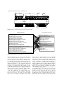
1
Reflow Soldering
Processes and
Troubleshooting:
SMT, BGA, CSP and
Flip Chip Technologies
To my mother, Shu-shuen Chang, for her care and encouragement
To my wife, Shen-chwen Lee, for her understanding and full support
Reflow Soldering
Processes and
Troubleshooting:
SMT, BGA, CSP
and Flip Chip
Technologies
Ning-Cheng Lee
BOSTON OXFORD AUCKLAND
MELBOURNE NEW DELHI
JOHANNESBURG
Copyright 2002 by Newnes, an imprint of Butterworth-Heinemann
All rights reserved.
No part of this publication may be reproduced, stored in a retrieval
system, or transmitted in any form or by any means, electronic, mechanical,
photocopying, recording, or otherwise, without the prior written permission
of the publisher.
Recognizing the importance of preserving what has been written,
Butterworth-Heinemann prints its books on acid-free paper
whenever possible.
Butterworth-Heinemann supports the efforts of American Forests
and the Global ReLeaf program in its compaign for the betterment
of trees, forests, and our environment.
Library of Congress Cataloging-in-Publication Data
A catalog record for this book is available from the Library of Congress
British Library Cataloguing-in-Publication Data
A catalog record for this book is available from the British Library
The Publisher offers special discounts on bulk orders of this book.
For information, please contact:
Manager of Special Sales
Butterworth-Heinemann
225 Wildwood Avenue
Woburn, MA 01801 – 2041
Tel: 781-904-2500
Fax: 781-904-2620
For information on all Newnes publications available,
contact our World Wide Web home page at: http://www.newnespress.com
10 9 8 7 6 5 4 3 2 1
Typeset by Laser Words Private Limited, Chennai, India
Printed in the United States of America
.......................Preface
1 Introduction
...............................................
to Surface Mount Technology
.................................................................
1.1 Surface mount technology
..................................................................
1.1.1 History and benefits
..............................................................................
1.1.2 Surface mount components
1.1.3 Types
.....................................................
of surface mount assembly technology
.........................................................................
1.1.4 Surface mount soldering process
1.1.5 Advantages
...................................................
of solder paste technology in SMT
.....................................................................
1.2 Surface mount technology trends
.........................................................................
1.2.1 Technology driving force
...................................................................
1.2.2 Area array packages
.........................................
1.3 Conclusion
2 Fundamentals
....................................................
of Solders and Soldering
.................................................
2.1 Soldering theory
..................................................
2.1.1 Spreading
.................................................
2.1.2 Fluid flow
..........................................................................
2.1.3 Dissolution of base metal
.......................................................
2.1.4 Intermetallics
2.2 .......................................................
Effect of elemental constituents on wetting
......................................................................
2.3 Phase diagram and soldering
....................................................................
2.4 Microstructure and soldering
...........................................................................
2.4.1 Deformation mechanisms
2.4.2 Desirable
.......................................................
solders and the soldering process
...........................................................................
2.4.3 Effect of impurities on soldering
..........................................
2.5 Conclusion
Appendix 2.1 Effect of flux surface tension on the spread of...........
molten solder
........................................................
3 Solder Paste Technology
..................................................
3.1 Fluxing reactions
.................................................................
3.1.1 Acid base reactions
..............................................................................
3.1.2 Oxidation reduction reactions
............................................................................
3.1.3 Fluxes for reflow soldering
..............................................
3.2 Flux chemistry
.............................................
3.2.1 Resins
..................................................
3.2.2 Activators
................................................
3.2.3 Solvents
....................................................................
3.2.4 Rheological additives
..............................................
3.3 Solder powder
.....................................................
3.3.1 Atomization
.......................................................................
3.3.2 Particle size and shape
3.4 Solder
...................................................
paste composition and manufacturing
..........................................................
3.5 Solder paste rheology
............................................................
3.5.1 Rheology basics
....................................................................
3.5.2 Solder paste viscosity measurement
...................................................................
3.6 Solder paste rheology requirement
........................................................................
3.6.1 Effect of composition on rheology
.........................................
3.7 Conclusion
..........................................................
4 Surface Mount Assembly Processes
...........................................................
4.1 Solder paste materials
..............................................................................
4.1.1 Paste handling and storage
............................................................
4.1.2 Paste deposition
................................................................
4.2 Printer level consideration
.............................................
4.2.1 Stencil
..................................................
4.2.2 Squeegee
...........................................................................
4.2.3 Printing and inspection process
...............................................
4.3 Pick-and-place
..................................
4.4 Reflow
.........................................................
4.4.1 Infrared reflow
.................................................................
4.4.2 Vapor phase reflow
..........................................................................
4.4.3 Forced convection reflow
.........................................................................
4.4.4 In-line-conduction reflow
.........................................................
4.4.5 Hot-bar reflow
......................................................
4.4.6 Laser reflow
..........................................................
4.5 Effect of reflow atmosphere on soldering
......................................................................
4.6 Special soldering considerations
.........................................................
4.6.1 Step soldering
..........................................................
4.6.2 Reflow-alloying
.......................................................
4.6.3 Paste-in-hole
..........................................................
4.7 Solder joint inspection
.....................................
4.8 Cleaning
................................................
4.9 In-circuit-testing
4.10 Principle
..................................................
of troubleshooting reflow soldering
............................................
4.11 Conclusion
.................................................................
5 SMT Problems Prior to Reflow
................................................
5.1 Flux separation
....................................
5.2 Crusting
.................................................
5.3 Paste hardening
...............................................
5.4 Poor stencil life
...................................................................
5.5 Poor paste release from squeegee
......................................................
5.6 Poor print thickness
.................................
5.7 Smear
...........................................
5.8 Insufficiency
.................................................
5.9 Needle clogging
...................................
5.10 Slump
.......................................
5.11 Low tack
..................................................
5.12 Short tack time
...........................................
5.13 Conclusion
...............................................................
6 SMT Problems During Reflow
........................................
6.1 Cold joints
.........................................
6.2 Nonwetting
.......................................
6.3 Dewetting
.....................................
6.4 Leaching
............................................
6.5 Intermetallics
...............................................
6.5.1 General
..........................................
6.5.2 Gold
............................................
6.6 Tombstoning
....................................
6.7 Skewing
....................................
6.8 Wicking
....................................
6.9 Bridging
.....................................
6.10 Voiding
......................................
6.11 Opening
..................................................
6.11.1 Pillowing
............................................................
6.11.2 Other openings
.....................................................
6.11.3 Fillet lifting
..............................................................
6.11.4 Projected solder
...............................................
6.12 Solder balling
.................................................
6.13 Solder beading
.........................................
6.14 Spattering
...........................................
6.15 Conclusion
7 SMT
...................................................
Problems At the Post- reflow Stage
.............................................
7.1 White residue
.................................................
7.2 Charred residue
........................................................
7.3 Poor probing contact
..................................................................
7.3.1 Flux residue content
...................................................................
7.3.2 Top-side flux spread
........................................................................
7.3.3 Bottom-side flux spread
...............................................................
7.3.4 Residue hardness
.................................................................
7.3.5 Reflow atmosphere
.......................................................
7.3.6 Metal content
...........................................................................
7.3.7 Soft-residue versus low-residue
.........................................................................
7.3.8 Soft-residue versus RMA residue
.........................................................................
7.3.9 Multiple cycles probing testability
7.4 Surface insulation resistance or electrochemical
...................
migration failure
......................................................................
7.4.1 Surface insulation resistance (SIR)
...........................................................................
7.4.2 Electrochemical migration (EM)
....................................................................
7.4.3 Effect of flux chemistry on IR values
............................................................................
7.4.4 Effect of soldering temperature
.................................................................
7.4.5 Effect of cleanliness of incoming parts
7.4.6
............................................................
Effect of conformal coating/encapsulation
7.4.7 Effect of interaction
..............................................
between flux and solder mask
7.4.8 Effect of interaction between solder paste flux residue
.................
and wave flux
7.5 Delamination/voiding/non-curing of conformal coating/
..............
encapsulants
..............................................
7.5.1 Voiding
.......................................................
7.5.2 Delamination
...............................................................
7.5.3 Incomplete curing
.........................................
7.6 Conclusion
8 Solder.................................................
Bumping for Area Array Packages
.............................................
8.1 Solder criteria
8.1.1 Alloys used in flip..........................................
chip solder bumping and soldering
8.1.2 Alloys used in BGA and CSP solder
...............................
bumping and soldering
..............................................................
8.1.3 Lead-free solders
........................................................................
8.2 Solder bumping and challenges
.............................................................
8.2.1 Build-up process
..............................................................................
8.2.2 Liquid solder transfer process
............................................................................
8.2.3 Solid solder transfer processes
.....................................................................
8.2.4 Solder paste bumping
.........................................
8.3 Conclusion
.........................................................
9 BGA and CSP Assembly and Rework
....................................................
9.1 Assembly process
..........................................................................
9.1.1 General stencil design guideline
...................................................................
9.1.2 BGA/CSP placement
.............................................
9.1.3 Reflow
..................................................
9.1.4 Inspection
...................................
9.2 Rework
......................................................
9.2.1 Process flow
...................................................
9.2.2 Pre-baking
..................................................................
9.2.3 Component removal
...............................................................
9.2.4 Reflow equipment
...........................................................
9.2.5 Site preparation
....................................................................
9.2.6 Solder replenishment
..........................................................................
9.2.7 Placement of component
.........................................................................
9.2.8 Reflow of BGA and CSP
9.3 Challenges
.....................................................
at assembly and rework stages
.................................................................
9.3.1 Starved solder joint
.................................................................
9.3.2 Poor self-alignment
......................................................
9.3.3 Poor wetting
..............................................
9.3.4 Voiding
...............................................
9.3.5 Bridging
...........................................
9.3.6 Open
.................................................................
9.3.7 Uneven joint height
...........................................................
9.3.8 Solder webbing
........................................................
9.3.9 Solder balling
..............................................................................
9.3.10 Popcorn and delamination
.........................................
9.4 Conclusion
................................................................
10 Flip Chip Reflow Attachment
.........................................................
10.1 Flip chip attachment
......................................................................
10.1.1 Conventional flip chip attachment
.....................................................
10.1.2 Snap cure
.....................................................
10.1.3 Epoxy flux
................................................
10.1.4 No-flow
............................................
10.1.5 SMT
..................................................................
10.1.6 Fluxless soldering
10.1.7 Wafer-applied underfill 10.1.8 Wafer level compressive-flow
............... underfill
.........................................
(WLCFU)
10.2 Problems
...................................................
during flip chip reflow attachment
..........................................................
10.2.1 Misalignment
........................................................
10.2.2 Poor wetting
...........................................................
10.2.3 Solder voiding
..............................................................
10.2.4 Underfill voiding
.................................................
10.2.5 Bridging
.............................................
10.2.6 Open
...........................................................
10.2.7 Underfill crack
.........................................................
10.2.8 Delamination
................................................................
10.2.9 Filler segregation
..........................................................................
10.2.10 Insufficient underfilling
...........................................
10.3 Conclusion
11 Optimizing a Reflow Profile Via Defect Mechanisms
..............
Analysis
.............................................
11.1 Flux reaction
11.1.1 Time/temperature requirement
......................................
for the fluxing reaction
11.1.2 Fluxing contribution
...........................................
below the melting temperature
.....................................................
11.2 Peak temperature
...............................................................................
11.2.1 Cold joint and poor wetting
11.2.2
.........................................................
Charring, delamination, and intermetallics
..................................................
11.2.3 Leaching
...............................................
11.3 Cooling stage
.........................................................
11.3.1 Intermetallics
....................................................
11.3.2 Grain size
...................................................................
11.3.3 Internal stress-component cracking
.....................................................................
11.3.4 Deformation of joints
11.3.5
...........................................................
Internal stress solder or pad detachment
...............................................
11.4 Heating stage
........................................................................
11.4.1 Slumping and bridging
............................................................
11.4.2 Solder beading
.................................................
11.4.3 Wicking
..............................................................................
11.4.4 Tombstoning and skewing
..........................................................
11.4.5 Solder balling
........................................................
11.4.6 Poor wetting
................................................
11.4.7 Voiding
..............................................
11.4.8 Opens
............................................................
11.5 Timing considerations
............................................................
11.5.1 Ramp-up stage
..........................................................
11.5.2 Soaking zone
.......................................................................
11.5.3 Onset temperature of spike zone
............................................................
11.6 Optimization of profile
....................................................................
11.6.1 Summary of desired profile feature
.......................................................................
11.6.2 Engineering the optimized profile
...........................................................
11.7 Comparison with conventional profiles
.....................................................................
11.7.1 Conventional profiles
..................................................................
11.7.2 Background of conventional profiles
......................................................................
11.7.3 Approach of conventional profiles
.................................................................
11.7.4 Compromise of conventional profiles
........................................................................
11.7.5 Earlier mass reflow technologies
11.7.6
............................................................
Forced air convection reflow technology
11.7.7 Defect potential associated
.......................................
with conventional profiles
..........................................
11.8 Discussion
11.8.1
.........................................................
Profiles for low temperature solder pastes
11.8.2........................................................
Profiles for high temperature solder pastes
...............................................................................
11.8.3 Limited oxidation tolerance
11.8.4 Unevenly distributed
..............................................
high thermal mass systems
...............................................................................
11.8.5 Nitrogen reflow atmosphere
.......................................................
11.8.6 Air flow rate
..............................................................................
11.8.7 Adjustment of optimal profile
...............................................................
11.9 Implementing linear ramp-up profile
.............................................
11.10 Conclusion
.................................................
12 Lead-free Soldering
................................................
12.1 Initial activities
...................................................
12.2 Recent activities
.......................................................................
12.3 Impact of Japanese activities
12.4 US reactions..................................................................................................
......................................................................
12.5 What is lead-free interconnect?
..................................................................
12.6 Criteria of lead-free solder
............................................................
12.7 Viable lead-free alloys
..........................................................
12.7.1 Sn96.5/Ag3.5
..........................................................
12.7.2 Sn99.3/Cu0.7
...................................................
12.7.3 Sn/Ag/Cu
.......................................................
12.7.4 Sn/Ag/Cu/X
......................................................
12.7.5 Sn/Ag/Bi/X
..............................................
12.7.6 Sn/Sb
.................................................
12.7.7 Sn/Zn/X
.............................................
12.7.8 Sn/Bi
................................
12.8 Cost
..............................................
12.9 PCB finishes
...............................................
12.10 Components
......................................................
12.11 Thermal damage
....................................................
12.12 Other problems
......................................................
12.13 Consortia activity
.............................................................
12.14 Opinions of consortia
.....................................................................
12.15 The selections of pioneers
................................................
12.16 Possible path
......................................................
12.17 Is lead-free safe?
.....................................................................
12.18 Summary of lead-free adoption
.............................................................
12.19 Troubleshooting lead-free soldering
.....................................................................
12.19.1 Compatibility with reflow process
.......................................................
12.19.2 Fillet lifting
...............................................................................
12.19.3 Conductive anode filament
..............................................................
12.19.4 Grainy surface
12.19.5 Sn/Pb/Bi
....................................................
ternary low melting eutectic phase
.............................................
12.20 Conclusion
.................... Index
Preface
Reflow soldering is the primary method for interconnecting surface mount technology (SMT) applications.
Successful implementation of this process depends on
whether a low defect rate can be achieved. In general,
defects often can be attributed to causes rooted in all three
aspects, including materials, processes, and designs. Troubleshooting of reflow soldering requires identification and
elimination of root causes. Where correcting these causes
may be beyond the reach of manufacturers, further optimizing the other relevant factors becomes the next best
option in order to minimize the defect rate.
Chapter 1 introduces the general design background
and trends of electronic packaging and surface mount
technology. Chapters 2 and 3 provide the fundamentals
of soldering and solder materials. Chapter 4 describes
the basics of reflow processes. These four chapters
serve as the fundamentals needed for analyzing soldering
defects. Chapters 5 through 7 discuss the defect types,
defect mechanisms, and solutions for eliminating the
defects encountered in the SMT process, while Chapters 8
through 10 address area array packages, including
BGA, CSP and flip chips. Chapter 11 focuses on
reflow profile optimization, since the profile is vital to
reflow performance and often is easily controllable by
manufacturers. Chapter 12 summarizes the background
and options of lead-free soldering. It also discusses the
defect types and mechanism of lead-free reflow processes.
This book emphasizes reflow process description
and troubleshooting. The solutions for troubleshooting
described should be regarded merely as examples. With
defect mechanisms identified and the impact of relevant
factors understood, only creativity can determine the
limits of approaches possible for solutions.
Ning-Cheng Lee
1/1
Introduction to
Surface Mount
Technology
1
1.1 Surface mount technology
1.1.1 History and benefits
Surface mount technology (SMT) is a revolutionary
change in the electronics industries. During the mid1960s, the early stages of SMT emerged due to the
advantage of being able to place components on both
sides of the PCBs. However, SMT did not prevail until
about 15 years later. During the late 1970s, throughhole technology (THT) ran into increasing difficulty in
meeting the constant need for higher densities, primarily
due to the increasing cost for drilling more holes for
an increasing number of leads, and to the difficulty of
drilling smaller holes for pitch dimensions smaller than
0.1 inch. It was then that interest in SMT increased rapidly
and its potential became recognized by industries. On the
other hand, the commercial availability of various plastic
surface mount devices (SMDs), such as PLCC, SOIC,
and SOT23, further ensured SMT to be a practical option.
Since then, SMT started its rapid development and quickly
became the major assembly technology.
By mounting flat leaded or leadless components
and electronic packages on the surface of printed
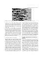
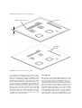
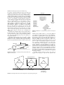
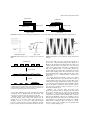
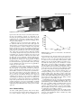
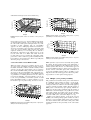
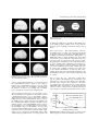
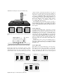
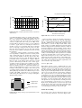
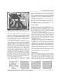
circuit boards (PCBs) (Figure 1.1(a)), as opposed to the
conventional THT (Figure 1.1(b)), SMT allows a higher
degree of automation, higher circuitry density, smaller
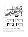
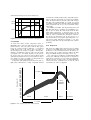
volume, lower cost, and better performance. An example
of the lower weights and smaller volumes offered by the
surface mount components (SMCs) versus the equivalent
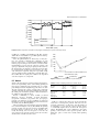
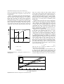
through-hole components (THCs) is shown in Figure 1.2,
where it is demonstrated that SMCs deliver up to 90
percent reduction in both weight and volume.
This is of particular interest in aerospace and portable
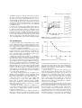
device applications. The benefit of higher circuitry density is a natural result of the reduced components’ size,
and can be illustrated by Figure 1.3. In reality, at high
lead density level, conventional THT is not only more
expensive, it is also unmanufacturable. Additional benefits of SMT include a lower cost in the shipping and
warehousing of components, and in the requirements of
manufacturing space and equipment.
1.1.2 Surface mount components
SMCs are available for almost any type of application,
such as capacitors, resistors, transistors, diodes, inductors, ICs, and connectors. However, due to the physical
size restriction imposed by the surface mounting process,
most SMCs are designed for power dissipation no higher
than 1 to 2 W. Given below is a brief illustration of some
commonly used components.
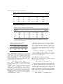
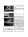
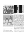
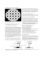
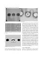
1.1.2.1 Chip resistors
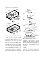
A chip resistor is the simplest SMC, as shown
in Figure 1.4. It consists of a rectangular ceramic
substrate body with a metallized termination, usually
palladium–silver (Pd–Ag), on both ends. A thick film
(a)
(b)
Figure 1.1 Schematic of printed circuit board technologies: (a) SMT, (b) THT
1/2 Reflow Soldering Processes and Troubleshooting
10000
0.25
THC volume
0.2
Volume (in.3)
0.15
THC weight
5000
SMC weight
0.1
2500
0.05
0
Weight (mg)
7500
SMC volume
16-pin
(DIP vs
SOIC)
20-pin
(DIP vs
PLCC)
0
44-pin
(DIP vs
PLCC)
Figure 1.2 Comparison of weight and volume of SMCs and THCs [1]
1000
Lead density, number/square inch
500
200
0.150 in SOIC
C-quad
100
0.300 in SOIC
PLCC
50
0.300 in DIP
20
5
0.600 in DIP
10
20
50
100
Number of leads
200
500
Figure 1.3 Lead density comparison of some SMCs and THCs [2]
resistor paste, generally based on ruthenium dioxide
(RuO2 ), is screened between the terminations and fired.
The resistive film is then covered by a protective lead
borosilicate glass film. A nickel barrier is usually applied
over the Pd–Ag terminations to prevent silver leaching,
and a final tin–lead or tin–lead–silver solder coating
is applied over the nickel to preserve its solderability.
The 1206 (0.120(L) × 0.060(W)-in.) and 0805 are the
dominant sizes, with a trend toward increasing use of
0603. Currently the smallest size available is 0201, which
has found use in hearing aids, and mobile phones.
1.1.2.2 Metal electrode face resistors
Metal electrode face resistors (MELFs) are similar
to leaded cylindrical resistors except that the leaded
electrodes are replaced by headed dumets, as shown in
Figure 1.5. The manufacturing process is cheaper than
Introduction to Surface Mount Technology 1/3
Protective
glass film
Thick film
resistance element
Land
termination
Edge
termination
Ceramic
dielectric
Termination
Electrode
Figure 1.6 Construction of multilayer ceramic chip capacitor
Inductor windings
High purity
alumina
substrate
Solderable
coating
Nickel barrier
Figure 1.4 Chip resistor [3]
Ceramic or
ferrite core
(a)
Headed dumet
Bumped
Glass sleeve
die
Termination
Ceramic or ferrite core
Inductor windings
Figure 1.5 Metal electrode face resistor [4]
that for the thick film chip resistor. For this reason, they
are widely used in the consumer-electronics orientated
Asian SMT industry. However, since they tend to roll
off the boards during the reflow process, their popularity
is gradually diminishing.
1.1.2.3 Chip capacitors
The most commonly used SMT chip capacitor is the multilayer ceramic chip, also called a chip cap or ceramic cap.
It consists of multiple layers of precious metal electrodes
separated by layers of ceramic dielectric (Figure 1.6).
Each layer’s electrode extends from one terminal
to almost the other terminal, and each neighboring
pair of electrodes forms a single capacitive layer. The
required capacitance is obtained by the stacked layers.
The construction of terminations are similar to that
of chip resistors. Commonly used dielectric materials
include (a) temperature-stable, low capacitance, primarily
composed of titanium oxide (TiO2 ), (b) semi-temperature
stable, medium capacitance, typically composed of
barium titanate (BaTiO3 ) and other types of ferroelectric
additives, and (c) general purpose, least thermally stable,
high capacitance materials.
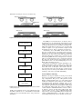
1.1.2.4 Chip inductors
Chip inductors employ a ceramic or ferrite core material wrapped around, either vertically or horizontally, by
a polyurethane enamelled fine copper wire (Figure 1.7).
(b)
Termination
Figure 1.7 Chip inductors. (a) Vertical windings; (b) horizontal
windings [2]
The chip is usually potted in an epoxy resin to facilitate
automated handling.
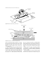
1.1.2.5 Discrete semiconductors
Surface-mounted discrete semiconductors, such as diodes
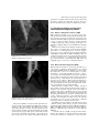
or transistors, often utilize similar types of packages. Typically, the SOT-23 (Figure 1.8(a)) and SOT-143 are used
for low-power single diode and dual diode, respectively.
The SOT-89 (Figure 1.8(b)) is used for high current devices. Here the center lead is extended across the bottom
of the die to help dissipate the heat.
1.1.2.6 Integrated circuits
Surface mount integrated circuits (ICs) are supplied in a
variety of packages. Some commonly used types include
small-outline integrated circuit (SOIC), thin small-outline
package (TSOP), plastic leaded chip carrier (PLCC),
leadless ceramic chip carrier (LCCC), quad flat pack
(QFP), and the more recently introduced ball grid array
(BGA). The solder joint configurations of the IC packages
can be represented by five major categories, as shown in
Figure 1.9.
1/4 Reflow Soldering Processes and Troubleshooting
IC package body
Epoxy
body
Collector
lead
Lead
Solder joint
PCB land pad
Bonding
wire
(a)
PCB
IC package body
Lead
Emitter
lead
Solder joint
PCB land pad
Passivated
semiconductor
chip
(b)
PCB
IC package body
Lead
Base lead
(a)
Passivated
semiconductor
chip
Solder joint
PCB land pad
Epoxy
body
(c)
Bonding
wire
PCB
Castellation with thick
film metallization
IC package
body
Solder joint
PCB land pad
Emitter
(d)
Collector
(b)
PCB
IC package body
Solder sphere
Base
Solder joint
PCB land pad
Figure 1.8 Discrete semiconductor packages. (a) SOT-23; (b) SOT89
(e)
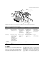
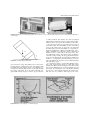
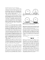
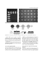
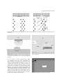
Gullwing leads (Figure 1.9(a)) are the most popular
lead configuration, particularly in the case of fine-pitch
and ultra-fine-pitch applications. However, these leads are
also susceptible to damage, such as bend or sweep, in
handling. The J-lead design (Figure 1.9(b)) offers better handlability. But this benefit is offset by the difficulties in rework, inspection, and lead-forming. Butt-leads
(Figure 1.9(c)) are easier to manufacture than both gullwing and J-lead designs. They are not as popular as gullwing leads, due to controversial performance in solder
joint reliability. Figure 1.9(d) shows the joint configuration of a leadless ceramic chip carrier. Again, the reliability of the joints often poses problems, primarily due to a
mismatch in the thermal coefficients of expansion of the
packages and the PCB materials. In addition, the cleanability of flux residue for areas underneath the components
also is questionable owing to the low standoff of the packages. The solder joint of BGA can be demonstrated by
Figure 1.9(e). Here the high melting point solder bump
underneath the plastic package is soldered onto the PCB
Chip land pad
PCB
Figure 1.9 IC package lead configurations. (a) Gullwing; (b) J-lead;
(c) Butt-lead; (d) Leadless metallization; (e) Ball-lead
through the use of solder paste. In the case of ceramic
BGAs developed by IBM, the solder bump comprises a
high melting solder column soldered onto the component.
The emergence of BGAs makes 0.3 mm pitch SMT virtually a dead issue in North America. Furthermore, BGA
will also provide an alternative to 0.4 mm processing.
BGA, CSP, and flip chip will be discussed in more detail
in section 1.2.2.
1.1.3 Types of surface mount assembly
technology
SMCs can be assembled onto PCBs with the use of solder paste reflow, wave soldering, or conductive adhesive
curing processes. The use of conductive adhesive is not
common, but can be found in some flexible circuit boards
Introduction to Surface Mount Technology 1/5
requires the use of both wave soldering and reflow soldering. This complicates the assembly, test, and rework
processes, and results in a need for more floor space.
or boards with heat sensitive components. The assembly
technology to be chosen depends on the board layout and
whether there are through-hole components to be attached.
In general, the assembly processes can be categorized into
three major types, as described below.
1.1.3.3 Type III
Type III SMT have THCs on one side of the board and
chip components on the other side, as shown in Figure 1.14. Similar to type II, the THCs can be inserted
either before or after the attachment of chip components,
as indicated in Figure 1.15. Type III requires only wave
soldering for the bonding process, and represents the initial stage of converting from conventional through-hole
technology to surface mount technology.
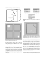
1.1.3.1 Type I
Type I surface mount boards have SMCs only for both
sides of the boards, as shown in Figure 1.10.
The assembly processes are depicted in Figure 1.11.
The first side typically uses solder paste for bonding.
The second side often also uses solder paste (see
Figure 1.11(a)), particularly if there are fine pitch
components to be attached. At the second reflow, the
pre-assembled underside solder joints will melt again.
The surface tension of solder in general is sufficient
to hold the suspended components in place during the
second reflow. However, it may be preferable to use the
wave soldering process if there are heavy components
involved on the underside at the second reflow. When
using wave soldering, adhesives have to be used to
secure the components in place (see Figure 1.11(b)). This
requirement results in a total of process steps more than
that of using solder paste only.
Depending on the flux chemistry, cleaning may or may
not be needed. In the former case, cleaning can be done
after the first pass or after the second pass. As a rule
of thumb, the more heating excursions the fluxes have
been through, the more difficult the cleaning will be.
Many manufacturers have successfully implemented a single cleaning process for their products.
1.1.4 Surface mount soldering process
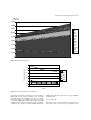
1.1.4.1 Wave soldering
As mentioned above, the two major soldering processes
involved in surface mount technology are wave soldering and reflow soldering. Wave soldering, a type of flow
soldering, has long been used in the through-hole technology era. Typically, the PCBs with THCs inserted are
prefluxed via a foam fluxer, then passed over a single laminar solder wave for soldering. However, this process is
not adequate for soldering SMCs. The presence of SMCs
on the bottom side of a PCB interferes with the laminar solder flow, and consequently results in a “shadowing
effect”. As a common symptom, the leads at the trailing
edge of a component usually exhibit insufficient solder
volume. In addition, direct contact of SMCs on the bottom side with the hot solder wave also causes potential
damage due to thermal shock. To minimize the shadowing
effect, a dual-wave, with a turbulent wave preceding the
laminar wave, is then used (Figure 1.16).
The turbulent wave ensures the wetting of all leads,
while the subsequent laminar wave removes excessive
solder in order to minimize solder bridging between the
leads. Thermal shock potential is addressed by implementing sufficient preheating prior to wave-soldering. A
typical wave-soldering thermal profile for SMCs soldering is shown in Figure 1.17. Use of dual-wave and proper
1.1.3.2 Type II
Type II boards have both SMCs and THCs on one side
of the board and chip components on the other side, as
shown in Figure 1.12. Normally the SMCs are attached
via reflow soldering, then followed by wave soldering the
THCs and chip components, as depicted in Figure 1.13.
The THCs can also be inserted after the adhesive has been
cured. Type II boards allow flexibility in using THCs for
some features for which the supplies of SMCs may not
be readily available. On the other hand, type II design
SO
PLCC
Chip capacitor
LCCC
Solder paste
printed on pads
LCCC
Chip capacitor
Figure 1.10 Schematic of type I surface mount boards
PLCC
SO
1/6 Reflow Soldering Processes and Troubleshooting
(a)
Print solder
paste
preheating allows small SMCs to be processed by wave
soldering. However, for large SMCs and fine-pitch components, starved solder joints or bridgings are still a
problem.
Place SMCs
1.1.4.2 Reflow soldering
Print solder
paste
Reflow
Place SMCs
Clean flux
residue
Reflow
Turn PCB over
Clean flux
residue
Apply adhesive
Turn PCB over
Place SMCs
1.1.5 Advantages of solder paste technology in
SMT
Print solder
paste
Cure adhesive
Place SMCs
Turn PCB over
Reflow
Wave solder
Clean flux
residue
Clean flux
residue
Reflow after
reflow
In order to eliminate the problems encountered in wave
soldering SMCs, reflow soldering technology is introduced
to SMT. Here the solder powder and flux are preblended
to form a solder paste. The rheology of the paste usually
is formulated to be thixotropic to facilitate the deposition
process. This material is then deposited, usually through
stencil printing or dispensing, onto the PCB pads where
the SMCs are subsequently placed. This tacky solder paste
serves as a temporary glue and holds the SMCs in place
prior to the soldering process. The populated boards are
then heated to above the liquidus temperature of the solder to reflow the solder powder. At this temperature, the
flux reacts and accordingly removes the oxide of both
solder powder and metallization of leads and pads, and
consequently allows the solder to form solder joints. Some
commonly used reflow methods include infrared reflow,
vapor phase reflow, convection reflow, conduction reflow,
and laser soldering.
(b)
Wave after reflow
Figure 1.11 Assembly processes for type I surface mount boards
SO
PLCC
As mentioned above, solder paste is the primary solder
material used in the SMT reflow soldering process. Use
of solder paste technology provides several major advantages over wave soldering technology. First, solder paste
serves not only as a solder material, but also as a glue.
The latter function allows the elimination of glue deposition and the curing process needed by wave soldering.
Second, the deposition of solder paste is usually conducted by the stencil or screen printing, dispensing, or
pin-transferring processes. The premetered deposition of
solder material onto the sites to be soldered ensures a
consistent solder volume for the joints, and accordingly
eliminates the insufficient solder volume problems due to
the shadowing effect encountered by wave soldering. In
addition, this premetered solder deposition also reduces
the incidence of bridging. This is particularly true in the
case of fine pitch applications. Third, the use of mass
DIP
LCCC
Solder paste
printed on pads
Adhesive
Chip capacitor
Chip capacitor
Figure 1.12 Schematic of type II surface mount boards
Chip capacitor
Introduction to Surface Mount Technology 1/7
Print solder
paste
Insert THCs
Place SMCs
Turn PCB over
Apply
adhesive
Apply adhesive
Place SMCs
Place SMCs
Cure adhesive
Turn PCB over
Cure adhesive
Turn PCB over
Apply
adhesive
Turn PCB over
Insert THCs
Wave soldering
Wave soldering
Clean flux
residue
Clean flux
residue
Reflow
Clean flux
residue
Insert THCs
Place SMCs
Cure adhesive
Turn PCB over
(a)
Figure 1.15 Assembly processes for type III surface mount boards,
(a) THC inserted before SMC placement, (b) THCs inserted after
the attachment of chip components
Wave soldering
Clean flux
residue
Figure 1.13 Assembly processes for type II surface mount boards
reflow process allows a well-controlled graduate heating
profile, thus eliminating potential damage of the SMCs
due to the thermal shock caused by the wave soldering.
Fourth, the use of solder paste allows the possibility of
step soldering. After the first step reflow, a solder paste
DIP
(b)
with a lower solder melting point can be dispensed onto
the sites to be soldered. This dispensed solder material can
be reflowed later at a lower temperature without remelting
the solder joints formed during the first step reflow. Fifth,
the soldering performance of solder paste is not sensitive
to the type of solder mask used on the PCBs. For the wave
soldering process, a solder mask with a smooth finish is
found to cause solder ball and bridging problems [1]. In
addition, solder skip increases with increasing solder mask
thickness [2].
DIP
DIP
DIP
Adhesive
Chip capacitor
Figure 1.14 Schematic of type III surface mount boards
Chip capacitor
Chip capacitor
1/8 Reflow Soldering Processes and Troubleshooting
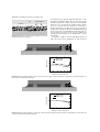
PCB
PCB
Fluxer
Preheat
Dual solder wave
Figure 1.16 Schematic of the wave-soldering process
600 °F
400 °F
200 °F
0 °F
+ × − −>
1
2
3
4
Figure 1.17 A typical wave-soldering thermal profile for SMCs soldering
The electronics industries are evolving constantly toward higher functional density, further miniaturization,
and higher yield. Wave soldering technology failed to
satisfy the constant need since the mid-1980s. It is the
advantages of solder paste technology mentioned above
that have enabled it to become the major board level
bonding technology in SMT since the late 1980s. Recent
studies [3–5] indicate that solder paste technology should
be able to support the needs of solder bonding down to
12-mil pitch level applications.
1.2 Surface mount technology trends
1.2.1 Technology driving force
The electronics industry is mainly driven by the demand
for “smaller, faster, higher complexity, lower power
consumption, and cheaper”. The Japanese industry, being
strongly oriented toward consumer electronics products,
places great emphasis on miniaturization and the cost
factor. For instance, ultrathin packages, as thin as 0.4 mm,
are prevailing in Japan [6], partly due to mature TAB
infrastructure. In the USA the demand for ultrathin
packages is low. The low limit of thickness is 1 mm. On
the other hand, the computer oriented American industry
appears to be more conscious of the speed and complexity
issue. The trends of those factors on the SMT industry will
be demonstrated in the following paragraphs. In fact, it
may not be easy to distinguish the impact of those driving
forces since improvement in one feature often results in
improvement in other aspects.
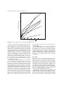
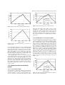
1.2.1.1 Speed
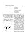
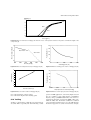
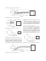
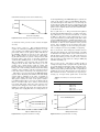
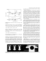
The trend of increasing speed can be best described by the
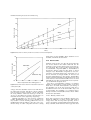
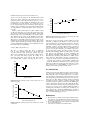
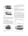
evolution of computer systems. Figure 1.18 [7] shows the
processing performance in million instructions per second
for computer systems. Low-end applications include consumer products, notebooks, personal computers and workstations. High-end applications include super, mainframe,
Processing performance (MIPS)
Introduction to Surface Mount Technology 1/9
1000
100
High-end
10
Low-end
1
0.1
1980
1985
1990
Time
1995
2000
Figure 1.18 Processing performance of computer systems [6]. Performance (MIPS) = 1000/(cycle time × cycles per instruction) where the
cycle time is in nanoseconds
0.25
0.5 µ
Line width
Gate delays (nanoseconds)
0.2
0.4 µ
0.15
0.3 µ
0.2 µ
0.1
0.15 µ
0.05
0
1993
1994
1995
1996
1997
1998
1999
2000
Time
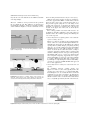
Figure 1.19 Gate delay of application-specific integrated circuits as a function of line width (µ)
mid-range computers, and possibly some advanced workstations as well [8]. In both instances, processing speed
increases approximately five times in every 5 years. This
increase in speed results from reduction in both on-chip
delay in semiconductors and packaging delay. Figure 1.19
shows the trend of reduction in gate delay of applicationspecific integrated circuits (ASICs) from 1993 to 2000 [9].
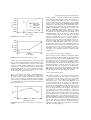
The trend of increasing speed can also be demonstrated
by the maximum performance (MHz) on chip reported by
the Semiconductor Industry Association Roadmap [10],
as indicated in Figure 1.20. The maximum performance
on chip is projected to increase four to five times from
1997 to 2012.
Obviously this improvement in speed is closely associated with miniaturization of IC components, as demonstrated by the simultaneous reduction in line widths. Due
to rapid advances in IC technology, packages have now
become the slowing factor in computer systems. Proper
choice, design, and manufacturing of a packaging system
become crucial in order to reduce cycle time and improve
performance.
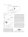
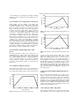
1.2.1.2 Complexity
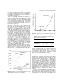
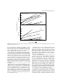
1.2.1.2.1 IC transistor integration Perhaps the trend of
the electronics industry toward complexity can be best
described by the evolution of computers. The complexity
of semiconductor chips can be measured by transistor
integration. Based on the “X86” CPU, the number of
transistors on Intel’s X86 microprocessors has increased
by a factor of about 190 since the 8086’s debut in 1978.
Furthermore, microprocessor integration has increased
by 2000× since its introduction in 1970, as shown in
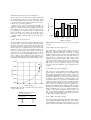
Figure 1.21 [11,12]. This increase in complexity of
Max. performance (MHz) on chip
1/10 Reflow Soldering Processes and Troubleshooting
3500
3000
2500
High performance products
2000
1500
1000
Cost performance products
500
0
1997
1999
2001
2003
2006
2009
2012
Year
Figure 1.20 SIA technology roadmap for maximum performance of chip for high performance and cost performance products [10]
1E+08
1E+07
Transistors per die
16M
Memory
Microprocessor
4M
P6
Pentium
1M
1E+06
486 CPU
256K
386 CPU
64K
1E+05
80286
16K
4K
1E+04 1K
8086
8080
1E+03
1970
4004
1975
1980
1985
Year
1990
1995
2000
Figure 1.21 Increasing complexity as measured by transistor integration predicted by Moore’s Law [11,12]
semiconductor chips essentially drives the evolution of
corresponding packaging and assembly technology, as
will be described later.
1.2.1.2.2 Pin count number A natural result of increasing IC complexity is an increase in the pin count number.
Figure 1.22 [13] is a packaging technology roadmap covering the period from 1980 to 2000 published by National
Semiconductor. In this roadmap, the pin count number
will increase almost 100× from the through-hole technology in the early 1980s to modules/system packaging
in the late 1990s. This increase in pin count number not
only directly drives the evolution of packaging types, but
also indirectly drives the trend toward miniaturization.
computers, cameras and portable phones. In fact,
miniaturization is not only an independent driver but
is also a logical result of the increasing complexity of
functions. When increasing number of functions are to be
built into increasingly smaller devices the only choice is
to miniaturize component size and to increase packaging
density.
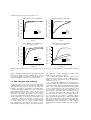
1.2.1.3 Miniaturization
IC feature size A typical example which best exemplifies the fact that miniaturization is a logical result of
increasing complexity of functions is the IC feature size.
Figure 1.23 shows the road to 5-million gate ASICs, as
depicted by the Toshiba Corporation [14]. As the number
of usable gates is to increase in ASICs, power consumption, gate delays, and line widths have to decrease in order
to achieve a reasonable performance.
Overall, due to the desire to make components smaller
and lighter, miniaturization is the general trend in the
electronics industries, particularly for consumer electronic
products. Examples include camcorders, portable personal
Discrete component size The miniaturization of discrete
components can be exemplified by the size evolution
of multilayer ceramic chip capacitors [15], as shown in
Introduction to Surface Mount Technology 1/11
1980
1500
1985
1990
’91
’92
’93
’94
1995
PCMCIA
Card
1000
2000
Flipchip
COG
TCP (TAB)
500
Display packaging
Flipchip/chip
scale packaging
BGA
PGA/PPGA
128
Advanced
MCM
Thin QFP
64
Adaptive
packaging
MCP/MCM
QFP
DIP
UTSOP
TSOP
(Type 1)
(Type 1) TSSOP/HEATSLUG memory
development
memory
PLCC
32
SOP
16
SOJ
8
Through hole
Surface mount
3D
SSOP
ISO TO
Fine pitch thin
COB
Modules/system
Usable gates
(millions)
6
4
2
0
1992
(a)
1997
2002
(b)
Power consumption
(microwatts/gate/MHz)
Figure 1.22 The ‘‘Package Technology Roadmap’’, published by National Semiconductor, depicts the evolution of package technology
and pin count number [13]
(c)
0.2
0.1
0
1992
1.5
1
0.5
0
1992
1997
2002
0.6
Line widths (µ)
Gate delays
(nanoseconds)
0.3
2
1997
2002
(d)
0.4
0.2
0
1992
1997
2002
Figure 1.23 The road to five-million gate ASICs, developed by Toshiba Corporation [14]. (a) Usable gate, (b) power consumption, (c) gate
delays, (d) line widths
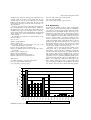
Figure 1.24. Apparently, chip size is gradually reducing
from 1206, with 0805 being the most popular size in 1989,
0603 in 1998, and 0402 projected to be the most popular
size in 2003. 0201 emerged in 1998, and is rapidly gaining
market acceptance, as shown in Figure 1.24. Difficulty
in handling the small chips such as 0201 may result in
a change in technology toward further miniaturization.
A potential candidate technology may include integrated
passives.
1.2.2 Area array packages
Area array packages are devices with I/Os interconnection distributed across the bottom side of components
in an area array pattern. The interconnections often are
composed of metal or polymer bumps, and the area array
packages are mounted onto substrates through soldering or
adhesives. Families of area array packages include BGA,
CSP, and FC, as will be briefly described below.
1/12 Reflow Soldering Processes and Troubleshooting
90
0201’
80
0402’
0805
1206
0603’
Constituent (%)
70
0805’
1206’
60
0603
Others
50
0402
40
30
20
10
0201
Others
0
81 82 83 84 85 86 87 88 89 90 91 92 93 94 95 96 97 98 99 00’ 01’ 02’ 03’ 04’ 05’
Figure 1.24 Size trends and life cycles for ceramic chip capacitors [15]
250
200
No. of 150
patents
issued
100
50
0
19821991
1992
1993
1994
1995
1996
1997
1998
1999
Figure 1.25 Number of patents issued for BGA, CSP, and WLP, according to International Interconnection Intelligence [16]
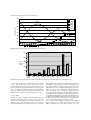
Area array packages are a new breed of surface mount
devices, and clearly represent the direction of surface
mount technology for the coming decades. This trend can
also be reflected by the patents issued for area array packages. According to International Interconnection Intelligence, the number of patents issued for CSP, BGA, and
WLP increases rapidly, as shown in Figure 1.25 [16].
1.2.2.1 BGA
Pressure of speed, complexity, and miniaturization have
driven the peripheral package design down to 0.3 mm
(16 mil) pitch for QFP [17], as shown in Figure 1.26.
However, the rapidly increasing defect rate associated
with miniaturization of peripheral design was recognized
very quickly as the bottleneck in further improvements in
performance. It is reported [17] that the assembly defect
rate (ppm) of QFP is a strong function of the pitch size.
The defect rate is 25 to 40 ppm for 50 mil pitch, and gradually increases to 25 to 100 ppm for 30 mil pitch and
40 to 233 ppm (5 sigma control) for 25 mil pitch. The
defect rate becomes prohibitively high, 100 to 2300 ppm,
for 20 mil pitch. This high defect rate is primarily associated with the vulnerability of the slim, thin gullwing leads
of QFP toward handling. The high precision required for
the ultra-fine-pitch component placement as well as solder
paste deposition further aggrevates the problem.
To address this challenge, ball grid array (BGA)
design emerges as a smart and logical answer. The
BGA components are represented in Figure 1.27 [18].
Introduction to Surface Mount Technology 1/13
100
DIP (2.5 mm)
PGA (2.5 mm)
Packaging efficiency
(pkg area : die area)
QFP (1.27 mm)
QFP (1.0 mm)
Co-fired chip
carrier (1.0 mm)
10
QFP (0.8 mm)
QFP (0.65 mm)
QFP (0.5 mm)
Pad array carrier (1.78 mm)
BGA (1.5 mm)
BGA (1.27 mm)
QFP (0.4 mm)
QFP
(0.3 mm)
BGA (1.0 mm)
1
1960
1970
Flip chip (0.35-0.2 mm)
1980
1990
Year of package introduction
SLICC
(0.8 mm)
CSP
(0.5 mm)
2000
Figure 1.26 IC package time line [17]
In Figure 1.27(a), a Plastic BGA (PBGA) is illustrated.
The I/O from a silicon die fans out to BT/glass substrate
via wire bonding, and is then redistributed through
the substrate to an area array pattern at the bottom
side of component which is bumped with solder balls,
such as Sn62/Pb36/Ag2 balls or Sn63/Pb37 balls. In
Figure 1.27(b), ceramic column grid array (CCGA) and
ceramic ball grid array (CBGA) are illustrated. In both
cases, the IC is mounted onto a ceramic carrier through a
flip chip interconnection, which will be described in the
following section. The I/Os from the flip chip further fan
out and are redistributed through the ceramic carrier. The
ceramic carrier is bumped with high melting temperature
solder spacers, such as 90Pb/10Sn solder columns or
90Pb/10Sn solder balls, in order to provide sufficient
standoff so that the mismatch in coefficient of thermal
expansion(CTE) between the ceramic substrate and the
polymer PCB can be tolerated during service. Both CCGA
and CBGA are typically soldered onto PCBs through the
use of 63Sn/37Pb solder paste.
A change of I/O distribution from QFP peripheral pattern to BGA area array pattern provides a quantum leap in
I/O density, as shown in Figure 1.25. This increase in I/O
density allows a larger pitch, such as 60 mil pitch BGA,
to be used to deliver the same I/O density of a fine-pitch
QFP, hence effectively reducing the pressure of implementing a more accurate pick and placement equipment as
well as a more precise solder paste deposition mechanism.
Other advantages include better control of coplanarity,
better space tolerance, design robustness, higher yield, and
lower inductance (noise). A study [16] has reported that
the PBGA assembly yield is 3.4 ppm (6 sigma control) for
60 and 50 mil pitch. This defect rate is several orders of
magnitude lower than that of fine-pitch QFPs. However,
the disadvantages of BGA should also be recognized.
These include higher cost (molding, BT, ceramics, polyimide), solder ball control-size, missing, void, possibly a
lower solder joint reliability, moisture sensitivity (“popcorn” effect), excessive PWB warpage during reflow, and
CTE variation due to higher density of vias, difficulty in
inspection, rework and cleaning (flux residue).
BGA technologies have been very rapidly accepted
by the industry, as shown in Figure 1.28 [19]. Other
reports [20] also indicate a strong growth in the BGA
market. In 1996, the semiconductor package volume was
300 billion, with 66 billion in IC, and 234 billion in
discretes. Within the IC packages, less than 1 percent is
packaged in BGA. In 2001, 85 billion IC packages will be
produced, and 4.5 percent will be packaged in BGA, and
PBGA/LGA/CSP will account for 15 billion IC packages.
TechSearch has reported [21] that an optimistic estimate
of the BGA market is 500 million units in 1997, and 920
million units in 2000. The conservative estimate is about
60 percent of optimistic value.
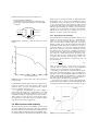
Perhaps the greatest challenge affecting BGA technology is the overall cost [22] of the package. The cost per
lead by package family is shown in Figure 1.29 [23].
For BGA, the cost per lead is somewhat higher than of
most other packages, such as DIP, SO, CC, and QFP.
Only PGA is considerably higher than BGA. However,
for BGA, the cost per lead is reducing at a rate of −6.01
percent for CAGR, which is faster than −5.49 percent
1/14 Reflow Soldering Processes and Troubleshooting
Silicon die
An bond wires
Ag-filled die attach
Epoxy
overmold
BT/glass PCB
62/36/2 Sn/Pb/Ag
solder balls
(a)
PBGA
CHIP
Ceramic
substrate
CHIP
Ceramic
substrate
CHIP
Ceramic
substrate
Casted
SCC
SCC
90Pb10Sn
63Sn37Pb
63Sn37Pb
90Pb10Sn
63Sn37Pb
SBC
CARD/PCB
(b)
CBGA and CCGA
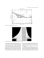
Figure 1.27 Schematic of various types of BGAs, (a) PBGA, (b) CBGA and CCGA
for DIP, −5.51 percent for CC, −2.39 percent for QFP,
and −4.71 percent for PGA. As a result, the cost disadvantage of BGA is gradually diminishing. At present, the
cost parity of the BGA to the QFP is above 200 I/O. The
design methodology used to date has been cost effective
for BGAs at or above 200 I/O but fails to be cost competitive below this pin count.
1.2.2.2 CSP
As indicated in Figure 1.26, the emergence of BGA satisfies the need for higher I/O density, but slows the drive
toward finer pitch. However, with increasing demand
toward further miniaturization, the packaging technology of BGA also reduces over time and consequently
results in chip scale packages (CSP). A CSP is an IC
area array package with size no larger than 1.2× of
IC in the linear dimension, or no larger than 1.5× of
IC in area. The package may use an interposer/carrier, and
the interposer may be ceramic, plastic, or flex-film [24].
Depending on the CSP design, the interconnection [25]
between IC and carrier may be wire bonding, TAB, Austud, soldering, or conductive adhesives. Currently, the
minimum CSP array pitch is 0.5 mm, and will be 0.4 mm
in 2000, and 0.3 mm in 2002 for the telecommunication
market [26]. For the mobile systems market, the reduction rate of minimum CSP array pitch is even faster, with
0.5 mm in 1998, 0.3 mm in 2000, and 0.2–0.25 mm in
2004, according to the roadmap published by NETPACK
(European Network in Microelectronic System Integration Technologies-Packaging). The options of alloys [24]
and liquidus temperature used for CSP ball and attachment may include: 63Sn37Pb (183° C), 62Sn36Pb2Ag
(179° C), 96.5Sn3.5Ag (221° C), 95Sn3.5Ag1.5In (218° C),
25In75Pb (264° C), and 10Sn90Pb (325° C).
For cellular phone applications, the most common I/Os
in use at this stage are 32, 48, 64, 80, and 100. The ball
size varies from 0.3 mm (12 mil) to 0.5 mm (20 mil), and
size variation tolerance ranges from 0.03 mm (0.2 mil) to
0.075 mm (0.5 mil) [27]. It should be noted that the ball
size changes for most of these devices depending on the
manufacturer. The preference is to use as large a ball size
as possible to assure the best reliability. The design of
the CSP package also plays an important role in selection
of ball size. For instance, Tessera’s µ BGA CSP uses
a compliant layer making it possible to use smaller balls
which reduces the chance of shorting, lowers weight and
allows wider trace routing channels [28].
For the automotive industry, the maximum chip I/Os
are 150 in 1998, and 200 in 2002, with CSP minimum
Introduction to Surface Mount Technology 1/15
Millions of
components
90 000
80 000
70 000
Bare die
DCA
CSP
BGA
CPGA
PPGA
Other
TAB
CQFP
PQFP
PLCC
SO
SIP/ZIP
CDIP
PDIP
SOT/TO
60 000
50 000
40 000
30 000
20 000
10 000
0
1996
Year
2001
Figure 1.28 BGA market forecast [19]
4
Price per lead (cents)
3.5
3
DIP
SO
CC
QFP
PGA
2.5
2
1.5
BGA
1
0.5
0
1998
1999
2000
2001
Year
2002
2003
Figure 1.29 Cost per lead by family of packages [22]
pitch being maintained at 0.8 mm from 1998 throughout
2004. CSP can also deliver performance for very high
I/O applications. The maximum chip I/Os for mobile
systems are 500 in 1998, 600 in 1999, and are projected
to be 700 in 2000, 800 in 2002, 900 in 2003, and 1000
in 2004 [25]. The current assembly yield [17] of CSP is
estimated to be 3.4 ppm for 0.75 mm (30 mil) and 0.5 mm
(20 mil) pitch, about the same level as a typical PBGA
assembly yield.
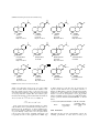
1.2.2.3 Flip chip
Flip chip is a chip connection technology which interconnects an IC chip to its next level of packaging in such
1/16 Reflow Soldering Processes and Troubleshooting
Wire
bond
WIT
Au
overcoat
Conductive
adhesive
Solder
Ni
IC
Solder
Elastomer
Polymer
IC
Pads on
substrate
IC
Fluxless
Pad on Conductive
solder bump
chip
particle
Ni/Au
bump
Solder
bump
IC
TAB
lead
Substrate
IC
IC
Thermosetting
adhesive
Solder
bump
Underfill
encapsulant
Figure 1.30 Various flip chip technology (courtesy of John H. Lau [29])
FC bumping feature
Metal bump
Metal bumping--Au
Metal bumping--Electroless NiAu
Metal bumping--Electroplated Au
Metal bumping--Electroplated AuSn
Metal bumping--Electroplated solder--Sn60
Metal bumping--Post (Cu)--WIT
Metal bumping--Reflowed solder paste
Metal bumping--Solder--95Pb5Sn or 97Pb3Sn
Metal bumping--Stud Au
Metal bumping--Stud Au--Raychem: BIP
Metal bumping--Stud solder--97Pb3Sn
Metal Polymer bumping--Stud & conductive adhesives
Polymer bumping--Compliant bumps
Polymer bumping--ICP--Sharp: Pad particles
Polymer bumping--ICP--Thermoplastic
Polymer bumping--ICP--Thermoset
Polymer bumping--ICP--Thermoset--B-stage
Pad
FC-board interconnection
Thermocompression
Thermocompression-- VIS
ACA
ACA-- Au on plastic ball
ACA-- Microconnector
ACA-- MCA
ACA Pad--Samsung & Zymet
ACF--Double layer
ICA
ICA Pad--Mitsubishi
ICA--Seiko Epson’s pad particles
NCA
Solder
Solder--PADs
Solder--C4
Solder--Reflow paste
Figure 1.31 Flip chip interconnections [25]
a manner that the IC’s active side faces the substrate. In
terms of packaging efficiency (package area versus die
area), flip chip technology reaches the ultimate goal of
reducing chip size, as shown in Figure 1.26. Interconnection of flip chip with the substrate is shown in Figure 1.30
[29]. The bumping technologies used by flip chips are
summarized in Figure 1.31 [24], and include plated metal
bump, Au stud, metal stud plus polymer, Cu post, solder bump, and polymer bump. The bonding processes
for flip chip attachment are also shown in Figure 1.28,
and involve thermocompression, anisotropic conductive
adhesives (ACA), isotropic conductive adhesives (ICA),
non-conductive adhesives (NCA), and soldering.
Flip chip technologies are gaining market acceptance very rapidly. According to Electronic Trend Publications [29], the flip chip market was 568.7 million
units in 1997, and will be 2.514 billion units in 2002,
with an expected calculated annual growth rate (CAGR)
34.62 percent, as shown in Figure 1.32 [30]. The Die
Attachment segment, including FCOB and FCOO (flip
chip on other), has increased from 558.6 million units in
1997 to an estimated 1.334 billion units in 2002, with a
CAGR of 19.02 percent. On the other hand, the Flip Chip
In Package (FCIP) segment, including BGA FC, CSP FC,
and MCM FC, has grown most rapidly from 10.1 million
units in 1997 to an estimated 1.180 billion units in 2002,
with a CAGR of 159.15 percent.
Prismark estimates flip chip die increased by 40 percent
to 899 million units in 1998, which is 1.5 percent of the
60 billion ICs produced in 1998. This 40 percent annual
growth rate is also expected for flip chip over the next
five years [31]. The 899 M units were mostly DCA and
50 million units of these were FCIP. The majority of these
FCIP will be delivered in BGA and CSP configurations.
Introduction to Surface Mount Technology 1/17
Flip chip forecast (million units)
3000
2500
2000
1500
1000
500
0
1997 1998 1999 2000
1.1
2.1
4.3
MCM FC 0.8
0
1.3 36.2 160.4
CSP FC
BGA FC 9.3 37.7 98.5 210.5
463.7 494.1 650.9 796.2
FCOO
95 108.5 152.7 211.6
FCOB
2001 2002
5.7
6.5
361.4 594.9
366.1 578.9
937.3 1000.5
280 333.5
Year
Figure 1.32 Flip chip forecast [30]
Non-solder bumped die (watch modules, smart cards,
RFID tags) (45.9%)
155
287
Lower leadcount (microcontrollers, small memory, pre
amps, op amps, typically <200 I/O) (31.9%)
28
16
10
Display drivers (chip on glass) (17.3%)
Processors, ASICs, etc. (typically >400 I/O) (3.1%)
6
0
Memory (SRAM, DRAM, flash) (1.1%)
High frequency (RF BiCMOS, GaAs) (0.7%)
Integrated passives (negligible)
413
Figure 1.33 Breakdown of flip chip global production (million units) in 1998 [31]
Growth in FCIP brings that share of total FC devices up to
an estimated 30 percent by 2004. A breakdown of global
flip chip production in 1998 (total 899 million units) is
shown in Figure 1.33.
A slightly more conservative forecast was released
by TechSearch. In that study, the flip chip market was
760 million units in 1999, and is estimated to be 1.130
billion units in 2000, 1.450 billion units in 2001, 1.750
billion units in 2002, 2.000 billion units in 2003, and
2.400 billion units in 2004 [21]. The FCIP of overall
FC will increase from 15 percent in 1999 to 27 percent
in 2004. The balance is FCOB. Automotive electronics
and watches, the two largest consumers of flip chip
today, are expected to grow, but will account for a
progressively smaller share of total flip chip consumed.
Flip chip mounted driver ICs, while expected to see
growth, will continue to represent about 10 percent of
the total market. Telecom’s share of the flip chip pie will
grow. The growth of flip chip in switching and network
applications will be overshadowed by the very large
increase in the use of flip chip devices for portable telecom
such as portable handsets and PDAs. The computer
industry, representing portables all the way through highend systems, is expected to see considerable growth. Its
share of the total flip chip market is expected to expand
to 40 percent by 2004. This will be driven by the growing
consumption of flip chip-mounted processors and ASICs
for home and portable personal computers.
1.3 Conclusion
Surface mount technology enables the progressing of
the electronic industry toward the trends of becoming
smaller, lighter, denser, faster, and cheaper. Competing
with wave soldering, reflow soldering has quickly become
the main stream interconnect technology, due to higher
yield, throughput, and reliability. Area array packages
alleviate pressure on peripheral packages toward finer
1/18 Reflow Soldering Processes and Troubleshooting
pitch, and provide higher I/O density together with easier
manufacturability, smaller package size, and higher speed.
BGA was the first array family to demonstrate the
robustness of the surface mountable-area array package
concept and now prevails in the industry. As a logical
consequence of need for miniaturization, and based on the
success of BGA, CSP and Flip Chip have both evolved
rapidly and have become the new stars on the stage of
advanced packaging technology. With the ultimate goal of
having package reduction down to die size being within
reach, the next challenge may be 3D packaging integration
design.
References
1. D. Feryance and F. Shubert, ‘‘Matte-surface Solder Masks
Reduce Solder Ball Defects‘‘, EP&P , pp. 58–60 (June 1993).
2. C. Hemens-Davis and R. Sunstrum, ‘‘No-clean: Material Compatibility Issues’’, Circuits Assembly , Vol. 4, No. 3, pp. 47–55
(March 1993).
3. M. Xiao, K. Lawless, and N.-C. Lee, ‘‘Prospects of Solder Paste
in UFPT Era’’, in Proc. of Surface Mount International 93, San
Jose, CA 29 (August–2 September 1993).
4. B.-T. Ma, A. Sarkhel, and C Woychik, ‘‘Evaluation Solder Paste
Printing and Reflow for Ultra Fine Pitch Surface Mount Process’’, in Proc. of Nepcon West, Anaheim, CA, pp. 506–517
(1993).
5. ‘‘Packaging Materials: Ball Grids Are Pinless PGAs’’, Electronic
Materials Report , Vol. 10, No. 1, pp. 8 (January 1994).
6. R. Iscoff, ‘‘Ultrathin Packages: Are They Ahead of Their Time?’’
Semiconductor International , pp. 48–52 (May 1994).
7. H. Wessely, O. Fritz, P. Klimke, W. Koschnick, and K. H. Schmidt, ‘‘Electronic Packaging in the 90s – A Perspective from
Europe,’’ Proceedings of the 40th IEEE Electronic Components
and Technology conference, pp. 16–33 (May 1991).
8. J. Lau and S. Erasmus, ‘‘Review of Packaging Methods to
Complement IC Performance’’, EP&P , pp. 50–56 (June 1993).
9. R. Ristelhueber, ‘‘Monster ASICs Emerge from ‘Deep Submicron Silicon’ ’’, Electronic Business Buyer , pp. 39–42 (February
1995).
10. C. Vaucher, ‘‘Electrical test of Bare Printed Circuit Board:
Requirements on the ‘System Houses’ Side’’, Future EMS
International , Issue 1, p. 46, (1999).
11. B. Siu and J. McMahon, ‘‘Evolution and Trends for Microprocessors’’, Circuits Assembly Market Supplement , S10–13
(September 1993).
12. T. R. Halfhill, ‘‘Intel’s P6’’, BYTE , pp. 42–58 (April 1995).
13. R. Iscoff, ‘‘Ultrathin Packages: Are They Ahead of Their Time?’’
Semiconductor International , pp. 48–52 (May 1994).
14. R. Ristelhueber, ‘‘Monster ASICs Emerge from ‘Deep Submicron Silicon’ ’’, Electronic Business Buyer , pp. 39–42 (February
1995).
15. M. Durkan, ‘‘Integrating Technologies to Bring Speed to Market’’, Future EMS International , Issue 1, pp. 69, (1999).
16. ‘‘Area Array Packaging Options Continue to Blossom’’, EP&P ,
p. 14 (November 1999).
17. I. Turlik, ‘‘Chip-Scale Packaging Technology Trends’’, Chip
Scale Review , Vol. 1, No. 2, pp. 30–35 (July 1997).
18. J. H. Lau,(ed.), ‘Ball Grid Array Technology’ , McGraw-Hill,
New York (1995).
19. R. Lasky, ‘‘Electronics: This is Only the Beginning’’, EP&P , pp.
48–52, (November 1997).
20. G. Olachea, ‘‘IC Packaging for the 21st Century’’, EP&P , Vol. 37,
No. 15, pp. 57–62, (November 1997).
21. T. Goodman, ‘‘Flip Chip: Key Technologies and Applications
Worldwide’’, in Proc. ISEPT’98, Beijing, China, 17–21, August,
pp. 435–439, (1998).
22. J. Miks and D. Daniels, ‘‘Cost Effective Approach to Fine Pitch
BGAs’’, in Proc. MCM’97, Denver, CO (April 1997).
23. S. Winkler, ‘‘Packaging Industry Outlook’’, HDI , Vol. 2, No. 6,
pp. 16–17 (June 1999).
24. V. Solberg, ‘‘Assembly Process Development for Chip-Scale
and Chip-Size uBGA ’’, in Proc. SMTA/IPC Electronics Assembly Expo, Providence, RI, 24–29, October pp. S12–S14,(1998).
25. N. C. Lee, ‘‘Interconnections for SMT, BGA, and Flip Chip
Technologies’’, Keynote Lecture, Nepcon Penang, 17, June
1996.
26. S. Berry, ‘‘The Future of Leadcounts’’, HDI , pp. 14–16, (April
1999).
27. Private communication from Jessie Buenaventura, AmkorManila, Philippines, 20, December, 1999.
28. Private communication from Joseph Fjelstad, Teserra, San
Jose, CA, 21, December 1999.
29. John H. Lau, (ed.), Flip Chip Technologies, McGraw-Hill, New
York, (1996).
30. Steve Berry and Sandra Winkler, ‘‘Flip Chip Market Expanding
to Meet Speed, Performance Demands’’, Chip Scale Review ,
11/12, p. 6 (1999).
31. L. Smith, C. Scanlan, and P. O’Brien, ‘‘FCIP Delivers Flip Chip
Benefits without DCA Complications’’, Advanced Packaging,
pp. 32–35, (August 1999).
2/19
Fundamentals of
Solders and
Soldering
2
Soldering uses molten filler metal to wet the surfaces of
a joint and form metallurgical bonds between two metal
parts. The melting temperature of the filler metal is lower
than 450 ° C. For filler materials that melt at a higher temperature, the joining process is classified as brazing [1].
Soldering is a vital interconnect technology involved in
both level 1 (IC packaging) and level 2 (mounting of
electronic components onto printed circuit boards) processes of the modern electronics industry. Therefore, to
achieve a high quality and high yield soldering process, it
is essential to understand the fundamentals of solder and
soldering.
compound layer [2]. In this figure, fluid stands for either
flux or soldering atmosphere, and the base metal is the
substrate.
2.1.1 Spreading
In order to solder, the solder material first has to be heated
to a molten state. This molten solder is then allowed to wet
to the surface of the base metal. Like any other wetting
phenomenon, wetting of liquid solder on a base metal, as
shown in Figure 2.1(a), has to comply with the physical
law of balance of interfacial tension, as expressed by
2.1 Soldering theory
γSF = γLS + γLF × cos θ
Although soldering has been carried out by humans for
more than several thousand years, an understanding of
this process was minimal until recently. The soldering
process can be depicted in Figure 2.1, and can be
roughly divided into three stages: (1) spreading, (2) base
metal dissolution, and (3) formation of an intermetallic
In this relation, γSF stands for the interfacial tension between the base metal substrate and the fluid, γLS is the
interfacial tension between substrate and the liquid solder,
γLF is the interfacial tension between liquid solder and the
fluid, and θ represents the contact angle between liquid
solder and the substrate.
(2.1)
g LF
Fluid
Molten solder
(a) Base metal
q
g SF = g LS + g LF × cos q
g LS
gSF
Molten solder
(b)
Molten solder
(c)
Intermetallic compound layer
Figure 2.1 Solder wetting process involves (a) liquid solder spreading over base metal, with contact angle θ dictated by balance of
interfacial tension forces, (b) base metal dissolving in liquid solder, (c) base metal reacting with liquid solder to form intermetallic
compound layer
2/20 Reflow Soldering Processes and Troubleshooting
Equation (2.1) predicts that the spreading of a liquid
on a solid surface reaches an equilibrium steady state
when the contact angle achieves a θ value where the
two opposite vector forces γSF and (γLS + γLF × cos θ )
are balanced.
For electronics industry soldering applications, a solder
joint with a satisfactory fillet formation is desired for minimum stress concentration, as demonstrated in Figure 2.2.
In order to achieve this, a solder spreading characteristic
with low θ value is needed. In fact, a small θ value is not
only desirable due to stress consideration, it must also
assure that a good metallurgical wetting is achieved, as
will be illustrated in the following sections.
A low θ value can be achieved with both chemistry and
physics approaches. The chemistry approach will be discussed later. The physics approach includes manipulation
of surface tension of materials involved in the soldering process. In principle, use of (1) a low surface tension
flux, (2) a high surface tension, or high surface energy,
substrate, and (3) a low surface tension solder will allow
formation of a low contact angle θ . The first situation
can be derived easily from the effect of surface tension
on interfacial tension, as shown in Appendix 2.1. The
second and third situations can also be derived similarly.
However, they can also be easily demonstrated by some
common phenomena. Thus, the second situation can be
illustrated by the poor wetting of water on a Teflon (low
surface energy) substrate but relatively good wetting on a
metal (high surface energy) substrate. The third situation
can be demonstrated by good wetting of alcohol (low surface tension) but poor wetting of mercury (high surface
energy) on a glass slide.
However, it should be emphasized again that for the
soldering process, the balance of interfacial tension is only
one of the driving forces determining the wetting phenomenon. Since generally the base metal will dissolve
in and react with the solder, and since soldering is a
short, non-equilibrated process instead of an equilibrated
one, factors such as fluid viscosity, metal dissolution, and
chemical reaction between solder and base metals often
play a more important role, as will be discussed in the
following sections.
2.1.2 Fluid flow
In the previous section, we showed that the spreading of
a fluid is determined by the balance in interfacial tension
established at the equilibrium state. However, in the actual
soldering process encountered in the electronics industry,
only seconds or minutes are allowed, and the equilibrium
condition virtually can never be met. Factors such as viscosity of the molten solder will affect the extent of solder
flow, and thus can play an important role when time is a
constraint.
Milner [3] has analyzed the fluid flow between two horizontal parallel plates with consideration of both surface
tension and fluid viscosity factors. The conclusion on the
rate of fluid flow through the parallel plates dl/dt drawn
from his study can be expressed as
dl/dt = (γLV D cos θ )/(6ηl)
(a)
(b)
Figure 2.2 Example of SMT 62Sn/36Pb/2Ag solder joints with
desired fillet formation, (a) melf on HAL pad, (b) IC gullwing lead
on Cu pad
(2.2)
Here l is the length of plates, η is the viscosity of the
fluid, γLV is the interfacial tension between fluid and the
surrounding vapor or atmosphere, D is the joint gap, and
θ is the contact angle between fluid and the plate. Therefore, the rate of the liquid flow through the parallel plates
dl/dt increases with increasing interfacial tension between
liquid and vapor γLV , increasing joint gap D, but with
decreasing contact angle θ , decreasing viscosity η, and
decreasing plate length l.
By applying equation (2.2) to solder spreading, γLV can
be rewritten as γLF , and represents the interfacial tension
between liquid solder (L) and flux (F). Since γLF = γL − γF
according to Antonow’s rule (see Appendix 2.1), for a
given solder with surface tension γL , an increase in γLF
would have to depend on a decrease in the surface tension
of flux γF . Hence a flux with a low surface tension will
not only increase the spread, as discussed in the previous
section, but will also increase the liquid solder flow rate.
Humpston and Jacobson [1] have calculated the filling
rate of molten solder in joints 50 µm wide with the use of
this equation, and found the filling rate is typically 0.3 to
0.7 m/s. Thus a joint 5 mm (0.2 in.) in length will be filled
in around 0.01 second. Considering that the surface energy
Fundamentals of Solders and Soldering 2/21
driving force is often opposed by viscosity and surface
irregularity, as reported by De Gennes [4], a joint filling
time of the order of 0.1 second may be more realistic.
2.1.3 Dissolution of base metal
Flow and spreading of liquid solder over a base metal
substrate are not sufficient to form metallurgical bonds,
which are required to form solder joints, as demonstrated
by placing liquid solder on a glass surface. In order to
form a metallurgical bond, the solder and base metal have
to be mixed at the atomic level at the interface. This is
typically accomplished through dissolution of base metal
into the solder at the microscopic level (<100 µm) [1], as
shown in Figure 2.1(b).
For the electronics industry, the soldering process is
often confined to a relatively low temperature, such as
220 ° C, and a short cycle time, often no longer than several seconds or minutes, due to materials limitations and
throughput consideration. Therefore, the dissolution of a
base metal in solder needs to be reasonably easy and
fast. For tin–lead systems, which have been the prevalent choice of solders for the past several decades, the
acceptable base metals or metallization include, but are
not limited to, Sn, Pb, Bi, Au, Ag, Cu, Pd, Pt, and Ni.
The dissolution rate dC/dt of some of those metallization
in 60Sn/40Pb as a function of temperature is shown in
Figure 2.3 [1,5], and can be represented by the Arrhenius
relationship, as shown in the following equation:
dC/dt ∝ exp[−E/(kT )]
(2.3)
where C is the concentration of the base metal, E is the
activation energy, k is the Boltzmann constant, and T is
temperature in degrees Kelvin. The dissolution rate of a
base metal in solder is also a function of time [1,6,7], as
expressed by
dC/dt = KA(CS − C)/V
(2.4)
1000
where C is the concentration of the base metal, CS is the
concentration limit of the dissolved metal in the molten
solder at any given temperature, t is time, K is the dissolution rate constant, A is the wetted surface area, and
V is the volume of the molten solder. By integrating
equation (2.4), the relation between C and t can be expressed by Figure 2.4 [1], where C reaches an equilibrium
concentration in an inverse exponential relationship with t.
The dissolution of a base metal in solder as a function of
time and temperature can be demonstrated by Figure 2.5,
where the dissolution of base metal silver in molten tin
increases with increasing time and temperature [8]. Humpston and Jacobson reported that the equilibrium condition
can be reached within seconds at the process temperature
according to their calculations, suggesting the feasibility
of predicting solder joint composition with an equilibrium
phase diagram.
The dissolution rate of a base metal in solder is a
function not only of time, temperature, and base metal
type but also of solder alloy type [5]. Therefore, for Ag,
the dissolution rate in solders decreases in the following order: Sn > 99Sn/1Cu > 90Sn/10Pb > 80Sn/20Pb >
62Sn/38Pb. For Cu, the dissolution rate decreases
as: Sn > 60Sn/40Pb > 35Sn/65Pb > 57Sn/38Pb/5Ag >
62Pb/33Sn/5Ag. The dissolution rate can be changed by
shifting the initial concentration of the base metal in the
solder by engineering the solder composition. Hence, by
adding 2 percent Ag to tin–lead solder, the dissolution
rate of base metal Ag can be reduced significantly, as
exemplified by comparing the dissolution rate of Ag in the
40Pb/60Sn and 36Pb/62Sn/2Ag solder systems [9] (see
Figure 2.6).
In general, the wettability of metallization appears to
increase with increasing dissolution rate in the solder.
Although this phenomenon may be related to chemical
reactions, as will be discussed in Section 2.1.4, it may
also be attributable to the entropy factor, since dissolution
of a base metal in solder will result in an increase in
Sn
Au
Ag
CS
Cu
10
Pd
1
C (concentration)
Dissolution rate, µm/s
100
Pt,Ni
0.1
0.01
100
1000
Temperature, °C
Figure 2.3 Dissolution rate of some commonly used metals and
metallizations in 60Sn/40Pb as a function of temperature [32,36]
t (Time)
Figure 2.4 The concentration C of base metal increases in an
inverse exponential relationship with time t , and approaches
equilibrium concentration Cs quickly [32]
2/22 Reflow Soldering Processes and Troubleshooting
25
Depth of erosion, µm
20
300°C
15
260°C
10
230°C
5
0
1
10
102
Time, s
103
104
Figure 2.5 Dissolution of silver by molten tin as a function of time and temperature
deterioration of joint reliability. These situations are not
desirable, and will be discussed later.
10
2.1.4 Intermetallics
Dissolution rate, µm/s
1
10−1
40Pb−60Sn
10−2
36Pb−62Sn−2Ag
10−3
10−4
0
75
100
25
50
Excess temperature above melting point, °C
Figure 2.6 Dissolution rate of silver in tin–lead and tin–lead–silver
solder systems [40]
entropy. Since the dissolution rate increases with increasing temperature and time, this allows control of dissolution rate with processing parameter. On the other hand,
the strong influence of the base metal type and the solder type on dissolution rate indicates the importance of
materials selection at the engineering design stage.
Although dissolution of a base metal is essential in
forming metallurgical bonds, too fast a dissolution rate
may result in a serious leaching problem hence loss of
metallurgical bonds. In addition, it may also cause a significant change in solder composition, therefore causing
Soldering often involves not only the physical dissolution of base metals in the molten solder but also the
chemical reaction products between base metal and solder components. The reaction products formed typically
are intermetallic compounds (IMC, or intermetallics) at
the interface between solder and base metal, as shown
in Figure 2.1(c). Intermetallic compounds are exact stoichiometric compounds which tend to form when one of
the two elements is strongly metallic in character and
the other significantly less so. For instance, intermetallics
Cu6 Sn5 and Cu3 Sn normally are formed between tin–lead
solder and base metal Cu. Intermetallics tend to be hard
and brittle because their crystal structure has low symmetry, and this limits the plastic flow.
The effect of intermetallics formation on soldering
includes (1) enhancement of solder wetting on the base
metal due to favorable thermodynamics, (2) slowing of
the dissolution rate of the base metal in solder due to
the diffusion barrier role of the intermetallics layer, and
(3) deteriorating the wettability of a pretinned surface
through oxidation of intermetallics. Those effects will be
discussed in detail below.
2.1.4.1 Wetting enhancement
It has been reported by Yost and Romig [10] that even
though the imbalance of surface energy will result in
energy release thus favoring solder spreading, the free
energy of formation of intermetallics between liquid antimony, cadmium, and tin with base metal copper was about
Fundamentals of Solders and Soldering 2/23
Total intermetallic layer thickness, µm
Solder, molten
Solder, molten
25
20
15
10
Solder, solid
5
Melting point
0
0
100
200
Temperature, °C
300
400
Figure 2.8 Growth of copper–tin intermetallic compound for copper substrate wetted by tin–lead solder for 100 seconds [32]
Table 2.1 Compound layer thickness immediately after
reflow soldering of solder pastes
Solder
63Sn/37Pb
62Sn/36Pb/2Ag
50Pb/50In
Intermetallic thickness (µm) on
Cu
Au/Pt
Au/Ni/W
2.4
2.1
3.5
2.0
2.0
2.0
2.0
2.0
<1.0
315°C
260°C
2.1.4.2 Dissolution barrier
25
20
15
Solder, solid
175°C
10
130°C
5
80°C
0
30
and the isothermal liquid state growth rate parameters
for the growth of the intermetallic layer, consisting of
a growth constant and an activation energy. The validity
of the method is demonstrated for intermetallic growth
between copper and 62Sn/36Pb/2Ag solder.
35
30
35
Total intermetallic layer thickness, µm
two orders of magnitude larger. Hence, it is no surprise
to learn that the wetting behavior increases with increasing formation rate of intermetallics, and is dictated by the
intermetallics formation rate.
The first intermetallic compound to be formed at the
solder/substrate interface can be predicted by calculating
metastable equilibria between the substrate and the liquid
solder phases and by comparing the calculated driving
forces of formation for individual phases. This feasibility
of prediction was demonstrated for the interface reactions between Cu substrate and Sn–Pb, Sn–Bi and Sn–Zn
binary eutectic solders [11].
Like the dissolution of a base metal in solder, the formation rate of intermetallics is also a function of time,
temperature, type of substrate metallization, and solder
type. Figure 2.7 shows the growth of copper–tin intermetallics on a copper substrate wetted by eutectic tin–lead
solder. The intermetallics thickness decreases with decreasing time and temperature [1]. Growth in intermetallics continues even at temperatures below the melting
point of solder, although at a much slower rate, as illustrated in Figure 2.8. Kay and Mackay [12] reported that
the thickness of tin-base intermetallic phases developed
at 170 ° C via solid-phase diffusion is a function of substrate materials, and varies in the following order: Co >
Ag > Cu > Ni > Fe. The effect of solder type on the
intermetallics formation rate of several metallizations has
been studied by Muckett et al. [13] and their findings are
reported in Table 2.1. It is interesting to note that, compared with 63Sn/37Pb and 62Sn/36Pb/2Ag, 50Pb/50In
produced a thicker intermetallics on Cu, but a thinner
intermetallics on Au/Ni/W metallization.
The intermetallic layer thickness at any time during the
soldering process can also be calculated with a numeric
method, as reported by Schaefer et al. [14]. As input, the
method requires the soldering temperature–time profile
0
1
2
3
4
Time, log10 s
5
6
Figure 2.7 Formation of copper–tin intermetallic layer for copper
substrate wetted by eutectic tin–lead solder [32]
In general, the intermetallics formed has a higher melting
point than the soldering temperature encountered in the
electronics industry, and will remain as a solid during the
soldering process. For many systems, the intermetallics
forms a continuous layer between molten solder and the
solid base metal, as demonstrated by the intermetallic
Cu3 Sn in Figure 2.9 [15], and consequently slows the rate
of base metal atoms diffusion through the intermetallics
layer. This is attributed to the phenomenon that the solidstate diffusion process is roughly two orders of magnitude slower than solid–liquid reactions. As a result, the
dissolution rate of the base metal in solder is greatly
reduced.
However, not all intermetallic compounds form layered structures. For instance, the Cu6 Sn5 intermetallics
between the eutectic SnPb solder and Cu have grown as
scallop-like grains into the molten solder. Between the
2/24 Reflow Soldering Processes and Troubleshooting
Figure 2.9 Cross-section of a coating 60Sn/40Pb on soft copper (marker = 20 µ). Two intermetallic compound layers Cu3 Sn and Cu6 Sn5
are produced [46]
Figure 2.10 Formation of Cu6 Sn5 intermetallics between Sn96.2/Ag2.5/Cu0.8/Sb0.5 and Cu substrate
Fundamentals of Solders and Soldering 2/25
10 µ
Figure 2.11 The PdSn3 lamellae grow in a direction normal to the interface for Pd substrate wetted by eutectic SnPb [48]
scallop grains, there are molten solder channels extending
almost all the way to the Cu interface. In aging, these
channels serve as fast diffusion and dissolution paths of
Cu in the solder to feed the reaction [16]. The Cu–Sn
intermetallics formed between Cu and a lead-free solder Sn96.2/Ag2.5/Cu0.8/Sb0.5 shows a similar structure
(Figure 2.10).
The structure of the intermetallic compound formed
may not be easy to predict. Therefore, the intermetallic
PdSn3 formed between a molten 63Sn/37Pb solder grows
as lamellae into the molten solder, instead of as a diffusion
barrier layer (see Figure 2.11). The direction of growth is
normal to the liquid/solid interface, and the molten solder between the lamellae serves as fast diffusion channels
during soldering. However, if the Pd is in contact with
molten Sn (Pb-free), the formation rate of intermetallics
PdSn4 is slower by one order of magnitude. No lamellar
structure was observed and the intermetallics grows as a
diffusion barrier between the Sn and Pd [17].
The results above indicate that the intermetallic compounds are wettable by solder, with Cu6 Sn5 being slightly
more wettable than Cu3 Sn. However, the wettability of
both intermetallics degraded much more rapidly than Cu
after storage. This vulnerability of intermetallics toward
oxidation suggests potential shelf-life concerns associated
with pretinned metallization and solderability problems
associated with the rework process. It has been suggested
that the intermetallics could be internally oxidized without
having broken through to the pretinned surface. The wetting difficulty would arise once the pretinned surface is
melted off during soldering [19,20]. In general, wettability
decreases with decreasing initial solder coating thickness
and increasing intermetallics thickness [21]. For immersion tin-coated printed wiring boards, a minimum thickness of approximately 60 µ-in. (1.5 µm) was determined
to be critical for assembly operations involving multiple
thermal excursions. The electroless copper substrate will
cause significantly more intermetallic formation [22].
2.1.4.3 Susceptibility toward oxidation
2.2 Effect of elemental constituents on
wetting
Although formation of intermetallics enhances wetting
during the soldering process, the solderability of intermetallics thus formed is actually poorer than the base
metal itself. Yost et al. [18] evaluated the wettability of
several solid samples including Cu, Cu6 Sn5 , and Cu3 Sn
at 235 ° C with the use of a wetting balance containing a
60Sn/40Pb solder bath. For the freshly etched solid samples, the wettability of Cu is much better than Cu3 Sn and
Cu6 Sn5 if a non-activated R flux is used for testing (see
Figure 2.12). The difference in wettability diminishes if a
mildly-activated RMA flux is used. However, if the solid
samples were stored at room temperature for 3 days before
testing, the wettability of all three samples degraded considerably if the R flux is used, with Cu being much better
than Cu6 Sn5 , which in turn is slightly better than Cu3 Sn.
The effect of storage on Cu is negligible when the RMA
flux is used, while both intermetallic compounds suffer
considerable degradation in wettability due to storage.
Since wetting is greatly affected by the formation of intermetallics, and since the formation of intermetallics is dictated by the reaction between elements, it is reasonable
to expect that the elemental constituents of solders should
have a significant effect on the wetting of solder alloys.
Humpston and Jacobson [23] studied the spreading characteristics of a series of eutectic binary alloys as a function
of excess temperature above the melting point of solders. Results indicate there is a ranking order for the
elements studied in their ability to promote spreading,
as follows: tin > lead > silver > indium > bismuth. This
ranking order is reported to be maintained even for ternary
and quaternary solders.
It should also be pointed out that the effect of elemental constituents on wetting should be treated as a
guideline only. Many other parameters, such as viscosity
or the additive effect, may override the elemental effect
and alter the relative order of spreading of solders. For
2/26 Reflow Soldering Processes and Troubleshooting
Wetting balance tests with R flux
Wetting force (fraction of 0.42 N/m)
Wetting force (fraction of 0.42 N/m)
Wetting balance tests with RMA flux
1.0
0.5
0.0
−0.5
Cu
Cu3Sn
Cu6Sn5
−1.0
−1.5
0
1
2
3
4
Time (s)
5
1.0
0.5
0.0
−0.5
Cu
Cu3Sn
Cu6Sn5
−1.0
−1.5
0
6
1.0
0.5
0.0
−0.5
Cu
Cu3Sn
Cu6Sn5
−1.0
−1.5
0
1
2
3
4
Time (s)
5
2
3
4
Time (s)
5
6
Wetting balance tests with R flux
after 3 days′ storage
Wetting force (fraction of 0.42 N/m)
Wetting force (fraction of 0.42 N/m)
Wetting balance tests with RMA flux
after 3 days′ storage
1
6
1.0
0.5
0.0
−0.5
Cu
Cu3Sn
Cu6Sn5
−1.0
−1.5
0
1
2
3
4
Time (s)
5
6
Figure 2.12 Wetting balance results on the solderability of Cu, Cu3 Sn, and Cu6 Sn5 using R and RMA fluxes and 60Sn/40Pb solder bath at
235 ° C
instance, although pure Sn is superior in wetting compared
with eutectic SnPb on Cu [24], SnAgBi alloys, such as
91.7Sn/3.5Ag/4.8Bi, wet better than eutectic SnAg [25],
despite the addition of the less favored element Bi.
2.3 Phase diagram and soldering
A phase diagram is a description of a thermodynamically
equilibrium state of phases as a function of composition
and thermodynamic parameters such as temperature. It is
helpful in providing the composition of probable phases
as well as the melting temperature of those components.
Being thermodynamic in nature, a phase diagram cannot
predict kinetic properties, such as reaction rate between
ingredients, and wetting characteristics, such as wetting
speed on an oxidized base metal. In addition, it cannot predict the morphology of various phases in the solder joint.
Although soldering is typically a short process
involving chemical reactions, hence being highly kinetic
in nature, proper use of a phase diagram together
with supplementary information does allow a deeper
understanding and some prediction of soldering behavior.
The application of a phase diagram to soldering can be
illustrated by the following examples.
For a SnPb solder system, the binary eutectic phase
diagram is shown in Figure 2.13. The soldering characteristics of various compositions can be exemplified by
compositions A–C.
At composition B (70Pb/30Sn), the solder begins to
melt at the solidus temperature of 183 ° C, but will not turn
completely to liquid before reaching the liquidus temperature of 257 ° C. The solidus indicates that the upper limit
of service temperature has to be considerably lower than
183 ° C. The 257 ° C liquidus indicates a sluggish flow of a
pasty solder is to be expected if the soldering is processed
at a temperature below this. This will inevitably result
in a poor spread of solder for joint formation. However,
if a proper flow is to be assured, a soldering temperature considerably higher than 257 ° C will be needed. This
high process temperature requirement will result in thermal damage to many of the electronic components, thus
eliminating this solder composition as a viable candidate
for mainstream electronic industry interconnect applications.
Fundamentals of Solders and Soldering 2/27
Weight percent tin
400
0
10
20
30
A
350
40
50
60
B
70
80
90 100
C
327.50 °C
Liquid
Temperature (°C)
300
Liquidus (L)
250
231.97 °C
Pasty
200
(Pb)
183°C
29.2
Solidus (S)
74.0
98.6
150
100
(b Sn)
Solid
50
(a Sn)
0
0
Pb
10
20
30
60
40
50
Atomic percent tin
70
80
90
13 °C
100
Sn
Figure 2.13 Phase diagram of binary Sn–Pb system
Figure 2.14 Fillet lifting of 91.8Sn/3.4Ag/4.8Bi with CDIP device leads [57]
Another disadvantage of solder with a wide pasty range
is the tendency of having fillet lift. Fillet lift is a phenomenon observed during wave soldering, where the fillet
is being lifted from the toe along the solder–substrate
interface, as shown in Figure 2.14 [26]. The mechanism
can be attributed to mismatch in thermal expansion coefficients between solder and the parts, which is further
aggravated by solders with a large pasty range, as illustrated by Figure 2.15 [27]. Upon cooling, the excessive
shrinkage of PCB on the z-axis and that of solder in the
x –y direction generates a lifting force on solder joints.
Before the solder can be fully solidified, this lifting force
may rupture the fillet from the toe where the stress is
highly concentrated. Thus 96.5Sn/3.5Ag shows the lowest tendency and 91.9Sn/3.4Ag/4.7Bi a severe tendency
toward fillet lift.
At composition A (63Sn/37Pb), the solder is eutectic
and will turn into liquid from solid instantly at 183 ° C.
The viscosity of this solder is minimal when compared
with adjacent composition [28], as shown in Figure 2.16.
The low viscosity together with the interaction of molten
solder with the base metal [29] drive the solder to spread
2/28 Reflow Soldering Processes and Troubleshooting
Thermal expansion mismatch
Cooling for stress-free state generates lifting forces
Alloys with a larger pasty range are more susceptible
to fillet lift
15 ×10−6 K−1
45 ×10−6 K−1
failure modes of solders in general are high-temperature
mechanisms, such as creep and recrystallization. Those
mechanisms are not only affected by the composition, but
are also strong functions of microstructure, which in turn
is affected by both composition and the soldering process.
Therefore understanding the structure–property and the
structure–process relationship of a solder microstructure
will allow the solder type and soldering process to be
tailored to form the desired microstructure.
2.4.1 Deformation mechanisms
25 ×10−6 K−1
Figure 2.15 Basic mechanism of fillet lift during wave soldering [57]
26
22
E
γ˙ = Aτ n exp −
KT
20
18
16
0
20
40
60
Tin concentration, wt%
80
100
Figure 2.16 Viscosity of SnPb solder at 50 ° C above the liquidus
temperature [58]
readily during soldering. This superior spreading characteristic is often the reason that eutectic solders are the
preferred choice over hypo- and hypereutectic compositions for soldering applications [1].
At composition A (97Pb/3Sn), the solder exhibits a
pasty range with solidus 316 ° C and liquidus 321 ° C. This
narrow pasty range allows the solder to be processed consistently for wetting at a high temperature around or above
340 ° C. Hence it can be used for certain specific soldering applications, such as flip chip C4 (controlled collapse
chip carrier) interconnect applications.
(2.5)
where γ˙ is the strain rate, τ is the stress, n is the stress
exponent, and E is activation energy, K is the Boltzmann
constant, and T is temperature in degrees Kelvin.
Depending on the stress level, the deformation mechanism can be represented by Figure 2.18 [31]. With increasing stress τ , the creep mechanisms shift from a dislocation
climb-controlled bulk creep mechanism to a grain boundary slide-controlled intergranular creep mechanism to a
dislocation glide-controlled creep mechanism.
At low stress, the solders creep by a mechanism dominated by the motion of dislocations through the bulk of the
crystal grains (dislocation climb). The activation energy is
Tertiary
Strain
Viscosity, mP
24
Creep is deformation of materials with time under a given
tension or shear load and occurs by a thermally activated process. It is important when the service temperature exceeds half the melting temperature (in degrees
kelvin) of solder. Creep is the most important deformation
mechanism of solder [30]. The creep behavior can be represented by Figure 2.17, and can be roughly divided into
three stages – primary, steady-state, and tertiary creep. In
the primary state, the strain rate gradually decreases and
reaches steady-state. The strain rate maintains the steadystate value for a while, until it reaches the tertiary state,
where the strain increases rapidly and eventually leads
to rupture. The strain rate at steady-state is most commonly used to characterize the creep behavior, and can
be represented by
Steady-state
Primary
2.4 Microstructure and soldering
The mechanical properties and reliability of solder joints
are greatly influenced by solder microstructures, including
motion of dislocations and growth and reconfiguration of
the grains. With the melting point being slightly above
room temperature, the deformation mechanisms as well as
Time
Figure 2.17 Typical creep response of solders
Fundamentals of Solders and Soldering 2/29
10−2
10−2
10−3
2
1
d = 9.9 µm
T°C
143
112
83
45
25
10−3
3
10−5
7
g sec −1
g sec−1
10−4
1
1
10−4
d = 5.7 µm
168 °C
138 °C
115 °C
98 °C
10−6
10−7
(a)
0
10
2
1
10−5 2
10
100
t psi
(b)
103
t psi
104
Figure 2.18 Creep data for eutectic Sn–Pb showing three phases of creep behavior, (1) dislocation climb-controlled creep (n ∼ 3),
(2) grain-boundary controlled creep (n ∼ 2), and (3) dislocation glide-controlled creep (n ∼ 3–7)
close to that for self-diffusion in the bulk (bulk diffusion),
and is sensitive to composition, not to microstructure. This
bulk deformation mechanism maintains contact along the
boundaries, and along three grain-junction lines.
At intermediate stress, intergranular creep can occur,
if the temperature is high enough and if the grain size is
small and equiaxed. The intergranular creep is deformation of solder by grain boundary sliding, in which grains
are displaced with respect to one another by slipping along
the boundary between them. Grain boundary sliding is
associated with boundary migration, and with rotations
and reorientation of individual grains and grain clusters
toward the direction of maximum shear stress which are
required to maintain grain coherency. The traces of grain
boundary migration are preferable sites for cavitation and
microcracking [32].
Intergranular creep rate is proportional to the reciprocal
of square of grain size, and is negligibly slow unless the
mean grain size is less than a few microns. Intergranular
creep has an activation energy close to that for grain boundary diffusion, and leads to a very stable and non-damaging
plastic deformation. This creep mechanism leads to superplasticity, in which a material undergoes creep strains of
several hundred percent prior to failure, hence providing
exceptional creep ductility and excellent fatigue resistance.
Furthermore, Mei and Morris [33,34] have reported that
cyclic deformation by intergranular creep causes little or
no microstructural damage. Although fine, equiaxed grain
size favors the occurrence of intergranular creep, the fine
grain size will grow and the growth rate will increase with
increasing service temperature.
At high stress, the deformation mechanism undergoes
a transition to tertiary creep and elongation to failure. The
creep is sensitive to microstructure and the mechanisms
include (1) onset of cavitation damage at grain boundaries
and (2) plastic instability leading to inhomogeneous
deformation. Morris et al. [34] have reported that
cavitation is responsible for tertiary creep in bulk solder
samples tested in tension. Cavities nucleate primarily at
three- or four-grain junctions. They grow with strain, and
merge to form larger voids to cause failure. This process is
aggravated by (1) increase in grain size, which enhances
the stress concentration at grain junctions, (2) irregular
grain shapes, which introduce sites of unusual stress
concentration, and (3) possibly intergranular precipitates,
which constrain deformation at grain boundaries, which
can result in uneven stress distribution. Plastic instability
occurs mainly at shear bands which often follow planes of
microstructural weakness, such as phase boundaries and
colony boundaries in eutectic materials [35,36]. It does
not necessarily lead to rapid failure. The development
of shear bands is particularly pronounced in solders
exhibiting unstable, eutectic microstructures that are
easily recrystallizable, such as eutectic Sn–Pb. In these
solders, the incipient shear bands cause development of
the well-defined recrystallized bands for joints that have
crept or fatigued in shear. Such a localized recrystallized
material usually observed near an intermetallic layer
2/30 Reflow Soldering Processes and Troubleshooting
Figure 2.19 Optical micrograph of a deformed SnPb solder joint, showing the shear band of coarsened and recrystallized material [34]
accelerates damage processes and shortens the fatigue
life of solder joints, as shown in Figure 2.19 [34].
The recrystallized Sn and Pb boundaries become well
organized and aligned with the direction of maximum
shear stress.
Formation of a thicker IMC layer results in a weaker
tensile strength, as demonstrated by Figure 2.20 [1]. However, the effect of IMC on reliability is fairly complicated.
In general, creep fatigue failure often is located within the
bulk solder, unless the IMC layer is thick. During a tensile test for 60Sn/40Pb solder, if the joint is solidified
slowly and forms a eutectic microstructure with doublelayered IMC layers, a crack often propagates through a
Cu6 Sn5 layer [37]. Formation of a thicker IMC layer does
not change the failure pattern, unless the long rods of
Cu6 Sn5 are allowed to be dispersed into the body of the
solder, where the fracture may shift from the IMC layer
Tensile strength, MPa
125
100
75
50
25
2
3
4
5
6
Intermetallic compound thickness, µm
7
Figure 2.20 Effect of Cu–Sn intermetallic compound thickness on
tensile strength of solder joint for 63Sn/3Pb at room temperature
into the solder due to the void nucleation effect of those
IMC rods.
2.4.2 Desirable solders and the soldering process
The eutectic lamellar structure exhibits high surface area,
therefore it is not stable and tends to form coarser equiaxed
grains with aging. The equiaxed grain structure is more
stable than the lamellar microstructure, due to the fine
mixture of two different phases for an equiaxed system.
To form the equiaxed fine-grain structure which is desirable for achieving intergranular creep behavior, hence a
better fatigue resistance, a soldering process with a rapid
cooling rate will be preferable.
To minimize the IMC thickness formed during soldering, a lower soldering temperature and a shorter dwell
time above the solder melting temperature will be desired,
as suggested earlier by Figures 2.7 and 2.8.
The creep resistance in descending order for several alloys was reported to be 62Sn/36Pb/2Ag>
96.5Sn/3.5Ag > 63Sn/37Pb > 58Bi/42Sn > 60Sn/40Pb >
70Sn/30In > 60In/40Sn [38]. Addition of 2% Ag appears
to be effective in refining and retaining the grain size of
eutectic Sn–Pb solder, thereby imparting a better fatigue
resistance. Also, addition of small amounts of In and
Cd to eutectic Sn–Pb inhibits complete formation of a
eutectic lamellar microstructure. This results in formation of featureless broad bands along the eutectic colony
boundaries, and provides significant improvement in shear
fatigue life [35,36]. Off-eutectic SnPb solders have better
fatigue resistance than Sn63, due to the formation of a
mixed microstructure that contains relatively large proeutectic grains.
2.4.3 Effect of impurities on soldering
Surface tension isotherms (250 ° C) for 60Sn/40Pb with
0–4 percent Bi or 0–5 percent Sb show a non-linear fall
with increasing ternary addition which may be explained
Fundamentals of Solders and Soldering 2/31
2
250
2
92
91
200
1
100
0.5
90
89
1
88
87
0.5
50
Bond strength
Melting point
Spread factor (%)
150
1.5
Bond strength (Kgf)
Melting temp. (°C)
1.5
86
Spread factor
Bond strength
0
0
85
0
Additive element wt %
Additive element wt %
Figure 2.21 Effect of additive amount on solder melting point, joint bond strength, and wetting (spread factor)
Table 2.2
Lowest impurity levels producing detrimental effect on a 60Sn/40Pb solder
Impurity element
Impurity, %
Aluminum
0.0005
Antimony
1
Arsenic
Bismuth
0.2
0.005
0.5
Cadmium
0.15
Copper
0.29
Gold
0.1
Iron
Nickel
Phosphorus
0.02
0.05
0.01
Silver
2
Sulfur
0.0015
Zinc
0.003
Effect
Oxide-promoting element, causes a lack of adhesion, grittiness, and dull solder
surface.
No dewetting on Cu or brass, 0.001% showed onset of dewetting on steel and nickel.
Sb eliminate Al by promoting rapid drossing-out of AlSb compound.
Area of spread decreases slightly with increase in Sb content.
Prevent transformation of beta Sn to alpha Sn at sub-zero temperature.
Drosses out Zn, Al, and Cd from solder.
25% decrease in area of spread.
Dewetting and grittiness on brass, probably due to formation of As−Zn IMC.
Discoloration and oxidation of solder coating.
Reduce the area of spread slightly.
Increase the rate of spread.
25% decrease in area of spread.
Dull surface due to oxide film.
Grittiness due to Cu–Sn IMC.
Excessive solder increases the liquidus temperature of the solder making it more
viscous or sluggish.
Negligible effect on wetting.
Gritty joints and surfaces.
Weaken solder dramatically at 4%.
Grittiness of solder coating.
Grittiness at over 0.02%.
Deoxidant.
Dewetting at 0.012% on Cu and steel.
Grittiness at 0.1% on Cu.
Increase spread and strength of solder, grittiness in excess of solubility.
Ag3 Sn IMC is soft and ductile and non-embrittling.
S additions up to 0.25% produced no dewetting effects, but give a severe gritty
appearance of the solder coating due to the presence of discrete IMC particles of
SnS and PbS.
A powerful grain refiner.
Oxide forming element.
Dewetting at 0.001%.
Loss of solder brightness at 0.005%.
2/32 Reflow Soldering Processes and Troubleshooting
by the lower surface tension of the third elements. Surface
tension isotherms for 60Sn/40Pb with 0–2 percent Ag
(215° and 250 ° C) or 0–0.6 percent Cu (250 ° C) indicated
higher values with increasing ternary additions which may
be explained by the higher surface tension of the third elements. However, the surface tension isotherm (250 ° C) for
60Sn/40Pb with 0–0.013 P indicated higher values with
increasing ternary additions. This result is not consistent
with the low surface tension of P and requires further
study [39].
The wetting process is favored by a low surface energy
between solder and substrate. However, both interfacial
energies γSF and γLF (see Figure 2.1) can be affected by
(a)
impurities in the solder. The general rule is that a small
amount of surface-active impurity can produce a marked
decrease in surface energy, while similar amounts of a
surface-inactive impurity do not produce more than a very
small rise in surface energy. It follows that the effects
of surface-inactive impurities on solder should be too
small to have any significant effect on wetting behavior [40]. Furusawa et al. [41] reported that addition of
small amounts of some additive elements will reduce the
melting temperature and the bond strength, but increase
initially, reaching a maximum, then decrease the wetting
of solders, as shown in Figure 2.21 [41]. The wetting
phenomenon observed in this case suggests the relation
(b)
Figure 2.22 Gritty surface of solder joint for 62Sn/36Pb/2Ag on (a) Cu pads and (b) 1.5 µ Au pads
Figure 2.23 Optical micrograph
Fundamentals of Solders and Soldering 2/33
Table 2.3 QQ-S-571E solder alloy specifications, showing major
composition and maximum impurities allowed
Element
Sn
Pb
Sb
Bi
Ag
Cu
Fe
Zn
Al
As
Total of others
Sn63
Sn62
Sn60
62.5–63.5
Remainder
0.20 to 0.50
0.25
61.5 to 62.5
Remainder
0.20 to 0.50
0.25
1.75 to 2.25
0.08
0.02
0.005
0.005
0.03
0.08
59.5 to 61.5
Remainder
0.20 to 0.50
0.25
0.08
0.02
0.005
0.005
0.03
0.08
0.08
0.02
0.005
0.005
0.03
0.08
between wetting and surface energy may only be a secondary effect.
Some impurity elements have a significantly adverse
impact on soldering performance. Table 2.2 shows the
lowest impurity levels producing a detrimental effect for
60Sn/40Pb solder [42]. Grittiness is a common symptom
of undesirable impurities. Figure 2.22 shows an example
of gritty solder fillet surface due to the formation of Sncontaining IMC for a 62Sn/36Pb/2Ag solder joint on both
Cu pads and Au pads. The gritty surface appearance originates from Au–Sn IMC particulate formation in the later
case, as shown in Figure 2.23. Table 2.3 shows QQ-S571E solder alloy specifications for several commonly
used SnPb solders, with major composition and maximum
impurities allowed.
2.5 Conclusion
The soldering process involves both physical spreading
of molten solder, dissolution of base metal, and chemical interaction between solder and base metal, and is
governed by the chemical reaction factor due to thermodynamic considerations. Both dissolution and IMC formation are influenced by time, temperature, type of solder,
and type of metallization of substrate. Although formation
of IMC is desired to achieve solder wetting, its presence
reduces the solderability of a base metal for a subsequent soldering process. Deformation of solder involves
grain boundary sliding, migration, grain rotation, and cavitation. Formation of a solder joint with fine grains is
desired for better creep and fatigue resistance, and can
be achieved by a rapid cooling process as well as use of
grain-refining additives. A thinner IMC layer is preferred
for higher mechanical strength and better fatigue performance, and is favored with a lower soldering temperature
and a shorter time. Impurities may affect surface tension, wetting, oxidation resistance, and solder appearance.
Overall, soldering is a process delivering low cost, high
throughput, and high quality interconnects. However, due
to the chemical reactions involved during soldering and
the evolving nature of the solder joints once formed, care
should be taken in the soldering process and in selecting
the material systems involved in soldering.
References
1. G. Humpston and D. Jacobson, Principles of Soldering and
Brazing, ASM International, Materials Park, OH (1993).
2. C. Lea, A Scientific Guide to Surface Mount Technology , Electrochemical Publications Ltd, (1988).
3. R. D. Milner, ‘‘A Survey of the Scientific Principles Related
to Wetting and Spreading’’, Br. Weld. J., Vol. 5, pp. 90–105
(1958).
4. P. G. de Gennes, ‘‘Wetting: Statistics and Dynamics’’, Review
of Modern Physics, Vol. 57(3), pp. 827–863 (1985).
5. R. J. Klein Wassink, Soldering in Electronics, Electrochemical
Publications Ltd, (1984).
6. J. R. Weeks and D. H. Gurinsky, Liquid Metals and Solidification, American Society for Metals, pp. 106–161 (1958).
7. N. Tunca, G. W. Delamore, and R. W. Smith, ‘‘Corrosion of
Mo, Nb, Cr, and Y in Molten Aluminum’’, Metall. Trans. A,
Vol. 21A (No. 11), pp. 2919–2928 (1990).
8. D. S. Evans and S. G. Denner, ‘‘An Apparatus for the Determination of Solid/Liquid Metal Interactions Under Controlled
Conditions’’, Pract. Metallogr., Vol. 15, pp. 486–493 (1978).
9. R. A. Bulwith and C. A. Mackay, ‘‘Silver Scavenging Inhibition
of Some Silver Loaded Solders’’, Weld. J., Vol. 64 (No. 3),
pp. 86s–90s (1985).
10. F. G. Yost and A. D. Romig, ‘‘Thermodynamics of Wetting
by Liquid Metals’’, Mater. Res. Soc. Symp. Proc., Vol. 108,
pp. 385–390 (1988).
11. B. J Lee, N. M. Hwang, and H. M. Lee, ‘‘Prediction of Interface
Reaction Products Between Cu and Various Solder Alloys by
Thermodynamic Calculation’’, Acta Materialia, Vol. 45, No. 5,
pp. 1867–1874 (1997).
12. P. J. Kay and C. A. Mackay, ‘‘Barrier Layers Against Diffusion’’,
Paper 4, Proc. 3rd Int. Brazing Soldering Conf., London, 1979.
13. S. J. Muckett, M. E. Warwick, and P. E. Davis, Plating and Surface Finishing, p. 44 (January 1986).
14. M. Schaefer, W. Laub, J. M. Sabee, R. A. Fournelle, and P. S.
Lee, A Numerical Method for Predicting Intermetallic Layer
Thickness Developed During the Formation Of Solder Joints’’,
Journal of Electronic Materials, Vol. 25, No. 6, pp. 992–1003
(June 1996).
15. M. E. Warwick and S. J. Muckett, ‘‘Observations on the Growth
and Impact of Intermetallic Compounds on Tin-coated Substrates’’, Circuit World , Vol. 9, No. 4, pp. 5–11 (1983).
16. H. K. Kim and K. N. Tu, ‘‘Kinetic Analysis of the Soldering
Reaction between Eutectic SnPb Alloy and Cu Accompanied
by Ripening’’, Physical Review B (Condensed Matter), Vol. 53,
No. 23, pp. 16027–16034 (1996).
17. Y. Wang and K. N. Tu, ‘‘Ultrafast Intermetallic Compound Formation between Eutectic SnPb and Pd Where the Intermetallic
is not a Diffusion Barrier’’, Applied Physics Letters, Vol. 67,
No. 8, pp. 1069–71 (August 1995).
18. F. G. Yost, F. M. Hosking, and D. R. Frear (eds), The Mechanics
of Solder Alloy – Wetting & Spreading, Van Nostrand Reinhold, New York (1993).
19. H. Geist and M. Kottke, IEEE Trans. On Components, Hybrids,
and Manufacturing Tech., Vol. 11, p. 270 (1988).
20. G. Lucey, J. Marshall, C. A. Handwerker, D. Tench, and A. Sunwoo, NEPCON’91 West Proc. Des Plaines, IL: Cahners Exposition Group, pp. 3–10, 1991.
21. P. E. Davis, M. E. Warwick, and P. J. Kay, ‘‘Intermetallic Compound Growth and Solderability’’, Plating and Surface Finishing, Vol. 69, pp. 72–76 (September 1982).
22. U. Ray, I. Artaki, and P. T. Vianco, ‘‘Influence of Temperature
and Humidity on the Wettability of Immersion Tin Coated
Printed Wiring Boards’’, IEEE Transactions on Components,
Packaging, and Manufacturing Technology , Part A, Vol. 18,
No. 1, pp. 153–162 (March 1995).
23. G. Humpston and D. M. Jacobson, ‘‘Solder Spread: a Criterion for Evaluation of Soldering’’, Gold Bull., Vol. 23, No. 3,
pp. 83–95 (1990).
24. P. T. Vianco, F. M. Hosking, and J. A. Rejent, ‘‘Wettability Analysis of Tin-based, Lead-free Solders’’, Proc. of Nepcon West’92,
Vol. 3, pp. 1730–1738 (1992).
25. B. Huang and N. C. Lee, ‘‘Prospects of Lead-free Alternatives
for Reflow Soldering’’, in Proc. of IPC Works‘99, S-03-10,
Minneapolis, MN, 23–28, October 1999.
2/34 Reflow Soldering Processes and Troubleshooting
26. ‘‘Lead-free Solder Project Final Report’’, NCMS Report
0401RE96 (August 1997).
27. C. Handwerker, ‘‘NCMS Lead Free Solder Project: A National
Program’’, NEMI Lead Free Solder Meeting, Chicago, 25,
May 1999.
28. H. J. Fisher and A. Pillips, ‘‘Viscosity and Density of Liquid
Lead–tin and Antimony–cadmium Alloys’’, J. Inst. Met.,
Vol. 11, pp. 1060–1070 (1954).
29. J. C. Ambrose, M. G. Nicholas, and A. M. Stoneham, ‘‘Kinetics
of Brazing Spreading’’, Proc. Conf. British Association for
Brazing and Soldering, 1992 Autumn Conference, Coventry,
UK.
30. J. Glazer, ‘‘Metallurgy of Low Temperature Pb-free Solders
for Electronic Assembly’’, International Materials Reviews,
Vol. 40, No. 2, pp. 65–93 (1995).
31. D. Grivas, MS Thesis, University of California at Berkeley,
January, 1974.
32. A. Zubelewicz and B. Sammakia, ‘‘Physically Based Reliability
Models for BGA Assemblies’’, in Proc. of Nepcon West 1998,
Anaheim, CA, 1–5, March 1998.
33. Z. Mei and J. W. Morris, Jr, Trans. ASME, J. Electronic Packaging, Vol. 114, p. 104 (1992).
34. J. W. Morris, Jr, J. L. Freer Goldstein, and Z. Mei, ‘‘Microstructural Influences on the Mechanical Properties of Solder’’,
in The Mechanics of Solder Alloy Interconnects, edited by
D. Frear, H. Morgan, S. Burchett, and J. Lau, Van Nostrand
Reinhold, New York (1994).
35. D. Tribula, PhD Thesis, University of California at Berkeley,
June 1990.
36. D. Tribula and J. W. Morris, Jr, ASME Journal of Electronic
Packaging, Vol. 112, p. 87 (1990).
37. L. Quan, D. R. Frear, D. Grivas, and J. W. Morris, Jr, J. Electronic Mater., Vol. 16, p. 203 (1987).
38. J. S. Hwang and R. M. Vargas, Solder. Surface Mount Technol., Vol. 5, pp. 38–45 (1990).
39. M. A. Carroll and M. E. Warwick, ‘‘Surface Tension of Some
Sn–Pb Alloys: Part 1 – Effect of Bi, Sb, P, Ag and Cu on
60Sn–40Pb Solder’’, Materials Science and Technology ,
Vol. 3, pp. 1040–1045 (December 1987).
40. H. A. H. Steen and G. Becker, ‘‘The Effect of Impurity Elements
on the Soldering Properties of Eutectic and Near-eutectic
Tin–lead Solder’’, Brazing & Soldering, Vol. 11, pp. 4–11,
(Autumn 1986).
41. A. Furusawa, K. Suetsugu, A. Yamaguchi, and H. Taketomo,
‘‘Thermoset Pb-free Solder Using Heat-resistant Sn–Ag
Paste’’, National Technical Report, Vol. 43, No. 1, Feb. 1997.
42. M. L. Ackroyd, C. A. MacKay, and C. J. Thwaites, ‘‘Effect of
Certain Impurity Elements on the Wetting Properties of
60%tin–40% Lead Solders’’, Metals Technology , pp. 73–85
(February 1975).
Appendix 2.1 Effect of flux surface
tension on the spread of molten solder
At reflow, a quasi-equilibrium state is established after
the solder is melted. The profile of this system can be
schematically expressed by the figure below, and the relation expressed in equation (2A.1)
γSF = γLS + γLF × cos θ
(2A.1)
In this relation, γSF stands for the interfacial tension between the substrate and the flux, γLS is the interfacial
tension between substrate and the liquid solder, γLF is the
interfacial tension between liquid solder and the flux, and
θ represents the contact angle between liquid solder and
the substrate.
The interfacial tension can be approximated, according
to Antonow’s rule, by the following relations:
γSF = γS − γF
(2A.2)
γLF = γL − γF
(2A.3)
where γS is the surface tension of substrate, γL is the surface tension of liquid solder, and γF is the surface tension
of flux.
If the flux is replaced with another flux with lower surface tension, γF , the equilibrium described above will be
disrupted until a new equilibrium with a new contact angle
θ is established again. The effect of flux surface tension
on contact angle can be derived through the following
relations.
Let
γF = γF − K
(2A.4)
Since
γSF
γF
(2A.5)
And
γLF
=
γL − γF
(2A.6)
We have
γSF
− (γLS + γLF
=
= γS −
(γS − γF ) −
× cos θ )
[γLS + (γL − γF ) × cos θ ]
from (2A.5) and (2A.6)
= [γS − (γF − K)] − {γLS + [γL − (γF − K)]
× cos θ } from (2A.4)
= [(γS − γF ) + K)] − {γLS + [(γL − γF )
+K)] × cos θ }
= [γSF + K] − {γLS + [γLF + K] × cos θ }
from (2A.2) and (2A.3)
= [γSF + K] − {(γLS + γLF × cos θ ) + K × cos θ }
= [γSF + K] − {γSF + K × cos θ } from (2A.1)
= K − K × cos θ
In the case of θ > 0, K is larger than K × cos θ . Accordingly, we have the result
γSF
> (γLS + γLF
× cos θ )
In other words, the liquid solder will tend to spread further until a new equilibrium condition with contact angle
θ is reached. Here the angle θ will be smaller than θ .
Physically speaking, the driving force for this spreading
after change of flux originates from an unequal increase
g LF
Flux
Base metal
Figure A2-1
Molten solder
(2A.7)
q
g SF = g LS + g LF × cos q
g LS
g SF
Fundamentals of Solders and Soldering 2/35
of tension in spreading and anti-spreading. Based on the
derivation shown above, the increase of tension is K
and K × cos θ for spreading and anti-spreading, respectively. Since K is always no less than K × cos θ , a new
equilibrium can only be obtained through spreading. This
concludes that a flux system with a higher surface tension
will result in less spreading for molten solder flow when
other parameters remain equal.
The relative magnitude of θ and θ can also be obtained
from the following derivation.
Accordingly,
cos θ − cos θ = [(γSF − γLS )/γLF ] − (γLS − γLS + K)/
(γLV + K)
= (γSF γLF − γLS γLF + K × γLF − γLF γSF
−K × γSF + γLF γSL + K × γLS )/
[(γLF + K)/γLV ]
= K(γLF + γLS − γSF )/[(γLF − +K) × γLF ]
At equilibrium, γSF = γLS + γLF × cos θ from equation (2A.1)
and
Therefore,
Also
= γLS + γLF
× cos θ γSF
[(γLF − +K) × γLF ] where 0 ≥ θ ≥ π
(2A.8)
cos θ = (γSF − γLS )/γLF
γSF
= γLS + K from (2A.2), (2A.4) and (2A.5)
= γLV + K from (2A.3), (2A.4) and (2A.6)
γLF
Hence
≥ K(γLF × cos θ + γLS − γSF )/
cos θ = (γSF
− γLS )/γLF
from (2A.8)
= [(γLS + K)] − γLS )/(γLV + K)
= (γLS − γLS + K)/(γLV + K)
=0
Hence
cos θ ≥ cos θ , or θ ≤ 0
θ ‘ = θ when θ = 0,
θ ‘ < θ when θ = 0
Therefore, the flux with a lower surface tension γF will
have a smaller contact angle θ ’ or a wider spread.
3/37
3
Solder paste is a creamy mixture of solder powder and
flux. This creamy nature of solder paste allows it to be
maneuvered by automated deposition equipment, such as
stencil printer or dispenser, thus enabling the implementation of high-speed, high-volume throughput production
practice. The particle size of solder is dictated by the end
application, with smaller particle sizes used for smaller
deposition. As to the flux, it serves two functions in solder paste. The first and also the primary function of flux is
a soldering aid. During soldering, the flux removes metal
oxides as well as other surface tarnishes such as grease or
metal carbonates, hence allowing the coalescence of solder powder and the wetting of parts by the molten solder.
The second function of flux is serving as a vehicle for solder powder. The rheology of the flux vehicle is required
to provide not only a stable suspension of solder powder
in this vehicle during storage and handling, but also a solder paste which can be easily handled by paste deposition
equipment. In addition, the rheology of solder paste needs
to sustain the subsequent reflow process without slumping
and bridging issue. With properly formulated solder paste,
the material can be fairly homogeneous thus allowing the
composition of the mixture to be consistent from dot to
dot during paste deposition.
3.1 Fluxing reactions
A solder flux needs to perform a number of important
functions at the same time. It must promote thermal
transfer to the area of the solder joint, enhance wetting
of the solder on the base metal, and prevent oxidation
of the metal surfaces at soldering temperatures. Among
those, the primary task is to remove the tarnish layer from
the metal joint that is about to be soldered. Although the
process of soldering electronic devices involves a multibillion-dollar industry, the actual chemical reactions that
occur during this fluxing process are not well understood.
For most of the fluxes used, the flux reactions can
be simulated with the interactions at the metal/metal
oxide/electrolyte solution interface. The fluxing reactions
that can occur at the oxide/solution interface include
acid–base reactions and oxidation–reduction reactions.
Variables such as the structure of the metal oxide,
temperature, pH, concentration of the electrolyte, and the
Solder Paste
Technology
chemical nature of the solute and solvent all affect the
reaction rates and mechanisms [1].
3.1.1 Acid–base reactions
As mentioned above, the primary role of flux is elimination of metal oxides. The most common type of flux
reaction is acid–base reaction. In general, this can be
accomplished with the use of organic acids, such as carboxylic acids, or inorganic acids, such as halogen acids,
as fluxes. The reactions between flux and metal oxides
can be exemplified by the simplified equations as shown
below:
MOn + 2nRCOOH −−−−→ M(RCOO)n + nH2 O
MOn + 2nHX −−−−→ MXn + nH2 O
where M stands for metal, O represents oxygen, RCOOH
represents carboxylic acids, and X stands for halides, such
as F, Cl or Br.
The fluxing reaction is favored in terms of free energy
of reaction, as exemplified by the negative values of G
calculated by Ludwig [2]. Table 3.1 shows the enthalpy
of fluxing reaction between MOn and HX, Table 3.2 the
entropy of reaction between MOn and HX, and Table 3.3
the free energy of reaction calculated accordingly [2].
Although the reactions shown in Tables 3.1–3.3 are
fairly illustrative for fluxing reaction, the detailed reaction can be more complicated. For instance, the reaction
between flux HCl and copper during soldering with eutectic tin–lead can be expressed as follows:
Cu2 O + 2HCl −−−−→ CuCl2 + Cu + H2 O
CuCl2 + Sn −−−−→ SnCl2 + Cu
2CuCl2 + Sn −−−−→ SnCl4 + 2Cu
CuCl2 + Pb −−−−→ PbCl2 + Cu
On the other hand, the fluxing reaction between H2 SO4
and cuprous oxide can be shown as
Cu2 O + H2 SO4 −−−−→ CuSO4 + Cu + H2 O
Since a fluxing reaction typically occurs at soldering
temperature, usually above 200 ° C, for systems involving multiple chemicals, study of the reaction mechanism
3/38 Reflow Soldering Processes and Troubleshooting
Table 3.1 Enthalpy of reaction between MOn and HX [2]
Reaction
kJ/mole
I
H
kJ/mole
PbO
−217
SnO2
−577
PbO
−217
II
III
2H+
0
4H+
0
2H+
0
+
+
+
2Cl−
2 (−167)
4Br−
4 (−121)
2Br−
2 (−121)
+
+
+
←−−→
←−−→
←−−→
PbCl2
−359
SnBr4
−377
PbBr2
−287
+
+
+
H2 O
−285
2H2 O
2 (−285)
H2 O
−285
−93
−114
−104
∗
Solvation effect of MXm is not considered. All MOn and MXm are in crystalline form, and all ionics are
aqueous 1 M in concentration.
Table 3.2
Entropy of reaction between MOn and HX [2]
Reaction
J/K.mole
I
II
III
S
J/K.mole
PbO
68.6
SnO2
49
PbO
68.6
+
+
+
2H+
0
4H+
0
2H+
0
+
+
+
2Cl−
2 (57)
4Br−
4 (82)
2Br−
2 (82)
←−−→
←−−→
←−−→
PbCl2
136
SnBr4
264
PbBr2
161
+
+
+
H2 O
70
2H2 O
2 (70)
H2 O
70
25
27
0
∗
Solvation effect of MXm is not considered. All MOn and MXm are in crystalline form, and all ionics
are aqueous 1 M in concentration.
Table 3.3 Gibbs free energy for reaction
between MOn and HX at 210 ° C [2]
Reaction
H
S
−T S
G
kJ/mole J/K.mole kJ/mole kJ/mole
I
II
III
−93
−114
−104
25
29
0
−12
−13
0
−105
−127
−104
often is difficult. This constraint may be overcome by
examining the chemical reaction between flux chemicals
and the metal oxide under a simplified condition. For
instance, by studying the reaction of SnO in aqueous
solution of HX, with X = F− , Cl− , or Br− , the reaction
mechanism shown below is expected to reflect the reaction
of fluxing during the soldering process.
SnO + 3HX −−−−→ [SnX3 ]− + H2 O
where [SnX3 ]− represents the predominant species
formed [3], with X− serving as a ligand for this complex
ion species.
Organic acids also form this type of three-coordinated
complex, such as [Sn(RCOO)3 ]− . For acetate in
organic solvent systems, polynuclear complexes such as
[Sn2 (CH3 COO)5 ]− and [Sn3 (CH3 COO)7 ]− are less stable,
but may also exist. In the case of insufficient X or
RCOO being present to complex all the tin to [SnX3 ]−
or [Sn(RCOO)3 ]− , the reaction may form [Sn(OH)X2 ]−
or [Sn(OH)(RCOO)2 ]− instead.
When SnO2 dissolves in aqueous solution of HX, the
predominant product formed is 6-coordinated [SnX6 ]2−
with an octahedral structure. Unlike the common occurrence of tin(II) carboxylate compounds, tin(IV) carboxylate compounds are not well known, and only a few, such
as Sn(CH3 COO)4 , have been synthesized via the following process:
Sn(CH=CH2 )4 + (CH3 CO)2 O −−−−→ Sn(CH3 COO)4
SnCl2 and SnBr2 are readily soluble in acetone, glycol,
alcohols, and THF, while SnCl4 and SnBr4 are soluble in
a wide range of organic solvents.
3.1.2 Oxidation–reduction reactions
The second type of flux reaction is oxidation–reduction.
Examples include the following:
N2 H4 + 2Cu2 O −−−−→ 4Cu + 2H2 O + N2
Another example of oxidation–reduction involves the
use of formic acid HCOOH. One wave soldering process designed introduces the formic acid into the wave
soldering chamber by bubbling nitrogen through a tank
containing liquid formic acid [4]. The concentration of
formic acid in nitrogen is less than 1 percent by volume.
In this vaporized form and at temperatures just below
150 ° C, formic acid is an effective stripper/eliminator of
metal oxides, as shown below:
MO + 2HCOOH −−−−→ M(COOH)2 + H2 O
Solder Paste Technology 3/39
The products of this reaction are not stable at soldering
temperature, and break down further as follows:
M(COOH)2 −−−−→ M + 2CO2 + H2
The reducing power of the hydrogen generated is
expected to enhance the reducing process of the formic
acid. It is speculated that the reaction here involves a
number of partial reactions, such as initial loosening
of the oxide layers, thermal breakdown of the resultant
chemicals, and final reduction of the oxides. It is
interesting to note that a white powder reaction product is
found in the system’s tunnel. The powder attaches itself
to the interior of the glass plates in the area of the solder
pot. The composition of this powder is almost entirely tin
oxides, and no lead oxide is present.
There is another oxidation–reduction fluxing reaction,
reduced oxide soldering activation (ROSA), introduced to
the industry in 1994. In this case, oxides of Sn, Sn–Pb,
and Cu are reduced to metallic surface in an aqueous
solution containing highly reducing vanadous ions that
can be continuously regenerated via an electrochemical
process in a closed-loop system [5,6]:
4V+2 −−−−→ 4V+3 + 4e
SnO2 + 4H+ + 4e −−−−→ Sn + 2H2 O
Regeneration of V+2 at cathode:
with the first domestic PADS technology licenses granted
in 1995. International licensing began in 1996.
3.1.3 Fluxes for reflow soldering
All the reactions described above can be considered as
fluxing reactions in a broad sense. Among those, only a
few of the systems are adequate for reflow applications. In
general, the chemicals to be used as flux for solder paste
have to be sufficiently non-reactive toward metals at room
temperature so that proper shelf life of the solder paste
can be obtained. In addition, the chemicals also have to
be retainable in the solder paste during the handling of
materials. Therefore chemicals that are either too reactive
or too volatile are not suitable as ingredient for the fluxes
used in solder pastes. The most commonly used fluxes for
solder pastes include organic acids, organic bases, organic
halogen compounds, and organic halide salts, as will be
discussed in the next section.
3.2 Flux chemistry
Since flux serves multiple functions for reflow applications, the ingredients in flux are often also fairly complicated. In general, fluxes used for solder paste comprise
resins, activators, solvents, and rheological additives. For
certain special systems, additives such as tackifiers, surfactants, or corrosion inhibitors may also be used.
4V+3 + 4e −−−−→ 4V+2
Regeneration reaction at anode:
2H2 O −−−−→ 4H+ + O2 + 4e
Net reaction of ROSA:
SnO2 −−−−→ Sn + O2
The recently developed ROSA method is shown to be
compatible with long-term use with mass soldering processes. The operating window for the process is reported
to be wide and component degradation caused by exposure to the fully charged solution is minimal. The ROSA
treatment is claimed to provide soldering performance
comparable to that attainable with a fully activated rosin
flux and offers the promise of providing low soldering
defect rates without the use of CFC solvents [7].
Instead of using a wet process, such as ROSA, a
dry oxidation–reduction treatment called plasma assisted
dry soldering (PADS) was developed by MCNC in 1995
that converts the surface oxide to oxyfluorides. This
conversion film passivates the solder surface and breaks
down when the solder melts in an inert oven or even in
air [5,8,9].
SF6 −−−−→ 4F · +SF2 + e
yF · +SnOx −−−−→ SnOx Fy
SnOx Fy (on top of molten solder) → Sn (wetted with
solder) + oxyfluoride residues.
The PADS method is attracting significant attention in
the marketplace. Considerable progress has been made
3.2.1 Resins
Resin refers to organic materials with medium to high
molecular weight. It may include natural products, such as
rosin, or synthetic materials, such as polymers. Often it is
used to provide fluxing activity, tackiness, and an oxygen
barrier. Sometimes it may also serve as a rheological aid.
The most commonly used resins are water-white rosin or
chemically modified rosins. The latter type is sometimes
referred to as synthetic rosin or synthetic resin by the
soldering industry. The major components of water-white
rosin are 80–90 percent abietic acid (C20 H30 O2 ), 10–15
percent dehydroabietic acid (C20 H28 O2 ) and dihydroabietic (C20 H32 O2 ), and 5–10 percent neutral matter [10].
Figure 3.1 shows some common isomers of rosin. Rosin
is a distillation product from the pine tree. Depending
on the species, regions, and environment, the composition of rosin may vary, and therefore it may introduce
some inconsistency, such as viscosity, color, and fluxing
activity. Although rosin is relatively thermally stable, it
does undergo isomeric transformations [11,12], as shown
in Figure 3.2. Most of the rosin isomers are sensitive
not only to heat but also to air and light [13,14]. Therefore, abietic acid will turn yellow upon exposure to air.
At higher temperatures, disproportionation of abietic acid
results in mixtures of dehydroabietic acid and di- and
tetra-hydroabeitic acid. Among those isomers, dehydroabietic acid exhibits the highest oxidative stability. Rosin
may also undergo thermal dimerization at elevated temperatures, such as 200 ° C [15]. It was postulated by Parkin
et al. [15] that these heat induced products are largely
ester in nature, probably resulting from addition of the
3/40 Reflow Soldering Processes and Troubleshooting
COOH
Abietic
C20H30O2
M.pt 172−175°C
COOH
Neoabietic
C20H30O2
M.pt 171−173°C
COOH
COOH
COOH
Palustric
C20H30O2
M.pt 162−167°C
COOH
COOH
Levopimaric
C20H30O2
M.pt 150−152°C
COOH
Dehydroabietic
C20H28O2
M.pt 172−173°C
Dihydroabietic
C20H32O2
Dihydropalustric
C20H32O2
M.pt 179−181°C
Tetrahydroabietic
C20H34O2
COOH
Pimaric
C20H30O2
M.pt 218−219°C
COOH
Isopimaric
C20H30O2
M.pt 162−164°C
COOH
Dihydropimaric
C20H32O2
COOH
Tetrahydropimaric
C20H34O2
Figure 3.1 Some common isomers of rosin [10]
abietic acid carboxylic group across one of the double
bonds of another abietic acid molecule. In addition, a further auto-oxidation reaction may occur in air [16,17,18],
and result in the formation of glycols, ketones and ethers
of varying molecular weights. The auto-oxidative polymerization mechanism can be schematically shown below:
oxygen
2R−C=C−CH2−R −−−−→ 2R−C=C−C(−OOH)−R
−water
−−−−→ (R−C=C−CR −)2 O
Some rosins used in the soldering industry are chemically modified, such as polymerization, hydrogenation, or
functional group modification, to impart additional features such as higher tackiness, better thermal stability,
or greater fluxing activity. Due to its non-polar nature,
rosin is rarely used in water washable applications, and
is typically used in no-clean applications or RMA type
of fluxes. However, rosin may also be cleaned by an
aqueous system with the aid of saponifiers, which is a
mixture of alkali amines, alcohols, and surfactants usually
applied in a 2–10% solution in water. The saponification
reaction converts the hydrophobic rosin C19 H29 COOH,
which is insoluble in water, into water soluble hydrophilic
reaction products CH19 H29 COOCH2 CH2 NH2 , as shown
below:
C19 H29 COOH +HOCH2 CH2 NH2 → CH19 H29 COOCH2
×CH2 NH2 + H2 O
Rosin
ethanolamine
water-soluble rosin
(saponifier)
soap
3.2.2 Activators
Although resin may provide certain fluxing activity, the
soldering performance of resin alone is rarely good
Solder Paste Technology 3/41
Heat
Acid
Acid
Moderate heat
COOH
COOH
Levopimaric
COOH
Abietic
Neoabietic
High heat
COOH
Dehydroabietic
Figure 3.2 Some isomeric transformations of abietic acid [10]
Table 3.4 Linear dicarboxylic acid activators [19]
Name
Structure
Oxalic acid
Malonic acid
Succinic acid
Glutaric acid
Adipic acid
Pimelic acid
Suberic acid
Azelaic acid
Sebacid acid
HOOCCOOH
HOOCCH2 COOH
HOOC(CH2 )2 COOH
HOOC(CH2 )3 COOH
HOOC(CH2 )4 COOH
HOOC(CH2 )5 COOH
HOOC(CH2 )6 COOH
HOOC(CH2 )7 COOH
HOOC(CH2 )8 COOH
Melting
point (° C)
pK1
pK2
Solubility in
100 parts water
189d
135d
187
97.5
152
105.8
140
106.5
134.5
1.271
2.826
4.207
3.77
4.418
4.484
4.512
4.53
4.59
4.272
5.696
5.635
6.08
5.412
5.424
5.404
5.4
5.59
9.5
154
7.7
64
1.4
5
0.16
0.24
0.1
enough for the electronics industry. Often some activator
chemicals have to be added to the flux in order to
boost fluxing activity. The most commonly used activators
include linear dicarboxylic acids (see Table 3.4), special
carboxylic acids (Table 3.5), and organic halide salts
(Table 3.6). Linear dicarboxylic acids are more effective
than mono-carboxylic acids as activators, and are most
effective at relatively low molecular weight. Activators
with a greater solubility in water, such as glutaric acid
and citric acid, generally are more adequate for water
washable flux systems, while those with a lower solubility,
such as adipic acid, are better for no-clean applications.
Halide salts often provide more effective fluxing activity than organic acids. However, halide salts also are more
reactive at ambient temperature, therefore causing some
concern on shelf life and open life of solder paste. Instead
of using halide salts, some solder paste utilizes covalent halides R−X as activator. At soldering temperature,
this covalent halogen dissociates and presumably forms
a halide salt which in turn undergoes fluxing reaction.
Since covalent halides typically are fairly stable at ambient temperature, use of covalent halides effectively lessens
concerns on shelf life and open life.
In addition to the use of organic acids or halides,
organic bases such as amines are also often used as
activators. It is a common practice of the electronics
industry to use a combination of some or all of those
groups of activators in fluxes used for solder pastes in
3/42 Reflow Soldering Processes and Troubleshooting
Table 3.5
Special carboxylic acid activators [19]
Name
Structure
Citric acid
Fumaric acid
Tartaric acid
Glutamic acid
Malic acid
Phthalic acid
Levulinic acid
Stearic acid
Benzoic acid
HOOCCH2 C(OH)(COOH)CH2 COOH
HOOCCH=CHCOOH
HOOCCH(OH)CH(OH)COOH
HOOCCH2 CH2 CH(NH)2 COOH
HOOCCH2 CH(OH)COOH
C6 H4 -1,2-(COOH)2
CH3 COCH2 CH2 COOH
CH3 (CH2 )16 COOH
C6 H5 COOH
Table 3.6
Melting
point (° C)
152
299d
210
200s
131
210d
30
67
122
Table 3.7
Organic halide salt activators [19]
Name
Structure
Melting
point (° C)
Dimethylamine
hydrochloride
Diethylamine
hydrochloride
Diethylamine
hydrobromide
Aniline hydrochloride
Pyridine hydrobromide
Pyridine hydrochloride
Ethanolamine
hydrochloride
Diethanolamine
hydrochloride
Triethanolamine
hydrochloride
(CH3 )2 NH·HCl
170
(C2 H5 )2 NH·HCl
227
(C2 H5 )2 NH·HBr
218
C6 H5 NH2 ·HCl
C5 H5 N·HBr
C5 H5 N·HCl
H2 NCH2 CH2 OH·HCl
196
200d
145
84
(HOCH2 CH2 )3 N·HCl
order to maximize soldering performance (see Tables 3.4
to 3.6).
3.2.3 Solvents
Virtually all the resins and activators discussed above,
together with solder powder, are solids. It is obvious that
a mixture of those materials still cannot be processed
with automated high volume, high throughput deposition
equipment such as printers or dispensers. In order to convert the soldering materials into a more maneuverable
homogeneous fluid form, use of solvents thus becomes
indispensable.
Commonly used solvents are referred to in Table 3.7.
Among those, glycol systems appear to be the most prevailing solvent chemistry used in the industry, primarily
due to balanced solvency power, soldering aid performance, and viscosity. Also commonly used are alcohols,
particularly terpineol solvent, due to its superior solvency
for rosins. The selection of a solvent chemistry for a flux
system is primarily determined by the flux chemistry. For
instance, for a water washable activator system, such as
citric acid, use of polar solvents such as glycols is often
necessary in order to dissolve the activator. Other factors to be considered include the odor of solder paste
3.128
3.1
3.22
2.162(+1)
4.761
4.6
4.81
4.272(0)
2.95
5.408
Solubility in
100 parts water
59
0.6
139
0.8
55.8
0.6
∞
Slightly
0.29
Commonly used solvents in fluxes of solder paste
Solvent family
Example
Alcohols
Isopropanol, n-butanol, isobutanol, ethanol,
terpineol
Aliphatic amines
Aliphatic esters
Aliphatic ethers
Ethylene glycol, propylene glycol, triethylene
glycol, tetraethylene glycol
Aliphatic ethylene glycol ethers, aliphatic
propylene glycol ethers
Aliphatic ethylene glycol esters, aliphatic
propylene glycol esters
Aliphatic hydrocarbons, aromatic
hydrocarbons, terpenes
Aliphatic ketones
M-pyrol, V-pyrol
Amines
Esters
Ethers
Glycols
Glycol ethers
Glycol esters
liquid
177
pK2
4.204
Hydrocarbons
(HOCH2 CH2 )2 NH·HCl
pK1
Ketones
Pyrols
as well as the target stencil life and tack time of solder
paste. Obviously selection of a volatile solvent will not
be adequate if a long stencil life and long tack time is
desired.
It should be mentioned that health and environmental
concerns are also very important factors to be considered.
For instance, the first five or six of the glycol solvents
shown in Table 3.8 have been cited as chemicals to be
banned by certain users or governments [20–22], primarily due to environmental considerations. However, the
remaining chemicals in the same table, although cited, are
virtually regarded as regular chemicals and are handled
with general precautions [23].
Being a very large chemical family involving several
hundred possible structures, the glycol family should not
be over-simplified and treated as one single chemical.
Since the glycol family typically provides superior features for flux applications as discussed earlier, a simple
elimination of the use of all glycol chemicals in the fluxes
can easily result in an unnecessary compromise in soldering performance.
3.2.4 Rheological additives
Although soldering materials in fluid form allow the possibility of automating the deposition process, a simple
Solder Paste Technology 3/43
Table 3.8
concerns
Glycol chemicals which have been cited as health
Chemicals
Ethylene glycol monomethyl ether
Ethylene glycol monomethyl ether
acetate
Ethylene glycol monoethyl ether
Ethylene glycol monoethyl ether
acetate
Diethylene glycol dimethyl ether
2-Ethoxyethyl acetate
Ethylene glycol
Ethylene glycol diformate
Ethylene glycol dinitrate
Ethylene glycol isopropyl ether
Ethylene glycol monobenzyl ether
Ethylene glycol monobutyl ether
Ethylene glycol monoethyl ether
acrylate
Ethylene glycol monophenyl ether
1,2-Propylene glycol
1,2-Propylene glycol dinitrate
Propylene glycol monomethyl ether
CAS #
References
109-86-4
110-49-6
20–22
20–22
110-80-5
111-15-9
20, 22
20, 22
111-96-6
110-11-9
107-21-1
629-15-2
628-96-6
109-59-1
622-08-2
111-76-2
106-74-1
20, 21
21
23
23
23
23
23
23
23
122-99-6
57-55-6
6423-43-4
107-98-2
23
23
23
23
mixture of flux chemicals, solvents, and solder powder
is usually the most acceptable to be used directly in surface mount applications. For instance, during the solder
paste printing process, the paste is required to flow easily
during printing, but not to flow at all after. On the other
hand, a paste is required to be sufficiently non-tacky to
be released from the stencil aperture, but tacky enough to
hold onto the substrate and the components to be placed
subsequently onto the paste after printing. In order to
meet the requirement of a variety of processes, the rheology of solder paste has to be tailored to each specific application. This can normally be accomplished with
the use of adequate rheological additives in the flux systems. Table 3.9 shows some commonly used rheological
additives.
Table 3.9
Perhaps the most commonly used rheological additives
are castor oil derivatives. This family is highly hydrocarbon in nature, and is typically used in no-clean or
RMA flux applications. For water-wash fluxes, polyethylene glycols or derivatives of polyethylene glycols are the
prevailing choices due to their high solubility in water.
3.3 Solder powder
Generally, the solder metal in powder form has to be
used if a fluidized solder material is desired for an automated deposition process. Solder powder is made by the
atomization process, as discussed below. The powder as
atomized needs to be sized to a proper dimension, then
mixed with flux to form a solder paste.
3.3.1 Atomization
Atomization is a process converting metal into very
fine particles. Commonly used methods are shown in
Table 3.10. Although potentially all those methods can
be used for solder materials, the preferred methods, such
as gas, centrifugal, or ultrasonic atomization, have to be
able to produce a low oxide, small, and highly spherical
powder required for surface mount applications.
Figure 3.3 shows a schematic detailed design of a gas
atomization nozzle [24]. The molten solder leaving the
reservoir orifice is bombarded with an inert gas stream and
blasted into many molten solder droplets which quickly
solidify before hitting the chamber wall. Figure 3.4 shows
the system design of a pilot-scale inert gas atomization
facility [24]. In this case, the powder collected is sent to a
cyclone collector for subsequent sizing. Figure 3.5 shows
a schematic design of rotating disk atomization [24].
The molten solder stream from a melt pot impinges a
rapidly spinning disk, and disintegrates into millions of
molten solder droplets at the periphery of disk. Again,
these droplets solidify quickly in the cold inert gas jet
environment and are collected for further sizing.
Some commonly used rheological additives [19]
Rheological
additives
Example
Note
Castor oil derivatives
Castor oil is triglyceride of fatty acids.
Fatty acid composition is
approximately 87% ricinoleic, 7%
oleic, 3% linoleic, 2% palmitic, 1%
stearic, and trace amounts of
dihydroxystearic.
Modification of castor oil may be
hydrogenation, etc. The nature of
modification is very proprietary.
Petrolatum
Polyethylene glycols (water soluble)
Derivatives of polyethylene glycols
Polyethylene
Vegetable wax
Activated silicate powders
Activated clays
No-clean/RMA fluxes
Petroleum-based waxes
Synthetic polymers
Natural waxes
Inorganic thixotropic
additives
No-clean/RMA fluxes
Water-wash fluxes
No-clean/RMA fluxes
No-clean/RMA fluxes
No-clean/RMA fluxes
3/44 Reflow Soldering Processes and Troubleshooting
Table 3.10 Methods of atomization [24]
Commercial
methods
Water
atomization
Oil atomization
Gas atomization
Vacuum
atomization
Rotating
electrode
atomization
Near-commercial
methods
Ultrasonic gas
atomization
Rotating disk
atomization
Electron beam
rotating disk
process
Roller atomization
Other
methods
Centrifugal shot
casting process
Spinning cup
atomization
Centrifugal impact
atomization
Gas
Gas
Laser spin
atomization
Durarc process
Vibrating electrode
atomization
3.3.2 Particle size and shape
Figure 3.3 Schematic of a confined gas atomization nozzle
For the electronics industry, the solder powder used can be
categorized into the dimensions shown in Table 3.11 [25].
Due to the miniaturization trend of the surface mount
industry, the prevailing solder powder size also reduces
with time, as shown in Figure 3.6 [26]. Type 2 solder
powder was used prior to the early 1990s. Currently type 3
is mainly used with the need for type 4 beginning to
emerge in 1998–1999. Although powder sizes of type 5
and type 6 are not common, there is already a demand for
those powders. These fine powders are primarily intended
for use in either ultra-fine pitch applications or wafer solder paste bumping.
Since sieving is commonly used for powder classification, solder powder particle size is often also expressed
in sieve number as shown in Table 3.12. For instance,
type 2 powder is designated as −200 mesh/+325 mesh,
indicating that the particle size is smaller than 200 mesh,
but larger than 325 mesh. Similarly, type 3 powder is
expressed as −325 mesh/+500 mesh, and type 4 powder
as −400 mesh/+500 mesh.
The solder powder not only has to be consistent in
particle size distribution, as specified in Table 3.11, but
also has to be highly spherical in order to facilitate a
good flow of paste during the deposition stage. Spherical
powder with a smooth surface also reflects the surface of
solder powder being very low in oxide during the atomization process. This allows the surface tension of molten
solder to serve as the dominant force which converts the
solder droplet into a spherical ball. Figure 3.7 shows an
example of type 3 62Sn/36Pb/2Ag solder powder with a
consistent spherical shape.
Vacuum induction
furnace chamber
Water cooled copper skull
induction melting crucible
Refractory free tundish
Inert gas atomization die
with refractory metal nozzle
Atomization tower
To cyclone collector
Figure 3.4 Schematic of a pilot-scale inert gas atomization facility
Solder Paste Technology 3/45
Table 3.12 Specifications for USA standard
testing sieves, ASTM-E-11
Melt
Helium gas
manifold
Sieve number
Microns
Inches
50
60
70
80
100
120
140
170
200
230
270
325
400
450
500
635
300
250
212
180
150
125
106
90
75
63
53
45
38
32
25
20
0.0117
0.0098
0.0083
0.007
0.0059
0.0049
0.0041
0.0035
0.0029
0.0025
0.0021
0.0017
0.0015
0.0012
0.001
0.0008
Helium jets
Rapidly
spinning disk
Particles
Figure 3.5 Schematic of a rotating disk atomization system
Table 3.11 Classification of solder powder size, expressed as
percent of sample by weight – nominal sizes [25]
Category None Less than 80% minimum 10% maximum
larger 1% larger
between
less than
than
than
Type
Type
Type
Type
Type
Type
1 160 µ
2 80 µ
3 50 µ
4 40 µ
5 30 µ
6 20 µ
150 µ
75 µ
45 µ
38 µ
25 µ
15 µ
150–75 µ
75–45 µ
45–25 µ
38–20 µ
25–15 µ
15–5 µ
20 µ
20 µ
20 µ
20 µ
15 µ
5µ
Solder powder with a size finer than type 3 or type 4
is not yet common. In general, finer solder powders with
a low oxide content are more difficult to produce and
classify. Figure 3.9 shows an example of a type 6 solder
powder.
Volume fraction
Besides the oxidation factor, the type of processes used
in solder atomization may also affect the shape of the
solder powder. Certain processes may have greater potential to promote formation of irregular shapes than other
methods, regardless of the oxygen content of the atomization atmosphere. Since an irregular shape represents a
larger surface area per unit solder volume compared with
a spherical shape, an undesirable higher solder oxide content is accordingly expected for those particles. Physical
defects in solder powder quality may include (1) fines,
(2) satellites, (3) elongated irregular particles, (4) flattened particles, (5) loose conglomerates, (6) welded conglomerates, (7) angled surface, and (8) wrapped particles,
as demonstrated in Figure 3.8.
100%
90%
80%
70%
60%
50%
40%
30%
20%
10%
0%
3.4 Solder paste composition and
manufacturing
Solder paste is manufactured by making flux and solder
powder individually first. The two components are then
blended together to form a solder paste. Depending on the
applications, the solder paste composition can be roughly
represented by Table 3.13. As a rule of thumb, the powder
size used should be no larger than 1/7 of aperture size
for printing applications, or no larger than 1/10 of needle
inner diameter for dispensing applications. The deposition
performance often is compromised if a powder coarser
than the size mentioned above is used.
The metal content shown in Table 3.13 is typical for
eutectic tin–lead solder paste. For solder alloys other than
Type 4
Type 3
Type 2
88
89
90
91
92
93 94
Year
Figure 3.6 Evolution of powder size for solder paste used in SMT industry
95
96
97
98
99
3/46 Reflow Soldering Processes and Troubleshooting
Figure 3.7 SEM picture of type 3, spherical, high quality 62Sn/36Pb/2Ag solder powder
Figure 3.8 SEM pictures of defects in solder powder, including (1) fines, (2) satellites, (3) elongated irregular particles, (4) flattened
particles, (5) loose conglomerates, (6) welded conglomerates, (7) angled surface, and (8) wrapped particles
Solder Paste Technology 3/47
Figure 3.8 (Continued )
Table 3.13 Composition of solder paste
Powder
size
Metal
content
(%)
Applications
Type 2
Type 3
88–90
85–88
Type 3
88–91
Type 4 or 5
85–88
Type 4 or 5
88–91
Type 5 or 6
89–91
Printing, 50 mil pitch
Dispensing, down to 20 mil pitch,
possible with 16 mil
Printing, down to 20 mil pitch,
possible with 16 mil pitch
Dispensing, down to 16 mil pitch,
possible with 12 mil
Printing, down to 16 mil pitch,
possible with 12 mil pitch
Printing, wafer level solder
bumping using solder paste
eutectic tin–lead, the solder density, and accordingly the
solder volume fraction of solder paste, will be different.
Since deposition performance is largely affected by the
solder volume fraction [27], the solder content should be
adjusted in order to maintain proper volume fraction of
solder in solder paste.
The solder volume fraction of solder paste can be calculated as follows:
x
ds
V =
100 − x
x
+
ds
df
where V represents the volume fraction of solder in solder
paste, x metal content (% w/w) of solder paste, ds the
density of solder alloy, and df the density of flux. For
instance, for 63Sn/37Pb solder paste with 90 percent w/w
metal content and using a flux with density 1 gm/cm3 , the
volume fraction of solder is calculated to be 51.7 percent,
as shown below. Here the solder density of 63Sn/37Pb is
8.4 gm/cm3 .
90
8.4
V =
= 0.517 (or 51.7%)
100 − 90
90
+
8.4
1.0
Figure 3.10 shows the relation between metal volume
percent and metal weight percent of 63Sn/37Pb solder
3/48 Reflow Soldering Processes and Troubleshooting
(1)
120
Sn63 volume %
100
80
60
40
20
0
0
20
40
60
Sn63 weight %
80
100
Figure 3.10 Relation between metal volume percent and metal
weight percent of Sn63 solder paste (sp.gr.: Sn63 8.40, flux/vehicle
1.00)
(2)
Figure 3.9 SEM picture of type 6 63Sn/37Pb solder powder
paste (sp.gr.: 63Sn/37Pb 8.40, flux 1.00). The volume
fraction of solder increases rapidly with increasing metal
content (w/w) at a metal load beyond 90 percent w/w,
suggesting a potentially high sensitivity of deposition performance toward metal content. This stipulation is verified
by the earlier work of Xiao et al. [27] which shows a high
sensitivity of viscosity, thixotropic index, tack, slump,
printing defects, and solder balling toward metal volume
fraction. The high sensitivity of solder paste performance
toward solder volume fraction validates the importance of
maintaining the solder volume fraction if the solder alloy
is to be changed for a given flux system. Figure 3.11
shows the calculated solder content (percent w/w) for
alloy X with various densities if a solder volume fraction equivalent to 89, 90, and 91 percent w/w of eutectic
tin–lead solder paste is desired. Here a value of 1 gm/cm3
is used to represent the flux density.
Mixing of solder powder with flux has to be carried
out with caution. Due to the soft nature of solder powder, high speed, high shear mixing should be avoided.
In addition, humidity and air-entrapment in the solder
paste due to mixing should also be avoided in order to
assure consistency in both viscosity and stability. Hence, a
slow thorough mixing under vacuum and/or an inert atmosphere at a controlled temperature is most desirable. Since
96.0
Metal content of alloy X (%w/w)
95.0
94.0
93.0
92.0
91.0
Equivalent in solder volume
fraction to Sn63 with metal
90.0
89.0
89% w/w
88.0
90% w/w
87.0
91% w/w
86.0
7
8
9
10
11
12
13
14
15
Density of solder alloy X (g/cm3)
Figure 3.11 The calculated solder content for alloy X with various density if a solder volume fraction equivalent to designated content
(% w/w) of eutectic tin–lead solder paste is desired. In this calculation, a flux density of 1.0 g/cm3 is used
Solder Paste Technology 3/49
powder in the flux fluid system during storage and handling. It needs to be sufficiently low during the paste
deposition stage so that the paste can flow readily through
the stencil aperture or the dispensing needle. Then again,
the paste needs to be high enough in viscosity after deposition in order to hold the shape of the deposited paste
and avoid slumping and bridging, either before or during
the reflow process. To make things more complicated, the
solder paste needs to be non-tacky enough to be released
from a squeegee and stencil aperture, but sufficiently tacky
to stick to the substrate and also to hold the components
placed on top of the paste deposits. Therefore, a thorough
understanding of rheology is essential in order to achieve
a high yield solder paste deposition and reflow process.
3.5.1 Rheology basics
Figure 3.12 A Ross double planetary mixing equipment used for
solder paste mixing
solder paste is not quite flowable, the mixing mechanism
should cover each space mechanically with the mixer
stirrer blades. Figure 3.12 shows a commercial double
planetary mixing equipment used for solder paste mixing [28]. During the mix cycle, two rectangularly shaped
stirrer blades revolve around the tank on a central axis.
Simultaneously, each blade revolves on its own axis at
approximately the speed of the central rotation. With each
revolution on its own axis, each stirrer blade advances
along the tank wall. Figure 3.13 shows the mixing pattern of this equipment [28]. After mixing, the paste is
then transferred to packing equipment which loads the
material into individual containers.
3.5 Solder paste rheology
Successful implementation of solder paste deposition and
reflow processes relies on a very well-engineered paste
rheology. The viscosity of solder paste needs to be high
enough to maintain a stable suspension of the heavy metal
1 revolution
Figure 3.13 Mixing pattern of double planetary mixer
One of the most commonly encountered rheological
properties is viscosity. Viscosity is the internal friction
of a fluid, caused by molecular or atomic attraction,
which makes it resist a tendency to flow [29]. Newton
defined viscosity with the use of the model shown in
Figure 3.14 [30] where V1 is speed of the top plane, and
V2 is the bottom plane of a fluid. In this model, the force F
required to maintain the speed difference, dv, of the two
parallel planes with surface area A is considered to be
proportional to the velocity gradient dv/dx. The relation
can be expressed as
dv
F
=η
A
dx
where η is a constant called viscosity. Hence, viscosity
may also be interpreted as the perturbation (shear stress)
needed in order to achieve certain flow (shear rate), as
shown below:
η (viscosity) = F (shear stress)/S (shear rate)
where F = F /A, and S = dv/dx.
Depending on the material’s property, the flow behavior may vary over a wide range. Newtonian fluid, as
shown in Figure 3.15, exhibits a constant viscosity regardless of the shear rate. For pseudoplastic fluid, the viscosity
decreases with increasing shear rate (see Figure 3.16). In
contrast to pseudoplastic fluid, dilatant fluid exhibits an
increasing viscosity with increasing shear rate, as shown
3 revolutions
36 revolutions
3/50 Reflow Soldering Processes and Troubleshooting
S
dv
V2
F
A
V1
A
dx
Figure 3.14 Definition of viscosity
h
f′
F′
Figure 3.18 Flow behavior of plastic fluid
h
S
Figure 3.15 Flow behavior of Newtonian fluid
h
T
Figure 3.19 Flow behavior of thixotropic fluid
h
S
Figure 3.16 Flow behavior of a pseudoplastic fluid
h
S
Figure 3.20 Flow behavior of thixotropic fluid under varying rates
of shear
S
Figure 3.17 Flow behavior of a dilatant fluid
in Figure 3.17. Plastic fluid remains solid-like when the
shear stress is less than the yield value, as shown in
Figure 3.18. Once the yield value is exceeded and flow
begins, the fluid may display any patterns such as that of
Newtonian, pseudoplastic, or dilatant fluids. Thixotropic
fluid exhibits a decrease in viscosity with time when subjected to constant shear rate, as shown in Figure 3.19.
When subjected to varying rates of shear, thixotropic fluid
will exhibit flow behavior as shown in Figure 3.20. On the
other hand, rheopectic fluid exhibits an increase in viscosity with time when subjected to a constant shear rate, as
shown in Figure 3.21. The flow behavior of rheopectic
fluid under varying shear rate is shown in Figure 3.22.
The “hysteresis loop” enclosed by the “up” and “down”
curves in Figures 3.20 and 3.22 reflects the effect of time
on viscosity for those two types of fluids.
3.5.2 Solder paste viscosity measurement
There are two major types of viscometer commonly used
for solder paste viscosity measurement. The most commonly used is the Brookfield viscometer, as shown in
Figure 3.23. Here a spindle with a cross-bar is immersed
Solder Paste Technology 3/51
h
Torque
sensor
Rotation
Outer
cylinder
Outlet
T
Figure 3.21 Flow behavior of rheopectic fluid
Inner
cylinder
h
Inlet
Specimen
Figure 3.24 Schematic of a spiral pump viscometer used for solder
paste viscosity measurement
S
Figure 3.22 Flow behavior of rheopectic fluid under varying rates
of shear
Another type of viscometer also commonly used for
solder paste applications is the spiral pump viscometer,
as shown in Figure 3.24. Rotation of inner cylinder/sensor
pumps the solder paste through the probe. The solder paste
exits from the upper opening and falls back to the paste
container.
Since the solder paste is often thixotropic in nature
and has memory of paste handling, the viscosity reading
is affected by the detailed measurement procedure, and
is sensitive to the paste handling as well. The spiral viscometer appears to be less sensitive, and is considered to
be more reproducible in viscosity measurement.
Measurement of viscosity should be conducted at a
controlled temperature, since the viscosity of solder paste
decreases with increasing temperature, as exemplified in
Figure 3.25. Some solder pastes exhibit a fairly high sensitivity toward temperature, such as paste B, while other
pastes may be less sensitive, such as pastes A and C.
0.125″
1.4″
i
Figure 3.23 Schematic of Brookfield viscometer used for solder
paste viscosity measurement
in the solder paste, and the viscosity is measured while
the spindle is travelling up and down within the solder
paste. The immersion depth, spindle travelling distance,
and number of vertical travelling cycles have to be specified if the data is to be cross-compared.
3.6 Solder paste rheology requirement
The rheology of solder paste desired is application
dependent. Bao and Lee [31] have reported that the
rheology of a solder paste has a significant effect
on its stencil printing, tack, and slump performance.
Their work describes a series of tests designed to
investigate the rheological properties of a series of
solder pastes and fluxes, and correlation with the solder
paste performance prior to reflow. Data indicate that
(1) print defect is proportional to the compliance (J1 and
J2) and inversely proportional to the elastic properties
(G /G and Recovery) and meta-rigidity (Yield Stress);
(2) slump resistance is proportional to elastic properties
(Recovery), solid characteristics (Stress [G = G ]), and
rigidity (|G∗ |); (3) high elastic properties (Recovery), low
compliance (J1 and J2), and low solid characteristics
(Stress [G = G ]) are required in order to achieve high
tack value. Good correlation between fluxes and solder
3/52 Reflow Soldering Processes and Troubleshooting
Viscosity (Kcps)
2500
2000
1500
1000
500
0
10
15
20
25
Temperature (°C)
30
35
40
Figure 3.25 Viscosity of solder pastes as a function of temperature when measured with a Brookfield viscometer at 5 rpm
pastes are observed for Yield Stress and Recovery only,
suggesting those two properties are primarily dictated by
fluxes.
Trend 1 dictates that solder pastes with lower compliance (J1 and J2), higher elastic properties (G /G and
Recovery), and higher meta-rigidity (Yield Stress) are desired in order to minimize the print defect. Materials with
lower compliance and higher meta-rigidity will have less
tendency to ooze out underneath the stencil during printing, and therefore are less likely to be smeared. Higher
elastic properties will help the material to pull together
during stencil release, and hence will reduce the chance
of clogging.
Trend 2 indicates that higher elastic properties (Recovery), higher solid characteristics (Stress [G = G ]), and
higher rigidity (|G∗ |) will help in reducing slump. It is
self-evident that an elastic material will be slump resistant.
An elastic material may slump slightly but an equilibrium
should be established very quickly and no further slump
should occur. Higher solid characteristics and higher rigidity (high G and high G ) will provide slump resistance
via both high storage modulus and high loss modulus.
Similar to the case of elastic properties, the high storage
modulus contributes to slump resistance via its elastic
nature. The high loss modulus will contribute to slump
resistance via the kinetic mechanism, i.e. by slowing down
the slumping process via high viscosity.
Trend 3 prescribes that high elastic properties (Recovery), low compliance (J1 and J2), and low solid characteristics (Stress [G = G ]) are required in order to achieve
high tack value. In general, tack is considered to be a
function of both cohesion and adhesion. A high cohesion
of material is required in order to prevent tack failure due
to rupture through the material itself. On the other hand, a
high adhesion is needed in order to avoid interfacial failure. Both high elastic properties and low compliance will
contribute to high cohesion properties. A low solid characteristic could enhance the wetting between the solder
paste and the devices, and accordingly improve adhesion.
The work of Bao and Lee indicates that a material with
a high yield stress and a high elastic property is favored
for stencil printing and dispensing applications. Since the
solder paste needs to be low in viscosity during deposition but high in viscosity before and after deposition,
a pseudoplastic material appears to be a better fit. However, the rheology of commercial solder pastes available
is primarily thixotropic in nature, due to the difficulty in
eliminating the effect of time on viscosity. Accordingly,
the emphasis of this book in the field of solder paste rheology will be on thixotropic materials.
The thixotropy of solder paste can be quantitatively
expressed as thixotropic index (TI), as shown in
Figure 3.26 [19]. Here the log value of viscosity is plotted
against the log value of shear rate, with the slope being
defined as TI. It should be noted that the definition used
here is widely accepted by the industry, but is not the
only way to define TI. For instance, Harada has arbitrarily
defined TI as the ratio of log viscosity at shear rate
1.8 s−1 to the viscosity at 18 s−1 [32]. By plotting the
a
Log visc
Y = a + b *X
Where
b = −TI
Log (shear rate)
Y = log value of viscosity
a = material constant
b = slope of the linear regression line for X
and Y relation, equals (−TI)
X = log value of shear rate of viscometer
Figure 3.26 Definition of thixotropic index (TI) [19]
Solder Paste Technology 3/53
Hagen and Poiseuille
0.8
Viscosity
h
0.7
Initial pressure
PO
TI
0.6
R
L
Q=
0.5
p( PO − PL )R 4
8hL
PL
0.4
Exit pressure
Q
Volume rate of flow
0.3
1000
2000
3000
4000
Viscosity at 6 s−1, poise
Figure 3.27 Harada operating window for good printing performance
TI value versus viscosity value determined at 6 s−1 for
a series of solder pastes, Harada observed that there is a
“window” for good printing performance, as shown in
Figure 3.27. Therefore, a solder paste with parameters
that fit within the window generally performs well on
printing. Since the optimum window is highly empirical
and may vary with flux chemistry, solder powder size
and content, stencil aperture design, as well as printing
parameters, care should be taken before adopting any
criteria for the purpose of solder paste selection. Harada
also noticed that pastes with too much hysteresis are
poorer in tolerating continuous working in production.
This observation supports that a pseudoplastic material
is considered a better fit for solder paste applications, as
discussed earlier.
The flow of fluids is affected not only by the rheology of fluids but also by the physical environment of the
fluid. For instance, the flow rate of fluid through a circular tube, such as solder paste being dispensed through
a needle, can be expressed by the Hagen and Poiseuillie
relation, as shown in Figure 3.28 [19]. This relation indicates that the dispensing rate is a strong function of the
tube inner-diameter (ID). Hence by reducing the tube ID
to 12 in dimension, the volume flow rate will be drastically
reduced to 161 although the cross-sectional area of the tube
opening is reduced only to 14 . In order to compensate for
the decrease in volume flow rate, a low viscosity material,
particularly a thixotroic material, is generally preferred.
3.6.1 Effect of composition on rheology
The rheological properties of solder paste are primarily determined by the flux chemistry. However, solder
powder size and metal content also contribute to the rheological behavior, as discussed below.
Figure 3.28 Flow through a circular tube
3.6.1.1 Effect of metal load
Generally, solder paste can be regarded as a composite
system. Since the volume content of filler, or
solder powder, appears to be more meaningful for
a structure–property correlation study of a composite
system, all the relations will be based on the volume
content parameter. Figure 3.10 shows the relation between
metal weight content and metal volume content for the
Sn63-containing solder pastes. The volume content of
solder first increases slowly, then rises rapidly with
increasing solder weight content. The rapid rise of volume
content results in an even more rapid rise in viscosity of
paste, as shown in Figure 3.29 [27].
Theoretically, the maximum powder volume content is
74 percent for a monodispersed sphere system with a face
centered cubic packing structure, or 68 percent for a body
centered cubic packing structure. Solder powder, although
it exhibits a broader size distribution, displays a considerably lower packing density. The tap density of Sn63
solder powders typically is about 4.9 gm/cm3 , and is not
sensitive to powder size distribution. This tap density is
equivalent to 59 percent solder volume occupancy. For the
solder paste used here, a 59 percent solder volume content is equivalent to 92.5 percent metal content. In other
3000
Viscosity (poise)
0
2000
1000
0
0%
20%
40%
60%
Sn63 volume %
80%
Figure 3.29 Relation between viscosity and metal volume content
of Sn63 solder paste
3/54 Reflow Soldering Processes and Troubleshooting
3.6.1.2 Effect of powder size
TI
The size of solder powder also plays a significant
role in paste rheology. Figure 3.31 shows that the
viscosity increases with decreasing powder size [27].
This can be explained by the increasing particle surface
area associated with finer powder. It results in an
increasing interaction force between flux and powder,
and consequently a higher viscosity. In the case of
0.9
0.8
0.7
0.6
0.5
0.4
0.3
0.2
0.1
0
0%
0.7
0.65
0.6
0.55
0.5
0.45
0.4
0
20
40
60
Ave. powder diameter (µ)
80
Figure 3.32 Relation between powder size and TI of Sn63 solder
pastes with 90.5 percent metal content
thixotropic property, the finer powder results in a lower
TI value, as indicated by Figure 3.32 [27] Again, this
can be attributed to the greater interaction force between
flux and the finer particles. This interaction force, being
primarily a surface adsorption phenomenon, is believed
to be non-thixotropic in nature. Since it contributes to the
paste’s viscosity, the material is accordingly expected to
be less thixotropic. Hence, the finer powder needed for
ultra-fine-pitch printing will increase the paste’s viscosity
and decrease the thixotropic property. Assuming that
the “Harada Operating Window” is also applicable to
ultra-fine-pitch printing, both influences would require
more from the flux/vehicle rheology development to
compensate for the changes caused by using finer powder.
Overall, paste rheology can be further optimized by
varying the metal load and flux rheology for better printability in an ultra-fine-pitch application. The fine powder
size required for good printability, in contrast, places a
burden on the rheology improvement effort.
3.7 Conclusion
50%
100%
Sn63 volume %
150%
Figure 3.30 Relation between metal volume content and TI of
Sn63 solder paste
Viscosity (poise, 10 rpm)
0.75
TI
words, 92.5 percent (w/w) is the maximum metal load
allowed for pastes. Therefore, this rapid increase in viscosity for solder content beyond 50 percent (v/v), or 89.5
percent (w/w), can most likely be attributed to the onset
of formation of powder clusters. As a result, the viscosity of a high metal load paste starts being dictated by the
solder powder continuity, and variation in the flux/vehicle
viscosity will have a relatively minor effect on the paste
viscosity.
Figure 3.30 shows the effect of solder volume content
on TI. It is interesting to note that the TI decreases first,
then increases with increasing solder volume content. The
turning point occurs at around 50 percent solder volume.
The initial decrease in TI can be attributed to the dilution effect of the thixotropic flux/vehicle by the powder.
The increase of TI with increasing metal content can be
attributed to the pseudo-thixotropic-additive effect of the
powder cluster network [27]. It indicates that the TI value
can be regulated through metal content adjustment for further improvement in printability.
3000
2500
2000
Solder paste is the vital element in surface mount technology. Its creamy characteristics enable the use of an automated deposition process. Solder paste serves as a temporary glue during component placement and forms a permanent electrical and mechanical interconnect after the soldering process. The fluxing chemistry employed includes
acid–base reaction as well as oxidation–reduction, with
the former being the primary system used for SMT applications. Thixotropic rheology prevails, although the hysteresis caused by the memory of paste shearing may result
in too low a viscosity and accordingly limited production
working time. Evolution of solder paste technology not
only supports the continuous miniaturization of surface
mount industry, but also promises the implementation of
low cost solder bumping processes.
1500
References
1000
20
30
40
50
60
Ave. powder diameter (µ)
70
Figure 3.31 Relation between powder size and viscosity of Sn63
solder paste
1. M. Nasta and H. C. Peebles, ‘‘A Model of the Solder Flux Reaction: Reactions at the Metal/metal oxide/electrolyte Solution
Interface’’, Circuit World , Vol. 21, No. 4, pp. 10–13 (July 1995).
2. R. T. Ludwig, Indium Corporation of America internal technical
report, 2 December 1999.
3. P. G. Harrison, Chemistry of Tin, Blackie (1989).
Solder Paste Technology 3/55
4. P. Fodor and P. J. Lensch, ‘‘Cover Gas Soldering Leaves Nothing to Clean Off PCB Assembly’’, EP&P , pp. 64–66 (April 1990).
5. J. S. Hwang, ‘‘Have You Heard of ROSA or PADS?’’ SMT ,
pp. 14–16 (June, 1994).
6. D. M. Tench, D. P. Anderson, P. Jambazian, P. Kim, J. White,
D. Hillman, G. K. Lucey, T. Gher, and B. Piekarski, ‘‘A
New Reduced-Oxide Soldering Activation Method’’, JOM ,
pp. 36–41 (June 1995).
7. D. M. Tench, D. P. Anderson, P. Jambazian, P. Kim, J. White,
D. Hillman, D. Frommelt, G. K. Lucey, T. Gher, and
B. Piekarski, ‘‘Reduced Oxide Soldering Activation (ROSA)
Production Compatibility Evaluation’’, Soldering & Surface
Mount Technology , No. 19, pp. 18–25 (February 1995).
8. J. H. Lau (ed.), Flip Chip Technologies, McGraw-Hill, New
York, (1996).
9. K. Koopman, ‘‘Fluxless Soldering Gaining Followers’’, Circuits
Assembly , Vol. No. 7, pp. 48, 50 (July 1996).
10. Merck Index, 11th edn, Merck & Co., Rahway, NJ (1989).
11. C. Lea, After CFCs? Electrochemical Publications, Isle of Man,
UK (1992).
12. I. Artake, U. Ray, H. M. Gordon, and M. S. Gervasio, ‘‘Thermal Degradation of Rosin During High Temperature Solder
Reflow’’, AT&T Bell Laboratories report, 1992.
13. L. F. Feiser and M. Feiser in Natural Products Related to
Phenanthrene, Chapter 2, Reinhold Publishing Corp., New
York (1949).
14. J. Simonsen and D. H. R Barton, in The Terpenes, Vol III,
Chapter V, Cambridge University Press, New York (1961).
15. B. A. Parkin Jr, W. H. Schuller, and R. V. Lawrence, I&EC Product Research and Development , Vol. 8, p. 304 (1969).
16. J. March in Advanced Organic Chemistry , 3rd edn, John
Wiley, New York (1985).
17. R. Stewart, Oxidation Mechanisms, p. 14, Benjamin, New York
(1964).
18. C. R. Martens (ed.) in Technology of Paints, Varnishes and
Lacquers, p. 390, R. E. Kreigler Publishing Inc., New York
(1974).
19. N. C. Lee, ‘‘How to Make Solder Paste Work in Ultra-fine-pitch
and Non-CFC Era’’, short course at Surface Mount International, San Jose, CA (September 1994).
20. Chemicals banned by IBM, according to IBM Engineering
Specification ‘‘Environmental Specification for VendorSupplied Parts and Materials’’ PN 99F6961 (10 November
1993).
21. Banned chemicals at Hewlett-Packard Bolingon, Germany
(1995).
22. Chemicals listed as ‘‘Developmental Toxicity’’ and ‘‘Male
Reproductive Toxicity’’ per California law ‘‘Proposition 65’’,
1986.
23. Controlled substances required to be reported at
concentration greater than 1 percent wt/wt, per Canada
SOR/DORS/88–66.
24. A. Lawley, Atomization – The Production of Metal Powders,
Metal Powder Industries Federation, Princeton, New Jersey
(1992).
25. J-STD-006, ‘‘General Requirements and Test Methods for Electronic Grade Solder Alloys and Fluxed and Non-Fluxed Solid
Solders for electronic Soldering Applications’’ (1994).
26. N. C. Lee, Market study of Indium Corporation of America
(1999).
27. M. Xiao, K. J. Lawless, and N. C. Lee, ‘‘Prospects of Solder
Paste Applications in Ultra-fine Pitch Era’’, in Proc. of Surface
Mount International , San Jose, CA (August 1993).
28. Product data sheet of Ross Corporation.
29. Webster’s New World Dictionary of the American Language,
2nd college edn (1971).
30. ‘‘More Solutions to Sticky Problems – A Guide to Getting More
from your Brookfield Viscometer’’, Literature of Brookfield
Engineering Laboratories, Inc., AG6000, 20 M, 5/85.
31. X. Bao and N. C. Lee, ‘‘Engineering Solder Paste Performance
Via Controlled Stress Rheology Analysis’’, in Proc. of Surface
Mount International , San Jose, CA, September 1996.
32. W. Rubin and M. Warwick, ‘‘Some Developments in Solder
Cream Technology’’, Journal of SMT , pp. 17–24 (April 1990).
4/57
Surface mount assembly is primarily a process of reflow
soldering, as shown in Section 1.1.3 of Chapter 1. It
involves deposition of solder paste, component placement,
reflow, and possibly wave soldering and cleaning.
Although detailed SMT processes may involve more
processes such as surface mount adhesive dispensing
and curing, the emphasis of this chapter will be on the
processes and equipment involving solder paste.
25
Temperature (°C)
4
Surface Mount
Assembly
Processes
20
15
10
Tube
Jar
Ambient
5
4.1 Solder paste materials
4.1.1 Paste handling and storage
In general, solder paste is relatively sensitive to exposure
to heat, air, or humidity. Heat may not only cause reaction
between flux and solder powder, but may also result in
a separation of flux and solder powder. Exposure to air
and humidity will result in drying, oxidation, and moisture pickup. Typically, solder paste is recommended to be
stored in a freezer or refrigerator. For storage of solder
paste in a cartridge, a vertical orientation with the nozzle
pointing downward is preferred to minimize the impact of
any flux separation. Prior to exposing the paste to open air,
the temperature of the paste should be brought to ambient
temperature to avoid moisture condensation. Depending
on the container size and the storage temperature, the
time needed for the thawing process may range from one
to several hours. Jaeger [1] showed that, for refrigerated
solder paste, one hour is sufficient for 500 gram paste in
a jar or 700 gram paste in a cartridge to be thawed properly when placed on a table under ambient temperature,
as shown in Figure 4.1.
4.1.2 Paste deposition
The most commonly used solder paste deposition process
is stencil printing, although other technologies are also
used, including dispensing, pin-transferring, and rollercoating.
4.1.2.1 Stencil printing
Stencil printing evolves from the screen printing process.
Compared with the screen (see Figure 4.2) use of a stencil allows more precise control of the solder paste volume
0
0
20
40
60
Time (minutes)
80
100
Figure 4.1 Time for refrigerated solder pastes to reach room temperature [1]
Emulsion
Figure 4.2 Schematic of a screen used in the solder paste printing
process
deposited, therefore a finer pitch application. The stencil printing process can be schematically illustrated by
Figure 4.3. A stencil is typically formed of metal foil with
a pattern of aperture matching the footprint on the PCB
where deposition of solder paste is desired. This stencil is
placed on top of the PCB with patterns registered properly. The solder paste is then deposited onto one side of
the stencil, followed by being wiped across the stencil
with the use of a squeegee. The PCB is then detached
from the stencil, with solder paste deposited on top of the
corresponding pads.
The printing process is the most commonly used solder
paste deposition technology. Compared with many other
technologies, it promises a higher speed, higher throughput, better pattern registration, and better solder paste
volume control. More details on stencil printing technology will be discussed in a later section. The constraint
of using the stencil printing process is the requirement
of a flat substrate surface for the stencil to be laid on.
4/58 Reflow Soldering Processes and Troubleshooting
Squeegee
Squeegee travel direction
Aperture
Paste
Stencil
PCB
Cu pad
1 Printing
2 Detach PCB from stencil
Paste printed
PCB
Figure 4.3 Schematic of the stencil printing process
This limits the potential of using the printing process for
rework purpose or for a soldering task on a non-flat surface.
Depending on the flux chemistry, solder paste used for
stencil printing often ranges from 800 to 1000 Kcps in
viscosity, with a metal load 88–91 percent for a eutectic
Sn−Pb alloy. The powder size employed typically is no
larger than 1/7 of the aperture size if a low printing defect
is desired [2]. Solder pastes used for screen printing are
typically slightly lower in both viscosity and metal content
than those for stencil printing. Screen printing does not
provide as precise paste volume control as stencil printing,
hence it is rarely used for fine-pitch applications.
Cartridge adapter:
12 cm3 or 30 cm3 adapter slips onto
cartridge to deliver air via 3 ft flexible
line. Swivel design prevents tangling
during production.
Follower plug:
Rubber follower fits
cartridge ID for more
uniform dispensing of
viscous materials.
Dispensing
cartridge:
12 cm3 or 30 cm3 nominal
capacity. Molded from
durable translucent
polypropylene.
Air
pressure
Syringe
Geared
stepping
motor
Tube
Elbow
Dispensing needle:
Twist-lock plastic or
aluminum body with
stainless steel extension.
Available in 0.030 in., 0.046 in. or
0.055 in. orifice sizes.
Worm
Worm
gear
Roller
wheel
Figure 4.5 Schematic of time/pressure pneumatic dispenser [4]
Elbow
4.1.2.2 Dispensing
Tip
Figure 4.4 Schematic of pneumatic roller wheel dispenser [3]
The dispensing process deposits solder paste by forcing the paste through a needle for paste registration
and volume control. Some commonly used dispensing
mechanisms include a pneumatic roller wheel dispenser
(see Figure 4.4 [3]), a time/pressure pneumatic dispenser
Surface Mount Assembly Processes 4/59
Paste flow
Figure 4.6 Schematic of time/pressure pinch valve pneumatic dispenser [5]
(see Figure 4.5 [4]), a time/pressure pinch valve pneumatic dispenser (see Figure 4.6 [5]), an Auger type with
an Archimedes screw dispenser (see Figure 4.7 [6,7]),
a tubing-squeezing positive displacement dispenser (see
Figure 4.8 [8]), and a piston positive displacement dispenser (see Figure 4.9 [6,7]).
The pneumatic roller wheel dispenser is good for handling large volume of continuous solder paste deposition applications, but falls short in handling small volume
deposition. Both types of time/pressure pneumatic dispenser provide some flexibility in controlling solder paste
volume to be dispensed, with the pinch valve version
being more precise in control. The precision level provided by these time/pressure dispensers may be acceptable
for coarse pitch SMT applications. An Archimedes Metering Valve type offers even higher precision than that of
pinch valve, and is acceptable for fine-pitch applications.
Tubing-squeezing and piston positive displacement systems offer the highest precision in small volume control,
and are considered more adequate for fine-pitch applications.
The dispensing process is a very versatile tool for addressing the need of reflow soldering on a non-flat surface.
Often it is used for component manufacturing or rework.
It may also be used for reflow soldering some manually
placed components, such as edge connectors.
Solder paste used for the dispensing process typically
exhibits a viscosity of 300–600 Kcps, with a particle size
no larger than 1/10 of needle ID. The metal load employed
ranges from 85–88 percent w/w for eutectic Sn−Pb, depending on the needle ID and particle size. For high Pb
solder alloys, the metal content may be higher due to
the greater density of solder alloys. On the other hand,
for indium-containing alloys, the metal content is often
lower, due to the tendency of cold welding of the soft
solder powder during dispensing.
4.1.2.3 Pin-transferring
For small objects with a relatively coarse pitch pattern,
pin-transfer (see Figure 4.10 [9]) solder paste deposition
may be a better choice in terms of speed. In this process, a matrix of pins is mounted on a base-holder with a
pattern of pins matching that of the footprint of pads to
be soldered. On the other hand, a solder paste is spread
and leveled on a flat bed with a controlled paste thickness. This matrix of pins is then dipped into the solder
paste, followed by lifting the pins, with the solder paste
wrapped around the tip of the pins. These pins with solder
paste are then stamped onto the footprint of the pads, with
the solder paste transferred from the pin tip to the pads,
followed by lifting the pins for the next cycle.
As in dispensing, the solder paste used for the pintransfer process is typically low in both metal content and
viscosity. The paste also has to be fairly non-hygroscopic
and drying resistant in order to be consistent in viscosity
upon constant exposure to ambient environment.
4.1.2.4 Roller coating
Roller-coating is a special type of solder paste deposition, mainly used for component manufacturing, such as
leaded chip capacitors. As shown in Figure 4.11 [9], a
2-in. cylindrical roller is mounted with a solder paste
reservoir, with a spacing of approximately 0.030–0.040in. between the reservoir wall and the roller surface. Upon
rotation, the roller drags the solder paste out of the reservoir and forms an even paste film on the surface of the
4/60 Reflow Soldering Processes and Troubleshooting
Motor
Encoder
Spring
Coupler housing
Coupler insert
Drive coupler assembly
Upper bearing
Screw
Cartridge housing
Lower bearing
O-ring
Supply fitting
Cartridge
Nozzle adapter cap
Nozzle adapter
Nozzle
Tip seal
(within nozzle body)
Figure 4.7 Auger type with Archimedes screw dispenser [6,7]
Paste reservoir
Pressure
regulators
Manifold
Top plate
open
Closed
Displacement bar
open
Closed
Bottom plate
closed
Open
Filling
Pinch-off block
Valve #1
Tube block
Needle block
Needle
Valve #2
Figure 4.8 Schematic of tubing-squeezing positive displacement dispenser diagram [8]
Dispensing
Surface Mount Assembly Processes 4/61
Adjustable collar
Calibrated collar
Hex head screws
Air cylinder
O-ring
Sleeve
Piston
O-ring
Dispense tip seal
Bushing
Metric ball plunger
Figure 4.9 Piston positive displacement dispenser [6,7]
Pin array
Solder paste
loaded pin
Substrate
Pads
Figure 4.10 Pin-transfer process [9]
roller, with the film thickness being governed by the adjustable spacing. An array of nail-head leads on a carrier
is conveyed across the bottom of the roller at a speed
synchronized with the roller rotation speed. The conveyor
is set at a height so that the nail-head tip almost reaches
the roller surface. As a result, the nail-head immerses in
the solder paste film as it is passing through the bottom
of the roller, then detaches from the paste film with some
paste being picked up by the nail-head. Two nail-head
leads with paste coated on the tips are then aligned and
assembled onto both ends of the capacitor, followed by
the reflow soldering process.
Other versions of the roller coating process have also
been developed. For instance, one design deposits solder
paste onto the tops of pins which have been inserted into
a PGA ceramic substrate. The paste film formed on the
roller is about 2–3 mils in thickness. After paste deposition, the paste is then reflowed so that the pins are
solder-bonded onto the Cu thick film on the PGA substrate.
Solder paste used for the roller coating process has to
be fairly low in both metal content and viscosity. The
viscosity typically is lower than 200 Kcps in order to
allow reasonable paste pick-up. Since the paste is constantly being well exposed to ambient atmosphere during
the deposition stage, it has to be non-hygroscopic, dryingresistant, and stable against oxidation.
4.2 Printer level consideration
At printer level, the most important factors affecting solder paste printing performance include stencil materials,
stencil forming technology, pattern design, squeegee type,
4/62 Reflow Soldering Processes and Troubleshooting
Solder paste layer
Solder paste
reservoir
Roller
Nail-head leads coated
with solder paste
Nail-head leads
Carrier
The carrier moving speed is synchronized with the roller rotation speed
Reflow
Chip capacitor
Figure 4.11 Schematic of roller coating process [9]
Figure 4.12 Molybdenum stencil [10–12]. (From M. D. Herbst, ‘‘Metal Mask Stencils for Ultra Fine Pitch Printing’’, in Proc. of Surface
Mount Technology, San Jose, CA, pp. 101–109 (29 August–2 September 1993): reprinted by permission.)
Surface Mount Assembly Processes 4/63
and printing setting, as will be discussed in the following
sections.
Table 4.1 Comparison of stencil manufacturing technology and
cost [9]
4.2.1 Stencil
Manufacturing
technology
4.2.1.1 Stencil materials
Chemical etch
Depending on cost considerations and the stencil forming
technology chosen, the materials used for stencil include
brass, stainless steel, molybdenum, nickel, and plastics,
as shown in Table 4.1. Stainless steel and brass are
the most commonly used materials for the chemical
etching process. Molybdenum stencil (see Figure 4.12) is
produced by similar processes to chemically etched brass
and stainless steel with a different and more hazardous
etchant solution. Molybdenum has been promoted as
an alternative metal to stainless steel or brass due to
its denser grain structure which reportedly will improve
solder paste release from the stencil [10–12]. Nickel is
the material of choice for electroforming technology,
due to chemistry requirements. For laser cut technology,
stainless steel is the primary choice. Recently a plastics
material, KEPOCH, has been introduced [13] for the
laser cut process, as shown in Figure 4.13. The primary
advantages claimed for the KEPOCH stencil system
are low cost, 6 hours’ turn around time, easy stencil
cleanability, better stencil release, and better resistance
against stencil deformation or denting.
4.2.1.2 Stencil forming technology
The most commonly used method is chemical etch
technology [10,14]. The process includes (1) cleaning
metal, (2) applying photoresist, (3) imaging photo tool,
Type
Conventional
Band-etch
Electroform
Laser cut
Extra treatment
Electropolish
Nickel plating
Step down
Material
Stainless steel
Brass
Molybdenum
Stainless steel
Nickel (only)
Stainless steel
Plastics
Stainless steel
(only)
Brass (only)
Stainless steel
Brass
Cost ($)
325
325
475
370
1500
1500
450
60
75
100
100
(4) developing, (5) etching, and (6) removing photoresist,
as shown in Figure 4.14. However, a 50 : 50 chemically
etched opening often suffers the hourglass profile
problem, as shown in Figure 4.15 [15]. The presence
of the hourglass profile hinders the release of solder
paste. The typical hourglass taper will measure less
than 0.0005 in. The smallest opening size achievable
versus stencil thickness is a ratio of 1.3 to 1.5,
although some stencil manufacturers claim to have a
capability up to a ratio of 1.1–1.2. During the dualsided etching process, the etchant etches not only in a
vertical direction but also laterally, therefore the original
artwork must be compensated to account for lateral
etching. Normal etch compensation calls for reducing pad
Figure 4.13 KEPOCH plastics laser cut stencil. (From Technical Data Sheet of K. J. Marketing Services, 1999: reprinted by permission.)
4/64 Reflow Soldering Processes and Troubleshooting
Etchant
Hourglass profile
Photoresist
Etchant
Typically 1/4 of the
thickness of foil
Figure 4.14 Chemical etch process and aperture [10,14]
Photoresist
Photoresist
Metal foil
Metal foil “underetch condition”
Figure 4.15 Metal foil with underetched aperture [15]
opening by half the thickness of the stencil foil. Besides
the hourglass profile caused by underetching, there are
other problems encountered during the chemical etch.
These include overetching, rounded pad opening, and
misregistered phototool, as shown in Figures 4.16–4.18,
respectively [15]. All these stencil defects will result in a
poor release of solder paste from the aperture.
L OE
Metal
foil
Metal foil “overetched”
Figure 4.16 Metal foil with overetched aperture [15]
Phototools are a key component in the chemical etching
process. However, the film will shrink or expand with
fluctuations of temperature and humidity, and this will
affect the accuracy of registration. Etching tolerance can
vary from +/−0.0005 to 0.002 in., depending on the stencil thickness, and can create a fairly large overall variation.
Surface Mount Assembly Processes 4/65
Photoresist
Lifting of photoresist
Metal foil
LA
Metal foil “rounded pad openings”
Figure 4.17 Metal foil with rounded pad openings [15]
Photoresist
LA
Metal foil
Metal foil “misregistered phototool”
Figure 4.18 Metal foil with misregistered phototools [15]
The chemical etch process is cheap and adequate,
hence preferred, for non-fine-pitch applications. When the
pitch becomes finer, the quality of aperture gradually
declines. To address this limitation, band etch stencil
technology has been developed to extend the potential of
chemical etch technology toward finer pitch applications.
Figure 4.19 shows the characteristics of band etching
Etchant
technology [16], where a thin sharply etched band is
formed around each aperture. A band width of 5–6 mil
is typical for 25 mil pitch or higher. Narrower band width
is possible for finer pitch.
The laser cut stencil process involves (1) processing
Gerber data, and (2) cutting image [10,17]. Typically
stainless steel or other low zinc content materials are used.
Common problems exhibited are a saw-toothed edge or
dross buildup on the stencil surface. Post-cutting processing such as electropolishing is able to remove the dross
buildup. The minimum feature size and tolerances for
laser are a function of the beam configuration and machine
parameters. Typical minimum aperture size is 0.002 to
0.004 in., with a tolerance of +/−0.00025 to 0.0003 in.
Both straight and tapered (0.001-in.) apertures are easily
achievable. Figure 4.20 shows a laser cut stencil aperture [17]. Being sequential in processing, the cost of laser
cut stencil increases with increasing number of apertures.
When a pattern with mixed pitches is desired, the stencil
is often made by using chemical-etch for the non-finepitch area, followed by laser cut for the fine-pitch area in
order to minimize the cost and maximize stencil quality.
Electropolishing is a secondary micro etching procedure applied to the stainless steel after the primary aperture forming process has been completed [10]. The process for electropolishing is placing the chemical etched
or laser cut stencil in a tank containing alkaline or acidic
solution and introducing an electric current into the solution. Electropolishing will remove the high points and
rough points from the stencil surface hence creating a
shiny surface. The process has been promoted as being
able to improve on the solder paste release from the fine
pitch openings. However, too shiny a surface may result
in skipping, hence improper rolling of the solder paste
during printing. This problem is resolved by selectively
polishing the aperture walls without polishing the surface of the stencil. Typically, electropolishing increases
the aperture size by about 1 mil which must be included
when performing etch compensation. A comparison of
Etchant
Photoresist
Etchant
Etchant
Side view
Figure 4.19 Schematic of band etch stencil technology [16]
Top view
4/66 Reflow Soldering Processes and Troubleshooting
Figure 4.20 Laser cut stencil aperture [17]
aperture walls before and after electropolishing is shown
in Figure 4.21 [18].
Electroforming is an additive process [10,17]. A
mandrel is used as a base for the photoresist application
and for resolution of the image. The mandrel is then
placed in a bath where Ni is plated. The opening will be
formed around the photoresist until the desired thickness
of the stencil has been achieved. The definition and
tolerances of electroforming are better than the chemical
etching process. However, it should be noted that nickel
is soft and more prone to damage. A smooth wall,
presumably plus low surface tension of Ni may favor
paste release from the aperture. The surface tension effect
may be questionable in the paste release process. The
surface may also be too smooth to allow for a proper
paste rolling action. The permanent gasket formed is
expected to reduce paste bleedout. The stencil thickness
ranges from 0.001 to 0.012 inch, with minimum aperture
width being 1.1 × thickness. Tapered side walls are also
possible. An example of an electroformed stencil is shown
in Figure 4.22.
As in electroforming, another additive process, but
mainly used as a surface finishing technology, is
nickel plated stencil [10,14,18]. The electroless nickel
is plated onto the finished stencil in a thickness range
of 0.0003–0.0005 in., as shown in Figure 4.23. This
increase in the stencil thickness and decrease in the
hole size should be compensated at the primary etch
phase. Surface passivation of brass is necessary with
caustic aqueous/saponifier cleaning. Ni-plating does not
actually increase tensile strength. It will neither improve
on the dimensional tolerances nor eliminate any defects
or imperfections created during the chemical etching
process. The reason for nickel plating is that by adding
a smooth coating onto the stencil, it will improve the
solder paste release from the fine pitch openings. Also, a
nickel coated surface exhibits low surface tension which
is expected to reduce the wear of the squeegee and extend
the service life of both squeegee and stencil. However, as
noted earlier, too smooth a surface may result in skip or
slide across the surface hence preventing the paste from
rolling properly.
Figure 4.21 Photomicrographs of hole wall geometry shown after etching (left) and after electropolishing (right). Such ‘‘substractive’’
coating is one of the preferred methods for stencil plates since the dimensions experience little change. (From T. R. Jillings, ‘‘Stencils:
Understanding the Basic Components’’, Surface Mount Technology, pp. 38–40 (February 1993): reproduced with permission.)
Surface Mount Assembly Processes 4/67
Stencil
Board
Chemical
Pad
Laser
Electroformed
Figure 4.24 Aperture profile of various stencil forming technologies [20]
Figure 4.22 Electroformed stencil aperture. (From Metal Etching
Technology, Technical Information (1993): reprinted with permission.)
Conventional fine-pitch pattern
“Zipper” fine-pitch pattern
Side wall without electroless
Ni plating
Side wall with electroless
Ni plating
Edge effect
Figure 4.25 Conventional versus zipper of staggered fine-pitch
pattern
Brass
Nickel plating
Figure 4.23 Electroless nickel plated stencil [19]
Some coatings may also be prone to delamination. This
is particularly true of nickel on stainless steel, which does
not adhere to laminations of any kind. Nickel will adhere
better to brass and Alloy 42. An alternative to the plain Niplating process is the PTFE/nickel impregnation process.
This can be performed at a cost in the range of $200 to
$250. Like electroforming technology, nickel plating technologies also tend to form a rim or lip around the apertures
of stencil, as shown in Figure 4.24 [19]. The presence of
this lip around the aperture has been reported to enhance
the gasketing effect during printing, accordingly reducing
the possibility of paste leaking or bleeding.
4.2.1.3 Pattern design for fine-pitch applications
Although printing is the dominant technology for solder paste deposition, fine pitch applications still face
challenges of delivering a high quality paste deposition.
Several approaches in pattern design such as zipper pattern, micromodification, step-down, and taper treatment
have been employed in order to address these challenges.
The conventional design of aperture pattern is almost
a carbon copy of the pad footprint design, as shown in
Figure 4.25. For fine pitch applications, particularly in
the case of QFP components, the small spacing between
neighboring paste deposits often results in bridging either
before or after reflow. To avoid this problem, the aperture
pattern can be modified to a zipper or staggered pattern,
where the spacing between neighboring deposits is virtually tripled.
In the previous section, micromodification has been
noted as a technique for correcting the impact of lateral
etching or electropolishing processes. The same technique
can also be used for improving fine-pitch solder paste
deposition, as shown in Figure 4.26. In this case, the
aperture for fine-pitch pads is reduced to a slightly smaller
scale. A commonly used guideline is about 1 mil recession for each side. This reduced paste volume deposition
effectively reduces paste smearing, slumping, and bridging problems.
A tapered aperture exhibits a wider bottom-side than
the top-side, as shown in Figure 4.27, thus supposedly
4/68 Reflow Soldering Processes and Troubleshooting
Conventional pattern
Tapered aperture
Stencil
Micromodification pattern
Paste
Printed circuit board
Figure 4.26 Conventional versus micromodification pattern
favoring a better release of solder paste. A tapered
aperture is a natural result of the stencil forming
process of laser cut and electroforming technologies,
as demonstrated by the cross-section of a laser cut
aperture (see Figure 4.28 [20]). Table 4.2 compares the
defect rate of tapered patterns versus that of non-tapered
patterns. The data are the averaged performance of all
pastes and all stencils. It is interesting to note that the
tapered pattern shows a considerably higher smear rate
than the non-tapered pattern. Presumably this can be
attributed to the wider opening of the bottom side of the
tapered aperture, which allows the paste to flow more
readily under printing pressure. In general, the tapering
treatment reduces the overall defect rate slightly, primarily
due to the reduction of insufficiency rate. Apparently
Figure 4.27 Schematic of tapered aperture
Table 4.2 Effect of tapering treatment on defect rate [2]
Aperture
feature
Smear
defect
rate
Insufficiency
defect
rate
Overall
defect
rate
Non-tapered
Tapered
Tapered/non-tapered
0.86%
1.97%
2.29
20.95%
19.19%
0.92
21.81%
21.16%
0.97
this can be related to the better release of the tapered
shape.
However, as shown in Figure 4.29, the tapering
treatment gradually shows an adverse effect on the
Figure 4.28 Cross-section of a laser cut stencil with a tapered aperture [21]
Defect rate ratio (taper/non-taper)
Surface Mount Assembly Processes 4/69
Table 4.3
1.2
Single-level stencil
configuration
1.0
Multi-level stencil
configuration
Stencil
Pitch
Opening
Stencil Step-down Pitch
thickness (in.) reduction (%) thickness
(in.)
(in.)
(in.)
(in.)
0.8
0.6
0.4
0.2
0.0
Commonly used stencil configuration [10]
2
3
4
5
6
Stencil thickness (mil)
7
8
0.008
0.007
0.007
0.007
0.006
0.006
0.005
0.005
0.025
0.025
0.020
0.015
0.020
0.015
0.015
0.012
15
10
20
25
10
20
10
20
0.008
0.008
0.008
0.008
0.008
0.008
0.008
0.007
0.006
0.006
0.005
0.005
0.004
0.004
0.025
0.020
0.025
0.020
0.015
0.015
0.012
Figure 4.29 Effect of stencil thickness on defect rate ratio (tapered/
non-tapered) [2]
overall defect rate with decreasing stencil thickness.
This is mainly due to the increasing contribution of
smear to the overall defect rate, as demonstrated in
Figure 4.1. For the ultra-fine-pitch printing process, since
the stencil thickness is expected to become smaller, it is
very questionable whether the tapering treatment is still
desirable [2].
The step-down pattern is also a commonly used approach for fine-pitch applications, as shown in Figure 4.30.
This approach employs a thinner stencil block for the finepitch area, and a thicker stencil block for the coarser pitch
area on the same stencil. In general, the gap for step-down
should not be greater than 4 mils, and the spacing between
the step-down pattern and the regular pattern should not
be less than 75 mils [17]. Table 4.3 shows the commonly
used stencil configuration [10].
The advantage of the step-stencil is its capability to
deliver various paste deposition thickness. It can be used
not only for systems containing both regular pitch and
fine pitch components, but also for mixed technology
systems containing both surface mount and through-hole
components. The process of utilizing reflow soldering for
through-hole applications is called the paste-in-hole process or intrusive reflow process. The trend of moving
toward paste-in-hole applications is driven by both cost
reduction and environmental considerations. By employing the solder paste reflow process for soldering both
surface mount components and through-hole components,
the wave soldering step can be eliminated. This accordingly will result in a reduced process step as well as
reduced VOC emission.
However, since through-hole solder joints require a
large amount of solder to form an adequate solder joint,
the volume of solder paste to be printed at the throughhole spot has to be much more than that for surface mount
solder joints. For mixed technology boards, this great variation in solder paste volume deposited on the same board
can be addressed with either a step-stencil approach or
a double-print process [12]. The step-stencil is 0.020 in.
thick in the through-hole components area and 0.006 to
0.008 in. in the surface mount components area, as shown
in Figure 4.31. This approach is less favorable, due to
(1) difficulty in manufacturing stencil with a large step,
(2) large clearance between through-hole and SMD areas,
4 mils maximum
20 mils minimum
5 mils minimum
75 mils minimum
100 mils recommended
Figure 4.30 Guideline for design of step-down stencil pattern [17]
4/70 Reflow Soldering Processes and Troubleshooting
Step stencil
0.008-in. thick inside step
0.020 in.
Through-hole/
SMT PCB
Figure 4.31 Step-stencil for mixed technology [12]
and (3) difficulty in printing a large step. The more favorable approach is the double-print process, as shown in
Figure 4.32. In this process, the paste for SMDs is printed
first with a stencil 0.006 to 0.008 in. thick. The board is
then printed for through-hole components with a stencil
0.020 in. thick. The latter has a relief-etch area on the contact side half into the foil (0.010 in. deep). Solder paste
from the first print is protected by the relief-etch area,
hence it is not disturbed or smeared by the second print.
Parts are placed and reflowed after the second print. The
double-print process is the more favorable option than
the paste-in-hole process. Although it requires one more
step in paste deposition, it does eliminate the drawback
encountered by the step-stencil approach and provides
optimum paste volume deposition.
4.2.2 Squeegee
The squeegee is a plate-like applicator which forces solder paste through the aperture while pushing it across the
stencil surface. The sharp edge of the plate wipes the solder paste cleanly from the stencil surface, and leaves a
well-defined solder paste brick on the PCB pad upon lifting of the stencil, as shown in Figure 4.3. There are two
major types of squeegee materials in use. The first type is
polyurethane rubber. Depending on the squeegee fixture
design, as demonstrated by Figure 4.33 [19], the shape
of the polyurethane squeegee may vary from model to
model. Examples include standard rectangular, diamond,
wedge end, double-wedge end, and double knife, as exemplified by Figure 4.34. The square-shaped rectangular and
Surface Mount Assembly Processes 4/71
Bottom side through-hole stencil
(second print)
0.020 in.
Relief etch
(0.010-in. deep)
SMT stencil
(first print)
0.008 in.
Through-hole/
SMT PCB
Figure 4.32 Double-print stencil for mixed technology [12]
(a)
(b)
(c)
Figure 4.33 Examples of side view of squeegee fixture design:
(a) metal squeegee, (b) polyurethane trailing edge, (c) polyurethane D-cut [20]
diamond types are designed for being used at all four
printable edges. The hardness of the polyurethane usually
ranges from Shore A hardness 55 to 95, with hardness
90 perhaps being the most popular choice [21]. Table 4.4
shows examples of rubber squeegee materials and their
applications [22].
The second type of squeegee material is metal [23].
The Permalex approach (see Figure 4.35) is based upon
a polymer which is metallurgically infused into a noble,
hard, porous edge layer of metal. The substrate is made
of a special spring alloy. The result is a composite design
with the lubricity and smoothness of a polymer, the hardness and stiffness and smoothness of noble metal, and the
4/72 Reflow Soldering Processes and Troubleshooting
T
45°
W
(a)
(b)
(c)
(d)
(e)
Figure 4.34 Type of polyurethane squeegee; (a) standard, (b) diamond, (c) wedge end, (d) double-wedge ends, and (e) double knife [22]
Hard porous
binding layer
Proprietary
low-friction
contact edge
Polymer
infusion
Permanant
permalex edge
Figure 4.35 Permalex edge coating technology for metal squeegee [24]
Table 4.4
Hardness
grade
Examples of rubber squeegee materials and applications [22]
Material
Remarks
Applications
60
Polyurethane
Soft
70
Polyurethane
Medium
80
Polyurethane
Medium hard
90
100
Polyurethane
Polyurethane
Hard
Harder
110
Polyurethane
Very hard
120
Polyurethane
180
Hi-density
polymer
Exceptionally
hard
Hardest
General screen printing, some thick
film printing
Widely used for most thick film
printing
Thick film printing, SMT, solder
paste
Solder paste, SMT applications
Fine-pitch solder paste, SMT
applications
Fine-pitch solder paste, SMT
applications
Fine-pitch solder paste, SMT
applications
Fine-pitch solder paste, SMT
applications
compliance of spring steel. This polymer coating material yields a low friction contact edge, thus preventing
scratching of the stencil upon printing. It is solvent and
heat resistant. The hard metal blade edge prevents the
scooping effect. The polyurethane rubber squeegee tends
to dig into the aperture and scoop solder paste due to
the softness of rubber, as shown in Figure 4.36. In contrast, the metal blade maintains a flat cut when wiping
through the aperture. Figure 4.37 shows a comparison of
the solder paste printed using these two types of squeegee.
Surface Mount Assembly Processes 4/73
Polyurethane blade
Stencil
Metal blade
Stencil
Figure 4.36 Polyurethane squeegee tends to scoop solder paste,
while the metal blade maintains a flat cut
Table 4.5 Print thickness reduction rate (µm/kg) versus
squeegee hardness. (Trailing edge polyurethane squeegee,
8.25 in. × 1.20 in. × 0.275 in.) [24]
Squeegee type
Metal
94 shore
94 shore tip /85 shore body
85 shore
85 Shore tip /94 Shore body
Fine-pitch pads Capacitor pads
0.9
4.5
4.2
13
12
0.9
5.9
6.6
16.3
17.4
Table 4.5 shows the print thickness reduction rate as a
function of squeegee hardness [24]. Obviously, the hardness of the squeegee tip dictates the extent of scooping,
with a greater hardness producing less scooping.
The metal blade maintains the compliance desired due
to the use of a thin blade. By combining an adequate
squeegee angle and squeegee pressure, this allows the
metal squeegee to be used not only on a flat surface,
but also on a step-stencil, as illustrated in Figure 4.38.
According to Transition Automation, the bending mechanics of a metal blade is such that given a 1/16-in. clearance
between the step and the pad opening, a metal blade
can bend to accommodate a 2 mil step. However, it has
been reported that 0.20-in. clearance is required for every
2 mil step.
The conventional printing process leaves the solder
paste exposed in front of the squeegee blade. This
inevitably results in the deterioration of solder paste
due to solvent loss, oxidation, and moisture pick-up.
Recently, a new printing head design retains the solder
paste in a closed chamber during printing [25], as shown
in Figure 4.39. Today, there are two major chamberprint designs on the market, one is ProFlow from DEK,
and the other is RheoPump from MPM. The elimination
of paste exposure avoids problems associated with
drying, oxidation, and moisture absorption. In addition,
the pressurized paste in the chamber ensures a better
aperture filling, thus reportedly yielding a better print
quality. However, there are also side effects observed for
some solder paste systems which function properly on
conventional printers. Some of those solder pastes tend
to thicken up in the chamber with an increasing number
of printings, while some others tend to turn soupy and
leak out of the chamber. Both symptoms are caused by
the excessive internal shearing of paste in the chamber,
as will be discussed in the following chapters.
4.2.3 Printing and inspection process
At the printing stage, the solder paste is loaded onto the
stencil by either manually transferring the paste from a
jar or automatically dispensing it from a cartridge. The
quantity of paste to be loaded depends on the type of
paste used. In general, the preferred diameter of the paste
doll formed in front of the squeegee ranges from about
0.25 in. to 0.75 in.
The printer can be set in off-contact mode or oncontact mode. For off-contact mode, the maximum snapoff should not be greater than 10 × stencil thickness.
The commonly used snap-off value ranges from 30 to
50 mil. During printing, the separation between stencil and
printed paste should be 1–2 in. behind the squeegee. Offcontact mode could reduce smear for a poorly registered
Figure 4.37 (Left) Flat cut solder paste bricks from metal squeegee, (right) scooped paste bricks from a polyurethane squeegee [24]
4/74 Reflow Soldering Processes and Troubleshooting
No dips into
apertures
Dips into
wide steps
Metal
Section of
stencil
Figure 4.38 Metal squeegee flexing mechanics [24]
Machine interface
F
Paste cassette
Transfer head
Piston
Conditioning
device
Solder
paste
Paste
retention
system
Stencil
Conditioning
chamber
PCB
Figure 4.39 Schematic of chamber print mechanism [25]
system. A clam-shell opening mechanism is acceptable.
The on-contact mode generally provides a more accurate
print. This mode requires a pure vertical motion opening
mechanism. In general, a slow snap-out speed, such as
0.04 in./sec, is more desirable in order to achieve good
print quality [24,26].
A commonly used squeegee speed ranges from 0.75
to 4 in./sec. In general, the finer the pitch, the slower
the squeegee speed desired. 3 in./sec is typically used for
50 mil pitch, and 0.75–1.0 in./sec for 20 mil pitch. However, at too slow a squeegee speed, the paste will not roll
and hence will not flow evenly into openings. When the
squeegee speed is too high, the paste will slide and skip
the apertures. As a result, insufficiency and shadowing
will occur. Currently the industry is gradually shifting
toward a faster squeegee speed, due to the demand for a
higher throughput. 5 in./sec print speed has been reported,
and 10 in./sec print condition is being included as a desired
feature in some solder paste evaluations for future applications.
For the off-contact mode, the squeegee pressure
commonly used is 1–1.5 lb/inch squeegee blade. For the
on-contact mode, a squeegee pressure of 0.75 lb/inch
squeegee blade is preferred for a trailing edge blade using
90+ Shore A rubber.
After the printing process, the paste deposited should
be sampled for inspection. A laser-based sensor can be
scanned over the circuit board to measure solder paste
Mils
Surface Mount Assembly Processes 4/75
12
10
8
6
4
2
0
75
50
ils
M
25
50
25
75
Mils
100
0
Figure 4.40 Process control for solder paste deposition with the use of laser-based sensor [29]
Point range
sensor
Detector
∆X
Laser diode
optical inspection device can also be used, as shown in
Figure 4.42. To measure solder paste height, operators
position the horizontal video measurement lines on the
laser stripe over the solder paste and over the circuit
board surface. The height value displayed on the monitor
indicates the solder paste height [27].
4.3 Pick-and-place
Laser beam
Optical
Object
surface
∆Z
Figure 4.41 Laser sensor technology [30]
characteristics [27], as shown in Figure 4.40. The sensing
principle most widely used for height measurement is
called triangulation, as shown in Figure 4.41. Light
from a laser diode is reflected from the object surface
(represented by the solid “object surface” rectangle) and
imaged onto a detector array. If the object surface was
closer to the sensor (dashed “object surface” rectangle),
the reflected light would be imaged to a different
location on the detector. The height measurement can
have a resolution of 0.38 µm [28]. A manually operated
After the solder paste has been printed, the PCB is then
transported to the next station for component pick-andplace. In terms of placement timing, there are four major
types of pick-and-place machines [29]. The first type is
In-line Placement. This machine configuration has individual placement stations where its respective components are placed as the board moves past that station.
The second type is Sequential Placement. Components
are individually placed in a specific order. This sequence
is determined by either a pre-programmed moving placement head or a moving X–Y table. The third type is
Sequential/simultaneous Placement. Using a moving X–Y
table and multiple placement heads, this machine places
individual components in succession. The last type is Simultaneous Placement. All the components are positioned
and placed on the board in a single operation.
For very small and simple chip placement, a high speed
chip shooter is used, and can be categorized according to
the movement of parts [30]. The first type is a stationary
placement head and movable PCB and movable feeder
table, as shown in Figure 4.43. The advantage is high
placement performance (theoretically up to approx. 25 000
components/hour). The disadvantages include: (1) considerable drop in performance when a batch is changed,
(2) replenishing of components is not possible during the
4/76 Reflow Soldering Processes and Troubleshooting
Figure 4.42 Measurement of solder paste deposition height with an optical device. (From T. L. Hodson, ‘‘Selecting pick-and-place
Equipment’’, EP&P, pp. 32–37 (June 1993): reprinted by permission.)
Movable feeder
table
Stationary
horizontal
revolver head
Moved
PCB
PCB conveyor
Figure 4.43 Classical chip shooter principle, with a movable feeder table and PCB but a stationary revolver head [32]
placement process, (3) the constant accelerating and decelerating may cause components which have already been
placed to slip, (4) placement of 0402 components is possible but very difficult due to the fixed relationship between
the pickup position of the vacuum nozzle on the revolver
head and the position of the feeder modules at right angles
to the transport movement, and (5) bulk component processing is impossible. The second type involves a fixed
PCB and feeder bank, but a movable revolver head, as
shown in Figure 4.44. The principle is combining the
advantages of the flexible pick-and-place systems with
those of the high-performance shooter. The major difference compared to the pick-and-place systems is that,
instead of a simple head, an X/Y gantry system carries
a revolver head with up to 12 vacuum nozzles and a
horizontal axis of rotation. Advantages over the classical
shooters include: (1) lower drops in performance when
a batch is changed and thus better suitability for JIT
philosophy, (2) the stationary component feeder permits
components to be replenished during operation, and (3) it
is impossible for components already placed to slip, since
the PCB is stationary.
Placement equipment is one source of capacitor cracking. After picking the component from the tape and reel
with its vacuum head, jaws grip the capacitors to align
them with the pads on the board. This gripping force can
damage the parts even if the normal force is adjusted to
a “reasonable” level. The reason is that the jaws’ speed
can still cause impact damage similar to a blow of a
hammer [31].
Surface Mount Assembly Processes 4/77
X /Y axis
Fixed feeder
bank
Revolver
head
Fixed
PCB
PCB conveyor
Figure 4.44 Collect and place chip shooter principle, with a movable revolver head and fixed PCB and feeder bank [32]
Table 4.6
Summary of reflow methods characteristics [32]
Features
Infrared
Vapor phase
Convection
In-line-conduction
Advantages
Rapid heat transfer. Rapid
heat recovery. Wide
range of temperatures
available.
Rapid uniform heating on
a wide variation of
assembly thermal
masses. Temperature is
constrained to a
known maximum.
Rapid heat recovery.
Even heat transfer to
board. Yield is not
sensitive to thermal
mass of components.
Easy maintenance.
Disadvantages
Different surface features
and body colors cause
nonlinear heating.
Source temperatures
higher than the T m of
solder. Source
temperature difficult to
monitor. Each
assembly requires a
unique thermal profile.
Medium to expensive
Heat flow is too rapid,
damaging some
components and
materials.
Low equipment and low
production use cost.
All objects heat
uniformly. The slow
heat transfer
minimizes component
cracking. The heat
transfer provides
adequate flux preheat.
Slow heat transfer. Slow
recovery rate.
Equipment may be
large.
Medium
Medium
Low
Low to medium
Low
Low
Relative cost of
equipment
Relative cost in
production
use
Medium to high
depending on profile
time.
4.4 Reflow
Once all the parts are placed onto the PCB, the loaded
board is then ready for reflow. Commonly used massive reflow methods include infrared reflow, vapor phase
reflow, forced convection reflow, and in-line-conduction
reflow. Table 4.6 shows the characteristics of those reflow
methods. Besides the methods listed in Table 4.6, other
Not easy for
double-sided PCBs.
Limited throughput.
methods are also in use, such as laser reflow, soft beam
reflow, hot-bar reflow, collet soldering, and resistance soldering. Those methods generally are not high volume
throughput processes, and will not be addressed in detail
in this chapter.
The heating rate of several major reflow methods are
shown in Table 4.7. Compared with other methods, with
vapor phase reflow it is more difficult to regulate the rapid
4/78 Reflow Soldering Processes and Troubleshooting
Table 4.7
Heating rate (Q) of major reflow methods [33]
Reflow methods
Heating rate
Legend
Vapor phase
Q = H AA (TS − TA )
Infrared
Q = σ AF εFa (T S 4 − T A 4 )
Convection
Q = HC AS (Tg − TS )
H = vapor heat transfer coeff.
AA = assembly area
TS = saturated vapor temp
TA = assembly temp
σ = Stefan–Boltzman constant
A = area being heated
F ε = source and product emissivity factor
Fa = configuration of the assembly
TS = temperature of the source
TA = temperature of the area being heated
HC = thermal convection conductance
AS = assembly surface area
Tg = gas temp. near the surface
TS = assembly surface temp
heating rate, and accordingly is more vulnerable to many
defects. Infrared is very efficient in heating. However, the
sensitivity of heating rate towards variation in material
type and color results in a great challenge in maintaining an even temperature distribution across the boards.
Convection reflow is effective in heat transfer. In addition, it is not sensitive to material type as well as color
of the parts, hence is the prevailing method of choice.
A commonly used profile is shown in Figure 4.45.
Many component manufacturers specify a maximum rate
of temperature rise of 2 to 4 ° C/sec, as expressed by dT /dt.
Too rapid a temperature rise will result in component
cracking, mainly caused by thermal stress build-up due
to temperature gradient formation, moisture-entrapment,
and mismatch in thermal expansion coefficients of the
component materials. This is particularly true for some
ceramic components. In the case of solder paste, a
rapid temperature rise may promote or aggravate slump
behavior. This is primarily due to the rapid drop in
viscosity before the solvent has a chance to dry out
thoroughly. In addition, rapid outgassing of volatiles can
contribute to the solder beading problem around low
stand-off components, such as chip capacitors and chip
resistors.
The purpose of soaking is to evaporate solvents and
activate the flux. A typical temperature range recommended by the solder paste vendors is between 150° and
250
Soak
Preheat
Reflow
Peak temp.
Temp. (°C)
200
T liquidus
150
100
50
dT
Dwell time
dt
0
Time
Figure 4.45 A commonly used reflow profile
175 ° C. Most fluxes are activated at temperatures above
150 ° C. The solvent evaporation rate may vary significantly from paste to paste, depending on the solvent
type used.
The second reason for a soaking period is to equilibrate
the temperature across the printed circuit board before
entering the reflow zone. With a smaller temperature
gap between components when entering the reflow zone,
a smaller difference will result between the maximum
temperature reached. If a significant temperature gradient
is developed at reflow, the following problems can result:
(1) cold solder joints coexist with charred boards or
components, and (2) tombstoning or walking parts due
to uneven wetting behavior at the two ends of chip
capacitors or chip resistors. However, too long a soaking
time will promote excessive powder oxidation and flux
volatilization, and will result in solder balling, voiding,
and poor wetting. This is especially true for the fine-pitch
process. In addition, many low-residue no-clean and water
washable solder pastes appear to be more sensitive to the
use of a long soaking time. The most commonly used
soaking time ranges from 30 seconds to 2.5 minutes.
As to the reflow zone, although Sn63 solder exhibits
a liquidus temperature of 183 ° C, a considerably higher
temperature is needed for the solder to flow and to wet
properly. A minimum peak temperature of 200 ° C should
be reached in order to obtain minimum acceptable joint
quality. However, whenever possible, a minimum peak
temperature of 210 ° C is preferred. The maximum peak
temperature allowed is dictated by solder paste chemistry,
the characteristics of components and the PCB materials.
In general, too high a peak temperature will cause discoloration or degradation of the PCB material, deterioration
of electrical properties of board materials or components,
a grainy or wrinkled solder joint surface, and a charred
flux residue. The commonly used maximum peak temperature specification ranges from 230° to 250 ° C. The dwell
time above liquidus temperature is to be kept as short as
possible. A longer time and a higher temperature lead to a
more rapid growth in intermetallics. Since the mechanical
and electrical properties are virtually affected by the thermal load, too long a dwell time has a similar effect to that
Surface Mount Assembly Processes 4/79
of too high a peak temperature. Typical dwell time used
by industry ranges from 30 to 90 seconds, depending on
the peak temperature.
However, it should be noted that the optimal reflow
profile is dictated by the reflow technology. The profile
shown in Figure 4.45 is primarily developed for infrared
reflow method. For the convection reflow method, a linear
ramp-up reflow profile is more adequate [34], as will be
discussed in a later chapter. In the following sections,
several major reflow methods will be discussed in further
detail.
4.4.1 Infrared reflow
The wavelength of the infrared region is located between
visible light and microwave region in the electromagnetic
spectrum, with 0.72 to 1.5 µ being near-IR, 1.5 to 5.6 µ
middle-IR, and 5.6 to 1000 µ far-IR. The wavelength of IR
emitted is determined by the emitter type used, as shown
in Table 4.8 [35].
One of the advantages of a near-IR reflow system is the
penetrating energy exerted, thus allowing an even temperature rise throughout the paste along with controlled
outgassing of volatiles [36], as shown in Figure 4.46. On
the other hand, the far-IR has the advantage of avoiding shadowing effects and sensitivity toward the color of
parts. In addition, the ability of far-IR to heat the air within
the furnace also enhances the rate of heat transfer [37,38].
Figure 4.47 shows the tunnel end view of an area source
IR furnace [39].
4.4.2 Vapor phase reflow
Vapor phase reflow was one of the prevailing reflow technologies in the 1980s. The equilibrium and maximum
temperatures provided by vapor phase soldering is the
boiling point of the primary fluorocarbon fluid. The reflow
results are not affected by the configuration and location
of components, and no overheating or cold joints will be
developed as long as a sufficient dwell time is allowed
at reflow. Since no tedious profiling work is required
regardless of variation in the board design, this method is
particularly useful for reflowing low volume and high mix
type products. Since the air is expelled from the reflow
zone by the inert fluorocarbon vapor, the soldering process
basically is conducted under an oxygen-free environment.
Accordingly the flux used in the solder paste can be fairly
moderate and still accomplish a satisfactory reflow result.
Although tombstoning and/or chip cracking could be a
problem associated with rapid heating of the vapor phase
soldering process, they can be prevented through addition of IR-preheat, proper pad design, improvement in the
solderability of components and boards [40]. Figure 4.48
shows an in-line vapor phase reflow system with IRpreheat [42].
Table 4.8 Characteristics and suitability for SMT of infrared sources [35]
Emitter type
Emission
Wattage
Suitability
Focused tungsten tube filament lamp
Near-IR
300 W/cm
Diffuse array of tungsten tube
filament lamps
Diffuse array of nichrome tube
filament lamps
Near-IR
50–100 W/cm
Shadowing by components. Thermal
degradation: board delamination,
board warping, charring. Color
selectivity
Color selectivity
Near-to middle-IR
15–50 W/cm
Area source secondary emitter
Middle-to far-IR
1–4 W/cm2
Greater component densities are
possible. Little color selectivity
problem.
No shadowing. No color selectivity
Penetrating energy
Figure 4.46 Advantage of lamp IR reflow system. Vapor phase and panel heater systems deliver all their energy to the surface of the
solder paste. Volatiles trapped beneath the hardened surface erupt causing spattering and solder balling (left). The high energy infrared
radiation from quartz lamps penetrates the solder paste and reflects throughout the suspended solder particles to achieve an even
temperature rise throughout the paste along with controlled outgassing of volatiles (right) [38]
4/80 Reflow Soldering Processes and Troubleshooting
Process area
Inner
bonnet
Upper panel
Stainless steel
conveyor belt
Outer
bonnet
Inert
atmosphere
introduction
tube
Lower panel
Figure 4.47 Area source IR furnace tunnel end view [41]
9
Vapor chamber
Preheat
tunnel
Product
load
3
Cooldown tunnel
Product
off load
6
1
8
9
7
4
2
5
Figure 4.48 In-line vapor phase reflow system with IR-preheat [42]. Vapor phase reflow soldering system and compartmentalization
diagram of functions. Ancillary systems include ceramic IR preheater (1), horizontal board (2), window (3), vapor containment (4),
saturated vapor (5), control (6), cooldown and vapor reclaim (7), 2.5-in. product reflow tunnel (8), and exit pallet area (9)
4.4.3 Forced convection reflow
True forced convection systems utilize heated, forced convection in all zones (upper and lower) within the heating
chamber. They are almost always multiple-zone systems,
in which the convection is distinctly divided into individual temperature-controlled zones. The method of heating is convection-dominant, with very little IR component. However, there is always some IR contribution to
PCB heating from the heated tunnel interior. A common
method of delivery in these systems is a perforated paneltype heater with a plenum behind it. Air or gas is forced
through the panel and heated in the process, and encounters the PCB. After heating the PCB, the gas is usually
drawn off through ducts positioned between the perforated
panels [41]. Some oven designs employ perpendicular gas
flow, as shown in Figure 4.49 [42], in order to eliminate
the stationary gas boundary layer on surface of the PCB
hence promoting better heat transfer efficiency [43].
The disadvantages of forced convection reflow is the
need for a high volume gas flow to provide efficient heating. Normally it is difficult to achieve low ppm oxygen
inert atmospheres – especially at reasonable cost. At the
same oxygen content levels, a forced convection system
tends to have more solder balling and wetting problems
than the IR reflow process, particularly in the case of low
residue no-clean and water soluble solder pastes. This is
due to a higher gas flow rate around devices, therefore
more oxidation is required for heating [41].
4.4.4 In-line-conduction reflow
There are two types of conduction reflow system
available, (1) belt-type, and (2) sweeping type. For a
Surface Mount Assembly Processes 4/81
Exhaust
Exhaust
Gas flow
N2 or air
source
Preheat
Reflow
Throat
Product
flow
Gas flow
N2 or air
source
Figure 4.49 Convection oven design using perpendicular gas flow [44]
belt-type system, the conveyor belt is made of a fiberglass
mesh impregnated with polytetrafluoroethylene (PTFE).
All Teflon-impregnated belts have carbon added to make
them electrically conductive, although all surfaces in
contact with the belt are nonconductive. Belt conductivity
allows the belt to be externally grounded with a tensile
wiper brush [44]. The belt-type system may also be
coupled with an IR system. The unit may employ bottomside conductive heat while introducing IR heat energy
from the top. The conductive heat passes through a thin
Teflon and carbon impregnated fiberglass belt, introducing
a sufficient amount of heat through the substrates into
the solder, together with top-side IR units that offer
independently controlled IR energy. The IR preheat unit
is of a non-focused panel type. Diffused IR heating via
a woven quartz cloth panel coated with black ceramic
for high emissivity. The usual wavelength range is 2.5
to 6.0 µ.
For a sweeping system, the heat is transferred directly
from the metal heating platen to the substrates to be
reflowed. A series of evenly spaced sweeping bars push
the parts across a series of heating platens at a preprogrammed temperature. The sweeping type may be
combined with a convection reflow system, as shown in
Figure 4.50 [45]. Here the hot air is being forced out of
the through-holes distributed across the heating platen,
thus providing additional means of heat transfer for the
reflow process.
4.4.5 Hot-bar reflow
The hot-bar reflow system is primarily a resistance soldering device. The electrode is normally molybdenum
through which the electric current is passed. The components can be placed on a printed solder paste, or solder
dipped, in order to aid solder flow over the top surface of the lead. The heat is supplied to the head either
continuously, maintaining a constant temperature, or by
a short pulse. The impulse heating mode gives better
results [46].
4.4.6 Laser reflow
The commonly used laser reflow systems include the
10.6 µ wavelength light emitted by the CO2 laser and
the 1.06 µ wavelength light emitted by the Nd:YAG laser.
Laser reflow is an ideal process for attaching heat sensitive
devices since the heat is applied only to the area of the
joint. It is also ideal for dense packaging of devices on
a board since it can reach closely spaced components
without disturbing adjacent parts. It is one of the few
techniques that will easily solder devices already attached
to heat sinks, including those attached to heat pipes [38].
However, improper soldering conditions such as too high
an energy or too short a time can cause inhomogeneous
heat transfer and will result in a number of defects
including solder balling and charring [46].
4/82 Reflow Soldering Processes and Troubleshooting
Hood
Vent
Component
Solder
Substrate
Heating platen
Force air convection
through holes
Figure 4.50 Diagram of conduction + convection reflow system [47]
4.5 Effect of reflow atmosphere on
soldering
Since the fluxing reaction involves removal of metal
oxides, any reflow atmosphere which minimizes the
formation of metal oxide will help in reducing the work
load of fluxes. This will result in a more satisfactory
soldering performance [47], and will be discussed in more
detail in a later chapter. Therefore, inert atmospheres,
such as nitrogen or helium, and reducing atmospheres,
such as hydrogen or carbon monoxide, will improve
reflow soldering performance. However, the extent of
this improvement is determined by flux chemistry. For
some robust fluxes such as some RMA or water-washable
solder pastes, the improvement may be negligible. For
other fluxes such as low residue fluxes, it can be very
significant.
4.6 Special soldering considerations
The reflow processes discussed above are typical SMT
processes. There are also applications requiring some special soldering processes, such as step soldering, reflow
alloying and paste-in-hole, as discussed below.
4.6.1 Step soldering
There are some applications where a series of soldering steps with a reduced soldering temperature for latter
steps will be required; for instance, to solder thermallysensitive components onto previously assembled board, or
to reduce the thermal exposure of previously assembled
components when reflow for the second-side assembly.
For those processes, the requirements for the solder alloy
melting temperature dictates that the liquidus temperature
of the solder for second-step reflow is to be no less than
40 ° C lower than the solidus temperature of the solder for
first-step reflow. The maximum reflow temperature for the
second-step soldering should be no less than 10 ° C lower
than the solidus temperature of the solder used in first-step
soldering [9].
4.6.2 Reflow-alloying
In many instances, the assembly procedures involve multiple soldering processes, such as soldering some preassembled plastic packages onto a PCB. Very often, the
final soldering process is dictated by the end users of
the packages and often requires the use of typical solders, such as Sn62/Pb36/Ag2 or Sn63/Pb37 solder alloys.
This requires the solder alloys used for the pre-assembly
process to have a melting point higher than the peak
temperature of the second reflow process, 220–230 ° C,
thus excluding the use of Sn96.5/Ag3.5 (melting point
221 ° C). In the case of pre-assembled plastic packages,
the options are fairly limited, due to the relatively poor
thermal stability of plastic materials. Typically, the maximum soldering temperature allowed for manufacturing
plastic components should not be higher than 250 ° C. On
the other hand, for the solder paste reflow process, the
reflow temperature needs to be about 30 ° C higher than
the melting point of solder. Accordingly, the solder to be
used for the pre-assembly component manufacturing process should have a melting point no higher than about
220 ° C [9].
The answer to this special constraint can be provided by
the reflow-alloying technique. Figure 4.51 illustrates the
mechanism of the reflow-alloying process. A low melting
alloy powder A is blended with a high melting alloy powder B in the solder paste. By reflowing the low melting
alloy A, the melting point of alloy A will be gradually
Surface Mount Assembly Processes 4/83
Heating
Solder paste with blended alloys powder
Low mp solder melted and wetted to metallization
surface, with high mp solder powder embedded
Heating
Low mp solder powder
High mp solder powder
New alloy formed after reflow
High mp solder dissolved and consequently
alloyed with low mp solder
Figure 4.51 Mechanism of reflow alloying process
Pb95/In5 (solidus 300 ° C, liquidus 313 ° C), the reflow
process can be conducted at 250 ° C. This reflowalloying process results in a new alloy with composition
Pb70.5/In29.5 (solidus 218 ° C, liquidus 250 ° C), as
verified by the differential scanning calorimetry data
shown in Figure 4.53 [49].
Some other alloy systems which may also be considered
for the reflow-alloying process include alloys with a high
content of Au, Ag, or Cu for a high melting alloy and
raised due to the dissolution of the high melting alloy B
at the reflow stage, and will eventually reach the melting point of a new alloy C. Here alloy C is the new
composition formed by alloying A and B [9].
An example of an alloy system for reflow-alloying
is the In–Pb system. Figure 4.52 shows the phase
diagram of In–Pb alloys [9,48]. By employing a solder
paste material composed of 70 percent of Pb60/In40
(solidus 197 ° C, liquidus 231 ° C) and 30 percent of
°C
350
Atomic percentage indium
10 20
30
40
50
60
70
80
90
327.502°
600°F
L
300
550°F
250
450°F
B
200
70.6
171.6°
C
350°F
158.9°
89.75
A
150
156.634°
(Pb)
250°F
100
(In)
b
150°F
50
100°F
0
Pb
10
20
30
40
50
60
70
Weight percentage indium
80
90
In
Figure 4.52 Indium–lead phase diagram [51], where A = Pb60/In40, B = Pb95/In5, C = 70 percent A + 30 percent B
4/84 Reflow Soldering Processes and Troubleshooting
1
309.1°C
194.2 °C
215.1 °C
−2
210.6 °C
226.3 °C
DSC (mW)
A
250.5 °C
C
−5
Solder alloy type
A = 60Pb 40In
B = 95Pb 5In
C = 70% A + 30% B
−8
B
−11
110
314.5 °C
170
230
Temp. °C (heating)
290
350
Figure 4.53 DSC data for In–Pb alloys and reflowed In–Pb alloys blend [52]. Sample A is Pb60/In40 solder power (−200/+35 mesh).
Sample B is Pb95/In5 solder power (−200/+325 mesh). Sample C is a solder paste, with 10 percent RMA flux, 63 percent Pb60/40 and
27 percent Pb95/In5 solder powder. Sample A and Sample B are measured on DSC as is. Sample C has been reflowed at 250 ° C for
30 seconds prior to DSC measurement. The DSC scanning rate is 10 ° C/min
alloys with high content in In for a low melting alloy. The
process is also called a modified solid-liquid-interdiffusion
(SLID) process [50–53].
4.6.3 Paste-in-hole
With the electronics industry becoming more cost and
environment conscious, elimination of the wave soldering
process is on the agenda of many assembly houses. By
eliminating the wave soldering process, the VOC emission rate on the assembly line, mostly due to wave fluxes,
can be significantly reduced. In addition, wave soldering
equipment, operating cost, and floor space occupied can
also be eliminated. Unfortunately, many of the throughhole components such as some connectors are still needed
due to either lack of availability of SMD or high mechanical strength requirement. A solution for soldering those
through-hole components is by employing the paste-inhole process. By printing solder paste at through-hole
sites, followed by inserting the components, the device
is then sent through a reflow furnace to complete the soldering process. Since the solder joint of a through-hole
component typically takes much more solder than a SMT
solder joint, the aperture size and stencil thickness have
to be enlarged in order to deliver sufficient solder volume.
Commonly used approaches include the step-stencil or the
double-print process, as shown in Figures 4.31 and 4.32.
For the no-clean process, the quantity of flux residue at
through-hole joints often far exceeds that of SMT solder
joints due to the use of a very large quantity of solder
paste per through-hole joint.
4.7 Solder joint inspection
Inspection of solder joints can be done with (1) visual,
(2) optical, (3) real-time X-ray, (4) laser-infrared, and
(5) acoustic microscopy inspections. Visual inspection
detects missing joints, solder bridging, wetting performance, part alignment, and solder balling, but not internal structure defects. On average, the accuracy of visual
inspection is believed to be below 75–85 percent, with
the limit of throughput about 10 joints per second. Visual
inspection varies with the operator. However, simplifying
the joint quality criteria may enhance consistency among
operators [54,55]. Table 4.9 summarizes the applications
of oblique and vertical viewing systems [56].
X-ray systems are good for inspecting voids, opens,
hidden solder balls, hidden bridging, and skewed solder
Surface Mount Assembly Processes 4/85
Table 4.9 Optical inspection systems [56]
Defect
Identification
techniques
Inspection
point
Corrective action
Coplanarity
Placement
Solderability
Bridging
Contamination
Solder paste defects
Epoxy paste defects
Oblique viewing
Vertical viewing
Oblique viewing
Oblique viewing
Oblique viewing
Oblique viewing
Oblique viewing
After reflow
Before/after reflow
After reflow
After reflow
After reflow
Before placement
Before reflow
Solder touch-up, replace package
Remove and resolder
Solder touch-up, or remove and resolder
Solder touch-up
Rework
Rescreening or restenciling
Touch-up
Figure 4.54 X-ray images of BGA solder joints inspected via a transmission (left) and a cross-sectional (right) X-ray system. (From
S. Rooks, ‘‘Controlling BGA Assembly using X-ray Laminography’’, EP&P, pp. 24–30 (January 1997): reprinted by permission.)
joints. Commonly used systems include transmission
X-ray and cross-section X-ray systems. Figure 4.54
shows the solder joints of a BGA assembly [57]. The
cross-sectional X-ray image clearly identifies the open
non-collapsible BGA joints (right). Transmission X-ray
systems often cannot detect open solder joints (left). This
constraint of transmission X-ray systems can be partially
relieved by inspecting the solder joints at a tilted angle.
However, this approach may not work for large boards,
due to the limitation in tilting angle allowed within the
chamber.
Laser IR inspection system uses a controlled pulse of
laser energy to slightly heat the joint surface. The resultant rise and decay curve becomes the joint’s “signature”.
It then compares the signature of a good joint for each
location on the PCB, and reports the location and amount
of deviation from predetermined standards. The operating
speed is 10 solder joints per second with 0.1-in. spacing and 30 millisecond exposure. The laser types include
heating (continuous ND: YAG, 15 watts min. at target)
and spotting (HeNe visible light, 1 mW max. at target).
The infrared detector used is cryogenically cooled indium
antimonide InSb [58]. Figure 4.55 shows some thermal
signatures correlated with some defects of solder joints.
Laser IR inspection is not a commonly adopted method
in production environment, presumably due to the complicated interpretation required for signature registered.
Acoustic microscopes produce very high resolution
images with ultrasound ranging in frequency from 10
to 500 MHz or higher. There are three intrinsically
different types of acoustic microscopes, as shown in
Figure 4.56 [59]. The SLAM (scanning laser acoustic
microscope) is a transmission mode instrument that
produces real-time images of a material, detecting defects
and discontinuities throughout the thickness of the sample.
Ultrasound frequencies employed range from 10 to
100 MHz, and possibly to 500 MHz. The other two
types are reflection mode instruments which use a single
focused transducer to send and receive the ultrasound
and create an image on a CRT in 8–10 seconds. These
instruments are known as scanning acoustic microscope
(SAM) and C-mode scanning acoustic microscope
(C-SAM). The SAM utilizes 100–400 MHz frequencies
of ultrasound to investigate the surface and near surface
regions of a sample (a few microns deep), while
the C-SAM utilizes 25–100 MHz frequencies to obtain
penetration power for inspecting deeper lying features
(several millimeters deep) [59].
4.8 Cleaning
Depending on the type of solder paste materials used, the
boards assembled may or may not need to be cleaned.
4/86 Reflow Soldering Processes and Troubleshooting
Laser beam
IC
Lead
Pad
Bad
Good
Substrate
Time
Temperature
Defective joint
IC
Hidden
void
Cooling period
Detached leads
contamination
large voids
Laser pulse
Infrared heat signal
Normal joint
Temperature
Heating pulse
(30 ms typical)
Porosity
insufficient
or cold
solder
Excess
solder
exposed
gold
Normal
joints
Bad
Good
Substrate
Time
Time
Figure 4.55 Thermal signatures vs defects of solder joints [61]
S
R S
R
LS
T
T
-Zone of application
within sample
T - Transducer
LS - Laser scanner
S - Send pulse
T
SLAM
SAM
C-SAM
R - Reflected pulse
Figure 4.56 Schematic of acoustic microscopy techniques [62]
Although the trend of the industry is gradually shifting
towards the no-clean process, a considerable part of the
industry still applies cleaning to postsolder PCBs.
The contamination on the PCB can be categorized
as particulates, ionics, and nonionics, shown in
Table 4.10 [60]. Hymes [61] has stated that the reasons
for cleaning include: (1) removal of residues which
could contribute to electromigration and result in current
leakage between circuitry, (2) eliminating the possibility
of corrosion of circuitry and component packages as
a result of flux residues themselves, or as a result of
pick-up of harmful particulate contaminants by the flux
residues, (3) providing for reliable adherence of correctly
applied protective coatings by removal of materials which
might result in porosity or reduce the bond strength
between the coating and the substrate or components,
(4) facilitating accurate, reliable, repeatable bed of nails
testing and inspection using visual or infrared techniques,
and (5) providing for cosmetically appealing solder joints.
Due to concern for ozone depletion, the primary cleaner
chlorofluorocarbon (CFC) solvents used in the past have
been replaced by other cleaner chemistries, including hydrochlorofluorocarbon (HCFC), non-halogenated organic
solvents, aqueous, and semi-aqueous systems. The first
Surface Mount Assembly Processes 4/87
Table 4.10 Classification of the chief contamination types on PCB [60]
Particulate
Polar, ionic, or inorganic
Nonpolar, nonionic, or organic
Resin and fiberglass debris from drilling
and/or punching operations
Metal and plastic chips from machining
and/or trimming operations
Dust
Handling soils
Flux activators
Flux resin
Activator residues
Flux rosin
Soldering salts
Handling soils (sodium
and potassium
chlorides)
Residual plating salts
Neutralizers
Ethanolamines
Surfactants (ionic)
Oils
Grease
Lint
Insulation
Hair/skin
two systems are a moderate transition from CFC cleaning
technology. While the cleaning efficiency is considered to
be satisfactory, disposal of these waste solvents remains a
problem. Aqueous cleaning is the most attractive cleaning
system, due to the low cost and the recyclability of water.
However, since most of the solder pastes used in the
industry are either rosin or non-hydrophilic resin systems,
aqueous cleaning will not be adequate and either semiaqueous or saponified aqueous cleaning systems have to
be employed to address the washability issue.
Once the cleaner chemistry is selected, the next decision is the choice of cleaning equipment. Board size and
volume requirement are two major factors determining
the equipment type for use. Cleanup of small boards produced in low volume is costly and inefficient within a
large in-line system environment, while large boards may
not fit in some of the smaller systems [62]. A benchtop
cleaning system is good for small volume manufacturers.
It can also be used for cleanup after manual operations. A
floor-standing batch cleaning system is pertinent for handling large boards and medium volumes. For very high
throughput and large PCBs, high-volume in-line systems
are needed. Heat, spray, and ultrasonic agitation improve
cleaning efficiency. However, the use of ultrasonics may
accelerate the failure of faulty wire-bonding. On the other
hand, it is argued that ultrasonic agitation can be used as
a good environmental “screen” for poor quality in component design and assembly. Figure 4.57 shows an example
of in-line defluxer with liquid seals [63], and Figure 4.58
illustrates an in-line water cleaning system [64,65].
4.9 In-circuit-testing
For some assembly lines in-circuit-testing will be needed
at the post-soldering or post-cleaning stage. In the noclean process, false opens may become an issue if the
presence of flux residue interferes with establishment of
electrical contact. The problem may be aggravated if the
Waxes
Synthetic polymers
Soldering oils
Metal oxides
Handling soils
Polyglycol degradation byproduct
Hand creams
Lubricants
Silicones
Surfactants (nonionic)
flux accumulates at the probe head. Although a higher
probing pressure may help in lessening the problem, constant brushing of the probe head may still be required in
order to reduce the rate of false opens. This problem can
also be resolved by utilizing an adequate solder paste, as
will be discussed in a later chapter.
4.10 Principle of troubleshooting reflow
soldering
The potential problems associated with using solder pastes
for SMT applications can be categorized into prior-toreflow and post-reflow stages. In general, virtually all
problems can be traced back to all three major contributing factors–material, process, and design–although sometimes one factor may contribute more than the others. To
troubleshoot the reflow soldering processing, the first step
is to identify the root causes of problems, ideally followed
by correcting these causes.
However, sometimes the root causes may not be within
the reach of the manufacturer. For situations like this, it
should be pointed out that the problems still might be
eliminated or lessened by examining and further optimizing the remaining contributing factors which are within
the capability of the manufacturer. Although possibly less
obvious, this approach often can be effective enough to
alleviate the problem completely. For instance, unbalanced pad dimension design may be the root cause of
tombstoning of chip capacitors in some assembly processes. For assembly contract manufacturers, requesting
the OEM to change the pad design may be either out
of the question or too time consuming. Fortunately, problems like this could still be solved by taking the processing
approach of employing a reflow profile with a slow rampup rate when crossing over the melting point of solders.
It may also be solved by taking the material approach
by employing a solder paste with a pasty range. Both
approaches are not considered root causes, but could be
4/88 Reflow Soldering Processes and Troubleshooting
60 psi
Ultrasonic sump
60 psi
Dist
sump
200 psi
Spray sump
Immersion sump
Boil sump
Figure 4.57 Scheme of conveyorized defluxed with liquid seals [66]
Tap water
input
Water
heater
70°C
Air knives
80°C
air
Travel
Sump 55°C
Sump 60°C
Sump
90°C
air
65°C
Recirculating
air
Drain
Drain
Pump
Drain
Drain
Drain
Figure 4.58 Example of in-line water cleaning system [67,68]. The stage on the left is the prewash. This is followed by three recirculating
washes connected in cascade, each with its own pump. As the PCBs progress the water becomes hotter and cleaner
effective enough to eliminate the tombstoning problem.
Details of this as well as other examples will be discussed
in subsequent chapters.
4.11 Conclusion
Surface mount assembly utilizes solder paste as the primary bonding material. Successful implementation of the
assembly process involves a good understanding of solder paste properties, an adequate stencil design as well
as printer setting, components placement, proper reflow,
inspection, and testing. Besides the trend toward miniaturization, cost reduction and environment-friendly considerations also drive the evolution of processing technology.
References
1. P. Jaeger, private communication, 26 April 2000.
2. M. Xiao, K. J. Lawless, and N. C. Lee, ‘‘Prospects of Solder
Paste Applications in Ultra-fine Pitch Era’’, in Proc. of Surface
Mount International, San Jose, CA, August 1993.
3. N. Peterson, ‘‘A Solder Paste Dispenser for SMD assembly’’,
Surface Mount Technology , International Electronic Packaging Society, 3–2 (1989).
4. Fusion product data sheet.
5. TSI product data sheet.
6. Universal Instrument Inc. product data sheet.
7. R. Ludwig, N. C. Lee, S. R. Marongelli, S. Porcari, and S. Chhabra, ‘‘Achieving Ultra-fine Dot Solder Paste Dispensing’’, in
Proceedings of Advanced Electronic Assembly Conference,
Providence, RI, October 1998.
8. SCM-Dispensit product data sheet.
9. N. C. Lee, ‘‘How to Make Solder Paste Work in Ultra-fine-pitch
and Non-CFC Era’’, short course at Surface Mount International, San Jose, CA, September 1994.
10. M. D. Herbst, ‘‘Metal Mask Stencils for Ultra Fine Pitch Printing’’, in Proc. of Surface Mount International, San Jose, CA,
pp. 101–109 (29 August–2 September 1993).
11. Elcon Inc.: Technical information.
12. W. E. Coleman, ‘Photochemically Etched Stencils for Ultrafine-pitch Printing’, Surface Mount Technology (June 1993).
13. Technical Data Sheet of KJ Marketing Services (1999).
14. Micro-Screen: Technical information (November 1993).
15. W. E. Coleman, ‘‘Stencils for Ultra Fine Pitch Solder
Paste Printing’’, in Proc. of Nepcon West, Anaheim, CA,
pp. 1219–1231 (7–11 February 1993).
16. K. Jenczewski and R. Venkat, ‘‘Band Etch Technology: An
Overview’’, Beam On Technology Corp., San Jose, CA (1993).
Surface Mount Assembly Processes 4/89
17. Metal Etching Technology: Technical information (November 1993).
18. T. R. Jillings, ‘‘Stencils: Understanding the Basic Components’’, Surface Mount Technology , pp. 38–40 (February 1993).
19. A. Johnson, short course on ‘‘Fine Pitch Stencil Printing and
Applications Class’’ (1999).
20. Photo Stencil Inc. technical data sheet (1993).
21. UNIPUR Co. technical data sheet (1994).
22. Microcircuit Engineering Corporation: Technical Information
on Precision Machined Polyurethane Squeegee Blades.
23. Transition Automation, ‘‘Everything You Wanted to Know
about Fine-pitch Printing (but were afraid to ask)’’, technical
literature (1992).
24. C. P. Brown, ‘‘Process Solutions for Ultra Fine Pitch Production’’, in Proc. of Surface Mount International, San Jose, CA,
pp. 119–126 (29 August–2 September 1993).
25. DEK ProFlow technical data sheet.
26. Y. Guo, ‘‘A Study of Solder Paste Printing Process’’, in Proc.
of Nepcon West, Anaheim, CA, pp. 1739–1754 (7–11 February
1993).
27. ‘‘Measure It! Process Control for Solder Paste Deposition’’,
CyberOptics: Surface Mount Technology Technotes.
28. S. K. Case, ‘‘Inspection of Solder Paste on the Board’’, EP&P
(May 1991).
29. T. L. Hodson, ‘‘Selecting Pick-and-place Equipment’’, EP&P ,
pp. 32–37 (June 1993).
30. H. Pawlischek, ‘‘Major Requirements for Fine-pitch SMD Placement Systems’’, in Proc. of Surface Mount International, San
Jose, CA, pp. 127–138 (29 August–2 September 1993).
31. J. M. Anderton and M. Sweeney, ‘‘Chip Cracking: A Study
of Capacitor Failure Modes’’, Surface Mount Technology ,
pp. 45–46 (March 1992).
32. P. Marcoux, Fine Pitch Surface Mount Technology: Quality,
Design and Manufacturing Techniques, Van Nostrand Reinhold, New York, pp. 169–198 (1992).
33. N. M. Dytrych, ‘‘Reviewing the Basics of Mass Reflow Soldering’’, EP&P , pp. 34–40 (July 1993).
34. N. C. Lee, ‘‘Optimizing Reflow Profile via Defect Mechanisms
Analysis’’, IPC Printed Circuits Expo ‘98.
35. S. J. Dow, ‘‘Use of Radiant Infra-red in Soldering Surface
Mounted Devices to PCBs’’, Brazing & Soldering, No. 8,
pp. 16–19 (1985).
36. Radiant Technology Corporation: ‘‘The Better Way to Solder
Attach Surface Mount Devices’’ (1993).
37. D. Schoenthaler, ‘‘Solder Joining and Fusing with Radiant
Heating’’, Assembly & Joining Techniques, IPC, Illinois (1978).
38. C. Lea, A Scientific Guide to Surface Mount Technology , Electrochemical Publications, Isle of Man, UK (1988).
39. S. J. Dow, ‘‘Use of Radiant Infra-red in Soldering Surface
Mounted Devices to PCBs’’, Brazing & Soldering, No. 8,
pp. 16–19 (1985).
40. S. Patel, ‘‘Vapor Phase: A User’s Point of View’’, Surface Mount
Technology , pp. 27–28 (March 1992).
41. D. Brammer, ‘‘Reductions in Inert Gas Usage and Noclean Processes in Recirculating Forced Convection SMT
42.
43.
44.
45.
46.
47.
48.
49.
50.
51.
52.
53.
54.
55.
56.
57.
58.
59.
60.
61.
62.
63.
64.
65.
Reflow Systems’’, in Proc. of NEPCON WEST, Anaheim, CA,
pp. 137–142 (1993).
Research Inc.: Technical Information on MICRO-FLO XG Forced
Convection Reflow System (April 1993).
N. Cox, ‘‘Optimizing Nitrogen Purity and Flow in a Convection
Reflow Oven’’, in Proc. of NEPCON WEST, Anaheim, CA,
pp. 149–157 (1993).
MCT/BROWNE: Application Notes on MCT/BROWNE 6800IR
Series Belt-Type Infra-red Reflow Soldering System.
Sikama International, Inc.: Technical Information on FALCON
8/C and FLACON 12/C (1993).
R. J. Klein-Wassink, Soldering in Electronics, 2nd edn, Electrochemical Publications, Ayr, Scotland (1989).
P. Jaeger and N.-C. Lee, ‘‘A Model Study of Low Residue Noclean Solder Paste’’, in Proc. of Nepcon West, Anaheim, CA
(February 1992).
Metal Handbook, Vol. 8: Metallography, Structures and Phase
Diagrams, 8th edn, American Society for Metals, Metals Park,
OH (1973).
Indium Corporation of America Technical Data (October 1993)
C. M. Melton, A. Skipor, and W. M. Beckenbaugh, ‘‘Low Temperature-wetting Tin-base Solder Pastes’’, US Patent 5,229,070
(20 July 1993).
L. Bernstein, ‘‘Semiconductor Joining by the Solid–LiquidInterdiffusion (SLID) Process: I. The Systems Ag-In, Au-In, and
Cu-In’’, Journal of the Electrochemical Society , pp. 1282–1288
(December 1966).
L. Bernstein and H. Bartholomew, ‘‘Applications of Solid–
Liquid Interdiffusion (SLID) Bonding in Integrated-circuit
Fabrication’’, Transactions of the Metallurgical Society of
AIME , Vol. 236, pp. 405–412 (March 1966).
J. W. Roman and T. W. Eagar, ‘‘Low Stress Die Attach by Low
Temperature Transient Liquid Phase Bonding’’, in Proc. of
ISHM, pp. 52–57 (1992).
AT&T-Federal Systems Division, Edward Barnes.
J. S. Hwang, Solder Paste in Electronics Packaging, Van Nostrand Reinhold, New York (1989).
P. E. Nothnagle, ‘‘Surface Mount and Optical Inspection’’, Circuits Assembly , pp. 38–39 (August 1993).
S. Rooks, ‘‘Controlling BGA Assembly using X-ray Laminography’’, EP&P , pp. 24–30 (January 1997).
Vanzetti Systems, Inc.: Technical Information on Laser Inspect
(1985).
Sonoscan, Inc.: Technical Information on Applications in
Acoustic Microscopy (1988).
ANSI/IPC-SC-60 1987.
L. Hymes (ed.), Cleaning Printed Wiring Assembles in Today’s
Environment , Van Norstrand Reinhold., New York (1991).
C. Hutchins, ‘‘Equipping for the Cleanup’’, Surface Mount
Technology , p. 11 (November 1992).
Allied-Signal/Baron-Blakeslee.
C. Lea, After CFCs? Electrochemical Publications, Isle of Man,
UK (1992).
Post-solder Aqueous Cleaning Handbook, Institute for
Interconnecting and Packaging Electronic Circuits, IPC-AC-62
(1986).
5/91
5
As described in Chapter 4, the processing of solder paste
starts with paste handling and storage therefore there are
associated problems. This chapter covers all the major
problems related to solder paste applications in SMT prior
to reflow, with a primary emphasis on storage, deposition,
and component placement.
5.1 Flux separation
Ideally, solder paste should be a homogeneous mixture
of flux and solder powder. However, sometimes it may
display flux separation upon opening the container. The
symptom typically is a yellow layer of flux on top of gray
paste in either a jar or a syringe container. In the case of
a syringe, if this is laid down on its side during storage,
the separated flux may show up as a stripe along the top.
Slight flux separation is acceptable but serious flux separation may result in smear and slump, as well as uneven
solder volume deposit, therefore it has to be corrected.
The possible causes of flux separation include: (1) too
high a shipping or storage temperature, (2) paste being left
too long on the shelf, (3) paste being too low in viscosity,
and (4) paste being too low in thixotropic property.
The solutions for eliminating flux separation can be
categorized as process and material. Processwise, the
solutions include: (1) using paste within its recommended
shelf life, (2) storing the paste on a rotating rack,
(3) storing the paste at a low temperature, usually −10°
to 5° C will be considered adequate although a lower
temperature often is more beneficial, and (4) stirring the
paste prior to use, either manually or using equipment.
However, it should be noted that excessive mixing of
the solder paste may result in hardening of the paste
due to cold welding, therefore this should be avoided.
Materialwise, the solutions include: (1) using a paste with
a sufficiently high viscosity and (2) using a paste with
a sufficiently high thixotropic property. For printing and
dispensing purposes, a thixotropic index of −0.5 to −0.8,
as defined in Chapter 3, is considered adequate.
5.2 Crusting
Solder paste may also display a layer of crust on its
surface. This can be observed in either a newly opened
container or a container with used paste.
SMT Problems
Prior to Reflow
Materialwise, crusting can be caused by employing solder alloys with a very high lead content, such as 97Pb/3Sn,
97.5Pb/2.5Ag, 97.5Pb/1.5Ag/1Sn, or 98Pb/2Sb. Alloys
with a high indium content also are prone to exhibiting
crusting. It may also be caused by using a flux which is
too corrosive or reactive in storage conditions. With the
flux reacting with the solder, the metal salts formed are
higher in molecular weight, therefore are higher in viscosity and appear as a skin or crust on the surface of solder
paste. Processwise, the paste may have been extensively
exposed to air or moisture, due to (1) trying to scavenge
a used paste, (2) container being left open for too long a
time, (3) inadequate paste packaging which allows moisture and air to penetrate through the container wall, and
(4) too high a storage temperature.
Materialwise, the solutions include: (1) using a paste
less corrosive or reactive in storage conditions and
(2) using solder alloys with a lower Pb or In content.
Processwise, the first solution is trying to avoid putting
the used paste back in the container and reusing it later.
One side benefit of using a cartridge as container is that
solder paste dispensed can be assured of being unused.
When using a jar as a container, the jar should be covered
with a lid whenever feasible. An insert in contact with the
paste is recommended. The paste packaging should be gas
tight, and using materials which do not allow moisture and
oxygen to permeate through the container wall. Unless
specified by the solder paste supplier, all solder pastes
are recommended to be stored at a low temperature. The
lower the storage temperature, the longer the shelf life
will be. It should be noted that, unlike liquid fluxes, solder
pastes typically have no flux crystallization problems due
to low storage temperature.
5.3 Paste hardening
The unused solder paste in a container may already turn
out to be hard or very viscous at the user site. This can
be observed for a well-packaged solder paste.
The causes of this problem can be due to the material
factor. The flux may be too reactive in storage conditions.
As discussed in Chapter 3, flux reacts with metal oxide
and forms a metal salt which is higher in viscosity than
the flux itself. This reaction may occur with or without the
5/92 Reflow Soldering Processes and Troubleshooting
presence of oxygen and moisture. Ideally, this flux reaction will occur at the soldering temperature. However, if
the reaction occurs extensively at storage temperature, the
solder paste may have too many metal salts hence may
become very viscous. In addition, solder powder without the protection of an oxide layer tends to cold weld
and form a hard powder cluster, thus further aggravating
the problem. This cold welding problem could be more
serious with soft alloys such as high indium-containing
solders. The process factor may include a too high shipping or storage temperature.
Effective solutions include: (1) reduced shipping and
storage temperature, and (2) employing fluxes with low
activity at shipping and storage temperatures. Also, using
solder powder with higher oxide content would help alleviate the problem. This is particularly true for soft alloys.
However, the latter approach may compromise soldering
performance, such as soldering balling, wetting, and voiding, as will be discussed later.
5.4 Poor stencil life
Paste viscosity
During stencil printing, the quality of print may initially
be good. However, with increasing printing time, the
print quality may start to degrade. The most commonly
encountered symptom is a paste gradually thickening
up, as shown in Figure 5.1, with resultant skipping,
incomplete filling, poor release from the squeegee, and
aperture clogging. For some type of pastes, the symptom
may be the opposite. The paste may gradually thin with
an increasing number of prints, and result in smearing
and flux bleeding. Both cases result in a compromised
stencil life.
For a conventional stencil printer, paste thickening on
the stencil can be caused by (1) paste becoming crusted
or solder powder cold-welded due to high flux activity at
ambient temperature, (2) paste drying out too quickly due
to the use of volatile solvents in the flux, (3) too low a
paste consumption / replenishment rate, (4) too high an
ambient temperature, (5) too high a humidity, and (6) too
much air drift above the stencil.
The effect of humidity on the viscosity of paste on
stencil can be twofold for no-clean or RMA solder pastes.
The paste viscosity often increases with time under high
humidity, such as 80%RH, due to the augmented chemical
Time or number of print
Figure 5.1 Solder paste thickens up with increasing number of
prints
reaction between flux and metal in the presence of moisture. On the other hand, low humidity such as 20%RH
or less may also cause problems. For no-clean and RMA
solder pastes with a volatile solvent system, paste viscosity often increases with increasing exposure time under
low humidity, mainly due to solvent loss.
For water-washable solder pastes, paste viscosity often
decreases with increasing time on stencil under high
humidity conditions. Since water washable solder paste
is hygroscopic in nature, the rapid viscosity decrease due
to moisture-pick-up often overtakes the viscosity increase
due to chemical reactions. It is fairly crucial to maintain a
low humidity while running water washable solder pastes.
To troubleshoot the stencil life problem for conventional printer applications, materialwise, a non-corrosive
paste with a low metal load and a non-volatile solvent
system will be desirable. Processwise, minimizing the air
drift above the stencil and maintaining a moderate humidity and temperature at the printer will be effective.
For closed chamber printing, such as RheoPump or
ProFlow design, stencil life may also be an issue. As
discussed in Chapter 4, the elimination of paste exposure avoids problems associated with drying, oxidation,
and moisture absorption, and therefore should result in a
longer stencil life. However, there are some side effects
observed for some solder paste systems which function
properly on conventional printers. Some solder pastes tend
to thicken in the chamber with increasing numbers of
printings, while others tend to thin and leak out of the
chamber.
As illustrated in Figure 5.2 [1], a conventional printer
shears solder paste through the contact of paste with a
standard squeegee head and stencil. There is a substantial
amount of solder paste doll free from surface shearing.
However, for a closed chamber printer, such as the rheometric pump shown in Figure 5.2, the solder paste is
sheared excessively all around through contact with the
chamber and the stencil. Depending on the paste’s chemistry, excessive shearing may cause either shear-thinning
or shear-thickening. Although more data are needed to
confirm the trend, solder pastes with low elastic properties or low recovery [2] are believed to be more prone to
having the shear-thinning symptom. On the other hand,
fluxes that are reactive or corrosive at ambient temperature will readily break down the solder oxide protective
layer, and consequently result in cold-welding or pastethickening under excessive shearing conditions [3]. The
symptom may appear as early as 50–60 prints, or as late
as about 1000 prints.
Materialwise, the solutions to achieve a better stencil life for closed chamber printing include: (1) lower
flux reactivity and corrosivity at room temperature, (2) a
higher elastic property or a higher recovery in rheology,
(3) lower metal load, such as 89 percent or 88 percent,
(4) coarser solder powder, and (5) a higher oxide content
in the solder powder. Items (3), (4), and (5) compromise
on slump, print definition, and solder balling/wetting performance respectively, as will be discussed later. Processwise, the solutions include (1) a slower print speed,
(2) a lower pressure on the solder paste, and (3) a more
frequent preventive maintenance schedule. Designwise,
SMT Problems Prior to Reflow 5/93
Pressurized
air
Standard
paste cartridge
Automatic
pressure controlled
paste feed
Force vector
Squeegee
blade
Print vector Roll vector
PCB
Nickel-coated
spring steel blades
Stencil
Stencil
Force
Round paste
chamber
Print direction
PCB
Figure 5.2 Comparison of paste shearing pattern for standard squeegee head (left) and rheometric pump print head (right) [1]
the chamber shape and paste feeding port might be further improved to eliminate the dead corner for solder
paste flow.
5.5 Poor paste release from squeegee
Figure 5.3 shows an example of poor release of solder
paste from the squeegee after one print for a single
squeegee system which prints in one direction only. When
the squeegee is moving back to the ready-to-print position,
the excessive paste remaining on the squeegee is dragged
across the stencil surface. During this some paste may be
left on the top of some of the apertures and consequently
contribute to smearing or clogging. Figure 5.4 shows an
example of poor release for a dual squeegee system. At
the end of one print in the right direction, the left squeegee
is lifted, with a significant amount of paste adhering to the
squeegee. The right squeegee is ready for the next print
in the left direction. However, only a very small amount
of paste is left in front of the squeegee for printing.
A similar problem can also occur for a single squeegee
system where the squeegee prints back and forth, and the
squeegee moves to the other end of the paste pile at the
end of one print, as shown in Figure 5.5.
The causes of poor paste release from a squeegee can be
attributed to: (1) the paste being too tacky, (2) the paste
being too stringy, (3) the paste gradually drying out on
the stencil, (4) insufficient paste placed on the stencil,
(5) the squeegee holder protruding too much together
with a short squeegee height, (6) too small a contact angle
between squeegee and stencil, and (7) too smooth a stencil
surface.
During printing, the paste often creeps up along the
squeegee, and results in a slightly greater contact area with
squeegee than with the stencil, as illustrated in Figure 5.6.
Upon squeegee lifting, the solder paste experiences two
competing forces: (1) adhesion to both squeegee and stencil, and (2) gravity of solder paste; the distribution of
solder paste is dependent on the balance of these two
forces. For a properly formulated solder paste, the sum
(a)
Figure 5.3 Schematic of poor release of solder paste from
squeegee during printing
(b)
Figure 5.4 Schematic of poor squeegee release for dual squeegee
system: (a) end of print toward right direction, (b) left squeegee
lifted, with significant amount of paste hung onto the squeegee.
Right squeegee is ready for next print toward left direction. However, there is not enough paste in front of the squeegee for
printing
5/94 Reflow Soldering Processes and Troubleshooting
Squeegee
Paste
Stencil
Figure 5.5 Poor release of paste from squeegee for single
squeegee system where the squeegee prints back and forth, and
the squeegee hops to the other end of the paste pile at the end of
one print
of gravity and adhesion with a stencil overrides adhesion with a squeegee, and most of the paste stays on the
stencil.
If the solder paste is very tacky or very stringy, the
gravity factor will be negligible relative to adhesion, and
the slightly larger contact surface area with the squeegee
determines the distribution of solder paste. As a result,
most of the paste will stick to the squeegee. A similar
symptom will be observed if the solder paste gradually
dries out, hence gradually gaining more tack. Although a
low tack solder paste will result in easy release from the
squeegee, the loss in ability to hold components during
the pick and place process essentially rules out the acceptability of this approach. A desirable solder paste will be
moderate in tack, with non-volatile solvents. Although a
lower metal content will also help in improving squeegee
release by reducing the tack value [4], this approach will
result in a higher slump, therefore it can remain only as
a supplementary option. In general, for fine-pitch SMT
applications, the metal load preferred is around or higher
than 90 percent w/w.
The effect of a larger contact surface area with the
squeegee than with the stencil is augmented if the paste
volume, hence the paste weight, is very small. Not surprisingly, this often results in poor squeegee release. Therefore, depending on the type of solder paste, the diameter
of the paste doll is recommended to be greater than 0.5 in.
For some solder pastes with a higher tack value, a doll
diameter of no less than 0.75 in will be desired. At the
end of one print, release of paste from the squeegee can
also be facilitated by holding the squeegee in place for
10–20 seconds before starting the next print. Other means
which can prevent the paste from drying out or thickening, as discussed in section 5.5, are also expected to help
in maintaining squeegee release performance.
The design of the squeegee holder also has a strong
influence on squeegee release. For some printers, the
squeegee height is short and the squeegee holder protrudes
considerably toward the stencil, as shown in Figure 5.7.
Upon printing, the paste smudges the holder, and results
in a much larger contact area between the paste and
the squeegee system, hence inevitably causing squeegee
release. Problems such as this can be corrected by
employing a squeegee with a large height and/or a thin
securing plate for the side facing the stencil, as shown
in Figure 5.8. In addition, a larger contact angle between
squeegee blade and stencil would help in reducing the
creeping height of the solder paste, hence reducing poor
squeegee release.
Since the squeegee release problem is a result of
adhesion between paste and the surface of the squeegee
and stencil, adjusting the surface properties may improve
squeegee release. In principle, a smooth surface and a
low surface energy are expected to result in low adhesion,
and consequently satisfactory squeegee release. Generally,
all squeegees, including those made of rubber or metal,
exhibit a smooth surface finish.
Squeegee
holder
Squeegee
Squeegee
blade
Paste
Paste
(a)
Stencil
(b)
Figure 5.6 Typical solder paste distribution (a) during printing,
and (b) upon squeegee lifting
Stencil
Figure 5.7 Schematic of poor solder paste release from squeegee
due to protruding squeegee holder together with a short squeegee
height
SMT Problems Prior to Reflow 5/95
Squeegee
holder
Squeegee
blade
Paste
(a)
Stencil
(b)
Figure 5.8 Modified squeegee system design for better solder
paste release: (a) squeegee blade with a greater height,
(b) squeegee holder with a thinner securing plate on the side
facing stencil
Furthermore, altering the surface finish properties by
applying Teflon coatings or plating with nickel has
been found to have no effect on improving squeegee
release [5]. However, on the other hand, it is feasible to
manufacture a stencil with a rough surface, thus increasing
adhesion between paste and stencil. This approach has
been proved to be fairly effective.
5.6 Poor print thickness
One study of SMT defects showed that most are due to
lead non-coplanarity (ASIC/bypass), missing parts, solder
bridging, and opens such as tombstoning, misaligned
parts and lack of solder [6]. Among the process-related
defects on the 100 percent populated SMT boards [7], the
causes were further categorized as solder paste printing
process (63.8 percent), component placement (15.3
percent), reflow soldering and cleaning (15.2 percent), and
incoming components (5.7 percent). Obviously, printing
quality is the most critical performance of the SMT
assembly process. Since the print thickness of solder
paste reflects the solder volume deposited, which in
turn governs defects such as opens, starved solder
joints, joints with excessive solder volume, tombstoning,
skewing, and bridging, as will be discussed later, it
is extremely important to have a consistent and wellcontrolled print thickness at printing [3]. Unfortunately,
the print thickness often deviates from the target thickness,
being either too high, or too low, or inconsistent.
Factors affecting print thickness, besides stencil
thickness, include: (1) solder powder size, (2) surface
finish of pads, (3) thickness of solder mask, (4) proximity
of labels, (5) debris on bottom of stencil or on
top of PCB, (6) leveling of squeegee, (7) squeegee
speed, (8) squeegee pressure and leveling, (9) squeegee
hardness, (10) squeegee wear, (11) snap-off, (12) leveling
of stencil versus PCB surface, (13) aperture warp,
(14) aperture size, and (15) aperture orientation.
Solder powder size affects the homogeneity of solder
paste. Apparently, too large a powder size is not going
to provide a smooth print. For a consistent, high quality print, the powder size should not exceed 1/7 of the
aperture size [4]. The surface finish of pads also affects
print thickness. HASL often results in inconsistent print
thickness, particularly for pads with high solder domes.
This is due to solder scoop and skips caused by the dome
of the pad entering the stencil opening [8]. Other surface
finishes such as Ni/Au, immersion Sn, immersion Ag, and
OSP have no adverse effect on print thickness.
If the thickness of the solder mask is greater than the
height of the pad, paste thickness can be greater than the
stencil thickness. An irregular solder mask thickness will
directly contribute to inconsistent print thickness. Similarly, if the label or legend is very close to the aperture,
the print thickness can also be greater. The presence of
debris on either the bottom of the stencil or on the top of
the PCB will result in an increase in print thickness.
Squeegee type and printer setting have a great impact
on print thickness. Thus the print thickness increases
with increasing snap-off, squeegee speed and decreasing squeegee pressure [9,10]. At a high squeegee speed,
the print thickness can even be greater than the stencil thickness. This is caused by the high fluid pressure
created at the squeegee tip forcing paste back under
the squeegee [9]. At lower squeegee speed, increasing
or decreasing the squeegee pressure produces a greater
change in print thickness than at a higher squeegee
speed [10]. This relationship is shown in Figure 5.9 [10].
This can probably be attributed to the flow time factor.
At a lower squeegee speed, the paste has a longer flow
time to allow it to comply with the pressure exerted by
0.38 mm pitch perpendicular pad
200
Height (µ)
190
180
Speed = 1 cm/s
170
Speed = 4.5 cm/s
160
150
140
130
45
115
Force (N)
Figure 5.9 Effect of squeegee speed and squeegee pressure on print height for pads perpendicular to squeegee printing direction [10]
5/96 Reflow Soldering Processes and Troubleshooting
the squeegee. Thus the higher the squeegee pressure, the
smaller the print thickness. On the other hand, at a higher
squeegee speed, the paste does not have sufficient time to
comply with the squeegee pressure. Hence, the print thickness becomes insensitive to squeegee pressure. As implied
by the effect of the squeegee pressure, squeegee leveling
also has a great influence on print thickness consistency.
The squeegee’s hardness may have the most obvious
effect on print thickness. A soft squeegee tends to
deform readily under pressure and dig into the aperture
during printing, as illustrated in Figure 5.10 [10]. This
will inevitably result in scooping, hence a smaller
print thickness. Table 4.5 in Chapter 4 demonstrated
that the print thickness reduction rate increases with
increasing softness [11]. Print thickness also increases
with increasing squeegee wear because there is no sharp
edge to dig into the openings, and also because the attack
angle of the squeegee increases [12], as illustrated in
Figure 5.11.
A greater snap-off will result in a larger print thickness.
For the same reason, if the stencil is not leveled properly
against the substrate’s surface, the print thickness will also
vary, with areas exhibiting larger snap-off, resulting in a
larger print thickness.
Obviously, stencil aperture warp can result in a larger
print thickness. The orientation of the aperture, as defined
in Figure 5.12, has a complicated effect on print thickness.
In general, perpendicular apertures result in a greater print
Squeegee
Parallel
Squeegee
motion
Perpendicular
Diagonal
Figure 5.12 Orientation of perpendicular, parallel and diagonal
apertures
thickness than parallel apertures, as reported by Mannan
et al. [10] for a squeegee speed range of 10–60 mm/sec.
The difference in print thickness is also supported by the
data on paste volume using a polyurethane squeegee, as
shown in Figure 5.13 [13]. Here the paste volume measured for parallel pads Nos. 1–40 and 81–120 is consistently less than that of perpendicular pads Nos. 41–80
and 121–160. A metal squeegee appears to be insensitive to aperture orientation, but, this is not always the
case. When using a metal squeegee at very low speed
such as 10 mm/sec, the print thickness for parallel orientation has been observed by Husman et al. [9] to be
greater than that for perpendicular orientation. When the
squeegee speed increases, the perpendicular orientation
gradually exhibits a greater print thickness than the parallel orientation [9]. The difference in print thickness caused
by aperture orientation can be eliminated by employing
diagonal orientation.
A smaller aperture width also reduces the extent of
digging of the squeegee’s edge into the aperture, thus
Squeegee
Paste pressure
Stencil
Aperture
Figure 5.10 Deformation of squeegee under pressure while traveling across the stencil
Squeegee direction
Holder
Holder
Squeegee
Squeegee
Holder
Squeegee
90°
<45°
Decreased angle
45°
Normal angle
Figure 5.11 Squeegee wear reduces contact angle and scooping during printing [12]
Increased angle of
attack due to
worn squeegee
SMT Problems Prior to Reflow 5/97
5000
4500
Paste volume (cu-mils)
4000
3500
3000
2500
2000
1500
Poly blades
1000
Metal blades
500
0
0
40
80
160 pin QFP (leads)
120
160
Figure 5.13 Effect of aperture orientation and squeegee material type on paste volume deposit [13]
5.7 Smear
Smear is the deposition of paste beyond the targeted deposition area upon lifting of the stencil during printing. It
may appear as smudged paste around the pads, or as solder
paste bridges between neighboring pads. Smear is often
directly caused by the coating of solder paste around the
aperture at the bottom of the stencil. Thus at the next print,
the solder paste around the aperture is then transferred to
the substrate and results in smear.
Factors contributing to smear include (1) stencil
thickness, (2) taper treatment, (3) pitch dimension,
(4) aperture orientation, (5) powder size, (6) squeegee
pressure, (7) downstop, (8) poor gasketing of stencil on
the PCB, (9) snap-off, (10) buildup of paste on the bottom
of stencil, and (11) HASL quality.
Smear generally decreases with increasing stencil thickness, as shown in Figure 5.14 [4]. Presumably the printing
pressure exerted onto the paste decreases gradually with
increasing distance from the top of the aperture. As a
result, the driving force for the paste to ooze into the
space between the stencil and the board also becomes
weaker when a thicker stencil is used.
35%
30%
Defect rate (%)
resulting in a smaller print thickness [10]. The aperture
width effect is measurable for a parallel aperture, but negligible for a perpendicular one.
Since the print thickness is affected by so many factors, it is crucial to maintain the consistency of each
factor in order to have a consistent print thickness. These
include proper leveling of stencil, board, consistent solder
mask thickness, proper snap-off, squeegee pressure, and
squeegee alignment, and proper wiping of the bottom of
the stencil. Also, inconsistency caused by one factor may
be compensated by another factor. For instance, if a diagonal orientation of aperture design is not possible, using
a larger parallel aperture width than a perpendicular aperture would allow an equal paste volume to be deposited
onto the footprint of a component.
25%
20%
15%
10%
5%
0%
2
3
4
5
6
7
8
Stencil thickness (mil)
Overall
Insufficiency
Smear
Figure 5.14 Effect of stencil thickness on print defect [4]
Table 5.1
Effect of tapering treatment on defect rate [4]
Aperture
feature
Non-tapered
Tapered
Tapered/
non-tapered
Smear
defect
rate(%)
Insufficiency
defect
rate(%)
Overall
defect
rate(%)
0.86
1.97
2.29
20.95
19.19
0.92
21.81
21.16
0.97
Table 5.1 compares the defect rate of tapered patterns
versus that of non-tapered patterns. The data are the
averaged performance of all pastes and all stencils. It
is interesting to note that the tapered pattern shows
a considerably higher smear rate than the non-tapered
pattern. Presumably this can be attributed to the wider
opening of the bottom of the tapered aperture, which
allows the paste to flow more readily under printing
pressure.
1.2
Defect ratio (parallel to vertical)
Defect rate ratio (taper/non-taper)
5/98 Reflow Soldering Processes and Troubleshooting
1.0
0.8
0.6
0.4
0.2
0.0
2
3
4
5
6
Stencil thickness (mil)
7
2.5
2
1.5
1
0.5
0
Total defect
8
Smear
Defect type
Insufficiency
Figure 5.17 Effect of aperture orientation on defect rate [4]
Figure 5.15 Effect of stencil thickness and taper treatment on the
defect rate [4]
As shown in Figure 5.15, the adverse effect of tapering
treatment on the overall defect rate gradually increases
with decreasing stencil thickness. This is mainly due to the
increasing contribution of smear to the overall defect rate,
as demonstrated in Figure 5.14. For the ultra-fine-pitch
printing process, since the stencil thickness is expected to
become less, it is very questionable whether the tapering
treatment is still desirable [4].
In Figure 5.16 the contribution of smear to the overall
defect increases from virtually 0 percent to 8 percent when
the pitch decreases from 50 to 8 mils [4]. This probably
can be explained by the relative rate of paste leaked out
versus spacing reduction. Hypothetically, the amount of
paste leaked out should decrease with decreasing aperture
size due to decreasing print pressure transmitted to the
paste near the bottom of the aperture. On the other hand, a
spacing reduction would enhance the probability of smear.
It is possible that the spacing reduction effect overcompensates the paste leakage reduction effect, resulting in an
increasing contribution of smear to the overall defect rate.
Parallel orientation of the aperture shows a higher
defect rate than that of perpendicular orientation. The
adverse effect of parallel orientation is particularly
pronounced for smear type defect, as shown in
Figure 5.17 [4]. This can be explained by the gasketing
and restrained flow effects. In the case of perpendicular
orientation, the aperture axis is parallel to the squeegee
axis. Hence the whole aperture is virtually pressed
simultaneously by the squeegee during printing. This will
not only create a very tight gasketing effect, but will also
leave no free opening for the paste to flow out of the
aperture. The former effect will result in a lower smear
rate, while the latter will ensure a better filling of aperture
with paste, and consequently a lower insufficiency rate.
The effect of aperture orientation on defect rate
suggests that printability probably can be improved
through redesigning the pattern orientation. Presumably
this can be accomplished relatively easily through
modifying the alignment of the printed circuit board on
the printer by 45° .
To address the printability issue of ultra-fine-pitch,
the use of fine powder is probably the most frequently
adopted approach. Figure 5.18 shows the effect of solder
powder size on defect type and defect rate. Here smear
decreases with decreasing particle size. Presumably this
can be accounted for by the restrained paste flow due to
the higher viscosity and higher tack associated with finer
powder [4].
Downstop is the downward distance the squeegee is
allowed to travel beyond the board surface during the
print stroke. Excessive squeegee pressure or downstop
will force paste to ooze from the bottom of aperture and
results in smear. Poor gasketing between stencil and board
Defect rate (%)
Defect type content (%)
100%
100%
80%
60%
40%
20%
0%
0
10
Smear part
20
30
Pitch (mil)
40
50
10%
1%
0%
20
30
40
50
Powder diameter (µ)
Insufficiency part
Figure 5.16 Effect of pitch dimension on distribution of various
type of defect [4]
Figure 5.18 Effect of powder size on defect rate [4]
60
70
SMT Problems Prior to Reflow 5/99
1000%
12
100%
16
20
10%
25
30
1%
20
30
40
50
60
Powder diam. (µ)
50
70
Figure 5.19 Results of printability test using 2 mil stencil. Both
powder size and pitch dimension varied [4]
5.8 Insufficiency
100%
Print defect rate (%)
A common problem at the stencil printing stage is insufficiency. Here the solder paste volume deposited onto the
pads is less than the targeted volume, mainly due to aperture clogging. The symptoms presented include partial
paste imprint or thinner print thickness.
Causes for insufficiency include (1) stencil thickness,
(2) taper treatment, (3) pitch dimension, (4) aperture orientation, (5) powder size, (6) inadequate aperture design,
(7) poor aperture quality, (8) insufficient squeegee pressure, and (9) inadequate paste rheology.
Figure 5.14 shows that, in general, the overall defect
level rapidly increases with increasing stencil thickness.
The print defect mainly constitutes insufficiency, which
also increases rapidly with increasing stencil thickness.
Apparently this is due to incomplete filling and clogging.
However, at 2 mils stencil thickness, the insufficiency rate
is substantially higher than the major trend. The unusually high defect rate associated with 2 mil stencil prints
holds true not only for coarse powders but also for fine
powders, as shown in Figure 5.19. Results indicate that
in all incidents, the print defect rate using 2 mils stencil is
always higher than 1 percent. This abnormity is attributed
to scooping during printing [4].
The tapering treatment reduces the overall defect rate
slightly, as shown in Table 5.1. This is primarily due to
the reduction of insufficiency rate. Apparently this can be
related to the better release of the tapered shape [4].
The print defect rate increases very rapidly with
decreasing pitch at a pitch level below 30 mils (see
Figure 5.20). As indicated in Figure 5.16, the primary
defect type is insufficiency. This is quite understandable,
since more and more clogging is expected to occur with
decreasing aperture size.
The effect of aperture orientation on insufficiency is
very small, as indicated in Figure 5.17. Here the parallel
aperture shows a slightly higher insufficiency than the
perpendicular aperture [4].
Figure 5.18 shows the effect of solder powder size on
defect type and defect rate. Data represent the averaged
performance of pastes with 90.5 percent metal load tested
Pitch (mil)
8
Defect rate
would allow the paste to leak out easily. This poor gasketing can be caused by (1) misregistration of the stencil on
the board, (2) too high a solder mask thickness, (3) poor
stencil leveling against the board, (4) too large a snap-off,
and (5) buildup of solder paste at the bottom of the stencil
around the aperture. Poor HASL quality, such as bridging
or formation of an icicle, may also cause poor gasketing
and result in smear.
In the event of having paste buildup at the bottom of
the stencil, the easiest troubleshooting approach may be
to employ stencil wiping. However, it should be noted
that the solvent used for stencil wiping should be chosen
properly. In general, a volatile and moderately polar solvent such as isopropanol will be adequate. If the solvent
is not volatile enough, the remaining solvent may blend
with the solder paste in the subsequent printing process,
and consequently further aggravate the smearing problem.
10%
1%
0%
0
10
20
30
Pitch (mil)
40
50
Figure 5.20 Effect of pitch dimension on defect rate [4]
on all stencils. The insufficiency is reduced with decreasing particle size. The relation observed for insufficiency
appears to be self-evident, since the chance of clogging
should be reduced with decreasing powder size, especially
for very small apertures [4].
Aperture design is a crucial factor affecting paste
release from the aperture. With an aspect ratio of opening
versus stencil thickness of less than 1.5, it becomes very
difficult to have a full paste release from the aperture.
In addition, a smooth aperture wall is also a necessary
condition for easy paste release. The laser cut stencil
process [14,15] often suffers problems of a saw-toothed
edge or dross buildup on the stencil surface, and postcutting processing such as electropolishing is commonly
used to remove dross buildup.
Clogging of the aperture can also be caused by a paste
film left on the stencil’s surface after the squeegee wiping
process. This paste film may be a result of (1) too low a
squeegee pressure, (2) too small a squeegee contact angle,
or (3) too stringy in paste rheology. Paste rheology is a
very important factor in governing paste release from the
aperture. Even in the case of a clean stencil wipe, clogging
can still be caused by a poor paste rheology resulting from
(1) too low thixotropy, (2) too high viscosity, possibly
5/100 Reflow Soldering Processes and Troubleshooting
due to poor formulation, using expired paste, or using
paste not thawed properly, (3) too much solvent loss due
to drying, and (4) crusting caused by a reaction between
flux and solder powder. The latter two cases can be the
result of leaving the paste too long on the stencil, printing
reused paste, or printing under high humidity conditions.
5.9 Needle clogging
As SMT advances toward further miniaturization, so
too will the needle size for paste dispensing, but this
is beset by clogging problems. Clogging occurs mainly
due to a gradual separation of the solder powder
from the flux/vehicle under a high shear force. This
separation first causes a thickening of the paste as the
metal percentage slowly rises due to excess flux being
dispensed. Eventually the needle clogs due to high metal
loading. The process of clogging is accelerated by rapid
and repetitive dispensing cycles. The symptoms include
(1) gradually decreasing paste volume dispensed with
time, and (2) missing shots.
Causes of needle clogging include (1) large powder
size, (2) high metal content, (3) inadequate viscosity,
(4) too high an ambient temperature, (5) too large a metal
load, (6) low thixotropy, (7) a soft and reactive alloy,
(8) a reactive flux, (9) inadequate design of paste flow
path in the dispensing headset, and (10) an inadequate
dispensing mechanism.
Minimizing separation is a difficult problem due to the
combined effects of the high shear forces during dispensing and the large density difference between the metal and
flux/vehicle (typically a factor of 10). This problem can be
minimized by using a smaller particle size, with adequate
particle size distribution of the powder in the paste and
by again ensuring that the proper viscosity paste is being
used. Too low a viscosity will result in powder settlement
and cause clogging. However, too high a viscosity will
create difficulty for the paste to go through the needle.
Too high an ambient temperature may reduce the paste
viscosity, and also result in clogging.
A lower metal content can also help. This will reduce
powder cluster formation, and accordingly clogging.
However, the trade-off would be a greater slump as well
as more flux/vehicle to be removed after reflow. In the
formulation of the paste, the separation can be reduced
by increasing the thixotropic property or by improving
the paste’s stability through careful design of a colloidal
flux/vehicle system [16].
If the solder alloy is soft, such as solder alloys with a
high indium content, repeated pressurizing can result in
cold welding of the powder and causing clogging. Also, if
the alloy is more prone to react with the flux, either due to
reactive alloy or reactive flux, the metal oxide protective
layer on the powder’s surface can be removed prematurely and cold welding can be developed more easily.
The reaction between solder powder and flux may also
cause clogging when a very fine solder powder is used.
This is because of the much greater surface area of powder
available for reacting with the flux.
Needle clogging can also be improved by eliminating
the dead corners of a dispensing device. The paste
being dispensed is constantly under repeated pressure
cycling. If there are dead corners along the paste’s
flow path, the accumulated effect of pressurizing can
result in cold welding and a cluster of powder
causing clogging. Stability increases with increasing flux
activation temperature for a pneumatic dispensing system,
as shown in Figure 5.21 [17], and is expected to be poor
for low thixotropy and low viscosity. A large powder
size may cause immediate clogging, while a small size
may cold weld under repeated pressure cycling using
pneumatic pump systems [17]. Positive displacement
dispensing is less prone to clogging, since the paste is not
under repeated pressure cycling. Solutions for eliminating
153 °C
148 °C
145 °C
147 °C
138.4 °C
138.6 °C
Dispensing rate (normalized
to initial dispensing rate)
1.4
1.2
1
0.8
0.6
Pneumatic, 35 psi
Nozzle ID 16 mils
Powder 31 µ
Metal content 85%
0.4
0.2
0
0
0.2
0.4
0.6
Fraction of syringe dispensed
0.8
Figure 5.21 Effect of flux activation temperature on the dispensing consistency using a pneumatic dispensing device [17]
SMT Problems Prior to Reflow 5/101
needle clogging include (1) adequate powder size, metal
load, viscosity, thixotropy, and ambient temperature
control, (2) non-reactive flux at ambient temperature, and
(3) a proper dispensing system design.
higher than B at a given print speed and both are acceptable for paste rolling and filling the aperture. However,
for paste with low thixotropy, the viscosity at zero shear is
lower than the A value, and consequently suffers slumping after printing. For paste with a high thixotropy, the
viscosity at zero shear is higher than A, hence it shows
no slump after printing. It should be pointed out that a
paste with high thixotropy but too low a viscosity at zero
shear is still not good enough to be slump-free.
The effect of metal load on slump has been studied by
Xiao et al. [4] using Sn63 solder pastes with −325/+500
mesh powder, with results shown in Figure 5.24. Here
the slump index reflects the tendency to slump. A higher
slump index represents a greater tendency to slump. For a
cold slump, the metal load has only a very slight positive
effect on reducing slump. At 100° C, there is no bridging observed for 91 and 92 percent metal load. However,
at a metal load below 90 percent, hot slump increases
rapidly with decreasing metal load. The low slump of the
high metal load paste can be attributed to high viscosity, since metal powder does not flow on its own before
melting. At temperature above the melting point of solder, the flow of molten solder is further restrained by the
high surface tension of solder and the powder coalescence
process. For fine-pitch pattern design, the spacing to pad
5.10 Slump
Depending on the temperature, slump can be categorized
into cold and hot slump. Cold slump refers to the slumping behavior occurring at ambient temperature. After the
printing process, the solder paste gradually spreads out
and the paste deposit slowly changes from a brick shape
into a smooth dome-shaped deposit at ambient conditions
(see Figure 5.22). Hot slump refers to the slumping during
the reflow stage.
The causes of cold slump include: (1) low thixotropy,
(2) low viscosity, (3) low metal or solid content, (4) small
particle size, (5) wide particle size distribution, (6) low
surface tension of flux, (7) high humidity, (8) hygroscopic
paste, and (9) high component placement pressure. In
addition, hot slump, is also affected by the ramp-up rate
of the reflow profile.
Slump is a phenomenon where the paste viscosity is
not high enough to resist the collapsing force exerted by
gravity, and consequently results in spreading beyond the
area to be deposited. The effect of thixotropy and viscosity
on slump can be illustrated by Figure 5.23. Here A stands
for the minimum viscosity needed to resist the gravity and
have no slump after a print, B is the maximum viscosity
allowed for the paste to roll and fill the aperture during
printing. In Figure 5.23, both pastes have a viscosity no
Paste
Slump index
1.20
1.00
0.80
25 °C
0.60
100 °C
0.40
0.20
Ambient condition
0.00
0.88
Time
Figure 5.22 Schematic of cold slump. Hot slump shows a similar
behavior at elevated temperatures
0.9
Metal % (w/w)
Figure 5.24 Effect of metal load on slump [4]
Squeegee speed
High thixotropy
A
Viscosity
Low thixotropy
B
0
Shear rate
Figure 5.23 Effect of thixotropy and viscosity on slump
0.92
5/102 Reflow Soldering Processes and Troubleshooting
width ratio normally is around 1 or slightly less than 1.
This suggests that a metal load of 90.5 percent or higher
should satisfy the non-bridging needs of ultra-fine-pitch
application.
Besides the metal load effect, slump typically also
reduces with increasing flux solid content. A flux with a
higher solid content usually exhibits a higher viscosity not
only at room temperature but also at elevated temperature,
and accordingly results in a greater slump resistance.
Solder powder particle size and particle size distribution also affect slump, as indicated by Figures 5.25 and
5.26. Since the solder powder remains solid at both room
temperature and 100 ° C, the greater slump observed in the
100 ° C test suggests that the slump is caused by flux thinning, since the flux melts at 100 ° C. This flux liquidizing
effect can be offset by reducing the powder size which
will result in an increase in paste viscosity. As a result,
the slump is reduced with decreasing powder size, particularly at 100 ° C. Also, it is found at both temperatures
that a wide particle size distribution (PSD) aggravates the
slump when compared with a narrow PSD. Upon heating,
the flux between particles melts, and serves as a lubricant
allowing the powders to pass each other and slump. The
higher the frequency of point-to-point contact, the more
the resistance against slippage, and the less the slump
will be. Presumably the greater slump associated with a
wide PSD can be attributed to the better packing of powder, which reduces the frequency of particle-to-particle
contact, as shown in Figure 5.27.
Slump index
0.33
0.32
0.31
0.30
20
30
40
50
60
Powder diameter (µ)
Narrow PSD
70
Wide PSD
Figure 5.25 Effect of powder size and size distribution on slump
at 25 ° C [4]
Narrow PSD, more point
contacts, less lubrication,
less slump
Figure 5.27 Effect of particle size distribution (PSD) on slump
The surface tension of the flux is another important factor affecting slump. Fluxes with a higher surface tension
have a greater tendency to minimize surface area, thus
having a greater resistance against spreading or slumping.
This is true at both ambient and elevated temperatures. A
high surface tension of flux not only reduces the slump
of solder paste, but also reduces the spreading of molten
solder, as discussed in Appendix 2.1.
If the humidity around the paste processing line is too
high, the paste can pick up significant amounts of moisture which results in low viscosity and slump. This is
particularly true for many water soluble solder pastes that
are fairly hygroscopic. For most solder pastes, a relative
humidity of 30–50 percent is considered adequate.
High component placement pressure squashes the
paste, hence aggravating slump behavior. However,
strictly speaking, paste squashing should be considered
outside the category of slump behavior.
Slump can also be affected by ramp-up rate at
reflow [18]. In general, the viscosity of materials with
a fixed composition and chemical structure decreases
with increasing temperature, due to increasing thermal
agitation at the molecular level. This decrease in viscosity
at a higher temperature will yield a greater slump. On the
other hand, an increase in temperature usually dries out
more solvent from the flux and results in an increase in
solid content, thus an increase in viscosity. These two
opposite effects, thermal agitation and solvent loss, are
shown in Figure 5.28.
The thermal agitation effect is an intrinsic material
property. It is a function of temperature only and is independent of time. Therefore, the ramp-up rate has no effect
Solvent loss effect
0.45
Viscosity
Slump index
0.55
0.35
0.25
20
Wide PSD, better packing thus
fewer point contacts, more
lubrication, more slump
30
40
50
60
70
Powder diameter (µ)
Narrow PSD
Wide PSD
Figure 5.26 Effect of powder size and size distribution on slump
at 100 ° C [4]
Thermal agitation effect
Temperature
Figure 5.28 The effect of thermal agitation and solvent loss on
viscosity as a function of temperature [18]
SMT Problems Prior to Reflow 5/103
on it. However, the solvent loss effect is a kinetic phenomenon and will be affected by the ramp-up rate. The
solvent vaporization rate is proportional to the thermal
energy, or temperature, of the solvent. The solvent loss
quantity is proportional to the product of the vaporization rate and the time allowed for vaporization. In other
words, the total solvent loss is a function of both time and
temperature, and hence can be regulated by varying the
reflow ramp-up rate. At a slow ramp-up rate, the viscosity
of solder paste is higher than that at the fast ramp-up rate
at any given elevated temperature due to a greater amount
of solvent loss, as shown in Figure 5.29.
Therefore, by applying a fairly slow ramp-up rate, the
solvent loss effect can be enhanced and can override
the thermal agitation effect. This will result in either a
viscosity decrease or even a net viscosity increase with
increasing temperature. Consequently, slump decreases
with decreasing ramp-up rate, as shown in Figure 5.30.
In general, a ramp-up rate of 0.5 to 1 ° C/sec from room
temperature to melting temperature is recommended.
Slump is primarily a characteristic of solder paste materials. Most of the solutions for reducing slump reside in
material design. Processwise, humidity control and rampup rate control are effective approaches in minimizing
slump.
5.11 Low tack
The symptom of low tack is that the components do
not adhere to the paste during or after placement.
Viscosity
Slow ramp-up rate
Fast ramp-up rate
Causes of low tack include (1) insufficient solder paste
deposited, (2) insufficient flux tackiness, (3) inadequate
metal content, (4) too coarse a powder size, (5) rapid
board movement at placement, (6) inadequate board
supporting design during placement, and (7) humidity.
Obviously, if the solder paste printed is not sufficient,
the paste will not be able to hold the components placed.
Causes of insufficient paste deposition or low print thickness have been discussed in sections 5.6 and 5.8.
The tackiness of flux is the dictating factor for the tackiness of the solder paste. A flux with a low tackiness will
result in a paste with a low tack value. Since powder offers
no tack of its own, an excessive amount of powder is
undesirable. However, the relation between metal content
and tack is fairly complicated, as shown in Figure 5.31
[4]. With increasing metal load, the tack drops rapidly at
first, then declines slowly until 40 percent volume content. This declining trend can most likely be related to the
sample thickness at test. In general, the lower the powder content, the more the paste can be squashed during
the tack test, and consequently the smaller the clearance
between the test probe and substrate will be. Since a
smaller clearance favors a better gasketing effect upon
detachment, a higher tack is then expected. At metal loads
beyond 40 percent, the tack shows an increase followed
by a decrease with a further increase in the metal load.
The increase in tack can be attributed to the increasing
cohesive force due to the increasing filler reinforcement
effect. The decrease in the tack at metal volume content
beyond 53 percent presumably can be related to the gradually increasing insufficiency of the flux binder for the
solder powder.
The effect of powder size on the tack of paste has
been reported for 63Sn/37Pb solder pastes with 90.5
percent metal load, as shown in Figure 5.32 [4]. The tack
increases with decreasing powder size and is believed
to be proportional to the adhesive and cohesives forces
of the paste. The adhesive force is governed by the
flux/vehicle alone. However, the cohesive force increases
with decreasing powder size due to the increase in the
viscosity of the paste, and consequently results in an
increase in the tack.
Temperature
120
Figure 5.29 Relation between ramp-up rate and viscosity due to
solvent loss effect [18]
Slump
Tack (g)
100
80
60
40
20
0
0%
20%
40%
Sn63 Vol %
60%
80%
Ramp-up rate
Figure 5.30 Relation between slump and ramp-up rate [18]
Figure 5.31 Relation between metal content and tack of 63Sn/37Pb
solder paste with powder size 25–45 µ [4]
5/104 Reflow Soldering Processes and Troubleshooting
70.00
60.00
Tack (g)
50.00
40.00
30.00
20.00
10.00
0.00
20
30
40
50
60
70
Powder diameter (µ)
Figure 5.32 Relation between solder power size and tack of 63Sn/37Pb solder paste [4]
5.12 Short tack time
A solder paste may have a proper or even a high tack when
exposed. However, the tack of the paste may decrease
very quickly with time after it is printed, thus resulting in
a very short process window.
Causes of short tack time include (1) metal load too
high, (2) solvent volatility too high, (3) powder size too
coarse, (4) crusting developed over time for the printed
paste, (5) the air drift around the printed paste too high,
(6) the humidity too low or too high, (7) the ambient temperature too high, and (8) stencil used too thin.
The effect of metal content on tack time for a Sn63
solder paste with −325/+500 mesh powder has been
reported, as shown in Figure 5.33 [4]. There is virtually no
tack time observed at 92 percent metal load, and the tack
time increases with decreasing metal load. Apparently
the increasing tack time associated with increasing flux
content can be easily attributed to an increase in solvent
Tack time (days)
12
10
8
6
4
2
0
88%
89%
90%
Metal % (w/w)
91%
92%
Figure 5.33 Relation between metal content and tack time of
63Sn/37Pb solder paste with 25–45 µ powder size [4]
content. Also a metal content of no more than 91 percent
(w/w) seems to be desirable for achieving a reasonable
tack time.
The effect of powder size on tack time is not a simple
relationship, as reflected in Figure 5.34 [4]. The tack time
increases first, then reaches the peak at approximately
35 µ powder diameter, then decreases with decreasing
powder size. The initial increase can be explained by
the increasing diffusion path length for the solvent to
Tack time (days)
A component’s holding power is determined not only
by the tackiness of the solder paste, but also by the
challenges presented by the pick-and-place equipment. A
solder paste may perform very well for one placement
machine but fail miserably for another. One of the
factors affecting the component’s holding capability is
board movement. If the board moves very quickly at the
placement stage, the inertia momentum of the components
can override the tack force of the paste and result in the
component falling off. Another factor is the steadiness of
the board during placement. If the board is not supported
firmly by the pellet and supporting rods, it may tremble
significantly upon being hit by the placement arm hence
throwing off the components. Adequate design should
include reasonable layout of supporting rods plus a sturdy
pellet for holding the board.
Since tack is a strong function of flux characteristics,
and since some flux may pick up moisture fairly readily,
it is no surprise that humidity will also affect the tack
value. High humidity can often cause either crusting or
paste thinning and result in low tack, and hence should
be avoided.
9
8
7
6
5
4
3
2
1
0
10
20
30
40
50
60
70
Powder diameter (µ)
Figure 5.34 Relation between powder size and tack time of
63Sn/37Pb solder paste with 25–45 powder size and 90.5 percent
metal content [4]
SMT Problems Prior to Reflow 5/105
reach the paste surface before it dries out. In addition, the
increase in powder surface area also helps to retain the
solvent longer due to increasing powder-solvent surface
adsorption. The declining trend beyond the peak can probably be attributed to the skin formation effect caused by
excessive chemical reactions between flux and the fine
powder. This dry skin formed consequently will reduce
the adhesive force of the paste, and result in a short
tack time.
5.13 Conclusion
Although the SMT solder paste reflow process is a mature
technology, care should be taken in handling the paste
at each stage in order to achieve a high yield, low cost
process. This is particularly true in the printing process,
since the majority of defects in the reflow process can be
attributed to problems at this stage. Other symptoms prior
to reflow also contribute directly or indirectly to the final
defect level, and therefore should be prevented as much
as possible.
References
1. Technical data sheet of MPM Technology Update, ‘‘Rheometric Pump Print Head Technology’’, October 1997.
2. X. Bao and N. C. Lee, ‘‘Engineering Solder Paste Performance
Via Controlled Stress Rheology Analysis’’, in Proc. of Surface
Mount International, San Jose, CA (September 1996).
3. N. C. Lee, ‘‘How to Make Solder Paste Work in Ultra-fine-pitch
and Non-CFC Era’’, short course at Surface Mount International, San Jose, CA, September 1994.
4. M. Xiao, K. J. Lawless, and N. C. Lee, ‘‘Prospects of Solder
Paste Applications in Ultra-fine Pitch Era’’, in Proc. of Surface
Mount International, San Jose, CA (August 1993).
5. Private communication from Alden Johnson, MPM, at Nepcon
East, Boston, MA, 13 June 2000.
6. H. Markstein, ‘‘Inspecting Assembled PCBs’’, EP&P , pp.70–74
(September 1993).
7. C.-H. Mangin, ‘‘Where Quality is Lost on SMT Boards’’, Circuits
Assembly (February 1991).
8. B. Willis, P. Hunter, and J. Porter, ‘‘Evaluation of Bare-Board
finishes – A Study of Solderability’’, Printed Circuit Fabrication, Vol.16, No.12, pp. 52–54 (December 1993).
9. M. S. Husman, J. P. Rukavina and Y. Guo, ‘‘A Study of Solder
Paste Volumes for Screen Printing’’, in Proc. of Nepcon West,
Anaheim, CA, pp.1771–1781 (7–11 February 1993).
10. S. H. Mannan, N. N. Ekere, E. K. Lo and I. Ismail, ‘‘Predicting
Scooping and Skipping in Solder Paste Printing for Reflow
Soldering of SMT Devices’’, Soldering & Surface Mount Technology , No.15, pp. 14–17 (October 1993).
11. C. P. Brown, ‘‘Process Solutions for Ultra Fine Pitch Production’’, in Proc. of Surface Mount International, San Jose, CA,
pp. 119–126 (29 August–2 September 1993).
12. C. Missele, ‘‘Screen Printing Primer – Part 3’’, Hybrid Circuit
Technology (May 1985).
13. Alden Johnson, short course on ‘‘Fine Pitch Stencil Printing &
Applications Class’’, 1999.
14. M. D. Herbst, ‘‘Metal Mask Stencils For Ultra Fine Pitch Printing’’, in Proc. of Surface Mount International, San Jose, CA,
pp.101–109 (29 August–2 September 1993).
15. Metal Etching Technology: Technical information (November
1993).
16. G. Evans and N. C. Lee, ‘‘Solder Paste: Meeting the SMT Challenge’’, SITE Magazine, 1987.
17. R. Ludwig, N. C. Lee, S. R. Marongelli, S. Porcari, and
S. Chhabra, ‘‘Achieving Ultra-Fine Dot Solder Paste
Dispensing’’, in Proceedings of Advanced Electronic Assembly
Conference, Providence, RI, October 1998.
18. N. C. Lee, ‘‘Optimizing Reflow Profile via Defect Mechanisms
Analysis’’, IPC Printed Circuits Expo ‘98.
6/107
6
Problems during reflow can be roughly categorized into
two major groups. The first relates to metallurgical phenomena, including (1) cold joints, (2) nonwetting, (3) dewetting, (4) leaching, and (5) excessive intermetallics.
The second group reflects abnormal solder joint conformation, including (1) tombstoning, (2) skewing, (3) wicking,
(4) bridging, (5) voiding, (6) opening, (7) solder balling,
(8) solder beading, and (9) spattering.
6.1 Cold joints
Cold joints refers to joints formed with signs of incomplete reflow, such as grainy joint appearance, irregular
joint shape, or incomplete coalescence of solder powder,
as shown in Figure 6.1.
Nominally, cold joints means an under-reflowed solder joint appearance. However, there are other factors
which also contribute to the formation of such joints.
Therefore, the causes of cold joints include (1) insufficient
heat input at reflow, (2) disturbed joint at the cooling
stage, (3) poisoning of flux due to surface contamination,
(4) insufficient fluxing capacity, and (5) poor solder powder quality.
SMT Problems
During Reflow
Insufficient heat input during reflow, either due to
too low a temperature or too short a dwell time
above liquidus temperature, will result in incomplete
coalescence of the solder powder. For eutectic Sn/Pb
solder, the recommended peak temperature is around
215 ° C with a recommended dwell time above the liquidus
temperature being 30–90 seconds.
At the cooling stage, if the solder joints are disturbed, a
rugged appearance may be retained on the joint’s surface.
This is particularly true for a temperature at or slightly
below the melting point where the solder is very soft.
The disturbance may be caused by either a strong cooling
air jet or a jerky conveyor belt movement.
Surface contamination on and around the pads or leads
may cause poisoning of the fluxing reaction and result in
incomplete reflow. In some instances, unreflowed solder
powder can be observed on the joint surface. An example
of such contamination is the remaining plating chemicals
used for certain pad/lead metallization. Causes such as this
should be addressed with a proper post-plating cleaning
process.
Insufficient fluxing capacity will result in an incomplete
removal of metal oxide, and consequently incomplete coalescence. Similar to the surface contamination case, the
symptom often includes solder balls around the solder
joints as well.
Poor solder powder quality can also cause a cold joint
problem. Figure 6.2 shows a cold joint with a spherical
inclusion, presumably caused by a highly oxidized powder
or a “wrapped” solder powder, as shown in Figure 3.8(8)
in Chapter 3.
6.2 Nonwetting
Figure 6.1 Example of cold joints
Nonwetting refers to the coverage of solder on substrate
metallization or lead being less than the targeted solder
wetting area, as shown in Figure 6.3. It is typically associated with a large contact angle between the solder and
the base metal. Here the solder paste may have a larger
coverage area prior to reflow than the final spread area.
Figure 6.4 shows a solder spread where the solder fully
wets where the solder paste was printed. Figure 6.5 gives
an example of nonwetting where the solder paste retracts
back upon reflow and leaves the base metal exposed.
6/108 Reflow Soldering Processes and Troubleshooting
(a)
Figure 6.4 Example of solder spread where solder paste fully wets
where the solder paste was printed
(b)
Figure 6.2 Cold joint with a spherical inclusion for a 62Sn/36Pb/
2Ag solder joint using solder paste with 45–75 µ solder powder
size on HAL surface, The spherical inclusion has a diameter 60 µ
Figure 6.5 Example of nonwetting where solder paste coalesces
and retracts back upon reflow
Figure 6.3 Example of nonwetting shown by the exposed copper
pads
Nonwetting also refers to the area where the solder may
be in contact but does not form metallurgical bonding
with the base metal, such as an unwetted spot within
a solder joint. Causes of nonwetting include: (1) poor
wettability of metallization, (2) poor solder alloy quality,
(3) poor solder powder quality, (4) poor flux activity, and
(5) inadequate reflow profile/atmosphere.
The poor wettability of metallization can be attributed
to impurity or tarnishes or the nature of the metallization
of pads or leads. For instance, the presence of phosphorus in a Ni/Au surface finish due to the plating process,
nickel oxide formation due to pin-hole formation in the
Au layer, oxidized copper pads, exposed alloy 42 at the
ends of leads, or too thick a layer of OSP coating can all
contribute to poor wetting.
The same comments are also applicable to solder alloys.
Impurities such as Al, Cd or As in solder can all result
in poor wetting, as shown in Table 2.2, Chapter 2. Poor
solder powder quality can be demonstrated by Figure 3.8
of Chapter 3. The irregular solder powder shape reflects
a greater oxide content, which in turn depletes more flux
and results in a poorer wetting. Apparently, poor wetting
is expected from poor flux activity.
Time, temperature, and reflow atmosphere have a great
impact on wetting performance. Insufficient heat input,
due either to too short a time or too low a temperature, will result in an incomplete fluxing reaction as well
as incomplete metallurgical wetting and accordingly will
result in poor wetting. On the other hand, an excessive
heat input prior to solder melting will not only oxidize the
metallization of pads and leads excessively, but also will
burn off more fluxes. Both phenomena will result in poor
wetting. This relation becomes more significant in an oxidative reflow atmosphere. A nitrogen reflow atmosphere
SMT Problems During Reflow 6/109
often results in a significant improvement in wetting, and
will be discussed in more detail later.
In general, the solder can easily wet fully on the HASL
pads, since the process of wetting is virtually a coalescence of molten solder from solder paste with that from
HASL. For surface finishes other than HASL, such as
OSP or Ni/Au, the pads often are not fully wetted around
the pad perimeter although an adequate fillet formation
may have been formed. Instead of being merely a coalescence process, the smaller amount of solder spreading
experienced with non-HASL surface finishes is attributed
to the energy and time needed for the solder to react and
form a metallurgical bond with those finishes.
Nonwetting may or may not be an issue. It is an issue
if the solder joint formed does not have sufficient bond
strength and fatigue resistance. However, if a proper contact angle is established for the fillet, the joint is usually
considered reliable even if an area on the pad is still
not wetted by the solder. For fine-pitch applications, the
aperture dimension is often smaller than the pad size in
order to assure a satisfactory gasketing effect as well as
minimizing bridging. As a result, nonwetting becomes
common around the perimeter of pads for non-HASL surface finishes. Depending on the design, generally an area
coverage of about 90 percent is considered acceptable.
6.3 Dewetting
Dewetting of a solder paste upon reflow has the appearance of water on a greasy surface, as shown in Figure 6.6.
The surface is wetted initially but retracts after a time
causing the solder to collect into discrete globules and
ridges. Although the remainder of the base metal surface
retains the gray color of solder, this solder layer is very
thin and has poor solderability. This thin layer is mainly
an intermetallic compound. Dewetting is a problem in a
variety of substrates and compromises the quality of solder joints by reducing the size of the solder fillets [1,2].
Causes of dewetting include (1) poor and uneven solderability of the base metal, (2) degeneration of solderability of the base metal, (3) outgassing, and (4) inadequate
reflow profile and atmosphere.
A relatively poor and uneven solderability of the base
metal can cause dewetting. Klein Wassink et al. [3] have
proposed a metastability model to demonstrate mathematically the occurrence of dewetting through this mechanism,
as shown in Figure 6.7. The small nonwettable spots cover
a fractional area f . After dewetting the solder droplets
have a base area A1 and a dome area A2 per dome. In
the left of Figure 6.7 a wettable surface with some nonwettable spots is completely covered with a thick layer
of solder. On the right the same base surface is partly
covered with solder droplets, and partly with a very thin
film of solder on the wettable surface and no solder on
the nonwettable spots. If the fractional area of spots is f ,
then, in the first case the free surface of solder per unit
substrate area (SS) is simply
SS(left) = 1 + f
Let the thickness of the solder coating be d. Then the
volume per unit area is also d.
In the second case the surface is partially dewetted. The
solder volume has been taken up into N domes per unit
substrate area. The dome is assumed here to be of equal
size, with base area A1 and dome top surface area A2 for
each dome. The free surface of solder, per unit substrate
area, is therefore the dome surface area (NA2 + f NA1 )
plus the film surface area (1 − f ) (1 − NA1 ).
SS(right) = (NA2 + f NA1 ) + (1 − f )(1 − NA1 )
The difference between these two solder surface areas
SS = SS(left) − SS(right) is a measure of the change in
the total surface energy of the system because the wettable
part of the substrate surface is completely wetted in both
cases and so contributes nothing to the energy change.
When SS is positive, then the flat solder layer is merely
metastable and dewetting can occur favorably. Its value
is a function of the solder thickness d, the fractional area
of nonwettable spots f , the number of droplets N and
the contact angle of the droplets which defines the ratio
A1 :A2 .
It should be noted that SS is an approximation for
estimating the potential of dewetting. The actual number
and size of solder bumps formed during dewetting are
affected not only by the total difference in surface area
SS, but also by the radius of curvature of the individual
domes, as illustrated by Figure 6.8. For a curved surface,
any point on the surface can be specified by two principal
Non-wettable spots
Solder
Solder dome
Metal
Figure 6.6 Example of dewetting where solder paste retracts back
upon reflow and wets only part of the area covered by paste.
A thin solder film formed on the area originally covered by the
solder paste, with scattered solder domes in between
Figure 6.7 A model to demonstrate the dewetting mechanism.
(Left) The base metal being covered by the molten solder in the
beginning. (Right) The equilibrated solder distribution
6/110 Reflow Soldering Processes and Troubleshooting
R1
R2
ne
Pla
of R
2
Curved
surface
e
an
Pl R 1
of
Figure 6.8 Relation between curvature and internal pressure for
formation of molten solder [22,26,27]
Young and Laplace equation:
P = γ
1
1
+
R1
R2
where
P = pressure in the solder (with respect to ambient pressure)
R1 and R2 are the principal radii of curvature of the surface
γ = the surface tension of the molten solder
radii of curvature. R1 is the radius of curvature in the plane
of the paper and R2 the radius of curvature perpendicular
to the plane of the paper. The effect of radius of curvature
on the dome stability can be revealed by
1
1
+
(6.1)
P = γ
R1
R2
Equation (6.1) describes the pressure difference across a
curved interface (P ) in terms of the surface tension of
the interface (γ ) and the two principal radii of curvature at a point on the surface [4]. Therefore, a smaller
radius of curvature represents a greater hydraulic pressure within the molten solder, and accordingly results in
a higher energy state that is less prone to form.
Even if the base metal is wettable initially, degeneration
of the solderability over time can still result in dewetting.
There may be contamination on a base metal under a
coating of tin, tin–lead, silver or gold. During soldering
the coating dissolves and the contamination is exposed.
Alternatively the growth of the intermetallic compound at
the interface might also cause dewetting, since generally
intermetallics rapidly become unsolderable when exposed
to air. In both cases, the solderability degenerates and
small nonwettable areas result.
Dewetting may also result from gas evolution during
exposure of the part to molten solder. Thermal breakdown of organics or the release of water of hydration from
inorganics generates the gas. Water vapor can also be generated from a fluxing reaction, as discussed in Chapter 3.
At soldering temperatures, water vapor is highly oxidizing and results in oxidation either of the surface of the
molten solder film or of the intermetallic surface at the
molten solder interface. Once the intermetallic is exposed,
if oxidized, it will become a nonwetting surface. Gas
released from heavy co-deposited organics in an alloyable
coating can also result in passivation of the intermetallic
surface. Degree of dewetting depends on the amount of
gas released, the composition of the gas, and the location
of the gas release. The greater the amount, the higher the
water vapor content, and the deeper the location of the
contamination causing the release, the more severe the
dewetting.
Inadequate reflow profile and atmosphere can also
cause dewetting. For a marginally wettable surface,
insufficient heat input such as too low a reflow
temperature or too short a dwell time will aggravate
poor wetting, and result in more non-wetted spots at
the solder–base metal interface. As discussed in the
metastability model section, this will cause dewetting.
On the other hand, excessive heat input may also cause
dewetting through degeneration or outgassing. It has often
been observed that higher soldering temperatures and
longer dwell times result in more severe dewetting. This
often happens when the unwettable hidden contamination
within the base metal is exposed after the wettable surface
finishes dissolve into the solder. As discussed earlier,
the degenerated solderability can result in dewetting.
Dewetting can also happen if the source of the outgassing
is in the base metal. The increased reaction rates at higher
temperatures produce a more vigorous release, while the
longer dwell time increases release time. Both result in
an increased release volume which may result in the
consequent dewetting.
An oxidative reflow atmosphere reduces the solderability of both solder and base metal. This will
aggravate the dewetting due to metastability and degeneration mechanisms. Solutions for elimination of dewetting
include (1) improving the solderability of the base metal,
(2) eliminating impurities and outgassing sources in the
base metal, (3) employing an inert or reducing reflow
atmosphere, and (4) applying an adequate reflow profile.
6.4 Leaching
Leaching is a phenomenon where the base metal dissolves
in the molten solder at reflow. As a result, the solder
joint may be saturated with these alien metals and discretes which may contain significant amounts of particles
of intermetallics derived from these metals. Very often, the
surface of a solder joint may appear to be gritty, due to the
surfacing of those particles. In the case of excessive leaching, the base metal, such as the surface metallization of a
thick film, can be totally deprived and accordingly results
in nonwetting. Leaching can be caused by (1) high dissolution rate of the base metal into the solder, (2) too thin
a metallization, (3) high flux activity, (4) a high reflow
temperature, and (5) a long dwell time at reflow.
Figure 6.9 shows the dissolution of metals and metallizations in 60Sn/40Pb [5]. The dissolution rate decreases
in the following order: Sn > Au > Ag > Cu > Pd > Ni.
Theoretically, the leaching problem caused by the high
dissolution rate of some base metals can be regulated by
either replacing with or introducing or combining with
some metals with a lower dissolution rate. The extremely
high dissolution rate of Sn plus its low melting temperature mandates that Sn can only be used as a surface finish,
not as a base metal. Au may be used as a base metal, such
as Au thick film. The leaching problem of Au supposedly
SMT Problems During Reflow 6/111
1000
Ln (dissolution rate) (µ/s)
0
Sn
Dissolution rate (µm/s)
100
Au
Ag
Cu
10
Pd
Ni
1
−1
−2
−3
−4
62Sn/36Pb/2Ag
60Sn/40Pb
−5
0.15
0.1
0.2
1/T K (× 100)
0.25
Figure 6.10 Effect of Ag addition to solder on Ag dissolution rate
in 60Sn/40Pb [6]
0.01
100
1000
Temperature, °C
Figure 6.9 Dissolution of metals and metallizations in 60Sn/
40Pb [5]
can be addressed by replacing it with Cu, Pd, or Ni to
reduce the leaching rate. However, Cu is prone to oxidation, and has to be protected by some surface finishes,
such as OSP. Pd is stable, but does not have very good
solderability. Ni is also prone to oxidation, and has to be
protected by some surface finishes. One practical solution is by taking composite material approach, such as
immersion Au on top of electroless Ni. Here the Au is a
3–8 µ-in. thin film and serves as an oxidation protection
layer, while the Ni is a 150–200 µ-in. layer, and serves
as both dissolution barrier and diffusion barrier. When
soldering on electroless Ni/immersion Au, the Au flash
normally completely dissolves in the solder within a fraction of a second, thus allowing direct metallurgical bond
formation between solder and the oxide-free Ni.
Other systems in use include electroless Au/electroless
Ni and electrolytic Au/electrolytic Ni. In the case of Ag,
often the Ag is alloyed with Pd in order to reduce the dissolution rate while still maintaining a satisfactory
solderability.
Leaching can be a problem if the base metal is too
thin, since a slight dissolution may completely eliminate
it from the substrate, thus causing nonwetting problems.
For hybrid applications, the thick film may also exhibit a
high dissolution rate due to the high porosity in the thick
film caused by a poor sintering process.
The high dissolution rate of base metal may also be
addressed by predoping the solder with the base metal. For
instance, the dissolution of Ag in the 60Sn/40Pb solder
alloy is significantly reduced by the addition of a small
amount of Ag to the solder, as shown in Figure 6.10 [6].
This is accomplished by shifting the equilibrium of Ag in
the solder with Ag doping.
However, the same approach cannot be applied to soldering onto an Au surface. Doping Au into a Sn/Pb system
will form too much AuSn4 intermetallics. The excessive
AuSn4 intermetallics will convert the solder into a sluggish fluid and consequently result in a poor wetting.
Although leaching is a metallurgical phenomenon, it
has been observed that the activity of flux may also play
a role. Leaching often is aggravated by the use of a more
active flux. It is stipulated that fluxes with a higher activity
would remove metal oxide more readily, thus allowing
intimate contact to be formed sooner and therefore longer
between the molten solder and the base metal. With a
fixed reflow profile, a longer contact time will mean a
greater extent of leaching.
A high process temperature and long dwell time at
reflow would have a dual impact on leaching. First, the
dissolution of metallization into solder will increase, as
indicated in Figure 6.9. Second, the flux activity will also
increase with increasing temperature, as discussed above,
thus allowing further increase in the extent of leaching.
In general, the window allowed for most reflow processes
can be approximated as “target peak temperature 220 ±
15 ° C”, and “target dwell time 75 ± 15 seconds”. Within
this window, variation in the reflow temperature will
have a greater effect than the dwell time on leaching.
For instance, the dissolution rate of Au in 60Sn/40Pb
may increase 1.5× when the dwell time increases from
60 seconds to 90 seconds, but will increase about 3×
when the soldering temperature increases from 205 ° C to
235 ° C, according to Figure 6.9.
Solutions for reducing leaching include (1) replacing
the base metal with a metal with a lower dissolution
rate, with or without the use of some surface finishes,
(2) doping the base metal with an element with a lower
dissolution rate, (3) doping the solder with the element of
the base metal, (4) assuring the sintering quality of thick
film, (5) using a flux with a lower activity, and (6) using
a lower heat input.
6.5 Intermetallics
When two metal elements have a limited solubility toward
each other, the alloys may form new phases when the
alloy solution solidifies. These new phases are not solid
solutions and are known as intermediate phases, or intermetallic compounds (IMCs), or simply as intermetallics.
6/112 Reflow Soldering Processes and Troubleshooting
6.5.1 General
The intermetallics can be categorized as stoichiometric
and non-stoichiometric compounds [5]. The density of the
free electrons that bind the atoms of the metal together
characterizes the metallic property. Exact stoichiometric
compounds tend to form when one of the two elements
is strongly metallic and the other significantly less so.
The crystal structures formed often are low in symmetry
which restrains the direction of plastic flow and results
in hard and brittle characteristics. The interfaces between
these compounds and other phases also tend to be weak.
Examples of such intermetallics include Cu3 P, Cu3 Sn, and
Cu6 Sn5 .
Non-stoichiometric compounds refer to compounds that
are stable over a range of compositions [5]. They tend to
be moderately ductile and have crystal structures exhibiting high symmetry. Those compounds tend to have a
negligible effect on joint properties. Examples include
Ag3 Sn, which is stable over the composition range from
13% to 20% Ag at room temperature.
Stoichiometric IMC results in a lower tensile strength
and shear strength [7]. For the latter case, Figure 6.11
shows the results obtained on plug-and-ring specimens
with Cu soldered with 30Sn/70Pb. The initial shear strength level represents the strength of the solder material
itself. As the intermetallic builds up to a thickness of about
1.3 µ, the shear strength increases by about 20 percent. On
25
Force (kg f)
24
23
22
21
20
19
0.5
1
1.5
2
IMC thickness (µ)
Figure 6.11 Effect of intermetallic layer thickness on shear
strength [7]
S
SC
(Substrate)
(a)
C
S
further buildup, the brittleness of the layer begins to manifest itself and the strength curve falls to below that of the
bulk solder itself. IMC also results in a poor solder wetting. Davis et al. [8] have reported wetting balance results
for 60Sn/40Pb coatings of 2, 4, and 8 µ in thickness on
copper after reflowing and aging at 135 ° C under vacuum. In general, wetting time increases with increasing
IMC layer thickness and decreasing initial solder coating
thickness. Wetting force displays the opposite trend. Since
both weak interfaces and poor wetting are not desirable in
a solder joint, the occurrence of intermetallics, particularly
that of stoichiometric IMC, should be avoided.
The morphology of IMC depends strongly on the
condition of formation. Steen [9] has reported that the
shape and growth of IMC formed between the base metal
and a liquid solder coating depends on the thickness
and flow state of the liquid solder, as illustrated in
Figure 6.12. Under a steady flow condition, as shown
in Figure 6.12(a), the surface of the IMC layer is
relatively planar, since any IMC texture protruding into
the liquid flow will dissolve rapidly. On the other
hand, during cooling, as shown in Figures 6.12(b) and
6.12(c), the exclusion of other species such as the
Pb and other impurities in Sn/Pb solder results in a
nodular or a dendritic structure, depending on the cooling
rate and the ability of the liquid coating to minimize
the concentration gradient at the interface. For Cu/Sn
IMC formation, the above relationship is demonstrated
by Schmitt-Thomas in Figure 6.13 [10]. When wave
soldering or hot solder dipping, the IMC surface is
swept by the liquid solder and accordingly evolves into
a smooth “cobblestone” appearance (see Figure 6.13(a)).
However, when reflow soldering, the solder volume is
very small and the solder flow is highly restricted,
thus a more fragile dendritic structure is formed, as
shown in Figure 6.13(b). Perhaps the most commonly
encountered IMCs in the electronics industry are Cu/Sn
intermetallics, with compositions Cu3 Sn and Cu6 Sn5 .
The Cu6 Sn5 phase is formed at all temperatures and
is relatively coarse in grain structure, as shown in
Figure 6.13. At temperatures above 60 ° C, the Cu3 Sn
phase begins to grow at the Cu–Cu6 Sn5 interface [11,12].
Factors affecting the IMC thickness include (1) time,
(2) temperature, (3) type of metallization of the base
metal, and (4) solder composition.
Since IMC is a reaction product between two metals, the formation rate is expected to be affected by the
SC
S
C
SC
(Coating)
Steady state
(b)
Cooling: large solder
reservoir
(c)
Figure 6.12 Schematic diagram showing the growth of IMC in contact with a liquid solder coating [9]
Cooling: no solder
reservoir
C
SMT Problems During Reflow 6/113
3 µm
(a)
(b)
Figure 6.13 SEM of Cu/Sn intermetallics formed between Cu and eutectic Sn/Pb solder: (a) IMC developed from a wave soldering process,
(b) IMC developed from a reflow soldering process [10]
35
Solder, molten
30
Total intermetallic layer thickness (µ)
Total intermetallic layer thickness (µ)
35
315°C
260°C
25
20
15
Solder, solid
175°C
10
130°C
5
0
1
2
3
4
5
Solder, molten
25
20
15
10
Solder, solid
5
Melting point
80°C
0
30
0
6
Time, log10 s
Figure 6.14 Growth rate of Cu/Sn IMC on Cu wetted by 63Sn/
37Pb [7]
temperature and time of reaction. Figure 6.14 shows the
growth of Cu/Sn IMC on Cu wetted by 63Sn/37Pb increases with both increasing time and temperature [7].
The growth rate of IMC is a strong function of phase
state. Thus, as shown in Figure 6.15, the growth rate
increases smoothly initially with increasing temperature
before reaching the melting temperature of solder. Beyond
the melting temperature, the IMC growth rate increases
much more rapidly. Effective means of reducing the
amount of IMC formed during reflow include use of both
a lower temperature and a shorter reflow time, particularly
at temperatures above the melting temperature of solders.
Besides the processing time and temperature, the type
of metallization of base metal also has a significant effect
on the IMC formed, as reported by Kay et al. [13]. In that
0
100
200
300
400
Temperature (°C)
Figure 6.15 Growth rate of Cu/Sn IMC on Cu wetted by 63Sn/37Pb
as a function of temperature [7]
study, various surface metallizations including Co, Ni–Fe,
Ag, Ni, and Fe with 5 µm thickness was electroplated
onto Cu or brass, followed by a layer of electroplated
tin of 25 µm thickness. The specimen was then aged at
170 ° C, with the IMC thickness being monitored as a function of time, as shown in Figure 6.16 [13]. Results here
indicate that iron has the least tendency to form IMC,
FeSn2, while cobalt has a strong tendency to form CoSn2
IMC, with remaining metallizations falling in between.
Cu is the prevailing choice of circuitry material, mainly
due to its superior electrical conductivity and good solderability. Unfortunately, the IMC formation rate of Cu is
still appreciable. Hence, use of a diffusion barrier on top
of copper to slow the IMC formation rate between Cu and
the solder appears to be a logical choice for enhancing the
solder joint’s reliability.
6/114 Reflow Soldering Processes and Troubleshooting
30
Ni-Fe
Co
Intermetallic thickness (µ)
25
Ag
Cu
20
Ni
15
Brass
10
Fe
5
2
4
6
8
10
Time at 170 °C √days
Figure 6.16 Effect of metallization type on intermetallics formation rate [13]
Figure 6.17 shows the growth of basis metal–tin compound at 170 ° C under a layer of fully reacted barrier metal–tin compound, (a) copper–tin, and (b) brass–tin [13].
Here speculum is a single-phase electroplated coating with
composition 38–42 percent Sn and 58–62 percent Cu, and
with a structure similar to the equilibrium phase Cu6 Sn5 .
A heat treatment for one hour at 135 ° C converts it to the
equilibrium phase Cu3 Sn for this composition. In general, Ni is considered a good choice of diffusion barrier
meeting the requirements of (1) reasonably good solderability, (2) very low IMC formation rate of its own, and
(3) satisfactory diffusion barrier capability. It is interesting to note that the presence of a Pb barrier layer appears
to accelerate the copper–tin IMC growth rate, compared
with unpreplated samples.
The intermetallic compound growth rate is also affected
by the composition of Sn–Pb solders, as shown in
Figure 6.18 [14]. The total IMC growth rate reduces with
increasing tin composition initially, then increases again
with a further increase in tin composition. This relation
is further illustrated in Figure 6.19, where the activation
energies derived from the Arrhenius plots for growth of
total IMC from all coatings on both hard and soft copper
is expressed as a function of tin composition [13]. There
appears to be a trend toward a maximum activation energy
for the lowest melting point alloy in this system. Although
Kay et al. [13] have proposed that such a relationship
implies a surface interaction between lead in the lead-rich
interface zone and the Cu6 Sn5 , which has to be overcome
by the incoming tin atoms, the exact mechanism has yet
to be elucidated.
The high IMC formation rate for high tin composition
suggests that the IMC may be a concern for Pb-free solder alternatives, since the choices are all high tin alloys,
such as eutectic Sn–Ag–Cu or eutectic Sn–Ag systems,
as will be discussed later. Solutions for minimizing the
formation of IMC include (1) soldering at a lower temperature and for a shorter time, (2) employing barrier metals,
such as Ni, and (3) employing solders with a proper Sn
composition.
6.5.2 Gold
Au is one of the most commonly encountered surface
metallizations used for solder joint formation in the electronics industry due to its superior stability and solderability. Gold, as an impurity in solder, is very detrimental
to ductility because of the formation of brittle Sn–Au
intermetallic compounds, mainly AuSn4 . Although a low
concentration of AuSn4 enhances the mechanical properties of many Sn-containing solders, including Sn−Pb [5],
the tensile strength, elongation at failure, and the impact
resistance of bulk 60Sn/40Pb drop quickly as the Au content in solder increases beyond 4 percent [1].
Pads with pure or alloyed Au up to 1.5 µ thickness can
completely dissolve in molten solder during wave soldering. The amount of AuSn4 formed is insufficient to impair
its mechanical properties. For the surface mount solder
paste process, the tolerable Au film thickness is much
SMT Problems During Reflow 6/115
Pb
Speculum
(a) Copper substrate
20
Copper−tin
Ag
15
r
in
Pla
pe
cop
10
Ni−Fe
Ni
Ni−Sn
Intermetallic thickness (µ)
5
(b) Brass substrate
25
Pb
Brass−tin
20
Speculum
15
10
Plain
brass
Ag
Ni
Ni−Sn
Ni−Fe
5
1
2
3
4
5
6
7
8
9
10
Time at 170 °C √days
Figure 6.17 Development of base metal–tin intermetallic compound at 170 ° C under layer of fully reacted barrier metal–tin compound:
(a) copper–tin, (b) brass–tin [13]
lower and needs to be calculated [15]. Glazer et al. [16]
have reported that the solder joints’ reliability is not impaired as long as the Au concentration in solder joints
between plastic quad flat packs and Cu–Ni–Au metallization on FR-4 PCBs does not exceed 3.0 w/o.
The presence of excessive IMC not only compromises
the joint strength due to the brittle nature of IMC, but also
affects the voiding performance of solder joints. Figure
6.20 shows the solder joints formed on a Cu–Ni–Au pad
with 1.63 µ Au layer. The pads are reflowed with 7 mils
(175 µ) 63Sn/37Pb no-clean solder paste with 91 percent
metal content. Au–Sn intermetallics dispersed widely as
particulates in the solder joint, as shown in Figure 6.20(a).
The solder joints formed are highly voided, as shown in
Figures 6.20(b) and 6.20(c), presumably caused by the
sluggish solder flow due to the presence of excessive IMC
particulates.
Unlike soldering on Ag surface metallization, where
addition of Ag to Sn−Pb solder slows the leaching of Ag,
addition of Ag to a Sn−Pb solder has a negligible effect
on the Au−Sn IMC growth rate [17,18]. Moreover, it may
interfere with the initial wetting [17]. Indium-rich solders,
such as In–Pb or In−Sn alloys, may be used to greatly
reduce embrittlement, since Au is less soluble in these
alloys [19]. Other alloys such as Sn–Cd and Sn−Pb–Cd
also give a combination of high heel strength with a low
rate of dissolution of Au.
Although erosion of Au by molten In increases with
increasing temperature, it levels off rapidly and is independent of time within a short time frame, as shown in
Figure 6.21 [5]. The low level of Au erosion is a result
of both the steep slope of the liquidus line on the In−Au
phase diagram and the formation of a thin, continuous
intermetallic compound (AuIn2 ) between the molten solder and the Au metallization.
However, the solid-state diffusion still continues slowly
with time. Therefore, the Au−In IMC layer thickness
increases with temperature and time in a long time frame
[19], as shown in Figure 6.22 [20], and eventually results
in failure of solder joints if a thick layer of Au surface
metallization is involved. Figure 6.23 shows peeling In/Pb
solder joints on Au pads after temperature cycling. The
thickness of Au is 2.5 µ (100 µ-in.), and is intended for
both soldering and wire bonding purpose. EDX of surface L shows the presence of Au, In and Pb. Surface M is
mostly Au with some In. Results here demonstrate that the
Au−In IMC can still grow with time and cause failure,
even with the use of preferred In/Pb solder alloys.
For applications involving both reflow soldering and
wire bonding on the same substrate plane, the conflicting
requirement in optimal Au layer thickness dictates that the
Au surface finish has to be prepared separately according
to applications. Thus, a thin Au layer will be advised for
6/116 Reflow Soldering Processes and Troubleshooting
0.5
3
1
Time (years)
2
3
4
5
6
Total thickness of intermetallic compound (µ)
Room temperature
2
100 Sn
10 Sn: 90 Pb
1
60 Sn: 40 Pb
30 Sn: 70 Pb
0
10
20
30
Time1/2
40
50
(days1/2)
Figure 6.18 Effect of tin–lead composition on total Cu−Sn intermetallic compound thickness on copper when stored at room temperature
[14]
Activation energy Q (kJ)
50
40
Hard Cu
30
Soft Cu
20
10
Pb
20
40
60
Wt % tin
80
100
Figure 6.19 Effect of Sn content on the activation energies for growth of total intermetallic compound for Sn−Pb solder system on both
hard and soft copper [14]
SMT Problems During Reflow 6/117
paste is then reflowed on either a hot plate or under hot
air, followed by removal of molten solder through either
vacuum or scraping. The board with all of the Au on SMT
pads being scavenged by the first reflow process is then
ready to undergo a regular SMT process for components
attachment.
Besides selecting the proper solder alloys or regulating
the Au layer thickness, modifying the Au-containing base
metal composition may also reduce intermetallic formation. For instance, 60Sn/40Pb can solder onto Au85Ni15
without Au embrittlement problems [21].
6.6 Tombstoning
(a)
(b)
(c)
Figure 6.20 Reflowed solder joint formed on Cu-Ni-Au pad with
1.63 µ Au layer printed with 7 mils (175 µ) 63Sn/37Pb no-clean
solder paste at 91 percent metal content: (a) Au−Sn intermetallics
dispersed as particulates in the solder joint, (b) solder joint of chip
capacitor, (c) solder joint of melf
reflow soldering, while a thick Au layer is desired for wire
bonding. For a high throughput process, a photo imaging
step may be needed to provide differential Au thickness
on the same board surface. However, for a low throughput
process, a shortcut can be taken to provide differential Au
thickness on the same board surface. Here a thick layer
of Au can be plated onto all the pads. Prior to the SMT
assembly process, a solder paste such as 63Sn/37Pb can
be printed onto the pads used for SMT solder joints. The
Tombstoning is the lifting of one end of a leadless component, such as a capacitor or a resistor, and standing on
another of its ends, as shown in Figure 6.24. Tombstoning is also known as the Manhattan effect, Drawbridging
effect, or Stonehenge effect. It is caused by an unbalanced
wetting of the two ends of the component at reflow and
accordingly the unbalanced surface tension pulling force
of the molten solder exerted onto the two ends, as illustrated in Figure 6.25. Here there are three forces exerted
onto the chip: (1) the weight F1 of the chip; (2) the surface tension vertical vector F2 of the molten solder surface
beneath the chip; (3) the surface tension vertical vector F3
of the molten solder surface on the right side of the chip.
Forces F1 and F2 are pulling downward and tend to keep
the component in place, whereas force F3 presses onto the
chip corner and tends to tilt the component to a vertical
position. Tombstoning occurs when force F3 overrides the
sum of forces F1 and F2 .
The pad spacing, pad size, chip termination dimension,
and thermal mass distribution play an important role in
affecting tombstoning. Inadequate spacing between the
two pads of the chips can cause tombstoning. Too small a
spacing will cause floating of chips over the molten solder
caps. Too large a spacing will cause easy detachment of
either end from the pad. In Lee and Evans’s [22] study, it
was found that for the 0805 resistor tested, the optimum
gap to produce the lowest tombstoning rate is approximately 43 mil (0.043 in.). Reduction of this gap resulted
in more tombstoning, presumably due to the increased
flotation of the light chips on the larger molten solder
bump. On the other hand, a marginal overlap between
the chip and the pad also yielded more tombstoning due
to easy detachment of either end from the pad. Therefore, simply for the sake of tombstoning, the optimum
gap between pads is considered to be slightly shorter than
the gap between the two metallizations on the termination
of the chips, as shown in Figure 6.26.
Pad size also affects tombstoning. Too short an extension of the solder pad beyond the chip ends will reduce
the effective angle, therefore increasing the vertical vector of pulling force at the fillet-side and aggravating the
tombstoning rate. If the solder pad is too wide, the chip
tends to float and disrupt the balance of the holding forces
between the two ends of the chip, hence causing tombstoning. Besides the rectangular pad, other shapes of pads
have also been used. There are several observations citing that the circular pads appear to provide a much lower
6/118 Reflow Soldering Processes and Troubleshooting
12
10
Depth of erosion (µ)
8
300°C
6
4
220°C
2
160°C
0
10
1
100
1000
Time, s
Figure 6.21 Erosion of Au metallization in molten indium [5]
Intermetallic layer thickness (µ)
75
150°C
100°C
50
25
70°C
InPb solder
IMC
L
0
0
4
1
2
3
Heat treatment time, h × 103
5
M
PCB
Figure 6.22 Effect of heat treatment time on the growth of Au−In
intermetallic phase at the interface between an Au metallization
and In−Pb solder at temperature below the solidus temperature
of the solder. Source: After Frear, Jones, and Kingsman [1991]
tombstoning rate than either rectangular or square pads.
The exact reason for this difference has yet to be identified.
The chip termination metallization dimension is another
factor affecting tombstoning. If the width and area of
metallization under the chip component are too small,
they will reduce the under-chip pulling force which acts
against the tombstoning driving force hence, aggravating
tombstoning.
Figure 6.23 The peeling solder joints after temperature cycling.
EDX of surface L shows the presence of Au, In and Pb. Surface M
is mostly Au with some In. The substrate metallization is 100 µ-in.
Au, for both soldering and wire bonding purpose. The solder used
is In/Pb alloy. (Source: Hughes Aircraft)
The temperature gradient may also be enhanced by
uneven thermal mass distribution or by a shadow effect
of nearby components. In the former case, one situation
which may not be obvious by visual examination is the
effect of a heat sink within the PCB on pad temperature. A
SMT Problems During Reflow 6/119
(a)
(b)
Figure 6.24 Examples of tombstoning: (a) chip resistor stands on one of its ends (left), and (b) one end of chip capacitor lifted free of
contact (right)
F1
F2
F3
Figure 6.25 Tombstoning model analysis
pad connected to a large heat sink may have a lower temperature than its counterpart pad, and consequently result
in tombstoning. The shadow effect is the impedance of
heating due to the blocking of flow of a heating medium
by nearby components. It can be reduced through adequate PCB circuitry design as well as proper selection
Figure 6.26 Effect of pad spacing on tombstoning [22]
of reflow methods. For instance, the short wavelength
infrared reflow method is more prone to the shadow effect,
while forced air convection is more immune to this effect.
Since the force balance is governed by the location of
the molten solder, the solderability of parts and wetting
power of the solder paste are expected to be important
in tombstoning. Uneven solderability of component termination metallization or PCB pad metallization, due to
either contamination or oxidation, is prone to inducing an
unbalanced force at both ends of the parts, hence causing tombstoning. On the other hand, if the pad finish is
a Sn−Pb coating, wetting onto the pads will be instantaneous once the solder melts. Consequently, it will be more
sensitive to a temperature gradient developed across the
pads, and will tend to cause more severe tombstoning than
pads with plain copper.
Lee and Evans [22] have reported that unbalanced wetting can be aggravated by the use of a flux with a short
wetting time. Thus a shorter wetting time is found to result
in a greater tombstoning rate, as shown in Figure 6.27. In
their study, the wetting time was controlled by adjusting
the activator content without changing the wetting force.
The data was not conclusive with regard to the cause,
6/120 Reflow Soldering Processes and Troubleshooting
Figure 6.27 Effect of wetting time on tombstoning. The wetting time is regulated through varying the flux activator content [22]
however. The most likely explanation is that one end of
the chip is completely wetted before the other end has the
chance to start wetting.
The alloy melting speed, hence the wetting speed, of
the solder being too fast can also cause tombstoning. Thus,
as reported by Klein Wassink and van Gerven [23], using
a solder paste with a delayed melting showed no tombstoning while a common solder paste suffered a severe
tombstoning rate. In that work, after application of the
two solder pastes, the boards were processed simultaneously: placing of components, predrying of the paste at
45 ° C for 25 minutes, and soldering in the vapor phase.
The delayed melting can be generated through the use
of a solder with a wide pasty range. For instance, use
of 62Sn/36Pb/2Ag has been observed by some assembly
houses to exhibit less tombstoning than 63Sn/37Pb. The
effect can be augmented by addition of Ag and Sb to a
eutectic Sn−Pb solder which results in a twin peak solder
alloy with a wide solidification range and effectively prevents tombstoning [24]. In the same work, it is noted that
if the Ag concentration is less than 0.1 percent or greater
than 0.6 percent the extended pasty range will disappear.
Delayed solder melting can also be generated by mixing
solder powder with different compositions. Thus, a mixture of 63Sn/37Pb and 62Sn/36Pb/2Ag will result in an
extended pasty range, which in turn improves the tombstoning defects. A similar effect can also be produced
through mixing Sn powder with Pb powder with the final
overall composition being equivalent to 63Sn/37Pb.
The temperature gradient across the board can be enlarged by using reflow methods with a fast heating rate.
Thus, the vapor phase reflow method tends to result in a
high tombstoning rate, compared with other reflow methods such as infrared reflow or hot air convection reflow
[22]. This is one of the main reasons that vapor phase
reflow technology, once prevailing in 1980s, gradually
faded out as the main-stream reflow technology in the
1990s.
The balance in wetting force between the two ends of
chips can also be interrupted by the rigorous outgassing
of the flux. This outgassing can be a result of flux solvent
volatility, or the rapid heating rate of the reflow methods
adopted, such as vapor phase reflow. Employment of a
predry step before reflow or using a profile with a long
soaking zone will help in minimizing the volatile content of the flux and accordingly the outgassing rate at the
solder reflow stage. Since tombstoning occurs only when
the solder starts to melt, use of a profile with a very slow
ramp-up rate through the melting temperature range will
provide the best chance to minimize the temperature gradient, as reported by Lee [25], and consequently result in
a minimal tombstoning rate. For instance, a profile ramping up from 175 ° C to 190 ° C in one minute is often very
effective in reducing the tombstoning rate.
Too thick a solder paste print thickness can also be an
issue. Greater print thicknesses cause more tombstoning,
primarily through “walking” of parts over the large molten
solder bump, as shown in Figure 6.28 [22]. Poor component placement accuracy will directly result in unbalanced
wetting on both ends of chip, hence aggravating tombstoning as well.
In summary, tombstoning can be reduced or eliminated
by the following measures.
Processes or designs:
Use a larger width and area of metallization under the
chip component.
Use adequate spacing between the two pads of the chips.
Use a proper extension of the solder pad beyond the chip
ends. Circular pads appear to be more promising than
rectangular or square pads.
Reduce the width of the solder pads.
Minimize the uneven distribution of the thermal mass,
including the connection of pads with heat sinks.
SMT Problems During Reflow 6/121
Figure 6.28 Effect of print thickness on tombstoning rate [22]
Minimize the shadow effect through adequate design of
PCB and selection of reflow methods.
Use organic solderability preservatives or nickel/gold
coating or Sn coating instead of a Sn−Pb coating on
copper pads.
Reduce the contamination or oxidation level of the component termination metallization or PCB pad
metallization.
Use a thinner paste print thickness.
Improve component placement accuracy.
Use a milder heating rate at reflow. Avoid using the vapor
phase reflow method.
Predry the paste before reflow or use a profile with a long
soaking zone to reduce the outgassing rate of the fluxes.
Use a profile with a very slow ramp rate across the melting
temperature of solder.
Materials:
Use a flux with a slower wetting speed.
Use a flux with a lower outgassing rate.
Use solder paste with retarded melting, such as a blend of
Sn powder and Pb powder or alloys with a wide pasty
range.
6.7 Skewing
Skewing, also known as floating, swimming, or walking,
is the movement of component in a horizontal plane and
consequently results in misalignment of the component
at reflow, as shown in Figure 6.29. It is caused directly
by the unbalanced surface tension of molten solder at the
two ends of the chip components. It may be considered
as an early stage of a version of tombstoning. Factors
causing tombstoning, as discussed in the previous section,
typically also aggravate skewing. In addition, skewing
is also sensitive to other factors, including (1) lifting of
components by the high density heating fluid at reflow,
Figure 6.29 Schematic of skewing
(2) solder pad design is not balanced for the two ends of
the chips, (3) the width and area of the undermetallization
of the components are too small, (4) poor solderability of
the component lead metallization, and (5) solder pad is
too narrow. Factors (3) and (4) aggravate skewing due to
the increasing risk of having the lead floating on top of a
molten solder dome.
The effect of solder pad size on skewing has been
studied by Klein Wassink et al. [23]. They analyzed the
effect of pad width on the calculated self-centering forces
(expressed in multiples of the surface tension) acting on
shifted components, as shown in Figure 6.30. Curve F w
is for a wide solder land, as indicated by the dotted curve;
F s is for narrow solder lands, as indicated by the solid
curve. (Dimensions: component width = 1.6 mm; component height = 0.6 mm; solder land width = 2.4 mm and
0.8 mm respectively.) In the case of a wide solder land,
the centering force gradually rises when the component
is shifted sideways. When one edge of the component
reaches the edge of the solder land at a shift of about
400 µ, the self-centering force increases abruptly. In the
6/122 Reflow Soldering Processes and Troubleshooting
2
Fw
Force (r )
1.5
Fw
Fs
g
1
0.5
Fw
Fs
0
0
200
400
Shift (µ)
600
800
Figure 6.30 Relation between component shift and the self-centering force. Curve Fw is for a wide solder land, as indicated by the
dotted curve; Fs is for narrow solder lands, as indicated by the solid curve. (Dimensions: component width = 1.6 mm; component
height = 0.6 mm; solder land width = 2.4 mm and 0.8 mm respectively) [23]
case of a narrow solder land, the centering force is negligible initially with increasing shifts. The force then rises
sharply at a shift near 400 µ, then gradually rises with
further increase in shift. Hence, it can be concluded that a
solder land narrower than the width of a component will
be more prone to show skewing symptom than a wider
solder land [23].
Overall, the solutions for reducing skewing can be summarized as below.
Processes or designs:
Reduce the heating rate at reflow. Avoid using the vapor
phase reflow method.
Balance the solder pad design for the two ends of the
chips, including pad size, thermal mass distribution,
heat sink connection, and shadow effect.
Increase the width and area of the undermetallization of
the components.
Increase the width of the solder pads.
Reduce the contamination level of the metallizations of
components and boards. Improve the storage conditions.
Reduce the paste print thickness.
Improve the component placement accuracy.
Predry the paste before reflow to reduce the outgassing
rate of the fluxes.
Materials:
Use a flux with a lower outgassing rate.
Use a flux with a slower wetting speed.
Use a solder paste with retarded melting behavior. Examples include use of a blend of Sn powder with Pb
powder for the solder alloys.
6.8 Wicking
In wicking the molten solder wets the component lead and
flows up the lead away from the joint area, to such an
extent that a ’starved joint’ or an ’open joint’ is formed,
as shown in Figure 6.31 for J-lead solder joints and in
Figure 6.32 for gullwing-lead solder joints [23].
Wicking occurs in three steps, as shown in Figure 6.33.
In the first step, the lead is placed in the solder paste. In
the second step, the paste in contact with the hot lead
melts and wicks up the component lead. In the third
step, a starved or open joint is formed once most of the
solder has wicked up along the lead. The direct driving
forces of wicking are the temperature difference between
lead and board as well as surface tension γ of molten
solder (see Figure 6.8) [22,26,27]. At reflow, the lead,
due to its smaller thermal mass, is often hotter than the
board. On the other hand, the internal pressure of a connected molten solder formation may vary from one spot
to another. In general, the greater the curvature (1/R1 +
1/R2 ), the greater the internal pressure P , as shown
in the Young and Laplace equation. In order to balance
this internal pressure, the surface with greater curvature
will smooth out and consequently pump molten solder to
the area with the smaller curvature. If the balanced new
solder formation deviates from the desired “ideal solder
formation”, this joint formed is then regarded as having a “wicking” problem. Due to this internal pressure
effect, leads with greater curvature will tend to entrap
more molten solder, thus aggravating wicking.
The wicking phenomena demonstrated in Figures 6.31
and 6.32 are directly caused by the smaller thermal mass
of the leads, which tend to heat up faster than the board in
many reflow methods. Use of bottom heating will allow
the solder to melt and wet to the PCB pads first. Once the
pads are wetted, the solder will not usually wick up to the
leads when the leads are heated up later. Bottom heating
can be achieved through on-contact reflow methods. It
can also be obtained by applying more bottom heating
in some reflow furnaces such as infrared reflow ovens. If
more bottom heating is not allowed due to oven design
constraints, use of a slow ramp-up rate will allow the heat
SMT Problems During Reflow 6/123
No solder joint
Figure 6.31 Example of solder wicking on a PLCC with J-leads. The third lead from the left has no solder joint, with solder wicked high
up on the wide part of the lead [23]
Figure 6.32 Example of wicking on an SO package with gullwing joints. Four leads in the picture showed ‘‘open’’ joints, with solder
wicked up along the leads [23]
to propagate through the board more evenly, based on the
natural heat propagation, and reduce wicking.
The symptom of wicking, such as starved or open solder
joints, can be further aggravated by the poor coplanarity of
leads. In addition, any situation which allows an easy wetting on leads will tend to aggravate wicking. For instance,
use of fusible surface finishes, such as eutectic Sn−Pb, on
leads will allow the molten solder from the solder paste
to wet easily along the lead. Naturally, this will lead to
wicking. Wicking may happen without the removal of
surface oxide of fusible surface finishes, as long as the
metallization under the oxide film melts during reflow.
6/124 Reflow Soldering Processes and Troubleshooting
Figure 6.33 Development of solder wicking: (Left ) The lead is
placed in the solder paste. (Middle) The solder paste in contact
with the hot lead will melt, wet the lead, and flow away from the
joint area. (Right ) When the rest of the solder paste melts, it may
form a partial or no joint with the lead [23]
In this case, the molten solder from the solder paste will
be pumped through the surface metallization layer underneath the thin oxide film. Use of a flux with a fast wetting speed or of solder alloys which wet easily will also
promote wicking. In the latter case, use of solder with
a slow melting or a wide pasty range, as described in
Section 6.6, will help in reducing the wicking problem.
Use of a flux with a high activation temperature will allow
more time for the lead and board to reach temperature
equilibrium before the flux is activated, and consequently
reduce wicking.
Wicking may also be aggravated by slumping.
Figure 6.34 shows wicking on a clip-on lead [28].
The symptom is further schematically illustrated in
Figure 6.35. Use of solder paste with low viscosity tends
to cause slumping more readily, and consequently result in
dripping downwards along the lead. In conjunction with
the use of a fusible surface finish, the solder inevitably
ends up being pumped down the leads.
Use of a fusible Sn−Pb coating as a board finish and
having a nearby via connected to the solder pad is another
example where wicking will occur easily, as shown in
Figure 6.36. Here the solder is pumped into the via, resulting in a gullwing-lead solder joint without a fillet at the toe
location. Problems here can be corrected by (1) placing a
strip of solder mask or solder dam between pad and via,
(2) tenting the via with a solder mask, if the via is small,
or (3) using nonfusible surface finishes on PCB.
Solutions for eliminating wicking are summarized as
listed below:
Processes or designs:
Use a slower heating rate. Avoid using the vapor phase
reflow method.
Use more bottom heating than top heating.
Improve component lead coplanarity.
Use Sn coatings or other nonfusible surface finishes for
board and leads.
Apply a solder mask between pad and via prior to application of the Sn−Pb coating for a board finish.
Tent the via.
Reduce the curvature of the leads.
Materials:
Use a paste with less tendency to slump such as a paste
with a higher viscosity.
Use a flux with a slower wetting speed.
Use a flux with a higher activation temperature.
Use a solder paste with retarded melting, for example a
blend of Sn powder with Pb powder.
6.9 Bridging
Bridging is the solder bridges formed between neighboring solder joints due to the presence of locally excessive
solder volume. The solder bridge formed may cross over
more than two solder joints. Bridging is of particular
Clip on lead
Hybrid board
Excessive
solder
Figure 6.34 Wicking on hybrid board in clip-on leads [28]
SMT Problems During Reflow 6/125
Solder paste
Solder joint
Clip-on lead
Clip-on lead
Hybrid board
Hybrid board
After reflow
Before reflow
Figure 6.35 Schematic of solder wicking for hybrid board in clip-on leads. Slumping of solder paste increases the wicking problem
Starved
joint
Lead
PCB
Solder robbing
Aperture
PCB
Pad
Land pattern design
After reflow
Figure 6.36 Solder wicking due to a nearby via for a pretinned
PCB
Printed paste
PCB
Paste slump
Reflow
Figure 6.37 Relation between solder robbing and bridging. The
solder allocates through the molten solder belt and results in new
solder distribution where the curvature formed is smaller than the
curvature of solder bumps without solder allocation
concern with gullwing-type leads, although other forms
of bridging such as bridging between neighboring chip
capacitors or resistors may also happen [22,29,30].
Bridging always occurs first through formation of solder paste bridges. These solder paste bridges may be
formed due to (1) excessive solder paste deposited, (2)
slumping of paste, (3) excessive component placement
pressure, and (4) smearing of paste. Slumping, besides
being caused by the factors described in Section 5.10, may
Figure 6.38 Schematic of stencil aperture design with alternate
triangles
also be the result of excessive solder paste deposited, or
by excessive component placement pressure. Figure 6.37
illustrates the bridging mechanism. Here the solder paste
volume deposited may be adequate for each pad. Upon
reflow, if the paste slumps and forms a continuous paste
belt across multiple pads, a corresponding molten solder belt will also be formed. This continuous solder belt
allows solder robbing where the solder allocates so that
the redistributed solder volume will result in either a minimal surface area or a minimal surface curvature (see
Figure 6.8).
To reduce bridging through the solder paste volume
control, Erdmann [31] has reported that the amount of
paste should be reduced by at least one third. This can be
achieved by reducing stencil thickness using step-etching,
or by reducing aperture length or shape. In addition, bridging can be further contained by using alternate squares,
dots, dog bones, triangles, wedges, teardrops, etc., as demonstrated in Figure 6.38.
Bridging rate increases with decreasing pitch.
Figure 6.39 indicates that the bridging rate starts from
0 percent for 50 mil center-to-center spacing and climbs
up rapidly to 17 percent (bridge/lead) for 30 mil spaced
components [22]. This trend is primarily due to the fact
that the print thickness reduction rate normally is slower
than the pitch dimension reduction rate. For instance, the
print thickness for 50 mil pitch typically is 8–10 mils,
while that for 25 mil pitch often is 5–6 mils. As a result,
the paste is more prone to slump and consequently tends
to have a higher bridging rate.
6/126 Reflow Soldering Processes and Troubleshooting
Bridging
15
Pads bridged (%)
20
12
12 mil print thickness
90% 63Sn/37Pb
vapor phase reflow
15
10
9
88%, A
6
88%, B
3
5
92
0
0
5
0
20
25
30
35
40
45
50
Center-to-center spacing (mil)
55
9
12
Print thickness (mils)
60
Figure 6.41 Effect of print thickness on bridging rate [32]
Figure 6.39 Effect of center-to-center spacing on bridging [22]
The bridging rate increases with increasing reflow temperature. This is reported by Roos-Kozel [32], as shown
in Figure 6.40, where the bridging rate is plotted against
the reflow temperature setting for soaking and the reflow
zone. The sensitivity toward reflow temperature is greater
for solder pastes with a lower metal load or lower viscosity. Apparently, this is a direct reflection of the relation between slump and reflow temperature, as discussed
in Section 5.11. In fact, this relation should be regarded
as a special case between slump and ramp-up rate. In
Section 5.11, it was elucidated that a higher ramp-up rate
will result in a greater slump, as shown in Figure 5.30
of Chapter 5. Since a higher temperature setting with the
same belt speed essentially indicates a higher ramp-up
rate, the higher bridging rate associated with higher reflow
temperature reported by Roos-Kozel actually can be attributed to a higher ramp-up rate.
Also reported by Roos-Kozel is that the bridging rate
increases with (1) increasing print thickness, as shown in
Figure 6.41, (2) decreasing metal load (see Figure 6.42),
(3) decreasing viscosity (see Figure 6.43), (4) increasing
solvent content (see Figure 6.44), (5) decreasing resin softening point (see Figure 6.45), and (6) decreasing solvent
vapor pressure (see Figure 6.46) [32]. Except for item (1),
all these factors essentially reflect the effect of viscosity
on slump.
Lee and Evans [22] have reported that the bridging
rate increases with increasing wetting time, as shown in
Figure 6.47. The rationale for this phenomenon is: when
wetting time is long, solder-robbing (redistribution of solder along neighboring leads) can occur along the belt of
molten solder which forms across the leads. This takes
place as the molten solder seeks to minimize its surface tension before it has a chance to wet the pads. This
will definitely cause bridging. The faster the solder wets
the pads, the smaller the chance that solder-robbing will
occur, hence the less risk there is of bridging.
Solutions for reducing or eliminating bridging can be
summarized as below:
Reduce solder paste volume by using thinner stencil, staggered aperture pattern, or reduced aperture size.
Increase the pitch.
Reduce component placement pressure.
Avoid smearing.
Use cooler reflow profile or slower ramp-up rate.
Heat board sooner than the components. Avoid using vapor
phase reflow method.
Use a flux with slower wetting speed.
Use a flux with higher vapor pressure.
Pads bridged (%)
10
86 %, 820 K
92 %, 800 K
88 %, 820 K
5
92 %, 880 K
0
130/255
160/285
Reflow temp (°C)
Figure 6.40 Effect of reflow temperature on bridging rate [32]
190/315
SMT Problems During Reflow 6/127
Bridging (%)
6
89%
5
4
88%
3
92%
2
1
0
0
25
50
75
100
125
150
175
200
2)
Force (g/in.
Figure 6.42 Effect of metal load on bridging rate. Here the ‘‘force’’ is the pressure exerted on the paste to simulate the weight of the
components [32]
25
6
Pads bridged (%)
Percent of pads bridged
9
88% metal
92% metal
3
0
500
600
700
800
900
20
15
10
5
0
1000
0
50
Viscosity (Kcps)
100
150
200
Softening point (°C)
Figure 6.43 Effect of solder paste viscosity on bridging rate [32]
Figure 6.45 Effect of softening point of resin on bridging rate [32]
7
25
Pads bridged (%)
Pads bridged (%)
6
5
4
3
2
1
0
30
40
Solvent content (%)
50
Figure 6.44 Effect of solvent content on bridging rate [32]
Use a flux with lower solvent content.
Use a flux with a higher resin softening point.
6.10 Voiding
Voiding is a phenomenon commonly associated with solder joints. This is especially true when reflowing a solder
20
15
10
5
0
0.001
0.01
0.1
1
10
Vapor pressure of solvents (mm Hg)
Figure 6.46 Effect of solvent vapor pressure on bridging rate [32]
paste in an SMT application, as shown by Figure 6.48. In
the case of LCCC, it was found that the overwhelming
majority of large (>0.0005 in./0.01 mm) voids were located between the LCCC pads and the PWB solder pads,
while the fillets near the LCCC castellations contained
very few small voids. The presence of voids will affect the
mechanical properties of joints and deteriorate strength,
6/128 Reflow Soldering Processes and Troubleshooting
30
Pads bridged (%)
25
20
15
12 mil print thickness
90% 63Sn/37Pb, 30 mil center-to-center
spacing vapor phase reflow
10
5
0
1
1.2
1.4
1.6
1.8
2
Wetting time S (sec)
Figure 6.47 Effect of wetting time S on bridging rate [22]
also produce spot overheating, hence lessening the reliability of joints. It is believed that, in general, voiding
could be attributed to (1) solder shrinkage during solidification, (2) laminate outgassing during soldering the plated
through-holes, and (3) entrapped flux. For solder paste
processes, the voiding mechanism is more complicated
[22,33,34].
The composition and structure of solder pastes have
the most significant effect on void formation [35]. Hance
and Lee [33] studied the voiding mechanism by reflowing
solder paste sandwiched between two pieces of copper
coupons. By examining the void appearance under the
optical microscope after the void–sample are peeled apart,
it is seen that most of the voids show no entrapped organic
residue, and only very few voids exhibit a noticeable
amount of residue (see Figure 6.49). This observation is
confirmed with the use of reflective infrared spectroscopy.
This indicates that most of the voids are formed due to
the outgassing of fluxes or fluxing reactions, and therefore
upon cooling the vapor condenses and leaves no sign of
residue.
The measurement results of the above work indicate
that the void content decreases with increasing flux activity, as shown in Figure 6.50 [33]. Here S is the wetting
time of the fluxes determined on a wetting balance. Since
higher flux activity supposedly will generate more fluxing reaction products, the lower void content associated
with higher fluxing activity suggests that fluxing reaction or activator and activator-induced decomposition are
not the major sources of outgassing. In other words, the
Void content (v/v %)
Figure 6.48 Example of voiding in solder joint of SMT component
[33]
20%
15%
10%
5%
0%
−1.5
−1
−0.5
0
0.5
1
Log (1/S ) (flux activity, 1/sec)
1.5
Figure 6.50 Effect of flux activity on voiding [33]
Void content (v/v %)
20%
15%
Figure 6.49 Picture of voids examined under optical microscope
after the void-sample was peeled apart [33]
10%
5%
ductility, creep and fatigue life, due to the growth in
voids which could coalesce to form ductile cracks and
consequently lead to failure. The deterioration could also
be due to the enhanced magnitude of the stresses and
strains of solder caused by voids. In addition, voids could
0%
−1.5
−1
−0.5
0
Log (1/S ) (solderability, 1/sec)
Figure 6.51 Effect of solderability on voiding [33]
0.5
SMT Problems During Reflow 6/129
outgassing of entrapped flux is directly responsible for the
major void formation, and a lower void content means a
smaller amount of entrapped flux. When using a solder
paste, the flux is in direct contact with the surface oxide
of powders and surface-to-be-soldered. Hence at reflow
any residual oxide can be expected to be accompanied by
some adhered flux. Considering that a higher activity flux
usually removes the oxide more rapidly and completely,
thereby leaving fewer spots for the flux to adhere to, the
relation observed in this figure becomes easily comprehensible.
The void content decreases with increasing solderability, as indicated by Figure 6.51 [33]. This can be explained by the mechanism discussed above. With increasing
solderability, the substrate oxide can be cleaned more
readily, hence allowing less opportunity for the flux to
be entrapped to form voids.
The voiding phenomenon is not a sole function of wetting time, and obviously is more sensitive to the solderability of the substrate (curve B) than to the flux activity
(curve A), as indicated in Figure 6.52. This discriminating sensitivity can be attributed to a ‘timing factor’. If
the paste coalesces much sooner than the substrate oxide
removal at reflow, the flux may adhere to the surface of
substrate oxide (an immobile phase) and becomes entrapped in the molten solder. Consequently this entrapped
Void content (v/v %)
20%
15%
Flux activity + Solderability
B
10%
5%
0%
A
−1
−0.5
0
0.5
Log (1/S ) (solderability, flux activity, 1/sec)
Figure 6.52 Relative impact of solderability and flux activity on
voiding – timing factor [33]
flux will serve as an outgassing source and will constantly release vapor which directly contributes to void
formation [33].
In general, the number fraction of voids decreases rapidly with increasing void diameter. This is true in spite of
the total void content. The volume fraction of voids versus
void diameter relations appear to be more complicated.
However, by examining the relations between the accumulated volume fraction of voids and void diameter (see
Figure 6.53), it becomes obvious that while the void content increases with decreasing flux activity, as discussed
above, so does the fraction of large voids [33]. Here the
flux activity increases from A to B to C to D.
The increasing rate of large voids fraction ramps up
rapidly with decreasing flux activity, as shown in Figure
6.54 [33]. Similar relationships are also observed on other
voiding factors, such as solderability. Therefore it can
be summarized that the volume fraction of large voids
increases with increasing void content as a result of voiding factor adjustment. Since it is reasonable to speculate
that large voids are more harmful than small voids, the
results here suggest that factors which cause voiding will
have an even greater impact on the solder joint’s reliability
than is shown by the data of total-void-volume analysis.
Voiding decreases with decreasing coverage area, as
shown in Figure 6.55. Since the print thickness and the
final joint height remain constant, a reduction in print
width means an increase in the ratio of side-opening to
total solder volume, and consequently facilitates outgassing and entrapped flux to escape. With advances in ultrafine pitch technology, the coverage area is expected to be
increasingly smaller. This suggests that, on the issue of
voiding, the coverage area factor is favoring a shift toward
ultra-fine-pitch technology [33].
The above findings on the effect of coverage area on
voiding suggests that voiding can be reduced by increasing the ratio of side-opening to total solder volume, such
as by raising the lead and splitting the molten solder joint
for a very short time during the soldering process. Indeed,
later work by Xie et al. reported that, for the Sn63Pb37
solder paste with a metal content of 90 percent, the solder joints produced by this method have no detectable
Accu. void volume (%)
100%
80%
60%
Flux A
40%
Flux B
Decreasing
flux activity
20%
Flux C
Flux D
0%
0
10
20
Void diameter (mils)
Figure 6.53 Effect of flux activity on void size distribution [33]
30
40
6/130 Reflow Soldering Processes and Troubleshooting
Min. diameter (mil)
25
30% voids (v/v %) exhibit
diameters greater than the value
specified
20
15
90% Sn63(−200/+325)
Cu conditioned at 100C/3hr
predried
10
5
−3.4
−2.9
−2.4
−1.9
Log C (activator content, fraction)
−1.4
Figure 6.54 Effect of flux activity on tendency of forming large voids [33]
Void content (v/v %)
1%
0.8%
0.6%
0.4%
Paste: B-3-90
without predry
0.2%
0%
0.1
0.2
0.3
Print width (in.)
0.4
0.5
Figure 6.55 Effect of paste coverage area on voiding [33]
0.7%
Void content (v/v %)
200/325
325/500
0.6%
0.5%
0.4%
0.3%
0.2%
0.1%
0%
82
84
86
88
90
92
94
Metal load (%)
Figure 6.56 Effect of metal load and powder size on voiding [33]
voids compared with 7.5 percent area fraction of pores
in normal IR reflow soldering. The joint strength also
increases by about 20–40 percent as compared with that
of normal solder joints. This method has promising applications, especially in the nitrogen reflow soldering technique, to yield void-free and robust solder joints [35]. The
fatigue properties and microstructure of the solder joints
are also critically studied by Xie et al. [36]. It is found
that the method of splitting is effective in eliminating
not only void formation (both gas and shrinkage pores),
but also inclusions in solder joints. The method is applicable to various solder pastes, including no-clean and
water-soluble. Thermal and mechanical fatigue cycling
tests show that the fatigue life of the solder joints can
be prolonged by more than 60 percent compared to that
without splitting. Fractographs illustrate that the fracture
in the fatigued joints occurs quite often at the interfaces
of printed circuit boards (PCBs) and copper pads when
splitting has been applied to the joints. This affirms that
the solder joints have been strengthened considerably by
splitting. Xie et al. consider that the proposed splitting
method is particularly suitable for specimens with a large
pad area in each joint or when the voids or inclusions are
likely to form during solder joint fabrication. Since special fixtures will be required for this splitting process, the
potential applications may be limited to rework processes
or processes involving only a single component during
reflow.
In Hance and Lee’s study [33], two series of pastes
are used, with metal load ranges from 85% to 92% in
both cases. The samples are processed without predrying. In general, both series show an increase in voiding
when the metal load increases (see Figure 6.56). Later
work by Chan et al. [37] also reported that a lower metal
load does not necessarily cause higher voiding in solder
joints. This can be attributed to (1) an increase in total
solder powder oxide, (2) a decrease in flux content for
copper oxide removal, and (3) possibly a greater difficulty for flux to escape due to tighter powder packing. The
increase in solder oxide not only reduces the flux quantity
Lead
Solder
PCB
Figure 6.57 Schematic of pillow effect (end view), where the lead
is sitting in the solder bump without formation of electrical contact
SMT Problems During Reflow 6/131
needed for cleaning substrate oxide, but also increases the
chances of leaving some trace of solder oxide entrapped
in the molten solder during reflow. However, the effect of
this factor should not be overemphasized, as will be discussed in the relation between powder size and voiding.
Decreasing the powder size causes only a slight increase
on voiding. Being a mobile phase, any residual solder
oxide can probably be segregated relatively easily from
the interior of molten solder. This may explain, at least
partially, why the powder size effect is much milder than
that of an immobile substrate oxide.
Results of Chan et al. on void formation processes during the whole infrared reflow soldering cycle show that
high area fractions of voids in solder joints correspond to
the peak temperatures in infrared reflow temperature profiles [35]. Tu and Chan reported that the fatigue lifetime
of the solder joints depends on the thickness of the IMCs
layer and the voids area fraction, and both are concerned
with reflow soldering time. The cracks mainly propagate
along the interface between the IMC layer and the solder bulk under long-period reflowing. If the reflow time
at the peak temperature of 220 ° C is too short, the area
fraction of voids will become large so that cracks initiate
principally in the large void. Data show that the optimal parameter of soldering is 220 ° C for 25 seconds by
preheating to 100 ° C for 100 seconds when using a threezone infrared oven [38].
Lai and Hui [39] studied the dimension and stability of
voids against thermal excursions in surface mount solder
joints fabricated using conventional infrared (IR) reflow
soldering. Two major types of specimens are employed
in their work: blank pad (with no component) and sandwiched solder joints including a gullwing leaded assembly
and shear specimen (i.e. strap specimen). It is found that
voids formed in a blank pad have a critical radius which is
independent of the reflow time. A void is stable and cannot be annihilated during reheating if its radius is below
the critical radius. The critical radius is enlarged and
strongly correlated with the maximum radius in the sandwiched solder joints. The void formation in sandwiched
solder joints is affected greatly by joint configuration. The
maximum principal radius is normally less than 0.2 mm
if the joint thickness is greater than 0.20 mm. However, it
may be more than 0.3 mm when the joint thickness is less
than 0.1 mm. Voids formed in the solder joints cannot be
eliminated even by prolonging the reflow time. In contrast,
the void radius usually increases with reflow time [39].
Yet, if the reflow time at the peak temperature of 220 ° C
is too short, the area fraction of voids would become large
so that cracks initiate principally in the large void. Data
show that the optimal parameter of soldering is 220 ° C
for 25 seconds by preheating to 100 ° C for 100 seconds
when using a three-zone infrared oven.
Generally the voids are caused by the outgassing of
entrapped flux in the sandwiched solder during reflow.
Voiding is mainly dictated by the solderability of metallization, and increases with decreasing solderability of
metallization, decreasing flux activity, increasing metal
load of powder, and increasing coverage area under the
lead of the joint. A decrease in solder particle size causes
only a slight increase on voiding. Voiding is also a function
of the timing between the coalescing of solder powder
and the elimination of immobile metallization oxide. The
sooner the coalescing of paste occurs, the worse the voiding will be. An increase in voiding is usually accompanied by an increasing fraction of large voids, suggesting
that factors causing voiding will have an even greater
impact on joint reliability than is shown by the total-voidvolume analysis results. Control of voiding may include
(1) improving component/substrate solderability, (2) using
fluxes with a higher flux activity, (3) reducing solder powder oxide, (4) using an inert heating atmosphere, (5) minimizing the coverage area of components, (6) splitting
the molten joints during soldering, (7) slowing the preheat stage to promote fluxing before reflow, and (8) using
adequate time at peak temperature.
6.11 Opening
Opening refers to the presence of a discontinuity in electrical contact with or without a mechanical contact in a
solder joint.
6.11.1 Pillowing
Pillowing is a lead sitting on a solder bump, which appears
as the lead being laid on a pillow, without formation
of electrical contact. It is shown in Figure 6.57, and is
caused by nonwetting between lead and solder. Solutions
for remedying pillowing are the same as those used for
nonwetting, as discussed in Section 6.2.
6.11.2 Other openings
Opening is also often associated with other soldering defects, such as tombstoning and extreme cases of wicking.
This can also be corrected by following the solutions
described in Sections 6.6 and 6.8. Opening may also be
caused by misregistration of component placement. Apparently, this has to be addressed by improving the accuracy of placement registration.
Warpage of components or boards may also cause
opens. Examples include soldering of PBGA. Solutions
for this cause could include (1) stiffening the components
through packaging design and (2) avoiding localized heating. An open may also be a result of cracking induced by
stress, such as soldering of PBGA. This can be caused
by a mismatch in thermal expansion, and can be remedied by reducing the temperature gradient between the
board and components. Excessive intermetallics formation
at interfaces of solder joints may also cause opens, such as
soldering of CCGA on aged HASL boards, and needs to
Lead
Lead
PCB
PCB
Figure 6.58 Schematic of fillet lifting
6/132 Reflow Soldering Processes and Troubleshooting
be corrected by avoiding formation of excessive IMC in
HASL boards. Detailed discussion on these cases involving area array packages will be covered in later chapters.
6.11.3 Fillet lifting
A special form of open is fillet lifting. Figure 6.58 shows
a schematic side view of a fillet lifting. Here a fine-pitch
gullwing solder fillet of the QFP (quad flat pack) completely lifted at the solder–pad interface after wave soldering. The detached solder fillet maintained the integrity of
fillet configuration. A likely cause is the mechanical stress
imparted to the leads during a pick test after the reflow
process. In pre-wave pick testing, a tweezer is drawn over
the leads of QFP components to determine if all the leads
had soldered in the reflow oven. This results in a nonalignment of toes when viewed from the top. Fillet lifting
may also be caused by mechanical damage imparted during board handling. The mechanical stress induced by the
deformed leads behaves like a spring under tension. Once
the underside heating of the wave causes a partial secondary reflow or merely weakens significantly the solder
strength at the land/fillet interface, this inbuilt stress could
be relieved by lifting of the lead and fillet from the board,
as reported by Barrett et al. [40]
Fillet lifting can be avoided by altering the sequence of
the pick test. By conducting the pick test after instead of
prior to wave soldering, the solder joints being touched by
the tweezers will no longer be heated and hence the fillet
lifting problem can be avoided. Barrett et al. also reported
that in a few instances, fillet lifting may also be observed
at some corner solder joints of QFP components where
the joints were not pick tested, and attributed it to the
excessive internal stress caused by mismatch in TCE of
the component and the board. The latter case might have
to be corrected by either minimizing the mismatch in TCE
or applying more top heating during wave soldering.
6.11.4 Projected solder
Open may also be caused by variation in lead coplanarity
and/or variation in paste print thickness. For instance,
the leads of QFP often exhibit a variation of ±25 µ in
coplanarity. By using a stencil with 125 µ thickness and
a conventional rectangular pad design, the solder bump
height after reflow will typically be around 70 µ, with a
variation shown in Figure 6.59. As shown in this graph,
the low end of the solder bump height distribution can be
lower than the high end of non-coplanarity distribution
of leads. This inevitably will result statistically in opens.
Figure 6.59 Relation between pad design, bump height distribution, and frequency of opens. Projected solder (PS) provides a greater
bump height, thus eliminating the opens due to coplanarity variation [41]
Pad
Solder
Figure 6.60 Land pattern (left) and reflowed solder bumps (right) of projected solder system for 12 mil pitch applications [41]
SMT Problems During Reflow 6/133
Figure 6.61 Example of solder balling
6.12 Solder balling
At reflow, small spherical particles with various diameters are formed away from the main solder pool and do
not coalesce with the solder pool after solidification, as
700
600
No. of solder balls
Opens due to this cause may be corrected by either reducing the non-coplanarity of leads of components or by
increasing the paste print thickness. The former approach
is limited by the component’s manufacturing capability,
while the latter approach may introduce bridging due to
excessive solder volume.
Wakigawa [41] has reported that this challenge may
be addressed with the projected solder (PS) approach,
which employs a pad design with an enlarged area in part
of the land pattern, as shown in Figures 6.59 and 6.60.
Figure 6.59 shows a top view of a typical rectangular pad
and a pad with a protrusion. It also illustrates the solder
bump shape by showing the side view of solder bumps
after reflow. The pad with protrusion (PS land) exhibits
a local bump height about 30 µ greater than that of the
rectangular pad. As shown in Figure 6.59, the low end
of bump height distribution is still about 30 µ higher than
the high end of lead coplanarity variation, thus preventing formation of opens. In order to avoid solder bridging,
the protrusion is arranged in a zig-zag pattern, as shown
in Figure 6.60 for a 12 mil pitch application. Wakigawa
has demonstrated this approach with a solder precoating
process. This PS approach is expected to be applicable to
solder paste process as well.
In summary, opening can be caused by (1) other soldering defects such as poor wetting, tombstoning, and wicking, (2) warpage of components or boards, (3) misregistration, (4) mismatch in thermal expansion, (5) excessive
intermetallics at interfaces of solder joints, (6) human factors such as the pick test, and (7) lead coplanarity variation as well as paste print thickness variation. It can
be prevented by (1) solutions discussed for improving
soldering defects such as for poor wetting, tombstoning
and wicking, (2) stiffening components or avoiding localized heating, (3) improving registration, (4) minimizing
temperature gradient between board and components, (5)
avoiding formation of excessive intermetallics of HASL
boards, (6) altering the sequence of the pick test, and (7)
employing design adjustment such as the projected solder
approach.
500
400
300
200
100
0
88%
89%
90%
Metal % (w/w)
91%
92%
Figure 6.62 Effect of metal load of 63Sn/37Pb (−325/+500 mesh)
on solder balling [42]
shown in Figure 6.61. In most instances, the particles are
composed of the solder powder used in the solder paste.
However, in other cases, the solder balls may be the result
of coalescence of several solder powder particles. Solder
balling is the most frequently publicized problem associated with the solder paste process. Formation of solder
balls causes concern for both circuit shorts or leakage
currents as well as the possibility of insufficient solder in
the joint. With advances in fine-pitch technology and noclean approaches, the demand for solder balling free SMT
processes is becoming increasingly stringent with time.
Solder balling is often caused by smearing due to an
inadequate printing process, such as poor gasketing during the printing stage. Too thick a solder coating may
result in paste leakage during printing due to the domeshaped solder bump. Misregisteration during printing can
also produce the same results. Excessive slump of solder
paste aggravates solder balling as well.
Solder balling may also be caused by poor solderability
of component leads and substrate metallization. Excessive
tarnish build-up on the metallization will consume some
flux and accordingly results in insufficient flux capacity
for solder balling control. Extensive exposure of paste to
oxidative environment will also aggravate solder balling.
This is usually caused by reuse of solder paste beyond the
recommended paste handling condition.
Inadequate drying conditions may also result in solder
balling. Insufficient drying may leave some volatiles in the
paste for some formulations. Those volatiles may result
in spattering at reflow.
6/134 Reflow Soldering Processes and Troubleshooting
No. of solder balls
1000
100
10
1
20
30
40
50
Powder diameter (µ)
60
70
Figure 6.63 Effect of 63Sn/37Pb powder size on solder balling [42]
accordingly result in solder balling. Interaction between
solder mask and solder paste serves as another cause of
solder balling. Some undercured low T g dry film may
release volatiles at the reflow stage. The volatiles can react
with the solder paste and cause solder balling.
Solder balling may be affected by metal load. Figure
6.62 shows the effect of metal load on the number of solder balls, as reported by Xiao et al. [42]. The powder used
in this study is −325/+500 mesh size. The results indicate that the number of solder balls first decreases rapidly,
then reaches the minimum value at 91 percent (w/w), followed by a slight increase with increasing metal content.
The initial drop in the number of solder balls with increasing metal load is mainly due to the decreasing slump. The
slight upswing of solder balling at a metal content beyond
91 percent is attributed to the increasing insufficiency of
relative flux capacity. Here the flux capacity is defined as
the molar concentration of effective flux functional groups
in the flux/vehicle.
Insufficient flux capacity will result in solder balling.
This can be due to insufficient flux activity or to excessive
solder powder oxides or contaminations. Too much fines
will also result in the same phenomenon. The effect of
particle size on solder balling is shown in Figure 6.63.
With decreasing particle size, the number of solder balls
1000
No. of solder balls
Thus, solder balling can be reduced by drying the
solder paste prior to reflow. Lea [1] has reported that
solder balling decreases with increasing drying time up
to 90 minutes at 50 ° C for RMA solder paste with 90
percent 62Sn/36Pb/2Ag solder powder. In the past, the
drying out of the solder paste was often performed in
air, at a temperature from 50 ° C up to 170 ° C, although
typically below 120 ° C. Lea has indicated that the general
guideline times were in the ranges 1–2 hours at 50 ° C,
30–60 minutes at 70 ° C, 5–20 minutes at 90 ° C, and
10 seconds at 170 ° C. However, over-drying may oxidize
solder powder too much and result in solder balling.
An inadequate reflow profile may also result in solder
balling. Too rapid a heating rate may cause spattering.
This is particularly true in the case of laser soldering.
Also, too long a preheat profile may promote excessive
powder oxidation and may result in solder balling. The
reflow process now employed rarely utilizes a drying procedure, due to a demand for high throughput and a better
reflow furnace and solder paste technology. In the event of
having solder balling, the symptom often can be reduced
by employing a tent reflow profile with a slow ramp up
rate, as reported by Lee [25].
Inappropriate volatiles incorporated into flux for specified reflow processes is another cause of solder balling.
Here the reflow technology has a significant effect on solder balling. Some heating methods deliver heat energy to
the surface of the solder paste. The volatiles entrapped
beneath the hardened surface may erupt causing spattering and solder balling at reflow. Vapor phase reflow does
not cause oxidation, but may promote spattering by the
volatile-entrapment mechanism. Infrared reflow employs
high energy infrared radiation which penetrates the solder paste and reflects throughout the solder powder, thus
achieving an even temperature within the solder paste.
Forced air convection reflow utilizes hot gas to convey
the heat to the parts to be soldered. For air reflow, the hot
air can oxidize solder paste thus causing solder balling.
This is particularly true for a high gas flow rate setting in
the oven. For solder pastes with marginal or insufficient
flux capacity, use of a nitrogen reflow atmosphere can
effectively reduce solder balling.
Many solder pastes deteriorate in solder balling performance when exposed to humid environments. This is
caused by accelerated solder oxide build-up as well as
spattering at reflow due to moisture pick-up. Solder pastes
with hygroscopic fluxes are often more prone to this problem. Lea [1] has reported that solder balling deteriorates
continuously with increasing exposure time below 85 percent RH. At 45 percent RH, solder balling increases initially, then levels off with increasing exposure time. In
general, it is recommended to control the humidity level
of solder paste process environment at or below 60 percent RH. However, it should be noted that, with advances
in flux technology, few current solder pastes are able to
withstand exposure under high humidity up to 85 percent
RH for 24 hours without solder balling.
The wicking effect can also contribute to solder balling.
A tight tolerance between components, such as chip capacitors or chip resistors, and a solder mask may draw the
solvent together with the powder under the component and
100
10
1
1E+05
1E+06
1E+07
1E+08
No. of powder grains/g paste
Figure 6.64 Effect of 63Sn/37Pb solder powder concentration on
solder balling [42]
SMT Problems During Reflow 6/135
Reduce the aperture dimension. An aperture dimension
with 50 µ recession on each end of the opening versus the pad size significantly improves solder balling
performance.
Reduce the solder coating thickness or use other thin
surface finishes for copper pads.
Use an inert reflow atmosphere.
Materialwise:
Use a paste with sufficient flux activity and capacity.
Reduce the oxide content or contamination level of the
solder powder.
Reduce the amount of fines.
Reduce paste slumping and its hygroscopic property
through adequate flux formulation.
Use a higher metal load.
Use coarser powder whenever the situation allows.
For specified reflow technologies or reflow profiles, adjust
flux volatiles to eliminate spattering.
Figure 6.65 Schematic (top) and example (bottom, with solder
bead shown by arrow) of solder beading
6.13 Solder beading
Processwise:
Adjust the printing process. Wipe the stencil’s underside
more frequently.
Improve the solderability of components and substrates.
Avoid scavenging leftover paste on the stencil for future
use.
Control the humidity of paste processing environment. A
relative humidity of no more than 50 percent is preferred for most solder pastes.
Use adequate paste drying conditions. Consult paste vendor for recommendations.
Use an adequate reflow profile. Avoid too long or too
short a reflow profile. Also avoid too rapid a heating
rate. A tent profile is often desired.
Select the proper reflow method. Bottom or penetrating
heating methods will produce a better solder ball performance.
Remove or reduce the solder mask thickness for certain leadless chip component areas to prevent the paste
wicking effect.
Select proper solder mask materials to prevent interactions
with solder paste.
Use proper registration during printing.
Solder beading is a special phenomenon of solder balling
when using solder paste in certain SMT applications. In
brief, solder beads refer to very large solder balls, with or
without the presence of tiny solder balls, formed around
components with very low stand-off, such as chip capacitors or chip resistors (see Figure 6.65) [43,44].
The reflow-generated solder beads are secured firmly
to the PCB, and only water or solvent cleaning is able to
dislodge the balls. For wave-generated solder balls, board
handling and vibration testing is able to move the solder
balls. For solder beads generated from the reflow process,
product vibration testing results in no solder bead movement [45], thus creating no concern on reliability. Solder
beads are often not desired mainly due to cosmetic considerations.
Solder beading is caused by flux outgassing which overrides the paste’s cohesive force during the preheat stage.
The outgassing promotes the formation of isolated paste
aggregates underneath the low clearance components. At
Paste Y (90% Sn63, −200/+325 mesh)
1.5
Solder beading rate
increases drastically. Presumably, the more powder grains
involved in the coalescence process, the greater the risk of
having some particles left behind. Besides the probability
mechanism, the high solder oxide content of fine powders
may also be responsible for the high frequency to solder
balls [42].
Solder balling worsens with increasing solder powder
particle concentration in the solder paste, as shown in
Figure 6.64. Again, the more powder grains involved in
the coalescence process, the greater the risk of having
some particles left behind [42].
In summary, the solutions for eliminating solder balling
can be categorized as follows:
1
0.5
0
110
130
150
170
190
Preheat temperature (°C)
Figure 6.66 Effect of preheat temperature on solder beading rate
for solder paste Y with 90 percent 63Sn/37Pb (−200/+325 mesh)
[43]
6/136 Reflow Soldering Processes and Troubleshooting
reflow, the isolated paste melts and, once it has emerged
from the underside of the components, coalesces into solder beads [43].
Hance et al. [43] first reported the solder beading phenomenon and found that the lower the preheat temperature, the lower the solder beading rate, as shown in
Figure 6.66. Apparently, the lower preheat temperature
allowed the paste to outgas at a slower rate. Therefore, it
provided less impetus to expel the paste from the main
deposit. In this experiment the preheat time was maintained constant. It is reasonable to expect that with each
chosen preheat temperature, the preheat time could also be
adjusted in order to achieve the best result. On the other
Wetting
S
f
F
t
Buoyancy
0.632 F
hand, since preheat could also induce further oxidation
of the solder powder which in turn would aggravate solder beading, the optimum preheat condition should be a
compromise between both effects. Lee has reported that,
based on defect mechanism analysis, a linear ramp-up
profile (also known as a tent profile) with a ramp-up rate
of 0.5.1 ° C/sec is an ideal profile for minimizing solder
beading [25].
Solder beading is affected by the activation temperature
of fluxes. In a practical sense, the activation temperature
can be defined as the minimum temperature needed for
a flux to function with a wetting time of no more than
a certain value. Since soldering applications could vary
considerably, the choice of criteria becomes a relatively
subjective decision. Here 20 seconds’ wetting time was
chosen considering that a solder paste reflow process normally would take several minutes.
In Hance et al.’s study [43], the activation temperature
of four fluxes was determined with the use of a wetting balance. The substrate material used was a copper
coupon that was precleaned and then baked at 100 ° C for
3 hours prior to use. Since the wetting behavior of fluxes
at a temperature near preheat condition was considered
essential for understanding cold welding, a solder alloy
46Bi/34Sn/20Pb with a melting point of 100 ° C was then
chosen and the wetting test was conducted at 150° , 180° ,
210° , and 240 ° C. For each flux the wetting time (see
Figure 6.67) at each temperature was determined and plotted against temperature, as shown in Figure 6.68. Data
here indicate that wetting time S can be expressed as
an exponential function of temperature, with S increasing
with decreasing temperature.
S = KeA/T
f = F(1−e−t /S)
s = Wetting time
Figure 6.67 Determination of wetting time S with the use of a
wetting balance
4
where K and A are constants (see Table 6.1) and T is
temperature in degrees Kelvin.
The activation temperature for the four fluxes A, B,
C, and D was then calculated using equation (6.1) and
the results listed in Table 6.1. The solder beading rate
increases with increasing activation temperature of fluxes,
as shown in Figure 6.69. This is due to the fact that fluxes
LN S (sec)
3
A
B
C
D
2
1
0
1.8
1.9
2
2.1
2.2
1/T × 1000 (1/deg Kelvin)
Figure 6.68 Relation between wetting time S and temperature [43]
(6.1)
2.3
2.4
2.5
SMT Problems During Reflow 6/137
Paste D (90% Sn63, −200/+325 mesh)
Activation temperature was determined
by setting S = 20 seconds
0.5
Solder beading rate
Solder beading rate
3
2
1
0
130
140
150
160
170
0.4
0.3
0.2
0.1
0
0
180
0.05
0.1
0.15
0.2
Metal oxide content (%)
0.25
Activation temp. (°C)
Figure 6.69 Effect of activation temperature of fluxes on solder
beading rate [43]
Solder beading rate
0.6
0.5
0.4
0.3
0.2
0.1
0.4
0.3
0.2
0.1
0
0
88
89
Paste D (90% Sn63, −200/+325 mesh)
0.5
Paste C (Sn63, −200/+325 mesh)
Solder beading rate
Figure 6.71 Effect of metal oxide content on solder beading rate
[43]
90
91
0
10
20
Print thickness (mils)
30
Metal load (%)
Figure 6.70 Effect of metal load on solder beading rate [43]
Table 6.1
Data for activation temperature study
Parameter
Flux
A
K
A
Corr.
Coef.
Act. Temp
( ° C)
B
C
D
9.64 × 10⁻⁵ 4.85 × 10⁻⁵ 7.64 × 10⁻⁵ 1.00 × 10⁻³
5.45 × 10³ 5.64 × 10³ 5.36 × 10³ 4.01 × 10³
0.993
0.992
0.993
9.973
172
163
156
131
with a lower activation temperature will promote cold
welding of solder powder during the preheat stage thus
resulting in a lower solder beading rate.
Clearly the solder beading rate decreases with increasing metal load, as shown in Figure 6.70 [43]. This could
be, at least partially, attributed to the cold welding mechanism. When the metal load increases, the powders are
packed more densely and therefore have more opportunity
to come into contact with each other. This in turn would
promote the probability of cold welding. On the other
hand, the metal load effect could also be explained by
the viscosity factor. In general, paste viscosity increases
with increasing metal load. It is reasonable to expect a
paste with a higher viscosity would hold its integrity better against outgassing. Also, at a higher metal load, the
source of outgassing is reduced. This could contribute to
the lower beading rate as well.
Figure 6.72 Effect of solder paste print thickness on solder beading
rate [43]
Paste with higher oxide content exhibited a higher solder beading rate (see Figure 6.71). This is consistent with
the cold welding model proposed by Hance et al. [43].
With a higher oxide content, the powders would have
more barriers to overcome before they could cold weld
to each other. Regarding the activation temperature, the
flux would require a higher temperature to clean up higher
amounts of oxide if the time allowed for fluxing is fixed.
In other words, the flux would display a higher apparent activation temperature. Accordingly, a higher solder
beading rate would be expected, as verified by the data.
In general, the pastes using coarser powders
(−200/+325 mesh) showed lower solder beading rates
than those using finer powders (−325/+500 mesh), as
shown in Table 6.2 [43]. This can probably be attributed
to the oxide content difference. With the same metal load
(90 percent), coarser powders, due to their smaller overall
Table 6.2
rate [43]
Effect of solder powder size on solder beading
Paste
A
B
C
D
Solder beading rate
−200/+325 mesh
(45/75 µ)
−325/+500 mesh
(25/45 µ)
2.90
0.60
0.30
0.01
3.43
1.20
0.60
0.03
6/138 Reflow Soldering Processes and Troubleshooting
Solder
paste
Pad : aperture = 1:1
(standard design)
Standard pad layout
Examples of promising designs for reducing solder beading rate
Aperture spacing wider
than pad spacing
Pad narrower than
chip width
Bow tie pattern
Trapezoid aperture
Aperture with reduced
center width
Thinner stencil
Reduced aperture size
Home plate pattern
Recessed inner edge
Figure 6.73 Pad or stencil design can reduce solder beading rate
powder surface area, normally exhibit less oxide content
than finer powders. A lower solder beading rate would
then be expected for the coarser powders.
The solder beading rate increases with increasing print
thickness, as shown in Figure 6.72. This may be attributed
to the higher slump potential and more flux available for
outgassing [43].
Perhaps the most commonly used approach for reducing
the solder beading rate on assembly lines is by modifying
the stencil aperture pattern. Figure 6.73 shows examples
of aperture or pad designs which effectively reduce or
eliminate solder beading. The guideline of aperture design
is reducing the amount of solder paste to be printed underneath the low standoff components. Thus, solder beading can be corrected by changing an aperture from a
large rectangle to a smaller trapezoid [46], merely using a
smaller aperture [47], or employing a thinner deposit [48].
It should be noted that although all designs shown in
Figure 6.73 can effectively reduce solder beading, some
of those designs may involve a tradeoff. For instance, a
Figure 6.74 Picture of flux spattered at reflow. Note the tiny flux
droplets highlighted by arrows on the solder mask (courtesy of
Micron)
SMT Problems During Reflow 6/139
small pad may aggravate skewing and compromise joint
strength, while an aperture spacing wider than the pad
spacing may be more prone to tombstoning and solder
balling. It is the author’s opinion that the bow tie and
home plate designs may involve the least tradeoff in overall performance.
Gervascio [49] has reported that IR preheat temperature and dwell time have the largest impact, while stencil thickness has only a minor effect. Obviously, for the
assembly house, approaches including reflow technology,
reflow profile, and stencil aperture/thickness design should
all be employed in order to minimize the possibility of
solder beading.
In summary, the solutions for solder beading can be
listed as follows:
Processeswise:
Reduce stencil thickness.
Reduce aperture size.
Use aperture design which will allow less paste to be
printed underneath the component.
Increase the spacing between printed paste.
Reduce pad width so that it is narrower than the component width.
Reduce preheat ramp-up rate.
Reduce preheat temperature.
Reduce component placement pressure.
Prebake components or boards before use.
Materialwise:
Use fluxes with lower activation temperatures.
Use paste with a higher metal load.
Use paste with a coarser powder.
Use paste with a low oxide solder powder.
Use paste with less slump.
Use solvents with adequate vapor pressure.
6.14 Spattering
Spattering is the spitting of flux or solder around solder
joints at reflow and may reach more than several millimeters in distance. If the spattered solder landed on nearby
gold fingers, it may form slight “bumps” which may create
a disruption of the planar surface of gold fingers and hinder the contact with connector. The solder bumps formed
are noncompliable, less electrically conductive and more
prone to oxidation than a gold surface finish. In some
instances, instead of solder spattering, the flux spatters and
results in watermark stains or tiny flux droplets, as shown
in Figure 6.74. The watermark stains have no impact on
functional performance, and are often referred to as gold
discoloration. On the other hand, flux droplets may raise
concern on the quality of electrical contact.
Spattering can be caused by moisture pickup of the
solder paste. Due to the abundant presence of hydrogen bonding, a water molecule accumulates considerable
amounts of thermal energy before it eventually breaks off
and vaporizes. This excessive thermal energy associated
with water molecules directly contributes to the explosive
vaporization action, or spattering. Moisture pickup can be
aggravated by exposing the solder paste under humid conditions, or by employing solder pastes with hygroscopic
fluxes. Many solder pastes tend to spatter badly when
exposed to 90 percent RH for only 20 minutes. Spattering
may also be caused by other volatiles with high polarity,
45
40
35
Spatter number
30
25
20
15
10
5
No. of flat dull, flux droplets (watermarks)
No. of defined, shiny flux droplets
Figure 6.75 Summary of spatter results for each material on a six-up array of memory modules [50]
Flux F
Flux F
Flux E
Flux E
Flux D
Flux D
Flux D
Flux D
Flux C
Flux C
Flux B
Flux B
Flux B
Flux B
Flux B
Flux B
Flux A
Flux A
0
6/140 Reflow Soldering Processes and Troubleshooting
Table 6.3
B
C
D
E
F
200
150
100
50
0
Time (seconds)
Figure 6.76 Example of linear ramp profile [50]
Table 6.4 Effect of drying on flux spattering with solder paste B
at 90 percent, Sn63Pb37 alloy [50]
Drying
temperature (° C)
150
160
170
1 minute
2 minutes
3 minutes
4 minutes
Flux spatter 1–2 spatters No spatter No spatter
observed
1–2 spatters No spatter
No spatter No spatter
No spatter
No spatter
No spatter No spatter
although favored for overall minimal reflow defect rate
purposes [25], resulted in some spattering for all materials and increased spattering for the base-line production
material. To reduce spattering performance, a profile with
additional drying will be required, as discussed above.
A more promising basic profile shape included a high
temperature soaking zone (dry-out) at 160° C to evaporate
all solvents, as demonstrated by Figure 6.77. This soaking
zone serves as a drying step, and effectively minimizes
spattering. However, the potential problems with such a
dry-out are poor wetting and voiding [25].
In summary, the solutions for minimizing spattering are:
Solder paste materials tested [50]
Flux type
used in
solder paste
A
250
Temperature (°C)
although cases such as this are considered rare. The spattering phenomenon is considerably more severe in the
presence of solder powder, presumably due to the strong
adsorption of moisture at the solder powder’s surface.
Spattering may also be caused by a solder’s coalescence action. At reflow, the interior of solder powder
melts. Once the solder powder surface oxide is eliminated by the fluxing reaction, the millions of tiny solder
droplets will coalesce and form one integral solder piece.
The faster the fluxing reaction rate, the stronger the coalescence driving force, and accordingly the more severe
the spattering to be expected.
The effect of fluxing reaction rate, or wetting speed, on
flux spattering was studied by Berntson et al. [50]. Six
solder pastes with varying wetting speeds, solvent contents, reflow atmospheres, and solvent volatilities were
examined at a memory module manufacturer’s site, as
shown in Table 6.3. The flux spattering results are given
in Figure 6.75, with defect types categorized as (1) flat,
dull flux droplets (watermarks), and (2) defined, shiny flux
droplets. Fluxes D–F showed a considerably lower spattering rate than fluxes A–C. By reviewing the parameters
involved, wetting speed appears to be the most crucial factor in flux spattering, with a slower wetting speed favoring
a lower spattering rate, as mentioned above.
Spattering can be minimized with a drying process, as
shown in Table 6.4 [50]. In general, spattering decreases
with either increasing drying time or increasing drying
temperature. The positive effect of drying on spattering
could be attributed to the following reasons: (1) the moisture pickup is dried out, (2) more oxide buildup during drying, thus slowing down the coalescence process,
(3) the flux is becoming more viscous due to loss of
volatiles, therefore reacting more slowly with solder oxide,
and (4) the solder powder coalesces more slowly due to
a more viscous flux medium.
Information from the drying study can be used to design
a reflow profile for minimizing spattering. A linear ramp
profile shown in Figure 6.76 with no plateau soak zone,
Description
Relative
wetting
speed
Solvent
content
Reflow atm.
Solvent
volatility
Current production material at memory
module manufacturer. It is a moderate
residue RMA based material
Advanced, high performance, long stencil
life, moderate residue material
Advanced, high performance, long stencil
life, moderate residue material
High performance, RMA type, long
stencil life, moderate residue material
Low residue, high solvent content air or
nitrogen reflow material (inert atmosphere
preferred)
Extremely low residue, inert reflow
material
Unknown
Moderate
Prefer inert
High
Fast
Moderate
Air or inert
Low
Fast
Moderate
Air or inert
Low
Slow
Moderate
Air or inert
Low
Slow
High
Prefer inert
Moderate
Slow
High
inert
Moderate
SMT Problems During Reflow 6/141
Temperature (C)
250
200
150
100
50
0
Time (Seconds)
Figure 6.77 Example of high temperature soak profile [50]
Processwise:
Avoid paste processing in a humid environment.
Use a predry step.
Use a profile with long soaking time and/or high soaking
temperature.
Use an air reflow atmosphere.
Materialwise:
Use a flux with minimum hygroscopic ingredients.
Use a flux with a slow wetting speed.
6.15 Conclusion
Problems during the SMT reflow process often require
rework to correct them. With all the parts already soldered onto the PCB, the rework process itself may compromise the reliability of products, not to mention the
increase in costs of manufacturing. Although the problems
can be corrected from all three aspects, including materials, designs, and processes, the most frequently used
approaches appears to be designs and processes, due to
the relatively short turnaround time for change implementation.
References
1. C. Lea, A Scientific Guide to Surface Mount Technology , Electrochemical Publications, Isle of Man, UK (1988).
2. J. A. DeVore, ‘‘To Solder Easily: the Mechanisms of Solderability and Solderability-related Failures’’, Circuits Manufacturing, pp. 62–70 (June 1984).
3. R. J. Klein Wassink and E. E. de Kluizenaar, ‘‘Dewetting of
Molten Solder from Copper’’, in Proc. of Deutscher Verlag
fur Schweisstechnik Conference on Soldering and Welding in
Electronics and Precision Mechanics, Munich, Germany, Vol.
DVS-71, pp. 16–21 (1981).
4. A. W. Adamson, ‘‘Physical Chemistry of Surfaces’’ , 3rd edn.,
John Wiley, New York 1976.
5. G. Humpston and D. M. Jacobson, Principles of Soldering and
Brazing, ASM International, Materials Park, OH (1993).
6. R. A. Bulwith and C. A. MacKay, ‘‘Silver Scavenging Inhibition
of Some Silver-Loaded Solders’’, Welding Journal Research
Supplement (1985).
7. S. F. Dirnfeld and J. J. Ramon, ‘‘Microstructure Investigation
of Copper–tin Intermetallics and the Influence of Layer Thickness on Shear Strength’’, Welding Research Supplement , pp.
373s–377s (October, 1990).
8. P. E. Davis, M. E. Warwick, and P. J. Kay, ‘‘Intermetallic Compound Growth And Solderability‘‘, Plating & Surface Finishing,
Vol. 69, pp. 72–76 (September, 1982).
9. H. A. H. Steen, ‘‘Aging of Component Leads and Printed Circuit Boards’’, Research Report IM-1716, Swedish Institute for
Metals Research (1982).
10. Kh. G. Schmitt-Thomas, ‘‘Status and Trends of Soft Soldering
Techniques in Research, Development and Industrial Applications’’, Proceedings Deutscher Verlag fur Schweisstechnik
Conference on ‘‘Soft Soldering in Research and Practice’’,
Munich, Vol. DVS-82, pp. 1–12 (1983).
11. Anon, ‘‘Copper–tin Intermetallics’’, Curcits Manufacturing,
Vol. 20, No. 9, pp. 56–64 (1980).
12. B. G. Le Fevre and R. A. Barczykowski, ‘‘Intermetallic Compound Growth on Tin and Solder Platings on Cu Alloys’’, Wire
Journal International , Vol. 18, No. 1, pp. 66–71 (1985).
13. P. J. Kay and C. A. MacKay, ‘‘Barrier Layers Against Diffusion,
Paper 4’’, in Proc. of 3rd Brazing Soldering Conf., London
(1979).
14. P. J. Kay and C. A. MacKay, ‘‘The Growth of Intermetallic Compounds on Common Basis Materials Coated with Tin and
Tin–lead Alloys’’, Transactions of the Institute of Metal Finishing, Vol. 54, pp. 68–74 (1976).
15. Technical Forum: ‘‘Soft Soldering Gold Coated Surfaces’’,
Focus on Tin, No. 2.
16. J. Glazer, P. A. Kramer and J. W. Morris, Jr, ‘‘Effect of Au on
the Reliability of Fine Pitch Surface Mount Solder Joints‘‘,
Journal of SMT , pp. 15–26 (October, 1991).
17. D. T. Novick and A. R. Kroehs, ‘‘Gold Scavenging Characteristics of Bonding Alloys’’, Solid State Technology , pp. 43–47
(June 1974).
18. S. J. Muckett, M. E. Warwick and P. E. Davis, ‘‘Thermal Aging
Effects between Thick-Film Metallizations and Reflowed Solder Creams’’, Plating & Surface Finishing, Vol. 73, pp. 44–50
(January, 1986).
19. G. Humpston and D. M. Jacobson, Principles of Soldering and
Brazing, ASM International, Materials Park, OH (1993).
20. D. R. Frear, W. B. Jones and K. R. Kingsman, ‘‘Solder Mechanics, A state of the Art Assessment’’, The Minerals, Metals and
Materials Society, Warrendale, PA (1991).
21. Technical Forum: ‘‘Soft Soldering Gold Coated Surfaces’’,
Focus on Tin, No. 2.
22. N. -C. Lee and G. P. Evans, ‘‘Solder Paste – Meeting the SMT
Challenge‘‘, SITE Magazine (June 1987).
23. R. J. Klein Wassink and J. A. H. van Gerven, ‘‘Displacement of
Components and Solder during Reflow Soldering’’, Soldering
& Surface Mount Technology , pp. 5–10 (February, 1989).
24. Senju Metal Industry Co, Ltd. of Tokyo, Japan with US6050480
(Solder paste for chip components) and JP10146690A2 (Solder
paste for soldering chip part).
25. N. C. Lee, ‘‘Optimizing Reflow Profile via Defect Mechanisms
Analysis’’, IPC Printed Circuits Expo ‘98.
26. R. A. Deighan, III, ‘‘Surface Tension of Solder Alloys’’, ISHM ,
Vol. 5, No. 2, pp. 307–313 (November 1982).
27. R. B. Bernston, D. W. Sbiroli and J. J. Anweiler, ‘‘Minimizing
solder spatter impact’’ Surface Mount Technology , pp. 51–58
(April 2000).
28. J. S. Hwang, Solder Paste in Electronics Packaging, Van Nostrand Reinhold, New York (1989).
29. Teo Kiat Choon and D. J. Williams, ‘‘Insufficient Solder and
Solder Bridges: an Experimental Study of the Interrelations
between Assembly Process Faults’’, Journal of Electronics
Manufacturing, Vol. 6, No. 2, pp. 93–9 (June 1996).
30. T. K. Choon, ‘‘The Origin and Prevention of Post Reflow
Defects in Surface Mount Assembly’’, Journal of Electronics
Manufacturing, Vol. 6, No. 1, pp. 1–12 (March 1996).
31. G. Erdmann, ‘‘Improved Solder Paste Stenciling Technique’’,
Circuits Assembly , pp. 66–73 (February, 1991).
32. B. L. Roos-Kozel, ‘‘Parameters Affecting the Incidence of Pad
Bridging in Surface Mounted Device Attachment’’, ISHM , Vol.
6(1), pp. 251–255 (October 1983).
33. W. B. Hance and N.-C. Lee, ‘‘Voiding Mechanisms in SMT’’,
China Lake’s 17th Annual Electronics Manufacturing Seminar,
China Lake, CA (2–4 February 1993).
34. T. A. Krinke and D. K. Pai, ‘‘Factors Affecting Thermal Fatigue
Life of LCCC Solder Joints’’, Welding Journal , pp. 33–40
(October 1988).
35. D. J. Xie, Y. C. Chan and J. K. L. Lai, ‘‘An Experimental
Approach to Pore-free Reflow Soldering’’, IEEE Transactions
on Components, Packaging and Manufacturing Technology,
Part B: Advanced Packaging, Vol. 19, No. 1, pp. 148–53
(February 1996).
6/142 Reflow Soldering Processes and Troubleshooting
36. D. J. Xie, Y. C. Chan, J. K. L. Lai and I. K. Hui, ‘‘Fatigue Life
Studies on Defect-free Solder Joints Fabricated from Modified Reflow Soldering’’, IEEE Transactions on Components,
Packaging and Manufacturing Technology, Part B: Advanced
Packaging, Vol. 19, No. 3, pp. 679–84 (August 1996).
37. Y. C. Chan, D. J. Xie and J. K. L. Lai, ‘‘Characteristics of Porosity in Solder Pastes during Infrared Reflow Soldering’’, Journal
of Materials Science, Vol. 30, No. 21, pp. 5543–50 (November
1995).
38. P. L. Tu and Y. C. Chan, ‘‘Optimization of Reflow Soldering
Process For The Surface Mounted Assembly’’, in Proc. of
The Third International Symposium of Electronic Packaging
Technology , pp. 214–218, 17–21 August 1998, Beijing, China.
39. J. K. L. Lai and I. K. Hui, ‘‘Fatigue Life Studies on Defect-free
Solder Joints Fabricated from Modified Reflow Soldering’’,
IEEE Transactions on Components, Packaging and Manufacturing Technology, Part B: Advanced Packaging, Vol. 19, No.
3, pp. 679–684 (August 1996).
40. J. Barrett, C. O. Mathuna and R. Doyle, ‘‘Case Studies in Quality and Reliability Analysis of Fine Pitch Solder Joints’’,
Soldering & Surface Mount Technology , No. 13, pp. 4–11
(February 1993).
41. A. Wakigawa, ‘‘Advanced Super Fine Pitch Technology’’, Proceedings of GlobalTronics’94, Singapore (September 1994).
42. M. Xiao, K. J. Lawless and N. C. Lee, ‘‘Prospects of Solder
Paste Applications in Ultra-fine Pitch Era’’, Surface Mount
International , San Jose, CA, August 1993.
43. W. B. Hance, P. A. Jaeger and N.-C. Lee, ‘‘Solder Beading in
SMT–Cause and Cure’’, Proc. of Surface Mount International ,
San Jose, CA (1990).
44. K. Brown, B. Freitag and S. Jopek,‘‘Inert Soldering of Discrete
Components’’, Circuits Assembly , pp. 50–53 (June 1993).
45. J. Poole, C. Fieselman and R. Noreika, ‘‘Movement of Solder
Balls on No-clean Assemblies’’, in Proc. of Surface Mount
International , San Jose, CA, pp. 453–457 (September 1997).
46. S. Gutierrez, R. Komm, C. Tulkoff and G. Rupp, ‘‘Making a
Transition from Solvents to Water to no-clean: a roadmap
for Success‘‘, in Proc. of Surface Mount International , San
Jose, CA, pp. 621–625 (29 August–2 September 1993).
47. R. L. Wade, ‘‘No Clean Soldering of Electronic Assemblies‘‘,
in Proc. of Nepcon West, Anaheim, CA, pp. 574–583 (7–11
February 1993).
48. M. M. F. Verguld and M. C. Seegers, ‘‘Solderballing: Just A
Matter of The Right Reflow Environment???’’, in Proc. of Nepcon West , Anaheim, CA, pp. 980–994 (7–11 February 1993).
49. T. Gervascio, ‘‘Solder Beads: How To Make Them A Vanishing
Act’’, in Proc. of Nepcon West , Anaheim, CA, pp. 1083–1089
(7–11 February 1993).
7/143
7
This chapter covers the major problems related to solder paste applications in the SMT post-reflow stage, with
a primary emphasis on the impact of flux residue on
reliability as well as on subsequent manufacturing operations.
7.1 White residue
White residues are flux residues remaining on the boards
after post-soldering cleaning. Here the cleaners used may
be aqueous or organic solvent systems. In general, although white residues may also appear to be yellow, gray,
or brown, most of them appear as a whitish film or solid
tiny organic granules on or around solder joints, as shown
in Figure 7.1. In some instances, the white residue may be
present as a whitish film on the solder mask around the
solder joints, particularly for the region between neighboring fine-pitch QFP solder joints.
The composition of the white residues is fairly
complicated. It may be flux itself, or charred flux
ingredients, or reaction products of flux with metals, cleaners, board laminates, or solder masks. Lea [1]
has summarized the composition of white residues as
(1) polymerized rosin, (2) oxidized rosin, (3) hydrolyzed
rosin, (4) laminate/flux interaction, (5) solder/activator
interaction, (6) metal abietate, (7) solder/solvent interaction, (8) laminate halide/flux interaction, (9) rheological
additive, and (10) aqueous cleaning.
One of the reasons for the appearance of the white
color for the insoluble flux residue is the “light scattering”
effect. Prior to cleaning, the flux residues generally appear
as clear or translucent solids. During cleaning, the cleaner
may extract and remove only some soluble ingredients of
the residue, and may leave behind the insoluble part as a
foamy, loose texture. The light scattered from the foamy
loose structure often results in a whitish appearance.
Depending on the nature of the white residues, the solutions for eliminating them may also vary. Materialwise,
enhancing the thermal and oxidation stability of fluxes
will reduce polymerization, charring, and oxidation of flux
ingredients, including rosins, resins, activators, and rheological additives. Selecting flux chemistries which do
not form insoluble metal salts, such as lead chloride or
SMT Problems
At the
Post-reflow
Stage
lead bromide, or employing flux chemistries which promote dissolution of the metal salts into either the flux
medium or solvents could eliminate metal salts as a factor in white residues. The chemistry of the laminate or
the solder mask should also be selected or cured properly
to avoid a chemical reaction with fluxes.
Selecting an adequate cleaner may be the quickest
solution for eliminating white residues. The solvency of
the cleaner should match that of the flux residues. The flux
residue typically comprises multiple ingredients varying
widely in polarity. If the cleaner chosen shows a proper
solvency for most of the ingredients, all the residues
may be completely removed, with the minor insoluble
parts being “carried away” by the majority of soluble
parts. However, if the cleaner chosen is only adequate
for a small portion of the residue ingredients, the “carried
away” effect would not be sufficient to result in a total
removal of residues.
This “carried away” effect explains why the cleanability of a residue may alter for the same cleaner. A flux
residue, originally cleanable with cleaner A, may become
uncleanable for the same cleaner if the flux residue has
been precleaned with a poorer cleaner B. The “precleaning action” of cleaner B may have extracted some of the
soluble parts, and leave only an insignificant number of
soluble parts for the better cleaner A. This results in a
reduced “carried away” effect for the insoluble parts and
consequently the white residue. Thus, it is very crucial
to conduct cleaning with the proper cleaner, since any
residue left will be more difficult to remove by another
cleaner due to a reduced “carried away” effect. Continuous use of a dirty cleaner often results in a white residue,
mainly due to the gradually reducing solvency of the
cleaner, thus diminishing the “carried away” effect.
The cleaner should not react with the flux residue
and form non-soluble reaction products. However, it
should be noted that certain reaction between the cleaner,
such as saponifiers, and flux actually augments the
solubility of flux residue and accordingly improves the
cleanability of flux residue. As discussed in Section 3.2.1,
the saponification reaction converts the hydrophobic rosin
C19 H29 COOH, which is insoluble in water, into watersoluble rosin soap CH19 H29 COOCH2 CH2 NH2 , as shown
below:
7/144 Reflow Soldering Processes and Troubleshooting
also very effective. A higher cleaning temperature often
provides a better cleaning efficiency, mainly via a greater
extent of residue softening as well as a better solvency of
cleaners at elevated temperatures.
The effect of cleaning temperature on cleaning efficiency may be more complicated than the situations
described above. In some instances, a higher cleaning temperature may decrease cleaning efficiency, and result in
more residues. For example, the fluxes usually react with
SnO2 to form metal salts during the soldering process.
Some types of those metal salts may hydrolyze to form
insoluble Sn(OH)4 during the hot water cleaning process,
and eventually form white residues. Inclusion of other
residues such as dusts of oxides may convert the white
residue to black residue. Under cold water, those metal
salts dissolve and form no residue. This adverse effect of
an elevated cleaning temperature on cleaning efficiency
has also been observed in other soldering processes, such
as soldering with preforms. Figure 7.2 shows some black
flux residue after aqueous cleaning for a process using a
water-soluble liquid flux in conjunction with a stamped
95Sn/5Ag preform. In the presence of excessive oxide on
the surface of preforms, black spots were observed when
manually cleaned with water with the water temperature
around 77 ° C. When the assembly was cleaned with water
at room temperature the black spots were not observed.
White residue may also be eliminated by reducing the
heat input at reflow. A reduced heat input, through either
a reduced temperature or heating time, would reduce the
oxidation and cross-linking of flux residues, and consequently a better cleanability of the residue. Use of an inert
reflow atmosphere also helps in reducing the oxidation
and decreases the white residue.
In summary, white residues can be eliminated by employing the following solutions:
Use of fluxes with thermally stable ingredients.
Use of fluxes with oxidatively stable ingredients.
Use of fluxes which do not form insoluble metal salts.
Figure 7.1 63Sn/37Pb solder bumps: (1) clean solder bump (top),
(2) solder bump with white residue (center), and (3) solder bump
close-up with white residue (bottom)
C19 H29 COOH +HOCH2 CH2 NH2 → CH19 H29 COOCH2
×CH2 NH2 + H2 O
rosin
ethanolamine
water-soluble rosin
(saponifier)
soap
Enhancing mechanical agitation such as applying ultrasonic agitation or employing a higher spray pressure is
Figure 7.2 Black residue after aqueous cleaning at 77 ° C for a process using water-soluble liquid flux in conjunction with a stamped
95Sn/5Ag preform. The residue disappears if cleaning at room
temperature
SMT Problems At the Post-reflow Stage 7/145
Use of PCBs with properly cured solder masks and
laminates.
Use of cleaners with proper solvency toward the flux
residues.
Use of a lower reflow temperature.
Use of a shorter reflow time.
Use of mechanical agitation during cleaning.
Employing a proper cleaning temperature.
7.2 Charred residue
Charred residues are caused by overheating, and may or
may not be cleanable. Since charring involves excessive
heating and oxidation, the thinner the flux film, the worse
the charring will be. Figure 7.3 shows a cleaned solder
bump with charred residue. The uncleanable charred
residue distributed around the perimeter of the flux also
spreads on top of the solder bump. The flux film at both
locations is thinner than on other areas, thus is more prone
to oxidation and charring.
The composition of charred residue is oxidized
ingredients, and can be regarded as a special type of white
residue. Solutions for elimination of charred residues
should address the two causes: heat, and oxygen, and can
be listed as below.
Use
Use
Use
Use
Use
of
of
of
of
of
fluxes with thermally stable ingredients.
fluxes with oxidatively stable ingredients.
a lower reflow temperature.
a shorter reflow time.
an inert reflow atmosphere.
If the residue is to be cleaned after reflow, then the
following three solutions would help to ease the symptom
of charred residue:
Use of cleaners with proper solvency toward the flux
residues.
Use of mechanical agitation during cleaning.
Employing a proper cleaning temperature.
7.3 Poor probing contact
Poor probing contact is the lack of electrical contact when
conducting an in-circuit test, because of the presence of
flux residue between the test probe and test pads or solder
joints. Due to ozone depletion and environmental concerns as well as cost saving considerations, the no-clean
process is rapidly becoming the assembly main stream
of the SMT industry. Obviously, abandoning the cleaning
process eliminates not only pollution due to the use of
the cleaner, but also the whole cleaning step and the costs
associated with it. In addition, there is a parallel trend of
phasing out the wave soldering process with reflow soldering alone in order to further enhance the benefit of the
no-clean process. Interestingly, the major challenge for
the industry is not soldering performance or product reliability, but the in-circuit testability issue. With the flux
residue remaining on the PCBs, the test probe either cannot penetrate the residue at all or is gummed up quickly
by the residue and eventually fails to establish electrical
contact. This is particularly true when the test site is the
lead tip or pin tip of through-hole components. Apparently, the nature of the flux residue plays a vital role in
this issue.
Xiao et al. [2] studied the probe testability of a variety of no-clean solder pastes in order to identify the flux
parameters which govern the success of testability. Factors examined include flux residue amount, flux residue
top-side spread, flux residue hardness, flux rosin content,
flux residue bottom-side spread, metal content, and reflow
atmosphere. In their study, the probe testability was represented by probeability and penetrability. The probeability
(Pr) of the flux residue on PCBs is determined for three
types of probing site with the following probing condition
(see Table 7.1). A micro-ohm meter is used to determine whether an electrical contact (resistance less than
0.1 ohm) has been established during the probing. Two
types of test probe are used: crown probe and spear probe.
7.3.1 Flux residue content
By plotting the solder paste residue content against probeability (Pr) and penetrability (Pe), it is found that the
Table 7.1 Test conditions and definitions for probeability and
penetrability study [2]
Test
site
Probe Probing
type
pressure
PGA
Crown 2–3 g
pin-tip
Pad
Crown 17 g
Via
Figure 7.3 Charred residue around a 63Sn/37Pb solder bump after
solvent cleaning
Spear
Probeability or
penetrability
Percentage of successful
electrical contact
Percentage of successful
electrical contact
17, 112, and Reciprocal of product of
190 g
(time taken to establish
electrical contact) and
(pressure)
7/146 Reflow Soldering Processes and Troubleshooting
Pad Pr (%)
100
80
60
40
20
4.00
5.00
Paste residue (%), air
6.00
Figure 7.4 Effect of paste residue on pad probeability for air reflowed systems [2]
100
Pad Pr (%)
60
1.5
2
2.5
3
Bottom-side flux spread, air (mm)
3.5
100
80
60
40
20
0
0
1
2
3
Bottom-side flux spread, N2 (mm)
80
60
Pad Pr (air)
40
Pad Pr (N2)
20
0
Bottom-side flux spread
(mm)
The bottom-side flux spread turned out to be a very interesting property. Although no trend can be discerned between this and pad Pr or via Pe, there is indeed a strong
relation between it and the pin-tip Pr, as demonstrated
10
70
Figure 7.7 Effect of bottom-side flux spread on pin-tip Pr for nitrogen reflowed system [2]
7.3.3 Bottom-side flux spread
5
80
Pin-tip Pr (%)
Since the further the flux residue spreads, the less flux
residue will remain on the pad, it is reasonable to predict
that the pad Pr will increase with increasing flux spread.
However, conversely to what would be expected, the topside flux spread is found to be inversely proportional to the
pad Pr, as shown in Figure 7.5 [2]. Perhaps this abnormal
behavior can be rationalized with the use of the residue
amount factor again. Presumably, a high residue amount
of paste is responsible for not only a wide spread in the
flux, but also a thick residue deposit on the pads, which
in turn results in a lower pad Pr value.
0
90
Figure 7.6 Effect of bottom-side flux spread on the pin-tip Pr for
air reflowed system [2]
7.3.2 Top-side flux spread
0
3.00
100
Pin-tip Pr (%)
Pr value for pads decreases with increasing amounts of
residue for air reflowed systems, as shown in Figure 7.4.
Obviously, the more flux residue left on the pad, the more
likely the test probe will fail to establish an electrical
contact. However, a similar trend cannot be assessed for
pin-tip Pr and via Pe. This suggests that properties other
than the amount of solder paste residue can override the
amount of residue and govern probe testability. Possible
properties may include flux residue top-side spread, flux
residue bottom-side spread, and flux residue hardness.
3.1
2.9
2.7
2.5
2.3
2.1
1.9
1.7
1.5
3.00
4.00
5.00
Solder paste residue (%)
6.00
Figure 7.8 Relation between solder paste residue amount (air
reflowed) and bottom-side flux spread [2]
by Figure 7.6 for an air reflowed system and Figure 7.7
for a nitrogen reflowed system. In both cases, the pintip Pr value increases with increasing bottom-side flux
spread, which in turn increases with decreasing solder
paste residue, as shown in Figure 7.8. The rationale for
this lies in the “dripping mechanism”. Generally, a paste
residue sample will have a low solid content and accordingly a low hot flux viscosity during soldering. This low
hot flux viscosity would allow the flux to drip out of
the solder paste in the through-hole and spread easily
around the bottom-side. The farther the flux spread on the
bottom-side, the less flux will accumulate at the pin-tip,
and consequently the easier for the test probe to penetrate.
15
Top-side flux spread (mm)
Figure 7.5 Relation between top-side flux spread and pad probeability [2]
7.3.4 Residue hardness
A soft residue is easier for the probe to penetrate, therefore
it should allow a higher Pr value. Figure 7.9 [2] illustrates
Pin-tip and pad
Pr (%), air
SMT Problems At the Post-reflow Stage 7/147
systems. In the case of pin-tip probing, the success rate
for both atmospheres is very high, hence the ratio is only
slightly greater than one. In the case of pad probing, the
difference becomes much more significant and the ratio
is considerably greater than one.
100
80
60
40
20
0
1
3
5
Soft - pad
Soft - pin
Hard - pad
Hard - pin
7
9
11
Figure 7.9 Effect of residue hardness on the pin-tip and pad Pr
value for air reflowed system [2]
7.3.6 Metal content
Since flux spread plays a vital role in probe testing, it is
important to be able to regulate its extent. Besides the flux
type discussed above, metal load is also a convenient tool.
A solder paste with a higher metal content is expected
to have less flux spread. This is shown by the data in
Figure 7.12 [2].
7.3.7 Soft-residue versus low-residue
0.03
0.02
0.01
0
1
3
Soft - via
Hard - via
5
7
9
11
Figure 7.10 Effect of residue hardness on the via Pe value for air
reflowed system [2]
the effect of flux residue hardness on the pin-tip and pad
Pr value for air reflowed systems. Clearly, the soft residue
systems exhibit a much higher Pr value than the hard
residue ones. A similar relation also applies to the via Pe
value, as demonstrated by Figure 7.10 [2].
7.3.5 Reflow atmosphere
A reflow atmosphere can also affect the probing success
rate. An inert atmosphere usually produces not only a
lower volume of residue, but also a residue with less
oxidation and crosslinking which can be penetrated more
easily. Figure 7.11 [2] compares the atmosphere effect by
examining the Pr ratio of nitrogen reflowed systems versus air reflowed systems. A Pr ratio greater than one represents a better probing success rate for inert atmosphere
For probe testing, a flux with no residue would be
ideal. However, with current flux technology, this is
not deliverable for solder paste. The next best option
becomes not so obvious. When an inert reflow atmosphere
is used, a solder paste with an extremely low paste
residue, for instance 0.4 percent, is now available.
In Xiao et al. [2], the low-residue-no-clean samples all
exhibit very promising testability, particularly on the pad
probeability. Figure 7.13 [2] shows that all low-residueno-clean solder pastes displayed a pad Pr value of 100
percent while the soft-residue solder pastes also exhibited
a pad Pr value nearly as good. As to pin-tip probeability,
the performance of low-residue-no-clean solder pastes
Top-side flux spread (mm)
Via Pe , air
(sec−1g−1)
0.04
12
10
8
6
4
2
0
89
89.5
90
Metal content (%)
90.5
Figure 7.12 Effect of metal content on top-side flux spread [2]
2
100
1.5
80
1
0.5
Pad (N2 /air)
0
Pin (N2 /air)
4
5
6
7
Sample
Pad Pr (%)
Pr ratio (N2 /air)
2.5
60
40
Soft
20
0
LR
1
2
3
Sample
Figure 7.11 Effect of reflow atmosphere on the Pr value for pin
and pad testing [2]
4
5
Figure 7.13 Soft residue versus low residue on the pad Pr value [2]
7/148 Reflow Soldering Processes and Troubleshooting
80
60
40
Soft
20
60
40
20
0
0
1
LR
2
3
4
1
may be either good or poor, and is formulation dependent,
as demonstrated by Figure 7.14 [2]. On the other hand,
the soft-residue solder pastes still performed very well,
regardless of their chemistry. The via penetrability
appears to be more challenging. Neither low-residue-noclean nor soft-residue pastes performed consistently well
across the various samples. This suggests that design
engineers should try to avoid using the via without a
through-hole component’s lead soldered onto it at the
test site when this via is filled with solder from the
no-clean reflow process. Overall, the soft-residue solder
pastes show a more satisfactory probe testability than the
low-residue-no-clean solder pastes. This is especially true
when the pin-tip is the test site.
7.3.8 Soft-residue versus RMA residue
When air reflow is the process condition, the use of solder pastes with considerable amount of flux residue is
inevitable. Under this condition, soft but nonsticky residue
appears to be the only option. Figure 7.15 [2] compares
the conventional RMA solder pastes with soft-residue solder pastes on the pad probeability. The soft-residue systems display a superior advantage over the RMA systems
on performance. A similar phenomenon is also observed
for pin-tip probeability, as shown by Figure 7.16 [2]. As
to the via’s penetrability, soft-residue systems are still
better than RMA systems, as shown in Figure 7.17 [2].
For all three types of probe testing, the success rate for
100
80
60
40
20
0
2 3
4
5
6
Soft
RMA
7
8
4
9
Soft
RMA
5
6
7
8
9
Sample
Figure 7.14 Soft residue versus low residue on the pin-tip Pr
value [2]
1
2 3
5
Sample
Pad Pr (%), air
80
10 11
Sample
Figure 7.15 Soft-residue versus RMA solder pastes on pad probeability for air reflowed systems [2]
10 11
Figure 7.16 Soft-residue versus RMA solder pastes on pin-tip
probeability for air reflowed systems [2]
0.04
Via Pe
(sec−1 g−1)
Pin-tip Pr (%)
100
Pin-tip Pr (%)
100
0.03
0.02
0.01
0
1
3
5
Soft
RMA
7
9
11
Sample
Figure 7.17 Soft-residue versus RMA solder pastes on via penetrability for air reflowed systems [2]
RMA systems is very low and is obviously unacceptable.
In contrast, the low-residue systems again demonstrate a
superior probe-testability for all conditions. Since the softresidue systems allow the use of a full residue approach
for paste formulation purposes, nitrogen is not required in
the use of these soft-residue pastes. The combination of
good probe testability with air reflow capability accordingly shows the soft-residue approach as the most promising system for no-clean probe-testing purposes.
7.3.9 Multiple cycles probing testability
The potential of soft-residue solder paste is demonstrated
by a multiple cycles probing test using a crown probe.
A soft-residue sample is tested against a typical RMA
solder paste. The test condition is exacerbated by applying
excessive amounts of sample volume. The flux residue of
RMA pastes is chiseled away upon probing. Within two
hundred cycles, the probe is gummed up by the residue of
RMA flux, as shown in Figure 7.18 [2]. However, for the
soft-residue sample, the residue opens up upon probing,
then self-seals afterwards. The probe remains very clean
even after 3200 cycles, as shown in Figure 7.19 [2].
Further tests indicate that the crown probe can last
60 000 cycles without picking up flux residues as well as
having no contact problem when tested on the pads that
have been soldered with soft-residue solder pastes. This
strongly demonstrates the practicality of the soft-residue
approach.
SMT Problems At the Post-reflow Stage 7/149
penetration. A higher metal load effectively reduces flux
spreading. Overall, the soft-residue approach appears to
be most promising in providing successful probe contact.
7.4 Surface insulation resistance or
electrochemical migration failure
7.4.1 Surface insulation resistance (SIR)
Figure 7.18 The crown probe is gummed up by the residue of
RMA flux after 200 testing cycles [2]
SIR is defined by the IPC [3] as “A property of the material and electrode system. It represents the electrical resistance between two electrical conductors separated by some
dielectric material(s). This property is loosely based on the
concept of sheet resistance, but also contains elements
of bulk conductivity, leakage through electrolytic contaminants, multiple dielectric and metallization materials
and air.”
SIR tests have long been the industry standard as a primary means of assessing the corrosion-related reliability
performance of soldering fluxes for electronic applications [4–7]. Some commonly used test methods include
J-STD-004 [8] and Bellcore GR-78-CORE [9]. The test
conditions typically involve elevated temperature, humidity, bias, and the use of a comb pattern. In general, the
pass criteria include a sufficiently high SIR value and
negligible signs of corrosion or dendrite formation.
7.4.2 Electrochemical migration (EM)
Figure 7.19 The crown probe remains clean after 3200 testing
cycles of probing on the soft-residue [2]
The probe-testability of no-clean solder paste flux residue at in-circuit test is determined mainly by the residue’s
amount, location, and hardness. Testability increases with
decreasing amounts of residue and top-side flux spread,
and increasing amounts of bottom-side flux spread. The
residue amount, top-side flux spread, and bottom-side flux
spread affect primarily pad probing, and pin-tip probing, respectively. An inert reflow atmosphere helps probe
Electrochemical migration is defined by the IPC [3] as
“the growth of conductive metal filaments on a printed
wiring board (PWB) under the influence of a DC voltage
bias. This may occur at an external surface, an internal interface, or through the bulk material of a composite. Growth of the metal filament is by electro-deposition
from a solution containing metal ions which are dissolved
from the anode, transported by the electric field and redeposited at the cathode.” Electrochemical migration is
referred to more widely as “electromigration” in the industry, which will be the term used in the subsequent discussion, and will also be represented by EM.
EM phenomena include surface dendrite formation
and conductive anodic filament (CAF) formation. Surface
dendrites form from the cathode to the anode under an
applied voltage when contamination is present, as shown
by Figure 7.20 [10]. For tin–lead solder, the dendrites will
be lead needles which form “tree-like” dendrites with a tin
coating. CAF is the growth of copper salt filament along
the glass–resin interface from the anode to the cathode
(see Figures 7.21 and 7.22 [11]). The anions commonly
involved in CAF are chlorides and bromides.
The EM test is fairly similar to the SIR test in testing
condition, testing vehicle design, and pass criteria. Both
tests monitor the insulation resistance (IR). Besides IR, the
SIR and the EM test may also monitor dendrite formation.
Table 7.2 summarizes the comparison of some SIR and
EM tests.
A low IR value for a PCB is developed either immediately after soldering or after the product has been subjected to the field service condition for a period of time.
7/150 Reflow Soldering Processes and Troubleshooting
CAF
Cathode
Anode
Figure 7.22 Using back lighting CAF appears as dark shadows
coming from the copper anode to the cathode. Source: Turbini
et al. [11]
Figure 7.20 Dendrite formation. Source: Phil Wittmer [10]
Epoxy
CAF
Glass
Figure 7.21 Conductive anodic filament formation (CAF) is a failure mode for printed wiring boards (PWBs) in which a conductive
filament forms along the epoxy/glass interface growing from
anode to cathode. The white region indicates a copper-containing
filament growing along the epoxy/glass interface. Source: Turbini
et al. [11]
Dendrite or CAF formation requires the presence of moisture and often will need some time to develop. Either a
low IR value or formation of a metallic filament reflects
or easily results in a short circuit or cross-talk, hence is it
not desired.
7.4.3 Effect of flux chemistry on IR values
Jozefowicz and Lee [12] investigated extensively the effect of flux chemistry on SIR and EM, therefore their
results will be introduced in more detail here in order to
illustrate the effect of flux chemistry on IR value. Their
work is confined to the no-clean flux reliability assessment. Therefore, flux samples evaluated on SIR and EM
tests are not cleaned with cleaners. Furthermore, all fluxes
tested are halide-free. The test specifications used in their
study are IPC-SF-818 class 3 SIR test [13] and Bellcore TR-NWT-000078 EM test [14]. In both tests, the
test coupons used are B or E of IPC-B-25 comb pattern
plated with solder. The major difference between IPC-SF818 and Bellcore TR-NWT-000078 EM tests is the bias
voltage, with the SIR test utilizing a considerably higher
voltage than the EM test.
Both SIR and EM tests are believed to reflect the impact
of flux corrosivity on the insulation resistance (IR)-related
reliability behavior. Therefore, in order to compare the
significance of these two tests, their results are analyzed
against the flux properties relevant to either corrosivity
or resistivity. A total of six flux properties are examined, as summarized in Table 7.3. The bulk flux resistivity
and water extract resistivity measurements are intended to
simulate the two extremes of the effect of existing ions on
resistivity. At 85 ° C and 85 percent RH, the flux resistivity
at a high level of moisture pickup (MPU) is expected to
be proportional to the water extract resistivity. In the case
of negligible MPU, the flux resistivity may be proportional to the bulk flux resistivity. Here it is assumed that
the effect of reflow may alter the magnitude but not the
relative order of the resistivity of fluxes. If flux resistivity
plays a vital role in determining the IR value, the relative
order of IR of various fluxes will be expected to fit the
intrapolated order from the two sets of extreme resistivity
data. The pH value is an important chemical property, and
is usually closely related to the corrosivity of chemicals.
Both pH and water extract resistivity data are taken on 5
percent aqueous solutions of 35 percent flux extracts in
isopropanol, i.e. approximately 1.75 percent flux in water.
The demineralized water used to prepare the solutions has
a pH value of 4.9 and a conductivity of 4.9 µ-mho/cm.
The MPU of flux residue is speculated to be inversely
SMT Problems At the Post-reflow Stage 7/151
Table 7.2
Comparison of several SIR and EM tests
Test
SIR
Test condition
Bias/test voltage (V)
Duration
Test vehicle
Line spacing (mil)
IR pass criteria (ohms)
Other pass criteria
J-STD-004
SIR
Bellcore
GR-78-CORE
EM
Bellcore
GR-78-CORE
85 ° C/85%RH
−50/100
1d no bias, measure at 1,4,7d
IPC-B-24
20
4, 7d > 108
Dendrites <25% spacing
35 ° C/85%RH
−50/100
1d no bias, measure at 4d
Bellcore IPC-B-25
50
12.5
>1011
>2 × 10¹⁰
No green/blue discoloration
65 ° C/85%RH
10/100
4d no bias, measure at 4, 21d
IPC-B-25
12.5
IR (21d) > 0.1 × IR (4d)
Dendrites <20% spacing
Note: d – day, V – volt.
Table 7.3
Flux characterization
Flux properties
Test conditions
Bulk flux resistivity
Resistivity of flux paste at room
temperature
Resistivity of 1.75% flux in
aqueous solution
pH of 1.75% flux in aqueous
solution
Reflow 1 gm flux in aluminum dish
through infrared furnace, then
measure the stabilized MPU of
residue under 20 ° C, 90% RH
via gravimetric method
Measure the thickness reduction
rate of Cu ribbon immersed in
flux at 60 ° C
Measure the thickness reduction
rate of Sn63 ribbon immersed
in flux at 60 ° C
Flux water extract
resistivity
pH
Flux residue MPU
Flux corrosivity on Cu
Flux corrosivity on Sn63
proportional to the IR value of fluxes. The corrosivity of
fluxes is determined on both copper and Sn63 solder metals at 60 ° C without bias and humidity, and is suspected
to be inversely proportional to the IR value as well.
7.4.3.1 Halide-free rosin fluxes
Initially, the comparison of EM data versus SIR data is
conducted on a series of halide-free rosin fluxes. The
chemistry of the fluxes is regulated with the use of organic
acids (OA) and organic bases (OB), as shown in Table 7.4.
Also shown are the characteristics of those fluxes. The
Table 7.4
Characteristics of rosin flux samples
Sample
Major flux
composition
R
RA
RB
RAB
Rosin
Rosin + OA
Rosin + OB
Rosin + OA + OB
negative value of corrosivity data represents a reduction
in metal thickness. Figure 7.23 shows EM data for representative rosin fluxes, while Figure 7.24 gives the SIR
data of those fluxes.
In general, the IR shows an initial drop, then a slow
increase with increasing time for both SIR and EM tests.
Apparently, the initial drop can be attributed to the MPU
effect. The gradual increase in IR value presumably can be
at least partly attributed to the ion sweeping effect, i.e. the
ions are forced by the electrical field to move toward the
electrodes with opposite polarity. All four fluxes investigated here pass both SIR and EM tests.
Both SIR and EM show a similar pattern of IR value as
a function of flux chemistry, i.e. RA > R > RAB > RB.
It is surprising that the RA flux shows a higher IR value
than the R flux. With the inclusion of acid activators in
the flux, the RA flux was expected to show a lower IR
value than the R flux which contains no activators at all.
The significance of this will be discussed below.
Bulk flux resistivity and flux water extract resistivity
exhibit no correlation with either SIR or EM values. This
lack of correlation with either type of resistivity suggests
that the IR value is not a simple result of plain migration
of existing ions in an electrical field.
Generally a flux with a higher corrosivity is expected
to result in a lower IR value. However, an opposite trend
is observed. These unexpected results suggest that the flux
corrosivity determined without bias and humidity may not
reflect the flux corrosivity behavior under SIR or EM test
conditions. In addition, it is possible that there are some
parameters which are more powerful than corrosivity in
affecting the results of both SIR and EM tests.
The pH value of fluxes may be such a parameter, as
indicated by Figure 7.25. Here the IR value increases
Bulk flux
resistivity
(-cm)
Flux water
extract
resistivity
(-cm)
pH
Flux residue
MPU (%)
Cu corrosion
(mil/yr)
Sn63 corrosion
(mil/yr)
4.0E+9
6.3E+8
2.8E+8
4.8E+7
5200
1950
6000
1080
3.9
3.5
5.6
4.4
2.0
1.9
2.2
2.1
−0.029
−0.069
0
−0.037
−0.159
−1.471
0
−0.037
7/152 Reflow Soldering Processes and Troubleshooting
1.0E + 11
RA > R > RAB > RB
IR (ohms)
MPU
1.0E + 10
R
RA
1.0E + 09
RB
Ion sweeping
1.0E + 08
0
5
RAB
10
15
Time (days)
20
25
Figure 7.23 EM data for representative rosin fluxes [12]
IR (ohms)
1.0E + 11
MPU
RA > R > RAB > RB
Ion sweeping
R
1.0E + 10
RA
1.0E + 09
RB
this unusual pH effect will be discussed in the next subsection.
Figure 7.26 shows the effect of MPU of rosin flux
residues on SIR and EM. In general, the IR value decreases with increasing MPU for both SIR and EM tests. This
appears to be a reasonable trend, considering that presence
of moisture usually reduces the resistivity of materials.
RAB
1.0E + 08
0
7.4.3.2 Low residue no-clean fluxes:
5
10
Time (days)
Due to public concern about CFCs, a new family of fluxes,
low residue no-clean (LRNC), is rapidly growing and
playing a very significant role in the SMT industries.
In order to reduce the residue, many LRNC fluxes contain very little or no rosin at all. Accordingly, in general,
the flux residue lacks the rosin-encapsulation effect for
the possible residual activators, and therefore is normally
required to be halide-free. To understand the impact of
this new flux family on SIR and EM tests, a series of
Figure 7.24 SIR data for representative rosin fluxes [12]
IR (ohms)
1E + 10
SIR
EM
1E + 10
3 3.5 4 4.5 5 5.5 6
pH
IR (ohms)
1E + 09
Figure 7.25 Effect of pH on SIR and EM for rosin fluxes [12]
rapidly with decreasing pH value. The effect of pH on the
IR value may explain the unexpected IR order (RA > R)
described previously. As expected from the fluxes’
composition, the pH value of fluxes increases in the following order: RA < R < RAB < RB. The order of IR
values observed is exactly the opposite. The meaning of
SIR
EM
1E + 09
1.9
2.0
2.2
Figure 7.26 Effect of rosin fluxes residue MPU on SIR and EM [12]
1.0E + 10
IR (ohms)
2.1
Flux residue MPU (%)
A
B
1.0E + 09
C
1.0E + 08
D
Ion sweeping
1.0E + 07
0
5
Figure 7.27 EM data for representative LRNC fluxes [12]
15
10
Time (days)
E
20
25
SMT Problems At the Post-reflow Stage 7/153
Table 7.5
Characteristics of low residue no-clean fluxes
Sample
Bulk Flux
Resistivity
(-cm)
Flux water
extract
resistivity
(-cm)
pH
Flux
residue
MPU (%)
Cu
corrosion
(mil/yr)
Sn63
corrosion
(mil/yr)
7.7E+ 7
2.2E+ 7
1.9E+ 7
3.7E+ 8
2.9E+ 8
3.7E+ 8
7.1E+ 7
3.7E+ 8
4.0E+ 9
2.9E+ 8
2.9E+ 8
3.7E+ 8
6.3E+ 7
1.6E+ 7
885
425
746
758
30600
31600
26200
31100
38300
35700
50800
1020
15400
990
3.8
4.4
3.5
3.6
4.8
5.2
4.9
5.4
6.0
5.5
5.4
3.6
7.0
4.1
1.3
2.1
1.3
1.6
1.4
1.7
4.8
1.6
1.3
2.1
1.5
1.6
1.6
2.0
−0.201
−0.123
−2.738
−0.061
−0.034
−0.026
0.013
−0.025
0.004
−0.026
−0.007
−0.032
−0.135
−0.311
−0.110
−0.047
−0.041
−0.043
−0.015
0
0
−0.042
0.055
−0.051
−0.082
−0.164
0.025
−0.091
A
B
C
D
E
F
G
H
I
J
K
L
M
N
LRNC fluxes is examined, as shown in Table 7.5. None
of the fluxes listed contain rosin. The flux chemistry is
regulated by varying the type and amount of OA and OB
as activators. Also listed in Table 7.5 are the results of
supplementary tests on those fluxes.
Typical examples of EM and SIR results for LRNC
fluxes are shown in Figures 7.27 and 7.28, respectively.
In general, the IR value is lower than that of rosin fluxes.
This can be attributed to the lack of the rosin-encapsulation effect in the LRNC flux system. It is interesting to
note that both SIR and EM data show an increase in
IR values with increasing time from the very beginning.
The absence of the initial dip in the IR curves, which is
observed in the rosin flux system, suggests that the MPU
of the LRNC flux residue establishes equilibrium very
rapidly. Obviously this can be attributed to the very low
residue level of the LRNC flux system. Therefore the ion
sweeping mechanism dominates almost immediately.
In the case of the EM test, there are two ramp-up stages.
The first is ion sweeping due to the test voltage. The
second is ion sweeping due to the combined effect of test
voltage and bias. After the second ramp-up stage, the IR
levels off very quickly, suggesting completion of the ion
sweeping mechanism and the absence of other IR-related
activity.
In the SIR test, however, it is interesting to note that
the IR curves show a continuously rising trend. Considering the higher bias voltage (−50 volts) used in the SIR
test, the SIR curves are actually expected to ramp-up very
quickly then level off. The rising trend observed here indicates that the IR behavior is not simply a result of the
ion sweeping effect. The continuously rising SIR curves
strongly suggest that there may be an electrolysis mechanism involved, as shown in Figure 7.29. In this electrolysis model, it is postulated that there are some electrolyzable polar chemicals in the system. These may originate
from the flux residue or even from the printed circuit
board itself, and constantly generate new ions due to electrolysis under the test conditions. At first the existing ions
are quickly removed by the ion sweeping mechanism, thus
forming the initial IR ramp-up. Although continuously
releasing new ions due to electrolysis since the beginning, the electrolyzable materials are gradually depleted,
thus resulting in a slowly increasing IR value. Apparently
this electrolysis mechanism does not occur in the EM test
for LRNC fluxes. Since electrolysis promotes generation
of more ions, hence a lower IR value, it also explains
the generally lower IR values observed in the SIR test
when compared with EM test results. Considering that
Electrolysis
IR (ohms)
1.0E + 09
Electrolysis ?
+
A
+
−
Ion
sweeping
B
1.0E + 08
−
+
C
1.0E + 07
D
Ion sweeping
1.0E + 06
0
5
Time (days)
E
10
Figure 7.28 SIR data for representative LRNC fluxes [12]
+
−
+
−
Figure 7.29 Scheme of electrolysis model [12]
−
7/154 Reflow Soldering Processes and Troubleshooting
the bias voltage is the only essential difference between
SIR and EM tests (50 V versus 10 V, respectively), it can
be concluded that the electrolysis mechanism is mainly
caused by the high bias voltage used in the SIR test. The
threshold bias voltage for this mechanism to commence
is higher than 10 volts but no more than 50 volts.
As in the case of rosin fluxes, the IR behavior of both
SIR and EM tests is independent of the fluxes’ resistivity. This indicates, again, the IR is not a simple result
of migration of existing ions under an electrical field.
Neither LRNC fluxes residue MPU nor flux corrosivity
show any effect on SIR and EM. The latter case indicates
that, similar to the rosin fluxes, the flux corrosivity determined without bias and humidity does not reflect the flux
corrosivity observed under SIR and EM test conditions.
Figure 7.30 shows the effect of pH on SIR and EM
results. Although data scattering is quite noticeable, two
trends can be easily discerned. First, the EM data appear
to be independent of pH values. Second, the SIR values decrease with increasing pH values. Combining these
trends with the previous conclusion that only SIR displays electrolysis in LRNC systems, it is logical to deduce
that the observed SIR–pH relation is actually a reflection
of the electrolysis–pH relation. Since electrolysis will ionize the electrolyzable chemicals and consequently result
in a lower IR value, a lower SIR value for a higher pH
flux suggests a greater extent of electrolysis in a higher pH
environment. Therefore, it can be summarized that, under
a high bias voltage, a higher pH will promote a more
extensive electrolysis and result in a lower IR value. The
nature of pH dependence on the electrolysis reaction is
still not quite clear.
The SIR results appear to be more sensitive to variation
of flux chemistry than the EM results. This can be
explained by the electrolysis model and the pH effect.
In this work, the LRNC fluxes with different chemistries
usually varied in pH values as well. Accordingly, in the
SIR test, these fluxes will undergo electrolysis to various
extents and end up with a wider split of IR curves. In
the EM test, the IR values of various fluxes are more
comparable since there is no electrolysis factor involved.
7.4.3.3 Effect of flux chemistry
It appears that rosin fluxes and LRNC fluxes respond to
bias-related electrolysis differently. For rosin flux systems,
both SIR and EM tests seem to show the electrolysis phenomenon, and both tests appears to be equally informative.
IR (ohms)
1E + 10
1E + 09
SIR
EM
1E + 08
1E + 07
However, in the case of LRNC systems, only the SIR
test displays electrolysis. This flux chemistry-dependent
relationship strongly suggests that one needs to be very
careful in deciding which reliability test to use when moving into LRNC technologies.
In this study, generally the fluxes with a lower pH
value display a higher IR value, except in the case of
LRNC fluxes in the EM test. Since all the no-clean fluxes
used in this study are relatively benign and nonpolar, the
positive effect of acidity on SIR and certain EM performance observed here may be a conditional phenomenon,
and it is reasonable to expect that fluxes containing highly
aggressive acids are not going to perform well in either
test. Similarly, the insignificant effects of corrosivity, flux
conductivity, and MPU on the IR value of either test may
also be observed only in mild fluxes. Presumably the conditions for this behavior are a combination of relatively
low corrosivity and low polarity of the fluxes. In addition,
absence of halides may also play a role.
By reviewing the test data in Figure 7.30, it can be
seen that eight of the fourteen LRNC fluxes show failure
in the SIR test, and most of those fluxes exhibit a higher
pH value. On the other hand, all the fluxes, including the
eight that failed the SIR test, pass the EM test. Hence
it can be concluded that the SIR test appears to be more
stringent than the EM test. However, in reality, most of the
electronic components are operated at around 5 to 6 volts.
In other words, compared with the EM test, the SIR test is
susceptible to a failure mechanism mainly due to the use
of a high bias voltage which will not be encountered by
real-life application. Accordingly, the greater stringency
of the SIR test is a result not of higher criteria in reliability, but of introducing a new failure mechanism which
may never occur in a real application environment.
7.4.3.4 Summary on effect of flux chemistry
The effect of flux chemistry variations on SIR and EM is
briefly summarized in Table 7.6.
Although fluxes with a high corrosivity are considered
harmful, for fluxes with a relatively low corrosivity neither the SIR nor the EM test results show correlation
with bulk flux resistivity, flux water extract resistivity,
flux residue moisture pickup, and flux corrosivity without
bias. However, in the case of rosin fluxes, the IR behavior of both SIR and EM tests is a function of the pH
value of the fluxes. This phenomenon is more noticeable
in the SIR test. In the case of LRNC fluxes, only the SIR
test displays such a pH-dependent relationship. Data suggest that the 50 volts bias voltage used in the SIR test
may be responsible for this, and can be explained with a
high-bias-voltage-induced electrolysis mechanism which
is more significant for fluxes with a higher pH value. For
LRNC fluxes, this failure mechanism is absent in the EM
test which utilizes 10 volts bias voltage, and probably will
not occur in normal 5 volts application conditions.
7.4.4 Effect of soldering temperature
3
4
5
pH
6
7
Figure 7.30 Effect of LRNC fluxes pH on SIR and EM [12]
Soldering temperature has a great impact on SIR and EM
performance. It is commonly known that too low a soldering temperature will result in a low IR value, and possibly
SMT Problems At the Post-reflow Stage 7/155
Table 7.6
Summary of effect of flux chemistry variation on EM and SIR test results
Flux properties
Rosin fluxes
LRNC fluxes
Remarks
Flux resistivity
SIR ≈ EM, no correlation
SIR≈ EM, no correlation
Flux residue
MPU
Flux corrosivity
SIR ≈ EM, IR decreases with
increasing MPU
SIR ≈ EM, IR increases with
increasing corrosivity?
SIR ≈ EM, IR decreases with
increasing pH
SIR ≈ EM, no correlation
Indicates IR not simply due to migration
of existing ions
Relation observed may be due to pH
effect
In rosin fluxes, pH effect overrides
corrosivity effect
50 V bias needed for electrolysis of
LRNC fluxes, 10 V bias sufficient for
electrolysis of rosin fluxes
pH
SIR ≈ EM, no correlation
EM no correlation, SIR decreases with increasing pH
dendrite formation. In general, the lower the soldering
temperature, the less flux will be burnt off, thus the more
residual flux activity will remain on the board. In addition, some solvents may still remain in the flux residue
and cause reduction in the moisture barrier capability of
the residue. At elevated temperature, humidity, and in bias
conditions, this residual flux activity often will react with
electrodes, undergo electrolysis, or migrate under bias,
thus causing problems such as a low IR value or dendrite
formation.
On the other hand, too high a soldering temperature
can also cause failure. Turbini et al. [11] have reported
that a higher board process temperature resulted in an
increased number of CAF for most of the water-soluble
fluxes tested, as shown in Table 7.7. The higher process
temperature may have promoted penetration of hygroscopic ingredients of fluxes at the interface of epoxy and
glass fiber of PCB, thus stimulating the formation of CAF.
7.4.5 Effect of cleanliness of incoming parts
Today, the no-clean process is the prevailing choice of
assembly process. It is understood that materials such as
solder pastes and wave fluxes introduced during assembly should meet no-clean, high reliability criteria. However, a high quality no-clean material can only assure
that the cleanliness of the parts will not be reduced by
those no-clean materials. If the incoming parts are not
clean, a subsequent no-clean process will not eliminate
pre-existing contaminants, and the reliability of the assembled parts will be greatly jeopardized. For PCBs, if the
substrates used have contaminants, the performance of
assembled boards on SIR and EM will often be compromised. Contamination introduced during handling has a
similar adverse effect.
For parts or boards with poor cleanliness, employment
of the cleaning process becomes essential in order to
prevent SIR or EM problems. Also, use of parts with adequate quality is crucial. PCB substrates with improperly
cured resin or substrates with some porosity often result
in low IR value or the EM phenomenon.
7.4.6 Effect of conformal coating/encapsulation
Conformal coating or encapsulation is widely used on
products to be used in a harsh environment. It not only
protects the assembled board from mechanical damage,
Table 7.7 Comparison of number of CAF associated with two
different reflow temperatures [11]
Fluxes
Polyethylene glycol-600
(PEG)
PEG/HCl
PEG/HBr
Polypropyl glycol-1200
(PPG)
PPG/HCl
PPG/HBr
Polyethylene propylene
glycol 1800 (PEPG
18)
PEPG 18/HCl
PEPG 18/HBr
Polyethylene propylene
glycol 2600 (PEPG
26)
PEPG 26/HCl
PEPG 26/HBr
Glycerine (GLY)
GLY/HCl
GLY/HBr
Ocyl phenol ethoxylate
(OPE)
OPE/HCl
OPE/HBr
Linear aliphatic
polyether (LAP)
LAP/HCl
LAP/HBr
No. of CAF at
201 ° C reflow
No. of CAF at
241 ° C reflow
90
55
None
None
None
None
None
455
None
1
1
379
423
406
10
9
None
135
279
91
6
None
None
None
3
None
218
51
56
583
104
83
14
2
None
62
599
Not tested
15
None
203
272
but also reduces the impact of moisture and airborne contaminants, thus minimizing SIR or EM problems.
7.4.7 Effect of interaction between flux and
solder mask
Interaction between the solder mask and flux may also
pose problems. This is particularly true for water-washable flux system. The interaction may result in a hygroscopic surface coating thus a lower IR value.
7/156 Reflow Soldering Processes and Troubleshooting
7.4.8 Effect of interaction between solder paste
flux residue and wave flux
Like the interaction between flux and the solder mask,
the interaction between the solder paste flux residue and
the wave flux can also result in undesirable reactions and
cause SIR or EM problems. Since in general the detailed
chemistry of all fluxes remains proprietary information, it
is important to run a compatibility test before implementing any combination of fluxes.
In summary, problems associated with SIR or EM can
be minimized by the following solutions:
Die
Underfill
Solder
bump
Halo
defect
Substrate
Use of fluxes with low corrosivity.
Use of fluxes with relatively low pH value and MPU.
Use of adequate soldering temperature.
Use of conformal coating.
Use of property clean parts.
Use of cleaning process when necessary.
Use of conformal coating or encapsulation.
Use of boards with adequate quality.
Use of boards that will not have an unacceptable reaction with fluxes.
Use of a flux combination that will not have unacceptable interaction.
Figure 7.31 Halo defect is a special type of voiding during the
underfilling process. It is often caused by the poor wettability of
flux residue [15]
7.5 Delamination/voiding/non-curing of
conformal coating/encapsulants
For many products, conformal coating or an encapsulation process, such as potting or underfilling, should follow the soldering process. Although these polymer-based
processes do not involve soldering, their yield and the
quality of finished products are highly dependent on the
flux characteristics used in the soldering process, particularly in the case of no-clean soldering. Examples of
problems commonly encountered include (1) voiding of
underfill, (2) delamination of the polymer coating, including conformal coating, potting compound, and underfill,
and (3) incomplete curing of polymer coating.
7.5.1 Voiding
Voiding of the underfill in the flip chip assembly process,
as illustrated schematically in Figure 7.31 [15], can be
caused by many factors such as high volatility of underfill
ingredients, moisture pickup of substrate surface, inadequate flip chip placement speed in a no-flow underfilling
process, and uneven surface topology. Voiding can also
be caused by a blocked flow in the underfilling process.
Here only the voiding mechanism related to soldering will
be discussed. For the no-clean soldering process, voiding
often increases with increasing flux residue, presumably
due to the physical blocking factor. However, the flow of
underfill may also be obstructed by the poor wettability
of the flux residue, even if the residue quantity is very
low. For instance, flux residue with a low surface tension
is expected to have poorer wettability, hence more MSK
of voiding of the underfill.
Figure 7.32 Delamination near the board side (eutectic bump–
stencil solder paste print process) [16]
7.5.2 Delamination
Delamination of the underfill is shown in Figure 7.32 [16]
as a cross-sectional view and in Figure 7.33 as a CSAM
view. Often delamination occurs after humidity treatment
followed by an additional reflow process. Delamination
is considered a more serious threat to flip chip reliability than underfill voiding, and is caused directly by poor
adhesion between the underfill and the base materials,
such as the chip carrier substrate or the silicon die. This
poor adhesion in turn is caused by the presence of flux
film between the underfill and the base materials. Certain
fluxes appear to be more compatible with some underfills.
Although the actual mechanism is still not well understood, it is possible that the solubility of flux residue may
play an important role. Fluxes with a residue that readily
dissolves in the underfill, and can thus be removed from
the interface, are considered to be harmless to the adhesion of underfill. Of course, the amount of flux residue
should still be low. For a conformal coating, a similar
mechanism may also apply.
SMT Problems At the Post-reflow Stage 7/157
of defects include white residue, charred residue, poor
probing contact, poor SIR or dendrite or CAF formation,
voiding of underfill, delamination, and incomplete curing.
Most of those defects can be minimized through properly
selecting fluxes. Post-soldering cleaning is also an effective means of improving performance.
References
Figure 7.33 CSAM picture illustrating delamination of underfill
(note the light colored area near the upper-right corner)
7.5.3 Incomplete curing
The curing of a thermoset encapsulant system, such as a
potting compound, has been observed to be retarded by a
certain flux chemistry for the no-clean process. For some
systems, the curing becomes incomplete when coated on
some flux residues. Presumably this can be attributed to
the poisoning effect. To eliminate this incomplete curing
problem, either a system with a compatible flux and a
thermoset should be used, or a cleaning process should
be implemented.
In summary, solutions for preventing voiding, incomplete curing, or delamination of a polymeric coating are
as follows:
Reduce the flux residue quantity.
Use a flux of which the residue dissolves readily into
the polymeric coating.
Select thermoset and flux carefully to assure compatibility.
Use the cleaning process if necessary.
7.6 Conclusion
A number of defects can occur at the post-soldering stage,
mainly due to the presence of flux residues. Examples
1. C. Lea, After CFCs? Electrochemical Publications, Isle of Man,
UK (1992).
2. M. Xiao, P. A. Jaeger, and N.-C. Lee, ‘‘Probe Testability of
No-Clean Solder Pastes’’, Proc. Nepcon West , Anaheim, CA
(1997).
3. IPC-9201, Surface Insulation Resistance Handbook, (1996).
4. E. J. Gorondy, ‘‘Surface Insulation Resistance – Part I: The
Development of an Automated SIR Measurement Technique’’,
IPC-TP-518, IPC Fall Meeting, San Francisco, California,
September (1984).
5. E. J. Gorondy, ‘‘Surface Insulation Resistance – Part II: Exploring The Correlation Between Standard Industry and Military
‘SIR’ Test Patterns – A Status Report’’, IPC Spring Conference,
New Orleans, LA, April (1985).
6. E. J. Gorondy, ‘‘Surface/Moisture Insulation Resistance
(SIR/MIR): Part III: Analysis of The Effect of Test Parameters
and Environmental Conditions on Test Results’’, IPC
Conference, Anehaim, California, 24–28 October 1988.
7. J. Brous, D. Culver, R. Lamoureux, B. Hall, and T. Giversen,
‘‘Surface Insulation Resistance Testing: What is it? How Should
It Be Done? What Does It Mean?’’, IPC-TP-992 panel discussion, International Conference on Solder Fluxes and Pastes,
Atlanta, Georgia, 27–29 May 1992.
8. ANSI/J-STD-004, ‘‘Requirements for Soldering Fluxes’’, January 1995.
9. Bellcore Technical Reference GR-78-CORE, Issue 1, September 1997, ‘‘Generic Requirements for the Physical Design and
Manufacture of Telecommunications Products and Equipment’’.
10. P. Wittmer, ‘‘Assembly Materials Interaction Study’’, in Proc.
of SMTA/IPC Electronics Assembly Expo, Providence, RI,
p. S23–29, 24–29 October 1998.
11. L. J. Turbini, W. R. Bent, W. J. Ready, ‘‘Impact of Higher
Melting Lead-free Solders on the Reliability of Printed
Wiring Assemblies’’, SMTA International, Chicago, IL,
20–24 September 2000.
12. M. E. Jozefowicz and N.-C. Lee, ‘Electromigration vs SIR’ ,
ISHM (1993).
13. ANSI/IPC-SF-818, ‘‘General Requirements for Electronic Soldering Fluxes’’.
14. Bellcore Technical Reference TR-NWT-000078, Issue 3,
December 1991, ‘‘Generic Physical Design Requirements for
Telecommunications Products and Equipment’’.
15. ‘‘Lab Finds Halo Defects in Flip Chips’’, EP&P , p. 12 (November 1997).
16. S. Yegnasubramanian, R. Deshmukh, J. Fulton, R. Fanucci,
J. Gannon, A. Serafino, J. R. Morris and K. Nikmanesh, ‘‘FlipChip-on-Board (FCOB) Assembly and Reliability’’, in Proc.
of SMTA/IPC Electronics Assembly Expo, Providence, RI,
p. S4–3, 24–29 October 1998.
8/159
8
Packaging trends throughout the history of electronics
manufacturing have moved progressively toward the characteristics of being smaller, faster, lighter, and cheaper,
as discussed in Chapter 1. In surface mount technology
(SMT), packages evolved further to the peripheral finepitch lead approach. This development ran into limitations
quickly at approximately 12–16 mil pitch applications. To
address this challenge, the area array packaging technology emerged, offering almost a quantum leap over the
peripheral packaging technology. From flip chips and chip
scale packages to ball grid arrays, area array packaging
now provides great benefits at both the IC and component
levels. Figure 8.1 shows the increasingly wide variety of
chip scale packages utilizing area array technologies [1].
Solder and soldering are by far the preferred approaches
to interconnecting area array packages [2]. This is especially true for the second-level assembly stage. Consequently, it is important to understand the nature, options,
and limitation of both solders and soldering categories
in order to successfully implement area array packaging
technology.
8.1 Solder criteria
The choice of solder alloys is determined by the requirements of both process and reliability. Initially, besides
meeting the solder wetting requirement, the solder chosen should be able to maintain its physical and mechanical
integrity during subsequent processing. In this manner, at
the end of the packaging and assembly processes, the solder joints formed initially will not be altered or damaged.
The second criterion for choosing a solder alloy is reliability. Since solder joints need to survive the challenges of
service life, the alloy should have sufficient fatigue resistance as well as sufficient standoff to absorb the thermal
expansion coefficient (CTE) differences between parts.
The former dictates that the solder should have appropriate mechanical properties in terms of shear, tensile,
creep, and fatigue. The latter requires that solder joint
height should be maintained above a certain value. This
can be achieved through either solder surface tension (in
the case of light components), or (in the case of heavy
components) when high melting point solder functions as
a spacer during the soldering process.
Solder Bumping
for Area Array
Packages
For area array packaging, interconnecting solder materials are usually introduced in two stages. The first is a
predeposit of solder onto the packaging, usually accomplished through solder bumping. The solder bumped package is then mounted onto the next level of packaging
through soldering. The soldering process here may or
may not need the introduction of additional solder materials which may or may not be the same solder alloy
as the solder bump on the packaging. When additional
solder materials are needed, they are often introduced
through either solder coating onto the next level of packaging or through solder paste deposition as a bonding
medium.
8.1.1 Alloys used in flip chip solder bumping
and soldering
For Flip Chip in Package (FCIP), the solders utilized for
flip chip solder bumping and joining normally must have
high melting points, such as 97Pb/3Sn or 95Pb/5Sn. This
ensures that the solder joints will not remelt during subsequent packaging and assembly processes using eutectic
63Sn/37Pb solders. For direct chip attachment (DCA) or
flip chip on board (FCOB) applications, the solders utilized for flip chip bumping as well as solder coating on
the next level packaging often are eutectic or near-eutectic
tin–lead solders. In some instances, In–Pb solders, such
as 81Pb/19In, are chosen for either better fatigue performance or better compatibility with a Ni/Au substrate
finish. An Au–Sn alloy system is also used for some
fluxless flip chip assembly applications, with a eutectic
80Au/20Sn cap on top of an Au bump or Ni bump base. In
the case of wire-bumping applications, the 97.5Sn/2.5Ag
alloy has been used as an option.
8.1.2 Alloys used in BGA and CSP solder
bumping and soldering
For heavy components such as ceramic column grid array
(CCGA) or ceramic ball grid array (CBGA) devices,
the solder used for either column or ball is typically
90Pb/10Sn. The column is mounted onto the area array
package via either casting or 63Sn/37Pb solder joining.
For CBGA, the 90Pb10Sn solder ball is typically mounted
8/160 Reflow Soldering Processes and Troubleshooting
µBGA®
NEC D2BGATM
Board-on-chip
Amkor m2BGA
Toshiba
Micron BOC
ChipPAC RamPACTM
Mitsubishi M-CSP
Kyocera Hi-TCE
Ceramic CSP
Fujitsu SuperCSPTM
Oki/Casio wafer CSP
Amkor wsCSPTM
Flip Chip Tech. Ultra CSPTM
Sandia miniBG, APack, IZM...
FormFactor MOSTTM
Figure 8.1 Various area array packages [1]
via 63Sn/37Pb solder paste soldering. The high melting
point of 90Pb/10Sn solder ensures the required standoff
of CCGA or CBGA on PCBs during board level soldering
assembly using eutectic 63Sn/37Pb or 62Sn/36Pb/2Ag
solders. For light components such as plastic ball grid
array (PBGA) devices, the components are bumped with
63Sn/37Pb or 62Sn/36Pb/2Ag, and soldered onto the PCB
either with flux alone or with solder pastes using similar
alloy systems. In the instance of chip scale packages
(CSPs), the alloys used are similar to that of PBGAs.
However, the use of solder paste rather than flux alone,
for board level assembly, is recommended.
solder systems comprise primarily alloys of Sn with Ag,
Bi, Cu, Sb, In, or Zn, as shown in Table 8.1.
These alloys may serve as substitutes for eutectic
Sn–Pb solders in area array packages. As to the
substitutes for high melting temperature solders, nothing
has been developed. However, it should be kept in
mind that most of the data generated are either material
properties or performance in typical SMT applications.
Direct data for Pb-free solders used in area array
packaging still needs to be generated.
8.2 Solder bumping and challenges
8.1.3 Lead-free solders
Due to the toxicity of Pb, there has been an effort
to eliminate it from solders. Through various concerted
efforts worldwide, some good Pb-free alternatives have
been identified, although none can serve as a 100% dropin replacement for existing solders. The favorable Pb-free
Solder bumping techniques for area array packaging can
be categorized into four major groups, as shown below.
Since the defects and challenges are fairly specific to
each individual technique, whenever possible, the problems encountered will be discussed and commented on
immediately after the description of each technique.
Solder Bumping for Area Array Packages 8/161
Table 8.1 Examples of lead-free solders
Melting
temperature
range (° C)
Alloy
227
221
221–226
205–213
207–212
200–216
226–228
213–218
232–240
189–199
175–186
138
217–219
216–218
217–219
217–218
217–219
99.3Sn/0.7Cu
96.5Sn/3.5Ag
98Sn/2Ag
93.5Sn/3.5Ag/3Bi
90.5Sn/7.5Bi/2Ag
91.8Sn/3.4Ag/4.8Bi
97Sn/2Cu/0.8Sb/0.2Ag
96.2Sn/2.5Ag/0.8Cu/0.5Sb
95Sn/5Sb
89Sn/8Zn/3Bi
77.2Sn/20In/2.8Ag
58Bi/42Sn
95.5Sn/4Ag/0.5Cu
93.6Sn/4.7Ag/1.7Cu
95.5Sn/3.8Ag/0.7Cu
96.3Sn/3.2Ag/0.5Cu
95Sn/4Ag/1Cu
[1], the solder materials used are 97Pb/3Sn or 95Pb/5Sn.
At first, a molybdenum metal mask is aligned to the bond
pads on the wafer and clamped. The under bump metal
(UBM) is deposited through evaporation onto Al pads by
(1) depositing a 0.15 µ Cr and 0.15 µ phased 50/50 CrCu
layer as an adhesion/barrier layer, (2) depositing 1 µ Cu
as a wetting layer, (3) depositing 0.15 µ Au as oxidation
barrier. The solder with a known composition and volume
is then also deposited through evaporation onto the UBM
surface. The molybdenum metal mask is then removed,
and the solder bump formed is often reflowed in order to
fuse the solder.
Motorola has developed an evaporated extended eutectic (E-3) wafer bumping process (see Figure 8.3). Here
E-3 bumps are formed by evaporative methods, producing
a bump with a pure Pb column and a pure Sn tip. It is not
reflowed prior to the die attachment [3].
In general, the evaporation process is adequate for
coarse pitch and low I/O devices, due to the constraints of
metal mask technology, although 100 µ diameter bumps
8.2.1 Build-up process
The solder bump is built up by depositing solder gradually
through either a dry process, such as evaporation, or a wet
process, such as electroplating.
8.2.1.1 Evaporation bumping
This is a dry solder build-up process, typically used for
wafer bumping. In the case of the IBM C4 (controlled
collapse chip connection) process as shown in Figure 8.2
Moly metal mask
PbSn
Nitride
CrCuAu
Silicon substrate
(a) After evaporation deposition
PbSn
Nitride
CrCuAu
Silicon substrate
(b) After reflow bump
Figure 8.2 Evaporation solder bumping process on wafer:
(a) solder bump after evaporation deposition, (b) solder bump
after reflow [1]
Figure 8.3 E-3 solder bumps [3]
8/162 Reflow Soldering Processes and Troubleshooting
Sn/Pb
Cu
Passivation
Al pad
1 Redefine passivation
3 Coat with resist
5 Electroplate Cu & Sn/Pb
7 Strip Cu/Ti
4 Pattern for the bump
6 Remove resist
8 Reflow
Cu
Ti
2 Sputter Ti/Cu
Figure 8.4 Electroplated wafer bumping process flow [5]
on a 250 µ pitch have been demonstrated. The quality
of the solder composition and volume is very high.
However, the cost of the evaporation process is of some
concern.
8.2.1.2 Electroplating bumping
Electroplating bumping can be regarded as a wet solder build-up process. At this stage, electroplating may
be the most commonly used process for wafer bumping.
Again, the solder alloys deposited are typically Sn–Pb
systems. First, the whole wafer is metallized with a seed
metal [4]. It is then patterned with photoresist with the
desired bumping location exposed. A static or pulsed current is then applied through the plating bath with the wafer
as the cathode. After plating, the photoresist is stripped
and the seed metal etched away. The solder deposited is
then reflowed with the use of flux to form solder bumps.
Figure 8.4 shows the process flow for electroplated wafer
bumping [5].
Wafer bump size variation However, some bump size
variation has been experienced. After reflow, the top view
of some neighboring solder bumps varies in diameter,
even though the plated solder bumps are dimensional even
prior to reflow. The pattern is generally a large bump
accompanied by a small bump, as shown in Figure 8.5.
The small bumps appear to be more grainy, with more
porosity between the grain structures of the bumps, particularly near the interface between solder and pad. No obvious round voids can be discerned. The symptom appears
to be more serious when reflowed at 270 ° C or higher,
and improves at the minimal process peak of temperature
265 ° C. Also, the symptom is uneven along the wafer.
One side of a wafer may indicate a serious problem, while
other side may not.
Figure 8.5 Schematic of solder bumping size consistency problem
encountered in electroplated solder bumping for wafers
Although the mechanism responsible for this phenomenon is not clear, it is reasonable to speculate that
this variation in solder volume from bump to bump may
be caused by an impurity. Upon reflow, the rigorous
outgassing of impurities in the plated solder or UBM
may have caused splashing of the molten solder domes,
and consequently resulted in contact between neighboring solder deposits. This transit contact between deformed
molten solder domes can easily result in solder robbing, hence forming uneven solder volumes in neighboring bumps. A higher process temperature enhances the
outgassing hence aggravating the problem. The impurity
outgassing model is also consistent with porosity observations, since an impurity often will prevent proper coalescence of molten solder and result in microvoids between
grain structures. The high occurrence of microvoids near
the interface between solder and pad suggests that the
impurity may come from UBM materials. The grainy
appearance associated with small bumps may reflect the
presence of an impurity in the bumps that splashed hence
a reduced solder volume. The proposed solutions for this
problem include (1) improving the plating quality of solder or the UBM quality in order to reduce the impurity
introduced, and (2) reducing the reflow temperature.
8.2.2 Liquid solder transfer process
In this process, the solder bump is formed by transferring
liquid solder onto the wafer metal base either by solder
dipping, such as meniscus bumping, or by liquid solder
dispensing, such as solder jetting.
8.2.2.1 Meniscus bumping
This is a solder dipping process [6] developed by
the Fraunhofer-Institute as a low cost alternative to
conventional processes in cases where–as for flip chip
on flex–only a relatively thin solder layer is needed.
The wafer level bumping is based on the deposition of
electroless Ni as a wettable UBM. Besides the possible
cost advantage of this process, a very high uniformity
of the layer and a near hermetic sealing of the Al-pad is
claimed. Then, a solder layer–80Au/20Sn is chosen in this
case for its high reliability and its high melting point–and
is applied by a well-controlled dipping technique. A mean
Solder Bumping for Area Array Packages 8/163
bump height of 32 µ with a variation of ±5 µ (Ni bump:
15 µ) is desired. This is reported to be sufficient for
the bonding process (laser based fiber push connection
technology, FPC) on the flexible substrate applied here.
The solder bumps formed through this process can be
soldered onto the flex through FPC technology. In this
instance, an adhesive is dispensed onto the flip chip bump
side, followed by placing a three-layer flexible substrate
(a copper layer sandwiched between polyimide layers) on
top of the flip chip bump. During the FPC process, the
fiber maintains bond strength while the laser pulse guided
through the fiber heats the contact zone. The temperature
generated results in the emission of IR radiation, which
is measured by a detector for in situ temperature control, thus avoiding overheating the flex. The FPC method
allows bonding through the polymer film due to the low
absorption of the flex at the wavelength provided by the
Nd : YAG laser (1064 nm). The copper leads are thus
selectively heated close to the interconnection area. Since
FPC technology utilizes sequential soldering instead of
mass soldering process, the inherent low rate of throughput can be of concern.
8.2.2.2 Solder jet bumping
Solder jetting is a process whereby a molten solder droplet
is ejected from an orifice with the use of a driving force.
At this stage, the most commonly used and also the most
successful driving mechanism is piezoelectric force, as
shown in Figure 8.6.
Solder jetting used for BGA solder bumping has
been demonstrated by Sandia National Laboratories
(see Figure 8.7) [7]. As mentioned earlier, the driving
mechanism used is piezoelectric force. Using a graphite
plate with 20 × 20 apertures matching that of a BGA pads,
as shown in Figure 8.8, the bumping of 400 pads can
be accomplished with a single shot. The BGA substrate
is positioned at 0.100-in. under the orifice plate, aligned
with the holes, and heated to 180 ° C to aid wetting. The
most consistent solder droplet with a diameter 30 mil (see
Figure 8.9) was produced at 205 ° C with a 14 mil orifice.
A higher temperature results in a larger solder droplet,
due to a lower solder viscosity.
Other mechanisms have also been attempted, such as
electromagnetic driving force reported by IBM [8], as
shown in Figure 8.10. This IBM design, known as the
micro dynamic solder pump (MDSP), utilizes electric current pulse and magnetic field to induce a driving force
exerted onto the molten solder and results in controlled
solder droplets with dimension down to 0.004 in. This
driving mechanism involves no mechanical movement,
hence eliminating any mechanical wear.
Temperature
controller
Orifice
Piezo crystal
Solder supply
Crystal driver
Nitrogen
Figure 8.6 The piezoelectric crystal exerts a pulsing mechanical
force to break up the solder jet stream to form solder droplets
For a drop-on-demand wafer bumping process developed by MPM and Microfab [9], the molten solder droplet
is directly ejected onto a wafer pad with an Au surface finish. The machine can deposit Sn63 solder droplets
(100 − 150 ± 10 µ). During jetting, the wafer stage moves
around, with the jetting area flooded with nitrogen. The
solder solidifies immediately upon landing. Microfab has
commented that the technique is limited to small solder droplet sizes. When trying to produce large solder
droplets, the machine control burnt down.
The solder jetting process converts molten solder directly into a solder bump, thereby eliminating all other
interim steps, such as electroplating, preform punching,
cleaning, etc., needed by other bumping techniques. It
may be one of the processes with the greatest potential as a low cost wafer bumping process. It has been
claimed that this process may cost $16/wafer for solder
bumping, versus $50–100/wafer for some plating bumping processes.
The limitation of this jetting technology on wafer bumping is at approximately 3 mil spacing. The solder bump
formed has no metallurgical bonding formation with the
Figure 8.7 Picture of solder jetting process taken at 1000 frames per second, 30 microsecond exposure time from left to right at the edge
of a 20 × 20 array of orifices. (From D. R. Frear, F. G. Yost, D. T. Schmale, and M. Essien, ‘‘Area Array Jetting Device for Ball Grid Arrays’’,
in Proc. Of Surface Mount International, San Jose, CA, pp. 41–46, (7–11 September 1997): reprinted by permission.)
8/164 Reflow Soldering Processes and Troubleshooting
Current
(I )
Magnetic
field (B )
Resultant
force
Solder
reservoir
Figure 8.8 Graphite orifice plate with a 20 × 20 array of 0.20-in.
holes. (From D. R. Frear, F. G. Yost, D. T. Schmale, and M. Essien,
‘‘Area Array Jetting Device for Ball Grid Arrays’’, in Proc. Of
Surface Mount International , San Jose, CA, pp. 41–46, (7–11
September 1997): reprinted by permission.)
B
I
Nozzle
Figure 8.10 Schematic of micro dynamic solder pump [7]
Figure 8.9 Solder bumps formed with Sandia solder jetting process. (From D. R. Frear, F. G. Yost, D. T. Schmale, and M. Essien,
‘‘Area Array Jetting Device for Ball Grid Arrays’’, in Proc. Of
Surface Mount International , San Jose, CA, pp. 41–46, (7–11
September 1997): reprinted by permission.)
pad, as shown by the lack of intermetallics, and apparently
adheres to the pad mainly by physical force. However,
true solder wetting can be developed by reflowing the
bumped wafer. If the quality of metallurgical bonding
after reflow can meet the reliability requirement, this reflow process can be implemented following the jetting
process at the bumping house, or may also be conducted
at the assembly house, if the solder bump will remelt again
in the flip chip attachment process.
One of the major concerns is that the throughput of
this process is still fairly low, as reflected by the maximum jetting speed of 250 drops/sec. The most important
issue may be the questionable consistency of bump size.
For the wafer bumping process, selectively reworking the
individual off-size bumps is cost prohibitive, and technically difficult. The jetting process is also sensitive to
the quality of solder used. Without an additional purification step, the molten solder tends to clog the orifice very
quickly. Perhaps due to those challenging issues, recently
some further developmental work on this wafer bumping
approach has been discontinued.
This reduction in developmental activity does not apply
to only MPM-Microfab wafer bumping applications. It is
also interesting to learn that, although the MDSP process is considered very ingenious, this technology was
said to be shelved at IBM. Today, solder jet bumping
seems to have disappeared from industry news or conferences. However, solder jetting has been adopted by
several sphere manufacturers for high throughput solder
sphere manufacturing, which is much less demanding in
aiming precision and size consistency. The success in
sphere manufacturing but not in bumping indicates that,
although throughput is not an issue, the major challenges
in achieving accuracy and/or size consistency have not
been fully resolved.
8.2.3 Solid solder transfer processes
The transferring of a solid solder mass to the pad area
forms the defined solder bumps. This process can be wire
bumping, sphere welding, decal solder transfer, tacky dot
Solder Bumping for Area Array Packages 8/165
Sphere
aligned
Welding
starts
Solder
wick up
Welding
completed
(1)
(2)
(3)
(4)
Figure 8.12 Sphere welding process for TBGA
Heating medium
Cooling medium
Cooling medium
(a)
(b)
Figure 8.11 Solder sphere manufacturing process: (a) dropping
solder preforms or short solder wire segments into a heating medium, following by solidifying in the cooling medium,
(b) dripping molten solder into cooling medium
solder transfer, pick-and-place solder transfer, fluxless solder sphere bumping, or integrated preform, as described
below.
Since normally the solder sphere is the solid solder
mass to be transferred, it will be useful to review briefly
the manufacturing technology for solder spheres. There
are several methods for making solder spheres. The first
type is by remelting solid solder tailored to the right solder mass in a heating medium, followed by solidifying
in a cooling medium. This solid solder can be preforms
punched from solder ribbon, or a short piece of solder
wire cut from a long spool, as shown in Figure 8.11(a).
The second type is by dripping molten solder into a cooling liquid medium via gravity as shown in Figure 8.11(b).
The third type is by the solder jetting process, as discussed
in the previous section. This molten solder droplet may
solidify in an inert gas, or in a cooling liquid medium.
The fourth type is by remelting solder paste prints and
resolidifying the coalesced solder piece. The sphere size
is regulated by the size of the solder paste deposit.
8.2.3.1 Wire bumping
Wire bumping is similar to wire bonding in that a solder
wire, such as 97.5Sn/2.5Ag, can be bonded directly onto
the aluminum bond pad using thermosonic energy. The
solder stud formed then can be reflowed to form a solder
ball. Ball size and pitch limitations are determined by the
diameter of the solder wire and the thermosonic bonder’s
capability.
8.2.3.2 Sphere welding
For TBGA, IBM Endicott has developed a solder bumping process using a fluxless welding approach, as shown
in Figure 8.12. The 25 mil diameter 90Pb/10Sn sphere is
Figure 8.13 Top view of TBGA, where the impression of vertically
aligned welding tips on the surfaced solder can be noticed easily
placed onto a thin nest with a cup to hold the sphere
in place. The TBGA tape with an Au-plated via is then
placed on top of the spheres on the nest, followed by
placing the setup under a welding machine. The welding
tip is then lowered onto the tape via, and presses the via
against the sphere underneath. If the welding tip traveling depth falls within the required specification, a current
is then passed through the tip. This current will heat up
the via Cu within a few milliseconds to 600–700 ° C on
the top side. The bottom side of the via is cooler, but is
hot enough to melt the top of the 90Pb/10Sn sphere. The
pressure on the via is maintained during the solder sphere
melting stage to force the molten solder not only to wet
the bottom side of the pad (including the pad side edge, by
forming AuSn4 intermetallics), but also to wick up the via
and emerge slightly from the top of it. Once the depth has
increased a pre-specified distance from the point before
solder melting, the power is then cut off. The solder cools
rapidly, and resolidifies. During the welding process, the
device holding stage moves around while the welding tip
fixture remains stationary. The welding process throughput is approximately 7.5 bumps/sec. Figure 8.13 shows
the top view of TBGA where the impression of two vertically aligned welding tips on the surfaced solder can be
8/166 Reflow Soldering Processes and Troubleshooting
Figure 8.14 Bottom view of TBGA
noticed easily for each solder site. Figure 8.14 shows the
bottom view of TBGA.
This TBGA process can rework unwelded vias or underwelded vias. However, it cannot rework an overwelded via.
If there is an overwelded via, the whole TBGA tape has to
be scrapped.
8.2.3.3 Laser attachment
Laser solder reflow and attachment provides excellent
results for CSP and extremely fine-pitch devices, as shown
in Figure 8.15. The method utilizes a specialized placement/reflow head which drops a single preformed sphere
onto the desired placement site. The patented placement
head as seen in Figure 8.16 simultaneously holds the ball
in the exact position. A small ND : YAG laser simply
heats each individual solder ball to reflow temperature
in an inert environment typically of nitrogen thereby
eliminating the need for flux or flux processes. This produces excellent results but the throughput is fairly low
and therefore it may not be adequate for high volume
applications [1].
Figure 8.15 Spheres attached to distributed array utilizing laser
attach method
Figure 8.16 Laser attachment head (courtesy Pac-Tech Industries)
8.2.3.4 Decal solder transfer
Decal solder transfer is a method reported to be simple as
well as effective for the addition of controlled amounts of
eutectic solder to flip chip attach (FCA) carrier pads or
BGA pads (see Figure 8.17). In this process developed
by IBM-Endicott [10,11], solder is plated onto a nonwettable decal substrate such as aluminum, and forms
solder studs with a pattern matching that of a flip chip or
BGA footprint. This decal substrate, loaded with solder
studs, is then placed on a fluxed wafer or BGA substrate,
with each solder stud registered onto a metallized pad such
as copper. This sandwiched assembly is then reflowed,
followed by removal of the decal. The solder studs
wet to the pad metallization and are detached from the
decal substrate. The method, based on electroplated “nonwettable” substrates or decals, is a viable technique for
chip attach and chip rework processes for card-on-board
(COB) or BGA mounting applications.
Two important characteristics of the “nonwettable”
substrate are the degree of wetting to the molten solder
and its planarity. If the substrate is wetted by the solder,
the solder bumps often become ruptured upon removal of
the decal, as shown in Figure 8.18. On the other hand,
if the decal is warped, some of the solder studs may not
Solder Bumping for Area Array Packages 8/167
Non wettable substrate
Solder mask
FR-4 card
Copper pad
Align, flux, place and reflow
Plated solder bump
Non wettable substrate
FR-4 card
(a)
Transferred solder bump
Figure 8.17 Schematic of decal solder transfer process [10,11]
contact the area array substrate pads, and hence may not
be transferred to the pads (see Figure 8.19). For instance,
for an 8-in. wafer bumping process with a target bump size
5 mil, a non-coplanarity of more than 2–3 mils out of 8-in.
decal plate is sufficient to result in missing bumps. This
stringent requirement may be a serious challenge for wafer
bumping. For BGA or CSP bumping, the coplanarity
requirement is much less stringent due to the larger size
of solder bumps. However, the large size of solder bumps
associated with BGA or CSP also requires a lengthy
electroplating time, hence reducing the throughput.
(b)
8.2.3.5 Tacky dot solder transfer
Du Pont has developed an approach using tacky dots on
polyimide film to transfer solder spheres for bumping CSP
and flip chip [12,13]. The process involves the following steps: (1) preparing polyimide film with an adhesive
coating, and covering the adhesive coating with a Mylar
cover sheet; (2) photoimaging the film to form the desired
tacky dot pattern to match the CSP or flip chip pattern,
with the tacky dot diameter being 20% to 30% of the
sphere diameter; (3) peeling off the Mylar cover sheet;
(4) pulling the polyimide film through a solder sphere bath
to populate the tacky dots with spheres followed by a full
inspection; (5) placing the bumped film onto a flex stage
typically used in the wafer dicing process; (6) cutting
off the individual sheet; (7) mounting the bumped sheet
onto a wafer printed with flux; and (8) either reflowing
the solder so that the solder sphere wets to the wafer
and detaches from the tape, followed by removal of the
film, or UV curing the tacky dot to release the sphere,
followed by inspecting the sphere on flux and then reflowing. The whole process may produce 1 wafer per minute,
and has been demonstrated with wafers containing 29 000
bumps.
The target application is solder bumping the CSP or flip
chip using small spheres. The spheres investigated range
from 5 to 20 mil diameter, primarily of eutectic SnPb solder. However, peeling off the Mylar cover sheet from the
(c)
Figure 8.18 Flip chip solder bumps from decal transfer process.
(a) The molten solder completely dewets the decal surface,
(b) some wetting has occurred, leading to a flattening of the
top of the solder bump, and (c) the wetting is so high that the
excessive force required to separate the decal substrate leads to
separation within the solder joint [10]
adhesive layer tends to generate a static charge, and the
static becomes a factor in handling these tiny spheres.
In addition, an agitated solder sphere bath tends to oxidize the solder sphere surface, which further increases
the sensitivity toward static. Therefore, the bottleneck is
attaching the sphere to a tacky dot on polyimide film
8/168 Reflow Soldering Processes and Troubleshooting
Bent decal substrate
Molten eutectic solder ball
Chip carrier
Cu pad
Figure 8.19 Poor coplanarity of decal substrate can result in missing bumps due to lack of contact [10]
carrying a static charge while at the same time achieving
a high yield.
8.2.3.6 Pick-and-place solder transfer
For BGA solder bumping, the most common process
involves using a pick-and-place machine to transfer solder
1 Position ball-mounter on top
of ball reservoir
spheres to a BGA substrate pre-deposited with flux or
solder paste, followed by reflow. The pick-and-place
mechanisms utilized include (1) vacuum pick-and-place,
and (2) gravity pick-and-place [14].
Figure 8.20 shows the process flow for the vacuum
pick-and-place solder bumping approach. Here a sphere
tray with a cavity pattern matching that of the BGA is connected to a sphere reservoir. The vacuum-regulated tray
cavity is first loaded with spheres through a cycled-tilting
process. Another vacuum fixture with a mirror cavity pattern is then placed near the top of the tray to pick up
the spheres through gas-blow-ejection plus a vacuum-pick
mechanism. The sphere is then ejected onto a BGA substrate pre-deposited with either tacky flux or solder paste.
The solder paste is often deposited via the stencil printing
process, while the tacky flux is deposited through either
stencil printing or a pin-transfer process. The BGA substrate loaded with spheres is then reflowed to complete
the solder bumping process.
2 Load balls onto ballmounter via vacuum
3 Balls secured on ballmounter via vacuum
Vacuum
Vacuum
4 Print flux or paste
onto BGA
5 Align loaded ball-mounter
with BGA printed with tacky
flux or paste
Vacuum
7 Balls released from ballmounter and are held on BGA by
tacky flux or paste. Ready for
inspection and reflow.
Figure 8.20 Process flow for vacuum-solder-sphere-placement for BGA solder bumping
6 Transfer balls onto
BGA printed with tacky
flux or paste
Vacuum
Solder Bumping for Area Array Packages 8/169
(1)
(4)
(a)
(2)
(5)
(3)
(6)
Figure 8.21 Gravity pick-and-place process. (1) Print solder paste
or flux onto BGA strip, (2) rotate BGA strip and sphere loader for
proper alignment, excessive spheres being drained from sphere
securing tray, (3) attach BGA strip to sphere on sphere securing
tray, (4) rotate loader/BGA strip to allow BGA strip to face upward,
(5) detach sphere-loaded BGA strip from loader, (6) rotate sphere
loader to reload sphere securing tray with spheres
In the gravity pick-and-place approach, no vacuum is
involved. A revolving process is used to first load spheres
onto a sphere tray, and subsequently transfer them onto a
BGA substrate pre-deposited with either tacky flux or solder paste, as shown in Figure 8.21. All sphere transferring
processes rely on gravity alone. This is possible through
the proper positioning of both tray and BGA substrate via
the revolving process. The populated BGA substrate is
then reflowed to complete the solder bumping process. In
wafer bumping, a prototype pick-and-place unit has been
built, and it is reported that a vacuum is not needed to
pick up and transfer the tiny solder spheres.
Both pick-and-place designs for BGA solder bumping
involves rolling the solder spheres back and forth between
the sphere tray and the reservoir. This inevitably oxidizes
the solder spheres and may pose a soldering quality issue
at a later stage. Earlier, almost all the solder spheres
available tended to turn dark within several hours on
the pick-and-place machine, as shown in Figure 8.22(a).
Considerable improvements have now been achieved, and
solder spheres which can easily last for more than 24 hours
on the machine are available, as shown in Figure 8.22(b).
These darkened spheres exhibit a heavy oxide on the
surface, which often persists after the sphere mounting
process. Figure 8.23(a) shows solder bumps produced
with dark sphere. Notice the wrinkled bump surface
due to the presence of heavy oxide film. This heavily
oxidized solder bump surface may compromise solder
joint quality at a subsequent second level assembly. In
(b)
Figure 8.22 (a) 63Sn37Pb solder spheres with 30 mil diameter turn
into dark after 12 hours’ use. (b) Solder spheres with improved
quality exhibit much higher oxidation resistance, as reflected by
the shiny appearance after 12 hours’ use
extreme cases, the sphere can be rendered completely
unwettable, as shown in Figure 8.24. Here the highly
oxidized 90Pb/10Sn spheres are not wettable at all by
63Sn/37Pb solder paste, and merely remain around the
63Sn/37Pb solder domes formed by reflowing the solder
paste. Figure 8.23(b) shows the bumps produced with a
shiny, oxidation resistant sphere. The bump surface also
appears smooth. In general, improvement in oxidation
resistance is obtained mainly with a layer of surface
coating which may be extremely thin and undiscernible,
as demonstrated by Figure 8.25.
As for wafer bumping, there are at least two
challenges facing the sphere placement approach. First,
at sphere size of smaller than 4–5 mils, precision
sphere dimension control, such as ±5 percent in
diameter, becomes very difficult. Second, static becomes
a factor in handling such tiny spheres. The type
of defects encountered in BGA/CSP bumping via
sphere placement include (1) missing, (2) misalignment,
(3) double/bridging, (4) wrinkled, dull, or high oxide
surface, and (5) voiding.
An example of a missing ball on BGA is shown in
Figure 8.26, while Figure 8.27 shows misalignment of
90Pb/10Sn bumps mounted with 63Sn/37Pb solder paste.
Double/bridging is shown in Figure 8.28, and the oxidized
8/170 Reflow Soldering Processes and Troubleshooting
(a)
Figure 8.24 90Pb/10Sn solder spheres are heavily oxidized and
are not wettable by 63Sn/37Pb solder paste. [17]
(a)
(b)
Figure 8.23 Top view of 63Sn/37Pb solder bump (a) with the use of
heavily oxidized 30 mil diameter dark solder sphere, and (b) with
the use of oxidation resistant shiny solder sphere
surface was demonstrated in Figure 8.23, while that of
voiding is shown in Figure 8.29.
Missing, misalignment, bridging A systematic study of
the reflow bumping process has been conducted by Chiu
and Lee [17]. The defect rate considered including missing, bridging, and misalignment. For a bumping process
involving Sn62 or Sn63 spheres, the use of solder paste for
sphere attachment produces excellent alignment results.
When using fluxes for Sn62 or Sn63 sphere attachment,
the defect rate increases with decreasing flux viscosity
(see Figure 8.30). Presumably this can be attributed to
the possibility that it is more difficult for a sphere to
roll across a high viscosity flux during reflow. The defect
rate also decreases with increasing solvent volatility, as
shown in Figure 8.31. Perhaps this can be attributed to the
hot viscosity effect of the fluxes. A solvent with a lower
boiling point will dry out more readily during reflow, and
(b)
Figure 8.25 30 mil diameter 63Sn37Pb solder sphere (a) treated
with surface coating, and (b) without surface coating. Virtually no
surface appearance difference can be discernible between the two
spheres
accordingly will develop a higher viscosity and exert a
greater restraint on the rolling of the spheres.
Increasing the pitch dimension results in a decreasing
defect rate, as demonstrated in Figure 8.32. Apparently,
a large pitch reduces the risk of solder coalescence that
Solder Bumping for Area Array Packages 8/171
Figure 8.26 Missing solder bump in BGA
Figure 8.28 Example of double/bridging of 63Sn/37Pb solder
bumps as marked by circle
(a)
Figure 8.27 Misalignment of 90Pb/10Sn solder bumps soldered to
pads with 63Sn/37Pb solder paste
occurs when the neighboring Sn63 spheres roll into each
other. Figure 8.33 indicates that a thicker flux deposition
results in a higher defect rate. This is attributed to the
flux barrier effect. Upon reflow, the flux stays between
the sphere and the pad. The greater the flux deposition
thickness, the longer it will take for the sphere to sink
through the flux and make contact with the pad, and
consequently the more risk of the sphere rolling away
before any solder wetting can occur. As to the flux activity, results indicate that the missing rate increases with
increasing activator content in a semi-log scale relationship, as shown in Figure 8.34. A stronger flux will react
more rigorously with the sphere oxide, and accordingly
will outgas more rigorously at reflow. This outgassing
very likely will affect the sphere’s rolling action. In addition, fluxes with higher activity remove the sphere oxide
film sooner. This allows the sphere to have more time and
therefore more opportunity to coalesce with neighboring
spheres when the spheres roll into each other.
(b)
Figure 8.29 Large voids in the cross-sectioned sample of
90Pb/10Sn solder bump, mounted with Sn63 solder paste and
examined with SEM
The missing rate of the balling process using Sn63
spheres and printed fluxes is found to increase with increasing pad dimension, as displayed in Figure 8.35. Here
the pitch dimension studied is 50 mil. The trend observed
8/172 Reflow Soldering Processes and Troubleshooting
30%
30%
20%
6 mil
8 mil
10%
10 mil
0%
500
700
Defect rate (%)
Defect rate (%)
F1
900
F2
20%
10%
0%
5
Viscosity (Kcps)
Figure 8.30 Effect of flux viscosity on the defect rate of balling
process using Sn63 sphere and printed flux
7.5
10
Deposition thickness (mil)
Figure 8.33 Effect of flux deposition thickness on solder bumping
defect rate using Sn63 sphere
10%
8%
6%
Defect rate (%)
Defect rate (%)
10%
4%
2%
0%
150
200
250
Solvent boiling point (°C)
5%
300
0%
1
Figure 8.31 Effect of flux solvent boiling point on the defect rate
of balling process using Sn63 sphere and printed flux
10
Relative activator content
100
Figure 8.34 Effect of activator content in the flux on the defect of
balling using Sn63 sphere
4%
Defect rate (%)
Defect rate (%)
25%
3%
2%
1%
0%
40
50
60
70
Pitch (mil)
Figure 8.32 Effect of pitch dimension on the defect rate of balling
process using Sn63 spheres and printed fluxes, with a pad diameter of 20 mil
can be explained by the surface tension driven, capillary
force enhanced barrier effect. The surface tension here
refers to that of organic liquid. At reflow, the liquid flux
typically wicks and accumulates around the bottom of
the sphere through the capillary force. Since the amount
of flux printed increases with increasing pad dimension,
more flux will accumulate on the bottom of the sphere
for large pads. As a result, the barrier effect, which is
also observed in the flux deposition thickness experiment
mentioned above, for the large pad will be more significant and consequently will result in a higher missing rate.
20%
15%
10%
5%
0%
20
25
Pad diameter (mil)
30
Figure 8.35 Effect of pad dimension on the missing rate of balling
process using Sn63 spheres and printed fluxes, with a pitch dimension of 50 mil
For systems using pastes for 90Pb/10Sn sphere attachment, no missing rate has been observed, and alignment
improves with decreasing paste deposition thickness, as
shown in Figure 8.36. This is explained by the solder
dome effect. The coalescence of Sn63 solder paste typically occurs sooner than any wetting which is to be developed on other solid metal surface, such as a 90Pb/10Sn
sphere. Accordingly, upon reflow, the Sn63 liquid solder
dome developed first, followed by wetting between the
Sn63 solder and the 90Pb/10Sn sphere. The thicker the
paste deposition thickness, the taller the solder dome will
be, and the more opportunity the 90Pb/10Sn sphere will
Solder Bumping for Area Array Packages 8/173
Alignment
Better
Worse
4
6
8
10
Deposition thickness (mil)
12
Figure 8.36 Effect of Sn63 solder paste deposition thickness on
the 90Pb/10Sn solder ball alignment
Figure 8.39 shows that large pads display a better Sn10
sphere alignment than small pads. Although the trend is
opposite to that of systems using Sn63 spheres and printed
fluxes, it can also be explained by a surface tension driven,
self-centering force effect. However, the surface tension
here refers to that of molten solder. For larger pads, more
paste is printed for each sphere attachment. Upon reflow,
this results in a larger volume of molten solder which
wicks and accumulates around the bottom of the Sn10
sphere. This larger molten solder volume will contribute
to a greater surface tension driven, self-centering force,
and accordingly result in a better alignment. The alignment of a 90Pb/10Sn sphere is also found to improve with
increasing metal load, as shown in Figure 8.40. This similar trend can be explained with the mechanisms described
above.
Alignment
Better
Alignment
Better
Worse
150
200
250
Solvent boiling point (°C)
300
Worse
0
Figure 8.37 Effect of solvent boiling point on the alignment of
90Pb/10Sn spheres soldered with Sn63 solder pastes
12
18
Figure 8.38 Effect of relative activator content on the alignment of
90Pb/10Sn spheres using Sn63 solder paste
Alignment
Better
Worse
15
20
25
30
35
Pad dimension (mil)
Figure 8.39 Effect of pad dimension on the alignment of 90Pb/10Sn
spheres attached with Sn63 solder pastes in the case of 50 mil pitch
BGA land pattern design
Better
Alignment
have to roll away from the center of the top of the liquid
solder dome. The extent of sphere rolling is not enough
to cause sphere missing, but will result in misalignment
of spheres. Figure 8.27 showed an example of misaligned
90Pb/10Sn spheres attached with Sn63 solder paste.
In contrast to the effect of flux volatility on the Sn63
sphere’s missing rate when using flux for sphere mounting, the alignment of a 90Pb/10Sn sphere attachment using
Sn63 solder paste is found to improve with increasing
solvent boiling point. This relation is demonstrated in
Figure 8.37, and can be explained by the viscosity-related
wicking effect. Presumably, the higher boiling point of the
solvent will allow the flux to remain low in viscosity during reflow. This low viscosity characteristic of flux will
facilitate better spreading and a better wicking ability. As
a result, the paste will wet better to the 90Pb/10Sn sphere
and allow a better self-centering effect on the sphere.
As expected, the defect rate increases with decreasing
solderability of 90Pb/10Sn spheres. On the other hand,
as shown in Figure 8.38, the alignment of 90Pb/10Sn
spheres soldered with Sn63 solder paste increases with
increasing flux activity, expressed as a relative activator content. Again, this can be explained by the oxide
film removal rate. Fluxes with higher activity remove the
90Pb/10Sn sphere oxide film more quickly. This allows
the sphere to be wetted sooner by the molten Sn63 solder,
and consequently less chance for the sphere to roll away.
Furthermore, a good wetting developed on the 90Pb/10Sn
sphere surface is expected to help self-centering of the
sphere due to the surface tension driving force of the
molten Sn63 solder.
6
Relative activator content
Worse
87
88
89
90
91
Metal load (%)
Figure 8.40 Effect of metal load on the alignment of 90Pb/10Sn
spheres using Sn63 solder paste for balling process
8/174 Reflow Soldering Processes and Troubleshooting
by the printing process. However, the pin-transfer process
becomes questionable when ball size becomes increasingly smaller, due to the fragility of the very fine pins
needed for delivering tiny flux dots.
Alignment
Better
Worse
1 hr @
100°C
3 hr @
100°C
9 hr @
100°C
Surface oxidative treatment
9 hr @
100°C +
one
reflow
Figure 8.41 Effect of BGA pad solderability on the alignment of
90Pb/10Sn spheres using Sn63 solder paste for the balling process
The pad’s solderability can be considered as inversely
proportional to the extent of pad surface oxidative
treatment. First, no missing rate can be detected during
attachment of 90Pb/10Sn spheres. Second, Figure 8.41
shows that the alignment of 90Pb/10Sn spheres attached
with a Sn63 solder paste is inversely proportional to the
extent of oxidative treatment, or is proportional to the
solderability of the BGA pads. Again, this relation can
be attributed to the solder dome effect. A poorer pad
solderability will result in a taller solder dome initially
during the paste coalescence stage. Undoubtedly, this
temporary tall solder dome will increase the misalignment
of 90Pb/10Sn spheres. Paste viscosity, pitch, and reflow
profile have negligible effect on the 90Pb/10Sn bumping
yield using Sn63 solder paste. The factors affecting the
performance of sphere attachment are summarized in
Table 8.2.
Although Chiu and Lee concluded that BGA sphere
placement with the use of solder paste produces a higher
yield, many packaging houses still use tacky fluxes for
BGA ball mounting, mainly due to the more forgiving
nature of fluxes on handling, and the difficulty in finding a robust solder paste with very long open time. The
tacky fluxes are deposited via pin-transfer process instead
of stencil printing process. This is mainly due to sphere
drifting problems associated with smeared fluxes caused
Voiding Lee and Randle studied voiding mechanisms
in BGA at the solder bumping stage using solder sphere
placement [29]. Their study includes spheres for both eutectic Sn–Pb and a high temperature 90Pb/10Sn system
with the use of real-time X-ray equipment. Figure 8.42
shows examples of voiding in both solder systems.
In the first place, the cross-sectioned solder bumps
show that virtually all the voids observed exist at
or near the interface of solder and substrate. This is
particularly pronounced for systems with Sn62 or Sn63
solder bumps, as shown by the eight pictures displayed
in Figure 8.43. The initiation of fume bubbles at the
solder/substrate interface is attributed to the fact that
the fume comes from the entrapped flux located at the
non-wetted spots on the substrate metallization surface.
The dominant interface-location for almost all the voids
indicates that this is a metastable location for the fume
bubbles at reflow. Apparently the buoyancy of the fume
bubble is not sufficient to overcome the attachment force
between the bubble and the interface. It appears that
the bubble needs to grow to a size large enough in
(a)
Table 8.2 Effect of various parameters on sphere attachment
using fluxes or solder pastes
Parameters
Print thickness
Flux activity
Viscosity
Sphere solderability
Flux volatility
Pitch dimension
Pad dimension
Pad solderability
Reflow profile
Defect rate changing trend
with increasing parameter value
Sn63 sphere
attachment
using flux
Sn10 sphere
attachment
using Sn63 paste
Higher
Higher
Lower
N/A
Lower
Lower
Higher
No effect
No effect
Higher
Lower
No effect
Lower
Higher
No effect
Lower
Lower
No effect
(b)
Figure 8.42 Thermal printout of X-ray image of 50 mil pitch solder
bumps of BGA: (a) Sn63 bumps with voids, (b) 90Pb/10Sn bumps
with voids
Solder Bumping for Area Array Packages 8/175
Molten solder
Floating
bubble
Anchored
bubble
Sxxxxxxx/ bubble
BGA substrate
Figure 8.44 Schematic of flux fume bubbles in the molten solder
bump during reflow
prohibits the bubble from detachment. The bubble stays
at the substrate surface until it grows so large that the
buoyancy factor eventually overrides the surface tension
factor.
Effect of flux activity The voiding tendency at the solder bumping stage is found to be inversely proportional
to the flux activator content. This relationship holds true
for BGA systems bumped with either a Sn63 sphere or a
90Pb/10Sn sphere, as shown in Figure 8.45. It has been
reported [30–32] that, within the composition range studied, flux activity is proportional to the activator content.
By applying that relationship to the results obtained here
it can be concluded that voiding decreases with increasing flux activity. This is consistent with the previous study
[1,2] and is attributed to the fact that a higher flux activity reduces the possibility of having non-wetted spots
on the substrate metallization at soldering. This consequently allows less risk of having flux entrapped at the
solder/substrate interface, which in turn results in less risk
of voiding.
order to develop sufficient buoyancy to break away from
the solder/substrate interface. Lack of voids observed
between the solder/substrate interface and the bump
surface indicates that, once the bubble is detached from
the interface, it surfaces very quickly and accordingly
leaves virtually no voids along the surfacing path.
Forming minimal liquid surface area at bubble surface
The attachment force is attributed to the tendency to form
a minimal liquid surface area on the bubble’s surface.
This tendency is driven by surface tension force. With the
bubble anchored at the solder/substrate interface, part of
the bubble’s surface will be formed by the substrate surface, as illustrated in Figure 8.44. The contribution of the
substrate surface to the medium/bubble interface reduces
the total surface area of molten solder needed for forming the bubble’s surface. If the bubble is to be detached
from the substrate/bubble interface, more energy will be
required in order to generate the additional molten solder
surface area to complete the whole bubble surface. This
additional energy required serves as an energy barrier and
Effect of sphere alloy type The effect of sphere alloy
type on voiding at the bumping stage is studied by comparing the two curves shown in Figure 8.45. Obviously,
the Sn63 sphere system is more sensitive to the impact
of voiding factors, such as flux activator content, than the
90Pb/10Sn sphere system. Hence, by decreasing the flux
activator content, voiding increases rapidly from almost
zero to about 5 percent. For the same flux activator content
5.0%
Void (%)
Figure 8.43 Eight examples of cross-sectioned Sn63 solder bump
examined with optical microscope. All voids observed located at
the solder/substrate interface
4.0%
Paste and Sn63 sphere
3.0%
Paste and Pb90 sphere
2.0%
1.0%
0.0%
0
5
10
Relative activator content
15
Figure 8.45 Effect of relative activator content on voiding at solder
bumping stage for both Sn63 and 90Pb/10Sn sphere systems
8/176 Reflow Soldering Processes and Troubleshooting
reduction conditions, the voiding of a 90Pb/10Sn sphere
system increases only moderately from 1.5% to 2.1%. It
is interesting to note that, at low voiding (such as systems with a high activator content), a 90Pb/10Sn sphere
results in higher voiding than an eutectic Sn–Pb sphere.
However, at high voiding (such as systems with a low
activator content), the eutectic Sn–Pb sphere results in
higher voiding than a 90Pb/10Sn sphere.
These X-ray image analysis data are consistent with
observations on the cross-sectioned samples, as demonstrated by the high voiding rate systems. In these systems,
both the 90Pb/10Sn and the Sn63 spheres are mounted
with Sn63 solder paste using a very low flux activator
content. Figure 8.29 showed the scanning electron microscope picture of a 90Pb/10Sn solder bump with large
voids. Comparing this with the large voids found in a Sn63
bump system (see Figure 8.43), the voids in a 90Pb/10Sn
bump are considerably smaller. The complicated relationship between alloy type and voiding rate can be attributed
to the results of two major effects: (1) sandwich, and
(2) radius of curvature.
Sandwich effect For Sn63 bump systems, the bubbles
can escape easily from the molten solder by surfacing
through the top. For 90Pb/10Sn bump systems, as shown
in Figure 8.29, the molten solder Sn63 is sandwiched
between the solid 90Pb/10Sn sphere and the BGA pad at
the bumping stage. In this figure, the light color phase is
the Pb-rich phase, and the dark color phase is the Sn-rich
phase. Any bubbles generated during reflow have to travel
to the side edge in order to escape from the molten solder. This limited escape path naturally results in a higher
voiding rate for 90Pb/10Sn bump systems. This is consistent with the previous findings that the larger the coverage
area for a sandwiched joint, the more voiding there will
be [30]. Furthermore, for 90Pb/10Sn bump systems, some
Pb dissolves in the molten solder Sn63 and forms many
solid, discrete Pb-rich particulates, especially around the
surface of a 90Pb/10Sn sphere. These Pb-rich particulates
hinder the traveling of bubbles and serve as traps for the
bubbles, hence enhancing the sandwich effect, as shown
in Figure 8.29(b).
The sandwich effect explains the phenomenon that the
90Pb/10Sn systems exhibit more voiding than eutectic
Sn–Pb systems when the voiding rate is low and voids
are small. However, when the voiding rate is high and
voids are large, 90Pb/10Sn systems exhibit less voiding
than eutectic Sn–Pb systems. This can be explained by
the radius of curvature effect, as discussed below.
Radius of curvature effect For a curved surface, any
point on the surface can be specified by two principal
radii of curvature, as shown in Figure 8.46. R1 is the
radius of curvature in the plane of the paper and R2 is
the radius of curvature perpendicular to the plane of the
paper.
For eutectic sphere systems (see Figure 8.43), the
sphere and solder paste melt and coalesce to form one
large integral piece of molten solder bump during reflow
(see Figure 8.47(a)). For 90Pb/10Sn sphere systems (see
Figure 8.29(a)), the sphere remains solid and only the
Sn63
Sn63
Void
(a)
(b)
Figure 8.46 Schematic drawing for the effect of bubble on the
shape of molten solder for (a) Sn63 bump, and (b) Sn63 bump
with void
Pb90
Pb90
Sn63
(a)
(b)
Void
Figure 8.47 Schematic drawing for the effect of bubble on the
shape of molten solder for (a) 90Pb/10Sn bump, and (b) 90Pb/10Sn
bump with the same size of void as Figure 8.46(b)
small amount of Sn63 solder from the solder paste melts
during reflow (see Figure 8.47(c)). The almost vertical
contour line of the Sn63 solder indicates that the molten
solder has a very large radius of curvature.
For systems with a large volume of molten solder (see
Figure 8.47(a)), forming a large void within the molten
solder (Figure 8.47(b)) has a negligible effect on the radius
of curvature. However, for a sandwiched system with a
small volume of molten solder (Figure 8.47(c)), forming
a large void within the molten solder will force the solder
to bulge out to accommodate the void inside the solder
(see Figure 8.47(d)). This will result in a small radius of
curvature.
The effect of radius of curvature on the void stability
can be revealed by
1
1
P = γ
+
(8.1)
R1
R2
Equation (8.1) describes the pressure difference across a
curved interface (P ) in terms of the surface tension
of the interface (γ ) and the two principal radii of
curvature at a point on the surface [33]. Therefore, a
smaller radius of curvature (see Figure 8.47(d)) represents
a greater hydraulic pressure exerted on the void within
the molten solder, and accordingly will compress the
void to a smaller size until a new pressure equilibrium
is established. In other words, in the same outgassing rate
condition, the systems with a sandwiched small volume
molten solder will have a small stable void.
The radius of curvature effect is negligible when the
void is small. However, when the void is large, as
shown in Figures 8.47(b) and 8.47(d), the effect becomes
the dominant factor, and Figure 8.47(d) shows a much
greater pressure resistance against large void formation
and accordingly explains the lower voiding rate observed
in 90Pb/10Sn systems than in Sn63 systems.
Solder Bumping for Area Array Packages 8/177
The sandwich effect is reported to be proportional to the
coverage area [30]. Since the coverage area in 90Pb/10Sn
bump systems is determined by the size of a 90Pb/10Sn
sphere, this effect is expected to be constant in this study,
regardless of void size. On the other hand, the radius of
curvature effect is expected to be a strong function of
void size. The larger the potential void, the greater the
difference in radius of curvature between the two alloy
systems, and consequently the greater the difference in
the stable void size resulting from the two alloy systems. This means a more rapidly increasing voiding rate
and void size for eutectic Sn–Pb bump systems than for
90Pb/10Sn bump systems. The relative contribution of the
two effects versus void size can be qualitatively expressed
by Figure 8.48.
Effect of pad dimension The effect of pad dimension
on voiding is reflected in Figure 8.49 for systems using
Sn63 sphere and paste for bumping. Results indicate that
the voiding increases with increasing pad dimension. Presumably, this can be attributed to two factors. The first
is the radius of curvature effect. Since the sphere used
is constant in diameter, the resultant bump will have an
increasing radius of curvature with an increase in pad
dimension, as shown in Figure 8.50. This increase results
in a larger void size due to a smaller hydraulic pressure
exerted on the void, as discussed above. The second is the
probability factor. Assuming the outgassing rate per unit
area of pad is constant at soldering, the larger the pad
dimension, the higher the outgassing frequency per pad
will be, and the greater number of voids can be obtained
per pad.
Effect of deposition thickness The effect of deposition
thickness on voiding is investigated for systems using flux
and a Sn63 sphere for bumping, with results shown in
Figure 8.51. Data indicate that the thicker the print deposition, the less the voiding will be. This can be explained
by the fact that the thicker print provides a higher flux
capacity to eliminate oxides, and consequently results in
less voiding.
Effect of viscosity Two systems are studied for the
effect of viscosity: Sn63 sphere bumping with flux (see
Figure 8.52) and Sn63 sphere bumping with a Sn63
solder paste (see Figure 8.53). The results indicate that
a higher viscosity provides a lower voiding rate. The
higher viscosity is a result of higher rosin content in
the flux. Since systems with a higher rosin content
normally provide a better wetting, it is believed that the
lower voiding is actually a result of better wetting [30],
R
(a)
(b)
R
Radius of
curvature
effect
Effects
Figure 8.50 Schematic of solder bumps with the same bump volume but various pad dimension. Larger pad (a) results in a solder
bump with a greater radius of curvature R
Void (%)
0.04%
Sandwich effect
0.00%
Void size
6
Figure 8.48 Relative contribution of sandwich effect and radius of
curvature effect versus void size
8
Flux deposition thickness (mil)
10
Figure 8.51 Effect of flux deposition thickness on voiding
0.08%
0.020%
Sn63 sphere and paste
0.06%
0.015%
Void (%)
Void (%)
0.02%
0.04%
0.02%
Flux and Sn63 sphere
0.010%
0.005%
0.00%
20
25
Pad diameter (mil)
Figure 8.49 Effect of pad dimension on void content
30
0.000%
500
750
Flux viscosity (Kcp)
Figure 8.52 Relation between flux viscosity and voiding
1000
8/178 Reflow Soldering Processes and Troubleshooting
for the high melting point 90Pb/10Sn sphere systems, the
oxide on the sphere’s surface is immobilized. Therefore,
any uncleaned sphere oxide will serve as an anchoring site
for the flux and will result in more outgassing from the
entrapped flux. The impact of this immobilized 90Pb/10Sn
sphere oxide is further enhanced by the sandwich effect,
as discussed above.
Void (%)
0.052%
0.051%
0.050%
0.049%
800
1200
Paste viscosity (Kcp)
1600
Figure 8.53 Relation between paste viscosity and voiding
as discussed in the previous section, instead of higher
viscosity.
Effect of sphere oxide level The oxidation treatment of
a sphere is conducted by tumbling the spheres in a semiopen container in an ambient environment for a specified
period. The surfaces of the spheres darken with increasing tumbling, reflecting an increase in the oxide level.
These oxidized spheres are then used for solder bumping. Results show that, in general, voiding increases with
increasing sphere oxide level, or increasing amounts of
oxidation time (tumbling time), as shown in Figure 8.54.
This is attributed to the increasing risk of having flux
entrapped in the molten solder and serving as an outgassing source, which directly results in voiding. The
larger the amount of oxide on the sphere, the more risk of
having some oxide remaining uncleaned by the flux during
soldering, and accordingly of having some flux anchored
to the oxide surface and serving as an outgassing source.
This effect is very pronounced for the 90Pb/10Sn bump
systems, but is only barely discernible for the Sn63 bump
systems. This is attributed to the effect of mobility of
sphere oxide during reflow. For the low melting point
Sn63 sphere systems, the oxide on the sphere’s surface
is mobilized during reflow and can be excluded from the
interior of molten solder due to surface tension driving
force. This will greatly reduce the risk of having some
anchored flux entrapped in the molten solder and contributing to voiding. In other words, the oxide level for the
Sn63 sphere has a negligible effect on voiding. However,
Effect of pad oxide level The pad oxide level is regulated
by subjecting the BGA substrates to (1) OSP coating striping, followed by (2) various heat treatments, as shown
in Table 8.3. The effect of pad oxidation level on voiding is demonstrated by systems bumped with Sn63 solder
paste and 90Pb/10Sn spheres, as illustrated in Figure 8.55.
Voiding increases with increasing pad oxidation level. The
mechanism of this has been discussed in the previous
section, and is attributed to the increasing risk of having some flux entrapped on the non-wetted pad surface,
and accordingly an increased possibility of outgassing.
Effect of metal load The voiding rate is found to increase
with increasing metal load, as shown in Figure 8.56. This
is attributed to the higher metal oxide content associated
with the larger powder surface area. This oxide factor has
been discussed in the previous sections, and is consistent
with previously reported studies of voiding in SMT [30]
and BGA assembly [31].
Effect of reflow profile The impact of reflow profile on
voiding is investigated by varying the reflow profile length
for systems bumped with Sn63 sphere and solder paste.
Results (see Figure 8.57) indicate that voiding increases
with increasing reflow profile length. This can probably be
attributed to two factors. The first is the viscosity-dictatedflux-exclusion-rate-factor, which has been reported previously [31]. A longer reflow profile dries out the flux
Table 8.3
levels
Heat history for various pad oxidation
Pad oxidation level
1
2
3
4
Heat treatment
100 ° C/1 hr
100 ° C/3 hr
100 ° C/9 hr
100 ° C/9 hr + 1 reflow
3.5%
3.0%
3.0%
Paste and Pb90 sphere
2.0%
1.5%
Paste and Pb90 sphere
1.0%
Paste and Sn63 sphere
Void (%)
Void (%)
2.5%
2.0%
1.0%
0.5%
0.0%
0.0%
0
5
10
15
20
Sphere oxidation time (hr)
Figure 8.54 Effect of sphere oxide level on voiding
25
1
2
3
BGA pad oxide level
Figure 8.55 Effect of pad oxide level on voiding
4
Solder Bumping for Area Array Packages 8/179
1.20%
Void (%)
1.00%
0.80%
Paste and
Sn63 sphere
Paste and
Pb90 sphere
0.60%
0.40%
0.20%
0.00%
87
88
89
90
91
Metal load (%)
Figure 8.56 Effect of metal load on voiding
0.25%
Void (%)
0.20%
0.15%
0.10%
0.05%
0.00%
Short
Medium
Profile length
Long
Figure 8.57 Effect of reflow profile length on voiding
volatiles more thoroughly during the reflow stage. This
leaves a flux remnant with higher viscosity which is more
difficult to be excluded from the interior of the molten
solder. As a result, a higher voiding rate is observed. The
second factor is oxidation. Reflow under air with a longer
profile typically results in a greater extent of oxidation of
the materials. This is expected to result in more voiding,
as discussed in the previous sections.
Effect of flux volatility The effect of flux volatility is regulated by varying the solvent boiling point of the fluxes.
The impact of the volatility is studied by comparing the
average of the voiding rate of all the samples using the
same solvent type. Results indicate that there is virtually
no correlation between the flux volatility and voiding, as
shown in Figure 8.58.
Void (%)
0.8%
0.4%
0.0%
150
200
250
Flux boiling point (°C)
300
Figure 8.58 Averaged effect of flux volatility on voiding for all
samples
Voiding summary Voiding in BGA at the 63Sn/37Pb
solder bumping stage typically occurs at the interface of
eutectic solder and the BGA pad, due to the tendency
to form a minimal molten solder surface area at bubble
surface. At low voiding levels, 90Pb/10Sn bump systems
exhibit more voiding than eutectic Sn−Pb bump systems,
due primarily to the sandwich effect which entraps fume
bubbles for 90Pb/10Sn systems. However, at high voiding level, 90Pb/10Sn bump systems exhibit less voiding
than eutectic Sn−Pb bump systems, due to the radius
of curvature effect which compresses the bubble size of
90Pb/10Sn bump systems. In general, voiding in BGA
at solder bumping stage increases with decreasing flux
activity, decreasing flux or paste deposition thickness,
increasing oxide level of spheres or pads, increasing pad
dimension, increasing reflow profile length, and increasing metal content. The sphere oxide effect is more pronounced for 90Pb/10Sn bump systems than for eutectic
Sn−Pb bump systems, due to the immobilized oxide for
the former systems as well as the sandwich effect. Voiding also increases with decreasing flux/paste viscosity,
presumably due to a decrease in the flux capacity. No
correlation can be identified between voiding and flux
volatility [29].
8.2.3.7 Fluxless solder sphere bumping
Ramos [16] has reported a fluxless solder sphere bumping process. Here, the BGA package is placed between a
graphite carrier plate and a graphite alignment plate. After
the spheres have been loaded into the cavity of alignment plate, the setup is secured with a handling frame, as
shown in Figure 8.59. Then an electrical current is passed
through the graphite, to heat up the device and to make
the solder balls reflowed and wetted onto the BGA pads.
The captured solder balls are aligned with the pads of the
BGA package and the walls of the alignment plate holes
prevent the balls from moving during processing.
8.2.3.8 Integrated preform
The integrated preform is a patterned solder preform,
as shown in Figure 8.60. The patterned preform has
a sub-preform corresponding to each pad of the BGA
land pattern, and all neighboring sub-preforms are
interconnected by a thin solder link. Bumping with
an integrated preform can be achieved by placing the
integrated preform on top of either flux or solder paste
printed onto the BGA substrates. This approach has been
reported by the Indium Corporation of America [17]
to be promising. Reducing the thickness and width of
the solder link is considered essential for achieving a
high bumping success rate. In addition to alloy link
matrices other preform designs include designs such as
the SolderQuickTM paper matrix which has 63Sn/37Pb
spheres integrated into a paper matrix placed on the top of
the designated BGA component, as shown in Figure 8.61.
The entire design is then reflowed. The final stages include
the removal of the paper matrix by utilizing a DI water
bath to both dissolve and remove the unwanted paper
fixture. The method has been successful for components
with I/Os exceeding 700 [18].
8/180 Reflow Soldering Processes and Troubleshooting
Alignment plate
Handling frame
Handling frame
BGA package
Carrier plate
Figure 8.59 Loaded handling frame cross-sectioned in the plane for a fluxless solder sphere bumping process. The captured solder balls
are perfectly aligned with the pads of the BGA package. The walls of the alignment plate holes prevent the balls from moving during
processing [16]
Figure 8.61 SolderQuickTM Integrated preform system
(1)
(2)
Figure 8.60 Integrated preform: (1) overall view, (2) close-up of
corner (left) and center (right) of integrated preform
8.2.4 Solder paste bumping
Solder bumping can also be accomplished with the use
of solder paste alone. This approach becomes increasingly attractive when the area array packaging becomes
further miniaturized, therefore the solder bumps become
increasingly smaller. This is due mainly to both cost and
throughput considerations.
With the use of the sphere transfer approach, since
the cost of the sphere remains the same regardless of
sphere size, the cost per bump is accordingly constant,
regardless of bump size. Conversely, the cost of solder
paste is determined by its volume. Therefore, with
decreasing bump size, the cost per solder bump will
reduce significantly when employing the solder paste
bumping approach. Figure 8.62 shows a comparison of
solder materials cost for processes using sphere placement
versus paste bumping. At bump sizes below 30 mils
(0.75 mm) diameter, the paste bumping cost becomes
increasingly favorable with further decrease in bump size.
In the case of wafer bumping, with the use of the solder evaporation or plating process, the cost per bump is
even higher. As mentioned in section 8.2.2.2, the cost
of the electroplating process is about $50–100/wafer, or
Solder Bumping for Area Array Packages 8/181
$ solder material/K bumps
Sphere cost/K bump
Paste cost/K bump
0.25
0.2
0.15
0.1
0.05
0
0
10
20
30
40
Sphere diameter (mil)
Figure 8.62 Comparison of solder materials cost using solder
paste versus sphere placement for producing 1000 solder bumps.
The solder paste bumping process becomes advantageous at
bump sizes below 30 mil diameter
$75/wafer on average. Assuming a wafer size of 8 in.
diameter, patterned with full area array dies each loaded
with 10 mil pitch bumps, the cost of electroplating solder
bumping is about $0.26/1000 bumps. For the solder paste
bumping process, the cost of solder paste for 10 mil pitch
bumps will be less than $0.001/1000 bumps. Obviously
this is more than two orders of magnitude lower than the
electroplating process.
Throughput is another major consideration. The sphere
placement process is sequential and is typically limited
to one chip per placement. The electroplating process
involves multiple time-consuming steps, as depicted in
Figure 8.4, therefore it is even lower in throughput. On the
other hand, solder paste bumping is a very high throughput process. With one printing stroke, it is possible to
deposit solder pastes onto hundreds of BGA or CSP packages or multiple wafers. Although the exact throughput
of paste bumping depends on the detailed approaches
chosen, the overall throughput is considered to be much
higher than all other processes. Processes of solder paste
bumping include print-detach-reflow, print-reflow-detach,
and dispense.
8.2.4.1 Print-detach-reflow
Solder paste printing is considered a viable low cost bumping process [15,19–26]. The most desirable procedure is
similar to the conventional surface mount process: print,
detach the stencil, then reflow. It offers the greatest potential to cut bumping costs markedly. However, in order to
deliver sufficient solder volume to form an adequate bump
height, the stencil aperture must be much larger than the
pad dimension. This will be fine for peripheral pad design
or staggered pad patterning. In both cases, an overprint
can be tolerated without causing problems.
However, for full area array designs, the slumping of
the overprinted solder paste will result in solder robbing
at reflow, and consequently uneven solder bump size.
Figure 8.63 shows an example of massive bridging due
to slump and solder robbing when using the print-detachreflow process. The appropriate solder volume can also be
Figure 8.63 Massive bridging caused by slumping and the resultant solder robbing during the 63Sn/37Pb paste bumping process.
The procedure used is print-detach stencil-reflow
achieved using a thick stencil instead of a large aperture.
The potential problem here is typically poor paste release
from the stencil aperture. Therefore, an easily releasable
solder paste is crucial for area-array BGA processes if a
regular print-release process is desired for bumping with
solder paste alone. In addition, the paste has to have minimal slump performance in order to avoid solder robbing.
Furthermore, the solder should wet to the pad quickly
during coalescence so that the molten solder bead will not
drift away from the pad. In general, it has been found that
a pre-bake treatment, for instance, 100 ° C for 10 minutes
in a forced air convection oven prior to reflow, is very
helpful in reducing the bumping defect rate. After prebake, running the paste through a profile with a long and
hot soaking zone, for example, 175 ° C for 2.5 minutes,
also helps reduce the defect rate. Presumably this can promote diffusion between the base metal and solder powder,
and consequently allow the solder paste glob to anchor to
the pad better, minimizing drift of the paste glob during spiking. BGA solder bumping with this process has
been reported to be successful for pitches of 1.0 and
1.5 mm [26].
Reducing pitch will necessitate the use of a finer solder powder. Although 25–45 µ powder size is adequate
for BGA solder bumping, a powder size less than 25 µ is
desired for wafer bumping. The excessive oxide caused by
the large surface area of solder powder requires a flux with
a high capacity to prevent void formation. Results from
the Fraunhofer Institute [25] for wafer bumping using solder paste with a powder size 15–25 µ showed a bump
height of 125–150 µ (standard deviation 4.5–5 µ) achieved for 300 µ pitch device, and 80–115 µ (standard deviation 5–5.5 µ) bump height for 200 µ pitch devices.
Figure 8.64 shows the four stages of the solder paste
bumping process for wafer [24]. Figure 8.65 shows the
solder bump height distribution for a 4-in. wafer bumped
with the solder paste reflow process [24]. The bumping
process has been advanced to the level that the quality and
consistency are virtually ready for production applications.
Thus, Huang and Lee [23] have reported successful solder
8/182 Reflow Soldering Processes and Troubleshooting
(a)
(b)
(c)
(d)
Distribution (%)
Figure 8.64 SEM pictures of solder bumping steps: (a) bond pad in initial state, (b) with Ni/Au UBM, (c) with printed solder paste and
(d) after solder reflow [24]
14
13
12
11
10
9
8
7
6
5
4
3
2
1
0
Measured bump
height
Gaussian function
40
60
80
100
120
Measured bump height [µm]
(a)
Figure 8.65 Solder bump height distribution when using solder
paste for 4-in. wafer bumping process [24]
paste bumping results for BGA, CSP, and wafer. The first
critical factor in this success is the satisfactory release of
solder paste during the printing stage. Figure 8.66 demonstrate the print quality for solder paste using a 16 mil
stencil with a 50 mil pitch BGA pattern. The aperture is
47 mil square. Figure 8.66(a) shows the overall view of
the print, while Figure 8.66(b) is a close-up view of the
print quality. A similar print quality is also achieved for
CSP and wafer bumping applications, as demonstrated in
Figures 8.67 and 8.68, respectively.
The second critical factor is good wetting and nonslumping. The Indium Corporation of America has reported the first successful development of paste bumping
(b)
Figure 8.66 63Sn/37Pb solder paste with 25–45 µ particle size
printed using a 16 mil stencil with a 50 mil pitch BGA pattern.
The aperture is 47 mil square. (a) The overall view of the print,
(b) a close-up of the print quality
Solder Bumping for Area Array Packages 8/183
Figure 8.67 A close-up view of 63Sn/37Pb solder paste with particle size 25–45 µ printed for CSP solder bumping. The stencil
used is 9 mil thick with 20 mil pitch pattern. The tapered aperture is 12 mil and 15 mil for the squeegee side and board side,
respectively
0.12
0.1
43 mil square aperture,
16 mil stencil, 50 mil pitch
Fraction
0.08
0.06
0.04
0.02
38.4
32
35.2
28.8
25.6
22.4
19.2
16
12.8
9.6
6.4
3.2
0
0
Bump height (mil)
Figure 8.69 SEM of array of 63Sn/37Pb solder bump processed
with solder paste print-detach-reflow for a 50 mil pitch BGA. Also
shown is the bump height distribution [23]
Figure 8.68 A close-up view of 63Sn/37Pb solder paste with a
particle size smaller than 20 µ printed for wafer solder bumping.
The stencil used is 3 mil thick with 10 mil pitch pattern. The tapered
aperture is 5.5 mil and 7 mil for the squeegee side and board side,
respectively
materials and processes via the print-detach-reflow process for area array packages including BGA, CSP, and
wafer [23]. Figure 8.69 shows an array of 63Sn/37Pb solder bumps processed with solder paste print-detach-reflow
for a 50 mil pitch BGA and bump height distribution.
Figure 8.70 illustrates the SEM of an array of 63Sn/37Pb
solder bumps processed with solder paste print-detachreflow for a 20 mil pitch CSP and bump height distribution. Figure 8.71 shows the SEM of an array of 63Sn/37Pb
solder bumps processed with solder paste print-detachreflow for a 10 mil pitch wafer and bump height distribution [23]. Cross-sectional views of those solder bumps are
shown in Figures 8.72–8.74 for BGA, CSP, and wafer,
respectively [23]. In general, those bumps present a fairly
normal microstructure compared with bumps produced
by sphere placement or other existing wafer bumping
processes.
If not formulated and processed properly, voiding may
still be an issue with the solder paste bumping process.
Figure 8.75(top) shows a cross-section of a void in a
63Sn/37Pb solder bump on CSP. The bump is formed
with a solder paste print-detach-reflow process. For wafer
bumping applications, extra attention should be paid to
the voiding issue due to the extremely fine solder powder
used. Figure 8.75(bottom) is an example of voiding in a
wafer solder bump formed with solder paste.
Stencil design is a very critical part of the paste bumping process. Always maximizing the opening and minimizing the stencil thickness should be the rule to be
applied to stencil pattern design for paste bumping purposes. Figure 8.76 shows an example of a stencil used in a
successful 50 mil pitch BGA paste bumping process [23].
This electroformed stencil has an aperture width of 47 mil,
with 3 mil spacing and 16 mil thickness.
Overall, solder paste bumping via the print-detachreflow process is considered the most attractive low cost
8/184 Reflow Soldering Processes and Troubleshooting
0.25
10 mil pitch, 3 mil
thick stencil, square
aperture with top
5.5/bottom 7 mil
0.18
0.14
0.2
Fraction
0.16
Square aperture top
12/bottom 15 mil, 9 mil
thick stencil, 20 mil pitch
Fraction
0.12
0.1
0.15
0.1
0.08
0.06
0.05
0.04
7
7.7
6.3
5.6
4.9
4.2
3.5
2.8
2.1
1.4
0
.6
14
.2
Bump height (mil)
12
8
11
4
9.
7
8.
6
2
5.
8
4.
4
2.
1.
0
0
0.7
0
0.02
Bump height (mil)
Figure 8.70 SEM of array of 63Sn/37Pb solder bump processed
with solder paste print-detach-reflow for a 20 mil pitch CSP. Also
shown is the bump height distribution [23]
Figure 8.71 SEM of array of 63Sn/37Pb solder bump processed
with solder paste print-detach-reflow for a 10 mil pitch wafer. Also
shown is the bump height distribution [23]
and high throughput option for area array packages.
Today, this process is almost ready for production
implementation.
8.2.4.2 Print-reflow-detach
The second alternative involves printing the paste onto
the area array packaging with the use of a metal stencil,
then reflowing the solder paste with the stencil left on,
and then the removal of the stencil, followed by cleaning.
This process does not require very stringent stencil release
and non-slump performance of the solder paste. However,
additional sets of stencils as well as stencil-securing fixtures and stencil cleaning steps add to the cost of this
process. In addition, the solder bumps formed may tilt
toward one side in some cases. Tilted solder bumps are
caused by surface tension. At reflow, the flux may wick up
one corner between the aperture wall and the molten solder bump, due to its tendency to form a minimal exposed
surface area. Meanwhile, the molten solder attempts to
minimize the exposed surface area by maximizing the
interface area between flux and solder. As a result, the
molten solder dome will tilt toward the flux-rich corner
Figure 8.72 SEM of cross-section of BGA solder bump manufactured with 63Sn/37Pb solder paste via the print-detach-reflow
process [23]
in the aperture well, and consequently solidify into a tilted
solder bump. This bump can be corrected by reflowing the
solder again with the presence of flux after removal of the
stencil.
Solder Bumping for Area Array Packages 8/185
Figure 8.73 SEM of cross-section of CSP solder bump manufactured with 63Sn/37Pb solder paste via the print-detach-reflow
process [23]
Figure 8.75 SEM view of voiding in cross-sectioned solder bump
on a CSP (top) and wafer (bottom). The solder bump is formed
through a 63Sn/37Pb solder paste print-detach-reflow process
Figure 8.74 SEM of cross-section of wafer solder bump manufactured with 63Sn/37Pb solder paste via the print-detach-reflow
process [23]
IBM-Charlotte has developed a process combining both
print-detach-reflow and print-reflow-detach techniques,
as shown in Figure 8.77 [27]. Here a metal mask is
mounted onto a BGA substrate and secured with magnets.
This temporary mask–BGA package is then sent through
a conventional solder paste printing process, using a
printer equipped with a stationary stencil. Thus, the
paste is printed through the stationary stencil onto the
mask–BGA package, which is then reflowed, followed
by mask-removal, and cleaning. This design allows the
solder paste volume control at the deposition stage to
be split between the stationary stencil and the metal
mask, therefore avoiding the challenge of paste release
using a single thick stencil for solder paste volume
delivery. In addition, it also avoids the challenge of
reflowing solder paste in the presence of a large thermal
mass due to the use of a thick metal mask when
using the print-reflow-detach process. This screen printing
method was applied to the bump forming of a chip
size/scale package (CSP) with a pitch from 0.3 to 0.8 mm
Figure 8.76 An electroformed stencil with 47 mil aperture width
and 16 mil thickness. This stencil is used for BGA paste bumping
process
[28]. However, it should be pointed out that attempts
in the industry to duplicate these results have been
unsuccessful.
The print-reflow-detach process costs more than the
print-detach-reflow process. However, it is still considered cheaper than existing bumping approaches, and is
8/186 Reflow Soldering Processes and Troubleshooting
Tooling assembly
Figure 8.77 Solder bumping with solder paste alone, using a combined print-detach-reflow and print-reflow-detach process [27]
regarded as an interim process before the print-detachreflow process is mature enough for implementation.
8.2.4.3 Dispensing
BGA solder bumping may also be achieved with a solder paste dispensing approach. Although non-slump performance is still a required paste property, there is no
issue related to an aperture non-clogging requirement.
However, this approach may be more challenging than
the printing approach. In order to deliver sufficient solder volume without slump, the paste volume dispensed
should be low and the paste metal content should be
high. The high metal content requirement directly conflicts with the low metal content requirement for a good
dispensable paste. In addition, the paste volume control
for a dispensing process is generally more difficult than
that for a printing process. The dispensing approach also
faces challenges on throughput. Being a linear sequential
process in nature, dispensing is expected to be low in
throughput.
The attractive feature of dispensing is in its indifference
in the coplanarity of substrate during the deposition stage.
Since area array packages are flat in general, the strength
of the dispensing technique is not able to contribute to
the performance in paste bumping. At this time, the dispensing approach remains of interest, but its feasibility
remains to be proven.
8.3 Conclusion
Soldering is the primary interconnection technology for
area array packages. Methods for solder bumping for
area array packages can be categorized as follows:
(1) build-up process, (2) liquid solder transfer, (3) solid
solder transfer, and (4) solder paste bumping. The
first group includes both evaporation and electroplating
processes, while the second includes meniscus bumping
and solder jetting. The third group includes wire bumping,
sphere welding, decal solder transfer, tacky dot solder
transfer, integrated preform, and pick-and-place solder
transfer processes, with the last being the current
prevailing option. Solder paste bumping has the greatest
potential to reduce bumping costs dramatically, and
includes the print-detach-reflow, print-reflow-detach, and
dispense approaches, with the first option being the lowest
in cost. At this stage, print-detach-reflow is ready almost
for production implementation.
References
1. Pack Tech, ‘‘Packaging Technologies’’, SB2 technology interface, http://www.pactech.de (1999).
2. N.-C. Lee and W. Casey, ‘‘Soldering Technology for Area Array
Packages’’ , SMTA International, San Jose, CA, September
(1999).
3. W. Chen, ‘‘FCOB Reliability Evaluation Simulating Multiple
Rework/Reflow Process’’, IEEE Transactions on Components,
Packaging, and Manufacturing Technology-Part C , Vol. 19,
No. 4 (October 1996).
4. J. H. Lau (ed.), ‘‘Flip Chip Technologies’’ , McGraw-Hill, New
York (1996).
5. M. Kelly and J. Lau, ‘‘Low Cost Solder Bumped Flip Chip
MCM-L Demonstration’’, Circuit World , Vol. 21, No. 4 (1995).
6. R. Aschenbrenner, Ch. Kallmayer, R. Miebner and H. Reichl,
‘‘High Density Assembly on Flexible Substrates’’, in Proc. of
The Third International Symposium of Electronic Packaging
Technology, pp. 371–379, 17–21 August 1998, Beijing, China.
7. D. R. Frear, F. G. Yost, D. T. Schmale, and M. Essien, ‘‘Area
Array Jetting Device for Ball Grid Arrays’’, Proc. of Surface
Mount International, San Jose, CA, 41–46, 7–11 September
1997.
8. T. Schiesser, E. Menard, T. Smith, and J. Akin, ‘‘Micro
Dynamic Solder Pump: An Innovative Liquid Solder Dispense
Solder Bumping for Area Array Packages 8/187
9.
10.
11.
12.
13.
14.
15.
16.
17.
18.
Solution to FCA and BGA Challenges’’, Proceedings NEPCON
West 95, p. 3, vol. 1994, 1680–7 vol.3, Anaheim, CA, USA; 26
February-2 March 1995.
D. J. Hayes, D. B. Wallace, M. T. Boldman, R. E. Marusak,
‘‘Picoliter Solder Droplet Dispensing’’, International Journal
of Microcircuits and Electronic Packaging, Vol. 16, No. 3,
pp. 173–180 (1993).
R. Venkatraman, M. Jimarez, and K. Fallon, ‘‘Decal Solder
Bumping Process for Direct Flip Chip Attach Applications’’,
Proceedings 1995 International Flip Chip, Ball Grid Array, TAB
and Advanced Packaging Symposium, ITAP ’95, p. 299, 88–95,
San Jose, CA, USA; 14–17 February 1995.
G. B. Hotchkiss, ‘‘Aluminum Decal for Transferring Solder
Spheres During Electronic Package Assembly’’, in Proc. of 47th
Electronic Components and Technology Conference, p. 1294,
1008–14, San Jose, CA, 18–21, May 1997.
A. Beikmohamadi, A. Cairncross, J. E. Gantzhorn, Jr., B. R.
Quinn, M. A. Saltzberg, G. Hotchkiss, G. Amador, L. Jacobs,
R. Stierman, S. Dunford, and AP. Hundt, ‘‘Tacky Dots
Technology for Flip Chip and BGA Solder Bumping’’, in Proc.
of 1998 Electronic Components and Technology Conference,
pp. 448–453.
G. Hotchkiss, G. Amador, L. Jacobs, R. Stierman, S. Dunford,
P. Hundt, A. Beikmohamadi, A. Cairncross, J. Gantzhorn,
B. Quinn, and M. Saltzberg, ‘‘Tacky Dots Transfer of Solder
Spheres for Flip Chip and Electronic Package Applications’’,
in Proc. of 1998 Electronic Components and Technology
Conference, pp. 434–447.
N. C. Lee, ‘‘Solder Ball Manufacturing and Attachment for
BGA’s’’, in Symposium of BGA, Nepcon West, Anaheim, CA,
February 1997.
J. Kloeser, R. Aschenbrenner and H. Reichl, ‘‘Low Cost Flipchip Assembly: a Challenge for Future Market’’, in Proc. of
The Third International Symposium of Electronic Packaging Technology, pp. 487–494, 17–21, August 1998, Beijing,
China.
R. Ramos, ‘‘Flux-Free Process for Placement and Attach of Solder Balls to Wafers, Flip Chips and All BGA Packages’’, in Proc.
of IMAPS ’98, San Diego, CA, pp. 345–355, 1–4 November
1998.
C. S. Chiu and N. C. Lee, ‘‘Options and Concerns of BGA solder
bumping’’, in Proc. of The Third International Symposium of
Electronic Packaging Technology, pp. 395–404, 17–21 August
1998, Beijing, China.
Winslow Automation, BGA Re-Balling instruction Manual San
Jose, CA, (1998). SolderQuick is a registered Trade mark of
Winslow Automation.
19. T. Oppert, T. Teutsch, E. Zakel, and D. Tovar, ‘‘A Low Cost
Bumping Process for 300 mm Wafers’’, in Proceedings of
IMAPS, pp. 34–38, 1999.
20. A. J. G. Strandjord, S. F. Popelar, and C. A. Erickson, ‘‘Low
Cost Wafer Bumping Processes for Flip Chip Applications
(Electroless Nickel-Gold/Stencil printing)’’, in Proceedings of
IMAPS, pp. 18–33, 1999.
21. J. Kloeser, P. Coskina, E. Jung, A. Ostmann, R. Aschenbrenner, and H. Reichl, ‘‘A Low Cost Bumping Process for
Flip Chip and CSP Applications’’, in Proceedings of IMAPS,
pp. 1–7, 1999.
22. J. D. Schake, ‘‘Stencil Printing for Wafer Bumping’’, Semiconductor International , pp. 133–144 (October 2000).
23. B. Huang and N.-C. Lee, ‘‘Low Cost Solder Bumping Via Paste
Reflow For Area Array Packages’’, in Proceedings of Etronix,
Anaheim, CA, 2001.
24. J. Kloeser, K. Kutzner, E. Jung, K. Heinricht, L. Lauter,
M. Topper,
¨
E. Ochi, R. Aschenbrenner, and H. Reichl,
‘‘Experience with a Fully Automatic Flip-chip Assembly Line
Integrating Smt‘‘, in Proc. of Nepcon West, Anaheim, CA, 1–5
March 1998.
25. J. Kloeser, R. Aschenbrenner, and H. Reichl, ‘‘Low Cost Flipchip Assembly: a Challenge for Future Market’’, in Proc. of
The Third International Symposium of Electronic Packaging
Technology, pp. 487–494, 17–21, August 1998, Beijing, China.
26. N.-C. Lee, ‘‘Troubleshooting BGA Assembly’’, in Symposium
of BGA, in Nepcon West, Anaheim, CA, February, 1998.
27. C. Brutovsky, C. Eieselman, and K. Slesinger, ‘‘Forming BGAs
with Solder Paste’’, Electronic Packaging & Production, p. 57
(May 1997).
28. S. Greathouse, ‘‘Critical Issues with Chip Scale Packages
(CSPs)‘‘, Proceedings of Surface Mount International
Advanced Electronic Manufacturing Technologies, p. 2
Vol. 826, 203–15, Vol. 1, San Jose, CA, USA (10–12 September
1996).
29. N.-C. Lee and K. Randle ‘‘Voiding in BGA at Solder Bumping
Stage’’, ISHM (1997).
30. W. B. Hance and N.-C. Lee, ‘‘Formation and Control of Voiding
in SMT’’, in Proc. of 1992 ISHM, San Francisco, CA, pp. 535
(1992).
31. W.B. O’Hara and N.-C. Lee, ‘‘Voiding in BGA’’, in Proc. of 1995
ISHM, Los Angeles, CA (1992).
32. W. O’Hara and N.-C Lee, ‘‘Solder Beading in SMT – Cause and
Cure’’, in Proc. of SMI, San Jose, CA, 1991.
33. A. W. Adamson, Physical Chemistry of Surfaces, 3rd edn.,
John Wiley, NewYork (1976).
9/189
BGA and CSP
Assembly and
Rework
9
One of the major advantages of BGA is its robustness
in handling. Unlike fine-pitch QFPs which use densely
lined-up flimmy leads for interconnect, the leadless BGA
is fairly easy to handle. Assembly and rework of BGA
typically result in high yield if processed properly. The
downside of BGA is the difficulty in inspecting the interior solder joints. CSP behaves similar to BGA, except in
being more sensitive to mis-handling. In this chapter, the
assembly and rework procedure for BGA and CSP will
be briefly reviewed, with the challenges discussed in more
detail.
paste printing to reflow. Due to the crucial role of solder volume of the joints in reliability, particularly in the
case of CSP, the stencil design guideline should be followed.
9.1.1 General stencil design guideline
Since solder joint reliability is a strong function of the
solder volume as well as the package type, the stencil
design should be tailored for each type of package, as
discussed below.
9.1.1.1 CBGA and CCGA
9.1 Assembly process
Assembly of BGA and CSP follows a typical SMT process: print solder paste, place components, reflow, and
inspection. Figure 9.1 [1] depicts the process flow from
CCGA and CBGA utilize high melting temperature solders such as 90Pb/10Sn or 95Pb/5Sn. The solder ball or
column does not melt during reflow, and the solder joint
with the PCB depends solely on the bonding of eutectic
PCB
Pad 0.6 mm diameter
Print solder paste
Print 0.6 mm diameter
0.15 mm thickness
BGA placement
0.7 mm diameter
Reflow solder paste
Alignment
1/3 > Pad
Figure 9.1 Process flow of BGA assembly. (Source: Kyocera [1])
9/190 Reflow Soldering Processes and Troubleshooting
Table 9.1
Recommended stencil design guideline for CBGA [2]
Package
type
Pitch
(mils)
CBGA
CCGA
Paste volume
requirement (mil3 )
Stencil pattern recommended
50
Min. 4800; nominal 7000
40
Range 2500 to 4600
50
Min. 3000; nominal 5000
40
Min. 2000; max. 5000
0.034 or 0.035-in. diameter opening in a
0.008-in. thick stencil
0.027-in. opening in a 0.0075-in. thick
stencil
0.032-in. diameter opening in a 0.008-in.
thick stencil
0.029-in. diameter opening in a 0.008-in.
thick stencil
Sn−Pb between the PCB pads and the high temperature
balls or columns. Accordingly, it is critical to meet the
minimal solder paste volume requirement in order to form
an adequate bonding. In general, CBGA requires slightly
more minimal solder paste volume than CCGA in order
to meet the minimal reliability requirement, as shown in
Table 9.1. This reflects the difference in the shape of ball
and column. In the former case, more paste volume is
needed to form an adequate solder fillet around the ball.
9.1.1.2 PBGA
With PBGA, the solder alloy for the ball is typically eutectic Sn−Pb solder. Upon reflow, the ball collapses and
wets to the pad, in the presence of flux. The contribution of solder paste to the solder volume of joint depends
on the metal content of solder paste, print diameter, and
print thickness. In general, the solder ball provides about
80–100 percent of final solder joint volume. For instance,
for PBGA with bumps made with a 30 mil diameter ball,
if the solder paste is 90 percent w/w in metal content,
Table 9.2
9.1.1.3 CSP
The solder volume of a CSP solder ball is considerably
smaller than that of a BGA. As a result, the solder joint
of CSP will be quite vulnerable if insufficient additional
solder volume is added through the solder paste printed.
Stencil aperture shapes and sizes and paste printed for CSP [3]
CSP
Type
Type
Type
Type
Type
or 52 percent v/v, with a print 35 mil in diameter and
8 mil in thickness, the solder volume provided by solder
ball comprises 78 percent of the final solder joint volume. However, if only flux is used for PBGA mounting,
the solder volume of solder ball will be 100 percent of the
final volume. The large solder joint size plus the dominant
solder volume contribution of the solder ball indicates the
paste volume control at PBGA assembly is not as critical
as for CCGA and CBGA. For 50–60 mil pitch PBGAs, the
stencil design is typically 0.026–0.034-in. diameter opening in a 0.006–0.008-in. stencil. For 40 mil pitch PBGAs,
a 0.020-in. diameter aperture in a 0.004-in. stencil is adequate to deliver the nominal solder volume of 1200 mil3
recommended [2].
PCB
A, 188 I/O
A, 46 I/O
B, 48 I/O
C, 324 I/O
D, 144 I/O
Table 9.3
Stencil 5 mil thick
Pad size (mm)
Pitch (mm)
Aperture (mm)
Aspect ratio
Shape
0.305 dia.
0.305 dia.
0.450 dia.
0.500 dia.
0.200 dia.
0.5
0.75
0.8
0.8
0.5
0.305 sq.
0.305 sq.
0.450 dia.
0.500 dia.
0.275 sq.
2.4
2.4
3.6
4.0
2.2
Square
Square
Round
Round
Square
A list of selected CSP components [3]
Type
Type
Type
Type
Type
Type
A 46
A 188
B 48
C 324
D 144
Flexible interposer
Flexible interposer
Rigid interposer
Wafer-level assembly
Size (mm)
I/O
Pitch (mm)
6×8
13 × 13
6×8
15 × 15
7 × 7.5
46
188
48
324
144
0.75
0.5
0.8
0.8
0.5
BGA and CSP Assembly and Rework 9/191
Critical solder volume for the CSP joint is a strong function of CSP type, ball size, CSP pad size, pitch, and PCB
pad size. For instance, Nakajima et al. [3] have reported
that the following stencil design (see Table 9.2) has been
applied to several types of CSP, as shown in Table 9.3.
The results are satisfactory in reliability except for Type
C, a ceramic rigid base CSP. On the other hand, Cole has
suggested [2] that, for CSP with 0.5 mm pitch and 0.008in. pad, the min–max paste volume is 100–500 mil3 . As
a rule of thumb, the solder paste volume for CSP should
be as high as possible in order to have better reliability.
The upper limit for paste volume should be the volume
where the bridging becomes a concern.
There are several approaches to deliver a high print volume, including an increase in stencil thickness and aperture diameter, and a change in aperture shape. The most
effective is employing a square aperture pattern, as shown
in Figure 9.2. In order to allow a better paste release,
a round corner is preferred, with a corner radius being
1× stencil thickness. With the use of a square aperture,
a maximum overprint becomes possible with a minimal
compromise in non-bridging performance, as shown in
Figure 9.3. Use of trapezoidal aperture would help a better release, as illustrated in Figure 9.4 [5,6].
1.3-1.5 mm (5-6 mil) thick
solder paste stencil
+0.02
Trapezoidal aperture
recommended
Figure 9.4 Trapezoidal aperture recommended for CSP stencil [4]
9.1.2 BGA/CSP placement
The self-centering capability of BGA due to the surface
tension of solder, as illustrated in Figure 9.5, allows
Ball
diameter
0.10R
For chemically etched
stencil, corner radius
is typically 1× stencil
thickness
Figure 9.2 Recommended stencil aperture design for CSP attachment [4]
Size-on-size
aperture
Attachment site
Expanded
aperture
Size-on-size
solder paste
print pattern
Overprint
solder paste
pattern
Figure 9.3 Overprint is desirable for CSP stencil design [4]
Figure 9.5 BGA will self-align to PCB land pads due to surface
tension of solder. (Source: Intel.)
significant misregistration at BGA placement. For 50 mil
pitch BGA, 50 percent of misregistration is acceptable,
while 40 percent off is acceptable for 40 mil pitch BGA.
For CSP, these devices exhibited significantly different
results from the other BGA packages. Failure occurred
with much less linear offset, while rotational skew produced no failures through 2° of theta. One factor that
contributed to the limitation of linear misplacement was
a reduced pad-to-pad spacing [7].
The equipment for BGA placement includes blackbody/binary vision and array vision systems. The first
system registers on the edge of the package. While the
accuracy is adequate, it is limited by array to body edge
registration. The array vision system defines the package
location with the use of a solder ball array. It is the fastest
option, and the best in accuracy, although it may suffer
false rejects caused by lighting contrast requirements and
ball surface variations [2].
9/192 Reflow Soldering Processes and Troubleshooting
220°C
183°C
110°C
Figure 9.6 Conventional reflow profile with a soaking plateau
9.1.3 Reflow
Temperature (°C)
As with other surface mount components, reflow of
BGA/CSP can be carried our with forced air convection,
infrared furnace, and vapor phase, with the first option
being the preferred method. Although a conventional
profile with a ramp, soak, reflow, and cool profile, as
shown in Figure 9.6, is fairly acceptable, a “Tent profile”
utilizing a gradual linear ramp-up, spike, and cool profile
(see Figure 9.7) is now being adopted [8,9]. In general,
the slower ramp rate (<0.7° C/sec below 100° C) found
with the Tent profile has been associated with lower defect
rates. Figure 9.8 shows an example of a Tent profile used
for 32.5 mm 1.27 mm pitch CCGA [2].
Components with peripheral interconnections such as
QFP, where all leads have a fairly comparable thermal
230
220
210
200
190
180
170
160
150
140
130
120
110
100
90
80
70
60
50
40
30
20
10
environment, normally display fairly comparable temperatures for all these leads. This is no longer true for BGA,
where the thermal mass around the center balls is larger
than that of the peripheral balls. As a result, it is crucial
to establish a profile so that all joints will reach minimum
reflow temperature but do not exceed maximum reflow
temperature.
For CBGA and CCGA, both high thermal mass and
high Pb solder impose a challenge for establishing a profile. On the one hand, all joints should reach the minimum reflow temperature, as discussed above. On the
other, the maximum reflow temperature should not exceed
220° C in order to minimize the dissolution of Pb into
the eutectic Sn−Pb solder joint. In the presence of a
large thermal mass, achieving this tight temperature control becomes fairly difficult. In principle, a very slow
ramp-up profile with an elongated heating time could be
promising.
9.1.4 Inspection
The criteria for a BGA solder joint inspection are similar
to those for other SMT solder joints. An ideal solder joint
should have a smooth transition between the ball or column and the edge of shiny solder. In addition, the fillet
shapes for CBGA should not be highly concave [2].
One of the biggest challenges in implementing BGA
is inspection. Although visual inspection of external row
joints allows verification of good wetting and alignment,
with the majority of solder joints concealed behind the
external row joints, a full inspection can only be carried
out with the use of X-ray equipment.
T = 200°−210°
Dwell
at liquidus
20-60 sec
Preflow
Preheat
2 to 3 min
Figure 9.7 ‘‘Tent’’ profile [8,9]. (Source: Heller Industries)
Reflow
Cooldown
BGA and CSP Assembly and Rework 9/193
Figure 9.8 Reflow profile with a linear ramp up for 32.5 mm 1.27 mm pitch CCGA [2]
Figure 9.9 Transmission versus cross-sectional X-ray systems. Transmission X-ray systems often cannot detect open solder joints (left).
The cross-sectional X-ray image clearly identifies the open non-collapsible BGA joints (right). (From S. Rooks, ‘‘Controlling BGA Assembly
using X-ray Laminography’’, EP & P, pp. 24–30 (January 1997): reprinted by permission)
Transmission X-ray can detect voiding, bridging, misalignment, and gross opens. Cases with marginal opens
are not easily detectable, as shown in Figure 9.9 [10].
Better wetting assessment may be provided with the use
of a teardrop pad design. Alternatively, tilting the PCB
against the X-ray path could also provide a side view
of solder joints hence wetting information. However, the
latter approach is limited by the relative size of the
PCB versus the X-ray sample chamber. Laminography Xray provides more graphical analysis of joint geometries.
Thus, by taking three image slices, a non-collapsible BGA
joint can be characterized by conducting four measurements: (1) location of the joint centroid, (2) joint radius,
(3) solder thickness in each of five annular rings concentric with the joint centroid, and (4) error of the joint shape
relative to a circle (circularity) (see Figure 9.10 [10]).
9.2 Rework
Due to the sensitivity toward moisture and warp, rework
of BGA and CSP requires extra caution. The process is
different from that of conventional peripheral components,
and has been studied extensively [11–39]. The key features will be discussed below.
9.2.1 Process flow
Described below is a general process for BGA rework
using a semi-automated rework system with special consideration of micro-BGA devices [13,40,42]. Procedure:
(1) board preparation for rework: apply low solid liquid
flux along one edge of the components, then tip the board
slightly; (2) component removal: preheat board from both
9/194 Reflow Soldering Processes and Troubleshooting
Pad
paste application; (8) select and run the component installation profile; (9) clean the assembly; (10) visually inspect
and X-ray for voiding and solder bridges; (11) perform
functional test when possible.
Package pad slice
Package
PCB
Ball
Ball slice
Pad
PCB pad slice
r r r r r
1 2 3 4 5
9.2.2 Pre-baking
Laminographic slice data
Pad radius - 15.13
Circularity - 0.91
Annular rings
R1 - 3.92
R2 - 7.86
R3 - 18.2
R4 - 25.2
R5 - 25.2
Top-down
view
Slice data
Top-down view
Due to the sensitivity of PBGA toward moisture, PBGAs
should be used within 8 hours after removal from the
dry-pack. Detailed handling conditions are shown in
Table 9.4. All BGAs either needing or undergoing repair
should be stored in a 5 percent RH drying box. If the
BGA has been exposed to the room environment for
more than 48 hours, it should be kept in the drying box
for a minimum of 48 hours or baked in an oven at 125° C
for 24 hours to remove the moisture absorbed by the
plastic PBGA body [38]. As a general precaution, it is
recommended to pre-bake the board and component prior
to component removal, particularly if the component is to
be reused.
9.2.3 Component removal
Figure 9.10 X-ray laminographic analysis on a non-collapsible
BGA joint [10]
top and bottom side to 100–120° C to prevent board warp,
then heat the board to 205–220° C; (3) site preparation for
installation: remove excessive solder from the pad, level
the pads, clean the site thoroughly, inspect for damage to
solder mask or pads, apply flux (a slightly tacky low solid
flux) or solder paste (square aperture helps release for
20 mil pitch and 12 mil diameter pad print); (4) component
installation: use a vacuum nozzle pick-up and a beamsplitting prism for alignment, preheat the board to prevent warp, peak temperature 205–230° C, at least 60 sec
above 183° C; (5) cleaning and inspection. In a production environment, the rework procedure can be simplified
as: (1) prepare the board for rework; (2) select and run
the component removal profile; (3) remove excess solder
from pads; (4) clean the sites; (5) inspect under microscope for pad or trace damage; (6) apply flux or solder
paste; (7) inspect under microscope for proper flux or
Table 9.4
MSL
1
2
2a
3
4
5
5a
6
In general, the heating profile for component removal is
the same as for component mounting. However, if the
component is not to be reused, and if the board does not
become thermally stressed excessively, a rapidly jumped
up profile can be used. Preheat should always be employed
in order to avoid warp.
9.2.4 Reflow equipment
During rework, the surrounding components should be
kept as cool as possible. Figure 9.11 shows a heat delivery system with the hot air exhausting through the top
opening, hence minimizing thermal damage to the adjacent SMD.
9.2.5 Site preparation
Site preparation is needed after component removal, since
all components leave behind variable amounts and types
of solders and flux residues. For instance, CBGA and
CCGA leave some 90Pb/10Sn balls/columns, besides
IPC/JEDEC moisture sensitivity levels or MSL [41]
Floor life after
opening bag and
storing at
≤30° C/60%RH
Unlimited
One year
Four weeks
One week
Three days
Two days
One day
Time on label
Pre-conditioning soak requirement
Standard
(duration, ambient)
168 hr, 85° C/85% RH
168 hr, 85° C/85% RH
696 hr, 30° C/60% RH
192 hr, 30° C/60% RH
96 hr, 30° C/60% RH
72 hr, 30° C/60% RH
48 hr, 30° C/60% RH
TOL, 30° C/60% RH
60° C/60% RH
accelerated
equivalent
NA
NA
120 hr
40 hr
20 hr
15 hr
10 hr
BGA and CSP Assembly and Rework 9/195
the PCB. However, the best way is to use the split-beam
prism system. Overlaying the image of balls on the pads
allows the component to be placed most accurately.
9.2.8 Reflow of BGA and CSP
As a rule of thumb, the reflow profile should duplicate
the production profile. Preheat is crucial, particularly in
the case of CBGA. The package is more sensitive to planarity variation between itself and the site on the board,
thus requiring more precise bottom-side preheat to minimize board warpage and planarity variations. Reflow of
the high temperature solder (302° C) should be avoided.
Mixing of this high temperature solder with that on the
pads will result in a high-temperature alloy that will make
any future site rework very difficult. Due to the high thermal mass of the ceramic body, heating the component
body along with the joints is necessary [24,26].
9.3 Challenges at assembly and rework
stages
Due to the robust package body design, the defect rate
of BGA/CSP processing is much lower than that of QFP.
Table 9.5 shows the BGA/QFP yield comparison for 304pin devices [43]. However, if the process is not properly
handled, problems still can occur to a significant extent,
as will be discussed below.
Figure 9.11 BGA reflow heat delivery system. (Source: OK Industries)
63Sn/37Pb solder, on PCB pads. A preparation step will
allow the site to be returned to an even mountable surface.
In addition, the warped board can also be flattened at
this step.
9.2.6 Solder replenishment
Solder can be replenished with the following approaches:
(1) printing solder paste to either the site or the component, (2) adding solid solder through the use of individual
or integrated preform, (3) adding liquid solder through
tooling such as a roller. For PBGA, replenishing solder
on the site may not be needed. Applying flux to site is
sufficient to form a well-wetted solder joint. However,
eliminating the solder addition step may compromise solder joint reliability due to reduced solder joint size.
A reballing process is applied to CCGA and CBGA
through stencil printing eutectic Sn−Pb solder paste followed by populating with high lead balls/columns and
then reflowing the eutectic Sn−Pb paste. For PBGA, a
new component is often used instead of reballing the used
component.
9.3.1 Starved solder joint
A starved solder joint is a solder joint where the solder volume is insufficient to form a reliable joint. The
most common cause is insufficient solder paste printed, as
shown by Figure 9.12 which illustrates the solder joints
Table 9.5 BGA/QFP yield comparison for 304-pin
devices (source: IBM)
Feature
BGA
QFP
Package size (mm2 )
Lead/ball pitch (mm)
Assembly defect rate
(ppm/lead)
Component reject rate*
Chip carrier signal noise
525
1.27
0.6
1600
0.5
100
0%
1.0X
7%
2.25X
∗
Due to bent leads; 2100 QFPs and 20000 BGAs
tested.
9.2.7 Placement of component
Placement of component can be done manually by registering the component between the diagonal marks on
Figure 9.12 Starved solder joint (left) versus normal solder joint
(right) for CBGA [2]
9/196 Reflow Soldering Processes and Troubleshooting
Starved joints
(a)
(b)
Figure 9.13 X-ray of PBGA solder joints, (a) normal BGA solder joints, (b) a starved solder joint caused by wicking into the via [44]
Figure 9.14 X-ray picture of starved solder joints, as marked by arrows, of a PBGA. The solder wicked along the trace into the via through
damaged solder mask coverage
of a CBGA. The picture on the left shows a starved, concaved bottom fillet shape. This is in contrast to the picture
on the right where the high-Pb ball is well wrapped by
the eutectic Sn−Pb fillet hence displaying a straight contour line.
Starved joints may also be caused by solder wicking.
Figure 9.13(a) shows PBGA normal solder joints, while
Figure 9.13(b) shows some starved solder joints plus
some plugged via holes [44]. The solder of BGA
bumps wicked into the via holes, presumably caused by
misregistration or a poor solder paste print coverage.
It should be noted that improper rework procedures or
improper handling of BGA components during rework
may also promote wicking and consequently starved
joints. Figure 9.14 shows starved solder joints caused by
wicking along the trace line into the via holes. Here the
solder mask on top of the trace line was damaged during
an earlier rework process.
Starved joints may also be caused by poor design. For
instance, Figure 9.15 shows a low stand-off solder joint on
top of a “via in pad” on the PCB. Apparently, a significant
part of the solder from the solder ball drained into the via
and resulted in a short standoff. One way to compensate
for this is to deposit extra amounts of solder paste at the
via in the pad area through the use of a thick stencil and
an enlarged aperture. Another solution to reduce solder
drainage is using microvia technology instead of a via in
pad design.
Another factor that also contributes to starved solder
joint is poor coplanarity. Even if the solder paste volume
deposited is accurate, the solder joint may appear starved
if the clearance between the BGA and the PCB is too
large. This is especially true in the case of CBGA.
In summary, the starved solder joint can be eliminated
by the following solutions.
Deposit a sufficient amount of solder paste.
Tent the via with a solder mask.
Avoid damaging the solder mask during rework.
Register properly during paste printing.
BGA and CSP Assembly and Rework 9/197
mainstream array packages. This linear offset tolerance
seems to gradually diminish with decreasing pitch
dimension. Hence, for 40 mil pitch BGA, the tolerance
is 40 percent, while for CSP, it becomes much less.
Although it was postulated that the reduced pad-topad spacing contributed to the limitation of linear
misplacement [7], results on a flip chip in the same study
indicate that self-alignment occurs at up to 60 percent
misplacement. Since a flip chip is typically fairly light, the
conflicting results suggest that the dominant factor might
rely on fundamental physics and reside in the relative
component weight per unit solder joint contour length.
With the above understanding on the limitations
of self-alignment, “poor self-alignment” can be categorized as insufficient self-alignment associated with
(1) misregistration beyond nominal tolerance range and
(2) misregistration within a nominal tolerance range.
9.3.2.1 Excessive misregistration
The first category is a simple result of placement accuracy, and can only be corrected by improving the placement equipment capability or programming accuracy. The
second category is a result of interference with the selfalignment process, which may be caused by the following
factors.
9.3.2.2 Insufficient solder volume
Figure 9.15 Starved solder joint of PBGA driven by solder filling
up the ‘‘via in pad’’
Register properly during BGA placement.
Handle component properly during rework.
Maintain high coplanarity of PCB, such as by employing
proper preheat during rework.
Use a microvia instead of a via in pad design to reduce
solder drainage.
9.3.2 Poor self-alignment
Before discussing poor self-alignment, as shown in
Figure 9.16 [44], it will be beneficial to review the
limitations of self-alignment capability. As discussed in
section 9.1.2, self-centering capability allows 50 percent
misregistration at 50 mil pitch BGA placement. Noreika
et al. [7] have reported that BGA packages exhibited
varied self-centering attributes, with ball metallurgy and
the ball-to-carrier interface appearing to be the most
significant factors. It was further concluded that the 50
percent linear offset prior to reflow is conservative for
A common phenomenon is insufficient solder paste deposited. With a reduced solder volume, the surface tension
driving force will often be reduced as well.
9.3.2.3 Poor spreading
If the solder cannot spread properly due to either poor
flux activity or poor pad solderability, as illustrated by
Figure 9.17(a), a compromised self-centering certainly will
result. Figure 9.17(b) shows a properly wetted solder joint.
The surface tension pulling force is exerted by both sides
of the joint surface.
9.3.2.4 Reduced surface tension
The apparent surface tension of solder can be affected
by the reflow environment. In an oxidizing reflow atmosphere, if the flux is not active enough, the surface of the
molten solder will oxidize and form an oxide film and
result in a lower apparent surface tension. Consequently,
BGA
BGA
PCB
(a)
Figure 9.16 A poor self-aligned PBGA solder joint [44]
PCB
(b)
Figure 9.17 BGA solder spread at reflow: (a) partial spread due to
either poor flux activity or poor pad solderability, (b) full spread.
The self-alignment driving force of (b) is stronger than that of
(a) due to contribution from both sides of joint for (b)
9/198 Reflow Soldering Processes and Troubleshooting
during CCGA assembly may pull the bottom of the column toward the pad center, but fail to pull the whole
heavy ceramic package with it. The column may tilt within
the 63Sn/37Pb joints to accommodate the shifted column
base, as shown in Figure 9.19. A similar phenomenon
may also occur to CBGA, but to a lesser extent.
9.3.2.7 Solder mask misregistration
Misregistration of the solder mask may result in partial
coverage of the BGA pads by the mask, and consequently
cause an incorrect center after self-alignment.
9.3.2.8 Large corner pads and overprint
Figure 9.18 X-ray photograph of a ball that did not self-align to
within 50 percent of the board pad [7]
the self-alignment driving force will be reduced. Use of
an inert atmosphere can eliminate this factor.
9.3.2.5 Changing solder composition
For CBGA assembly, if the solder bumping process is
conducted at 240° C instead of 220° C when using high
temperature sphere and eutectic solder paste, the bumping
process will be satisfactory. However, component alignment for later PCB attachment will be poor due to the
dissolved Pb in the solder joint between the ball and the
BGA component. This high Pb particulate, as demonstrated by Figure 8.29(b) will make a eutectic solder joint
increase in melting point and become sluggish at later
board level assembly [45]. This high Pb particulate formation may also cause an individual ball to fail to selfalign to within 50 percent of the board pad, as shown in
Figure 9.18. In general, TBGA was reported to have a tendency to have incomplete self-alignment [7], presumably
also attributable to this reason.
9.3.2.6 High inertia of momentum of component
For CCGA, where the 90Pb/10Sn column is soldered onto
the package with 63Sn/37Pb, the self-alignment action
The self-alignment of BGA or CSP can be improved
through a design change. By utilizing a large board pad
for the corners, the package will have a greater tolerance
to misregistration, as illustrated in Figure 9.20. This large
pad approach can be enhanced by over printing the large
pads with solder paste so that more solder volume will be
available to facilitate the self-centering process.
In summary, poor self-alignment of BGA and CSP can
be improved through the following approaches:
Improve accuracy of placement.
Increase solder paste volume deposited.
Improve pad or ball solderability.
Use fluxes with a higher activity.
Use an inert reflow atmosphere.
Reduce the soldering temperature for both CBGA bumping and mounting processes.
For CCGA, cast the 90Pb/10Sn column onto the package
instead of soldering onto it with 63Sn/37Pb.
Improve solder mask registration accuracy.
Use large corner pads for the board footprint design.
Overprint the large corner pads with solder paste.
9.3.3 Poor wetting
The wetting here refers to the wetting of bump or column with either a solder paste or a board pad. Although
wetting is usually not a problem for eutectic Sn–Pb solder bumps, a highly oxidized bump surface may cause
wetting problems. Oxidation of the bump often occurs at
the ball shipping or ball placement stage and appears as a
dull ball. Although the metallurgical phase structure was
CCGA
CCGA
63Sn/37Pb
90Pb/10Sn
63Sn/37Pb solder paste
PCB
PCB
Figure 9.19 Schematic view of partial self-alignment of CCGA. The heavy mass of ceramic package prevented it from movement, and the
column tilted to adopt the offset in anchoring sites
BGA and CSP Assembly and Rework 9/199
BGA
Solder ball
Solder paste
PCB
Misregistration
Two-tone bump
BGA
PCB
Reflow
BGA
PCB
Self-centering
BGA
PCB
Figure 9.20 Enlarged corner pads allow the BGA to have more
opportunity to be pulled back after a misregistered placement. An
overprint of solder paste on the corner pads provides more solder
volume, hence may enhance the self-centering force
found to have some correlation with the oxidation rate,
the presence and type of surface coating appears to be the
dominant factor in determining how fast a ball will turn
into a dull ball. The chemistry and process of those coatings are typically proprietary information. Alternatively,
a dull bump can be avoided by using a “first come, first
go” ball placement mechanism so that perturbation of the
balls can be minimized.
Upon solder bumping, if the flux activity and flux coverage is not sufficient, the oxide film may remain on the
(a)
Figure 9.22 A ‘‘two-tone’’ solder bump
surface of the bump and maintain its dull ball appearance,
as shown in Figure 9.21(b), in contrast to a shiny ball (see
Figure 9.21(a)). Figure 9.22 shows a half-shiny, half-dull
solder bump or “two tone” bump caused by partial coverage of the bump surface with flux. Obviously, use of
a more active and better wicking flux will improve both
coverage and oxide removal. In addition, a more active
flux will allow a higher tolerance for the solderability of
board pads. In the case of a no-clean BGA mounting process where use of an aggressive flux may raise concern
about reliability, improving the solderability of board pads
then becomes the preferred option.
For high Pb balls or columns, an oxidized surface often
poses difficulties in wetting, since wetting cannot be facilitated by coalescence of a high Pb solder with an eutectic
Sn−Pb solder. The relative ease of oxidation for high lead
solder further increases the problem.
Unlike leaded components, the wettability of solder
bumps on BGA and CSP is not easily measurable. Reynolds and Romm [46] have suggested modifying ANSI/
EIA-638, a procedure for solderability testing of fine-pitch
SMDs, for testing BGA and CSP. The modified procedure
can be described as follows.
Deposition of solder paste on to a ceramic plate (0.035-in.
thick) via a stencil in the pattern of the BGA balls to
be tested.
(b)
Figure 9.21 62Sn/36Pb/2Ag solder bump: (a) shiny bump, (b) dull bump
9/200 Reflow Soldering Processes and Troubleshooting
(a)
(b)
Figure 9.23 BGAs after reflow in the solderability test. (a) BGA with a good solderability, where solder paste evenly wets to each bump
with no bridge formed, (b) BGA with a poor solderability, where solder paste bridges instead of evenly wets to each bump [46]
The devices are then placed on the solder paste print.
The substrate is processed through a reflow cycle and
allowed to cool before the units are removed from the
ceramic and inspected.
Figure 9.23 shows BGAs after reflow in the solderability test and Figure 9.23(a) shows BGA with a good
solderability. Here the solder paste evenly wets each bump
with no bridge formed. Figure 9.23(b) shows BGA with
a poor solderability. Here the solder paste bridges due to
excessive solder paste volume caused by poor wettability
of the solder bumps [46].
In summary, poor wetting can be reduced by the following approaches:
Avoid shaking the balls by using a “first come, first go”
ball placement mechanism.
Use balls with better oxidation resistance.
Use a more active and better wicking flux.
Improve the solderability of board pads.
9.3.4 Voiding
Voiding in BGA (see Figure 9.24) has been a controversial
issue for many years. On the one hand, a void is
considered a stress concentrator. The presence of voids
is expected to affect the mechanical properties of
joints [47] and reduce strength, ductility, creep and fatigue
life [48,49]. It can also produce spot overheating [50],
hence reducing the reliability of joints. On the other hand,
a void is also considered a crack terminator. It may slow
crack propagation by forcing re-initiation of the crack,
thus having crack arresting properties [51].
Since both schools of thought have valid arguments,
perhaps the best way to understand the impact of voiding on reliability is by reviewing the correlation between
voiding and reliability. Unfortunately, there are few data
published on this issue. In order to establish a preliminary
consensus on voiding, the author would like to cite a few
statements on voiding learned through either conference
conversations or private communications:
IBM: Considers 20 percent voiding (area/area) in BGA
joints would be a considerable threat to reliability, and
sets 15 percent as a maximum allowable voiding extent.
Solectron: Considers 25 percent (area/area) as a maximum
allowable voiding extent.
Delco: Has carried out a voiding study on flip chip applications and examined the void size effect. Six or seven
large voids (at 20 percent solder joint diameter) result
in 50 percent reduction in performance in a temperature
cycling failure test. Four voids were set as a criterion
(16 percent area/area) and three were found to be maximum in production conditions.
HP : A small amount of voiding is not a concern.
Motorola: A voiding content up to 24 percent (area/
area) is still acceptable for reliability.
General Instruments: The upper control limit for void area
is set at 15 percent.
The statements cited above suggest that:
Voiding is acceptable at low contents.
Too much voiding is unacceptable.
An acceptable maximum void area could be about 15–25
percent.
Figure 9.24 Cross-section of a PBGA solder joint showing the
presence of a void
Since the consensus appears to be that excessive voiding
is harmful, it becomes clear that it is crucial to understand
the factors governing voiding behavior in order to control
voiding level.
O’Hara and Lee [52] have studied voiding mechanisms
in BGA assembly and their findings will be briefly introduced below. The first observation they have made is that
voiding is negligible at solder ball and BGA component
BGA and CSP Assembly and Rework 9/201
stage. Voiding is introduced mainly at the BGA assembly stage.
9.3.4.1 Effect of solvent volatility
The effect of the solvent’s boiling point on voiding for
both flux soldering and solder paste soldering is shown
in Figure 9.25 [52]. Here the tack fluxes used vary in
solvent boiling point and the solder pastes used are composed of the same series of tack fluxes and are 90 percent
(w/w) in Sn63 (−325/+500 mesh) metal content. Results
indicate that the void content increases with decreasing
boiling point. This trend holds true for either type of soldering material. Primavera et al. [53] have reported that
the lowest void producing paste has the highest weight
loss during flux activation dwell time. In their study, the
flux chemistry was not maintained constant, therefore it
is difficult to attribute the voiding trend to the weight loss
factor instead of flux chemistry.
Voiding in a typical SMT process has been
reported [54] to be directly caused by the outgassing of
an entrapped flux in the molten solder during reflow. In
this study, both flux and paste samples which display the
highest void content in the corresponding series utilize
a solvent with the lowest boiling point (137° C) in the
series. Since this boiling point is much lower than the peak
temperature (226° C) at reflow, the solvent is expected
to dry out at a fairly early stage during reflow. In
other words, the remaining solvent content during reflow
should not be the dictating factor of outgassing which is
responsible for voiding. Other sources such as the flux
chemical itself or the released product from a fluxing
reaction could be equally important.
9.3.4.2 Flux-exclusion-rate model
The voiding trend observed above can be explained by
a viscosity-dictated flux-exclusion-rate model. The fluxes
drying out more readily will result in a flux remnant with
a higher viscosity. This higher viscosity remnant will be
difficult to exclude from the interior of the molten solder,
therefore there will be more risk of its being entrapped
in the molten solder and serving as an outgassing source,
hence contributing to more voiding. In other words, the
solvent volatility affects voiding through the viscosity
factor instead of direct solvent outgassing. The higher
the solvent volatility, the more risk of the flux remnant
being entrapped, therefore the stronger the tendency to
form voids.
9.3.4.3 Effect of reflow profile
Figure 9.26 shows the effect of reflow temperature on the
voiding of BGA joints [52]. Obviously, the cool reflow
profile (peak temperature 205° C) results in less voiding
than the typical profile (peak temperature 226° C). The
difference in voiding between the two reflow profiles
decreases with increasing solvent boiling point. The
relations observed above can also be explained by the
viscosity-dictated flux-exclusion-rate model. Presumably,
the cool reflow temperature dries out the volatile solvent
less readily than does the typical profile. The remaining
undried solvent effectively reduces the viscosity of the
flux remnant, hence facilitating exclusion of the flux from
the molten solder, and resulting in less voiding.
With an increasing solvent boiling point, it becomes
increasingly difficult to dry out the solvent, and the
amount of remaining solvent becomes increasingly less
sensitive to the reflow temperature employed. As a result,
the difference in voiding between the two profiles also
diminishes.
Besides the simple time–temperature variation studies discussed above, Lee[8] has reported that, based on
defect mechanisms analysis, a linear ramp-up profile (Tent
profile) will result in less oxidation and better wetting,
therefore less voiding. Heller [9] later concurred that BGA
components can be successfully reflowed with a traditional ramp, soak, reflow, and cool profile or with a gradual ramp-up, spike, and cool or Tent profile. In general, the
1.60%
10.00%
1.20%
Void content (%)
Void content (%)
Solder paste
1.00%
0.10%
Typical
profile
0.80%
0.40%
Flux
0.01%
100
Cool
profile
0.00%
100
150
200
250
300
150
200
250
300
Boiling point (°C)
Boiling point (°C)
Figure 9.25 Effect of solvent boiling point on the voiding of BGA
joints using 63Sn/37Pb solder pastes or fluxes [52]
Figure 9.26 Effect of reflow temperature on the voiding of BGA
joints soldered with 63Sn/37Pb solder paste in an air atmosphere [52]
9/202 Reflow Soldering Processes and Troubleshooting
9.3.4.4 Effect of metal content
−500
−400/
+500
−325/
+500
0.00%
−200/
+325
0.20%
Powder size (mesh)
The effect of metal content was studied with metal content
varying from 0% to 91% (w/w), under a typical profile and
air reflow atmosphere. The results shown in Figure 9.27
indicate that the void content increases with increasing
metal content [52]. A similar trend was also observed by
Primavera et al. [53]. This can be attributed partly to an
increase in solder powder oxide, therefore an increase in
outgassing due to an increasing fluxing reaction. It can
also be due to an increasing difficulty for flux to escape
due to tighter powder packing and the formation of a
greater amount of high viscosity metal salt. This is consistent with the flux-exclusion-rate model postulated above.
0.50%
0.40%
Void content (%)
0.40%
Void content (%)
slower ramp rate (<0.7° C/sec below 100° C) found with
the Tent profile has been associated with lower defect
rates. Similar findings have also been reported by Shina
et al. [55]. However, the two later studies did not specifically focus on voiding performance.
Primavera et al. [53] have also studied the effect of
profile on voiding. They reported that the variable soak
temperature seems to have only a negligible effect when
the soak time is at the upper value of 2.5 min and the
peak temperature is at the lower value of 205° C. Of the
reflow parameters, the soak time is the primary factor
that affects voiding. The peak temperature also shows
a slightly smaller significant effect as does time above
liquidus.
Figure 9.28 Relation between powder size and voiding of BGA
joints [52]
9.3.4.5 Effect of solder powder size
Four mesh ranges of Sn63 solder powder are used in
this study, with mesh-dimension correlation shown in
Table 9.6. As indicated in Figure 9.28, there is a slight
trend showing that voiding increases with increasing mesh
number (or decreasing powder size) [52]. This trend was
also reported in a later study [53]. This relation can be
attributed to the increasing oxide content of the powder
associated with decreasing powder size. As discussed in
sub-section 9.3.4.4, section, the increasing oxide content
will result in greater outgassing and also more high
viscosity metal salt formation, and consequently more
voiding.
9.3.4.6 Effect of reflow atmosphere
0.30%
0.20%
0.10%
0.00%
0
25
50
75
Metal content (%)
100
Figure 9.27 Effect of Sn63 (−325/+500 mesh) metal content on
voiding of BGA joints [52]
Table 9.6 Correlation between
mesh number and size
Mesh number
Size (µ)
200
325
400
500
74
44
38
25
The presence of oxygen during reflow usually promotes
metal oxidation and results in poorer solderability [56].
This can be fairly significant when trying to solder onto
an immobile metallization, such as copper or nickel. As
discussed in Chapter 6, section 6.10, poor wetting directly
contributes to more voiding due to entrapped flux at nonwetted sites. Primavera et al. [53] have confirmed that the
voiding frequency for joints reflowed in a nitrogen atmosphere of less than 50 ppm O2 , was one half as much as
joints reflowed in air. In their study, the substrates are
primarily immobilized surface finishes. With the metallization being solder itself, the solderability of both BGA
bumps and PCB pads is very good and should not be
sensitive to the reflow atmosphere. This is found to be
true, as demonstrated in Figure 9.29. Within experimental error, the reflow atmosphere basically shows no effect
on the voiding of BGA joints [52].
9.3.4.7 Effect of surface finishes
In general, the Ni/Au attachment pads showed the fewest
voids, followed by HASL, OSP with one reflow, Ni/Pd,
and Ni/Pd with an Au flash. A significant increase in voiding was observed when OSP coated attachment pads were
BGA and CSP Assembly and Rework 9/203
10.00%
Void content (%)
Paste
(N2)
1.00%
Paste
(air)
0.10%
Flux (air)
0.01%
0.00
0.50
1.00
Flux activity (s-1)
Figure 9.29 Relation between flux activity and voiding in BGA
joints [52]
printed after cleaning in acetone or isopropanol. Minimal
differences were noted on other finishes studied. PCBs
covered with human fingerprints showed more voids [53].
9.3.4.8 Effect of paste exposure time
Voiding increases with increasing paste exposure
time [53]. Presumably increasing exposure time will
result in more oxidation and more moisture pickup, hence
more voiding.
9.3.4.9 Effect of board pad design
Board pad design has a considerable effect on voiding and
several examples are given below.
Via in Pad Via in pad is a design where the via is positioned within the pad instead of laying next to the pad
and forming a dumbbell. It allows more space between
pads for trace routing, thus enabling a higher I/O density design. For BGA attached onto a via in the pad land
pattern with the use of solder paste, large voids tend to
form next to the base of the BGA package, as shown
in Figure 9.30. Air reflow yielded less voiding, associated with higher standoff. If a tacky flux is used instead
(a)
of solder paste for a BGA attachment, then the voiding
problem is eliminated.
At first, it is interesting to note the large voids being
retained in the joints instead of escaping. This is attributed
to the surface tension effect. The buoyancy effect is able
to bring the void up to the top of joint. However, to further
escape from the joint the large void will have to flatten
its round shape in order to pass through the small standoff between the BGA and PCB. Since a flattened void
has more surface area than a round one, this flattening
requirement is unfavorable due to the additional surface
energy needed in order to provide this extra surface area.
In other words, the dictating factor here for large voiding
is the low standoff.
Air reflow usually produces more voiding due to poorer
wetting, as discussed in section 9.3.4.6. In this case, the
poorer wetting results in less spreading on the board pad
and consequently a higher standoff for the joint. A higher
standoff would allow the large void to escape much more
easily, thus explaining the positive effect of air reflow on
reducing voiding.
Voiding is caused by outgassing which in turn is the
result of fluxing reactions or flux volatiles. When a solder
paste is used for BGA attachment onto the card with a
via in the pad, the paste filled within the via hole will
melt, coalesce, and wet to the parts at the same time.
During this coalescence process, some flux will inevitably
be temporarily entrapped within the molten solder. At this
stage, any outgassing from the entrapped flux will result
in voiding. Coalescence of small voids plus the effect of
buoyancy plus the low standoff eventually result in a large
void stuck at the top of the solder joint.
On the other hand, if a tacky flux is used instead of a
solder paste, the solder joint will be progressively formed
through the meltdown and spreading of the solder bump.
The molten solder from the solder bump will progressively advance down through the via hole, with flux staying in front of the solder front. Any outgassing during
this process can be easily emitted into the air and cause
no voiding, since all flux is located at the outside of the
molten solder.
Although the use of a tacky flux will alleviate the
voiding problem here, it will also eliminate the additional solder volume introduced by solder paste and result
in an unacceptably low standoff for meeting reliability
requirements. Presumably, this problem can be resolved
by prefilling the via hole with solder or another filler. It
(b)
Figure 9.30 Cross-section of BGA attached to via in pad with solder paste. (a) Fairly large voids are found next to the base of the BGA
package. (b) Close-up of a large void. (Courtesy Motorola)
9/204 Reflow Soldering Processes and Troubleshooting
may also be overcome with the use of a BGA loaded with
extra large bumps.
Microvia Similar to via in pad, microvia also positions
the via within the pad. The difference is that microvia
uses build-up technology, and the via typically is smaller,
and is a blind via. Figure 9.31 shows a schematic view of
L1
L2
L3
Figure 9.31 Schematic of microvia with penetration down to
layer 1 and layer 2 [57]
BGA
microvia with penetration down to layers 1 and 2 [57].
With the increasing adoption of microvia technology,
it becomes apparent that BGA or CSP solder joints on
microvia tend to have more voids [58] than joints on a
flat pad. The typical symptom is a void sitting on the
opening end of microvia, as shown by the left-side joint
in Figure 9.32. However, sometimes the voids may be
located on the upper side of the joint, as shown by the
right-side joint.
The voiding problem associated with microvia can
probably be primarily attributed to the semi-sealed via
structure. Due to the confined opening, the following effects can be expected:
• Greater difficulty in via plating quality control and subsequent cleaning efficiency.
Figure 9.33 shows an example of uneven plating thickness at a microvia cavity site. This implies that the solderability may also be uneven. In addition, the confined
opening will very likely hamper post-plating cleaning
efficiency. As a result of both factors, the solderability
within the microvia cavity will very likely be compromised. As shown by the earlier discussion, voiding is
caused by outgassing, which in turn is caused by flux
volatiles or fluxing reactions. Any spot on the pad being
unsolderable will serve as a source for entrapped flux
and consequent outgassing. Apparently, the compromised solderability of a microvia cavity will contribute
to voiding. Although using flux with a higher activity will help in compensating the reduced solderability,
concerns on corrosion and SIR will limit this approach
for no-clean applications.
• Greater difficulty in releasing the void formed at the via
opening.
PCB
Figure 9.32 Cross-section of BGA solder joints formed on
microvia. Voids tend to form at the opening of microvia, but
can also form at the upper side of the joint. (Source: Ericsson)
By examining microvia voiding closely (see
Figures 9.32 and 9.33), the voids typically stick to the
opening rim of the microvia, as schematically illustrated in Figure 9.34. As a result, the surface of the rim
contributes to part of the void surface. To dislodge the
anchored void from the via opening, additional energy
will be needed in order to create the extra solder surface
area, S, originally provided by the rim of the microvia.
Figure 9.33 Examples of BA solder joints on microvia with voids formed on microvia opening [58]
BGA and CSP Assembly and Rework 9/205
Dislodged
void
S
S
Anchored
void
Figure 9.35 Cross-section of laser-ablated holes after electrolytic
Cu and SnPb plating and reflow [60]
Figure 9.34 Schematic of voiding in a BGA solder joint. To dislodge the anchored void from the via opening, additional energy
will be needed in order to create the extra solder surface area S
originally provided by the rim of the microvia
This is unacceptable, therefore the void tends to stay
until the buoyancy overrides the surface energy factor.
• Greater difficulty in expelling the flux entrapped within
the via cavity.
The semi-sealed cavity structure dictates that the
entrapped flux will have greater difficulty in escaping.
As long as the flux is still entrapped within the cavity,
it will continuously outgas and contribute to voiding.
Based on the voiding mechanisms discussed above, the
following directions are considered promising in reducing
or eliminating the voids:
Increase the solderability of the microvia.
Fill the cavity prior to BGA attachment.
Use flux with minimum outgassing, at least at a temperature above the melting point of solders.
Use a reflow profile which provides better wetting and
burns off the volatiles.
One attempt to pre-fill the cavity was carried out
by printing solder paste onto the pads, followed by
reflow. The board was then sent through a normal BGA
attachment process. Unfortunately, the results showed no
improvement in voiding [59]. The failure experienced
here can probably be explained by the untouched root
cause. If poor solderability within the cavity is the root
cause, it cannot be corrected by pre-filling the cavity with
reflowed solder paste, and the entrapped flux at nonsolderable sites will still outgas during the subsequent
BGA attachment process.
Perhaps the problem can be corrected by electroplating solder onto the microvia, followed by applying flux
and reflow. Figure 9.35 shows a cross-section of laserablated holes after electrolytic Cu and SnPb plating and
reflow [60]. Since flux can only stay on the top of the
electroplated solder layer, the flux entrapment problem is
accordingly eliminated for the solder filling process. In
Figure 9.35, although the top microvia is not completely
filled by the solder, this can be easily improved by electroplating more solder onto the microvia. Once the microvia
is leveled with the solder, the root cause for microvia
voiding is then eliminated.
9.3.4.10 Effect of quality of parts
Voiding in BGA can also be affected by the quality
of parts. For instance, some unacceptable voiding has
been experienced when attaching BGA to via in pad.
Figure 9.36 shows cross-sectioned samples with such
joints. In Figures 9.36(d), 9.36(e), and 9.36(f), the voids
are so large that little solder is left in the via. The solder
paste used for this assembly was found to be normal when
tested.
The cause resides in the barrel quality. After investigation, it was found that the barrel was not properly
plated, and exhibited very high porosity. Upon reflow, the
volatiles from a PCB escaped through the porous barrel
and blew the solder out of its way.
Although the problem was eventually eliminated by
straightening the barrel plating process, those problematic PCBs were scavenged by pre-baking them prior to
solder paste deposition. Without volatiles from the board,
a solid, well-filled joint was produced again, as shown in
Figure 9.15.
The case described above serves as a very good
example of troubleshooting. As mentioned earlier, almost
all the problems can be attributed to material, process, and
design. If the cause of a problem is beyond the control
of the manufacturer, the problem still can be solved or
minimized through tempering with other factors. Here the
plating quality of via is the cause. However, the problem
was solved by pre-baking the boards long before the
plating process was straightened out.
9.3.4.11 Effect of process orientation
Depending on the location of a void, a void can cause
more damage to the joint if little solder can be found
around the void. Figure 9.37 shows a cross-section of
BGA 63Sn/37Pb solder joints after a temperature cycling
test. The solder joint has an asymmetrical shape, with
package side being smaller than the PCB side. Both
9/206 Reflow Soldering Processes and Troubleshooting
(a)
(b)
(c)
(d)
(e)
(f)
Figure 9.36 62Sn/36Pb/2Ag solder joints of BGA mounted on via in pad. The joints exhibit extremely bad voiding behavior
BGA
reliability may be achieved by locating the voids at the
least vulnerable location within the solder joint.
Location control can be accomplished through process
orientation. Although voids in BGA joints may appear at
either top or bottom sides [61], buoyancy does drive more
voids toward the top sides of the joints [59, 62]. Hence,
for a double-sided PCB containing BGAs or CSPs with an
asymmetrical solder joint configuration, better reliability
can be achieved if the wider side of the solder joint is
in the upper position during the second reflow step, as
shown in Figure 9.38.
PCB
9.3.5 Bridging
Figure 9.37 Cross-section of BGA 63Sn/37Pb solder joints after
temperature cycling test. Both joints have voids of comparable
size. The joint on the left cracked due to a smaller solder volume
around the void. The joint on the right held well due to a larger
solder volume around the void [59]
joints have voids of comparable size. The joint on the
left cracked due to a smaller solder volume around the
void but the joint on the right held well due to a larger
solder volume around the void [59]. The results here
indicate that if the void location can be controlled, better
Bridging (see Figure 9.39) constitutes one of the major
defect types of BGA [15]. Poor solderability of solder
balls can be the cause of bridging, as demonstrated by
Figure 9.23 [46]. In general this occurs on CBGA and
CCGA. Fauser et al.[63] have reported that bridging can
result from excessive solder paste deposited. The same
study also reported that bridges can also be caused by
a manual tweaking device to correct misalignment after
machine placement. Long, thin, uni-axial bridges, encompassing two or more joints, characterized this occurrence
BGA and CSP Assembly and Rework 9/207
(a)
(b)
Figure 9.38 BGA joint (a) is expected to have better reliability than
joint (b)
Figure 9.41 X-ray photograph of PBGA solder joints. Bridges may
occur due to popcorn or delamination of PBGA. The joints flatten
out and form bridges [63]
Figure 9.39 X-ray photograph of BGA joints with bridges
rotational skew, evidenced when one device in four
resulted in solder bridges. Figure 9.42 shows the bridging
condition that was observed during a linear misplacement
of 80 percent [7]. The “flattened” eutectic ball of PBGA
caused by collapse of the ball at reflow minimizes spacing
between balls and contributes to solder bridging when
misplaced more than 62 percent off the pad. This device
has the same 1° rotational limitation as CBGA, with solder
bridging as the failure mechanism (see Figure 9.43). For
CSP, due to the smaller pitch plus the overprint area of
solder paste commonly used for CSP paste deposition,
CSP is more sensitive to linear misplacement.
In summary, bridging can be eliminated by the following solutions:
Improve the solderability of packages.
Control the solder paste volume deposited.
Avoid manually mishandling devices after placement.
Figure 9.40 X-ray photograph of BGA joints with bridges caused
by manually tweaking device to correct misalignment after
machine placement [63]
(see Figure 9.40). In addition, bridges may also occur
due to popcorn or delamination of PBGA. The joints
flatten out and form bridges, as shown in Figure 9.41. Foreign material under the device may also cause
shorts [63].
Bridging is often aggravated by misregistration of
component placement, including both linear offset and
rotational skew. CBGA appears to be limited to 1° of
Figure 9.42 X-ray photograph of CBGA ball-to-ball bridging at 80
percent offset [7]
9/208 Reflow Soldering Processes and Troubleshooting
CBGA
PCB
Figure 9.44 Cross-section of CBGA solder joints showing opens
caused by pad contamination [10]
Figure 9.43 X-ray photograph of PBGA bridging at 1° rotation [7]
Pre-bake PBGA when necessary to avoid the popcorn
effect.
Avoid leaving foreign materials under the device.
Avoid misregistration at device placement.
9.3.6 Open
Open can be caused by several factors, including insufficient solder volume, poor solderability, non-coplanarity,
misregistration at placement, mismatch in thermal expansion, and outgassing through the solder mask, and will be
discussed below.
9.3.6.1 Insufficient solder volume
Insufficient solder paste deposited, mostly caused by clogging, can result in open. This is more likely when CBGA
or CCGA is being attached, since both types of device do
not collapse during reflow.
Figure 9.45 PBGA solder joints showing an open [44]
9.3.6.2 Poor solderability
Pad contamination or oxidation often cause wetting problems. In Figure 9.44, the open (left) is caused by pad
contamination. Since the solder cannot wet to the PCB
pad, it wicks up the solder ball to the component interface [10]. A similar defect has also been observed for
DBGA [64]. In addition, this poor solderability of the pad
can also cause open in collapsible PBGA, as shown in
Figure 9.45 [44] .
9.3.6.4 Misregistration at placement
Excessive misregistration at placement often causes open.
Figure 9.46 shows opens in a CSP caused by misplacement. The picture on the right shows jumping a row
caused by 50 percent linear misplacement [7], that on the
left suggests that the problem is further aggravated by
skewing at placement.
9.3.6.5 Mismatch in thermal expansion
9.3.6.3 Non-coplanarity
Non-coplanarity often contributes to or directly causes
open. Therefore, PCB variation in coplanarity should not
exceed max 5 mils local or 1 percent overall per IPC600A, acceptability D, class 2&3 [15]. During the rework
process, ensuring a preheat procedure will minimize the
warp and reduce the problem.
Solder joint open can be caused by a shearing force generated by internal stress. This can be due to the excessive
temperature gradient developed across the board in certain process conditions. For instance, for a SMT reflow
process followed by wave soldering, the PBGA corner
joints formed in the reflow process can crack open at
the interface of the solder joint and the package at the
wave soldering stage, as shown in Figure 9.47. In some
BGA and CSP Assembly and Rework 9/209
Figure 9.46 X-ray photographs of CSP showing jumping a row caused by 50 percent linear misplacement [7]. Picture at left suggests a
problem further aggravated by skewing at placement
PBGA
Crack
63Sn/37Pb
PCB
Figure 9.47 Schematic of PBGA 63Sn/37Pb solder cracked
between joint and PBGA package during wave soldering
PBGA
The direct cause is the high temperature gradient from
the board to the package. During wave soldering, the hot
solder emerges through the via to the topside of PCB, and
causes the PCB’s topside surface to rise quickly in temperature. As solder is a good thermal conductor, the joint
temperature accordingly also quickly rises. However, the
package itself does not have as good a thermal conductivity, and accordingly warms up much more slowly. Since a
hot solder is fairly weak in mechanical strength, the stress
developed between the hot PCB and the cold PBGA due
to mismatch in thermal expansion consequently results in
rupture between the solder and the package pad. In some
instances, adhesion between pad and board may be weaker
than the bond strength between solder and package pad.
This conversely results in the pad lifting from the board
instead. Corner joints suffer most due to a larger distance
to a neutral point, therefore a greater mismatch in thermal
expansion.
The problem can be solved by covering the vias with a
solder mask. The opens then become much fewer than in
cases with uncovered vias. If the volume is not high, manually applying a tape at the vias prior to wave soldering
can also eliminate the problem.
9.3.6.6 Outgassing from beneath the solder mask
Pad lifted
63Sn/37Pb
PCB
For a BGA with solder mask defined pad, an open has
also been observed as a result of outgassing. Here the
volatiles vigorously emitted from the interface between
solder mask and package pad may blow the solder away
from the package pad and cause an open, as shown in
Figure 9.49. This problem can be minimized by prebaking the PBGA prior to attachment.
Figure 9.48 Schematic of PBGA solder joint with corner pad lifted
from the board during wave soldering
instances, at corners of PBGA, the solder ball remains
in contact with both the PBGA component and the PCB
pad. However, the pad is peeled away from the PCB and is
barely connected to the PCB through the traces, as shown
in Figure 9.48. In both instances, the PBGA solder joints
are close to vias.
(a)
(b)
Figure 9.49 Schematic of BGA joint with open caused by outgassing from underneath the solder mask on the package side
9/210 Reflow Soldering Processes and Troubleshooting
In summary, an open can be eliminated by the following approaches.
Deposit sufficient solder paste.
Improve the solderability of the board pad.
Maintain coplanarity of the board.
Place component accurately.
Avoid development of temperature gradient. Cover the via
prior to wave soldering.
Pre-bake the components.
9.3.7 Uneven joint height
The solder joint of BGA and CSP typically is a round convex shape, with joint height determined by surface tension
of solder, pad dimension, solder mask layout around the
pad, and component weight. For a double-sided PCB, the
joint height of the bottom-side components may be elongated depending on the weight of the package. In most
instances, the joint still remains a convex shape. However,
if the component is heavy, the joint may be stretched to
a slim concave shape. In general, the joint height is even
and all these solder joint configurations are considered
acceptable, with the elongated joints preferred under certain conditions due to a higher standoff, therefore a better
capability in absorbing mismatch in thermal expansion.
However, there are occasions where the joint height is
not even and the elongated solder joint is not acceptable.
It has been observed that during assembly of some
PBGA types, the outer joints were stretched to about
27 mils in height, while the inner joints were around
19 mils in height. A closer look revealed that the outer
joints surfaces appeared rough, with some orange peel
texture showing some signs of rupture or micro-cracks.
A cross-section of those joints showed irregularly shaped
micro-voids (<25 µ) formed near the interface of solder
and board pad. Those micro-voids were deeper around
some voids near the interface [65]. Since either a microcrack at the surface or a micro-void within the solder
joint often serve as crack initiators, these elongated
solder joints are considered not acceptable, regardless
of the higher standoff associated with them. Further
investigation indicated that the PBGA molding compound
and PBGA substrate exhibited a mismatch in TCE,
with the molding compound displaying a higher TCE.
The structure of the assembled PBGA is illustrated in
Figure 9.50.
Obviously, the uneven joint height is caused by the
warp of the PBGA package which in turn is caused by
the mismatch in TCE of the molding compound and the
PBGA substrate. When the package begins to cool, the
package starts to warp, with the edge being pulled upward.
The warp continues to increase with decreasing temperature, even at a temperature below the solidification temperature of solder, causing the outer joints to be longer
than the inner joints.
The microvoiding and surface fracture phenomena are
attributed to the cold-drawing of solder. At a temperature just below solidification temperature, the solder is
soft and weak. Under warp tension, the soft solder starts
to deform and microvoids start to develop, presumably
between grain boundaries. Meanwhile, the surface also
starts to show a rupture texture. Since the PCB has a larger
thermal mass than PBGA, thus cooling more slowly, these
effects are expected to be more serious near the board’s
surface where the solder temperature is higher and the
solder is weaker.
The cause of the problem is a mismatch in TCE within
PBGA. Adjusting the reflow profile will not alter this
mismatch, therefore it will not be helpful in correcting
the problem. The ideal way to eliminate the problem
is employing packaging materials with a matching TCE.
Another way to fix the problem, which has been attempted
and successful, is stiffening the BGA substrate with one
more copper layer so that the BGA substrate will not bend.
9.3.8 Solder webbing
Solder webbing is a continuous film of solder parallel to
but not necessarily adhering to surfaces between separate
conductive patterns [15]. It is caused by temporary
bridging followed by incomplete breaking apart of the
solder. This temporary bridging can be caused by a
smeared solder paste, a misplacement, or a tweaking
action. Upon reflow, if the solder volume is not sufficient
to sustain a stable solder bridge, the solder will snap open
and form individual joints. However, if the flux activity
PBGA
Molding compound
BGA substrate
PCB
Figure 9.50 Schematic of BGA with uneven joint heights
Figure 9.51 X-ray photograph of underfilled 63Sn/37Pb solder
joints showing solder webbing
BGA and CSP Assembly and Rework 9/211
Figure 9.52 Cross-section of the 2-layer PBGA package after level 2a/260° C stressing indicating delamination within the die attach layer
and internal/substrate layers [41]
is not sufficient to remove the surface oxide film of the
solder, this surface oxide film, or dross, will remain as
solder webbing. In general, most of the fluxes available
should be active enough to prevent the formation of solder
webbing.
Solder webbing may also occur in the presence of
underfill. For certain CSP assembly processes, underfill
is used between CSP and PCB to enhance the reliability of CSP solder joint. Upon curing of the underfill, or
upon a subsequent reflow process after underfilling the
CSP, the underfilled CSP solder joints may remelt or be
malleable enough to be squeezed by the internal pressure
of underfill. The leaked solder forms a thin film along
any path with a weak flow resistance, such as the interface between underfill and substrate. Figure 9.51 shows
63Sn/37Pb solder webbing caused by underfill.
Besides selecting an underfill with adequate adhesion
and curing behavior, use of a lower curing temperature or
avoiding reflowing underfilled solder joints should help in
eliminating solder webbing.
(see Table 9.4) then reflowed with a peak temperature of
260° C. A delamination is found within the die attach layer
and internal substrate layers [41]. Solutions for preventing
those problems have been discussed in section 9.2.2.
9.3.9 Solder balling
References
Perhaps the most common problem encountered in any
SMT solder paste reflow process is solder balling. Attachment of BGA and CSP may also have this problem. This
is particularly true if a manual printing solder paste is
required during the rework stage. Generally, the causes
and cures of solder balling for BGA/CSP are fairly comparable to those for a typical SMT process, as discussed
in Chapter 6.
9.3.10 Popcorn and delamination
Due to moisture absorption, plastic BGA is prone to have
popcorn or delamination problems if not handled properly.
Figure 9.52 shows a two-layer PBGA package after being
conditioned at IPC/JEDEC moisture sensitivity level 2a
9.4 Conclusion
BGA and CSP are taking center stage now for producing
miniaturized high density electronic devices. Although the
leadless feature allows them to be processed easily without the need of ultra-fine pitch equipment capability, the
two-dimensional area array I/O feature imposes a great
challenge on the assembly and rework due to the temperature gradient factor and the hidden joint formation
process. In addition, the high density substrate technology needed for area array assembly further complicates
the process control needed. The challenges discussed in
this chapter show that additional considerations should be
given in order to have a high yield process.
1. ‘‘Kyocera Dimpled BGA’’, RDP-TB-0102-2. Kyocera Corp.
(1995).
2. M. Cole, ‘‘BGA Design and Assembly Considerations’’, short
course in SMTA International, Chicago, IL, 24–28 September
2000.
3. K. Nakajima, A. Lewis, and N. Brathwaite, ‘‘Implementation
and Qualification of Chip Scale Package On-Board Assembly
Process’’, in Proc. of Nepcon West 1999, Anaheim, CA, 21–25
February 1999.
4. V. Solberg, ‘‘Assembly Process Development for Chip-Scale
and Chip-Size uBGA’’, In Proc. of SMTA/IPC Electronics
Assembly Expo, Providence, RI, p. S12–4, 24–29, October
1998.
5. M. Xiao, K. J. Lawless, and N. C. Lee, ‘‘Prospects of Solder
Paste Applications in Ultra-fine Pitch Era’’, in Proc. of Surface
Mount International, San Jose, CA, (August 1993).
6. N. C. Lee, ‘‘How to Make Solder Paste Work in Ultra-fine-pitch
and Non-CFC Era’’, short course at Surface Mount International, San Jose, CA, September, 1994.
9/212 Reflow Soldering Processes and Troubleshooting
7. R. Noreika, C. Fieselman, K. Slesinger, and M. Wells, ‘‘SMT
Component Self-centering Properties during Solder Reflow’’,
in Proc. of Surface Mount International, San Jose, CA,
pp. 338–346 September 1997.
8. N. C. Lee, ‘‘Optimizing Reflow Profile via Defect Mechanisms
Analysis’’, IPC Printed Circuits Expo ‘98.
9. D. Heller, ‘‘CSP and uBGA Reflow’’, in Proc. of Nepcon West
1999, Anaheim, CA, 21–25 February 1999.
10. S. Rooks, ‘‘Controlling BGA Assembly Using X-ray Laminography’’, EP&P , pp. 24–30 (January 1997).
11. M. Deley and C. C. Ramsey, ‘‘Accurate Placement of Ball Grid
Array Packages’’, EP&P , pp. 36–42 (April 1996).
12. E. Zamborsky, ‘‘BGAs in the Assembly Process’’, Circuits
Assembly , pp. 68–70 (May 1996).
13. E. J. Vardaman, ‘‘Rework and Repairs: Still Issues for the ’90s’’,
Circuits Assembly , pp. 22–25 (May 1996).
14. V. Solberg, ‘‘Ball Grid Array Assembly’’, SMT , pp. 124–134
(August 1995).
15. J. Kratz, ‘‘BGA Removal & Replacement’’, short course in
IMAPS/ISHM’97, Philadelphia, PA, 12, October 1997.
16. J. Chen, private communication on reworking BGA experience
at Solectron, Austin, TX, 14 October 1997.
17. J. Nash, ‘‘Sharing the Knowledge: Close Encounters During
BGA Rework’’, SMTA Newsletter , p. 2 (October 1997).
18. L. K. Bergman and M. Tazi, ‘‘The Critical Steps of BGA Rework
and Repair’’, Surface Mount Technology , Vol. 11, No. 8, pp. 50,
52–3 (August 1997).
19. D. L. Foster, ‘‘BGA Repair – a Review of the Fundamentals’’,
Proc. of SMTA National Symposium Emerging Packaging
Technologies, pp. 138, 95–106, 18–21 November 1996.
20. J. G. Davis, C. R. LeCoz, and J. J. Tomaine, ‘‘Circuit Board
Repair and Engineering Change for BGA’’ in Proc. of SMI,
San Jose, CA. p. 2, Vol. 826, 181–7, Vol. 1, September 1996.
21. L. Abbagnaro, ‘‘Reparing BGA components’’, in Proc. of Nepcon West 95, p. 3, Vol. 1994, 1017–34, vol. 2, Anaheim, CA,
February 1995.
22. L. K. Bergman and M. Tazi, ‘‘The Critical Steps of BGA Rework
and Repair’’, Surface Mount Technology , Vol. 11, No. 8, pp. 50,
52–3 (August, 1997).
23. B. Mullins, ‘‘Reworking Ball Grid Array Assemblies’’, Electronic Packaging and Production, Vol. 36, No. 9, pp. 35–6, 38,
40 (August 1996).
24. D. J. Peck and T. Lee, ‘‘Successful BGA Rework’’, Circuits
Assembly , Vol. 7, No. 4, pp. 36–8, 53, (April 1996).
25. M. J. Jones, ‘‘Increasing BGA Manufacturing Yields’’, Electronic Packaging and Production, Vol. 36, No. 2, pp. 38–40,
42, 44, 46 (February 1996).
26. T. C. Chung and P. A. Mescher, ‘‘Rework of Ball Grid Array
Assemblies’’, in Proc.of Nepcon West 95, p. 3, Vol. 1994,
334–45, Vol. 1, Anaheim, CA, February 1995.
27. J. G. Spadafora, ‘‘A Rework Process for Ball Grid Array
Packages Containing Flip-chip Silicon-on-silicon Multi-chip
Modules’’, Proc. of SMI, pp. 723, 219–24, San Jose, CA, USA,
28 August-1 September 1994.
28. L. K. Bergman and M. Tazi, ‘‘The Critical Steps of BGA Rework
and Repair’’, Surface Mount Technology , Vol. 11, No. 8, pp. 50,
52–3, August 1997.
29. B. Mullins, ‘‘Reworking Ball Grid Array Assemblies’’, Electronic Packaging and Production, Vol. 36, No. 9, pp. 35–36,
38, 40 (August 1996).
30. G. Dody, and T. Burnette, ‘‘BGA Assembly Process and
Rework’’, Proceedings of Surface Mount International
Conference, pp. 1082, 361–6, San Jose, CA, USA, 29–31
August 1995.
31. W. Goers, ‘‘Reworking BGAs – a Joint Concern’’, Surface
Mount Technology , Vol. 10, No. 3, pp. 42, 45, (March 1996).
32. M. J. Jones, ‘‘Increasing BGA Manufacturing Yields’’, Electronic Packaging and Production, Vol. 36, No. 2, pp. 38–40,
42, 44, 46, (February 1996).
33. R. C. Lasky, A. Primavera, P. Borgesen, and C. Lassen, ‘‘Critical Issues in Electronic Packaging. II’’, Circuits Assembly ,
Vol. 7, No. 1, pp. 50, 52, 54, (January 1996).
34. W. Goers, ‘‘Rework of BGAs – A Comparative study’’, Proceedings Nepcon West 95, p. 3, Vol. 1994, 360-4 Vol. 1, Anaheim,
CA, USA, 26 February-2 March 1995.
35. T. C. Chung and P. A. Mescher, ‘‘Rework of Ball Grid Array
Assemblies’’, Proceedings Nepcon West 95, p. 3, Vol. 1994,
334-45 Vol. 1, Anaheim, CA, USA, 26 February-2 March 1995.
36. M. Economou, L. Repellin, G. Vial-David, R. Braude, and
S. Sato, ‘‘Reworking Area Array Components’’, Surface Mount
Technology , Vol. 8, No. 8, pp. 113–14, 116, 118, (August 1994)
37. L. Abbagnaro, ‘‘Repairing BGA Components’’, Proceedings
Nepcon West 95, p. 3, Vol. 1994, 1017-34 Vol. 2, Anaheim, CA,
USA, 26 February-2 March 1995.
38. J. Tien, T. Kao, M. Duh, and R. Davis, ‘‘Implementation of a
PBGA Into a High Volume Digital Set-Top Box Application’’,
In Proc. of SMTA/IPC Electronics Assembly Expo, Providence,
RI, p. S2-1, 24–29, October 1998.
39. D. J. Peck, ‘‘BGA Rework in Perspective’’, In Proc. of SMTA/IPC
Electronics Assembly Expo, Providence, RI, p. S5–1, 24–29,
October 1998.
40. Conceptronics report (1996).
41. B. T. Vaccaro, R. L. Shook, and D. L. Gerlach, ‘‘The Impact of
Lead-free Reflow Temperatures on the Moisture Sensitivity
Performance of Plastic Surface Mount Packages’’ , SMTA International, Chicago, IL, 24–28, September 2000.
42. S. F. Kench, ‘‘Rework Process for Chip Scale Components’’,
in Proc. of Surface Mount International, p. 2, Vol. 826, 260–4,
Vol. 1, San Jose, CA, 10–12, September 1996.
43. E. Zamborsky, ‘‘BGA and CSP Rework: Theory, Methods, and
Applications’’, short course at SMTA International, Chicago,
IL, 24–28 September 2000.
44. B. Farrell, B. Clark, and D. DePalma, ‘‘Process Control for
Assembly and Rework of High Pin Count PBGA’s’’, In Proc.
of SMTA/IPC Electronics Assembly Expo, Providence, RI,
p. S2–3, 24–29, October 1998.
45. R Master, private communication regarding AMD’s internal
data, 17 October 1997.
46. W. R. Reynolds and D. W. Romm, ‘‘Testing BGA Solderability’’, SMT , pp. 64–65, (June 1997).
47. D. T. Novick, ‘‘A Metallurgical Approach to Cracked Joints,’’
Welding J. Res. Suppl. Vol. 52, No. 4, pp. 154S–158S (1973).
48. A. der Marderosian and V. Gionet, ‘‘The Effects of Entrapped
Bubbles in Solder for the Attachment of Leadless Ceramic Chip
Carriers,’’ in Proc. 21st IEEE International Reliability Physics
Symposium, Phoenix, Arizona, pp. 235–241 (1983).
49. V. Tvergaard, ‘‘Material Failure by Void Growth to
Coalescence,’’ in Advances in Applied Mechanics, Vol. 27,
pp. 83–149, Pergamon Press (1989).
50. M. Mahalingham, M. Nagarkar, L. Lofgran, J. Andrews, D. R.
Olsen, and H. M. Berg, ‘‘Thermal Effects of Die Bond Voids
in Metal, Ceramics and Plastic Packages,’’ in Proc. 34th IEEE
Electronic Components Conference, New Orleans, Louisiana,
pp. 469–477 (1984).
51. D. R. Banks, T. E. Burnette, Y. C. Cho, W. T. DeMarco, and A. J.
Mawer, ‘‘The Effect of Solder Joint Voiding on Plastic Ball
Grid Array Reliability’’, in Proc. of SMI 96, San Jose, CA,
pp. 121–126, August 1996.
52. W. O’Hara and N.-C. Lee, ‘‘Voiding Mechanism in BGA Assembly’’, ISHM , (1995).
53. A. A. Primavera, R. Sturm, S. Prasad, and K. Srihari, ‘‘Factors
that Affect Void Formation in BGA Assembly’’, in Proc. of
IPC/SMTA Electronics Assembly Expo 1998, S2–2-1, Providence, RI, October 1998.
54. W. B. Hance and N.-C. Lee, ‘‘Formation and Control of Voiding
in SMT’’, in Proc. of 1992 ISHM, San Francisco, CA, p. 535
(1992).
55. S. Shina, H. Belbase, K. Walters, T. Bresnan, P. Biocca, T. Skidmore, D. Pinsky, P. Provencal, and D. Abbott, ‘‘Design of
Experiments for Lead Free Materials, Surface Finishes and
Manufacturing Processes of Printed Wiring Boards’’, SMTA
International, Chicago, IL, 20–24 September 2000.
56. P. A. Jaeger and N.-C. Lee, ‘‘A Model Study of Low Residue No
Clean Solder Paste’’, in Proc. of 1992 Nepcon West, Anaheim,
CA, pp. 394–404 (1992).
57. H. Nakahara, ‘‘Fabrication Technologies for IC Packages and
High-density PWBs Are Merging’’, Chip Scale Review , Vol. 1,
No. 3, pp. 26–35 (September 1997).
58. L. Gopalakrishnan, V. Sion, and R. Srivastava, ‘‘Reliability
Experiments for Different Microvia Constructions’’, Journal
of SMT , Vol. 12, Issue 4, pp. 22–27 (October 1999).
BGA and CSP Assembly and Rework 9/213
59. T. Castello, R. Lund, and W. Oden, private communication, 11,
December 2000.
60. D. J. Powell and M. Weinhold, ‘‘Laser Ablation of Microvia
Holes in Nonwoven Aramid-reinforced PWBs’’, Chip Scale
Review , Vol. 1, No. 3, pp. 38–45 (September 1997).
61. S. Chiu and N.-C. Lee, ‘‘Voiding in BGA at Solder Bumping
stage’’, ISHM, 1997.
62. D. Bell, Private communication, October 1997.
63. S. Fauser, C. Ramirez, and L. Hollinger, ‘‘High Pin-Count PBGA
Assembly’’, Circuits Assembly , pp. 36–40 (February 1995).
64. T. Scheler, P. Viswanadham, M. A. Garza, S. Dunford, and
B. Thomas, ‘‘Ceramic Ball Grid Array Assembly Reliability
in Military Applications’’, in Proc. of SMTA/IPC Electronics
Assembly Expo, Providence, RI, p. S8–4, 24–29, October
1998.
65. Hewlett-Packard, private communication, 1993.
10/215
10
Flip Chip Reflow
Attachment
A flip chip is a chip mounted on the substrate with
the chip’s active surface facing the substrate. The
bonding feature on the flip chip includes metal (Au,
NiAu, Cu, solders) bumping or studding, polymer
bumping (compliant bumps, isotropic conductive polymer
bumps), a combination of metal and polymer bumping,
and metal pads. The interconnecting methods can be
thermosonic or thermocompression (VIS), anisotropic
conductive adhesive bonding (OKI’s Au on plastic
ball, Microconnector, MCA, Samsung & Zymet method,
Double Layer), isotropic conductive adhesive bonding
(Mitsubishi’s method, Seiko Epson’s pad particles),
and soldering (PADS, C4, solder paste reflow) (see
Figure 1.31, Chapter 1). At this stage, the reflow soldering
process is the prevailing method. Therefore, its process
and troubleshooting will be the emphasis of this chapter.
In addition, since underfilling is an integral part of flip
chip attachment, it will also be covered in the discussion.
10.1 Flip chip attachment
Flip chip attachment involves mounting a silicon die onto
substrate. Ceramic substrates have been used for the C4
process for about 30 years. However, the high cost of
multiplayer ceramic substrate prevents flip chip technology from being adopted widely, hence the practice of
mounting a flip chip on a polymeric substrate. Although a
polymeric substrate can be much cheaper, its high thermal
expansion coefficient also poses a TCE mismatch problem, as shown in Figure 10.1. Underfilling a flip chip with
IC
Substrate
materials that bond strongly to both a silicon die and a
substrate can help to constrain the CTE mismatch locally
and to couple the die and substrate mechanically, thus significantly alleviating stress on solder joints and extending
the fatigue life of a flip chip. In addition, the underfill materials can enhance heat dissipation, thus further
increasing the reliability of a flip chip. The introduction
of the underfill layer results in a paradigm shift in reliability mechanics wherein the focus changes from the familiar
fatigue damage (creep, stress history, joint profile etc.) of
the solder interconnect to the mechanical integrity of the
die–substrate structure [1]. Furthermore, use of underfill
not only enables the use of cheap polymeric substrates,
but also benefits ceramic substrate applications. Accordingly, a flip chip attachment via a reflow process almost
always involves both soldering and underfilling.
The conventional flip chip attachment process starts
with soldering and is then followed by cleaning and
underfilling. With increasing demands for lower cost and
a higher throughput, many new materials and processes
have emerged. The representative approaches will be
introduced in the following sections.
10.1.1 Conventional flip chip attachment
Depending on the alloys used for flip chip solder bumps
and the type of substrate to be mounted, the soldering
process can be categorized as four major types, as shown
in Figure 10.2. Figure 10.2(a) represents the collapse of a
high melting solder bump, 10.2(b) represents bonding of
TCE = 2.6
TCE = 6 − 27 or higher
Glass
Alumina
Epoxy glass
Polyester flex
6.1
7.8
18
27
Figure 10.1 Flip chip mounted on a substrate. The significant mismatch in TCE between silicon die and polymeric substrate causes stress
in solder joints. Use of underfill forms strong bonding with both die and substrate, thus greatly reducing the stress on solder joints
10/216 Reflow Soldering Processes and Troubleshooting
Silicon die
Silicon die
Silicon die
Silicon die
97Pb/3Sn
97Pb/3Sn
63Sn/37Pb
63Sn/37Pb
63Sn/37Pb
Ceramic substrate
63Sn/37Pb
Polymeric substrate
Polymeric substrate
Polymeric substrate
Silicon die
Silicon die
63Sn/37Pb
63Sn/37Pb
Silicon die
Silicon die
97Pb/3Sn
97Pb/3Sn
Ceramic substrate
(a)
63Sn/37Pb
Polymeric substrate
(b)
Polymeric substrate
(c)
Polymeric substrate
(d)
Figure 10.2 Types of flip chip assembly materials match
a high melting bump with eutectic Sn–Pb solder, 10.2(c)
depicts the collapse of an eutectic Sn–Pb bump, and
10.2(d) shows the collapse of an eutectic Sn–Pb bump
with additional solder volume from the board side.
In Figures 10.2(b) and 10.2(d) the eutectic solder on
the board side may be solder paste printed, which will
be discussed later. It may also be provided by a coating
process [1,2]. In Motorola manufacturing, eutectic solder
is plated and fused on the PCB Cu pads, followed by
mechanical flattening [2]. The addition of the 63Sn/Pb
solder to the substrate typically increased the cost of the
board by 20–35 percent. Often board solder deposition
costs more than the expense of bumping the flip chip
used [3].
10.1.1.1 Fluxing
Where solder paste is not used for flip chip attachment purposes, the use of flux becomes necessary, as reflected by the “flip chip fluxing and
placement” step in the simplified flip chip attachment process flow chart (see Figure 10.3). This
fluxing step can be used for each combination
depicted in Figure 10.2. The detailed processes and
options are described below.
Dip A schematic of dip-flux process flow is shown
in Figure 10.4. At first, a creamy flux is applied to a
rotating disk equipped with a doctor blade. The thickness of flux film, e.g. 50 µ, is controlled by the clearance
of the doctor blade (see Figure 10.4(a)). The board now
enters the placement tool. Depending on the design, the
board may already have SMDs placed on the printed
solder paste. The die is picked from a feeder medium,
such as waffle pack feeders, tape and reel, surf tape or
a direct wafer feeder, and is then imaged and centered
by a stationary flip chip camera or an on-board camera
in the placement head chassis. Afterwards, the chip is
brought to the dip flux module (see Figure 10.4(a)) and
dipped into the flux film for a preset amount of time (see
Figure 10.4(b)). Once dipped, the chip with the bottoms
of solder bumps covered by flux is brought to the board
(see Figure 10.4(c) and 10.4(d)) and placed onto the corresponding pads (Figure 10.4(e)). The assembled device
is then reflowed in an oven, typically in an inert atmosphere. The solder wets to the pad to form the joint and
self-aligns (see Figure 10.4(f)). Figure 10.5 shows a dipflux device [4].
Imaging the flip chip prior to dip fluxing has the disadvantage that the mechanical contact of the flip chip bumps
with the flux carrier can have a negative impact on placement accuracy. Alternatively, the flip chip imaging step
may be carried out after the dip fluxing step. There is
a very slight risk that the optical bump image can be
adversely influenced by the flux material. Dipping prior
to imaging seems to be the preferable sequence [4].
To avoid the possibility of placing flip chips in the
wrong orientation, the programming bump pattern used
for recognition should be asymmetric. The minimum flux
film thickness depends on the bump height variations
within a die. To ensure good soldering of the solder bumps
Flip Chip Reflow Attachment 10/217
on the die, all the bumps have to be dipped in the flux.
This principle of dip flux is most suitable for high viscosity fluxes. The amount of flux involved in the process
is brought to a minimum by fluxing only the bump’s
underside. This is particularly important for the no-clean
process. Dip fluxing is not adequate for fluxes with a high
evaporation rate [4–6].
Print solder paste
Place SMD
Spray The process flow for spray fluxing is shown in
Figure 10.6. The PCB is placed in the sprayer sample
stage, then sprayed with flux. After spraying, the flip chip
is placed on the pads. Depending on the flux solvent system, a period of time is allowed for the volatile solvent
to evaporate at ambient or slightly elevated temperature.
The assembled board is then sent through the reflow oven
for soldering.
Like dip fluxing, spray fluxing is one of the two most
commonly used methods. This sprays a mist of flux over
the footprint area. Figure 10.7 shows a flux jetting system for spray applications [7]. This system can apply a
flux quantity of 1–2 µg per mm2 , with 5 percent volume
consistency. The throughput is 1500 units per hour.
Figure 10.8 shows a coaxial flux jetting system. This
employs a coaxial air column to further force the flux
droplets landed on the board to spread out and form a uniform film [7]. It prefers fluxes with a viscosity of 7–30 cps
and applies 4 µg per mm2 flux on board. Surface tension
of the substrate surface is important for control of spray
quality.
Most fluxes used for spray fluxing are low solid content fluxes with an alcohol content of 95–98 percent. The
fluxes are sprayed on to the substrate before placement
and the alcohol evaporates rapidly at room temperature.
The remaining flux, when properly formulated, can provide sufficient tackiness to hold the flip chip in place
during board handling and reflow.
Flip chip
fluxing & placement
Reflow
Inspection
Dispense underfill
Brush The process flow for brush fluxing is almost identical to spray fluxing. The only difference is that the spray
action is replaced by brushing.
Figure 10.9 shows a brush fluxing setup. A low viscosity flux, such as 80 cps, is stored in a reservoir. The brush
Cure underfill
Figure 10.3 Flip chip attachment process flow
Spin disk, position flip chip on top of disk
Flip chip
Doctor blade
Tacky flux
Halt spin, dip flip chip into flux film
Doctor blade
Tacky flux
Flip chip
Disk
(a)
Lift flip chip, resume spin
Flip chip
Doctor blade
Tacky flux
Disk
(b)
(c)
Place flip chip
Reflow
Disk
Position flip chip on top of PCB
Flip chip
Flip chip
Flip chip
PCB
PCB
(f)
Figure 10.4 Dip-flux process flow
(e)
PCB
(d)
10/218 Reflow Soldering Processes and Troubleshooting
Figure 10.5 A dip fluxing device [4]
Spray flux onto PCB
Place flip chip and
let flux dry
Figure 10.7 Accujet Flux Jetting system for spray flux applications [7]
10.1.1.2 Underfilling
Reflow
Figure 10.6 Spray fluxing process flow
is wetted by the flux fed through a small tubing with an
outlet hidden in the interior of the brush. Upon brushing, the brush sweeps through the flip chip footprint area
along a programmed path and deposits a layer of flux. In
general, the flux quantity applied is greater than that by
spray fluxing.
Dispense Again, the process flow is identical to spray
fluxing. Figure 10.10 shows an example of dispense fluxing setup [7]. Dispense fluxing utilizes the same principle
as spray, except that control of volume and flux film formation is poorer.
Stamp Stamp fluxing is more similar to brush fluxing in
principle. The stamp is made of a spongy rigid material
and is wetted by the flux fed through the back of the
stamp. Figure 10.11 shows a pad/stamp headset.
Once the reflow cycle is complete, the board is inspected,
and cleaned if necessary, followed with an underfill cycle.
The cleaning process can be a tedious and difficult process. The cleaner used may be hazardous, such as xylene,
although some non-hazardous cleaners have also been
identified as effective [8]. The cleaning process is expected to run into more problems with increasing die size and
decreasing die standoff, and may eventually be ruled out
as an acceptable process.
The underfill is dispensed around the die, and allowed
to flow and fill the gap between the flip chip and the
PCB. Once a proper fillet is formed around the flip chip,
it is then placed in an isothermal oven to cure. For most
conventional filled underfills this curing cycle can take up
to 1.5 hours at 165 ° C.
The underfill dispensing pattern commonly used includes straight line, L shape, and U shape, as shown in
Figure 10.12 [9]. The needle of the valve should be positioned as close to the die edge as possible in order to
avoid contamination around the die perimeter. In general,
a distance of 0.003–0.005 in. should be sufficient (see
Figure 10.13). The needle tip should be positioned just
below the lower surface of the die in order to maximize
the flow underneath the die [11].
Usually a dispensing underfill cannot be completed in
one pass. For a die smaller than 3 mm2 , one pass may
Flip Chip Reflow Attachment 10/219
Figure 10.10 A dispense fluxing setup [7]
Figure 10.8 Accujet Coaxial Flux Jetting system for spray flux
applications. A coaxial air column forces the landed flux droplets
to spread out uniformly [7]
Figure 10.11 A pad/stamp headset [7]
Figure 10.9 A brush fluxing setup [7]
be sufficient. For dies larger than 3 mm2 and smaller than
6 mm2 a two-sided pass may be preferred in an “L” shape.
These special “L” shaped passes may be performed in different ways as shown in Figure 10.14. For dies larger than
6 mm2 repetitive passes along the same edge of the die
may be needed in order to fill the flip chip properly and
minimize the spread of fillet at the same time. The time
interval between passes should be long enough to allow
the materials previously deposited to flow underneath the
die, and also should be short enough so that the throughput
does not suffer. The second, third, and even fourth passes
should be made at heights slightly more than the previous
passes in order to maximize flow and reduce contamination around edges where the material is being dispensed.
At the sides of the die where the underfill emerges
through capillary flow, one more pass is preferred in
order to optimize the underfill fillet shape, as shown in
10/220 Reflow Soldering Processes and Troubleshooting
Underfill
Flip chip
Straight line
L shape
U shape
caused a fracture of the interconnections on one side of
the die [11]. Too much material can be unacceptable not
only from a cosmetic point of view but also because of
concern on contaminating SMD components around the
die, making it difficult to rework them. Relatively, an
excessive dispense is better than an insufficient one [11].
Figure 10.15 illustrates three dispense volume statuses,
(1) excessive dispense, (2) insufficient dispense, and
(3) complete fillet dispense [11].
The available space around the dies may not allow a
close-up dispense in all cases, as demonstrated by Figure
10.16 [4]. Here dispensing is only possible on one side of
the die. An underfill material that forms fillets by itself is
then required.
10.1.2 Snap cure
Figure 10.12 Three common patterns used in underfill dispensing
[9]
Dispense distance
0.003 - 0.005 in. from die
Needle
Die
Conventional underfilling takes a long time to cure the
underfill. In order to reduce the cycle time and increase the
throughput, the cure time has to be shortened. A snap cure
underfill fills the gap and offers a considerably shorter
cure time. The snap cure underfill process is exactly the
same as that of conventional underfill, except that the cure
cycle is much shorter. Table 10.1 shows cycle time comparisons of different flip chip underfill materials, including normal, snap cure, and no-flow, which will be discussed later.
Studies indicate that a snap cure underfill appears to
be the most attractive option, due to its high throughput
performance while still retaining the reliability of normal
underfill [1,12].
PCB
Figure 10.13 Desired needle-to-die distance before underfilling
10.1.3 Epoxy flux
Figure 10.14 [10]. If not, the dispense side has a much
larger fillet. It has been seen that during curing the
underfill material, the die may be subjected to uneven
stresses that in some cases have lifted up the die and
Epoxy flux is an epoxy-based flux. It is a viscous, honeylike material, and is used in dip fluxing as a flux. The
epoxy flux process is exactly the same as the dip fluxing process. Epoxy flux will remove metal oxide upon
heating, thus allowing solder to wet to board pads. It
Slowest flow, least trapped
Wait between passes
After flow out time
25% to 33% mg lines
Faster flow,
After flow out time
66% to 75% mg line
Optimal flow speed, trapped air sensitive
After flow out time
Figure 10.14 Design of underfill dispense pattern [10]
Remaining material
Flip Chip Reflow Attachment 10/221
Excessive underfill
Insufficient underfill
Complete fillet dispense
Figure 10.15 Examples of underfilling filling results [11]
SMT components
Dispense
path
Flip chip
Flip chip
Figure 10.16 Cluttered spacing between components allows only
one side dispense [4]
Table 10.1 Cycle time comparisons of different flip chip underfill
options [12]
Feature
IC fluxing
Reflow
Underfilling
Curing
Total time
Flip chip underfill options
Normal
Snap cure
No-flow
4–15
300
8–15
900
1212–1230 sec
4–15
300
8–15
180–300
492–630 sec
6
300
0
300–900
606–1206 sec
also cures and forms a thermoset flux residue, thus it is
not cleanable. Since this flux residue is expected to bond
strongly to any surface, and since it is an epoxy-based
thermoset material, it is expected to be compatible with
the subsequent epoxy underfilling process and to form an
integral part of the underfiller system.
Lewis [6] has reported that placement force and dwell
time when placing on board are not important on the yield.
However, placement offset, dip flux height, and dip time
exert a significant impact on the process yield and will be
discussed later.
10.1.4 No-flow
No-flow is a process which provides fluxing and underfilling, or encapsulation, at the same time. Depending on
the type of materials used, no-flow can be categorized as
a “liquid no-flow” process (see Figure 10.17, left, [13])
and “film no-flow” process (see Figure 10.17, right). The
first process starts with a dispense liquid no-flow underfill,
followed by pick and place flip chip, and ends with the
reflow/cure step. The second process starts with heating
up the PCB, then placing of the no-flow underfill film,
allowing the underfill film to melt, followed by pick and
place flip chip, and ends with the reflow/cure step. In both
processes, at the reflow/cure stage, the underfill removes
metal oxides and allows solder to wet to the board pads.
The underfill also wets to the surface of substrate, die,
and solder joint, and cures as an encapsulant.
The major advantage of no-flow is that it is a highly
simplified process. It consolidates fluxing, soldering,
cleaning, underfilling, and curing into deposition and
heating, thus eliminating many steps associated with the
conventional fluxing and underfilling process. It is an
intrinsic no-clean process. Since the flux and underfill are
the same, it eliminates issues of incompatibility between
flux residues and underfill.
Lau et al. [14] have compared several underfill technologies. Their results indicate that liquid no-flow is SMT
compatible, while film no-flow is not. The latter is much
more complicated, and much higher in production cost
than the former. Although the adhesion of both systems
is excellent, both liquid and film no-flow suffer serious
voiding problems [14].
Besides a tendency to form voids, no-flow underfill suffers one more major constraint. Since a filler normally does
not give way for molten solder bumps to contact board
pads, the presence of filler greatly restricts formation of
solder joints. As a result, no filler can be used in no-flow
underfill materials. This results in an increase in thermal
expansion coefficients and a decrease in thermal conductivity and modulus, hence a compromised performance in
reliability enhancement. Lau [14] has also reported that the
solder bump thermal reliability of the flip chip assemblies
with the epoxy-based no-flow underfill materials is not as
good as that with the conventional underfill.
10.1.5 SMT
A flip chip may also be attached with the use of solder
paste. The process flow can be described as shown in
Figure 10.18. Due to the extremely fine pitch involved,
the solder powder used also has to be very small. In
general, type 5 or type 6 is considered acceptable for
this process. Figure 10.19 shows solder paste prints for
10/222 Reflow Soldering Processes and Troubleshooting
Heat, place no -flow film, place flip chip
Dispense, pick -and -place
Encapsulant
No -flow film
Reflow /cure
Reflow /cure
Figure 10.17 No-flow process flow using liquid (left) and film (right) no-flow underfill [13]
Print solder paste
Place SMD and flip chip
Reflow
Inspection
Dispense underfill
Cure underfill
Figure 10.18 Flip chip attachment process via conventional SMT
solder paste process
10 mil pitch peripheral and area array bumped flip chip
attachment, with the use of a 3 mil thickness stencil. The
solder paste used is 63Sn/37Pb, with 5–15 µ powder size
distribution.
The SMT process described above is attractive due to
the elimination of an additional flip chip fluxing step. In
addition, solder paste deposition adds more solder volume
to the flip chip joints, hence it should provide higher reliability. The requirement of using type 5 or 6 powder will
result in a higher cost in paste material. Compared with
the benefits, however, this is considered a trivial factor.
Alternatively, since other SMDs attached at the same
time do not require the use of such fine powder, the paste
material cost can be reduced by employing a sequential
printing process, with a fine powder paste printed for flip
chip first, followed by a printing type 3 powder paste for
the remaining SMDs. For the second print, use of a stencil
with a recessed bottom-side cavity covering the preprinted
flip chip paste should retain the print quality of the first
print. However, the cost of the double-print process very
likely will override that of paste.
Perhaps the real challenge is: will the underfill be compatible with the flux residue of solder paste? Solder paste
in general yields a higher flux residue than using flux
alone. This is due to the higher solid content in the solder paste flux needed for paste rheology control and for
removing oxides of solder powder. With advances in flux
technology, this issue is gradually diminishing.
10.1.6 Fluxless soldering
MCNC has developed a fluxless, no-clean process which
has been successful with assembly of a variety of flip
chip configurations. The process, called plasma assisted
fluxless soldering (PADS) relies on a pretreatment which
enables the subsequent solder reflow in inert ambients.
Conventional mass production soldering tools can be
used, eliminating the flux dispense and flux cleaning steps,
and adding the pretreatment step. Examples include high
lead (97Pb/3Sn) bumped flip chips joined to multilayer
ceramic substrates with Mo/Ni/Au microsockets at 350 ° C
in nitrogen, eutectic Sn–Pb solder bumped flip chips
joined at 250 ° C to bare copper, 95Pb/5Sn bumped flip
chips joined to eutectic dipped FR4 printed circuit boards,
joining of 90Pb/10Sn bumps to each other at 350 ° C, and
solder bumped flip chips joined to flexible circuits [15].
Flip Chip Reflow Attachment 10/223
(a)
(b)
Figure 10.19 Solder paste prints for 10 mil pitch flip chip attachment using 3 mil stencil and 63Sn/37Pb solder paste with 5–15 µ particle
size: (a) peripheral footprint, (b) area array footprint
Package
underfilled
die
Process
semiconductor
wafer
Bump
wafer
CHIP
Print paste
and
place SMT
components
Place underfilled die
Process
underfill
thin film
Dice
wafer
CHIP
Finished assembly
Figure 10.20 Low-cost flip chip processing based on wafer-applied underfill systems. (Source: Georgia Institute of Technology.)
Another fluxless process is based on soldering
techniques using Au–Sn metallurgy. Soldering is
performed with a thermode and a laser-based system. For
these FC-joining processes, alternative bump metallurgies
based on electroplated gold, electroplated gold–tin,
mechanical gold and electroless nickel gold bumps are
also applied [16].
Although both fluxless soldering techniques have been
demonstrated to be feasible, lack of a chip-securing mechanism during the soldering process is a major concern for
high-volume applications.
a SMT line to a simple placement step for a flip chip. At
wafer level, after the solder bumping step, a thin layer of
flux/underfill is formed by processes such as spin coating.
This wafer level single deposition step virtually replaces
the multiple deposition steps needed for placing multiple
flip chips at a SMT line, thus it is considered a potentially
lower defect process. The underfill coated wafer is then
diced, and packed for a later SMT assembly process.
Although the process is fairly simple, the possibility of
void formation within the underfill still exists. In addition,
a heated stage for flip chip placement may be needed in
order to activate the tack of flux/underfill.
10.1.7 Wafer-applied underfill
10.1.8 Wafer level compressive-flow underfill
(WLCFU)
One process under development at Georgia Tech is the
wafer-applied underfill system, as shown in Figure 10.20.
This process follows the approach of no-flow underfill
technology. However, it allocates the flux/underfill deposition step to wafer level, thus streamlining the process of
Another process also under development at Georgia Tech
is wafer level compressive flow underfill (WLCFU), as
illustrated in Figure 10.21 This process addresses the lack
of tack issue associated with a wafer-applied underfill by
10/224 Reflow Soldering Processes and Troubleshooting
After patterning
After bumping
After WLCFU coating and drying
Finished assembly
After dicing
Silicon IC chip
WLCFU
Solder bump
Copper pad
Substrate
Pick and place on
SMT facilities
Tacky film
Carrying film
After flipped over and
placed on a tacky film
Figure 10.21 Wafer level compressive-flow underfill (WLCFU) process and materials. (Source: Georgia Institute of Technology.)
attaching a tacky film on top of the underfill layer, thus
allowing flip chip placement to be conducted at ambient
environment.
10.2 Problems during flip chip reflow
attachment
Flip chip reflow attachment is a process involving
both soldering and underfilling. Therefore, the problems
encountered are much more diverse than other surface
mount reflow processes, even including BGAs and CSPs
reflow attachment. For the problems to be discussed
below, emphasis will be placed on the conventional flip
chip attachment process. However, other processes such
as no-flow or epoxy flux will also be discussed in more
detail.
tolerate large amounts of rotational skew. This is because
the relative shift of bumps near the centroid is far less than
those bumps near the perimeter, providing more bump-topad contact area, thus a greater associated self-centering
force.
10.2.1.1 Causes of misalignment
Misalignment can be caused by: (1) excessive misregistration, (2) low flux tackiness, (3) conveyer is not flat
and stable, (4) unbalanced gas flow in oven, (5) poor
support of PCB during reflow, (6) reflow profile [2],
10.2.1 Misalignment
Misalignment in flip chip, as shown in Figure 10.22 [6],
will compromise reliability and will thus have to be minimized. Noreika et al. [17] have reported that flip chip
self-centering capability is impressive, given the minimal initial chip-to-board contact area prior to reflow. The
study suggests that self-alignment occurs at up to 60 percent misplacement, validating the accepted rule of 50
percent minimum bump-to-pad overlap. However, defect
rates increased rapidly at linear misplacements beyond
this range. The array configuration of flip chips appears to
Figure 10.22 X-ray image and cross-section of misaligned die.
(From B. J. Lewis, ‘‘Process Characterization and the Effect of
Process Defects on Flip-Chip Reliability’’, APEX, Long Beach, CA,
14–16 March 2000: reprinted by permission.)
200 µ nominal pad width
1000
1000
100
Defects (ppm)
Placement defects (ppm)
Flip Chip Reflow Attachment 10/225
10
1
0
0
2
4
6
8 10 12 14 16 18 20 22 24
Machine accuracy (µ)
Figure 10.23 Effect of machine placement accuracy on placement
defect rate [4]
200 µ trench
100
10
250 µ trench
1
0.1
0
0.1
0.2
0.3
0.4
0.5
Placement accuracy (mil)
Figure 10.25 Effect of trench size on defect rate [4]
(7) insufficient fluxing activity, (8) oxidative reflow atmosphere, or (9) inadequate solder mask opening. The first
five causes belong to mechanical perturbation and are
self-evident. Figure 10.23 shows the effect of placement
accuracy on placement defect rate [4] for 200 µ nominal pad width. A placement accuracy of 11 µ is sufficient
to render a 1 ppm defect rate, indicating the demand on
machine accuracy is not extremely high. Due to the light
mass of a flip chip, a high gas flow rate in the oven may
blow the chip away from its site. If a flux with a higher
tack value is not available, reducing the gas flow rate will
be mandatory.
Cause (6) is related partially to mechanical perturbation and partially to a fluxing reaction. For a reflow profile
with a fairly high ramp rate, the flux may outgas rigorously and cause shifting of the flip chip. On the other
hand, if the ramp rate is too slow, the flux may burn off
prematurely before self-alignment is complete. Without
flux, the oxide on the molten solder and board pad will
prevent a full wetting. It will also cause a lower apparent surface tension of solder, hence resulting in a weaker
driving force for self-alignment. Causes (7) and (8) are
related to fluxing reaction. A compromised fluxing, due
either to insufficient fluxing reaction or to excessive oxide
formation, will result in incomplete oxide removal and
accordingly obstruct self-centering. It has been seen that,
although flip chip attachment onto a PCB can be processed
together with SMT components in an air atmosphere,
self-centering has suffered. Use of a nitrogen atmosphere
eliminated this problem.
Copper traces
Solder mask
Solder mask trench
Cause (9) relates to physical constraints caused by too
small a solder mask opening [17]. The flip chip bumps
mate to corresponding board pads, with pad dimensions
typically defined by the solder mask openings on the
board surface, as shown in Figure 10.24. These solder
mask openings are usually slightly larger than the bump
diameter. Chip placement outside this tolerance results in
mechanical interference between bumps and the wall of
the opening, tilting the chip and preventing proper contact
with the board during solder joint formation. By widening
the solder mask opening, the defect rate will reduce significantly, as shown in Figure 10.25 [4]. However, it should
be kept in mind that while a wider opening results in a
higher self-centering success rate, it also causes a lower
standoff for the solder joints thereby compromising reliability. Solder mask registration accuracy is also an integral
part of flip chip attachment placement requirements, and
can be critical to chip attach yield.
10.2.1.2 Epoxy flux
Epoxy fluxe appears to have a similar behavior to the
true fluxes. Lewis [6] studied the effect of five placement
variables on the process yield when using epoxy flux for
flip chip attachment. Of all the dies that were offset in the
study, 93 percent self-aligned fully onto the corresponding
pads, 5 percent of the offset dies did not align completely
and 2 percent did not recover from the extreme offsets
to which they were exposed. Dip flux height was clearly
the largest factor in the yield and self-alignment of the
die studied, with alignment yield rising with increasing
dip height, as shown in Figure 10.26. Placement offset
and dip time were also important factors while placement
force and dwell time on board were not, as shown in
Figure 10.27. Self-alignment occurred for dies placed 40
percent off the center of the pad. Lewis’s data show that
for the larger dip heights, solder self-alignment occurs
even when 40 percent off the center of the pad.
10.2.2 Poor wetting
Figure 10.24 Pad design showing copper pad defined by solder
mask trench [4]
Poor wetting can be detected with X-rays based on the
lack of joint image distortion, as shown in Figure 10.28.
10/226 Reflow Soldering Processes and Troubleshooting
on the dip fluxer could be seen at any given oxygen
level [4]. Perhaps this can be interpreted by the existence
of an amount of threshold flux and the flux quantities
used in Hessen’s study exceeding this threshold value.
He also reported that all the fluxes used showed a need
for an inert atmosphere during reflow. The oxygen level
must be less then 1000 ppm to achieve good soldering
results [4]. The author considers that, to assure solder
joint quality for a flip chip attachment, an oxygen level
no higher than 200 ppm is recommended. This is particularly true for applications using low residue fluxes
due to the need to have better subsequent underfilling
results. A low residue flux must be processed under a high
purity reflow atmosphere, since there is only a minimal
oxygen barrier ingredient included in the flux. If possible, the oxygen concentration must be maintained below
50 ppm.
Poor wetting is also observed when using epoxy flux
[6], as shown in Figure 10.29 and no-flow underfills [13],
as in Figure 10.30. In both instances, the poor wetting
could be caused by either a weak fluxing of epoxy materials or an early onset of gelling of epoxy. In general, epoxy
flux or no-flow underfill does not employ aggressive flux
activators, thus exhibiting only a marginal wetting ability.
This weak fluxing characteristic plus the gelling interference are the most common causes of poor wetting for
epoxy fluxing systems.
120
100
80
60
40
20
0
−20
0 5 10 15 20 25 30 35 40 45 50 55 60
Offset percentage
120
Yield
100
80
60
40
20
0
0 5 10 15 20 25 30 35 40 45 50 55 60 65
Offset percentage
120
100
80
60
40
10.2.3 Solder voiding
20
As discussed in section 9.3.4, voiding in solder joints
can result in significant reductions in performance in a
temperature cycling failure test. Figure 10.31 shows a
cross-section of a large void in a flip chip solder joint.
Voiding in flip chip joints can be detected by X-ray and
scanning acoustic microscopy. The former is shown in
Figure 10.32 together with an optical image of a columnshaped void in a solder joint [6]. The latter is demonstrated in Figure 10.33 [18]. Solder voiding behavior will
be discussed separately for flux and epoxy flux
applications.
0
Offset percentage
Figure 10.26 Effect of epoxy flux dip height on yield when the die
was placed off center. Top plot is for 25 µ dip height, middle for
45 µ dip height, and bottom for 65 µ dip height [6]
Discussion in previous chapters has concluded that poor
wetting can be caused by either insufficient flux activity or an oxidative reflow atmosphere. Hessen reported
that no significant sensitivity to the amount of flux used
0
35
0
10
0
50
25
65
0
2
0
2
1000
985
970
955
940
Placement
off
Placement
force
Dip flux
height
Dip
time
Dwell
time
Figure 10.27 Effect of placement variables on process yield of flip chip attachment with epoxy flux [6]
Flip Chip Reflow Attachment 10/227
Die
UBM
63Sn/37Pb
No-flow
underfill
Ni
PCB
Figure 10.28 X-ray of flip chip shows the visible joint formation
due to the pad geometry. Poorly wetted pads on the substrate are
easy to detect, since the bumps will not deform during reflow [4]
Figure 10.30 A joint that fails to form due to early onset of the
gelling of the encapsulant [13]
Die
Solder
Underfill
Solder
wicking
Solder mask
Void
Cu
BT
Figure 10.29 C-SAM images of inadequate wetting of solder joints.
While the rear picture shows sign of wicking, the front picture
shows virtually no wetting. Epoxy flux is used for this flip chip
attachment [6]
10.2.3.1 Flux
Poor wetting is the primary cause of solder voiding. This
can be attributed to (1) weak flux, (2) poor solderability of
board pad, or (3) oxidative reflow atmosphere. The mechanism is similar to that of a typical surface mount process.
In the case of solder mask defined board pad, voiding is a
processing-induced failure mode. The emission of moisture in the solder mask and bulk board contribute to void
formation [2]. Using solder paste for attachment often displays more voiding than using flux alone. The cause for
this has been discussed in the section on BGA/CSP.
A flux which works well for BGA or CSP may not
work for a flip chip attachment. This is attributed to
the relative volume factor. For instance, while the linear
dimension reduces ten times from BGA to flip chip, the
oxidized surface area of flip chip bump and pad is reduced
to 1/100; meanwhile the flux volume deposited for a flip
chip attachment is reduced to 1/1000. Since the oxide
Figure 10.31 Close-up view of one solder bump with a large
void [14]
thickness often does not reduce with decreasing feature
size, the more rapid reduction rate of relative flux volume
will inevitably result in more difficult fluxing. A study by
Xiao et al. [22] has found that the oxide layer thickness
increases at very small feature size. This is interpreted
by the higher energy state associated with a surface with
a smaller radius of curvature, and this higher energy
state is more prone to oxidize under oxygen. Therefore,
both relative flux quantity factor and absolute oxide layer
thickness are becoming more unfavorable for a good
wetting with decreasing feature size. As a result, a flux
which works for BGA may no longer be good enough for
flip chip.
10.2.3.2 Epoxy flux
Solder voiding behavior in the use of epoxy flux complies
with the rules of normal fluxes. However, there is one
additional solder voiding behavior associated with epoxy
flux. While use of more epoxy flux through a higher dip
10/228 Reflow Soldering Processes and Troubleshooting
Figure 10.32 X-ray of a gross solder void and optical image of a column void [6]
Figure 10.33 Each solder bump has a length of 0.25 mm in this 230MHz acoustic image. White areas are voids in the chip-to-bump
bond [18]
Gross solder void
Figure 10.34 C-SAM image of solder voiding associated with a dip
height of 65 µ when using epoxy flux [6]
intriguing phenomenon is also reflected by the thermal
shock reliability and self-alignment yield results as a function of epoxy flux dip height, as shown in Figure 10.35
[6]. Here a higher dip height results in a higher selfalignment yield, but poorer thermal shock reliability.
Perhaps this perplexing behavior can be explained by
an “encapsulation effect”. A higher dip height provides
a higher flux capacity, therefore promoting better wetting
and better self-alignment. However, a higher dip height
also means a greater coverage of the solder bump by the
epoxy flux. At reflow, the epoxy flux will cure and form
a partial or full coverage around the solder joint. The
greater the dip height, the better the coverage of the solder joint. Figure 10.36 shows a flip chip solder joint fully
encapsulated by the unfilled epoxy flux, indicating the
encapsulation effect can be very significant.
As discussed above, voiding is caused by outgassing of
any entrapped flux within the molten solder. Outgassing
often continues during the course of reflow until the solder solidifies. Upon reflow, a lower dip height results in
poorer wetting, therefore there may be more non-wetted
sites within the solder joints which serve as anchoring
sites for entrapped flux. Since for a lower dip height
encapsulation is also lower, the volatiles produced can
easily escape, thus not fully contributing to the final voiding. However, in the case of a higher dip height, even
though the outgassing may be lower due to a better wetting, the vapor generated will have greater difficulty in
escaping since the solder joint is wrapped around by a
cured epoxy encapsulant. Consequently, a higher voiding results for a dip height which provides better wetting
and self-alignment. A similar encapsulation effect is also
expected for no-flow underfill systems, since both utilize
the same fluxed epoxy approach.
10.2.4 Underfill voiding
height yielded a better self-alignment, larger voids were
also observed with higher dip height, as demonstrated in
Figure 10.34, where the dip height was 65 µ [6]. This
Voiding in underfill may appear as a halo around the
solder joint, or as small or large voids within the underfill, as shown in Figure 10.37. Here the halo defects are
Yield percentage
Flip Chip Reflow Attachment 10/229
100
90
80
70
60
50
40
30
20
10
0
500
1000
1200
1400
1600
1800
25 µ
45 µ
65 µ
Dip height
Figure 10.35 Thermal shock reliability and alignment yield results as a function of epoxy flux dip height [6]
in the solder mask and board, (3) fingering of underfill
flow, (4) an inadequate dispense path, (5) solder mask
geometry, and (6) flux residue.
Die
UBM
Unfilled underfill
(epoxy flux)
Filled
underfill
Filled
underfill
Solder
Ni
Solder
mask
Cu
Substrate
Figure 10.36 Cross-sectional view of a flip chip solder joint formed
with epoxy flux followed by conventional underfilling. Note the
solder joint on the left is fully encapsulated by the unfilled epoxy
flux. The righthand side shows more detail. The amount of flux is
related directly to the reliability of these devices. Results showed
that from 1000 to 2000 thermal shock cycles, the 25 µ dip height
only showed a 4 percent failure rate compared to 35 percent for
the 45 and 65 µ heights [19]
Underfill
Solder
Voids
Air or volatiles in the underfill During curing, the volatiles in the underfill will vaporize, and accordingly may
form voids. Air bubbles pre-existing in the underfill can
also contribute to voids. Underfill materials on the market in general exhibit a very low content of air bubbles
in order to minimize this factor. However, volatiles may
still be a problem, particularly in the case of moisture.
Predrying the filler will help in eliminating the moisture
adsorbed on the filler surface.
Moisture in the solder mask and board Liu et al. [20]
have reported that voiding is a processing-induced failure
mode. The emission of moisture in the solder mask and
bulk board contributes to void formation. Although for
filled underfills this is not a major factor, it is still good
practice to prebake the board prior to underfilling if the
boards have been stored in humid conditions.
Fingering of underfill flow Certain underfill chemistries
display uneven flow characteristics, and result in a fingerlike flow front, as shown in Figure 10.38. Upon closure of
these fingers, some air can be entrapped and form voids.
Voids such as these can occur at the very beginning of
a flow as well as at a later stage. The cause of this is
often inhomogeneous material composition of the underfills. However, uneven surfaces of the flip chip or board
can also aggravate this problem.
Halo
Figure 10.37 Voiding in underfill
delamination-like vertical spacings between underfill and
solder joint. Voiding phenomena will be discussed based
on regular underfill and no-flow underfill.
10.2.4.1 Regular underfill
For filled underfill systems, voids in underfill can be
caused by (1) air or volatiles in the underfill, (2) moisture
Inadequate dispense path Formation of voids can be
easily induced via an incorrectly planned dispensing path
and timing. For instance, carrying out a final fillet dispensing pass before the underfill emerges from beneath
the die will most likely generate voids. In a way, this
can be regarded as an artificially created fingering phenomenon. Figure 10.39 shows an acoustic image of voids
formed under a large die due to an inadequate dispense
pattern [13]. Unfortunately, there is no simple rule about
which dispense path is the best choice. Performance is
often affected by the underfill material type, the flip chip
10/230 Reflow Soldering Processes and Troubleshooting
Void
Die
Adequate geometry
Acceptable geometry
Fingers
Flow
direction
Underfill
Geometry hinders flow,
causing voids
Figure 10.40 Effect of solder mask geometry on underfill voiding [6]
Figure 10.38 Fingering of underfill
Halo
Figure 10.41 White halo defects partly surround the peripheral
solder bumps in this acoustic image. Halo defects are a type
of vertical delamination, and probably result when flux residue
contaminates the bump surface. Solder will probably creep into
the delamination [18]
Figure 10.39 Acoustic images of voids under large dies formed
because of inadequate dispense pattern [13]
I/O pattern, the surface condition of both die and board,
and the standoff. Practice is still the only way to find out
which path is adequate.
Solder mask geometry Proper flow of underfill is not
usually a concern on a flat surface. However, when the
underfill is applied to a flip chip on a PCB, the topology
is complicated by solder joints and the solder mask. If the
solder mask forms an open trough with the solder joint,
as shown in the top two schemes in Figure 10.40 underfill
can still fill the cavity without leaving voids. However, if
the trough is semi-closed as shown in the bottom scheme
in Figure 10.40, air can be entrapped easily and becomes
voids [6,19].
Flux residue Besides restriction of flow, the presence of
an organic flux residue can reduce the surface energy of
inorganic materials (such as solder) of devices thus causing more difficulty in underfill spread and flow. The flux
residue may be responsible for halo defects. Figure 10.41
shows white halo defects partly surrounding the peripheral
solder bumps in this acoustic image. Halo defects probably result when flux residue contaminates the bump’s
surface, causing either poor wetting or easy delamination due to poor adhesion. With air pockets formed on
the joints surface, the solder will probably creep into the
delamination either under stress or in the subsequent heating process [18]. With the industry moving toward the
no-clean process, this flux residue issue poses a challenge
to the flip chip attachment process.
No-flow Causes for voiding in no-flow processes are not
exactly the same as those for regular underfill systems. In
Flip Chip Reflow Attachment 10/231
Void
Void
Large void
several dispense patterns (see Figure 10.44) and found
that the glob pattern entrapped no air voids while the
other two occasionally created a small void around a
solder joint and sometimes an elongated void running
down the trench. They accordingly concluded that when
multiple flow fronts converge during placement they are
more likely to trap air voids.
Placement also plays a role in no-flow voiding. Slow
placement speed generates much less voiding than fast
placement. This is understandable considering that the
underfill will need time to wet and wick the underside
of the flip chip as well as the board’s surface.
10.2.5 Bridging
Figure 10.42 TAMI2-D view of the solder bumped flip chip on lowcost substrate with the no-flow (liquid-like) underfill material [14]
general, the voiding problem in a no-flow system is more
serious than conventional underfill, as demonstrated by
Figure 10.42 [14]. The causes may include the following
factors: (1) air or volatiles in the underfill, (2) moisture
in the solder mask and board, (3) inadequate dispense
path, (4) wrong curing condition, (5) solder mask geometry, and (6) placement speed.
Since no-flow does not contain fillers, the viscosity
is lower than that of regular underfill, especially at elevated temperatures. This lower viscosity material allows
volatiles or moisture to expand more easily within the
underfill to form voids, hence making the no-flow process more sensitive to volatiles and moisture in the solder
mask and board. Using an incorrect curing profile can
aggravate this voiding problem [2]. As a result, prebaking the board prior to the no-flow process becomes crucial
for non-voiding performance. DeBarros et al. [21] have
studied the effect of prebaking on no-flow voiding. Their
results indicate that when the prebaking time and temperature increase, the voiding symptom lessens. At prebaking
for 2 hours at 120 ° C, no voids can be discerned (see
Figure 10.43). Other studies also indicate that a 2-hour
board baking at 125 ° C before underfill was sufficient to
remove any accumulated moisture [3].
The dispense path is also important for a liquid
no-flow process. DeBarros et al. [21] have compared
No prebake
Prebake 24 hr at 60°C
Bridging behavior in a flip chip (see Figure 10.45) is different from that of BGA or CSP, mainly due to its very
low weight and the use of underfill. It can be caused
by (1) insufficient flux tack value, (2) improper reflow
profile, (3) movement of parts, (4) inadequate underfill
system, and (5) inadequate cure profile.
It has been observed that the bridging rate is high (5–10
percent) when reflowed in a belt furnace. Due to either
insufficient tack value or excessive outgassing caused by
an incorrect reflow profile, the flux is seen to cause frequent random movements of the chips before they are
finally drawn back to their normal position by overall
self-alignment force [2].
Bridging can also be caused by the underfill. It has been
seen in previous sections that voids can be generated in the
underfill if not processed correctly. If the void occurs next
to a solder joint, as shown in Figure 10.46 [14], solder
extrusion may occur where solder creeps or flows into the
void under stress, particularly at an elevated temperature.
Figure 10.47 shows the evolution of solder extrusion, with
a bridge eventually formed [21]. The occurrence of solder
extrusion can be fairly extensive and may cover many
solder joints. Figure 10.48 shows solder extrusion where,
due to the popcorning effect, the solder migrates into the
die–underfill interface and into underfill voids.
10.2.6 Open
Open may be caused by too high an oxygen level during
reflow [2]. Using fluxes with insufficient activity or using
boards with poor pad solderability will have the same
effect. Open may also occur due to the inability to make
contact as a result of too large a spacing. Figure 10.49
shows a flip chip without a solder connection [17]. This
Prebake 96 hr at 60°C
Prebake 2 hr at 120°C
Figure 10.43 Moisture absorbed by the substrate previous to assembly can create voids in the no-flow underfills during reflow processing.
To eliminate moisture-induced voids, the substrate must be pre-baked [21]
10/232 Reflow Soldering Processes and Troubleshooting
X pattern (10 mg ea.)
Glob (20 mg)
5 dots (4 mg ea. corner,
8 mg center dot)
Figure 10.44 Dispense patterns for no-flow underfills. The glob pattern entrapped no air voids while the X pattern and five-dot pattern
occasionally created a small void around a solder joint and sometimes an elongated void running down the trench [21]
is due to an increase in clearance due to chip tilting, which
in turn can be caused by either too high an oven gas flow
rate, a jerky belt movement, or an uneven flux deployment. Apparently, a poor coplanarity on the board or a
gross misregistration can also result in the same symptom.
Open may also be caused by a barrier between the
bump and the pad. Figure 10.50 shows no solder joint
formed in a no-flow process [14]. This open is probably
caused by an early onset of gelling of underfill, which
prevents solder from contacting the pad.
Underfill
Solder
Solder
Bridge
Solder joint
Figure 10.45 X-ray photograph of flip chip showing bridged joints
[4]
Die
UBM
Underfill
Solder
Void
Figure 10.47 Solder migrating into voids between bumps [21]
Ni
Solder
mask
10.2.7 Underfill crack
Cu
BT
Figure 10.46 Cross-section of flip chip showing a void formed
next to the solder bump [14]
Cracks in an underfill fillet may occur immediately after
curing. Figure 10.51 shows a schematic corner crack of
underfill, while Figure 10-52(a) is an optical photograph
of a corner crack, with delamination developed from
this corner crack after temperature cycling (see Figure
10.52(b)) [23]. The underfill can also occur at the
bottom edge of a die, as shown in Figure 10.53, or
Flip Chip Reflow Attachment 10/233
Solder joints
Solder film
Figure 10.48 Popcorning led to solder-migration into the die–underfill interface and into underfill voids. (Courtesy Universal Instruments
Corporation.)
Die
Die
Solder
Void
Solder
Gap
NSMD
Cu
Cu
BT
Substrate
Figure 10.49 Flip chip with no solder connection due to tilt. Chips
used in this study contained an optimal volume of eutectic solder
to create the joint, delivered as a ‘‘tin cap’’ covering the high-melt
bumps [17]
the edge of fillet, as shown in Figure 10.54(a), which
can eventually develop into edge delamination (see
Figure 10.54(b)) [23]. The fillet edge crack or fillet corner
crack are caused by mismatch in TCE, as can be seen
easily in Figure 10.55. The crack developed at the bottom
edge of the die is caused by unbalanced shear stress and
normal stress (compression), as shown in Figure 10.56.
Borgesen et al. [23] have indicated that whether the
compression is sufficient to suppress the initiation of shear
driven delamination depends, among other things, on the
adhesive strength as well as on the thicknesses of chip,
substrate and edge fillet. It has been observed that an
underfill with a lower modulus, thus being less brittle,
can effectively eliminate crack formation.
Figure 10.50 Close-up view of one solder bump with solder flows
into the nearby void in a no-flow underfilling process. Notice that
there is no joint formed between the badly shaped solder bump
and copper pad [14]
Silicon
Figure 10.51 Schematic of underfill corner crack [23]
10/234 Reflow Soldering Processes and Troubleshooting
Figure 10.52 Optical micrograph of flip chip assembly with corner crack extending into solder mask (a). This corner crack further
developed into delamination after temperature cycling (b) [23]
r
q0
qs
r
Figure 10.55 Stress distribution at end of underfill fillet [23]
Figure 10.53 Crack opening forces outward and downward from
bottom of vertical chip edge [23]
Normal stress
10
Silicon
(a)
0
−10
−20
h
(b)
Figure 10.54 Schematic of underfill: (a) edge crack and (b) the
delamination developed from the edge crack [23]
Although voids are considered undesirable for an underfill, delamination may be an even greater threat to the
reliability of a flip chip. Yegnasubramanian et al. [1] have
40
60
80
100
120
30
20
10
0
10.2.8 Delamination
20
40
Shear stress
Silicon
0
0
40
80
Distance to chip center (mil)
120
Figure 10.56 Stresses at chip passivation/underfill (solder) interface from center to chip edge shows singularity in shear stress at
edge. Here a perfect adhesion everywhere is assumed [23]
Flip Chip Reflow Attachment 10/235
60
Adhering
Normal stress
40
Delaminated
20
0
−20
−40
20
Shear stress
reported that, in the case of high lead bumps, the most
common failure mechanism is delamination of the underfill from the chip interface followed by a fatigue crack
of the solder joint near the chip side. In the case of
eutectic solder bumps, a fatigue crack was found near
the board side and in some instances, near both the chip
and board sides. Also delamination of the underfill from
the board interface was seen in some instances, as shown
in Figure 10.57.
Liu et al. [20] have reported that, due to the
numerous interfaces, the first important failure mode
of flip chip packaging is delamination. Cracking is the
second important failure mode, including die cracking,
underbump cracking, underfill cracking, and substrate
PTH/microvia cracking. For a traditional underfilled
(highly filled with filler) flip chip package, delamination
between the passivation and underfill is more critical.
For the reflowable underfills (having very low or no
filler content), the fracture occurs through the solder
interconnect near the substrate surface.
Delamination usually occurs after temperature cycling
[1] or humidity treatment. This failure is often a result of
the combined effects of insufficient adhesion, mismatch
in thermal expansion coefficients with parts, and moisture pickup. Figure 10.52(b) shows delamination caused
by a corner fillet crack, while Figure 10.54(b) illustrates a
delamination caused by a fillet edge crack. Delamination
can be increased by poor adhesion between underfill and
solder joints. Borgesen et al. [23] showed that the compression stress varies with distance to the center while
shear stress increases considerably in the absence of adhesion between underfill and solder, as illustrated in
Figure 10.58. The increase in shear stress plus local reduction of compression inevitably enhances the probability of
delamination.
For a no-clean process, the most important factor is
probably the compatibility between underfill and flux
residue. A lower flux residue usually provides a better
result, although this is not always true. For a conventional
0
Delaminated
Adhering
−20
105
110
115
Distance to chip center
120
Figure 10.58 Normal and shear stresses across chip/underfill and
chip/solder interfaces with and without adhesion at underfill/solder
interface. Here a solder joint of 5 mil diameter centered 10 mil from
the chip edge which is 125 mil from the center [23]
Figure 10.59 Acoustic image shows segregation of filler particles
in underfill. Dark areas are concentrations of filler particles. The
two white dots are voids, which often formed on the segregated
area [18]
underfill process, carefully selecting and testing the flux
and underfill appears to be the only way to prevent
delamination.
10.2.9 Filler segregation
Figure 10.57 Delamination near the board side for a flip chip
bumped with eutectic Sn–Pb solder [1]
One of the common symptoms encountered during
underfilling is filler segregation. This happens when the
underfill is flowing through the small clearance between
die and board. Two common types of filler segregation are
10/236 Reflow Soldering Processes and Troubleshooting
Die
(1) striation and (2) particle settlement. The first can be
demonstrated by Figure 10.59. The acoustic image shows
tree-like segregation of filler particles in the underfill.
Dark areas are concentrations of filler particles. These
areas are often the sites for formation of voids such as
the two shown here [18]. The second type of segregation
is illustrated in Figure 10.60 where the SEM micrograph
shows segregation of an underfill after dispensing and curing [12]. The segregation can be seen especially if the
clearance between a silicon and a PCB is thin, e.g. less
than 50 mm.
Segregation results in uneven underfill properties. It
will cause uneven stress distribution as well as uneven
Filler particles
Underfill
FR-4
Normal stress
Figure 10.60 SEM micrograph showing a segregation of an underfill after dispensing and curing [12]
4
0.018′′ FR-4
2
0.062′′ FR-4
0
−2
−4
0
40
90
Distance to chip center (mil)
125
Figure 10.61 Stress analysis indicates a tension stress exists at the edge of die in the absence of edge fillet for a 25 mil thick chip on a
thin (18 mil) and a thick (62 mil) FR-4 [23]
Normal stress
4
0.018′′ FR-4
0.062′′ FR-4
2
0
−2
−4
0
40
90
Distance to chip center (mil)
125
Figure 10.62 Stress analysis indicates a compression stress exists at the edge of die in the presence of edge fillet for a 25 mil thick chip
on a thin (18 mil) and a thick (62 mil) FR-4 [23]
Flip Chip Reflow Attachment 10/237
thermal conductivity, thus compromising the reliability
of a flip chip. Filler segregation is mainly governed by
the underfill property. Therefore, care should be taken in
selecting an underfill.
10.2.10 Insufficient underfilling
Sometimes underfill may not form a proper fillet, or may
not completely fill underneath a flip chip. Insufficient
underfill at the bottom of die will cause a premature
solder joint crack due to lack of bonding support from
the underfill. In addition, lack of fillet formation can also
cause delamination initiated from the edge of the die, as
reported by Borgensen et al. [23]. Figure 10.61 shows a
tension stress at the edge of a die in the absence of an
edge fillet, while Figure 10.62 illustrates a compression
stress in the presence of edge fillet.
Insufficient underfilling can be caused by (1) too fast
a cure rate, (2) too high a viscosity, (3) too large a filler
particle size, (4) uneven surface smoothness and coplanarity, and (5) improper curing temperature. The first two
causes are self-evident. As to filler particle size, too large
a particle size may result in staggering or particles, thus
restricting the flow of the underfill. As a rule of thumb,
the particle size should be no larger than 1/3 of the standoff. In general, the filler size used is no larger than 10 µ
in diameter.
10.3 Conclusion
Flip chip reflow attachment is a sophisticated process.
The need for underfilling further complicates the subject
and differentiates it from BGA and CSP assembly. The
process is still evolving rapidly, as reflected by the
new underfilling materials under development. The author
expects that advances in materials will be the major
emphasis in order to achieve a low cost, high yield and
high throughput process.
References
1. S. Yegnasubramanian, R. Deshmukh, J. Fulton, R. Fanucci,
J. Gannon, A. Serafino, J. R. Morris and Khalil Nikmanesh,
‘‘Flip-Chip-on-Board (FCOB) Assembly and Reliability’’, in
Proc. Of SMTA/IPC Electronics Assembly Expo, Providence,
RI, p. S4–3, 24–29 October 1998.
2. Chang Liangbin, Wei Koh, Jay Huang, and Wei Chun, ‘‘Failures in DCA Assembly’’, in Proc. of The Third International
Symposium of Electronic Packaging Technology, pp. 287–290,
17–21 August 1998, Beijing, China.
3. P. Elenius, ‘‘Flip Chip Bumping for IC Packaging Contractors’’,
in Proc. of Nepcon West 1998, pp. 210–205, Anaheim, CA, 1–5
March 1998.
4. W. P. von Hessen, ‘‘Flip Chip – Integrated in a Standard SMT
Process’’, APEX, Long Beach, CA, 14–16 March 2000.
5. G. Schiebel, ‘‘High-speed Second – Level CSP and Flip Chip
Assembly Using Flip Chip Shooters’’, SMTA International,
San Jose, CA, 12–16 September 1999.
6. B. J. Lewis, ‘‘Process Characterization and the Effect of Process
Defects on Flip Chip Reliability’’, APEX, Long Beach, CA, 14–16
March 2000.
7. Technical literature from Nordson Corporation.
8. R. N. Master, M. Khan, and M. Guardado, ‘‘Advances in Materials and Processes for Flip Chip Packaging’’, APEX 2000, Long
Beach, CA, 14–16 March 2000.
9. J. Kloeser, K. Kutzner, E. Jung, K. Heinricht, L. Lauter, M.
Topper,
¨
E. Ochi, R. Aschenbrenner and H. Reichl, ‘‘Experience
with a Fully Automatic Flip-Chip Assembly Line Integrating
SMT‘‘, in Proc. of Nepcon West 1998, Anaheim, CA, 1–5
March 1998.
10. J. Newbold and A. Lewis, ‘‘The Effects of New Trends in Flip
Chip Packages on Automating the Underfill Processes’’, in
Proc. of Nepcon West 1998 , Anaheim, CA, February 1998.
11. M. J. Norris, ‘‘Dispensing Flip Chip Underfill Process Problems
and Solutions’’, in Proc of Nepcon West 1998 , Anaheim, CA,
February 1998.
12. K. Kulojarvi,
¨
‘‘Flip Chip Processing for Miniaturized Telecommunications Applications’’, APEX 2000, Long Beach, CA, 14–16
March 2000.
13. P. A. Kondos and P. Borgesen, ‘‘Flip Chip Assembly with
Reflow Encapsulants’’, SMTA International, Chicago, IL,
September 2000.
14. J. H. Lau, C. Chang, and C. Ouyang, ‘‘No-Flow Underfill for
Solder Bumped Flip Chip on Low-Cost Substrates’’, in Proc. of
Nepcon West 1999 , Anaheim, CA, February 1999.
15. N. Koopman, S. Nangalia, and V. Rogers, ‘‘Fluxless No-clean
Assembly of Solder Bumped Flip Chips‘‘, Proceedings, 46th
Electronic Components and Technology Conference, p. 1311,
552–8, Orlando, FL, USA, 28–31 May 1996.
16. R. Aschenbrenner, E. Zakel, G. Azdasht, A. Kloeser, and
H. Reichl, ‘‘Fluxless Flip-chip Bonding on Flexible Substrates:
A Comparison between Adhesive Bonding and Soldering’’,
Soldering & Surface Mount Technology , No.23, pp. 5–11
(June 1996).
17. R. Noreika, C. Fieselman, K. Slesinger, and M. Wells, SMT
Component Self-centering Properties During Solder Reflow’’,
in Proc. of Surface Mount International, San Jose, CA, pp.
338–346 (September 1997).
18. J. E. Semmens and T. Adams, ‘‘Flip Chip Package Failure
Mechanisms’’, Solid State Technology , pp. 59–64 (April, 1998).
19. P. N. Houston, B. A. Smith, D. F. Baldwin, and B. J. Lewis,
‘‘Failure Mode Analysis of Advanced Electronics Packaging’’,
Apex 2000, Long Beach, CA, March 2000.
20. Sheng Liu, Jianjun Wang, and Zhengfang Qian, ‘‘Several Reliability Related Issues For Flip-Chip Packaging’’, in Proc. of
The Third International Symposium of Electronic Packaging
Technology, pp. 349–356, 17–21 August 1998, Beijing, China.
21. T. DeBarros and D. Katze, ‘‘Achieving SMT Compatible Flip
Chip Assembly with No-flow Fluxing Underfills’’, in Proc. of
Nepcon West 2000 , Anaheim, CA, February 2000.
22. M. Xiao, K. J. Lawless, and N. C. Lee, ‘‘Prospects of Solder
Paste Applications in Ultra-fine Pitch Era’’, Proc. of Surface
Mount International , San Jose, CA (August 1993).
23. P. Borgesen, D. Blass, and K. Srihari, ‘‘Flip Chip Reliability’’,
Apex, Long Beach, CA, 14–16 March 2000.
24. S. Wang and N.-C. Lee, Indium Corporation of America, unpublished data.
11/239
Reflow solder paste is the primary method of forming
solder joints at board level assembly in SMT industries.
In general, when correctly performed, the reflow process
provides a high yield, high reliability, and low cost advantages. Among all the process considerations, reflow profile
is one of the most important factors in determining the
soldering defect rate. The types of defects [1] affected
by a reflow profile include component cracking, tombstoning, wicking, solder balling, bridging, solder beading, cold joints, excessive intermetallics formation, poor
wetting, voiding, skewing, charring, delamination, leaching, dewetting, solder or pad detachment. Therefore, it
is extremely important to have the reflow profile engineered properly in order to achieve both high yield and
high reliability.
In general, a reflow profile can be roughly divided
into three major elements: the peak temperature, the heating stage, and the cooling stage. Each element has its
impact on the reflow results. Based on an understanding
of defect formation mechanisms, the discussion in this
chapter will focus on how each part of the profile can be
engineered to minimize the defect rate and to maximize
reliability.
11.1 Flux reaction
In the SMT industries, soldering normally starts with fluxing to clean up the metal oxides, then solder wetting to
form the solder joints. Therefore, before discussing any
profile setting, it is essential to understand the time and
temperature requirements for the fluxing reaction.
11.1.1 Time/temperature requirement for the
fluxing reaction
The fluxing reaction usually can be monitored by determining the wetting time S with the use of a wetting
balance, as illustrated by Figure 11.1. A short wetting
time normally reflects a fast fluxing reaction. It can also
be investigated by examining the coalescence, or reflow,
behavior of solder paste. Again, a fast solder paste coalescence process indicates a fast fluxing reaction.
Wetting buoyancy
11
Optimizing a
Reflow Profile
Via Defect
Mechanisms
Analysis
S
t
0.632 F
f
F
f = F (1-exp [−t /S])
S = wetting time
Figure 11.1 Kinetics of wetting
Reflow of solder pastes can usually be completed in a
very short time. This can be demonstrated easily by printing a small dot of 63Sn/37Pb solder paste onto a copper
coupon, followed by reflowing this sample on a hot plate
with a reasonable surface temperature. The paste reflow
and solder spreading processes can usually be completed
in a few seconds.
This rapid reflow, or fluxing, behavior of solder paste
can also be confirmed by examining the wetting time of
fluxes with the use of a wetting balance. Table 11.1 shows
the wetting time of four fluxes A, B, C, and D, from several commercially available 63Sn/37Pb solder pastes at
200° and 240° C, respectively. The copper coupons tested
have been prebaked in a forced air convection oven at
100° C for 3 hours to simulate the “difficult to solder situation”. The solders used in this study are 63Sn/37Pb and
62Sn/36Pb/2Ag. Results indicate that the wetting time is
around several seconds at the designated temperatures.
Therefore, it can be concluded that the fluxing reaction
does not require more than a few seconds as long as
the temperature can be raised to about 200° C or higher.
A simple, extremely rapid heating profile is sufficient to
complete the fluxing and yield a good reflow and wetting
result.
11/240 Reflow Soldering Processes and Troubleshooting
Table 11.1 Wetting time of several fluxes tested at 200° and
240° C using 63Sn/37Pb and 62Sn/36Pb/2Ag
Fluxes
Wetting time (seconds)
63Sn/37Pb
A
B
C
D
62Sn/36Pb/2Ag
200° C
240° C
200° C
240° C
2.87
1.03
1.65
2.50
1.48
0.50
1.00
1.44
4.68
1.44
2.60
3.48
2.52
0.63
1.03
2.10
4
Ln S (seconds)
F1
3
150 °C
F4
180 °C
210 °C
1
240 °C
0
0.0018
11.2.2 Charring, delamination, and
intermetallics
The maximum peak temperature required is about 235° C.
Beyond this, the charring and delamination of epoxy boards
and plastic parts may become a problem. Furthermore, an
excessive amount of intermetallic compound may also be
formed and result in a brittle solder joint.
F2
F3
2
typically take longer to coalesce than is shown by wetting
balance test. Accordingly, the minimal peak temperature
should be about 25–30° C above the solder melting
temperature. A reflow with a peak temperature lower than
this will have more risk of yielding cold joints as well as
insufficient wetting. In the case of eutectic Sn−Pb solder,
this minimum peak temperature is approximately 210° C.
0.002
0.0022
0.0024
11.2.3 Leaching
Leaching [2] is a problem in hybrid applications when
excessive amounts of base metal appear in the solder. The
extent of leaching is dictated by the peak temperature, and
can be reduced by using a lower peak temperature. Using
a shorter time at a temperature above the liquidus would
also help to reduce leaching.
1/T (K)
Figure 11.2 Wetting time S of fluxes as a function of temperature
11.1.2 Fluxing contribution below the melting
temperature
In order to understand the contribution of the fluxing reaction below the melting temperature, the wetting times of
fluxes F1, F2, F3, and F4 from four RMA solder pastes are
measured with the use of a low melting temperature solder (46Bi/34Sn/20Pb, with a melting point of 95–108° C).
Although this low melting temperature solder in general
shows a slower wetting behavior than eutectic Sn−Pb solder, the wetting time measured at various temperatures is
expected to reflect the relative fluxing reaction rate at the
corresponding temperature. Results shown in Figure 11.2
indicate that the wetting time is proportional to the reciprocal of absolute temperature. This is true at least for the
temperature ranging from 150° to 240° C. At 150° C, the
wetting time is about one or two orders of magnitude
longer than the wetting time at 210–240° C. Hence, it can
be concluded that (1) temperature is the dominant factor in the fluxing reaction, and (2) with equal dwell time,
the contribution of the fluxing reaction at lower temperatures is negligible when compared with that at higher
temperatures.
11.2 Peak temperature
11.2.1 Cold joint and poor wetting
The peak temperature of a reflow profile is usually
determined by the solder melting temperature and the
temperature tolerance of the board and parts to be
assembled. Being heterogeneous in nature, solder pastes
11.3 Cooling stage
11.3.1 Intermetallics
The optimum cooling stage is also relatively easy to determine. A slow cooling rate at a temperature above the
melting temperature of solder will result in excessive intermetallics. To minimize intermetallics, a fast cooling
rate is required.
11.3.2 Grain size
A slow cooling rate often results in solder joints with
a large grain structure due to the annealing effect. This
mainly refers to the temperature range between the melting temperature and a temperature below this. This large
grain structure typically exhibits a poor fatigue resistance
and thus it is not desired. Solder joints with a fine grain
structure can be produced with the use of a fast cooling
rate. However, the cooling rate effect diminishes with an
increasing temperature gap. A 50° C temperature gap is
believed to be sufficient to have a negligible annealing
effect.
11.3.3 Internal stress-component cracking
The maximum cooling rate allowed is often determined
by the tolerance of the components against thermal shock.
For components such as chip capacitors, the maximum
cooling rate tolerable is approximately 4° C/min.
11.3.4 Deformation of joints
The cooling mechanism of a reflow oven is typically operated by using forced cold air. A very fast cooling rate
Optimizing a Reflow Profile Via Defect Mechanisms Analysis 11/241
will require the use of a very fast cold air blown onto the
molten solder joints, which may result in deformed solder
joints. In general, solder joint deformation is negligible at
a cooling rate no higher than 4° C/min.
The cooling rate may also affect the delamination of pads
from the board or detachment of solder joints from the
pads. A fast cooling rate may result in too high a temperature gradient between components and board, and
accordingly yield a mismatch in thermal expansion. This
in turn will create internal stress around the solder joints,
and consequently result in detachment of solder joints
from the pads, or delamination of pads from the board.
Examples include detachment of the corner solder joints
of BGAs in some instances.
Viscosity
11.3.5 Internal stress solder or pad detachment
Slow ramp-up rate
Fast ramp-up rate
Temperature
Figure 11.4 Relation between ramp-up rate and viscosity due to
solvent loss effect
Perhaps the heating stage can be regarded as the most
complicated part of a reflow profile. As in the cooling
stage, the parameters involved here are both time and
temperature.
Slump
11.4 Heating stage
11.4.1 Slumping and bridging
Bridging is a direct result of slumping. Therefore, the discussion here will focus on the slumping of solder paste.
Since slumping only occurs at the paste stage, the temperature in our discussion will be at or below the melting
point of the solder.
In general, the viscosity of materials with a fixed composition and chemical structure decreases with increasing
temperature, due to increasing thermal agitation at the
molecular level. This decrease in viscosity at a higher
temperature will yield a greater slump. On the other hand,
the increase in temperature usually dries out more solvent
of the flux and results in an increase in solid content, thus
an increase in the viscosity. These two opposite effects,
thermal agitation effect and solvent loss effect, are shown
in Figure 11.3.
Viscosity
Solvent loss effect
Ramp-up rate
Figure 11.5 Relation between slump and ramp-up rate
The thermal agitation effect is an intrinsic material
property. It is a function of temperature only and is independent of time. Therefore, the ramp-up rate has no effect
on it. However, the solvent loss effect is a kinetic phenomenon and will be affected by the ramp-up rate. The
solvent vaporization rate is proportional to the thermal
energy, or temperature, of the solvent. The solvent loss
quantity is proportional to the product of the vaporization rate and the time allowed for vaporization. In other
words, the total solvent loss is a function of both time
and temperature, hence it can be regulated by varying the
reflow ramp-up rate. At a slow ramp-up rate, the viscosity of solder paste is higher than that of the fast ramp-up
rate at any given elevated temperature due to the greater
amount of solvent loss, as shown in Figure 11.4.
Therefore, by applying a fairly slow ramp-up rate, the
solvent loss effect can be enhanced and can override the
thermal agitation effect. This will result in either a viscosity decrease or even a net viscosity increase with increasing temperature. Consequently, slumping decreases with
decreasing ramp-up rate, as shown in Figure 11.5. In general, a ramp-up rate of 0.5–1° C/sec from room temperature to melting temperature is recommended.
Thermal agitation effect
Temperature
Figure 11.3 The effect of thermal agitation and solvent loss on
viscosity as a function of temperature
11.4.2 Solder beading
Solder beading [3] is caused by flux outgassing which
overrides the paste’s cohesive force during the preheat
11/242 Reflow Soldering Processes and Troubleshooting
stage. The outgassing promotes the formation of
isolated paste aggregates underneath the low-clearance
components. At reflow, the isolated paste melts and, once
it has emerged from the underside of the components,
coalesces into solder beads. The outgassing rate can be
controlled by controlling the ramp-up rate at the heating
stage prior to melting of solder. At a very slow rampup rate, the outgassing of flux can occur via the diffusion
process instead of rigorous vaporization, hence preventing
the formation of isolated paste aggregates caused by
the erupting outgassing force, and consequently avoiding
formation of solder beading.
11.4.6 Poor wetting
Poor wetting can result from excessive oxidation at a temperature prior to the solder’s coalescence. As with the
solder balling discussed above, the heat energy input prior
to solder melting should be minimized in order to minimize this oxidation. The required profile is a heating time
as brief as possible. If the heating time cannot be shortened due to other considerations, then a linear ramp-up
profile from ambient temperature to solder melting temperature is crucial for minimizing oxidation.
11.4.7 Voiding
11.4.3 Wicking
In wicking [4] the molten solder wets the component lead
and flows up the lead away from the joint area, to such
an extent that a starved or an open joint is formed. It is a
result of the lead being hotter than the pad of the PCB at
the solder melting stage. This can be prevented by using
more bottom-side heating or a very slow ramp-up rate
at a temperature around the melting point of solder. By
doing so, it will allow the temperature of leads and pads
to reach equilibrium before any solder wetting occurs.
Once the solder wets onto the pads, the solder fillet shape
will remain stable and will no longer be sensitive to the
ramp-up rate.
11.4.4 Tombstoning and skewing
Tombstoning [1] and skewing [2] are caused by uneven
wetting occurring at the two ends of the chip. As with
the wicking defect, these can be minimized by using a
very slow ramp-up rate profile around the melting point
of solder to allow the temperatures of the two ends of the
chip to reach equilibrium. Below the melting temperature,
the ramp-up rate has no impact on these two defects at
all. Above the melting point, wetting has usually occurred
therefore the ramp-up rate also has no impact.
Voiding [5] is primarily caused by outgassing of flux entrapped at the unwetted sites at the interface of solder–substrate or solder–lead. The unwetted sites can be reduced
by lowering the oxidation, as described in the previous
section, that is, either a heating time as short as possible or a linear ramp-up profile from ambient temperature
to solder melting temperature. If the solderability is very
good, such as a HASL board, then wetting is not an issue,
and voiding can be further improved by reducing the viscosity of the flux remnant. This can be accomplished with
the use of a cooler profile [6].
11.4.8 Opens
Opens can be caused by either wicking or non-wetting.
Wicking can be reduced by using the profile described in
section 11.4.3, that is, using either more bottom-side heating or a very slow ramp-up rate at a temperature around
the melting point of solder. In the non-wetting case, it is
often observed as the “pillow effect”. Here the lead sags
into the solder bump without formation of a real bonding or wetting. Problems such as this can be minimized
by reducing the oxidation, as discussed in section 11.4.6.
Again, a linear ramp-up profile from ambient temperature
to solder melting temperature is desired.
11.5 Timing considerations
11.4.5 Solder balling
11.5.1 Ramp-up stage
Solder balling can be caused by spattering. In many
instances, this can happen at a ramp-up rate greater
than about 2° C/sec prior to solder coalescence. A slow
ramp-up rate is a very effective means of preventing
spattering. However, too slow a ramp-up rate can also
introduce excessive oxidation and also deplete the flux
capacity.
Solder balling can also be caused by excessive oxidation at a temperature prior to the solder’s coalescence.
To minimize this oxidation, the heat energy input prior
to solder melting should be minimized. Therefore, when
both spattering and oxidation factors are considered, the
optimal heating process to minimize overall solder balling
would be a profile with a linear ramp-up until the solder’s
melting temperature is reached.
For the heating stage, it has been suggested in previous
sections that, to minimize most defects (such as slumping, bridging, solder beading, solder balling, etc.), a slow
ramp-up rate is required for the temperature range between
ambient and the melting temperature of solder. It is recommended that a linear ramp-up rate be applied between
room temperature and slightly below the melting temperature.
11.5.2 Soaking zone
Although mass reflow technology is improving in heating
efficiency, a small temperature gradient may still exist
across the board. In order to minimize defects (such
as tombstoning, skewing, and wicking) caused by a
temperature gradient across the melting temperature of
Optimizing a Reflow Profile Via Defect Mechanisms Analysis 11/243
solder, a short plateau is recommended as a soaking zone.
In general, the less efficient the heating, the longer the
soaking zone should be. However, adapting a soaking
zone may imply a compromise in a slow ramp-up rate
prior to solder melting. With a constant overall profile
length, the longer the soaking zone, the higher the rampup rate prior to the soaking zone will be. A soaking
period of 30 seconds is considered adequate for a heatingefficient reflow technology.
11.5.3 Onset temperature of spike zone
The profile section around the peak temperature with both
a fast ramp-up rate and a fast cooling rate is often referred
to as spike zone. Considering the possibility of internalstress-related component cracking, the ramp-up and cooling rates used are normally between 2.5–3.5° C/sec, with
the maximum change rate no higher than 4° C/sec. This
onset temperature of spike zone is adequate for a reflow
technology that is able to maintain the temperature gradient on the board to within about 5° C.
11.6 Optimization of profile
11.6.1 Summary of desired profile feature
Listed in Table 11.2 are the major reflow-related defect
types, mechanisms of defect formation, and the desired
profile features, as well as a breakdown of the desired
profile elements for each of these subjects discussed here.
11.6.2 Engineering the optimized profile
The desired profile features are also shown in Table 11.2.
An optimized profile should minimize most of the defects,
Table 11.2 Desired profile features for minimizing defects
Subjects
Parts cracking
Defect mechanisms
Tombstoning
Too high an internal stress due to fast
temperature change rate
Uneven wetting at both ends of chip
Skewing
Uneven wetting at both ends of chip
Wicking
Leads hotter than PCB
Solder balling
Spattering
Solder balling
Excessive oxidation before solder
melting
Hot slump
Viscosity drops with increasing
temperature
Bridging
Hot slump
Solder beading
Rapid outgassing under low standoff
components
Wicking
Opens
Non-wetting
Desired profile feature
Ramp-up Peak Cooling
rate
temp.
rate
Slow temperature change rate
Slow
Use slow ramp-up rate at temperature near
and above solder mp to minimize the
temperature gradients across the chip
Use slow ramp-up rate at temperature near
and above solder mp to minimize the
temperature gradients across the chip
Slow ramp-up rate to allow the board and
components reaching temperature
equilibrium before solder melts; more
bottom side heating
Slow ramp-up rate to dry out paste
solvents or moisture gradually
Minimize heat input prior to reflow (slow
ramp-up rate, no plateau at soaking
zone) to reduce oxidation
Slow ramp-up rate to dry out paste
solvent gradually before viscosity
decreases too much
Slow ramp-up rate to dry out paste
solvent gradually before viscosity
decreases too much
Slow ramp-up rate prior to reflow to slow
down the outgassing rate of paste
Slow ramp-up rate to allow the board and
components reaching temperature
equilibrium before solder melts; more
bottom-side heating
Minimize heat input prior to reflow
(minimize soaking zone, or use linear
ramp-up from ambient to solder
melting temperature) to reduce
oxidation
Slow
Slow
Slow
Slow
Slow
Slow
Slow
Slow
Slow
Slow
Slow
(continued overleaf )
11/244 Reflow Soldering Processes and Troubleshooting
Table 11.2 (Continued )
Subjects
Defect mechanisms
Poor wetting
Excessive oxidation
Voiding
Excessive oxidation
Flux remnant too high in viscosity
Charring
Leaching
Overheat
Overheat at temperature above solder
mp
Dewetting
Overheat at temperature above solder
mp
Cold joints
Excessive
intermetallics
Large grain size
Insufficient coalescence
Too much heat input above solder mp
Solder or pad
detachment
Annealing effect due to slow cooling
rate
High stress due to mismatch in
thermal expansion
Desired profile feature
Minimize heat input prior to reflow
(minimize soaking zone, or use linear
ramp-up from ambient to solder
melting temperature) to reduce
oxidation
Minimize heat input prior to reflow
(minimize soaking zone, or use linear
ramp-up from ambient to solder
melting temperature) to reduce
oxidation
Cooler reflow profile to allow more
solvents in flux remnant
Lower temperature, shorter time
Minimize heat input at temperature above
solder mp by using lower temperature
or shorter time
Minimize heat input at temperature above
solder mp by using lower temperature
or shorter time
Use high enough peak temperature
Lower peak temperature and use shorter
time
Fast cooling rate
Ramp-up
rate
Peak
temp.
Cooling
rate
Slow
Slow
Low
Low
Low
Fast
Fast
Low
Fast
Medium
Low
Fast
Fast
Slow cooling rate
Slow
100%
80%
Percentage of
defect types
benefited
60%
High
40%
Low
20%
0%
Ramp-up
rate
Peak
Ramp-down
rate
Profile zone
Figure 11.6 Summary of relative preference on profile characteristics based on percentage of defect types benefited
even if it may not be the best choice for reducing certain
defects. For a heating zone, thirteen defects require a low
ramp-up rate, and none require high one. In other words,
100 percent of all defect types will benefit from a low
ramp-up rate. For a cooling zone, two defects require a
low ramp-down rate, and five a high one, or 71 percent
of defect types relevant needing a high ramp-down rate.
For a peak temperature, five require a low temperature,
and one a high one. These results are summarized in
Figure 11.6. Therefore, the dominant trend can be summarized as a slow ramp-up rate to a low peak temperature,
followed by a fast cooling rate. Combined with the tim-
250
250
200
183
150
200
183
150
Temperature (°C)
Temperature (°C)
Optimizing a Reflow Profile Via Defect Mechanisms Analysis 11/245
100
50
Optimized
Conventional
50
0
0
0
100
200
300
Time (seconds)
400
0
500
Figure 11.7 Optimized profile via defect mechanisms analysis
100
300
200
Time (seconds)
400
500
Figure 11.9 Optimized profile versus conventional profile
until about 150–160° C, then leveling off for a couple
of minutes as a soaking zone. This is then followed by
the spike zone with a relatively slow cooling rate after
reaching the peak temperature. The primary difference
between the optimized profile and the conventional profiles is that the former has a negligible plateau structure
in the curve.
250
200
150
100
11.7.2 Background of conventional profiles
50
0
0
100
200
300
Time (seconds)
400
500
Figure 11.8 ‘‘Tent’’ profile with linear ramp-up to peak, then cooling down rapidly
ing considerations discussed above, the optimized profile
can be represented by Figure 11.7. Here the temperature
ramps up slowly with a ramp-up rate of 0.5–1° C/sec
until reaching about 180° C. The temperature is then gradually raised further to 186° C within about 30 seconds,
then raised quickly at about 2.5–3.5° C/sec until reaching 220° C. Then, the temperature is reduced with a rapid
cooling rate which is no higher than 4° C/sec.
By examining Figure 11.7, it can be noticed that the
small soaking shoulder causes only a ripple in the rampup path. The effect of that small shoulder may not be
significant, and a linear ramp-up path may be preferred
due to the ease of setting up on the oven. Figure 11.8
represent a profile with such a linear ramp-up to peak
temperature, then cooling down quickly. As the shape of
this profile resembles that of a tent, it can also be called
a “Tent” profile.
11.7 Comparison with conventional
profiles
11.7.1 Conventional profiles
It is interesting to compare the optimized profile with the
conventional “textbook profiles” prevailing in the past,
as shown in Figure 11.9. The conventional profiles typically are composed of an initial rapid ramp-up as preheat
Conventional profiles were generated due to the constraint
of reflow technologies used in the past. Before the emergence of modern forced air convection reflow technology, an infrared mass reflow oven was the mainstream
reflow technology. Although this has provided relatively
satisfactory reflow results, infrared reflow technology suffers several major constraints, including sensitivity toward
uneven thermal mass distribution, difference in color and
material type of board or parts, and component shadow
effect. As a result, a considerable temperature gradient
can be developed quickly across the board. With a linear
ramp-up profile, such as that shown in Figure 11.7, the
temperature gradient can become so significant that the
hot spots may be just right but the cold spots may still
be under-reflowed, or the cold spots may be just right
but the hot spots may already be burned, as shown in
Figure 11.10.
250
Temperature (°C)
Temperature (°C)
100
200
183
150
100
Hot spot
50
Cold spot
0
0
100
200
300
Time (seconds)
400
500
Figure 11.10 Typical temperature gradient developed using linear
ramp-up profile on an infrared reflow
250
250
200
183
200
183
150
Temperature (°C)
Temperature (°C)
11/246 Reflow Soldering Processes and Troubleshooting
150
100
Cold spot
50
(c)
(a)
100
(d)
(b)
Optimized
Conventional
50
Hot spot
0
0
0
100
200
300
Time (seconds)
400
0
500
Figure 11.11 Typical temperature gradient developed using conventional profile on an infrared reflow oven
11.7.3 Approach of conventional profiles
In order to minimize the temperature gradient, a plateaushaped equilibrating zone then becomes necessary, as
shown in Figure 11.11. By bringing the temperature of the
hot spots to below the melting temperature of solder and
holding it there for a couple of minutes, the temperature
of the cold spots will be able to catch up with it. After all
parts have reached the same temperature, another rapid
ramp-up process will bring them to the peak temperature.
Since all parts start at a temperature near the melting
point, the new temperature gradient developed becomes
much smaller hence it is much more tolerable.
100
200
300
Time (seconds)
400
500
Figure 11.12 Unfavorable attributes of the conventional profiles
when compared with the optimized profile
Table 11.3 Defects associated with conventional profile
characteristics
Attributes
Defects
a
Solder balling, hot slump, bridging, solder
beading
Voiding, poor wetting, solder balling,
opens
Tombstoning, wicking, skewing, parts
cracking, opens
Intermetallics, large grain size, charring,
leaching, dewetting
b
c
d
11.7.4 Compromise of conventional profiles
The rapid ramp-up from room temperature needed to form
the plateau is not the desired due to the reasons discussed
in the previous sections. However, without the plateau, or
equilibrating zone, the board will encounter an even more
serious problem. Besides the defects caused by the temperature gradient, the board may also be either charred or
under-reflowed. Therefore, the conventional profiles with
the plateau structure yield relatively better performances
than a profile without it.
11.7.5 Earlier mass reflow technologies
Implementation of the optimized profile (Figure 11.7)
requires the support of a heating-efficient mass reflow
technology with a controllable heating rate. Vapor phase
reflow can provide rapid heating, but has difficulty in
controlling the heating rate. The high defect rate caused by
the significant temperature gradient developed eventually
results in the phasing out of this mass reflow technology.
Infrared reflow can regulate the heating rate, therefore it is
more competitive than the vapor phase reflow. However,
it is sensitive to variation in features of the parts, as
described above.
11.7.6 Forced air convection reflow technology
Forced air convection reflow also provides a controllable
heating rate. In addition, it has a better heating efficiency
than the infrared reflow and is not sensitive to the difference in material type, color, and thermal mass of components or boards, as is its infrared counterpart. As a result,
the temperature gradient across the board becomes much
less significant and the justification for the equilibrating
zone is no longer valid. Consequently, the plateau structure can be minimized, and the rapid initial ramp-up rate
can be slowed to allow realization of the optimized profile.
11.7.7 Defect potential associated with
conventional profiles
The unfavorable attributes of the conventional profiles
can be categorized as (a) rapid initial ramp-up, (b) long
soaking time at about 150–160° C, therefore excessive
heat energy input and oxidation, (c) rapid ramp-up when
passing through the melting point, and (d) slow cooling,
therefore excessive heat input, as noted in Figure 11.12.
The types of defect potential associated with each of those
attributes are summarized in Table 11.3.
11.8 Discussion
The profile discussed here relates to eutectic Sn–Pb solder pastes with the use of typical flux systems. For solder
pastes with other solder alloys or with flux systems with
more constraints, although the defect mechanisms and the
principles of optimization are still the same, the emphasis
Optimizing a Reflow Profile Via Defect Mechanisms Analysis 11/247
When dealing with low melting solder alloys such
as 58Bi/42Sn (mp 138° C) using a low temperature
profile, the dominant factor is usually the heat energy
input. In general, the higher the temperature and the
longer dwell time allowed for the peak temperature,
the better the reflow results will be. This is attributed
to the fact that (1) oxidation of metallization is not
an issue at a low heating temperature, and (2) most
current flux technologies developed for solder pastes
often exhibit a relatively high activation temperature.
The latter is particularly true for no-clean solder paste
systems. Therefore, under low temperature reflow process
conditions, poor wetting and solder balling are usually
the main defect types, and consequently the additional
heat energy input becomes the most crucial approach for
reducing defect rates. As a result, the optimum profile may
resemble a bell shape, as shown in Figure 11.13. Here the
temperature is quickly brought up to the peak temperature,
then held there as long as possible before cooling.
Temperature (°C)
11.8.1 Profiles for low temperature solder pastes
400
300
200
100
0
0
400
200
183
150
100
50
0
60
120
180
Time (seconds)
240
Figure 11.15 Profile for solder pastes with limited oxidation tolerance
For high temperature solder paste systems such as
90Pb/10Sn (mp 275–302° C), flux residue charring often
is one of the main problems. Hence, the preferred profile
may exhibit minimal exposure to high temperature in
order to avoid flux-charring. As a result, the optimized
profile usually has a higher ramp-up rate than that of
an eutectic Sn–Pb reflow profile, as demonstrated in
Figure 11.14.
11.8.3 Limited oxidation tolerance
Some solder paste systems may have very limited oxidation tolerance. For instance, most of the low residue noclean solder pastes belong to this category [7]. If exposed
200
Temperature (°C)
200
300
Time (seconds)
250
0
11.8.2 Profiles for high temperature solder
pastes
100
Figure 11.14 Example of reflow profile for high temperature solder paste
Temperature (°C)
can be different and accordingly the resultant optimized
profiles can also be different. Several examples are discussed below.
to heat in air beyond the tolerance limit prior to solder
melting, the solder paste may not even reflow. Accordingly, the optimum profile often is a short one with a
linear ramp-up all the way to the peak temperature, as
shown in Figure 11.15. This short and linear ramp-up profile minimizes oxidation of metallization prior to solder
melting. By eliminating the rapid ramp-up spike zone, it
also maximizes the dwell time above the melting temperature allowed by this short profile. The trade-off of this
type of profile is limited in utilizing the advantage of a
slow ramp-up rate.
11.8.4 Unevenly distributed high thermal mass
systems
For a system where the thermal mass of some components is very large and is fairly unevenly distributed on the
topside of the board, the profile needs to be lengthened.
In addition, more bottom-side heating plus a very long
dwell time above the solder melting temperature should
be utilized to allow establishment of temperature equilibrium. In order to minimize intermetallics formation and
charring, the peak temperature should be lowered considerably, as shown in Figure 11.16.
160
120
80
40
0
0
100
200
Time (seconds)
300
Figure 11.13 Profile for low temperature solder pastes
400
11.8.5 Nitrogen reflow atmosphere
The oxidation problem associated with an extended soaking dwell time is caused by oxygen in the air. When
11/248 Reflow Soldering Processes and Troubleshooting
Temperature (°C)
250
200
183
150
100
50
0
0
200
400
600
Time (seconds)
800
Figure 11.16 Profile for an unevenly distributed high thermal mass
system
the reflow is performed in a nitrogen atmosphere, the
oxidation factor is minimized and can be ignored when
considering optimization.
recommended that the optimized reflow profile described
in this chapter should be used as a starting point. Its
adaptability should be checked by monitoring the temperature gradient and the type and extent of soldering
defects developed. For instance, if too large a temperature gradient is reached, the heating efficiency of the
reflow oven used is not high enough and the profile should
be adjusted to have a longer dwell time for the soaking zone.
Another example is tombstoning. If there is no other
issues except that the tombstoning rate is particularly high,
whether this is due to component, solder alloy type, or
board design issues, the profile can be tailored to further minimize the possibility of tombstoning. Figure 11.17
demonstrates such a profile, where the soaking shoulder (see Figure 11.7) has been extended for considerably longer time than the standard optimized profile. This
extended soaking zone, again, crosses over the melting
temperature of solder with a slow-ramp rate. Here the
ramp-up rate from room temperature up to the onset of
the soaking zone has been increased in order to minimize
11.8.6 Air flow rate
Some forced air convection oven designs utilize fairly
high air flow rates to deliver heating efficiency. This often
increases oxidation and results in wetting and poor solder
balling. If the air flow rate cannot be reduced, a profile with shorter heating time will usually help lessen the
symptoms.
Temperature (°C)
250
11.8.7 Adjustment of optimal profile
The optimal profile characteristics are a function of reflow
technology. When the heating-efficiency or control of the
heating rate differs from that of an efficient forced air
convection reflow system, the timing requirements for
the ramp-up rate, soaking zone dwell time, and the total
heating time should also be adjusted accordingly. It is
200
150
100
50
0
0
200
400
Time (seconds)
Figure 11.17 Reflow profile with emphasis on suppressing tombstoning
240
220
T1 = 200 to 210°C
200
Temperature (°C)
180
160
Dwell at liquidus
20 to 60 seconds
140
120
100
80
60
40
20
Preheat
0
Figure 11.18 Reflow profile with linear ramp-up [9]
600
Preflow
Reflow
Cooldown
Optimizing a Reflow Profile Via Defect Mechanisms Analysis 11/249
Temperature (°C)
the increase in reflow cycle time due to a longer soaking
time. This extended soaking time allows better temperature equilibration across the board. In addition, it dries
out the solvent more thoroughly and renders the flux stickier at elevated temperatures, and hence can hold the chip
better to prevent tombstoning.
230
220
210
200
190
180
170
160
150
140
130
120
110
100
90
80
70
60
50
40
30
20
10
11.9 Implementing linear ramp-up profile
The optimized reflow profile with a linear ramp-up based
on defect mechanisms analysis was first reported in 1998
by Lee [8]. Since then, it has been adopted and echoed
by industry [9,10]. Figure 11.18 and 11.19 represents
T = 200°–210°
Dwell
at liquidous
20−60 sec.
Preheat
Reflow
Preflow
Cooldown
2 to 3 min
Figure 11.19 ‘‘Tent’’ profile [10]. (Source: Heller Industries)
Celcius
316
166
16
0.0
0.8
1.6
2.4
3.2
4.0
4.8
5.6
6.4
7.2
Minutes
313
Celcius
253
193
133
73
13
0.0
0.5
1.0
1.5
2.0
2.5
3.0
3.5
4.0
4.5
5.0
Minutes
Figure 11.20 Linear ramp-up profile (top) 63Sn/37Pb paste (220° C peak), (bottom) 95.5Sn/3.9Ag/0.6Cu (249° C peak) [11]
11/250 Reflow Soldering Processes and Troubleshooting
Temperature
Reflow profile
Time
Figure 11.21 Profile used for 95.5Sn/3.8Ag/0.7Cu solder paste
reflow process [12]
Weighted defect/PCB
600
500
400
Soak
Linear
300
a slow ramp-up rate is desired in order to minimize hot
slump, bridging, tombstoning, skewing, wicking, opens,
solder beading, solder balling, and component cracking.
A minimized soaking zone reduces voiding, poor wetting, solder balling, and opens. Use of low peak temperature lessens charring, delamination, intermetallics, leaching, dewetting, and voiding. A rapid cooling rate helps
reduce intermetallics, charring, leaching, dewetting, and
grain size. However, a slow cooling rate reduces solder or
pad detachment. The optimized profile requires the temperature to ramp-up slowly until reaching about 180° C.
It is then gradually raised further to 186° C within about
30 seconds, then rapidly until reaching about 220° C. Then,
the temperature is brought down with a rapid cooling rate.
The conventional profile was developed due to the limitations of previous reflow technologies. Implementation
of the optimized profile requires the support of a heatingefficient reflow technology with a controllable heating
rate. Vapor phase reflow can provide rapid heating, but has
difficulty in controlling the heating rate. Infrared reflow
can regulate the heating rate, but is sensitive to variations in component geometry. Emergence of forced air
convection reflow provides a controllable heating rate. In
addition, it is not sensitive to variation in components thus
allowing realization of the optimized profile.
200
References
100
0
1
2
3
4
Profiles
Figure 11.22 Linear ramp-up profiles (3,4) show a lower defect
rate then conventional profile with a profound soaking zone (1,2)
[13]
different versions of recommended profiles reflecting the
approaches of linear ramp-up. In Figure 11.20 the top
profile shows an example used for processing 63Sn/37Pb
solder paste [11].
The linear ramp-up profile is recommended not
only for eutectic Sn–Pb reflow but also for Pb-free
reflow. Figure 11.20 (bottom profile) and Figure 11.21 are
examples used for Pb-free solders. Practice indicates the
linear ramp-up profile provides better yield not only for
Sn−Pb solders [10] but also for Pb-free solders, as shown
in Figure 11.22 [13]. This is expected, since in defect
mechanisms analysis, the failure mode is applicable for
both Sn–Pb and Pb-free solders.
11.10 Conclusion
The reflow profile is engineered to optimize soldering performance based on defect mechanisms analysis. In general,
1. N.-C. Lee, ‘‘Reflow Soldering: Meeting the SMT Challenge’’, in
Proc. of Nepcon West, Anaheim, CA, (February 1997).
2. N.-C. Lee, ‘‘How to Make Solder Paste Work in Ultra-fine-pitch
and Non-CFC Era’’, Short course at Nepcon West, Anaheim,
CA, (February 1994).
3. W. Hance and N.-C. Lee, ‘‘Solder Beading in SMT–Cause and
Cure’’, in Proc. of SMI, San Jose, CA, (1991).
4. N.-C. Lee and G. Evans, ‘‘Solder Paste: Meeting the SMT Challenge’’, SITE Magazine (1987).
5. W. Hance and N.-C. Lee, ‘‘Voiding Mechanisms in SMT’’, in
Proc. of China Lake’s 17th Annual Electronics Manufacturing
Seminar, (1993).
6. W. Hance and N.-C. Lee, ‘‘Voiding Mechanism in BGA Assembly’’, in Proc. of ISHM (1995).
7. P. Jaeger and N.-C. Lee, ‘‘A Model Study of Low Residue NoClean Solder Paste’’, in Proc. of Nepcon West, Anaheim, CA,
(1992).
8. N.-C. Lee, ‘‘Optimizing Reflow Profile Via Defect Mechanisms
Analysis’’, IPC Printed Circuits Expo’98.
9. P. Zarrow, ‘‘Reflow Profiling: Revisited, Rethought and
Revamped’’, Circuits Assembly , pp.28–30 (February 2000).
10. D. Heller, ‘‘CSP and uBGA Reflow’’, in Proc. of Nepcon West
1999, Anaheim, CA, 21–25 (February 1999).
11. S. Prasad, F. Carson, G.S. Kim, J.S. Lee, P. Roubaud,
G. Henshall, S. Kamath, A. Garcia, R. Herber and R. Bulwith,
‘‘Board Level Reliability of Lead-Free Packages’’, SMTA
International, Chicago, IL, 24–28 (September 2000).
12. A. Butterfield, V. Visintainer, and V. Goudarzi, ‘‘Lead Free Solder Flux Vehicle Selection Process’’, SMTA International,
Chicago, IL, 20–24 (September 2000).
13. S. Shina, H. Belbase, K. Walters, T. Bresnan, P. Biocca,
T. Skidmore, D. Pinsky, P. Provencal, and D. Abbott, ‘‘Design
of Experiments for Lead Free Materials, Surface Finishes and
Manufacturing Processes of Printed Wiring Boards’’, SMTA
International, Chicago, IL, 20–24 (September 2000).
12/251
12
Lead-free
Soldering
Lead (Pb) has been widely used in the industry for
a long time. Of the approximately 5 million tons of
lead consumed globally every year, 81 percent is
used in storage batteries, with ammunition and lead
oxides together accounting for about 10 percent, as
shown in Table 12.1 [1]. However, despite the long-term
acceptance of lead by human society, lead poisoning is
now well recognized as a health threat. The common
types of lead poisoning may be classified according
to (a) alimentary; (b) neuromotor; and (c) encephalic [2].
Lead poisoning commonly occurs following prolonged
exposure to lead or lead compounds. The damage is often
induced slowly. Some historians even speculate that the
fall of the Roman Empire could be related to the use of
lead in pipelines for their drinking water.
With obvious evidence of toxicity, use of lead chemicals in paint and gasoline applications has been prohibited for many years. Storage batteries, due to almost 100
percent recycling, do not contribute to pollution or contamination hence pose no immediate threats. On the other
hand, although solder is only a small percentage by weight
of electronic products (TVs, refrigerators, PCs, phones
etc.), these often end up in landfill sites after disposal,
Table 12.1 Lead Consumption by Product [1]
Product
Storage batteries
Other oxides (paint, glass
and ceramic products,
pigments, and chemicals)
Ammunition
Sheet lead
Cable covering
Casting metals
Brass and bronze billets and
ingots
Pipes, traps, other extruded
products
Solder (excluding electronic
solder)
Electronic solder
Miscellaneous
Consumption (%)
80.81
4.78
4.69
1.79
1.40
1.13
0.72
0.72
0.70
0.49
2.77
and lead could be leached out into the water supply. For
instance, in Japan the lead elution environmental standard in landfills is set at 0.3 mg/l. In the toxic materials
detection tests recently performed by the Japanese Environmental Agency it was confirmed that the amount of
lead leaching from the pulverized remains of TV tubes
and printed substrates for PCs and pachinko machines
far exceeds the environmental standard [3]. In the USA,
the regulatory limit for lead in drinking water is set at
0.015 mg/l per EPA40 CFR141. The limit is set at 5 mg/l
if the test follows the Toxicity Characteristics Leaching
Procedure (TCLP) per EPA40 CFR261. A recent study [4]
demonstrates that the lead leached out from solder can be
several hundred times higher than the limit.
12.1 Initial activities
The attempt to ban lead from electronic solder was initiated in the US Congress. In 1990, Reid S2638, which was
subsequently modified to S729, proposed to ban all leadbearing alloys, including electronic solders, and a tax of
$1.69/kg on primary lead and $0.83/kg on secondary lead
used in industry. However, lead solders were removed
from the bills after intense lobbying by the US electronics
industry.
In 1994, Denmark, Sweden, Norway, Finland and Iceland signed a statement to phase out Pb in the long run.
On 16 June 1997, a press release from the Swedish government identified lead as one of the elements to be eliminated from products over the following 10 years. The
Sweden Environmental Quality Objectives direct that any
new products, including batteries, introduced to Sweden
should be largely free of lead by 2020. Swedish manufacturers are also under a voluntary ban effective from
2000 [5].
At about the same time, recycling laws were proposed
in various Asian countries. The Japanese Ministry of Trade
(MITI) has drafted a recycling law (approved on February
1998) requiring consumers and business users of electrical appliances to return end-of-life goods to retailers or
local authorities for recycling. This will come into force in
April 2001 and mainly targets TVs, refrigerators, washing
machines and air conditioning units. Manufacturers are
expected to recycle parts made from copper, aluminium,
12/252 Reflow Soldering Processes and Troubleshooting
iron, zinc, tin and glass. An extension to cover other
product types such as PCs, audio equipment and game
machines is also expected at a later date. Consumers are
required to return goods to retailers and pay recycling
costs. Retailers are then obliged to return the goods to the
manufacturer who must recycle them [7].
Many companies are setting up recycling plants to deal
with waste electronic equipment and are also voluntarily reducing the amount of hazardous materials used in
their products. Also in 1996, the Japanese Automobile
Industrial Association set up a self-managed environmental program. The Pb used in new automobiles is to be cut
by half by 2000 (excluding Pb used in batteries), and to
one third by 2005 (versus 1996). Most of the Pb usage in
Japanese vehicles now is in paint and radiators.
12.2 Recent activities
There are impending producer responsibility laws for
electronic and electrical equipment for a number of
European countries. Laws were passed in Holland
and Switzerland before 1999 involving producer
responsibility. Norway followed in 1999 and Sweden in
2000. In some cases producer responsibility may involve
the manufacturer, importer or reseller taking responsibility
for the return of products and proper end-of-life treatment.
Threshold limits for recycling of specified materials types
may also be included. Denmark has its own lead ban
proposed, but CRTs and electronics are not included [8].
In 1998 the European Union (EU) introduced a draft
directive (law) called the WEEE (Waste from Electrical
and Electronic Equipment) Directive. This calls for a ban
on lead in all electronics (except automotive) by 1 January 2004. The WEEE Directive intends to ban the selling
and/or import of electrical/electronic equipment containing lead interconnect, and encountered objections from
many European electronics trade bodies including EUROBIT (IT), ECTEL (telecommunications), PCIF (Printed
Circuit Industry Federation), and FEI (Federation of Electronics Industries). The move toward Pb-free attracted the
attention of some major manufacturers. Nortel Network is
one of the lead-free pioneers in Europe. They initiated a
lead-free program in 1991, selected Sn99.3/Cu0.7 in 1994,
built 500 lead-free phones in 1998, and targeted meeting
the second WEEE Directive in 2001 [9]. Ericsson also
set a goal in 2000 to use lead-free solder in 80 percent of
their new products by the end of 2001.
On 13 June, 2000 the European Commission adopted
two proposals:
(1) Directive on Waste of Electrical and Electronic Equipment (WEEE): requires Member States to set up return
centers for end-of-life recovery at no cost to the consumer.
(2) Directive on the restriction of the use of certain hazardous substances in electrical and electronic equipment: requires lead-free electronics by 2008, but
exempts lead in cathode ray tubes, (CRTs), light bulbs
and fluorescent tubes, and lead as an alloying agent in
steel (< 0.3 wt%), aluminum (< 0.4 wt%), and copper
(< 4.0 wt%) [9].
Table 12.2 JEIDA’s roadmap for introduction of lead-free
solders [9]
Year
Activity
1999
2000
2000
2001
2001
2002
2003
2005
First mass production using lead-free solders
Adoption of lead-free components
Adoption of lead-free in wave soldering
Expansion of lead-free components
Expansion of lead-free products
General use of lead-free solders in new products
Full use of lead-free solders in all new products
Lead-containing solders used only exceptionally
In Asia, since 1998, recycling laws have been enacted
in various countries including Japan and Taiwan. In Japan,
the recycling law applies only to TVs, refrigerators and
similar items. On 30 January, 1998, the Japanese Electronic Industry Development Association JEIDA and the
Japanese Institute of Electronics Packaging (JIEP) presented a lead-free roadmap, as shown in Table 12.2 [10].
Some major Japanese OEMs have begun jointly to
develop recycling processes for electronic products. A
number of major Japanese companies (e.g. Sony, Toshiba,
Matsushita, Hitachi, and NEC) have made commitments
to be lead-free in their products by 2001. This is in advance of Japanese legislation on “take-back” due to come
into force in April 2001. The lead-free advances of these
companies are described below.
Matsushita (Panasonic) have shipped 40 000 MiniDisc
players/month with lead-free solder since 1 October, 1998
and will eliminate all lead interconnect for four products
by April 2001. Matsushita’s market share of its lead-free
MiniDisc player jumped from 4.6 percent to 15 percent in
6 months in Japan. This lead-free product was reported to
be introduced into Europe in March 1999. Matsushita is
using Sn/Ag/Bi for reflow soldering. Currently only disk,
and TVs are using lead-free solder, and Matsushita had
no plan to roll out products in the summer of 1999.
Sony proposed using Sn93.4/Ag2/Bi4/Cu0.5/Ge0.1
solder for assembly. By 2001, all lead will be eliminated
except for high density electronics packaging. Akikazu
Shibata of Sony 1999 predicts 50 percent lead-free in
1–2 years and more than 75 percent in 5 years. Toshiba
plans to eliminate Pb solder in mobile phones by 2000.
Hitachi plans to cut lead usage 50 percent by 1999 from
the 1997 level and will eliminate Pb interconnect by
April, 2001. NEC will reduce lead use by 50 percent by
2002 (versus 1997). NTT announced no Pb or Cd in newly
purchased equipment. Many other announcements were
expected from OEMs in 1999.
12.3 Impact of Japanese activities
By 2001 the leading Japanese OEMs will have introduced
products that contain no lead in interconnect systems. This
will allow them to be positioned to exclude products from
Japan that do not meet these environmental standards.
Furthermore, Japanese products will justify European legislation requiring lead reduction and highly recyclable
Lead-free Soldering 12/253
electronic products by 2004 [11] and therefore will further increase pressure on the rest of the world to convert
to lead-free.
12.4 US reactions
Since the initial attempt in Congress in the early 1990s,
very little activity was seen in the USA until recently.
The automotive industry is probably the only segment
with a sustained interest and there is no legislation pending. The Lead Industry Association (LIA), EIA, IPC, and
NEMA all have been active in lobbying against lead-free
legislation.
Obviously, the message from offshore is clear and loud.
You either work on lead-free soldering now, or you can
forget about doing business. Hence, NEMI called for a
“Lead Free Initiative Meeting” in February 1999 at Anaheim, CA, to review the situation, and since then has
rolled out a series of action items to establish a leadfree direction for the US electronics industry. The second NEMI Meeting was held on 26–27 May, 1999 at
Northbrook, IL. This meeting effectively motivated many
manufacturers to become involved in lead-free development. Then IPC announced that they are not lobbying
against lead-restrictions, but feel they can better serve the
industry by helping with lead-free. The IPC statement
probably fairly reflects the opinion of most US industry: “Pb in electronics is not perceived as a health issue,
but government and commercial drivers will push for its
adoption anyway. Thus IPC will facilitate activities to
enable it to happen.” [12] IPC also organized a conference, IPC Works’99, to be held in October 1999 at
Minneapolis with a major emphasis on lead-free issues.
The HAL User Group (HUG), an organization composed
of manufacturers of PCBs, OEMs, CMs, chemical suppliers, and equipment, also held a meeting in August 1999
to address lead-free surface finishes issue as a response to
the pressure on lead-free soldering. NEMI considers that
North American OEMs/CEMs need to prepare processes
to deliver lead-free products by 2001 with an “eye” to
total elimination of lead by 2004.
Nontoxic
Available and affordable
Narrow plastic range
Acceptable wetting
Material manufacturable
Acceptable processing temperature
Form reliable joints
12.7 Viable lead-free alloys
The following alloys are considered representative of
viable candidates for replacing eutectic Sn/Pb systems.
Many of the systems are based on adding small quantities
of third or fourth elements to binary alloy systems in
order to lower the melting point and increase wetting
and reliability. It is reported that with increasing amount
of additive elements, (1) the melting point of system
decreases, (2) the bond strength first rapidly decreases,
then almost levels off, then decreases again, and (3) the
wettability increases rapidly first, reaching the maximum
at composition corresponding to mid-point of plateau of
bond strength, then decreases [12].
12.7.1 Sn96.5/Ag3.5
Sn96.5/Ag3.5 (221 ° C) is one of the most promising by
NCMS, Ford, Motorola, and TI Japan. A German study
has suggested it to be one of the most suitable alloys.
There is long experience of using this alloy and the Indium
Corporation reported it to have the poorest wetting for
reflow soldering among high Sn alloys [13].
12.7.2 Sn99.3/Cu0.7
Sn99.3/Cu0.7 (227 ° C) is reported by Nortel to have a
soldering quality equal to eutectic Sn/Pb in telephone
manufacturing. In air reflow the wettability reduced and
the fillet exhibits a rough and textured appearance. It is
probably the “poorest” in mechanical properties available
from all lead-free solders but is preferred for wave soldering due to its low material cost and inerting of waves.
12.5 What is lead-free interconnect?
Lead may be present in metals, such as tin, as an impurity at a level of <0.1 percent by weight. Obviously
this impurity is going to carry over into lead-free alloys.
In addition, it is difficult to have all components converted to lead-free finishes in a given amount of time.
It was therefore proposed by the High Density Packages
User Group (HDPUG, a UK organization) that a target
lead content of 1 percent by weight in the interconnect
now would be reasonable with a level of <0.1 percent
in several years. When considering the presence of lead
per weight of product, the concentration may be around
100 ppm [5].
12.6 Criteria of lead-free solder
The criteria used for screening candidate lead-free alloys
can be categorized as follows:
12.7.3 Sn/Ag/Cu
This is ternary eutectic at 217 ° C, although the exact composition is to be clarified. Cu is added to Sn/Ag in order to
slow Cu dissolution, lower the melting temperature, and
improve wettability, creep and thermal fatigue characteristics. Nokia and Multicore found yields and reliability
comparable or better than eutectic Sn/Pb alloy. A BriteEuram project reported better reliability and solderability than Sn/Ag and Sn/Cu, and recommended this alloy
for general-purpose use. The following compositions are
examples:
Sn93.6/Ag4.7/Cu1.7 (216–218 ° C, AMES Labs, covers
any alloy containing 3.5–7.7 percent Ag and 1–4 percent Cu)
Sn95/Ag4.0/Cu1 (217–219 ° C, AMES Labs)
96.5Sn/3.0Ag/0.5Cu (Harris Brazing Co.)
12/254 Reflow Soldering Processes and Troubleshooting
Sn95.5/Ag4.0/Cu0.5 (217–219 ° C, published 50 years
ago: unpatentable)
Sn95.5/Ag3.8/Cu0.7 (217–219 ° C, unpatented)
Sn96.3/Ag3.2/Cu0.5 (217–218 ° C, unpatented)
Sn95.75/Ag3.5/Cu0.75 (Senju)
12.7.4 Sn/Ag/Cu/X
Sn96.2/Ag2.5/Cu0.8/Sb0.5 (213–218 ° C, AIM, Castin
Alloy) is reported by the International Tin Research
Institute, Lucent, Ford, and Sandia Labs to have
greater fatigue performance than eutectic Sn/Pb alloy.
A Brite-Euram Project reported 0.5 percent Sb addition
may strengthen the alloy further. Sn97/Cu2/Sb0.8/Ag0.2
(226–228 ° C, Kester, SAF-A-LLOY) may be considered
for wave and hand soldering applications. Sn/Ag/Cu/In
(Tamura) may also be promising.
12.7.5 Sn/Ag/Bi/X
Addition of ≤5 percent Bi lowers the melting point and
improves wettability of Sn/Ag systems. Solderability is
the best among a range of lead-free alloys, confirmed
by the Indium Corporation [13] and Matsushita. NCMS
observed fillet lifting at through-hole joints as a concern
for wave soldering, and other alloys such as Sn96.5/Ag3.5
also suffer fillet lifting although to a lesser extent. Fillet lift is caused by mismatch in TCE between solder
and PCB materials, and aggravated by solders with a
pasty range. It can be altered by addition of other elements. Addition of Cu and/or Ge results in improvements
in strength and possibly wettability. Adding Pb to Sn/Bi
alloys can cause a 96 ° C ternary eutectic Bi52/Pb32/Sn16
to form. Calculations predict that at a fixed 6 percent Pb,
even alloys with ≤4.8 percent Bi can have this eutectic liquid form, hence Sn/Pb surface finishes should be
avoided. The Japan Electronic Industry Promotion Association recommended both Sn/Ag/Cu and Sn/Ag/Bi. Some
examples are shown below. There are no unpatented compositions.
Sn91.8/Ag3.4/Bi4.8 (202–215 ° C, Sandia Labs): NCMS
considered these, along with eutectic Sn/Ag and
eutectic Sn/Bi the most promising alloys.
Sn93.5/Ag3.5/Bi3 (210–217 ° C, Nihon Handa)
Sn90.5/Bi7.5/Ag2 (191–210 ° C, Tamura Kaken)
Sn/Ag/Bi (Matsushita)
Sn94/Ag3/Bi3 (213 ° C)
Sn92/Ag3/Bi5 (210 ° C)
Sn92.7/Ag3.2/Bi3/Cu1.1/Ge (Japan Solder)
Sn93/Ag3.5/Bi0.5/In3 (Harima, Mitsui Metals)
Addition of a large amount (∼5–20 percent) of Bi
lowers the melting point of eutectic Sn/Pb solders but
loses the beneficial properties of eutectic Sn/Ag systems.
Moreover, a low temperature eutectic Bi58/Sn42 which
has a low partial melting point (138 ° C) is formed. Also
there are reliability problems such as interfacial problems
with plating containing Pb on the electrodes of electronic
components. It is attractive for low cost manufacturing.
Examples are shown below.
Sn/Ag2/Bi7.5/Cu0.5 (Alloy H, Alpha Metals, developed
at ITRI)
Sn/Ag2.0–2.8/Bi13–17/Cu0-1 (Hitachi)
Sn/Ag2.8/Bi10/Cu0.6 (Ono)
Sn/Ag/Bi3 (210 ° C, Matsushita)
Sn/Ag/Bi6 (220 ° C, Matsushita)
Sn/Ag/Bi10 (205 ° C, Matsushita)
Sn/Ag/Bi15 (209 ° C, Matsushita)
12.7.6 Sn/Sb
Sn95/Sb5 (232–240 ° C) has poor wetting, although it is
better than Sn96.5/Ag3.5, but the liquidus temperature is
too high.
12.7.7 Sn/Zn/X
Sn91/Zn9 (eutectic 199 ° C) is fairly reactive, since Zn
causes oxidation and corrosion, and reacts with flux to
form a hardend paste. Japanese home electronics manufacturers are interested in Sn89/Zn8/Bi3. Bi replaces Zn to
reduce Zn corrosion in humid conditions. Sn/Zn/Bi alloys
can have a melting point close to that of eutectic Sn/Pb.
Developed primarily by home electronics manufacturers
targeting low cost products.
Sn90/Zn9/In1 (AT&T)
Sn89/Zn8/Bi3 (191–195° , Matsushita, Senju)
Sn/Zn/Bi/X (Hitachi Harima, Tamura)
12.7.8 Sn/Bi
Bi58/Sn42 (138 ° C) is recommended by NCMS as a promising replacement. Eutectic Bi58/Sn42 is unusually resistant to coarsening. It is reported by HP to have properties
better/equivalent to eutectic Sn/Pb and it is promising for
low temperature applications or some consumer products.
Addition of 1 percent Cu dramatically slows coarsening of
eutectic Sn/Bi. Problems are (1) eutectic Bi52/Pb32/Sn16
(96 ° C) formed on lead surface finishes, (2) Bi is a byproduct of lead mining.
12.8 Cost
The cost of a solder bar is dictated by the raw materials
cost (see Table 12.3). However, for fabricated products
such as solder pastes, the processing cost of manufacturing
this material can become a dominant factor, and the difference between Sn/Pb and Pb-free materials becomes
very small.
12.9 PCB finishes
Lead-free surface finishes for PCBs are readily available, some of which have a long history of use, such
as Ni/Au and Organic Solderability Preservative (OSP).
Shown below are some more promising options.
• OSP – such as benzotriazole or benzimidazole. However, the low temperature process may not remove OSP,
Lead-free Soldering 12/255
Table 12.3 Relative cost of lead free solder materials [14]
Solder alloy
Sn63/Pb37
Sn96.5/Ag3.5
Sn95/Ag3/Bi2
Sn96.1/Ag2.6/Cu0.8/Sb0.5
Sn91.8/Ag3.4/Bi4.8
Sn95/Ag3.5/Cu0.5/Zn1
Sn93.6/Ag4.7/Cu1.7
Sn96.1/Ag3.2/Cu0.7
Sn95.2/Ag3.5/Cu1.3
Relative bar
cost ($/kg)
Relative
paste cost ($/kg)
1
2.29
2.17
2.06
2.26
2.27
2.56
2.21
2.28
1
1.07
1.06
1.05
1.06
1.06
1.08
1.06
1.06
Note: Relative cost of selected metals: Pb – 1, Zn – 1.7, Cu – 3,
Sb – 3.9, Bi – 8.6, Sn – 11, Ag – 260, Au – 15000
•
•
•
•
•
•
•
but the high temperature process may remove OSP and
allow oxidation, particularly for multiple passes.
Immersion Ag (organic Ag, Alpha Level)
Immersion Au/Electroless Ni
HASL Sn/Cu
Sn/Bi
Electroless Pd/Electroless Ni
Electroless Pd/Cu
Sn – pure whiskerless varieties.
12.10 Components
Lead can exist in components in three different forms.
Among the following, the second and the third categories
are related to soldering:
Lead used in functional materials in piezoelectric elements, capacitors, glass, fuses, etc.
Lead in solder used in internal connections within the
components
Lead in solder-plating surface finishes on the leads of
components
In general, it is relatively easy to eliminate lead from
surface finishes of the leads of components. Examples
of alternatives include Sn, Pd/Ni, Au, Ag, Ni/Pd, Ni/Au,
Ag/Pt, Ag/Pd, Pt/Pd/Ag, Ni/Au/Cu, Pd, and Ni. However,
Pd plating is difficult when the leads are made out of iron
Alloy 42 [3,5]. Also, Ag/Pd can cause voids due to Ag
diffusion into the solder. As to the Pb in solder used in
internal connections within the components, such as flip
chip in package, the first level interconnection solder melting temperature (around 300 ° C) is normally considerably
higher than the second (about 180 ° C).
If the melting temperature for the latter interconnection
is set around 220 ° C, then the first level interconnection
needs to have a melting point at least above 260–270 ° C
in order to avoid remelt during subsequent reflow processes. There are only few alloys identified into that category, including Au80/Sn20 (280 ° C) and Sn65/Ag25/Sb10
(365 ° C). The former is very expensive, while the latter, known as J alloy, exhibits very low ductility and
unacceptable thermal and mechanical fatigue life for die
attach [3]. For the lead used in functional materials in
components, technologically it will be even more difficult
to substitute.
12.11 Thermal damage
There is more to consider besides finding solder alloy
alternatives to phase out lead. Since most of the promising
alloy alternatives require a higher processing temperature,
whether the components or substrates used can sustain
the process becomes a large question [5]. For instance,
electrolytic capacitors are highly susceptible to high
temperature damage as are wound components, such as
relays. It is also considered likely to have an increased
tendency to have popcorn effect from plastic-encapsulated
ICs close to their expiry date. In addition, a parametric
damage to memory ICs processed around 250 ° C is
possible. As mentioned above, PCB and BGA polymeric
substrates and solder masks may also suffer from higher
processing temperatures and the plastic insulation of
connectors may also distort. All those pose a great
challenge to material scientists and design engineers.
12.12 Other problems
The corrosion and electromigration tendencies of the
new alloys need to be measured as well as Rework
studies – lead-free solder on lead solder, lead-free solder
on lead-free solder, etc. Pastes, fluxes need to be
evaluated. Since solder without lead is different in
appearance and is more difficult to monitor via Xrays, new standards for visual and X-ray inspections
are needed.
12.13 Consortia activity
There are many coordinated efforts addressing the leadfree challenge. In North America, the National Center for
Manufacturing Sciences (NCMS) has invested $10 million
over four years, with reports released in August 1997. The
National Institute of Standards and Technology (NIST) is
also active in participating in lead-free programs. Currently, National Electronics Manufacturing Initiative, Inc.
(NEMI) is most active in leading the industry in finalizing
the options for lead-free soldering processes.
In Japan, NEDO has committed 350 million yen over
two years to find answers, while in Europe, Improved
Design Life and Environmentally Aware Manufacture of
Electronic Assemblies by Lead-Free Soldering (IDEALS,
an European collaboration supported by the Brite/EuRam
program of the European Commission, six partners)
project is scheduled for 3 years (May 1996 to April 1999).
The International Tin Research Institute (ITRI) has been
involved in developing lead-free solder options since the
early 1990s.
12.14 Opinions of consortia
In the USA, NCMS recommends three alloys: Sn96.5/
Ag3.5, Sn91.7/Ag3.5/Bi4.8, Bi58/Sn42. NEMI maintains
that Sn/Ag/Cu without Bi (217–221 ° C) is the best
12/256 Reflow Soldering Processes and Troubleshooting
in reliability in the presence of lead contamination.
The highest melt alloy with Bi is more manufacturable but the 96 ° C Pb/Sn/Bi phase is a problem. NEMI recommends 95.5Sn/3.9Ag/0.6Cu for reflow,
99.3Sn/0.7Cu for wave. The Brite-Euram Project recommends Sn95.5/Ag3.8/Cu0.7 for general-purpose soldering. Other alloys with potential are Sn99.3/Cu0.7,
Sn96.5/Ag3.5 and Sn/Ag/Bi. In the UK, The Department of Trade and Industry (DTI) notes that the favored
options vary depending on applications: high professional
group (automotive, military) – Sn/Ag/Cu(Sb); medium
professional group (industrial, telecoms) – Sn/Ag/Cu,
Sn/Ag, general consumer & low professional group
(TV, audio-video, office equipment) – Sn/Ag/Cu(Sb),
Sn/Ag, Sn/Cu, Sn/Ag/Bi. JEIDA favors Sn/Ag/Cu
(before lead-free components were available) and
Sn/Ag/Bi alloys (after lead-free components were
available). In January 1999, JEIDA standardized the
lead-free solder alloys as follows: (1) wave soldering: Sn−3.5Ag, Sn−(2–4)Ag−(0.5–1)Cu, or Sn−0.7Cu
with small amounts of other elements (Ag, Au,
Ni, Ge, In); (2) reflow soldering: (a) low temperature: Sn−57Bi−1Ag, (b) medium/high temperature:
Sn−3.5Ag, Sn−(2–4)Ag−(0.5–1)Cu, Sn−(2–4)Ag−
(1–6)Bi including some with 1–2 percent In, and
Sn−8Zn–(0–3)Bi, (c) high temperature (chip attachment): not available [9]. In Germany, the favored alloys
appear to be Sn96.5/Ag3.5 and Sn99/Cu1.
12.15 The selections of pioneers
The following is a list of the selections or seriously considered candidates of some lead-free pioneering companies. Since new data are being generated rapidly, the
favored options may change with time.
Nortel – Sn99.3/Cu0.7 (N2 ) wave and reflow
Motorola – Sn95.5/Ag3.8/Cu0.7 and Sn96.5/Ag3.5 (most
likely)
Ford – Sn96.5/Ag3.5
Texas Instruments – Sn/Ag/Cu/Sb (Ni/Pd finish)
Delco – Sn/Ag/Cu (probably)
Nokia – Sn95.5/Ag3.8/Cu0.7
Ericsson – Sn95.5/Ag3.8/Cu0.7
Hitachi – Sn91.75/Ag3.5/Bi5/Cu0.7
NEC – Sn94.25/Ag2/Bi3/Cu0.75 and Sn97.25/Ag2/
Cu0.75
Matsushita – Sn90.5/Ag3.5/Bi6 and Sn/Ag/Bi/X series
Fujitsu – Sn42.9/Bi57/Ag0.1
Toshiba – Sn/Ag/Cu
Sony – Sn93.4/Ag2/Bi4/Cu0.5/Ge0.1 (claimed to have
5× reliability of Sn/Pb)
Solectron – may end up with a high and low temperature alloy but would prefer only one for bar, paste and
rework.
12.16 Possible path
According to NEMI [7], the possible path to lead-free
soldering can be a sequence as shown below. However,
this sequence may vary between manufacturers.
SMT solder pastes and rework
Board finishes
Component metallizations
Wave solders
Internal component interconnects
As reported in a NEMI meeting [10], the Japanese
appear to be taking a cautious step, as shown below:
Initial implementation of Sn/Ag/Bi/X in low tier products.
Convert high tier products when lead-free components
available or utilize Sn/Ag/X alloys.
Lower temperature components useable versus Sn/Ag/X
(5–10 ° C).
12.17 Is lead-free safe?
While the industry is moving quickly toward lead-free
soldering processes, and while everything seems to fall
into place on supporting a green world, an odd question is asked: “Is lead-free solder environmentally safe?”
According to a recent study [4], five lead-free solders –
Sn96.3/Ag3.2/Cu0.5, Sn96.5/Ag3.5, Sn98/Ag2, Sn99.3/
Cu0.7, and Sn95/Sb5 – were leached using EPA methods, which were designed to simulate waste disposal and
groundwater contact. The results indicate that Sb and Ag
alloys failed every test. Sn/Cu has the least environmental impact. Sn did not leach significantly, due to the low
solubility of Sn salt in water. Since both Sb and Ag elements, particularly Ag, are very likely to be included in
the lead-free alloy alternatives, the data above demonstrates that the road to a lead-free soldering world may be
more bumpy than anticipated.
12.18 Summary of lead-free adoption
Lead-free soldering for the electronics industry is part of
a global trend toward a lead-free environment. Although
initiated in the USA in the early 1990s, it developed
much more rapidly in Japan and Europe. This differentiation in lead-free progress triggered great concerns of
users of lead-containing solders about maintaining business opportunity, thereby further expedites the advances
of lead-free soldering programs. The favored lead-free
solder alternatives vary from region to region. However,
in general, high tin alloys are preferred, including Sn/Ag,
Sn/Cu, Sn/Ag/Cu, Sn/Ag/Bi, and various versions of those
alloys with small amounts of other elements, such as
Sb. Sn/Ag/Bi systems are already used in some Japanese
products. However, Sn/Ag/Cu systems are more tolerant toward lead contamination than Bi-containing systems, therefore are more compatible with existing infrastructures for the transition stage. Lead-free surface finishes for PCBs include OSP, immersion Ag, immersion
Au/electroless Ni, HASL Sn/Cu, Sn/Bi, electroless Pd/
electroless Ni, electroless Pd/Cu, and Sn. The challenge
for components is greater than for solder materials or
PCBs. Although some lead-free surface finishes for components do exist, such as Sn, Pd/Ni, Au, Ag, Ni/Pd, Ni/Au,
Ag/Pt, Ag/Pd, Pt/Pd/Ag, Ni/Au/Cu, Pd, and Ni, their performance remains to be verified. In addition, options for
Lead-free Soldering 12/257
higher melting temperature solder are still not available
for high temperature applications, including first level
interconnect within the components. Thermal damage can
be a concern for both PCBs and components.
of view, the Sn/Ag/Bi family is expected to be the main
choice for improving yield.
12.19 Troubleshooting lead-free
soldering
Fillet lifting is a solder cracking phenomenon where
the solder fillet lifted from the edge, as shown in
Figure 12.2 [16]. This symptom occurs mostly at wave
soldering, and occasionally at reflow soldering. Separation
usually occurs between intermetallic and solder, and the
crack stops at the knee on the land side. Sometimes
cracking also occurs between component lead and solder.
It is seen in high-Sn alloys, including Sn−3.5Ag, but
not observed in eutectic Sn−Pb and Sn−Bi. It is
also more frequently observed with pasty alloys, Bicontaining alloys, and Pb contamination [17]. It should
be noted that lead-free solders are sensitive to lead
contamination, and 1 percent lead will lower the
solidus by 40–50 ° C: for instance, (1) Sn99.3/Cu0.7:
227 ° C to 183 ° C; (2) Sn96.5/Ag3.5: 221 ° C to 179 ° C,
(3) Sn42/Bi58: 138 ° C to 96 ° C.
The direct cause of fillet lifting can be attributed to
mismatch in TCE, as shown in Figure 12.3. Upon cooling
from the liquid state, solder generates a tearing shearing
force in the x –y direction due to its higher TCE than
PCB, while PCB generates a tearing tension force in the
z-direction due to its higher TCE than solder. Altogether,
the tearing forces result in fillet lifting.
It is caused by thermal expansion mismatch. Cooling from a stress-free state generates lifting forces, and
alloys with a larger pasty range are more susceptible to
fillet lift, thus Sn96.5/3.5Ag shows lowest tendency and
Implementing lead-free soldering encounters a series of
challenges, as discussed above. The first is overall compatibility with reflow process. The challenges then can be
further broken down to performances such as fillet lifting,
grainy solder surface, poor wetting, etc.
12.19.1 Compatibility with reflow process
In a study conducted by Huang and Lee [13], a group of
representative lead-free solders were evaluated for their
compatibility with the reflow process. The materials tested
include ten lead-free solders and ten flux chemistries. The
latter include (1) no-clean, and water-wash; (2) medium
temperature flux and high-temperature flux; (3) halidecontaining, and halide-free; (4) air-reflow, and nitrogenreflow; (5) probe testable, and non-probe testable. The
performance evaluated includes: wetting, solder balling,
joint appearance, shelf life, and tack time. Their results
showed that the lead-free alloys are not as compatible
as eutectic Sn−Pb with the reflow process. Figure 12.1
shows the rankings in compatibility, with a grade 30 being
full score.
By reviewing the data in Figure 12.1, it becomes obvious that the Sn/Ag/Bi group is the best in compatibility
with the reflow process, followed by a large group of
alloys including Sn/Ag/Cu, Sn/Bi, Sn/Cu, Sn/Ag/Cu/Sb,
and Sn/Sb. Sn/Ag eutectic is measurably poorer than this
large group, while Sn/Zn/Bi is way below all the groups.
A better compatibility in process with reflow suggests
a higher process yield. Therefore, from a process point
12.19.2 Fillet lifting
Lead
Sn89Zn8Bi3
Sn96.5Ag3.5
Sn95Sb5
Sn96.2Ag2.5Cu0.8Sb0.5
Solder
Sn99.3Cu0.7
Sn93.6Ag4.7Cui.7
Sn42Bi58
Sn95.5Ag3.8Cu0.7
FR-4
Sn90.5Bi7.5Ag2
Via
barrel
Sn91.7Bi4.8Ag3.5
Sn63Pb37
0
5
10 15 20
Compatibility
25
30
Figure 12.1 Ranking of lead-free alloys on compatibility in process
with reflow process [13]
Figure 12.2 Cross-section of solder joint showing fillet lifting phenomenon [15]
12/258 Reflow Soldering Processes and Troubleshooting
Sn–Bi alloy
15 × 10−6 K−1
Dendrite
45 × 10−6 K−1
Liquid
Bi
25 × 10−6 K−1
Bi
Cu land
Figure 12.3 Mechanism of fillet lifting. This is caused by thermal
expansion mismatch. Cooling from a stress-free state generates
lifting forces, and alloys with larger pasty ranges are more susceptible to fillet lift. Thus Sn96.5/3.5Ag shows the lowest tendency
and Sn91.9/Ag3.4/Bi4.7 shows a severe tendency [14]
(a)
Bi-rich liquid layer
Sn–Bi alloy
Sn-3Bi fillet
Cu land
50 µ
Bi
Figure 12.4 Cross-section of 97Sn/3Bi fillet and Bi mapping [17]
Cu land
PWB
(b)
Thermal
shrinkage
Heat flow
Sn91.9/Ag3.4/Bi4.7 shows a severe tendency [14]. However, this mechanism is applicable to all alloys, and does
not explain why certain alloys are more susceptible to
fillet lifting than others.
The lifting problem associated with a pasty range is
easy to understand. Upon cooling, the alloy solidifies gradually instead of instantaneously like eutectic solder. In the
liquid state, no stress can be accumulated, thus there is no
problem. When the solder is partially solidified, the pasty
nature causes the alloy to be fairly weak and prone to
tearing. Upon further cooling, the stress can be too high
for the pasty alloy to tolerate and this results in tearing.
Since the solder temperature is higher at the board interface due to a larger thermal mass of the PCB, and since
the fillet tip exhibits the highest stress due to mismatch in
TCE, it becomes understandable that tearing occurs first
at the fillet tip.
The fillet lifting problem associated with some
Bi-containing alloys is not so easy to explain.
Suganuma [17] studied the Bi-bearing alloy systems by
examining the cross-section of 97Sn/3Bi fillet and Bi
mapping. Bi segregation is apparent near the Cu–solder
interface, as shown in Figure 12.4.
Solidification
shrinkage
+
Thermal
shrinkage
Figure 12.5 Fillet lifting mechanism associated with Bi-bearing
alloys [17]
Even for solder with 2 percent Bi, fillet lifting results
from the presence of a low melting temperature phase
along the Cu–solder interface. Long distance of Bi diffusion in solder fillet is not a necessary condition for fillet
lifting, but rather the Bi micro-segregation accompanied
by dendrite formation. Suganuma proposed the fillet lifting mechanism as follows [17].
Upon solidification, Bi is enriched into the liquid interface region between a solder fillet and a Cu land by
dendrite formation (see Figure 12.5(a)). The diffusion distance is only a few microns. A substantial amount of Bi
along the interface remains in a liquid state.
Heat flow through the Cu land retards cooling of the interface region (see Figure 12.5(b)).
Mismatch in TCE between solder and substrate results in
fillet lifting.
Dendrite skeleton formation may absorb residual liquid
and aggravate the lifting process.
Suganuma [17] further investigated the fillet-lifting observed on the top side only for Sn−Pb finished components wave soldered with 99.3Sn/0.7Cu, as shown in
Figure 12.6. He concluded that Sn−Cu solder touches the
lead wire of the bottom of a PCB and flows up to the topside by means of the through-hole (see Figure 12.7). The
surface Sn−Pb coating dissolved by the Sn−Cu liquid
flow is conveyed to the topside. Sn−Cu with Pb exhibit
a lower solidus temperature.
Lead-free Soldering 12/259
Sn-0.7Cu
Pb
Top-side
Sn-Pb
Sn-0.7Cu
Cu
PCB
Figure 12.6 Fillet lifting observed on top side only for Sn−Pb
finished components wave soldered with 99.3Sn/0.7Cu [17]
Figure 12.8 Ruptures in the vicinity of Sn−Ag−Bi−Cu solder/Cu
pad interface formed with the reflow process [18]
Top side
Cu lead
Pb-rich liquid layer
Pb flow
Printed circuit
Nakatsuka et al. [18] studied ruptures in the vicinity of
a Sn−Ag−Bi−Cu solder/Cu pad interface formed with a
reflow process, as shown in Figure 12.8. Their findings
indicate that the nature of the rupture is similar to fillet
lifting. Ruptures of SMCs are caused by warps of PCBs
and constituent, particularly Bi, redistribution in joints.
They can be avoided by prevention of warps in PCBs.
Constituent redistribution generates a vicinity of eutectic
Bi−Sn composition with a low melting point. A higher
thermal capacity of a SMC results in a greater temperature gradient, thus more constituent redistribution. Most
importantly, temperature equalization in joints reduces
ruptures. Nakasuka et al. applied heating on the top side
of a PCB at the cooling zone of a wave soldering process
in order to eliminate the temperature gradient from board
to component, and found the rupture was significantly
reduced. The joint strength also increased.
12.19.3 Conductive anode filament
Bottom side
Figure 12.7 Fillet lifting mechanism on top side only for Sn−Pb
finished components wave soldered with 99.3Sn/0.7Cu [17]
Suganuma proposed that fillet lifting can be prevented
by stopping micro-segregation of Bi along the solder/Cu
land interface on solidification. Micro-segregation is accompanied by the formation of dendrites and suppressing
the formation of dendrites can stop the Bi segregation.
Rapid cooling and adding third elements, both of which
are typical refining treatments for an alloy microstructure,
are expected to reduce Bi segregation, retaining Bi deep
inside the solder.
Conductive anodic filament formation (CAF) is a failure mode for printed wiring boards (PWBs) in which
a conductive filament forms along the epoxy/glass interface growing from anode to cathode. In Figure 12.9, the
white region indicates a copper-containing filament growing along the epoxy/glass interface. In Figure 7.22, the
CAF appears as dark shadows coming from anode to
cathode.
Turbini et al. [9] studied the effect of reflow temperature on CAF, and found that a higher board processing
temperature results in increased numbers of CAF for most
of the water-washable fluxes tested. Since lead-free solders typically have a higher melting temperature, therefore a higher process temperature, the CAF problem may
become a major issue if a water-cleanable flux is used.
12/260 Reflow Soldering Processes and Troubleshooting
To prevent this CAF problem, the following approaches
are recommended:
Use a no-clean or solvent cleanable flux system. Do not
use water-soluble fluxes.
Use a lower reflow temperature whenever possible.
Use a board material with better thermal stability.
12.19.4 Grainy surface
Lead-free solders typically yield a grainy, dull surface
texture instead of a shiny, smooth one, as shown in
Figure 12.9. This grainy appearance can be attributed to
the crystalline structure of the high tin alloys. It poses a
great challenge to inspection. Lee [19] studied the effect
of process condition, and found that the surface texture
is fairly sensitive to reflow cooling rate. With a high
cooling rate, the surface can be shiny and smooth. With
a low cooling rate, the surface becomes fairly grainy and
rough. Figures 12.10 and 12.11 show the effect of cooling
rate on surface texture for alloy 95.5Sn/3.8Ag/0.7Cu and
91.5Sn/3.7Ag/4.8Cu alloys, respectively. Apparently, the
effect of cooling rate on surface texture is much stronger
for lead-free solders than for eutectic Sn−Pb solders. The
surface appearance of the latter is often insensitive to the
cooling rate.
Although a large grainy structure is associated with a
poorer fatigue life for an eutectic Sn−Pb system, it is to
Figure 12.9 95.5Sn/3.8Ag/0.7Cu solder joints
Fast cooling
Slow cooling
Figure 12.10 Effect of reflow cooling rate on the surface texture of 95.5Sn/3.5Ag/0.7Cu
Fast cooling
Slow cooling
Figure 12.11 Effect of reflow cooling rate on the surface texture of 91.5Sn/3.7Ag/4.8Cu
Lead-free Soldering 12/261
be verified for lead-free solders. To prevent formation of
this grainy surface texture, a reflow furnace with a very
high cooling rate will be needed.
12.19.5 Sn/Pb/Bi ternary low melting eutectic
phase
Mei et al. [20] studied the effect of lead contamination
on a Sn−Bi eutectic, and found the formation of a
Sn−Pb−Bi ternary eutectic phase results in drastic failure
of the solder, as shown in Figure 12.12. Figure 12.12(a)
shows the as-solidified microstructure of 58Bi/42Sn solder
joints between a hot air leveled (HAL) 63Sn/37Pb
pad and an 80Sn/20Pb coated component lead. The
microstructure appears normal. Figure 12.12(b) shows
the microstructure after 400 cycles between −45 ° C and
+100 ° C over 16 days. The lead dissolves into molten
Bi−Sn during the soldering process, resulting in the
formation of a 52Bi/30Pb/18Sn ternary eutectic structure
in the solidified solder joint. The solder joints became
weak in mechanical strength when subjected to thermal
cycling with a temperature above 96 ° C because the low
melting ternary eutectic phase accelerated grain growth
and phase agglomeration. A small addition of indium
(such as 2–3 percent) to 58Bi/42Sn solder may eliminate
the formation of the ternary eutectic phase, indicated by
the disappearance of a ternary phase peak in differential
scanning calorimeter measurements.
The adverse effect of lead contamination is not confined
to an eutectic Sn−Bi system. Other findings indicate that
SnBiX alloys such as SnAgBi systems are also vulnerable to lead contamination. Although the SnAgBi system
has been demonstrated to be a very high reliability solder [21], its vulnerability to lead contamination virtually
rules out this alloy system as a primary lead-free alternative, at least in phase one where lead contamination may
still be prevailing. It is the author’s opinion that SnAgBi
may become the logical choice once the lead contamination problem has been solved. This is mainly due to the
very high reliability demonstrated [21], plus its superior
processability for reflow applications [13].
12.20 Conclusion
Lead-free soldering is an unstoppable global trend, due to
both environmental concern and business considerations.
At this stage, consensus gradually developed on the
mainstream options and eutectic Sn−Ag−Cu appears
to be the most popular choice for reflow applications.
Sn−Ag−Bi systems also receive great attention, due
to their high reliability, in the absence of lead, and
processability. Perhaps the logical choice will be using
Sn−Ag−Cu in phase one, but Sn−Ag−Bi−X system
in phase two, when lead contamination is no longer an
issue. Challenges for using lead-free alloys are inevitable.
Fortunately, the failure modes of those problems are being
gradually identified, and troubleshooting strategies are
also being developed. It is expected that the lead-free
soldering movement will drive the industry into a world
which is greener and better in product reliability.
References
(a)
(b)
Figure 12.12 Microstructure of eutectic Bi/Sn solder which has
been contaminated by Pb before (a) and after (b) temperature
cycling [20]
1. National Center for Manufacturing Sciences, ‘‘Lead and the
Electronic Industry: A Proactive Approach’’, May 1995.
2. N. Ir. Sax, Dangerous Properties of Industrial Materials, 6th
edn, Van Nostrand Reinhold Company, New York (1984).
3. ‘‘Lead-Free Solder Roadmap – A Scenario for Commercial
Application’’, http:\\www.jeida.or.jp/document/geppou/etc/
9802namari.html, JEIDA, 3 February 1998.
4. E. B. Smith III and L. K. Swanger, ‘‘Are Lead-free Solders Really
Environmental Friendly?’’ SMT , pp. 64–66 (March 1999).
5. ‘‘Lead-Free Soldering 1’’, HDP User Group International, Inc,
Doc Number Proj032, Rev A, June 1999.
6. K. Ninmo, ‘‘Environmental Issues in Electronics and the Transition to Lead-free Soldering’’, SMTA International, San Jose,
CA, 13–17 (September 1999).
7. NEMI, Lead Free Task Meeting, Northbrook, IL, 26 May 1999.
8. F. Gibbs, ‘‘Pb Free Interconnect’’, NEMI Lead Free Meeting,
Chicago, 25 May 1999.
9. L. J. Turbini, W. R. Bent, and W. J. Ready, ‘‘Impact of Higher
Melting Lead-free Solders on the Reliability of Printed Wiring
Assemblies’’, SMTA International, Chicago, IL, 20–24 September 2000.
10. E. Bradley, ‘‘Overview of No-lead Solder Issue’’, NEMI meeting, Anaheim, 23 February 1999.
11. M. Buetow, ‘‘The Latest on the Lead-Free Issue’’, Technical
Source, IPC 1999 Spring/Summer Catalog.
12. A. Furusawa, K. Suetsugu, A. Yamaguchi, and H. Taketomo,
‘‘Thermoset Pb-Free Solder Using Heat-Resistant Sn−Ag
Paste’’, National Technical Report, Vol. 43, No. 1,
February 1997.
13. B. L. Huang and N. C. Lee, ‘‘Prospects of Lead Free Alternatives
For Reflow Soldering’’, in Proc. of IMAPS’99, Chicago, 28
October 1999.
12/262 Reflow Soldering Processes and Troubleshooting
14. C. Handwerker, ‘‘NCMS Lead Free Solder Project: A National
Program’’, NEMI Lead Free Solder Meeting, Chicago, 25
May 1999.
15. ‘‘Lead-Free Solder Project Final Report’’, NCMS Report
0401RE96, August 1997.
16. K. Nimmo, ‘‘Worldwide Environmental Issues in Electronics
and the Transition to Lead-free’’, IPCWorks ’99, Minneapolis,
MN, 27 October 1999.
17. K. Suganuma, ‘‘Mechanism and Prevention of Lift-off in Leadfree Soldering’’, IMAPS, pp. 325–329, Boston, MA, 20–22
September 2000.
18. T. Nakatsuka, K. Serizawa, T. Soga, H. Shimokawa, and
A. Nishimura, ‘‘Reliability of Pb-free Solder Joints of Surfacemounted LSI Packages after Flow-soldering’’, IMAPS,
pp. 330–335, Boston, MA, 20–22, September 2000.
19. N. -C. Lee, unpublished information.
20. Z. Mei, F. Hua, and J. Glazer, ‘‘SN-BI-X SOLDERS’’, SMTA
International, San Jose, CA, 13–17 September 1999.
21. P. T. Vianco, J. A. Rejent, I. Artaki, and U. Ray, ‘‘An Evaluation of Prototype Circuit Boards Assembled with a Sn−
Ag−Bi Solder’’, IPCWorks, Minneapolis, MN, 22 October
1999.
263
Index
Acid–base reactions 37–8
Acoustic microscope inspection 85, 86, 228, 229–30, 235–6
Activators 40–2, 170, 171, 175
Air reflowed systems 146, 147, 148, 203, 246, 248
Alignment 169–70, 171, 173, 174, 197–8, 224–5
Amine activators 41
Antonow’s rule 20, 34
Aperture patterns 5, 67–9, 96–9, 138–9, 183, 184, 190–1
Application-specific integrated circuits (ASIC) 9
Aqueous cleaning 87, 144
Archimedes screw dispenser 59, 60
Area array packages 11–17, 159–87
Arrhenius relationship 21
Assembly processes 4–5, 6, 7, 57–89
ball grid arrays 189–93, 195–211
chip scale packages 189–93, 195–211
no-clean process 145, 147–9, 152–4, 155, 156,
222, 235, 247
process flow 189
Atomization 43–4, 45
Auger type dispensers 59, 60
Auto-oxidation reactions 40
Automotive industry applications 14, 17
Ball grid arrays (BGA) 3, 4, 12–14, 15
assembly 189–93, 195–211
bridging 206–8
joint height 210
joint inspection 192–3, 194
openings 209
pick-and-place solder transfer 168–79
placement 191
reflow profile 192, 195, 201
rework 193–211
self-alignment 197–8
solder balling 211
solder bumping 159–60, 163, 164, 166, 179–86, 199–200
starved solder joints 196
voiding 179, 200–6
wettability 199–200
Band etching 65
Base metal dissolution 21–2, 23–5, 110–11
Boiling points, solvents 173, 179, 201
Bonding 15, 16, 31–2
Brass–tin system 114, 115
Bridging 124–7, 128, 241, 243
area array packages 170, 171, 181
ball grid arrays 200, 206–8, 210–11
flip chips 231, 232
Brookfield viscometer 50–1, 52
Brush fluxing 217–18, 219
Bubbles 175, 176, 229
Build-up process 161–2, 204
Bumping technologies 16
Butt-leads 4
C-SAM imaging 156–7, 228
Capacitor cracking 76, 243, 255
Carboxylic acid activators 41, 42
Castor oil derivatives 43
Cavitation 29
Cellular phone applications 14
Ceramic ball grid arrays (CBGA) 13
bridging 206–7
joint inspection 192
reflow profile 192, 195
solder bumping 159–60
solder composition 198
solder replenishment 195
starved solder joints 195–6
stencil design 189–90
Ceramic chips 3, 10–11, 12
Ceramic column grid arrays (CCGA) 13
bridging 206
reflow profile 192
solder bumping 159
solder replenishment 195
stencil design 189–90
Ceramic substrates 215
Chamber-print designs 73
Charred residues 145, 240, 244
Chemical etch technology 63–5
Chip capacitors 3, 10–11, 12, 119
Chip inductors 3
Chip resistors 1–2, 119
Chip scale packages (CSP) 14–15
assembly 189–93, 195–211
joint height 210
placement 191
reflow profile 192, 195
264 Index
Chip scale packages (CSP) (Continued)
rework 193–211
solder balling 211
solder bumping 159, 160, 166–7, 183, 185, 199–200
solder webbing 211
stencil design 190–1
wettability 199–200
Chip shooters 75–7
Chlorofluorocarbons (CFC) 86–7
Clam-shell opening mechanism 74
Cleaning:
aqueous 87, 144
printed circuit boards 85–7
surface mount boards 5
white residues 143–5
Clip-on leads 124, 125
Clogging 52, 99–101
Coating:
conformal 155, 156
polymer 71–3, 156
roller 59, 61, 62
Cohesion properties 52
Cold-drawing 210
Cold joints 107–8, 240, 244
Cold slump 101
Complexity 9–10
Compliance 51–2, 73
Components:
chip size 10–11
lead-containing 255
momentum inertia 198
pick-and-place 75–7, 104
placement 75, 191, 195, 197–8, 207, 208, 209, 225, 226
removal 194
skewing 121–2, 207, 224, 242, 243
surface mount technology 1–4
warpage 131, 194, 210, 259
Computer processing speed 8–9
Conduction reflow 80–1, 82
Conductive adhesive curing 4
Conductive anodic filaments (CAF) 149–50, 155, 259–60
Conformal coating 155, 156
Contact angle 19, 34–5
Contacts:
openings 131–3, 208–10
probe testing 145–9
Contamination:
base metal 110
cold joints 107
lead–bismuth solders 261
pads 208
printed circuit boards 86–7
Convection reflow 80, 81, 246
Coplanarity 132–3, 167, 168, 196, 208, 232
Copper–nickel–gold system 115, 117
Copper–tin system 22–5, 30, 113, 114, 115, 116
Corner pads 198, 199, 209
Corrosivity 150–1, 255
Cracking:
capacitors 76, 240, 243, 255
underfill fillets 232–4, 235, 257
Creep 28–30
Cross-sectional X-ray inspection 193
Crown probes 148–9
Crusting 91, 92
Cuprous oxide 37
Curing 157, 220
Curvature effect 109–10, 176–7
Decal solder transfer 166–7, 168
Defects:
print 51–2, 95, 99
reflow profile optimization 243–5, 248–50
solder powder 45, 46–7
stencils 63, 64, 68–9, 97–8
Deformation mechanisms 28–30
Delamination 67, 156–7, 211, 229, 232–3, 234–5, 240, 241
Dendrite formation 149, 150, 258–9
Deposition, solder paste 57–61
Dewetting 109–10, 244
Dilatant fluids 50
Dip-flux process 216–17, 218, 220, 226, 229
Direct chip attachment (DCA) 159
Discontinuities 131
Discrete semiconductors 3, 4
Dislocation climb 28–9
Dislocations 28–9
Dispense fluxing 218, 219
Dispensing 58–9, 186, 218–20, 229–30, 231, 232
needle clogging 100–1
rate 53
Dissolution:
barrier 23–5
rates 21–2, 110–11
Doctor blade 216–17
Double-print process 70, 71
Downstop 98
Drawbridging effect 117–21
Drop-on-demand wafer bumping 163
Drying 140–1
Elastic properties 51–2
Electrochemical migration (EM) 149–56, 255
Electroforming 66, 67, 183, 185
Electroless nickel plating 66–7
Electrolysis model 153–4
Electroplating:
electroless 66–7
microvia 204–5
solder bumping 162, 180–1
Electropolishing 65–6
Encapsulation 155, 157, 221
Enthalpy of reaction 38
Epoxy flux 220–1, 225, 226, 227–8
Equiaxed grain structure 30
Etching 63–5
European legislation 252
Eutectic binary alloys 25–7, 159–60
Evaporative bumping 161–2, 180
Exposure time 203
Failure 29–30
Fatigue resistance 29–30, 130, 159, 215, 235, 240
FC-joining 223
Feature size 10
Fillets:
formation 20, 236, 237
lifting 27–8, 131, 132, 257–9
segregation 235–7, 259
Film no-flow process 221, 222
Fine-pitch applications
flip chip attachment 221–2, 223
stencil design 67–70
Finger-like flow front 229, 230
Index 265
Flip chip on board (FCOB) 159, 160, 166–7
Flip chip in package (FCIP) 16, 159
Flip chips 15–17
assembly processes 156, 159, 160
bonding processes 15, 16
global production 16, 17
reflow attachment 215–37
solder bumping 166, 167, 215–16
Floating components 121–2
Flow rate 53
Fluid flow 20–1, 53
Flux-exclusion-rate model 201
Flux jetting 217, 218, 219
Fluxes:
activation temperature 136–7
chemistry 39–43, 53, 143, 150–4, 155
deposition thickness 171, 172–3, 177
flip chip attachment 216–18
mask interactions 155
reflow soldering 39
residues 143–9, 152–4, 156, 230
separation 91, 100
spattering 138, 139–41, 242, 243
spreading 146
surface tension 20, 30, 32, 34–5, 102, 172, 173
tackiness 103, 201, 203
viscosity 170, 172, 173, 177–8, 201, 231
voiding 128, 129, 130, 171, 174–8
volatility 173, 179
Fluxing reactions 37–9, 82, 217–19, 225, 239–40
Fluxless soldering 39, 179, 180, 222–3
Fluxless welding 165
Forced convection reflow 80, 81, 246
Formic acid 38–9
Gas evolution 110
Gasketing effect 98–9, 103
Gate delay 9
Gibbs free energy 38
Glycol systems 42, 43
Gold–indium system 115, 118
Gold–tin system 114–15, 117, 159, 162–3, 165, 223
Grain boundary sliding 29
Grain structure 30, 240, 244, 260–1
Gravity pick-and-place solder bumping 169
Grittiness 32, 33
Gullwing leads 4, 122, 123, 124, 125, 131, 132
Hagen and Poiseuille relation 53
Halide salt activators 41, 42
Halo defect 156, 228–9, 230
Harada operating window 52–3, 54
Hardness:
residues 146–7
solder paste 91–2
squeegee 72–3, 96
Heat input 77–9, 107–8, 110, 144, 194, 195, 240–6, 248
Hot-bar reflow 81
Hot slump 101, 241, 243
Hourglass profile problem 63–4
Humidity 102, 134, 156
Hydrochlorofluorocarbons (HCFC) 86–7
Impurity effects 30–3, 108
In-circuit-testing 87, 145, 149
In-line conduction reflow 80–1, 82
In-line placement 75
Indium–lead system 83–4
gold erosion 115, 118
Inert atmospheres 147
Infrared reflow 77, 79, 80, 130, 131, 134, 246
Input/output density 13
Inspection:
printing 73–5
solder joints 84–5, 192–3, 194
Integrated circuits (IC) 3–4
solder joint configurations 3, 4
transistor integration 9–10
Integrated preform 179, 180
Intel 9
Interfacial tension 19–20, 34–5
Intergranular creep 28–9
Intermetallic compounds 22–5, 110, 111–17, 118, 240, 244
International Interconnection Intelligence 12
Intrusive reflow process 69–70
Ion sweeping 153
J-lead configuration 4, 122, 123
Japan 8, 251–3, 255, 256
Joints:
bond strength 31–2
bridging 124–7, 128, 206–8, 241, 243
cold 107–8, 240, 244
configurations 3, 4
copper–nickel–gold 115, 117
deformation 240–1
flip chip attachment 225–7
grain structure 240, 244
height 210
inspection 84–5, 192–3, 194
mechanical properties 28
peeling 115, 118
reliability 28, 159, 189, 200, 206, 215
starved 195–7
strength 130
voiding 127–31, 226–31
KEPOCH stencil system
63
Lamellar microstructure 25, 30
Laminography 193, 194
Land patterns 132, 133
Laser attachment 81, 166
Laser-based sensors 74–5
Laser cut stencil process 63, 65, 66
Laser-infrared inspection 85, 86
Laser reflow 81, 166
Leaching 22, 110–11, 240, 244
Lead:
in components 255
consortia activity 255–6
global consumption 251
particulates 198
phasing out 251–2, 255–7
Lead-free solders 160, 251–62
Lead–tin system
fluxless soldering 222
intermetallic compounds 25
missing rate 172–3
266 Index
Lead–tin system (Continued)
solder bumping 159–60, 161, 165, 172–3, 175–8
voiding 174
Leadless ceramic chip carriers (LCCC) 2, 3
Leads:
configurations 3, 4
pillowing 130, 131
wicking 122–4, 125, 242, 243
Legislation 251–3
Light scattering effects 143
Linear dicarboxylic acid activators 41, 42
Liquid no-flow process 221, 222, 231
Liquid solder transfer process 162–4
Low residue no-clean fluxes (LRNC) 152–4, 247
Manhattan effect 117–21
Manufacture, solder paste 45, 48–9
Masks:
flux interactions 155
geometry 230
misregistration 198, 199, 225
print–reflow–detach process 185
Mass reflow process 6–7, 246
Melting points, solder 31–2, 159, 198, 240, 255
Meniscus bumping 162–3
Meta-rigidity 51–2
Metal blade squeegee 71–3, 74
Metal electrode face resistors (MELF) 2–3
Metal filaments 149–50, 155, 259–60
Metal load effects 53–4, 147
alignment 173
bridging 126, 127
slump 101–2
solder balling 133, 134
solder beading 137
tack 103, 104
voiding 130–1, 178, 179, 202
Metallization:
intermetallic compound formation 113–14, 115
solderability 128, 129, 131, 133
tombstoning 118
wettability 21, 108
Micro dynamic solder pump (MDSP) 163, 164
Micromodification 65, 67–8
Microstructure 25, 28–33, 30, 260, 261
Microvia 204
Miniaturization 9, 10, 12, 14, 180
Minimal liquid surface area 175
Misalignment 169–70, 171, 173, 174, 197–8, 224–5
Mismatch in thermal expansion 27–8, 159, 208–9, 210, 215,
257–8
Misregistration 197, 207, 208, 209
masks 198, 199, 225
phototools 64, 65
Missing solder bumping 169–70, 171–3, 174
Moisture 139–40, 155, 194, 211, 229
Molybdenum stencils 62, 63
Morphology, intermetallic compounds 112
Multilayer ceramic chip capacitors 10–11, 12
Needle clogging 100–1
Newtonian fluids 49–50
Nickel plated stencils 66–7
Nitrogen reflowed systems 146, 147, 225, 247–8
No-clean process 145, 147–9, 152–4, 155, 156, 222, 235, 247
No-flow process 221, 222, 223, 230–1, 232, 233
Nonwetting 107–9, 131, 166, 242
Off-contact mode 73–4
On-contact mode 74
Opens 131–3, 208–10, 231–2, 233, 242, 243
Optical inspection 85, 232, 234
Organic solderability preservative (OSP) 245–6
Outgassing 128–9, 131, 135–6, 162, 171, 203, 204, 209–10,
228
Overetching 64
Overheating 145
Oxidation:
charred residues 145
defect mechanisms 242, 243–5, 246
solder bumping 169, 170, 173, 178, 197–8
Oxidation–reduction reactions 38–9
Oxidative atmosphere 110, 197, 202
Oxides 37–9, 137, 169, 170, 173, 178, 197–8
Pads:
corner 198, 199, 209
design 138–9, 203–5
detachment 241, 244
oxide level 178
rounded openings 64, 65
size 117–18, 121–2, 171–2, 173, 177
spacing 117–18, 119
Particle size and shape 44–5, 48
defect effects 98, 99
needle clogging 100–1
print thickness 95
rheology 54
slump 102
solder balling 134–5, 137
tack 103–5
voiding 200
Paste see Solder paste
Paste-in-hole process 69–70, 84
Patents 12
Peeling 115, 118
Permalex edge coating 71–3
pH values 150–2, 154
Phase diagrams 26–8, 83
Photoresists 63, 66
Phototools 63, 64, 65
Pick-and-place 75–7, 104, 168–79
Pick test sequence 132
Piezoelectric force 163
Pillowing 130, 131
Pin count number 10, 11
Pin-transferring 59, 174
Piston positive displacement dispensers 59, 61
Pitch 67–70, 98, 125, 170–1, 171–2, 181
Placement 75, 191, 195, 197–8, 207, 208, 209, 225, 226
Plasma assisted fluxless soldering (PADS) 39, 222
Plastic ball grid arrays (PBGA) 13
bridging 207–8
delamination 211
joint height 210
openings 208, 209
pre-baking 194
solder replenishment 195
starved solder joints 196, 197
stencil design 190
Plastic leaded chip carriers (PLCC) 3
Index 267
Pneumatic dispensers 58–9, 100
Poiseuille flow 53
Polyimide film 167–8
Polymer coating 71–3, 156, 167–8
Polymeric substrate 215
Polymerization 40
Polyurethane rubber 70–3
Popcorning effect 211, 231, 233
Positive displacement dispensers 59, 60, 61, 100
Potting 157
Powder see Solder powder
Pre-baking 109, 194, 205, 231
Preforms 179, 180
Printed circuit boards (PCB)
cleaning 85–7, 155
component alignment 198
contamination 86–7
lead-free surface finish 254–5
site preparation 194–5
surface insulation resistance 149
Printed wiring boards (PWB) 149–56, 259–60
Printing:
defects 51–2, 95, 99
Harada operating window 52–3, 54
head design 73
inspection process 73–5
performance 61–75
quality 182, 183
solder paste thickness 73, 92, 95–7, 120–1, 126, 132, 137,
138
see also Stencil printing
Print–detach–reflow process 181–4, 185, 186
Print–reflow–detach process 184–6
Probing testing 145–9
crown probes 148–9
Projected solder approach 132–3
Pseudoplastic fluids 49–50
Quad flat packs (QFP) 3, 192, 195
Ramp-up rate 102–3, 153, 201–2, 225, 241, 242, 243–6,
248–50
Reballing process 195
Recycling 251–2
Reduced oxide soldering activation (ROSA) 39
Reduction reactions 38–9
Reflow-alloying 82–3
Reflow attachment, flip chips 215–37
Reflow profile 78–9, 192, 195
conventional profiles 245–6
cooling stage 240–1
defect mechanisms analysis 239–50
dewetting 110, 244
heating stage 241–2, 243–4
misalignment 225
optimization 243–5, 248–50
peak temperature 240, 247
ramp-up rate 102–3, 153, 201–2, 225, 241, 242, 243–6,
248–50
solder balling 134, 242
spattering 140, 242, 243
spike zone 243
voiding 178–9, 201–2, 242, 244
Reflow soldering 5, 6
atmosphere effects 82, 140–1, 147, 202
flip chips 215–37
fluxes 39
intrusive process 69–70
methods 77–82
special processes 82–4
troubleshooting 87–8, 205, 257–61
Reliability, solder joints 28, 159, 189, 200, 206, 215
Residues 143–9, 152–4, 156, 230
Resins 39–40
Rework:
ball grid arrays 193–211
chip scale packages 193–211
lead-free solders 255
process flow 193–4
Rheological additives 42–3
Rheology 49–54, 53–4
RMA solder pastes 148–9
Roller coating 59, 61, 62
Rosin fluxes 39–40, 41, 143–4, 151–2, 154, 177
Rounded pad openings 64, 65
Rupture 259
Sandwich effect 176, 177
Screen printing 57
Segregation 235–7, 259
Self-alignment 191, 197–8, 224–5
Self-centering force effect 173, 225, 226
Semiconductor Industry Association Roadmap 9–10, 252
Semiconductors, discrete 3, 4
Sensors, laser-based 74–5
Sequential placement 75
Shear bands 29–30
Shear rate 49–50
Shear strength, intermetallic compounds 112
Shear stress 233, 234, 235, 236, 258
Shearing, solder paste 92–3
Sieve number 44–5
Silicon dies 215
Simultaneous placement 75
Skewing 121–2, 207, 224, 242, 243
Slump 101–3, 181, 182–3, 241, 243
resistance 51–2
wicking 124, 125
Small-outline integrated circuits (SOIC) 3
Smearing 52, 68–70, 97–9
Snap cure 220
Snap-off value 73, 96
Soaking 78, 140–1, 242–4, 248–9
Soft-residue systems 147–9
Softening point 126, 127
Solder balling 133–9, 195, 211, 242, 243
Solder beading 135–9, 241–2, 243
Solder bumping:
area array packages 159–87
build-up process 161–2
liquid solder transfer process 162–4
misalignment 169–70, 171, 173, 174, 224–5
missing rate 169–70, 171–3, 174
oxidation 169, 170, 173, 178, 197–8, 242, 243–4
print–detach–reflow process 181–4
print–reflow–detach process 184–6
solder composition 198
solder paste bumping 180–6
solid solder transfer processes 164–80
Solder jet bumping 163–4
Solder paste technology 37–55
advantages 6–8
during reflow 107–42
flip chip attachment 221–2, 223
268 Index
Solder paste technology (Continued)
post-reflow stage 143–57
prior to reflow 91–105
Solder pastes:
composition 45, 47–9, 198
costs 254, 255
crusting 91, 92
deposition 57–61
dewetting 109–10
dispensing 53, 58–9, 100–1, 186, 218–20, 229–30, 231,
232
exposure time 203
handling and storage 57
hardening 91–2
height 75–6, 159
high temperature 247
insufficiency 98, 99–100, 195–7, 208
low temperature 247
manufacture 45, 48–9
materials 57–61, 139–41, 180, 181
nonwetting 107–9, 131, 166
reflow 4, 5, 239
replenishment 195
residues 143–9, 152–4, 156, 230
rheology 49–54
RMA 148–9
shearing 92–3
smearing 52, 68–70, 97–9
solder bumping 180–6
spattering 138–41, 242, 243
squeegee release 93–5
tack value 51–2, 103–5
thickening 92
thixotropy 50–1, 52–3, 54, 101
viscosity 49–54, 92, 101–5, 231
volume fraction 47–8, 53, 125
wave flux interaction 156
Solder powder 43–5
defects 45, 46–7
mixing 48, 49
rheology effects 54
see also Particle size and shape
Solder webbing 210–11
Solderability 128, 129, 131, 133, 173, 174, 200, 204–5, 208
Soldering theory 19–25
SolderQuickTM integrated preform 179, 180
Solders:
area array packages 159–60
cold-drawing 210
lead-free 160, 251–62
melting point 31–2, 159, 198
replenishment 195
spattering 138, 139–41, 242, 243
sphere manufacturing 165
spreading 19–20, 25, 31–2, 34–5, 197
surface tension 197–8
tin–lead system 21–2, 23–5
wetting 19, 21, 22–3, 25–6, 31–2, 159, 240
wicking 122–4, 125, 131, 133, 134, 173, 196
Solid solder transfer processes 164–80
Solvents 42, 86–7
boiling points 173, 179, 201
bridging 126, 127, 241, 243
solder bumping 170, 172
solvent loss effect 103, 241
spattering 140
stencil wiping 99
Spattering 138, 139–41, 242, 243
Sphere welding 165–6
Split-beam prism system 195
Spray fluxing 217, 218
Spreading 19–20, 197
bottom-side flux spread 146
elemental constituent effects 25
impurity effects 31–2
surface tension effects 34–5, 197
top-side flux spread 146
Squeegee 66, 70–3
downstop 98
hardness 72–3, 96
holders 94–5
materials 70–3
paste release 93–5
pressure 74, 95–6
print thickness 95–7
speed 74, 95
Staggered patterns 67
Stamp fluxing 218, 219
Starved solder joints 195–7
Stencil printing 51–2, 57–8, 92–3
Stencils 63–70
aperture patterns 5, 67–9, 96–9, 138–9, 183, 184,
190–1
defects 63, 64, 68–9, 97–9
design 67–70, 183, 184, 189–91
forming technology 63–7
life 92–3
materials 63
print–reflow–detach process 184
thickness 97, 99, 181
wiping 99
Step-down patterns 69–70
Step soldering 7, 82
Step-stencils 73, 74
Stonehenge effect 117–21
Strain rate 28
Structure–property correlation 53
Substrates 215
Surface finish 202, 254–5, 260–1
Surface insulation resistance (SIR) 149–56
Surface mount boards
cleaning 5, 143–5, 155
site preparation 194–5
type I 5, 6, 7
type II 5, 6
type III 5, 7
warpage 131, 194, 210, 259
Surface mount technology
assembly processes 4–5, 57–89
components 1–4
during reflow 107–42
flip chip attachment 221–2, 223
history 1
introduction 1–18
post-reflow stage 143–57
prior to reflow 91–105
soldering process 5–8
trends 8–17
Index 269
Surface tension 20, 30, 32, 102
solder bumping 159, 172, 173, 175
solder spreading 34–5, 197
tombstoning 117–21
Swimming components 121–2
Tack value 51–2, 103–5
Tacky dot solder transfer 167–8, 174
Tacky film 224
Tapered apertures 67–9, 97–9
Tearing 258
Temperature:
bridging 126
electrochemical migration 154–5, 255
solder beading 135–7
solder paste materials 57
surface insulation resistance 154–5
thermal damage 255
tombstoning 118–20, 248–9
see also Heat input; Reflow profile
Testing:
electrochemical migration 149, 150, 151
in-circuit 87, 145, 149
multiple cycles 148–9
pick sequence 132
probing contact 145–9
surface insulation resistance 149, 150, 151
Texture 260–1
Thermal agitation effect 102–3, 241
Thermal expansion mismatch 27–8, 159, 208–9, 210, 215,
257–8
Thermal mass 247, 248
Thermoset encapsulant systems 157
Thickness:
flux deposition thickness 171, 172–3, 177
solder paste 73, 92, 95–7, 120–1, 126, 132, 137, 138
stencils 97, 99, 181
Thin small-outline packages (TSOP) 3
Thixotropy 50–1, 52–3, 54, 101
thixotropic index (TI) 52–3, 54
Through-hole applications 69–70
Throughput 181
Tin oxides 38, 144
Tin–antimony systems 254, 256, 257
Tin–bismuth system 254, 255–6, 257, 258, 261
Tin–copper system 253, 256, 258–9
Tin–lead system:
base metal dissolution 21–2, 23–5, 110–11
creep 29
dendrite formation 149, 150
flip chip attachment 222, 223
fluxless soldering 222
intermetallic compound formation 114, 115
metal content 45, 47
phase diagrams 26–7
pick-and-place solder transfer 169, 170
reflow profiles 245–7
replacement 253, 255–6
solder balling 133–4
solder bumping 159–62, 177, 179, 185
surface tension 30–2
tack 103–4
voiding 174–9, 183
wetting 199, 239–40
white residues 144
wicking 124, 125
Tin–lead–bismuth system 261
Tin–lead–gold system 114–15, 117
Tin–lead–silver system 21–2, 25, 32, 33, 111, 159, 199,
239–40
Tin–silver system 253, 255–6, 257
Tin–silver–bismuth systems 254, 255–61, 257, 259
Tin–silver–copper systems 160, 253–4, 255–6, 257, 259
Tin–zinc systems 254, 256, 257
Tombstoning 117–21, 131, 242, 243, 248–9
Toshiba Corporation 10, 11
Transistors 9–10
Transmission X-ray inspection 193
Trapezoidal apertures 191
Triangulation 75
Troubleshooting 87–8, 205, 257–61
Tubing-squeezing positive displacement dispensers 59, 60
Ultra-fine-pitch applications 98, 129
Ultrathin packages 8
Underetching 64
Underfilling 156, 211, 215, 218–24, 222–34, 228–37
USA 8, 251, 253, 255–6
Vacuum pick-and-place solder bumping 168
Vapor phase reflow 77, 79–80, 246
Via in pad design 203–4
Viscometers 50–1, 52
Viscosity:
bridging 126, 127, 241, 243
fluid flow 20
flux-exclusion-rate model 201
fluxes 170, 172, 173, 177–8, 231
measurement 50–1, 52
solder paste 49–54, 92, 101–5, 231
Visual inspection 84, 192
Voiding 127–31, 242, 244
ball grid arrays 200–6
flip chip attachment 156, 226–31
solder bumping 171, 174–9, 183, 185
Volatile organic chemicals emission 69
Volume fraction, solder paste 47–8, 53, 125
Wafer-applied underfill system 223
Wafer bumping 162, 163–4, 167, 169, 180–3, 185
Wafer level compressive-flow underfill (WLCFU) 223–4
Walking components 121–2
Water-washable flux system 155
Wave soldering 4, 5–6, 8, 145, 208–9
flux–residue interaction 156
Waxes 43
Wetting 19, 159, 242, 244
bridging 126, 128, 200
dewetting 109–10, 244
elemental constituent effects 25–6
enhancement 22–3
impurity effects 31–2, 108
kinetics 239–40
metallization 21, 108
270 Index
Wetting (Continued)
nonwetting 107–9, 131, 166, 242
solder beading 136
solder bumping 182–3, 198–200
spattering 140
tombstoning 117–21, 242, 243
voiding 177, 227, 242
wicking 122–4, 125
X-ray detection 225–6, 227
White residues 143–5
Wicking 122–4, 125, 131, 133, 134, 242, 243
area array packages 173
ball grid arrays 196
Wire bonding 115
Wire bumping 165
X86 microprocessors
9
X-ray image analysis 174, 176
X-ray inspection 84–5, 192–3, 194, 225–7, 228
X-ray laminographic analysis 193, 194
Yield stress 51–2
Zipper patterns
67