1
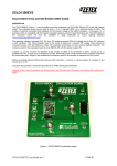
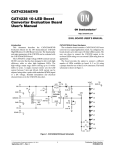
ZXLD1362EV3 USER GUIDE
DESCRIPTION
The ZXLD1362EV3, Figure 1, is a PCB constructed using an aluminium base for evaluating the ZXLD1362 LED
driver with internal switch [1]. The evaluation board can be used to drive an external choice of LEDs; the total forward
voltage across the LEDs depending on the number and type connected.
The operating voltage is nominally higher than 30V for the external LEDs, and can be raised to 60V maximum, which
will reduce the supply current. Please refer to the Zetex ZXLD1360 and ZXLD1350 products for applications requiring
input voltages lower than 30V.
The nominal current for the evaluation board is set at 700mA with a 0.15Ω sense resistor, R1.
The 68uH inductor used in the circuit is based on a 30V nominal supply, which should be connected across +VIN and
GND pins.
Note: The evaluation board does not have reverse polarity protection. It is fitted with a 2.1mm DC power plug with
positive to the centre pole.
Test point ADJ provides a connection point for DC or PWM dimming and shutdown.
Warning: with 700mA output, the connected LED will be hot and very bright
Figure 1: ZXLD1362EV3 evaluation board
ZXLD1362EV3 User Guide issue 1
1/7
11-01-2008
ZXLD1362 DEVICE DESCRIPTION
The ZXLD1362 is a continuous mode inductive driver in a TSOT23-5 package, for driving one or more series
connected LEDs efficiently from a voltage source higher than the LED voltage. The device includes the output
switch and a current sense circuit, which requires an external sense resistor to set the nominal current up to
1000mA.
DEVICE APPLICATIONS
•
LED flashlights.
•
High Power LED driving.
•
Low-voltage halogen replacement LEDs.
•
Automotive lighting.
•
Illuminated signs.
ZXLD1362 DEVICE FEATURES
•
Drives one or more series-connected LEDs
•
LEDs up to 1000mA.
•
Internal 60V switch.
•
Wide input voltage: 7V to 60V.
•
Inherent open circuit LED protection.
•
Brightness control using DC or PWM.
•
Internal PWM filter.
ZXLD1362 Device Packages, Pin and Definitions
TSOT23-5 pack
ZXLD1362 Device Pin Definition
Name
Pin No
LX
1
GND
2
ADJ
3
ISENSE
4
VIN
5
Description
Drain of NDMOS switch.
Ground (0V).
Internal voltage ref. pin (1.25V) :
•
Leave floating for normal operation.
•
Connect to GND to turn off output current.
•
Drive with a DC voltage (0.3V to 1.25V) or with a PWM signal to adjust
output current
•
Connect a capacitor from this pin to ground to set the soft-start time.
Connect a sense resistor, Rs, from the ADJ pin to VIN to sense the nominal
output current. Nominal Iout = 0.1/ R1
Input voltage: 7V to 60V. Decouple to ground with a 100nF and a 10uF or
higher ceramic capacitor depending on the input voltage[1].
ORDERING INFORMATION
EVALBOARD ORDER NUMBER
ZXLD1362EV3
DEVICE ORDER NUMBER
ZXLD1362E5TA
Please note: Evaluation boards are subject to
availability and qualified leads.
ZXLD1362EV3 User Guide issue 1
2/7
11-01-2008
ZXLD1362EV3 EVALUATION BOARD
REFERENCE DESIGN
The ZXLD1362EV3 is configured to the reference design in Figure 2. The target application is a driver for one or
more series-connected LEDs for luminaires in both commercial and automotive applications.
The maximum operating voltage is 60V, and the nominal current is set at 700mA with a 0.15Ω sense resistor R1. The
device operates in continuous mode at approximately 150 kHz, with a 68uH inductor.
An accurate way of determining the current, avoiding the need to insert an ammeter in the current path, is to measure
the voltage on the sense resistor. A 10K resistor and a 1uF capacitor can be used to form a low pass filter and the
voltage across the capacitor represents a more stable dc reading of current. Using this method, 100mV represents
0.7 Amp when using a 0.15Ω sense resistor.
The ADJ pin connects to a low pass filter within the ZXLD1362 chip to provide some decoupling, but the external
capacitor C2 (100nF) is used to provide additional decoupling to reduce any high frequency noise as well as
enabling the soft start function.
Both DC and PWM dimming can be achieved by driving the ADJ pin. For DC dimming, the ADJ pin may be driven
between 0.3V and 1.25V. Driving the ADJ pin below 0.2V will shut down the output current. For PWM dimming, an
external open-collector NPN transistor or open-drain N-channel MOSFET can be used to drive the ADJ pin. The
PWM frequency can be low, around 100Hz to 1 kHz, or high between 10 kHz to 50 kHz.
For low frequency, PWM capacitor C2 should be removed on the evaluation board, to give a more accurate duty
cycle.
Shorting R2 will connect the test pin ADJ to device pin ADJ if needed.
The external capacitor C2 on the ADJ pin sets the soft start time. The amount of soft start time achievable is
approximately 0.2ms/nF.
For other reference designs or further applications information, please refer to the ZXLD1362 datasheet.
Schematic Diagram
Figure 2 shows the schematic for the ZXLD1362EV3 evaluation board.
LED A
R1
Vin
4
5
Vin
C1
ADJ
C3
V sense
D1
C4
R2
3
ADJ
ZXLD1362
1
L1
LX
LED K
GND
C2
GND
Figure 2: Schematic for the evaluation board ZXLD1362EV3
ZXLD1362EV3 User Guide issue 1
3/7
11-01-2008
ZXLD1362 Operation
In normal operation, when voltage is applied at +VIN, the ZXLD1362 internal NDMOS switch is turned on. Current
starts to flow through sense resistor R1, inductor L1, and the LEDs. The current ramps up linearly, and the ramp rate
is determined by the input voltage +VIN and the inductor L1. This rising current produces a voltage ramp across R1.
The internal circuit of the ZXLD1362 senses the voltage across R1 and applies a proportional voltage to the input of
the internal comparator. When this voltage reaches an internally set upper threshold, the NDMOS switch is turned off.
The inductor current continues to flow through R1, L1, the LEDs, the Schottky diode D1, and back to the supply rail,
but it decays, with the rate of decay determined by the forward voltage drop of the LEDs and the Schottky diode. This
decaying current produces a falling voltage at R1, which is sensed by the ZXLD1362. A voltage proportional to the
sense voltage across R1 is applied at the input of the internal comparator. When this voltage falls to the internally set
lower threshold, the NDMOS switch is turned on again. This switch-on-and-off cycle continues to provide an average
current (set by the sense resistor R1) to the LEDs, . Please refer to the datasheet [1] for the threshold limits,
ZXLD1362 internal circuits, electrical characteristics and parameters.
ZXLD1362EV1 Evaluation Board - BOM
Ref
R1
R2
C1
C2,C4
C3
L1
D1
U1
Value
0.15R
1kΩ
10uF 100V
100nF, 100V
100nF
68uH
100V, 3A
ZXLD1362
Package
0805
0805
SMD
0805
1206
SMC
TSOT23-5
Part Number
CRL1220 R15TD
Generic
NACEW100M1006.3x8TR13F
NMC0805X7R104K100TRPLPF
NMC1206X7R104K100TRPLP3KF
NPIS24H680MTRF
30BQ100PBF
ZXLD1362E5TA
Manufacturer
Tyco
NIC
NIC
NIC
NIC
IR
Zetex
Notes
5%, 200ppm
Electrolytic - 20%
20%
68uH/1.5A rms
Schottky diode
DC-DC converter
The aluminium PCB guarantees a good thermal dissipation for the ZXLD1362 device, which can produce up to 1 watt
of heat under maximum load conditions. Other sources of heat are the Schottky diode, the inductor and the sense
resistor. Care must be taken in their placement.
Warning: At 60V operation with 700mA output, the board temperature rises by around 50C from ambient
after 30 minutes of operation.
Figure 3: Component layout and circuit board view
ZXLD1362EV3 User Guide issue 1
4/7
11-01-2008
ZXLD1362EV3 Connection Point Definition
Name
Description
+VIN
Positive supply voltage.
GND
Supply Ground (0V).
ADJ
Internal voltage ref. pin (1.25V). This pin can be used to achieve dimming and soft-start,
and for switching the output current off.
•
Leave floating for normal operation.
•
See 'Circuit Features' section to achieve dimming, soft-start and for switching the
output current off.
LED A connects to the external LED anode
LED K connects to the external LED cathode
LED A
LED K
ZXDL1362EV3 Basic operation at full voltage
1.
Connect external LEDs across test pins ‘LED A’ (anode) and ‘LED K’ (cathode). The number of external
LEDs that can be connected depends on their operating power and forward voltage drop, but typically 16 x
3.4V LEDs can be connected using a 60V rail. For an external load other than LEDs, the positive terminal of
the load should be connected the anode and the negative to the cathode.
2.
Connect VIN and GND.
Warning: The board does not feature reverse battery/supply protection.
3.
Set the PSU to the desired input voltage (usually between 30V and 60V)
4.
Turn on the PSU. The external LEDs will illuminate and the current should be approximately 700mA.
Warning: Do not stare at the LEDs directly.
Circuit features
N.B. Remove power whilst changing components!
Soft-start
1.
The evaluation board is fitted with capacitor C2, which performs the soft start function by slowing the rise
time of the adjust pin at start-up. The pin output impedance is 50K so CxR is the time constant to reach 66%
of output current.
PWM
1.
Remove the soft start capacitor C2
2.
Refer to the datasheet for how to perform PWM
Switching off the output current
3.
Shorting the ADJ pin to GND will cause the LED current to go to zero. Releasing this pin will switch on the
system (creating a soft-start power up sequence if the C2 capacitor is used).
Changing the LED current
1.
Remove R1
2.
Calculate and fit a new sense resistor, R1, the value of which is based on the required LED current without
dimming. R1 can be calculated using following equation :
R1 = 0.1(V / IOUT) where
IOUT = the LED current.
R1 = the sense resistor value in ohms.
0.1V is the nominal sense voltage with ADJ open circuit or set to 1.25V.
ZXLD1362EV3 User Guide issue 1
5/7
11-01-2008
PERFORMANCE
The system efficiency depends on the sense resistor, supply voltage, switching inductor, and the number of LEDs.
With a 60V supply and 15 LEDs, the switching frequency is typically 200 kHz and efficiency levels >90% are
achievable.
Visit our website www.zetex.com to find useful tools for circuit design and simulation.
REFERENCE
[1] ZXLD1362 Datasheet – www.zetex.com
ZXLD1362EV3 User Guide issue 1
6/7
11-01-2008
Definitions
Product change
Zetex Semiconductors reserves the right to alter, without notice, specifications, design, price or conditions of supply of any product or service.
Customers are solely responsible for obtaining the latest relevant information before placing orders.
Applications disclaimer
The circuits in this design/application note are offered as design ideas. It is the responsibility of the user to ensure that the circuit is fit for the user’s
application and meets with the user’s requirements. No representation or warranty is given and no liability whatsoever is assumed by Zetex with
respect to the accuracy or use of such information, or infringement of patents or other intellectual property rights arising from such use or otherwise.
Zetex does not assume any legal responsibility or will not be held legally liable (whether in contract, tort (including negligence), breach of statutory
duty, restriction or otherwise) for any damages, loss of profit, business, contract, opportunity or consequential loss in the use of these circuit
applications, under any circumstances.
Life support
Zetex products are specifically not authorized for use as critical components in life support devices or systems without the express written approval of
the Chief Executive Officer of Zetex Semiconductors plc. As used herein:
A.
Life support devices or systems are devices or systems which:
1. are intended to implant into the body
or
2. support or sustain life and whose failure to perform when properly used in accordance with instructions
for use provided in the labeling can be reasonably expected to result in significant injury to the user.
B.
A critical component is any component in a life support device or system whose failure to perform can be reasonably expected to cause the
failure of the life support device or to affect its safety or effectiveness.
Reproduction
The product specifications contained in this publication are issued to provide outline information only which (unless agreed by the company in writing)
may not be used, applied or reproduced for any purpose or form part of any order or contract or be regarded as a representation relating to the
products or services concerned.
Terms and Conditions
All products are sold subjects to Zetex’ terms and conditions of sale, and this disclaimer (save in the event of a conflict between the two when the
terms of the contract shall prevail) according to region, supplied at the time of order acknowledgement.
For the latest information on technology, delivery terms and conditions and prices, please contact your nearest Zetex sales office.
Quality of product
Zetex is an ISO 9001 and TS16949 certified semiconductor manufacturer.
To ensure quality of service and products we strongly advise the purchase of parts directly from Zetex Semiconductors or one of our regionally
authorized distributors. For a complete listing of authorized distributors please visit: www.zetex.com/salesnetwork
Zetex Semiconductors does not warrant or accept any liability whatsoever in respect of any parts purchased through unauthorized sales channels.
ESD (Electrostatic discharge)
Semiconductor devices are susceptible to damage by ESD. Suitable precautions should be taken when handling and transporting devices. The
possible damage to devices depends on the circumstances of the handling and transporting, and the nature of the device. The extent of damage can
vary from immediate functional or parametric malfunction to degradation of function or performance in use over time. Devices suspected of being
affected should be replaced.
Green compliance
Zetex Semiconductors is committed to environmental excellence in all aspects of its operations which includes meeting or exceeding regulatory
requirements with respect to the use of hazardous substances. Numerous successful programs have been implemented to reduce the use of
hazardous substances and/or emissions.
All Zetex components are compliant with the RoHS directive, and through this it is supporting its customers in their compliance with WEEE and ELV
directives.
Product status key:
“Preview”
“Active”
“Last time buy (LTB)”
“Not recommended for new designs”
“Obsolete”
Datasheet status key:
“Draft version”
“Provisional version”
“Issue”
Future device intended for production at some point. Samples may be available
Product status recommended for new designs
Device will be discontinued and last time buy period and delivery is in effect
Device is still in production to support existing designs and production
Production has been discontinued
This term denotes a very early datasheet version and contains highly provisional
information, which may change in any manner without notice.
This term denotes a pre-release datasheet. It provides a clear indication of anticipated performance. However,
changes to the test conditions and specifications may occur, at any time and without notice.
This term denotes an issued datasheet containing finalized specifications. However, changes to specifications
may occur, at any time and without notice.
Europe
Americas
Asia Pacific
Corporate Headquarters
Zetex GmbH
Kustermann-park
Balanstraße 59
D-81541 München
Germany
Telefon: (49) 89 45 49 49 0
Fax: (49) 89 45 49 49 49
[email protected]
Zetex Inc
700 Veterans Memorial Highway
Hauppauge, NY 11788
USA
Zetex (Asia Ltd)
3701-04 Metroplaza Tower 1
Hing Fong Road, Kwai Fong
Hong Kong
Zetex Semiconductors plc
Zetex Technology Park, Chadderton
Oldham, OL9 9LL
United Kingdom
Telephone: (1) 631 360 2222
Fax: (1) 631 360 8222
[email protected]
Telephone: (852) 26100 611
Fax: (852) 24250 494
[email protected]
Telephone (44) 161 622 4444
Fax: (44) 161 622 4446
[email protected]
© 2006 Published by Zetex Semiconductors plc.
ZXLD1362EV3 User Guide issue 1
7/7
11-01-2008