1
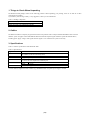
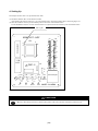
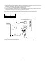
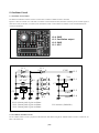
M38C29T-ADF
Temporary Target Board for M38C29RLFS
User’s Manual
Keep safety first in your circuit designs!
Renesas Technology Corporation and Renesas Solutions Corporation put the maximum effort into making semiconductor products
better and more reliable, but there is always the possibility that trouble may occur with them. Trouble with semiconductors may lead to
personal injury, fire or property damage. Remember to give due consideration to safety when making your circuit designs, with
appropriate measures such as (i) placement of substitutive, auxiliary circuits, (ii) use of nonflammable material or (iii) prevention
against any malfunction or mishap.
Notes regarding these materials
These materials are intended as a reference to assist our customers in the selection of the Renesas Technology product best suited
to the customer's application; they do not convey any license under any intellectual property rights, or any other rights, belonging to
Renesas Technology Corporation, Renesas Solutions Corporation or a third party.
Renesas Technology Corporation and Renesas Solutions Corporation assume no responsibility for any damage, or infringement of
any third-party's rights, originating in the use of any product data, diagrams, charts, programs, algorithms, or circuit application
examples contained in these materials.
All information contained in these materials, including product data, diagrams, charts, programs and algorithms represents information
on products at the time of publication of these materials, and are subject to change by Renesas Technology Corporation and
Renesas Solutions Corporation without notice due to product improvements or other reasons. It is therefore recommended that
customers contact Renesas Technology Corporation, Renesas Solutions Corporation or an authorized Renesas Technology product
distributor for the latest product information before purchasing a product listed herein. The information described here may contain
technical inaccuracies or typographical errors. Renesas Technology Corporation and Renesas Solutions Corporation assume no
responsibility for any damage, liability, or other loss rising from these inaccuracies or errors. Please also pay attention to information
published by Renesas Technology Corporation and Renesas Solutions Corporation by various means, including the Renesas home
page (http://www.renesas.com).
When using any or all of the information contained in these materials, including product data, diagrams, charts, programs, and
algorithms, please be sure to evaluate all information as a total system before making a final decision on the applicability of the
information and products. Renesas Technology Corporation and Renesas Solutions Corporation assume no responsibility for any
damage, liability or other loss resulting from the information contained herein.
Renesas Technology semiconductors are not designed or manufactured for use in a device or system that is used under
circumstances in which human life is potentially at stake. Please contact Renesas Technology Corporation, Renesas Solutions
Corporation or an authorized Renesas Technology product distributor when considering the use of a product contained herein for any
specific purposes, such as apparatus or systems for transportation, vehicular, medical, aerospace, nuclear, or undersea repeater use.
The prior written approval of Renesas Technology Corporation and Renesas Solutions Corporation is necessary to reprint or
reproduce in whole or in part these materials.
If these products or technologies are subject to the Japanese export control restrictions, they must be exported under a license from
the Japanese government and cannot be imported into a country other than the approved destination. Any diversion or reexport
contrary to the export control laws and regulations of Japan and/or the country of destination is prohibited.
Please contact Renesas Technology Corporation or Renesas Solutions Corporation for further details on these materials or the
products contained therein.
Precautions to be taken when using this product
This product is a development supporting unit for use in your program development and evaluation stages. In mass-producing your
program you have finished developing, be sure to make a judgment on your own risk that it can be put to practical use by performing
integration test, evaluation, or some experiment else.
In no event shall Renesas Solutions Corporation be liable for any consequence arising from the use of this product.
Renesas Solutions Corporation strives to renovate or provide a workaround for product malfunction at some charge or without charge.
However, this does not necessarily mean that Renesas Solutions Corporation guarantees the renovation or the provision under any
circumstances.
This product has been developed by assuming its use for program development and evaluation in laboratories. Therefore, it does not
fall under the application of Electrical Appliance and Material Safety Law and protection against electromagnetic interference when
used in Japan.
CAUTION
Renesas Tools Homepage
Rev.1.00
Apr. 19, 2006
REJ10J1356-0100
If the requirements shown in the "CAUTION" sentences are ignored,
the equipment may cause personal injury or damage to the products.
http://www.renesas.com/en/tools
(1/8)
1. Things to Check When Unpacking
The M38C29T-ADF package consists of the following products. When unpacking your package, check to see that all of these
components are included.
If you find any item missing or faulty, or any suggestion, contact your local distributor.
Table 1.1 Package components
Item
M38C29T-ADF temporary target board
M38C29T-ADF User’s Manual (this manual)
2. Outline
The M38C29T-ADF is a temporary target board used to develop software with a compact emulator M38000T2-CPE or PC4701
emulator system. It supplies to the M38C29RLFS MCU the minimum required signals needed to operate the emulator MCU,
including power supply voltage, clock signals and reset signals. Use it when the user system is not ready.
3. Specifications
Table 3.1 lists the specifications of the M38C29T-ADF.
Table 3.1 Specifications
Applicable MCU
M38C29RLFS
Clock
4.0MHz oscillator mounted (oscillator circuit board OSC-2 used)
32.768kHz (can be disconnected by SW1)
Vcc
Supplied separately*
Vss
Supplied separately
RESET
- Reset circuit mounted (power-on reset and reset switch)
- Connects the reset output of an emulation pod
External dimensions Width
90mm
Depth
115mm
Others
Universal part prepared
* Power cannot be supplied from the emulator (e.g. M38000T2-CPE). A separate power supply is needed.
(2/8)
4. Setting Up
This chapter describes how to set up the M38C29T-ADF.
(1) Mount the emulator MCU on the M38C29T-ADF.
After checking the position of the No. 1 pin of the emulator MCU, mount the emulator MCU referencing Figure 4.1.
(2) Insert the connector on the tip of the emulator probe to the socket on the emulator MCU.
For the M38000T2-CPE, the converter board PCA4933 is required between the emulator probe and emulator MCU.
No. 1 pin
M38C2 9 T - ADF
1
I C1
100
100
26
J2
75
81
1
Universal part
J1
80
30
5
95
35
10
65
90
30
70
51
31
40
15
50
85
3 2K
OSC
20
45
J3
25
80
55
7650
51
TP1
Vcc
TP2
Vs s
TP3
RESET
NC Vcc
SW4
Vss Vc c
XOUT
SW3
CNVs s
SW2
J1 -21 Vc c
SW1
XCI N PORT
VREF
C6
PORT/ XCI N
1
I C3
OSC - 2
60
SW5
Universal part
RESET
TP4
VREF
MADE I N JAPAN
Figure 4.1 Position of No. 1 pin of the M38C29T-ADF's emulator MCU
CAUTION
Cautions to Be Taken for This Product:
Always shut OFF power before connecting this product. The power ON state could destroy internal circuit.
(3/8)
(3) Connect the RESET cable (white) and the GND cable (black) of the emulation pod to the RESET (TP3) pin and Vss (TP2) pin of
the M38C29T-ADF respectively. And connect the Vcc cable (red) to the Vcc (TP1) pin.
(4) Set the MCU type select switch of the M38000T2-CPE to the RLSS side.
(5) Connect a power supply (not included) to the Vcc (TP1) pin of the M38C29T-ADF. And connect the GND output of the power
supply to the Vss (TP2) pin. Use the power supply whose rising time is 10ms or less.
Table 4.1 lists the correspondence of the connector cables and signals, and Figure 4.2 shows the connection pattern.
Table 4.1 Connector cables of the M38000T2-CPE and applicable signals
Cable color
WHITE
BLACK
RED
Signal
RESET
Vss
Vcc (SENSE)
REV . B
M38C29 T- ADF
J1
I C1
100
81
80
1
Emulator
30
51
31
RLSS/RLFS
C1 50
OSC- 2
J3
TP1
TP2
TP3
TP4
RED
WH IT E
BLACK
+5V 0V
Figure 4.2 Connection pattern of the M38C29T-ADF
(4/8)
S W4
SW 5
Vc c NC
CNVs s
S W3
Vs s Vc c
CNVs s
S W2
VREF
S W1
J1-21 Vc c
C6
XCIN PORT
PORT/ XCI N
1
I C3
C5
RESET
J2
(6) Setting SW
Set the SW1 to SW4 according to your application. Table 4.2 describes the functions of the SW1 to SW4.
Table 4.2 Functions of the SW1, SW2, SW3 and SW4 of the M38C29T-ADF
No.
SW1
Name
PORT/XCIN
SW2
VREF
SW3
CNVss
SW4
XOUT
Function
Allows you to choose whether to supply the sub-clock signals (32.768kHz) to the
MCU's XCIN pin (pin 43).
To use P61/XCIN as an output port, choose the PORT side.
To use the sub-clock signals, choose the XCIN side.
Allows you to choose whether to apply Vcc or some other source to the MCU's VREF
pin (pin 21). In the case of the latter, choose the J1-21 side, and apply a voltage within
a prescribed range to the J1-21.
Allows you to choose which to connect, Vcc or Vss, to the MCU's CNVss pin (pin
39).
Allows you to choose whether to pull up the MCU's XOUT pin (pin 46).
To use the oscillator circuit of OSC-2 on the temporary target board, or to input the
external clock, set SW4 to Vcc to pull up XOUT pin.
To use the oscillator circuit with a resonator between XIN and XOUT, set SW4 to NC.
(5/8)
Factory-setting
PORT
Vcc
Vss
Vcc
5. Oscillator Circuit
5.1 Oscillator Circuit Board
The M38C29T-ADF has a built-in oscillator circuit board on which a 4.0MHz oscillator is mounted.
Figure 5.1 shows an external view of the OSC-2 oscillator circuit board (bare board) and where connector pins are located. Figure 5.2
shows the circuitry of the OSC-2 oscillator circuit board (bare board). Use the number of oscillator circuits recommended by the
oscillator manufacturer.
J1-4: GND
J1-3: Oscillation output
J1-2: GND
J1-1: VCC
Figure 5.1 External view of the oscillator board (OSC-2) and connector pin assignment
IC1
IC1
11
10
9
C LK
8
J1-3
R1
*
*
X1 ,X2
C2
X3*
1
Vcc
2
J1-1
R2
C1
3
4
5
6
13
12
C3
14
IC1
7
J1-2
GND
J1-4
IC1
GND
2-pin oscillator
*X1:5.08-mm-pitch
.
X2:2.54-mm-pitch 2-pin oscillator
X3:2.54-mm-pitch 3-pin oscillator
IC1:Inverter (Unbuffer)
Figure 5.2 Circuit of the oscillator board (OSC-2)
5.2 32.768kHz Oscillator Circuit
The 32.768kHz oscillator circuit is prepared on the M38C29T-ADF. When using the 32.768kHz oscillator circuit as a sub-clock, set
SW1 to the XCIN side.
(6/8)
6. Reset Circuit
Figure 6.1 shows the reset circuit and its waveform. In this product, reset is cleared in about 100ms from the instant Vcc passes about
2.1V after having started from 0 V. When Vcc drops down to about 2.1V, reset turns effective.
Detected power voltage (V )
Approx. 1. 25 x (R3 + R4 ) / R4
TP3
Vcc
1
R3
6. 8 K
R4
10 K
RESET
I C3
R5
Vcc
2
M5195 7BL OUT
IN
1 0K
5
SW4
CD
Vss
3
MCU RESET
4
C5
0. 33u F
CD
1 .25V
Input volage
( IC3- 2-pin)
t
H
td
td
Output state
( IC3 - 5-pin )
L
t d = 0 . 34 x CD (pF ) usec
Figure 6.1 Reset circuit and its waveform
By using SW5, the MCU can be reset manually.
Table 6.1 Function of SW5 (reset switch)
No.
SW5
Name
RESET
Function
This is the reset switch. Press down this switch to reset the MCU.
(7/8)
t
7. Pin Layout
Figure 7.1 shows the pin layout of the M38C29T-ADF.
I C1
1
J1 -1
2
J1 -2
3
J1 -3
4
J1 -4
5
J1 -5
J1 -6
6
7
J1 -7
8
J1 -8
9
J1 -9
10
J1-10
11
J1-11
12
J1-12
13
J1-13
14
J1-14
15
J1-15
16
J1-16
17
J1-17
18
J1-18
19
J1-19
J1-20
J1-21
20
SW2 VREF TP4
J1-21
VREF
Vc c
21
22
J1 -22
23
J1 -23
24
J1 -24
25
J1 -25
26
J2 -26
27
J2 -27
28
J2 -28
29
J2 -29
30
J2 -30
31
J2 -31
32
33
J2 -32
J2 -33
34
J2 -34
35
36
J2 -35
J2 -36
37
J2 -37
38
J2 -38
SW3 CNV ss
J2 -39
39
Vcc
Vs s
J2-40
TP3
RESET
J2 -41
40
41
NC
NC
NC
NC
NC
P04
NC
P05
NC
P06
NC
P07
NC
P10
P03
P11
P02
P12
P01
P13
P00
P14
P57
P15
P56
P16
P55
P17
P54
P53
P52
P51
P50
AV s s
VREF
P47
P46
NC
J2-42
SW1 PORT / XCIN
J2 -43
43
NC
NC
NC
NC
NC
P24
NC
P25
NC
P26
NC
P27
NC
VL 3
P45
COM1
P44
COM2
P43
COM2
P42
COM3
P41
P30
P40
P31
CNVs s
XCI N
TP2
NC
RESET
44
45
OSC - 2
4 MH z
P36
P62 /XCOUT
NC
NC
NC
P61 /XC I N
NC
NC
J2-44
J2-45
P34
P35
PORT
Vs s
P32
P33
NC
32.768kHz
J1 -99
98
97
J1 -98
J1 -97
96
J1 -96
95
J1 -95
94
J1 -94
93
J1 -93
92
J1 -92
91
J1 -91
90
J1 -90
89
J1 -89
88
J1 -88
87
J1 -87
86
P20
85
P21
84
P22
83
P23
82
NC
81
NC
80
NC
79
NC
78
NC
77
NC
76
NC
NC
42
J1 -100
99
J1 -86
J1 -85
J1 -84
J1 -83
J1 -82
J1 -81
J1 -80
J1 -79
J1 -78
J1 -77
J1 -76
NC
RESET IC
10K
100
Vs s
XIN
J2 -75
74
J2 -74
73
J2 -73
72
J2 -72
71
J2 -71
70
J2 -70
69
J2 -69
68
J2 -68
67
J2 -67
66
J2 -66
65
J2 -65
64
J2 -64
63
J2 -63
62
J2 -62
61
J2 -61
60
J2 -60
59
J2 -59
58
J2 -58
57
J2 -57
56
J2 -56
55
J2 -55
54
J2 -54
53
J2 -53
52
J2 -52
51
NC
N C 50
P37 49
J2 -51
J2-50
J2-49
P60 48
Vc c
4
3
2
1
75
J2-48
Vcc
47
NC
TP1
J2-47
SW4 XOUT
XOUT 46
NC
Figure 7.1 Pin layout of the M38C29T-ADF
(8/8)
1K
Vcc
J2 -46