1
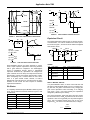
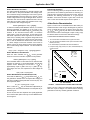
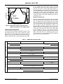
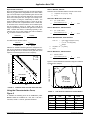
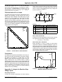
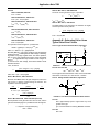
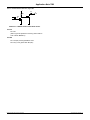
Power MOSFET Switching Waveforms: A New Insight Application Note /Title AN75 2) Subect Power OSET witch ng aveorms: New nsi ht) Autho () Keyords Interil orpoation, emionuctor) Cretor () DOCI FO dfark The examination of power MOSFET voltage and current waveforms during switching transitions reveals that the device characterization now practiced by industry is inadequate. In this Note, device waveforms are explained by considering the interaction of a vertical JFET driven in cascode from a lateral MOSFET in combination with the interelectrode capacitances. Particular attention is given to the drain-voltage waveform and its dual-slope nature. The three terminal capacitances now published by the industry are shown to be valid only for zero drain current. For cases where the gate drive is a voltage step generator with internal fixed resistance, the drain voltage characteristics are inferred from the gate current drive behavior and compared to observed waveforms. The nature of the “asymmetric switching times” is explained. A waveform family is proposed as a more descriptive and accurate method of characterization. This new format is a plot of drain voltage and gate voltage versus normalized time. A family of curves is presented for a constant load resistance with VDS varied. Gate drive during switching transitions is a constant current with voltage compliance limits of 0 and 10 volts. Time is normalized by the value of gate driving current. The normalization shows excellent agreement with data over five orders of magnitude, and is bounded on one extreme by gate propagation effects and on the other by transition time self-heating (typically tens of nanoseconds to hundreds of microseconds). Device Models The keystone of an understanding of power MOSFET switching performance is the realization that the active device is bimodal and must be described using a model that accounts for the dual nature. Buried in today’s power MOSFET devices is the equivalent of a depletion layer JFET that contributes significantly to switching speed. Figure 1 is a cross-sectional view of a typical power MOSFET, with MOSFET/JFET symbols superimposed on the structure. Figure 2 is obtained by taking the lateral MOS and vertical JFET from this conception and adding all the possible nodeto-node capacitances. Computed values of the six capacitances for a typical device structure suggest that device behavior may be adequately modeled using only three capacitors in the manner of Figure 3. This is the model to be employed for analysis and study. Pageode Useutines October 1999 AN-7502 SOURCE METAL POLY GATE GLASS GATE OXIDE n+ SOURCE p BODY MOS JFET p+ 0 10 VOLTS DEPLETION EDGE n- 40 VOLTS n+ DRAIN FIGURE 1. CROSS-SECTION VIEW OF MOSFET SHOWING EQUIVALENT MOS TRANSISTOR AND JFET C6 C3 C2 DRAIN GATE C4 C5 C1 SOURCE FIGURE 2. MOS TRANSISTOR WITH CASCODE-CONNECTED JFET AND ALL CAPACITORS Cx DRAIN GATE CDS CGS SOURCE FIGURE 3. FIGURE 2 SIMPLIFIED Gate Drive: Constant Voltage or Constant Current Before moving on to the study of the equivalent circuit states of the model, a gate-drive forcing function which is easy to represent, relates to reality, and best illustrates device behavior must be chosen. The choice may be immediately narrowed to two: (1) An instantaneous step voltage with internal resistance R, Figure 5. (2) An instantaneous step current with infinite internal resistance, Figure 6. ©2002 Fairchild Semiconductor Corporation Application Note 7502 Rev. A1 Application Note 7502 i(t) IG DRAIN VOLTAGE VG(SAT) -VG = v(t) -IG 2 3 4 STATES 5 6 TURN ON IGt v(t) = C i(t) = IG, 0 < t < T IG = CONSTANT T T IG t TURN OFF VT VDK -I t v(t) = 2VG G C VD(SAT) -IG i(t) = IG, T < t < 2T TIME FIGURE 4. FIGURE 6. STEP CURRENT FORCING FUNCTION IDEALIZED POWER MOSFET WAVEFORMS RO Equivalent Circuit v(t) -VG The lumped-parameter model of Figure 3, with the cascodeconnected JFET, can now be reduced to the linear equivalent circuit of Figure 7, and the six device states investigated from full off to full on. v(t) VG i(t) C t -IPK = VG/RO GATE VGS i(t) TURN ON v(t) = VG (1 - e) -t/ROC i(t) = VG e -t/ROC VX gMJ VX VD gM VG CGS RL CDS IPK = VG/RO RO FIGURE 5. IG t G CX DRAIN RO TURN OFF v(t) = VG e -t/ROC i(t) = - V e -t/ROC SOURCE STEP-VOLTAGE FORCING FUNCTION Power MOSFET devices are highly capacitive in nature; hence, simple capacitor responses to the forcing functions offer a good vehicle for comparison. The advantageous choice is immediately obvious: Figure 6. Voltage/time responses dominated by capacitance are straight lines (when constant current is used). The slope of these lines is proportional to current and inversely proportional to capacitance. Analytically, then, constant current is most convenient. It is quite another matter, however, to build a bidirectional current drive that is accurate across the many decades of both current and time required to establish experimental verification. Six States To completely characterize power MOSFET switching waveforms, the six states that a device assumes, Figure 6, must be addressed: STATE t i(t) VOLTAGE C 1 IGT C v(t) GATE VOLTAGE VGS VDD MOS JFET Turn-on 1 Off Off Turn-on 2 Active Active Turn-on 3 Active Saturated† Turn-off 4 Saturated Saturated† Turn-off 5 Active Saturated Turn-off 6 Active Active †The term saturated is taken to mean a constant low-voltage drain-source condition. ©2002 Fairchild Semiconductor Corporation LEGEND VGS - Gate Voltage CDS - Drain Source Capacitance VX - JFET Driving Voltage gM - MOSFET Transconductance VD - Drain Voltage gMJ - JFET Transconductance CGS - Gate Source Capacitance RL - Drain Load Resistance CX IG - Constant Current Amplitude - MOSFET Feedback Capacitance FIGURE 7. POWER MOSFET EQUIVALENT CIRCUIT State 1: MOS Off, JFET Off In a power-MOSFET device, no drain current will flow until the device’s gate threshold voltage, Vgs(TH), is reached. During this time, the gate’s current drive is only charging the gate source capacitance. More accurately, IG is charging CISS (CISS = CGS + CGD, CDS shorted), the capacitance designation published by the industry. The current generators, gMVG and gMJVX are open circuits for zero drain current, and RL is presumed to be so low as to represent a short circuit (generally true for practical applications). This is academic however since CGS is very much larger that CX. The time to reach threshold, then, is simply: T1 = CISS Vgs(TH) IG Application Note 7502 Rev. A1 Application Note 7502 State 2: MOS ActIve, JFET ActIve This state graphically illustrates the dramatic influence that the JFET has on the power MOSFET drain-voltage waveform. Instead of having to discharge C x from VDD to ground, the lateral MOSFET need only swing VX to ground, a much smaller voltage thanks to the grounded gate JFET. Since the interaction of RL with the device capacitances has a secondorder effect on the drain voltage, the equivalent circuit of Figure 7 predicts a drain voltage change of: dVG/dt = gMRLlG/[CGS + CX(1 + gM/gMJ)] In all but the smallest power-MOSFET devices, Cx is several thousand picofarads and gM/gMJ is of the order of 3:1. Power-MOSFET devices exhibit a high dVD/dt switching rate because of the cascode-connected JFET, not because CRSS (CRSS = CGD) is a small value, as zero-drain-current data sheet capacitance values might lead one to believe. If CRSS were, in actuality, small, long drain voltage tails would not exist. The tail response is a direct result of JFET saturation. In order to delineate the transition from state 2 to state 3, a drain voltage at which the transition occurs must be defined. VDK is the knee voltage at which linear extrapolations of drain-voltage slopes intersect. The time duration of state 2 is: Experimental Verification The four switching states just analyzed indicate that for a given device, all four switching state times are inversely proportional to the magnitude of the gate drive current. Figure 8 illustrates the switching performance of a typical power MOSFET across three decades of gate drive current and time. In each case the data slope is almost a perfect -1. A New Device Characterization Figure 8 could not be a reasonable device data sheet presentation because it does not give the designer any information on a typical value for CX, nor does it convey how VDK, gM, gM/gMJ, and VG(sat) vary with drain current. What would be of enormous value to the designer is a plot of VD(t), VG(t) for selected values of VDD and ID within device ratings. A reasonable characterization would be as follows: 1. The x axis would be normalized in terms of gate current drive. 2. The y axis would be normalized in terms of percent maximum rated BVDSS (0 to 100%). 3. RL = BVDSS/ID(max) would define the drain load resistance. 4. Four plots of VD(t), VG(t) at 100%, 75%, 50%, and 25% BVDSS(max) would be shown. 10 t2(t6) = (VDD - VDK)[CGS + CX(1 + gM/gMJ)]/gMRLIG RFM15N15 VDD = 75V ID = 7.5A RO = ∞ Ω VG = 10V State 3: MOS Active, JFET Saturated dVD/dt = gMRLIG/[CGS + CX(1 + gMRL)] This is the Miller effect so often referred to in older texts that describe the behavior of grounded-cathode vacuum-tube amplifier circuits. Allowing for the fact that 1 + gMRL is approximately equal to gMRL and CX(1 + gMRL) is very much larger than CGS, the expression for drain-voltage tail time is: (t) - MICROSECONDS When the JFET saturates, the gMJVX current generator becomes a short circuit and the equivalent circuit predicts: 1 0.1 DATA THEORY t3(t5) = (VDK - VD(SAT))Cx/lG tD(OFF) tR tF tD(ON) State 4: MOS Saturated, JFET Saturated (Turn-Off) In this state, in addition to gMJVX being shorted, the gMVG current generator is shorted, and IG is occupied with charging CX and CGS, in parallel, from the peak value of V G to VG(SAT). The time required for this is: t4 = (VG - VG(SAT))(CGS + Cx)/IG Since a value for CGS may be measured independently of switching time, the method described is the simplest way of determining CX. 0.01 1 FIGURE 8. 10 100 (IG) - MILLIAMPERES 1000 CONSTANT GATE CURRENT SWITCHING TIME Figure 9 is such a plot for the RFM15N15 power MOSFET. With such a plot, a designer can estimate device switching performance under any resistive gate/drain conditions. On turn-off, the state time equations are equally applicable, but in reverse order (states 5 and 6); see the idealized waveform of Figure 4. ©2002 Fairchild Semiconductor Corporation Application Note 7502 Rev. A1 Application Note 7502 sis for resistive step voltage inputs, which is complex because the gate current is no longer constrained to be constant, but is a function of device gate-voltage response, is covered in Appendix A. (A second, shorter appendix, B, has been added to illustrate the estimation of RO for some practical gate drive circuits.) Table 1 summarizes the common switching equations, and indicates the appropriate 1G to be used in each state for relating step voltage drives to the characterization curves. 100 % RATES VDSS 75 50 RFM15N15 IT = 1mA VG = 10 VOLTS RL = VDSS/ID(RMS) 25 Experimental Verification Since the switching equations for step currents and voltages differ only by gate-current magnitudes for the same device type, one would expect a plot of switching time versus 1/RO to be of the same form as those obtained for a step current drive. This is exactly the case, as Figure 10 is merely a variation of Figure 8. Using the relationships of Table 1, the observed differences between Figures 7 and 9 can be pinpointed. The two sets of experimental curves confirm that, on the basis of the short-circuit drive current VG/RO equalling the constant IG, tD(on), tR, tD(off), and tF will all be longer, as predicted by the ratios of the gate drive currents of Table 1. Notice also that tR, tF switching symmetry is disrupted by the use of a step voltage with source resistance RO. For states 2 and 6 the time ratio is: 0 20IT/IG 40IT/IG 60IT/IG TIME - microseconds 80IT/IG FIGURE 9. NORMALIZED RFM15N15 SWITCHING WAVEFORMS FOR CANSTANT GATE-CURRENT DRIVE. Step-Voltage Gate Drive The majority of power MOSFET applications employ a step gate-voltage input with a finite source resistance RO. Often RO for turn-on is not the same as RO for turn-off. How can switching times for these situations be estimated using the switching characterization curves just described? The analy- TABLE 1. CONSTANT CURRENT t= T U R N O N COMMON SWITCHING EQUATIONS STATE 1: MOS OFF, JFET OFF CISS VGS(TH) CONSTANT VOLTAGE [1] t = RO CISS In IG IG = IT STATE 2: ACTIVE, ACTIVE [1 - VGS(TH)/VG] IG = (VG - VGS(TH))/RO [VDD - VDK] [CGS + Cx (1 + gM/gMJ)] t= gMRLIG IG = IT STATE 3: ACTIVE, SATURATED IG = (VG - VG(SAT))/RO (VDK - VD(SAT))CX t= IG IG = IT t= T U R N O F F STATE 4: SATURATED, SATURATED (CGS + CX)(VG - VG(SAT)) IG = -VG/RO t = RO(CGS + CX) In (VG/VG(SAT)) IG IG = IT STATE 5: ACTIVE, SATURATED t= IG = (VG - VG(SAT))/RO (VDK - VD(SAT))CX IG IG = IT STATE 6: ACTIVE, ACTIVE t= IG = (VG - VG(SAT))/RO [VDD - VDK] [CGS + CX (1 + gM/gMJ)] gMRLIG ©2002 Fairchild Semiconductor Corporation Application Note 7502 Rev. A1 Application Note 7502 Experimental Verification State 1: MOS Off, JFET Off Since the switching equations for step currents and voltages differ only by gate-current magnitudes for the same device type, one would expect a plot of switching time versus 1/RO to be of the same form as those obtained for a step current drive. This is exactly the case, as Figure 10 is merely a variation of Figure 8. Using the relationships of Table 1, the observed differences between Figures 7 and 9 can be pinpointed. The two sets of experimental curves confirm that, on the basis of the short-circuit drive current VG/RO equalling the constant IG, tD(on), tR, tD(off), and tF will all be longer, as predicted by the ratios of the gate drive currents of Table 1. Notice also that tR, tF switching symmetry is disrupted by the use of a step voltage with source resistance RO. For states 2 and 6 the time ratio is: This time can be estimated without recourse to the curves tTURN-ON tTURN-OFF VG(SAT) VG - VGS(TH) = t= 100(1200 x 10-12) ln [1/(1 - 4/10)] t= 61 ns State 2 & 6: MOS Active, JFET Active IG = tTURN-OFF 9 60 = 150ns IG = = 467ns (10 - 7)/100 = 30mA (curve divisions) x IT µs t= 30 = 14 30 State 4: MOS Saturated, JFET Saturated CGS + Cx Utilization of available maximum gate drive voltage and current can be optimized for fastest power MOSFET switching speed through the use of constant-current gate drive at the expense of increased gate-drive circuit complexity. = (gate voltage slope)(test current) = (1.5 x 10⁻⁶s/5 volts)(10mA) = 3000pF t= 100(3000 x 10-12) ln [10/6.6] t= 125ns State 5: MOS Active, JFET Saturated IG = 10 RFM15N15 VDD = 75V ID = 7.5A VG = 10V 6.6/100 = 66mA (curve divisions) x IT µs t= 66 = 8 66 = 121ns Figure 11 shows RFM15N15 waveforms using the conditions specified in the example. 1 75 VD 0.1 DATA THEORY tD(OFF) tR tF tD(ON) 0.01 10-4 10-3 1/RO VGS DRAIN VOLTAGE - VOLTS (t) - MICROSECONDS 60 = State 3: MOS Active, JFET Saturated VG(SAT) VG - VG(SAT) = (curve divisions) x IT µs t= For states 3 and 5 the time ratio is: tTURN-ON (10 - 4)/100 = 60mA 10-2 RFM15N15 VDD = 75 VOLTS RL = 10 OHMS VG = 10 VOLTS RO = 100 OHMS 10-1 0 FIGURE 10. 0 CONSTANT GATE VOLTAGE SWITCHING TIME Using the Characterization Curve, Figure 9 FIGURE 11. To estimate the switching times for an RFM15N15 power MOSFET under the conditions VG = 10V, VDD = 75V, RO = 100 ohms, and RL = 10 ohms, precedes as follows: STATE 1 ©2002 Fairchild Semiconductor Corporation 1.5 TIME - MICROSECONDS 3 STEP GATE VOLTAGE INPUT TO AN RFM15N15 CALCULATED TIME MEASURED TIME RATIO (tC, ns) (tM, ns) (tC/tM) 61 60 1.02 2+3 617 670 0.92 4 125 137 0.91 5+6 271 375 0.72 Application Note 7502 Rev. A1 Application Note 7502 For peak gate voltages other than 10 volts, and load resistances other than BVDSS/ID(MAX), the equations of Table 1 may be used in conjunction with slope estimates from the characterization curves for CX and CGS + CX(1 + gM/gMJ) at the appropriate drain-current level. states must be examined using the same device equivalent circuit as was used for the constant-gate-current case, but with the forcing function replaced wIth a step voltage with internal resistance RO, Figure A-1. GATE Characterization-Curve Limits The switching-time range over which the characterization can be applied is very impressive. For gate currents of the order of microamperes, device dissipation is the limiting factor. For gate currents of the order of amperes, the device response will be slowed by gate propagation delay. This delay, of course, degrades the linear switching relationship to gate current. However, as Figure 12 graphically shows, the characterization is valid across five decades of gate current and switching time, allowing all but a very few switching applications to be described by the characterization curves of Figure 9. 104 RFM15N15 tD(OFF) tR tF tD(ON) TIME(t) - MICROSECONDS 103 CX RO VGS 102 VX gMJ VX VD DRAIN VG gM VG CGS RL CDS SOURCE LEGEND VGS - Gate Voltage VX - JFET Driving Voltage gM - MOSFETTransconductance VD - Drain Voltage gMJ - JFET Transconductance CGS - Gate Source Capacitance RL - Drain Load Resistance CX - MOSFET Feedback Capacitance IG - Constant Current Amplitude FIGURE A-1. CDS - Drain Source Capacitance POWER MOSFET EQUIVALENT CIRCUIT State 1: Mos Off, JFET Off 101 As before, both current generators are open circuits, reducing the equivalent circuit to simply charging CISS through RO. 100 t= ROCISSIn(1/(1 - VGS(TH)/VG)] State 2: Mos Active, JFET Active 10-1 10-2 100 101 102 103 104 105 GATE CURRENT (IG) - MICROAMPERES FIGURE 12. 106 FIVE DECADES OF LINEAR RESPONSE Before proceeding, it is wise to examine an actual device response and make use of available simplifications. Figure A-2 shows iG(t) and iD(t) for a typical power MOSFET driven by a step gate voltage. For truly resistive switching, realize that these waveforms are only mirror images of their voltage counterparts vG(t) and vD(t). Using Figure A-2, applicable gate currents for each of the device states may be listed. IPK1 Conclusions Appendix A - Analysis for Resistive Step Voltage Inputs IPK2 iD(t) IPK3 CURRENT The viability of the proposed characterization curves using constant current has been demonstrated and the limits of application defined. The existence of a vertical JFET in a power MOSFET makes data-sheet capacitances of little use for estimating switching times. The classical method of defining switching time by 10% and 90% is a poor representation for power MOSFETs because of the dual-slope nature of the drain waveforms. Switching influences are masked because the 10% level is controlled by one mechanism and the 90% level by another. Device comparisons based on the classical switching definition can be very misleading. iG(t) IPK6 IPK4 IPK5 TIME FIGURE A-2. iG(t) AND iD(t) FOR A TYPICAL POWER MOSFET DRIVEN BY A STEP GATE VOLTAGE Step Voltage Gate Drive To obtain the necessary relationships, six device switching ©2002 Fairchild Semiconductor Corporation Application Note 7502 Rev. A1 Application Note 7502 Turn-On State 5: Mos Active, JFET Saturated The JFET current generator VxgmJ, is operative. State 1: MOS Off, JFET Off IPK1 = VG/RO [VDK - VD[SAT])CX t= State 2: MOS Active, JFET Active IPK2 = (VG - VGS(TH))/RO IPK5 IPK5 = VG(SAT)/RO State 3: MOS Active, JFET Saturated State 6: Mos Active, JFET Active IPK3 = (VG - VG(SAT))/RO The Miller effect is now reduced by the activation of VGgMJ, and the equivalent circuit predicts: Turn-Off State 4: MOS Saturated, JFET Saturated [VDD - VDK][CGS + CX(1 + gM/gMJ)] t= IPK4 = VG/RO State 5: MOS Active, JFET Saturated gMRL IPAK6 IPAK6 = VG(SAT)/RO IPK5 = VG(SAT)/RO Appendix B - Estimating RO for Some Typical Gate-Drive Circuits State 6: MOS Active, JFET Active IPK6 = VG(SAT)/RO The equivalent circuit of Figure A-1 predicts that: Case 1: Typical Pulse-Generator Drive, Figure B-1 dVD/dt = (-gMRL(VG - VGS(TH))e-t/T1) /T1 VDD where T1 = ROCGS + (1 + gM/gMJ)ROCX Note that gMRL(VG - VGS(TH)) is usually an order of magnitude greater than VDD, indicating that the drain voltage is discharging toward a very large negative value. The device operation, then, is on the early, almost linear, portion of the exponential, where e-t/T1 approximates unity. The drain current of Figure A2, and hence the drain voltage, does indeed exhibit a linear decrease with time. Thus, for state 2: RGEN TYPICAL PULSE-GENERATOR DRIVE CIRCUIT Turn-On and Turn-Off RO = RGENRGS/(RGEN + RGS) gMRL IPK2 For the typical case where R GEN = 50Ω, and a coaxial-cable termination of 50 ohms, RO = 25Ω and VG = VGEN/2. where IPK2 = (VG - VGS(TH))/RO State 3: Mos Active, JFET Saturated Case 2: Voltage-Follower Gate Drive, Figure B-2 Because of the Miller effect, the gate voltage and, hence, the gate current, is almost constant during the tail time. The equivalent circuit then predicts: dVD dt = gMRLlG CGS + (1 + gMRL)CX = + RL VDD lG CX RS lG = IPK3 = (VG - VG(SAT))/RO and t= VG RGS FIGURE B-1. [VDD - VDK][CGS + CX(1 + gM/gMJ)] t= RL VGEN (VDK - VD[SAT])Cx IPK3 State 4: Mos Saturated, JFET Saturated (Turn-off) Both equivalent-circuit generators are short circuits, and the gate drive is discharging CX in parallel with CGS through RO. t = RO(CGS + CX) ln[VG/VG(SAT)] IPK4 = VG/RO FIGURE B-2. VOLTAGE-FOLLOWER GATE-DRIVE CIRCUIT Turn-On RO is approximately equal to 1/gM for RS very much greater than 1/gM. gm = transconductance of driving MOSFET transistor. Turn Off RO = RS ©2002 Fairchild Semiconductor Corporation Application Note 7502 Rev. A1 Application Note 7502 Case 3 :Common-Source Gate Drive, Figure B-3 + RL RD VDD 10V 0V FIGURE B-3. COMMON-SOURCE GATE-DRIVE CIRCUIT Turn-On RO = RD (drain-to-ground capacitance of driving device adds to CGS of driven MOSFET.) Turn Off RO = rDS(ON) of driving MOSFET when RD is very much greater than RDS(ON) ©2002 Fairchild Semiconductor Corporation Application Note 7502 Rev. A1 TRADEMARKS The following are registered and unregistered trademarks Fairchild Semiconductor owns or is authorized to use and is not intended to be an exhaustive list of all such trademarks. ACEx Bottomless CoolFET CROSSVOLT DenseTrench DOME EcoSPARK E2CMOSTM EnSignaTM FACT FACT Quiet Series FAST â FASTr FRFET GlobalOptoisolator GTO HiSeC I2C ISOPLANAR LittleFET MicroFET MicroPak MICROWIRE OPTOLOGIC â OPTOPLANAR PACMAN POP Power247 PowerTrench â QFET QS QT Optoelectronics Quiet Series SILENT SWITCHER â UHC SMART START UltraFET â SPM VCX STAR*POWER Stealth SuperSOT-3 SuperSOT-6 SuperSOT-8 SyncFET TinyLogic TruTranslation STAR*POWER is used under license DISCLAIMER FAIRCHILD SEMICONDUCTOR RESERVES THE RIGHT TO MAKE CHANGES WITHOUT FURTHER NOTICE TO ANY PRODUCTS HEREIN TO IMPROVE RELIABILITY, FUNCTION OR DESIGN. FAIRCHILD DOES NOT ASSUME ANY LIABILITY ARISING OUT OF THE APPLICATION OR USE OF ANY PRODUCT OR CIRCUIT DESCRIBED HEREIN; NEITHER DOES IT CONVEY ANY LICENSE UNDER ITS PATENT RIGHTS, NOR THE RIGHTS OF OTHERS. LIFE SUPPORT POLICY FAIRCHILDS PRODUCTS ARE NOT AUTHORIZED FOR USE AS CRITICAL COMPONENTS IN LIFE SUPPORT DEVICES OR SYSTEMS WITHOUT THE EXPRESS WRITTEN APPROVAL OF FAIRCHILD SEMICONDUCTOR CORPORATION. As used herein: 2. A critical component is any component of a life 1. Life support devices or systems are devices or support device or system whose failure to perform can systems which, (a) are intended for surgical implant into be reasonably expected to cause the failure of the life the body, or (b) support or sustain life, or (c) whose support device or system, or to affect its safety or failure to perform when properly used in accordance with instructions for use provided in the labeling, can be effectiveness. reasonably expected to result in significant injury to the user. PRODUCT STATUS DEFINITIONS Definition of Terms Datasheet Identification Product Status Definition Advance Information Formative or In Design This datasheet contains the design specifications for product development. Specifications may change in any manner without notice. Preliminary First Production This datasheet contains preliminary data, and supplementary data will be published at a later date. Fairchild Semiconductor reserves the right to make changes at any time without notice in order to improve design. No Identification Needed Full Production This datasheet contains final specifications. Fairchild Semiconductor reserves the right to make changes at any time without notice in order to improve design. Obsolete Not In Production This datasheet contains specifications on a product that has been discontinued by Fairchild semiconductor. The datasheet is printed for reference information only. Rev. H5