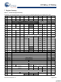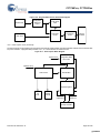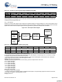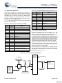
1
CY7C601xx, CY7C602xx
enCoRe™ II Low Voltage Microcontroller
1. Features
■
■
enCoRe™ II Low Voltage (enCoRe II LV)—enhanced
component reduction
❐ Internal crystalless oscillator with support for optional external clock or external crystal or resonator
❐ Configurable IO for real world interface without external components
■ Enhanced 8-bit microcontroller
❐ Harvard architecture
❐ M8C CPU speed up to 12 MHz or sourced by an external
crystal, resonator, or clock signal
■ Internal memory
❐ 256 bytes of RAM
❐ 8 Kbytes of Flash including EEROM emulation
■ Low power consumption
❐ Typically 2.25 mA at 3 MHz
❐ 5 μA sleep
■ In-system reprogrammability
❐ Allows easy firmware update
■ General purpose IO ports
❐ Up to 36 General Purpose IO (GPIO) pins
❐ 2 mA source current on all GPIO pins. Configurable 8 or
50 mA per pin current sink on designated pins
❐ Each GPIO port supports high impedance inputs, configurable pull up, open drain output, CMOS and TTL inputs, and
CMOS output
❐ Maskable interrupts on all IO pins
■
■
■
■
■
■
■
■
■
■
■
■
SPI serial communication
❐ Master or slave operation
❐ Configurable up to 2 Mbit per second transfers
❐ Supports half duplex single data line mode for optical sensors
2-channel 8-bit or 1-channel 16-bit capture timer registers.
Capture timer registers store both rising and falling edge times
❐ Two registers each for two input pins
❐ Separate registers for rising and falling edge capture
❐ Simplifies interface to RF inputs for wireless applications
Internal low power wakeup timer during suspend mode
❐ Periodic wakeup with no external components
Programmable interval timer interrupts
Reduced RF emissions at 27 MHz and 96 MHz
Watchdog timer (WDT)
Low voltage detection with user selectable threshold voltages
Improved output drivers to reduce EMI
Operating voltage from 2.7V to 3.6V DC
Operating temperature from 0–70°C
Available in 24 and 40-pin PDIP, 24-pin SOIC, 24-pin QSOP
and SSOP, 28-pin SSOP, and 48-pin SSOP
Advanced development tools based on Cypress PSoC® tools
Industry standard programmer support
2. Logic Block Diagram
Interrupt
Control
4 SPI/GPIO
Pins
16 Extended
I/O Pins
16 GPIO
Pins
Wakeup
Timer
Internal
12 MHz
Oscillator
M8C CPU
Clock
Control
POR /
Low-Voltage
Detect
Flash
8K Byte
12-bit Timer
Capture
Timers
Watchdog
Timer
Vdd
Crystal
Oscillator
CY7C601xx only
RAM
256 Byte
Cypress Semiconductor Corporation
Document 38-16016 Rev. *E
•
198 Champion Court
•
San Jose, CA 95134-1709
•
408-943-2600
Revised December 08, 2008
[+] Feedback
CY7C601xx, CY7C602xx
3. Applications
The CY7C601xx and CY7C602xx are targeted for the following
applications:
■
PC wireless HID devices
❐ Mice (optomechanical, optical, trackball)
❐ Keyboards
❐ Presenter tools
■
Gaming
❐ Joysticks
❐ Gamepad
■
General purpose wireless applications
❐ Remote controls
❐ Barcode scanners
❐ POS terminal
❐ Consumer electronics
❐ Toys
4. Introduction
The enCoRe II LV family brings the features and benefits of the
enCoRe II to non USB applications. The enCoRe II family has an
integrated oscillator that eliminates the external crystal or
resonator, reducing overall cost. Other external components,
such as wakeup circuitry, are also integrated into this chip.
The enCoRe II LV is a low voltage, low cost 8-bit Flash programmable microcontroller.
The enCoRe II LV features up to 36 GPIO pins. The IO pins are
grouped into five ports (Port 0 to 4). The pins on Ports 0 and 1
are configured individually, when the pins on Ports 2, 3, and 4
are only configured as a group. Each GPIO port supports high
impedance inputs, configurable pull up, open drain output,
CMOS and TTL inputs, and CMOS output with up to five pins that
support programmable drive strength of up to 50 mA sink current.
Additionally, each IO pin is used to generate a GPIO interrupt to
the microcontroller. Each GPIO port has its own GPIO interrupt
vector with the exception of GPIO Port 0. GPIO Port 0 has, in
addition to the port interrupt vector, three dedicated pins that
have independent interrupt vectors (P0.2–P0.4).
The enCoRe II LV features an internal oscillator. Optionally, an
external 1 MHz to 24 MHz crystal is used to provide a higher
precision reference. The enCoRe II LV also supports external
clock.
The enCoRe II LV has 8 Kbytes of Flash for user code and 256
bytes of RAM for stack space and user variables.
Document 38-16016 Rev. *E
In addition, enCoRe II LV includes a watchdog timer, a vectored
interrupt controller, a 16-bit free running timer with capture
registers, and a 12-bit programmable interval timer. The power
on reset circuit detects when power is applied to the device,
resets the logic to a known state, and executes instructions at
Flash address 0x0000. When power falls below a programmable
trip voltage, it generates a reset or is configured to generate an
interrupt. There is a low voltage detect circuit that detects when
VCC drops below a programmable trip voltage. This is configurable to generate a LVD interrupt to inform the processor about
the low voltage event. POR and LVD share the same interrupt;
there is no separate interrupt for each. The watchdog timer
ensures the firmware never gets stalled in an infinite loop.
The microcontroller supports 17 maskable interrupts in the
vectored interrupt controller. All interrupts can be masked.
Interrupt sources include LVR or POR, a programmable interval
timer, a nominal 1.024 ms programmable output from the free
running timer, two capture timers, five GPIO ports, three GPIO
pins, two SPI, a 16-bit free running timer wrap, and an internal
wakeup timer interrupt. The wakeup timer causes periodic interrupts when enabled. The capture timers interrupt whenever a
new timer value is saved due to a selected GPIO edge event. A
total of eight GPIO interrupts support both TTL or CMOS
thresholds. For additional flexibility, on the edge-sensitive GPIO
pins, the interrupt polarity is programmable to be either rising or
falling.
The free running timer generates an interrupt at 1024 μs rate. It
also generates an interrupt when the free running counter
overflow occurs—every 16.384 ms. The duration of an event
under firmware control is measured by reading the timer at the
start and end of an event, then calculating the difference
between the two values. The two 8-bit capture timer registers
save a programmable 8-bit range of the free running timer when
a GPIO edge occurs on the two capture pins (P0.5 and P0.6).
The two 8-bit capture registers are ganged into a single 16-bit
capture register.
The enCoRe II LV supports in-system programming by using the
P1.0 and P1.1 pins as the serial programming mode interface.
5. Conventions
In this document, bit positions in the registers are shaded to
indicate which members of the enCoRe II LV family implement
the bits.
Available in all enCoRe II LV family members
CY7C601xx only
Page 2 of 68
[+] Feedback
CY7C601xx, CY7C602xx
6. Pinouts
Figure 6-1. Package Configurations
Top View
CY7C60223
24-Pin PDIP
P3.0
P3.1
SCLK/P1.4
SMOSI/P1.5
SMISO/P1.6
P1.7
NC
NC
P0.7
TIO1/P0.6
TIO0/P0.5
INT2/P0.4
1
2
3
4
5
6
7
8
9
10
11
12
24
23
22
21
20
19
18
17
16
15
14
13
P1.3/SSEL
P1.2
VDD
P1.1
P1.0
VSS
P2.0
P2.1
P0.0/CLKIN
P0.1/CLKOUT
P0.2/INT0
P0.3/INT1
CY7C60113
28-Pin SSOP
VDD
P2.7
P2.6
P2.5
P2.4
P0.7
TIO1/P0.6
TIO0/P0.5
INT2/P0.4
INT1/P0.3
INT0/P0.2
CLKOUT/P0.1
CLKIN/P0.0
VSS
1
2
3
4
5
6
7
8
9
10
11
12
13
14
28
27
26
25
24
23
22
21
20
19
18
17
16
15
Document 38-16016 Rev. *E
CY7C60223
24-Pin QSOP
CY7C60223
24-Pin SOIC
VSS
P3.7
P3.6
P3.5
P3.4
P1.7
P1.6/SMISO
P1.5/SMOSI
P1.4/SCLK
P1.3/SSEL
P1.2
VDD
P1.1
P1.0
NC
P0.7
TIO1/P0.6
TIO0/P0.5
INT2/P0.4
INT1/P0.3
INT0/P0.2
CLKOUT\P0.1
CLKIN\P0.0
P2.1
P2.0
VSS
1
2
3
4
5
6
7
8
9
10
11
12
24
23
22
21
20
19
18
17
16
15
14
13
NC
P1.7
P1.6/SMISO
P1.5/SMOSI
P1.4/SCLK
P3.1
P3.0
P1.3/SSEL
P1.2
VDD
P1.1
P1.0
1
2
3
4
5
6
7
8
9
10
11
12
13
14
15
16
17
18
19
20
40
39
38
37
36
35
34
33
32
31
30
29
28
27
26
25
24
23
22
21
1
2
3
4
5
6
7
8
9
10
11
12
P1.7
P1.6/SMISO
P1.5/SMOSI
P1.4/SCLK
P3.1
P3.0
P1.3/SSEL
P1.2
VDD
P1.1
P1.0
VSS
24
23
22
21
20
19
18
17
16
15
14
13
CY7C60123
48-Pin SSOP
CY7C60123
40-Pin PDIP
VDD
P4.1
P4.0
P2.7
P2.6
P2.5
P2.4
P2.3
P2.2
P2.1
P2.0
P0.7
T1O1/P0.6
TIO0/P0.5
INT2/P0.4
INT1/P0.3
INT0/P0.2
CLKOUT/P0.1
CLKIN/P0.0
VSS
NC
P0.7
TIO1/P0.6
TIO0/P0.5
INT2/P0.4
INT1/P0.3
INT0/P0.2
CLKOUT\P0.1
CLKIN\P0.0
P2.1
P2.0
NC
VSS
P4.3
P4.2
P3.7
P3.6
P3.5
P3.4
P3.3
P3.2
P3.1
P3.0
P1.7
P1.6/SMISO
P1.5/SMOSI
P1.4/SCLK
P1.3/SSEL
P1.2
VDD
P1.1
P1.0
NC
NC
NC
NC
VDD
P4.1
P4.0
P2.7
P2.6
P2.5
P2.4
P2.3
P2.2
P2.1
P2.0
P0.7
TIO1/P0.6
TIO0/PO.5
INT2/P0.4
INT1/P0.3
INT0/P0.2
CLKOUT/P0.1
CLKIN/P0.0
VSS
1
2
3
4
5
6
7
8
9
10
11
12
13
14
15
16
17
18
19
20
21
22
23
24
48
47
46
45
44
43
42
41
40
39
38
37
36
35
34
33
32
31
30
29
28
27
26
25
NC
NC
NC
NC
VSS
P4.3
P4.2
P3.7
P3.6
P3.5
P3.4
P3.3
P3.2
P3.1
P3.0
P1.7
P1.6/SMISO
P1.5/SMOSI
P1.4/SCLK
P1.3/SSEL
P1.2
VDD
P1.1
P1.0
Page 3 of 68
[+] Feedback
CY7C601xx, CY7C602xx
6.1 Pin Assignments
Table 6-1. Pin Assignments
48
40
28
24
24
SSOP PDIP SSOP QSOP SOIC
24
PDIP
Name
Description
7
3
P4.0
6
2
P4.1
42
38
P4.2
43
39
P4.3
34
30
19
18
1
35
31
20
19
2
36
32
37
33
38
34
24
P3.4
39
35
25
P3.5
40
36
26
P3.6
41
37
27
P3.7
15
11
11
11
18
P2.0
14
10
10
10
17
P2.1
13
9
12
8
11
7
5
P2.4
10
6
4
P2.5
9
5
3
P2.6
8
4
2
P2.7
25
21
15
14
13
20
P1.0
GPIO Port 1 bit 0
If this pin is used as a general purpose output it draws current.
It is, therefore, configured as an input to reduce current draw.
26
22
16
15
14
21
P1.1
GPIO Port 1 bit 1
If this pin is used as a general purpose output it draws current.
It is, therefore, configured as an input to reduce current draw.
28
24
18
17
16
23
P1.2
GPIO Port 1 bit 2
29
25
19
18
17
24
P1.3/SSEL
GPIO Port 1 bit 3—Configured individually
Alternate function is SSEL signal of the SPI bus.
30
26
20
21
20
3
P1.4/SCLK
GPIO Port 1 bit 4—Configured individually
Alternate function is SCLK signal of the SPI bus.
31
27
21
22
21
4
P1.5/SMOSI
GPIO Port 1 bit 5—Configured individually
Alternate function is SMOSI signal of the SPI bus.
32
28
22
23
22
5
P1.6/SMISO
GPIO Port 1 bit 6—Configured individually
Alternate function is SMISO signal of the SPI bus.
33
29
23
24
23
6
P1.7
GPIO Port 1 bit 7—Configured individually
TTL voltage threshold.
P3.0
GPIO Port 4—configured as a group (nibble)
GPIO Port 3—configured as a group (byte)
P3.1
P3.2
P3.3
GPIO Port 2—configured as a group (byte)
P2.2
P2.3
Document 38-16016 Rev. *E
Page 4 of 68
[+] Feedback
CY7C601xx, CY7C602xx
Table 6-1. Pin Assignments (continued)
48
40
28
24
24
SSOP PDIP SSOP QSOP SOIC
24
PDIP
Name
Description
23
19
13
9
9
16
P0.0/CLKIN
22
18
12
8
8
15
P0.1/CLKOUT GPIO Port 0 bit 1—Configured individually
On CY7C601xx, optional Clock Out when external oscillator is
disabled or external oscillator output drive when external oscillator is enabled.
On CY7C602xx, oscillator output when configured as Clock Out.
21
17
11
7
7
14
P0.2/INT0
GPIO port 0 bit 2—Configured individually
Optional rising edge interrupt INT0.
20
16
10
6
6
13
P0.3/INT1
GPIO port 0 bit 3—Configured individually
Optional rising edge interrupt INT1.
19
15
9
5
5
12
P0.4/INT2
GPIO port 0 bit 4—Configured individually
Optional rising edge interrupt INT2.
18
14
8
4
4
11
P0.5/TIO0
GPIO port 0 bit 5—Configured individually
Alternate function timer capture inputs or timer output TIO0.
17
13
7
3
3
10
P0.6/TIO1
GPIO port 0 bit 6—Configured individually
Alternate function timer capture inputs or timer output TIO1.
16
12
6
2
2
9
P0.7
GPIO port 0 bit 7—Configured individually
1,2,3,
4
1
1
7
NC
No connect
45,46,
47,48
12
24
8
NC
No connect
VDD
Power
VSS
Ground
5
1
17
27
23
1
16
15
22
44
40
14
–
–
–
24
20
28
13
12
19
Document 38-16016 Rev. *E
GPIO Port 0 bit 0—Configured individually
On CY7C601xx, optional Clock In when external oscillator is
disabled or external oscillator input when external oscillator is
enabled.
On CY7C602xx, oscillator input when configured as Clock In.
Page 5 of 68
[+] Feedback
CY7C601xx, CY7C602xx
7. Register Summary
Table 7-1. enCoRe II LV Register Summary
The XIO bit in the CPU Flags Register must be set to access the extended register space for all registers above 0xFF.
Addr
Name
7
6
5
4
3
2
1
0
R/W
Default
00
P0DATA
P0.7
P0.6/TIO1
P0.5/TIO0
P0.4/INT2
P0.3/INT1
P0.2/INT0
P0.1/
CLKOUT
P0.0/CLKIN
bbbbbbbb
00000000
01
P1DATA
P1.7
P1.4/SCLK
P1.3/SSEL
P1.2
P1.1
P1.0
bbbbbbbb
00000000
02
P2DATA
P2.7–P2.2
P2.1–P2.0
bbbbbbbb
00000000
03
P3DATA
P3.7–P3.2
P3.1–P3.0
bbbbbbbb
00000000
04
P4DATA
----bbbb
00000000
05
P00CR
Reserved
Int Enable
Int Act Low
TTL Thresh
High Sink
Open Drain
Pull up
Enable
Output
Enable
-bbbbbbb
00000000
06
P01CR
CLK Output
Int Enable
Int Act Low
TTL Thresh
High Sink
Open Drain
Pull Up
Enable
Output
Enable
bbbbbbbb
00000000
07–09
P02CR–
P04CR
Int Act Low
TTL Thresh
Reserved
Open Drain
Pull Up
Enable
Output
Enable
--bb-bbb
00000000
0A–0B
P05CR–
P06CR
TIO Output
Int Enable
Int Act Low
TTL Thresh
Reserved
Open Drain
Pull Up
Enable
Output
Enable
bbbb-bbb
00000000
0C
P07CR
Reserved
Int Enable
Int Act Low
TTL Thresh
Reserved
Open Drain
Pull Up
Enable
Output
Enable
-bbb-bbb
00000000
0D
P10CR
Reserved
Int Enable
Int Act Low
Output
Enable
-bb----b
00000000
0E
P11CR
Reserved
Int Enable
Int Act Low
0F
P12CR
CLK Output
Int Enable
Int Act Low
TTL
Threshold
10
P13CR
Reserved
Int Enable
Int Act Low
11–13
P14CR–
P16CR
SPI Use
Int Enable
14
P17CR
Reserved
15
P2CR
16
17
P1.6/SMISO P1.5/SMOSI
Reserved
Reserved
P4.3–P4.0
Reserved
Reserved
Open Drain
Reserved
Output
Enable
-bb--b-b
00000000
Reserved
Open Drain
Pull Up
Enable
Output
Enable
bbbb-bbb
00000000
Reserved
High Sink
Open Drain
Pull Up
Enable
Output
Enable
-bb-bbbb
00000000
Int Act Low
Reserved
High Sink
Open Drain
Pull Up
Enable
Output
Enable
bbb-bbbb
00000000
Int Enable
Int Act Low
Reserved
High Sink
Open Drain
Pull Up
Enable
Output
Enable
-bb-bbbb
00000000
Reserved
Int Enable
Int Act Low
TTL Thresh
High Sink
Open Drain
Pull Up
Enable
Output
Enable
-bbbbbbb
00000000
P3CR
Reserved
Int Enable
Int Act Low
TTL Thresh
High Sink
Open Drain
Pull Up
Enable
Output
Enable
-bbbbbbb
00000000
P4CR
Reserved
Int Enable
Int Act Low
TTL Thresh
Reserved
Open Drain
Pull Up
Enable
Output
Enable
-bbb-bbb
00000000
20
FRTMRL
Free Running Timer [7:0]
bbbbbbbb
00000000
21
FRTMRH
Free Running Timer [15:8]
bbbbbbbb
00000000
22
TCAP0R
Capture 0 Rising [7:0]
rrrrrrrr
00000000
23
TCAP1R
Capture 1 Rising [7:0]
rrrrrrrr
00000000
24
TCAP0F
Capture 0 Falling [7:0]
rrrrrrrr
00000000
25
TCAP1F
Capture 1 Falling [7:0]
rrrrrrrr
00000000
26
PITMRL
Prog Interval Timer [7:0]
rrrrrrrr
00000000
27
PITMRH
28
PIRL
Reserved
Prog Interval Timer [11:8]
Prog Interval [7:0]
29
PIRH
2A
TMRCR
Reserved
2B
TCAPINTE
Reserved
Cap1 Fall
Active
Cap1 Rise
Active
Cap0 Fall
Active
2C
TCAPINTS
Reserved
Cap1 Fall
Active
Cap1 Rise
Active
Cap0 Fall
Active
30
CPUCLKCR
31
TMRCLKCR
32
CLKIOCR
First Edge
Hold
Prog Interval [11:8]
8-bit Capture Prescale
Cap0 16-bit
Enable
TCAPCLK Divider
Document 38-16016 Rev. *E
Reserved
TCAPCLK Select
XOSC
Select
ITMRCLK Divider
XOSC
Enable
EFTB
Disabled
00000000
00000000
----bbbb
00000000
bbbbb---
00000000
Cap0 Rise
Active
----bbbb
00000000
Cap0 Rise
Active
----bbbb
00000000
CPU
CLK Select
-------b
00000000
Reserved
Reserved
----rrrr
bbbbbbbb
ITMRCLK Select
bbbbbbbb
10001111
CLKOUT Select
---bbbbb
00000000
Page 6 of 68
[+] Feedback
CY7C601xx, CY7C602xx
Table 7-1. enCoRe II LV Register Summary (continued)
The XIO bit in the CPU Flags Register must be set to access the extended register space for all registers above 0xFF.
Addr
Name
34
IOSCTR
35
XOSCTR
36
LPOSCTR
3C
SPIDATA
3D
SPICR
7
6
5
4
3
2
foffset[2:0]
1
0
Gain[4:0]
Reserved
XOSC XGM [2:0]
32 kHz Low
Power
Reserved
32 kHz Bias Trim [1:0]
Swap
LSB First
Comm Mode
Reserved
Mode
32 kHz Freq Trim [3:0]
SPIData[7:0]
DA
INT_CLR0 GPIO Port 1 Sleep Timer
INT1
GPIO Port 0
DB
INT_CLR1
TCAP0
DC
INT_CLR2
Reserved
DE
INT_MSK3
ENSWINT
DF
INT_MSK2
Reserved
E1
INT_MSK1
TCAP0
Prog Interval 1 ms Timer
Int Enable
Timer
Int Enable
Int Enable
E0
INT_MSK0 GPIO Port 1 Sleep Timer
Int Enable Int Enable
CPOL
CPHA
SPI Receive
SPI Transmit
Prog Interval 1 ms Timer
Timer
SCLK Select
INT0
POR/LVD
Reserved
GPIO Port 4 GPIO Port 3 GPIO Port 2
Reserved
GPIO Port 4 GPIO Port 3 GPIO Port 2
Int Enable
Int Enable
Int Enable
Reserved
SPI Receive
Int Enable
---bbb-b
000ddddd
b-bbbbbb
d-dddddd
bbbbbbbb
00000000
bbbbbbbb
00000000
bbbbbbbb
00000000
bbb-----
00000000
00000000
16-bit
Counter
Wrap
TCAP1
-bbb-bbb
r-------
00000000
INT2
Int Enable
16-bit
Counter
Wrap Int
Enable
TCAP1
Int Enable
-bbb-bbb
00000000
bbb-----
00000000
bbbbbbbb
00000000
Reserved
GPIO Port 0
Int Enable
Default
000ddddd
INT2
Reserved
INT1
Int Enable
R/W
bbbbbbbb
SPI Transmit
Int Enable
INT0
Int Enable
POR/LVD
Int Enable
E2
INT_VC
Pending Interrupt [7:0]
bbbbbbbb
00000000
E3
RESWDT
Reset Watchdog Timer [7:0]
wwwwwww
w
00000000
--
CPU_A
Temporary Register T1 [7:0]
--------
00000000
--
CPU_X
X[7:0]
--------
00000000
--
CPU_PCL
Program Counter [7:0]
--------
00000000
--
CPU_PCH
Program Counter [15:8]
--------
00000000
--
CPU_SP
F7
CPU_F
FF
CPU_SCR
1E0
OSC_CR0
Stack Pointer [7:0]
Reserved
GIES
Reserved
Reserved
1E3
LVDCR
Reserved
1EB
ECO_TR
Sleep Duty Cycle [1:0]
1E4
VLTCMP
WDRS
No Buzz
--------
00000000
XIO
Super
Carry
Zero
Global IE
---brbbb
00000010
PORS
Sleep
Reserved
Reserved
Stop
r-ccb--b
00010100
CPU Speed [2:0]
--bbbbbb
00000000
VM[2:0]
--bb-bbb
00000000
bb------
00000000
------rr
00000000
Sleep Timer [1:0]
PORLEV[1:0]
Reserved
Reserved
Reserved
LVD
PPOR
Note In the R/W column:
b = Both Read and Write
r = Read Only
w = Write Only
c = Read or Clear
d = Calibration Value. Must not change during normal use
Document 38-16016 Rev. *E
Page 7 of 68
[+] Feedback
CY7C601xx, CY7C602xx
8. CPU Architecture
This family of microcontrollers is based on a high performance,
8-bit, Harvard architecture microprocessor. Five registers control
the primary operation of the CPU core. These registers are
affected by various instructions, but are not directly accessible
through the register space by the user.
Table 8-1. CPU Registers and Register Name
Register
Register Name
Flags
CPU_F
Program Counter
CPU_PC
Accumulator
CPU_A
Stack Pointer
CPU_SP
Index
CPU_X
The 16-bit Program Counter Register (CPU_PC) directly
addresses the full 8 Kbytes of program memory space.
The Accumulator Register (CPU_A) is the general purpose
register that holds results of instructions that specify any of the
source addressing modes.
The Index Register (CPU_X) holds an offset value used in the
indexed addressing modes. Typically, this is used to address a
block of data within the data memory space.
The Stack Pointer Register (CPU_SP) holds the address of the
current top-of-stack in the data memory space. It is affected by
the PUSH, POP, LCALL, CALL, RETI, and RET instructions,
which manage the software stack. It is also affected by the SWAP
and ADD instructions.
The Flag Register (CPU_F) has three status bits: Zero Flag bit
[1]; Carry Flag bit [2]; Supervisory State bit [3]. The Global
Interrupt Enable bit [0] is used to globally enable or disable interrupts. The user cannot manipulate the Supervisory State status
bit [3]. The flags are affected by arithmetic, logic, and shift operations. The manner in which each flag is changed is dependent
upon the instruction being executed (AND, OR, XOR). See
Table 10-1.
9. CPU Registers
9.1 Flags Register
The Flags Register is only set or reset with logical instruction.
Table 9-1. CPU Flags Register (CPU_F) [R/W]
Bit #
7
Field
6
5
Reserved
4
3
2
1
0
XIO
Super
Carry
Zero
Global IE
Read/Write
–
–
–
R/W
R
R/W
R/W
R/W
Default
0
0
0
0
0
0
1
0
Bit [7:5]: Reserved
Bit 4: XIO
Set by the user to select between the register banks.
0 = Bank 0
1 = Bank 1
Bit 3: Super
Indicates whether the CPU is executing user code or supervisor code. (This code cannot be accessed directly by the user.)
0 = User Code
1 = Supervisor Code
Bit 2: Carry
Set by CPU to indicate whether there is a carry in the previous logical or arithmetic operation.
0 = No Carry
1 = Carry
Bit 1: Zero
Set by CPU to indicate whether there is a zero result in the previous logical or arithmetic operation.
0 = Not Equal to Zero
1 = Equal to Zero
Bit 0: Global IE
Determines whether all interrupts are enabled or disabled.
0 = Disabled
1 = Enabled
Note This register is readable with explicit address 0xF7. The OR F, expr and AND F, expr are used to set and clear the CPU_F
bits.
Document 38-16016 Rev. *E
Page 8 of 68
[+] Feedback
CY7C601xx, CY7C602xx
9.1.1 Accumulator Register
Table 9-2. CPU Accumulator Register (CPU_A)
Bit #
7
6
5
Field
4
3
2
1
0
CPU Accumulator [7:0]
Read/Write
–
–
–
–
–
–
–
–
Default
0
0
0
0
0
0
0
0
Bit [7:0]: CPU Accumulator [7:0]
8-bit data value holds the result of any logical or arithmetic instruction that uses a source addressing mode.
9.1.2 Index Register
Table 9-3. CPU X Register (CPU_X)
Bit #
7
6
5
4
Field
3
2
1
0
X [7:0]
Read/Write
–
–
–
–
–
–
–
–
Default
0
0
0
0
0
0
0
0
2
1
0
Bit [7:0]: X [7:0]
8-bit data value holds an index for any instruction that uses an indexed addressing mode.
9.1.3 Stack Pointer Register
Table 9-4. CPU Stack Pointer Register (CPU_SP)
Bit #
7
6
5
4
Field
3
Stack Pointer [7:0]
Read/Write
–
–
–
–
–
–
–
–
Default
0
0
0
0
0
0
0
0
3
2
1
0
Bit [7:0]: Stack Pointer [7:0]
8-bit data value holds a pointer to the current top-of-stack.
9.1.4 CPU Program Counter High Register
Table 9-5. CPU Program Counter High Register (CPU_PCH)
Bit #
7
6
5
Field
4
Program Counter [15:8]
Read/Write
–
–
–
–
–
–
–
–
Default
0
0
0
0
0
0
0
0
3
2
1
0
Bit [7:0]: Program Counter [15:8]
8-bit data value holds the higher byte of the program counter.
9.1.5 CPU Program Counter Low Register
Table 9-6. CPU Program Counter Low Register (CPU_PCL)
Bit #
7
6
5
Field
4
Program Counter [7:0]
Read/Write
–
–
–
–
–
–
–
–
Default
0
0
0
0
0
0
0
0
Bit [7:0]: Program Counter [7:0]
8-bit data value holds the lower byte of the program counter.
Document 38-16016 Rev. *E
Page 9 of 68
[+] Feedback
CY7C601xx, CY7C602xx
9.2 Addressing Modes
9.2.1 Source Immediate
9.2.3 Source Indexed
The result of an instruction using this addressing mode is placed
in the A register, the F register, the SP register, or the X register,
which is specified as part of the instruction opcode. Operand 1
is an immediate value that serves as a source for the instruction.
Arithmetic instructions require two sources; the second source is
the A, X, SP, or F register specified in the opcode. Instructions
using this addressing mode are two bytes in length.
The result of an instruction using this addressing mode is placed
in either the A register or the X register, which is specified as part
of the instruction opcode. Operand 1 is added to the X register
forming an address that points to a location in either the RAM
memory space or the register space that is the source for the
instruction. Arithmetic instructions require two sources; the
second source is the A register or X register specified in the
opcode. Instructions using this addressing mode are two bytes
in length.
Table 9-7. Source Immediate
Opcode
Operand 1
Instruction
A,
Opcode
Operand 1
Instruction
Examples
ADD
Table 9-9. Source Indexed
Immediate Value
7
;In this case, the immediate value of 7 is added
with the Accumulator and the result is placed in
the Accumulator.
MOV
X,
8
;In this case, the immediate value of 8 is moved
to the X register.
AND
F,
9
;In this case, the immediate value of 9 is logically
ANDed with the F register and the result is placed
in the F register.
9.2.2 Source Direct
The result of an instruction using this addressing mode is placed
in either the A register or the X register, which is specified as part
of the instruction opcode. Operand 1 is an address that points to
a location in either the RAM memory space or the register space
that is the source for the instruction. Arithmetic instructions
require two sources; the second source is the A register or X
register specified in the opcode. Instructions using this
addressing mode are two bytes in length.
Instruction
Examples
ADD
A,
[X+7]
;In this case, the value in the memory
location at address X + 7 is added with
the Accumulator, and the result is
placed in the Accumulator.
MOV
X,
REG[X+8]
;In this case, the value in the register
space at address X + 8 is moved to the
X register.
9.2.4 Destination Direct
The result of an instruction using this addressing mode is placed
within either the RAM memory space or the register space.
Operand 1 is an address that points to the location of the result.
The source for the instruction is either the A register or the X
register, which is specified as part of the instruction opcode.
Arithmetic instructions require two sources; the second source is
the location specified by Operand 1. Instructions using this
addressing mode are two bytes in length.
Table 9-10. Destination Direct
Table 9-8. Source Direct
Opcode
Source Index
Opcode
Operand 1
Source Address
Operand 1
Instruction
Destination Address
Examples
Examples
ADD
A,
[7]
;In this case, the value in the RAM
memory location at address 7 is added
with the Accumulator, and the result is
placed in the Accumulator.
MOV
X,
REG[8]
;In this case, the value in the register
space at address 8 is moved to the X
register.
Document 38-16016 Rev. *E
ADD
[7],
A
;In this case, the value in the memory
location at address 7 is added with the
Accumulator, and the result is placed
in the memory location at address 7.
The Accumulator is unchanged.
MOV
REG[8],
A
;In this case, the Accumulator is
moved to the register space location at
address 8. The Accumulator is
unchanged.
Page 10 of 68
[+] Feedback
CY7C601xx, CY7C602xx
9.2.5 Destination Indexed
9.2.7 Destination Indexed Source Immediate
The result of an instruction using this addressing mode is placed
within either the RAM memory space or the register space.
Operand 1 is added to the X register forming the address that
points to the location of the result. The source for the instruction
is the A register. Arithmetic instructions require two sources; the
second source is the location specified by Operand 1 added with
the X register. Instructions using this addressing mode are two
bytes in length.
The result of an instruction using this addressing mode is placed
within either the RAM memory space or the register space.
Operand 1 is added to the X register to form the address of the
result. The source for the instruction is Operand 2, which is an
immediate value. Arithmetic instructions require two sources; the
second source is the location specified by Operand 1 added with
the X register. Instructions using this addressing mode are three
bytes in length.
Table 9-11. Destination Indexed
Opcode
Table 9-13. Destination Indexed Source Immediate
Operand 1
Instruction
Destination Index
Example
ADD
Opcode
Instruction
Operand 1
Destination Index
Examples
[X+7],
A
;In this case, the value in the memory
location at address X+7 is added with the
Accumulator and the result is placed in the
memory location at address X+7. The
Accumulator is unchanged.
ADD
[X+7],
5
;In this case, the value in the memory
location at address X+7 is added
with the immediate value of 5, and
the result is placed in the memory
location at address X+7.
MOV
REG[X+8],
6
;In this case, the immediate value of
6 is moved into the location in the
register space at address X+8.
9.2.6 Destination Direct Source Immediate
The result of an instruction using this addressing mode is placed
within either the RAM memory space or the register space.
Operand 1 is the address of the result. The source for the
instruction is Operand 2, which is an immediate value. Arithmetic
instructions require two sources; the second source is the
location specified by Operand 1. Instructions using this
addressing mode are three bytes in length.
Table 9-12. Destination Direct Source Immediate
Opcode
Instruction
Operand 1
Destination Address
Operand 2
Immediate Value
MOV REG[8],
9.2.8 Destination Direct Source Direct
The result of an instruction using this addressing mode is placed
within the RAM memory. Operand 1 is the address of the result.
Operand 2 is an address that points to a location in the RAM
memory that is the source for the instruction. This addressing
mode is only valid on the MOV instruction. The instruction using
this addressing mode is three bytes in length.
Table 9-14. Destination Direct Source Direct
Opcode
Instruction
Examples
ADD [7],
Operand 2
Immediate Value
5
6
;In this case, value in the memory location
at address 7 is added to the immediate
value of 5, and the result is placed in the
memory location at address 7.
;In this case, the immediate value of 6 is
moved into the register space location at
address 8.
Document 38-16016 Rev. *E
Operand 1
Destination Address
Operand 2
Source Address
Example
MOV
[7],
[8]
;In this case, the value in the memory location
at address 8 is moved to the memory location
at address 7.
Page 11 of 68
[+] Feedback
CY7C601xx, CY7C602xx
9.2.9 Source Indirect Post Increment
9.2.10 Destination Indirect Post Increment
The result of an instruction using this addressing mode is placed
in the Accumulator. Operand 1 is an address pointing to a
location within the memory space, which contains an address
(the indirect address) for the source of the instruction. The
indirect address is incremented as part of the instruction
execution. This addressing mode is only valid on the MVI
instruction. The instruction using this addressing mode is two
bytes in length. Refer to the PSoC Designer: Assembly
Language User Guide for further details on MVI instruction.
The result of an instruction using this addressing mode is placed
within the memory space. Operand 1 is an address pointing to a
location within the memory space, which contains an address
(the indirect address) for the destination of the instruction. The
indirect address is incremented as part of the instruction
execution. The source for the instruction is the Accumulator. This
addressing mode is only valid on the MVI instruction. The
instruction using this addressing mode is two bytes in length.
Table 9-16. Destination Indirect Post Increment
Table 9-15. Source Indirect Post Increment
Opcode
Instruction
Opcode
Operand 1
Operand 1
Instruction
Destination Address Address
Source Address Address
Example
Example
MVI
A,
MVI
[8]
[8],
A
;In this case, the value in the memory
location at address 8 is an
indirect;address. The Accumulator is
moved into the memory location pointed
to by the indirect address. The indirect
address is then incremented.
;In this case, the value in the memory location
at address 8 is an indirect address. The
memory location pointed to by the Indirect
address is moved into the Accumulator. The
indirect address is then incremented.
10. Instruction Set Summary
The instruction set is summarized in Table 10-1 numerically and serves as a quick reference. For more information, the Instruction
Set Summary tables are described in detail in the PSoC Designer Assembly Language User Guide (available on the www.cypress.com
web site).
Bytes
Flags
Cycles
Instruction Format
Opcode Hex
Bytes
Flags
Cycles
Instruction Format[1, 2]
Opcode Hex
Bytes
Cycles
Opcode Hex
Table 10-1. Instruction Set Summary Sorted Numerically by Opcode Order
Instruction Format
Flags
00 15 1
SSC
2D 8
2
OR [X+expr], A
Z
5A 5
2
MOV [expr], X
01 4
2
ADD A, expr
C, Z
2E 9
3
OR [expr], expr
Z
5B 4
1
MOV A, X
02 6
2
ADD A, [expr]
C, Z
2F 10 3
OR [X+expr], expr
Z
5C 4
1
MOV X, A
03 7
2
ADD A, [X+expr]
C, Z
30
HALT
5D 6
2
MOV A, reg[expr]
Z
04 7
2
ADD [expr], A
C, Z
31 4
2
XOR A, expr
Z
5E 7
2
MOV A, reg[X+expr]
Z
05 8
2
ADD [X+expr], A
C, Z
32 6
2
XOR A, [expr]
Z
5F 10 3
MOV [expr], [expr]
06 9
3
ADD [expr], expr
C, Z
33 7
2
XOR A, [X+expr]
Z
60 5
2
MOV reg[expr], A
07 10 3
ADD [X+expr], expr
C, Z
34 7
2
XOR [expr], A
Z
61 6
2
MOV reg[X+expr], A
08
PUSH A
35 8
2
XOR [X+expr], A
Z
62 8
3
MOV reg[expr], expr
3
XOR [expr], expr
Z
63 9
3
MOV reg[X+expr],
expr
Z
64
4 1
ASL A
C, Z
65
7 2
ASL [expr]
C, Z
66
8 2
ASL [X+expr]
C, Z
67
4 1
ASR A
C, Z
68
7 2
ASR [expr]
C, Z
8 2
4 1
9 1
Z
09 4
2
ADC A, expr
C, Z
36 9
0A 6
2
ADC A, [expr]
C, Z
37 10 3
XOR [X+expr], expr
0B 7
2
ADC A, [X+expr]
C, Z
38
5 2
ADD SP, expr
0C 7
2
ADC [expr], A
C, Z
39
5 2
CMP A, expr
0D 8
2
ADC [X+expr], A
C, Z
3A 7 2
CMP A, [expr]
0E 9
3
ADC [expr], expr
C, Z
3B 8 2
CMP A, [X+expr]
0F 10 3
ADC [X+expr], expr
C, Z
3C 8 3
CMP [expr], expr
69
ASR [X+expr]
C, Z
10
4 1
PUSH X
3D 9 3
CMP [X+expr], expr
6A 4 1
RLC A
C, Z
11
4 2
SUB A, expr
C, Z
3E 10 2
MVI A, [ [expr]++ ]
6B 7 2
RLC [expr]
C, Z
12
6 2
SUB A, [expr]
C, Z
3F 10 2
MVI [ [expr]++ ], A
6C 8 2
RLC [X+expr]
C, Z
Document 38-16016 Rev. *E
if (A=B)
Z=1
if (A<B)
C=1
Z
Page 12 of 68
[+] Feedback
CY7C601xx, CY7C602xx
15
8 2
SUB [X+expr], A
C, Z
16
9 3
1
Instruction Format
Flags
6D 4 1
RRC A
C, Z
AND reg[expr], expr
Z
6E 7 2
RRC [expr]
C, Z
42 10 3
AND reg[X+expr],
expr
Z
6F 8 2
RRC [X+expr]
C, Z
OR reg[expr], expr
Z
70
AND F, expr
C, Z
OR F, expr
C, Z
9 3
3
NOP
Bytes
41
Flags
Cycles
40 4
C, Z
Instruction Format
Opcode Hex
C, Z
SUB [expr], A
Bytes
SUB A, [X+expr]
7 2
Flags
Cycles
7 2
14
Instruction Format[1, 2]
Opcode Hex
Cycles
13
Bytes
Opcode Hex
Table 10-1. Instruction Set Summary Sorted Numerically by Opcode Order (continued)
SUB [expr], expr
C, Z
43 9
17 10 3
SUB [X+expr], expr
C, Z
44 10 3
OR reg[X+expr], expr Z
71 4
18
5 1
POP A
Z
45
XOR reg[expr], expr
Z
72
4 2
XOR F, expr
C, Z
19
4 2
SBB A, expr
C, Z
46 10 3
XOR reg[X+expr],
expr
Z
73
4 1
CPL A
Z
1A 6 2
SBB A, [expr]
C, Z
47
8 3
TST [expr], expr
Z
74
4 1
INC A
C, Z
1B 7 2
SBB A, [X+expr]
C, Z
48
9 3
TST [X+expr], expr
Z
75
4 1
INC X
C, Z
1C 7 2
SBB [expr], A
C, Z
49
9 3
TST reg[expr], expr
Z
76
7 2
INC [expr]
C, Z
1D 8 2
SBB [X+expr], A
C, Z
4A 10 3
TST reg[X+expr], expr Z
77
8 2
INC [X+expr]
C, Z
1E 9 3
SBB [expr], expr
C, Z
4B 5 1
SWAP A, X
Z
78
4 1
DEC A
C, Z
1F 10 3
SBB [X+expr], expr
C, Z
4C 7 2
SWAP A, [expr]
Z
79
4 1
DEC X
C, Z
20
5 1
POP X
4D 7 2
SWAP X, [expr]
7A 7 2
DEC [expr]
C, Z
21
4 2
AND A, expr
Z
4E 5 1
SWAP A, SP
7B 8 2
DEC [X+expr]
C, Z
22
6 2
AND A, [expr]
Z
4F 4
1
MOV X, SP
7C 13 3
LCALL
23
7 2
AND A, [X+expr]
Z
50 4
2
MOV A, expr
Z
7D 7
3
LJMP
24
7 2
AND [expr], A
Z
51 5
2
MOV A, [expr]
Z
7E 10 1
RETI
25
8 2
AND [X+expr], A
Z
52 6
2
MOV A, [X+expr]
Z
7F 8 1
RET
26
9 3
AND [expr], expr
Z
53 5
2
MOV [expr], A
8x
JMP
27 10 3
AND [X+expr], expr
Z
54 6
2
MOV [X+expr], A
9x 11 2
CALL
28 11 1
ROMX
Z
55 8
3
MOV [expr], expr
Ax 5
2
JZ
29 4
2
OR A, expr
Z
56 9
3
MOV [X+expr], expr
Bx 5
2
JNZ
2A 6
2
OR A, [expr]
Z
57 4
2
MOV X, expr
Cx 5
2
JC
2B 7
2
OR A, [X+expr]
Z
58 6
2
MOV X, [expr]
Dx 5
2
JNC
2C 7
2
OR [expr], A
Z
59 7
2
MOV X, [X+expr]
Ex 7
2
JACC
9 3
Z
4 2
2
5 2
Fx 13 2
INDEX
C, Z
Z
Notes
1. Interrupt routines take 13 cycles before execution resumes at interrupt vector table.
2. The number of cycles required by an instruction is increased by one for instructions that span 256 byte boundaries in the Flash memory space.
Document 38-16016 Rev. *E
Page 13 of 68
[+] Feedback
CY7C601xx, CY7C602xx
11. Memory Organization
11.1 Flash Program Memory Organization
Figure 11-1. Program Memory Space with Interrupt Vector Table
after reset
Address
16-bit PC
0x0000
Program execution begins here after a reset
0x0004
POR/LVD
0x0008
INT0
0x000C
SPI Transmitter Empty
0x0010
SPI Receiver Full
0x0014
GPIO Port 0
0x0018
GPIO Port 1
0x001C
INT1
0x0020
Reserved
0x0024
Reserved
0x0028
Reserved
0x002C
Reserved
0x0030
Reserved
0x0034
1 ms Interval timer
0x0038
Programmable Interval Timer
0x003C
Timer Capture 0
0x0040
Timer Capture 1
0x0044
16-bit Free Running Timer Wrap
0x0048
INT2
0x004C
Reserved
0x0050
GPIO Port 2
0x0054
GPIO Port 3
0x0058
GPIO Port 4
0x005C
Reserved
0x0060
Reserved
0x0064
Sleep Timer
0x0068
Program Memory begins here (if below interrupts not used,
program memory can start lower)
0x1FFF
Document 38-16016 Rev. *E
Page 14 of 68
[+] Feedback
CY7C601xx, CY7C602xx
11.2 Data Memory Organization
The CY7C601xx and CY7C602xx microcontrollers provide up to 256 bytes of data RAM
Figure 11-2. Data Memory Organization
After Reset
Address
8-bit PSP
0x00
Top of RAM Memory
Stack begins here and grows upward
0xFF
11.3 Flash
11.4 SROM
This section describes the Flash block of enCoRe II LV. Much of
the visible Flash functionality, including programming and
security, are implemented in the M8C Supervisory Read Only
Memory (SROM). enCoRe II LV Flash has an endurance of 1000
erase and write cycles and a ten year data retention capability.
The SROM holds the code to boot the part, calibrate circuitry, and
perform Flash operations (Table 11-1 lists the SROM functions).
The functions of the SROM are accessed in normal user code or
operating from Flash. The SROM exists in a separate memory
space from user code. To access SROM functions, the Supervisory System Call instruction (SSC) is executed, which has an
opcode of 00h. Before executing SSC, the M8C’s accumulator is
loaded with the desired SROM function code from Table 11-1.
Undefined functions causes a HALT if called from user code. The
SROM functions execute code with calls; therefore, the functions
require stack space. With the exception of Reset, all of the
SROM functions have a parameter block in SRAM that must be
configured before executing the SSC. Table 11-2 lists all possible
parameter block variables. The meaning of each parameter, with
regards to a specific SROM function, is described later in this
section.
11.3.1 Flash Programming and Security
All Flash programming is performed by code in the SROM. The
registers that control Flash programming are only visible to the
M8C CPU when it is executing out of SROM. This makes it
impossible to read, write, or erase the Flash by avoiding the
security mechanisms implemented in the SROM.
Customer firmware only programs Flash via SROM calls. The
data or code images are sourced through any interface with the
appropriate support firmware. This type of programming requires
a ‘boot-loader’—a piece of firmware resident on the Flash. For
safety reasons this boot-loader is not overwritten during firmware
rewrites.
The Flash provides four extra auxiliary rows to hold Flash block
protection flags, boot time calibration values, configuration
tables, and any device values. The routines to access these
auxiliary rows are documented in the SROM section. The
auxiliary rows are not affected by the device erase function.
11.3.2 In-System Programming
enCoRe II LV devices enable in-system programming by using
the P1.0 and P1.1 pins as the serial programming mode
interface. This allows an external controller to make the enCoRe
II LV part enter serial programming mode and then use the test
queue to issue Flash access functions in the SROM.
Document 38-16016 Rev. *E
Table 11-1. SROM Function Codes
Function Code
Function Name
Stack Space
00h
SWBootReset
0
01h
ReadBlock
7
02h
WriteBlock
10
03h
EraseBlock
9
05h
EraseAll
11
06h
TableRead
3
07h
CheckSum
3
Page 15 of 68
[+] Feedback
CY7C601xx, CY7C602xx
Two important variables used for all functions are KEY1 and
KEY2. These variables help discriminate between valid and
inadvertent SSCs. KEY1 always has a value of 3Ah, while KEY2
has the same value as the stack pointer when the SROM
function begins execution. This is the Stack Pointer value when
the SSC opcode is executed, plus three. If either of the keys do
not match the expected values, the M8C halts (with the exception
of the SWBootReset function). The following code puts the
correct value in KEY1 and KEY2. The code starts with a halt, to
force the program to jump directly into the setup code and not
run into it.
halt
SSCOP: mov [KEY1], 3ah
mov X, SP
mov A, X
add A, 3
mov [KEY2], A
Table 11-2. SROM Function Parameters
Variable Name
SRAM Address
Key1/Counter/Return Code
0,F8h
Key2/TMP
0,F9h
BlockID
0,FAh
Pointer
0,FBh
Clock
0,FCh
Mode
0,FDh
Delay
0,FEh
PCL
0,FFh
11.4.1 Return Codes
The SROM also features Return Codes and Lockouts.
Return codes determine the success or failure of a particular
function. The return code is stored in KEY1’s position in the
parameter block. The CheckSum and TableRead functions do
not have return codes because KEY1’s position in the parameter
block is used to return other data.
Table 11-3. SROM Return Codes
Return Code
Description
00h
Success
01h
Function not allowed due to level of protection
on block
02h
Software reset without hardware reset
03h
Fatal error, SROM halted
Document 38-16016 Rev. *E
Read, write, and erase operations may fail if the target block is
read or write protected. Block protection levels are set during
device programming.
The EraseAll function overwrites data in addition to leaving the
entire user Flash in the erase state. The EraseAll function loops
through the number of Flash macros in the product, executing
the following sequence: erase, bulk program all zeros, erase.
After the user space in all Flash macros are erased, a second
loop erases and then programs each protection block with zeros.
11.5 SROM Function Descriptions
11.5.1 SWBootReset Function
The SROM function, SWBootReset, is responsible for transitioning the device from a reset state to running user code. The
SWBootReset function is executed whenever the SROM is
entered with an M8C accumulator value of 00h: the SRAM
parameter block is not used as an input to the function. This
happens, by design, after a hardware reset, because the M8C's
accumulator is reset to 00h or when user code executes the SSC
instruction with an accumulator value of 00h. The SWBootReset
function does not execute when the SSC instruction is executed
with a bad key value and a non zero function code. An enCoRe
II LV device executes the HALT instruction if a bad value is given
for either KEY1 or KEY2.
The SWBootReset function verifies the integrity of the calibration
data by way of a 16-bit checksum, before releasing the M8C to
run user code.
11.5.2 ReadBlock Function
The ReadBlock function is used to read 64 contiguous bytes
from Flash: a block.
The function first checks the protection bits and determines if the
desired BLOCKID is readable. If read protection is turned on, the
ReadBlock function exits setting the accumulator and KEY2 back
to 00h. KEY1 has a value of 01h, indicating a read failure. If read
protection is not enabled, the function reads 64 bytes from the
Flash using a ROMX instruction and stores the results in SRAM
using an MVI instruction. The first of the 64 bytes is stored in
SRAM at the address indicated by the value of the POINTER
parameter. When the ReadBlock completes successfully the
accumulator, KEY1 and KEY2 all have a value of 00h.
Table 11-4. ReadBlock Parameters
Name
Address
Description
KEY1
0,F8h
3Ah
KEY2
0,F9h
Stack Pointer value, when SSC is
executed
BLOCKID
0,FAh
Flash block number
POINTER
0,FBh
First of 64 addresses in SRAM
where returned data is stored
Page 16 of 68
[+] Feedback
CY7C601xx, CY7C602xx
Table 11-6. EraseBlock Parameters
11.5.3 WriteBlock Function
The WriteBlock function is used to store data in Flash. Data is
moved 64 bytes at a time from SRAM to Flash using this function.
The WriteBlock function first checks the protection bits and determines if the desired BLOCKID is writable. If write protection is
turned on, the WriteBlock function exits setting the accumulator
and KEY2 back to 00h. KEY1 has a value of 01h, indicating a
write failure. The configuration of the WriteBlock function is
straightforward. The BLOCKID of the Flash block, where the
data is stored, is determined and stored at SRAM address FAh.
The SRAM address of the first of the 64 bytes to be stored in
Flash is indicated using the POINTER variable in the parameter
block (SRAM address FBh). Finally, the CLOCK and DELAY
value are set correctly. The CLOCK value determines the length
of the write pulse used to store the data in Flash. The CLOCK
and DELAY values are dependent on the CPU speed and must
be set correctly. Refer to the Clocking section for additional information.
Table 11-5. WriteBlock Parameters
Name
Address
Description
KEY1
0,F8h
3Ah
KEY2
0,F9h
Stack Pointer value, when SSC is
executing
BLOCK ID
0,FAh
8 KB Flash block number (00h–7Fh)
4 KB Flash block number (00h–3Fh)
3 KB Flash block number (00h–2Fh)
POINTER
0,FBh
First 64 addresses in SRAM where
the data is stored in Flash is located
before calling WriteBlock
CLOCK
0,FCh
Clock Divider used to set the write
pulse width
DELAY
0,FEh
For a CPU speed of 12 MHz set to 56h
11.5.4 EraseBlock Function
The EraseBlock function is used to erase a block of 64
contiguous bytes in Flash. The EraseBlock function first checks
the protection bits and determines if the desired BLOCKID is
writable. If write protection is turned on, the EraseBlock function
exits setting the accumulator and KEY2 back to 00h. KEY1 has
a value of 01h, indicating a write failure. The EraseBlock function
is only useful as the first step in programming. Erasing a block
does not make data in a block fully unreadable. If the objective
is to obliterate data in a block, the best method is to perform an
EraseBlock followed by a WriteBlock of all zeros.
To set up the parameter block for EraseBlock, correct key values
must be stored in KEY1 and KEY2. The block number to be
erased is stored in the BLOCKID variable and the CLOCK and
DELAY values are set based on the current CPU speed.
Document 38-16016 Rev. *E
Name
Address
Description
KEY1
0,F8h
3Ah
KEY2
0,F9h
Stack Pointer value, when SSC is
executed
BLOCKID
0,FAh
Flash block number (00h–7Fh)
CLOCK
0,FCh
Clock Divider used to set the erase
pulse width
DELAY
0,FEh
For a CPU speed of 12 MHz set to
56h
11.5.5 ProtectBlock Function
The enCoRe II LV devices offer Flash protection on a
block-by-block basis. Table 11-7 lists the protection modes
available. In the table, ER and EW indicate the ability to perform
external reads and writes; IW is used for internal writes. Internal
reading is always permitted using the ROMX instruction. The
ability to read using the SROM ReadBlock function is indicated
by SR. The protection level is stored in two bits according to
Table 11-7. These bits are bit packed into 64 bytes of the
protection block. Therefore, each protection block byte stores
the protection level for four Flash blocks. The bits are packed into
a byte, with the lowest numbered block’s protection level stored
in the lowest numbered bits in Table 11-7.
The first address of the protection block contains the protection
level for blocks 0 through 3; the second address is for blocks 4
through 7. The 64th byte stores the protection level for blocks
252 through 255.
Table 11-7. Protection Modes
Mode
Settings
Description
Marketing
00b
SR ER EW IW Unprotected
Unprotected
01b
SR ER EW IW Read protect
Factory upgrade
10b
SR ER EW IW Disable external Field upgrade
write
11b
SR ER EW IW Disable internal
write
7
6
Block n+3
5
4
Block n+2
3
Full protection
2
Block n+1
1
0
Block n
Only an EraseAll decreases the protection level by placing zeros
in all locations of the protection block. To set the level of
protection, the ProtectBlock function is used. This function takes
data from SRAM, starting at address 80h, and ORs it with the
current values in the protection block. The result of the OR
operation is then stored in the protection block. The EraseBlock
function does not change the protection level for a block.
Because the SRAM location for the protection data is fixed and
there is only one protection block per Flash macro, the ProtectBlock function expects very few variables in the parameter block
to be set before calling the function. The parameter block values
that are, besides the keys, are the CLOCK and DELAY values.
Page 17 of 68
[+] Feedback
CY7C601xx, CY7C602xx
Table 11-8. ProtectBlock Parameters
Name
Address
Description
KEY1
0,F8h
3Ah
KEY2
0,F9h
Stack Pointer value when SSC is
executed
CLOCK
0,FCh
Clock Divider used to set the write
pulse width
DELAY
0,FEh
For a CPU speed of 12 MHz set to 56h
11.5.6 EraseAll Function
The EraseAll function performs a series of steps that destroy the
user data in the Flash macros and resets the protection block in
each Flash macro to all zeros (the unprotected state). The
EraseAll function does not affect the three hidden blocks above
the protection block in each Flash macro. The first of these four
hidden blocks is used to store the protection table for its eight
Kbytes of user data.
The EraseAll function begins by erasing the user space of the
Flash macro with the highest address range. A bulk program of
all zeros is then performed on the same Flash macro, to destroy
all traces of previous contents. The bulk program is followed by
a second erase that leaves the Flash macro ready for writing.
The erase, program, erase sequence is then performed on the
next lowest Flash macro in the address space if it exists.
Following erase of the user space, the protection block for the
Flash macro with the highest address range is erased. Following
erase of the protection block, zeros are written into every bit of
the protection table. The next lowest Flash macro in the address
space then has its protection block erased and filled with zeros.
The result of the EraseAll function is that all user data in Flash is
destroyed and the Flash is left in an unprogrammed state, ready
to accept one of the various write commands. The protection bits
for all user data are also reset to the zero state.
Besides the keys, the CLOCK and DELAY parameter block
values are also set.
Table 11-9. EraseAll Parameters
Description
11.5.7 TableRead Function
The TableRead function gives the user access to part specific
data stored in the Flash during manufacturing. It also returns a
Revision ID for the die (not to be confused with the Silicon ID).
Table 11-10. Table Read Parameters
Name
Address
Description
KEY1
0,F8h
3Ah
KEY2
0,F9h
Stack Pointer value when SSC is
executed.
BLOCKID
0,FAh
Table number to read.
The table space for the enCoRe II LV is simply a 64 byte row
broken up into eight tables of eight bytes. The tables are
numbered zero through seven. All user and hidden blocks in the
CY7C601xx/CY7C602xx parts consist of 64 bytes.
An internal table (Table 0) holds the Silicon ID and returns the
Revision ID. The Silicon ID is returned in SRAM, while the
Revision and Family IDs are returned in the CPU_A and CPU_X
registers. The Silicon ID is a value placed in the table by
programming the Flash and is controlled by Cypress Semiconductor Product Engineering. The Revision ID is hard coded into
the SROM and also redundantly placed in SROM Table 1. This
is discussed in more detail later in this section.
SROM Table 1 holds Family/Die ID and Revision ID values for
the device and returns a one-byte internal revision counter. The
internal revision counter starts with a value of zero and is incremented when one of the other revision numbers is not incremented. It is reset to zero when one of the other revision
numbers is incremented. The internal revision count is returned
in the CPU_A register. The CPU_X register is always set to FFh
when Table 1 is read. The CPU_A and CPU_X registers always
return a value of FFh when Tables 2-7 are read. The BLOCKID
value, in the parameter block, indicates which table must be
returned to the user. Only the three least significant bits of the
BLOCKID parameter are used by TableRead function for
enCoRe II LV devices. The upper five bits are ignored. When the
function is called, it transfers bytes from the table to SRAM
addresses F8h–FFh.
Name
Address
KEY1
0,F8h
3Ah
KEY2
0,F9h
Stack Pointer value when SSC is
executed
The M8C’s A and X registers are used by the TableRead function
to return the die’s Revision ID. The Revision ID is a 16-bit value
hard coded into the SROM that uniquely identifies the die’s
design.
CLOCK
0,FCh
Clock Divider used to set the write pulse
width
The return values for corresponding Table calls are tabulated as
shown in Table 11-11.
DELAY
0,FEh
For a CPU speed of 12 MHz set to 56h
Table 11-11. Return Values for Table Read
Return Value
Table Number
X
0
Revision ID
1
Internal Revision Counter 0xFF
2-7
Document 38-16016 Rev. *E
A
0xFF
Family ID
0xFF
Page 18 of 68
[+] Feedback
CY7C601xx, CY7C602xx
11.6 SROM Table Read Description
The Silicon IDs for enCoRe II LV devices are stored in SROM tables in the part, as shown in Figure 11-3. on page 20
The Silicon ID can be read out from the part using SROM Table reads. This is demonstrated in the following pseudo code. As
mentioned in the section SROM on page 15, the SROM variables occupy address F8h through FFh in the SRAM. Each of the variables
and their definition are given in the section SROM on page 15.
AREA SSCParmBlkA(RAM,ABS)
org
F8h // Variables are defined starting at address F8h
SSC_KEY1:
SSC_RETURNCODE:
blk 1
SSC_KEY2 :
blk 1
SSC_BLOCKID:
blk 1
SSC_POINTER:
blk 1
SSC_CLOCK:
blk 1
SSC_MODE:
blk 1
SSC_DELAY:
blk 1
SSC_WRITE_ResultCode: blk
; F8h supervisory key
; F8h result code
;F9h supervisory stack ptr key
; FAh block ID
; FBh pointer to data buffer
; FCh Clock
; FDh ClockW ClockE multiplier
; FEh flash macro sequence delay count
1 ; FFh temporary result code
_main:
mov
mov
mov
mov
add
mov
A, 2
[SSC_BLOCKID], A// To read from Table 2 - trim values for the IMO are stored in table 2
X, SP
; copy SP into X
A, X
; A temp stored in X
A, 3
; create 3 byte stack frame (2 + pushed A)
[SSC_KEY2], A
; save stack frame for supervisory code
; load the supervisory code for flash operations
mov
[SSC_KEY1], 3Ah ;FLASH_OPER_KEY - 3Ah
mov
A,6
; load A with specific operation. 06h is the code for Table read
Table 11-1
SSC
; SSC call the supervisory ROM
// At the end of the SSC command the silicon ID is stored in F8 (MSB) and F9(LSB) of the SRAM
.terminate:
jmp .terminate
Document 38-16016 Rev. *E
Page 19 of 68
[+] Feedback
CY7C601xx, CY7C602xx
Figure 11-3. SROM Table
F8h
F9h
Silicon ID
[15-8]
Silicon ID
[7-0]
Table 1
Family /
Die ID
Revision
ID
FBh
Table 2
32 KHz
32 KHz
FCh
FDh
24 MHz
IOSCTR
at 3.30V
24 MHz
IOSCTR
at 3.00V
FEh
FFh
lid in g
Va rat n
pe i o
O Re g
Table 0
FAh
32 KHz
24 MHz
IOSCTR
at 2.85V
24 MHz
IOSCTR
at 2.70V
32 KHz
Table 3 LPOSCTR LPOSCTR LPOSCTR LPOSCTR
at 3.30V
at 3.00V
at 2.85V
at 2.70V
Table 4
Table 5
Table 6
Table 7
11.6.1 Checksum Function
The Checksum function calculates a 16-bit checksum over a
user specifiable number of blocks, within a single Flash macro
(Bank) starting from block zero. The BLOCKID parameter is
used to pass in the number of blocks to calculate the checksum
over. A BLOCKID value of ‘1’ calculates the checksum of only
block 0, while a BLOCKID value of ‘0’ calculates the checksum
of all 256 user blocks. The 16-bit checksum is returned in KEY1
and KEY2. The parameter KEY1 holds the lower eight bits of the
checksum and the parameter KEY2 holds the upper eight bits of
the checksum.
Table 11-12. Checksum Parameters
Name
Address
KEY1
0,F8h
3Ah
Description
KEY2
0,F9h
Stack Pointer value when SSC is
executed
BLOCKID
0,FAh
Number of Flash blocks to calculate
checksum on
The checksum algorithm executes the following sequence of
three instructions over the number of blocks times 64 to be
checksummed.
romx
add [KEY1], A
adc [KEY2], 0
Document 38-16016 Rev. *E
Page 20 of 68
[+] Feedback
CY7C601xx, CY7C602xx
12. Clocking
The enCoRe II LV has two internal oscillators, the internal 24
MHz oscillator and the 32 kHz low power oscillator.
The internal 24 MHz oscillator is designed such that it is trimmed
to an output frequency of 24 MHz over temperature and voltage
variation. The internal 24 MHz oscillator accuracy is 24 MHz
–22% to +10% (between 0° and 70°C). No external components
are required to achieve this level of accuracy.
Firmware is responsible for selecting the correct trim values from
the user row to match the power supply voltage in the end application and writing the values to the trim registers IOSCTR and
LPOSCTR.
The internal low speed oscillator of nominally 32 kHz provides a
slow clock source for the enCoRe II LV in suspend mode, particularly to generate a periodic wakeup interrupt and also to provide
a clock to sequential logic during power up and power down
events when the main clock is stopped. In addition, this oscillator
can be used as a clocking source for the Interval Timer clock
(ITMRCLK) and Capture Timer clock (TCAPCLK). The 32 kHz
low power oscillator can operate in low power mode or provide a
more accurate clock in normal mode. The internal 32 kHz low
power oscillator accuracy ranges from –53.12% to +56.25%. The
32 kHz low power oscillator can be calibrated against the internal
24 MHz oscillator or another timing source, if desired.
enCoRe II LV provides the ability to load new trim values for the
24 MHz oscillator based on voltage. This allows Vdd to be
monitored and have firmware trim the oscillator based on voltage
present. The IOSCTR register is used to set trim values for the
24 MHz oscillator. enCoRe II LV is initialized with 3.30V trim
values at power on, then firmware is responsible for transferring
the correct set of trim values to the trim registers to match the
application’s actual Vdd. The 32 kHz oscillator generally does
not require trim adjustments for voltage but trim values for the 32
kHz are also stored in Supervisory ROM.
To improve the accuracy of the IMO, new trim values are loaded
based on supply voltage to the part. For this, firmware needs to
make modifications to two registers:
1. The internal oscillator trim register at location 0x34.
2. The gain register at location 0x38.
Document 38-16016 Rev. *E
12.1 Trim Values for the IOSCTR Register
The trim values are stored in SROM tables in the part as shown
in Figure 11-3.
The trim values are read out from the part based on voltage
settings and written to the IOSCTR register at location 0x34. The
following pseudo code shows how this is done.
_main:
mov
A, 2
mov
[SSC_BLOCKID], A
Call SROM operation to read the SROM table (Refer to section
SROM Table Read Description on page 19)
//After this command is executed, the trim
//values for 3.3, 3.0, 2.85 and 2.7 are stored
//at locations FC through FF in the RAM. SROM
//calls are explained in the previous section of
//this data sheet
;
mov
A, [FCh] // trim values for 3.3V
mov
A, [FDh] // trim values for 3.0V
;
mov
A, [FEh] // trim values for 2.85V
;
mov
A, [FFh] // trim values for 2.70V
mov
reg[IOSCTR],A // Loading IOSCTR with
// trim values for
// 3.0V
.terminate:
jmp .terminate
Gain value for the register at location [0x38]:
3.3V = 0x40
3.0V = 0x40
2.85V = 0xFF
2.70V = 0xFF
Load register [0x38] with the gain values corresponding to the
appropriate voltage.
Table 12-1. Oscillator Trim Values vs. Voltage Settings
Supervisory ROM Table
Table2 FCh
Table2 FDh
Table2 FEh
Table2 FFh
Table3 F8h
Table3 F9h
Function
24 MHz IOSCTR at 3.30V
24 MHz IOSCTR at 3.00V
24 MHz IOSCTR at 2.85V
24 MHz IOSCTR at 2.70V
32 kHz LPOSCTR at 3.30V
32 kHz LPOSCTR at 3.00V
Page 21 of 68
[+] Feedback
CY7C601xx, CY7C602xx
When using the 32 kHz oscillator, the PITMRL/H is read until two
consecutive readings match before sending and receiving data.
The following firmware example assumes the developer is
interested in the lower byte of the PIT.
12.2 Clock Architecture Description
Read_PIT_counter:
mov A, reg[PITMRL]
mov [57h], A
mov A, reg[PITMRL]
mov [58h],A
mov [59h], A
mov A, reg[PITMRL]
mov [60h], A
;;;Start comparison
mov A,[60h]
mov X, [59h]
sub A, [59h]
jz done
mov A, [59h]
mov X, [58h]
sub A, [58h]
jz done
mov X, [57h]
;;;correct data is in memory location 57h
done:
mov [57h], X
ret
On the CY7C601xx, the external oscillator is sourced by the
crystal oscillator. When the crystal oscillator is disabled, it is
sourced directly from the CLKIN pin. The external crystal
oscillator is fed through the EFTB block, which is optionally
bypassed.
The enCoRe II LV clock selection circuitry allows the selection of
independent clocks for the CPU, Interval Timers, and Capture
Timers.
12.2.1 CPU Clock
The CPU clock, CPUCLK, is sourced from the external crystal
oscillator, the internal 24 MHz oscillator, or the Internal 32 kHz
low power oscillator. The selected clock source can optionally be
divided by 2n-1 where n is 0–7 (see Table 12-3).
When it is not being used by the external crystal oscillator, the
CLKOUT pin is driven from one of many sources. This is used
for test and also in some applications. The sources that drive the
CLKOUT are:
■
CLKIN after the optional EFTB filter.
■
Internal 24 MHz Oscillator.
■
Internal 32 kHz Oscillator.
■
CPUCLK after the programmable divider.
The CY7C601xx part is optionally sourced from an external
crystal oscillator. The external clock driving on CLKIN range is
from 187 KHz to 24 MHz.
Document 38-16016 Rev. *E
Page 22 of 68
[+] Feedback
CY7C601xx, CY7C602xx
Figure 12-1. CPU Clock Block Diagram
XOSC
SEL
EN
P0.1
CLKOUT
XTAL OSC
1-24MHz
P0.0
CLKIN
EFTB
CLK_EXT
MUX
CY7C601xx only
CY7C601xx
only
Crystal Oscillator Disabled
LP OSC
32-KHz
CLK_32KHz
CPUCLK
SEL
CLK_EXT
SCALE
(divide by 2n, n = 0-5,7)
CLK_CPU
Doubler
CLK_HS
MUX
CLK_24MHz
Table 12-2. CPU Clock Configuration (CPUCLKCR) [0x30] [R/W]
Bit #
7
6
5
Field
4
3
2
1
Reserved
0
CPUCLK Select
Read/Write
–
–
–
–
–
–
–
R/W
Default
0
0
0
0
0
0
0
0
Bit [7:1]: Reserved
Bit 0: CPU CLK Select
0 = Internal 24 MHz Oscillator
1 = External oscillator source
Note The CPU speed selection is configured using the OSC_CR0 Register (Table 12-3).
Table 12-3. OSC Control 0 (OSC_CR0) [0x1E0] [R/W]
Bit #
Field
7
6
Reserved
Document 38-16016 Rev. *E
5
No Buzz
4
3
Sleep Timer [1:0]
2
1
0
CPU Speed [2:0]
Page 23 of 68
[+] Feedback
CY7C601xx, CY7C602xx
Table 12-3. OSC Control 0 (OSC_CR0) [0x1E0] [R/W] (continued)
Read/Write
–
–
R/W
R/W
R/W
R/W
R/W
R/W
Default
0
0
0
0
0
0
0
0
Bit [7:6]: Reserved
Bit 5: No Buzz
During sleep (the Sleep bit is set in the CPU_SCR Register—Table 13-1), the LVD and POR detection circuit is turned on periodically
to detect any POR and LVD events on the VCC pin (the Sleep Duty Cycle bits in the ECO_TR are used to control the duty
cycle—Table 15-3). To facilitate the detection of POR and LVD events, the No Buzz bit is used to continuously enable the LVD and
POR detection circuit during sleep. This results in a faster response to an LVD or POR event during sleep at the expense of a slightly
higher than average sleep current. Obtaining the absolute lowest power usage in sleep mode requires the No Buzz bit be clear.
0 = The LVD and POR detection circuit is turned on periodically as configured in the Sleep Duty Cycle.
1 = The Sleep Duty Cycle value is overridden. The LVD and POR detection circuit is always enabled.
Note The periodic Sleep Duty Cycle enabling is independent with the sleep interval shown in the Sleep [1:0] bits below.
Bit [4:3]: Sleep Timer [1:0]
Sleep Timer
[1:0]
00
01
10
11
Sleep Timer Clock
Frequency (Nominal)
512 Hz
64 Hz
8 Hz
1 Hz
Sleep Period
(Nominal)
1.95 ms
15.6 ms
125 ms
1 sec
Watchdog Period
(Nominal)
6 ms
47 ms
375 ms
3 sec
Note Sleep intervals are approximate.
Bit [2:0]: CPU Speed [2:0]
The enCoRe II LV operates over a range of CPU clock speeds. The reset value for the CPU Speed bits is zero; therefore, the default
CPU speed is 3 MHz.
CPU Speed
[2:0]
000
001
010
011
100
101
110
111
CPU when Internal
Oscillator is selected
3 MHz (Default)
6 MHz
12 MHz
Reserved
1.5 MHz
750 KHz
187 KHz
Reserved
External Clock
Clock In/8
Clock In/4
Clock In/2
Reserved
Clock In/16
Clock In/32
Clock In/128
Reserved
Note This register exists in the second bank of IO space. This requires setting the XIO bit in the CPU flags register.
Document 38-16016 Rev. *E
Page 24 of 68
[+] Feedback
CY7C601xx, CY7C602xx
Table 12-4. Clock IO Configuration (CLKIOCR) [0x32] [R/W]
Bit #
7
6
5
Reserved
Field
4
3
2
XOSC
Select
XOSC
Enable
EFTB
Disabled
1
0
CLKOUT Select
Read/Write
–
–
–
R/W
R/W
R/W
R/W
R/W
Default
0
0
0
0
0
0
0
0
Bit [7:5]: Reserved
Bit 4: XOSC Select
This bit, when set, selects the external crystal oscillator clock as clock source of external clock. When selecting the crystal
oscillator clock, first enable the crystal oscillator and wait for few cycles. This is the oscillator stabilization period. Then select
the crystal clock as clock source. Similarly, to deselect crystal clock, first deselect crystal clock as clock source then disable the
crystal oscillator.
0 = Not select external crystal oscillator clock.
1 = Select the external crystal oscillator clock.
Bit 3: XOSC Enable
This bit is only available on the CY7C601xx.
This bit when set enables the external crystal oscillator. The external crystal oscillator shares pads CLKIN and CLKOUT with
two GPIOs—P0.0 and P0.1 respectively. When the external crystal oscillator is enabled, the CLKIN signal comes from the
external crystal oscillator block and the output enables on the GPIOs for P0.0 and P0.1 are disabled, eliminating the possibility
of contention. When the external crystal oscillator is disabled, the source for CLKIN signal comes from the P0.0 GPIO input.
0 = Disable the external oscillator.
1 = Enable the external oscillator.
Note The external crystal oscillator startup time takes up to 2 ms.
Bit 2: EFTB Disabled
This bit is only available on the CY7C601xx.
0 = Enable the EFTB filter.
1 = Disable the EFTB filter, causing CLKIN to bypass the EFTB filter.
Bit [1:0]: CLKOUT Select
0 0 = Internal 24 MHz Oscillator
0 1 = External oscillator source
1 0 = Internal 32 kHz low power oscillator
1 1 = CPUCLK
12.2.2 Interval Timer Clock (ITMRCLK)
The Interval Timer Clock (ITMRCLK) is sourced from the external
crystal oscillator, the internal 24 MHz oscillator, the internal 32
kHz low power oscillator, or the Timer Capture clock. A programmable prescaler of 1, 2, 3, or 4 then divides the selected source.
The 12-bit Programmable Interval Timer is a simple down
counter with a programmable reload value. It provides a 1 μs
resolution by default. When the down counter reaches zero, the
next clock is spent reloading. The reload value is read and
written when the counter is running, but ensure that the counter
does not unintentionally reload when the 12-bit reload value is
only partially stored—between two writes of the 12-bit value. The
programmable interval timer generates an interrupt to the CPU
on each reload.
Document 38-16016 Rev. *E
The parameters to be set shows up on the device editor view of
PSoC Designer when you place the enCoRe II LV timer user
module. The parameters are PITIMER_Source and
PITIMER_Divider. The PITIMER_Source is the clock to the timer
and the PITIMER_Divider is the value the clock is divided by.
The interval register (PITMR) holds the value that is loaded into
the PIT counter on terminal count.
The programmable interval timer resolution is configurable. For
example:
TCAPCLK divide by x of CPU clock (for example TCAPCLK
divide by 2 of a 24 MHz CPU clock gives a frequency of 12 MHz)
ITMRCLK divide by x of TCAPCLK (for example, ITMRCLK
divide by 3 of TCAPCLK is 4 MHz so resolution is 0.25 μs)
Page 25 of 68
[+] Feedback
CY7C601xx, CY7C602xx
Figure 12-2. Programmable Interval Timer Block Diagram
System Clock
Configuration
Status and
Control
12-bit reload
value
12-bit down
counter
Clock Timer
12-bit reload
control
Interrupt
Controller
12.2.3 Timer Capture Clock (TCAPCLK)
The Timer Capture clock (TCAPCLK) is sourced from the external crystal oscillator, the internal 24 MHz oscillator or the internal 32 kHz
low power oscillator. A programmable prescaler of 2, 4, 6, or 8 then divides the selected source.
Figure 12-3. Timer Capture Block Diagram
System Clock
Configuration Status
and Control
Captimer Clock
16-bit counter
Prescale Mux
Capture Registers
1ms
timer
Overflow
Interrupt
Capture0 Int
Capture1 Int
Interrupt Controller
Document 38-16016 Rev. *E
Page 26 of 68
[+] Feedback
CY7C601xx, CY7C602xx
Table 12-5. Timer Clock Configuration (TMRCLKCR) [0x31] [R/W]
Bit #
7
Field
TCAPCLK Divider
6
5
4
TCAPCLK Select
3
2
1
ITMRCLK Divider
0
ITMRCLK Select
Read/Write
R/W
R/W
R/W
R/W
R/W
R/W
R/W
R/W
Default
1
0
0
0
1
1
1
1
Bit [7:6]: TCAPCLK Divider [1:0]
TCAPCLK Divider controls the TCAPCLK divisor.
0 0 = Divider Value 2
0 1 = Divider Value 4
1 0 = Divider Value 6
1 1 = Divider Value 8
Bit [5:4]: TCAPCLK Select
The TCAPCLK Select field controls the source of the TCAPCLK.
0 0 = Internal 24 MHz Oscillator
0 1 = External Crystal Oscillator—external crystal oscillator on CLKIN and CLKOUT if the external crystal oscillator is enabled,
CLKIN input if the external crystal oscillator is disabled (the XOSC Enable bit of the CLKIOCR Register is cleared—Table 12-4.)
1 0 = Internal 32 kHz Oscillator
1 1 = TCAPCLK Disabled
Note The 1024 μs interval timer is based on the assumption that TCAPCLK is running at 4 MHz. Changes in TCAPCLK frequency
cause a corresponding change in the 1024 μs interval timer frequency.
Bit [3:2]: ITMRCLK Divider
ITMRCLK Divider controls the ITMRCLK divisor.
0 0 = Divider value of 1
0 1 = Divider value of 2
1 0 = Divider value of 3
1 1 = Divider value of 4
Bit [1:0]: ITMRCLK Select
0 0 = Internal 24 MHz Oscillator
0 1 = External crystal oscillator—external crystal oscillator on CLKIN and CLKOUT if the external crystal oscillator is enabled,
CLKIN input if the external crystal oscillator is disabled.
1 0 = Internal 32 kHz Oscillator
1 1 = TCAPCLK
Note Changing the source of TMRCLK requires both the source and destination clocks to be running. It is not possible to change
the clock source away from TCAPCLK after that clock is stopped.
Document 38-16016 Rev. *E
Page 27 of 68
[+] Feedback
CY7C601xx, CY7C602xx
12.2.4 Internal Clock Trim
Table 12-6. IOSC Trim (IOSCTR) [0x34] [R/W]
Bit #
7
6
Field
5
4
3
foffset[2:0]
2
1
0
Gain[4:0]
Read/Write
R/W
R/W
R/W
R/W
R/W
R/W
R/W
R/W
Default
0
0
0
D
D
D
D
D
The IOSC Calibrate Register is used to calibrate the internal oscillator. The reset value is undefined, but during boot the SROM
writes a calibration value that is determined during manufacturing test. The ‘D’ indicates that the default value is trimmed to
24 MHz at 3.30V at power on.
Bit [7:5]: foffset [2:0]
This value is used to trim the frequency of the internal oscillator. These bits are not used in factory calibration and is zero. Setting
each of these bits causes the appropriate fine offset in oscillator frequency.
foffset bit 0 = 7.5 kHz
foffset bit 1 = 15 kHz
foffset bit 2 = 30 kHz
Bit [4:0]: Gain [4:0]
The effective frequency change of the offset input is controlled through the gain input. A lower value of the gain setting increases
the gain of the offset input. This value sets the size of each offset step for the internal oscillator. Nominal gain change
(KHz/offsetStep) at each bit, typical conditions (24 MHz operation):
Gain bit 0 = –1.5 kHz
Gain bit 1 = –3.0 kHz
Gain bit 2 = –6 kHz
Gain bit 3 = –12 kHz
Gain bit 4 = –24 kHz
12.2.5 External Clock Trim
Table 12-7. XOSC Trim (XOSCTR) [0x35] [R/W]
Bit #
7
6
Field
5
4
Reserved
3
2
XOSC XGM [2:0]
1
0
Reserved
Mode
Read/Write
–
–
–
R/W
R/W
R/W
–
R/W
Default
0
0
0
D
D
D
–
D
This register is used to calibrate the external crystal oscillator. The reset value is undefined, but during boot the SROM writes a
calibration value that is determined during manufacturing test. This is the meaning of ‘D’ in the Default field.
Bit [7:5]: Reserved
Bit [4:2]: XOSC XGM [2:0]
Amplifier transconductance setting. The Xgm settings are recommended for resonators with frequencies of interest for the
enCoRe II LV as below:
Resonator
XGM Setting
Worst Case R (Ohms)
6 MHz Crystal
001
403
12 MHz Crystal
011
201
Reserved
111
-
6 MHz Ceramic
001
70.4
12 MHz Ceramic
011
41
Bit 1: Reserved
Bit 0: Mode
0 = Oscillator Mode
1 = Fixed Maximum Bias Test Mode
Document 38-16016 Rev. *E
Page 28 of 68
[+] Feedback
CY7C601xx, CY7C602xx
12.2.6 LPOSC Trim
Table 12-8. LPOSC Trim (LPOSCTR) [0x36] [R/W]
Bit #
7
6
Field
32 kHz Low
Power
Reserved
5
4
3
Read/Write
R/W
–
R/W
R/W
R/W
R/W
R/W
R/W
Default
0
–
D
D
D
D
D
D
32 kHz Bias Trim [1:0]
2
1
0
32 kHz Freq Trim [3:0]
This register is used to calibrate the 32 kHz low speed oscillator. The reset value is undefined but during boot the SROM writes
a calibration value that is determined during manufacturing test. This is the meaning of ‘D’ in the Default field. The trim value is
adjusted vs. voltage as noted in Table 12-2.
Bit 7: 32 kHz Low Power
0 = The 32 kHz low speed oscillator operates in normal mode.
1 = The 32 kHz low speed oscillator operates in a low power mode. The oscillator continues to function normally but with reduced
accuracy.
Bit 6: Reserved
Bit [5:4]: 32 kHz Bias Trim [1:0]
These bits control the bias current of the low power oscillator.
0 0 = Mid bias
0 1 = High bias
1 0 = Reserved
1 1 = Reserved
Note Do not program the 32 kHz Bias Trim [1:0] field with the reserved 10b value as the oscillator does not oscillate at all corner
conditions with this setting.
Bit [3:0]: 32 kHz Freq Trim [3:0]
These bits are used to trim the frequency of the low power oscillator.
12.3 CPU Clock During Sleep Mode
When the CPU enters sleep mode the CPUCLK Select (Bit 0, Table 12-2) is forced to the internal oscillator, and the oscillator is
stopped. When the CPU comes out of sleep mode it runs on the internal oscillator. The internal oscillator recovery time is three
clock cycles of the internal 32 kHz low power oscillator.
If the system requires the CPU to run off the external clock after waking from sleep mode, firmware needs to switch the clock
source for the CPU. If the external clock source is the external oscillator and the oscillator is disabled, firmware needs to enable
the external oscillator, wait for it to stabilize, and then change the clock source.
Document 38-16016 Rev. *E
Page 29 of 68
[+] Feedback
CY7C601xx, CY7C602xx
13. Reset
The microcontroller supports two types of resets: Power on Reset (POR) and Watchdog Reset (WDR). When reset is initiated, all
registers are restored to their default states and all interrupts are disabled.
The occurrence of a reset is recorded in the System Status and Control Register (CPU_SCR). Bits within this register record the
occurrence of POR and WDR Reset respectively. The firmware interrogates these bits to determine the cause of a reset.
The microcontroller resumes execution from Flash address 0x0000 after a reset. The internal clocking mode is active after a reset,
until changed by user firmware.
Note The CPU clock defaults to 3 MHz (internal 24 MHz oscillator divide-by-8 mode) at POR to guarantee operation at the low VCC
that might be present during the supply ramp.
Table 13-1. System Status and Control Register (CPU_SCR) [0xFF] [R/W]
Bit #
7
6
5
4
3
2
1
0
Field
GIES
Reserved
WDRS
PORS
Sleep
Reserved
Reserved
Stop
Read/Write
R
–
R/C[3]
R/C[3]
R/W
–
–
R/W
Default
0
0
0
1
0
1
0
0
The bits of the CPU_SCR register are used to convey status and control of events for various functions of an enCoRe II LV device.
Bit 7: GIES
The Global Interrupt Enable Status bit is a read only status bit and its use is discouraged. The GIES bit is a legacy bit, which
was used to provide the ability to read the GIE bit of the CPU_F register. However, the CPU_F register is now readable. When
this bit is set, it indicates that the GIE bit in the CPU_F register is also set which, in turn, indicates that the microprocessor
services interrupts.
0 = Global interrupts disabled
1 = Global interrupt enabled
Bit 6: Reserved
Bit 5: WDRS
The WDRS bit is set by the CPU to indicate that a WDR event has occurred. The user can read this bit to determine the type of
reset that has occurred. The user can clear but not set this bit.
0 = No WDR
1 = A WDR event has occurred
Bit 4: PORS
The PORS bit is set by the CPU to indicate that a POR event has occurred. The user can read this bit to determine the type of
reset that has occurred. The user can clear but not set this bit.
0 = No POR
1 = A POR event has occurred. (Note that WDR events does not occur until this bit is cleared.)
Bit 3: SLEEP
Set by the user to enable CPU sleep state. CPU remains in sleep mode until any interrupt is pending. The Sleep bit is covered
in more detail in the Sleep Mode section.
0 = Normal operation
1 = Sleep
Bit [2:1]: Reserved
Bit 0: STOP
This bit is set by the user to halt the CPU. The CPU remains halted until a reset (WDR, POR, or external reset) takes place. If
an application wants to stop code execution until a reset, the preferred method is to use the HALT instruction rather than writing
to this bit.
0 = Normal CPU operation
1 = CPU is halted (not recommended)
Document 38-16016 Rev. *E
Page 30 of 68
[+] Feedback
CY7C601xx, CY7C602xx
13.1 Power On Reset
POR occurs every time the power to the device is switched on.
POR is released when the supply is typically 2.6V for the upward
supply transition, with typically 50 mV of hysteresis during the
power on transient. Bit 4 of the System Status and Control
Register (CPU_SCR) is set to record this event (the register
contents are set to 00010000 by the POR). After a POR, the
microprocessor is held off for approximately 20 ms for the VCC
supply to stabilize before executing the first instruction at
address 0x00 in Flash. If the VCC voltage drops below the POR
downward supply trip point, POR is reasserted. The VCC supply
needs to ramp linearly from 0 to VCC in less than 200 ms.
Note The PORS status bit is set at POR and is only cleared by
the user; it cannot be set by firmware.
13.2 Watchdog Timer Reset
The user has the option to enable the WDT. The WDT is enabled
by clearing the PORS bit. When the PORS bit is cleared, the
WDT cannot be disabled. The only exception to this is if a POR
event takes place, which disables the WDT.
The sleep timer is used to generate the sleep time period and the
watchdog time period. The sleep timer uses the internal 32 kHz
low power oscillator system clock to produce the sleep time
period. The user programs the sleep time period using the sleep
timer bits of the OSC_CR0 Register (Table 12-3). When the
sleep time elapses (sleep timer overflows), an interrupt to the
sleep timer Interrupt Vector is generated.
The watchdog timer period is automatically set to be three counts
of the sleep timer overflow. This represents between two and
three sleep intervals depending on the count in the sleep timer
at the previous WDT clear. When this timer reaches three, a
WDR is generated. The user either clears the WDT, or the WDT
and the sleep timer. Whenever the user writes to the Reset WDT
Register (RES_WDT), the WDT is cleared. If the data written is
the hex value 0x38, the sleep timer is also cleared at the same
time.
Table 13-2. Reset Watchdog Timer (RESWDT) [0xE3] [W]
Bit #
7
6
5
Field
4
3
2
1
0
Reset Watchdog Timer [7:0]
Read/Write
W
W
W
W
W
W
W
W
Default
0
0
0
0
0
0
0
0
Any write to this register clears the watchdog timer, a write of 0x38 also clears the sleep timer.
Bit [7:0]: Reset Watchdog Timer [7:0]
14. Sleep Mode
intended for waking is disabled through the Interrupt Mask
Registers.
The CPU is put to sleep only by the firmware. This is
accomplished by setting the Sleep bit in the System Status and
Control Register (CPU_SCR). This stops the CPU from
executing instructions, and the CPU remains asleep until an
interrupt is pending, or there is a reset event (either a Power on
Reset or a Watchdog Timer Reset).
When the CPU enters sleep mode the CPUCLK Select (Bit 1,
Table 12-2) is forced to the internal oscillator. The internal
oscillator recovery time is three clock cycles of the internal 32
kHz low power oscillator. The internal 24 MHz oscillator restarts
immediately on exiting sleep mode. If the external crystal
oscillator is used, firmware needs to switch the clock source for
the CPU.
The Low Voltage Detection circuit (LVD) drops into fully
functional power reduced states, and the latency for the LVD is
increased. The actual latency is traded against power
consumption by changing Sleep Duty Cycle field of the ECO_TR
Register.
The internal 32 kHz low speed oscillator remains running. Before
entering suspend mode, firmware optionally configures the 32
kHz low speed oscillator to operate in a low power mode to help
reduce the overall power consumption (using the 32 kHz low
power bit, Table 12-8). This helps to save approximately 5 μA;
however, the trade off is that the 32 kHz low speed oscillator is
less accurate (–53.12% to +56.25% deviation).
All interrupts remain active. Only the occurrence of an interrupt
wakes the part from sleep. The Stop bit in the System Status and
Control Register (CPU_SCR) is cleared for a part to resume out
of sleep. The Global Interrupt Enable bit of the CPU Flags
Register (CPU_F) does not have any effect. Any unmasked
interrupt wakes the system. As a result, any interrupt not
Unlike the internal 24 MHz oscillator, the external oscillator is not
automatically shut down during sleep. Systems that need the
external oscillator disabled in sleep mode needs to disable the
external oscillator before entering sleep mode. In systems where
the CPU runs off the external oscillator, firmware needs to switch
the CPU to the internal oscillator before disabling the external
oscillator.
On exiting sleep mode, after the clock is stable and the delay
time has expired, the instruction immediately following the sleep
instruction is executed before the interrupt service routine (if
enabled).
The sleep interrupt allows the microcontroller to wake up
periodically and poll system components while maintaining very
low average power consumption. The sleep interrupt is also used
to provide periodic interrupts during non-sleep modes.
Note
3. C = Clear. This bit can only be cleared by the user and cannot be set by firmware.
Document 38-16016 Rev. *E
Page 31 of 68
[+] Feedback
CY7C601xx, CY7C602xx
14.1 Sleep Sequence
14.1.1 Low Power in Sleep Mode
The SLEEP bit is an input into the sleep logic circuit. This circuit
is designed to sequence the device into and out of the hardware
sleep state. The hardware sequence to put the device to sleep
is shown in Figure 14-1. and is defined as follows.
1. Firmware sets the SLEEP bit in the CPU_SCR0 register. The
Bus Request (BRQ) signal to the CPU is immediately
asserted. This is a request by the system to halt CPU
operation at an instruction boundary. The CPU samples BRQ
on the positive edge of CPUCLK.
2. Due to the specific timing of the register write, the CPU issues
a Bus Request Acknowledge (BRA) on the following positive
edge of the CPU clock. The sleep logic waits for the following
negative edge of the CPU clock and then asserts a system
wide Power Down (PD) signal. In Figure 14-1. the CPU is
halted and the system wide power down signal is asserted.
3. The system wide PD signal controls several major circuit
blocks: the Flash memory module, the internal 24 MHz
oscillator, the EFTB filter, and the bandgap voltage reference.
These circuits transition into a zero power state. The only
operational circuits on chip are the low power oscillator, the
bandgap refresh circuit, and the supply voltage monitor
(POR/LVD) circuit.
To achieve the lowest possible power consumption during
suspend or sleep, the following conditions are observed in
addition to considerations for the sleep timer and external crystal
oscillator:
The external crystal oscillator on enCoRe II LV devices is not
automatically powered down when the CPU enters the sleep
state. Firmware must explicitly disable the external crystal oscillator to reduce power to levels specified.
For low power considerations during sleep when external clock
is used as the CPUCLK source, the clock source must be held
low to avoid unintentional leakage current. If the clock is held
high, then there may be a leakage through M8C. To avoid current
consumption make sure ITMRCLK and TCPCLK are not sourced
by either low power 32 KHz oscillator or 24 MHz crystal-less
oscillator. Do not select 24 MHz or 32 KHz oscillator clocks on to
the P01_CLKOUT pin.
■
All GPIOs are set to outputs and driven low
■
Clear P11CR[0], P10CR[0]
■
Set P10CR[1]
■
Make sure 32 KHz oscillator clock is not selected as clock
source to ITMRCLK, TCAPCLK, and not even as clock output
source onto P01_CLKOUT pin.
All the other blocks go to the power down mode automatically on
suspend.
The following steps are user configurable and help in reducing
the average suspend mode power consumption.
1. Configure the power supply monitor at a large regular
intervals, control register bits are 1,EB[7:6] (power system
sleep duty cycle PSSDC[1:0]).
2. Configure the low power oscillator into low power mode,
control register bit is LOPSCTR[7].
Figure 14-1. Sleep Timing
Firmware write to SCR
SLEEP bit causes an
immediate BRQ
CPU
CPU captures BRQ
on next CPUCLK responds with
a BRA
edge
On the falling edge of CPUCLK,
PD is asserted. The 24/48 MHz
system clock is halted; the Flash
and bandgap are powered down
CPUCLK
IOW
SLEEP
BRQ
BRA
PD
Document 38-16016 Rev. *E
Page 32 of 68
[+] Feedback
CY7C601xx, CY7C602xx
14.2 Wakeup Sequence
When asleep, the only event that wakes the system up is an
interrupt. The global interrupt enable of the CPU flag register
need not be set. Any unmasked interrupt wakes the system up.
It is optional for the CPU to actually take the interrupt after the
wakeup sequence. The wakeup sequence is synchronized to the
32 kHz clock for purposes of sequencing a startup delay, to allow
the Flash memory module enough time to power up before the
CPU asserts the first read access. Another reason for the delay
is to allow the oscillator, Bandgap, and LVD and POR circuits
time to settle before actually being used in the system. As shown
in Figure 14-2., the wakeup sequence is as follows:
1. The wakeup interrupt occurs and is synchronized by the negative edge of the 32 kHz clock.
2. At the following positive edge of the 32 kHz clock, the system
wide PD signal is negated. The Flash memory module,
internal oscillator, EFTB, and bandgap circuit are all powered
up to a normal operating state.
3. At the following positive edge of the 32 kHz clock, the current
values for the precision POR and LVD have settled and are
sampled.
4. At the following negative edge of the 32 kHz clock (after about
15 µs nominal), the BRQ signal is negated by the sleep logic
circuit. On the following CPUCLK, BRA is negated by the CPU
and instruction execution resumes. Note that in Figure 14-2.
fixed function blocks, such as Flash, internal oscillator, EFTB,
and bandgap, have about 15 µs start up. The wakeup times
(interrupt to CPU operational) range from 75 µs to 105 µs.
Figure 14-2. Wakeup Timing
Interrupt is double sam pled by
Sleep Tim er or G PIO
32K clock and PD is negated to
interrupt occurs
system
C PU is restarted after
90m s (nom inal)
C LK32K
IN T
SLEEP
PD
BANDGAP
EN ABLE
SAM PLE
SAM PLE LVD /
PO R
C PU C LK/
24M H z
(N ot to S cale)
BR Q
BR A
C PU
Document 38-16016 Rev. *E
Page 33 of 68
[+] Feedback
CY7C601xx, CY7C602xx
15. Low Voltage Detect Control
Table 15-1. Low Voltage Control Register (LVDCR) [0x1E3] [R/W]
Bit #
7
Field
6
5
Reserved
4
PORLEV[1:0]
3
2
Reserved
1
0
VM[2:0]
Read/Write
–
–
R/W
R/W
–
R/W
R/W
R/W
Default
0
0
0
0
0
0
0
0
This register controls the configuration of the Power on Reset and Low Voltage Detection circuit. This register is accessed only
in the second bank of IO space. This requires setting the XIO bit in the CPU flags register.
Bit [7:6]: Reserved
Bit [5:4]: PORLEV[1:0]
This field controls the level below which the precision power on-reset (PPOR) detector generates a reset.
0 0 = 2.7V Range (trip near 2.6V)
0 1 = 3V Range (trip near 2.9V)
1 0 = Reserved
1 1 = PPOR does not generate a reset, but values read from the Voltage Monitor Comparators Register (Table 15-2) give the
internal PPOR comparator state with trip point set to the 3V range setting.
Bit 3: Reserved
Bit [2:0]: VM[2:0]
This field controls the level below which the low-voltage-detect trips—possibly generating an interrupt and the level at which
Flash is enabled for operation.
Note This register exists in the second bank of IO space. This requires setting the XIO bit in the CPU flags register.
VM[2:0]
LVD Trip Point (V)
Min
Max
Typical
000
2.69
2.72
2.7
001
2.90
2.94
2.92
010
3.00
3.04
3.02
011
3.10
3.15
3.13
100
Reserved
101
Reserved
110
Reserved
111
Reserved
Document 38-16016 Rev. *E
Page 34 of 68
[+] Feedback
CY7C601xx, CY7C602xx
15.1 POR Compare State
Table 15-2. Voltage Monitor Comparators Register (VLTCMP) [0x1E4] [R]
Bit #
7
6
5
Field
4
3
2
Reserved
1
0
LVD
PPOR
Read/Write
–
–
–
–
–
–
R
R
Default
0
0
0
0
0
0
0
0
This read-only register allows reading the current state of the LVD and PPOR comparators.
Bit [7:2]: Reserved
Bit 1: LVD
This bit is set to indicate that the LVD comparator has tripped, indicating that the supply voltage has gone below the trip point
set by VM[2:0] (See Table 15-1).
0 = No low-voltage-detect event
1= A low-voltage-detect has tripped
Bit 0: PPOR
This bit is set to indicate that the PPOR comparator has tripped, indicating that the supply voltage is below the trip point set by
PORLEV[1:0].
0 = No precision-power-on-reset event
1= A precision-power-on-reset event has occurred
Note This register exists in the second bank of IO space. This requires setting the XIO bit in the CPU flags register.
15.2 ECO Trim Register
Table 15-3. ECO (ECO_TR) [0x1EB] [R/W]
Bit #
Field
7
6
5
4
3
Sleep Duty Cycle [1:0]
2
1
0
Reserved
Read/Write
R/W
R/W
–
–
–
–
–
–
Default
0
0
0
0
0
0
0
0
This register controls the ratios (in numbers of 32 kHz clock periods) of “on” time versus “off” time for LVD and POR detection
circuit.
Bit [7:6]: Sleep Duty Cycle [1:0]
0 0 = 1/128 periods of the Internal 32 kHz low speed oscillator.
0 1 = 1/512 periods of the Internal 32 kHz low speed oscillator.
1 0 = 1/32 periods of the Internal 32 kHz low speed oscillator.
1 1 = 1/8 periods of the Internal 32 kHz low speed oscillator.
Note This register is only accessed in the second bank of IO space. This requires setting the XIO bit in the CPU flags register.
Document 38-16016 Rev. *E
Page 35 of 68
[+] Feedback
CY7C601xx, CY7C602xx
16. General Purpose IO Ports
16.1 Port Data Registers
16.1.1 P0 Data
Table 16-1. P0 Data Register (P0DATA)[0x00] [R/W]
Bit #
7
6
5
4
3
2
1
0
Field
P0.7
P0.6/TIO1
P0.5/TIO0
P0.4/INT2
P0.3/INT1
P0.2/INT0
P0.1/CLKOUT
P0.0/CLKIN
Read/Write
R/W
R/W
R/W
R/W
R/W
R/W
R/W
R/W
Default
0
0
0
0
0
0
0
0
This register contains the data for Port 0. Writing to this register sets the bit values to be output on output enabled pins. Reading
from this register returns the current state of the Port 0 pins.
Bit 7: P0.7 Data
Bit [6:5]: P0.6–P0.5 Data/TIO1 and TIO0
Beside their use as the P0.6–P0.5 GPIOs, these pins are also used for alternate functions as the Capture Timer input or timer
output pins (TIO1 and TIO0). To configure the P0.5 and P0.6 pins, refer to the P0.5/TIO0–P0.6/TIO1 Configuration Register
(Table 16-9).
Bit [4:2]: P0.4–P0.2 Data/INT2–INT0
Beside their use as the P0.4–P0.2 GPIOs, these pins are also used for the alternate functions as the interrupt pins (INT0–INT2).
To configure the P0.4–P0.2 pins, refer to the P0.2/INT0–P0.4/INT2 Configuration Register (Table 16-8).
Bit 1: P0.1/CLKOUT
Beside its use as the P0.1 GPIO, this pin is also used for the alternate function as the CLK OUT pin. To configure the P0.1 pin,
refer to the P0.1/CLKOUT Configuration Register (Table 16-7).
Bit 0: P0.0/CLKIN
Beside its use as the P0.0 GPIO, this pin is also used for the alternate function as the CLKIN pin. To configure the P0.0 pin, refer
to the P0.0/CLKIN Configuration Register (Table 16-6).
16.1.2 P1 Data
Table 16-2. P1 Data Register (P1DATA) [0x01] [R/W]
Bit #
7
6
5
4
3
2
1
0
Field
P1.7
P1.6/SMISO
P1.5/SMOSI
P1.4/SCLK
P1.3/SSEL
P1.2
P1.1
P1.0
Read/Write
R/W
R/W
R/W
R/W
R/W
R/W
R/W
R/W
Default
0
0
0
0
0
0
0
0
This register contains the data for Port 1. Writing to this register sets the bit values to be output on output enabled pins. Reading
from this register returns the current state of the Port 1 pins.
Bit 7: P1.7 Data
Bit [6:3]: P1.6–P1.3 Data/SPI Pins (SMISO, SMOSI, SCLK, SSEL)
Beside their use as the P1.6–P1.3 GPIOs, these pins are also used for the alternate function as the SPI interface pins. To
configure the P1.6–P1.3 pins, refer to the P1.3–P1.6 Configuration Register (Table 16-14).
Bit [2:0]: P1.2–P1.0
Document 38-16016 Rev. *E
Page 36 of 68
[+] Feedback
CY7C601xx, CY7C602xx
16.1.3 P2 Data
Table 16-3. P2 Data Register (P2DATA) [0x02] [R/W]
Bit #
7
6
5
Field
4
3
2
1
P2.7–P2.2
0
P2.1–P2.0
Read/Write
R/W
R/W
R/W
R/W
R/W
R/W
R/W
R/W
Default
0
0
0
0
0
0
0
0
This register contains the data for Port 2. Writing to this register sets the bit values to be output on output enabled pins. Reading
from this register returns the current state of the Port 2 pins.
Bit [7:2]: P2 Data [7:2]
Bit [1:0]: P2 Data [1:0]
16.1.4 P3 Data
Table 16-4. P3 Data Register (P3DATA) [0x03] [R/W]
Bit #
7
6
5
Field
4
3
2
1
P3.7–P3.2
0
P3.1–P3.0
Read/Write
R/W
R/W
R/W
R/W
R/W
R/W
R/W
R/W
Default
0
0
0
0
0
0
0
0
This register contains the data for Port 3. Writing to this register sets the bit values to be output on output enabled pins. Reading
from this register returns the current state of the Port 3 pins.
Bit [7:2]: P3 Data [7:2]
Bit [1:0]: P3 Data [1:0]
16.1.5 P4 Data
Table 16-5. P4 Data Register (P4DATA) [0x04] [R/W]
Bit #
7
6
Field
5
4
3
2
Reserved
1
0
P4.3–P4.0
Read/Write
–
–
–
–
R/W
R/W
R/W
R/W
Default
0
0
0
0
0
0
0
0
This register contains the data for Port 4. Writing to this register sets the bit values to be output on output enabled pins. Reading
from this register returns the current state of the Port 2 pins.
Bit [7:4]: Reserved
Bit [3:0]: P4 Data [3:0]
P4.3–P4.0 only exist in the CY7C601xx.
16.2 GPIO Port Configuration
All GPIO configuration registers have common configuration
controls. By default all GPIOs are configured as inputs. To
prevent the inputs from floating, pull up resistors are enabled.
Firmware configures each of the GPIOs before use. The
following are bit definitions of the GPIO configuration registers.
16.2.1 Int Enable
When set, the Int Enable bit allows the GPIO to generate interrupts. Interrupt generate occurs regardless of whether the pin is
configured for input or output. All interrupts are edge sensitive.
However, for interrupts that are shared by multiple sources
(Ports 2, 3, and 4), all inputs are deasserted before a new
interrupt occurs.
When clear, the corresponding interrupt is disabled on the pin.
Document 38-16016 Rev. *E
It is possible to configure GPIOs as outputs, enable the interrupt
on the pin, and then generate the interrupt by driving the appropriate pin state. This is useful in test and may find value in applications as well.
16.2.2 Int Act Low
When clear, the corresponding interrupt is active HIGH. When
set, the interrupt is active LOW. For P0.2–P0.4 Int Act Low
makes interrupts active on the rising edge. Int Act Low set makes
interrupts active on the falling edge.
16.2.3 TTL Thresh
When set, the input has TTL threshold. When clear, the input has
standard CMOS threshold.
Note The GPIOs default to CMOS threshold. User’s firmware
needs to configure the threshold to TTL mode if necessary.
Page 37 of 68
[+] Feedback
CY7C601xx, CY7C602xx
16.2.4 High Sink
16.2.7 Output Enable
When set, the output sinks up to 50 mA.
When set, the output driver of the pin is enabled.
When clear, the output sinks up to 8 mA.
When clear, the output driver of the pin is disabled.
On the CY7C601xx, only the P3.7, P2.7, P0.1, and P0.0 have
50 mA sink drive capability. Other pins have 8 mA sink drive
capability.
For pins with shared functions there are some special cases.
P0.0(CLKIN) and P0.1(CLKOUT) are not output enabled when
the crystal oscillator is enabled. Output enables for these pins
are overridden by XOSC Enable.
On the CY7C602xx, only the P1.7–P1.3 have 50 mA sink drive
capability. Other pins have 8 mA sink drive capability.
16.2.8 SPI Use
16.2.5 Open Drain
The
P1.3(SSEL),
P1.4(SCLK),
P1.5(SMOSI),
and
P1.6(SMISO) pins are used for their dedicated functions or for
GPIO. To enable the pin for GPIO, clear the corresponding SPI
Use bit. The SPI function controls the output enable for its
dedicated function pins when their GPIO enable bit is clear.
When set, the output on the pin is determined by the Port Data
Register. If the corresponding bit in the Port Data Register is
set, the pin is in high impedance state; if it is clear, the pin is
driven LOW.
When clear, the output is driven LOW or HIGH.
16.2.6 Pull Up Enable
When set the pin has a 7K pull up to VDD.
When clear, the pull up is disabled.
Figure 16-1. GPIO Block Diagram
VCC
VREG
3.3V Drive
Pull-Up Enable
Output Enable
VCC
VREG
RUP
Open Drain
Port Data
Data Out
GPIO
PIN
High Sink
VCC GND
VREG GND
Data In
TTL Threshold
16.2.9 P0.0/CLKIN Configuration
Table 16-6. P0.0/CLKIN Configuration (P00CR) [0x05] [R/W]
Bit #
7
6
5
4
3
2
1
0
Field
Reserved
Int Enable
Int Act Low
TTL Thresh
High Sink
Open Drain
Pull up Enable
Output Enable
Read/Write
–
R/W
R/W
R/W
R/W
R/W
R/W
R/W
Default
0
0
0
0
0
0
0
0
This pin is shared between the P0.0 GPIO use and the CLKIN pin for the external crystal oscillator. When the external oscillator
is enabled the settings of this register are ignored.
The alternate function of the pin as the CLKIN is only available in the CY7C601xx. When the external oscillator is enabled (the
XOSC Enable bit of the CLKIOCR Register is set—Table 12-4), the GPIO function of the pin is disabled.
The 50 mA sink drive capability is only available in the CY7C601xx. In the CY7C602xx, only 8 mA sink drive capability is available
on this pin regardless of the setting of the High Sink bit.
Document 38-16016 Rev. *E
Page 38 of 68
[+] Feedback
CY7C601xx, CY7C602xx
16.2.10 P0.1/CLKOUT Configuration
Table 16-7. P0.1/CLKOUT Configuration (P01CR) [0x06] R/W]
Bit #
7
6
5
4
3
2
1
0
Field
CLK Output
Int Enable
Int Act Low
TTL Thresh
High Sink
Open Drain
Pull up Enable
Output Enable
Read/Write
R/W
R/W
R/W
R/W
R/W
R/W
R/W
R/W
Default
0
0
0
0
0
0
0
0
This pin is shared between the P0.1 GPIO use and the CLKOUT pin for the external crystal oscillator. When the external oscillator
is enabled the settings of this register are ignored. When CLK output is set, the internally selected clock is sent out onto
P0.1CLKOUT pin.
The alternate function of the pin as the CLKOUT is only available in the CY7C601xx. When the external oscillator is enabled
(the XOSC Enable bit of the CLKIOCR Register is set—Table 12-4), the GPIO function of the pin is disabled.
The 50 mA sink drive capability is only available in the CY7C601xx. In the CY7C602xx, only 8 mA sink drive capability is available
on this pin regardless of the setting of the High Sink bit.
Bit 7: CLK Output
0 = The clock output is disabled.
1 = The clock selected by the CLK Select field (Bit [1:0] of the CLKIOCR Register—Table 12-4) is driven out to the pin.
16.2.11 P0.2/INT0–P0.4/INT2 Configuration
Table 16-8. P0.2/INT0–P0.4/INT2 Configuration (P02CR–P04CR) [0x07–0x09] [R/W]
Bit #
7
Field
6
Reserved
5
4
3
2
1
0
Int Act Low
TTL Thresh
Reserved
Open Drain
Pull up Enable
Output Enable
Read/Write
–
–
R/W
R/W
–
R/W
R/W
R/W
Default
0
0
0
0
0
0
0
0
These registers control the operation of pins P0.2–P0.4 respectively. These pins are shared between the P0.2–P0.4 GPIOs and
the INT0–INT2. The INT0–INT2 interrupts are different from all other GPIO interrupts. These pins are connected directly to the
interrupt controller to provide three edge-sensitive interrupts with independent interrupt vectors. These interrupts occur on a
rising edge when Int Act Low is clear and on a falling edge when Int Act Low is set. These pins are enabled as interrupt sources
in the interrupt controller registers (Table 19-8 and Table 19-6).
To use these pins as interrupt inputs, configure them as inputs by clearing the corresponding Output Enable. If the INT0–INT2
pins are configured as outputs with interrupts enabled, firmware generates an interrupt by writing the appropriate value to the
P0.2, P0.3, and P0.4 data bits in the P0 Data Register.
Regardless of whether the pins are used as Interrupt or GPIO pins the Int Enable, Int Act Low, TTL Threshold, Open Drain, and
Pull up Enable bits control the behavior of the pin.
The P0.2/INT0–P0.4/INT2 pins are individually configured with the P02CR (0x07), P03CR (0x08), and P04CR (0x09) respectively.
Note Changing the state of the Int Act Low bit generates an unintentional interrupt. When configuring these interrupt sources,
follow this procedure:
1. Disable interrupt source
2. Configure interrupt source
3. Clear any pending interrupts from the source
4. Enable interrupt source
Document 38-16016 Rev. *E
Page 39 of 68
[+] Feedback
CY7C601xx, CY7C602xx
16.2.12 P0.5/TIO0–P0.6/TIO1 Configuration
Table 16-9. P0.5/TIO0–P0.6/TIO1 Configuration (P05CR–P06CR) [0x0A–0x0B] [R/W]
Bit #
7
6
5
4
3
2
1
0
Field
TIO Output
Int Enable
Int Act Low
TTL Thresh
Reserved
Open Drain
Pull up Enable
Output Enable
Read/Write
R/W
R/W
R/W
R/W
–
R/W
R/W
R/W
Default
0
0
0
0
0
0
0
0
These registers control the operation of pins P0.5 through P0.6, respectively.
P0.5 and P0.6 are shared with TIO0 and TIO1 respectively. To use these pins as capture timer inputs, configure them as inputs
by clearing the corresponding Output Enable. To use TIO0 and TIO1 as timer outputs, set the TIOx Output and Output Enable
bits. If these pins are configured as outputs and the TIO Output bit is clear, firmware controls the TIO0 and TIO1 inputs by writing
the value to the P0.5 and P0.6 data bits in the P0 Data Register.
Regardless of whether either pin is used as a TIO or GPIO pin the Int Enable, Int Act Low, TTL Threshold, Open Drain, and Pull
up Enable control the behavior of the pin.
TIO0(P0.5) when enabled outputs a positive pulse from the 1024 μs interval timer. This is the same signal that is used internally
to generate the 1024 μs timer interrupt. This signal is not gated by the interrupt enable state. The pulse is active for one cycle
of the capture timer clock.
TIO1(P0.6) when enabled outputs a positive pulse from the programmable interval timer. This is the same signal that is used
internally to generate the programmable timer interval interrupt. This signal is not gated by the interrupt enable state.The pulse
is active for one cycle of the interval timer clock.
The P0.5/TIO0 and P0.6/TIO1 pins are individually configured with the P05CR (0x0A) and P06CR (0x0B), respectively.
16.2.13 P0.7 Configuration
Table 16-10. P0.7 Configuration (P07CR) [0x0C] [R/W]
Bit #
7
6
5
4
3
2
1
0
Field
Reserved
Int Enable
Int Act Low
TTL Thresh
Reserved
Open Drain
Pull up Enable
Output Enable
Read/Write
–
R/W
R/W
R/W
–
R/W
R/W
R/W
Default
0
0
0
0
0
0
0
0
3
2
This register controls the operation of pin P0.7.
16.2.14 P1.0 Configuration
Table 16-11. P1.0 Configuration (P10CR) [0x0D] [R/W]
Bit #
7
6
5
Field
Reserved
Int Enable
Int Act Low
4
Read/Write
R/W
R/W
R/W
–
–
Default
0
0
0
0
0
1
0
P1.0 and P1.1
Pull Up Enable
Output Enable
–
–
R/W
0
0
0
Reserved
This register controls the operation of the P1.0 pin.
Bit1: P1.0 and P1.1 Pull Up Enable
0 = Disable the P1.0 and P1.1 pull up resistors.
1 = Enable the internal pull up resistors for both the P1.0 and P1.1. Each of the P1.0 and P1.1 pins is pulled up with RUP1 (see
DC Characteristics on page 59).
Note There is no 2 mA sourcing capability on this pin. The pin can only sink 5 mA at VOL3 (see DC Characteristics on page 59)
The P1.0 is an open drain only output. It actively drives a signal low, but cannot actively drive a signal high.
If this pin is used as a general purpose output, it draws current. It is therefore configured as an input to reduce current draw.
Document 38-16016 Rev. *E
Page 40 of 68
[+] Feedback
CY7C601xx, CY7C602xx
16.2.15 P1.1 Configuration
Table 16-12. P1.1 Configuration (P11CR) [0x0E] [R/W]
Bit #
7
6
5
Field
Reserved
Int Enable
Int Act Low
4
3
Read/Write
–
R/W
R/W
–
–
Default
0
0
0
0
0
Reserved
2
1
0
Open Drain
Reserved
Output Enable
R/W
–
R/W
0
0
0
This register controls the operation of the P1.1 pin.
The pull up resistor on this pin is enabled by the P10CR Register.
Note There is no 2 mA sourcing capability on this pin. The pin can only sink 5 mA at VOL3 (see DC Characteristics on page 59)
If this pin is used as a general purpose output, it draws current. It is, therefore, configured as an input to reduce current draw.
16.2.16 P1.2 Configuration
Table 16-13. P1.2 Configuration (P12CR) [0x0F] [R/W]
Bit #
7
6
5
4
3
2
1
0
Field
CLK Output
Int Enable
Int Act Low
TTL Threshold
Reserved
Open Drain
Pull up Enable
Output Enable
Read/Write
R/W
R/W
R/W
R/W
–
R/W
R/W
R/W
Default
0
0
0
0
0
0
0
0
This register controls the operation of the P1.2.
Bit 7: CLK Output
0 = The internally selected clock is not sent out onto P1.2 pin.
1 = This CLK Output is used to observe connected external crystal oscillator clock connected in CY7C601xx. When CLK Output
is set, the internally selected clock is sent out onto P1.2 pin.
Note:Table 12-4 on page 25 is used to select the external or internal clock in enCoRe II devices
16.2.17 P1.3 Configuration (SSEL)
Table 16-14. P1.3 Configuration (P13CR) [0x10] [R/W]
Bit #
7
6
5
4
3
2
1
0
Field
Reserved
Int Enable
Int Act Low
Reserved
High Sink
Open Drain
Pull Up Enable
Output Enable
Read/Write
–
R/W
R/W
–
R/W
R/W
R/W
R/W
Default
0
0
0
0
0
0
0
0
This register controls the operation of the P1.3 pin. This register exists in all enCoRe II LVparts.
The P1.3 GPIO’s threshold is always set to TTL.
When the SPI hardware is enabled or disabled, the pin is controlled by the Output Enable bit and the corresponding bit in the
P1 data register.
Regardless of whether the pin is used as an SPI or GPIO pin the Int Enable, Int act Low, High Sink, Open Drain, and Pull Up
Enable control the behavior of the pin.
Document 38-16016 Rev. *E
Page 41 of 68
[+] Feedback
CY7C601xx, CY7C602xx
16.2.18 P1.4–P1.6 Configuration (SCLK, SMOSI, SMISO)
Table 16-15. P1.4–P1.6 Configuration (P14CR–P16CR) [0x11–0x13] [R/W]
Bit #
7
6
5
4
3
2
1
0
Field
SPI Use
Int Enable
Int Act Low
Reserved
High Sink
Open Drain
Pull Up Enable
Output Enable
Read/Write
R/W
R/W
R/W
–
R/W
R/W
R/W
R/W
Default
0
0
0
0
0
0
0
0
These registers control the operation of pins P1.4–P1.6, respectively. These registers exist in all enCoRe II LV parts.
Bit 7: SPI Use
0 = Disable the SPI alternate function. The pin is used as a GPIO
1 = Enable the SPI function. The SPI circuitry controls the output of the pin
The P1.4–P1.6 GPIO’s threshold is always set to TTL.
When the SPI hardware is enabled, pins that are configured as SPI Use have their output enable and output state controlled by
the SPI circuitry. When the SPI hardware is disabled or a pin has its SPI Use bit clear, the pin is controlled by the Output Enable
bit and the corresponding bit in the P1 data register.
Regardless of whether any pin is used as an SPI or GPIO pin the Int Enable, Int act Low, High Sink, Open Drain, and Pull up
Enable control the behavior of the pin.
Note for Comm Modes 01 or 10 (SPI Master or SPI Slave, see Table 17-2 on page 45)
When configured for SPI (SPI Use = 1 and Comm Modes [1:0] = SPI Master or SPI Slave mode), the input and output direction
of pins P1.5, and P1.6 is set automatically by the SPI logic. However, pin P1.4's input and output direction is NOT automatically
set; it must be explicitly set by firmware. For SPI Master mode, pin P1.4 must be configured as an output; for SPI Slave mode,
pin P1.4 must be configured as an input.
16.2.19 P1.7 Configuration
Table 16-16. P1.7 Configuration (P17CR) [0x14] [R/W]
Bit #
7
6
5
4
3
2
1
0
Field
Reserved
Int Enable
Int Act Low
Reserved
High Sink
Open Drain
Pull Up Enable
Output Enable
Read/Write
–
R/W
R/W
–
R/W
R/W
R/W
R/W
Default
0
0
0
0
0
0
0
0
This register controls the operation of pin P1.7.
The 50 mA sink drive capability is only available in CY7C602xx. In CY7C601xx, only 8 mA sink drive capability is available on
this pin regardless of the setting of the High Sink bit.
The P1.7 GPIO’s threshold is always set to TTL.
16.2.20 P2 Configuration
Table 16-17. P2 Configuration (P2CR) [0x15] [R/W]
Bit #
7
6
5
4
3
2
1
0
Field
Reserved
Int Enable
Int Act Low
TTL Thresh
High Sink
Open Drain
Pull Up Enable
Output Enable
Read/Write
–
R/W
R/W
R/W
R/W
R/W
R/W
R/W
Default
0
0
0
0
0
0
0
0
In CY7C602xx, this register controls the operation of pins P2.0–P2.1. In CY7C601xx, this register controls the operation of pins
P2.0–P2.7.
The 50 mA sink drive capability is only available on pin P2.7 and only on CY7C601xx. In CY7C602xx, only 8 mA sink drive
capability is available on this pin regardless of the setting of the High Sink bit.
Document 38-16016 Rev. *E
Page 42 of 68
[+] Feedback
CY7C601xx, CY7C602xx
16.2.21 P3 Configuration
Table 16-18. P3 Configuration (P3CR) [0x16] [R/W]
Bit #
7
6
5
4
3
2
1
0
Field
Reserved
Int Enable
Int Act Low
TTL Thresh
High Sink
Open Drain
Pull Up Enable
Output Enable
Read/Write
–
R/W
R/W
R/W
R/W
R/W
R/W
R/W
Default
0
0
0
0
0
0
0
0
In CY7C602xx, this register controls the operation of pins P3.0–P3.1. In CY7C601xx, this register controls the operation of pins
P3.0–P3.7.
The 50 mA sink drive capability is only available on pin P3.7 and only on CY7C601xx. In CY7C602xx, only 8 mA sink drive
capability is available on this pin regardless of the setting of the High Sink bit.
16.2.22 P4 Configuration
Table 16-19. P4 Configuration (P4CR) [0x17] [R/W]
Bit #
7
6
5
4
3
2
1
0
Field
Reserved
Int Enable
Int Act Low
TTL Thresh
High Sink
Open Drain
Pull Up Enable
Output Enable
Read/Write
–
R/W
R/W
R/W
R/W
R/W
R/W
R/W
Default
0
0
0
0
0
0
0
0
This register exists only in CY7C601xx. This register controls the operation of pins P4.0–P4.3.
Document 38-16016 Rev. *E
Page 43 of 68
[+] Feedback
CY7C601xx, CY7C602xx
17. Serial Peripheral Interface (SPI)
The SPI Master and Slave Interface core logic runs on the SPI clock domain. The SPI clock is a divider off of the CPUCLK when in
Master Mode. SPI is a four pin serial interface comprised of a clock, an enable, and two data pins.
Figure 17-1. SPI Block Diagram
Register Block
SCK Speed Sel
SCK Clock Generation
Master/Slave Sel
SCK Clock Select
SCK Polarity
SCK_OE
SCK Clock Phase/Polarity
Select
SCK Phase
SCK
SCK
Little Endian Sel
LE_SEL
GPIO Block
SS_N
SS_N
SPI State Machine
SS_N_OE
SS_N
Data (8 bit)
Load
MISO_OE
Output Shift Buffer
Empty
Master/Slave Set
MISO/MOSI
Crossbar
MISO
SCK
LE_SEL
Shift Buffer
MOSI_OE
MOSI
Data (8 bit)
Input Shift Buffer
Load
Full
Sclk Output Enable
Slave Select Output Enable
Master IN, Slave Out OE
Master Out, Slave In, OE
Document 38-16016 Rev. *E
SCK_OE
SS_N_OE
MISO_OE
MOSI_OE
Page 44 of 68
[+] Feedback
CY7C601xx, CY7C602xx
17.1 SPI Data Register
Table 17-1. SPI Data Register (SPIDATA) [0x3C] [R/W]
Bit #
7
6
5
4
Field
3
2
1
0
SPIData[7:0]
Read/Write
R/W
R/W
R/W
R/W
R/W
R/W
R/W
R/W
Default
0
0
0
0
0
0
0
0
When read, this register returns the contents of the receive buffer. When written, it loads the transmit holding register.
Bit [7:0]: SPI Data [7:0]
When an interrupt occurs to indicate to firmware that a byte of receive data is available or the transmitter holding register is empty,
firmware has seven SPI clocks to manage the buffers—to empty the receiver buffer or to refill the transmit holding register. Failure to
meet this timing requirement results in incorrect data transfer.
17.2 SPI Configure Register
Table 17-2. SPI Configure Register (SPICR) [0x3D] [R/W]
Bit #
7
6
Field
Swap
LSB First
5
Read/Write
R/W
R/W
R/W
Default
0
0
0
4
3
2
CPOL
CPHA
R/W
R/W
R/W
R/W
R/W
0
0
0
0
0
Comm Mode
1
0
SCLK Select
Bit 7: Swap
0 = Swap function disabled
1 = The SPI block swaps its use of SMOSI and SMISO. Among other things, this is useful to implement single wire communications similar to SPI.
Bit 6: LSB First
0 = The SPI transmits and receives the MSB (Most Significant Bit) first.
1 = The SPI transmits and receives the LSB (Least Significant Bit) first.
Bit [5:4]: Comm Mode [1:0]
0 0: All SPI communication disabled
0 1: SPI master mode
1 0: SPI slave mode
1 1: Reserved
Bit 3: CPOL
This bit controls the SPI clock (SCLK) idle polarity.
0 = SCLK idles low
1 = SCLK idles high
Bit 2: CPHA
The Clock Phase bit controls the phase of the clock on which data is sampled. Table 17-3 shows the timing for various combinations of LSB First, CPOL, and CPHA.
Bit [1:0]: SCLK Select
This field selects the speed of the master SCLK. When in master mode, SCLK is generated by dividing the base CPUCLK
Important Note for Comm Modes 01b or 10b (SPI Master or SPI Slave)
When configured for SPI, (SPI Use = 1 – Table 16-15), the input and output direction of pins P1.3, P1.5, and P1.6 is set automatically by the SPI logic. However, pin P1.4's input and output direction is NOT automatically set; it must be explicitly set by
firmware. For SPI Master mode, pin P1.4 is configured as an output; for SPI Slave mode, pin P1.4 is configured as an input.
Document 38-16016 Rev. *E
Page 45 of 68
[+] Feedback
CY7C601xx, CY7C602xx
Table 17-3. SPI Mode Timing vs. LSB First, CPOL, and CPHA
LSB
First
0
CPHA CPOL
0
Diagram
0
SCLK
SSEL
D AT A
0
0
X
MSB
B it 7
B it 6
B it 5
B it 4
B it 3
B it 2
X
LSB
1
SC LK
SSEL
DAT A
0
1
X
MSB
B it 7
B it 6
B it 5
B it 4
B it 3
B it 2
X
LSB
0
SC LK
SSEL
DAT A
0
1
X
MSB
B it 7
B it 6
B it 5
B it 4
B it 3
B it 2
LS B
X
X
MS B
B it 7
B it 6
B it 5
B it 4
B it 3
B it 2
LSB
X
1
SC L K
SSEL
D AT A
1
0
0
SCLK
SSEL
DAT A
1
0
X
LSB
B it 2
B it 3
B it 4
B it 5
B it 6
B it 7
MS B
X
X
LSB
Bit 2
Bit 3
Bit 4
Bit 5
Bit 6
Bit 7
MSB
X
1
SCLK
SSEL
DAT A
1
1
0
SCLK
SSEL
DAT A
1
1
X
LSB
Bit 2
Bit 3
Bit 4
Bit 5
Bit 6
Bit 7
MSB
X
X
LSB
Bit 2
Bit 3
Bit 4
Bit 5
Bit 6
Bit 7
MSB
X
1
SC LK
SSEL
DAT A
Document 38-16016 Rev. *E
Page 46 of 68
[+] Feedback
CY7C601xx, CY7C602xx
Table 17-4. SPI SCLK Frequency
SCLK CPUCLK
Select Divisor
SCLK Frequency when
CPUCLK = 12 MHz
00
6
2 MHz
01
12
1 MHz
10
48
250 kHz
11
96
125 kHz
17.3 SPI Interface Pins
The SPI interface uses the P1.3–P1.6 pins. These pins are configured using the P1.3 and P1.4–P1.6 configuration.
18. Timer Registers
All timer functions of the enCoRe II LV are provided by a single timer block. The timer block is asynchronous from the CPU clock.
The 16-bit free running counter is used as the time base for timer captures and also as a general time base by software.
18.1 Registers
18.1.1 Free Running Counter
The 16-bit free running counter is clocked by the Timer Capture Clock (TCAPCLK). It is read in software for use as a general
purpose time base. When reading the low order byte, the high order byte is registered. Reading the high order byte reads this
register allowing the CPU to read the 16-bit value atomically (loads all bits at one time). The free running timer generates an
interrupt at 1024 μs rate when clocked by a 4 MHz source. It also generates an interrupt when the free running counter overflow
occurs—every 16.384 ms (with a 4 MHz source). This extends the length of the timer.
Figure 18-1. 16-Bit Free Running Counter Block Diagram
Overflow
Interrupt/W rap
Interrupt
Tim er Capture
C lock
16-bit Free
Running Counter
1024-µs
Tim er
Interrupt
Table 18-1. Free Running Timer Low Order Byte (FRTMRL) [0x20] [R/W]
Bit #
7
6
5
Field
4
3
2
1
0
Free Running Timer [7:0]
Read/Write
R/W
R/W
R/W
R/W
R/W
R/W
R/W
R/W
Default
0
0
0
0
0
0
0
0
Bit [7:0]: Free Running Timer [7:0]
This register holds the low order byte of the 16-bit free running timer. Reading this register moves the high order byte into a
holding register allowing an automatic read of all 16 bits simultaneously.
For reads, the actual read occurs in the cycle when the low order is read. For writes, the actual time the write occurs is the cycle
when the high order is written.
When reading the free running timer, the low order byte is read first and the high order second. When writing, the low order byte
is written first then the high order byte.
Document 38-16016 Rev. *E
Page 47 of 68
[+] Feedback
CY7C601xx, CY7C602xx
Table 18-2. Free Running Timer High Order Byte (FRTMRH) [0x21] [R/W]
Bit #
7
6
5
Field
4
3
2
1
0
Free Running Timer [15:8]
Read/Write
R/W
R/W
R/W
R/W
R/W
R/W
R/W
R/W
Default
0
0
0
0
0
0
0
0
Bit [7:0]: Free Running Timer [15:8]
When reading the free running timer, the low order byte is read first and the high order second. When writing, the low order byte
is written first, then the high order byte.
18.1.2 Time Capture
enCoRe II LV has two 8-bit captures. Each capture has a separate register for rising and falling time. The two 8-bit captures can be
configured as a single 16-bit capture. When configured in this way, the capture 1 registers hold the high order byte of the 16-bit timer
capture value. Each of the four capture registers can be programmed to generate an interrupt when it is loaded.
Figure 18-2. Time Capture Block Diagram
Programmable
Interval Timer
External
Clock
Internal
24-MHz
Oscillator
Timer Capture
Clock Output
(4-MHz Default)
Source Control and
Configuration
Internal
Low Power
32-KHz
Oscillator
16-bit Free
Running Counter
Table 18-3. Timer Configuration (TMRCR) [0x2A] [R/W]
Bit #
7
Field
First Edge Hold
6
5
4
Read/Write
R/W
R/W
R/W
R/W
R/W
–
–
–
Default
0
0
0
0
0
0
0
0
8-bit Capture Prescale [2:0]
3
2
Cap0 16-bit
Enable
1
0
Reserved
Bit 7: First Edge Hold
The First Edge Hold function applies to all four capture timers.
0 = The time of the most recent edge is held in the Capture Timer Data Register. If multiple edges have occurred since reading
the capture timer, the time for the most recent one is read.
1 = The time of the first occurrence of an edge is held in the Capture Timer Data Register until the data is read. Subsequent
edges are ignored until the Capture Timer Data Register is read.
Bit [6:4]: 8-bit Capture Prescale [2:0]
This field controls which eight bits of the 16 Free Running Timer are captured when in bit mode.
0 0 0 = capture timer[7:0]
0 0 1 = capture timer[8:1]
0 1 0 = capture timer[9:2]
0 1 1 = capture timer[10:3]
1 0 0 = capture timer[11:4]
1 0 1 = capture timer[12:5]
1 1 0 = capture timer[13:6]
1 1 1 = capture timer[14:7]
Bit 3: Cap0 16-bit Enable
0 = Capture 0 16-bit mode is disabled
1 = Capture 0 16-bit mode is enabled. Capture 1 is disabled and the Capture 1 rising and falling registers are used as an extension
to the Capture 0 registers—extending them to 16 bits.
Bit [2:0]: Reserved
Document 38-16016 Rev. *E
Page 48 of 68
[+] Feedback
CY7C601xx, CY7C602xx
Table 18-4. Capture Interrupt Enable (TCAPINTE) [0x2B] [R/W]
Bit #
7
6
Field
5
4
Reserved
3
2
1
0
Cap1 Fall
Enable
Cap1 Rise
Enable
Cap0 Fall
Enable
Cap0 Rise
Enable
Read/Write
–
–
–
–
R/W
R/W
R/W
R/W
Default
0
0
0
0
0
0
0
0
4
3
2
1
0
Bit [7:4]: Reserved
Bit 3: Cap1 Fall Enable
0 = Disable the capture 1 falling edge interrupt
1 = Enable the capture 1 falling edge interrupt
Bit 2: Cap1 Rise Enable
0 = Disable the capture 1 rising edge interrupt
1 = Enable the capture 1 rising edge interrupt
Bit 1: Cap0 Fall Enable
0 = Disable the capture 0 falling edge interrupt
1 = Enable the capture 0 falling edge interrupt
Bit 0: Cap0 Rise Enable
0 = Disable the capture 0 rising edge interrupt
1 = Enable the capture 0 rising edge interrupt
Table 18-5. Timer Capture 0 Rising (TCAP0R) [0x22] [R/W]
Bit #
7
6
5
Field
Capture 0 Rising [7:0]
Read/Write
R
R
R
R
R
R
R
R
Default
0
0
0
0
0
0
0
0
Bit [7:0]: Capture 0 Rising [7:0]
This register holds the value of the free running timer when the last rising edge occurred on the TIO0 input. When Capture 0 is
in 8-bit mode, the bits that are stored here are selected by the Prescale [2:0] bits in the Timer Configuration register. When
Capture 0 is in 16-bit mode this register holds the lower order eight bits of the 16-bit timer.
Table 18-6. Timer Capture 1 Rising (TCAP1R) [0x23] [R/W]
Bit #
7
6
5
Field
4
3
2
1
0
Capture 1 Rising [7:0]
Read/Write
R
R
R
R
R
R
R
R
Default
0
0
0
0
0
0
0
0
Bit [7:0]: Capture 1 Rising [7:0]
This register holds the value of the free running timer when the last rising edge occurred on the TIO1 input. The bits that are
stored here are selected by the Prescale [2:0] bits in the Timer Configuration register. When Capture 0 is in 16-bit mode this
register holds the high order eight bits of the 16-bit timer from the last TIO0 rising edge.
Table 18-7. Timer Capture 0 Falling (TCAP0F) [0x24] [R/W]
Bit #
7
6
5
Field
4
3
2
1
0
Capture 0 Falling [7:0]
Read/Write
R
R
R
R
R
R
R
R
Default
0
0
0
0
0
0
0
0
Bit [7:0]: Capture 0 Falling [7:0]
This register holds the value of the free running timer when the last falling edge occurred on the TIO0 input. When Capture 0 is
in 8-bit mode, the bits that are stored here are selected by the Prescale [2:0] bits in the Timer Configuration register. When
Capture 0 is in 16-bit mode this register holds the lower order eight bits of the 16-bit timer.
Document 38-16016 Rev. *E
Page 49 of 68
[+] Feedback
CY7C601xx, CY7C602xx
Table 18-8. Timer Capture 1 Falling (TCAP1F) [0x25] [R/W]
Bit #
7
6
5
Field
4
3
2
1
0
Capture 1 Falling [7:0]
Read/Write
R
R
R
R
R
R
R
R
Default
0
0
0
0
0
0
0
0
Bit [7:0]: Capture 1 Falling [7:0]
This register holds the value of the free running timer when the last falling edge occurred on the TIO1 input. The bits stored here
are selected by the Prescale [2:0] bits in the Timer Configuration register. When capture 0 is in 16-bit mode this register holds
the high order eight bits of the 16-bit timer from the last TIO0 falling edge.
‘
Table 18-9. Capture Interrupt Status (TCAPINTS) [0x2C] [R/W]
Bit #
7
6
Field
5
4
Reserved
3
2
1
0
Cap1 Fall
Active
Cap1 Rise
Active
Cap0 Fall
Active
Cap0 Rise
Active
Read/Write
–
–
–
–
R/W
R/W
R/W
R/W
Default
0
0
0
0
0
0
0
0
These four bits contains the status bits for the four timer captures for the four timer block capture interrupt sources. Writing any
of these bits with 1 clears that interrupt.
Bit [7:4]: Reserved
Bit 3: Cap1 Fall Active
0 = No event
1 = A falling edge has occurred on TIO1
Bit 2: Cap1 Rise Active
0 = No event
1 = A rising edge has occurred on TIO1
Bit 1: Cap0 Fall Active
0 = No event
1 = A falling edge has occurred on TIO0
Bit 0: Cap0 Rise Active
0 = No event
1 = A rising edge has occurred on TIO0
Note The interrupt status bits are cleared by firmware to enable subsequent interrupts. This is achieved by writing a ‘1’ to the
corresponding Interrupt status bit.
18.1.3 Programmable Interval Timer
Table 18-10. Programmable Interval Timer Low (PITMRL) [0x26] [R]
Bit #
7
6
5
Field
4
3
2
1
0
Prog Interval Timer [7:0]
Read/Write
R
R
R
R
R
R
R
R
Default
0
0
0
0
0
0
0
0
Bit [7:0]: Prog Interval Timer [7:0]
This register holds the low order byte of the 12-bit programmable interval timer. Reading this register moves the high order byte
into a holding register allowing an automatic read of all 12 bits simultaneously.
Document 38-16016 Rev. *E
Page 50 of 68
[+] Feedback
CY7C601xx, CY7C602xx
Table 18-11. Programmable Interval Timer High (PITMRH) [0x27] [R]
Bit #
7
6
Field
5
4
3
Reserved
2
1
0
Prog Interval Timer [11:8]
Read/Write
--
--
--
--
R
R
R
R
Default
0
0
0
0
0
0
0
0
Bit [7:4]: Reserved
Bit [3:0]: Prog Internal Timer [11:8]
This register holds the high order nibble of the 12-bit programmable interval timer. Reading this register returns the high order
nibble of the 12-bit timer at the instant when the low order byte was last read.
Table 18-12. Programmable Interval Reload Low (PIRL) [0x28] [R/W]
Bit #
7
6
5
Field
4
3
2
1
0
Prog Interval [7:0]
Read/Write
R/W
R/W
R/W
R/W
R/W
R/W
R/W
R/W
Default
0
0
0
0
0
0
0
0
Bit [7:0]: Prog Interval [7:0]
This register holds the lower eight bits of the timer. When writing into the 12-bit reload register, write lower byte first then the higher
nibble.
Table 18-13. Programmable Interval Reload High (PIRH) [0x29] [R/W]
Bit #
7
6
Field
5
4
3
Reserved
2
1
0
Prog Interval[11:8]
Read/Write
--
--
--
--
R/W
R/W
R/W
R/W
Default
0
0
0
0
0
0
0
0
Bit [7:4]: Reserved
Bit [3:0]: Prog Interval [11:8]
This register holds the higher 4 bits of the timer. When writing into the 12-bit reload register, write lower byte first then the higher
nibble.
Document 38-16016 Rev. *E
Page 51 of 68
[+] Feedback
CY7C601xx, CY7C602xx
Figure 18-3. Timer Functional Sequence Diagram
Document 38-16016 Rev. *E
Page 52 of 68
[+] Feedback
CY7C601xx, CY7C602xx
Figure 18-4. 16-Bit Free Running Counter Loading Timing Diagram
clk_sys
write
valid
addr
write data
FRT reload
ready
Clk Timer
12b Prog Timer
12b reload
interrupt
12-bit programmable timer load timing
Capture timer
clk
16b free running
counter load
16b free
running counter
00A0 00A1 00A2 00A3 00A4 00A5 00A6 00A7 00A8 00A9 00AB 00AC 00AD 00AE 00AF 00B0 00B1 00B2 ACBE ACBF ACC0
16-bit free running counter loading timing
Figure 18-5. Memory Mapped Registers Read and Write Timing Diagram
clk_sys
rd_wrn
Valid
Addr
rdata
wdata
Memory mapped registers Read/Write timing diagram
Document 38-16016 Rev. *E
Page 53 of 68
[+] Feedback
CY7C601xx, CY7C602xx
19. Interrupt Controller
Table 19-1. Interrupt Priorities, Address, and Name (contin-
The interrupt controller and its associated registers allow the
user’s code to respond to an interrupt from almost every
functional block in the enCoRe II LV devices. The registers
associated with the interrupt controller are disabled either
globally or individually. The registers also provide a mechanism
for users to clear all pending and posted interrupts or clear
individual posted or pending interrupts.
Interrupt
Priority
Interrupt
Address
16
0040h
17
0044h
16-bit Free Running Timer Wrap
18
0048h
INT2
Name
Timer Capture 1
19
004Ch
Reserved
Table 19-1 lists all interrupts and the priorities that are available
in the enCoRe II LV devices.
20
0050h
GPIO Port 2
21
0054h
GPIO Port 3
Table 19-1. Interrupt Priorities, Address, and Name
22
0058h
GPIO Port 4
23
005Ch
Reserved
24
0060h
Reserved
25
0064h
Sleep Timer
Interrupt
Priority
Interrupt
Address
0
0000h
Reset
1
0004h
POR/LVD
2
0008h
INT0
3
000Ch
SPI Transmitter Empty
4
0010h
SPI Receiver Full
5
0014h
GPIO Port 0
6
0018h
GPIO Port 1
7
001Ch
INT1
8
0020h
Reserved
9
0024h
Reserved
10
0028h
Reserved
11
002Ch
Reserved
Name
19.1 Architectural Description
An interrupt is posted when its interrupt conditions occur. This
results in the flip-flop in Figure 19-1. clocking in a ‘1’. The
interrupt remains posted until the interrupt is taken or until it is
cleared by writing to the appropriate INT_CLRx register.
A posted interrupt is not pending unless it is enabled by setting
its interrupt mask bit (in the appropriate INT_MSKx register). All
pending interrupts are processed by the Priority Encoder to
determine the highest priority interrupt which is taken by the M8C
if the Global Interrupt Enable bit is set in the CPU_F register.
Disabling an interrupt by clearing its interrupt mask bit (in the
INT_MSKx register) does not clear a posted interrupt, nor does
it prevent an interrupt from being posted. It simply prevents a
posted interrupt from becoming pending.
12
0030h
Reserved
13
0034h
1 mS Interval timer
14
0038h
Programmable Interval Timer
15
003Ch
Timer Capture 0
Nested interrupts are accomplished by reenabling interrupts
inside an interrupt service routine. To do this, set the IE bit in the
Flag Register. A block diagram of the enCoRe II LV Interrupt
Controller is shown in Figure 19-1..
Figure 19-1. Interrupt Controller Block Diagram
Priority
Encoder
Interrupt Taken
or
Interrupt Vector
INT_CLRx Write
Posted
Interrupt
Pending
Interrupt
1
D
... ...
R
Interrupt
Request
Q
Interrupt
Source
(Timer,
GPIO, etc.)
M8C Core
CPU_F[0]
GIE
INT_MSKx
Mask Bit Setting
Document 38-16016 Rev. *E
Page 54 of 68
[+] Feedback
CY7C601xx, CY7C602xx
19.2 Interrupt Processing
The sequence of events that occur during interrupt processing is
as follows:
1. An interrupt becomes active, either because:
a. The interrupt condition occurs (for example, a timer expires).
b. A previously posted interrupt is enabled through an update
of an interrupt mask register.
c. An interrupt is pending and GIE is set from 0 to 1 in the CPU
Flag register.
2. The current executing instruction finishes.
3. The internal interrupt is dispatched, taking 13 cycles. During
this time, the following actions occur:
a. The MSB and LSB of Program Counter and Flag registers
(CPU_PC and CPU_F) are stored onto the program stack
by an automatic CALL instruction (13 cycles) generated
during the interrupt acknowledge process.
b. The PCH, PCL, and Flag register (CPU_F) are stored onto
the program stack (in that order) by an automatic CALL
instruction (13 cycles) generated during the interrupt
acknowledge process.
c. The CPU_F register is then cleared. Since this clears the
GIE bit to 0, additional interrupts are temporarily disabled.
d. The PCH (PC[15:8]) is cleared to zero.
e. The interrupt vector is read from the interrupt controller and
its value placed into PCL (PC[7:0]). This sets the program
counter to point to the appropriate address in the interrupt
table (for example, 0004h for the POR and LVD interrupt).
4. Program execution vectors to the interrupt table. Typically, a
LJMP instruction in the interrupt table sends execution to the
user's Interrupt Service Routine (ISR) for this interrupt.
5. The ISR executes. Note that interrupts are disabled since
GIE = 0. In the ISR, interrupts are re-enabled if desired, by
setting GIE = 1 (avoid stack overflow).
6. The ISR ends with a RETI instruction which restores the
Program Counter and Flag registers (CPU_PC and CPU_F).
The restored Flag register re-enables interrupts, since
GIE = 1 again.
7. Execution resumes at the next instruction, after the one that
occurred before the interrupt. However, if there are more
pending interrupts, the subsequent interrupts are processed
before the next normal program instruction.
19.3 Interrupt Latency
The time between the assertion of an enabled interrupt and the
start of its ISR is calculated from the following equation.
Latency = Time for current instruction to finish + Time for internal
interrupt routine to execute + Time for LJMP instruction in
interrupt table to execute.
For example, if the 5 cycle JMP instruction is executing when an
interrupt becomes active, the total number of CPU clock cycles
before the ISR begins is as follows:
(1 to 5 cycles for JMP to finish) + (13 cycles for interrupt routine)
+ (7 cycles for LJMP) = 21 to 25 cycles.
In the example above, at 12 MHz, 25 clock cycles take 2.08 µs.
19.4 Interrupt Registers
19.4.1 Interrupt Clear Register
The Interrupt Clear Registers (INT_CLRx) are used to enable the
individual interrupt sources’ ability to clear posted interrupts.
When an INT_CLRx register is read, any bits that are set
indicates an interrupt has been posted for that hardware
resource. Therefore, reading these registers gives the user the
ability to determine all posted interrupts.
Table 19-2. Interrupt Clear 0 (INT_CLR0) [0xDA] [R/W]
Bit #
7
6
5
4
3
2
1
0
Field
GPIO Port 1
Sleep Timer
INT1
GPIO Port 0
SPI Receive
SPI Transmit
INT0
POR/LVD
Read/Write
R/W
R/W
R/W
R/W
R/W
R/W
R/W
R/W
Default
0
0
0
0
0
0
0
0
When reading this register,
0 = There is no posted interrupt for the corresponding hardware.
1 = There is a posted interrupt for the corresponding hardware.
Writing a ‘0’ to the bits clears the posted interrupts for the corresponding hardware. Writing a ‘1’ to the bits and to the ENSWINT
(Bit 7 of the INT_MSK3 Register) posts the corresponding hardware interrupt.
The GPIO interrupts are edge-triggered.
Document 38-16016 Rev. *E
Page 55 of 68
[+] Feedback
CY7C601xx, CY7C602xx
Table 19-3. Interrupt Clear 1 (INT_CLR1) [0xDB] [R/W]
Bit #
7
6
5
Field
TCAP0
Prog Interval
Timer
1-ms Programmable Interrupt
4
3
Read/Write
R/W
R/W
R/W
–
–
Default
0
0
0
0
0
2
1
0
–
–
–
0
0
0
Reserved
When reading this register,
0 = There is no posted interrupt for the corresponding hardware.
1 = There is a posted interrupt for the corresponding hardware.
Writing a ‘0’ to the bits clears the posted interrupts for the corresponding hardware. Writing a ‘1’ to the bits AND to the ENSWINT
(Bit 7 of the INT_MSK3 Register) posts the corresponding hardware interrupt.
Table 19-4. Interrupt Clear 2 (INT_CLR2) [0xDC] [R/W]
Bit #
7
6
5
4
3
2
1
0
Field
Reserved
GPIO Port 4
GPIO Port 3
GPIO Port 2
Reserved
INT2
16-bit Counter
Wrap
TCAP1
Read/Write
–
R/W
R/W
R/W
–
R/W
R/W
R/W
Default
0
0
0
0
0
0
0
0
When reading this register,
0 = There is no posted interrupt for the corresponding hardware.
1 = There is a posted interrupt for the corresponding hardware.
Writing a ‘0’ to the bits clears the posted interrupts for the corresponding hardware. Writing a ‘1’ to the bits AND to the ENSWINT
(Bit 7 of the INT_MSK3 Register) posts the corresponding hardware interrupt.
19.4.2 Interrupt Mask Registers
The Interrupt Mask Registers (INT_MSKx) enable the individual
interrupt sources’ ability to create pending interrupts.
There are four Interrupt Mask Registers (INT_MSK0,
INT_MSK1, INT_MSK2, and INT_MSK3) which are referred to in
general as INT_MSKx. If cleared, each bit in an INT_MSKx
register prevents a posted interrupt from becoming a pending
interrupt (input to the priority encoder). However, an interrupt can
still post even if its mask bit is zero. All INT_MSKx bits are
independent of all other INT_MSKx bits.
If an INT_MSKx bit is set, the interrupt source associated with
that mask bit generates an interrupt that becomes a pending
interrupt.
The Enable Software Interrupt (ENSWINT) bit in INT_MSK3[7]
determines the way an individual bit value written to an
INT_CLRx register is interpreted. When cleared, writing 1s to an
INT_CLRx register has no effect. However, writing 0s to an
INT_CLRx register, when ENSWINT is cleared, causes the
corresponding interrupt to clear. If the ENSWINT bit is set, 0s
written to the INT_CLRx registers are ignored. However, 1s
written to an INT_CLRx register, when ENSWINT is set, causes
an interrupt to post for the corresponding interrupt.
Software interrupts aid in debugging interrupt service routines by
eliminating the need to create system level interactions that are
sometimes necessary to create a hardware only interrupt.
Table 19-5. Interrupt Mask 3 (INT_MSK3) [0xDE] [R/W]
Bit #
7
Field
ENSWINT
6
5
4
Read/Write
R
–
–
–
Default
0
0
0
0
3
2
1
0
–
–
–
–
0
0
0
0
Reserved
Bit 7: Enable Software Interrupt (ENSWINT)
0= Disable. Writing 0s to an INT_CLRx register, when ENSWINT is cleared, clears the corresponding interrupt.
1= Enable. Writing 1s to an INT_CLRx register, when ENSWINT is set, posts the corresponding interrupt.
Bit [6:0]: Reserved
Document 38-16016 Rev. *E
Page 56 of 68
[+] Feedback
CY7C601xx, CY7C602xx
Table 19-6. Interrupt Mask 2 (INT_MSK2) [0xDF] [R/W]
Bit #
7
6
5
4
3
2
1
0
Field
Reserved
GPIO Port 4
Int Enable
GPIO Port 3
Int Enable
GPIO Port 2
Int Enable
Reserved
INT2
Int Enable
16-bit Counter
Wrap Int Enable
TCAP1
Int Enable
Read/Write
–
R/W
R/W
R/W
–
R/W
R/W
R/W
Default
0
0
0
0
0
0
0
0
4
3
2
1
0
Bit 7: Reserved
Bit 6: GPIO Port 4 Interrupt Enable
0 = Mask GPIO Port 4 interrupt
1 = Unmask GPIO Port 4 interrupt
Bit 5: GPIO Port 3 Interrupt Enable
0 = Mask GPIO Port 3 interrupt
1 = Unmask GPIO Port 3 interrupt
Bit 4: GPIO Port 2 Interrupt Enable
0 = Mask GPIO Port 2 interrupt
1 = Unmask GPIO Port 2 interrupt
Bit 3: Reserved
Bit 2: INT2 Interrupt Enable
0 = Mask INT2 interrupt
1 = Unmask INT2 interrupt
Bit 1: 16-bit Counter Wrap Interrupt Enable
0 = Mask 16-bit Counter Wrap interrupt
1 = Unmask 16-bit Counter Wrap interrupt
Bit 0: TCAP1 Interrupt Enable
0 = Mask TCAP1 interrupt
1 = Unmask TCAP1 interrupt
The GPIO interrupts are edge-triggered.
Table 19-7. Interrupt Mask 1 (INT_MSK1) [0xE1] [R/W]
Bit #
7
6
5
Field
TCAP0
Int Enable
Prog Interval
Timer
Int Enable
1-ms Timer
Int Enable
Read/Write
R/W
R/W
R/W
–
–
–
–
–
Default
0
0
0
0
0
0
0
0
Reserved
Bit 7: TCAP0 Interrupt Enable
0 = Mask TCAP0 interrupt
1 = Unmask TCAP0 interrupt
Bit 6: Prog Interval Timer Interrupt Enable
0 = Mask Prog Interval Timer interrupt
1 = Unmask Prog Interval Timer interrupt
Bit 5: 1 ms Timer Interrupt Enable
0 = Mask 1 ms interrupt
1 = Unmask 1 ms interrupt
Bit [4:0]: Reserved
Document 38-16016 Rev. *E
Page 57 of 68
[+] Feedback
CY7C601xx, CY7C602xx
Table 19-8. Interrupt Mask 0 (INT_MSK0) [0xE0] [R/W]
Bit #
7
6
5
4
3
2
1
0
Field
GPIO Port 1
Int Enable
Sleep Timer
Int Enable
INT1
Int Enable
GPIO Port 0
Int Enable
SPI Receive
Int Enable
SPI Transmit
Int Enable
INT0
Int Enable
POR/LVD
Int Enable
Read/Write
R/W
R/W
R/W
R/W
R/W
R/W
R/W
R/W
Default
0
0
0
0
0
0
0
0
3
2
1
0
Bit 7: GPIO Port 1 Interrupt Enable
0 = Mask GPIO Port 1 interrupt
1 = Unmask GPIO Port 1 interrupt
Bit 6: Sleep Timer Interrupt Enable
0 = Mask Sleep Timer interrupt
1 = Unmask Sleep Timer interrupt
Bit 5: INT1 Interrupt Enable
0 = Mask INT1 interrupt
1 = Unmask INT1 interrupt
Bit 4: GPIO Port 0 Interrupt Enable
0 = Mask GPIO Port 0 interrupt
1 = Unmask GPIO Port 0 interrupt
Bit 3: SPI Receive Interrupt Enable
0 = Mask SPI Receive interrupt
1 = Unmask SPI Receive interrupt
Bit 2: SPI Transmit Enable
0 = Mask SPI Transmit interrupt
1 = Unmask SPI Transmit interrupt
Bit 1: INT0 Interrupt Enable
0 = Mask INT0 interrupt
1 = Unmask INT0 interrupt
Bit 0: POR/LVD Interrupt Enable
0 = Mask POR/LVD interrupt
1 = Unmask POR/LVD interrupt
19.4.3 Interrupt Vector Clear Register
Table 19-9. Interrupt Vector Clear Register (INT_VC) [0xE2] [R/W]
Bit #
7
6
5
Field
4
Pending Interrupt [7:0]
Read/Write
R/W
R/W
R/W
R/W
R/W
R/W
R/W
R/W
Default
0
0
0
0
0
0
0
0
The Interrupt Vector Clear Register (INT_VC) holds the interrupt vector for the highest priority pending interrupt when read, and
when written clears all pending interrupts.
Bit [7:0]: Pending Interrupt [7:0]
8-bit data value holds the interrupt vector for the highest priority pending interrupt. Writing to this register clears all pending
interrupts.
Note
4. Available only on CY7C601xx P2.7, P3.7, P0.0, P0.1; CY7C602xx P1.3,P1.4,P1.5,P1.6,P1.7.
Document 38-16016 Rev. *E
Page 58 of 68
[+] Feedback
CY7C601xx, CY7C602xx
20. Absolute Maximum Ratings
Maximum Total Sink Output Current into Port 0
and 1 and Pins............................................................. 70 mA
Storage Temperature ................................... –40°C to +90°C
Maximum Total Source Output Current into GPIO Pins30 mA
Ambient Temperature with Power Applied..... –0°C to +70°C
Supply Voltage on VCC Relative to VSS ..........–0.5V to +7.0V
Maximum On-chip Power Dissipation
on any GPIO Pin......................................................... 50 mW
DC Input Voltage ............................... –0.5V to + VCC + 0.5V
Power Dissipation .................................................... 300 mW
DC Voltage Applied to Outputs in
High-Z State....................................... –0.5V to + VCC + 0.5V
Static Discharge Voltage ............................................. 2200V
Latch-up Current ...................................................... 200 mA
20.1 DC Characteristics
Description
Parameter
Conditions
General
Min
Typical
Max
Unit
3.6
V
VCC1
Operating Voltage
TFP
Operating Temperature
Flash programming
70
°C
ICC1
VCC Operating Supply Current
CPU =12 MHz, Vdd = 3.3V, T = 75C
4.25
11
mA
CPU =12 MHz, Vdd = 2.7V, T = 25C
3.25
-
mA
9
mA
CPU speed <= 12 MHz
2.7
0
ICC2
VCC Operating Supply Current
CPU = 6 MHz, Vdd = 3.3V, T = 75C
3.15
CPU = 6 MHz, Vdd = 3.3V, T = 25C
2.45
-
mA
ICC3
VCC Operating Supply Current
CPU = 3 MHz, Vdd = 2.7V, T = 25C
2.0
-
mA
ISB1
Standby Current
Internal and external oscillators,
Bandgap, Flash, CPU clock, timer
clock all disabled
10
μA
2.7
V
Low Voltage Detect
VLVD
Low Voltage Detect Trip Voltage
LVDCR [2:0] set to 000
2.681
General Purpose IO Interface
RUP
Pull Up Resistance
4
12
KΩ
VICR
Input Threshold Voltage Low, CMOS
Mode
Low to high edge
40%
65%
VCC
VICF
Input Threshold Voltage Low, CMOS
Mode
High to low edge
30%
55%
VCC
VHC
Input Hysteresis Voltage, CMOS Mode High to low edge
3%
10%
VCC
VILTTL
Input Low Voltage, TTL Mode
0.72
V
VIHTTL
Input HIGH Voltage, TTL Mode
1.6
V
VOL1
Output Low Voltage, High
Drive[4]
IOL1 = 50 mA
1.4
V
VOL2
Output Low Voltage, High Drive[4]
IOL1 = 25 mA
0.4
V
VOL3
Output Low Voltage, Low Drive
IOL2 = 8 mA
VOH
Output High Voltage[4]
IOH = 2 mA
0.8
VCC – 0.5
V
V
Notes
5. Refer to Clocking on page 21 for details on loading proper trim values.
6. In Master mode first bit is available 0.5 SPICLK cycle before Master clock edge available on the SCLK pin.
Document 38-16016 Rev. *E
Page 59 of 68
[+] Feedback
CY7C601xx, CY7C602xx
20.2 AC Characteristics
Parameter
Description
Conditions
Min
Typical
Max
Unit
Clock
TECLKDC
External Clock Duty Cycle
45
55
%
TECLK2
External Clock Frequency
1
24
MHz
FIMO
Internal Main Oscillator Frequency
With proper trim values loaded[5]
18.72
26.4
MHz
FILO
Internal Low Power Oscillator
With proper trim values loaded[5]
15.0001
50.0
KHz
GPIO Timing
TR_GPIO
Output Rise Time
Measured between 10 and 90% Vdd
and Vreg with 50 pF load
50
ns
TF_GPIO
Output Fall Time
Measured between 10 and 90% Vdd
and Vreg with 50 pF load
15
ns
TSMCK
SPI Master Clock Rate
FCPUCLK/6
2
MHz
TSSCK
SPI Slave Clock Rate
2.2
MHz
TSCKH
SPI Clock High Time
High for CPOL = 0, Low for CPOL = 1
125
TSCKL
SPI Clock Low Time
Low for CPOL = 0, High for CPOL = 1
125
TMDO
Master Data Output Time[6]
SCK to data valid
–25
TMDO1
Master Data Output Time,
First bit with CPHA = 0
Time before leading SCK edge
100
ns
TMSU
Master Input Data Setup time
50
ns
TMHD
Master Input Data Hold time
50
ns
TSSU
Slave Input Data Setup Time
50
ns
TSHD
Slave Input Data Hold Time
50
ns
TSDO
Slave Data Output Time
SCK to data valid
100
ns
TSDO1
Slave Data Output Time,
First bit with CPHA = 0
Time after SS LOW to data valid
100
ns
TSSS
Slave Select Setup Time
Before first SCK edge
150
ns
TSSH
Slave Select Hold Time
After last SCK edge
150
ns
SPI Timing
ns
ns
50
ns
Figure 20-1. Clock Timing
TCYC
TCH
CLOCK
TCL
Document 38-16016 Rev. *E
Page 60 of 68
[+] Feedback
CY7C601xx, CY7C602xx
Figure 20-2. GPIO Timing Diagram
90%
GPIO Pin Output
Voltage
10%
TR_GPIO
TF_GPIO
Figure 20-3. SPI Master Timing, CPHA = 1
SS
(SS is under firmware control in SPI Master mode)
TSCKL
SCK (CPOL=0)
TSCKH
SCK (CPOL=1)
TMDO
MSB
MOSI
MISO
MSB
LSB
LSB
TMSU TMHD
Document 38-16016 Rev. *E
Page 61 of 68
[+] Feedback
CY7C601xx, CY7C602xx
Figure 20-4. SPI Slave Timing, CPHA = 1
SS
TSSS
TSSH
TSCKL
SCK (CPOL=0)
TSCKH
SCK (CPOL=1)
MOSI
MSB
LSB
TSSU TSHD
TSDO
MSB
MISO
LSB
Figure 20-5. SPI Master Timing, CPHA = 0
SS
(SS is under firmware control in SPI Master mode)
TSCKL
SCK (CPOL=0)
TSCKH
SCK (CPOL=1)
TMDO
TMDO1
MSB
MOSI
MISO
MSB
LSB
LSB
TMSU TMHD
Document 38-16016 Rev. *E
Page 62 of 68
[+] Feedback
CY7C601xx, CY7C602xx
Figure 20-6. SPI Slave Timing, CPHA = 0
SS
TSSH
TSSS
TSCKL
SCK (CPOL=0)
TSCKH
SCK (CPOL=1)
MSB
MOSI
LSB
TSSU TSHD
TSDO
TSDO1
MISO
MSB
LSB
1
21. Ordering Information
Ordering Code
FLASH Size
RAM Size
Package Type
CY7C60123-PVXC
8K
256
48-SSOP
CY7C60123-PXC
8K
256
40-PDIP
CY7C60113-PVXC
8K
256
28-SSOP
CY7C60223-PXC
8K
256
24-PDIP
CY7C60223-SXC
8K
256
24-SOIC
CY7C60223-QXC
8K
256
24-QSOP
22. Package Handling
Some IC packages require baking before they are soldered onto a PCB to remove moisture that may have been absorbed after leaving
the factory. A label on the packaging has details about actual bake temperature and the minimum bake time to remove this moisture.
The maximum bake time is the aggregate time that the parts are exposed to the bake temperature. Exceeding this exposure time may
degrade device reliability.
Parameter
Description
TBAKETEMP
Bake Temperature
TBAKETIME
Bake Time
Document 38-16016 Rev. *E
Min
See package label
Typical
Max
Unit
125
See package label
°C
72
hours
Page 63 of 68
[+] Feedback
CY7C601xx, CY7C602xx
23. Package Diagrams
Figure 23-1. 24-Pin (300-Mil) SOIC S13
NOTE :
1. JEDEC STD REF MO-119
PIN 1 ID
2. BODY LENGTH DIMENSION DOES NOT INCLUDE MOLD PROTRUSION/END FLASH,BUT
DOES INCLUDE MOLD MISMATCH AND ARE MEASURED AT THE MOLD PARTING LINE.
12
1
MOLD PROTRUSION/END FLASH SHALL NOT EXCEED 0.010 in (0.254 mm) PER SIDE
3. DIMENSIONS IN INCHES
MIN.
MAX.
4. PACKAGE WEIGHT 0.65gms
0.291[7.391]
0.300[7.620]
*
0.394[10.007]
0.419[10.642]
13
24
PART #
S24.3 STANDARD PKG.
SZ24.3 LEAD FREE PKG.
0.026[0.660]
0.032[0.812]
SEATING PLANE
0.597[15.163]
0.615[15.621]
0.092[2.336]
0.105[2.667]
*
0.050[1.270]
TYP.
*
0.004[0.101]
0.004[0.101]
0.0118[0.299]
0.015[0.381]
0.050[1.270]
0.0091[0.231]
0.0125[0.317]
0.013[0.330]
0.019[0.482]
51-85025 *C
Figure 23-2. 24-Pin (300-Mil) PDIP P13
51-85013-*B
Document 38-16016 Rev. *E
Page 64 of 68
[+] Feedback
CY7C601xx, CY7C602xx
Figure 23-3. 24-Pin QSOP O241
0.033
REF.
12
0.228
1
PIN 1 ID
0.150
0.157
DIMENSIONS IN INCHES MIN.
MAX.
0.244
13
24
0.337
0.344
SEATING
PLANE
0.007
0.010
0.053
0.069
0.004
0.004
0.010
0.008
0.012
0.016
0.034
0.025
BSC.
0°-8°
51-85055-*B
Figure 23-4. 28-Pin (5.3 mm) Shrunk Small Outline Package O28
51-85079-*C
Document 38-16016 Rev. *E
Page 65 of 68
[+] Feedback
CY7C601xx, CY7C602xx
Figure 23-5. 40-Pin (600-Mil) Molded DIP P17
51-85019-*A
Figure 23-6. 48-Pin Shrunk Small Outline Package O48
51-85061-*C
Document 38-16016 Rev. *E
Page 66 of 68
[+] Feedback
CY7C601xx, CY7C602xx
24. Document History Page
Document Title: CY7C601xx, CY7C602xx enCoRe™ II Low Voltage Microcontroller
Document Number: 38-16016
Rev.
ECN
Orig. of
Change
Submission
Date
Description of Change
**
327601
BON
See ECN
New data sheet
*A
400134
BHA
See ECN
Updated Power consumption values
Corrected Pin Assignment Table for 24 QSOP, 24 PDIP and 28 SSOP
packages
Minor text changes for clarification purposes
Corrected INT_MSK0 and INT_MSK1 register address
Corrected register bit definitions
Corrected Protection Mode Settings in Table 10-7
Updated LVD Trip Point values
Added Block diagrams for Timer functional timing
Replaced TBD’s with actual values
Added SPI Block Diagram
Added Timing Block Diagrams
Removed CY7C60123 DIE from Figure 5-1
Removed CY7C60123-WXC from Section 22.0 Ordering Information
Updated internal 24 MHz oscillator accuracy information
Added information on sending/receiving data when using 32 KHz oscillator
*B
505222
TYJ
See ECN
Minor text changes
GPIO capacitance and timing diagram included
Method to clear Capture Interrupt Status bit discussed
Sleep and Wakeup sequence documented
PIT Timer registers’ R/W capability corrected to read only
Modified Free Running Counter text in section 17.1.1
*C
524104
KKVTMP
See ECN
Change title from Wireless enCoRe II to enCoRe II Low Voltage
*D
1821746
VGT/FSU/AES
A
See ECN
Changed “High current drive” on GPIO pins to “2 mA source current on all GPIO
pins”.
Changed the storage temperature from -40C to 90C in “Absolute Maximum
ratings” section.
Added the line “The GPIOs interrupts are edge-triggered.” in Tables 19-2 and
19-6.
Made timing changes in Table 43.
Added Figure 12-1 (SROM Table) and text after it. Also modified Table 12-1
based on Figure 12-1 (SROM Table).
Changed “CAPx” to “TIOx” in Tables 18-8 and 18-9.
Changed “Capturex” to “TIOx” in Figure 18-3.
*E
2620679
CMCC/PYRS
12/12/08
Added Package Handling information
Formatted code in Clocking section, Removed reference to external crystal
oscillator in Tables 12-2 and 12-4
Document 38-16016 Rev. *E
Page 67 of 68
[+] Feedback
CY7C601xx, CY7C602xx
Sales, Solutions, and Legal Information
Worldwide Sales and Design Support
Cypress maintains a worldwide network of offices, solution centers, manufacturer’s representatives, and distributors. To find the office
closest to you, visit us at cypress.com/sales.
Products
PSoC
Clocks & Buffers
PSoC Solutions
psoc.cypress.com
clocks.cypress.com
General
Low Power/Low Voltage
psoc.cypress.com/solutions
psoc.cypress.com/low-power
Wireless
wireless.cypress.com
Precision Analog
Memories
memory.cypress.com
LCD Drive
psoc.cypress.com/lcd-drive
image.cypress.com
CAN 2.0b
psoc.cypress.com/can
USB
psoc.cypress.com/usb
Image Sensors
psoc.cypress.com/precision-analog
© Cypress Semiconductor Corporation, 2006-2008. The information contained herein is subject to change without notice. Cypress Semiconductor Corporation assumes no responsibility for the use of
any circuitry other than circuitry embodied in a Cypress product. Nor does it convey or imply any license under patent or other rights. Cypress products are not warranted nor intended to be used for
medical, life support, life saving, critical control or safety applications, unless pursuant to an express written agreement with Cypress. Furthermore, Cypress does not authorize its products for use as
critical components in life-support systems where a malfunction or failure may reasonably be expected to result in significant injury to the user. The inclusion of Cypress products in life-support systems
application implies that the manufacturer assumes all risk of such use and in doing so indemnifies Cypress against all charges.
Any Source Code (software and/or firmware) is owned by Cypress Semiconductor Corporation (Cypress) and is protected by and subject to worldwide patent protection (United States and foreign),
United States copyright laws and international treaty provisions. Cypress hereby grants to licensee a personal, non-exclusive, non-transferable license to copy, use, modify, create derivative works of,
and compile the Cypress Source Code and derivative works for the sole purpose of creating custom software and or firmware in support of licensee product to be used only in conjunction with a Cypress
integrated circuit as specified in the applicable agreement. Any reproduction, modification, translation, compilation, or representation of this Source Code except as specified above is prohibited without
the express written permission of Cypress.
Disclaimer: CYPRESS MAKES NO WARRANTY OF ANY KIND, EXPRESS OR IMPLIED, WITH REGARD TO THIS MATERIAL, INCLUDING, BUT NOT LIMITED TO, THE IMPLIED WARRANTIES
OF MERCHANTABILITY AND FITNESS FOR A PARTICULAR PURPOSE. Cypress reserves the right to make changes without further notice to the materials described herein. Cypress does not
assume any liability arising out of the application or use of any product or circuit described herein. Cypress does not authorize its products for use as critical components in life-support systems where
a malfunction or failure may reasonably be expected to result in significant injury to the user. The inclusion of Cypress’ product in a life-support systems application implies that the manufacturer
assumes all risk of such use and in doing so indemnifies Cypress against all charges.
Use may be limited by and subject to the applicable Cypress software license agreement.
Document 38-16016 Rev. *E
Revised December 08, 2008
Page 68 of 68
PSoC is a registered trademark and enCoRe is a trademark of Cypress Semiconductor Corporation. All product and company names mentioned in this document may be the trademarks of their
respective holders.
[+] Feedback