1
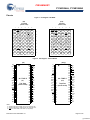
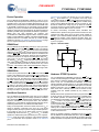
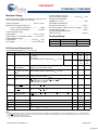
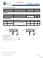
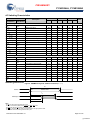
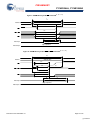
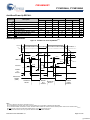
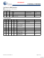
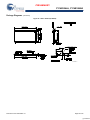
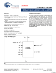
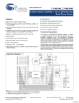
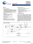
PRELIMINARY
CY14B104LA, CY14B104NA
4 Mbit (512K x 8/256K x 16) nvSRAM
Features
Functional Description
■
20 ns, 25 ns, and 45 ns access times
■
Internally organized as 512K x 8 (CY14B104LA) or 256K x 16
(CY14B104NA)
■
Hands off automatic STORE on power down with only a small
capacitor
■
STORE to QuantumTrap® nonvolatile elements initiated by
software, device pin, or AutoStore® on power down
■
RECALL to SRAM initiated by software or power up
■
Infinite Read, Write, and Recall cycles
■
200,000 STORE cycles to QuantumTrap
The Cypress CY14B104LA/CY14B104NA is a fast static RAM,
with a nonvolatile element in each memory cell. The memory is
organized as 512K bytes of 8 bits each or 256K words of 16 bits
each. The embedded nonvolatile elements incorporate
QuantumTrap technology, producing the world’s most reliable
nonvolatile memory. The SRAM provides infinite read and write
cycles, while independent nonvolatile data resides in the highly
reliable QuantumTrap cell. Data transfers from the SRAM to the
nonvolatile elements (the STORE operation) takes place
automatically at power down. On power up, data is restored to
the SRAM (the RECALL operation) from the nonvolatile memory.
Both the STORE and RECALL operations are also available
under software control.
■
20 year data retention
■
Single 3V +20%, -10% operation
■
Commercial and industrial temperatures
■
48-ball FBGA and 44/54-pin TSOP-II packages
■
Pb-free and RoHS compliance
Logic Block Diagram[1, 2, 3]
4XDWUXP7UDS
;
$
$
$
$
$
$
$
$
$
$
$
5
2
:
'
(
&
2
'
(
5
6725(
9&&
9&$3
32:(5
&21752/
5(&$//
6725(5(&$//
&21752/
67$7,&5$0
$55$<
;
62)7:$5(
'(7(&7
+6%
$$
'4
'4
'4
'4
,
1
3
8
7
%
8
)
)
(
5
6
'4
'4
'4
'4
'4
'4
'4
'4
&2/801,2
2(
&2/801'(&
:(
'4
'4
&(
'4
$ $ $ $ $ $ $ $
'4
%/(
%+(
Notes
1. Address A0 - A18 for x8 configuration and Address A0 - A17 for x16 configuration.
2. Data DQ0 - DQ7 for x8 configuration and Data DQ0 - DQ15 for x16 configuration.
3. BHE and BLE are applicable for x16 configuration only.
Cypress Semiconductor Corporation
Document #: 001-49918 Rev. *A
•
198 Champion Court
•
San Jose, CA 95134-1709
•
408-943-2600
Revised March 11, 2009
[+] Feedback
PRELIMINARY
CY14B104LA, CY14B104NA
Pinouts
Figure 1. Pin Diagram - 48 FBGA
(x8)
Top View
(not to scale)
(x16)
Top View
(not to scale)
1
2
3
4
5
6
A
BLE
OE
A0
A1
A2
NC
A
NC
B
DQ8
BHE
A3
A4
CE
DQ0
B
NC
DQ4
C
DQ9 DQ10
A5
A6
DQ1
DQ2
C
A7
DQ5
VCC
D
VSS
A17
A7
DQ3
VCC
D
2
3
4
5
6
NC
OE
A0
A1
A2
NC
NC
NC
A3
A4
CE
DQ0
NC
A5
A6
VSS
DQ1
A17
1
DQ11
VCC
DQ2
VCAP
A16
DQ6
VSS
E
VCC DQ12
VCAP
A16
DQ4
VSS
E
DQ3
NC
A14
A15
NC
DQ7
F
DQ14 DQ13
A14
A15
DQ5
DQ6
F
A12
A13
WE
NC
G
DQ15 HSB
A12
A13
WE
DQ7
G
A9
A10
A11
H
NC
A9
A10
A11
[5]
NC
H
[5]
HSB
NC
A18
A8
NC
[4]
[4]
A8
Figure 2. Pin Diagram - 44 Pin TSOP II
(x16)[6]
(x8)
NC
[5]
NC
A0
A1
A2
A3
A4
CE
DQ0
DQ1
VCC
VSS
DQ2
DQ3
WE
A5
A6
A7
A8
A9
NC
NC
1
2
3
4
5
6
7
8
9
10
11
12
13
14
15
16
17
18
19
20
21
22
44 - TSOP II
(x8)
Top View
(not to scale)
44
43
42
41
40
39
38
37
36
35
34
33
32
31
HSB
NC
[4]
NC
A18
A17
A16
A15
OE
DQ7
DQ6
VSS
VCC
DQ5
DQ4
30
29
28
27
26
25
24
23
VCAP
A14
A13
A12
A11
A10
NC
NC
A0
A1
A2
A3
A4
CE
DQ0
DQ1
DQ2
DQ3
VCC
VSS
DQ4
DQ5
DQ6
DQ7
WE
A5
A6
A7
A8
A9
1
2
3
4
5
6
7
8
9
10
11
12
13
14
15
16
17
18
19
20
21
22
44 - TSOP II
(x16)
Top View
(not to scale)
44
43
42
41
40
39
38
37
36
35
34
33
32
31
30
29
28
27
26
25
24
23
A17
A16
A15
OE
BHE
BLE
DQ15
DQ14
DQ13
DQ12
VSS
VCC
DQ11
DQ10
DQ9
DQ8
VCAP
A14
A13
A12
A11
A10
Notes
4. Address expansion for 8 Mbit. NC pin not connected to die.
5. Address expansion for 16 Mbit. NC pin not connected to die.
6. HSB pin is not available in 44-TSOP II (x16) package.
Document #: 001-49918 Rev. *A
Page 2 of 23
[+] Feedback
PRELIMINARY
CY14B104LA, CY14B104NA
Pinouts
(continued)
Figure 3. Pin Diagram - 54 Pin TSOP II (x16)
NC
[5]
NC
A0
A1
A2
A3
A4
CE
DQ0
DQ1
DQ2
DQ3
VCC
VSS
DQ4
DQ5
DQ6
DQ7
WE
A5
A6
A7
A8
A9
NC
NC
NC
1
2
3
4
5
6
7
8
9
10
11
12
13
14
15
16
17
18
19
20
21
22
23
24
25
26
27
54
53
52
51
50
49
54 - TSOP II
(x16)
Top View
(not to scale)
48
47
46
45
44
43
42
41
40
39
38
37
36
35
34
33
32
31
30
29
28
HSB
NC [4]
A17
A16
A15
OE
BHE
BLE
DQ15
DQ14
DQ13
DQ12
VSS
VCC
DQ11
DQ10
DQ9
DQ8
VCAP
A14
A13
A12
A11
A10
NC
NC
NC
Pin Definitions
Pin Name
I/O Type
A0 – A18
Input
A0 – A17
DQ0 – DQ7
Description
Address Inputs Used to Select one of the 524,288 bytes of the nvSRAM for x8 Configuration.
Address Inputs Used to Select one of the 262,144 words of the nvSRAM for x16 Configuration.
Input/Output Bidirectional Data I/O Lines for x8 Configuration. Used as input or output lines depending on
operation.
DQ0 – DQ15
Bidirectional Data I/O Lines for x16 Configuration. Used as input or output lines depending on
operation.
WE
Input
Write Enable Input, Active LOW. When selected LOW, data on the I/O pins is written to the specific
address location.
CE
Input
Chip Enable Input, Active LOW. When LOW, selects the chip. When HIGH, deselects the chip.
OE
Input
Output Enable, Active LOW. The active LOW OE input enables the data output buffers during read
cycles. I/O pins are tri-stated on deasserting OE HIGH.
BHE
Input
Byte High Enable, Active LOW. Controls DQ15 - DQ8.
BLE
Input
Byte Low Enable, Active LOW. Controls DQ7 - DQ0.
VSS
Ground
VCC
HSB
[6]
VCAP
NC
Ground for the Device. Must be connected to the ground of the system.
Power Supply Power Supply Inputs to the Device.
Input/Output Hardware Store Busy (HSB). When LOW this output indicates that a hardware store is in progress.
When pulled LOW external to the chip it initiates a nonvolatile STORE operation. A weak internal pull
up resistor keeps this pin HIGH if not connected (connection optional). After each store operation HSB
is driven HIGH for short time with standard output high current.
Power Supply AutoStore Capacitor. Supplies power to the nvSRAM during power loss to store data from SRAM to
nonvolatile elements.
No Connect
No Connect. This pin is not connected to the die.
Document #: 001-49918 Rev. *A
Page 3 of 23
[+] Feedback
PRELIMINARY
CY14B104LA, CY14B104NA
Device Operation
The CY14B104LA/CY14B104NA nvSRAM is made up of two
functional components paired in the same physical cell. They are
a SRAM memory cell and a nonvolatile QuantumTrap cell. The
SRAM memory cell operates as a standard fast static RAM. Data
in the SRAM is transferred to the nonvolatile cell (the STORE
operation), or from the nonvolatile cell to the SRAM (the RECALL
operation). Using this unique architecture, all cells are stored and
recalled in parallel. During the STORE and RECALL operations,
SRAM read and write operations are inhibited. The
CY14B104LA/CY14B104NA supports infinite reads and writes
similar to a typical SRAM. In addition, it provides infinite RECALL
operations from the nonvolatile cells and up to 200K STORE
operations. See the Truth Table For SRAM Operations on page
16 for a complete description of read and write modes.
SRAM Read
Characteristics on page 8 for the size of VCAP. The voltage on
the VCAP pin is driven to VCC by a regulator on the chip. A pull
up should be placed on WE to hold it inactive during power up.
This pull up is effective only if the WE signal is tri-state during
power up. Many MPUs tri-state their controls on power up. This
should be verified when using the pull up. When the nvSRAM
comes out of power-on-recall, the MPU must be active or the WE
held inactive until the MPU comes out of reset.
To reduce unnecessary nonvolatile stores, AutoStore and
hardware store operations are ignored unless at least one write
operation has taken place since the most recent STORE or
RECALL cycle. Software initiated STORE cycles are performed
regardless of whether a write operation has taken place. The
HSB signal is monitored by the system to detect if an AutoStore
cycle is in progress.
Figure 4. AutoStore Mode
Vcc
0.1uF
10kOhm
The CY14B104LA/CY14B104NA performs a read cycle when
CE and OE are LOW and WE and HSB are HIGH. The address
specified on pins A0-18 or A0-17 determines which of the 524,288
data bytes or 262,144 words of 16 bits each are accessed. Byte
enables (BHE, BLE) determine which bytes are enabled to the
output, in the case of 16-bit words. When the read is initiated by
an address transition, the outputs are valid after a delay of tAA
(read cycle 1). If the read is initiated by CE or OE, the outputs
are valid at tACE or at tDOE, whichever is later (read cycle 2). The
data output repeatedly responds to address changes within the
tAA access time without the need for transitions on any control
input pins. This remains valid until another address change or
until CE or OE is brought HIGH, or WE or HSB is brought LOW.
Vcc
WE
VCAP
VSS
VCAP
SRAM Write
A write cycle is performed when CE and WE are LOW and HSB
is HIGH. The address inputs must be stable before entering the
write cycle and must remain stable until CE or WE goes HIGH at
the end of the cycle. The data on the common I/O pins DQ0–15
are written into the memory if the data is valid tSD before the end
of a WE controlled write or before the end of an CE controlled
write. The Byte Enable inputs (BHE, BLE) determine which bytes
are written, in the case of 16-bit words. It is recommended that
OE be kept HIGH during the entire write cycle to avoid data bus
contention on common I/O lines. If OE is left LOW, internal
circuitry turns off the output buffers tHZWE after WE goes LOW.
AutoStore Operation
The CY14B104LA/CY14B104NA stores data to the nvSRAM
using one of the following three storage operations: Hardware
Store activated by HSB; Software Store activated by an address
sequence; AutoStore on device power down. The AutoStore
operation is a unique feature of QuantumTrap technology and is
enabled by default on the CY14B104LA/CY14B104NA.
During a normal operation, the device draws current from VCC to
charge a capacitor connected to the VCAP pin. This stored
charge is used by the chip to perform a single STORE operation.
If the voltage on the VCC pin drops below VSWITCH, the part
automatically disconnects the VCAP pin from VCC. A STORE
operation is initiated with power provided by the VCAP capacitor.
Figure 4 shows the proper connection of the storage capacitor
(VCAP) for automatic store operation. Refer to DC Electrical
Document #: 001-49918 Rev. *A
Hardware STORE Operation
The CY14B104LA/CY14B104NA provides the HSB[6] pin to
control and acknowledge the STORE operations. Use the HSB
pin to request a hardware STORE cycle. When the HSB pin is
driven LOW, the CY14B104LA/CY14B104NA conditionally
initiates a STORE operation after tDELAY. An actual STORE cycle
only begins if a write to the SRAM has taken place since the last
STORE or RECALL cycle. The HSB pin also acts as an open
drain driver that is internally driven LOW to indicate a busy
condition when the STORE (initiated by any means) is in
progress.
SRAM read and write operations that are in progress when HSB
is driven LOW by any means are given time to complete before
the STORE operation is initiated. After HSB goes LOW, the
CY14B104LA/CY14B104NA continues SRAM operations for
tDELAY. If a write is in progress when HSB is pulled LOW it is
enabled a time, tDELAY to complete. However, any SRAM write
cycles requested after HSB goes LOW are inhibited until HSB
returns HIGH. In case the write latch is not set, HSB is not driven
LOW by the CY14B104LA/CY14B104NA. But any SRAM read
and write cycles are inhibited until HSB is returned HIGH by MPU
or other external source.
During any STORE operation, regardless of how it is initiated,
the CY14B104LA/CY14B104NA continues to drive the HSB pin
LOW, releasing it only when the STORE is complete. When the
STORE operation is completed, the CY14B104LA/CY14B104NA
Page 4 of 23
[+] Feedback
PRELIMINARY
CY14B104LA, CY14B104NA
remains disabled until the HSB pin returns HIGH. Leave the HSB
unconnected if it is not used.
The software sequence may be clocked with CE controlled reads
or OE controlled reads. After the sixth address in the sequence
is entered, the STORE cycle commences and the chip is
disabled. HSB is driven LOW. It is important to use read cycles
and not write cycles in the sequence, although it is not necessary
that OE be LOW for a valid sequence. After the tSTORE cycle time
is fulfilled, the SRAM is activated again for the read and write
operation.
Hardware RECALL (Power Up)
During power up or after any low power condition
(VCC< VSWITCH), an internal RECALL request is latched. When
VCC again exceeds the sense voltage of VSWITCH, a RECALL
cycle is automatically initiated and takes tHRECALL to complete.
During this time, HSB is driven LOW by the HSB driver.
Software RECALL
Software STORE
Transfer the data from the nonvolatile memory to the SRAM with
a software address sequence. A software RECALL cycle is
initiated with a sequence of read operations in a manner similar
to the software STORE initiation. To initiate the RECALL cycle,
the following sequence of CE controlled read operations must be
performed.
1. Read Address 0x4E38 Valid READ
2. Read Address 0xB1C7 Valid READ
3. Read Address 0x83E0 Valid READ
4. Read Address 0x7C1F Valid READ
5. Read Address 0x703F Valid READ
6. Read Address 0x4C63 Initiate RECALL Cycle
Transfer data from the SRAM to the nonvolatile memory with a
software address sequence. The CY14B104LA/CY14B104NA
software STORE cycle is initiated by executing sequential CE
controlled read cycles from six specific address locations in
exact order. During the STORE cycle an erase of the previous
nonvolatile data is first performed, followed by a program of the
nonvolatile elements. After a STORE cycle is initiated, further
input and output are disabled until the cycle is completed.
Because a sequence of READs from specific addresses is used
for STORE initiation, it is important that no other read or write
accesses intervene in the sequence, or the sequence is aborted
and no STORE or RECALL takes place.
To initiate the software STORE cycle, the following read
sequence must be performed.
1. Read Address 0x4E38 Valid READ
2. Read Address 0xB1C7 Valid READ
3. Read Address 0x83E0 Valid READ
4. Read Address 0x7C1F Valid READ
5. Read Address 0x703F Valid READ
6. Read Address 0x8FC0 Initiate STORE Cycle
Internally, RECALL is a two step procedure. First, the SRAM data
is cleared; then, the nonvolatile information is transferred into the
SRAM cells. After the tRECALL cycle time, the SRAM is again
ready for read and write operations. The RECALL operation
does not alter the data in the nonvolatile elements.
Table 1. Mode Selection
CE
WE
OE, BHE, BLE[3]
A15 - A0[7]
Mode
I/O
Power
H
X
X
X
Not Selected
Output High Z
Standby
L
H
L
X
Read SRAM
Output Data
Active
L
L
X
X
Write SRAM
Input Data
Active
L
H
L
0x4E38
0xB1C7
0x83E0
0x7C1F
0x703F
0x8B45
Read SRAM
Read SRAM
Read SRAM
Read SRAM
Read SRAM
AutoStore
Disable
Output Data
Output Data
Output Data
Output Data
Output Data
Output Data
Active[8]
Notes
7. While there are 19 address lines on the CY14B104LA (18 address lines on the CY14B104NA), only the 13 address lines (A14 - A2) are used to control software modes.
Rest of the address lines are don’t care.
8. The six consecutive address locations must be in the order listed. WE must be HIGH during all six cycles to enable a nonvolatile cycle.
Document #: 001-49918 Rev. *A
Page 5 of 23
[+] Feedback
PRELIMINARY
CY14B104LA, CY14B104NA
Table 1. Mode Selection (continued)
CE
WE
OE, BHE, BLE[3]
A15 - A0[7]
Mode
I/O
Power
L
H
L
0x4E38
0xB1C7
0x83E0
0x7C1F
0x703F
0x4B46
Read SRAM
Read SRAM
Read SRAM
Read SRAM
Read SRAM
AutoStore Enable
Output Data
Output Data
Output Data
Output Data
Output Data
Output Data
Active[8]
L
H
L
0x4E38
0xB1C7
0x83E0
0x7C1F
0x703F
0x8FC0
Read SRAM
Read SRAM
Read SRAM
Read SRAM
Read SRAM
Nonvolatile Store
Output Data
Output Data
Output Data
Output Data
Output Data
Output High Z
Active ICC2[8]
L
H
L
0x4E38
0xB1C7
0x83E0
0x7C1F
0x703F
0x4C63
Read SRAM
Read SRAM
Read SRAM
Read SRAM
Read SRAM
Nonvolatile
Recall
Output Data
Output Data
Output Data
Output Data
Output Data
Output High Z
Active[8]
Preventing AutoStore
Data Protection
The AutoStore function is disabled by initiating an AutoStore
disable sequence. A sequence of read operations is performed
in a manner similar to the software STORE initiation. To initiate
the AutoStore disable sequence, the following sequence of CE
controlled read operations must be performed:
1. Read address 0x4E38 Valid READ
2. Read address 0xB1C7 Valid READ
3. Read address 0x83E0 Valid READ
4. Read address 0x7C1F Valid READ
5. Read address 0x703F Valid READ
6. Read address 0x8B45 AutoStore Disable
The CY14B104LA/CY14B104NA protects data from corruption
during low voltage conditions by inhibiting all externally initiated
STORE and write operations. The low voltage condition is
detected
when
VCC
<
VSWITCH.
If
the
CY14B104LA/CY14B104NA is in a write mode (both CE and WE
are LOW) at power up, after a RECALL or STORE, the write is
inhibited until the SRAM is enabled after tLZHSB (HSB to output
active). This protects against inadvertent writes during power up
or brown out conditions.
Noise Considerations
Refer to CY application note AN1064.
The AutoStore is re-enabled by initiating an AutoStore enable
sequence. A sequence of read operations is performed in a
manner similar to the software RECALL initiation. To initiate the
AutoStore enable sequence, the following sequence of CE
controlled read operations must be performed:
1. Read address 0x4E38 Valid READ
2. Read address 0xB1C7 Valid READ
3. Read address 0x83E0 Valid READ
4. Read address 0x7C1F Valid READ
5. Read address 0x703F Valid READ
6. Read address 0x4B46 AutoStore Enable
If the AutoStore function is disabled or re-enabled, a manual
STORE operation (hardware or software) must be issued to save
the AutoStore state through subsequent power down cycles. The
part comes from the factory with AutoStore enabled.
Document #: 001-49918 Rev. *A
Page 6 of 23
[+] Feedback
PRELIMINARY
CY14B104LA, CY14B104NA
Best Practices
■
Power up boot firmware routines should rewrite the nvSRAM
into the desired state (for example, autostore enabled). While
the nvSRAM is shipped in a preset state, best practice is to
again rewrite the nvSRAM into the desired state as a safeguard
against events that might flip the bit inadvertently such as
program bugs and incoming inspection routines.
■
The VCAP value specified in this data sheet includes a minimum
and a maximum value size. Best practice is to meet this
requirement and not exceed the maximum VCAP value because
the nvSRAM internal algorithm calculates VCAP charge and
discharge time based on this max VCAP value. Customers that
want to use a larger VCAP value to make sure there is extra
store charge and store time should discuss their VCAP size
selection with Cypress to understand any impact on the VCAP
voltage level at the end of a tRECALL period.
nvSRAM products have been used effectively for over 15 years.
While ease-of-use is one of the product’s main system values,
experience gained working with hundreds of applications has
resulted in the following suggestions as best practices:
■
The nonvolatile cells in this nvSRAM product are delivered from
Cypress with 0x00 written in all cells. Incoming inspection
routines at customer or contract manufacturer’s sites
sometimes reprogram these values. Final NV patterns are
typically repeating patterns of AA, 55, 00, FF, A5, or 5A. End
product’s firmware should not assume an NV array is in a set
programmed state. Routines that check memory content
values to determine first time system configuration, cold or
warm boot status, and so on should always program a unique
NV pattern (that is, complex 4-byte pattern of 46 E6 49 53 hex
or more random bytes) as part of the final system manufacturing test to ensure these system routines work consistently.
Document #: 001-49918 Rev. *A
Page 7 of 23
[+] Feedback
PRELIMINARY
CY14B104LA, CY14B104NA
Maximum Ratings
Transient Voltage (<20 ns) on
Any Pin to Ground Potential................ ..–2.0V to VCC + 2.0V
Exceeding maximum ratings may impair the useful life of the
device. These user guidelines are not tested.
Package Power Dissipation
Capability (TA = 25°C) ....................................................1.0W
Storage Temperature ..................................–65°C to +150°C
Surface Mount Pb Soldering
Temperature (3 Seconds)...........................................+260°C
Maximum Accumulated Storage Time
At 150°C Ambient Temperature..........................1000h
DC Output Current (1 output at a time, 1s duration) ....15 mA
At 85°C Ambient Temperature.................... ..20 Years
Static Discharge Voltage ......................................... > 2001V
(per MIL-STD-883, Method 3015)
Ambient Temperature with
Power Applied .............................................–55°C to +150°C
Latch Up Current................................................... > 200 mA
Operating Range
Supply Voltage on VCC Relative to GND.......... –0.5V to 4.1V
Voltage Applied to Outputs
in High-Z State ...................................... –0.5V to VCC + 0.5V
Range
Ambient Temperature
VCC
0°C to +70°C
2.7V to 3.6V
–40°C to +85°C
2.7V to 3.6V
Commercial
Input Voltage .......................................... –0.5V to Vcc + 0.5V
Industrial
DC Electrical Characteristics
Over the Operating Range (VCC = 2.7V to 3.6V)
Parameter
Description
ICC1
Average VCC Current
Test Conditions
Min
Max
Unit
tRC = 20 ns
Commercial
tRC = 25 ns
tRC = 45 ns
Values obtained without output loads (IOUT = 0 mA) Industrial
65
65
50
mA
mA
mA
70
70
52
mA
mA
mA
All Inputs Don’t Care, VCC = Max
Average current for duration tSTORE
10
mA
ICC2
Average VCC Current
during STORE
ICC3[9]
Average VCC Current at All I/P cycling at CMOS levels.
tRC= 200 ns, 3V, 25°C Values obtained without output loads (IOUT = 0 mA).
typical
35
mA
ICC4
Average VCAP Current All Inputs Don’t Care, VCC = Max
during AutoStore Cycle Average current for duration tSTORE
5
mA
ISB
VCC Standby Current
5
mA
IIX[10]
Input Leakage Current VCC = Max, VSS < VIN < VCC
(except HSB)
–1
+1
μA
Input Leakage Current VCC = Max, VSS < VIN < VCC
(for HSB)
–100
+1
μA
–1
+1
μA
2.0
VCC +
0.5
V
Vss – 0.5
0.8
IOZ
Off-State Output
Leakage Current
VIH
Input HIGH Voltage
CE > (VCC – 0.2V). All others VIN < 0.2V or > (VCC – 0.2V). Standby
current level after nonvolatile cycle is complete.
Inputs are static. f = 0 MHz.
VCC = Max, VSS < VOUT < VCC, CE or OE > VIH or BHE/BLE > VIH
or WE < VIL
VIL
Input LOW Voltage
VOH
Output HIGH Voltage
VOL
Output LOW Voltage
IOUT = 4 mA
VCAP[11]
Storage Capacitor
Between VCAP pin and VSS, 5V Rated
IOUT = –2 mA
2.4
61
V
V
0.4
V
180
μF
Notes
9. Typical conditions for the active current shown on the DC Electrical characteristics are average values at 25°C (room temperature), and VCC = 3V. Not 100% tested.
10. The HSB pin has IOUT = -2 uA for VOH of 2.4V when both active HIGH and LOW drivers are disabled. When they are enabled standard VOH and VOL are valid. This
parameter is characterized but not tested.
11. VCAP (storage capacitor) nominal value is 68 uF.
Document #: 001-49918 Rev. *A
Page 8 of 23
[+] Feedback
PRELIMINARY
CY14B104LA, CY14B104NA
Data Retention and Endurance
Parameter
Description
Min
Unit
DATAR
Data Retention
20
Years
NVC
Nonvolatile STORE Operation
200
K
Capacitance
In the following table, the capacitance parameters are listed.[12]
Parameter
Description
CIN
Input Capacitance
COUT
Output Capacitance
Test Conditions
TA = 25°C, f = 1 MHz,
VCC = 0 to 3.0V
Max
Unit
7
pF
7
pF
Thermal Resistance
In the following table, the thermal resistance parameters are listed. [12]
Parameter
ΘJA
ΘJC
Description
Thermal Resistance
(Junction to Ambient)
Thermal Resistance
(Junction to Case)
Test Conditions
48-FBGA
Test conditions follow standard test methods
and procedures for measuring thermal
impedance, in accordance with EIA/JESD51.
28.82
44-TSOP II 54-TSOP II
31.11
30.73
°C/W
Unit
7.84
5.56
6.08
°C/W
Figure 5. AC Test Loads
577Ω
577Ω
3.0V
3.0V
R1
for tri-state specs
R1
OUTPUT
OUTPUT
30 pF
R2
789Ω
5 pF
R2
789Ω
AC Test Conditions
Input Pulse Levels ....................................................0V to 3V
Input Rise and Fall Times (10% - 90%) ........................ <3 ns
Input and Output Timing Reference Levels .................... 1.5V
Note
12. These parameters are guaranteed but not tested.
Document #: 001-49918 Rev. *A
Page 9 of 23
[+] Feedback
PRELIMINARY
CY14B104LA, CY14B104NA
AC Switching Characteristics
Parameters
Cypress
Parameters
20 ns
Description
Alt
Parameters
Min
25 ns
Max
Min
45 ns
Max
Min
Max
Unit
SRAM Read Cycle
tACE
tACS
Chip Enable Access Time
tRC[13]
tRC
Read Cycle Time
tAA[14]
tAA
Address Access Time
20
25
45
ns
tDOE
tOE
Output Enable to Data Valid
10
12
20
ns
[14]
tOH
Output Hold After Address Change
3
3
3
ns
tLZCE[12, 15]
tLZ
Chip Enable to Output Active
3
3
3
ns
[12, 15]
tOHA
20
20
25
25
tHZ
Chip Disable to Output Inactive
tOLZ
Output Enable to Output Active
tHZOE[12, 15]
tOHZ
Output Disable to Output Inactive
tPU[12]
tPA
Chip Enable to Power Active
[12]
tPS
Chip Disable to Power Standby
20
25
45
ns
-
Byte Enable to Data Valid
10
12
20
ns
[12]
-
Byte Enable to Output Active
tHZBE[12]
-
Byte Disable to Output Inactive
tPD
tDBE
tLZBE
0
10
ns
ns
tLZOE[12, 15]
tHZCE
8
45
45
0
8
0
10
0
0
15
0
15
0
0
8
ns
ns
0
10
ns
ns
ns
15
ns
SRAM Write Cycle
tWC
tWC
Write Cycle Time
20
25
45
ns
tPWE
tWP
Write Pulse Width
15
20
30
ns
tSCE
tCW
Chip Enable To End of Write
15
20
30
ns
tSD
tDW
Data Setup to End of Write
8
10
15
ns
tHD
tDH
Data Hold After End of Write
0
0
0
ns
tAW
tAW
Address Setup to End of Write
15
20
30
ns
tSA
tAS
Address Setup to Start of Write
0
0
0
ns
tHA
tWR
Address Hold After End of Write
0
tHZWE[12, 15,16]
tWZ
Write Enable to Output Disable
tOW
Output Active after End of Write
3
3
3
ns
-
Byte Enable to End of Write
15
20
30
ns
tLZWE
tBW
[12, 15]
Switching Waveforms
0
8
0
10
ns
15
ns
Figure 6. SRAM Read Cycle #1: Address Controlled[13, 14, 17]
tRC
Address
Address Valid
tAA
Data Output
Previous Data Valid
Output Data Valid
tOHA
Notes
13. WE must be HIGH during SRAM read cycles.
14. Device is continuously selected with CE, OE and BHE / BLE LOW.
15. Measured ±200 mV from steady state output voltage.
16. If WE is LOW when CE goes LOW, the outputs remain in the high impedance state.
17. HSB must remain HIGH during read and write cycles.
Document #: 001-49918 Rev. *A
Page 10 of 23
[+] Feedback
PRELIMINARY
CY14B104LA, CY14B104NA
Figure 7. SRAM Read Cycle #2: CE and OE Controlled[3, 13, 17]
Address
Address Valid
tRC
tHZCE
tACE
CE
tAA
tLZCE
tHZOE
tDOE
OE
tHZBE
tLZOE
tDBE
BHE, BLE
tLZBE
Data Output
High Impedance
ICC
Output Data Valid
tPU
tPD
Active
Standby
Figure 8. SRAM Write Cycle #1: WE Controlled[3, 16, 17, 18]
tWC
Address
Address Valid
tSCE
tHA
CE
tBW
BHE, BLE
tAW
tPWE
WE
tSA
tSD
Data Input
Input Data Valid
tHZWE
Data Output
tHD
Previous Data
tLZWE
High Impedance
Note
18. CE or WE must be >VIH during address transitions.
Document #: 001-49918 Rev. *A
Page 11 of 23
[+] Feedback
PRELIMINARY
CY14B104LA, CY14B104NA
Figure 9. SRAM Write Cycle #2: CE Controlled[3, 16, 17, 18]
tWC
Address Valid
Address
tSA
tSCE
tHA
CE
tBW
BHE, BLE
tPWE
WE
tHD
tSD
Input Data Valid
Data Input
High Impedance
Data Output
Figure 10. SRAM Write Cycle #3: BHE and BLE Controlled[3, 16, 17, 18]
tWC
Address
Address Valid
tSCE
CE
tSA
tHA
tBW
BHE, BLE
tAW
tPWE
WE
tSD
Data Input
tHD
Input Data Valid
High Impedance
Data Output
Document #: 001-49918 Rev. *A
Page 12 of 23
[+] Feedback
PRELIMINARY
CY14B104LA, CY14B104NA
AutoStore/Power Up RECALL
20 ns
Parameters
Description
tHRECALL [19]
tSTORE [20]
tDELAY [21]
VSWITCH
tVCCRISE
VHDIS[12]
tLZHSB
tHHHD
Power Up RECALL Duration
STORE Cycle Duration
Time Allowed to Complete SRAM Cycle
Low Voltage Trigger Level
VCC Rise Time
HSB Output Driver Disable Voltage
HSB To Output Active Time
HSB High Active Time
Switching Waveforms
Min
25 ns
Max
20
8
20
2.65
150
Min
45 ns
Max
20
8
25
2.65
150
Min
Max
20
8
25
2.65
150
1.9
5
500
1.9
5
500
1.9
5
500
Unit
ms
ms
ns
V
μs
V
μs
ns
Figure 11. AutoStore or Power Up RECALL[22]
VSWITCH
VHDIS
VVCCRISE
Note20
Note20
tSTORE
tHHHD
Note23
tHHHD
HSB OUT
tSTORE
tDELAY
tLZHSB
Autostore
tLZHSB
tDELAY
POWERUP
RECALL
Read & Write
Inhibited
(RWI)
tHRECALL
POWER-UP
RECALL
Read & Write
tHRECALL
BROWN
OUT
Autostore
POWER-UP
RECALL
Read & Write
POWER
DOWN
Autostore
Notes
19. tHRECALL starts from the time VCC rises above VSWITCH.
20. If an SRAM write has not taken place since the last nonvolatile cycle, no AutoStore or Hardware Store takes place.
21. On a Hardware STORE, Software Store / Recall, AutoStore Enable / Disable and AutoStore initiation, SRAM operation continues to be enabled for time tDELAY.
22. Read and write cycles are ignored during STORE, RECALL, and while VCC is below VSWITCH.
23. HSB pin is driven HIGH to VCC only by internal 100 kOhm resistor, HSB driver is disabled.
Document #: 001-49918 Rev. *A
Page 13 of 23
[+] Feedback
PRELIMINARY
CY14B104LA, CY14B104NA
Software Controlled STORE/RECALL Cycle
In the following table, the software controlled STORE and RECALL cycle parameters are listed.[24, 25]
Parameters
tRC
tSA
tCW
tHA
tRECALL
20 ns
Min
Max
20
0
15
0
200
Description
STORE/RECALL Initiation Cycle Time
Address Setup Time
Clock Pulse Width
Address Hold Time
RECALL Duration
25 ns
Min
Max
25
0
20
0
200
45 ns
Min
Max
45
0
30
0
200
Unit
ns
ns
ns
ns
μs
Switching Waveforms
Figure 12. CE and OE Controlled Software STORE/RECALL Cycle[25]
W5&
$GGUHVV
W5&
$GGUHVV
W6$
$GGUHVV
W&:
W&:
&(
W+$
W6$
W+$
W+$
W+$
2(
W+++'
+6%6725(RQO\
W+=&(
W/=&(
W'(/$<
W/=+6%
+LJK,PSHGDQFH
W6725(W5(&$//
'4'$7$
5:,
Figure 13. AutoStore Enable/Disable Cycle
$GGUHVV
W6$
&(
W5&
W5&
$GGUHVV
$GGUHVV
W&:
W&:
W+$
W6$
W+$
W+$
W+$
2(
W/=&(
W+=&(
W66
W'(/$<
'4'$7$
5:,
Notes
24. The software sequence is clocked with CE controlled or OE controlled reads.
25. The six consecutive addresses must be read in the order listed in Table 1 on page 5. WE must be HIGH during all six consecutive cycles.
Document #: 001-49918 Rev. *A
Page 14 of 23
[+] Feedback
PRELIMINARY
CY14B104LA, CY14B104NA
Hardware STORE Cycle
Parameters
20 ns
Description
Min
tDHSB
HSB To Output Active Time when write latch not set
tPHSB
Hardware STORE Pulse Width
tSS [26, 27]
Soft Sequence Processing Time
Switching Waveforms
25 ns
Max
Min
45 ns
Max
20
Min
25
15
15
Max
25
ns
100
μs
15
100
100
Unit
ns
Figure 14. Hardware STORE Cycle[20]
Write latch set
tPHSB
HSB (IN)
tSTORE
tHHHD
tDELAY
HSB (OUT)
tLZHSB
DQ (Data Out)
RWI
Write latch not set
tPHSB
HSB pin is driven high to VCC only by Internal
100kOhm resistor,
HSB driver is disabled
SRAM is disabled as long as HSB (IN) is driven low.
HSB (IN)
tDELAY
HSB (OUT)
tDHSB
tDHSB
RWI
Figure 15. Soft Sequence Processing[26, 27]
Soft Sequence
Command
Address
Address #1
tSA
Address #6
tCW
tSS
Soft Sequence
Command
Address #1
tSS
Address #6
tCW
CE
VCC
Notes
26. This is the amount of time it takes to take action on a soft sequence command. Vcc power must remain HIGH to effectively register command.
27. Commands such as STORE and RECALL lock out I/O until operation is complete which further increases this time. See the specific command.
Document #: 001-49918 Rev. *A
Page 15 of 23
[+] Feedback
PRELIMINARY
CY14B104LA, CY14B104NA
Truth Table For SRAM Operations
HSB should remain HIGH for SRAM Operations.
For x8 Configuration
Inputs/Outputs[2]
CE
WE
OE
H
X
X
High Z
Deselect/Power down
Mode
Standby
Power
L
H
L
Data Out (DQ0–DQ7);
Read
Active
L
H
H
High Z
Output Disabled
Active
L
L
X
Data in (DQ0–DQ7);
Write
Active
For x16 Configuration
CE
WE
OE
BHE[3]
BLE[3]
H
X
X
X
X
L
X
X
H
L
H
L
L
L
H
L
L
H
L
L
H
L
H
L
Inputs/Outputs[2]
Mode
Power
High-Z
Deselect/Power down
Standby
H
High-Z
Output Disabled
Active
L
Data Out (DQ0–DQ15)
Read
Active
H
L
Data Out (DQ0–DQ7);
DQ8–DQ15 in High-Z
Read
Active
L
H
Data Out (DQ8–DQ15);
DQ0–DQ7 in High-Z
Read
Active
H
L
L
High-Z
Output Disabled
Active
H
H
L
High-Z
Output Disabled
Active
H
H
L
H
High-Z
Output Disabled
Active
L
L
X
L
L
Data In (DQ0–DQ15)
Write
Active
L
L
X
H
L
Data In (DQ0–DQ7);
DQ8–DQ15 in High-Z
Write
Active
L
L
X
L
H
Data In (DQ8–DQ15);
DQ0–DQ7 in High-Z
Write
Active
Document #: 001-49918 Rev. *A
Page 16 of 23
[+] Feedback
PRELIMINARY
CY14B104LA, CY14B104NA
Ordering Information
Speed
(ns)
20
25
Ordering Code
Package
Diagram
Package Type
CY14B104LA-ZS20XCT
51-85087
44-pin TSOP II
CY14B104LA-ZS20XC
51-85087
44-pin TSOP II
CY14B104LA-ZS20XIT
51-85087
44-pin TSOP II
CY14B104LA-ZS20XI
51-85087
44-pin TSOP II
CY14B104LA-BA20XCT
51-85128
48-ball FBGA
CY14B104LA-BA20XC
51-85128
48-ball FBGA
CY14B104LA-BA20XIT
51-85128
48-ball FBGA
CY14B104LA-BA20XI
51-85128
48-ball FBGA
CY14B104NA-ZS20XCT
51-85087
44-pin TSOP II
CY14B104NA-ZS20XC
51-85087
44-pin TSOP II
CY14B104NA-ZS20XIT
51-85087
44-pin TSOP II
CY14B104NA-ZS20XI
51-85087
44-pin TSOP II
CY14B104NA-BA20XCT
51-85128
48-ball FBGA
CY14B104NA-BA20XC
51-85128
48-ball FBGA
CY14B104NA-BA20XIT
51-85128
48-ball FBGA
CY14B104NA-BA20XI
51-85128
48-ball FBGA
CY14B104NA-ZSP20XCT
51-85160
54-pin TSOP II
CY14B104NA-ZSP20XC
51-85160
54-pin TSOP II
CY14B104NA-ZSP20XIT
51-85160
54-pin TSOP II
CY14B104NA-ZSP20XI
51-85160
54-pin TSOP II
CY14B104LA-ZS25XCT
51-85087
44-pin TSOP II
CY14B104LA-ZS25XC
51-85087
44-pin TSOP II
CY14B104LA-ZS25XIT
51-85087
44-pin TSOP II
CY14B104LA-ZS25XI
51-85087
44-pin TSOP II
CY14B104LA-BA25XCT
51-85128
48-ball FBGA
CY14B104LA-BA25XC
51-85128
48-ball FBGA
CY14B104LA-BA25XIT
51-85128
48-ball FBGA
CY14B104LA-BA25XI
51-85128
48-ball FBGA
CY14B104NA-ZS25XCT
51-85087
44-pin TSOP II
CY14B104NA-ZS25XC
51-85087
44-pin TSOP II
CY14B104NA-ZS25XIT
51-85087
44-pin TSOP II
CY14B104NA-ZS25XI
51-85087
44-pin TSOP II
CY14B104NA-BA25XCT
51-85128
48-ball FBGA
CY14B104NA-BA25XC
51-85128
48-ball FBGA
CY14B104NA-BA25XIT
51-85128
48-ball FBGA
CY14B104NA-BA25XI
51-85128
48-ball FBGA
CY14B104NA-BA25I
51-85128
48-ball FBGA
CY14B104NA-ZSP25XCT
51-85160
54-pin TSOP II
CY14B104NA-ZSP25XC
51-85160
54-pin TSOP II
CY14B104NA-ZSP25XIT
51-85160
54-pin TSOP II
CY14B104NA-ZSP25XI
51-85160
54-pin TSOP II
Document #: 001-49918 Rev. *A
Operating
Range
Commercial
Industrial
Commercial
Industrial
Commercial
Industrial
Commercial
Industrial
Commercial
Industrial
Commercial
Industrial
Commercial
Industrial
Commercial
Industrial
Commercial
Industrial
Commercial
Industrial
Page 17 of 23
[+] Feedback
PRELIMINARY
CY14B104LA, CY14B104NA
Ordering Information (continued)
Speed
(ns)
45
Ordering Code
Package
Diagram
Package Type
CY14B104LA-ZS45XCT
51-85087
44-pin TSOP II
CY14B104LA-ZS45XC
51-85087
44-pin TSOP II
CY14B104LA-ZS45XIT
51-85087
44-pin TSOP II
CY14B104LA-ZS45XI
51-85087
44-pin TSOP II
CY14B104LA-BA45XCT
51-85128
48-ball FBGA
CY14B104LA-BA45XC
51-85128
48-ball FBGA
CY14B104LA-BA45XIT
51-85128
48-ball FBGA
CY14B104LA-BA45XI
51-85128
48-ball FBGA
CY14B104NA-ZS45XCT
51-85087
44-pin TSOP II
CY14B104NA-ZS45XC
51-85087
44-pin TSOP II
CY14B104NA-ZS45XIT
51-85087
44-pin TSOP II
CY14B104NA-ZS45XI
51-85087
44-pin TSOP II
CY14B104NA-BA45XCT
51-85128
48-ball FBGA
CY14B104NA-BA45XC
51-85128
48-ball FBGA
CY14B104NA-BA45XIT
51-85128
48-ball FBGA
CY14B104NA-BA45XI
51-85128
48-ball FBGA
CY14B104NA-ZSP45XCT
51-85160
54-pin TSOP II
CY14B104NA-ZSP45XC
51-85160
54-pin TSOP II
CY14B104NA-ZSP45XIT
51-85160
54-pin TSOP II
CY14B104NA-ZSP45XI
51-85160
54-pin TSOP II
Operating
Range
Commercial
Industrial
Commercial
Industrial
Commercial
Industrial
Commercial
Industrial
Commercial
Industrial
The above table contains Preliminary information. Contact your local Cypress sales representative for availability of these parts.
Document #: 001-49918 Rev. *A
Page 18 of 23
[+] Feedback
PRELIMINARY
CY14B104LA, CY14B104NA
Part Numbering Nomenclature
CY 14 B 104 L A -ZS P 20 X C T
Option:
T - Tape & Reel
Blank - Std.
Temperature:
C - Commercial (0 to 70°C)
I - Industrial (–40 to 85°C)
X - Pb-Free
Blank - SnPb
P - 54 Pin
Blank - 44 Pin/48 Ball
Speed:
20 - 20 ns
25 - 25 ns
45 - 45 ns
Package:
BA - 48 FBGA
ZS - TSOP II
Die Revision:
Blank - No Rev
A - 1st Rev
Voltage:
B - 3.0V
Data Bus:
L - x8
N - x16
Density:
104 - 4 Mb
NVSRAM
14 - Auto Store + Software Store + Hardware Store
Cypress
Document #: 001-49918 Rev. *A
Page 19 of 23
[+] Feedback
PRELIMINARY
CY14B104LA, CY14B104NA
Package Diagrams
Figure 16. 44-Pin TSOP II (51-85087)
DIMENSION IN MM (INCH)
MAX
MIN.
PIN 1 I.D.
1
23
10.262 (0.404)
10.058 (0.396)
11.938 (0.470)
11.735 (0.462)
22
EJECTOR PIN
44
TOP VIEW
0.800 BSC
(0.0315)
OR E
K X A
SG
BOTTOM VIEW
0.400(0.016)
0.300 (0.012)
10.262 (0.404)
10.058 (0.396)
BASE PLANE
0.210 (0.0083)
0.120 (0.0047)
0°-5°
0.10 (.004)
Document #: 001-49918 Rev. *A
0.150 (0.0059)
0.050 (0.0020)
1.194 (0.047)
0.991 (0.039)
18.517 (0.729)
18.313 (0.721)
SEATING
PLANE
0.597 (0.0235)
0.406 (0.0160)
51-85087-*A
Page 20 of 23
[+] Feedback
PRELIMINARY
CY14B104LA, CY14B104NA
Package Diagrams
(continued)
Figure 17. 48-Ball FBGA - 6 mm x 10 mm x 1.2 mm (51-85128)
BOTTOM VIEW
TOP VIEW
A1 CORNER
Ø0.05 M C
Ø0.25 M C A B
A1 CORNER
Ø0.30±0.05(48X)
2
3
4
5
6
6
5
4
3
2
1
C
C
E
F
G
D
E
2.625
D
0.75
A
B
5.25
A
B
10.00±0.10
10.00±0.10
1
F
G
H
H
1.875
A
A
B
0.75
6.00±0.10
0.53±0.05
B
0.15 C
0.21±0.05
0.25 C
3.75
6.00±0.10
0.15(4X)
Document #: 001-49918 Rev. *A
1.20 MAX
0.36
SEATING PLANE
C
51-85128-*D
Page 21 of 23
[+] Feedback
PRELIMINARY
CY14B104LA, CY14B104NA
Package Diagrams
(continued)
Figure 18. 54-Pin TSOP II (51-85160)
51-85160-**
Document #: 001-49918 Rev. *A
Page 22 of 23
[+] Feedback
PRELIMINARY
CY14B104LA, CY14B104NA
Document History Page
Document Title: CY14B104LA/CY14B104NA 4 Mbit (512K x 8/256K x 16) nvSRAM
Document Number: 001-49918
Submission
Date
Rev.
ECN No.
Orig. of Change
Description of Change
**
2606696
GVCH/PYRS
11/13/08
New Data Sheet
*A
2672700
GVCH/PYRS
03/12/09
Added best practices
Added CY14B104NA-BA25I part number
Added footnote12 for HZ/LZ parameters
Sales, Solutions, and Legal Information
Worldwide Sales and Design Support
Cypress maintains a worldwide network of offices, solution centers, manufacturer’s representatives, and distributors. To find the office
closest to you, visit us at cypress.com/sales.
Products
PSoC
Clocks & Buffers
PSoC Solutions
psoc.cypress.com
clocks.cypress.com
General
Low Power/Low Voltage
psoc.cypress.com/solutions
psoc.cypress.com/low-power
Wireless
wireless.cypress.com
Precision Analog
Memories
memory.cypress.com
LCD Drive
psoc.cypress.com/lcd-drive
image.cypress.com
CAN 2.0b
psoc.cypress.com/can
USB
psoc.cypress.com/usb
Image Sensors
psoc.cypress.com/precision-analog
© Cypress Semiconductor Corporation, 2008-2009. The information contained herein is subject to change without notice. Cypress Semiconductor Corporation assumes no responsibility for the use of
any circuitry other than circuitry embodied in a Cypress product. Nor does it convey or imply any license under patent or other rights. Cypress products are not warranted nor intended to be used for
medical, life support, life saving, critical control or safety applications, unless pursuant to an express written agreement with Cypress. Furthermore, Cypress does not authorize its products for use as
critical components in life-support systems where a malfunction or failure may reasonably be expected to result in significant injury to the user. The inclusion of Cypress products in life-support systems
application implies that the manufacturer assumes all risk of such use and in doing so indemnifies Cypress against all charges.
Any Source Code (software and/or firmware) is owned by Cypress Semiconductor Corporation (Cypress) and is protected by and subject to worldwide patent protection (United States and foreign),
United States copyright laws and international treaty provisions. Cypress hereby grants to licensee a personal, non-exclusive, non-transferable license to copy, use, modify, create derivative works of,
and compile the Cypress Source Code and derivative works for the sole purpose of creating custom software and or firmware in support of licensee product to be used only in conjunction with a Cypress
integrated circuit as specified in the applicable agreement. Any reproduction, modification, translation, compilation, or representation of this Source Code except as specified above is prohibited without
the express written permission of Cypress.
Disclaimer: CYPRESS MAKES NO WARRANTY OF ANY KIND, EXPRESS OR IMPLIED, WITH REGARD TO THIS MATERIAL, INCLUDING, BUT NOT LIMITED TO, THE IMPLIED WARRANTIES
OF MERCHANTABILITY AND FITNESS FOR A PARTICULAR PURPOSE. Cypress reserves the right to make changes without further notice to the materials described herein. Cypress does not
assume any liability arising out of the application or use of any product or circuit described herein. Cypress does not authorize its products for use as critical components in life-support systems where
a malfunction or failure may reasonably be expected to result in significant injury to the user. The inclusion of Cypress’ product in a life-support systems application implies that the manufacturer
assumes all risk of such use and in doing so indemnifies Cypress against all charges.
Use may be limited by and subject to the applicable Cypress software license agreement.
Document #: 001-49918 Rev. *A
Revised March 11, 2009
Page 23 of 23
AutoStore and QuantumTrap are registered trademarks of Cypress Semiconductors. All other products and company names mentioned in this document are the trademarks of their respective holders.
[+] Feedback