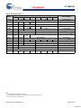
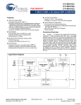
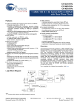
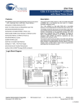
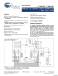
1
PRELIMINARY
CY14B101P
1 Mbit (128K x 8) Serial SPI nvSRAM
with Real Time Clock
Features
■
■
1 Mbit NonVolatile SRAM
❐ Internally organized as 128K x 8
®
❐ STORE to QuantumTrap nonvolatile elements initiated
automatically on power down (AutoStore®) or by user using
HSB pin (Hardware Store) or SPI instruction (Software Store)
®
❐ RECALL to SRAM initiated on power up (Power Up Recall )
or by SPI Instruction (Software Recall)
❐ Automatic STORE on power down with a small capacitor
■
Write Protection
❐ Hardware Protection using Write Protect (WP) Pin
❐ Software Protection using Write Disable Instruction
❐ Software Block Protection for 1/4, 1/2, or entire Array
■
Low Power Consumption
❐ Single 3V +20%, –10% operation
❐ Average Vcc current of 10 mA at 40 MHz operation
■
Industry Standard Configurations
❐ Commercial and industrial temperatures
❐ 16-pin SOIC Package
❐ RoHS compliant
High Reliability
❐
❐
❐
Infinite Read, Write, and RECALL cycles
200,000 STORE cycles to QuantumTrap
Data Retention: 20 Years
■
Real Time Clock
❐ Full featured Real Time Clock
❐ Watchdog timer
❐ Clock alarm with programmable interrupts
❐ Capacitor or battery backup for RTC
❐ Backup current of 300 nA
■
High Speed Serial Peripheral Interface (SPI)
❐ 40 MHz Clock rate - RTC Read at 25 MHz
❐ Supports SPI Modes 0 (0,0) and 3 (1,1)
Overview
The Cypress CY14B101P combines a 1 Mbit nonvolatile static
RAM with full featured real time clock in a monolithic integrated
circuit with serial SPI interface. The memory is organized as
128K words of 8 bits each. The embedded nonvolatile elements
incorporate the QuantumTrap technology, creating the world’s
most reliable nonvolatile memory. The SRAM provides infinite
read and write cycles, while the QuantumTrap cells provide
highly reliable nonvolatile storage of data. Data transfers from
SRAM to the nonvolatile elements (STORE operation) takes
place automatically at power down. On power up, data is
restored to the SRAM from the nonvolatile memory (RECALL
operation). The STORE and RECALL operations can also be
initiated by the user.
VCC
Logic Block Diagram
CS
WP
SCK
Quantum Trap
128K X 8
Instruction decode
Write protect
Control logic
Instruction
register
SI
STORE/RECALL
Control
RECALL
128K X 8
Address
Decoder
Power Control
STORE
SRAM ARRAY
HOLD
VCAP
HSB
D0-D7
A0-A16
Xout
Xin
INT
RTC
Data I/O register
MUX
SO
Status register
Cypress Semiconductor Corporation
Document #: 001-44109 Rev. *B
•
198 Champion Court
•
San Jose, CA 95134-1709
•
408-943-2600
Revised February 2, 2009
[+] Feedback
CY14B101P
PRELIMINARY
Pinouts
Figure 1. Pin Diagram - 16-Pin SOIC
NC
1
16
VCC
VRTCbat
2
15
INT
Xout
3
14
VCAP
13
SO
12
SI
Top View
Xin
4
WP
5
HOLD
6
11
SCK
7
10
CS
8
9
HSB
VRTCcap
GND
not to scale
Table 1. Pin Definitions
Pin Name
I/O Type
Description
CS
Input
Chip Select. Activates the device when pulled LOW. Driving this pin HIGH puts the device in low
power standby mode.
SCK
Input
Serial Clock. Runs at speeds up to a maximum of 25 MHz. All inputs are latched at the rising edge
of this clock. Outputs are driven at the falling edge of the clock.
Serial Input. Pin for input of all SPI instructions and data.
SI
Input
SO
Output
WP
Input
Write Protect. Implements hardware write protection in SPI.
HOLD
Input
HOLD Pin. Suspends Serial Operation.
HSB
Input/Output
Hardware Store Busy: A weak internal pull up keeps this pin pulled HIGH. If not used, this pin is
left as No Connect.
Output: Indicates busy status of nvSRAM when LOW.
Input: Hardware Store implemented by pulling this pin LOW externally.
VCAP
Power Supply
AutoStore Capacitor. Supplies power to the nvSRAM during power loss to STORE data from the
SRAM to nonvolatile elements. If AutoStore is not needed, this pin must be left as No Connect. It
must never be connected to GND.
VRTCcap
Power Supply
Capacitor Backup for RTC. Left unconnected if VRTCbat is used.
VRTCbat
Power Supply
Battery Backup for RTC. Left unconnected if VRTCcap is used.
Xout
Output
Xin
Input
INT
Output
NC
No Connect
Serial Output. Pin for output of data through SPI.
Crystal Output connection. Drives crystal on start up.
Crystal Input connection. For 32.768 kHz crystal.
Interrupt Output. Programmable to respond to the clock alarm, the watchdog timer, and the power
monitor. Also programmable to either active HIGH (push or pull) or LOW (open drain).
No Connect. This pin is not connected to the die.
GND
Power Supply
Ground
VCC
Power Supply
Power Supply (2.7-3.6V)
Document #: 001-44109 Rev. *B
Page 2 of 32
[+] Feedback
PRELIMINARY
Device Operation
CY14B101P is a 1-Mbit nvSRAM memory with integrated RTC
and SPI interface. All the reads and writes to nvSRAM happen
to the SRAM which gives nvSRAM the unique capability to
handle infinite writes to the memory. The data in SRAM is
secured by a STORE sequence that transfers the data in parallel
to the nonvolatile Quantum Trap cells. A small capacitor (VCAP)
is used to AutoStore the SRAM data in nonvolatile cells when
power goes down providing power down data security. The
Quantum Trap nonvolatile elements built in the reliable SONOS
technology make nvSRAM the ideal choice for secure data
storage.
In CY14B101P, the 1-Mbit memory array is organized as
128K words x 8 bits. The memory is accessed through a
standard SPI interface that enables very high clock speeds upto
40 MHz with zero delay read and write cycles. CY14B101P
supports SPI modes 0 and 3 (CPOL, CPHA = 0, 0 & 1, 1) and
operates as SPI slave. The device is enabled using the Chip
Select pin (CS) and accessed through Serial Input (SI), Serial
Output (SO), and Serial Clock (SCK) pins.
CY14B101P provides the feature for hardware and software
write protection through WP pin and WRDI instruction.
CY14B101P also provides mechanisms for block write
protection (1/4, 1/2, or full array) using BP0 and BP1 pins in the
status register. Further, the HOLD pin is used to suspend any
serial communication without resetting the serial sequence.
CY14B101P uses the standard SPI opcodes for memory access.
In addition to the general SPI instructions for read and write,
CY14B101P provides four special instructions that allow access
to four nvSRAM specific functions: STORE, RECALL, AutoStore
Disable (ASDISB), and AutoStore Enable (ASENB).
The major benefit of nvSRAM SPI over serial EEPROMs is that
all reads and writes to nvSRAM are performed at the speed of
SPI bus with zero cycle delay. Therefore, no wait time is required
after any of the memory accesses. The STORE and RECALL
operations need finite time to complete and all memory accesses
are inhibited during this time. While a STORE or RECALL
operation is in progress, the busy status of the device is indicated
by the Hardware Store Busy (HSB) pin and also reflected on the
RDY bit of the Status Register.
SRAM Write
All writes to nvSRAM are carried out on the SRAM and do not
use up any endurance cycles of the nonvolatile memory. This
enables user to perform infinite write operations. A write cycle is
performed through the SPI WRITE instruction. The WRITE
instruction is issued through the SI pin of the nvSRAM and
consists of the WRITE opcode, 3 bytes of address and 1 byte of
data. Writes to nvSRAM is done at SPI bus speed with zero cycle
delay.
CY14B101P allows burst mode writes to be performed through
SPI. This enables write operations on consecutive addresses
without issuing a new WRITE instruction. When the last address
in memory is reached in burst mode, the address rolls over to
0x0000 and the device continues to write.
The SPI write cycle sequence is defined in the Memory Access
section of SPI Protocol Description.
Document #: 001-44109 Rev. *B
CY14B101P
SRAM Read
A read cycle in CY14B101P is performed at the SPI bus speed
and the data is read out with zero cycle delay after the READ
instruction is performed. The READ instruction is issued through
the SI pin of the nvSRAM and consists of the READ opcode and
3 bytes of address. The data is read out on the SO pin.
CY14B101P allows burst mode reads to be performed through
SPI. This enables reads on consecutive addresses without
issuing a new READ instruction. When the last address in
memory is reached in burst mode read, the address rolls over to
0x0000 and the device continues to read.
The SPI read cycle sequence is defined in the Memory Access
section of SPI Protocol Description
STORE Operation
STORE operation transfers the data from the SRAM to the
nonvolatile Quantum Trap cells. The CY14B101P STOREs data
to the nonvolatile cells using one of the three STORE operations:
AutoStore, activated on device power down; Software Store,
activated by a STORE instruction in the SPI; and Hardware
Store, activated by the HSB. During the STORE cycle, an erase
of the previous nonvolatile data is first performed, followed by a
program of the nonvolatile elements. After a STORE cycle is
initiated, further input and output are disabled until the cycle is
completed.
The HSB signal or the RDY bit in the Status register can be
monitored by the system to detect if a STORE cycle is in
progress. The busy status of nvSRAM is indicated by HSB being
pulled LOW or RDY bit being set to ‘1’. To avoid unnecessary
nonvolatile STOREs, AutoStore and Hardware Store operations
are ignored unless at least one write operation has taken place
since the most recent STORE or RECALL cycle. However,
software initiated STORE cycles are performed regardless of
whether a write operation has taken place.
AutoStore Operation
The AutoStore operation is a unique feature of nvSRAM which
automatically stores the SRAM data to QuantumTrap during
power down. This STORE mechanism is implemented using a
capacitor (VCAP) and enables the device to safely STORE the
data in the nonvolatile memory when power goes down.
During normal operation, the device draws current from VCC to
charge the capacitor connected to the VCAP pin. When the
voltage on the VCC pin drops below VSWITCH during power down,
the device inhibits all memory accesses to nvSRAM and
automatically performs a conditional STORE operation using the
charge from the VCAP capacitor. The AutoStore operation is not
initiated if no write cycle has been performed since last RECALL.
During power down, the memory accesses are inhibited after the
voltage on VCC pin drops below VSWITCH. To avoid inadvertent
writes, ensure that CS is not left floating prior to this event.
Therefore, during power down the device must be deselected
and CS must be allowed to follow VCC.
Figure 2 shows the proper connection of the storage capacitor
(VCAP) for AutoStore operation. Refer to DC Electrical Characteristics on page 22 for the size of the VCAP.
Page 3 of 32
[+] Feedback
PRELIMINARY
CY14B101P
cycle is in progress. The RECALL operation in no way alters the
data in the nonvolatile elements.
Figure 2. AutoStore Mode
Vcc
Hardware Recall (Power Up)
During power up, when VCC crosses VSWITCH, an automatic
RECALL sequence is initiated which transfers the content of
nonvolatile memory on to the SRAM.
10kOhm
0.1uF
Vcc
CS
A Power Up Recall cycle takes tFA time to complete and the
memory access is disabled during this time. HSB pin is used to
detect the Ready status of the device.
V CAP
V SS
Software Recall
V CAP
Software Recall allows the user to initiate a RECALL operation
to restore the content of nonvolatile memory on to the SRAM. In
CY14B101P, this can be done by issuing a RECALL instruction
in SPI.
A Software Recall takes tRECALL to complete during which all
memory accesses to nvSRAM are inhibited. The controller must
provide sufficient delay for the RECALL operation to complete
before issuing any memory access instructions.
Software Store Operation
Disabling and Enabling AutoStore
Software Store allows the user to trigger a STORE operation
through a special SPI instruction. This operation is initiated
irrespective of whether a write has been performed since last nv
operation.
If the application does not require the AutoStore feature, it can
be disabled in CY14B101P by using the ASDISB instruction. If
this is done, the nvSRAM does not perform a STORE operation
at power down.
A STORE cycle takes tSTORE time to complete, during which all
the memory accesses to nvSRAM are inhibited. The RDY bit of
the Status register or the HSB pin may be polled to find the
Ready/Busy status of the nvSRAM. After the tSTORE cycle time
is completed, the SRAM is activated again for read and write
operations.
AutoStore can be re-enabled by using the ASENB instruction.
However, these operations are not nonvolatile and if the user
needs this setting to survive power cycle, a STORE operation
must be performed following Autostore Disable or Enable
operation.
Hardware Store and HSB pin Operation
Note CY14B101P comes from the factory with AutoStore
Enabled.
The HSB pin in CY14B101P is used to control and acknowledge
STORE operations. If no STORE/RECALL is in progress, this pin
can be used to request a Hardware Store cycle. When the HSB
pin is driven LOW, the CY14B101P conditionally initiates a
STORE operation after tDELAY duration. An actual STORE cycle
starts only if a write to the SRAM has been performed since the
last STORE or RECALL cycle. Reads and Writes to the memory
are inhibited for tSTORE duration or as long as HSB pin is LOW.
Note If AutoStore is disabled and VCAP is not required, it is
recommended that the VCAP pin is left open. VCAP pin must
never be connected to GND. Power Up Recall operation cannot
be disabled in any case.
The HSB pin also acts as an open drain driver that is internally
driven LOW to indicate a busy condition, when a STORE cycle
(initiated by any means) or Power up Recall is in progress. Upon
completion of the STORE operation, CY14B101P remains
disabled until the HSB pin returns HIGH. HSB pin must be left
unconnected if not used.
The SPI is a four-pin interface with Chip Select (CS), Serial Input
(SI), Serial Output (SO), and Serial Clock (SCK) pins.
CY14B101P provides serial access to nvSRAM through SPI
interface. The SPI bus on CY14B101P can run at speeds up to
40 MHz for all instructions except RDRTC which runs at 25 MHz.
RECALL Operation
A RECALL operation transfers the data stored in the nonvolatile
Quantum Trap elements to the SRAM. In CY14B101P, a
RECALL may be initiated in two ways: Hardware Recall, initiated
on power up; and Software Recall, initiated by a SPI RECALL
instruction.
Internally, RECALL is a two step procedure. First, the SRAM data
is cleared. Next, the nonvolatile information is transferred into the
SRAM cells. All memory accesses are inhibited while a RECALL
Document #: 001-44109 Rev. *B
Serial Peripheral Interface
SPI Overview
The SPI is a synchronous serial interface which uses clock and
data pins for memory access and supports multiple devices on
the data bus. A device on SPI bus is activated using the Chip
Select pin.
The relationship between chip select, clock, and data is dictated
by the SPI mode. CY14B101P supports SPI modes 0 and 3. In
both these modes, data is clocked into the nvSRAM on the rising
edge of SCK starting from the first rising edge after CS goes
active.
The SPI protocol is controlled by opcodes. These opcodes
specify the commands from the bus master to the slave device.
After CS is activated the first byte transferred from the bus
Page 4 of 32
[+] Feedback
PRELIMINARY
master is the opcode. Following the opcode, any addresses and
data are then transferred. The CS must go inactive after an
operation is complete and before a new opcode can be issued.
The commonly used terms used in SPI protocol are given below:
SPI Master
The SPI Master device controls the operations on a SPI bus. An
SPI bus may have only one master with one or more slave
devices. All the slaves share the same SPI bus lines and master
may select any of the slave devices using the Chip Select pin.
All the operations must be initiated by the master activating a
slave device by pulling the CS pin of the slave LOW. The master
also generates the Serial Clock (SCK) and all the data transmission on SI and SO lines are synchronized with this clock.
SPI Slave
SPI slave device is activated by the master through the Chip
Select line. A slave device gets the Serial Clock (SCK) as an
input from the SPI master and all the communication is
synchronized with this clock. SPI slave never initiates a
communication on the SPI bus and acts on the instruction from
the master.
CY14B101P
Data Transmission SI/SO
SPI data bus consists of two lines, SI and SO, for serial data
communication. The SI is also referred to as MOSI (Master Out
Slave In) and SO is referred to as MISO (Master In Slave Out).
The master issues instructions to the slave through the SI pin,
while slave responds through the SO pin. Multiple slave devices
may share the SI and SO lines as described earlier.
CY14B101P has two separate pins for SI and SO which can be
connected with the master as shown in Figure 3 on page 6.
Most Significant Bit (MSB)
The SPI protocol requires that the first bit to be transmitted is the
Most Significant Bit (MSB). This is valid for both address and
data transmission.
CY14B101P requires a 3-byte address for any read or write
operation. However, since the actual address is only 17 bits, it
implies that the first seven bits, which are fed in, are ignored by
the device. Although these seven bits are ‘don’t care’, Cypress
recommends that these bits are treated as 0s to enable
seamless transition to higher memory densities.
Serial Opcode
CY14B101P operates as a slave device and may share the SPI
bus with multiple CY14B101P devices or other SPI devices.
After the slave device is selected with CS going LOW, the first
byte received is treated as the opcode for the intended operation.
Chip Select (CS)
CY14B101P uses the standard opcodes for memory accesses.
In addition to the memory accesses, CY14B101P provides
additional opcodes for the nvSRAM specific functions: STORE,
RECALL, AutoStore Enable, and AutoStore Disable. Refer to
Table 2 on page 7 for details on opcodes.
For selecting any slave device, the master needs to pull down
the corresponding CS pin. Any instruction can be issued to a
slave device only while the CS pin is LOW.
The CY14B101P is selected when the CS pin is LOW. When the
device is not selected, data through the SI pin is ignored and the
serial output pin (SO) remains in a high impedance state.
Invalid Opcode
Note A new instruction must begin with the falling edge of Chip
Select (CS). Therefore, only one opcode can be issued for each
active Chip Select cycle.
If an invalid op-code is received, the op-code is ignored and the
device ignores any additional serial data on the SI pin. and no
valid data is sent out on the SO pin. Opcode for a new instruction
is recognized only after the next falling edge of CS.
Serial Clock (SCK)
Status Register
Serial clock is generated by the SPI master and the communication is synchronized with this clock after CS goes LOW.
CY14B101P has an 8-bit status register. The bits in the status
register are used to configure the SPI bus. These bits are
described in the Table 4 on page 8.
CY14B101P allows SPI modes 0 and 3 for data communication.
In both these modes, the inputs are latched by the slave device
on the rising edge of SCK and outputs are issued on the falling
edge. Therefore, the first rising edge of SCK signifies the arrival
of first bit (MSB) of SPI instruction on the SI pin. Further, all data
inputs and outputs are synchronized with SCK.
Document #: 001-44109 Rev. *B
Page 5 of 32
[+] Feedback
CY14B101P
PRELIMINARY
Figure 3. System Configuration Using SPI nvSRAM
SCK
M OSI
M IS O
SCK
SI
SO
SCK
SI
SO
u C o n tro lle r
C Y14B 101P
CS
C Y14B 101P
HO LD
CS
HO LD
CS1
HO LD 1
CS2
HO LD 2
SPI Modes
CY14B101P device may be driven by a microcontroller with its
SPI peripheral running in either of the following two modes:
■
SPI Mode 0 (CPOL=0, CPHA=0)
■
SPI Mode 3 (CPOL=1, CPHA=1)
For both these modes, input data is latched in on the rising edge
of Serial Clock (SCK) starting from the first rising edge after CS
goes active. If the clock starts from a HIGH state (in mode 3), the
first rising edge after the clock toggles are considered. The
output data is available on the falling edge of Serial Clock (SCK).
The two SPI modes are shown in Figure 4 and Figure 5. The
status of clock when the bus master is in Standby mode and not
transferring data is:
■
SCK remains at 0 for Mode 0
■ SCK remains at 1 for Mode 3
CPOL and CPHA bits must be set in the SPI controller for the
either Mode 0 or Mode 3. CY14B101P detects the SPI mode
from the status of SCK pin when device is selected by bringing
the CS pin LOW. If SCK pin is LOW when device is selected, SPI
Mode 0 is assumed and if SCK pin is HIGH, CY14B101P works
in SPI Mode 3.
Figure 4. SPI Mode 0
Figure 5. SPI Mode 3
CS
CS
0
1
2
3
4
5
6
7
SCK
SI
0
1
2
3
4
5
6
7
SCK
7
6
5
4
MSB
Document #: 001-44109 Rev. *B
3
2
1
0
LSB
SI
7
MSB
6
5
4
3
2
1
0
LSB
Page 6 of 32
[+] Feedback
CY14B101P
PRELIMINARY
SPI Operating Features
Active Power and Standby Power Modes
Power Up
When Chip Select (CS) is LOW, the device is selected, and is in
the Active Power mode. The device consumes ICC current, as
specified in DC Electrical Characteristics on page 22. When Chip
Select (CS) is HIGH, the device is deselected and the device
goes into the Standby Power mode if a STORE or RECALL cycle
is not in progress. If a STORE/RECALL cycle is in progress, the
device goes into the Standby Power Mode after the
STORE/RECALL cycle is completed. In the Standby Power
mode the current drawn by the device drops to ISB.
Power up is defined as the condition when the power supply is
turned on and VCC crosses Vswitch voltage. During this time, the
Chip Select (CS) must be enabled to follow the VCC voltage.
Therefore, CS must be connected to VCC through a suitable pull
up resistor. As a built in safety feature, Chip Select (CS) is both
edge sensitive and level sensitive. After power up, the device is
not selected until a falling edge is detected on Chip Select (CS).
This ensures that Chip Select (CS) must have been HIGH,
before going Low to start the first operation.
As described earlier, nvSRAM performs a Power Up Recall
operation after power up and therefore, all memory accesses are
disabled for tRECALL duration after power up. The HSB pin can
be probed to check the ready/busy status of nvSRAM after power
up.
Power On Reset
A Power On Reset (POR) circuit is included to prevent
inadvertent writes. At power up, the device does not respond to
any instruction until the VCC reaches the Power On Reset
threshold voltage (VSWITCH). After VCC transitions the POR
threshold, the device is internally reset and performs a Power Up
Recall operation. The device is in the following state after POR:
■
Deselected (after Power up, a falling edge is required on Chip
Select (CS) before any instructions are started).
■
Standby Power mode
■
Not in the Hold Condition
SPI Functional Description
The CY14B101P uses an 8-bit instruction register. Instructions
and their operation codes are listed in Table 2. All instructions,
addresses, and data are transferred with the MSB first and start
with a HIGH to LOW CS transition. There are, in all, 12 SPI
instructions which provide access to most of the functions in
nvSRAM. Further, the WP and HOLD pins provide additional
functionality driven through hardware.
Table 2. Instruction Set
Instruction
Category
Status
Register
Instructions
■
Status register state:
❐ Write Enable (WEN) bit is reset to 0.
❐ WPEN, BP1, BP0 unchanged from previous power down
The WPEN, BP1, and BP0 bits of the Status Register are nonvolatile bits and remain unchanged from the previous power down.
Before selecting and issuing instructions to the memory, a valid
and stable VCC voltage must be applied. This voltage must
remain valid until the end of the transmission of the instruction.
Power Down
At power down (continuous decay of VCC), when VCC drops from
the normal operating voltage and below the VSWITCH threshold
voltage, the device stops responding to any instruction sent to it.
If a write cycle is in progress during power down, it is allowed
tDELAY time to complete after Vcc transitions below VSWITCH.
After this, all memory accesses are inhibited and a conditional
AutoStore operation is performed (AutoStore is not performed if
no writes have happened since last RECALL cycle). This feature
prevents inadvertent writes to nvSRAM from happening during
power down.
However, to avoid the possibility of inadvertent writes during
power down, ensure that the device is deselected and is in
Standby Power Mode, and the Chip Select (CS) follows the
voltage applied on VCC.
Document #: 001-44109 Rev. *B
SRAM
Read/Write
Instructions
RTC
Read/Write
Instructions
Special NV
Instructions
Reserved
Instruction
Name
Opcode
Operation
WREN
0000 0110
Set Write Enable
Latch
WRDI
0000 0100
Reset Write
Enable Latch
RDSR
0000 0101
Read Status
Register
WRSR
0000 0001
Write Status
Register
READ
0000 0011
Read Data From
Memory Array
WRITE
0000 0010
Write Data To
Memory Array
WRTC
0001 0010
Write RTC
Registers
RDRTC
0001 0011
Read RTC
Registers
STORE
0011 1100
Software Store
RECALL
0110 0000
Software Recall
ASENB
0101 1001
AutoStore Enable
ASDISB
0001 1001
AutoStore Disable
- Reserved -
0001 1110
Reserved for
Internal use
The SPI instructions in CY14B101P are divided based on their
functionality in following types:
❐ Status Register Access: WRSR and RDSR instructions
❐ Write Protection Functions: WREN and WRDI instructions
along with WP pin and WEN, BP0 and BP1 bits
❐ SRAM memory Access: READ and WRITE instructions
❐ RTC access: RDRTC and WRTC instructions
❐ nvSRAM special instructions: STORE, RECALL, ASENB and
ASDISB
Page 7 of 32
[+] Feedback
CY14B101P
PRELIMINARY
Status Register
tion and read by RDSR instruction. However, only WPEN, BP1
and BP0 bits of the Status Register can be modified by using
WRSR instruction. WRSR instruction has no effect on WEN and
RDY bits. The default value shipped from the factory for BP1,
BP2 and WPEN bits is ‘0’.
The status register bits are listed in Table 3. The status register
consists of Ready bit (RDY) and data protection bits BP1, BP0,
WEN and WPEN. The RDY bit can be polled to check the
Ready/Busy status while a nvSRAM STORE cycle is in
progress. The status register can be modified by WRSR instrucTable 3. Status Register Format
Bit 7
Bit 6
Bit 5
Bit 4
Bit 3
Bit 2
Bit 1
Bit 0
WPEN (0)
X
X
X
BP1 (0)
BP0 (0)
WEN
RDY
Table 4. Status Register Bit Definition
Bit
Definition
Description
Bit 0 (RDY)
Ready
Read Only bit indicates the ready status of device to perform a memory access. This
bit is set to “1” by the device while a STORE or Software Recall cycle is in progress.
Bit 1 (WEN)
Write Enable
Bit 2 (BP0)
Block Protect bit ‘0’
Used for block protection. For details see Table 5 on page 9.
Bit 3 (BP1)
Block Protect bit ‘1’
Used for block protection. For details see Table 5 on page 9.
Bit 7(WPEN)
Write Protect Enable bit
WEN indicates if the device is write-enabled. Setting WEN = '1' enables writes and
setting WEN = '0' disables all write operations
Used for enabling the function of Write Protect Pin (WP). For details see Table 6 on
page 10.
Read Status Register (RDSR) Instruction
to select one of four levels of block protection. Further, WPEN bit
must be set to ‘1’ to enable the use of Write Protect (WP) pin.
The Read Status Register instruction provides access to the
status register. This instruction is used to probe the Write Enable
Status of the device or the Ready status of the device. RDY bit
is set by the device to 1 whenever a STORE cycle is in progress.
The Block Protection and WPEN bits indicate the extent of
protection employed.
WRSR instruction is a write instruction and needs writes to be
enabled (WEN bit set to ‘1’) using the WREN instruction before
it is issued. The instruction is issued after the falling edge of CS
using the opcode for WRSR followed by eight bits of data to be
stored in the Status Register. Since, only bits 2, 3, and 7 can be
modified by WRSR instruction, it is recommended to leave the
other bits as ‘0’ while writing to the Status Register.
This instruction is issued after the falling edge of CS using the
opcode for RDSR.
Note In CY14B101P, the values written to Status Register are
saved to nonvolatile memory only after a STORE operation. If
AutoStore is disabled, any modifications to the Status Register
must be secured by using a Software STORE operation
Write Status Register (WRSR) Instruction
The WRSR instruction enables the user to write to the Status
register. However, this instruction cannot be used to modify bit 0
and bit 1 (WEN and RDY). The BP0 and BP1 bits can be used
Figure 6. Read Status Register (RDSR) Instruction Timing
CS
0
1
2
3
4
5
6
7
0
1
0
MSB
1
2
3
4
5
6
7
SCK
SI
SO
0
0
0
0
HI-Z
0
1
0
D7 D6 D5 D4 D3 D2 D1 D0
MSB
Document #: 001-44109 Rev. *B
LSB
Data
LSB
Page 8 of 32
[+] Feedback
CY14B101P
PRELIMINARY
Figure 7. Write Status Register (WRSR) Instruction Timing
CS
0
1
2
3
4
5
6
7
0
1
2
3
4
5
6
7
SCK
Data in
Opcode
SI
0
0
0
0
0
0
0
1 D7 0
0
0 D3 D2 0
MSB
Write Protection and Block Protection
CY14B101P provides features for both software and hardware
write protection using WRDI instruction and WP. Additionally, this
device also provides block protection mechanism through BP0
and BP1 pins of the Status Register.
The write enable and disable status of the device is indicated by
WEN bit of the status register. The write instructions (WRSR,
WRITE, and WRTC) and nvSRAM special instruction (STORE,
RECALL, ASENB, ASDISB) need the write to be enabled (WEN
bit = 1) before they can be issued.
Write Enable (WREN) Instruction
Note After completion of a write instruction (WRSR, WRITE, or
WRTC) or nvSRAM special instruction (STORE, RECALL,
ASENB, ASDISB) instruction, WEN bit is cleared to ‘0’. This is
done to provide protection from any inadvertent writes.
Therefore, WREN instruction needs to be used before a new
write instruction can be issued.
Figure 8. WREN Instruction
CS
2
3
4
5
6
7
SCK
SI
SO
0
0
0
0
0
1
1
0
Hi-Z
Write Disable (WRDI) Instruction
Write Disable instruction disables the write by clearing the WEN
bit to ‘0’ in order to protect the device against inadvertent writes.
This instruction is issued following the falling edge of CS followed
Document #: 001-44109 Rev. *B
by opcode for WRDI instruction. The WEN bit is cleared on the
rising edge of CS following a WRDI instruction.
Figure 9. WRDI Instruction
CS
0
1
2
3
4
5
6
7
SCK
0
SI
0
0
0
0
1
0
0
Hi-Z
SO
On power up, the device is always in the write disable state. The
following WRITE, WRSR, WRTC, or nvSRAM special instruction
must therefore be preceded by a Write Enable instruction. If the
device is not write enabled (WEN = ‘0’), it ignores the write
instructions and returns to the standby state when CS is brought
HIGH. A new CS falling edge is required to re-initiate serial
communication. The instruction is issued following the falling
edge of CS. When this instruction is used, the WEN bit of status
register is set to ‘1’.
1
LSB
HI-Z
SO
0
0
Block Protection
Block protection is provided using the BP0 and BP1 pins of the
Status register. These bits can be set using WRSR instruction
and probed using the RDSR instruction. The nvSRAM is divided
into four array segments. One-quarter, one-half, or all of the
memory segments can be protected. Any data within the
protected segment is read only. Table 5 shows the function of
Block Protect bits.
Table 5. Block Write Protect Bits
Level
Status Register Bits
BP1
BP0
Array Addresses Protected
0
0
0
None
1 (1/4)
0
1
0x18000-0x1FFFF
2 (1/2)
1
0
0x10000-0x1FFFF
3 (All)
1
1
0x00000-0x1FFFF
Hardware Write Protection (WP Pin)
The write protect pin (WP) is used to provide hardware write
protection. WP pin allows all normal read and write operations
when held HIGH. When the WP pin is brought LOW and WPEN
bit is “1”, all write operations to the status register are inhibited.
The hardware write protection function is blocked when the
WPEN bit is “0”. This allows the user to install the CY14B101P
in a system with the WP pin tied to ground, and still write to the
status register.
WP pin can be used along with WPEN and Block Protect bits
(BP1 and BP0) of the status register to inhibit writes to memory.
Page 9 of 32
[+] Feedback
CY14B101P
PRELIMINARY
When WP pin is LOW and WPEN is set to “1”, any modifications
to status register are disabled. Therefore, the memory is
protected by setting the BP0 and BP1 bits and the WP pin inhibits
any modification of the status register bits, providing hardware
write protection.
data (D7-D0) at the specific address is shifted out on the SO line
on the falling edge of SCK. Any other data on SI line after the last
address bit is ignored.
CY14B101P allows reads to be performed in bursts through SPI
which can be used to read consecutive addresses without
issuing a new READ instruction. If only one byte is to be read,
the CS line must be driven HIGH after one byte of data comes
out. However, the read sequence may be continued by holding
the CS line LOW and the address is automatically incremented
and data continues to shift out on SO pin. When the last data
memory address (0x1FFFF) is reached, the address rolls over to
0x0000 and the device continues to read.
Note WP going LOW when CS is still LOW has no effect on any
of the ongoing write operations to the status register.
Table 6 summarizes all the protection features provided in the
CY14B101P.
Table 6. Write Protection Operation
Unprotected Status
WEN Protected
Blocks
Blocks
Register
WPEN
WP
X
X
0
Protected
Protected
Protected
0
X
1
Protected
Writable
Writable
1
LOW
1
Protected
Writable
Protected
1
HIGH
1
Protected
Writable
Writable
Write Sequence (WRITE)
The write operations on CY14B101P are performed through the
Serial Input (SI) pin. To perform a write operation CY14B101P, if
the device is write disabled, then the device must first be write
enabled through the WREN instruction. When the writes are
enabled (WEN = ‘1’), WRITE instruction is issued after the falling
edge of CS. A WRITE instruction constitutes transmitting the
WRITE opcode on SI line followed by 3-bytes address sequence
and the data (D7-D0) which is to be written. The Most Significant
address byte contains A16 in bit 0 with other bits being don’t
cares. Address bits A15 to A0 are sent in the following two
address bytes.
Memory Access
All memory accesses are done using the READ and WRITE
instructions. These instructions cannot be used while a STORE
or RECALL cycle is in progress. A STORE cycle in progress is
indicated by the RDY bit of the status register and the HSB pin.
CY14B101P allows writes to be performed in bursts through SPI
which can be used to write consecutive addresses without
issuing a new WRITE instruction. If only one byte is to be written,
the CS line must be driven HIGH after the D0 (LSB of data) is
transmitted. However, if more bytes are to be written, CS line
must be held LOW and address incremented automatically. The
following bytes on the SI line are treated as data bytes and
written in the successive addresses. When the last data memory
address (0x1FFFF) is reached, the address rolls over to 0x0000
and the device continues to write.
Read Sequence (READ)
The read operations on CY14B101P are performed by giving the
instruction on Serial Input pin (SI) and reading the output on
Serial Output (SO) pin. The following sequence needs to be
followed for a read operation: After the CS line is pulled LOW to
select a device, the read opcode is transmitted through the SI
line followed by three bytes of address. The Most Significant
address byte contains A16 in bit 0 and other bits as don’t cares.
Address bits A15 to A0 are sent in the following two address
bytes. After the last address bit is transmitted on the SI pin, the
The WEN bit is reset to “0” on completion of a WRITE sequence.
Figure 10. Read Instruction Timing
CS
1
2
3
4
5
6
7
0
1
2
3
4
5
Op-Code
SI
0
0
0
0
0
SO
0
6
7
~
~ ~
~
0
SCK
20 21 22 23 0
1
2
3
4
5
6
7
17-bit Address
1
1
0 0
MSB
0
0
0
0
0 A16
A3 A2 A1 A0
LSB
D7 D6 D5 D4 D3 D2 D1 D0
LSB
Data
MSB
Document #: 001-44109 Rev. *B
Page 10 of 32
[+] Feedback
CY14B101P
PRELIMINARY
Figure 11. Burst Mode Read Instruction Timing
CS
2
3
4
5
6
7
1
0
2
3
4
5
6
7
Op-Code
0
0
0
0
1
2
3
4
5
6
7
0
0
7
1
2
3
4
5
6
7
17-bit Address
0
1
0
1
0
0
0
0
0
0
~
~
SI
20 21 22 23 0
~
~
1
~
~
0
SCK
A16
0
MSB
A3 A2 A1 A0
LSB
Data Byte N
SO
~
~
Data Byte 1
D7 D6 D5 D4 D3 D2 D1 D0 D7 D0 D7 D6 D5 D4 D3 D2 D1 D0
MSB
LSB
MSB
LSB
Figure 12. Write Instruction Timing
CS
1
2
3
4
5
0
7
6
1
2
3
4
5
6
Op-Code
SI
0
0
0
0
0
7
~
~ ~
~
0
SCK
20 21
22 23
0
1
2
3
4
5
6
7
17-bit Address
0
1
0
0
0
0
0
0
0
A3 A2 A1 A0 D7 D6 D5 D4 D3 D2 D1 D0
A16
0
MSB
LSB MSB
LSB
Data
HI-Z
SO
Figure 13. Burst Mode Write Instruction Timing
CS
4
5
6
7
1
0
2
3
4
5
6
Op-Code
SI
0
0
0
0
0
7
20 21 22 23 0
1
0
0
0
MSB
SO
0
0
0
0
0
A16
3
4
5
6
7
0
7
0
1
2
3
4
5
6
7
Data Byte N
A3 A2 A1 A0 D7 D6 D5 D4 D3 D2 D1 D0 D7 D0 D7 D6 D5 D4 D3 D2 D1 D0
LSB MSB
LSB
HI-Z
READ RTC (RDRTC) Instruction
Read RTC (RDRTC) instruction allows the user to read the
contents of RTC registers. Reading the RTC registers through
the serial output (SO) pin requires the following sequence: After
the CS line is pulled LOW to select a device, the RDRTC opcode
is transmitted through the SI line followed by eight address bits
for selecting the register. Any data on the SI line after the address
bits is ignored. The data (D7-D0) at the specified address is then
shifted out onto the SO line. RDRTC also allows burst mode read
operation. When reading multiple bytes from RTC registers, the
address rolls over to 0x00 after the last RTC register address
(0x0F) is reached.
Document #: 001-44109 Rev. *B
2
Data Byte 1
17-bit Address
0
1
~
~
3
~
~
2
~
~
1
~
~
0
SCK
The R bit in RTC Flag register must be set to '1' before reading
RTC time keeping registers to avoid reading transitional data.
Modifying the RTC Flag registers requires a Write RTC cycle.
The R bit must be cleared to '0' after completion of the read
operation.
The easiest way to read RTC registers is to perform RDRTC in
burst mode. The read may start from the first RTC register (0x00)
and the CS must be held LOW to allow the data from all 16 RTC
registers to be transmitted through the SO pin.
Note Read RTC instruction operates at a maximum clock
frequency of 25 MHz.
Page 11 of 32
[+] Feedback
CY14B101P
PRELIMINARY
Figure 14. Read RTC (RDRTC) Instruction Timing
CS
0
1
2
3
4
5
6
1
7
0
1
0 0
MSB
2
4
3
5
6
7
0
1
2
3
4
5
6
7
SCK
Op-Code
0
SI
0
0
1
0
0
1
0
0 A3 A2 A1 A0
LSB
SO
D7 D6 D5 D4 D3 D2 D1 D0
MSB
WRITE RTC (WRTC) Instruction
LSB
Data
of data. WRTC allows burst mode write operation. When writing
more than one registers in burst mode, the address rolls over to
0x00 after the last RTC address (0x0F) is reached.
WRITE RTC (WRTC) instruction allows the user to modify the
contents of RTC registers. The WRTC instruction requires the
WEN bit to be set to '1' before it can be issued. If WEN bit is '0',
a WREN instruction needs to be issued before using WRTC.
Writing RTC registers requires the following sequence: After the
CS line is pulled LOW to select a device, WRTC opcode is transmitted through the SI line followed by eight address bits identifying the register which is to be written to and one or more bytes
Note that writing to RTC timekeeping and control registers
require the W bit to be set to '1'. The values in these RTC
registers take effect only after the W bit is cleared to '0'. Write
Enable bit (WEN) is automatically cleared to ‘0’ after completion
of the WRTC instruction.
Figure 15. Write RTC (WRTC) Instruction Timing
CS
0
1
2
3
4
5
6
7
1
0
2
3
4
5
6
7
0
1
2
3
4
5
6
7
SCK
Op-Code
SI
0
0
0
1
0
0
4-bit Address
1
0
0
0
0
0
A3 A2 A1 A0
MSB
D7 D6 D5 D4 D3 D2 D1 D0
LSB MSB
LSB
Data
HI-Z
SO
irrespective of whether a write has taken place since last STORE
or RECALL operation.
nvSRAM Special Instructions
CY14B101P provides four special instructions that allow access
to the nvSRAM specific functions: STORE, RECALL, ASDISB,
and ASENB. Table 7 lists these instructions.
Table 7. nvSRAM Special Instructions
Function Name
Opcode
STORE
0011 1100
Figure 16. Software STORE Operation
CS
0
Operation
1
2
3
4
5
6
7
SCK
Software Store
RECALL
0110 0000
Software Recall
ASENB
0101 1001
AutoStore Enable
ASDISB
0001 1001
AutoStore Disable
SI
SO
0
0
1
1
1
1
0
0
Hi-Z
Software Store (STORE)
When a STORE instruction is executed, CY14B101P performs a
Software Store operation. The STORE operation is issued
Document #: 001-44109 Rev. *B
To issue this instruction, the device must be write enabled (WEN
bit = ‘1’).The instruction is performed by transmitting the STORE
opcode on the SI pin following the falling edge of CS. The WEN
Page 12 of 32
[+] Feedback
CY14B101P
PRELIMINARY
bit is cleared on the positive edge of CS following the STORE
instruction.
bit is cleared on the positive edge of CS following the ASENB
instruction.
Software Recall (RECALL)
Figure 19. AutoStore Enable Operation
When a RECALL instruction is executed, CY14B101P performs
a Software Recall operation. To issue this instruction, the device
must be write enabled (WEN = ‘1’).
The instruction is performed by transmitting the RECALL opcode
on the SI pin following the falling edge of CS. The WEN bit is
cleared on the positive edge of CS following the RECALL
instruction.
Figure 17. Software RECALL Operation
CS
0
1
2
3
4
5
6
7
SCK
SI
0
1
0
1
1
0
0
1
Hi-Z
SO
CS
0
1
2
3
4
5
6
7
SCK
HOLD Pin Operation
1
1
0
0
0
0
0
Hi-Z
SO
AutoStore Disable (ASDISB)
AutoStore is enabled by default in CY14B101P. The AutoStore
Disable instruction disables the AutoStore on CY14B101P. This
setting is not nonvolatile and needs to be followed by a STORE
sequence if this is desired to survive power cycle.
To issue this instruction, the device must be write enabled (WEN
= ‘1’). The instruction is performed by transmitting the ASDISB
opcode on the SI pin following the falling edge of CS. The WEN
bit is cleared on the positive edge of CS following the ASDISB
instruction.
.
Figure 18. AutoStore Disable Operation
The HOLD pin is used to pause the serial communication. When
the device is selected and a serial sequence is underway, HOLD
is used to pause the serial communication with the master device
without resetting the ongoing serial sequence. To pause, the
HOLD pin must be brought LOW when the SCK pin is LOW. To
resume serial communication, the HOLD pin must be brought
HIGH when the SCK pin is LOW (SCK may toggle during HOLD).
While the device serial communication is paused, inputs to the
SI pin are ignored and the SO pin is in the high impedance state.
This pin can be used by the master with the CS pin to pause the
serial communication by bringing the pin HOLD LOW and
deselecting an SPI slave to establish communication with
another slave device, without the serial communication being
reset. The communication may be resumed at a later point by
selecting the device and setting the HOLD pin HIGH.
Figure 20. HOLD Operation
CS
SCK
~
~
~ ~
0
SI
CS
0
1
2
3
4
5
6
7
SCK
SI
SO
HOLD
SO
0
0
0
1
1
0
0
1
Hi-Z
AutoStore Enable (ASENB)
The AutoStore Enable instruction enables the AutoStore on
CY14B101P. This setting is not nonvolatile and needs to be
followed by a STORE sequence if this is desired to survive power
cycle.
To issue this instruction, the device must be write enabled (WEN
= ‘1’). The instruction is performed by transmitting the ASENB
opcode on the SI pin following the falling edge of CS. The WEN
Document #: 001-44109 Rev. *B
Page 13 of 32
[+] Feedback
CY14B101P
PRELIMINARY
Real Time Clock Operation
nvTIME Operation
The CY14B101P offers internal registers that contain clock,
alarm, watchdog, interrupt, and control functions. The RTC
registers occupy a separate address space from nvSRAM and
are accessible through Read RTC (RDRTC) and Write RTC
(WRTC) instructions on register addresses 0x00 to 0x0F. Internal
double buffering of the clock and the timer information registers
prevents accessing transitional internal clock data during a read
or write operation. Double buffering also circumvents disrupting
normal timing counts or the clock accuracy of the internal clock
when accessing clock data. Clock and alarm registers store data
in BCD format.
Clock Operations
The clock registers maintain time up to 9,999 years in
one-second increments. The time can be set to any calendar
time and the clock automatically keeps track of days of the week
and month, leap years, and century transitions. There are eight
registers dedicated to the clock functions, which are used to set
time with a write cycle and to read time during a read cycle.
These registers contain the time of day in BCD format. Bits
defined as ‘0’ are currently not used and are reserved for future
use by Cypress.
Reading the Clock
The double buffered RTC register structure reduces the chance
of reading incorrect data from the clock. The user must stop
internal updates to the CY14B101P time keeping registers
before reading clock data, to prevent reading of data in transition.
Stopping the register updates does not affect clock accuracy.
The updating process is stopped by writing a ‘1’ to the read bit
‘R’ (in the flags register at 0x00), and does not restart until a ‘0’
is written to the read bit. The RTC registers are read while the
internal clock continues to run. After a ‘0’ is written to the read bit
(‘R’), all RTC registers are simultaneously updated within 20 ms.
Setting the Clock
Setting the write bit ‘W’ (in the flags register at 0x00) to a ‘1’ stops
updates to the time keeping registers and enables the time to be
set. The correct day, date, and time is then written into the
registers and must be in 24-hour BCD format. The time written
is referred to as the “Base Time”. This value is stored in nonvolatile registers and used in the calculation of the current time.
Resetting the write bit to ‘0’ transfers the values of timekeeping
registers to the actual clock counters, after which the clock
resumes normal operation.
If the time written to the timekeeping registers is not in the correct
BCD format, each invalid nibble of the RTC registers continue
counting to 0xF before rolling over to 0x0 after which RTC
resumes normal operation.
Note The values entered in the timekeeping, alarm, calibration,
and interrupt registers must be saved to nonvolatile memory by
a STORE operation. Therefore, while working in AutoStore
disabled mode, perform a STORE operation after writing into the
RTC registers for the modifications to be correctly recorded.
Document #: 001-44109 Rev. *B
Backup Power
The RTC in the CY14B101P is intended for permanently
powered operation. The VRTCcap or VRTCbat pin is connected
depending on whether a capacitor or battery is chosen for the
application. When the primary power, VCC, fails and drops below
VSWITCH the device switches to the backup power supply.
The clock oscillator uses very little current, which maximizes the
backup time available from the backup source. Regardless of the
clock operation with the primary source removed, the data stored
in the nvSRAM is secure, having been stored in the nonvolatile
elements when power was lost.
During backup operation, the CY14B101P consumes a
maximum of 300 nanoamps at room temperature. The user must
choose capacitor or battery values according to the application.
Backup time values based on maximum current specifications
are shown in the following table. Nominal backup times are
approximately two times longer.
Table 8. RTC Backup Time
Capacitor Value
Backup Time
0.1F
72 hours
0.47F
14 days
1.0F
30 days
Using a capacitor has the obvious advantage of recharging the
backup source each time the system is powered up. If a battery
is used, a 3V lithium is recommended and the CY14B101P
sources current only from the battery when the primary power is
removed. However, the battery is not recharged at any time by
the CY14B101P. The battery capacity must be chosen for total
anticipated cumulative down time required over the life of the
system.
Stopping and Starting the Oscillator
The OSCEN bit in the calibration register at 0x08 controls the
enable and disable of the oscillator. This bit is nonvolatile and is
shipped to customers in the “enabled” (set to 0) state. To
preserve the battery life when the system is in storage, OSCEN
must be set to ‘1’. This turns off the oscillator circuit, extending
the battery life. If the OSCEN bit goes from disabled to enabled,
it takes approximately one second (two seconds maximum) for
the oscillator to start.
While system power is off, If the voltage on the backup supply
(VRTCcap or VRTCbat) falls below their respective minimum level,
the oscillator may fail.The CY14B101P has the ability to detect
oscillator failure when system power is restored. This is recorded
in the OSCF (Oscillator Failed bit) of the flags register at the
address 0x00. When the device is powered on (VCC goes above
VSWITCH) the OSCEN bit is checked for “enabled” status. If the
OSCEN bit is enabled and the oscillator is not active within the
first 5 ms, the OSCF bit is set to “1”. The system must check for
this condition and then write ‘0’ to clear the flag. Note that in
addition to setting the OSCF flag bit, the time registers are reset
to the “Base Time” (see Setting the Clock on page 14), which is
the value last written to the timekeeping registers. The control or
calibration registers and the OSCEN bit are not affected by the
‘oscillator failed’ condition.
Page 14 of 32
[+] Feedback
PRELIMINARY
The value of OSCF must be reset to ‘0’ when the time registers
are written for the first time. This initializes the state of this bit
which may have become set when the system was first powered
on.
To reset OSCF, set the write bit “W” (in the Flags register at 0x00)
to a “1” to enable writes to the Flag register. Write a “0” to the
OSCF bit and then reset the write bit to “0” to disable writes.
Calibrating the Clock
The RTC is driven by a quartz controlled crystal with a nominal
frequency of 32.768 kHz. Clock accuracy depends on the quality
of the crystal and calibration. The crystals available in market
typically have an error of +20 ppm to +35 ppm. However,
CY14B101P employs a calibration circuit that improves the
accuracy to +1/–2 ppm at 25°C. This implies an error of +2.5
seconds to -5 seconds per month.
The calibration circuit adds or subtracts counts from the oscillator
divider circuit to achieve this accuracy. The number of pulses that
are suppressed (subtracted, negative calibration) or split (added,
positive calibration) depends upon the value loaded into the five
calibration bits found in Calibration register at 0x08. The
calibration bits occupy the five lower order bits in the Calibration
register. These bits are set to represent any value between ‘0’
and 31 in binary form. Bit D5 is a sign bit, where a ‘1’ indicates
positive calibration and a ‘0’ indicates negative calibration.
Adding counts speeds the clock up and subtracting counts slows
the clock down. If a binary ‘1’ is loaded into the register, it corresponds to an adjustment of 4.068 or –2.034 ppm offset in oscillator error, depending on the sign.
Calibration occurs within a 64-minute cycle. The first 62 minutes
in the cycle may, once per minute, have one second shortened
by 128 or lengthened by 256 oscillator cycles. If a binary ‘1’ is
loaded into the register, only the first two minutes of the
64-minute cycle are modified. If a binary 6 is loaded, the first 12
are affected, and so on. Therefore, each calibration step has the
effect of adding 512 or subtracting 256 oscillator cycles for every
125,829,120 actual oscillator cycles, that is, 4.068 or –2.034 ppm
of adjustment per calibration step in the Calibration register.
To determine the required calibration, the CAL bit in the Flags
register (0x00) must be set to ‘1’. This causes the INT pin to
toggle at a nominal frequency of 512 Hz. Any deviation
measured from the 512 Hz indicates the degree and direction of
the required correction. For example, a reading of 512.01024 Hz
indicates a +20 ppm error. Hence, a decimal value of –10
(001010b) must be loaded into the Calibration register to offset
this error.
Note Setting or changing the Calibration register does not affect
the test output frequency.
To set or clear CAL, set the write bit “W” (in the flags register at
0x00) to “1” to enable writes to the Flag register. Write a value to
CAL, and then reset the write bit to “0” to disable writes.
Alarm
The alarm function compares user programmed values of alarm
time and date (stored in the registers 0x01-5) with the corresponding time of day and date values. When a match occurs, the
alarm internal flag (AF) is set and an interrupt is generated on
INT pin if Alarm Interrupt Enable (AIE) bit is set.
Document #: 001-44109 Rev. *B
CY14B101P
There are four alarm match fields - date, hours, minutes, and
seconds. Each of these fields has a match bit that is used to
determine if the field is used in the alarm match logic. Setting the
match bit to ‘0’ indicates that the corresponding field is used in
the match process. Depending on the match bits, the alarm
occurs as specifically as once a month or as frequently as once
every minute. Selecting none of the match bits (all 1s) indicates
that no match is required and therefore, alarm is disabled.
Selecting all match bits (all 0s) causes an exact time and date
match.
There are two ways to detect an alarm event: by reading the AF
flag or monitoring the INT pin. The AF flag in the flags register at
0x00 indicates that a date or time match has occurred. The AF
bit is set to “1” when a match occurs. Reading the flags register
clears the alarm flag bit (and all others). A hardware interrupt pin
may also be used to detect an alarm event.
To set, clear or enable an alarm, set the ‘W’ bit (in Flags Register
- 0x00) to ‘1’ to enable writes to Alarm Registers. After writing the
alarm value, clear the ‘W’ bit back to “0” for the changes to take
effect.
Note CY14B101P requires the alarm match bit for seconds
(0x02 - D7) to be set to ‘0’ for proper operation of Alarm Flag and
Interrupt.
Watchdog Timer
The Watchdog Timer is a free running down counter that uses
the 32 Hz clock (31.25 ms) derived from the crystal oscillator.
The oscillator must be running for the watchdog to function. It
begins counting down from the value loaded in the Watchdog
Timer register.
The timer consists of a loadable register and a free running
counter. On power up, the watchdog time out value in register
0x07 is loaded into the Counter Load register. Counting begins
on power up and restarts from the loadable value any time the
Watchdog Strobe (WDS) bit is set to ‘1’. The counter is compared
to the terminal value of ‘0’. If the counter reaches this value, it
causes an internal flag and an optional interrupt output. You can
prevent the time out interrupt by setting WDS bit to ‘1’ prior to the
counter reaching ‘0’. This causes the counter to reload with the
watchdog time out value and to be restarted. As long as the user
sets the WDS bit prior to the counter reaching the terminal value,
the interrupt and WDT flag never occur.
New time out values are written by setting the watchdog write bit
to ‘0’. When the WDW is ‘0’, new writes to the watchdog time out
value bits D5-D0 are enabled to modify the time out value. When
WDW is ‘1’, writes to bits D5-D0 are ignored. The WDW function
enables a user to set the WDS bit without concern that the
watchdog timer value is modified. A logical diagram of the
watchdog timer is shown in Figure 21 on page 16. Note that
setting the watchdog time out value to ‘0’ disables the watchdog
function.
The output of the watchdog timer is the flag bit WDF that is set if
the watchdog is allowed to time out. If the Watchdog Interrupt
Enable (WIE) bit in the Interrupt register is set, a hardware
interrupt on INT pin is also generated on watchdog timeout. The
flag and the hardware interrupt are both cleared when user reads
the Flags registers.
Page 15 of 32
[+] Feedback
PRELIMINARY
.
Interrupt register and can be used to drive level or pulse mode
output from the INT pin. In pulse mode, the pulse width is
internally fixed at approximately 200 ms. This mode is intended
to reset a host microcontroller. In the level mode, the pin goes to
its active polarity until the Flags register is read by the user. This
mode is used as an interrupt to a host microcontroller. The
control bits are summarized in the following section.
Figure 21. Watchdog Timer Block Diagram
Clock
Divider
Oscillator
32,768 KHz
1 Hz
32 Hz
Counter
Zero
Compare
WDF
Load
Register
WDS
Q
D
Interrupts are only generated while working on normal power and
are not triggered when system is running in backup power mode.
Note CY14B101P generates valid interrupts only after the
Powerup Recall sequence is completed. All events on INT pin
must be ignored for tFA duration after powerup.
Interrupt Register
WDW
Q
write to
Watchdog
Register
CY14B101P
Watchdog
Register
Power Monitor
The CY14B101P provides a power management scheme with
power fail interrupt capability. It also controls the internal switch
to backup power for the clock and protects the memory from low
VCC access. The power monitor is based on an internal band gap
reference circuit that compares the VCC voltage to VSWITCH
threshold.
As described in the section “AutoStore Operation” on page 3,
when VSWITCH is reached as VCC decays from power loss, a data
store operation is initiated from SRAM to the nonvolatile
elements, securing the last SRAM data state. Power is also
switched from VCC to the backup supply (battery or capacitor) to
operate the RTC oscillator.
When operating from the backup source, read and write operations to nvSRAM are inhibited and the clock functions are not
available to the user. The clock continues to operate in the
background. The updated clock data is available to the user
tHRECALL delay after VCC is restored to the device (see
“AutoStore or Power Up RECALL” on page 26).
Interrupts
The CY14B101P has a Flags register, Interrupt register, and
Interrupt logic that can signal interrupt to the microcontroller.
There are three potential sources for interrupt: watchdog timer,
power monitor, and alarm timer. Each of these can be individually
enabled to drive the INT pin by appropriate setting in the Interrupt
register (0x06). In addition, each has an associated flag bit in the
Flags register (0x00) that the host processor uses to determine
the cause of the interrupt. The INT pin driver has two bits that
specify its behavior when an interrupt occurs.
An Interrupt is raised only if both a flag is raised by one of the
three sources and the respective interrupt enable bit in Interrupts
register is enabled (set to ‘1’). After an interrupt source is active,
two programmable bits, H/L and P/L, determine the behavior of
the output pin driver on INT pin. These two bits are located in the
Document #: 001-44109 Rev. *B
Watchdog Interrupt Enable - WIE. When set to ‘1’, the
watchdog timer drives the INT pin and an internal flag when a
watchdog time out occurs. When WIE is set to ‘0’, the watchdog
timer only affects the WDF flag in Flags register.
Alarm Interrupt Enable - AIE. When set to ‘1’, the alarm match
drives the INT pin and an internal flag. When AIE is set to ‘0’, the
alarm match only affects the AF flag in Flags register.
Power Fail Interrupt Enable - PFE. When set to ‘1’, the power
fail monitor drives the pin and an internal flag. When PFE is set
to ‘0’, the power fail monitor only affects the PF flag in Flags
register.
High/Low - H/L. When set to a ‘1’, the INT pin is active HIGH
and the driver mode is push pull. The INT pin drives high only
when VCC is greater than VSWITCH. When set to a ‘0’, the INT pin
is active LOW and the drive mode is open drain. The INT pin
must be pulled up to Vcc by a 10k resistor while using the
interrupt in active LOW mode.
Pulse/Level - P/L. When set to a ‘1’ and an interrupt occurs, the
INT pin is driven for approximately 200 ms. When P/L is set to a
‘0’, the INT pin is driven high or low (determined by H/L) until the
Flags or Control register is read.
When an enabled interrupt source activates the INT pin, an
external host reads the Flags registers to determine the cause.
Remember that all flags are cleared when the register is read. If
the INT pin is programmed for Level mode, then the condition
clears and the INT pin returns to its inactive state. If the pin is
programmed for Pulse mode, then reading the flag also clears
the flag and the pin. The pulse does not complete its specified
duration if the Flags register is read. If the INT pin is used as a
host reset, the Flags register is not read during a reset.
Flags Register
The Flag register has three flag bits: WDF, AF, and PF, which can
be used to generate an interrupt. These flags are set by the
watchdog timeout, alarm match, or power fail monitor respectively. The processor can either poll this register or enable interrupts to be informed when a flag is set. These flags are automatically reset once the register is read. The flags register is
automatically loaded with the value 0x00 on power up (except for
the OSCF bit. See “Stopping and Starting the Oscillator” on
page 14.)
Page 16 of 32
[+] Feedback
CY14B101P
PRELIMINARY
Accessing the Real Time Clock through SPI
CY14B101P uses 16 registers for Real Time Clock (RTC). These
registers can be read out or written to by accessing all 16
registers in burst mode or accessing each register, one at a time.
The RDRTC and WRTC instructions are used to access the
RTC.
All the RTC registers can be read in burst mode by issuing the
RDRTC instruction and and reading all 16 bytes without bringing
the CS pin HIGH. The ‘R’ bit must be set while reading the RTC
timekeeping registers to ensure that transitional values of time
are not read.
Writes to the RTC register are performed using the WRTC
instruction. Writing RTC timekeeping registers and control
registers, except for the flag register needs the ‘W’ bit of the flag
register to be set to “1”. The internal counters are updated with
the new date and time setting when the ‘W’ bit is cleared to ‘0’.
All the RTC registers can also be written in burst mode using the
WRTC instruction.
Figure 22. RTC Recommended Component Configuration
Recommended Values
C1
Y1
C2
Y1 = 32.768KHz
C1 = 21pF
C2 = 21pF
Xout
Xin
Note: The recommended values for C1 and C2 include
board trace capacitance.
Figure 23. Interrupt Block Diagram
WDF
Watchdog
Timer
WIE
PF
Power
Monitor
PFE
P/L
VCC
Pin
Driver
INT
VINT
H/L
VSS
WDF - Watchdog Timer Flag
WIE - Watchdog Interrupt
Enable
PF - Power Fail Flag
PFE - Power Fail Enable
AF - Alarm Flag
AIE - Alarm Interrupt Enable
P/L - Pulse Level
H/L - High/Low
AF
Clock
Alarm
AIE
Document #: 001-44109 Rev. *B
Page 17 of 32
[+] Feedback
CY14B101P
PRELIMINARY
Table 9. RTC Register Map[1, 2]
Register
BCD Format Data
D7
0x0F
0x0E
D6
D5
D3
D2
D1
10s Years
0
0
0x0D
0
0
0x0C
0
0
0x0B
0
0
0x0A
0
0
0
0
0
0x07
WDS (0) WDW (0)
0x06
WIE (0)
AIE (0)
0x05
M (1)
0
0x04
M (1)
0
0x03
M (1)
0x02
M (1)
Months: 01–12
Day Of Month
Day of Month: 01–31
Day of week: 01–07
Hours
Hours: 00–23
Minutes
Minutes: 00–59
Seconds
Cal Sign
(0)
Seconds: 00–59
Calibration Values [3]
Calibration (00000)
Watchdog [3]
WDT (000000)
PFE (0)
0
H/L (1)
P/L (0)
10s Alarm Date
0
0
Alarm Day
10s Alarm Hours
Interrupts [3]
Alarm, Day of Month: 01–31
Alarm Hours
Alarm, Hours: 00–23
10 Alarm Minutes
Alarm Minutes
Alarm, Minutes: 00–59
10 Alarm Seconds
Alarm, Seconds
Alarm, Seconds: 00–59
Centuries
Centuries: 00–99
10s Centuries
WDF
Months
Day of week
10s Seconds
0
Function/Range
Years: 00–99
10s Hours
OSCEN
(0)
D0
Years
0
10s Minutes
0x08
0x01
10s
Months
10s Day of Month
0x09
0x00
D4
AF
PF
OSCF
0
CAL (0)
W (0)
R (0)
Flags [3]
Note
1. ( ) designates values shipped from the factory.
2. The unused bits of RTC registers are reserved for future use and should be set to ‘0’
3. This is a binary value, not a BCD value.
Document #: 001-44109 Rev. *B
Page 18 of 32
[+] Feedback
CY14B101P
PRELIMINARY
Table 10. Register Map Detail
Time Keeping - Years
D7
D6
0x0F
D5
D4
D3
D2
10s Years
D1
D0
Years
Contains the lower two BCD digits of the year. Lower nibble (four bits) contains the value for years; upper nibble (four
bits) contains the value for 10s of years. Each nibble operates from 0 to 9. The range for the register is 0–99.
Time Keeping - Months
0x0E
D7
D6
D5
D4
0
0
0
10s Month
D3
D2
D1
D0
Months
Contains the BCD digits of the month. Lower nibble (four bits) contains the lower digit and operates from 0 to 9; upper
nibble (one bit) contains the upper digit and operates from 0 to 1. The range for the register is 1–12.
Time Keeping - Date
0x0D
D7
D6
0
0
D5
D4
D3
10s Day of Month
D2
D1
D0
Day of Month
Contains the BCD digits for the date of the month. Lower nibble (four bits) contains the lower digit and operates from 0
to 9; upper nibble (two bits) contains the 10s digit and operates from 0 to 3. The range for the register is 1–31. Leap
years are automatically adjusted for.
Time Keeping - Day
0x0C
D7
D6
D5
D4
D3
0
0
0
0
0
D2
D1
D0
Day of Week
Lower nibble (three bits) contains a value that correlates to day of the week. Day of the week is a ring counter that
counts from 1 to 7 then returns to 1. The user must assign meaning to the day value, because the day is not integrated
with the date.
Time Keeping - Hours
0x0B
D7
D6
0
0
D5
D4
D3
D2
10s Hours
D1
D0
Hours
Contains the BCD value of hours in 24 hour format. Lower nibble (four bits) contains the lower digit and operates from
0 to 9; upper nibble (two bits) contains the upper digit and operates from 0 to 2. The range for the register is 0–23.
Time Keeping - Minutes
D7
0x0A
D6
0
D5
D4
D3
D2
10s Minutes
D1
D0
Minutes
Contains the BCD value of minutes. Lower nibble (four bits) contains the lower digit and operates from 0 to 9; upper
nibble (three bits) contains the upper minutes digit and operates from 0 to 5. The range for the register is 0–59.
Time Keeping - Seconds
D7
D6
0x09
D5
D4
D3
D2
10s Seconds
D1
D0
Seconds
Contains the BCD value of seconds. Lower nibble (four bits) contains the lower digit and operates from 0 to 9; upper
nibble (three bits) contains the upper digit and operates from 0 to 5. The range for the register is 0–59.
Calibration/Control
0X08
OSCEN
D7
D6
D5
OSCEN
0
Calibration
Sign
D4
D3
D2
D1
D0
Calibration
Oscillator Enable. When set to 1, the oscillator is stopped. When set to 0, the oscillator runs. Disabling the oscillator
saves battery or capacitor power during storage.
Calibration Determines if the calibration adjustment is applied as an addition (1) to or as a subtraction (0) from the time-base.
Sign
Calibration These five bits control the calibration of the clock.
Document #: 001-44109 Rev. *B
Page 19 of 32
[+] Feedback
CY14B101P
PRELIMINARY
Table 10. Register Map Detail (continued)
WatchDog Timer
0x07
D7
D6
WDS
WDW
D5
D4
D3
D2
D1
D0
WDT
WDS
Watchdog Strobe. Setting this bit to 1 reloads and restarts the watchdog timer. Setting the bit to 0 has no effect. The bit
is cleared automatically after the watchdog timer is reset. The WDS bit is write only. Reading it always returns a 0.
WDW
Watchdog Write Enable. Setting this bit to 1 disables any WRITE to the watchdog timeout value (D5–D0). This enables
the user to set the watchdog strobe bit without disturbing the timeout value. Setting this bit to 0 allows bits D5–D0 to
be written to the watchdog register when the next write cycle is complete. This function is explained in more detail in
Watchdog Timer on page 15.
WDT
Watchdog timeout selection. The watchdog timer interval is selected by the 6-bit value in this register. It represents a
multiplier of the 32 Hz count (31.25 ms). The range of timeout value is 31.25 ms (a setting of 1) to 2 seconds (setting
of 3 Fh). Setting the watchdog timer register to 0 disables the timer. These bits can be written only if the WDW bit was
set to 0 on a previous cycle.
Interrupt Status/Control
0x06
D7
D6
D5
D4
D3
D2
D1
D0
WIE
AIE
PFE
0
H/L
P/L
0
0
WIE
Watchdog Interrupt Enable. When set to 1 and a watchdog timeout occurs, the watchdog timer drives the INT pin and
the WDF flag. When set to 0, the watchdog timeout affects only the WDF flag.
AIE
Alarm Interrupt Enable. When set to 1, the alarm match drives the INT pin and the AF flag. When set to 0, the alarm
match only affects the AF flag.
PFE
Power Fail Enable. When set to 1, the alarm match drives the INT pin and the PF flag. When set to 0, the power fail
monitor affects only the PF flag.
0
Reserved for future use
H/L
HIGH/LOW. When set to 1, the INT pin is driven active HIGH. When set to 0, the INT pin is open drain, active LOW.
P/L
Pulse/Level. When set to 1, the INT pin is driven active (determined by H/L) by an interrupt source for approximately
200 ms. When set to 0, the INT pin is driven to an active level (as set by H/L) until the flags register is read.
Alarm - Day
0x05
D7
D6
M
0
D5
D4
D3
D2
10s Alarm Date
D1
D0
Alarm Date
Contains the alarm value for the date of the month and the mask bit to select or deselect the date value.
M
Match. When this bit is set to 0, the date value is used in the alarm match. Setting this bit to 1 causes the match circuit
to ignore the date value.
Alarm - Hours
0x04
D7
D6
M
D5
D4
D3
D2
10s Alarm Hours
D1
D0
Alarm Hours
Contains the alarm value for the hours and the mask bit to select or deselect the hours value.
M
Match. When this bit is set to 0, the hours value is used in the alarm match. Setting this bit to 1 causes the match circuit
to ignore the hours value.
Alarm - Minutes
0x03
D7
M
D6
D5
10s Alarm Minutes
D4
D3
D2
D1
D0
Alarm Minutes
Contains the alarm value for the minutes and the mask bit to select or deselect the minutes value.
M
Match. When this bit is set to 0, the minutes value is used in the alarm match. Setting this bit to 1 causes the match
circuit to ignore the minutes value.
Document #: 001-44109 Rev. *B
Page 20 of 32
[+] Feedback
CY14B101P
PRELIMINARY
Table 10. Register Map Detail (continued)
Alarm - Seconds
0x02
D7
D6
M
D5
D4
D3
10s Alarm Seconds
D2
D1
D0
Alarm Seconds
Contains the alarm value for the seconds and the mask bit to select or deselect the seconds’ value.
M
Match. When this bit is set to 0, the seconds value is used in the alarm match. Setting this bit to 1 causes the match
circuit to ignore the seconds value.
Time Keeping - Centuries
0x01
D7
D6
D5
D4
D3
D2
10s Centuries
D1
D0
Centuries
Contains the BCD value of centuries. Lower nibble contains the lower digit and operates from 0 to 9; upper nibble
contains the upper digit and operates from 0 to 9. The range for the register is 0-99 centuries.
Flags
0x00
D7
D6
D5
D4
D3
D2
D1
D0
WDF
AF
PF
OSCF
0
CAL
W
R
WDF
Watchdog Timer Flag. This read only bit is set to 1 when the watchdog timer is allowed to reach 0 without being reset
by the user. It is cleared to 0 when the Flags register is read or on power up
AF
Alarm Flag. This read only bit is set to 1 when the time and date match the values stored in the alarm registers with the
match bits = 0. It is cleared when the Flags register is read or on power up.
PF
Power Fail Flag. This read only bit is set to 1 when power falls below the power fail threshold VSWITCH. It is cleared to
0 when the Flags register is read or on power up.
OSCF
Oscillator Fail Flag. Set to 1 on power up if the oscillator is enabled and not running in the first 5 ms of operation. This
indicates that RTC backup power failed and clock value is no longer valid. This bit survives power cycle and is never
cleared internally by the chip. The user must check for this condition and write '0' to clear this flag.
CAL
Calibration Mode. When set to 1, a 512 Hz square wave is output on the INT pin. When set to 0, the INT pin resumes
normal operation. This bit defaults to 0 (disabled) on power up.
W
Write Enable: Setting the W bit to 1 freezes updates of the RTC registers. The user can then write to RTC registers,
Alarm registers, Calibration register, Interrupt register and Flags register. Setting the W bit to 0 causes the contents of
the RTC registers to be transferred to the time keeping counters if the time has been changed (a new base time is
loaded). This bit defaults to 0 on power up.
R
Read Enable: Setting R bit to 1, stops clock updates to user RTC registers so that clock updates are not seen during
the reading process. Set R bit to 0 to resume clock updates to the holding register. Setting this bit does not require W
bit to be set to 1. This bit defaults to 0 on power up.
Document #: 001-44109 Rev. *B
Page 21 of 32
[+] Feedback
CY14B101P
PRELIMINARY
Maximum Ratings
Transient Voltage (<20 ns) on
Any Pin to Ground Potential .................. –2.0V to VCC + 2.0V
Exceeding maximum ratings may shorten the useful life of the
device. These user guidelines are not tested.
Package Power Dissipation
Capability (TA = 25°C) ................................................... 1.0W
Storage Temperature ................................. –65°C to +150°C
Surface Mount Lead Soldering
Temperature (3 Seconds) .......................................... +260°C
Maximum Accumulated Storage Time
At 150°C Ambient Temperature........ ................ 1000h
DC Output Current (1 output at a time, 1s duration)..... 15mA
At 85°C Ambient Temperature..................... 20 Years
Static Discharge Voltage.......................................... > 2001V
(per MIL-STD-883, Method 3015)
Ambient Temperature with
Power Applied ............................................ –55°C to +150°C
Supply Voltage on VCC Relative to GND ........–0.5V to +4.1V
DC Voltage Applied to Outputs
in High-Z State....................................... –0.5V to VCC + 0.5V
Input Voltage.......................................... –0.5V to VCC + 0.5V
Latch-up Current.................................................... > 200 mA
Table 11. Operating Range
Range
Commercial
Industrial
Ambient Temperature
VCC
0°C to +70°C
2.7V to 3.6V
–40°C to +85°C
2.7V to 3.6V
DC Electrical Characteristics
Over the Operating Range (VCC = 2.7V to 3.6V)
Parameter
Description
Average Vcc Current
ICC1
ICC2
Average VCC Current
during STORE
ICC4
Average VCAP Current
during AutoStore
Cycle
VCC Standby Current
ISB
Input Leakage Current
IIX[4]
(except HSB)
Input Leakage Current
(for HSB)
IOZ
Off State Output
Leakage Current
VIH
Input HIGH Voltage
Input LOW Voltage
VIL
Output HIGH Voltage
VOH
VOL
Output LOW Voltage
[5]
Storage Capacitor
VCAP
Test Conditions
At fSCK = 40 MHz
All Inputs Don’t Care, VCC = Max.
Average current for duration tSTORE
All Inputs Don’t Care, VCC = Max.
Average current for duration tSTORE
Min
VCC = Max, VSS < VIN < VCC
VCC = Max, VSS < VIN < VCC
VCC = Max, VSS < VOUT < VCC
IOUT = –2 mA
IOUT = 4 mA
Between VCAP pin and VSS, 5V Rated
Max
10
10
Unit
mA
mA
5
mA
–1
5
+1
mA
µA
–100
+1
µA
–1
+1
µA
2.0
VSS – 0.5
2.4
VCC + 0.5
0.8
V
V
V
V
µF
61
0.4
180
Notes
4. The HSB pin has IOUT = -2 uA for VOH of 2.4V when both active HIGH and LOW drivers are disabled. When they are enabled standard VOH and VOL are valid. This
parameter is characterized but not tested.
5. VCAP (Storage capacitor) nominal value is 68uF.
Document #: 001-44109 Rev. *B
Page 22 of 32
[+] Feedback
CY14B101P
PRELIMINARY
Data Retention and Endurance
Parameter
Description
Min
Unit
DATAR
Data Retention
20
Years
NVC
Nonvolatile STORE Operations
200
K
Max
Unit
6
pF
8
pF
16-SOIC
Unit
TBD
°C/W
TBD
°C/W
Capacitance
Parameter[6]
Description
CIN
Input Capacitance
COUT
Output Pin Capacitance
Test Conditions
TA = 25°C, f = 1MHz,
VCC = 3.0V
Thermal Resistance
Parameter[6]
Description
ΘJA
Thermal Resistance
(Junction to Ambient)
ΘJC
Test Conditions
Test conditions follow standard test methods
and procedures for measuring thermal
impedance, per EIA / JESD51.
Thermal Resistance
(Junction to Case)
Figure 24. AC Test Loads and Waveforms
577Ω
577Ω
3.0V
3.0V
R1
R1
OUTPUT
OUTPUT
30 pF
R2
789Ω
5 pF
R2
789Ω
AC Test Conditions
Input Pulse Levels ....................................................0V to 3V
Input Rise and Fall Times (10% - 90%) ........................ <3 ns
Input and Output Timing Reference Levels .................... 1.5V
Note
6. These parameters are guaranteed by design and are not tested.
Document #: 001-44109 Rev. *B
Page 23 of 32
[+] Feedback
CY14B101P
PRELIMINARY
Table 12. RTC Characteristics
Parameters
IBAK
[7]
Description
RTC Backup Current
Test Conditions
Min
Typ
Max
Units
o
Room Temperature (25 C)
300
nA
Hot Temperature (85oC)
450
nA
V
VRTCbat
RTC Battery Pin Voltage
1.8
3.0
3.3
VRTCcap
RTC Capacitor Pin Voltage
1.5
3.0
3.6
V
tOCS
RTC Oscillator Time to Start
1
2
sec
AC Switching Characteristics
Cypress
Parameter
Alt. Parameter
25 MHz
(RDRTC Instruction)
40 MHz
Description
Min
Max
Min
40
Unit
Max
fSCK
fSCK
Clock Frequency, SCK
25
tCL
tWL
Clock Pulse Width LOW
11
18
ns
tCH
tWH
Clock Pulse Width HIGH
11
18
ns
tCS
tCE
CS HIGH Time
20
20
ns
tCSS
tCES
CS Setup Time
10
10
ns
tCSH
tCEH
CS Hold Time
10
10
ns
tSD
tSU
Data In Setup Time
5
5
ns
tHD
tH
Data In Hold Time
5
5
ns
tHH
tHD
HOLD Hold Time
5
5
ns
tSH
tCD
HOLD Setup Time
5
tCO
tV
Output Valid
9
15
ns
tHHZ
tHZ
HOLD to Output HIGH Z
15
15
ns
tHLZ
tLZ
HOLD to Output LOW Z
15
15
ns
tOH
tHO
Output Hold Time
tHZCS
tDIS
Output Disable Time
25
ns
5
0
ns
0
25
MHz
ns
Notes
7. Current drawn from either VRTCcap or VRTCbat when VCC < VSWITCH.
Document #: 001-44109 Rev. *B
Page 24 of 32
[+] Feedback
CY14B101P
PRELIMINARY
Figure 25. Synchronous Data Timing (Mode 0)
tCS
CS
tCSS
tCH
tCL
tCSH
SCK
tSD
tHD
VALID IN
SI
tCO
SO
tOH
tHZCS
HI-Z
HI-Z
~
~
~ ~
Figure 26. HOLD Timing
CS
SCK
tSH
tHH
tHH
tSH
HOLD
tHHZ
tHLZ
SO
Document #: 001-44109 Rev. *B
Page 25 of 32
[+] Feedback
CY14B101P
PRELIMINARY
AutoStore or Power Up RECALL
Parameters
CY14B101P
Description
Min
tFA [8]
Power Up RECALL Duration
tSTORE [9]
STORE Cycle Duration
tDELAY [10]
VSWITCH
tVCCRISE
Time Allowed to Complete SRAM Cycle
VHDIS[6]
tLZHSB
tHHHD
Low Voltage Trigger Level
VCC Rise Time
HSB Output Driver Disable Voltage
Max
20
ms
8
ms
25
ns
2.65
1.9
V
µs
V
5
500
µs
ns
150
HSB To Output Active Time
HSB High Active Time
Unit
Switching Waveforms
Figure 27. AutoStore or Power Up RECALL[10]
VSWITCH
VHDIS
VVCCRISE
Note9
Note9
tSTORE
tHHHD
tHHHD
HSB OUT
tSTORE
Note11
tDELAY
tLZHSB
tLZHSB
Autostore
tDELAY
POWER-UP
RECALL
tFA
tFA
Read and Write
Inhibited (RWI)
POWER-UP
RECALL
Read and Write
BROWN
OUT
AUTOSTORE
POWER-UP
RECALL
Read and Write
POWER
DOWN
AUTOSTORE
Notes
8. tFA starts from the time VCC rises above VSWITCH.
9. If an SRAM write has not taken place since the last nonvolatile cycle, no AutoStore or Hardware Store takes place.
10. On a Hardware Store, Software Store / Recall, AutoStore Enable / Disable and AutoStore initiation, SRAM operation continues to be enabled for time tDELAY.Read and
Write cycles are ignored during STORE, RECALL, and while VCC is below VSWITCH.
11. HSB pin is driven HIGH to VCC only by internal 100kOhm resistor, HSB driver is disabled.
Document #: 001-44109 Rev. *B
Page 26 of 32
[+] Feedback
CY14B101P
PRELIMINARY
Software Controlled STORE/RECALL Cycles
CY14B101P
Parameter
Description
Unit
Min
tRECALL
tSS
[11, 13]
Max
RECALL Duration
200
µs
Soft Sequence Processing Time
100
µs
Figure 28. Software STORE Cycle[13]
CS
0
1
2
3
4
5
6
7
SCK
SI
0
0
1
1
1
1
0
0
tSTORE
Hi-Z
RWI
RDY
Figure 29. Software RECALL Cycle[13]
CS
0
1
2
3
4
5
6
7
0
1
1
0
0
0
0
0
SCK
SI
tRECALL
RWI
Hi-Z
RDY
Notes
12. This is the amount of time it takes to take action on a soft sequence command. Vcc power must remain HIGH to effectively register command.
13. Commands such as STORE and RECALL lock out IO until operation is complete which further increases this time. See the specific command.
Document #: 001-44109 Rev. *B
Page 27 of 32
[+] Feedback
CY14B101P
PRELIMINARY
Hardware STORE Cycle
CY14B101P
Parameter
Description
Unit
Min
tDHSB
HSB To Output Active Time when write latch not set
tPHSB
Hardware STORE Pulse Width
Max
25
15
ns
ns
Figure 30. Hardware STORE Cycle[9]
Write Latch set
~
~
tPHSB
HSB (IN)
tSTORE
tDELAY
~
~
~
~
HSB (OUT)
tHHHD
SO
tLZHSB
RWI
HSB (OUT)
tDELAY
RWI
Document #: 001-44109 Rev. *B
tDHSB
HSB pin is driven high to VCC only by Internal
100K: resistor, HSB driver is disabled
SRAM is disabled as long as HSB (IN) is driven LOW.
tDHSB
~
~
tPHSB
HSB (IN)
~
~
Write Latch not set
Page 28 of 32
[+] Feedback
CY14B101P
PRELIMINARY
Ordering Information
Ordering Code
Package Diagram
Package Type
CY14B101P-SFXCT
51-85022
16 SOIC
CY14B101P-SFXC
51-85022
16 SOIC
CY14B101P-SFXIT
51-85022
16 SOIC
CY14B101P-SFXI
51-85022
16 SOIC
Operating Range
Commercial
Industrial
All the above parts are Pb - free. The above table contains advance information. Contact your local Cypress sales representative for availability of these parts.
Part Numbering Nomenclature
CY 14 B 101 P - SF X C T
Option:
T - Tape & Reel
Blank - Std.
Pb-Free
Temperature:
C - Commercial (0 to 70°C)
I - Industrial (-40 to 85°C)
Package:
SF - 16 SOIC
P - Serial SPI nvSRAM with RTC
Density:
Voltage:
B - 3.0V
101 - 1 Mb
nvSRAM
14 - Auto Store + Software Store + Hardware Store
Cypress
Document #: 001-44109 Rev. *B
Page 29 of 32
[+] Feedback
PRELIMINARY
CY14B101P
Package Diagrams
Figure 31. 16-Pin (300 mil) SOIC Package (51-85022)
51-85022 *B
Document #: 001-44109 Rev. *B
Page 30 of 32
[+] Feedback
CY14B101P
PRELIMINARY
Document History Page
Document Title: CY14B101P 1 Mbit (128K x 8) Serial SPI nvSRAM with Real Time Clock
Document Number: 001-44109
REV.
ECN NO.
Submission
Date
Orig. of
Change
UNC/AESA
Description of Change
**
1939467
See ECN
*A
2607447
11/21/2008
GSIN/
Updated the “Feature” section, Clock rate changed from 40 MHz to 25 MHz
GVCH/AESA Updated nvSRAM STORE, RECALL, AutoStore Enable/Disable sections
-- Removed Soft Sequence, added SPI instructions for STORE, RECALL,
AutoStore Enable and Disable, Updated SPI with following changes:
-- Added more information for protocol
-- Added four new SPI instruction
-- WEN bit cleared on CS going HIGH edge after Write instructions and four
nvSRAM special instructions
-- Added RDY bit to Status Register for indicating Store/Recall in progress
Added READ RTC and WRITE RTC instructions.
Changed RTC recommended configuration values.
Updated tOCS values for normal and room temperature
Other changes as per new EROS
-- Removed 8 SOIC package
-- Added two new 8DFN packages
-- Changed tCO parameter to 9 ns
-- Updated data sheet template
--Replaced CY14B101P with CY14B101PA.
Changed title to “CY14B101PA 1Mbit (128K x 8) Serial SPI nvSRAM with
Real-Time-Clock”
*B
2654487
02/04/2009
GVCH/GSIN/ Moved from Advance information to Preliminary
PYRS
Changed part number from CY14B101PA to CY14B101P
Changed X1, X2 pin names to Xout, Xin respectively
Updated pin description of VCAP pin
Updated Device operation and SPI peripheral interface description
Added Factory setting values for BP1, BP2 and WPEN bits
Updated Real Time Clock operation description
Added footnote 2
Added default values to RTC Register Map” table 8
Added footnote 3
Updated flag register description in Register Map Detail” table 9
Changed C1, C2 values to 21pF, 21pF respectively
Changed ICC2 from 5 mA to 10 mA
Changed IBAK value from 350 nA to 450 nA at hot temperature
Changed VRTCcap typical value from 2.4V to 3.0V
Document #: 001-44109 Rev. *B
New Data Sheet
Page 31 of 32
[+] Feedback
PRELIMINARY
CY14B101P
Sales, Solutions, and Legal Information
Worldwide Sales and Design Support
Cypress maintains a worldwide network of offices, solution centers, manufacturer’s representatives, and distributors. To find the office
closest to you, visit us at cypress.com/sales.
Products
PSoC
Clocks & Buffers
PSoC Solutions
psoc.cypress.com
clocks.cypress.com
General
Low Power/Low Voltage
psoc.cypress.com/solutions
psoc.cypress.com/low-power
Wireless
wireless.cypress.com
Precision Analog
Memories
memory.cypress.com
LCD Drive
psoc.cypress.com/lcd-drive
image.cypress.com
CAN 2.0b
psoc.cypress.com/can
USB
psoc.cypress.com/usb
Image Sensors
psoc.cypress.com/precision-analog
© Cypress Semiconductor Corporation, 2008-2009. The information contained herein is subject to change without notice. Cypress Semiconductor Corporation assumes no responsibility for the use of
any circuitry other than circuitry embodied in a Cypress product. Nor does it convey or imply any license under patent or other rights. Cypress products are not warranted nor intended to be used for
medical, life support, life saving, critical control or safety applications, unless pursuant to an express written agreement with Cypress. Furthermore, Cypress does not authorize its products for use as
critical components in life-support systems where a malfunction or failure may reasonably be expected to result in significant injury to the user. The inclusion of Cypress products in life-support systems
application implies that the manufacturer assumes all risk of such use and in doing so indemnifies Cypress against all charges.
Any Source Code (software and/or firmware) is owned by Cypress Semiconductor Corporation (Cypress) and is protected by and subject to worldwide patent protection (United States and foreign),
United States copyright laws and international treaty provisions. Cypress hereby grants to licensee a personal, non-exclusive, non-transferable license to copy, use, modify, create derivative works of,
and compile the Cypress Source Code and derivative works for the sole purpose of creating custom software and or firmware in support of licensee product to be used only in conjunction with a Cypress
integrated circuit as specified in the applicable agreement. Any reproduction, modification, translation, compilation, or representation of this Source Code except as specified above is prohibited without
the express written permission of Cypress.
Disclaimer: CYPRESS MAKES NO WARRANTY OF ANY KIND, EXPRESS OR IMPLIED, WITH REGARD TO THIS MATERIAL, INCLUDING, BUT NOT LIMITED TO, THE IMPLIED WARRANTIES
OF MERCHANTABILITY AND FITNESS FOR A PARTICULAR PURPOSE. Cypress reserves the right to make changes without further notice to the materials described herein. Cypress does not
assume any liability arising out of the application or use of any product or circuit described herein. Cypress does not authorize its products for use as critical components in life-support systems where
a malfunction or failure may reasonably be expected to result in significant injury to the user. The inclusion of Cypress’ product in a life-support systems application implies that the manufacturer
assumes all risk of such use and in doing so indemnifies Cypress against all charges.
Use may be limited by and subject to the applicable Cypress software license agreement.
Document #: 001-44109 Rev. *B
Revised February 2, 2009
Page 32 of 32
AutoStore and QuantumTrap are registered trademarks of Cypress Semiconductor Corporation. All products and company names mentioned in this document are the trademarks of their respective
holders.
[+] Feedback