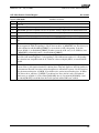
1
AMD-8151TM AGP Tunnel Data Sheet
24888 Rev 3.03 - July 12, 2004
TM
AMD-8151
Cover page
HyperTransportTM AGP3.0
Graphics Tunnel
Data Sheet
1
Overview
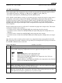
The AMD-8151TM HyperTransportTM AGP3.0 Graphics Tunnel (referred to as the IC in this document) is a
HyperTransport™ technology (referred to as link in this document) tunnel developed by AMD that provides an
AGP 3.0 compliant (8x transfer rate) bridge.
1.1
•
Device Features
HyperTransport technology tunnel with side A
and side B.
• Side A is 16 bits (input and output); side B is
8 bits.
• Either side may connect to the host or to a
downstream HyperTransport technology
compliant device.
• Each side supports HyperTransport technology-defined reduced bit widths: 8-bit, 4-bit,
and 2-bit.
• Side A supports transfer rates of 1600, 1200,
800, and 400 mega-transfers per second.
Side B supports transfer rates of 800 and
400 mega-transfers per second.
• Maximum bandwidth is 6.4 gigabytes per
second across side A (half upstream and half
downstream) and 1.6 gigabytes per second
across side B.
• Independent transfer rate and bit width
selection for each side.
• Link disconnect protocol supported.
•
•
•
AGP 8x bridge.
• Compliance with AGP 3.0 specification signaling, supporting 4x and 8x transfer rates.
• Compliance with AGP 2.0 specification 1.5volt signaling, supporting 1x, 2x, and 4x
data-transfer modes.
• Supports up to 32 outstanding requests.
31 x 31 millimeter, 564-ball BGA package.
1.5 volt AGP signaling; some 3.3 volt IO; 1.2
volt link signaling; 1.8 volt core.
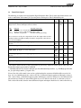
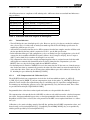
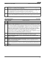
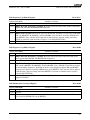
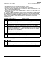
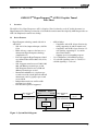
AMD-8151TM Device
TM
Host
HyperTransport
Link
16 bits upstream,
16 bits downstream
Side A
Side B
tunnel
AGP
Bridge
HyperTransport
Link
8 bits upstream,
8 bits downstream
Downstream
Device
AGP Graphics
Controller
Figure 1: System block diagram.
1
24888 Rev 3.03 - July 12, 2004
AMD-8151TM AGP Tunnel Data Sheet
© 2004 Advanced Micro Devices, Inc.
All rights reserved.The contents of this document are provided in connection with Advanced Micro Devices, Inc. ("AMD") products. AMD makes
no representations or warranties with respect to the accuracy or completeness of the contents of this publication and reserves the right to make
changes to specifications and product descriptions at any time without
notice. No license, whether express, implied, arising by estoppel or otherwise, to any intellectual property rights is granted by this publication.
Except as set forth in AMD's Standard Terms and Conditions of Sale,
AMD assumes no liability whatsoever, and disclaims any express or
implied warranty, relating to its products including, but not limited to, the
implied warranty of merchantability, fitness for a particular purpose, or
infringement of any intellectual property right. AMD's products are not
designed, intended, authorized or warranted for use as components in systems intended for surgical implant into the body, or in other applications
intended to support or sustain life, or in any other application in which the
failure of AMD's product could create a situation where personal injury,
death, or severe property or environmental damage may occur. AMD
reserves the right to discontinue or make changes to its products at any
time without notice.
Trademarks
AMD, the AMD Arrow logo, and combinations thereof, and AMD-8151 are trademarks of Advanced Micro
Devices, Inc.
HyperTransport is a licensed trademark of the HyperTransport Technology Consortium.
Other product names used in this publication are for identification purposes only and may be trademarks of
their respective companies.
2
24888 Rev 3.03 - July 12, 2004
AMD-8151TM AGP Tunnel Data Sheet
Table of Contents
1
Overview . . . . . . . . . . . . . . . . . . . . . . . . . . . . . . . . . . . . . . . . . . . . . . . . . . . . . . . . . . . . . . . . . . . . . . . 1
1.1 Device Features. . . . . . . . . . . . . . . . . . . . . . . . . . . . . . . . . . . . . . . . . . . . . . . . . . . . . . . . . . . . . . 1
2
Ordering Information. . . . . . . . . . . . . . . . . . . . . . . . . . . . . . . . . . . . . . . . . . . . . . . . . . . . . . . . . . . . . 6
3
Signal Descriptions . . . . . . . . . . . . . . . . . . . . . . . . . . . . . . . . . . . . . . . . . . . . . . . . . . . . . . . . . . . . . . . 6
3.1 Terminology . . . . . . . . . . . . . . . . . . . . . . . . . . . . . . . . . . . . . . . . . . . . . . . . . . . . . . . . . . . . . . . . 6
3.2 Tunnel Link Signals . . . . . . . . . . . . . . . . . . . . . . . . . . . . . . . . . . . . . . . . . . . . . . . . . . . . . . . . . . 7
3.3 AGP Signals . . . . . . . . . . . . . . . . . . . . . . . . . . . . . . . . . . . . . . . . . . . . . . . . . . . . . . . . . . . . . . . . 8
3.4 Test and Miscellaneous Signals . . . . . . . . . . . . . . . . . . . . . . . . . . . . . . . . . . . . . . . . . . . . . . . . 10
3.5 Power and Ground . . . . . . . . . . . . . . . . . . . . . . . . . . . . . . . . . . . . . . . . . . . . . . . . . . . . . . . . . . 10
3.5.1 Power Plane Sequencing . . . . . . . . . . . . . . . . . . . . . . . . . . . . . . . . . . . . . . . . . . . . . . . 10
4
Functional Operation . . . . . . . . . . . . . . . . . . . . . . . . . . . . . . . . . . . . . . . . . . . . . . . . . . . . . . . . . . . . 11
4.1 Overview. . . . . . . . . . . . . . . . . . . . . . . . . . . . . . . . . . . . . . . . . . . . . . . . . . . . . . . . . . . . . . . . . . 11
4.2 Reset And Initialization . . . . . . . . . . . . . . . . . . . . . . . . . . . . . . . . . . . . . . . . . . . . . . . . . . . . . . 11
4.3 Clocking . . . . . . . . . . . . . . . . . . . . . . . . . . . . . . . . . . . . . . . . . . . . . . . . . . . . . . . . . . . . . . . . . . 11
4.3.1 Clock Gating . . . . . . . . . . . . . . . . . . . . . . . . . . . . . . . . . . . . . . . . . . . . . . . . . . . . . . . . 11
4.4 Tunnel Links . . . . . . . . . . . . . . . . . . . . . . . . . . . . . . . . . . . . . . . . . . . . . . . . . . . . . . . . . . . . . . . 12
4.4.1 Link PHY . . . . . . . . . . . . . . . . . . . . . . . . . . . . . . . . . . . . . . . . . . . . . . . . . . . . . . . . . . . 12
4.5 AGP. . . . . . . . . . . . . . . . . . . . . . . . . . . . . . . . . . . . . . . . . . . . . . . . . . . . . . . . . . . . . . . . . . . . . . 12
4.5.1 Tags, UnitIDs, And Ordering. . . . . . . . . . . . . . . . . . . . . . . . . . . . . . . . . . . . . . . . . . . . 12
4.5.2 Various Behaviors . . . . . . . . . . . . . . . . . . . . . . . . . . . . . . . . . . . . . . . . . . . . . . . . . . . . 13
4.5.2.1 AGP Compensation And Calibration Cycles . . . . . . . . . . . . . . . . . . . . . . . . . . . . . . 13
5
Registers. . . . . . . . . . . . . . . . . . . . . . . . . . . . . . . . . . . . . . . . . . . . . . . . . . . . . . . . . . . . . . . . . . . . . . .
5.1 Register Overview. . . . . . . . . . . . . . . . . . . . . . . . . . . . . . . . . . . . . . . . . . . . . . . . . . . . . . . . . . .
5.1.1 Configuration Space. . . . . . . . . . . . . . . . . . . . . . . . . . . . . . . . . . . . . . . . . . . . . . . . . . .
5.1.2 Register Naming and Description Conventions. . . . . . . . . . . . . . . . . . . . . . . . . . . . . .
5.2 AGP Device Configuration Registers . . . . . . . . . . . . . . . . . . . . . . . . . . . . . . . . . . . . . . . . . . . .
5.3 AGP Bridge Configuration Registers . . . . . . . . . . . . . . . . . . . . . . . . . . . . . . . . . . . . . . . . . . . .
14
14
14
14
15
30
6
Electrical Data. . . . . . . . . . . . . . . . . . . . . . . . . . . . . . . . . . . . . . . . . . . . . . . . . . . . . . . . . . . . . . . . . .
6.1 Absolute Ratings . . . . . . . . . . . . . . . . . . . . . . . . . . . . . . . . . . . . . . . . . . . . . . . . . . . . . . . . . . . .
6.2 Operating Ranges . . . . . . . . . . . . . . . . . . . . . . . . . . . . . . . . . . . . . . . . . . . . . . . . . . . . . . . . . . .
6.3 DC Characteristics . . . . . . . . . . . . . . . . . . . . . . . . . . . . . . . . . . . . . . . . . . . . . . . . . . . . . . . . . .
6.4 AC Characteristics . . . . . . . . . . . . . . . . . . . . . . . . . . . . . . . . . . . . . . . . . . . . . . . . . . . . . . . . . .
34
34
34
35
37
7
Ball Designations. . . . . . . . . . . . . . . . . . . . . . . . . . . . . . . . . . . . . . . . . . . . . . . . . . . . . . . . . . . . . . . . 39
8
Package Specification . . . . . . . . . . . . . . . . . . . . . . . . . . . . . . . . . . . . . . . . . . . . . . . . . . . . . . . . . . . . 42
9
Test . . . . . . . . . . . . . . . . . . . . . . . . . . . . . . . . . . . . . . . . . . . . . . . . . . . . . . . . . . . . . . . . . . . . . . . . . . . 43
9.1 High Impedance Mode . . . . . . . . . . . . . . . . . . . . . . . . . . . . . . . . . . . . . . . . . . . . . . . . . . . . . . . 43
9.2 NAND Tree Mode . . . . . . . . . . . . . . . . . . . . . . . . . . . . . . . . . . . . . . . . . . . . . . . . . . . . . . . . . . 43
10
Appendix . . . . . . . . . . . . . . . . . . . . . . . . . . . . . . . . . . . . . . . . . . . . . . . . . . . . . . . . . . . . . . . . . . . . . . 45
10.1 Revision History . . . . . . . . . . . . . . . . . . . . . . . . . . . . . . . . . . . . . . . . . . . . . . . . . . . . . . . . . . . . 45
3
24888 Rev 3.03 - July 12, 2004
AMD-8151TM AGP Tunnel Data Sheet
List of Figures
Figure 1:
Figure 2:
Figure 3:
Figure 4:
Figure 5:
System block diagram................................................................................................................... 1
Configuration space. ................................................................................................................... 14
Ball designations. ........................................................................................................................ 39
Package mechanical drawing. ..................................................................................................... 42
NAND tree. ................................................................................................................................. 43
4
24888 Rev 3.03 - July 12, 2004
AMD-8151TM AGP Tunnel Data Sheet
List of Tables
Table 1:
Table 2:
Table 3:
Table 4:
Table 5:
Table 6:
Table 7:
Table 8:
Table 9:
Table 10:
Table 11:
Table 12:
Table 13:
Table 14:
Table 15:
Table 16:
Table 17:
IO signal types. ............................................................................................................................. 6
Translation from AGP requests to link requests. ........................................................................ 13
Configuration spaces................................................................................................................... 15
Memory mapped address spaces................................................................................................. 15
Register attributes. ...................................................................................................................... 15
Absolute maximum ratings. ........................................................................................................ 34
Operating ranges. ........................................................................................................................ 34
Current and power consumption. ................................................................................................ 35
DC characteristics for signals on the VDD33 power plane. ....................................................... 35
DC characteristics for signals on the VDD15 power plane, AGP 2.0 signaling......................... 36
DC characteristics for signals on the VDD15 power plane, AGP 3.0 signaling......................... 36
AC data for clocks....................................................................................................................... 37
AC data for common clock operation of AGP signals................................................................ 37
AC data for clock-forwarded operation of AGP signals............................................................. 38
Signal BGA positions.................................................................................................................. 40
Power and ground BGA positions. ............................................................................................. 41
Test modes................................................................................................................................... 43
5
AMD-8151TM AGP Tunnel Data Sheet
24888 Rev 3.03 - July 12, 2004
2
Ordering Information
AMD-8151
BL
C
Case Temperature
C = Commercial temperature range
Package Type
BL = Organic Ball Grid Array with lid
Family/Core
AMD-8151
3
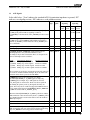
Signal Descriptions
3.1
Terminology
See section 5.1.2 for a description of the register naming convention used in this document. See the
AMD-8151TM HyperTransportTM AGP3.0 Graphics Tunnel Design Guide for additional information.
Signals with a # suffix are active low.
Signals described in this chapter utilize the following IO cell types:
Name Notes
Input
Input signal only.
Output
Output signal only. This includes outputs that are capable of being in the high-impedance state.
OD
Open drain output. These signals are driven low and expected to be pulled high by external circuitry.
IO
Input or output signal.
IOD
Analog
w/PU
Input or open-drain output.
Analog signal.
With pullup. The signal includes a pullup resistor to the signal’s power plane. The resistor value is
nominally 8K ohms.
Table 1: IO signal types.
The following provides definitions and reference data about each of the IC’s pins. “During Reset” provides the
state of the pin while RESET# is asserted. “After Reset” provides the state of the pin immediately after
RESET# is deasserted. “Func.” means that the pin is functional and operating per its defined function.
6
24888 Rev 3.03 - July 12, 2004
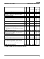
3.2
AMD-8151TM AGP Tunnel Data Sheet
Tunnel Link Signals
The following are signals associated with the HyperTransportTM links. [B, A] in the signal names below refer
to the A and B sides of the tunnel. [P, N] are the positive and negative sides of differential pairs.
Pin name and description
IO cell Power During After
type plane* reset
reset
LDTCOMP[3:0]. Link compensation pins for both sides of the tunnel. These are
designed to be connected through resistors as follows:
Analog VDD12B
Bit
[0]
[1]
[3, 2]
Function
External Connection
Positive receive compensation Resistor to VDD12B
Negative receive compensationResistor to VSS
Transmit compensation
Resistor from bit [2] to bit [3]
These resistors are used by the compensation circuit. The output of this circuit is
combined with DevA:0x[E8, E4, E0] to determine compensation values that are
passed to the link PHYs.
LRACAD_[P, N][15:0]; LRBCAD_[P, N][7:0]. Receive link command-addressdata bus.
Link VDD12
input
LRACLK[1, 0]_[P, N]; LRBCLK0_[P, N]. Receive link clock.
Link VDD12
input
LR[B, A]CTL_[P, N]. Receive link control signal.
Link VDD12
input
LTACAD_[P, N][15:0]; LTBCAD_[P, N][7:0]. Transmit link command-addressdata bus.
Link VDD12 Diff
Func.
output
High**
LTACLK[1, 0]_[P, N]; LTBCLK0_[P, N]. Transmit link clock.
Link VDD12 Func.
output
Func.
LT[B, A]CTL_[P, N]. Transmit link control signal.
Link VDD12 Diff
output
Low**
Func.
* The signals connected to the A side of the tunnel are powered by VDD12A and the signals connected to the
B side of the tunnel are powered by VDD12B.
** Diff High and Diff Low for these link pins specifies differential high and low; e.g., Diff High specifies that
the _P signal is high and the _N signal is low.
If one of the sides of the tunnel is not used on a platform then the unconnected link should be treated as follows, for every 10 differential pairs: connect all of the _P differential inputs together and through a resistor to
VSS; connect all the _N differential inputs together and through a resistor to VDD12; leave the differential outputs unconnected. If there are unused link signals on an active link (because the IC is connected to a device
with a reduced bit width), then the unused differential inputs and outputs should also be connected in this way.
7
AMD-8151TM AGP Tunnel Data Sheet
24888 Rev 3.03 - July 12, 2004
3.3
AGP Signals
In the table below, “Term” indicates the standard AGP 3.0 termination impedance to ground; “PU”
indicates a weak pullup resistor; “PD” indicates a weak pulldown resistor.
Pin name and description
IO cell Power
type
plane
AGP 3.0
Signaling
AGP 2.0
Signaling
During After During After
reset
reset
reset
reset
A_ADSTB0_[P, N]. AGP differential strobe for A_AD[15:0] and
A_CBE_L[1:0]. When AGP 3.0 signaling is enabled,
A_ADSTB0_P is the first strobe and A_ADSTB0_N is the second
strobe.
IO
VDD15 Term
Term
_P: PU _P: PU
_N: PD _N: PD
A_ADSTB1_[P, N]. AGP differential strobe for AD[31:16],
A_CBE_L[3:2], and A_DBI[H,L]. When AGP 3.0 signaling is
enabled, A_ADSTB1_P is the first strobe and A_ADSTB1_N is
the second strobe.
IO
VDD15 Term
Term
_P: PU _P: PU
_N: PD _N: PD
A_AD[31:0]. AGP address-data bus.
IO
VDD15 Term
Term
PU
Low
A_CBE_L[3:0]. AGP command-byte enable bus.
IO
VDD15 Term
Term
PU
Low
A_CAL[D, S] and A_CAL[D, S]#. Compensation pins for
matching impedance of system board AGP traces. See
DevA:0x[54, 50] for more information. These are designed to be
connected through resistors as follows:
Signal
A_CALD
A_CALD#
A_CALS
A_CALS#
Compensation Function
Rising edge of data signals
Falling edge of data signals
Rising edge of strobe signals
Falling edge of strobe signals
Analog VDD15
External Connection
Resistor to VSS
Resistor to VDD15
Resistor to VSS
Resistor to VDD15
These resistors are used by the compensation circuit. The output of
this circuit is combined with DevA:0x[54, 50] to determine compensation values that are passed to the link PHYs.
IO
VDD15 Term
Term
PU
PU
A_DEVSEL#. AGP device select.
IO
VDD15 Term
Term
PU
PU
A_FRAME#. AGP frame signal.
IO
VDD15 Term
Term
PU
PU
PU
PU
PU
A_DBI[H, L]. Data bus inversion [high, low]. When
DevA:0xA4[AGP3MD]=1, A_DBIL applies to AD[15:0];
A_DBIH applies to AD[31:16]. 1=AD signals are inverted.
0=A_AD signals are not inverted. The IC uses these signals in
determining the polarity of the A_AD signals when they are
inputs. These may also be enabled to support the DBI function of
the IC output signals by DevA:0x40[DBIEN]. Both A_DBIH and
A_DBIL are strobed with A_ADSTB1_[P, N].
When DevA:0xA4[AGP3MD]=0: A_DBIL is pulled low with the
AGP termination value and not used by the IC; A_DBIH is pulled
up to VDD15 through a weak resistor and becomes the AGP 2.0
PIPE# input signal.
A_GC8XDET#. 0=Specifies that the graphics device supports
AGP 3.0 signaling. The state of this signal is latched on the rising
edge of A_RESET# before being passed to internal logic.
Input VDD15
w/PU
PU
8
AMD-8151TM AGP Tunnel Data Sheet
24888 Rev 3.03 - July 12, 2004
Pin name and description
IO cell Power
type
plane
AGP 3.0
Signaling
AGP 2.0
Signaling
During After During After
reset
reset
reset
reset
A_GNT#. AGP master grant signal.
Low
PU
High
Term
PU
PU
Low
Low
Low
Low
VDD15 Term
Term
PU
Low
A_PCLK. 66 MHz AGP clock.
Output VDD33 Func.
Func.
Func.
Func.
A_PLLCLKO. PLL clock output. See section 4.3 for details.
Output VDD33 Func.
Func.
Func.
Func.
Term
PU
PU
Low
High
Low
High
A_RBF#. AGP read buffer full signal.
Input VDD15 Term
Term
PU
PU
A_SBSTB_[P, N]. AGP differential side band address strobe. In
AGP 3.0 signaling mode, A_SBSTB_P is the first strobe and
A_SBSTB_N is the second strobe.
Input VDD15 Term
Term
A_SBA[7:0]. AGP side band address signals.
Input VDD15 Term
Term
PU
PU
Output VDD15 Term
Low
PU
Low
A_IRDY#. AGP master ready signal.
Output VDD15 Term
IO
VDD15 Term
A_MB8XDET#. This pin is controlled by DevA:0x40[8XDIS]. It Output VDD15
is designed to be connected to the AGP connector to indicate
support for AGP 3.0 signaling.
A_PAR. AGP parity signal.
A_PLLCLKI. PLL clock input. See section 4.3 for details.
IO
Input VDD33
A_REFCG. AGP signal reference output.
Analog VDD15
output
A_REFGC. AGP signal reference input.
Analog VDD15
input
A_REQ#. AGP master request signal.
Input VDD15 Term
Output VDD33
A_RESET#. AGP bus reset signal. This is asserted whenever
RESET# is asserted or when programmed by
DevB:0x3C[SBRST]. Assertion of this pin does not reset any logic
internal to the IC.
A_ST[2:0]. AGP status signals.
_P: PU _P: PU
_N: PD _N: PD
A_STOP#. AGP target abort signal.
IO
VDD15 Term
Term
PU
PU
A_TRDY#. AGP target ready signal.
IO
VDD15 Term
Term
PU
PU
Term
PU
PU
Input VDD33
A_TYPEDET#. AGP IO voltage level type detect. 0=1.5 volts;
1=3.3 volts (not supported by the IC). The state of this pin is
provided in DevA:0x40[TYPEDET]. This pin is also used for testmode selection; see section 9. This signal requires an external
pullup resistor to VDD33 on the systemboard.
A_WBF#. AGP write buffer full signal.
Input VDD15 Term
The SERR# and PERR# signals are not supported on the AGP bridge.
9
24888 Rev 3.03 - July 12, 2004
3.4
AMD-8151TM AGP Tunnel Data Sheet
Test and Miscellaneous Signals
Pin name and description
CMPOVR. Link automatic compensation override. 0=Link automatic compensation
is enabled. 1=The compensation values stored in DevA:0x[E0, E4, E8] control the
compensation circuit. The state of this signal determines the default value for
DevA:0x[E0, E4, E8][ACTL and BCTL] at the rising edge of PWROK.
IO cell Power During After
type
plane reset
reset
Input VDD33
FREE[7:1]. These should be left unconnected.
LDTSTOP#. Link disconnect control signal. This pin is also used for test-mode
selection; see section 9.
Input VDD33
NC[1:0]. These should be left unconnected.
PWROK. Power OK. 1=All power planes are valid. The rising edge of this signal is
deglitched; it is not observed internally until it is high for more than 6 consecutive
REFCLK cycles. See section 4.2 for more details about this signal.
Input VDD33
REFCLK. 66 MHz reference clock. This is required to be operational and valid for a
minimum of 200 microseconds prior to the rising edge of PWROK and always while
PWROK is high.
Input VDD33
RESET#. Reset input. See section 4.2 for details.
Input VDD33
STRAPL[19:13, 11:0]. Strapping option to be tied low. These pins should be tied to
ground. STRAPL0 is used for test-mode selection; see section 9.
IO
VDD15 3-State 3-State
STRAPL[22:20]. Strapping option to be tied low. These pins should be tied to
ground.
IO
VDD33 3-State 3-State
TEST. This is required to be tied low for functional operation. See section 9 for
details.
3.5
Input VDD33
Power and Ground
VDD12[B, A]. 1.2 volt power plane for the HyperTransportTM technology pins. VDD12A provides power to
the A side of the tunnel. VDD12B provides power to the B side of the tunnel.
VDD15. 1.5 volt power plane for AGP.
VDD18. 1.8-volt power plane for the core of the IC.
VDDA18. Analog 1.8-volt power plane for the PLLs in the core of the IC. This power plane is required to be
filtered from digital noise.
VDD33. 3.3-volt power plane for IO.
VSS. Ground.
3.5.1
Power Plane Sequencing
The following are power plane requirements that may imply power supply sequencing requirements.
• VDD33 is required to always be higher than VDD18, VDDA18, VDD15, and VDD12[B, A].
• VDD18 and VDDA18 are required to always be higher than VDD15 and VDD12[B, A].
• VDD15 is required to always be higher than VDD12[B, A].
10
24888 Rev 3.03 - July 12, 2004
4
Functional Operation
4.1
Overview
AMD-8151TM AGP Tunnel Data Sheet
The IC connects to the host through either the side A or side B HyperTransportTM link interface. The other side
of the tunnel may or may not be connected to another device. Host-initiated transactions that do not target the
IC or the bridge flow through the tunnel to the downstream device. Transactions claimed by the device are
passed to internal registers or to the AGP bridge.
See section 5.1 for details about the software view of the IC. See section 5.1.2 for a description of the register
naming convention. See the AMD-8151TM HyperTransportTM AGP3.0 Graphics Tunnel Design Guide for additional information.
4.2
Reset And Initialization
RESET# and PWROK are both required to be low while the power planes to the IC are invalid and for at least
1 millisecond after the power planes are valid. Deassertion of PWROK is referred to as a cold reset. After
PWROK is brought high, RESET# is required to stay low for at least 1 additional millisecond. After RESET#
is brought high, the links go through the initialization sequence.
After a cold reset, the IC may be reset by asserting RESET# while PWROK remains high. This is referred to as
a warm reset. RESET# must be asserted for no less than 1 millisecond during a warm reset.
4.3
Clocking
It is required that REFCLK be valid in order for the IC to operate. Also, the LR[B, A]CLK inputs from the
operation links must also be valid at the frequency defined DevA:0xCC[FREQA] and DevA:0xD0[FREQB].
The IC provides A_PCLK as the clock to the AGP device.
The systemboard is required to include a connection from A_PLLCLKO to A_PLLCLKI. The length of this
connection is required to be approximately the same as length of the A_PCLK trace from the IC to the external
AGP devices (including approximately 2.5 inches of etch on the AGP card). The IC uses this loopback to help
match the external trace delay.
4.3.1
Clock Gating
Internal clocks may be disabled during power-managed system states such as power-on suspend. It is required
that all upstream requests initiated by the IC be suspended while in this state.
To enable clock gating, DevA:0xF0[ICGSMAF] is programmed to the values in which clock gating will be
enabled. Stop Grant cycles and STPCLK deassertion link broadcasts interact to define the window in which the
IC is enabled for clock gating during LDTSTOP# assertions. The system is placed into power managed states
by steps that include a broadcast over the links of the Stop Grant cycle that includes the System Management
Action Field (SMAF) followed by the assertion of LDTSTOP#. When the IC detects the Stop Grant broadcast
which is enabled for clock gating, it enables clock gating for the next assertion of LDTSTOP#. While exiting
the power-managed state, the system is required to broadcast a STPCLK deassertion message. The IC uses this
message to disable clock gating during LDTSTOP# assertions. This is important because an LDTSTOP# assertion is not guaranteed to occur after the Stop Grant broadcast is received. The clock gating window must be
closed to insure that clock gating does not occur during Stop Grant for LDTSTOP# assertions that are not associated with the power states specified by DevA:0xF0[ICGSMAF].
11
24888 Rev 3.03 - July 12, 2004
AMD-8151TM AGP Tunnel Data Sheet
In summary, Stop Grant broadcasts with SMAF fields specified by DevA:0xF0[ICGSMAF] enable the clock
gating window and STPCLK deassertion broadcasts disable the window. If LDTSTOP# is asserted while the
clock gating window is enabled, then clock gating occurs.
Also, DevA:0xF0[ECGSMAF] may be used in a similar way to disable A_PCLK and the internal clock grids
associated with the AGP bridge. The same rules for the clock gating window that apply to DevA:0xF0[ICGSMAF] also apply to DevA:0xF0[ECGSMAF]. If clock gating is enabled, then A_PCLK is forced low within
two clock periods after LDTSTOP# is asserted. It becomes active again within two clock periods after LDTSTOP# is deasserted. It is required that there be no AGP-card-initiated upstream or downstream traffic while
A_PCLK is gated. In addition, it is required that there be no host accesses to the bridge or internal registers in
progress from the time that LDTSTOP# is asserted for clock gating until the link reconnects after LDTSTOP#
is deasserted.
4.4
Tunnel Links
HyperTransport link A supports CLK receive and transmit frequencies of 200, 400, 600, and 800 MHz. Link B
supports frequencies of 200 and 400 MHz. The side A and side B frequencies are independent of each other.
4.4.1
Link PHY
The PHY includes automatic compensation circuitry and a software override mechanism, as specified by
DevA:0x[E8, E4, E0]. The IC only implements synchronous mode clock forwarding FIFOs. So only the link
receive and transmit frequencies specified in DevA:0x[D0, CC][FREQB, FREQA] are allowed.
4.5
AGP
The AGP bridge supports AGP 3.0 signaling at 8x and 4x data rates and 1.5-volt AGP 2.0 signaling at 4x, 2x,
and 1x data rates. 64-bit upstream and 32-bit downstream addressing is supported. AGP 3.0 dynamic bus inversion is supported on output signals in 8X mode only, not in 4X mode; dynamic bus inversion on input signals is
supported in both 4X and 8X modes.
4.5.1
Tags, UnitIDs, And Ordering
The IC requires three HyperTransportTM technology-defined UnitIDs. They are allocated as follows:
• First UnitID is not used. This is to avoid a potential conflict with the host (because it may be zero; see
DevA:0xC0[BUID]).
• Second UnitID is used for PCI-mode upstream requests and responses to host requests.
• Third UnitID is used for AGP (high priority and low priority) upstream requests.
The SrcTag value that is assigned to upstream non-posted AGP requests increments with each request from 0
to 27 and then rolls over to 0 again; the first SrcTag assigned after reset is 0. Up to 28 non-posted link requests
may be outstanding at a time. The SrcTag value that is assigned to non-posted PCI requests is always 28.
12
24888 Rev 3.03 - July 12, 2004
AMD-8151TM AGP Tunnel Data Sheet
All AGP transactions are compliant to AGP ordering rules. APG transactions are translated into link transactions as follows:
AGP transaction
Link transaction
High priority write
WrSized, posted channel, PassPW = 1
High priority read
RdSized, PassPW = 1, response PassPW = 1
Low priority write
WrSized, posted channel, PassPW = 0
Low priority read
RdSized, PassPW = 0, response PassPW = 1
Low priority flush
Flush, PassPW = 0
Low priority fence
None (wait for all outstanding read responses)
Table 2: Translation from AGP requests to link requests.
4.5.2
Various Behaviors
• The AGP bridge does not claim link special cycles. However, special cycles that are encoded in configuration cycles to device 31 of the AGP secondary bus number (per the PCI-to-PCI bridge specification) are
translated to AGP bus special cycles.
• AGP and PCI read transactions that receive NXA responses from the host complete onto the AGP bus with
the data provided by the host (which is required to be all 1’s, per the link specification).
• In the translation from type 1 link configuration cycles to secondary bus type 0 configuration cycles, the IC
converts the device number to IDSEL AD signal as follows: device 0 maps to AD[16]; device 1 maps to
AD[17]; and so forth. Device numbers 16 through 31 are not valid.
• The compensation values for drive strength and input impedance that are assigned to non-clock forwarded
AGP signals are automatically determined and set by the IC during the first compensation cycle after
RESET#. Once set, they do not change until the next RESET# assertion.
• Per the link protocol, when the COMPAT bit is set in the transaction, the IC does not ever claim the transaction. Such transactions are automatically passed to the other side of the tunnel (or master aborted if the IC is
at the end of the chain). This is true of all transactions within address space that is otherwise claimed by the
IC, including the space defined by DevB:0x3C[VGAEN].
4.5.2.1
AGP Compensation And Calibration Cycles
The AGP PHY includes one compensation circuit for the clock forwarded data signals, A_AD[31:0],
A_CBE_L[3:0], and A_DBI[H, L], and one compensation circuit for the strobes, A_ADSTB[1:0]. Each compensation circuit calculates the required rising-edge (P) and falling-edge (N) signal drive strength through a
free-running state machine that generates a new value approximately every four microseconds. These values
are provided in DevA:0x[50, 54][NCOMP, PCOMP].
Programmable skew values between data signals and strobes are also provided in DevA:0x58.
The compensation values provided to the AGP PHY are software selectable between the calculated compensation values, fixed programmable bypass values, or fixed programmable offsets from the calculated values.
Regardless of which value is selected, the value presented to the PHY is never updated until there is a calibration cycle.
Calibration cycles consist of taking control of the AGP bus, updating the AGP PHY compensation values, and
then releasing (see DevA:0xA8[PCALCYC]). If enabled by DevA:0xB0[CALDIS], they occur periodically
with the period specified by DevA:0xA8[PCALCYC].
13
AMD-8151TM AGP Tunnel Data Sheet
24888 Rev 3.03 - July 12, 2004
The first calibration cycle occurs approximately 4 milliseconds after the deassertion of RESET# (whether AGP
2.0 or 3.0 signaling is enabled).
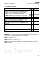
5
Registers
5.1
Register Overview
The IC includes several sets of registers accessed through a variety of address spaces. IO address space refers
to register addresses that are accessed through x86 IO instructions such as IN and OUT. PCI configuration
space is typically accessed by the host through IO cycles to CF8h and CFCh. There is also memory space and
indexed address space in the IC.
5.1.1
Configuration Space
The address space for the IC configuration registers is broken up into busses, devices, functions, and, offsets, as
defined by the link specification. It is accessed by HyperTransport™ technology-defined type 0 configuration
cycles. The device number is mapped into bits[15:11] of the configuration address. The function number is
mapped into bits[10:8] of the configuration address. The offset is mapped to bits[7:2] of the configuration
address.
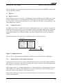
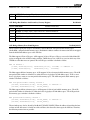
The following diagram shows the devices in configuration space as viewed by software.
Primary bus
AGP Device
DevA:0xXX
Device header
First device
Function 0
AGP Bridge
DevB:0xXX
Bridge header
Second device
Function 0
AGP Slot
Secondary bus
Figure 2: Configuration space.
Device A, above, is programmed to be the link base UnitID and device B is the link base UnitID plus 1.
5.1.2
Register Naming and Description Conventions
Configuration register locations are referenced with mnemonics that take the form of Dev[A|B]:[7:0]x[FF:0],
where the first set of brackets contain the device number, the second set of brackets contain the function number, and the last set of brackets contain the offset.
Other register locations (e.g. memory mapped registers) are referenced with an assigned mnemonic that specifies the address space and offset. These mnemonics start with two or three characters that identify the space
followed by characters that identify the offset within the space.
Register fields within register locations are also identified with a name or bit group in brackets following the
register location mnemonic.
14
AMD-8151TM AGP Tunnel Data Sheet
24888 Rev 3.03 - July 12, 2004
The following are configuration spaces:
Device
Function
Mnemonic Registers
"A"
0
DevA:0xXX AGP device header; link and AGP capabilities blocks
"B"
0
DevB:0xXX PCI-PCI bridge registers for AGP
Table 3: Configuration spaces.
The IC does not claim configuration-register accesses to unimplemented functions within its devices (they are
forwarded to the other side of the tunnel). Accesses to unimplemented register locations within implemented
functions are claimed; such writes are ignored and reads always respond with all zeros.
The following are memory mapped spaces:
Base address
register
Size
(bytes)
Mnemonic Registers
DevA:0x10
Variable
None
Graphic virtual memory aperture; minimum of 32 megabytes.
DevA:0xB8
4K
None
GART block in physical memory.
Table 4: Memory mapped address spaces.
The following are register attributes found in the register descriptions.
Type
Description
Read or read-only
Capable of being read by software. Read-only implies that the register cannot be written to by
software.
Write
Capable of being written by software.
Set by hardware
Register bit is set high by hardware.
Write once
After RESET#, these registers may be written to once. After being written, they become read only
until the next RESET# assertion. The write-once control is byte based. So, for example, software
may write each byte of a write-once DWORD as four individual transactions. As each byte is
written, that byte becomes read only.
Write 1 to clear
Software must write a 1 to the bit in order to clear it. Writing a 0 to these bits has no effect.
Write 1 only
Software can set the bit high by writing a 1 to it. However subsequent writes of 0 will have no
effect. RESET# must be asserted in order to clear the bit.
Table 5: Register attributes.
5.2
AGP Device Configuration Registers
These registers are located in PCI configuration space, in the first device (device A), function 0. See section
5.1.2 for a description of the register naming convention.
AGP Vendor And Device ID Register
Default: 7454 1022h
Bits Description
DevA:0x00
Attribute: Read only.
31:16 AGP device ID.
15:0 Vendor ID.
15
AMD-8151TM AGP Tunnel Data Sheet
24888 Rev 3.03 - July 12, 2004
AGP Device Status And Command Register
Default: 0210 0000h
Bits Description
DevA:0x04
Attribute: See below.
31
DPE: detected parity error. Read only. This bit is fixed in the low state.
30
SSE: signaled system error. Read; set by hardware; write 1 to clear. 1=A system error was signaled
(both links were flooded with sync packets) as a result of a CRC error (see
DevA:0x[C8:C4][CRCFEN, CRCERR]). Note: this bit is cleared by PWROK reset but not by
RESET#.
29
RMA: received master abort. Read; set by hardware; write 1 to clear. 1=A request (AGP or PCI)
sent to the host bus received a master abort (an NXA error response). Note: this bit is cleared by
PWROK reset but not by RESET#.
28
RTA: received target abort. Read; set by hardware; write 1 to clear. 1=A request (AGP or PCI) sent
to the host bus received a target abort (a non-NXA error response). Note: this bit is cleared by
PWROK reset but not by RESET#.
27:21 Read only. These bits are fixed in their default state.
20
Capabilities pointer. Read only. This bit is fixed in the high state.
19:3 Read only. These bits are fixed in their default state.
2
MASEN: PCI master enable. Read-write. This bit controls no hardware in the IC.
1
MEMEN: memory enable. Read-write. 1=Enables access to the memory space specified by
DevA:0x10. This bit controls no hardware in the IC.
0
IO enable. Read only. This bit is fixed in the low state.
AGP Device Revision and Class Code Register
Default: 0600 00??h
Bits Description
DevA:0x08
Attribute: See below.
31:8 CLASSCODE. Read; write once. Provides the AGP bridge class code.
7:0
REVISION. Read only.
AGP Device BIST-Header-Latency-Cache Register
Default: 0000 0000h
Bits Description
DevA:0x0C
Attribute: Read only.
31:24 BIST. These bits fixed at their default values.
23:16 HEADER. These bits fixed at their default values.
15:8 LATENCY. These bits fixed at their default values.
7:0
CACHE. These bits fixed at their default values.
16
AMD-8151TM AGP Tunnel Data Sheet
24888 Rev 3.03 - July 12, 2004
AGP Device Graphic Virtual Memory Aperture Register
DevA:0x10
It is expected that the state of this register is copied into the host by software. This register controls no hardware in the IC.
Default: 0000 0000 0000 0008h
Bits Description
Attribute: See below.
63:32 APBARHI. Read-write. Aperture base address register high. Note: bits[63:40] are required to be
programmed low; setting any of these bits high results in undefined behavior. Note: if
DevA:0x10[64BIT]=0, then these bits are read only, all zero.
31:22 APBARLO. Aperture base address register low. These bits are a combination of read-write and readonly zero, based on the state of DevA:0xB4[APSIZE]; see that register for details.
21:4 Reserved.
3
Read only. This bit is fixed at its default value to indicate that this register points prefetchable space.
2
64BIT: 64-bit pointer. Read; write once. 1=DevA:0x10 is a 64-bit pointer. 0=DevA:0x10 is a 32-bit
pointer; bits[63:32] are reserved.
1:0
Read only. These bits are fixed at their default value to indicate that this register points memory space.
AGP Device Subsystem ID and Subsystem Vendor ID Register
Default: 0000 0000h
Bits Description
DevA:0x2C
Attribute: Read; write once.
31:16 Subsystem ID. This field controls no hardware.
15:0 Subsystem vendor ID. This field controls no hardware.
AGP Capabilities Pointer
Default: 0000 00A0h
Bits Description
DevA:0x34
Attribute: Read only.
31:8 Reserved.
7:0
Capabilities pointer. Specifies the offset in DevA:0 address space for the AGP capabilities block.
17
24888 Rev 3.03 - July 12, 2004
AMD-8151TM AGP Tunnel Data Sheet
AGP Miscellaneous Control Register
Default: 0000 0000h
Bits Description
DevA:0x40
Attribute: See below.
31:8 Reserved.
7
Must be low. This bit is required to be low at all times; setting it high results in undefined behavior.
6
Must be low. This bit is required to be low at all times; setting it high results in undefined behavior.
5
Must be low. This bit is required to be low at all times; setting it high results in undefined behavior.
4
Must be low. This bit is required to be low at all times; setting it high results in undefined behavior.
3
FWDIS: fast write disable. Read-write. 1=DevA:0xA4[FWSUP] is low. 0=DevA:0xA4[FWSUP] is
high.
2
8XDIS: AGP 3.0 signaling mode disable. Read-write. 0=The IC drives A_MB8XDET# low to
indicate support for AGP 3.0 signaling. 1=The IC does not drive A_MB8XDET low. This bit may be
used in conjunction with DevB:0x3C[SBRST] to revert back to AGP 2.0 signaling. To do this,
software should (1) set DevB:0x3C[SBRST] in order to reset the AGP card, (2) set 8XDIS to cause
A_MB8XDET# to float high, and (3) clear DevB:0x3C[SBRST].
1
TYPEDET: AGP voltage type detection. Read only. This bit reflects the state of the A_TYPEDET#
pin. 0=The AGP master supports 1.5 volt signaling. 1=The AGP master requires 3.3 volt signaling
and is therefore not compatible with the IC. If this bit is detected high by BIOS, an error should be
signaled.
0
DBIEN: dynamic bus inversion enable. Read-write. 1= A_DBI[H, L] enabled to dynamically invert
the state of the A_AD signals when the IC is driving these. This only applies to AGP 3.0 transfers in
the downstream direction (fast writes and read responses to AGP master requests). For PCI transfers
in the downstream direction, A_DBI[H, L] are held inactive and no inversion takes place. 0=When
the IC drives the A_AD lines, A_DBI[H, L] are driven low. Note: this bit is only valid when 8x
transfer rates are enabled; if (1) DevA:0xA4[AGP3MD]=0 or (2) DevA:0xA4[AGP3MD]=1 and
DevA:0xA8[DRATE] is not 010b, then this field is ignored and the DBI is not enabled.
18
24888 Rev 3.03 - July 12, 2004
AMD-8151TM AGP Tunnel Data Sheet
AGP PHY Control Register
DevA:0x[54, 50]
These registers apply to the compensation values of AGP clock-forwarded data and strobe signals as follows:
• DevA:0x50: data signals A_AD[31:0], A_CBE_L[3:0], A_DBI[H, L], and A_SBA[7:0].
• DevA:0x54: strobe signals A_ADSTB[1:0]_[P, N] and A_SBSTB_[P, N].
NCTL, NDATA, and NCOMP are related to (1) the falling edge drive strength of the signals as outputs and (2)
the impedance of the signals as inputs. PCTL, PDATA, and PCOMP are related to the rising edge drive
strength of the signals as outputs only. For the [N, P]DATA and [N, P]COMP fields of these registers, 00h corresponds to the weakest drive strength and the highest receive impedance. For the [N, P]DATA and [N,
P]COMP fields of these registers, the highest values corresponds to the strongest drive strength and lowest
receive impedance.
External compensation resistors are used by the IC to determine the proper drive strength values. The resistors
correlate the calculated values as follows:
• A_CALD is used to calculate DevA:0x50[PCOMP] (data signal rising edge drive strength).
• A_CALD# is used to calculate DevA:0x50[NCOMP] (data signal falling edge drive strength and receive
impedance).
• A_CALS is used to calculate DevA:0x54[PCOMP] (strobe rising edge drive strength).
• A_CALS# is used to calculate DevA:0x54[NCOMP] (strobe falling edge drive strength and receive impedance).
Note: when new values are written to these registers, new compensation values are not updated to the AGP
PHY automatically; the periodic calibration cycle specified by DevA:0xA8[PCALCYC] must pass in order for
the AGP PHY calibration values to take effect.
Default: 000? 000?h
Bits Description
Attribute: See below.
31:30 NCTL: AGP PHY N (falling edge) compensation control. Read-write. These two bits combine to
specify the PHY falling edge compensation value that is applied to AGP signals as follows:
NCTL
00b
01b
10b
11b
Description
Apply NCOMP directly as the compensation value.
Apply NDATA directly as the compensation value.
Apply the sum of NCOMP and NDATA as the compensation value. If the sum
exceeds 3Fh, then 3Fh is applied.
Apply the difference of NCOMP minus NDATA as the compensation value. If the difference is less than 00h, then 00h is applied.
29:28 Reserved.
27:22 NDATA: AGP falling edge drive strength control. Read-write. This value is applied to the fallingedge (N transistor) PHY compensation as described in NCTL.
21:16 NCOMP: AGP falling edge drive strength. Read only. This provides the calculated value of the
falling-edge (N transistor) drive strength of the AGP signals. The default for this field varies. This
field is updated by the hardware approximately every 8 microseconds.
19
AMD-8151TM AGP Tunnel Data Sheet
24888 Rev 3.03 - July 12, 2004
15:14 PCTL: AGP PHY P (rising edge) compensation control. Read-write. These two bits combine to
specify the PHY rising edge compensation value that is applied to AGP signals as follows:
PCTL
00b
01b
10b
11b
Description
Apply PCOMP directly as the compensation value.
Apply PDATA directly as the compensation value.
Apply the sum of PCOMP and PDATA as the compensation value. If the sum exceeds
1Fh, then 1Fh is applied.
Apply the difference of PCOMP minus PDATA as the compensation value. If the difference is less than 00h, then 00h is applied.
13:12 Reserved.
11
RW: read-write bit. Read-write. This controls no logic.
10:6 PDATA: AGP rising edge drive strength control. Read-write. This value is applied to the risingedge (P transistor) PHY compensation as described in PCTL.
5
4:0
Reserved.
PCOMP: AGP rising edge drive strength. Read only. This provides the calculated value of the rising-edge (P transistor) drive strength of the AGP signals. The default for this field varies. This field is
updated by the hardware approximately every 8 microseconds.
AGP PHY Skew Control Register
DevA:0x58
DSKEW and SSKEW are designed such that when they are both programmed to the same value, the AGP output strobes transition near the center of the data eye. To move the strobe to a later point in the data eye, the
value of SSKEW is increased. To move the strobe to an earlier point in the data eye, DSKEW is increased.
These values translate into skew approximately as follows:
For values 0h to 8h, the skew is about: [D, S]SKEW x 80 picoseconds.
For values 9h to Fh, the skew is about: 800 + ([D, S]SKEW - 8) x 400 picoseconds.
However, these values vary with process, temperature, and voltage. Note that the lower values provide fine resolution and the upper values provide coarse resolution.
Default: 0000 0000h.
Bits Description
Attribute: Read-write.
31:8 Reserved.
7:4
DSKEW: AGP data skew. Read-write. This specifies the alignment of the AGP data signal outputs,
A_AD[31:0], A_CBE_L[3:0], and A_DBI[H, L], relative internal clocks. 0h=The strobe transitions
earliest. Fh=The strobe transitions latest.
3:0
SSKEW: AGP strobe skew. Read-write. This specifies the alignment of the AGP strobe signal outputs, A_ADSTB[1:0], relative internal clocks. 0h=The strobe transitions earliest. Fh=The strobe transitions latest.
20
AMD-8151TM AGP Tunnel Data Sheet
24888 Rev 3.03 - July 12, 2004
AGP Most Recent Request Register
DevA:0x60
As each PIPE mode or SBA mode AGP request is transferred into the IC, the fields are placed into this register.
Thus, this register provides the fields of the most recent AGP requests. Any sticky bits from prior requests that
have not been updated in the current request are also valid. Note: fences are not captured by this register.
Default: 0000 0000 0000 0000h
Bits Description
Attribute: Read only.
63:44 Reserved.
43:40 MRC: most recent command field. Specifies the command field of the most recent AGP request.
0h=LP (low priority) read. 1h=HP (high priority) read. 4h=LP write. 5h=HP write. 8h=LP long read.
9h=HP long read. Ah=Flush.
39:3 MRA: most recent address. Specifies address bits[39:3] of the most recent AGP request.
2:0
MRL: most recent length field. Specifies the length field of the most recent AGP request.
AGP Revision and Capability Register
Default: 0030 C002h
Bits Description
DevA:0xA0
Attribute: Read only.
31:24 Reserved.
23:16 AGP specification. This field is hardwired to indicate that the IC conforms to AGP specification
revision 3.
15:8 Next capabilities block. Specifies the offset to the next capabilities block.
7:0
Capabilities type. Specifies the AGP capabilities block.
AGP Status Register
DevA:0xA4
Default: 1F00 0B2?h (see bit descriptions for bits[3:0])Attribute: Read only.
Bits Description
31:24 RQ: maximum number of outstanding requests. This field is set to indicate support for 32
outstanding requests.
23:18 Reserved.
17
Isochronous support. This bit fixed in the low state to indicate that the IC does not support
isochronous modes.
16:13 Reserved.
12:10 Calibration cycle. This field is set to indicate a requirement for calibration cycles every 64 milliseconds.
9
SBA support. This field is set to indicate support for SBA.
8
Coherency. This bit fixed high.
7
64-bit GART support. This bit fixed low.
6
Host translation#. This bit fixed low.
5
Greater-than 4 gigabyte support. This bit fixed high.
21
24888 Rev 3.03 - July 12, 2004
AMD-8151TM AGP Tunnel Data Sheet
4
FWSUP: fast write support flag. 0=Fast writes are not supported. 1=Fast writes are supported. The
state of this bit is controlled by DevA:0x40[FWDIS].
3
AGP3MD: AGP 3.0 signaling mode detected. 1=The IC detected connection to an AGP 3.0-capable
master and is programmed for AGP 3.0 signaling. 0=The IC detected connection to an AGP 2.0 or
earlier capable master or is not programmed for 1.5-volt, AGP 2.0 signaling. If
DevA:0x40[8XDIS]=0 and the pin A_GC8XDET#=0, then this bit is high. Otherwise, it is low.
2:0
RATE: data rate. When AGP3MD=1, then this field defaults to 011b to indicate support for 4x and
8x data rates. When AGP3MD=0, this field defaults to 111b to indicate support for 4x, 2x, and 1x data
rates.
AGP Command Register
Default: 0000 0000h
Bits Description
DevA:0xA8
Attribute: Read-write.
31:13 Reserved.
12:10 PCALCYC: periodic calibration cycle. Specifies the period between calibration cycles as follows:
000b=4 milliseconds; 001b=16 milliseconds; 010=64 milliseconds; 011b=256 milliseconds; all other
values are reserved. When DevA:0xA4[AGP3MD]=1, calibration cycles are as specified in the AGP
3.0 specification. When DevA:0xA4[AGP3MD]=0, calibration cycles consist of (1) the internal
calibration logic requests the bus; (2) once granted, the calibration values are update in less than 6
A_PCLK cycles while the AGP bus is in a quiescent state. Note: after changing this value, the IC may
not perform another calibration cycle until the internal counter rolls over as much as 256
microseconds later; in order to avoid this, DevA:0xB0[CALDIS] should be set high before changing
PCALCYC and then DevA:0xB0[CALDIS] should be cleared afterward.
9
SBA_EN: side band address enable. 1=SBA addressing is enabled. Note: when
DevA:0xA4[AGP3MD]=1, SBA addressing is enabled and the state of this bit is ignored.
8
AGPEN: AGP operation enable. 1=The IC accepts master-initiated AGP commands. 0=AGP
commands are ignored.
7:6
Reserved.
5
R4GEN: receive greater-than 4-gigabyte access enable. 1=The IC accepts AGP accesses to
addresses greater than 4 gigabytes.
4
FWEN: fast write enable. 1=Fast writes are enabled. When DevA:0xA4[FWSUP]=0, this bit is
required to be programmed low; if, in this case, this bit is programmed high, then undefined behavior
results.
3
Reserved.
22
AMD-8151TM AGP Tunnel Data Sheet
24888 Rev 3.03 - July 12, 2004
2:0
DRATE: data transfer mode rate. This field is combined with DevA:0xA4[AGP3MD] to specify
the AGP data rate as follows:
AGP3MD
X
0
0
0
1
1
1
DRATE
000
001
010
100
001
010
100
No AGP mode selected.
1x AGP rate; AGP 2.0 signaling.
2x AGP rate; AGP 2.0 signaling.
4x AGP rate; AGP 2.0 signaling.
4x AGP rate; AGP 3.0 signaling.
8x AGP rate; AGP 3.0 signaling.
Reserved.
AGP Control Register
Default: 0000 0000h
Bits Description
DevA:0xB0
Attribute: Read-write.
31:10 Reserved.
9
CALDIS: calibration cycle disable. 1=Calibration cycles (as defined in DevA:0xA8[PCALCYC])
are disabled.
8
APEREN: graphics aperture enable. This bit controls no hardware in the IC. It is expected that the
state of this bit is copied into the host by software.
7
GTLBEN: graphics translation look-aside buffer enable. This bit controls no hardware in the IC. It
is expected that the state of this bit is copied into the host by software.
6:0
Reserved.
AGP Aperture Size Register
Default: 0001 0F00h
Bits Description
DevA:0xB4
Attribute: See below.
31:28 PGSZSEL: page size select. Read-write. The only legal value for these bits is 0000b, which specifies
a 4-kilobyte page.
27
Reserved.
26:16 Page size support. Read only. These bits are fixed in their default state to indicate that the IC
supports 4-kilobyte pages.
15:12 Reserved.
23
AMD-8151TM AGP Tunnel Data Sheet
24888 Rev 3.03 - July 12, 2004
11:0 APSIZE: graphic virtual memory aperture size. Read-write (except bits[11, 7:6, and 2:0] which
are read only, fixed at the default value). This field specifies the size of the aperture pointed to by
DevA:0x10. This field also controls read only versus read-write control over several bits in
DevA:0x10. It is encoded as follows:
DevA:0x10
DevA:0x10
Bits[10, 9, 8, 5, 4, 3]
Aperture size read-write bits read-only bits
1 1 1 1 1 1
32 MB
[63:25]
[24:0]
1 1 1 1 1 0
64 MB
[63:26]
[25:0]
1 1 1 1 0 0
128 MB
[63:27]
[26:0]
1 1 1 0 0 0
256 MB
[63:28]
[27:0]
1 1 0 0 0 0
512 MB
[63:29]
[28:0]
1 0 0 0 0 0
1024 MB
[63:30]
[29:0]
0 0 0 0 0 0
2048 MB
[63:31]
[30:0]
It is expected that the state of this field is copied into the host by software. Note: DevA:0x10[2] is
“read; write once,” even though it is shown as read-only above. Also, based on the state of
DevA:0x10[2], DevA:0x10[63:32] may be read-only, all zeros.
AGP Device GART Pointer
DevA:0xB8
This register controls no hardware in the IC. It is expected that the state of this register is copied into the host
by software.
Default: 0000 0000 0000 0000h
Bits Description
Attribute: Read-write.
63:32 GARTHI: GART base address register high.
31:12 GARTLO: GART base address register low.
11:0 Reserved.
Link Command Register
Default: 0060 0008h
Bits Description
DevA:0xC0
Attribute: See below.
31:29 Slave/primary interface type. Read only.
28
DOUI: drop on uninitialized link. Read-write. This specifies the behavior of transactions that are
sent to uninitialized links. 0=Transactions that are received by the IC and forwarded to a side of the
tunnel, when DevA:0x[C4/C8][INITCPLT and ENDOCH] for that side of the tunnel are both low,
remain in buffers awaiting transmission indefinitely (waiting for INITCPLT to be set high). 1=Transactions that are received by the IC and forwarded to a side of the tunnel, when
DevA:0x[C4/C8][INITCPLT and ENDOCH] for that side of the tunnel are both low, behave as if
ENDOCH were high. Note: this bit is cleared by PWROK reset but not by RESET#.
27
DEFDIR: default direction. Read-write. 0=Send AGP master requests to the master link host as
specified by DevA:0xC0[MASHST]. 1=Send AGP master requests to the opposite side of the tunnel.
24
24888 Rev 3.03 - July 12, 2004
26
AMD-8151TM AGP Tunnel Data Sheet
MASHST: master host. Read; set and cleared by hardware. This bit indicates which link is the path
to the master (or only) host bridge on the HyperTransport™ technology chain. 1=The hardware set
this bit as a result of a write command from the B side of the tunnel to any of the bytes of
DevA:0xC0[31:16]. 0=The hardware cleared this bit as a result of a write command from the A side
of the tunnel to any of the bytes of DevA:0xC0[31:16]. This bit, along with DEFDIR, is used to
determine the side of the tunnel to which AGP master requests are sent.
25:21 UnitID count. Read only. Specifies the number of UnitIDs used by the IC (three).
20:16 BUID: base UnitID. Read-write. This specifies the link-protocol base UnitID. The IC's logic uses
this value to determine the UnitIDs for link request and response packets. When a new value is
written to this field, the response includes a UnitID that is based on the new value in this register.
Note: some legacy operating systems may require that this value be set to zero for normal operation
so that the AGP capability block is part of device 0. Since the IC does not use the base unit ID in any
link transactions, there is no conflict with the host unit ID. However, at boot, BIOS is required to
temporarily change the BUID value of the IC so that the BUID values in downstream devices may be
initialized. After downstream BUID values are initialized, this field may be set to zero to be
compatible with legacy operating systems.
15:8 Reserved.
7:0
Capabilities ID. Read only. Specifies the capabilities ID for link configuration space.
Link Configuration And Control Register
DevA:0xC4 and DevA:0xC8
DevA:0xC4 applies side A of the tunnel and DevA:0xC8 applies to side B of the tunnel. The default value for
bit[5] may vary (see the definition).
Default: ??11 0020h for DevA:0xC4 and ??00 0020h for DevA:0xC8.Attribute: See below.
Bits Description
31
Reserved.
30:28 LWO: link width out. Read-write. Specifies the operating width of the outgoing link. Legal values
are 001b (16 bits; DevA:0xC4 only), 000b (8 bits), 101b (4 bits), 100b (2 bits), and 111b (not
connected). Note: this field is cleared by PWROK reset but not by RESET#; the default value of this
field depends on the widths of the links of the connecting device, per the link specification. Note:
after this field is updated, the link width does not change until either RESET# is asserted or a link
disconnect sequence occurs through or LDTSTOP#.
27
Reserved.
26:24 LWI: link width in. Read-write. Specifies the operating width of the incoming link. Legal values are
001b (16 bits; DevA:0xC4 only), 000b (8 bits), 101b (4 bits), 100b (2 bits), and 111b (not connected).
Note: this field is cleared by PWROK reset but not by RESET#; the default value of this field depends
on the widths of the links of the connecting device, per the link specification. Note: after this field is
updated, the link width does not change until either RESET# is asserted or a link disconnect sequence
occurs through an LDTSTOP# assertion.
23
Reserved.
22:20 Max link width out. Read only. This specifies the width of the outgoing link to be 16 bits wide for
side A and 8 bits wide for side B.
19
Reserved.
25
24888 Rev 3.03 - July 12, 2004
AMD-8151TM AGP Tunnel Data Sheet
18:16 Max link width in. Read only. This specifies the width of the incoming link to be 16 bits wide for
side A and 8 bits wide for side B.
15
Reserved.
14
EXTCTL: extended control time during initialization. Read-write. This specifies the time in
which LT[B, A]CTL is held asserted during the initialization sequence that follows an LDTSTOP#
deassertion, after LR[B, A]CTL is detected asserted. 0=At least 16 bit times. 1=About 50
microseconds. Note: this bit is cleared by PWROK reset but not by RESET#.
13
LDT3SEN: link three-state enable. Read-write. 1=During the LDTSTOP# disconnect sequence, the
link transmitter signals are placed into the high impedance state and the receivers are prepared for the
high impedance mode. For the receivers, this includes cutting power to the receiver differential
amplifiers and ensuring that there are no resultant high-current paths in the circuits. 0=During the
LDTSTOP# disconnect sequence, the link transmitter signals are driven, but in an undefined state,
and the link receiver signals are assumed to be driven. Note: this bit is cleared by PWROK reset but
not by RESET#. AMD recommends that this bit be set high in single-processor systems and be low in
multi-processor systems.
12:10 Reserved.
9:8
CRCERR: CRC Error. Read; set by hardware; write 1 to clear. Bit[9] applies to the upper byte of
the link (DevA:0xC4 only) and bit[8] applies to the lower byte. 1=The hardware detected a CRC error
on the incoming link. Note: this bit is cleared by PWROK reset but not by RESET#.
7
TXOFF: transmitter off. Read; write 1 only. 1=No output signals on the link toggle; the input link
receivers are disabled and the pins may float.
6
ENDOCH: end of chain. Read; write 1 only or set by hardware. 1=The link is not part of the logical
HyperTransport technology chain; packets which are issued or forwarded to this link are either
dropped or result in an NXA error response, as appropriate; packets received from this link are
ignored and CRC is not checked; if the transmitter is still enabled (TXOFF), then it drives only NOP
packets with good CRC. ENDOCH may be set by writing a 1 to it or it may be set by hardware if the
link is determined to be disconnected at the rising edge of RESET#.
5
INITCPLT: initialization complete. Read only. This bit is set by hardware when low-level link
initialization has successfully completed. If there is no device on the other end of the link, or if the
device on the other side of the link is unable to properly perform link initialization, then the bit is not
set. This bit is cleared when RESET# is asserted or after the link disconnect sequence completes after
the assertion of LDTSTOP#.
4
LKFAIL: link failure. Read; set by hardware; write 1 to clear. This bit is set high by the hardware
when a CRC error is detected on the link (if enabled by CRCFEN) or if the link is not used in the
system. Note: this bit is cleared by PWROK reset, not by RESET#.
3
CRCERRCMD: CRC error command. Read-write. 1=The link transmission logic generates
erroneous CRC values. 0=Transmitted CRC values match the values calculated per the link
specification. This bit is intended to be used to check the CRC failure detection logic of the device on
the other side of the link.
2
Reserved.
1
CRCFEN: CRC flood enable. Read-write. 1=CRC errors (in link A for DevA:0xC4[CRCFEN]; in
link B for DevA:0xC8[CRCFEN]) result in sync packets to both outgoing links, DevA:0x04[SSE] is
set, and the LKFAIL bit is set. 0=CRC errors do not result in sync packets, setting of
DevA:0x04[SSE] or the LKFAIL bit.
0
Reserved.
26
24888 Rev 3.03 - July 12, 2004
AMD-8151TM AGP Tunnel Data Sheet
Link Frequency Capability 0 Register
Default: 0035 0022h.
Bits Description
DevA:0xCC
Attribute: See below.
31:16 FREQCAPA: link A frequency capability. Read only. These bits indicate that A side of the tunnel
supports 200, 400, 600, and 800 MHz link frequencies.
15:12 Reserved.
11:8 FREQA: link A frequency. Read-write. Specifies the link side A frequency. Legal values are 0h (200
MHz), 2h (400 MHz), 4h (600 MHz), and 5h (800 MHz). Note: this bit is cleared by PWROK reset,
not by RESET#. Note: after this field is updated, the link frequency does not change until either
RESET# is asserted or a link disconnect sequence occurs through LDTSTOP#.
7:0
REVISION. Read only. Revision A of the IC is designed to version 1.02 of the link specification.
Link Frequency Capability 1 Register
Default: 0035 0002h.
Bits Description
DevA:0xD0
Attribute: See below.
31:16 FREQCAPB: link B frequency capability. Read only. These bits indicate that that B side of the
tunnel supports 200, 400, 600, and 800 MHz link frequencies.
15:12 Reserved.
11:8 FREQB: link B frequency. Read-write. Specifies the link side B frequency. Legal values are 0h (200
MHz), and 2h (400 MHz), 4h (600 MHz), and 5h (800 MHz). Note: although it is possible to program
this field for higher frequencies, the B link of the IC is only designed to support 200 and 400 MHz
operation. Note: this bit is cleared by PWROK reset, not by RESET#. Note: after this field is updated,
the link frequency does not change until either RESET# is asserted or a link disconnect sequence
occurs through LDTSTOP#.
7:0
Link device feature capability indicator. Read only. These bits are set to indicate that the IC
supports LDTSTOP#.
Link Enumeration Scratchpad Register
Default: 0000 0000h.
Bits Description
DevA:0xD4
Attribute: See below.
31:16 Reserved.
15:0 ESP: enumeration scratchpad. Read-write. This field controls no hardware within the IC. Note: this
bit is cleared by PWROK reset, not by RESET#.
27
24888 Rev 3.03 - July 12, 2004
AMD-8151TM AGP Tunnel Data Sheet
Link PHY Compensation Control Registers
DevA:0x[E8, E4, E0]
The link PHY circuitry includes automatic compensation that is used to adjust the electrical characteristics for
the link transmitters and receivers on both sides of the tunnel. There is one compensation circuit for the receivers and one for each polarity of the transmitters. These registers provide visibility into the calculated output of
the compensation circuits, the ability to override the calculated value with software-controlled values, and the
ability to offset the calculated values with a fixed difference. The overrides and difference values may be different between sides A and B of the tunnel. These registers specify the compensation parameters as follows:
• DevA:0xE0: transmitter rising edge (P) drive strength compensation.
• DevA:0xE4: transmitter falling edge (N) drive strength compensation.
• DevA:0xE8: receiver impedance compensation.
For DevA:0x[E4, E0], higher values represent higher drive strength; the values range from 01h to 13h (19
steps). For DevA:0xE8, higher values represent lower impedance; the values range from 00h to 1Fh (32 steps).
Note: the default state of these registers is set by PWROK reset; assertion of RESET# does not alter any of the
fields.
Default: See below.
Bits Description
31
Attribute: See below.
Must be low. Read-write. This bit is required to be low at all times; setting it high results in undefined
behavior.
30:21 Reserved.
20:16 CALCCOMP: calculated compensation value. Read only. This provides the calculated value from
the auto compensation circuitry. The default value of this field is not predictable.
15
Reserved.
14:13 BCTL: link side B PHY control value. Read-write. These two bits combine to specify the PHY
compensation value that is applied to side B of the tunnel as follows:
BCTL
00b
01b
10b
11b
Description
Apply CALCCOMP directly as the compensation value.
Apply BDATA directly as the compensation value.
Apply the sum of CALCCOMP and BDATA as the compensation value. In
DevA:0x[E4, E0], if the sum exceeds 13h, then 13h is applied. In DevA:0x[E8], if the
sum exceeds 1Fh, then 1Fh is applied.
Apply the difference of CALCCOMP minus BDATA as the compensation value. If the
difference is less than 01h, then 01h is applied.
The default value of this field (from PWROK reset) is controlled by the CMPOVR signal. If
CMPOVR = 0, the default is 00b. If CMPOVR = 1, the default is 01b.
12:8 BDATA: link side B data value. Read-write. This value is applied to the side B of the tunnel PHY
compensation as described in BCTL. The default for DevA:0x[E4, E0] is 08h. The default for
DevA:0xE8 is 0Fh.
7
Reserved.
28
24888 Rev 3.03 - July 12, 2004
6:5
AMD-8151TM AGP Tunnel Data Sheet
ACTL: link side A PHY control value. Read-write. These two bits combine to specify the PHY
compensation value that is applied to side A of the tunnel as follows:
ACTL
00b
01b
10b
11b
Description
Apply CALCCOMP directly as the compensation value.
Apply ADATA directly as the compensation value.
Apply the sum of CALCCOMP and ADATA as the compensation value. In
DevA:0x[E4, E0], if the sum exceeds 13h, then 13h is applied. In DevA:0x[E8], if the
sum exceeds 1Fh, then 1Fh is applied.
Apply the difference of CALCCOMP minus ADATA as the compensation value. If the
difference is less than 01h, then 01h is applied.
The default value of this field (from PWROK reset) is controlled by the CMPOVR signal. If
CMPOVR = 0, the default is 00b. If CMPOVR = 1, the default is 01b.
4:0
ADATA: link side A data value. Read-write. This value is applied to the side A of the tunnel PHY
compensation as described in ACTL. The default for DevA:0x[E4, E0] is 08h. The default for
DevA:0xE8 is 0Fh.
Clock Control Register
DevA:0xF0
See section 4.3.1 for details on clock gating. AMD system recommendations for System Management Action
Field (SMAF) codes are: 0=ACPI C2; 1=ACPI C3; 2=FID/VID change; 3=ACPI S1; 4=ACPI S3; 5=Throttling; 6=ACPI S4/S5. For server and desktop platforms, AMD recommends setting this register to 0004_0008h
(to gate clocks during S1). For mobile platforms, AMD recommends setting this register to 0004_0A0Ah (to
gate clocks during C3 and S1).
Default: 0000 0000h.
Bits Description
Attribute: Read-write.
31:19 Reserved.
18
CGEN: clock gate enable. 1=Internal clock gating, as specified by bits[7:0] of this register, is
enabled.
17
Must be low. This bit is required to be low at all times; setting it high results in undefined behavior.
16
Must be low. This bit is required to be low at all times; setting it high results in undefined behavior.
15:8 ECGSMAF: external clock gating system management action fields. Each of the bits of this field
correspond to SMAF values that are captured in Stop Grant cycles from the host. For each bit,
1=When LDTSTOP# is asserted prior to a Stop Grant cycle in which the SMAF field matches the
ECGSMAF bit that is asserted, then A_PCLK and internal clock grids associated with the AGP
bridges are forced low. 0=A_PCLK and the internal clock grids are active while LDTSTOP# is
asserted. For example, if A_PCLK gating is required for SMAF values of 3 and 5, then ECGSMAF[3,
5] must be high. See section 4.3.1 for details.
7:0
ICGSMAF: internal clock gating system management action fields. Each of the bits of this field
correspond to SMAF values that are captured in Stop Grant cycles from the host. For each bit,
1=When LDTSTOP# is asserted prior to a Stop Grant cycle in which the SMAF field matches the
ICGSMAF bit that is asserted, then the IC power is reduced through gating of internal clocks. 0=No
power reduction while LDTSTOP# is asserted. For example, if clock gating is required for SMAF
values of 3 and 5, then ICGSMAF[3, 5] must be high. See section 4.3.1 for details.
29
AMD-8151TM AGP Tunnel Data Sheet
24888 Rev 3.03 - July 12, 2004
5.3
AGP Bridge Configuration Registers
These registers are located in PCI configuration space, in the second device (device B), function 0. See section
5.1.2 for a description of the register naming convention.
AGP Bridge Vendor And Device ID Register
Default: 7455 1022h
Bits Description
DevB:0x00
Attribute: See below.
31:16 AGP bridge device ID. Bits[31:20] are read only; bits[19:16] are write-once. When the LSBs are left
at the default value, some operating systems may load a generic graphics driver. System BIOS should
program the LSBs to 6h in order to circumvent the loading of such a driver.
15:0 Vendor ID. Read only.
AGP Bridge Status And Command Register
Default: 0220 0000h
Bits Description
DevB:0x04
Attribute: See below.
31:9 Read only. These bits are fixed in their default state.
8
7:3
SERREN: SERR# enable. Read-write. This bit controls no hardware.
Special cycle enable. Read only. This bit is hardwired low.
2
MASEN: PCI master enable. Read-write. 1=Enables the AGP bus master to initiate PCI cycles to
the host.
1
MEMEN: memory enable. Read-write. 1=Enables access to the AGP bus memory space.
0
IOEN: IO enable. Read-write. 1=Enables access to the AGP bus IO space.
AGP Bridge Revision and Class Code Register
Default: 0604 00??h
Bits Description
DevB:0x08
Attribute: Read only.
31:8 CLASSCODE.
7:0
REVISION.
AGP Bridge BIST-Header-Latency-Cache Register
Default: 0001 0000h
Bits Description
DevB:0x0C
Attribute: See below.
31:24 BIST. Read only. These bits fixed at their default values.
23:16 HEADER. Read only. These bits fixed at their default values.
30
AMD-8151TM AGP Tunnel Data Sheet
24888 Rev 3.03 - July 12, 2004
15:8 LATENCY. Read-write. These bits control no hardware.
7:0
CACHE. Read only. These bits fixed at their default values.
AGP Bridge Bus Numbers And Secondary Latency Register
Default: 0000 0000h
Bits Description
DevB:0x18
Attribute: Read-write.
31:24 SECLAT. Secondary latency timer. These bits control no hardware.
23:16 SUBBUS. Subordinate bus number.
15:8 SECBUS. Secondary bus number.
7:0
PRIBUS. Primary bus number.
AGP Bridge Memory Base-Limit Registers
DevB:0x[30:1C]
These registers specify the IO-space (DevB:0x1C and DevB:0x30), non-prefetchable memory-space
(DevB:0x20), and prefetchable memory-space (DevB:0x24) address windows for transactions that are mapped
from the 40-bit link address space to the AGP bus.
The links support 25 bits of IO space. AGP supports 32 bits of IO space. Host accesses to the link-defined IO
region are mapped to the AGP IO window with the 7 MSB always zero. AGP IO accesses in which any of the
7 MSBs are other than zero are ignored. The AGP IO space window is defined as follow:
AGP IO window =
{7'h00, DevB:30[24:16], DevB:0x1C[15:12], 12'hFFF} >= address >=
{7'h00, DevB:30[8:0],
DevB:0x1C[7:4], 12'h000};
The links support 40 bits of memory space. AGP supports 32 bits of non-prefetchable memory space. The AGP
non-prefetchable window is defined to be within the lowest 4 gigabytes of link address space. AGP accesses
above 4 gigabytes cannot access non-prefetchable memory space. The AGP non-prefetchable memory space
window is defined as follows:
AGP non-prefetchable memory window =
{32'h00, DevB:0x20[31:20], 20'hF_FFFF} >= address >=
{32'h00, DevB:0x20[15:4], 20'h0_0000};
The links support 40 bits of memory space. AGP supports 32 bits of prefetchable memory space. The AGP
prefetchable window is defined to be within the lowest 4 gigabytes of link address space. The AGP prefetchable memory space window is defined as follows:
AGP prefetchable memory window =
{32'h00, DevB:0x24[31:20], 20'hF_FFFF} >= address >=
{32'h00, DevB:0x24[15:4], 20'h0_0000};
These windows may also be altered by DevB:0x3C[VGAEN, ISAEN]. When the address (from either the host
or from an AGP bus master) is inside one of the windows, then the transaction targets the AGP bus. Therefore,
the following transactions are possible:
31
AMD-8151TM AGP Tunnel Data Sheet
24888 Rev 3.03 - July 12, 2004
• Host-initiated transactions inside the windows are routed to the AGP bus.
• PCI transactions initiated on the AGP bus inside the windows are not claimed by the IC.
• Host initiated transactions outside the windows are passed through the tunnel or master aborted if the IC is at
the end of a HyperTransport technology chain.
• PCI transactions initiated on the AGP bus outside the windows are claimed by the IC using medium decoding and passed to the host.
So, for example, if IOBASE > IOLIM, then no host-initiated IO-space transactions are forwarded to the AGP
bus and all AGP-bus-initiated IO-space (not configuration) transactions are forwarded to the host. If MEMBASE > MEMLIM and PMEMBASE > PMEMLIM, then no host-initiated memory-space transactions are forwarded to the AGP bus and all AGP-bus-initiated memory-space (not configuration) transactions are
forwarded to the host.
DevB:0x1C. Default: 0220 01F1h
Bits Description
Attribute: See below.
31:30 Reserved.
29
RMA: received master abort. Read; set by hardware; write 1 to clear. 1=The IC received a master
abort as a PCI master on the AGP bus. Note: this bit is cleared by PWROK reset but not by RESET#.
28
RTA: received target abort. Read; set by hardware; write 1 to clear. 1=The IC received a target abort
as a PCI master on the AGP bus. Note: this bit is cleared by PWROK reset but not by RESET#.
27
STA: signaled target abort. Read; set by hardware; write 1 to clear. 1=The IC generated a target
abort as a PCI target on the AGP bus. The IC generates target aborts if it receives a target abort (a nonNXA error) response from the host to an AGP bus PCI master transaction request. Note: this bit is
cleared by PWROK reset but not by RESET#.
26:16 Read only. These bits are fixed in their default state.
15:12 IOLIM. IO limit address bits[15:12]. See DevB:0x[30:1C] above.
11:8 Reserved.
7:4
IOBASE. IO base address bits[15:12]. See DevB:0x[30:1C] above.
3:0
Reserved.
DevB:0x20. Default: 0000 FFF0h
Bits Description
Attribute: Read-write.
31:20 MEMLIM. Non-prefetchable memory limit address bits[31:20]. See DevB:0x[30:1C] above.
19:16 Reserved.
15:4 MEMBASE. Non-prefetchable memory base address bits[31:20]. See DevB:0x[30:1C] above.
3:0
Reserved.
32
24888 Rev 3.03 - July 12, 2004
DevB:0x24. Default: 0000 FFF0h
Bits Description
AMD-8151TM AGP Tunnel Data Sheet
Attribute: Read-write.
31:20 PMEMLIM. Prefetchable memory limit address bits[31:20]. See DevB:0x[30:1C] above.
19:16 Reserved.
15:4 PMEMBASE. Prefetchable memory base address bits[31:20]. See DevB:0x[30:1C] above.
3:0
Reserved.
DevB:0x30. Default: 0000 FFFFh
Bits Description
Attribute: Read-write.
31:16 IOLIM. IO limit address bits[31:16]. See DevB:0x[30:1C] above.
15:0 IOBASE. IO base address bits[31:16]. See DevB:0x[30:1C] above.
AGP Bridge Interrupt and Bridge Control Register
Default: 0000 00FFh
Bits Description
DevB:0x3C
Attribute: See below.
31:23 Reserved.
22
SBRST: AGP bus reset. Read-write. 1=A_RESET# asserted; AGP bus placed into reset state.
0=A_RESET# not asserted.
21:20 Reserved.
19
VGAEN: VGA decoding enable. Read-write. 1=Host-initiated commands targeting VGAcompatible address ranges are routed to the AGP bus. These include memory accesses from A0000h
to BFFFFh (within the bottom megabyte of memory space only), IO accesses in which address
bits[9:0] range from 3B0h to 3BBh or 3C0h to 3DFh (address bits[15:10] are not decoded, regardless
of DevB:0x3C[ISAEN]; also this only applies to the first 64K of IO space; i.e., address bits[31:16]
must be low). 0=The IC does not decode VGA-compatible address ranges.
18
ISAEN: ISA decoding enable. Read-write. 1=The IO address window specified by
DevB:0x1C[15:0] and DevB:0x30 is limited to the first 256 bytes of each 1K byte block specified;
this only applies to the first 64K bytes of IO space. 0=The PCI IO window is the whole range
specified by DevB:0x1C[15:0] and DevB:0x30.
17:16 Reserved.
15:8 INTERRUPT_PIN. Read; write once. These bits control no internal logic.
7:0
INTERRUPT_LINE. Read-write. These bits control no internal logic.
33
AMD-8151TM AGP Tunnel Data Sheet
24888 Rev 3.03 - July 12, 2004
6
Electrical Data
6.1
Absolute Ratings
The IC is not designed to operate beyond the parameters shown in the following table.
Parameter
Minimum
Maximum
VDD12[B, A]
–0.5 V
1.7 V
VDD15
–0.5 V
2.0 V
VDD18, VDDA18
–0.5 V
2.3 V
VDD33
–0.5 V
3.6 V
85 °C
TCASE (Under Bias)
TSTORAGE
Comments
-65 °C
150 °C
Table 6: Absolute maximum ratings.
6.2
Operating Ranges
The IC is designed to provide functional operation if the voltage and temperature parameters are within the
limits defined in the following table.
Parameter
Minimum
Typical
Maximum Units
VDD12[B, A]
1.14
1.2
1.26
V
VDD15
1.425
1.5
1.575
V
VDD18, VDDA18
1.71
1.8
1.89
V
VDD33
3.135
3.3
3.465 V
V
85
deg C
TCASE (Under Bias)
Comments
Table 7: Operating ranges.
34
AMD-8151TM AGP Tunnel Data Sheet
24888 Rev 3.03 - July 12, 2004
6.3
DC Characteristics
See the HyperTransportTM Technology Electrical Specification for the DC characteristics of link signals.
The following table shows current consumption in amps and power in watts for each power plane.
Typical
Max
Supply
Parameter Description
Current
Power
Current
Power
VDD12
VDD12[B, A] current, power
0.21 A
0.25 W
0.27 A
0.34 W
VDD15
VDD15 current, power
0.05 A
0.08 W
0.08 A
0.13 W
VDD18
VDD18 current, power; operational
1.30 A
2.34 W
1.75 A
3.30 W
VDD18
VDD18 current, power; internal clock gating
enabled (DevA:0xF0[ICGSMAF])
0.40 A
0.72 W
0.50 A
0.95 W
VDD18
VDD18 current, power; internal and external clock 0.21 A
gating enabled (DevA:0xF0[I/ECGSMAF])
0.38 W
0.30 A
0.57 W
VDDA18 VDDA18 current, power
0.02 A
0.04 W
0.03 A
0.06 W
VDD33
0.05 A
0.17 W
0.07 A
0.24 W
VDD33 current, power
Total power (no clock gating enabled)
2.88 W
Comments
4.07 W
Table 8: Current and power consumption.
The following table shows DC characteristics for signals on the VDD33 power plane.
Symbol
Parameter Description
Min
Max
Units
VIL
Input low voltage
-0.5
0.3 VDD33
V
VIH
Input high voltage
0.6 VDD33
0.5 + VDD33 V
VOL
Output low voltage; IOUT = 1.5 mA
VOH
Output high voltage; IOUT = -0.5 mA
ILI
Input leakage current
+/- 10
uA
CIN
Input capacitance
8
pF
0.1 VDD33
0.9 VDD33
Comments
V
V
Table 9: DC characteristics for signals on the VDD33 power plane.
35
AMD-8151TM AGP Tunnel Data Sheet
24888 Rev 3.03 - July 12, 2004
The following table shows DC characteristics for signals on the VDD15 power plane when AGP 2.0 signaling
is enabled.
Symbol
Parameter Description
Min
Max
Units
VIL
Input low voltage
-0.5
0.4 VDD15
V
VIH
Input high voltage
0.6 VDD15
0.5 + VDD15 V
VOL
Output low voltage; IOUT = 1.0 mA
VOH
Output high voltage; IOUT = 0.2 mA
0.85 VDD15
VREFI
Input reference voltage on A_REFGC
0.48 VDD15
0.52 VDD15
V
VREFO
Output reference voltage on A_REFCG
0.48 VDD15
0.52 VDD15
V
IIL
Input leakage current
+/- 10
uA
CIN
Input capacitance
8
pF
0.15 VDD15
Comments
V
V
Table 10: DC characteristics for signals on the VDD15 power plane, AGP 2.0 signaling.
The following table shows DC characteristics for signals on the VDD15 power plane when AGP 3.0 signaling
is enabled.
Symbol
Parameter Description
Min
Max
Units
VIL
Input low voltage
-0.3
VREFI - 0.1
V
VIH
Input high voltage
VREFI + 0.1
VDD15 + 0.3 V
VOL
Output low voltage; IOUT = 1.5 mA
VOH
Output high voltage; 50 ohm load to
ground
VREFI
0.05
V
0.750
0.850
V
Input reference voltage on A_REFGC
0.34
0.36
V
VREFO
Output reference voltage on A_REFCG
0.226 VDD15 0.240 VDD15 V
CDIE
Input die capacitance
8
pF
ZTERM
Terminator equivalent impedance; VOH = 45
0.8V; ZTARG = 50 Ohm
55
Ohms
ZPU
Pull-up equivalent impedance; VOH =
0.8V; ZTARG = 50 Ohm
46.2
Ohms
39.3
Comments
Table 11: DC characteristics for signals on the VDD15 power plane, AGP 3.0 signaling.
36
AMD-8151TM AGP Tunnel Data Sheet
24888 Rev 3.03 - July 12, 2004
6.4
AC Characteristics
See the HyperTransport Technology Electrical Specification for the AC characteristics of link signals.
The following table shows AC specification data for clocks.
Symbol
Parameter Description
Min
Max
Units
tREF
REFCLK cycle time
15
18
ns
tCYC
A_PCLK cycle time
15
ns
tHIGH
A_PCLK high time
6
ns
tLOW
A_PCLK low time
6
ns
tSLEW
A_PCLK slew rate
1
4
Comments
Matches REFCLK
V/ns
Table 12: AC data for clocks.
The following table shows AC specification data for common clock (A_PCLK) operation of AGP signals.
Symbol
Parameter Description
Min
Max
Units
tVAL
A_PCLK to signal valid delay
1
5.5
ns
tON
A_PCLK to signal float-to-active delay
1
6
ns
tOFF
A_PCLK to signal active-to-float delay
1
14
ns
tSU
Signal input setup time to A_PCLK
6
ns
tH
AGP signal input hold time after A_PCLK 0
ns
tRF
Signal output rise and fall slew rate
2
3.5
Notes
V/ns
Table 13: AC data for common clock operation of AGP signals.
37
AMD-8151TM AGP Tunnel Data Sheet
24888 Rev 3.03 - July 12, 2004
The following table shows AC specification data for clock-forwarded operation of AGP signals.
AGP 2X
AGP 4X
AGP 8X
Symbol
Parameter Description
Min Max Min Max Min Max Units
tTSF
A_PCLK to transmit strobe first strobe edge
tTSR
A_PCLK to transmit strobe final strobe
edge
tDVB
Data valid before strobe
1.7
-0.95
0.527
ns
tDVA
Data valid after strobe
1.9
1.15
0.477
ns
tOND
A_PCLK to float-to-active delay
-1
9
-1
7
-1
7
ns
tOFFD
A_PCLK to active-to-float delay
1
12
1
14
1
14
ns
tONS
Strobe active to first edge delay
6
10
4
9
4
9
ns
tOFFS
Strobe final edge to float delay
6
10
4
9
4
9
ns
tRSSU
Receive requirement for last strobe setup
time to next A_PCLK
6
6
6
ns
tRSH
Receive requirement for first strobe hold
time after A_PCLK
1
0.5
0.5
ns
tDSU
Receive data setup time to strobe
1
0.4
0.085
ns
tDH
Receive data hold time after strobe
1
0.7
0.210
ns
tRF
Transmit rise and fall slew rate
2
2
12
1.9
20
3.5
8
1.5
20
2
3.5
Notes
ns
19.5 ns
2
3.5 V/ns
Table 14: AC data for clock-forwarded operation of AGP signals.
38
AMD-8151TM AGP Tunnel Data Sheet
24888 Rev 3.03 - July 12, 2004
7
Ball Designations
1
2
A
3
4
5
6
7
8
9
10
11
12
13
14
15
16
17
18
19
20
21
22
23
24
A
LTACAD LTACAD LTACAD LTACAD LTACLK0 LTACLK0 LTACAD LTACAD LTACAD LTACAD LRACTL LRACTL LRACAD LRACAD LRACAD LRACAD LRACAD LRACAD LRACAD LRACAD
_P0
_N0
_P2
_N2
_P
_N
_P5
_N5
_P7
_N7
_N
_P
_N6
_P6
_N4
_P4
_N3
_P3
_N1
_P1
B
VDD12A
VSS
LTACAD VDD18 LTACAD
_P1
_P3
C
VDD12A
D
VSS
E
VDD12A
F
A_DBIH VDD12A
G
A_SBA0 A_DBIL VDD12A VDD12A VDD12A
H
A_SBA2 A_SBA1 STRAPL VDD15
0
J
A_SBA3
VSS
K
A_SB
STB_P
A_SB
STB_N
L
A_SBA5 A_SBA4
M
A_SBA6
N
A_AD31 A_SBA7
NC1
A_REQ#
P
A_AD29 A_AD30
VSS
STRAPL STRAPL VDD15
13
7
R
A_AD28
FREE2
VDD15
VSS
T
A_AD26 A_AD27 FREE3
A_ST0
U
A_AD25 A_AD24
VSS
V
A_AD
STB1_P
A_ST2
W
A_AD23
Y
A_AD21 A_AD22
VSS
VSS
VSS
LTACLK1 VDD18 LTACAD
_P
_P13
VSS
LTACTL_ VDD18 LRACAD
P
_N7
LTACAD VDD18
_P15
LTACAD LTACAD LTACAD LTACAD LTACAD LTACAD LTACAD LTACAD FREE7
_P9
_N9
_P11
_N11
_P12
_N12
_P14
_N14
VSS
VDD12A
VSS
VSS
STRAPL STRAPL STRAPL
10
1
8
LRACAD VDD18 LRACLK
_N5
0_N
VSS
VSS
LRACAD VDD18 LRACAD
_N14
_N12
VSS
LRACAD VDD18 LRACAD
_N11
_N9
VDD18
VSS
VDD18
VSS
VDD18
VSS
VDD18
VSS
VDD18
VSS
VDD18
VSS
VDD18
VSS
VDD18
VSS
VDD12A
VSS
VDD18
VSS
VDD18
VSS
VDD18
VSS
VDD18
VSS
VDD18
VSS
VDD18
VSS
VDD18
VSS
VDD12A
VSS
VDD12A
VSS
VDD18
VSS
VDD18
VSS
VDD18
VSS
VDD18
VSS
VDD18
VSS
VSS
VDD12B
VSS
VDD18
VSS
VDD18
VSS
VDD18
VSS
VDD12A
VSS
VSS
VDD12A VDD12A VDD12A
VDD12A VDD12A VDD12A
VSS
VDD18
VSS
VDD18
VSS
VDD12B
VSS
VDD15
VSS
VDD15
VSS
VDD18
VSS
VDD18
VSS
VDD18
VSS
VDD18
VSS
VSS
VDD15
VSS
VDD15
VSS
VDD18
VSS
VDD18
VSS
VDD18
VSS
VDD18
VSS
VDD18
VSS
VSS
VDD15
VSS
VDD15
VSS
VDD18
VSS
VDD18
VSS
VDD18
VSS
VDD18
VSS
VSS
VDD15
VSS
VDD18
VSS
VDD18
VSS
VDD18
VSS
VDD18
VSS
VDD18
VSS
VDD15
VSS
VDD15
VSS
VDD18
VSS
VDD18
VSS
VDD18
VSS
VDD18
VSS
VSS
VDD15
VSS
VDD15
VSS
VDD15
VSS
VDD15
VSS
VDD15
VSS
VDD12B
VSS
VDD18
A_ST1
VSS
VSS
VDD15
VSS
VDD15
VSS
VDD15
VSS
VDD15
VSS
VSS
VDD12B VDD18
VDD15
VSS
VDD15
VSS
VDD15
VSS
VDD15
VSS
VDD15
VSS
VDD15
VSS
VDD12B
VSS
VDD18
A_AD A_CBE_ A_MB8X
STB1_N
L3
DET#
VSS
VSS
VDD15
VSS
VDD15
VSS
VDD15
VSS
VDD15
VSS
VDD15
VSS
VDD12B
VSS
A_RBF#
VSS
A_CALS STRAPL STRAPL
5
6
VSS
STRAPL STRAPL STRAPL VDD15 STRAPL STRAPL
4
18
19
20
21
VSS
VDD12B
VSS
LDTCOM
P3
VSS
TEST
VSS
VDD12B
VSS
VDD12B
A_PLL REFCLK
CLKI
VSS
RESET#
VSS
CMP
OVR
LDT- A_PCLK
STOP#
VSS
NC0
AB
A_AD19 A_AD17 A_AD18 STRAPL
15
VSS
VSS
AD
STRAPL VDD15 A_WBF# A_CALD VDD15 A_CALS
A_
VDD15 A_STOP A_PAR
14
#
FRAME#
#
A_AD16
VSS
VSS
A_CALD STRAPL A_IRDY# A_DEVS A_TRDY
#
16
EL#
#
A_CBE_ A_AD14
L1
VSS
A_AD12 A_AD9
VSS
VSS
3
4
5
6
7
8
9
10
A_AD A_AD6
STB0_P
11
VDD15 STRAPL A_PLL STRAPL
3
CLKO
22
A_AD5 STRAPL
2
A_CBE_ STRAPL A_AD15 A_AD13 A_AD11 A_AD10 A_AD8 A_CBE_ A_AD A_AD7
L2
17
L0
STB0_N
2
VDD12A
D
VSS
E
VDD12B
F
VDD12B VDD12B
G
12
VSS
VSS
A_AD2
A_AD1
VSS
A_AD4
A_AD3
A_AD0
A_REF
GC
13
14
15
16
VSS
VSS
VSS
VSS
VSS
VSS
VSS
LTBCAD
_P2
L
LTBCAD LTBCAD LTBCAD
_N3
_P3
_N2
M
VDD18 LTBCAD LTBCAD LTBCAD VDD18 LTBCLK0
_P7
_P6
_N6
_P
N
VDD18 LTBCAD LTBCAD LTBCAD
_P5
_P4
_N4
VSS
VSS
LTBCAD
_N5
VSS
VSS
LTBCAD VDD18 LTBCTL_ LTBCTL_ LTBCLK0
_N7
N
P
_N
18
P
LRBCTL
_N
R
LRBCLK LRBCLK LRBCTL
0_P
0_N
_P
T
VDD18 LRBCAD LRBCAD LRBCAD VDD18 LRBCAD
_N4
_N5
_P5
_N3
U
VDD18 LRBCAD LRBCAD LRBCAD
_N6
_N7
_P7
VSS
VSS
LRBCAD
_P6
VSS
VSS
LRBCAD VDD18 LRBCAD LRBCAD LRBCAD
_P4
_P2
_N2
_P3
W
LRBCAD LRBCAD LRBCAD
_P0
_N0
_P1
Y
VSS
VDD12B VDD12B VDD12B
VSS
VDD33
19
20
21
V
LRBCAD
_N1
VDD18 LDTCOM LDTCOM LDTCOM
P0
P1
P2
VSS
VSS
VDD12B
VSS
AA
VSS
VDD12B
AB
AC
VDD12B
AD
A_REF PWROK
A_
A_TYPE VDD33 VDDA18
CG
RESET# DET#
17
H
K
VDD18
VSS
VSS
VDD18 LTBCAD LTBCAD LTBCAD
_N1
_P1
_N0
VSS
VSS
C
J
VDD18
STRAPL VDD15
11
VDD12A
VDD18 LTBCAD
_P0
VDD12B VDD12B VDD12B
VSS
A_GNT# STRAPL
9
VSS
VSS
FREE6 LRACAD LRACAD LRACAD LRACAD LRACLK LRACLK LRACAD LRACAD LRACAD LRACAD VDD12A
_N15
_P15
_N13
_P13
1_N
1_P
_N10
_P10
_N8
_P8
VDD15
VSS
VSS
FREE5
B
LRACAD VDD18 LRACAD VDD12A
_N2
_N0
VSS
A_AD20
1
VSS
VDD15
VSS
FREE1 A_GC8X
DET#
AA
AC
LTACAD VDD18 LTACAD
_P4
_P6
LTACAD LTACAD LTACAD LTACAD LTACLK1 LTACAD LTACAD LTACAD LTACAD LTACTL_ FREE4 LRACAD LRACAD LRACAD LRACAD LRACLK LRACAD LRACAD LRACAD LRACAD
_N8
_N1
_N10
_N3
_N
_N4
_N13
_N6
_N15
N
_P7
_P14
_P5
_P12
0_P
_P11
_P2
_P9
_P0
VDD12A LTACAD VDD18 LTACAD
_P8
_P10
VSS
VSS
22
23
24
Top side view.
Figure 3: Ball designations.
39
AMD-8151TM AGP Tunnel Data Sheet
24888 Rev 3.03 - July 12, 2004
Alphabetical listing of signals and corresponding BGA designators.
Signal name
A_AD0
A_AD1
A_AD2
A_AD3
A_AD4
A_AD5
A_AD6
A_AD7
A_AD8
A_AD9
A_AD10
A_AD11
A_AD12
A_AD13
A_AD14
A_AD15
A_AD16
A_AD17
A_AD18
A_AD19
A_AD20
A_AD21
A_AD22
A_AD23
A_AD24
A_AD25
A_AD26
A_AD27
A_AD28
A_AD29
A_AD30
A_AD31
A_ADSTB0_N
A_ADSTB0_P
A_ADSTB1_N
A_ADSTB1_P
A_CALD
A_CALD#
A_CALS
A_CALS#
A_CBE_L0
A_CBE_L1
A_CBE_L2
A_CBE_L3
A_DBIH
A_DBIL
A_DEVSEL#
A_FRAME#
A_GC8XDET#
A_GNT#
A_IRDY#
A_MB8XDET#
Ball
15AD
15AC
14AC
14AD
13AD
12AB
12AC
12AD
9AD
9AC
8AD
7AD
8AC
6AD
6AC
5AD
3AC
2AB
3AB
1AB
1AA
1Y
2Y
1W
2U
1U
1T
2T
1R
1P
2P
1N
11AD
11AC
2W
1V
6AA
6AB
7Y
8AA
10AD
5AC
3AD
3W
1F
2G
9AB
9AA
4K
4L
8AB
4W
Signal name
A_PAR
A_PCLK
A_PLLCLKI
A_PLLCLKO
A_RBF#
A_REFCG
A_REFGC
A_REQ#
A_RESET#
A_SBA0
A_SBA1
A_SBA2
A_SBA3
A_SBA4
A_SBA5
A_SBA6
A_SBA7
A_SBSTB_N
A_SBSTB_P
A_ST0
A_ST1
A_ST2
A_STOP#
A_TRDY#
A_TYPEDET#
A_WBF#
CMPOVR
FREE1
FREE2
FREE3
FREE4
FREE5
FREE6
FREE7
LDTCOMP0
LDTCOMP1
LDTCOMP2
LDTCOMP3
LDTSTOP#
LRACAD_N0
LRACAD_N1
LRACAD_N2
LRACAD_N3
LRACAD_N4
LRACAD_N5
LRACAD_N6
LRACAD_N7
LRACAD_N8
LRACAD_N9
LRACAD_N10
LRACAD_N11
LRACAD_N12
Ball
12AA
19AC
15AB
15AA
5Y
17AD
16AD
4N
19AD
1G
2H
1H
1J
2L
1L
1M
2N
2K
1K
4T
4U
3V
11AA
10AB
20AD
5AA
17AC
3K
3R
3T
13C
13D
12E
11E
20W
21W
22W
20Y
18AC
22B
21A
20B
19A
17A
16B
15A
14B
21E
21D
19E
19D
17D
Signal name
LRACAD_N13
LRACAD_N14
LRACAD_N15
LRACAD_P0
LRACAD_P1
LRACAD_P2
LRACAD_P3
LRACAD_P4
LRACAD_P5
LRACAD_P6
LRACAD_P7
LRACAD_P8
LRACAD_P9
LRACAD_P10
LRACAD_P11
LRACAD_P12
LRACAD_P13
LRACAD_P14
LRACAD_P15
LRACLK0_N
LRACLK0_P
LRACLK1_N
LRACLK1_P
LRACTL_N
LRACTL_P
LRBCAD_N0
LRBCAD_N1
LRBCAD_N2
LRBCAD_N3
LRBCAD_N4
LRBCAD_N5
LRBCAD_N6
LRBCAD_N7
LRBCAD_P0
LRBCAD_P1
LRBCAD_P2
LRBCAD_P3
LRBCAD_P4
LRBCAD_P5
LRBCAD_P6
LRBCAD_P7
LRBCLK0_N
LRBCLK0_P
LRBCTL_N
LRBCTL_P
LTACAD_N0
LTACAD_N1
LTACAD_N2
LTACAD_N3
LTACAD_N4
LTACAD_N5
LTACAD_N6
Ball
15E
15D
13E
22C
22A
20C
20A
18A
16C
16A
14C
22E
21C
20E
19C
17C
16E
15C
14E
18B
18C
17E
18E
13A
14A
23Y
24W
23V
24U
20U
21U
20R
21R
22Y
24Y
22V
24V
20V
22U
20T
22R
23T
22T
24R
24T
4A
4C
6A
6C
8C
10A
10C
Signal name
LTACAD_N7
LTACAD_N8
LTACAD_N9
LTACAD_N10
LTACAD_N11
LTACAD_N12
LTACAD_N13
LTACAD_N14
LTACAD_N15
LTACAD_P0
LTACAD_P1
LTACAD_P2
LTACAD_P3
LTACAD_P4
LTACAD_P5
LTACAD_P6
LTACAD_P7
LTACAD_P8
LTACAD_P9
LTACAD_P10
LTACAD_P11
LTACAD_P12
LTACAD_P13
LTACAD_P14
LTACAD_P15
LTACLK0_N
LTACLK0_P
LTACLK1_N
LTACLK1_P
LTACTL_N
LTACTL_P
LTBCAD_N0
LTBCAD_N1
LTBCAD_N2
LTBCAD_N3
LTBCAD_N4
LTBCAD_N5
LTBCAD_N6
LTBCAD_N7
LTBCAD_P0
LTBCAD_P1
LTBCAD_P2
LTBCAD_P3
LTBCAD_P4
LTBCAD_P5
LTBCAD_P6
LTBCAD_P7
LTBCLK0_N
LTBCLK0_P
LTBCTL_N
LTBCTL_P
NC0
Ball
12A
3C
4E
5C
6E
8E
9C
10E
11C
3A
4B
5A
6B
8B
9A
10B
11A
3D
3E
5D
5E
7E
9D
9E
11D
8A
7A
7C
7D
12C
12B
24K
22K
24M
22M
22L
20M
22N
20P
24J
23K
24L
23M
21L
20L
21N
20N
24P
24N
22P
23P
4Y
Signal name
NC1
PWROK
REFCLK
RESET#
STRAPL0
STRAPL1
STRAPL2
STRAPL3
STRAPL4
STRAPL5
STRAPL6
STRAPL7
STRAPL8
STRAPL9
STRAPL10
STRAPL11
STRAPL13
STRAPL14
STRAPL15
STRAPL16
STRAPL17
STRAPL18
STRAPL19
STRAPL20
STRAPL21
STRAPL22
TEST
Ball
3N
18AD
16AB
18AB
3H
4J
13AB
14AA
11Y
8Y
9Y
5P
5J
5L
3J
3M
4P
3AA
4AB
7AB
4AD
12Y
13Y
15Y
16Y
16AA
17AA
Table 15: Signal BGA positions.
40
AMD-8151TM AGP Tunnel Data Sheet
24888 Rev 3.03 - July 12, 2004
Signal
name
VDD12A
VDD12A
VDD12A
VDD12A
VDD12A
VDD12A
VDD12A
VDD12A
VDD12A
VDD12A
VDD12A
VDD12A
VDD12A
VDD12A
VDD12A
VDD12A
VDD12A
VDD12A
VDD12A
VDD12A
VDD12A
VDD12A
VDD12A
VDD12B
VDD12B
VDD12B
VDD12B
VDD12B
VDD12B
VDD12B
VDD12B
VDD12B
VDD12B
VDD12B
VDD12B
VDD12B
VDD12B
VDD12B
VDD12B
VDD12B
VDD12B
VDD12B
VDD12B
VDD12B
VDD15
VDD15
VDD15
VDD15
VDD15
VDD15
VDD15
VDD15
Ball
1C
1E
2B
2D
2F
3G
4F
4G
5G
6H
7J
8J
9J
17J
18H
19H
20H
21G
22F
23B
23E
24C
24D
16T
16U
16V
17W
18K
18Y
19J
19AA
20J
20AB
21J
21AA
21AB
22H
22AB
23G
23AA
23AC
24F
24G
24AB
4H
4M
4R
4V
4AA
6K
6M
6P
Signal
name
VDD15
VDD15
VDD15
VDD15
VDD15
VDD15
VDD15
VDD15
VDD15
VDD15
VDD15
VDD15
VDD15
VDD15
VDD15
VDD15
VDD15
VDD15
VDD15
VDD15
VDD15
VDD15
VDD15
VDD15
VDD15
VDD15
VDD15
VDD15
VDD15
VDD15
VDD15
VDD15
VDD18
VDD18
VDD18
VDD18
VDD18
VDD18
VDD18
VDD18
VDD18
VDD18
VDD18
VDD18
VDD18
VDD18
VDD18
VDD18
VDD18
VDD18
VDD18
VDD18
Ball
Signal
name
6T
VDD18
6V
VDD18
7L
VDD18
7N
VDD18
7R
VDD18
7U
VDD18
7W
VDD18
7AA VDD18
8K
VDD18
8M
VDD18
8P
VDD18
8T
VDD18
8V
VDD18
9L
VDD18
9N
VDD18
9R
VDD18
9U
VDD18
9W
VDD18
10T
VDD18
10V
VDD18
10AA VDD18
11U
VDD18
11W VDD18
12T
VDD18
12V
VDD18
13U
VDD18
13W VDD18
13AA VDD18
14T
VDD18
14V
VDD18
14Y
VDD18
15W VDD18
4D
VDD18
5B
VDD18
6F
VDD18
7G
VDD18
8D
VDD18
8F
VDD18
8H
VDD18
9B
VDD18
9G
VDD18
10F
VDD18
10H
VDD18
10K
VDD18
10M
VDD18
10P
VDD18
11G
VDD18
11J
VDD18
11L
VDD18
11N
VDD18
11R
VDD18
12D
VDD18
Ball
12F
12H
12K
12M
12P
13B
13G
13J
13L
13N
13R
14F
14H
14K
14M
14P
15G
15J
15L
15N
15R
16D
16F
16H
16K
16M
16P
17B
17G
17L
17N
17R
17U
18F
18M
18P
18T
18V
19G
19L
19N
19R
19U
19W
20D
20F
21B
21K
21P
21V
23J
23N
Signal
name
VDD18
VDD33
VDD33
VDDA18
VSS
VSS
VSS
VSS
VSS
VSS
VSS
VSS
VSS
VSS
VSS
VSS
VSS
VSS
VSS
VSS
VSS
VSS
VSS
VSS
VSS
VSS
VSS
VSS
VSS
VSS
VSS
VSS
VSS
VSS
VSS
VSS
VSS
VSS
VSS
VSS
VSS
VSS
VSS
VSS
VSS
VSS
VSS
VSS
VSS
VSS
VSS
VSS
Ball
Signal
name
23U
VSS
21AC VSS
21AD VSS
22AD VSS
1D
VSS
2C
VSS
2E
VSS
2J
VSS
2M
VSS
2R
VSS
2V
VSS
2AA VSS
2AC
VSS
3B
VSS
3F
VSS
3L
VSS
3P
VSS
3U
VSS
3Y
VSS
4AC
VSS
5F
VSS
5H
VSS
5K
VSS
5M
VSS
5N
VSS
5R
VSS
5T
VSS
5U
VSS
5V
VSS
5W
VSS
5AB
VSS
6D
VSS
6G
VSS
6J
VSS
6L
VSS
6N
VSS
6R
VSS
6U
VSS
6W
VSS
6Y
VSS
7B
VSS
7F
VSS
7H
VSS
7K
VSS
7M
VSS
7P
VSS
7T
VSS
7V
VSS
7AC
VSS
8G
VSS
8L
VSS
8N
VSS
Ball
8R
8U
8W
9F
9H
9K
9M
9P
9T
9V
10D
10G
10J
10L
10N
10R
10U
10W
10Y
10AC
11B
11F
11H
11K
11M
11P
11T
11V
11AB
12G
12J
12L
12N
12R
12U
12W
13F
13H
13K
13M
13P
13T
13V
13AC
14D
14G
14J
14L
14N
14R
14U
14W
Signal
name
VSS
VSS
VSS
VSS
VSS
VSS
VSS
VSS
VSS
VSS
VSS
VSS
VSS
VSS
VSS
VSS
VSS
VSS
VSS
VSS
VSS
VSS
VSS
VSS
VSS
VSS
VSS
VSS
VSS
VSS
VSS
VSS
VSS
VSS
VSS
VSS
VSS
VSS
VSS
VSS
VSS
VSS
VSS
VSS
VSS
VSS
VSS
VSS
VSS
VSS
VSS
VSS
Ball
14AB
15B
15F
15H
15K
15M
15P
15T
15U
15V
16G
16J
16L
16N
16R
16W
16AC
17F
17H
17K
17M
17P
17T
17V
17Y
17AB
18D
18G
18J
18L
18N
18R
18U
18W
18AA
19B
19F
19K
19M
19P
19T
19V
19Y
19AB
20G
20K
20AA
20AC
21F
21H
21M
21T
Signal
name
VSS
VSS
VSS
VSS
VSS
VSS
VSS
VSS
VSS
VSS
VSS
VSS
VSS
VSS
VSS
VSS
VSS
Ball
21Y
22D
22G
22J
22AA
22AC
23C
23D
23F
23H
23L
23R
23W
23AB
24E
24H
24AA
Table 16: Power and ground BGA positions.
41
AMD-8151TM AGP Tunnel Data Sheet
24888 Rev 3.03 - July 12, 2004
8
Package Specification
A1 CORNER
D
A1 CORNER
D1
D3
Øb (Nx Plcs)
E3
E2
E
E1
e
D2
BOTTOM VIEW
TOP VIEW
LID
NOT TO SCALE
A2
SEE NOTES
A
SIDE VIEW
A1
AMD
PACKAGE
SYMBOL
GENERAL NOTES
D/E
D1/E1
1. All dimensions are specified in millimeters (mm).
2. Dimensioning and tolerancing per ASME-Y14.5M-1994.
3. This corner which consists of a triangle on both sides
of the package identifies ball A1 corner and can be used for
handling and orientation purposes.
4. Symbol "M" determines ball matrix size and "N" is number of balls.
5. Dimension "b" is measured at maximum solder ball diameter
on a plane parallel to datum C.
6. "x" in front of package variation denotes non-qualified package
per AMD 01-002.3.
7. The following features are not shown on drawings:
a) Marking on die, label on package
b) Laser elements
c) Die and passive fudicials
VARIATIONS
xOLF564
max.
31.2
min.
30.8
29.21 BSC.
D2/E2
27.8
28.2
D3/E3
22.8
23.2
A1
3.25
0.5
3.56
0.7
A2
0.9
1.1
A
e
Øb
1.27 BSC
0.6
0.9
M
24
N
564
aaa
0.2
bbb
0.25
0.125
ccc
Figure 4: Package mechanical drawing.
42
AMD-8151TM AGP Tunnel Data Sheet
24888 Rev 3.03 - July 12, 2004
9
Test
The IC includes the following test modes.
Mode
TEST A_TYPEDET LDTSTOP# STRAPL0 Notes
Operational
0
X
X
X
High impedance
1
0
0
0
NAND tree
1
0
0
1
Table 17: Test modes.
9.1
High Impedance Mode
In high-impedance mode, all the signals of the IC are placed into the high-impedance state.
9.2
NAND Tree Mode
There are several NAND trees in the IC. Some of the inputs are differential (e.g., LR[B, A] pins); for these, the
_P and _N pairs of signals are converted into a single signal that is part of the NAND tree, as shown in
Signal_3 in the following diagram.
VDD
Signal_1
Signal_2
Signal_3_P
Signal_3_N
…
…
1
to output signal
+
-
0
Signal_41
Output signal
NAND Tree Mode
Figure 5: NAND tree.
43
AMD-8151TM AGP Tunnel Data Sheet
24888 Rev 3.03 - July 12, 2004
NAND tree 1: output signal is STRAPL[5]. However, the gate connected to the last signal in this NAND tree
(LDTCOMP[3]) is an AND gate rather than a NAND gate; so the expected output of this NAND tree is
inverted compared to the other NAND trees.
1
LRBCLK0_[P,N]
11 LTBCLK0_P
21 LTBCAD_P[4]
2
LRBCAD_[P,N][0]
12 LTBCLK0_N
22 LTBCAD_N[4] 32 LDTCOMP[3]
3
LRBCAD_[P,N][1]
13 LTBCAD_P[0]
23 LTBCAD_P[5]
4
LRBCAD_[P,N][2]
14 LTBCAD_N[0] 24 LTBCAD_N[5]
5
LRBCAD_[P,N][3]
15 LTBCAD_P[1]
6
LRBCAD_[P,N][4]
16 LTBCAD_N[1] 26 LTBCAD_N[6]
7
LRBCAD_[P,N][5]
17 LTBCAD_P[2]
8
LRBCAD_[P,N][6]
18 LTBCAD_N[2] 28 LTBCAD_N[7]
9
LRBCAD_[P,N][7]
19 LTBCAD_P[3]
10 LRBCTL_[P,N]
31 LDTCOMP[2]
25 LTBCAD_P[6]
27 LTBCAD_P[7]
29 LTBCTL_P
20 LTBCAD_N[3] 30 LTBCTL_N
NAND tree 2: output signal is STRAPL[4].
1
LRACLK0_[P,N]
21 LTACLK0_N
41 LTACAD_N[4]
2
LRACLK1_[P,N]
22 LTACLK1_P
42 LTACAD_P[12]
3
LRACAD_[P,N][0]
23 LTACLK1_N
43 LTACAD_N[12]
4
LRACAD_[P,N][8]
24 LTACAD_P[0]
44 LTACAD_P[5]
5
LRACAD_[P,N][1]
25 LTACAD_N[0] 45 LTACAD_N[5]
6
LRACAD_[P,N][9]
26 LTACAD_P[8]
7
LRACAD_[P,N][2]
27 LTACAD_N[8] 47 LTACAD_N[13]
8
LRACAD_[P,N][10] 28 LTACAD_P[1]
9
LRACAD_[P,N][3]
50 LTACAD_P[14]
31 LTACAD_N[9] 51 LTACAD_N[14]
12 LRACAD_[P,N][12] 32 LTACAD_P[2]
13 LRACAD_[P,N][5]
48 LTACAD_P[6]
29 LTACAD_N[1] 49 LTACAD_N[6]
10 LRACAD_[P,N][11] 30 LTACAD_P[9]
11 LRACAD_[P,N][4]
46 LTACAD_P[13]
52 LTACAD_P[7]
33 LTACAD_N[2] 53 LTACAD_N[7]
14 LRACAD_[P,N][13] 34 LTACAD_P[10] 54 LTACAD_P[15]
15 LRACAD_[P,N][6]
35 LTACAD_N[10] 55 LTACAD_N[15]
16 LRACAD_[P,N][14] 36 LTACAD_P[3]
17 LRACAD_[P,N][7]
56 LTACTL_P
37 LTACAD_N[3] 57 LTACTL_N
18 LRACAD_[P,N][15] 38 LTACAD_P[11]
19 LRACTL_[P,N]
39 LTACAD_N[11]
20 LTACLK0_P
40 LTACAD_P[4]
44
AMD-8151TM AGP Tunnel Data Sheet
24888 Rev 3.03 - July 12, 2004
NAND tree 3: output signal is STRAPL[3].
1
STRAPL[1]
21 A_DBIL
41 A_CBE_L[2]
61 A_AD[12]
2
STRAPL[8]
22 A_DBIH
42 A_CBE_L[3]
62 A_AD[13]
3
STRAPL[10]
23 A_AD[31]
43 A_ST[0]
63 A_AD[11]
4
STRAPL[9]
24 A_AD[30]
44 A_ST[1]
64 A_AD[10]
5
A_GC8XDET#
25 A_AD[29]
45 A_ST[2]
65 A_AD[9]
6
A_SBA[0]
26 A_AD[28]
46 A_MB8XDET# 66 A_AD[8]
7
A_SBA[1]
27 A_AD[27]
47 A_RBF#
67 A_ADSTB0_N
8
A_SBA[2]
28 A_AD[26]
48 A_WBF#
68 A_ADSTB0_P
9
A_SBA[3]
29 A_AD[25]
49 STRAPL[14]
69 A_CBE_L[0]
10 A_SBSTB_N
30 A_AD[24]
50 STRAPL[15]
70 A_AD[7]
11 A_SBSTB_P
31 A_ADSTB1_N 51 STRAPL[17]
71 A_AD[6]
12 A_SBA[4]
32 A_ADSTB1_P
52 STRAPL[16]
72 A_AD[5]
13 A_SBA[5]
33 A_AD[23]
53 A_IRDY#
73 A_AD[4]
14 A_SBA[6]
34 A_AD[22]
54 A_DEVSEL#
74 A_AD[3]
15 A_SBA[7]
35 A_AD[21]
55 A_FRAME#
75 A_AD[1]
16 A_GNT#
36 A_AD[20]
56 STRAPL[6]
76 A_AD[2]
17 STRAPL[11]
37 A_AD[19]
57 A_TRDY#
77 A_AD[0]
18 A_REQ#
38 A_AD[17]
58 A_CBE_L[1]
78 A_STOP#
19 STRAPL[13]
39 A_AD[18]
59 A_AD[15]
79 A_PAR
20 STRAPL[7]
40 A_AD[16]
60 A_AD[14]
80 STRAPL[18]
STRAPL[19]
Nand tree 4: output signal is STRAPL[2].
1
CMPOVR
6
A_PLLCLKI
2
RESET#
7
STRAPL[20]
3
PWROK
8
STRAPL[21]
4
REFCLK
9
STRAPL[22]
5
A_PLLCLKO
10 A_RESET#
11 A_PCLK
Notes:
• LDTSTOP#, A_TYPEDET#, TEST, STRAPL[0], A_REFCG, A_REFGC, A_CALD, A_CALD#, A_CALS,
and A_CALS# are not in the NAND trees.
• While in NAND-tree mode, the link and AGP input compensation is placed at a “mid-band” value.
• While in NAND-tree mode, the AGP signals operate under AGP 2.0 signaling rules.
10
Appendix
10.1 Revision History
Revision 3.02
• Initial release.
Revision 3.03
• Removed Preliminary.
45