1
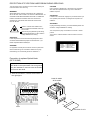
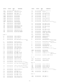
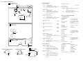
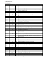
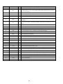
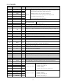
CSD-TD51 U(S),K(S),EZ(S)
CSD-TD52 U(W)
CSD-TD53 U(L)
SERVICE MANUAL
COMPACT DISC RADIO
CASSETTE RECORDER
• BASIC TAPE MECHANISM : TN-21ZVC-2000
• BASIC CD MECHANISM : DA11T3C
S/M Code No. 09-003-343-3R1
DA
TA
RE
VI
SIO
N
This Service Manual is the “Revision Publishing” and replaces “Simple Manual”
CSD-TD51 U(S)/TD52 U(W)/TD53 U(L)(S/M Code No. 09-003-343-3T1)
CSD-TD51 EZ(S),K(S)(S/M Code No. 09-003-343-3T2).
SPECIFICATIONS
U MODEL
EZ MODEL
•
•
Design and specifications are subject to change without
notice .
Design and specifications are subject to change without
notice .
K MODEL
•
Design and specifications are subject to change without
notice .
2
PROTECTION OF EYES FROM LASER BEAM DURING SERVICING
This set employs laser. Therefore, be sure to follow carefully the
instructions below when servicing.
CAUTION
Use of controls or adjustments or performance of procedures
other than those specified herein may result in hazardous
radiation exposure.
WARNING!
WHEN SERVICING, DO NOT APPROACH THE LASER EXIT
WITH THE EYE TOO CLOSELY. IN CASE IT IS NECESSARY TO
CONFIRM LASER BEAM EMISSION. BE SURE TO OBSERVE
FROM A DISTANCE OF MORE THAN 30cm FROM THE
SURFACE OF THE OBJECTIVE LENS ON THE OPTICAL
PICK-UP BLOCK.
ATTENTION
L'utilisation de commandes, réglages ou procédures autres que
ceux spécifiés peut entraîner une dangereuse exposition aux
radiations.
ADVARSEL!
Usynlig laserståling ved åbning, når sikkerhedsafbrydereer ude
af funktion. Undgå udsættelse for stråling.
Caution: Invisible laser radiation when
open and interlocks defeated avoid exposure to beam.
Advarsel:Usynling laserståling ved åbning,
når sikkerhedsafbrydere er ude af funktion.
Undgå udsættelse for stråling.
This Compact Disc player is classified as a CLASS 1 LASER
product.
The CLASS 1 LASER PRODUCT label is located on the rear
exterior.
VAROITUS!
Laiteen Käyttäminen muulla kuin tässä käyttöohjeessa mainitulla tavalla saattaa altistaa käyt-täjän turvallisuusluokan 1 ylittävälle näkymättömälle lasersäteilylle.
CLASS 1
KLASSE 1
LUOKAN 1
KLASS 1
VARNING!
Om apparaten används på annat sätt än vad som specificeras i
denna bruksanvising, kan användaren utsättas för osynling
laserstrålning, som överskrider gränsen för laserklass 1.
LASER PRODUCT
LASER PRODUKT
LASER LAITE
LASER APPARAT
Precaution to replace Optical block
(SF-P101NR)
Body or clothes electrostatic potential could ruin
laser diode in the optical block. Be sure ground
body and workbench, and use care the clothes
do not touch the diode.
1) After the connection, remove solder shown in
the right figure.
PICK UP ASSY
SF-P101NR
1
16
Solder
TO/FROM CD C.B
3
ELECTRICAL MAIN PARTS LIST
REF. NO
PART NO.
KANRI
NO.
DESCRIPTION
REF. NO
IC
87-A21-550-010
87-A21-185-040
87-A21-064-010
87-A21-520-040
87-A20-446-010
IC,TA2149N
C-IC,LC72121M
IC,LA4227
C-IC,M61509FP
C-IC,LA9241ML
87-A20-459-010
87-A21-093-010
8A-CH4-661-010
87-A21-431-010
C-IC,LC78622ED
IC,LA6541D
C-IC,LC867132V-5P07
IC,BA4560N
TRANSISTOR
89-327-143-080
87-026-447-080
89-111-624-080
87-026-213-080
89-503-025-010
TR,2SC2714 (0.1W)
TR,2SC1740S R
TR,2SA1162Y
CHIP-TR,DTC114YK
C-FET,2SK302GR<51 K<S>,51 EZ<S>>
89-320-011-080
TR,2SC2001 (15W)<51 K<S>,51
87-026-230-080
CHIP-TR,DTA114YK<51 K<S>,51
PART NO.
C317
C801
C805
C806
C807
KANRI
DESCRIPTION
NO.
87-010-197-080
CAP, CHIP 0.01 DM
87-010-248-080
CAP, ELECT 220-10V
87-012-365-080
C-CAP,S 0.027-25VBK
87-012-365-080
C-CAP,S 0.027-25VBK
87-010-405-080
CAP, ELECT 10-50V
C808
C809
C810
C811
C812
87-010-405-080
87-010-401-080
87-010-401-080
87-010-178-080
87-010-178-080
CAP,
CAP,
CAP,
CHIP
CHIP
C816
C817
C821
C822
C823
87-010-180-080
87-010-180-080
87-010-401-080
87-010-401-080
87-010-178-080
C-CER 1500P
C-CER 1500P
CAP, ELECT 1-50V
CAP, ELECT 1-50V
CHIP CAP 1000P
C824
C829
C830
C833
C834
87-010-178-080
87-010-178-080
87-010-178-080
87-018-195-080
87-010-248-080
CHIP
CHIP
CHIP
CAP,
CAP,
87-010-322-080
87-010-322-080
87-010-197-080
87-018-124-080
87-010-178-080
C-CAP,S 100P-50 CH
C-CAP,S 100P-50 CH
CAP, CHIP 0.01 DM
CAP, CER 270P-50V
CHIP CAP 1000P
ELECT 10-50V
ELECT 1-50V
ELECT 1-50V
CAP 1000P
CAP 1000P
CAP 1000P
CAP 1000P
CAP 1000P
CER 1200P-16V
ELECT 220-10V
EZ<S>>
89-327-125-080
89-112-965-080
87-026-463-080
CHIP TR,2SC2712GR
TR,2SA1296 (0.75W)
TR,2SA933S (0.3W)
C835
C836
C843
C844
C845
87-026-291-080
89-213-702-080
87-026-462-080
89-318-154-080
89-109-332-380
TR,DTC124XS
TR,2SB1370E
TR,2SC1740 S(RS 0.3W)
TR,2SC1815 (0.4W)
TR,2SA933RS
C846
C851
C852
C853
CN201
87-010-263-080
87-010-186-080
87-010-178-080
87-018-211-080
87-099-018-010
CAP, ELECT 100-10V
CAP,CHIP 4700P
CHIP CAP 1000P
CAP, CER 0.01-50
CONN,16P
89-113-187-080
87-026-295-080
87-026-237-080
87-026-239-080
87-026-464-080
TR,2SA1318TU
TR,DTC144TK
CHIP-TR,DTC124XK
TR,DTC114TK (0.2W)
TR,DTC114TS (0.3W)
CN801
CNA302
CNA801
L801
SW801
87-A60-110-010
8A-CD9-629-010
8A-CD9-630-010
87-007-342-010
8Z-CD9-609-010
CONN,4P V S2M-4W
CONN ASSY,6P MA-TU
CONN ASSY, 4P RPH
COIL,OSC 85K BIAS
SW,SL 1-6-2 PS62D01
C30
C251
C261
C262
C263
87-010-260-080
87-010-404-080
87-010-402-080
87-010-402-080
87-010-178-080
CAP,
CAP,
CAP,
CAP,
CHIP
ELECT 47-25V
ELECT 4.7-50V
ELECT 2.2-50V
ELECT 2.2-50V
CAP 1000P
C264
C265
C266
C267
C268
87-010-178-080
87-010-263-080
87-010-263-080
87-010-112-080
87-010-112-080
CHIP
CAP,
CAP,
CAP,
CAP,
CAP 1000P
ELECT 100-10V
ELECT 100-10V
ELECT 100-16V
ELECT 100-16V
C271
C272
C278
C279
C301
87-010-237-080
87-010-237-080
87-010-405-080
87-010-385-080
87-016-495-000
CAP, ELECT 1000-16V
CAP, ELECT 1000-16V
CAP, ELECT 10-50V
CAP, ELECT 220-25V
CAP,E 3300-25 M SMG
EZ<S>>
DIODE
CD C.B
87-070-345-080
87-A40-616-070
87-A40-128-080
87-017-072-080
87-027-399-080
DIODE,IN4148
VARI-CAP,SVC384(S/T)
C-VARI-CAP,HVU202A
ZENER,HZS3B1
ZENER,HZ7A3L (200MA)<51 U<S>,53
U<L>,52 U<W>>
87-027-607-080
87-A40-648-080
87-017-978-080
87-020-465-080
87-027-702-080
ZENER,HZ7B3L<51 K<S>,51 EZ<S>>
ZENER,MTZJ8.2A
DIODE,1N4003
DIODE,1SS133 (110MA)
DIODE,ZENER HZ6C2L (200MA)
87-A40-465-010
DIODE,FR202
C211
C212
C215
C216
C231
87-A11-603-080
87-A11-603-080
87-016-460-080
87-016-460-080
87-010-213-080
CAP, S 0.05-16
CAP, S 0.15-16
C-CAP,S 0.22-16 B
C-CAP,S 0.22-16 B
C-CAP,S 0.015-50 B
C306
C307
C308
C311
C312
87-010-404-080
87-010-401-080
87-010-221-080
87-010-263-080
87-010-385-080
CAP,
CAP,
CAP,
CAP,
CAP,
ELECT
ELECT
ELECT
ELECT
ELECT
C232
C233
C234
C235
C236
87-010-213-080
87-A10-201-080
87-A10-201-080
87-016-669-080
87-016-669-080
C-CAP,S 0.015-50 B
C-CAP,S0.33-16 KB
C-CAP,S0.33-16 KB
C-CAP,S 0.1-25 K B
C-CAP,S 0.1-25 K B
C321
C322
C325
C401
C402
87-010-197-080
87-010-263-080
87-010-405-080
87-010-403-080
87-010-197-080
CAP,
CAP,
CAP,
CAP,
CAP,
CHIP 0.01 DM
ELECT 100-10V
ELECT 10-50V
ELECT 3.3-50V
CHIP 0.01 DM
C237
C239
C240
C247
C248
87-010-371-080
87-010-197-080
87-010-197-080
87-010-401-080
87-010-401-080
CAP,
CAP,
CAP,
CAP,
CAP,
ELECT 470-50V
CHIP 0.01 DM
CHIP 0.01 DM
ELECT 1-50V
ELECT 1-50V
C403
C404
C405
C406
C407
87-010-263-080
87-010-248-080
87-010-197-080
87-010-374-080
87-010-178-080
CAP,
CAP,
CAP,
CAP,
CHIP
ELECT 100-10V
ELECT 220-10V
CHIP 0.01 DM
ELECT 47-10V
CAP 1000P
C310
C316
87-010-248-080
87-010-263-080
CAP, ELECT 220-10V
CAP,E 100-10
C408
C409
87-010-198-080
87-010-248-080
CAP, CHIP 0.022
CAP, ELECT 220-10V
MAIN C.B
4
4.7-50V
1-50V
470-10V
10-10V
220-25V
REF. NO
PART NO.
C410
C411
C412
C413
C414
KANRI
DESCRIPTION
NO.
87-010-263-080
CAP, ELECT 100-10V
87-A11-177-080
C-CAP,S 0.15-16 K B
87-010-401-080
CAP, ELECT 1-50V
87-016-369-080
C-CAP,S 0.033-25 B K
87-010-405-080
CAP, ELECT 10-50V
REF. NO
C503
C504
C505
C506
C510
KANRI
NO.
87-010-322-080
C-CAP,S
87-010-322-080
C-CAP,S
87-010-322-080
C-CAP,S
87-010-322-080
C-CAP,S
87-016-669-080
C-CAP,S
C416
C417
C418
C419
C420
87-010-545-080
87-012-157-080
87-010-213-080
87-A11-608-080
87-016-369-080
CAP, ELECT 0.22-50V
C-CAP,S 330P-50 CH
C-CAP,S 0.015-50 B
C-CAP,S 0.33-25 K B
C-CAP,S 0.033-25 B K
C831
CN202
CN205
CN301
CN401
87-010-198-080
8A-CH4-689-010
87-A60-109-010
8A-CH4-689-010
87-A60-424-010
CAP, CHIP 0.022
CONN,3P V 2.5
CONN,2P V S2M-2W
CONN,3P V 2.5
CONN,16P V TOC-B
C421
C422
C423
C424
C425
87-A11-177-080
87-010-183-080
87-010-956-080
87-010-993-080
87-010-176-080
C-CAP,S 0.15-16 K B
C-CAP,S 2700P-50 B
CHIP-CAP,S 0.068-25B
C-CAP,S 0.056-25 B
C-CAP,S 680P-50 SL
CN403
CN802
CNA205
CNA402
CNA802
87-099-201-010
8A-CH4-687-010
8A-CD9-631-010
8A-CD9-625-010
8A-CD9-631-010
CONN,8P 6216 H
CONN,4P V 2.5
CONN ASSY, 2P DOOR
CONN ASSY,6P CD-ME
CONN ASSY, 4P TP-ME
C426
C428
C429
C430
C431
87-A11-608-080
87-010-197-080
87-010-186-080
87-012-156-080
87-010-545-080
C-CAP,S 0.33-25 K B
CAP, CHIP 0.01 DM
CAP,CHIP 4700P
C-CAP,S 220P-50 CH
CAP, ELECT 0.22-50V
L401
L404
SFR430
SW205
X401
87-003-102-080
87-003-152-080
87-024-437-080
87-036-389-010
8Z-CD5-633-010
COIL, 10UH
COIL, 100UH
SFR100K,RH063EC
SW, PUSH 1-1-1 R8120125
VIB, CER16.93MHZ FCR16.93M2
C432
C433
C434
C435
C436
87-010-374-080
87-010-401-080
87-010-184-080
87-010-197-080
87-010-374-080
CAP,
CAP,
CHIP
CAP,
CAP,
C437
C438
C439
C440
C441
87-010-404-080
87-016-669-080
87-010-178-080
87-010-145-080
87-010-197-080
CAP, ELECT 4.7-50V
C-CAP,S 0.1-25 K B
CHIP CAP 1000P
C-CAP, S 1P-50 C CH
CAP, CHIP 0.01 DM
C601
C602
C603
C604
C605
87-010-313-080
87-010-315-080
87-010-319-080
87-010-312-080
87-010-317-080
CAP, CHIP 18P
C-CAP,S 27P-50
C-CAP,S 56P-50
C-CAP,S 15P-50
C-CAP,S 39P-50
C442
C445
C446
C447
C448
87-010-312-080
87-012-368-080
87-012-368-080
87-012-368-080
87-010-315-080
C-CAP,S
C-CAP,S
C-CAP,S
C-CAP,S
C-CAP,S
C607
C608
C610
C611
C612
87-010-196-080
87-010-196-080
87-010-555-040
87-010-196-080
87-A10-189-040
CHIP CAPACITOR,0.1-25
CHIP CAPACITOR,0.1-25
CAP,E 100-10 GAS
CHIP CAPACITOR,0.1-25
CAP,E 220-10
C450
C451
C455
C457
C458
87-012-140-080
87-012-156-080
87-010-247-080
87-010-312-080
87-010-312-080
CAP 470P
C-CAP,S 220P-50 CH
CAP, ELECT 100-50V
C-CAP,S 15P-50 CH
C-CAP,S 15P-50 CH
C613
C614
C615
C616
C620
87-010-495-040
87-010-196-080
87-010-493-040
87-010-494-040
87-015-785-080
CAP,E 2.2-50 GAS
CHIP CAPACITOR,0.1-25
CAP,E 0.47-50 GAS
CAP,E 1-50 GAS
CHIP CAPACITOR, 0.1FZ-25Z
C459
C460
C461
C462
C463
87-010-263-080
87-015-819-080
87-010-197-080
87-010-248-080
87-010-197-080
CAP, ELECT 100-10V
CAPACITOR,0.01
CAP, CHIP 0.01 DM
CAP, ELECT 220-10V
CAP, CHIP 0.01 DM
C625
C627
C629
C630
C631
87-A12-317-080
87-010-196-080
87-A12-317-080
87-A12-317-080
87-A12-317-080
C-CAP,U 0.1-50 Z F
CHIP CAPACITOR,0.1-25
C-CAP,U 0.1-50 Z F
C-CAP,U 0.1-50 Z F
C-CAP,U 0.1-50 Z F
C465
C466
C467
C469
C470
87-010-404-080
87-012-368-080
87-010-263-080
87-012-154-080
87-010-544-080
CAP, ELECT 4.7-50V
C-CAP,S 0.1-50 F
CAP, ELECT 100-10V
C-CAP,S 150P-50 CH
CAP, ELECT 0.1-50V
C632
C633
C635
C636
C637
87-A12-317-080
87-A12-317-080
87-012-195-080
87-012-195-080
87-012-195-080
C-CAP,U
C-CAP,U
C-CAP,S
C-CAP,S
C-CAP,S
0.1-50 Z F
0.1-50 Z F
100P-50 J CH
100P-50 J CH
100P-50 J CH
C471
C472
C473
C474
C475
87-015-785-080
87-015-785-080
87-015-785-080
87-015-785-080
87-010-197-080
CHIP
CHIP
CHIP
CHIP
CAP,
C638
C639
C640
C641
C642
87-012-195-080
87-012-195-080
87-012-195-080
87-012-195-080
87-012-195-080
C-CAP,S
C-CAP,S
C-CAP,S
C-CAP,S
C-CAP,S
100P-50
100P-50
100P-50
100P-50
100P-50
J
J
J
J
J
CH
CH
CH
CH
CH
C476
C477
C478
C479
C480
87-010-236-080
87-010-197-080
87-010-263-080
87-010-197-080
87-010-221-080
CAP,E 1000-10 SME
CAP, CHIP 0.01 DM
CAP, ELECT 100-10V
CAP, CHIP 0.01 DM
CAP, ELECT 470-10V
C643
C644
C645
C646
C647
87-012-195-080
87-012-195-080
87-012-195-080
87-012-195-080
87-012-195-080
C-CAP,S
C-CAP,S
C-CAP,S
C-CAP,S
C-CAP,S
100P-50
100P-50
100P-50
100P-50
100P-50
J
J
J
J
J
CH
CH
CH
CH
CH
C481
C482
C489
C490
C491
87-010-405-080
87-010-405-080
87-012-368-080
87-012-368-080
87-010-197-080
CAP, ELECT 10-50V
CAP, ELECT 10-50V
C-CAP,S 0.1-50 F
C-CAP,S 0.1-50 F
CAP, CHIP 0.01 DM
C648
C649
C650
C651
C652
87-012-195-080
87-012-195-080
87-012-195-080
87-012-195-080
87-012-195-080
C-CAP,S
C-CAP,S
C-CAP,S
C-CAP,S
C-CAP,S
100P-50
100P-50
100P-50
100P-50
100P-50
J
J
J
J
J
CH
CH
CH
CH
CH
C492
C494
C495
C501
C502
87-010-221-080
87-010-197-080
87-016-669-080
87-012-368-080
87-010-322-080
CAP, ELECT 470-10V
CAP, CHIP 0.01 DM
C-CAP,S 0.1-25 K B
C-CAP,S 0.1-50 F
C-CAP,S 100P-50 CH
C653
C654
C655
C656
C657
87-012-195-080
87-012-195-080
87-012-195-080
87-012-195-080
87-012-195-080
C-CAP,S
C-CAP,S
C-CAP,S
C-CAP,S
C-CAP,S
100P-50
100P-50
100P-50
100P-50
100P-50
J
J
J
J
J
CH
CH
CH
CH
CH
C658
CN601
87-A12-317-080
87-099-033-010
C-CAP,U 0.1-50 Z F
CONN,16P 6216 H
ELECT 47-10V
ELECT 1-50V
CAPACITOR 3300P(K)
CHIP 0.01 DM
ELECT 47-10V
15P-50
0.1-50
0.1-50
0.1-50
27P-50
PART NO.
DESCRIPTION
100P-50 CH
100P-50 CH
100P-50 CH
100P-50 CH
0.1-25 K B
FRONT C.B
CH
F
F
F
CH
CAPACITOR, 0.1FZ-25Z
CAPACITOR, 0.1FZ-25Z
CAPACITOR, 0.1FZ-25Z
CAPACITOR, 0.1FZ-25Z
CHIP 0.01 DM
5
CH
CH
CH
CH
REF. NO
PART NO.
CN602
CNA603
CNA604
L601
LCD601
KANRI
DESCRIPTION
NO.
87-099-201-010
CONN,8P 6216 H
8A-CD9-624-010
CONN ASSY,4P TU-FR
8A-CD9-623-010
CONN ASSY,4P KEY
87-003-102-080
COIL, 10UH
8Z-CH4-635-010
LCD,HLC7365 ZCH-4
REF. NO
C43
C44
C45
C46
C47
KANRI
DESCRIPTION
NO.
87-012-349-080
C-CAP,S 1000P-50 CH
87-010-311-080
CAP 12P
87-010-312-080
C-CAP,S 15P-50 CH
87-010-197-080
CAP, CHIP 0.01 DM
87-010-197-080
CAP, CHIP 0.01 DM
LED602
LED603
LED604
LED606
LED607
88-CD6-630-010
88-CD6-630-010
88-CD6-630-010
88-CD6-630-010
88-CD6-630-010
LED,934ID
LED,934ID
LED,934ID
LED,934ID
LED,934ID
C48
C49
C50
C51
C52
87-010-197-080
87-012-140-080
87-010-197-080
87-010-316-080
87-010-197-080
CAP, CHIP 0.01
CAP 470P
CAP, CHIP 0.01
C-CAP,S 33P-50
CAP, CHIP 0.01
LED608
LED610
S601
S604
S605
88-CD6-630-010
88-CD6-631-010
87-A90-164-080
87-A90-164-080
87-A90-164-080
LED,934ID RED
LED,934GD GRN
SW,TACT SKQAB(N)
SW,TACT SKQAB(N)
SW,TACT SKQAB(N)
C53
C54
87-010-197-080
87-014-055-080
C55
C71
C72
87-010-197-080
87-010-197-080
87-010-263-080
CAP, CHIP 0.01 DM
CAP,PP 820P-100 J<51 K<S>,51
EZ<S>>
CAP, CHIP 0.01 DM
CAP, CHIP 0.01 DM
CAP, ELECT 100-10V
S606
S607
S611
S613
S614
87-A91-704-080
87-A91-704-080
87-A90-164-080
87-A90-164-080
87-A91-704-080
SW,TACT
SW,TACT
SW,TACT
SW,TACT
SW,TACT
C73
C75
C91
C92
C93
87-010-197-080
87-010-197-080
87-012-140-080
87-010-197-080
87-010-197-080
CAP, CHIP
CAP, CHIP
CAP 470P
CAP, CHIP
CAP, CHIP
S615
X601
X602
87-A91-704-080
87-030-273-010
87-030-376-080
SW,TACT EVQ 214 05R
VIB,XTAL 32.768K5PPM
VIB,CER CSA5.76MG200
CF1
CF2
CF3
CN2
CN3
87-A91-094-010
87-008-261-010
87-008-261-010
87-099-854-010
87-A60-110-010
FLTR,CDA10.7 MG80A
FILTER, SFE10.7MA5-A
FILTER, SFE10.7MA5-A
CONN,6P S2M-6W
CONN,4P V S2M-4W
C1
C2
C3
C5
C6
87-010-314-080
87-010-316-080
87-010-314-080
87-A11-067-080
87-010-313-080
C-CAP,S 22P-50V
C-CAP,S 33P-50 CH
C-CAP,S 22P-50V
C-CAP,S 1-10 K B
CAP, CHIP 18P<51 U<S>,53 U<L>,52
U<W>>
CN605
HD1
HD2
L2
L3
87-A60-113-010
88-CD6-661-010
88-CD6-661-010
87-A50-560-010
8A-CH4-670-010
CONN,2P H S2M-2WR
HLDR,BAR ANT.
HLDR,BAR ANT.
COIL,FM BPF(ACD)
BAR-ANT,MW 2B-ACH(COI)<51 U<S>,53
U<L>,52 U<W>>
C7
C8
C10
C11
C12
87-014-049-080
87-012-349-080
87-010-197-080
87-010-197-080
87-010-197-080
CAP,PP 470P-100 J
C-CAP,S 1000P-50 CH
CAP, CHIP 0.01 DM
CAP, CHIP 0.01 DM
CAP, CHIP 0.01 DM
L3
8A-CH4-671-010
L4
L5
L6
L7
87-A50-420-010
87-A50-566-010
87-A50-567-010
87-A91-308-010
BAR-ANT,MW/LW 3B-ACH(COI)<51
K<S>,51 EZ<S>>
COIL,MW OSC(SYN)
COIL,FM RF EX(ACH)
COIL,FM OSC(ACH)
FLTR,PCFAZH- 450T (TOK)
C13
C14
C15
C16
C17
87-010-150-080
87-010-303-080
87-012-349-080
87-010-374-080
87-010-198-080
C-CAP,S 6P-50 CH
C-CAP,S 330P-50CH
C-CAP,S 1000P-50 CH
CAP, ELECT 47-10V
CAP, CHIP 0.022
L8
L51
87-005-849-080
87-A50-421-010
COIL,10UH(CECS)
COIL,LW OSC(SYN)<51 K<S>,51
C18
C19
C20
C21
C22
87-015-835-080
87-010-263-080
87-010-404-080
87-010-197-080
87-010-197-080
C-CAP,0.047 D
CAP, ELECT 100-10V
CAP, ELECT 4.7-50V
CAP, CHIP 0.01 DM
CAP, CHIP 0.01 DM
LED601
LED609
TC1
88-CD6-630-010
88-CD6-630-010
87-011-254-080
LED,934ID RED
LED,934ID RED
TRIMER,20P LAR
TC51
87-A91-659-010
X1
87-A70-061-010
TRIMMER,50P 4.0X4.5 ECRL<51
K<S>,51 EZ<S>>
VIB,XTAL 4.500MHZ CSA-309
C23
C24
C25
C27
C28
87-010-197-080
87-015-770-080
87-016-460-080
87-A11-067-080
87-016-669-080
CAP, CHIP 0.01 DM
C-CHIP,330P(SL)K
C-CAP,S 0.22-16 B
C-CAP,S 1-10 K B
C-CAP,S 0.1-25 K B
8A-CD9-628-010
87-A60-685-010
87-A60-569-010
CONN ASSY,3P MA-HP
CONN,4P H WHT EH
JACK,HTJ-035-18
C29
C30
87-016-669-080
87-010-213-080
C30
87-010-198-080
C31
87-010-213-080
C31
87-010-198-080
C-CAP,S 0.1-25 K B
C-CAP,S 0.015-50 B<51 K<S>,51
EZ<S>>
CAP, CHIP 0.022<51 U<S>,53
U<L>,52 U<W>>
C-CAP,S 0.015-50 B<51 K<S>,51
EZ<S>>
CAP, CHIP 0.022<51 U<S>,53
U<L>,52 U<W>>
C901
C902
C903
C904
CNA901
87-010-192-080
87-010-192-080
87-010-192-080
87-010-192-080
8A-CD9-627-010
C-CAP,S 0.022-50
C-CAP,S 0.022-50
C-CAP,S 0.022-50
C-CAP,S 0.022-50
CONN ASSY,3P PWR
C33
C34
C35
C36
C37
87-012-358-080
87-012-358-080
87-015-819-080
87-010-263-080
87-010-197-080
C-CAP,S 0.47-10 F Z
C-CAP,S 0.47-10 F Z
CAPACITOR,0.01
CAP, ELECT 100-10V
CAP, CHIP 0.01 DM
!PR901
87-A90-092-080
SP901
SP902
87-CD6-213-010
87-CD6-213-010
PROTECTOR,2.5A 491<51 K<S>,51
EZ<S>>
SPR-C,BATT (-)
SPR-C,BATT (-)
C38
C39
C40
C41
C42
87-010-374-080
87-010-404-080
87-010-197-080
87-012-349-080
87-012-349-080
CAP, ELECT 47-10V
CAP, ELECT 4.7-50V
CAP, CHIP 0.01 DM
C-CAP,S 1000P-50 CH
C-CAP,S 1000P-50 CH
BATT2 C.B
87-CD6-213-010
87-CD6-213-010
SPR-C,BATT (-)
SPR-C,BATT (-)
RED
RED
RED
RED
RED
EVQ 214 05R
EVQ 214 05R
SKQAB(N)
SKQAB(N)
EVQ 214 05R
TUNER C.B
PART NO.
DM
DM
CH
DM
0.01 DM
0.01 DM
0.01 DM
0.01 DM
EZ<S>>
H.P. CB
CN101
CN102
HP1
BATT1 C.B
SP903
SP904
6
F
F
F
F
LCD DISPLAY
REF. NO
PART NO.
KANRI
NO.
DESCRIPTION
MOTOR C.B
M2
PIN3
SW1
9X-262-576-910
91-564-722-110
91-572-085-120
MOTOR GEAR ASSY
CONNECTOR 6P
LEAF SW
87-A91-704-080
87-A90-164-080
87-A90-164-080
SW,TACT EVQ 214 05R
SW,TACT SKQAB(N)
SW,TACT SKQAB(N)
KEY C.B
S608
S609
S610
• Regarding connectors, they are not stocked as they are not the initial order items.
The connectors are available after they are supplied from connector manufacturers upon the order is received.
CHIP RESISTOR PART CODE
Chip Resistor Part Coding
8 8
A
Figure
Resistor Code
Value of resistor
Chip resistor
L
W
t
:A
Resistor Code : A
1.0
0.5
0.35
104
Dimensions (mm)
Wattage
1/16W
Type
1005
Tolerance
5%
Symbol
CJ
1/16W
1/10W
1608
2125
5%
5%
CJ
CJ
1/8W
3216
5%
CJ
Form
L
t
W
1.6
0.8
0.45
108
2
1.25
0.45
118
3.2
1.6
0.55
128
TRANSISTOR ILLUSTRATION
ECB
ECB
2SA1296
2SC1815
2SC2001
C
B
ECB
2SA1162
2SC2712
2SC2714
DTA114YK
DTC114TK
DTC114YK
DTC124XK
DTC144TK
2SA1318
2SA933
2SC1740
DTC114TS
DTC124XS
S
D
E
ECB
G
2SK302
BCE
2SB1370
7
8
WIRING-1 (MAIN/CD)
1
2
3
4
5
6
7
8
9
10
11
12
A
B
C
D
E
F
G
H
I
J
K
9
10
13
14
SCHEMATIC DIAGRAM-1 (MAIN)
NM : NO MOUNTED
11
12
SCHEMATIC DIAGRAM-2 (CD)
13
14
WIRING-2 (MOTOR)
1
2
3
4
5
6
7
IC BLOCK DIAGRAM
IC, LC7212M
IC, LA6541D
A
B
H MOTOR C.B
C
M2
IC, TA2149N
+
D
F
G
IC, M61509FP
SW1
(INSIDE LIMIT SW)
mono. SW
M3
(SPINDLE MOTOR)
PIN3
E
TO B CD C.B CNA402
_
M2
(SLED MOTOR)
SW1
_
+
M3
Control logic
H
IC, BA4560N
I
J
K
15
16
WIRING-3 (FRONT/HP/BATT1/BATT2/KEY)
1
2
3
4
5
6
7
9
8
11
10
12
13
A
F BATT1 C.B
G BATT2 C.B
(INSERTED PARTS)
E HP C.B
(INSERTED PARTS)
B
A
SPEAKER
B
L
R
4
EZ,K
MODEL
1
U MODEL
SP902
SP901
3
SP903
DRY BATTERY
R14x8
DC 12V
HP1
PHONES
C
SP904
1
TO B CD C.B
CN301
D
J1
AC
TO B CD C.B
CN202
PT901
B
AC
A
TO A MAIN C.B
CN201
TO B CD C.B (2/2)
CN403
DC
U:AC 120V 60Hz
EZ,K:AC 230V 50Hz
E
C FRONT C.B
15
16
1 7
2 8
1
2
C FRONT C.B
(INSERTED PARTS)
(CHIP PARTS)
I KEY C.B
I KEY C.B
(CHIP PARTS)
(INSERTED PARTS)
F
S613
3 MODE
EQUALIZER
S609
BAND
RADIO
TO D TUNER C.B
CN003
1
S610
POWER
STANDBY
TAPE
4
CNA603
S611
QSOUND
S608
CD
1
3
G
P2
NOTE
123
Rxxx
H
S615
EZ,K MODEL
U MODEL
VOLUME
LED608
STANDBY
OPE/BATT
S601
FM MODE
/OSC
E C B
LED610
QSOUND
P1 1
3
E C B
1
2
3
S614
I
PLAY/PAUSE
EXCEPT
U LC
S606
J
S607
PLAY/PAUSE/PRESET
S605
SKIP/SEARCH
TUNING
ROCK
POP
JAZZ
RADIO
CD
S604
STOP/MEMORY
K
17
18
14
SCHEMATIC DIAGRAM-3 (FRONT/KEY)
C FRONT C.B
HLC7365 ZCH-4
(DISPLAY)
L-934ND
S20
S21
S22
S23
TO B CD C.B (2/2)
CN403
C657-635
100P
R637
100K
R636
1K
COM3
L-934ND
R
C631
0.1
#
R657 1K
C630
0.1
R
R635
1K
C629
0.1
L-934ND
#
#
R
#
O-H.DUBB
-5907
SYSTEM CONTROL
#
#
#
L-934ID
C632
0.1
O-DUBB
LED
TO A MAIN C.B
CN201
R653 100
L604 1µH
RADIO
R638
1K
R
R639
1K
C633
0.1
L-934ID
R
C634
0.1
50
L602
4.7µH
0.1
L605
1µH
R
L-934GD
R654
10
R655 100
Q605-610
LED DRIVER
C625 0.1
O-QSOUND
AC 12V
C627 0.1
I KEY C.B
TO D TUNER C.B
CN003
32.768
MHz
R656
10
5.76
MHz
P1
3
P2
3
P1
2
P2
2
P2
1
P1
1
L603
1µH
RESET
R
R
SW
HOLD
#
FM MODE/OSC
3 MODE EQUALIZER
1SS133
1SS133
VOLUME
VOLUME
1SS133
19
1SS133
20
STANDBY
OPE/BATT
L-934ID
SCHEMATIC DIAGRAM-4 (TUNER U)
21
22
WIRING-4 (TUNER: U)
1
2
3
4
A
B
C
D
E
F
G
H
I
J
K
23
5
6
7
WIRING-5 (TUNER: EZ, K)
1
2
3
4
A
B
C
D
E
F
G
H
I
J
K
24
5
6
7
SCHEMATIC DIAGRAM-5 (TUNER EZ/K)
25
26
ELECTRICAL ADJUSTMENT
< TUNER SECTION >
D TUNER C.B
567
TC001
2
1
L003 (MW BAR ANT)
L004
L051
3
123
TP2(VT)
TC051
+
L006
L005
C039
TP1(DET)
16
4
21
IC001
IC002
1
1
L007
89
1. FM VT Adjustment
Settings : • Test point : TP2 (VT)
• Adjustment location :
L006
Method : Set to FM 108.0MHz and adjust L006 so that the
test point voltage becomes 6.0V ± 0.05V.
12. Bias frequncy Adjustment
L801..................................................................85kHz±0.5kHz
< CD SECTION >
13. FE Balance Adjustment
Settings : • Test point : IC401 PIN58 (VR), IC401 PIN 20
(FE)
• Adjustment location : SFR430
Method : Playback the disc and adjust SFR430 so that the
test point voltage becomes 0V.
2. MW VT Adjustment
Settings : • Test point : TP2 (VT)
• Adjustment location :
L004
Method : Set to MW 1000kHz (U), MW 999kHz (EZ,K)
and adjust L004 so that the test point voltage
becomes 3.75V ± 0.05V.
3. LW VT Adjustment <EZ,K>
Settings : • Test point : TP2 (VT)
• Adjustment location :
L051
Method : Set to LW 288kHz and adjust L051 so that the
test point voltage becomes 4.5V ± 0.05V.
PRACTICAL SERVICE FIGURE
< TUNER SECTION >
< FM SECTION >
Sensitivity:
(THD 3%)
4. FM Tracking Adjustment
L005.........................................................................98.0MHz
Signal to Noise Ratio:
(Input 60dB)
5. MW Tracking Adjustment <U>
L003...........................................................................600kHz
TC001.......................................................................1400kHz
B CD C.B
Distortion:
(Input 60dB)
Intermediate frequency:
Stereo separation:
6. MW Tracking Adjustment <EZ,K>
L003...........................................................................603kHz
TC001.......................................................................1404kHz
SFR430
#
Sensitivity:
(S/N 10dB)
Distortion:
(Input 74dB)
Intermediate frequency:
8. AM IF Adjustment <U>
Settings : • Test point : TP1(DET)
• Adjustment location :
L007
Method : Adjust L007 so that the output level at 1400kHz
becomes maximum.
CN401
A MAIN C.B
IC801
CN801
CN201
Sensitivity:
(S/N 10dB)
9. AM IF Adjustment <EZ,K>
Settings : • Test point : TP1 (DET)
• Adjustment location :
L007
Method : Adjust L007 so that the output level at 1404kHz
becomes maximum.
Distortion:
(Input 80dB)
Intermediate frequency:
E H.P. C.B
CASSETTE DECK HEAD
J251 PHONES
0
0!
!
27
450kHz
Less than 60dB (at 153kHz)
Less than 56dB (at 198kHz)
Less than 52dB (at 288kHz)
Less than 3%
450kHz
< CASSETTE SECTION >
< DECK SECTION >
CASSETTE DECK MOTOR
Less than 48dB (at 600kHz)
Less than 46dB (at 1000kHz)
Less than 44dB (at 1400kHz)
Less than 3%
< LW SECTION >
L801
@
10.7MHz
More than 20dB
< AM SECTION >
7. LW Tracking Adjustment <EZ,K>
L003...........................................................................153kHz
TC051.........................................................................288kHz
IC404
Less than 18dB (87.5MHz)
Less than 18dB (98.0MHz)
Less than 18dB (108.0MHz)
More than 66dB (at 98.0MHz)
(EXCEPT U)
More than 58dB (at 98.0MHz)
(U)
Less than 3% (at 98.0MHz)
Tape speed:
Wow & flutter:
Take-up torque:
FF torque:
Rew torque:
S/N ratio:
Distortion:
Noise (PB):
10. Tape Speed Adjustment
Settings : • Test tape : TTA–100
• Test point : J251 (PHONES jack)
• Adjustment location : SFR of deck motor
Method : Play back the test tape and adjust SFR so that
the frequency counter reads 3000Hz ± 30Hz.
11. Head Azimuth Adjustment
Settings : • Test tape : TTA–320
• Test point : J251 (PHONES jack)
• Adjustment location : Azimuth adjustment
screw
Method : Play back the 8kHz signal of the test tape and
adjust screw so that the output becomes
maximum.
Erasing Ratio (W/FILTER):
28
3000Hz±60Hz
Less than 0.3% (JIS RMS)
30-60g-cm (FWD)
55-140g-cm
55-140g-cm
More than 35dB
Less than 3.0% (PB)
Less than 1mV
(AC/DC, MIN)
More than 45dB
IC DESCRIPTION
IC, LA9241ML
Pin No.
Pin Name
I/O
1
FIN2
I
Description
Pin to which external pickup photo diode is connected. RF signal is created by adding
with the FIN1 pin signal. FE signal is created by subtracting from the FIN1 pin signal.
2
FIN1
I
3
E
I
Pin to which external pickup photo diode is connected.
Pin to which external pickup photo diode is connected. TE signal is created by
subtracting from the F pin signal.
4
F
I
Pin to which external pickup photo diode is connected.
5
TB
I
DC component of the TE signal is input.
6
TE-
I
Pin to which external resistor setting the TE signal gain is connected between the TE
pin.
7
TE
O
8
TESI
I
TE signal output pin.
TES “Track Error Sense” comparator input pin. TE signal is passed through a bandpass filter then input.
9
SCI
I
Shock detection signal input pin.
10
TH
I
Tracking gain time constant setting pin.
11
TA
O
TA amplifier output pin.
12
TD-
I
Pin to which external tracking phase compensation constants are connected between
the TD and VR pins.
13
TD
I
Tracking phase compensation setting pin.
14
JP
I
Tracking jump signal (kick pulse) amplitude setting pin.
15
TO
O
Tracking control signal output pin.
16
FD
O
Focusing control signal output pin.
17
FD-
I
Pin to which external focusing phase compensation constants are connected between
the FD and FA pins.
18
FA
I
Pin to which external focusing phase compensation constants are connected between
the FD– and FA– pins.
19
FA-
I
Pin to which external focusing phase compensation constants are connected between
the FA and FE pins.
20
FE
O
FE signal output pin.
21
FE-
I
Pin to which external FE signal gain setting resistor is connected between the FE pin.
22
AGND
—
Analog signal GND.
23
SP
O
Signal ended output of the CV+and CV- pin input signal.
24
SPI
I
Spndle amp input.
25
SPG
I
Pin to which external spindle gain setting resistor in 12 cm mode is connected.
26
SP-
I
Pin to which external spindle phase compensation constants are connected together
with SPD pin.
27
SPD
O
Spindle control signal output pin.
28
SLEQ
I
Pin to which external sled phase compensation constants are connected.
29
SLD
O
Sled control signal output pin.
30, 31
SL-, SL+
I
Sled advance signal input pin from microprocessor.
32, 33
JP-, JP+
I
Tracking jump signal input pin from DSP.
34
TGL
I
Tracking gain control signal input from DSP. Low gain when TGL = H.
35
TOFF
I
Tracking off control signal input pin from DSP. Off when TOFF = H.
29
Pin No.
Pin Name
I/O
36
TES
O
37
HFL
O
Description
Pin from which TES signal is output to DSP.
“High Frequency Level” is used to judge whether the main beam position is on top of
bit or on top of mirror.
38
SLOF
I
Sled servo off control input pin.
39, 40
CV–, CV+
I
CLV error signal input pin from DSP.
41
RFSM
O
RF output pin.
42
RFS-
I
RF gain setting and EFM signal 3T compensation constant setting pin together with
RFSM pin.
43
SLC
O
“Slice Level Control” is the output pin which controls the RF signal data slice level by
DSP.
44
SLI
I
Input pin which control the data slice level by the DSP.
45
DGND
—
Digital system GND.
46
FSC
O
Output pin to which external focus search smoothing capacitor is connected.
47
TBC
I
“Tracking Balance Control” EF balance variable range setting pin.
48
NC
—
No connection.
49
DEF
O
Disc defect detector output pin.
50
CLK
I
Reference clock input pin. 4.23 MHz of the DSP is input.
51
CL
I
Microprocessor command clock input pin.
52
DAT
I
Microprocessor command data input pin.
53
CE
I
Microprocessor command chip enable input pin.
54
DRF
O
“Detect RF” RF level detector output.
55
FSS
I
“Focus Search Select” focus search mode (± search/+ search) select pin.
56
VCC2
—
Servo system and digital system Vcc pin.
57
REFI
—
Pin to which external bypass capacitor for reference voltage is connected.
58
VR
O
Reference voltage output pin.
59
LF2
I
Disc defect detector time constant setting pin.
60
PH1
I
Pin to which external capacitor for RF signal peak holding is connected.
61
BH1
I
Pin to which external capacitor for RF signal bottom holding is connected.
62
LDD
O
APC circuit output pin.
63
LDS
I
APC circuit input pin.
64
VCC1
—
RF system Vcc pin.
30
IC, LC78622ED
Pin No.
Pin Name
I/O
1
DEFI
I
2
TAI
I
Test signal input pin with built-in pull-down resistor. Be sure to connect to 0V.
3
PDO
O
Phase comparator output pin to control external VCO.
4
VVSS
—
5
ISET
I
6
VVDD
—
7
FR
I
8
VSS
—
9
EFMO
O
10
EFMIN
I
EFM signal input pin.
11
T2
I
Test signal input pin with built-in pull-down resistor. Be sure to connect to 0V.
12, 13
CLV+, CLK-
O
Disc motor control output. Three level output is possible using command.
14
V/P
___
O
Description
Defect sense signal (DEF) input pin. (Connect to 0V when not used).
For PLL.
GND pin for built-in VCO. Be sure to connect to 0V.
Pin to which external resistor adjusting the PD0 output current.
Power supply pin for built-in VCO.
Pin for VCO frequency range adjustment.
Digital system GND. Be sure to connect to 0V.
For slice level control.
EFM signal output pin.
Rough servo or phase control automatic selection monitoring output pin. Rough servo
at H. Phase servo at L.
15
HFL
I
Track detect signal input pin. Schmidt input.
16
TES
I
Tracking error signal input pin. Schmidt input.
17
TOFF
O
Tracking OFF output pin.
18
TGL
O
Tracking gain selection output pin. Gain boost at L.
19, 20
JP+, JP-
O
Track jump control signal output pin. Three level output is possible using command.
21
PCK
O
EFM data playback clock monitoring pin 4.3218 MHz when phase is locked in.
22
FSEQ
O
Sync signal detection output pin. H when the sync signal which is detected from EFM
signal and thesync signal which is internally generated agree.
23
VDD
—
Digital system power supply pin.
24
SL+
O
Moves the sled to outer circumference.
25
SL-
O
Moves the sled to inner circumference.
26
CONT3 (NC)
—
Not connected.
27
PUIN
I
CD pickup inner switch detection.
_______
28
RW
O
Read, wright signal.
29
EMPH
O
De-emphasis monitor output pin. De-emphasis disc is being played back at H.
30
C2F
O
C2 flag output pin.
31
DOUT
O
DIGITAL OUT output pin. (EIAJ format).
32, 33
T3, T4
I
Test signal input pin with built-in pull-down resistor. Be sure to connect to 0V.
34
N.C.
—
35
MUTEL
O
36
LVDD
—
37
LCHO
O
L-channel output pin.
38
LVSS
—
L-channel GND. Be sure to connect to 0V.
39
RVSS
—
R-channel GND. Be sure to connect to 0V.
40
RCHO
O
41
RVDD
—
R-channel power supply pin.
42
MUTER
O
R-channel mute output pin.
Not used. Set the pin to open.
L-channel mute output pin.
L-channel 1-bit DAC.
R-channel 1-bit DAC.
31
L-channel power supply pin.
R-channel output pin.
Pin No.
Pin Name
I/O
Description
43
XVDD
—
44
XOUT
O
45
XIN
I
46
XVSS
—
Crystal oscillator GND pin. Be sure to connect to 0V.
47
SBSY
O
Subcode block sync signal output pin.
48
EFLG
O
C1, C2, single and dual correction monitoring pin.
49
PW
O
Subcode P, Q, R, S, T, U and W output pin.
50
SFSY
O
Subcode frame sync signal output pin. Falls down when subcode enters standby.
51
SBCK
I
Crystal oscillator power supply pin.
Pin to which external 16.9344 MHz crystal oscillator is connected.
Subcode read clock input pin. Schmidt input. (Be sure to connected to 0V when not
in use.)
52
FSX
O
Pin outputting the 7.35 kHz sync signal which is generated by dividing frequency of
crystal oscillator.
53
WRQ
O
Subcode Q output standby output pin.
54
RWC
I
Read/write control input pin. Schmidt input.
55
SQOUT
O
Subcode Q output pin.
COIN
I
Command input pin from microprocessor.
56
___________
57
CQCK
I
Command input read clock or subcode read input clock from SQOUT pin
58
RES
I
LC78622 reset input pin. Set this pin to L once when the main power is turned on.
59
T11
O
Test signal output pin. Use this pin as open (normally L output).
60
16M
O
16.9344 MHz output pin.
61
4.2M
O
4.2336 MHz output pin.
62
T5
I
Test signal input pin with built-in pull-down resistor. Be sure to connect to 0V.
______
63
CS
I
Chip select signal input pin with built-in pull-down resistor. Be sure to connect to 0V
while it is not controlling.
64
T1
I
Test signal input pin without built-in pull-down resistor. Be sure to connect to 0V.
32
IC, LC867132V-5P07
Pin No.
Pin Name
I/O
Description
Pin No.
Pin Name
I/O
1
O-RMC/CE
O
CD read/write control output and TU CE.
2
O-DATA
O
3
O-CLK
4
51-54
S20- S23
—
Not connected.
Data output to M62495FP.
55
O-CD LED
O
LED ON/OFF control output for CD functions.
O
Output CLK to tuner PLL.(Not connected)
56
O-TU LED
O
LED ON/OFF control output for TU functions.
—
—
Not Connected.
57
O-TA LED
O
LED ON/OFF control output for TAPE functions. (Not Connected)
5
O-CLK SFT
O
Clock shift output of the microcomputer.
58
O-ROCK LED
O
LED ON/OFF control output for ROCK.
6
I-HOLD
I
Hold status detection.
59
O-POP LED
O
LED ON/OFF control output for POP.
7
RST
I
Microcomputer reset.
60
O-JAZZ LED
O
LED ON/OFF control output for JAZZ.
8
XT1 (IN)
I
61
—
—
Not connected.
9
XT2 (OUT)
O
62
I-CD TEST
—
Not connected.
10
VSS1
—
63
I-TU TEST
—
Not connected.
11
CF1 (IN)
I
64-66
COM0-COM2
O
LCD common output.
12
CF2 (OUT)
O
67
—
—
Not connected.
13
VDD1
—
Power supply for microcomputer (+5V).
68
VSS2
—
GND.
14
I-ST IND
I
FM STEREO status input.
69
VDD2
—
Power supply for microcomputer (+5V).
15
I-KEYO
I
KEY AD input.
70
O-CD ON
O
CD PWR control output.
16
I-CD SW
I
CD DOOR SW status detection input.
71
O-TU ON
O
TU PWR control output.
17
I-KEY1
I
KEY AD input.
72
O-P.CONT
O
Power supply control output.
Connected to 32.768KHZ crystal oscillator.
GND.
Connected to 6MHZ Ceramic Filter.
Description
___________________
18
I-MOTOR
I
DECK MECHA MOTOR status input.
73
O-H.DUBB
O
Dubbing speed control output.
19
I-REC
I
REC status input.
74
O-MUTE
O
Main mute output.
20
I-FM/AM
I
FM, AM status input. (Not connected)
75
O-MO/ST
O
FM mono/stereo output.
21
I-TU DO
I
Data input from tuner PLL.(Not connected)
76
O-BEAT CONT
O
BEAT switch over output.
22
O-BASS LED
O
BASS LED ON/OFF control output.
77
O-QSOUND
O
Q-Sound ON/OFF output.
23
O-QS LED
O
Q-Sound LED ON/OFF control output.
78
O-COIN
O
CD command output.
24
O-DUBB LED
O
LED control output used for high-speed dubbing.
79
I-SQOUT
I
CD sub-code Q input.
25
O-INT
O
INT DIODE MATRIX detection output.(Not connected)
80
O-CQCK
O
CLK for CD commands/sub-codes.
26
I-DRF
I
CD RF level detection input.
27
I-WRQ
I
CD sub-code Q standby input.
28
I-REMO
I
Remote control input.
29
S0/PA0
O
LCD segment output.
30
S1/PA1
O
LCD segment output.
31
S2/PA2
O
LCD segment output.
32
S3/PA3
O
LCD segment output.
33
S4/PA4
O
LCD segment output.
34
S5/PA5
O
LCD segment output.
35
S6/PA6
O
LCD segment output.
36
S7/PA7
O
37-40
S8~S11
O
41
VDD3
—
Power supply for microcomputer (+5V).
42
VSS3
—
GND.
43, 44
S12, S13
O
LCD segment output.
45-50
S14- S19
O
LCD segment output.
LCD segment output.
33
34
MECHANICAL EXPLODED VIEW 1/1
32
34
35
36
33
18
48
47
13
31
B
LCD
17
30
P.C.B
29
D
C
28
H
e
I
11
b
26
A
B
38
19
P.C.B
27
37
20
F
F
D
c
D
CUSHION,
CD A
H
E
23
J
A
5
39
44
41
d
42
21
a
P.C.B
D
GRILLE, SPKR L
D
16
SHIELD
PLATE
CUSHION,
CD A
22
H
E
G
25
TN-21ZVC-2000
8
14
24
CHAS,TU A
D
K
P.C.B
7
BAR, ANT
A
10
P.C.B
B
D
45
11
b
WIRE, FASTON ASSY ANT
c
8
d
9
B
49
D
4
15
2
GRILLE, SPKR R
1
CABI, FR U
35
B
40
9
3
46
B
A
10
B
P.C.B
D
a
RUBBER FOOT
CHAS,TU B
43
12
e
D
F
HT-SINK
P.C.B
6
43
P.C.B
36
MECHANICAL PARTS LIST 1/1
REF. NO
KANRI
DESCRIPTION
NO.
1 8Z-CL7-107-010
BADGE,AIWA SILVER
2 8A-CD8-007-010
WINDOW,CASS<EXCEPT 53 U<L>,52
U<W>>
2 8A-CH8-040-010
WINDOW,CASS (L)<53 U<L>>
2 8A-CH8-021-010
WINDOW,CASS (W)<52 U<W>>
3 8A-CD8-006-010
BOX,CASS<EXCEPT 53 U<L>,52 U<W>>
3
3
4
5
6
PART NO.
8A-CH8-039-010
8A-CH8-020-010
8A-CD8-207-010
8A-CD8-209-010
8A-CD8-018-010
REF. NO
PART NO.
KANRI
NO.
8A-CH8-037-010
8A-CH8-018-010
8A-CD8-027-010
8A-CH8-038-010
8A-CH8-019-010
32
32
32
33
33
BOX,CASS (L)<53 U<L>>
BOX,CASS (W)<52 U<W>>
SPR-T,CASS
HLDR,TRANS
PANEL,FR L<EXCEPT 53 U<L>,52
DESCRIPTION
BOX,CD (L)<53 U<L>>
BOX,CD (W)<52 U<W>>
BOX,CD EX<EXCEPT 53 U<L>,52 U<W>>
CHAS,CD (L)<53 U<L>>
CHAS,CD (W)<52 U<W>>
33 8A-CD8-028-010
CHAS,CD EX<EXCEPT 53 U<L>,52
34
34
34
35
U<W>>
HANDL,FR<EXCEPT 53 U<L>,52 U<W>>
HANDL,FR (L)<53 U<L>>
HANDL,FR (W)<52 U<W>>
SW,PUSH LOCK
8A-CD8-008-010
8A-CH8-041-010
8A-CH8-022-010
87-036-389-010
U<W>>
6
6
7
7
8A-CH8-048-010
8A-CH8-029-010
8A-CH8-014-010
8A-CH8-003-010
8 88-CD8-622-010
(L)<53 U<L>>
(W)<52 U<W>>
EX<51 K<S>,51 EZ<S>>
U<51 U<S>,53 U<L>,52
U<W>>
SPKR,F 77 7OHM 3W
36 8A-CD8-009-010
HANDL,REAR<EXCEPT 53 U<L>,52
!
36
37
38
39
HANDL,REAR (W)<52 U<W>>
SPR-T,CD
BRACKET
PT,E 2.5W<51 K<S>,51 EZ<S>>
!
39 8A-CD8-602-010
PT,U 2.5W<51 U<S>,53 U<L>,52
40 8A-CD9-630-010
41 87-A60-178-010
41 87-A60-177-010
42 87-A90-086-010
U<W>>
CONN ASSY,4P RPH
JACK,AC E W/SW<51 K<S>,51 EZ<S>>
JACK,AC U W/SW<51 U<S>,53 U<L>,52
U<W>>
COVER,AC-SOCKET
43
44
45
46
46
88-CD8-209-010
8A-CD8-212-010
8A-CD9-620-010
8A-CD8-003-010
8A-CH8-036-010
SPR-C,BATT
HLDR,ANT
FF-CABLE, 16P FR-MAIN
LID,BATT<EXCEPT 53 U<L>,52 U<W>>
LID,BATT (L)<53 U<L>>
46
47
47
47
48
8A-CH8-017-010
8A-CH8-002-010
8A-CH8-035-010
8A-CH8-016-010
8Z-CH4-640-010
LID,BATT (W)<52 U<W>>
CABI,REAR<EXCEPT 53 U<L>,52 U<W>>
CABI,REAR (L)<53 U<L>>
CABI,REAR U (W)<52 U<W>>
ANT,ROD
49
A
B
C
D
8A-CD9-631-010
87-B10-242-010
87-641-096-410
87-254-097-410
87-741-095-410
CONN ASSY,4P TP-ME
UT2+3-30 W/O CR
UT1+3-10 GLD
U+3-12 CR
UT2+3-8 GLD
E
F
G
H
I
87-342-074-010
87-353-076-210
87-571-032-410
87-WA5-253-010
87-751-094-410
UT2+2.6-8
VT2+2.6-12
VIT+2-3
W,3.3-10-0.8
VT2+3-6 W10SL0T
PANEL,FR L
PANEL,FR L
WINDOW,LCD
WINDOW,LCD
9
10
11
12
12
8A-CD8-210-010
8A-CD8-211-010
84-CD5-215-010
8A-CD8-021-010
8A-CH8-047-010
HLDR,SPKR A
HLDR,SPKR B
GEAR
CHAS,CASS<EXCEPT 53 U<L>,52 U<W>>
CHAS,CASS (L)<53 U<L>>
12
13
14
15
8A-CH8-031-010
8A-CD9-633-010
8A-CD9-626-010
8A-CD8-022-010
CHAS,CASS (W)<52 U<W>>
CONN ASSY,4P SP
CONN ASSY,2P DOOR
PANEL,FR R<EXCEPT 53 U<L>,52
U<W>>
U<W>>
15 8A-CH8-049-010
PANEL,FR R (L)<53 U<L>>
15 8A-CH8-030-010
16 8A-CH8-005-010
16 8A-CH8-046-010
16 8A-CH8-027-010
17 8A-CD8-014-010
PANEL,FR R (W)<52 U<W>>
KEY,CONTROL CD<EXCEPT 53 U<L>,52
U<W>>
KEY,CONTROL CD (L)<53 U<L>>
KEY,CONTROL CD (W)<52 U<W>>
KEY,VOL<EXCEPT 53 U<L>,52 U<W>>
17
17
18
19
20
8A-CH8-044-010
8A-CH8-025-010
8A-CD8-017-010
8A-CH8-201-010
8A-CH8-004-010
KEY,VOL (L)<53 U<L>>
KEY,VOL (W)<52 U<W>>
KEY,QSOUND
HLDR,LCD
KEY,FUNC<EXCEPT 53 U<L>,52 U<W>>
20
20
21
21
21
8A-CH8-045-010
8A-CH8-026-010
8A-CH8-043-010
8A-CH8-024-010
8A-CD8-011-010
KEY,FUNC
KEY,FUNC
KEY,CASS
KEY,CASS
KEY,CASS
(L)<53 U<L>>
(W)<52 U<W>>
(L)<53 U<L>>
(W)<52 U<W>>
SET<EXCEPT 53 U<L>,52
U<W>>
22
23
24
25
26
8A-CD8-213-010
M8-ZZK-E90-070
8A-CD9-622-010
8A-CD9-621-010
8Z-CDB-169-010
SPR-P,REC
DA11T3C
FF-CABLE, 8P CD-FR
FF-CABLE, 16P CD-RF
PANEL,CD SANYO
27
28
29
30
31
88-CD9-211-210
8Z-CDB-170-010
87-036-368-010
84-CT5-209-010
8Z-CH4-225-110
RING,CHUCK
BASE,CHUCK
MAGNET
PLATE,MAGNET
HLDR,CHUCK A(S)
8A-CH8-023-010
8A-CD8-208-010
84-CD5-216-010
8A-CD8-603-010
J 87-661-097-410
k 87-067-566-010
TAPPING SCREW, VFT1+3-12
TAPPING SCREW, VFTT+3-6
COLOR NAME TABLE
Basic color symbol
Color
Basic color symbol
Color
Basic color symbol
Color
B
Black
C
Cream
D
Orange
G
Green
H
Gray
L
Blue
LT
Transparent Blue
N
Gold
P
Pink
R
Red
S
Silver
ST
Titan Silver
T
Brown
V
Violet
W
White
WT
Transparent White
Y
Yellow
YT
Transparent Yellow
LM
Metallic Blue
LL
Light Blue
GT
Transparent Green
LD
Dark Blue
DT
Transparent Orange
37
TAPE MECHANISM EXPLODED VIEW 1/1
F
LUG PLATE
G
52
1
46
E
2
4
3
5
47
8
25
11
a
10
9
J
L
12
21
20
b
22
14
16
18
23
13
15
31
17
19
49
30
24
32
34
36
c
35
c
51
26
33
b
A
27
28
A
6
29
a
7
C
48
37
C
38
40
39
D
D
K
41
42
I
B
B
50
43
H
45
38
44
TAPE MECHANISM PARTS LIST 1/1
REF. NO
KANRI
DESCRIPTION
NO.
S1-921-030-4A0
HEAD BASE
S1-821-030-070
AZIMUTH SPRING
S1-921-030-090
PANEL P SPRING
S1-921-260-050
GEAR PLATE SPRING
S1-921-265-020
GEAR PLATE ASSY
36
37
38
39
40
S1-921-140-030
S1-921-140-170
S1-921-073-040
S1-921-070-030
S1-921-260-020
REC BUTTON LEVER
P.S.LEVER SPRING
RF CLUTCH ASSY
RF BELT
CAM GEAR
6
7
8
9
10
S1-510-020-020
S1-921-015-010
S1-921-030-110
S1-921-143-160
S1-921-141-8A0
REC SPRING PLATE
CHASSIS ASSY
HEAD PANEL
BASE ASSY
M CONTROL SPRING
41
42
43
44
45
S1-921-140-160
S1-921-093-210
S1-921-090-380
S1-921-120-590
S6-002-030-220
E ACTUATOR SPRING
FLYWHEEL ASSY
MAIN BELT
MOTOR PULLEY
MOTOR EG530AD-2B
11
12
13
14
15
S1-921-260-4A0
S1-921-043-100
S1-921-130-010
S1-921-141-3A0
S1-921-140-550
SENSING LEVER
PINCH ROLLER ARM ASSY
EJECT SLIDE LEVER
P CONTROL SPRING
PAUSE LEVER(E)
46
47
48
49
50
S6-209-100-100
S1-921-030-050
S1-921-140-210
S1-821-100-690
S1-821-128-9A0
E HEAD PH-K380-MS1
MG ARM
REC BUTTON LEVER SPRING
RECORD SAFETY LEVER
MOTOR BRACKET
16
17
18
19
20
S1-921-140-120
S1-921-140-110
S1-921-140-150
S1-821-011-590
S1-921-141-070
PAUSE LEVER SPRING
PAUSE STOPPER
BUTTON LEVER SPRING(B)
E KICK LEVER
BUTTON LEVER SPRING(A)
51
52
A
B
C
S1-821-010-500
S6-201-011-110
S9-P04-200-310
S1-921-120-020
S9-B10-200-510
PLAY BUTTON LEVER SPRING
HEAD,RP7442ES-0951
C TAPPING SCREW 2-3
MOTOR COLLER SCREW
P TAPPING BIND SCREW M2-5
21
22
23
24
25
S6-401-011-490
S1-921-140-090
S1-921-140-080
S1-921-140-190
S1-921-030-100
LEAF SW MSW-1541T
SWITCH ACTUATOR
PUSH BUTTON ACTUATOR
PLAY BUTTON LEVER
MG ARM SPRING
D
E
F
G
H
S9-C07-204-510
S9-P01-200-610
S9-B01-200-310
S9-F08-200-710
S1-921-120-030
SCREW,TAPPING(CAMERA)M2-4.5
SCREW,M2-6
(+)BIND SCREW M2-3
AZIMUTH SCREW M2-7
MB SCREW
26
27
28
29
30
S1-921-140-040
S1-921-140-050
S1-921-140-060
S1-921-140-600
S1-821-100-700
REW BUTTON LEVER
FF,BUTTON REVER
STOP BUTTON LEVER
PAUSE BUTTON LEVER
FF GEAR
I
J
K
L
S9-W02-300-100
S9-W02-500-100
S9-W01-400-100
S9-W01-130-200
P
P
P
P
31
32
33
34
35
S1-921-050-060
S1-921-053-100
S1-829-100-010
S1-921-050-150
S1-921-050-220
SENSER
TAKE UP REEL ASSY
PACK SPRING
S REEL HUB
BACK TENSION SPRING
1
2
3
4
5
PART NO.
39
WASHER
WASHER
WASHER
WASHER
CUT 1.2-3.8-0.3
CUT 1.45-3.8-0.5
2-3.5-0.4
2.1-4-0.13
CD MECHANISM EXPLODED VIEW 1/1
B
SHAFT,SLIDE
B
SF-P101NR
1
2
A
A
CHASSIS
3
SPINDLE
MOTOR(M3)
MOTOR C,B
40
CD MECHANISM PARTS LIST 1/1
REF. NO
1
2
3
A
B
PART NO.
KANRI
DESCRIPTION
NO.
S2-121-A28-400
COVER GEAR
S2-511-A21-000
GEAR MIDDLE
S2-511-A21-100
GEAR,DRIVE
S1-PN2-03R-OSE
SCR PAN PCS 2-3
87-261-073-410
SCR S-TPG FLT 2.6-6
ALL M8-ZZK-E90-070
DA11T3C
ACCESSORIES/PACKAGE LIST
REF. NO
!
!
!
PART NO.
KANRI
DESCRIPTION
NO.
1 8A-CH8-906-010
IB,EZ(9L)B<51 EZ<S>>
1 8A-CH8-905-010
IB,K(E)B<51 K<S>>
1 8A-CH8-903-010
IB,U(ESF)B<51 U<S>,53 U<L>,52 U
<W>>
2 87-A80-036-010
AC CORD SET ASSY,E W/FLTR VOL<51
EZ<S>>
2 87-A80-034-010
AC CORD SET ASSY,K W/F MAY-BG<51
K<S>>
2 87-A80-109-010
AC CORD,HK7281 BLK U<51 U<S>,53
U<L>,52 U<W>>
41
2–11, IKENOHATA 1–CHOME, TAITO-KU, TOKYO 110, JAPAN TEL:03 (3827) 3111
931196
Printed in Singapore