1
Programming Guide
Agilent Technologies
Series 66lxxA
MPS Power Modules
Agilent Part No. 5959-3362
Microfiche Part No. 5959-3363
Printed in USA: September 1997
Update April 2000
Safety Guidelines
The beginning of the Users Guide for GPIB Power Modules Series 66lxxA has a Safety Summary page. Be sure you are
familiar with the information on that page before programming the power module for operation from a controller.
Printing History
The current edition of this guide is indicated below. Reprints of this guide containing minor corrections and updates may
have the same printing date. New editions are identified by a new printing date and, in some cases, by a new part number.
A new edition incorporates all new or corrected material since the previous edition. Changes to the guide occurring
between editions are covered by change sheets shipped with the guide.
Edition 1......... October, 1991
Edition 2......... February, 1992
Update............. August, 1992
Update............. February, 1993
Edition 3.......... September, 1997
Update.......... April, 2000
© Copyright 1991,1992, 1997 Agilent Technologies, Inc.
This document contains proprietary information protected by copyright. All rights are reserved. No part of this document
may be photocopied, reproduced, or translated into another language without the prior consent of Agilent Technologies.
The information contained in this document is subject to change without notice.
2
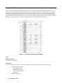
Contents
1.
Introduction
About this Guide ..........................................................................................................................................7
Documentation Summary .............................................................................................................................7
External References......................................................................................................................................7
VXIPlug&Play Power Products Instrument Drivers ....................................................................................8
2.
Introduction to Programming
GPIB Capabilities of the Power Module ......................................................................................................9
Module GPIB Address .................................................................................................................................9
Introduction to SCPI.....................................................................................................................................9
Conventions...............................................................................................................................................9
Types of SCPI Messages .........................................................................................................................10
Types of SCPI Commands ......................................................................................................................10
Structure of a SCPI Message ...................................................................................................................10
The Message Unit.................................................................................................................................10
Combining Message Units....................................................................................................................10
Parts of a SCPI Message .........................................................................................................................11
Headers............................................................................................................... ..................................11
Query Indicator..........................................................................................................12
Message Unit Separator........................................................................................................................12
Root Specifier.......................................................................................................................................12
Message Terminator .............................................................................................................................12
Traversing the Command Tree ................................................................................................................13
Active Header Path...............................................................................................................................13
The Effect of Optional Headers............................................................................................................13
Moving Among Subsystems.................................................................................................................14
Including Common Commands...............................................................................................................14
SCPI Data Formats.....................................................................................................................................14
Numerical Data........................................................................................................................................14
Boolean Data ...........................................................................................................................................15
String Data...............................................................................................................................................15
Character Data.........................................................................................................................................15
System Considerations ...............................................................................................................................16
Assigning the Address in Programs.........................................................................................................16
DOS Drivers ............................................................................................................................................16
Types of Drivers ...................................................................................................................................16
Agilent 82335A Driver.........................................................................................................................16
National Instruments GPIB Driver .......................................................................................................16
Error Handling......................................................................................................................................17
Agilent BASIC for Series 300 .................................................................................................................17
Translation Among Languages...................................................................................................................17
General Setup Information for GWBASIC .............................................................................................17
Using the Agilent 82335A/82990A/16062B GPIB Command Library ................................................17
Using the National Instruments GPIB Interface ...................................................................................18
General Setup Information for Microsoft C ............................................................................................18
Using the Agilent 82335A/82990A/16062B GPIB Command Library ................................................18
Using the National Instruments GPIB Interface ...................................................................................18
Sending Commands to and Receiving Data from the Module.................................................................19
3.
Language Dictionary
Introduction ................................................................................................................................................23
Parameters ..................................................................................................................................................23
3
Related Commands.....................................................................................................................................23
Order of Presentation .................................................................................................................................23
Common Commands ..................................................................................................................................23
Subsystem Commands................................................................................................................................23
Description of Common Commands ..........................................................................................................24
*CLS........................................................................................................................................................24
*ESE........................................................................................................................................................25
*ESR?......................................................................................................................................................25
*IDN? ......................................................................................................................................................26
*OPC .......................................................................................................................................................26
*OPC? .....................................................................................................................................................26
*OPT? .....................................................................................................................................................27
*PSC........................................................................................................................................................27
*RCL .......................................................................................................................................................28
*RST .......................................................................................................................................................28
*SAV.......................................................................................................................................................29
*SRE .......................................................................................................................................................29
*STB?......................................................................................................................................................30
*TRG.......................................................................................................................................................31
*TST?......................................................................................................................................................31
*WAI.......................................................................................................................................................31
Description of Subsystem Commands........................................................................................................31
ABOR......................................................................................................................................................31
Calibration Subsystem.............................................................................................................................32
CAL:AUTO..........................................................................................................................................32
CAL:CURR ..........................................................................................................................................33
CAL:CURR:LEV .................................................................................................................................33
CAL:PASS ...........................................................................................................................................33
CAL:SAV.............................................................................................................................................34
CAL:STAT...........................................................................................................................................34
CAL:VOLT ..........................................................................................................................................34
CAL:VOLT:LEV .................................................................................................................................34
CAL:VOLT:PROT ...............................................................................................................................35
Current Subsystem...................................................................................................................................35
CURR ...................................................................................................................................................35
CURR:MODE ......................................................................................................................................35
CURR:PROT:STAT.............................................................................................................................36
CURR:TRIG.........................................................................................................................................36
DISP:STAT ..........................................................................................................................................36
INIT......................................................................................................................................................36
INIT:CONT ..........................................................................................................................................36
List Subsystem.........................................................................................................................................37
LIST:COUN .........................................................................................................................................37
LIST:CURR .........................................................................................................................................37
LIST:CURR:POIN? .............................................................................................................................38
LIST:DWEL.........................................................................................................................................38
LIST:DWEL:POIN?.............................................................................................................................38
LIST:STEP ...........................................................................................................................................38
LIST:VOLT..........................................................................................................................................39
LIST:VOLT:POIN? .............................................................................................................................39
MEAS:CURR? .....................................................................................................................................39
MEAS:VOLT? .....................................................................................................................................39
Output Subsystem....................................................................................................................................39
OUTP ...................................................................................................................................................39
OUTP:DFI ............................................................................................................................................40
4
OUTP:DFI:LINK .................................................................................................................................40
OUTP:DFI:SOUR ................................................................................................................................40
OUTP:PROT:CLE ...............................................................................................................................40
OUTP:PROT:DEL ...............................................................................................................................41
OUTP:REL...........................................................................................................................................41
OUTP:REL:POL ..................................................................................................................................41
OUTP:TTLT ........................................................................................................................................42
OUTP:TTLT:LINK ..............................................................................................................................42
OUTP:TTLT:SOUR .............................................................................................................................42
Status Subsystem.....................................................................................................................................42
STAT:OPER?.......................................................................................................................................43
STAT:OPER:COND? ..........................................................................................................................43
STAT:OPER:ENAB.............................................................................................................................43
STAT:OPER:NTR ...............................................................................................................................44
STAT:OPER:PTR ................................................................................................................................44
STAT:PRES .........................................................................................................................................44
STAT:QUES? ......................................................................................................................................45
STAT:QUES:COND? ..........................................................................................................................45
STAT:QUES:ENAB ............................................................................................................................45
STAT:QUES:NTR ...............................................................................................................................45
STAT:QUES:PTR ................................................................................................................................45
SYST:ERR? .........................................................................................................................................46
SYST:VERS? .......................................................................................................................................46
Trigger Subsystem...................................................................................................................................46
TRIG .................................................................................................................. ..................................46
TRIG:DEL............................................................................................................................................47
TRIG:LINK ..........................................................................................................................................47
TRIG:SOUR.........................................................................................................................................47
Voltage Subsystem ..................................................................................................................................48
VOLT .................................................................................................................. .................................48
VOLT:MODE ......................................................................................................................................48
VOLT:PROT ........................................................................................................................................48
VOLT:SENS:SOUR? ...........................................................................................................................49
VOLT:TRIG.........................................................................................................................................49
Link Parameter List .................................................................................................................................50
Power Module Programming Parameters ................................................................................................50
4.
Status Reporting
Power Module Status Structure ..................................................................................................................51
Status Register Bit Configuration...............................................................................................................51
Operation Status Group ..............................................................................................................................51
Register Functions ...................................................................................................................................51
Register Commands.................................................................................................................................51
Questionable Status Group .........................................................................................................................52
Register Functions ...................................................................................................................................52
Register Commands.................................................................................................................................52
Standard Event Status Group......................................................................................................................53
Register Functions ...................................................................................................................................53
Register Commands.................................................................................................................................53
Status Byte Register ...................................................................................................................................54
The RQS Bit ............................................................................................................................................54
The MSS Bit............................................................................................................................................54
Determining the Cause of a Service Interrupt..........................................................................................54
Output Queue .............................................................................................................................................54
5
Location of Event Handles .........................................................................................................................54
Initial Conditions at Power On ...................................................................................................................55
Status Registers .......................................................................................................................................55
The PON Bit............................................................................................................................................55
Examples .................................................................................................................... ................................55
Servicing an Operation Status Event .......................................................................................................55
Adding More Operation Events...............................................................................................................56
Servicing Questionable Status Events .....................................................................................................56
Monitoring Both Phases of a Status Transition .......................................................................................56
5.
Synchronizing Power Module Output Changes
Introduction ................................................................................................................................................57
Trigger Subsystem......................................................................................................................................57
Model of Fixed-Mode Trigger Operation ................................................................................................57
Idle State...............................................................................................................................................58
Initiated State........................................................................................................................................58
Delaying State ......................................................................................................................................58
Output Change State.............................................................................................................................59
Model of List-Mode Trigger Operation...................................................................................................59
Output Change State.............................................................................................................................59
Dwelling State ......................................................................................................................................59
The INIT:CONT Function.......................................................................................................................59
Trigger Status and Event Signals.............................................................................................................59
Trigger In and Trigger Out ......................................................................................................................60
List Subsystem............................................................................................................................................61
Basic Steps of List Sequencing ...............................................................................................................61
Programming the List Output Levels.......................................................................................................61
Programming List Intervals .....................................................................................................................61
Automatically Repeating a List ...............................................................................................................62
Triggering a List......................................................................................................................................62
Dwell-Paced Lists.................................................................................................................................62
Trigger-Paced Lists ..............................................................................................................................62
DFI (Discrete Fault Indicator) Subsystem ..................................................................................................64
RI (Remote Inhibit) Subsystem ..................................................................................................................64
SCPI Command Completion ......................................................................................................................64
6.
Error Messages
Power Module Hardware Error Messages ..................................................................................................65
System Error Messages ..............................................................................................................................65
A.
SCPI Conformance Information ............................................................................................................67
B.
Application Programs..............................................................................................................................69
Index ..........................................................................................................................................................111
6
1
Introduction
About This Guide
You will find the following information in the rest of this guide:
Chapter 2
Chapter 3
Chapter 4
Chapter 5
Chapter 6
Appendix A
Appendix B
Introduction to SCPI messages structure, syntax, and data formats. Examples of SCPI programs.
Dictionary of SCPI commands. Table of module programming parameters.
Description of the status registers.
Description of synchronizing outputs with triggers and lists.
Error messages.
SCPI conformance information.
Application programs that illustrate features of the power module.
Note
Instructions for the Agilent 60001A MPS Keyboard are in the User’s Guide supplied with each module.
Documentation Summary
The following related documents shipped with the system have information helpful to programming the power module:
•
Mainframe User’s Guide. Information on the GPIB address switch, trigger connections, fault (FLT) and
remote inhibit (INH) connections.
•
Module User’s Guide. Includes specifications and supplemental characteristics, use of the module
configuration switch, device related error messages, calibration procedures and use of the MPS keyboard.
External References
SCPI References
The following documents will assist you with programming in SCPI:
•
Beginner’s Guide to SCPI. Part No. H2325-90001. Highly recommended for anyone who has not had previous
experience programming with SCPI.
•
Tutorial Description of the GPIB . Part No. 5952-0156. Highly recommended for those not familiar with the
IEEE 488.1 and 488.2 standards.
To obtain a copy of the above documents, contact your local Agilent Technologies Sales and Support Office.
GPIB References
The most important GPIB documents are your controller programming manuals - GW BASIC, GPIB Command Library for
MS DOS, etc. Refer to these for all non-SCPI commands (for example: Local Lockout).
The following are two formal documents concerning the GPIB interface:
2
ANSI/IEEE Std. 488.1-1987 IEEE Standard Digital Interface for Programmable Instrumentation . Defines
•
the technical details of the GPIB interface. While much of the information is beyond the need of most
programmers, it can serve to clarify terms used in this guide and in related documents.
2
•
ANSI/IEEE Std. 488.2-1987 IEEE Standard Codes, Formats, Protocols, and Common Commands .
Recommended as a reference only if you intend to do fairly sophisticated programming. Helpful for finding
precise definitions of certain types of SCPI message formats, data types, or common commands.
The above two documents are available from the IEEE (Institute of Electrical and Electronics Engineers), 345 East 47th
Street, New York, NY 10017, USA.
Introduction
7
VXIplug&play Power Products Instrument Drivers
VXIplug&play instrument drivers for Microsoft Windows 95 and Windows NT are now available on the Web at
http://www.agilent.com/find/drivers. These instrument drivers provide a high-level programming interface to your Agilent
Technologies electronic load. VXIplug&play instrument drivers are an alternative to programming your instrument with
SCPI command strings. Because the instrument driver’s function calls work together on top of the VISA I/O library, a
single instrument driver can be used with multiple application environments.
Supported Applications
ñ
ñ
ñ
ñ
ñ
ñ
Agilent VEE
Microsoft Visual BASIC
Microsoft Visual C/C++
Borland C/C++
National Instruments LabVIEW
National Instruments LabWindows/CVI
System Requirements
The VXIplug&play instrument driver complies with the following:
ñ
ñ
ñ
ñ
Microsoft Windows 95
Microsoft Windows NT 4.0
HP VISA revision F.01.02
National Instruments VISA 1.1
Downloading and Installing the Driver
NOTE:
Before installing the VXIplug&play instrument driver, make sure that you have one of the supported
applications installed and running on your computer.
1.
Access Agilent Technologies Web site at http://www.agilent.com/find/drivers.
2.
Select the instrument for which you need the driver.
3.
Click on the driver, either Windows 95 or Windows NT, and download the executable file to your PC.
4.
Locate the file that you downloaded from the Web. From the Start menu select Run <path>:\agxxxx.exe - where
<path> is the directory path where the file is located, and agxxxx is the instrument driver that you downloaded .
5.
Follow the directions on the screen to install the software. The default installation selections will work in most
cases. The readme.txt file contains product updates or corrections that are not documented in the on-line help. If
you decide to install this file, use any text editor to open and read it.
6.
To use the VXIplug&play instrument driver, follow the directions in the VXIplug&play online help for your
specific driver under “Introduction to Programming”.
Accessing Online Help
A comprehensive online programming reference is provided with the driver. It describes how to get started using the
instrument driver with Agilent VEE, LabVIEW, and LabWindows. It includes complete descriptions of all function calls
as well as example programs in C/C++ and Visual BASIC.
ñ
To access the online help when you have chosen the default Vxipnp start folder, click on the Start button and select
Programs | Vxipnp | Agxxxx Help (32-bit).
- where Agxxxx is the instrument driver.
8
Introduction
2
Introduction To Programming
GPIB Capabilities Of The Power Module
All power module functions except for setting the GPIB address are programmable over the GPIB. The IEEE 488.1
capabilities of the power module are listed in the User’s Guide.
Module GPIB Address
The power module operates from a primary GPIB address that is set by a switch on the mainframe. The power module’s
secondary GPIB address is determined by its slot position within the mainframe. See the mainframe Installation Guide for
details.
Introduction To SCPI
SCPI (Standard Commands for Programmable Instruments) is a programming language for controlling instrument functions
over the GPIB (IEEE 488) instrument bus. SCPI is layered on top of the hardware-portion of IEEE 488.2. The same SCPI
commands and parameters control the same functions in different classes of instruments. For example, you would use the
same DISPlay command to control the power module display state and the display state of a SCPI-compatible multimeter.
Conventions
The following conventions are used throughout this chapter:
Angle brackets
< >
Items within angle brackets are parameter abbreviations. For example, <NR1>
indicates a specific form of numerical data.
Vertical bar
|
Vertical bars separate one of two or more alternative parameters. For example,
0|OFF indicates that entering either "0" or "OFF" performs the same function.
Square Brackets [ ]
Items within square brackets are optional. The representation [SOURce]:LIST
means that SOURce may be omitted.
Braces
Braces indicate parameters that may be repeated zero or more times. It is used
especially for showing arrays. The notation <A>{<,B>} shows that parameter
"A" must be entered, while parameter "B" may be omitted or may be entered one
or more times.
{ }
Boldface font
Boldface font is used to emphasize syntax in command definitions.
TRIGger:DELay <NRf> shows a command definition.
Computer font
Computer font is used to show program lines in text. TRIGger: DELay .5 shows a
program line.
Introduction To Programming
9
Types of SCPI Messages
There are two types of SCPI messages, program and response.
•
A program message consists of one or more properly formatted SCPI commands sent from the controller to
the power module. The message, which may be sent at any time, requests the power module to perform some
action.
•
A response message consists of data in a specific SCPI format sent from the power module to the controller.
The power module sends the message only when commanded by a special program message called a "query."
Types of SCPI Commands
SCPI has two types of commands, common and subsystem. Common commands generally are not related to specific
operation but to controlling overall power module functions, such as reset, status, and synchronization. All common
commands consist of a three-letter mnemonic preceded by an asterisk:
*RST
*IDN?
*SRE 8
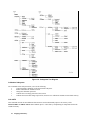
Subsystem commands perform specific power module functions. They are organized into an inverted tree structure with the
"root" at the top (see Figure 3-2). Some are single commands while others are grouped within specific subsystems.
Note
If you have the optional Agilent 66001A MPS Keyboard, you may want to use it as a quick introduction
to message structure. See "Appendix A".
Structure of a SCPI Message
SCPI messages consist of one or more message units ending in a message terminator. The terminator is not part of the
syntax, but implicit in the way your programming language indicates the end of a line (such as a newline or end-of-line
character).
The Message Unit
The simplest SCPI command is a single message unit consisting of a command header (or keyword) followed by a message
terminator.
ABOR<newline>
VOLT?<newline>
The message unit may include a parameter after the header. The parameter usually is numeric, but it can be a string:
VOLT 20<newline>
VOLT MAX<newline>
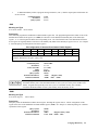
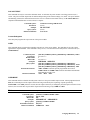
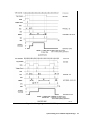
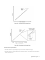
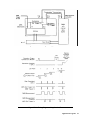
Combining Message Units
The following command message is briefly described here, with details in subsequent paragraphs.
10
Introduction To Programming
Figure 2-1. Command Message Structure
The basic parts of the above message are:
Message Component
Headers
Header Separator
Data
Data Separator
Message Units
Message Unit Separator
Root Specifier
Query Indicator
Message Terminator
Example
VOLT LEV PROT CURR
The colon in VOLT:LEV
8.0 8.8
The space in VOLT 8. 0 and PROT 8. 8
VOLT:LEV 8.0 PROT 8.8 CURR?
The semicolons in VOLT: LEV 8. 0; and PROT 8. 8;
The colon in PROT 8. 8; : CURR?
The question mark in CURR?
The <NL> (newline) indicator. Terminators are not part of the SCPI syntax.
Parts of a SCPI Message
Headers
Headers are instructions recognized by the power module interface. Headers (which are sometimes known as "keywords")
may be either in the long form or the short form.
Long Form
Short Form
The header is completely spelled out, such as VOLTAGE, STATUS, and DELAY.
The header has only the first three or four letters, such as VOLT, STAT, and DEL.
Short form headers are constructed according to the following rules:
•
•
•
If the header consists of four or fewer letters, use all the letters. (DFI
LIST)
If the header consists of five or more letters and the fourth letter is not a vowel (a,e,i,o,u), use the first four
letters. (CURRent STATus)
If the header consists of five or more letters and the fourth letter is a vowel (a,e,i,o,u), use the first three letters.
(DELay RELay)
You must follow the above rules when entering headers. Creating an arbitrary form, such as POLAR for POLarity, will result
in an error.
Introduction To Programming
11
The SCPI interface is not sensitive to case. It will recognize any case mixture, such as TRIGGER, Trigger, TRIGger, triGgeR.
Note
Shortform headers result in faster program execution.
Header Convention. In this manual, headers are emphasized with boldface type. The proper short form is shown in
upper-case letters, such as DELay.
Header Separator. If a command has more than one header, you must separate them with a colon (VOLT: PROT
OUTPut:RELay:POLarity).
Optional Headers. The use of some headers is optional. Optional headers are shown in brackets, such as
OUTPut[: STATe] ON. However, if you combine two or more message units into a compound message, you may need to
enter the optional header. This is explained under "Traversing the Command Tree."
Note
The optional Agilent 66001A MPS Keyboard does not display optional headers.
Query Indicator
Following a header with a question mark turns it into a query (VOLT?, VOLT:PROT?). If a query contains a parameter, place
the query indicator at the end of the last header (VOLT: PROT? MAX).
Message Unit Separator
When two or more message units are combined into a compound message, separate the units with a semicolon
(STATus:OPERation?;QUEStionable?). You can combine message units only at the current path of the command tree (see
"Traversing the Command Tree").
Root Specifier
When it precedes the first header of a message unit, the colon becomes the root specifier. It indicates that the parser is at the
root or top node of the command tree. Note the difference between root specifiers and header separators in the following
examples:
OUTP:PROT:DEL .1
:OUTP:PROT:DEL .1
OUTP: PROT: DEL . 1; :VOLT 12.5
All colons are header separators.
Only the first colon is a root specifier.
Only the third colon is a root specifier.
Message Terminator
A terminator informs SCPI that it has reached the end of a message. Three permitted messages terminators are:
•
•
•
newline (<NL>), which is ASCII decimal 10 or hex 0A.
end or identify (<END>)
both of the above (<NL><END>).
In the examples of this guide, there is an assumed message terminator at the end of each message. If the terminator needs to
be shown, it is indicated as <NL> regardless of the actual terminator character.
12
Introduction To Programming
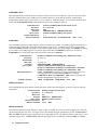
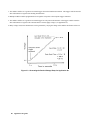
Traversing the Command Tree
Figure 2-2 shows a portion of the subsystem command tree (you can see the complete tree in Figure 3-2). Note the location
of the ROOT node at the top of the tree. The SCPI interface is at this location when:
•
•
•
•
The power module is powered on.
A device clear (DCL) is sent to the power module.
The interface encounters a message terminator.
The interface encounters a root specifier.
Figure 2-2. Partial Command Tree
Active Header Path
In order to properly traverse the command tree, you must understand the concept of the active header path. When the power
module is turned on (or under any of the other conditions listed above), the active path is at the root. That means the
interface is ready to accept any command at the root level, such as OUTPUT or STATUS in Figure 2-2. Note that you do not
have to proceed either command with a colon; there is an implied colon in front of every root-level command.
If you enter OUTPUT, the active header path moves one colon to the right. The interface is now ready to accept :STATE,
:PROTECTION, or :RELAY as the next header. Note that you must include the colon, because it is required between headers.
If you now enter :PROTECTION, the active path again moves one colon to the right. The interface is now ready to accept
either :CLEAR or :DELAY as the next header.
If you now enter :CLEAR, you have reached the end of the command string. The active header path remains at :CLEAR. If
you wished, you could have entered :CLEAR; DELAY 20 and it would be accepted. The entire message would be
OUTPUT:PROTECTION:CLEAR;DELAY 20. The message terminator after DELAY 20 returns the path to the root.
The Effect of Optional Headers
If a command includes optional headers, the interface assumes they are there. For example, if you enter OUTPUT OFF, the
interface recognizes it as OUTPUT: STATE OFF (see Figure 2-2). This returns the active path to the root (:OUTPUT). But if
you enter OUTPUT: STATE OFF, then the active path remains at :STATE. This allows you to send OUTPUT: STATE OFF;
PROTECTION: CLEAR in one message. If you tried to send OUTPUT OFF;PROTECTION:CLEAR, the header path would return
to :OUTPUT instead of :PROTECTION.
Introduction To Programming
13
The optional header SOURCE precedes the current, list, and voltage subsystems (see Figure 3-2). This effectively makes
:CURRENT, :LIST, and :VOLTAGE root-level commands.
Note
The optional Agilent 66001 Keyboard does not display optional headers.
Moving Among Subsystems
In order to combine commands from different subsystems, you need to be able to restore the active path to the root. You do
this with the root specifier (:). For example, you could clear the output protection and check the status of the Operation
Condition register as follows (see Figure 2-2):
OUTPUT:PROTECTION:CLEAR
STATUS:OPERATION:CONDITION?
By using the root specifier, you could do the same thing in one message:
OUTPUT:PROTECTION:CLEAR;:STATUS:OPERATION:CONDITION?
Note
The SCPI parser traverses the command tree as described in Appendix A of the IEEE 488.2 standard.
The "Enhanced Tree Walking Implementation" given in that appendix is not implemented in the power
module.
The following message shows how to combine commands from different subsystems as well as within the same subsystem
(see Figure 3-2):
VOLTAGE:LEVEL 7;PROTECTION 8;:CURRENT:LEVEL 3;MODE LIST
Note the use of the optional header LEVEL to maintain the correct path within the voltage and current subsystems and the
use of the root specifier to move between subsystems.
Including Common Commands
You can combine common commands with system commands in the same message. Treat the common command as a
message unit by separating it with the message unit separator. Common commands do not affect the active header path;
you may insert them anywhere in the message.
VOLT:TRIG 7.5;INIT;*TRG
OUTP OFF;*RCL 2;OUTP ON
SCPI Data Formats
All data programmed to or returned from the power module is ASCII. The data may be numerical or character string.
Numerical Data
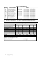
Table 2-1 and Table 2-2 summarize the numerical formats.
14
Introduction To Programming
Symbol
<NR1>
<NR2>
<NR3>
Table 2-1. Numerical Data Formats
Data Form
Talking Formats
Digits with an implied decimal point assumed at the right of the least-significant
digit. Examples: 273 0273
Digits with an explicit decimal point. Example: 273. .0273
Digits with an explicit decimal point and an exponent. Example: 2.73E+2 273.0E-2
Listening Formats
Extended format that includes <NR1>, <NR2> and <NR3>. Examples: 273 273.
2.73E2
Expanded decimal format that includes <NRf> and MIN MAX. Examples: 273 273.
2.73E2 MAX. MIN and MAX are the minimum and maximum limit values that are
implicit in the range specification for the parameter.
<NRf>
<NRf+>
Class
Current
Amplitude
Time
Suffix
A
V
S
lE3
1E-3
1E-6
Table 2-2. Suffixes and Multipliers
Unit
Unit with Multiplier
Ampere
MA (milliampere)
Volt
MV (millivolt)
second
MS (millisecond)
Common Multipliers
K
kilo
M
milli
U
micro
Boolean Data
Either form 1 | 0 or ON | OFF may be sent with commands. Queries always return 1 or 0.
OUTPut OFF
CURRent:PROTection 1
String Data
Strings are used for both program (listening) and response (talking) data. String content is limited to the characters required
for the link command parameters (see "Chapter 3 - Language Dictionary").
Note
The IEEE 488.2 format for a string parameter requires that the string be enclosed within either single
(’ ’) or double (" ") quotes. Be certain that your program statements comply with this requirement.
Character Data
Character strings returned by query statements may take either of the following forms, depending on the length of the
returned string:
<CRD>
<AARD>
Character Response Data. Permits the return of character strings.
Arbitrary ASCII Response Data. Permits the return of undelimited 7-bit ASCII. This data type has an
implied message terminator.
Introduction To Programming
15
System Considerations
The remainder of this chapter addresses some system issues concerning programming. These are power module addressing
and the use of the following types of GPIB system interfaces:
1.
2.
3.
HP Vectra PC controller with Agilent 82335A GPIB Interface Command Library
IBM PC controller with National Instruments GPIB-PCII Interface/Handler
Agilent controller with Agilent BASIC Language System
Note
Some specific application programs are given in Appendix B.
Assigning the GPIB Address in Programs
The power module address cannot be set remotely. It is determined by the position of the mainframe address switch and the
position of power module (slot position) within the mainframe. ( See the Mainframe Users Guide for details.)
The following examples assume that the GPIB select code is 7, the mainframe interface address is 6, and that the power
module address will be assigned to the variable PM3 (power module in the third mainframe slot).
1060
1070
1070
1080
1080
1090
1090
! Power Module installed in Primary Mainframe
PM3=70602
! Agilent 82335A Interface
ASSIGN @PM3TO 70602
! Agilent BASIC Interface
!
! Power Module installed in Auxiliary Mainframe
PM=70610
! Agilent 82335A Interface
ASSIGN @PM3 TO 70610 ! Agilent BASIC Interface
For systems using the National Instruments DOS driver, the address is specified in the software configuration program
(IBCONFIG.EXE) and assigned a symbolic name. The address then is referenced only by this name within the application
program (see the National Instruments GPIB documentation).
DOS Drivers
Types of Drivers
The Agilent 82335A and National Instruments GPIB are two popular DOS drivers. Each is briefly described here. See the
software documentation supplied with the driver for more details.
Agilent 82335A Driver. For GW-BASIC programming, the GPIB library is implemented as a series of subroutine calls.
To access these subroutines, your application program must include the header file SETUP.BAS, which is part of the DOS
driver software.
SETUP.BAS starts at program line 5 and can run up to line 999. Your application programs must begin at line 1000.
SETUP.BAS has built-in error checking routines that provide a method to check for GPIB errors during program execution.
You can use the error-trapping code in these routines or write your own code using the same variables as used by
SETUP.BAS.
National Instruments GPIB Driver. Your program must include the National Instruments header file DECL.BAS. This
contains the initialization code for the interface. Prior to running any applications programs, you must set up the interface
with the configuration program (IBCONF.EXE).
16
Introduction To Programming
Your application program will not include the power module symbolic name and GPIB address. These must be specified
during configuration (when you run IBCONF.EXE). Note that the primary address range is from 0 to 30 but any secondary
address must be specified in the address range of 96 to 126. The power supply expects a message termination on EOI or
line feed, so set EOI w/last byte of Write. It is also recommended that you set Disable Auto Serial Polling.
All function calls return the status word IBSTA%, which contains a bit (ERR) that is set if the call results in an error. When
ERR is set, an appropriate code is placed in variable IBERR %. Be sure to check IBSTA %, after every function call. If it is
not equal to zero, branch to an error handler that reads IBERR% to extract the specific error.
Error Handling
If there is no error-handling code in your program, undetected errors can cause unpredictable results. This includes
"hanging up" the controller and forcing you to reset the system. Both of the above DOS drivers have routines for detecting
program execution errors.
Important
Use error detection after every call to a subroutine.
Agilent BASIC Controllers
The Agilent BASIC Programming Language provides access to GPIB functions at the operating system level. This makes it
unnecessary to have the header files required in front of DOS applications programs. Also, you do not have to be concerned
about controller "hangups" as long as your program includes a timeout statement. Because the power module can be
programmed to generate SRQ on errors, your program can use an SRQ service routine for decoding detected errors. The
detectable errors are listed in "Chapter 5 - Error Messages".
TRANSLATION AMONG LANGUAGES
This section explains how to translate between Agilent BASIC and several other popular programming environments. For
explicit information on initializing interface cards or syntax of language, see the documentation that accompanies your
GPIB interface product.
General Setup Information for GWBASIC
Using the Agilent 82335A/82990A/61062B GPIB Command Library
•
•
•
•
•
When CALLs are made to the GPIB Command Library, all parameters are passed as variables.
The address of a module is a real number, determined in the same manner as in Agilent BASIC. For example,
the address 70501 means 7 is the select code of the GPIB interface, 05 is the GPIB address of the mainframe, 01 is
the slot number (secondary address) of the module.
The module expects each command to be terminated by line feed (character 10) and/or EOI. The default
configuration of the GPIB Command Library is carriage return + line feed for end-of-line termination and EOI at
the end of a line. Therefore, the defaults are correct for use with the module.
The GPIB Command Library supports strings, numeric and array data formats. However, multiple data types
cannot be sent in a single command. To send both string and numeric data in one command, convert all numeric
data to strings, concatenate with the string data and send the combined string to the module. To read multiple data
types, read the data into a string, and then manipulate the string by converting each piece into the appropriate data
format.
Error handling is accomplished by checking the variable PCIB.ERR. If it is nonzero, an error has occurred.
See the command library documentation for trapping and interpreting this error variable.
Introduction To Programming
17
Using the National Instruments GPIB Interface
•
•
•
•
•
•
When CALLs are made to the GPIB driver, all parameters are passed as variables.
The module is identified as a device in two ways. First, the GPIB.COM driver is modified to include the
module. Use the mainframe address as the primary bus address and the slot address as the secondary address. The
driver requires secondary address 0 (which is for slot 0) to be entered as 96, secondary address 1 to be entered as
97, etc.
It is recommended that you disable auto serial poll in the GPIB.COM driver.
The module expects each command to be terminated by a line feed (character 10) and/or EOI. Configure the
GPIB.COM driver to terminate all reads and writes with EOI.
The GPIB driver does all communication via strings. To send numeric data, number to-string conversion must
be performed before the IBWRT( ). To read numeric data, string-to-number conversion must be performed after
each IBRD( ).
Error handling is accomplished by checking the variable IBSTA%. If it is less than zero, an error has occurred.
See the GPIB interface documentation for trapping and interpreting this error variable.
General Setup Information for Microsoft C
Using the Agilent 82335A/82990A/61062B GPIB Command Library
•
The address of a module is of type long and is determined the same as with Agilent BASIC. For example, the
address 70501L means 7 is the select code of the GPIB interface, 05 is the GPIB address of the mainframe, 01 is
the slot number (secondary address) of the module.
•
The module expects each command to be terminated by a line feed (character 10) and/or EOI. The default
configuration of the GPIB Command Library is carriage return+line feed for end-of-line termination and EOI at the
end of a line. Therefore, the defaults are correct for use with the module.
•
The GPIB Command Library supports strings, numeric and array data formats. However, multiple data types
cannot be sent in a single command. To send both string and numeric data in one command, convert all numeric
data to strings, concatenate with the string data and send the combined string to the module. To read multiple data
types, read the data into a string, and then manipulate the string by converting each piece into the appropriate data
format.
•
Each command library call returns an int. If the value is zero, no error has occurred. Error handling is
accomplished by checking the return value. See the command library documentation for interpretation of this error
value.
Using the National Instruments GPIB Interface
•
•
The module is identified as a device in two ways. First, the GPIB.COM driver is modified to include the
module. Use the mainframe address as the primary bus address. Use the slot address as the secondary address.
The driver requires that secondary address 0 (which is for slot 0) be entered as 96, secondary address 1 be entered
as 97, etc.
It is recommended that you disable the auto serial poll in the GPIB.COM driver.
•
The module expects each command to be terminated by either a line feed (character 10) and/or EOI.
Configure the GPIB.COM driver to terminate all reads and writes with EOI.
•
The GPIB driver does all communication via strings. To send numeric data, number to-string conversion
must be performed before the ibwrt( ). To read numeric data, string-to-number conversion must be performed after
each ibrd( ).
•
Error handling is accomplished by checking the variable IBSTA%. If bit 15 is set, an error has occurred. See
the GPIB interface documentation for the interpretation of this error variable.
18
Introduction To Programming
Sending Commands to and Receiving Data from the Module
Sending the Command “VOLT 5”
**********************************************
Agilent BASIC ************************************************
2100
2110
2120
OUTPUT 70501;"VOLT 5" ! where 70501 means 7 is the select code of the GPIB interface 05 is the
!
GPIB address of the mainframe, 01 is the slot number (secondary address)
!
of the module
************************* GWBASICAgilent
(
82335A/82990A/61062B GPIB Command Library) ************************
2100
2110
2120
2130
2140
MODULE.ADDRESS=70501
COMMAND$ - "VOLT 5"
L - LENGTH(COMMAND$)
CALL IOOUTPUTS(MODULE.ADDRESS,COMMAND$,L)
IF PCIB.ERR&<>O THEN ERROR PCIB.BASERR’
! ERROR TRAP
********************************** GWBASIC (National Instruments GPIB Interface) ********************************
2100
2110
2120
2130
COMMAND$ = "VOLT 5"
CALL IBWRT(MODULE.ADDRESS%, COMMAND$)
IF IBSTA% &< 0 GOTO 5000
!
! TRAP ERROR WITH ERROR HANDLER
AT LINE 5000
Sending the Command “VOLT 5” in BASIC
*********************** Microsoft C Agilent
(
82335A/82990A/61062B HPIB Command Library) *************************
/* Assumes that you have an error handler routine, called ‘error_handler’ that accepts a float. The error handler in then passed the float
that is returned from each call to the library. */
*include &<stdio.h>
*include &<chpib.h>
*include &<cfunc.h>
*define module_address 70501L
char *cmd;
cmd = "VOLT 5”;
error = iooutputs(MODULE_ADDRESS, cmd, strlen(cmd));
error_handler(error);
****************************** Microsoft C (National Instruments GPIB Interface) ************************************
/* Assumes that you have an error handler routine, called ‘error-handler’. The error handler is then passed the float that is returned from
each call to the library. */
*include &<stdio.h>
*include &<decl.h>
*define ERR (l&<&<15) /* Error is detected as bit i5 of ibsta */
int module-address; /* Device is configured in the GPIB.COM handler. Use ibfind() to assign a value to module-address. */
char *cmd;
cmd - "VOLT 5”
ibwrt(MODULE_ADDRESS, cmd, strlen(cmd));
if (ibsta & ERR)
error_handler();
Sending the Command "VOLT 5” in C
Introduction To Programming
19
Receiving Data from the Module
The following screens show how to enter data from the module with various interfaces.
******************************************* Agilent BASIC ******************************************
2100
2110
2120
2130
ENTER 70501; MEASUREMENT !
!
!
!
where 70501 means 7 is the select code of the GPIB interface,
05 is the GPIB address of the mainframe, 01 is the slot number
(secondary address) of the module, MEASUREMENT is a real number
sent by the module
**************** GWBASIC (Agilent 82335A/82990A/61062B GPIB Command Library) ***********************
2100 MODULE.ADDRESS=70501
2110 CALL IOENTER(MODULE.ADDRESS,MEASUREMENT)
2120 IF PCIB.ERR&< >0 THEN ERROR PCIB.BASERR
! ERROR TRAP
************************** GWBASIC (National Instruments GPIB Interface) *******************************
2100 MEASUREMENT$ - SPACE$(20)
! DRIVER CAN ONLY READ STRINGS, SO RESERVE
2110 !
SPACE IN A STRING
2120 CALL IBRD(MODULE.ADDRESS%, MEASUREMENT$)
2130 IF IBSTA% &< 0 GOTO 5000
! TRAP ERROR WITH ERROR HANDLER AT LINE 5000
2140 MEASURED.VALUE=VAL(MEASUREMENT$)” ! CONVERT THE STRING TO A NUMBER
Receiving Module Data with BASIC
20
Introduction To Programming
***************** Microsoft C (Agilent 82335A/82990A/61062B GPIB Command Library) *********************
/* Assumes that you have an error handler routine, called ’error_handler’ that accepts a float. The error handler is then
passed the float that is returned from each call to the library. */
#include &<stdio.h>
#include k<chpib.h>
#include &<cfunc.h>
#define MODULE_ADDRESS 70501L
char *cmd;
float measurement;
error = ioenter(MODULE_ADDRESS, &&measurement);
error_handler(error);
**************************** Microsoft C (National Instruments GPIB Interface) ****************************
/* Assumes that you have an error handler routine, called ’error_handler’. The error handler is then passed the float that is
returned from each call to the library. */
#include &<stdio.h>
#include &<stdlib.h>
#include &<decl.h>
#define ERR (1&<&<15)
#define STRING_LENGTH 20
/* Error is detected as bit 15 of ibsta */
/* Length of string to hold measurement */
int module_address;
/* Device is configured in the GPIB.COM handler. Use
ibfind( ) to assign a value to module_address. */
char measurement[STRING_LENGTH];
float measured_value;
/* Holds float conversion of measurement */
ibwrt(module_address, measurement, STRING_LENGTH);
if (ibsta & ERR)
error_handler();
measured_value = atof(measurement);
/* Converts measurement string to float */
Receiving Module Data with C
Introduction To Programming
21
3
Language Dictionary
Introduction
This section gives the syntax and parameters for all the IEEE 488.2 SCPI commands and the Common commands used by
the Agilent Series 66l0xA power modules. It is assumed that you are familiar with the material in "Chapter 2 - Introduction
to Programming". That chapter explains the terms, symbols, and syntactical structures used here and gives an introduction
to programming.
The programming commands function the same way in all Agilent Series 66l0xA power modules. Since SCPI syntax
remains the same for all programming languages, the examples are generic.
Syntax definitions use the long form, but only short form headers (or "keywords") appear in the examples. If you have any
concern that the meaning of a header in your program listing will not be obvious at some later time, then use the long form
to help make your program self-documenting.
Parameters
Most commands require a parameter and all queries will return a parameter. The range for a parameter may vary according
to the model of power module. Parameters for all current models are listed in Table 3-3, at the end of this chapter.
Related Commands
Where appropriate, related commands or queries are included. These are listed either because they are directly related by
function or because reading about them will clarify or enhance your understanding of the original command or query.
Order of Presentation
The dictionary is organized as follows:
•
•
IEEE 488.2 common commands, in alphabetical order.
Subsystem commands.
COMMON Commands
Common commands begin with an * and consist of three letters (command) or three letters and a ? (query). Common
commands are defined by the IEEE 488.2 standard to perform some common interface functions. The Agilent Series
6610xA power modules respond to the 13 required common commands that control status reporting, synchronization, and
internal operations. The power modules also respond to five optional common commands controlling triggers, power-on
conditions, and stored operating parameters.
Subsystem Commands
Subsystem commands are specific to power module functions. They can be a single command or a group of commands.
The groups are comprised of commands that extend one or more levels below the root. The description of subsystem
commands follows the description of the common commands.
Language Dictionary
23
Description Of Common Commands
Figure 3-1 shows the common commands and queries. These commands are listed alphabetically in the dictionary. If a
command has a corresponding query that simply returns the data or status specified by the command, then both command
and query are included under the explanation for the command. If a query does not have a corresponding command or is
functionally different from the command, then the query is listed separately. The description for each common command or
query specifies any status registers affected. In order to make use of this information, you must refer to "Chapter 4 - Status
Reporting", which explains how to read specific register bits and use the information that they return.
Figure 3-1. Common Commands Syntax Diagram
*CLS
Meaning and Type
Clear Status Device Status
Description
This command causes the following actions (see "Chapter 4 - Status Reporting" for descriptions of all registers):
•
•
24
•
•
•
•
Clears the following registers:
Standard Event Status
Operation Status Event
Questionable Status Event
Status Byte
Clears the Error Queue
Language Dictionary
•
If *CLS immediately follows a program message terminator (<NL>), then the output queue and the MAV bit
are also cleared.
Command Syntax
*CLS
Parameters
(None)
Query Syntax
(None)
*ESE
Meaning and Type
Event Status Enable Device Status
Description
This command programs the Standard Event Status Enable register bits. The programming determines which events of the
Standard Event Status Event register (see *ESR?) are allowed to set the ESB (Event Summary Bit) of the Status Byte
register. A "1" in the bit position enables the corresponding event. All of the enabled events of the Standard Event Status
Event register are logically ORed to cause the Event Summary Bit (ESB) of the Status Byte register to be set. See "Chapter
4 - Status Reporting" for descriptions of all three registers.
Bit Configuration of Standard Event Status Enable Register
7
6
5
4
3
2
1
0
Bit Position
PON
0
CME
EXE
DDE
QYE
0
OPC
Bit Name
128
64
32
16
8
4
2
1
Bit Weight
CME = Command error; DDE = Device-dependent error; EXE = Execution error; OPC = Operation
complete; PON Power-on; QYE = Query error
Command Syntax
Parameters
Power On Value
Suffix
Example
Query Syntax
Returned Parameters
Related Commands
*ESE <NRf>
0 to 255
(See *PSC)
(None)
*ESE 129
*ESE?
<NR1>
(Register value)
*ESR? *PSC *STB?
If PSC is programmed to 0, then the *ESE command causes a write cycle to nonvolatile memory. The
nonvolatile memory has a finite maximum number of write cycles (see in the power module User’s
Guide). Programs that repeatedly cause write cycles to nonvolatile memory can eventually
exceed the maximum number of write cycles and may cause the memory to fail.
*ESR?
Meaning and Type
Event Status Register
Device Status
Description
This query reads the Standard Event Status Event register. Reading the register clears it. The bit configuration of this
register is the same as the Standard Event Status Enable register (*ESE). See "Chapter 4 - Status Reporting" for a detailed
explanation of this register.
Query Syntax
*ESR?
Parameters
(None)
Returned Parameters
<NR1>
(Register binary value)
Related Commands
*CLS *ESE *ESE? *OPC
Language Dictionary
25
*IDN?
Identification Query
Meaning and Type
Identification System Interface
Description
This query requests the power module to identify itself. It returns a string composed of four fields separated by commas.
Query Syntax
Returned Parameters
Example
Related Commands
*IDN?
<AARD>
Field
Information
Agilent Technologies Manufacturer
xxxxxA
5-digit model number followed by a letter
nnnnA-nnnnn
10-character serial number or 0
<R>.xx.xx
Revision levels of firmware
Agilent Technologies,66101A,0,A.00.01
(None)
*OPC
Meaning and Type
Operation Complete Device Status
Description
This command causes the interface to set the OPC bit (bit 0) of the Standard Event Status register when the power module
has completed all pending operations. (see *ESE for the bit configuration of the Standard Event Status register.) Pending
operations are complete when:
•
•
•
All commands sent before *OPC have been executed. This includes overlapped commands. Most commands
are sequential and are completed before the next command is executed. Overlapped commands are executed in
parallel with other commands. Commands that affect output voltage, current or state, relays, and trigger actions are
overlapped with subsequent commands sent to the power module. The *OPC command provides notification that
all overlapped commands have been completed.
Any change in the output level caused by previous commands has been completed (completion of settling
time, relay bounce, etc.)
All triggered actions are completed.
*OPC does not prevent processing of subsequent commands but Bit 0 will not be set until all pending operations are
completed.
Command Syntax
*OPC
Parameters
(None)
Related Commands
*OPC? *WAI
*OPC?
Meaning and Type
Operation Complete Device Status
Description
This query causes the interface to place an ASCII "1" in the Output Queue when all pending operations are completed.
Pending operations are as defined for the *OPC command. Unlike *OPC, *OPC? prevents processing of all subsequent
commands. *OPC? is intended to be used at the end of a command line so that the application program can then monitor
the bus for data until it receives the "1" from the power module Output Queue.
26
Language Dictionary
Do not follow *OPC? with *TRG or GPIB bus triggers. Such triggers sent after *OPC? will be
prevented from executing and will prevent the power module from accepting further commands. If
this occurs, the only programmable way to restore operation is by sending the power module a GPIB
DCL (Device Clear) command.
Query Syntax
Returned Parameters
Related Commands
*OPC?
<NR1>
ASCII 1 is placed in the Output Queue when the
power module has completed operations.
*OPC *TRIG *WAI
*OPT?
Identification Query
Meaning and Type
Identification System Interface
Description
This query requests the power module to identify any options that are installed. Options are identified by number, as shown
below. A 0 indicates no options are installed.
Query Syntax
Returned Parameters
Related Commands
*OPT?
<AARD>
(None)
*PSC
Meaning and Type
Power-on Status Clear
Device Initialization
Description
This command controls the automatic clearing at power on the following registers (see "Chapter 4 - Status Reporting" for
register details):
•
Service Request Enable.
•
Standard Event Status Enable.
If the command parameter = 1 (or any non-zero value), then the above registers are cleared at power on. If the command
parameter = 0, then the above registers are not cleared but are programmed to their last state prior to power turn on. This is
the most common application for *PSC and enables the power module to generate an SRQ (Service Request interrupt) at
power on.
Command Syntax
*PSC <bool>
Parameters
0 | 1 | OFF | ON
Example
*PSC 0 *PSC 1
Query Syntax
*PSC?
Returned Parameters
<NR1> 0 | 1
Related Commands
*ESE *SRE
*PSC causes a write cycle to nonvolatile memory. If *PSC is programmed to 0, then the *ESE and
*SRE commands also cause a write cycle to nonvolatile memory. The nonvolatile memory has a finite
number of write cycles (see Table 1-2 in the power module User’s Guide). Programs that
repeatedly write to nonvolatile memory can eventually exceed the maximum number of write cycles
and may cause the memory to fail.
Language Dictionary
27
*RCL
Meaning and Type
Recall Device State
Recalling a previously stored state may place hazardous voltage at the power module output.
Description
This command restores the power module to a state that was previously stored in memory with a *SAV command to the
specified location. The following states are recalled:
CAL:AUTO
CURR[:LEV][:IMM]
CURR:MODE
CURR:PROT:STAT
DISP:STAT
INIT:CONT
LIST:COUN
LIST:STEP
OUTP[:STAT]
OUTP:DFI[:STAT]
OUTP:DFI:LINK
OUTP:PROT:DEL
OUTP:REL[:STAT]
OUTP:REL:POL
OUTP:TTLT[:STAT]
OUTP:TTLT:LINK
OUTP:TTLT:SOUR
TRIG:DEL
TRIG:LINK
TRIG:SOUR
VOLT[:LEV][IMM]
VOLT:MODE
VOLT:PROT[:LEV]
Sending *RCL also does the following:
•
Forces an ABORt command before resetting any parameters (this cancels any uncompleted trigger actions).
•
Disables the calibration function by setting CAL:STATe to OFF.
The device state stored in location 0 is automatically recalled at power turn-on when the power module configuration switch
is set for this mode of operation (see the power module User’s Guide).
Note
Whenever the power module is powered up, the state stored in location 0 is written to the 5 volatile
locations (5 through 9).
Command Syntax
Parameters
Example
Query Syntax
Related Commands
*RCL <NRf>
0 through 9
*RCL 3
(None)
*PSC *RST *SAV
*RST
Meaning and Type
Reset Device State
Description
This command resets the power module to a factory-defined state as defined below. *RST also forces an ABORt command.
COMMAND
CAL:AUTO
CAL:STAT
CURR[:LEV][:IMM]
CURR:PROT:STAT
CURR:MODE
DISP[:WIND]:STAT
INIT:CONT
LIST:STEP
LIST:COUN
28
STATE
OFF
OFF
1
OFF
FIX
ON
OFF
A UTO
1
Language Dictionary
COMMAND
OUTP[:STAT]
OUTP:DFI
OUTP:DFI:SOUR
OUTP:DFI:LINK
OUTP:PROT:DEL
OUTP:REL[:STAT]
OUTP:REL:POL
OUTP:TTLT[STAT]
OUTP:TTLT:SOUR
STATE
OFF
OFF
LINK
“SUM3”
1
OFF
NORM
OFF
BUS
COMMAND
OUTP.TTLT:LINK
TRIG:DEL
TRIG:LINK
TRIG:SOUR
VOLT[:LEV][:IMM]
VOLT:MODE
VOLT:PROT:LEV
1
Model-dependent value. See
Table 3-2.
STATE
OFF
0
OFF
BUS
0
FIX
MAX
Command Syntax
Parameters
Query Syntax
Related Commands
*RST
(None)
(None)
*PSC *SAV
*SAV
Meaning and Type
Save Device State
Description
This command stores the present state of the power module to a specified location in memory. Up to 10 states can be
stored. Storage locations 0 through 4 are in nonvolatile memory and locations 5 through 9 are in volatile memory. If a
particular state is desired at power on, it should be stored in location 0. It then will be recalled at power on if the power
module configuration switch is set for this mode of operation (see the power module User’s Guide).
The following power module states are stored by *SAV:
CAL:AUTO
CURR[:LEV][:IMM]
CURR:MODE
CURR:PROT:STAT
DISP:STAT
INIT:CONT
LIST:COUN
LIST:STEP
OUTP[:STAT]
OUTP:DFI[:STAT]
OUTP:DFI:LINK
OUTP:PROT:DEL
Command Syntax
Parameters
Query Syntax
Related Commands
OUTP:REL[:STAT]
OUTP:REL:POL
OUTP:TTLT[:STAT]
OUTP:TTLT:LINK
OUTP:TTLT:SOUR
TRIG:DEL
*SAV
0 to 9
(None)
PSC *RCL
TRIG:LINK
TRIG:SOUR
VOLT[:LEV][IMM]
VOLT:MODE
VOLT:PROT[:LEV]
*RST
*SRE
Meaning and Type
Service Request Enable
Device Interface
Description
This command sets the condition of the Service Request Enable register. This register determines which bits from the
Status Byte register (see *STB for its bit configuration) are allowed to set the Master Status Summary (MSS) bit and the
Request for Service (RQS) summary bit. A 1 in any Service Request Enable register bit position enables the corresponding
Status Byte register bit and all such enabled bits then are logically ORed to cause Bit 6 of the Status Byte register to be set.
See "Chapter 4 - Status Reporting" for more details concerning this process.
When the controller conducts a serial poll in response to SRQ, the RQS bit is cleared, but the MSS bit is not. When *SRE
is cleared (by programming it with 0), the power module cannot generate an SRQ to the controller.
Command Syntax
Parameters
Default Value
Example
Query Syntax
Returned Parameters
Related Commands
*SRE <NRf>
0 to 255
(See *PSC)
*SRE 20
*SRE?
<NR1>
(Register binary value)
*ESE *ESR *PSC
Language Dictionary
29
If *PSC is programmed to 0, then the *SRE command causes a write cycle to nonvolatile memory.
The nonvolatile memory has a finite number of write cycles (see Table 1-2 in the power module
User’s Guide). Programs that repeatedly write to nonvolatile memory can eventually exceed the
maximum number of write cycles and may cause the memory to fail.
*STB?
Meaning and Type
Status Byte Device Status
Description
This query reads the Status Byte register, which contains the status summary bits and the Output Queue MAV bit. Reading
the Status Byte register does not clear it. The input summary bits are cleared when the appropriate event registers are read
(see “Chapter 4 - Status Reporting”) for more information). The MAV bit is cleared at power on or by *CLS.
A serial poll also returns the value of the Status Byte register, except that bit 6 returns Request for Service (RQS) instead of
Master Status Summary (MSS). A serial poll clears RQS, but not MSS. When MSS is set, it indicates that the power
module has one or more reasons for requesting service.
Bit Configuration of Status Byte Register
6
5
4
3
2
2
MSS
ESB
MAV
QUES
(RQS)
128
64
32
16
8
4
Bit Weight
ESB = Event status byte summary; M = Message available
MSS = Master status summary; OPER = Operation status summary;
QUES = Questionable status summary; RQS = Request for service
1
Also represents RQS. 2These bits are always zero.
Bit Position
Condition
7
OPER
Query Syntax
Returned Parameters
Related Commands
*STB?
<NR1>
(None)
1
0
2
2
2
1
(Register binary value)
*TRG
Meaning and Type
Trigger Device Trigger
Description
This command generates a trigger to any subsystem that has BUS selected as its source (for example, TRIG:SOUR BUS,
OUTP:TTLT:SOUR BUS). The command has the same affect as the Group Execute Trigger (<GET>) command.
Command Syntax
Parameters
Query Syntax
Related Commands
30
Language Dictionary
*TRG
(None)
(None)
ABOR CURR:TRIG
INIT TRIG[:IMM]
VOLT:TIUG
*TST?
Meaning and Type
Test Device Test
Description
This query causes the power module to do a self-test and report any errors (see "Selftest Error Messages" in Chapter 3 of the
power module User’s Guide).
Query Syntax
Returned Parameters
Related Commands
*TST?
<NR1>
0
Nonzero
(None)
Indicates power module passed self-test.
Indicates an error code.
*WAI
Meaning and Type
Wait to Continue Device Status
Description
This command instructs the power module not to process any further commands until all pending operations are completed.
"Pending operations" are as defined under the *OPC command. *WAI can be aborted only by sending the power module a
GPIB DCL (Device Clear) command.
Command Syntax
Parameters
Query Syntax
Related Commands
*WAI
(None)
(None)
*OPC
Description of Subsystem Commands
Figure 3-2 is a tree diagram of the subsystem commands. Commands followed by a question mark (?) take only the query
form. Except as noted in the syntax descriptions, all other commands take both the command and query form. The
commands are listed in alphabetical order and the commands within each subsystem are grouped alphabetically under the
subsystem.
ABOR
This command cancels any trigger actions presently in process. Pending trigger levels are reset equal to their corresponding
immediate values. ABOR also cancels any programmed lists that may be in process.
ABOR also resets the WTG bit in the Operation Condition Status register (see "Chapter 4 - Status Reporting"). If
INIT:CONT ON has been programmed, the trigger subsystem initiates itself immediately after ABORt, thereby setting
WTG. ABOR is executed at power turn on and upon execution of *RCL, RST, or any implied abort command (see List
Subsystem).
Command Syntax
Parameters
Examples
Query Syntax
Related Commands
ABORt
(None)
ABOR
(None)
INIT *RST
*TRG
TRIG
Language Dictionary
31
Figure 3-2. Subsystem Tree Diagram
Calibration Subsystem
The commands in this subsystem allow you to do the following:
•
Control automatic calibration of the measurement subsystem.
•
Enable and disable the calibration mode.
•
Change the calibration password.
•
Calibrate the overvoltage protection (OVP) circuit.
•
Calibrate the current and voltage output levels, and store new calibration constants in nonvolatile memory.
CAL:AUTO
This command controls the autocalibration function and is used to substantially improve the accuracy of the
MEAS:CURR? and MEAS:VOLT? data readback queries. It does this by compensating for temperature drift in the
readback circuitry.
32
Language Dictionary
Whenever CAL:AUTO ONCE is sent, the power module performs an immediate readback temperature compensation.
CAL:AUTO ONCE is a sequential command that takes several seconds to complete. When CAL:AUTO ON is sent, the
power module automatically performs a readback temperature compensation before executing every MEAS command. Use
of this command extends the execution time of every MEAS query.
Command Syntax
Parameters
*RST Value
Examples
Query Syntax
Returned Parameters
Related Commands
CALibrate:AUTO <bool> | ONCE
0 | OFF | 1 | ON | ONCE
OFF
CAL:AUTO 1 CAL:AUTO ONCE
CALibrate:AUTO?
0|1
MEAS:CURR? MEAS:VOLT?
CAL:CURR
This command can only be used in the calibration mode. It enters a current value that you obtain by reading an external
meter. You must first select a calibration level (CAL:CURR:LEV) for the value being entered. Two successive values
(one for each end of the calibration range) must be selected and entered. The power module then computes new current
calibration constants. These constants are not stored in nonvolatile memory until saved with the CAL:SAVE command.
Command Syntax
Parameters
Default Suffix
Examples
Query Syntax
Related Commands
CALibrate:CURRent[:DATA] <NRf>
(See Table 3-2)
A
CAL:CURR 3222.3 MA CAL:CURR:DATA 5.000
(None)
CAL:SAVE CAL:STAT
CAL:CURR:LEV
This command can only be used in the calibration mode. It sets the power module to a calibration point that is then entered
with CAL:CURR[:DATA]. During calibration, two points must be entered and the low-end point (MIN) must be selected
and entered first.
Command Syntax
Parameters
Examples
Query Syntax
Related Commands
CALibrate:CURRent:LEVel <CRD>
MINimum |MAXimum
CAL:CURR:LEV MIN CAL:CURR:LEV MAX
(None)
CAL:CURR[:DATA] CAL:STAT
CAL:PASS
This command can only be used in the calibration mode. It allows you to change the calibration password. Unless it is
changed subsequently to shipment, the password is the model number of the power module. A new password is
automatically stored in nonvolatile memory and does not have to be stored with the CAL:SAVE command.
If the password is set to 0, password protection is removed and the ability to enter the calibration mode is unrestricted.
Command Syntax CALibrate:PASScode <NRf>
Parameters <NRf>
Examples CAL:PASS 66102 CAL:PASS 09.1991
Query Syntax (None)
Related Commands CAL:STAT
Language Dictionary
33
CAL:SAVE
This command can only be used in the calibration mode. It saves any new calibration constants (after a current or voltage
calibration procedure has been completed) in nonvolatile memory.
Command Syntax:
Parameters
Examples
Query Syntax
Related Commands
CALibrate:SAVE
(None)
CAL:SAVE
(None)
CAL:CURR CAL:VOLT
CAL:STAT
CAL:STAT
This command enables and disables the calibration mode. The calibration mode must be enabled before the power module
will accept any other calibration commands except CAL:AUTO.
The first parameter specifies the enabled or disabled state. The second parameter is the password. It is required if the
calibration mode is being enabled and the existing password is not 0. If the second parameter is not entered or is incorrect,
an error is generated and the calibration mode remains disabled. The query statement returns only the state, not the
password.
Whenever the calibration mode is changed from enabled to disabled, any new calibration constants are lost unless they have
been stored with CAL:SAVE.
Command Syntax:
Parameters
*RST Value
Examples
Query Syntax
Returned Parameters
Related Commands
CALibrate:STATe <bool> [,<NRf>]
0 | OFF | 1 | ON[,<NRf>]
OFF
CAL:STAT 1,66102 CAL:STAT OFF
CALibrate:STATe?
0|1
CAL:PASS CAL:SAVE
CAL:VOLT
This command can only be used in the calibration mode. It enters a voltage value that is obtained from an external meter.
You must first select a calibration level (CAL:VOLT:LEV) for the value being entered. Two successive values (one for
each end of the calibration range) must be selected and entered. The power module then computes new voltage calibration
constants. These constants are not stored in nonvolatile memory until saved with the CAL:SAVE command.
Command Syntax
Parameters
Default Suffix
Examples
Query Syntax
Related Commands
CALibrate:VOLTage[:DATA] <NRf>
See Table 3-2
V
CAL:VOLT 310.0 MV CAL:VOLT 5.000
(None)
CAL:SAVE CAL:STAT
CAL:VOLT:LEV
This command can only be used in the calibration mode. It sets the power module to a calibration point that is then entered
with CAL:VOLT[:DATA]. During calibration, two points must be entered and the low-end point (MIN) must be selected
and entered first.
Command Syntax
Parameters
Examples
Query Syntax
Related Commands
34
Language Dictionary
CALibrate:VOLTage:LEVel <CRD>
MINimum |MAXimum
CAL:VOLT:LEV MIN CAL:VOLT:LEV MAX
(None)
CAL:VOLT[:DATA] CAL:STAT
CAL:VOLT:PROT
This command can only be used in the calibration mode. It calibrates the power module overvoltage protection (OV)
circuit. The power module output must be enabled and operating in the constant voltage (CV) mode. The power module
automatically performs the calibration and stores the new OV constant in nonvolatile memory. CAL:VOLT:PROT is a
sequential command that takes several seconds to complete.
Command Syntax:
Parameters
Example
Query Syntax
Related Commands
CALibrate:VOLTage:PROTection
(None)
CAL:VOLT:PROT
(None)
CAL:STAT
Current Subsystem
This subsystem programs the output current of the power module.
CURR
This command directly programs the immediate current level of the power module. The immediate level is the current
applied at the output terminals. This command is always active, even when the current subsystem is in the list mode (see
CURR:MODE).
Command Syntax
Parameters
Default Suffix
*RST Value
Examples
Query Syntax
Returned Parameters
Related Commands
[SOURce]:CURRent[:LEVel] [:IMMediate][:AMPLitude] <NRf+>
See Table 3-2
A
See Table 3-2
CURR 500 MA CURR:LEV .5
[SOURce]:CURRent[:LEVel] [:IMMediate][:AMPLitude]?
[SOURce]:CURRent[:LEVel] [:IMMediate][:AMPLitude]? MAX
[SOURce]:CURRent[:LEVel] [:IMMediate][:AMPLitude]? MIN
<NR3> CURR? returns the present programmed current level.
CURR? MAX and CURR? MIN return the maximum and minimum
programmable current levels.
*SAV *RCL *RST
CURR:MODE
This command enables or disables list subsystem control over the power module output current. When programmed with
FIX, this command prevents the output current from being controlled by the sequencing of points specified by
LIST:CURR. If the LIST parameter is used, then the output current may be changed by the subsequent execution of a list.
However, the list mode does not prevent the output current from being set by CURR and *RCL.
Note
CURR:MODE:LIST is an implied ABORt command.
Command Syntax
Parameters
*RST Value
Examples
Query Syntax
Returned Parameters
Related Commands
[SOURce]:CURRent:MODE <CRD>
FIXed | LIST
FIX
CURR:MODE LIST CURR:MODE FIX
[SOURce]:CURRent:MODE?
FIX | LIST
CURR:LIST *RCL
Language Dictionary
35
CURR:PROT:STAT
This command enables or disables the power module overcurrent (OC) protection function. If the overcurrent protection
function is enabled and the power module goes into constant current (CC) mode, then the output is disabled and the
Questionable Condition status register OC bit is set (see "Chapter 4 - Status Reporting"). An overcurrent condition can be
cleared with the OUTP:PROT:CLE command after the cause of the condition is removed.
Command Syntax
Parameters
*RST Value
Examples
Query Syntax
Returned Parameters
Related Commands
[SOURce]:CURRent:PROTection:STATe <bool>
0 | 1 | OFF | ON
OFF
CURR:PROT:STAT 0 CURR:PROT:STAT OFF
[SOURce]:CURRent:PROTection:STATe?
0|1
OUTP:PROT:CLE OUTP:PROT:DEL *RCL
*SAV
CURR:TRIG
This command programs the pending triggered current level of the power module. The pending triggered current level is a
stored value that is transferred to the output terminals when a trigger occurs. A pending triggered level is unaffected by
subsequent CURR commands and remains in effect until the trigger subsystem receives a trigger or an ABORt command is
given. If there is no pending triggered level, then the query form returns the IMMediate current level. In order for
CURR:TRIG to be executed, the trigger subsystem must be initiated (see INITiate).
Command Syntax
Parameters
Default Suffix
*RST Value
Examples
Query Syntax
Returned Parameters
Related Commands
[SOURce]:CURRent[:LEVel]:TRIGgered [:AMPLitude] <NRf+>
See Table 3-2
A
See Table 3-2
CURR:TRIG 1200 MA CURR:LEV:TRIG 1.2
SOURce]:CURRent[LEVel]:TRIGgered [:AMPLitude]?
[SOURce]:CURRent[LEVel]:TRIGgered [:AMPLitude]? MAXimum
[SOURce]:CURRent[:LEVel]:TRIGgered [:AMPLitude]? MIN
<NR3> CURR:TRIG? returns the presently programmed triggered level.
If no triggered level is programmed, the CURR level is returned.
CURR:TRIG? MAX and CURR:TRIG? MIN return the maximum and
minimum programmable triggered current levels.
ABOR CURR[:IMM] CURR:MODE INIT *RST
DISPlay Command
This command turns the power module optional front panel voltage and current displays on and off. It does not affect the
annunciators.
Command Syntax DISPlay[:WINDow]:STAT <bool>
Parameters 0 | 1 | OFF | ON
*RST Value ON
Examples DISP:STAT 1 DISP:STAT OFF
Query Syntax DISPlay[:WINDow]:STAT?
Returned Parameters 0 |1
Related Commands *SAV *RCL
INITiate Command
This command enables the trigger subsystem. When a trigger is enabled, an event on the selected trigger source causes the
specified triggering action to occur. If a trigger circuit is not enabled, all trigger commands are ignored. If INIT:CONT is
OFF, then INIT enables the trigger subsystem only for a single trigger action. The subsystem must be enabled prior to each
subsequent trigger action. If INIT:CONT is ON, then the trigger system is continuously enabled and INIT is redundant.
36
Language Dictionary
Command Syntax
Parameters
*RST Value
Examples
Query Syntax
Returned Parameters
Related Commands
INITiate[:IMMediate]
INITiate:CONTinuous <bool>
For INIT[:IMM]
(None)
For INIT:CONT
0 | 1 | OFF | ON
OFF
INIT INIT:CONT 1 INIT:CONT ON
For INIT[:IMM]
(None)
For INIT:CONT
INITiate:CONTinuous?
0|1
ABOR CURR:TRIG TRIG *TRG VOLT:TRIG
List Subsystem
This subsystem controls the generation of parameter lists that sequence the power module output through values of voltage
and current. Two subsystem commands specify lists of output voltages (LIST:VOLT), and currents (LIST:CURR). A
count command (LIST:COUN) determines how many times the power module sequences through a list before that list is
completed. A dwell command (LIST:DWEL) specifies the time interval that each value (point) of a list is to remain in
effect. A step command (LIST:STEP) determines if a trigger causes a list to advance only to its next point or to sequence
through all of its points.
Each list can have from 1 to 20 points. Normally, voltage, current, and dwell lists must have the same number of points, or
an error is generated when the first list point is triggered. The exception is a list consisting of only one point. Such a list is
treated as if it had the same number of points as the other lists, with all the points having the same value as the one specified
point.
Note
All list subsystem commands (as well as CURR:MODE LIST and VOLT:MODE LIST) are implied
ABORt commands.
LIST:COUN
This command sets the number of times that the list is executed before it is completed. The command accepts parameters in
the range 1 through 9.9E37, but any number greater than 65534 is interpreted as INFinity. Use INF if you wish to execute a
list indefinitely.
Command Syntax
[SOURce]:LIST:COUNt <NRf+>
Parameters
1 to 9.9E37 | INFinity
*RST Value
1
Examples
LIST:COUN 3 LIST:COUN INF
Query Syntax
[SOURce]:LIST:COUNt?
Returned Parameters
<NR3>
Related Commands
CURR:MODE LIST:CURR LIST:DWEL LIST:STEP
LIST:VOLT VOLT:MODE
LIST:CURR
This command specifies the output current points in a list. The current points are given in the command parameters, which
are separated by commas. Up to 20 points may be entered and the output current values specified by the points will be
generated in the same order as they were entered.
Command Syntax
Parameters
Default Suffix
Examples
Query Syntax
Related Commands
[SOURce]:LIST:CURRent <NRf+> {,<NRf+>}
See Table 3-2
A
LIST:CURR 2.5,3.0,3.5 LIST:CURR MAX,2.5,MIN
(None)
CURR:MODE LIST:CURR:POIN? LIST:DWEL
Language Dictionary
37
LIST:CURR:POIN?
This query returns the number of points specified in LIST:CURR. Note that it returns only the total number of points, not
the point values.
Query Syntax
[SOURce]:LIST:CURRent:POINts?
Returned Parameters
<NR1>
Example
LIST:CURR:POIN?
Related Commands
CURR:MODE LIST:CURR LIST:DWEL
LIST:DWEL
This command sets the dwell points for the output current list and output voltage list. Each dwell point specifies the time, in
seconds, that the output of the power module is to remain at the level specified by the corresponding point in the current or
voltage list. At the end of the dwell time, the output of the power module depends upon the following conditions:
•
If LIST:STEP AUTO has been programmed, the output automatically changes to the next point in the list.
•
If LIST:STEP ONCE has been programmed, the output remains at the present level until a trigger sequences
the next point in the list.
Command Syntax
Parameters
Default Suffix
Examples
Query Syntax
Related Commands
[SOURce]:LIST:DWEL1 <NRf+> {,<NRf+>}
0.01 to 65 |MINimum | MAXimum
S
LIST:DWEL .5,.5,1.5
(None)
CURR:MODE LIST:COUN LIST:CURR
LIST:VOLT VOLT:MODE
LIST:STEP
LIST:DWEL:POIN?
This query returns the number of points specified in LIST:DWEL. Note that it returns only the total number of points, not
the point values.
Query Syntax
Returned Parameters
Example
Related Commands
[SOURce]:LIST:DWFL1:POINts?
<NR1>
LIST:DWEL:POIN?
LIST:CURR LIST:DWEL LIST:VOLT
LIST:STEP
This command specifies how list sequencing occurs in response to triggers. If LIST:STEP AUTO is sent, then a single
trigger causes the list (voltage, current, or dwell) to sequence through all its points. The time that a list remains at each
point is as specified in the dwell list. As soon as the dwell interval expires, the list moves to the next point.
If LIST:STEP ONCE is sent, then a single trigger advances a list only one point. After the specified dwell interval, the list
remains at that point until the next trigger occurs.
In either mode, triggers that occur during a dwell interval are ignored.
Command Syntax
Parameters
*RST Value
Examples
Query Syntax
Returned Parameters
Related Commands
38
Language Dictionary
[SOURce]:LIST:STEP <CRD>
AUTO | ONCE
AUTO
LIST:STEP ONCE
[SOURce]:LIST:STEP?
AUTO | ONCE
CURR:MODE LIST:COUN LIST:CURR
LIST:VOLT VOLT:MODE
LIST:DWEL
LIST:VOLT
This command specifies the output voltage points in a list. The voltage points are given in the command parameters, which
are separated by commas. Up to 20 points may be entered and the output voltage values specified by the points will be
generated in the same order as they were entered.
Command Syntax
Parameters
Default Suffix
Examples
Query Syntax
Related Commands
[SOURce]:LIST:VOLTage <NRf+> {,<NRf+>}
See Table 3-2
V
LIST:VOLT 2.0,2.5,3.0 LIST:VOLT MAX,2.5,MIN
(None)
VOLT:MODE LIST:VOLT:POIN? LIST:DWEL
LIST:VOLT:POIN?
This query returns the number of points specified in LIST:VOLT. Note that it returns only the total number of points, not
the point values.
Query Syntax
Returned Parameters
Example
Related Commands
[SOURce]:LIST:VOLTage:POINts?
<NR1>
LIST:VOLT:POIN?
VOLT:MODE LIST:VOLT LIST:DWEL
MEASure Query
This query returns the current measured at the power module output terminals or the voltage measured at the sense
terminals. The query format allows two optional parameters for specifying the expected value and desired measurement
accuracy. The power module accepts the optional parameters but ignores them.
Query Syntax
Parameters
Default Suffix
Examples
Returned Parameters
Related Commands
MEASure:CURRent[:DC]? [<NRf>[,<NRf>]]
MEASure:VOLTage[:DC]? [<NRf>[,<NRf>]]
(None)
A for MEAS:CURR? V for MEAS:VOLT?
MEAS:CURR? MEAS:VOLT?
MEASURE:VOLTAGE:DC? MV
<NR3>
CAL:AUTO
Output Subsystem
This subsystem controls the power module voltage and current outputs and the optional output relay.
OUTP
This command enables or disables the power module output. The state of a disabled output is a condition of zero output
voltage and a model-dependent minimum source current.
If the power module is configured to use the relay option, the command opens the relay contacts when the output is disabled
and closes them when it is enabled. Transitions between the output ON and OFF states are sequenced so that the relay is
switched while the power mesh is disabled. Use of the second (NORelay) parameter prevents the command from having
any effect on the relay; it remains in its existing state when OUTPut is executed. The query form returns the output state,
excluding that of the relay (see OUTP:REL?).
Language Dictionary
39
Command Syntax
Parameters
*RST Value
Examples
Query Syntax
Returned Parameters
Related Commands
OUTPut[:STATe] <bool>[,NORelay]
0 | OFF[,NORelay] | 1 | ON[,NORelay]
0
OUTP 1 OUTP:STAT ON,NORELAY
OUTPut[:STATe]?
0|1
*RCL *SAV
OUTP:DFI
This command enables or disables the discrete fault indicator (DFI) signal to the power module backplane.
Command Syntax
Parameters
*RST Value
Examples
Query Syntax
Returned Parameters
Related Commands
OUTPut:DFI[:STATe] <bool>
0 |1 | OFF | ON
OFF
OUTP:DFI:1 OUTP:DFI OFF
OUTPut:DFI[:STATe]?
0|1
OUTP:DFI:LINK OUTP:DFI:SOUR
OUTP:DFI:LINK
This command specifies which events within the power module are linked to DFI source events.
Command Syntax
Parameters
*RST Value
Examples
Query Syntax
Returned Parameters
Related Commands
OUTPut:DFI:LINK <CRD>
See Table 3-2
SUM3
OUTP:DFI:LINK "CC" OUTP:DFI:LINK “OFF”
OUTPut:DFI:LINK?
See Table 3-2
OUTP:DFI:SOUR OUTP:DFI[:STAT]
OUTP:DFI:SOUR
This command selects the source for DFI events. The only available source is LINK.
Command Syntax
Parameters
*RST Value
Examples
Query Syntax
Returned Parameters
Related Commands
OUTP:DFI:SOUR <CRD>
LINK
LINK
OUTP:DFI:SOUR LINK
OUTPut:DFI:SOUR?
LINK
OUTP:DFI:LINK OUTP:DFI[:STAT]
OUTP:PROT
There are two output protection commands that do the following:
OUTP:PROT:CLE
40
Clears any overvoltage (OV), overcurrent (OC), overtemperature (OT), or remote inhibit (RI)
protection features. After this command, the output is restored to the state it was in before the
protection feature occurred.
Language Dictionary
OUTP:PROT:DEL
Sets the delay time between the programming of an output change that produces a CV, CC, or
UNREG condition and the recording of that condition by the Status Operation Condition register.
The delay prevents momentary changes in power module status that can occur during
reprogramming from being registered as events by the status subsystem. Since the delay applies
to CC status, it also delays the OCP (overcurrent protection) feature. The OVP (overvoltage
protection) feature is not affected by this delay.
Command Syntax
Parameters
Default Suffix
*RST Value
Examples
Query Syntax
Returned Parameters
Related Commands
OUTPut:PROTection:CLEar
OUTPut:PROTection:DELay <NRf+>
OUTP:PROT:CLE, (none)
OUTP:PROT:DEL 0 to 32.767 | MIN | MAX
S
100 (milliseconds)
OUTP:PROT:CLE OUTP:PROT:DEL 75E-1
OUTP:PROTection:CLEar (None)
OUTPut:PROTection:DELay?
OUTPut:PROTection:DELay? MINimum
OUTPut:PROTection:DELay? MAXimum
<NR3>
OUTP:PROT:CLE (None)
OUTP:PROT:DEL *RCL *SAV
OUTP:REL
This command is valid only if the power module is configured for the optional relay connector. Programming ON closes
the relay contacts; programming OFF opens them. The relay is controlled independently of the output state. If the power
module is supplying power to a load, that power will appear at the relay contacts during switching. If the power module is
not configured for the relay connector, sending either relay command generates an error.
Command Syntax
Parameters
*RST Value
Examples
Query Syntax
Returned Parameters
Related Commands
OUTPut:RELay[:STATe] <bool>
0 | 1 | OFF | ON
0
OUTP:REL 1 OUTP:REL OFF
OUTPut:RELay?
0 |1
OUTP[:STAT] *RCL *SAV
OUTP:REL:POL
This command is valid only if the power module is configured for the optional relay connector. Programming NORMal
causes the relay output polarity to be the same as the power module output. Programming REVerse causes the relay output
polarity to be opposite to that of the power module output. If OUTP[:STAT] = ON when either relay command is sent, the
power module output voltage is set to 0 during the time that the relays are changing polarity. If the power module is not
configured for the relay connector, sending either relay command generates an error.
Command Syntax
Parameters
*RST Value
Examples
Query Syntax
Returned Parameters
Related Commands
OUTPut:RELay:POLarity <CRD>
NORMal | REVerse
NORM
OUTP:REL:POL NORM
OUTPut:RELay:POLarity?
NORM | REV
OUTP[:STAT] *RCL *SAV
Language Dictionary
41
OUTP:TTLT
This command enables or disables the power module Trigger Out signal, which is available at a BNC connector on the rear
of the mainframe. Trigger Out is the logical OR of all the power module TTLTrig signals (see "Chapter 5 - Synchronizing
Power Module Output Changes"). It also may be selected as a trigger input (see TRIGger:SOURce).
Command Syntax
Parameters
*RST Value
Examples
Query Syntax
Returned Parameters
Related Commands
OUTPut:TTLTrg[:STATe] <bool>
0 | 1 | OFF | ON
OFF
OUTP:TTLT 1 OUTP:TTLT OFF
OUTPut:TTLrg[:STATe]?
0 |1
OUTP:TTLT:LINK OUTP:TTLT:SOUR
OUTP:TTLT:LINK
This command specifies which events within the power module are linked to TTLTrg source events when LINK is the
parameter for the OUTP:TTLT:SOUR command.
Command Syntax
Parameters
*RST Value
Examples
Query Syntax
Returned Parameters
Related Commands
OUTPut:TTLrg:LINK <CRD>
See Table 3-1
OFF
OUTP:TTLT:LINK "CC" OUTP:TTLT:LINK "OFF"
OUTPut:TTLrg:LINK?
See Table 3-1
OUTP:TTLT:SOUR OUTP:TTLT[:STAT]
OUTP:TTLT:SOUR
This command selects the signal source for the Trig Out signal as follows:
BUS
EXT
*TRG or <GET> (Group Execute Trigger)
Mainframe backplane Trigger In bus
HOLD
LINK
No trigger source except TRIG:IMM
Internal power module event as
specified by TRIG:LINK
When an event becomes true at the selected TTLTrg source, a pulse is sent to the BNC connector on the rear of the
mainframe.
Command Syntax
OUTPut:TTLrg:SOURce <CRD>
Parameters
BUS | EXTernal | LINK | HOLD
*RST Value
BUS
Examples
OUTP:TTLT:SOUR LINK
Query Syntax
OUTPut:TTLrg:SOURce?
Returned Parameters
BUS | EXT | LINK | HOLD
Related Commands
OUTP:TTLT:LINK OUTP:TTLT[:STAT]
Status Subsystem
This subsystem programs the power module status registers. The power module has three groups of status registers;
Operation, Questionable, and Standard Event. The Standard Event group is programmed with Common commands as
described in "Chapter 4 - Status Reporting". The Operation and Questionable status groups each consist of the following
five registers:
Condition
42
Enable
Event
Language Dictionary
NTR Filter
PTR Filter
Status Operation Registers
The bit configuration of all Status Operation registers is shown in the following table:
Bit Configuration of Operation Registers
11
10
9
8
7
6
5
4
3
2
1
Bit Position 12
STC NU
CC
NU
CV
NU
NU
WTG NU
NU
NU
NU
Bit Name
4096 2048 1024 512
256
128
64
32
16
8
4
2
Bit Weight
CAL = Interface is computing new calibration constants; CC = The power module is in constant current mode;
CV = The power module is in constant voltage mode; NU = (Not used); STC = The list step is complete;
WTG = Interface is waiting for a trigger.
Note
0
CAL
1
See "Chapter 4 - Status Reporting" for more explanation of these registers
STAT:OPER?
This query returns the value of the Operation Event register. The Event register is a read-only register which holds (latches)
all events that are passed by the Operation NTR and/or PTR filter. Reading the Operation Event register clears it.
Query Syntax
Parameters
Returned Parameters
Examples
Related Commands
STATus:OPERation[:EVENt]?
(None)
<NR1> (Register Value)
STAT:OPER:EVEN?
*CLS STAT:OPER:NTR STAT:OPER:PTR
STAT:OPER:COND?
This command returns the value of the Operation Condition register. That is a read-only register which holds the real-time
(unlatched) operational status of the power module.
Query Syntax
Parameters
Examples
Returned Parameters
Related Commands
STATus:OPERation:CONDition?
(None)
STAT:OPER:COND?
<NR1> (Register value)
(None)
STAT:OPER:ENAB
This command and its query set and read the value of the Operation Enable register. This register is a mask for enabling
specific bits from the Operation Event register to set the operation summary bit (OPER) of the Status Byte register. This bit
(bit 7) is the logical OR of all the Operation Event register bits that are enabled by the Status Operation Enable register.
Command Syntax
Parameters
Suffix
Default Value
Examples
Query Syntax
Returned Parameters
Related Commands
STATus:OPERation:ENABle <NRf>
0 to 32727
(None)
0
STAT:OPER:ENAB 1312 STAT:OPER:ENAB 1
STATus:OPERation:ENABle?
<NRI> (Register value)
STAT:OPER:EVEN
Language Dictionary
43
STAT:OPER:NTR|PTR Commands
These commands set or read the value of the Operation NTR (Negative-Transition) and PTR (Positive-Transition) registers.
These registers serve as polarity filters between the Operation Enable and Operation Event registers to cause the following
actions:
•
•
•
•
Note
When a bit in the Operation NTR register is set to 1, then a 1-to-0 transition of the corresponding bit in the
Operation Condition register causes that bit in the Operation Event register to be set.
When a bit of the Operation PTR register is set to 1, then a 0-to-I transition of the corresponding bit in the
Operation Condition register causes that bit in the Operation Event register to be set.
If the same bits in both NTR and PTR registers are set to 1, then any transition of that bit at the Operation
Condition register sets the corresponding bit in the Operation Event register.
If the same bits in both NTR and PTR registers are set to 0, then no transition of that bit at the Operation
Condition register can set the corresponding bit in the Operation Event register.
Setting a bit in the value of the PTR or NTR filter can of itself generate positive or negative events in the
corresponding Operation Event register.
Command Syntax
Parameters
Suffix
Default Value
Examples
Query Syntax
Returned Parameters
Related Commands
STATus:OPERation:NTRansition <Nrf>
STATus:OPERation:PTRansition <NRf>
0 to 32727
(None)
0
STAT: OPER: NTR 32 STAT: OPER: PTR 1312
STAT:OPER:NTR? STAT:OPER:PTR?
<NR1> (Register value)
STAT:OPER:ENAB
STAT:PRES
This command sets all defined bits in the Status Subsystem PTR registers and clears all bits in the subsystem NTR and
Enable registers. STAT:OPER:PTR is set to 1313 and STAT:QUES:PTR is set to 1555.
Command Syntax
Parameters
Examples
Query Syntax
Related Commands
STATus:PRESet
(None)
STAT:PRES
(None)
(None)
Status Questionable Registers
The bit configuration of all Status Questionable registers is as follows:
Bit Configuration of Questionable Registers
9
8
7
6
5
4
3
2
1
0
Bit Position 15-11 10
NU
UNR RI
NU
NU
NU
NU
OT
NU
NU
OC
OV
Condition
1024 512
256
128
64
32
16
8
4
2
1
Bit Weight
NU = (Not used); OC = Overcurrent protection circuit has tripped; OT = Overtemperature status condition exists;
OV = Overvoltage protection circuit has tripped; RI = Remote inhibit is active; UNR = Power supply output is
unregulated.
Note
44
See "Chapter 4 - Status Reporting" for more explanation of these registers.
Language Dictionary
STAT:QUES?
This command returns the value of the Questionable Event register. The Event register is a read-only register which holds
(latches) all events that are passed by the Questionable NTR and/or PTR filter. Reading the Questionable Event register
clears it.
Query Syntax
STATus:QUEStionable[:EVENt]?
Parameters
(None)
Returned Parameters
<NR1> (Register Value)
Examples
STAT:QUES:EVEN?
Related Commands
*CLS STAT:QUES:NTR STAT:QUES:PTR
STAT:QUES:COND?
This query returns the value of the Questionable Condition register. That is a read-only register which holds the real-time
(unlatched) questionable status of the power module.
Query Syntax
Example
Returned Parameters
Related Commands
STATus:QUEStionable:CONDition?
STAT: QUES: COND?
<NR1>
(Register value)
(None)
STAT:QUES:ENAB
This command sets or reads the value of the Questionable Enable register. This register is a mask for enabling specific bits
from the Questionable Event register to set the questionable summary (QUES) bit of the Status Byte register. This bit (bit
3) is the logical OR of all the Questionable Event register bits that are enabled by the Questionable Status Enable register.
Command Syntax
Parameters
Suffix
Default Value
Example
Query Syntax
Returned Parameters
Related Commands
STATus:QUEStionable:ENABle <NRf>
0 to 32727
(None)
0
STAT:QUES:ENAB 18
STATus:QUEStionable:ENABle?
<NR1>
(Register value)
STAT:QUES:EVEN?
STAT:QUES:NTR|PTR Commands
These commands allow the values of the Questionable NTR (Negative-Transition) and PTR (Positive-Transition) registers
to be set or read. These registers serve as polarity filters between the Questionable Enable and Questionable Event registers
to cause the following actions:
•
•
•
•
Note
When a bit of the Questionable NTR register is set to 1, then a 1-to-0 transition of the corresponding bit of the
Questionable Condition register causes that bit in the Questionable Event register to be set.
When a bit of the Questionable PTR register is set to 1, then a 0-to-I transition of the corresponding bit in the
Questionable Condition register causes that bit in the Questionable Event register to be set.
If the same bits in both NTR and PTR registers are set to 1, then any transition of that bit at the Questionable
Condition register sets the corresponding bit in the Questionable Event register.
If the same bits in both NTR and PTR registers are set to 0, then no transition of that bit at the Questionable
Condition register can set the corresponding bit in the Questionable Event register.
Setting a bit in the PTR or NTR filter can of itself generate positive or negative events in the
corresponding Questionable Event register.
Language Dictionary
45
Command Syntax
Parameters
Suffix
Default Value
Example
Query Syntax
Returned Parameters
Related Commands
STATus:QUEStionable:NTRansition <NRf>
STATus:QUEStionable:PTRansition <NRf>
0 to 32727
(None)
0
STAT:QUES:NTR 16 STAT:QUES:PTR 512
STATus:QUEStionable:NTRansition?
STATus:QUEStionable:PTRansitiion?
<NR1> (Register value)
STAT:QUES:ENAB
SYST:ERR?
This query returns the next error number followed by its corresponding error message string from the remote programming
error queue. The queue is a FIFO (first-in, first-out) buffer that stores errors as they occur. As it is read, each error is
removed from the queue. When all errors have been read, the query returns 0,NO ERROR. If more errors are accumulated
than the queue can hold, the last error in the queue is -350,TOO MANY ERRORS.
Query Syntax
Parameters
Returned Parameters
Example
SYSTem:ERRor?
(None)
<NR1>,<SRD>
SYST:ERR?
SYST:VERS?
This query returns the SCPI version number to which the power module complies. The returned value is of the form
YYYY.V, where YYYY represents the year and V is the revision number for that year.
Query Syntax
Parameters
Returned Parameters
Example
Related Commands
SYSTem:VERSion?
(none)
<NR2>
SYST:VERS?
(None)
Trigger Subsystem
This subsystem controls the triggering of the power module. See "Chapter 5 - Synchronizing Power Module Output
Changes" for an explanation of the Trigger Subsystem.
Note
The trigger subsystem must be enabled from the Initiate Subsystem or no triggering action will occur.
TRIG
When the trigger subsystem is enabled, TRIG generates an immediate trigger signal that bypasses any selected
TRIG:SOUR and TRIG:DEL. The trigger will then:
1.
2.
3.
Initiate a pending level change as specified by CURR[:LEV]:TRIG or VOLT[:LEV]:TRIG.
Initiate a pending level change as specified by CURR:MODE LIST or VOLT:MODE LIST and in accordance
with LIST:STEP.
Clear the WTG bit in the Status Operation Condition register.
46
Language Dictionary
Command Syntax
Parameters
Examples
Query Syntax
Related Commands
TRIGger[:STARt][:IMMediate]
(None)
TRIG TRIG: IMM
(None)
ABOR CURR:MODE CURR:TRIG
VOLT:MODE VOLT:TRIG
INIT
*TRG
TRIG:DEL
This command sets the time delay between the detection of an event on the specified trigger source and the start of any
corresponding trigger action on the power module’s output.
Command Syntax
Parameters
Default Suffix
*RST Value
Examples
Query Syntax
Returned Parameters
Related Commands
TRIGger[:STARt]:DELay <NRf+>
0 to 65 | MIN | MAX
S
0
TRIG:DEL .25 TRIG:DEL MAX
TRIGger[:STARt]:DELay?
<NR3>
ABOR CURR:TRIG INIT *TRG
VOLT:TRIG
TRIG[:IMM]
TRIG:LINK
This command specifies which event conditions within the power module are linked to trigger source events when LINK is
the parameter of the TRIG:SOUR command.
Command Syntax
Parameters
*RST Value
Examples
Query Syntax
Returned Parameters
Related Commands
TRIGger[:STARt]:LINK <CRD>
(See Table 3-1)
OFF
TRIG:LINK "CC" TRIG:LINK "OPER"
TRIGger[:STARt]:LINK?
<CRD> (See Table 3-1)
ABOR INIT *TRG TRIG[:IMM]
TRIG:SOUR
TRIG:SOUR
This command selects the power module input trigger source as follows:
BUS
EXT
HOLD
LINK
TTLT
*TRG or <GET> (Group Execute Trigger)
Mainframe backplane Trigger In bus
No trigger source except TRIG:IMM
Internal power module event as specified by TRIG:LINK
Mainframe Trigger Out bus
Command Syntax
Parameters
*RST Value
Examples
Query Syntax
Returned Parameters
Related Commands
TRIGger[:STARt]:SOURce <CRD>
BUS | EXT | HOLD | LINK | TTLT
BUS
TRIG: SOUR BUS TRIG: SOUR LINK
TRIGger[:STARt]:SOURce?
BUS | EXT | HOLD | TTLT
ABOR CURR:TRIG INIT OUTP:TTLT
VOLT:TRIG
Language Dictionary
47
Voltage Subsystem
This subsystem programs the output voltage of the power module.
VOLT
This command directly programs the immediate voltage level of the power module. The immediate level is the voltage
applied at the output terminals. This command is always active, even when the voltage subsystem is in the list mode (see
VOLT:MODE).
Command Syntax
Parameters
Default Suffix
*RST Value
Examples
Query Syntax
Returned Parameters
Related Commands
[SOURce]:VOLTage[:LEVel] [:IMMediate][:AMPLitude] <NRf+>
Table 3-2
V
Table 3-2
VOLT 2500 MV VOLT:LEV 2.5
[SOURce]:VOLTage[:LEVel] [:IMMediate][:AMPlitude]?
[SOURce]:VOLTage[:LEVel] [:IMMediate][:AMPLitude]? MAX
[SOURce]:VOLTage[:LEVel] [:IMMediate][:AMPLitude]? MIN
<NR3> VOLT? returns the presently programmed immediate voltage
level.
VOLT? MAX and VOLT? MIN return the maximum and minimum
programmable immediate voltage levels.
*SAV *RCL *RST
VOLT:MODE
This command enables or disables list subsystem control over the power module output voltage. When programmed with
FIX, this command prevents the output voltage from being controlled by the sequencing of points specified by
LIST:VOLT. If the LIST parameter is used, then the output voltage may be changed by the subsequent execution of a list.
However, the list mode does not prevent the output voltage from being set by VOLT[:IMM] and *RCL.
Note
VOLT:MODE LIST is an implied ABORT command.
Command Syntax
Parameters
*RST Value
Examples
Query Syntax
Returned Parameters
Related Commands
[SOURce]:VOLTage:MODE <CRD>
FIXed | LIST
FIX
VOLT:MODE LIST VOLT:MODE FIX
[SOURce]:VOLTage:MODE?
FIX | LIST
VOLT:LIST *RCL
VOLT:PROT
This command sets the overvoltage protection (OVP) level of the power module. If the output voltage exceeds the OVP
level, then the power module output is disabled and the Questionable Condition status register OV bit is set (see "Chapter 4
- Status Reporting"). An overvoltage condition can be cleared with the OUTP:PROT:CLE command after the condition
that caused the OVP trip is removed. The OVP always trips with zero delay and is unaffected by the OUTP:PROT:DEL
command.
Command Syntax
Parameters
Default Suffix
*RST Value
Examples
48
Language Dictionary
[SOURce]:VOLTage:PROTection [:LEVel] <NRf+>
See Table 3-2
V
MAX
VOLT:PROT 2.5 VOLT:PROT:LEV MAX
Query Syntax
Returned Parameters
Related Commands
[SOURce]:VOLTage:PROTection [:LEVel]?
[SOURce]:VOLTage:PROTection [:LEVel]? MIN
[SOURce]:VOLTage:PROTection [:LEVel]? MAX
<NR3> VOLT:PROT? returns presently programmed OVP level.
VOLT:PROT? MAX and VOLT:PROT? MIN return the
maximum and minimum programmable OVP levels.
OUTP:PROT:CLE *RST *SAV *RCL
VOLT:SENS:SOUR?
This command reads the state of the power module output connector remote sense switch. The INTernal parameter
corresponds to the LOCAL position of the switch. (See the power module User’s Guide for more information about this
switch.) VOLT:SENS:SOUR is an alias for the SCPI VOLT:ALC:SOUR command.
Query Syntax
Example
Returned Parameters
Related Commands
[SOURce]:VOLTage:SENSe:SOURce?
VOLT:SENS:SOUR?
EXTernal | INTernal
VOLT:ALC:SOUR?
VOLT:TRIG
This command programs the pending triggered voltage level of the power module. The pending triggered voltage level is a
stored value that is transferred to the output terminals when a trigger occurs. A pending triggered level is unaffected by
subsequent VOLT:LEV[:IMM] commands and remains in effect until the trigger subsystem receives a trigger or an
ABORt command is given. In order for VOLT:TRIG to be executed, the trigger subsystem must be initiated (see
INITiate).
Command Syntax
Parameters
Default Suffix
*RST Value
Examples
Query Syntax
Returned Parameters
Related Commands
[SOURce]:VOLTage[:LEVel]:TRIGgered [:AMPLitude] <NRf+>
See Table 3-2
V
See Table 3-2
VOLT:TRIG 1200 MV VOLT:LEV:TRIG 1.2
[SOURce]:VOLTage[:LEVel]:TRIGgered [:AMPLitude]?
[SOURce]:VOLTage[LEVel]:TRIGgered [:AMPLitude]? MAX
[SOURce]:VOLTage[:LEVel]:TRIGgered [:AMPLitude]? MIN
<NR3> VOLT:TRIG? returns the presently programmed current
level. If the TRIG level is not programmed, the IMM level is returned.
VOLT:TRIG? MAX and VOLT:TRIG? MIN return the
maximum and minimum programmable triggered voltage levels.
ABOR VOLT[:IMM] VOLT:MODE INIT *RST
Language Dictionary
49
Table 3-1. Link Parameter List
Parameter
CC
CV
ESB
LSC
OPC
OPER
QUES
MAV
OFF
RQS
RTG
STC
STS
SUM3
TDC
1
True Event Condition
Constant current event bit 1
Constant voltage event bit1
Standard event summary bit1
List sequence complete pulse2
Operation complete bit1
Operation summary bit1
Questionable summary bit1
Message available summary bit1
No linked event condition
Request service summary bit1
Received a trigger bit2
List step completed pulse2
List step started pulse2
OPER or QUES or ESB bit1
Trigger delay complete pulse 2
See “Chapter 4 - Status Reporting”
OUTP:DFI:LINK
OUTP:DFI:LINK
OUTP:DFI:LINK
OUTP:DFI:LINK
OUTP:DFI:LINK
OUTP:DFI:LINK
OUTP:DFI:LINK
OUTP:DFI:LINK
OUTP:DFI:LINK
OUTP:DFI:LINK
2
Valid for
OUTP:TTLT:LINK
OUTP:TTLT:LINK
OUTP:TTLT:LINK
OUTP:TTLT:LINK
OUTP:TTLT:LINK
OUTP:TTLT:LINK
OUTP:TTLT:LINK
OUTP:TTLT:LINK
OUTP:TTLT:LINK
OUTP:TTLT:LINK
OUTP:TTLT:LINK
OUTP:TTLT:LINK
OUTP:TTLT:LINK
OUTP:TTLT:LINK
OUTP:TTLT:LINK
TRIG[:STAR]:LINK
TRIG[:STAR]:LINK
TRIG[:STAR]:LINK
TRIG[:STAR]:LINK
TRIG[:STAR]:LINK
TRIG[:STAR]:LINK
TRIG[:STAR]:LINK
TRIG[:STAR]:LINK
TRIG[:STAR]:LINK
TRIG[:STAR]:LINK
TRIG[:STAR]:LINK
TRIG[:STAR]:LINK
TRIG[:STAR]:LINK
TRIG[:STAR]:LINK
TRIG[:STAR]:LINK
See “Chapter 5 - Synchronizing Power Module Output Changes”.
Table 3-2. Power Module Programming Parameters
Parameter
Output Programming Range
(maximum programmable values):
Voltage:
Current:
OV Protection:
Average Resolution
Voltage:
Current:
OV Protection:
*RST State Values1
Voltage:
Current:
OV Protection:
66101A
66102A
Agilent Model
66103A
66104A
66105A
66106A
8.190 V
16.380 A
8.8 V
20.475 V
7.678 A
22.0 V
35.831 V
4.607 A
38.5 V
61.425 V
2.559 A
66.0 V
122.85 V
1.280 A
132.0 V
204.75 V
0.768 A
220.0 V
2.4 mV
4.6 mA
50 mV
5.9 mV
2.3 mA
120 mV
10.4 mV
1.4 mA
200 mV
18.0 mV
0.75 mA
375 mV
36.0 mV
0.38 mA
750 mV
60.0 mV
0.23 mA
1.25 V
257 mA
8.8 V
120 mA
22.0 V
72 mA
38.5 V
40 mA
66.0 V
20 mA
132.0 V
12 mA
220.0 V
0
1
These also are the power-on reset values when the factory default parameters are left in effect (see "Chapter 2
Installation” in the power module User’s Guide).
Nonvolatile Memory Locations:
Volatile Memory Locations:
:
50
Language Dictionary
5; (0 through 4)
5; (5 through 9)
4
Status Reporting
Power Module Status Structure
Figure 4-1 shows the status register structure of the power module. The Standard Event, Status Byte, and Service Request
Enable registers and the Output Queue perform standard GPIB functions as defined in the IEEE 488.2 Standard Digital
Interface for Programmable Instrumentation. The Operation Status and Questionable Status registers implement status
functions specific to the power module.
Status Register Bit Configuration
Table 4-2 and Figure 4-1 show the bit configuration of each status register.
Operation Status Group
Register Functions
The Operation Status registers record signals that occur during normal operation. The group consists of the following
registers:
•
A Condition register that holds real-time status of the circuits being monitored. It is a read-only register.
•
A PTR/NTR (positive transition/negative transition) Filter that functions as described under
STAT:OPER:NTR|PTR COMMANDS in "Chapter 3 - Language Dictionary". This is a read/write register.
•
An Event register that latches any condition that is passed through the PTR or NTR filters. Reading the Event
register clears it.
•
An Enable register that functions as described under STAT:OPER:ENAB in "Chapter 3 -Language
Dictionary". This is a read/write register.
The outputs of the Operation Status group are logically-ORed into the OPER(ation) summary bit (7) of the Status Byte
register.
Register Commands
Commands that access this group are derived from the STAT:OPER commands described in "Chapter 3 - Language
Dictionary" and summarized in Table 4-1.
Table 4-1. Status Operation Commands
Command
Query
STAT:OPER:COND?
Register
Condition
(None)
Cleared By
Cannot be cleared
PTR Filter
STAT:OPER:PTR <NRf>
STAT:OPER:PTR?
NTR Filter
STAT:OPER:NTR <NRf>
STAT:OPER:NTR?
Programming 0 or
STAT:PRES
Programming 0
Event
(None)
STAT:OPER:EVEN?
Reading or *CLS
Enable
STAT:OPER:ENAB <NRf>
STAT:OPER:ENAB?
Programming 0
Status Reporting
51
Bit
Signal
0
CAL
5
8
WTG
CV
10
CC
12
DWE
Table 4-2. Bit Configurations of Status Registers
Meaning
Bit Signal
Meaning
Operation Status Group
Standard Event Status Group
The interface is computing new
calibration constants
The interface is waiting for a trigger
The power module is in constant
voltage mode
The power module is in constant
current mode
The list step is active (dwelling)
0
OPC
Operation complete
2
3
QYE
DDE
Query error
Device-dependent error
4
EXE
Execution error
5
7
CME
PON
3
QUES
Command error
Power on
Status Byte and Service Request
Enable Registers
Questionable status summary bit
4
MAV
Message Available summary bit
5
ESB
Event Status summary bit
6
MSS
RQS
OPER
Master Status summary bit
Request Service bit
Operation status summary bit
Questionable Status Group
0
OV
1
OC
4
OT
9
RI
10
UNR
The power module overvoltage
protection circuit has tripped
The power module overcurrent
protection circuit has tripped
The power module has an
overtemperature condition
The power module remote inhibit state
is active
The power module output is
unregulated
7
Questionable Status Group
Register Functions
The Questionable Status registers record signals that indicate abnormal operation of the power module. As shown in Figure
4-1, the group consists of the same type of registers as the Status Operation group. The outputs of the Questionable Status
group are logically-ORed into the QUES(tionable) summary bit (3) of the Status Byte register.
Register Commands
Programming for this group is derived from the STAT:QUES commands described in "Chapter 3 - Language Dictionary"
and summarized in Table 4-3.
Table 4-3. Status :Questionable Commands
Command
Query
Cleared By
Cannot be cleared
STAT:QUES:COND?
Register
Condition
(None)
PTR Filter
STAT:QUES:PTR <NRf>
STAT:QUES:PTR?
Programming 0
NTR Filter
STAT:QUES:NTR <NRf>
STAT:QUES:NTR?
Event
(None)
STAT:QUES:EVEN?
Programming 0 or
STAT:PRES
Reading or *CLS
Enable
STAT:QUES:ENAB <NRf>
STAT:QUES:ENAB?
Programming 0
52
Status Reporting
Figure 4-1. Power Module Status Model
Standard Event Status Group
Register Functions
This group consists of an Event register and an Enable register that are programmed by COMMON commands. The
Standard Event register latches events relating to interface communication status (see Table 4-2). It is a read-only register
that is cleared when read. The Standard Event Enable register functions similarly to the enable registers of the Operation
and Questionable status groups.
Register Commands
The common *ESE command programs specific bits in the Standard Event Status Enable register. Because the power
module implements *PSC, the register is cleared at power on if *PSC = 1.
*ESR? reads the Standard Event Status Event register. Reading the register clears it.
Status Reporting
53
Status Byte Register
This register summarizes the information from all other status groups as defined in the IEEE 488.2 Standard Digital
Interface for Programmable Instrumentation standard. The bit configuration is shown in Table 4-2. The register can be
read either by a serial poll or by *STB?. Both methods return the same data, except for bit 6. Sending *STB? returns MSS
in bit 6, while polling returns RQS in bit 6.
The RQS Bit
Whenever the power module requests service, it sets the SRQ interrupt line true and latches RQS into bit 6 of the Status
Byte register. When the controller services the interrupt, RQS is cleared inside the register and returned in bit position 6 of
the response. The remaining bits of the Status Byte register are not disturbed.
The MSS Bit
This is a real-time (unlatched) summary of all Status Byte register bits that are enabled by the Service Request Enable
register. MSS is set whenever the power module has at least one reason (and possible more) for requesting service. Sending
*STB? reads the MSS in bit position 6 of the response. No bits of the Status Byte register are cleared by reading it.
Determining the Cause of a Service Interrupt
You can determine the reason for an SRQ by the following actions:
•
Use a serial poll or the *STB? query to determine which summary bits are active.
•
Read the corresponding Event register for each summary bit to determine which events caused the summary
bit to be set. When an Event register is read, it is cleared. This also clears the corresponding summary bit.
•
The interrupt will recur until the specific condition that caused the each event is removed. If this is not
possible, the event may be disabled by programming the corresponding bit of the status group Enable register or
NTR|PTR filter. A faster way to prevent the interrupt is to disable the service request by programming the
appropriate bit of the Service Request Enable register.
Output Queue
The Output Queue is a first-in, first-out (FIFO) data register that stores power module-to-controller messages until the
controller reads them. Whenever the queue holds one or more bytes, it sets the MAV bit (4) of the Status Byte register. If
too many unread error messages are accumulated in the queue, a system error message is generated (see "Chapter 6 - Error
Messages"). The Output Queue is cleared at power on and by *CLS.
Location Of Event Handles
"Event handles" are signals within the interface that can be used for triggers, for a Trigger Out signal, or for a DFI signal.
Those event handles derived from signals in the Status Subsystem are shown as circled numbers in Figure 4-1. Other event
handles are described in "Chapter 5 - Synchronizing Power Module Output Changes".
54
Status Reporting
Initial Conditions At Power On
Status Registers
When the power module is turned on, a sequence of commands initializes the status registers. Table 4-4 shows the register
states and corresponding power-on commands for the factory-default *RST power-on state. If the module power-on function
switch is set to 0, then the power-on state is determined by the parameters stored in location 0 (see Chapter 4 of the User’s
Guide).
Table 4-4. Default Power On Register States
Register
Condition
Caused By
Operation PTR; Questionable PTR
All bits = 1
STAT:PRE
Operation NTR; Questionable NTR
All bits = 0
STAT:PRE
Operation Event; Questionable Event
All bits = 0
*CLS
Operation Enable; Questionable Enable
All bits = 0
STAT:PRE
Standard Event Status Enable
All bits = 01
*ESE 0
Status Byte
All bits = 0
*CLS
Status Request Enable
All bits = 01
*SRE 0
Output Queue
Cleared
*CLS
1
If PSC=1. If PSC = 0, then the last previous state before turn on is recalled. The value of PSC is
stored in nonvolatile memory.
The PON (Power On) Bit
The PON bit in the Standard Event register is set whenever the power module is turned on. The most common use for PON
is to generate an SRQ at power on following an unexpected loss of power. To do this, bit 7 of the Standard Event Enable
register must be set so that a power-on event registers in the ESB (Standard Event Summary Bit). Also, bit 5 of the Service
Request Enable register must be set to permit an SRQ to be generated. The commands to accomplish these two conditions
are:
*ESE 128
*SRE 32
If *PSC is programmed to 0, the contents of the Standard Event Enable and Service Request Enable registers are saved in
nonvolatile memory and recalled at power on. This allows a PON event to generate SRQ at power on. Programming *PSC
to 1 prevents these registers from being saved and they are cleared at power on. This prevents a PON event from generating
SRQ at power on.
Examples
Note
These examples are generic SCPI commands. See "Chapter 2 - Programming Introduction" for
information about encoding the commands as language strings.
Servicing an Operation Status Mode Event
This example assumes you want a service request generated whenever the power module switches to the CC (constant
current) mode. From Figure 4-1, note that the required path is for a condition at bit 10 (CC) of the Operation Status register
to set bit 6 (RQS) of the Status Byte register. The required register programming is as follows:
Status Reporting
55
Table 4-5. Generating RQS from the CC Event
Register
Operation PTR
Command
STAT:OPER:PTR 1024
Operation Enable
STAT:OPER:ENAB 1024
Service Request Enable
*SRE 128
Operation Condition
STAT:OPER:EVEN?
Comment
Allows a positive transition at the CC input (bit 10) to be
latched into the Status Event register. 1
Allows the latched CC event to be summed into the OPER
summary bit.
Enables the OPER summary bit from the Status Byte register to
generate RQS.
When you service the request, read the event register to
determine that bit 10 (CC) is set and to clear the register for the
next event.
1
All bits of the PTR registers bits are set to 1 at power on.
Adding More Operation Events
To add CV (constant voltage) and DWE (dwelling) events to this example, it is only necessary to add the decimal values for
bit 8 (value 64) and bit 12 (value 4096) to the programming commands of the Operation Status group. The commands to do
this are:
STAT:OPER:PTR 5376;ENAB 5376
It is not necessary to change any other registers, since the programming for the operation summary bit (OPER) path has
already been done.
Servicing Questionable Status Events
To add OC (overcurrent) and OT (overtemperature) events to this example, program Questionable Status group bits
1 and 4.
STAT:QUES:PTR 18;ENAB 18
Next, you must program the Service Request Enable register to recognize both the questionable (QUES) and the operational
(OPER) summary bits.
*SRE 136
Now when there is a service request, read back both the operational and the questionable event registers.
STAT:OPER:EVEN?;QUES:EVEN?
Monitoring Both Phases of a Status Transition
You can monitor a status signal for both its positive and negative transitions. For example, to generate RQS when the
power module either enters the CC (constant current) condition or leaves that condition, program the Operational Status
PTR/NTR filter as follows:
STAT:OPER:PTR 1024;NTR 1024
STAT:OPER:ENAB 1024;*SRE 128
The PTR filter will cause the OPER summary bit to set RQS when CC occurs. Then the controller subsequently reads the
event register (STAT: OPER: EVEN?), the register is cleared. When CC subsequently goes false, the NTR filter causes the
OPER summary bit to again set RQS.
56
Status Reporting
5
Synchronizing Power Module Output Changes
Introduction
If you use only the VOLT [: LEV] : TRIG and/or CURR [: LEV] : TRIG commands to trigger output changes, you do not need the
information in this chapter. This chapter gives supplemental information on how you can synchronize power module output
changes to internal or external events. The output changes can be:
•
A change in output voltage level.
•
A change in output current level.
•
The start of an internally-paced list of output voltage or current levels.
•
A step to the next level in a list of output voltage or current levels.
•
A change in the output state (on or off).
The event to which the output change is synchronized can be any of the following:
•
A command from the controller.
•
A GPIB bus command.
•
An event that occurs within the power module.
•
An event that occurs within another power module.
•
An external signal at the mainframe trigger input.
•
An external signal at the mainframe fault inhibit input (INH).
The output synchronization is implemented by the following power module functions:
•
Trigger subsystem.
•
List subsystem.
•
Remote inhibit (RI) subsystem.
•
Discrete fault indicator (DFI) subsystem.
Trigger Subsystem
Two simplified models of the trigger subsystem are presented. The first model shows how the trigger subsystem functions
during fixed-mode output. This mode occurs when VOLT:MODE FIX or CURR:MODE FIX is in effect (see "Chapter 3 Language Dictionary"). In this mode of output control, each triggered output voltage or current value is explicitly specified
by a triggered-level command (for example, VOLT: TRIG 20 or CURR: TRIG 1.55). The trigger then causes the output to
change to this pending triggered level.
The second model shows the difference in trigger subsystem operation during list-mode output. This mode occurs when the
VOLT:MODE LIST or CURR:MODE LIST command is programmed (see "List Subsystem" further in this chapter for an
explanation of lists). In this mode of output operation, the triggered output voltage or current levels are specified within a
list and the trigger controls the sequencing through the values in the list.
Model of Fixed-Mode Trigger Operation
Figure 5-lA is a simplified model of trigger subsystem operation when the power module is programmed for fixed-mode
output. The rectangular boxes represent states. The arrows show the transitions between states. These are labeled with the
input or event that causes the transition to occur.
Synchronizing Power Module Output Changes
57
Idle State
When the power module is turned on, the trigger subsystem is in the idle state. In this state, the trigger subsystem ignores
all triggers. When the trigger action has been completed, the trigger subsystem returns to this state. It also returns to the
Idle state if the ABORt command or an implied ABORt command (*RST, *RCL, or any LIST) is sent.
Initiated State
The INITiate command moves the trigger subsystem from the Idle state to the Initiated State. This enables the power module
to receive triggers. The source of the trigger is selected with the TRIGger:SOURce command (see "Chapter 3 - Language
Dictionary"). When in the Initiated state, the power module responds to events on the selected trigger source by transferring
to the Delaying state. As shown in Figure 5-lA there is another trigger signal that is not subject to TRIG: SOUR control. This
is the TRIGger:IMMediate command. If the trigger subsystem is in the Initiated state, this command generates a trigger that
transfers the trigger subsystem directly to the Output Change state, bypassing the Delaying state.
Delaying State
When a trigger event occurs on the selected trigger source, the trigger subsystem transfers to the Delaying state. In this
state, the subsystem waits for the interval specified by the TRIGger:DELay command before moving to the next state. As
shown in Figure 5-1A, a TRIGger: IMMediate command will bypass any programmed delay and cause an immediate transition
to the Output Change state.
Figure 5-1. Simplified Models of Trigger Modes
58
Synchronizing Power Module Output Changes
Output Change State
When the trigger subsystem enters the Output Change state, the output voltage and current are set to the pending levels
programmed by the VOLTage:TRIGgered and CURRent:TRIGgered commands. Once this occurs, the existing triggered levels
are cleared and must be reprogrammed. If no triggered levels are programmed, then the trigger has no effect on the output
levels. When the triggered actions are completed, the trigger subsystem returns to the Idle state.
Model of List Mode Trigger Operation
Figure 5-1B is a simplified model of trigger subsystem operation when power module is programmed for list-mode output.
Operation in the Idle, Initiated, and Delaying states are identical to that described under fixed-mode operation.
Output Change State
When the trigger subsystem enters the Output Change state in List mode, the output voltage and/or current is set to the next
value (point) in the programmed list. The trigger subsystem then transfers to the next (Dwelling) state and increments the
list to the next point. If there are no more points in the list, the subsystem resets the list to the first point. This completes
the list, unless LIST: COUNt is programmed to greater than one. In that case, the list is not completed until it has repeated the
list sequence the number of times specified by the count.
Dwelling State
Each voltage and current list point has an associated dwell interval specified by the LIST:DWELL command. After the new
output value is established, the trigger system pauses for the programmed dwell interval. During this dwell interval, trigger
events are ignored and only an ABORt (or implied abort) command can transfer the subsystem out of the Dwelling state.
At the end of the dwell interval, the transition to the next state depends on whether or not the list has completed its
sequencing and on how the LIST: STEP command has been programmed.
•
•
If the list is completed, the trigger subsystem returns to the Idle state.
If the list is not completed, then the subsystem reacts as follows:
•
If LIST: STEP ONCE has been programmed, the trigger subsystem returns to the Idle state.
•
If LIST: STEP AUTO has been programmed, the trigger subsystem returns to the Output Change state and
immediately executes the next list point.
The INITiate:CONTinuous Command
In the above descriptions of the trigger subsystem models, the INITiate: IMMediate command was used to move from the Idle
to the Initiated state. In some applications, it may be desirable to have the subsystem return directly to the Initiated state
after a trigger action has completed. Programming INITiate:CONTinuous ON does this by bypassing the Idle state. If the
ABORt command is given while INIT: CONT is ON, the trigger subsystem transfers to the Idle state but immediately exits to
the Initiated state.
Trigger Status and Event Signals
Some transitions of the trigger subsystem provide inputs to the status subsystem. Others are defined as "event handles",
which are selectable trigger sources by way of parameters in link commands TRIGger:LINK, OUTPut:DFI:LINK and
OUTPut:TTLT:LINK (see Table 3-1). Table 5-1 summarizes these signals.
Synchronizing Power Module Output Changes
59
Signal
DWE
LSC
RTG
TDC
STC
STS
WTG
Table 5-1. Trigger Subsystem Status and Event Signals
Type
Description
Status Bit
Dwelling. True only during the dwelling state. DWE can be monitored at the
Operation Status register (see "Chapter 4 - Status Reporting").
Event Handle List Sequence Complete. Occurs upon exit from the Dwelling state after the
last programmed list point has been executed. If LIST: COUNt is greater than
1, LSC occurs once for each count until the list is done.
Event Handle Received a trigger. Occurs upon exit from the Initiated state.
Event Handle Trigger delay complete. Occurs upon exit from the Delaying state.
Event Handle Step Completed. Occurs upon exit from the Dwelling state.
Event Handle Step Started. Occurs upon transition into the Dwelling state.
Status Bit
Waiting for trigger. True only when the trigger subsystem is in either the
Initiated or the Delaying state. WTG can be monitored at the Operation Status
register (see "Chapter 4 - Status Reporting”).
Trigger In and Trigger Out
The mainframe has two bnc connectors labeled Trigger In and Trigger Out. Figure 5-2 shows the model for these signals,
which are applied to all power modules in the mainframe (see “TrigIn/TrigOut Characteristics” in Chapter 1 of Agilent
66000A Installation Guide for electrical parameters). Trigger In and Trigger Out are electrically isolated at each power
module from the mainframe chassis reference ground.
Trigger In
Trigger In is a TTL level input that can be selected as a trigger source for each module. Modules recognize a Trigger In
signal on its falling edge. Trigger In is selected as a trigger source with the EXTernal parameter. For example:
TRIGger:SOURce EXT
OUTPut:TTLT:SOURce EXT
Trigger Out
The Trigger Out signal is a 20-microsecond, negative-true TTL pulse. This pulse can be driven by each power module by
programming the OUTPut:TTLTrg commands. Each module can also select Trigger Out as a trigger source by programming
the SCPI TRIGger:SOURce TTLT command (see "Chapter 3 - Language Dictionary" for details of these commands).
•
•
To select the Trigger In connector as a trigger source, use TRIG: SOUR EXT
To apply a trigger to the Trigger Out connector, use OUTP:TTLT ON. You must also select the source
(OUTP:TTLT:SOUR).
Figure 5-2. TTLT Trigger Model
60
Synchronizing Power Module Output Changes
List Subsystem
The List Subsystem commands allow you to program a sequence of voltage and/or current values that will be applied to the
power module output when it is the list mode (VOLTage:MODE LIST or CURRent:MODE LIST). Up to 20 voltage and current
values, with 20 associated time intervals (dwells), may be programmed. By using lists, you can program a complex
sequence of power module outputs with minimal interaction between the controller and the power module. Lists allow you
to time output changes more precisely or to better synchronize them (using triggers) with asynchronous events.
Basic Steps of List Sequencing
You can program the number of output levels (or points) in the list, the time interval that each level is maintained, the
number of times that the list will be executed, and how the levels change in response to triggers. This is a synopsis of the
list commands:
List Function
Enable the voltage list function
Enable the current list function
Specify the voltage output levels (points)
Specify the current output levels (points)
Specify the time duration of each output level
Specify the times the list is repeated
Select the list response to a trigger
Command
VOLT:MODE LIST
CURR:MODE LIST
LIST:VOLT <NRf+>
LIST:CURR <NRf+>
LIST:DWEL <NRf+>
LIST:COUN <NRf+>
LIST:STEP AUTO|ONCE
Programming the List Output Levels
1. Enable the specific output to be controlled by the list. For example,
VOLT:MODE LIST
CURR:MODE LIST
2. Program the desired output levels or points. The order of the points determines the order in which the output levels will
occur. To sequence the voltage through values of 1, 1.5, 3, 1.5, and 1 volts, program:
LIST:VOLT 1,1.5,3.0,1.5,1
You can specify lists for both voltage and current. For example:
LIST:VOLT 1,2,5,6,8
LIST:CURR 10,5,2,1.67,1.25
Both lists must have the same number of points. The exception is if a list has only a single point. In this case, the singlepoint list is treated as if it has the same number of points as the other list with each point equal to the programmed value.
For example, if you send:
LIST:VOLT 1,2,5,6,8;CURR 1
then the power module will respond as if the two lists were:
LIST:VOLT 1,2,5,6,8
LIST:CURR 1,1,1,1,1
Note
Execution of a list will be aborted if an ABORt command or an implied ABORt command (another list
command, the *RST command or the *RCL command) is sent.
Programming List Intervals
The dwell time is the interval that the output remains at the programmed value. The time unit is seconds. The following
command specifies five dwell intervals:
LIST:DWEL 1,1.5,3,1.5,.5
Synchronizing Power Module Output Changes
61
The number of dwell points must equal the number of output points:
LIST:VOLT 3.0,3.25,3.5,3.75
LIST:DWEL 10,10,25,40
The only exception is for a dwell list with one value, which gives the same interval to all the points in the corresponding
voltage or current list.
Note
Sending a VOLT [: LEV: IMM] or CURR [: LEV: IMM] command during an interval will override the list
output value for that interval. When the next interval begins, the output will be determined by the list
value for that interval.
Automatically Repeating a List
You can repeat a list by entering a LIST: COUNt parameter. The parameter determines how many times a list is executed or
sequenced. Enter an integer or enter the value INF to make the list repeat indefinitely. For example, to make the current list
2,3,12,15 repeat 5 times, send:
LIST:CURR 2,3,12,15
LIST:COUN 5
The LIST: COUNt parameter is stored by *SAV and restored by *RCL. The GPIB *RST value is 1.
Triggering a List
No list will execute without a trigger. How the list responds to a trigger depends on how you program the LIST: STEP AUTO
| ONCE command. The method you use will depend upon whether you want the list to be paced by dwell intervals or by
triggers.
Dwell-Paced Lists
For a closely controlled sequence of output levels, you can use a dwell-paced list. Each list output point remains in effect
for the dwell time associated with that point. When the dwell time expires, the output immediately changes to the next point
in the list.
For dwell pacing, program LIST: STEP to AUTO (see Figure 5-3-A). The dwell-paced list requires only a single trigger to
start the list. The trigger subsystem remains in the dwelling state until the list is completed. If LIST: COUN is greater than 1,
the entire list is repeated until the count has been satisfied (see Figure 5-1-B).
Trigger-Paced Lists
If you need the output to closely follow asynchronous events, then a trigger-paced list is more appropriate. Program LIST:
STEP to ONCE (see Figure 5-3-B). Now expiration of a dwell interval returns the trigger subsystem to the Initiated state.
The subsystem then waits for a trigger to start the next dwell interval. During this time, the power module output remains at
the level set by the last executed point in the list.
Note
62
If the subsystem is not in the dwelling state, a TRIGger [: IMMediate] command will sequence the next point
in the list.
Synchronizing Power Module Output Changes
Figure 5-3. Timing diagrams of LIST:STEP Operation
Synchronizing Power Module Output Changes
63
DFI (Discrete Fault Indicator) Subsystem
Whenever a fault is detected in the power module, it is capable of generating a low-true TTL signal at the mainframe FLT
jack for communication with external devices (see “INH/FLT Characteristics” in Chapter 1 of the Agilent 66000A
Installation Guide for the electrical parameters). The source for the DFI signal can be any of the parameters of the
OUTPut:DFI:LINK command (see Table 3-1). The SUM3 link parameter allows any combination of Questionable, Operation,
or Event status bits to generate the DFI signal. The GPIB *RST command sets the link parameter to SUM3.
RI (Remote Inhibit) Subsystem
Each power module is connected to the mainframe INH jack via a function selector switch. (See Chapter 2 of the Operating
Guide for details concerning this switch.) When the switch is set to enable the RI function, a low-true TTL signal at the INH
input will shut down the power module. This generates an RI status bit at the Questionable Status register (see "Chapter 4 Status Reporting"). By programming the status subsystem, you may use RI to generate a service request (SRQ) to the
controller and/or to create a DFI output at the mainframe FLT jack. By using RI/DFI in this way, you can chain the power
modules to create a serial shutdown in response to the INH input.
SCPI Command Completion
SCPI commands sent to the power module are processed either sequentially or in parallel. Sequential commands finish
execution before a subsequent command begins. A parallel command can begin execution while a preexisting command is
still executing (overlapping commands). Commands that affect list and trigger actions are among the parallel commands.
There *WAI, *OPC, and *OPC? common commands provide different ways of indicating when all transmitted commands,
including any parallel ones, have completed their operations. The syntax and parameters for these commands are described
in "Chapter 3 - Language Dictionary". Some practical considerations for using these commands are as follows:
*WAI
*OPC?
*OPC
This prevents the power module from processing subsequent commands until all pending operations are
completed. If something prevents completion of an existing operation, *WAI can place the module and the
controller in a "hang-up" condition.
This places a 1 in the Output Queue when all pending operations have completed. Because it requires
your program to read the returned value from the queue before executing the next program statement,
*OPC? could prevent subsequent commands from being executed.
This sets the OPC status bit when all pending operations have completed. Since your program can read
this status bit on an interrupt basis, *OPC allows subsequent commands to be executed.
The trigger subsystem must be in the Idle state in order for the status OPC bit to be true. Therefore, as far as triggers and
lists are concerned, OPC is false whenever the trigger subsystem is in the Initiated state. However, OPC is also false if there
are any commands pending within any other subsystems. For example, if you send CURR: TRIG 1 . 5 after a VOLT:LIST
command, completion of the CURR:TRIG command will not set OPC if the list command is still executing.
Note
64
For a detailed discussion of *WAI, *OPC and *OPC?, see "Device/Controller Synchronization Techniques"
in ANSI/IEEE Std. 488.2-1987.
Synchronizing Power Module Output Changes
6
Error Messages
Power Module Hardware Error Messages
Front panel error messages resulting from selftest errors or runtime failures are described in the power module User’s
Guide.
System Error Messages
System error messages are read back via the SYST:ERR? query. The error number is the value placed in the power module
error queue. SYST:ERR? returns the error number into a variable and combines the number and the error message into a
string. Table 6-1 lists the system errors that are associated with SCPI syntax errors and interface problems. Information
inside the brackets is not part of the standard error message, but is included for clarification. When system errors occur, the
Standard Event Status register (see "Chapter 4 - Status Reporting") records them as follows:
Bit Set
5
4
Error
Number
-100
-101
-102
-103
-104
-105
-108
-109
-112
-113
-121
-123
-124
-128
-131
-138
-141
-148
-150
-151
-158
-161
-168
-200
-220
Error Code
-100 thru -199
-200 thru -299
Standard Event Status Register Error Bits
Error Type
Bit Set
Error Code
Command
-300 thru -399
3
Execution
-400 thru -499
2
Error Type
Device-dependent
Query
Table 6-1. Summary of System Error Messages
Error String [Description/Explanation/Examples]
Command error [generic]
Invalid character
Syntax error [unrecognized command or data type]
Invalid separator
Data type error [e.g., “numeric or string expected, got block date”]
GET not allowed
Parameter not allowed [too many parameters]
Missing parameter [too few parameters]
Program mnemonic too long [maximum 12 characters]
Undefined header [operation not allowed for this device]
Invalid character in number [includes "9" in octal data, etc.]
Numeric overflow [exponent too large; exponent magnitude >32 k]
Too many digits [number too long; more than 255 digits received]
Numeric data not allowed
Invalid suffix [unrecognized units, or units not appropriate]
Suffix not allowed
Invalid character data [bad character, or unrecognized]
Character data not allowed
String data error
Invalid string data [e.g., END received before close quote]
String data not allowed
Invalid block data [e.g., END received before length satisfied]
Block data not allowed
Execution error [generic]
Parameter error
Error Messages
65
Error
Number
-222
-223
-241
-310
-330
-350
-400
-410
-420
-430
-440
66
Table 6-1. Summary of System Error Messages (continued)
Error String [Description/Explanation/Examples]
Data out of range [e.g., too large for this device]
Too much data [out of memory; block, string, or expression too long]
Hardware missing [device-specific]
System error
Self-test failed
Too many errors [errors lost due to queue overflow]
Query error [generic]
Query INTERRUPTED [query followed by DAB or GET before response complete]
Query UNTERMINATED [addressed to talk, incomplete programming message received]
Query DEADLOCKED [too many queries in command string]
Query UNTERMINATED [after indefinite response]
Error Messages
A
SCPI Conformance Information
Note
See Chapter 3 - Language Dictionary for command syntax.
SCPI Version
This power module conforms to Version 1990.0.
SCPI Confirmed Commands
ABOR
CAL:AUT
CAL:STAT
DISP[:WIND][:STAT]
DISP[:WIND][:STAT]?
INIT[:IMM]
INIT:CONT
INIT:CONT?
MEAS:CURR[:DC]?
MEAS:VOLT[:DC]?
OUTP[:STAT]
OUTP[:STAT?]
OUTP:PROT:CLE
OUTP:PROT:DEL
OUTP:PROT:DEL?
OUTP:TTLT[:STAT]
OUTP:TTLT[:STAT]?
OUTP:TTLT:LINK
OUTP:TTLT:LINK?
OUTP:TTLT:SOUR
OUTP:TTLT:SOUR?
STAT:OPER[:EVEN]?
STAT:OPER:COND?
STAT:OPER:ENAB
STAT:OPER:ENAB?
STAT:OPER:NTR
STAT:OPER:NTR?
STAT:OPER:PTR
STAT:OPER:PTR?
STAT:PRES
STAT:QUES[:EVEN]?
STAT:QUES:COND?
STAT:QUES:ENAB
STAT:QUES:ENAB?
[SOUR]:CURR[:LEV][:IMM][:AMPL]
[SOUR]:CURR[:LEV][:IMM][:AMPL]?
[SOUR]:CURR[:LEV]:TRIG[:AMPL]
[SOUR]:CURR[:LEV]:TRIG[:AMPL]?
[SOUR]:CURR:MODE
[SOUR]:CURR:MODE?
[SOUR]:CURR:PROT:STAT
[SOUR]:CURR:PROT:STAT?
[SOUR]:LIST:COUN
[SOUR]:LIST:COUN?
[SOUR]:LIST:CURR
[SOUR]:LIST:CURR:POIN?
[SOUR]:LIST:DWEL?
[SOUR]:LIST:DWEL:POIN?
[SOUR]:LIST:STEP
[SOUR]:LIST:STEP?
[SOUR]:LIST:VOLT
[SOUR]:LIST:VOLT:POIN?
[SOUR]:VOLT[:LEV][:IMM][:AMPL)
[SOURI:VOLT[:LEV][:IMM][:AMPL]?
[SOUR]:VOLT[:LEV][:TRIG][:AMPL]
[SOUR]:VOLT[:LEV][:TRIG][:AMPL]?
[SOUR]:VOLT:MODE
[SOUR]:VOLT:MODE?
[SOUR]:VOLT:PROT[:LEV]
[SOUR]:VOLT:PROT[:LEV]?
SYST:ERR?
SYST:VERS?
TRIG[:STAR][:IMM]
TRIG:DEL
TRIG:DEL?
TRIG:LINK
TRIG:LINK?
TRIG:SOUR
TRIG:SOUR?
*CLS
*ESE *ESE? *ESR?
*IDN?
*OPC *OPC? *OPT?
*PSC *PSC?
*RCL *RST
*SAV *SRE *STB?
*TRG *TST?
*WAI
SCPI Approved Commands
(None)
SCPI Conformance Information
67
Non-SCPI Commands
CAL:CURR
CAL:PASS
CAL:SAVE
CAL:VOLT
OUTP:DFI[:STAT]
OUTP:DFI[:STAT]?
OUTP:DFI:LINK
OUTP:DFI:LINK?
OUTP:DFI:SOUR
68
OUTP:DFI:SOUR?
OUTP:REL[:STAT]
OUTP:REL[:STAT]?
OUTP:REL:POL
OUTP:REL:POL?
[SOUR]:LIST:STEP
[SOUR]:LIST:STEP?
[SOUR]:VOLT:SENS?
SCPI Conformance Information
B
Application Programs
This section contains seven example applications. For each application, there is:
•
•
•
•
•
•
•
An overview of the application.
Which MPS features are used to implement the application.
The advantages and benefits of the MPS solution.
The details of the implementation of the solution.
A block diagram of the setup.
A sample program listing in Agilent BASIC.
A description of variations on the application.
The following table lists what MPS features are used in each of the applications. It can be used as an index into this section.
Application 1. Sequencing Multiple Modules During Power Up
Application 2. Sequencing Multiple Modules to Power Down on Event
Application 3. Controlling Output Voltage Ramp Up at Turn On
Application 4. Providing Time-Varying Voltages
Application 5. Providing Time-Varying Current Limiting
Application 6. Output Sequencing Paced by the Computer
Application 7. Output Sequencing Without Computer Intervention
Application
1
2
3
Lists
20-point current List
20-point voltage List
Repetitive Lists
Dwell time
List Pacing
Dwell-paced Lists
Trigger-paced Lists
Actions Due To A Change In Status
Generate an SRQ
Generate a trigger
Disable the output
Stop the List
Triggers
Change the voltage on trigger
Trigger in/out from MPS backplane TTL
Trigger
Trigger on a GPIB trigger command
Trigger delay
Other Features
Active downprogramming
Overcurrent protection
l
l
l
l
l
l
l
l
l
l
4
5
l
l
l
l
l
l
l
l
l
6
7
l
l
l
l
l
l
l
l
l
l
l
l
l
l
l
l
l
l
l
l
l
l
l
Application Programs
69
Application 1. Sequencing Multiple Modules During Power Up
Overview of Application
When testing mixed signal devices, ± bias supply voltages are typically applied before logic bias supply voltages. For a
device that is sensitive to when bias voltages are applied, the order of power up of multiple power modules can be
controlled.
For this example, the device requires three bias supplies, + 5 V for the logic circuits and ± 15 V for amplifier circuits. To
properly power up the device, the supplies must be sequenced so that the ± 15 V are applied first and the + 5 V is applied 50
ms later.
The MPS can easily address this application through the use of triggers. The trigger will cause the modules to change from
0 V, where they are not powering the DUT, to their final voltage. By delaying the response to the trigger, you can control
when the module's output voltage changes. This means you can control the sequence of the modules during power up.
MPS Features Used
•
•
•
•
Change the voltage on trigger.
Trigger in/out from MPS mainframe backplane TTL Trigger.
Trigger on a GPIB trigger command Trigger delay.
Trigger delay.
Advantages/Benefits Of The MPS Solution
By using trigger delay, the timing is accurate and repeatable.
The sequence is simpler to program (no timing loops).
The computer is not devoted to sequencing power modules.
The computer does not provide timing for the sequence.
One command initiates the sequence.
Implementation Details
How the MPS Implements The Sequence
The computer sends a trigger command to the first module.
The first module simultaneously sends a backplane trigger to other two modules and goes to + 15 V.
The second module receives the backplane TTL Trigger and immediately goes to - 15 V.
The third module receives the backplane TTL Trigger, delays 50 ms, and then goes to + 5 V.
MPS Set Up
Module in slot 0:
The module is connected to + 15 V on the DUT.
The initial voltage setting is 0 V.
The module listens for the computer to send a trigger command.
Upon receipt of the trigger command, the module goes to 15 V.
Also upon receipt of the trigger command, the module generates a backplane TTL Trigger.
Module in slot 1:
The module is connected to - 15 V on the DUT.
The initial voltage setting is 0 V.
The module listens for a backplane TTL Trigger.
Upon receipt of the trigger, the module goes to 15 V.
70
Application Programs
Module in slot 2:
The module is connected to + 5 V on the DUT.
The initial voltage setting is 0 V.
The module listens for a backplane TTL Trigger.
The trigger delay is programmed to 50 ms.
Upon receipt of the trigger, the module waits the trigger delay time and then goes to 5 V.
Variations On This Implementation
1. The modules could be set to generate SRQ when the last module (+ 5 V) reaches its final output value. This would notify
the computer that power has been applied to the DUT and the testing can begin.
2. To provide a delay between the application of the + 15 V and the - 15 V bias, you can program different trigger delays
into modules 2 and 3. The delay time will be relative to the module in slot 0.
3. To get all three modules to apply power to the DUT at the same time, simply eliminate the trigger delay on the + 5 V
module.
4. When modules need to be connected in parallel to increase current, they will also need to be synchronized so that they all
apply power simultaneously. To get modules in parallel to apply power at the same time, use the approach described in
this example, but eliminate any trigger delays.
Figure B1-1. Block Diagram of Application #1
Application Programs
71
Figure B1-2. Timing Diagram of Application #1
72
Application Programs
10
20
30
40
50
60
70
80
90
100
110
120
130
140
150
160
170
180
190
200
210
220
230
240
250
260
270
280
290
300
310
320
330
340
350
360
370
380
390
400
410
420
430
440
450
460
470
480
490
500
510
520
530
540
550
! APPLICATION #1: SEQUENCING MULTIPLE MODULES DURING POWER UP
! PROGRAM: APP_1
!
ASSIGN @Slot0 TO 70500
! SELECT CODE 7, MAINFRAME ADDRESS 05, SLOT 00
ASSIGN @Slot1 TO 70501
! SELECT CODE 7, MAINFRAME ADDRESS 05, SLOT 01
ASSIGN @Slot2 TO 70502
! SELECT CODE 7, MAINFRAME ADDRESS 05, SLOT 02
!
! SET UP MODULE IN SLOT 0 AS +15 V BIAS SUPPLY
--------------------1
OUTPUT@Slot0;"*RST;*CLS;STATUS:PRESET"
!
RESET AND CLEAR MODULE
OUTPUT@Slot0;”VOLT 0”
!
START AT 0 V
OUTPUT@Slot0;”VOLT:TRIGGERED 15”
!
GO TO 15 V ON TRIGGER
OUTPUT@Stot0;”TRIGGER:SOURCE BUS”
!
TRIGGER SOURCE IS Agilent -18 'BUS'
OUTPUT@Stot0;”OUTPUT:TTLTRG:SOURCE BUS" !
GENERATE BACKPLANE TTL TRIGGER WHEN GPIB 'BUS' TRIGGER IS
RECEIVED
OUTPUT@Slot0;”OUTPUT:TTLTRG:STATE ON"
I
ENABLE BACKPLANE TTL TRIGGER DRIVE
OUTPUT@Slot0;”OUTPUT ON"
!
ENABLE OUTPUT
OUTPUT@Slot0;”INITIATE"
!
ENABLE RESPONSE TO TRIGGER
!
! SET UP MODULE IN SLOT 1 AS -15 V BIAS SUPPLY
--------------------1
OUTPUT@Slot1;"*RST;*CLS;STATUS:PRESET"
!
RESET AND CLEAR MODULE
OUTPUT@Slot1;"VOLT 0”
!
START AT 0 V
OUTPUT@Slot1;"VOLT:TRIGGERED 15”
!
GO TO 15 V ON TRIGGER
OUTPUT@Slot1;"TRIGGER:SOURCE TTLTRG"
!
TRIGGER SOURCE IS BACKPLANE TTL TRIGGER
OUTPUT @Slot1;"OUTPUT ON"
!
ENABLE OUTPUT
OUTPUT @Slot1;"INITIATE"
!
ENABLE RESPONSE TO TRIGGER
!
! SET UP MODULE IN SLOT 2 AS +5 V BIAS SUPPLY --------------------!
OUTPUT @Slot2;"*RST;*CLS;STATUS:PRESET" !
RESET AND CLEAR MODULE
OUTPUT @Slot2;"VOLT 0”
!
START AT 0 V
OUTPUT @Slot2;"VOLT:TRIGGERED 5”
!
GO TO 5 V ON TRIGGER
OUTPUT @Slot2;"TRIGGER:SOURCE TTLTRG"
!
TRIGGER SOURCE IS BACKPLANE TTL TRIGGER
OUTPUT @Slot2;"TRIGGER:DELAY 0.050”
!
50 ms TRIGGER DELAY
OUTPUT @Slot2;"OUTPUT ON"
!
ENABLE OUTPUT
OUTPUT @Slot2;"INITIATE"
!
ENABLE RESPONSE TO TRIGGER
!
! BEFORE TRIGGERING THE MODULES, DETERMINE IF THE MODULES ARE READY BY CHECKING FOR
! 'WAITING FOR TRIGGER' (BIT 5 OF THE OPERATION STATUS REGISTER). IF THE LAST MODULE PROGRAMMED
! IS READY THEN SO ARE THE OTHERS, SO JUST CHECK SLOT 2.
!
!
YOU COULD ELIMINATE THIS STEP BY SIMPLY INSERTING A PAUSE IN THE PROGRAM. HOWEVER, BY
!
CHECKING THE INSTRUMENT STATUS, YOU CAN AVOID TIMING PROBLEMS. ALSO, ANY OTHER OPERATIONS
!
THAT TAKE TIME WILL GIVE THE MODULES A CHANCE TO COMPLETE PROCESSING.
!
REPEAT
OUTPUT @Slot2;"STATUS:OPERATION:CONDITION?"
ENTER @Slot2;Condition_data
UNTIL BIT(Condition_data,5)
!
TEST FOR BIT 5 = TRUE
!
! TRIGGER MODULE IN SLOT 0 TO BEGIN SEQUENCING THE 3 MODULES TO POWER UP
!
OUTPUT @Slot0;"*TRG”
!
SEND Agilent -1B 'BUS' TRIGGER
!
END
Figure B1-3. Agilent BASIC Program Listing for Application #1
Application Programs
73
Application 2. Sequencing Multiple Modules to Power Down on Event
Overview Of Application
When testing devices, such as some GaAs and ECL devices that are sensitive to when bias voltages are removed, the order
of power-down of multiple power modules can be controlled. The power-down sequence can be initiated by an event, such
as a change in power module status, fault condition, detection of a TTL signal, etc.
For this example, there are three supplies + 5 V and ± 15 V. (See previous application for how to generate a power up
sequence.) Once the power has been applied to the DUT, the modules can be reprogrammed to perform the power down
sequence. The power down sequence is initiated when a fault in the DUT draws excessive current from the power module,
causing the module to change from CV to CC. To prevent damage to the DUT, it is necessary to remove the + 5 V first,
then the ± 15 V modules 15 ms later.
Once again, MPS triggering can solve the application. In this scenario, the CV-to-CC crossover event will be used as the
trigger source. The trigger will cause the modules, in the correct order, to change from their programmed voltages down to
0 V.
MPS Features Used
•
•
•
•
Generate a trigger on a change in internal status.
Change the voltage on trigger.
Trigger in/out from MPS mainframe backplane TTL Trigger o Trigger delay.
Active downprogramming.
Advantages/Benefits Of The MPS Solution
By using the modules' change in status to automatically generate a trigger, the computer is not devoted to polling the
modules to detect a change in state.
By letting each module monitor its status, the CC condition will generate a response faster than if the computer was polling
the module to detect a change in state.
The sequence is simpler to program (no timing loops).
By using trigger delay, the timing is accurate and repeatable because the computer does not provide timing for the sequence.
The active downprogrammers in the module output can quickly discharge the module's output capacitors and any
capacitance in the DUT.
Implementation Details
How The MPS Implements The Solution
All modules are set to listen for a backplane TTL Trigger.
When any module detects a change in status from CV to CC, it sends out a backplane TTL Trigger.
When the + 5 V module receives the trigger, it immediately goes to 0 V.
When the + 15 V and - 15 V modules receive the trigger, they wait the trigger delay time and then go to 0 V.
Note
74
Any module can generate both the backplane TTL Trigger signal and be triggered by that same signal.
Application Programs
MPS Set Up
Module in slot 0:
The module is connected to + 15 V on the DUT.
The initial voltage setting is 15 V.
The module monitors its status.
The module will generate a backplane TTL Trigger on CV-to-CC crossover.
The module listens for a backplane TTL Trigger.
The trigger delay is programmed to 15 ms.
Upon receipt of the trigger, the module waits the trigger delay time and then goes to 0 V.
Module in slot 1:
The module is connected to supply - 15 V to the DUT.
The initial voltage setting is 15 V
The module monitors its status.
The module will generate a backplane TTL Trigger on CV-to-CC crossover.
The module listens for backplane TTL Trigger.
The trigger delay is programmed to 15 ms.
Upon receipt of the trigger, the module waits the trigger delay time and then goes to 0 V.
Module in slot 2.
The module is connected to supply + 5 V to the DUT.
The initial voltage setting is 5 V.
The module monitors its status.
The module will generate a backplane TTL Trigger on CV-to-CC crossover.
The module listens for backplane TTL Trigger.
Upon receipt of the trigger, the module immediately goes to 0 V.
Variations On This Implementation
1. The modules could be set to generate SRQ when the last module reaches 0 V. This could notify the computer that power
has been removed from the DUT.
2. The modules could be set to generate a DFI (Discrete Fault Indicator) signal on the MPS rear panel on a change in status.
This signal could be used to shut down other power modules, to flash an alarm light, or to sound a buzzer. This could
also be routed to other instruments to signal them to stop making measurements.
3. To get all three modules to remove power from the DUT at the same time, simply eliminate the trigger delay on the ± 15
V modules.
4. To provide a delay between the removal of the three bias voltages, you can program a different trigger delay into each
module.
Application Programs
75
Figure B2-1. Block Diagram of Application #2
Figure B2-2. Timing Diagram of Application #2
76
Application Programs
10
20
30
40
50
60
70
80
90
100
110
120
130
140
150
160
170
180
190
200
210
220
230
240
250
260
270
280
290
300
310
320
330
340
350
360
370
380
390
400
410
420
430
440
450
460
470
480
490
500
510
520
! APPLICATION #2: SEQUENCING MULTIPLE MODULES TO POWER DOWN ON EVENT
! PROGRAM: APP_2
!
ASSIGN @Slot0 TO 70500
! SELECT CODE 7, MAINFRAME ADDRESS 05, SLOT 00
ASSIGN @Slot1 To 70501
! SELECT CODE 7, MAINFRAME ADDRESS 05, SLOT 01
ASSIGN @Slot2 TO 70502
! SELECT CODE 7, MAINFRAME ADDRESS 05, SLOT 02
!
! SET UP MODULE IN SLOT 0 AS +15 V BIAS SUPPLY
--------------------!
OUTPUT @Slot0;"*RST;*CLS;STATUS:PRESET"
! RESET AND CLEAR MODULE
OUTPUT @Slot0;”CURR .5”
OUTPUT @Slot0;”VOLT 15”
! START AT 15 V
OUTPUT @Slot0;”VOLT:TRIGGERED 0”
! GO TO 0 V ON TRIGGER
OUTPUT @Slot0;”TRIGGER:SOURCE TTLTRG"
! TRIGGER SOURCE IS TTL TRIGGER
OUTPUT @Slot0;”TRIGGER:DELAY .015”
! 15 ms TRIGGER DELAY
OUTPUT @Slot0;”INITIATE"
! ENABLE RESPONSE TO TRIGGER
OUTPUT @Slot0;"OUTPUT:TTLTRG:SOURCE LINK" ! GENERATE A BACKPLANE TTL TRIGGER
OUTPUT @Slot0;”OUTPUT:TTLTRG:LINK 'CC’ “
! WHEN A CV-TO-CC TRANSITION OCCURS
OUTPUT @Slot0;”OUTPUT:TTLTRG:STATE ON"
! ENABLE TTL TRIGGER DRIVE
OUTPUT @Slot0;"OUTPUT ON"
! ENABLE OUTPUT
!
! SET UP MODULE IN SLOT 1 AS -15 V BIAS SUPPLY --------------------!
OUTPUT @Slot1;"*RST;*CLS;STATUS:PRESET"
! RESET AND CLEAR MODULE
OUTPUT @Slot1;"CURR .5”
OUTPUT @Slot1;"VOLT 15”
! START AT 15 V
OUTPUT @Slot1;"VOLT:TRIGGERED 0”
! GO TO 0 V ON TRIGGER
OUTPUT @Slot1;"TRIGGER:SOURCE TTLTRG"
! TRIGGER SOURCE IS BACKPLANE TTL TRIGGER
OUTPUT @Slot1;"TRIGGER:DELAY .015”
! 15 ms TRIGGER DELAY
OUTPUT @Slot1;"INITIATE"
! ENABLE RESPONSE TO TRIGGER
OUTPUT @Slot1;"OUTPUT:TTLTRG:SOURCE LINK" ! GENERATE A BACKPLANE TTL TRIGGER
OUTPUT @Slot1;"OUTPUT:TTLTRG:LINK 'CC’ “
! WHEN A CV-TO-CC TRANSITION OCCURS
OUTPUT @Slot1;"OUTPUT:TTLTRG:STATE ON"
! ENABLE TTL TRIGGER DRIVE
OUTPUT @Slot1;"OUTPUT ON"
! ENABLE OUTPUT
!
! SET UP MODULE IN SLOT 2 AS +5 V BIAS SUPPLY
---------------------!
OUTPUT @Slot2;"*RST;*CLS;STATUS:PRESET"
! RESET AND CLEAR MODULE
OUTPUT @Slot2;"CURR .5”
OUTPUT @Slot2;"VOLT 5”
! START AT 5 V
OUTPUT @Slot2;"VOLT:TRIGGERED 0”
! GO TO 0 V ON TRIGGER
OUTPUT @Slot2;"TRIGGER:SOURCE TTLTRG"
! TRIGGER SOURCE IS BACKPLANE TTL TRIGGER
OUTPUT @Slot2;"INITIATE"
! ENABLE RESPONSE TO TTL TRIGGER
OUTPUT @Slot2;"OUTPUT:TTLTRG:SOURCE LINK" ! GENERATE A BACKPLANE TTL TRIGGER
OUTPUT @Slot2;"OUTPUT:TTLTRG:LINK 'CC’ “
! WHEN A CV-TO-CC TRANSITION OCCURS
OUTPUT @Slot2;"OUTPUT:TTLTRG:STATE ON"
! ENABLE TTL TRIGGER DRIVE
OUTPUT @Slot2;"OUTPUT ON"
! ENABLE OUTPUT
!
! THE POWER MODULES ARE NOW SET UP TO IMPLEMENT THE POWER DOWN ON EVENT.
! ANY TIME ANY MODULE GOES INTO CC, THE SEQUENCE WILL OCCUR.
!
END
Figure B2-3. Agilent BASIC Program Listing for Application #2
Application Programs
77
Application 3. Controlling Output Voltage Ramp Up at Turn On
Overview Of Application
When control over the rate of voltage ramp up at turn-on of the power module output is required, the desired shape can be
approximated by downloading and executing a series of voltage and dwell time points.
For this example, you need to program the power module to change its output from 2 volts to 10 volts, slewing through the 8
volt transition in 0.5 seconds. This results in a turn-on ramp-up of 16 V per second.
The MPS can create this voltage versus time characteristic using Lists. The desired characteristic (in this case, linear) is
simulated using the 20 available voltage points. To determine the value of each point in the transition, simply divide the
change in voltage by 20. To determine the dwell time of each voltage point, divide the total transition time by 19. After the
List has been executed, the module will continue to output the final value (in this case, 10 volts) until the output has been
reprogrammed to another value. Note that the dwell-time of the last point is not part of the transition time.
To determine the slowest ramp up (longest transition time) that can be generated, you must consider how smooth you need
the voltage versus time characteristic to be. As the dwell time associated with each point gets longer, the output voltage will
become more like a "stair step" and less like a linear transition. (see Figure B3-1)
To determine the fastest ramp up (shortest transition time) that can be generated, you must consider the minimum dwell time
specification (10 ms) and the maximum risetime of specification the power module (20 ms). If you program 10 ms dwell
times, the power module will not be able to reach its output voltage before the next voltage point is output. (see Figure B32)
MPS Features Used
•
•
•
20-point voltage List.
Dwell time.
Dwell-paced Lists.
Advantages/Benefits Of The MPS Solution
By using Lists, the module changes its output voltage automatically, so that the computer is not devoted to reprogramming
the output voltage.
The outputs can change faster when dwell paced than when the computer must explicitly reprogram each change.
The sequence is simpler to program (no timing loops). By using dwell times, the timing of each point is accurate and
repeatable.
The computer does not provide timing for the sequence. For negative-going ramps, the active downprogrammers in the
module output can quickly discharge the module’s output capacitors and any capacitance in the DUT when negative going
ramps are required.
Implementation Details
How the MPS Implements The Sequence
The module is programmed to List mode.
The module will execute a dwell-paced List.
The 20 voltage points are downloaded to the module.
The 20 dwell times are downloaded to the module.
When the transition must occur, the module is triggered by the computer.
The module output ramps under its own control.
78
Application Programs
Figure B3-1. Simulating a Slow Voltage Ramp
Figure B3-2. Simulating a Fast Voltage Ramp
Variations On This Implementation
1. The module could be set to begin ramping in response to an external or backplane TTL Trigger.
2. The module could be set to generate SRQ when it has finished its transition. This would notify the computer that the
voltage is at the proper level.
Application Programs
79
3. The module could be set to generate an external trigger when it has finished its transition. This trigger could be routed to
other instruments as a signal to start making measurements.
4. Multiple modules could be programmed to slew together in response to the computer trigger command.
5. The module could be set to generate an external trigger for each point in the transition. This trigger could be routed to
other instruments as a signal to take a measurement at various supply voltages. (see application #7)
6. Many voltage versus time characteristics can be generated by varying the voltage values and the dwell times in the List.
Figure 3-3. Generating the Desired Voltage Ramp for Application #3
80
Application Programs
10
20
30
40
50
60
70
80
90
100
110
120
130
140
150
160
170
180
190
200
210
220
230
240
250
260
270
280
290
300
310
320
330
340
350
360
370
380
390
400
410
420
430
440
450
460
470
480
490
! APPLICATION #3: CONTROLLING VOLTAGE RAMP UP AT TURN ON
! PROGRAM: APP_3
!
ASSIGN @Slot0 To 70500
!
SELECT CODE 7, MAINFRAME ADDRESS 05, SLOT 00
!
OPTION BASE 1
DIM V_Step(20)
!
ARRAY TO HOLD THE VOLTAGE RAMP STEPS
Vstart=2
!
START VOLTAGE FOR RAMP
Vstop=10
!
STOP VOLTAGE FOR RAMP
Ramp_time=.5
!
SECONDS TO CHANGE FROM Vstart TO Vstop
Dwell=Ramp_time/19
!
IN SECONDS
!
! SINCE THE OUTPUT STAYS AT THE LAST VOLTAGE POINT AFTER ITS DWELL TIME EXPIRES, THE DWELL TIME OF THE
! LAST POINT IS NOT PART OF THE TRANSITION TIME. THEREFORE, DIVIDE THE TOTAL TIME BY 19 POINTS, NOT 20.
! ALSO, YOU ONLY NEED TO DOWNLOAD 1 DWELL TIME. IF THE MODULE RECEIVES ONLY 1 DWELL TIME, IT ASSUMES
! YOU WANT THE SAME DWELL TIME FOR EVERY POINT IN THE LIST.
!
FOR I=1 TO 20
V_step(l)=Vstart+(((Vstop-Vstart)/20)*I)
!
CALCULATES VOLTAGE LIST POINTS
NEXT I
!
OUTPUT @Slot0;"*RST;*CLS;STATUS:PRESET"
!
RESET AND CLEAR MODULE
OUTPUT @Slot0;”VOLT ";Vstart
!
START RAMP AT Vstart
OUTPUT @Slot0;”CURR .1”
OUTPUT @Slot0;"OUTPUT ON"
!
ENABLE OUTPUT
OUTPUT @Slot0;”VOLT:MODE LIST"
!
SET TO GET VOLTAGE FROM LIST
OUTPUT @Slot0;”LIST:VOLT ";V_step(*)
!
DOWNLOAD VOLTAGE POINTS
OUTPUT @Slot0;”LIST:DWELL ";Dwell
!
DOWNLOAD 1 DWELL TIME
OUTPUT @Slot0;”LIST:STEP AUTO"
!
DWELL-PACED LIST
OUTPUT @Slot0;”INITIATE"
!
ENABLE TRIGGER TO START LIST
!
! BEFORE TRIGGERING THE MODULE, DETERMINE IF IT IS READY BY CHECKING FOR
! 'WAITING FOR TRIGGER' (BIT 5 OF THE OPERATION STATUS REGISTER).
!
! YOU COULD ELIMINATE THIS STEP BY SIMPLY INSERTING A PAUSE IN THE PROGRAM. HOWEVER, BY
! CHECKING THE INSTRUMENT STATUS, YOU CAN AVOID TIMING PROBLEMS. ALSO, ANY OTHER OPERATIONS
! THAT TAKE TIME WILL GIVE THE MODULE A CHANCE TO COMPLETE PROCESSING.
!
REPEAT
OUTPUT @Slot0;”STATUS:OPERATION:CONDITION?"
ENTER @Slot0;Condition_data
UNTIL BIT(Condition_data,5)
!
TEST FOR BIT 5 = TRUE
!
! SEND TRIGGER COMMAND TO START LIST AND GENERATE THE VOLTAGE RAMP
!
OUTPUT @Slot0;”TRIGGER:IMMEDIATE"
!
THIS IS AN IMMEDIATE TRIGGER, WHICH IS ALWAYS ACTIVE.
!
THEREFORE, IT DOES NOT NEED TO BE SELECTED AS A TRIGGER
SOURCE.
!
END
Figure B3-4. Agilent BASIC Program Listing for Application #3
Application Programs
81
Application 4. Providing Time-Varying Voltages
Overview of Application
To burn-in devices using thermal or mechanical cycling/stress, cyclical time-varying voltage is provided by programming a
set of voltage and dwell time points that repetitively sequence over time.
For this example, the power module must provide the repetitive waveform shown in Figure B4-1. This time-varying voltage
will be applied to a hybrid IC. By continually cycling the voltage from 0 to 7 volts over a 33 second interval, the hybrid is
given time to heat up and undergo thermal and mechanical stress as the welds inside the hybrid expand and contract, and
then subsequently cool down.
Figure B4-1. Voltage Waveform for Application #4
In addition to generating the cyclical voltage, it is desirable to have the power module notify the computer should the device
fail and stop the cycling. Since the module is monitoring test status, the computer is free to perform other tests.
The MPS can address this application using dwell-paced repetitive Lists. This application could be thought of as a simple
power arbitrary waveform generator. To get the desired time-varying voltage, you must be able to describe the waveform in
20 discrete voltage points, with each point ranging from 10 ms to 65 seconds. This range of dwell times determines the
range of frequencies (or time rate of change) of the voltage waveform to be generated.
Once the waveform has been described, it is downloaded to the module. Upon being triggered, it will repetitively generate
the waveform without computer intervention.
The module will also be set up to generate an SRQ and stop the voltage cycling of the hybrid should fail. If the hybrid fails
by shorting, the module will go into CC. This change in status will cause the module to protect the DUT by disabling the
output, which will stop the test and generate an SRQ. (Open circuit failures will not be detected. Since failures of this type
are less likely to have destructive consequences, detection is not required.)
82
Application Programs
MPS Features Used
•
•
•
•
•
•
•
•
•
•
20-point voltage List.
Repetitive Lists.
Dwell time.
Dwell-paced Lists.
Generate an SRQ on a change in internal status.
Disable the output on a change in internal status.
Stop the List on a change in internal status.
Trigger on a GPIB trigger command.
Overcurrent protection.
Active downprogramming.
Advantages/Benefits Of The MPS Solution
By using Lists, the module changes its output voltage automatically, so that the computer is not devoted to reprogramming
the output voltage.
The output can change faster when dwell paced than when the computer must explicitly reprogram each change.
Overcurrent protection can disable the output before the DUT is damaged.
By letting each module monitor its status, the CC condition will be responded to faster than if the computer was responsible
for stopping the test.
The sequence is simpler to program (no timing loops),
By using dwell times, the timing of each point is accurate and repeatable because the computer does not provide timing for
the sequence.
When the output is disabled, the active downprogrammers in the module output can quickly discharge the module’s output
capacitors and any capacitance in the DUT.
Implementation Details
How The MPS Implements The Sequence
The module is programmed to List mode.
The module will execute a dwell-paced List.
The 3 voltage points are downloaded to the module.
The 3 dwell times are downloaded to the module.
To begin the cycling, the module is triggered by the computer.
The module continuously generates the voltage waveform.
The module continuously monitors its status.
If the module goes into CC, the overcurrent protection disables the output.
The module generates an SRQ when the overcurrent protection occurs.
Module set up
Set voltage mode to List.
Download voltage List.
Download dwell times.
Set Lists to dwell paced.
Set Lists to infinitely repeat.
Enable status monitoring of overcurrent condition.
Enable overcurrent protection.
Enable SRQ generation on overcurrent protection occurrence.
Application Programs
83
Variations On This Implementation
1. The module could be set to begin generating the waveform in response to an external or backplane TTL Trigger.
2. The module could be set to generate external triggers for each point in the List. This trigger could be routed to other
instruments to synchronize external measurements to the change in voltage. (see application #7) Using this technique,
parametric measurements could be made on the device during the thermal cycling.
3. Multiple modules could be programmed to cycle together in response to the computer trigger command.
4. To determine how many times the hybrid was cycled before it failed, you can use the SRQ (that was generated when the
hybrid failed and the module went into CC) to timestamp the failure. The elapsed time will give the number of cycles
executed.
84
Application Programs
10
20
30
40
50
60
70
80
90
100
110
120
130
140
150
160
170
180
190
200
210
220
230
240
250
260
270
280
290
300
310
320
330
340
350
360
370
380
390
400
410
420
430
440
450
460
470
480
490
500
510
! APPLICATION #4: PROVIDING TIME-VARYING VOLTAGES
! PROGRAM: APP_4
!
ASSIGN Slot0 TO 70500
!
SELECT CODE 7, MAINFRAME ADDRESS 05, SLOT 00
!
! INITIALIZE THE MODULE
!
OUTPUT @Slot0;"*RST;*CLS;STATUS:PRESET"
!
RESET AND CLEAR MODULE
OUTPUT @Slot0;”VOLT 0”
!
START TEST AT 0 V
OUTPUT @Slot0;”CURR .1”
!
SET CURRENT LIMIT
OUTPUT @Slot0;”OUTPUT ON"
!
ENABLE OUTPUT
!
! SET UP OVERCURRENT PROTECTION (OCP) AND GENERATE SRQ ON OCP TRIP
!
OUTPUT @Slot0;”CURRENT:PROTECTION:STATE ON"
! ENABLE OCP
OUTPUT @Slot0;”OUTPUT:PROTECTION:DELAY 0”
! NO DELAY BEFORE PROTECTION OCCURS
OUTPUT @Slot0;”STATUS:QUESTIONABLE:ENABLE 2”
! ENABLE DETECTION OF OC CONDITION IN THE
! QUESTIONABLE REGISTER, WHERE OC = BIT 1 = VALUE 2.
OUTPUT @Slot0;”STATUS:QUESTIONABLE:PTRANSITION 2”
! ENABLES DETECTION ON POSITIVE TRANSITION, I.E.,
GOING INTO OC.
OUTPUT @Slot0;"*SRE 8”
! ENABLES THE SERVICE REQUEST REGISTER TO GENERATE
! AN SRQ WHEN ANY EVENT IN THE QUESTIONABLE REGISTER
! IS ASSERTED. THE QUESTIONABLE REGISTER = BIT 3= VALUE 8.
!
! SET UP THE VOLTAGE LIST
!
OUTPUT @Slot0;”VOLT:MODE LIST"
!
SET TO GET VOLTAGE FROM LIST
OUTPUT @Slot0;”LIST:VOLT 5,7,0”
!
DOWNLOAD VOLTAGE POINTS
OUTPUT @Slot0;”LIST:DWELL 1,2,30”
!
DOWNLOAD DWELL TIMES
OUTPUT @Slot0;’LIST:STEP AUTO"
!
DWELL-PACED LIST
OUTPUT @Slot0;”LIST:COUNT INF"
!
CONTINUOUSLY REPEAT LIST (INF = INFINITE)
OUTPUT @Slot0;”INITIATE"
!
ENABLE TRIGGER TO START LIST
!
!
! BEFORE TRIGGERING THE MODULE, DETERMINE IF IT IS READY BY CHECKING FOR
! 'WAITING FOR TRIGGER' (BIT 5 OF THE OPERATION STATUS REGISTER).
! YOU COULD ELIMINATE THIS STEP BY SIMPLY INSERTING A PAUSE IN THE PROGRAM. HOWEVER, BY
! CHECKING THE INSTRUMENT STATUS, YOU CAN AVOID TIMING PROBLEMS. ALSO, ANY OTHER OPERATIONS
! THAT TAKE TIME WILL GIVE TNE MODULE A CHANCE TO COMPLETE PROCESSING.
!
REPEAT
OUTPUT @Slot0;”STATUS:OPERATION:CONDITION?"
ENTER @Slot0;Condition_data
UNTIL BIT(Condition_data,5)
!
TEST FOR BIT 5 = TRUE
!
! SEND Agilent -1B TRIGGER COMMAND TO START LIST
!
OUPUT @Slot0;”TRIGGER:IMMEDIATE"
!
THIS IS AN IMMEDIATE TRIGGER, WHICH IS ALWAYS ACTIVE.
!
THEREFORE, IT DOES NOT NEED TO BE SELECTED AS A TRIGGER
SOURCE.
!
END
Figure B4-2. Agilent BASIC Programming Listing for Application #4
Application Programs
85
Application 5. Providing Time-Varying Current Limiting
Overview Of Application
To provide current limit protection which varies as a function of time, multiple thresholds on current limit are required.
Having multiple thresholds can provide a high limit to protect the DUT during its power-up in-rush with automatic
switchover to a lower limit to protect the DUT during its steady state operation.
For this example, the DUT is a printed circuit assembly. This assembly is being tested prior to installation in the end
product. The module provides power to the assembly, which will undergo a functional test. The assembly has capacitors
on-board, and when power is applied, the in-rush current approaches 4 A. After the capacitors charge, which takes about
500 milliseconds, the steady state current settles to 600 mA. See Figure B5-1.
The MPS can address this application using dwell-paced Lists. In this case, the List will consist of a set of current limits
and dwell times, because the voltage will remain constant throughout the test.
Once power has been applied, the first current limit, which provides protection to a shorted DUT while still allowing high
current in-rush to occur, will remain in effect for the dwell time. Then the current limit will switch to its next setting in the
List. The result is a current limit which changes with time and provides protection as the DUT current requirements drop
off to their steady state value. When the dwell time expires for the last current limit in the List, the current limit stays at this
value until reprogrammed. Thus, the actual value of the last dwell time is not important. The last current List point would
be the current limit for the steady state operation during the test of the DUT. See Figure B5-2 for how the MPS implements
this protection.
Throughout List execution, overcurrent protection will be enabled. If at any time the module goes into CC, the output will
be disabled, the test stopped, and the DUT protected.
MPS Features Used
•
•
•
•
•
•
•
•
•
20-point current List.
Dwell time.
Dwell-paced Lists.
Disable the output on a change in internal status.
Stop the List on a change in internal status.
Change the voltage on trigger.
Trigger on a GPIB trigger command.
Overcurrent protection.
Active downprogramming.
Advantages/Benefits Of The MPS Solution
By using Lists, the module changes its current limit automatically, so that the computer is not devoted to reprogramming the
current limit.
The output can change faster when dwell paced than when the computer must explicitly reprogram each change.
Overcurrent protection can disable the output before the DUT is damaged.
By letting the modules monitor status, the CC condition will be responded to faster than if the computer was responsible for
stopping the test.
The sequence is simpler to program (no timing loops).
By using dwell times, the timing of each point is accurate and repeatable because the computer does not provide timing for
the sequence.
When the output is disabled, the active downprogrammers in the module output can quickly discharge the module’s output
capacitors and any capacitance in the DUT.
86
Application Programs
Figure B5-1. Typical DUT Current vs. Time
Figure B5-2. Desired Current vs. Time
Application Programs
87
Implementation Details
How The MPS Implements The Sequence.
The module is programmed to current List mode.
The module will execute a dwell-paced current List.
The current limit List points are downloaded to the module.
The dwell times are downloaded to the module.
To begin powering the DUT, the module is triggered by the computer. This one trigger causes the current List to begin
executing and the voltage to go to its programmed value.
The module steps through the current limit List.
The module continuously monitors its status.
If the modules goes into CC, the overcurrent protection disables the output.
Module Set Up
Set the current mode to List.
Download current List.
Download the dwell times.
Set the List to be dwell paced.
Enable overcurrent protection.
The initial voltage setting is 0 V.
The module listens for the computer to send a trigger command.
Upon receipt of the trigger command, the module goes to 12 V.
Also upon receipt of the trigger command, the module begins executing its current limit List.
Variations On This Implementation
1. The module could be set to begin applying power in response to an external or backplane TTL Trigger.
2. Multiple modules could be programmed to cycle together in response to the computer trigger command. Each module
could have unique current limits, voltage settings, and dwell times.
3. The module could be set to generate an SRQ if the overcurrent protection disables the output.
4. The module could be set to generate an external or backplane TTL Trigger if the overcurrent protection disables the
output.
5. The in-rush current can be controlled using the current limit settings of the current List. Instead of setting the current
limit slightly above 4 A, it could be set at a much lower value. This would limit the in-rush current to the value in the
List. It would take longer to charge the capacitors on the assembly, but the inrush condition would be controlled. In this
variation, the overcurrent protection could not be used, because you want the module to be in CC.
88
Application Programs
10
20
30
40
50
60
70
80
90
100
110
120
130
140
150
160
170
180
190
200
210
220
230
240
250
260
270
280
290
300
310
320
330
340
350
360
370
380
390
! APPLICATION #5: PROVIDING TIME-VARYING CURRENT LIMITING
! PROGRAM: APP_5
!
DIM C_limit$[50],Dwell[50]
!
C_limit$=”4.1, 3.0, 2.0 , 1.0, 0.7”
!
CURRENT LIMIT DATA
Dwell$="0.2, 0.05, 0.1, 0.15, 0.1”
!
DWELL TIME DATA
!
ASSIGN @Slot0 To 70500
!
SELECT CODE 7, MAINFRAME ADDRESS 05, SLOT 00
!
OUTPUT @Slot0;"*RST;*CLS;STATUS:PRESET"
!
RESET AND CLEAR MODULE
OUTPUT @Slot0;”VOLT 0”
!
START TEST AT 0 V
OUTPUT @Slot0;”OUTPUT ON"
!
ENABLE OUTPUT
OUTPUT @Slot0;”CURRENT:PROTECTION:STATE ON" !
ENABLE OCP
OUTPUT @Slot0;"OUTPUT:PROTECTION:DELAY 0” !
NO DELAY BEFORE PROTECTION OCCURS
OUTPUT @Slot0;”CURRENT:MODE LIST"
!
SET TO GET CURRENT FROM LIST
OUTPUT @Slot0;”LIST:CURRENT ";C _limit$
!
DOWNLOAD CURRENT POINTS
OUTPUT @Slot0;”LIST:DWELL ";Dwell$
!
DOWNLOAD DWELL TIMES
OUTPUT @Slot0;”LIST:STEP AUTO"
!
DWELL-PACED LIST
OUTPUT @Slot0;”VOLT:TRIGGERED 12”
!
GO TO 12 V WHEN TRIGGERED
OUTPUT @Slot0;”INITIATE"
!
ENABLE TRIGGER TO START LIST AND APPLY 12 V
!
! BEFORE TRIGGERING THE MODULE, DETERMINE IF IT IS READY BY CHECKING FOR
! 'WAITING FOR TRIGGER' (BIT 5 OF THE OPERATION STATUS REGISTER).
!
! YOU COULD ELIMINATE THIS STEP BY SIMPLY INSERTING A PAUSE IN THE PROGRAM. HOWEVER, BY
! CHECKING THE INSTRUMENT STATUS, YOU CAN AVOID TIMING PROBLEMS. ALSO, ANY OTHER OPERATIONS
! THAT TAKE TIME WILL GIVE THE MODULE A CHANCE TO COMPLETE PROCESSING.
!
REPEAT
OUTPUT @Slot0;”STATUS:OPERATION:CONDITION?"
ENTER @Slot0;Condition_data
UNTIL BIT(Condition_data,5)
!
TEST FOR BIT 5 = TRUE
!
! SEND Agilent -1BTRIGGER COMMAND TO START LIST AND APPLY 12 V
!
OUTPUT @Slot0;”TRIGGER:IMMEDIATE"
!
THIS IS AN IMMEDIATE TRIGGER, WHICH IS
!
ALWAYS ACTIVE. THEREFORE, IT DOES NOT NEED
END
!
TO BE SELECTED AS A TRIGGER SOURCE.
Figure B5-3. Agilent BASIC Program Listing for Application #5
Application Programs
89
Application 6. Output Sequencing Paced by the Computer
Overview Of Application
When performing bias supply margin testing, throughput can be maximized by eliminating the command processing time
associated with reprogramming all outputs for each set of limit conditions. Instead, multiple sets of bias limit conditions can
be downloaded to the power modules during test system initialization. During the testing, the computer can use a single
command to simultaneously signal all power modules to step through each test condition.
In this example, the DUT requires + 5 V and ± 12 V. The DUT is tested to ensure proper operation at marginal supply
voltages. The margin specified is ± 5 % of nominal voltage. At each of the combinations given below, the computer first
sets up the three modules and makes a measurement on the DUT. The combinations to be tested are:
Nominal 5 V
4.75 V
5V
5.25 V
5V
5V
5V
5V
Nominal + 12 V
12 V
12 V
12 V
11.4 V
12.6 V
12 V
12 V
Nominal - 12 V
-12 V
-12 V
-12 V
-12 V
-12 V
- 11.4 V
- 12.6 V
When conducting this test, the modules will need to be reprogrammed 21 times and seven measurements made. The
command processing time could slow down this test.
The MPS can be used to increase throughput. By downloading all of the combinations into the three modules, each setting
can be quickly stepped through by triggering all modules to change to their next voltage setting and then taking a
measurement from the DUT. This permits testing without command processing overhead.
MPS Features Used
•
•
•
•
20-point voltage List.
Trigger-paced Lists.
Trigger in/out from MPS mainframe backplane TTL Trigger.
Trigger on a GPIB trigger command.
Advantages/Benefits Of The MPS Solution
By using Lists, the module changes its voltage without delays due to processing the command to change the output voltage.
By using triggers, all three outputs can be changed with one command.
The computer loop to change the settings and take a measurement is simplified, because you do not have to explicitly
reprogram each module output. Instead, the loop becomes "Trigger" and "Measure".
Implementation Details
How The MPS Implements The Sequence
The following steps are performed for each point in the List:
The computer sends a trigger command to the first module.
The first module simultaneously sends a backplane TTL Trigger to the other two modules and goes to its next List point.
The second module receives the backplane TTL Trigger and immediately goes to its next List point.
The third module receives the backplane TTL Trigger, immediately goes to its next List point.
The computer gets a measurement from the measurement instrument.
90
Application Programs
MPS Set Up
Module in slot 0:
The module is connected to + 5 V on the DUT.
The initial voltage setting is 0 V.
Set the voltage mode to List.
Download the voltage List.
Set the List to be trigger paced.
The module listens for the computer to send a trigger command. Upon receipt of the trigger command, the module outputs
its next List point.
Also upon receipt of the trigger command, the module generates a backplane TTL Trigger.
Module in slot 1:
The module is connected to + 12 V on the DUT.
The initial voltage setting is 0 V.
Set the voltage mode to List.
Download the voltage List.
Set the List to be trigger paced.
The module listens for a backplane TTL Trigger.
Upon receipt of a trigger, the module goes to its next List point.
Module in slot 2.
The module is connected to - 12 V on the DUT.
The initial voltage setting is 0 V.
Set the voltage mode to List.
Download the voltage List.
Set the List to be trigger paced,
The module listens for a backplane TTL Trigger.
Upon receipt of a trigger, the module goes to its next List point.
Variations On This Implementation
1. A current List could also have been executed by the module so that for each voltage point, a corresponding current limit
could be programmed.
2. Overcurrent protection could be enabled to protect a faulty DUT.
3. The module could generate an SRQ when it finishes changing voltage for each point in the List based on the STC (Step
Completed) status bit, which indicates when the module has completed executing the next point in the List. The SRQ
could tell the computer to get a measurement from the measurement instrument.
4. The module could be told to output its next List point in response to an external or backplane TTL Trigger. (see next
application.)
Application Programs
91
Figure B6-1. Block Diagram of Application #6
Figure B6-2. Timing Diagram of Application #6
92
Application Programs
10
20
30
40
50
60
70
80
90
100
110
120
130
140
150
160
170
180
190
200
210
220
230
240
250
260
270
280
290
300
310
320
330
340
350
360
370
380
390
400
410
420
430
440
450
460
470
480
490
500
510
520
530
540
550
560
570
580
590
! APPLICATION #6: OUTPUT SEQUENCING PACED BY THE COMPUTER
! PROGRAM: APP-6
!
DIM Plus_5v$[50],Plus_12v$[50],Minus_12v$[50]
!
Plus_5v$=”4.75, 5, 5.25, 5, 5, 5, 5”
!
THESE ARE THE BIAS
Ptus_12v$="12, 12, 12, 11.4, 12.6, 12, 12”
!
SUPPLY LIMIT CONDITIONS
Minus_12v$="12, 12, 12, 12, 12, 11.4, 12.6”
!
TO BE TESTED
!
Num_test_steps=7
!
NUMBER OF BIAS SUPPLY LIMIT C0MBINATIONS
Dwell=.0I0
!
SECONDS OF DWELL TIME
!
ASSIGN @Slot0 TO 70500
! SELECT CODE 7, MAINFRAME ADDRESS 05, SLOT 00
ASSIGN @Slot1 TO 70501
! SELECT CODE 7, MAINFRAME ADDRESS 05, SLOT 01
ASSIGN @Slot2 TO 70502
! SELECT CODE 7, MAINFRAME ADDRESS 05, SLOT 02
!
! SET UP MODULE IN SLOT 0 AS +5 V BIAS SUPPLY
--------------------!
OUTPUT @Slot0;"*RST;*CLS;STATUS:PRESET" !
RESET AND CLEAR MODULE
OUTPUT @Slot0;”VOLT 0”
!
START AT 0 V
OUTPUT @Slot0;”OUTPUT ON"
!
ENABLE OUTPUT
OUTPUT @Slot0;”VOLTAGE:MODE LIST"
!
SET TO GET VOLTAGE FROM LIST
OUTPUT @Slot0;”LIST:VOLTAGE ";Plus_5v$
!
DOWNLOAD VOLTAGE LIST POINTS
OUTPUT @Slot0;”LIST:DWELL”;Dwell
!
DOWNLOAD I DWELL TIME (ASSUMES SAME FOR ALL POINTS)
OUTPUT @Slot0;”LIST:STEP ONCE"
!
EXECUTE 1 LIST POINT PER TRIGGER
OIJTPUT @Slot0;”TRIGGER:SOURCE BUS"
!
TRIGGER SOURCE IS GPIB 'BUS'
OUTPUT @Slot0;”OUTPUT:TTLTRG:SOURCE BUS"!
GENERATE BACKPLANE TTL TRIGGER WHEN GPIB 'BUS' TRIGGER IS RECEIVED
OUTPUT @Slot0;"OUTPUT:TTLTRG:STATE ON" !
ENABLE TTL TRIGGER DRIVE
OUTPUT @Slot0;”INITIATE"
!
ENABLE RESPONSE TO TRIGGER
!
! SET UP MODULE IN SLOT 1 AS +12 V BIAS SUPPLY
--------------------!
OUTPUT @Slot1;"*RST;*CLS;STATUS:PRESET" !
RESET AND CLEAR MODULE
OUTPUT @Slot1;"VOLT 0”
!
START AT 0 V
OUTPUT @Slot1;"OUTPUT ON"
!
ENABLE OUTPUT
OUTPUT @Slot1;"VOLT:MODE LIST"
!
SET TO GET VOLTAGE FROM LIST
OUTPUT @Slot1;"LIST:VOLTAGE ";Plus_12v$
!
DOWNLOAD VOLTAGE LIST POINTS
OUTPUT @Slot1;"LIST:DWELL”;Dwell
!
DOWNLOAD 1 DWELL TIME (ASSUMES SAME FOR ALL POINTS)
OUTPUT @Slot1;"LIST:STEP ONCE"
!
EXECUTE 1 LIST POINT PER TRIGGER
OUTPUT @Slot1;"TRIGGER:SOURCE TTLTRG"
!
TRIGGER SOURCE IS BACKPLANE TTL TRIGGER
OUTPUT @Slot1;"INITIATE"
!
ENABLE RESPONSE TO TRIGGER
!
! SET UP MODULE IN SLOT 2 AS -12 V BIAS SUPPLY
---------------------!
OUTPUT @Slot2;"*RST;*CLS;STATUS:PRESET" !
RESET AND CLEAR MODULE
OUTPUT @Slot2;"VOLT 0
!
START AT 0 V
OUTPUT @Slot2;"OUTPUT ON"
!
ENABLE OUTPUT
OUTPUT @Slot2;"VOLT:MODE LIST"
!
SET TO GET VOLTAGE FROM LIST
OUTPUT @Slot2;"LIST:VOLTAGE ";Minus_12v$
!
DOWNLOAD VOLTAGE LIST POINTS
OUTPUT @Slot2;"LIST:DWELL”;Dwell
!
DOWNLOAD 1 DWELL TIME (ASSUMES SAME FOR ALL POINTS)
OUTPUT @Slot2;"LIST:STEP ONCE"
!
EXECUTE 1 LIST POINT PER TRIGGER
OUTPUT @Slot2;"TRIGGER:SOURCE TTLTRG"
!
TRIGGER SOURCE IS BACKPLANE TTL TRIGGER
OUTPUT @Slot2;"INITIATE"
!
ENABLE RESPONSE TO TTL TRIGGER
!
! BEFORE TRIGGERING THE MODULES, DETERMINE IF THE MODULES ARE READY BY CHECKING FOR
! 'WAITING FOR TRIGGER' (BIT 5 OF THE OPERATION STATUS REGISTER). IF THE LAST MODULE PROGRAMMED
! IS READY THEN SO ARE THE OTHERS, SO JUST CHECK SLOT 2.
!
! YOU COULD ELIMINATE THIS STEP BY SIMPLY INSERTING A PAUSE IN THE PROGRAM. HOWEVER, BY
Application Programs
93
600
610
620
630
640
650
660
670
680
690
700
710
720
730
740
750
760
770
780
790
800
810
820
830
840
850
860
! CHECKING THE INSTRUMENT STATUS, YOU CAN AVOID TIMING PROBLEMS. ALSO, ANY OTHER OPERATIONS
! THAT TAKE TIME WILL GIVE THE MODULES A CHANCE TO COMPLETE PROCESSING.
!
REPEAT
OUTPUT @Slot2;"STATUS:OPERATION:CONDITION?"
ENTER @Slot2;Condition_data
UNTIL BIT(Condition_data,5)
!
TEST FOR BIT 5 = TRUE
!
! GENERATE A TRIGGER AND MAKE A MEASUREMENT FOR EACH TEST CONDITION
!
FOR Loop_count=1 TO Num_test_steps
OUTPUT @Slot0;"*TRG"
!
SEND Agilent -1B BUS TRIGGER
GOSUB Get_measurement
NEXT Loop_count
!
STOP
!
Get_measurement:
!
! THIS IS JUST TO SHOW YOU WHERE YOU WOULD ADD CODE TO GET DATA FROM THE MEASUREMENT INSTRUMENT.
! THE MEASUREMENT MUST TAKE LONGER THAN THE PROGRAMMED DWELL TIME OR YOU WILL MISS TRIGGERS.
!
WAIT .1
!
RETURN
!
END
Figure B6-3. Agilent BASIC Program Listing for Application #6
94
Application Programs
Application 7. Output Sequencing Without Computer Intervention
Overview Of Application
When characterizing devices, the DUT’s performance is measured over a range of power supply voltages. This test can be
performed without computer intervention by using hardware signals from the measurement instrument to cause the power
module to sequence to the next voltage in a preprogrammed List. By buffering these readings in the measurement
instrument, the entire test can be executed without computer involvement. For characterizations that require long
measurement times, the computer is free to do other tasks. For characterizations that must execute at hardware speeds, the
computer is not involved and will not slow down the test loop.
In this example, the power module must apply 8 to 14 volts (in 13 0.5-volt increments) to an automotive engine sensor. The
module varies the bias voltage to the engine sensor and the sensor’s output is measured to characterize its performance over
the range of possible "battery voltages". The sensor output is measured by a DMM that has an internal buffer and stores
each reading.
By combining Lists and trigger capabilities, the MPS can be used to address this application. The module can be
programmed to use its triggering capabilities to the fullest extent. Each time the module executes the next step in its List
and changes voltage, the module will generate an external trigger. The external trigger will cause the DMM, equipped with
an external trigger input, to take and store a reading. The DMM, also equipped with a "Measurement Complete" output,
sends its output trigger signal to the module to tell the module to go to its next List point. Effectively, the module and the
DMM "handshake", so that the two function at hardware speeds without computer intervention.
When the test is complete, either device can signal the computer to get the data from the DMM. For the purpose of this
example, the module will generate an SRQ when the last List point has been executed. This is indicated by the OPC
(Operation Complete) bit in the status register.
Another detail that needs attention is timing. The DUT may require some settling time before the DMM is told to take a
reading. The module’s dwell time can be used to do this. The STC (Step Complete) status signal indicates when the point
has been executed and its dwell time has expired. The dwell time is programmed to be the engine sensor’s settling time.
The external trigger is generated when STC is asserted. Thus, the DMM will not be triggered until the dwell time has
expired and the sensor’s output has settled.
This type of self-paced test execution is useful in two situations. When the test must execute very fast, there is no time for
the computer to be involved in each iteration of the test loop. Therefore, the test must execute without computer
intervention. The second situation is when the test is very long. For example, if the measurement instrument took 1 minute
to make each measurement, the test would take 13 minutes to execute. The computer is not used efficiently if it is idle while
waiting for each measurement loop, so it would be best to have the computer executing another task. Without self-pacing,
you would need to develop interrupt driven software that stops every 1 minute to take a reading. By letting the module and
the DMM run on their own, code development is much simpler and computer resources are used more efficiently.
MPS Features Used
•
•
•
•
•
•
•
20-point voltage List.
Dwell time.
Trigger-paced Lists.
Generate an SRQ on a change in internal status.
Generate a trigger on a change in internal status.
Trigger in/out from MPS mainframe backplane TTL Trigger.
Trigger on a GPIB trigger command.
Application Programs
95
Advantages/Benefits Of The MPS Solution
The entire test executes without computer involvement, the command processing time is eliminated from the test loop.
The entire test executes without computer involvement, so the computer can perform other tasks while the test executes.
Software development is simplified; you do not need to write a test loop because the module and the DMM are running on
their own.
By using dwell times, the trigger out signal can be sent at the correct time, which permits the DUT to settle before a reading
is taken.
Implementation Details
How The MPS Implements The Sequence
The module listens for the computer to send a trigger command.
Upon receipt of the trigger command, the module outputs its first List point.
After the dwell time expires, the STC is asserted and the module generates an external trigger.
The DMM receives the external trigger, takes and stores a reading.
The DMM generates a "Measurement Complete" output signal when it’s done.
The module receives the DMM output signal as an external trigger in.
Also upon receipt of the trigger in, the module outputs its next List point.
The process repeats for each List point.
After the last List point has executed, the module generates SRQ, telling the computer the test has completed.
MPS Set Up
Set the voltage mode to List.
Download the voltage List.
Download the dwell time List.
Set the List to be trigger paced.
Set the trigger source to external trigger.
Note
The computer trigger command "TRIGGER:IMMEDIATE" is always active, even if the external trigger
is the selected source.
Set the module to generate a backplane TTL Trigger on STC. This backplane TTL Trigger drives external trigger out.
Set the module to generate SRQ on OPC.
Variations On This Implementation
1. A current List could also have been executed by the module so that for each voltage point, a corresponding current limit
could be programmed.
2. Overcurrent protection could be enabled to protect a faulty engine sensor.
3. If the DMM does not have an internal buffer, the computer could take a reading on each iteration of the test loop (see
previous application).
96
Application Programs
Figure B7-1. Block Diagram of Application #7
Figure B7-2. Timing Diagram of Application #7
Application Programs
97
10
20
30
40
50
60
70
80
90
100
110
120
130
140
150
160
170
180
190
200
210
220
230
240
250
260
270
280
290
300
310
320
330
340
350
360
370
380
390
400
410
420
430
440
450
460
470
480
490
500
510
520
530
540
550
560
570
580
! APPLICATION #7: OIJTPUT SEQUENCING WITHOUT COMPUTER INTERVENTION
! PROGRAM: APP_7
!
ASSIGN @Slot0 TO 70500
!
SELECT CODE 7, MAINFRAME ADDRESS 05, SLOT 00
!
DIM Vlist$[80]
Vlist$=”8, 8.5, 9, 9.5, 10, 10.5, 11, 11.5, 12, 12.5, 13, 13.5, 14” ! VOLTAGE LIST POINTS
!
OUTPUT @Slot0;"*RST;*CLS;STATUS:PRESET" !
RESET AND CLEAR MODULE
OUTPUT @Slot0;”VOLT 0”
!
START AT 0 V
OUTPUT @Slot0;”CURR 1"
!
SET CURRENT LIMIT
OUTPUT @Slot0;"OUTPUT ON"
!
ENABLE OUTPUT
OUTPUT @Slot0;”VOLT:MODE LIST"
!
SET TO GET VOLTAGE FROM LIST
OUTPUT @Slot0;”LIST:VOLT ";Vlist$
!
DOWNLOAD VOLTAGE LIST POINTS
OUTPUT @Slot0;”LIST:DWELL .050”
!
DOWNLOAD 1 DWELL POINT (ASSUMES SAME FOR ALL POINTS)
!
USE A 50 ms SETTLING TIME AS THE DWELL TIME
OUTPUT @Slot0;”LIST:STEP ONCE"
!
EXECUTE 1 POINT PER TRIGGER
!
OUTPUT @Slot0;"*ESE 1”
!
ENABLES DETECTION OF OPC IN THE STANDARD EVENT REGISTER.
!
OPC = BIT 0 = VALUE 1 OF THE STANDARD EVENT REGISTER.
OUTPUT @Slot0;"*SRE 32”
!
ENABLES THE SERVICE REQUEST REGISTER TO GENERATE AN SRQ WHEN
!
ANY EVENT IN THE STANDARD EVENT REGISTER IS ASSERTED.
THE STANDARD EVENT REGISTER = BIT 5 = VALUE 32.
!
OUTPUT @Slot0;"OUTPUT:TTLTRG:STATE ON" !
ENABLE BACKPLANE TTL TRIGGER DRIVE
OUTPUT @Slot0;”OUTPUT:TTLTRG:SOURCE LINK"
!
WHEN THE MODULE INDICATES SIC (STEP COMPLETED),
OUTPUT @Slot0;”OUTPUT:TTLTRG:LINK ‘STC’” !
GENERATE A BACKPLANE TTL TRIGGER
OUTPUT @Slot0;”TRIGGER:SOURCE EXTERNAL" !
USE EXTERNAL TRIGGER IN BNC AS TRIGGER SOURCE
OUTPUT @Slot0;’INITIATE"
!
ENABLE RESPONSE TO TRIGGER
OUTPUT @Slot0;"*OPC”
!
TELLS MODULE TO ASSERT OPC (OPERATION COMPLETE)
!
WHEN IT COMPLETES THE LIST. OPC GENERATES SRO.
!
ON INTR.7 GOSUB Srq_handler
!
ENABLE SRQ INTERRUPT AND
ENABLE INTR 7;2
!
IDENTIFY HANDLER SUBROUTINE
!
! BEFORE TRIGGERING THE MODULE, DETERMINE IF IT IS READY BY CHECKING FOR
! 'WAITING FOR TRIGGER' (BIT 5 OF THE OPERATION STATUS REGISTER).
!
! YOU COULD ELIMINATE THIS STEP BY SIMPLY INSERTING A PAUSE IN THE PROGRAM. HOWEVER, BY
! CHECKING THE INSTRUMENT STATUS, YOU CAN AVOID TIMING PROBLEMS. ALSO, ANY OTHER OPERATIONS
! THAT TAKE TIME WILL GIVE THE MODULE A CHANCE TO COMPLETE PROCESSING.
!
REPEAT
OUTPUT @Slot0;”STATUS:OPERATION:CONDITION?"
ENTER @Slot0;Condition_data
UNTIL BIT(Condition_data,5)
!
TEST FOR BIT 5 = TRUE
!
! BEGIN THE SELF-PACED TEST LOOP BY TRIGGERING THE MODULE TO START THE LIST
!
OUTPUT @Slot0;”TRIGGER:IMMEDIATE"
!
THIS IS AN IMMEDIATE TRIGGER, WHICH IS ALWAYS ACTIVE.
!
IT DOES NOT NEED TO BE SELECTED AS TRIGGER SOURCE.
!
GOTO 530
!
IDLE IN LOOP WAITING FOR SRQ OR GO DO OTHER TASKS
!
Srq_handler: !
!
! ADD LINES HERE TO READ THE DATA BUFFER FROM THE DMM
!
590
END
Figure B7-3. Agilent BASIC Program Listing of Application #7
98
Application Programs
Supplemental Information
This appendix contains program listings translated into the following DOS-compatible languages and GPIB interfaces:
•
•
•
•
GWBASIC and the Agilent 61062/82990/82335A GPIB Command Library for MS-DOS
GWBASIC and the National Instruments GPIB-PC Interface Card
Microsoft C and the Agilent 61062/82990/82335A GPIB Command Library for MS-DOS
Microsoft C and the National Instruments GPIB-PC Interface Card
Each program is translated from the Agilent BASIC listing found in application #3. This example program was chosen as
representative of all application programs because it shows how to:
•
•
•
•
•
Configure the interface card.
Address the power module.
Write strings to the power module.
Write real arrays to the power module.
Receive real numbers from the power module.
The six other application programs all use a subset of the above functions.
1
2
1000
1010
1020
1030
1040
1050
1060
1070
1080
1090
1100
1110
1120
1130
1140
1150
1160
1170
1180
1190
1200
1210
1220
1230
1240
1250
1260
1270
1280
1290
1300
1310
1320
1330
’ MERGE "SETUP.BAS" AS DESCRIBED IN YOUR GPIB COMMAND LIBRARY MANUAL
‘
‘ APPLICATION #3: CONTROLLING VOLTAGE RAMP UP AT TURN ON
‘ FOR GWBASIC AND THE Agilent 61062/82990/82335A GPIB COMMAND LIBRARY
‘ PROGRAM: Agilent 3.BAS
‘
OPTION BASE 1
INTERFACE = 7
‘ SELECT CODE OF THE GPIB CARD
SLOTO 705001
‘ SELECT CODE 7, MAINFRAME ADDRESS 05, SLOT 00
CR.LFS CHR$(13) + CHR$(10)
‘ CARRIAGE RETURN + LINE FEED = END OF LINE TERMINATION
DIM VSTEP(20)
‘ ARRAY TO HOLD THE VOLTAGE RAMP STEPS
NUM.POINTS = 20
‘ NUMBER OF POINTS IN THE VOLTAGE RAMP ARRAY
VSTART = 2
‘ START VOLTAGE FOR RAMP
VSTOP = 10
‘ STOP VOLTAGE FOR RAMP
RAMPTIME = .5
‘ TIME IN SECONDS TO CHANGE FROM VSTART TO VSTOP
DWELL = RAMPTIME / 19
‘ DWELL TIME FOR EACH POINT
‘
‘ SINCE THE OUTPUT STAYS AT THE LAST VOLTAGE POINT AFTER ITS DWELL TIME EXPIRES, THE DWELL TIME OF THE
‘ LAST POINT IS NOT PART OF THE TRANSITION TIME. THEREFORE, DIVIDE THE TOTAL TIME BY 19 POINTS, NOT 20.
‘ YOU WANT THE SAME DWELL TIME FOR EVERY POINT IN THE LIST, SO YOU NEED TO DOWNLOAD ONLY 1 DWELL TIME.
‘
FOR I=1 TO 20
VSTEP(I) = VSTART + ((( VSTOP - VSTART ) / 20 ) * I )
‘ CALCULATES VOLTAGE LIST POINTS
NEXT I
‘
NOTE REGARDING GPIB READ/WRITE TERMINATIONS:
‘
‘ THE DEFAULT MODE OF THE INTERFACE CARD IS THAT EOI IS ENABLED AND THE READ/WRITES TERMINATE
‘ ON CARRIAGE RETURN/LINE FEED. THE MODULE TERMINATES ON EITHER EOI OR LINE FEED, SO THE
‘ DEFAULT SETTINGS OF THE CARD ARE SUFFICIENT.
‘
CMD$ = "*RST;*CLS;STATUS:PRESET"
‘ RESET AND CLEAR MODULE
L = LEN( CMD$ )
CALL IOOUTPUTS( SLOTO, CMD$, L )
IF PCIB.ERR<>0 THEN ERROR PCIB.BASERR
‘
Application Programs
99
1340
1350
1360
1370
1380
1390
1400
1410
1420
1430
1440
1450
1460
1470
1480
1490
1500
1510
1520
1530
1540
1550
1560
1570
1580
1590
1600
1610
1620
1630
1640
1650
1660
1670
1680
1690
1700
1710
1720
1730
1740
1750
1760
1770
1780
1790
1800
1810
1820
1830
1840
1850
1860
1870
1880
1890
1900
1910
1920
1930
CMD$ = "VOLT+ STR$( VSTART )
‘ START RAMP AT VSTART. USE NUMBER TO STRING
L = LEN( CMD$ )
‘ CONVERSION TO SEND REAL NUMBERS OVER THE BUS
CALL IOOUTPUTS( SLOTO, CMD$, L )
‘ AS PART OF THE COMMAND STRING.
IF PCIB.ERR<>0 THEN ERROR PCIB.BASERR
‘
CMD$ = "CURR .1”
L = LEN( CMD$ )
CALL IOOUTPUTS( SLOTO, CMD$, L )
IF PCIB.ERR<>0 THEN ERROR PCIB.BASERR
‘
CMD$ = "OUTPUT ON"
‘ ENABLE OUTPUT
L = LEN( CMD$ )
CALL IOOUTPUTS( SLOTO, CMD$, L )
IF PCIB.ERR<>0 THEN ERROR PCIB.BASERR
‘
CMD$ = "VOLT:MODE LIST"
‘ SET TO GET VOLTAGE FROM LIST
L = LEN( CMD$ )
CALL IOOUTPUTS( SLOTO, CMD$, L )
IF PCIB.ERR<>0 THEN ERROR PCIB.BASERR
‘
‘ SENDING THE VOLTAGE DATA POINTS REQUIRES TWO STEPS USING THE GPIB COMMAND LIBRARY. THE INSTRUCTION CONTAINS BOTH
‘ STRING DATA AND A REAL ARRAY. FIRST, SEND THE STRING DATA COMMAND HEADER "LIST:VOLT" TO THE MODULE USING lOOUTPUTS.
‘ THEN, SEND THE REAL ARRAY USING IOOUTPUTA. HOWEVER, YOU MUST INHIBIT THE EOI AND END-OF-LINE TERMINATOR AFTER THE
‘ IOOUTPUTS COMMAND OR THE MODULE WILL STOP TAKING DATA. THEN RE-ENABLE THEM TO TERMINATE THE IOOUTPUTA.
‘
EOI.STATE = 0
‘ TURN OFF EOI
CALL IOEOI( INTERFACE, EOI.STATE )
IF PCIB.ERR<>0 THEN ERROR PCIB.BASERR
‘
END.OF.LINE = 0
‘ TURN OFF END-OF-LINE TERMINATION
CALL IOEOL( INTERFACE, CR.LF$, END.OF.LINE )
IF PCIB.ERR<>0 THEN ERROR PCIB.BASERR
‘
CMD$ = "LIST:VOLT
L = LEN( CMD$ )
CALL IOOUTPUTS( SLOTO, CMD$, L )
‘ SEND THE VOLTAGE HEADER (STRING) ...
IF PCIB.ERR<>0 THEN ERROR PCIB.BASERR
‘
EOI.STATE = 1
‘ TURN ON EOI
CALL IOEOI( INTERFACE, EOI.STATE )
IF PCIB.ERR<>0 THEN ERROR PCIB.BASERR
‘
END.OF.LINE = LEN (CR.LF$ )
‘ TURN ON END-OF-LINE TERMINATION
CALL IOEOL( INTERFACE, CR.LF$ , END.OF.LINE )
IF PCIB.ERR<>0 THEN ERROR PCIB.BASERR
‘
CALL IOOUTPUTA( SLOTO, VSTEP(1), NUM.POINTS ) ‘ DOWNLOAD THE VOLTAGE POINTS (ARRAY)
IF PCIB.ERR<>0 THEN ERROR PCIS.BASERR
‘
CMD$ = "LIST:DWELL “ + STR$( DWELL )
‘ DOWNLOAD 1 DWELL TIME. USE NUMBER TO STRING
L = LEN( CMD$ )
‘ CONVERSION TO SEND REAL NUMBERS OVER THE BUS
CALL IOOUTPUTS( SLOTO, CMD$, L )
‘ AS PART OF THE COMMAND STRING.
IF PCIB.ERR<>0 THEN ERROR PCIB.BASERR
‘
CMD$ = "LIST:STEP AUTO"
‘ DWELL-PACED LIST
L = LEN( CMD$ )
CALL IOOUTPUTS( SLOTO, CMD$, L )
IF PCIB.ERR<>0 THEN ERROR PCIB.BASERR
‘
CMD$ = "INITIATE"
‘ ENABLE TRIGGER TO START LIST
100
Application Programs
1940
L = LEN( CMD$ )
1950
CALL IOOUTPUTS( SLOTO, CMDS, L )
1960
IF PCIB.ERR<>0 THEN ERROR PCIB.BASERR
1970
‘
1980
‘ BEFORE TRIGGERING THE MODULE, DETERMINE IF IT IS READY BY CHECKING FOR
1990
' WAITING FOR TRIGGER' (BIT 5 OF THE OPERATION STATUS REGISTER).
2000
2010
‘ YOU COULD ELIMINATE THIS STEP BY SIMPLY INSERTING A PAUSE IN THE PROGRAM. HOWEVER, BY
2020
‘ CHECKING THE INSTRUMENT STATUS, YOU CAN AVOID TIMING PROBLEMS. ALSO, ANY OTHER OPERATIONS
2030
‘ THAT TAKE TIME WILL GIVE THE MODULE A CHANCE TO COMPLETE PROCESSING.
2040
‘
2050
CONDITION.DATA = 0
2060
‘
2070
WHILE ( ( CONDITION.DATA AND 32 ) ) <> 32 )
‘ CONTINUE TO LOOP UNTIL BIT 5 (VALUE 32) = TRUE
2080
CMD$ = "STATUS:OPERATION:CONDITION?"
2090
L = LEN( CMD$ )
2100
CALL IOOUTPUTS( SLOTO, CMD$, L )
2110
IF PCIB.ERR<>0 THEN ERROR PCIB.BASERR
2120
CALL IOENTER( SLOTO, CONDITION.DATA )
2130
IF PCIB.ERR<>0 THEN ERROR PCIB.BASERR
2140
WEND
2150
‘
2160
‘ SEND TRIGGER COMMAND TO START LIST AND GENERATE THE VOLTAGE RAMP
2170
‘
2180
CMD$ = "TRIGGER:IMMEDIATE"
‘ THIS IS AN IMMEDIATE TRIGGER, WHICH IS ALWAYS
2190
L = LEN( CMD$ )
‘ ACTIVE. THEREFORE, IT DOES NOT NEED TO BE
2200
CALL IOOUTPUTS( SLOTO, CMD$, L )
‘ SELECTED AS A TRIGGER SOURCE.
2210
IF PCIB.ERR<>0 THEN ERROR PCIB.BASERR
2220
‘
2230 END
Application Programs
101
1
2
1000
1010
1020
1030
1040
1050
1060
1070
1080
1090
1100
1110
1120
1130
1140
1150
1160
1170
1180
1190
1200
1210
1220
1230
1240
1250
1260
1270
1280
1290
1300
1310
1320
1330
1340
1350
1360
1370
1380
1390
1400
1410
1420
1430
1440
1450
1460
1470
1480
1490
1500
1510
1520
1530
1540
1550
1560
1570
‘
‘
‘
‘
‘
‘
‘
‘
‘
‘
MERGE "DECL.BAS" AS INSTRUCTED IN YOUR NATIONAL INSTRUMENTS GPIB-PC MANUAL
APPLICATION #3: CONTROLLING VOLTAGE RAMP UP AT TURN ON
FOR GWBASIC AND THE NATIONAL INSTRUMENTS GPIB-PC INTERFACE CARD
PROGRAM: N3.BAS
CONFIGURE THE GPIB.COM HANDLER FOR THE FOLLOWING:
EOI ENABLED FOR BOTH READ AND WRITE
DISABLE AUTO SERIAL POLL
‘ INSTRUMENT.NAME$ = "SLOTO"
CALL IBFIND( INSTRUMENT.NAME$, SLOTO% )
IF SLOTO% < 0 THEN PRINT “COULDN'T FIND MODULE" : STOP
‘
OPTION BASE 1
VSTEP$ = “”
‘ STRING TO HOLD THE VOLTAGE RAMP STEPS
VSTART = 2
‘ START VOLTAGE FOR RAMP
VSTOP = 10
‘ STOP VOLTAGE FOR RAMP
RAMPTIME = .5
‘ TIME IN SECONDS TO CHANGE FROM VSTART TO VSTOP
DWELL = RAMPTIME / 19
‘ DWELL TIME FOR EACH POINT
‘
‘ SINCE THE OUTPUT STAYS AT THE LAST VOLTAGE POINT AFTER ITS DWELL TIME EXPIRES, THE DWELL TIME OF THE
' LAST POINT IS NOT PART OF THE TRANSITION TIME. THEREFORE, DIVIDE THE TOTAL TIME BY 19 POINTS, NOT 20.
' YOU WANT THE SAME DWELL TIME FOR EVERY POINT IN THE LIST, SO YOU NEED TO DOWNLOAD ONLY 1 DWELL TIME.
'
' SINCE THE NATIONAL INSTRUMENTS GPIB-PC WORKS WITH STRINGS, THE RAMP DATA MUST BE CONSOLIDATED INTO A
' SINGLE STRING WHICH CONTAINS ALL THE POINTS, SEPARATED BY COMMAS.
‘
FOR I=1 TO 20
‘ MAKES THE STRING EQUIVALENTS OF THE
VSTEP$ = VSTEP$ + STR$( VSTART + ((( VSTOP - VSTART ) / 20 *I )) ‘ VOLTAGE POINTS AND CONCATENATES THEM ONLY
IF I <> 20 THEN VSTEP$=VSTEP$+","
‘ FOR THE FIRST 19 POINTS, EACH FOLLOWED
NEXT I
‘ BY A COMMA. THE LAST POINT IS NOT
‘
‘ FOLLOWED BY A COMMA.
‘
CMD$ = "*RST;*CLS;STATUS:PRESET"
‘ RESET AND CLEAR MODULE
CALL IBWRT( SLOTO%, CMD$ )
IF IBSTA% < 0 THEN GOTO 1960
‘
CMD$ = "VOLT “ + STR$( VSTART )
‘ START RAMP AT VSTART. USE NUMBER TO STRING
CALL IBWRT( SLOTO%, CMD$ )
‘ CONVERSION TO SEND REAL NUMBERS OVER THE BUS
IF IBSTA% < 0 THEN GOTO 1960
‘ AS PART OF THE COMMAND STRING.
‘
CMD$
= "CURR .1"
CALL IBWRT( SLOTO%, CMD$
IF IBSTA% < 0 THEN GOTO 1960
‘
CMD$ = "OUTPUT ON"
‘ ENABLE OUTPUT
CALL IBWRT( SLOTO%, CMD$ )
IF IBSTA% < 0 THEN GOTO 1960
‘
CMD$ = "VOLT:MODE LIST"
‘ SET TO GET VOLTAGE FROM LIST
CALL IBWRT( SLOTO%, CMD$ )
IF IBSTA% < 0 THEN GOTO 1960
‘
CMD$ = "LIST:VOLT “ + VSTEP$
‘ DOWNLOAD VOLTAGE LIST POINTS
CALL IBWRT( SLOTO%, CMD$ )
IF IBSTA% < 0 THEN GOTO 1960
‘
CMD$ = "LIST:DWELL” + STR$(DWELL )
‘ DOWNLOAD 1 DWELL TIME. USE NUMBER TO STRING
102
Application Programs
1580
1590
1600
1610
1620
1630
1640
1650
1660
1670
1680
1690
1700
1710
1720
1730
1740
1750
1760
1770
1780
1790
1800
1810
1820
1830
1840
1850
1860
1870
1880
1890
1900
1910
1920
1930
1940
1950
1960
1970
1980
1990
CALL IBWRT( SLOTO%, CMD$ )
‘ CONVERSION TO SEND REAL NUMBERS OVER THE BUS
IF IBSTA% < 0 THEN GOTO 1960
‘ AS PART OF THE COMMAND STRING.
‘
CMD$ = "LIST:STEP AUTO"
‘ DWELL-PACED LIST
CALL IBWRT( SLOTO%, CMD$ )
IF IBSTA% < 0 THEN GOTO 1960
‘
CMD$ = "INITIATE"
‘ ENABLE TRIGGER TO START LIST
CALL IBWRT( SLOTO%, CMD$ )
IF IBSTA% < 0 THEN GOTO 1960
‘
‘ BEFORE TRIGGERING THE MODULE, DETERMINE IF IT IS READY BY CHECKING FOR
' WAITING FOR TRIGGER' (BIT 5 OF THE OPERATION STATUS REGISTER).
‘
‘ YOU COULD ELIMINATE THIS STEP BY SIMPLY INSERTING A PAUSE IN THE PROGRAM. HOWEVER, BY
‘ CHECKING THE INSTRUMENT STATUS, YOU CAN AVOID TIMING PROBLEMS. ALSO, ANY OTHER OPERATIONS
‘ THAT TAKE TIME WILL GIVE THE MODULE A CHANCE TO COMPLETE PROCESSING.
‘
CONDITION.DATA$ = SPACE$(20)
‘ RESERVE SPACE FOR READING IN STRING
‘
WHILE ( (VAL( CONDITION.DATA$ ) AND 32 ) <> 32) ‘ CONTINUE TO LOOP UNTIL BIT 5 (VALUE 32) = TRUE
CMD$ = "STATUS:OPERATION:CONDITION?"
CALL IBWRT( SLOTO%, CMD$ )
IF IBSTA% < 0 THEN GOTO 1960
CALL IBRD( SLOTO%, CONDITION.DATA$ )
IF IBSTA% < 0 THEN GOTO 1960
WEND
‘
‘ SEND TRIGGER COMMAND TO START LIST AND GENERATE THE VOLTAGE RAMP
‘
CMD$ = "TRIGGER:IMMEDIATE"
' THIS IS AN IMMEDIATE TRIGGER, WHICH IS ALWAYS
CALL IBWRT( SLOTO%, CMDS )
' ACTIVE THEREFORE, IT DOES NOT NEED TO BE
IF IBSTA% < 0 THEN GOTO 1960
' SELECTED AS A TRIGGER SOURCE.
‘
STOP
‘
‘ GENERAL ERROR HANDLER
‘
PRINT “GPIB function call error: “
PRINT "IBSTA% =; IBSTA%, "IBERR% =”; IBERR% “lBCNT% = “;IBCNT%
‘
END
Application Programs
103
/* APPLICATION #3: CONTROLLING VOLTAGE RAMP UP AT TURN ON
FOR MICROSOFT C AND THE Agilent 61062/82990/82335A GPIB COMMAND LIBRARY FOR MS-DOS PROGRAM: Agilent3.C
#include <stdio.h>
#include <stdlib.h>
#include <string.h>
#include "chpib.h”
#include "cfunc.h”
#define INTERFACE
#define SLOTO
#define WTG
#define NUM_PTS
7L
70500L
32
20
*/
/* Select code 7 for the Agilent -1B interface card.
/* Select code 7, mainframe address 05, slot 00. */
/* Waiting for Trigger (WTG) = bit 5 = value 32. */
/* 20 points in the voltage List.
*/
int error;
main( )
{
char *cmd;
char cmd-buff[255];
static char cr_lf[3] = { 13, 10, 0 };
int i;
float condition_data;
float vstart = 2.0;
float vstop = 10.0;
float vstep[NUM_PTS];
float ramptime = 0.5;
float dwell;
dwell = ramptime / 19.0;
/*
/*
/*
/*
/*
/*
/*
/*
/*
/*
/*
Used to hold command strings sent to the module. */
Used to hold command strings during string manipulations. */
Carriage return+line feed = end of line. */
Loop counter. */
Used to hold data from read back of status conditions. */
Start voltage for the ramp. */
Stop voltage for the ramp. */
Used to hold voltage List points for the ramp. */
Transition time (in seconds) for the ramp. */
Dwell time (in seconds) for each ramp step. */
Since the output stays at the last voltage point after its dwell
time expires, the dwelt time of the last point is not part of the transition time.
Therefore, divide the total time by 19 points, not 20. You want the same dwell
time for every point in the List, so only download 1 dwell time. */
for (i = 1; i <= NUM_PTS; i++)
/*
vstep[i] = vstart + (((vstop - vstart) / NUM_PTS) * i );
Calculate the voltage List points */
error = ioreset(INTERFACE);
error_handler(error, "Resetting the interface");
/*
To get the interface to its defaults. */
error = iotimeout(INTERFACE, (double)2.0);
error_handler(error, "Setting the timeout”);
/* Enables timeout of 2 seconds. */
/* Note regarding GPIB read/write terminations:
The default of the interface card is that EOI is enabled and the read/writes terminate on carriage return/line feed. The module terminates
on either EOI or Line feed, so the default settings of the card are sufficient.
*/
cmd = "*RST;*CLS;STATUS:PRESET”;
error = iooutputs(SLOTO, cmd, strlen(cmd));
error_handler(error, cmd);
/*
sprintf(cmd_buff , "VOLT %f”, vstart);
/*
error = iooutputs(SLOTO, cmd_buff, strlen(cmd_buff)); /*
error_handler(error, cmd-buff);
/*
Reset and clear module. */
Start ramp at vstart. Use number to string */
conversion to send real numbers over the */
bus as part of the command string.
*/
cmd = "CURR .1”;
error = iooutputs(SLOT0, cmd, strlen(cmd));
error-handler(error, cmd);
cmd = “OUTPUT ON";
104
Application Programs
/*
Enable output */
error = iooutputs(SLOTO, cmd, strlen(cmd));
error_handler(error, cmd);
cmd = "VOLT:MODE LIST”;
error = iooutputs(SLOTO, cmd, strlen(cmd));
error_ handler(error, cmd);
/*
Set to get voltage from List */
/* Sending voltage data points requires two steps using the Agilent -1B Command Library. The instruction contains both string data and a
real
array. First, send the string data command header "LIST:VOLT “ to the module using iooutputs. Then, send the real array using iooutputa.
However, you must inhibit the EOI and End-of-Line terminator after the iooutputs or the module will stop taking data. Then, re-enable them
to terminate the iooutputa.
*/
error = ioeoi(INTERFACE, 0);
error_handler(error, "Disabling EOI”);
/*
Turn off EOI */
error = ioeol(INTERFACE, “”, 0);
error-handler(error, "Disabling EOI”);
/*
Turn off End-of-Line termination */
cmd = "LIST:VOLT “;
error = iooutputs(SLOTO, cmd, strlen(cmd));
error_handler(error, cmd);
/*
First send the voltage header (string) ... */
error = ioeoi(INTERFACE, 1);
error_handler(error, "Enabling EOI”);
/*
Turn on EOI */
error = ioeoL(INTERFACE, cr_lf, strlen(cr_lf));
error_handler(error, "Enabling EOL”);
/*
Turn on End-of-Line termination */
error = iooutputa(SLOTO, &vstep[1], NUM_PTS);
error_handler(error, "Voltage List Array");
/*
/*
Download voltage points (array), starting */
with the element 1, not 0. */
sprintf(cmd_buff, "LIST:DWELL %f”, dwell);
/*
error = iooutputs(SLOTO, cmd_buff, strlen(cmd_buff)); /*
error_handler(error, cmd_buff);
/*
/*
Download 1 dwell time. Use number to */
string conversion to send the real
*/
number over the bus as part of the
*/
command string.
*/
cmd = "LIST:STEP AUTO";
error = iooutputs(SLOTO, cmd, strlen(cmd));
error_handler(error, cmd);
/*
Dwell-paced List */
cmd = "INITIATE";
error = iooutputs(SLOTO, cmd, strlen(cmd));
error_handler(error, cmd);
/*
Enable trigger to start List
/* Before triggering the module, determine if it is ready by checking for
'Waiting for Trigger' (bit 5 of the Operation Status Register).
You could eliminate this step by simply inserting a pause in the program. However, by checking the instrument status,
you can avoid timing problems. Also, any other operations that take time will give the module a chance to complete processing. */
do {
cmd = "STATUS:OPERATION:CONDITION?”;
error = iooutputs(SLOTO, cmd, strlen(cmd));
error_handler(error, cmd);
error = ioenter(SLOTO, &condition_data);
error_handler(error, "Read back of status");
/*
/*
You must convert float to integer */
to do an integer bit test. */
Application Programs
105
} while (((int)condition_data && WTG) == 0) ;
/*
Loop until bit 5 (value 32) is true. */
/* Send trigger command to start List and generate the voltage ramp. */
cmd = "TRIGGER:IMMEDIATE”;
error = iooutputs(SLOTO, cmd, strlen(cmd));
error_handler(error, cmd);
}
error_handler(error,bad_string)
/*
/*
/*
This is an immediate trigger, which is always */
active. Therefore, it does not need to be
*/
selected as a trigger source.
*/
/*
This is a generalized error checking routine.
int error;
char *bad_string;
{
if (error != 0) {
printf("Agilent -1B error while sending or receiving ‘%s’.\n”, bad_string);
printf("Error #: %d - - %s\n”, error, errstr(error));
}
}
106
Application Programs
*/
/* APPLICATION #3: CONTROLLING VOLTAGE RAMP UP AT TURN ON,
FOR MICROSOFT C AND THE NATIONAL INSTRUMENTS GPIB-PC INTERFACE CARD
PROGRAM: N3.C
Configure the GPIB.COM handler for the following:
#include <stdio.h>
#include <stdlib.h>
#include <string.h>
#include "decl.h”
EOl enabled for both read and write
Disable auto serial poll
*/
#define ERR
(1<<15)
#define NUM_PTS 20
#define MAX_LEN 255
#define SMALL_STRING 15
#define WTG 32
/*
/*
/*
/*
/*
Error detected as bit 15 of ibsta.
*/
The number of points in the voltage List.
*/
Maximum length of a string = 255 characters.*/
When you need a small string of 15 characters. */
Waiting for Trigger (WTG) = bit 5 = value 32 */
int slot0;
/*
Device number of module in slot 0. Slot0 is configured in GPIB.Com as
GPIB address 5, secondary address 96.
*/
main( )
{
char *cmd;
char cmd_buff[MAX_LEN];
char vpoint[SMALL_STRING];
char vlist[MAX_LEN];
char condition_data[SMALL_STRING];
int i;
float vstart = 2.0;
float vstop = 10.0;
float ramptime = 0.5;
float dwell;
dwell = ramptime / 19.0;
/*
/*
/*
/*
/*
/*
/*
/*
/*
/*
/*
Used to hold command strings sent to the module. */
Used to hold command strings during string manipulations. */
Used to hold the string equivalent of one voltage ramp step. */
Used to hold the entire voltage List command header and points. */
Reserve space for reading back status conditions. */
Loop counter. */
Start voltage for the ramp. */
Stop voltage for the ramp. */
Transition time for the ramp. */
Dwell time for each ramp step. */
Since the output stays at the last voltage point after its
dwell expires, the dwell time of the last point is not part of the
transition time. Therefore, divide the total time by 19 points, not 20.
You want the same dwell time for every point in the List, so only
download 1 dwell time. */
if ((slot0 = ibfind(“SLOT0”)) < 0)
finderr( );
/*
/*
Assign unique identifier to the device slot0 and store in */
variable slot0. Error = negative value returned.
*/
cmd = "*RST;*CLS;STATUS:PRESET”;
ibwrt(slot0, cmd, strlen(cmd));
if (ibsta & ERR)
error(cmd);
/*
Reset and clear module. */
sprintf(cmd_buff , "VOLT %f”, vstart);
/*
ibwrt(slot0, cmd_buff, strlen(cmd_buff));
if (ibsta & ERR)
error(cmd_buff);
/*
Start ramp at vstart. Use number to string conversion to send */
real numbers over the bus as part of the command string.
*/
cmd = "CURR .1”;
ibwrt(slot0, cmd, strlen(cmd));
if (ibsta & ERR)
error(cmd);
cmd = "OUTPUT ON";
ibwrt(slot0, cmd, strlen(cmd));
if (ibsta & ERR)
error(cmd);
/* Enable output */
Application Programs
107
cmd = "VOLT:MODE LIST”;
ibwrt(sloto, cmd, strten(cmd));
if (ibsta & ERR)
error(cmd);
/* Set to get voltage from List */
strcpy(vlist, "LIST:VOLT “);
/* Start with the command header for the voltage List. */
for (i = 1; i < NUM_PTS; i++) {
sprintf(vpoint, “ %f, “, vstart+(((vstop - vstart) / NUM_PTS) * i));
strcat(vlist, vpoint);
}
sprintf(vpoint , “%f” , vstop);
strcat(vlist, vpoint);
/*
/*
/*
/*
/*
/*
/*
The Loop calculates the string
equivalents of the voltage List
points and concatenates them for
only the first 19 because there
should not be comma after the
last point. Do the last point
separately with no comma.
ibwrt(slot0, vlist, strlen(vlist));
if (ibsta & ERR)
error(vlist);
/*
Download voltage List points */
sprintf(cmd_buff, "LIST:DWELL %f”, dwell);
ibwrt(slot0, cmd_buff, strlen(cmd_buff));
if (ibsta & ERR)
error(cmd_buff);
/*
/*
/*
/*
Download 1 dwell time. Use number to */
string conversion to send the real
*/
number over the bus as part of the
*/
command string.
*/
cmd = "LIST:STEP AUTO”;
ibwrt(slot0, cmd, strlen(cmd));
if (ibsta & ERR)
error(cmd);
/*
Dwelt-paced List */
cmd = "INITIATE";
ibwrt(slot0, cmd, strlen(cmd));
if (ibsta & ERR)
error(cmd);
/*
Enable trigger to start List */
*/
*/
*/
*/
*/
*/
*/
/* Before triggering the module, determine if it is ready by checking for
'Waiting for Trigger' (bit 5 of the Operation Status Register).
You could eliminate this step by simply inserting a pause in the program. However, by checking the instrument status, you can avoid
timing problems. Also, any other operations that take time will give the module a chance to complete processing. */
do
{
cmd = "STATUS:OPERATION:CONDITION?";
ibwrt(slot0, cmd, strlen(cmd));
if (ibsta & ERR)
error(cmd);
ibrd(slot0, condition_data, SMALL_STRING);
if (ibsta & ERR)
/*
error(condition_data);
/*
/*
/* Allow to read SMALL_STRING bytes, which is more */
than enough. Note that first byte will be a + sign, */
so you must convert the string to float, then to int, */
to do an integer bit test.
*/
} while (((int)(atof(condition_data)) && WTG) == 0); / * Loop until WTG = bit 5 (value 32) is true.
*/
/* Send trigger command to start List and generate the voltage ramp. */
cmd = "TRIGGER:IMMEDIATE”;
ibwrt(slot0, cmd, strlen(cmd));
if (ibsta & ERR)
error(cmd);
108
Application Programs
/*
/*
/*
This is an immediate trigger, which is always
active. Therefore, it does not need to be
selected as a trigger source.
*/
*/
*/
}
firiderr( )
{
/*
Indicates that ibfind failed */
printf(“lbfind error: Does device name given match configuration name?\n”);
}
error(bad_string)
/*
This is a generalized error checking routine. */
char *bad_string;
{
printf("GPIB error while sending or receiving ‘%s’.\n”, bad_string);
printf("GPIB status: ibsta = 0x%x, iberr = 0x%x, ibcnt = 0x%x\n”, ibsta, iberr, ibcnt);
}
Application Programs
109
Index
A
<AARD> .....................................................................................................................................................................15
ANSI/IEEE, .......................................................................................................................................7-8, 23, 51, 54, 64
C
CAL bit, ................................................................................................................................................................43, 52
calibration password, ..................................................................................................................................................33
CC bit, .......................................................................................................................................................43, 50, 52, 56
commands
common, ................................................................................................................................................10, 14, 23, 24
completion, ..............................................................................................................................................................64
diagram (see tree diagram)
overlapped, ........................................................................................................................................................26, 64
related, .....................................................................................................................................................................23
CME bit, ...............................................................................................................................................................25, 52
<CRD>, ......................................................................................................................................................................15
CV bit, .......................................................................................................................................................43, 50, 52, 55
D
data
boolean, ...................................................................................................................................................................15
character, ..................................................................................................................................................................15
multiplier, ................................................................................................................................................................15
numerical, ................................................................................................................................................................14
suffix,........................................................................................................................................................................15
DCL command,......................................................................................................................................................27, 31
DDE bit, ................................................................................................................................................................25, 52
default state (see *RST state)
DFI output, ...........................................................................................................................................................49, 62
DWE bit,..........................................................................................................................................................52, 56, 59
DOS driver, .................................................................................................................................................................16
E
error queue, ...........................................................................................................................................................24, 46
error messages
runtime,........................................................................................................................................................................65
selftest, ..................................................................................................................................................................31, 65
system, ........................................................................................................................................................................65
ESB bit, ..............................................................................................................................................25, 30, 50, 52, 55
event handle, .........................................................................................................................................................49, 54
EXE bit, ................................................................................................................................................................25, 52
F
factory-default state (see *RST state)
FLT output (see DFI)
Index 111
G
<GET>, .................................................................................................................................................................31, 47
GWBASIC, ...........................................................................................................................................................17, 20
H
header, ........................................................................................................................................................................11
conventions, .........................................................................................................................................................12
long form, ............................................................................................................................................................11
optional, .........................................................................................................................................................12, 13
path, .....................................................................................................................................................................13
separator, .............................................................................................................................................................12
short form, ...........................................................................................................................................................11
GPIB address
primary , ..........................................................................................................................................9, 11, 17, 18
secondary, .............................................................................................................................................9, 17, 18
setting, ...............................................................................................................................................................9
Agilent BASIC, .......................................................................................................................................17, 18, 19
GPIB capabilities, ..................................................................................................................................................9
I
IEEE (see ANSI/IEEE)
INH input (see RI)
implied ABORT, ............................................................................................................................................28, 37, 60
interrupt, source of, .....................................................................................................................................................54
K
keyboard operation (see User’s Guide)
keyword (see header)
L
language, SCPI (see SCPI)
link parameters, ...........................................................................................................................................................50
local lockout command, ................................................................................................................................................7
local sense switch, ......................................................................................................................................................48
list, ..............................................................................................................................................................................61
commands, .......................................................................................................................................35, 37, 38, 39, 48
dwell-paced, .............................................................................................................................................................62
intervals, ..................................................................................................................................................................61
programming, ...........................................................................................................................................................61
sequencing, ..............................................................................................................................................................61
trigger-paced, ...........................................................................................................................................................62
LSC pulse, ............................................................................................................................................................49, 59
M
manuals, Series 66lxxA, ...............................................................................................................................................7
MAV bit, ...................................................................................................................... .............................30, 50, 52, 54
message terminator, ....................................................................................................................................................12
message unit, ...............................................................................................................................................................10
112
Index
message unit separator, ...............................................................................................................................................12
message units, combining, ..........................................................................................................................................10
Microsoft C, ..........................................................................................................................................................18, 19
module identification, .................................................................................................................................................26
module options, ..........................................................................................................................................................27
MSS bit, ...................................................................................................................... ..............................29, 30, 52, 54
N
National Instruments DOS driver, ..............................................................................................................................18
non-SCPI commands, .................................................................................................................................................67
nonvolatile memory, .................................................................................................................................26, 28, 29, 30
<NRF>,......................................................................................................................... ...............................................15
<NRF+>,........................................................................................................................ ..............................................15
O
OC bit, ......................................................................................................................................................36, 41, 45, 56
OCP, .....................................................................................................................................................................36, 41
OPC bit, ..................................................................................................................................25, 26, 41, 52, 63, 72, 74
OPER bit, ......................................................................................................................................30, 45, 50, 52, 55, 56
OT bit, ......................................................................................................................................................41, 45, 52, 56
output queue, ........................................................................................................................................................27, 54
overcurrent protection (see OCP)
overlapped commands, .........................................................................................................................................26, 63
overvoltage protection (see OVP)
OV bit, .............................................................................................................................................................45, 50, 52
P
parallel commands (see commands, overlapped)
parameters, ................................................................................................................................................23, 24, 31, 50
passcode, calibration (see calibration password)
pending operations, ...............................................................................................................................................27, 31
PON bit, ..........................................................................................................................................................25, 52, 55
power-on status (see *RST state)
primary address (see GPIB address)
program message, .......................................................................................................................................................10
programming voltage, ...........................................................................................................................................77, 78
PSC , ...............................................................................................................................................................25, 27, 54
Q
query, ....................................................................................................................................................................12, 23
QUES bit, .................................................................................................................................................30, 45, 50, 52
QYE bit, ................................................................................................................................................................25, 52
R
reading registers,..........................................................................................................................................................55
recalled parameters, ....................................................................................................................................................28
reference documents, ....................................................................................................................................................7
remote inhibit (see RI)
remote sense switch, ...................................................................................................................................................49
Index 113
reset, parameters, ........................................................................................................................................................50
reset state (see *RST state)
response message, .......................................................................................................................................................10
RI
configuration switch for (see Chapter 2 in User’s Guide)
description of, .......................................................................................................................................................62
digital connector pins for (see Chapter 3 in Installation Guide)
examples of use (see Chapter 4 in User’s Guide)
example of wiring (see Chapter 3 in Installation Guide)
RI Questionable Status bit, ......................................................................................................................41, 45, 52
signal electrical characteristics (see Chapter 1 in Installation Guide)
root specifier, ..............................................................................................................................................................12
RQS bit, ..............................................................................................................................................29, 30, 52, 53, 55
*RST state, ............................................................................................................................................................28, 50
RTG pulse, ......................................................................................................................................................50, 60, 63
S
saved parameters, ........................................................................................................................................................29
SCPI, .............................................................................................................................................................................9
confirmed commands, .............................................................................................................................................67
version, .............................................................................................................................................................49, 67
secondary address (see GPIB address)
sequential commands, .................................................................................................................................................63
serial poll, ...................................................................................................................................................................4-3
SETUP.BAS, .............................................................................................................................................................2-8
SRQ, .........................................................................................................................................................27, 30, 54, 55
STC pulse, ......................................................................................................................................................43, 50, 60
STS pulse,....................................................................................................................................................... 49, 60, 63
SUM3 bit, ...................................................................................................................................................................49
T
TDC pulse, ......................................................................................................................................................49, 60, 63
tree diagram, ..........................................................................................................................................................31-32
Trigger In, ...................................................................................................................................................................60
trigger
delay, .....................................................................................................................................................................58
fixed mode, ............................................................................................................................................................58
initiating, ...............................................................................................................................................................58
list mode, .........................................................................................................................................................58, 59
Trigger Out, ................................................................................................................................................................60
fixed, .....................................................................................................................................................................58
list, .........................................................................................................................................................................59
U
units (see data suffix)
UNR bit, ...............................................................................................................................................................45, 52
W
WTG bit, .....................................................................................................................................32, 43, 47, 52, 59, 105
114
Index
Agilent Sales and Support Offices
For more information about Agilent Technologies test and measurement products, applications, services,
and for a current sales office listing, visit our web site: http://www.agilent.com/find/tmdir
You can also contact one of the following centers and ask for a test and measurement sales
representative.
United States:
Agilent Technologies
Test and Measurement Call Center
P.O. Box 4026
Englewood, CO 80155-4026
(tel) 1 800 452 4844
Latin America:
Agilent Technologies
Latin American Region Headquarters
5200 Blue Lagoon Drive, Suite #950
Miami, Florida 33126
U.S.A.
(tel) (305) 267 4245
(fax) (305) 267 4286
Canada:
Agilent Technologies Canada Inc.
5150 Spectrum Way
Mississauga, Ontario
L4W 5G1
(tel) 1 877 894 4414
Australia/New Zealand:
Agilent Technologies Australia Pty Ltd
347 Burwood Highway
Forest Hill, Victoria 3131
(tel) 1-800 629 485 (Australia)
(fax) (61 3) 9272 0749
(tel) 0 800 738 378 (New Zealand)
(fax) (64 4) 802 6881
Europe:
Agilent Technologies
Test & Measurement European Marketing Organisation
P.O. Box 999
1180 AZ Amstelveen
The Netherlands
(tel) (31 20) 547 9999
Asia Pacific:
Agilent Technologies
24/F, Cityplaza One, 1111 King’s Road,
Taikoo Shing, Hong Kong
tel: (852)-3197-7777
fax: (852)-2506-9284
Japan:
Agilent Technologies Japan Ltd.
Measurement Assistance Center
9-1, Takakura-Cho, Hachioji-Shi,
Tokyo 192-8510, Japan
(tel) (81) 426 56 7832
(fax) (81) 426 56 7840
Technical data is subject to change.
115
Manual Updates
The following updates have been made to this manual since the print revision indicated on the title page.
4/15/00
All references to HP have been changed to Agilent.
All references to HP-IB have been changed to GPIB.
Information about VXIPlug&Play instrument drivers has been added to chapter 1.