1
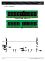
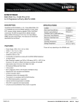
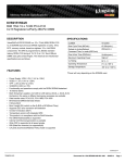
Memory Module Specifications
KVR21R15D8K4/32
32GB (8GB 2Rx8 1G x 72-Bit x 4 pcs.) PC4-2133
CL15 Registered w/Parity 288-Pin DIMM Kit
DESCRIPTION
ValueRAM's KVR21R15D8K4/32 is a kit of four 1G x 72-bit
(8GB) DDR4-2133 CL15 SDRAM (Synchronous DRAM)
registered w/ parity, 2Rx8, ECC, memory module, based on
eighteen 512M x 8-bit FBGA components per module. Total kit
capacity is 32GB. The SPD is programmed to JEDEC standard
latency DDR4-2133 timing of 15-15-15 at 1.2V. Each 288-pin
DIMM uses gold contact fingers. The electrical and mechanical
specifications are as follows:
SPECIFICATIONS
CL(IDD)
15 cycles
Row Cycle Time (tRCmin)
47.05ns(min.)
Refresh to Active/Refresh
Command Time 1x mode (tRFCmin)
260ns(min.)
Row Active Time (tRASmin)
33.00ns(min.)
Maximum Operating Power
TBD W*
UL Rating
94 V - 0
Operating Temperature
0o C to +85o C
Storage Temperature
-55o C to +100o C
FEATURES
*Power will vary depending on the SDRAM used.
• Power Supply: VDD=1.2V (1.14V to 1.26V)
• VDDQ = 1.2V (1.14V to 1.26V)
• VPP - 2.5V (2.375V to 2.75V)
• VDDSPD=2.25V to 2.75V
• Functionality and operations comply with the DDR4 SDRAM datasheet
• 16 internal banks
• Bank Grouping is applied, and CAS to CAS latency (tCCD_L, tCCD_S) for
the banks in the same or different bank group accesses are available
• Data transfer rates: PC4-2133, PC4-1866, PC4-1600
• Bi-Directional Differential Data Strobe
• 8 bit pre-fetch
• Burst Length (BL) switch on-the-fly BL8 or BC4(Burst Chop)
• Supports ECC error correction and detection
• On-Die Termination (ODT)
• Temperature sensor with integrated SPD
• This product is in compliance with the RoHS directive.
• Per DRAM Addressability is supported
• Internal Vref DQ level generation is available
• Write CRC is supported at all speed grades
• CA parity (Command/Address Parity) mode is supported
Continued >>
kingston.com
Document No. VALUERAM1471-001.A00
04/30/15
Page 1
MODULE DIMENSIONS
Front
Back
kingston.com
Document No. VALUERAM1471-001.A00
Page 2