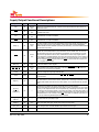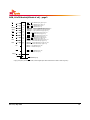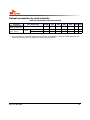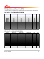
1
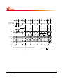
240pin DDR3L SDRAM Registered DIMM
DDR3L SDRAM Registered DIMM
Based on 4Gb B-die
HMT451R7BFR8A
HMT41GR7BFR8A
HMT41GR7BFR4A
HMT42GR7BFR4A
HMT84GR7BMR4A
*SK hynix reserves the right to change products or specifications without notice.
Rev. 1.0 /May. 2014
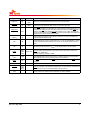
1
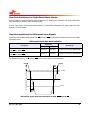
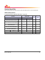
Revision History
Revision No.
History
Draft Date
0.1
Initial Release
Mar.2014
1.0
Revision 1.0 Release
May.2014
Rev. 1.0 / May. 2014
Remark
2
Description
SK hynix Registered DDR3L SDRAM DIMMs (Registered Double Data Rate Synchronous DRAM Dual In-Line
Memory Modules) are low power, high-speed operation memory modules that use DDR3L SDRAM devices.
These Registered SDRAM DIMMs are intended for use as main memory when installed in systems such as
servers and workstations.
Features
•
•
•
•
•
•
•
•
•
•
•
•
•
•
Power Supply: VDD=1.35V (1.283V to 1.45V)
VDDQ = 1.35V (1.283V to 1.45V)
VDDSPD=3.0V to 3.6V
Backward Compatible with 1.5V DDR3 Memory Module
8 internal banks
Data transfer rates: PC3-14900, PC3-12800, PC3-10600, PC3-8500
Bi-Directional Differential Data Strobe
8 bit pre-fetch
Burst Length (BL) switch on-the-fly BL8 or BC4(Burst Chop)
Supports ECC error correction and detection
On-Die Termination (ODT)
Temperature sensor with integrated SPD
Backward compatible with 1.5V DDR3 Memory module.
This product is in compliance with the RoHS directive.
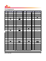
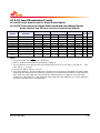
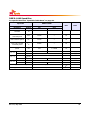
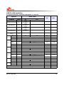
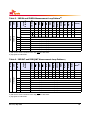
Ordering Information
Density
Organization
Component Composition
# of
ranks
FDHS
HMT451R7BFR8A-H9/PB/RD
4GB
512Mx72
512Mx8(H5TC4G83BFR)*9
1
X
HMT41GR7BFR8A-H9/PB/RD
8GB
1Gx72
512Mx8(H5TC4G83BFR)*18
2
X
HMT41GR7BFR4A-H9/PB/RD
8GB
1Gx72
1Gx4(H5TC4G43BFR)*18
1
X
HMT42GR7BFR4A-H9/PB/RD
16GB
2Gx72
1Gx4(H5TC4G43BFR)*36
2
O
HMT84GR7BMR4A-G7/H9/PB
32GB
4Gx72
DDP 2Gx4(H5TC8G43BMR)*36
4
O
Part Number
* In order to uninstall FDHS, please contact sales administrator
Rev. 1.0 / May. 2014
3
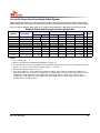
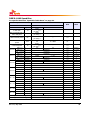
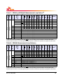
Key Parameters
MT/s
Grade
tCK
(ns)
CAS
Latency
(tCK)
tRCD
(ns)
tRP
(ns)
tRAS
(ns)
tRC
(ns)
CL-tRCD-tRP
DDR3L-1066
-G7
1.875
7
13.125
13.125
37.5
50.625
7-7-7
DDR3L-1333
-H9
1.5
9
13.5
13.5
(13.125)* (13.125)*
36
49.5
(49.125)*
9-9-9
DDR3L-1600
-PB
1.25
11
13.75
13.75
(13.125)* (13.125)*
35
48.75
(48.125)*
11-11-11
DDR3L-1866
-Rd
1.07
13
13.91
13.91
(13.125)* (13.125)*
34
47.91
(48.125)*
13-13-13
*SK hynix DRAM devices support optional downbinning to CL11, CL9 and CL7. SPD setting is programmed to match.
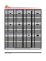
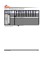
Speed Grade
Frequency [MHz]
Grade
Remark
CL6
CL7
CL8
CL9
CL10
-G7
800
1066
1066
-H9
800
1066
-PB
800
-RD
800
CL11
1066
1333
1333
1066
1066
1333
1333
1600
1066
1066
1333
1333
1600
CL12
CL13
1866
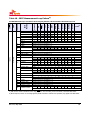
Address Table
4GB(1Rx8)
8GB(1Rx4)
8GB(2Rx8)
16GB(2Rx4)
32GB(4Rx4)
Refresh Method
8K/64ms
8K/64ms
8K/64ms
8K/64ms
8K/64ms
Row Address
A0-A15
A0-A15
A0-A15
A0-A15
A0-A15
Column Address
A0-A9
A0-A9,A11
A0-A9
A0-A9,A11
A0-A9,A11
Bank Address
BA0-BA2
BA0-BA2
BA0-BA2
BA0-BA2
BA0-BA2
Page Size
1KB
1KB
1KB
1KB
1KB
Rev. 1.0 / May. 2014
4
Pin Descriptions
Pin Name
Description
Num
ber
Pin Name
Description
Num
ber
CK0
Clock Input, positive line
1
ODT[1:0]
On Die Termination Inputs
2
CK0
Clock Input, negative line
1
DQ[63:0]
Data Input/Output
64
CK1
Clock Input, positive line
1
CB[7:0]
CK1
Clock Input, negative line
1
DQS[8:0]
Clock Enables
2
DQS[8:0]
RAS
Row Address Strobe
1
DM[8:0]/
DQS[17:9],
TDQS[17:9]
CAS
Column Address Strobe
1
DQS[17:9],
TDQS[17:9]
WE
Write Enable
1
EVENT
S[3:0]
Chip Selects
4
TEST
Memory bus test tool (Not Connected and Not Usable on DIMMs)
1
Address Inputs
14
RESET
Register and SDRAM control pin
1
A10/AP
Address Input/Autoprecharge
1
VDD
Power Supply
22
A12/BC
Address Input/Burst chop
1
VSS
Ground
59
BA[2:0]
SDRAM Bank Addresses
3
VREFDQ
Reference Voltage for DQ
1
Reference Voltage for CA
1
Termination Voltage
4
SPD Power
1
CKE[1:0]
A[9:0],A11,
A[15:13]
SCL
Serial Presence Detect (SPD)
Clock Input
1
VREFCA
SDA
SPD Data Input/Output
1
VTT
SA[2:0]
SPD Address Inputs
3
VDDSPD
Par_In
Parity bit for the Address and
Control bus
1
Err_Out
Parity error found on the
Address and Control bus
1
Rev. 1.0 / May. 2014
Data check bits Input/Output
Data strobes
Data strobes, negative line
Data Masks / Data strobes,
Termination data strobes
Data strobes, negative line,
Termination data strobes
Reserved for optional hardware
temperature sensing
8
9
9
9
9
1
5
Input/Output Functional Descriptions
Symbol
Type
Polarity
CK0
IN
Positive
Line
Positive line of the differential pair of system clock inputs that drives input to the onDIMM Clock Driver.
CK0
IN
Negative
Line
Negative line of the differential pair of system clock inputs that drives the input to the
on-DIMM Clock Driver.
CK1
IN
Positive
Line
Terminated but not used on RDIMMs.
CK1
IN
Negative
Line
Terminated but not used on RDIMMs.
IN
Active
High
CKE[1:0]
Function
CKE HIGH activates, and CKE LOW deactivates internal clock signals, and device input
buffers and output drivers of the SDRAMs. Taking CKE LOW provides PRECHARGE
POWER-DOWN and SELF REFRESH operation (all banks idle), or ACTIVE POWER DOWN
(row ACTIVE in any bank)
Enables the command decoders for the associated rank of SDRAM when low and disables decoders when high. When decoders are disabled, new commands are ignored
and previous operations continue. Other combinations of these input signals perform
unique functions, including disabling all outputs (except CKE and ODT) of the register(s)
on the DIMM or accessing internal control words in the register device(s). For modules
with two registers, S[3:2] operate similarly to S[1:0] for the second set of register outputs or register control words.
S[3:0]
IN
Active
Low
ODT[1:0]
IN
Active
High
On-Die Termination control signals
RAS, CAS, WE
IN
Active
Low
When sampled at the positive rising edge of the clock, CAS, RAS, and WE define the
operation to be executed by the SDRAM.
VREFDQ
Supply
Reference voltage for DQ0-DQ63 and CB0-CB7.
VREFCA
Supply
Reference voltage for A0-A15, BA0-BA2, RAS, CAS, WE, S0, S1, CKE0, CKE1, Par_In,
ODT0 and ODT1.
BA[2:0]
IN
—
Selects which SDRAM bank of eight is activated.
BA0 - BA2 define to which bank an Active, Read, Write or Precharge command is being
applied. Bank address also determines mode register is to be accessed during an MRS
cycle.
A[15:13,
12/BC,11,
10/AP,[9:0]
IN
—
Provided the row address for Active commands and the column address
and Auto Precharge bit for Read/Write commands to select one location out of the memory array in the respective bank. A10 is sampled during a Precharge command to determine whether the Precharge applies to one bank (A10 LOW) or all banks (A10 HIGH). If
only one bank is to be precharged, the bank is selected by BA. A12 is also utilized for BL
4/8 identification for ‘’BL on the fly’’ during CAS command. The address inputs also provide the op-code during Mode Register Set commands.
DQ[63:0],
CB[7:0]
I/O
—
Data and Check Bit Input/Output pins
DM[8:0]
IN
Active
High
VDD, VSS
Supply
Power and ground for the DDR SDRAM input buffers and core logic.
VTT
Supply
Termination Voltage for Address/Command/Control/Clock nets.
Rev. 1.0 / May. 2014
Masks write data when high, issued concurrently with input data.
6
Symbol
Type
Polarity
Function
DQS[17:0]
I/O
Positive
Edge
Positive line of the differential data strobe for input and output data.
DQS[17:0]
I/O
Negative
Edge
Negative line of the differential data strobe for input and output data.
TDQS/TDQS is applicable for X8 DRAMs only. When enabled via Mode Register A11=1 in
MR1,DRAM will enable the same termination resistance function on TDQS/TDQS that is
applied to DQS/DQS. When disabled via mode register A11=0 in MR1, DM/TDQS will
provide the data mask function and TDQS is not used. X4/X16 DRAMs must disable the
TDQS function via mode register A11=0 in MR1
TDQS[17:9]
TDQS[17:9]
OUT
SA[2:0]
IN
—
These signals are tied at the system planar to either VSS or VDDSPD to configure the
serial SPD EEPROM address range.
SDA
I/O
—
This bidirectional pin is used to transfer data into or out of the SPD EEPROM. A resistor
must be connected from the SDA bus line to VDDSPD on the system planar to act as a
pullup.
SCL
IN
—
This signal is used to clock data into and out of the SPD EEPROM. A resistor may be connected from the SCL bus time to VDDSPD on the system planar to act as a pullup.
EVENT
OUT
(open
drain)
VDDSPD
Supply
Serial EEPROM positive power supply wired to a separate power pin at the connector
which supports from 3.0 Volt to 3.6 Volt (nominal 3.3V) operation.
RESET
IN
The RESET pin is connected to the RESET pin on the register and to the RESET pin on
the DRAM.
Par_In
IN
Parity bit for the Address and Control bus. (“1 “: Odd, “0 “: Even)
Err_Out
OUT
(open
drain)
TEST
Rev. 1.0 / May. 2014
This signal indicates that a thermal event has been detected in the thermal sensing
device.The system should guarantee the electrical level requirement is met for the
Active Low
EVENT pin on TS/SPD part.
No pull-up resister is provided on DIMM.
Parity error detected on the Address and Control bus. A resistor may be connected from
Err_Out bus line to VDD on the system planar to act as a pull up.
Used by memory bus analysis tools (unused (NC) on memory DIMMs)
7
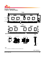
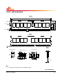
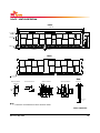
Pin Assignments
Pin #
Front Side
(left 1–60)
Pin #
Back Side
(right 121–180)
Pin #
Front Side
(left 61–120)
Pin #
Back Side
(right 181–240)
1
VREFDQ
121
VSS
61
A2
181
A1
2
VSS
122
DQ4
62
VDD
182
VDD
3
DQ0
123
DQ5
63
NC, CK1
183
VDD
4
DQ1
124
VSS
64
NC, CK1
184
CK0
5
VSS
125
DM0,DQS9,
TDQS9
65
VDD
185
CK0
6
DQS0
126
NC,DQS9,
TDQS9
66
VDD
186
VDD
7
DQS0
127
VSS
67
VREFCA
187
EVENT, NC
8
VSS
128
DQ6
68
Par_In, NC
188
A0
9
DQ2
129
DQ7
69
VDD
189
VDD
10
DQ3
130
VSS
70
A10 / AP
190
BA1
11
VSS
131
DQ12
71
BA0
191
VDD
12
DQ8
132
DQ13
72
VDD
192
RAS
13
DQ9
133
VSS
73
WE
193
S0
14
VSS
134
DM1,DQS10,
TDQS10
74
CAS
194
VDD
15
DQS1
135
NC,DQS10,
TDQS10
75
VDD
195
ODT0
16
DQS1
136
VSS
76
S1, NC
196
A13
17
VSS
137
DQ14
77
ODT1, NC
197
VDD
18
DQ10
138
DQ15
78
VDD
198
S3, NC
19
DQ11
139
VSS
79
S2, NC
199
VSS
20
VSS
140
DQ20
80
VSS
200
DQ36
21
DQ16
141
DQ21
81
DQ32
201
DQ37
22
DQ17
142
VSS
82
DQ33
202
VSS
83
VSS
203
DM4,DQS13,
TDQS13
23
VSS
143
DM2,DQS11,
TDQS11
24
DQS2
144
NC,DQS11,
TDQS11
84
DQS4
204
NC,DQS13,
TDQS13
25
DQS2
145
VSS
85
DQS4
205
VSS
26
VSS
146
DQ22
86
VSS
206
DQ38
27
DQ18
147
DQ23
87
DQ34
207
DQ39
28
DQ19
148
VSS
88
DQ35
208
VSS
29
VSS
149
DQ28
89
VSS
209
DQ44
30
DQ24
150
DQ29
90
DQ40
210
DQ45
31
DQ25
151
VSS
91
DQ41
211
VSS
NC = No Connect; RFU = Reserved Future Use
Rev. 1.0 / May. 2014
8
Pin #
Front Side
(left 1–60)
Pin #
Back Side
(right 121–180)
Pin #
Front Side
(left 61–120)
Pin #
Back Side
(right 181–240)
32
VSS
152
DM3,DQS12,
TDQS12
92
VSS
212
DM5,DQS14,
TDQS14
33
DQS3
153
NC,DQS12,
TDQS12
93
DQS5
213
NC,DQS14,
TDQS14
34
DQS3
154
VSS
94
DQS5
214
VSS
35
VSS
155
DQ30
95
VSS
215
DQ46
36
DQ26
156
DQ31
96
DQ42
216
DQ47
37
DQ27
157
VSS
97
DQ43
217
VSS
38
VSS
158
CB4, NC
98
VSS
218
DQ52
39
CB0, NC
159
CB5, NC
99
DQ48
219
DQ53
40
CB1, NC
160
VSS
100
DQ49
220
VSS
41
VSS
161
NC,DM8,DQS17,
TDQS17
101
VSS
221
DM6,DQS15,
TDQS15
42
DQS8
162
NC,DQS17,
TDQS17
102
DQS6
222
NC,DQS15,
TDQS15
43
DQS8
163
VSS
103
DQS6
223
VSS
44
VSS
164
CB6, NC
104
VSS
224
DQ54
45
CB2, NC
165
CB7, NC
105
DQ50
225
DQ55
46
CB3, NC
166
VSS
106
DQ51
226
VSS
47
VSS
167
NC(TEST)
107
VSS
227
DQ60
VTT, NC
168
RESET
108
DQ56
228
DQ61
109
DQ57
229
VSS
48
KEY
KEY
49
VTT, NC
169
CKE1, NC
110
VSS
230
DM7,DQS16,
TDQS16
50
CKE0
170
VDD
111
DQS7
231
NC,DQS16,
TDQS16
51
VDD
171
A15
112
DQS7
232
VSS
52
BA2
172
A14
113
VSS
233
DQ62
53
Err_Out, NC
173
VDD
114
DQ58
234
DQ63
54
VDD
174
A12 / BC
115
DQ59
235
VSS
55
A11
175
A9
116
VSS
236
VDDSPD
56
A7
176
VDD
117
SA0
237
SA1
57
VDD
177
A8
118
SCL
238
SDA
58
A5
178
A6
119
SA2
239
VSS
59
A4
179
VDD
120
VTT
240
VTT
60
VDD
180
A3
NC = No Connect; RFU = Reserved Future Use
Rev. 1.0 / May. 2014
9
Registering Clock Driver Specifications
Capacitance Values
Symbol
CI
CIR
Parameter
Conditions
Min
Typ
Max
Unit
Input capacitance, Data inputs
1.5
-
2.5
pF
Input capacitance, CK, CK, FBIN, FBIN
(up to DDR3-1600)
1.5
-
2.5
pF
-
-
3
pF
Input capacitance, RESET, MIRROR,
QCSEN
VI = VDD or GND; VDD = 1.5v
Input & Output Timing Requirements
Symbol
Parameter
Conditions
DDR3L-800
1066/1333
DDR3L-1600
DDR3L-1866
Unit
Min
Max
Min
Max
Min
Max
fclock
Input clock frequency
Application frequency
300
670
300
810
300
945
Mhz
fTEST
Input clock frequency
Test frequency
70
300
70
300
70
300
Mhz
tSU
Setup time
Input valid before
CK/CK
100
-
50
-
40
-
ps
tH
Hold time
Input to remain
valid after CK/CK
175
-
125
-
75
-
ps
tPDM
Propagation
delay, single-bit CK/CK to output
switching
0.65
1.0
0.65
1.0
0.65
1.0
ns
tDIS
Output disable
Yn/Yn to output
0.5 +
time (1/2-Clock
tQSK1(min)
float
prelaunch)
-
0.5 +
tQSK1(min)
-
0.5 +
tQSK1(min)
-
ps
tEN
Output enable
Output driving to
0.5 time (1/2-Clock
tQSK1(max)
Yn/Yn
prelaunch)
-
0.5 tQSK1(max)
-
0.5 tQSK1(max)
-
ps
Rev. 1.0 / May. 2014
10
On DIMM Thermal Sensor
The DDR3 SDRAM DIMM temperature is monitored by integrated thermal sensor. The integrated thermal
sensor comply with JEDEC “TSE2002av, Serial Presence Detect with Temperature Sensor”.
Connection of Thermal Sensor
EVENT
SCL
SDA
SA0
SPD with SA1
Integrated SA2
TS
EVENT
SCL
SA0
SDA
SA1
SA2
Temperature-to-Digital Conversion Performance
Parameter
Temperature Sensor Accuracy (Grade B)
Resolution
Rev. 1.0 / May. 2014
Condition
Min
Typ
Max
Unit
Active Range,
75°C < TA < 95°C
-
± 0.5
± 1.0
°C
Monitor Range,
40°C < TA < 125°C
-
± 1.0
± 2.0
°C
-20°C < TA < 125°C
-
± 2.0
± 3.0
°C
0.25
°C
11
RODT0B
PCK0B
RCKE0B
RWEB
PCK0B
A[O:N]/BA[O:N]
ODT
CK
CKE
CK
CAS
WE
ODT
CK
CKE
CK
WE
CAS
D5
ODT
CK
CKE
CK
WE
CAS
D6
A[O:N]/BA[N:O]
ZQ
ODT
CK
CKE
CK
D7
A[N:O]/BA[N:O]
ZQ
WE
RAS
CS
A[N:O]/BA[N:O]
ODT
CK
CKE
CK
ZQ
A[O:N]/BA[N:O]
DQS
DQS
TDQS
TDQS
DQ [7:0]
ZQ
D0
RCASB
DQS7
DQS7
DM7/DQS16
DQS16
DQ[63:56]
RAS
DQS
DQS
TDQS
TDQS
DQ [7:0]
CS
DQS6
DQS6
DM6/DQS15
DQS15
DQ[55:48]
D4
CAS
ODT
A[O:N]/BA[N:O]
A[N:O]/BA[N:O]
ODT
DQS
DQS
TDQS
TDQS
DQ [7:0]
RAS
ODT
ODT
CK
CKE
CK
CKE
CK
CKE
RS0B
RRASB
A[N:O]A
/BA[N:O]A
RODT0A
PCK0A
RCKE0A
CK
CKE
CK
CK
D1
WE
CAS
RAS
CK
WE
ZQ
DQS
DQS
TDQS
TDQS
DQ [7:0]
CS
CK
CAS
WE
WE
CAS
CAS
CAS
D2
WE
RAS
CS
CS
RAS
RAS
ZQ
DQS5
DQS5
DM5/DQS14
DQS14
DQ[47:40]
CS
DQS
DQS
TDQS
TDQS
DQ [7:0]
D3
DQS
DQS
TDQS
TDQS
DQ [7:0]
RAS
DQS1
DQS1
DM1/DQS10
DQS10
DQ[15:8]
ZQ
ZQ
DQS4
DQS4
DM4/DQS13
DQS13
DQ[39:32]
CS
DQS
DQS
TDQS
TDQS
DQ [7:0]
A[N:O]/BA[N:O]
DQS2
DQS2
DM2/DQS11
DQS11
DQ[23:16]
D8
A[O:N]/BA[N:O]
DQS
DQS
TDQS
TDQS
DQ [7:0]
RAS
DQS3
DQS3
DM3/DQS12
DQS12
DQ[31:24]
CS
DQS
DQS
TDQS
TDQS
DQ [7:0]
CS
RWEA
ZQ
DQS8
DQS8
DM8/DQS17
DQS17
CB[7:0]
DQS0
DQS0
DM0/DQS9
DQS9
DQ[7:0]
PCK0A
RS0A
RRASA
RCASA
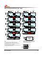
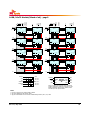
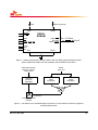
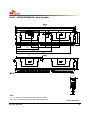
4GB, 512Mx72 Module(1Rank of x8)
A[N:O]B
/BA[N:O]B
Functional Block Diagram
Vtt
VDDSPD
SPD
VDD
D0–D8
VTT
VREFCA
D0–D8
VREFDQ
D0–D8
VSS
D0–D8
Note:
1.DQ-to-I/O wiring may be changed within byte.
2.ZQ resistors are 240 Ω ±1%.For all other resistor values refer to the
appropriate wiring diagram.
Vtt
S0
S1
BA[N:0]
A[N:0]
RAS
CAS
WE
CKE0
ODT0
CK0
CK0
CK0
CK0
PAR_IN
120 Ω
±1%
1:
2
R
E
G
I
S
T
E
R
/
P
L
L
120 Ω
±1%
RESET
OERR
RST
RS0A → CS0: SDRAMs D[3:0], D8
RS0B → CS0: SDRAMs D[7:4]
RBA[N:0]A → BA[N:0]: SDRAMs D[3:0], D8
RBA[N:0]A → BA[N:0]: SDRAMs D[7:4]
RA[N:0]A → A[N:0]: SDRAMs D[3:0], D8
RA[N:0]A → A[N:0]: SDRAMs D[7:4]
RRASA → RAS: SDRAMs D[3:0], D8
RRASA → RAS: SDRAMs D[7:4]
RCASA → CAS: SDRAMs D[3:0], D8
RCASA → CAS: SDRAMs D[7:4]
RWEA → WE: SDRAMs D[3:0], D8
RWEA → WE: SDRAMs D[7:4]
RCKE0A → CKE0: SDRAMs D[3:0], D8
RCKE0B → CKE0: SDRAMs D[7:4]
RODT0A → ODT0: SDRAMs D[3:0], D8
RODT0B → ODT0: SDRAMs D[7:4]
PCK0A → CK: SDRAMs D[3:0], D8
PCK0B → CK: SDRAMs D[7:4]
PCK0A → CK: SDRAMs D[3:0], D8
PCK0B → CK: SDRAMs D[7:4]
VDDSPD
EVENT
SCL
SDA
VDDSPD
SA0
SA0
EVENT SPD with SA1
Integrated SA2
SCL
TS
VSS
SDA
SA1
SA2
VSS
Plan to use SPD with Integrated TS of Class B and
might be changed on customer’s requests. For more
details of SPD and Thermal sensor, please contact
local SK hynix sales representative
Err_Out
RST: SDRAMs D[8:0]
S[3:2], CKE1, ODT1, are NC (Unused register inputs ODT1 and CKE1 have a 330 Ω resistor to ground
Rev. 1.0 / May. 2014
12
ODT
CK
CKE
CK
VSS
A[O:N]/BA[O:N]
ODT
CK
CKE
CK
WE
CAS
VSS
A[O:N]/BA[O:N]
ODT
CK
CKE
CK
VSS
A[O:N]/BA[O:N]
ODT
CK
CK
CKE
D15
ODT
CK
CKE
VSS
D16
A[O:N]/BA[O:N]
ZQ
CK
RAS
CS
CAS
ZQ
CAS
RAS
CS
D14
CAS
ODT
A[O:N]/BA[O:N]
A[O:N]/BA[O:N]
ODT
CK
CKE
D7
RAS
DQS
DQS
DM
DQ [3:0]
ZQ
WE
DQS16
DQS16
VSS
DQ[63:60]
ZQ
RAS
A[O:N]/BA[O:N]
ODT
CK
CKE
CK
CKE
D6
D13
WE
DQS
DQS
DM
DQ [3:0]
ZQ
ZQ
WE
DQS15
DQS15
VSS
DQ[55;52]
CS
VSS
VSS
A[O:N]/BA[O:N]
DQS
DQS
DM
DQ [3:0]
VSS
ODT
VSS
DQS14
DQS14
VSS
DQ[47:44]
CS
RODT0B
A[O:N]B
/BA[O:N]B
RWEB
PCK0B
RCASB
PCK0B
RCKE0B
CK
CKE
CK
WE
CK
WE
CAS
CAS
CAS
CAS
RAS
CS
DQS
DQS
DM
DQ [3:0]
Vtt
VSS
D9
A[O:N]/BA[O:N]
ZQ
RAS
CS
CS
A[O:N]/BA[O:N]
ODT
CK
CKE
CK
WE
CAS
D10
D5
CK
DQS
DQS
DM
DQ [3:0]
DQS13
DQS13
VSS
DQ[39:36]
ZQ
WE
DQS7
DQS7
VSS
DQ[59:56]
ZQ
RAS
A[O:N]/BA[O:N]
A[O:N]/BA[O:N]
ODT
CK
CKE
CK
WE
CAS
D11
D4
CK
DQS
DQS
DM
DQ [3:0]
ZQ
WE
RS0B
RRASB
DQS6
DQS6
VSS
DQ[51:48]
ZQ
RAS
DQS
DQS
DM
DQ [3:0]
CS
VSS
A[O:N]/BA[O:N]
VSS
DQS5
DQS5
VSS
DQ[43:40]
VSS
ODT
DQS
DQS
DM
DQ [3:0]
VSS
ODT
CK
CKE
CK
WE
CAS
D12
WE
CS
RAS
RAS
CS
DQS4
DQS4
VSS
DQ[35:32]
ZQ
CAS
A[O:N]/BA[O:N]
ODT
CK
CKE
CK
WE
D0
CK
CKE
DQS
DQS
DM
DQ [3:0]
ZQ
D17
CK
DQS9
DQS9
VSS
DQ[7:4]
CS
A[O:N]/BA[O:N]
ODT
CK
CKE
CK
WE
CAS
D1
ZQ
WE
DQS
DQS
DM
DQ [3:0]
CAS
DQS10
DQS10
VSS
DQ[15:12]
ZQ
RAS
A[O:N]/BA[O:N]
ODT
CK
CKE
CK
WE
CAS
D2
RAS
DQS
DQS
DM
DQ [3:0]
CS
DQS11
DQS11
VSS
DQ23:20]
ZQ
RAS
A[O:N]/BA[O:N]
ODT
CK
CKE
CK
WE
CAS
D3
CS
PCK0A
RCKE0A
RODT0A
RWEA
PCK0A
A[O:N]A
/BA[O:N]A
VSS
CAS
DQS
DQS
DM
DQ [3:0]
ZQ
CAS
CS
RAS
RAS
CS
CS
RAS
RAS
CS
A[O:N]/BA[O:N]
DQS
DQS
DM
DQ [3:0]
VSS
DQS0
DQS0
VSS
DQ[3:0]
DQS12
DQS12
VSS
DQ[31:28]
VSS
DQS
DQS
DM
DQ [3:0]
DQS
DQS
DM
DQ [3:0]
VSS
DQS1
DQS1
VSS
DQ[11;8]
DQS17
DQS17
VSS
CB[7:4]
VSS
DQS
DQS
DM
DQ [3:0]
ODT
DQS2
DQS2
VSS
DQ[19:16]
D8
CK
CKE
DQS
DQS
DM
DQ [3:0]
ZQ
CK
DQS3
DQS3
VSS
DQ[27:24]
RAS
DQS
DQS
DM
DQ [3:0]
CS
DQS8
DQS8
VSS
CB[3:0]
WE
RS0A
RRASA
RCASA
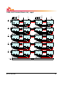
8GB, 1Gx72 Module(1Rank of x4) - page1
Vtt
VDDSPD
EVENT
SCL
SDA
SA0
SA0
EVENT SPD with SA1
Integrated SA2
SCL
TS
VSS
SDA
VDDSPD
SA1
SA2
VSS
Plan to use SPD with Integrated TS of Class B and
might be changed on customer’s requests. For more
details of SPD and Thermal sensor, please contact
local SK hynix sales representative
Note:
1. DQ-to-I/O wiring may be changed within a nibble.
2. Unless otherwise noted, resistor values are 15%.
5
3. See the wiring diagrams for all resistors associated with the command, address and control bus.
For
1 all other resistor values refer to the appro4. ZQ resistors are 240%.
priate wiring diagram.
Rev. 1.0 / May. 2014
VDDSPD
SPD
VDD
D0–D17
VTT
VREFCA
D0–D17
VREFDQ
D0–D17
VSS
D0–D17
D0–D17
13
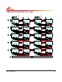
8GB, 1Gx72 Module(1Rank of x4) - page2
S0
S1
1:2
BA[N:0]
R
E
A[N:0]
G
RAS
I
S
T
E
R
/
P
L
L
CAS
WE
CKE0
ODT0
RS0A → CS0: SDRAMs D[3:0], D[12:8], D17
RS0B → CS0: SDRAMs D[7:4], D[16:13]
RS1A → CS1: SDRAMs D[12:9], D17
RS1B → CS1: SDRAMs D[16:13]
RBA[N:0]A → BA[N:0]: SDRAMs D[3:0], D[12:8], D17
RBA[N:0]B → BA[N:0]: SDRAMs D[7:4], D[16:13]
RA[N:0]A → A[N:0]: SDRAMs D[3:0], D[12:8], D17
RA[N:0]B → A[N:0]: SDRAMs D[7:4], D[16:13]
RRASA → RAS: SDRAMs D[3:0], D[12:8], D17
RRASB → RAS: SDRAMs D[7:4], D[16:13]
RCASA → CAS: SDRAMs D[3:0], D[12:8], D17
RCASB → CAS: SDRAMs D[7:4], D[16:13]
RWEA → WE: SDRAMs D[3:0], D[12:8], D17
RWEB → WE: SDRAMs D[7:4], D[16:13]
RCKE0A → CKE0: SDRAMs D[3:0], D[12:8], D17
RCKE0B → CKE0: SDRAMs D[7:4], D[16:13]
RODT0A → ODT0: SDRAMs D[3:0], D[12:8]. D17
RODT0B → ODT0: SDRAMs D[7:4], D[16:13]
CK0
PCK0A → CK: SDRAMs D[3:0], D8
PCK0B → CK: SDRAMs D[7:4]
CK0
PCK0A → CK: SDRAMs D[3:0], D8
PCK0B → CK: SDRAMs D[7:4]
PAR_IN
OERR Err_Out
RESET
RST
RST: SDRAMs D[17:0]
* S[3:2], CKE1, ODT1, CK1 and CK1 are NC (Unused register inputs ODT1 and CKE1 have a 330 resistor to ground.)
Rev. 1.0 / May. 2014
14
RODT1B
A[N:O]/BA[N:O]
ODT
A[N:O]/BA[N:O]
A[O:N]/BA[N:O]
ODT
ODT
ODT
CK
CKE
CK
CKE
A[N:O]/BA[N:O]
PCK1B
CK
WE
CK
CKE
CK
CKE
CK
WE
WE
D16
CAS
ZQ
RAS
DQS
DQS
TDQS
TDQS
DQ [7:0]
CK
WE
D15
CAS
CS
ZQ
RAS
DQS
DQS
TDQS
TDQS
DQ [7:0]
CK
RAS
CS
CAS
D14
CAS
CS
RAS
A[N:O]/BA[N:O]
ZQ
PCK1B
RCKE1B
RS1B
A[N:O]B
/BA[N:O]B
A[N:O]/BA[N:O]
D13
DQS
DQS
TDQS
TDQS
DQ [7:0]
CS
ODT
CK
CKE
ZQ
A[N:O]/BA[N:O]
ODT
CK
CKE
CK
CKE
ODT
ODT
CK
CKE
CK
DQS
DQS
TDQS
TDQS
DQ [7:0]
A[N:O]/BA[N:O]
PCK0B
RCKE0B
RODT0B
PCK0B
RCASB
RWEB
WE
CK
CK
WE
WE
ZQ
D7
A[N:O]/BA[N:O]
ODT
CK
CKE
VDDSPD
EVENT
Vtt
SCL
SDA
Note:
1. DQ-to-I/O wiring may be changed within a byte.
2. Unless otherwise noted, resistor values are 15 Ω ±5%.
3. ZQ resistors are 240 Ω ±1%. For all other resistor values
refer to the appropriate wiring diagram.
4. See the wiring diagrams for all resistors associated with the
command, address and control bus.
Rev. 1.0 / May. 2014
WE
DQS
DQS
TDQS
TDQS
DQ [7:0]
CK
RS0B
RRASB
DQS7
DQS7
DM7/DQS16
DQS16
DQ[63:56]
D6
CAS
CS
ZQ
RAS
DQS
DQS
TDQS
TDQS
DQ [7:0]
CAS
DQS6
DQS6
DM6/DQS15
DQS15
DQ55:48]
D5
CAS
CS
ZQ
RAS
DQS
DQS
TDQS
TDQS
DQ [7:0]
RAS
DQS5
DQS5
DM5/DQS14
DQS14
DQ[47:40]
D4
CAS
CS
ZQ
RAS
DQS
DQS
TDQS
TDQS
DQ [7:0]
CS
PCK1A
RODT1A
ODT
A[N:O]/BA[N:O]
A[N:O]/BA[N:O]
ODT
ODT
A[N:O]/BA[N:O]
ODT
CK
CKE
CK
CKE
A[O:N]/BA[N:O]
CK
CKE
CK
CKE
CK
CAS
WE
WE
D9
CAS
RAS
DQS4
DQS4
DM4/DQS13
DQS13
DQ[39:32]
Vtt
DQS
DQS
TDQS
TDQS
DQ [7:0]
ZQ
CK
CAS
WE
WE
D10
CAS
CS
ZQ
RAS
DQS
DQS
TDQS
TDQS
DQ [7:0]
CK
RAS
CS
D11
CK
RAS
CS
D12
DQS
DQS
TDQS
TDQS
DQ [7:0]
ZQ
CK
WE
CAS
D17
DQS
DQS
TDQS
TDQS
DQ [7:0]
ZQ
PCK1A
RCKE1A
RS1A
CS
ZQ
RAS
DQS
DQS
TDQS
TDQS
DQ [7:0]
CS
RODT0A
A[N:O]A
/BA[N:O]A
A[N:O]/BA[N:O]
ODT
ODT
A[N:O]/BA[N:O]
A[N:O]/BA[N:O]
ODT
ODT
ODT
A[O:N]/BA[N:O]
CK
CKE
CK
CKE
CK
CKE
CK
CKE
A[N:O]/BA[N:O]
RWEA
PCK0A
RCASA
PCK0A
RCKE0A
CK
CKE
WE
CK
CK
D0
WE
CS
ZQ
CK
WE
DQS
DQS
TDQS
TDQS
DQ [7:0]
CK
D1
WE
CS
ZQ
DQS0
DQS0
DM0/DQS9
DQS9
DQ[7:0]
WE
DQS
DQS
TDQS
TDQS
DQ [7:0]
CAS
DQS1
DQS1
DM1/DQS10
DQS10
DQ[15:8]
D2
CAS
CS
ZQ
RAS
DQS
DQS
TDQS
TDQS
DQ [7:0]
RAS
DQS2
DQS2
DM2/DQS11
DQS11
DQ[23:16]
D3
CAS
CS
ZQ
RAS
DQS
DQS
TDQS
TDQS
DQ [7:0]
CAS
DQS3
DQS3
DM3/DQS12
DQS12
DQ[31:24]
D8
CAS
CS
ZQ
RAS
DQS
DQS
TDQS
TDQS
DQ [7:0]
RAS
DQS8
DQS8
DM8/DQS17
DQS17
CB[7:0]
CK
RS0A
RRASA
8GB, 1Gx72 Module(2Rank of x8) - page1
VDDSPD
SA0
SA0
EVENT SPD with SA1
Integrated SA2
SCL
TS
VSS
SDA
SA1
SA2
VSS
Plan to use SPD with Integrated TS of Class B and
might be changed on customer’s requests. For more
details of SPD and Thermal sensor, please contact
local SK hynix sales representative
VDDSPD
Serial PD
VDD
D0–D17
VTT
VREFCA
D0–D17
VREFDQ
D0–D17
VSS
D0–D17
D0–D17
15
8GB, 1Gx72(2Rank of x8) - page2
S0
1:2
S1
S[3:2] NC
BA[N:0]
R
E
G
I
S
T
E
R
/
P
L
L
A[N:0]
RAS
CAS
WE
CKE0
CKE1
ODT0
ODT1
CK0
120 Ω
±5%
CK0
CK1
CK1
120 Ω
±5%
PAR_IN
RS0A → CS0: SDRAMs D[3:0], D8
RS0B → CS0: SDRAMs D[7:4]
RS1A → CS1: SDRAMs D[12:9], D17
RS1B → CS1: SDRAMs D[16:13]
RBA[N:0]A → BA[N:0]: SDRAMs D[3:0], D[12:8], D17
RBA[N:0]B → BA[N:0]: SDRAMs D[7:4], D[16:13]
RA[N:0]A → A[N:0]: SDRAMs D[3:0], D[12:8], D17
RA[N:0]B → A[N:0]: SDRAMs D[7:4], D[16:13]
RRASA → RAS: SDRAMs D[3:0], D[12:8], D17
RRASB → RAS: SDRAMs D[7:4], D[16:13]
RCASA → CAS: SDRAMs D[3:0], D[12:8], D17
RCASB → CAS: SDRAMs D[7:4], D[16:13]
RWEA → WE: SDRAMs D[3:0], D[12:8], D17
RWEB → WE: SDRAMs D[7:4], D[16:13]
RCKE0A → CKE0: SDRAMs D[3:0], D8
RCKE0B → CKE0: SDRAMs D[7:4]
RCKE1A → CKE1: SDRAMs D[12:9], D17
RCKE1B → CKE1: SDRAMs D[16:13]
RODT0A → ODT0: SDRAMs D[3:0], D8
RODT0B → ODT0: SDRAMs D[7:4]
RODT1A → ODT1: SDRAMs D[12:9], D17
RODT1A → ODT1: SDRAMs D[16:13]
PCK0A → CK: SDRAMs D[3:0], D8
PCK0B → CK: SDRAMs D[7:4]
PCK1A → CK: SDRAMs D[12:9], D17
PCK1B → CK: SDRAMs D[16:13]
PCK0A → CK: SDRAMs D[3:0], D8
PCK0B → CK: SDRAMs D[7:4]
PCK1A → CK: SDRAMs D[12:9], D17
PCK1B → CK: SDRAMs D[16:13]
OERR Err_Out
RESET
RST
RST: SDRAMs D[17:0]
* S[3:2], CK1 and CK1 are NC
Rev. 1.0 / May. 2014
16
DQS0
DQS0
VSS
DQ[3:0]
DQS
DQS
DM
DQ [3:0]
Vtt
Rev. 1.0 / May. 2014
D0
D18
DQS9
DQS9
VSS
DQ[7:4]
DQS
DQS
DM
DQ [3:0]
D9
DQS
DQS
DM
DQ [3:0]
A[N:O]/BA[N:O]
A[N:O]/BA[N:O]
D27
ODT
D19
ODT
CK
CKE
DQS
DQS
DM
DQ [3:0]
CK
CKE
D21
D20
A[N:O]/BA[N:O]
ODT
CK
CKE
CK
WE
CAS
RAS
CS
A[N:O]/BA[N:O]
ODT
CK
CKE
CK
WE
CAS
RAS
CS
A[N:O]/BA[N:O]
ODT
CK
CKE
CK
WE
CAS
D26
A[N:O]/BA[N:O]
ODT
CK
CKE
DQS
DQS
DM
DQ [3:0]
CK
WE
CAS
RAS
CS
DQS
DQS
DM
DQ [3:0]
CK
WE
CAS
RAS
CS
A[N:O]/BA[N:O]
ODT
CK
CKE
CK
WE
CAS
DQS
DQS
DM
DQ [3:0]
CK
WE
CAS
RAS
D1
CS
D2
A[N:O]/BA[N:O]
ODT
CK
CKE
CK
WE
CAS
D3
A[N:O]/BA[N:O]
ODT
CK
CKE
CK
WE
CAS
RAS
D8
A[N:O]/BA[N:O]
ODT
DQS
DQS
DM
DQ [3:0]
CK
CKE
DQS1
DQS1
VSS
DQ[11:8]
CK
DQS
DQS
DM
DQ [3:0]
RAS
DQS2
DQS2
VSS
DQ[19:16]
RAS
DQS
DQS
DM
DQ [3:0]
CS
DQS3
DQS3
VSS
DQ[27:24]
RAS
CS
A[N:O]/BA[N:O]
ODT
DQS
DQS
DM
DQ [3:0]
CS
CS
A[N:O]/BA[N:O]
ODT
CK
CKE
CK
WE
CAS
RAS
CS
DQS8
DQS8
VSS
CB[3:0]
WE
CAS
RAS
D28
CS
D29
A[N:O]/BA[N:O]
ODT
CK
CKE
D30
A[N:O]/BA[N:O]
ODT
CK
CKE
CK
WE
CAS
RAS
CS
A[N:O]/BA[N:O]
ODT
CK
CKE
CK
WE
CAS
D35
A[N:O]/BA[N:O]
ODT
DQS
DQS
DM
DQ [3:0]
CK
CKE
DQS
DQS
DM
DQ [3:0]
CK
CKE
DQS
DQS
DM
DQ [3:0]
CK
WE
CAS
RAS
CS
DQS
DQS
DM
DQ [3:0]
CK
WE
CAS
RAS
CS
A[N:O]/BA[N:O]
ODT
CK
CKE
CK
WE
CAS
DQS
DQS
DM
DQ [3:0]
CK
WE
CAS
RAS
D10
A[N:O]/BA[N:O]
D11
A[N:O]/BA[N:O]
ODT
CK
CKE
CK
WE
CAS
D12
A[N:O]/BA[N:O]
ODT
CK
CKE
CK
WE
CAS
RAS
DQS
DQS
DM
DQ [3:0]
D17
CS
CS
DQS10
DQS10
VSS
DQ[15:12]
RAS
DQS
DQS
DM
DQ [3:0]
ODT
CS
DQS11
DQS11
VSS
DQ[23:20]
RAS
DQS
DQS
DM
DQ [3:0]
CK
CKE
CS
DQS12
DQS12
VSS
DQ[31:28]
RAS
DQS
DQS
DM
DQ [3:0]
CK
CS
DQS17
DQS17
VSS
CB[7:4]
WE
CAS
RAS
CS
R0DT1A
RCKE1A
PCK1A
PCK1A
RS1A
A[O:N]A
/BA[O:N]A
RODT0A
PCK0A
RCKE0A
PCK0A
RWEA
RCASA
RS0A
RRASA
R0DT1A
RCKE1A
PCK1A
PCK1A
RS1A
A[O:N]A
/BA[O:N]A
RODT0A
PCK0A
RCKE0A
PCK0A
RWEA
RCASA
RS0A
RRASA
16GB, 2Gx72 Module(2Rank of x4) - page1
Vtt
17
R0DT1B
A[N:O]/BA[N:O]
ODT
A[N:O]/BA[N:O]
A[N:O]/BA[N:O]
ODT
ODT
ODT
CK
CKE
CK
CKE
CK
CKE
A[N:O]/BA[N:O]
RCKE1B
PCK1B
PCK1B
CK
CKE
CK
WE
D24
WE
CAS
DQS
DQS
DM
DQ [3:0]
CK
D33
WE
CAS
RAS
CS
DQS
DQS
DM
DQ [3:0]
CK
WE
D23
CK
CAS
RAS
CS
DQS
DQS
DM
DQ [3:0]
RAS
A[N:O]B
/BA[N:O]B
RS1B
D31
CAS
RAS
CS
DQS
DQS
DM
DQ [3:0]
CS
ODT
A[N:O]/BA[N:O]
A[N:O]/BA[N:O]
A[N:O]/BA[N:O]
ODT
CK
CKE
CK
CKE
ODT
ODT
CK
CKE
D6
A[N:O]/BA[N:O]
PCK0B
RCKE0B
RWEB
RODT0B
CK
CKE
CK
CK
CAS
CAS
CAS
CAS
RAS
CS
CS
RAS
RAS
CS
CK
DQS
DQS
DM
DQ [3:0]
D15
CK
DQS6
DQS6
VSS
DQ[51:48]
PCK0B
RCASB
DQS
DQS
DM
DQ [3:0]
WE
DQS15
DQS15
VSS
DQ[55:52]
D5
WE
DQS
DQS
DM
DQ [3:0]
D13
WE
DQS5
DQS5
VSS
DQ[43:40]
RAS
DQS
DQS
DM
DQ [3:0]
CS
DQS13
DQS13
VSS
DQ[39:36]
WE
RS0B
RRASB
R0DT1B
A[N:O]/BA[N:O]
ODT
ODT
A[N:O]/BA[N:O]
PCK1B
Vtt
A[N:O]/BA[N:O]
ODT
ODT
CK
CKE
CK
CKE
WE
CAS
D25
A[N:O]/BA[N:O]
CK
WE
CAS
CK
CKE
CK
CKE
CK
WE
CAS
DQS
DQS
DM
DQ [3:0]
CK
WE
CAS
D34
CK
RAS
RCKE1B
PCK1B
RS1B
CS
RAS
RAS
CS
D22
DQS
DQS
DM
DQ [3:0]
CS
A[N:O]B
/BA[N:O]B
A[N:O]/BA[N:O]
D32
DQS
DQS
DM
DQ [3:0]
RAS
ODT
CK
CKE
CK
DQS
DQS
DM
DQ [3:0]
CS
CK
CKE
ODT
ODT
CK
CKE
CK
WE
WE
A[N:O]/BA[N:O]
PCK0B
RCKE0B
RODT0B
RWEB
PCK0B
CK
WE
CAS
CAS
D7
CAS
RAS
CS
CS
RAS
RAS
CS
D16
A[N:O]/BA[N:O]
DQS
DQS
DM
DQ [3:0]
D4
A[N:O]/BA[N:O]
DQS7
DQS7
VSS
DQ[59:56]
ODT
DQS
DQS
DM
DQ [3:0]
CK
CKE
DQS16
DQS16
VSS
DQ[63:60]
CK
DQS
DQS
DM
DQ [3:0]
D14
CAS
DQS4
DQS4
VSS
DQ[35:32]
RAS
DQS
DQS
DM
DQ [3:0]
CS
DQS14
DQS14
VSS
DQ[47:44]
WE
RS0B
RRASB
RCASB
16GB, 2Gx72 Module(2Rank of x4) - page2
Vtt
VDDSPD
SPD
VDD
D0–D35
VTT
VREFCA
D0–D35
VREFDQ
D0–D35
VSS
D0–D35
D0–D35
VDDSPD
EVENT
SCL
SDA
VDDSPD
SA0
SA0
EVENT SPD with SA1
Integrated SA2
SCL
TS
VSS
SDA
SA1
SA2
VSS
Plan to use SPD with Integrated TS of Class B and
might be changed on customer’s requests. For more
details of SPD and Thermal sensor, please contact
local SK hynix sales representative
Note:
1. DQ-to-I/O wiring may be changed within a nibble.
2. See wiring diagrams for all resistors values.
3. ZQ pins of each SDRAM are connected to individual RZQ resistors (240+/-1%) ohms.
Rev. 1.0 / May. 2014
18
16GB, 2Gx72 Module(2Rank of x4) - page3
S0
1:2
S1
R
E
G
I
S
T
E
R
/
P
L
L
BA[N:0]
A[N:0]
RAS
CAS
WE
CKE0
CKE1
ODT0
ODT1
CK0
CK0
CK1
CK1
120 Ω
±5%
PAR_IN
RS0A → CS0: SDRAMs D[3:0], D[12:8], D17
RS0B → CS0: SDRAMs D[7:4], D[16:13]
RS1A → CS1: SDRAMs D[21:18], D[30:26], D35
RS1B → CS1: SDRAMs D[25:22], D[34:31]
RBA[N:0]A → BA[N:0]: SDRAMs D[3:0], D[12:8], D[21:17], D[30:26], D35
RBA[N:0]B → BA[N:0]: SDRAMs D[7:4], D[16:13], D[25:22], D[34:31]
RA[N:0]A → A[N:0]: SDRAMs D[3:0], D[12:8], D[21:17], D[30:26], D35
RA[N:0]B → A[N:0]: SDRAMs D[7:4], D[16:13], D[25:22], D[34:31]
RRASA → RAS: SDRAMs D[3:0], D[12:8], D[21:17], D[30:26], D35
RRASB → RAS: SDRAMs D[7:4], D[16:13], D[25:22], D[34:31]
RCASA → CAS: SDRAMs D[3:0], D[12:8], D[21:17], D[30:26], D35
RCASB → CAS: SDRAMs D[7:4], D[16:13], D[25:22], D[34:31]
RWEA → WE: SDRAMs D[3:0], D[12:8], D[21:17], D[30:26], D35
RWEB → WE: SDRAMs D[7:4], D[16:13], D[25:22], D[34:31]
RCKE0A → CKE0: SDRAMs D[3:0], D[12:8], D17
RCKE0B → CKE0: SDRAMs D[7:4], D[16:13]
RCKE1A → CKE1: SDRAMs D[21:18], D[30:26], D35
RCKE1B → CKE1: SDRAMs D[25:22], D[34:31]
RODT0A → ODT0: SDRAMs D[3:0], D[12:8], D17
RODT0B → ODT0: SDRAMs D[7:4], D[16:13]
RODT1A → ODT1: SDRAMs D[21:18], D[30:26], D35
RODT1A → ODT1: SDRAMs D[25:22], D[34:31]
PCK0A → CK: SDRAMs D[3:0], D[12:8], D17
PCK0B → CK: SDRAMs D[7:4], D[16:13]
PCK1A → CK: SDRAMs D[21:18], D[30:26], D35
PCK1B → CK: SDRAMs D[25:22], D[34:31]
PCK0A → CK: SDRAMs D[3:0], D[12:8], D17
PCK0B → CK: SDRAMs D[7:4], D[16:13]
PCK1A → CK: SDRAMs D[21:18], D[30:26], D35
PCK1B → CK: SDRAMs D[25:22], D[34:31]
Err_Out
RESET
RST
RST: SDRAMs D[35:0]
* S[3:2], CK1 and CK1 are NC
Rev. 1.0 / May. 2014
19
VSS
DQS0
DQS0
VSS
DQ[3:0]
ZQ
DQS
DQS
DM
DQ [3:0]
Rev. 1.0 / May. 2014
D1
ZQ
DQS
DQS
DM
DQ [3:0]
D0
D53
ZQ
DQS
DQS
DM
DQ [3:0]
A[N:O]/BA[N:O]
A[N:O]/BA[N:O]
D52
ODT
D50
ODT
CK
CKE
ZQ
DQS
DQS
DM
DQ [3:0]
CK
CKE
D46
D48
A[N:O]/BA[N:O]
ODT
CK
CKE
CK
WE
A[N:O]/BA[N:O]
ODT
CK
CKE
CK
WE
CAS
RAS
CS
D44
A[N:O]/BA[N:O]
ODT
CK
CKE
ZQ
DQS
DQS
DM
DQ [3:0]
CK
WE
CAS
RAS
CS
ZQ
DQS
DQS
DM
DQ [3:0]
CK
WE
CAS
RAS
CS
A[N:O]/BA[N:O]
ODT
CK
CKE
ZQ
DQS
DQS
DM
DQ [3:0]
CK
WE
VSS
CAS
VSS
RAS
CS
VSS
CAS
VSS
RAS
D51
A[N:O]/BA[N:O]
ODT
CK
WE
CAS
RAS
VSS
CS
D49
A[N:O]/BA[N:O]
ODT
CK
CKE
D47
A[N:O]/BA[N:O]
ODT
CK
CKE
CK
WE
CAS
CS
D45
A[N:O]/BA[N:O]
ODT
ZQ
DQS
DQS
DM
DQ [3:0]
CK
CKE
ZQ
DQS
DQS
DM
DQ [3:0]
CK
CKE
ZQ
DQS
DQS
DM
DQ [3:0]
CK
WE
CAS
ZQ
DQS
DQS
DM
DQ [3:0]
CK
WE
CAS
RAS
CS
A[N:O]/BA[N:O]
ODT
CK
CKE
ZQ
DQS
DQS
DM
DQ [3:0]
CK
WE
VSS
CAS
VSS
RAS
CS
VSS
RAS
CS
VSS
RAS
D2
A[N:O]/BA[N:O]
ODT
CK
WE
VSS
CS
D4
A[N:O]/BA[N:O]
ODT
CK
CKE
CK
WE
D6
A[N:O]/BA[N:O]
ODT
CK
CKE
CK
WE
CAS
RAS
CS
D8
A[N:O]/BA[N:O]
ODT
ZQ
DQS
DQS
DM
DQ [3:0]
CK
CKE
ZQ
DQS
DQS
DM
DQ [3:0]
CK
WE
CAS
ZQ
DQS
DQS
DM
DQ [3:0]
CK
CKE
CAS
RAS
CS
A[N:O]/BA[N:O]
ODT
CK
CKE
CK
CAS
WE
ZQ
DQS
DQS
DM
DQ [3:0]
CK
WE
VSS
CAS
VSS
RAS
CS
VSS
RAS
CS
A[N:O]/BA[N:O]
ODT
CK
CKE
CK
CAS
WE
VSS
CAS
D3
A[N:O]/BA[N:O]
ODT
D5
A[N:O]/BA[N:O]
ODT
CK
CKE
CK
CAS
WE
D7
A[N:O]/BA[N:O]
CK
CKE
CK
CAS
WE
RAS
ZQ
DQS
DQS
DM
DQ [3:0]
D9
RAS
CS
VSS
DQS1
DQS1
VSS
DQ[11:8]
RAS
ZQ
DQS
DQS
DM
DQ [3:0]
VSS
CS
CS
VSS
DQS2
DQS2
VSS
DQ[19:16]
RAS
ZQ
DQS
DQS
DM
DQ [3:0]
ODT
CS
VSS
DQS3
DQS3
VSS
DQ[27:24]
RAS
ZQ
DQS
DQS
DM
DQ [3:0]
CK
CKE
CS
VSS
DQS8
DQS8
VSS
CB[3:0]
CK
CAS
WE
RAS
CS
VDD
BRCKE1A
BRS3A
BRA[N:O]A
/BRBA[N:O]A
BRODT1A
BPCK0A
BRCKE0A
BPCK0A
BRWEA
BRCASA
BRS2A
BRRASA
VDD
ARCKE1A
ARS1A
ARA[N:O]A
/ARBA[N:O]A
ARODT0A
APCK0A
ARCKE0A
APCK0A
ARWEA
ARCASA
ARS0A
ARRASA
32GB, 4Gx72 Module(4Rank of x4) - page1
Vtt
20
VSS
DQS9
DQS9
VSS
DQ[7:4]
ZQ
DQS
DQS
DM
DQ [3:0]
Rev. 1.0 / May. 2014
D19
ZQ
DQS
DQS
DM
DQ [3:0]
D18
D71
ZQ
DQS
DQS
DM
DQ [3:0]
A[N:O]/BA[N:O]
A[N:O]/BA[N:O]
D70
ODT
D68
ODT
CK
CKE
ZQ
DQS
DQS
DM
DQ [3:0]
CK
CKE
D64
D66
A[N:O]/BA[N:O]
ODT
CK
CKE
CK
WE
A[N:O]/BA[N:O]
ODT
CK
CKE
CK
WE
CAS
RAS
CS
D62
A[N:O]/BA[N:O]
ODT
CK
CKE
ZQ
DQS
DQS
DM
DQ [3:0]
CK
WE
CAS
RAS
CS
ZQ
DQS
DQS
DM
DQ [3:0]
CK
WE
CAS
RAS
CS
A[N:O]/BA[N:O]
ODT
CK
CKE
ZQ
DQS
DQS
DM
DQ [3:0]
CK
WE
VSS
CAS
VSS
RAS
CS
VSS
CAS
VSS
RAS
D69
A[N:O]/BA[N:O]
ODT
CK
WE
CAS
RAS
VSS
CS
D67
A[N:O]/BA[N:O]
ODT
CK
CKE
D65
A[N:O]/BA[N:O]
ODT
CK
CKE
CK
WE
CAS
CS
D63
A[N:O]/BA[N:O]
ODT
ZQ
DQS
DQS
DM
DQ [3:0]
CK
CKE
ZQ
DQS
DQS
DM
DQ [3:0]
CK
CKE
ZQ
DQS
DQS
DM
DQ [3:0]
CK
WE
CAS
ZQ
DQS
DQS
DM
DQ [3:0]
CK
WE
CAS
RAS
CS
A[N:O]/BA[N:O]
ODT
CK
CKE
ZQ
DQS
DQS
DM
DQ [3:0]
CK
WE
VSS
CAS
VSS
RAS
CS
VSS
RAS
CS
VSS
RAS
D20
A[N:O]/BA[N:O]
ODT
CK
WE
VSS
CS
D22
A[N:O]/BA[N:O]
ODT
CK
CKE
CK
WE
D24
A[N:O]/BA[N:O]
ODT
CK
CKE
CK
WE
CAS
RAS
CS
D26
A[N:O]/BA[N:O]
ODT
ZQ
DQS
DQS
DM
DQ [3:0]
CK
CKE
ZQ
DQS
DQS
DM
DQ [3:0]
CK
WE
CAS
ZQ
DQS
DQS
DM
DQ [3:0]
CK
CKE
CAS
RAS
CS
A[N:O]/BA[N:O]
ODT
CK
CKE
CK
CAS
WE
ZQ
DQS
DQS
DM
DQ [3:0]
CK
WE
VSS
CAS
VSS
RAS
CS
VSS
RAS
CS
A[N:O]/BA[N:O]
ODT
CK
CKE
CK
CAS
WE
VSS
CAS
D21
A[N:O]/BA[N:O]
ODT
D23
A[N:O]/BA[N:O]
ODT
CK
CKE
CK
CAS
WE
D25
A[N:O]/BA[N:O]
CK
CKE
CK
CAS
WE
RAS
ZQ
DQS
DQS
DM
DQ [3:0]
D27
RAS
CS
VSS
DQS10
DQS10
VSS
DQ[11:8]
RAS
ZQ
DQS
DQS
DM
DQ [3:0]
VSS
CS
CS
VSS
DQS11
DQS11
VSS
DQ[23:20]
RAS
ZQ
DQS
DQS
DM
DQ [3:0]
ODT
CS
VSS
DQS12
DQS12
VSS
DQ[31:28]
RAS
ZQ
DQS
DQS
DM
DQ [3:0]
CK
CKE
CS
VSS
DQS17
DQS17
VSS
CB[7:4]
CK
CAS
WE
RAS
CS
VDD
BRCKE1A
BRS3A
BRA[N:O]A
/BRBA[N:O]A
BRODT1A
BPCK0A
BRCKE0A
BPCK0A
BRWEA
BRCASA
BRS2A
BRRASA
VDD
ARCKE1A
ARS1A
ARA[N:O]A
/ARBA[N:O]A
ARODT0A
APCK0A
ARCKE0A
APCK0A
ARWEA
ARCASA
ARS0A
ARRASA
32GB, 4Gx72 Module(4Rank of x4) - page2
Vtt
21
VSS
DQS7
DQS7
VSS
DQ[59:56
ZQ
DQS
DQS
DM
DQ [3:0]
Rev. 1.0 / May. 2014
D17
D16
D37
ZQ
DQS
DQS
DM
DQ [3:0]
A[N:O]/BA[N:O]
A[N:O]/BA[N:O]
D36
ODT
CK
CKE
D38
ODT
CK
CKE
ZQ
DQS
DQS
DM
DQ [3:0]
D40
A[N:O]/BA[N:O]
ODT
CK
CKE
CK
WE
CAS
RAS
CS
D42
A[N:O]/BA[N:O]
ODT
CK
CKE
CK
WE
CAS
RAS
CS
ZQ
DQS
DQS
DM
DQ [3:0]
CK
WE
CAS
ZQ
DQS
DQS
DM
DQ [3:0]
CK
WE
VSS
RAS
CS
VSS
CAS
VSS
RAS
A[N:O]/BA[N:O]
ODT
CK
CKE
CK
VSS
CS
D39
A[N:O]/BA[N:O]
ODT
CK
CKE
D41
A[N:O]/BA[N:O]
ODT
CK
CKE
WE
CAS
RAS
CS
D13
A[N:O]/BA[N:O]
ODT
ZQ
DQS
DQS
DM
DQ [3:0]
CK
CKE
ZQ
DQS
DQS
DM
DQ [3:0]
CK
WE
CAS
ZQ
DQS
DQS
DM
DQ [3:0]
CK
WE
CAS
RAS
CS
ZQ
DQS
DQS
DM
DQ [3:0]
CK
WE
VSS
CAS
VSS
RAS
CS
VSS
RAS
A[N:O]/BA[N:O]
ODT
CK
CKE
CK
WE
VSS
CS
D14
A[N:O]/BA[N:O]
ODT
D12
A[N:O]/BA[N:O]
ODT
CK
CKE
CK
WE
CAS
RAS
CS
D10
A[N:O]/BA[N:O]
ODT
ZQ
DQS
DQS
DM
DQ [3:0]
CK
CKE
ZQ
DQS
DQS
DM
DQ [3:0]
CK
WE
CAS
ZQ
DQS
DQS
DM
DQ [3:0]
CK
CKE
CAS
RAS
CS
A[N:O]/BA[N:O]
ODT
CK
CKE
CK
CAS
WE
ZQ
DQS
DQS
DM
DQ [3:0]
CK
WE
VSS
CAS
VSS
RAS
CS
VSS
RAS
D15
A[N:O]/BA[N:O]
ODT
D13
A[N:O]/BA[N:O]
ODT
CK
CKE
CK
CAS
WE
D11
A[N:O]/BA[N:O]
CK
CKE
CK
CAS
WE
RAS
ZQ
DQS
DQS
DM
DQ [3:0]
VSS
CS
CS
VSS
DQS6
DQS6
VSS
DQ[51:48]
RAS
ZQ
DQS
DQS
DM
DQ [3:0]
ODT
CS
VSS
DQS5
DQS5
VSS
DQ[43:40]
RAS
ZQ
DQS
DQS
DM
DQ [3:0]
CK
CKE
CS
VSS
DQS4
DQS4
VSS
DQ[35:32]
CK
CAS
WE
RAS
CS
VDD
BRCKE1B
BRS3B
BRA[N:O]B
/BRBA[N:O]B
BRODT1B
BPCK0B
BRCKE0B
BPCK0B
BRWEB
BRCASB
BRS2B
BRRASB
VDD
ARCKE1B
ARS1B
ARA[N:O]B
/ARBA[N:O]B
ARODT0B
APCK0B
ARCKE0B
APCK0B
ARWEB
ARCASB
ARS0B
ARRASB
32GB, 4Gx72 Module(4Rank of x4) - page3
Vtt
22
BRCKE1B
VDD
A[N:O]/BA[N:O]
CK
CKE
CK
ODT
A[N:O]/BA[N:O]
A[N:O]/BA[N:O]
ODT
ODT
ODT
CK
CKE
CK
CKE
CK
CKE
CAS
WE
WE
CK
CK
WE
WE
D54
CK
CS
RAS
RAS
CS
CAS
CAS
RAS
CS
D56
ZQ
DQS
DQS
DM
DQ [3:0]
CS
A[N:O]/BA[N:O]
D58
ZQ
DQS
DQS
DM
DQ [3:0]
CAS
A[N:O]/BA[N:O]
A[N:O]/BA[N:O]
ODT
ODT
CK
CKE
WE
D55
D60
ZQ
DQS
DQS
DM
DQ [3:0]
RAS
A[N:O]/BA[N:O]
CK
CKE
CK
ODT
ODT
CK
CKE
CK
CKE
VSS
ZQ
DQS
DQS
DM
DQ [3:0]
ZQ
DQS
DQS
DM
DQ [3:0]
A[N:O]/BA[N:O]
BRS3B
BRA[N:O]B
/BRBA[N:O]B
BPCK0B
BRCKE0B
BRODT1B
BRWEB
BPCK0B
BRCASB
D57
WE
CAS
RAS
CS
CK
WE
VSS
CK
CAS
RAS
CS
D59
CK
BRS2B
BRRASB
CAS
RAS
CS
WE
VSS
ZQ
DQS
DQS
DM
DQ [3:0]
CAS
ODT
CK
CKE
CK
WE
CAS
D34
A[N:O]/BA[N:O]
VSS
ZQ
DQS
DQS
DM
DQ [3:0]
D61
ZQ
DQS
DQS
DM
DQ [3:0]
CS
ODT
CK
CKE
CK
WE
CAS
D32
A[N:O]/BA[N:O]
VSS
VSS
ZQ
DQS
DQS
DM
DQ [3:0]
RAS
VDD
ODT
A[N:O]/BA[N:O]
A[N:O]/BA[N:O]
ODT
CK
CKE
CK
WE
D30
CAS
CS
RAS
RAS
CK
CKE
VSS
ZQ
DQS
DQS
DM
DQ [3:0]
CS
CK
WE
CAS
RAS
CS
D28
ZQ
DQS
DQS
DM
DQ [3:0]
CS
ODT
D35
A[N:O]/BA[N:O]
VSS
VSS
ZQ
DQS
DQS
DM
DQ [3:0]
RAS
A[N:O]/BA[N:O]
ODT
ODT
A[N:O]/BA[N:O]
A[N:O]/BA[N:O]
ODT
CK
CAS
WE
D33
ARCKE1B
ARS1B
ARA[N:O]B
/ARBA[N:O]B
ARODT0B
APCK0B
ARWEB
CAS
WE
CK
CAS
WE
VSS
CAS
WE
RAS
CS
CS
RAS
RAS
CS
CK
CKE
ZQ
DQS
DQS
DM
DQ [3:0]
D31
CK
CKE
VSS
DQS16
DQS16
VSS
DQ[63:60]
VSS
CK
CKE
ZQ
DQS
DQS
DM
DQ [3:0]
D29
CK
CKE
VSS
DQS15
DQS15
VSS
DQ[55:52]
APCK0B
ARCKE0B
ARCASB
ZQ
DQS
DQS
DM
DQ [3:0]
VSS
CK
VSS
DQS14
DQS14
VSS
DQ[47:44]
RAS
ZQ
DQS
DQS
DM
DQ [3:0]
CS
VSS
DQS13
DQS13
VSS
DQ[39:36]
CK
ARS0B
ARRASB
32GB, 4Gx72 Module(4Rank of x4) - page4
Vtt
VDDSPD
VDD
SPD
D0–D71
VTT
VREFCA
D0–D71
VREFDQ
D0–D71
VSS
D0–D71
VDDSPD
EVENT
SCL
SDA
VDDSPD
SA0
SA0
EVENT SPD with SA1
Integrated SA2
SCL
TS
SDA
VSS
SA1
SA2
VSS
Plan to use SPD with Integrated TS of Class B and
might be changed on customer’s requests. For more
details of SPD and Thermal sensor, please contact
local Hynix sales representative
Note:
1. DQ-to-I/O wiring may be changed within a nibble.
2. Unless otherwise noted, resistor values are 15 Ohms ±5%.
3. See the wiring diagrams for all resistors associated with the command, address and
control bus.
4. ZQ resistors are 240 Ohms ±1%. For all other resistor values refer to the appropriate
wiring diagram.
Rev. 1.0 / May. 2014
23
32GB, 4Gx72 Module(4Rank of x4) - page5
S0
1:2
WE
R
E
G
I
S
T
E
R
/
P
L
L
CKE0
A
S1
BA[N:0]
A[N:0]
RAS
CAS
CKE1
ODT0
CK0
120 Ω
±5%
CK0
PAR_IN
RESET
ARS0A → CS1: SDRAMs D1,D3,D5,D7 D9,
D19, D21, D23, D25, D27
ARS0B → CS1: SDRAMs D11, D13, D15, D17,
D29, D31, D33, D35
S2
1:2
S3
ARS1A → CS0: SDRAMs D0, D2, D4, D6, D8,
D18, D20, D22, D24, D26
ARS1B → CS0: SDRAMs D10, D12, D14, D16,
D28, D30, D32, D34
ARBA[N:0]A → BA[N:0]: SDRAMs D[9:0],D[27:18] BA[N:0]
ARBA[N:0]B → BA[N:0]: SDRAMs D[17:10],D[35:28]
ARA[N:0]A → A[N:0]: SDRAMs D[9:0],D[27:18]
A[N:0]
ARA[N:0]B → A[N:0]: SDRAMs D[17:10],D[35:28]
RAS
ARRASA → RAS: SDRAMs D[9:0],D[27:18]
ARRASB → RAS: SDRAMs D[17:10],D[35:28]
ARCASA → CAS: SDRAMs D[9:0],D[27:18]
CAS
ARCASB → CAS: SDRAMs D[17:10],D[35:28]
ARWEA → WE: SDRAMs D[9:0],D[27:18]
WE
ARWEB → WE: SDRAMs D[17:10],D[35:28]
ARCKE0A → CKE1: SDRAMs D1,D3,D5,D7,D9,
CKE0
D19, D21, D23, D25, D27
ARCKE0B → CKE1: SDRAMs D11,D13,D15,D17,
D29, D31, D33, D35
CKE1
ARCKE1A → CKE0: SDRAMs D0,D2,D4,D6,D8,
D18, D20, D22, D24, D26
ARCKE1B → CKE0: SDRAMs D10,D12,D14,D16,
D28, D30, D32, D34
ARODT0A → ODT1: SDRAMs D1,D3,D5,D7,D9,
ODT1
D19, D21, D23, D25, D27
ARODT0B → ODT0: SDRAMs D11,D13,D15,D17,
D29, D31, D33, D35
APCK0A → CK: SDRAMs D[9:0]
CK0
APCK0B → CK: SDRAMs D[17:10]
120 Ω
APCK1A → CK: SDRAMs D[27:18]
±5%
APCK1B → CK: SDRAMs D[35:28]
APCK0A → CK: SDRAMs D[9:0]
CK0
APCK0B → CK: SDRAMs D[17:10]
APCK1A → CK: SDRAMs D[27:18]
APCK1B → CK: SDRAMs D[35:28]
Err_Out
RST
R
E
G
I
S
T
E
R
/
P
L
L
B
PAR_IN
RESET
BRS2A → CS1: SDRAMs D45,D47,D49,D51,D53
D63,D65,D67,D69,D71
BRS2B → CS1: SDRAMs D37,D39,D41,D43,
D55,D57,D59,D61
BRS3A → CS0: SDRAMs D44.D46,D48,D50,D52,
D62,D64,D66,D68,D70
BRS3B → CS0: SDRAMs D36,D38,D40,D42,
D54,D56,D58,D60
BRBA[N:0]A → BA[N:0]: SDRAMs D[53:44],D[71:62]
BRBA[N:0]B → BA[N:0]: SDRAMs D[43:36],D[61:54]
BRA[N:0]A → A[N:0]: SDRAMs D[55:44],D[71:62]
BRA[N:0]B → A[N:0]: SDRAMs D[43:36],D[61:54]
BRRASA → RAS: SDRAMs D[53:44],D[71:62]
BRRASB → RAS: SDRAMs D[43:36],D[61:54]
BRCASA → CAS: SDRAMs D[53:44],D[71:62]
BRCASB → CAS: SDRAMs D[43:36],D[61:54]
BRWEA → WE: SDRAMs D[53:44],D[71:62]
BRWEB → WE: SDRAMs D[43:36],D[61:54]
BRCKE0A → CKE1: SDRAMs D45,D47,D49,D51,D53,
D63,D65,D67,D69,D71
BRCKE0B → CKE1: SDRAMs D37,D39,D41,D43,
D55,D57,D59,D61
BRCKE1A → CKE0: SDRAMs D44.D46,D48,D50,D52,
D62,D64,D66,D68,D70
BRCKE1B → CKE0: SDRAMs D36,D38,D40,D42,
D54,D56,D58,D60
BRODT1A → ODT1: SDRAMs D45,D47,D49,D51,D53
D63,D65,D67,D69,D71
BRODT1B → ODT0: SDRAMs D37,D39,D41,D43
D55,D57,D59,D61
BPCK0A → CK: SDRAMs D[53:44]
BPCK0B → CK: SDRAMs D[43:36]
BPCK1A → CK: SDRAMs D[71:62]
BPCK1B → CK: SDRAMs D[61:54]
BPCK0A → CK: SDRAMs D[53:44]
BPCK0B → CK: SDRAMs D[43:36]
BPCK1A → CK: SDRAMs D[71:62]
BPCK1B → CK: SDRAMs D[61:54]
Err_Out
RST
RST: SDRAMs D[35:0]
CK1
CK1
120 Ω
±5%
1. CK0 and CK0 are differentially terminated with a single 120 Ohms ±5% resistor.
2. CK1 and CK1 are differentially terminated with a single 120 Ohms ±5% resistor, but is not used.
3. Unused register inputs ODT1 for Register A and ODT0 for Register B are tied to ground.
4. The module drawing on this page is not drawn to scale.
Rev. 1.0 / May. 2014
24
Absolute Maximum Ratings
Absolute Maximum DC Ratings
Absolute Maximum DC Ratings
Symbol
VDD
VDDQ
Parameter
Rating
Units
Notes
Voltage on VDD pin relative to Vss
- 0.4 V ~ 1.80 V
V
1,3
Voltage on VDDQ pin relative to Vss
- 0.4 V ~ 1.80 V
V
1,3
- 0.4 V ~ 1.80 V
V
1
C
1, 2
VIN, VOUT Voltage on any pin relative to Vss
TSTG
-55 to +100
Storage Temperature
o
Notes:
1. Stresses greater than those listed under “Absolute Maximum Ratings” may cause permanent damage to the
device. This is a stress rating only and functional operation of the device at these or any other conditions above
those indicated in the operational sections of this specification is not implied. Exposure to absolute maximum rating conditions for extended periods may affect reliability.
2. Storage Temperature is the case surface temperature on the center/top side of the DRAM. For the measurement
conditions, please refer to JESD51-2 standard.
3. VDD and VDDQ must be within 300mV of each other at all times; and VREF must not be greater than
0.6XVDDQ,When VDD and VDDQ are less than 500mV; VREF may be equal to or less than 300mV.
DRAM Component Operating Temperature Range
Temperature Range
Symbol
TOPER
Parameter
Rating
Units
Notes
Normal Operating Temperature Range
0 to 85
oC
1,2
Extended Temperature Range
85 to 95
oC
1,3
Notes:
1. Operating Temperature TOPER is the case surface temperature on the center / top side of the DRAM. For measurement conditions, please refer to the JEDEC document JESD51-2.
2. The Normal Temperature Range specifies the temperatures where all DRAM specifications will be supported. During operation, the DRAM case temperature must be maintained between 0 - 85oC under all operating conditions.
3. Some applications require operation of the DRAM in the Extended Temperature Range between 85oC and 95oC
case temperature. Full specifications are guaranteed in this range, but the following additional conditions apply:
a. Refresh commands must be doubled in frequency, therefore reducing the Refresh interval tREFI to 3.9 µs. It
is also possible to specify a component with 1X refresh (tREFI to 7.8µs) in the Extended Temperature Range.
Please refer to the DIMM SPD for option availability
b. If Self-Refresh operation is required in the Extended Temperature Range, then it is mandatory to use the
Manual Self-Refresh mode with Extended Temperature Range capability (MR2 A6 = 0b and MR2 A7 = 1b).
DDR3 SDRAMs support Extended Temperature Range and please refer to component datasheet and/or the
DIMM SPD for tFEFI requirements in the Extended Temperature Range.
Rev. 1.0 / May. 2014
25
AC & DC Operating Conditions
Recommended DC Operating Conditions
Recommended DC Operating Conditions - DDR3L (1.35V) operation
Symbol
VDD
VDDQ
Parameter
Rating
Units
Notes
1.45
V
1,2,3,4
1.45
V
1,2,3,4
Min.
Typ.
Max.
Supply Voltage
1.283
1.35
Supply Voltage for Output
1.283
1.35
Notes:
1. Maximum DC value may not be greater than 1.425V. The DC value is the linear average of VDD/VDDQ (t) over a
very long period of time (e.g., 1 sec).
2. If maximum limit is exceeded, input levels shall be governed by DDR3 specifications.
3. Under these supply voltages, the device operates to this DDR3L specification.
4. Once initialized for DDR3L operation, DDR3 operation may only be used if the device is in reset while VDD and
VDDQ are changed for DDR3 operation (see Figure 0).
Recommended DC Operating Conditions - - DDR3 (1.5V) operation
Symbol
VDD
VDDQ
Parameter
Rating
Units
Notes
1.575
V
1,2,3
1.575
V
1,2,3
Min.
Typ.
Max.
Supply Voltage
1.425
1.5
Supply Voltage for Output
1.425
1.5
Notes:
1. If minimum limit is exceeded, input levels shall be governed by DDR3L specifications.
2. Under 1.5V operation, this DDR3L device operates to the DDR3 specifications under the same speed timings as
defined for this device.
3. Once initialized for DDR3 operation, DDR3L operation may only be used if the device is in reset while VDD and
VDDQ are changed for DDR3L operation (see Figure 0).
Rev. 1.0 / May. 2014
26
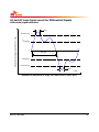
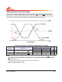
Ta
Tb
Tc
Td
Te
Tf
Tg
Th
Ti
Tj
Tk
CK,CK#
VDD, VDDQ (DDR3)
tCKSRX
Tmin = 10ns
VDD, VDDQ (DDR3L)
Tmin = 10ns
Tmin = 200us
T = 500us
RESET#
Tmin = 10ns
CKE
VALID
tDLLK
tIS
COMMAND
READ
BA
READ
1)
tXPR
tMRD
tMRD
tMRD
tMOD
MRS
MRS
MRS
MRS
MR2
MR3
MR1
MR0
tZQinit
ZQCL
1)
VALID
VALID
tIS
ODT
READ
tIS
Static LOW in case RTT_Nom is enabled at time Tg, otherwise static HIGH or LOW
VALID
RTT
NOTE 1: From time point “Td” until “Tk” NOP or DES commands must be applied
between MRS and ZQCL commands.
TIME BREAK
DON’T CARE
Figure 0 - VDD/VDDQ Voltage Switch Between DDR3L and DDR3
Rev. 1.0 / May. 2014
27
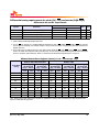
AC & DC Input Measurement Levels
AC and DC Logic Input Levels for Single-Ended Signals
AC and DC Input Levels for Single-Ended Command and Address Signals
Single Ended AC and DC Input Levels for Command and Address
DDR3L-800/1066
Symbol
VRefCA(DC)
DDR3L-1866
Unit Notes
Min
VIH.CA(DC90)
VIL.CA(DC90)
VIH.CA(AC160)
VIL.CA(AC160)
VIH.CA(AC135)
VIL.CA(AC135)
VIH.CA(AC125)
VIL.CA(AC125)
DDR3L-1333/1600
Parameter
Max
Min
Max
Min
Max
DC input logic high Vref + 0.09
VDD
Vref + 0.09
VDD
Vref + 0.09
VDD
DC input logic low
VSS
Vref - 0.09
VSS
Vref - 0.09
VSS
Vref - 0.09
AC input logic high Vref + 0.160 Note2 Vref + 0.160 Note2
AC input logic low
Note2 Vref - 0.160 Note2 Vref - 0.160
AC Input logic high Vref + 0.135 Note2 Vref + 0.135 Note2 Vref + 0.135 Note2
AC input logic low
Note2 Vref - 0.135 Note2 Vref - 0.135 Note2 Vref - 0.135
AC Input logic high
Vref + 0.125 Note2
AC input logic low
Note2 Vref - 0.125
Reference Voltage for
0.49 * VDD 0.51 * VDD 0.49 * VDD 0.51 * VDD 0.49 * VDD 0.51 * VDD
ADD, CMD inputs
V
V
V
V
V
V
V
V
1
1
1,2,5
1,2,5
1,2,5
1,2,5
1,2,5
1,2,5
V
3,4
Notes:
1. For input only pins except RESET, Vref = VrefCA (DC).
2. Refer to "Overshoot and Undershoot Specifications" on page 41.
3. The ac peak noise on VRef may not allow VRef to deviate from VRefCA(DC) by more than +/-1% VDD (for
ence: approx. +/- 13.5 mV).
refer-
4. For reference: approx. VDD/2 +/- 13.5 mV
5. These levels apply for 1.35 volt (see table above) operation only. If the device is operated at 1.5V (table "Single
Ended AC and DC Input Levels for DQ and DM" on page 29), the respective levels in JESD79-3 (VIH/L.CA(DC100),
VIH/L.CA(AC175), VIH/L.CA(AC150), VIH/L.CA(AC135), VIH/L.CA(AC125) etc.) apply. The 1.5V levels (VIH/
L.CA(DC100), VIH/L.CA(AC175), VIH/L.CA(AC150), VIH/L.CA(AC135), VIH/L.CA(AC125) etc.) do not apply when
the device is operated in the 1.35 voltage range.
Rev. 1.0 / May. 2014
28
AC and DC Input Levels for Single-Ended Signals
DDR3 SDRAM will support two Vih/Vil AC levels for DDR3-800 and DDR3-1066s specified in table below.
DDR3 SDRAM will also support corresponding tDS values (Table 43 and Table 50 in “DDR3L Device Operation”) as well as derating tables Table 46 in “DDR3L Device Operation” depending on Vih/Vil AC levels.
Single Ended AC and DC Input Levels for DQ and DM
DDR3L-800/1066
Symbol
VRefDQ(DC)
DDR3L-1866
Unit Notes
Min
VIH.DQ(DC90)
VIL.DQ(DC90)
VIH.DQ(AC160)
VIL.DQ(AC160)
VIH.DQ(AC135)
VIL.DQ(AC135)
VIH.DQ(AC130)
VIL.DQ(AC130)
DDR3L-1333/1600
Parameter
Max
Min
Max
Min
Max
DC input logic high Vref + 0.09
VDD
Vref + 0.09
VDD
Vref + 0.09
VDD
DC input logic low
VSS
Vref - 0.09
VSS
Vref - 0.09
VSS
Vref - 0.09
AC input logic high Vref + 0.160
Note2
AC input logic low
Note2
Vref - 0.160
AC Input logic high Vref + 0.135
Note2
Vref + 0.135
Note2
AC input logic low
Note2
Vref - 0.135
Note2
Vref - 0.135
AC Input logic high
Vref + 0.130
Note2
AC input logic low
Note2
Vref - 0.130
Reference Voltage
0.49 * VDD 0.51 * VDD 0.49 * VDD 0.51 * VDD 0.49 * VDD 0.51 * VDD
for DQ, DM inputs
V
V
V
V
V
V
V
V
1
1
1, 2, 5
1, 2, 5
1, 2, 5
1, 2, 5
1, 2, 5
1, 2, 5
V
3, 4
Notes:
1. Vref = VrefDQ (DC).
2. Refer to "Overshoot and Undershoot Specifications" on page 41.
3. The ac peak noise on VRef may not allow VRef to deviate from VRefDQ(DC) by more than +/-1% VDD (for reference:
approx. +/- 13.5 mV). 4. For reference: approx. VDD/2 +/- 13.5 mV
4. For reference: approx. VDD/2 +/- 13.5 mV
5. These levels apply for 1.35 volt (table "Single Ended AC and DC Input Levels for Command and Address" on
page 28) operation only. If the device is operated at 1.5V (table above), the respective levels in JESD79-3 (VIH/
L.DQ(DC100), VIH/L.DQ(AC175), VIH/L.DQ(AC150), VIH/L.DQ(AC135) etc.) apply. The 1.5V levels (VIH/
L.DQ(DC100), VIH/L.DQ(AC175), VIH/L.DQ(AC150), VIH/L.DQ(AC135) etc.) do not apply when the device is
operated in the 1.35 voltage range.
Rev. 1.0 / May. 2014
29
Vref Tolerances
The dc-tolerance limits and ac-noise limits for the reference voltages VRefCA and VRefDQ are illustrated in
figure below. It shows a valid reference voltage VRef (t) as a function of time. (VRef stands for VRefCA and
VRefDQ likewise).
VRef (DC) is the linear average of VRef (t) over a very long period of time (e.g. 1 sec). This average has to
meet the min/max requirements in the table "Differential Input Slew Rate Definition" on page 36. Furthermore VRef (t) may temporarily deviate from VRef (DC) by no more than +/- 1% VDD.
voltage
VDD
VRef ac-noise
VRef(DC)
VRef(t)
VRef(DC)max
VDD/2
VRef(DC)min
VSS
time
Illustration of VRef(DC) tolerance and VRef ac-noise limits
The voltage levels for setup and hold time measurements VIH(AC), VIH(DC), VIL(AC), and VIL(DC) are dependent on VRef.
“VRef ” shall be understood as VRef(DC), as defined in figure above.
This clarifies that dc-variations of VRef affect the absolute voltage a signal has to reach to achieve a valid
high or low level and therefore the time to which setup and hold is measured. System timing and voltage
budgets need to account for VRef(DC) deviations from the optimum position within the data-eye of the input
signals.
This also clarifies that the DRAM setup/hold specification and derating values need to include time and
voltage associated with VRefac-noise. Timing and voltage effects due to ac-noise on VRef up to the specified limit (+/- 1% of VDD) are included in DRAM timings and their associated deratings.
Rev. 1.0 / May. 2014
30
AC and DC Logic Input Levels for Differential Signals
Differential signal definition
tDVAC
Differential Input Voltage(i.e.DQS - DQS#, CK - CK#)
VIL.DIFF.AC.MIN
VIL.DIFF.MIN
0
half cycle
VIL.DIFF.MAX
VIL.DIFF.AC.MAX
tDVAC
time
Definition of differential ac-swing and “time above ac-level” tDVAC
Rev. 1.0 / May. 2014
31
Differential swing requirements for clock (CK - CK) and strobe (DQS-DQS)
Differential AC and DC Input Levels
DDR3L-800, 1066, 1333, 1600
Symbol
Parameter
VIHdiff
VILdiff
VIHdiff (ac)
VILdiff (ac)
Unit Notes
Differential input high
Differential input logic low
Differential input high ac
Differential input low ac
Min
Max
+ 0.180
Note 3
2 x (VIH (ac) - Vref)
Note 3
Note 3
- 0.180
Note 3
2 x (VIL (ac) - Vref)
V
V
V
V
1
1
2
2
Notes:
1. Used to define a differential signal slew-rate.
2. For CK - CK use VIH/VIL (ac) of AADD/CMD and VREFCA; for DQS - DQS, DQSL, DQSL, DQSU, DQSU use VIH/VIL
(ac) of DQs and VREFDQ; if a reduced ac-high or ac-low levels is used for a signal group, then the reduced level
applies also here.
3. These values are not defined; however, the single-ended signals Ck, CK, DQS, DQS, DQSL, DQSL, DQSU, DQSU
need to be within the respective limits (VIH (dc) max, VIL (dc) min) for single-ended signals as well as the limitations for overshoot and undershoot. Refer to "Overshoot and Undershoot Specifications" on page 41.
Allowed time before ringback (tDVAC) for CK - CK and DQS - DQS
DDR3L-800/1066/1333/1600
Slew Rate
[V/ns]
tDVAC [ps]
@ |VIH/Ldiff
(ac)| = 320mV
min
max
tDVAC [ps]
@ |VIH/Ldiff
(ac)| = 270mV
min
max
DDR3L-1866
tDVAC [ps]
@ |VIH/Ldiff
(ac)| = 270mV
min
max
tDVAC [ps]
@ |VIH/Ldiff
(ac)| = 250mV
min
max
tDVAC [ps]
@ |VIH/Ldiff
(ac)| = 260mV
min
max
> 4.0
189
-
201
-
163
-
168
-
176
-
4.0
189
-
201
-
163
-
168
-
176
-
3.0
162
-
179
-
140
-
147
-
154
-
2.0
109
-
134
1.8
91
-
119
-
80
-
91
-
97
-
1.6
69
-
100
-
62
-
74
-
78
-
1.4
40
-
76
-
37
-
52
-
56
-
1.2
note
-
44
-
5
-
22
-
24
-
1.0
note
-
note
-
note
-
note
-
note
-
< 1.0
note
-
note
-
note
-
note
-
note
-
95
105
111
note : Rising input signal shall become equal to or greater than VIH(ac) level and Falling input signal shall become
equal to or less than VIL(ac) level.
Rev. 1.0 / May. 2014
32
Single-ended requirements for differential signals
Each individual component of a differential signal (CK, DQS, DQSL, DQSU, CK, DQS, DQSL, of DQSU) has
also to comply with certain requirements for single-ended signals.
CK and CK have to approximately reach VSEHmin / VSELmax (approximately equal to the ac-levels (VIH
(ac) / VIL (ac)) for ADD/CMD signals) in every half-cycle.
DQS, DQSL, DQSU, DQS, DQSL have to reach VSEHmin / VSELmax (approximately the ac-levels (VIH (ac)
/ VIL (ac)) for DQ signals) in every half-cycle preceding and following a valid transition.
Note that the applicable ac-levels for ADD/CMD and DQ’s might be different per speed-bin etc. E.g., if
VIH.CA(AC150)/VIL.CA(AC150) is used for ADD/CMD signals, then these ac-levels apply also for the singleended signals CK and CK.
VDD or VDDQ
VSEHmin
VSEH
VDD/2 or VDDQ/2
CK or DQS
VSELmax
VSS or VSSQ
VSEL
time
Single-ended requirements for differential signals.
Note that, while ADD/CMD and DQ signal requirements are with respect to Vref, the single-ended components of differential signals have a requirement with respect to VDD / 2; this is nominally the same. the
transition of single-ended signals through the ac-levels is used to measure setup time. For single-ended
components of differential signals the requirement to reach VSELmax, VSEHmin has no bearing on timing,
but adds a restriction on the common mode characteristics of these signals.
Rev. 1.0 / May. 2014
33
Single-ended levels for CK, DQS, DQSL, DQSU, CK, DQS, DQSL or DQSU
DDR3L-800, 1066, 1333, 1600, 1866
Symbol
VSEH
VSEL
Parameter
Single-ended high level for strobes
Single-ended high level for Ck, CK
Single-ended low level for strobes
Single-ended low level for CK, CK
Unit Notes
Min
Max
(VDD / 2) + 0.175
(VDD /2) + 0.175
Note 3
Note 3
Note 3
Note 3
(VDD / 2) - 0.175
(VDD / 2) - 0.175
V
V
V
V
1,2
1,2
1,2
1,2
Notes:
1. For CK, CK use VIH/VIL (ac) of ADD/CMD; for strobes (DQS, DQS, DQSL, DQSL, DQSU, DQSU) use VIH/VIL (ac)
of DQs.
2. VIH (ac)/VIL (ac) for DQs is based on VREFDQ; VIH (ac)/VIL (ac) for ADD/CMD is based on VREFCA; if a reduced
ac-high or ac-low level is used for a signal group, then the reduced level applies also here.
3. These values are not defined; however, the single-ended signals Ck, CK, DQS, DQS, DQSL, DQSL, DQSU, DQSU
need to be within the respective limits (VIH (dc) max, VIL (dc) min) for single-ended signals as well as the limitations for overshoot and undershoot. Refer to "Overshoot and Undershoot Specifications" on page 41.
Rev. 1.0 / May. 2014
34
Differential Input Cross Point Voltage
To guarantee tight setup and hold times as well as output skew parameters with respect to clock and
strobe, each cross point voltage of differential input signals (CK, CK and DQS, DQS) must meet the
requirements in table below. The differential input cross point voltage VIX is measured from the actual
cross point of true and complement signals to the midlevel between of VDD and VSS
Vix Definition
Cross point voltage for differential input signals (CK, DQS)
DDR3L-800, 1066, 1333, 1600, 1866
Symbol
Parameter
Unit Notes
Min
Max
VIX(CK)
Differential Input Cross Point Voltage
relative to VDD/2 for CK, CK
-150
-175
150
175
mV
mV
2
1
VIX(DQS)
Differential Input Cross Point Voltage
relative to VDD/2 for DQS, DQS
-150
150
mV
2
Notes:
1. Extended range for VIX is only allowed for clock and if single-ended clock input signals CK and CK are monotonic
with a single-ended swing VSEL / VSEH of at least VDD/2 +/-250 mV, and when the differential slew rate of CK CK is larger than 3 V/ns.
2. The relation between Vix Min/Max and VSEL/VSEH should satisfy following.
(VDD/2) + Vix (Min) - VSEL 25mV
VSEH - ((VDD/2) + Vix (Max)) 25mV
Rev. 1.0 / May. 2014
35
Slew Rate Definitions for Single-Ended Input Signals
See 7.5 “Address / Command Setup, Hold and Derating” in “DDR3 Device Operation” for single-ended slew
rate definitions for address and command signals.
See 7.6 “Data Setup, Hold and Slew Rate Derating” in “DDR3 Device Operation” for single-ended slew rate
definition for data signals.
Slew Rate Definitions for Differential Input Signals
Input slew rate for differential signals (CK, CK and DQS, DQS) are defined and measured as shown in table
and figure below.
Differential Input Slew Rate Definition
Measured
Description
Differential input slew rate for rising edge
(CK-CK and DQS-DQS)
Differential input slew rate for falling edge
(CK-CK and DQS-DQS)
Defined by
Min
Max
VILdiffmax
VIHdiffmin
[VIHdiffmin-VILdiffmax] / DeltaTRdiff
VIHdiffmin
VILdiffmax
[VIHdiffmin-VILdiffmax] / DeltaTFdiff
Differential Input Voltage (i.e. DQS-DQS; CK-CK)
Notes:
The differential signal (i.e. CK-CK and DQS-DQS) must be linear between these thresholds.
Delta
TRdiff
VIHdiffmin
0
VILdiffmax
Delta
TFdiff
Differential Input Slew Rate Definition for DQS, DQS and CK, CK
Rev. 1.0 / May. 2014
36
AC & DC Output Measurement Levels
Single Ended AC and DC Output Levels
Table below shows the output levels used for measurements of single ended signals.
Single-ended AC and DC Output Levels
Symbol
Parameter
VOH(DC)
DC output high measurement level (for IV curve linearity)
VOM(DC)
DC output mid measurement level (for IV curve linearity)
VOL(DC)
VOH(AC)
DDR3L-800, 1066,
1333, 1600, 1866
0.8 x VDDQ
Unit
Notes
V
V
DC output low measurement level (for IV curve linearity)
0.5 x VDDQ
0.2 x VDDQ
AC output high measurement level (for output SR)
VTT + 0.1 x VDDQ
V
1
AC output low measurement level (for output SR)
VTT - 0.1 x VDDQ
V
1
VOL(AC)
V
Notes:
1. The swing of ±0.1 x VDDQ is based on approximately 50% of the static single ended output high or low swing with
a driver impedance of 40 Ω and an effective test load of 25 Ω to VTT = VDDQ / 2.
Differential AC and DC Output Levels
Table below shows the output levels used for measurements of single ended signals.
Differential AC and DC Output Levels
Symbol
VOHdiff (AC)
VOLdiff (AC)
Parameter
DDR3L-800, 1066,
1333, 1600, 1866
+ 0.2 x VDDQ
AC differential output high measurement level (for output SR)
- 0.2 x VDDQ
AC differential output low measurement level (for output SR)
Unit
Notes
V
1
V
1
Notes:
1. The swing of ±0.2 x VDDQ is based on approximately 50% of the static differential output high or low swing with
a driver impedance of 40 Ω and an effective test load of 25 Ω to VTT = VDDQ/2 at each of the differential outputs.
Rev. 1.0 / May. 2014
37
Single Ended Output Slew Rate
When the Reference load for timing measurements, output slew rate for falling and rising edges is defined
and measured between VOL(AC) and VOH(AC) for single ended signals are shown in table and figure below.
Single-ended Output slew Rate Definition
Measured
Description
Defined by
From
To
Single-ended output slew rate for rising edge
VOL(AC)
VOH(AC)
[VOH(AC)-VOL(AC)] / DeltaTRse
Single-ended output slew rate for falling edge
VOH(AC)
VOL(AC)
[VOH(AC)-VOL(AC)] / DeltaTFse
Notes:
1. Output slew rate is verified by design and characterisation, and may not be subject to production test.
Single Ended Output Voltage(l.e.DQ)
Delta TRse
VOH(AC)
V∏
VOl(AC)
Delta TFse
Single Ended Output slew Rate Definition
Output Slew Rate (single-ended)
DDR3L-800 DDR3L-1066DDR3L-1333DDR3L-1600DDR3L-1866
Parameter
Symbol Min
Single-ended Output Slew Rate SRQse
1.75
Max
Min
Max
Min
Max
Min
Max
Min
Max
51)
1.75
51)
1.75
51)
1.75
51)
1.75
51)
Units
V/ns
Description: SR; Slew Rate
Q: Query Output (like in DQ, which stands for Data-in, Query-Output)
se: Single-ended Signals
For Ron = RZQ/7 setting
Note 1): In two cases, a maximum slew rate of 6V/ns applies for a single DQ signal within a byte lane.
Case 1 is a defined for a single DQ signal within a byte lane which is switching into a certain direction (either from high
to low or low to high) while all remaining DQ signals in the same byte lane are static (i.e. they stay at either high or low).
Case 2 is a defined for a single DQ signal within a byte lane which is switching into a certain direction (either from high
to low or low to high) while all remaining DQ signals in the same byte lane switching into the opposite direction (i.e. from
low to high of high to low respectively). For the remaining DQ signal switching in to the opposite direction, the regular
maximum limite of 5 V/ns applies.
Rev. 1.0 / May. 2014
38
Differential Output Slew Rate
With the reference load for timing measurements, output slew rate for falling and rising edges is defined
and measured between VOLdiff (AC) and VOHdiff (AC) for differential signals as shown in table and figure
below.
Differential Output Slew Rate Definition
Measured
Description
Defined by
From
To
Differential output slew rate for rising edge
VOLdiff (AC)
VOHdiff (AC)
[VOHdiff (AC)-VOLdiff (AC)] / DeltaTRdiff
Differential output slew rate for falling edge
VOHdiff (AC)
VOLdiff (AC)
[VOHdiff (AC)-VOLdiff (AC)] / DeltaTFdiff
Notes:
1. Output slew rate is verified by design and characterization, and may not be subject to production test.
Differential Output Voltage(i.e. DQS-DQS)
Delta
TRdiff
VOHdiff(AC)
O
VOLdiff(AC)
Delta
TFdiff
Differential Output slew Rate Definition
Differential Output Slew Rate
DDR3L-800 DDR3L-1066 DDR3L-1333 DDR3L-1600 DDR3L-1866
Parameter
Symbol Min
Max
Min
Max
Min
Differential Output Slew Rate SRQdiff 3.5
12
3.5
12
3.5
Description: SR; Slew Rate
Q: Query Output (like in DQ, which stands for Data-in, Query-Output)
se: Single-ended Signals
For Ron = RZQ/7 setting
Rev. 1.0 / May. 2014
Max
Min
Max
Min
Max
12
3.5
12
3.5
12
Units
V/ns
39
Reference Load for AC Timing and Output Slew Rate
Figure below represents the effective reference load of 25 ohms used in defining the relevant AC timing
parameters of the device as well as output slew rate measurements.
It is not intended as a precise representation of any particular system environment or a depiction of the
actual load presented by a production tester. System designers should use IBIS or other simulation tools to
correlate the timing reference load to a system environment. Manufacturers correlate to their production
test conditions, generally one or more coaxial transmission lines terminated at the tester electronics.
VDDQ
CK, CK
DUT
DQ
DQS
DQS
25 Ohm
VTT = VDDQ/2
Reference Load for AC Timing and Output Slew Rate
Rev. 1.0 / May. 2014
40
Overshoot and Undershoot Specifications
Address and Control Overshoot and Undershoot Specifications
AC Overshoot/Undershoot Specification for Address and Control Pins
DDR3 DDR3 DDR3 DDR3 DDR3
Parameter
L-800 L-1066 L-1333 L-1600 L-1866
Maximum peak amplitude allowed for overshoot area. (See Figure below)
Maximum peak amplitude allowed for undershoot area. (See Figure below)
Maximum overshoot area above VDD (See Figure below)
Maximum undershoot area below VSS (See Figure below)
0.4
0.4
0.67
0.67
0.4
0.4
0.5
0.5
0.4
0.4
0.4
0.4
0.4
0.4
0.33
0.33
Units
0.4
V
0.4
V
0.28 V-ns
0.28 V-ns
(A0-A15, BA0-BA3, CS, RAS, CAS, WE, CKE, ODT)
See figure below for each parameter definition
Maximum Amplitude
Overshoot Area
Volts
(V)
VDD
VSS
Undershoot Area
Maximum Amplitude
Time (ns)
Address and Control Overshoot and Undershoot Definition
Rev. 1.0 / May. 2014
41
Clock, Data, Strobe and Mask Overshoot and Undershoot Specifications
AC Overshoot/Undershoot Specification for Clock, Data, Strobe and Mask
DDR3 DDR3 DDR3 DDR3 DDR3
Parameter
L-800 L-1066L-1333L-1600L-1866
Maximum peak amplitude allowed for overshoot area. (See Figure below)
Maximum peak amplitude allowed for undershoot area. (See Figure below)
Maximum overshoot area above VDD (See Figure below)
Maximum undershoot area below VSS (See Figure below)
0.4
0.4
0.25
0.25
0.4
0.4
0.19
0.19
0.4
0.4
0.15
0.15
0.4
0.4
0.13
0.13
Units
0.4
V
0.4
V
0.11 V-ns
0.11 V-ns
(CK, CK, DQ, DQS, DQS, DM)
See figure below for each parameter definition
Maximum Amplitude
Overshoot Area
Volts
(V)
VDDQ
VSSQ
Undershoot Area
Maximum Amplitude
Time (ns)
Clock, Data, Strobe and Mask Overshoot and Undershoot Definition
Rev. 1.0 / May. 2014
42
Refresh parameters by device density
Refresh parameters by device density
Parameter
REF command ACT or
REF command time
Average periodic
refresh interval
RTT_Nom Setting
512Mb
1Gb
2Gb
4Gb
8Gb
tRFC
90
110
160
260
350
ns
7.8
7.8
7.8
7.8
7.8
us
3.9
3.9
3.9
3.9
3.9
us
tREFI
0 C TCASE 85 C
85 C TCASE 95 C
Units Notes
1
Notes:
1. Users should refer to the DRAM supplier data sheet and/or the DIMM SPD to determine if DDR3 SDRAM devices
support the following options or requirements referred to in this materia.
Rev. 1.0 / May. 2014
43
Standard Speed Bins
DDR3 SDRAM Standard Speed Bins include tCK, tRCD, tRP, tRAS and tRC for each corresponding bin.
DDR3L-800 Speed Bins
For specific Notes See "Speed Bin Table Notes" on page 49.
Speed Bin
DDR3L-800E
CL - nRCD - nRP
6-6-6
Unit
Parameter
Symbol
min
max
Internal read command to first data
tAA
15
20
ns
ACT to internal read or write delay time
tRCD
15
—
ns
PRE command period
tRP
15
—
ns
ACT to ACT or REF command period
tRC
52.5
—
ns
ACT to PRE command period
tRAS
37.5
9 * tREFI
ns
tCK(AVG)
2.5
3.3
ns
CL = 6
CWL = 5
Supported CL Settings
6
nCK
Supported CWL Settings
5
nCK
Rev. 1.0 / May. 2014
Notes
1,2,3
44
DDR3L-1066 Speed Bins
For specific Notes See "Speed Bin Table Notes" on page 49.
Speed Bin
DDR3L-1066F
CL - nRCD - nRP
Parameter
Symbol
Unit
7-7-7
min
max
Note
Internal read command to
first data
tAA
13.125
20
ns
ACT to internal read or
write delay time
tRCD
13.125
—
ns
PRE command period
tRP
13.125
—
ns
ACT to ACT or REF
command period
tRC
50.625
—
ns
ACT to PRE command
period
tRAS
37.5
9 * tREFI
ns
CWL = 5
tCK(AVG)
2.5
3.3
ns
1,2,3,6
CWL = 6
tCK(AVG)
Reserved
ns
1,2,3,4
CWL = 5
tCK(AVG)
Reserved
ns
4
CWL = 6
tCK(AVG)
ns
1,2,3,4
CWL = 5
tCK(AVG)
ns
4
CWL = 6
tCK(AVG)
ns
1,2,3
CL = 6
CL = 7
CL = 8
1.875
< 2.5
Reserved
1.875
< 2.5
Supported CL Settings
6, 7, 8
nCK
Supported CWL Settings
5, 6
nCK
Rev. 1.0 / May. 2014
45
DDR3L-1333 Speed Bins
For specific Notes See "Speed Bin Table Notes" on page 49.
Speed Bin
DDR3L-1333H
CL - nRCD - nRP
Parameter
Symbol
Unit
9-9-9
min
max
Note
Internal read
command to first data
tAA
13.5
(13.125)5,10
20
ns
ACT to internal read or
write delay time
tRCD
13.5
(13.125)5,10
—
ns
PRE command period
tRP
13.5
(13.125)5,10
—
ns
ACT to ACT or REF
command period
tRC
49.5
(49.125)5,10
—
ns
ACT to PRE command
period
tRAS
36
9 * tREFI
ns
CWL = 5
tCK(AVG)
2.5
3.3
ns
1,2,3,7
CWL = 6
tCK(AVG)
Reserved
ns
1,2,3,4,7
CWL = 7
tCK(AVG)
Reserved
ns
4
CWL = 5
tCK(AVG)
Reserved
ns
4
CWL = 6
tCK(AVG)
ns
1,2,3,4,7
CWL = 7
tCK(AVG)
Reserved
ns
1,2,3,4
CWL = 5
tCK(AVG)
Reserved
ns
4
CWL = 6
tCK(AVG)
ns
1,2,3,7
CWL = 7
tCK(AVG)
Reserved
ns
1,2,3,4
CWL = 5, 6
tCK(AVG)
Reserved
ns
4
CL = 6
CL = 7
CL = 8
CL = 9
CWL = 7
tCK(AVG)
CWL = 5, 6
tCK(AVG)
CWL = 7
tCK(AVG)
1.875
< 2.5
(Optional)5,10
1.875
< 2.5
ns
1,2,3,4
ns
4
(Optional)
ns
ns
1,2,3
5
Supported CL Settings
6, 7, 8, 9, 10
nCK
Supported CWL Settings
5, 6, 7
nCK
CL = 10
Rev. 1.0 / May. 2014
1.5
<1.875
Reserved
1.5
<1.875
46
DDR3L-1600 Speed Bins
For specific Notes See "Speed Bin Table Notes" on page 49.
Speed Bin
DDR3L-1600K
CL - nRCD - nRP
Parameter
Symbol
Unit
11-11-11
min
max
Note
Internal read
command to first data
tAA
13.75
(13.125)5,10
20
ns
ACT to internal read or
write delay time
tRCD
13.75
(13.125)5,10
—
ns
PRE command period
tRP
13.75
(13.125)5,10
—
ns
ACT to ACT or REF
command period
tRC
48.75
(48.125)5,10
—
ns
ACT to PRE command
period
tRAS
35
9 * tREFI
ns
tCK(AVG)
tCK(AVG)
tCK(AVG)
tCK(AVG)
2.5
3.3
ns
1,2,3,8
Reserved
ns
1,2,3,4,8
Reserved
ns
4
ns
4
CWL = 5
CL = 6
CWL = 6
CWL = 7
CWL = 5
CL = 7
CWL = 6
tCK(AVG)
CWL = 7
CWL = 5, 6
tCK(AVG)
tCK(AVG)
tCK(AVG)
tCK(AVG)
tCK(AVG)
tCK(AVG)
tCK(AVG)
CWL = 7
tCK(AVG)
CWL = 8
CWL = 5
CL = 8
CWL = 6
CWL = 7
CWL = 8
CL = 9
tCK(AVG)
CWL = 5, 6 tCK(AVG)
tCK(AVG)
CL = 10 CWL = 7
tCK(AVG)
CWL = 8
CWL = 5, 6,7 tCK(AVG)
CL = 11
tCK(AVG)
CWL = 8
Supported CL Settings
Supported CWL Settings
Reserved
1.875
(Optional)5,10
Reserved
ns
1,2,3,4,8
ns
1,2,3,4,8
Reserved
ns
4
Reserved
ns
4
1.875
< 2.5
ns
1,2,3,8
ns
1,2,3,4,8
Reserved
ns
1,2,3,4
Reserved
ns
4
ns
1,2,3,4,8
ns
1,2,3,4
Reserved
1.5
<1.875
(Optional)5,10
CWL = 8
Rev. 1.0 / May. 2014
< 2.5
Reserved
Reserved
ns
4
ns
1,2,3,8
Reserved
ns
1,2,3,4
Reserved
ns
4
ns
nCK
nCK
1,2,3
1.5
<1.875
1.25
<1.5
5, 6, 7, 8, 9, 10, 11
5, 6, 7, 8
47
DDR3L-1866 Speed Bins
For specific Notes See "Speed Bin Table Notes" on page 49.
Speed Bin
DDR3L-1866M
CL - nRCD - nRP
Parameter
Symbol
Internal read command
to first data
tAA
ACT to internal read or
write delay time
tRCD
PRE command period
tRP
ACT to PRE command
period
tRAS
ACT to ACT or PRE
command period
tRC
tCK(AVG)
tCK(AVG)
CL = 6
CWL = 6
CWL = 7,8,9 tCK(AVG)
tCK(AVG)
CWL = 5
tCK(AVG)
CWL = 6
CL = 7
CWL = 7,8,9 tCK(AVG)
tCK(AVG)
CWL = 5
tCK(AVG)
CWL = 6
CL = 8
tCK(AVG)
CWL = 7
tCK(AVG)
CWL = 8,9
tCK(AVG)
CWL = 5, 6
tCK(AVG)
CWL = 7
CL = 9
tCK(AVG)
CWL = 8
tCK(AVG)
CWL = 9
tCK(AVG)
CWL = 5, 6
tCK(AVG)
CL = 10
CWL = 7
tCK(AVG)
CWL = 8
CWL = 5,6,7 tCK(AVG)
tCK(AVG)
CWL = 8
CL = 11
tCK(AVG)
CWL = 9
CWL = 5,6,7,8 tCK(AVG)
CL = 12
tCK(AVG)
CWL = 9
CWL = 5,6,7,8 tCK(AVG)
CL = 13
tCK(AVG)
CWL = 9
Supported CL Settings
Supported CWL Settings
CWL = 5
Rev. 1.0 / May. 2014
Unit
13-13-13
min
13.91
Note
max
20
ns
—
ns
—
ns
9 * tREFI
ns
-
ns
3.3
ns
1,2,3,9
Reserved
ns
1,2,3,4,9
Reserved
ns
4
(13.125)5,11
13.91
(13.125)5,11
13.91
(13.125)5,11
34
47.91
(47.125)5,11
2.5
Reserved
ns
4
ns
1,2,3,4,9
Reserved
ns
4
Reserved
ns
4
1.875
< 2.5
1.875
ns
1,2,3,9
Reserved
< 2.5
ns
1,2,3,4,9
Reserved
ns
4
Reserved
ns
4
ns
1,2,3,4,9
Reserved
ns
1,2,3,4,9
Reserved
ns
4
1.5
<1.875
Reserved
ns
4
ns
1,2,3,9
Reserved
ns
1,2,3,4,9
Reserved
ns
4
ns
1,2,3,4,9
ns
1,2,3,4
1.5
<1.875
1.25
<1.5
Reserved
Reserved
ns
4
Reserved
ns
1,2,3,4
Reserved
1.07
<1.25
6, 7, 8, 9, 10, 11, 13
5, 6, 7, 8, 9
ns
4
ns
1, 2, 3
nCK
nCK
48
Speed Bin Table Notes
Absolute Specification (TOPER; VDDQ = VDD = 1.35V +0.100/- 0.067 V);
1. The CL setting and CWL setting result in tCK(AVG).MIN and tCK(AVG).MAX requirements. When making a selection of tCK(AVG), both need to be fulfilled: Requirements from CL setting as well as requirements from CWL setting.
2. tCK(AVG).MIN limits: Since CAS Latency is not purely analog - data and strobe output are synchronized by the DLL - all possible intermediate frequencies may not be guaranteed. An application should
use the next smaller JEDEC standard tCK(AVG) value (3.0, 2.5, 1.875, 1.5, or 1.25 ns) when calculating CL [nCK] = tAA [ns] / tCK(AVG) [ns], rounding up to the next ‘Supported CL’, where tCK(AVG) =
3.0 ns should only be used for CL = 5 calculation.
3. tCK(AVG).MAX limits: Calculate tCK(AVG) = tAA.MAX / CL SELECTED and round the resulting tCK(AVG)
down to the next valid speed bin (i.e. 3.3ns or 2.5ns or 1.875 ns or 1.25 ns). This result is
tCK(AVG).MAX corresponding to CL SELECTED.
4. ‘Reserved’ settings are not allowed. User must program a different value.
5. ‘Optional’ settings allow certain devices in the industry to support this setting, however, it is not a mandatory feature. Refer to DIMM data sheet and/or the DIMM SPD information if and how this setting is
supported.
6. Any DDR3-1066 speed bin also supports functional operation at lower frequencies as shown in the
table which are not subject to Production Tests but verified by Design/Characterization.
7. Any DDR3-1333 speed bin also supports functional operation at lower frequencies as shown in the
table which are not subject to Production Tests but verified by Design/Characterization.
8. Any DDR3-1600 speed bin also supports functional operation at lower frequencies as shown in the
table which are not subject to Production Tests but verified by Design/Characterization.
9. Any DDR3-1866 speed bin also supports functional operation at lower frequencies as shown in the
table which are not subject to Production Tests but verified by Design/Characterization.
10. DDR3 SDRAM devices supporting optional down binning to CL=7 and CL=9, and tAA/tRCD/tRP must
be 13.125 ns or lower. SPD settings must be programmed to match. For example, DDR3-1333H
devices supporting down binning to DDR3-1066F should program 13.125 ns in SPD bytes for tAAmin
(Byte 16), tRCDmin (Byte 18), and tRPmin (Byte 20). DDR3-1600K devices supporting down binning to
DDR3-1333H or DDR3-1600F should program 13.125 ns in SPD bytes for tAAmin (Byte 16), tRCDmin
(Byte 18), and tRPmin (Byte 20). Once tRP (Byte 20) is programmed to 13.125ns, tRCmin (Byte 21,23)
also should be programmed accordingly. For example, 49.125ns (tRASmin + tRPmin = 36 ns + 13.125
ns) for DDR3-1333H and 48.125ns (tRASmin + tRPmin = 35 ns + 13.125 ns) for DDR3-1600K.
11. DDR3 SDRAM devices supporting optional down binning to CL=11, CL=9 and CL=7, tAA/tRCD/tRPmin
must be 13.125ns. SPD setting must be programed to match. For example, DDR3-1866 devices supporting down binning to DDR3-1600 or DDR3-1333 or 1066 should program 13.125ns in SPD bytes for
tAAmin(byte 16), tRCDmin(byte 18) and tRPmin(byte 20) is programmed to 13.125ns, tRCmin(byte
21,23) also should be programmed accordingly. For example, 47.125ns (tRASmin + tRPmin = 34ns +
13.125ns)
Rev. 1.0 / May. 2014
49
Environmental Parameters
Symbol
Parameter
Rating
TOPR
Operating temperature
See Note
HOPR
Operating humidity (relative)
10 to 90
TSTG
Storage temperature
HSTG
Storage humidity (without condensation)
PBAR
Barometric Pressure (operating & storage)
Units
Notes
3
%
1
o
C
1
5 to 95
%
1
105 to 69
K Pascal
1, 2
-50 to +100
Note:
1. Stress greater than those listed may cause permanent damage to the device. This is a stress rating only, and
device functional operation at or above the conditions indicated is not implied. Expousure to absolute maximum
rating conditions for extended periods may affect reliablility.
2. Up to 9850 ft.
3. The designer must meet the case temperature specifications for individual module components.
Rev. 1.0 / May. 2014
50
IDD and IDDQ Specification Parameters and Test Conditions
IDD and IDDQ Measurement Conditions
In this chapter, IDD and IDDQ measurement conditions such as test load and patterns are defined. Figure
1. shows the setup and test load for IDD and IDDQ measurements.
•
IDD currents (such as IDD0, IDD1, IDD2N, IDD2NT, IDD2P0, IDD2P1, IDD2Q, IDD3N, IDD3P, IDD4R,
IDD4W, IDD5B, IDD6, IDD6ET and IDD7) are measured as time-averaged currents with all VDD balls
of the DDR3 SDRAM under test tied together. Any IDDQ current is not included in IDD currents.
•
IDDQ currents (such as IDDQ2NT and IDDQ4R) are measured as time-averaged currents with all
VDDQ balls of the DDR3 SDRAM under test tied together. Any IDD current is not included in IDDQ currents.
Attention: IDDQ values cannot be directly used to calculate IO power of the DDR3 SDRAM. They can
be used to support correlation of simulated IO power to actual IO power as outlined in Figure 2. In
DRAM module application, IDDQ cannot be measured separately since VDD and VDDQ are using one
merged-power layer in Module PCB.
For IDD and IDDQ measurements, the following definitions apply:
•
”0” and “LOW” is defined as VIN <= VILAC(max).
•
”1” and “HIGH” is defined as VIN >= VIHAC(max).
•
“MID_LEVEL” is defined as inputs are VREF = VDD/2.
•
Timing used for IDD and IDDQ Measurement-Loop Patterns are provided in Table 1.
•
Basic IDD and IDDQ Measurement Conditions are described in Table 2.
•
Detailed IDD and IDDQ Measurement-Loop Patterns are described in Table 3 through Table 10.
•
IDD Measurements are done after properly initializing the DDR3 SDRAM. This includes but is not limited to setting
RON = RZQ/7 (34 Ohm in MR1);
Qoff = 0B (Output Buffer enabled in MR1);
RTT_Nom = RZQ/6 (40 Ohm in MR1);
RTT_Wr = RZQ/2 (120 Ohm in MR2);
TDQS Feature disabled in MR1
•
Attention: The IDD and IDDQ Measurement-Loop Patterns need to be executed at least one time
before actual IDD or IDDQ measurement is started.
•
Define D = {CS, RAS, CAS, WE}:= {HIGH, LOW, LOW, LOW}
•
Define D = {CS, RAS, CAS, WE}:= {HIGH, HIGH, HIGH, HIGH}
Rev. 1.0 / May. 2014
51
IDDQ (optional)
IDD
VDD
VDDQ
RESET
CK/CK
DDR3L
SDRAM
CKE
CS
RAS, CAS, WE
DQS, DQS
DQ, DM,
TDQS, TDQS
A, BA
ODT
ZQ
VSS
RTT = 25 Ohm
VDDQ/2
VSSQ
Figure 1 - Measurement Setup and Test Load for IDD and IDDQ (optional) Measurements
[Note: DIMM level Output test load condition may be different from above
Application specific
memory channel
environment
IDDQ
Test Load
Channel
IO Power
Simulation
IDDQ
Simulation
IDDQ
Simulation
Correction
Channel IO Power
Number
Figure 2 - Correlation from simulated Channel IO Power to actual Channel IO Power supported
by IDDQ Measurement
Rev. 1.0 / May. 2014
52
Table 1 -Timings used for IDD and IDDQ Measurement-Loop Patterns
Symbol
tCK
DDR3L-1066
DDR3L-1333
DDR3L-1600
DDR3L-1866
7-7-7
9-9-9
11-11-11
13-13-13
1.875
1.5
1.25
1.07
Unit
ns
CL
7
9
11
13
nCK
nRCD
7
9
11
13
nCK
nRC
27
33
39
45
nCK
nRAS
20
24
28
32
nCK
nRP
7
9
11
13
nCK
1KB page size
20
20
24
26
nCK
2KB page size
27
30
32
33
nCK
1KB page size
4
4
5
5
nCK
nFAW
nRRD
6
5
6
6
nCK
nRFC -512Mb
2KB page size
48
60
72
85
nCK
nRFC-1 Gb
59
74
88
103
nCK
nRFC- 2 Gb
86
107
128
150
nCK
nRFC- 4 Gb
139
174
208
243
nCK
nRFC- 8 Gb
187
234
280
328
nCK
Table 2 -Basic IDD and IDDQ Measurement Conditions
Symbol
Description
Operating One Bank Active-Precharge Current
CKE: High; External clock: On; tCK, nRC, nRAS, CL: see Table 1; BL: 8a); AL: 0; CS: High between ACT and
IDD0
PRE; Command, Address, Bank Address Inputs: partially toggling according to Table 3; Data IO: MID-LEVEL;
DM: stable at 0; Bank Activity: Cycling with one bank active at a time: 0,0,1,1,2,2,... (see Table 3); Output Buffer and RTT: Enabled in Mode Registersb); ODT Signal: stable at 0; Pattern Details: see Table 3.
Operating One Bank Active-Precharge Current
CKE: High; External clock: On; tCK, nRC, nRAS, nRCD, CL: see Table 1; BL: 8a); AL: 0; CS: High between ACT,
IDD1
RD and PRE; Command, Address; Bank Address Inputs, Data IO: partially toggling according to Table 4; DM:
stable at 0; Bank Activity: Cycling with on bank active at a time: 0,0,1,1,2,2,... (see Table 4); Output Buffer and
RTT: Enabled in Mode Registersb); ODT Signal: stable at 0; Pattern Details: see Table 4.
Rev. 1.0 / May. 2014
53
Symbol
Description
Precharge Standby Current
CKE: High; External clock: On; tCK, CL: see Table 1; BL: 8a); AL: 0; CS: stable at 1; Command, Address, Bank
IDD2N
Address Inputs: partially toggling according to Table 5; Data IO: MID_LEVEL; DM: stable at 0; Bank Activity: all
banks closed; Output Buffer and RTT: Enabled in Mode Registersb); ODT Signal: stable at 0; Pattern Details:
see Table 5.
Precharge Standby ODT Current
CKE: High; External clock: On; tCK, CL: see Table 1; BL: 8a); AL: 0; CS: stable at 1; Command, Address, Bank
IDD2NT Address Inputs: partially toggling according to Table 6; Data IO: MID_LEVEL; DM: stable at 0; Bank Activity: all
banks closed; Output Buffer and RTT: Enabled in Mode Registersb); ODT Signal: toggling according to Table 6;
Pattern Details: see Table 6.
Precharge Power-Down Current Slow Exit
IDD2P0
CKE: Low; External clock: On; tCK, CL: see Table 1; BL: 8a); AL: 0; CS: stable at 1; Command, Address, Bank
Address Inputs: stable at 0; Data IO: MID_LEVEL; DM: stable at 0; Bank Activity: all banks closed; Output Buffer and RTT: Enabled in Mode Registersb); ODT Signal: stable at 0; Precharge Power Down Mode: Slow Exitc)
Precharge Power-Down Current Fast Exit
IDD2P1
CKE: Low; External clock: On; tCK, CL: see Table 1; BL: 8a); AL: 0; CS: stable at 1; Command, Address, Bank
Address Inputs: stable at 0; Data IO: MID_LEVEL; DM: stable at 0; Bank Activity: all banks closed; Output Buffer and RTT: Enabled in Mode Registersb); ODT Signal: stable at 0; Precharge Power Down Mode: Fast Exitc)
Precharge Quiet Standby Current
IDD2Q
CKE: High; External clock: On; tCK, CL: see Table 1; BL: 8a); AL: 0; CS: stable at 1; Command, Address, Bank
Address Inputs: stable at 0; Data IO: MID_LEVEL; DM: stable at 0; Bank Activity: all banks closed; Output Buffer and RTT: Enabled in Mode Registersb); ODT Signal: stable at 0
Active Standby Current
CKE: High; External clock: On; tCK, CL: see Table 1; BL: 8a); AL: 0; CS: stable at 1; Command, Address, Bank
IDD3N
Address Inputs: partially toggling according to Table 5; Data IO: MID_LEVEL; DM: stable at 0; Bank Activity: all
banks open; Output Buffer and RTT: Enabled in Mode Registersb); ODT Signal: stable at 0; Pattern Details: see
Table 5.
Active Power-Down Current
IDD3P
CKE: Low; External clock: On; tCK, CL: see Table 1; BL: 8a); AL: 0; CS: stable at 1; Command, Address, Bank
Address Inputs: stable at 0; Data IO: MID_LEVEL; DM: stable at 0; Bank Activity: all banks open; Output Buffer
and RTT: Enabled in Mode Registersb); ODT Signal: stable at 0
Rev. 1.0 / May. 2014
54
Symbol
Description
Operating Burst Read Current
CKE: High; External clock: On; tCK, CL: see Table 1; BL: 8a); AL: 0; CS: High between RD; Command, Address,
IDD4R
Bank Address Inputs: partially toggling according to Table 7; Data IO: seamless read data burst with different
data between one burst and the next one according to Table 7; DM: stable at 0; Bank Activity: all banks open,
RD commands cycling through banks: 0,0,1,1,2,2,...(see Table 7); Output Buffer and RTT: Enabled in Mode
Registersb); ODT Signal: stable at 0; Pattern Details: see Table 7.
Operating Burst Write Current
CKE: High; External clock: On; tCK, CL: see Table 1; BL: 8a); AL: 0; CS: High between WR; Command, Address,
IDD4W
Bank Address Inputs: partially toggling according to Table 8; Data IO: seamless read data burst with different
data between one burst and the next one according to Table 8; DM: stable at 0; Bank Activity: all banks open,
WR commands cycling through banks: 0,0,1,1,2,2,...(see Table 8); Output Buffer and RTT: Enabled in Mode
Registersb); ODT Signal: stable at HIGH; Pattern Details: see Table 8.
Burst Refresh Current
CKE: High; External clock: On; tCK, CL, nRFC: see Table 1; BL: 8a); AL: 0; CS: High between REF; Command,
IDD5B
Address, Bank Address Inputs: partially toggling according to Table 9; Data IO: MID_LEVEL; DM: stable at 0;
Bank Activity: REF command every nREF (see Table 9); Output Buffer and RTT: Enabled in Mode Registersb);
ODT Signal: stable at 0; Pattern Details: see Table 9.
Self-Refresh Current: Normal Temperature Range
TCASE: 0 - 85 oC; Auto Self-Refresh (ASR): Disabledd);Self-Refresh Temperature Range (SRT): Normale); CKE:
IDD6
Low; External clock: Off; CK and CK: LOW; CL: see Table 1; BL: 8a); AL: 0; CS, Command, Address, Bank
Address Inputs, Data IO: MID_LEVEL; DM: stable at 0; Bank Activity: Self-Refresh operation; Output Buffer
and RTT: Enabled in Mode Registersb); ODT Signal: MID_LEVEL
Self-Refresh Current: Extended Temperature Range (optional)
TCASE: 0 - 95 oC; Auto Self-Refresh (ASR): Disabledd);Self-Refresh Temperature Range (SRT): Extendede);
IDD6ET
CKE: Low; External clock: Off; CK and CK: LOW; CL: see Table 1; BL: 8a); AL: 0; CS, Command, Address, Bank
Address Inputs, Data IO: MID_LEVEL; DM: stable at 0; Bank Activity: Extended Temperature Self-Refresh
operation; Output Buffer and RTT: Enabled in Mode Registersb); ODT Signal: MID_LEVEL
Rev. 1.0 / May. 2014
55
Symbol
Description
Operating Bank Interleave Read Current
CKE: High; External clock: On; tCK, nRC, nRAS, nRCD, NRRD, nFAW, CL: see Table 1; BL: 8a),f); AL: CL-1; CS:
High between ACT and RDA; Command, Address, Bank Address Inputs: partially toggling according to Table
IDD7
10; Data IO: read data burst with different data between one burst and the next one according to Table 10;
DM: stable at 0; Bank Activity: two times interleaved cycling through banks (0, 1,...7) with different addressing, wee Table 10; Output Buffer and RTT: Enabled in Mode Registersb); ODT Signal: stable at 0; Pattern
Details: see Table 10.
a) Burst Length: BL8 fixed by MRS: set MR0 A[1,0]=00B
b) Output Buffer Enable: set MR1 A[12] = 0B; set MR1 A[5,1] = 01B; RTT_Nom enable: set MR1 A[9,6,2] = 011B;
RTT_Wr enable: set MR2 A[10,9] = 10B
c) Precharge Power Down Mode: set MR0 A12=0B for Slow Exit or MR0 A12 = 1B for Fast Exit
d) Auto Self-Refresh (ASR): set MR2 A6 = 0B to disable
e) Self-Refresh Temperature Range (SRT): set MR2 A7 = 0B for normal or 1B for extended temperature range
f) Read Burst Type: Nibble Sequential, set MR0 A[3] = 0B
Rev. 1.0 / May. 2014
56
Command
CS
RAS
CAS
WE
ODT
BA[2:0]
A[15:11]
A[10]
A[9:7]
A[6:3]
A[2:0]
0
ACT
0
0
1
1
0
0
00
0
0
0
0
-
1,2
D, D
1
0
0
0
0
0
00
0
0
0
0
-
D, D
1
1
1
1
0
0
00
0
0
0
0
-
0
0
0
-
Cycle
Number
Datab)
Sub-Loop
CKE
CK, CK
Table 3 - IDD0 Measurement-Loop Patterna)
0
3,4
...
nRAS
Static High
toggling
...
repeat pattern 1...4 until nRAS - 1, truncate if necessary
PRE
0
0
1
0
0
0
00
0
repeat pattern 1...4 until nRC - 1, truncate if necessary
1*nRC+0
ACT
0
0
1
1
0
0
00
0
0
F
0
-
1*nRC+1, 2
D, D
1
0
0
0
0
0
00
0
0
F
0
-
D, D
1
1
1
1
0
0
00
0
0
F
0
-
0
-
1*nRC+3, 4
...
1*nRC+nRAS
repeat pattern 1...4 until 1*nRC + nRAS - 1, truncate if necessary
PRE
0
0
1
0
0
0
00
0
0
...
repeat pattern 1...4 until 2*nRC - 1, truncate if necessary
1
2*nRC
repeat Sub-Loop 0, use BA[2:0] = 1 instead
2
4*nRC
repeat Sub-Loop 0, use BA[2:0] = 2 instead
3
6*nRC
repeat Sub-Loop 0, use BA[2:0] = 3 instead
4
8*nRC
repeat Sub-Loop 0, use BA[2:0] = 4 instead
5
10*nRC
repeat Sub-Loop 0, use BA[2:0] = 5 instead
6
12*nRC
repeat Sub-Loop 0, use BA[2:0] = 6 instead
7
14*nRC
repeat Sub-Loop 0, use BA[2:0] = 7 instead
F
a) DM must be driven LOW all the time. DQS, DQS are MID-LEVEL.
b) DQ signals are MID-LEVEL.
Rev. 1.0 / May. 2014
57
Command
CS
RAS
CAS
WE
ODT
BA[2:0]
A[15:11]
A[10]
A[9:7]
A[6:3]
A[2:0]
0
ACT
0
0
1
1
0
0
00
0
0
0
0
-
1,2
D, D
1
0
0
0
0
0
00
0
0
0
0
-
D, D
1
1
1
1
0
0
00
0
0
0
0
-
0
0
00000000
0
0
0
-
Cycle
Number
Datab)
Sub-Loop
CKE
CK, CK
Table 4 - IDD1 Measurement-Loop Patterna)
0
3,4
...
nRCD
...
nRAS
Static High
toggling
...
repeat pattern 1...4 until nRCD - 1, truncate if necessary
RD
0
1
0
1
0
0
00
0
0
repeat pattern 1...4 until nRAS - 1, truncate if necessary
PRE
0
0
1
0
0
0
00
0
repeat pattern 1...4 until nRC - 1, truncate if necessary
1*nRC+0
ACT
0
0
1
1
0
0
00
0
0
F
0
-
1*nRC+1,2
D, D
1
0
0
0
0
0
00
0
0
F
0
-
D, D
1
1
1
1
0
0
00
0
0
F
0
-
1*nRC+3,4
...
1*nRC+nRCD
...
1*nRC+nRAS
repeat pattern nRC + 1,...4 until nRC + nRCE - 1, truncate if necessary
RD
0
1
0
1
0
0
00
0
0
F
0
00110011
repeat pattern nRC + 1,...4 until nRC + nRAS - 1, truncate if necessary
PRE
0
0
1
0
0
0
00
0
0
F
...
repeat pattern nRC + 1,...4 until *2 nRC - 1, truncate if necessary
1
2*nRC
repeat Sub-Loop 0, use BA[2:0] = 1 instead
2
4*nRC
repeat Sub-Loop 0, use BA[2:0] = 2 instead
3
6*nRC
repeat Sub-Loop 0, use BA[2:0] = 3 instead
4
8*nRC
repeat Sub-Loop 0, use BA[2:0] = 4 instead
5
10*nRC
repeat Sub-Loop 0, use BA[2:0] = 5 instead
6
12*nRC
repeat Sub-Loop 0, use BA[2:0] = 6 instead
7
14*nRC
repeat Sub-Loop 0, use BA[2:0] = 7 instead
0
-
a) DM must be driven LOW all the time. DQS, DQS are used according to RD Commands, otherwise MID-LEVEL.
b) Burst Sequence driven on each DQ signal by Read Command. Outside burst operation, DQ signals are MID_LEVEL.
Rev. 1.0 / May. 2014
58
Static High
CS
RAS
CAS
WE
ODT
BA[2:0]
A[15:11]
A[10]
A[9:7]
A[6:3]
A[2:0]
0
D
1
0
0
0
0
0
0
0
0
0
0
-
1
D
1
0
0
0
0
0
0
0
0
0
0
-
2
D
1
1
1
1
0
0
0
0
0
F
0
-
3
D
1
1
1
1
0
0
0
0
0
F
0
-
Cycle
Number
Command
0
toggling
Datab)
Sub-Loop
CKE
CK, CK
Table 5 - IDD2N and IDD3N Measurement-Loop Patterna)
1
4-7
repeat Sub-Loop 0, use BA[2:0] = 1 instead
2
8-11
repeat Sub-Loop 0, use BA[2:0] = 2 instead
3
12-15
repeat Sub-Loop 0, use BA[2:0] = 3 instead
4
16-19
repeat Sub-Loop 0, use BA[2:0] = 4 instead
5
20-23
repeat Sub-Loop 0, use BA[2:0] = 5 instead
6
24-17
repeat Sub-Loop 0, use BA[2:0] = 6 instead
7
28-31
repeat Sub-Loop 0, use BA[2:0] = 7 instead
a) DM must be driven LOW all the time. DQS, DQS are MID-LEVEL.
b) DQ signals are MID-LEVEL.
Static High
CS
RAS
CAS
WE
ODT
BA[2:0]
A[15:11]
A[10]
A[9:7]
A[6:3]
A[2:0]
0
D
1
0
0
0
0
0
0
0
0
0
0
-
1
D
1
0
0
0
0
0
0
0
0
0
0
-
2
D
1
1
1
1
0
0
0
0
0
F
0
-
3
D
1
1
1
1
0
0
0
0
0
F
0
-
Cycle
Number
Command
0
toggling
Datab)
Sub-Loop
CKE
CK, CK
Table 6 - IDD2NT and IDDQ2NT Measurement-Loop Patterna)
1
4-7
repeat Sub-Loop 0, but ODT = 0 and BA[2:0] = 1
2
8-11
repeat Sub-Loop 0, but ODT = 1 and BA[2:0] = 2
3
12-15
repeat Sub-Loop 0, but ODT = 1 and BA[2:0] = 3
4
16-19
repeat Sub-Loop 0, but ODT = 0 and BA[2:0] = 4
5
20-23
repeat Sub-Loop 0, but ODT = 0 and BA[2:0] = 5
6
24-17
repeat Sub-Loop 0, but ODT = 1 and BA[2:0] = 6
7
28-31
repeat Sub-Loop 0, but ODT = 1 and BA[2:0] = 7
a) DM must be driven LOW all the time. DQS, DQS are MID-LEVEL.
b) DQ signals are MID-LEVEL.
Rev. 1.0 / May. 2014
59
CS
RAS
CAS
WE
ODT
BA[2:0]
A[15:11]
A[10]
A[9:7]
A[6:3]
A[2:0]
0
RD
0
1
0
1
0
0
00
0
0
0
0
00000000
1
D
1
0
0
0
0
0
00
0
0
0
0
-
2,3
D,D
1
1
1
1
0
0
00
0
0
0
0
-
4
RD
0
1
0
1
0
0
00
0
0
F
0
00110011
5
D
1
0
0
0
0
0
00
0
0
F
0
-
D,D
1
1
1
1
0
0
00
0
0
F
0
-
Cycle
Number
Command
Static High
0
toggling
Datab)
Sub-Loop
CKE
CK, CK
Table 7 - IDD4R and IDDQ4R Measurement-Loop Patterna)
6,7
1
8-15
repeat Sub-Loop 0, but BA[2:0] = 1
2
16-23
repeat Sub-Loop 0, but BA[2:0] = 2
3
24-31
repeat Sub-Loop 0, but BA[2:0] = 3
4
32-39
repeat Sub-Loop 0, but BA[2:0] = 4
5
40-47
repeat Sub-Loop 0, but BA[2:0] = 5
6
48-55
repeat Sub-Loop 0, but BA[2:0] = 6
7
56-63
repeat Sub-Loop 0, but BA[2:0] = 7
a) DM must be driven LOW all the time. DQS, DQS are used according to RD Commands, otherwise MID-LEVEL.
b) Burst Sequence driven on each DQ signal by Read Command. Outside burst operation, DQ signals are MID-LEVEL.
A[2:0]
1
1
1
1
1
1
=
=
=
=
=
=
=
A[6:3]
ODT
WE
CAS
RAS
CS
0
1
0
0
1
0
0
0
1
1
1
1
0
1
0
0
1
0
0
0
1
1
1
1
Sub-Loop 0, but BA[2:0]
Sub-Loop 0, but BA[2:0]
Sub-Loop 0, but BA[2:0]
Sub-Loop 0, but BA[2:0]
Sub-Loop 0, but BA[2:0]
Sub-Loop 0, but BA[2:0]
Sub-Loop 0, but BA[2:0]
A[9:7]
WR
D
D,D
WR
D
D,D
repeat
repeat
repeat
repeat
repeat
repeat
repeat
A[10]
1
2
3
4
5
6
7
1
2,3
4
5
6,7
8-15
16-23
24-31
32-39
40-47
48-55
56-63
A[15:11]
0
BA[2:0]
0
Command
Cycle
Number
Sub-Loop
CKE
Static High
toggling
CK, CK
Table 8 - IDD4W Measurement-Loop Patterna)
Datab)
0
0
0
0
0
0
00
00
00
00
00
00
0
0
0
0
0
0
0
0
0
0
0
0
0
0
0
F
F
F
0
0
0
0
0
0
00000000
00110011
-
1
2
3
4
5
6
7
a) DM must be driven LOW all the time. DQS, DQS are used according to WR Commands, otherwise MID-LEVEL.
b) Burst Sequence driven on each DQ signal by Write Command. Outside burst operation, DQ signals are MID-LEVEL.
Rev. 1.0 / May. 2014
60
Command
CS
RAS
CAS
WE
ODT
BA[2:0]
A[15:11]
A[10]
A[9:7]
A[6:3]
A[2:0]
0
0
REF
0
0
0
1
0
0
0
0
0
0
0
-
1
1.2
D, D
1
0
0
0
0
0
00
0
0
0
0
-
D, D
1
1
1
1
0
0
00
0
0
F
0
-
Cycle
Number
Datab)
Sub-Loop
CKE
CK, CK
Table 9 - IDD5B Measurement-Loop Patterna)
Static High
toggling
3,4
2
5...8
repeat cycles 1...4, but BA[2:0] = 1
9...12
repeat cycles 1...4, but BA[2:0] = 2
13...16
repeat cycles 1...4, but BA[2:0] = 3
17...20
repeat cycles 1...4, but BA[2:0] = 4
21...24
repeat cycles 1...4, but BA[2:0] = 5
25...28
repeat cycles 1...4, but BA[2:0] = 6
29...32
repeat cycles 1...4, but BA[2:0] = 7
33...nRFC-1
repeat Sub-Loop 1, until nRFC - 1. Truncate, if necessary.
a) DM must be driven LOW all the time. DQS, DQS are MID-LEVEL.
b) DQ signals are MID-LEVEL.
Rev. 1.0 / May. 2014
61
Table 10 - IDD7 Measurement-Loop Patterna)
2
3
4
Static High
5
6
7
8
9
10
4*nRRD
nFAW
nFAW+nRRD
nFAW+2*nRRD
nFAW+3*nRRD
nFAW+4*nRRD
2*nFAW+0
2*nFAW+1
2&nFAW+2
11
2*nFAW+nRRD
2*nFAW+nRRD+1
2&nFAW+nRRD+2
12
13
2*nFAW+2*nRRD
2*nFAW+3*nRRD
14
2*nFAW+4*nRRD
15
16
17
18
3*nFAW
3*nFAW+nRRD
3*nFAW+2*nRRD
3*nFAW+3*nRRD
19
3*nFAW+4*nRRD
00110011
-
0
-
0
-
0
0
0
00110011
-
0
0
0
00000000
-
0
-
0
-
A[10]
0
0
0
ODT
00000000
-
WE
0
0
0
CAS
ACT
0
0
1
1
0
0
00
0
0
0
RDA
0
1
0
1
0
0
00
1
0
0
D
1
0
0
0
0
0
00
0
0
0
repeat above D Command until nRRD - 1
ACT
0
0
1
1
0
1
00
0
0
F
RDA
0
1
0
1
0
1
00
1
0
F
D
1
0
0
0
0
1
00
0
0
F
repeat above D Command until 2* nRRD - 1
repeat Sub-Loop 0, but BA[2:0] = 2
repeat Sub-Loop 1, but BA[2:0] = 3
D
1
0
0
0
0
3
00
0
0
F
Assert and repeat above D Command until nFAW - 1, if necessary
repeat Sub-Loop 0, but BA[2:0] = 4
repeat Sub-Loop 1, but BA[2:0] = 5
repeat Sub-Loop 0, but BA[2:0] = 6
repeat Sub-Loop 1, but BA[2:0] = 7
D
1
0
0
0
0
7
00
0
0
F
Assert and repeat above D Command until 2* nFAW - 1, if necessary
ACT
0
0
1
1
0
0
00
0
0
F
RDA
0
1
0
1
0
0
00
1
0
F
D
1
0
0
0
0
0
00
0
0
F
Repeat above D Command until 2* nFAW + nRRD - 1
ACT
0
0
1
1
0
1
00
0
0
0
RDA
0
1
0
1
0
1
00
1
0
0
D
1
0
0
0
0
1
00
0
0
0
Repeat above D Command until 2* nFAW + 2* nRRD - 1
repeat Sub-Loop 10, but BA[2:0] = 2
repeat Sub-Loop 11, but BA[2:0] = 3
D
1
0
0
0
0
3
00
0
0
0
Assert and repeat above D Command until 3* nFAW - 1, if necessary
repeat Sub-Loop 10, but BA[2:0] = 4
repeat Sub-Loop 11, but BA[2:0] = 5
repeat Sub-Loop 10, but BA[2:0] = 6
repeat Sub-Loop 11, but BA[2:0] = 7
D
1
0
0
0
0
7
00
0
0
0
Assert and repeat above D Command until 4* nFAW - 1, if necessary
RAS
Datab)
CS
A[9:7]
A[15:11]
BA[2:0]
Command
A[2:0]
1
0
1
2
...
nRRD
nRRD+1
nRRD+2
...
2*nRRD
3*nRRD
A[6:3]
0
toggling
Cycle
Number
Sub-Loop
CKE
CK, CK
ATTENTION! Sub-Loops 10-19 have inverse A[6:3] Pattern and Data Pattern than Sub-Loops 0-9
a) DM must be driven LOW all the time. DQS, DQS are used according to RD Commands, otherwise MID-LEVEL.
b) Burst Sequence driven on each DQ signal by Read Command. Outside burst operation, DQ signals are MID-LEVEL.
Rev. 1.0 / May. 2014
62
IDD Specifications (Tcase: 0 to 95oC)
* Module IDD values in the datasheet are only a calculation based on the component IDD spec and register power.
The actual measurements may vary according to DQ loading cap.
4GB, 512M x 72 R-DIMM: HMT451R7BFR8A
Symbol
IDD0
IDD1
IDD2N
IDD2NT
IDD2P0
IDD2P1
IDD2Q
IDD3N
IDD3P
IDD4R
IDD4W
IDD5B
IDD6
IDD6ET
IDD7
DDR3L 1333
998
1070
881
908
300
300
872
917
327
1349
1394
1889
318
345
1799
DDR3L 1600
998
1070
890
926
300
300
881
917
327
1394
1439
1889
318
345
1844
DDR3L 1866
1016
1088
899
935
309
309
890
935
336
1502
1529
1889
318
345
1934
Unit
mA
mA
mA
mA
mA
mA
mA
mA
mA
mA
mA
mA
mA
mA
mA
note
DDR3L 1866
1268
1412
1034
1106
390
390
1016
1106
444
2168
2204
3014
408
462
3104
Unit
mA
mA
mA
mA
mA
mA
mA
mA
mA
mA
mA
mA
mA
mA
mA
note
8GB, 1G x 72 R-DIMM: HMT41GR7BFR4A
Symbol
IDD0
IDD1
IDD2N
IDD2NT
IDD2P0
IDD2P1
IDD2Q
IDD3N
IDD3P
IDD4R
IDD4W
IDD5B
IDD6
IDD6ET
IDD7
Rev. 1.0 / May. 2014
DDR3L 1333
1232
1376
998
1052
372
372
980
1070
426
1844
1934
3014
408
462
2834
DDR3L 1600
1232
1376
1016
1088
372
372
998
1070
426
1934
2024
3014
408
462
2924
63
8GB, 1G x 72 R-DIMM: HMT41GR7BFR8A
Symbol
IDD0
IDD1
IDD2N
IDD2NT
IDD2P0
IDD2P1
DDR3L 1333
1115
1187
998
1052
372
372
DDR3L 1600
1151
1223
1016
1088
372
372
DDR3L 1866
1187
1259
1034
1106
390
390
Unit
mA
mA
mA
mA
mA
mA
IDD2Q
IDD3N
IDD3P
IDD4R
IDD4W
IDD5B
IDD6
980
1070
426
1466
1511
2006
408
462
1916
998
1070
426
1547
1592
2042
408
462
1997
1016
1106
444
1673
1700
2060
408
462
2105
mA
mA
mA
mA
mA
mA
mA
mA
mA
DDR3L 1866
1610
1754
1304
1448
552
552
1268
1448
660
2510
2546
3356
660
696
3446
Unit
mA
mA
mA
mA
mA
mA
mA
mA
mA
mA
mA
mA
mA
mA
mA
IDD6ET
IDD7
note
16GB, 2G x 72 R-DIMM: HMT42GR7BFR4A
Symbol
IDD0
IDD1
IDD2N
IDD2NT
IDD2P0
IDD2P1
IDD2Q
IDD3N
IDD3P
IDD4R
IDD4W
IDD5B
IDD6
IDD6ET
IDD7
Rev. 1.0 / May. 2014
DDR3L 1333
1466
1610
1232
1340
516
516
1196
1376
624
2078
2168
3248
588
696
3068
DDR3L 1600
1538
1682
1268
1412
516
516
1232
1376
624
2240
2330
3320
588
696
3230
note
64
32GB, 4G x 72 R-DIMM: HMT84GR7BMR4A
Symbol
IDD0
IDD1
IDD2N
IDD2NT
IDD2P0
IDD2P1
DDR3L 1066
1916
2060
1700
1916
804
804
DDR3L 1333
1934
2078
1700
1916
804
804
DDR3L 1600
2150
2294
1772
2060
804
804
Unit
mA
mA
mA
mA
mA
mA
IDD2Q
IDD3N
IDD3P
IDD4R
IDD4W
IDD5B
IDD6
1628
1916
1020
2456
2546
3716
948
1164
3356
1628
1988
1020
2546
2636
3716
948
1164
3536
1700
1988
1020
2852
2942
3932
948
1164
3842
mA
mA
mA
mA
mA
mA
mA
mA
mA
IDD6ET
IDD7
Rev. 1.0 / May. 2014
note
65
Module Dimensions
512Mx72 - HMT451R7BFR8A
Front
133.35
128.95
Detail A
Detail B
1
Detail C
120
1
2X3.00±0.10
5.175
47.00
30.00
Registering
Clock Driver
4X3.00±0.10
9.50
17.30
SPD/TS
2.10±0.15
71.00
5.0
Back
121
240
1
2x R0.75 Max
Side
3.64mm max
0.80± 0.05
3.80
0.35
2.50±0.20
2.50
2.50±0.20
1.20± 0.15
3± 0.1
Detail of Contacts C
Detail of Contacts B
0.3 ±0.15
Detail of Contacts A
0.3~0.1
1.00
1.50 ±0.10
5.00
1.27±010mm
max
Note:
1. 0.13 tolerance on all dimensions unless otherwise stated.
Units: millimeters
Rev. 1.0 / May. 2014
66
1Gx72 - HMT41GR7BFR4A
Front
133.35
128.95
SPD/TS
2.10±0.15
Detail C
Detail B
1
120
1
2X3.00±0.10
5.175
47.00
30.00
4X3.00±0.10
9.50
17.30
23.30
Registering
Clock Driver
Detail A
71.00
5.0
Back
121
240
1
2x R0.75 Max
Side
3.64mm max
0.80± 0.05
2.50±0.20
3.80
2.50
2.50±0.20
0.35
3± 0.1
Detail of Contacts C
Detail of Contacts B
1.20± 0.15
0.3 ±0.15
Detail of Contacts A
0.3+0.1
1.00
1.50 ±0.10
5.00
1.27±010mm
max
Note:
1. 0.13 tolerance on all dimensions unless otherwise stated.
Units: millimeters
Rev. 1.0 / May. 2014
67
1Gx72 - HMT41GR7BFR8A
Front
133.35
128.95
SPD/TS
2.10±0.15
Detail C
Detail B
1
120
1
2X3.00±0.10
5.175
47.00
30.00
4X3.00±0.10
9.50
17.30
23.30
Registering
Clock Driver
Detail A
71.00
5.0
Back
121
240
1
2x R0.75 Max
Side
3.64mm max
0.80± 0.05
2.50±0.20
3.80
2.50
2.50±0.20
0.35
3± 0.1
Detail of Contacts C
Detail of Contacts B
1.20± 0.15
0.3 ±0.15
Detail of Contacts A
0.3+0.1
1.00
1.50 ±0.10
5.00
1.27±010mm
max
Note:
1. 0.13 tolerance on all dimensions unless otherwise stated.
Units: millimeters
Rev. 1.0 / May. 2014
68
2Gx72 - HMT42GR7BFR4A
Front
133.35
Detail B
128.95
SPD/TS
2.10±0.15
1
120
1
2X3.00±0.10
47.00
Detail C
5.175
9.50
17.30
23.30
Registering
Clock Driver
4X3.00±0.10
30.00
Detail A
71.00
5.0 Detail D
Back
121
240
1
2x R0.75 Max
Side
Detail of Contacts A
Detail of Contacts C
Detail of Contacts B
1.20± 0.15
3.64mm max
Detail of Contacts D
0.80± 0.05
2.50
14.90
2.50±0.20
0.3 ±0.15
2.50±0.20
0.20
3± 0.1
3.80
0.4
13.60
0.3~0.1
1.00
1.50 ±0.10
5.00
1.27±010mm
max
Note:
1. 0.13 tolerance on all dimensions unless otherwise stated.
Units: millimeters
Rev. 1.0 / May. 2014
69
2Gx72 - HMT42GR7BFR4A - Heat Spreader
Front
133.75
133.35
127
42.7
2.786
8
36.7
22.00
30.20
6.3
2.15
7.74
14.214
Registering
Clock Driver
3.69
5.39
10
20.9
6.35
120
1
7.36
33.4
33.4
46.46
80.54
119.64
57.2
Back
15.36
Registering
Clock Driver
121
22.00
2.7
240
2x R0.75 Max
Side
7.65mm max
1.27±010mm
max
Note:
1. 0.13 tolerance on all dimensions unless otherwise stated.
2.In order to uninstall FDHS, please contact sales administrator.
Rev. 1.0 / May. 2014
Units: millimeters
70
4Gx72 - HMT84GR7BMR4A
Front
133.35
128.95
Detail B
DDP
DDP
DDP
DDP
DDP
DDP
DDP
DDP
DDP
4X3.00±0.10
DDP
DDP
DDP
DDP
DDP
DDP
DDP
DDP
1
120
1
2X3.00±0.10
47.00
Detail C
5.175
30.00
DDP
Registering
Clock Driver
Detail A
9.50
17.30
23.30
SPD/TS
2.10±0.15
71.00
5.0 Detail D
Back
DDP
DDP
DDP
DDP
DDP
DDP
DDP
DDP
Registering
Clock Driver
SPD/TS
DDP
DDP
DDP
DDP
DDP
DDP
DDP
DDP
DDP
DDP
121
240
1
2x R0.75 Max
Side
Detail of Contacts A
Detail of Contacts D
Detail of Contacts C
Detail of Contacts B
1.20± 0.15
3.64mm max
0.80± 0.05
2.50
14.90
2.50±0.20
0.3 ±0.15
0.20
2.50±0.20
13.60
3± 0.1
3.80
0.4
0.3~0.1
1.00
1.50 ±0.10
5.00
1.27±010mm
max
Note:
1. 0.13 tolerance on all dimensions unless otherwise stated.
Units: millimeters
Rev. 1.0 / May. 2014
71
4Gx72 - HMT84GR7BMR4A - Heat Spreader
Front
133.75
133.35
127
42.7
2.786
8
36.7
22.00
30.20
6.3
2.15
7.74
14.214
Registering
Clock Driver
3.69
5.39
10
20.9
6.35
120
1
7.36
33.4
33.4
46.46
80.54
119.64
57.2
Back
15.36
Registering
Clock Driver
121
22.00
2.7
240
2x R0.75 Max
Side
7.65mm max
1.27±010mm
max
Note:
1. 0.13 tolerance on all dimensions unless otherwise stated.
2.In order to uninstall FDHS, please contact sales administrator.
Rev. 1.0 / May. 2014
Units: millimeters
72