1
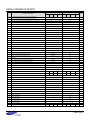
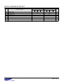
SERIAL PRESENCE DETECT
M393B2G70BH0-YF809/YH909/YMA09/YK009
Organization : 2G x 72
Composition : 1G x 4 * 36ea
Used component part # : K4B4G0446B-HYF8/HYH9/HYK0/HYMA
# of rows in module : 2 Row
# of banks in component : 8 Banks
Feature : 30mm height & double sided component
Refresh : 8K/64ms
Bin Sort : F8(DDR3 1066@CL=7), H9(DDR3 1333@CL=9), K0(DDR3 1600@CL=11), MA(DDR3 1866@CL=13)
RCD Vendor and Revision : Inphi UV GS02
Function Supported
Byte
#
Hex Value
Function Described
Note
YF809 YH909 YMA09 YK009 YF809 YH909 YMA09 YK009
Number of Serial PD Bytes Written / SPD Device Size / CRC Coverage
0
1
SPD Revision
2
Key Byte / DRAM Device Type
3
Key Byte / Module Type
4
SDRAM Density and Banks
5
SDRAM Addressing
6
Module Nominal Voltage, VDD
7
CRC coverage 0~116Byte, SPD Byte
Total :256Byte, SPD Byte Use :
176Byte
92h
Version 1.1
11h
DDR3 SDRAM
0Bh
Registered DIMM
01h
4Gb 8banks
04h
Row : 16, Column : 11
22h
1.35V and 1.5V
02h
Module Organization
2Rank / x4
08h
8
Module Memory Bus Width
ECC, 64bit
0Bh
9
Fine Timebase Dividend and Divisor
1ps
11h
10
Medium Timebase Dividend
1/8 (0.125ns)
01h
11
Medium Timebase Divisor
1/8 (0.125ns)
08h
12
SDRAM Minimum Cycle Time (tCKmin)
13
Reserved
1.875ns
1.5ns
1.071ns
1.25ns
0Fh
0Ch
Reserved
CAS Latencies Supported, Least Significant Byte
14
0Ah
6, 7, 8
6, 7, 8,
9
6, 7, 8,
9 , 10,
11, 13
6, 7, 8,
9 , 10,
11
1Ch
3Ch
FCh
FCh
6, 7, 8
6, 7, 8,
9
6, 7, 8,
9 , 10,
11, 13
6, 7, 8,
9 , 10,
11
00h
00h
02h
00h
28h
30h
CAS Latencies Supported, Most Significant Byte
15
09h
00h
16
Minimum CAS Latency Time(tAAmin)
13.125ns
69h
17
Minimum Write Recovery Time (tWRmin)
18
Minimum RAS# to CAS# Delay Time (tRCDmin)
15ns
78h
19
Minimum Row Active to Row Active Delay Time (tRRDmin)
20
Minimum Row Precharge Time (tRPmin)
21
Upper Nibbles for tRAS and tRC
22
Minimum Active to Precharge Time (tRASmin), Least Significant Byte
23
Minimum Active to Active/Refresh Time (tRCmin), Least Significatn Byte
24
Minimum Refresh Recovery Time (tRFCmin), Least Significant Byte
260ns
20h
25
Minimum Refresh Recovery Time (tRFCmin), Most Significant Byte
260ns
08h
26
Minimum Internal Write to Read Command Delay Time (tWTRmin)
7.5ns
3Ch
27
Minimum Internal Read to Precharge Command Delay Time (tRTPmin)
7.5ns
28
Upper Nibble for tFAW
37.5ns
30ns
27ns
30ns
01h
00h
00h
00h
29
Minimum Four Activate WIndow Delay Time (tFAWmin), Least Significant Byte
37.5ns
30ns
27ns
30ns
2Ch
F0h
D8h
F0h
30
SDRAM Output Drivers supported
31
SDRAM Thermal and Refresh Options
32
Module Thermal Sensor
33
SDRAM Device Type
34
Fine Offset for SDRAM Minimum Cycle Time(tCKmin)
CAh
00h
35
Fine Offset for Minimum CAS Latency Time(tAAmin)
13.125ns
7.5ns
37.5ns
6ns
5ns
69h
6ns
3Ch
30h
13.125ns
69h
-
11h
36ns
34ns
35ns
50.625ns 49.125ns 47.125ns 48.125ns
2Ch
20h
10h
18h
95h
89h
79h
81h
3Ch
DLL off Mode, RZQ/6, RZQ/7
83h
No ODTS, No ASR
01h
with TS
80h
Standard Monolithic DRAM Device
1.875ns
1.5ns
1.071ns
13.125ns
1.25ns
00h
00h
00h
00h
FEB. 2012
SERIAL PRESENCE DETECT
Function Supported
Byte
#
Hex Value
Function Described
Note
YF809 YH909 YMA09 YK009 YF809 YH909 YMA09 YK009
36
Fine Offset for Minimum RAS# to CAS# Delay Time(tRCDmin)
13.125ns
00h
37
Fine Offset for Minimum Row Precharge Delay Time(tRPmin)
13.125ns
00h
38
Fine Offset for Minimum Active to Active/Refresh Delay Time(tRCmin)
50.625ns 49.125ns 47.125ns 48.125ns
00h
39~59
Reserved, General Section
Reserved
00h
30mm
0Fh
Planar Double sides
11h
R/C E, 2.0
44h
60
Module Nominal Height
61
Module Maximum Thickness
62
Reference Raw Card Used
63
DIMM Module Attributes
2 Rows of DRAM / 1 Register used
09h
64
Heat Spreader Solution
without HS
00h
65
Register vendor ID code(LSB)
Inphi
04h
66
Register vendor ID code(MSB)
Inphi
B3h
67
Register Revision Number
Inphi UVGS02
21h
68
Register Type
SSTE32882
00h
69
Register Control Word Functions(RC0/RC1)
Default
00h
70
Register Control Word Functions(RC2/RC3)
R/C E
50h
71
Register Control Word Functions(RC4/RC5)
R/C E
55h
72
Register Control Word Functions(RC6/RC7)
Default
00h
73
Register Control Word Functions(RC8/RC9)
Default
00h
74
Register Control Word Function(RC10, RC11)
Default
00h
75
Register Control Word Function(RC12, RC13)
Default
00h
76
Register Control Word Function(RC14, RC15)
Default
00h
-
00h
77~116
Reserved
117
Module Manufacturer ID Code, Least Significant Byte
Samsung
80h
118
Module Manufacturer ID Code, Most Significant Byte
Samsung
CEh
119
Module ID: Module Manufacturing Location
Onyang Korea
01h
120
Module ID: Module Manufacturing Date
-
00h
121
Module ID: Module Manufacturing Date
-
00h
122~125 Module ID : Module Serial Number
-
00h
126
Cyclical Redundancy Code
-
-
127
Cyclical Redundancy Code
-
-
128
Module Part Number
M
4Dh
129
Module Part Number
3
33h
130
Module Part Number
9
39h
131
Module Part Number
3
33h
132
Module Part Number
B
42h
133
Module Part Number
2
32h
134
Module Part Number
G
47h
135
Module Part Number
7
37h
136
Module Part Number
0
30h
137
Module Part Number
B-die
42h
138
Module Part Number
H
48h
139
Module Part Number
0
30h
140
Module Part Number
-
2Dh
141
Module Part Number
Y
142
Module Part Number
F
H
M
K
46h
143
Module Part Number
8
9
A
0
38h
DEh
9Ch
FBh
A8h
90h
39h
EEh
E6h
48h
4Dh
4Bh
39h
41h
30h
59h
FEB. 2012
SERIAL PRESENCE DETECT
Function Supported
Byte
#
Hex Value
Function Described
Note
YF809 YH909 YMA09 YK009 YF809 YH909 YMA09 YK009
144
Module Part Number
Blank
20h
145
Module Part Number
Blank
20h
-
00h
146~147 Module Revision Code
148
SDRAM Manufacturer's JEDEC ID Code
Samsung
80h
149
SDRAM Manufacturer's JEDEC ID Code
Samsung
CEh
150~175 Manufacturer's Specific Data
-
00h
176~255 Open for customer use
-
00h
FEB. 2012