1
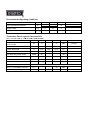
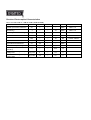
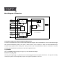
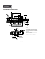
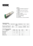
Features
n Compliant with IEEE802.3z Gigabit Ethernet
Standard
n Compliant with Fiber Channel 100-SM-LC-L
standard
n Industry standard small form pluggable (SFP)
package
n Simplex SC connector
n Differential LVPECL inputs and outputs
n Single power supply 3.3V
n TTL signal detect indicator
n Hot Pluggable
n Class 1 laser product complies with EN 60825-1
Ordering Information
PART NUMBER
TX/RX
INPUT/OUTPUT
SIGNAL
TEMPERATURE
LD Type
Distance
DETECT
LS48-C3S-TC-N-K5 1550/1310
AC/AC
TTL
0°C to 70 °C
1550 DFB
10km
LS48-C3S-TI-N-K5 1550/1310
AC/AC
TTL
-40°C to 85 °C
1550 DFB
10km
Absolute Maximum Ratings
PARAMETER
SYMBOL
MIN
MAX
UNITS
TS
-40
85
°C
Supply Voltage
Vcc
-0.5
4.0
V
Input Voltage
VIN
-0.5
Vcc
V
Output Current
Io
---
50
mA
Operating Current
IOP
---
400
mA
Storage Temperature
NOTE
Recommended Operating Conditions
PARAMETER
SYMBOL
MIN
0
-40
MAX
70
85
UNITS
Case Operating Temperature
TC
Supply Voltage
Vcc
3.1
3.5
V
Supply Current
ITX + IRX
---
300
mA
°C
NOTE
LS48-C3S-TC-N-K5
LS48-C3S-TI-N-K5
Transmitter Electro-optical Characteristics
Vcc = 3.1 V to 3.5 V, TC = 0 °C to 70 °C (-40 °C to 85 °C)
PARAMETER
Output Optical Power
9/125 mm fiber
SYMBOL
MIN
TYP.
MAX
UNITS
NOTE
Pout
-9
---
-3
dBm
Average
Extinction Ratio
ER
9
---
---
dB
Center Wavelength
lC
1530
1550
1570
nm
Spectral Width (-20dB)
Dl
---
---
1
nm
SMSR
30
Rise/Fall Time, (20-80%)
Tr , f
---
---
260
ps
Relative Intensity Noise
RIN
---
---
-120
dB/Hz
TJ
---
---
227
ps
Side Mode Suppression Ratio
Total Jitter
Output Eye
dB
Compliant with IEEE802.3z
Max. Pout TX-DISABLE Asserted
POFF
---
---
-45
dBm
Differential Input Voltage
VDIFF
0.4
---
2.0
V
Receiver Electro-optical Characteristics
Vcc = 3.1 V to 3.5 V, TC = 0 °C to 70 °C (-40 °C to 85 °C)
PARAMETER
SYMBOL
MIN
TYP.
MAX
UNITS
NOTE
Optical Input Power-maximum
Optical Input Power-minimum
(Sensitivity)
PIN
-1
---
---
dBm
BER < 10-12
PIN
---
---
-21
dBm
BER < 10-12
Operating Center Wavelength
lC
1260
---
1360
nm
Optical Return Loss
ORL
14
---
---
dB
l=1260~1360nm
Optical isolation
ISO
---
---
-40
dB
l=1260~1360nm
Signal Detect-Asserted
PA
---
---
-21
dBm
Signal Detect-Deasserted
PD
-35
---
---
dBm
Differential Output Voltage
VDIFF
0.5
---
1.2
V
T r, f
---
---
0.35
ns
RX_LOSL
0
---
0.5
V
RX_LOSH
2.4
---
VCC
V
Data Output Rise, Fall Time
(20-80%)
Receiver Loss of Signal Output
Voltage-Low
Receiver Loss of Signal Output
Voltage-High
Block Diagram of Transceiver
DATA
DATA/
LD Drive
&
Fault Sense
LD
TX_DISABLE
TX_FAULT
PRE.
AMPLIFIER
IC
(0)
(1)
PD
WDM Filter
MOD_DEF
(2)
OPTICAL
DATA
DATA/
SUB-ASSEMBLIES
POST-Amp
&
LOS Detect
RX_LOS
Transmitter and Receiver Optical Sub-assembly Section
A 1550 nm InGaAsP laser and an InGaAs PIN photodiode integrate with an WDM filter to form a bi-directional single
fiber optical subassembly (OSA). The laser of OSA is driven by a LD driver IC which converts differential input
LVPECL logic signals into an analog laser driving current. And, The photodiode of OSA is connected to a circuit
providing post-amplification quantization, and optical signal detection.
TX_DISABLE
The TX_DISABLE signal is high (TTL logic “1”) to turn off the laser output.
Receive Loss (RX_LOS)
The RX_LOS is high (logic “1”) when there is no incoming light from the companion transceiver. This signal is normally
used by the system for the diagnostic purpose. The signal is operated in TTL level.
Dimensions
DIMENSIONS ARE IN MILLIMETERS
ALL DIMENSIONS ARE 0.2mm UNLESS OTHERWISE SPECIFIED
SFP host board mechanical layout
X
Y
S XY
A
1
LX A S
1
PIN1
LXA S
LEGEND
A SB S
PIN1
1.PADS AND VIAS ARE CHASSIS GROUND
2.THROUGH HOLES, PLATING OPTIONAL
3.HATCHED AREA DENOTES COMPONENT
AND TRACE KEEPOUT(EXCEPT CHASSIS
GROUND)
4.AREA DENOTES COMPONENT KEEPOUT
(TRACES ALLOWED)
DIMENSIONS ARE IN MILLIMETERS
A SB S
A SB S
Unit: mm
Pin Assignment
Pin-Out
Pin
PIN 11
PIN 20
PIN 10
PIN 1
Signal Name
Description
1
2
TGND
TX_FAULT
Transmit Ground
Transmit Fault
3
4
5
TX_DISABLE
MOD_DEF (2)
Transmit Disable
SDA Serial Data Signal
SCL Serial Clock Signal
6
7
8
9
MOD_DEF (1)
MOD_DEF (0)
RATE SELECT
RX_LOS
R GND
10
11
R GND
R GND
Receiver Ground
Receiver Ground
12
13
RXRX+
R GND
VCCR
VCCT
TGND
Receive Data Bar, Differential PECL, ac coupled
Receive Data, Differential PECL, ac coupled
14
15
16
17
18
19
20
TX+
TXTGND
TTL Low
Open Circuit
Receiver Loss of Signal, TTL High, open collector
Receiver Ground
Receiver Ground
Receiver Power Supply
Transmitter Power Supply
Transmitter Ground
Transmit Data, Differential PCEL, ac coupled
Transmit Data Bar, Differential PCEL, ac coupled
Transmitter Ground
Eye Safety Mark
The LS4 series singlemode transceiver is a class 1
laser product. It complies with EN 60825-1 and FDA
21 CFR 1040.10 and 1040.11. In order to meet laser
safety requirements the transceiver shall be operated
within the Absolute Maximum Ratings.
Required Mark
Class 1 Laser Product
Complies with
21 CFR 1040.10 and 1040.11
Caution
All adjustments have been done at the factory
before the shipment of the devices. No
maintenance and user serviceable part is
required. Tampering with and modifying the
performance of the device will result in voided
product warranty.
Note : All information contained in this document is subject to change without notice.