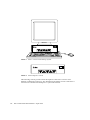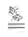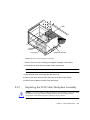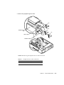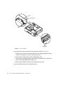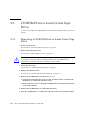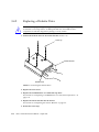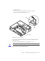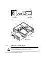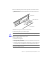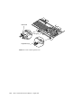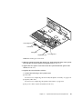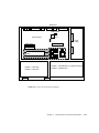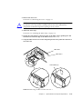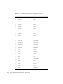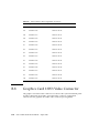
1
Ultra™ 1 Creator Series
Service Manual
Sun Microsystems, Inc.
901 San Antonio Road
Palo Alto, CA 94303-4900 USA
650 960-1300
Fax 650 969-9131
Part No.: 802-4148-10
Revision A, August 1996
Send comments about this document to: [email protected]
1997 Sun Microsystems, Inc., 901 San Antonio Road, Palo Alto, California 94303-4900 U.S.A. All rights reserved
This product or document is protected by copyright and distributed under licenses restricting its use, copying, distribution, and decompilation.
No part of this product or document may be reproduced in any form by any means without prior written authorization of Sun and its licensors,
if any.
Portions of this product may be derived from the UNIX® system, licensed from Novell, Inc., and from the Berkeley 4.3 BSD system, licensed
from the University of California. UNIX is a registered trademark in the United States and in other countries and is exclusively licensed by
X/Open Company Ltd. Third-party software, including font technology in this product, is protected by copyright and licensed from Sun’s
suppliers. RESTRICTED RIGHTS: Use, duplication, or disclosure by the U.S. Government is subject to restrictions of FAR 52.227-14(g)(2)(6/87)
and FAR 52.227-19(6/87), or DFAR 252.227-7015(b)(6/95) and DFAR 227.7202-3(a).
Sun, Sun Microsystems, the Sun logo, and Solaris are trademarks or registered trademarks of Sun Microsystems, Inc. in the United States and in
other countries. All SPARC trademarks are used under license and are trademarks or registered trademarks of SPARC International, Inc. in the
United States and in other countries. Products bearing SPARC trademarks are based upon an architecture developed by Sun Microsystems, Inc.
The OPEN LOOK® and Sun™ Graphical User Interfaces were developed by Sun Microsystems, Inc. for its users and licensees. Sun
acknowledges the pioneering efforts of Xerox Corporation in researching and developing the concept of visual or graphical user interfaces for
the computer industry. Sun holds a nonexclusive license from Xerox to the Xerox Graphical User Interface, which license also covers Sun’s
licensees who implement OPEN LOOK GUIs and otherwise comply with Sun’s written license agreements.
THIS PUBLICATION IS PROVIDED“AS IS” WITHOUT WARRANTY OF ANY KIND, EITHER EXPRESS OR IMPLIED, INCLUDING, BUT
NOT LIMITED TO, THE IMPLIED WARRANTIES OF MERCHANTABILITY, FITNESS FOR A PARTICULAR PURPOSE, OR NONINFRINGEMENT.
Copyright 1997 Sun Microsystems, Inc., 901 San Antonio Road, Palo Alto, Californie 94303-4900 U.S.A. Tous droits réservés.
Ce produit ou document est protégé par un copyright et distribué avec des licences qui en restreignent l’utilisation, la copie et la décompilation.
Aucune partie de ce produit ou de sa documentation associée ne peut être reproduite sous aucune forme, par quelque moyen que ce soit, sans
l’autorisation préalable et écrite de Sun et de ses bailleurs de licence, s’il y en a.
Des parties de ce produit pourront être derivées du système UNIX® licencié par Novell, Inc. et du système Berkeley 4.3 BSD licencié par
l’Université de Californie. UNIX est une marque enregistrée aux Etats-Unis et dans d’autres pays, et licenciée exclusivement par X/Open
Company Ltd. Le logiciel détenu par des tiers, et qui comprend la technologie relative aux polices de caractères, est protégé par un copyright et
licencié par des fournisseurs de Sun.
Sun, Sun Microsystems, le logo Sun, et Solaris sont des marques déposées ou enregistrées de Sun Microsystems, Inc. aux Etats-Unis et dans
d’autres pays. Toutes les marques SPARC, utilisées sous licence, sont des marques déposées ou enregistrées de SPARC International, Inc. aux
Etats-Unis et dans d’autres pays. Les produits portant les marques SPARC sont basés sur une architecture développée par Sun Microsystems,
Inc.
Les utilisateurs d’interfaces graphiques OPEN LOOK® et Sun™ ont été développés de Sun Microsystems, Inc. pour ses utilisateurs et licenciés.
Sun reconnaît les efforts de pionniers de Xerox Corporation pour la recherche et le développement du concept des interfaces d’utilisation
visuelle ou graphique pour l’industrie de l’informatique. Sun détient une licence non exclusive de Xerox sur l’interface d’utilisation graphique,
cette licence couvrant aussi les licenciés de Sun qui mettent en place les utilisateurs d’interfaces graphiques OPEN LOOK et qui en outre se
conforment aux licences écrites de Sun.
CETTE PUBLICATION EST FOURNIE "EN L’ETAT" SANS GARANTIE D’AUCUNE SORTE, NI EXPRESSE NI IMPLICITE, Y COMPRIS, ET
SANS QUE CETTE LISTE NE SOIT LIMITATIVE, DES GARANTIES CONCERNANT LA VALEUR MARCHANDE, L’APTITUDE DES
PRODUITS A REPONDRE A UNE UTILISATION PARTICULIERE OU LE FAIT QU’ILS NE SOIENT PAS CONTREFAISANTS DE PRODUITS
DE TIERS.
Please
Recycle
Contents
Preface
1.
2.
Product Description
1-1
1.1
Ultra 1 Series Overview
1.2
I/O Devices (Ultra 1 Creator Series Desktop)
1.3
Supported I/O Devices (Ultra 1 Creator Series Desktop)
System Unit Features
1.3.2
System Unit Components
1-3
1-4
1-4
1-5
2-1
SunVTS Overview
2-1
2.1.1
SunVTS Kernel
2.1.2
SunVTS User Interface
2.1.3
SunVTS Teletype
Power-On Self-Test
2-2
2-2
2-3
3-1
3.1
POST Overview
3.2
Pre-POST Preparation
3.3
1-1
1.3.1
SunVTS Overview
2.1
3.
xv
3-1
3-2
3.2.1
Setting Up a Tip Connection
3.2.2
Verifying the Baud Rate
Initilizing POST
3-2
3-4
3-4
Contents
iii
3.4
4.
5.
Max and Min Levels of POST
3.4.1
Diag-Level NVRAM Variable Set to Max
3.4.2
Diag-level NVRAM Variable Set to Min
3.5
POST Progress and Error Reporting
3-10
3.6
Typical Error Code Failure Message
3-11
3.7
Bypassing POST
3.8
Additional Keyboard Control Commands
3.9
System and Keyboard LEDs
3.10
System Board Test
3-6
3-9
3-11
3-12
3-12
3-13
Troubleshooting Procedures
4-1
4.1
Power-On Failure
4.2
Video Output Failure
4.3
Disk or CD-ROM Drive Failure
4.4
Power Supply Test
4.5
DSIMM Failure
4.6
OpenBoot PROM On-Board Diagnostics
4-1
4-2
4-2
4-4
4-7
4-8
4.6.1
watch-clock
4-8
4.6.2
watch-net, watch-tpe, and watch-net-all
4.6.3
probe-scsi and probe-scsi-all
4.6.4
test <Alias Name>, <Device Path>, -All
4.6.5
FFB Card
4-13
Safety and Tool Requirements
5.1
Safety Requirements
5.2
Symbols
5.3
Safety Precautions
5.4
5-1
5-1
5-1
5-2
5.3.1
Modification to Equipment
5-2
5.3.2
Placement of a Sun Product
5-2
Power Cord Connection
5.4.1
iv
3-5
5-3
Electrostatic Discharge
Ultra 1 Creator Series Service Manual • August 1996
5-3
4-10
4-12
4-9
5.4.2
5.5
6.
7.
8.
Lithium Battery
Tools Required
Power On and Off
5-3
5-3
6-1
6.1
Powering On the System
6-1
6.2
Powering Off the System
6-2
Internal Access
7-1
7.1
Removing the Cover
7.2
Attaching the Wrist Strap
7.3
Replacing the Cover
Major Subassemblies
8.1
8.2
8.3
8.4
8.5
8.6
Power Supply
7-1
7-2
7-3
8-1
8-1
8.1.1
Removing the Power Supply
8-1
8.1.2
Replacing the Power Supply
8-3
Disk Drive Fan
8-5
8.2.1
Removing the Disk Drive Fan Assembly
8.2.2
Replacing the Disk Drive Fan
Speaker
8-6
8-7
8-9
8.3.1
Removing the Speaker
8-9
8.3.2
Replacing the Speaker
8-12
Diskette Cable
8-14
8.4.1
Removing the Diskette Cable
8-14
8.4.2
Replacing the Diskette Cable
8-16
SCSI Cable/Backplane Assembly
8-18
8.5.1
Removing the SCSI Cable/Backplane Assembly
8-19
8.5.2
Replacing the SCSI Cable/Backplane Assembly
8-21
Peripheral Power Cable
8-23
8.6.1
Removing the Peripheral Power Cable
8-23
8.6.2
Replacing the Peripheral Power Cable
8-26
Contents
v
8.7
9.
9.2
9.3
9.4
Removing the Speaker/LED Cable
8-29
8.7.2
Replacing the Speaker/LED Cable
8-34
Disk Drive
9-1
9-1
9.1.1
Removing a Disk Drive
9-1
9.1.2
Replacing a Disk Drive
9-3
Media Bay Chassis Bracket
9-5
9.2.1
Removing the Chassis Bracket
9-5
9.2.2
Replacing the Chassis Bracket
9-7
CD-ROM Drive or 4-mm/8-mm Tape Drive
10.2
10.3
10.4
9-10
9.3.1
Removing a CD-ROM Drive or 4-mm/8-mm Tape Drive
9-10
9.3.2
Replacing a CD-ROM Drive or 4-mm/8-mm Tape Drive
9-11
Diskette Drive
9-12
9.4.1
Removing a Diskette Drive
9-12
9.4.2
Replacing a Diskette Drive
9-14
System Board and Component Replacement
10.1
System Board
Removing a System Board
10-2
10.1.2
Replacing a System Board
10-4
NVRAM/TOD
10-1
10-1
10.1.1
10-12
10.2.1
Removing a NVRAM/TOD
10-12
10.2.2
Replacing a NVRAM/TOD
10-13
SBus Card
10-14
10.3.1
Removing an SBus Card
10-14
10.3.2
Replacing an SBus Card
10-16
10.3.3
Removing the SBus Card Adapter Bracket
FFB Card (Workstation Only)
10.4.1
vi
8-29
8.7.1
Storage Devices
9.1
10.
Speaker/LED Cable
Removing an FFB Card
Ultra 1 Creator Series Service Manual • August 1996
10-19
10-19
10-17
10.4.2
10.5
10.6
11.
DSIMM
Replacing an FFB Card
10-21
10-23
10.5.1
Removing a DSIMM
10-24
10.5.2
Replacing a DSIMM
10-26
System Board Fan
10-28
10.6.1
Removing the System Board Fan
10.6.2
Replacing the Board Fan
Replacement Parts
10-30
11-1
A. Product Specifications
B. Signal Descriptions
10-28
A-1
B-1
C. Functional Description
C-1
Contents
vii
viii
Ultra 1 Creator Series Service Manual • August 1996
Figures
FIGURE 1-1
Ultra 1 Creator Series Desktop System 1-2
FIGURE 1-2
Ultra Enterprise 1 Server
FIGURE 1-3
System Unit Rear View
FIGURE 1-4
System Unit with Cover Removed 1-8
FIGURE 3-1
Sun Type-5 Keyboard 3-5
FIGURE 3-2
Power LED 3-12
FIGURE 4-1
Power Supply Connector J2601
4-5
FIGURE 4-2
Power Supply Connector J2603
4-6
FIGURE 6-1
Rear View of the System
FIGURE 6-2
Sun Type-5 Keyboard 6-2
FIGURE 7-1
Location of Lock Block
FIGURE 7-2
Removing the Cover
FIGURE 7-3
Attaching the Wrist Strap 7-3
FIGURE 7-4
Replacing the Cover 7-4
FIGURE 8-1
Removing the Power Supply 8-3
FIGURE 8-2
Replacing the Power Supply
FIGURE 8-3
Securing and Connecting the Power Supply
FIGURE 8-4
Fan Power Cable Connection
FIGURE 8-5
Disk Drive Fan 8-7
1-2
1-7
6-1
7-1
7-2
8-4
8-5
8-6
Figures
ix
x
FIGURE 8-6
Replacing the Disk Drive Fan 8-8
FIGURE 8-7
Fan and Speaker Cable Connection 8-10
FIGURE 8-8
Removing the Fan/Speaker Bracket
FIGURE 8-9
Removing the Speaker from the Fan/Speaker Bracket 8-12
FIGURE 8-10
Replacing the Fan/Speaker Bracket
FIGURE 8-11
Removing the Drive Bracket 8-15
FIGURE 8-12
Diskette Cable
FIGURE 8-13
Replacing the Drive Bracket
FIGURE 8-14
SCSI/Backplane Assembly Cable Connection 8-20
FIGURE 8-15
Removing the Backplane Assembly 8-21
FIGURE 8-16
Replacing the SCSI Backplane
FIGURE 8-17
Removing the Drive Bracket 8-24
FIGURE 8-18
Removing the Peripheral Power Cable Connection
FIGURE 8-19
Backplane Assembly Peripheral Power Cable Routing
FIGURE 8-20
Replacing the Peripheral Power Cable Connection 8-27
FIGURE 8-21
Replacing the Drive Bracket
FIGURE 8-22
Removing the Drive Bracket 8-30
FIGURE 8-23
Placing the Bracket on Top of the Disk Drive 8-31
FIGURE 8-24
Removing/Replacing the Speaker/LED Cable 8-32
FIGURE 8-25
Speaker/LED Cable Connection
FIGURE 8-26
Speaker Connector on the System Board
FIGURE 8-27
Replacing the Drive Bracket
FIGURE 9-1
EMI Door
FIGURE 9-2
Removing the Disk Drive
FIGURE 9-3
Replacing the Disk Drive 9-4
FIGURE 9-4
Replacing the EMI Door
FIGURE 9-5
Chassis Bracket
FIGURE 9-6
Placing the Chassis Bracket on Top of the Disk Drive
8-11
8-13
8-16
8-18
8-22
8-25
8-26
8-28
8-33
8-33
8-35
9-2
9-2
9-5
9-6
Ultra 1 Creator Series Service Manual • August 1996
9-7
FIGURE 9-7
Connecting Cables to the CD-ROM Drive, 4-mm/8-mm Tape Drive, and Diskette Drive 9-8
FIGURE 9-8
Positioning the Chassis Bracket
FIGURE 9-9
Positioning the CD-ROM Drive or 4-mm/8-mm Tape Drive 9-11
FIGURE 9-10
Positioning the Diskette Drive
9-13
FIGURE 9-11
Positioning the Diskette Drive
9-14
FIGURE 10-1
DC Power Disconnection
FIGURE 10-2
Captive Screws on the Back Panel 10-4
FIGURE 10-3
Sliding the System Board Out of the Chassis
FIGURE 10-4
Removing SBus Filler Panels from the Back Panel 10-5
FIGURE 10-5
Card Guide Exploded view 10-6
FIGURE 10-6
Installing the Card Guide
FIGURE 10-7
Sliding the System Board Into The Chassis 10-8
FIGURE 10-8
DC Power Connection
FIGURE 10-9
Location of the Serial Port Jumpers 10-11
FIGURE 10-10
Identifying Jumper Pins
FIGURE 10-11
NVRAM/TOD
FIGURE 10-12
SBus Slot Locations. 10-14
FIGURE 10-13
Removing an SBus Card from Slot 0 or 1 10-15
FIGURE 10-14
Removing the SBus Card Extractor
FIGURE 10-15
Replacing the SBus Card 10-18
FIGURE 10-16
Preparing to Remove the FFB Card 10-20
FIGURE 10-17
Removing the FFB Card
FIGURE 10-18
Replacing the FFB Card 10-21
FIGURE 10-19
Seating an FFB Card Into the UPA Socket 10-22
FIGURE 10-20
Securing the FFB Card Into the Chassis
FIGURE 10-21
DSIMM Ejection Lever 10-25
FIGURE 10-22
Removing a DSIMM 10-26
FIGURE 10-23
Installing a DSIMM
9-9
10-3
10-4
10-7
10-9
10-12
10-13
10-17
10-20
10-23
10-28
Figures
xi
FIGURE 10-24
System Board Fan Plastic Cover 10-29
FIGURE 10-25
System Board Fan
FIGURE B-1
Keyboard/Mouse Connector Pin Configuration B-2
FIGURE B-2
Serial Ports A and B Connector Configuration B-3
FIGURE B-3
TPE Connector Configuration
FIGURE B-4
Fast Wide SCSI Connector Configuration B-6
FIGURE B-5
Audio Connector Configuration
FIGURE B-6
Parallel Port Connector Pin Configuration
FIGURE B-7
MII Connector Configuration
FIGURE B-8
UPA Connector Pin Configuration B-15
FIGURE B-9
Graphics Card 13W3 Video Con
FIGURE C-1
System Unit or Server Functional Block Diagram C-2
FIGURE C-2
Ultra 1 Creator Series System Board Block Diagram
FIGURE C-3
xii
10-30
Identifying Jumper Pins
B-5
B-10
B-11
B-13
B-21
C-18
Ultra 1 Creator Series Service Manual • August 1996
C-17
Tables
TABLE 1-1
Supported I/0 Devices 1-3
TABLE 1-2
System Unit/Server Components
TABLE 2-1
SunVTS Documentation 2-2
TABLE 3-1
Diag-Level Switch Settings
TABLE 3-2
Keyboard LED Patterns
TABLE 4-1
Internal Drives Identification 4-3
TABLE 4-2
Connector 2601 Pin Description
4-5
TABLE 4-3
Connector 2603 Pin Description
4-6
TABLE 4-4
DSIMM Physical Memory Address
TABLE 4-5
Selected OBP On-Board Diagnostic Tests
TABLE 8-1
Peripheral Power Cable Connections 8-25
TABLE 10-1
Serial Port Jumper Settings
TABLE 10-2
DSIMM Bank and Socket Pair Locations
TABLE 11-1
List of Replacement Parts
TABLE A-1
System Unit/Server Physical Specifications
TABLE A-2
17-Inch Monitor Physical Specifications A-2
TABLE A-3
20-Inch Monitor Physical Specifications A-2
TABLE A-4
Electrical Specifications
TABLE A-5
Environmental Requirements
TABLE B-1
Keyboard/Mouse Connector Pin Assignments
1-5
3-2
3-13
4-7
4-13
10-9
10-24
11-1
A-1
A-2
A-3
B-2
Tables
xiii
xiv
TABLE B-2
Serial A and B Port Connector Pin Assignments
TABLE B-3
TPE Connector Pin Assignments
TABLE B-4
Fast Wide SCSI Connector Pin Assignments
TABLE B-5
Audio Connector Line Assignment B-10
TABLE B-6
Parallel Port Connector Pin Assignments
TABLE B-7
MII Connector Pin Assignments
TABLE B-8
UPA Connector Pin Assignments
TABLE B-9
Graphics Card 13W3 Video Connector Pin Assignments
TABLE C-1
Supported Disk Drives C-6
TABLE C-2
Audio Port Functions
C-9
TABLE C-3
Audio Specifications
C-10
TABLE C-4
Built-In Speaker Specifications
TABLE C-5
Ultra 1 Creator Series Desktop Workstation and Ultra Enterprise 1 Server Power Supply
Budget C-16
TABLE C-6
Serial Port Jumper Settings
TABLE C-7
Flash PROM Jumper Settings C-19
TABLE C-8
Additional System Board Jumper Blocks
B-3
B-5
B-6
B-11
B-13
B-15
B-21
C-10
C-18
Ultra 1 Creator Series Service Manual • August 1996
C-19
Preface
The Ultra™ 1 Creator Series Service Manual provides detailed procedures that describe
the removal and replacement of field replaceable units (FRUs) in the Ultra 1 Creator
series computer (system unit) and the Ultra Enterprise™ 1 server (server). People
that should use this book include technicians, advanced computer system end-users
with experience in replacing hardware and troubleshooting, system administrators,
and qualified service providers.
Document Organization
This book is comprised of seven parts. Each part is divided into chapters as listed in
here.
TABLE P-1
Document Organization
Part Number/Title
Chapter Number/Title
Content Description
Part 1, “System
Information”
Chapter 1, “Product
Description”
Describes the major components
of the Ultra 1 Creator series
desktop system and the Ultra
Enterprise 1 server
Part 2,
“Troubleshooting”
Chapter 2, “SunVTS
Overview”
Describes the execution of
individual tests for verifying
hardware configuration and
functionality
Chapter 3, “Power-On
Self-Test (POST)”
Describes the execution of POST
and provides examples of POST
output patterns
Preface
xv
TABLE P-1
Document Organization (Continued)
Part Number/Title
Chapter Number/Title
Content Description
Chapter 4,
“Troubleshooting
Procedures”
Provides actions to generalized
hardware symptom casualty
Chapter 5, “Safety and
Tool Requirements”
Explains how to work safely when
servicing the Ultra 1 Creator series
Chapter 6, “Power On
and Off”
Provides step-by-step procedures
to power on and power off the
Ultra 1 Creator series
Chapter 7, “Internal
Access”
Provides step-by-step procedures
to remove the Ultra 1 Creator
series cover, attach the wrist strap,
and replace the cover
Chapter 8, “Major
Subassemblies”
Provides step-by-step procedures
to remove and replace major
subassemblies
Chapter 9, “Storage
Devices”
Provides step-by-step procedures
to remove and replace storage
devices
Part 5, “System Board”
Chapter 10, “System
Board and Component
Replacement”
Provides step-by-step procedures
to remove and replace the system
board, and to remove and replace
various components associated
with system board operation
Part 6, “Illustrated Parts
Breakdown”
Chapter 11,
“Replacement Parts”
Lists replaceable parts for the
Ultra 1 Creator series system unit
Part 7, “Appendixes,
Glossary, and Index”
Appendix A, B, and C
Provide product specifications,
signal descriptions, and functional
descriptions for the Ultra 1
Creator series, respectively
Glossary
Provides a listing of acronyms,
terms, and definitions
Index
Provides a quick reference to
specific topics
Part 3, “Preparing for
Service”
Part 4, “Subassembly
Removal and
Replacement”
xvi
Ultra 1 Creator Series Service Manual • August 1996
Warnings and Cautions
Caution – This equipment contains lethal voltage. Accidental contact can result in
serious injury or death. The surface of the UltraSPARC CPU‰ chip may be hot and
cause personal injury if touched. Avoid contact.
!
!
Caution – Improper handling by unqualified personnel can cause serious damage to
this equipment. Unqualified personnel who tamper with this equipment may be
held liable for any resultant damage to the equipment.
Caution – Use proper ESD grounding techniques when handling components. Wear
an antistatic wriststrap and use an ESD-protected mat. Store ESD-sensitive
components in antistatic bags before placing it on any surface.
Individuals servicing this equipment must observe all safety precautions and ensure
compliance with skill level requirements, certification, and all applicable local and
national laws.
Procedures in this document must be performed by trained maintenance providers.
Only people who have been trained by the Sun MicrosystemsTM training facilities (or
by Sun Microsystems affiliates) and have been certified as required by local and
national laws are considered qualified.
Note – Prior to performing service or repair, carefully read the associated procedure.
If a similar repair has not been performed on comparable equipment, DO NOT
ATTEMPT to perform the procedure.
Preface
xvii
Typographic Conventions
Typographic conventions used in this service manual are listed in here.
TABLE P-2
Typeface or
Symbol
Typographic Conventions
Meaning
Example
AaBbCc123
The names of commands, files, and
directories; on-screen computer output
Edit your.login file.
Use ls -a to list all files.
machine_name% You have mail.
AaBbCc123
What you type, contrasted with onscreen computer output
machine_name% suPassword:
AaBbCc123
Command-line placeholder:
replace with a real name or value
To delete a file, type rm filename.
AaBbCc123
Book titles, new words or terms, or
words to be emphasized
Read Chapter 6 in the User’s Guide.
These are called class options.
You must be root to do this.
Related Documentation
Additional information for servicing the Ultra 1 Series system are listed in here.
These documents are also available on-line on the Ultra 1 Series Hardware
AnswerBookTM or on SolarisTM on Sun Hardware AnswerBook TM.
TABLE P-3
Related Documents
Application
Title
Installation
Sun‰
1 Creator Series Installation Guide
(Southern Europe)
802-4145
Diagnostics
Sun‰ Ultra‰ 1 Creator Series Internal Storage
Device User’s Guide
802-4151
Configuration
Sun‰ Ultra‰ 1 Creator Series Reference Manual
802-4147
Specification
17-Inch Entry, 17-Inch Premium, and 20-Inch
Premium Color Monitors Specifications
802-6168
xviii
Part Number
Ultra‰
Ultra 1 Creator Series Service Manual • August 1996
TABLE P-3
Related Documents (Continued)
Application
Title
Specification
SunCD™
Part Number
Specification
Diskette Drive Specification
802-5283
Specification
2.5-Gbyte QIC Tape Drive Specifications
802-3615
Specification
8-mm Tape Drive Specifications
802-5775
Specification
4-mm Tape Drive Specifications
802-5324
Diagnostic
SunVTS‰ 1.0 User’s Guide
801-7271
Diagnostic
SunVTS‰ 1.0 Test Reference Manual
802-1448
Diagnostic
SunVTS‰ 1.0 Quick Reference Card
802-3622
Diagnostics
SunVTS‰ 2.0 User’s Guide
802-5331
Diagnostics
SunVTS‰ 2.0 Test Reference Manual
802-5330
Diagnostics
SunVTS‰ 2.0 Quick Reference Card
802-5329
4 Drive Specifications
802-4157
Shell Prompts in Command Examples
The following table lists the default system prompt and superuser prompt for the C
shell, Bourne shell, and Korn shell.
TABLE P-4
Shell Prompts
Shell
Prompt
C shell
machine_name%
C shell superuser
machine_name#
Bourne shell and Korn shell
$
Bourne shell and Korn shell
superuser
#
Preface
xix
Ordering Sun Documents
The SunDocs™ Order Desk is a distribution center for Sun Microsystems technical
documents. Technical documents may be purchased through major credit cards or
company purchase orders. The following table lists the locations where you can
order documents.
TABLE P-5
Ordering Sun Documents
Country
Telephone
Fax
United States
1-800-873-7869
1-800-944-0661
United Kingdom
0-800-89-88-88
0-800-89-88-87
France
05-90-61-57
05-90-61-58
Belgium
02-720-09-09
02-725-88-5
Luxembourg
32-2-720-09-09
32-2-725-88-5
Germany
01-30-81-61-91
01-30-81-61-92
The Netherlands
06-022-34-45
06-022-34-46
Sweden
020-79-57-26
020-79-57-27
Switzerland
155-19-26
155-19-27
Japan
0120-33-9096
0120-33-9097
World Wide Web: http://www.sun.com/sunexpress/
Sun Welcomes Your Comments
Please use the Reader Comment Card that accompanies this document. We are
interested in improving our documentation and welcome your comments and
suggestions.
You can also email or fax your comments to us. Please include the part number of
your document in the subject line of your email or fax message:
xx
Ultra 1 Creator Series Service Manual • August 1996
■
Email:[email protected]
■
Fax:
SMCC Document Feedback
1-415-786-6443
Preface
xxi
xxii
Ultra 1 Creator Series Service Manual • August 1996
CHAPTER
1
Product Description
The UltraTM 1 Creator series desktop workstation and the Ultra Enterprise TM 1 server
are uniprocessor devices that use the family of UltraSPARCTM processors. Both the
desktop workstation and the server offer super-scalar processor technology,
multiprocessing, high-performance memory interconnection, and high bandwidth
input/output (I/O). In addition, the desktop workstation provides accelerated
graphics.
1.1
Ultra 1 Series Overview
Major components comprising the Ultra 1 Creator series desktop workstation and
the Ultra Enterprise 1 server include:
■
I/O devices:
■
Monitor (included with desktop workstation)
■
Keyboard (included with desktop workstation)
■
Mouse (included with desktop workstation)
■
Microphone (not illustrated, included with desktop workstation)
■
Color camera (optional, not illustrated)
■
External cables (not illustrated, included with desktop workstation and server)
■
System unit
FIGURE 1-1 illustrates the Ultra 1 Creator series desktop workstation and Figure 1-2
illustrates the Ultra Enterprise 1 server.
1-1
FIGURE 1-1
Ultra 1 Creator Series Desktop System
FIGURE 1-2
Ultra Enterprise 1 Server
The following sections provide a brief description of the Ultra 1 Creator series
desktop workstation I/O devices. Also included is a detailed overview of the Ultra 1
Creator series and the Ultra Enterprise 1 system unit features.
1-2
Ultra 1 Creator Series Service Manual • August 1996
1.2
I/O Devices (Ultra 1 Creator Series
Desktop)
The Ultra 1 Creator series desktop workstation uses the following I/O devices:
■
■
■
■
■
Keyboard
Optical mouse
Microphone
Color camera
One of several types of monitors
The following table lists the supported I/O devices and provides a brief description
of each device.
TABLE 1-1
Supported I/0 Devices
I/O Device
Description
17-inch (43-cm)
color monitor
1152 x 900 resolution, 76- or 66-Hz refresh rate,
100 dots per inch (DPI)
1280 x 1024 resolution, 76- or 66-Hz refresh rate, 110 DPI
960 x 680 resolution, 112-Hz refresh rate, 81 DPI
20-inch (51-cm)
color monitor
1152 x 900 resolution, 76- or 66-Hz refresh rate, 84 DPI
1280 x 1024 resolution, 76- or 66-Hz refresh rate, 93 DPI
960 x 680 resolution, 112-Hz refresh rate, 79 DPI
Microphone
SunMicrophoneTM II
Color camera
Optional SunVideoTM and SunCameraTM
Keyboard
Sun Type-5; AT 101 or UNIX layout available
Optical mouse
Optomechanical, 3-button
Chapter 1
Product Description
1-3
1.3
Supported I/O Devices (Ultra 1 Creator
Series Desktop)
1.3.1
System Unit Features
System unit components are located in a Sun Ultra 1 Creator chassis. Overall chassis
dimensions (width x depth x height) are 16.44 inches x 17.44 inches
X 4.07 inches (418mm x 443mm x 104mm). System unit electronics are contained on
a single 9.6-inch x 11.0-inch (244mm x 279mm) printed circuit board (system board)
The system board contains the CPU cluster, memory, system control application
specific integrated circuits (ASICs), and I/O ASICs. The CPU cluster consists of the
UltraSPARC processor, five cache chips, and two UltraSPARC data buffer ASICS.
System unit electronics and peripherals contain (or may be upgraded to contain) the
following features:
■
1-4
SPARCTM V9 64-bit UltraSPARCTM processor
■
167-Megahertz (MHz) processor
■
200-MHz processor
■
SolarisTM 2.5.1 operating system
■
SolarisTM 2.5 Hardware: 1/96
■
High performance UltraSPARC Port ArchitectureTM (UPA)
■
High bandwidth memory system using 144-bit, 60-nanosecond (ns) dynamic
random access memory (DRAM) single in-line memory module (SIMM)
■
Eight DRAM SIMM (DSIMM) sockets providing from 32 Mbytes to
1 gigabyte (Gbyte) of memory using 16-Mbyte, 32-Mbyte, 64-Mbyte, or
128-Mbyte DSIMMs
■
Fast frame buffer (FFB) graphics (67-MHz graphics clock) with 24-bit color and 8bit overlay: single buffer FFB, double buffer FFB (Ultra 1 Creator series desktop
only).
■
Double buffer FFB with 66-MHz graphics clock (Ultra 1 Creator 3D series desktop
only)
■
16-bit CD quality audio with support for line in/out, headphone, and stereo
microphone
■
20-Mbyte-per-second small computer system interface (SCSI)
■
10-megabits-per-second (Mbps)/100-Mbps twisted-pair Ethernet (TPE) and
media-independent interface (MII) networking
Ultra 1 Creator Series Service Manual • August 1996
■
Two IEEE 1496-compliant 25-MHz SBus input/output (I/O) slots
■
Two DB25-type standard connector serial ports
Each serial port supports synchronous and asynchronous communication.
■
DB25-type connector parallel port (Centronics compatible)
■
Standard Sunness
Note – Standard Sunness includes the time of day (TOD)/nonvolatile randomaccess memory (NVRAM), and boot programmable read-only memory (PROM) or
FlashPROM for Power-On Self-Test/OpenBoot PROM (POST/OBP)
1.3.2
■
Built-in speaker
■
Diagnostic LED
■
Power conservation support
System Unit Components
System unit components are listed in TABLE 1-2. FIGURE 1-3 illustrates the system unit
interior. FIGURE 1-4 illustrates the system unit rear panel.
Note – Part numbers listed in
TABLE 1-2 are correct as of the service manual
publication date but are subject to change without notice. Consult your authorized
Sun sales representative or service provider to confirm a part number prior to
ordering a replacement part.
TABLE 1-2
System Unit/Server Components
Component
Part Number
Description
CPU
501-2486
Ultra 1 Creator Series system board
(167-MHz)
CPU
501-4134
Ultra 1 Creator Series system board
(200-MHz)
TOD/NVRAM
525-1430
TOD/NVRAM
DSIMM
501-2479
DSIMM, 16-Mbyte
DSIMM
501-2622
DSIMM, 32-Mbyte
Chapter 1
Product Description
1-5
TABLE 1-2
1-6
System Unit/Server Components (Continued)
Component
Part Number
Description
DSIMM
501-2480
DSIMM, 64-Mbyte
DSIMM
501-3136
DSIMM, 128-Mbyte
Graphics card
(desktop workstation only)
501-2633
FFB board, double buffer, 67-MHz
Graphics card
(desktop workstation only)
501-2634
FFB board, single buffer, 67-MHz
Graphics card
(desktop workstation only)
501-4126
FFB board, double buffer, 67-MHz
Graphics card
(desktop workstation only)
501-4127
FFB board, single buffer, 67-MHz
Drive
540-2729
1.05-Gbyte disk drive
Drive
540-2730
2.1-Gbyte disk drive
Drive
370-2102
CD-ROM drive 1.6-inch
Drive
370-2151
Diskette drive
Power supply
300-1308
180 W power supply
Fan assembly
540-2761
System board fan
Fan assembly
540-2666
Disk fan (80 mm)
Speaker
370-1579
Speaker
Cable assembly
530-1871
TPE cable type 5
Cable assembly
530-2153
SCSI cable/backplane assy
Cable assembly
530-2175
Cable, speaker/LED
Cable assembly
530-2176
Cable, peripheral power
Cable assembly
530-2187
Cable, diskette
Ultra 1 Creator Series Service Manual • August 1996
Serial port B
(RS-423/RS-232)
Power outlet
(Female socket)
Power on/standby
Power inlet
(Male plug)
UPA slot
Serial port A
(RS-423/RS-232)
Parallel port
connector
MII connector
Keyboard/mouse
connector
FIGURE 1-3
SBus slot 0
SBus slot 1
SCSI connector
TPE connector
Audio
connector (4)
System Unit Rear View
Chapter 1
Product Description
1-7
Cover
DSIMM
SBus card
Chassis
Disk fan
SBus card slot (2)
System board
Disk drive
Power supply
Speaker
CD-ROM drive
(may be exchanged with either
4-mm tape drive or 8-mm tape drive)
Diskette
drive
FIGURE 1-4
1-8
System Unit with Cover Removed
Ultra 1 Creator Series Service Manual • August 1996
CHAPTER
2
SunVTS Overview
This chapter contains an overview of the Sun validation and test suite (SunVTS ™)
diagnostic tool/application. The following is the list of the SunVTS diagnostic topics
presented in this chapter.
■
■
■
2.1
“SunVTS Kernel” on page 2
“SunVTS User Interface” on page 2
“SunVTS Teletype” on page 3
SunVTS Overview
The SunVTS software executes multiple diagnostic hardware tests from a single user
interface and is used to verify configuration and functionality of most hardware
controllers and devices. SunVTS operates primarily from the OpenWindows ™ user
interface, allowing test parameters to be set quickly and easily while a diagnostic
test operation is being performed.
2-1
The SunVTS operation is provided in the documents listed in TABLE 2-1. These
documents furnish detailed information about SunVTS and are available on the
Solaris on Sun Hardware AnswerBook. The Solaris on Sun Hardware AnswerBook is
provided on the SMCC Updates CD for the Solaris release being operated.
TABLE 2-1
SunVTS Documentation
Title
Part Number
Description
SunVTS User’s Guide
802-5331
Describes the SunVTS environment;
starting and controlling various user
interfaces; feature descriptions
SunVTS Test Reference Manual
802-5330
Describes each SunVTS test;
provides various test options and
command line arguments
SunVTS Quick Reference Card
802-5329
Provides overview of vtsui
interface features
The main features of the SunVTS environment include:
■
■
■
2.1.1
SunVTS kernel
SunVTS user interface
SunVTS teletype
SunVTS Kernel
The SunVTS kernel (vtsk) diagnostic tool controls all testing and operates in the
OpenWindows background. When activated, vtsk probes the hardware
configuration of the system tested and responds to vtsui. vtsk coordinates
execution of individual tests and manages the messages sent by these tests.
2.1.2
SunVTS User Interface
The SunVTS user interface (vtsui) diagnostic tool operates in the OpenWindows
background. Upon activation, vtsui provides vtsk control, various user options,
tests, and read-log files.
2-2
Ultra 1 Creator Series Service Manual • August 1996
2.1.3
SunVTS Teletype
The SunVTS teletype (vtstty) diagnostic tool controls the vtsk from either a
command shell or a terminal attached to a serial port. Most options available in
vtstty have equivalent options in vtsui.
Chapter 2
SunVTS Overview
2-3
2-4
Ultra 1 Creator Series Service Manual • August 1996
CHAPTER
3
Power-On Self-Test
his chapter contains procedures to initiate the Power-on self-test (POST) diagnostics.
Procedures are also included to support pre-POST preparation, POST data
interpretation, and bypassing POST diagnostics. The following is a list of the POST
diagnostic topics presented in this chapter.
■
■
■
■
■
■
■
■
■
3.1
“POST Overview” on page 1
“Pre-POST Preparation” on page 2
“Initilizing POST” on page 4
“Max and Min Levels of POST” on page 5
“POST Progress and Error Reporting” on page 10
“Bypassing POST” on page 11
“Additional Keyboard Control Commands” on page 12
“System and Keyboard LEDs” on page 12
“System Board Test” on page 13
POST Overview
POST is useful in determining if a portion of the system has failed and should be
replaced. POST detects approximately 85 percent of Ultra 1Creator series system
faults and is located in the system board OpenBoot™ PROM (OBP). The setting of the
3-1
diag-level switch determines the POST function. TABLE 3-1 lists the diag-level switch
settings for disabling POST (off), enabling POST maximum (max), or enabling POST
minimum (min).
TABLE 3-1
3.2
Diag-Level Switch Settings
Diag-Level Switch
Setting
POST
Initialization?
Serial Port A I/O
Serial Port A
Error Output
Diag-Switch
Setting
Off
No
N/A
N/A
Don’t care
Max
Yes (power-on)
Enabled
Enabled
True
Min
Yes (power-on)
Disabled
Enabled
True
Pre-POST Preparation
Pre-POST preparation includes:
■
Setting up a tip connection to another workstation or terminal to view POST
progress and error messages.
See Section 3.2.1 “Setting Up a Tip Connection” on page 3-2.
■
Verifying baud rates between a workstation and a monitor or a workstation and a
terminal.
See Section 3.2.2 “Verifying the Baud Rate” on page 3-4.
If a terminal or a monitor is not connected to serial port A (default port) of a
workstation or server to be tested, the keyboard LEDs are used to determine error
conditions (see Section 3.9 “System and Keyboard LEDs” on page 3-12.)
3.2.1
Setting Up a Tip Connection
A tip connection permits a remote shell window to be used as a terminal to display
test data of a system being tested. Serial port A or serial port B of a workstation or
server being tested is used to establish the tip connection between the workstation or
server being tested and another Sun workstation monitor or TTY-type terminal. The
tip connection is used in a SunOS window and provides features to help with the
OBP.
To set up a tip connection:
3-2
Ultra 1 Creator Series Service Manual • August 1996
1. Connect serial port A of the system being tested to another Sun Workstation serial
port B using a serial null modem cable (connect cable pins 2-3, 3-2, 7-20, and 20-7).
2. At the other Sun workstation, check the /etc/remote file:
hardwire:\
:dv=/dev/term/b:br#9600:el=^C^S^Q^U^D:ie=%$:oe=^D:
Note – The example shows connection to serial port B, ttyb
3. To use serial port A:
a. Copy and paste the following:
hardwire:\
:dv=/dev/term/b:br#9600:el=^C^S^Q^U^D:ie=%$:oe=^D:
b. Then modify as follows:
hardwirea:\
:dv=/dev/term/a:br#9600:el=^C^S^Q^U^D:ie=%$:oe=^D:
4. In a shell tool window on the Sun Workstation, enter tip hardwire.
The system replies:
hostname% tip hardwire
connected
Note – The shell window is now a tip window directed to the serial port of the
Sun Workstation or server being tested. When power is applied to the system being
tested, POST messages will be displayed in this window.
5. When POST is completed, disconnect the tip window as follows:
a. Open a shell tool.
b. Enter ps -a to view the active tip line and process ID (PID) number.
Chapter 3
Power-On Self-Test
3-3
c. Enter kill -9 XXXX (where XXXX is the PID number) of the tip hardwire
process.
hostname% kill -9 PID# of tip hardwire process
3.2.2
Verifying the Baud Rate
To verify the baud rate between the system being tested and a terminal or another
Sun workstation monitor:
1. Open a shell tool.
2. Enter eeprom.
3. Verify the following serial port default settings as follows:
ttyb-mode = 9600,8,n,1
ttya-mode = 9600,8,n,1
Note – Ensure that the above settings are consistent with TTY-type terminal or
workstation monitor settings.
3.3
Initilizing POST
POST may be initilized by two ways: by setting the diag-switch? NVRAM variable
to true and then power cycling the system or by simultaneously pressing the
keyboard Stop and D keys while power is applied to the system.
To set the diag-switch? NVRAM variable to true and power cycle the system:
1. At the system prompt, enter: setenv diag-switch? true. Verify the prompt,
diag-switch? true, is displayed
2. At the Sun type-5 keyboard, power cycle the system by simultaneously pressing
the shift key and the power-on key (FIGURE 3-1). After a few seconds, press the
power-on key.
3. Verify the following:
3-4
Ultra 1 Creator Series Service Manual • August 1996
a. The display prompt disappears.
b. The monitor power-on indicator flashes on and off.
c. The keyboard Caps Lock key indicator flashes on and off.
4. When the POST is complete, set the diag-switch? variable to false (default
setting).
Scroll Lock
key indicator
Power-on key
Stop
key
Caps Lock
key indicator
Shift key
FIGURE 3-1
3.4
D key
Compose
key indicator
Num Lock
key indicator
Sun Type-5 Keyboard
Max and Min Levels of POST
Two levels of POST are available: max (maximum level) and min (minimum level).
The system initiates the selected level of POST based upon the setting of diaglevel, a NVRAM variable.
The default setting for diag-level is max. An example of a max level POST output
on serial port A is provided in Section 3.4.1 “Diag-Level NVRAM Variable Set to
Max” on page 3-6 An example of a min level POST output on serial port A is
provided in Section 3.4.2 “Diag-level NVRAM Variable Set to Min” on page 3-9”
To set the diag-level variable to min, enter:
ok setenv diag-level min
Chapter 3
Power-On Self-Test
3-5
To return to the default setting:
ok setenv diag-level max
3.4.1
Diag-Level NVRAM Variable Set to Max
When the diag-level NVRAM parameter is set to max, POST enables an extended set
of diagnostic-level tests. This mode requires approximately 1.5 minutes to complete.
CODE EXAMPLE 3-1 identifies a typical serial port A POST output with the diag-level
NVRAM variable set to max.
Note – XXXX placeholders used in table entries represent numeric values that may
change without notice.
CODE EXAMPLE 3-1
Diag-level NVRAM Variable Set to Max
ok Hardware Power ON
Button Power ON
Button Power ON
@(#)Sun Ultra X UPA/SBus X.X X.X FCS Test PROM Version X created XXXX/XX/XX XX:XX
Clearing DTAGS 0000.0000.0008.0000 Done
Probing keyboard Done
%o0 = 0000.0000.0000.4001
Executing Power On SelfTest
0>@(#) Sun Ultra Enterprise X POST, FCS_Version XX.XX.XX X/XX/XX XX:XX XX
0>@(#) Sun Ultra Enterprise X POST, FCS_Version XX.XX.XX X/XX/XX XX:XX XX
0> UltraSparcX Version X.X
0>Ecache Probe
0> Ecache size XXXX Kb
0> Ecache size XXXX Kb
0>Ecache Tag Test
0>Ecache RAM Test
0>Ecache Address Line Test
0>Initialize and Verify Ecache
0>SC Initialization
0>
SC_MP id=XXXX, UPA Number=X, Impl=X, Ver=X
0>BMX Test
3-6
Ultra 1 Creator Series Service Manual • August 1996
CODE EXAMPLE 3-1
Diag-level NVRAM Variable Set to Max (Continued)
0>
Checking BMX's 0>Probing Memory
0> Found Memory Group (Variable based upon memory configuration)
0>
Found (Variable based upon memory configuration) of usable Main Memory
0>SIMM Group
Base Addr
Size
Group Status
0>
0
00000000.00000000 08000000 00
0>
1
00000000.20000000 08000000 00
0>Quick Memory Test
0>Clear and Test Stack Memory
SelfTest Initializing
0>Basic CPU Test
0>
Instruction Cache Tag RAM Test
0>
Instruction Cache Instruction RAM Test
0>
Instruction Cache Next Field RAM Test
0>
Instruction Cache Pre-decode RAM Test
0>
Data Cache RAM Test
0>
Data Cache Tags Test
0>MMU Enable Test
0>
DMMU Registers Access Test
0>
DMMU TLB DATA RAM Access Test
0>
DMMU TLB TAGS Access Test
0>
IMMU Registers Access Test
0>
IMMU TLB DATA RAM Access Test
0>
IMMU TLB TAGS Access Test
0>
DMMU Init
0>
IMMU Init
0>
Mapping Selftest Enabling MMUs
0>FPU Register Test
0>
FPU Registers and Data Path Test
0>
FSR Read/Write Test
0>EPROMs Test
0>
PROM Datapath Test
0>Serial Ports Test
0>
Slavio Serial Ports Test
0>NVRAM TOD Test
0>
M48T59 (TOD) Init
0>
M48T59 (TOD) Functional Part 1 Test
SelfTest Initializing
0>Memory Test
0>
Memory Clear Test
0> Test being relocated into Cache
0>
Memory RAM (blk) Test
0> Test being relocated into Cache
Chapter 3
Power-On Self-Test
3-7
CODE EXAMPLE 3-1
0>
0>
0>
0>
Diag-level NVRAM Variable Set to Max (Continued)
Memory Stress Test
Test being relocated into Memory
Memory Address Line Test
Test being relocated into Memory
>
Memory Address Line Test
0> Test being relocated into Memory
0>Forcing ECC Faults Test
0>
ECC CE Pattern Test
0>
ECC CE Check bit Test
0>
ECC UE Pattern Test
0>
ECC UE Check bit Test
0>SysIO Registers Test
0>
SysIO Regsiter Initialization
0>
IOMMU Registers and RAM Test
0>
Streaming Buffer Registers and RAM Test
0>
SBus Control and Config Registers Test
0>
SysIO RAM Initialization
0>SysIO Functional Test
0>
Mapping Selftest Enabling MMUs
0>
Clear Interrupt Map and State Registers
0>
SysIO Interrupts Test
0>
SysIO Timers/Counters Test
0>
IOMMU Virtual Address TLB Tag Compare Test
0>
Streaming Buffer Flush Test
0>
DMA Merge Buffer Test
0>CPU Speed
0>
CPU 0 Running at XXX MHZ.
0>Ecache Stress Test
0>
Ecache Stress Test
0>APC Test
0>
APC Registers Tests Test
0>
APC DVMA Test
0>Data Cache
0>
Dcache
0>
Dcache
0>
Dcache
Test
Init
Enable Test
Functionality Test
0>FEPS Test
0>
Parallel Port Registers Test
0>
Parallel Port ID is: XxX
0>
Parallel Port DVMA burst mode read/write Test
3-8
Ultra 1 Creator Series Service Manual • August 1996
CODE EXAMPLE 3-1
Diag-level NVRAM Variable Set to Max (Continued)
0>
FAS366 Registers Test
0>
ESP FAS366 DVMA burst mode read/write Test
0>
FEPS Internal Loopbacks Test
0>
Ethernet Transceiver Internal Loopbacks Test
0>CPU Functional Test
0>
Mapping Selftest Enabling MMUs
0>
SPARC Atomic Instructions Test
0>
CPU Dispatch Control Register Test
0>
CPU Softint Registers and Interrupts Test
0>
CPU Tick and Tick Compare Registers Test
0>
Uni-Processor Cache Coherence Test
0>
UltraSPARC-2 Prefetch Instructions Test
0> *UltraSparc-1 module detected, tests skipped
0>Cross Calls Test (Dual CPU configuration only)
0>
Cross Calls Test
0>Cache Coherency Test
0>
Multi-Processor Cache Coherence Test
0>
<< POST COMPLETE(0) >>
3.4.2
Diag-level NVRAM Variable Set to Min
When the diag-level NVRAM parameter is set to min, POST enables an
abbreviated set of diagnostic-level tests. This mode requires approximately 30
seconds to complete. CODE EXAMPLE 3-2 identifies a serial port A POST output with
the diag-level NVRAM variable set to min.
Chapter 3
Power-On Self-Test
3-9
Note – XXXX placeholders used in table entries represent numeric values that may
change without notice.
CODE EXAMPLE 3-2
Diag-Level NVRAM variable Set to Min
Hardware Power ON
Button Power ON
Button Power ON
@(#) Sun Ultra X UPA/SBus X.X X.X FCS Test PROM Version Xcreated XXXX/XX/XX XX:XX
Clearing DTAGS 0000.0000.0008.0000 Done
Probing keyboard Done
%o0 = 0000.0000.0000.2001
Executing Power On SelfTest
0>@(#) Sun Ultra Enterprise X POST, FCS_Version XX.XX.XX X/XX/XXXX XX:XX XX
1>@(#) Sun Ultra Enterprise X POST, FCS_Version XX.XX.XX X/XX/XXXX XX:XX XX
0> UltraSparcX Version X.X
1> UltraSparcX Version X.X
0 << POST COMPLETE(0) >>
Power On Selftest Completed
Status = 0000.0000.0000.0000 0000.XXXX.XXXX.XXXX XXXX.XXXX.XXXX.XXXX
Software Power ON
3.5
POST Progress and Error Reporting
While POST is initialized, the Caps Lock key on the Sun type-5 keyboard flashes on
and off to indicate that POST tests are being executed. Additional POST progress
indications are also visible when a TTY-type terminal or a tip line is connected
between serial port A (default port) of the system being tested and a POST
monitoring system.
If an error occurs during the POST execution, the keyboard Caps Lock key indicator
stops flashing and an error code is displayed using the Caps Lock, Compose, Scroll
Lock, and Num Lock key indicators. The error code indicates a particular system
hardware failure.
3-10
Ultra 1 Creator Series Service Manual • August 1996
Note – An error code may only be visible for a few seconds. Observe the Caps Lock,
Compose, Scroll Lock, and Num Lock key indicators closely while POST is active.
In most cases, POST also attempts to send a failure message to the POST monitoring
system. TABLE 3-1 identifies the typical appearance of a failure message. If a keyboard
error code is displayed, determine the meaning of the error code by comparing the
keyboard error code pattern to the corresponding error code meaning listed in
TABLE 3-2 on page 3-13.
Note – The system does not automatically boot if a POST error occurs; it halts at the
ok prompt to alert the user of a failure.
3.6
Typical Error Code Failure Message
Power On Self Test Failed.
Cause: SIMM U0701 or System Board
ok
3.7
Bypassing POST
POST may be disabled and thereby bypassed. To bypass POST:
1. Prior to powering on the system, press and hold the Stop key on the Sun type-5
keyboard.
2. With the Stop key pressed, turn on the system by pressing the power-on key
(FIGURE 3-1 on page 3-5).
Chapter 3
Power-On Self-Test
3-11
3.8
Additional Keyboard Control
Commands
■
Stop Key
If the diag-switch? variable is set to true and POST is not to be executed when
the system is powered on, press and hold the keyboard Stop key and press the
keyboard power-on key.
■
Stop and N Keys
If the system NVRAM parameters are set to the original default settings, press and
hold the Stop and N keys before powering on the system. Continue to hold the Stop
and N keys until the system banner appears on the monitor.
3.9
System and Keyboard LEDs
The power LED, located at the chassis front, remains lighted when the system is
operating normally. FIGURE 3-2 shows the location of the power LED.
LED
FIGURE 3-2
Power LED
This section describes the keyboard light-emitting diode (LED) patterns as a result of
POST and their meaning. While POST is executing and making progress, the Caps
Lock key LED blinks while the rest of the LEDs are off. If POST finds an error, a
pattern is encoded in the LEDs to indicate the defective part. If POST completes with
no errors, all LEDs will be turned off before returning to the OpenBoot ‰ PROM
(OBP).
3-12
Ultra 1 Creator Series Service Manual • August 1996
TABLE 3-2 defines the keyboard LED patterns. FIGURE 3-1 on page 3-5 shows the
location of the LED keys on the Sun type 5-c keyboard.
TABLE 3-2
Keyboard LED Patterns
Caps Lock
Compose
Scroll Lock
Num Lock
Bit Value
Meaning of LED Pattern
Blink
Off
Off
Off
x000(2)
POST in progress
Off
Off
Off
Off
0000(2)
POST successful completion
Off
Off
Off
On
0001(2)
DSIMM in slot U 0601 failure
Off
Off
On
Off
0010(2)
DSIMM in slot U 0701 failure
Off
Off
On
On
0011(2)
DSIMM in slot U 0602 failure
Off
On
Off
Off
0100(2)
DSIMM in slot U 0702 failure
Off
On
Off
On
0101(2)
DSIMM in slot U 0603 failure
Off
On
On
Off
0110(2)
DSIMM in slot U 0703 failure
Off
On
On
On
0111(2)
DSIMM in slot U 0604 failure
On
Off
Off
Off
1000(2)
DSIMM in slot U 0704 failure
On
Off
Off
On
1001(2)
System board failure
On
Off
On
Off
1010(2)
No memory found
On
Off
On
On
1011(2)
Reserved
On
On
Off
Off
1100(2)
Reserved
On
On
Off
On
1101(2)
Reserved
On
On
On
Off
1110(2)
Reserved
On
On
On
On
1111(2)
Reserved
3.10
System Board Test
To initialize the POST system board test:
1. At the Sun type-5 keyboard:
a. Simultaneously press and hold the Stop and D keys.
b. While holding the Stop and D keys, press the power-on key.
Chapter 3
Power-On Self-Test
3-13
2. Verify the keyboard LEDs light to confirm the system is in the POST mode and
the keyboard Caps Lock key LED flashes on and off to indicate the system has
enabled the POST.
3. If a failure occurs during POST, a keyboard key LED other than the Caps Lock
key LED may light, indicating a failed system component.
See Section 3.9 “System and Keyboard LEDs” on page 3-12.
4. If the Caps Lock key LED fails to flash after the Stop and D keys are pressed,
POST has failed.
See Section 3.9 “System and Keyboard LEDs” on page 3-12.
Note – The most probable cause of this type of failure is the system board.
However, optional system components could also cause POST to fail.
5. Before replacing the system board, remove any optional components such as SBus
cards and memory, and repeat the POST.
Note – Non-optional components such as: two DSIMMs in slots U601 and U701; the
system board; the power supply; and the keyboard must be installed for POST to
execute properly. Removing the optional system components and retesting the
system isolates the possibility that those components are the cause of the failure.
6. To receive additional POST failure information, establish a tip connection.
See Section 3.2.1 “Setting Up a Tip Connection” on page 3-2.
3-14
Ultra 1 Creator Series Service Manual • August 1996
CHAPTER
4
Troubleshooting Procedures
This chapter describes how to troubleshoot possible problems and includes the
corrective actions you can take.
■
■
■
■
■
■
4.1
“Power-On Failure” on page 1
“Video Output Failure” on page 2
“Disk or CD-ROM Drive Failure” on page 2
“Power Supply Test” on page 4
“DSIMM Failure” on page 7
“OpenBoot PROM On-Board Diagnostics” on page 8
Power-On Failure
The following provides examples of power-on failure symptoms and suggested
actions.
SYMPTOM
The system unit does not power up when the keyboard power switch is pressed.
ACTION
Check the AC power cord. Ensure that the AC power cord is properly connected to
the system unit and to the wall receptacle. Verify that the wall receptacle is
supplying AC power to the system.
Press the power switch at the rear of the system unit. If the system powers on, the
keyboard may be defective or the system unit is unable to accept the keyboard
power-on signal. Power off the system unit and press the keyboard power-on switch
again. If the system unit powers on, no further action is required. If the system unit
does not power on, the keyboard may be defective. Connect a spare Sun type-5
keyboard to the system unit and press the power-on key.
4-1
If the wall receptacle AC power has been verified and the system unit does not
power up, the system unit power supply may be defective. See Section 4.4 “Power
Supply Test” on page 4-4.
SYMPTOM
The system unit attempts to power up but does not boot or initialize the monitor.
ACTION
Press the power-on switch and watch the keyboard. You should see the keyboard
LEDs light briefly and hear a tone from the keyboard. If you do not hear a tone or if
the keyboard LEDs do not light briefly, the system unit power supply may be
defective. See Section 4.4 “Power Supply Test” on page 4-4. If you hear a keyboard
tone and see the keyboard LEDs light briefly but the system unit still fails to
initialize, refer to Section 3.9 “System and Keyboard LEDs” on page 3-12.
4.2
Video Output Failure
The following provides an example of a video output failure symptom and
suggested action.
SYMPTOM
No video at the system monitor.
ACTION
Check the monitor AC power cord. Ensure that the AC power cord is connected to
the monitor and to the wall receptacle. Verify that the wall receptacle is supplying
AC power to the monitor. Check the video cable connection between the monitor
and the system unit graphics card output port at the rear of the system unit. If the
AC connection to the monitor is correct and the video cable is correctly connected,
the system monitor or the system unit graphics card may be defective. Replace the
monitor or the graphics card.
4.3
Disk or CD-ROM Drive Failure
The following provides examples of disk drive and CD-ROM drive failure
symptoms and suggested actions.
SYMPTOM
4-2
Ultra 1 Creator Series Service Manual • August 1996
■
A disk drive read, write, or parity error is reported by the operating system or
customer application.
■
A CD-ROM drive read error or parity error is reported by the operating system or
customer applications.
ACTION
■
Replace the drive indicated by the failure message. The operating system
identifies the internal drives as identified in TABLE 4-1.
.
TABLE 4-1
Internal Drives Identification
Operating System Address
Drive Physical Location and Target
c0t0d0s#
Lower SCSI Disk, target 0
c0t1d0s#
Upper SCSI Disk, target 1
c0t6d0s#
CD-ROM drive, target 6 (optional)
c0t5d0s#
Tape drive, target 5 (optional)
Note – The # symbol in the examples may be a numeral between 0 and 7 that
describes the slice or partition on the drive.
SYMPTOM
Disk drive or CD-ROM drive fails to boot or is not responding to commands.
ACTION
Test the drive response to the probe-scsi command as follows:
1. At the system ok prompt:
a. Enter reset-all.
b. Enter probe-scsi.
2. If the disk drive responds correctly to probe-scsi, the message identified in
CODE EXAMPLE 4-4 on page 4-11 appears.
If the drives respond and a message is displayed, the system SCSI controller has
successfully probed the devices. This is an indication that the system board is
operating correctly. If one drive does not respond to the SCSI controller probe but
the others do, replace the unresponsive drive.
Chapter 4
Troubleshooting Procedures
4-3
If one internal disk drive is configured with the system and the probe-scsi test
fails to show the device in the message, replace the drive. If the problem is still
evident after replacing the drive, replace the system board. If replacing both the disk
drive and the system board does not correct the problem, replace the internal disk
drive cable and SCSI backplane assembly.
4.4
Power Supply Test
The following provides instructions to test the power supply.
Note –
FIGURE 4-1 and TABLE 4-2 identify power supply connector J2601. FIGURE 4-2
and TABLE 4-3 identify power supply connector J2603.
● Use a digital voltage meter (DVM) to check the power supply output voltages as
follows:
Note – Power supply connectors J2601 through J2603 must remain connected to the
system board.
a. With the negative probe of the VOM placed on a connector ground (Gnd) pin,
position the positive probe on each power pin.
b. Verify +12 VDC, -12 VDC, +5 VDC, +3.3 VDC and +3.0 VDC.
c. If any power pin signal is not present with the power supply active and
properly connected to the system board, replace the power supply.
4-4
Ultra 1 Creator Series Service Manual • August 1996
1
8
9
16
FIGURE 4-1
Power Supply Connector J2601
TABLE 4-2
Connector 2601 Pin Description
Pin
Description
Pin
Description
1
+12V
9
Thermal sensor
2
Gnd
10
-12V
3
Power on
11
Power off
4
Not used
12
Undefined
5
Not used
13
Undefined
6
+3V sense
14
Gnd
7
+3V set
15
Thermal sensor
8
+3V ovp
16
Power on reset
Chapter 4
Troubleshooting Procedures
4-5
4-6
1
9
10
18
FIGURE 4-2
Power Supply Connector J2603
TABLE 4-3
Connector 2603 Pin Description
Pin
Description
Pin
Description
1
+5V
10
Gnd
2
+5V
11
Gnd
3
+5V
12
Gnd
4
+3.3V
13
Gnd
5
+3.3V
14
Gnd
6
+3.3V
15
Gnd
7
+3.0V
16
Gnd
8
+3.0V
17
Gnd
9
+3.0V
18
Gnd
Ultra 1 Creator Series Service Manual • August 1996
4.5
DSIMM Failure
At times the operating system, diagnostic program, or POST may not display a
DSIMM location (U number) as part of a memory error message. In this situation,
the only available information is a physical memory address and failing byte (or bit).
TABLE 4-4 to locate the defective DSIMM.
TABLE 4-4
DSIMM Physical Memory Address
DSIMM Slot Location
Physical Memory
Address Start
Physical Memory
Address End
Bank 0
0000 0000
0fff ffff
1000 000
1fff ffff
2000 000
2fff ffff
3000 000
3fff ffff
U0701 (byte 00-15, bits 000-127)
U0601 (byte 16-31, bits 128-255)
Bank 1
U0702 (byte 00-15, bits 000-127)
U0602 (byte 16-31, bits 128-255)
Bank 2
U0703 (byte 00-15, bits 000-127)
U0603 (byte 16-31, bits 128-255)
Bank 3
U0704 (byte 00-15, bits 000-127)
U0604 (byte 16-31, bits 128-255)
Each bank listed in TABLE 4-4 (Bank 0, Bank 1, Bank 2, and Bank 3) allows enough
address space to accommodate two 16-Mbyte, two 32-Mbyte,
two 64-Mbyte, or two 128-Mbyte DSIMMs. Unused addresses are mapped out by the
memory management hardware. Regardless of the installed DSIMM capacity, the
physical memory starting address is as listed in TABLE 4-4.
Chapter 4
Troubleshooting Procedures
4-7
4.6
OpenBoot PROM On-Board Diagnostics
The following sections describe the OpenBoot PROM (OBP) on-board diagnostics. To
execute the OBP on-board diagnostics, the system must be at the ok prompt.The
OBP on-board diagnostics are listed as follows:
4.6.1
watch-clock
—page 4-8
watch-net, watch-tpe, and watch-net-all
—page 4-9
probe-scsi and probe-scsi-all
—page 4-10
test <Alias Name>, <Device Path>, -All
—page 4-12
FFB Card
—page 4-12
watch-clock
watch-clock reads a register in the NVRAM/TOD chip and displays the result as
a seconds counter. During normal operation, the seconds counter repeatedly
increments from 0 to 59 until interrupted by pressing any key on the Sun type-5
keyboard. CODE EXAMPLE 4-1 identifies the watch-clock output message.
CODE EXAMPLE 4-1
watch-clock Output Message
ok watch-clock
4-8
Watching the 'seconds' register of
the real time clock chip.
Type any key to stop.
It should be 'ticking' once
a second.
41
41 is an example. Counter
increments from 0 to 59
Ultra 1 Creator Series Service Manual • August 1996
4.6.2
watch-net, watch-tpe, and watch-netall
watch-net, watch-tpe, and watch-net-all monitor Ethernet packets on the
Ethernet cable(s) connected to the system. Good packets received by the system are
indicated by a period (.). Errors such as the framing error and the cyclic redundancy
check (CRC) error are indicated with an X and an associated error description.
CODE EXAMPLE 4-2 identifies the watch-net output message. CODE EXAMPLE 4-3
identifies the watch-net-all output message.
CODE EXAMPLE 4-2
watch-net Output Message
ok watch-net
Internal loopback test -succeeded.
Transceiver check -- Using
Onboard Transceiver - Link up.
passed
Using Onboard
Transceiver - Link
up.
Looking for Ethernet packets.
'.' is a good packet.'X' is a
bad packet.
Type any key to stop.
Chapter 4
Troubleshooting Procedures
4-9
CODE EXAMPLE 4-3
watch-net-all Output Message
ok watch-net-all
/sbus@1f,0/lebuffer@1,40000/le@1,60000
Internal loopback test -- succeeded.
External loopback test -- succeeded.
Looking for Ethernet packets.
'.' is a good packet. 'X' is a bad packet.
Type any key to stop.
.........................................................
...................
............................(keyboard key pressed here)
/sbus@1f,0/SUNW,hme@e,8c00000
Internak loopback test -- succeeded.
Transceiver check -- Using Onboard Transceiver - Link Up.
passed
Using Onboard Transceiver - Link Up.
Looking for Ethernet packets.
'.' is a good packet. 'X' is a bad packet.
Type any key to stop.
.........................................................
..................
4.6.3
probe-scsi and probe-scsi-all
probe-scsi transmits an inquiry command to internal and external SCSI devices
connected to the Ultra 1 Creator series on-board SCSI interface. If the SCSI device is
connected and active, the target address, unit number, device type, and
manufacturer name is displayed. probe-scsi-all transmits an inquiry command
to SCSI devices connected to the system SCSI host adapters. The first identifier listed
in the display is the SCSI host adapter address in the system device tree followed by
the SCSI device identification data.
4-10
Ultra 1 Creator Series Service Manual • August 1996
CODE EXAMPLE 4-4 identifies the probe-scsi output message and CODE EXAMPLE 4-5
identifies the probe-scsi-all output message.
CODE EXAMPLE 4-4
probe-scsi Output Message
ok probe-scsi
This command may hang the system
if a Stop-A or halt command has
been executed. Please type resetall to reset the system before
executing this command.
Do you wish to continue? (y/n)
Enter n
Enter reset-all
Verify display blanks for
approximately 5 seconds and
returns to the ok prompt.
ok probe-scsi
This command may hang the system
if a Stop-A or halt command has
been executed. Please type resetall to reset the system before
executing this command.
Do you wish to continue? (y/n)
Enter y
Target 0
Unit 0
Disk
SEAGATE ST32550W
Sun2.1G041200000000
Copyright (c) 1995 Seagate
All rights reserved ASA2
Target 1
Unit 0
Disk
Target 6
Unit 0
device
Removable Read Only
SEAGATE ST32550W
Sun2.1G041200000000
Copyright (c) 1995 Seagate
All rights reserved ASA2
TOSHIBA XM5301TASUN4XCD173506/22/95
Chapter 4
Troubleshooting Procedures
4-11
CODE EXAMPLE 4-5
probe-scsi-all Output Message
ok probe-scsi-all
This command may hang the system if
a Stop-A or halt command has been
executed. Please type reset-all to
reset the system before executing
this command.
Do you wish to continue? (y/n
Enter n
Enter reset-all
Verify display blanks for
approximately 5 seconds
and returns to the ok
prompt.
ok probe-scsi-all
This command may hang the system if
a Stop-A or halt command has been
executed. Please type reset-all to
reset the system before executing
this command.
Do you wish to continue? (y/n)
Enter y
/sbus@1f,0/SUNW, fas@e, 8800000
Target 0
Unit 0
Disk
Target 1
Unit 0
Disk
Target 6
Unit 0 Removable Read Only device
4.6.4
SEAGATE ST32550W
Sun2.1G041200000000
Copyright (c) 1995 Seagate
All rights reserved ASA2
SEAGATE ST32550W
Sun2.1G041200000000
Copyright (c) 1995 Seagate
All rights reserved ASA2
TOSHIBA XM5301TASUN4XCD173506/22/95
test <Alias Name>, <Device Path>, -All
The test command, combined with a device alias or device path, enables a device
self-test program. If a device has no self-test program, the message:
No selftest method for <device name> is displayed. To enable the self-test
program for a device, enter the test command followed by the device alias or
4-12
Ultra 1 Creator Series Service Manual • August 1996
device path name. CODE EXAMPLE 4-6 identifies the test output message. TABLE 4-5
lists test <alias name> selections, a description of the selection, and
preparation.
Note – The floppy drive is selected as the test <alias name> example.
CODE EXAMPLE 4-6
test Output Message
ok test floppy
Testing floppy disk system. A
formatted disk should be in the
drive.
Test succeeded.
TABLE 4-5
Selected OBP On-Board Diagnostic Tests
Type of Test
Description
Preparation
test screen
Tests system video graphics hardware and
monitor
Diag-switch? NVRAM parameter must be
true for the test to execute.
test floppy
Tests floppy drive response to commands
A formatted diskette must be inserted into
the drive.
test net
Performs internal/external loopback test of
the system
auto-selected Ethernet interface
An Ethernet cable must be attached to the
system and to an Ethernet tap or hub or the
external loopback test fails.
test ttya
test ttyb
Outputs an alphanumeric test pattern on
the system serial ports:ttya, serial port A;
ttyb, serial port B
A terminal must be connected to the port
being tested to observe the output.
test keyboard
Executes the keyboard selftest.
Four keyboard LEDs should flash once and
a message is displayed: Keyboard
Present.
test-all
Sequentially test
system-configured devices containing
selftest.
Tests are sequentially executed in devicetree order (viewed with the show-devs
command).
4.6.5
FFB Card
The FFB card contains a built-in diagnostic test that is enabled through the OBP. The
FFB card built-in diagnostic test verifies basic graphics functionality without booting
the operating system software.
Chapter 4
Troubleshooting Procedures
4-13
To execute the built-in diagnostic test, the system must be at the OBP monitor ok
prompt.
To initilize the FFB card diagnostic:
1. Enter setenv diag-switch? true at the ok prompt. The diag-switch? =
true prompt and the ok prompt are displayed.
Note – If the FFB card is being used as the system display device, perform Steps 2
and 4. If the FFB card is not being used as the system display device, perform Steps
3 and 4.
2. Enter test screen at the ok prompt.
CODE EXAMPLE 4-7
Verifying Console Mode for Frame Buffer Board
This will take a few minutes.
Verifying Frame Buffer Memory used for console mode
This will take about two minutes.
a. A series of patterns are displayed.
b. FFB Frame Buffer functional test passed appears.
3. Enter test /SUNW,ffb at the ok prompt.
CODE EXAMPLE 4-8
Verifying Console Mode for Frame Buffer Board
This will take a few minutes.
Verifying Frame Buffer Memory used for console mode
This will take about two minutes.
a. A series of patterns are displayed.
b. FFB Frame Buffer functional test passed appears.
4. When the FFB on-board diagnostics are completed, enter
setenv diag-switch? false. The diag-switch? = false is displayed.
4-14
Ultra 1 Creator Series Service Manual • August 1996
CHAPTER
5
Safety and Tool Requirements
This chapter provides a description of safety requirements, symbols, safety
precautions, and tools required.
■
■
■
■
5.1
“Safety Requirements” on page 1
“Symbols” on page 1
“Safety Precautions” on page 2
“Tools Required” on page 3
Safety Requirements
For protection, observe the following safety precautions when setting up the
equipment:
5.2
■
Follow all cautions, warnings, and instructions marked on the equipment.
■
Ensure that the voltages and frequency rating of the power receptacle match the
electrical rating label on the equipment.
■
Never push objects of any kind through openings in the equipment. They may
touch dangerous voltage points or short components resulting in fire or electric
shock.
■
Refer servicing of equipment to qualified personnel.
Symbols
The following symbols mean:
5-1
!
Caution – Risk of personal injury and equipment damage. Follow the instructions.
Caution – Hazardous voltages are present. To reduce the risk of electric shock and
danger to personal health, follow the instructions.
Caution – Hot surfaces. Avoid contact. Surfaces are hot and may cause personal
injury if touched.
5.3
Safety Precautions
The following safety precautions mean:
5.3.1
Modification to Equipment
!
5.3.2
Sun Microsystems is not responsible for regulatory compliance of a modified Sun
product.
Placement of a Sun Product
!
5-2
Caution – Do not make mechanical or electrical modifications to the equipment.
Caution – To ensure reliable operation of the Sun product and to protect it from
overheating, openings in the equipment must not be blocked or covered. A Sun
product should never be placed near a radiator or hot air register.
Ultra 1 Creator Series Service Manual • August 1996
5.4
Power Cord Connection
Caution – Not all power cords have the same current ratings. Household extension
cords do not have overload protection. Do not use household extension cords with
the Sun product.The power switch of this product functions as a standby type device
only. The power cord serves as the primary disconnect device for the system. Be sure
to connect the power cord into a grounded electrical receptacle that is nearby the
system and is readily accessible. Do not connect the power cord when the power
supply has been removed from the system chassis.
5.4.1
Electrostatic Discharge
Caution – The boards and hard disk drive contain electronic components that are
!
5.4.2
extremely sensitive to static electricity. Ordinary amounts of static electricity from
clothes or work environment can destroy components. Do not touch the components
themselves or any metal parts. Wear a wrist strap when handling the drive
assemblies, boards or cards.
Lithium Battery
Caution – On Sun system boards, a lithium battery is molded into the real-time
!
5.5
clock, SDS No. M48T59Y,MK48TXXB-XX, M48T18-XXXPCZ or M48T59W-XXXPCZ.
Batteries are not customer replaceable parts. They may explode if mistreated. Do not
dispose of the battery in fire. Do not disassemble it or attempt to recharge it.
Tools Required
The following tools are required to service the Ultra 1 series desktop workstation
and the Ultra Enterprise 1 server.
■
No. 1 Phillips screwdriver
■
Needle-nose pliers
Chapter 5
Safety and Tool Requirements
5-3
■
Grounding wrist strap
■
Digital voltage meter (DVM)
■
Antistatic surface
Place ESD-sensitive components such as system board, circuit cards, disk drives, and
TOD/NVRAM on an antistatic surface. The following items can
be used as an antistatic surface:
5-4
■
Bag used to wrap a Sun replacement part
■
Shipping container used to package a Sun replacement part
■
Inner side (metal part) of the system unit cover
■
Sun ESD mat, part no. 250-1088 (may be purchased through your Sun sales
representative)
■
Disposable ESD mat; shipped with replacement parts or optional system features
Ultra 1 Creator Series Service Manual • August 1996
CHAPTER
6
Power On and Off
This chapter explains how to work safely when servicing the Ultra 1 Creator series.
■
■
6.1
“Powering On the System” on page 1
“Powering Off the System” on page 2
Powering On the System
To power-on the system, proceed as follows.
1. Turn on power to all connected peripherals.
Note – Peripheral power is activated prior to system power so the system can
recognize the peripherals when it is activated.
2. Set the power on/standby switch to the on (I) position (FIGURE 6-1) or press the Sun
type-5 keyboard power-on key (FIGURE 6-2).
Power on/standby switch
FIGURE 6-1
Rear View of the System
6-1
FIGURE 6-2
6.2
Sun Type-5 Keyboard
Powering Off the System
To power-off the system, proceed as follows.
Caution – Prior to turning off system power, exit from the operating system. Failure
to do so may result in loss of data.
1. Notify users that the system is going down.
2. Back up system files and data.
3. Halt the system.
4. Set the power on/standby switch to the stand-by (O) position
(FIGURE 6-1) or press the Sun Type-5 keyboard power-on key (FIGURE 6-2).
5. Verify the following:
a. Front panel LED is off.
b. System fans are not spinning.
Caution – Disconnect the AC power cord from the AC receptacle prior to handling
the power supply. When servicing system components other than the power supply,
the AC power cord should remain connected to the AC receptacle.
6-2
Ultra 1 Creator Series Service Manual • August 1996
6. When the power on/standby switch is in stand-by (0) and the AC power cord
remains connected to a power receptacle, AC voltage is present in the power
supply primary.
7. Turn off the power to the monitor.
8. Disconnect cables to any peripheral equipment.
Chapter 6
Power On and Off
6-3
6-4
Ultra 1 Creator Series Service Manual • August 1996
CHAPTER
7
Internal Access
This section provides step-by-step procedures to remove the Ultra 1 Creator series
cover, attach the wrist strap, and replace the cover.
■
■
■
7.1
“Removing the Cover” on page 1
“Attaching the Wrist Strap” on page 2
“Replacing the Cover” on page 3
Removing the Cover
To remove the cover:
1. Power off the system.
See Section 6.2 “Powering Off the System” on page 6-2
2. Use a No. 1 Phillips screwdriver to remove the lock block (FIGURE 7-1).
Lock block
FIGURE 7-1
Location of Lock Block
3. Loosen the captive screws securing the cover (FIGURE 7-2).
7-1
4. Grasping the sides of the cover, lift the cover up from the rear. After the cover
clears the back panel, push the cover away from the front panel.
Cover
Captive screw (2)
FIGURE 7-2
7.2
Removing the Cover
Attaching the Wrist Strap
To attach the wrist strap:
!
Caution – Wear an antistatic wrist strap and use an ESD-protected mat when
handling components. When removing components other than the power supply,
leave the power cord connected to both the system/server unit and the wall
receptacle. When removing the power supply, attach the copper end of the wrist
strap to the system/server unit chassis, not the power supply. Store
ESD-sensitive components in antistatic bags before placing it on any surface.
1. Unwrap the first two folds of the wrist strap; wrap the adhesive side firmly
against the wrist (FIGURE 7-3).
7-2
Ultra 1 Creator Series Service Manual • August 1996
2. Peel the liner from the copper foil at the opposite end of the wrist strap. Attach
the copper end of the wrist strap to the power supply top.
Wrist strap
Copper foil end
Power supply
FIGURE 7-3
7.3
Attaching the Wrist Strap
Replacing the Cover
To replace the cover:
1. Position the cover on the system (FIGURE 7-4).
2. Lower the rear of the cover until the cover channels align with the chassis flanges.
Press down on each side of the cover until the cover firmly seats (FIGURE 7-4).
3. Tighten the captive screws securing the cover.
4. Use a No. 1 Phillips screwdriver to replace the lock block (FIGURE 7-1).
Chapter 7
Internal Access
7-3
5. Power-on the system.
Channel
(2 places)
Cover
Flange
Captive screw (2)
Flange
FIGURE 7-4
7-4
Replacing the Cover
Ultra 1 Creator Series Service Manual • August 1996
CHAPTER
8
Major Subassemblies
This chapter contains procedures to remove and replace the major subassemblies of
the system and server units. The following is a list of the major subassemblies:
■
■
■
■
■
■
■
8.1
“Power Supply” on page 1
“Disk Drive Fan” on page 5
“Speaker” on page 9
“Diskette Cable” on page 14
“SCSI Cable/Backplane Assembly” on page 18
“Peripheral Power Cable” on page 23
“Speaker/LED Cable” on page 29
Power Supply
To remove and replace the power supply, proceed as follows.
Caution – When removing the power supply, attach the copper end of the wrist
!
8.1.1
strap to the system/server unit chassis, vice power supply. When removing
components other than the power supply, leave the AC power cord connected to
both the system unit and the wall receptacle.
Removing the Power Supply
1. Power-off the system.
See Section 6.2 “Powering Off the System” on page 6-2.
2. Remove the system unit cover.
See Section 7.1 “Removing the Cover” on page 7-1.
8-1
Caution – Use proper ESD grounding techniques when handling components. Wear
!
an antistatic wrist strap and use an ESD-protected mat. Store ESD-sensitive
components in antistatic bags before placing it on any surface.
Caution – When removing the power supply, attach the copper end of the wrist
!
strap to the system/server unit chassis, not the power supply.
3. Attach the wrist strap.
See Section 7.2 “Attaching the Wrist Strap” on page 7-2.
4. Disconnect the AC power cord from the system.
5. Disconnect the power supply as follows FIGURE 8-1:
a. Disconnect the power supply connector from the system board at J2603.
b. Disconnect the power supply connector from the system board at J2601.
c. Remove the DC harness from the clip; disconnect the DC connector from the
peripheral power cable at P1.
6. Loosen the power supply captive screw from the back panel.
7. Push the power supply toward the front side of the chassis to disengage the
mounting hooks.
8. Tilt the power supply slightly toward the system board; lift the power supply
from the chassis.
8-2
Ultra 1 Creator Series Service Manual • August 1996
Clip
DC Harness
P1
Power supply
J2603
J2601
Captive
screw
FIGURE 8-1
8.1.2
Removing the Power Supply
Replacing the Power Supply
Caution – Use proper ESD grounding techniques when handling components. Wear
!
an antistatic wrist strap and use an ESD-protected mat. Store ESD-sensitive
components in antistatic bags before placing it on any surface.
1. Position the power supply into the chassis.
2. Push the power supply toward the chassis rear, engaging the mounting hooks
(FIGURE 8-2).
Chapter 8
Major Subassemblies
8-3
Note – Ensure that the hooks located on the chassis base engage with the cutouts
located on the bottom of the power supply.
Power supply
System board
Mounting hook (3)
Chassis
Back panel
FIGURE 8-2
Replacing the Power Supply
3. Tighten the captive screw securing the power supply to the back panel.
4. Connect the power supply as follows (FIGURE 8-3):
a. Connect the DC connector to the peripheral power cable at P1.
b. Route and insert the DC harness through the clip on the drive bracket.
c. Connect the power supply connector to the system board at J2603.
d. Connect the power supply connector to the system board at J2601.
5. Detach the wrist strap.
6. Replace the system unit cover.
See Section 7.3 “Replacing the Cover” on page 7-3.
8-4
Ultra 1 Creator Series Service Manual • August 1996
7. Power-on the system.
See Section 6.1 “Powering On the System” on page 6-1.
Clip
P1
Power supply
J2603
J2601
Captive screw
FIGURE 8-3
8.2
Securing and Connecting the Power Supply
Disk Drive Fan
To remove and replace the disk drive fan assembly, proceed as follows.
Chapter 8
Major Subassemblies
8-5
8.2.1
Removing the Disk Drive Fan Assembly
1. Power-off the system.
See Section 6.2 “Powering Off the System” on page 6-2.
2. Remove the system unit cover.
See Section 7.1 “Removing the Cover” on page 7-1.
!
Caution – Use proper ESD grounding techniques when handling components. Wear
an antistatic wrist strap and use an ESD-protected mat. Store ESD-sensitive
components in antistatic bags before placing it on any surface.
3. Attach the wrist strap.
See Section 7.2 “Attaching the Wrist Strap” on page 7-2.
4. Disconnect the fan power cable from the fan (FIGURE 8-4).
Fan power cable
Fan
FIGURE 8-4
Fan Power Cable Connection
5. Prepare to remove the fan assembly as follows FIGURE 8-5:
8-6
Ultra 1 Creator Series Service Manual • August 1996
a. Press the middle tab on the fan/speaker bracket toward the center of the
chassis.
b. Grasp the fan and pull it from the fan/speaker bracket.
Disk drive fan
Fan/speaker bracket
Chassis
Middle tab
FIGURE 8-5
8.2.2
Disk Drive Fan
Replacing the Disk Drive Fan
Caution – Use proper ESD grounding techniques when handling components. Wear
!
an antistatic wrist strap and use an ESD-protected mat. Store ESD-sensitive
components in antistatic bags before placing it on any surface.
1. Position the fan assembly so the arrow on the fan (not illustrated) faces the
chassis and the harness faces the power supply (FIGURE 8-6).
Chapter 8
Major Subassemblies
8-7
Disk drive fan
Fan/speaker bracket
Chassis
FIGURE 8-6
Replacing the Disk Drive Fan
Note – The arrow on the fan assembly indicates the airflow direction.
2. Insert the fan assembly into the fan/speaker bracket in the chassis.
3. Connect the fan connector to the fan power cable (FIGURE 8-4).
4. Detach the wrist strap.
5. Replace the system unit cover.
See Section 7.3 “Replacing the Cover” on page 7-3.
6. Power-on the system.
See Section 6.1 “Powering On the System” on page 6-1.
8-8
Ultra 1 Creator Series Service Manual • August 1996
8.3
Speaker
To remove and replace the speaker, proceed as follows.
8.3.1
Removing the Speaker
1. Power-off the system.
See Section 6.2 “Powering Off the System” on page 6-2.
2. Remove the system unit cover.
See Section 7.1 “Removing the Cover” on page 7-1.
Caution – Use proper ESD grounding techniques when handling components. Wear
!
an antistatic wrist strap and use an ESD-protected mat. Store ESD-sensitive
components in antistatic bags before placing it on any surface.
3. Attach the wrist strap.
See Section 7.2 “Attaching the Wrist Strap” on page 7-2.
4. Disconnect the speaker as follows (FIGURE 8-7 and FIGURE 8-8):
a. Disconnect the fan power cable from the fan.
b. Use needle-nose pliers to disconnect the speaker connectors.
c. Push in the tabs of the fan/speaker bracket on the chassis.
d. Remove the fan/speaker bracket from the chassis.
Chapter 8
Major Subassemblies
8-9
Fan power cable
Speaker
Speaker connector (2)
Fan
FIGURE 8-7
8-10
Fan and Speaker Cable Connection
Ultra 1 Creator Series Service Manual • August 1996
Fan/speaker bracket
Chassis
Tab (3)
FIGURE 8-8
Removing the Fan/Speaker Bracket
5. Release the bottom portion of the speaker from the bracket and remove the
speaker (FIGURE 8-9).
Chapter 8
Major Subassemblies
8-11
Fan/speaker bracket
Speaker
FIGURE 8-9
8.3.2
Removing the Speaker from the Fan/Speaker Bracket
Replacing the Speaker
!
Caution – Use proper ESD grounding techniques when handling components. Wear
an antistatic wrist strap and use an ESD-protected mat. Store ESD-sensitive
components in antistatic bags before placing it on any surface.
1. Replace the fan/speaker bracket as follows (FIGURE 8-10):
a. Position the speaker in the fan/speaker bracket.
b. Insert the fan/speaker bracket into the chassis.
c. Verify the tabs are locked into the chassis to ensure proper replacement.
8-12
Ultra 1 Creator Series Service Manual • August 1996
Fan power cable
Speaker cable
Fan/speaker bracket
Chassis
Tab (3)
FIGURE 8-10
Replacing the Fan/Speaker Bracket
Note – Ensure the speaker connectors are on the top.
2. Connect the speaker as follows (FIGURE 8-7):
a. Use needle-nose pliers to connect the speaker cable to the speaker.
Note – Speaker cable connectors are keyed to ensure correct connection.
b. Connect the fan power cable to the fan.
3. Detach the wrist strap.
Chapter 8
Major Subassemblies
8-13
4. Replace the system unit cover.
See Section 7.3 “Replacing the Cover” on page 7-3.
5. Power-on the system.
See Section 6.1 “Powering On the System” on page 6-1.
8.4
Diskette Cable
To remove and replace the diskette cable, proceed as follows.
8.4.1
Removing the Diskette Cable
Note – If the system is configured with a CD-ROM drive or a tape drive, complete
Step 1. If the system is not configured with a CD-ROM drive or a tape drive, skip
Step 4 and proceed to Step 5.
1. Power-off the system.
See Section 6.2 “Powering Off the System” on page 6-2.
2. Remove the system unit cover.
See Section 7.1 “Removing the Cover” on page 7-1.
!
Caution – Use proper ESD grounding techniques when handling components. Wear
an antistatic wrist strap and use an ESD-protected mat. Store ESD-sensitive
components in antistatic bags before placing it on any surface.
3. Attach the wrist strap.
See Section 7.2 “Attaching the Wrist Strap” on page 7-2.
4. Remove the drive bracket as follows (FIGURE 8-11 and FIGURE 8-12):
a. Remove the two mounting screws securing the drive bracket to the chassis.
b. Remove the DC harness from the clip located on the drive bracket.
c. Push the drive bracket toward the disk drive bay; gently flip the drive bracket
over.
d. Place the drive bracket on top of the disk drive bay.
8-14
Ultra 1 Creator Series Service Manual • August 1996
5. Disconnect the diskette cable from the diskette drive.
6. Disconnect the diskette cable from the SCSI backplane.
7. Remove the diskette cable.
Clip
Mounting screw (2)
FIGURE 8-11
Removing the Drive Bracket
Chapter 8
Major Subassemblies
8-15
Drive bracket
Diskette drive
Diskette cable
Disk drive bay
SCSI backplane
FIGURE 8-12
8.4.2
Diskette Cable
Replacing the Diskette Cable
!
Caution – Use proper ESD grounding techniques when handling components. Wear
an antistatic wrist strap and use an ESD-protected mat. Store ESD-sensitive
components in antistatic bags before placing it on any surface.
1. Connect the diskette cable to the socket (marked FLOPPY) on the SCSI backplane.
2. Connect the diskette cable to the diskette drive (FIGURE 8-12).
8-16
Ultra 1 Creator Series Service Manual • August 1996
Note – If a CD-ROM drive or a tape drive is installed in the system, perform Step 3.
3. Replace the drive bracket as follows (FIGURE 8-12 and FIGURE 8-13):
a. Position the drive bracket in the chassis.
b. Slide it away toward the openings in the side of the chassis.
Note – The hooks in the chassis base must lock into the holes in the bottom of the
drive bracket.
c. Route the DC harness through the clip on the side of the drive bracket.
d. Replace the two drive bracket mounting screws.
4. Detach the wrist strap.
5. Replace the system unit cover.
See Section 7.3 “Replacing the Cover” on page 7-3.
6. Power-on the system.
See Section 6.1 “Powering On the System” on page 6-1.
Chapter 8
Major Subassemblies
8-17
Drive bracket
Chassis
DC harness
Clip
Screw (2)
FIGURE 8-13
8.5
Replacing the Drive Bracket
SCSI Cable/Backplane Assembly
To remove and replace the SCSI cable/backplane assembly, proceed as follows.
8-18
Ultra 1 Creator Series Service Manual • August 1996
8.5.1
Removing the SCSI Cable/Backplane Assembly
1. Power-off the system.
Section 6.2 “Powering Off the System” on page 6-2.
2. Remove the system unit cover.
See Section 7.1 “Removing the Cover” on page 7-1.
!
Caution – Use proper ESD grounding techniques when handling components. Wear
an antistatic wrist strap and use an ESD-protected mat. Store ESD-sensitive
components in antistatic bags before placing it on any surface.
3. Attach the wrist strap.
See Section 7.2 “Attaching the Wrist Strap” on page 7-2.
4. Remove the drive bracket from the chassis.
See Section 9.2.1 “Removing the Chassis Bracket” on page 9-5.
Caution – Each drive slot has a unique SCSI target address (lower drive slot is
!
target address 0, upper drive slot is target address 1). Make note of the drive slot for
each disk drive. Installing a disk drive into the incorrect drive slot could result in file
system or system boot problems.
5. Remove the disk drive assembly.
See Section 9.1.1 “Removing a Disk Drive” on page 9-1.
Note – If the system is configured with two disk drives are, remove each.
6. Disconnect the following (FIGURE 8-14 and FIGURE 8-15):
a. The peripheral power cable (P4) from the backplane assembly connector
marked PWR.
b. The diskette cable (if present) from the backplane assembly connector marked
FLOPPY.
Chapter 8
Major Subassemblies
8-19
SCSI cable
Backplane assembly
P4
Screw (2)
Diskette cable
FIGURE 8-14
8-20
SCSI/Backplane Assembly Cable Connection
Ultra 1 Creator Series Service Manual • August 1996
J2602
Cable
Clip (3)
SCSI cable
FIGURE 8-15
Backplane assembly
Removing the Backplane Assembly
7. Remove the two screws securing the backplane assembly to the bracket.
8. Disconnect the SCSI cable from J2602 on the system board.
Note – J2602 is located between the disk drive bay and the system board.
9. Pull the SCSI cable out through the disk drive bay.
10. Remove the SCSI cable from the cable clips in the base of the chassis.
11. Remove the backplane assembly from the bracket.
8.5.2
Replacing the SCSI Cable/Backplane Assembly
Caution – Use proper ESD grounding techniques when handling components. Wear
!
an antistatic wrist strap and use an ESD-protected mat. Store ESD-sensitive
components in antistatic bags before placing it on any surface.
Chapter 8
Major Subassemblies
8-21
1. Route the SCSI cable under the three cable clips in the base of the chassis and
through the opening near the front edge of the system board (FIGURE 8-15).
2. Connect the SCSI cable to J2602 on the system board.
3. Position the backplane assembly on the disk drive bay so the backplane assembly
slots sit on the tabs (FIGURE 8-16).
4. Replace the two screws securing the backplane assembly to the bracket.
Disk drive bay
P4
Tab (4)
SCSI backplane slot
(4 places)
Screw (2)
Diskette cable
FIGURE 8-16
Replacing the SCSI Backplane
5. Connect the following (FIGURE 8-14):
a. The peripheral power cable (P4) to the backplane assembly connector marked
PWR.
b. The diskette cable (if present) to the backplane assembly connector marked
FLOPPY.
8-22
Ultra 1 Creator Series Service Manual • August 1996
Caution – Each drive slot has a unique SCSI target address (lower drive slot is
target address 0, upper drive slot is target address 1). Make note of the drive slot for
each disk drive. Installing a disk drive into the incorrect drive slot could cause file
system or system boot problems.
6. Replace the disk drive assembly(ies).
See Section 9.4.2 “Replacing a Diskette Drive” on page 9-14.
7. Replace the bracket into the chassis.
See Section 9.2.2 “Replacing the Chassis Bracket” on page 9-7.
8. Detach the wrist strap.
9. Replace the system unit cover.
See Section 7.3 “Replacing the Cover” on page 7-3.
10. Power-on the system.
See Section 6.1 “Powering On the System” on page 6-1.
8.6
Peripheral Power Cable
To remove and replace the peripheral power cable, proceed as follows.
8.6.1
Removing the Peripheral Power Cable
1. Power-off the system.
See Section 6.2 “Powering Off the System” on page 6-2.
2. Remove the system unit cover.
See Section 7.1 “Removing the Cover” on page 7-1.
!
Caution – Use proper ESD grounding techniques when handling components. Wear
an antistatic wrist strap and use an ESD-protected mat. Store ESD-sensitive
components in antistatic bags before placing it on any surface.
3. Attach the wrist strap.
See Section 7.2 “Attaching the Wrist Strap” on page 7-2.
Chapter 8
Major Subassemblies
8-23
4. Disconnect the DC harness as follows (Figure 8-17):
a. Remove the two screws securing the drive bracket to the chassis.
b. Remove the DC harness from the drive bracket clip.
c. Disconnect the DC harness from the peripheral power cable at P1.
P1
Clip
Screw (2)
FIGURE 8-17
Removing the Drive Bracket
5. Position the drive bracket as follows 8-18:
a. Push the drive bracket toward the disk drive bay.
b. Gently flip the drive bracket over and set on top of the disk drive bay.
c. Disconnect the peripheral power cable from the peripherals and the fan
(TABLE 8-1).
6. Remove the peripheral power cable from the cable clips on the backplane
assembly.
8-24
Ultra 1 Creator Series Service Manual • August 1996
7. Remove the peripheral power cable.
P2
P3
Diskette drive
bay
P4
SCSI cable
Diskette cable
FIGURE 8-18
Removing the Peripheral Power Cable Connection
TABLE 8-1
Peripheral Power Cable Connections
Connector
Peripheral
P2
Diskette drive
Chapter 8
Major Subassemblies
8-25
TABLE 8-1
Peripheral Power Cable Connections
Connector
Peripheral
P3
CD-ROM/tape drive
P4
SCSI backplane (PWR)
Fan power connector
Fan
Backplane
assembly
Peripheral power cable
Cable clip (4)
FIGURE 8-19
8.6.2
Backplane Assembly Peripheral Power Cable Routing
Replacing the Peripheral Power Cable
!
Caution – Use proper ESD grounding techniques when handling components. Wear
an antistatic wrist strap and use an ESD-protected mat. Store ESD-sensitive
components in antistatic bags before placing it on any surface.
1. Connect the peripheral power cable to each peripheral (TABLE 8-1 and FIGURE 8-20).
8-26
Ultra 1 Creator Series Service Manual • August 1996
P2
P3
Disk drive
bay
P4
SCSI cable
Diskette cable
FIGURE 8-20
Replacing the Peripheral Power Cable Connection
2. Route the peripheral power cable through the backplane assembly cable clips
(FIGURE 8-19).
3. Position and secure the drive bracket as follows (FIGURE 8-21):
a. Position the drive bracket in the chassis; slide the drive bracket toward the
opening in the chassis side.
b. Connect the DC harness to the peripheral power cable at P1.
c. Route the DC harness through the drive bracket clip.
d. Replace the two screws securing the drive bracket to the chassis.
Chapter 8
Major Subassemblies
8-27
4. Detach the wrist strap.
5. Replace the system unit cover.
See Section 7.3 “Replacing the Cover” on page 7-3.
6. Power-on the system.
See Section 6.1 “Powering On the System” on page 6-1.
Drive bracket
Chassis
DC harness
Clip
Screw (2)
FIGURE 8-21
8-28
Replacing the Drive Bracket
Ultra 1 Creator Series Service Manual • August 1996
8.7
Speaker/LED Cable
To remove and replace the speaker/LED cable, proceed as follows.
8.7.1
Removing the Speaker/LED Cable
1. Power-off the system.
See Section 6.2 “Powering Off the System” on page 6-2.
2. Remove the system unit cover.
See Section 7.1 “Removing the Cover” on page 7-1.
Caution – Use proper ESD grounding techniques when handling components. Wear
!
an antistatic wrist strap and use an ESD-protected mat. Store ESD-sensitive
components in antistatic bags before placing it on any surface.
3. Attach the wrist strap.
See Section 7.2 “Attaching the Wrist Strap” on page 7-2.
Note – If the system is not configured with a CD-ROM drive or a tape drive,
proceed to Step 5.
4. Disconnect the DC harness as follows (FIGURE 8-22):
a. Remove the two screws securing the drive bracket to the chassis.
b. Remove the DC harness from the drive bracket clip.
Chapter 8
Major Subassemblies
8-29
Clip
Screw (2)
FIGURE 8-22
Removing the Drive Bracket
5. Position the CD-ROM/tape drive bracket as follows (FIGURE 8-23):
a. Push the CD-ROM/tape drive bracket toward the disk drive bay and gently flip
it over.
b. Place the CD-ROM/tape drive bracket on top of the disk drive bay.
8-30
Ultra 1 Creator Series Service Manual • August 1996
Drive bracket
CD-ROM drive/tape drive
Disk drive bay
FIGURE 8-23
Placing the Bracket on Top of the Disk Drive
6. Slide the LED from the cavity and remove the speaker/LED cable from the two
cable clips (FIGURE 8-24).
Chapter 8
Major Subassemblies
8-31
LED
Black wire
Flat side
Cable clip (2)
Speaker/LED cable
FIGURE 8-24
Removing/Replacing the Speaker/LED Cable
7. Use the needle-nose pliers to disconnect the speaker/LED cable from the speaker
(FIGURE 8-25).
8. Remove any SBus card(s).
See Section 10.3.1 “Removing an SBus Card” on page 10-14.
9. Disconnect the speaker/LED cable from the system board at J2001 ( FIGURE 8-26).
10. Pull the speaker/LED cable from the chassis, removing it from the backplane
assembly clips.
8-32
Ultra 1 Creator Series Service Manual • August 1996
Speaker
connector (2)
FIGURE 8-25
Speaker
Speaker/LED Cable Connection
Speaker/LED cable
System board
J2001
FIGURE 8-26
Speaker Connector on the System Board
Chapter 8
Major Subassemblies
8-33
8.7.2
Replacing the Speaker/LED Cable
!
Caution – Use proper ESD grounding techniques when handling components. Wear
an antistatic wrist strap and use an ESD-protected mat. Store ESD-sensitive
components in antistatic bags before placing it on any surface.
1. Route the speaker/LED cable as follows (FIGURE 8-26):
a. Connect the speaker/LED cable to the system board at J2001.
b. Route the harness as shown.
c. Secure the cable through the backplane assembly clips.
2. Replace any SBus card(s).
See Section 10.3.2 “Replacing an SBus Card” on page 10-16.
3. Use the needle-nose pliers to connect the speaker/LED cable to the speaker
(FIGURE 8-25).
Note – The speaker/LED cable connectors are keyed to ensure correct connection.
4. Route the speaker/LED cable through the cable clips and insert the LED into the
cavity (FIGURE 8-24).
Note – If the LED is being replaced, verify that the flat side of the LED is aligned
with the black wire.
Note – Complete Steps 5 through 8 if the system is configured with a CD-ROM
drive or tape drive.
5. Position the bracket assembly into the chassis as follows ( FIGURE 8-27):
a. Slide the bracket assembly toward the opening in the chassis side.
b. Ensure the chassis base hooks lock into the holes in the bottom of the drive
bracket.
6. Connect the DC harness to the peripheral power cable at P1.
7. Route the DC power harness through the drive bracket clip.
8. Replace the two screws securing the drive bracket to the chassis.
8-34
Ultra 1 Creator Series Service Manual • August 1996
Drive bracket
Chassis
P1
Hole (3)
DC Harness
Clip
Screw (2)
FIGURE 8-27
Replacing the Drive Bracket
Chapter 8
Major Subassemblies
8-35
8-36
Ultra 1 Creator Series Service Manual • August 1996
CHAPTER
9
Storage Devices
This chapter contains procedures to remove and replace the storage devices of the
system and server units. The following is the list of the storage devices and support
hardware:
■
■
■
■
9.1
“Disk Drive” on page 1
“Media Bay Chassis Bracket” on page 5
“CD-ROM Drive or 4-mm/8-mm Tape Drive” on page 10
“Diskette Drive” on page 12
Disk Drive
To remove and replace a disk drive, proceed as follows.
9.1.1
Removing a Disk Drive
1. Power-off the system.
See Section 6.2 “Powering Off the System” on page 6-2.
2. Remove the system unit cover.
See Section 7.1 “Removing the Cover” on page 7-1.
!
Caution – Use proper ESD grounding techniques when handling components. Wear
an antistatic wrist strap and use an ESD-protected mat. Store ESD-sensitive
components in antistatic bags before placing it on any surface.
3. Attach the wrist strap.
See Section 7.2 “Attaching the Wrist Strap” on page 7-2.
9-1
4. Remove the EMI door from the right side of the chassis (FIGURE 9-1).
5. Open the disk drive handle.
Chassis
EMI door
FIGURE 9-1
EMI Door
6. Fully extend the disk drive handle to disconnect the disk drive from the system
(FIGURE 9-2).
Disk drive
Drive handle
FIGURE 9-2
9-2
Removing the Disk Drive
Ultra 1 Creator Series Service Manual • August 1996
7. Hold the drive handle and pull it out to remove the disk drive from the chassis.
Note – The disk drive rear connector is disconnected when the disk drive is ejected.
8. Place the disk drive on an antistatic surface.
9.1.2
Replacing a Disk Drive
Caution – Each drive slot has a unique SCSI target address (lower drive slot is
!
target address 0, upper drive slot is target address 1). Make note of the drive slot for
each disk drive. Installation of a disk drive into an incorrect drive slot can cause file
system or system boot problems.
Caution – Use proper ESD grounding techniques when handling components. Wear
!
an antistatic wrist strap and use an ESD-protected mat. Store ESD-sensitive
components in antistatic bags before placing it on any surface.
1. With the drive handle open, press on the disk drive end and insert the disk drive
into the chassis; connect the disk drive to the backplane assembly ( FIGURE 9-3).
2. Close the drive handle until the release latch clicks and the handle is securely
latched to the chassis.
Note – The drive handle does not latch if the disk drive is not properly seated into
the slot.
Chapter 9
Storage Devices
9-3
Chassis
Drive handle
Disk drive
Drive handle
FIGURE 9-3
Replacing the Disk Drive
3. Replace the EMI door as follows (FIGURE 9-4):
Note – The EMI door must be flush with the chassis or the top cover will not fit
correctly.
a. Position the EMI door on the chassis; the two tabs should be hooked into the
two slots.
b. Push the EMI door in until it is flush with the chassis.
4. Detach the wrist strap.
5. Replace the system unit cover.
See Section 7.3 “Replacing the Cover” on page 7-3.
6. Power-on the system.
See Section 6.1 “Powering On the System” on page 6-1.
9-4
Ultra 1 Creator Series Service Manual • August 1996
Chassis
EMI door
FIGURE 9-4
9.2
Replacing the EMI Door
Media Bay Chassis Bracket
It is necessary to remove and replace the media bay chassis bracket (chassis bracket)
in order to remove and replace either the CD-ROM drive (or 4-mm/8-mm tape
drive) or the diskette drive. The chassis bracket is not a field replaceable unit (FRU).
To remove and replace the chassis bracket, proceed as follows.
9.2.1
Removing the Chassis Bracket
1. Remove the DC harness as follows (FIGURE 9-5):
a. Remove the two screws securing the chassis to the chassis bracket.
b. Remove the DC harness from the chassis bracket clip.
2. Disconnect the DC harness from the peripheral power cable at P1.
Chapter 9
Storage Devices
9-5
P1
DC harness
Clip
Screw (2)
FIGURE 9-5
Chassis Bracket
3. Disconnect the following from the chassis bracket as follows ( FIGURE 9-6):
a. Push the chassis bracket toward the disk drive bay and gently flip the chassis
bracket over and place it on top of the disk drive bay.
b. Disconnect the SCSI cable from the CD-ROM/tape drive.
c. Disconnect the peripheral power cable from the CD-ROM drive or tape drive
(P3), and from the diskette drive (P2) if any.
d. Disconnect the diskette cable from the diskette drive (if any).
4. Place the chassis bracket on an antistatic surface.
9-6
Ultra 1 Creator Series Service Manual • August 1996
P2
P3
Chassis bracket
Disk drive bay
P4
SCSI cable
Diskette cable
FIGURE 9-6
9.2.2
Placing the Chassis Bracket on Top of the Disk Drive
Replacing the Chassis Bracket
Caution – Use proper ESD grounding techniques when handling components. Wear
!
an antistatic wrist strap and use an ESD-protected mat. Store ESD-sensitive
components in antistatic bags before placing it on any surface.
Chapter 9
Storage Devices
9-7
1. Place the chassis bracket on top of the disk drive bay and connect the following to
the chassis bracket if present (FIGURE 9-7):
a. The diskette cable to the diskette drive.
b. The peripheral power cable to the CD-ROM drive or tape drive (P3), and to the
diskette drive (P2).
c. The SCSI cable to the CD-ROM drive or tape drive.
P2
P3
P4
Disk drive bay
SCSI cable
Diskette cable
FIGURE 9-7
9-8
Connecting Cables to the CD-ROM Drive, 4-mm/8-mm Tape Drive, and
Diskette Drive
Ultra 1 Creator Series Service Manual • August 1996
2. Position the chassis bracket in the chassis and slide the chassis bracket toward the
opening in the chassis side (FIGURE 9-8).
3. Connect the DC harness to the peripheral power cable at P1.
Chassis bracket
Chassis
P1
Bottom hole (3)
Clip
Screw (2)
FIGURE 9-8
Positioning the Chassis Bracket
Note – Hooks at the chassis base must lock into the bottom holes of the drive
bracket.
4. Replace the DC harness as follows (FIGURE 9-5):
a. Route the DC harness through the drive bracket clip.
b. Replace the two screws securing the chassis to the chassis bracket.
5. Place the chassis bracket on an antistatic surface.
Chapter 9
Storage Devices
9-9
9.3
CD-ROM Drive or 4-mm/8-mm Tape
Drive
To remove and replace the CD-ROM drive or the 4-mm/8-mm tape drive, proceed as
follows.
9.3.1
Removing a CD-ROM Drive or 4-mm/8-mm Tape
Drive
1. Power-off the system.
See Section 6.2 “Powering Off the System” on page 6-2.
2. Remove the system unit cover.
See Section 7.1 “Removing the Cover” on page 7-1.
Caution – Use proper ESD grounding techniques when handling components. Wear
!
an antistatic wrist strap and use an ESD-protected mat. Store ESD-sensitive
components in antistatic bags before placing it on any surface.
3. Attach the wrist strap.
See Section 7.2 “Attaching the Wrist Strap” on page 7-2.
4. Remove the chassis bracket.
See Section 9.2.1 “Removing the Chassis Bracket” on page 9-5.
5. Remove the CD-ROM drive as follows (FIGURE 9-9):
a. Position the chassis bracket on top of a flat, antistatic surface, so that the CDROM drive or 4-mm/8-mm tape drive is flat.
b. Remove the four screws securing the CD-ROM drive or 4-mm/8-mm tape drive
to the chassis bracket.
6. Remove the CD-ROM drive or 4-mm/8-mm tape drive.
7. Place the CD-ROM drive or 4-mm/8-mm tape drive aside on an antistatic surface.
9-10
Ultra 1 Creator Series Service Manual • August 1996
Screw (4)
Chassis bracket
Diskette
drive
CD-ROM drive or
4-mm/8-mm tape drive
FIGURE 9-9
9.3.2
Positioning the CD-ROM Drive or 4-mm/8-mm Tape Drive
Replacing a CD-ROM Drive or 4-mm/8-mm Tape
Drive
Caution – Use proper ESD grounding techniques when handling components. Wear
!
an antistatic wrist strap and use an ESD-protected mat. Store ESD-sensitive
components in antistatic bags before placing it on any surface.
1. Position and align the CD-ROM drive or 4-mm/8-mm tape drive on the surface
edge of an antistatic surface (FIGURE 9-9).
2. Position the chassis bracket on top of the CD-ROM drive or the
4-mm/8-mm tape drive.
Chapter 9
Storage Devices
9-11
Note – If the system is configured with a diskette drive, the diskette drive is
assembled on the chassis bracket.
3. Replace the four screws securing the CD-ROM drive or the 4-mm/8-mm tape drive
to the chassis bracket.
4. Replace the chassis bracket.
See Section 9.2.2 “Replacing the Chassis Bracket” on page 9-7.
5. Detach the wrist strap.Replace the system unit cover.
See Section 7.3 “Replacing the Cover” on page 7-3.
6. Power-on the system.
See Section 6.1 “Powering On the System” on page 6-1.
9.4
Diskette Drive
To remove and replace the diskette drive, proceed as follows.
9.4.1
Removing a Diskette Drive
1. Power-off the system.
See Section 6.2 “Powering Off the System” on page 6-2.
2. Remove the system unit cover.
See Section 7.1 “Removing the Cover” on page 7-1.
Caution – Use proper ESD grounding techniques when handling components. Wear
!
an antistatic wrist strap and use an ESD-protected mat. Store ESD-sensitive
components in antistatic bags before placing it on any surface.
3. Attach the wrist strap.
See Section 7.2 “Attaching the Wrist Strap” on page 7-2.
4. Remove the chassis bracket.
See Section 9.2.1 “Removing the Chassis Bracket” on page 9-5.
9-12
Ultra 1 Creator Series Service Manual • August 1996
5. Remove the CD-ROM drive or 4-mm/8-mm tape drive.
See Section 9.3.1 “Removing a CD-ROM Drive or 4-mm/8-mm Tape Drive” on
page 9-10.
6. Remove the four screws securing the diskette drive to the chassis bracket
(FIGURE 9-10).
7. Remove the diskette drive.
8. Place the diskette drive on an antistatic surface.
Screw (4)
Chassis bracket
Diskette
drive
FIGURE 9-10
Positioning the Diskette Drive
Chapter 9
Storage Devices
9-13
9.4.2
Replacing a Diskette Drive
Caution – Use proper ESD grounding techniques when handling components. Wear
!
an antistatic wrist strap and use an ESD-protected mat. Store ESD-sensitive
components in antistatic bags before placing it on any surface.
1. Position the diskette drive in the chassis bracket (FIGURE 9-11).
Screw (4)
Chassis bracket
Diskette drive
FIGURE 9-11
Positioning the Diskette Drive
2. Replace the four screws.
3. Replace the CD-ROM drive or 4-mm/8-mm tape drive.
See Section 9.3.2 “Replacing a CD-ROM Drive or 4-mm/8-mm Tape Drive” on
page 9-11.
4. Replace the chassis bracket into the chassis.
See Section 9.2.2 “Replacing the Chassis Bracket” on page 9-7.
5. Detach the wrist strap.
9-14
Ultra 1 Creator Series Service Manual • August 1996
6. Replace the system unit cover.
See Section 7.3 “Replacing the Cover” on page 7-3.
7. Power-on the system.
See Section 6.1 “Powering On the System” on page 6-1.
Chapter 9
Storage Devices
9-15
9-16
Ultra 1 Creator Series Service Manual • August 1996
CHAPTER
10
System Board and Component
Replacement
This chapter contains removal and replacement procedures for the system board and
components of the system board. The following is a list of topics presented.
■
■
■
■
■
■
10.1
“System Board” on page 1
“NVRAM/TOD” on page 12
“SBus Card” on page 14
“FFB Card (Workstation Only)” on page 19
“DSIMM” on page 23
“System Board Fan” on page 28
System Board
To remove and replace a system board, proceed as follows.
Caution – Use an antistatic mat when working with the system board. An antistatic
!
mat contains the cushioning needed to protect the underside components, to prevent
board flexing, and to provide antistatic protection.
Note – If the system board is being replaced, remove all DSIMMs, FFB card, and
SBus card(s) prior to removing the system board. Note the chassis slot location for
each DSIMM, FFB card, and SBus card prior to removal.
10-1
Note – The NVRAM/TOD clock contains the system host identification (ID) and
Ethernet address. If the same ID and Ethernet address are to be used on the
replacement system board, remove the NVRAM/TOD from the defective system
board and install it on the replacement system board after the replacement system
board is installed.
10.1.1
Removing a System Board
1. Power-off the system.
See Section 6.2 “Powering Off the System” on page 6-2.
2. Disconnect all cables, excluding the power cable, from the back of the system or
server unit.
3. Remove the unit cover.
See Section 7.1 “Removing the Cover” on page 7-1.
4. Attach a wrist strap.
See Section 7.2 “Attaching the Wrist Strap” on page 7-2.
Caution – Use proper ESD grounding techniques when handling components. Wear
!
an antistatic wrist strap and use an ESD-protected mat. Store ESD-sensitive
components in antistatic bags before placing it on any surface.
5. Depopulate the system board as follows:
a. Remove the NVRAM/TOD with carrier.
See Section 10.2.1 “Removing a NVRAM/TOD” on page 10-12.
b. Remove all SBus card(s).
See Section 10.3.1 “Removing an SBus Card” on page 10-14.
c. Remove all DSIMMs.
See Section 10.5.1 “Removing a DSIMM” on page 10-24.
d. Remove the FFB card (workstation only).
See Section 10.4.1 “Removing an FFB Card” on page 10-19.
6. Disconnect the following:
a. SCSI cable.
See Section 8.5.1 “Removing the SCSI Cable/Backplane Assembly” on page 8-19.
10-2
Ultra 1 Creator Series Service Manual • August 1996
b. Speaker/LED cable.
See Section 8.7.1 “Removing the Speaker/LED Cable” on page 8-29.
c. DC power cables at J2601 and J2603 (FIGURE 10-1).
J2603
J2601
System board
FIGURE 10-1
DC Power Disconnection
7. Loosen the two captive screws that secure the system board back panel to the
chassis (FIGURE 10-2).
8. Grasp the system board and slide it out of the chassis (FIGURE 10-3).
Caution – Handle the system board by the back panel or by the edges only.
!
9. Place the system board on an antistatic surface.
Chapter 10
System Board and Component Replacement
10-3
Captive screw
FIGURE 10-2
Captive screw
Captive Screws on the Back Panel
Chassis
Chassis
System board
FIGURE 10-3
10.1.2
Sliding the System Board Out of the Chassis
Replacing a System Board
Caution – Use proper ESD grounding techniques when handling components. Wear
!
10-4
an antistatic wrist strap and use an ESD-protected mat. Store ESD-sensitive
components in antistatic bags before placing it on any surface.
Ultra 1 Creator Series Service Manual • August 1996
1. Remove the SBus filler panel(s) from the replacement system board as follows:
a. Squeeze the filler panel bottom locking tabs to unhook them from the back
panel (FIGURE 10-4).
Back panel
SBus filler panel
Locking tab (2)
FIGURE 10-4
Removing SBus Filler Panels from the Back Panel
b. Pull the filler panel away from the back panel.
!
Caution – Handle the system board by the back panel or by the edges only.
2. Prepare to install the system board as follows
(FIGURE 10-5 and FIGURE 10-6):
a. Install the front card guide.
b. Insert the vertical tab on the far left of the front card guide into the slot at the
front edge of the system board.
c. Swing the card guide forward until the registration pin on the far right side of
the card guide clicks into engagement with the motherboard front edge slot.
Note – The card guide will flex enough to allow the vertical tab to fit into its slot
and hold the card guide in position.
Chapter 10
System Board and Component Replacement
10-5
Vertical tab
Card guide
Registration pin
FIGURE 10-5
10-6
Card Guide Exploded view
Ultra 1 Creator Series Service Manual • August 1996
Front edge slot
Vertical tab
Card guide
Front edge slot
Registration pin
FIGURE 10-6
Installing the Card Guide
3. Slide the system board into the chassis rear. Verify that both sides of the system
board fit into the chassis plastic board guide slots (FIGURE 10-7).
4. Tighten the two captive screws that secure the system board back panel to the
chassis (FIGURE 10-2).
5. Populate the system board as follows:
a. Connect the following to the system board:
■
SCSI cable
See Section 8.5.2 “Replacing the SCSI Cable/Backplane Assembly” on page 8-21.
■
Speaker/LED cable
See Section 8.7.2 “Replacing the Speaker/LED Cable” on page 8-34.
■
DC power cables at J2601 and J2603 (FIGURE 10-8).
Chapter 10
System Board and Component Replacement
10-7
Chassis
Plastic board
guide slot (2)
System board
FIGURE 10-7
Sliding the System Board Into The Chassis
b. Replace the following to the system board:
■
■
■
■
10-8
NVRAM/TOD with carrier (removed in Section 10.1.1 “Removing a System
Board” on page 10-2). See Section 10.2.2 “Replacing a NVRAM/TOD” on
page 10-13.
All SBus card(s). See Section 10.3.2 “Replacing an SBus Card” on page 10-16.
All DSIMMs. Section 10.5.2 “Replacing a DSIMM” on page 10-26.
The FFB card (workstation only). See Section 10.4.2 “Replacing an FFB Card” on
page 10-21.
Ultra 1 Creator Series Service Manual • August 1996
J2603
J2601
System board
FIGURE 10-8
DC Power Connection
6. Use a pair of long-nose pliers to set the system board serial port jumpers J2104
and J2105.
See TABLE 10-1 and FIGURE 10-9.
TABLE 10-1
Serial Port Jumper Settings
Jumper
Pins 1 + 2 Select
Pins 2 + 3 Select
Default Shunt
on Pins
J2104
RS-232
RS-423
2+3
J2105
RS-232
RS-423
2+3
Note – Jumpers J2104 and J2105 can be set to either RS-423 or RS-232 serial
interface. The jumpers are preset for RS-423. RS-232 is required for digital
telecommunication within the European Community.
Chapter 10
System Board and Component Replacement
10-9
Note – System board jumpers are identified with part numbers. Jumper pins are
located immediately adjacent to the part number. Pin 1 is marked with an asterisk in
any of the positions shown (FIGURE 10-10). Ensure that the serial port jumpers are set
correctly.
7. Reset the #power-cycles NVRAM variable to zero as follows:
a. Set system power to on.
See Section 6.1 “Powering On the System” on page 6-1.
b. Press the keyboard Stop and A keys after the system banner appears on the
monitor.
c. At the ok prompt, type:
ok setenv #power-cycles 0
d. Verify the #power-cycles NVRAM variable increments each time the system
is power cycled.
Note – The Solaris operating environment Power Management software uses the
#power-cycles NVRAM variable to control the frequency of automatic system
shutdown if automatic shutdown is enabled.
10-10
Ultra 1 Creator Series Service Manual • August 1996
Back panel
SCSI
TPE
K/B
MII
Audio ports
Parallel port
J2003-J2204
Fan
J 2104
J 2105
J2002
System board
Power
supply
UPA slot
CPU chip set
SBus slot 0
SBus slot 1
Fan
DSIMM slots:
U604
U601—
UPPER — CD-ROM drive or 4-mm/8-mm tape drive
LOWER — Diskette drive
UPPER — Disk drive
LOWER — Disk drive
Fan
Speaker
FIGURE 10-9
Location of the Serial Port Jumpers
Chapter 10
System Board and Component Replacement
10-11
J 2 XXX
Part number
Pins
*
*
*
*
*
FIGURE 10-10
10.2
*
Identifying Jumper Pins
NVRAM/TOD
To remove and replace the NVRAM/TOD, proceed as follows.
10.2.1
Removing a NVRAM/TOD
1. Power-off the system.
See Section 6.2 “Powering Off the System” on page 6-2.
2. Remove the unit cover.
See Section 7.1 “Removing the Cover” on page 7-1.
3. Attach a wrist strap.
See Section 7.2 “Attaching the Wrist Strap” on page 7-2.
!
Caution – Use proper ESD grounding techniques when handling components. Wear
an antistatic wrist strap and use an ESD-protected mat. Store ESD-sensitive
components in antistatic bags before placing it on any surface.
4. Locate the NVRAM/TOD and carrier on the system board (FIGURE 10-11).
5. Grasp the NVRAM/TOD carrier at each end. Lift the NVRAM/TOD carrier
straight up.
Note – Gently wiggle the NVRAM/TOD as necessary.
6. Place the NVRAM/TOD and carrier on an antistatic surface.
10-12
Ultra 1 Creator Series Service Manual • August 1996
System board
NVRAM/TOD
FIGURE 10-11
10.2.2
NVRAM/TOD
Replacing a NVRAM/TOD
Caution – Use proper ESD grounding techniques when handling components. Wear
!
an antistatic wrist strap and use an ESD-protected mat. Store ESD-sensitive
components in antistatic bags before placing it on any surface.
1. Position the replacement NVRAM/TOD and carrier on the system board
(FIGURE 10-11).
2. Carefully insert the NVRAM/TOD and carrier into the socket.
Note – The carrier is keyed so the NVRAM/TOD can be installed only one way.
3. Push the NVRAM/TOD into the carrier until properly seated.
4. Detach the wrist strap.
5. Replace the unit cover.
See Section 7.3 “Replacing the Cover” on page 7-3.
Chapter 10
System Board and Component Replacement
10-13
6. Power-on the system.
See Section 6.1 “Powering On the System” on page 6-1.
10.3
SBus Card
To remove and replace the SBus card, proceed as follows.
10.3.1
Removing an SBus Card
Note – If there are two SBus cards in the system and the defective SBus card is
installed in SBus slot 0, perform the following steps to remove the SBus card from
slot 1 followed by the removal of the defective card from slot 0.
1. Power-off the system.
See Section 6.2 “Powering Off the System” on page 6-2.
2. Disconnect all cables from the SBus slots (FIGURE 10-12).
SBus slot 1
UPA slot
SBus slot 0
System board
FIGURE 10-12
10-14
SBus Slot Locations.
Ultra 1 Creator Series Service Manual • August 1996
3. Remove the unit cover.
See Section 7.1 “Removing the Cover” on page 7-1.
!
Caution – Use proper ESD grounding techniques when handling components. Wear
an antistatic wrist strap and use an ESD-protected mat. Store ESD-sensitive
components in antistatic bags before placing it on any surface.
4. Attach the wrist strap.
See Section 7.2 “Attaching the Wrist Strap” on page 7-2.
5. Unlock the card retainers at the back edge of the SBus card by pushing the card
retainers back from the edge of the SBus card (FIGURE 10-13).
6. Grasp the SBus card at each corner and pull upwards slowly until the connector is
out of the slot.
SBus slot 1
SBus slot 0
Card retainer (2)
FIGURE 10-13
Removing an SBus Card from Slot 0 or 1
Chapter 10
System Board and Component Replacement
10-15
Caution – Avoid applying force to one end or one side of the board or connector
!
pin damage may occur.
7. Place the SBus card on an antistatic surface.
10.3.2
!
Replacing an SBus Card
Caution – Use proper ESD grounding techniques when handling components. Wear
an antistatic wrist strap and use an ESD-protected mat. Store ESD-sensitive
components in antistatic bags before placing it on any surface.
Note – Read the SBus card product guide for information about jumper or switch
settings, slot requirements, and required tools.
1. Identify the SBus slot and open the SBus card retainers.
2. As applicable, remove SBus filler panels as follows:
a. Use both hands to grasp the tabs at the base of the SBus filler panel.
b. Squeeze both tabs until the filler panel base disengages from the chassis.
c. Swing the filler panel base toward you and remove.
3. Holding the SBus card by the edges, proceed as follows:
a. Unpack the SBus card.
b. Place the SBus card on an antistatic surface.
c. If required, set the SBus card jumpers or switches (refer to the SBus card
product guide).
4. If the SBus card being installed has backplate tabs, proceed as follows:
a. Remove the two screws that secure the backplate adapter to the backplate.
b. Remove the backplate adapter.
c. Identify the SBus slot and open the SBus card retainers.
d. Discard the screws and backplate adapter.
10-16
Ultra 1 Creator Series Service Manual • August 1996
10.3.3
Removing the SBus Card Adapter Bracket
1. Remove the SBus card extractor (if any) as follows (FIGURE 10-14):
a. Slightly bend one extractor leg towards the outside until the extractor leg hook
clears the SBus card hole.
b. Remove the other side of the extractor.
SBus card extractor
SBus card
FIGURE 10-14
Removing the SBus Card Extractor
2. Install the SBus card into the chassis as follows (FIGURE 10-15):
a. Holding the SBus card at an angle, insert the SBus card backplate behind the
tabs at the top of the card opening.
b. Lower the SBus card into position.
c. Push the SBus card into the SBus slot by carefully pressing the SBus card
corners.
!
Caution – Do not force the card or SBus slot pin damage may occur. Ensure the
card backplate is visible through the back panel slot.
3. Push the card retainers forward over the edge of the SBus card.
Note – Refer to the SBus product guide to complete any required software
installation, configuration, or setup procedures.
Chapter 10
System Board and Component Replacement
10-17
4. Detach the wrist strap.
5. Replace the unit cover.
See Section 7.3 “Replacing the Cover” on page 7-3.
6. Connect all cables to the SBus slots.
7. Power-on the system.
See Section 6.1 “Powering On the System” on page 6-1.
Back panel tabs (2)
Card backplate
Card retainer (2)
FIGURE 10-15
10-18
Replacing the SBus Card
Ultra 1 Creator Series Service Manual • August 1996
10.4
FFB Card (Workstation Only)
To remove and replace the FFB card, proceed as follows.
Note – Illustrations supporting the FFB card removal and replacement are not
representative of a system unit or sever chassis.
10.4.1
Removing an FFB Card
1. Power-off the system.
See Section 6.2 “Powering Off the System” on page 6-2.
2. Disconnect the video cable from the graphics card 13W3 video connector.
3. Remove the unit cover.
See Section 7.1 “Removing the Cover” on page 7-1.
!
Caution – Use proper ESD grounding techniques when handling components. Wear
an antistatic wrist strap and use an ESD-protected mat. Store ESD-sensitive
components in antistatic bags before placing it on any surface.
4. Attach the wrist strap.
See Section 7.2 “Attaching the Wrist Strap” on page 7-2.
5. Unlock the card retainers (FIGURE 10-16).
Chapter 10
System Board and Component Replacement
10-19
FFB card
Card retainer (2)
UPA slot
FIGURE 10-16
Preparing to Remove the FFB Card
6. Hold the FFB card at each corner and gently pull the FFB card up to disconnect it
from the UPA socket (FIGURE 10-17).
Back panel
Backplate
FFB board
UPA slot
FIGURE 10-17
10-20
Removing the FFB Card
Ultra 1 Creator Series Service Manual • August 1996
!
Caution – Avoid applying unequal force to one end or one side of the FFB card or
connector pin damage may occur.
7. Slowly lift the FFB card at an upward angle.
8. Lower the FFB card backplate.
9. Disengage the FFB card backplate from the back panel.
10. Place the FFB card on antistatic surface.
10.4.2
!
Replacing an FFB Card
Caution – Use proper ESD grounding techniques when handling components. Wear
an antistatic wrist strap and use an ESD-protected mat. Store ESD-sensitive
components in antistatic bags before placing it on any surface.
1. Verify that both card retainers are pushed back (FIGURE 10-18).
Back panel tab (2)
Backplate
FFB card
UPA socket
Card retainer (2)
FIGURE 10-18
Replacing the FFB Card
2. Remove the replacement FFB card from its container.
Chapter 10
System Board and Component Replacement
10-21
3. At an angle, lower the FFB card into the chassis over the UPA socket.
4. Hook the FFB card backplate under the chassis back panel tabs. Ensure that the
FFB card backplate is visible through the back panel slot.
5. Carefully press both corners of the FFB card evenly to seat the FFB card connector
into the UPA socket (FIGURE 10-19).
Caution – Avoid applying force to one end or one side of the FFB board or the
connector pin may be damaged.
FFB
card
UPA socket
FIGURE 10-19
Seating an FFB Card Into the UPA Socket
6. Push the card retainer onto the board (FIGURE 10-20).
7. Detach the wrist strap.
8. Replace the unit cover.
See Section 7.3 “Replacing the Cover” on page 7-3.
9. Connect the video cable to the 13W3 video connector.
10. Power-on the system.
See Section 6.1 “Powering On the System” on page 6-1.
10-22
Ultra 1 Creator Series Service Manual • August 1996
FFB card
Card retainer (2)
FIGURE 10-20
10.5
Securing the FFB Card Into the Chassis
DSIMM
To remove and replace a DSIMM, proceed as follows.
Caution – DSIMMs consist of electronic components that are extremely sensitive to
!
static electricity. Ordinary amounts of static electricity from clothing or work
environment can destroy the DSIMM.
Caution – When removing a DSIMM an identical replacement is required. The
!
replacement DSIMM must be inserted into the same socket as the removed DSIMM.
The Ultra 1 Creator series system must have at least two identical DSIMMs installed
in paired sockets of any DSIMM bank. TABLE 10-2 identifies DSIMM installation
locations.
Chapter 10
System Board and Component Replacement
10-23
Caution – Each DSIMM bank must contain two DSIMMs of equal density (for
example: two 16-Mbyte DSIMMs to function properly. Do not mix DSIMM densities
in any bank.
TABLE 10-2
10.5.1
DSIMM Bank and Socket Pair Locations
Bank
Socket Pair
0
U0701 + U0601
1
U0702 + U0602
2
U0703 + U0603
3
U0704 + U0604
Removing a DSIMM
Caution – Handle DSIMMs only by the edges. Do not touch the DSIMM
!
components or metal parts. Always wear a grounding strap when handling a
DSIMM.
1. Power-off the system.
See Section 6.2 “Powering Off the System” on page 6-2.
2. Remove the unit cover.
See Section 7.1 “Removing the Cover” on page 7-1.
Caution – Use proper ESD grounding techniques when handling components. Wear
!
an antistatic wrist strap and use an ESD-protected mat. Store ESD-sensitive
components in antistatic bags before placing it on any surface.
3. Attach the wrist strap.
See Section 7.2 “Attaching the Wrist Strap” on page 7-2.
4. Locate the DSIMM to be removed.
5. Push the lever away from the DSIMM (FIGURE 10-21).
10-24
Ultra 1 Creator Series Service Manual • August 1996
DSIMM
DSIMM
Ejection lever
FIGURE 10-21
DSIMM Ejection Lever
6. Remove the DSIMM from the socket (FIGURE 10-22).
Chapter 10
System Board and Component Replacement
10-25
DSIMM
U0U7 0604
U07U0603 04
0
U
3
U07 0602
U0U7 0601 02
01
DSIMM socket
Lever
FIGURE 10-22
10.5.2
!
Removing a DSIMM
Replacing a DSIMM
Caution – DSIMMs are made of electronic components that are extremely sensitive
to static electricity. Ordinary amounts of static electricity from clothing or work
environment can destroy the DSIMM.
Caution – Do not remove any DSIMM from the anti-static container until ready to
!
10-26
install it on the system board. Handle DSIMMs only by their edges. Do not touch
DSIMM components or metal parts. Always wear a grounding strap when handling
DSIMMs.
Ultra 1 Creator Series Service Manual • August 1996
Caution – Each DSIMM bank must contain two DSIMMs of equal density (for
!
example: two 16-Mbyte DSIMMs) to function properly. Do not mix DSIMM density
in any bank.
Caution – Use proper ESD grounding techniques when handling components. Wear
!
an antistatic wrist strap and use an ESD-protected mat. Store ESD-sensitive
components in antistatic bags before placing it on any surface.
1. Locate and select an available pair of DSIMM slots on the system board.
Note – Use only DSIMMs that are specifically designed for system and server units.
!
Caution – Hold DSIMMs by edges only.
2. Remove the DSIMM from the antistatic container.
3. Install the DSIMM as follows (FIGURE 10-23):
a. Position the DSIMM in the socket, ensure that the notch is on the same side as
the lever.
b. Use thumbs to press firmly on the DSIMM top until the DSIMM is properly
seated.
Note – Proper DSIMM seating is verified by a clicking sound.
c. Push the lever toward the DSIMM.
4. Detach the wrist strap.
5. Replace the unit cover.
See Section 7.3 “Replacing the Cover” on page 7-3.
6. Power-on the system.
See Section 6.1 “Powering On the System” on page 6-1.
Chapter 10
System Board and Component Replacement
10-27
DSIMM
Notch
U0U7 0604
U07U0603 04
0
U
3
U07 0602
U0U7 0601 02
01
DSIMM slot
Lever
FIGURE 10-23
10.6
Installing a DSIMM
System Board Fan
To remove and replace the system board fan, proceed as follows.
10.6.1
Removing the System Board Fan
1. Power-off the system.
See Section 6.2 “Powering Off the System” on page 6-2.
2. Remove the unit cover.
See Section 7.1 “Removing the Cover” on page 7-1.
10-28
Ultra 1 Creator Series Service Manual • August 1996
Caution – Use proper ESD grounding techniques when handling components. Wear
!
an antistatic wrist strap and use an ESD-protected mat. Store ESD-sensitive
components in antistatic bags before placing it on any surface.
3. Attach the wrist strap.
See Section 7.2 “Attaching the Wrist Strap” on page 7-2.
4. Remove the two screws securing the system board fan and heatsink cover to the
system board (FIGURE 10-24).
5. Lift the plastic cover and pull the plastic cover up to remove it from the system
board.
Screw (2)
Plastic cover
System board fan
FIGURE 10-24
System Board Fan Plastic Cover
6. Disconnect the board fan connector from the system board at J0101 ( FIGURE 10-25).
7. Remove the system board fan from the system board.
Chapter 10
System Board and Component Replacement
10-29
Plastic cover
System board fan
J0101
FIGURE 10-25
10.6.2
System Board Fan
Replacing the Board Fan
Caution – Use proper ESD grounding techniques when handling components. Wear
!
an antistatic wrist strap and use an ESD-protected mat. Store ESD-sensitive
components in antistatic bags before placing it on any surface.
1. Position the replacement system board fan on the system board ( FIGURE 10-25).
2. Connect the system board fan connector to the system board at J0101.
3. Position the plastic cover on top of the system board fan.
4. Replace the two screws securing the plastic cover and system board fan to the
system board (FIGURE 10-24)
10-30
Ultra 1 Creator Series Service Manual • August 1996
5. Detach the wrist strap.
6. Replace the unit cover.
See Section 7.3 “Replacing the Cover” on page 7-3.
7. Connect the video cable to the 13W3 video connector.
8. Power-on the system.
See Section 6.1 “Powering On the System” on page 6-1.
Chapter 10
System Board and Component Replacement
10-31
10-32
Ultra 1 Creator Series Service Manual • August 1996
CHAPTER
11
Replacement Parts
This chapter lists the authorized replaceable parts for the Ultra 1 Creator series
system unit and the Ultra Enterprise 1 server. TABLE 11-1 lists replaceable parts by
nomenclature and part number. A brief description is also provided.
Note – Part numbers listed in TABLE 11-1 are correct as of the service manual
publication date but are subject to change without notice. Consult your authorized
Sun sales representative or service provider to confirm a part number prior to
ordering a replacement part.
TABLE 11-1
List of Replacement Parts
Replacement Parts
Part Number
Description
CPU
501-2486
Ultra 1 Creator Series system board (167-MHz)
CPU
501-4134
Ultra 1 Creator Series system board (200-MHz)
TOD/NVRAM
525-1430
TOD/NVRAM
DSIMM
501-2479
DSIMM, 16-Mbyte
DSIMM
501-2622
DSIMM, 32-Mbyte
DSIMM
501-2480
DSIMM, 64-Mbyte
DSIMM
501-3136
DSIMM, 128-Mbyte
Graphics card
501-2633
FFB board, double buffer, 67-MHz (desktop
workstation only)
Graphics card
501-2634
FFB board, single buffer, 67-MHz (desktop
workstation only)
11-1
TABLE 11-1
11-2
List of Replacement Parts (Continued)
Replacement Parts
Part Number
Description
Graphics card
501-4126
FFB board, double buffer, 67-MHz (desktop
workstation only)
Graphics card
501-4127
FFB board, single buffer, 67-MHz (desktop
workstation only)
Drive
540-2729
1.05-Gbyte disk drive
Drive
540-2730
2.1-Gbyte disk drive
Drive
370-2102
CD-ROM drive 1.6-inch
Drive
370-2151
Diskette drive
Power supply
300-1308
180 W power supply
Fan assembly
540-2761
System board fan
Fan assembly
540-2666
Disk fan (80 mm)
Speaker
370-1579
Speaker
Cable assembly
530-1871
TPE cable type 5
Cable assembly
530-2153
SCSI cable/backplane assy
Cable assembly
530-2175
Cable, speaker/LED
Cable assembly
530-2176
Cable, peripheral power
Cable assembly
530-2187
Cable, diskette
Ultra 1 Creator Series Service Manual • August 1996
APPENDIX
A
Product Specifications
This appendix provides product specifications for the Ultra 1 Creator series system
(system unit) and the Ultra Enterprise 1 server (server) and is divided into three
parts:
■
■
■
A.1
Physical specifications
Electrical specifications
Environmental specifications
Physical Specifications
TABLE A-1 lists physical specifications for the system unit and server. TABLE A-2 lists
physical specifications for the 17-inch color monitor. TABLE A-3 lists physical
specifications for the 20-inch color monitor.
TABLE A-1
System Unit/Server Physical Specifications
Specification
U.S.A.
Metric
Height
4.07 inches
10.35 cm
Width
16.44 inches
41.75 cm
Depth
17.44 inches
44.30 cm
Weight range
21.0 to 27.5 lbs
9.55 to 12.50 kg
A-1
TABLE A-2
Specification
Value
Height
16.40 in. (41.40 cm)
Width
16.00 in. (40.60 cm))
Depth
17.70 in. (45.00 cm)
Weight (approx)
57.00 lb. (25.90 kg)
TABLE A-3
A.2
17-Inch Monitor Physical Specifications
20-Inch Monitor Physical Specifications
Specification
Value
Height
18.50 in. (47.10 cm)
Width
18.70 in. (47.50 cm))
Depth
19.50 in. (49.50 cm)
Weight (approx)
80.30 lb. (36.50 kg)
Electrical Specifications
TABLE A-4 lists electrical specifications for the system unit and server.
TABLE A-4
A-2
Electrical Specifications
Parameter
Description
Value
Input
Voltage range
Current, maximum
Current frequency range
100 to 240 VAC
3.1 to 1.5A
47 to 63 Hz
Output
1
+5V, 18A
Output
2
+3.3V, 12 A
Output
3
+2.5 to 3.6 V, 12 to 8.3 A
Output
4
+12V, 5.1 A
Ultra 1 Creator Series Service Manual • August 1996
TABLE A-4
Electrical Specifications
Parameter
Description
Value
Output
5
-12V, 0.3 A
Input Power rating
260 W
Volt-Ampere rating
260 VA
Power factor
A.3
>0.98
Environmental Requirements
TABLE A-5 lists environmental requirements for the Ultra 1 Creator Series system.
TABLE A-5
Environmental Requirements
Environmental
Operating
Non-operating
Temperature
41 to 104° F (5 to 40° C)
-40 to 140° F (-40 to 60° C)
Humidity
20 to 80% noncondensing
at 104° F (40° C)
95% noncondensing
at 104° F (40° C)
Altitude
10,000 ft (3 km)
40,000 ft (12 km)
Max Dwells at
Extremes
16 hr
16 hr
Appendix A
Product Specifications
A-3
A-4
Ultra 1 Creator Series Service Manual • August 1996
APPENDIX
B
Signal Descriptions
This appendix provides signal descriptions for the Ultra 1 Creator series desktop
workstation and the Ultra Enterprise 1 server back panel connectors. Tables B-1
through B-9 list connector pin assignments and signal descriptions. An illustration of
each connector is also provided.
■
■
■
■
■
■
■
■
■
“Keyboard/Mouse and Serial Ports A and B” on page 1
“Serial Ports A and B (RS-423/RS-232) Connector” on page 2
“TPE (Twisted Pair Ethernet) Connector” on page 4
“Fast Wide SCSI (Small Computer System Interface) Connector” on page 5
“Audio Connectors” on page 9
“Parallel Port Connector” on page 10
“MII (Media Independent Interface) Connector” on page 12
“UPA Connector” on page 15
“Graphics Card 13W3 Video Connector” on page 20
B.1
Keyboard/Mouse and Serial Ports A and
B
B.1.1
Keyboard/Mouse Connector
The keyboard/mouse connector is a DIN-8 type connector located on the system
back panel. FIGURE B-1 illustrates the keyboard/mouse connector configuration.
TABLE B-1 lists the keyboard/mouse connector pin assignments.
B-1
7
8
5
4
2
B.1.2
6
3
1
FIGURE B-1
Keyboard/Mouse Connector Pin Configuration
TABLE B-1
Keyboard/Mouse Connector Pin Assignments
Pin
Signal Name
Description
1
Gnd
Ground
2
Gnd
Ground
3
+5 Vdc
+5 Vdc
4
Mse-rxd
Mouse receive data
5
Kbd-txd
Keyboard out
6
Kbd-rxd
Keyboard in
7
Kbd-pwk
Keyboard power in
8
+5 Vdc
+5 Vdc
Serial Ports A and B (RS-423/RS-232) Connector
The serial ports A and B connector are DB-25 type connectors located on the system
board back panel. FIGURE B-2 illustrates the serial port A and serial port B connector
configuration. TABLE B-2 lists the serial A and B port connector pin assignments.
B-2
Ultra 1 Creator Series Service Manual • August 1996
13
1
25
Serial port A
14
13
1
25
Serial port B
14
FIGURE B-2
Serial Ports A and B Connector Configuration
TABLE B-2
Serial A and B Port Connector Pin Assignments
Pin
Signal Name
Description
1
Not connected
None
2
Transmit Data
TxD
3
Receive Data
RxD
4
Ready To Send
RTS
5
Clear To Send
CTS
6
Data Set Ready
DSR
7
Signal Ground
Gnd
8
DCD
Data Carrier Detect
9
NC
Not connected
10
NC
Not connected
11
NC
Not connected
12
NC
Not connected
13
NC
Not connected
14
Not connected
None
15
Transmit Clock
TRxC
16
Not connected
None
Appendix B
Signal Descriptions
B-3
TABLE B-2
B.2
Serial A and B Port Connector Pin Assignments (Continued)
Pin
Signal Name
Description
17
Receive Clock
RTxC
18
Not connected
None
19
Not connected
None
20
Data Terminal Ready
DTR
21
NC
Not connected
22
NC
Not connected
23
NC
Not connected
24
TxC
Transmit Clock
25
NC
Not connected
TPE (Twisted Pair Ethernet) Connector
The TPE connector is a RJ-45 type connector located on the system board back panel.
FIGURE B-3 illustrates the TPE connector configuration. TABLE B-3 lists the TPE
connector pin assignments.
B-4
Ultra 1 Creator Series Service Manual • August 1996
8
B.3
1
FIGURE B-3
TPE Connector Configuration
TABLE B-3
TPE Connector Pin Assignments
Pin
Signal Name
Description
1
tpe0
Transmit data +
2
tpe1
Transmit data -
3
tpe2
Receive data +
4
Common mode termination
Termination
5
Common mode termination
Termination
6
tpe3
Receive data -
7
Common mode termination
Termination
8
Common mode termination
Termination
Fast Wide SCSI (Small Computer System
Interface) Connector
The fast wide SCSI connector is located on the system board back panel. FIGURE B-4
illustrates the fast wide SCSI connector configuration. TABLE B-4 lists the fast wide
SCSI connector pin assignments.
Appendix B
Signal Descriptions
B-5
B-6
1
34
35
68
FIGURE B-4
Fast Wide SCSI Connector Configuration
TABLE B-4
Fast Wide SCSI Connector Pin Assignments
Pin
Signal Name
Description
1
Gnd
Ground
2
Gnd
Ground
3
Gnd
Ground
4
Gnd
Ground
5
Gnd
Ground
6
Gnd
Ground
7
Gnd
Ground
8
Gnd
Ground
9
Gnd
Ground
10
Gnd
Ground
11
Gnd
Ground
12
Gnd
Ground
13
Gnd
Ground
14
Gnd
Ground
15
Gnd
Ground
16
Gnd
Ground
Ultra 1 Creator Series Service Manual • August 1996
TABLE B-4
Fast Wide SCSI Connector Pin Assignments (Continued)
Pin
Signal Name
Description
17
Termpower
Termpower
18
Termpower
Termpower
19
Not used
Undefined
20
Gnd
Ground
21
Gnd
Ground
22
Gnd
Ground
23
Gnd
Ground
24
Gnd
Ground
25
Gnd
Ground
26
Gnd
Ground
27
Gnd
Ground
28
Gnd
Ground
29
Gnd
Ground
30
Gnd
Ground
31
Gnd
Ground
32
Gnd
Ground
33
Gnd
Ground
34
Gnd
Ground
35
Dat<12>_
Data 12
36
Dat<13>_
Data 13
37
Dat<14>_
Data 14
38
Dat<15>_
Data 15
39
Par1 l_
Parity 1
Appendix B
Signal Descriptions
B-7
TABLE B-4
B-8
Fast Wide SCSI Connector Pin Assignments (Continued)
Pin
Signal Name
Description
40
Dat<0>_
Data 0
41
Dat<1>_
Data 1
42
Dat<2>_
Data 2
43
Dat<3>_
Data 3
44
Dat<4>_
Data 4
45
Dat<5>_
Data 5
46
Dat<6>_
Data 6
47
Dat<7>_
Data 7
48
Par0 l_
Parity 0
49
Gnd
Ground
50
Term_dis_
Term disable
51
Termpower
Termpower
52
Termpower
Termpower
53
Not used
Undefined
54
Gnd
Ground
55
Atn_
Attention
56
Gnd
Ground
57
Bsy_
Busy
58
Ack_
Acknowledge
59
Rst_
Reset
60
Msg_
Message
61
Sel_
Select
62
Cd_
Command
Ultra 1 Creator Series Service Manual • August 1996
TABLE B-4
Fast Wide SCSI Connector Pin Assignments (Continued)
Pin
Signal Name
Description
63
Req_
Request
64
IO_
In/Out
65
Dat<8>_
Data 8
66
Dat<9>_
Data 9
67
Dat<10>_
Data 10
68
Dat<11>_
Data 11
Note – _ (underscore) signifies active low
B.4
Audio Connectors
The audio connectors are located on the system board back panel. These connectors
use EIA standard 3.5-mm/0.125-inch jacks.FIGURE B-5 illustrates each audio
connector configuration. TABLE B-5 lists each audio connector line assignment.
Appendix B
Signal Descriptions
B-9
Headphones
B.5
Line-out
Line-in
Microphone
FIGURE B-5
Audio Connector Configuration
TABLE B-5
Audio Connector Line Assignment
Headphones
Line Out
Line In
Microphone
Tip
Left channel
Left channel
Left channel
Left channel
Ring (center)
Right channel
Right channel
Right channel
Right channel
Shield
Ground
Ground
Ground
Ground
Parallel Port Connector
The parallel port connector is a DB-25 type connector located on the system board
back panel. FIGURE B-6 illustrates the parallel port connector configuration. TABLE B-6
lists the parallel port connector pin assignments.
B-10
Ultra 1 Creator Series Service Manual • August 1996
13
1
25
14
FIGURE B-6
Parallel Port Connector Pin Configuration
TABLE B-6
Parallel Port Connector Pin Assignments
Pin
Signal Name
Description
1
nStrobe
Strobe
2
Data[0]
Date bit 0
3
Data[1]
Data bit 1
4
Data[2]
Data bit 2
5
Data[3]
Data bit 3
6
Data[4]
Data bit 4
7
Data[5]
Data bit 5
8
Data[6
Data bit 6
9
Data[7]
Data bit 7
10
nAck
Acknowledge
11
Busy
Busy
12
PError
Parity error
13
Select
Select
14
nAuto Fd
Auto feed
15
nFault
Fault
16
nInit
Initiate
17
nSelectIn
Input select
Appendix B
DB-25
Signal Descriptions
B-11
TABLE B-6
B.6
Parallel Port Connector Pin Assignments (Continued)
Pin
Signal Name
Description
18
Signal ground
Signal ground
19
Signal ground
Signal ground
20
Signal ground
Signal ground
21
Signal ground
Signal ground
22
Signal ground
Signal ground
23
Signal ground
Signal ground
24
Signal ground
Signal ground
25
Signal ground
Signal ground
MII (Media Independent Interface)
Connector
The MII connector is located on the system board. FIGURE B-7 illustrates the MII
connector configuration. TABLE B-7 lists the MII connector pin assignment.
B-12
Ultra 1 Creator Series Service Manual • August 1996
1
20
21
40
FIGURE B-7
MII Connector Configuration
TABLE B-7
MII Connector Pin Assignments
Pin
Signal Name
Description
1
Pwr
Power
2
Mdio
Management data I/O
3
Mdc
Management data clock
4
Rxd3
Receive data 3
5
Rxd2
Receive data 2
6
Rxd1
Receive data 1
7
Rxd0
Receive data 0
8
Rx dv
Receive data valid
9
Rx clk
Receive clock
10
Rx er
Receive error
11
Tx er
Transmit error
12
Tx clk
Transmit clock
13
Tx en
Transmit data enable
14
Txd0
Transmit data 0
15
Txd1
Transmit data 1
16
Txd2
Transmit data 2
17
Txd3
Transmit data 3
Appendix B
Signal Descriptions
B-13
TABLE B-7
B-14
MII Connector Pin Assignments (Continued)
Pin
Signal Name
Description
18
Col
Collision detected
19
Crs
Carrier sense
20
Pwr
Power
21
Pwr
Power
22
Gnd
Ground
23
Gnd
Ground
24
Gnd
Ground
25
Gnd
Ground
26
Gnd
Ground
27
Gnd
Ground
28
Gnd
Ground
29
Gnd
Ground
30
Gnd
Ground
31
Gnd
Ground
32
Gnd
Ground
33
Gnd
Ground
34
Gnd
Ground
35
Gnd
Ground
36
Gnd
Ground
37
Gnd
Ground
38
Gnd
Ground
39
Gnd
Ground
40
Pwr
Power
Ultra 1 Creator Series Service Manual • August 1996
B.7
UPA Connector
The UPA connector is located on the system board. FIGURE B-8 illustrates the UPA
connector configuration. TABLE B-8 lists the UPA connector pin assignment.
FIGURE B-8
UPA Connector Pin Configuration
TABLE B-8
UPA Connector Pin Assignments
Pin
Signal Name
Description
1
Adrbus1<00>
Address bus bit 0
2
Adrbus1<01>
Address bus bit 1
3
Adrbus1<02>
Address bus bit 2
4
Adrbus1<03>
Address bus bit 3
5
Adrbus1<04>
Address bus bit 4
6
Adrbus1<05>
Address bus bit 5
7
Adrbus1<06>
Address bus bit 6
8
Adrbus1<07>
Address bus bit 7
9
Adrbus1<08>
Address bus bit 8
10
Adrbus1<09>
Address bus bit 9
11
Adrbus1<10>
Address bus bit 10
12
Adrbus1<11>
Address bus bit 11
13
Adrbus1<12>
Address bus bit 12
Appendix B
Signal Descriptions
B-15
TABLE B-8
B-16
UPA Connector Pin Assignments (Continued)
Pin
Signal Name
Description
14
Adrbus1<13>
Address bus bit 13
15
Adrbus1<14>
Address bus bit 14
16
Adrbus1<15>
Address bus bit 15
17
Adrbus1<16>
Address bus bit 16
18
Adrbus1<17>
Address bus bit 17
19
Adrbus1<18>
Address bus bit 18
20
Adrbus1<19>
Address bus bit 19
21
Adrbus1<20>
Address bus bit 20
22
Adrbus1<21>
Address bus bit 21
23
Adrbus1<22>
Address bus bit 22
24
Adrbus1<23>
Address bus bit 23
25
Adrbus1<24>
Address bus bit 24
26
Adrbus1<25>
Address bus bit 25
27
Adrbus1<26>
Address bus bit 26
28
Adrbus1<27>
Address bus bit 27
29
Adrbus1<28>
Address bus bit 28
30
GND
Ground
31
GND
Ground
32
+12 V
+12 volts DC
33
Graphic1 int l
Interrupt
34
+12 V
+12 volts DC
35
Mod tdi
JTAG TDI
36
Adr bus1 val
UPA address bus 1 value
Ultra 1 Creator Series Service Manual • August 1996
TABLE B-8
UPA Connector Pin Assignments (Continued)
Pin
Signal Name
Description
37
Mod1 tms
JTAG TMS
38
Tclk2
JTAG clock
39
Trst l
JTAG reset
40
Mod1 tdo
JTAG tdo
41
S reply3<0>
UPA s reply 3<0>
42
S reply3<1>
UPA s reply 3<1>
43
S reply3<2>
UPA s reply 3<2>
44
GND
Ground
45
VCC
VCC
46
Clk pos<4>
Clock
47
VCC
VCC
48
GND
Ground
49
VCC
VCC
50
Clk neg<4>
Clock
51
-12V
-12 volts DC
52
GND
Ground
53
P reply3<0>
UPA p reply 3<0>
54
P reply3<1>
UPA s reply 3<1>
55
Reset1 l
Reset 1
56
GND
Ground
57
Databus1<00>
Data bus bit 0
58
Databus1<01>
Data bus bit 1
59
Databus1<02>
Data bus bit 2
Appendix B
Signal Descriptions
B-17
TABLE B-8
B-18
UPA Connector Pin Assignments (Continued)
Pin
Signal Name
Description
60
Databus1<03>
Data bus bit 3
61
Databus1<04>
Data bus bit 4
62
Databus1<05>
Data bus bit 5
63
Databus1<06>
Data bus bit 6
64
Databus1<07>
Data bus bit 7
65
Databus1<08>
Data bus bit 8
66
Databus1<09>
Data bus bit 9
67
Databus1<10>
Data bus bit 10
68
Databus1<11>
Data bus bit 11
69
Databus1<12>
Data bus bit 12
70
Databus1<13>
Data bus bit 13
71
Databus1<14>
Data bus bit14
72
Databus1<15>
Data bus bit 15
73
Databus1<16>
Data bus bit 16
74
Databus1<17>
Data bus bit 17
75
Databus1<18>
Data bus bit18
76
Databus1<19>
Data bus bit 19
77
Databus1<20>
Data bus bit 20
78
Databus1<21>
Data bus bit 21
79
Databus1<22>
Data bus bit 22
80
Databus1<23>
Data bus bit 23
81
Databus1<24>
Data bus bit 24
82
Databus1<25>
Data bus bit 25
Ultra 1 Creator Series Service Manual • August 1996
TABLE B-8
UPA Connector Pin Assignments (Continued)
Pin
Signal Name
Description
83
Databus1<26>
Data bus bit 26
84
Databus1<27>
Data bus bit 27
85
Databus1<28>
Data bus bit 28
86
Databus1<29>
Data bus bit 29
87
Databus1<30>
Data bus bit 30
88
Databus1<31>
Data bus bit 31
89
Databus1<32>
Data bus bit 32
90
Databus1<33>
Data bus bit 33
91
Databus1<34>
Data bus bit 34
92
Databus1<35>
Data bus bit 35
93
Databus1<36>
Data bus bit 36
94
Databus1<37>
Data bus bit 37
95
Databus1<38>
Data bus bit 38
96
Databus1<39>
Data bus bit 39
97
Databus1<40>
Data bus bit 40
98
Databus1<41>
Data bus bit 41
99
Databus1<42>
Data bus bit 42
100
Databus1<43>
Data bus bit 43
101
Databus1<44>
Data bus bit44
102
Databus1<45>
Data bus bit 45
103
Databus1<46>
Data bus bit 46
104
Databus1<47>
Data bus bit 47
105
Databus1<48>
Data bus bit 48
Appendix B
Signal Descriptions
B-19
TABLE B-8
B.8
UPA Connector Pin Assignments (Continued)
Pin
Signal Name
Description
106
Databus1<49>
Data bus bit 49
107
Databus1<50>
Data bus bit 50
108
Databus1<51>
Data bus bit 51
109
Databus1<52>
Data bus bit 52
110
Databus1<53>
Data bus bit 53
111
Databus1<54>
Data bus bit 54
112
Databus1<55>
Data bus bit 55
113
Databus1<56>
Data bus bit 56
114
Databus1<57>
Data bus bit 57
115
Databus1<58>
Data bus bit 58
116
Databus1<59>
Data bus bit 59
117
Databus1<60>
Data bus bit 60
118
Databus1<61>
Data bus bit 61
119
Databus1<62>
Data bus bit 62
120
Databus1<63>
Data bus bit 63
Graphics Card 13W3 Video Connector
The graphics card 13W3 video connector is located on the system board back panel.
FIGURE B-9 illustrates the graphics card 13W3 video connector configuration.
TABLE B-9 lists the graphics card 13W3 video connector pin assignment.
B-20
Ultra 1 Creator Series Service Manual • August 1996
1
A1
6
5
10
A2
A3
FIGURE B-9
Graphics Card 13W3 Video Con
TABLE B-9
Graphics Card 13W3 Video Connector Pin Assignments
Pin
Signal Name
Description
A1
R
Red
A2
G
Green
A3
B
Blue
1
Serial Read
Serial Read
2
Vert Sync
Vertical Sync
3
Sense <0>
Sense <0>
4
Gnd
Ground
5
Comp Sync
Composite Sync
6
Horiz Sync
Horizontal Sync
7
Serial Write
Serial Write
8
Sense <1>
Sense <1>
9
Sense <2>
Sense <2>
10
Gnd
Ground
Appendix B
Signal Descriptions
B-21
B-22
Ultra 1 Creator Series Service Manual • August 1996
APPENDIX
C
Functional Description
This section provides a functional description for the Ultra 1 Creator Series system.
■
■
■
■
■
■
■
■
C.1
“System Unit/Server Overview” on page 1
“ASICS” on page 11
“Power Supply” on page 15
“System Board” on page 16
“Jumper Descriptions” on page 17
“Enclosure” on page 20
“Environmental Compliance” on page 21
“Agency Compliance” on page 21
System Unit/Server Overview
Refer to FIGURE C-1. The processor-to-memory interconnection is provided by the
UPA mechanism. The output of the UltraSPARC processor and the output of the
system I/O controller (SYSIO) ASIC reside on the UPA. A slave UPA port is
provided for graphic device communications between the fast frame buffer (FFB),
the buffered memory crossbar (BMX) ASIC, and the SYSIO ASIC. All UPA
interactions are orchestrated by the system controller uniprocessor
(SC-UP) ASIC.
The I/O sub-system connects to the processor-to-memory sub-system through the
SYSIO ASIC. The SYSIO ASIC provides connectivity to two SBus slots, the fast
Ethernet parallel port SCSI (FEPS) ASIC, the audio processor controller (APC) ASIC,
and the slave I/O (Slavio) ASIC.
C-1
UltraSPARC
processor
Control, Address
Data
P/O UPA AB 0
DTAGs
UPA processor data bus
144
UPA data bus72
SYSIO
ASIC
FFB
UPA AB 1
FBC
ASIC
UPA data bus64
RAMDAC
ASIC
Control
P/O UPA AB 0
SC-UP
ASIC
3DRAM
Clock control
Data
72
BMX ASIC
Memory data bus288
SBus
RISC
ASIC
DSIMM
(8 max.)
SBus
Flash
PROM
SBus slots
(2)
FEPS ASIC
SCSI
TPE/
MII
FIGURE C-1
C-2
Parallel
port
APC
ASIC
Mic.
Line
in
in out
Headphone
SLAVIO
ASIC
Keyboard
and
mouse
Floppy drive
Serial
ports
System Unit or Server Functional Block Diagram
Ultra 1 Creator Series Service Manual • August 1996
EBus
TOD/NVRAM
C.1.1
UPA
The UPA is a cache-coherent processor-to-memory interconnect. A key advantage of
the UPA processor-to-memory interconnect is a scalable bandwidth through support
of multiple bussed interconnects for both data
and address. Other advantages include more bandwidth, high-performance graphics
support with two-cycle, single-word writes on the 64-bit UPA data bus, and
centralized coherence and memory controller functions. The UPA consists of the
following, as implemented on the system board:
■
Eighteen BMX ASICs
■
■
C.1.2
The BMX ASICs connect the 144-bit UPA processor data bus to a 288-bit
memory data bus and a 72-bit UPA data bus for graphics and I/O devices
The memory path is 64 bits
■
The processor shares a UPA address bus (UPA address bus 0) with the SYSIO
ASIC; a second address bus (UPA address bus 1) supports slave UPA connection
to the expansion slot for graphics capability
■
Low voltage transistor-transistor logic (TTL) voltage levels for signal input
■
Up to 100 MHz operation (10-nanosecond system cycle time). A
6-nanosecond UltraSPARC operation results in a 12-nanosecond UPA operation.
A 5-nanosecond UltraSPARC results in a 10-nanosecond UPA operation
SBus
The system unit or server uses the IEEE 1496 SBus specification. This includes:
■
16.6-MHz to 25-MHz operation. Default frequency is 25 MHz; independent of
processor and UPA operating frequencies
■
Extended transfer mode (64-bit data path)
Transfer sizes to 64 bytes (maximum)
Parity
Dedicated interrupts per SBus slot.
■
■
■
The system unit or server supports two SBus slots. The slots are configured in a
stacked configuration.
C.1.3
UltraSPARC Processor
The UltraSPARC processor is mounted on a module that is plugged into the system
board. The UltraSPARC processor has the following features:
■
SPARC V9 compatibility
Appendix C
Functional Description
C-3
■
■
Provides for 64-bit data and addressing as well as other features to enhance
operating system and application performance
■
Implements 44-bit virtual address bits and 41-bit physical address bits
■
Implements the visual instruction set (VIS) used by the FFB graphics device to
provide optimal graphics performance (this also includes instructions to help
with imaging performance)
■
16-Kbyte direct mapped data cache with 32-bit line size and 16-bit
sub-blocks. 16-Kbyte two-way set associate to a 32-bit line size
■
512-Kbyte external cache with 64-bit line size. Four synchronous SRAMs are used
for data and one SRAM is used for dual tags (DTAGs). Datapath to Ecache is 128
bits wide and parity protected.
■
System interface is provided through two instances of a Spitfire data buffer (SDB)
ASIC. System interface is 128 bits wide and is parity protected.
■
Features:
■
5-nanosecond or 6-nanosecond UltraSPARC processor.
■
Separate core and I/O power rails.
■
■
C.1.4
Specifies a 64-bit instruction set architecture
Air cooled using an impingement fan (SDB ASIC and SRAMs are cooled by
heatsink).
Two temperature levels: warning and shutdown.
Memory
Memory uses conventional 5-VDC DRAM SIMMs (DSIMMs) with a
60-nanosecond access time. The system unit or server memory configuration allows
for 8 DSIMMs. Supported DSIMM sizes include 16-Mbyte, 32-Mbyte, 64-Mbyte, and
128-Mbyte.Memory capacities are as follows: 16-Mbyte DSIMMs, 128 Mbytes; 32Mbyte DSIMMs, 256 Mbytes; 64-Mbyte DSIMMs, 512 Mbytes; 128-Mbyte DSIMM, 1
Gbyte.
Memory configuration allows either one, two, three, or four DSIMM pairs to be
installed. DSIMM capacities must be identical in a DSIMM pair, however, DSIMM
pairs can be of different capacities, in which case the lower capacity DSIMM pair
will determine the capacity of the DSIMM pair.
C-4
Ultra 1 Creator Series Service Manual • August 1996
C.1.5
Graphics and Imaging (Workstation Only)
The system unit takes advantage of UPA features to provide high performance
graphics through the fast frame buffer (FFB). The FFB consists of the frame buffer
controller (FBC), the 3D RAM (3DRAM), the RAM digital-to-analog converter
(RAMDAC), and associated circuitry. The FFB connects to the system unit through
the UPA64S expansion connector.
The 3DRAM is a standard DRAM that includes a multi-level cache in front of it and
a separate graphics port. The FBC ASIC provides acceleration for 2D and 3D
imaging primitives that permits a write-mostly interface. This, combined with the
3DRAM cache and support for graphics operations, allows a high performance
frame buffer.
FFB supports the VESA standard for monitor control. FFB also supports stereo
video.
C.1.6
Peripherals
The following peripherals are supported by the system unit or server:
CD-ROM drive, floppy drive, and disk drive. A small computer system interface
(SCSI) and optional tape drive components; 2.5-Gbyte, 4-mm, and
8-mm are also supported.
C.1.6.1
CD-ROM Drive
The CD-ROM drive is a standard device with multimedia features. This includes
multi-session capability and fast access (quadra-speed) for image and video data.
The CD-ROM drive dimensions are 5.94 inch x 7.78 inch x 1.71 inch (149.5 mm x 196
mm x 43 mm) and the drive slot is a standard 1.6-in. (40.64 mm) bay that uses
industry standard bezels. Headphone access, eject, pin eject, and volume control is
available on the front panel. Audio from the CD is available through either the front
panel headphone connection, the line-out connector at the system unit or server rear
(accessible by cabling from front to rear), or the internal speaker.
The CD-ROM drive supports an approximate 600-KByte-per-second data transfer
rate and an access time of 350 ms (maximum). The SunCD 4 Drive Specifications,
document part number 802-4157, provides cleaning, jumper setting, and operation
instructions for the CD-ROM drive.
Note – Both multifunction and quadra-speed CD-ROM drives are supported as long
as they conform to the 5.94-inch x 7.78-inch x 1.71-inch dimensions.
Appendix C
Functional Description
C-5
C.1.6.2
Diskette Drive
The system unit or server uses a standard 1.44-Mbyte diskette drive that is
1 inch (25.40 mm) high. The system unit- to-diskette drive or server-to-diskette drive
interface is an 82077 style interface. The Diskette Drive Specification, document part
number 802-5283, provides cleaning, jumper setting, and diskette instructions for the
diskette drive.
C.1.6.3
Disk Drives
The system unit or server supports two 1.05-Gbyte or two 2.1-Gbyte SCSI disk
drives. Each drive is of the 3.5-inch form factor with a single connector
configuration. A drive bracket is used to mount the drive to the system unit or
server. TABLE C-1 lists the supported disk drives. The 1.05 Gbyte Disk Drive
Specifications, document part number 802-4057, provides installation instructions,
power requirements, and performance data for the 1.05-Gbyte disk drive. The 2.1
Gbyte Disk Drive Specifications, document part number 802-4058, provides installation
instructions, power requirements, and performance data for the
2.1-Gbyte disk drive.
TABLE C-1
C.1.6.4
Supported Disk Drives
Form Factor
Dimension
Disk Drive Capacity
Fast
Wide
RPM
Access
Time
1 inch
1.05 Gbytes
No
5400
10.5 ms
1 inch
1.05 Gbyte
Yes
5400
11.0 ms
1 inch
2.1 Gbytes
Yes
7200
7.8 ms
SCSI Interface
The system unit or server provides a 20-Mbyte per second SCSI interface that is
supported by the FEPS ASIC. A 16-bit single-ended operation provides a
20-Mbyte per second throughput at 10 MHz. Both internal and external peripherals
are connected to the same daisy chain. External connection is provided through a 68pin SCSI connector.
Configuration rules for SCSI interface are as follows:
■
C-6
System configuration requires devices to be connected in a daisy chain
configuration.
Ultra 1 Creator Series Service Manual • August 1996
■
A maximum of 15 devices (3 internal and 12 external) may be daisy-chained
through a maximum cable length of 19.69 feet (6 meters). An internal cable length
of approximately 35 inches (90 centimeters) must be accounted for in the total
cable length.
■
A maximum of five CD-ROM drives in DSP enclosures or a maximum of four
CD-ROM drives in Togo enclosures are allowed. The number is reduced by one if
there is an internal CD-ROM drive.
■
A maximum of two tape drives are allowed if disk drives or CD-ROM drives
reside on the same bus. If there are no disk drives or CD-ROM drives, an
additional tape drive is allowed.
■
SCSI target address 7 is reserved for the onboard SCSI host adapter (FEPS).
■
SCSI target address 0 and target address 1 are automatically assigned to the
internal SCSI disk drives when installed and SCSI target address 6 is
recommended for the internal CD-ROM drive. SCSI target address 4 or 5 is
recommended for the internal tape drive.
■
The end of the daisy chain must be terminated with an active terminator.
Note – Certain devices, such as devices mounted within desktop storage enclosures,
provide automatic termination.
■
C.1.6.5
If both 50-pin and 68-pin external devices are connected externally, the
68-pin device must be connected earlier in the daisy chain. A special terminator/
adapter, which terminates the extra signals and converts the extra signals into a
50-pin configuration, is available for the last 68-pin device. The last 50-pin device
must be terminated.
Optional 2.5-Gbyte, 4-mm, and 8-mm Tape Drives
The system unit or server supports the optional 2.5-Gbyte, 4-mm, and 8-mm tape
drives. Either the 2.5-Gbyte tape drive, 4-mm tape drive, or 8-mm tape drive may be
installed in the system/server unit in lieu of the CD_ROM drive.
2.5-Gbyte Tape Drive
The 2.5-Gbyte tape drive is a 1/4-inch tape drive that is equipped with an intelligent
controller and an embedded SCSI-type interface. The 2.5-Gbyte QIC Tape Drive
Specifications, document part number 802-3615, provides cleaning, jumper setting,
and tape cartridge instructions for the 2.5-Gbyte tape drive.
Appendix C
Functional Description
C-7
4-mm Tape Drive
The 4-mm tape drive is equipped with a single-ended SCSI controller and a
1-MByte on-drive buffer. The 4-mm Tape Drive Specifications, document part number
802-5324, provides cleaning, jumper setting, and tape cartridge instructions for the 4mm tape drive.
8-mm Tape Drive
The 8-mm tape drive is an enhanced 8-mm digital helical-scan cartridge tape
subsystem. It is packaged in the industry standard 5.25-inch half-height form factor.
The 8-mm Tape Drive Specifications, document part number
802-5775, provides cleaning, jumper setting, and tape cartridge instructions for the 8mm tape drive.
C.1.7
Networking
The system unit or server supports 10-Mbit per second and 100-Mbit per second
local area Ethernet IEEE standard 802.3u (also known as 100BASE-T) through the
FEPS ASIC. The FastEthernet standard is backwards-compatible with the standard
10-Mbit per second Ethernet standard. The speed is
auto-sensed.
Category 5-type twisted-pair Ethernet support is provided through a RJ45 connector.
In addition, a media independent interface (MII) connection provides support to any
other form of Ethernet (AUI/TP/ThinNet/Fiber). The MII connection is provided
through a 40-pin MII connector. MII converters include MII-to-AUI and MII-to-fiber
optic.
C.1.8
Terminal, Modem, Keyboard, and Mouse
Connectivity
Terminal, modem, keyboard, and mouse connectivity is traditional Sunness
connectivity. Two serial ports provide synchronous and asynchronous
communication. The synchronous port supports data throughput rates up to 64
Kbaud. The asynchronous port supports data throughput rates up to 76.8 Kbaud.
Both RS-232 and RS-423 interface standards are supported. RS-232 or RS-423
interface selection is provided through a jumper setting. Default configuration is RS423. Two DB25 connectors are provided for the two serial ports.
C-8
Ultra 1 Creator Series Service Manual • August 1996
Keyboard and mouse functionality is provided through a DIN8 connector. Sun type5 keyboards and a new mechanical mouse are supported.
C.1.9
Printer connectivity
Parallel printer port connectivity is provided with a DB25 connector. This interface
supports up to a 2-Mbyte per second data throughput and is Centronics-compatible.
All SPARC printers are supported.
C.1.10
Audio
Audio includes interface, built-in speaker, and microphone.
C.1.10.1
Interface
The system unit or server includes the Codec for audio functionality. Four external
connectors are supplied: line input, line output, a headphone, and stereo
microphone. All connectors are 0.125-inch (3.18-mm) mini-stereo connectors. Line-in
and line-out support 16-bit CD quality stereo. TABLE C-2 lists each audio port
function. TABLE C-3 identifies the audio specifications.
TABLE C-2
Audio Port Functions
Port
Function
Headphones
Connects stereophonic headphones for private listening of audio
output
Line Out
Connects the system audio output to an external stereophonic
amplifier and loudspeakers
Line In
Connects external stereophonic audio sources such as a compact
disc player or cassette tape player to the system
Microphone
Connects the SunMicrophoneTM II (or other suitable microphone1)
to the system
1. The Ultra 1 Creator Series microphone port accepts stereophonic input; however, the Sun Microphone II is
a monophonic device. Note also that the older SunMicrophone is not compatible with the Ultra 1 Creator
Series system.
Appendix C
Functional Description
C-9
Note – Specifications listed in
TABLE C-2 assume that the Audio Tool format setting,
“CD-ROM or DAT” is selected.
TABLE C-3
Audio Specifications
Stereo I/Os
Specifications
Line In
2V typical, 4V max.; 5-50W impedance
Frequency Response
20 Hz-17 kHz +/- 0.5 dB
Internal CD Input
Input Level
0.1 Vrms typical at 10 kW; 2Vpp max.
Distortion
0.01%, typical at 1 kHz
S/N Ratio
84 dB, typical IEC 179 A-weighted
Frequency
Response
20 Hz-17 kHz +/- 0.5 dB
Microphone Input
15 mV typical, 0.6-1.0 kW impedance;
+5 VDC input bias via a 2.2kW resistor
C.1.10.2
Headphone Output
1V typical, 2.4V max.; 16W-1kW impedance
Line Out
1V typical, 2.4V max.; 5-50 kW impedance
Built-In Speaker
The system unit or server contains a cost-effective speaker. The speaker provides
audio functionality in the absence of external speakers. Audio from all sources is
available. TABLE C-4 lists the built-in speaker specifications.
TABLE C-4
C-10
Built-In Speaker Specifications
Speaker
Specifications
Power Output
1.5W average, 3W peak
Distortion
0.02%, typical at 1 kHz
Impedance
16Ω +/- 20%
Frequency Response
150 Hz-17 kHz +/- 0.5 dB
Ultra 1 Creator Series Service Manual • August 1996
C.1.10.3
Microphone
A SunMicrophone II mono microphone is included with each system unit.
C.1.11
Standard System Facilities
In addition to the previously listed features, the system unit or server provides the
following:
C.1.12
■
TOD/NVRAM for clock and identification functions
■
Flash PROM for operating system initialization. The flash PROM is
re-programmable through UNIX and OBP utilities.
■
Single LED for status. If LED is lighted, the system unit has power and some
functional intelligence through OBP.
Frequency Operation
The system unit or server provides three frequencies of interest: processor frequency,
system frequency, and SBus frequency. Processor frequency, system frequency, and
SBus frequency are:
■
■
■
C.2
Processor frequency, 167 MHz or 200 MHz
System frequency, 83.5 MHz or 100 MHz
SBus frequency, 25 MHz
ASICS
The system unit or server achieves a high level of integration through
application-specific intergrated circuits (ASICs). All ASICs are 1149.1 (JTAG)
compliant. The following ASICs are highlighted and are described in the following
paragraphs:
■
■
■
■
■
■
■
■
■
System controller uniprocessor (SC-UP)
System I/O controller (SYSIO)
Buffered memory crossbar (BMX)
Reset, interrupt, scan, and clock controller (RISC)
Frame buffer controller (FBC)
RAM digital-to-analog controller (RAMDAC)
Fast Ethernet parallel interface (FEPS)
Slave I/O (SLAVIO)
Audio processor controller (APC)
Appendix C
Functional Description
C-11
C.2.1
System Controller Uniprocessor
The system controller uniprocessor (SC-UP) ASIC is the key element for controlling
the UPA and main memory. The SC-UP ASIC controls accesses from UPA master
device to UPA slave device, and UPA accesses to memory. SC-UP includes a
complete coherency controller which controls system dual tags (DTAGs).
A highlight of the SC-UP ASIC features follow:
C.2.2
■
Integrates memory controller functionality
■
Supports four banks of memory, each with two SIMMs
■
Supports DSIMMs with 4-Mbyte, 16-Mbyte, 64-Mbyte, 60-nanosecond DRAM
■
Maximum memory configurations of 1 Gbytes with eight 128-Mbyte DSIMMs
■
Supports two UPA masters and one UPA slave with independent address busses
(independent busses are required for graphics streaming)
■
Controls the BMX ASIC which connects the UPA data bus and memory
■
83-MHz or 100-MHz operation
■
225-pin BGA package
■
3.3-VDC and 5-VDC power supply voltage
System I/O Controller
The system I/O controller (SYSIO) ASIC provides bridging between the UPA and
the SBUS.
A highlight of the SYSIO ASIC features follow:
■
■
■
■
■
■
C.2.3
Contains the IOMMU
Integrates streaming buffer to enhance sequential I/O performance
Provides logic for dispatching interrupt vectors to processors
Provides ECC generation and checking logic
Provides 372-pin BGA packaging
Provides 3.3-VDC and 5-VDC (for SBus) supply voltages
Buffered Memory Crossbar
The buffered memory crossbar (BMX) ASIC is a three-port crossbar connecting a
144-bit UPA data bus, a 288-bit-wide DRAM memory bus, and a 72-bit UPA data
bus. To maintain a manageable pin count, the devices are sliced so that 18 BMX
ASICs are needed to form the complete switch function.
A highlight of the BMX ASIC features follow:
C-12
Ultra 1 Creator Series Service Manual • August 1996
■
■
■
■
C.2.4
8 bits of UPA 128, 4 bits of UPA 72, and 16 bits of DRAM bus per ASIC
3.3-VDC and 5-VDC power supply voltage
Switch connections controlled by SC
48-pin TSSOP package
Reset, Interrupt, Scan, and Clock Controller
The reset, interrupt, scan, and clock (RISC) ASIC implements four functions: reset,
interrupt, scan, and clock. Generation and stretching of the reset pulse is performed
in this ASIC. Interrupt logic concentrates 42 different interrupt sources into a 6-bit
code which communicates with the SYSIO ASIC. It also integrates a JTAG controller.
A highlight of the RISC ASIC features follow:
C.2.5
■
Determines system clock frequency
■
Controls reset generation
■
Provides JTAG
■
Performs SBus and miscellaneous interrupt concentration for SYSIO
■
Controls flash PROM programming, frequency margining, and lab console
operation
■
25-MHz operation
■
160-pin MQFP package
■
3.3-VDC and 5-VDC supply voltage
Frame Buffer Controller
The frame buffer controller (FBC) ASIC is the graphics draw ASIC that provides
interface between the UPA and the 3DRAM. The FBC ASIC provides 2D and 3D
graphics draw acceleration.
A highlight of the FBC ASIC features follow:
■
UPA slave device with write-mostly philosophy
■
Supports single buffered and double buffered with Z buffer configurations
■
Interfaces with 3DRAM to achieve accelerated graphics performance
■
Supports frame buffer to frame buffer copy
■
Supports viewport clipping, picking, and pixel processing
■
Supports byte, plane masks, raster operations, blend operations, and conditional
writes in 3DRAM
■
83/400-MHz UPA operation and 75-MHz 3DRAM operation
Appendix C
Functional Description
C-13
C.2.6
■
313-pin BGA package
■
3.3-VDC and 5-VDC (for RAMDAC ASIC) supply voltage
RAM Digital-to-Analog Controller
The RAM digital-to-analog controller (RAMDAC) ASIC is listed for reference. It is
being designed in conjunction with an outside vendor.
A highlight of the RAMDAC ASIC features follow:
C.2.7
■
Built in VTG
■
Direct interface to 3DRAM
■
Onboard phase-lock loop (PLL) and clock generator circuitry for the pixel clock
■
64 X 64 cursor LUT
■
Direct support for X visual types
■
208-pin PQFP package
■
5-VDC supply voltage
Fast Ethernet Parallel Port SCSI
The fast Ethernet parallel port SCSI (FEPS) ASIC provides throughput for I/O
devices connected to the Ethernet, SCSI, and parallel ports.
A highlight of the FEPS ASIC features follow:
C.2.8
■
Integrates 20 Mbytes-per-second SCSI interface core with low system overhead
■
Integrates 10 Mbits-per-second and 100 Mbit-per-second Ethernet
■
Complies with IEEE 1496 SBus specification. Also provides for 64-bit SBUS
transfers
■
Supports SBus extended transfer and 64-byte burst transfer
■
25-MHz SBus operation
■
5-VDC supply voltage
Slave I/O
The slave I/O (SLAVIO) ASIC integrates serial ports and Ebus control.
A highlight of the SLAVIO ASIC features follow:
■
C-14
Connects Sunness I/O devices through the Ebus
Ultra 1 Creator Series Service Manual • August 1996
C.2.9
■
Integrated keyboard/mouse interface, two serial port controllers (asynchronous
only)
■
Provides two synchronous/asynchronous port controllers
■
Complies with IEEE 1496 SBus specification
■
25-MHz SBus operation
■
5-VDC supply voltage
Audio Processor Controller
The audio processor controller (APC) ASIC provides audio functionality.
A highlight of the APC ASIC features follow:
■
■
■
■
■
C.3
Connects to CODEC crystal semiconductor
Audio direct memory access (DMA) controller
Power management
Complies with IEEE 1496 SBus specification
5-VDC supply voltage
Power Supply
FIGURE C-1 lists power budgets for the Ultra 1 Creator series desktop workstation
and the Ultra Enterprise 1 server power supply.
A highlight of the power supply features follow:
■
Remote sensing for UltraSPARC processor core voltage; 2.5 VDC to 3.5 VDC
■
Three cable required for power distribution: one to the peripherals and two to the
system board
■
An unswitched outlet (IEC type 320 rated at 4 A) is provided for optional monitor
connection (optional cable is required)
Appendix C
Functional Description
C-15
Note – Power values listed in FIGURE C-1 translate to worse-case current
requirements. Peak current requirements are greater. Note that the amount of power
dissipated as heat is not listed. Also, the maximum delivered power is not the same
as the sum of the output powers because of configuration restrictions and peripheral
power-dissipation limits that are smaller than peak current requirements. All
component power supply budget values are measured as a function of wattage.
TABLE C-5
Ultra 1 Creator Series Desktop Workstation and Ultra Enterprise 1 Server
Power Supply Budget
+12V
-12V
Power Delivered
(max)
0.0
0.0
0.0
45.0
0.0
14.6
0.0
0.0
14.6
13.2
0.0
1.5
0.5
0.0
14.7
System board
10.0
0.0
6.6
8.8
0.5
25.9
SBus/+
0.0
0.0
30.0
12.0
2.4
44.4
Component
3.3V
Programmable
UltraSPARC
processor
15.0
30.0
Memory
0.0
Graphics
Disks
0.0
0.0
<12.0
<29.0
0.0
30.0
CDROM
0.0
0.0
<4.0
<12.0
0.0
12.0
Diskette drive
0.0
0.0
1.5
0.0
0.0
1.5
Keyboard/mouse
0.0
0.0
1.6
0.0
0.0
Output rated at
40
30.0
.
0
Total
C.4
5V
<8
<6
0
.
0
1.6
<
1
.
0
5
.
0
180.0
System Board
FIGURE C-2 illustrates a block diagram of the system unit or server system board.
C-16
Ultra 1 Creator Series Service Manual • August 1996
Back panel
SCSI
TPE
K/B
MII
Audio ports
Parallel port
J2003-J2204
System board
J 2104
J 2105
Fan
J2002
UPA slot
CPU chip set
SBus slot 0
SBus slot 1
Fan
Left panel
Power
supply
DSIMM
U604
slots:
U601—
UPPER — CD-ROM drive
LOWER — Diskette drive
UPPER — Hard disk drive
LOWER — Hard disk drive
Speaker
Fan
FIGURE C-2
C.5
Ultra 1 Creator Series System Board Block Diagram
Jumper Descriptions
Jumper descriptions include brief overviews of serial port jumpers, flash PROM
jumpers, and additional system board jumper and connector blocks.
Jumpers are identified on the system board by J designations. Jumper pins are
located immediately adjacent to the J designator. Pin 1 is marked with an asterisk in
any of the positions shown (FIGURE C-3). Ensure that the serial port jumpers are set
correctly.
Appendix C
Functional Description
C-17
J2XXX
Part number
Pins
*
*
*
*
*
FIGURE C-3
C.5.1
*
Identifying Jumper Pins
Serial Port Jumpers
Serial port jumpers J2104 and J2105 can be set to either RS-423 or RS-232 serial
interface. The jumpers are preset for RS-423. RS-232 is required for digital
telecommunication within the European Community. TABLE C-6 identifies serial port
jumper settings. If the system is being connected to a public X.25 network, the serial
port mode jumper setting may need to change from RS-423 to RS-232 mode.
To change the serial port mode jumper setting:
1. Power-off the system
2. Remove the unit cover
Caution – Use proper ESD grounding techniques when handling components. Wear
!
an antistatic wriststrap and use an ESD-protected mat. Store ESD-sensitive
components in antistatic bags before placing it on any surface.
3. Attach the wrist strap.
4. Locate the jumpers on the system board and change the selection of jumpers J2104
and J2105 to position B.
5. Detach the wrist strap.
6. Replace the unit cover.
7. Power-on the system.
TABLE C-6
C-18
Serial Port Jumper Settings
Jumper
Pins 1 + 2 Select
Pins 2 + 3 Select
Default Jumper on Pins
J2104
RS-232
RS-423
2+3
J2105
RS-232
RS-423
2+3
Ultra 1 Creator Series Service Manual • August 1996
C.5.2
Flash PROM Jumpers
Flash PROM jumpers J2002, J2003, and J2004 permit the reprogramming of specific
code blocks. TABLE C-7 identifies the flash PROM jumper settings. The default setting
of J2002 through J2004 is on pins 1 and 2. TABLE C-7 identifies the signals controlled
by the non-default settings of jumpers J2003 and J2004.
TABLE C-7
C.5.3
Flash PROM Jumper Settings
Jumper
Pins 1 + 2 Select
Pins 2 +3 Select
Default
Jumper on
Pins
J2002
Flash PROM
Not to be used
1+2
FLASH PROM SEL
J2003
Write protect
Write Enable
1+2
FLASH PROM PROG
ENABLE
J2004
High half
booting
Normal
Booting
2+3
XOR LOGIC SET
Signal Controlled
Additional System Board Jumper Blocks
Additional system board jumper blocks are identified in TABLE C-8 and are listed for
informational purposes only.
Note – Do not attempt to add jumpers to jumper blocks identified in
TABLE C-8
TABLE C-8.
Additional System Board Jumper Blocks
Jumper Block ID
Description
J2103
Enable Test Edge Serial Ports Enable (manufacturing only)
J2201
External Reset (jumper pin 1 to 2 forces XIR reset; jumper pin 2 to
3 forces POR reset)
J2202
Manufacturing ROMBO/JSSC scan test connector
J2203
Manufacturing JTAG/Scan test connector
J3602
Manufacturing JTAG/Scan test Connector
J3603
Enable Test Edge Ethernet Port (manufacturing only)
Appendix C
Functional Description
C-19
C.6
Enclosure
The Sun Ultra 1 Creator series uses an enclosure that reflects style, ergonomics,
serviceability, functionality, versatility, and quality. Physical orientation allows for a
rack-mount or desktop installation. The enclosure design complies with all necessary
environmental and regulatory specifications.
C.6.1
Enclosure Basics
Overall dimensions of the enclosure are (width x depth x height)
16.44 inches x 17.44 inches x 4.07 inches (41.75 cm x 44.30 cm x 10.35 cm). The
enclosure houses:
■
One 3.5-inch (8.89cm) diskette drive
■
One 1.6-inch (4.06cm) CD-ROM drive in a industry standard 5.25-inch
(13.33cm) bay
Note – The CD-ROM drive slot may be used for either a CD-ROM drive or an
optional 4-mm or 8-mm tape drive.
C.6.2
■
One 1.6-inch-high (4.06cm) or two 1-inch-high (2.54cm) single-connector
3.5-inch (8.89cm) disk drives
■
One 9.6-inch x 11.0-inch (24.38cm x 27.94cm) system board
■
Eight DSIMMs
■
Two SBus modules
■
One UPA64S module
Enclosure Features
Enclosure features include:
C-20
■
Good service access for internal upgrades and field replaceable units (FRUs)
■
Optimized system board layout
■
Graphics expansion module (UPA64S connector)
■
UltraSPARC processor integration on to system board
■
All standard connectors and no splitter cables on rear panel
Ultra 1 Creator Series Service Manual • August 1996
C.7
Environmental Compliance
The Ultra 1 Creator series meets or exceeds the specifications defined by the
“Controlled Office” classification of the 990-1146-03, Rev A document.
C.8
Agency Compliance
The Ultra 1 Creator series complies with international and domestic regulatory
requirements for safety, ergonomics, EMI, immunity, electrical, and
telecommunication.
Appendix C
Functional Description
C-21
C-22
Ultra 1 Creator Series Service Manual • August 1996
Glossary
address
APC
A unique location within a computer memory or a peripheral. Reference is
usually made to an address for retrieving or storing data.
Audio processor controller. An ASIC responsible for audio processing control.
ASIC
Application specific integrated circuit.
BMX
Buffered memory crossbar. An ASIC responsible for connecting a 144-bit UPA
data bus, a 288-bit-wide DRAM memory bus, and a 72-bit UPA data bus.
boot
A term used to identify the process of reading in initial software to the
computer.
boot PROM
default
DMA
In Sun Workstations, contains the PROM monitor program, a command
interpreter used for booting, resetting, low-level configuration, and simple test
procedures.
A preset value that is assumed to be correct unless changed by the user.
Direct memory access.
DPI
Dots per inch.
DPS
Data path scheduler. Controls all data flow coordinating the activity of the
BMX chips.
DRAM
DSIMM
DTAG
EMI
Dynamic random-access memory. A read/write dynamic memory in which the
data can be read or written in approximately the same amount of time for any
memory location.
DRAM Single In-line Memory Module. A small printed circuit card that
contains dynamic random access memory (DRAM) chips.
Dual tag or data tag.
Electrostatic magnetic interference. Electrical phenomena that directly or
indirectly, contributes to a degradation in performance of an electronic system.
Glossary-1
Ethernet
A type of network hardware that permits communication between systems
connected directly together by transceiver taps, transceiver cables, and various
cable types; coaxial or twisted-pair, fiberoptic.
FBC
Frame buffer controller. An ASIC responsible for the interface between the
UPA and the 3DRAM. Also controls graphic draw acceleration.
FFB
Fast frame buffer. Circuit card consisting of the FBC, FBRAM, RAMDAC, and
associated circuitry.
FEPS
Fast Ethernet parallel port SCSI. An ASIC responsible for implementing three
master devices on the SBus: the Ethernet, SCSI, and parallel port.
FRU
I/O
Field replaceable unit.
Input/output.
LED
Light-emitting diode.
Mbps
Megabits-per-second.
MHz
ns
NVRAM
OBP
Megahertz.
Nanosecond.
Non-volatile random access memory. Stores system variables used by the boot
PROM. Contains the system hostIDnumber and Ethernet address.
OpenBoot
™
PROM. A routine that allows testing of control registers, network controller,
diskette drive system, memory, cache, system clock, and network monitoring.
PID
POST
RAMDAC
Power-on self-test. Initialized at system turn-on or when the system is
rebooted. A series of tests that verify system board components are operating
properly.
RAM digital-to-analog converter. An ASIC responsible for direct interface to
3DRAM. Also provides onboard phase-lock loop (PLL) and clock generator
circuitry for the pixel clock
RISC
Reset, interrupt, scan, and clock. An ASIC responsible for reset, interrupt, scan,
and clock.
SCSI
Small computer system interface.
SC-UP
SDB
Glossary-2
Process ID.
System controller uniprocessor. An ASIC responsible for UPA and memory
control.
Spitfire data buffer.
Ultra 1 Creator Series Service Manual • August 1996
SIMM
Single in-line memory module.
Slavio
Slave I/O. An ASIC responsible for implementing three slave interfaces on the
SBus: serial, keyboard/mouse, and diskette drive.
SunVTS
SYSIO
TPE
TOD
Sun validation and test suite. A diagnostic application designed to test
hardware.
System I/O. An ASIC responsible for bridging data transfers between the UPA
and the SBus. Acts as an I/O hub, providing IOMMU and streaming buffers to
accelerate sequential I/O access.
Twisted-pair Ethernet.
Time of day. A timekeeping IC.
TTL
Transistor-transistor logic.
UPA
UltraSPARC port architecture. Provides processor-to-memory interconnection.
UPA AB 0
UPA address bus 0. Provides data interface between the UltraSPARC processor
and the SYSIO ASIC.
UPA AB 1
UPA address bus 1. Supports slave UPA connection to the expansion slot for
graphics capability.
VIS
Visual instruction set.
vtsk
VTS kernel. A SunVTS diagnostic tool that control all testing; operates in
OpenWindows.
vtsui
VTS user interface. A SunVTS diagnostic tool that provides vtsk control,
various user options, tests, and read-log files.
vtstty
VTS teletype. A SunVTS diagnostic tool that controls the vtsk from either
a command shell or a terminal attached to a serial port.
Glossary-3
Glossary-4
Ultra 1 Creator Series Service Manual • August 1996
Index
NUMERICS
C
17-inch monitor, physical specifications, A-2
20-inch monitor, physical specifications, A-2
4-mm/8-mm tape drive
removing, 9-10
replacing, 9-11
card guide, installing, 10-6, 10-7
CD-ROM drive, C-5
failure, 4-2
removing, 9-10
replacing, 9-11
chassis bracket
positioning, 9-9
removing, 9-5
replacing, 9-7
clock chip (RISC), C-13
compliance
agency, C-21
environmental, C-21
connecting cables from
4-mm/8-mm tape drive, 9-8
CD-ROM drive, 9-8
diskette drive, 9-8
connection
fan cable, 8-10
speaker cable, 8-10
connectivity
keyboard, C-8
modem, C-8
mouse, C-8
terminal, C-8
connector
audio, B-9
keyboard/mouse, B-1
parallel port, B-10
serial port, B-2
cover
removing, 7-1
A
about this book, xv
additional keyboard control commands, 3-12
agency compliance, C-21
ASICS, C-11
BMX, C-12
FEPS, C-14
RISC, C-13
SC_MP, C-12
SLAVIO, C-14
SYSIO, C-12
audio, C-9
built-in speaker, C-10
connector, B-9
interface, C-9
microphone, C-11
B
baud rate, verifying, 3-4
buffered memory cross bar (BMX), C-12
built-in speaker, audio, C-10
bypassing POST, 3-11
Index-1
replacing, 7-3
D
description, product, 1-1
desktop overview
I/O devices, 1-3
system unit components, 1-5
system unit features, 1-4
diag-level
NVRAM variable
set to max, 3-6
set to min, 3-9
switch settings, 3-2
disk drive
failure, 4-2
removing, 9-1
replacing, 9-3
disk drive fan
removing, 8-6
replacing, 8-7
disk drives, C-6
disk drives, supported, C-6
diskette cable
removing, 8-14
replacing, 8-16
diskette drive
removing, 9-12
replacing, 9-14
document organization, xv
documentation
SunVTS, 2-2
DSIMM, 4-7
bank location, 10-24
ejection lever, 10-25
installing, 10-28
removing, 10-24
replacing, 10-26
socket pair location, 10-24
basics, C-20
features, C-20
environmental
compliance, C-21
requirements, A-3
error reporting, POST, 3-10
extractor, SBus card, 10-17
F
failure, power-on, 4-1
failures, 4-7
fan cable connection, 8-10
fan/speaker bracket, 8-9, 8-12
fan/speaker bracket, removing, 8-11
fast ethernet parallel interface (FEPS), C-14
FEPS ASIC
FBC, C-13
RAMDAC, C-14
FFB card
removing, 10-19
replacing, 10-21
floppy drive, C-6
frame buffer controller (FBC), C-13
functional
block diagram
server, C-2
system unit, C-2
G
graphics, C-5
graphics card
13W3 video connector
pin assignments, B-21
pin configuration, B-21
signal description, B-20
I
E
electrical specifications, A-2
EMI door
removing, 9-2
replacing, 9-4
enclosure
Index-2
I/O devices, 1-3
identifying jumper pins, 10-12, C-18
imaging, C-5
initilizing POST, 3-4
installing
card guide, 10-6, 10-7
Ultra 1 Creator Series Service Manual • August 1996
DSIMM, 10-28
interface, audio, C-9
J
jumper settings, serial port, 10-9
K
kernel, SunVTS, 2-2
keyboard
connectivity, C-8
control commands, additional, 3-12
keyboard/mouse connector, B-1
pin configuration, B-2
L
LED
keyboard, 3-12
power, 3-12
status lights, 3-12
system, 3-12
LEDs, 3-5, 6-2
lock block, 7-1
M
max level of POST, 3-5
memory, C-4
microphone, audio, C-11
min level of POST, 3-5
modem connectivity, C-8
mouse connectivity, C-8
multi-processing system controller (SC_MP), C-12
N
networking, C-8
NVRAM/TOD
removing, 10-12
replacing, 10-13
O
OBP
on-board diagnostics
probe-scsi, 4-10
probe-scsi-all, 4-10
watch clock, 4-8
watch-net, 4-9
watch-net-all, 4-9
optional
2.1-Gbyte tape drive, C-7
4-mm tape drive, C-7
8-mm tape drive, C-7
ordering Sun documents, xx
output message
watch-clock, 4-8
watch-net, 4-9
watch-net-all, 4-10
overview
POST, 3-1
server, C-1
SunVTS, 2-1
system unit, C-1
Ultra 1 series, 1-1
P
parallel connector, B-10
peripheral power cable
connection, 8-25
removing, 8-23
replacing, 8-26
peripherals, C-5
2.1-Gbyte tape drive, C-7
4-mm tape drive, C-7
8-mm tape drive, C-7
CD-ROM drive, C-5
disk drives, C-6
floppy drive, C-6
SCSI interface, C-6
physical specifications, A-1
17-inch monitor, A-2
20-inch monitor, A-2
server, A-1
system unit, A-1
pin
assignments
graphics card 13W3 video connector, B-21
configuration
Index-3
graphics card 13W3 video connector, B-21
keyboard/mouse connector, B-2
positioning chassis bracket, 9-9
POST
bypassing, 3-11
error reporting, 3-10
initilizing, 3-4
max level, 3-5
min level, 3-5
overview, 3-1
progress reporting, 3-10
power
LED, 3-12
off, 6-2
power supply, C-15
removing, 8-1
replacing, 8-3
test, 4-4
powering on the system, 6-1
power-on
failure, 4-1
self-test, 3-1
pre-POST preparation, 3-2
setting up tip connection, 3-2
verifying baud rate, 3-4
printer connectivity, C-9
probe
SCSI, 4-10
SCSI-all, 4-10
product description, 1-1
progress reporting, POST, 3-10
R
RAM digital-to-analog converter (RAMDAC), C-14
removing
4-mm/8-mm tape drive, 9-10
CD-ROM drive, 9-10
chassis bracket, 9-5
cover, 7-1
disk drive, 9-1
disk drive fan, 8-6
diskette cable, 8-14
diskette drive, 9-12
DSIMM, 10-24
fan/speaker bracket, 8-11
FFB card, 10-19
lock block, 7-1
Index-4
NVRAM/TOD, 10-12
peripheral power cable, 8-23
power supply, 8-1
SBus card, 10-14
adapter bracket, 10-17
SBus filler panel, 10-5
SCSI cable/backplane assembly, 8-19
speaker, 8-9
speaker/LED cable, 8-29
system board, 10-2
system board fan, 10-28
replacement parts, 11-1
part
replacement, 11-1
replacing
4-mm/8-mm tape drive, 9-11
CD-ROM drive, 9-11
chassis bracket, 9-7
cover, 7-3
disk drive, 9-3
disk drive fan, 8-7
diskette cable, 8-16
diskette drive, 9-14
DSIMM, 10-26
EMI door, 9-4
FFB card, 10-21
NVRAM/TOD, 10-13
peripheral power cable, 8-26
power supply, 8-3
SBus card, 10-16
SCSI cable/backplane, 8-21
speaker, 8-12
speaker/LED cable, 8-34
system board, 10-4
system board fan, 10-30
requirements, environmental, A-3
S
safety requirements, 5-1
SBus, C-3
SBus card
adapter bracket, removing, 10-17
extractor, 10-17
removing, 10-14
replacing, 10-16
SBus filler panel
removing, 10-5
Ultra 1 Creator Series Service Manual • August 1996
SCSI
cable/backplane assembly
removing, 8-19
interface, C-6
SCSI cable/backplane
replacing, 8-21
serial port
connector, B-2
jumper settings, 10-9
server
components, 1-5
features, 1-4
functional block diagram, C-2
overview
audio, built-in speaker, C-10
connectivity, printer, C-9
memory, C-4
peripherals, C-5
SBus, C-3
UltraSPARC processor, C-3
UPA, C-3
setting up tip connection, 3-2
shell prompts, xix
signal description
graphics card 13W3 video connector, B-20
slave I/O (SLAVIO), C-14
sliding system board into chassis, 10-8
speaker
removing, 8-9
replacing, 8-12
speaker cable connection, 8-10
speaker/LED cable
removing, 8-29
replacing, 8-34
specifications
electrical, A-2
physical, A-1
Sun
type-5 keyboard, 3-5, 6-2
type-5 keyboard LEDs, 3-5, 6-2
SunVTS
documentation, 2-2
kernel, 2-2
overview, 2-1
tty, 2-3
user interface, 2-2
SunVTS overview, 2-1
supported, disk drives, C-6
switch settings
diag-level, 3-2
symbols, 5-1
system, C-1
unit
components, 1-5
features, 1-4
functional block diagram, C-2
overview, C-1
audio, C-9
interface, C-9
microphone, C-11
audio, built-in speaker, C-10
connectivity, printer, C-9
graphics, C-5
imaging, C-5
memory, C-4
networking, C-8
peripherals, C-5
SBus, C-3
server, C-1
UltraSPARC processor, C-3
UPA, C-3
system board
removing, 10-2
replacing, 10-4
sliding into chassis, 10-8
system board fan
removing, 10-28
replacing, 10-30
system board test, 3-13
system I/O controller (SYSIO), C-12
T
terminal connectivity, C-8
test
power supply, 4-4
system board, 3-13
tip connection, setting up, 3-2
tools required, 5-3
troubleshooting procedures
CD-ROM drive, 4-2
disk drive, 4-2
power-on failure, 4-1
Index-5
video output, 4-2
tty, SunVTS, 2-3
typographic conventions, xviii
U
Ultra
1 Creator series
overview
desktop system,
1-2
1 series
overview, 1-1
UltraSPARC processor, C-3
UPA, C-3
user interface, SunVTS, 2-2
V
verifying baud rate, 3-4
video out failure, 4-2
W
watch-clock, 4-8
watch-clock output message, 4-8
watch-net output message, 4-9
watch-net, watch-aui, watch-tpe, watch-net-all, 4-8
watch-net-all output message, 4-10
wrist strap, 7-2
Index-6
Ultra 1 Creator Series Service Manual • August 1996