1
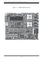
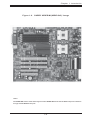
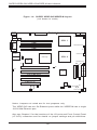
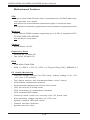
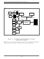
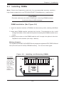
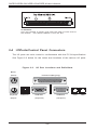
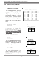
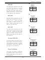
SUPER
®
SUPER X5DE8-GG
SUPER X5DEI-GG
SUPER X5DEE-M
USER’S MANUAL
Revision 1.0b
The information in this User’s Manual has been carefully reviewed and is believed to be
accurate. The vendor assumes no responsibility for any inaccuracies that may be
contained in this document, makes no commitment to update or to keep current the
information in this manual, or to notify any person or organization of the updates.
Please Note: For the most up-to-date version of this manual, please
see our web site at www.supermicro.com.
SUPERMICRO COMPUTER reserves the right to make changes to the product described in
this manual at any time and without notice. This product, including software, if any, and
documentation may not, in whole or in part, be copied, photocopied, reproduced, translated
or reduced to any medium or machine without prior written consent.
IN NO EVENT WILL SUPERMICRO COMPUTER BE LIABLE FOR DIRECT, INDIRECT,
SPECIAL, INCIDENTAL, OR CONSEQUENTIAL DAMAGES ARISING FROM THE USE OR
INABILITY TO USE THIS PRODUCT OR DOCUMENTATION, EVEN IF ADVISED OF THE
POSSIBILITY OF SUCH DAMAGES. IN PARTICULAR, THE VENDOR SHALL NOT HAVE
LIABILITY FOR ANY HARDWARE, SOFTWARE, OR DATA STORED OR USED WITH THE
PRODUCT, INCLUDING THE COSTS OF REPAIRING, REPLACING, INTEGRATING,
INSTALLING OR RECOVERING SUCH HARDWARE, SOFTWARE, OR DATA.
Any disputes arising between manufacturer and customer shall be governed by the laws of
Santa Clara County in the State of California, USA. The State of California, County of
Santa Clara shall be the exclusive venue for the resolution of any such disputes.
Supermicro's total liability for all claims will not exceed the price paid for the hardware
product.
Unless you request and receive written permission from SUPER MICRO COMPUTER,
you may not copy any part of this document.
Information in this document is subject to change without notice. Other products and
companies referred to herein are trademarks or registered trademarks of their respective
companies or mark holders.
Copyright © 2003 by SUPER MICRO COMPUTER INC.
All rights reserved.
Printed in the United States of America
Preface
Preface
About This Manual
This manual is written for system integrators, PC technicians and
knowledgeable PC users. It provides information for the installation and use
of the SUPER X5DE8-GG/X5DEI-GG/X5DEE-M serverboard. The SUPER
X5DE8-GG/X5DEI-GG/X5DEE-M supports single or dual Intel ® 604-pin
Xeon TM processors at a 533/400 MHz front side bus - please refer to the
motherboard specifications pages on our web site ( http://
www.supermicro.com/Product_page/product-m.htm) for updates on supported processors. This product is intended to be professionally installed.
Manual Organization
Chapter 1 begins with a checklist of what should be included in your
mainboard box, describes the features, specifications and performance of
the motherboard and provides detailed information about the chipset.
Chapter 2 begins with instructions on handling static-sensitive devices.
Read this chapter when you want to install the processor and DIMM memory
modules and when mounting the mainboard in the chassis. Also refer to
this chapter to connect the floppy and hard disk drives, SCSI drives, the IDE
interfaces, the parallel and serial ports, the keyboard and mouse, the power
supply and various control panel buttons and indicators.
If you encounter any problems, see Chapter 3, which describes troubleshooting procedures for the video, the memory and the setup configuration
stored in CMOS. For quick reference, a general FAQ [Frequently Asked
Questions] section is provided. Instructions are also included for contacting technical support. In addition, you can visit our web site (at
www.supermicro.com/techsupport.htm) for more detailed information.
Chapter 4 includes an introduction to BIOS and provides detailed information on running the CMOS Setup utility.
Appendix A gives information on BIOS POST messages.
Appendix B provides BIOS POST codes.
iii
SUPER X5DE8-GG/X5DEI-GG/X5DEE-M User's Manual
Table of Contents
Preface
About This Manual ....................................................................................................... iii
Manual Organization .................................................................................................... iii
Chapter 1: Introduction
1-1
Overview ............................................................................................................ 1-1
Checklist .................................................................................................... 1-1
Contacting Supermicro ............................................................................. 1-2
Super X5DE8-GG Image ........................................................................... 1-4
Super X5DEE-M/X5DEI-GG Image .......................................................... 1-5
Super X5DE8-GG Layout ......................................................................... 1-6
Super X5DE8-GG Quick Reference ......................................................... 1-7
Super X5DEI-GG/X5DEE-M Layout ......................................................... 1-8
Super X5DEI-GG/X5DEE-M Quick Reference ........................................ 1-9
Motherboard Features ............................................................................... 1-10
ServerWorks GC-SL Chipset: System Block Diagram ....................... 1-12
1-2
Chipset Overview ............................................................................................ 1-13
1-3
Special Features ............................................................................................ 1-13
ATI Graphics Controller .......................................................................... 1-13
BIOS Recovery ........................................................................................ 1-13
Recovery from AC Power Loss .............................................................. 1-13
1-4
PC Health Monitoring .................................................................................... 1-14
1-5
ACPI Features ............................................................................................... 1-15
1-6
Power Supply ................................................................................................. 1-17
1-7
Super I/O .......................................................................................................... 1-17
Chapter 2: Installation
2-1
Static-Sensitive Devices ................................................................................. 2-1
Precautions ................................................................................................ 2-1
Unpacking .................................................................................................. 2-1
2-2
PGA Processor and Heatsink Installation .................................................... 2-2
2-3
Installing DIMMs .............................................................................................. 2-5
2-4
I/O Ports/Control Panel Connectors .............................................................. 2-6
2-5 Connecting Cables ............................................................................................ 2-8
ATX Power Connector ............................................................................... 2-8
Processor Power Connector .................................................................... 2-8
Power LED ................................................................................................... 2-8
HDD LED ................................................................................................... 2-9
iv
Table of Contents
NIC2 LED ................................................................................................... 2-9
NIC1 LED ................................................................................................... 2-9
Overheat LED (OH) ................................................................................... 2-9
Power Fail Button ....................................................................................... 2-9
Reset Button ........................................................................................... 2-10
Power Button ........................................................................................... 2-10
Chassis Intrusion .................................................................................... 2-10
Universal Serial Bus (USB0/1) .............................................................. 2-10
Extra Universal Serial Bus Headers (USB2/3) .................................... 2-11
Serial Ports ............................................................................................. 2-11
GLAN1/2 (Ethernet Ports) ........................................................................ 2-11
ATX PS/2 Keyboard and Mouse Ports ................................................... 2-11
Fan Headers ............................................................................................ 2-12
Power LED/Speaker Header (JF2) ........................................................ 2-12
Third Power Supply Fail Header .............................................................. 2-12
Wake-On-LAN ............................................................................................ 2-13
2-6
Jumper Settings ............................................................................................. 2-14
Explanation of Jumpers .......................................................................... 2-14
CMOS Clear ............................................................................................ 2-14
VGA Enable/Disable ............................................................................... 2-15
Watch Dog Enable/Disable ...................................................................... 2-15
System Bus Speed ................................................................................... 2-15
OH/Chassis Fan Select ........................................................................... 2-15
SCSI Channel Termination Enable/Disable ............................................ 2-16
SCSI Enable/Disable ................................................................................ 2-16
LAN 1/2 Enable/Disable ......................................................................... 2-15
2-7
DIP Switch Settings ...................................................................................... 2-17
DIP Switch 1: Processor Speed ............................................................. 2-17
2-8
Onboard Indicators ........................................................................................ 2-17
2-9
Parallel Port, Floppy/Hard Disk Drive and SCSI Connections ................. 2-18
GLAN LEDs ............................................................................................... 2-17
Parallel Port Connector .......................................................................... 2-18
Floppy Connector .................................................................................... 2-19
IDE Connectors ....................................................................................... 2-19
Ultra320 SCSI Connectors ....................................................................... 2-20
2-10 Installing Software Drivers ............................................................................ 2-21
v
SUPER X5DE8-GG/X5DEI-GG/X5DEE-M User's Manual
Chapter 3: Troubleshooting
3-1
Troubleshooting Procedures ........................................................................ 3-1
Before Power On .................................................................................... 3-1
No Power .................................................................................................. 3-1
No Video ................................................................................................... 3-1
Memory Errors .......................................................................................... 3-2
Losing the System’s Setup Configuration ........................................... 3-2
3-2
Technical Support Procedures .................................................................... 3-2
3-3
Frequently Asked Questions ........................................................................ 3-3
3-4
Returning Merchandise for Service ............................................................ 3-5
Chapter 4: BIOS
4-1
Introduction ....................................................................................................... 4-1
4-2
BIOS Features .................................................................................................. 4-2
4-3
Running Setup .................................................................................................. 4-2
4-4
Advanced Setup .............................................................................................. 4-4
4-5
Chipset Setup ................................................................................................. 4-15
4-6
PCI PnP Setup ................................................................................................ 4-17
4-7
Power Setup .................................................................................................. 4-19
4-8
Boot Setup ...................................................................................................... 4-20
4-9
Security Setup ............................................................................................... 4-22
4-10 Exit ................................................................................................................... 4-24
Appendices:
Appendix A: BIOS POST Messages ..................................................................... A - 1
Appendix B: BIOS POST Codes ............................................................................. B-1
vi
Chapter 1: Introduction
1-1
Introduction
Chapter 1
Introduction
Overview
Checklist
Congratulations on purchasing your computer motherboard from an acknowledged leader in the industry. Supermicro boards are designed with
the utmost attention to detail to provide you with the highest standards in
quality and performance.
Please check that the following items have been included with your motherboard. If anything listed here is damaged or missing, contact your retailer.
One (1) Supermicro Mainboard
One (1) ribbon cable for IDE devices
One (1) floppy ribbon cable
One (1) USB cable
One (1) COM port (serial) cable
One (1) I/O backpanel shield
One (1) Supermicro CD or diskettes containing drivers and utilities
One (1) User's/BIOS Manual
Two (2) Pentium 4 Xeon active heatsinks (FAN-042, retail only)
Two (2) heatsink retention clip kits (SKT-095-604)
SCSI Accessories (X5DE8-GG only)
One (1) 68-pin LVD Ultra320/160 SCSI cable
One (1) set of SCSI driver diskettes
One (1) SCSI manual
1-1
SUPER X5DE8-GG/X5DEI-GG/X5DEE-M User's Manual
Contacting Supermicro
Introduction
Headquarters
Address:
Tel:
Fax:
Email:
Web Site:
SuperMicro Computer, Inc.
980 Rock Ave.
San Jose, CA 95131 U.S.A.
+1 (408) 503-8000
+1 (408) 503-8008
[email protected] (General Information)
[email protected] (Technical Support)
www.supermicro.com
Europe
Address:
Tel:
Fax:
Email:
SuperMicro Computer B.V.
Het Sterrenbeeld 28, 5215 ML
's-Hertogenbosch, The Netherlands
+31 (0) 73-6400390
+31 (0) 73-6416525
[email protected] (General Information)
[email protected] (Technical Support)
[email protected] (Customer Support)
Asia-Pacific
Address:
SuperMicro, Taiwan
D5, 4F, No. 16 Chien-Ba Road
Chung-Ho 235, Taipei Hsien, Taiwan, R.O.C.
Tel:
+886-(2) 8226-3990
Fax:
+886-(2) 8226-3991
Web Site:
www.supermicro.com.tw
Technical Support:
Email:
[email protected]
Tel:
886-2-8228-1366, ext.132 or 139
1-2
Chapter 1: Introduction
Introduction
Notes
1-3
SUPER X5DE8-GG/X5DEI-GG/X5DEE-M User's Manual
Figure 1-1. SUPER X5DE8-GG Image
Introduction
1-4
Figure 1-2. SUPER X5DEE-M/(X5DEI-GG)* Image
*Note:
The X5DEI-GG has the same basic layout as the X5DEE-M but has two Gb Ethernet ports instead of
a single 10/100 Mb Ethernet port.
1-5
Introduction
Chapter 1: Introduction
SUPER X5DE8-GG/X5DEI-GG/X5DEE-M User's Manual
Introduction
Figure 1-3. SUPER X5DE8-GG Layout
(not drawn to scale)
Keyboard
J11
Mouse
J5
SUPER
ATX PWR CONN
JP2
®
X5DE8-GG
J7
J8
JF2
CPU/Chassis Fan1
USB0/1
COM2
Parallel Port
CPU 1
DIMM 4
COM1
DIMM 3
J9
CPU/Chassis Fan2
DIMM 2
DIMM 1
VGA
JF1
Chassis Fan1
GLAN1
JPL1
GLAN2
CPU 2
North Bridge
ATI
Rage
OH/Chassis Fan3
JP1
JP4
SMB
J10
64-bit 33 MHz PCI #5
64-bit 33 MHz PCI #3
IPMB
Ultra SCSI CH B
33 MHz PCI #2
AIC-7902
33 MHz PCI #1
BIOS
SW1
Battery
Ultra SCSI CH B
JA2
JBT1
WOL
JPA3
Speaker
IDE #1
J19 J18
J12
JA3
JA1
Ultra III LVD SCSI CH A
IPMI
South Bridge
FLOPPY
64-bit 33 MHz PCI #4
IDE #2
JP3
JPL2
USB2/3
JPA2
JPA1
Chassis Fan2
Notes: Jumpers not noted are for test purposes only.
The external SCSI port at JA3 is designed for use with rackmount chassis only.
The JA1 and JA2 ports should be used in tower configurations.
Also see Chapter 2 for the locations of the I/O ports and Front Control Panel (JF1/
JF2) connectors and for details on jumper settings and pin definitions.
1-6
Chapter 1: Introduction
Jumper
JBT1
JF2
JP1
JP2
JP3
JP4
JPA1/JPA2
JPA3
JPL1
JPL2
Description
CMOS Clear
Speaker Enable (page 2-12)
VGA Enable/Disable
Watch Dog Enable/Disable
System (Front Side) Bus Speed
OH/Chassis Fan Select
SCSI CH A/B Termination
SCSI Enable/Disable
LAN1 Enable/Disable
LAN2 Enable/Disable
Default Setting
See Chapter 2
Close 6-7 (Enabled)
Pins 1-2 (Enabled)
Open (Disabled)
Pins 1-2 (Auto MHz)
Open (OH Fan)
Open (Enabled)
Pins 1-2 (Enabled)
Pins 1-2 (Enabled)
Pins 1-2 (Enabled)
Switch
DIP Switch 1
Description
Processor Speed
Connector
ATX PWR CONN
COM1/COM2
CPU/CHS/OH FAN
DIMM1-DIMM4
GLAN1/2
IPMI
J7
J8
J9
J10
J11
J12
J18/19
JA1/JA2
JA3
JF1
JF2
JWOR
USB0/1
USB2/3
WOL
Description
Primary ATX Power Connector
COM1/COM2 Serial Port Connector
CPU/Chassis/Overheat Fan Headers
Memory (RAM) Slots
G-bit Ethernet Ports 1and 2
IPMI 1.5 Slot (for daughter card)
Processor Power Connector
Third Power Supply Fail Header
Parallel (Printer) Port
Chassis Intrusion Header
PS/2 Keyboard/Mouse Ports
Floppy Disk Drive Connector
IDE1/2 Hard Disk Drive Connector
Ultra320 LVD SCSI CH A/B Connector
Ultra SCSI CH B Connector
Front Control Panel Connector
Speaker/PWR LED Headers
Wake-on-Ring Header
Universal Serial Bus Ports
Additional USB Headers
Wake-on-LAN Header
1-7
Introduction
X5DE8-GG Quick Reference
SUPER X5DE8-GG/X5DEI-GG/X5DEE-M User's Manual
Introduction
Figure 1-4. SUPER X5DEI-GG/X5DEE-M Layout
(not drawn to scale)
Keyboard
J11
Mouse
J5
SUPER
ATX PWR CONN
JP2
®
X5DEI-GG
J7
J8
JF2
CPU/Chassis Fan1
USB0/1
DIMM 4
Parallel Port
COM2
COM1
DIMM 3
J9
CPU 1
CPU/Chassis Fan2
DIMM 2
DIMM 1
VGA
JF1
Chassis Fan1
GLAN1
JPL1
GLAN2
CPU 2
North Bridge
ATI
Rage
OH/Chassis Fan3
JP1
JP4
SMB
J10
64-bit 33 MHz PCI #5
64-bit 33 MHz PCI #3
IDE #1
IPMI
South Bridge
FLOPPY
64-bit 33 MHz PCI #4
IDE #2
JP3
JPL2
J19 J18
J12
IPMB
33 MHz PCI #2
33 MHz PCI #1
BIOS
SW1
Battery
WOL
Speaker
JA1
USB2/3
Chassis Fan2
JBT1
Notes: Jumpers not noted are for test purposes only.
The X5DEI-GG has two Gb Ethernet ports while the X5DEE-M has a single
10/100 Mb Ethernet port.
Also see Chapter 2 for the locations of the I/O ports and Front Control Panel
(JF1/JF2) connectors and for details on jumper settings and pin definitions.
1-8
Chapter 1: Introduction
Jumper
JBT1
JF2
JP1
JP2
JP3
JP4
JPL1*
JPL2*
Description
CMOS Clear
Speaker Enable (page 2-12)
VGA Enable/Disable
Watch Dog Enable/Disable
System (Front Side) Bus Speed
OH/Chassis Fan Select
LAN1 Enable/Disable
LAN2 Enable/Disable
Default Setting
See Chapter 2
Close 6-7 (Enabled)
Pins 1-2 (Enabled)
Open (Disabled)
Pins 1-2 (Auto MHz)
Open (OH Fan)
Pins 1-2 (Enabled)
Pins 1-2 (Enabled)
Switch
DIP Switch 1
Description
Processor Speed
Connector
ATX PWR CONN
COM1/COM2
CPU/CHS/OH FAN
DIMM1-DIMM4
GLAN1/2*
IPMI
J7
J8
J9
J10
J11
J12
J18/19
JF1
JF2
USB0/1
USB2/3
WOL
Description
Primary ATX Power Connector
COM1/COM2 Serial Port Connector
CPU/Chassis/Overheat Fan Headers
Memory (RAM) Slots
G-bit Ethernet Ports 1and 2
IPMI 1.5 Slot (for daughter card)
Processor Power Connector
Third Power Supply Fail Header
Parallel (Printer) Port
Chassis Intrusion Header
PS/2 Keyboard/Mouse Ports
Floppy Disk Drive Connector
IDE1/2 Hard Disk Drive Connector
Front Control Panel Connector
Speaker/PWR LED Headers
Universal Serial Bus Ports
Additional USB Headers
Wake-on-LAN Header
*The X5DEI-GG has two Gb Ethernet ports while the X5DEE-M has a single
10/100 Mb Ethernet port.
1-9
Introduction
X5DEI-GG/X5DEE-M* Quick Reference
SUPER X5DE8-GG/X5DEI-GG/X5DEE-M User's Manual
Motherboard Features
CPU
Introduction
• Single or dual Intel® 604-pin Xeon TM processors at a 533/400 MHz front
side (system) bus speed.
Note: Please refer to the motherboard specifications pages on our web site (http://
www.supermicro.com/Product_page/product-m.htm) for updates on supported processors.
Memory
• Four 184-pin DIMM sockets supporting up to 4 GB of registered ECC
PC2100 (DDR-266) SDRAM
Note: See Section 2-3 for details.
Chipset
• ServerWorks GC-SL
Expansion Slots
• Three 64-bit, 33 MHz PCI
• Two 32-bit, 33 MHz PCI
BIOS
• 4 Mb AMI® Flash ROM
• APM 1.2, DMI 2.1, PCI 2.2, ACPI 1.0, Plug and Play (PnP), SMBIOS 2.3
PC Health Monitoring
• Onboard voltage monitors for CPU cores, chipset voltage, 3.3V, +5V,
+12V and 3.3V standby
• Fan status monitor with firmware/software on/off control
• CPU/chassis temperature monitors
• Environmental temperature monitor and control
• CPU fan auto-off in sleep mode
• CPU slow-down on temperature overheat
• CPU overheat LED header
• Power-up mode control for recovery from AC power loss
• Auto-switching voltage regulator for CPU core
• System overheat LED and control
• Chassis intrusion detection
• System resource alert
1-10
Chapter 1: Introduction
ACPI Features (optional)
• Microsoft OnNow
• Main switch override mechanism
Onboard I/O
• AIC-7902 for dual channel Ultra320 SCSI (X5DE8-GG)
• Zero channel SCSI RAID support (X5DE8-GG)
• Integrated ATI Rage XL graphics controller
• Two Intel 82540EM Gb Ethernet controllers (X5DE8-GG, X5DEI-GG)
• One Intel 82551 10/100 Mb Ethernet controller (X5DEE-M)
• 2 EIDE Ultra DMA/100 bus master interfaces
• 1 floppy port interface (up to 2.88 MB)
• 2 Fast UART 16550A compatible serial ports
• 1 EPP/ECP Parallel Port
• PS/2 mouse and PS/2 keyboard ports
• Up to 4 USB 1.1 (Universal Serial Bus) ports
Other
• Internal/external modem ring-on
• Wake-on-LAN (WOL)
• Console redirection
• IPMI (optional)
CD/Diskette Utilities
• BIOS flash upgrade utility and device drivers
Dimensions
• Extended ATX: 12" x 13.05" (304.8 x 331.5 mm)
1-11
Introduction
• Slow blinking LED for suspend state indicator
SUPER X5DE8-GG/X5DEI-GG/X5DEE-M User's Manual
Introduction
32-bit/33 MHz PCI
ATI XL
VGA
LAN
Processor 1
Processor 0
64-bit/33 MHz PCI
SCSI
533/400 MHz Host Bus
PCI Bus
ATA 100
Ports
USB
Ports
SMBus
Serial
Port
Thin IMB
North Bridge
(CMIC-SL)
CSB6
LPC Bus
DDR-266 SDRAM
SIO
Parallel
Port
Floppy
Port
Figure 1-5.
ServerWorks Grand Champion SL Chipset:
System Block Diagram
Note: This is a general block diagram. Please see the previous Motherboard
Features Section for details on the features of each motherboard.
1-12
Chapter 1: Introduction
Chipset Overview
The Grand Champion SL TM is a fourth-generation product of ServerWorks
"Champion" chipset technology. The chipset for the X5DE8-GG/X5DEI-GG/
X5DEE-M is comprised of a North Bridge (CMIC-SL) and a South Bridge
(CSB6).
The North Bridge interfaces directly to the processors via a 100 MHz Host
bus and integrates the functions of the main memory subsystem and the
IMB bus interface unit. The memory subsystem consists of a 4-DIMM configuration accessed over a 266 MHz memory bus at a peak bandwidth of
1.6 GB/sec.
The South Bridge provides various integrated functions, including the PCI
bridge and support for UDMA100, security (passwords and system protection), Plug & Play, USBs, power management, interrupt controllers and the
LPC Bus.
1-3
Special Features
ATI Graphics Controller
The X5DE8-GG/X5DEI-GG/X5DEE-M has an integrated ATI video controller
based on the Rage XL graphics chip. The Rage XL fully supports sideband
addressing and AGP texturing. This onboard graphics package can provide
a bandwidth of up to 512 MB/sec over a 32-bit graphics memory bus.
BIOS Recovery
The BIOS Recovery function allows you to recover your BIOS image file if
the BIOS flashing procedure fails (see Section 3-3).
Recovery from AC Power Loss
BIOS provides a setting for you to determine how the system will respond
when AC power is lost and then restored to the system. You can choose
for the system to remain powered off (in which case you must hit the
power switch to turn it back on) or for it to automatically return to a power-
1-13
Introduction
1-2
SUPER X5DE8-GG/X5DEI-GG/X5DEE-M User's Manual
on state. See the Power Lost Control setting in the Advanced BIOS Setup
section (Peripheral Device Configuration) to change this setting. The default setting is Always On.
Introduction
1-4
PC Health Monitoring
This section describes the PC health monitoring features of the SUPER
X5DE8-GG/X5DEI-GG/X5DEE-M. All have an onboard System Hardware
Monitor chip that supports PC health monitoring.
Onboard Voltage Monitors for the CPU Cores, Chipset
Voltage, +3.3V, +5V, +12V and +3.3V Standby
An onboard voltage monitor will scan these voltages continuously. Once a
voltage becomes unstable, a warning is given or an error message is sent
to the screen. Users can adjust the voltage thresholds to define the
sensitivity of the voltage monitor.
Fan Status Monitor with Firmware/Software On/Off Control
The PC health monitor can check the RPM status of the cooling fans. The
onboard 3-pin CPU and chassis fans are controlled by the power management functions. The thermal fan is controlled by the overheat detection
logic.
Environmental Temperature Control
The thermal control sensor monitors the CPU temperature in real time and
will turn on the thermal control fan whenever the CPU temperature exceeds
a user-defined threshold. The overheat circuitry runs independently from
the CPU. It can continue to monitor for overheat conditions even when the
CPU is in sleep mode. Once it detects that the CPU temperature is too high,
it will automatically turn on the thermal control fan to prevent any overheat
damage to the CPU. The onboard chassis thermal circuitry can monitor the
overall system temperature and alert users when the chassis temperature
is too high.
CPU Fan Auto-Off in Sleep Mode
The CPU fan activates when the power is turned on. It continues to operate
when the system enters Standby mode. When in sleep mode, the CPU will
not run at full power, thereby generating less heat.
1-14
Chapter 1: Introduction
This feature is available when the user enables the CPU overheat warning
function in the BIOS. This allows the user to define an overheat temperature. When this temperature is exceeded, both the overheat fan and the
warning LED are triggered.
System Resource Alert
This feature is available when used with Intel's LANDesk Client Manager
(optional). LDCM is used to notify the user of certain system events. For
example, if the system is running low on virtual memory and there is insufficient hard drive space for saving the data, you can be alerted of the
potential problem.
Auto-Switching Voltage Regulator for the CPU Core
The auto-switching voltage regulator for the CPU core can support up to
20A current and auto-sense voltage IDs ranging from 1.4V to 3.5V. This
will allow the regulator to run cooler and thus make the system more stable.
1-5 ACPI Features
ACPI stands for Advanced Configuration and Power Interface. The ACPI
specification defines a flexible and abstract hardware interface that provides a standard way to integrate power management features throughout
a PC system, including its hardware, operating system and application software. This enables the system to automatically turn on and off peripherals
such as CD-ROMs, network cards, hard disk drives and printers. This also
includes consumer devices connected to the PC such as VCRs, TVs, telephones and stereos.
In addition to enabling operating system-directed power management, ACPI
provides a generic system event mechanism for Plug and Play and an operating system-independent interface for configuration control. ACPI leverages the Plug and Play BIOS data structures while providing a processor
architecture-independent implementation that is compatible with both Windows 2000 and Windows NT 5.0.
1-15
Introduction
CPU Overheat LED and Control
SUPER X5DE8-GG/X5DEI-GG/X5DEE-M User's Manual
Microsoft OnNow
Introduction
The OnNow design initiative is a comprehensive, system-wide approach to
system and device power control. OnNow is a term for a PC that is always
on but appears to be off and responds immediately to user or other requests.
Slow Blinking LED for Suspend-State Indicator
When the CPU goes into a suspend state, the chassis power LED will start
blinking to indicate that the CPU is in suspend mode. When the user presses
any key, the CPU will wake-up and the LED will automatically stop blinking
and remain on.
Main Switch Override Mechanism
When an ATX power supply is used, the power button can function as a
system suspend button to make the system enter a SoftOff state. The
monitor will be suspended and the hard drive will spin down. Depressing
the power button again will cause the whole system to wake-up. During
the SoftOff state, the ATX power supply provides power to keep the required circuitry in the system alive. In case the system malfunctions and
you want to turn off the power, just depress and hold the power button for
4 seconds. This option can be set in the Power section of the BIOS Setup
routine.
External Modem Ring-On
Wake-up events can be triggered by a device such as the external modem
ringing when the system is in the SoftOff state. Note that external modem
ring-on can only be used with an ATX 2.01 (or above) compliant power
supply.
Wake-On-LAN (WOL)
Wake-On-LAN is defined as the ability of a management application to remotely power up a computer that is powered off. Remote PC setup, updates and asset tracking can occur after hours and on weekends so that
daily LAN traffic is kept to a minimum and users are not interrupted. The
motherboards have a 3-pin header (WOL) to connect to the 3-pin header on
1-16
Chapter 1: Introduction
1-6
Power Supply
As with all computer products, a stable power source is necessary for
proper and reliable operation. It is even more important for processors that
have high CPU clock rates.
The SUPER X5DE8-GG/X5DEI-GG/X5DEE-M accommodates ATX power supplies. Although most power supplies generally meet the specifications required by the CPU, some are inadequate. You should use one that will
supply at least 400W of power and includes the additional +12V, 8-pin
power connector - an even higher wattage power supply is recommended
for high-load configurations. Also your power supply must supply 1.5A for
the LAN port(s).
NOTE: Auxiliary 12v power (J15) is necessary to support Intel Xeon
CPUs. Failure to provide this extra power will result in the CPUs
becoming unstable after only a few minutes of operation. See
Section 2-5 for details on connecting the power supply cables.
It is strongly recommended that you use a high quality power supply that
meets ATX power supply Specification 2.02 or above. It must also be SSI
compliant (info at http://www.ssiforum.org/). Additionally, in areas where
noisy power transmission is present, you may choose to install a line filter
to shield the computer from noise. It is recommended that you also install a
power surge protector to help avoid problems caused by power surges.
1-7
Super I/O
The disk drive adapter functions of the Super I/O chip include a floppy disk
drive controller that is compatible with industry standard 82077/765, a data
separator, write pre-compensation circuitry, decode logic, data rate selection, a clock generator, drive interface control logic and interrupt and DMA
logic. The wide range of functions integrated onto the Super I/O greatly
reduces the number of components required for interfacing with floppy disk
drives. The Super I/O supports 360 K, 720 K, 1.2 M, 1.44 M or 2.88 M disk
drives and data transfer rates of 250 Kb/s, 500 Kb/s or 1 Mb/s.It also
provides two high-speed, 16550 compatible serial communication ports
1-17
Introduction
a Network Interface Card (NIC) that has WOL capability. Wake-On-LAN
must be enabled in BIOS. Note that Wake-On-Lan can only be used with an
ATX 2.01 (or above) compliant power supply.
SUPER X5DE8-GG/X5DEI-GG/X5DEE-M User's Manual
Introduction
(UARTs), one of which supports serial infrared communication. Each UART
includes a 16-byte send/receive FIFO, a programmable baud rate generator,
complete modem control capability and a processor interrupt system. Both
UARTs provide legacy speed with baud rate of up to 115.2 Kbps as well as
an advanced speed with baud rates of 250 K, 500 K, or 1 Mb/s, which
support higher speed modems.
The Super I/O supports one PC-compatible printer port (SPP), Bi-directional
Printer Port (BPP) , Enhanced Parallel Port (EPP) or Extended Capabilities
Port (ECP).
The Super I/O provides functions that comply with ACPI (Advanced Configuration and Power Interface), which includes support of legacy and ACPI
power management through an SMI or SCI function pin. It also features
auto power management to reduce power consumption.
The IRQs, DMAs and I/O space resources of the Super I/O can flexibly
adjust to meet ISA PnP requirements, which suppport ACPI and APM (Advanced Power Management).
1-18
Chapter 2: Installation
Chapter 2
Installation
2-1
Static-Sensitive Devices
Electric-Static-Discharge (ESD) can damage electronic components. To prevent damage to your system board, it is important to handle it very carefully.
The following measures are generally sufficient to protect your equipment
from ESD.
Precautions
• Use a grounded wrist strap designed to prevent static discharge.
• Touch a grounded metal object before removing the board from the antistatic bag.
• Handle the board by its edges only; do not touch its components, peripheral chips, memory modules or gold contacts.
• When handling chips or modules, avoid touching their pins.
• Put the motherboard and peripherals back into their antistatic bags when
not in use.
• For grounding purposes, make sure your computer chassis provides excellent conductivity between the power supply, the case, the mounting
fasteners and the motherboard.
Unpacking
The motherboard is shipped in antistatic packaging to avoid static damage.
When unpacking the board, make sure the person handling it is static protected.
2-1
SUPER X5DE8-GG/X5DEI-GG/X5DEE-M User's Manual
2-2
PGA Processor and Heatsink Installation
!
When handling the processor package, avoid placing direct
pressure on the label area of the fan. Also, do not place the
motherboard on a conductive surface, which can damage the
BIOS battery and prevent the system from booting up.
IMPORTANT: Always connect the power cord last and always remove it
before adding, removing or changing any hardware components. Make
sure that you install the processor into the CPU socket before you install
the CPU heat sink. (The pictures below show a 603-pin socket.)
1. Locate the following components, which are included in the shipping
package.
Clips (2)
Screws* (4)
Retention brackets
(2)
Black anchors (4)
White pegs (4)
*These screws are for mounting the
motherboard to the back panel of a
chassis that has four mounting holes
(as shown on right).
For chassis that do not have four
mounting holes, use the anchor/peg
assemblies:
2. Insert the white pegs into the
black anchors. Do not force the
white pegs all the way in - only
about 1/3 of the way into the black
anchors.
3. Place a retention bracket in the
proper position and secure it by
pressing pegs into two of the retention
holes until you hear a *click*. The
clicking sound indicates that the peg is
locked and secured.
2-2
Anchor/peg
assemblies
Two pegs in
position
One retention bracket in
position
Chapter 2: Installation
4. Secure the other retention
bracket into position by
repeating Step 3.
5. Lift the lever on the CPU socket:
lift the lever completely or you will
damage the CPU socket when
power is applied. (Install CPU1
first.)
Socket lever
6. Insert the CPU in the socket, making sure
that pin 1 of the CPU aligns with pin 1 of the
socket (both corners are marked with a
Triangles
triangle - see Figure 2-1). When using only
one CPU, install it into CPU socket #1 (socket
#2 is automatically disabled if only one CPU is
used).
7. Press the lever down until
you hear it *click* into the
locked position.
Socket lever in
locked position
Heatsink
8. Apply the proper amount of thermal
compound to the CPU die and place
the heatsink and fan on top of the
CPU.
CPU
9. Secure the heatsink by locking the
retention clips into their proper
position.
Retention clip
CPU fan
wires
10. Connect the three wires of
the CPU fan to the respective CPU
fan connector.
CPU fan
connector
2-3
SUPER X5DE8-GG/X5DEI-GG/X5DEE-M User's Manual
Figure 2-1. PGA604 Socket: Empty and with Processor Installed
Empty socket
Lever
!
Warning!
Make
sure you lift the
lever completely
when installing the
CPU. If the lever is
only partly raised,
damage to the
socket or CPU may
result.
Triangle
Processor
(installed)
Triangle
Mounting the Motherboard in the Chassis
All motherboards have standard mounting holes to fit different types of
chassis. Make sure the location of all the mounting holes for both the
motherboard and the chassis match. Although a chassis may have both
plastic and metal mounting fasteners, metal ones are highly recommended
because they ground the motherboard to the chassis. Make sure the metal
standoffs click in or are screwed in tightly. Then use a screwdriver to
secure the motherboard onto the motherboard tray.
2-4
Chapter 2: Installation
2-3
Installing DIMMs
Note: Check the Supermicro web site for recommended memory modules:
http://www.supermicro.com/TECHSUPPORT/FAQs/Memory_vendors.htm
CAUTION
Exercise extreme care when installing or removing DIMM modules
to prevent any possible damage.
DIMM Installation (See Figure 2-2)
1. Insert the desired number of DIMMs into the memory slots, starting with Bank
1.
2. Insert each DIMM module vertically into its slot. Pay attention to the notch
along the bottom of the module to prevent inserting the DIMM module incorrectly.
3. Gently press down on the DIMM module until it snaps into place in the slot.
Repeat for all modules (see step 1 above).
Memory Support
The X5DE8-GG/X5DEI-GG/X5DEE-M only supports registered ECC DDR-266 and
200 (PC2100 and PC1600) SDRAM memory. Do not mix both types.
Figure 2-2.
Installing and Removing DIMMs
To Install:
Insert module
vertically and
press down
until it snaps
into place.
Pay attention
to the
alignment
notch at the
bottom.
2-5
SUPER X5DE8-GG/X5DEI-GG/X5DEE-M User's Manual
To Remove:
Use your thumbs to gently push near the edge of both ends of
the module. This should release it from the slot.
2-4
I/OPorts/Control Panel Connectors
The I/O ports are color coded in conformance with the PC 99 specification.
See Figure 2-3 below for the colors and locations of the various I/O ports.
Figure 2-3.
I/O Port Locations and Definitions
Mouse
Parallel Port (Burgundy)
(Green)
Keyboard
(Purple)
USB Ports
COM1 Port
COM2 Port
(Turquoise)
(Turquoise)
2-6
LAN1
LAN2
Chapter 2: Installation
Front Control Panel
JF1 contains header pins for various buttons and indicators that are normally located on a control panel at the front of the chassis. These connectors are designed specifically for use with Supermicro server chassis. See
Figure 2-4 for the descriptions of the various control panel buttons and LED
indicators. Refer to the following section for descriptions and pin definitions.
Figure 2-4.
JF1 Header Pins
20
19
NMI
Ground
X
X
Power LED
Vcc
HDD LED
Vcc
NIC2 LED
Vcc
NIC1 LED
Vcc
Overheat LED
Vcc
Power Fail Button
Vcc
Ground
Ground
2
1
2-7
Reset
Reset Button
Pwr
Power Button
SUPER X5DE8-GG/X5DEI-GG/X5DEE-M User's Manual
2-5
Connecting Cables
ATX Power Connector
The main power supply connector
on the X5DE8-GG/X5DEI-GG/
X5DEE-M meets the SSI (Superset
ATX) 24-pin specification, however it also supports a 20-pin
power supply connector. Make
sure that the orientation of the
connector is correct.
See the
table on the right for pin definitions.
ATX Power Supply 24-pin Connector
Pin Definitions
Pin Number
13
14
15
16
17
18
19
20
21
22
23
24
Definition
+3.3V
-12V
COM
PS_ON#
COM
COM
COM
Res(NC)
+5V
+5V
+5V
COM
Pin Number Definition
1
+3.3V
2
+3.3V
3
COM
4
+5V
5
COM
6
+5V
7
COM
8
PW R_OK
9
5VSB
10
+12V
11
+12V
12
+3.3V
Processor Power
Connector
8-Pin +12v Power Supply
Connector (J7)
In addition to the Primary ATX
power connector (above), the 12v
8-pin Processor connector at J7
must also be connected to your
power supply. See the table on
the right for pin definitions.
Pins
Definition
1 thru 4
5 thru 8
Ground
+12v
NMI Button
The non-maskable interrupt button
header is located on pins 19 and
20 of JF1. Refer to the table on
the right for pin definitions.
NMI Button Pin
Definitions (JF1)
Pin
Definition
Number
Ground
19
Control
20
Power LED
The Power LED connection is located on pins 15 and 16 of JF1.
Refer to the table on the right for
pin definitions.
2-8
PW R_LED Pin Definitions
(JF1)
Pin
Definition
Number
Vcc
15
Control
16
Chapter 2: Installation
HDD LED
The HDD LED connection (for IDE
and SCSI Disk Drives) is located
on pins 13 and 14 of JF1. Attach
the hard drive LED cable here to
display disk activity. See the table
on the right for pin definitions.
NIC2 LED
HDD L ED Pin
Definitions
(JF 1)
Pin
Number Definition
13
Vcc
14
HD Active
N IC2 LED Pin
Definitions
(JF1)
The NIC LED connection for the
LAN2 port is located on pins 11
and 12 of JF1. Attach the LAN2
LED cable to display network activity. Refer to the table on the
right for pin definitions.
NIC1 LED
Pin
Number Definition
11
Vcc
12
GN D
N IC1 LED Pin
Definitions
(JF1)
The NIC LED connection for the
LAN1 port is located on pins 9 and
10 of JF1. Attach the LAN1 LED
cable to display network activity.
Refer to the table on the right for
pin definitions.
Pin
Number Definition
Vcc
9
GN D
10
Overheat LED (OH)
Connect an LED to the OH connection on pins 7 and 8 of JF1 to provide advanced warning of chassis
overheating. Refer to the table on
the right for pin definitions.
Power Fail Button
Overheat (OH) LED
Pin Definitions
(JF 1)
Pin
Number Definition
7
Vcc
8
GND
Power Fail Button
Pin Definitions
(JF 1)
The Power Fail Button connection
is located on pins 5 and 6 of JF1.
Refer to the table on the right for
pin definitions.
2-9
Pin
Number Definition
Vcc
5
GND
6
SUPER X5DE8-GG/X5DEI-GG/X5DEE-M User's Manual
Reset Button
Reset Pin
Definitions
(JF 1)
The Reset Button connection is located on pins 3 and 4 of JF1. Attach it to the hardware reset
switch on the computer case.
Refer to the table on the right for
pin definitions.
Pin
Number Definition
Reset
3
Ground
4
Power Butto n
Connector
Pin Definitions
(JF1)
Power Button
The Power Button connection is
located on pins 1 and 2 of JF1.
Momentarily contacting both pins
will power on/off the system. This
button can also be configured to
function as a suspend button
(with a setting in BIOS - see Chapter 4). To turn off the power
when set to suspend mode, depress the button for at least 4
seconds. Refer to the table on the
right for pin definitions.
Pin
Number Definition
PW _O N
1
Ground
2
Chassis Intrusion
A Chassis Intrusion header is located at J10. Attach the appropriate cable to inform you of a chassis intrusion.
Universal Serial Bus
(USB0/1)
Universal Serial Bus Pin Definitions
USB0
Two USB ports are located beside
the PS/2 keyboard/mouse ports.
USB0 is the bottom connector and
USB1 is the top connector. See
the table on the right for pin definitions.
2-10
Pin
Number
1
2
3
4
5
USB1
Pin
Definition Number
+5V
1
P02
P0+
3
Ground 4
N/A
5
Definition
+5V
P0P0+
Ground
Key
Chapter 2: Installation
Extra Universal Serial Bus
Headers
Front Panel Universal Serial Bus Pin
Definitions
FPUSB0/FPUSB2
Two additional USB headers
(USB2/USB2) have been included
on your motherboard. You will
need a USB cable to use either
connection. Refer to the tables on
the right for pin definitions.
Pin
Number
1
2
3
4
5
FPUSB1/FPUSB3
Pin
Definition Number
+5V
1
P02
P0+
3
Ground 4
N/A
5
Definition
+5V
P0P0+
Ground
Key
Serial Ports
The COM1 serial port is located
under the parallel port (see Figure
2-3). COM2 is a header on the
motherboard near the DIMM 4 slot.
See the table on the right for pin
definitions.
Serial Port Pin Definitions
(COM1, COM2)
Pin Number
1
2
3
4
5
Definition Pin Number
DCD
6
DSR
7
Serial In
8
RTS
9
Serial Out
10
GLAN 1/2 (Ethernet Ports)
Two G-bit Ethernet ports (designated GLAN1 and GLAN2) are located beside the VGA port on the
IO backplane. These ports accepts RJ45 type cables.
Note: the X5DEE-M has a single
10/100 Mb port only.
ATX PS/2 Keyboard and
PS/2 Mouse Ports
PS/2 Keyboard
and Mouse Port
Pin Definitions
(J11)
The ATX PS/2 keyboard and PS/2
mouse are located on J11. See
the table at right for pin definitions.
(See Figure 2-3 for the locations
of each.)
2-11
Pin
Number Definition
Data
1
NC
2
Ground
3
VCC
4
Clock
5
NC
6
Definition
CTS
DTR
RI
G round
NC
SUPER X5DE8-GG/X5DEI-GG/X5DEE-M User's Manual
Fan Headers
The X5DE8-GG/X5DEI-GG/X5DEEM has five fan headers, which are
designated CPU Chassis Fan1,
CPU Chassis Fan2, Chassis Fan1,
Chassis Fan2 and Overheat/Chassis Fan3. See the table on the
right for pin definitions.
Fan H eader Pin Definitions
Pin
Number
1
2
3
Definition
Ground (black)
+12V (red)
Tachometer
Caution: Fan headers are DC
power.
Power LED/Speaker (JF2)
Speaker Co nnector Pin
Definitio ns (JF2)
On the JF2 header, pins 1-3 are
for the PWR LED and pins 4-7 are
for the speaker connection. See
the table on the right for speaker
pin definitions. Note: The speaker
connector pins are for use with an
external speaker. If you wish to
use the onboard speaker, you
should close pins 6-7 with a
jumper.
Pin
Number Function
Definition
6
+
R ed wire, Speaker data
7
Key
No connection
8
Key
9
Speaker data
Third Power Supply Fail
Header
Connect a cable from your power
supply to the J8 header to provide
warning of power supply failure.
This warning signal is passed
through the PWR_LED pin on JF2
to indicate a power failure on the
chassis. See the table on the right
for pin definitions.
2-12
T hird Power Sup ply Fail Header
Pin Definitions (J8)
Pin
Number
1
2
3
4
Definition
P/S 1 Fail Signal
P/S 2 Fail Signal
P/S 3 Fail Signal
R eset (from MB)
Note: This feature is only available when using
redundant Supermicro power supplies.
Chapter 2: Installation
Wake-On-LAN
The Wake-On-LAN header is designated WOL. See the table on the
right for pin definitions. You must
enable the LAN Wake-Up setting in
BIOS to use this feature. You
must also have a LAN card with a
Wake-on-LAN connector and
cable.
2-13
W ake-On-LAN Pin
Definitions (W OL)
Pin
Number
1
2
3
Definition
+5V Standby
Ground
W ake-up
SUPER X5DE8-GG/X5DEI-GG/X5DEE-M User's Manual
2-6
Jumper Settings
Explanation of
Jumpers
Connector
Pins
To modify the operation of the
motherboard, jumpers can be used
to choose between optional
settings. Jumpers create shorts
between two pins to change the
function of the connector. Pin 1 is
identified with a square solder pad
on the printed circuit board. See
the motherboard layout pages for
jumper locations.
No te : On two pin jumpers,
"Closed" means the jumper is on
and "Open" means the jumper is
2
1
3
2
1
Jumper
Cap
Setting
off the pins.
CMOS Clear
JBT1 is used to clear CMOS. Instead of pins, this
jumper consists of contact pads to prevent accidentally clearing the contents of CMOS.
To clear CMOS,
1) First shut down the system and unplug the power
cord(s).
2) With the power disconnected, short the CMOS pads
with a metal object such as a small screwdriver.
3) Remove the screwdriver (or shorting device).
4) Reconnect the power cord(s) and power on the system.
Note: Do not use the PW_ON connector to clear
CMOS.
2-14
3
Pin 1-2 short
Chapter 2: Installation
VGA Enable/Disable
VGA Enable/Disable
Jumper Settings
(JP1)
JP1 allows you to enable or disable the VGA port. The default
position is on pins 1 and 2 to enable VGA. See the table on the
right for jumper settings.
Watch Dog Enable/Disable
Use JP2 to enable or disable the
Watch Dog feature. The default position is open to disable it. When
enabled, Watch Dog can reboot
your PC if an application is "hung
up" or the system goes down. See
the table on the right for jumper settings.
Jumper
Position
1-2
2-3
Definition
Enabled
Disabled
W atch Dog T imer Enable/
Disable Jumper Settings
(JP2)
Jumper
Position
Open
Closed
Definition
Disabled
Enabled
System Bus Speed
System Bus Speed
Jumper Settings (JP39)
JP3 allows you to select the system
(front side) bus speed to 400 MHz,
533 MHz or Auto. The speed you
select must conform to that of your
processor(s). "Auto" is the default
setting and will allow BIOS to determine and set the system bus speed.
See the table on the right for jumper
settings.
OH/Chassis Fan Select
JP4 allows you to select the function of the OH/Chassis Fan: either
as an overheat fan or as a chassis
fan. The default position is open to
use as an overheat fan. See the
table on the right for jumper settings.
2-15
Jumper
Position
Pins 1-2
Pins 2-3
Off
Definition
Auto
400 MHz
533 Mhz
Overheat/Chassis Fan
Select Jumper Settings
(JP4)
Jumper
Position
Open
Closed
Definition
Overheat Fan
Chassis Fan
SUPER X5DE8-GG/X5DEI-GG/X5DEE-M User's Manual
SCSI Channel Termination
Enable/Disable (X5DE8-GG)
Jumpers JPA1 and JPA2 allow you to
enable or disable termination for each
SCSI channel. Jumper JPA1 controls
channel A and JPA2 controls channel
B. The default setting is open to enable (teminate) both SCSI channels.
If you wish to connect external SCSI
devices, you should disable termination for the channel(s) you will be connecting them to. Note that the external SCSI port is for use with
rackmount chassis only. See the
table on the right for jumper settings.
SCSI Enable/Disable
(X5DE8-GG)
SCSI Channel T ermination
Enable/Disable
Jumper Settings
(JPA1, JPA2)
Jumper
Position
Open
Closed
Definition
Enabled
Disabled
SCSI Enable/Disable
Jumper Settings
(JPA3)
The SCSI Termination jumper at
JPA3 allows you to enable or disable the onboard SCSI controller.
The normal (default) position is on
pins 1-2 to enable (terminate) the
onboard SCSI. See the table on
the right for jumper settings.
Jumper
Position
Pins 1-2
Pins 2-3
Definition
Enabled
Disabled
LAN1/2
Enable/Disable
Jumper Settings
(JPL1, JPL2)
LAN1/2 Enable/Disable
Change the setting of jumper JPL1
(for LAN1) or JPL2 (for LAN2) to
enable or disable the Ethernet
ports on the motherboard. See the
table on the right for jumper settings. The default setting is enabled.
Note: the X5DEE-M has a single
LAN port and thus a single jumper.
2-16
Jumper
Position
Pins 1-2
Pins 2-3
Definition
Enabled
Disabled
Chapter 2: Installation
2-7
DIP Switch Settings
DIP Switch 1:
Processor Speed
The red "DIP" switch labeled SW1
has four individual switches,
which are used to set the speed
of the processor.
The table on the right shows you
the switch settings for the various
speeds your processor may be
able to run at. (This table is also
silkscreened on the motherboard.)
Note: Most Intel processors have
a fixed Core/Bus ratio that overwrites the setting of DIP Switch 1.
2-8
Processor Speed Selection
(DIP S witch 1)
CPU
SW SW SW SW
#1 #2 #3 #4
1.3 GHz ON
ON
1.4 GHz
ON ON
1.5 GHz ON ON ON
1.6 GHz
ON
1.7 GHz ON
ON
1.8 GHz
ON
ON
1.9 GHz ON ON
ON
2.0 GHz
ON ON < Default
2.1 GHz ON
ON ON
2.2 GHz
ON ON ON
2.4 GHz ON ON ON ON
Onboard Indicators
GLAN LEDs (X5DE8-GG,
X5DEI-GG)
1 Gb LAN Right LED
Indicator
The Gb Ethernet LAN ports (located beside the VGA port) has
two LEDs. The yellow LED indicates activity while the other LED
may be green, orange or off to indicate the speed of the connection. See the table at right for the
functions associated with the second LED.
2-17
LED
Color
Off
Green
Orange
Definition
No Connection
100 MHz
1 GHz
SUPER X5DE8-GG/X5DEI-GG/X5DEE-M User's Manual
2-9 Parallel Port, Floppy/Hard Disk Drive and SCSI
Connections
Note the following when connecting the floppy and hard disk drive cables:
• The floppy disk drive cable has seven twisted wires.
• A red mark on a wire typically designates the location of pin 1.
• A single floppy disk drive ribbon cable has 34 wires and two connectors to
provide for two floppy disk drives. The connector with twisted wires always
connects to drive A, and the connector that does not have twisted wires
always connects to drive B.
Parallel (Printer) Port
Connector
Parallel (Printer) Port Pin Definitio ns
(J9)
The parallel (printer) port is located on J9. See the table on the
right for pin definitions.
2-18
Pin Number
1
3
5
7
9
11
13
15
17
19
21
23
25
Function Pin Number Function
Strobe2
Auto FeedData Bit 0
4
ErrorData Bit 1
6
InitData Bit 2
8
SLCT INData Bit 3
10
GND
Data Bit 4
12
GND
Data Bit 5
14
GND
Data Bit 6
16
GND
Data Bit 7
18
GND
ACK
20
GND
BUSY
22
GND
PE
24
GND
SLCT
26
NC
Chapter 2: Installation
Floppy Connector
The floppy connector is located
on JP12. See the table below for
pin definitions.
Floppy Connector Pin Definitions (JP12)
Pin Number
1
3
5
7
9
11
13
15
17
19
21
23
25
27
29
31
33
Function
GND
GND
Key
GND
GND
GND
GND
GND
GND
GND
GND
GND
GND
GND
GND
GND
GND
IDE Connectors
There are no jumpers to
configure the onboard IDE#1
and #2 connectors (at J18
and J19, respectively). See
the table on the right for pin
definitions.
Pin Number
Function
2
FDHDIN
4
Reserved
6
FDEDIN
8
Index10
M otor Enable
12
D rive Select B14
D rive Select A16
M otor Enable
18
DIR20
STEP22
W rite Data24
W rite Gate26
Track 0028
W rite Protect30
Read Data32
Side 1 Select34
Diskette
IDE Connector Pin Definitions
(J18, J19)
Pin Number
1
3
5
7
9
11
13
15
17
19
21
23
25
27
29
31
33
35
37
39
2-19
Function
Reset IDE
Host Data 7
Host Data 6
Host Data 5
Host Data 4
Host Data 3
Host Data 2
Host Data 1
Host Data 0
GND
DRQ3
I/O W riteI/O ReadIOCHRDY
DACK3IRQ14
Addr 1
Addr 0
Chip Select 0
Activity
Pin Number
2
4
6
8
10
12
14
16
18
20
22
24
26
28
30
32
34
36
38
40
Function
G ND
Host Data 8
Host Data 9
Host Data 10
Host Data 11
Host Data 12
Host Data 13
Host Data 14
Host Data 15
Key
G ND
G ND
G ND
BALE
G ND
IOC S16G ND
Addr 2
Chip Select 1G ND
SUPER X5DE8-GG/X5DEI-GG/X5DEE-M User's Manual
Ultra320 SCSI
Connectors (X5DE8-GG)
Refer to the table below for the
pin definitions of the Ultra320 SCSI
connectors located at JA1 and
JA2.
68-pin Ultra320/160 SCSI Connectors (JA1, JA2)
Connector
Contact
Number
1
2
3
4
5
6
7
8
9
10
11
12
13
14
15
16
17
18
19
20
21
22
23
24
25
26
27
28
29
30
31
32
33
34
Signal Names
Connector
Contact
Number
Signal Names
+D B(12)
+D B(13)
+D B(14)
+D B(15)
+D B(P1)
+DB(0)
+DB(1)
+DB(2)
+DB(3)
+DB(4)
+DB(5)
+DB(6)
+DB(7)
+DB(P)
GR OUND
DIF FSENS
TER MPW R
TER MPW R
RESERVED
GR OUND
+ATN
GR OUND
+BSY
+ACK
+RST
+MSG
+SEL
+C/D
+REQ
+I/O
+DB(8)
+DB(9)
+D B(10)
+D B(11)
35
36
37
38
39
40
41
42
43
44
45
46
47
48
49
50
51
52
53
54
55
56
57
58
59
60
61
62
63
64
65
66
67
68
-DB(12)
-DB(13)
-DB(14)
-DB(15)
-DB(P1)
-DB(0)
-DB(1)
-DB(2)
-DB(3)
-DB(4)
-DB(5)
-DB(6)
-DB(7)
-DB(P)
GROUND
GROUND
TERMPW R
TERMPW R
RESERVED
GROUND
-ATN
GROUND
-BSY
-ACK
-RST
-MSG
-SEL
-C/D
-REQ
-I/O
-DB(8)
-DB(9)
-DB(10)
-DB(11)
2-20
Chapter 2: Installation
2-10 Installing Software Drivers
After all the hardware has been installed you must install the software
drivers. The necessary drivers are all included on the Supermicro CD that
came packaged with your motherboard. After inserting this CD into your
CD-ROM drive, the display shown in Figure 2-5 should appear. (If this
display does not appear, click on the My Computer icon and then on the icon
representing your CD- ROM drive. Finally, double click on the S "Setup"
icon.)
Figure 2-5.
Driver/Tool Installation Display Screen
Click the icons showing a hand writing on paper to view the readme files
for each item. The bottom icon with a CD on it allows you to view the
entire contents of the CD.
2-21