1
DSP56012UM/D
Rev. 0
Published 11/98
DSP56012
24-Bit Digital Signal Processor
User’s Manual
Motorola, Incorporated
Semiconductor Products Sector
DSP Division
6501 William Cannon Drive West
Austin, TX 78735-8598
DSP56012UM/D
Rev. 0
Published 11/98
This document (and other documents) can be viewed on the World Wide
Web at http://www.motorola-dsp.com.
This manual is one of a set of three documents. You need the following
manuals to have complete product information: Family Manual, User’s
Manual, and Technical Data.
OnCE is a trademark of Motorola, Inc.
MOTOROLA INC., 1998
Order this document by DSP56012UM/AD
Motorola reserves the right to make changes without further notice to any products
herein. Motorola makes no warranty, representation or guarantee regarding the
suitability of its products for any particular purpose, nor does Motorola assume any
liability arising out of the application or use of any product or circuit, and specifically
disclaims any and all liability, including without limitation consequential or
incidental damages. “typical” parameters which may be provided in Motorola data
sheets and/or specifications can and do vary in different applications and actual
performance may vary over time. All operating parameters, including “Typicals”
must be validated for each customer application by customer’s technical experts.
Motorola does not convey any license under its patent rights nor the rights of others.
Motorola products are not designed, intended, or authorized for use as components
in systems intended for surgical implant into the body, or other applications
intended to support life, or for any other application in which the failure of the
Motorola product could create a situation where personal injury or death may occur.
Should Buyer purchase or use Motorola products for any such unintended or
unauthorized application, Buyer shall indemnify and hold Motorola and its officers,
employees, subsidiaries, affiliates, and distributors harmless against all claims, costs,
damages, and expenses, and reasonable attorney fees arising out of, directly or
indirectly, any claim of personal injury or death associated with such unintended or
unauthorized use, even if such claim alleges that Motorola was negligent regarding
the design or manufacture of the part. Motorola and
are registered trademarks of
Motorola, Inc. Motorola, Inc. is an Equal Opportunity/Affirmative Action Employer.
Table of Contents
1.1
1.1.1
1.1.2
1.2
1.3
1.3.1
1.3.2
1.3.2.1
1.3.2.2
1.3.2.3
1.3.2.4
1.3.2.5
1.3.2.6
1.3.2.7
1.3.3
1.3.3.1
1.3.3.2
1.3.3.3
1.3.3.4
1.3.3.5
1.3.3.6
1.3.3.7
1.3.3.8
1.3.4
1.3.4.1
1.3.4.2
1.3.4.3
1.3.4.4
1.3.4.5
2.1
2.2
2.3
2.4
2.5
Motorola
INTRODUCTION . . . . . . . . . . . . . . . . . . . . . . . . . . . . . . . . . . 1-3
Manual Organization. . . . . . . . . . . . . . . . . . . . . . . . . . . . . 1-4
Manual Conventions . . . . . . . . . . . . . . . . . . . . . . . . . . . . . 1-5
DSP56012 FEATURES . . . . . . . . . . . . . . . . . . . . . . . . . . . . . 1-6
DSP56012 ARCHITECTURAL OVERVIEW . . . . . . . . . . . . . 1-8
Peripheral Modules . . . . . . . . . . . . . . . . . . . . . . . . . . . . . 1-10
DSP Core Processor . . . . . . . . . . . . . . . . . . . . . . . . . . . 1-10
Data Arithmetic and Logic Unit (Data ALU) . . . . . . . . 1-11
Address Generation Unit (AGU). . . . . . . . . . . . . . . . . 1-11
Program Control Unit . . . . . . . . . . . . . . . . . . . . . . . . . 1-12
Data Buses. . . . . . . . . . . . . . . . . . . . . . . . . . . . . . . . . 1-12
Address Buses . . . . . . . . . . . . . . . . . . . . . . . . . . . . . . 1-12
Phase Lock Loop (PLL) . . . . . . . . . . . . . . . . . . . . . . . 1-12
On-Chip Emulation (OnCE) Port . . . . . . . . . . . . . . . . 1-13
Memories . . . . . . . . . . . . . . . . . . . . . . . . . . . . . . . . . . . . 1-13
Program Memory . . . . . . . . . . . . . . . . . . . . . . . . . . . . 1-13
X Data Memory . . . . . . . . . . . . . . . . . . . . . . . . . . . . . 1-15
Y Data Memory . . . . . . . . . . . . . . . . . . . . . . . . . . . . . 1-15
On-Chip Memory Configuration Bits . . . . . . . . . . . . . 1-15
Memory Configuration Bits. . . . . . . . . . . . . . . . . . . . . 1-16
External Memory . . . . . . . . . . . . . . . . . . . . . . . . . . . . 1-16
Bootstrap ROM . . . . . . . . . . . . . . . . . . . . . . . . . . . . . 1-16
Reserved Memory Spaces. . . . . . . . . . . . . . . . . . . . . 1-16
Input/Output . . . . . . . . . . . . . . . . . . . . . . . . . . . . . . . . . . 1-16
Parallel Host Interface (HI). . . . . . . . . . . . . . . . . . . . . 1-18
Serial Host Interface (SHI) . . . . . . . . . . . . . . . . . . . . . 1-18
Serial Audio Interface (SAI) . . . . . . . . . . . . . . . . . . . . 1-19
General Purpose I/O . . . . . . . . . . . . . . . . . . . . . . . . . 1-19
Digital Audio Transmitter (DAX) . . . . . . . . . . . . . . . . . 1-19
SIGNAL GROUPINGS . . . . . . . . . . . . . . . . . . . . . . . . . . . . . 2-3
POWER . . . . . . . . . . . . . . . . . . . . . . . . . . . . . . . . . . . . . . . . . 2-5
GROUND . . . . . . . . . . . . . . . . . . . . . . . . . . . . . . . . . . . . . . . 2-6
PHASE LOCK LOOP (PLL). . . . . . . . . . . . . . . . . . . . . . . . . . 2-7
INTERRUPT AND MODE CONTROL . . . . . . . . . . . . . . . . . . 2-8
iii
2.6
2.7
2.8
2.8.1
2.8.2
2.9
2.10
2.11
3.1
3.2
3.2.1
3.2.2
3.3
3.3.1
3.3.2
3.3.3
3.4
3.4.1
3.4.2
HOST INTERFACE (HI) . . . . . . . . . . . . . . . . . . . . . . . . . . . 2-10
SERIAL HOST INTERFACE (SHI) . . . . . . . . . . . . . . . . . . . 2-13
SERIAL AUDIO INTERFACE (SAI) . . . . . . . . . . . . . . . . . . 2-16
SAI Receive Section. . . . . . . . . . . . . . . . . . . . . . . . . . . . 2-16
SAI Transmit Section . . . . . . . . . . . . . . . . . . . . . . . . . . . 2-17
GENERAL PURPOSE INPUT/OUTPUT (GPIO) . . . . . . . . 2-18
DIGITAL AUDIO INTERFACE (DAX) . . . . . . . . . . . . . . . . . 2-18
ONCE PORT. . . . . . . . . . . . . . . . . . . . . . . . . . . . . . . . . . . . 2-19
INTRODUCTION. . . . . . . . . . . . . . . . . . . . . . . . . . . . . . . . . . 3-3
DSP56012 DATA AND PROGRAM MEMORY. . . . . . . . . . . 3-3
X and Y Data ROM. . . . . . . . . . . . . . . . . . . . . . . . . . . . . . 3-4
Bootstrap ROM. . . . . . . . . . . . . . . . . . . . . . . . . . . . . . . . . 3-4
DSP56012 DATA AND PROGRAM MEMORY MAPS . . . . . 3-4
Reserved Memory Spaces . . . . . . . . . . . . . . . . . . . . . . . . 3-5
Dynamic Switch of Memory Configurations . . . . . . . . . . . 3-8
Internal I/O Memory Map . . . . . . . . . . . . . . . . . . . . . . . . 3-10
OPERATING MODE REGISTER (OMR) . . . . . . . . . . . . . . 3-12
DSP Operating Mode (MC, MB, MA)—Bits 4, 1, and 0 . 3-12
Program RAM Enable A and Program RAM Enable B (PEA and
PEB)—Bits 2 and 33-12
3.4.3
Stop Delay (SD)—Bit 6. . . . . . . . . . . . . . . . . . . . . . . . . . 3-12
3.5
OPERATING MODES. . . . . . . . . . . . . . . . . . . . . . . . . . . . . 3-13
3.6
INTERRUPT PRIORITY REGISTER . . . . . . . . . . . . . . . . . 3-15
3.7
PHASE LOCK LOOP (PLL) CONFIGURATION . . . . . . . . . 3-19
3.8
OPERATION ON HARDWARE RESET . . . . . . . . . . . . . . . 3-20
4.1
INTRODUCTION. . . . . . . . . . . . . . . . . . . . . . . . . . . . . . . . . . 4-3
4.2
PORT B CONFIGURATION . . . . . . . . . . . . . . . . . . . . . . . . . 4-3
4.2.1
Port B Control (PBC) Register . . . . . . . . . . . . . . . . . . . . . 4-6
4.2.2
Port B Data Direction Register (PBDDR) . . . . . . . . . . . . . 4-7
4.2.3
Port B Data (PBD) Register . . . . . . . . . . . . . . . . . . . . . . . 4-7
4.3
PROGRAMMING THE GPIO . . . . . . . . . . . . . . . . . . . . . . . . 4-8
4.4
HOST INTERFACE (HI) . . . . . . . . . . . . . . . . . . . . . . . . . . . . 4-9
4.4.1
HI Features. . . . . . . . . . . . . . . . . . . . . . . . . . . . . . . . . . . 4-10
4.4.2
HI Block Diagram . . . . . . . . . . . . . . . . . . . . . . . . . . . . . . 4-11
4.4.3
HI—DSP Viewpoint . . . . . . . . . . . . . . . . . . . . . . . . . . . . 4-12
4.4.4
Programming Model—DSP Viewpoint . . . . . . . . . . . . . . 4-13
4.4.4.1
HI Control Register (HCR) . . . . . . . . . . . . . . . . . . . . . 4-14
4.4.4.1.1
HCR HI Receive Interrupt Enable (HRIE)—Bit 0 . 4-15
iv
Motorola
4.4.4.1.2
4.4.4.1.3
4.4.4.1.4
4.4.4.1.5
4.4.4.1.6
4.4.4.2
4.4.4.2.1
4.4.4.2.2
4.4.4.2.3
4.4.4.2.4
4.4.4.2.5
4.4.4.2.6
4.4.4.2.7
4.4.4.3
4.4.4.4
4.4.4.5
4.4.4.6
4.4.4.7
4.4.5
4.4.5.1
4.4.5.2
4.4.5.3
4.4.5.3.1
4.4.5.3.2
4.4.5.3.3
4.4.5.3.4
4.4.5.3.5
4.4.5.3.6
4.4.5.3.7
4.4.5.4
4.4.5.5
4.4.5.5.1
4.4.5.5.2
4.4.5.5.3
4.4.5.6
4.4.5.6.1
4.4.5.6.2
4.4.5.6.3
Motorola
HCR HI Transmit Interrupt Enable (HTIE)—Bit 1 . 4-15
HCR HI Command Interrupt Enable (HCIE)—Bit 2 4-15
HCR HI Flag 2 (HF2)—Bit 3 . . . . . . . . . . . . . . . . . 4-15
HCR HI Flag 3 (HF3)—Bit 4 . . . . . . . . . . . . . . . . . 4-15
HCR Reserved—Bits 5, 6, and 7. . . . . . . . . . . . . . 4-16
HI Status Register (HSR). . . . . . . . . . . . . . . . . . . . . . 4-16
HSR HI Receive Data Full (HRDF)—Bit 0. . . . . . . 4-16
HSR HI Transmit Data Empty (HTDE)—Bit 1 . . . . 4-16
HSR HI Command Pending (HCP)—Bit 2. . . . . . . 4-17
HSR HI Flag 0 (HF0)—Bit 3 . . . . . . . . . . . . . . . . . 4-17
HSR HI Flag 1 (HF1)—Bit 4 . . . . . . . . . . . . . . . . . 4-17
HSR Reserved—Bits 5 and 6 . . . . . . . . . . . . . . . . 4-18
HSR DMA Status (DMA)—Bit 7 . . . . . . . . . . . . . . 4-18
HI Receive Data Register (HORX). . . . . . . . . . . . . . . 4-18
HI Transmit Data Register (HOTX) . . . . . . . . . . . . . . 4-19
Register Contents After Reset . . . . . . . . . . . . . . . . . . 4-19
DSP Interrupts . . . . . . . . . . . . . . . . . . . . . . . . . . . . . . 4-20
HI Usage Considerations—DSP Side . . . . . . . . . . . . 4-21
HI—Host Processor Viewpoint . . . . . . . . . . . . . . . . . . . . 4-21
Programming Model—Host Processor Viewpoint . . . 4-21
Host Command . . . . . . . . . . . . . . . . . . . . . . . . . . . . . 4-22
Interrupt Control Register (ICR) . . . . . . . . . . . . . . . . . 4-24
ICR Receive Request Enable (RREQ)—Bit 0 . . . . 4-24
ICR Transmit Request Enable (TREQ)—Bit 1 . . . 4-24
ICR Reserved—Bit 2 . . . . . . . . . . . . . . . . . . . . . . . 4-25
ICR HI Flag 0 (HF0)—Bit 3 . . . . . . . . . . . . . . . . . . 4-25
ICR HI Flag 1 (HF1)—Bit 4 . . . . . . . . . . . . . . . . . . 4-26
ICR HI Mode Control (HM1 and HM0)—Bits 5 and 64-26
ICR Initialize Bit (INIT)—Bit 7 . . . . . . . . . . . . . . . . 4-27
HI Initialization . . . . . . . . . . . . . . . . . . . . . . . . . . . . . . 4-27
Command Vector Register (CVR) . . . . . . . . . . . . . . . 4-29
CVR HI Vector (HV)—Bits 0–5 . . . . . . . . . . . . . . . 4-29
CVR Reserved—Bit 6 . . . . . . . . . . . . . . . . . . . . . . 4-30
CVR Host Command (HC)—Bit 7 . . . . . . . . . . . . . 4-30
Interrupt Status Register (ISR). . . . . . . . . . . . . . . . . . 4-30
ISR Receive Data Register Full (RXDF)—Bit 0. . . 4-30
ISR Transmit Data Register Empty (TXDE)—Bit 1 4-31
ISR Transmitter Ready (TRDY)—Bit 2 . . . . . . . . . 4-31
v
4.4.5.6.4
4.4.5.6.5
4.4.5.6.6
4.4.5.6.7
4.4.5.6.8
4.4.5.7
4.4.5.8
4.4.5.9
4.4.5.10
4.4.6
4.4.6.1
4.4.6.2
4.4.6.3
4.4.6.4
4.4.6.5
4.4.6.6
4.4.7
4.4.7.1
4.4.7.2
4.4.7.3
4.4.7.4
4.4.7.5
4.4.8
4.4.8.1
4.4.8.2
4.4.8.2.1
4.4.8.2.2
4.4.8.2.3
4.4.8.2.4
4.4.8.3
4.4.8.3.1
4.4.8.3.2
4.4.8.3.3
4.4.8.3.4
4.4.8.4
4.4.8.4.1
4.4.8.4.2
4.4.8.4.3
vi
ISR HI Flag 2 (HF2)—Bit 3 (read only) . . . . . . . . . 4-31
ISR HI Flag 3 (HF3)—Bit 4 (read only) . . . . . . . . . 4-31
ISR Reserved—Bit 5 . . . . . . . . . . . . . . . . . . . . . . . 4-31
ISR DMA Status (DMA)—Bit 6 . . . . . . . . . . . . . . . 4-32
ISR Host Request (HOREQ)—Bit 7 . . . . . . . . . . . 4-32
Interrupt Vector Register (IVR) . . . . . . . . . . . . . . . . . 4-32
Receive Byte Registers (RXH, RXM, RXL) . . . . . . . . 4-32
Transmit Byte Registers (TXH, TXM, TXL) . . . . . . . . 4-33
Registers After Reset. . . . . . . . . . . . . . . . . . . . . . . . . 4-33
HI Signals . . . . . . . . . . . . . . . . . . . . . . . . . . . . . . . . . . . . 4-35
HI Data Bus (H0–H7) . . . . . . . . . . . . . . . . . . . . . . . . . 4-35
HI Address (HOA2–HOA0) . . . . . . . . . . . . . . . . . . . . 4-35
HI Read/Write (HR/W) . . . . . . . . . . . . . . . . . . . . . . . . 4-35
HI Enable (HEN) . . . . . . . . . . . . . . . . . . . . . . . . . . . . 4-35
Host Request (HOREQ). . . . . . . . . . . . . . . . . . . . . . . 4-35
Host Acknowledge (HACK) . . . . . . . . . . . . . . . . . . . . 4-36
Servicing the HI . . . . . . . . . . . . . . . . . . . . . . . . . . . . . . . 4-37
HI—Host Processor Data Transfer . . . . . . . . . . . . . . 4-37
Host Interrupts using Host Request (HOREQ) . . . . . 4-38
Polling . . . . . . . . . . . . . . . . . . . . . . . . . . . . . . . . . . . . 4-38
Servicing Non-DMA Interrupts . . . . . . . . . . . . . . . . . . 4-39
Servicing DMA Interrupts . . . . . . . . . . . . . . . . . . . . . . 4-41
Host Interface Application Examples . . . . . . . . . . . . . . . 4-42
HI Initialization . . . . . . . . . . . . . . . . . . . . . . . . . . . . . . 4-42
Polling/Interrupt Controlled Data Transfer . . . . . . . . . 4-45
Host to DSP—Data Transfer . . . . . . . . . . . . . . . . . 4-49
Host to DSP–Command Vector . . . . . . . . . . . . . . 4-51
Host to DSP—Bootstrap Loading Using the HI . . . 4-54
DSP to Host—Data Transfer . . . . . . . . . . . . . . . . . 4-56
DMA Data Transfer . . . . . . . . . . . . . . . . . . . . . . . . . . 4-59
Host to DSP—Internal Processing . . . . . . . . . . . . 4-61
Host to DSP—DMA Procedure . . . . . . . . . . . . . . . 4-62
DSP to HI —Internal Processing . . . . . . . . . . . . . . 4-64
DSP to Host—DMA Procedure . . . . . . . . . . . . . . . 4-65
HI Port Usage Considerations—Host Side . . . . . . . . 4-65
Unsynchronized Reading of Receive Byte Registers4-65
Overwriting Transmit Byte Registers. . . . . . . . . . . 4-66
Synchronization of Status Bits from DSP to Host . 4-66
Motorola
4.4.8.4.4
Overwriting the Host Vector . . . . . . . . . . . . . . . . . 4-66
4.4.8.4.5
Cancelling a Pending Host Command interrupt . . 4-66
4.4.8.4.6
Coordinating Data Transfers . . . . . . . . . . . . . . . . . 4-67
4.4.8.4.7
Unused Pins . . . . . . . . . . . . . . . . . . . . . . . . . . . . . 4-67
5.1
INTRODUCTION. . . . . . . . . . . . . . . . . . . . . . . . . . . . . . . . . . 5-3
5.2
SERIAL HOST INTERFACE INTERNAL ARCHITECTURE . 5-4
5.3
SHI CLOCK GENERATOR . . . . . . . . . . . . . . . . . . . . . . . . . . 5-5
5.4
SERIAL HOST INTERFACE PROGRAMMING MODEL . . . 5-5
5.4.1
SHI Input/Output Shift Register (IOSR)—Host Side. . . . . 5-8
5.4.2
SHI Host Transmit Data Register (HTX)—DSP Side . . . . 5-8
5.4.3
SHI Host Receive Data FIFO (HRX)—DSP Side . . . . . . . 5-9
5.4.4
SHI Slave Address Register (HSAR)—DSP Side . . . . . . 5-9
5.4.4.1
HSAR Reserved Bits—Bits 17–0,19 . . . . . . . . . . . . . . 5-9
5.4.4.2
HSAR I2C Slave Address (HA[6:3], HA1)—Bits 23–20,185-9
5.4.5
SHI Clock Control Register (HCKR)—DSP Side . . . . . . . 5-9
5.4.5.1
Clock Phase and Polarity (CPHA and CPOL)—Bits 1–05-10
5.4.5.2
HCKR Prescaler Rate Select (HRS)—Bit 2 . . . . . . . . 5-11
5.4.5.3
HCKR Divider Modulus Select (HDM[5:0])—Bits 8–3 5-12
5.4.5.4
HCKR Reserved Bits—Bits 23–14, 11–9. . . . . . . . . . 5-12
5.4.5.5
HCKR Filter Mode (HFM[1:0]) — Bits 13–12 . . . . . . . 5-12
5.4.6
SHI Control/Status Register (HCSR)—DSP Side. . . . . . 5-13
5.4.6.1
HCSR Host Enable (HEN)—Bit 0 . . . . . . . . . . . . . . . 5-13
5.4.6.1.1
SHI Individual Reset . . . . . . . . . . . . . . . . . . . . . . . 5-13
5.4.6.2
HCSR I2C/SPI Selection (HI2C)—Bit 1 . . . . . . . . . . . 5-13
5.4.6.3
HCSR Serial Host Interface Mode (HM[1:0])—Bits 3–25-14
5.4.6.4
HCSR Reserved Bits—Bits 23, 18, 16, and 4 . . . . . . 5-14
5.4.6.5
HCSR FIFO-Enable Control (HFIFO)—Bit 5 . . . . . . . 5-14
5.4.6.6
HCSR Master Mode (HMST)—Bit 6 . . . . . . . . . . . . . 5-14
5.4.6.7
HCSR Host-Request Enable (HRQE[1:0])—Bits 8–7 5-15
5.4.6.8
HCSR Idle (HIDLE)—Bit 9 . . . . . . . . . . . . . . . . . . . . . 5-15
5.4.6.9
HCSR Bus-Error Interrupt Enable (HBIE)—Bit 10 . . . 5-16
5.4.6.10
HCSR Transmit-Interrupt Enable (HTIE)—Bit 11. . . . 5-16
5.4.6.11
HCSR Receive Interrupt Enable (HRIE[1:0])—Bits 13–12.
5-16
5.4.6.12
HCSR Host Transmit Underrun Error (HTUE)—Bit 14 5-17
5.4.6.13
HCSR Host Transmit Data Empty (HTDE)—Bit 15 . . 5-17
5.4.6.14
Host Receive FIFO Not Empty (HRNE)—Bit 17 . . . . 5-18
5.4.6.15
Host Receive FIFO Full (HRFF)—Bit 19 . . . . . . . . . . 5-18
Motorola
vii
5.4.6.16
Host Receive Overrun Error (HROE)—Bit 20 . . . . . . 5-18
5.4.6.17
Host Bus Error (HBER)—Bit 21 . . . . . . . . . . . . . . . . . 5-18
5.4.6.18
HCSR Host Busy (HBUSY)—Bit 22. . . . . . . . . . . . . . 5-19
5.5
CHARACTERISTICS OF THE SPI BUS. . . . . . . . . . . . . . . 5-19
5.6
CHARACTERISTICS OF THE I2C BUS . . . . . . . . . . . . . . . 5-20
5.6.1
Overview. . . . . . . . . . . . . . . . . . . . . . . . . . . . . . . . . . . . . 5-20
5.6.2
I2C Data Transfer Formats . . . . . . . . . . . . . . . . . . . . . . . 5-22
5.7
SHI PROGRAMMING CONSIDERATIONS . . . . . . . . . . . . 5-23
5.7.1
SPI Slave Mode . . . . . . . . . . . . . . . . . . . . . . . . . . . . . . . 5-23
5.7.2
SPI Master Mode . . . . . . . . . . . . . . . . . . . . . . . . . . . . . . 5-24
5.7.3
I2C Slave Mode . . . . . . . . . . . . . . . . . . . . . . . . . . . . . . . 5-25
5.7.3.1
Receive Data in I2C Slave Mode . . . . . . . . . . . . . . . . 5-26
5.7.3.2
Transmit Data In I2C Slave Mode . . . . . . . . . . . . . . . 5-27
5.7.4
I2C Master Mode . . . . . . . . . . . . . . . . . . . . . . . . . . . . . . 5-27
5.7.4.1
Receive Data in I2C Master Mode . . . . . . . . . . . . . . . 5-29
5.7.4.2
Transmit Data In I2C Master Mode . . . . . . . . . . . . . . 5-29
5.7.5
SHI Operation During Stop. . . . . . . . . . . . . . . . . . . . . . . 5-30
6.1
INTRODUCTION. . . . . . . . . . . . . . . . . . . . . . . . . . . . . . . . . . 6-3
6.2
SERIAL AUDIO INTERFACE INTERNAL ARCHITECTURE 6-4
6.2.1
Baud-Rate Generator . . . . . . . . . . . . . . . . . . . . . . . . . . . . 6-4
6.2.2
Receive Section Overview . . . . . . . . . . . . . . . . . . . . . . . . 6-5
6.2.3
SAI Transmit Section Overview . . . . . . . . . . . . . . . . . . . . 6-6
6.3
SERIAL AUDIO INTERFACE PROGRAMMING MODEL. . . 6-8
6.3.1
Baud Rate Control Register (BRC). . . . . . . . . . . . . . . . . . 6-9
6.3.1.1
Prescale Modulus select (PM[7:0])—Bits 7–0 . . . . . . 6-10
6.3.1.2
Prescaler Range (PSR)—Bit 8. . . . . . . . . . . . . . . . . . 6-10
6.3.1.3
BRC Reserved Bits—Bits 15–9 . . . . . . . . . . . . . . . . . 6-10
6.3.2
Receiver Control/Status Register (RCS) . . . . . . . . . . . . 6-10
6.3.2.1
RCS Receiver 0 Enable (R0EN)—Bit 0 . . . . . . . . . . . 6-10
6.3.2.2
RCS Receiver 1 Enable (R1EN)—Bit 1 . . . . . . . . . . . 6-11
6.3.2.3
RCS Reserved Bit—Bits 13 and 2 . . . . . . . . . . . . . . . 6-11
6.3.2.4
RCS Receiver Master (RMST)—Bit 3 . . . . . . . . . . . . 6-11
6.3.2.5
RCS Receiver Word Length Control (RWL[1:0])—Bits 4 and 5
6-11
6.3.2.6
RCS Receiver Data Shift Direction (RDIR)—Bit 6 . . . 6-12
6.3.2.7
RCS Receiver Left Right Selection (RLRS)—Bit 7 . . 6-12
6.3.2.8
RCS Receiver Clock Polarity (RCKP)—Bit 8 . . . . . . . 6-13
6.3.2.9
RCS Receiver Relative Timing (RREL)—Bit 9. . . . . . 6-13
viii
Motorola
6.3.2.10
6.3.2.11
6.3.2.12
6.3.2.13
6.3.2.14
6.3.3
6.3.4
6.3.4.1
6.3.4.2
6.3.4.3
6.3.4.4
6.3.4.5
RCS Receiver Data Word Truncation (RDWT)—Bit 106-14
RCS Receiver Interrupt Enable (RXIE)—Bit 11 . . . . . 6-15
RCS Receiver Interrupt Location (RXIL)—Bit 12 . . . . 6-15
RCS Receiver Left Data Full (RLDF)—Bit 14 . . . . . . 6-16
RCS Receiver Right Data Full (RRDF)—Bit 15 . . . . . 6-16
SAI Receive Data Registers (RX0 and RX1) . . . . . . . . . 6-17
Transmitter Control/Status Register (TCS). . . . . . . . . . . 6-17
TCS Transmitter 0 Enable (T0EN)—Bit 0 . . . . . . . . . 6-17
TCS Transmitter 1 Enable (T1EN)—Bit 1 . . . . . . . . . 6-17
TCS Transmitter 2 Enable (T2EN)—Bit 2 . . . . . . . . . 6-18
TCS Transmitter Master (TMST)—Bit 3. . . . . . . . . . . 6-18
TCS Transmitter Word Length Control (TWL[1:0])—Bits 4 & 5
6-18
6.3.4.6
TCS Transmitter Data Shift Direction (TDIR)—Bit 6 . 6-18
6.3.4.7
TCS Transmitter Left Right Selection (TLRS)—Bit 7 . 6-19
6.3.4.8
TCS Transmitter Clock Polarity (TCKP)—Bit 8 . . . . . 6-19
6.3.4.9
TCS Transmitter Relative Timing (TREL)—Bit 9 . . . . 6-20
6.3.4.10
TCS Transmitter Data Word Expansion (TDWE)—Bit 106-20
6.3.4.11
TCS Transmitter Interrupt Enable (TXIE)—Bit 11 . . . 6-21
6.3.4.12
TCS Transmitter Interrupt Location (TXIL)—Bit 12 . . 6-22
6.3.4.13
TCS Reserved Bit—Bit 13 . . . . . . . . . . . . . . . . . . . . . 6-22
6.3.4.14
TCS Transmitter Left Data Empty (TLDE)—Bit 14 . . 6-22
6.3.4.15
TCS Transmitter Right Data Empty (TRDE)—Bit 15 . 6-23
6.3.5
SAI Transmit Data Registers (TX2, TX1 and TX0). . . . . 6-23
6.4
PROGRAMMING CONSIDERATIONS. . . . . . . . . . . . . . . . 6-24
6.4.1
SAI Operation During Stop . . . . . . . . . . . . . . . . . . . . . . . 6-24
6.4.2
Initiating a Transmit Session . . . . . . . . . . . . . . . . . . . . . 6-24
6.4.3
Using a Single Interrupt to Service Both Receiver and
Transmitter Sections6-24
6.4.4
SAI State Machine . . . . . . . . . . . . . . . . . . . . . . . . . . . . . 6-25
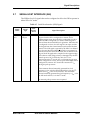
7.1
INTRODUCTION. . . . . . . . . . . . . . . . . . . . . . . . . . . . . . . . . . 7-3
7.2
GPIO PROGRAMMING MODEL . . . . . . . . . . . . . . . . . . . . . 7-3
7.3
GPIO REGISTER (GPIOR). . . . . . . . . . . . . . . . . . . . . . . . . . 7-3
7.3.1
GPIOR Data Bits (GD[7:0])—Bits 7–0 . . . . . . . . . . . . . . . 7-4
7.3.2
GPIOR Data Direction Bits (GDD[7:0])—Bits 15–8 . . . . . 7-4
7.3.3
GPIOR Control Bits (GC[7:0])—Bits 23–16 . . . . . . . . . . . 7-4
8.1
OVERVIEW. . . . . . . . . . . . . . . . . . . . . . . . . . . . . . . . . . . . . . 8-3
8.2
DAX SIGNALS . . . . . . . . . . . . . . . . . . . . . . . . . . . . . . . . . . . 8-4
Motorola
ix
8.3
DAX FUNCTIONAL OVERVIEW . . . . . . . . . . . . . . . . . . . . . 8-5
8.4
DAX PROGRAMMING MODEL . . . . . . . . . . . . . . . . . . . . . . 8-6
8.5
DAX INTERNAL ARCHITECTURE. . . . . . . . . . . . . . . . . . . . 8-6
8.5.1
DAX Audio Data Registers A and B (XADRA/XADRB) . . 8-7
8.5.2
DAX Audio Data Buffer (XADBUF). . . . . . . . . . . . . . . . . . 8-7
8.5.3
DAX Audio Data Shift Register (XADSR) . . . . . . . . . . . . . 8-8
8.5.4
DAX Control Register (XCTR) . . . . . . . . . . . . . . . . . . . . . 8-8
8.5.4.1
DAX Enable (XEN)—Bit 0 . . . . . . . . . . . . . . . . . . . . . . 8-8
8.5.4.2
DAX Interrupt Enable (XIEN)—Bit 1 . . . . . . . . . . . . . . 8-8
8.5.4.3
DAX Stop Control (XSTP)—Bit 2 . . . . . . . . . . . . . . . . . 8-8
8.5.4.4
DAX Clock Input Select (XCS[1:0])—Bits 3–4 . . . . . . . 8-9
8.5.4.5
XCTR Reserved Bits—Bits 5-9, 16-23. . . . . . . . . . . . . 8-9
8.5.4.6
DAX Channel A Validity (XVA)—Bit 10 . . . . . . . . . . . . 8-9
8.5.4.7
DAX Channel A User Data (XUA)—Bit 11 . . . . . . . . . . 8-9
8.5.4.8
DAX Channel A Channel Status (XCA)—Bit 12. . . . . . 8-9
8.5.4.9
DAX Channel B Validity (XVB)—Bit 13 . . . . . . . . . . . . 8-9
8.5.4.10
DAX Channel B User Data (XUB)—Bit 14 . . . . . . . . . 8-10
8.5.4.11
DAX Channel B Channel Status (XCB)—Bit 15. . . . . 8-10
8.5.5
DAX Status Register (XSTR) . . . . . . . . . . . . . . . . . . . . . 8-10
8.5.5.1
DAX Audio Data Register Empty (XADE)—Bit 0 . . . . 8-10
8.5.5.2
XSTR Reserved Bits—Bits 1, 5–23 . . . . . . . . . . . . . . 8-10
8.5.5.3
DAX Transmit Underrun Error Flag (XAUR)—Bit 2 . . 8-10
8.5.5.4
DAX Block Transfer Flag (XBLK)—Bit 3 . . . . . . . . . . 8-11
8.5.5.5
DAX Transmit In Progress (XTIP)—Bit 4 . . . . . . . . . . 8-11
8.5.6
DAX Non-Audio Data Buffer (XNADBUF) . . . . . . . . . . . 8-12
8.5.7
DAX Parity Generator (PRTYG) . . . . . . . . . . . . . . . . . . . 8-12
8.5.8
DAX Biphase Encoder . . . . . . . . . . . . . . . . . . . . . . . . . . 8-12
8.5.9
DAX Preamble Generator. . . . . . . . . . . . . . . . . . . . . . . . 8-12
8.5.10
DAX Clock Multiplexer . . . . . . . . . . . . . . . . . . . . . . . . . . 8-13
8.5.11
DAX State Machine . . . . . . . . . . . . . . . . . . . . . . . . . . . . 8-14
8.6
DAX PROGRAMMING CONSIDERATIONS . . . . . . . . . . . 8-14
8.6.1
Initiating A Transmit Session . . . . . . . . . . . . . . . . . . . . . 8-14
8.6.2
Transmit Register Empty Interrupt Handling . . . . . . . . . 8-14
8.6.3
Block Transferred Interrupt Handling . . . . . . . . . . . . . . . 8-14
8.6.4
DAX Operation During Stop . . . . . . . . . . . . . . . . . . . . . . 8-15
A.1
INTRODUCTION. . . . . . . . . . . . . . . . . . . . . . . . . . . . . . . . . . A-3
A.2
BOOTSTRAPPING THE DSP. . . . . . . . . . . . . . . . . . . . . . . . A-3
A.3
BOOTSTRAP PROGRAM LISTING . . . . . . . . . . . . . . . . . . . A-4
x
Motorola
B.1
B.2
B.3
B.4
B.5
B.6
Motorola
INTRODUCTION. . . . . . . . . . . . . . . . . . . . . . . . . . . . . . . . . .
PERIPHERAL ADDRESSES . . . . . . . . . . . . . . . . . . . . . . . .
INTERRUPT ADDRESSES . . . . . . . . . . . . . . . . . . . . . . . . .
INTERRUPT PRIORITIES . . . . . . . . . . . . . . . . . . . . . . . . . .
INSTRUCTION SET SUMMARY . . . . . . . . . . . . . . . . . . . . .
PROGRAMMING SHEETS. . . . . . . . . . . . . . . . . . . . . . . . . .
B-3
B-3
B-3
B-3
B-3
B-3
xi
xii
Motorola
List of Figures
Figure 1-1
DSP56012 Block Diagram. . . . . . . . . . . . . . . . . . . . . . . . . . . . . . 1-9
Figure 2-1
DSP56012 Signals . . . . . . . . . . . . . . . . . . . . . . . . . . . . . . . . . . . 2-4
Figure 3-1
Memory Maps for PEA = 0, PEB = 0. . . . . . . . . . . . . . . . . . . . . . 3-5
Figure 3-2
Memory Maps for PEA = 1, PEB = 0. . . . . . . . . . . . . . . . . . . . . . 3-6
Figure 3-3
Memory Maps for PEA = 0, PEB = 1. . . . . . . . . . . . . . . . . . . . . . 3-7
Figure 3-4
Memory Maps for PEA = 1, PEB = 1. . . . . . . . . . . . . . . . . . . . . . 3-8
Figure 3-5
Operating Mode Register (OMR) . . . . . . . . . . . . . . . . . . . . . . . 3-12
Figure 3-6
Interrupt Priority Register (Addr X:$FFFF) . . . . . . . . . . . . . . . . 3-16
Figure 3-7
PLL Configuration . . . . . . . . . . . . . . . . . . . . . . . . . . . . . . . . . . . 3-20
Figure 4-1
Port B Interface . . . . . . . . . . . . . . . . . . . . . . . . . . . . . . . . . . . . . . 4-3
Figure 4-2
Parallel Port B Registers . . . . . . . . . . . . . . . . . . . . . . . . . . . . . . . 4-4
Figure 4-3
Port B GPIO Signals and Registers . . . . . . . . . . . . . . . . . . . . . . 4-5
Figure 4-4
Port B I/O Pin Control Logic . . . . . . . . . . . . . . . . . . . . . . . . . . . . 4-6
Figure 4-5
Instructions to Write/Read Parallel Data with Port B . . . . . . . . . . 4-8
Figure 4-6
I/O Port B Configuration . . . . . . . . . . . . . . . . . . . . . . . . . . . . . . . 4-9
Figure 4-7
HI Block Diagram . . . . . . . . . . . . . . . . . . . . . . . . . . . . . . . . . . . 4-12
Figure 4-8
HI Programming Model–DSP Viewpoint . . . . . . . . . . . . . . . . . . 4-14
Figure 4-9
HI Flag Operation . . . . . . . . . . . . . . . . . . . . . . . . . . . . . . . . . . . 4-18
Figure 4-10
Host Processor Programming Model–Host Side. . . . . . . . . . . . 4-23
Figure 4-11
HI Register Map . . . . . . . . . . . . . . . . . . . . . . . . . . . . . . . . . . . . 4-24
Figure 4-12
HSR and HCR Operation . . . . . . . . . . . . . . . . . . . . . . . . . . . . . 4-26
Motorola
xiii
Figure 4-13
Command Vector Register . . . . . . . . . . . . . . . . . . . . . . . . . . . . .4-29
Figure 4-14
Host Processor Transfer Timing . . . . . . . . . . . . . . . . . . . . . . . . .4-37
Figure 4-15
Interrupt Vector Register Read Timing . . . . . . . . . . . . . . . . . . . .4-40
Figure 4-16
HI Interrupt Structure . . . . . . . . . . . . . . . . . . . . . . . . . . . . . . . . .4-40
Figure 4-17
DMA Transfer Logic and Timing . . . . . . . . . . . . . . . . . . . . . . . . .4-41
Figure 4-18
HI Initialization Flowchart . . . . . . . . . . . . . . . . . . . . . . . . . . . . . .4-42
Figure 4-19
HI Initialization—DSP Side . . . . . . . . . . . . . . . . . . . . . . . . . . . . .4-43
Figure 4-20
HI Initialization—Host Side, Interrupt Mode . . . . . . . . . . . . . . . .4-44
Figure 4-21
HI Mode and INIT Bits. . . . . . . . . . . . . . . . . . . . . . . . . . . . . . . . .4-45
Figure 4-22
HI Initialization—Host Side, Polling Mode. . . . . . . . . . . . . . . . . .4-46
Figure 4-23
HI Configuration—Host Side. . . . . . . . . . . . . . . . . . . . . . . . . . . .4-46
Figure 4-24
HI Initialization–Host Side, DMA Mode . . . . . . . . . . . . . . . . . . . .4-47
Figure 4-25
Bits Used for Host-to-DSP Transfer . . . . . . . . . . . . . . . . . . . . . .4-48
Figure 4-26
Data Transfer from Host to DSP . . . . . . . . . . . . . . . . . . . . . . . . .4-50
Figure 4-27
Host Command . . . . . . . . . . . . . . . . . . . . . . . . . . . . . . . . . . . . . .4-52
Figure 4-28
Receive Data from Host—Main Program . . . . . . . . . . . . . . . . . .4-53
Figure 4-29
Receive Data from Host Interrupt Routine . . . . . . . . . . . . . . . . .4-53
Figure 4-30
Transmit/Receive Byte Registers . . . . . . . . . . . . . . . . . . . . . . . .4-54
Figure 4-31
Bootstrap Using the Host Interface . . . . . . . . . . . . . . . . . . . . . . .4-55
Figure 4-32
Bits Used for DSP to Host Transfer . . . . . . . . . . . . . . . . . . . . . .4-57
Figure 4-33
Data Transfer from DSP to Host . . . . . . . . . . . . . . . . . . . . . . . . .4-58
Figure 4-34
Main Program: Transmit 24-bit Data to Host . . . . . . . . . . . . . . .4-59
Figure 4-35
HI Hardware–DMA Mode . . . . . . . . . . . . . . . . . . . . . . . . . . . . . .4-60
xiv
Motorola
Figure 4-36
DMA Transfer and HI Interrupts . . . . . . . . . . . . . . . . . . . . . . . . .4-61
Figure 4-37
Host to DSP DMA Procedure . . . . . . . . . . . . . . . . . . . . . . . . . . .4-63
Figure 5-1
Serial Host Interface Block Diagram . . . . . . . . . . . . . . . . . . . . . . .5-4
Figure 5-2
SHI Clock Generator. . . . . . . . . . . . . . . . . . . . . . . . . . . . . . . . . . .5-5
Figure 5-3
SHI Programming Model—Host Side . . . . . . . . . . . . . . . . . . . . . .5-5
Figure 5-4
SHI Programming Model—DSP Side . . . . . . . . . . . . . . . . . . . . . .5-6
Figure 5-5
SHI I/O Shift Register (IOSR) . . . . . . . . . . . . . . . . . . . . . . . . . . . .5-8
Figure 5-6
SPI Data-To-Clock Timing Diagram . . . . . . . . . . . . . . . . . . . . . .5-10
Figure 5-7
I2C Bit Transfer . . . . . . . . . . . . . . . . . . . . . . . . . . . . . . . . . . . . . .5-20
Figure 5-8
I2C Start and Stop Events. . . . . . . . . . . . . . . . . . . . . . . . . . . . . .5-21
Figure 5-9
Acknowledgment on the I2C Bus . . . . . . . . . . . . . . . . . . . . . . . .5-21
Figure 5-10
I2C Bus Protocol For Host Write Cycle . . . . . . . . . . . . . . . . . . . .5-22
Figure 5-11
I2C Bus Protocol For Host Read Cycle . . . . . . . . . . . . . . . . . . . .5-22
Figure 6-1
SAI Baud-Rate Generator Block Diagram . . . . . . . . . . . . . . . . . .6-4
Figure 6-2
SAI Receive Section Block Diagram. . . . . . . . . . . . . . . . . . . . . . .6-5
Figure 6-3
SAI Transmit Section Block Diagram . . . . . . . . . . . . . . . . . . . . . .6-7
Figure 6-4
SAI Registers . . . . . . . . . . . . . . . . . . . . . . . . . . . . . . . . . . . . . . . .6-8
Figure 6-5
Receiver Data Shift Direction (RDIR) Programming . . . . . . . . . .6-12
Figure 6-6
Receiver Left/Right Selection (RLRS) Programming . . . . . . . . .6-12
Figure 6-7
Receiver Clock Polarity (RCKP) Programming. . . . . . . . . . . . . .6-13
Figure 6-8
Receiver Relative Timing (RREL) Programming . . . . . . . . . . . .6-14
Figure 6-9
Receiver Data Word Truncation (RDWT) Programming. . . . . . .6-14
Figure 6-10
Transmitter Data Shift Direction (TDIR) Programming . . . . . . . .6-19
Motorola
xv
Figure 6-11
Transmitter Left/Right Selection (TLRS) Programming . . . . . . .6-19
Figure 6-12
Transmitter Clock Polarity (TCKP) Programming . . . . . . . . . . . .6-20
Figure 6-13
Transmitter Relative Timing (TREL) Programming. . . . . . . . . . .6-20
Figure 6-14
Transmitter Data Word Expansion (TDWE) Programming . . . . .6-21
Figure 7-1
GPIO Control/Data Register . . . . . . . . . . . . . . . . . . . . . . . . . . . . .7-3
Figure 7-2
GPIO Circuit Diagram . . . . . . . . . . . . . . . . . . . . . . . . . . . . . . . . . .7-5
Figure 8-1
Digital Audio Transmitter (DAX) Block Diagram . . . . . . . . . . . . . .8-4
Figure 8-2
DAX Programming Mode . . . . . . . . . . . . . . . . . . . . . . . . . . . . . . .8-7
Figure 8-3
DAX Relative Timing. . . . . . . . . . . . . . . . . . . . . . . . . . . . . . . . . .8-11
Figure 8-4
Preamble sequence . . . . . . . . . . . . . . . . . . . . . . . . . . . . . . . . . .8-13
Figure 8-5
Clock Multiplexer Diagram . . . . . . . . . . . . . . . . . . . . . . . . . . . . .8-13
Figure B-1
On-chip Peripheral Memory Map . . . . . . . . . . . . . . . . . . . . . . . . B-4
xvi
Motorola
List of Tables
Table 1-1
High True / Low True Signal Conventions. . . . . . . . . . . . . . . . . . 1-6
Table 1-2
DSP56012 Internal Memory Configurations . . . . . . . . . . . . . . . . 1-7
Table 1-3
Interrupt Starting Addresses and Sources
Table 1-4
Internal Memory Configurations
Table 1-5
On-chip Peripheral Memory Map . . . . . . . . . . . . . . . . . . . . . . . 1-17
Table 2-1
DSP56012 Functional Signal Groupings . . . . . . . . . . . . . . . . . . 2-3
Table 2-2
Power Inputs . . . . . . . . . . . . . . . . . . . . . . . . . . . . . . . . . . . . . . . . 2-5
Table 2-3
Grounds. . . . . . . . . . . . . . . . . . . . . . . . . . . . . . . . . . . . . . . . . . . . 2-6
Table 2-4
Phase Lock Loop Signals . . . . . . . . . . . . . . . . . . . . . . . . . . . . . . 2-7
Table 2-5
Interrupt and Mode Control . . . . . . . . . . . . . . . . . . . . . . . . . . . . 2-8
Table 2-6
Host Interface . . . . . . . . . . . . . . . . . . . . . . . . . . . . . . . . . . . . . . 2-10
Table 2-7
Serial Host Interface (SHI) Signals . . . . . . . . . . . . . . . . . . . . . 2-13
Table 2-8
Serial Audio Interface (SAI) Receive Signals . . . . . . . . . . . . . . 2-16
Table 2-9
Serial Audio Interface (SAI) Transmit Signals . . . . . . . . . . . . . . 2-17
Table 2-10
General Purpose I/O (GPIO) Signals . . . . . . . . . . . . . . . . . . . . 2-18
Table 2-11
Digital Audio Interface (DAX) Signals . . . . . . . . . . . . . . . . . . . . 2-18
Table 2-12
On-Chip Emulation Port (OnCE) Signals
Table 3-1
Internal Memory Configurations . . . . . . . . . . . . . . . . . . . . . . . . . 3-3
Table 3-2
Internal I/O Memory Map . . . . . . . . . . . . . . . . . . . . . . . . . . . . . 3-10
Table 3-3
Operating Modes . . . . . . . . . . . . . . . . . . . . . . . . . . . . . . . . . . . 3-13
Table 3-4
Interrupt Priorities . . . . . . . . . . . . . . . . . . . . . . . . . . . . . . . . . . 3-16
Motorola
. . . . . . . . . . . . . . . 1-13
. . . . . . . . . . . . . . . . . . . . . . . 1-15
. . . . . . . . . . . . . . . . 2-19
xvii
Table 3-5
Interrupt Vectors . . . . . . . . . . . . . . . . . . . . . . . . . . . . . . . . . . . .3-17
Table 4-1
HI Registers after Reset—DSP CPU Side . . . . . . . . . . . . . . . .4-19
Table 4-2
HOREQ Pin Definition. . . . . . . . . . . . . . . . . . . . . . . . . . . . . . . . .4-25
Table 4-3
HI Mode Bit Definition . . . . . . . . . . . . . . . . . . . . . . . . . . . . . . . .4-26
Table 4-4
HOREQ Pin Definition . . . . . . . . . . . . . . . . . . . . . . . . . . . . . . . .4-28
Table 4-5
HI Registers after Reset (Host Side) . . . . . . . . . . . . . . . . . . . . .4-34
Table 4-6
Port B Pin Definitions . . . . . . . . . . . . . . . . . . . . . . . . . . . . . . . . .4-36
Table 5-1
SHI Interrupt Vectors . . . . . . . . . . . . . . . . . . . . . . . . . . . . . . . . . .5-7
Table 5-2
SHI Internal Interrupt Priorities . . . . . . . . . . . . . . . . . . . . . . . . . . .5-7
Table 5-3
SHI Noise Reduction Filter Mode . . . . . . . . . . . . . . . . . . . . . . . .5-12
Table 5-4
SHI Data Size . . . . . . . . . . . . . . . . . . . . . . . . . . . . . . . . . . . . . .5-14
Table 5-5
HREQ Function In SHI Slave Modes . . . . . . . . . . . . . . . . . . . . .5-15
Table 5-6
HCSR Receive Interrupt Enable Bits
Table 6-1
SAI Interrupt Vector Locations . . . . . . . . . . . . . . . . . . . . . . . . . . .6-9
Table 6-2
SAI Internal Interrupt Priorities . . . . . . . . . . . . . . . . . . . . . . . . . . .6-9
Table 6-3
Receiver Word Length Control . . . . . . . . . . . . . . . . . . . . . . . . . .6-11
Table 6-4
Transmitter Word Length
Table 7-1
GPIO Pin Configuration . . . . . . . . . . . . . . . . . . . . . . . . . . . . . . . .7-4
Table 8-1
DAX Interrupt Vectors . . . . . . . . . . . . . . . . . . . . . . . . . . . . . . . . . .8-6
Table 8-2
DAX Interrupt Priority . . . . . . . . . . . . . . . . . . . . . . . . . . . . . . . . . .8-6
Table 8-3
Clock Source Selection. . . . . . . . . . . . . . . . . . . . . . . . . . . . . . . . .8-9
Table 8-4
Preamble Bit Patterns . . . . . . . . . . . . . . . . . . . . . . . . . . . . . . . .8-12
Table B-1
Interrupt Starting Addresses and Sources . . . . . . . . . . . . . . . . . B-5
xviii
. . . . . . . . . . . . . . . . . . . .5-17
. . . . . . . . . . . . . . . . . . . . . . . . . . . . .6-18
Motorola
Table B-2
Interrupt Priorities Within an IPL . . . . . . . . . . . . . . . . . . . . . . . . B-6
Table B-3
Instruction Set Summary (Sheet 1 of 7). . . . . . . . . . . . . . . . . . . B-8
Motorola
xix
xx
Motorola
SECTION 1
OVERVIEW
MOTOROLA
DSP56012 User’s Manual
1-1
Overview
1.1
1.1.1
1.1.2
1.2
1.3
1.3.1
1.3.2
1.3.3
1.3.4
1-2
INTRODUCTION . . . . . . . . . . . . . . . . . . . . . . . . . . . . . . . . . . 1-3
Manual Organization . . . . . . . . . . . . . . . . . . . . . . . . . . . . . 1-4
Manual Conventions . . . . . . . . . . . . . . . . . . . . . . . . . . . . . 1-5
DSP56012 FEATURES . . . . . . . . . . . . . . . . . . . . . . . . . . . . . 1-6
DSP56012 ARCHITECTURAL OVERVIEW . . . . . . . . . . . . . 1-8
Peripheral Modules . . . . . . . . . . . . . . . . . . . . . . . . . . . . . 1-10
DSP Core Processor. . . . . . . . . . . . . . . . . . . . . . . . . . . . 1-10
Memories . . . . . . . . . . . . . . . . . . . . . . . . . . . . . . . . . . . . 1-13
Input/Output . . . . . . . . . . . . . . . . . . . . . . . . . . . . . . . . . . 1-16
DSP56012 User’s Manual
MOTOROLA
Overview
Introduction
1.1
INTRODUCTION
This manual describes in detail the DSP56012 24-bit Digital Signal Processor (DSP),
its memory, operating modes, and peripheral modules. This manual is intended to be
used with the DSP56000 Family Manual (DSP56KFAMUM/AD) and the DSP56012
Technical Data sheet (DSP56012/D). The family manual describes the Central
Processing Unit (CPU), programming models, and the instruction set. The data sheet
provides electrical specifications, timing, pinouts, and packaging descriptions. These
documents, as well as Motorola’s DSP development tools, can be obtained through a
local Motorola Semiconductor Sales Office or authorized distributor.
To receive the latest information, access the Motorola DSP home page located at
http://www.motorola-dsp.com
The DSP56012 is a high-performance programmable DSP specifically developed for
Digital Versatile Disk (DVD), High-Definition Television (HDTV), and advanced
set-top audio decoding. Flexible peripheral modules and interface software allow
simple connection to a wide variety of video and audio system decoders. The
memory configuration and peripherals differentiate this DSP from the other 56000
family members. The DSP56012 also provides the following on-chip peripherals to
support its target applications:
• Parallel Host Interface (HI)—a byte-wide parallel port with Direct Memory
Access (DMA) support
• Serial Host Interface (SHI)—simple communications and control interface
between a host processor and the DSP
• Serial Audio Interface (SAI)—user-programmable interface that provides
support for a wide variety of serial audio formats to support a number of
standard audio devices
• Dedicated General Purpose Input/Output (GPIO) Signals—eight additional
individually controlled input or output signals
• Digital Audio Transmitter (DAX)—outputs digital audio data in AES/EBU,
CP-340, and IEC958 formats
The DSP56012 has the power and ease-of-programming required for stand-alone,
embedded applications. The versatile, on-board peripherals allow the DSP to be
connected easily to almost any other processor with little or no additional logic.
MOTOROLA
DSP56012 User’s Manual
1-3
Overview
Introduction
1.1.1
Manual Organization
This manual includes the following sections:
• Section 1—Overview furnishes a description of the manual organization and
provides a brief description of the DSP56012.
• Section 2—Signal Descriptions describes the DSP56012 signals and signal
groupings.
• Section 3—Memory, Operating Modes, and Interrupts describes the internal
memory organization, operating modes, interrupt processing, and chip
initialization during hardware reset.
• Section 4—Parallel Host Interface describes the parallel Host Interface (HI) port,
its registers, and its controls.
• Section 5—Serial Host Interface describes the operation, registers, and control of
the Serial Host Interface (SHI).
• Section 6—Serial Audio Interface describes the operation of the Serial Audio
Interface (SAI), its registers, and its controls.
• Section 7—Digital Audio Transmitter describes the Digital Audio Transmitter
(DAX) functionality, architecture, registers, and programming considerations.
• Section 8—Serial Audio Interface describes the operation of the Serial Audio
Interface (SAI), its registers, and its controls.
• Appendix A—Bootstrap Code Listings lists the code used to bootstrap the
DSP56012.
• Appendix B—Programming Reference provides a quick reference for the
instructions and registers used by the DSP56012. These sheets are provided
with the expectation that they be photocopied and used by programmers
when programming the registers.
1-4
DSP56012 User’s Manual
MOTOROLA
Overview
Introduction
1.1.2
Manual Conventions
The following conventions are used in this manual:
• The word “reset” is used in three different contexts in this manual. There is a
reset pin that is always written as “RESET”, there is a reset instruction that is
always written as “RESET”, and the word reset, used to refer to the reset
function, is written in lower case (with a leading capital letter as grammar
dictates.)
• Bits within a register are indicated AA[n:0] when more than one bit is
involved in a description. For purposes of description, the bits are presented
as if they are contiguous within the register; however, this is not always the
case. Refer to the programming model diagrams or to the programming sheets
to see the exact location of bits within a register.
• When a bit is described as “set”, its value is 1. When a bit is described as
“cleared”, its value is 0.
• Hex (hexadecimal) values are indicated with a dollar sign ($) preceding the
hex value, as in “$FFFB is the X memory address for the Interrupt Priority
Register (IPR).”
• Code examples are displayed in a monospaced font, as shown in
Example 1-1.
Example 1-1 Sample Code Listing
movep #0,x:EOR0
; drive 2nd read trigger
bset #ERTS,x:ECSR
; set read triggers by reading EDDR
do #(N-2),end_OL
; loop to drive more (N-2) triggers
• Pins or signals listed in code examples that are asserted low have a tilde (~) in
front of their names.
• The word “assert” means that a high true (active high) signal is pulled high (to
VCC) or that a low true (active low) signal is pulled low (to ground).
• The word “deassert” means that a high true signal is pulled low (to ground) or
that a low true signal is pulled high (to VCC).
• Overbars are used to indicate a signal that is active when pulled to ground
(see Table 1-1). For example, the RESET pin is active when pulled to ground.
Therefore, references to the RESET pin will always have an overbar. Such pins
and signals are also said to be “active low” or “low true.”
MOTOROLA
DSP56012 User’s Manual
1-5
Overview
DSP56012 Features
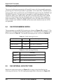
Table 1-1 High True / Low True Signal Conventions
Signal/Symbol
Logic State
Signal State
Voltage
PIN1
True
Asserted
VCC3
PIN1
False
Deasserted
Ground2
PIN1
True
Asserted
Ground2
PIN1
False
Deasserted
VCC3
Notes: 1.
2.
3.
1.2
PIN is a generic term for any pin on the device.
Ground is an acceptable low voltage level. See the appropriate data sheet for the range
of acceptable low voltage levels (typically a TTL logic low).
VCC is an acceptable high voltage level. See the appropriate data sheet for the range of
acceptable high voltage levels (typically a TTL logic high).
DSP56012 FEATURES
• Digital Signal Processing Core
1-6
–
Efficient, object-code compatible, 24-bit DSP56000 family DSP engine
–
40.5 Million Instructions Per Second (MIPS)—24.69 ns instruction cycle at
81 MHz
–
Highly parallel instruction set with unique DSP addressing modes
–
Two 56-bit accumulators including extension byte
–
Parallel 24 × 24-bit multiply-accumulate in 1 instruction cycle (2 clock
cycles)
–
Double precision 48 × 48-bit multiply with 96-bit result in 6 instruction
cycles
–
56-bit addition/subtraction in 1 instruction cycle
–
Fractional and integer arithmetic with support for multi-precision
arithmetic
–
Hardware support for block-floating point Fast Fourier Transforms (FFT)
–
Hardware nested DO loops
–
Zero-overhead fast interrupts (2 instruction cycles)
DSP56012 User’s Manual
MOTOROLA
Overview
DSP56012 Features
–
PLL-based clocking with a wide range of frequency multiplications (1 to
4096) and power saving clock divider (2i: i = 0 to 15), which reduces clock
noise
–
Four 24-bit internal data buses and three 16-bit internal address buses for
simultaneous accesses to one program and two data memories
• Memory
–
Modified Harvard architecture allows simultaneous access to program and
data memories
–
15360 × 24-bit on-chip Program ROM1
–
4096 × 24-bit on-chip X-data RAM and 3584 × 24-bit on-chip X-data ROM*
–
4352 × 24-bit on-chip Y-data RAM and 2048 × 24-bit on-chip Y-data ROM*
–
256 × 24-bit on-chip Program RAM and 32 × 24-bit bootstrap ROM
–
As much as 2304 × 24 bits of X- and Y-data RAM can be switched to
Program RAM, giving a total of 2560 × 24 bits of Program RAM
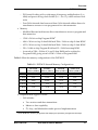
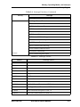
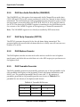
Table 1-2 lists the memory configurations of the DSP56012.
Table 1-2 DSP56012 Internal Memory Configurations
No Switch
(PEA=0, PEB=0)
Switch A
(PEA=1, PEB=0)
Switch B
(PEA=0, PEB=1)
Switch A+B
(PEA=1, PEB=1)
P: RAM
0.25 K
1.0 K
1.75 K
2.5 K
X: RAM
4.0 K
3.25 K
3.25 K
2.5 K
Y: RAM
4.25 K
4.25 K
3.5 K
3.5 K
P: ROM
15 K
15 K
15 K
15 K
X: ROM
3.5 K
3.5 K
3.5 K
3.5 K
Y: ROM
2.0 K
2.0 K
2.0 K
2.0 K
• Peripheral and Support Circuits
–
SAI includes:
• Two receivers and three transmitters
• Master or slave capability
• I2S, Sony, and Matshushita audio protocol implementations
1.These ROMs may be factory programmed with data/program provided by the application developer.
MOTOROLA
DSP56012 User’s Manual
1-7
Overview
DSP56012 Architectural Overview
• Two sets of SAI interrupt vectors
–
SHI features:
• Single master capability
• SPI and I2C protocols
• 10-word receive FIFO
• Support for 8-, 16- and 24-bit words.
1.3
–
Byte-wide Parallel Host Interface with DMA support capable of
reconfiguration as fifteen General Purpose Input/Output (GPIO) lines
–
DAX features one serial transmitter capable of supporting S/PDIF, IEC958,
CP-340, and AES/EBU formats.
–
Eight dedicated, independent, programmable GPIO lines
–
On-chip peripheral registers memory mapped in data memory space
–
OnCE™ port for unobtrusive, processor speed-independent debugging
–
Software programmable PLL-based frequency synthesizer for the core
clock
–
Power saving Wait and Stop modes
–
Fully static, HCMOS design for operating frequencies from 81 MHz down
to DC
–
100-pin plastic Thin Quad Flat Pack (TQFP) surface-mount package
–
5 V power supply
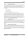
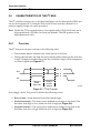
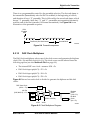
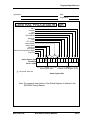
DSP56012 ARCHITECTURAL OVERVIEW
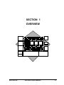
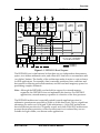
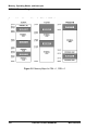
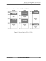
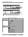
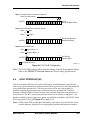
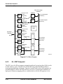
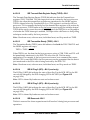
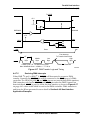
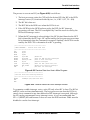
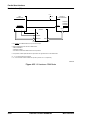
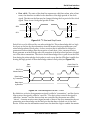
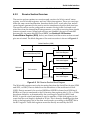
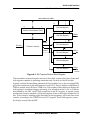
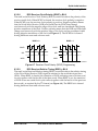
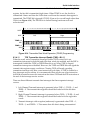
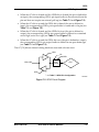
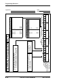
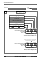
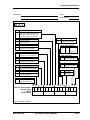
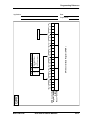
The DSP56012 is a member of the 24-bit DSP56000 family. The DSP is composed of
the 24-bit DSP56000 core, memory, and a set of peripheral modules, as shown in
Figure 1-1. The 24-bit DSP56000 core is composed of a Data Arithmetic Logic Unit
(ALU), an Address Generation Unit (AGU), a Program Controller, an On-Chip
Emulation (OnCE) port, and a PLL designed to allow the DSP to run at full speed
while using a low-speed clock. The DSP56000-family architecture, upon which the
DSP56012 is built, was designed to maximize throughput in data-intensive digital
signal processing applications. The result is a dual-natured, expandable architecture
with sophisticated on-chip peripherals and versatile GPIO.
1-8
DSP56012 User’s Manual
MOTOROLA
Overview
DSP56012 Architectural Overview
8
15
Parallel
Host
Interface
(HI)
General
Purpose
I/O
(GPIO)
5
9
Serial
Audio
Interface
(SAI)
2
Serial
Digital
Host
Audio
Interface Transmitter
(SHI)
(DAX)
Program
Memory
X Data
Memory
Y Data
Memory
Expansion
Area
24-Bit
DSP56000
Core
GDB
Internal
Data
Bus
Switch
PDB
XDB
YDB
OnCETM Port
Program
Interrupt
Controller
Clock
PLL
Gen.
3
Program
Decode
Controller
Program Control Unit
4
EXTAL
PAB
XAB
YAB
Address
Generation
Unit
Program
Address
Generator
Data ALU
24 × 24 + 56 → 56-Bit MAC
Two 56-Bit Accumulators
4
IRQA, IRQB, NMI, RESET
16-Bit Bus
24-Bit Bus
Figure 1-1 DSP56012 Block Diagram
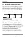
The DSP56000 core is dual-natured in that there are two independent data memory
spaces, two address arithmetic units, and a Data ALU that has two accumulators and
two shifter/limiters. The duality of the architecture makes it easier to write software
for DSP applications. For example, data is naturally partitioned into coefficient and
data spaces for filtering and transformations, and into real and imaginary spaces for
performing complex arithmetic.
Note: Although the DSP56000 core has built-in support for external memory
expansion, the DSP56012 does not implement this function. For DSP56012
applications, external memory expansion is a function of the host processor.
The DSP56000 architecture is especially suited for audio applications since its
arithmetic operations are executed on 24-bit or 48-bit data words. This is a significant
advantage for audio over 16-bit and 32-bit architectures—16-bit DSP architectures
have insufficient precision for CD-quality sound, and while 32-bit DSP architectures
possess the necessary precision, with extra silicon and cost overhead they are not
suitable for high-volume, cost-driven audio applications
MOTOROLA
DSP56012 User’s Manual
1-9
Overview
DSP56012 Architectural Overview
1.3.1
Peripheral Modules
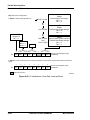
The following peripheral modules are included on the DSP56012:
• Parallel Host Interface—The Host Interface (HI) provides a byte-wide parallel
interface for parallel data transfer between the DSP56012 and a host processor
or another parallel peripheral device. The HI will operate with 8-, 16-, and
24-bit words
• Serial Host Interface (SHI)—The Serial Host Interface provides a fast, yet
simple serial interface to connect the DSP56012 to a host processor or to
another serial peripheral device. Two serial protocols are available: the
Motorola Serial Peripheral Interface (SPI) bus and the Philips Inter
Integrated-circuit Control (I2C) bus. The SHI will operate with 8-, 16-, and
24-bit words and the receiver contains an optimal 10-word First-In, First-Out
(FIFO) register to reduce the receive interrupt rate.
• Serial Audio Interface (SAI)—The SAI provides a synchronous serial
interface that allows the DSP56012 to communicate using a wide range of
standard serial data formats used by audio manufacturers at bit rates up to
one third the DSP core clock rate (e.g., 27 MHz for an 81 MHz clock). There
are three synchronized data transmission lines and two synchronized data
reception lines, all of which are double-buffered.
• General Purpose Input/Output (GPIO)—The GPIO has eight dedicated
signal lines that can be independently programmed to be inputs, standard
TTL outputs, open collector outputs, or disconnected.
• Digital Audio Transmitter (DAX)—The DAX is a serial audio interface
module that outputs digital audio data in AES/EBU, CP-340, and IEC958
formats.
1.3.2
DSP Core Processor
The 24-bit DSP56000 core is composed of a Data ALU, an AGU, a program controller,
and the buses that connect them together. The OnCE port and a PLL are integral
parts of this processor. Figure 1-1 on page 1-9 illustrates the DSP block diagram,
showing the components of the core processor, as well as the peripherals specific to
the DSP56012. The following paragraphs present a brief overview of the DSP56000
core processor. For more thorough detail, refer to the DSP56000 Family Manual.
1-10
DSP56012 User’s Manual
MOTOROLA
Overview
DSP56012 Architectural Overview
1.3.2.1
Data Arithmetic and Logic Unit (Data ALU)
The Data Arithmetic and Logic Unit (Data ALU) has been designed to be fast and
provide the capability to process signals having a wide dynamic range. Special
circuitry has been provided to facilitate the processing of data overflows and
round-off errors. The Data ALU performs all of the arithmetic and logical
operations on data operands. The Data ALU consists of four 24-bit input registers,
two 48-bit accumulator registers (also usable as four 24-bit accumulators), two 8-bit
accumulator extension registers, an accumulator shifter, two data shifter/limiters,
and a parallel single-cycle non-pipelined Multiplier-Accumulator (MAC). Data
ALU operations use fractional two’s-complement arithmetic. Data ALU registers
may be read or written over the X Data Bus (XDB) and Y Data Bus (YDB) as 24- or
48-bit operands. The 24-bit data words provide 144 dB of dynamic range. This is
sufficient for most real-world applications, including high-quality audio
applications, since the majority of Analog-to-Digital (A/D) and Digital-to-Analog
(D/A) converters are 16 bits or less, and certainly not greater than 24 bits. The 56-bit
accumulation internal to the Data ALU provides 336 dB of internal dynamic range,
assuring no loss of precision due to intermediate processing.
Two data shifter/limiters provide special post-processing on data reads (from the
Data ALU accumulator registers and directed to the XDB or YDB). The data shifters
are capable of shifting data one bit to the left or to the right, as well as passing the
data unshifted. Each data shifter has a 24-bit output with overflow indication. The
data shifters are controlled by scaling-mode bits. These shifters permit no-overhead
dynamic scaling of fixed point data by simply programming the scaling mode bits.
This permits block floating-point algorithms to be implemented efficiently. For
example, Fast Fourier Transform (FFT) routines can use this feature to selectively
scale each butterfly pass. Saturation arithmetic is accommodated to minimize errors
due to overflow. Overflow occurs when a source operand requires more bits for
accurate representation than there are available in the destination. To minimize the
error due to overflow, “limiting” causes the maximum (or minimum, if negative)
value to be written to the destination with an error flag.
1.3.2.2
Address Generation Unit (AGU)
The Address Generation Unit (AGU) performs all address storage and effective
address calculations necessary to access data operands in memory. It implements
three types of arithmetic to update addresses—linear, modulo, and reverse carry.
This unit operates in parallel with other chip resources to minimize address
generation overhead. The AGU contains eight address registers R[7:0] (i.e., Rn), eight
offset registers N[7:0] (i.e., Nn), and eight modifier registers M[7:0] (i.e., Mn). The Rn
are 16-bit registers that may contain an address or data. Each Rn register may
provide addresses to the X memory Address Bus (XAB), Y memory Address Bus
(YAB), and the Program Address Bus (PAB). The Nn and Mn registers are 16-bit
registers that are normally used to update the Rn registers, but may be used for data.
MOTOROLA
DSP56012 User’s Manual
1-11
Overview
DSP56012 Architectural Overview
AGU registers may be read from or written to via the Global Data Bus as 16-bit
operands. The AGU has two modulo arithmetic units that can generate two
independent 16-bit addresses every instruction cycle for any two of the XAB, YAB, or
PAB.
1.3.2.3
Program Control Unit
The program control unit performs instruction prefetch, instruction decoding,
hardware DO loop control, and exception processing. It contains six directly
addressable registers—the Program Counter (PC), Loop Address (LA), Loop Counter
(LC), Status Register (SR), Operating Mode Register (OMR), and Stack Pointer (SP).
The program control unit also contains a 15 level by 32-bit system stack memory. The
16-bit PC can address 65,536 (64 K) locations in program memory space.
1.3.2.4
Data Buses
Data movement on the chip occurs over four bidirectional 24-bit buses—the X Data
Bus (XDB), the Y Data Bus (YDB), the Program Data Bus (PDB), and the Global Data
Bus (GDB). Certain instructions concatenate XDB and YDB to form a 48-bit data bus.
Data transfers between the Data ALU and the two data memories, X and Y, occur
over the XDB and YDB, respectively. These transfers can occur simultaneously on the
DSP, maximizing data throughput. All other data transfers, such as I/O transfers to
internal peripherals, occur over the GDB. Instruction word pre-fetches take place
over the PDB in parallel with data transfers. Transfers between buses are
accomplished through the internal bus switch.
1.3.2.5
Address Buses
Addresses are specified for internal X data memory and Y data memory using two
unidirectional 16-bit buses—the X Address Bus (XAB) and the Y Address Bus (YAB).
program memory addresses are specified using the 16-bit Program Address Bus
(PAB).
1.3.2.6
Phase Lock Loop (PLL)
The Phase Lock Loop (PLL) reduces the need for multiple oscillators in a system
design, thus reducing the overall system cost. An additional benefit of the PLL is that
it permits the use of a low-frequency external clock with no sacrifice of processing
speed. The PLL converts the low-frequency external clock to the high speed internal
clock needed to run the DSP at maximum speed. This diminishes the electromagnetic
interference generated by high frequency clocking. The PLL performs frequency
multiplication to allow the processor to use almost any available external system
clock for full-speed operation. It also improves the synchronous timing of the
processor’s external memory port, significantly reducing the timing skew between
EXTAL and the internal chip phases when the Multiplication Factor (MF) ≤ 4. The
PLL is unique in that it provides a low power divider on its output, which can reduce
or restore the chip operating frequency without losing the PLL lock.
1-12
DSP56012 User’s Manual
MOTOROLA
Overview
DSP56012 Architectural Overview
1.3.2.7
On-Chip Emulation (OnCE) Port
The On-Chip Emulation (OnCE) port provides a sophisticated debugging tool that
allows simple, inexpensive, and speed-independent access to the processor’s internal
registers and peripherals. The OnCE port tells the application programmer the exact
status of most of the on-chip registers, memory locations, and buses, as well as
storing the addresses of the last five instructions that were executed.
1.3.3
Memories
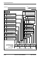
The three independent memory spaces of the DSP56012—X data, Y data, and
program—and their configurations are discussed briefly here. See Section 3,
Memory, Operating Modes, and Interrupts for more detail.
1.3.3.1
Program Memory
The on-chip program memory is 24-bits wide. Addresses are received from the
Program Control Logic (usually the Program Counter) over the Program Address
Bus (PAB). Program memory may be written using MOVEM instructions. The
interrupt vectors are located in the bottom 128 locations of program memory.
Table 1-3 lists the interrupt vector addresses and indicates the Interrupt Priority
Level (IPL) of each interrupt source. Program RAM has many advantages. It
provides a means to develop code efficiently. Programs can be changed dynamically,
allowing efficient overlaying of DSP software algorithms. In this way the on-chip
Program RAM operates as a fixed cache, thereby minimizing accesses to slower
external memory.
The Bootstrap mode, described in Appendix A, provides a convenient, low-cost
method to load the DSP56012 Program RAM through the HI or the SHI (using either
SPI or I2C formats) after a power-on reset.
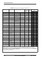
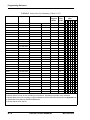
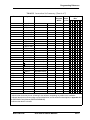
Table 1-3 Interrupt Starting Addresses and Sources
Interrupt
Starting Address
IPL
P:$0000
3
Hardware RESET
P:$0002
3
Stack Error
P:$0004
3
Trace
P:$0006
3
SWI
P:$0008
0–2
IRQA
P:$000A
0–2
IRQB
P:$000C
MOTOROLA
Interrupt Source
Reserved
DSP56012 User’s Manual
1-13
Overview
DSP56012 Architectural Overview
Table 1-3 Interrupt Starting Addresses and Sources (Continued)
Interrupt
Starting Address
IPL
P:$000E
Reserved
P:$0010
0–2
SAI Left Channel Transmitter if TXIL = 0
P:$0012
0–2
SAI Right Channel Transmitter if TXIL = 0
P:$0014
0–2
SAI Transmitter Exception if TXIL = 0
P:$0016
0–2
SAI Left Channel Receiver if RXIL = 0
P:$0018
0–2
SAI Right Channel Receiver if RXIL = 0
P:$001A
0–2
SAI Receiver Exception if RXIL = 0
P:$001C
Reserved
P:$001E
3
P:$0020
0–2
SHI Transmit Data
P:$0022
0–2
SHI Transmit Underrun Error
P:$0024
0–2
SHI Receive FIFO Not Empty
P:$0026
NMI
Reserved
P:$0028
0–2
SHI Receive FIFO Full
P:$002A
0–2
SHI Receive Overrun Error
P:$002C
0–2
SHI Bus Error
P:$002E
Reserved
P:$0030
0–2
Host Receive Data
P:$0032
0–2
Host Transmit Data
P:$0034
0–2
Host Command (default)
P:$0036
Reserved; available for Host Command, see p. B-5–B-6.
:
:
P:$003C
1-14
Interrupt Source
Reserved; available for Host Command, see p. B-5–B-6.
P:$003E
3
Illegal Instruction
P: $0040
0–2
SAI Left Channel Transmitter if TXIL = 1
P: $0042
0–2
SAI Right Channel Transmitter if TXIL = 1
P: $0044
0–2
SAI Transmitter Exception if TXIL = 1
P: $0046
0–2
SAI Left Channel Receiver if RXIL = 1
P: $0048
0–2
SAI Right Channel Receiver if RXIL = 1
P: $004A
0–2
SAI Receiver Exception if RXIL = 1
P: $004C
Reserved; available for Host Command, see p. B-5–B-6.
P: $004E
Reserved; available for Host Command, see p. B-5–B-6.
DSP56012 User’s Manual
MOTOROLA
Overview
DSP56012 Architectural Overview
Table 1-3 Interrupt Starting Addresses and Sources (Continued)
Interrupt
Starting Address
IPL
P: $0050
0–2
DAX Transmit Underrun Error
P: $0052
0–2
DAX Block Transferred
P: $0054
Interrupt Source
Reserved; available for Host Command, see p. B-5–B-6.
P: $0056
0–2
DAX Transmit Register Empty
P: $0058
Reserved; available for Host Command, see p. B-5–B-6.
:
Reserved; available for Host Command, see p. B-5–B-6.
P: $007E
Reserved; available for Host Command, see p. B-5–B-6.
1.3.3.2
X Data Memory
The on-chip X data memory shown in Table 1-4 is 24 bits wide. Addresses are
received from the XAB, and data transfers to the Data ALU occur on the XDB.
1.3.3.3
Y Data Memory
The on-chip Y data memory shown in Table 1-4 is 24 bits wide. Addresses are
received from the YAB, and data transfers to the Data ALU occur on the YDB.
1.3.3.4
On-Chip Memory Configuration Bits
Through the use of bits PEA and PEB in the OMR, four different memory
configurations are possible. These configurations provide appropriate memory sizes
for a variety of applications (see Table 1-4). Section 3 provides detailed information
about memory configuration.
Table 1-4 Internal Memory Configurations
No Switch
(PEA = 0
PEB = 0)
Switch A
(PEA = 1
PEB = 0)
Switch B
(PEA = 0
PEB = 1)
Switch A+B
(PEA = 1
PEB = 1)
Program RAM
0.25 K
1.0 K
1.75 K
2.5 K
X RAM
4.0 K
3.25 K
3.25 K
2.5 K
Y RAM
4.25 K
4.25 K
3.5 K
3.5 K
Program ROM
15 K
15 K
15 K
15 K
X ROM
3.5 K
3.5 K
3.5 K
3.5 K
Y ROM
2.0 K
2.0 K
2.0 K
2.0 K
MOTOROLA
DSP56012 User’s Manual
1-15
Overview
DSP56012 Architectural Overview
1.3.3.5
Memory Configuration Bits
Through the use of bits PEA and PEB in the Operating Mode Register (OMR), four
different memory configurations are possible, to provide appropriate memory sizes
for a variety of applications (see Table 1-4).
1.3.3.6
External Memory
The DSP56012 does not extend internal memory off chip.
1.3.3.7
Bootstrap ROM
The bootstrap ROM occupies locations 0–31 ($0–$1F) in the memory map on the
DSP56012. The bootstrap ROM is factory- programmed to perform the bootstrap
operation following hardware reset. It downloads a 256-word user program from
either the HI port or the SHI port (in SPI or I2C format). The bootstrap ROM activity
is controlled by the bits MC, MB, and MA, which are located in the OMR. When in
the Bootstrap mode, the first 256 words of program RAM are read-disabled but
write-accessible. The contents of the bootstrap ROM are listed in Appendix A.
1.3.3.8
Reserved Memory Spaces
The memory spaces marked as reserved should not be accessed by the user. They are
reserved for the expansion of future versions or variants of this DSP. Write
operations to the reserved range are ignored. Read operations from addresses in the
reserved range (with values greater than or equal to $2E00 in X memory space and
$2800 in Y memory space, and values from the reserved area of program memory
space), return the value $000005, which is the opcode for the ILLEGAL instruction,
and causes an illegal instruction interrupt service. If a read access is performed from
the reserved area below address $2000 in X or Y data memory, the resulting data will
be undetermined. If an instruction fetch is attempted from addresses in the reserved
area, the value returned is $000005 (ILLEGAL opcode).
1.3.4
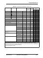
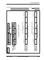
Input/Output
A variety of system configurations are facilitated by the DSP56012 Input/Output
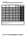
(I/O) structure. Each I/O interface has its own control, status, and double-buffered
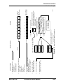
data registers that are memory-mapped in the X-data memory space (see Table 1-5).
The HI, SHI, SAI , and DAX also have several dedicated interrupt vector addresses
and control bits to enable and disable interrupts (see Table 1-3 on page 1-13). These
interrupt vectors minimize the overhead associated with servicing an interrupt by
immediately executing the appropriate service routine. Each interrupt can be
configured to one of three maskable priority levels.
1-16
DSP56012 User’s Manual
MOTOROLA
Overview
DSP56012 Architectural Overview
Table 1-5 On-chip Peripheral Memory Map
Address
Register
X:$FFFF
Interrupt Priority Register (IPR)
X:$FFFE
Reserved
X:$FFFD
PLL Control Register (PCTL)
X:$FFFC
Reserved
X:$FFFB
Reserved
X:$FFFA
Reserved
X:$FFF9
Reserved
X:$FFF8
Reserved
X:$FFF7
GPIO Control/Data Register (GPIOR)
X:$FFF6
Reserved
X:$FFF5
Reserved
X:$FFF4
Reserved
X:$FFF3
SHI Receive FIFO/Transmit Register (HRX/HTX)
X:$FFF2
SHI I2C Slave Address Register (HSAR)
X:$FFF1
SHI Host Control/Status Register (HCSR)
X:$FFF0
SHI Host Clock Control Register (HCKR)
X:$FFEF
Reserved
X:$FFEE
Port B Data Register (PBD)
X:$FFED
Port B Data Direction Register (PBDDR)
X:$FFEC
Port B Control Register (PBC)
X:$FFEB
Host Receive/Transmit Register (HORX/HOTX)
X:$FFEA
Reserved
X:$FFE9
Host Status Register (HSR)
X:$FFE8
Host Control Register (HCR)
X:$FFE7
SAI TX2 Data RegisteR (TX2)
X:$FFE6
SAI TX1 Data Register (TX1)
X:$FFE5
SAI TX0 Data Register (TX0)
X:$FFE4
SAI TX Control/Status Register (TCS)
X:$FFE3
SAI RX1 Data Register (RX1)
X:$FFE2
SAI RX0 Data Register (RX0)
X:$FFE1
SAI RX Control/Status Register (RCS)
X:$FFE0
SAI Baud Rate Control Register (BRC)
X:$FFDF
DAX Status Register (XSTR)
MOTOROLA
DSP56012 User’s Manual
1-17
Overview
DSP56012 Architectural Overview
Table 1-5 On-chip Peripheral Memory Map (Continued)
Address
Register
X:$FFDE
DAX Control Register (XCTR)
X:$FFDD
Reserved
X:$FFDC
DAX Transmit Data Registers (XADRA/XADRB)
X:$FFDB
Reserved
:
:
X:$FFC0
Reserved
1.3.4.1
Parallel Host Interface (HI)
The parallel Host Interface (HI) is a byte-wide, full-duplex, double-buffered, parallel
port that can be connected directly to the data bus of a host processor. The host
processor can be any of a number of industry-standard microcomputers or
microprocessors, another DSP, or DMA hardware, because this interface looks like
static memory to the host processor. The HI is asynchronous and consists of two sets
of registers—one set accessible only to the host processor and a second set accessible
only to the DSP CPU (see Section 4, Parallel Host Interface).
1.3.4.2
Serial Host Interface (SHI)
The Serial Host Interface (SHI) provides a serial path for communication and
program/coefficient data transfers between the DSP and an external host processor
or other serial peripheral devices. This interface can connect directly to one of two
well-known and widely-used synchronous serial buses: the Serial Peripheral
Interface (SPI) bus defined by Motorola and the Inter Integrated-circuit Control (I2C)
bus defined by Philips. The SHI handles both SPI and I2C bus protocols as required
from a slave or a single-master device. In order to minimize DSP overhead, the SHI
supports single-, double-, and triple-byte data transfers. An optimal ten-word receive
FIFO register reduces the DSP overhead for data reception (see Section 5, Serial
Host Interface).
1-18
DSP56012 User’s Manual
MOTOROLA
Overview
DSP56012 Architectural Overview
1.3.4.3
Serial Audio Interface (SAI)
The DSP can communicate with other devices through its serial audio interfaces. The
Serial Audio Interface (SAI) provides a synchronous full-duplex serial port for serial
connection with a variety of audio devices such as Analog-to-Digital (A/D)
converters, Digital-to-Analog (D/A) converters, Compact Disc (CD) devices, etc. The
SAI implements a wide range of serial data formats in use by audio manufacturers.
Examples are:
• I2S format (Philips)
• CDP format (Sony)
• MEC format (Matsushita)
• Most industry-standard serial A/D and D/A formats
The SAI consists of independent transmit and receive sections and a common baud
rate generator. The transmitter consists of three transmitters controlled by one
transmitter controller. This enables simultaneous data transmission to as many as
three stereo audio devices, or transmission of three separate stereo pairs of audio
channels. The receiver consists of two receivers and a single receive controller. This
enables simultaneous data reception from up to two stereo audio devices. The
transmit and receive sections are fully asynchronous and may transmit and receive at
different rates (see Section 6, Serial Audio Interface).
1.3.4.4
General Purpose I/O
The General Purpose Input/Output (GPIO) pins are used for control and handshake
functions between the DSP and external circuitry. The GPIO port has eight dedicated
pins (GPIO0–GPIO7) that are controlled through a memory-mapped register.
Associated with each GPIO pin is a data bit, a control bit, and a data direction bit that
configures the pin as an input or an output, open-collector or normal (see Section 7,
GPIO).
1.3.4.5
Digital Audio Transmitter (DAX)
The Digital Audio Transmitter (DAX) is a serial audio interface module that outputs
digital audio data in the AES/EBU, CP-340, and IEC958 formats. The DAX transmits
one frame (consisting of two sub-frames) of audio and non-audio data at a time.
However, the DAX data path is double buffered so the next frame data can be stored
in the DAX without affecting the frame currently being transmitted (see Section 8,
Digital Audio Transmitter).
MOTOROLA
DSP56012 User’s Manual
1-19
Overview
DSP56012 Architectural Overview
1-20
DSP56012 User’s Manual
MOTOROLA
SECTION 2
SIGNAL DESCRIPTIONS
MOTOROLA
DSP56012 User’s Manual
2-1
Signal Descriptions
2.1
2.2
2.3
2.4
2.5
2.6
2.7
2.8
2.9
2.10
2.11
2-2
SIGNAL GROUPINGS. . . . . . . . . . . . . . . . . . . . . . . . . . . . . . 2-3
POWER . . . . . . . . . . . . . . . . . . . . . . . . . . . . . . . . . . . . . . . . . 2-5
GROUND. . . . . . . . . . . . . . . . . . . . . . . . . . . . . . . . . . . . . . . . 2-6
PHASE LOCK LOOP (PLL) . . . . . . . . . . . . . . . . . . . . . . . . . . 2-7
INTERRUPT AND MODE CONTROL . . . . . . . . . . . . . . . . . . 2-8
HOST INTERFACE (HI) . . . . . . . . . . . . . . . . . . . . . . . . . . . 2-10
SERIAL HOST INTERFACE (SHI) . . . . . . . . . . . . . . . . . . . 2-13
SERIAL AUDIO INTERFACE (SAI) . . . . . . . . . . . . . . . . . . . 2-16
GENERAL PURPOSE INPUT/OUTPUT (GPIO) . . . . . . . . . 2-18
DIGITAL AUDIO INTERFACE (DAX) . . . . . . . . . . . . . . . . . 2-18
OnCE PORT . . . . . . . . . . . . . . . . . . . . . . . . . . . . . . . . . . . . 2-19
DSP56012 User’s Manual
MOTOROLA
Signal Descriptions
Signal Groupings
2.1
SIGNAL GROUPINGS
The DSP56012 input and output signals are organized into the ten functional groups
shown in Table 2-1. The individual signals are shown in Figure 2-1 on page 2-4.
Table 2-1 DSP56012 Functional Signal Groupings
Number of
Signals
Detailed
Description
Power (VCC)
13
Table 2-2
Ground (GND)
17
Table 2-3
PLL
4
Table 2-4
Interrupt and Mode Control
4
Table 2-5
15
Table 2-6
Serial Host Interface (SHI)
5
Table 2-7
Serial Audio Interface (SAI)
9
Table 2-8
Table 2-9
General Purpose Input/Output (GPIO)
8
Table 2-10
Digital Audio Transmitter (DAX)
2
Table 2-11
OnCE Port
4
Table 2-12
Functional Group
Host Interface (HI)
MOTOROLA
Port B
DSP56012 User’s Manual
2-3
Signal Descriptions
Signal Groupings
DSP56012
VCCP
VCCQ
VCCA
VCCD
VCCH
VCCS
GNDP
GNDQ
GNDA
GNDD
GNDH
GNDS
PLOCK
PCAP
PINIT
EXTAL
4
2
1
3
2
4
3
2
4
3
Power Inputs:
PLL
Internal Logic
A
D
HI
SHI
Grounds:
PLL
Internal Logic
A
D
HI
SHI
PLL
Host
Interface
(HI) Port
8
Serial Host
Interface (SHI)
MOSI/HA0
SS/HA2
MISO/SDA
SCK/SCL
HREQ
Serial Audio
Interface (SAI)
Rec0
Rec1
WSR
SCKR
SDI0
SDI1
WST
SCKT
SDO0
SDO1
SDO2
Tran0
Tran1
Tran2
MODA/IRQA
MODB/IRQB
MODC/NMI
RESET
Interrupt
/Mode
Control
H0–H7
HOA0
HOA1
HOA2
HR/W
HEN
HOREQ
HACK
General Purpose
Input/Output (GPIO)
8
Digital Audio
Transmitter (DAX)
OnCE™
Port
Port B GPIO
PB0–PB7
PB8
PB9
PB10
PB11
PB12
PB13
PB14
GPIO0–GPIO7
ADO
ACI
DSCK/OS1
DSI/OS0
DSO
DR
Figure 2-1 DSP56012 Signals
2-4
DSP56012 User’s Manual
MOTOROLA
Signal Descriptions
Power
2.2
POWER
Table 2-2 Power Inputs
Power Name
Description
VCCP
PLL Power—VCCP is VCC dedicated for Phase Lock Loop (PLL) use. The voltage
should be well-regulated and the input should be provided with an extremely
low impedance path to the VCC power rail. VCCP should be bypassed to GNDP
by a 0.1 µF capacitor located as close as possible to the chip package.
VCCQ
Quiet Power—VCCQ is an isolated power for the internal processing logic. This
input must be tied externally to all other chip power inputs. The user must
provide adequate external decoupling capacitors.
VCCA
A Power—VCCA is an isolated power for sections of the internal chip logic. This
input must be tied externally to all other chip power inputs. The user must
provide adequate external decoupling capacitors.
VCCD
D Power—VCCD is an isolated power for sections of the internal chip logic. This
input must be tied externally to all other chip power inputs. The user must
provide adequate external decoupling capacitors.
VCCH
Host Power—VCCH is an isolated power for the HI I/O drivers. This input must
be tied externally to all other chip power inputs. The user must provide adequate
external decoupling capacitors.
VCCS
Serial Host Power—VCCS is an isolated power for the SHI I/O drivers. This
input must be tied externally to all other chip power inputs. The user must
provide adequate external decoupling capacitors.
MOTOROLA
DSP56012 User’s Manual
2-5
Signal Descriptions
Ground
2.3
GROUND
Table 2-3 Grounds
Ground Name
Description
GNDP
PLL Ground—GNDP is ground dedicated for PLL use. The connection should be
provided with an extremely low-impedance path to ground. VCCP should be
bypassed to GNDP by a 0.1 µF capacitor located as close as possible to the chip
package.
GNDQ
Internal Logic Ground—GNDQ is an isolated ground for the internal processing
logic. This connection must be tied externally to all other chip ground
connections. The user must provide adequate external decoupling capacitors.
GNDA
A Ground—GNDA is an isolated ground for sections of the internal logic. This
connection must be tied externally to all other chip ground connections. The user
must provide adequate external decoupling capacitors.
GNDD
D Ground—GNDD is an isolated ground for sections of the internal logic. This
connection must be tied externally to all other chip ground connections. The user
must provide adequate external decoupling capacitors.
GNDH
Host Ground—GNDH is an isolated ground for the HI I/O drivers. This
connection must be tied externally to all other chip ground connections. The user
must provide adequate external decoupling capacitors.
GNDS
Serial Host Ground—GNDS is an isolated ground for the SHI I/O drivers. This
connection must be tied externally to all other chip ground connections. The user
must provide adequate external decoupling capacitors.
2-6
DSP56012 User’s Manual
MOTOROLA
Signal Descriptions
Phase Lock Loop (PLL)
2.4
PHASE LOCK LOOP (PLL)
Table 2-4 Phase Lock Loop Signals
Type
State During
Reset
Output
Indeterminate
Signal Name
PLOCK
Signal Description
Phase Locked—PLOCK is an output signal that, when
driven high, indicates that the PLL has achieved phase
lock. After Reset, PLOCK is driven low until lock is
achieved.
Note:
PCAP
Input
Input
PLOCK is a reliable indicator of the PLL lock
state only after the chip has exited the Reset
state. During hardware reset, the PLOCK state is
determined by PINIT and the current PLL lock
condition.
PLL Capacitor—PCAP is an input connecting an off-chip
capacitor to the PLL filter. Connect one capacitor
terminal to PCAP and the other terminal to VCCP.
If the PLL is not used, PCAP may be tied to VCC, GND,
or left floating.
PINIT
Input
Input
PLL Initial—During assertion of RESET, the value of
PINIT is written into the PLL Enable (PEN) bit of the PLL
Control Register, determining whether the PLL is
enabled or disabled.
EXTAL
Input
Input
External Clock/Crystal Input—EXTAL interfaces the
internal crystal oscillator input to an external crystal or
an external clock.
MOTOROLA
DSP56012 User’s Manual
2-7
Signal Descriptions
Interrupt and Mode Control
2.5
INTERRUPT AND MODE CONTROL
Table 2-5 Interrupt and Mode Control
Signal Name
MODA/IRQA
Type
State During
Reset
Input Input
Signal Description
Mode Select A/External Interrupt Request A—This
input has two functions:
1. to select the initial chip operating mode, and
2.
after synchronization, to allow an external device
to request a DSP interrupt.
MODA is read and internally latched in the DSP when the
processor exits the Reset state. MODA, MODB, and
MODC select the initial chip operating mode. Several
clock cycles (depending on PLL stabilization time) after
leaving the Reset state, the MODA signal changes to
external interrupt request IRQA. The chip operating
mode can be changed by software after reset. The IRQA
input is a synchronized external interrupt request that
indicates that an external device is requesting service. It
may be programmed to be level-sensitive or
negative-edge-sensitive. If the processor is in the Stop
state and IRQA is asserted, the processor will exit the Stop
state.
MODB/IRQB
Input Input
Mode Select B/External Interrupt Request B—This input
has two functions:
1. to select the initial chip operating mode, and
2.
after internal synchronization, to allow an
external device to request a DSP interrupt.
MODB is read and internally latched in the DSP when the
processor exits the Reset state. MODA, MODB, and
MODC select the initial chip operating mode. Several
clock cycles (depending on PLL stabilization time) after
leaving the Reset state, the MODB signal changes to
external interrupt request IRQB. After reset, the chip
operating mode can be changed by software. The IRQB
input is an external interrupt request that indicates that
an external device is requesting service. It may be
programmed to be level-sensitive or
negative-edge-triggered.
2-8
DSP56012 User’s Manual
MOTOROLA
Signal Descriptions
Interrupt and Mode Control
Table 2-5 Interrupt and Mode Control (Continued)
Signal Name
MODC/NMI
Type
State During
Reset
Input Input
Signal Description
Mode Select C/Non-maskable Interrupt Request— This
input has two functions:
1. to select the initial chip operating mode, and
2.
after internal synchronization, to allow an
external device to request a non-maskable DSP
interrupt.
MODC is read and internally latched in the DSP when the
processor exits the Reset state. MODA, MODB, and
MODC select the initial chip operating mode. Several
clock cycles (depending on PLL stabilization time) after
leaving the Reset state, the MODC signal changes to the
nonmaskable external interrupt request NMI. After reset,
the chip operating mode can be changed by software. The
NMI input is an external interrupt request that indicates
that an external device is requesting service. It may be
programmed to be level-sensitive or
negative-edge-sensitive.
RESET
MOTOROLA
Input Input
Reset—This input is a direct hardware reset on the
processor. When RESET is asserted low, the DSP is
initialized and placed in the Reset state. A Schmitt trigger
input is used for noise immunity. When the RESET signal
is deasserted, the initial chip operating mode is latched
from the MODA, MODB, and MODC signals. The
internal reset signal is deasserted synchronous with the
internal clocks. In addition, the PINIT pin is sampled and
written into the PEN bit of the PLL Control Register.
DSP56012 User’s Manual
2-9
Signal Descriptions
Host Interface (HI)
2.6
HOST INTERFACE (HI)
The HI provides a fast parallel data to 8-bit port, which may be connected directly
to the host bus. The HI supports a variety of standard buses, and can be directly
connected to a number of industry standard microcomputers, microprocessors,
DSPs, and DMA hardware.
Table 2-6 Host Interface
Signal Name
H0–H7
Type
Input/
Output
State During
Reset
Input
Signal Description
Host Data Bus (H0–H7)—This data bus transfers data
between the host processor and the DSP56012.
When configured as a Host Interface port, the
H0–H7signals are tri-stated as long as HEN is
deasserted. The signals are inputs unless HR/W is high
and HEN is asserted, in which case H0–H7 become
outputs, allowing the host processor to read the
DSP56012 data. H0–H7 become outputs when HACK is
asserted during HOREQ assertion.
Port B GPIO 0–7 (PB0–PB7)—These signals are General
Purpose I/O signals (PB0–PB7) when the Host Interface is
not selected.
PB0–PB7
After reset, the default state for these signals is GPIO
input.
HOA0–HOA2
PB8–PB10
Input
Input/
Output
Input
Host Address 0 – Host Address 2
(HOA0–HOA2)—These inputs provide the address
selection for each Host Interface register.
Port B GPIO 8–10 (PB8–PB10)—These signals are
General Purpose I/O signals (PB8–PB10) when the Host
Interface is not selected.
After reset, the default state for these signals is GPIO
input.
2-10
DSP56012 User’s Manual
MOTOROLA
Signal Descriptions
Host Interface (HI)
Table 2-6 Host Interface (Continued)
Signal Name
HR/W
PB11
Type
State During
Reset
Input
Input
Input/
Output
Signal Description
Host Read/Write—This input selects the direction of
data transfer for each host processor access. If HR/W is
high and HEN is asserted, H0–H7 are outputs and DSP
data is transferred to the host processor. If HR/W is low
and HEN is asserted, H0–H7 are inputs and host data is
transferred to the DSP. HR/W must be stable when
HEN is asserted.
Port B GPIO 11 (PB11)—This signal is a General
Purpose I/O signal (PB11) when the Host Interface is
not being used.
After reset, the default state for this signal is GPIO
input.
HEN
Input
PB12
Input/
Output
Input
Host Enable—This input enables a data transfer on the
host data bus. When HEN is asserted and HR/W is
high, H0–H7 become outputs and the host processor
may read DSP56011 data. When HEN is asserted and
HR/W is low, H0–H7 become inputs. Host data is
latched inside the DSP on the rising edge of HEN.
Normally, a chip select signal derived from host address
decoding and an enable strobe are used to generate
HEN.
Port B GPIO 12 (PB12)—This signal is a General
Purpose I/O signal (PB12) when the Host Interface is
not being used.
After reset, the default state for this signal is GPIO
input.
HOREQ
Opendrain
Output
Input
Host Request— This signal is used by the Host Interface
to request service from the host processor, DMA
controller, or a simple external controller.
Note:
PB13
Input/
Output
HOREQ should always be pulled high when it
is not in use.
Port B GPIO 13 (PB13)—This signal is a General
Purpose (not open-drain) I/O signal (PB13) when the
Host Interface is not selected.
After reset, the default state for this signal is GPIO
input.
MOTOROLA
DSP56012 User’s Manual
2-11
Signal Descriptions
Host Interface (HI)
Table 2-6 Host Interface (Continued)
Signal Name
HACK
Type
State During
Reset
Input
Input
Signal Description
Host Acknowledge— This input has two functions. It
provides a host acknowledge handshake signal for
DMA transfers and it receives a host interrupt
acknowledge compatible with MC68000 family
processors.
Note:
PB14
Input/
Output
HACK should always be pulled high when it is
not in use.
Port B GPIO 14 (PB14)—This signal is a General
Purpose I/O signal (PB14) when the Host Interface is
not selected.
After reset, the default state for this signal is GPIO
input.
2-12
DSP56012 User’s Manual
MOTOROLA
Signal Descriptions
Serial Host Interface (SHI)
2.7
SERIAL HOST INTERFACE (SHI)
The SHI has five I/O signals that can be configured to allow the SHI to operate in
either SPI or I2C mode.
Table 2-7 Serial Host Interface (SHI) Signals
Signal
Name
SCK/
SCL
Signal
Type
Input or
Output
State
during
Reset
Tri-stated
Signal Description
SPI Serial Clock/I2C Serial Clock—The SCK signal is an
output when the SPI is configured as a master, and a
Schmitt-trigger input when the SPI is configured as a slave.
When the SPI is configured as a master, the SCK signal is
derived from the internal SHI clock generator. When the SPI
is configured as a slave, the SCK signal is an input, and the
clock signal from the external master synchronizes the data
transfer. The SCK signal is ignored by the SPI if it is defined
as a slave and the Slave Select (SS) signal is not asserted. In
both the master and slave SPI devices, data is shifted on one
edge of the SCK signal and is sampled on the opposite edge
where data is stable. Edge polarity is determined by the SPI
transfer protocol. SCL carries the clock for I2C bus
transactions in the I2C mode. SCL is a Schmitt-trigger input
when configured as a slave, and an open-drain output when
configured as a master. SCL should be connected to VCC
through a pull-up resistor.
The maximum allowed internally generated bit clock
frequency is fosc/4 for the SPI mode and fosc/6 for the I2C
mode where fosc is the clock on EXTAL. The maximum
allowed externally generated bit clock frequency is fosc/3 for
the SPI mode and fosc/5 for the I2C mode
An external pull-up resistor is not required.
MOTOROLA
DSP56012 User’s Manual
2-13
Signal Descriptions
Serial Host Interface (SHI)
Table 2-7 Serial Host Interface (SHI) Signals (Continued)
Signal
Name
MISO/
SDA
Signal
Type
Input or
Output
State
during
Reset
Tri-stated
Signal Description
SPI Master-In-Slave-Out/I2C Data and
Acknowledge—When the SPI is configured as a master,
MISO is the master data input line. The MISO signal is used
in conjunction with the MOSI signal for transmitting and
receiving serial data. This signal is a Schmitt-trigger input
when configured for the SPI Master mode, an output when
configured for the SPI Slave mode, and tri-stated if
configured for the SPI Slave mode when SS is deasserted.
In I2C mode, SDA is a Schmitt-trigger input when receiving
and an open-drain output when transmitting. SDA should be
connected to VCC through a pull-up resistor. SDA carries the
data for I2C transactions. The data in SDA must be stable
during the high period of SCL. The data in SDA is only
allowed to change when SCL is low. When the bus is free,
SDA is high. The SDA line is only allowed to change during
the time SCL is high in the case of start and stop events. A
high to low transition of the SDA line while SCL is high is an
unique situation, which is defined as the start event. A low to
high transition of SDA while SCL is high is an unique
situation, which is defined as the stop event.
An external pull-up resistor is not required.
MOSI/
HA0
Input or
Output
Tri-stated
SPI Master-Out-Slave-In/I2C Slave Address 0—When the
SPI is configured as a master, MOSI is the master data output
line. The MOSI signal is used in conjunction with the MISO
signal for transmitting and receiving serial data. MOSI is the
slave data input line when the SPI is configured as a slave.
This signal is a Schmitt-trigger input when configured for the
SPI Slave mode.
This signal uses a Schmitt-trigger input when configured for
the I2C mode. When configured for I2C Slave mode, the HA0
signal is used to form the slave device address. HA0 is
ignored when it is configured for the I2C Master mode.
An external pull-up resistor is not required.
2-14
DSP56012 User’s Manual
MOTOROLA
Signal Descriptions
Serial Host Interface (SHI)
Table 2-7 Serial Host Interface (SHI) Signals (Continued)
Signal
Name
SS/HA2
Signal
Type
Input
State
during
Reset
Tri-stated
Signal Description
SPI Slave Select/I2C Slave Address 2—This signal is an
active low Schmitt-trigger input when configured for the SPI
mode. When configured for the SPI Slave mode, this signal is
used to enable the SPI slave for transfer. When configured for
the SPI Master mode, this signal should be kept deasserted. If
it is asserted while configured as SPI master, a bus error
condition will be flagged.
This signal uses a Schmitt-trigger input when configured for
the I2C mode. When configured for the I2C Slave mode, the
HA2 signal is used to form the slave device address. HA2 is
ignored in the I2C Master mode. If SS is deasserted, the SHI
ignores SCK clocks and keeps the MISO output signal in the
high-impedance state.
This signal is tri-stated during hardware, software, or
personal reset (no need for external pull-up in this state).
HREQ
Input or
Output
Tri-stated
Host Request—This signal is an active low Schmitt-trigger
input when configured for the Master mode, but an active
low output when configured for the Slave mode.
When configured for the Slave mode, HREQ is asserted to
indicate that the SHI is ready for the next data word transfer
and deasserted at the first clock pulse of the new data word
transfer. When configured for the Master mode, HREQ is an
input, and when asserted by the external slave device, it will
trigger the start of the data word transfer by the master. After
finishing the data word transfer, the master will await the
next assertion of HREQ to proceed to the next transfer.
This signal is tri-stated during hardware, software, personal
reset, or when the HREQ1–HREQ0 bits in the HCSR are
cleared (no need for external pull-up in this state).
MOTOROLA
DSP56012 User’s Manual
2-15
Signal Descriptions
Serial Audio Interface (SAI)
2.8
SERIAL AUDIO INTERFACE (SAI)
The SAI is composed of separate receiver and transmitter sections.
2.8.1
SAI Receive Section
The receive section of the SAI has four dedicated signals.
Table 2-8 Serial Audio Interface (SAI) Receive Signals
Signal
Name
SDI0
Signal
Type
Input
State
during
Reset
Signal Description
Tri-stated
Serial Data Input 0—This is the receiver 0 serial data input.
This signal is high impedance during hardware or software
reset, while receiver 0 is disabled (R0EN = 0), or while the chip
is in the Stop state. No external pull-up resistor is required.
SDI1
Input
Tri-stated
Serial Data Input 1—This is the receiver 1 serial data input.
This signal is high impedance during hardware or software
reset, while receiver 1 is disabled (R1EN = 0), or while the chip
is in the Stop state. No external pull-up resistor is required.
SCKR
Input or
Output
Tri-stated
Receive Serial Clock—SCKR is an output if the receiver
section is programmed as a master, and a Schmitt-trigger
input if programmed as a slave.
SCKR is high impedance if all receivers are disabled (personal
reset) and during hardware or software reset, or while the chip
is in the Stop state. No external pull-up is necessary.
WSR
Input or
Output
Tri-stated
Receive Word Select—WSR is an output if the receiver section
is programmed as a master, and a Schmitt-trigger input if
programmed as a slave. WSR is used to synchronize the data
word and to select the left/right portion of the data sample.
WSR is high impedance if all receivers are disabled (personal
reset), during hardware reset, during software reset, or while
the chip is in the stop state. No external pull-up is necessary.
2-16
DSP56012 User’s Manual
MOTOROLA
Signal Descriptions
Serial Audio Interface (SAI)
2.8.2
SAI Transmit Section
The transmit section of the SAI has five dedicated signals.
Table 2-9 Serial Audio Interface (SAI) Transmit Signals
Signal
Name
Signal
Type
State
during
Reset
Signal Description
SDO0
Output
Driven
high
Serial Data Output 0—SDO0 is the transmitter 0 serial output.
SDO0 is driven high if transmitter 0 is disabled, during
personal reset, hardware reset and software reset, or when the
chip is in the Stop state.
SDO1
Output
Driven
high
Serial Data Output 1—SDO1 is the transmitter 1 serial output.
SDO1 is driven high if transmitter 1 is disabled, during
personal reset, hardware reset and software reset, or when the
chip is in the Stop state.
SDO2
Output
Driven
high
Serial Data Output 2—SDO2 is the transmitter 2 serial output.
SDO2 is driven high if transmitter 2 is disabled, during
personal reset, hardware reset and software reset, or when the
chip is in the Stop state.
SCKT
Input
or
Output
Tri-stated
Transmit Serial Clock—This signal provides the clock for the
Serial Audio Interface (SAI). The SCKT signal can be an output
if the transmit section is programmed as a master, or a
Schmitt-trigger input if the transmit section is programmed as
a slave. When the SCKT is an output, it provides an internally
generated SAI transmit clock to external circuitry. When the
SCKT is an input, it allows external circuitry to clock data out
of the SAI.
SCKT is tri-stated if all transmitters are disabled (personal
reset), during hardware reset, software reset, or while the chip
is in the Stop state. No external pull-up is necessary.
WST
Input
or
Output
Tri-stated
Transmit Word Select—WST is an output if the transmit
section is programmed as a master, and a Schmitt-trigger input
if programmed as a slave. WST is used to synchronize the data
word and select the left/right portion of the data sample.
WST is tri-stated if all transmitters are disabled (personal
reset), during hardware or software reset, or while the chip is
in the Stop state. No external pull-up is necessary.
MOTOROLA
DSP56012 User’s Manual
2-17
Signal Descriptions
General Purpose Input/Output (GPIO)
2.9
GENERAL PURPOSE INPUT/OUTPUT (GPIO)
Table 2-10 General Purpose I/O (GPIO) Signals
Signal
Name
GPIO0–
GPIO7
2.10
Signal Type
Input or
Output
(standard or
open-drain)
State during
Reset
Disconnected
internally
Signal Description
General Purpose Input/Output—These signals
are used for control and handshake functions
between the DSP and external circuitry. Each
GPIO signal may be individually programmed to
be one of four states:
• Not connected
• Input
• Standard output
• Open-drain output
DIGITAL AUDIO INTERFACE (DAX)
Table 2-11 Digital Audio Interface (DAX) Signals
Signal Name
Type
State During
Reset
Signal Description
ADO
Output
Output, driven Digital Audio Data Output—This signal is an
high
audio and non-audio output in the form of
AES/EBU, CP340 and IEC958 data in a biphase
mark format. The signal is driven high when the
DAX is disabled, and during hardware or software
reset.
ACI
Input
Tri-stated
2-18
Audio Clock Input—This is the DAX clock input.
When programmed to use an external clock, this
input supplies the DAX clock. The external clock
frequency must 256, 384, or 512 times the audio
sampling frequency (256 x Fs, 384 x Fs or 512 x Fs,
respectively). The ACI signal is high impedance
(tri-stated) only during hardware or software reset.
If the DAX is not used, connect the ACI signal to
ground through an external pull-down resistor to
ensure a stable logic level at the input.
DSP56012 User’s Manual
MOTOROLA
Signal Descriptions
OnCE Port
2.11
OnCE PORT
Table 2-12 On-Chip Emulation Port (OnCE) Signals
Signal
Name
Signal
Type
State
during
Reset
DSI/OS0
Input/O
utput
Low
Output
Signal Description
Debug Serial Input/Chip Status 0—Serial data or commands
are provided to the OnCE controller through the DSI/OS0
signal when it is an input. The data received on the DSI signal
will be recognized only when the DSP has entered the Debug
mode of operation. Data is latched on the falling edge of the
DSCK serial clock. Data is always shifted into the OnCE serial
port Most Significant Bit (MSB) first. When the DSI/OS0 signal
is an output, it works in conjunction with the OS1 signal to
provide chip status information. The DSI/OS0 signal is an
output when the processor is not in Debug mode. When
switching from output to input, the signal is tri-stated.
Note:
DSCK/
OS1
Input/O
utput
Low
Output
If the OnCE interface is in use, an external pull-down resistor
should be attached to this pin. If the OnCE interface is not in
use, the resistor is not required.
Debug Serial Clock/Chip Status 1—The DSCK/OS1 signal
supplies the serial clock to the OnCE when it is an input. The
serial clock provides pulses required to shift data into and out
of the OnCE serial port. (Data is clocked into the OnCE on the
falling edge and is clocked out of the OnCE serial port on the
rising edge.) The debug serial clock frequency must be no
greater than 1/8 of the processor clock frequency. When
switching from input to output, the signal is tri-stated.
When it is an output, this signal works with the OS0 signal to
provide information about the chip status. The DSCK/OS1
signal is an output when the chip is not in Debug mode.
Note:
MOTOROLA
If the OnCE interface is in use, an external pull-down resistor
should be attached to this pin. If the OnCE interface is not in
use, the resistor is not required.
DSP56012 User’s Manual
2-19
Signal Descriptions
OnCE Port
Table 2-12 On-Chip Emulation Port (OnCE) Signals (Continued)
Signal
Name
DSO
Signal
Type
Output
State
during
Reset
Pulled
high
Signal Description
Debug Serial Output—Data contained in one of the OnCE
controller registers is provided through the DSO output signal,
as specified by the last command received from the external
command controller. Data is always shifted out the OnCE
serial port MSB first. Data is clocked out of the OnCE serial
port on the rising edge of DSCK.
The DSO signal also provides acknowledge pulses to the
external command controller. When the chip enters the Debug
mode, the DSO signal will be pulsed low to indicate
(acknowledge) that the OnCE is waiting for commands. After
the OnCE receives a read command, the DSO signal will be
pulsed low to indicate that the requested data is available and
the OnCE serial port is ready to receive clocks in order to
deliver the data. After the OnCE receives a write command, the
DSO signal will be pulsed low to indicate that the OnCE serial
port is ready to receive the data to be written; after the data is
written, another acknowledge pulse will be provided.
DR
Input
Input
Debug Request—The debug request input (DR) allows the
user to enter the Debug mode of operation from the external
command controller. When DR is asserted, it causes the DSP to
finish the current instruction being executed, save the
instruction pipeline information, enter the Debug mode, and
wait for commands to be entered from the DSI line. While in
Debug mode, the DR signal lets the user reset the OnCE
controller by asserting it and deasserting it after receiving
acknowledge. It may be necessary to reset the OnCE controller
in cases where synchronization between the OnCE controller
and external circuitry is lost. DR must be deasserted after the
OnCE responds with an acknowledge on the DSO signal and
before sending the first OnCE command. Asserting DR will
cause the chip to exit the Stop or Wait state. Having DR
asserted during the deassertion of RESET will cause the DSP to
enter Debug mode.
Note:
2-20
If the OnCE interface is not in use, attach an external pull-up
resistor to the DR input.
DSP56012 User’s Manual
MOTOROLA
SECTION 3
MEMORY, OPERATING MODES,
AND INTERRUPTS
Memory, Operating Modes, and Interrupts
SECTION
3.1
3.2
3.2.1
3.2.2
3.3
3.3.1
3.3.2
3.3.3
3.4
3.4.1
3.4.2
3.4.3
3.4.4
3.5
3.6
3.7
3.8
3-2
3
MEMORY, OPERATING MODES,
AND INTERRUPTS . . . . . . . . . . . . . . . . . . . . . . . . . 3-1
INTRODUCTION . . . . . . . . . . . . . . . . . . . . . . . . . . . . . . . . . . 3-3
DSP56012 DATA AND PROGRAM MEMORY . . . . . . . . . . . 3-3
X and Y Data ROM . . . . . . . . . . . . . . . . . . . . . . . . . . . . . . 3-4
Bootstrap ROM . . . . . . . . . . . . . . . . . . . . . . . . . . . . . . . . . 3-4
DSP56012 DATA AND PROGRAM MEMORY MAPS . . . . . 3-4
Reserved Memory Spaces . . . . . . . . . . . . . . . . . . . . . . . . 3-5
Dynamic Switch of Memory Configurations . . . . . . . . . . . 3-7
Internal I/O Memory Map . . . . . . . . . . . . . . . . . . . . . . . . . 3-9
OPERATING MODE REGISTER (OMR). . . . . . . . . . . . . . . 3-11
DSP Operating Mode (MC, MB, MA)—Bits 4, 1, and 0. . 3-11
Program RAM Enable A (PEA)—Bit 2 . . . . . . . . . . . . . . 3-11
Program RAM Enable B (PEB)—Bit 3 . . . . . . . . . . . . . . 3-11
Stop Delay (SD)—Bit 6 . . . . . . . . . . . . . . . . . . . . . . . . . . 3-12
OPERATING MODES . . . . . . . . . . . . . . . . . . . . . . . . . . . . . 3-12
INTERRUPT PRIORITY REGISTER. . . . . . . . . . . . . . . . . . 3-14
PHASE LOCK LOOP (PLL) CONFIGURATION . . . . . . . . . 3-18
OPERATION ON HARDWARE RESET . . . . . . . . . . . . . . . 3-19
DSP56012 User’s Manual
MOTOROLA
Memory, Operating Modes, and Interrupts
Introduction
3.1
INTRODUCTION
The DSP56012 program and data memories are independent, and the on-chip data
memory is divided into two separate memory spaces, X and Y. There are also two
on-chip data ROMs in the X and Y data memory spaces, and a bootstrap ROM that
can overlay part of the Program RAM. The data memories are divided into two
independent spaces to work with the two Address ALUs to feed two operands
simultaneously to the Data ALU. Through the use of Program RAM Enable bits (PEA
and PEB) in the Operating Mode Register (OMR), four different memory
configurations are possible to provide appropriate memory sizes for a variety of
applications (see Table 3-1).
Table 3-1 Internal Memory Configurations
Memory Type
No Switch
(PEA = 0,
PEB = 0)
Switch A
(PEA = 1,
PEB = 0)
Switch B
(PEA = 0,
PEB = 1)
Switch A + B
(PEA = 1,
PEB = 1)
Program RAM
0.25 K
1.0 K
1.75 K
2.5 K
XRAM
4.0 K
3.25 K
3.25 K
2.5 K
YRAM
4.25 K
4.25 K
3.5 K
3.5 K
Program ROM
15 K
15 K
15 K
15 K
XROM
3.5 K
3.5 K
3.5 K
3.5 K
YROM
2.0 K
2.0 K
2.0 K
2.0 K
This section also includes details of the interrupt vectors and priorities and describes
the effect of a hardware reset on the PLL Multiplication Factor (MF).
3.2
DSP56012 DATA AND PROGRAM MEMORY
The memory in the DSP56012 can be mapped into four different configurations
according to the PEA and PEB bits of the OMR register. The internal data and
program memory configurations are shown in Table 3-1.
Note:
Internal Data and Program ROMs are factory-programmed to support
specific applications. Refer to the DSP56012 Technical Data sheet,
order number DSP56012/D, for more information about available
configurations.
MOTOROLA
DSP56012 User’s Manual
3-3
Memory, Operating Modes, and Interrupts
DSP56012 Data and Program Memory Maps
3.2.1
X and Y Data ROM
The X data ROM occupies locations $2000–$2DFF in the X memory space. The Y data
ROM occupies locations $2000–$27FF in the Y memory space.
3.2.2
Bootstrap ROM
The bootstrap ROM allows the user to use the on-chip pre-loaded Program ROM or
load a program into the first 256 words of Program RAM and use it for applications.
The bootstrap ROM occupies locations 0–31 ($0–$1F) in the DSP56012 memory map.
It is factory-programmed to perform the bootstrap operation following hardware
reset. The bootstrap ROM activity is controlled by the Mode A, Mode B, and Mode C
(MA, MB, and MC) bits in the Operating Mode Register (OMR). The bootstrap modes
are described in Section 3.5.
Basically, the user can configure the chip using the MOD pins (MODA, MODB, and
MODC), which are read and reflected by the mode bits. The mode selected by the
MOD pin/MOD bit values can select a bypass mode (Mode 4) that causes the DSP to
use the on-chip Program ROM, or one of three bootstrap modes (Modes 1, 5, and 7).
When in one of the three bootstrap modes, the first 256 words of Program RAM are
disabled for read but accessible for write, and the bootstrap routine loads up to 256
words into the reserved RAM space. The selected mode determines the method by
which the Program RAM is loaded:
• Parallel Host Interface (Mode 1)
• Serial Host Interface (SHI) using the SPI protocol (Mode 5)
• SHI using the I2C protocol (Mode 7)
Note:
The SHI operates in the Slave mode, with the 10-word FIFO enabled,
and with the HREQ pin enabled for receive operation.
The contents of the bootstrap ROM are provided in Appendix A.
3.3
DSP56012 DATA AND PROGRAM MEMORY MAPS
The memory in the DSP56012 can be mapped into four different configurations
according to the Program RAM Enable (PEA and PEB) bits in the OMR. Memory
maps for each of the four configurations are shown in Figure 3-1, Figure 3-2,
Figure 3-3, and Figure 3-4, on the following pages.
3-4
DSP56012 User’s Manual
MOTOROLA
Memory, Operating Modes, and Interrupts
DSP56012 Data and Program Memory Maps
3.3.1
Reserved Memory Spaces
Certain areas of the memory maps are labelled ‘reserved.’ Memory spaces marked as
reserved should not be accessed by the user. They are reserved to retain
compatibility with future enhanced or derivative versions of this device. Write
operations to the reserved range are ignored. Read operations from addresses in the
reserved range return the value $000005, which is the opcode for the ILLEGAL
instruction. If an instruction fetch is attempted from an address in the reserved area,
the value returned is $000005, (ILLEGAL opcode).
Figure 3-1 Memory Maps for PEA = 0, PEB = 0
MOTOROLA
DSP56012 User’s Manual
3-5
Memory, Operating Modes, and Interrupts
DSP56012 Data and Program Memory Maps
Figure 3-2 Memory Maps for PEA = 1, PEB = 0
3-6
DSP56012 User’s Manual
MOTOROLA
Memory, Operating Modes, and Interrupts
DSP56012 Data and Program Memory Maps
Figure 3-3 Memory Maps for PEA = 0, PEB = 1
MOTOROLA
DSP56012 User’s Manual
3-7
Memory, Operating Modes, and Interrupts
DSP56012 Data and Program Memory Maps
Figure 3-4 Memory Maps for PEA = 1, PEB = 1
3.3.2
Dynamic Switch of Memory Configurations
The internal memory configuration is altered by re-mapping RAM modules from X
and Y data memories into program memory space and vice versa. Data contents of
the switched RAM modules are preserved.
The memory can be dynamically switched from one configuration to another by
changing the PEA and PEB bits in the OMR. The address ranges that are directly
affected by the switch operation are P:$0200–$0AFF, X:$0A00–$0FFF and
Y:$0E00–$10FF (see Figure 3-1, Figure 3-2, Figure 3-3, and Figure 3-4). The memory
switch can be accomplished provided that the affected address ranges are not being
accessed during the instruction cycle in which the switch operation takes place.
Specifically, the following two conditions must be observed for trouble-free dynamic
switching:
• No accesses to or from X:$0A00–$0FFF or Y:$0E00–$10FF are allowed during
the switch cycle.
3-8
DSP56012 User’s Manual
MOTOROLA
Memory, Operating Modes, and Interrupts
DSP56012 Data and Program Memory Maps
• No accesses (including instruction fetches) to/from P:$0200–$0AFF are
allowed during the switch cycle.
Note:
The switch actually occurs three instruction cycles after the instruction
that modifies the PEA/PEB bits.
Any sequence that complies with the switch conditions is valid. For example, if the
program flow executes in the address range that is not affected by the switch (other
than P:$0200–$0AFF), the switch conditions can be met very easily. In this case a
switch can be accomplished by just changing PEA/PEB bits in OMR in the regular
program flow, assuming no accesses to X:$0A00–$0FFF or Y:$0E00–$10FF occur up to
three instructions after the instruction that changes the OMR bits.
A more intricate case is one in which switch memory operation takes place while the
program flow is being executed (or should proceed) in the affected program address
range (P:$0200–$0AFF). In this case, a particular switch sequence should be
performed. Interrupts must be disabled before executing the switch sequence, since
an interrupt could cause the DSP to fetch instructions out of sequence. The interrupts
must be disabled at least four instruction cycles before switching, due to pipeline
latency of the interrupt processing.
Special attention should be given when running a memory switch routine using the
OnCE port. Running the switch routine in Trace mode, for example, can cause the
switch to complete after the PEA/PEB bit changes while the DSP is in Debug mode.
As a result, subsequent instructions might be fetched according to the new memory
configuration (after the switch), and thus might execute improperly. A general
purpose routine in which the switch conditions are always met, independent of
where the program flow originates (before the switch) or where it proceeds (after the
switch), is shown below:
;Switch to Program RAM enabled:
ORI
#03,MR
; Disable interrupts
INST1
; Four instruction cycles guarantee no interrupts
INST2
; after interrupts were disabled.
INST3
; INST# denotes a one-word instruction, however,
INST4
; two one-word instructions can be replaced by
; one two-word instruction.
ORI
#$C,OMR
; Set PEA/PEB bits in OMR
ANDI
#$FC,MR
; Allow a delay for remapping,
; meanwhile re-enable interrupts
JMP
>Next_Address
; 2-word (long) jump instruction (uninterruptable)
;Switch to Program RAM disabled:
ORI
#03,MR
; Disable interrupts
INST1
; Four instruction cycles guarantee no interrupts
INST2
; after interrupts were disabled.
INST3
; INST# denotes any one-word instruction, however,
INST4
; two one-word instructions can be replaced by
; one two-word instruction.
MOTOROLA
DSP56012 User’s Manual
3-9
Memory, Operating Modes, and Interrupts
DSP56012 Data and Program Memory Maps
ANDI
ANDI
#$F3,OMR
#$FC,MR
JMP
>Next_Address
;
;
;
;
Clear PEA/PEB bit in OMR
Allow a delay for remapping,
meanwhile re-enable interrupts
2-word (long) jump instruction (uninterruptable)
“Next_Address” is any valid program address in the new memory
configuration (after the switch). The two-word instruction “JMP
>Next_Address” can be replaced by a sequence of an NOP followed by
a one-word “JMP <Next_Address” (jump short) instruction. In cases in
which interrupts are already disabled, the sequence would be a write to
OMR with PE modified (ORI/ANDI/MOVEC), followed by an NOP as
a delay for remapping, and then followed by a JMP >long (or another
NOP and JMP <short instead).
Note:
3.3.3
Internal I/O Memory Map
The DSP56012 on-chip peripheral modules have their registers mapped to the
addresses in the internal I/O memory range, as shown in Table 3-2.
Location X:$FFFE is the Bus Control Register (BCR) for the DSP56000
core. Although labelled “Reserved” on the DSP56012, the BCR remains
active. The BCR is cleared by reset and should remain cleared (i.e., do
not write to this location) since the DSP56012 does not make use of the
BCR function.
Note:
Table 3-2 Internal I/O Memory Map
Location
Register
X: $FFFF
Interrupt Priority Register (IPR)
X: $FFFE
Reserved
X: $FFFD
PLL Control Register (PCTL)
X: $FFFC
Reserved
X: $FFFB
Reserved
X: $FFFA
Reserved
X: $FFF9
Reserved
X: $FFF8
Reserved
X: $FFF7
GPIO Control/Data Register (GPIOR)
X: $FFF6
Reserved
3-10
DSP56012 User’s Manual
MOTOROLA
Memory, Operating Modes, and Interrupts
DSP56012 Data and Program Memory Maps
Table 3-2 Internal I/O Memory Map (Continued)
Location
Register
X: $FFF5
Reserved
X: $FFF4
Reserved
X: $FFF3
SHI Receive FIFO/Transmit Register (HRX/HTX)
X: $FFF2
SHI I2C Slave Address Register (HSAR)
X: $FFF1
SHI Host Control/Status Register (HCSR)
X: $FFF0
SHI Host Clock Control Register (HCKR)
X: $FFEF
Reserved
X: $FFEE
Port B Data Register (PBD)
X: $FFED
Port B Data Direction Register (PBDDR)
X: $FFEC
Port B Control Register (PBC)
X: $FFEB
Host Receive/Transmit Register (HORX/HOTX)
X: $FFEA
Reserved
X: $FFE9
Host Status Register (HSR)
X: $FFE8
Host Control Register (HCR)
X: $FFE7
SAI TX2 Data Register (TX2)
X: $FFE6
SAI TX1 Data Register (TX1)
X: $FFE5
SAI TX0 Data Register (TX0)
X: $FFE4
SAI TX Control/Status Register (TCS)
X: $FFE3
SAI RX1 Data Register (RX1)
X: $FFE2
SAI RX0 Data Register (RX0)
X: $FFE1
SAI RX Control/Status Register (RCS)
X: $FFE0
SAI Baud Rate Control Register (BRC)
X: $FFDF
DAX Status Register (XSTR)
X: $FFDE
DAX Control Register (XCTR)
X: $FFDD
Reserved
X:$FFDC
DAX Transmit Data Registers (XADRA and XADRB)
X:$FFDB–FFC0
Reserved
MOTOROLA
DSP56012 User’s Manual
3-11
Memory, Operating Modes, and Interrupts
Operating Mode Register (OMR)
3.4
OPERATING MODE REGISTER (OMR)
The Operating Mode Register (OMR) is illustrated in Figure 3-5.
23
7
6
SD
5
4
3
2
1
MC PEB PEA MB
0
MA
Operating Mode A,B
Program RAM Enable A
Program RAM Enable B
Operating Mode C
Stop Delay
Bits 5 and 7–23 are reserved, read as 0s, and should be written with 0s
for future compatibility.
AA0291k
Figure 3-5 Operating Mode Register (OMR)
3.4.1
DSP Operating Mode (MC, MB, MA)—Bits 4, 1, and 0
The DSP operating mode bits, MC, MB, and MA, select the operating mode of the
DSP56012. These operating modes are described below in Section 3.5 Operating
Modes. On hardware reset, MC, MB, and MA are loaded from the external mode
select pins MODC, MODB, and MODA, respectively. After the DSP leaves the reset
state, MC, MB, and MA can be changed under software control.
3.4.2
Program RAM Enable A and Program RAM Enable B (PEA
and PEB)—Bits 2 and 3
The Program RAM Enable A (PEA) and Program RAM Enable B (PEB) bits are used
to alter the memory configuration on the DSP56012. Refer to Table 3-1 on page 3-3
for a summary of the memory configurations. The internal memory maps, as selected
by the PEA and PEB bits, are shown in Figure 3-1 through Figure 3-4. PEA and PEB
are cleared by hardware reset.
3.4.3
Stop Delay (SD)—Bit 6
When leaving the Stop state, the Stop Delay (SD) bit is interrogated. If the SD bit is
cleared (SD = 0), a 65,535 core clock cycle delay (131,072 T states) is implemented
before continuation of the STOP instruction cycle. If the SD bit is set (SD = 1), the
delay before continuation of the STOP instruction cycle is set as eight clock cycles (16
3-12
DSP56012 User’s Manual
MOTOROLA
Memory, Operating Modes, and Interrupts
Operating Modes
T states). When the DSP is driven by a stable external clock source, setting the SD bit
before executing the STOP instruction will allow a faster start up of the DSP.
3.5
OPERATING MODES
The DSP56012 operating modes are defined as described below and summarized in
Table 3-3. The operating modes are latched from pins MODA, MODB, and MODC
during reset and can be changed by writing to the OMR.
Table 3-3 Operating Modes
Mode
MMM
CBA
0
000
Normal operation, bootstrap disabled
1
001
Bootstrap from parallel Host Interface
2
010
Reserved
3
011
Reserved
4
100
Wake up in Program ROM address $0A00
5
101
Bootstrap from SHI (SPI mode)
6
110
Reserved
7
111
Bootstrap from SHI (I2C mode)
Operating Mode
The operating modes are described in the following paragraphs.
Mode 0
Note:
In this mode, the internal Program RAM is enabled and the bootstrap
ROM is disabled. All bootstrap programs end by selecting this
operating mode. This mode is identical to DSP56002 Mode 0.
It is not possible to reach operating Mode 0 during hardware reset. Any
attempt to start up in Mode 0 defaults to Mode 1.
Mode 1
In this mode, the bootstrap ROM is enabled and the bootstrap
program is executed after hardware reset. The internal Program RAM
is loaded with up to 256 words from the parallel Host Interface.
Mode 2
Reserved.
Mode 3
Reserved.
Note:
It is not possible to reach operating Mode 3 during hardware reset. Any
attempt to start up in Mode 3 defaults to Mode 1.
Mode 4
MOTOROLA
In this mode, the bootstrap ROM is enabled and the bootstrap
program is executed after hardware reset. The bootstrap program
DSP56012 User’s Manual
3-13
Memory, Operating Modes, and Interrupts
Operating Modes
ends up in the first location of the Program ROM (program address
$0A00).
Note:
It is not possible to reach operating Mode 4 during hardware reset. Any
attempt to start up in Mode 4 defaults to Mode 1.
Mode 5
In this mode, the bootstrap ROM is enabled and the bootstrap
program is executed after hardware reset. The internal Program RAM
is loaded with 256 words from the Serial Host Interface (SHI). The SHI
operates in the SPI Slave mode, with 24-bit word width.
Mode 6
Reserved.
Note:
Mode 7
Note:
3-14
It is not possible to reach operating Mode 6 during hardware reset. Any
attempt to start up in Mode 6 defaults to Mode 1.
In this mode, the bootstrap ROM is enabled and the bootstrap
program is executed after hardware reset. The internal Program RAM
is loaded with 256 oords from the Serial Host Interface (SHI). The SHI
operates in the I2C Slave mode, with 24-bit word width.
The OnCE port operation is enabled at hardware reset. This means the
device can enter the Debug mode at any time after hardware reset.
DSP56012 User’s Manual
MOTOROLA
Memory, Operating Modes, and Interrupts
Interrupt Priority Register
3.6
INTERRUPT PRIORITY REGISTER
Interrupt priorities are determined in the 24-bit Interrupt Priority Register (IPR). The
Interrupt Priority Level (IPL) for each on-chip peripheral device and for two of the
external interrupt sources can be programmed, under software control, to one of
three maskable priority levels (IPL 0,1 or 2). IPLs are set by writing to the IPR. The
IPR configuration is shown in Figure 3-6.
• Bits 5–0 of the IPR are used by the DSP56000 core for two of the external
interrupt request inputs, IRQA (IAL [2:0]) and IRQB (IBL[2:0]); assuming the
same IPL, IRQA has higher a priority than IRQB.
• Bits 9–6 and 23–18 are reserved for future use.
• Bits 17–10 are available for determining IPLs for each peripheral (Host, SHI,
DAX, SAI). Two IPL bits are required for each peripheral interrupt group.
The interrupt priorities are shown in Table 3-4 on page 3-16 and the interrupt
vectors are shown in Table 3-5 on page 3-17.
MOTOROLA
DSP56012 User’s Manual
3-15
Memory, Operating Modes, and Interrupts
Interrupt Priority Register
11
10
9
8
7
6
SAL1 SAL0
5
4
3
2
1
0
IBL2 IBL1 IBL0 IAL2 IAL1 IAL0
IRQA Mode
IRQB Mode
Reserved
SAI IPL
23
22
21
20
19
18
17
16
15
14
13
12
DTL1 DTL0 HPL1 HPL0 SHL1 SHL0
SHI IPL
Host IPL
DAX IPL
Reserved
Reserved, read as 0, and should be written with 0 for future compatibility
AA0292.11
Figure 3-6 Interrupt Priority Register (Addr X:$FFFF)
Table 3-4 Interrupt Priorities
Priority
Interrupt
Level 3 (Nonmaskable)
Highest
Hardware RESET
Illegal Instruction
NMI
Stack Error
Lowest
Trace
SWI
Levels 0, 1, 2 (Maskable)
Highest
IRQA
IRQB
SAI Receiver Exception
SAI Transmitter Exception
SAI Left Channel Receiver
SAI Left Channel Transmitter
3-16
DSP56012 User’s Manual
MOTOROLA
Memory, Operating Modes, and Interrupts
Interrupt Priority Register
Table 3-4 Interrupt Priorities (Continued)
Priority
Interrupt
SAI Right Channel Receiver
SAI Right Channel Transmitter
SHI Bus Error
SHI Receive Overrun Error
SHI Transmit Underrun Error
SHI Receive FIFO Full
SHI Transmit Data
SHI Receive FIFO Not Empty
HOST Command Interrupt
HOST Receive Data Interrupt
HOST Transmit Data Interrupt
DAX Transmit Underrun Error
DAX Block Transferred
Lowest
DAX Transmit Register Empty
Table 3-5 Interrupt Vectors
Address
Interrupt Source
P: $0000
Hardware RESET
P: $0002
Stack Error
P: $0004
Trace
P: $0006
SWI
P: $0008
IRQA
P: $000A
IRQB
P: $000C
Reserved
P: $000E
Reserved
P: $0010
SAI Left Channel Transmitter if TXIL = 0
P: $0012
SAI Right Channel Transmitter if TXIL = 0
P: $0014
SAI Transmitter Exception if TXIL = 0
P: $0016
SAI Left Channel Receiver if RXIL = 0
MOTOROLA
DSP56012 User’s Manual
3-17
Memory, Operating Modes, and Interrupts
Interrupt Priority Register
Table 3-5 Interrupt Vectors (Continued)
Address
Interrupt Source
P: $0018
SAI Right Channel Receiver if RXIL = 0
P: $001A
SAI Receiver Exception if RXIL = 0
P: $001C
Reserved
P: $001E
NMI
P: $0020
SHI Transmit Data
P: $0022
SHI Transmit Underrun Error
P: $0024
SHI Receive FIFO Not Empty
P: $0026
Reserved
P: $0028
SHI Receive FIFO Full
P: $002A
SHI Receive Overrun Error
P: $002C
SHI Bus Error
P: $002E
Reserved
P: $0030
Host Receive Data
P: $0032
Host Transmit Data
P: $0034
Host Command (Default)
P: $0036
Reserved
.
.
.
.
.
.
P: $003C
Reserved
P: $003E
Illegal Instruction
P: $0040
SAI Left Channel Transmitter if TXIL = 1
P: $0042
SAI Right Channel Transmitter if TXIL = 1
P: $0044
SAI Transmitter Exception if TXIL = 1
P: $0046
SAI Left Channel Receiver if RXIL = 1
P: $0048
SAI Right Channel Receiver if RXIL = 1
P: $004A
SAI Receiver Exception if RXIL = 1
P: $004C
Reserved
P: $004E
Reserved
P: $0050
DAX Transmit Underrun Error
3-18
DSP56012 User’s Manual
MOTOROLA
Memory, Operating Modes, and Interrupts
Phase Lock Loop (PLL) Configuration
Table 3-5 Interrupt Vectors (Continued)
Address
Interrupt Source
P: $0052
DAX Block Transferred
P: $0054
Reserved
P: $0056
DAX Transmit Register Empty
P: $0058
Reserved
.
.
.
.
.
.
P: $007E
Reserved
3.7
PHASE LOCK LOOP (PLL) CONFIGURATION
Section 9 of the DSP56000 Family Manual provides detailed information about the
PLL. The information included here is a brief overview of the PLL.
The PLL is configured and controlled by bits in the PLL Control Register (PCTL). The
PLL Multiplication Factor and the clock applied to EXTAL determine the frequency
at which the Voltage Controlled Oscillator (VCO) will oscillate, that is, the output
frequency of the PLL.
If the PLL is used as the DSP internal clock (PCTL bit PEN = 1):
• the PLL VCO output is used directly as the internal DSP clock if the PCTL
Chip Clock Source Bit (CSRC) is set, and
• the PLL VCO frequency is divided by the Low Power Divider (LPD) and then
used as the internal DSP clock if the CSRC bit is cleared.
The DSP56012 PLL Multiplication Factor is set to 3 during hardware reset, which
means that the Multiplication Factor bits (MF1[1:0] in the PCTL) are set to $002. The
PLL may be disabled (PEN = 0) upon reset by pulling the PINIT pin low. The DSP
will subsequently operate at the frequency of the clock applied to the EXTAL pin
until the PEN bit is set. This reset value cannot be modified by the user until the DSP
comes out of Reset. The DSP56012 LPD Division Factor bits (DF[3:0] in the PCTL) are
cleared during hardware reset. Once the PEN bit is set, it cannot be cleared by
software.
MOTOROLA
DSP56012 User’s Manual
3-19
Memory, Operating Modes, and Interrupts
Operation on Hardware Reset
EXTAL
Phase
Detector
(PD)
Charge
Pump
Loop
Filter
Voltage
Controlled
Oscillator
(VCO)
Low
Power
Divider
20 to 215
Divider Out
DF[3:0]
VCO Out
Frequency
Multiplier
Multiplication
Factor
1 to 4096
MF[11:0]
AA0293k
Figure 3-7 PLL Configuration
3.8
OPERATION ON HARDWARE RESET
The processor enters the Reset processing state when the external RESET pin is
asserted (hardware reset occurs). The Reset state:
• resets internal peripheral devices and initializes their control registers as
described in the peripheral sections,
• sets the modifier registers to $FFFF,
• clears the Interrupt Priority Register,
• clears the Stack Pointer,
• clears the Scaling mode, Trace mode, Loop Flag, Double Precision Multiply
mode and condition code bits, and sets the interrupt mask bits of the Status
Register (SR), and
• clears the Stop Delay (SD) bit and the Program RAM Enable (PEA and PEB)
bits in the OMR.
The DSP remains in the Reset state until the RESET pin is deasserted. When the
processor leaves the Reset state it:
• loads the chip operating mode bits of the OMR from the external mode select
pins (MODC, MODB, MODA), and
• begins program execution of the bootstrap ROM starting at address $0000.
3-20
DSP56012 User’s Manual
MOTOROLA
SECTION 4
PARALLEL HOST INTERFACE
MOTOROLA
DSP56012 User’s Manual
4-1
Parallel Host Interface
4.1
4.2
4.3
4.4
4-2
INTRODUCTION . . . . . . . . . . . . . . . . . . . . . . . . . . . . . . . . . .
PORT B CONFIGURATION . . . . . . . . . . . . . . . . . . . . . . . . .
PROGRAMMING THE GPIO. . . . . . . . . . . . . . . . . . . . . . . . .
HOST INTERFACE (HI) . . . . . . . . . . . . . . . . . . . . . . . . . . . .
DSP56012 User’s Manual
4-3
4-3
4-8
4-9
MOTOROLA
Parallel Host Interface
Introduction
4.1
INTRODUCTION
The parallel Host Interface (HI) can serve as an 8-bit, bidirectional parallel port or, as
Port B, a set of General Purpose Input/Output (GPIO) signals (see Figure 4-1). When
configured as the HI, the port provides a convenient connection to another processor.
Port B supports up to fifteen GPIO pins, each pin individually configurable as an
output or an input. This section describes both functions, including examples of how
to configure and use this port.
8
8
Port B
I/0
(15)
PB0–PB7
PB8
PB9
PB10
PB11
PB12
PB13
PB14
Parallel
Host
Interface
H0–H7
HOA0
HOA1
HOA2
HR/W
HEN
HOREQ
HACK
Figure 4-1 Port B Interface
4.2
PORT B CONFIGURATION
Port B functionality is controlled by three memory-mapped registers (see Figure 4-2
on page 4-4) that define the functions associated with fifteen external pins (see
Figure 4-3 on page 4-5). They are:
• Port B Control register (PBC)
• Port B Data Direction Register (PBDDR)
• Port B Data register (PBD)
Figure 4-4 on page 4-6 shows an overview of the Port B control logic.
Note: Because reset clears both the PBC and PBDDR registers, the default function of
the fifteen specified pins following reset is GPIO input.
Note: Circuitry connected to the Port B pins may need external pull-ups until the
pins are configured for operation.
MOTOROLA
DSP56012 User’s Manual
4-3
Parallel Host Interface
Port B Configuration
23
X:$FFEC 0
0
0
0
0
0
0
0
0
0
0
0
0
0
0
0
0
0
0
0
Parallel I/O (Reset Condition)
0
1
HI
1
0
HI (with HACK pin as GPIO)
1
1
Reserved
0
0
0
0
0
0
0
0
0
0
0
Function
0
Port B Data
BD BD BD BD BD BD BD BD BD BD BD BD BD BD BD Direction
0
14 13 12 11 10 9 8 7 6 5 4 3 2 1 0 Register
(PBDDR)
0
23
0
0
BC0
BDx
X:$FFEE 0
0
BC1
23
X:$FFED 0
0
0
Port B Control
BC BC Register
0
1 0 (PBC)
0
Data Direction
0
Input (Reset Condition)
1
Output
0
PB PB PB PB PB PB PB PB PB PB PB PB PB PB PB Port B Data
0
Register
14 13 12 11 10 9 8 7 6 5 4 3 2 1 0
(PBD)
AA0308.11
Figure 4-2 Parallel Port B Registers
4-4
DSP56012 User’s Manual
MOTOROLA
Parallel Host Interface
Port B
Port B Configuration
PB0
PB1
PB2
PB3
PB4
PB5
PB6
PB7
PB8
PB9
PB10
PB11
PB12
PB13
PB14
Enabled by
bits in
X:$FFEC
Direction
Selected by
bits in
X:$FFED
Input/Output
Data
X:$FFEE
BC0/BC1
BC0/BC1
BC0/BC1
BC0/BC1
BC0/BC1
BC0/BC1
BC0/BC1
BC0/BC1
BC0/BC1
BC0/BC1
BC0/BC1
BC0/BC1
BC0/BC1
BC0/BC1
BC0/BC1
BD0
BD1
BD2
BD3
BD4
BD5
BD6
BD7
BD8
BD9
BD10
BD11
BD12
BD13
BD14
PB0
PB1
PB2
PB3
PB4
PB5
PB6
PB7
PB8
PB9
PB10
PB11
PB12
PB13
PB14
PBDDR
PBD
PBC
AA0309.11
Figure 4-3 Port B GPIO Signals and Registers
MOTOROLA
DSP56012 User’s Manual
4-5
Parallel Host Interface
Port B Configuration
Port Control
Register Bit
Data Direction
Register Bit
Pin Function
0
0
Port B Input Pin
0
1
Port B Output Pin
1
X
HI Function
Port B Data (PBD)
Register Bit
Port B
Registers
Pin
(GPIO
Position)
Data Direction
Register (PBDDR) Bit
Port B Control
Register (PBC) Bit
(Input
Position)
Port B Input Data Bit
HI Output Data Bit
Peripheral
Logic
HI Data Direction Bit
HI Input Data Bit
AA0310.11
Figure 4-4 Port B I/O Pin Control Logic
4.2.1
Port B Control (PBC) Register
The Port B Control (PBC) register determines which set of functions are used with the
external multiplexed pins. As shown in Figure 4-2 on page 4-4, there are three valid
combinations:
• Parallel I/O (default)
• Host Interface
• Host Interface (with HACK as GPIO)
The default setting (BC1:BC0 = 00) defines the pins as GPIO signals. The other
settings must be programmed by writing to the PBC register. Writing a $1 to the
register defines the pins as the HI port. Writing a $2 to the PBC register defines the
pins as an HI port without a HACK signal; the pin used by HACK in the HI is
defined as a GPIO pin (PB14).
4-6
DSP56012 User’s Manual
MOTOROLA
Parallel Host Interface
Port B Configuration
4.2.2
Port B Data Direction Register (PBDDR)
For pins configured as GPIO by the PBC Register, the Port B Data Direction Register
(PBDDR) determines whether the pins are inputs (bit = 0) or outputs (bit = 1).
Note: The default setting after reset is input.
4.2.3
Port B Data (PBD) Register
The Port B Data (PBD) register provides access to the fifteen Port B pins as follows:
• If a pin is configured as a GPIO input and the processor reads the PBD
register, the processor sees the logic level on the pin. If the processor writes to
the PBD register, the data is latched there, but does not appear on the pin
because the buffer is in the high-impedance state.
• If a pin is configured as a GPIO output and the processor reads the PBD
register, the processor sees the contents of the PBD register rather than the
logic level on the pin, which allows the PBD register to be used as a general
purpose register. If the processor writes to the PBD register, the data is latched
there and appears on the pin during the following instruction cycle.
Note: If a pin is configured as a host pin, the Port B GPIO registers can help in
debugging HI operations. If the PBDDR bit for a given pin configured as an
input (i.e., 0), the PBD register shows the logic level on the pin, regardless of
whether the HI function is using the pin as an input or an output. If the
PBDDR is set (configured as an output) for a pin that is configured as a host
pin, when the processor reads the PBD register, it sees the contents of the PBD
register rather than the logic level on the pin—another case that allows the
PBD register to act as a general purpose register.
Note: The external host processor should be carefully synchronized to the DSP56012
to assure that the DSP and the external host properly read status bits
transmitted between them. There is more discussion of such port usage issues
in Sections 4.4.4.7 HI Usage Considerations—DSP Side and 4.4.8.4 HI
Port Usage Considerations—Host Side.
MOTOROLA
DSP56012 User’s Manual
4-7
Parallel Host Interface
Programming the GPIO
4.3
PROGRAMMING THE GPIO
The DSP56012 on-chip peripheral memory map is illustrated in Section 3, Memory,
Operating Modes, and Interrupts and in Appendix B, Programming Reference.
The standard MOVE instruction transfers data between Port B and a register. As a
result, MOVE takes two instructions to perform a memory-to-memory data transfer
and uses a temporary holding register. The MOVEP instruction is specifically
designed for I/O data transfer, as shown in Figure 4-5. Although the MOVEP
instruction can take twice as long to execute as a MOVE instruction, only one
MOVEP is required for a memory-to-memory data transfer, and MOVEP does not
use a temporary register. Using the MOVEP instruction allows a fast interrupt to
move data to/from a peripheral or from/to memory and execute one other
instruction or move the data to an absolute address. MOVEP is the only
memory-to-memory move instruction. However, one of the memory operands must
be in the top sixty-four locations of either X: or Y: memory, which are reserved for
internal and external I/O, respectively.
•
MOVE
#$0,X:$FFEC
;Select Port B to be
;GPIO
;Select pins PB0–PB7 to be inputs
;and pins PB8–PB14 to be outputs
MOVE
#$7F00,X:$FFED
MOVEP
#data_out,X:$FFEE
MOVEP
X:$FFEE,#data_in
•
•
;Put bits 8–14 of “data_out” on pins
;PB8–PB14, bits 0–7 are ignored.
;Put PB0–PB7 in bits 0–7 of “data_in”
Figure 4-5 Instructions to Write/Read Parallel Data with Port B
The bit-oriented instructions that use I/O short addressing (BCHG, BCLR, BSET,
BTST, JCLR, JSCLR, JSET, and JSSET) can also address individual bits for faster I/O
processing. The DSP does not have a hardware data strobe to move data out of the
GPIO port. If a strobe is needed, use software to toggle one of the GPIO pins to
emulate a strobe signal.
Figure 4-6 on page 4-9 illustrates the process of programming Port B as GPIO.
Generally, it is not good programming practice to activate a peripheral before
programming it. Thus, even though reset initializes the Port B as fifteen GPIO inputs,
it is best to configure Port B as GPIO inputs explicitly, and then configure the data
direction and data registers. However, some situations may require programming
the data direction or the data registers first to prevent two devices from driving one
signal. The order of steps 1, 2, and 3 in Figure 4-6 is optional and can be changed as
needed.
4-8
DSP56012 User’s Manual
MOTOROLA
Parallel Host Interface
Host Interface (HI)
Step 1. Activate Port B For General Purpose I/O:
Write 0s to Bits 0 And 1
15
0
BC BC
1 0
X:$FFEC
Port B
Control Register (PBC)
Step 2. Set Individual Pins To Input Or Output:
BDxx = 0
Input
or
BDxx = 1
Output
15
0
BD BD BD BD BD BD BD BD BD BD BD BD BD BD BD
14 13 12 11 10 9 8 7 6 5 4 3 2 1 0
X:$FFED
Port B Data Direction
Register (PBDDR)
Step 3. Write Or Read Data:
PDxx
Input if BDxx = 0
or
PDxx
Output if BDxx = 1
15
X:$FFEE
0
PB PB PB PB PB PB PB PB PB PB PB PB PB PB PB
14 13 12 11 10 9 8 7 6 5 4 3 2 1 0
Reserved; write as 0
Port B Data
register (PBD)
AA0312.11
Figure 4-6 I/O Port B Configuration
Note: The Port B GPIO timing differs from the timing of the GPIO peripheral. Please
refer to the DSP56012 Technical Data sheets for the timing specifications.
4.4
HOST INTERFACE (HI)
The Host Interface (HI) is a byte-wide, full-duplex, double-buffered, parallel port
that can be connected directly to the data bus of a host processor to be used primarily
as a parallel data transfer port. The host processor can be any of a number of
industry-standard microcomputers or microprocessors, another DSP, or Direct
Memory Address (DMA) devices because this interface looks like static memory to
those devices. The HI is asynchronous and consists of two banks of registers—one
bank accessible to the host processor and a second bank accessible to the DSP Central
Processing Unit (CPU) (see Figure 4-7 on page 4-12).
Note: Unlike other DSPs in this Motorola family, this device uses the SHI for a host
control interface, and the HI as a high-speed parallel data transfer interface.
MOTOROLA
DSP56012 User’s Manual
4-9
Parallel Host Interface
Host Interface (HI)
4.4.1
HI Features
• Speed—6.6 million words/sec (19.8 MBytes/sec) Interrupt Driven Data
Transfer Rate (this is the maximum interrupt rate for the DSP56012 running at
81 MHz)
• Signals (fifteen pins):
–
H[7:0]—HI data bus
–
HOA[2:0]—HI Address select
–
HEN—HI Enable
–
HR/W—HI Read/Write select
–
HOREQ—HI Request
–
HACK —HI Acknowledge
• Interface—DSP CPU side:
–
Mapping: three X-memory locations
–
Data Word: 24 bits
–
Transfer Modes:
• DSP-to-Host
• Host-to-DSP
• Host Command
• Handshaking Protocols
–
Software polled
–
Interrupt-driven (fast or long interrupts)
–
Direct Memory Access (DMA)
• Instructions
4-10
–
Memory-mapped registers allow the standard MOVE instruction to be
used.
–
Special MOVEP instruction provides for I/O service capability using fast inter
rupts.
–
Bit addressing instructions (BCHG, BCLR, BSET, BTST, JCLR, JSCLR, JSET,
JSSET) simplify I/O service routines.
DSP56012 User’s Manual
MOTOROLA
Parallel Host Interface
Host Interface (HI)
–
I/O short addressing provides faster execution with fewer instruction
words.
• Interface—Host side
–
Mapping:
• Eight consecutive memory locations
• Memory-mapped peripheral for microprocessors, DMA controllers, etc.
–
8-bit Data Word
–
Transfer Modes
• DSP-to-Host
• Host-to-DSP
• Host Command
• Mixed 8-, 16-, and 24-bit data transfers
–
Handshaking Protocols
• Software Polled
• Interrupt-Driven and Compatible with MC68000
• Cycle Stealing DMA with Initialization
–
Dedicated Interrupts:
• Separate interrupt vectors for each interrupt source
• Special host commands force DSP CPU interrupts under host processor
control, which are useful for:
4.4.2
–
Real-time production diagnostics
–
Debugging window for program development
–
Host control protocols and DMA setup
HI Block Diagram
Figure 4-7 is a block diagram illustrating the registers in the HI. These registers can
be divided vertically down the middle into registers visible to the host processor on
the left and registers visible to the DSP on the right. They can also be divided
horizontally into control (at the top), DSP-to-host data transfer (in the middle), and
host-to-DSP data transfer (at the bottom).
MOTOROLA
DSP56012 User’s Manual
4-11
Parallel Host Interface
Host Interface (HI)
•
$0
ICR
Interrupt Control
Register
(Read/Write)
$1
CVR
Command Vector
Register
(Read/Write)
$2
ISR
Interrupt Status
Register
(Read Only)
$3
IVR
Host MPU
Data Bus
Interrupt Vector
Register
(Read/write)
8
H[7:0]
$5
RXH
$6
RXM
Receive Byte
Registers
(Read Only)
24
DSP CPU Global
Data Bus
X:$FFE8
HCR
X:$FFE9
HSR
$5
TXH
Host Status Register
(Read Only)
Control
Logic
X:$FFEB
HOTX
$7
RXL
Transmit Byte
Registers
Host Control Register
(Read/Write)
X:$FFEB
Host Transmit
Data Register
(Write Only)
24
(Write Only)
24
$6
TXM
HORX
Host Recieve
Data Register
(Read Only)
$7
TXL
AA0313k
Figure 4-7 HI Block Diagram
4.4.3
HI—DSP Viewpoint
The DSP views the HI as a memory-mapped peripheral occupying three 24-bit words
in data memory space. The DSP accesses the HI using either standard polled or
interrupt programming techniques. Separate transmit and receive data registers are
double-buffered to allow the DSP and host processor to transfer data efficiently at
high speed. Memory mapping allows communication with the HI registers to use
4-12
DSP56012 User’s Manual
MOTOROLA
Parallel Host Interface
Host Interface (HI)
standard instructions and addressing modes. The MOVEP instruction allows
host-to-memory and memory-to-host data transfers with no intermediate register.
4.4.4
Programming Model—DSP Viewpoint
The HI has two programming models: one for the DSP programmer and one for the
host processor programmer. In most cases, the notation used reflects the DSP
perspective. The host-to-HI programming model is shown in Figure 4-8. There are
three registers: the HI Control Register (HCR), the HI Status Register (HSR), and a HI
data Transmit/Receive register (HOTX/HORX). These registers can only be accessed
by the DSP56012; they can not be accessed by the host processor. The HI-to-host
processor programming model is presented in Section 4.4.5 HI—Host Processor
Viewpoint and is illustrated in Figure 4-10 on page 4-23.
MOTOROLA
DSP56012 User’s Manual
4-13
Parallel Host Interface
Host Interface (HI)
DSP CPU Flags
Host Flag 3
Host Flag 2
7
0
X:$FFE8
0
0
HF3
(0)
0
HF2 HCIE HTIE HRIE Host Control Register (HCR)
(0)
(0)
(0)
(0) (Read/Write)
Interrupt Enables
Host Receive
Host Transmit
Host Command
Host Flags
Host Flag 1
Host Flag 0
7
X:$FFE9
0
DMA
(0)
0
HF1
(0)
0
HF0
(0)
HCP HTDE HRDF Host Status Register (HSR)
(0)
(1)
(0) (Read Only)
Host Receive Data Full
Host Transmit Data Empty
Host Command Pending
23
16 15
8 7
0
X:$FFEB
Receive
High Byte
Receive
Middle Byte
Receive
Low Byte
Host Receive Data
Register (HORX) (Read Only)
X:$FFEB
Transmit
High Byte
Transmit
Middle Byte
Transmit
Low Byte
Host Transmit Data
Register (HOTX) (Write Only)
7
Note:
1.
0 7
0 7
0
The numbers in parentheses are reset initialization values.
AA0315k
Figure 4-8 HI Programming Model–DSP Viewpoint
The following paragraphs describe the purpose and operation of each bit in each
register of the HI that is visible to the DSP. The effects of the different types of reset
on these registers are shown. A brief discussion of interrupts and operation of the
DSP side of the HI complete the programming model from the DSP viewpoint. The
programming model from the host viewpoint begins at Section 4.4.5.1
Programming Model—Host Processor Viewpoint.
4.4.4.1
HI Control Register (HCR)
The HI Control Register (HCR) is an 8-bit read/write control register used by the
DSP to control the host interrupts and flags. The HCR cannot be accessed by the host
processor. It occupies the low-order byte of the internal data bus; the high-order
4-14
DSP56012 User’s Manual
MOTOROLA
Parallel Host Interface
Host Interface (HI)
portion is 0-filled. Any reserved bits are read as 0s and should be written with 0s for
compatibility with future revisions. Bit manipulation instructions are useful for
accessing the individual bits in the HCR. The control bits are described in the
following paragraphs.
Note: The contents of the HCR are cleared by hardware reset or software reset.
4.4.4.1.1
HCR HI Receive Interrupt Enable (HRIE)—Bit 0
The HI Receive Interrupt Enable (HRIE) bit is used to enable a DSP interrupt when
the HI Receive Data Full (HRDF) status bit in the HI Status Register (HSR) is set.
When HRIE is cleared, HRDF interrupts are disabled. When HRIE is set, a host
receive data interrupt request will occur if HRDF is also set.
Note: Hardware reset and software reset clear HRIE.
4.4.4.1.2
HCR HI Transmit Interrupt Enable (HTIE)—Bit 1
The HI Transmit Interrupt Enable (HTIE) bit is used to enable a DSP interrupt when
the HI Transmit Data Empty (HTDE) status bit in the HSR is set. When HTIE is
cleared, HTDE interrupts are disabled. When HTIE is set, a host transmit data
interrupt request will occur if HTDE is also set.
Note: Hardware reset and software reset clear the HTIE.
4.4.4.1.3
HCR HI Command Interrupt Enable (HCIE)—Bit 2
The HI Command Interrupt Enable (HCIE) bit is used to enable a vectored DSP
interrupt when the HI Command Pending (HCP) status bit in the HSR is set. When
HCIE is cleared, HCP interrupts are disabled. When HCIE is set, a host command
interrupt request will occur if HCP is also set. The starting address of this interrupt is
determined by the HI Vector (HV).
Note: Hardware reset and software reset clear the HCIE.
4.4.4.1.4
HCR HI Flag 2 (HF2)—Bit 3
The HI Flag 2 (HF2) bit is used as a general purpose flag for DSP-to-host
communication. HF2 can be set or cleared by the DSP. HF2 is visible to the host
processor in the Interrupt Status Register (ISR) (see Figure 4-9 on page 4-18).
Note: Hardware reset and software reset clear HF2.
4.4.4.1.5
HCR HI Flag 3 (HF3)—Bit 4
The HI Flag 3 (HF3) bit is used as a general purpose flag for DSP-to-host
communication. HF3 can be set or cleared by the DSP. HF3 is visible to the host
processor in the ISR (see Figure 4-9 on page 4-18).
MOTOROLA
DSP56012 User’s Manual
4-15
Parallel Host Interface
Host Interface (HI)
Note: Hardware reset and software reset clear HF3.
Note: There are four general purpose host flags: two used by the host to signal the
DSP (HF0 and HF1), and two used by the DSP to signal the host processor
(HF2 and HF3). They are not designated for any specific purpose. These four
flags do not generate interrupts; they must be polled. These flags can be used
individually or as encoded pairs. See Section 4.4.4.7 HI Usage
Considerations—DSP Side and Figure 4-9 for additional information. An
example of the usage of host flags is the bootstrap loader, which is listed in
Appendix A. HI flags are used to signal the bootstrap program whether or not
to terminate early.
4.4.4.1.6
HCR Reserved—Bits 5, 6, and 7
These unused bits are reserved for expansion and should be written with 0s for
compatibility with future revisions.
4.4.4.2
HI Status Register (HSR)
The HI Status Register (HSR) is an 8-bit read-only status register used by the DSP to
interrogate the HI status and flags bits. The HSR can not be directly accessed by the
host processor. When the HSR is read to the internal data bus, the register contents
occupy the low-order byte of the data bus; the high-order portion is 0-filled. The HSR
status bits are described in the following paragraphs.
4.4.4.2.1
HSR HI Receive Data Full (HRDF)—Bit 0
The HI Receive Data Full (HRDF) bit indicates that the HI Receive data register
(HORX) contains data from the host processor. HRDF is set when data is transferred
from the TXH:TXM:TXL registers to the HORX register. HRDF is cleared when
HORX is read by the DSP. HRDF can also be cleared by the host processor using the
initialize function.
Note: Hardware reset, software reset, individual reset, and Stop mode clear HRDF.
4.4.4.2.2
HSR HI Transmit Data Empty (HTDE)—Bit 1
The HI Transmit Data Empty (HTDE) bit indicates that the HI Transmit data register
(HOTX) is empty and can be written by the DSP. HTDE is set when the HOTX
register is transferred to the RXH:RXM:RXL registers. HTDE is cleared when HOTX
is written by the DSP. HTDE can also be set by the host processor using the initialize
function.
Note: Hardware reset, software reset, individual reset, and Stop mode set HTDE.
4-16
DSP56012 User’s Manual
MOTOROLA
Parallel Host Interface
Host Interface (HI)
4.4.4.2.3
HSR HI Command Pending (HCP)—Bit 2
The HI Command Pending (HCP) bit indicates that the host has set the HC bit and
that a host command interrupt is pending. The HCP bit reflects the status of the Host
Command (HC) bit in the Command Vector Register (CVR). HC and HCP are cleared
by the DSP interrupt hardware when the interrupt is taken. The host can clear HC,
which also clears HCP.
Note: Hardware reset, software reset, individual reset, and Stop mode clear HCP.
4.4.4.2.4
HSR HI Flag 0 (HF0)—Bit 3
The HI Flag 0 (HF0) bit in the HSR indicates the state of Host Flag 0 in the ICR (on the
host processor side). HF0 in HSR can only be changed by the host processor (see
Figure 4-9).
Note: Hardware reset, software reset, individual reset, and Stop mode clear HF0.
4.4.4.2.5
HSR HI Flag 1 (HF1)—Bit 4
The HI Flag 1 (HF1) bit in the HSR indicates the state of host flag 1 in the ICR (on the
host processor side). HF1 can only be changed by the host processor (see Figure 4-9).
Note: Hardware reset, software reset, individual reset, and Stop mode clear HF1.
MOTOROLA
DSP56012 User’s Manual
4-17
Parallel Host Interface
Host Interface (HI)
Host to DSP56012 Status Flags
7
Host
$0
0
INIT
HM1
HM0
HF1
HF0
0
TREQ RREQ
7
DSP56012
X:$FFE9
0
DMA
0
0
HF1
HF0
HCP
HTDE
HRDF
Interrupt Control Register
(ICR)
(Read/write)
Host Status Register
(HSR)
(Read Only)
DSP56012 to Host Status Flags
7
Host
0
$2 HOREQ DMA
0
HF3
HF2
TRDY
TXDE
RXDF
7
DSP56012
X:$FFE8
0
0
0
0
HF3
HF2
HCIE
HTIE
HRIE
Interrupt Status Register
(ISR)
(Read Only)
Host Control Register
(HCR)
(Read/write)
AA0316
Figure 4-9 HI Flag Operation
4.4.4.2.6
HSR Reserved—Bits 5 and 6
These status bits are reserved for future revisions and read as 0s during DSP read
operations.
4.4.4.2.7
HSR DMA Status (DMA)—Bit 7
The DMA bit indicates that the host processor has enabled the DMA mode of the HI
by setting HM1 or HM0 to 1. When the DMA bit is 0, it indicates that the DMA mode
is disabled by the HM0 and HM1 bits (in the ICR) and that no DMA operations are
pending. When the DMA bit is set, the DMA mode has been enabled if one or more
of the host mode bits have been set. The channel not in use can be used for polling or
interrupt operation by the DSP.
Note: Hardware reset, software reset, individual reset, and Stop clear the DMA bit.
4.4.4.3
HI Receive Data Register (HORX)
The HI Receive data register (HORX) is used for host-to-DSP data transfers. The
HORX register is viewed as a 24-bit read-only register by the DSP CPU. The HORX
register is loaded with 24-bit data from the Transmit data registers (TXH:TXM:TXL)
on the host processor side when both the host-side Transmit Data register Empty
4-18
DSP56012 User’s Manual
MOTOROLA
Parallel Host Interface
Host Interface (HI)
(TXDE) and DSP HI Receive Data Full (HRDF) bits are cleared. This transfer
operation sets TXDE and HRDF. The HORX register contains valid data when the
HRDF bit is set. Reading HORX clears HRDF. The DSP can program the HRIE bit to
cause a host-receive-data interrupt when HRDF is set.
Note: Resets do not affect HORX.
4.4.4.4
HI Transmit Data Register (HOTX)
The HI Transmit data register (HOTX) is used for DSP-to-host data transfers. The
HOTX register is viewed as a 24-bit write-only register by the DSP CPU. Writing the
HOTX register clears HTDE. The DSP can program the HTIE bit to cause a host
transmit data interrupt when HTDE is set. The HOTX register is transferred as 24-bit
data to the Receive byte registers (RXH:RXM:RXL) if both the DSP-side HTDE bit
and host-side Receive Data Full (RXDF) status bits are cleared. This transfer
operation sets RXDF and HTDE. Data should not be written to the HOTX until HTDE
is set to prevent the previous data from being overwritten.
Note: Resets do not affect HOTX.
4.4.4.5
Register Contents After Reset
Table 4-1 shows the results of four reset types on bits in each of the HI registers, as
seen by the DSP CPU. The Hardware reset (HW) is caused by the deasserting the
RESET pin; the Software reset (SW) is caused by executing the RESET instruction; the
Individual Reset (IR) is caused by clearing PBC register bits 0 and 1, and the Stop
reset (ST) is caused by executing the STOP instruction.
Table 4-1 HI Registers after Reset—DSP CPU Side
Reset Type
MOTOROLA
Register
Name
Register
Data
HCR
X:$FFE8
HW
Reset
SW
Reset
IR
Reset
ST
Reset
HF[3:2]
0
0
—
—
HCIE
0
0
—
—
HTIE
0
0
—
—
HRIE
0
0
—
—
DSP56012 User’s Manual
4-19
Parallel Host Interface
Host Interface (HI)
Table 4-1 HI Registers after Reset—DSP CPU Side (Continued)
Reset Type
4.4.4.6
Register
Name
Register
Data
HSR
X:$FFE9
HW
Reset
SW
Reset
IR
Reset
ST
Reset
DMA
0
0
0
0
HF[1:0]
0
0
0
0
HCP
0
0
0
0
HTDE
1
1
1
1
HRDF
0
0
0
0
HORX
X:$FFEB
HORX
[23:0]
—
—
—
—
HOTX
X:$FFEB
HOTX
[23:0]
—
—
—
—
DSP Interrupts
The HI interface can request interrupt service from either the DSP or the host
processor. The DSP interrupts are internal and do not require the use of an external
interrupt pin (see Figure 4-10 on page 4-23). When the appropriate mask bit in the
HCR is set, an interrupt condition caused by the host processor sets the appropriate
bit in the HSR, which generates an interrupt request to the DSP. The DSP
acknowledges interrupts caused by the host processor by jumping to the appropriate
interrupt service routine. The three possible interrupts are:
1. receive data register full,
2. transmit data register empty, and
3. host command.
The host command can access any interrupt vector in the interrupt vector table
although it has a set of vectors reserved for host command use. The DSP interrupt
service routine must read or write the appropriate HI register (clearing HRDF or
HTDE, for example) to clear the interrupt.
Note: In the case of host command interrupts, the interrupt acknowledge from the
program controller clears the pending interrupt condition.
4-20
DSP56012 User’s Manual
MOTOROLA
Parallel Host Interface
Host Interface (HI)
4.4.4.7
HI Usage Considerations—DSP Side
Synchronization is a common problem when two asynchronous systems are
connected, and careful synchronization is required when reading multiple-bit
registers that are written by another asynchronous system. The considerations for
proper operation on the DSP CPU side are discussed in the following paragraphs,
and considerations for the host processor side are discussed in Section 4.4.8.4 HI
Port Usage Considerations—Host Side.
The DMA, HF1, HF0, HCP, HTDE, and HRDF status bits are set or cleared by the
host processor side of the interface. These bits are individually synchronized to the
DSP clock.
Note: The only system problem with reading status occurs if HF1 and HF0 are
encoded as a pair because each of their four combinations (00, 01, 10, and 11)
has significance. There is a small possibility that the DSP will read the status
bits during the transition and receive “01” or “10” instead of “11”. The
solution to this potential problem is to read the bits twice for consensus (see
Section 4.4.8.4 HI Port Usage Considerations—Host Side for additional
information).
4.4.5
HI—Host Processor Viewpoint
The host can access the HI asynchronously by using either polling techniques or
interrupt-based techniques. Separate transmit and receive data registers are
double-buffered to allow the DSP CPU and host processor to transfer data efficiently
at high speed. The HI contains a rudimentary DMA controller, which makes
generating addresses (HOA[2:0]) for the TX/RX registers in the HI unnecessary.
4.4.5.1
Programming Model—Host Processor Viewpoint
The HI appears to the host processor as a memory-mapped peripheral occupying
eight bytes in the host processor address space (see Figure 4-10). These registers can
be viewed as the Interrupt Control Register (ICR), the Interrupt Status Register (ISR),
three Receive/Transmit data registers (RXH/TXH, RXM/TXM, and RXL/TXL), and
two vector registers, the Interrupt Vector Register (IVR) and the Command Vector
Register (CVR). The CVR is a special command register that is used by the host
processor to issue commands to the DSP. These registers can be accessed only by the
host processor; they can not be accessed by the DSP. Host processors can use
standard host processor instructions (e.g., byte move) and addressing modes to
communicate with the HI registers. The HI registers are addressed so that 8-bit
MC6801-type host processors can use 16-bit load (LDD) and store (STD) instructions
for data transfers. The 16-bit MC68000/MC68010 host processor can address the HI
using the special MOVEP instruction for word (16-bit) or long-word (32-bit)
MOTOROLA
DSP56012 User’s Manual
4-21
Parallel Host Interface
Host Interface (HI)
transfers. The 32-bit MC68020 host processor can use its dynamic bus sizing feature
to address the HI using standard MOVE word (16-bit), long-word (32-bit) or
quad-word (64-bit) instructions. The HOREQ and HACK handshake flags are
provided for polled or interrupt-driven data transfers with the host processor.
Because the DSP interrupt response is sufficiently fast, most host microprocessors
can load or store data at their maximum programmed I/O (non-DMA) instruction
rate without testing the handshake flags for each transfer. If the full handshake is not
needed, the host processor can treat the DSP as fast memory, and data can be
transferred between the host processor and the DSP at the fastest host processor data
rate. DMA hardware can be used without host processor intervention, using the
handshake flags to transfer data.
4.4.5.2
Host Command
One of the most innovative features of the HI is the host command feature. With this
feature, the host processor can issue vectored interrupt requests to the DSP56012. The
host can select any one of sixty-four DSP56012 interrupt routines to be executed by
writing to a vector address register in the HI. This flexibility allows the host
programmer to execute up to sixty-four preprogrammed functions inside the
DSP56012. For example, host interrupts can allow the host processor to read or write
DSP56012 registers (X, Y, or program memory locations), force interrupt handlers
(e.g., SHI, SAI, DAX, IRQA, IRQB interrupt routines), and perform control and
debugging operations, if interrupt routines are implemented in the DSP56012 to
perform these tasks.
4-22
DSP56012 User’s Manual
MOTOROLA
Parallel Host Interface
Host Interface (HI)
Modes
Flags
7
0
INIT
(0)
$0
HM1
(0)
HM0
(0)
0
0
Interrupt Mode (DMA Off)
0
1
24-Bit DMA Mode
1
0
GPIO-Bit DMA Mode
1
1
8-Bit DMA Mode
7
HF0
(0)
TREQ RREQ Interrupt Control Register (ICR)
(Read/Write)
(1)
(0)
0
5
HC
(0)
$1
HF1
(0)
0
Host Vector
($17)
0
Flags
Command Vector Register (CVR)
(Read/Write)
Status
7
$2
0
HOREQ DMA
(0)
(0)
0
HF3
(0)
HF2
(0)
TRDY TXDE RXDF Interrupt Status Register (ISR)
(Read Only)
(1)
(1)
(0)
7
0
Interrupt Vector Number
($0F)
$3
Interrupt Vector Register (IVR)
(Read/Write)
Receive Byte Registers (RXH:RXM:RXL)
(Read Only)
31
$4
24 23
$5
16 15
$6
8 7
$7
0
00000000
RXH
Receive High Byte
RXM
Receive Middle Byte
RXL
Receive Low Byte
Not Used
TXH
Transmit High Byte
TXM
Transmit Middle Byte
TXL
Transmit Low Byte
7
0 7
0 7
0 7
0
Transmit Byte Registers (TXH:TXM:TXL)
(Write Only)
Note:
1.
The numbers in parentheses are reset initialization values.
AA0319k
Figure 4-10 Host Processor Programming Model–Host Side
MOTOROLA
DSP56012 User’s Manual
4-23
Parallel Host Interface
Host Interface (HI)
$0
ICR
Interrupt Control
$1
CVR
Command Vector
$2
ISR
Interrupt Status
Host Address $3
HOA[2:0] $4
IVR
Interrupt Vector
00000000
$5
RXH/TXH
$6
RXM/TXM
$7
RXL/TXL
Unused
Receive/Transmit
Bytes
HI Data Bus
H[7:0]
AA0320k
Figure 4-11 HI Register Map
4.4.5.3
Interrupt Control Register (ICR)
The Interrupt Control Register (ICR) is an 8-bit read/write control register used by
the host processor to control the HI interrupts and flags. The ICR cannot be accessed
by the DSP CPU. The ICR is a read/write register that allows the use of bit
manipulation instructions on control register bits. The control bits are described in
the following paragraphs.
4.4.5.3.1
ICR Receive Request Enable (RREQ)—Bit 0
The Receive Request Enable (RREQ) bit is used to control the HOREQ pin for host
receive data transfers. In Interrupt mode (DMA off), RREQ is used to enable
interrupt requests via the external HI Request (HOREQ) pin when the Receive Data
Register Full (RXDF) status bit in the ISR is set. When RREQ is cleared, RXDF
interrupts are disabled. When RREQ is set, the external HOREQ pin will be asserted
if RXDF is set.
In DMA modes, RREQ must be set or cleared by software to select the direction of
DMA transfers. Setting RREQ sets the direction of DMA transfer to be DSP-to-host
and enables the HOREQ pin to request data transfer.
Note: Hardware reset, software reset, individual reset, and Stop clear RREQ.
4.4.5.3.2
ICR Transmit Request Enable (TREQ)—Bit 1
The Transmit Request enable (TREQ) bit is used to control the HOREQ pin for host
transmit data transfers. In Interrupt mode (DMA off), TREQ is used to enable
interrupt requests via the external HOREQ pin when the Transmit Data register
Empty (TXDE) status bit in the ISR is set. When TREQ is cleared, TXDE interrupts are
disabled. When TREQ is set, the external HOREQ pin will be asserted if TXDE is set.
4-24
DSP56012 User’s Manual
MOTOROLA
Parallel Host Interface
Host Interface (HI)
In DMA modes, TREQ must be set or cleared by software to select the direction of
DMA transfers. Setting TREQ sets the direction of DMA transfer to be host to DSP
and enables the HOREQ pin to request data transfer.
Note: Hardware reset, software reset, individual reset, and Stop mode clear TREQ.
Table 4-2 summarizes the effect of RREQ and TREQ on the HOREQ pin.
Table 4-2 HOREQ Pin Definition
TREQ
RREQ
HOREQ Pin
Interrupt Mode
0
0
No Interrupts (Polling)
0
1
RXDF Request (Interrupt)
1
0
TXDE Request (Interrupt)
1
1
RXDF and TXDE Request
(Interrupts)
DMA Mode
4.4.5.3.3
0
0
No DMA
0
1
DSP to Host Request (RX)
1
0
Host to DSP Request (TX)
1
1
Undefined (Illegal)
ICR Reserved—Bit 2
This bit is reserved and unused, reads as 0 and should be written with 0 for
compatibility with future device revisions.
4.4.5.3.4
ICR HI Flag 0 (HF0)—Bit 3
The HI Flag 0 (HF0) bit is used as a general purpose flag for host-to-DSP
communication. HF0 can be set or cleared by the host processor and cannot be
changed by the DSP. HF0 is visible to the DSP as the read-only flag HF0 in the HSR
(see Figure 4-9 on page 4-18).
Note: Hardware reset, software reset, individual reset, and Stop mode clear HF0.
MOTOROLA
DSP56012 User’s Manual
4-25
Parallel Host Interface
Host Interface (HI)
Mask
7
X:$FFE8
0
0
0
0
HF3
HF2 HCIE HTIE HRIE
HCR
DSP CPU Interrupts
Receive Data Full
P:$0030
Transmit Data Empty
P:$0032
Host Command
P:(2 × HV → $0000–$007E)
Reset → HV = $0017 in CVR
7
X:$FFE9
DMA
0
0
0
HF1
HF0
HCP HTDE HRDF
HSR
Status
AA0317.11
Figure 4-12 HSR and HCR Operation
4.4.5.3.5
ICR HI Flag 1 (HF1)—Bit 4
The HI Flag 1 (HF1) bit is used as a general purpose flag for host-to-DSP
communication. HF1 can be set or cleared by the host processor and cannot be
changed by the DSP.
Note: Hardware reset, software reset, individual reset, and Stop mode clear HF1.
4.4.5.3.6
ICR HI Mode Control (HM1 and HM0)—Bits 5 and 6
The HI Mode Control 1 (HM1) and HI Mode Control 0 (HM0) bits select the transfer
mode of the HI (see Table 4-3). HM1 and HM0 enable the DMA mode of operation
or the Interrupt (non-DMA) mode of operation.
Table 4-3 HI Mode Bit Definition
4-26
HM1
HM0
Mode
0
0
Interrupt Mode (DMA Off)
0
1
DMA Mode (24-bit)
1
0
DMA Mode (16-bit)
1
1
DMA Mode (8-bit)
DSP56012 User’s Manual
MOTOROLA
Parallel Host Interface
Host Interface (HI)
When both HM1 and HM0 are cleared, the DMA mode is disabled, and the TREQ
and RREQ control bits are used for host processor interrupt control via the external
HOREQ output pin. Also, in the non-DMA mode, the HACK input pin is used for the
MC68000-family vectored interrupt acknowledge input.
When HM1 or HM0 are set, the DMA mode is enabled, and the HOREQ pin is used
to request DMA transfers. When the DMA mode is enabled, the TREQ and RREQ bits
select the direction of DMA transfers. The HACK input pin is used as a DMA transfer
acknowledge input. If the DMA direction is from DSP to host, the contents of the
selected register are enabled onto the host data bus when HACK is asserted. If the
DMA direction is from host to DSP, the selected register is written from the host data
bus when HACK is asserted.
The size of the DMA word to be transferred is determined by the DMA control bits,
HM0 and HM1. The HI register selected during a DMA transfer is determined by a
2-bit address counter, which is preloaded with the value in HM1 and HM0. The
address counter substitutes for the HOA1 and HOA0 bits of the host during a DMA
transfer. The HI Address bit (HOA2) is forced to 1 during each DMA transfer. The
address counter can be initialized with the INIT bit feature. After each DMA transfer
on the host data bus, the address counter is incremented to the next register. When
the address counter reaches the highest register (RXL or TXL), the address counter is
not incremented, but is loaded with the value in HM1 and HM0. This allows 8-, 16- or
24-bit data to be transferred in a circular fashion and eliminates the need for the
DMA controller to supply the HOA2, HOA1, and HOA0 pins. For 16- or 24-bit data
transfers, the DSP CPU interrupt rate is reduced by a factor of 2 or 3, respectively,
from the host request rate—that is, for every two or three host processor data
transfers of one byte each, there is only one 24-bit DSP CPU interrupt.
Note: Hardware reset, software reset, individual reset, and Stop mode clear HM1
and HM0.
4.4.5.3.7
ICR Initialize Bit (INIT)—Bit 7
The Initialize (INIT) bit is used by the host processor to force initialization of the HI
hardware. Initialization consists of configuring the HI transmit and receive control
bits, and loading HM1 and HM0 into the internal DMA address counter. Loading
HM1 and HM0 into the DMA address counter causes the HI to begin transferring
data on a word boundary rather than transferring only part of the first data word.
4.4.5.4
HI Initialization
There are two methods of initialization:
1. allowing the DMA address counter to be automatically set after transferring a
word, and
2. setting the INIT bit, which sets the DMA address counter.
MOTOROLA
DSP56012 User’s Manual
4-27
Parallel Host Interface
Host Interface (HI)
Using the INIT bit to initialize the HI hardware may or may not be necessary,
depending on the software design of the interface. The type of initialization
performed when the INIT bit is set depends on the state of TREQ and RREQ in the
HI. The INIT command, which is local to the HI, is designed to conveniently
configure the HI into the desired data transfer mode. The commands are described in
the following paragraphs and in Table 4-4. The host sets the INIT bit, which causes
the HI hardware to execute the INIT command. The interface hardware clears the
INIT bit when the command has been executed.
Note: Hardware reset, software reset, individual reset, and Stop clear INIT.
Table 4-4 HOREQ Pin Definition
TREQ
RREQ
After INIT Execution
Transfer
Direction
Initialized
Interrupt Mode (HM1 = 0, HM0 = 0) INIT Execution
0
0
INIT = 0; Address Counter = 00
None
0
1
INIT = 0; RXDF = 0; HTDE = 1;
Address Counter = 00
DSP to Host
1
0
INIT = 0; TXDE = 1; HRDF = 0;
Address Counter = 00
Host to DSP
1
1
INIT = 0; RXDF = 0; HTDE = 1;
TXDE = 1; HRDF = 0; Address
Counter = 00
Host to/from
DSP
DMA Mode (HM1 or HM0 = 1) INIT Execution
0
0
INIT = 0; Address Counter =
HM1, HM0
None
0
1
INIT = 0; RXDF = 0; HTDE = 1;
Address Counter = HM1, HM0
DSP to Host
1
0
INIT = 0; TXDE = 1; HRDF = 0;
Address Counter = HM1, HM0
Host to DSP
1
1
Undefined (Illegal)
Undefined
Note: INIT execution always loads the DMA address counter and clears the channel
according to TREQ and RREQ. INIT execution is not affected by HM1 and
HM0.
The internal DMA counter is incremented with each DMA transfer (each HACK
pulse) until it reaches the last data register (RXL or TXL). When the DMA transfer is
completed, the counter is loaded with the value of the HM1 and HM0 bits. When
changing the size of the DMA word (changing HM0 and HM1 in the ICR), the DMA
4-28
DSP56012 User’s Manual
MOTOROLA
Parallel Host Interface
Host Interface (HI)
counter is not automatically updated, and, as a result, the DMA counter will point to
the wrong data register immediately after HM1 and HM0 are changed. The INIT
function must be used to correctly preset the internal DMA counter. Always set INIT
after changing HM0 and HM1. However, the DMA counter can not be initialized in
the middle of a DMA transfer. Even though the INIT bit is set, the internal DMA
controller will wait until after completing the data transfer in progress before
executing the initialization.
4.4.5.5
Command Vector Register (CVR)
The host processor uses the Command Vector Register (CVR) to cause the DSP to
execute a vectored interrupt. The host command feature is independent of the data
transfer mechanisms in the HI. It can be used to cause any of the sixty-four possible
interrupt routines in the DSP CPU to be executed. The command vector register is
shown in Figure 4-13.
4.4.5.5.1
CVR HI Vector (HV)—Bits 0–5
The six HI Vector (HV) bits select the host command interrupt address to be used by
the host command interrupt logic. When the host command interrupt is recognized
by the DSP interrupt control logic, the starting address of the interrupt taken is 2 ×
HV. The host can write HC and HV in the same write cycle, if desired.
7
6
HC
*
5
4
3
2
1
0
HV5 HV4 HV3 HV2 HV1 HV0 Command Vector Register (CVR)
Host Vector
Reserved
Host Command
AA0321k
Figure 4-13 Command Vector Register
The host processor can select any of the sixty-four possible interrupt routine starting
addresses in the DSP by writing the chosen interrupt routine starting address,
divided by 2, into HV[5:0]. This means that the host processor can force any of the
existing DSP interrupt handlers (SAI, SHI, DAX, IRQA, IRQB, etc.) and can use any
of the reserved or otherwise unused starting addresses provided they have been
preprogrammed in the DSP. HV is set to $17 (vector location $0034) by hardware
reset, software reset, individual reset, and Stop mode.
Note: The HV should not be used with a value of 0 because the reset location is
normally programmed with a JMP instruction. Doing so will cause an
improper fast interrupt.
MOTOROLA
DSP56012 User’s Manual
4-29
Parallel Host Interface
Host Interface (HI)
4.4.5.5.2
CVR Reserved—Bit 6
This reserved bit is unused and read by the host processor as 0.
4.4.5.5.3
CVR Host Command (HC)—Bit 7
The Host Command (HC) bit is used by the host processor to handshake the
execution of host command interrupts. Normally, the host processor sets HC to
request the host command interrupt from the DSP. When the host command
interrupt is acknowledged by the DSP, the HC bit is cleared by the HI hardware. The
host processor can read the state of HC to determine when the host command has
been accepted. The host processor can elect to clear the HC bit, canceling the host
command interrupt request at any time before it is accepted by the DSP CPU.
Note: Once HC is set, the command interrupt might be recognized by the DSP and
executed before it can be canceled by the host, even if the host clears the HC
bit.
Setting HC causes the Host Command Pending bit (HCP in the HSR) to be set. The
host can write HC and HV in the same write cycle if desired.
Note: Hardware reset, software reset, individual reset, and Stop mode clear HC.
4.4.5.6
Interrupt Status Register (ISR)
The Interrupt Status Register (ISR) is an 8-bit read-only status register used by the
host processor to interrogate the status and flag bits of the HI. The host processor can
write to this address without affecting the internal state of the HI. This is allows a
program to access all of the HI registers by stepping through the HI addresses. The
ISR can not be accessed by the DSP. The status bits are described in the following
paragraphs.
4.4.5.6.1
ISR Receive Data Register Full (RXDF)—Bit 0
The Receive Data register Full (RXDF) bit indicates that the receive byte registers
(RXH, RXM, and RXL) contain data from the DSP CPU and can be read by the host
processor. RXDF is set when the HOTX is transferred to the receive byte registers.
RXDF is cleared when the Receive data Low (RXL) register is read by the host
processor. RXL is normally the last byte of the receive byte registers to be read by the
host processor. RXDF can be cleared by the host processor using the initialize
function. RXDF can be used to assert the external HOREQ pin if the RREQ bit is set.
Regardless of whether the RXDF interrupt is enabled, RXDF provides valid status so
that polling techniques can be used by the host processor.
Note: Hardware reset, software reset, individual reset, and Stop mode clear RXDF.
4-30
DSP56012 User’s Manual
MOTOROLA
Parallel Host Interface
Host Interface (HI)
4.4.5.6.2
ISR Transmit Data Register Empty (TXDE)—Bit 1
The Transmit Data Register Empty (TXDE) bit indicates that the Transmit byte
registers (TXH, TXM, and TXL) are empty and can be written by the host processor.
TXDE is set when the transmit byte registers are transferred to the HORX register.
TXDE is cleared when the Transmit byte Low (TXL) register is written by the host
processor. TXL is normally the last byte of the transmit byte registers to be written by
the host processor. TXDE can be set by the host processor using the initialize feature.
TXDE can be used to assert the external HOREQ pin if the TREQ bit is set. Regardless
of whether the TXDE interrupt is enabled, TXDE provides valid status so that polling
techniques can be used by the host processor.
Note: Hardware reset, software reset, individual reset, and Stop mode set TXDE.
4.4.5.6.3
ISR Transmitter Ready (TRDY)—Bit 2
The Transmitter Ready (TRDY) status bit indicates that both the TXH-TXM-TXL and
the HORX registers are empty.
TRDY = TXDE • HRDF
When TRDY is set, the data that the host processor writes to TXH, TXM, and TXL will
be immediately transferred to the DSP CPU side of the HI. This has many
applications. For example, if the host processor issues a host command that causes
the DSP CPU to read the HORX, the host processor can be guaranteed that the data it
just transferred to the HI is what is being received by the DSP CPU.
Note: Hardware reset, software reset, individual reset, and Stop mode set TRDY.
4.4.5.6.4
ISR HI Flag 2 (HF2)—Bit 3 (read only)
The HI Flag 2 (HF2) bit indicates the state of host flag 2 in the HCR. HF2 in the ISR
can only be changed by the DSP changing HF2 in the HCR (see Figure 4-12
on page 4-26).
Note: HF2 is cleared by hardware reset and software reset.
4.4.5.6.5
ISR HI Flag 3 (HF3)—Bit 4 (read only)
The HI Flag 3 (HF3) bit indicates the state of host flag 3 in the HCR. HF3 in the ISR
can only be changed by the DSP changing HF3 in the HCR (see Figure 4-12
on page 4-26).
Note: HF3 is cleared by hardware reset and software reset.
4.4.5.6.6
ISR Reserved—Bit 5
This bit is reserved for future expansion and will read as 0 during host processor read
operations.
MOTOROLA
DSP56012 User’s Manual
4-31
Parallel Host Interface
Host Interface (HI)
4.4.5.6.7
ISR DMA Status (DMA)—Bit 6
The DMA status (DMA) bit indicates that the host processor has enabled the DMA
mode of the HI (HM1 or HM0 = 1). When the DMA status bit is clear, it indicates that
the DMA mode is disabled (HM0 = HM1 = 0) and no DMA operations are pending.
When DMA is set, it indicates that the DMA mode is enabled and the host processor
should not use the active DMA channel (RXH, RXM, RXL or TXH, TXM, TXL,
depending on DMA direction) to avoid conflicts with the DMA data transfers. The
channel not in use can be used for polled operation by the host and operates in the
Interrupt mode for internal DSP interrupts or polling.
Note: Hardware reset, software reset, individual reset, and Stop mode clear the
DMA status bit.
4.4.5.6.8
ISR Host Request (HOREQ)—Bit 7
The Host Request (HOREQ) bit indicates the state of the external Host Request
output pin (HOREQ). When the HOREQ status bit is cleared, it indicates that the
external HOREQ pin is deasserted and no host processor interrupts or DMA
transfers are being requested. When the HOREQ status bit is set, it indicates that the
external HOREQ pin is asserted, indicating that the DSP is interrupting the host
processor or that a DMA transfer request is occurring. The HOREQ interrupt request
can originate from either or both of two sources—the receive byte registers are full or
the transmit byte registers are empty. These conditions are indicated by the ISR
RXDF and TXDE status bits, respectively. If the interrupt source has been enabled by
the associated request enable bit in the ICR, HOREQ will be set if one or more of the
two enabled interrupt sources is set.
Note: Hardware reset, software reset, individual reset, and Stop mode clear
HOREQ.
4.4.5.7
Interrupt Vector Register (IVR)
The Interrupt Vector Register (IVR) is an 8-bit read/write register that typically
contains the interrupt vector number used with MC68000 family processor vectored
interrupts. Only the host processor can read and write this register. The contents of
the IVR are placed on the host data bus (H0–H7) when both the HOREQ and HACK
pins are asserted and the DMA mode is disabled.
Note: Hardware reset and software reset initialize the contents of this register to $0F,
which corresponds to the uninitialized interrupt vector in the MC68000
family.
4.4.5.8
Receive Byte Registers (RXH, RXM, RXL)
The receive byte registers are viewed by the host processor as three 8-bit read-only
registers. These registers are called Receive High (RXH), Receive Middle (RXM), and
4-32
DSP56012 User’s Manual
MOTOROLA
Parallel Host Interface
Host Interface (HI)
Receive Low (RXL). These three registers receive data from the high byte, middle
byte, and low byte, respectively, of the HOTX register and are selected by three
external host address inputs (HOA[2:0]) during a host processor read operation or by
an on-chip address counter in DMA operations. The receive byte registers (at least
RXL) contain valid data when the Receive Data Register Full (RXDF) bit is set. The
host processor can program the RREQ bit to assert the external HOREQ pin when
RXDF is set. This informs the host processor or DMA controller that the receive byte
registers are full. These registers can be read in any order to transfer 8-, 16-, or 24-bit
data. However, reading RXL clears the receive data full RXDF bit. Because reading
RXL clears the RXDF status bit, it is normally the last register read during a 16- or
24-bit data transfer.
Note: Reset does not affect RXH, RXM, or RXL.
4.4.5.9
Transmit Byte Registers (TXH, TXM, TXL)
The transmit byte registers are viewed as three 8-bit write-only registers by the host
processor. These registers are called Transmit High (TXH), Transmit Middle (TXM),
and Transmit Low (TXL). These three registers send data to the high byte, middle
byte and low byte, respectively, of the HORX register and are selected by three
external host address inputs (HOA[2:0]) during a host processor write operation.
Data can be written into the transmit byte registers when the Transmit Data Register
Empty (TXDE) bit is set. The host processor can program the TREQ bit to assert the
external HOREQ pin when TXDE is set. This informs the host processor or DMA
controller that the transmit byte registers are empty. These registers can be written in
any order to transfer 8-, 16-, or 24-bit data. However, writing TXL clears the TXDE
bit. Because writing the TXL register clears the TXDE status bit, TXL is normally the
last register written during a 16- or 24-bit data transfer. The transmit byte registers
are transferred as 24-bit data to the HORX register when both TXDE and the HRDF
bit are cleared. This transfer operation sets TXDE and HRDF.
Note: Reset does not affect TXH, TXM, or TXL.
4.4.5.10
Registers After Reset
Table 4-5 shows the result of four kinds of reset on bits in each of the HI registers
seen by the host processor. The hardware reset is caused by asserting the RESET pin;
the software reset is caused by executing the RESET instruction; the individual reset
is caused by clearing the PBC register bit 0; and the stop reset is caused by executing
the STOP instruction.
MOTOROLA
DSP56012 User’s Manual
4-33
Parallel Host Interface
Host Interface (HI)
Table 4-5 HI Registers after Reset (Host Side)
Reset Type
Register
Name
Register
Data
ICR
HW
Reset
SW
Reset
IR
Reset
ST
Reset
INIT
0
0
0
0
HM (1–0)
0
0
0
0
TREQ
0
0
0
0
RREQ
0
0
0
0
HF (1–0)
0
0
0
0
HC
0
0
0
0
HV (5–0)
$17
$17
$17
$17
HOREQ
0
0
0
0
DMA
0
0
0
0
HF (3–2)
0
0
—
—
TRDY
1
1
1
1
TXDE
1
1
1
1
RXDF
0
0
0
0
IVR
$3
IV (7–0)
$0F
$0F
—
—
RXH
$5
RXH
(23–16)
—
—
—
—
RXM
$6
RXM (15–8)
—
—
—
—
RXL
$7
RXL (7–0)
—
—
—
—
TXH
$5
TXH
(23–21)
—
—
—
—
TXM
$6
TXM (15–8)
—
—
—
—
TXL
$7
TXL (7–0)
—
—
—
—
$0
CVR
$1
ISR
$2
4-34
DSP56012 User’s Manual
MOTOROLA
Parallel Host Interface
Host Interface (HI)
4.4.6
HI Signals
The fifteen HI signals are described here for convenience. Additional information,
including timing, is provided in the DSP56012 Technical Data sheet (DSP56012/D).
4.4.6.1
HI Data Bus (H0–H7)
This bidirectional data bus transfers data between the host processor and the
DSP56012. It acts as an input unless HEN is asserted and HR/W is high, making
H[7:0] become outputs and allowing the host processor to read DSP56012 data. It is
high impedance when HEN is deasserted. H[7:0] can be programmed as GPIO pins
(PB[7:0]) when the HI is not being used. These pins are configured as GPIO input
pins during hardware reset.
4.4.6.2
HI Address (HOA2–HOA0)
These inputs provide the address selection for each HI register. HOA[2:0] can be
programmed as GPIO pins (PB[10:8]) when the HI is not being used. These signals
are configured as GPIO inputs during hardware reset.
4.4.6.3
HI Read/Write (HR/W)
The HI Read/Write (HR/W) signal selects the direction of data transfer for each host
processor access. If HR/W is high and HEN is asserted, H[7:0] are configured as
outputs and DSP data is transferred to the host processor. If HR/W is low and HEN
is asserted, H[7:0] are configured as inputs and host data is transferred to the DSP.
HR/W is stable when HEN is asserted. HR/W can be configured as a GPIO pin
(PB11) when the HI is not being used, and is configured as a GPIO input pin during
hardware reset.
4.4.6.4
HI Enable (HEN)
The HI Enable (HEN) input enables a data transfer on the host data bus. When HEN
is asserted and HR/W is high, H[7:0] become outputs and the host processor may
read DSP56012 data. When HEN is asserted and HR/W is low, H[7:0] become inputs.
When HEN is deasserted, host data is latched inside the DSP. Normally, a chip select
signal derived from host address decoding and an enable clock are used to generate
HEN. HEN can be configured as a GPIO pin (PB12) when the HI is not being used,
and is configured as a GPIO input pin during hardware reset.
4.4.6.5
Host Request (HOREQ)
The Host Request (HOREQ) open-drain output signal is used by the DSP56012 HI to
request service from the host processor, DMA controller, or simple external
controller. HOREQ can be connected to an interrupt request pin of a host processor, a
MOTOROLA
DSP56012 User’s Manual
4-35
Parallel Host Interface
Host Interface (HI)
transfer request pin of a DMA controller, or a control input of external circuitry.
HOREQ is asserted when an enabled request occurs in the HI. HOREQ is deasserted
when the enabled request is cleared or masked, DMA HACK is asserted, or the DSP
is reset. HOREQ can be programmed as a GPIO pin (not open-drain) called PB13
when the HI is not being used.
4.4.6.6
Host Acknowledge (HACK)
The Port B control register allows the user to program the Host Acknowledge
(HACK) input independently of the other HI pins. When the port is configured for
GPIO, this input acts as a GPIO pin called PB14. When the port is defined as the HI,
the user can manipulate the Port B control register to configure this input as either
PB14, or as the HACK pin. Table 4-6 shows the Port B Control register bit
configurations.
HACK can act as a data strobe for HI DMA data transfers (See Figure 4-18
on page 4-42). Or, if HACK is used as an MC68000 host interrupt acknowledge, it
enables the host Interrupt Vector Register (IVR) on the host data bus (H[7:0]) if
HOREQ is asserted (See Figure 4-17 on page 4-41). In this case, all other HI control
pins are ignored and the state of the HI is not affected.
Table 4-6 Port B Pin Definitions
BC0
BC1
Function
0
0
Parallel I/O (Reset Condition)
0
1
HI
1
0
HI (HACK is defined as GPIO)
1
1
Reserved
Note: HACK should always be pulled high when it is not in use.
4-36
DSP56012 User’s Manual
MOTOROLA
Parallel Host Interface
Host Interface (HI)
DSP56012
3
HOA0–HOA2
HOA0–HOA2
HR/W
HR/W
HEN
HEN
8
H[7:0]
H[7:0]
+5
Write
Data
Latched
In Host
Read
HOREQ
+5
HACK
AA0322.11
Figure 4-14 Host Processor Transfer Timing
4.4.7
Servicing the HI
The HI can be serviced by using one of the following protocols:
• Polling
• Interrupts, which can be either:
–
non-DMA
–
DMA
From the host processor viewpoint, the service consists of making a data transfer,
since this is the only way to reset the appropriate status bits.
4.4.7.1
HI—Host Processor Data Transfer
The HI looks like Static RAM to the host processor. Accordingly, in order to transfer
data with the HI, the host processor:
1. asserts the Host Address (HOA[2:0]) to select the register to be read or written;
2. asserts HR/W to select the HI for the current access, and
MOTOROLA
DSP56012 User’s Manual
4-37
Parallel Host Interface
Host Interface (HI)
3. strobes the data transfer using HEN.
When data is being written to the HI by the host processor, the positive-going edge of
HEN latches the data in the selected HI register. When data is being read by the host
processor, the negative-going edge of HEN strobes the data onto the data bus
H0–H7. This process is illustrated in Figure 4-16 on page 4-40. The timing
relationships are specified in the DSP56012 Technical Data sheet.
4.4.7.2
Host Interrupts using Host Request (HOREQ)
The host processor interrupts are external and use the HOREQ pin. HOREQ is
normally connected to the host processor maskable interrupt input (IPL0, IPL1, or
IPL2 in Figure 4-17 on page 4-41). The host processor acknowledges host interrupts
by executing an interrupt service routine. The Most Significant Bit (HOREQ) of the
ISR can be tested by the host processor to determine if the DSP is the interrupting
device and the two Least Significant Bits (RXDF and TXDE) can be tested to
determine the interrupt source (see Figure 4-21 on page 4-45). The host processor
interrupt service routine must read or write the appropriate HI register to clear the
interrupt. HOREQ is deasserted when one of the following occurs:
• the enabled request is cleared or masked,
• DMA HACK is asserted, or
• the DSP is reset.
4.4.7.3
Polling
In the Polling mode of operation, the HOREQ pin is not connected to the host
processor and HACK must be deasserted to insure DMA data or IVR data is not
being output on H0–H7 when other registers are being polled.
The host processor first performs a data read transfer to read the ISR (see Figure 4-16
on page 4-40) to determine, whether:
1. RXDF = 1, signifying the receive data register is full and, therefore, a data read
should be performed.
2. TXDE = 1, signifying the transmit data register is empty so that a data write
can be performed.
3. TRDY = 1, signifying the transmit data register is empty and that the receive
data register on the DSP CPU side is also empty so that the data written by the
host processor will be transferred directly to the DSP side.
4. HF2 • HF3 ≠ 0, signifying that an application-specific state within the DSP
CPU has been reached, and requires action on the part of the host processor.
4-38
DSP56012 User’s Manual
MOTOROLA
Parallel Host Interface
Host Interface (HI)
5. DMA = 1, signifying the HI is currently being used for DMA transfers; if DMA
transfers are possible in the system, deactivate HACK prior to reading the ISR
so both DMA data and the contents of ISR are not simultaneously output on
H0–H7.
6. If HOREQ = 1, the HOREQ pin has been asserted, and one of the previous five
conditions exists.
Generally, after the appropriate data transfer has been made, the corresponding
status bit will toggle.
If the host processor has issued a command to the DSP by writing the CVR and
setting the HC bit, it can read the HC bit in the CVR to determine when the command
has been accepted by the interrupt controller in the DSP’s central processing module.
When the command has been accepted for execution, the interrupt controller will
reset the HC bit.
4.4.7.4
Servicing Non-DMA Interrupts
When HM0 = HM1 = 0 (non-DMA) and HOREQ is connected to the host processor
interrupt input, the HI can request service from the host processor by asserting
HOREQ. In the non-DMA mode, HOREQ will be asserted when TXDE = 1 and/or
RXDF = 1 and the corresponding mask bit (TREQ or RREQ) is set. This is illustrated
in Figure 4-16.
Generally, servicing the interrupt starts with reading the ISR, as described in the
previous section on polling, to determine which DSP has generated the interrupt and
why. When multiple DSPs occur in a system, the HOREQ bit in the ISR will normally
be read first to determine the interrupting device. The host processor interrupt
service routine must read or write the appropriate HI register to clear the interrupt.
HOREQ is deasserted when the enabled request is cleared or masked.
In the case where the host processor is a member of the MC680XX family, servicing
the interrupt will start by asserting HOREQ to interrupt the processor (see
Figure 4-17). The host processor then acknowledges the interrupt by asserting
HACK. While HOREQ and HACK are simultaneously asserted, the contents of the
IVR are placed on the host data bus. This vector will tell the host processor which
routine to use to service the HOREQ interrupt.
The HOREQ pin is an open-drain output pin so that it can be wire-ORed with the
HOREQ pins from other DSP56012 processors in the system. When the DSP56012
generates an interrupt request, the host processor can poll the HOREQ bit in the ISR
of each of the connected DSPs to determine which device generated the interrupt.
MOTOROLA
DSP56012 User’s Manual
4-39
Parallel Host Interface
Host Interface (HI)
7
0
Interrupt Vector Number
$3
Interrupt Vector Register (IVR)
(Read/Write)
+5 V
MC68000
DSP56012
1. The DSP56012 Asserts HOREQ to interrupt the host
processor.
1K
IPL2
IPL1
IPL0
HOREQ
2. The host processor asserts HACK with its interrupt
acknowledge cycle.
HACK
IACK
A1–A31
IACK
LOGIC
FC0–FC2
AS
3. When HOREQ and HACK are asserted simultaneously,
the contents of the IVR are placed on the host data bus.
$0F
H0–H7
D0–D7
Interrupt
Vector
Register
(IVR)
AA0323.11
Figure 4-15 Interrupt Vector Register Read Timing
Status
0
7
$2
HOREQ DMA 0
HF3
HF2
TRDY TXDE RXDF
ISR
interrupt Source
HOREQ Asserted
HOREQ
7
$3
INIT
0
HM1 HM0
HF1
HF0
0
TREQ RREQ
ICR
AA0324k
Mask
Figure 4-16 HI Interrupt Structure
4-40
DSP56012 User’s Manual
MOTOROLA
Parallel Host Interface
Host Interface (HI)
To IRQB
+5 V
IRQ
CI
+5 V
D
Q
REQ0
DSP56012
MC68440
HOREQ
+5 V
ACK0
HACK
A0
A1
AS
OWN
Burst
REQ0
8T
High
Byte
HACK
Fast Interrupt
To Transfer 24-bit Word
Middle
Byte
High
Byte
Low
Byte
1 DMA Cycle = 8T = 4 DMA Clock Cycles
Max. MC68440 Clock = 10 MHz = > T = 50 ns
DMA ACK Gated Off
AA0325k
Figure 4-17 DMA Transfer Logic and Timing
4.4.7.5
Servicing DMA Interrupts
When HM0 ≠ 0 and/or HM1 ≠ 0, HOREQ will be asserted to request a DMA
transfer. Generally the HOREQ pin will be connected to the REQ input of a DMA
controller. The HOA[2:0], HR/W, and HEN pins are not used during DMA transfers;
DMA transfers only use the HOREQ and HACK pins after the DMA channel has
been initialized. HACK is used to strobe the data transfer, as shown in Figure 4-17
on page 4-41 where an MC68440 is used as the DMA controller. DMA transfers to
and from the HI are presented in more detail in Section 4.4.8 Host Interface
Application Examples.
MOTOROLA
DSP56012 User’s Manual
4-41
Parallel Host Interface
Host Interface (HI)
4.4.8
Host Interface Application Examples
The following paragraphs describe examples of initializing the HI, transferring data
with the HI, bootstrapping via the HI, and performing DMA transfers through the
HI.
4.4.8.1
HI Initialization
Initializing the HI takes two steps (see Figure 4-18). The first step is to initialize the
DSP side of the HI, which requires that the options for interrupts and flags be
selected and then the HI be selected (see Figure 4-19 on page 4-43). The second step
is for the host processor to clear the HC bit by writing the CVR, select the data
transfer method-polling, interrupts, or DMA (see Figure 4-25 on page 4-48 and
Figure 4-26 on page 4-50), and write the IVR (in the case of an MC680XX family host
processor). Figure 4-19 on page 4-43 through Figure 4-22 on page 4-46 provide a
general description of how to initialize the HI. Later paragraphs in this section
provide more detailed descriptions of specific examples. These subsections include
some code fragments illustrating how to initialize and transfer data using the HI.
Step 1
The DSP CPU initializes the DSP side
of the HI by writing:
1) HCR at X:$FFE8 and
2) PBC at X:$FFE0
STEP 2
The Host Processor initializes the host
side of the HI by writing:
1) ICR at $0 and/or
2) CVR at $1 and/or
3) IVR at $3
AA0326k
Figure 4-18 HI Initialization Flowchart
4-42
DSP56012 User’s Manual
MOTOROLA
Parallel Host Interface
Host Interface (HI)
STEP 1 of HI Port Configuration
1.Enable/Disable
Host Receive Data Full Interrupt
Enable Interrupt:Bit 0 = 1
Disable Interrupt:Bit 0 = 0
2.Enable/Disable
Host Transmit Data Empty Interrupt
Enable Interrupt: Bit 1 = 1
Disable Interrupt: Bit 1 = 0
3.Enable/Disable
Host Command Pending Interrupt
Enable Interrupt: Bit 2 = 1
Disable Interrupt: Bit 2 = 0
4.Set/Clear
Host Flag 2 (Optional)
Enable Flag: Bit 3 = 1
Disable Flag: Bit 3 = 0
5.Set/Clear
Host Flag 3 (Optional)
Enable Flag: Bit 4 = 1
Disable Flag: Bit 4 = 0
7
6
5
X:$FFE8
4
HF3
3
2
1
0
Host Control Register (HCR)
HF2 HCIE HTIE HRIE (Read/Write)
6.Select Port B For HI Port Operation:
15
0
BC
1
X:$FFEC
BC
0
Reserved; write as 0.
Note:
1.
The host flags are general-purpose semaphores. They are not required for host
port operation but can be used in some applications.
AA0327
Figure 4-19 HI Initialization—DSP Side
MOTOROLA
DSP56012 User’s Manual
4-43
Parallel Host Interface
Host Interface (HI)
Step 2 Of HI Port Configuration
2. Option 3: Select Interrupt Mode For:
DSP To Host
Enable
Receive Data Full Interrupt
Bit 0 = 1
Bit 1 = 0
Or
Host To DSP
Initialize DSP
Initialize HI
Bit 7 = 1
Or
DMA Off
Bit 5 = 0
Bit 6 = 0
7
$0
6
Enable
Transmit Data Empty Interrupt
Bit 0 = 0
Bit 1 = 1
5
DSP To Host
And
Host To DSP
Optional
4
INIT HM1 HM0 HF1
3
2
1
Enable
Receive Data Full Interrupt And
Transmit Data Empty Interrupt
Bit 0 = 1
Bit 1 = 1
0
Interrupt Control Register (ICR)
HF0
TREQ RREQ (Read/Write)
2. Option 4: Load HI Interrupt vector if using the interrupt mode and the host processor requires an interrupt
vector.
$3
7
6
5
4
3
2
1
0
IV7
IV6
IV5
IV3
IV2
IV2
IV1
IV0
Interrupt Vector Register (IVR)
(Read/Write)
Reserved; write as 0
AA0328k
Figure 4-20 HI Initialization—Host Side, Interrupt Mode
4-44
DSP56012 User’s Manual
MOTOROLA
Parallel Host Interface
Host Interface (HI)
Modes
7
Host Sets
INIT Bit
6
5
INIT HM1 HM0
4
HF1
3
2
1
0
(Read/Write)
0
0
1
1
0
1
0
1
Reset Condition
Interrupt Mode (DMA Off)
24-Bit DMA Mode
16-Bit DMA Mode
8-Bit DMA Mode
DMA Mode
Interrupt Mode (DMA Off)
TREQ RREQ
Interrupt Control Register
HF0 HF00 TREQ RREQ (ICR)
INIT Execution
TREQ RREQ
INIT Execution
0
0
INIT = 0; Address Counter = 00
0
0
INIT = 0; Address Counter = HM1, HM0
0
1
INIT = 0; RXDF = 0; HTDE = 1;
Address Counter = 00
0
1
INIT = 0; RXDF = 0; HTDE = 1;
Address Counter = HM1, HM0
1
0
INIT = 0; TXDE = 1; HRDF = 0;
Address Counter = 00
1
0
INIT = 0; TXDE = 1; HRDF = 0;
Address Counter = HM1, HM0
1
1
INIT = 0; RXDF = 0; HTDE = 1: TXDE = 1;
HRDF = 0; Address Counter = 00
1
1
Undefined (Illegal)
INIT is used by the host to force initialization of the HI hardware.
The HI hardware automatically clears INIT when the command is executed.
INIT is cleared by DSP RESET.
AA0329k
Figure 4-21 HI Mode and INIT Bits
4.4.8.2
Polling/Interrupt Controlled Data Transfer
Handshake flags are provided for polled or interrupt-driven data transfers. Because
the DSP interrupt response is sufficiently fast, most host microprocessors can load or
store data at their maximum programmed I/O (non-DMA) instruction rate without
testing the handshake flags for each transfer. If the full handshake is not needed, the
host processor can treat the DSP as fast memory, and data can be transferred between
the host and DSP at the fastest host processor rate. DMA hardware can be used with
the external host request and host acknowledge pins to transfer data at the maximum
DSP interrupt rate.
MOTOROLA
DSP56012 User’s Manual
4-45
Parallel Host Interface
Host Interface (HI)
10
Step 2 of HI Port configuration
2. Option 2: Select polling mode for Host-to-DSP communication
Initialize DSP
And HI Port
Disable Interrupts
Bit 0 = 0
Bit 1 = 0
DMA Off
Bit 5 = 0
Bit 6 = 0
7
$0
INIT
6
Optional
5
HM1 HM0
4
3
HF1
HF0
2
1
0
Interrupt Control Register (ICR)
TREQ RREQ (Read/Write)
AA0330k
Reserved; write as 0.
Figure 4-22 HI Initialization—Host Side, Polling Mode
Step 2 Of HI Port Configuration
1. Clear Host Command bit (HC):
Bit 7 = 0
7
$1
6
HC
0
RREQ
Command Vector Register (CVR)
(Read/Write)
Reserved; write as 0.
2. Option 1: Select Host Vector (HV)
Optional since HV can be set any time before the host command is executed. DSP Interrupt Vector = The
Host vector multiplied by 2. Default (upon DSP reset): HV = $17 ⇒ DSP Interrupt Vector $0034
AA0331k
Figure 4-23 HI Configuration—Host Side
The basic data transfer process from the host processor’s view (see Figure 4-16
on page 4-40) is for the host to:
1. Assert HOREQ when the HI is ready to transfer data.
2. Assert HACK (if the interface is using HACK).
3. Assert HR/W to select whether this operation will read or write a register.
4. Assert the HI address (HOA2, HOA1, HOA0) to select the register to be read
or written.
4-46
DSP56012 User’s Manual
MOTOROLA
Parallel Host Interface
Host Interface (HI)
5. Assert HEN to enable the HI.
6. When HEN is deasserted, the data can be latched or read as appropriate if the
timing requirements have been observed.
7. HOREQ will be deasserted if the operation is complete.
This transfer description is an overview. Specific and exact information for HI data
transfers and their timing can be found in 4.4.8.3 DMA Data Transfer and in the
DSP56012 Technical Data sheet (DSP56012/D).
Step 2 Of Host Port configuration
2. Option 5: Select DMA mode for
Initialize DSP
Initialize HI *
Bit 7 = 1
24-bit DMA
Bit 5 = 1
Bit 6 = 0
enable
Receive Data Full interrupt
Bit 0 = 1
Bit 1 = 0
DSP TO HOST
OR
16-bit DMA
Bit 5 = 0
Bit 6 = 1
OR
OR
DMA off
Bit 5 = 1
Bit 6 = 1
$0
enable
Transmit Data Empty interrupt
Bit 0 = 0
Bit 1 = 1
HOST TO DSP
Optional
7
6
5
4
3
INIT
HM1
HM0
HF1
HF0
2
1
0
TREQ
RREQ
INTERRUPT CONTROL REGISTER (ICR)
(read/write)
*See Figure 4-26.
Reserved; write as 0
AA0332k
Figure 4-24 HI Initialization–Host Side, DMA Mode
MOTOROLA
DSP56012 User’s Manual
4-47
4-48
6
HF3
5
0
4
HF3
3
HF2
2
TRDY
1
TXDE
0
INTERRUPT
STATUS
REGISTER (ISR)
(READ ONLY)
$0
DSP56012 User’s Manual
HM0
0
1
0
1
0
0
1
1
5
HM1
6
HF0
3
0
2
8 Bit DMA Mode
16 Bit DMA Mode
24 Bit DMA Mode
1
0
TREQ RREQ
Interrupt Mode (DMA Off)
HF1
4
INTERRUPT
CONTROL
REGISTER (ICR)
(READ/WRITE)
DMA
0
6
0
5
HF1
4
HF0
3
HCP
2
DSP56012
HTDE
1
HOST STATUS
HRDF REGISTER (HSR)
(READ ONLY)
0
HOREQ
7
HM1
6
HM0
5
HF1
4
HF0
3
DSP INTERRUPT IS CAUSED BY HRDF = 1
1 = INTERRUPT P:$0030 ENABLED.
0 = INTERRUPT P:$0030 DISABLED.
2
TREQ
HRIE—HOST RECEIVE INTERRUPT ENABLE
ENABLES INTERRUPT AT P:$0030
X:$FFE8
0
AA0333
HOST CONTROL
TREQ RREQ REGISTER (HCR)
(READ/WRITE)
1
DMA —INDICATES THE HOST PROCESSOR HAS ENABLED THE DMA MODE
1 = DMA ON.
0 = HOST MODE.
HRDF—HOST RECEIVE DATA FULL
1 = THE HOST RECEIVE REGISTER (HORX) CONTAINS DATA FROM THE
HOST PROCESSOR.
0 = HORX IS EMPTY.
X:$FFE9
7
Figure 4-25 Bits Used for Host-to-DSP Transfer
TREQ—TRANSMIT REQUEST ENABLE
USED TO ENABLE INTERRUPTS THAT COME FROM TXDE TO THE HOST
VIA THE HOREQ PIN.
1 = TXDE INTERRUPTS PASS TO HOREQ.
0 = TXDE INTERRUPTS ARE MASKED.
INIT
7
MODES
TRDY—TRANSMITTER READY = TXDE • HRDF
1 = BOTH THE TRANSMIT BYTE REGISTERS AND THE HOST RECEIVE DATA
REGISTERS ARE EMPTY.
0 = ONE OR BOTH REGISTERS ARE FULL.
TXDE—TRANSMIT DATA REGISTER EMPTY
1 = INDICATES THE TRANSMIT BYTE REGISTERS (TXH, TXM, TXL) ARE EMPTY.
0 = CLEARED BY WRITING TO TXL; TXDE CAN BE USED TO ASSERT THE
HOREQ PIN.
$2 HOREQ DMA
7
HOST
Parallel Host Interface
Host Interface (HI)
MOTOROLA
Parallel Host Interface
Host Interface (HI)
4.4.8.2.1
Host to DSP—Data Transfer
Figure 4-26 on page 4-50 shows the bits in the ISR and ICR used by the host
processor and the bits in the HSR and HCR used by the DSP to transfer data from the
host processor to the DSP. The registers shown are the status register and control
register as they are seen by the host processor, and the status register and control
register as they are seen by the DSP. Only the registers used to transmit data from the
host processor to the DSP are described. Figure 4-27 on page 4-52 illustrates the
process of that data transfer. The steps in Figure 4-27 can be summarized as follows:
1. When the TXDE bit in the ISR is set, it indicates that the Host is ready to
receive a data byte from the host processor because the transmit byte registers
(TXH, TXM, TXL) are empty.
2. The host processor can poll as shown in this step.
3. Alternatively, the host processor can use interrupts to determine the status of
this bit. Setting the TREQ bit in the ICR causes the HOREQ pin to interrupt the
host processor when TXDE is set.
4. Once the TXDE bit is set, the host can write data to the Host. It does this by
writing three bytes to TXH, TXM, and TXL, or two bytes to TXM and TXL, or
one byte to TXL.
5. Writing data to TXL clears TXDE in the ISR.
6. From the DSP’s viewpoint, when the HRDF bit in the HSR is set, it indicates
that data is waiting in the Host for the DSP.
7. When the DSP reads the HORX, the HRDF bit is automatically cleared and
TXDE in the ISR is set.
8. When TXDE = 0 and HRDF = 0, data is automatically transferred from TBR to
HORX which sets HRDF.
9. The DSP can poll HRDF to see when data has arrived, or it can use interrupts.
10. If HRIE (in the HCR) and HRDF are set, interrupt processing is started using
interrupt vector P:$0030.
MOTOROLA
DSP56012 User’s Manual
4-49
4-50
6
0
5
INIT
HF2
3
0
2
HM0
HM1
HF1
4
HF0
3
0
2
TREQ
TRANSMIT REQUEST ENABLE
0
0
5
1
1
1
1
RREQ
0
DSP56012 User’s Manual
LAST WRITE
TRANSMIT BYTE
REGISTERS (TBR)
TXL
$6
$7
TXH
TXM
$5
7
5. WRITE TO TXL CLEARS TXDE IN ISR.
0
0
0
5
HF0
3
HCP
2
HTDE
HRDF
HOST RECEIVE DATA FULL
HF1
4
23
HIGH BYTE
MIDDLE BYTE
0
0
6
HF3
4
HF2
3
HCIE
2
P:$0030
HTIE
HRIE
HOST RECEIVE INTERRUPT ENABLE
0
5
FAST INTERRUPT
OR
LONG INTERRUPT
HOST RECEIVE DATA VECTOR
10. IF HRDF = 1 AND INTERRUPTS ARE ENABLED, THEN
interrupt PROCESSING BEGINS.
X:$FFE8
7
1
LOW BYTE
9. THE TRANSFER SETS HRDF FOR THE DSP56012 TO POLL.
X:$FFEB
8. WHEN TXDE = 0 AND HRDF = 0, THEN TRANSFER OCCURS.
DMA
0
6
Figure 4-26 Data Transfer from Host to DSP
TRANSFER
4. HOST WRITES DATA TO TRANSMIT BYTE REGISTERS.
HOREQ
PIN
X:$FFE9
7
1
1
0
0
0
0
AA0334
HOST CONTROL
REGISTER (HCR)
HOST RECEIVE
DATA
REGISTER
(HORX)
HOST STATUS
REGISTER (HSR)
VIEW FROM DSP56012
6. IF DSP56012 HAS OLD DATA IN HORX, THEN HRDF = 1.
7. WHEN DSP56012 READS HORX, THEN HRDF = 0.
INTERRUPT CONTROL
REGISTER (ICR)
INTERRUPT
RXDF STATUS
REGISTER (ISR)
0
3. IF TREQ = 1, THEN HOREQ PIN IS ASSERTED TO INTERRUPT HOST.
$0
6
2. HOST can POLL TXDE.
7
HF3
4
TXDE
TRANSMIT DATA REGISTER EMPTY
$2 HOREQ DMA
7
1. WHEN TXDE = 1, TDR IS EMPTY.
VIEW FROM HOST
Parallel Host Interface
Host Interface (HI)
MOTOROLA
Parallel Host Interface
Host Interface (HI)
The MAIN PROGRAM initializes the Host and then hangs in a wait loop while it
allows interrupts to transfer data from the host processor to the DSP. The first three
MOVEP instructions enable the Host and configure the interrupts. The following
MOVE enables the interrupts (this should always be done after the interrupt
programs and hardware are completely initialized) and prepares the DSP CPU to
look for the host flag, HF0 = 1. The JCLR instruction is a polling loop that looks for
HF0 = 1, which indicates that the host processor is ready. When the host processor is
ready to transfer data to the DSP, the DSP enables HRIE in the HCR, which allows
the interrupt routine to receive data from the host processor. The jump-to-self
instruction that follows is for test purposes only; it can be replaced by any other code
in normal operation.
The receive routine in Figure 4-28 on page 4-53 was implemented as a long interrupt
(the instruction at the interrupt vector location, which is not shown, is a JSR). Since
there is only one instruction, this could have been implemented as a fast interrupt.
The MOVEP instruction moves data from the Host to a buffer area in memory and
increments the buffer pointer so that the next word received will be put in the next
sequential location.
4.4.8.2.2
Host to DSP–Command Vector
The host processor can cause three types of interrupts in the DSP (see Figure 4-28).
These are host receive data (P:$0030), host transmit data (P:$0032), and host
command (P:$0034–P:$007E). The Host Command (HC) can be used to control the
DSP by forcing it to execute any interrupt routine, which can be used to run tests,
transfer data, process data, etc.
Note: To prevent possible interrupt conflicts when using the SAI and DAX
peripherals, do not allow the Host Command to use the vector address in the
range P:$0040–$004A, which are reserved for SAI interrupts, or addresses
$P:$0050, $0052, and $0056, which are reserved for DAX interrupts. In other
words, when using these peripherals, restrict the HC to the following
interrupt vector addresses: P:$0034–$003C, $004C–$004E, $0054, and
$0058–007E.
MOTOROLA
DSP56012 User’s Manual
4-51
4-52
DSP56012 User’s Manual
0
HC
HOST COMMAND
1
5
COMMAND
VECTOR
REGISTER (CVR)
$1
5
0
7
0
HC—HOST COMMAND (STATUS)
HOST VECTOR (HV)
0
DMA
0
6
HF1
4
HF0
3
HCP
HOST COMMAND PENDING
0
5
0
6
0
5
HF3
4
HF2
3
P:$007E
P:$0034
1
2
1
2
FAST INTERRUPT
OR
LONG INTERRUPT
AVAILABLE FOR HOST COMMAND
AVAILABLE FOR HOST COMMAND
AVAILABLE FOR HOST COMMAND
HOST COMMAND DEFAULT VECTOR
interrupt VECTOR TABLE
HCIE
HOST COMMAND INTERRUPT ENABLE
0
P:$0000
X:$FFE8
7
4. HOST COMMAND IS MASKED UNTIL HCIE = 1.
X:$FFE9
7
Figure 4-27 Host Command
COMMAND VECTOR
REGISTER (CVR)
VIEW FROM DSP56012
3. HCP IS SET UNTIL INTERRUPT IS ACKNOWLEDGED.
Note: When using the SAI and DAX
peripherals, do not use interrupt vector
addresses P:$0040–$004A, $0050,
$0052, and $0056.
$17—DEFAULT
interrupt VECTOR
ADDRESS = HV x 2
HOST VECTOR (HV)
0
5. WHEN THE HOST COMMAND interrupt IS ACKNOWLEDGED, THE HC
BIT IS CLEARED BY THE HOST COMMAND LOGIC. HC CAN BE READ AS
A STATUS BIT.
$1
7
2. SET HC = 1.
1. WRITE CVR WITH DESIRED HV.
VIEW FROM HOST
HTIE
1
HTDE
1
HRIE
0
HRDF
0
AA0336
HOST CONTROL
REGISTER (HCR)
HOST STATUS
REGISTER (HSR)
Parallel Host Interface
Host Interface (HI)
MOTOROLA
Parallel Host Interface
Host Interface (HI)
The process to execute an HC (see Figure 4-28) is as follows:
1. The host processor writes the CVR with the desired HV (the HV is the DSP’s
interrupt vector (IV) location divided by two, i.e., if HV = $17, IV = $34).
2. The HC bit is then set.
3. The HCP bit in the HSR is set when the HC bit is set.
4. If the HCIE bit in the HCR has been set by the DSP, the HC interrupt
processing will start. The HV is multiplied by 2 and the result is used by the
DSP as the interrupt vector.
5. When the HC interrupt is acknowledged, the HC bit (and therefore the HCP
bit) is cleared by the HC logic. HC can be read by the host processor as a status
bit to determine when the command is accepted. Similarly, the HCP bit can be
read by the DSP CPU to determine if an HC is pending.
;****************************************
; MAIN PROGRAM... receive data from host
;****************************************
ORG
P:$80
MOVE
#0,R0
MOVE
#3,M0
MOVEP
#1,X:PBC
;Enable HI
MOVEP
#0,X:HCR
;Turn off XMT and RCV interrupts
MOVEP
#$0C00,X:IPR
;Turn on host interrupt
MOVE
#0,SR
;Unmask interrupts
JCLR
#3,X:HSR,*
;Wait for HF0 (from host) set
MOVEP
#$1,X:HGR
;Enable host receive interrupt
JMP
*
;Now wait for interrupt
Figure 4-28 Receive Data from Host—Main Program
;************************************
; Receive from Host Interrupt Routine
;************************************
MOVEP
X:HORX,X:(R0)+;Receive data.
RTI
END
Figure 4-29 Receive Data from Host Interrupt Routine
To guarantee a stable interrupt vector, write HV only when HC is clear. The HC bit
and HV can be written simultaneously. The host processor can clear the HC bit to
cancel a host command at any time before the DSP interrupt is accepted. Although
the HV can be programmed to any interrupt vector, it is not recommended that
HV = 0 (RESET) be used because it does not reset the DSP hardware. DMA must be
disabled to use the host interrupt.
MOTOROLA
DSP56012 User’s Manual
4-53
Parallel Host Interface
Host Interface (HI)
4.4.8.2.3
Host to DSP—Bootstrap Loading Using the HI
The circuit shown in Figure 4-31 will cause the DSP to boot through the HI on power
up. During the bootstrap program, the DSP looks at the MODC, MODB, and MODA
bits. If the MODC:MODB:MODA bits = 001, the DSP will load from the HI. Data is
written by the host processor in a pattern of four bytes, with the high byte being a
dummy and the low byte being the low byte of the DSP word (see Figure 4-31 and
Figure 4-30). Figure 4-32 on page 4-57 shows how an 8-, 16-, 24-, or 32-bit word in
the host processor maps into the HI registers. The HI register at address $4 is not
used and will read as 0. It is not necessary to use address $4, but since many host
processors are 16- or 32-bit processors, address $4 will often be used as part of the 16or 32-bit word. The low order byte (at $7) should always be written last, since writing
to it causes the HI to initiate the transfer of the word to the HORX. Data is then
transferred from the HORX to the DSP program memory. If the host processor needs
to terminate the bootstrap loading before 512 words have been downloaded, it can
set the HF0 bit in the ICR. The DSP will then terminate the download and start
executing at location P:$0000. Since the DSP56012 is typically faster than the host
processor, handshaking during the data transfer is normally not required.
Host
Transmit/Receive
Byte Registers
NOTE: Access the low byte last
7
31
Host
Data
24 23
Read—00000000
Write—XXXXXXXX
16 15
High
Host Byte
Address
0
00000000
4
TXH/RXH
High Byte
5
TXM/RXM
Middle Byte
6
TXL/RXL
Low Byte
7
8 7
Middle
Access to
Low Byte
Initiates
Transfer
0
Low
8-bit Transfer
16-bit Transfer
24-bit Transfer
32-bit Transfer, Lowest 24 Bits Are Significant
AA0338k
Figure 4-30 Transmit/Receive Byte Registers
4-54
DSP56012 User’s Manual
MOTOROLA
Parallel Host Interface
Host Interface (HI)
+5 V
FROM OPEN
COLLECTOR
BUFFER
DR
HEN
LDS
F32
HACK
AS
F32
MODA/IRQA
ADDRESS
DECODE
MODC/NMI
A4–A23
MC68000
+5 V
DSP56012
FROM
RESET
FUNCTION
MDB301*
LS09
DTACK
RESET
F32
HR/W
MDB301*
FROM OPEN
COLLECTOR
BUFFER
F32
8
H[7:0]
$0
(12.5 MHz)
1K
3
HOA0–HOA2
R/W
D0–D7
A1–A3
MODB/IRQB
HOST
7
6
5
4
3
2
1
INIT
HM1
HM0
HF1
HF0
0
TREQ
Notes: 1. *This diode must be a Schottky diode.
2. All resistors are 15 KΩ unless noted otherwise.
3. When in Reset, IRQA, IRQB and NMI must
be deasserted by external peripherals.
0
RREQ
INTERRUPT CONTROL REGISTER (ICR)
(READ/WRITE)
SETTING HF0 TERMINATES BOOTSTRAP LOADING AND STARTS
EXECUTION AT LOCATION P:$0000.
SET HF0 FOR EARLY TERMINATION
HOST ADDRESSCONTENTS LOADED
WRITTENTO INTERNAL Program RAM at:
4 (DUMMY)
5P:$0000 High BYTE
6P:$0000 Mid BYTE
7P:$0000 Low BYTE
••
••
••
4 (DUMMY)•
5P:$01FF High BYTE
6P:$01FF Mid BYTE
7P:$01FF Low BYTE
• Because the DSP56012 is so fast, host handshaking is generally not required.
AA0337k
Figure 4-31 Bootstrap Using the Host Interface
The actual code used in the bootstrap program is provided in Appendix A.
MOTOROLA
DSP56012 User’s Manual
4-55
Parallel Host Interface
Host Interface (HI)
4.4.8.2.4
DSP to Host—Data Transfer
Data transfers from the DSP to the host processor are similar to transfers from the
host processor to the DSP. Figure 4-35 on page 4-60 shows the bits in the status
registers (ISR and HSR) and control registers (ICR and HCR) used by the host
processor and DSP CPU, respectively. The DSP CPU (see Figure 4-33 on page 4-58)
can poll the HTDE bit in the HSR (1) to see when it can send data to the host, or it can
use interrupts enabled by the HTIE bit in the HCR (2). If HTIE = 1 and interrupts are
enabled, interrupt processing begins at interrupt vector P:$0032 (3). The interrupt
routine should write data to the HOTX (4), which will clear HTDE in the HSR. From
the host’s viewpoint, (5) reading the RXL clears RXDF in the ISR. When RXDF = 0
and HTDE = 0 (6) the contents of the HOTX will be transferred to the receive byte
registers (RXH:RXM:RXL). This transfer sets RXDF in the ISR (7), which the host
processor can poll to see if data is available or, if the RREQ bit in the ICR is set, the HI
will interrupt the host processor with HOREQ (8).
4-56
DSP56012 User’s Manual
MOTOROLA
MOTOROLA
6
0
5
HF3
4
HF2
3
TRDY
2
TXDE
1
RXDF
0
$0
HM1
6
HM0
5
HF1
4
HF0
3
0
2
0
TREQ RREQ
1
INTERRUPT
CONTROL
REGISTER (ICR)
(READ/WRITE)
INTERRUPT
STATUS
REGISTER (ISR)
(READ ONLY)
DSP56012 User’s Manual
DMA
0
6
0
5
HF1
4
HF0
3
HCP
2
DSP56012
0
7
0
6
0
5
HF3
4
HF2
3
HTIE—HOST TRANSMIT INTERRUPT ENABLE
1 = ENABLE THE DSP INTERRUPT TO P:$0032.
0 = DISABLE THE DSP INTERRUPT TO P:$0032.
DSP INTERRUPT IS CAUSED BY HTDE = 1
X:$FFE8
HCIE
2
HTDE—HOST TRANSMIT DATA EMPTY
1 = HOTX IS EMPTY AND CAN BE WRITTEN BY DSP.
0 = HOTX IS FULL.
X:$FFE8
7
Figure 4-32 Bits Used for DSP to Host Transfer
RREQ —RECEIVE REQUEST ENABLE (USED TO CONTROL THE HOREQ PIN)
1 = ENABLE INTERRUPT REQUESTS CREATED BY RXDF.
0 = DISABLE INTERRUPT REQUESTS.
INIT
7
MODES
RXDF—RECEIVE DATA REGISTER FULL
1 = INDICATES THE RECIEVE BYTE REGISTERS (RXH, RXM, RXL)
CONTAIN DATA FROM THE DSP.
0 = CLEARED BY READING RXL.
$2 HOREQ DMA
7
HOST
HTIE
1
HTDE
1
AA0339
HOST CONTROL
HRIE REGISTER (HCR)
(READ/WRITE)
0
HOST STATUS
HRDF REGISTER (HSR)
(READ ONLY)
0
Parallel Host Interface
Host Interface (HI)
4-57
4-58
RECEIVE BYTE
REGISTERS (RBR)
RXL
RXM
$6
$7
6
DSP56012 User’s Manual
HM0
HM1
INIT
HF1
4
HF3
4
0
2
TXDE
1
TREQ
1
RXDF
RECEIVE
DATA FULL
TRDY
2
RREQ
RECEIVE
REQUEST ENABLE
HF0
3
HF2
3
1
0
1
0
INTERRUPT
CONTROL
REGISTER (ICR)
INTERRUPT
STATUS
REGISTER (ISR)
HOREQ
PIN
0
HF1
4
0
7
HCP
2
0
5
HF3
4
HF2
3
HCIE
2
HTIE
HOST TRANSMIT INTERRUPT ENABLE
0
6
HF0
3
HTDE
HOST TRANSMIT DATA EMPTY
0
5
2. DSP56012 can POLL HTDE.
DMA
6
1
1
1
1
HRIE
0
HRDF
0
HOST CONTROL
REGISTER (HCR)
HOST STATUS
REGISTER (HSR)
VIEW FROM HOST
FAST INTERRUPT
OR
LONG INTERRUPT
AVAILABLE FOR HOST COMMAND
HOST TRANSMIT DATA VECTOR
HIGH BYTE
23
MIDDLE BYTE
LOW BYTE
0
AA0340K
HOST TRANSMIT
DATA
REGISTER (HOTX)
4. DSP56012 WRITES DATA TO HOTX, WHICH CLEARS HTDE IN HSR.
P:$007E
P:$0032
P:$0000
3. IF HTIE = 1, AND INTERRUPTS ARE ENABLED, THEN INTERRUPT
PROCESSING BEGINS.
X:$FFEB
X:$FFE8
$X:$FFE9
7
1. WHEN HTDE = 1, THEN HOTX IS EMPTY.
Figure 4-33 Data Transfer from DSP to Host
8. IF RREQ = 1, THEN HOREQ PIN IS ASSERTED TO INTERRUPT HOST.
$0
5
6
0
5
7
$2 HOREQ DMA
7
7. THE TRANSFER SETS RXDF FOR THE HOST TO POLL.
LAST READ
RXH
$5
70
6. WHEN RXDF = 0 AND HTDE = 0, THEN TRANSFER OCCURS.
5. READ OF RXL BY HOST CLEARS RXDF IN ISR.
VIEW FROM HOST
Parallel Host Interface
Host Interface (HI)
MOTOROLA
Parallel Host Interface
Host Interface (HI)
The code shown in Figure 4-34 is essentially the same as the MAIN PROGRAM in
Figure 4-29 on page 4-53 except that, since this code will transmit instead of receive
data, the HTIE bit in the HCR is set instead of the HRIE bit.
The transmit routine used by the code in Figure 4-34 is illustrated in Figure 4-36
on page 4-61. The interrupt vector contains a JSR, which makes it a long interrupt.
The code sends a fixed test pattern ($123456) and then resets the HI for the next
interrupt.
4.4.8.3
DMA Data Transfer
The DMA mode allows the transfer of 8-, 16- or 24-bit data through the DSP HI under
the control of an external DMA controller. The HI provides the pipeline data registers
and the synchronization logic between the two asynchronous processor systems. The
DSP host interrupts provide cycle-stealing data transfers with the DSP internal or
external memory. This technique allows the DSP memory address to be generated
using any of the DSP addressing modes and modifiers. Queues and circular sample
buffers are easily created for DMA transfer regions. The host interrupts can be
programmed as high priority fast or long interrupt service routines. The external
DMA controller provides the transfers between the DSP HI registers and the external
DMA memory. The external DMA controller must provide the address to the
external DMA memory; however, the address of the selected HI register is provided
by a DMA address counter in the HI.
**********************************************
; MAIN PROGRAM... transmit 24-bit data to host
;****************************************
ORG
P:$80
MOVEP
#1,X:PBC
;Turn on HI Port
MOVEP
#$0C00,X:IPR
;Turn on host interrupt
MOVEP
#0,X:HCR
;Turn off XMT and RCV interrupts
MOVE
#0,SR
;Unmask interrupts
JCLR
#3,X:HSR,*
;Wait for HF0 (from host) set
AND
X0,A
JEQ
LOOP
MOVEP
#$2,X:HCR
;Enable host transmit interrupt
JMP
*
;Now wait for interrupt
Figure 4-34 Main Program: Transmit 24-bit Data to Host
DMA transfers can only be in one direction at a time; however, the host processor can
access any of the registers not in use during the DMA transfer by deasserting HACK
and using HEN and HOA0–HOA2 to transfer data. The host can therefore transfer
data in the other direction during the DMA operation using polling techniques.
MOTOROLA
DSP56012 User’s Manual
4-59
Parallel Host Interface
Host Interface (HI)
+5 V
DMA
CONTROLLER
1K
DSP56012
HOST INTERFACE
HOREQ
TRANSFER REQUEST
INTERNAL
ADDRESS
COUNTER
TRANSFER
ACKNOWLEDGE
HACK
H[7:0]
MEMORY
R/W
CONTROL
ADDRESS
DATA
Characteristics of HI DMA Mode
• The HOREQ pin is NOT available for host processor interrupts.
• TREQ and RREQ select the direction of DMA transfer.
—DMA to DSP56012
—DSP56012 to DMA
—Simultaneous bidirectional DMA transfers are not permitted.
• Host processor software polled transfers are permitted in the opposite direction of the DMA transfer.
• 8-, 16-, or 24-bit transfers are supported.
• 16-, or 24-bit transfers reduce the DSP interrupt rate by a factor of 2 or 3, respectively.
AA0341k
Figure 4-35 HI Hardware–DMA Mode
4-60
DSP56012 User’s Manual
MOTOROLA
Parallel Host Interface
Host Interface (HI)
XFEREQ
HOREQ
DSP56012
DMA
CONTROLLER
HACK
XFERACK
24-BIT TRANSFER
(INTERNAL COUNTER)
H
(01)
M
(10)
L
(11)
H
(01)
M
(10)
L
(11)
16-BIT TRANSFER
(INTERNAL COUNTER)
M
(10)
L
(11)
M
(10)
L
(11)
M
(10)
L
(11)
8-BIT TRANSFER
(INTERNAL COUNTER)
L
(11)
HOST
RECEIVE
INTERRUPT
L
(11)
L
(11)
L
(11)
L
(11)
FAST INTERRUPT ROUTINE
P:$0030 MOVE X:$FFE8, A READ HORX
P:$0031 MOVE A, Y:(R7)+; AND PUT INTO Y MEMORY
L
(11)
AA0342.11
Figure 4-36 DMA Transfer and HI Interrupts
4.4.8.3.1
Host to DSP—Internal Processing
The following procedure outlines the steps that the HI hardware takes to transfer
DMA data from the host data bus to DSP memory (see Figure 4-36 and Figure 4-37
on page 4-63).
1. Host asserts the HOREQ pin when TXDE = 1.
2. DMA controller enables data on H0–H7 and asserts HACK.
3. When HACK is asserted, the host deasserts HOREQ.
4. When the DMA controller deasserts HACK, the data on H0–H7 is latched into
the TXH, TXM, TXL registers.
5. If the byte register written was not TXL (i.e., not $7), the DMA address counter
internal to the HI increments and HOREQ is again asserted. Steps 2–5 are then
repeated.
6. If TXL ($7) was written, TXDE will be cleared and the address counter in the
HI will be loaded with the contents of HM1 and HM0. When TXDE = 0, the
contents of TXH:TXM:TXL are transferred to HORX (provided that
HRDF = 0). After the transfer to HORX, TXDE will be set, and HOREQ will be
asserted to start the transfer of another word from external memory to the HI.
MOTOROLA
DSP56012 User’s Manual
4-61
Parallel Host Interface
Host Interface (HI)
When the transfer to HORX occurs within the HI, HRDF is set. Assuming HRIE = 1, a
host receive interrupt will be generated. The interrupt routine must read the HORX
to clear HRDF.
Note: The transfer of data from the TXH, TXM, TXL registers to the HORX register
automatically loads the DMA address counter from the HM1 and HM0 bits in
the DMA (in the host-to-DSP mode). This DMA address is used with the HI to
place the received byte in the correct register (TXH, TXM, or TXL).
Figure 4-36 on page 4-61 shows the differences between 8-, 16-, and 24-bit DMA data
transfers. The interrupt rate is three times faster for 8-bit data transfers than for 24-bit
transfers. TXL is always loaded last.
4.4.8.3.2
Host to DSP—DMA Procedure
The following procedure outlines the typical steps that the host processor must take
to setup and terminate a host-to-DSP DMA transfer (see Figure 4-36 on page 4-61).
1. Set up the external DMA controller (1) source address, byte count, direction,
and other control registers. Enable the DMA controller channel.
2. Initialize the HI (2) by writing the ICR to select the word size (HM0 and HM1),
to select the direction (TREQ = 1, RREQ = 0), and to initialize the channel
setting INIT = 1 (see Figure 4-36 on page 4-61).
3. The DSP’s destination pointer (3) used in the DMA interrupt handler (for
example, an address register) must be initialized and HRIE must be set to
enable the HRDF interrupt to the DSP CPU. This procedure can be done with
a separate host command interrupt routine in the DSP. HOREQ will be
asserted (4) immediately by the HI to begin the DMA transfer.
4. Perform other tasks (5) while the DMA controller transfers data (6) until
interrupted by the DMA controller DMA transfer complete interrupt (7). The
DSP Interrupt Control Register (ICR), the Interrupt Status Register (ISR), and
RXH, RXM, and RXL registers can be accessed at any time by the host
processor but the TXH, TXM and TXL registers can not be accessed until the
DMA mode is disabled.
5. Terminate the DMA controller channel (8) to disable DMA transfers.
6. Terminate the DSP-to-DMA mode (9) in the ICR by clearing the HM1 and
HM0 bits and clearing TREQ.
4-62
DSP56012 User’s Manual
MOTOROLA
MOTOROLA
9. TERMINATE DSP DMA MODE BY
CLEARING HM1, HM0, AND TREQ.
8. TERMINATE DMA CHANNEL.
5. HOST IS FREE TO PERFORM
OTHER TASKS (i.e., DSP TO HOST
TRANSFER ON A POLLED BASIS).
3. TELL DSP56012
—WHERE TO STORE DATA (i.e., PROGRAM
ADDRESS REGISTER R7).
—ENABLE INTERRUPT HRIE (CAN BE
DONE WITH A HOST COMMAND).
2. INITIALIZE DSP56012 HOST INTERFACE.
—MODE 24 BIT DMA
—HOST TO DSP
—USE INIT BIT TO:
SET TXDE
CLEAR HRDF
LOAD DMA COUNTER
1. PROGRAM DMA CONTROLLER.
—START ADDRESS
—BYTE COUNT
—TRANSFER DIRECTION
—START DMA CHANNEL
HOST PROCESSOR
X:$FFE8
$0
DSP56012 User’s Manual
TXL
TXH
TXM
TXL
10
11
01
10
11
TXM
TXL
10
11
0
HF3
4
HM0
HF1
4
HF2
3
HF0
3
HCIE
2
0
2
DSP56012
P:$007E
P:$0032
P:$0000
HTIE
1
HRIE
1
0
HOST CONTROL
REGISTER (HCR)
INTERRUPT
CONTROL
REGISTER (ICR)
FAST INTERRUPT
OR
LONG INTERRUPT
AVAILABLE FOR HOST COMMAND
HOST TRANSMIT DATA VECTOR
AA0343.11
Note: When using the SAI and DAX
peripherals, do not use interrupt vector
addresses P:$0040–$004A, $0050,
$0052, and $0056.
interrupt VECTOR TABLE
HOREQ
PIN
0
0
TREQ RREQ
1
1
4. ASSERT HOREQ TO START DMA TRANSFER.
0
5
HM1
INIT
6
1
5
0
6
7. DMA CONTROLLER INTERRUPTS HOST
WHEN TRANSFERS ARE DONE.
0
7
1
7
Figure 4-37 Host to DSP DMA Procedure
TXH
01
•
•
•
TXH
TXM
01
6. DMA CONTROLLER PERFORMS READS.
WRITE ICR
DMA CONTROLLER
Parallel Host Interface
Host Interface (HI)
4-63
Parallel Host Interface
Host Interface (HI)
The HOREQ will be active immediately after initialization is completed (depending
on hardware) because the default data direction is from the host to the DSP, and
TXH, TXM, and TXL registers are empty. When the host writes data to TXH, TXM,
and TXL, this data will be immediately transferred to the HORX. If the DSP is due to
work in Interrupt mode, HRIE must be enabled.
4.4.8.3.3
DSP to HI —Internal Processing
The following procedure outlines the steps that the HI hardware takes to transfer
DMA data from DSP memory to the host data bus.
1. On the DSP side of the HI, a host transmit interrupt will be generated when
HTDE = 1 and HTIE = 1. The interrupt routine must write HOTX, thereby
setting HTDE = 0.
2. If RXDF = 0 and HTDE = 0, the contents of HOTX will be automatically
transferred to RXH:RXM:RXL, thereby setting RXDF = 1 and HTDE = 1. Since
HTDE = 1 again on the initial transfer, a second host transmit interrupt will be
generated immediately, and HOTX will be written, which will clear HTDE
again.
3. When RXDF is set, the HI’s internal DMA address counter is loaded (from
HM1 and HM0) and HOREQ is asserted.
4. The DMA controller enables the data from the appropriate byte register onto
H0–H7 by asserting HACK. When HACK is asserted, HOREQ is deasserted
by the HI.
5. The DMA controller latches the data presented on H[0:7] and deasserts
HACK. If the byte register read was not RXL (i.e., not $7), the HI’s internal
DMA counter increments, and HOREQ is again asserted. Steps 3, 4, and 5 are
repeated until RXL is read.
6. If RXL was read, RXDF will be cleared and, since HTDE = 0, the contents of
HOTX will be automatically transferred to RXH:RXM:RXL, and RXFD will be
set. Steps 3, 4, and 5 are repeated until RXL is read again.
Note: The transfer of data from the HOTX register to the RXH:RXM:RXL registers
automatically loads the DMA address counter from the HM1 and HM0 bits
when in the DMA DSP-Host mode. This DMA address is used within the HI
to place the appropriate byte on H[0:7].
4-64
DSP56012 User’s Manual
MOTOROLA
Parallel Host Interface
Host Interface (HI)
4.4.8.3.4
DSP to Host—DMA Procedure
The following procedure outlines the typical steps that the host processor must take
to setup and terminate a DSP-to-host DMA transfer.
1. Set up the DMA controller (1) destination address, byte count, direction, and
other control registers. Enable the DMA controller channel.
2. Initialize the HI (2) by writing the ICR to select the word size (HM0 and HM1),
the direction (TREQ = 0, RREQ = 1), and setting INIT = 1.
3. The DSP’s source pointer (3) used in the DMA interrupt handler (e.g., an
address register) must be initialized, and HTIE must be set to enable the DSP
host transmit interrupt. This could be done by the host processor with a host
command interrupt routine.
4. The DSP host transmit interrupt will be activated immediately after HTIE is
set. The DSP CPU will move data to HOTX. The HI circuitry will transfer the
contents of HOTX to RXH:RXM:RXL, setting RXDF, which asserts HOREQ.
Asserting HOREQ (4) starts the DMA transfer from RXH, RXM, and RXL to
the host processor.
5. Perform other tasks (5) while the DMA controller transfers data (6) until
interrupted by the DMA controller DMA complete interrupt (7). The DSP
Interrupt Control Register (ICR), the Interrupt Status Register (ISR), and TXH,
TXM, and TXL can be accessed at any time by the host processor but the RXH,
RXM and RXL registers can not be accessed until the DMA mode is disabled.
6. Terminate the DMA controller channel (8) to disable DMA transfers.
7. Terminate the DSP Host DMA mode (9) in the Interrupt Control Register
(ICR) by clearing bits HM1 and HM0 and clearing RREQ.
4.4.8.4
HI Port Usage Considerations—Host Side
Synchronization is a common problem when two asynchronous systems are
connected, and careful synchronization is required when reading multi-bit registers
that are written by another asynchronous system. The considerations for proper
operation are discussed below.
4.4.8.4.1
Unsynchronized Reading of Receive Byte Registers
When reading receive byte registers, RXH, RXM, or RXL, the host programmer
should use interrupts or poll the RXDF flag which indicates that data is available.
This guarantees that the data in the receive byte registers will be stable.
MOTOROLA
DSP56012 User’s Manual
4-65
Parallel Host Interface
Host Interface (HI)
4.4.8.4.2
Overwriting Transmit Byte Registers
The host programmer should not write to the transmit byte registers, TXH, TXM, or
TXL, unless the TXDE bit is set, indicating that the transmit byte registers are empty.
This guarantees that the DSP will read stable data when it reads the HORX register.
4.4.8.4.3
Synchronization of Status Bits from DSP to Host
HC, HOREQ, DMA, HF3, HF2, TRDY, TXDE, and RXDF status bits are set or cleared
from inside the HI and read by the host processor. The host can read these status bits
very quickly without regard to the clock rate used by the DSP, but there is a chance
that the state of the bit could be changing during the read operation. This possible
change is generally not a system problem, since the bit will be read correctly in the
next pass of any host polling routine.
However, if the host holds HEN for the minimum assertion time plus x clock cycles
(see “Host Port Usage Considerations” in the DSP56012 Technical Data sheet
(DSP56012/D) for the minimum number of cycles), the status data is guaranteed to
be stable. The x clock cycles are used to synchronize the HEN signal and block
internal updates of the status bits. There is no other minimum HEN assertion time
relationship to DSP clocks. There is a minimum HEN deassertion time so that the
blocking latch can be updated if the host is in a tight polling loop. This minimum
time only applies to reading status bits.
The only potential problem with the host processor’s reading of status bits would be
its reading HF3 and HF2 as an encoded pair. For example, if the DSP changes HF3
and HF2 from “00” to “11”, there is a small possibility that the host could read the
bits during the transition and receive “01” or “10” instead of “11”. If the combination
of HF3 and HF2 has significance, the host processor could potentially read the wrong
combination. Two solutions would be to 1) read the bits twice and check for
consensus, or 2) hold HEN access for HEN + x clock cycles so that status bit
transitions are stabilized.
4.4.8.4.4
Overwriting the Host Vector
The host programmer should change the host vector register only when the HC bit is
clear. This will guarantee that the DSP interrupt control logic will receive a stable
vector.
4.4.8.4.5
Cancelling a Pending Host Command interrupt
The host processor can elect to clear the HC bit to cancel the host command interrupt
request at any time before it is recognized by the DSP. The DSP CPU can execute the
host interrupt after the HC bit is cleared because the host processor does not know
exactly when the interrupt will be recognized. This uncertainty in timing is due to
differences in synchronization between the host processor and DSP CPU and the
4-66
DSP56012 User’s Manual
MOTOROLA
Parallel Host Interface
Host Interface (HI)
uncertainties of pipelined interrupt processing. For this reason, the HV should not be
changed at the same time the HC bit is cleared. However, the HV can be changed
when the HC bit is set.
4.4.8.4.6
Coordinating Data Transfers
When using the HOREQ pin for handshaking, wait until HOREQ is asserted and
then start writing/reading data using HEN or the HACK pin.
When not using HOREQ for handshaking, poll the INIT bit in the ICR to make sure it
is cleared by the hardware (which means the INIT execution is completed). Then,
start writing/reading data.
If using neither HOREQ for handshaking, nor polling the INIT bit, wait at least 6T
after the deassertion of HEN that wrote the ICR, before writing/reading data. This
wait ensures that the INIT is completed, because it needs 3T for synchronization
(worst case) plus 3T for executing the INIT.
4.4.8.4.7
Unused Pins
All unused input pins should be terminated. Also, any pin that is temporarily not
driven by an output during reset, when reprogramming a port or pin, when a bus is
not driven, or at any other time, should be pulled up or down with a resistor. For
example, HEN is capable of reacting to a 2 ns noise spike when not terminated.
Allowing HACK to float can cause problems even though it is not needed in a circuit.
MOTOROLA
DSP56012 User’s Manual
4-67
Parallel Host Interface
Host Interface (HI)
4-68
DSP56012 User’s Manual
MOTOROLA
SECTION 5
SERIAL HOST INTERFACE
MOTOROLA
DSP56012 User’s Manual
5-1
Serial Host Interface
5.1
5.2
5.4
5.5
5.6
5.7
5-2
INTRODUCTION . . . . . . . . . . . . . . . . . . . . . . . . . . . . . . . . . . 5-3
SERIAL HOST INTERFACE INTERNAL ARCHITECTURE . 5-4
SERIAL HOST INTERFACE PROGRAMMING MODEL. . . . 5-5
CHARACTERISTICS OF THE SPI BUS . . . . . . . . . . . . . . . 5-19
CHARACTERISTICS OF THE I2C BUS . . . . . . . . . . . . . . . 5-20
SHI PROGRAMMING CONSIDERATIONS . . . . . . . . . . . . 5-23
DSP56012 User’s Manual
MOTOROLA
Serial Host Interface
Introduction
5.1
INTRODUCTION
The Serial Host Interface (SHI) is a serial I/O interface that provides a path for
communication and program/coefficient data transfers between the DSP and an
external host processor. The SHI can also communicate with other serial peripheral
devices. The SHI can interface directly to either of two well-known and widely used
synchronous serial buses: the Motorola Serial Peripheral Interface (SPI) bus and the
Philips Inter-Integrated-circuit Control (I2C) bus. The SHI supports either the SPI or
I2C bus protocol, as required, from a slave or a single-master device. To minimize
DSP overhead, the SHI supports single-, double-, and triple-byte data transfers. The
SHI has a 10-word receive FIFO that permits receiving up to 30 bytes before
generating a receive interrupt, reducing the overhead for data reception.
When configured in the SPI mode, the SHI can:
• Identify its slave selection (in Slave mode)
• Simultaneously transmit (shift out) and receive (shift in) serial data
• Directly operate with 8-, 16- and 24-bit words
• Generate vectored interrupts, separately for receive and transmit events, and
update status bits
• Generate a separate vectored interrupt in the event of a receive exception
• Generate a separate vectored interrupt in the event of a bus-error exception
• Generate the serial clock signal (in Master mode)
When configured in the I2C mode, the SHI can:
• Detect/generate start and stop events
• Identify its slave (ID) address (in Slave mode)
• Identify the transfer direction (receive/transmit)
• Transfer data byte-wise according to the SCL clock line
• Generate ACK signal following a byte receive
• Inspect ACK signal following a byte transmit
• Directly operate with 8-, 16- and 24-bit words
• Generate vectored interrupts separately for receive and transmit events and
update status bits
• Generate a separate vectored interrupt in the event of a receive exception
• Generate a separate vectored interrupt in the event of a bus error exception
• Generate the clock signal (in Master mode)
MOTOROLA
DSP56012 User’s Manual
5-3
Serial Host Interface
Serial Host Interface Internal Architecture
5.2
SERIAL HOST INTERFACE INTERNAL ARCHITECTURE
The DSP views the SHI as a memory-mapped peripheral in the X data memory space.
The DSP may use the SHI as a normal memory-mapped peripheral using standard
polling or interrupt programming techniques. Memory mapping allows DSP
communication with the SHI registers to be accomplished using standard
instructions and addressing modes. In addition, the MOVEP instruction allows
interface-to-memory and memory-to-interface data transfers without going through
an intermediate register. The single master configuration allows the DSP to directly
connect to dumb peripheral devices. For that purpose, a programmable baud-rate
generator is included to generate the clock signal for serial transfers. The host side
invokes the SHI, for communication and data transfer with the DSP, through a shift
register that may be accessed serially using either the I2C or the SPI bus protocols.
Figure 5-1 shows the SHI block diagram.
Host Accessible
DSP Accessible
DSP
Global
Data
Bus
Clock
Generator
SCK/SCL
HCKR
HCSR
MISO/SDA
MOSI/HA0
Controller
Logic
Pin
Control
Logic
HTX
INPUT/OUTPUT Shift Register
(IOSR)
SS/HA2
HREQ
Slave
Address
Recognition
Unit
(SAR)
HRX
(FIFO)
HSAR
24 BIT
AA0416
Figure 5-1 Serial Host Interface Block Diagram
5-4
DSP56012 User’s Manual
MOTOROLA
Serial Host Interface
SHI Clock Generator
5.3
SHI CLOCK GENERATOR
The SHI clock generator generates the serial clock to the SHI if the interface operates
in the Master mode. The clock generator is disabled if the interface operates in the
Slave mode. When the SHI operates in the Slave mode, the clock is external and is
input to the SHI (HMST = 0). Figure 5-2 illustrates the internal clock path
connections. It is the user’s responsibility to select the proper clock rate within the
range as defined in the I2C and SPI bus specifications.
HMST
SHI Clock
SCK/SCL
FOSC
Divide
By 2
HMST = 0
Divide By 1
To
Divide By 64
Divide By
1 or 8
HDM0–HDM5
HRS
Clock
Logic
SHI
Controller
HMST = 1
CPHA, CPOL, HI2C
AA0417k
Figure 5-2 SHI Clock Generator
5.4
SERIAL HOST INTERFACE PROGRAMMING MODEL
The Serial Host Interface programming model is divided in two parts:
• Host side—see Figure 5-3 below and Section 5.4.1 on page 5-8
• DSP side—see Figure 5-4 on page 5-6 and Sections 5.4.2 on page 5-8
through 5.4.6 on page 5-13 for detailed information
23
0
IOSR
I/O Shift Register (IOSR)
AA0418
Figure 5-3 SHI Programming Model—Host Side
MOTOROLA
DSP56012 User’s Manual
5-5
5-6
HA4
HA5
HA6
HA3
20
22
21
20
21
HBER
22
HBUSY
HROE
20
DSP56012 User’s Manual
HRFF
19
19
19
18
18
HA1
18
HRNE
17
17
17
16
16
16
HTDE
15
15
15
HTUE
14
14
14
11
11
11
HTIE
9
HIDLE
HBIE
HTX
9
9
10
10
10
FIFO (10 Words Deep)
HRX
HRIE1 HRIE0
12
HFM0
HFM1
13
12
12
13
13
HRQE1
6
6
5
HDM2
5
5
4
4
4
HDM1
HMST HFIFO
6
HDM3
HRQE0
7
HDM4
HDM5
8
7
7
8
8
Figure 5-4 SHI Programming Model—DSP Side
Reserved bit, read as 0, should be written with 0 for future compatibility.
SHI Transmit Data Register (HTX)
(write only, X: $FFF3)
23
SHI Receive Data FIFO (HRX)
(read only, X: $FFF3)
23
23
SHI Control/Status Register (HCSR)
X: $FFF1
23
SHI Clock Control Register (HCKR)
X: $FFF0
21
22
23
SHI I2C Slave Address Register (HSAR)
X: $FFF2
HM1
3
HDM0
3
3
HM0
2
HRS
2
2
HEN
AA0419k
0
0
0
HI2C
CPHA
0
0
1
CPOL
1
1
Serial Host Interface
Serial Host Interface Programming Model
MOTOROLA
Serial Host Interface
Serial Host Interface Programming Model
The interrupt vector table for the Serial Host Interface is shown in Table 5-1 and the
exceptions generated by the SHI are prioritized as shown in Table 5-2.
Table 5-1 SHI Interrupt Vectors
Address
Interrupt Source
P: $0020
SHI Transmit Data
P: $0022
SHI Transmit Underrun Error
P: $0024
SHI Receive FIFO Not Empty
P: $0026
Reserved
P: $0028
SHI Receive FIFO Full
P: $002A
SHI Receive Overrun Error
P: $002C
SHI Bus Error
Table 5-2 SHI Internal Interrupt Priorities
Priority
Highest
Interrupt
SHI Bus Error
SHI Receive Overrun Error
SHI Transmit Underrun Error
SHI Receive FIFO Full
SHI Transmit Data
Lowest
MOTOROLA
SHI Receive FIFO Not Empty
DSP56012 User’s Manual
5-7
Serial Host Interface
Serial Host Interface Programming Model
5.4.1
SHI Input/Output Shift Register (IOSR)—Host Side
The variable length Input/Output Shift Register (IOSR) can be viewed as a
serial-to-parallel and parallel-to-serial buffer in the SHI. The IOSR is involved with
every data transfer in both directions (read and write). In compliance with the I2C
and SPI bus protocols, data is shifted in and out MSB first. In single-byte data transfer
modes, the most significant byte of the IOSR is used as the shift register. In 16-bit
data transfer modes, the two most significant bytes become the shift register. In 24-bit
transfer modes, the shift register uses all three bytes of the IOSR (see Figure 5-5).
Note: The IOSR cannot be accessed directly either by the host processor or by the
DSP. It is fully controlled by the SHI controller logic.
23
15
16
Mode of Operation
8-Bit Data
Mode
8
7
16-Bit Data
Mode
0
24-Bit Data
Mode
Stops Data When Data Mode is Selected
Passes Data When Data Mode is Selected
AA0420k
Figure 5-5 SHI I/O Shift Register (IOSR)
5.4.2
SHI Host Transmit Data Register (HTX)—DSP Side
The Host Transmit data register (HTX) is used for DSP-to-Host data transfers. The
HTX register is 24 bits wide. Writing to the HTX register clears the HTDE flag. The
DSP may program the HTIE bit to cause a Host transmit data interrupt when HTDE
is set (see 5.4.6.10 HCSR Transmit-Interrupt Enable (HTIE)—Bit 11 on page 5-16).
Data should not be written to the HTX until HTDE is set in order to prevent
overwriting the previous data. HTX is reset to the empty state when in Stop mode
and during hardware reset, software reset, and individual reset.
In the single-byte data transfer mode the most significant byte of the HTX is
transmitted; in the double-byte mode the two most significant bytes, and in the
triple-byte mode all the HTX is transferred.
5-8
DSP56012 User’s Manual
MOTOROLA
Serial Host Interface
Serial Host Interface Programming Model
5.4.3
SHI Host Receive Data FIFO (HRX)—DSP Side
The 24-bit Host Receive data FIFO (HRX) is a 10-word deep, First-In-First-Out (FIFO)
register used for Host-to-DSP data transfers. The serial data is received via the shift
register and then loaded into the HRX. In the single-byte data transfer mode, the
most significant byte of the shift register is transferred to the HRX (the other bits are
filled with 0s); in the double-byte mode the two most significant bytes are transferred
(the least significant byte is filled with 0s), and in the triple-byte mode, all 24 bits are
transferred to the HRX. The HRX may be read by the DSP while the FIFO is being
loaded from the shift register. The HRX is reset to the empty state (cleared) when the
chip is in Stop mode, and during hardware reset, software reset, and individual reset.
5.4.4
SHI Slave Address Register (HSAR)—DSP Side
The 24-bit Slave Address Register (HSAR) is used when the SHI operates in the I2C
Slave mode and is ignored in the other operational modes. HSAR holds five bits of
the 7-bit slave address of the device. The SHI also acknowledges the general call
address (all 0s, 7-bit address, and a 0 R/W bit) specified by the I2C protocol. HSAR
cannot be accessed by the host processor.
5.4.4.1
HSAR Reserved Bits—Bits 17–0,19
These bits are reserved and unused. They read as 0s and should be written with 0s
for future compatibility.
5.4.4.2
HSAR I2C Slave Address (HA[6:3], HA1)—Bits 23–20,18
2C slave device address is stored in the read/write HA[6:3], HA1 bits of
Part of the I
HSAR. The full 7-bit slave device address is formed by combining the HA[6:3], HA1
bits with the HA0 and HA2 pins to obtain the HA[6:0] slave device address. The full
7-bit slave device address is compared to the received address byte whenever an I2C
master device initiates an I2C bus transfer. During hardware reset or software reset,
HA[6:3] = 1011 while HA1 is cleared; this results in a default slave device address of
1011_HA2_0_HA0.
5.4.5
SHI Clock Control Register (HCKR)—DSP Side
The SHI Clock Control Register (HCKR) is a 24-bit read/write register that controls
the SHI clock generator operation. The HCKR bits should be modified only while the
SHI is in the individual reset state (HEN = 0 in the HCSR).
MOTOROLA
DSP56012 User’s Manual
5-9
Serial Host Interface
Serial Host Interface Programming Model
Note: The maximum-allowed internally generated bit clock frequency is fosc/4 for
the SPI mode and fosc/6 for the I2C mode (the maximum-allowed externally
generated bit clock frequency is fosc/3 for the SPI mode and fosc/5 for the I2C
mode). The programmer should not use the combination HRS = 1 and
HDM[5:0] = 000000, since it may cause synchronization problems and
improper operation (it is therefore considered an illegal combination).
Note: The HCKR bits are cleared during hardware reset or software reset, except for
CPHA, which is set. The HCKR is not affected by the Stop state.
The HCKR bits are described in the following paragraphs.
5.4.5.1
Clock Phase and Polarity (CPHA and CPOL)—Bits 1–0
The programmer may select any of four combinations of Serial Clock (SCK) phase
and polarity when operating in the SPI mode (refer to Figure 5-6 on page 5-10). The
clock polarity is determined by the Clock Polarity (CPOL) control bit, which selects
an active-high or active-low clock. When CPOL is cleared, it produces a steady-state
low value at the SCK pin of the master device whenever data is not being transferred.
If the CPOL bit is set, a high value is produced at the SCK pin of the master device
whenever data is not being transferred.
SS
SCK (CPOL = 0, CPHA = 0)
SCK (CPOL = 0, CPHA = 1)
SCK (CPOL = 1, CPHA = 0)
SCK (CPOL = 1, CPHA = 1)
MISO/
MOSI
MSB
6
5
4
3
2
1
Internal Strobe for Data Capture
LSB
AA0421
Figure 5-6 SPI Data-To-Clock Timing Diagram
The Clock Phase (CPHA) bit controls the relationship between the data on the MISO
and MOSI pins and the clock produced or received at the SCK pin. This control bit is
5-10
DSP56012 User’s Manual
MOTOROLA
Serial Host Interface
Serial Host Interface Programming Model
used in conjunction with the CPOL bit to select the desired clock-to-data relationship.
The CPHA bit, in general, selects the clock edge that captures data and allows it to
change states. It has its greatest impact on the first bit transmitted (MSB) in that it
does or does not allow a clock transition before the data capture edge.
When in Slave mode and CPHA = 0, the SS line must be deasserted and asserted by
the external master between each successive word transfer. SS must remain asserted
between successive bytes within a word. The DSP core should write the next data
word to HTX when HTDE = 1, clearing HTDE. However, the data will be transferred
to the shift register for transmission only when SS is deasserted. HTDE is set when
the data is transferred from HTX to the shift register.
When in Slave mode and CPHA = 1, the SS line may remain asserted between
successive word transfers. The SS must remain asserted between successive bytes
within a word. The DSP core should write the next data word to HTX when
HTDE = 1, clearing HTDE. The HTX data will be transferred to the shift register for
transmission as soon as the shift register is empty. HTDE is set when the data is
transferred from HTX to the shift register.
When in Master mode and CPHA = 0, the DSP core should write the next data word
to HTX when HTDE = 1, clearing HTDE; the data is transferred immediately to the
shift register for transmission. HTDE is set only at the end of the data word
transmission.
Note: The master is responsible for deasserting and asserting the slave device SS line
between word transmissions.
When in Master mode and CPHA = 1, the DSP core should write the next data word
to HTX when HTDE = 1, clearing HTDE. The HTX data will be transferred to the shift
register for transmission as soon as the shift register is empty. HTDE is set when the
data is transferred from HTX to the shift register.
The clock phase and polarity should be identical for both the master and slave SPI
devices. CPHA and CPOL are functional only when the SHI operates in the SPI
mode, and are ignored in the I2C mode. The CPHA bit is set and the CPOL bit is
cleared during hardware reset and software reset.
5.4.5.2
HCKR Prescaler Rate Select (HRS)—Bit 2
The HRS bit controls a prescaler in series with the clock generator divider. This bit is
used to extend the range of the divider when slower clock rates are desired. When
HRS is set, the prescaler is bypassed. When HRS is cleared, the fixed divide-by-eight
MOTOROLA
DSP56012 User’s Manual
5-11
Serial Host Interface
Serial Host Interface Programming Model
prescaler is operational. HRS is ignored when the SHI operates in the Slave mode.
The HRS bit is cleared during hardware reset and software reset.
5.4.5.3
HCKR Divider Modulus Select (HDM[5:0])—Bits 8–3
The HDM[5:0] bits specify the divide ratio of the clock generator divider. A divide
ratio between 1 and 64 (HDM[5:0] = 0 to $3F) may be selected. When the SHI operates
in the Slave mode, the HDM[5:0] bits are ignored. The HDM[5:0] bits are cleared
during hardware reset and software reset.
5.4.5.4
HCKR Reserved Bits—Bits 23–14, 11–9
These bits in HCKR are reserved and unused. They are read as 0s and should be
written with 0s for future compatibility.
5.4.5.5
HCKR Filter Mode (HFM[1:0]) — Bits 13–12
The read/write control bits HFM[1:0] specify the operational mode of the noise
reduction filters, as described in Table 5-3 on page 5-12. The filters are designed to
eliminate undesired spikes that might occur on the clock and data-in lines and allow
the SHI to operate in noisy environments when required. One filter is located in the
input path of the SCK/SCL line and the other is located in the input path of the data
line (i.e., the SDA line when in I2C mode, the MISO line when in SPI Master mode,
and the MOSI line when in SPI Slave mode).
Table 5-3 SHI Noise Reduction Filter Mode
HFM1
HFM0
Description
0
0
Bypassed (Disabled)
0
1
Reserved
1
0
Narrow Spike Tolerance
1
1
Wide Spike Tolerance
When HFM[1:0] are cleared, the filter is bypassed (spikes are not filtered out). This
mode is useful when higher bit-rate transfers are required and the SHI operates in a
noise-free environment.
When HFM1 = 1 and HFM0 = 0, the narrow-spike-tolerance filter mode is selected. In
this mode the filters eliminate spikes with durations of up to 20ns. This mode is
suitable for use in mildly noisy environments and imposes some limitations on the
maximum achievable bit-rate transfer.
When HFM1 = 1 and HFM0 = 1, the wide-spike-tolerance filter mode is selected. In
this mode the filters eliminate spikes up to 100 ns. This mode is recommended for use
5-12
DSP56012 User’s Manual
MOTOROLA
Serial Host Interface
Serial Host Interface Programming Model
in noisy environments; the bit-rate transfer is strictly limited. The wide-spiketolerance filter mode is highly recommended for use in I2C bus systems as it fully
conforms to the I2C bus specification and improves noise immunity.
Note: HFM[1:0] are cleared during hardware reset and software reset.
After changing the filter bits in the HCKR to a non-bypass mode (HFM[1:0] not equal
to ‘00’), the programmer should wait at least ten times the tolerable spike width
before enabling the SHI (setting the HEN bit in the HCSR). Similarly, after changing
the I2C bit in the HCSR or the CPOL bit in the HCKR, while the filter mode bits are in
a non-bypass mode (HFM[1:0] not equal to ‘00’), the programmer should wait at least
ten times the tolerable spike width before enabling the SHI (setting HEN in the
HCSR).
5.4.6
SHI Control/Status Register (HCSR)—DSP Side
The HCSR is a 24-bit read/write register that controls the SHI operation and reflects
its status. Each bit is described in one of the following paragraphs. When in the Stop
state or during individual reset, the HCSR status bits are reset to their hardware-reset
state, while the control bits are not affected.
5.4.6.1
HCSR Host Enable (HEN)—Bit 0
The read/write control bit Host Enable (HEN) enables the overall operation of the
SHI. When HEN is set, SHI operation is enabled. When HEN is cleared, the SHI is
disabled (individual reset state, see below). The HCKR and the HCSR control bits are
not affected when HEN is cleared. When operating in Master mode, HEN should be
cleared only after the SHI is idle (HBUSY = 0). HEN is cleared during hardware reset
and software reset.
5.4.6.1.1
SHI Individual Reset
While the SHI is in the individual reset state, SHI input pins are inhibited, output and
bidirectional pins are disabled (high impedance), the HCSR status bits and the
transmit/receive paths are reset to the same state produced by hardware reset or
software reset. The individual reset state is entered following a one-instruction-cycle
delay after clearing HEN.
5.4.6.2
HCSR I2C/SPI Selection (HI2C)—Bit 1
The read/write control bit HI2C selects whether the SHI operates in the I2C or SPI
modes. When HI2C is cleared, the SHI operates in the SPI mode. When HI2C is set,
the SHI operates in the I2C mode. HI2C affects the functionality of the SHI pins as
described in Section 2 Pin Descriptions. It is recommended that an SHI individual
MOTOROLA
DSP56012 User’s Manual
5-13
Serial Host Interface
Serial Host Interface Programming Model
reset be generated (HEN cleared) before changing HI2C. HI2C is cleared during
hardware reset and software reset.
5.4.6.3
HCSR Serial Host Interface Mode (HM[1:0])—Bits 3–2
The read/write control bits HM[1:0] select the size of the data words to be
transferred, as shown in Table 5-4 on page 5-14. HM[1:0] should be modified only
when the SHI is idle (HBUSY = 0). HM[1:0] are cleared during hardware reset and
software reset.
Table 5-4 SHI Data Size
HM1
HMO
Description
0
0
8-bit data
0
1
16-bit data
1
0
24-bit data
1
1
Reserved
5.4.6.4
HCSR Reserved Bits—Bits 23, 18, 16, and 4
These bits in HCSR are reserved and unused. They are read as 0s and should be
written with 0s for future compatibility.
5.4.6.5
HCSR FIFO-Enable Control (HFIFO)—Bit 5
The read/write control bit HCSR FIFO-enable control (HFIFO) selects the size of the
receive FIFO. When HFIFO is cleared, the FIFO has a single level. When HFIFO is set,
the FIFO has 10 levels. It is recommended that an SHI individual reset be generated
(HEN cleared) before changing HFIFO. HFIFO is cleared during hardware reset and
software reset.
5.4.6.6
HCSR Master Mode (HMST)—Bit 6
The read/write control bit HCSR Master (HMST) determines the operating mode of
the SHI. If HMST is set, the interface operates in the Master mode. If HMST is
cleared, the interface operates in the Slave mode. The SHI supports a single-master
configuration, in both I2C and SPI modes. When configured as an SPI Master, the SHI
drives the SCK line and controls the direction of the data lines MOSI and MISO. The
SS line must be held deasserted in the SPI Master mode; if the SS line is asserted
when the SHI is in SPI Master mode, a bus error will be generated (the HCSR HBER
bit will be set—see Section 5.4.6.17 Host Bus Error (HBER)—Bit 21). When
configured as an I2C Master, the SHI controls the I2C bus by generating start events,
clock pulses, and stop events for transmission and reception of serial data. It is
5-14
DSP56012 User’s Manual
MOTOROLA
Serial Host Interface
Serial Host Interface Programming Model
recommended that an SHI individual reset be generated (HEN cleared) before
changing HMST. HMST is cleared during hardware reset and software reset.
5.4.6.7
HCSR Host-Request Enable (HRQE[1:0])—Bits 8–7
The read/write Host-Request Enable control bits (HRQE[1:0]) are used to enable the
operation of the HREQ pin. When HRQE[1:0] are cleared, the HREQ pin is disabled
and held in the high impedance state. If either HRQE0 or HRQE1 are set and the SHI
is operating in a Master mode, the HREQ pin becomes an input that controls SCK:
deasserting HREQ will suspend SCK. If either HRQE0 or HRQE1 are set and the SHI
is operating in a Slave mode, HREQ becomes an output and its operation is defined
in Table 5-5. HRQE[1:0] should be modified only when the SHI is idle (HBUSY = 0).
HRQE[1:0] are cleared during hardware reset and software reset.
Table 5-5 HREQ Function In SHI Slave Modes
HRQE1
HRQE0
HREQ Pin Operation
0
0
High impedance
0
1
Asserted if IOSR is ready to receive a new word
1
0
Asserted if IOSR is ready to transmit a new word
1
1
I2C: Asserted if IOSR is ready to transmit or receive
SPI: Asserted if IOSR is ready to transmit and receive
5.4.6.8
HCSR Idle (HIDLE)—Bit 9
The read/write control/status bit Host Idle (HIDLE) is used only in the I2C Master
mode; it is ignored otherwise. It is only possible to set the HIDLE bit during writes to
the HCSR. HIDLE is cleared by writing to HTX. To ensure correct transmission of the
slave device address byte, HIDLE should be set only when HTX is empty (HTDE =
1). After HIDLE is set, a write to HTX will clear HIDLE and cause the generation of a
stop event, a start event, and then the transmission of the eight MSBs of the data as
the slave device address byte. While HIDLE is cleared, data written to HTX will be
transmitted ‘as is.’ If the SHI completes transmitting a word and there is no new data
in HTX, the clock will be suspended after sampling ACK.
HIDLE determines the acknowledge that the receiver sends after correct reception of
a byte. If HIDLE is cleared, the reception will be acknowledged by sending a ‘0’ bit on
the SDA line at the ACK clock tick. If HIDLE is set, the reception will not be
acknowledged (a ‘1’ bit is sent). It is used to signal an end-of-data to a slave
transmitter by not generating an ACK on the last byte. As a result, the slave
transmitter must release the SDA line to allow the master to generate the stop event.
If the SHI completes receiving a word and the HRX FIFO is full, the clock will be
MOTOROLA
DSP56012 User’s Manual
5-15
Serial Host Interface
Serial Host Interface Programming Model
suspended before transmitting an ACK. While HIDLE is cleared the bus is busy, that
is, the start event was sent but no Stop event was generated. Setting HIDLE will
cause a stop event.
Note: HIDLE is set while the SHI is not in the I2C Master mode. HIDLE is set during
hardware reset, software reset, individual reset, and while the chip is in the
Stop state.
5.4.6.9
HCSR Bus-Error Interrupt Enable (HBIE)—Bit 10
The read/write HCSR Bus-error Interrupt Enable (HBIE) control bit is used to enable
the SHI bus-error interrupt. If HBIE is cleared, bus-error interrupts are disabled, and
the HBER status bit must be polled to determine if an SHI bus error occurred. If both
HBIE and HBER are set, the SHI will request SHI bus-error interrupt service from the
interrupt controller. HBIE is cleared by hardware reset and software reset.
Note: Clearing HBIE will mask a pending bus-error interrupt only after a
one-instruction-cycle delay. If HBIE is cleared in a long interrupt service
routine, it is recommended that at least one other instruction separate the
instruction that clears HBIE and the RTI instruction at the end of the interrupt
service routine.
5.4.6.10
HCSR Transmit-Interrupt Enable (HTIE)—Bit 11
The read/write HCSR Transmit-Interrupt Enable (HTIE) control bit is used to enable
the SHI transmit data interrupts. If HTIE is cleared, transmit interrupts are disabled,
and the HTDE status bit must be polled to determine if the SHI transmit-data register
is empty. If both HTIE and HTDE are set and HTUE is cleared, the SHI will request
SHI transmit-data interrupt service from the interrupt controller. If both HTIE and
HTUE are set, the SHI will request SHI transmit-underrun-error interrupt service
from the interrupt controller. HTIE is cleared by hardware reset and software reset.
Note: Clearing HTIE will mask a pending transmit interrupt only after a
one-instruction cycle-delay. If HTIE is cleared in a long interrupt service
routine, it is recommended that at least one other instruction separate the
instruction that clears HTIE and the RTI instruction at the end of the interrupt
service routine.
5.4.6.11
HCSR Receive Interrupt Enable (HRIE[1:0])—Bits 13–12
The read/write HCSR Receive Interrupt Enable (HRIE[1:0]) control bits are used to
enable the SHI receive-data interrupts. If HRIE[1:0] are cleared, receive interrupts are
disabled, and the HRNE and HRFF (bits 17 and 19, see below) status bits must be
polled to determine if there is data in the receive FIFO. If HRIE[1:0] are not cleared,
receive interrupts will be generated according to Table 5-6.
5-16
DSP56012 User’s Manual
MOTOROLA
Serial Host Interface
Serial Host Interface Programming Model
Table 5-6 HCSR Receive Interrupt Enable Bits
HRIE[1:0]
Interrupt
Condition
00
Disabled
Not applicable
01
Receive FIFO not empty
Receive Overrun Error
HRNE = 1 and HROE = 0
HROE = 1
10
Reserved
Not applicable
11
Receive FIFO full
Receive Overrun Error
HRFF = 1 and HROE = 0
HROE = 1
Note: HRIE[1:0] are cleared by hardware and software reset.
Note: Clearing HRIE[1:0] will mask a pending receive interrupt only after a
one-instruction-cycle delay. If HRIE[1:0] are cleared in a long interrupt service
routine, it is recommended that at least one other instruction separate the
instruction that clears HRIE[1:0] and the RTI instruction at the end of the
interrupt service routine.
5.4.6.12
HCSR Host Transmit Underrun Error (HTUE)—Bit 14
The read-only status bit Host Transmit Underrun Error (HTUE) indicates that a
transmit-underrun error occurred. Transmit-underrun errors can occur only when
operating in a Slave mode (in a Master mode, transmission takes place on demand
and no underrun can occur). It is set when both the shift register and the HTX
register are empty and the external master begins reading the next word:
• When operating in the I2C mode, HTUE is set in the falling edge of the ACK
bit. In this case, the SHI will retransmit the previously transmitted word.
• When operating in the SPI mode, HTUE is set at the first clock edge if
CPHA = 1; it is set at the assertion of SS if CPHA = 0.
If a transmit interrupt occurs with HTUE set, the transmit-underrun interrupt vector
will be generated. If a transmit interrupt occurs with HTUE cleared, the regular
transmit-data interrupt vector will be generated. HTUE is cleared by reading the
HCSR and then writing to the HTX register. HTUE is cleared by hardware reset,
software reset, SHI individual reset, and during the Stop state.
5.4.6.13
HCSR Host Transmit Data Empty (HTDE)—Bit 15
The read-only status bit Host Transmit Data Empty (HTDE) indicates that the HTX
register is empty and can be written by the DSP. HTDE is set when the data word is
transferred from HTX to the shift register, except for a special case in SPI Master
mode when CPHA = 0 (see HCKR). When operating in the SPI Master mode with
MOTOROLA
DSP56012 User’s Manual
5-17
Serial Host Interface
Serial Host Interface Programming Model
CPHA = 0, HTDE is set after the end of the data word transmission. HTDE is cleared
when HTX is written by the DSP. HTDE is set by hardware reset, software reset, SHI
individual reset, and during the Stop state.
5.4.6.14
Host Receive FIFO Not Empty (HRNE)—Bit 17
The read-only status bit Host Receive FIFO Not Empty (HRNE) indicates that the
Host Receive FIFO (HRX) contains at least one data word. HRNE is set when the
FIFO is not empty. HRNE is cleared when HRX is read by the DSP, reducing the
number of words in the FIFO to 0. HRNE is cleared during hardware reset, software
reset, SHI individual reset, and during the Stop state.
5.4.6.15
Host Receive FIFO Full (HRFF)—Bit 19
The read-only status bit Host Receive FIFO Full (HRFF) indicates that the Host
Receive FIFO (HRX) is full. HRFF is set when the HRX FIFO is full. HRFF is cleared
when HRX is read by the DSP and at least one place is available in the FIFO. HRFF is
cleared by hardware reset, software reset, SHI individual reset, and during the Stop
state.
5.4.6.16
Host Receive Overrun Error (HROE)—Bit 20
The read-only status bit Host Receive Overrun Error (HROE) indicates that a
data-receive overrun error occurred. Receive-overrun errors can not occur when
operating in the I2C Master mode, since the clock is suspended if the receive FIFO is
full. HROE is set when the shift register (IOSR) is filled and ready to transfer the data
word to the HRX FIFO and the FIFO is already full (HRFF is set). When a
receive-overrun error occurs, the shift register is not transferred to the FIFO. If a
receive interrupt occurs with HROE set, the receive-overrun interrupt vector will be
generated. If a receive interrupt occurs with HROE cleared, the regular receive-data
interrupt vector will be generated. HROE is cleared by reading the HCSR with HROE
set, followed by reading HRX. HROE is cleared by hardware reset, software reset,
SHI individual reset, and during the Stop state.
5.4.6.17
Host Bus Error (HBER)—Bit 21
The read-only status bit Host Bus Error (HBER) indicates that an SHI bus error
occurred when operating as a master (HMST set). In I2C mode, HBER is set if the
transmitter does not receive an acknowledge after a byte is transferred; in this case, a
stop event will be generated and then transmission will be suspended. In SPI mode,
the bit is set if SS is asserted; in this case, transmission is suspended at the end of
transmission of the current word. HBER is cleared only by hardware reset, software
reset, SHI individual reset, and during the Stop state.
5-18
DSP56012 User’s Manual
MOTOROLA
Serial Host Interface
Characteristics Of The SPI Bus
5.4.6.18
HCSR Host Busy (HBUSY)—Bit 22
The read-only status bit Host Busy (HBUSY) indicates that the I2C bus is busy (when
in the I2C mode) or that the SHI itself is busy (when in the SPI mode). When
operating in the I2C mode, HBUSY is set after the SHI detects a Start event and
remains set until a Stop event is detected. When operating in the Slave SPI mode,
HBUSY is set while SS is asserted. When operating in the Master SPI mode, HBUSY is
set if the HTX register is not empty or if the IOSR is not empty. HBUSY is cleared
otherwise. HBUSY is cleared by hardware reset, software reset, SHI individual reset,
and during the Stop state.
5.5
CHARACTERISTICS OF THE SPI BUS
The SPI bus consists of two serial data lines (MISO and MOSI), a clock line (SCK),
and a Slave Select line (SS).During an SPI transfer, a byte is shifted out one data pin
while a different byte is simultaneously shifted in through a second data pin. It can
be viewed as two 8-bit shift registers connected together in a circular manner, where
one shift register is located on the master side and the other on the slave side. Thus
the data bytes in the master device and slave device are effectively exchanged. The
MISO and MOSI data pins are used for transmitting and receiving serial data. When
the SPI is configured as a master, MISO is the master data input line, and MOSI is the
master data output line. When the SPI is configured as a slave device, these pins
reverse roles.
Clock control logic allows a selection of clock polarity and a choice of two
fundamentally different clocking protocols to accommodate most available
synchronous serial peripheral devices. When the SPI is configured as a master, the
control bits in the HCKR select the appropriate clock rate, as well as the desired clock
polarity and phase format (see Figure 5-6 on page 5-10).
The SS line allows individual selection of a slave SPI device; slave devices that are not
selected do not interfere with SPI bus activity (i.e., they keep their MISO output pin
in the high-impedance state). When the SHI is configured as an SPI master device,
the SS line should be held high. If the SS line is driven low when the SHI is in SPI
Master mode, a bus error will be generated (the HCSR HBER bit will be set).
MOTOROLA
DSP56012 User’s Manual
5-19
Serial Host Interface
Characteristics Of The I2C Bus
5.6
CHARACTERISTICS OF THE I2C BUS
The I2C serial bus consists of two bi-directional lines, one for data signals (SDA) and
one for clock signals (SCL). Both the SDA and SCL lines must be connected to a
positive supply voltage via a pull-up resistor.
Note: Within the I2C bus specifications, a low-speed mode (2 kHz clock rate) and a
high-speed mode (100 kHz clock rate) are defined. The SHI operates in the
high-speed mode only.
5.6.1
Overview
The I2C bus protocol must conform to the following rules:
• Data transfer may be initiated only when the bus is not busy.
• During data transfer, the data line must remain stable whenever the clock line
is high. Changes in the data line when the clock line is high will be interpreted
as control signals (see Figure 5-7).
SDA
SCL
Data Line
Stable:
Data Valid
Change
of Data
Allowed
AA0422
Figure 5-7 I2C Bit Transfer
Accordingly, the I2C bus protocol defines the following events:
• Bus not busy—Both data and clock lines remain high.
• Start data transfer—The start event is defined as a change in the state of the
data line, from high to low, while the clock is high (see Figure 5-8).
• Stop data transfer—The stop event is defined as a change in the state of the
data line, from low to high, while the clock is high (see Figure 5-8).
5-20
DSP56012 User’s Manual
MOTOROLA
Serial Host Interface
Characteristics Of The I2C Bus
• Data valid—The state of the data line represents valid data when, after a Start
event, the data line is stable for the duration of the high period of the clock
signal. The data on the line may be changed during the low period of the clock
signal. There is one clock pulse per bit of data.
SDA
SCL
S
P
Start Event
Stop Event
AA0423
Figure 5-8 I2C Start and Stop Events
Each 8-bit word is followed by one acknowledge bit. This acknowledge bit is a high
level put on the bus by the transmitter when the master device generates an extra
acknowledge-related clock pulse. A slave receiver that is addressed is obliged to
generate an acknowledge after the reception of each byte. Also, a master receiver
must generate an acknowledge after the reception of each byte that has been clocked
out of the slave transmitter. The device that acknowledges has to pull down the SDA
line during the acknowledge clock pulse in such a way that the SDA line is stable low
during the high period of the acknowledge-related clock pulse (see Figure 5-9).
Start
Event
SCL From
Master Device
Clock Pulse For
Acknowledgment
1
2
8
9
Data Output
by Transmitter
Data Output
by Receiver
S
AA0424
Figure 5-9 Acknowledgment on the I2C Bus
By definition, a device that generates a signal is called a “transmitter,” and the device
that receives the signal is called a “receiver.” The device that controls the signal is
called the “master” and the devices that are controlled by the master are called
“slaves”. A master receiver must signal an end-of-data to the slave transmitter by not
generating an acknowledge on the last byte that has been clocked out of the slave
device. In this case the transmitter must leave the data line high to enable the master
MOTOROLA
DSP56012 User’s Manual
5-21
Serial Host Interface
Characteristics Of The I2C Bus
generation of the stop event. Handshaking may also be accomplished by use of the
clock synchronizing mechanism. Slave devices can hold the SCL line low, after
receiving and acknowledging a byte, to force the master into a wait state until the
slave device is ready for the next byte transfer. The SHI supports this feature when
operating as a master device and will wait until the slave device releases the SCL line
before proceeding with the data transfer.
I2C Data Transfer Formats
5.6.2
I2C bus data transfers follow the following format: after the start event, a slave device
address is sent. This address is 7 bits wide, the eighth bit is a data direction bit
(R/W); ‘0’ indicates a transmission (write), and ‘1’ indicates a request for data (read).
A data transfer is always terminated by a stop event generated by the master device.
However, if the master device still wishes to communicate on the bus, it can generate
another start event, and address another slave device without first generating a stop
event (this feature is not supported by the SHI when operating as an I2C master
device). This method is also used to provide indivisible data transfers. Various
combinations of read/write formats are illustrated in Figure 5-10 and Figure 5-11.
ACK from
Slave Device
S Slave Address
Start
Bit
0
A
ACK from
Slave Device
First Data Byte
Data Byte
Figure 5-10 I
1
R/W
A
Start or
Stop Bit
AA0425
Bus Protocol For Host Write Cycle
ACK from
Slave Device
S Slave Address
A S, P
N = 0 to M
Data Bytes
R/W
2C
Start
Bit
A
ACK from
Slave Device
ACK from
Master Device
No ACK
from Master Device
A
1
Data Byte
Last Data Byte
N = 0 to M
Data Bytes
P
Stop
Bit
AA0426
Figure 5-11 I2C Bus Protocol For Host Read Cycle
5-22
DSP56012 User’s Manual
MOTOROLA
Serial Host Interface
SHI Programming Considerations
Note: The first data byte in a write-bus cycle can be used as a user-predefined
control byte (e.g., to determine the location to which the forthcoming data
bytes should be transferred).
5.7
SHI PROGRAMMING CONSIDERATIONS
The SHI implements both SPI and I2C bus protocols and can be programmed to
operate as a slave device or a single-master device. Once the operating mode is
selected, the SHI may communicate with an external device by receiving and/or
transmitting data. Before changing the SHI operational mode, an SHI individual reset
should be generated by clearing the HEN bit. The following paragraphs describe
programming considerations for each operational mode.
5.7.1
SPI Slave Mode
The SPI Slave mode is entered by enabling the SHI (HEN = 1), selecting the SPI mode
(HI2C = 0), and selecting the Slave mode of operation (HMST = 0). The programmer
should verify that the CPHA and CPOL bits (in the HCKR) correspond to the
external host clock phase and polarity. Other HCKR bits are ignored. When
configured in the SPI Slave mode, the SHI external pins operate as follows:
• SCK/SCL is the SCK serial clock input.
• MISO/SDA is the MISO serial data output.
• MOSI/HA0 is the MOSI serial data input.
• SS/HA2 is the SS Slave Select input.
• HREQ is the Host Request output.
In the SPI Slave mode, a receive, transmit, or full-duplex data transfer may be
performed. Actually, the interface simultaneously performs both data receive and
transmit. The status bits of both receive and transmit paths are active; however, the
programmer may disable undesired interrupts and ignore non-relevant status bits. It
is recommended that an SHI individual reset (HEN cleared) be generated before
beginning data reception in order to reset the HRX FIFO to its initial (empty) state
(e.g., when switching from transmit to receive data).
If a write to HTX occurs, its contents are transferred to IOSR between data word
transfers. The IOSR data is shifted out (via MISO) and received data is shifted in (via
MOSI). The DSP may write HTX if the HTDE status bit is set. If no writes to HTX
MOTOROLA
DSP56012 User’s Manual
5-23
Serial Host Interface
SHI Programming Considerations
occurred, the contents of HTX are not transferred to IOSR, so the data that is shifted
out when receiving is the same as the data present in the IOSR at the time. The HRX
FIFO contains valid receive data, which may be read by the DSP, if the HRNE status
bit is set.
The HREQ output pin, if enabled for receive (HRQE1–HRQE0 = 01), is asserted when
the IOSR is ready for receive and the HRX FIFO is not full; this operation guarantees
that the next received data word will be stored in the FIFO. The HREQ output pin, if
enabled for transmit (HRQE1–HRQE0 = 10), is asserted when the IOSR is loaded
from HTX with a new data word to transfer. If HREQ is enabled for both transmit
and receive (HRQE1–HRQE0 = 11), it is asserted when the receive and transmit
conditions are true simultaneously. HREQ is deasserted at the first clock pulse of the
next data word transfer. The HREQ line may be used to interrupt the external master
device. Connecting the HREQ line between two SHI-equipped DSPs, one operating
as an SPI master device and the other as an SPI slave device, enables full hardware
handshaking if operating with CPHA = 1.
The SS line should be kept asserted during a data word transfer. If the SS line is
deasserted before the end of the data word transfer, the transfer is aborted and the
received data word is lost.
5.7.2
SPI Master Mode
The SPI Master mode is initiated by enabling the SHI (HEN = 1), selecting the SPI
mode (HI2C = 0), and selecting the Master mode of operation (HMST = 1). Before
enabling the SHI as an SPI master device, the programmer should program the
proper clock rate, phase, and polarity in HCKR. When configured in the SPI Master
mode, the SHI external pins operate as follows:
• SCK/SCL is the SCK serial clock output.
• MISO/SDA is the MISO serial data input.
• MOSI/HA0 is the MOSI serial data output.
• SS/HA2 is the SS input. It should be kept deasserted (high) for proper
operation.
• HREQ is the Host Request input.
The external slave device can be selected either by using external logic or by
activating a GPIO pin connected to its SS pin. However, the SS input pin of the SPI
master device should be held deasserted (high) for proper operation. If the SPI
master device SS pin is asserted, the Host Bus Error status bit (HBER) is set. If the
5-24
DSP56012 User’s Manual
MOTOROLA
Serial Host Interface
SHI Programming Considerations
HBIE bit is also set, the SHI issues a request to the DSP interrupt controller to service
the SHI Bus Error interrupt.
In the SPI Master mode the DSP must write to HTX to receive, transmit, or perform a
full-duplex data transfer. Actually, the interface performs simultaneous data receive
and transmit. The status bits of both receive and transmit paths are active; however,
the programmer may disable undesired interrupts and ignore non-relevant status
bits. In a data transfer, the HTX is transferred to IOSR, clock pulses are generated, the
IOSR data is shifted out (via MOSI) and received data is shifted in (via MISO). The
DSP programmer may write HTX (if the HTDE status bit is set) to initiate the transfer
of the next word. The HRX FIFO contains valid receive data, which may be read by
the DSP, if the HRNE status bit is set.
Note: Motorola recommends that an SHI individual reset (HEN cleared) be
generated before beginning data reception in order to reset the receive FIFO to
its initial (empty) state, such as when switching from transmit to receive data.
The HREQ input pin is ignored by the SPI master device if the HRQE[1:0] bits are
cleared, and considered if any of them is set. When asserted by the slave device,
HREQ indicates that the external slave device is ready for the next data transfer. As a
result, the SPI master sends clock pulses for the full data word transfer. HREQ is
deasserted by the external slave device at the first clock pulse of the new data
transfer. When deasserted, HREQ will prevent the clock generation of the next data
word transfer until it is asserted again. Connecting the HREQ line between two
SHI-equipped DSPs, one operating as an SPI master device and the other as an SPI
slave device, enables full hardware handshaking if CPHA = 1. For CPHA = 0, HREQ
should be disabled by clearing HRQE[1:0].
5.7.3
I2C Slave Mode
The I2C Slave mode is entered by enabling the SHI (HEN = 1), selecting the I2C mode
(HI2C = 1), and selecting the Slave mode of operation (HMST = 0). In this operational
mode the contents of HCKR are ignored. When configured in the I2C Slave mode, the
SHI external pins operate as follows:
• SCK/SCL is the SCL serial clock input.
• MISO/SDA is the SDA open drain serial data line.
• MOSI/HA0 is the HA0 slave device address input.
• SS/HA2 is the HA2 slave device address input.
• HREQ is the Host Request output.
MOTOROLA
DSP56012 User’s Manual
5-25
Serial Host Interface
SHI Programming Considerations
When the SHI is enabled and configured in the I2C Slave mode, the SHI controller
inspects the SDA and SCL lines to detect a start event. Upon detection of the start
event, the SHI receives the slave device address byte and enables the slave device
address recognition unit. If the slave device address byte was not identified as its
personal address, the SHI controller will fail to acknowledge this byte by not driving
low the SDA line at the ninth clock pulse (ACK = 1). However, it continues to poll the
SDA and SCL lines to detect a new start event. If the personal slave device address
was correctly identified, the slave device address byte is acknowledged (ACK = 0 is
sent) and a receive/transmit session is initiated according to the eighth bit of the
received slave device address byte (i.e., the R/W bit).
5.7.3.1
Receive Data in I2C Slave Mode
A receive session is initiated when the personal slave device address has been
correctly identified and the R/W bit of the received slave device address byte has
been cleared. Following a receive initiation, data in the SDA line is shifted into IOSR
MSB first. Following each received byte, an acknowledge (ACK = 0) is sent at the
ninth clock pulse via the SDA line. Data is acknowledged bytewise, as required by
the I2C bus protocol, and is transferred to the HRX FIFO when the complete word
(according to HM0–HM1) is filled into IOSR. It is the responsibility of the
programmer to select the correct number of bytes in an I2C frame so that they fit in a
complete number of words. For this purpose, the slave device address byte does not
count as part of the data, and therefore, it is treated separately.
In a receive session, only the receive path is enabled and HTX to IOSR transfers are
inhibited. The HRX FIFO contains valid data, which may be read by the DSP if the
HRNE status bit is set. When the HRX FIFO is full and IOSR is filled, an overrun
error occurs and the HROE status bit is set. In this case, the last received byte will not
be acknowledged (ACK = 1 is sent) and the word in the IOSR will not be transferred
to the HRX FIFO. This may inform the external I2C master device of the occurrence of
an overrun error on the slave side. Consequently the I2C master device may
terminate this session by generating a stop event.
The HREQ output pin, if enabled for receive (HRQE1–HRQE0 = 01), is asserted when
the IOSR is ready to receive and the HRX FIFO is not full; this operation guarantees
that the next received data word will be stored in the FIFO. HREQ is deasserted at the
first clock pulse of the next received word. The HREQ line may be used to interrupt
the external I2C master device. Connecting the HREQ line between two
SHI-equipped DSPs, one operating as an I2C master device and the other as an I2C
slave device, enables full hardware handshaking.
5-26
DSP56012 User’s Manual
MOTOROLA
Serial Host Interface
SHI Programming Considerations
5.7.3.2
Transmit Data In I2C Slave Mode
A transmit session is initiated when the personal slave device address has been
correctly identified and the R/W bit of the received slave device address byte has
been set. Following a transmit initiation, the IOSR is loaded from HTX (assuming the
latter was not empty) and its contents are shifted out, MSB first, on the SDA line.
Following each transmitted byte, the SHI controller samples the SDA line at the ninth
clock pulse, and inspects the ACK status. If the transmitted byte was acknowledged
(ACK = 0), the SHI controller continues and transmits the next byte. However, if it
was not acknowledged (ACK = 1), the transmit session is stopped and the SDA line is
released. Consequently, the external master device may generate a stop event in
order to terminate the session.
HTX contents are transferred to IOSR when the complete word (according to
HM0–HM1) has been shifted out. It is, therefore, the responsibility of the
programmer to select the correct number of bytes in an I2C frame so that they fit in a
complete number of words. For this purpose, the slave device address byte does not
count as part of the data, and therefore, it is treated separately.
In a transmit session, only the transmit path is enabled and the IOSR-to-HRX FIFO
transfers are inhibited. When the HTX transfers its valid data word to IOSR, the
HTDE status bit is set and the DSP may write a new data word to HTX. If both IOSR
and HTX are empty, an underrun condition occurs, setting the HTUE status bit; if
this occurs, the previous word will be retransmitted.
The HREQ output pin, if enabled for transmit (HRQE1–HRQE0 = 10), is asserted
when HTX is transferred to IOSR for transmission. When asserted, HREQ indicates
that the slave device is ready to transmit the next data word. HREQ is deasserted at
the first clock pulse of the next transmitted data word. The HREQ line may be used to
interrupt the external I2C master device. Connecting the HREQ line between two
SHI-equipped DSPs, one operating as an I2C master device and the other as an I2C
slave device, enables full hardware handshaking.
5.7.4
I2C Master Mode
The I2C Master mode is entered by enabling the SHI (HEN = 1), selecting the I2C
mode (HI2C = 1) and selecting the Master mode of operation (HMST = 1). Before
enabling the SHI as an I2C master, the programmer should program the appropriate
clock rate in HCKR.
When configured in the I2C Master mode, the SHI external pins operate as follows:
MOTOROLA
DSP56012 User’s Manual
5-27
Serial Host Interface
SHI Programming Considerations
• SCK/SCL is the SCL serial clock output.
• MISO/SDA is the SDA open drain serial data line.
• MOSI/HA0 is the HA0 slave device address input.
• SS/HA2 is the HA2 slave device address input.
• HREQ is the Host Request input.
In the I2C Master mode, a data transfer session is always initiated by the DSP by
writing to the HTX register when HIDLE is set. This condition ensures that the data
byte written to HTX will be interpreted as being a slave address byte. This data byte
must specify the slave device address to be selected and the requested data transfer
direction.
Note: The slave address byte should be located in the high portion of the data word,
whereas the middle and low portions are ignored. Only one byte (the slave
address byte) will be shifted out, independent of the word length defined by
the HM0–HM1 bits.
In order for the DSP to initiate a data transfer the following actions are to be
performed:
• The DSP tests the HIDLE status bit.
• If the HIDLE status bit is set, the DSP writes the slave device address and the
R/W bit to the most significant byte of HTX.
• The SHI generates a start event.
• The SHI transmits one byte only, internally samples the R/W direction bit
(last bit), and accordingly initiates a receive or transmit session.
• The SHI inspects the SDA level at the ninth clock pulse to determine the ACK
value. If acknowledged (ACK = 0), it starts its receive or transmit session
according to the sampled R/W value. If not acknowledged (ACK = 1), the
HBER status bit in HCSR is set, which will cause an SHI Bus Error interrupt
request if HBIE is set, and a stop event will be generated.
The HREQ input pin is ignored by the I2C master device if HRQE1 and HRQE0 are
cleared, and considered if either of them is set. When asserted, HREQ indicates that
the external slave device is ready for the next data transfer. As a result, the I2C master
device sends clock pulses for the full data word transfer. HREQ is deasserted by the
external slave device at the first clock pulse of the next data transfer. When
deasserted, HREQ will prevent the clock generation of the next data word transfer
until it is asserted again. Connecting the HREQ line between two SHI-equipped
5-28
DSP56012 User’s Manual
MOTOROLA
Serial Host Interface
SHI Programming Considerations
DSPs, one operating as an I2C master device and the other as an I2C slave device,
enables full hardware handshaking.
5.7.4.1
Receive Data in I2C Master Mode
A receive session is initiated if the R/W direction bit of the transmitted slave device
address byte is set. Following a receive initiation, data in SDA line is shifted into
IOSR MSB first. Following each received byte, an acknowledge (ACK = 0) is sent at
the ninth clock pulse via the SDA line if the HIDLE control bit is cleared. Data is
acknowledged bytewise, as required by the I2C bus protocol, and is transferred to the
HRX FIFO when the complete word (according to HM0–HM1) is filled into IOSR. It
is the responsibility of the programmer to select the correct number of bytes in an I2C
frame so that they fit in a complete number of words. For this purpose, the slave
device address byte does not count as part of the data, and therefore, it is treated
separately.
If the I2C slave transmitter is acknowledged, it should transmit the next data byte. In
order to terminate the receive session, the programmer should set the HIDLE bit at
the last required data word. As a result, the last byte of the next received data word is
not acknowledged, the slave transmitter releases the SDA line, and the SHI generates
the stop event and terminates the session.
In a receive session, only the receive path is enabled and the HTX-to-IOSR transfers
are inhibited. If the HRNE status bit is set, the HRX FIFO contains valid data, which
may be read by the DSP. When the HRX FIFO is full, the SHI suspends the serial
clock just before acknowledge. In this case, the clock will be reactivated when the
FIFO is read (the SHI gives an ACK = 0 and proceeds receiving) or when HIDLE is set
(the SHI gives ACK = 1, generates the stop event, and ends the receive session).
5.7.4.2
Transmit Data In I2C Master Mode
A transmit session is initiated if the R/W direction bit of the transmitted slave device
address byte is cleared. Following a transmit initiation, the IOSR is loaded from HTX
(assuming HTX is not empty) and its contents are shifted out, MSB-first, on the SDA
line. Following each transmitted byte, the SHI controller samples the SDA line at the
ninth clock pulse, and inspects the ACK status. If the transmitted byte was
acknowledged (ACK = 0), the SHI controller continues transmitting the next byte.
However, if it was not acknowledged (ACK = 1), the HBER status bit is set to inform
the DSP side that a bus error (or overrun, or any other exception in the slave device)
has occurred. Consequently, the I2C master device generates a stop event and
terminates the session.
HTX contents are transferred to the IOSR when the complete word (according to
HM0–HM1) has been shifted out. It is, therefore, the responsibility of the
programmer to select the right number of bytes in an I2C frame so that they fit in a
MOTOROLA
DSP56012 User’s Manual
5-29
Serial Host Interface
SHI Programming Considerations
complete number of words. Remember that for this purpose, the slave device address
byte does not count as part of the data.
In a transmit session, only the transmit path is enabled and the IOSR-to-HRX FIFO
transfers are inhibited. When the HTX transfers its valid data word to the IOSR, the
HTDE status bit is set and the DSP may write a new data word to HTX. If both IOSR
and HTX are empty, the SHI will suspend the serial clock until new data is written
into HTX (when the SHI proceeds with the transmit session) or HIDLE is set (the SHI
reactivates the clock to generate the Stop event and terminate the transmit session).
5.7.5
SHI Operation During Stop
The SHI operation cannot continue when the DSP is in the Stop state, since no DSP
clocks are active. While the DSP is in the stop state, the SHI will remain in the
individual reset state.
While in the individual Reset state:
• SHI input pins are inhibited.
• Output and bidirectional pins are disabled (high impedance).
• The HCSR status bits and the transmit/receive paths are reset to the same
state produced by hardware reset or software reset.
• The HCSR and HCKR control bits are not affected.
Note: Motorola recommends that the SHI be disabled before entering the Stop state.
5-30
DSP56012 User’s Manual
MOTOROLA
SECTION 6
SERIAL AUDIO INTERFACE
MOTOROLA
DSP56012 User’s Manual
6-1
Serial Audio Interface
6.1
6.2
6.3
6.4
6-2
INTRODUCTION . . . . . . . . . . . . . . . . . . . . . . . . . . . . . . . . . . 6-3
SERIAL AUDIO INTERFACE INTERNAL ARCHITECTURE 6-4
SERIAL AUDIO INTERFACE PROGRAMMING MODEL . . . 6-8
PROGRAMMING CONSIDERATIONS . . . . . . . . . . . . . . . . 6-24
DSP56012 User’s Manual
MOTOROLA
Serial Audio Interface
Introduction
6.1
INTRODUCTION
The DSP communicates with data sources and sinks through its Serial Audio
Interface (SAI). The SAI is a synchronous serial interface dedicated for audio data
transfers. It provides a full duplex serial port for serial connection with a variety of
audio devices, such as Analog-to-Digital (A/D) converters, Digital-to-Analog (D/A)
converters, CD devices, etc. The SAI implements a wide range of serial data formats
currently in use by audio manufacturers. Examples are:
• I2S (Inter Integrated-circuit Sound) format (Philips)
• CDP format (Sony)
• MEC format (Matsushita)
• Most Industry-Standard A/D and D/A
The SAI consists of independent transmit and receive sections and a shared
baud-rate generator. The transmitter and receiver sections may each operate in either
the Master or Slave mode. In the Master mode the serial clock and the word select
lines are driven internally according to the baud-rate generator programming. In the
Slave mode these signals are supplied from an external source. The transmitter
consists of three transmit-data registers, three fully synchronized output-shift
registers, and three serial-data output lines controlled by one transmitter controller.
This permits data transmission to one, two, or three stereo audio devices
simultaneously. The receiver consists of two receive-data registers, two fully
synchronized input-shift registers, and two serial data input lines controlled by one
receiver controller. This permits data reception from one or two stereo audio devices
simultaneously.
The following is a short list of the SAI features:
• Programmable serial clock generator with high resolution:
fsck = fosc/2i (for i > 1)
• Maximum external serial clock rate equal to one third of the DSP core clock
• Separate transmit and receive sections
• Master or Slave operating modes
• Three synchronized data transmission lines
• Two synchronized data reception lines
• Double-buffered
MOTOROLA
DSP56012 User’s Manual
6-3
Serial Audio Interface
Serial Audio Interface Internal Architecture
• User programmable to support a wide variety of serial audio formats
• Three receive interrupt vectors: Receive Left Channel, Receive Right Channel,
and Receive with Exception
• Three transmit interrupt vectors: Transmit Left Channel, Transmit Right
Channel, and Transmit with Exception
6.2
SERIAL AUDIO INTERFACE INTERNAL ARCHITECTURE
The SAI is functionally divided into three parts: the baud-rate generator, the receiver
section, and the transmitter section. The receive and transmit sections are completely
independent and can operate concurrently or separately. The following paragraphs
describe the operation of these sections.
6.2.1
Baud-Rate Generator
The baud-rate generator produces the internal serial clock for the SAI if either or both
of the receiver and transmitter sections are configured in the Master mode. The
baud-rate generator is disabled if both receiver and transmitter sections are
configured as slaves. Figure 6-1 illustrates the internal clock path connections. The
receiver and transmitter clocks can be internal or external depending on the
configuration of the Receive Master (RMST) and Transmit Master (TMST) control
bits.
TMST = 0
TClock
Tx
SCKT
TMST = 1
TMST
RMST = 0
RClock
Rx
SCKR
RMST = 1
Internal Clock
RMST
FOSC
Divide
By 2
Prescale
Divide By 1
or
Divide By 8
Divider
Divide By 1
To
Divide By 256
PSR
PM0–PM7
AA0427k
Figure 6-1 SAI Baud-Rate Generator Block Diagram
6-4
DSP56012 User’s Manual
MOTOROLA
Serial Audio Interface
Serial Audio Interface Internal Architecture
6.2.2
Receive Section Overview
The receive section contains two receivers and consists of a 16-bit control/status
register, two 24-bit shift registers, and two 24-bit data registers. These two receivers
share the same control mechanism, therefore the bit clock, word select line, and all
control signals generated in the receive section simultaneously affect both receivers.
The receiver section can be configured as a master driving its bit clock and word
select lines from the internal baud-rate generator, or as a slave receiving these signals
from an external source. When both receivers are disabled, the receive controller
becomes idle, the status bits RLDF and RRDF (see Section 6.3.2 Receiver
Control/Status Register (RCS), below) are cleared, and the receive section external
pins are tri-stated. The block diagram of the receiver section is shown in Figure 6-2.
Global Data Bus (GDB)
15
23
0
0
RX0 Data Register
Rx Control/Status (RCS)
23
0
SDI0
RX0 Shift Register
23
RCLOCK
0
Status
RX1 Data Register
Rx Controller
23
0
Control
SDI1
RX1 Shift Register
AA0428
Figure 6-2 SAI Receive Section Block Diagram
The 24-bit shift registers receive the incoming data from the Serial Data In pins (SDI0
and SDI1, or SDIx). Data is shifted in at the transitions of the serial receive clock
SCKR. Data is assumed to be received MSB first if RDIR is cleared, and LSB first if
RDIR is set. Data is transferred to the SAI receive data registers after 16, 24, or 32 bits
have been shifted in, as determined by the word length control bits RWL1 and
RWL0. A special control mechanism is used to emulate a 32-bit shift register in the
event that the word length is defined as 32 bits. This is done by disabling eight data
shifts at the beginning/end of the data word transfer, according to the RDWT bit in
the RCS register. These shift registers cannot be directly accessed by the DSP.
MOTOROLA
DSP56012 User’s Manual
6-5
Serial Audio Interface
Serial Audio Interface Internal Architecture
6.2.3
SAI Transmit Section Overview
The transmit section contains three transmitters and consists of a 16-bit
control/status register, three 24-bit shift registers, and three 24-bit data registers.
These three transmitters are controlled by the same control mechanism, therefore, the
bit clock, word select line, and all control signals generated in the transmit section
equally affect all three transmitters. The transmit section can be configured as a
master driving its bit clock and word select lines from the internal baud-rate
generator, or as a slave receiving these signals from an external source. Each of the
three transmitters can be enabled separately. When a transmitter is disabled, its
associated Serial Data Out (SDO) pin goes to high level. When all transmitters are
disabled, the transmit controller becomes idle, the status bits TRDE and TLDE are
cleared, and the transmit section external pins, Word Select Transmit (WST) and
Serial Clock Transmit (SCKT), are tri-stated. The transmitter section is illustrated in
Figure 6-3.
6-6
DSP56012 User’s Manual
MOTOROLA
Serial Audio Interface
Serial Audio Interface Internal Architecture
Global Data Bus (GDB)
23
15
0
0
TX0 Data Register
Transmit Control/Status (TCS)
0
23
SDO0
TX0 Shift Register
0
23
Status
TCLOCK
TX1 Data Register
Transmit Controller
0
23
Control
SDO1
TX1 Shift Register
23
0
TX2 Data Register
23
0
SDO2
TX2 Shift Register
AA0429k
Figure 6-3 SAI Transmit Section Block Diagram
.
The transmitter section data path consists of three fully synchronized sets of data and
shift registers capable of operating simultaneously. In each set, the 24-bit shift
register contains the data being transmitted. Data is shifted out to the associated SDO
pin at the transitions of the serial transmit clock SCKT. Data is shifted out MSB first if
TDIR is cleared, and LSB first if TDIR is set. The number of bits shifted out before the
shift register is considered empty and ready to be reloaded can be 16, 24, or 32 bits as
determined by the TWL1 and TWL0 control bits in the TCS register. A special control
mechanism is used to emulate a 32-bit shift register if the word length is defined as 32
bits. This is done by enabling eight data shifts at the beginning/end of the data word
transfer, according to the TDWE bit in the TCS register. These shift registers cannot
be directly accessed by the DSP.
MOTOROLA
DSP56012 User’s Manual
6-7
Serial Audio Interface
Serial Audio Interface Programming Model
6.3
SERIAL AUDIO INTERFACE PROGRAMMING MODEL
The Serial Audio Interface registers that are available to the programmer are shown
in Figure 6-4. The registers are described in the following paragraphs.
Baud Rate Control Register (BRC) X: $FFE0
23
16
15
14
13
12
11
10
9
8
7
6
5
4
3
2
PSR
PM7
PM6
PM5
PM4
PM3
PM2
3
2
1
0
PM1 PM0
Receive Control/Status Register (RCS) X: $FFE1
23
16
15
14
13
RRDF RLDF
12
11
10
9
8
7
6
5
4
RXIL RXIE RDWT RREL RCKP RLRS RDIR RWL1 RWL0 RMST
1
0
R1EN R0EN
Transmit Control/Status Register (TCS) X: $FFE4
23
16
15
14
13
TRDE TLDE
12
TXIL
11
10
9
8
7
6
5
4
3
2
1
0
TXIE TDWE TREL TCKP TLRS TDIR TWL1 TWL0 TMST T2EN T1EN T0EN
23
0
Receiver 0 Data Register
read-only
X: $FFE2
23
0
Receiver 1 Data Register
read-only
X: $FFE3
23
0
Transmitter 0 Data Register
write-only
X: $FFE5
23
0
Transmitter 1 Data Register
write-only
X: $FFE6
23
0
Transmitter 2 Data Register
write-only
X: $FFE7
Reserved Bit(s)
AA0430k
Figure 6-4 SAI Registers
The SAI interrupt vectors can be located in either of two different regions in memory.
The transmit interrupt vector locations are controlled by TXIL bit in the Transmit
Control Status (TCS) register. Similarly, the receive interrupt vector locations are
controlled by RXIL bit in the Receive Control Status (RCS) register. The interrupt
vector locations for the SAI are shown in Table 6-1. The interrupts generated by the
SAI are prioritized as shown in Table 6-2.
6-8
DSP56012 User’s Manual
MOTOROLA
Serial Audio Interface
Serial Audio Interface Programming Model
Table 6-1 SAI Interrupt Vector Locations
Interrupt
TXIL = 0
TXIL = 1
RXIL = 0
RXIL = 1
Left Channel Transmit
P: $0010
P: $0040
—
—
Right Channel Transmit
P: $0012
P: $0042
—
—
Transmit Exception
P: $0014
P: $0044
—
—
Left Channel Receive
—
—
P: $0016
P: $0046
Right Channel Receive
—
—
P: $0018
P: $0048
Receive Exception
—
—
P: $001A
P: $004A
Table 6-2 SAI Internal Interrupt Priorities
Priority
Highest
Interrupt
SAI Receive
SAI Transmit
SAI Left Channel Receive
SAI Left Channel Transmit
SAI Right Channel Receive
Lowest
6.3.1
SAI Right Channel Transmit
Baud Rate Control Register (BRC)
The serial clock frequency is determined by the control bits in the Baud Rate Control
register (BRC) as described in the following paragraphs. The BRC is illustrated in
Figure 6-4 on page 6-8. The maximum allowed internally generated bit clock
frequency is fosc/4 and the maximum allowed external bit clock frequency is fosc/3.
BRC bits should be modified only when the baud-rate generator is disabled (i.e.,
when both receiver and transmitter sections are defined as slaves or when both are in
the individual reset state); otherwise improper operation may result. When read by
the DSP, the BRC appears on the two low-order bytes of the 24-bit word, and the
high-order byte is read as 0s. The BRC is cleared during hardware reset and software
reset.
MOTOROLA
DSP56012 User’s Manual
6-9
Serial Audio Interface
Serial Audio Interface Programming Model
6.3.1.1
Prescale Modulus select (PM[7:0])—Bits 7–0
The PM[7:0] bits specify the divide ratio of the prescale divider in the SAI baud-rate
generator. A divide ratio between 1 and 256 (PM[7:0] = $00 to $FF) may be selected.
The PM[7:0] bits are cleared during hardware reset and software reset.
Note: The programmer should not use the combination PSR = 1 and
PM[7:0] = 00000000, since it may cause synchronization problems and
improper operation (it is considered an illegal combination).
6.3.1.2
Prescaler Range (PSR)—Bit 8
The Prescaler Range (PSR) bit controls a fixed divide-by-eight prescaler connected in
series with the variable prescale divider. This bit is used to extend the range of the
prescaler for those cases in which a slower clock rate is desired. When PSR is set, the
fixed prescaler is bypassed. When PSR is cleared, the fixed divide-by-eight prescaler
is operational. The PSR bit is cleared during hardware reset and software reset.
6.3.1.3
BRC Reserved Bits—Bits 15–9
Bits 15–9 in the BRC are reserved and unused. They read as 0s and should be written
with 0s for future compatibility.
6.3.2
Receiver Control/Status Register (RCS)
The Receiver Control/Status register (RCS) is a 16-bit read/write control/status
register used to direct the operation of the receive section in the SAI (see Figure 6-4
on page 6-8). The control bits in the RCS determine the serial format of the data
transfers, whereas the status bits of the RCS are used by the DSP programmer to
interrogate the status of the receiver. Receiver-enable and interrupt-enable bits are
also provided in the RCS. When read by the DSP, the RCS appears on the two
low-order bytes of the 24-bit word, and the high-order byte is read as 0s. Hardware
reset and software reset clear all the bits in the RCS. If both R0EN and R1EN bits are
cleared, the receiver section is disabled and it enters the individual reset state. The
individual reset state is entered 1 instruction cycle after bits R0EN and R1EN are
cleared. While in the Stop or individual reset state, the status bits in RCS are also
cleared. Stop or individual reset do not affect the RCS control bits. The programmer
should change the RCS control bits (except for RXIE) only while the receiver section
is in the individual reset state (i.e., disabled), otherwise improper operation may
result. The RCS bits are described in the following paragraphs.
6.3.2.1
RCS Receiver 0 Enable (R0EN)—Bit 0
The read/write Receiver 0 Enable (R0EN) control bit enables the operation of SAI
Receiver 0. When R0EN is set, Receiver 0 is enabled. When R0EN is cleared, Receiver
0 is disabled. If both R0EN and R1EN are cleared, the receiver section is disabled,
6-10
DSP56012 User’s Manual
MOTOROLA
Serial Audio Interface
Serial Audio Interface Programming Model
which is equivalent to the individual reset state. The R0EN bit is cleared during
hardware reset and software reset.
6.3.2.2
RCS Receiver 1 Enable (R1EN)—Bit 1
The read/write Receiver 1 Enable (R1EN) control bit enables the operation of SAI
Receiver 1. When R1EN is set, Receiver 1 is enabled. When R1EN is cleared, Receiver
1 is disabled. If both R0EN and R1EN are cleared, the receiver section is disabled,
which is equivalent to the individual reset state. The R1EN bit is cleared during
hardware reset and software reset.
6.3.2.3
RCS Reserved Bit—Bits 13 and 2
Bits 13 and 2 in the RCS are reserved and unused. They read as 0s and should be
written with 0s for future compatibility.
6.3.2.4
RCS Receiver Master (RMST)—Bit 3
The read/write control bit Receiver Master (RMST) switches the operation of the
receiver section between Master and Slave modes. When RMST is set, the SAI
receiver section is configured as a master. In the Master mode the receiver drives the
SCKR and WSR pins. When RMST is cleared, the SAI receiver section is configured as
a slave. In the Slave mode, the SCKR and WSR pins are driven from an external
source. The RMST bit is cleared during hardware reset and software reset.
6.3.2.5
RCS Receiver Word Length Control (RWL[1:0])—Bits 4 and 5
The read/write Receiver Word Length (RWL[1:0]) control bits are used to select the
length of the data words received by the SAI. The data word length is defined by the
number of serial clock cycles between two edges of the word select signal. Word
lengths of 16, 24, or 32 bits may be selected, as shown in Table 6-3.
Table 6-3 Receiver Word Length Control
RWL1
RWL0
Number of Bits/Word
0
0
16
0
1
24
1
0
32
1
1
Reserved
The receive data registers are always loaded with 24 bits when a new data word
arrives. If the 16-bit word length is selected, the received 16-bit data word will be
placed in the 16 Most Significant Bits of the receive data register, independent of the
Receiver data shift Direction bit (RDIR, see below), while the 8 Least Significant Bits
of the receive data register are cleared. If a 32-bit word length is selected, 8 bits are
MOTOROLA
DSP56012 User’s Manual
6-11
Serial Audio Interface
Serial Audio Interface Programming Model
discarded according to the Receiver Data Word Truncation (RDWT) control bit (see
below). RWL[1:0] are also used to generate the word select indication when the
receiver section is configured as master (RMST = 1). The RWL[1:0] bits are cleared
during hardware reset and software reset.
6.3.2.6
RCS Receiver Data Shift Direction (RDIR)—Bit 6
The read/write Receiver data shift Direction (RDIR) control bit selects the shift
direction of the received data. When RDIR is cleared, receive data is shifted in Most
Significant Bit first. When RDIR is set, the data is shifted in Least Significant Bit first
(see Figure 6-5). The RDIR bit is cleared during hardware reset and software reset.
1
2
3
4
5
6
7
8
9
10
11
12
13
14
15
16
SCKR
RDIR = 0
MSB
LSB
LSB
MSB
SDI
RDIR = 1
SDI
AA0431
Figure 6-5 Receiver Data Shift Direction (RDIR) Programming
6.3.2.7
RCS Receiver Left Right Selection (RLRS)—Bit 7
The read/write Receiver Left Right Selection (RLRS) control bit selects the polarity of
the Receiver Word Select (WSR) signal that identifies the left or right word in the
input bit stream. When RLRS is cleared, WSR low identifies the left data word and
WSR high identifies the right data word. When RLRS is set, WSR high identifies the
left data word and WSR low identifies the right data word (see Figure 6-6). The RLRS
bit is cleared during hardware reset and software reset.
RLRS = 0
WSR
Left
WSR
RLRS = 1
Left
Right
Right
AA0432
Figure 6-6 Receiver Left/Right Selection (RLRS) Programming
6-12
DSP56012 User’s Manual
MOTOROLA
Serial Audio Interface
Serial Audio Interface Programming Model
6.3.2.8
RCS Receiver Clock Polarity (RCKP)—Bit 8
The read/write Receiver Clock Polarity (RCKP) control bit selects the polarity of the
receiver serial clock. When RCKP is cleared, the receiver clock polarity is negative.
When RCKP is set, the receiver clock polarity is positive. Negative polarity means
that the Word Select Receive (WSR) and Serial Data In (SDIx) lines change
synchronously with the negative edge of the clock, and are considered valid during
positive transitions of the clock. Positive polarity means that the WSR and SDIx lines
change synchronously with the positive edge of the clock, and are considered valid
during negative transitions of the clock (see Figure 6-7). The RCKP bit is cleared
during hardware reset and software reset.
RCKP = 0
RCKP = 1
SCKR
SCKR
SDI
SDI
WSR
WSR
AA0433
Figure 6-7 Receiver Clock Polarity (RCKP) Programming
6.3.2.9
RCS Receiver Relative Timing (RREL)—Bit 9
The read/write Receiver Relative timing (RREL) control bit selects the relative timing
of the Word Select Receive (WSR) signal as referred to the serial data input lines
(SDIx). When RREL is cleared, the transition of WSR, indicating start of a data word,
occurs together with the first bit of that data word. When RREL is set, the transition
of WSR occurs one serial clock cycle earlier (together with the last bit of the previous
data word), as required by the I2S format (see Figure 6-8). The RREL bit is cleared
during hardware reset and software reset.
MOTOROLA
DSP56012 User’s Manual
6-13
Serial Audio Interface
Serial Audio Interface Programming Model
RREL = 0
Left
WSR
Right
MSB
LSB
MSB
LSB MSB
SDI
RREL = 1
WSR
Left
Right
LSB MSB
LSB MSB
LSB MSB
SDI
AA0434
Figure 6-8 Receiver Relative Timing (RREL) Programming
6.3.2.10
RCS Receiver Data Word Truncation (RDWT)—Bit 10
The read/write Receiver Data Word Truncation (RDWT) control bit selects which
24-bit portion of a received 32-bit word will be transferred from the shift register to
the data register. When RDWT is cleared, the first 24 bits received are transferred to
the data register. When RDWT is set, the last 24 bits received are transferred to the
data register. The RDWT bit is ignored if RWL[1:0] are set for a word length other
than 32 bits (see Figure 6-9 on page 6-14).The RDWT bit is cleared during hardware
reset and software reset.
1 2 4 6 8 10 12 14 16 18 20 22 24 26 28 30 321 2 4 6 8 10 12 14 16 18 20 22 24 26 28 30 32
SCKR
WSR
Left
Right
RDWT = 0
SDI
RDWT = 1
SDI
AA0435k
Figure 6-9 Receiver Data Word Truncation (RDWT) Programming
6-14
DSP56012 User’s Manual
MOTOROLA
Serial Audio Interface
Serial Audio Interface Programming Model
6.3.2.11
RCS Receiver Interrupt Enable (RXIE)—Bit 11
When the read/write Receiver Interrupt Enable (RXIE) control bit is set, receiver
interrupts for both left and right data words are enabled, and the DSP is interrupted
if either the RLDF or RRDF status bit is set. When RXIE is cleared, receiver interrupts
are disabled, however, RLDF and RRDF bits still indicate the receive data register full
conditions and can be polled for status. Note that clearing RXIE will mask a pending
receiver interrupt only after a one-instruction-cycle delay. If RXIE is cleared in a long
interrupt service routine, it is recommended that at least one other instruction should
be inserted between the instruction that clears RXIE and the RTI instruction at the
end of the interrupt service routine.
There are three different receive data interrupts that have separate interrupt vectors:
1. Left Channel Receive interrupt is generated when RXIE = 1, RLDF = 1, and
RRDF = 0.
2. Right Channel Receive interrupt is generated when RXIE = 1, RLDF = 0, and
RRDF = 1.
3. Receive interrupt with exception (overrun) is generated when RXIE = 1,
RLDF = 1, and RRDF = 1. This means that the previous data in the receive data
register was lost and an overrun occurred.
To clear RLDF or RRDF during Left or Right channel interrupt service, the receive
data registers of the enabled receivers must be read. Clearing RLDF or RRDF will
clear the respective interrupt request. If the “Receive interrupt with exception”
indication is signaled (RLDF = RRDF = 1), then RLDF and RRDF are both cleared by
reading the RCS register, followed by reading the receive data register of the enabled
receivers.
Note: Receivers 0 and 1 share the same controller. This means that the enabled
receivers will be operating in parallel and any interrupt signaled will indicate
a condition on all enabled receive data registers. The RXIE bit is cleared
during hardware reset and software reset.
6.3.2.12
RCS Receiver Interrupt Location (RXIL)—Bit 12
The read/write Receiver Interrupt Location (RXIL) control bit determines the
location of the receiver interrupt vectors. When RXIL = 0, the Left Channel Receiver,
the Right Channel Receiver and the Receiver Exception interrupt vectors are located
in program addresses $16, $18, and $1A, respectively. When RXIL = 1, the Left
Channel Receiver, the Right Channel Receiver and the Receiver Exception interrupt
vectors are located in program addresses $46, $48, and $4A, respectively. The RXIL
bit is cleared during hardware reset and software reset. Refer to Table 6-1
on page 6-9.
MOTOROLA
DSP56012 User’s Manual
6-15
Serial Audio Interface
Serial Audio Interface Programming Model
6.3.2.13
RCS Receiver Left Data Full (RLDF)—Bit 14
Receiver Left Data Full (RLDF) is a read-only status bit that, together with RRDF (see
below), indicates the status of the enabled receive data registers. RLDF is set when
the left data word (as indicated by WSR pin and the RLRS bit in the RCS) is
transferred to the receive data registers after it was shifted in via the shift register of
the enabled receiver. Since audio data samples are composed of left and right data
words that are read alternately, normal operation of the receivers occurs when either
RLDF or RRDF is set, in a corresponding alternating sequence. A receive overrun
condition is indicated when both RLDF and RRDF are set. RLDF is cleared when the
DSP reads the receive data register of the enabled receiver, provided that
(RLDF ⊕ RRDF = 1). In case of a receive overrun condition, (RLDF • RRDF = 1),
RLDF is cleared by first reading the RCS, followed by reading the receive data
register of the enabled receivers. RLDF is also cleared by hardware and software
reset, when the DSP is in the Stop state, and when all receivers are disabled (R0EN
and R1EN cleared). If RXIE is set, an interrupt request will be issued when RLDF is
set. The vector of the interrupt request will depend on the state of the receive overrun
condition. The RLDF bit is cleared during hardware reset and software reset.
6.3.2.14
RCS Receiver Right Data Full (RRDF)—Bit 15
Receiver Right Data Full (RRDF) is a read-only status bit which, in conjunction with
RLDF, indicates the status of the enabled receive data register. RRDF is set when the
right data word (as indicated by the WSR pin and the RLRS bit in RCS) is transferred
to the receive data registers after being shifted in via the shift register of the enabled
receiver. Since audio data samples are composed of left and right data words that are
read alternately, normal operation of the receivers occurs when either RLDF or RRDF
is set, in a corresponding alternating sequence. A receive overrun condition is
indicated when both RLDF and RRDF are set. RRDF is cleared when the DSP reads
the receive data register of the enabled receiver, provided that (RLDF ⊕ RRDF = 1).
In case of a receive overrun condition, (RLDF • RRDF = 1), RRDF is cleared by first
reading the RCS, followed by reading the receive data register of the enabled
receiver. RRDF is also cleared by hardware reset and software reset, when the DSP is
in the Stop state, and when all receivers are disabled (R0EN and R1EN cleared). If
RXIE is set, an interrupt request will be issued when RRDF is set. The vector of the
interrupt request will depend on the state of the receive overrun condition. The
RRDF bit is cleared during hardware reset and software reset.
6-16
DSP56012 User’s Manual
MOTOROLA
Serial Audio Interface
Serial Audio Interface Programming Model
6.3.3
SAI Receive Data Registers (RX0 and RX1)
The Receive data registers (RX0 and RX1) are 24-bit read-only registers that accept
data from the receive shift registers when all bits of the incoming data words have
been received. The receive data registers alternately contain left-channel and
right-channel data. The first data to appear in the data registers, after enabling
operation of the respective receivers, will be the data for the left channel.
6.3.4
Transmitter Control/Status Register (TCS)
The TCS is a 16-bit read/write control/status register used to direct the operation of
the transmit section in the SAI. The TCS register is shown in Figure 6-4 on page 6-8.
The control bits in the TCS determine the serial format of the data transfers. The
status bits of the TCS are used by the DSP programmer to interrogate the status of the
transmitter section. Separate transmit enable and interrupt enable bits are also
provided in the TCS. When read by the DSP, the TCS appears on the two low-order
bytes of the 24-bit word, and the high-order byte is read as 0s. Hardware reset and
software reset clear all the bits in TCS. When the T0EN, T1EN, and T2EN bits are
cleared, the SAI transmitter section is disabled and it enters the individual reset state
after a one instruction cycle delay. While in the Stop or individual reset state, the
status bits in TCS are cleared. Stop or individual reset do not affect the TCS control
bits. The programmer should change TCS control bits (except for TXIE) only while
the transmitter section is in the individual reset state, otherwise improper operation
may result. The TCS bits are described in the following paragraphs.
6.3.4.1
TCS Transmitter 0 Enable (T0EN)—Bit 0
The read/write control bit T0EN enables the operation of the SAI Transmitter 0.
When T0EN is set, Transmitter 0 is enabled. When T0EN is cleared, Transmitter 0 is
disabled and the SDO0 line is set to high level. If T0EN, T1EN, and T2EN are cleared,
the SAI transmitter section is disabled and enters the individual reset state. The T0EN
bit is cleared during hardware reset and software reset.
6.3.4.2
TCS Transmitter 1 Enable (T1EN)—Bit 1
The read/write control bit T1EN enables the operation of the SAI Transmitter 1.
When T1EN is set, Transmitter 1 is enabled. When T1EN is cleared, Transmitter 1 is
disabled and the SDO1 line is set to high level. If T0EN, T1EN and T2EN are cleared,
the SAI transmitter section is disabled and enters the individual reset state. The T1EN
bit is cleared during hardware reset and software reset.
MOTOROLA
DSP56012 User’s Manual
6-17
Serial Audio Interface
Serial Audio Interface Programming Model
6.3.4.3
TCS Transmitter 2 Enable (T2EN)—Bit 2
The read/write control bit T2EN enables the operation of the SAI Transmitter 2.
When T2EN is set, Transmitter 2 is enabled. When T2EN is cleared, Transmitter 2 is
disabled and the SDO2 line is set to high level. If T0EN, T1EN, and T2EN are cleared,
the SAI transmitter section is disabled and enters the individual reset state. The T2EN
bit is cleared during hardware reset and software reset.
6.3.4.4
TCS Transmitter Master (TMST)—Bit 3
The read/write control bit Transmitter Master (TMST) determines whether the
transmitter section operates in the Master or Slave mode. When TMST is set, the SAI
transmit section is configured as master. In the Master mode, the transmitter drives
the SCKT and WST pins. When TMST is cleared, the SAI transmitter section is
configured as a slave. In the Slave mode, the SCKT and WST pins are driven from an
external source. The TMST bit is cleared during hardware reset and software reset.
6.3.4.5
TCS Transmitter Word Length Control (TWL[1:0])—Bits 4 & 5
The read/write control bits Transmitter Word Length (TWL[1:0]) are used to select
the length of the data words transmitted by the SAI. The data word length is defined
by the number of serial clock cycles between two edges of the word select signal.
Word lengths of 16, 24, or 32 bits may be selected, as shown in Table 6-4.
Table 6-4 Transmitter Word Length
TWL1
TWL0
Number of Bits per Word
0
0
16
0
1
24
1
0
32
1
1
Reserved
If the 16-bit word length is selected, the 16 MSBs of the transmit data registers will be
transmitted according to the data shift direction selected (see TDIR bit, below). If
32-bit word length is selected, the 24-bit data word from the transmit data register is
expanded to 32 bits according to the TDWE control bit (see TDWE, below). TWL[1:0]
are also used to generate the word select indication when the transmitter is
configured as master (TMST = 1). The TWL[1:0] bits are cleared during hardware
reset and software reset.
6.3.4.6
TCS Transmitter Data Shift Direction (TDIR)—Bit 6
The read/write Transmitter data shift Direction (TDIR) control bit selects the shift
direction of the transmitted data. When TDIR is cleared, transmit data is shifted out
MSB first. When TDIR is set, the data is shifted out LSB first (see Figure 6-10). The
TDIR bit is cleared during hardware reset and software reset.
6-18
DSP56012 User’s Manual
MOTOROLA
Serial Audio Interface
Serial Audio Interface Programming Model
1
2
3
4
5
6
7
8
9
10
11
12
13
14
15
16
SCKT
MSB
LSB
LSB
MSB
SDO
TDIR = 0
TDIR = 1
SDO
AA0436k
Figure 6-10 Transmitter Data Shift Direction (TDIR) Programming
6.3.4.7
TCS Transmitter Left Right Selection (TLRS)—Bit 7
The read/write Transmitter Left Right Selection (TLRS) control bit switches the
polarity of the Word Select Transmit (WST) signal that identifies the left or right
word in the output bit stream. When TLRS is cleared, WST low identifies the left data
word and WST high identifies the right data word. When TLRS is set, WST high
identifies the left data word and WST low identifies the right data word (see
Figure 6-11). The TLRS bit is cleared during hardware reset and software reset.
TLRS = 0
WST
Left
TLRS = 1 WST
Left
Right
Right
AA0437k
Figure 6-11 Transmitter Left/Right Selection (TLRS) Programming
6.3.4.8
TCS Transmitter Clock Polarity (TCKP)—Bit 8
The read/write Transmitter Clock Polarity (TCKP) control bit switches the polarity
of the transmitter serial clock. When TCKP is cleared, the transmitter clock polarity is
negative. Negative polarity means that the Word Select Transmit (WST) and Serial
Data Out (SDOx) lines change synchronously with the negative edge of the clock,
and are considered valid during positive transitions of the clock. When TCKP is set,
the transmitter clock polarity is positive. Positive polarity means that the WST and
SDOx lines change synchronously with the positive edge of the clock, and are
considered valid during negative transitions of the clock (see Figure 6-12). The TCKP
bit is cleared during hardware reset and software reset.
MOTOROLA
DSP56012 User’s Manual
6-19
Serial Audio Interface
Serial Audio Interface Programming Model
TCKP = 0
TCKP = 1
SCKT
SCKT
SDO
SDO
WST
WST
AA0438k
Figure 6-12 Transmitter Clock Polarity (TCKP) Programming
6.3.4.9
TCS Transmitter Relative Timing (TREL)—Bit 9
The read/write Transmitter Relative timing (TREL) control bit selects the relative
timing of the WST signal in reference to the serial data output lines (SDOx). When
TREL is cleared, the transition of WST, indicating the start of a data word, occurs
together with the first bit of that data word. When TREL is set, the transition of WST
occurs one serial clock cycle earlier (together with the last bit of the previous data
word), as required by the I2S format (see Figure 6-13).The TREL bit is cleared during
hardware reset and software reset.
TREL = 0
Left
WST
MSB
Right
LSB
MSB
LSB MSB
SDO
TREL = 1
WST
Left
LSB MSB
Right
LSB MSB
LSB MSB
SDO
AA0439
Figure 6-13 Transmitter Relative Timing (TREL) Programming
6.3.4.10
TCS Transmitter Data Word Expansion (TDWE)—Bit 10
The read/write Transmitter Data Word Expansion (TDWE) control bit selects the
method used to expand a 24-bit data word to 32 bits during transmission. When
TDWE is cleared, after transmitting the 24-bit data word from the transmit data
6-20
DSP56012 User’s Manual
MOTOROLA
Serial Audio Interface
Serial Audio Interface Programming Model
register, the last bit is transmitted eight times. When TDWE is set, the first bit is
transmitted 8 times and then the 24-bit data word from the transmit data register is
transmitted. The TDWE bit is ignored if TWL[1:0] are set for a word length other than
32 bits (see Figure 6-14). The TDWE bit is cleared during hardware reset and
software reset.
1 2 4 6 8 10 12 14 16 18 20 22 24 26 28 30 321 2 4 6 8 10 12 14 16 18 20 22 24 26 28 30 32
SCKT
WST
Left
Right
TDWE = 0
SDI
TDWE = 1
SDO
AA0440k
Figure 6-14 Transmitter Data Word Expansion (TDWE) Programming
6.3.4.11
TCS Transmitter Interrupt Enable (TXIE)—Bit 11
When the read/write Transmitter Interrupt Enable (TXIE) control bit is set,
transmitter interrupts for both left and right data words are enabled, and the DSP is
interrupted if either the TLDE or TRDE status bit is set. When TXIE is cleared,
transmitter interrupts are disabled. However, the TLDE and TRDE bits still signal the
transmit data register empty conditions. Clearing TXIE will mask a pending
transmitter interrupt only after a one-instruction-cycle delay. If TXIE is cleared in a
long interrupt service routine, it is recommended that at least one other instruction
should be inserted between the instruction that clears TXIE and the RTI instruction at
the end of the interrupt service routine.
There are three different transmit data interrupts that have separate interrupt
vectors:
1. Left Channel Transmit interrupt is generated when TXIE = 1, TLDE = 1, and
TRDE = 0. The transmit data registers should be loaded with the left data
words.
2. Right Channel Transmit interrupt is generated when TXIE = 1, TLDE = 0, and
TRDE = 1. The transmit data registers should be loaded with the right data
words.
3. Transmit interrupt with exception (underrun) is generated when TXIE = 1,
TLDE = 1, and TRDE = 1. This means that old data is being retransmitted.
MOTOROLA
DSP56012 User’s Manual
6-21
Serial Audio Interface
Serial Audio Interface Programming Model
To clear TLDE or TRDE during left or right channel interrupt service, the transmit
data registers of the enabled transmitters must be written. Clearing TLDE or TRDE
will clear the respective interrupt request. If the “Transmit interrupt with exception”
indication is signaled (TLDE = TRDE = 1), then TLDE and TRDE are both cleared by
reading the TCS register, followed by writing to the transmit data register of the
enabled transmitters.
Note: Transmitters 0, 1, and 2 share the same controller. This means that the enabled
transmitters will be operating in parallel and any interrupt that is signaled will
indicate a condition on all enabled transmit data registers. The TXIE bit is
cleared during hardware reset and software reset.
6.3.4.12
TCS Transmitter Interrupt Location (TXIL)—Bit 12
The read/write Transmitter Interrupt Location (TXIL) control bit selects the location
of the transmitter interrupt vectors. When TXIL = 0, the Left Channel Transmitter, the
Right Channel Transmitter, and the Transmitter Exception interrupt vectors are
located in program addresses $10, $12, and $14, respectively. When TXIL = 1, the Left
Channel Transmitter, the Right Channel Transmitter, and the Transmitter Exception
interrupt vectors are located in program addresses $40, $42, and $44, respectively.
The TXIL bit is cleared during hardware reset and software reset. Refer to Table 6-1
on page 6-9.
6.3.4.13
TCS Reserved Bit—Bit 13
Bit 13 in TCS is reserved and unused. It is read as 0s and should be written with 0 for
future compatibility.
6.3.4.14
TCS Transmitter Left Data Empty (TLDE)—Bit 14
Transmitter Left Data Empty (TLDE) is a read-only status bit that, in conjunction
with TRDE, indicates the status of the enabled transmit data registers. TLDE is set
when the right data words (as indicated by the TLRS bit in TCS) are simultaneously
transferred from the transmit data registers to the transmit shift registers in the
enabled transmitters. This means that the transmit data registers are now free to be
loaded with the left data words. Since audio data samples are composed of left and
right data words that are transmitted alternately, normal operation of the
transmitters is achieved when only one of the status bits (TLDE or TRDE) is set at a
time. A transmit underrun condition is indicated when both TLDE and TRDE are set.
TLDE is cleared when the DSP writes to the transmit data registers of the enabled
transmitters, provided that (TLDE ⊕ TRDE = 1). When a transmit underrun
condition occurs, (TLDE • TRDE = 1), the previous data (which is still present in the
data registers) will be re-transmitted. In this case, TLDE is cleared by first reading the
TCS register, followed by writing the transmit data registers of the enabled
transmitters. If TXIE is set, an interrupt request will be issued when TLDE is set. The
vector of the interrupt request will depend on the state of the transmit underrun
6-22
DSP56012 User’s Manual
MOTOROLA
Serial Audio Interface
Serial Audio Interface Programming Model
condition. TLDE is cleared by hardware reset and software reset, when the DSP is in
the Stop state, and when all transmitters are disabled (T2EN, T1EN, and T0EN
cleared).
6.3.4.15
TCS Transmitter Right Data Empty (TRDE)—Bit 15
Transmitter Right Data Empty (TRDE) is a read-only status bit that, in conjunction
with TLDE, indicates the status of the enabled transmit data registers. TRDE is set
when the left data words (as indicated by the TLRS bit in TCS) are simultaneously
transferred from the transmit data registers to the transmit shift registers in the
enabled transmitters. This indicates that the transmit data registers are now free to be
loaded with the right data words. Since audio data samples are composed of left and
right data words that are transmitted alternately, normal operation of the
transmitters is achieved when only one of the status bits (TLDE or TRDE) is set at a
time. A transmit underrun condition is indicated when both TLDE and TRDE are set.
TRDE is cleared when the DSP writes to the transmit data register of the enabled
transmitters, provided that (TLDE ⊕ TRDE = 1). When a transmit underrun
condition occurs (TLDE • TRDE = 1), the previous data (which is still present in the
data registers) will be re-transmitted. In this case, TRDE is cleared by first reading the
TCS register, followed by writing the transmit data registers of the enabled
transmitters. If TXIE is set, an interrupt request will be issued when TRDE is set. The
vector of the interrupt request will depend on the state of the transmit underrun
condition. The TRDE is cleared by hardware and software reset, when the DSP is in
the Stop state, and when all transmitters are disabled (T2EN, T1EN and T0EN
cleared).
6.3.5
SAI Transmit Data Registers (TX2, TX1 and TX0)
The three Transmit data registers (TX2, TX1, and TX0) are each 24 bits wide. Data to
be transmitted is written to these registers and is automatically transferred to the
associated shift register after the last bit is shifted out. The transmit data registers
should be written with left channel and right channel data alternately. The first word
to be transmitted, after enabling the operation of the respective transmitter, will be
the left channel word.
MOTOROLA
DSP56012 User’s Manual
6-23
Serial Audio Interface
Programming Considerations
6.4
PROGRAMMING CONSIDERATIONS
This section discusses some important considerations for programming the SAI.
6.4.1
SAI Operation During Stop
The SAI operation cannot continue when the DSP is in the Stop state, since no DSP
clocks are active. Incoming serial data will be ignored. While the DSP is in the Stop
state, the SAI sections will remain in the individual reset state and the status bits in
the RCS and TCS registers will be cleared. No control bits in the RCS and TCS
registers are affected. It is recommended that the SAI be disabled before entering the
Stop state.
6.4.2
Initiating a Transmit Session
The recommended method of initializing a transmit session is to first write valid data
to the transmit data registers and then enable the transmit operation. This will ensure
that known data will be transmitted as soon as the transmitters are enabled (if
operating in the Master mode), or as soon as the word select event for the left word is
detected on the WST pin (if operating in the Slave mode). Note that even though the
TRDE and TLDE status flags are always cleared while the transmitter section is in the
individual reset state, the transmit data registers may be written in this state. The
data will remain in the transmit data registers while the transmitter section is in the
individual reset state, and will be transferred to the transmit shift registers only after
the respective transmitters are enabled and when the left word transmission slot
occurs (immediately for Master mode, or according to WST for Slave mode).
6.4.3
Using a Single Interrupt to Service Both Receiver and
Transmitter Sections
It is possible to use a single interrupt routine to service both the receiver and
transmitter sections if both sections are fully synchronized. To ensure full
synchronization, both sections must operate with the same protocol and the same
clock source. Only the receive interrupts (RXIE = 1) should be enabled for proper
operation in this configuration. When the condition arises for the receive interrupt to
occur, the same interrupt service routine may be used to read data from the receiver
section and to write data to the transmitter section.
6-24
DSP56012 User’s Manual
MOTOROLA
Serial Audio Interface
Programming Considerations
When operating in the Master mode, the following initialization procedure is
recommended:
1. Write the left data words to the transmit data registers.
2. Enable the operation of the SAI receivers while ensuring that RXIE = 1 (RCS
register).
3. Enable the operation of the SAI transmitters while ensuring that TXIE = 0 (TCS
register). Enabling the transmitters will transfer the left data words from the
transmit data registers to the shift registers.
4. Poll the TRDE status bit in the TCS register to detect when it is possible to load
the right data words into the transmit data registers. Write the right data
words to the transmit data registers when TRDE is set.
5. From now on, the receive interrupts should be used to service both the
transmitters and receivers. When the left channel receive interrupt is
generated, the interrupt service routine should write the left data words to the
transmitters and read the received left data words from the receivers (repeat
this methodology for the right channel receivers/transmitters).
6.4.4
SAI State Machine
When the SAI operates in the Slave mode and the bit clock and word select inputs
change unexpectedly, irregular or unexpected operation might result. In particular,
this can happen when SCKR (SCKT) runs freely and WSR/WST transitions occur
earlier or later than expected (in terms of complete bit clock cycles). In order to
explore the SAI reaction in such irregular conditions, the operation of the SAI state
machine is described here. After completion of a data word transfer (or upon exiting
the individual reset state) the SAI searches for the particular WSR/WST transition
with regard to the left/right orientation of the next expected word. For example, after
completion of a right data word transfer or upon exiting the individual reset state,
the SAI searches for a WSR/WST transition, which determines the start of a left data
word transfer. Similarly, after completion of a left data word transfer, the SAI
searches for a WSR/WST transition, which determines the start of a right data word
transfer. As soon as the correct transition is detected the SAI begins to shift the data
in (receive) or out (transmit) one shift per bit-clock cycle. A data word transfer is
complete when the number of the incoming bit clocks in SCKR (SCKT) since the
detection of the correct WSR/WST transition reaches the value of the
pre-programmed data word length. During a data word transfer (i.e., before
completion), all transitions in WSR/WST are ignored. After completion of a data
word transfer the SAI stops shifting data in and out until the next correct WSR/WST
transition is detected.
MOTOROLA
DSP56012 User’s Manual
6-25
Serial Audio Interface
Programming Considerations
As a result, when the WSR/WST transition appears earlier than expected, the
transition is ignored and the next pair of data words (right and left) is lost. Likewise,
when the WSR/WST transition appears later than expected, in the time period
between the completion of the previous word and the appearance of the late
WSR/WST transition, the data bits being received are ignored and no data is
transmitted.
These characteristics can be used to disable reception or transmission of undesired
data words by keeping SCKR (SCKT) running freely and gating WSR/WST for a
certain number of bit-clock cycles.
6-26
DSP56012 User’s Manual
MOTOROLA
SECTION 7
GPIO
MOTOROLA
DSP56012 User’s Manual
7-1
GPIO
7.1
7.2
7.3
7-2
INTRODUCTION . . . . . . . . . . . . . . . . . . . . . . . . . . . . . . . . . . 7-3
GPIO PROGRAMMING MODEL . . . . . . . . . . . . . . . . . . . . . . 7-3
GPIO REGISTER (GPIOR) . . . . . . . . . . . . . . . . . . . . . . . . . . 7-3
DSP56012 User’s Manual
MOTOROLA
GPIO
Introduction
7.1
INTRODUCTION
The General Purpose Input/Output (GPIO) pins are used for control and handshake
functions between the DSP and external circuitry. The GPIO port has eight I/O pins
(GPIO0–GPIO7) that are controlled through a memory-mapped register. Each GPIO
pin may be individually programmed as an output or as an input.
7.2
GPIO PROGRAMMING MODEL
The GPIO pins are controlled through the GPIO control/data Register (GPIOR),
which is illustrated in Figure 7-1. The register is described in the following
paragraphs.
7
6
5
4
3
2
1
0
GD7
GD6
GD5
GD4
GD3
GD2
GD1
GD0
15
14
13
12
11
10
9
8
GPIOR
X:$FFF7
GDD7 GDD6 GDD5 GDD4 GDD3 GDD2 GDD1 GDD0
23
22
21
20
19
18
17
16
GC7
GC6
GC5
GC4
GC3
GC2
GC1
GC0
AA0441.11
Figure 7-1 GPIO Control/Data Register
7.3
GPIO REGISTER (GPIOR)
The GPIO Register (GPIOR) is a 24-bit read/write control/data register used to
operate and configure the GPIO pins. The control bits in the GPIOR select the
direction of data transfer for each pin, whereas the data bits in the GPIOR are used to
read from or write to the GPIO pins. Hardware reset and software reset clear all the
bits in GPIOR. The GPIOR bits are described in the following paragraphs.
MOTOROLA
DSP56012 User’s Manual
7-3
GPIO
GPIO Register (GPIOR)
7.3.1
GPIOR Data Bits (GD[7:0])—Bits 7–0
The read/write GPIO Data bits (GD[7:0]) are used to read from or write to the
corresponding GPIO[7:0] pins. If the GPIOx pin is defined as an input, the GDx bit
will reflect the logic value present on the GPIOx pin. If the GPIOx pin is defined as an
output, the GPIOx pin will reflect the value written to the GDx bit. The GD[7:0] bits
are cleared during hardware reset and software reset.
7.3.2
GPIOR Data Direction Bits (GDD[7:0])—Bits 15–8
The read/write GPIO Data Direction bits (GDD[7:0]) select the direction of data
transfer for each of the GPIO[7:0] pins (see Table 7-1). When the GDDx bit is cleared,
the corresponding GPIOx pin is defined as an input. When the GDDx bit is set, the
corresponding GPIOx pin is defined as an output. The GDD[7:0] bits are cleared
during hardware reset and software reset.
Table 7-1 GPIO Pin Configuration
7.3.3
GDDx
GCx
GPIO Pin Definition
0
0
Disconnected
0
1
Input
1
0
Standard active high/active low output
1
1
Open-drain output
GPIOR Control Bits (GC[7:0])—Bits 23–16
The read/write GPIO Control bits (GC[7:0]) select the type of output buffer for each
of the GPIO[7:0] pins when the pins are defined as outputs, and select whether or not
the input buffer is connected to the pin when the pin is defined as an input.
7-4
DSP56012 User’s Manual
MOTOROLA
GPIO
GPIO Register (GPIOR)
• When the GCx bit is cleared and the GDDx bit is cleared (the pin is defined as
an input), the corresponding GPIOx pin input buffer is disconnected from the
pin and does not require an external pull-up (see Table 7-1 and Figure 7-2).
• When the GCx bit is set and the GDDx bit is cleared (the pin is defined as
input), the corresponding GPIOx pin input buffer is connected to the pin (see
Table 7-1 and Figure 7-2).
• When the GCx bit is cleared and the GDDx bit is set (the pin is defined as
output), the corresponding GPIOx pin output buffer is defined as a standard
active high/active low type (see Table 7-1 and Figure 7-2).
• When the GCx bit is set and the GDDx bit is set (the pin is defined as output),
the corresponding GPIOx pin output buffer is defined as an open-drain type
(see Table 7-1 and Figure 7-2).
The GC[7:0] bits are cleared during hardware reset and software reset.
GDD
GC
GDD
Buffer
Control*
GD0–GD7
PIN
GDD
* See Table 7-1 GPIO Pin Configuration.
AA0442k
Figure 7-2 GPIO Circuit Diagram
MOTOROLA
DSP56012 User’s Manual
7-5
GPIO
GPIO Register (GPIOR)
7-6
DSP56012 User’s Manual
MOTOROLA
SECTION 8
DIGITAL AUDIO TRANSMITTER
MOTOROLA
DSP56012 User’s Manual
8-1
Digital Audio Transmitter
8.1
8.2
8.3
8.4
8.5
8.6
8-2
OVERVIEW . . . . . . . . . . . . . . . . . . . . . . . . . . . . . . . . . . . . . . 8-3
DAX SIGNALS. . . . . . . . . . . . . . . . . . . . . . . . . . . . . . . . . . . . 8-4
DAX FUNCTIONAL OVERVIEW . . . . . . . . . . . . . . . . . . . . . . 8-5
DAX PROGRAMMING MODEL. . . . . . . . . . . . . . . . . . . . . . . 8-6
DAX INTERNAL ARCHITECTURE . . . . . . . . . . . . . . . . . . . . 8-6
DAX PROGRAMMING CONSIDERATIONS . . . . . . . . . . . . 8-14
DSP56012 User’s Manual
MOTOROLA
Digital Audio Transmitter
Overview
8.1
OVERVIEW
The Digital Audio Transmitter (DAX) is a serial audio interface module that outputs
digital audio data in the AES/EBU, CP-340 and IEC958 formats. Some of the key
features of the DAX are listed below.
• Operates on a frame basis—The DAX can handle one frame (consisting of
two sub-frames) of audio and non-audio data at a time.
• Double-buffered audio and non-audio data—The DAX data path is
double-buffered so the next frame data can be stored in the DAX without
affecting the frame currently being transmitted.
• Programmable clock source—Users can select the DAX clock source, and this
selection configures the DAX to operate in Slave or Master mode.
• Supports both Master mode and Slave mode in a digital audio network—If
the user selects a divided DSP core clock, the DAX will operate in the Master
mode. If the user selects an external clock source, the DAX will operate in the
Slave mode.
The accessible DAX registers are all mapped in the X I/O memory space. This allows
programmers to access the DAX using standard instructions and addressing modes.
Interrupts generated by the DAX can be handled with a fast interrupt for cases in
which the non-audio data does not change from frame to frame. When the DAX
interrupt is disabled, it can still be served by a “polling” technique. A block diagram
of the DAX is shown in Figure 8-1.
Note: The shaded registers in Figure 8-1 are directly accessible by DSP instructions.
MOTOROLA
DSP56012 User’s Manual
8-3
Digital Audio Transmitter
DAX Signals
Global Data Bus
23
0
23
0
XSTR
23
XCTR
0
23
XADRA
Upload
0
XADRB
Upload
MUX
XADBUF
Upload
MUX
XNADBUF
DAX
State
Machine
Control
Signals
23
0
XADSR
PRTYG
DAX
Clocks
Biphase
Encoder
MUX
C-U-V
MUX
26
Preamble
Generator
ADO
ACI
DAX
Clock
MUX
DSP
Core Clock
AA0606k
Figure 8-1 Digital Audio Transmitter (DAX) Block Diagram
8.2
DAX SIGNALS
The DAX has two signal lines:
• DAX Digital Audio Output (ADO)—The ADO pin sends audio and
non-audio data in the AES/EBU, CP340, and IEC958 formats in a biphase
mark format. ADO stays high when the DAX is disabled, and during
hardware reset and software reset.
• DAX Clock Input (ACI)—When the DAX clock is configured to be supplied
externally, the external clock is applied to the ACI pin. The frequency of the
external clock must be 256 times, 384 times, or 512 times the audio sampling
frequency (256 × Fs, 384 × Fs, or 512 × Fs). The ACI pin is high impedance
during hardware reset and software reset.
Note: If the DAX is not used, connect the ACI pin to ground through an external
pull-down resistor to ensure a stable logic level at the input.
8-4
DSP56012 User’s Manual
MOTOROLA
Digital Audio Transmitter
DAX Functional Overview
8.3
DAX FUNCTIONAL OVERVIEW
The DAX consists of:
• Audio Data Register A and Audio Data Register B (XADRA and XADRB), one
for each channel
• Audio Data Buffer (XADBUF)
• Non-Audio Data Buffer (XNADBUF)
• Audio and non-audio Data Shift Register (XADSR)
• Control Register (XCTR)
• Status Register (XSTR)
• Parity Generator (PRTYG)
• Preamble generator
• Biphase encoder
• Clock multiplexer
• Control state machine
One frame of audio data and non-audio data (stored in XADRA/XADRB and XCTR,
respectively) is transferred to the XADSR (for Channel A) and to the
XADBUF/XNADBUF registers (for Channel B) at the beginning of a frame
transmission. This is called an “upload.” At this time the DAX Audio Data register
Empty (XADE) flag is set, and, if DAX interrupt is enabled, an interrupt request is
sent to the DSP core. The interrupt handling routine then stores the next frame of
audio data in the XADRA/XADRB and the non-audio data bits in the XCTR.
At the beginning of a frame transmission, one of the 8-bit Channel A preambles
(Z-preamble for the first sub-frame in a block, or X-preamble otherwise) is generated
in the preamble generator, and then shifted out to the ADO pin in the first eight time
slots. The preamble is generated in biphase mark format. The twenty-four audio and
three non-audio data bits in the XADSR are shifted out to the biphase encoder, which
shifts them out through the ADO pin in the biphase mark format in the next fifty-four
time slots. The parity generator calculates an even parity over the 27 bits of audio and
non-audio data, and then outputs the result through the biphase encoder to the ADO
pin at the last two time slots. This is the end of the first (Channel A) sub-frame
transmission.
MOTOROLA
DSP56012 User’s Manual
8-5
Digital Audio Transmitter
DAX Programming Model
The second sub-frame transmission (Channel B) starts with the preamble generator
generating the Channel B preamble (Y-preamble). At the same time, Channel B audio
and non-audio data is transferred to the XADSR shift-register from the XADBUF and
XNADBUF registers. The generated Y-preamble is output immediately after the
Channel A parity and is followed by the audio and non-audio data in the XADSR,
which is in turn followed by the calculated parity for Channel B. This completes a
frame transmission. When the Channel B parity is sent, the audio data for the next
frame, stored in the XADRA/XADRB and the non-audio data bits from the XCTR,
are uploaded.
8.4
DAX PROGRAMMING MODEL
The programmer-accessible DAX registers are shown in Figure 8-2 on page 8-7. The
registers are described in the following subsections. The Interrupt Vector table for the
DAX is shown in Table 8-1. The internal interrupt priority is shown in Table 8-2.
Table 8-1 DAX Interrupt Vectors
Condition
Address
Description
XADE & XAUR
P:$0050
DAX Transmit Underrun Error
XADE & XBLK
P:$0052
DAX Block Transferred
XADE
P:$0056
DAX Transmit Register Empty
Table 8-2 DAX Interrupt Priority
Priority
highest
Interrupt
DAX Transmit Underrun Error
DAX Block Transferred
lowest
8.5
DAX Transmit Register Empty
DAX INTERNAL ARCHITECTURE
Hardware components shown in Figure 8-1 on page 8-4 are described in the
following sub-sections. The DAX programming model is illustrated in Figure 8-2.
8-6
DSP56012 User’s Manual
MOTOROLA
Digital Audio Transmitter
DAX Internal Architecture
23
22
21
20
19
18
17
16
15
14
13
12
11
10
9
8
7
6
5
XCB XUB XVB XCA XUA XVA
23
22
21
20
19
18
17
16
15
14
13
12
11
10
4
3
2
1
XCS1 XCS0 XSTP XIEN XEN
9
8
7
6
5
4
3
2
1
XTIP XBLK XAUR
23
0
0
XADE
XCTR
X:$FFDE
XSTR
X:$FFDF
0
XADRA
XADRB
X:$FFDC
Accessed Alternately
Reserved bit
AA0607k
Figure 8-2 DAX Programming Mode
8.5.1
DAX Audio Data Registers A and B (XADRA/XADRB)
XADRA and XADRB are 24-bit write-only registers. One frame of audio data, which
is to be transmitted in the next frame slot, is stored in these registers. The XADRA
and the XADRB are mapped to the same X Memory I/O address. Successive write
accesses to this address will access XADRA and XADRB alternately. When a new
frame transmission starts, write access to the XADRA is enabled to ensure that
accessing the XADRA always occurs first within an interrupt service. When the
XADRB is accessed, the XADE bit in the XSTR is cleared.
8.5.2
DAX Audio Data Buffer (XADBUF)
XADBUF is a 24-bit register that holds Channel B audio data for the current frame
while Channel A audio and non-audio data are being transmitted. At the beginning
of a frame transmission, audio data stored in the XADRA is directly transferred to
the XADSR for Channel A transmission, and at the same time the Channel B audio
data stored in XADRB is transferred to the XADBUF. The Channel B audio data in
the XADBUF is transferred to the XADSR at the beginning of the Channel B
transmission. This double buffering mechanism provides more cycles to write the
next audio data to XADRA and XADRB. This register is not directly accessible by
DSP instructions.
MOTOROLA
DSP56012 User’s Manual
8-7
Digital Audio Transmitter
DAX Internal Architecture
8.5.3
DAX Audio Data Shift Register (XADSR)
The XADSR is a 27-bit shift register that shifts the 24-bit audio data and the 3-bit
non-audio data for one sub-frame. The contents of XADRA are directly transferred to
the XADSR at the beginning of the frame transmission (at the beginning of the
Channel A sub-frame transmission). At the same time, the three bits of non-audio
data(V-bit, U-bit and C-bit) for Channel A in the DAX control register is transferred
to the three highest-order bits of the XADSR. At the beginning of the Channel B
transmission, audio and non-audio data for Channel B is transferred from the
XADBUF and the XNADBUF to the XADSR for shifting. The data in the XADSR is
shifted toward the lowest-order bit at the fifth to thirty-first bit slot of each sub-frame
transmission. This register is not directly accessible by DSP instructions.
8.5.4
DAX Control Register (XCTR)
The XCTR is a 24-bit read/write register that controls the DAX operation. It also
holds the three bits of non-audio data for a frame. The contents of the XCTR are
shown in Figure 8-2 on page 8-7. The XCTR bits are described in the following
paragraphs.
8.5.4.1
DAX Enable (XEN)—Bit 0
When the XEN bit is set, the DAX is enabled. If the DAX Stop (XSTP) control bit is set,
XEN is sampled at every frame boundary, thus clearing XEN during the middle of a
frame transmission will stop transmission at the next frame boundary. If XSTP is
cleared, clearing XEN stops the DAX immediately (individual reset).
Note: This bit is cleared by software reset and hardware reset.
8.5.4.2
DAX Interrupt Enable (XIEN)—Bit 1
When the XIEN bit is set, the DAX interrupt is enabled and sends an interrupt
request signal to the DSP if the XADE status bit is set. When this bit is cleared, the
DAX interrupt is disabled.
Note: This bit is cleared by software reset and hardware reset.
8.5.4.3
DAX Stop Control (XSTP)—Bit 2
The XSTP bit selects how the DAX is disabled. When this bit is cleared, disabling the
DAX (by clearing XEN) stops the frame transmission immediately. When this bit is
set, disabling the DAX is done at the next frame boundary after finishing the current
frame transmission.
Note: This bit is cleared by software reset and hardware reset.
8-8
DSP56012 User’s Manual
MOTOROLA
Digital Audio Transmitter
DAX Internal Architecture
8.5.4.4
DAX Clock Input Select (XCS[1:0])—Bits 3–4
The XCS[1:0] bits select the source of the DAX clock and/or its frequency. Table 8-3
shows the configurations selected by these bits. These bits should be changed only
when the DAX is disabled.
Table 8-3 Clock Source Selection
XCS1
XCS0
DAX Clock Source
0
0
DSP Core Clock (f = 1024 × fs)
0
1
ACI Pin, f = 256 × fs
1
0
ACI Pin, f = 384 × fs
1
1
ACI Pin, f = 512 × fs
Note: The XCS bits are cleared by software reset and hardware reset.
8.5.4.5
XCTR Reserved Bits—Bits 5-9, 16-23
These XCTR bits are reserved and unused. They read as 0s and should be written
with 0s for future compatibility.
8.5.4.6
DAX Channel A Validity (XVA)—Bit 10
The value of the XVA bit is transmitted as the twenty-ninth bit (Bit 28) of Channel A
sub-frame in the next frame.
Note: This bit is not affected by any of the DAX reset states.
8.5.4.7
DAX Channel A User Data (XUA)—Bit 11
The value of the XUA bit is transmitted as the thirtieth bit (Bit 29) of the Channel A
sub-frame in the next frame.
Note: This bit is not affected by any of the DAX reset states.
8.5.4.8
DAX Channel A Channel Status (XCA)—Bit 12
The value of the XCA bit is transmitted as the thirty-first bit (Bit 30) of the Channel A
sub-frame in the next frame.
Note: This bit is not affected by any of the DAX reset states.
8.5.4.9
DAX Channel B Validity (XVB)—Bit 13
The value of the XVB bit is transmitted as the twenty-ninth bit (Bit 28) of the Channel
B sub-frame in the next frame.
Note: This bit is not affected by any of the DAX reset states.
MOTOROLA
DSP56012 User’s Manual
8-9
Digital Audio Transmitter
DAX Internal Architecture
8.5.4.10
DAX Channel B User Data (XUB)—Bit 14
The value of the XUB bit is transmitted as the thirtieth bit (Bit 29) of the Channel B
sub-frame in the next frame.
Note: This bit is not affected by any of the DAX reset states.
8.5.4.11
DAX Channel B Channel Status (XCB)—Bit 15
The value of the XCB bit is transmitted as the thirty-first bit (Bit 30) of the Channel B
sub-frame in the next frame.
Note: This bit is not affected by any of the DAX reset states.
8.5.5
DAX Status Register (XSTR)
The XSTR is a 24-bit read-only register that contains the DAX status flags. The
contents of the XSTR are shown in Figure 8-2 on page 8-7. The XSTR bits are
described in the following paragraphs.
8.5.5.1
DAX Audio Data Register Empty (XADE)—Bit 0
When cleared, the XADE status flag indicates that the DAX audio data registers are
empty (and ready to receive the next audio data). This bit is set at the beginning of
every frame transmission (more precisely, when an audio data upload from the
XADRA/XADRB to XADSR/XADBUF occurs). When XADE is set and the DAX
interrupt is enabled (XIEN = 1), a DAX interrupt request with the Transmit Data
Empty interrupt vector is sent to the DSP core.
Note: XADE is cleared by writing data to XADRA and XADRB. It is cleared by
software reset and hardware reset, and by the Stop state.
8.5.5.2
XSTR Reserved Bits—Bits 1, 5–23
These XSTR bits are reserved and unused. They read as 0s, and should be written
with 0s to ensure compatibility with future device versions.
8.5.5.3
DAX Transmit Underrun Error Flag (XAUR)—Bit 2
The XAUR status flag is set when the DAX audio data registers (XADRA/XADRB)
are empty (XADE = 1) and the next audio data upload occurs. When a DAX
underrun error occurs, the previous data will be re-transmitted. This bit alone does
not cause any interrupts. However, it causes a change in the interrupt vector that is
sent to DSP core, if an interrupt is generated. This allows programmers to write an
exception handling routine for this special case.
8-10
DSP56012 User’s Manual
MOTOROLA
Digital Audio Transmitter
DAX Internal Architecture
Note: The XAUR bit is cleared by reading the XSTR register with XAUR set,
followed by writing data to XADRA and XADRB. It is also cleared by software
reset and hardware reset, and by the Stop state.
8.5.5.4
DAX Block Transfer Flag (XBLK)—Bit 3
The XBLK flag indicates that the frame being transmitted is the last frame in a block.
This bit is set at the beginning of the transmission of the last frame (the 191st frame).
This bit does not cause any interrupt. However, it causes a change in the interrupt
vector sent to DSP core in the event of an interrupt, so that a different interrupt
routine can be called (providing the next non-audio data structures for the next block
as well as storing audio data for the next frame). Writing to XADRA and XADRB
clears this bit.
Note: Software reset, hardware reset, and the Stop state clear XBLK.
The relative timing of transmit frames and XADE and XBLK flags is shown in
Figure 8-3 on page 8-11.
Frame
#000 #001 #002 #003 #004 #005 #006 #007 #008 #009 #010 #011 #012 #013 #014 #015 #016 #017 #018 #019 #020 #021 #022 #023
XADE
XBLK
Frame
#024 #025 #026 #027 #028 #029 #030 #031 #032 #033 #034 #035 #036 #037 #038 #039 #040 #041 #042 #043 #044 #045 #046 #047
XADE
XBLK
Frame
#168 #169 #170 #171 #172 #173 #174 #175 #176 #177 #178 #179 #180 #181 #182 #183 #184 #185 #186 #187 #188 #189 #190 #191
XADE
XBLK
AA0608
Figure 8-3 DAX Relative Timing
8.5.5.5
DAX Transmit In Progress (XTIP)—Bit 4
The XTIP status flag indicates that the DAX is enabled and transmitting data. When
XTIP is set, it indicates that the DAX is active. When XTIP is cleared, it indicates that
the DAX is inactive. This bit provides programmers with the means to determine
whether the DAX is active or inactive. Since the DAX can be active and transmitting
data even after the XEN bit in the XCTR has been cleared (with XSTP = 1), it can be
necessary to know when the DAX actually becomes inactive. This bit is set a moment
after the DAX is enabled (XEN = 1). It is cleared either immediately (by clearing the
XEN bit, when XSTP = 0), or it is cleared at the next frame boundary (if XSTP = 1).
Note: Software reset, hardware reset, and the Stop state clear XTIP immediately.
MOTOROLA
DSP56012 User’s Manual
8-11
Digital Audio Transmitter
DAX Internal Architecture
8.5.6
DAX Non-Audio Data Buffer (XNADBUF)
The XNADBUF is a 3-bit register that temporarily holds Channel B non-audio data
(XVB, XUB and XCB) for the current transmission while the Channel A data is being
transmitted. This mechanism provides programmers more instruction cycles to store
the next frame’s non-audio data to the XCB, XUB, XVB, XCA, XUA and XVA bits in
the XCTR. The data in the XNADBUF register is transferred to the XADSR along with
the contents of the XADBUF register at the beginning of Channel B transmission.
Note: The XNADBUF register is not directly accessible by DSP instructions.
8.5.7
DAX Parity Generator (PRTYG)
The PRTYG generates the parity bit for the sub-frame being transmitted. The
generated parity bit ensures that sub-frame bits four to thirty-one will carry an even
number of 1s and 0s.
8.5.8
DAX Biphase Encoder
The DAX biphase encoder encodes each audio and non-audio bit into its biphase
mark format, and shifts this encoded data out to the ADO output pin synchronous to
the biphase clock.
8.5.9
DAX Preamble Generator
The DAX preamble generator automatically generates one of three preambles in the
8-bit preamble shift register at the beginning of each sub-frame transmission, and
shifts it out. The generated preambles always start with “0”. Bit patterns of
preambles generated in the preamble generator are shown in Table 8-4. The
preamble bits are already in the biphase mark format.
Table 8-4 Preamble Bit Patterns
8-12
Preamble
Bit Pattern
Channel
X
00011101
A
Y
00011011
B
Z
00010111
A (first in block)
DSP56012 User’s Manual
MOTOROLA
Digital Audio Transmitter
DAX Internal Architecture
There is no programmable control for the preamble selection. The first sub-frame to
be transmitted (immediately after the DAX is enabled) is the beginning of a block,
and therefore it has a “Z” preamble. This is followed by the second sub-frame, which
has an “Y” preamble. After that, “X” and “Y” preambles are transmitted alternately
until the end of the block transfer (192 frames transmitted). See Figure 8-4 for an
illustration of the preamble sequence.
DAX
Enabled
Here
Z
Y
X
Y
X
Y
X
Y
Z
Y
First Block (384 Sub-frames)
X
Y
Second Block
AA0609k
Figure 8-4 Preamble sequence
8.5.10
DAX Clock Multiplexer
The DAX clock multiplexer selects one of the clock sources and generates the biphase
clock (128 × Fs) and shift clock (64 × Fs). The clock source can be selected from the
following options (see also Section 8.5.4.4 on page 8-9).
• The internal DSP core clock—assumes 1024 × Fs
• DAX clock input pin(ACI)—512 × Fs
• DAX clock input pin(ACI)—384 × Fs
• DAX clock input pin(ACI)—256 × Fs
Figure 8-5 shows how each clock is divided to generate the biphase and bit shift
clocks.
DSP Core Clock
(1024 × Fs)
1/2
1
0
1
MUX
0
MUX
ACI Pin
{256,384,512} × Fs
MUX
1/4
1
0
(XCS1 or XCS0)
2/3
XCS1
Biphase
Clock
(128 × Fs)
1/2
XCS0
1/2
Bit Shift
Clock
(64 × Fs)
AA0610
Figure 8-5 Clock Multiplexer Diagram
MOTOROLA
DSP56012 User’s Manual
8-13
Digital Audio Transmitter
DAX Programming Considerations
Note: For proper operation of the DAX, the DSP core clock frequency must be at
least five times higher than the DAX bit shift clock frequency (64 × Fs).
8.5.11
DAX State Machine
The DAX state machine generates a set of sequencing signals used in the DAX.
8.6
8.6.1
DAX PROGRAMMING CONSIDERATIONS
Initiating A Transmit Session
To initiate the DAX operation, follow this procedure:
1. Write the audio data in the XADRA/XADRB registers
2. Write the non-audio data and transmit mode to the corresponding bits in the
XCTR register; ensure that the XEN bit remains cleared
3. Set the XEN bit in the XCTR; transmission begins
8.6.2
Transmit Register Empty Interrupt Handling
When the XIEN bit is set and the DAX is active, a Transmit Audio Data register
Empty interrupt (XADE = 1) is generated once at the beginning of every frame
transmission. Typically, within an XADE interrupt, one frame of audio data to be
transmitted in the next frame is stored in the XADRA and the XADRB by two
consecutive MOVEP instructions within a fast interrupt routine. This clears the
XADE bit in the XSTR.
8.6.3
Block Transferred Interrupt Handling
An interrupt with the XBLK vector indicates the end of a block transmission and can
require some computation to provide the next non-audio data structures that are to
be transmitted within the next block. Within the routine, the next audio data can be
stored in the XADRA/XADRB registers, and the next non-audio data can also be
stored in the XCTR.
8-14
DSP56012 User’s Manual
MOTOROLA
Digital Audio Transmitter
DAX Programming Considerations
8.6.4
DAX Operation During Stop
The DAX operation cannot continue when the DSP is in the Stop state since no DSP
clocks are active. While the DSP is in the Stop state, the DAX will remain in the
individual reset state and the status flags are initialized as described for resets. No
DAX control bits are affected. It is recommended that the DAX be disabled, by
clearing the XEN bit in the XCTR, before the DSP enters the Stop state.
MOTOROLA
DSP56012 User’s Manual
8-15
Digital Audio Transmitter
DAX Programming Considerations
8-16
DSP56012 User’s Manual
MOTOROLA
APPENDIX A
BOOTSTRAP ROM CONTENTS
00
11
00
00
0100101001011010
1
0
0
1010101010110110
0
1010101010010111
0
1
0100101001011010
1
0
0
0101001010010111
1
00
11
1010101010110110
0
11
1000101010100100
0
1010101010010111
0
1
0100010101011101
00 0101001010010111
11
1
1
0
11
0
1000101010100100
00
1
0100010101011101
1
0
MOTOROLA
DSP56012 User’s Manual
1
A-1
Bootstrap ROM Contents
A.1
A.2
A.3
A-2
INTRODUCTION . . . . . . . . . . . . . . . . . . . . . . . . . . . . . . . . . . A-3
BOOTSTRAPPING THE DSP . . . . . . . . . . . . . . . . . . . . . . . . A-3
BOOTSTRAP PROGRAM LISTING . . . . . . . . . . . . . . . . . . . A-4
DSP56012 User’s Manual
MOTOROLA
Bootstrap ROM Contents
A.1
INTRODUCTION
This section presents the bootstrap programs (ROM code) contained in the DSP.
A.2
BOOTSTRAPPING THE DSP
The bootstrap ROM for the DSP occupies locations 0–31 ($0–$1F) of the DSP56012
memory map. The DSP can bootstrap from an external device attached to the Host
Interface (HI), through the Serial Host Interface (SHI) using the SPI protocol, or
through the SHI using the I2C protocol, depending on how the three mode pins
(MODC, MODB, and MODA) are configured.
The bootstrap ROM is factory-programmed to perform the bootstrap operation
following hardware reset.
Note: If MC:MB:MA = 000 at reset, a hardware override forces the chip into Mode 1
before it enters the bootstrap routine.
During the bootstrap program, the DSP looks at the mode bits (MA, MB, and MC) in
the OMR, which are loaded with the values present on the MODC, MODB, and
MODA pins upon exit from reset. The bootstrap program evaluates the MA bit first,
then the MC bit, and finally the MB bit to determine which bootstrap method to use.
• MA = 0 (i.e., MC:MB:MA = xx0)—The bootstrap program immediately
terminates by jumping to the program ROM and starts executing the program
at location P:$0A00. (Mode 4)
• MA = 1 and MC = 0 (i.e., MC:MB:MA = 0x1)—The program loads up to 256
24-bit words into the internal Program RAM from the Host Interface, starting
at P:$0. If less than 256 words are to be loaded, the Host Interface bootstrap
load program can be stopped by setting Host Flag 0 (HF0). This terminates the
bootstrap loading operation and starts executing the loaded program at
location P:$0 of the internal Program RAM. (Mode 1)
• MA = 1 and MC = 1 (i.e., MC:MB:MA = 1x1)—The program loads 256 24-bit
word into the internal Program RAM from the Serial Host Interface, starting at
P:$0. The MB bit value selects the protocol under which data is loaded:
–
MB = 0—The SHI uses the SPI protocol. (Mode 5)
–
MB = 1—The SHI uses the I2C protocol. (Mode 7)
MOTOROLA
DSP56012 User’s Manual
A-3
Bootstrap ROM Contents
A.3
BOOTSTRAP PROGRAM LISTING
; BOOTSTRAP CODE FOR DSP56012—(C) Copyright 1997 Motorola Inc.
; Revised August 28, 1997.
;
; bootstrap through HOST, SHI-SPI and SHI-I2C,according to op-modes MC:MB:MA.
comment
!
_________
/ RESET \
Wake up on bootstrap mode
\_________/
with OnCE port enabled
|
/ \
/
\
0
( MA? )--------------------------+
\
/
|
\ /
|
| 1
|
/ \
|
/
\
0
|
( MC? )--------------+
|
\
/
|
|
\ /
|
|
| 1
|
|
/ \
|
|
0
/
\
|
|
+--------------( MB? )
|
|
|
\
/
|
|
|
\ / 1
|
|
______|______
______|______
______|______
|
| Download |
| Download |
| Download |
|
| SHI/SPI |
| SHI/I2C |
|
HOST
|
|
|___________|
|___________|
|___________|
|
|
|
|
|
+-----------------+-----------------+
|
_______|________
_______|________
| Switch to
|
| Switch to
|
| Normal mode |
| Normal mode, |
| & Goto P:$0 |
| Goto P:$0A00 |
|
_______|
|
_______|
|______/
|______/
!
Note: The internal Program ROM is factory-programmed. Refer to the DSP56012
Technical Data sheet for available Program ROM packages.
A-4
DSP56012 User’s Manual
MOTOROLA
Bootstrap ROM Contents
bcr
equ
$fffe
; BCR Register
pbc
hsr
horx
hf0
hrdf
equ
equ
equ
equ
equ
$ffec
$ffe9
$ffeb
3
0
;
;
;
;
;
Port
HOST
HOST
HOST
HOST
hrne
hrx
hcsr
hi2c
equ
equ
equ
equ
17
$fff3
$fff1
1
;
;
;
;
SHI
SHI
SHI
SHI
ma
mb
mc
equ
equ
equ
0
1
4
; OMR Mode A
; OMR Mode B
; OMR Mode C
org
p:$0
; bootstrap code starts at $0
move
move
jclr
#$000A00,a0
#<0,r0
#ma,omr,exit
; Program ROM starting address($0A00)
; r0 points to internal Program RAM
; if MC:MB:MA = xx0 goto Program ROM
clr a
#$A9,r1
jset
#mc,omr,shild
start
B Control Register
Status Register
Receive Register
HF0 flag
RX Full flag
FIFO Not Empty flag
HRX FIFO
Control/Status Register
IIC Enable Control Bit
downld
;clear a0—Program RAM starting address
; prepare SHI control value in r1
; HEN = 1, HI2C = 0, HM1-HM0 = 10, HFIFO = 1, HMST = 0,
; HRQE1-HRQE0 = 01, HIDLE = 0, HBIE = 0, HTIE = 0, HRIE1-HRIE0 = 00
; If MC:MB:MA = 1X1 load from SHI
; “hostld” is the routine that loads from the parallel Host Interface.
; If MC:MB:MA = 001, the internal Program RAM is loaded with up to 256 words
; from an external device connected to the Host Interface.
hostld
bset
#0,x:pbc
; configure Port B as Host Interface
_LBLA
do
jclr
enddo
jmp
#256,_loop1
#hf0,x:hsr,_LBLB ; if HF0 = 1, stop loading data
; must terminate the loop
<_loop1
jclr
movep
#hrdf,x:hsr,_LBLA ; wait for data present
x:horx,p:(r0)+
; store in Program RAM
jmp
<exit
_LBLB
_loop1
MOTOROLA
; Exit bootstrap ROM
DSP56012 User’s Manual
A-5
Bootstrap ROM Contents
;
;
;
;
;
;
;
;
;
“shild” is the routine that loads from the Serial Host Interface.
MC:MB:MA = 101—bootstrap from SHI (SPI)
MC:MB:MA = 111—bootstrap from SHI (IIC)
If MC:MB:MA = 1X1, the internal Program RAM is loaded with 256 words
received through the Serial Host Interface (SHI).
The SHI operates in the Slave mode
with the 10-word FIFO enabled, and with the HREQ pin enabled for
receive operation. The word size for transfer is 24 bits. The SHI
operates in the SPI or in the IIC mode, according to the bootstrap mode.
shild
jclr
#mb,omr,shi_loop ; If MC:MB:MA = 101, select SPI mode
bset
#hi2c,r1
; otherwise select I2C mode.
movep
do
jclr
movep
r1,x:hcsr
#256,_loop2
#hrne,x:hcsr,*
x:hrx,p:(r0)+
; enable SHI
; Exit bootstrap ROM
exit
clr a
andi
a0,r0
#$ec,omr
movep
a1,x:bcr
jmp
(r0)
;
;
;
;
;
;
;
shi_loop
; wait for HRX not empty
; store in Program RAM
_loop2
r0 points to destination address
set operating mode to 0
(and trigger an exit from
bootstrap mode).
Delay needed for Op. Mode change
used to clear BCR register.
Then go to destination address.
; This code fills the unused bootstrap ROM locations with their address
dup $020-*
dc *
endm
A-6
DSP56012 User’s Manual
MOTOROLA
APPENDIX B
PROGRAMMING REFERENCE
MOTOROLA
DSP56012 User’s Manual
B-1
Programming Reference
B.1
B.2
B.3
B.4
B.5
B.6
B-2
INTRODUCTION . . . . . . . . . . . . . . . . . . . . . . . . . . . . . . . . . . B-3
PERIPHERAL ADDRESSES. . . . . . . . . . . . . . . . . . . . . . . . . B-3
INTERRUPT ADDRESSES . . . . . . . . . . . . . . . . . . . . . . . . . . B-3
INTERRUPT PRIORITIES. . . . . . . . . . . . . . . . . . . . . . . . . . . B-3
INSTRUCTION SET SUMMARY. . . . . . . . . . . . . . . . . . . . . . B-3
PROGRAMMING SHEETS . . . . . . . . . . . . . . . . . . . . . . . . . . B-3
CENTRAL PROCESSOR:
Status Register (SR) . . . . . . . . . . . . . . . . . . . . . . . . . . . . B-15
Interrupt Priority Register (IPR). . . . . . . . . . . . . . . . . . . . B-16
Operating Mode Register (OMR) . . . . . . . . . . . . . . . . . . B-17
PLL Control Register (PCTL) . . . . . . . . . . . . . . . . . . . . . B-18
PARALLEL HOST INTERFACE
Port B . . . . . . . . . . . . . . . . . . . . . . . . . . . . . . . . . . . . . . . B-19
DSP Side. . . . . . . . . . . . . . . . . . . . . . . . . . . . . . . . . . . . . B-19
Processor Side . . . . . . . . . . . . . . . . . . . . . . . . . . . . . . . . B-21
SERIAL HOST INTERFACE
Slave Address and Clock control Registers
(HSAR, HCKR) . . . . . . . . . . . . . . . . . . . . . . . . . . . . . . . . B-24
Host Data Registers . . . . . . . . . . . . . . . . . . . . . . . . . . . . B-25
Control/Status Register (HCSR) . . . . . . . . . . . . . . . . . . . B-26
SERIAL AUDIO INTERFACE
Receiver Control/Status Register (RCS). . . . . . . . . . . . . B-27
Transmitter Control/Status Register (TCS) . . . . . . . . . . . B-28
Baud Rate Control and Receive Data Registers. . . . . . . B-29
Transmit Data Registers . . . . . . . . . . . . . . . . . . . . . . . . . B-30
GPIO CONTROL/DATA REGISTER (GPIOR) . . . . . . . . . . B-31
DIGITAL AUDIO TRANSMITTER
Control Register . . . . . . . . . . . . . . . . . . . . . . . . . . . . . . . B-32
Status Registers . . . . . . . . . . . . . . . . . . . . . . . . . . . . . . . B-32
DSP56012 User’s Manual
MOTOROLA
PERIPHERAL ADDRESSES
B.1
Programming Reference
INTRODUCTION
This section has been compiled as a reference for programmers. It contains a memory
map showing the addresses of all the DSP’s memory-mapped peripherals, an
interrupt priority table, an instruction set summary, and programming sheets for all
the programmable registers on the DSP. The programming sheets are grouped by the
central processor and by each peripheral, and provide room to write in the value of
each bit and the hexadecimal value for each register. The programmer can photocopy
these sheets and reuse them for each application development project.
B.2
PERIPHERAL ADDRESSES
Figure B-1 on page B-4 is a memory map of the on-chip peripherals showing their
addresses in memory.
B.3
INTERRUPT ADDRESSES
Table B-1 on page B-5 lists the interrupt starting addresses and sources.
B.4
INTERRUPT PRIORITIES
Table B-2 on page B-6 lists the priorities of specific interrupts within interrupt
priority levels.
B.5
INSTRUCTION SET SUMMARY
Table B-3 on page B-8 summarizes the instruction set. For more complete and
detailed information about the instructions, consult the DSP56000 Family Manual.
B.6
PROGRAMMING SHEETS
Pages B-15 through B-32 are programming sheets for each of the complete set of
programmable registers on the DSP.
MOTOROLA
DSP56012 User’s Manual
B-3
Programming Reference
23
16 15
87
0
X:$FFFF
X:$FFFE
X:$FFFD
X:$FFFC
X:$FFFB
X:$FFFA
X:$FFF9
X:$FFF8
X:$FFF7
X:$FFF6
X:$FFF5
X:$FFF4
X:$FFF3
X:$FFF2
X:$FFF1
X:$FFF0
X:$FFEF
X:$FFEE
X:$FFED
X:$FFEC
X:$FFEB
X:$FFEA
X:$FFE9
X:$FFE8
X:$FFE7
X:$FFE6
X:$FFE5
X:$FFE4
X:$FFE3
X:$FFE2
X:$FFE1
X:$FFE0
X:$FFDF
X:$FFDE
X:$FFDD
X:$FFDC
X:$FFDB
X:$FFDA
X:$FFD9
X:$FFD8
X:$FFD7
X:$FFD6
X:$FFD5
X:$FFD4
X:$FFD3
Interrupt Priority Register (IPR)
Reserved
PLL Control Register (PCTL)
Reserved
Reserved
Reserved
Reserved
Reserved
GPIO Control/Data Register (GPIOR)
Reserved
Reserved
Reserved
SHI Receive FIFO/Transmit Register (HRX/HTX)
SHI I2C Slave Address Register (HSAR)
SHI Host Control/Status Register (HCSR)
SHI Host Clock Control Register (HCKR)
Reserved
Port B Data Register (PBD)
Port B Data Direction Register (PBDDR)
Port B Control Register (PBC)
HI Receive/Transmit Register (HORX/HOTX)
Reserved
Host Interface Status Register (HSR)
Host Interface Control Register (HCR)
SAI TX2 Data Register (TX2)
SAI TX1 Data Register (TX1)
SAI TX0 Data Register (TX0)
SAI TX Control/Status Register (TCS)
SAI RX1 Data Register (RX1)
SAI RX0 Data Register (RX0)
SAI RX Control/Status Register (RCS)
SAI Baud Rate Control Register (BRC)
DAX Status Register (XSTR)
DAX Control Register (XCTR)
Reserved
DAX Transmit Data Registers (XADRA/XADRB)
Reserved
Reserved
Reserved
Reserved
Reserved
Reserved
Reserved
Reserved
Reserved
X:$FFC0
Reserved
= Unused and reserved; read as a random number; should not be written, to ensure future compatibility
= Unused and reserved; consult the appropriate chapter for information on how to ensure future compatibility
Figure B-1 On-chip Peripheral Memory Map
B-4
DSP56012 User’s Manual
MOTOROLA
Programming Reference
Table B-1 Interrupt Starting Addresses and Sources
Interrupt
Starting Address
P:$0000
P:$0002
P:$0004
P:$0006
P:$0008
P:$000A
P:$000C
P:$000E
P:$0010
P:$0012
P:$0014
P:$0016
P:$0018
P:$001A
P:$001C
P:$001E
P:$0020
P:$0022
P:$0024
P:$0026
P:$0028
P:$002A
P:$002C
P:$002E
P:$0030
P:$0032
P:$0034
P:$0036
P:$0038
P:$003A
P:$003C
P:$003E
P: $0040
P: $0042
P: $0044
P: $0046
P: $0048
MOTOROLA
IPL
3
3
3
3
0–2
0–2
0–2
0–2
0–2
0–2
0–2
0–2
3
0–2
0–2
0–2
0–2
0–2
0–2
0–2
0–2
0–2
3
0–2
0–2
0–2
0–2
0–2
Interrupt Source
Hardware RESET
Stack Error
Trace
SWI
IRQA
IRQB
Reserved
Reserved
SAI Left Channel Transmitter if TXIL = 0
SAI Right Channel Transmitter if TXIL = 0
SAI Transmitter Exception if TXIL = 0
SAI Left Channel Receiver if RXIL = 0
SAI Right Channel Receiver if RXIL = 0
SAI Receiver Exception if RXIL = 0
Reserved
NMI
SHI Transmit Data
SHI Transmit Underrun Error
SHI Receive FIFO Not Empty
Reserved
SHI Receive FIFO Full
SHI Receive Overrun Error
SHI Bus Error
Reserved
HI Receive Data
HI Transmit Data
HI Command (Default)
Available for Host Command
Available for Host Command
Available for Host Command
Available for Host Command
Illegal Instruction
SAI Left Channel Transmitter if TXIL = 1
SAI Right Channel Transmitter if TXIL = 1
SAI Transmitter Exception if TXIL = 1
SAI Left Channel Receiver if RXIL = 1
SAI Right Channel Receiver if RXIL = 1
DSP56012 User’s Manual
B-5
Programming Reference
Table B-1 Interrupt Starting Addresses and Sources (Continued)
Interrupt
Starting Address
P: $004A
P: $004C
:
P: $004E
P: $0050
P: $0052
P: $0054
P: $0056
P: $0058
:
P: $007E
IPL
Interrupt Source
0–2 SAI Receiver Exception if RXIL = 1
Available for Host Command
:
Available for Host Command
0–2 DAX Transmit Underrun Error
0–2 DAX Block Transferred
Available for Host Command
0–2 DAX Transmit Register Empty
Available for Host Command
:
Available for Host Command
Table B-2 Interrupt Priorities Within an IPL
Priority
Interrupt
Level 3 (Nonmaskable)
Highest
Hardware RESET
Illegal Instruction
NMI
Stack Error
Trace
Lowest
B-6
SWI
DSP56012 User’s Manual
MOTOROLA
Programming Reference
Table B-2 Interrupt Priorities Within an IPL (Continued)
Priority
Interrupt
Levels 0, 1, 2 (Maskable)
Highest
IRQA
IRQB
SAI Receiver Exception
SAI Transmitter Exception
SAI Left Channel Receiver
SAI Left Channel Transmitter
SAI Right Channel Receiver
SAI Right Channel Transmitter
SHI Bus Error
SHI Receive Overrun Error
SHI Transmit Underrun Error
SHI Receive FIFO Full
SHI Transmit Data
SHI Receive FIFO Not Empty
HI Command Interrupt
HI Receive Data Interrupt
HI Transmit Data Interrupt
DAX Transmit Underrun Error
DAX Block Transferred
Lowest
MOTOROLA
DAX Transmit Register Empty
DSP56012 User’s Manual
B-7
Programming Reference
Table B-3 Instruction Set Summary (Sheet 1 of 7)
Mnemonic
ABS
ADC
ADD
ADDL
ADDR
AND
AND(I)
ASL
ASR
BCHG
Syntax
Parallel Moves
Instruction Osc.
Status Request
Program Clock
Bits:
Words
Cycles S L E U N Z V C
1+mv
2+mv * * * * * * * 1+mv
2+mv * * * * * * * *
1+mv
2+mv * * * * * * * *
1+mv
2+mv * * * * * * ? *
1+mv
2+mv * * * * * * * *
1+mv
2+mv * * - - ? ? 0 1
2
? ? ? ? ? ? ? ?
1+mv
2+mv * * * * * * ? ?
1+mv
2+mv * * * * * * 0 ?
1+ea
4+mvb ? ? ? ? ? ? ? ?
D
(parallel move)
S,D
(parallel move)
S,D
(parallel move)
S,D
(parallel move)
S,D
(parallel move)
S,D
(parallel move)
#xx,D
D
(parallel move)
D
(parallel move)
#n,X:<aa>
#n,X:<pp>
#n,X:<ea>
#n,Y:<aa>
#n,Y:<pp>
#n,Y:<ea>
#n,D
BCLR
#n,X:<aa>
1+ea
4+mvb ? ? ? ? ? ? ? ?
#n,X:<pp>
#n,X:<ea>
#n,Y:<aa>
#n,Y:<pp>
#n,Y:<ea>
#n,D
BSET
#n,X:<aa>
1+ea
4+mvb ? ? ? ? ? ? ? ?
#n,X:<pp>
#n,X:<ea>
#n,Y:<aa>
#n,Y:<pp>
#n,Y:<ea>
#n,D
- indicates that the bit is unaffected by the operation
* indicates that the bit may be set according to the definition, depending on parallel move conditions
? indicates that the bit is set according to a special definition; see the instruction descriptions in Appendix A of
the DSP56000 Family Manual (DSP56KFAMUM/AD)
0 indicates that the bit is cleared
B-8
DSP56012 User’s Manual
MOTOROLA
Programming Reference
Table B-3 Instruction Set Summary (Sheet 2 of 7)
Mnemonic
BTST
CLR
CMP
CMPM
DEBUG
DEBUGcc
DEC
DIV
DO
ENDDO
EOR
ILLEGAL
INC
Jcc
JCLR
Syntax
#n,X:<aa>
#n,X:<pp>
#n,X:<ea>
#n,Y:<aa>
#n,Y:<pp>
#n,Y:<ea>
#n,D
D
S1,S2
S1,S2
Parallel Moves
(parallel move)
(parallel move)
(parallel move)
D
S,D
X:<ea>,expr
X:<aa>,expr
Y:<ea>,expr
Y:<aa>,expr
#xxx,expr
S,expr
S,D
(parallel move)
Instruction Osc.
Status Request
Program Clock
Bits:
Words
Cycles S L E U N Z V C
1+ea
4+mvb - * - - - - - ?
1+mv
1+mv
1+mv
1
1
1
1
2
2+mv
2+mv
2+mv
4
4
2
2
6+mv
*
*
*
*
*
*
*
*
*
*
?
*
*
*
-
?
*
*
*
-
?
*
*
*
-
?
*
*
*
-
?
*
*
*
?
-
*
*
*
?
-
1
1+mv
1
1
1+ea
2
2
2+mv
8
2
4+jx
6+jx
*
*
*
*
*
*
-
*
-
?
*
-
?
*
-
0
*
-
*
-
D
xxx
#n,X:<ea>,xxxx
#n,X:<aa>,xxxx
#n,X:<pp>,xxxx
#n,Y:<ea>,xxxx
#n,Y:<aa>,xxxx
#n,Y:<pp>,xxxx
- indicates that the bit is unaffected by the operation
* indicates that the bit may be set according to the definition, depending on parallel move conditions
? indicates that the bit is set according to a special definition; see the instruction descriptions in Appendix A of
the DSP56000 Family Manual (DSP56KFAMUM/AD)
0 indicates that the bit is cleared
MOTOROLA
DSP56012 User’s Manual
B-9
Programming Reference
Table B-3 Instruction Set Summary (Sheet 3 of 7)
Mnemonic
Syntax
Parallel Moves
Instruction Osc.
Status Request
Program Clock
Bits:
Words
Cycles S L E U N Z V C
#n,S,xxxx
xxxx
1+ea
4+jx
- - - - - - - ea
JScc
xxxx
1+ea
4+jx
- - - - - - - ea
JSCLR
#n,X:<ea>,xxxx
2
6+jx
* * - - - - - #n,X:<aa>,xxxx
#n,X:<pp>,xxxx
#n,Y:<ea>,xxxx
#n,Y:<aa>,xxxx
#n,Y:<pp>,xxxx
#n,S,xxxx
JSET
#n,X:<ea>,xxxx
2
6+jx
* * - - - - - #n,X:<aa>,xxxx
#n,X:<pp>,xxxx
#n,Y:<ea>,xxxx
#n,Y:<aa>,xxxx
#n,Y:<pp>,xxxx
#n,S,xxxx
JSR
xxx
1+ea
4+jx
- - - - - - - ea
JSSET
#n,X:<ea>,xxxx
2
6+jx
* * - - - - - #n,X:<aa>,xxxx
#n,X:<pp>,xxxx
#n,Y:<ea>,xxxx
#n,Y:<aa>,xxxx
#n,Y:<pp>,xxxx
#n,S,xxxx
LSL
D
(parallel move)
1+mv
2+mv * * - - ? ? 0 ?
LSR
D
(parallel move)
1+mv
2+mv * * - - ? ? 0 ?
LUA
<ea>,D
1
4
- - - - - - - - indicates that the bit is unaffected by the operation
* indicates that the bit may be set according to the definition, depending on parallel move conditions
? indicates that the bit is set according to a special definition; see the instruction descriptions in Appendix A of
the DSP56000 Family Manual (DSP56KFAMUM/AD)
0 indicates that the bit is cleared
JMP
B-10
DSP56012 User’s Manual
MOTOROLA
Programming Reference
Table B-3 Instruction Set Summary (Sheet 4 of 7)
Mnemonic
Syntax
MAC
(+)S2,S1,D
(+)S1,S2,D
(+)S,#n,D
MACR
(+)S2,S1,D
(+)S1,S2,D
(+)S,#n,D
MOVE
S,D
No parallel data move
Immediate short
data move
Register to register
data move
Address register update
X memory data move
Register and X memory
data move
Y memory data move
Parallel Moves
(parallel move)
(parallel move)
(no parallel move)
(parallel move)
(parallel move)
(no parallel move)
Instruction Osc.
Status Request
Program Clock
Bits:
Words
Cycles S L E U N Z V C
1+mv
2+mv * * * * * * * 1
1+mv
2
2+mv
* * * * * * * -
(.....)
(.....)#xx,D
1
1+mv
mv
mv
2
2+mv
mv
mv
* * - - - - - - - - - - - - - - - - - - - -
(.....)S,D
mv
mv
* * - - - - - -
(.....)ea
(.....)X:<ea>,D
(.....)X:<aa>,D
(.....)S,X:<ea>
(.....)S,X:<aa>
(.....)#xxxxxx,D
(.....)X:<ea>,D1
(.....)S1,X:<ea>
(.....)#xxxxxx,D1
(.....)A,X:<ea>
(.....)B,X:<ea>
(.....)Y:<ea>,D
(.....)Y:<aa>,D
(.....)S,Y:<ea>
(.....)S,Y:<aa>
(.....)#xxxxxx,D
mv
mv
mv
mv
- - - - - - - * * - - - - - -
mv
mv
* * - - - - - -
mv
mv
* * - - - - - -
S2,D2
S2,D2
S2,D2
X0,A
X0,B
- indicates that the bit is unaffected by the operation
* indicates that the bit may be set according to the definition, depending on parallel move conditions
? indicates that the bit is set according to a special definition; see the instruction descriptions in Appendix A of
the DSP56000 Family Manual (DSP56KFAMUM/AD)
0 indicates that the bit is cleared
MOTOROLA
DSP56012 User’s Manual
B-11
Programming Reference
Table B-3 Instruction Set Summary (Sheet 5 of 7)
Mnemonic
Syntax
Register and Y memory
data move
Long memory data move
XY memory data move
MOVE(C)
Parallel Moves
(.....)S1,D1
(.....)S1,D1
(.....)S1,D1
(.....)Y0,A
(.....)Y0,B
(.....)L:<ea>,D
(.....)L:<aa>,D
(.....)S,L:<ea>
(.....)S,L:<aa>
(.....)X:<eax>,D1
(.....)X:<eax>,D1
(.....)S1,X:<eax>
(.....)S1,X:<eax>
Instruction Osc.
Status Request
Program Clock
Bits:
Words
Cycles S L E U N Z V C
Y:<ea>,D2 mv
mv
* * - - - - - S2,Y:<ea>
#xxxxxx,D2
A,Y:<ea>
B,Y:<ea>
mv
mv
* * - - - - - -
Y:<eay>,D2 mv
S2,Y:<eay>
Y:<eay>,D2
S2,Y:<eay>
1+ea
mv
* * - - - - - -
X:<ea>,D1
2+mvc ? ? ? ? ? ? ? ?
X:<aa>,D1
S1,X:<ea>
S1,X:<aa>
Y:<ea>,D1
Y:<aa>,D1
S1,Y:<ea>
S1,Y:<aa>
S1,D2
S2,D1
#xxxx,D1
#xx,D1
MOVE(M)
P:<ea>,D
1+ea
2+mvm ? ? ? ? ? ? ? ?
S,P:<ea>
S,P:<aa>
P:<aa>,D
MOVE(P)
X:<pp>,D
1+ea
2+mvp ? ? ? ? ? ? ? ?
X:<pp>,X:<ea>
- indicates that the bit is unaffected by the operation
* indicates that the bit may be set according to the definition, depending on parallel move conditions
? indicates that the bit is set according to a special definition; see the instruction descriptions in Appendix A of
the DSP56000 Family Manual (DSP56KFAMUM/AD)
0 indicates that the bit is cleared
B-12
DSP56012 User’s Manual
MOTOROLA
Programming Reference
Table B-3 Instruction Set Summary (Sheet 6 of 7)
Mnemonic
MPY
MPYR
NEG
NOP
NORM
NOT
OR
ORI
REP
Syntax
X:<pp>,Y:<ea>
X:<pp>,P:<ea>
S,X:<pp>
#xxxxxx,X:<pp>
X:<ea>,X:<pp>
Y:<ea>,X:<pp>
P:<ea>,X:<pp>
Y:<pp>,D
Y:<pp>,X:<ea>
Y:<pp>,Y:<ea>
Y:<pp>,P:<ea>
S,Y:<pp>
#xxxxxx,Y:<pp>
X:<ea>,Y:<pp>
Y:<ea>,Y:<pp>
P:<ea>,Y:<pp>
(+)S2,S1,D
(+)S1,S2,D
(+)S,#n,D
(+)S2,S1,D
(+)S1,S2,D
(+)S,#n,D
D
Rn,D
D
S,D
#xx,D
X:<ea>
X:<aa>
Y:<ea>
Parallel Moves
(parallel move)
(parallel move)
(no parallel move)
(parallel move)
(parallel move)
(no parallel move)
(parallel move)
(parallel move)
(parallel move)
Instruction Osc.
Status Request
Program Clock
Bits:
Words
Cycles S L E U N Z V C
1+mv
2+mv
* * * * * * * -
1
1+mv
2
2+mv
* * * * * * * -
1
1+mv
1
1
1+mv
1+mv
1
1
2
2+mv
2
2
2+mv
2+mv
2
4+mv
*
*
*
?
?
*
*
*
*
?
?
*
*
?
-
*
*
?
-
*
*
?
?
?
-
*
*
?
?
?
-
*
?
0
0
?
-
?
-
- indicates that the bit is unaffected by the operation
* indicates that the bit may be set according to the definition, depending on parallel move conditions
? indicates that the bit is set according to a special definition; see the instruction descriptions in Appendix A of
the DSP56000 Family Manual (DSP56KFAMUM/AD)
0 indicates that the bit is cleared
MOTOROLA
DSP56012 User’s Manual
B-13
Programming Reference
Table B-3 Instruction Set Summary (Sheet 7 of 7)
Mnemonic
Syntax
Parallel Moves
Instruction Osc.
Status Request
Program Clock
Bits:
Words
Cycles S L E U N Z V C
Y:<aa>
S
#xxx
RESET
RND
ROL
ROR
RTI
RTS
SBC
STOP
SUB
SUBL
SUBR
SWI
Tcc
D
D
D
(parallel move)
(parallel move)
(parallel move)
S,D
(parallel move)
S,D
S,D
S,D
(parallel move)
(parallel move)
(parallel move)
S1,D1
S1,D1 S2,D2
S,D
S
1
1+mv
1+mv
1+mv
1
1
1+mv
1
1+mv
1+mv
1+mv
1
1
4
2+mv
2+mv
2+mv
4+rx
4+rx
2+mv
n/a
2+mv
2+mv
2+mv
8
2
*
*
*
?
*
*
*
*
-
*
*
*
?
*
*
*
*
-
*
?
*
*
*
*
-
*
?
*
*
*
*
-
*
?
?
?
*
*
*
*
-
*
?
?
?
*
*
*
*
-
*
0
0
?
*
*
?
*
-
?
?
?
*
*
*
*
-
TFR
(parallel move)
1+mv
2+mv * * - - - - - TST
(parallel move)
1+mv
2+mv * * * * * * 0 WAIT
1
n/a
- - - - - - - - indicates that the bit is unaffected by the operation
* indicates that the bit may be set according to the definition, depending on parallel move conditions
? indicates that the bit is set according to a special definition; see the instruction descriptions in Appendix A of
the DSP56000 Family Manual (DSP56KFAMUM/AD)
0 indicates that the bit is cleared
B-14
DSP56012 User’s Manual
MOTOROLA
Programming Reference
Date:
Application:
Programmer:
Sheet 1 of 4
CENTRAL PROCESSOR SR
Carry
Overflow
Zero
Negative
Unnormalized
Extension
Limit
FFT Scaling
Interrupt Mask
Scaling Mode
Reserved
Trace Mode
Double Precision Multiply Mode
Loop Flag
15 14 13 12 11 10 9
Status Register (SR)
Read/Write
Reset = $0300
LF DM
T
*0
S1
S0
I1
8
7
6
5
4
3
2
1
0
I0
S
L
E
U
N
Z
V
C
Mode Register (MR)
* = Reserved, write as 0
Condition Code Register (CCR)
Status Register (SR)
Note: The operation and function of the Status Register is detailed in the
DSP56000 Family Manual
MOTOROLA
DSP56012 User’s Manual
B-15
B-16
*
DAX IPL
Enabled
No
Yes
Yes
Yes
HI IPL
HPL0
0
1
0
1
DSP56012 User’s Manual
ILA2
0
1
ILA2
0
1
= Reserved, write as 0
0
*0 *0 *0 *0 *0 *0
0
IBL1
0
0
1
1
SAI IPL
8
7
6
IPL
—
0
1
2
IBL0
0
1
0
1
*0 *0 *0 *0
9
Interrupt Priority Register (IPR)
DTL1 DTL0 HPL1 HPL0 SHL1 SHL0 SAL1 SAL0
IAL0
0
1
0
1
IRQB Mode
IAL1
0
0
1
1
IRQA Mode
SAL1 SAL0 Enabled
0
0
No
0
1
Yes
1
0
Yes
1
1
Yes
Trigger
Level
Neg. Edge
Trigger
Level
Neg. Edge
23 22 21 20 19 18 17 16 15 14 13 12 11 10
IPL
—
0
1
2
IPL
—
0
1
2
IPL
—
0
1
2
IBL2
5
IBL1
4
Enabled
No
Yes
Yes
Yes
Enabled
No
Yes
Yes
Yes
IBL0
3
IPL
—
0
1
2
IPL
—
0
1
2
2
IAL2
1
IAL1
0
IAL0
Application:
Interrupt Priority
Register (IPR)
X:$FFFF Read/Write
Reset = $000000
DTL1 DTL0 Enabled
0
0
No
0
1
Yes
1
0
Yes
1
1
Yes
HPL1
0
0
1
1
SHL1 SHL0 Enabled
0
0
No
0
1
Yes
1
0
Yes
1
1
Yes
SHI IPL
CENTRAL PROCESSOR IPR
Programming Reference
Date:
Programmer:
Sheet 2 of 4
MOTOROLA
MOTOROLA
DSP56012 User’s Manual
1
0
0
0
Operating Mode Register (OMR)
0
*0
2
*0 *0 *0 *0 *0 *0 *0 *0 *0 *0 *0 *0 *0 *0 *0 *0 *0
3
4
MC PEB PEA MB
5
6
SD
8
7
23 22 21 20 19 18 17 16 15 14 13 12 11 10 9
Stop Delay
0 = 128 K T Stabilization
1 = 16 T Stabilization
Normal operation, bootstrap disabled
Bootstrap from HI
Wake up in Program ROM address $0B00
Reserved
Reserved
Bootstrap from SHI (SPI)
Reserved
Bootstrap from SHI (I2C)
Operating Mode
0
MA
Application:
* = Bits 5 and 7 through 23 are reserved, write as 0
Operating Mode
Register (OMR)
Read/Write
Reset = $000000
RAM Memory Switch
(see Section 3)
Mode M M M
CBA
0
000
1
001
2
010
3
011
4
100
5
101
6
110
7
111
CENTRAL PROCESSOR OMR
Programming Reference
Date:
Programmer:
Sheet 3 of 4
B-17
B-18
DSP56012 User’s Manual
* = Reserved, write as 0
*0 *0
CSRC
*0 *0
PEN PSTP
*0
DF2
DF1
DF0 MF11 MF10 MF9
8
MF8
PLL Control Register (PCTL)
DF3
9
MF7
7
MF6
6
MF5
5
MF4
4
MF3
3
MF2
2
Division Factor Bits DF0–DF11
DF11–DF0
Division Factor MF
$0
20
$1
21
$2
22
•
•
•
•
•
•
$E
214
$F
215
23 22 21 20 19 18 17 16 15 14 13 12 11 10
PLL Enable Bit (PEN)
0 = Disable PLL
1 = Enable PLL
1
MF1
0
MF0
Application:
PLL Control
Register (PCTL)
X:$FFFD Read/Write
Reset = $000002(PINIT = GND)
Reset = $040002(PINIT = Vcc)
Chip Clock Source Bit (CSRC)
0 = Output from Low Power Divider
1 = Output from VCO
Stop Processing State Bit (PSTP)
0 = PLL Disabled During Stop Processing State
1 = PLL Enabled During Stop Processing State
Multiplication Factor Bits MF0–MF11
MF11–MF0
Multiplication Factor MF
$000
1
$001
2
$002
3
•
•
•
•
•
•
$FFE
4095
$FFF
4096
CENTRAL PROCESSOR PCTL
Programming Reference
Date:
Programmer:
Sheet 4 of 4
MOTOROLA
Programming Reference
Date:
Application:
Programmer:
Sheet 1 of 5
HI
Port B
PBC1 PBC0
Function
0
0
General Purpose I/O (Reset Condition)
0
1
Host Interface
1
0
Host Interface (with HACK Pin as GPIO)
1
1
Reserved
23 • • • 15
14
13
12
Port B
*
* *
* *
Control Register
0
0 0 0 0
(PBC)
X:$FFEC Read/Write
$0
Reset = $000000
* = Reserved, write as 0
11
10
9
8
7
6
5
4
3
2
*
0
*
0
*
0
*
0
*
0
*
0
*
0
*
0
*
0
*
0
2
$0
1
0
PBC1 PBC0
$0
Port B Control Register (PBC)
DSP Side
Host Receive Interrupt Enable (HRIE)
0 = disable/1 = enable — interrupt on HRDF
Host Transmit Interrupt Enable (HTIE)
0 = disable/1 = enable — interrupt on HTDE
Host Command Interrupt Enable (HCIE)
0 = disable/1 = enable — interrupt on HCP
Host Flags (HF3, HF2)
general purpose read/write flags
23 • • •
Host Control Register (HCR)
X:$FFE8 Read/Write
Reset = $00
*
0
7
*
0
6
*
0
5
4
3
*
0
HF3
HF2 HCIE
1
0
HTIE
HRIE
* = Reserved, write as 0
Host Control Register (HCR)
MOTOROLA
DSP56012 User’s Manual
B-19
Programming Reference
Date:
Application:
Programmer:
Sheet 2 of 5
DSP Side
HI
Host Receive Data Full (HRDF)
0 = wait/1 = read
Host Transmit Data Empty (HTDE)
0 = wait/1 = write
Host Command Pending (HCP)
0 = wait/1 = ready
Host Flags (HFO, HF1)
read only
DMA Status (DMA)
read only
0 = disabled/1 = enabled
Host Status Register (HSR)
X:$FFE9 Read Only
Reset = $000002
23 • • •
7
DMA
*
0
6
5
4
3
*
0
*
0
HF1
HF0
2
1
HCP
HTDE
0
HRDF
* = Reserved, write as 0
Host Status Register (HSR)
Host Receive Data Register (HORX)
X:$FFEB Read Only
Reset = $000000
23
22
21 20 19 18 17
Receive High Byte
16
15
Host Receive Data (Usually Read by Program)
14
13 12 11 10 9
Receive Middle Byte
8
7
6
5
4
3
2
Receive Low Byte
1
0
Host Receive Data Register (HORX)
Host Transmit Data Register (HOTX)
X:$FFEB Write Only
Reset = $000000
23
22
21 20 19 18 17
Receive High Byte
16
15
14
Host Transmit Data (Usually Loaded by Program)
13 12 11 10 9
Receive Middle Byte
8
7
6
5
4
3
2
Receive Low Byte
1
0
Host Transmit Data Register (HOTX)
B-20
DSP56012 User’s Manual
MOTOROLA
Programming Reference
Date:
Application:
Programmer:
Sheet 3 of 5
HI
Processor Side
Receive Request Enable (RREQ)
DMA Off: 0 = interrupts disabled/1 = interrupts enabled
DMA On: 0 = Host → DSP/1 = DSP → Host
Transmit Request Enable (TREQ)
DMA Off: 0 = interrupts disabled/1 = interrupts enabled
DMA On: 0 = DSP → Host/1 = Host → DSP
Host Flags (HF0, HF1)
Write Only
Host Mode Control (HM0, HM1)
00 = DMA off/01 = 24 Bit DMA
10 = 16 Bit DMA/11 = 8 Bit DMA
Initialize (INIT)
Write Only
0 = no action/1 = initialize DMA
7
6
5
INIT
HM1
HMO
4
3
2
1
HF1
HF0
*
0
TREQ
Interrupt Control Register (ICR)
$0 Read/Write
Reset = $00
0
RREQ
* = Reserved, write as 0
Interrupt Control Register (ICR)
Host Vector (HV[5:0])
Executive Interrupt Routine 0-63
Host Command (HC)
0 = Idle/1 = Interrupt DSP
7
6
5
HC
*
0
HV5
Command Vector Register (CVR)
$1 Read/Write
Reset = $17
4
3
HV4
HV3
2
1
HV2
HV1
0
HV0
* = Reserved, write as 0
Command Vector Register (CVR)
MOTOROLA
DSP56012 User’s Manual
B-21
Programming Reference
Date:
Application:
Programmer:
Sheet 4 of 5
HI
Processor Side
Receive Data Register Full (RXDF)
0 = wait/1 = read
Transmit Data Register Empty (TXDE)
0 = wait/1 = write
Transmitter Ready (TRDY)
0 = data in HI/1 = data not in HOST8
Host Flags (HF3, HF2)
Read Only
DMA Status (DMA)
0 = DMA disabled/1 = DMA enabled
Host Request (HOREQ)
0 = HOREQ deasserted/1 = HOREQ asserted
7
6
HOREQ DMA
Interrupt Status Register (ISR)
$2 Read/Write
Reset = $06
5
4
*
0
HF3
3
2
1
0
HF2 TRDY TXDE RXDF
* = Reserved, write as 0
Interrupt Status Register (ISR)
Interrupt Vector Number For Use By MC68000
Processor Family Vectored Interrupts.
7
6
5
IV7
IV6
IV5
4
IV4
3
2
1
0
IV3
IV2
IV1
IV0
Interrupt Vector Register (IVR)
$3 Read/Write
Reset = $0F
* = Reserved, write as 0
Interrupt Vector Register (IVR)
B-22
DSP56012 User’s Manual
MOTOROLA
MOTOROLA
DSP56012 User’s Manual
$6
$7
0
7
$5
Transmit High Byte
Transmit Byte Registers
Transmit Middle Byte
7
$5
Receive High Byte
Host Transmit Data (Usually Loaded by Program)
Transmit Low Byte
0
7
0
0
0
7
0
7
0
0
0
0
0
$4
0
0
Not Used
$4
0
Not Used
0
0
0
0
0
0
0
0
Application:
7
0
Receive Byte Registers
$6
$7
7
Receive Middle Byte
0
Host Receive Data (Usually Read by Program)
Processor Side
Receive Low Byte
Transmit Byte Registers
$7, $6, $5, $4 Write Only
Reset = $00
7
Receive Byte Registers
$7, $6, $5, $4 Read Only
Reset = $00
HI
Programming Reference
Date:
Programmer:
Sheet 5 of 5
B-23
B-24
HA6
HA5
HA4
HA3
*0
DSP56012 User’s Manual
0
6
5
4
3
2
1
0
0
Result
Prescaler operational
Prescaler bypassed
*0 *0 *0
9
0
7
6
5
4
3
2
1
0
HDM5 HDM4 HDM3 HDM2 HDM1 HDM0 HRS CPOL CPHA
8
HCKR Divider Modulus Select
HRS
0
1
* = Reserved, write asSHI0 Clock Control Register (HCKR)
0
*0 *0 *0 *0 *0 *0 *0 *0 *0 *0
HFM1 HFM0
0
CPOL CPHA Result
0
0
SCK active low, strobe on rising edge
0
1
SCK active low, strobe on falling edge
1
0
SCK active high, strobe on falling edge
1
1
SCK active high, strobe on rising edge
23 22 21 20 19 18 17 16 15 14 13 12 11 10
0
7
Application:
SHI Clock Control
Register (HCKR)
X:$FFF0
Reset = $000001
8
*0 *0 *0 *0 *0 *0 *0 *0 *0 *0 *0 *0 *0 *0 *0 *0 *0 *0
9
SHI Slave Address Register (HSAR)
HA1
23 22 21 20 19 18 17 16 15 14 13 12 11 10
HSAR I2C Slave Address
Slave address = Bits HA6-HA3, HA1 and external pins HA2, HA0
Slave address after reset = 1011_HA2_0_HA0
HFM1 HFM0 SHI Noise Reduction Filter Mode
0
0
Bypassed (Filter disabled)
0
1
Reserved
1
0
Narrow spike tolerance
1
1
Wide spike tolerance
SHI Slave Address
Register (HSAR)
X:$FFF2
Reset = $Bx0000
S.H.I.
Programming Reference
Date:
Programmer:
Sheet 1 of 3
MOTOROLA
MOTOROLA
7
8
7
6
6
5
5
4
4
3
3
2
2
1
1
0
0
Application:
DSP56012 User’s Manual
SHI Host Receive Data Register (HRX)
SHI Host Receive 23 22 21 20 19 18 17 16 15 14 13 12 11 10 9
Data Register (HRX)
X:$FFF3 Read Only
Reset = $xxxxxx
Host Receive Data Register Contents
SHI Host Transmit Data Register (HTX)
8
Host Transmit Data Register Contents
SHI Host Transmit 23 22 21 20 19 18 17 16 15 14 13 12 11 10 9
Data Register (HTX)
X:$FFF3 Write Only
Reset = $xxxxxx
S.H.I.
Programming Reference
Date:
Programmer:
Sheet 2 of 3
B-25
B-26
I2C
Stop event
SHI detects
Start
DSP56012 User’s Manual
MOTOROLA
*
= Reserved, write as 0
*0
HBUSY HBER HROE HRFF
*0
HRNE
8
7
6
5
*0
4
HM1
3
HI2C
0
1
1
HM0 HI2C
2
Result
SPI mode
I2C mode
HEN
0
HEN Description
0 SHI disabled
1 SHI enabled
Description
8 bit data
16 bit data
24 bit data
Reserved
HMST Result
0
Slave mode
1
Master mode
SHI Host Control/Status Register (HCSR)
*0
9
HM0
0
1
0
1
HFIFO Description
0
1 level FIFO
1
10 level
HM1
0
0
1
1
HTDE HTUE HRIE1 HRIE0 HTIE HBIE HIDLE HRQE1 HRQE0 HMST HFIF0
23 22 21 20 19 18 17 16 15 14 13 12 11 10
SPI Mode
Not Busy
SS detected
(Slave)
-ORHTX/IOSR not
empty (master)
HTIE Description
0
Transmit Interrupt disabled
1
Transmit Interrupt activated
HBIE Description
0
Bus Error Interrupt disabled
1
Bus Error Interrupt enabled
HIDLE Description
0
Bus busy
1
Stop event
Condition
n.a.
HRNE=1 & HROE=0
HROE=1
n.a.
HRFF=1 & HROE=0
HROE=1
HRQE1 HRQE0 HREQ Pin Operation
0
0
High impedance
0
1
Asserted if IOSR ready to receive new word
1
0
Asserted if IOSR ready to transmit new word
1
1
I2C: Asserted if IOSR ready to transmit or receive
SPI: Asserted if OISR ready to transmit and receive
Application:
SHI Control/Status
Register (HCSR)
X:$FFF1
Reset = $008200
HBUSY
0
1
HBER
I2C
SPI Mode
0
No error
No error
1
No acknowledge SS asserted
Host Receive Overrun Error
Read Only Status Bit
Host Receive FIFO Full
Read Only Status Bit
Host Receive FIFO Not Empty
Read Only Status Bit
Host Transfer Data Empty
Read Only Status Bit
Host Transmit Underrun Error
Read Only Status Bit
HRIE1 HRIE0
Interrupt
0
0
disabled
1
Receive FIFO not empty
0
0
Receive Overrun Error
1
reserved
1
Receive FIFO full
1
Receive Overrun Error
S.H.I.
Programming Reference
Date:
Programmer:
Sheet 3 of 3
Programming Reference
Date:
Application:
Programmer:
Sheet 1 of 4
S.A.I.
RLRS
0
1
Description
WSR low identifies Left data word;
WSR high identifies Right data word
WSR high identifies Left data word;
WSR low identifies Right data word
RDIR
0
1
RCKP Description
0
Polarity is negative
1
Polarity is positive
RREL
0
1
Description
WSR occurs with first bit
WSR occurs 1 cycle earlier
RWL1 RWL0 Bits/Word
0
0
16
0
1
24
1
0
32
1
1
Reserved
RDWT Description
0
First twenty-four bits transferred
1
Last twenty-four bits transferred
RXIE
0
1
Description
Receiver interrupts disabled
Receiver interrupts enabled
RXIL
0
1
Description
Rx interrupt vector location at $1x
Rx interrupt vector location at $4x
RLDF
0
1
Description—Read Only Status Bit
Left data register empty
Left data register full
Description
Data shifted in MSB first
Data shifted in LSB first
R0EN
0
1
Description
Receiver 0 disabled
Receiver 0 enabled
R1EN
0
1
Description
Receiver 1 disabled
Receiver 1 enabled
RMST Description
0
SAI slave
1
SAI master
RRDF Description—Read Only
0
Right data register empty
1
Right data register full
15 14 13 12 11 10
Receiver Control/Status
Register (RCS)
X:$FFE1
Reset = $0000
RRDF RLDF
*0
9
8
7
6
5
4
3
RXIL RXIE RDWT RREL RCKP RLRS RDIR RWL1 RWL0 RMST
2
*0
1
0
R1EN R0EN
SAI Receiver Control/Status Register (RCS)
* = Reserved, write as 0
MOTOROLA
DSP56012 User’s Manual
B-27
Programming Reference
Date:
Application:
Programmer:
Sheet 2 of 4
TLRS
0
S.A.I.
TCKP
0
1
TREL
0
1
1
Description
Polarity is negative
Polarity is positive
TDIR
0
1
Description
WSR occurs with first bit
WSR occurs 1 cycle earlier
TXIE
0
1
Description
Transmitter interrupts disabled
Transmitter interrupts enabled
TXIL
0
1
Description
Tx interrupt vector location at $1x
Tx interrupt vector location at $4x
TLDE
0
1
Description—Read Only
Left data register full
Left data register empty
TRDE
0
1
Description—Read Only
Right data register full
Right data register empty
* = Reserved, write as 0
B-28
15 14 13 12 11 10
TRDE TLDE
Description
Data shifted out MSB first
Data shifted out LSB first
TWL1 TWL0 Number of Bits/Word
0
0
16
0
1
24
1
0
32
1
1
Reserved
TDWE Description
0
Last bit transmitted eight times
1
First bit transmitted eight times
Transmitter Control/
Status Register (TCS)
X:$FFE4
Reset = $0000
Description
WST low identifies Left data word;
WST high identifies Right data word
WST high identifies Left data word;
WST low identifies Right data word
*0
9
T0EN
0
1
Description
Transmitter 0 disabled
Transmitter 0 enabled
T1EN
0
1
Description
Transmitter 1 disabled
Transmitter 1 enabled
T2EN
0
1
Description
Transmitter 2 disabled
Transmitter 2 enabled
TMST
0
1
Description
SAI slave
SAI master
8
7
6
5
4
3
2
1
0
TXIL TXIE TDWE TREL TCKP TLRS TDIR TWL1 TWL0 TMST T2EN T1EN T0EN
SAI Transmitter Control/Status Register (TCS)
DSP56012 User’s Manual
MOTOROLA
MOTOROLA
5
4
3
2
PM4 PM3 PM2
1
DSP56012 User’s Manual
SAI Receive Data Register 1 (RX1)
23 22 21 20 19 18 17 16 15 14 13 12 11 10 9
8
Receive Data Register 1 Contents
8
Receive Data Register 0 Contents
7
7
6
6
5
5
4
4
3
3
2
2
1
1
0
0
Application:
SAI Receive Data
Register 1 (RX1)
X:$FFE3 Read Only
Reset = $xxxxxx
0
PM1 PM0
Baud Rate Control Register (BRC)
* = Bits 9 through 15 are reserved. write as 0
0
6
*0 *0 *0 *0 *0 *0 *0
7
8
PSR PM7 PM6 PM5
Prescale Modulus Select for SAI
Baud Rate Generator
15 14 13 12 11 10 9
PSR Description
0
Divide by 8 prescaler operational
1
Divide by 8 prescaler bypassed
SAI Receive Data 23 22 21 20 19 18 17 16 15 14 13 12 11 10 9
Register 0 (RX0)
X:$FFE2 Read Only
Reset = $xxxxxx
SAI Receive Data Register 0 (RX0)
Baud Rate Control
Register (BRC)
X:$FFE0
Reset = $0000
S.A.I.
Programming Reference
Date:
Programmer:
Sheet 3 of 4
B-29
B-30
DSP56012 User’s Manual
8
SAI Transmit Data Register 2 (TX2)
8
7
7
7
6
6
6
5
5
5
4
4
4
3
3
3
2
2
2
1
1
1
0
0
0
Application:
SAI Transmit Data 23 22 21 20 19 18 17 16 15 14 13 12 11 10 9
Register 2 (TX2)
X:$FFE7 Write Only
Reset = $xxxxxx
Transmit Data Register 2 Contents
SAI Transmit Data Register 1 (TX1)
SAI Transmit Data 23 22 21 20 19 18 17 16 15 14 13 12 11 10 9
Register 1 (TX1)
X:$FFE6 Write Only
Reset = $xxxxxx
Transmit Data Register 1 Contents
SAI Transmit Data Register 0 (TX0)
8
Transmit Data Register 0 Contents
SAI Transmit Data 23 22 21 20 19 18 17 16 15 14 13 12 11 10 9
Register 0 (TX0)
X:$FFE5 Write Only
Reset = $xxxxxx
S.A.I.
Programming Reference
Date:
Programmer:
Sheet 4 of 4
MOTOROLA
MOTOROLA
GPIO Control/Data
Register (GPIOR)
X:$FFF7
Reset = $000000
GPIO
GDDx
0
1
0
1
GPIO Pin Definition
Disconnected
Standard output
Input
Open-drain output
GC7
GC6
GC5 GC4 GC3
GC2
9
8
7
6
GD6
4
3
2
GD5 GD4 GD3 GD2
5
GPIO Data Bits
1
0
GD1 GD0
Application:
DSP56012 User’s Manual
GPIO Control/Data Register (GPIOR)
GC1 GC0 GDD7 GDD6 GDD4 GDD4 GDD3 GDD2 GDD1 GDD0 GD7
23 22 21 20 19 18 17 16 15 14 13 12 11 10
GCx
0
0
1
1
Programming Reference
Date:
Programmer:
Sheet 1 of 1
B-31
B-32
XCS0
0
1
0
1
DSP56012 User’s Manual
7
6
5
8
* = Reserved; write as 0
2
7
6
5
3
2
XTIP XBLK XAUR
4
XAUR DAX Underrun error
0
No error
1
Underrun error
*0 *0 *0 *0 *0 *0 *0 *0 *0 *0 *0 *0 *0 *0 *0 *0 *0 *0 *0
23 22 21 20 19 18 17 16 15 14 13 12 11 10 9
3
1
0
XCS1 XCS0 XSTP XIEN XEN
4
XEN DAX Enable
0
DAX disabled
1
DAX enabled
0
XADE
1
*0
XADE DAX Audio Data Empty
0
Register(s) full
1
Register(s) empty
*0 *0 *0 *0 *0
XBLK DAX Block transfer
0
not last frame
1
191st frame transmission
XTIP DAX Transfer in Progress
0
DAX inactive
1
DAX active
*0 *0 *0 *0 *0 *0 *0 *0
XCB XUB XVB XCA XUA XVA
8
DAX Clock Source
DSP Core Clock (f = 1024 x fs)
ACI Pin, f = 256 x fs
ACI Pin, f = 384 x fs
ACI Pin, f = 512 x fs
XIEN DAX Interrupt Enable
0
DAX interrupts disabled
1
DAX interrupts enabled
Application:
DAX Status
Register (XSTR)
X:$FFDF
Reset = $0000
XCS1
0
0
1
1
XSTP DAX Stop Control
0
DAX stops immediately
1
DAX stops after current frame
23 22 21 20 19 18 17 16 15 14 13 12 11 10 9
Channel B Validity (XVB)
Channel B User Data (XUB)
Channel B Status (XCB)
Channel A Validity (XVA)
Channel A User Data (XUA)
Channel A Status (XCA)
DAX Control
Register (XCTR)
X:$FFDE
Reset = $0000
DAX
Programming Reference
Date:
Programmer:
Sheet 1 of 1
MOTOROLA
Index
A
Address Buses 1-12
Address Generation Unit 1-11
AES/EBU 8-3
B
bootstrap loading using the HI 4-54
Bootstrap Program Listing A-4
bootstrap ROM 1-16
Bootstrap ROM — See Appendix A
C
CDP Format 1-19, 6-3
Clock 2-7
Command Vector Register (CVR) 4-29
CP-340 8-3
CPHA and CPOL (HCKR Clock Phase and
Polarity Controls) 5-10
CVR register 4-29
bit 0–5—Host Vector bits (HV) 4-29
bit 6—reserved 4-30
bit 7—Host Command bit (HC) 4-30
D
Data ALU 1-11
Data Buses 1-12
data transfer
DMA 4-59
DSP to host 4-19, 4-56
host to DSP 4-18, 4-49
polling/interrupt controlled 4-45
DAX
Block Transferred Interrupt Handling 8-14
Initiating A Transmit Session 8-14
Transmit Register Empty Interrupt
Handling 8-14
DAX Audio Data register Empty (XADE) status
flag 8-10
DAX Audio Data Registers (XADRA/XADRB) 8-7
DAX Audio Data Shift Register (XADSR) 8-8
DAX biphase encoder 8-12
DAX Block transfer (XBLK) flag 8-11
DAX Channel A Channel status (XCA) bit 8-9
DAX Channel A User data (XUA) bit 8-9
Motorola
DAX Channel A Validity (XVA) bit 8-9
DAX Channel B Channel Status (XCB) bit 8-10
DAX Channel B User Data (XUB) bit 8-10
DAX Channel B Validity (XVB) bit 8-9
DAX Clock input Select bits 8-9
DAX clock multiplexer 8-13
DAX clock selection 8-9
DAX Control Register (XCTR) 8-8
DAX Enable (XEN) bit 8-8
DAX internal architecture 8-6
DAX Interrupt Enable (XIEN) bit 8-8
DAX Non-Audio Data Buffer (XNADBUF) 8-12
DAX Operation During Stop 8-15
DAX Parity Generator (PRTYG) 8-12
DAX preamble generator 8-12
DAX Preamble sequence 8-13
DAX Programming Considerations 8-14
DAX programming model 8-6
DAX Status Register (XSTR) 8-10
DAX Stop control (XSTP) bit 8-8
DAX Transmit In Progress (XTIP) status flag 8-11
DAX Transmit Underrun error (XAUR) status
flag 8-10
Digital Audio Transmitter (DAX) 8-3
DMA bit 4-18, 4-32
DMA mode 4-26
DMA procedure
DSP to host 4-65
host to DSP 4-62
DMA Status bit (DMA) 4-18, 4-32
DSP to host
DMA procedure 4-65
internal processing 4-64
DSP56011 Features 1-6
F
Frequency Multiplication by the PLL 1-12
G
GC0-GC3 (GPIOR Control Bits) 7-4
GD0-GD3 (GPIOR Data Bits) 7-4
GDD0-GDD3 (GPIOR Data Direction Bits) 7-4
General Purpose I/O — See Section 7
General Purpose I/O (GPIO) 1-19
General Purpose Input/Output (GPIO) 1-10
GPIO
I-1
Circuit Diagram 7-5
Control/Data Register 7-3
GPIOR
Control Bits 7-4
Data Bits 7-4
Data Direction Bits 7-4
Pin Definition 7-4
Programming Model 7-3
programming port B 4-8
Ground 2-6
PLL 2-6
H
H0–H7 pins 4-35
HA1, HA3-HA6 (HSAR I2C Slave Address) 5-9
HACK pin 4-36
HBER (HCSR Bus Error) 5-18
HBIE (HCSR Bus Error Interrupt Enable) 5-16
HBUSY (HCSR Host Busy) 5-19
HC bit 4-30
HCKR (SHI Clock Control Register) 5-9
HCP bit 4-21
HCR register
bit 5–7—reserved 4-16
HCSR
Receive Interrupt Enable Bits 5-17
SHI Control/Status Register 5-13
HDM0-HDM5 (HCKR Divider Modulus
Select) 5-12
HEN 4-35
HEN (HCSR SHI Enable) 5-13
HF0 bit 4-21, 4-25
reading during transition 4-21
HF1 bit 4-21, 4-26
reading during transition 4-21
HF2 bit 4-31
HF3 bit 4-31
HFIFO (HCSR FIFO Enable Control) 5-14
HFM0-HFM1 (HCKR Filter Mode) 5-12
HI
application examples
bootstrap from host 4-54
HI initialization 4-42
host to DSP data transfer 4-49
polling/interrupt controlled data
transfer 4-45
interrupts 4-38
programming model 4-13, 4-21
servicing protocols 4-37
usage considerations—DSP side 4-21
HI Command Interrupt Enable (HCIE) bit 4-15
HI Command Pending (HCP) bit 4-17
HI DMA bit 4-21
I-2
HI Flag 0 (HF0) bit 4-17
HI Flag 1 (HF1) bit 4-17
HI Flag 2 (HF2) bit 4-15
HI Flag 3 (HF3) bit 4-15
HI Pins
Host Enable (HEN) 4-35
host read/write (HR/W) 4-35
HI pins
Host Acknowledge (PB14/HACK) 4-36
Host Acknowledge pin (PB14/HACK) 4-36
Host Address pins (HOA0–HOA2) 4-35
Host Data Bus pins (H0–H7) 4-35
Host Request (PB13/HOREQ) 4-35
HI Receive Data Full (HRDF) bit 4-16
HI Receive data register (HORX) 4-18
HI Receive Interrupt Enable (HRIE) bit 4-15
HI registers after reset
as seen by DSP 4-19
HI Registers after Reset—DSP CPU Side 4-19
HI Transmit Data Empty (HTDE) bit 4-16
HI Transmit Interrupt Enable (HTIE) 4-15
HI08 2-10
HI2C (HCSR Serial Host Interface I2C/SPI
Selection) 5-13
HIDLE (HCSR Idle) 5-15
HI—Host Processor Data Transfer 4-37
HI—Host Processor Viewpoint 4-21
HM0-HM1 (HCSR Serial Host Interface
Mode) 5-14
HM1–HM0 bits 4-26
HMST (HCSR Master Mode) 5-14
HOA0–HOA2 pins 4-35
HOREQ 4-38
HOREQ bit 4-32
HOREQ pin 4-27, 4-35
HOREQ signal 4-24
Host
Receive Data FIFO (HRX) 5-9
Receive Data FIFO—DSP Side 5-9
Transmit Data Register (HTX) 5-8
Transmit Data Register—DSP Side 5-8
Host Acknowledge pin (HACK) 4-36
Host Address pins (HOA0–HOA2) 4-35
Host Command bit (HC) 4-30
host command feature 4-22
Host Control Register (HCR) 4-14
Host Data Bus pins (H0–H7) 4-35
Host Flag 0 bit (HF0) 4-25
Host Flag 1 bit (HF1) 4-26
Host Flag 2 bit (HF2) 4-31
Host Flag 3 bit (HF3) 4-31
Host Flag operation 4-16
Host Interface 2-10, 4-3, 4-9
Host Interface (HI) 4-9
Motorola
Host Mode Control bits (HM1–HM0) 4-26
host port
usage considerations 2-10
host registers after reset
as seen by host processor 4-33
Host Request bit (HOREQ) 4-32
Host Request pin (PB13/HOREQ) 4-35
Host Status Register (HSR) 4-16
host to DSP DMA procedure 4-62
host to DSP internal processing 4-61
Host Transmit Data Empty bit (HTDE) 4-16
Host Transmit Data register (HOTX) 4-19
HOTX register 4-19
HR/W 4-35
HRDF bit 4-21
HREQ Function In SHI Slave Modes 5-15
HRFF (HCSR Host Receive FIFO Full) 5-18
HRIE0-HRIE1 (HCSR Receive Interrupt
Enable) 5-16
HRNE (HCSR Host Receive FIFO Not Empty) 5-18
HROE (HCSR Host Receive Overrun Error) 5-18
HRQE0-HRQE1 (HCSR Host Request Enable) 5-15
HSR register 4-16
bit 1—Host Transmit Data Empty bit
(HTDE) 4-16
bit 5, 6—reserved 4-18
bit 7—DMA Status bit (DMA) 4-18
HTDE (HCSR Host Transmit Data Empty) 5-17
HTDE bit 4-16, 4-21
HTIE (HCSR Transmit Interrupt Enable) 5-16
HTUE (HCSR Host Transmit Underrun Error) 5-17
HV 4-29, 4-53
HV5–HV0 bits 4-29
I
I2C 1-18, 5-3, 5-20
Bit Transfer 5-20
Bus Protocol For Host Read Cycle 5-22
Bus Protocol For Host Write Cycle 5-22
Data Transfer Formats 5-22
Master Mode 5-27
Protocol for Host Read Cycle 5-22
Protocol for Host Write Cycle 5-22
Receive Data In Master Mode 5-29
Receive Data In Slave Mode 5-26
Slave Mode 5-25
Start and Stop Events 5-21
Transmit Data In Master Mode 5-29
Transmit Data In Slave Mode 5-27
I2C Bus Acknowledgment 5-21
I2C Mode 5-3
I2S Format 1-19
I2S Format 6-3
Motorola
ICR register 4-24
bit 0—Receive Request Enable bit (RREQ) 4-24
bit 1—Transmit Request Enable bit
(TREQ) 4-24
bit 3—Host Flag 0 bit (HF0) 4-25
bit 4—Host Flag 1 bit (HF1) 4-26
bit 5, 6—Host Mode Control bits
(HM1–HM0) 4-26
bit 7—Initialize bit (INIT) 4-27
reserved bit 4-25
IEC958 8-3
INIT bit 4-27
Initialize bit (INIT) 4-27
Input/Output 1-16
Instruction Set Summary B-8
Inter Integrated Circuit Bus 5-3
Inter Integrated-Circuit Bus 1-18
Internal Exception Priorities
SHI 5-7
Internal Interrupt Priorities
SAI 6-9
internal processing
DSP to host 4-64
host to DSP 4-61
Interrupt
Priority Register (IPR) 3-15
Sources 1-13, B-5
Starting Addresses 1-13, B-5
interrupt
DMA 4-41
host command 4-51
host receive data 4-51
host transmit data 4-51
non-DMA 4-39
interrupt and mode control 2-8
interrupt control 2-8
Interrupt Control Register (ICR) 4-24
Interrupt Status Register (ISR) 4-30
Interrupt Vector Register (IVR) 4-32
Interrupt Vectors
SHI 5-7
Interrupts — See Section 3
ISR register 4-30
bit 0—Receive Data Register Full bit
(RXDF) 4-30
bit 1—Transmit Data Register Empty bit
(TXDE) 4-31
bit 2—Transmitter Ready bit (TRDY) 4-31
bit 3—Host Flag 2 bit (HF2) 4-31
bit 4—Host Flag 3 bit (HF3) 4-31
bit 5—reserved 4-31
bit 6—DMA Status bit (DMA) 4-32
bit 7—Host Request bit (HOREQ) 4-32
IVR register 4-32
I-3
Low Power Divider 1-12
HI 4-13, 4-21
Programming Reference — See Appendix B
PSR (BRC Prescaler Range) 6-10
M
R
Manual Conventions 1-5
MEC Format 1-19, 6-3
Memories 1-13
Memory — See Section 3
Memory Maps 1-17
MF0-MF11 (PLL Multiplication Factor) 3-19
MODB/IRQB 2-8
mode control 2-8
Mode Select A/External Interrupt Request A 2-8
Mode Select B/External Interrupt Request B 2-8,
2-9
Multiplication Factor 3-19
R0EN (RCS Receiver 0 Enable) 6-10
R1EN (RCS Receiver 1 Enable) 6-11
RCKP (RCS Receiver Clock Polarity) 6-13
RCS (Receiver Control/Status Register) 6-10
RDIR (RCS Receiver Data Shift Direction) 6-12
RDWT (RCS Receiver Data Word Truncation) 6-14
Receive Byte registers (RXH, RXM, RXL) 4-32
Receive Data Register Full bit (RXDF) 4-30
Receive Request Enable bit (RREQ) 4-24
reserved bit
in CVR register 4-30
in HCR register 4-16
in HSR register 4-18
in ISR register 4-31
RESET 2-9
Reset 2-9
reset
HI register contents 4-19
RLDF (RCS Receiver Left Data Full) 6-16
RLRS (RCS Receiver Left Right Selection) 6-12
RMST (RCS Receiver Master) 6-11
RRDF (RCS Receiver Right Data Full) 6-16
RREQ bit 4-24
RWL0-RWL1 (RCS Receiver Word Length
Control) 6-11
RX0 and RX1 (Receive Data Registers) 6-17
RXDF bit 4-30
RXH register 4-32
RXIE (RCS Receiver Interrupt Enable) 6-15
RXIL (RCS Receiver Interrupt Location) 6-15
RXL register 4-32
RXM register 4-32
L
O
On-Chip Emulation (OnCE) Port 1-13
On-chip Peripherals Memory Map 1-17, B-4
Operating Modes — See Section 3
P
Parallel Host Interface 1-10
PBC register 4-3
Peripheral Memory Map 1-17, B-4
Phase Lock Loop (PLL) 1-12
PLL 2-7
PLL (Phase Lock Loop)
Multiplication Factor (MF) 3-19
PM0-PM7 (BRC Prescale Modulus Select) 6-10
polling 4-38
Port B
pin control logic 4-7
Port B Control register (PBC) 4-3
Program Control Unit 1-12
Program Memory 1-13
Programming
SAI Considerations 6-24
Transmitter Clock Polarity (TCKP) 6-20
Transmitter Data Shift Direction (TDIR) 6-19
Transmitter Data Word Expansion
(TDWE) 6-21
Transmitter Left Right Selection (TLRS) 6-19
Programming Model
GPIO 7-3
SAI 6-8
SHI—DSP Side 5-6
SHI—Host Side 5-5
programming model
I-4
S
SAI 6-3
Baud Rate Control Register (BRC) 6-9
Baud Rate Generator 6-4
BRC
Prescale Modulus Select 6-10
Prescaler Range 6-10
Reserved Bits 6-10
Initiating A Transmit Session 6-24
Internal Architecture 6-4
Internal Interrupt Priorities 6-9
Operation During Stop 6-24
Operation Under Irregular Conditions 6-25
Programming Considerations 6-24
Motorola
Programming Model 6-8
RCS
Receiver 0 Enable 6-10
Receiver 1 Enable 6-11
Receiver Clock Polarity 6-13
Receiver Data Shift Direction 6-12
Receiver Data Word Truncation 6-14
Receiver Interrupt Enable 6-15
Receiver Interrupt Location 6-15
Receiver Left Data Full 6-16
Receiver Left Right Selection 6-12
Receiver Master 6-11
Receiver Relative Timing 6-13
Receiver Right Data Full 6-16
Receiver Word Length Control 6-11
Receive Data Registers 6-17
Receive Section 6-5
Receive Section Block Diagram 6-5
Receiver Clock Polarity (RCKP)
Programming 6-13
Receiver Clock Polarity Programming 6-13
Receiver Control/Status Register 6-10
Receiver Data Shift Direction (RDIR)
Programming 6-12
Receiver Data Word Truncation (RDWT)
Programming 6-14
Receiver Left Right Selection (RLRS)
Programming 6-12
Receiver Relative Timing (RREL)
Programming 6-14
Registers 6-8
Single Interrupt To Service Receiver And
Transmitter 6-24
TCS
Transmitter 0 Enable 6-17
Transmitter 1 Enable 6-17
Transmitter 2 Enable 6-18
Transmitter Clock Polarity 6-19
Transmitter Data Shift Direction 6-18
Transmitter Data Word Expansion 6-20
Transmitter Interrupt Enable 6-21
Transmitter Interrupt Location 6-22
Transmitter Left Data Empty 6-22
Transmitter Left Right Selection 6-19
Transmitter Master 6-18
Transmitter Relative Timing 6-20
Transmitter Right Data Empty 6-23
Transmitter Word Length Control 6-18
Transmit Data Registers 6-23
Transmit Section 6-6
Transmit Section Block Diagram 6-7
Transmitter Clock Polarity Programming 6-20
Transmitter Control/Status Register
(TCS) 6-17
Motorola
Transmitter Data Shift Direction
Programming 6-19
Transmitter Data Word Expansion
Programming 6-21
Transmitter Left Right Selection
Programming 6-19
Serial Audio Interface — See Section 6
Serial Audio Interface (SAI) 1-10, 1-19, 6-3
Serial Host Interface (SHI) 1-10, 1-18, 5-3
Serial Host Interface—See Section 5
Serial Peripheral Interface Bus 1-18, 5-3
SHI 1-18, 5-3
Block Diagram 5-4
Clock Control Register—DSP Side 5-9
Clock Generator 5-5
Control/Status Register—DSP Side 5-13
Data Size 5-14
Exception Priorities 5-7
HCKR
Clock Phase and Polarity Controls 5-10
Divider Modulus Select 5-12
Prescaler Rate Select 5-11
HCKR Filter Mode 5-12
HCSR
Bus Error Interrupt Enable 5-16
FIFO Enable Control 5-14
Host Request Enable 5-15
Idle 5-15
Master Mode 5-14
Serial Host Interface I2C/SPI
Selection 5-13
Serial Host Interface Mode 5-14
SHI Enable 5-13
Host Receive Data FIFO—DSP Side 5-9
Host Transmit Data Register—DSP Side 5-8
HREQ
Function In SHI Slave Modes 5-15
HSAR
I2C Slave Address 5-9
Slave Address Register 5-9
I/O Shift Register 5-8
Input/Output Shift Register—Host Side 5-8
Internal Architecture 5-4
Internal Interrupt Priorities 5-7
Interrupt Vectors 5-7
Introduction 5-3
Operation During Stop 5-30
Programming Considerations 5-23
Programming Model 5-5
Programming Model—DSP Side 5-6
Programming Model—Host Side 5-5
Slave Address Register—DSP Side 5-9
SHI Noise Reduction Filter Mode 5-12
SPI 1-18, 5-3, 5-19
I-5
HCSR
Bus Error 5-18
Host Busy 5-19
Host Receive FIFO Full 5-18
Host Receive FIFO Not Empty 5-18
Host Receive Overrun Error 5-18
Host Transmit Data Empty 5-17
Host Transmit Underrun Error 5-17
Receive Interrupt Enable 5-16
Master Mode 5-24
Slave Mode 5-23
SPI Data-To-Clock Timing 5-10
SPI Data-To-Clock Timing Diagram 5-10
SPI Mode 5-3
T
T0EN (TCS Transmitter 0 Enable) 6-17
T1EN (TCS Transmitter 1 Enable) 6-17
T2EN (TCS Transmitter 2 Enable) 6-18
TCKP (TCS Transmitter Clock Polarity) 6-19
TCS 6-22
TDIR (TCS Transmitter Data Shift Direction) 6-18
TDWE (TCS Transmitter Data Word
Expansion) 6-20
Timing Skew 1-12
TLDE (TCS Transmitter Left Data Empty) 6-22
TMST (TCS Transmitter Master) 6-18
Transmit Byte Registers (TXH, TXM, TXL) 4-33
Transmit Data Register Empty bit (TXDE) 4-31
Transmit Request Enable bit (TREQ) 4-24
Transmitter Ready bit (TRDY) 4-31
TRDE (TCS Transmitter Right Data Empty) 6-23
TRDY bit 4-31
TREL (TCS Transmitter Relative Timing) 6-20
TREQ bit 4-24
TWL0-TWL1 (TCS Transmitter Word Length
Control) 6-18
TX0, TX1 and TX2 (SAI Transmit Data
Registers) 6-23
TXDE bit 4-31
TXH register 4-33
TXIE (TCS Transmitter Interrupt Enable) 6-21
TXIL (TCS Transmitter Interrupt Location) 6-22
TXL register 4-33
TXM register 4-33
X
X Data Memory 1-15
Y
Y Data Memory 1-15
I-6
Motorola