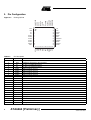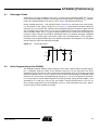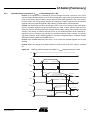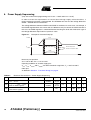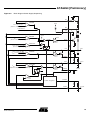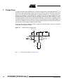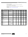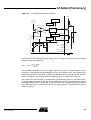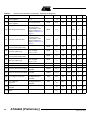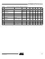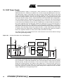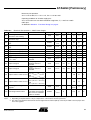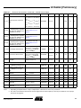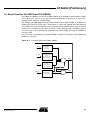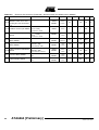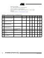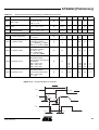
1
Features
•
•
•
•
•
•
•
•
•
•
•
•
•
Maximum Supply Voltage 40V
One Programmable/Adjustable Boost Converter
Two Programmable Buck Converters
One Programmable Linear Regulator
OTP Customer Mode
16-bit Serial Interface
Two ISO9141 Interfaces (One Interface Programmable to LIN Functionality)
Watchdog
Various Diagnosis Functions
5 Voltage Sources Tailored to Resistor Measurement
Charge Pump
Small, 44-pin Package
ESD Protection Against 2kV and 4kV
Airbag Power
Supply IC
ATA6264
1. Description
With the introduction of the ATA6264, Atmel® introduces a new generation of airbag
power supplies for future airbag systems tailored to the needs of the automotive
industry. It is designed in Atmel’s 0.8 micron BCDMOS technology. ATA6264 contains
all the necessary blocks to supply the microcontroller, the firing capacitors, and
peripheral components of the airbag system. The power supply specifically fulfills the
power requirements of dual-voltage microcontrollers used in modern ECUs. The integrated watchdog and diagnosis blocks additionally support the safety aspects. The
8-MHz 16-bit SPI enables a high communication speed. Despite the high-level functionality, ATA6264 comes in a space-saving QFP44 package.
Preliminary
4929B–AUTO–01/07
Figure 1-1.
Block Diagram
SVSAT
VBATT
RESQ
Serial Interface
Watchdog
Reset
RESQ2
K15
CP
CP_OUT
SCLK
SSQ
MISO
MOSI
VSAT
CP Logic
GKEYLogic
K30
GNDD
GEVZ
EVZRegulator
TxD1
OCEVZ
GNDB
RxD1
TxD2
EVZ
RxD2
FBEVZ
VEVZ
K1
ISO9141
K2
COMEVZO
SVSAT
COMSATO
IASG1
IASG2
VSATRegulator
IASG3
COMSATI
IASG
IASG4
VVSAT
VSAT
IASG5
SVPERI
ISENS
VPERIRegulator
VPERI
VVPERI
SVCORE
UZP
UZP
AMUX
VCORE
VVCORE
GNDA
COMCOI
IREF
VINT
USP
USP
Internal Supply
Reference
VCORERegulator
COMCOO
VBATT
2
ATA6264 [Preliminary]
4929B–AUTO–01/07
ATA6264 [Preliminary]
1.1
Block Description
1.1.1
Integrated Boost Converter EVZ
With an external n-channel FET, the integrated boost converter EVZ provides 3 different voltages adjustable via the serial interface for the energy reserve and firing capacitors. Two
voltages are fixed values; one voltage can be adjusted using an external resistive divider.
1.1.2
Integrated Buck Converter VSAT
The integrated buck converter VSAT is a fully integrated step-down converter supplied by the
boost converter, EVZ, and providing 7.8V, 9.1V, or 10.4V. The user can program the voltage via
an OTP system.
1.1.3
Integrated Buck Converter VCORE
The integrated buck converter VCORE is a fully integrated step-down converter supplied either
by the boost converter, EVZ, or by the battery, and providing 1.88V, 2.5V, or 5V. The user can
program the voltage via an OTP system.
1.1.4
Linear Regulator VPERI
The linear regulator, VPERI, is supplied from the buck converter VSAT and provides an accurate
voltage of 3.3V ±3% or 5V ±4% as a supply for sensitive elements such as sensors and ADC
references with the current capability of 100 mA. The user can program the voltage via an OTP
system. With a sophisticated power-sequencing concept of VCORE and VPERI, ATA6264 supports dual-voltage-supply microcontrollers, so that under all conditions the voltage difference
between the two linear regulator voltages never drops below a defined value. This measure
guarantees the safe operation of the system.
1.1.5
Blocks Included
• A general purpose comparator USP, for, for example, low battery voltage detection
• A band gap as reference for all internal voltages and currents
• Two ISO9141 interfaces, one of which is configurable via OTP in accordance with the LIN
specification
• Five constant voltage sources with current-to-voltage mirrors used for resistance
measurements, such as buckle switch detection in the range from –0.5 mA to –40 mA
• An AMUX block with push-pull buffer stage provides the output of all analog values such as
voltage sources, low voltage detection, or the chip temperature for continuous diagnosis
• A 16-bit serial interface for the communication with the microcontroller which includes a 16-bit
shift register, a 16-bit latch, and a decoder-logic block
• A watchdog to monitor the microcontroller and to generate reset signals in the case of failure
• Internal oscillator generates internal clock signals
• GKEY function to control the main switch of the ECU via a logic signal
3
4929B–AUTO–01/07
2. Pin Configuration
Pinning QFP44
COMEVZO
GNDB
GEVZ
OCEVZ
FBEVZ
CP
SVCORE
CP-OUT
COMCOO
COMCOI
COMSATO
Figure 2-1.
1
44 43 42 41 40 39 38 37 36 35 34
33
2
32
3
31
4
30
5
29
6
7
28
27
8
26
9
25
10
24
11
23
12 13 14 15 16 17 18 19 20 21 22
K15
EVZ
SVSAT
VSAT
GNDD
VINT
COMSATI
VCORE
GNDA
SVPERI
VPERI
RESQ
RxD2
RxD1
TxD2
MISO
SSQ
SCLK
MOSI
RESQ2
IREF
UZP
USP
K30
K1
K2
IASG1
IASG2
IASG3
IASG4
IASG5
ISENS
TxD1
Table 2-1.
4
Pin Description
Pin
Symbol
Function
1
USP
2
K30
Continuous connection to the car battery
3
K1
Bus line of 1st ISO9141 interface
4
K2
Bus line of 2nd ISO9141 interface
5
IASG1
Output of voltage source 1
6
IASG2
Output of voltage source 2
7
IASG3
Output of voltage source 3
8
IASG4
Output of voltage source 4
9
IASG5
Output of voltage source 5
10
ISENS
Output of the current mirror from the IASGx interface
11
TXD1
Data input of the 1st ISO9141 interface
12
RESQ
Reset output
13
RXD2
Data output of the 2nd ISO9141 interface
14
RXD1
Data output of the 1st ISO9141 interface
15
TXD2
Data input of the 2nd ISO9141 interface
16
MISO
Data output of the serial interface
17
SSQ
Chip select of the serial interface
18
SCLK
Clock input of the serial interface
19
MOSI
Data input of the serial Interface
20
RESQ2
21
IREF
Connection for the external reference resistor
22
UZP
Analog measurement output
Comparator input
Redundant reset output
ATA6264 [Preliminary]
4929B–AUTO–01/07
ATA6264 [Preliminary]
Table 2-1.
Pin Description
Pin
Symbol
23
VPERI
24
SVPERI
25
GNDA
26
VCORE
27
COMSATI
Function
Input for the VPERI regulator, internally used VPERI supply
Output of VPERI regulator power transistor
Analog GND
Input for VCORE regulator
Input of the VSAT externally compensated error amplifier
28
VINT
29
GNDD
Digital GND
Output of internal supply voltage
30
VSAT
Input for VSAT regulator, internally used VSAT supply
31
SVSAT
32
EVZ
Input for EVZ regulator, internally used EVZ supply
33
K15
Connection to car battery via the ignition key
34
COMSATO
Output of the VSAT externally compensated error amplifier
35
COMCOI
Input of the VCORE externally compensated error amplifier
36
COMCOO
37
CP-OUT
Switchable output of charge pump voltage
38
SVCORE
Output of VCORE regulator power transistor
39
CP
Output of VSAT regulator power transistor
Output of the VCORE externally compensated error amplifier
Charge pump output
40
FBEVZ
Input for external resistor divider to adjust EVZ voltage
41
OCEVZ
Input for overcurrent measurement of the EVZ regulator
42
GEVZ
Gate driver output for the external FET of the EVZ regulator
43
GNDB
GND connection of all power stages
44
COMEVZO
Output of the EVZ externally compensated error amplifier
5
4929B–AUTO–01/07
3. Absolute Maximum Ratings
Stresses beyond those listed under “Absolute Maximum Ratings” may cause permanent damage to the device. This is a stress rating
only and functional operation of the device at these or any other conditions beyond those indicated in the operational sections of this
specification is not implied. Exposure to absolute maximum rating conditions for extended periods may affect device reliability.
All voltages are referenced to an ideal ground level of an ECU connected to the GNDA, GNDB and GNDD pins.
Parameters
Voltage at pins, connected directly or
indirectly to the car battery
(K30, K15, USP)
Remark
Minimum
Maximum
Unit
–0.3
+45
V
Any combination of one or more pins
applied with any voltage between the
limits
K30 and K15 connected via diode to VBatt.
USP connected via minimum 5 kΩ to VBatt
(maximum reverse current 5 mA).
Voltage at pins, connected directly or
indirectly to the car battery (K1, K2)
Any combination of one or more pins
applied with any voltage between the
limits
–25
+45
V
Voltage at pins, connected directly or
indirectly to the car battery (IASG1,
IASG2, IASG3, IASG4, IASG5)
Any combination of one or more pins
applied with any voltage between the
limits
Voltage
necessary to
drive –40 mA
stored in 20 µH
45
V
Voltage at ECU internal pins (FBEVZ,
EVZ, VSAT)
Any combination of one or more pins
applied with any voltage between the
limits
–0.3
+45
V
1
V/µs
Maximum rate of change at pin VSAT
Voltage at ECU internal pins (SVSAT,
SVCORE)
Any combination of one or more pins
applied with any voltage between the
limits
–1
+45
V
Voltage at ECU internal pins (CP,
CP-OUT)
Any combination of one or more pins
applied with any voltage between the
limits
–0.3
+56
V
Voltage at ECU internal pins (GEVZ,
OCEVZ)
Any combination of one or more pins
applied with any voltage between the
limits
–0.3
+10
V
–0.3
+7
V
–3
+3
mA
Voltage at ECU internal pins (COMEVZO,
COMSATO, COMSATI, VPERI, SVPERI,
These voltages can be applied in any
VCORE, COMCOI, COMCOO, IREF, UZP,
combination with any voltage between the
ISENS, RXD1, TXD1, RXD2, TXD2,
limits
RESQ, RESQ2, MISO, MOSI, SSQ,
SCLK, VINT)
Current at logic pins
Connected to voltages outside of
maximum voltage ratings via resistor
ESD classification at pins connected to
devices outside the ECU (K30, K15)
Human body model (HBM)
6
HBM
AEC Q100-002
±4000
V
ATA6264 [Preliminary]
4929B–AUTO–01/07
ATA6264 [Preliminary]
3. Absolute Maximum Ratings (Continued)
Stresses beyond those listed under “Absolute Maximum Ratings” may cause permanent damage to the device. This is a stress rating
only and functional operation of the device at these or any other conditions beyond those indicated in the operational sections of this
specification is not implied. Exposure to absolute maximum rating conditions for extended periods may affect device reliability.
All voltages are referenced to an ideal ground level of an ECU connected to the GNDA, GNDB and GNDD pins.
Parameters
Remark
Minimum
Maximum
Unit
ESD classification at pins connected to
devices outside the ECU (IASG1 to
IASG5)
Human body model (HBM)
HBM
AEC Q100-002
±3000
V
HBM
AEC Q100-002
±2500
V
HBM
AEC Q100-002
±1500
V
Charged device model (CDM) – no corner CDM
pins
ESD STM5.3.1-1999
±500
V
Charged device model (CDM) – corner
pins
±750
V
ESD classification at pins connected to
devices outside the ECU (K1 and K2)
Human body model (HBM)
General ESD classification for all other
pins
Human body model (HBM)
7
4929B–AUTO–01/07
4. Functional Range
Within the functional range, the ATA6264 works as specified. All voltages are referenced to the
ideal ground level of an ECU connected to the GNDA, GNDB and GNDD pins.
At the beginning of each specification table, supply voltage and temperature conditions are
described.
Table 4-1.
Electrical Characteristics – Functional Range
No. Parameters
1.1
Test Conditions
Pin
Symbol
Min.
Voltage on pins K30, K15,
USP
1.1a Voltage on pins K1, K2
Typ.
Max.
Unit
–0.3
+40
V
–25
+40
V
50
V/µs
1.2
Rate of supply voltage rise
(K30, K15, K1, K2)
1.3
Supply voltage EVZ
–0.3
+40
V
1.4
Supply voltage VSAT
–0.3
+14
V
1.5
Supply voltages VCORE,
VPERI
–0.3
+5.5
V
1.6
Supply voltage CP, CP-OUT
–0.3
+50
V
1.7
Voltage on digital I/O pins
–0.3
+5.5
V
1.8
Voltage on pins SVSAT,
SVCORE
–1.0
+40
V
1.9
Voltage on pins UZP,
ISENS, COMCOI,
COMCOO, COMSATO,
COMSATI, COMEVZO,
FBEVZ, IREF, VINT
–0.3
+5.5
V
1.10
Voltage on pins GEVZ,
OCEVZ
–0.3
+10
V
1.11 Voltage on pin SVPERI
–0.3
+6
V
Voltage on pins IASGx
1.12
(x = 1 to 5)
Voltage
necessary to
drive –40 mA
stored in 20 µH
40
V
– 40
+ 90
°C
– 40
+150
°C
– 55
+105
°C
60
K/W
Temperatures:
Operating ambient
temperature range
1.14 Operating junction
temperature range
Storage ambient/junction
temperature range
1.15
Thermal resistance junction
ambient
Substrate current which can
be drawn without
1.16
disturbances to upper
defined blocks/functions(1)
–40
Type*
mA
*) Type means: A = 100% tested, B = 100% correlation tested, C = Characterized on samples, D = Design parameter
Note:
8
1. No substrate current occurs at pins K1, K2 down to VK1, VK2 > –25V
ATA6264 [Preliminary]
4929B–AUTO–01/07
ATA6264 [Preliminary]
4.1
Protection Against Substrate Currents
Due to the fact that the ATA6264 is connected to the wiring harness and to components outside
of the ECU, negative voltages at the following pins might occur:
• IASG interface:
IASG1, IASG2, IASG3, IASG4, IASG5
• USP comparator:
USP
If substrate currents occur, it is guaranteed by design that no disturbance and malfunction of the
following blocks and functions will happen:
• No disturbance of RESET block.
• No voltage changes of any regulators outside of their tolerances.
• No impact on digital circuitry (for example, changes of latches, status register, etc.)
• No latch up of any circuitry
9
4929B–AUTO–01/07
5. Supply Currents
A minimum current has to flow into each pin for proper functioning of the IC.
Table 5-1.
Electrical Characteristics – Supply currents
No. Parameters
Test Conditions
Pin
Symbol
Min.
2.1
Supply current at K30
Standby mode: 0V = VK30 = 18V,
VK15 = 3V and KEYLATCH = OFF
K30
IK30
2.1a Supply current at K30
Standby mode: 18V < VK30 = 40V,
VK15 = 3V and KEYLATCH = OFF
K30
2.1b Supply current at K30
Startup mode: 0V < VK30 = 18V,
VK15 > 4.15V or KEYLATCH = ON,
VEVZ = 0V, CCP = 47 nF
2.1c Supply current at K30
Typ.
Max.
Unit
Type*
0
50
µA
A
IK30
0
5
mA
A
K30
IK30
0
7
mA
A
Startup mode: 18V < VK30 = 40V
VK15 > 4.15V or KEYLATCH = ON
VEVZ = 0V, CCP = 47 nF
K30
IK30
0
10
mA
A
2.1d Supply current at K30
Normal mode: 0V < VK30 = 18V,
VEVZ > VK30, VK15 > 4V or
KEYLATCH = ON, SVCORE open,
AMUX Measurement K30 active
K30
IK30
0
6.5
mA
A
2.1e Supply current at K30
Normal mode: 18V < VK30 = 40V,
VEVZ > VK30, VK15 > 4.15V or
KEYLATCH = ON, SVCORE open,
AMUX Measurement K30 active
K30
IK30
0
10
mA
A
2.2
Supply current at EVZ
Startup mode: 0V < VEVZ = 40V,
VSAT = VPERI = VCORE = 0V,
VK30 > 5V, VK15 > 4.15V, SVCORE
and SVSAT open
EVZ
IEVZ
0
5
mA
A
2.2a Supply current at EVZ
Normal mode: 0V < VEVZ = 40V,
VPERI and VCORE > Reset
Threshold, VEVZ > VK30,
VSAT = 10V, VK30 > 5V,
VK15 > 4.15V, SVCORE and
SVSAT open, AMUX Measurement
EVZ active
EVZ
IEVZ
0
6
mA
A
2.2b Supply current at EVZ
Autonomous mode:
0V < VEVZ = 40V, VPERI and VCORE
> Reset Threshold, VEVZ > VK30,
VSAT = 10V, VK30 < 3.85V,
VK15 < 3V, SVCORE and SVSAT
open, AMUX Measurement EVZ
active
EVZ
IEVZ
0
10
mA
A
2.3
Supply current at VSAT
0V < VSAT = 14V, SVPERI open,
AMUX measurement VSAT active
VSAT
IVSAT
0
1.5
mA
A
2.4
Supply current at
VPERI
0V < VPERI = 5.3V, AMUX
measurement VPERI active
VPERI
IVPERI
–0.2
2.2
mA
A
2.5
Supply current at
VCORE
0V < VCORE = 5.3V, AMUX
measurement VCORE active
VCORE
IVCORE
–0.45
1
mA
A
*) Type means: A = 100% tested, B = 100% correlation tested, C = Characterized on samples, D = Design parameter
10
ATA6264 [Preliminary]
4929B–AUTO–01/07
ATA6264 [Preliminary]
5.1
Discharger Circuit
Applications using the ATA6264 usually use a reverse polarity protection diode (D1 in Figure
5-1) in the power supply to prevent any damage if the wrong polarity is applied to VK30. Unfortunately, this method includes some risk as can be seen in the following description:
During Standby mode (VK15 < 3V and KEYLATCH = OFF) the IC consumes only a low current,
IK30. Any peaks on the supply voltage (VPulse in Figure 5-1) will gradually charge the blocking
capacitor (C1). D1 prevents the capacitor from being discharged via the power supply and the
very small quiescent current via the IC can also be neglected. This means that during long periods of Standby mode, the IC’s supply voltage could increase continuously until finally the
maximum supply voltage limit would be exceeded and the IC could be damaged. ATA6264
therefore features a discharger circuit which avoids such unwanted effects. If VK30 exceeds a
threshold value of approximately 26.8V, the blocking capacitor is discharged via an integrated
resistor until VK30 again falls below the threshold.
Figure 5-1.
Discharger Circuit
K30
8 kΩ
C1
D1
VBatt
VPulse
26.8V
5.2
Initial Programming of the ATA6264
The ATA6264 supports different output voltages at the VSAT, VPERI and the VCORE regulators. In addition, different modes at the ISO9141 interfaces can be adjusted at the initial
programming (IP). The memory cells are one-time programmable (OTP) and cannot be changed
after the IP (default values are “0”). In general, the IP is done after mounting the ATA6264 on the
PCB with an in-circuit tester. The programming voltage of 11.7V has to be applied on pin VSAT.
It is also possible to use the VSAT regulator as the programming voltage because VSAT is programmed to 11.7V (±0.5V) as long as the Test mode is entered and the lock bit is not set. To
ensure proper programming of the ATA6264, at least a 10-µF electrolytic cap and a 100-nF
ceramic cap have to be applied at pin VSAT.
11
4929B–AUTO–01/07
The following settings can be made at the initial programming:
MSBit
VR1
Table 5-2.
VR3
VR4
EXT
ISO/LIN
Parity
LSBit
Lock bit
Initial Programming Settings
VR1
VR2
VR3
VR4
0
0
0
0
0
0
0
1
1.88V
3.3V
0
0
1
0
1.88V
3.3V
9.1V
0
0
1
1
1.88V
3.3V
10.4V
0
1
0
0
2.5V
3.3V
7.8V
0
1
0
1
2.5V
3.3V
9.1V
0
1
1
0
2.5V
3.3V
10.4V
0
1
1
1
1.88V
5V
7.8V
1
0
0
0
1.88V
5V
9.1V
1
0
0
1
1.88V
5V
10.4V
1
0
1
0
2.5V
5V
7.8V
1
0
1
1
2.5V
5V
9.1V
1
1
0
0
2.5V
5V
10.4V
1
1
0
1
5V
5V
7.8V
1
1
1
0
5V
5V
9.1V
1
1
1
1
5V
5V
10.4V
EXT
ISO/LIN
12
VR2
VCORE
VPERI
VSAT
All regulators deactivated (default)
7.8V
Set to 0
Set to 1
No external transistor at VPERI (default)
External transistor at VPERI applied
Set to 0
Set to 1
ISO9141 mode is activated at K1 (default)
LIN mode is activated at K1
ATA6264 [Preliminary]
4929B–AUTO–01/07
ATA6264 [Preliminary]
The IP data is valid only if the parity is odd. If the IP data is not valid, or if the lock bit is not set,
the programming will not be executed.
Figure 5-2.
Programming Sequence
Contact pins RESQ, RESQ2
TxD1, TxD2, SSQ, MOSI,
SCLK, VPERI, K15, K30
Apply 12V at K15, K30 and5V
at VPERI
Set RESQ and TxD1 to GND
and RESQ2 and TxD2 to 5V
Transmit 5A5A(h) via SPI
to Enable Testmode
Wait until VSAT = 11.7V
Transmit IP command A9xx(h)
via SPI to configure ATA6264
Wait 1 ms
Remove all voltages and pinloads
to get out of Test mode
13
4929B–AUTO–01/07
5.3
Start-up and Power-down Procedure
The ATA6264 is powered via the pin K30 (battery voltage) and via a diode or a resistor it is connected to the ignition key line K15. In order to detect an interruption on one of these pins
correctly, resistors are implemented at these pins. Normally, the main supply pin of ATA6264 is
pin K30. In the case of a missing or a too-low voltage at pin K30, the whole IC is supplied from
the backup power supply capacitor hooked up to pin EVZ.
Figure 5-3.
Block Diagram Start-up and Power-down Procedure
K15
K15GOOD
VEVZ
VK15 = 3V to 4.15V
(40 mV to 175mV Hysteresis)
Comp
K30
Serial interface
(KEY - LATCH)
CP
IREF lost
signal
K30GOOD
VK30
VK30 = 3.85V to 5V
(50 mV to 150 mV Hysteresis)
EVZEN
Comp
GEVZ
VEVZ
driver
CORESWAP
VK30 = 6.1V to 8.1V (ON)
(0.5V to 1V Hysteresis)
VCP
5V
IP
Comp
VEVZ
EVZ
VEVZ = 7.5V to 9V (ON)
VEVZ = 5.5V to 6.2V (OFF)
VCP
EVZGOOD
Comp
VSAT
driver
SVSAT
VVSAT
VSAT
VEVZ
VSATGOOD
VSAT = 6.77V to 7.2V
(200 mV to 500 mV Hysteresis)
Power
sequencing
Comp
VPERI
driver
SVPER
VVPERI
VPERI
K30
IP
VCP
VCORE
driver
SVCORE
VCP
CORE_EN
VCORE
VPERI = 1.25V to 1.7V
(50 mV to 150 mV Hysteresis)
14
Comp
VCore
driver
VVCORE
EVZ
ATA6264 [Preliminary]
4929B–AUTO–01/07
ATA6264 [Preliminary]
Depending on the initial programming of the ATA6264, the start-up procedure takes place in different phases.
5.3.1
Start-up Procedure if VVCORE is Programmed to Be 5V or 2.5V
Phase1: After switching on the ignition key, K15 voltage will apply at pin K15. If, in addition, the
voltage at pin K30 is larger than 3.85V to 5V, the EVZ regulator will be enabled. The signal
K15GOOD can be replaced by the serial interface command KEYLATCH which can be set via
the serial interface.
Phase2: If VEVZ is larger than 7.5V to 9V the VSAT regulator starts operating and the VCORE
regulator will be enabled.
Phase3: After V VSAT has reached 6.77V to 7.2V, the VPERI regulator starts working. The
VCORE regulator starts operating depending on the charge pump voltage.
5.3.2
The Power-down Procedure Takes Place in Different Phases
Phase1: If the ignition key is switched off, K15 voltage will vanish at pin K15. If the serial interface command KEYLATCH is not set, the EVZ regulator stops working. The external charge
pump is still working because EVZ is above VSAT and the VSAT regulator is not in Permanent-on mode. The charge-pump voltage still supplies the VSAT regulator and the VCORE
regulator. Because the EVZ regulator stops working, VCORE will be switched to EVZ.
Phase2: The EVZ capacitor will be discharged, and as soon as the voltage at pin VSAT drops to
low, the VSAT regulator will go into Permanent-on mode. If VSAT reaches Permanent-on mode,
the external charge pump stops working and the VSAT voltage falls analog to the EVZ voltage. If
the voltage at VSAT is below 6.27V to 7V, the VPERI regulator will be switched off. Depending
on the charge-pump voltage, the VCORE regulator stops working.
Phase3: When the voltage at the EVZ capacitor gets to be lower than 5.5V to 6.2V, VSAT is
switched off.
15
4929B–AUTO–01/07
Figure 5-4.
Start-Up and Power-Down Procedure if VVCORE Programmed to Be 5V or 2.5V
VK30
t
VK15
3V to 4.15V
3V to 4.15V
t
VGEVZ
Threshold to enable
VCORE regulator
t
VEVZ
7.5V to 9V
Threshold to start
VCORE regulator
too low EVZ voltage
VSAT goes into On Mode
charge pump deactivated
5.5V to 6.2V
t
VVSAT
6.77V to 7.2V
7V to 6.27V
t
VVPERI
t
VVCORE
t
5.3.3
Start-up Procedure if VVCORE Programmed to Be 1.88V
Phase1: After switching on the ignition key, the K15 voltage will appear at pin K15. If, in addition, the voltage at pin K30 is larger than 3.85V to 5V, the EVZ regulator will be enabled. The
signal K15GOOD can be replaced by the serial interface command KEYLATCH which can be
set by the serial interface.
Phase2: If VEVZ is larger than 7.5V to 9V, the VSAT regulator starts operating.
Phase3: After VVSAT has reached 6.77V to 7.2V, the VPERI regulator starts working.
Phase4: If VVPERI is higher than 1.25V to 1.7V, the VCORE regulator will be enabled.
16
ATA6264 [Preliminary]
4929B–AUTO–01/07
ATA6264 [Preliminary]
5.3.4
The Power-down Procedure for VVCORE is Programmed to be 1.88V
Phase1: If the ignition key is switched off, the K15 voltage will vanish at pin K15. If the serial
interface command KEYLATCH is not set, the EVZ regulator stops working. The external charge
pump is still working because EVZ is above VSAT and the VSAT regulator is not in the Permanent-on mode. The charge-pump voltage still supplies the VSAT regulator and the VCORE
regulator. Because the EVZ regulator stops working, VCORE will be switched to EVZ.
Phase2: The EVZ capacitor will be discharged, and as soon as the voltage at pin VSAT drops
too low, the VSAT regulator will go into Permanent-on mode. If VSAT reaches Permanent-on
mode, the external charge pump stops working and the VSAT voltage falls analog to the EVZ
voltage. If the voltage at VSAT is below 6.27V to 7V, the VPERI regulator will be switched off.
Depending on the charge-pump voltage, the VCORE regulator stops working. The power
sequencing function for the VPERI regulator is still active and guarantees a maximum voltage
difference between VPERI and VCORE of 2.8V
Phase3: After VVPERI becomes lower than 1.1V to 1.55V, the VCORE regulator has to stop
working.
Phase4: When the voltage at the EVZ capacitor is lower than 5.5V to 6.2V, VSAT is switched
off.
Figure 5-5.
Start-up and Power-down Procedure if VVCORE Programmed to Be 1.88V
VK30
t
VK15
3V to 4.15V
3V to 4.15V
t
VGEVZ
t
VEVZ
7.5V to 9V
too low EVZ voltage
VSAT goes into On Mode
charge pump deactivated
5.5V to 6.2V
t
VVSAT
6.77V to 7.2V
7V to 6.27V
t
VVPERI
1.25V to 1.7V
VVCORE
1.1V to 1.55V
t
t
17
4929B–AUTO–01/07
6. Power Supply Sequencing
(Only active when initial programming sets VVCORE = 1.88V and VVPERI = 3.3V)
In order to meet the requirements of several dual-voltage-supply microcontrollers, a
power-sequencing function is implemented. The ATA6264 ensures that the voltage difference
VPERI – VCORE will not exceed 2.8V.
The voltage difference between VPERI and VCORE is monitored. In error cases, for example, if
the VCORE regulator does not start to work, the difference may rise above the 2.8V threshold. In
this case, the VPERI regulator is switched off before reaching this level and switched on again if
the voltage difference drops below a hysteresis value.
Figure 6-1.
Example for Incorrect Ramp Up
VVPERI
3.3V
t
Not allowed area:
VVPERI - VVCORE > 2.8V
VVCORE
1.88V
t
Necessary for operation:
VEVZ = 0V to 40V, VINT = 3.7V to 5.47V
Operating conditions of all other supply pins:
VK30, VVSAT, VVPERI and VVCORE are within functional range limits, Tj = –40°C to 150°C
Other pins:
As defined in Section 4. ”Functional Range” on page 8.
Table 6-1.
Electrical Characteristics – Power Supply Sequencing
No. Parameters
Test Conditions
Pin
Symbol
Min
Typ.
Max.
Unit
Type*
5.1
Maximum voltage difference
VVPERI – VVCORE
VPERI,
VCORE
VVPERI
– VVCORE
0
2.8
V
A
5.2a
Voltage level VVPERI – VVCORE to
switch off VPERI regulator
VPERI,
VCORE
VVPERI
– VVCORE
2.3
2.8
V
A
5.2b
Hysteresis for VVPERI – VVCORE to
enable VPERI regulator
100
mV
A
VHYS
*) Type means: A = 100% tested, B = 100% correlation tested, C = Characterized on samples, D = Design parameter
18
ATA6264 [Preliminary]
4929B–AUTO–01/07
ATA6264 [Preliminary]
Figure 6-2.
Block Diagram Power Supply Sequencing
K15
K15GOOD
VEVZ
VK15 = 3V to 4.15V
(40 mV to 175mV Hysteresis)
Comp
K30
Serial interface
(KEY - LATCH)
CP
K30GOOD
IREF lost
signal
VK30
VK30 = 3.85V to 5V
(50 mV to 150 mV Hysteresis)
EVZEN
Comp
GEVZ
VEVZ
driver
CORESWAP
VK30 = 6.1V to 8.1V (ON)
(0.5V to 1V Hysteresis)
VCP
5V
Comp
IP
VEVZ
EVZ
VEVZ = 7.5V to 9V (ON)
VEVZ = 5.5V to 6.2V (OFF)
VCP
EVZGOOD
Comp
VSAT
driver
SVSAT
VVSAT
VSAT
VEVZ
VSATGOOD
VSAT = 6.77V to 7.2V
(200 mV to 500 mV Hysteresis)
Comp
IP
VPERI
driver
SVPER
VVPERI
VPERI
Delta
< 2.8V
VCORE - Regulator
SVCORE
VCORE
VVCORE
19
4929B–AUTO–01/07
7. Charge Pump
To supply the VSAT and VCORE drivers, an external charge pump is provided. Both FETs(1) are
driven by the high charge pump voltage VCP to ensure that they can be switched to a low-ohmic
state. For correct function of the charge pump, an external capacitor of C = 47 nF has to be connected to pin SVSAT, and another of C = 100 nF to pin CP. A double diode has to be
implemented for proper function of the charge pump. An external series resistor is recommended to suppress spikes during switching of the SVSAT. The CP block is supplied by EVZ
and VSAT voltage and starts to operate as soon as the thresholds for VK15, K30 and EVZ are
achieved. An additional start-up circuitry is implemented to support the VSAT driver during the
start-up phase, thus enabling a reliable system startup.
The charge pump has an output CP-OUT to supply the external circuitry, and can be switched
via the SPI. It is capable of 250 µA.
Figure 7-1.
Block Diagram Charge Pump
External circuit
CP-Out
Status
register
CP
REF
VSAT
REF
SVSAT
Status
register
Serial
interface
I = 1.4 mA
EVZ
Note:
20
1. Connected to the drivers (see Figure 5-3)
ATA6264 [Preliminary]
4929B–AUTO–01/07
ATA6264 [Preliminary]
Necessary for operation:
VEVZ = 5.5V to 40V or VK30 = 5.5V to 40V, VK15 > 3V, VVINT = 3.7V to 5.47V
Operating conditions of all other supply pins:
VVSAT, VVPERI and VVCORE are within functional range limits, Tj = –40°C to 150°C
Other pins:
As defined in Section 4. ”Functional Range” on page 8.
Table 7-1.
Electrical Characteristics – Charge Pump
No. Parameters
Test Conditions
Pin
Symbol
Min
6.11 Supply current at pin CP
CP off, supply of
internal circuitry
CP
ICP
CP-OUT
Time between wrong CP-OUT
6.12 voltage and valid data in status
register
6.13
Current limitation at pin
CP-OUT
6.14
Voltage difference VCP – VEVZ
for detecting wrong CP
Note: Threshold is in
the range of 5V to 7V
Time between wrong CP
6.15 voltage and valid data in status
register
Max.
Unit
Type*
0
50
µA
A
td
0
50
µs
A
CP-OUT
ICP-OUT
–0.8
–4.2
mA
A
CP
VDiff
5
V
A
CP
td
50
µs
A
CP-OUT
VDiff
5
V
A
0
Typ.
Voltage difference VCP-OUT –
6.16 VEVZ for detecting wrong
CP-OUT
Note: Threshold is in
the range of 5V to 7V
6.17 Voltage at pin CP
VEVZ = 5.5V to 40V,
VK30 < VEVZ
ICP + ICP_Out = –100 µA
(current consumption of
VSAT and VCORE have to
be added)
CP
VCP
VEVZ + 7
VEVZ + 11
V
A
6.18 Voltage at pin CP
VEVZ = 5.5V to 40V,
VK30 < VEVZ
ICP + ICP_Out = –100 µA
(current consumption of
VSAT and VCORE have to
be added)
CP
VCP
VK30 + 7
VK30 + 11
V
A
*) Type means: A = 100% tested, B = 100% correlation tested, C = Characterized on samples, D = Design parameter
21
4929B–AUTO–01/07
8. GKEY Function
The GKEY function is used to enable or disable the ECU via a powerless signal. If the voltage at
pin K15 is larger than 3V to 4.15V, the charge pump and the EVZ regulator (for correct EVZ
function, the K30 pin has to be connected to the battery) will start operating. If the K15 pin is
open, an internal pull-down resistor of approximately 220 kΩ discharges the pin. A logical connection between the voltage at the K15 pin, a serial-interface-driven latch command, and the
K30 voltage determines the EVZ Enable signal. In order to achieve the Switch Function of the
GKEY function, a transformer has to be used.
Table 8-1.
Overview of the Start-up Conditions
VK30
VK15
Serial-interfacedriven Latch
(Default: “0” = OFF)
EVZ Regulator
x
x
Disabled
x
Enabled
1
Enabled
1)
Low
Note:
High
2)
High
2)
3)
High
x
1. Less than the value shown in number 7.3 of Table 8-2 on page 23
2. Greater than the value shown in number 7.3 of Table 8-2 on page 23
3. Greater than the value shown in number 7.1 of Table 8-2 on page 23
Figure 8-1.
Application With Low-current Switch (GKEY Function Used)
VBATT
K15
GKEYLogic
K30
GEVZ
EVZ
OCEVZ
GNDB
EVZ
VEVZ
FBEVZ
COMEVZO
22
ATA6264 [Preliminary]
4929B–AUTO–01/07
ATA6264 [Preliminary]
Figure 8-2.
Application With High Current Switch (GKEY Function Not Used)
VBATT
K15
K30
GKEYLogic
GEVZ
OCEVZ
EVZ
GNDB
VEVZ
EVZ
FBEVZ
COMEVZO
Necessary for operation:
VK15 = 3V to 40V, VK30 = 3.85V to 40V
Operating conditions of all other supply pins:
VEVZ, VSAT, VPERI and VCORE are within functional range limits, Tj = –40°C to 150°C
Other pins:
As defined in Section 4. ”Functional Range” on page 8.
Table 8-2.
Electrical Characteristics – GKEY Function
No. Parameters
Test Conditions
Pin
Symbol
Min
VK15 increasing,
VK30 > 5V
K15
VK15
K15
Typ.
Max.
Unit
Type*
3
4.15
V
A
VK15
40
175
mV
A
K30
VK30
3.85
5
V
A
7.1
Voltage level at K15 to enable
the EVZ regulator
7.2
Hysteresis at K15 to disable the
EVZ regulator
7.3
Voltage level at K30 to enable
the EVZ regulator
7.4
Hysteresis at K30 to disable the
EVZ regulator
K30
VK30
50
150
mV
A
7.5
Pull-down resistor at K15
K15
RK15
70
365
kΩ
A
7.6
Pull-down resistor at K30
K30
RK30
320
1700
kΩ
A
7.7
Current at K15
K15
IK15
0
1.1
mA
A
VK30 increasing,
VK15 > 4.15V
0V ≤ VK15 ≤ 40V,
AMUX measurement
EVZ active
*) Type means: A = 100% tested, B = 100% correlation tested, C = Characterized on samples, D = Design parameter
23
4929B–AUTO–01/07
9. EVZ Step-up Regulator
A boost converter generates the supply voltage for energy reserve and firing capacitors in the
system. Using a voltage divider at pin FBEVZ, this voltage can be adjusted between 15V and
40V. Thus, high-voltage charged capacitors will be used to supply the whole system during the
stand-alone time (for example, broken K30 line after a crash). The step-up regulator has to start
running as soon as a certain threshold voltage at the K15 pin is exceeded. The regulator has to
stop running again if the voltage at the K15 pin falls below a voltage level (or voltage at pin K30
is missing, see Section 5.3 ”Start-up and Power-down Procedure” on page 14).
An inductor is PWM-switched by an external n-channel power FET with a fixed frequency of
100 kHz. A driver stage for the external FET is integrated into the ATA6264. The current limitation of the external FET is implemented by using an external resistor in series between the
source connection of the external FET and GND, sensing the voltage drop at this resistor via the
pins OCEVZ and GNDA.
The reference section provides a reference voltage of 1.24V for the regulation loop. An error
amplifier compares the reference voltage with the feedback signal, which is provided either from
two different serial-interface-programmable internal dividers (VEVZ1 = 22V, VEVZ2 = 31.5V) or
an external voltage divider network (VEVZExt). These dividers determine the output voltage
EVZ.
Figure 9-1.
EVZ Regulator With External Divider
K30
Max. duty-cycle
Bandgap
reference
L
Low battery
Sawtooth oscillator
RVZ1
+
-
+
-
Logic and
driver
GEVZ
PWM
comp.
Error
amp.
OCEVZ
Overcurrent
C +
EVZ
overvoltage
SPI
SPI
SPI
RVZ2
GNDA
EVZ
FBEVZ
COMEVZO
24
ATA6264 [Preliminary]
4929B–AUTO–01/07
ATA6264 [Preliminary]
Figure 9-2.
EVZ Regulator With Internal Divider
K30
Max. duty-cycle
Bandgap
reference
L
Low battery
Sawtooth oscillator
+
-
+
-
Logic and
driver
GEVZ
PWM
comp.
Error
amp.
OCEVZ
Overcurrent
C +
EVZ
overvoltage
SPI
SPI
SPI
GNDA
EVZ
FBEVZ
COMEVZO
A draft formula for calculating the EVZ voltage, which is programmed by the external voltage
divider network at pin FBEVZ, is:
R VZ1 + R VZ2
V EVZ = V REF × -------------------------------R VZ2
The pins EVZ and FBEVZ have to be shorted in applications without an external divider in order
to ensure a safe operation of the ATA6264 in the case of an EVZ-pin fault. If the voltage at pin
FBEVZ is larger than the voltage at pin EVZ, the ATA6264 switches the feedback path automatically to pin FBEVZ. The remaining voltage at FBEVZ causes the regulator to switch off.
The output of the error amplifier is compared with a periodic linear ramp of a saw-tooth generator by the PWM comparator. A logic signal with variable pulse width is generated, which controls
the PWM frequency of the external FET. A maximum duty cycle is determined by the duration of
the falling ramp of the saw-tooth oscillator. The saw-tooth generator is controlled by the internal
100-kHz oscillator.
25
4929B–AUTO–01/07
Figure 9-3.
Functional Principle of the EVZ Regulator
Sawtooth
t
Error amp. output = f (VEVZ)
PWM
output
on
off
t
The output transistor conduction is suppressed immediately if the current through the power
FET exceeds a certain level, determined by the voltage drop across an external resistor in the
range of 0.2Ω. The ATA6264 itself will see a voltage at the OCEVZ pin. If this voltage exceeds
typically 0.5V, the output transistor conduction has to be suppressed.
The external FET also has to be switched off if a low battery voltage at K30 or overvoltage on pin
EVZ is detected. Multiple output pulses at pin GEVZ during one oscillator period are suppressed
by internal logic.
In the default state - for example, before the minimum input voltage for starting the regulator has
been reached - the external transistor is switched off.
During startup, the voltage on pin EVZ is too low and the PWM comparator requires a duty cycle
of more than 90%. Due to an increasing inductance current, after several periods the overcurrent sensor becomes active and reduces the maximum duty cycle to improve magnetic energy
transfer.
Figure 9-4.
Output Current During Start-up
Output
current
Current limit
t
A capacitance of 10 mF or more may be applied at pin EVZ. The equivalent series resistance
(ESR) should have a value of less than 0.5Ω.
After power-on, the default state of the internal dividers should always be the low EVZ voltage
divider.
The voltage at pin GNDA is compared with the voltage at pin GNDD, and if GNDA is not connected, bit b6 of the APACE status register is set. Pin GNDB is also compared with pin GNDD.
Pin GNDB not being connected will also result in bit b6 being set, and, additionally, in the EVZ
regulator being switched off.
26
ATA6264 [Preliminary]
4929B–AUTO–01/07
ATA6264 [Preliminary]
Necessary for operation:
VK15 = 3V to 40V, VK30 = 5V to 40V, CGEVZ = 200 pF to 2 nF, VINT = 3.7V to 5.47V
Operating conditions of all other supply pins:
VSAT, VPERI and VCORE are within functional range limits, Tj = –40°C to 150°C
Other pins:
As defined in Section 4. ”Functional Range” on page 8.
Table 9-1.
Electrical Characteristics – EVZ Step-up Regulator
No. Parameters
Test Conditions
Pin
Symbol
Min
Typ.
Max.
Unit
Type*
8.1
Switching frequency
VK30 ≥ 8V or VEVZ ≥ 8V
(after startup)
GEVZ
fGEVZ
–5%
100
+5%
kHz
A
8.2
Switching frequency
4V < VK30 < 8V or
4V < VEVZ < 8V
(after startup)
GEVZ
fGEVZ
–10%
100
+10%
kHz
A
8.3
Voltage level at K15 to start the
EVZ regulator
See number 7.1 of
Table 8-2 on page 23
A
8.4
Hysteresis at K15 to stop the
EVZ regulator
See number 7.2 of
Table 8-2 on page 23
A
8.5
Voltage level at K30 to start the
EVZ regulator
See number 7.3 of
Table 8-2 on page 23
A
8.6
Hysteresis at K30 to stop the
EVZ regulator
See number 7.4 of
Table 8-2 on page 23
A
8.7
Voltage at pin GEVZ to switch
through the external driver
VK30 ≥ 3.85V to 5V
(ON threshold)
GEVZ
VGEVZ
VK30 –
0.5V
VK30
V
A
8.8
Voltage at pin GEVZ to switch
through the external driver
VK30 ≥ 7V
GEVZ
VGEVZ
6
10
V
A
8.9
Driving current at pin GEVZ to
switch through the external
driver
VGEVZ ≤ 5V
GEVZ
IGEVZ
–600
–80
mA
A
8.10
Gate charge delivered to the
external FET
VGEVZ = 5V
GEVZ
QGEVZ
10
nC
D
8.11
Gate charge delivered to the
external FET
VGEVZ = 10V
GEVZ
QGEVZ
20
nC
D
8.12 Pull-down resistor at pin GEVZ
GEVZ
RGEVZ
20
50
kΩ
A
of dynamic sinking
R
8.13 Dson
transistor at GEVZ
GEVZ
RGEVZ
28
Ω
A
OCEVZ
VOCEVZ
0.475
0.525
V
A
8.15
Voltage between pins OCEVZ
and GND to detect overcurrent
8.16 Maximum switch duty cycle
VK30 ≥ 8V or VEVZ ≥ 8V
(after startup)
VEVZ ≥ 8V
GEVZ
DGEVZ
87.5
90
92.5
%
A
8.17 Maximum switch duty cycle
4V < VK30 < 8V or
4V < VEVZ < 8V
(after startup)
GEVZ
DGEVZ
75
90
92.5
%
A
GEVZ
DGEVZ
0
%
A
VEVZ
VEVZ
46.2
V
A
8.18 Minimum switch duty cycle
8.19
Overvoltage at pin EVZ to switch VEVZExt programmed
(via external divider)
off the regulator
40.5
*) Type means: A = 100% tested, B = 100% correlation tested, C = Characterized on samples, D = Design parameter
27
4929B–AUTO–01/07
Table 9-1.
Electrical Characteristics (Continued)– EVZ Step-up Regulator
No. Parameters
Test Conditions
Pin
Symbol
Min
Typ.
Max.
Unit
Type*
8.19a
Overvoltage at pin EVZ to switch
VEVZ1 programmed
off the regulator
VEVZ
VEVZ
25
28.5
V
A
8.19b
Overvoltage at pin EVZ to switch
VEVZ2 programmed
off the regulator
VEVZ
VEVZ
35
39.5
V
A
8.20 Overvoltage switch-off time
Time between reaching
overvoltage and
reaching 90% of the
value at numbers 8.7
and 8.8 of Table 9-1 on
page 27
GEVZ
toffov
200
ns
D
8.21 Overcurrent switch-off time
Time between reaching
overcurrent and
reaching 90% of the
value at numbers 8.7
and 8.8 of Table 9-1 on
page 27
GEVZ
toffoc
500
ns
A
8.22
Switch-on delay time for the
boost converter output stage
GEVZ
tdon
50
250
ns
A
8.23
Time between 0.5V and
Switch-on rise time for the boost
4.5V at GEVZ,
converter output stage
CGEVZ = 2 nF
GEVZ
tron
10
200
ns
A
8.24
Switch-off delay time for the
boost converter output stage
GEVZ
tdoff
50
150
ns
A
8.25
Switch-off fall time for the boost
converter output stage
GEVZ
tfoff
10
100
ns
A
8.26 Leakage current at pin OCEVZ
OCEVZ
IOCEVZ
–10
+10
µA
A
8.27 Leakage current at pin FBEVZ
FBEVZ
IOCEVZ
–10
+10
µA
A
1.20
V
A
1.28
V
A
Time between 4.5V and
0.5V at GEVZ,
CGEVZ = 2 nF
8.28 Switch-on threshold via FBEVZ
Band-gap tolerance
included
FBEVZ
VFBEVZ
8.29 Switch-on threshold via FBEVZ
Band-gap tolerance
included
FBEVZ
VFBEVZ
8.30 VEVZ voltage #1 set by SPI
VEVZ1 programmed,
Band-gap tolerance
included
EVZ
VEVZ1
20
23
V
A
VEVZ2 programmed,
Band-gap tolerance
included
EVZ
VEVZ2
28.6
33
V
A
1.24
1.24
8.31
VEVZ voltage #2
set by SPI
8.31a
Temperature shutdown
activation
Toff
155
185
°C
B
8.31b
Hysteresis for reactivation of
GEVZ
Thys
5
25
K
B
*) Type means: A = 100% tested, B = 100% correlation tested, C = Characterized on samples, D = Design parameter
28
ATA6264 [Preliminary]
4929B–AUTO–01/07
ATA6264 [Preliminary]
Table 9-1.
Electrical Characteristics (Continued)– EVZ Step-up Regulator
No. Parameters
Test Conditions
Pin
Symbol
Min
Typ.
Max.
Unit
Type*
Error Amplifier
8.32
Output current at pin COMEVZO
sinking to low
COMEVZO
ICOMEVZO
0.4
3
mA
A
8.33
Output current at pin COMEVZO
driving to high
COMEVZO
ICOMEVZO
–1000
–150
µA
A
8.34 Input offset voltage
–10
+10
mV
D
8.35 DC open-loop gain
70
dB
D
8.36 Unity-gain bandwidth
2
MHz
D
8.37
Output voltage low on pin
COMEVZO
ICOMEVZO = 100 µA
COMEVZO
VCOMEVZO
0
0.2
V
A
8.38
Output voltage high on pin
COMEVZO
ICOMEVZO = –100 µA
COMEVZO
VCOMEVZO
VINT –
0.3V
VINT
V
A
GNDA
VGNDA
0.2
0.4
V
A
GNDA
td
10
50
µs
A
GNDB
VGNDB
0.2
0.4
V
A
GNDA/GNDB Disconnect
8.40 GNDA lost detection
VGNDA – VGNDD
8.41 Delay for GNDA lost detection
8.42 GNDB lost detection
VGNDB – VGNDD
*) Type means: A = 100% tested, B = 100% correlation tested, C = Characterized on samples, D = Design parameter
29
4929B–AUTO–01/07
10. VSAT Power Supply
A stabilized VSAT supply is realized by a buck converter. An external inductance is
PWM-switched with a frequency of 200 kHz via an internal high-side DMOS power transistor.
The VSAT power supply is connected to the boost converter output (EVZ), and uses the stored
energy of the boost converter capacitor if the voltage at K30 is missing. The regulator uses both
current and voltage feedback. The basis for the regulation loop is a temperature-compensated
band-gap reference voltage, which is compared with the internally divided output voltage VSAT.
The error amplifier output is applied to the inverting input of a comparator, the current feedback
is connected with the positive input. The PWM flip-flop (which is set every 5 µs by the oscillator)
is reset if the current feedback reaches the error amplifier level. In order to adjust the compensation of the regulation loop and therefore improve the behavior in case of load changes in
continuous-mode operation, pin COMSATO has to be connected to COMSATI via a compensation network. Because of the fact that current-mode-controlled converters exhibit sub-harmonic
oscillations when operating at duty cycles higher than 50%, a slope compensation (which adds
an artificial ramp to the comparator) is implemented. If the regulator input voltage at pin EVZ is
too low, the regulator switches to a duty cycle of 100% (Permanent-on mode).
The VSAT voltage can be programmed via the serial interface to one of three different voltage
values during initial programming.
Figure 10-1. Functional Principle of the VSAT Regulator
CP
EVZ
Current
measurement
and leading edge
blanking
Slope
compensation
VSAT
Bandgap
reference
COMSATI
+
-
+
-
SPI
OTP
VSAT
Overcurrent
OSC
Comp.
Error
amp.
SVSAT
S
Q
Logic and
driver
+
R
Overvoltage
COMSATO
The duration of the output transistor conduction depends on the VSAT level and current feedback. Conduction is suppressed immediately if the current through the output transistor exceeds
850 mA typically. A logic circuit disables, in the case of short spikes, multiple-pulse operation
during one oscillating period. If pin VSAT is open (VSAT loss), an internal current source connected to a higher voltage than VSAT acts as pull-up for this pin, to prevent the VSAT voltage
from rising up to EVZ. In order to ensure the gate voltage for the output transistor, the driver
stage is supplied by the charge pump (pin CP).
30
ATA6264 [Preliminary]
4929B–AUTO–01/07
ATA6264 [Preliminary]
Necessary for operation:
VEVZ = 5.5V to 40V, VCP > VEVZ + 7V, VINT = 3.7V to 5.45V
Operating conditions of all other supply pins:
VK30, VPERI and VCORE are within functional range limits, Tj = –40°C to +150°C
Other pins:
As defined in Section 4. ”Functional Range” on page 8.
Table 10-1.
Electrical Characteristics – VSAT Power Supply
No. Parameters
Test Conditions
Pin
Symbol
Min
Typ.
Max.
Unit
Type*
9.1
VEVZ voltage for the buck
converter to start running
EVZ
VEVZ
7.5
9
V
A
9.2
VEVZ voltage for the buck
converter to stop
EVZ
VEVZ
5.5
6.2
V
A
9.3
Regulator switch-on time via pin
EVZ
SVSAT
tSVSAT
0
20
µs
A
9.4
Regulator switch-off time via pin
EVZ
SVSAT
tSVSAT
0
5
µs
A
9.5
Regulator switching frequency
VEVZ ≥ 8V
SVSAT
fSVSAT
–5%
200
+5%
kHz
A
5.5V > VEVZ ≥ 8V
SVSAT
fSVSAT
–10%
200
+10%
kHz
A
0.8
1
A
A
1
Ω
A
9.5a Regulator switching frequency
9.6
Output current limit
SVSAT
ISVSAT
9.7
RDson of output transistor
SVSAT
RSVSAT
9.8
Output voltage #1 only at
VPERI = 3.3V
Band-gap tolerance
included
VSAT
VVSAT1
–4%
7.8
+4%
V
A
9.9
Output voltage #2
VVSAT2 programmed,
Band-gap tolerance
included
VSAT
VVSAT2
–4%
9.1
+4%
V
A
9.10 Output voltage #3
VVSAT3 programmed,
Band-gap tolerance
included
VSAT
VVSAT3
–4%
10.4
+4%
V
A
Time between reaching
0.1 × (VEVZmax – VSVSATmin)
9.11 Output transistor switch-on time
and
0.9 × (VEVZmax – VSVSATmin)
150
ns
A
Time between reaching
0.9 × (VEVZmax – VSVSATmin)
9.12 Output transistor switch-on time
and
0.1 × (VEVZmax – VSVSATmin)
150
ns
A
1.1 ×
VSATX
V
A
0.4
µs
A
9.13
Overvoltage switching off the
regulator
9.14 Overvoltage switch-on time
Time between reaching
overvoltage and reaching
90% of VSVSAT maximum
under on condition
VSAT
VVSAT
SVSAT
tSVSAToff
0
*) Type means: A = 100% tested, B = 100% correlation tested, C = Characterized on samples, D = Design parameter
Notes:
1. Depending on implementation of slope compensation; sub-harmonics must be prevented
2. The value of the minimum load current must be higher than the internal pull-up current at pin VSAT to ensure proper function of the regulator
31
4929B–AUTO–01/07
Table 10-1.
Electrical Characteristics (Continued)– VSAT Power Supply
No. Parameters
Test Conditions
Pin
Symbol
Min
9.15 Overcurrent switch-on time
Time between reaching
overcurrent and reaching
90% of VSVSAT maximum
under on condition
SVSAT
tSVSAToff
9.16 Leakage current at pin SVSAT
Output transistor off
SVSAT
Typ.
Max.
Unit
Type*
0
0.5
µs
A
ISVSAT
–10
+10
µA
A
Error Amplifier
9.17
Maximum output current at pin
COMSATO sinking to low
COMSATO
ICOMSATO
200
3000
µA
A
9.18
Maximum output current at pin
COMSATO sourcing to high
COMSATO
ICOMSATO
–165
–85
µA
A
9.19
Input impedance at pin
COMSATI
COMSATI
RCOMSATI
9
23
kΩ
A
9.20 Input offset voltage
–10
+10
mV
D
9.21 DC open-loop gain
70
dB
D
9.22 Unity-gain bandwidth
2
MHz
D
9.23 Output voltage low
ICOMSATO = 165 µA
COMSATO
VCOMSATO
0
0.3
V
A
9.24 Output voltage high
ICOMSATO = –85 µA
COMSATO
VCOMSATO
VVINT –
0.6V
VVINT
V
A
tblank
150
200
ns
D
Slope of artificial ramp for slope
compensation
dV/dt
150(1)
240(1)
mV/µs
D
9.27 VSAT loss detection threshold(2)
ILoad
0
1.5
mA
D
9.25 Leading-edge blanking time
9.26
*) Type means: A = 100% tested, B = 100% correlation tested, C = Characterized on samples, D = Design parameter
Notes:
1. Depending on implementation of slope compensation; sub-harmonics must be prevented
2. The value of the minimum load current must be higher than the internal pull-up current at pin VSAT to ensure proper function of the regulator
32
ATA6264 [Preliminary]
4929B–AUTO–01/07
ATA6264 [Preliminary]
11. VPERI Power Supply
With the VPERI regulator a stabilized and ripple-free voltage is generated out of the VSAT supply
voltage. This voltage is intended to be used for sensitive components, for example, sensors or
reference inputs of A/D converters from microcontrollers. For this reason, a linear regulator is
implemented to guarantee high ripple rejection and a precise voltage. The regulator output is
short-circuit protected by an overcurrent protection. If pin VPERI is disconnected, the regulator
is switched off and RESQ/RESQ2 are set to low.
Figure 11-1. Functional Principle of the VPeripheral Regulator
VSAT
VSAT
SVPERI
VPeripheral
VPeripheral
Linear regulator
VPERI
If a higher current capability of the regulator is requested or if the power dissipation of the linear
regulator is too high, an external transistor can boost the regulator.
Figure 11-2. Functional Principle of the VPERI Regulator With External Boost Transistor
VSAT
VSAT
SVPERI
VPeripheral
Linear regulator
VPERI
VPeripheral
The VPERI voltage can be programmed via the serial interface to one of two different voltage
values during initial programming.
33
4929B–AUTO–01/07
Necessary for operation:
VSAT > 7.5V, VINT = 3.7V to 5.47V, VCORE < VPERI + 0.3V
Operating conditions of all other supply pins:
VK30, VEVZ and VCORE are within functional range limits, Tj = –40°C to 150°C
Other pins:
As defined in Section 4. ”Functional Range” on page 8.
Table 11-1.
Electrical Characteristics – VPERI Power Supply
No. Parameters
Test Conditions
Pin
Symbol
Min
Typ.
Max.
Unit
Type*
10.1
Voltage level at VSAT to enable
VPERI regulator
VSAT
VVSAT
6.77
7.2
V
A
10.2
Hysteresis at VSAT to disable
VPERI regulator
VSAT
VVSAT
0.2
0.5
V
A
10.3 Output voltage #1
VVPERI1 programmed,
band-gap tolerance
included
VPERI
VVPERI
–3.6%
5
+4%
V
A
10.4 Output voltage #2
VVPERI2 programmed,
band-gap tolerance
included
VPERI
VVPERI
–4%
3.3
+3%
V
A
10.5 Output current
VVSAT = 7.5V to 12.5V
VPERI
IVPERI
–100
mA
A
VPERI
IVPERI
–200
–110
mA
A
10.7 Line regulation
VVSAT = 8V to 12.5V
IPERI = –1 mA to –100 mA
(IPERI is constant during
measurement)
VPERI
VVPERI
–10
+10
mV
A
10.8 Load regulation
VSAT = 8V to 12.5V (VVSAT
is constant during
measurement)
IPERI = –1 mA to –100 mA
VPERI
VVPERI
–10
+10
mV
A
10.10 Supply voltage rejection
IPERI = –100 mA,
f = 100 kHz – 20 MHz,
CPERI = 47 µF + 100 nF
(ceramic)
dB
D
10.6 Short-circuit current
40
*) Type means: A = 100% tested, B = 100% correlation tested, C = Characterized on samples, D = Design parameter
34
ATA6264 [Preliminary]
4929B–AUTO–01/07
ATA6264 [Preliminary]
12. VCORE Power Supply
The voltage of the VCORE regulator is generated out of the K30 voltage using a step-down regulator as long as the K30 voltage is available. During times when K30 is not present
(power-down or stand-alone time), the VCORE regulator is supplied out of VEVZ. Depending on
the initial programming, the supply switch signal is derived from the CORESWAP comparator or
the EVZEN comparator. The VCORE voltage can be programmed via the serial interface to 3
different voltage values during initial programming. In the case of short spikes, a logic circuit disables multiple-pulse operation during one oscillating period. The regulator uses both current and
voltage feedback. In the following cases, the output transistor of the regulator is switched off at
once and may be switched on again with the beginning of the next clock period:
1. If the current through the transistor exceeds the output current limit value, the transistor
is switched off immediately.
2. If overvoltage is detected at the pin VCORE, the transistor is switched off immediately.
3. If the feedback voltage at the pin VCORE is missing (disconnected pin), the regulator is
switched off.
Figure 12-1. Functional Principle of the VCORE Regulator
Controlsignal
K30/EVZ
K30
Slope
compensation
Current
measurement
and leading edge
blanking
Overcurrent
OSC
VCORE
VCORE
COMCOI
SVCORE
S
Bandgap
reference
Q
+
-
+
-
Logic and
driver
R
+
Comp.
Error
amp.
Overvoltage
SPI
OTP
Slope
compensation
Current
measurement
and leading edge
blanking
EVZ
COMCOO
CP
In order to trim the compensation of the regulation loop and to improve the behavior at load
changes, pin COMCOO has to be connected to COMCOI via a compensation network. Because
of the fact that current-mode-controlled converters exhibit sub-harmonic oscillations when operating at duty cycles larger than 50%, a slope compensation (which adds an artificial ramp to the
comparator) is implemented. If the regulator input voltage at pin EVZ or pin K30 is too low, the
regulator switches to a duty cycle of 100% (Permanent-on mode). Backward feeding of EVZ and
K30 is avoided. In order to ensure the gate voltage for the output transistors of the regulator, the
driver stages are supplied by the charge pump (pin CP).
35
4929B–AUTO–01/07
Necessary for operation:
VEVZ = 5.5V to 40V or VK30 = 5.5V to 40V, VCP > VEVZ + 7V or VCP > VK30 + 7V,
VPERI > VCORE – 0.3V, VINT = 3.7V to 5.47V
Operating conditions of all other supply pins:
VSAT is within functional range limits, Tj = –40°C to 150°C
Other pins:
As defined in Section 4. ”Functional Range” on page 8.
Table 12-1.
Electrical Characteristics – VCORE Power Supply
No.
Parameters
11.1
VEVZ voltage for the VCORE Initial programming:
regulator to start running
VVCORE = 5V or 2.5V
VVPERI voltage for the
11.1a VCORE regulator to start
running
11.2
Initial programming:
VVCORE = 1.88V
VEVZ voltage for the VCORE Initial programming:
regulator to stop running
VVCORE = 5V or 2.5V
Hysteresis at VPERI for the
11.2a VCORE regulator to stop
running
11.3
Test Conditions
Initial programming:
VVCORE = 1.88V
Switch-on time via pin EVZ
Pin
Symbol
Min
EVZ
VEVZ
VPERI
Max.
Unit
Type*
7.5
9
V
A
VVPERI
1.25
1.7
V
A
EVZ
VEVZ
5.5
6.2
V
A
VPERI
VHYS
50
150
mV
A
SVCORE
tSVCORE
0
20
µs
A
SVCORE
tSVCORE
0
10
µs
A
SVCORE
fSVCORE
11.4
Switch-off time via pin EVZ
11.5
Regulator switching
frequency
11.6
Output current limit
SVCORE
ISVCORE
11.7
RDson of output transistor
SVCORE
RSVCORE
11.8
Output voltage #1
VVCORE1 programmed,
band-gap tolerance
included
VCORE
VVCORE1
–4%
11.9
Output voltage #2
VVCORE2 programmed,
band-gap tolerance
included
VCORE
VVCORE2
11.10 Output voltage #3
VVCORE3 programmed,
band-gap tolerance
included
VCORE
VVCORE3
Time between reaching
0.1 × (VK30max – VVCOREmin)
and
0.9 × (VK30max – VVCOREmin)
or
0.1 × (VEVZmax – VVCOREmin)
and
0.9 × (VEVZmax – VVCOREmin)
SVORE
tSVCOREon
11.11
Output transistor switch-on
time
See numbers 8.1 and 8.2
of Table 9-1 on page 27
Typ.
A
0.7
0.9
A
A
1.2
Ω
A
5.0
+4%
V
A
–4%
2.5
+4%
V
A
–4%
1.88
+4%
V
A
150
ns
A
*) Type means: A = 100% tested, B = 100% correlation tested, C = Characterized on samples, D = Design parameter
Notes:
1. Depending on implementation of slope compensation, sub-harmonics have to be prevented.
2. The value of the minimum load current must be higher than the internal pull-up current at pin VCORE to ensure proper
function of the regulator.
36
ATA6264 [Preliminary]
4929B–AUTO–01/07
ATA6264 [Preliminary]
Table 12-1.
No.
Electrical Characteristics (Continued)– VCORE Power Supply
Pin
Symbol
Max.
Unit
Type*
SVCORE
tSVCOREoff
150
ns
A
11.14 Overvoltage switch-off time
Time between reaching
overvoltage and reaching
90% of VSCORE maximum
under on condition
SVORE
tSVCOREoff
0
0.4
µs
A
11.15 Overcurrent switch-off time
Time between reaching
overcurrent and reaching
90% of VSCORE maximum
under on condition
SVCORE
tSVCOREoff
0
0.5
µs
A
Output transistor off
SVCORE
ISVCORE
–10
10
µA
A
COMCOO
ICOMCOO
200
3000
µA
A
COMCOO
ICOMCOO
–165
–85
µA
A
COMCOI
RCOMCOI
7.5
13
18
27
kΩ
kΩ
A
11.20 Input offset voltage
–10
10
mV
D
11.21 DC open loop gain
70
dB
D
11.22 Unity-gain bandwidth
2
MHz
D
11.12
Parameters
Test Conditions
Output transistor switch-off
time
Time between reaching
0.1 × (VK30max – VVCOREmin)
and
0.9 × (VK30max – VVCOREmin)
or
0.1 × (VEVZmax – VVCOREmin)
and
0.9 × (VEVZmax – VVCOREmin)
Min
Typ.
Overvoltage at pin VCORE
See numbers 14.6 and
for switching off the regulator
11.13
14.6a of Table 15-2 on
and setting pin RESQ to low
page 45
(VCORE is set to 5V)
Overvoltage at pin VCORE
See numbers 14.7 and
for switching off the regulator
11.13a
14.7a of Table 15-2 on
and setting pin RESQ to low
page 45
(VCORE is set to 2.5V)
Overvoltage at pin VCORE
See numbers 14.8 and
for switching off the regulator
11.13b
14.8a of Table 15-2 on
and setting pin RESQ to low
page 45
(VCORE is set to 1.8V)
11.16
Leakage current at pin
SVCORE
Error Amplifier
11.17
Maximum output current at
pin COMCOO sinking to low
Maximum output current at
11.18 pin COMCOO sourcing to
high
11.19
Input impedance at pin
COMCOI
VCORE = 1.88V
VCORE = 2.5V/5V
11.23
Output voltage low at pin
COMCOO
ICOMCOO = 165 µA
COMSATO
VCOMSATO
0
0.3
V
A
11.24
Output voltage high at pin
COMCOO
ICOMCOO = –85 µA
COMSATO
VCOMSATO
VINT –
0.6
VINT
V
A
*) Type means: A = 100% tested, B = 100% correlation tested, C = Characterized on samples, D = Design parameter
Notes:
1. Depending on implementation of slope compensation, sub-harmonics have to be prevented.
2. The value of the minimum load current must be higher than the internal pull-up current at pin VCORE to ensure proper
function of the regulator.
37
4929B–AUTO–01/07
Table 12-1.
No.
Electrical Characteristics (Continued)– VCORE Power Supply
Parameters
Test Conditions
Pin
11.25 Leading-edge blanking time
11.26
Slope of artificial ramp for
slope compensation
Symbol
Min
tblank
dV/dt
Typ.
Max.
Unit
Type*
150
200
ns
D
80(1)
150(1)
mV/µs
D
Voltage level at K30 to switch VK30 increasing
VCORE supply from EVZ to See number 7.3 of Table
11.27
K30 (VVCORE = 1.8V or 2.5V 8-2 on page 23
programmed)
A
Hysteresis at K30 to switch
VCORE supply from K30 to
11.28 EVZ
(VVCORE = 1.8V or 2.5V
programmed)
A
VK30 decreasing
See number 7.4 of Table
8-2 on page 23
Voltage level at K30 to switch
VCORE supply from EVZ to
11.29
VK30 increasing
K30 (VVCORE = 5V
programmed)
K30
VK30
6.1
8.1
V
A
Hysteresis at K30 to switch
VCORE supply from K30 to
11.30
EVZ (VVCORE = 5V
programmed)
K30
VK30
0.5
1
V
A
SVCORE
tswitch
0
7.6
µs
D
VCORE
ILoad
0
1
mA
D
VK30 decreasing
Time to switch VCORE
11.31 supply from EVZ to K30 or
K30 to EVZ
11.32
VCORE loss-detection
threshold(2)
*) Type means: A = 100% tested, B = 100% correlation tested, C = Characterized on samples, D = Design parameter
Notes:
1. Depending on implementation of slope compensation, sub-harmonics have to be prevented.
2. The value of the minimum load current must be higher than the internal pull-up current at pin VCORE to ensure proper
function of the regulator.
38
ATA6264 [Preliminary]
4929B–AUTO–01/07
ATA6264 [Preliminary]
13. USP Comparator for General Purpose
The USP comparator is used for general purposes, for example, low battery detection. An external resistive voltage divider provides the input signal for pin USP. A missing USP connection or
VUSP < 2.44V sets the status register bit b7 to low. During normal operation (VUSP > 2.44V) the
status register bit b7 stays high.
Figure 13-1. Functional Principle of the USP Comparator
to AMUX
USP
+
Status register
2.44V
GNDA
Necessary for operation:
VEVZ = 5.5V to 40V, VPERI > reset threshold, VCORE > reset threshold, VINT = 3.7V to 5.47V
Operating conditions of all other supply pins:
VSAT and VK30 are within functional range limits, Tj = –40°C to 150°C
Other pins:
As defined in Section 4. ”Functional Range” on page 8.
Table 13-1.
Electrical Characteristics – USP Comparator for General Purpose
No. Parameters
Test Conditions
Pin
Symbol
Min
12.1 Input current at pin USP
VUSP = 2.44V
USP
IUSP
12.2 Input current at pin USP
VUSP = 0 to 40V
USP
IUSP
12.3 Threshold voltage at pin USP
Trigger voltage for status
register bit 7= high with
increasing VUSP
USP
VUSP
12.4 De-glitching time
tdeglitch
Typ.
Max.
Unit
Type*
–2.5
+2.5
µA
A
–2.5
+2.5
µA
A
V
A
µs
D
2.44 ±5%
20
60
*) Type means: A = 100% tested, B = 100% correlation tested, C = Characterized on samples, D = Design parameter
39
4929B–AUTO–01/07
14. Reference Voltage and Reference Current Generation
The pin IREF is an output derived directly from the chip’s internal reference voltage. This reference source is a band gap. All internally used precise voltages are derived from this band-gap
voltage. At pin IREF a reference resistor of 12.4 kΩ has to be applied, providing a reference current. All internally used precise currents are derived from this current. In case of a missing
resistor at IREF, the regulators will stop. The power-sequencing block still operates as specified.
A defect of the band-gap reference source can be detected by a microcontroller by comparing
the voltage at IREF with the voltage at pin VINT (Internal 5V supply), because VVINT is derived
from a different band gap.
Table 14-1.
State
Truth Table for VINT
K30GOOD
K15GOOD
(VK30 > 4.2V to 5V) (VK15 > 3V to 4V)
VEVZ
VVINT
1
Low
Low
0
OFF
2
High
Low
0
OFF
3
Low
High
0
OFF
4
High
High
VEVZ < VK30
ON (Supply: K30)
5
Low
Low
VEVZ > 5.5V
ON (Supply: EVZ) – only valid if VINT was
already enabled via state #4
6
High
Low
VEVZ > 5.5V
ON (Supply: EVZ) – only valid if VINT was
already enabled via state #4
7
Low
High
VEVZ > 5.5V
ON (Supply: EVZ) – only valid if VINT was
already enabled via state #4
8
High
High
VEVZ > VK30
ON (Supply: K30)
Necessary for operation:
VEVZ = 5.5V to 40V or VK30 = 3.85V to 40V
Operating conditions of all other supply pins:
VSAT, VPERI and VCORE are within functional range limits, Tj = –40°C to +150°C
Other pins:
As defined in Section 4. ”Functional Range” on page 8.
Table 14-2.
Electrical Characteristics – Reference Voltage and Reference Current Generation
Pin
Symbol
Unit
Type*
13.1 Reference voltage VIREF
No. Parameters
Test Conditions
IREF
VIREF
Min
1.24 ± 4%
Typ.
Max.
V
A
13.2 Reference current IREF
IREF
IIREF
100 ± 4%
µA
A
13.3a Voltage at VINT
VK30 > VEVZ
VK30 = VK30GOOD to 5V
VINT
VVINT
3.35
5.47
V
A
13.3b Voltage at VINT
VK30 > VEVZ, VK30 = 5V to 6V
VINT
VVINT
3.7
5.47
V
A
13.3c Voltage at VINT
VK30 > VEVZ, VK30 = 6V
IREF
VIREF
4.2
5.47
V
A
13.3d Voltage at VINT
VEVZ > VK30
VK30 = 0V, VEVZ > 6V
IREF
VIREF
4.2
5.47
V
A
*) Type means: A = 100% tested, B = 100% correlation tested, C = Characterized on samples, D = Design parameter
40
ATA6264 [Preliminary]
4929B–AUTO–01/07
ATA6264 [Preliminary]
15. Reset Function (Pin RESQ and Pin RESQ2)
Pins RESQ and RESQ2 are low-active digital outputs of the ATA6264, which provide a digital
“low” signal in the case of a missing or incorrect watchdog transmission or in the case of
improper VEVZ, VPERI or VCORE voltage.
The voltage at pin RESQ depends on the proper voltages at pins EVZ, VCORE, and VPERI. The
RESQ signal will be set to high after a 16-ms delay as soon as the VCORE reset threshold and
the VPERI reset threshold and the EVZ reset threshold (signal EVZGOOD = high) have been
reached. If the watchdog circuitry does not detect a valid watchdog trigger, the RESQ signal is
set to low again. If the watchdog was triggered successfully, RESQ stays high and RESQ2 is
also set to high.
In the case that an overvoltage at VCORE or VPERI is detected, the voltages at pins RESQ and
RESQ2 are set to low.
Figure 15-1. Functional Principle of RESQ, RESQ2
VEVZ
VCORE
VEVZ is above
reset
threshold
VCORE is above
reset
threshold and
below overvoltage
RESQ
VPERI
VPERI is above
reset
threshold and
below overvoltage
RESQ2
WD-logic
Watchdog is
triggered
41
4929B–AUTO–01/07
Figure 15-2. Functional Principle of RESQ, RESQ2
VEVZGOOD
t
"VPERI-OK"
t
"VCORE-OK"
t
RESQ
16 ms
t
chip
internal
trigger
window
4 ms 4 ms
t
Trg Wdg CMD
any different
SPI CMD
WD cyc*
Trg Wdg CMD
Trg Wdg CMD
SPI
communication
WD cyc*
re-configure
prescaler
16 ms
t
Re-configure prescaler while
1 st and 2nd trigger watchdog
command
RESQ2
t
* Watchdog cycle, see pages 48 and 49
42
ATA6264 [Preliminary]
4929B–AUTO–01/07
ATA6264 [Preliminary]
The RESQ2 signal results from a logical AND of the Reset signal and an OK signal from the
watchdog circuitry, so RESQ2 will go high after the watchdog triggers correctly.
RESQ and RESQ2 have to be set to low if VVPERI or VEVZ are below the specified threshold.
VCORE is designed as an essential supply for a microcontroller core, and therefore special
supervisor circuits for this regulator will affect the signals at pin RESQ and RESQ2 such that
both outputs are set to low if the voltage at pin VCORE spends more than 4 regulator cycles in
an overvoltage or undervoltage condition at their corresponding switching marks. In addition, a
detected overcurrent signal during switch-on gives information about regulator problems, and
results in a low-level signal for RESQ/RESQ2.
Figure 15-3. Functional Principle of the Supervisor Circuit for VCORE Monitoring (Values are
Valid for VVCORE = 1.88V and VVPERI = 3.3V)
EVZ
HIGH: 7.5V to 9V
+
-
LOW: 5.5V to 6V
VPERI
3.0V to 3.16V
+
-
3.44V to 3.6V
+
1.68V to 1.73V
+
VCORE
D Q
CLK
D Q
CLK
D Q
CLK
D Q
CLK
RESQ
Regulator ON
2.03V to 2.08V
+
-
D Q
CLK
D Q
CLK
D Q
CLK
D Q
CLK
Regulator OFF
Signal overcurrent VCORE at
regulator ON
ON
OFF
OFF
VCORE
Voltage
ON
ON
If the watchdog is triggered incorrectly, RESQ and RESQ2 are set to low as well. Voltage spikes
on EVZ smaller than or equal to 10 µs to 20 µs do not influence the RESQ or RESQ2 pins.
If the ATA6264 internal supply voltage (VINT) is below its proper value, RESQ and RESQ2 are
also set to low.
For all voltages at VPERI below the reset threshold, pins RESQ and RESQ2 are switched to
low. Both pins deliver a valid low until VPERI goes lower than 1V.
43
4929B–AUTO–01/07
Table 15-1.
Reset Truth Table
VPERI
VCORE
VEVZ
WATCHDOG
RESQ
RESQ2
< 1V
X
X
X
Undefined (low
via resistor)
Undefined (low
via resistor)
1V to VVPERI = OK
X
X
X
Low
Low
VVCORE = Not OK
X
X
Low
Low
After startup
(no trigger has occurred)
High
Low
Correctly triggered
(trigger occurred 1st time)
High
Low -> high
Correctly triggered
High
High
Incorrectly triggered
High -> low
High -> low
X
Low
Low
> VVPERI = OK
EVZGOOD = high
(VEVZ = OK)
VVCORE = OK
EVZGOOD = low
(VEVZ = Not OK)
X
Figure 15-4. Application Example
VEVZ
VCORE
VEVZ is above
reset
"threshold"
VCORE is above
reset
"threshold" and
below overvoltage
RESQ
VPERI
VPERI is above
reset
"threshold" and
below overvoltage
Microcontroller
dual voltage
supply
(1.88V, 3.3V)
Safety system
monitoring
microcontroller
(3.3V)
RESQ2
WD-logic
Watchdog is
triggered
Other
peri
(3.3V)
Necessary for operation:
VEVZ = 5.5V to 40V, VPERI = 1V to 5.5V, VINT = 3.7V to 5.47V
Operating conditions of all other supply pins:
VK30, VSAT, and VCORE are within functional range limits, Tj = –40°C to 150°C
Other pins:
As defined in Section 4. ”Functional Range” on page 8.
44
ATA6264 [Preliminary]
4929B–AUTO–01/07
ATA6264 [Preliminary]
Table 15-2.
Electrical Characteristics – Reset Function (Pin RESQ and Pin RESQ2)
No. Parameters
Test Conditions
Pin
Symbol
Min
14.1 RESQ and RESQ2 high level
IRESQ, IRESQ2 =
–200 µA to 0 µA
RESQ
RESQ2
VRESQ
VRESQ2
14.2 RESQ and RESQ2 low level
IRESQ, IRESQ2 = 0 mA to 2 mA
RESQ
RESQ2
14.3 Reset threshold at pin VCORE VVCORE is set to 5V
Voltage difference
14.3a VVCORE – reset threshold at
VCORE (see number 14.3)
Max.
Unit
Type*
VVPERI
– 0.8
VVPERI
V
A
VRESQ
VRESQ2
0
0.4
V
A
VCORE
VVCORE
4.5
5.03
V
A
VCORE
dVVCORE
0.17
0.7
V
A
14.4 Reset threshold at pin VCORE VVCORE is set to 2.5V
VCORE
VVCORE
2.25
2.5
V
A
Voltage difference
14.4a VVCORE – reset threshold at
VCORE (see number 14.4)
VCORE
dVVCORE
0.1
0.35
V
A
14.5 Reset threshold at pin VCORE VVCORE is set to 1.88V
VCORE
VVCORE
1.68
1.8852
V
A
Voltage difference
14.5a VVCORE – reset threshold at
VCORE (see number 14.5)
VCORE
dVVCORE
0.07
0.275
V
A
Overvoltage at pin VCORE to
14.6 switch off the regulator and set VVCORE is set to 5V
RESQ to low
VCORE
VVCORE
4.97
5.5
V
A
Voltage difference reset
14.6a threshold at VCORE (see
number 14.6) – VVCORE
VCORE
dVVCORE
0.17
0.7
V
A
Overvoltage at pin VCORE to
14.7 switch off the regulator and set VVCORE is set to 2.5V
RESQ to low
VCORE
VVCORE
2.5
2.8
V
A
Voltage difference reset
14.7a threshold at VCORE (see
number 14.7) – VVCORE
VCORE
dVVCORE
0.1
0.35
V
A
Overvoltage at pin VCORE to
14.8 switch off the regulator and set VVCORE is set to 1.88V
RESQ to low
VCORE
VVCORE
1.8748
2.11
V
A
Voltage difference reset
14.8a threshold at VCORE (see
number 14.8) – VVCORE
VVCORE is set to 1.88V
VCORE
dVVCORE
0.07
0.275
V
A
14.9 Reset threshold at pin VPERI
VVPERI is set to 5V
VPERI
VVPERI
4.5
4.82
V
A
14.10 Reset threshold at pin VPERI
VVPERI is set to 3.3V
VPERI
VVPERI
2.94
3.16
V
A
Overvoltage at pin VPERI to
14.11
set RESQ to low
VVPERI is set to 5V
VPERI
VVPERI
5.2
5.51
V
A
VPERI
VVPERI
3.4
3.63
V
A
VVCORE is set to 5V
VVCORE is set to 2.5V
VVCORE is set to 1.88V
VVCORE is set to 5V
VVCORE is set to 2.5V
Typ.
14.12
Overvoltage at pin VPERI to
set RESQ to low
VVPERI is set to 3.3V
14.13
Threshold for signal
EVZGOOD = OK
VEVZ rising
EVZ
VEVZ
7.5
9
V
A
14.14
Threshold for signal
EVZGOOD = Not OK
VEVZ falling
EVZ
VEVZ
5.5
6.2
V
A
*) Type means: A = 100% tested, B = 100% correlation tested, C = Characterized on samples, D = Design parameter
45
4929B–AUTO–01/07
Table 15-2.
Electrical Characteristics (Continued)– Reset Function (Pin RESQ and Pin RESQ2)
No. Parameters
Test Conditions
Pin
Symbol
Min
Delay time for RESQ and
RESQ2 to switch to low after
14.15
reaching the reset threshold of
VEVZ
RESQ
RESQ2
tRESQ
tRESQ2
RESQ is switched to low
14.16 Pull-down current at pin RESQ (VRESQ = 0.4V),
1V ≤ VVPERI < 5.5V
RESQ
RESQ2 is switched to low
(VRESQ = 0.4V),
1V ≤ VVPERI < 5.5V
14.17
Pull-down current at pin
RESQ2
14.18
Pull-down resistor at pin
RESQ, RESQ2
14.19
Output current high side
RESQ, RESQ2
14.20
RESQ, RESQ2 are
Output current low side RESQ,
switched to high,
RESQ2
VRESQ, VRESQ2 = VVPERI
RESQ, RESQ2 are
switched to high,
VRESQ, VRESQ2 = 0V
Typ.
Max.
Unit
Type*
10
20
µs
A
IRESQ
1
2
mA
A
RESQ2
IRESQ2
1
2
mA
A
RESQ
RESQ2
RRESQ
RRESQ2
0.5
1.5
MΩ
D
RESQ
RESQ2
IRESQ
IRESQ2
–550
–250
µA
A
RESQ
RESQ2
IRESQ
IRESQ2
4
10
mA
A
14.21 Rise time RESQ, RESQ2
30-pF external capacitive
load
RESQ
RESQ2
tRESQ
tRESQ2
4.0
µs
A
14.22 Fall time RESQ, RESQ2
30-pF external capacitive
load
RESQ
RESQ2
tRESQ
tRESQ2
0.5
µs
A
*) Type means: A = 100% tested, B = 100% correlation tested, C = Characterized on samples, D = Design parameter
46
ATA6264 [Preliminary]
4929B–AUTO–01/07
ATA6264 [Preliminary]
16. Watchdog Function
To verify the proper function of the microcontroller, watchdog logic is included. As the ATA6264
is powered up, the RESQ2 signal stays low until the first valid watchdog trigger is detected.
Features:
• Watchdog trigger has to be done via the serial interface
• In case of a watchdog-trigger mismatch, the ATA6264 is set into its default state (latches,
MISO status, etc.) and RESQ is set to low.
• Watchdog has to be triggered cyclically (prescaler for repetition time is set via serial interface
command). Default: 16-ms repetition time
Figure 16-1. Watchdog Trigger Functional Principle
VCORE
5.0V
4.8V
t
RESQ
16 ms
t
chip
internal
trigger
window
4 ms 4 ms
t
Trg Wdg CMD
any different
SPI CMD
WD cyc*
Trg Wdg CMD
Trg Wdg CMD
Serial
interface
communication
WD cyc*
re-configure
prescaler
16 ms
t
Re-configure prescaler during
1 st and 2nd trigger watchdog
command
* Watchdog cycle, see pages 48 and 49
47
4929B–AUTO–01/07
Requirements for successful trigger:
• Minimum one valid different serial interface command between two trigger watchdog
commands is necessary. Exception: First trigger watchdog command need not be preceded
by a different serial interface command.
• Cyclic repetition for the trigger watchdog command within ±25% tolerance is necessary.
Incorrect trigger causes RESQ active.
The prescaler will be set to its default value with RESQ = low
Initial phase:
Timing for the first trigger watchdog is fixed to 16 ms after RESQ changes from low to high (trigger window ±25% means ±4-ms trigger window for first trigger watchdog command). After the
first watchdog trigger, the prescaler can be reconfigured within a specified time window (< 1 ms).
Only one configuration command is allowed in this time window. For watchdog trigger handling,
the Serial Interface Reconfigure command can be chosen as a different serial interface command. Any further configuration inside or outside this time window will cause an immediate reset
via RESQ.
Figure 16-2. Reconfiguration Prescaler Functional Principle
Succesful
reconfiguration
No succesful
reconfiguration
RESQ
inactive
active
t
chip
internal
trigger
window
1 ms
1 ms
re-configure
prescaler
Trg Wdg CMD
re-configure
prescaler
Trg Wdg CMD
t
Serial
interface
communication
t
48
ATA6264 [Preliminary]
4929B–AUTO–01/07
ATA6264 [Preliminary]
The trigger watchdog cycle can be set to the following retrigger times:
• 4 ms
• 8 ms
• 16 ms (default)
• 32 ms
• 64 ms
• 128 ms
Cyclic phase:
Between two trigger commands a different SPI command must be seen by the SPI decoder
Figure 16-3. Watchdog Trigger Functional Principle (Successful Watchdog Trigger)
RESQ
inactive
t
t_retrigger
chip
internal
trigger
window
t_retrigger
t_retrigger
4
4
4
4
Trg Wdg CMD
Additional
SPI-CMD
Trg Wdg CMD
Additional
SPI-CMD
Trg Wdg CMD
Additional
SPI-CMD
Serial
interface
communication
Trg Wdg CMD
t
t
49
4929B–AUTO–01/07
Figure 16-4. Watchdog Trigger Functional Principle (Unsuccessful Watchdog Trigger)
RESQ
inactive
inactive
active
active
chip
internal
trigger
window
4
t
t_retrigger
t_retrigger
4
4
4
Trg Wdg CMD
additional
serial interface
command
Trg Wdg CMD
Missing
additional
serial interface
command
Trg Wdg CMD
Trg Wdg CMD
t
Serial
interface
communication
t
RESQ
inactive
inactive
active
chip
internal
trigger
window
active
t_retrigger
4
t_retrigger
4
4
t
4
Trg Wdg CMD
Trg Wdg CMD
Trg Wdg CMD
additional
serial interface
command
Trg Wdg CMD
t
Serial
interface
communication
t
50
ATA6264 [Preliminary]
4929B–AUTO–01/07
ATA6264 [Preliminary]
Configuration of watchdog trigger:
For the configuration of the watchdog prescaler, a special serial interface command is
necessary.
MSByte
LSByte
Description
7
6
5
4
3
2
1
0
7
6
5
4
3
2
1
0
Hex Code
Configure prescaler
0
1
1
0
0
0
0
0
1
1
1
1
0
a
b
c
60Fx
Note:
a, b, and c to be set as defined in Table 16-1
Table 16-1.
Watchdog Prescaler Command
Selection Bits
a
b
c
Retrigger Time (ms)
0
0
0
Set to default (16 ms)
0
0
1
4
0
1
0
8
0
1
1
16
1
0
0
32
1
0
1
64
1
1
0
128
1
1
1
Set to default (16 ms)
The status of the watchdog prescaler is indicated in the status register.
51
4929B–AUTO–01/07
Necessary for operation:
VPERI > Reset threshold, VCORE > Reset threshold
Operating conditions of all other supply pins:
VK30, VEVZ and VVSAT are within functional range limits, Tj = –40°C to 150°C
Other pins:
As defined in Section 4. ”Functional Range” on page 8.
Table 16-2.
Electrical Characteristics – Watchdog Function
No. Parameters
Test Conditions
Pin
15.1 Oscillator frequency
15.2
Power-up extension of RESQ
signal
RESQ
Start of first watchdog trigger
15.3 window after rising edge at
RESQ
15.4
Maximum width of first
watchdog-trigger window
Maximum time for prescaler
15.5 configuration after first
watchdog-trigger command
15.6 Programmed watchdog cycle
Symbol
Min
Typ.
Max.
Unit
Type*
fos
–5%
100
+5%
kHz
A
tRESQ
16
16
100
---------f os
A
t
12
12
100
---------f os
A
t
8
8
100
---------f os
A
t
1
1
100
---------f os
A
tWD
tWD
A
tWD as set by prescaler
(default 16 ms)
15.7
Start of programmed watchdog
window
75% ×
tWD
75% ×
tWD
A
15.8
Max. programmed window
duration
50% ×
tWD
50% ×
tWD
A
15.9
Time for RESQ = low after
watchdog timeout
16
16
(Missing watchdog trigger)
RESQ
t
100
---------f os
A
*) Type means: A = 100% tested, B = 100% correlation tested, C = Characterized on samples, D = Design parameter
52
ATA6264 [Preliminary]
4929B–AUTO–01/07
ATA6264 [Preliminary]
Figure 16-5. Watchdog Trigger
VCC
5.0V
4.75V
t
RESQ
15.9 ms
15.2 ms
t
15.4 ms
15.8 ms
chip
internal
trigger
window
15.3 ms
15.6 ms
t
Trg Wdg CMD
any different
serial interface
command
Trg Wdg CMD
re-configure
prescaler
15.5 ms
Trg Wdg CMD
Serial
interface
communication
15.7 ms
t
Re-configure prescaler during
1 st and 2nd trigger watchdog
command
53
4929B–AUTO–01/07
17. LIN/ISO 9141 Interfaces
The ATA6264 includes two complete ISO 9141 interfaces. Interface #1 is controlled via the pins
RxD1 and TxD1, interface #2 is controlled via the pins RxD2 and TxD2. In order to support both
ISO9141 and LIN bus requirements, interface #1 can be configured during initial programming.
In applications where one or both ISO9141 interfaces are not needed, the output transistors of
K1 and K2 may be used as simple low-side transistors, switched on or off by the serial interface.
In this mode, a diagnosis of the pins K1 and K2 via the analog multiplexer is possible. The K1
and K2 outputs include an internal current limitation and overtemperature protection circuit.
Figure 17-1. Functional Principle of the LIN/ISO 9141 Interfaces
UZP
µC Analog input
Serial
interface
Analog
MUX
K30
Mode
select
K
TXD
GNDB
RXD
+
0.5 × VK30
Necessary for operation:
VEVZ = 9V to 40V, VK30 = 5.5V to 40V, VVPERI > Reset threshold, VVCORE > Reset threshold,
VVINT = 3.7V to 5.47V
Operating conditions of all other supply pins:
VVSAT is within functional range limits, Tj = –40°C to +150°C
Other pins:
As defined in Section 4. ”Functional Range” on page 8.
54
ATA6264 [Preliminary]
4929B–AUTO–01/07
ATA6264 [Preliminary]
Table 17-1.
No.
Electrical Characteristics – LIN/ISO 9141 Interfaces
Parameters
Test Conditions
Pin
Symbol
Min
Typ.
Max.
Unit
Type*
–50
–65
µA
A
General (Valid for All Modes)
16.1
Pull-up current to VPERI at
pin TxDx
(x = 1, 2)
TxDx
ITxDx
–35
16.2
Kx input receiver low
(x = 1, 2)
Kx
VKx
0
0.4 ×
VK30
V
A
16.3
Kx input receiver high
(x = 1, 2)
Kx
VKx
0.6 ×
VK30
VK30
V
A
16.4
Kx input receiver threshold
(x = 1, 2)
Kx
VKx
V
A
16.5
Kx input receiver hysteresis
(x = 1, 2)
Kx
VKx
0.07 ×
VK30
V
A
16.6
Kx output sink current
(x = 1, 2),
K output voltage 1.5V
Kx
IKx
35
mA
A
16.7
Kx output voltage drop
(x = 1, 2),
IKx = 0 mA to 40 mA
Kx
VKx
1.7
V
A
16.8
Kx output capacitance
(x = 1, 2), capacitance
between Kx and GNDB
Kx
CKx
10
pF
D
16.9
Kx output current limitation
(x = 1, 2)
Kx
IKx
50
100
mA
A
16.10 Kx leakage current
(x = 1, 2), output driver
deactivated
Kx
IKx
–10
+10
µA
A
16.11 RxDx voltage drop high side
(x = 1, 2),
with IRxDx = 0 µA to –500 µA
RxDx
VRxDx
VVPERI
– 0.8
VVPERI
V
A
16.12 RxDx voltage drop low side
(x = 1, 2),
IRxDx = 0 mA to 1mA
RxDx
VRxDx
0
0.4
V
A
(x = 1, 2),
VRxDx = 0V
RxDx
IRxDx
–1.1
–0.2
mA
A
16.14 RxDx low-side output current
(x = 1, 2),
VRxDx = VVPERI
RxDx
IRxDx
1
4
mA
A
16.15 RxDx output rise time
(x = 1, 2), 30-pF external
load
RxDx
tRxDx
1
µs
A
16.16 RxDx output fall time
(x = 1, 2), 30-pF external
load
RxDx
tRxDx
1
µs
A
16.13
RxDx high-side output
current
VK30 /
2
0.2 ×
VK30
16.17
TxDx input-voltage high-level (VPERI = 5V),
threshold
(x = 1, 2)
TxDx
VTxDx
0.5 ×
VVPERI
VVPERI
+ 0.3V
V
A
16.18
TxDx input-voltage high-level (VPERI = 3.3V),
threshold
(x = 1, 2)
TxDx
VTxDx
0.6 ×
VPERI
VPERI +
0.3V
V
A
(VPERI = 3.3V),
(x = 1, 2)
TxDx
VTxDx
0.2 ×
VVPERI
V
A
550
mV
A
5
pF
D
16.19 TxDx input-voltage low level
16.20 TxDx input-voltage hysteresis (x = 1, 2)
TxDx
VTxDx
16.21 TxDx input capacitance
(x = 1, 2)
TxDx
CTxDx
16.22 Kx thermal shutdown
(x = 1, 2)
TJKx
155
185
°C
B
(x=1, 2)
DTJKx
5
25
K
B
16.22a
Kx thermal-shutdown
hysteresis
100
*) Type means: A = 100% tested, B = 100% correlation tested, C = Characterized on samples, D = Design parameter
55
4929B–AUTO–01/07
Table 17-1.
No.
Electrical Characteristics (Continued)– LIN/ISO 9141 Interfaces
Parameters
Test Conditions
Pin
Symbol
Min
62.5
Typ.
Max.
Unit
Type*
kBd
A
ISO 9141 Mode
Kx
fKx
Propagation delay
TxDx = low to Kx = low
(x = 1, 2),
measured from TxDx
H to L to Kx = 0.9 × VK30
RKx = 510Ω to K30,
CKx = 470 pF to GNDB
Kx
tPDtL
1
µs
A
Propagation delay
TxDx = high to Kx = high
(x = 1, 2),
measured from TxDx
L to H to Kx = 0.1 × VK30
RKx = 510Ω to K30,
CKx = 470 pF to GNDB
Kx
tPDtH
1
µs
A
16.26 Kx rise time
(x = 1, 2), measured from
0.1 × VK30 to 0.9 × VK30
RKx = 510Ω to K30,
CKx = 470 pF to GNDB
Kx
tKrise
3
µs
A
16.27 Kx fall time
(x = 1, 2), measured from
0.9 × VK30 to 0.1 × VK30
RKx = 510Ω to K30,
CKx = 470 pF to GNDB
Kx
tKfall
3
µs
A
16.23 Maximum baud rate
16.24
16.25
16.28
Propagation delay Kx = low
to RxDx = low
(x = 1, 2), measured from
Kx = 0.4 × VK30 to
RxDx = H to L
Kx
tPDkL
4
µs
A
16.29
Propagation delay Kx = high
to RxDx = high
(x = 1, 2), from
Kx = 0.6 × VK30 to
xDx = L to H
Kx
tPDkH
4
µs
A
16.30
Symmetry of transmitter
delay
(x = 1, 2),
tSYM_Tx = (tPDtL + tKfall) –
(tPDtH + tKrise)
Kx
tSYM_Tx
–1
1
µs
A
16.31
Symmetry of receiver
propagation delay
(x = 1, 2),
tSYM_Rx = tPDkL – tPDkH
Kx
tSYM_Rx
–1
1
µs
A
K1
dVK1/dt
1
3
V/µs
A
K1
tKx
20
kBd
A
Measured from TxD1
H-> L to K1 = 0.9 × VK30
RK1 = 1 kΩ to K30,
CK1 = 3.3 nF to GNDB
K1
tPDtL
2.5
µs
A
Measured from TxD1
Propagation delay TxD1 high L to H to K1 = 0.1 × VK30
16.35
to K1 = high
RK1 = 1 kΩ to K30,
CK1 = 3.3 nF to GNDB
K1
tPDtH
2.5
µs
A
K1
tPDkL
4
µs
A
LIN Bus Mode (Necessary for Operation: VK30 = 8V to 18V)
16.32
Slew rate for rising and
falling edge
Measured between
high level = 0.8 × VK30 and
low level = 0.2 × VK30,
RK1 = 1 kΩ to K30,
CK1 = 3.3 nF to GNDB
16.33 Maximum baud rate
Propagation delay TxD1 low
16.34
to K1 = low
16.36
Propagation delay K1 low to
RxD1 = low
Measured from
K1 = 0.4 × VK30 to
RxD1 = H to L
*) Type means: A = 100% tested, B = 100% correlation tested, C = Characterized on samples, D = Design parameter
56
ATA6264 [Preliminary]
4929B–AUTO–01/07
ATA6264 [Preliminary]
Table 17-1.
No.
Electrical Characteristics (Continued)– LIN/ISO 9141 Interfaces
Parameters
Test Conditions
Pin
Symbol
16.37
Measured from
Propagation delay K1 high to
K1 = 0.6 × VK30 to
RxD1 = high
RxD1 = L to H
K1
tPDkH
16.38
Symmetry of transmitter
delay
tSYM_T1 = tPDtL – tPDtH
K1
tSYM_T1
16.39
Symmetry of receiver
propagation delay
tSYM_R1 = tPDkL – tPDkH
K1
tSYM_R1
16.40 Kx output voltage drop
IKx = 40 mA
IKx = 20 mA
Kx
16.41 Kx switch-on delay
(x = 1, 2), measured from
rising edge of SSQ to
VKx = 16.40V, RKx = 250Ω to
K30, CKx = 3.3 nF to GNDB
Min
Typ.
Max.
Unit
Type*
4
µs
A
–1
1
µs
A
–1
1
µs
A
VKx
1.7
1.2
V
A
Kx
tKx
50
µs
A
16.42 Kx switch-off delay
(x = 1, 2), measured from
rising edge of SSQ to
VKx = 0.9 × VK30,
RKx = 250Ω to K30,
CKx = 3.3 nF to GNDB
Kx
tKx
10
µs
A
16.43 Kx leakage current
(x = 1, 2), output driver
deactivated, AMUX
measurement activated and
deactivated
K30 = 5.5V to 15V
K30 > 15V to 25V
K30 > 25V to 40V
Kx
IKx
–10
–10
–10
+100
+160
+260
µA
µA
µA
A
A
A
(x = 1, 2), output driver
deactivated, AMUX
measurement deactivated
K30 = 5.5V to 40V
Kx = –25V
Kx
–150
+10
µA
A
LS Driver Mode
16.44 Kx leakage current
IKx
*) Type means: A = 100% tested, B = 100% correlation tested, C = Characterized on samples, D = Design parameter
Figure 17-2. Timing LIN/ISO 9141 Interface
2
Baudrate
VTXD
Baudrate =
VK
2
ton + toff
90%
60%
40%
tPDtL
10%
tPDtH
VRXD
tPDkL
tPDkH
57
4929B–AUTO–01/07
18. Voltage/Current Sources (IASGx Sources)
For a variable resistance measurement and especially for buckle-switch detection, five constant
voltage sources, switchable between two different voltages (V1 and V2) are implemented. The
current delivered by these voltage sources is mirrored by a factor of 1 / 10 or 1 / 15 to the pin
ISENS and causes a voltage drop at the external resistor connected to this pin. This voltage
drop can be measured at pin UZP by choosing the corresponding AMUX command. The external resistor at pin IASGx can be calculated using the following formulas:
V V1 – V V2
R ISENS
R IASGx = ------------------ × ----------------------------------------------- or
V ISENS1 – V ISENS2
10
V V1 – V V2
R ISENS
R IASGx = ------------------ × ----------------------------------------------15
V ISENS1 – V ISENS2
The current through pin IASGx is internally limited to a value between IIASGx = –150 mA and
–50 mA. If the voltage at pin ISENS becomes higher than VVPERI, the voltage at pin IASG and,
consequently, the current at pin IASGx is reduced until VISENS = VVPERI. This function can be
used to reduce the current limitation of pin IASGx to values lower than the internal limit by choosing an adequate external resistor at pin ISENS. In this case, the maximum current through pin
IASGx can be calculated as:
V VPERI
I IASGxlim = 10 × ------------------ or
R ISENS
V VPERI
I IASGxlim = 15 × -----------------R ISENS
For high accuracy, the IASGx current needs to be between 0.5 mA and 40 mA, and the maximum ISENS voltage must be < VPERI – 40%. Under a clamping condition, the voltage at pin
ISENS is clamped to VPERI + 5%. Calculation of the resistor at pin ISENS:
CR1
RSENS = 0.96 × V PERI × -------------------I ASGmax
In applications with one or more unused IASG channels, the IASG pins can be used as measurement inputs. The five IASG pins are connected to the analog multiplexer block via different
dividers. Voltages applied to these IASG pins can be measured at the UZP pin, selected via SPI
commands.
58
ATA6264 [Preliminary]
4929B–AUTO–01/07
ATA6264 [Preliminary]
Figure 18-1. Functional Principle of the IASG Interface
Serial
interface
Serial
interface
10
1
Current mirror
15
1
Short circuit
protection
Serial
interface
VV1
VV2
+
-
UZP
Current limit
if VISENS >VPERI
Analog
multiplexer
IASGx
I = f(R)
C > 10 pF
Resistive
sensor
ISENS
I/10
or
I/15
RISENS
RIASGx
Necessary for operation:
VVCORE and VVPERI > Reset threshold, VEVZ = 9V to 40V for operation with IASGx switched to 5V
VVCORE and VVPERI > Reset threshold, VEVZ = 15V to 40V for operation with IASGx switched to 10V
VINT = 3.7V to 5.47V, VCP > VEVZ + 7V
Operating conditions of all other supply pins:
VK30 and VVSAT are within functional range limits, Tj = –40°C to 150°C
Other pins:
As defined in Section 4. ”Functional Range” on page 8, CIASGx ≥ 10 nF and
825Ω ≥ RISENS ≥ 5 kΩ
59
4929B–AUTO–01/07
Table 18-1.
Electrical Characteristics – Voltage/Current Sources (IASGx Sources)
No. Parameters
Test Conditions
Pin
Symbol
Min
Typ.
Max.
Unit
Type*
17.1 Output voltage (V1)
(x = 1 to 5),
–40 mA < IIASGx < –0.5 mA
VISENS = 0.96 × VVPERI
IASGx
V1IASGx
–6%
10
+6%
V
A
17.2 Output voltage (V2)
(x = 1 to 5),
–40 mA < IIASGx < –0.5 mA
VISENS = 0.96 × VVPERI
IASGx switched to 5V
VEVZ > 11V
IASGx
V2IASGx
–6%
5
+6%
V
A
17.2a Output voltage (V2)
(x = 1 to 5),
–25 mA < IIASGx < –0.5 mA
VISENS = 0.96 × VVPERI
IASGx switched to 5V
VEVZ > 9V to 11V
IASGx
V2IASGx
–6%
5
+6%
V
A
Output voltage overshoot at
17.3 IASGx due to regulator
characteristic
(x = 1 to 5)
when IASG = 5V
when IASG = 10V
IASGx
∆VIASGx
5.9
11.3
V
V
A
A
(x = 1 to 5),
with VIASGx = 10V / 0.5 mA <
RLOAD < VIASGx = 5V / 40 mA
IASGx
tIASGx
30
µs
A
17.4
Maximum duration of voltage
overshoot at IASGx
17.5
Linear range for current mirror (x = 1 to 5),
at IASGx
0V = VISENS = 0.96 × VPERI
IASGx
IIASGx
–40
–0.5
mA
A
17.6
Internal current limitation at
IASGx
(x = 1 to 5)
IASGx
IIASGx
–150
–50
mA
A
17.7 Current ratio #1
(x = 1 to 5),
CR1x = IIASGx / IISENS
0V = VISENS = 0.96 × VVPERI
–40 mA < IIASGx< –0.5mA
IASGx
CR1x
–3%
9.9
+3%
A
17.8 Current ratio #2
(x = 1 to 5),
CR2x = IIASGx / IISENS
0V = VISENS = 0.96 × VVPERI
–40 mA < IIASGx < –0.5 mA
IASGx
CR2x
–3%
14.9
+3%
A
17.9 Settling time
(x = 1 to 5),
RIASGx = 250Ω, no capacitive
load at IASGx
ISENSE
tISENSE
0
50
µs
A
17.10 Switch-on delay
(x = 1 to 5)
Measured from rising edge
of SSQ to
VIASGx = 0.1 × VIASGx
RIASGx = 250Ω, no
capacitive load at IASGx
IASGx
tIASGx
0
50
µs
A
*) Type means: A = 100% tested, B = 100% correlation tested, C = Characterized on samples, D = Design parameter
60
ATA6264 [Preliminary]
4929B–AUTO–01/07
ATA6264 [Preliminary]
Table 18-1.
Electrical Characteristics (Continued)– Voltage/Current Sources (IASGx Sources)
No. Parameters
Test Conditions
Pin
Symbol
Min
(x = 1 to 5), (Y = 1, 2)
(VISENS ≤ VVPERI regulator
active)
ISENSE
VISENSE
17.12 ISENS leakage current
VISENS = 0V to 0.96 × VVPERI
ISENSE
17.13 IASGx leakage current
(x = 1 to 5)
IASGx channel deactivated,
0V < VIASGx < VEVZ
IASGx
Typ.
Max.
Unit
Type*
0.96 ×
VVPERI
1.05 ×
VVPERI
V
A
IISENSE
–1.6
+1.6
µA
A
IIASGx
–1.6
+1.6
µA
A
IIASGx > CRY × VVPERI / RISEN
17.11
Output voltage clamping
(VISENS ≤ VVPERI)
S
*) Type means: A = 100% tested, B = 100% correlation tested, C = Characterized on samples, D = Design parameter
61
4929B–AUTO–01/07
19. AMUX (Analog Multiplexer for Voltage Measurements)
Various voltages and the chip temperature inside of the ATA6264 can be measured at the analog measurement output UZP. Different voltage dividers ensure that the values of the measured
voltages at UZP are in the range of 0V to VPERI. To select a specific measurement, a serial interface command has to be sent to the ATA6264.
For the list of measurable voltages and temperatures, refer to Section 22. ”Serial Interface Commands” on page 68. The overall accuracy of the measurement part inside the ATA6264 can be
calculated using the following formula:
V meas
V UZP = -------------------------------------------------------- ± V UZPoffset
ratio ± ratio tolerance
Figure 19-1. AMUX Tolerances
max.
VUZP
VUZP_max
typ.
min.
VUZP_min
VUZP_offset
Vmeas
Vin
In order to describe the behavior of the whole measurement properly, the tolerance of the voltage-divider ratio (ratio tolerance) and the offset tolerance of the UZP buffer (V UZPoffset) are
defined in separate points. The UZP buffer is defined in the following section.
Necessary for operation:
VEVZ = 8V to 40V or VCP = 10V to 50V, VVINT = 3.7V to 5.47V
Operating conditions of all other supply pins:
VK30, VVSAT, VVPERI and VVCORE are within functional range limits, Tj = –40°C to +150°C
Other pins:
As defined in Section 4. ”Functional Range” on page 8.
62
ATA6264 [Preliminary]
4929B–AUTO–01/07
ATA6264 [Preliminary]
Table 19-1.
Electrical Characteristics – AMUX (Analog Multiplexer for Voltage Measurements)
No.
Parameters
Test Conditions
Pin
Symbol
Min
18.1
Output offset error
Has to be calculated from the
values of the differential
measurement
UZP
VUZPoffset
–5
18.2
Ratio VK15 / VUZP
For VVPERI = 5V (1.5V to 3V)
For VVPERI = 5V (> 3V to 25V)
UZP
Ratio
6.05 ± 4%
6.05 ± 2.3%
A
A
18.2a Ratio VK15 / VUZP
For VVPERI = 3.3V (1.5V to 3V)
For VVPERI = 3.3V (> 3V to 25V)
UZP
Ratio
9.12 ± 6%
9.12 ± 2.3%
A
A
18.3
For VVPERI = 5V (1.5V to 3V)
For VVPERI = 5V (> 3V to 25V)
UZP
Ratio
6.04 ± 6%
6.04 ± 2.3%
A
A
For VVPERI = 3.3V (1.5V to 3V)
For VVPERI = 3.3V (> 3V to 25V)
UZP
Ratio
9.11 ± 6%
9.11 ± 2.3%
A
A
For VVPERI = 5V
UZP
Ratio
9.9 ± 2.3%
A
18.4a Ratio VEVZ / VUZP
For VVPERI = 3.3V
UZP
Ratio
14.78 ± 2.6%
A
18.5
For VVPERI = 5V (1.5V to 3V)
For VVPERI = 5V (> 3V to 25V)
UZP
Ratio
6.05 ± 6%
6.05 ± 2.3%
A
A
For VVPERI = 3.3V (1.5V to 3V)
For VVPERI = 3.3V (> 3V to 25V)
UZP
Ratio
9.12 ± 6%
9.12 ± 2.3%
A
A
For VVPERI = VVCORE = 5V
UZP
Ratio
2 ± 2.3%
A
Ratio VK30 / VUZP
18.3a Ratio VK30 / VUZP
18.4
Ratio VEVZ / VUZP
Ratio VSAT / VUZP
18.5a Ratio VSAT / VUZP
18.6
Ratio VVCORE / VUZP
18.6a Ratio VVCORE / VUZP
Typ.
Max.
Unit
Type*
+15
mV
A
For VVPERI > VVCORE
UZP
Ratio
0.995 ± 1%
A
18.7
Ratio VISENS / VUZP
VVPERI – 0.2V ≥ VISENS ≥ 0.2V
UZP
Ratio
0.992 ± 1%
A
18.8
Ratio VK1 / VUZP
For VVPERI = 5V (1.5V to 3V)
For VVPERI = 5V (> 3V to 25V)
UZP
Ratio
6.06 ± 3.5%
6.06 ± 2.3%
A
A
18.8a Ratio VK1 / VUZP
For VVPERI = 3.3V (1.5V to 3V)
For VVPERI = 3.3V (> 3V to 25V)
UZP
Ratio
9.16 ± 3.5%
9.16 ± 2.3%
A
A
18.9
For VVPERI = 5V (1.5V to 3V)
For VVPERI = 5V (> 3V to 25V)
UZP
Ratio
6.06 ± 3.5%
6.06 ± 2.3%
A
A
18.9a Ratio VK2 / VUZP
For VVPERI = 3.3V (1.5V to 3V)
For VVPERI = 3.3V (> 3V to 25V)
UZP
Ratio
9.16 ± 3.5%
9.16 ± 2.3%
A
A
18.10 Ratio VIASG1 / VUZP
For VVPERI = 5V
UZP
Ratio
10 ± 3%
A
18.10a Ratio VIASG1 / VUZP
For VVPERI = 3.3V
UZP
Ratio
14.75 ± 3%
A
18.11 Ratio VIASG2 / VUZP
For VVPERI = 5V (1.5V to 3V)
For VVPERI = 5V (> 3V to 25V)
UZP
Ratio
6.04 ± 6%
6.04 ± 2.3%
A
A
18.11a Ratio VIASG2 / VUZP
For VVPERI = 3.3V (1.5V to 3V)
For VVPERI = 3.3V (> 3V to 25V)
UZP
Ratio
9.11 ± 6%
9.11 ± 2.3%
A
A
18.12 Ratio VIASG3 / VUZP
For VVPERI = 5V (1.5V to 3V)
For VVPERI = 5V (> 3V to 25V)
UZP
Ratio
6.04 ± 6%
6.04 ± 2.3%
A
A
18.12a Ratio VIASG3 / VUZP
For VVPERI = 3.3V (1.5V to 3V)
For VVPERI = 3.3V (> 3V to 25V)
UZP
Ratio
9.11 ± 6%
9.11± 2.3%
A
A
18.13 Ratio VIASG4 / VUZP
For VVPERI = 5V (1.5V to 3V)
For VVPERI = 5V (> 3V to 25V)
UZP
Ratio
6.04 ± 6%
6.04 ± 2.3%
A
A
18.13a Ratio VIASG4 / VUZP
For VVPERI = 3.3V (1.5V to 3V)
For VVPERI = 3.3V (> 3V to 25V)
UZP
Ratio
9.11 ± 6%
9.11 ± 2.3%
A
A
UZP
Ratio
0.995 ± 1%
A
Ratio VK2 / VUZP
18.14 Ratio VIASG5 / VUZP
*) Type means: A = 100% tested, B = 100% correlation tested, C = Characterized on samples, D = Design parameter
63
4929B–AUTO–01/07
Table 19-1.
No.
Electrical Characteristics (Continued)– AMUX (Analog Multiplexer for Voltage Measurements)
Parameters
Test Conditions
Pin
Symbol
Min
Typ.
Max.
Unit
Type*
18.15 Ratio VUSP / VUZP
For VVPERI = 5V (1.5V to 3V)
For VVPERI = 5V (> 3V to 25V)
UZP
Ratio
6.02 ± 6%
6.02 ± 2.3%
A
A
18.15a Ratio VUSP / VUZP
For VVPERI = 3.3V (1.5V to 3V)
For VVPERI = 3.3V (> 3V to 25V)
UZP
Ratio
9.07 ± 6%
9.07 ± 2.3%
A
A
18.16 Ratio VVINT / VUZP
UZP
Ratio
3.99 ± 2.6%
A
Voltage 0.9 × VVPERI
18.17
switched to VUZP
UZP
Ratio
(0.9 × VVPERI) ± 2%
A
Voltage 0.1 × VVPERI
switched to VUZP
UZP
Ratio
(0.1 × VVPERI) ± 2%
A
Special Measurement (For Detection of Band-gap Defect)
18.18
Input voltage range for
18.19 proper function of 10 or 14.6
divider
VInput
6
40
V
A
Input voltage range for
18.20 proper function of 6 or 9.1
divider
VInput
1.5
25
V
A
Input voltage range for
18.21 proper function of 4 and 2
divider
VInput
4
6
V
A
Input voltage range for
proper function of 1 buffer
VInput
0.2
VVPERI
– 0.2
V
A
18.22
18.23 Ratio VREF / VUZP
–2%
1
0%
A
*) Type means: A = 100% tested, B = 100% correlation tested, C = Characterized on samples, D = Design parameter
64
ATA6264 [Preliminary]
4929B–AUTO–01/07
ATA6264 [Preliminary]
20. UZP Buffer
The pin UZP is an analog output pin of the ATA6264. The UZP buffer is realized as a tristate output with the ability to drive to VPERI as well as to GNDA. The selected measurement result is
given to the pin UZP as long as no new measurement is selected or the tristate command has
been sent. Driver capability is typically 4 mA.
Figure 20-1. Functional Principle of the UZP Buffer
VVPERI
Tristate / normal
operating
2 to 8 mA
Voltage selected
voltage from
AMUX
Driver
circuitry
UZP
Driver
circuitry
470 to 2000Ω
1 to 47 nF
2 to 8 mA
GNDA
Necessary for operation:
VPERI > Reset threshold, VCP = 10V to 50V, VVINT = 3.7V to 5.47V
Operating conditions of all other supply pins:
VK30, VEVZ, VVSAT and VVCORE are within functional range limits, TJ = –40°C to +150°C
Other pins:
As defined in Section 4. ”Functional Range” on page 8.
65
4929B–AUTO–01/07
Table 20-1.
Electrical Characteristics – UZP Buffer
No. Parameters
Test Conditions
Pin
Symbol
Min
Output current high side,
19.1 driving current with
measurement activated
VUZP = 0V,
UZP connected to GND
UZP
IUZP
Output current low side,
V
= VVPERI
19.2 sink current with measurement UZP
UZP connected to GND
activated
UZP
IUZP
Typ.
Max.
Unit
Type*
–8
–2
mA
A
2
8
mA
A
19.3 Output settling time
Measured from rising edge
of SSQ to 90% of VUZP, no
load at pin UZP
UZP
tUZP
10
µs
A
19.4 Output settling time
Load 2 kΩ/22 nF low-pass
filter connected to pin UZP,
measured from rising edge
of SSQ to 90% of
VLow pass filter out
UZP
tUZP
250
µs
A
UZP
RUZP
100
Ω
A
UZP
VUZP
0.2
VVPERI
– 0.2
V
A
19.5 Output resistance
19.6 Linear measurement range
19.7 Maximum output voltage
VIASG5 switched via AMUX
to UZP, VIASG5 = 6V
UZP
VUZP
VVPERI
–
50 mV
VVPERI
+
50 mV
V
A
19.8 Output leakage current
VUZP = 0V to VVPERI, UZP
buffer in tristate mode
UZP
IUZP
–5
+5
µA
A
19.9 Output capacitance
UZP buffer in tristate mode
UZP
CUZP
0
10
pF
D
Measured from rising edge
19.10 Time to switch to tristate mode of SSQ to Ileak within
tolerance
UZP
tUZP
3
µs
A
*) Type means: A = 100% tested, B = 100% correlation tested, C = Characterized on samples, D = Design parameter
66
ATA6264 [Preliminary]
4929B–AUTO–01/07
ATA6264 [Preliminary]
21. Chip Temperature Measurement
A serial interface command allows measuring a chip-temperature–dependent voltage which is
generated by two diodes connected in series. Three 2-diode sensors are connected in parallel
and located in the following blocks: VPERI, VCORE, and VSAT. The diodes are supplied by a
temperature-constant current source, the voltage drop of the diodes is switched via AMUX to pin
UZP. If the overtemperature level is exceeded, bit a7 in the status register is set to “1”.
Necessary for operation:
VINT = 3.7V to 5.47V
Operating conditions of all other supply pins:
VK30, VEVZ, VVSAT, VVPERI and VVCORE are within functional range limits, Tj = –40°C to 150°C
Other pins:
As defined in Section 4. ”Functional Range” on page 8.
Table 21-1.
Electrical Characteristics – Chip Temperature Measurement
No. Parameters
Test Conditions
Pin
Symbol
Min
Typ.
Max.
Unit
Type*
–3.6
–3.2
mV/K
D
20.1
Temperature coefficient of
chip-temperature sensor
Chip temperature switched
via AMUX to UZP
UZP
VUZP
–4
20.2
Output voltage temperature
sensor
Chip temperature switched
via AMUX to UZP, TJ = 25°C
UZP
VUZP
1.29
1.54
V
A
20.3
Threshold overtemperature
detection
If overtemperature is
detected, voltage drops by
35 mV
UZP
VUZP
155
185
°C
B
20.3a
Hysteresis for overtemperature
detection
UZP
VUZP
5
25
K
B
*) Type means: A = 100% tested, B = 100% correlation tested, C = Characterized on samples, D = Design parameter
67
4929B–AUTO–01/07
22. Serial Interface Commands
22.1
Overview
All functions of the ATA6264 are triggered by 16-bit serial interface commands. Some of these
commands are latched because their actions have to continue for a longer time. Other commands have to be executed as long as no other command is received via the serial interface.
The pin SSQ (low active) is used to select the ATA6264. If pin SSQ is inactive (high), the output
pin MISO is disabled (tristate) and the signals at the pins SCLK and MOSI are ignored and do
not affect the data in the serial interface register.
With the falling edge at pin SSQ, the ATA6264 response on the previous command is latched in
the ATA6264 status register and, after a short delay time, the signal at pin MISO is valid. With
the rising edge at pin SCLK, the data at pin MOSI is shifted into the serial interface input register
and the next bit of the status register is shifted to pin MISO. A command received at pin MOSI is
valid and will be executed if the number of rising edges at pin SCLK was exactly 16 during data
transmission; otherwise, the received signal will be ignored.
The slave select pin, SSQ, allows the individual selection of different slave SPI devices. Slave
devices that are not selected do not interfere with SPI bus activities. To ensure deactivation of
the device in case of an open SSQ pin, an internal current source is implemented to drive the
SSQ pin to high level (VPERI).
All commands, independent of their function, consist of 16 bits. The serial interface includes a
16-bit input shift register, 16-bit latches, and a decoder logic block for the generation of the SPI
command signals.
To suppress data transfer errors in the case of spikes or glitches on the clock signal, a
16-clock-cycle counter is provided. Only after 16 clock cycles does the rising edge of SSQ cause
an internal signal latch enable, which transfers the data from the shift register to the 16-bit latch.
The data word is decoded to address the correct functional block.
Table 22-1.
Electrical Characteristics – Serial Interface Commands
No. Parameters
Pin
Symbol
Min
SSQ to SCLK rising-edge
21.1
isolation
Test Conditions
SCLK
tiso
21.2 SSQ lag time
SSQ
tlag
Unit
Type*
100
ns
A(3)
100
ns
A(3)
SSQ, SCLK,
MOSI
tf
20
ns
A(3)
MISO
tf
20
ns
A
SSQ, SCLK,
MOSI
tr
20
ns
A(3)
MISO
tr
20
ns
A
21.5 Data set-up time
MOSI
tsu
20
ns
A(3)
21.6 Data hold time
MOSI
thold
20
ns
A(3)
21.3 Fall time
21.3a Fall time
(2)
21.4 Rise time
21.4a Rise time
(2)
Typ.
Max.
*) Type means: A = 100% tested, B = 100% correlation tested, C = Characterized on samples, D = Design parameter
Note:
1. Voltage levels for serial interface timing measurements: High level = 0.7 × VVPERI, low level = 0.2 × VVPERI
2. Timing specified with a 100-pF external load at pin MISO
3. System requirement
68
ATA6264 [Preliminary]
4929B–AUTO–01/07
ATA6264 [Preliminary]
Table 22-1.
Electrical Characteristics (Continued)– Serial Interface Commands
No. Parameters
Test Conditions
Pin
Symbol
Min
Typ.
Max.
Unit
Type*
21.7
Time from SSQ falling edge to
MISO MSB valid
(2)
MISO
tMISOMSB_V
0
400
ns
A
21.8
Time from SCLK rising edge to
MISO valid
(2)
MISO
tMISOV
0
40
ns
A
21.9
Time from SSQ rising edge to
MISO tristate condition
(2)
MISO
tMISOhiZ
0
40
ns
A
21.10
No-data time between serial
interface commands
tnodata
1.5
µs
A(3)
fSCLK
0
8
MHz
A(3)
21.11 Clock frequency
CLK
21.12 Pull-up current VPERI
SSQ
Rpu_SSQ
–95
–45
µA
A
21.13 Pull-up current VPERI
SCLK
Rpu_SCLK
–95
–45
µA
A
21.14 SCLK high/low time
SCLK
tCL
40
ns
A(3)
21.15 Input voltage high level
SSQ, SCLK,
MOSI
VH
21.16 Input voltage low level
SSQ, SCLK,
MOSI
VL
0.25 ×
VVPERI
SCLK
VHYS
50
250
mV
A
21.17 Input voltage hysteresis
0.5 ×
VVPERI
A
A
21.18 Output voltage high level
IMISO = –1 mA to 0 mA
MISO
VH
VVPERI
– 0.8
VVPERI
V
A
21.19 Output voltage low level
IMISO = 0 mA to 1 mA
MISO
VL
0
0.4
V
A
21.20
Output current high level driven
VVPERI = 5V
to short circuit
MISO
IMISO
–47
–10
mA
A
21.21
Output current low level sinking
VVPERI = 5V
from VPERI level
MISO
IMISO
6
45
mA
A
SSQ, SCLK,
MOSI
CIN
10
pF
D
21.22 Input capacitance
21.23 Output capacitance
Switched-off condition
MISO
CMISO
21.24 Leakage current
Switched-off condition
MISO
IMISO
Number of clock cycles to be
detected between falling and
21.25
rising edge of SSQ, to set error
signal in status register to “0”
10
pF
D
–10
+10
µA
A
16
16
A
*) Type means: A = 100% tested, B = 100% correlation tested, C = Characterized on samples, D = Design parameter
Note:
1. Voltage levels for serial interface timing measurements: High level = 0.7 × VVPERI, low level = 0.2 × VVPERI
2. Timing specified with a 100-pF external load at pin MISO
3. System requirement
69
4929B–AUTO–01/07
Figure 22-1. Timing Serial Interface
10. (> 1.5 µs)
SSQ
4. (< 20 ns)
#1
SCLK
5. (> 20 ns)
MOSI
not defined
22.2
2. (> 100 ns)
1. (> 100 ns)
#16
6. (> 20 ns)
MSB
LSB
9. (< 40 ns)
8. (< 40 ns)
7. (< 400 ns)
MISO
3. (< 20 ns)
14. (> 40 ns)
not
defined
MSB
LSB
not
defined
Set Commands
After a reset due to the watchdog or undervoltage, all internal control registers and decoded signals are set to their default values.
Table 22-2.
Set of Serial Interface Commands
MSByte
LSByte
7 6 5 4 3 2 1 0 7 6 5 4 3 2 1 0
Command
Latch
Hex
Description
NOP
No
0000
0 0 0 0 0 0 0 0 0 0 0 0 0 0 0 0
Command
Option and Data
Key latch
Yes
3xxx
See Table 22-3 on
0 0 1 1 x x x x x x x x x x x x
page 71
Watchdog
No
6xxx
See Table 22-4 on
0 1 1 0 x x x x x x x x x x x x
page 71
Switch commands
Yes
9xxx
See Table 22-5 on
1 0 0 1 x x x x x x x x x x x x
page 71
Initial programming
N/A
Axxx
See Table 22-6 on
1 0 1 0 x x x x x x x x x x x x
page 72
Diagnosis
No
Cxxx
See Table 22-7 on
1 1 0 0 x x x x x x x x x x x x
page 72
IASG
No
Fxxx
See Table 22-8 on
1 1 1 1 x x x x x x x x x x x x
page 73
Test mode 1
No
55AA
0 1 0 1 0 1 0 1 1 0 1 0 1 0 1 0
Test mode 2
No
AA55
1 0 1 0 1 0 1 0 0 1 0 1 0 1 0 1
Test mode 3
No
5500
0 1 0 1 0 1 0 1 0 0 0 0 0 0 0 0
Test-mode enable
No
5A5A
0 1 0 1 1 0 1 0 0 1 0 1 1 0 1 0
Serial interface commands other than those listed in Table 22-2 on page 70 lead to an interruption of measurements via AMUX, cause pin UZP to be switched to tristate, and IASG sources to
be deactivated. The status of the latches does not change.
70
ATA6264 [Preliminary]
4929B–AUTO–01/07
ATA6264 [Preliminary]
Table 22-3.
Key Latch Commands
MSByte
LSByte
Description
7
6
5
4
3
2
1
0
7
6
5
4
3
2
1
0
Hex Code
Key latch set
0
0
1
1
1
1
1
1
1
1
1
1
1
1
1
1
3FFF
Key latch reset (default)
0
0
1
1
0
0
0
0
0
0
0
0
0
0
0
0
3000
Table 22-4.
Watchdog Commands
MSByte
LSByte
Description
7
6
5
4
3
2
1
0
7
6
5
4
3
2
1
0
Hex Code
Trigger watchdog
0
1
1
0
1
0
1
0
0
1
0
1
0
1
0
1
6A55
Configure prescaler
0
1
1
0
0
0
0
0
1
1
1
1
0
a
b
c
60Fx
2
1
0
Hex Code
Table 22-5.
Switch Commands
MSByte
Description
7
6
5
4
3
LSByte
2
1
0
7
6
5
4
3
Enable EVZ switching
1
0
0
1
1
0
1
0
0
1
0
1
1
0
1
0
9A5A
EVZ switched to 33V
1
0
0
1
0
0
1
1
0
0
0
0
1
1
1
1
930F
EVZ switched to 23V
(default)
1
0
0
1
0
0
1
1
1
1
1
1
0
0
0
0
93F0
EVZ switched to external
divider
1
0
0
1
0
0
1
1
1
0
0
1
0
1
1
0
9396
CP-OUT switched to
high-ohmic state (default)
1
0
0
1
0
1
1
0
0
0
0
0
1
1
1
1
960F
CP-OUT switched to
low-impedance state
1
0
0
1
0
1
1
0
1
1
1
1
0
0
0
0
96F0
K1 interface works as
ISO9141 or LIN interface
(depending on ISO/LIN bit
of initial programming)
(default)
1
0
0
1
1
0
0
1
1
1
1
1
0
0
0
0
99F0
K1 interface works in LS
driver mode
1
0
0
1
1
0
0
1
1
1
1
1
1
1
1
1
99FF
K1 switched to high-ohmic
state (default)
1
0
0
1
1
1
0
0
1
1
1
1
0
0
0
0
9CF0
K1 switched to
low-impedance state
1
0
0
1
1
1
0
0
1
1
1
1
1
1
1
1
9CFF
K2 interface works as
ISO9141 interface (default)
1
0
0
1
1
0
0
1
0
0
0
0
0
0
0
0
9900
K2 interface works in LS
driver mode
1
0
0
1
1
0
0
1
0
0
0
0
1
1
1
1
990F
K2 switched to high-ohmic
state (default)
1
0
0
1
1
1
0
0
0
0
0
0
0
0
0
0
9C00
K2 switched to
low-impedance state
1
0
0
1
1
1
0
0
0
0
0
0
1
1
1
1
9C0F
Because the K1 and K2 interfaces are by default switched to ISO (LIN) mode, the commands
9CF0, 9CFF, 9C00, and 9C0F default to invalid commands.
71
4929B–AUTO–01/07
Table 22-6.
Initial Programming (IP Command)
MSByte
LSByte
Description
7
6
5
4
3
2
1
0
7
6
5
4
3
2
1
0
Hex Code
Write data to IP register
1
0
1
0
1
0
0
1
x
x
x
x
x
x
x
x
A9xx
The initial programming command is only available in Test mode. For more information about
the programming flow and the register contents, see Section 5.2 ”Initial Programming of the
ATA6264” on page 11.
Table 22-7.
Diagnosis Commands
MSByte
Description
7
6
5
4
3
2
1
0
7
6
5
4
3
2
1
0
Hex Code
Set UZP to tristate mode
and switch off all
measurements
1
1
0
0
0
0
0
0
0
0
0
0
0
0
0
0
C000
Switch VEVZ via AMUX to
UZP
1
1
0
0
1
0
1
0
0
0
1
1
0
0
0
1
CA31
Switch VVSAT via AMUX to
UZP
1
1
0
0
1
0
1
0
0
0
1
1
0
0
1
0
CA32
Switch 90% × VVPERI via
AMUX to UZP
1
1
0
0
1
0
1
0
0
0
1
1
0
1
0
0
CA34
Switch 10% × VVPERI via
AMUX to UZP
1
1
0
0
1
0
1
0
0
0
1
1
1
0
0
0
CA38
Switch VVCORE via AMUX to
UZP
1
1
0
0
1
0
1
0
0
1
1
0
0
0
0
1
CA61
Switch VK15 via AMUX to
UZP
1
1
0
0
1
0
1
0
0
1
1
0
0
0
1
0
CA62
Switch VK30 via AMUX to
UZP
1
1
0
0
1
0
1
0
0
1
1
0
0
1
0
0
CA64
Switch VIREF via AMUX to
UZP
1
1
0
0
1
0
1
0
0
1
1
0
1
0
0
0
CA68
Switch VIASG1 via AMUX to
UZP
1
1
0
0
1
0
1
0
1
0
0
1
0
0
1
0
CA92
Switch VIASG2 via AMUX to
UZP
1
1
0
0
1
0
1
0
1
0
0
1
0
1
0
0
CA94
Switch VIASG3 via AMUX to
UZP
1
1
0
0
1
0
1
0
1
0
0
1
1
0
0
0
CA98
Switch VIASG4 via AMUX to
UZP
1
1
0
0
1
0
1
0
1
1
0
0
0
0
0
1
CAC1
Switch VIASG5 via AMUX to
UZP
1
1
0
0
1
0
1
0
1
1
0
0
0
0
1
0
CAC2
Switch VUSP via AMUX to
UZP
1
1
0
0
1
0
1
0
1
1
0
0
0
1
0
0
CAC4
Switch VK1 via AMUX to
UZP
1
1
0
0
1
0
1
0
1
1
0
0
1
0
0
0
CAC8
Switch VK2 via AMUX to
UZP
1
1
0
0
1
0
1
0
1
1
1
0
0
0
0
1
CAE1
Note:
72
LSByte
1. UZP voltage will be influenced by the USP voltage
ATA6264 [Preliminary]
4929B–AUTO–01/07
ATA6264 [Preliminary]
Table 22-7.
Diagnosis Commands (Continued)
MSByte
LSByte
Description
7
6
5
4
3
2
1
0
7
6
5
4
3
2
1
0
Hex Code
Switch VVINT via AMUX to
UZP
1
1
0
0
1
0
1
0
1
1
1
0
0
0
1
0
CAE2
Switch voltage at
chip-temperature sensor
via AMUX to UZP
1
1
0
0
1
0
1
0
1
1
1
0
0
1
0
0
CAE4(1)
Note:
1. UZP voltage will be influenced by the USP voltage
Because the diagnosis commands are non-latching commands, any new serial interface commands, except watchdog triggering (6A55) and the Kx switching commands (9Cxx), interrupt the
diagnosis.
Table 22-8.
IASG Commands
MSByte
LSByte
Description
7
6
5
4
3
2
1
0
7
6
5
4
3
2
1
0 Hex Code
IASGx switched to 10V
(mirror factor 10:1)
1
1
1
1
0
a
b
c
0
0
1
1
0
0
1
1
Fx33
IASGx switched to 10V
(mirror factor 15:1)
1
1
1
1
0
a
b
c
0
0
1
1
1
1
0
0
Fx3C
IASGx switched to 5V
(mirror factor 10:1)
1
1
1
1
0
a
b
c
1
1
0
0
0
0
1
1
FxC3
IASGx switched to 5V
(mirror factor15:1)
1
1
1
1
0
a
b
c
1
1
0
0
1
1
0
0
FxCC
Note:
a, b, and c represent the IASG number in binary format; only 001 = IASG1, 010 = IASG2,
011 = IASG3, 100 = IASG4, and 101 = IASG5 are valid commands
Table 22-9.
Example
MSByte
LSByte
Description
7
6
5
4
3
2
1
0
7
6
5
4
3
2
1
0
Hex Code
IASG1 switched to 10V
(mirror factor 10:1)
1
1
1
1
0
0
0
1
0
0
1
1
0
0
1
1
F133
IASG5 switched to 5V
(mirror factor 15:1)
1
1
1
1
0
1
0
1
1
1
0
0
1
1
0
0
F5CC
Because the IASG commands are non-latching commands, any new serial interface command,
except watchdog triggering (6A55) and the Kx switching commands (9Cxx), interrupts the IASG
function.
73
4929B–AUTO–01/07
22.3
Serial Interface Status Register
For all serial interface commands except the test-mode commands (55AAh, AA55h, 5500h), the
ATA6264 status is available at the MISO line. For the status register a 16-bit structure is used,
one bit for each information.
Table 22-10. Status Register
Byte A
Byte B
MSBit
a7
LSBit MSBit
a6
a5
a4
a3
a2
a1
a0
b7
LSBit
b6
b5
b4
b3
b2
b1
b0
Table 22-11. Information Provided by the Itemized Bits of the Status Register
Bit
Set To
a7
High
Chip temperature reports overtemperature
Low
Chip temperature reports normal temperature
High
Overtemperature at K1 output
Low
Normal temperature at K1 output
High
Overtemperature at K2 output
Low
Normal temperature at K2 output
High
Latch for GKEY function is set
Low
Latch for GKEY function is not set
a6
a5
a4
a3
a2
a1
a0
b7
b6
b5
b4
b3
74
Information
High
EVZ switched to 33V, EVZ switched to external divider
Low
EVZ switched to 23V
High
CP-OUT switch is low impedance
Low
CP-OUT switch is high ohmic
High
CP-OUT voltage too low
Low
CP-OUT voltage is in correct voltage range
High
CP voltage too low
Low
CP voltage is in correct voltage range
High
Voltage at pin USP above detection threshold
Low
Voltage at pin USP below detection threshold
High
GNDA or GNDB disconnected
Low
GNDA and GNDB connected
High
Previously sent serial interface command was invalid (default after power-on reset)
Low
Previously sent serial interface command was valid
High
Error during last serial interface transmission (default after power-on reset)
Low
No error during last serial interface transmission
High
IC is in Test mode
Low
IC is in Normal mode
b2
Reflects bit b2 of the watchdog prescaler
b1
Reflects bit b1 of the watchdog prescaler
b0
Reflects bit b0 of the watchdog prescaler
ATA6264 [Preliminary]
4929B–AUTO–01/07
ATA6264 [Preliminary]
The overtemperature bits a5, a6 and a7 are latched when overtemperature is detected. These
bits will be reset with the next SPI command, unless overtemperature still exists.
In the case of a reset, bits b4 and b5 are not set to their default state. These bits show the status
before reset so that the microcontroller can detect whether or not the ATA6264 is in power-up
state.
Table 22-12. Test Command Issued via the MISO line as a Result of the Test Mode
Commands
Description
Command
Test mode 1
55AA
1
0
1
0
1
0
1
0
0
1
0
1
0
1
0
1
AA55
Test mode 2
AA55
0
1
0
1
0
1
0
1
1
0
1
0
1
0
1
0
55AA
Test mode 3
5500
0
0
0
0
0
0
0
1
a
b
c
d
e
f
g
h
01xx
Note:
MISO Answer
Hex Code
a, b, c, d, e, f, g, h represent the contents of the Initial Programming Register
75
4929B–AUTO–01/07
23. Test Mode
For better testability of the ATA6264, a test mode is implemented. This mode is activated if the
pins RESQ and TxD1 are connected to GND, the pins RESQ2 and TxD2 are connected to
VPERI, and the serial interface command 5A5Ah is sent to the ATA6264. Test mode is latched
as long as the ATA6264 is powered (VK30 > 4.2V to 5V and VK15 > 3V to 4V). In Test mode the
watchdog is disabled, which means that RESQ and RESQ2 depend on the voltage levels of the
pins VCORE, VPERI and EVZ. In order to provide the programming voltage at VSAT for the initial programming, VVSAT is set to 11.7V (±0.5V) in Test mode if the lock bit is not set.
After a reset, Test mode is disabled (default).
The following serial interface commands are used for the ATA6264 supplier test: E6B5(h) and
E6BA(h).
Figure 23-1. How to Enable Test Mode
RESQ
TxD1
RESQ2
VPERI
TxD2
Enable
testmode
SSQ
MISO
SPI
decoder
MOSI
5A5A (h)
SCLK
76
ATA6264 [Preliminary]
4929B–AUTO–01/07
ATA6264 [Preliminary]
24. Application Circuits
Figure 24-1. Overview of a Typical Airbag System
K30
K15
K30 K15
D, L, C
net
USP
IREF
K1
K2
IASG1 to 5
K1
K2 IASG1 to 5
RESQ2
UZP
RxD2
TxD2
RxD1
TxD1
RESQ
GNDD
GEVZ
OCEVZ
GNDB
EVZ
FBEVZ
COMEVZ
SVSAT
COMSATO
COMSATI
VSAT
VPERI
VPERIFB
SVCORE
VCORE
COMCOI
COMCOO
Microcontroller
Sensor
Safetysystem
monitoring
Serial
interface
ISENS
GNDA
CP
CP-OUT
Enable
Firing ASIC
Enable
Firing loops
77
4929B–AUTO–01/07
78
K2
KL30
K1
KL30
CP-OUT
UZP
RESQ2
RxD2
TxD2
TxD2
SSQ
SSQ
Cp
GNDB
GNDA
GNDD
IREF
SVCORE
VCORE
SVSAT
VSAT
VPERI
CP-OUT
SVPERI
COMCOO
COMCOI
COMSATI
COMSATO
EVZ
GEVZ
OCEVZ
FBEVZ
COMEVZ
USP
K30
K15
SCLK
SCLK
ISENS
ATA6264
IASG5
IASG4
IASG3
IASG2
IASG1
K2
K1
UZP
TxD1
RxD1
RxD1
TxD1
MOSI
MOSI
RxD2
MISO
MISO
VINT
RESQ
RESQ
RESQ2
VCORE (5V)
VSAT (9V)
VPERI (5V)
EVZ (33V)
KL15
Figure 24-2. Typical Application Circuit
ATA6264 [Preliminary]
4929B–AUTO–01/07
ATA6264 [Preliminary]
25. Ordering Information
Extended Type Number
Package
Remarks
ATA6264-ALTW
P-TQFP44
Tray
ATA6264-ALQW
P-TQFP44
Taped and reeled
26. Package Information
Package: P-TQFP 44
(acc. JEDEC OUTLINE No. MO-112)
Dimensions in mm
12±0.2
10±0.05
8
34
33
11
23
0.8
1
12
22
0.1±0.05
+0.08
0.37-0.07
Drawing-No.: 6.543-5131.01-4
0.6±0.15
44
0.2
1.4±0.05
technical drawings
according to DIN
specifications
Issue: 1; 11.05.06
79
4929B–AUTO–01/07
27. Revision History
Please note that the following page numbers referred to in this section refer to the specific revision
mentioned, not to this document.
80
Revision No.
History
4929B-AUTO-01/07
• Put datasheet in a new template
• Section 23 “Test Mode” on page 76 changed
ATA6264 [Preliminary]
4929B–AUTO–01/07
ATA6264 [Preliminary]
28. Table of Contents
Features ..................................................................................................... 1
1
Description ............................................................................................... 1
1.1 Block Description .................................................................................................3
1.1.1 Integrated Boost Converter EVZ .....................................................................3
1.1.2 Integrated Buck Converter VSAT ....................................................................3
1.1.3 Integrated Buck Converter VCORE ................................................................3
1.1.4 Linear Regulator VPERI ..................................................................................3
1.1.5 Blocks Included ...............................................................................................3
2
Pin Configuration ..................................................................................... 4
3
Absolute Maximum Ratings .................................................................... 6
4
Functional Range ..................................................................................... 8
4.1
5
Protection Against Substrate Currents .................................................................9
Supply Currents ..................................................................................... 10
5.1
Discharger Circuit ...............................................................................................11
5.2
Initial Programming of the ATA6264 ..................................................................11
5.3 Start-up and Power-down Procedure .................................................................14
5.3.1 Start-up Procedure if VVCORE is Programmed to Be 5V or 2.5V ................15
5.3.2 The Power-down Procedure Takes Place in Different Phases .....................15
5.3.3 Start-up Procedure if VVCORE Programmed to Be 1.88V ...........................16
5.3.4 The Power-down Procedure for VVCORE is Programmed to be 1.88V .......17
6
Power Supply Sequencing .................................................................... 18
7
Charge Pump .......................................................................................... 20
8
GKEY Function ....................................................................................... 22
9
EVZ Step-up Regulator .......................................................................... 24
10 VSAT Power Supply ............................................................................... 30
11 VPERI Power Supply ............................................................................. 33
12 VCORE Power Supply ........................................................................... 35
13 USP Comparator for General Purpose ................................................. 39
14 Reference Voltage and Reference Current Generation ...................... 40
15 Reset Function (Pin RESQ and Pin RESQ2) ........................................ 41
16 Watchdog Function ............................................................................... 47
81
4929B–AUTO–01/07
17 LIN/ISO 9141 Interfaces ......................................................................... 54
18 Voltage/Current Sources (IASGx Sources) ......................................... 58
19 AMUX (Analog Multiplexer for Voltage Measurements) ..................... 62
20 UZP Buffer .............................................................................................. 65
21 Chip Temperature Measurement .......................................................... 67
22 Serial Interface Commands ................................................................... 68
22.1 Overview ............................................................................................................68
22.2 Set Commands ..................................................................................................70
22.3 Serial Interface Status Register .........................................................................74
23 Test Mode ............................................................................................... 76
24 Application Circuits ............................................................................... 77
25 Ordering Information ............................................................................. 79
26 Package Information ............................................................................. 79
27 Revision History ..................................................................................... 80
82
ATA6264 [Preliminary]
4929B–AUTO–01/07
Atmel Corporation
2325 Orchard Parkway
San Jose, CA 95131, USA
Tel: 1(408) 441-0311
Fax: 1(408) 487-2600
Regional Headquarters
Europe
Atmel Sarl
Route des Arsenaux 41
Case Postale 80
CH-1705 Fribourg
Switzerland
Tel: (41) 26-426-5555
Fax: (41) 26-426-5500
Asia
Room 1219
Chinachem Golden Plaza
77 Mody Road Tsimshatsui
East Kowloon
Hong Kong
Tel: (852) 2721-9778
Fax: (852) 2722-1369
Japan
9F, Tonetsu Shinkawa Bldg.
1-24-8 Shinkawa
Chuo-ku, Tokyo 104-0033
Japan
Tel: (81) 3-3523-3551
Fax: (81) 3-3523-7581
Atmel Operations
Memory
2325 Orchard Parkway
San Jose, CA 95131, USA
Tel: 1(408) 441-0311
Fax: 1(408) 436-4314
RF/Automotive
Theresienstrasse 2
Postfach 3535
74025 Heilbronn, Germany
Tel: (49) 71-31-67-0
Fax: (49) 71-31-67-2340
Microcontrollers
2325 Orchard Parkway
San Jose, CA 95131, USA
Tel: 1(408) 441-0311
Fax: 1(408) 436-4314
La Chantrerie
BP 70602
44306 Nantes Cedex 3, France
Tel: (33) 2-40-18-18-18
Fax: (33) 2-40-18-19-60
1150 East Cheyenne Mtn. Blvd.
Colorado Springs, CO 80906, USA
Tel: 1(719) 576-3300
Fax: 1(719) 540-1759
Biometrics
Avenue de Rochepleine
BP 123
38521 Saint-Egreve Cedex, France
Tel: (33) 4-76-58-47-50
Fax: (33) 4-76-58-47-60
ASIC/ASSP/Smart Cards
Zone Industrielle
13106 Rousset Cedex, France
Tel: (33) 4-42-53-60-00
Fax: (33) 4-42-53-60-01
1150 East Cheyenne Mtn. Blvd.
Colorado Springs, CO 80906, USA
Tel: 1(719) 576-3300
Fax: 1(719) 540-1759
Scottish Enterprise Technology Park
Maxwell Building
East Kilbride G75 0QR, Scotland
Tel: (44) 1355-803-000
Fax: (44) 1355-242-743
Literature Requests
www.atmel.com/literature
Disclaimer: The information in this document is provided in connection with Atmel products. No license, express or implied, by estoppel or otherwise, to any
intellectual property right is granted by this document or in connection with the sale of Atmel products. EXCEPT AS SET FORTH IN ATMEL’S TERMS AND CONDITIONS OF SALE LOCATED ON ATMEL’S WEB SITE, ATMEL ASSUMES NO LIABILITY WHATSOEVER AND DISCLAIMS ANY EXPRESS, IMPLIED OR STATUTORY
WARRANTY RELATING TO ITS PRODUCTS INCLUDING, BUT NOT LIMITED TO, THE IMPLIED WARRANTY OF MERCHANTABILITY, FITNESS FOR A PARTICULAR
PURPOSE, OR NON-INFRINGEMENT. IN NO EVENT SHALL ATMEL BE LIABLE FOR ANY DIRECT, INDIRECT, CONSEQUENTIAL, PUNITIVE, SPECIAL OR INCIDENTAL DAMAGES (INCLUDING, WITHOUT LIMITATION, DAMAGES FOR LOSS OF PROFITS, BUSINESS INTERRUPTION, OR LOSS OF INFORMATION) ARISING OUT
OF THE USE OR INABILITY TO USE THIS DOCUMENT, EVEN IF ATMEL HAS BEEN ADVISED OF THE POSSIBILITY OF SUCH DAMAGES. Atmel makes no
representations or warranties with respect to the accuracy or completeness of the contents of this document and reserves the right to make changes to specifications
and product descriptions at any time without notice. Atmel does not make any commitment to update the information contained herein. Unless specifically provided
otherwise, Atmel products are not suitable for, and shall not be used in, automotive applications. Atmel’s products are not intended, authorized, or warranted for use
as components in applications intended to support or sustain life.
© Atmel Corporation 2007. All rights reserved. Atmel ®, logo and combinations thereof, Everywhere You Are® and others are registered trademarks or trademarks of Atmel Corporation or its subsidiaries. Other terms and product names may be trademarks of others.
4929B–AUTO–01/07