1
PAM1400/1000/600/300
SERVICE MANUAL
SERVICE MANUAL PAM1400/1000/600/300
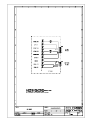
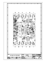
INDEX
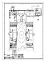
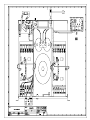
- BLOCK DIAGRAM
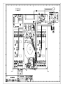
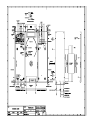
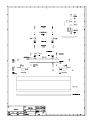
- SCHEMATICS
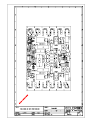
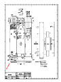
- COMPONENTS LOCATION SCHEMA
- TESTING AND QUALITY CONTROL
- TECHNICAL CHARACTERISTICS
- WIRING DIAGRAM
- MECHANICAL DIAGRAM
- PACKING DIAGRAM
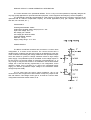
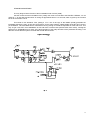
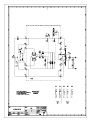
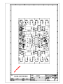
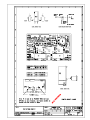
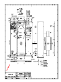
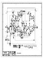
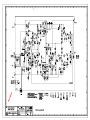
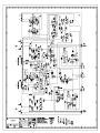
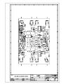
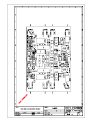
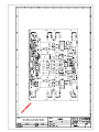
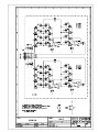
MODULE CIRCUIT 11.0504B OPERATION - DESCRIPTION
The control element is the operational NE5534. This is a very low noise operational, especially designed for
very high quality applications in professional audio equipment, control equipment and telephony channel amplifiers.
The operational is internally compensated for a gain equal to or higher than three. Frequency response can be
optimized with an external compensation capacity, for several applications (unity gain amplifier, capacitive load,
slew-rate, low overshoot, etc...).
Characteristics:
Small-signal bandwidth: 10Mhz
Output drive capability: 600Ω 10V(rms) at Vs="18V
Input noise voltage: 4nV/ Hz
DC voltage gain: 100000%
AC voltage gain: 6000 at 10KHz
Power bandwidth: 200KHz
Slew-rate: 13V/µs
Supply voltage range: "3 to "20V
POWER SUPPLY
The BF871 and BF872 transistors are mounted in a common base
configuration, in a current source structure. The current sources have a
double function: polarizing the gate-source links in the MOSFETs to the limit
of the conduction and moving the voltage variations at the operational output
which are refered to ground to voltage variations refered to high voltage
power supply. The polarization point is calculated so the voltage dropout in
Rc (R112+R111) is the limit voltage of conduction of the MOSFETs (.2 to
3V), enough to carry the bias current. If we modulate in AC the base-emitter
voltage, the Ic and VRc will vary proportionally. In our configuration, as the
reference voltage Vref is constant (it is a part of the operational power
supply), we add the operational output voltage to the transistors emitter
through Re (R107-R108).
The Rc value fixes the source output impedance. We do not
recommend to raise it higher than 1KΩ because of frequency response and
slew rate reasons. This voltage circuit's gain is, as usual in a common base
configuration with Rc/Re emitter resistor, 0.45.
1
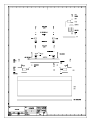
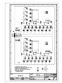
BIAS CURRENT ADJUST
The bias current adjust is performed through the
variable resistor connected between the emitters of the current
sources R110 (5KΩ). It delivers a supplementary current (it
does not go through the operational) which simultaneously
increases the voltage which falls in the Rc load resistors.
This is the easiest way of acting with just one adjust
over both branches at the same time. In order to adjust the
bias current the adjustable resistor must be varied until a
current of about 80mA circulates through each MOSFET. So,
for instance, for a PAM1400 in which there are six MOSFETs it
will be 80 x 6 = 480mA. The bias current depends on the
MOSFETs temperature and the stabilizing circuit transistors
temperature.
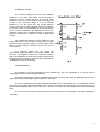
TEMPERATURE STABILIZING CIRCUIT
Temperature affects MOSFETs conduction in two different
ways: first, the conduction threshold voltage has a negative temperature
coefficient; second, the drain-source conduction resistance increases
with temperature. Depending on which of the two things is
predominating the temperature coefficient of the drain can be positive
or negative. In our case, in which the gate-source voltage in the
MOSFETs is very low when they conduct, the temperature coefficient of
drain current -which is positive- is predominating.
To avoid thermal runaway in the polarizing current we must
decrease the gate-source voltage as the MOSFETs get hot.
Temperature stabilization is performed by modifying the reference
voltage of both sources. If the temperature increases the Vref must
decrease so that Ic and VRc decrease and, as a consequence, the
gate-source voltage also decreases.
The circuit used is shown in figure 3. The base-emitter Vbe
temperature/voltage feature is used to obtain the final result we need.
The main idea is adequately choosing R1 and R2 to obtain the right
temperature coefficient.
2
SYMMETRY ADJUST
The threshold voltage varies much, even between
MOSFETs of the same kind. When connecting them in
parallel we must be careful that they all have the same
conduction current if we want equal currents circulating in all
of them. If the conduction voltage of P an N channels
MOSFETs is not the same they will conduct different
currents, even when we apply identical gate-source voltages.
As the bias current of the N MOSFETs must be identical to
the one of the P MOSFETs the feedback will correct the
continuous voltage at the operational output to polarize the
MOSFETs with different voltages until both conduct equal
currents.
If the operational output is not 0 V its capacity to give
voltage and current is not the same in both senses. To avoid
this we must put a symmetry adjust. It is just an adjust which
allows to vary the collector resistance of one of the current
sources (R111).
The symmetry adjust does not correct the
asymmetrical clipping saturation of the power amplifier with
real load. This happens because the conduction resistors
(Ron) of the MOSFETs N and P are not equal. Channel P has
a higher Ron than channel N. This characteristic depends on
the MOSFET's physical construction.
POWER MOSFETs
The MOSFETs used are IRFP9240 (P) and IRFP240 (N). They are assembled in a common source
configuration so they can be completely saturated.
This kind of configuration has two drawbacks compared to a common drain one: less stability (because of the
configuration gain itself) and high output impedance in open loop.
The source resistances (0.22Ω) are needed for the MOSFETs to work in parallel. E.g.: Two MOSFETs excited
by the same Vgs voltage (gate-source voltage) of 5V. If they have different transconductance curves (Id function Vgs)
they will conduct different drain currents; let's say 1A and 3A. The second one will dissipate more power and will get
hotter.
The use of source resistances tends to match the current that each of the MOSFETs connected in parallel is
conducting.
3
This resistance performs a negative feedback on the gate, lowering down the Vgs, relating to the drain current;
like this:
Vgs = Vgg - Id*Rs
The higher the Id, the lower the Vgs voltage. The gate is
protected by a zener, preventing a possible overload during an
unexpected change from overload to real clipping.
Given the high input impedance and the broad frequency response of the MOSFETs there is a high risk of
self-oscillations if all gates are excited connected to the same node. Intercalating serial resistances and ferrite beads at
the gate this possibility is minimized, because the Q of the LC network made by the inductances and gate-source
capacity is reduced.
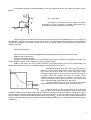
PROTECTION CIRCUIT
The protection circuit monitors the dissipated power at the MOSFETs stage. It has two basic parts:
MOSFET Id current detection.
MOSFET Vds voltage detection.
The goal is limiting the MOSFET so it works inside an area close to the SOA, as indicated in the figure. We
chose channel N because, due to construction reasons, its SOA is lower.
ZONE A. This zone is for very low loads, around 0Ω. As the load voltage is very low, the voltage held by the
MOSFET will always be high. The protections should be activated with very low current.
Fast protections and some of the slow ones are working in
this zone. The circuit that configures the fast ones is made of: D120,
D121, D123, R174, R175, R176, R177, R178, R179, C127, Q122
and Q123 for the N channel. There is also an equivalent circuit in the
P channel. These start working when there is a sudden current
variation because of a shortcircuit or a transitory. The reaction time
-from the exact moment when these things occur to when the current
stops circulating through the MOSFETs- is about 80µs.
The time constant is given by C127, R174 and R179 and the
load circuit made by the LED diode of the IC104 (opto-coupler).
Id
C
B
A
Please note that in order for the protection to be activated
Q122 and Q123 must conduct simultaneously, through which R174
is linked to negative power supply, being C127(1µF) loaded very quickly through this resistance, activating the LED of
the opto-coupler, sending a pulse to the protection circuit, which will open the corresponding channel's relay, being this
way the output from the power amplifier disconnected from the load (0Ω), in this case. Q122, together with the zeners
and the base polarization resistances, configure the voltage detector (this group is in parallel with the Vds voltage of the
N MOSFET).
Vds
4
Q123, together with the resistances which make the base divider, configure the current detector (this divider
takes its voltage from one of the source resistances of a N MOSFET, which is proportional to the current circulating
through itself).
The threshold separating zone A from zone B is determinated by the D125 zener. When this zener stops
working and there is no current circulating through it because the Vds voltage is lower (let's remember this circuit is
also in parallel with this voltage) or, what is the same, the load voltage grows because it is not 0O anymore and has a
given value, like 0.5Ω to 1Ω, and the help given by D126 stops so more current will be needed for the shot. We have
climbed the first stair of the stairway of the SOA graphic.
When the zeners D124 and D118 stop working because the load voltage goes on growing (values higher than
1Ω) or -what is the same- the Vds decreases, the Q125 transistor does not receive current anymore in its base and so
it is shorted, allowing Q124 to enter conduction. This way R172 stays in parallel with the base-emitter of Q121, making
up a voltage divider with R173. This divider will climb another stair of the stairway and enter the ZONE C.
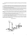
The link between the module's protection circuit and the relays' control circuit is made through IC103 and
IC104 which are, as mentioned earlier, opto-couplers, just to insulate the existing high voltages at the power amplifying
module, "90V in the case of the PAM1400, and the power supply voltage of the existing logic circuits in the relays'
control card.
Once the pulse generated by the protections is detected, the control circuitry resident in the protection card,
appart from opening the corresponding relay, returns the signal A.O. SUPPLY CONTROL to the module,
which cuts by means of Q119, Q120 and IC102 the operational's power supply.
This is the way to insure a fast and safe cut of the Id current in the MOSFETs (around 80µs time), because
they stop receiving their respective reference voltages and, consequently, their Vgs polarization voltages so they are
cut. The circuit is shown in figure 9 and its operation is very simple.
When the A.O. SUPPLY CONTROL (+10V) signal appears, the Q119 transistor starts conducting,
shortcircuiting to ground the positive power supply of the operational. On the other hand, the signal is also applied to
the IC102's LED (opto TIL112 (4N35)), which puts its internal transistor and Q120 into conduction, connecting the
negative power supply of the operational to ground.
5
6
7
ZOBEL NETWORK
This circuit tries to get a constant load impedance for the power module, in spite of the amplifier's load and
frequency, to avoid phase shifting of the feedback signal.
The values have been experimentally calculated through a study with square signal by trying to minimize the
power amplifier's ringing with very capacitive loads (2,2µF//4Ω).
The Zobel Network eliminates possible oscillations of the MOSFETs between 5MHz and 10MHz, too. This is
why it must be physically placed at the module's output, avoiding long wiring. Great care must be taken for the signal
not to be too shifted at the output, because the feedback could turn negative.
FEEDBACK
The whole amplifier is compensated with just one capacity, which places the amplifier's general pole at:
1
Fp = -------------- = 140KHz
2*π*Rf*Cf
Rf = R106
Cf = C109-C110
8
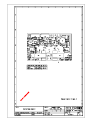
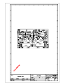
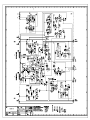
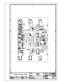
PROTECTION CIRCUIT 11.0411 OPERATION - DESCRIPTION
The circuit is configured by:
- A POWER SUPPLY.
- A THERMAL PROBE DC AMPLIFIER.
- A TEMPERATURE DETECTOR.
- A DC OUT DETECTOR PER CHANNEL.
- A CLIP CIRCUIT PER CHANNEL.
- A RESET (TURN OFF/TURN ON) CIRCUIT.
- A BINARY COUNTER PER CHANNEL.
- TWO MONOSTABLE CIRCUITS PER CHANNEL.
The circuit power supply is performed through various sources: +V, module's power supply. This voltage feeds
the relays circuit, manual reset circuit and part of the clip circuit. Alternate voltage from a transformer's
secondary (manual reset circuit).
There is also a stabilized 10V power supply which feeds the card's circuitry, made of IC301 (7805) plus the
zener D302 (Z4.7) 4.7+5 . 10V. We will also need a regulated power supply to get 14Vmax at 0.7A, which can be
obtained with IC302 (7805) plus an auxiliary circuitry that will be analysed below.
The cooling fan speed is automatically regulated in relation to the power module's temperature, which is read
by a thermal probe (LM35D), jointly linked to the heat sink.
This high sensitivity thermal probe gives variations of 10mV for every EC. This voltage is picked up and
amplified by the IC305 (LM358). Of course, there is a probe for each L and R heatsink. The output of both amplifiers is
linked through two diodes D304 and D305, making an O gate, whose cathodes go to the regulator, applying the DC of
any of them to the regulator. This provides a variable voltage at its output which oscillates from a minimum of
approximately 7V for a temperature of 20EC (cold heatsink) to a maximum of 14V for temperatures of 76EC or higher.
The gain of the amplifiers has been calculated for this temperatures window. The maximum voltage allowed by
the heatsink in order to work properly is 14V. This maximum is given by the zener D305 (Z9.1/1); as the regulator is a
7805 the voltage will be -as maximum- 9.1+5 = 14.1V. When the zener is not working (not enough voltage) the voltage
on the fan will be the output amplifiers', less 0.6V (diodes fall), plus the 5V of the IC302.
9
10
TEMPERATURE DETECTOR
This circuit is calculated to operate over the output relay opening it if any of both modules' temperature
excedes 90EC, approximately. It is made with a comparator per channel (L-R), resident in the same IC306. Both share
a reference voltage provided by D306 (TL431A), which gives excellent stability at that voltage "1%. These comparators
reveive, like the DC amplifiers, the signal from their probes, comparing them with the Vref. Once this voltage is
surpassed by any of both probes, the output of the corresponding comparator is balanced to the power supply (+10V),
acting through D307, R318, D308 and R319 over the respective bases of transistors Q301 y Q307, which makes the
corresponding relay open. This output is also connected to the THERMAL LEDs, which light up as the relays are open.
Note that each time the relay is open through any of the variables which act upon it the PROTECT LED must
light up. The circuit acting over this LED is made of R327, R328, R329, R4, R5 and Q303. When Q302 stops
conducting (open relay), Q303 receives its base current through R327, R326, R6 and the relay's coil, putting this
transistor into saturation. This way the LED is linked to the power supply (+V) by means of the group of resistances
R328, R329, R4 and R5.
11
DC OUT CIRCUIT
The circuit shown in the figure corresponds to the DC OUT of channel L. The goal of this circuit is protecting
the loudspeakers when, because of a module fail, there is some DC appearing at the output. The voltages indicated in
the figure correspond to rest state and they are given by the dividers made of R320-R322 and R332-R323.
The resistances R323-R322 are linked by their extreme to the leg 7(Q) of the monostable IC310 (4538), which
has +10V at rest state. On the other hand R320-R321 are linked by their extreme to the L output, which, in these
conditions, has 0V respect to ground. If we apply Ohm's Law to these dividers we will obtain the above mentioned
voltages.
Let's remember briefly the function of a NOR gate like the HEF4001B.
A
B
C
0
0
1
0
1
0
1
0
0
1
1
0
Let's suppose there is a continuous voltage appearing at the module output, because of any malfunction.
This makes the voltage dividers lose balance, no matter if the above mentioned voltage is positive or negative,
the gate goes to 0V, the base Q302 loses the current stream and, as a consequence, the relay K301 opens. The aim
of the zeners D309 and D310 is protecting the gates, avoiding the voltage in them to be higher than 8.2V when the
voltage is positive and lower than -0.6V when it is negative; as you can see, the zener plays the role of a diode.
12
CLIP CIRCUIT
The other half of IC307(4001) is used in the clip circuit. Given that we have two gates more and we just need
one for our purposes we will connect them in parallel for a higher output current and a more effective LED lighting up.
The clip threshold or point where we want the LED to light up is determined by the zener D313. In our case it is
between 0.5 and 1dB or, what is the same, when the output signal level over the load reaches a value close to that of
the power supply (+V), exactly Vout = V - 5.6, moment in which Q304 loses the base-emitter voltage stopping
conduction; this makes the zener D312 voltage disappear (0V) and the output from IC307 go to "1" logic (+10V),
making the LED light up.
13
GENERAL RESET CIRCUIT (TURN OFF/TURN ON)
TURN OFF RESET. This circuit starts working when the AC current from the transformer secondary
disappears or, what is the same, when we turn the power amplifier off by pushing the power off switch, actually
disconnecting it from mains.
Circuit operation: The AC signal present at the anode D321 is rectified by this, attenuated and filtered by R13,
R348, R347 and C322, apllying it to the base of Q306, which is conducting into saturation and, as a consequence,
Q305 is cut. When this signal disappears Q306 is cut and then Q305 has its base feeded through R345, R346 and
R14 from the +V power supply, which has begun to lose voltage -because we have just cut the mains- but, because of
the high capacity value of the filter condensers, there is enough time to saturate Q305, which puts the resistances R15
and R344 (50Ω) in parallel with the power supply (+10V) of the logic circuitry, completely discharging the capacities of
the circuit, leaving it ready for a new reset pulse -the connection one-, what warranties the new turn-on, even with very
short time intervals (.1s) between turn-off and connection pulses.
CONNECTION RESET
This is made of C315, R336 and D314. It is the classical reset circuit, used in lots of applications.
In the exact connection moment the condenser C315 is not charged, with a high amount of current circulating
through it, or a high voltage in R336. This current decreases as the condenser is charging until it disappears. At the
same time, the voltage -in the extremes- of the resistance goes from maximal, in the beginning, to 0V. This way we get
a pulse whose duration depends on the time constant RC. The aim of the diode D314 is a fast discharging of C315
during disconnection.
14
BINARY COUNTER HEF4520
This is a 4-bit double binary counter. Configured in a way in which when there is the binary code equivalent to
decimal number 5 at its output -so this is 1 0 0- it is blocked in this position, until it receives a new MR reset pulse. The
blocking action is performed by the NAND gate between legs Q2 and CP1. At this state Q2 becomes "H" one logical,
the NAND changes its state putting the leg CP1 to "L" zero logical and -as you can see in the table of functions- the
mode can not change in this conditions.
CPO
CP1
MR
MODE
8
H
L
counter advance
L
9
L
counter advance
9
X
L
no change
X
8
L
no change
8
L
L
no change
H
9
L
no change
X
X
H
Q0 to Q3=low
The general turn-on reset initializes the counter. Every time it receives a pulse from the module opto-couplers
because of a protections shot it is counted. If during an interval of approximately 5 minutes it does not receive any
other pulse, the counter will go back to the original zero state, because it receives a new MR reset pulse from the
monostable IC311, whose time constant is approximately 5 minutes (R342,C319). This monostable begins counting
from the very first pulse received by the counter, because both are linked to the PROTECT SIGNAL from the module
and, consequently, activated at the same time.
If during this time interval (about 5 minutes) a minimum of 5 successive pulses are received, these will make
the counter block at that position. This translates into a logical "1" at the Q2 leg of the counter, a "0" at the NAND
(IC308) output; this zero makes a "1" at the output of the next NAND, giving a result of "0" at the collector of Q301, so
Q302 is not conducting and the relay K301 remains open. It will stay this way until the reset from the monostable
happens or there is a manual mains disconnection by pushing the power off button.
The reset circuit associated with the monostable is made of C320, D320, R339 and D318 (above we have
always been refering to channel L). By means of diodes D317 and D318 we build an "O" gate, with which we apply any
of the above mentioned reset pulses to the counter.
15
16
STANDBY MONOSTABLE
The only thing left is the function of the monostable made of IC310 (4538).
Like the counter and the monostable IC311 (4538), this circuit is connected to the PROTECT SIGNAL, too. Its
output is "1" in rest state and becomes "0" during an approximate time of 1.3 seconds, which is given by the constant
RC of the circuit R341 C316.
This leads to two situations: First, putting a "0" in one of the legs of the NAND (IC308) generates the
immediate opening the relay, as we have seen before. On the other hand the voltage divider of the DC OUT circuit is
put off balance. The monostable time is calculated to be long enough to unload the capacities of C312 and C313. This
way we get a DC OUT circuit initialization as we had done a manual reset (disconnection from mains), causing the
tipical turn-on STANDBY time for each of the disconnections of the relays because of the protections shooting. Let's
take into account that the system is locked after the fifth disconnection.
17
PARTS LIST:
MODEL : PAM1400/1000/600/300
DATE: 180595
ANTICLIP CIRCUIT
DRW. No 33.0004PL
SHEET 1 OF 1 REPLACES:
REFERENCE
VALUE
C401
C402
C403
D401
D402
D403
D404
D405
H401
IC401
J401
J402
J403
J404
J405
R401
R402
R403
R404
R405
R406
R407
R408
R409
R410
R411
PC 11.0503B
2µ2/63
2µ2/63
22pF
Z10
1N4148
1N4148
1N4148
1N4148
VTL5C8
TL071
O5JQ-BT
JP
JP+MJ
JP
O5JQ-BT
10Ω
MF20k0
MF100k
22k
22k
100Ω
1k5
3k3
3k9
10Ω
1k
PRINTED CIRCUIT
REV: A
REPLACED BY:
PARTS LIST:
MODEL : PAM1400/1000/600/300
DATE: 081193
ANTICLIP CIRCUIT
DRW. No 33.0004PL
SHEET 1 OF 1 REPLACES:
REFERENCE
VALUE
C401
C402
D401
D402
D403
D404
D405
H401
IC401
J401
J402
J403
J404
J405
R401
R402
R403
R404
R405
R406
R407
R408
R409
R410
PC 11.0503
2µ2/63
2µ2/63
Z10
1N4148
1N4148
1N4148
1N4148
VTL5C8
TL071
O5JQ-BT
TP
TP+MJ
TP
O5JQ-BT
10Ω
MF20k0
MF100k
22k
22k
1k2
470Ω
2k
2k7
10Ω
PRINTED CIRCUIT
REV:
REPLACED BY:
PARTS LIST:
MODEL : PAM1400/1000
DATE: 081193
INPUT CIRCUIT
DRW. No 33.0002PL
SHEET 1 OF 2 REPLACES:
REFERENCE
VALUE
C201
C202
C203
C204
C205
C206
C207
C208
C209
C210
C211
C212
C213
C214
C215
C216
D201
D202
D203
D204
D205
D206
D207
D208
D209
D210
D211
D212
IC201
IC202
J201
J202
J203
J204
J205
J206
J207
J208
J209
J210
J211
L201
L202
L203
L204
R201
R202
R203
R204
R205
R206
R207
R208
R209
R210
R211
220p
220p
47µ/25
C100n
47µ/25
C100n
220p
220p
C15p
C8p2
10µ/35
C15p
C8p2
10µ/35
C100n
C100n
1N4148
1N4148
1N4148
1N4148
1N4148
1N4148
1N4148
1N4148
1N4148
1N4148
Z18/1
Z18/1
NE5532A
TL072
YKF52-5003
YKF52-5005
B3P-VH
YKF52-5003
YKF52-5005
2600-6TS
2600-6TS
B3P-VH
2600-7TS
B5P-VH
B5P-VH
68µH
68µH
68µH
68µH
MF1k00
MF1k00
W1k8/7
W1k8/7
MF1k00
MF1k00
MF23k7
MF47k5
MF23k7
MF47k5
MF23k7
REV:
REPLACED BY:
PARTS LIST:
MODEL : PAM1400/1000
DATE: 081193
INPUT CIRCUIT
DRW. No 33.0002PL
SHEET 2 OF 2 REPLACES:
REFERENCE
VALUE
R212
R213
R214
R215
R216
R217
R218
R219
R220
R221
R222
R223
R224
R225
S601
WIRE 27
WIRE 27
CTO 11.0497-8
MF47k5
MF23k7
MF47k5
MF1k00
MF1k00
MF340k
56
MF1k00
MF340k
MF1k00
56
1k5
1k5
1k5
17.155
WIRE 27
WIRE 27
CTO.FRA.CU.
REV:
REPLACED BY:
PARTS LIST:
MODEL : PAM1400/1000/600/300
DATE: 081193
ATTENUATOR CIRCUIT
DRW. No 33.0003PL
SHEET 1 OF 1 REPLACES:
REFERENCE
VALUE
J501
J502
R501
R502
CTO 11.0502
B4P-S-VH
B4P-S-VH
10A10k
10A10k
CTO.FRA.CU.
REV:
REPLACED BY:
PARTS LIST:
MODEL : PAM1400/1000/600/300
DATE: 081193
LEDS CIRCUIT
DRW. No 33.0005PL
SHEET 1 OF 1 REPLACES:
REFERENCE
VALUE
D701
D702
D703
D704
D705
D706
D707
D708
D709
J701
J702
R701
R702
CTO 11.0501
YELLOW
RED
RED
YELLOW
RED
RED
RED
GREEN
GREEN
B6P-VH
B3P-VH
2k2
2k2
CTO.FRA.CU.
REV:
REPLACED BY:
PARTS LIST:
MODEL : PAM1400/1000
DATE: 081193
SOFT START AND POWER CIRCUIT
DRW. No 33.0006PL
SHEET 1 OF 1 REPLACES:
REFERENCE
VALUE
C801
C802
C803
C804
C805
D801
D802
D803
D804
F801
J801
J802
J803
J804
J805
J806
J807
J808
J809
J810
J811
K801
K802
R801
R802
R803
R804
R805
R806
R807
WIRE 26
WIRE 5
WIRE 6
WIRE 7
CTO 11.0499
2µ2/63
2µ2/63
47µ/100
47µ/100
10n/400
1N4007
1N4007
1N4007
1N4007
TF117ºC
FASTON 6.3
FASTON 6.3
TP+MJ
FASTON 6.3
FASTON 6.3
FASTON 6.3
FASTON 6.3
FASTON 6.3
FASTON 6.3
FASTON 6.3
FASTON 6.3
E3209 6000Û
E3209 6000Û
W4k7/5
6k8/2
6k8/2
2,2/1
W39/8
W39/8
W39/8
WIRE 26
WIRE 5
WIRE 6
WIRE 7
CTO.FRA.CU.
REV:
REPLACED BY:
PARTS LIST:
MODEL:PAM1400
DATE: 000621
POWER CIRCUIT AND AND SHORT CIRCUIT PROTECTION
DRW.Nº 33.0001PL
REV: A
SHEET 1 OF 4
REPLACED BY:
REFERENCE
VALUE
C101
C102
C103
C104
C105
C106
C107
C108
C109
C110
C111
C112
C113
C114
C115
C116
C117
C118
C119
C120
C121
C122
C123
C124
C125
C126
C127
C128
D101
D102
D103
D104
D105
D106
D107
D108
D109
D110
D111
D112
D113
D114
D115
D116
D117
D118
D119
D120
D121
D122
D123
D124
D125
D126
F101
F102
IC101
IC102
47µ/100
C100n
10µ/50
10µ/50
C15p
C100n
C100n
C100n
C39p
C39p
47µ/100
47µ/100
100n/400
47n/400
47µ/50
47µ/50
680n
680n
220n/100
220n/100
220n/100
220n/100
220n/100
220n/100
680n
680n
1µ/63
100µ/25
Z3.6/1
Z3.6/1
Z11/1
Z11/1
Z12
Z12
Z12
Z12
Z12
Z12
Z12
Z12
Z12
Z12
Z12
Z12
Z30/1
Z30/1
Z30/1
Z30/1
Z30/1
1N4148
1N4148
Z27/1
Z10
TL431
TI-16A
TI-16A
5534N
4N35
PARTS LIST:
MODEL:PAM1400
DATE: 000621
POWER CIRCUIT AND AND SHORT CIRCUIT PROTECTION
DRW.Nº 33.0001PL
REV: A
SHEET 2 OF 4
REPLACED BY:
REFERENCE
VALUE
IC103
IC104
IC105
J101
J102
J103
J104
J105
J107
J108
J109
Q101
Q102
Q103
Q104
Q105
Q106
Q107
Q108
Q109
Q110
Q111
Q112
Q113
Q114
Q115
Q116
Q117
Q118
Q119
Q120
Q121
Q122
Q123
Q124
Q125
Q126
Q127
R101
R102
R103
R104
R105
R106
R107
R108
R109
R110
R111
R112
R113
R114
R115
R116
R117
R118
R119
R120
4N35
4N32
LM35D
FASTON 6.3mm
FASTON 6.3mm
FASTON 6.3mm
INPUT
PROTEC
B5B-XH
B5B-XH
2600-3TS
BF871
BF872
MJE15031
MJE15030
IRFP240
IRFP240
IRFP240
IRFP240
IRFP240
IRFP240
IRFP9240
IRFP9240
IRFP9240
IRFP9240
IRFP9240
IRFP9240
2N5401
2N5401
BC337
BC337
2N5551
2N5551
2N5551
BC547B
BC547B
BD437
BD437
MF1k00
MF47k5
MF1k00
680k
680k
MF51k1
1k5
1k5
1k5/.5
5k
500O
NF 390O/.5
NF 680O/.5
MF787O
MF191O
MF191O
MF787O
NF120O/1
10O/.5
NF120O/1
PARTS LIST:
MODEL:PAM1400
DATE: 000621
POWER CIRCUIT AND AND SHORT CIRCUIT PROTECTION
DRW.Nº 33.0001PL
REV: A
SHEET 3 OF 4
REPLACED BY:
REFERENCE
VALUE
R121
R122
R123
R124
R125
R126
R127
R128
R129
R130
R131
R132
R133
R134
R135
R136
R137
R138
R139
R140
R141
R142
R143
R144
R145
R146
R147
R148
R149
R150
R151
R152
R153
R154
R155
R156
R157
R158
R159
R160
R161
R162
R163
R164
R165
R166
R167
R168
R169
R170
R171
R172
R173
R174
R175
R176
R177
R178
10O/.5
6.8O/.5
6.8O/.5
W.22O/5
W.22O/5
W.22O/5
W.22O/5
W.22O/5
W.22O/5
NF330O/.5
NF330O/.5
NF330O/.5
NF330O/.5
NF330O/.5
NF330O/.5
NF330O/.5
NF330O/.5
NF330O/.5
NF330O/.5
NF330O/.5
NF330O/.5
W.22O/5
W.22O/5
W.22O/5
W.22O/5
W.22O/5
W.22O/5
NF2.2O/2
6.8O
6.8O
10O/2
W1k8/7
W6.8O/5
W1k8/7
MF1k00
MF487
5k6/.5
8k2/.5
2k7
22k
330k
10k
100O
3k3
820
330k
10k
10k/.5
4k7/.5
MF5k62
27k/.5
MF464
MF1k00
2k7
8k2/.5
5k6/.5
MF487
MF1k00
PARTS LIST:
MODEL:PAM1400
DATE: 000621
POWER CIRCUIT AND AND SHORT CIRCUIT PROTECTION
DRW.Nº 33.0001PL
REV: A
SHEET 4 OF 4
REPLACED BY:
REFERENCE
VALUE
R179
R180
R181
CTO 11.0504
22k
1k
2k7
CTO.FRA.CU
PARTS LIST:
MODEL:PAM1400
DATE: 081193
POWER CIRCUIT AND AND SHORT CIRCUIT PROTECTION
DRW.Nº 33.0001PL
REV:
SHEET 1 OF 4
REPLACED BY:
REFERENCE
VALUE
C101
C102
C103
C104
C105
C106
C107
C108
C109
C110
C111
C112
C113
C114
C115
C116
C117
C118
C119
C120
C121
C122
C123
C124
C125
C126
C127
C128
D101
D102
D103
D104
D105
D106
D107
D108
D109
D110
D111
D112
D113
D114
D115
D116
D117
D118
D119
D120
D121
D122
D123
D124
D125
D126
F101
F102
IC101
IC102
47µ/100
C100n
10µ/50
10µ/50
C15p
C100n
C100n
C100n
C39p
C39p
47µ/100
47µ/100
100n/400
47n/400
47µ/50
47µ/50
680n
680n
220n/100
220n/100
220n/100
220n/100
220n/100
220n/100
680n
680n
1µ/63
100µ/25
Z3.6/1
Z3.6/1
Z11/1
Z11/1
Z12
Z12
Z12
Z12
Z12
Z12
Z12
Z12
Z12
Z12
Z12
Z12
Z30/1
Z30/1
Z30/1
Z30/1
Z30/1
1N4148
1N4148
Z27/1
Z10
TL431
TI-16A
TI-16A
5534N
TIL112
PARTS LIST:
MODEL:PAM1400
DATE: 081193
POWER CIRCUIT AND AND SHORT CIRCUIT PROTECTION
DRW.Nº 33.0001PL
REV:
SHEET 2 OF 4
REPLACED BY:
REFERENCE
VALUE
IC103
IC104
IC105
J101
J102
J103
J104
J105
J107
J108
J109
Q101
Q102
Q103
Q104
Q105
Q106
Q107
Q108
Q109
Q110
Q111
Q112
Q113
Q114
Q115
Q116
Q117
Q118
Q119
Q120
Q121
Q122
Q123
Q124
Q125
Q126
Q127
R101
R102
R103
R104
R105
R106
R107
R108
R109
R110
R111
R112
R113
R114
R115
R116
R117
R118
R119
R120
TIL112
4N32
LM35D
FASTON 6.3mm
FASTON 6.3mm
FASTON 6.3mm
INPUT
PROTEC
B5B-XH
B5B-XH
2600-3TS
BF871
BF872
MJE15031
MJE15030
IRFP240
IRFP240
IRFP240
IRFP240
IRFP240
IRFP240
IRFP9240
IRFP9240
IRFP9240
IRFP9240
IRFP9240
IRFP9240
2N5401
2N5401
BC337
BC337
2N5551
2N5551
2N5551
BC547B
BC547B
BD437
BD437
MF1k00
MF47k5
MF1k00
680k
680k
MF51k1
1k5
1k5
1k5/.5
5k
500O
NF 390O/.5
NF 680O/.5
MF787O
MF191O
MF191O
MF787O
NF120O/1
10O/.5
NF120O/1
PARTS LIST:
MODEL:PAM1400
DATE: 081193
POWER CIRCUIT AND AND SHORT CIRCUIT PROTECTION
DRW.Nº 33.0001PL
REV:
SHEET 3 OF 4
REPLACED BY:
REFERENCE
VALUE
R121
R122
R123
R124
R125
R126
R127
R128
R129
R130
R131
R132
R133
R134
R135
R136
R137
R138
R139
R140
R141
R142
R143
R144
R145
R146
R147
R148
R149
R150
R151
R152
R153
R154
R155
R156
R157
R158
R159
R160
R161
R162
R163
R164
R165
R166
R167
R168
R169
R170
R171
R172
R173
R174
R175
R176
R177
R178
10O/.5
6.8O/.5
6.8O/.5
W.22O/5
W.22O/5
W.22O/5
W.22O/5
W.22O/5
W.22O/5
NF330O/.5
NF330O/.5
NF330O/.5
NF330O/.5
NF330O/.5
NF330O/.5
NF330O/.5
NF330O/.5
NF330O/.5
NF330O/.5
NF330O/.5
NF330O/.5
W.22O/5
W.22O/5
W.22O/5
W.22O/5
W.22O/5
W.22O/5
NF2.2O/2
6.8O
6.8O
10O/2
W1k8/7
W6.8O/5
W1k8/7
MF1k00
MF487
5k6/.5
8k2/.5
2k7
22k
330k
10k
100O
3k3
820
330k
10k
10k/.5
4k7/.5
MF5k62
27k/.5
MF464
MF1k00
2k7
8k2/.5
5k6/.5
MF487
MF1k00
PARTS LIST:
MODEL:PAM1400
DATE: 081193
POWER CIRCUIT AND AND SHORT CIRCUIT PROTECTION
DRW.Nº 33.0001PL
REV:
SHEET 4 OF 4
REPLACED BY:
REFERENCE
VALUE
R179
R180
R181
CTO 11.0504
22k
1k
2k7
CTO.FRA.CU
PARTS LIST:
MODEL : PAM1400
DATE: 241293
PROTECTIONS CIRCUIT
DRW. No 33.0007PL
SHEET 1 OF 4 REPLACES:
REFERENCE
VALUE
AC
AC
C301
C302
C303
C304
C305
C306
C307
C308
C309
C310
C311
C312
C313
C314
C315
C316
C317
C318
C319
C320
C321
C322
C323
C324
C325
C326
C327
C328
C329
C330
C331
D301
D302
D303
D304
D306
D307
D308
D309
D310
D311
D312
D313
D314
D315
D316
D317
D321
D322
D323
D324
D325
D326
D327
FAST.2.8
FAST.2.8
2200µ/35
10µ/50
10µ/50
100n
10µ/50
10µ/50
100n
100n
470n
470n
10µ/50
10µ/35
10µ/35
100n
22µ/35
2µ2/35
10µ/50
2µ2/35
220µ/25
10µ/50
220µ/25
47µ/16
100n
10µ/35
10µ/35
100n
100n
100n
100n
100n
100n
BAS16
Z4.7
Z9.1/1
BAV70
TL431
BAS16
BAS16
Z8.2
Z8.2
1N4007
Z8.2
Z5.6
BAV99
BAS16
BAV99
BAV99
1N4007
Z8.2
Z8.2
1N4007
Z8.2
Z5.6
B250C1000
REV:
REPLACED BY:
PARTS LIST:
MODEL : PAM1400
DATE: 241293
PROTECTIONS CIRCUIT
DRW. No 33.0007PL
SHEET 2 OF 4 REPLACES:
REFERENCE
VALUE
FAN
GND
IC301
IC302
IC305
IC306
IC307
IC308
IC309
IC310
IC311
IC312
INSULANT WASHER
INSULANT WASHER
J302
J303
J304
J305
J306
J307
J309
J310
J311
K301
K302
MA301
MA302
MA303
MA304
NUT
NUT
PL.N.1777
Q301
Q302
Q303
Q304
Q305
Q307
Q308
Q308
Q309
Q310
R1
R10
R11
R12
R13
R14
R15
R2
R3
R301
R302
R303
R304
R305
FAST.2.8
FAST.2.8
7805
7805
LM358D
LM358D
HEF4001B
HEF4011B
HEF4520B
HEF4538B
HEF4538B
HEF4001B
R19
R19
FAST.6.3
FAST.6.3
B6P-VH
B6P-VH
FAST.6.3
FAST.6.3
B3P-VH
B3P-VH
B3P-VH
E 3209/6000Ω
E 3209/6000Ω
MAGNET
MAGNET
MAGNET
MAGNET
M3
M3
RADIATOR
BC847B
2N5551
2N5551
2N5401
BC817
BC847B
2N5551
2N5551
2N5551
2N5401
680
100k
39K
100k
100k
68K
100
100k
39K
2K2
680
7K50
90K9
15K
REV:
REPLACED BY:
PARTS LIST:
MODEL : PAM1400
DATE: 241293
PROTECTIONS CIRCUIT
DRW. No 33.0007PL
SHEET 3 OF 4 REPLACES:
REFERENCE
VALUE
R306
R307
R308
R309
R310
R311
R312
R313
R314
R315
R316
R317
R318
R319
R320
R321
R322
R323
R324
R325
R326
R327
R328
R329
R330
R331
R332
R333
R334
R335
R336
R337
R338
R339
R340
R341
R342
R343
R344
R345
R346
R347
R348
R349
R350
R351
R352
R353
R354
R355
R356
R357
R358
R359
R360
R361
7K50
90K9
15K
10K
1K
2K7
1K43
604
10K
1K
2M2
2M2
5K6
5K6
332K
332K
590K
226K
5K6
5K6
4K7
100k
6K8
6K8
560
100K
100k
100k
10K
100k
5K6
10K
100k
10K
680K
680K
1M2
1M2
100
100
68K
47K
100k
100k
10K
5K6
4K7
590K
332K
332K
226K
5K6
100k
6K8
6K8
560
REV:
REPLACED BY:
PARTS LIST:
MODEL : PAM1400
DATE: 241293
PROTECTIONS CIRCUIT
DRW. No 33.0007PL
SHEET 4 OF 4 REPLACES:
REFERENCE
VALUE
R362
R363
R364
R365
R366
R4
R5
R6
R7
R8
R9
SCREW
SCREW
WASHER
WASHER
PC 11.0411
100k
100k
100k
39K
39K
6K8
6K8
4K7
4K7
6K8
6K8
M3X8 DIN7985 NINE
M3X8 DIN7985 NINE
ADE M3
ADE M3
PRINTED CIRCUIT
REV:
REPLACED BY:
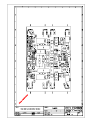
PROFESSIONAL PAM SERIES - TESTING RULES
PRELIMINARY
GROUND LINK Testing.
- Verify that when the switch is at the ON position there is continuity between the chassis ground and the
speakers ground terminal and that the opposite happens at the OFF position. Leave it at ON.
- Put the power amplifier in stereo mode.
- We will need a 1800VA variac for our test purposes.
- Take off one of the fuses of the module in which the testing is being made and connect an ammeter (10A DC
scale) in its place.
- Put the oscilloscope probe between TP-GND.
SET UP
- Unplug the fuses of the module that we are NOT setting up.
- Connect the power amplifier mains cable to the output of the variac. Set the variac output at 0V.
- Switch the power amplifier on with no load or signal. Turn the variac up progressively step by step until 220V.
While mains voltage is growing up make sure the module's current does never exceed 0.8A. Once the circuit is
stable make sure the current is 480mA/400mA/320mA/240mA respectively for PAM1400/ PAM1000/ PAM600/
PAM300 and the symmetry (measured up with the oscilloscope probe) is #50mV. If your figures do not match
these numbers adjust CURRENT (5K) and SYMMETRY (470Ω) until you get the above mentioned numbers.
- Test the operational amplifier power supply ("18V) "1V.
- Put the fuse back in its place into the module (with the power amplifier turned off) and repeat the same
procedure for the other channel.
CROSS DISTORTION
By using a signal generator introduce a level of 100mV RMS at 1kHz and make sure there is no cross
distortion at the output (attenuators at 0dB position).
MOSFETS CONDUCTION
By using a signal generator introduce a level of 0.5V at 1kHz and load the amplifier with 4Ω.Check that all
MOSFETs are conducting approximately the same current level (measure this current with the oscilloscope probe
by palcing it on the 0,22 Ω source resistances).The maximum conduction difference between MOSFETs should
be 100mV. When making this test be sure the oscilloscope ground is not connected to any other place of the
circuit when making the reading; just to the 0,22 Ω resistance.If you do not follow this rule you could produce a
shortcircuit between two points of the circuit and therefore a very important damage.
POWER
- Verify the amplifier's power at 8 and 4 Ω.
- Maintain the mains voltage at 220V by means of the variac.
- Check that your own figures match the following at close-to-clip point:
Vin.1VRMS/Vo 4 Ω
Vin.1VRMS/Vo 8 Ω
$
$
PAM1400
49.0Vrms
56.0Vrms
PAM1000
45.1Vrms
49.7Vrms
PAM600
34.5Vrms
39.7Vrms
PAM300
26Vrms
30Vrms
FREQUENCY RESPONSE
0.5V input signal.
Verify frequency response at 20Hz/2kHz/20kHz. We must get the same signal output for the actual load
at any of the frequencies. Set the frequency at 50kHz; the output level should not decrease more than 1 or 2 dB
and there should not be any noticeable distortion.
CLIPPING AT 1kHz
Introduce such a signal that the amplifier is just about to clip. Measure the voltage up at the output (with
the actual load) and check that when the voltage decreases between 0.5 and 1 dB the clipping LEDs light down.
Check each LED corresponds to its fader.
DC OUT
For this test you must disconnect the load from the amplifier.
Introduce a 1V signal at #5Hz with the generator. Turn the output of the generator up until the protection
relays open and close.
MONO-STEREO
Make this test with a load of 8 Ω connected between left and right channels' terminals.
Set the MONO-STEREO switch in MONO. Verify that the fader of channel 1 is operating while channel 2
is NOT operating. Verify that the MONO LED is lighten up. Check the signal cut over the load is clean. Set the
amplifier back to STEREO mode.
PROTECTIONS
Disconnect the amplifier from the load and introduce with the signal generator a level of approximately
100mV RMS at 1KHz. Leave the attenuators at 0dB and shortcircuit the left channel output (just for a while)
checking the PROTECT LED is lighting up and the relay opens the circuit (you can check this by placinf an
oscilloscope probe at the amplifier's output and watching the signal disappear during the STAND BY time in which
the protection circuit is working).Repeat the same process for the right channel.
Set the amplifier in MONO mode in the same way as previously. Shortcircuit both channel output
terminals (L and R) (just for a while).Any of both channels must go into protect mode, lighting the corresponding
LED and making the relay open the circuit.
PROFESSIONAL PAM SERIES - QUALITY CONTROL
We will use a mixer with balanced output -if possible- and a nominal output level of 1V as the signal
source for test purposes.
Connect the mixer outputs to the power amplifier inputs. Plug the power amplifier to mains (make sure its
specified voltage matches that of mains) and make sure that PROTECT, ON and SIGNAL PRESENT LEDs all
light up when you turn on the amplifier by pushing the ON button. Turn up the mixer output level untill the CLIP
LEDs light up on the power amplifier. Turn down the mixer output and connect the loudspeakers.
Make an exhaustive test of:
- Sound quality (no distorsions or noises)
- Faders action (fader travel, signal cut at their low end, no scratching or clicking noises and correct stereo
channel for each one).
- Cooling fan operation.
- While the power amplifier is working shake it or throw it a table to make sure the output sound goes on playing
correctly.
- Shortcircuit the power amplifier output and make sure the corresponding channel's PROTECT LED lights up,
the relay opens and the output signal is cut for a short period of time (STAND BY) and returned back into normal
operation. Repeat the same procedure four times more and then the STAND BY time should be about 5 minutes.
Repeat the same steps for the other channel.
TECHNICAL CHARACTERISTICS
PAM300
Frequency response at max.
power output.
PAM600
PAM1000
PAM1400
7Hz to 60kHz +0 -1dB
Harmonic distortion+noise
from 20Hz to 20kHz meas.band
0,02%
0,02%
0,02%
0,02%
Intermodulation distortion
(SMPTE) using frequencies of
50Hz and 7kHz at 4:1 ratio,
nominal power.
#0,03%
#0,03%
#0,03%
$0,03%
TIM 100
#0,05%
#0,05%
#0,05%
#0,03%
Signal noise ratio
from 20Hz to 20kHz Ref.1W/4Ω
To 4Ω nominal power.
$85dB
$107dB
$80dB
$105dB
$80dB
$106dB
$85dB
$110dB
Damping factor at 1kHz 8Ω
$350
$310
$400
$420
Slewrate
"32V/µs
"75V/µs
"80V/µs
"85V/µs
Channel crosstalk at 1kHz
at 20kHz
$80dB
$60dB
$80dB
$60dB
$80dB
$55dB
$80dB
$55dB
Inputs balanced and provided
with XLR3.
CLIP indicators at -0,3dB
Sensitivity/load
Outputs
These are provided with 2 pairs of 4mm banana.
Protections
-Delayed turn-on heavy duty relay with PROTECT indicator ON
during standby.
-DC:4Hz or DC at 2V,PROTECT INDICATOR.
-Thermal:A sensor activates a high temperature detection
circuit,channel shut down at 90? ,THERMAL indicator.
-Overload:Protection against output short circuit.PROTECT
indicator.
-Autoreset:Four automatic reset during five minutes in case
of short circuit.After this period reset mustbe done manually.
-Soft start system (PAM 1000/1400)
-Varispeed Fan controled according to internal temperature.
Power requirements 110V,120V
220V,230V,240V AC 50/60Hz
530VA
Dimensions Front pannel
Chassis
482,6x88x5mm
440x88x420mm
Weight
14,35kg
0dBV/1V/47kΩ
965VA
1443VA
1800VA
482,6x132,5x5mm
440x132,5x420mm
15,90kg
21,85kg
24,35kg
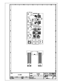
PARTS LIST:
MODEL:PAM1400/1000
DATE: 180297
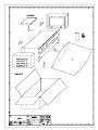
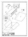
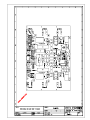
MECHANICAL DIAGRAM
DRW.Nº 300001PL
SHEET
1 OF 1
REV: C
REPLACES:
REPLACED BY:
QUANTITY DESCRIPT
10
2
36
5
1
4
6
4
10
1
6
4
9
2
1
1
1
3
4
6
4
1
1
4
4
1
1
1
1
2
1
1
1
1
1
1
6
SCREW 2,9x6,5 DIN7981
SCREW 3,5x6,5 DIN 7981
SCREW M4x6 SPANLO DIN7985
SCREW M4x12 DIN7985
SCREW M4x20 DIN7985
SCREW M4x10 SPANLO DIN966
SCREW M4x8 TX SPIRALFORM
SCREW M4x6 DIN7985
METAL WASHER ADE M4
METAL WASHER 4,2x9x0,5
METAL WASHER 4x7x0,5
METAL WASHER 4,2x9x1,5
NUT M4 DIN934
METAL WASHER AND NUT POTENTIOMETER
RIVET NUT M4-PSM
GROUND TERMINAL Nº00.1761
SECURITY WASHER M4
NYLON RIVET 1303
MINIATURE SUPPORT MSP-6N
SEPARATOR Nº00.1636
BASE 11x25
FUSE HOLDER 6x32
COMMUTATOR Nº17.120
SUPPORT LKC
FLANGE T-50L
TRANSFORMER REF.21U212 (20Z194) WIT ASSEMBLY KIT
FAN REF.NMB4515 PL-04W B30
CHASSIS WD.00.2372
CHASSIS WD.002371
HANDLE ASSEMBLY WD.00.2374
COVER WD.00.2375
UPPER FRONT PANEL WD.00.2364
LOWER FRONT PANEL WD.00.2370
PROTECTOR FAN LZ-20
SCREW M4x10 DIN7500C ZNBL
CHASSIS WD.00.2307
SCREW 2.9x13 DIN7982
PARTS LIST:
MODEL : PAM1400/1000
DATE: 021293
MECHANICAL DIAGRAM
DRW. No 30.0001PL
SHEET 1 OF 1
REV:
REPLACED BY:
QUANTITY VALUE
10
2
36
5
1
4
6
4
10
1
6
4
9
8
4
2
1
1
1
3
4
6
4
1
1
4
4
1
1
1
1
2
1
1
1
2
1
SCREW 2,9x6,5 DIN7981
SCREW 3,5x6,5 DIN 7981
SCREW M4x6 SPANLO DIN7985
SCREW M4x12 DIN7985
SCREW M4x20 DIN7985
SCREW M4x10 SPANLO DIN966
SCREW M4x8 TX SPIRALFORM
SCREW M4x6 DIN7985
METAL WASHER ADE M4
METAL WASHER 4,2x9x0,5
METAL WASHER 4x7x0,5
METAL WASHER 4,2x9x1,5
NUT M4 DIN934
NUT M5 DIN934
METAL WASHER 5,2x10x1
METAL WASHER AND NUT POTENTIOMETER
RIVET NUT M4-PSM
GROUND TERMINAL Nº00.1761
SECURITY WASHER M4
NYLON RIVET 1303
MINIATURE SUPPORT MSP-6N
SEPARATOR Nº00.1636
BASE 11x25
FUSE HOLDER 6x32
COMMUTATOR Nº17.120
SUPPORT LKC
FLANGE T-50L
TRANSFORMER REF.21U212 (30Z194) WIT ASSEMBLY KIT
FAN REF.NMB4515 PL-04W B30
CHASSIS Nº00.1965
CHASSIS Nº00.1964
HANDLE ASSEMBLY Nº00.1966
COVER Nº00.1963
UPPER FRONT PANEL Nº00.1956
LOWER FRONT PANEL Nº00.1958
JOINED CONNECTOR LOUDSPEAKER
PROTECTOR FAN LZ-20
PARTS LIST:
MODEL : PAM1400/1000
DATE: 101293
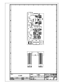
ASSEMBLY MODULE
DRW. No 30.0002PL
SHEET 1 OF 1 REPLACES:
QUANTITY VALUE
3
2
2
2
1
4
4
4
4
2
2
2
2
2
4
1
1
2
2
1
METAL WASHER 3.2X6X0.5
INSULANT. WASHER R19
MICA TO-220
MICA TO-126
WIRE Nº9
SCREW M3X8 SPIRALFORM DIN7985
SCREW M3X15 SPIRALFORM DIN 7985
NYLON SEPARATOR 3.6X6.4
SCREW M4X6 SPANLO DIN7985
RIVET NUT M3X3
ACCESSORY PL.Nº1775
SCREW M3X8 DIN7985
WASHER ADE M3
ACCESSORY PL. Nº1915
CARTON WASHER 3.2X6X1
INSULANT CARTON PL.Nº03.0067
RADIATOR Z-10585
RADIATOR Nº2906.6
INSULANT SARCON 116x20mm
SUPPORT RADIATOR N.00.1961
REV:
REPLACED BY:
PARTS LIST:
MODEL : PAM1400/1000/600/300
DATE: 091293
ASSEMBLY FILTER CAPACITOR
DRW. No 30.0003PL
SHEET 1 OF 1
QUANTITY VALUE
4
1
4
1
4
1
1
2
SCREW M5x10 DIN933
SCREW M4x8 DIN7985
METAL WASHER 5x10x0,5
WASHER ADE M4
SECURITY WASHER M5
RIVET NUT M4-PSM
GROUND CHASSIS Nº00.1634
ADHESIVE RIBBON 20mm
REV:
REPLACED BY:
PARTS LIST:
MODEL : PAM1400/1000
DATE: 091293
PACKING DIAGRAM
DRW. No 32.0001PL
SHEET 1 OF 1 REPLACES:
QUANTITY VALUE
4
4
1
1
2
1
1
1
1
1
METAL WASHER 5x11,5x0,8
WASHER AT 5x11,5x3,5 ABS BLACK
FUSE 16A 6x32TI PO90610
BOX PAM1400
POLIETILENE PROTECTOR M940
CASE MANUAL 21,5x32,5
PLASTIC BAG 75x65
BAG 60x80
MANUAL PAM1400
WARRANTY CARD
REV:
REPLACED BY:
PARTS LIST:
MODEL : PAM1000
DATE: 000621
POWER CIRCUIT AND SHORT CIRCUIT PROTECTION
DRW. No 33.0008PL
REV: A
SHEET 1 OF 4 REPLACES:
REPLACED BY:
REFERENCE
VALUE
C101
C102
C103
C104
C105
C106
C107
C108
C109
C110
C111
C112
C113
C114
C115
C116
C117
C118
C119
C120
C121
C122
C123
C124
C125
C126
C127
C128
CTO 11.0504
D101
D102
D103
D104
D106
D107
D108
D109
D110
D112
D113
D114
D115
D116
D117
D118
D119
D120
D121
D122
D123
D124
D125
D126
F101
F102
IC101
47µ/100
C100n
10µ/50
10µ/50
C15p
C100n
C100n
C100n
C47p
C47p
47µ/100
47µ/100
100n/400
47n/400
47µ/50
47µ/50
680n
680n
220n/100
220n/100
220n/100
220n/100
220n/100
220n/100
680n
680n
1µ/63
100µ/25
CTO.FRA.CU.
Z3.6/1
Z3.6/1
Z11/1
Z11/1
Z12
Z12
Z12
Z12
Z12
Z12
Z12
Z12
Z12
Z12
Z24/1
Z24/1
Z24/1
Z24/1
Z24/1
1N4148
1N4148
Z24/1
Z15/1
TL431
TI-16A
TI-16A
5534N
PARTS LIST:
MODEL : PAM1000
DATE: 000621
POWER CIRCUIT AND SHORT CIRCUIT PROTECTION
DRW. No 33.0008PL
REV: A
SHEET 2 OF 4 REPLACES:
REPLACED BY:
REFERENCE
VALUE
IC102
IC103
IC104
IC105
J101
J102
J103
J104
J105
J107
J108
J109
Q101
Q102
Q103
Q104
Q106
Q107
Q108
Q109
Q110
Q112
Q113
Q114
Q115
Q116
Q117
Q118
Q119
Q120
Q121
Q122
Q123
Q124
Q125
Q126
Q127
R101
R102
R103
R104
R105
R106
R107
R108
R109
R110
R111
R112
R113
R114
R115
R116
R117
R118
R119
4N35
4N35
4N32
LM35D
FASTON 6.3mm
FASTON 6.3mm
FASTON 6.3mm
B3P-VH
B3P-VH
B5B-XH
B5B-XH
2600-3TS
BF871
BF872
MJE15031
MJE15030
IRFP240
IRFP240
IRFP240
IRFP240
IRFP240
IRFP9240
IRFP9240
IRFP9240
IRFP9240
IRFP9240
2N5401
2N5401
BC337
BC337
2N5551
2N5551
2N5551
BC547B
BC547B
BD437
BD437
MF1k00
MF47k5
MF1k00
680k
680k
MF43k2
1k5
1k5
1k5/.5
5k
500O
NF 390O/.5
NF 680O/.5
MF787O
MF191O
MF191O
MF787O
NF68O/1
10O/.5
PARTS LIST:
MODEL : PAM1000
DATE: 000621
POWER CIRCUIT AND SHORT CIRCUIT PROTECTION
DRW. No 33.0008PL
REV: A
SHEET 3 OF 4 REPLACES:
REPLACED BY:
REFERENCE
VALUE
R120
R121
R122
R123
R125
R126
R127
R128
R129
R131
R132
R133
R134
R135
R137
R138
R139
R140
R141
R143
R144
R145
R146
R147
R148
R149
R150
R151
R152
R153
R154
R155
R156
R157
R158
R159
R160
R161
R162
R163
R164
R165
R166
R167
R168
R169
R170
R171
R172
R173
R174
R175
R176
R177
R178
R179
NF68/1
10O/.5
1O/.5
1O/.5
W.22O/5
W.22O/5
W.22O/5
W.22O/5
W.22O/5
NF330O/.5
NF330O/.5
NF330O/.5
NF330O/.5
NF330O/.5
NF330O/.5
NF330O/.5
NF330O/.5
NF330O/.5
NF330O/1
W.22O/5
W.22O/5
W.22O/5
W.22O/5
W.22O/5
NF2.2O/2
6.8O
6.8O
10O/2
W1k8/7
W6.8/5
W1k8/7
MF1k00
MF487
5k6/.5
8k2/.5
2k2
22k
330k
10k
100O
3k3
820
330k
10k
10k/.5
3k3/.5
MF5k62
27k/.5
MF464
MF1k00
2k2
8k2/.5
5k6/.5
MF487
MF1k00
22k
PARTS LIST:
MODEL : PAM1000
DATE: 000621
POWER CIRCUIT AND SHORT CIRCUIT PROTECTION
DRW. No 33.0008PL
REV: A
SHEET 4 OF 4 REPLACES:
REPLACED BY:
REFERENCE
VALUE
R180
R181
1k
2k2
PARTS LIST:
MODEL : PAM1000
DATE: 081193
POWER CIRCUIT AND SHORT CIRCUIT PROTECTION
DRW. No 33.0008PL
REV:
SHEET 1 OF 4 REPLACES:
REPLACED BY:
REFERENCE
VALUE
C101
C102
C103
C104
C105
C106
C107
C108
C109
C110
C111
C112
C113
C114
C115
C116
C117
C118
C119
C120
C121
C122
C123
C124
C125
C126
C127
C128
CTO 11.0504
D101
D102
D103
D104
D106
D107
D108
D109
D110
D112
D113
D114
D115
D116
D117
D118
D119
D120
D121
D122
D123
D124
D125
D126
F101
F102
IC101
47µ/100
C100n
10µ/50
10µ/50
C15p
C100n
C100n
C100n
C47p
C47p
47µ/100
47µ/100
100n/400
47n/400
47µ/50
47µ/50
680n
680n
220n/100
220n/100
220n/100
220n/100
220n/100
220n/100
680n
680n
1µ/63
100µ/25
CTO.FRA.CU.
Z3.6/1
Z3.6/1
Z11/1
Z11/1
Z12
Z12
Z12
Z12
Z12
Z12
Z12
Z12
Z12
Z12
Z24/1
Z24/1
Z24/1
Z24/1
Z24/1
1N4148
1N4148
Z24/1
Z15/1
TL431
TI-16A
TI-16A
5534N
PARTS LIST:
MODEL : PAM1000
DATE: 081193
POWER CIRCUIT AND SHORT CIRCUIT PROTECTION
DRW. No 33.0008PL
REV:
SHEET 2 OF 4 REPLACES:
REPLACED BY:
REFERENCE
VALUE
IC102
IC103
IC104
IC105
J101
J102
J103
J104
J105
J107
J108
J109
Q101
Q102
Q103
Q104
Q106
Q107
Q108
Q109
Q110
Q112
Q113
Q114
Q115
Q116
Q117
Q118
Q119
Q120
Q121
Q122
Q123
Q124
Q125
Q126
Q127
R101
R102
R103
R104
R105
R106
R107
R108
R109
R110
R111
R112
R113
R114
R115
R116
R117
R118
R119
TIL112
TIL112
4N32
LM35D
FASTON 6.3mm
FASTON 6.3mm
FASTON 6.3mm
B3P-VH
B3P-VH
B5B-XH
B5B-XH
2600-3TS
BF871
BF872
MJE15031
MJE15030
IRFP240
IRFP240
IRFP240
IRFP240
IRFP240
IRFP9240
IRFP9240
IRFP9240
IRFP9240
IRFP9240
2N5401
2N5401
BC337
BC337
2N5551
2N5551
2N5551
BC547B
BC547B
BD437
BD437
MF1k00
MF47k5
MF1k00
680k
680k
MF43k2
1k5
1k5
1k5/.5
5k
500O
NF 390O/.5
NF 680O/.5
MF787O
MF191O
MF191O
MF787O
NF68O/1
10O/.5
PARTS LIST:
MODEL : PAM1000
DATE: 081193
POWER CIRCUIT AND SHORT CIRCUIT PROTECTION
DRW. No 33.0008PL
REV:
SHEET 3 OF 4 REPLACES:
REPLACED BY:
REFERENCE
VALUE
R120
R121
R122
R123
R125
R126
R127
R128
R129
R131
R132
R133
R134
R135
R137
R138
R139
R140
R141
R143
R144
R145
R146
R147
R148
R149
R150
R151
R152
R153
R154
R155
R156
R157
R158
R159
R160
R161
R162
R163
R164
R165
R166
R167
R168
R169
R170
R171
R172
R173
R174
R175
R176
R177
R178
R179
NF68/1
10O/.5
1O/.5
1O/.5
W.22O/5
W.22O/5
W.22O/5
W.22O/5
W.22O/5
NF330O/.5
NF330O/.5
NF330O/.5
NF330O/.5
NF330O/.5
NF330O/.5
NF330O/.5
NF330O/.5
NF330O/.5
NF330O/1
W.22O/5
W.22O/5
W.22O/5
W.22O/5
W.22O/5
NF2.2O/2
6.8O
6.8O
10O/2
W1k8/7
W6.8/5
W1k8/7
MF1k00
MF487
5k6/.5
8k2/.5
2k2
22k
330k
10k
100O
3k3
820
330k
10k
10k/.5
3k3/.5
MF5k62
27k/.5
MF464
MF1k00
2k2
8k2/.5
5k6/.5
MF487
MF1k00
22k
PARTS LIST:
MODEL : PAM1000
DATE: 081193
POWER CIRCUIT AND SHORT CIRCUIT PROTECTION
DRW. No 33.0008PL
REV:
SHEET 4 OF 4 REPLACES:
REPLACED BY:
REFERENCE
VALUE
R180
R181
1k
2k2
PARTS LIST:
MODEL : PAM1000
DATE: 241293
PROTECTIONS CIRCUIT
DRW. No 33.0014PL
SHEET 1 OF 4 REPLACES:
REFERENCE
VALUE
AC
AC
C301
C302
C303
C304
C305
C306
C307
C308
C309
C310
C311
C312
C313
C314
C315
C316
C317
C318
C319
C320
C321
C322
C323
C324
C325
C326
C327
C328
C329
C330
C331
D301
D302
D303
D304
D306
D307
D308
D309
D310
D311
D312
D313
D314
D315
D316
D317
D321
D322
D323
D324
D325
D326
D327
FAST.2.8
FAST.2.8
2200µ/35
10µ/50
10µ/50
100n
10µ/50
10µ/50
100n
100n
470n
470n
10µ/50
10µ/35
10µ/35
100n
22µ/35
2µ2/35
10µ/50
2µ2/35
220µ/25
10µ/50
220µ/25
47µ/16
100n
10µ/35
10µ/35
100n
100n
100n
100n
100n
100n
BAS16
Z4.7
Z9.1/1
BAV70
TL431
BAS16
BAS16
Z8.2
Z8.2
1N4007
Z8.2
Z5.6
BAV99
BAS16
BAV99
BAV99
1N4007
Z8.2
Z8.2
1N4007
Z8.2
Z5.6
B250C1000
REV:
REPLACED BY:
PARTS LIST:
MODEL : PAM1000
DATE: 241293
PROTECTIONS CIRCUIT
DRW. No 33.0014PL
SHEET 2 OF 4 REPLACES:
REFERENCE
VALUE
FAN
GND
IC301
IC302
IC305
IC306
IC307
IC308
IC309
IC310
IC311
IC312
INSULANT WASHER
INSULANT WASHER
J302
J303
J304
J305
J306
J307
J309
J310
J311
K301
K302
MA301
MA302
MA303
MA304
NUT
NUT
PL.N.1777
Q301
Q302
Q303
Q304
Q305
Q307
Q308
Q308
Q309
Q310
R1
R10
R11
R12
R13
R14
R15
R2
R3
R301
R302
R303
R304
R305
FAST.2.8
FAST.2.8
7805
7805
LM358D
LM358D
HEF4001B
HEF4011B
HEF4520B
HEF4538B
HEF4538B
HEF4001B
R19
R19
FAST.6.3
FAST.6.3
B6P-VH
B6P-VH
FAST.6.3
FAST.6.3
B3P-VH
B3P-VH
B3P-VH
E 3209/6000Ω
E 3209/6000Ω
MAGNET
MAGNET
MAGNET
MAGNET
M3
M3
RADIATOR
BC847B
2N5551
2N5551
2N5401
BC817
BC847B
2N5551
2N5551
2N5551
2N5401
680
100k
39K
100k
100k
68K
100
100k
39K
2K2
680
7K50
90K9
15K
REV:
REPLACED BY:
PARTS LIST:
MODEL : PAM1000
DATE: 241293
PROTECTIONS CIRCUIT
DRW. No 33.0014PL
SHEET 3 OF 4 REPLACES:
REFERENCE
VALUE
R306
R307
R308
R309
R310
R311
R312
R313
R314
R315
R316
R317
R318
R319
R320
R321
R322
R323
R324
R325
R326
R327
R328
R329
R330
R331
R332
R333
R334
R335
R336
R337
R338
R339
R340
R341
R342
R343
R344
R345
R346
R347
R348
R349
R350
R351
R352
R353
R354
R355
R356
R357
R358
R359
R360
R361
7K50
90K9
15K
10K
1K
2K7
1K43
604
10K
1K
2M2
2M2
5K6
5K6
332K
332K
590K
226K
5K6
5K6
0
100k
6K8
6K8
560
100K
100k
100k
10K
100k
5K6
10K
100k
10K
680K
680K
1M2
1M2
100
100
68K
47K
100k
100k
10K
5K6
0
590K
332K
332K
226K
5K6
100k
6K8
6K8
560
REV:
REPLACED BY:
PARTS LIST:
MODEL : PAM1000
DATE: 241293
PROTECTIONS CIRCUIT
DRW. No 33.0014PL
SHEET 4 OF 4 REPLACES:
REFERENCE
VALUE
R362
R363
R364
R365
R366
R4
R5
R6
R7
R8
R9
SCREW
SCREW
WASHER
WASHER
PC 11.0411
100k
100k
100k
39K
39K
6K8
6K8
0
0
6K8
6K8
M3X8 DIN7985 NINE
M3X8 DIN7985 NINE
ADE M3
ADE M3
PRINTED CIRCUIT
REV:
REPLACED BY:
PARTS LIST:
MODEL:PAM600
DATE: 000621
POWER CIRCUIT AND SHORT CIRCUIT PROTECTION
DRW.Nº 33.0009PL
REV : A
SHEET 1 OF 3
REPLACED BY:
REFERENCE
VALUE
C101
C102
C103
C104
C105
C106
C107
C108
C109
C110
C111
C112
C113
C114
C115
C116
C117
C118
C119
C120
C121
C122
C123
C124
C125
C126
C127
C128
CTO 11.0504
D101
D102
D103
D104
D105
D107
D108
D110
D111
D113
D114
D116
D117
D118
D119
D120
D121
D122
D123
D124
D125
D126
F101
F102
IC101
IC102
IC103
IC104
IC105
47µ/100
C100n
10µ/50
10µ/50
C15p
C100n
C100n
C100n
C68p
C68p
47µ/100
47µ/100
100n/400
47n/400
47µ/50
47µ/50
680n
680n
220n/100
220n/100
220n/100
220n/100
220n/100
220n/100
680n
680n
1µ/63
100µ/25
CTO.FRA.CU.
Z3.6/1
Z3.6/1
Z11/1
Z11/1
Z12
Z12
Z12
Z12
Z12
Z12
Z12
Z12
Z18/1
Z18/1
Z18/1
Z18/1
Z18/1
1N4148
1N4148
Z18/1
Z15
TL431
TI-12.5
TI-12.5
5534N
4N35
4N35
4N32
LM35D
PARTS LIST:
MODEL:PAM600
DATE: 000621
POWER CIRCUIT AND SHORT CIRCUIT PROTECTION
DRW.Nº 33.0009PL
REV : A
SHEET 2 OF 3
REPLACED BY:
REFERENCE
VALUE
J101
J102
J103
J104
J105
J107
J108
J109
Q101
Q102
Q103
Q104
Q105
Q107
Q108
Q110
Q111
Q113
Q114
Q116
Q117
Q118
Q119
Q120
Q121
Q122
Q123
Q124
Q125
Q126
Q127
R101
R102
R103
R104
R105
R106
R107
R108
R109
R110
R111
R112
R113
R114
R115
R116
R117
R118
R119
R120
R121
R122
R123
R124
R126
R127
R129
FASTON 6.3mm
FASTON 6.3mm
FASTON 6.3mm
B3P-VH
PROTEC
B5B-XH
B5B-XH
2600-3TS
BF871
BF872
MJE15031
MJE15030
IRFP240
IRFP240
IRFP240
IRFP240
IRFP9240
IRFP9240
IRFP9240
IRFP9240
2N5401
2N5401
BC337
BC337
2N5551
2N5551
2N5551
BC547B
BC547B
BD437
BD437
MF1k00
MF47k5
MF1k00
680k
680k
MF33k2
1k5
1k5
1k/.5
5k
500O
NF390O/.5
NF680O/.5
MF787O
MF191O
MF191O
MF787O
NF68O/1
10O/.5
NF68O/1
10O/.5
1O/.5
1O/.5
W.22O/5
W.22O/5
W.22O/5
W.22O/5
PARTS LIST:
MODEL:PAM600
DATE: 000621
POWER CIRCUIT AND SHORT CIRCUIT PROTECTION
DRW.Nº 33.0009PL
REV : A
SHEET 3 OF 3
REPLACED BY:
REFERENCE
VALUE
R130
R132
R133
R135
R136
R138
R139
R141
R142
R144
R145
R147
R148
R149
R150
R151
R152
R153
R154
R155
R156
R157
R158
R159
R160
R161
R162
R163
R164
R165
R166
R167
R168
R169
R170
R171
R172
R173
R174
R175
R176
R177
R178
R179
R180
R181
R182
NF330O/.5
NF330O/.5
NF330O/.5
NF330O/.5
NF330O/.5
NF330O/.5
NF330O/.5
NF330O/.5
W.22O/5
W.22O/5
W.22O/5
W.22O/5
NF2.2O/2
6.8O
6.8O
10O/2
W1k5/4
W6.8O/5
W1k5/4
MF1k00
MF487O
5k6/.5
8k2/.5
1k8
22k
330k
10k
100O
3k3
820O
330k
5k6
5k6/.5
1k8/.5
MF3k65
10k/.5
MF487O
MF1k00
1k8
8k2/.5
5k6/.5
MF487
MF1k00
22k
1k8
1k8
MF3k65
PARTS LIST:
MODEL:PAM600
DATE: 081193
POWER CIRCUIT AND SHORT CIRCUIT PROTECTION
DRW.Nº 33.0009PL
REV :
SHEET 1 OF 3
REPLACED BY:
REFERENCE
VALUE
C101
C102
C103
C104
C105
C106
C107
C108
C109
C110
C111
C112
C113
C114
C115
C116
C117
C118
C119
C120
C121
C122
C123
C124
C125
C126
C127
C128
CTO 11.0504
D101
D102
D103
D104
D105
D107
D108
D110
D111
D113
D114
D116
D117
D118
D119
D120
D121
D122
D123
D124
D125
D126
F101
F102
IC101
IC102
IC103
IC104
IC105
47µ/100
C100n
10µ/50
10µ/50
C15p
C100n
C100n
C100n
C68p
C68p
47µ/100
47µ/100
100n/400
47n/400
47µ/50
47µ/50
680n
680n
220n/100
220n/100
220n/100
220n/100
220n/100
220n/100
680n
680n
1µ/63
100µ/25
CTO.FRA.CU.
Z3.6/1
Z3.6/1
Z11/1
Z11/1
Z12
Z12
Z12
Z12
Z12
Z12
Z12
Z12
Z18/1
Z18/1
Z18/1
Z18/1
Z18/1
1N4148
1N4148
Z18/1
Z15
TL431
TI-12.5
TI-12.5
5534N
TIL112
TIL112
4N32
LM35D
PARTS LIST:
MODEL:PAM600
DATE: 081193
POWER CIRCUIT AND SHORT CIRCUIT PROTECTION
DRW.Nº 33.0009PL
REV :
SHEET 2 OF 3
REPLACED BY:
REFERENCE
VALUE
J101
J102
J103
J104
J105
J107
J108
J109
Q101
Q102
Q103
Q104
Q105
Q107
Q108
Q110
Q111
Q113
Q114
Q116
Q117
Q118
Q119
Q120
Q121
Q122
Q123
Q124
Q125
Q126
Q127
R101
R102
R103
R104
R105
R106
R107
R108
R109
R110
R111
R112
R113
R114
R115
R116
R117
R118
R119
R120
R121
R122
R123
R124
R126
R127
R129
FASTON 6.3mm
FASTON 6.3mm
FASTON 6.3mm
B3P-VH
PROTEC
B5B-XH
B5B-XH
2600-3TS
BF871
BF872
MJE15031
MJE15030
IRFP240
IRFP240
IRFP240
IRFP240
IRFP9240
IRFP9240
IRFP9240
IRFP9240
2N5401
2N5401
BC337
BC337
2N5551
2N5551
2N5551
BC547B
BC547B
BD437
BD437
MF1k00
MF47k5
MF1k00
680k
680k
MF33k2
1k5
1k5
1k/.5
5k
500O
NF390O/.5
NF680O/.5
MF787O
MF191O
MF191O
MF787O
NF68O/1
10O/.5
NF68O/1
10O/.5
1O/.5
1O/.5
W.22O/5
W.22O/5
W.22O/5
W.22O/5
PARTS LIST:
MODEL:PAM600
DATE: 081193
POWER CIRCUIT AND SHORT CIRCUIT PROTECTION
DRW.Nº 33.0009PL
REV :
SHEET 3 OF 3
REPLACED BY:
REFERENCE
VALUE
R130
R132
R133
R135
R136
R138
R139
R141
R142
R144
R145
R147
R148
R149
R150
R151
R152
R153
R154
R155
R156
R157
R158
R159
R160
R161
R162
R163
R164
R165
R166
R167
R168
R169
R170
R171
R172
R173
R174
R175
R176
R177
R178
R179
R180
R181
R182
NF330O/.5
NF330O/.5
NF330O/.5
NF330O/.5
NF330O/.5
NF330O/.5
NF330O/.5
NF330O/.5
W.22O/5
W.22O/5
W.22O/5
W.22O/5
NF2.2O/2
6.8O
6.8O
10O/2
W1k5/4
W6.8O/5
W1k5/4
MF1k00
MF487O
5k6/.5
8k2/.5
1k8
22k
330k
10k
100O
3k3
820O
330k
5k6
5k6/.5
1k8/.5
MF3k65
10k/.5
MF487O
MF1k00
1k8
8k2/.5
5k6/.5
MF487
MF1k00
22k
1k8
1k8
MF3k65
PARTS LIST:
MODEL : PAM600
DATE: 081193
INPUT CIRCUIT
DRW. No 33.0010PL
SHEET 1 OF 2
REFERENCE
VALUE
C201
C202
C203
C204
C205
C206
C207
C208
C209
C210
C211
C212
C213
C214
C215
C216
CABLE27
CABLE27
CTO 11.0497-8
D201
D202
D203
D204
D205
D206
D207
D208
D209
D210
D211
D212
IC201
IC202
J201
J202
J203
J204
J205
J206
J207
J208
J209
J210
J211
L201
L202
L203
L204
R201
R202
R203
R204
R205
R206
R207
R208
220p
220p
47µ/25
C100n
47µ/25
C100n
220p
220p
C15p
C8p2
10µ/35
C15p
C8p2
10µ/35
C100n
C100n
CABLE27
CABLE27
CTO.FRA.CU
1N4148
1N4148
1N4148
1N4148
1N4148
1N4148
1N4148
1N4148
1N4148
1N4148
Z18/1
Z18/1
NE5532A
TL072
YKF52-5003
YKF52-5005
B3P-VH
YKF52-5003
YKF52-5005
2600-6TS
2600-6TS
B3P-VH
2600-7TS
B5P-VH
B5P-VH
68µH
68µH
68µH
68µH
MF1k00
MF1k00
W1k5/4
W1k5/4
MF1k00
MF1k00
MF23k7
MF47k5
REV:
REPLACED BY:
PARTS LIST:
MODEL : PAM600
DATE: 081193
INPUT CIRCUIT
DRW. No 33.0010PL
SHEET 1 OF 2
REFERENCE
VALUE
R209
R210
R211
R212
R213
R214
R215
R216
R217
R218
R219
R220
R221
R222
R223
R224
R225
S601
MF23k7
MF47k5
MF23k7
MF47k5
MF23k7
MF47k5
MF1k00
MF1k00
MF340k
56
MF1k00
MF340k
MF1k00
56
1k5
1k5
1k5
17.155
REV:
REPLACED BY:
PARTS LIST:
MODEL : PAM600/300
DATE: 081193
POWER CIRCUIT
DRW. No 33.0011PL
SHEET 1 OF 1
REFERENCE
VALUE
WIRE 5
WIRE 6
CTO 11.0500
J901
J902
J903
J904
J905
J906
J907
J908
WIRE 5
WIRE 6
CTO.FRA.CU.
FASTON 6.3
FASTON 6.3
FASTON 6.3
FASTON 6.3
FASTON 6.3
FASTON 6.3
FASTON 6.3
FASTON 6.3
REV:
REPLACED BY:
PARTS LIST:
MODEL : PAM600/300
DATE: 241293
PROTECTIONS CIRCUIT
DRW. No 33.0013PL
SHEET 1 OF 4 REPLACES:
REFERENCE
VALUE
AC
AC
C301
C302
C303
C304
C305
C306
C307
C308
C309
C310
C311
C312
C313
C314
C315
C316
C317
C318
C319
C320
C321
C322
C323
C324
C325
C326
C327
C328
C329
C330
C331
D301
D302
D303
D304
D306
D307
D308
D309
D310
D311
D312
D313
D314
D315
D316
D317
D321
D322
D323
D324
D325
D326
D327
FAST.2.8
FAST.2.8
2200µ/35
10µ/50
10µ/50
100n
10µ/50
10µ/50
100n
100n
470n
470n
10µ/50
10µ/35
10µ/35
100n
22µ/35
2µ2/35
10µ/50
2µ2/35
220µ/25
10µ/50
220µ/25
47µ/16
100n
10µ/35
10µ/35
100n
100n
100n
100n
100n
100n
BAS16
Z4.7
Z9.1/1
BAV70
TL431
BAS16
BAS16
Z8.2
Z8.2
1N4007
Z8.2
Z5.6
BAV99
BAS16
BAV99
BAV99
1N4007
Z8.2
Z8.2
1N4007
Z8.2
Z5.6
B250C1000
REV:
REPLACED BY:
PARTS LIST:
MODEL : PAM600/300
DATE: 241293
PROTECTIONS CIRCUIT
DRW. No 33.0013PL
SHEET 2 OF 4 REPLACES:
REFERENCE
VALUE
FAN
GND
IC301
IC302
IC305
IC306
IC307
IC308
IC309
IC310
IC311
IC312
INSULANT WASHER
INSULANT WASHER
J302
J303
J304
J305
J306
J307
J309
J310
J311
K301
K302
MA301
MA302
MA303
MA304
NUT
NUT
PL.N.1777
Q301
Q302
Q303
Q304
Q305
Q307
Q308
Q308
Q309
Q310
R1
R10
R11
R12
R13
R14
R15
R2
R3
R301
R302
R303
R304
R305
FAST.2.8
FAST.2.8
7805
7805
LM358D
LM358D
HEF4001B
HEF4011B
HEF4520B
HEF4538B
HEF4538B
HEF4001B
R19
R19
FAST.6.3
FAST.6.3
B6P-VH
B6P-VH
FAST.6.3
FAST.6.3
B3P-VH
B3P-VH
B3P-VH
E 3209/4000Ω
E 3209/4000Ω
MAGNET
MAGNET
MAGNET
MAGNET
M3
M3
RADIATOR
BC847B
2N5551
2N5551
2N5401
BC817
BC847B
2N5551
2N5551
2N5551
2N5401
680
100k
39K
100k
100k
68K
100
100k
39K
2K2
680
7K50
90K9
15K
REV:
REPLACED BY:
PARTS LIST:
MODEL : PAM600/300
DATE: 241293
PROTECTIONS CIRCUIT
DRW. No 33.0013PL
SHEET 3 OF 4 REPLACES:
REFERENCE
VALUE
R306
R307
R308
R309
R310
R311
R312
R313
R314
R315
R316
R317
R318
R319
R320
R321
R322
R323
R324
R325
R326
R327
R328
R329
R330
R331
R332
R333
R334
R335
R336
R337
R338
R339
R340
R341
R342
R343
R344
R345
R346
R347
R348
R349
R350
R351
R352
R353
R354
R355
R356
R357
R358
R359
R360
R361
7K50
90K9
15K
10K
1K
2K7
1K43
604
10K
1K
2M2
2M2
5K6
5K6
332K
332K
590K
226K
5K6
5K6
0
100k
6K8
6K8
560
100K
100k
100k
10K
100k
5K6
10K
100k
10K
680K
680K
1M2
1M2
100
100
68K
47K
100k
100k
10K
5K6
0
590K
332K
332K
226K
5K6
100k
6K8
6K8
560
REV:
REPLACED BY:
PARTS LIST:
MODEL : PAM600/300
DATE: 241293
PROTECTIONS CIRCUIT
DRW. No 33.0013PL
SHEET 4 OF 4 REPLACES:
REFERENCE
VALUE
R362
R363
R364
R365
R366
R4
R5
R6
R7
R8
R9
SCREW
SCREW
WASHER
WASHER
PC 11.0411
100k
100k
100k
39K
39K
6K8
6K8
0
0
6K8
6K8
M3X8 DIN7985 NINE
M3X8 DIN7985 NINE
ADE M3
ADE M3
PRINTED CIRCUIT
REV:
REPLACED BY:
PARTS LIST:
MODEL:PAM600/300
DATE: 180297
MECHANICAL DIAGRAM
DRW.Nº 300004PL
SHEET
1 OF 1
REV: C
REPLACES:
REPLACED BY:
QUANTITY DESCRIPT
10
2
34
5
1
4
4
4
10
1
4
2
9
2
1
1
1
3
4
4
4
1
1
4
4
1
1
1
1
1
1
1
1
1
1
1
1
6
SCREW 2,9x6,5 DIN7981
SCREW 3,5x6,5 DIN 7981
SCREW M4x6 SPANLO DIN7985
SCREW M4x12 DIN7985
SCREW M4x20 DIN7985
SCREW M4x10 SPANLO DIN966
SCREW M4x8 TX SPIRALFORM
SCREW M4x6 DIN7985
METAL WASHER ADE M4
METAL WASHER 4,2x9x0,5
METAL WASHER 4x7x0,5
METAL WASHER 4,2x9x1,5
NUT M4 DIN934
METAL WASHER AND NUT POTENTIOMETER
RIVET NUT M4-PSM
GROUND TERMINAL Nº00.1761
SECURITY WASHER M4
NYLON RIVET 1303
MINIATURE SUPPORT MSP-6N
SEPARATOR Nº00.1636
BASE 11x25
FUSE HOLDER 6x32
COMMUTATOR Nº17.120
SUPPORT LKC
FLANGE T-50L
TRANSFORMER REF.18Z160 (19Z130) WIT ASSEMBLY KIT
FAN REF.NMB3110NL-04W B50
CHASSIS WD.00.2367
CHASSIS WD.00.2366
HANDLE ASSEMBLY WD.00.2369
COVER WD.00.2375
UPPER FRONT PANEL WD.00.2364
LOWER FRONT PANEL WD.00.2365
FAN PROTECTOR 80x80mm
HANDLE ASSEMBLY Nº00.1962
SCREW M4x10 DIN7500C ZNBL
CHASSIS WD.00.2307
SCREW 2.9x13 DIN7982
PARTS LIST:
MODEL:PAM600/300
DATE: 021293
MECHANICAL DIAGRAM
DRW.Nº 300004PL
SHEET
1 OF 1
REV:
REPLACES:
REPLACED BY:
QUANTITY DESCRIPT
10
2
34
5
1
4
4
4
10
1
4
2
9
8
4
2
1
1
1
3
4
4
4
1
1
4
4
1
1
1
1
1
1
1
1
2
1
1
SCREW 2,9x6,5 DIN7981
SCREW 3,5x6,5 DIN 7981
SCREW M4x6 SPANLO DIN7985
SCREW M4x12 DIN7985
SCREW M4x20 DIN7985
SCREW M4x10 SPANLO DIN966
SCREW M4x8 TX SPIRALFORM
SCREW M4x6 DIN7985
METAL WASHER ADE M4
METAL WASHER 4,2x9x0,5
METAL WASHER 4x7x0,5
METAL WASHER 4,2x9x1,5
NUT M4 DIN934
NUT M5 DIN934
METAL WASHER 5,2x10x1
METAL WASHER AND NUT POTENTIOMETER
RIVET NUT M4-PSM
GROUND TERMINAL Nº00.1761
SECURITY WASHER M4
NYLON RIVET 1303
MINIATURE SUPPORT MSP-6N
SEPARATOR Nº00.1636
BASE 11x25
FUSE HOLDER 6x32
COMMUTATOR Nº17.120
SUPPORT LKC
FLANGE T-50L
TRANSFORMER REF.18Z160 (19Z130) WIT ASSEMBLY KIT
FAN REF.NMB3110NL-04W B50
CHASSIS Nº00.1960
CHASSIS Nº00.1959
HANDLE ASSEMBLY Nº00.1967
COVER Nº00.1963
UPPER FRONT PANEL Nº00.1956
LOWER FRONT PANEL Nº00.1957
JOINED CONNECTOR LOUDSPEAKER
PROTECTOR FAN 80x80mm
HANDLE ASSEMBLY Nº00.1962
PARTS LIST:
MODEL : PAM600
DATE: 101293
ASSEMBLY MODULE
DRW. No 30.0005PL
SHEET 1 OF 1 REPLACES:
QUANTITY VALUE
3
2
2
2
1
4
4
4
4
2
2
2
2
2
4
1
8
1
2
1
METAL WASHER 3.2X6X0.5
INSULANT. WASHER R19
MICA TO-220
MICA TO-126
WIRE Nº9
SCREW M3X8 SPIRALFORM DIN7985
SCREW M3X15 SPIRALFORM DIN 7985
NYLON SEPARATOR 3.6X6.4
SCREW M4X6 SPANLO DIN7985
RIVET NUT M3X3
ACCESSORY PL.Nº1775
SCREW M3X8 DIN7985
WASHER ADE M3
ACCESSORY PL. Nº1915
CARTON WASHER 3.2X6X1
INSULANT CARTON PL.Nº03.0067
INSULANT SARCON N.03.0059
RADIATOR Z-11269
RADIATOR Nº2906.6
SUPPORT RADIATOR N.00.1961
REV:
REPLACED BY:
PARTS LIST:
MODEL:PAM600/300
DATE: 091293
PACKING DIAGRAM
DRW.Nº 32.0002PL
SHEET
1 OF 1
QUANTITY DESCRIPT
4
4
1
1
2
1
1
1
1
1
2
METAL WASHER 5x11,5x0,8
WASHER AT 5x11,5x3,5 ABS BLACK
FUSE 16A 6x32TI PO90610
BOX PAM1400
POLIETILENE PROTECTOR M940
CASE MANUAL 21,5x32,5
PLASTIC BAG 75x65
BAG 60x80
MANUAL PAM1400
WARRANTY CARD
POLIETILENE SEPARATOR
REV:
REPLACES:
REPLACED BY:
PARTS LIST:
MODEL:PAM300
DATE: 000621
POWER CIRCUIT AND SHORT CIRCUIT PROTECTION
DRW.Nº 33.0012PL
REV : A
SHEET 1 OF 3
REPLACED BY:
REFERENCE
VALUE
C101
C102
C103
C104
C105
C106
C107
C108
C109
C110
C111
C112
C113
C114
C115
C116
C117
C118
C119
C120
C121
C122
C123
C124
C125
C126
C127
C128
CTO 11.0504
D101
D102
D103
D104
D106
D108
D110
D112
D114
D116
D117
D118
D119
D120
D121
D122
D123
D124
D125
D126
F101
F102
IC101
IC102
IC103
IC104
IC105
J101
J102
47µ/100
C100n
10µ/50
10µ/50
C15p
C100n
C100n
C100n
C82p
C82p
47µ/100
47µ/100
100n/400
47n/400
47µ/50
47µ/50
680n
680n
220n/100
220n/100
220n/100
220n/100
220n/100
220n/100
680n
680n
1µ/63
100µ/25
CTO.FRA.CU.
Z3.6/1
Z3.6/1
Z11/1
Z11/1
Z12
Z12
Z12
Z12
Z12
Z12
Z13/1
Z13/1
Z13/1
Z13/1
Z13/1
1N4148
1N4148
Z10/1
Z15
TL431
TI-10A
TI-10A
5534N
4N35
4N35
4N32
LM35D
FASTON 6.3mm
FASTON 6.3mm
PARTS LIST:
MODEL:PAM300
DATE: 000621
POWER CIRCUIT AND SHORT CIRCUIT PROTECTION
DRW.Nº 33.0012PL
REV : A
SHEET 2 OF 3
REPLACED BY:
REFERENCE
VALUE
J103
J104
J105
J107
J108
J109
Q101
Q102
Q103
Q104
Q106
Q108
Q110
Q112
Q114
Q116
Q117
Q118
Q119
Q120
Q121
Q122
Q123
Q124
Q125
Q126
Q127
R101
R102
R103
R104
R105
R106
R107
R108
R109
R110
R111
R112
R113
R114
R115
R116
R117
R118
R119
R120
R121
R122
R123
R125
R127
R129
R131
R133
R135
R137
R139
FASTON 6.3mm
B3P-VH
B3P-VH
B5B-XH
B5B-XH
2600-3TS
BF871
BF872
MJE15031
MJE15030
IRFP240
IRFP240
IRFP240
IRFP9240
IRFP9240
IRFP9240
2N5401
2N5401
BC337
BC337
2N5551
2N5551
2N5551
BC547B
BC547B
BD437
BD437
MF1k00
MF47k5
MF1k00
680k
680k
MF24k3
1k5
1k5
1k/.5
5k
500O
NF 390O/.5
NF 680O/.5
MF787O
MF191O
MF191O
MF787O
NF68O/1
10O/.5
NF68O/1
10O/.5
1O/.5
1O/.5
W.22O/5
W.22O/5
W.22O/5
NF220/.5
NF220/.5
NF220/.5
NF220/.5
NF220/.5
PARTS LIST:
MODEL:PAM300
DATE: 000621
POWER CIRCUIT AND SHORT CIRCUIT PROTECTION
DRW.Nº 33.0012PL
REV : A
SHEET 3 OF 3
REPLACED BY:
REFERENCE
VALUE
R141
R143
R145
R147
R148
R149
R150
R151
R152
R153
R154
R155
R156
R157
R158
R159
R160
R161
R162
R163
R164
R165
R166
R167
R168
R169
R170
R171
R172
R173
R174
R175
R176
R177
R178
R179
R180
R181
R182
NF220/.5
W.22O/5
W.22O/5
W.22O/5
NF2.2O/2
6.8O
6.8O
10O/2
W1k2/2
W6.8O/5
W1k2/2
MF1k00
MF487O
5k6/.5
8k2/.5
1k2
22k
330k
10k
100O
3k3
820O
330k
5k6
5k6/.5
2k2/.5
MF5k23
10k/.5
MF634
MF1k00
1k2
8k2/.5
5k6/.5
MF487O
MF1k00
22k
1k8
1k2
MF2k8
PARTS LIST:
MODEL:PAM300
DATE: 081193
POWER CIRCUIT AND SHORT CIRCUIT PROTECTION
DRW.Nº 33.0012PL
REV :
SHEET 1 OF 3
REPLACED BY:
REFERENCE
VALUE
C101
C102
C103
C104
C105
C106
C107
C108
C109
C110
C111
C112
C113
C114
C115
C116
C117
C118
C119
C120
C121
C122
C123
C124
C125
C126
C127
C128
CTO 11.0504
D101
D102
D103
D104
D106
D108
D110
D112
D114
D116
D117
D118
D119
D120
D121
D122
D123
D124
D125
D126
F101
F102
IC101
IC102
IC103
IC104
IC105
J101
J102
47µ/100
C100n
10µ/50
10µ/50
C15p
C100n
C100n
C100n
C82p
C82p
47µ/100
47µ/100
100n/400
47n/400
47µ/50
47µ/50
680n
680n
220n/100
220n/100
220n/100
220n/100
220n/100
220n/100
680n
680n
1µ/63
100µ/25
CTO.FRA.CU.
Z3.6/1
Z3.6/1
Z11/1
Z11/1
Z12
Z12
Z12
Z12
Z12
Z12
Z13/1
Z13/1
Z13/1
Z13/1
Z13/1
1N4148
1N4148
Z10/1
Z15
TL431
TI-10A
TI-10A
5534N
TIL112
TIL112
4N32
LM35D
FASTON 6.3mm
FASTON 6.3mm
PARTS LIST:
MODEL:PAM300
DATE: 081193
POWER CIRCUIT AND SHORT CIRCUIT PROTECTION
DRW.Nº 33.0012PL
REV :
SHEET 2 OF 3
REPLACED BY:
REFERENCE
VALUE
J103
J104
J105
J107
J108
J109
Q101
Q102
Q103
Q104
Q106
Q108
Q110
Q112
Q114
Q116
Q117
Q118
Q119
Q120
Q121
Q122
Q123
Q124
Q125
Q126
Q127
R101
R102
R103
R104
R105
R106
R107
R108
R109
R110
R111
R112
R113
R114
R115
R116
R117
R118
R119
R120
R121
R122
R123
R125
R127
R129
R131
R133
R135
R137
R139
FASTON 6.3mm
B3P-VH
B3P-VH
B5B-XH
B5B-XH
2600-3TS
BF871
BF872
MJE15031
MJE15030
IRFP240
IRFP240
IRFP240
IRFP9240
IRFP9240
IRFP9240
2N5401
2N5401
BC337
BC337
2N5551
2N5551
2N5551
BC547B
BC547B
BD437
BD437
MF1k00
MF47k5
MF1k00
680k
680k
MF24k3
1k5
1k5
1k/.5
5k
500O
NF 390O/.5
NF 680O/.5
MF787O
MF191O
MF191O
MF787O
NF68O/1
10O/.5
NF68O/1
10O/.5
1O/.5
1O/.5
W.22O/5
W.22O/5
W.22O/5
NF220/.5
NF220/.5
NF220/.5
NF220/.5
NF220/.5
PARTS LIST:
MODEL:PAM300
DATE: 081193
POWER CIRCUIT AND SHORT CIRCUIT PROTECTION
DRW.Nº 33.0012PL
REV :
SHEET 3 OF 3
REPLACED BY:
REFERENCE
VALUE
R141
R143
R145
R147
R148
R149
R150
R151
R152
R153
R154
R155
R156
R157
R158
R159
R160
R161
R162
R163
R164
R165
R166
R167
R168
R169
R170
R171
R172
R173
R174
R175
R176
R177
R178
R179
R180
R181
R182
NF220/.5
W.22O/5
W.22O/5
W.22O/5
NF2.2O/2
6.8O
6.8O
10O/2
W1k2/2
W6.8O/5
W1k2/2
MF1k00
MF487O
5k6/.5
8k2/.5
1k2
22k
330k
10k
100O
3k3
820O
330k
5k6
5k6/.5
2k2/.5
MF5k23
10k/.5
MF634
MF1k00
1k2
8k2/.5
5k6/.5
MF487O
MF1k00
22k
1k8
1k2
MF2k8
PARTS LIST:
MODEL:PAM300
DATE: 091293
INPUT CIRCUIT
DRW.Nº 33.0211PL
SHEET
1 OF 2
REFERENCE
DESCRIPT
C201
C202
C203
C204
C205
C206
C207
C208
C209
C210
C211
C212
C213
C214
C215
C216
CTO 11.497-8
D201
D202
D203
D204
D205
D206
D207
D208
D209
D210
D211
D212
IC201
IC202
J201
J202
J203
J204
J205
J206
J207
J208
J209
J210
J211
L201
L202
L203
L204
R201
R202
R203
R204
R205
R206
R207
R208
R209
R210
220p
220p
47µ/25
C100n
47µ/25
C100n
220p
220p
C15p
C8p2
10µ/35
C15p
C8p2
10µ/35
C100n
C100n
CTO.FRA.CU.
1N4148
1N4148
1N4148
1N4148
1N4148
1N4148
1N4148
1N4148
1N4148
1N4148
Z18/1
Z18/1
NE5532A
TL072
YKF52-5003
YKF52-5005
B3P-VH
YKF52-5003
YKF52-5005
2600-6TS
2600-6TS
B3P-VH
2600-7TS
B5P-VH
B5P-VH
68µH
68µH
68µH
68µH
MF1k00
MF1k00
W1k2/2
W1k2/2
MF1k00
MF1k00
MF23k7
MF47k5
MF23k7
MF47k5
REV:
REPLACES:
REPLACED BY:
PARTS LIST:
MODEL:PAM300
DATE: 091293
INPUT CIRCUIT
DRW.Nº 33.0211PL
SHEET
2 OF 2
REFERENCE
DESCRIPT
R211
R212
R213
R214
R215
R216
R217
R218
R219
R220
R221
R222
R223
R224
R225
S601
WIRE 27
WIRE 27
MF23k7
MF47k5
MF23k7
MF47k5
MF1k00
MF1k00
MF340k
56
MF1k00
MF340k
MF1k00
56
1k5
1k5
1k5
17.155
WIRE 27
WIRE 27
REV:
REPLACES:
REPLACED BY:
PARTS LIST:
MODEL: FA2-LP
DATE: 291194
LOW PASS FILTER
DRW. No 33.0085PL
SHEET 1 OF 2 REPLACES:
REFERENCE
VALUE
IC101
IC102
C101
C102
C103
C104
C105
C106
C107
C108
C109
C110
J101
J102
J103
J104
J105
J106
J107
J108
J109
J110
J111
J112
J113
J114
J115
J116
J117
J118
J119
J120
J121
J122
J123
J124
J125
R101
R102
R103
R104
R105
R106
R107
R108
R109
R110
R111
R112
R113
R114
R115
R116
R117
R118
R119
TL072
TL072
100n
22µ/35
47n
12n
47n
100n
22µ/35
47n
12n
47n
2600-7TS
JP(JUMPER PIN)
JP
JP
JP
JP
JP
JP
JP
JP
JP+MJ
JP+MJ
JP+MJ
JP
JP
JP
JP
JP
JP
JP
JP
JP
JP+MJ
JP+MJ
JP+MJ
MF68k1
MF68k1
MF34k0
MF54k9
MF54k9
MF27k4
MF45k3
MF45k3
MF22k1
MF34k0
MF34k0
MF16k9
56Ω
MF68k1
MF68k1
MF34k0
MF54k9
MF54k9
MF27k4
REV:
REPLACED BY:
PARTS LIST:
MODEL: FA2-LP
DATE: 291194
LOW PASS FILTER
DRW. No 33.0085PL
SHEET 2 OF 2 REPLACES:
REFERENCE
VALUE
R120
R121
R122
R123
R124
R125
R126
PC 11.0536
MF45k3
MF45k3
MF22k1
MF34k0
MF34k0
MF16k9
56Ω
PRINTED CIRCUIT
REV:
REPLACED BY:
PARTS LIST:
MODEL: FA2-HP
DATE: 291194
HIGH PASS FILTER
DRW. No 33.0084PL
SHEET 1 OF 2 REPLACES:
REFERENCE
VALUE
IC101
IC102
C101
C102
C103
C104
C105
C106
C107
C108
C109
C110
J101
J102
J103
J104
J105
J106
J107
J108
J109
J110
J111
J112
J113
J114
J115
J116
J117
J118
J119
J120
J121
J122
J123
J124
J125
R101
R102
R103
R104
R105
R106
R107
R108
R109
R110
R111
R112
R113
R114
R115
R116
R117
R118
R119
TL072
TL072
100n
22µ/35
47n
47n
47n
100n
22µ/35
47n
47n
47n
2600-7TS
JP(JUMPER PIN)
JP
JP
JP+MJ
JP
JP
JP
JP+MJ
JP
JP
JP
JP+MJ
JP
JP
JP
JP+MJ
JP
JP
JP
JP+MJ
JP
JP
JP
JP+MJ
MF16k9
MF13k7
MF11k3
MF8k45
MF68k1
MF53k6
MF45k3
MF34k0
MF34k0
MF27k4
MF22k1
MF16k9
56Ω
MF16k9
MF13k7
MF11k3
MF8k45
MF68k1
MF53k6
REV:
REPLACED BY:
PARTS LIST:
MODEL: FA2-HP
DATE: 291194
HIGH PASS FILTER
DRW. No 33.0084PL
SHEET 2 OF 2 REPLACES:
REFERENCE
VALUE
R120
R121
R122
R123
R124
R125
R126
W101
W102
PC 11.0535
MF45k3
MF34k0
MF34k0
MF27k4
MF22k1
MF16k9
56Ω
10mm
10mm
PRINTED CIRCUIT
REV:
REPLACED BY: