1
MVME167BUG
167Bug Debugging Package
User's Manual
(MVME167BUG/D3)
Notice
While reasonable efforts have been made to assure the accuracy of this document,
Motorola, Inc. assumes no liability resulting from any omissions in this document, or
from the use of the information obtained therein. Motorola reserves the right to revise
this document and to make changes from time to time in the content hereof without
obligation of Motorola to notify any person of such revision or changes.
No part of this material may be reproduced or copied in any tangible medium, or
stored in a retrieval system, or transmitted in any form, or by any means, radio,
electronic, mechanical, photocopying, recording or facsimile, or otherwise, without the
prior written permission of Motorola, Inc.
It is possible that this publication may contain reference to, or information about
Motorola products (machines and programs), programming, or services that are not
announced in your country. Such references or information must not be construed to
mean that Motorola intends to announce such Motorola products, programming, or
services in your country.
Restricted Rights Legend
If the documentation contained herein is supplied, directly or indirectly, to the U.S.
Government, the following notice shall apply unless otherwise agreed to in writing by
Motorola, Inc.
Use, duplication, or disclosure by the Government is subject to restrictions as set forth
in subparagraph (c)(1)(ii) of the Rights in Technical Data and Computer Software
clause at DFARS 252.227-7013.
Motorola, Inc.
Computer Group
2900 South Diablo Way
Tempe, Arizona 85282
Preface
The MVME167Bug Debugging Package UserÕs Manual provides general information and
a diagnostic Þrmware guide for the MVME167Bug (167Bug) Debugging Package.
This edition (/D3) covers 167Bug versions 1.4 and up only; and is usable with all
versions of the MVME167 series of microcomputers.
Use of the debugger, the debugger command set, use of the one-line assembler/
disassembler, and system calls for the Debugging Package are all contained in the
Debugging Package for Motorola 68K CISC CPUs User's Manual (68KBUG1/Dx and
68KBUG2/Dx).
This manual is intended for anyone who wants to design OEM systems, supply
additional capability to an existing compatible system, or work in a lab environment
for experimental purposes.
A basic knowledge of computers and digital logic is assumed.
Note also that for these 68K CISC-chip based debuggers, data sizes are: byte (8 bits),
word (16 bits), and longword (32 bits). In addition, commands that act on words or
longwords over a range of addresses may truncate the selected range so as to end on a
properly aligned boundary.
To use this manual, you should be familiar with the publications listed in the Related
Documentation section in Chapter 1 of this manual.
The following conventions are used in this document:
bold
is used for user input that you type just as it appears. Bold is also used for
commands, options and arguments to commands, and names of programs,
directories, and Þles.
italic
is used for names of variables to which you assign values. Italic is also used for
comments in screen displays and examples.
courier
is used for system output (e.g., screen displays, reports), examples, and system
prompts.
RETURN or <CR>
represents the carriage return key.
CTRL
represents the Control key. Execute control characters by pressing the CTRL
key and the letter simultaneously, e.g., CTRL-d.
The computer programs stored in the Read Only Memory of this device contain
material copyrighted by Motorola Inc., Þrst published 1990, and may be used only
under a license such as the License for Computer Programs (Article 14) contained in
Motorola's Terms and Conditions of Sale, Rev. 1/79.
The software described herein and the documentation appearing herein are furnished
under a license agreement and may be used and/or disclosed only in accordance with
the terms of the agreement.
The software and documentation are copyrighted materials. Making unauthorized
copies is prohibited by law. No part of the software or documentation may be
reproduced, transmitted, transcribed, stored in a retrieval system, or translated into
any language or computer language, in any form or by any means without the prior
written permission of Motorola, Inc.
!
WARNING
This equipment generates, uses, and can radiate radio frequency energy and if not
installed and used in accordance with the documentation for this product, may
cause interference to radio communications. It has been tested and found to comply
with the limits for a Class A Computing Device pursuant to Subpart J of Part 15 of
FCC rules, which are designed to provide reasonable protection against such
interference when operated in a commercial environment. Operation of this
equipment in a residential area is likely to cause interference in which case the user,
at the userÕs own expense, will be required to take whatever measures necessary to
correct the interference.
Motorola and the Motorola symbol are registered trademarks of Motorola, Inc.
Delta SeriesTM, SYSTEM V/68TM, VMEmodule, and VMEsystemTM are trademarks of
Motorola, Inc.
TimekeeperTM and ZeropowerTM are trademarks of Thompson Components.
UNIX is a registered trademark in the United States and other countries, licensed
exclusively through X/Open Company Limited.
All other products mentioned in this document are trademarks or registered
trademarks of their respective holders.
DISCLAIMER OF WARRANTY
Unless otherwise provided by written agreement with Motorola, Inc., the software and
the documentation are provided on an Òas isÓ basis and without warranty. This disclaimer of warranty is in lieu of all warranties whether express, implied, or statutory,
including implied warranties of merchantability or Þtness for any particular purpose.
©Copyright Motorola 1991, 1992, 1993, 1994
All Rights Reserved
Printed in the United States of America
July 1994
Contents
Overview of M68000 Firmware 1-1
Description of 167Bug 1-1
167Bug Implementation 1-11
166Bug Implementation 1-11
Detailed Installation and Start-Up 1-11
BOOTBUG 1-14
166BBug Implementation 1-14
Execute User Program 1-15
Setup System Parameters 1-16
ROMboot 1-17
Memory Requirements 1-17
Diagnostic Facilities 1-17
Related Documentation 1-18
Manual Terminology 1-19
Scope 2-1
Overview of Diagnostic Firmware 2-1
System Startup 2-1
Design Requirements 2-1
Assembly Language 2-1
Bug Interface 2-1
Compatibility 2-2
Menu Driven 2-2
Diagnostic Monitor 2-2
Monitor Start-Up 2-2
Command Entry and Directories 2-3
Utilities 2-4
Append Error Messages Mode - Command AEM 2-5
Clear Error Messages - Command CEM 2-5
Test Group ConÞguration (cf) Parameters Editor - Command CF 2-5
Display Error Counters - Command DE 2-5
Display Error Messages - Command DEM 2-6
Display Pass Count - Command DP 2-6
Help - Command HE 2-6
Help Extended - Command HEX 2-6
Loop Always Mode - PreÞx LA 2-8
Loop-Continue Mode - PreÞx LC 2-8
Loop-On-Error Mode - PreÞx LE 2-8
Line Feed Suppression Mode - PreÞx LF 2-8
Loop Non-Verbose Mode - PreÞx LN 2-9
Display/Revise Self Test Mask - Command MASK 2-9
Non-Verbose Mode - PreÞx NV 2-9
Switch Directories - Command SD 2-10
Stop-On-Error Mode - PreÞx SE 2-10
Self Test - Command ST 2-10
Clear (Zero) Error Counters - Command ZE 2-10
Zero Pass Count - Command ZP 2-11
Local RAM (RAM) and Static RAM (SRAM) Tests 3-2
Memory Addressing - ADR 3-3
Alternating Ones/Zeros - ALTS 3-4
Bit Toggle - BTOG 3-5
Code Execution/Copy - CODE 3-7
Data Patterns - PATS 3-8
Local Parity Memory Error Detection - PED 3-9
Permutations - PERM 3-11
Quick Write/Read - QUIK 3-12
Memory Refresh Testing - REF 3-13
Random Data - RNDM 3-15
MK48T0x (RTC) Tests 3-16
BBRAM Addressing - ADR 3-17
Clock Function - CLK 3-18
Battery Backed-Up SRAM - RAM 3-20
Peripheral Channel Controller (PCC2) Tests 3-21
Prescaler Clock Adjust - ADJ 3-22
FAST Bit - FAST 3-23
GPIO Interrupts - GPIO 3-24
LANC Interrupts - LANC 3-26
MIEN Bit - MIEN 3-28
Prescaler Clock - PCLK 3-29
Printer `ACK' Interrupts - PRNTA 3-30
Printer `FAULT' Interrupts - PRNTB 3-32
Printer `SEL' Interrupts - PRNTC 3-34
Printer `PE' Interrupts - PRNTD 3-36
Printer `BUSY' Interrupts - PRNTE 3-38
Device Access - REGA 3-40
Register Access - REGB 3-41
Timer 1 Counter - TMR1A 3-42
Timer 1 Free-Run - TMR1B 3-43
Timer 1 Clear On Compare - TMR1C 3-44
Timer 1 Overßow Counter - TMR1D 3-45
Timer 1 Interrupts - TMR1E 3-46
Timer 2 Counter - TMR2A 3-48
Timer 2 Free-Run - TMR2B 3-49
Timer 2 Clear On Compare - TMR2C 3-50
Timer 2 Overßow Counter - TMR2D 3-51
Timer 2 Interrupts - TMR2E 3-52
Vector Base Register - VBR 3-54
ECC Memory Board (MCECC) Tests 3-55
Check-Bit DRAM - CBIT 3-57
Exceptions - EXCPTN 3-59
Multi-Bit-Error - MBE 3-60
Single-Bit-Error - SBE 3-61
Scrubbing - SCRUB 3-62
MEMC040 Memory Controller (MEMC1/MEMC2) Tests 3-64
Alternate Control and Status Registers - ALTC_S 3-65
Bus Clock Register - BUSCLK 3-66
Chip ID Register - CHIPID 3-67
Chip Revision Register - CHIPREV 3-68
RAM Control Register - RAMCNTRL 3-69
MC68040 Internal Cache (DCAC) Tests 3-72
Data Cache Copyback - DCAC_CB 3-73
Data Cache Registers - DCAC_RD 3-75
Data Cache Writethrough - DCAC_WT 3-76
Serial Port (ST2401) Tests 3-78
Baud Rates, Async, Internal Loopback - BAUD 3-80
DMA I/O, Async, Internal Loopback - DMA 3-82
Polled I/O, Async, Internal Loopback - POLL 3-84
Interrupt I/O, Async, Internal Loopback - INTR 3-86
ST2401 Error Messages 3-88
Memory Management Unit (MMU) Tests 3-89
Display Table Search - DISPSRCH 3-91
Build Default Tables - TBLBLD 3-92
Verify Default Tables - TBLVERF 3-93
TC Register Test - TC 3-94
RP Register Test - RP 3-95
Tablewalk Mapped Pages - WALK 3-96
Mapped ROM Read Test - MAPROM 3-97
Used Page Test - USEDPAGE 3-98
ModiÞed Page Test - MODPAGE 3-99
Invalid Page Test - INVPAGE 3-100
Write Protect Page Test - WPPAGE 3-101
VME Interface ASIC (VME2) Tests 3-102
Register Access - REGA 3-103
Register Walking Bit - REGB 3-104
Software Interrupts (Polled Mode) - SWIA 3-106
Software Interrupts (Processor Interrupt Mode) - SWIB 3-108
Software Interrupts Priority - SWIC 3-110
Timer Accuracy Test - TACU 3-112
Tick Timer Increment - TMRA, TMRB 3-114
Prescaler Clock Adjust - TMRC 3-115
Tick Timer No Clear On Compare - TMRD, TMRE 3-116
Tick Timer Clear On Compare - TMRF, TMRG 3-117
Overßow Counter - TMRH, TMRI 3-118
Watchdog Timer Counter - TMRJ 3-119
Watchdog Timer Board Fail - TMRK 3-120
VSB Interface ASIC (VSB2) Tests 3-121
Register Access - REGACC 3-122
Local Walking Bit - L_WKB 3-123
Prescaler Count Register - PRSCAL 3-125
Local Write Post Interrupt - L_WP_WI 3-127
MC68230 Parallel Interface/Timer (PIT) Tests 3-129
PI/T Port's Register/Data - REG 3-130
PI/T Port's IRQ - IRQ 3-131
LAN Coprocessor for Ethernet (LANC) Tests 3-133
Chip Self Test - CST 3-135
Diagnose Internal Hardware - DIAG 3-137
Dump ConÞguration/Registers - DUMP 3-139
External Loopback Cable - ELBC 3-140
External Loopback Transceiver - ELBT 3-143
+12VDC Fuse - FUSE 3-146
Internal Loopback - ILB 3-147
Interrupt Request - IRQ 3-150
Monitor (Incoming Frames) Mode - MON 3-151
Time Domain Reßectometry - TDR 3-152
Additional Error Messages 3-154
NCR 53C710 SCSI I/O Processor (NCR) Tests 3-157
Device Access - ACC1 3-158
Register Access - ACC2 3-160
DMA FIFO - DFIFO 3-162
Interrupts - IRQ 3-163
Loopback - LPBK 3-166
SCRIPTs Processor - SCRIPTS 3-167
SCSI FIFO - SFIFO 3-170
Introduction 4-1
ConÞgure Board Information Block (CNFG) 4-1
Set Environment to Bug/Operating System (ENV) 4-2
ConÞgure MVME167Bug Parameters 4-2
ConÞgure VMEbus Interface 4-7
ConÞgure MVME166Bug Parameters 4-13
List of Figures
Flow Diagram of Board Operational Mode (Sheet 1 of 4) 1-3
Flow Diagram of 166Bug/167Bug System Operational Mode 1-7
Flow Diagram of 166BootBug Board Operational Mode
(Sheet 1 of 3) 1-8
Help Screen 2-7
List of Tables
Diagnostic Utilities 2-4
Diagnostic Test Groups 3-1
RAM and SRAM Test Group 3-2
RTC Test Group 3-16
PCC2 Test Group 3-21
MCECC Test Group 3-55
MEMC1/MEMC2 Test Group 3-64
DCAC Test Group 3-72
ST2401 Test Group 3-78
MMU Test Group 3-89
VME2 Test Group 3-102
VSB2 Test Group 3-121
PIT Test Group 3-129
LANC Test Group 3-133
NCR Test Group 3-157
xi
xii
167BUG GENERAL
INFORMATION
1
Overview of M68000 Firmware
This member of the M68000 firmware family is implemented on the MVME166
and MVME167 CISC Single Board Computers (SBC), and is known as the
MVME166BUG or 166Bug on the MVME166, and MVME167BUG or 167Bug
on the MVME167 computer.
N ote
This manual supports both the MVME166 and the
MVME167 boards. Specific references are made to 166Bug
and the MVME166 to note exceptions or differences from
the 167Bug and the MVME167.
Description of 167Bug
167Bug consists of three parts:
❏
A command-driven, user-interactive software debugger, described in the
Debugging Package for Motorola 68K CISC CPUs User's Manual, and
hereafter referred to as "the debugger" or "167Bug".
❏
A command-driven diagnostic package for the MVME167 hardware,
described in Chapter 2 and hereafter referred to as "the diagnostics".
❏
A user interface which accepts commands from the system console
terminal.
When using 167Bug, you operate out of either the debugger directory or the
diagnostic directory. If you are in the debugger directory, the debugger
prompt 167-Bug> is displayed and you have all of the debugger commands at
your disposal. If you are in the diagnostic directory, the diagnostic prompt
167-Diag> is displayed and you have all of the diagnostic commands at your
disposal as well as all of the debugger commands. You may switch between
directories by using the Switch Directories (SD) command, or you may
examine the commands in the particular directory that you are currently in by
using the Help (HE) command.
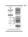
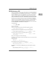
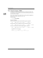
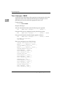
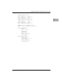
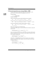
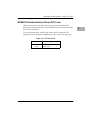
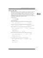
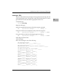
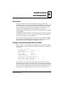
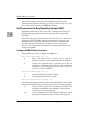
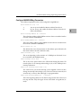
Because 167Bug is command-driven, it performs its various operations in
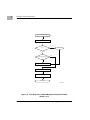
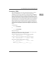
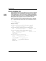
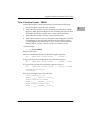
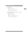
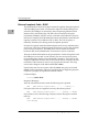
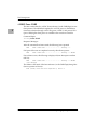
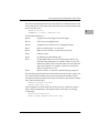
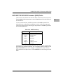
response to user commands entered at the keyboard. The flow of control in
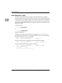
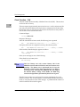
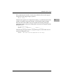
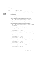
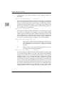
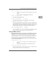
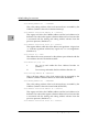
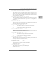
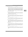
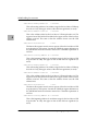
167Bug is shown in Figure 1-1. (sheets 1, 3, and 4)and Figure 1-2. The flow of
control in 166Bug is shown in Figure 1-1 (sheets 2, 3, and 4) and Figure 1-2. The
MVME167BUG/D31-1
1
167Bug General Information
flow of control for the MVME166 board operating in BootBug mode (166BBug)
is shown in Figure 1-3. When you enter a command, 167Bug executes the
command and the prompt reappears. However, if you enter a command that
causes execution of user target code (e.g., GO), then control may or may not
return to 167Bug, depending on the outcome of the user program.
1-2
167Bug Debugging Package UserÕs Manual
Description of 167Bug
POWER-UP RESET
2A
2B
CONFIGURE HARDWARE PER
ROM DEFAULT PARAMETERS
CLEAR ROM AT ZERO BIT
SET VMEBUS REQUEST LEVEL TO
LEVEL 3. INITIALIZE CACHES/ATCS
ECC MEMORY INITIALIZATION
MEMORY TEST ON SPECIFIED
DEBUGGER WORK PAGE (64KBYTES)
AS PER NVRAM/ROM PARAMETERS
(MEMORY SEARCH DIRECTIVES)
CONFIDENCE TEST
INTERRUPT STUCK.
SRAM
IF WORK PAGE CANNOT BE
FOUND USE SRAM
FOR DEBUGGER WORK PAGE
SETUP TEMPORARY
STACK IN SRAM
IF POWER-UP
NO
YES
IS THIS A
RESET/ABORT
?
CLEAR DEBUGGER WORK PAGE
SET POWER-UP INDICATOR
CLEAR WARM START FLAG
SET SYSFAIL NEGATE FLAG
YES
NO
INITIALIZE DEBUGGER VARIABLES
(STACK, VECTOR TABLES, ETC.)
IS
GPI1 BIT SET
(JUMPER OUT)
?
YES
INITIALIZE BOARD IDENTIFIER BLOCK
INITIALIZE CHARACTER I/O PORTS
CLEAR CHARACTER I/O BUFFERS
NO
CONFIGURE HARDWARE
PER NVRAM PARAMETERS
YES
WARM START
2A
NO
INITIALIZE (CLEAR) BREAKPOINT TABLE
2B
INITIALIZE MACRO SUBSYSTEM
3
fc014 9212
Figure 1-1. Flow Diagram of Board Operational Mode (Sheet 1 of 4)
NOTE: This diagram applies to the 167Bug Board Only
MVME167BUG/D3
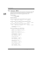
1-3
1
1
167Bug General Information
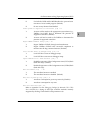
POWER-UP RESET
2A
2B
CONFIGURE HARDWARE PER
ROM DEFAULT PARAMETERS
CLEAR ROM AT ZERO BIT
ECC MEMORY INITIALIZATION
IS
GPI3 BIT SET
(JUMPER OUT)
?
YES
NO
GO TO BOOT BUG
MEMORY TEST ON SPECIFIED
DEBUGGER WORK PAGE (64KBYTES)
AS PER NVRAM/ROM PARAMETERS
(MEMORY SEARCH DIRECTIVES)
IF WORK PAGE CANNOT BE FOUND
USE SRAM FOR DEBUGGER WORK
PAGE
SET VMEBUS REQUEST LEVEL TO
LEVEL 3. INITIALIZE CACHES/ATCS
NO
CONFIDENCE TEST
INTERRUPT STUCK
SRAM
IF POWER-UP
YES
CLEAR DEBUGGER WORK PAGE
SET POWER-UP INDICATOR
CLEAR WARM START FLAG
SET SYSFAIL NEGATE FLAG
SETUP TEMPORARY
STACK IN SRAM
IS THIS A
RESET/ABORT
?
INITIALIZE DEBUGGER VARIABLES
(STACK, VECTOR TABLES, ETC.)
SET SYSFAIL NEGATE FLAG
YES
NO
IS
GPI1 BIT SET
(JUMPER OUT)
?
INITIALIZE BOARD IDENTIFIER BLOCK
YES
INITIALIZE CHARACTER I/O PORTS
CLEAR CHARACTER I/O BUFFERS
NO
YES
WARM START
CONFIGURE HARDWARE
PER NVRAM PARAMETERS
NO
INITIALIZE (CLEAR) BREAKPOINT TABLE
2B
2A
INITIALIZE MACRO SUBSYSTEM
3
10908.00 9402
Figure 1-1. Flow Diagram of Board Operational Mode (Sheet 2 of 4)
NOTE: This diagram applies to the 166Bug Board Only
1-4
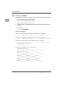
167Bug Debugging Package UserÕs Manual
Description of 167Bug
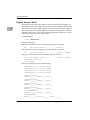
4
3
LOAD NVRM PARAMETERS TO LOCAL COPY
SAVE LOAD STATUS (CHECKSUM ERROR)
WARM START?
RESET LOCAL SCSI BUS PER NVRAM
PARAMETERS (Y/N)
YES
RETRIEVE VERSION REGISTER
AND DISPLAY CLOCK
SPEED MESSAGE
NO
INITIALIZE REGISTER BLOCK
IF NVRAM LOAD
OKAY AND MPU CLOCK
SPEED DOES NOT MATCH NVRAM
PARAMETERS?
DISPLAY SIGNON/REVISION MESSAGE
WARM START?
NO
YES
NO
YES
DISPLAY WARNING MESSAGE OF MPU
CLOCK SPEED DOES NOT MATCH
CLEAR SYSFAIL NEGATE FLAG
DISPLAY WARM START MESSAGE
DISPLAY COLD START MESSAGE
CALCULATE
EPROM CHECKSUM AND
COMPARE WITH VALUE CONTAINED
IN ROM. DO VALUES
COMPARE ?
IF NVRAM LOAD
OKAY AND SYSTEM PROBE
FOR SUPPORTED DISK/TAPE
CONTROLLERS?
NO
YES
YES
PROBE SYSTEM FOR SUPPORTED
DISK/TAPE CONTROLLERS
NO
DISPLAY WARNING MESSAGE
ROM CHECKSUM MIS-COMPARE
INITIALIZE DIAGNOSTIC SUBSYSTEM
DISPLAY LOCAL MEMORY FOUND MESSAGE
IF LOCAL
MEMORY SIZE DOES NOT
EQUAL NVRAM PARAMETERS
AND NVRAM LOAD
OKAY?a
NO
IF POWER-UP
AND AC-FAIL SHUDOWN
FLAG TRUE?
NO
YES
YES
DISPLAY WARNING MESSAGE OF LOCAL
MEMORY CONFIGURATION STATUS
CLEAR SYSFAIL NEGATE FLAG
NVRAM LOAD OKAY?
DISPLAY WARNING MESSAGE OF AC
FAILURE ON LAST SHUTDOWN
YES
ENABLE ABORT BUTTON AND AC
FAILURE INTERRUPTS
NO
DISPLAY WARNING MESSAGE OF NVRAM
LOAD (CONFIGURATION DATA FAILURE,
BOARD CONFIGURATION DATA FAILURE)
CLEAR SYSFAIL NEGATE FLAG
4
5
10913.00 9402
Figure 1-1. Flow Diagram of Board Operational Mode (Sheet 3 of 4)
NOTE: This diagram applies to the 167Bug and 166Bug Boards
MVME167BUG/D3
1-5
1
1
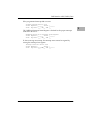
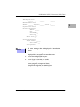
167Bug General Information
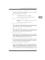
5
SYSTEM MODE
?
NO
NETWORK BOOT ENABLED
?
NO
YES
ATTEMPT NET BOOT
YES
GO TO SYSTEM MODE
IF NET BOOT LOAD OKAY
?
SYSFAIL NEGATE FLAG TRUE
?
NO
NO
YES
EXECUTE NET BOOT CODE
GO TO TARGET STATE
YES
NEGATE SYSFAIL
ROM BOOT ENABLED
AND ROM BOOT CODE
INSTALLED
?
GO TO MAIN (MONITOR)
NO
MAIN
DISPLAY DEBUGGER PROMPT
YES
EXECUTE ROM BOOT CODE
GO TO TARGET STATE
INPUT
AUTO BOOT ENABLED
NO
NO
GO TO MAIN
YES
?
TARGET CODE EXECUTION
?
YES
YES
NO
ATTEMPT AUTO BOOT
EXECUTE COMMAND
IF AUTO BOOT LOAD OKAY
?
NO
RESTORE TARGET STATE
EXECUTE TARGET CODE
YES
EXECUTE AUTO BOOT CODE
GO TO TARGET STATE
EXCEPTION
SAVE TARGET STATE
DISPLAY TARGET REGISTERS
GO TO MAIN
10914.00 9402
Figure 1-1. Flow Diagram of Board Operational Mode (Sheet 4 of 4)
NOTE: This diagram applies to the 167Bug and 166Bug Boards
1-6
167Bug Debugging Package UserÕs Manual
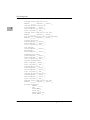
Description of 167Bug
SYSTEM
WAIT 5 SECONDS
FOR ANY CHARACTER
TO HALT
DISPLAY SERVICE MENU
CONTINUE START-UP
DISPLAY ERRORS
SELECT ALTERNATE
BOOT DEVELOPMENT
DUMP MEMORY
TO TAPE
SYSTEM DEBUGER
START CONVERSATION
MODE
SERICE CALL
EXIT CONCURRENT
MODE
ERROR
EXTENSIVE
SYSTEM SELF TEST
NO ERRORS
ERROR
BOOTLOADER
NO ERRORS
OPERATING SYSTEM
OR
DIAGNOSTICS
10915.00 9402
Figure 1-2. Flow Diagram of 166Bug/167Bug System Operational Mode
MVME167BUG/D3
1-7
1
1
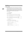
167Bug General Information
BOOT BUG
INITIALIZE CACHES AND ATCs
INITIALIZE MEMORY CONTROLLER
ASICs
ENABLE MEMORY BOARDS
YES
IS
GPI0 BIT SET
(JUMPER OUT)
?
NO
TEST LOCAL DRAM
IS
LOCAL DRAM
GOOD
?
YES
NO
TEST LOCALSRAM
IS
LOCAL SRAM
GOOD
?
YES
NO
FLASH FAIL LED
2
10916.00 9402
Figure 1-3. Flow Diagram of 166BootBug Board Operational Mode
(Sheet 1 of 3)
1-8
167Bug Debugging Package UserÕs Manual
Description of 167Bug
2
SET UP DEBUGGER VARIABLES
AND STACK IN GOOD RAM
TURN OFF “STAT” LED
DISPLAY SIGNON/REVISION MESSAGE
INITIALIZE DISK I/O SUBSYSTEM
INITIALIZE NETWORK I/O SUBSYSTEM
GO TO MAIN (MONITOR)
10917.00 9402
Figure 1-3. Flow Diagram of 166BootBug Board Operational Mode
(Sheet 2 of 3)
MVME167BUG/D3
1-9
1
1
167Bug General Information
MAIN
DISPLAY DEBUGGER PROMPT
NO
INPUT
?
GO TO MAIN
YES
TARGET CODE EXECUTION
?
YES
NO
EXECUTE COMMAND
EXECUTE TARGET CODE
EXCEPTION
GO TO MAIN
10918.00 9402
Figure 1-3. Flow Diagram of 166BootBug Board Operational Mode
(Sheet 3 of 3)
1-10
167Bug Debugging Package UserÕs Manual
167Bug Implementation
167Bug Implementation
Physically, 167Bug is contained in two of the four 44-pin PLCC/CLCC
EPROMs, providing 512KB (128K longwords) of storage. Both EPROMs are
necessary regardless of how much space is actually occupied by the firmware,
because of the 32-bit longword-oriented MC68040 memory bus architecture.
166Bug Implementation
Physically, 166Bug is contained in four FLASH memory components. The
onboard FLASH memory provides 1.0MB (256KB longwords) of nonvolatile
storage. The 166Bug consumes the first half (512KB) of this memory, leaving
the second half available for user applications. A command is provided, both
in the regular "Bug" product and the "BootBug" product, to allow erasing and
reprogramming this FLASH memory.
!
Reprogramming any portion of FLASH memory, will erase
everything currently contained in FLASH, including the
166Bug product! You must copy the 166Bug from FLASH to
RAM, combine your application with the 166Bug image,
and then reprogram FLASH with the combined object
image.
WARNING
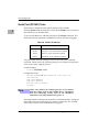
Detailed Installation and Start-Up
Even though the MVME167Bug firmware is installed on the MVME167
module, for 167Bug to operate properly with the MVME167, follow the
general setup procedure given in the Debugging Package for Motorola 68K CISC
CPUs User's Manual, AND the steps given below:
C aution
1.
Inserting or removing modules while power is applied
could damage module components.
Turn all equipment power OFF. Refer to the MVME167 Single Board
Computer User's Manual and install/remove jumpers on headers as
required for your particular application.
❏
Jumpers on header J1 affect 167Bug operation as listed below.
❏
Jumpers on header J3 affect 166Bug operation as listed below.
MVME167BUG/D3
1-11
1
1
167Bug General Information
The default condition is with all eight jumpers installed, between pins 1-2,
3-4, 5-6, 7-8, 9-10, 11-12, 13-14, and 15-16.
The MVME166 or MVME167 may be configured with these readable
jumpers. These jumpers can be read as a register (at $FFF40088) in the
VMEchip2 LCSR. The bit values are read as a one when the jumper is off,
and as a zero when the jumper is on. The jumper block contains eight bits.
Refer to the MVME166/MVME167/MVME187 Single Board Computers
Programmer's Reference Guide.
The MVME167BUG reserves/defines the four lower order bits (GPI3 to
GPI0). The following is the description for the bits reserved/defined by
the debugger:
2.
1-12
Bit
J1 or J3
Pins
Bit #0 (GPI0)
1-2
When this bit is a one (high), it instructs the
debugger to use local Static RAM for its work page
(i.e., variables, stack, vector tables, etc.).
Bit #1 (GPI1)
3-4
When this bit is a one (high), it instructs the
debugger to use the default setup/operation
parameters in ROM versus the user setup/operation
parameters in NVRAM. This is the same as
depressing the RESET and ABORT switches at the
same time. This feature can be used in the event the
user setup is corrupted or does not meet a sanity
check. Refer to the ENV command for the ROM
defaults.
Bit #2 (GPI2)
5-6
Reserved for future use.
Bit #3 (GPI3)
7-8
For 166Bug operation only, when this bit is a one
(jumper out) the BootBug will continue execution
after reset or power up. Normal operation (jumper
in) results in the BootBug executing the 166Bug
debugger in Flash memory.
On the MVME167, this bit is unused and reserved for
future use.
Bit #4 (GPI4)
9-10
Open to your application.
Description
Bit #5 (GPI5)
11-12
Open to your application.
Bit #6 (GPI6)
13-14
Open to your application.
Bit #7 (GPI7)
15-16
Open to your application.
For the MVME167, conÞgure header J2 by installing/removing a jumper
between J2 pins 1 and 2. For the MVME166, conÞgure header J6 by
installing/removing a jumper between J6 pins 1 and 2. A jumper
installed/removed enables/disables the system controller function of the
MVME167.
167Bug Debugging Package UserÕs Manual
Detailed Installation and Start-Up
3.
On the MVME167 only, install jumpers on headers J6 and J7 to conÞgure
serial port 4 to use clock signals provided by the RTXC4 and TRXC4 signal
lines. Headers J6 and J7 on the MVME167 conÞgure serial port 4 to drive
or receive RTXC4 and TRXC4, respectively. Factory conÞguration is with
port 4 set to receive both signals (jumpers between pins 2 and 3 on both J6
and J7). The alternative conÞguration is with port 4 set to drive both
signals (jumpers between pins 1 and 2 on both J6 and J7). The remaining
conÞguration of the clock lines is accomplished using the Serial Port 4
Clock ConÞguration Select header on the MVME712M transition module.
Refer to the MVME712M Transition Module and MVME147P2 Adapter Board
User's Manual for configuration of that header.
4.
On the MVME167 only, be sure that the two 128K x 16 167Bug EPROMs
are installed in proper sockets on the MVME167 module. Install the odd
label (such as B01) EPROM in socket XU1 (for Least SigniÞcant Words),
and install the even label (such as B02) EPROM in XU2 (for Most
SigniÞcant Words). Be sure that physical chip orientation is correct, with
ßattened corner of each EPROM aligned with corresponding portion of
EPROM socket on the MVME167 module.
5.
Connect the terminal which is to be used as the 167Bug system console to
the default debug EIA-232-D port at serial port 1 through an MVME712X
transition module. Refer to the MVME166/MVME167/MVME187 Single
Board Computers Programmer's Reference Guide for some possible
connection diagrams.
6.
If you want to connect devices (such as a host computer system and/or a
serial printer) to the other EIA-232-D port connectors (marked SERIAL
PORTS 2, 3, and 4 on the MVME712X transition module), connect the
appropriate cables and conÞgure the port(s) as detailed in step 5 above.
After power-up, this(these) port(s) can be reconÞgured by programming
the MVME167 CD2401 Serial Controller Chip (SCC), or by using the
167Bug PF command.
Note that the MVME166 and MVME167 also contain a parallel port. To use a
parallel device, such as a printer, connect it to the "printer" port through an
MVME712X transition module. Refer to the MVME166/MVME167/MVME187
Single Board Computers Programmer's Reference Guide for some possible
connection diagrams. However, you could also use a module such as the
MVME335 for a parallel port connection.
MVME167BUG/D3
1-13
1
1
167Bug General Information
BOOTBUG
166BBug Implementation
The MVME166 board has a byte-wide EPROM in addition to the FLASH
memory used to contain the debugger and diagnostics firmware. The EPROM
supplied contains the BootBug product (166BBug). Since FLASH memory can
be electronically erased, the firmware contained in this EPROM is a miniature
version of the regular debugger product. It contains enough functionality to
enable downloading of object code (by means of the VMEbus, serial port, SCSI
bus, or the network) and reprogramming of the FLASH memory.
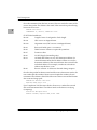
The following table lists the the new commands available in the 166BBug
product.
Command
Description
EXEC
Execute User Program
SETUP
Set "System" Parameters
Detailed descriptions of additional subset commands can be found in the
Debugging Package for Motorola 68K CISC CPUs User's Manual. These debugger
commands are summarized in the following table.
Command
Mnemonic
1-14
Title
BC
Block of Memory Compare
BF
Block of Memory Fill
BM
Block of Memory Move
BS
Block of Memory Search
BV
Block of Memory Verify
CS
Checksum
DC
Data Conversion
HE
Help
IOP
I/O Physical (Direct Disk Access)
IOT
I/O Teach for ConÞguring Disk Controller
LO
Load S-Records from Host
MD or MDS
Memory Display
M or MM
Memory Modify
167Bug Debugging Package UserÕs Manual
BOOTBUG
Command
Mnemonic
MS
Title
Memory Set
NIOP
Network I/O Physical
NIOT
Network I/O Teach
PF/NOPF
Port Format/Detach
PFLASH
SET
TIME
Program FLASH Memory
Set Time and Date
Display Time and Date
TM
Transparent Mode
VE
Verify S-Records Against Memory
There is a jumper on the MVME166 board that controls the operation of the
BootBug. If the jumper at J3 pins 7 and 8 is in place (GPI3), then the BootBug
(which always executes at reset and powerup) will unconditionally jump to
the debugger product contained in the FLASH memory. If this jumper is
removed, execution will continue in the (diminished functionality) BootBug.
Before using some of the features of the MVME166 BootBug, some parameters
may need to be defined. For example, the SCSI ID, the Ethernet address, the
clock speed of the board, or possibly the mapping of VMEbus. There is a new
command provided for this purpose, the setup command. You should run
this command and answer the prompts to be sure the board is configured
properly before using any SCSI, VME, or Ethernet I/O.
Execute User Program
EXEC [ADDR]
The EXEC command is used to initiate target code execution. The specified
address ("ADDR") is placed in the target Program Counter (PC). Execution
will start at the target PC address.
MVME167BUG/D3
1-15
1
1
167Bug General Information
Setup System Parameters
SETUP
Setup allows configuring certain parameters that are necessary for some I/O
operations (SCSI, VME, and Ethernet). When this command is executed, the
operator is prompted for input after displaying the default value, if any is
available.
The SETUP command VME parameters do not stay through a reset. These
parameters are not saved to NVRAM. The remaining parameters (MPU Clock
Speed, Ethernet Address, Local SCSI Identifier) are saved to NVRAM, but are
not checksummed.
166-Bug>setup
MPU Clock Speed = "3300"?
Ethernet Address = 000000000000?
Local SCSI Identifier = "07"?
VME Slave Enable [Y/N]= N?
VME Slave Starting Address= 00000000?
VME Slave Ending Address= 00000000?
VME Slave Address Translation Address= 00000000?
VME Slave Address Translation Select= 00000000?
VME Slave Control= 0000?
VME Master Enable [Y/N]= Y?
VME Master Starting Address= 40000000?
VME Master Ending Address= 4FFFFFFF?
VME Master Address Translation Address= 00000000?
VME Master Address Translation Select= 00000000?
VME Master Control= 0D?
1-16
167Bug Debugging Package UserÕs Manual
ROMboot
ROMboot
There are two spare EPROM sockets, XU3 and XU4, available to carry userprogrammed EPROMs. Therefore, you do not have to reprogram the 167Bug
EPROMs in order to implement this feature.
On the MVME166, if you want to add other firmware applications, you must
note that anytime FLASH memory is programmed, the entire contents of
FLASH will be erased, including the 166Bug product! You should make use
of the "block move" command (BM) to copy the debugger from FLASH to
RAM, combine your own object with the debugger in RAM, and then
reprogram FLASH from this combined image.
Memory Requirements
The program portion of 167Bug is approximately 512KB of code consisting of
download, debugger, and diagnostic packages. It is contained entirely in
EPROM/FLASH. The firmware memory on the MVME167 is mapped starting
at location $FF800000. 167Bug requires a minimum of 64KB of contiguous
read/write memory to operate.
The ENV command controls where this block of memory is located.
Regardless of where the onboard RAM is located, the first 64KB is used for
167Bug stack and static variable space and the rest is reserved as user space.
Whenever the MVME167 is reset, the target PC is initialized to the address
corresponding to the beginning of the user space, and the target stack pointers
are initialized to addresses within the user space, with the target Interrupt
Stack Pointer (ISP) set to the top of the user space.
At power up or reset, all 8KB of memory at addresses $FFE0C000 through
$FFE0DFFF is completely changed by the 167Bug initial stack.
Diagnostic Facilities
Included in the 167Bug package is a complete set of hardware diagnostics
intended for testing and troubleshooting of the MVME167 (refer to Chapter 2).
To use the diagnostics, you must switch directories to the diagnostic directory.
If you are in the debugger directory, you can switch to the diagnostic directory
by entering the debugger command Switch Directories (SD). The diagnostic
prompt (167-Diag>) should appear. Refer to Chapter 2 for complete
descriptions of the diagnostic routines available and instructions. Note that
some diagnostics depend on restart defaults that are set up only in a particular
restart mode. Refer to the documentation on a particular diagnostic for the
correct mode.
MVME167BUG/D3
1-17
1
1
167Bug General Information
Related Documentation
The following publications are applicable to 167Bug and may provide
additional helpful information. If not shipped with this product, they may be
purchased by contacting your local Motorola sales office. Non-Motorola
documents may be obtained from the sources listed.
Motorola
Publication
Number
Document Title
N ote
M68040 Microprocessor User's Manual
M68040UM
MVME167 Single Board Computer User's Manual
MVME167
MVME166 Single Board Computer User's Manual
MVME166
Single Board Computers SCSI Software User's Manual
SBCSCSI
MVME166/MVME167/MVME187 Single Board Computers
Programmer's Reference Guide
MVME187PG
Debugging Package for Motorola 68K CISC CPUs User's Manual
68KBUG1 and
68KBUG2
MVME712M Transition Module and MVME147P2 Adapter Board
User's Manual
MVME712M
MVME712A/MVME712AM/MVME712B Transition Module and
MVME147P2 Adapter Board User's Manual
MVME712A
Although not shown in the above list, each Motorola
Computer Group manual publication number is suffixed
with characters which represent the revision level of the
document, such as "/D2" (the second revision of a manual).
A supplement bears the same number as a manual but has a
suffix such as "/D2A1" (the first supplement to the second
revision of the manual).
The following publications are available from the sources indicated.
ANSI Small Computer System Interface-2 (SCSI-2), Draft Document X3.131-198X,
Revision 10c; Global Engineering Documents, P.O. Box 19539, Irvine, CA
92714.
1-18
167Bug Debugging Package UserÕs Manual
Manual Terminology
Versatile Backplane Bus: VMEbus, ANSI/IEEE Std 1014-1987, The Institute of
Electrical and Electronics Engineers, Inc., 345 East 47th Street, New York, NY
10017 (VMEbus Specification). This is also available as Microprocessor system
bus for 1 to 4 byte data, IEC 821 BUS, Bureau Central de la Commission
Electrotechnique Internationale; 3, rue de VarembŽ, Geneva, Switzerland.
Manual Terminology
Throughout this manual, a convention has been maintained whereby data and
address parameters are preceded by a character which specifies the numeric
format as follows:
$
dollar
speciÞes a hexadecimal character
%
percent
speciÞes a binary number
&
ampersand
speciÞes a decimal number
Unless otherwise specified, all address references are in hexadecimal
throughout this manual.
An asterisk (*) following the signal name for signals which are level significant
denotes that the signal is true or valid when the signal is low.
An asterisk (*) following the signal name for signals which are edge significant
denotes that the actions initiated by that signal occur on high to low transition.
In this manual, assertion and negation are used to specify forcing a signal to a
particular state. In particular, assertion and assert refer to a signal that is active
or true; negation and negate indicate a signal that is inactive or false. These terms
are used independently of the voltage level (high or low) that they represent.
Data and address sizes are defined as follows:
❏
A byte is eight bits, numbered 0 through 7, with bit 0 being the least
significant.
❏
A word is 16 bits, numbered 0 through 15, with bit 0 being the least
significant.
❏
A longword is 32 bits, numbered 0 through 31, with bit 0 being the least
significant.
MVME167BUG/D3
1-19
1
1
167Bug General Information
1-20
167Bug Debugging Package UserÕs Manual
DIAGNOSTIC FIRMWARE
2
Scope
This chapter contains information about the operation and use of the
MVME167 Diagnostic Firmware Package, hereinafter referred to as Òthe
diagnosticsÓ. The Diagnostic Monitor on page 2-2 gives you guidance in setting
up the system and invoking the various utilities and tests. Utilities on page 2-4
describes utilities available to users.
The diagnostic tests themselves are described inChapter 3.
Overview of Diagnostic Firmware
The MVME167 diagnostic firmware package consists of two 128K x 16
EPROMs which are installed on the MVME167. These two EPROMs (which
also contain 167Bug) contain a complete diagnostic monitor along with a
battery of utilities and tests for exercise, test, and debug of hardware in the
MVME167 environment. The diagnostics are menu driven for ease of use. The
Help (HE) command displays a menu of all available diagnostic functions; i.e.,
the tests and utilities. Several tests have a subtest menu which may be called
using the HE command. In addition, some utilities have subfunctions, and as
such have subfunction menus.
System Startup
Refer to Detailed Installation and Start-Up in Chapter 1.
Design Requirements
The design requirements for the diagnostic firmware are as follows.
Assembly Language
Low-level hardware interface code is written in assembly language to control
the hardware exactly. Where possible, ÒCÓ is used to speed coding and
improve readability and portability.
Bug Interface
The diagnostic package shares ROM space with the 167Bug, but the interface
between these programs is minimal and is well defined. This facilitates
independent development and modification.
MVME167BUG/D32-1
Diagnostic Firmware
2
Compatibility
Although the MVME167 diagnostic package contains a totally new test set, the
user interface is similar to existing diagnostic packages. If you are familiar
with a current package you should be able to use this test set without study.
Menu Driven
The user interface is menu driven. A Help (HE) command is available for each
test or set of tests in the package.
Diagnostic Monitor
The tests described in this manual are called, commands are input, and results
reported via a common diagnostic monitor (the system monitor used for
167Bug), hereafter called monitor. This monitor is command line driven and
provides input/output facilities, command parsing, error reporting, interrupt
handling, and a multi-level directory for menu selection.
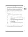
Monitor Start-Up
When the monitor is first brought up, following power up or pushing the
RESET switch, the following is displayed on the diagnostic video display
terminal (port 1 terminal):
Copyright Motorola Inc. 1988, 1989, 1990, 1991, All Rights Reserved
MVME167 Debugger/Diagnostics Release Version x.x - mm/dd/yy
COLD Start
Local Memory Found =00400000 (&4194304)
MPU Clock Speed =25Mhz
167-Bug>
If after a delay, the 167Bug begins to display test result messages on the bottom
line of the screen in rapid succession, the MVME167 is in the Bug system
mode. If this is not the desired mode of operation, then press the ABORT
switch. When the menu is displayed, enter a 3 to go to the system debugger.
The environment may be changed by using the Set Environment to
Bug/Operating System (ENV) command. Refer to the Debugging Package for
Motorola 68K CISC CPUs User's Manual for details of Bug operation in the
system mode.
At the 167-Bug> prompt, enter SD to switch to the diagnostics directory. The
Switch Directories (SD) command is described elsewhere in this chapter. The
prompt should now read 167-Diag>.
2-2
167Bug Debugging Package UserÕs Manual
Diagnostic Monitor
Command Entry and Directories
2
Entry of commands is made when the prompt 167-Diag> appears. The
mnemonic name for the command is entered before pressing the carriage return
<CR>. Multiple commands may be entered. If a command expects parameters
and another command is to follow it, separate the two with a semicolon (;). For
instance, to invoke the command RTC CLK after the command RAM ADR,
the command line would read RAM ADR; RTC CLK. Spaces are not required
before or after the semicolon but are shown here for legibility. Spaces are
required between commands and their arguments. Several commands may be
combined on one line.
Several commands consist of a command name that is listed in a main (root)
directory and a subcommand that is listed in the directory for that particular
command. In the main directory are commands such as RAM and VME2.
These commands are used to refer to a set of lower level commands. To call up
a particular RAM test, enter (on the same line) RAM ADR. This command
causes the monitor to find the RAM subdirectory, and then to execute the
command (test) ADR from that subdirectory.
Examples:
Root-Level Commands:
HE
Help
DE
Display Error Counters
Subdirectory-Level Commands:
RAM ADR
Random Access Memory Tests (directory), Memory
Addressing test
VME2 REGB
VMEchip2 Tests (directory), Register Walking Bit test
The RAM and VME2 directories in these examples are test group names. If the
first part of a command is a test group name, any number and/or sequence of
tests from that test group may be entered after the test group name so long as
the bug's input buffer size limit is not exceeded.
Example:
RAM PATS ADR
MVME167BUG/D3
2-3
Diagnostic Firmware
2
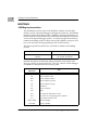
Utilities
In addition to individual or sets of tests, the diagnostic package supports the
utilities (root-level commands or general commands) listed in the table below
and described on the following pages.
Table 2-1. Diagnostic Utilities
Mnemonic
AEM
CEM
CF
DE
DEM
DP
HE
HEX
LA
LC
LE
LF
LN
MASK
NV
SD
SE
ST
ZE
ZP
2-4
Description
Append Error Messages Mode
Clear Error Messages
Test Group ConÞguration (cf) Parameters Editor
Display Error Counters
Display Error Messages
Display Pass Count
Help
Help Extended
Loop Always Mode
Loop-Continue Mode
Loop-On-Error Mode
Line Feed Suppression Mode
Loop Non-Verbose Mode
Display/Revise Self Test Mask
Non-Verbose Mode
Switch Directories
Stop-On-Error Mode
Self Test
Clear (Zero) Error Counters
Zero Pass Count
167Bug Debugging Package UserÕs Manual
Utilities
Append Error Messages Mode - Command AEM
2
This command allows you to accumulate error messages in the internal error
message buffer of the diagnostic monitor. The AEM command sets the internal
append error messages flag of the diagnostic monitor. When the internal
append error messages flag is clear, the diagnostic error message buffer is
erased (cleared of all character data) before each test is executed. The duration
of this command is for the life of the command line being parsed by the
diagnostic monitor. The default of the internal append error messages flag is
clear. The internal flag is not set until it is encountered in the command line by
the diagnostic monitor.
Clear Error Messages - Command CEM
This command allows you to clear the internal error message buffer of the
diagnostic monitor manually.
Test Group Configuration (cf) Parameters Editor - Command CF
The cf parameters control the operation of all tests in a test group. For
example, the RAM test group has parameters such as starting address, ending
address, parity enable, etc. At the time of initial execution of the diagnostic
monitor, the default configuration parameters are copied from the firmware
into the debugger work page. Here you can modify the configuration
parameters via the CF command. When you invoke the CF command, you are
interactively prompted with a brief parameter description and the current
value of the parameter. You may enter a new value for that parameter, or a
carriage return to proceed to the next configuration parameter. You may
specify one or more test groups as argument(s) immediately following the CF
command on the command line. If no arguments follow the CF command, the
parameters for all test groups are presented so you may change them if you
wish.
Display Error Counters - Command DE
Each test or command in the diagnostic monitor has an individual error
counter. As errors are encountered in a particular test, that error counter is
incremented. If you were to run a self-test or just a series of tests, the results
could be broken down as to which tests passed by examining the error
counters. To display all errors, enter DE. DE displays the results of a particular
test if the name of that test follows DE. Only nonzero values are displayed.
MVME167BUG/D3
2-5
Diagnostic Firmware
2
Display Error Messages - Command DEM
This command allows you to display (dump) the internal error message buffer
of the diagnostic monitor manually.
Display Pass Count - Command DP
A count of the number of passes in Loop-Continue (LC) mode is kept by the
monitor. This count is displayed with other information at the conclusion of
each pass. To display this information without using LC, enter DP.
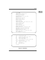
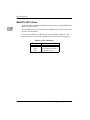
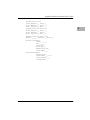
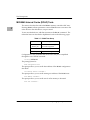
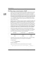
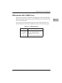
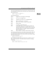
Help - Command HE
On-line documentation has been provided in the form of a Help command
(syntax: HE [command name]). This command displays a menu of the top level
directory of utility commands and test group names if no parameters are
entered, or the menu of a subdirectory if the name of that subdirectory is
entered. (The top level directory lists Ò(DIR)” after the name of each command
that has a subdirectory.) For example, to bring up a menu of all the memory
tests, enter HE RAM. When a menu is too long to fit on the screen, it pauses
until you press the carriage return, <CR>, again. To review a description of an
individual test, enter the full name, i.e., HE RAM CODE displays information
on the RAM Code Execution/Copy test routine. The Help screen is shown in
Figure 2-1. Help Screen on page 2-7.
Help Extended - Command HEX
The HEX command goes into an interactive, continuous mode of the HE
command. The syntax is HEX<CR>. The prompt displayed for HEX is the?.
You may then type the name of a directory, or command. You must type QUIT
to exit.
2-6
167Bug Debugging Package UserÕs Manual
Utilities
2
167-Diag>he
AEMAppend Error Messages Mode
CEMClear Error Messages
CFConfiguration Editor
DCACMC68040 Data Cache Tests (DIR)
DEDisplay Errors
DEMDisplay Error Messages
DPDisplay Pass Count
HEHelp on Tests/Commands
HEXHelp Extended
LALoop Always Mode
LANCLAN Coprocessor (Intel 82596) Tests (DIR)
LCLoop Continuous Mode
LELoop on Error Mode
LFLine Feed Mode
LNLoop Non-Verbose Mode
MASKSelf Test Mask
MCECCECC Memory Board Diagnostics (DIR)
MEMC1Memory Controller #1 ASIC (DIR)
MEMC2Memory Controller #2 ASIC (DIR)
MMUMC68040 MMU Tests (DIR)
NCRNCR 53C710 SCSI I/O Processor Test (DIR)
NVNon-Verbose Mode
Press "RETURN" to continue
PCC2
PCCchip2 Tests (DIR)
RAM
Random Access Memory Tests (DIR)
RTC
MK48T0x Timekeeping (DIR)
SE
Stop on Error Mode
SRAM
Static Random Access Memory Tests (DIR)
ST
Self Test (DIR)
ST2401 CD2401 Serial Self-Tests (DIR)
VME2
VME2Chip2 Tests (DIR)
ZE
Zero Errors
ZP
Zero Pass Count
167-Diag>
Figure 2-1. Help Screen
MVME167BUG/D3
2-7
Diagnostic Firmware
2
Loop Always Mode - Prefix LA
To endlessly repeat a test or series of tests, the prefix LA is entered. The LA
command modifies the way that a failed test is endlessly repeated. The LA
command has no effect until a test failure occurs, at which time, if the LA
command has been previously encountered in the user command line, the
failed test is endlessly repeated. To break the loop, press the BREAK key on the
diagnostic video display terminal. Certain tests disable the BREAK key
interrupt, so pressing the ABORT or RESET switches on the MVME167 front
panel may become necessary.
Loop-Continue Mode - Prefix LC
To endlessly repeat a test or series of tests, the prefix LC is entered. This loop
includes everything on the command line. To break the loop, press the BREAK
key on the diagnostic video display terminal. Certain tests disable the BREAK
key interrupt, so pressing the ABORT or RESET switches on the MVME167
front panel may become necessary.
Loop-On-Error Mode - Prefix LE
Occasionally, when an oscilloscope or logic analyzer is in use, it becomes
desirable to endlessly repeat a test (loop) while an error is detected. The LE
command modifies the way that a failed test is endlessly repeated. The LE
command has no effect until a test failure occurs, at which time, if the LE
command has been previously encountered in the user command line, the
failed test is re-executed as long as the previous execution returned failure
status. To break the loop, press the BREAK key on the diagnostic video display
terminal. Certain tests disable the BREAK key interrupt, so pressing the
ABORT or RESET switches on the MVME167 front panel may become
necessary.
Line Feed Suppression Mode - Prefix LF
The LF command sets the internal line feed mode flag of the diagnostic
monitor. The default state of the internal line feed mode flag is clear which
causes the executing test title/status line(s) to be terminated with a line feed
character (scrolled). The duration of the LF command is the life of the user
command line in which it appears. The line feed mode flag is normally used
by the diagnostic monitor when executing a system mode selftest. Although
rarely invoked as a user command, the LF command is available to the
diagnostic user.
2-8
167Bug Debugging Package UserÕs Manual
Utilities
Loop Non-Verbose Mode - Prefix LN
2
The LN command modifies the way that a failed test is endlessly repeated. The
LN command has no effect until a test failure occurs, at which time, if the LN
command has been previously encountered in the user command line, further
printing of the test title and pass/fail status is suppressed. This is useful for
more rapid execution of the failing test; i.e., the LN command contributes to a
ÒtighterÓ loop.
Display/Revise Self Test Mask - Command MASK
The syntax is: MASK [TEST NAME]
where TEST NAME is the name of a diagnostic test.
MASK is used with an argument to enable/disable a test from running under
Self Test. If mask is invoked with NO arguments, the currently disabled tests
are displayed.
When the mask command is used on an MVME167 system, the mask values
are preserved in non-volatile memory. This allows the system to be completely
powered down without disturbing the Self Test mask.
If the mask command is invoked with a parameter, the parameter must be a
specific test name (e.g., mask ram adr).
The mask command is a ÒtoggleÓ command -- if the specified test name mask
was SET, it will be RESET; if it was RESET, it will be SET. After the toggle, the
new Self Test mask is displayed.
If the mask command is invoked with an invalid test name or a test directory
(as opposed to a specific test name), an appropriate error message is output.
The mask command may be invoked with NO parameters, in which case the
current Self Test mask is displayed.
Non-Verbose Mode - Prefix NV
Upon detecting an error, the tests display a substantial amount of data. To
avoid the necessity of watching the scrolling display, a mode is provided that
suppresses all messages except PASSED or FAILED. This mode is called nonverbose and is invoked prior to calling a command by entering NV. NV ST
would cause the monitor to run the self-test, but show only the names of the
subtests and the results (pass/fail).
MVME167BUG/D3
2-9
Diagnostic Firmware
2
Switch Directories - Command SD
To leave the diagnostic directory (and disable the diagnostic tests), enter SD.
At this point, only the commands for 167Bug function. When in the 167Bug
directory, the prompt reads 167-Bug>. To return to the diagnostic directory, the
command SD is entered again. When in the diagnostic directory, the prompt
reads 167-Diag>. The purpose of this feature is to allow you to access 167Bug
without the diagnostics being visible.
Stop-On-Error Mode - Prefix SE
It is sometimes desirable to stop a test or series of tests at the point where an
error is detected. SE accomplishes that for most of the tests. To invoke SE,
enter it before the test or series of tests that is to run in Stop-On-Error mode.
Self Test - Command ST
The monitor provides an automated test mechanism called self test. This
mechanism runs all the tests included in an internal self-test directory. The
command HE ST lists the top level of the self test directory in alphabetical
order.
Each test for that particular command is listed in the section pertaining to the
command.
When in system mode, the suite of tests that are run at system mode start up
can be executed from Bug. This is done with the ST command. This command
is useful for debugging board failures that may require toggling between the
test suite and Bug. Upon completion of running the test suite, the Bug prompt
is displayed, ready for other commands. For details on extended confidence
test operation, refer to the Debugging Package for Motorola 68K CISC CPUs
User's Manual.
Clear (Zero) Error Counters - Command ZE
The error counters originally come up with the value of zero, but it is
occasionally desirable to reset them to zero at a later time. This command
resets all of the error counters to zero. The error counters can be individually
reset by entering the specific test name following the command. Example: ZE
VME2 TMRA clears the error counter associated with VME2 TMRA.
2-10
167Bug Debugging Package UserÕs Manual
Utilities
Zero Pass Count - Command ZP
2
Invoking the ZP command resets the pass counter to zero. This is frequently
desirable before typing in a command that invokes the Loop-Continue mode.
Entering this command on the same line as LC results in the pass counter being
reset every pass.
MVME167BUG/D3
2-11
Diagnostic Firmware
2
2-12
167Bug Debugging Package UserÕs Manual
TEST DESCRIPTIONS
3
Detailed descriptions of 167Bug's diagnostic tests are presented in this chapter.
The test sets are described in the order shown in the following table.
Table 3-1. Diagnostic Test Groups
Test Set
Description
RAM
Local RAM Tests
SRAM
Static RAM Tests
RTC
MK48T0x Real-Time Clock Tests
PCC2
Peripheral Channel Controller Tests
MCECC
Memory Board Tests
MEMC1
MC040 Memory Controller 1 ASIC Tests
MEMC2
MC040 Memory Controller 2 ASIC Tests
DCAC
MC68040 Internal Data Cache Tests
ST2401
CD2401 Serial Port Tests
MMU
Memory Management Unit Tests
VME2
VME Interface ASIC VMEchip2 Tests
VSB2
VSB Interface ASIC VSBchip2 Tests
PIT
LANC
NCR
MVME167BUG/D33-1
Parallel Interface/Timer MC68230 Tests
LAN Coprocessor (Intel 82596) Tests
NCR 53C710 SCSI I/O Processor Tests
Test Descriptions
Local RAM (RAM) and Static RAM (SRAM) Tests
These sections describe the individual RAM and SRAM tests. The SRAM
tests are identical in function to the corresponding tests in the RAM test group
test but are executed over the range of Static RAM on the MVME167.
3
Entering RAM or SRAM without parameters causes all RAM or SRAM tests
to execute in the order shown in the table below, except as noted.
To run an individual test, add that test name to the RAM or SRAM command.
The individual tests are described in alphabetical order on the following
pages.
Table 3-2. RAM and SRAM Test Group
Mnemonic
Description
QUIK
Quick Write/Read
ALTS
Alternating Ones/Zeros
PATS
Data Patterns
ADR
Memory Addressing
CODE
Code Execution/Copy
PERM
Permutations
RNDM
Random Data
BTOG
Bit Toggle
Bypassed during SRAM testing:
3-2
PED
Parity Error Detection
REF
Memory Refresh
167Bug Debugging Package UserÕs Manual
Local RAM (RAM) and Static RAM (SRAM) Tests
Memory Addressing - ADR
This is the memory addressability test, the purpose of which is to verify
addressing of memory in the range specified by the configuration parameters
for the RAM test group. Addressing errors are sought by using a memory
locations address as the data for that location. This test is coded to use only 32bit data entities. The test proceeds as follows:
1.
A Locations Address is written to its location (n).
2.
The next location (n+4) is written with its address complemented.
3.
The next location (n+8) is written with the most signiÞcant (MS) 16 bits
and least signiÞcant (LS) 16 bits of its address swapped with each other.
4.
Steps 1, 2, and 3 are repeated throughout the speciÞed memory range.
5.
The memory is read and veriÞed for the correct data pattern(s) and any
errors are reported.
6.
The test is repeated using the same algorithm as above (steps 1 through 5)
except that inverted data is used to insure that every data bit is written and
veriÞed at both "0" and "1".
Command Input:
167-Diag>RAM ADR
or:
167-Diag>SRAM ADR
Response/Messages:
Note that in all responses shown below, the response "RAM " is RAM or SRAM,
depending upon which test set is being performed. After the command has
been issued, the following line is printed:
RAM
ADR: Addressability..................... Running --->
If all parts of the test are completed correctly, then the test passes.
RAM
ADR: Addressability..................... Running ---> PASSED
If the test fails, then the display appears as follows.
RAM
ADR: Addressability..................... Running ---> FAILED
Data Miscompare Error:
Address =________, Expected =________, Actual =________
MVME167BUG/D3
3-3
3
Test Descriptions
Alternating Ones/Zeros - ALTS
This test verifies addressing of memory in the range specified by the
configuration parameters for the RAM test group. Addressing errors are
sought by using a memory locations address as the data for that location. This
test is coded to use only 32-bit data entities. The test proceeds as follows:
3
1.
Location (n) is written with data of all bits 0.
2.
The next location (n+4) is written with all bits 1.
3.
Steps 1 and 2 are repeated throughout the speciÞed memory range.
4.
The memory is read and veriÞed for the correct data pattern(s) and any
errors are reported.
Command Input:
167-Diag>RAM ALTS
or:
167-Diag>SRAM ALTS
Response/Messages:
Note that in all responses shown below, the response "RAM " is RAM or SRAM,
depending upon which test set is being performed.
After the command has been issued, the following line is printed:
RAM
ALTS: Alternating Ones/Zeroes........... Running --->
If all parts of the test are completed correctly, then the test passes.
RAM
ALTS: Alternating Ones/Zeroes........... Running ---> PASSED
If the test fails, then the display appears as follows.
RAM
ALTS: Alternating Ones/Zeroes........... Running ---> FAILED
Data Miscompare Error:
Address =________, Expected =________, Actual =________
3-4
167Bug Debugging Package UserÕs Manual
Local RAM (RAM) and Static RAM (SRAM) Tests
Bit Toggle - BTOG
The memory range is specified by the RAM test directory configuration
parameters. (Refer to Test Group Configuration (cf) Parameters Editor - Command
CF.) The RAM test directory configuration parameters also determine the
value of the global random data seed used by this test. The global random
data seed is incremented after it is used by this test. This test uses the
following test data pattern generation algorithm:
1.
Random data seed is copied into a work register.
2.
Work register data is shifted right one bit position.
3.
Random data seed is added to work register using unsigned arithmetic.
4.
Data in the work register may or may not be complemented.
5.
Data in the work register is written to current memory location.
If the RAM test directory configuration parameter for code cache enable equals
"Y", the microprocessor code cache is enabled. This test is coded to operate
using the 32-bit data size only. Each memory location in the specified memory
range is written with the test data pattern. Each memory location in the
specified memory range is then written with the test data pattern
complemented before it is written. The memory under test is read back to
verify that the complement test data is properly retained. Each memory
location in the specified memory range is then written with the test data
pattern. The memory under test is read back to verify that the test data is
properly retained.
Command Input:
167-Diag>RAM BTOG
or:
167-Diag>SRAM BTOG
Response/Messages:
Note that in all responses shown below, the response "RAM " is RAM or SRAM,
depending upon which test set is being performed.
After the command has been issued, the following line is printed:
RAM
BTOG: Bit Toggle........................ Running --->
If all parts of the test are completed correctly, then the test passes.
RAM
MVME167BUG/D3
BTOG: Bit Toggle........................ Running ---> PASSED
3-5
3
Test Descriptions
If the test fails, then the display appears as follows.
RAM
BTOG: Bit Toggle........................ Running ---> FAILED
Data Miscompare Error:
Address =________, Expected =________, Actual =________
3
3-6
167Bug Debugging Package UserÕs Manual
Local RAM (RAM) and Static RAM (SRAM) Tests
Code Execution/Copy - CODE
Copy test code to memory and execute. The code in the memory under test
copies itself to the next higher memory address and execute the new copy.
This process is repeated until there is not enough memory, as specified by the
configuration parameters, to perform another code copy and execution.
Command Input:
167-Diag>RAM CODE
or:
167-Diag>SRAM CODE
Response/Messages:
Note that in all responses shown below, the response "RAM " is RAM or SRAM,
depending upon which test set is being performed. After the command has
been issued, the following line is printed:
RAM
CODE: Code Execution/Copy............... Running --->
If all parts of the test are completed correctly, then the test passes.
RAM
CODE: Code Execution/Copy............... Running ---> PASSED
The test failure mode is typified by the nondisplay of the PASSED message
above after more than about 1 minute, which indicates that the MPU has
irrecoverably crashed. Hardware reset is required to recover from this error.
MVME167BUG/D3
3-7
3
Test Descriptions
Data Patterns - PATS
If the test address range (test range) is less than 8 bytes, the test immediately
returns pass status. The effective test range end address is reduced to the next
lower 8-byte boundary if necessary. Memory in the test range is filled with all
ones ($FFFFFFFF). For each location in the test range, the following patterns
are used:
3
$00000000
$01010101
$03030303
$07070707
$0F0F0F0F
$1F1F1F1F
$3F3F3F3F
$7F7F7F7F
Each location in the test range is, individually, written with the current pattern
and the 1's complement of the current pattern. Each write is read back and
verified. This test is coded to use only 32-bit data entities.
Command Input:
167-Diag>RAM PATS
or:
167-Diag>SRAM PATS
Response/Messages:
Note that in all responses shown below, the response "RAM " is RAM or SRAM,
depending upon which test set is being performed. After the command has
been issued, the following line is printed:
RAM
PATS: Patterns................... Running --->
If all parts of the test are completed correctly, then the test passes.
RAM
PATS: Patterns................... Running ---> PASSED
If the test fails, then the display appears as follows.
RAM
PATS: Patterns................... Running ---> FAILED
Data Miscompare Error:
Address =________, Expected =________, Actual =_________
3-8
167Bug Debugging Package UserÕs Manual
Local RAM (RAM) and Static RAM (SRAM) Tests
Local Parity Memory Error Detection - PED
The memory range and address increment is specified by the RAM test
directory configuration parameters. (Refer to Test Group Configuration (cf)
Parameters Editor - Command CF.)
3
First, each memory location to be tested has the data portion verified by
writing/verifying all zeros, and all ones. Each memory location to be tested is
tested once with parity interrupt disabled, and once with parity interrupt
enabled. Parity checking is enabled, and data is written and verified at the test
location that causes the parity bit to toggle on and off (verifying that the parity
bit of memory is good). Next, data with incorrect parity is written to the test
location. The data is read, and if a parity error exception does occur, the fault
address is compared to the test address. If the addresses are the same, the test
passed and the test location is incremented until the end of the test range has
been reached.
Command Input:
167-Diag>RAM PED
or:
167-Diag>SRAM PED
Response/Messages:
Note that in all responses shown below, the response "RAM " is RAM or SRAM,
depending upon which test set is being performed. After the command has
been issued, the following line is printed:
RAM
PED: Local Parity Memory Detection.... Running --->
If all parts of the test are completed correctly, then the test passes.
RAM
PED: Local Parity Memory Detection.... Running ---> PASSED
If any part of the test fails, then the display appears as follows.
RAM
PED: Local Parity Memory Detection.... Running ---> FAILED (error
message)
Here, (error message) is one of the following:
If a data verification error occurs:
RAM/PED Test Failure Data:
Data Miscompare Error:
Address =________, Expected =________, Actual =________
MVME167BUG/D3
3-9
Test Descriptions
If an unexpected exception, such as a parity error being detected as the parity
bit was being toggled:
RAM/PED Test Failure Data:
3
Unexpected Exception Error, Vector =________
Address Under Test =________
If no exception occurred when data with bad parity was read:
RAM/PED Test Failure Data:
Parity Error Detection Exception Did Not Occur
Exception Vector =________
Address Under Test =________
If the exception address was different from that of the test location:
RAM/PED Test Failure Data:
Fault Address Miscompare, Expected =________, Actual =________
3-10
167Bug Debugging Package UserÕs Manual
Local RAM (RAM) and Static RAM (SRAM) Tests
Permutations - PERM
This command performs a test which verifies that the memory in the test
range can accommodate 8-, 16-, and 32-bit writes and reads in any
combination. The test range is the memory range specified by the RAM test
group configuration parameters for starting and ending address. If the test
address range (test range) is less than 16 bytes, the test immediately returns
pass status. The effective test range end address is reduced to the next lower
16-byte boundary if necessary. This test performs three data size test phases in
the following order: 8, 16, and 32 bits. Each test phase writes a 16-byte data
pattern (using its data size) to the first 16 bytes of every 256-byte block of
memory in the test range. The 256-byte blocks of memory are aligned to the
starting address configuration parameter for the RAM test group. The test
phase then reads and verifies the 16-byte block using 8-, 16-, and 32-bit access
modes.
Command Input:
167-Diag>RAM PERM
or:
167-Diag>SRAM PERM
Response/Messages:
Note that in all responses shown below, the response "RAM " is RAM or SRAM,
depending upon which test set is being performed.
After the command has been issued, the following line is printed:
RAM
PERM: Permutations............. Running --->
If all parts of the test are completed correctly, then the test passes.
RAM
PERM: Permutations............. Running ---> PASSED
If the test fails, then the display appears as follows.
RAM
PERM: Permutations............. Running ---> FAILED
Data Miscompare Error:
Address =________, Expected =________, Actual =________
MVME167BUG/D3
3-11
3
Test Descriptions
Quick Write/Read - QUIK
Each pass of this test fills the test range with a data pattern by writing the
current data pattern to each memory location from a local variable and reading
it back into that same register. The local variable is verified to be unchanged
only after the write pass through the test range. This test uses a first pass data
pattern of 0, and $FFFFFFFF for the second pass. This test is coded to use only
32-bit data entities.
3
Command Input:
167-Diag>RAM QUIK
or:
167-Diag>SRAM QUIK
Response/Messages:
Note that in all responses shown below, the response "RAM " is RAM or SRAM,
depending upon which test set is being performed. After the command has
been issued, the following line is printed:
RAM
QUIK: Quick Write/Read.......... Running --->
If all parts of the test are completed correctly, then the test passes.
RAM
QUIK: Quick Write/Read.......... Running ---> PASSED
If the test fails, then the display appears as follows.
RAM
QUIK: Quick Write/Read.......... Running ---> FAILED
Data Miscompare Error:
Expected =________, Actual =________
3-12
167Bug Debugging Package UserÕs Manual
Local RAM (RAM) and Static RAM (SRAM) Tests
Memory Refresh Testing - REF
The memory range and address increment is specified by the RAM test
directory configuration parameters. (Refer to Test Group Configuration (cf)
Parameters Editor - Command CF.)
3
First, the real time clock is checked to see if it is functioning properly. Second,
each memory location to be tested has the data portion verified by
writing/verifying all zeros, and all ones. Next a data pattern is written to the
test location. After all the data patterns are filled for all test locations, a refresh
wait cycle is executed. After the wait cycle, the data is read, and if the
previously entered data pattern does not match the data pattern read in, a
failure occurs. If the data patterns match, then the test is passed.
Command Input:
167-Diag>RAM REF
or:
167-Diag>SRAM REF
Response/Messages:
Note that in all responses shown below, the response "RAM " is RAM or SRAM,
depending upon which test set is being performed. After the command has
been issued, the following line is printed:
RAM
REF: Memory Refresh................... Running --->
If all parts of the test are completed correctly, then the test passes.
RAM
REF: Memory Refresh................... Running ---> PASSED
If any part of the test fails, then the display appears as follows.
RAM
REF: Memory Refresh................... Running ---> FAILED
(error message)
Here, (error message) is one of the following:
If the real time clock is not functioning properly, one of the following is
printed:
RAM/REF Test Failure Data:
RTC is stopped, invoke SET command.
or:
RAM/REF Test Failure Data:
RTC is in write mode, invoke SET command.
MVME167BUG/D3
3-13
Test Descriptions
or:
RAM/REF Test Failure Data:
RTC is in read mode, invoke SET command.
3
If a data verification error occurs before the refresh wait cycle:
RAM/REF Test Failure Data:
Immediate Data Miscompare Error:
Address =________, Expected =________, Actual =________
If a data verification error occurs following the refresh wait cycle:
RAM/REF Test Failure Data:
Unrefreshed Data Miscompare Error:
Address =________, Expected =________, Actual =________
3-14
167Bug Debugging Package UserÕs Manual
Local RAM (RAM) and Static RAM (SRAM) Tests
Random Data - RNDM
The test block is the memory range specified by the RAM test group
configuration parameters. The test proceeds as follows:
3
1.
A random pattern is written throughout the test block.
2.
The random pattern complemented is written throughout the test block.
3.
The complemented pattern is veriÞed.
4.
The random pattern is rewritten throughout the test block.
5.
The random pattern is veriÞed.
This test is coded to use only 32-bit data entities. Each time this test is
executed, the random seed in the RAM test group configuration parameters is
post incremented by 1.
Command Input:
167-Diag>RAM RNDM
or:
167-Diag>SRAM RNDM
Response/Messages:
Note that in all responses shown below, the response "RAM " is RAM or SRAM,
depending upon which test set is being performed. After the command has
been issued, the following line is printed:
RAM
RNDM: Random Data.................... Running --->
If all parts of the test are completed correctly, then the test passes.
RAM
RNDM: Random Data....................... Running ---> PASSED
If the test fails, then the display appears as follows.
RAM
RNDM: Random Data....................... Running ---> FAILED
Data Miscompare Error:
Address =________, Expected =________, Actual =________
MVME167BUG/D3
3-15
Test Descriptions
MK48T0x (RTC) Tests
These tests check the BBRAM, SRAM, and clock portions of the MK48T08 Real
Time Clock (RTC) chips.
3
Entering RTC without parameters causes all RTC tests to execute in the order
shown in the table below.
To run an individual test, add that test name to the RTC command. The
individual tests are described in alphabetical order on the following pages.
Table 3-3. RTC Test Group
Mnemonic
3-16
Description
CLK
Clock Function
RAM
Battery Backed-Up SRAM
ADR
BBRAM Addressing
167Bug Debugging Package UserÕs Manual
MK48T0x (RTC) Tests
BBRAM Addressing - ADR
This test is designed to assure proper addressability of the MK48T0x BBRAM.
The algorithm used is to fill the BBRAM with data pattern "a", a single address
line of the MK48T0x is set to one, and pattern "b" is written to the resultant
address. All other locations in the BBRAM are checked to ensure that they
were not affected by this write. The "a" pattern is then restored to the resultant
address. All address lines connected to the MK48T0x are tested in this manner.
Since this test overwrites all memory locations in the BBRAM, the BBRAM
contents are saved in debugger system memory prior to writing the BBRAM.
The RTC test group features a configuration parameter which overrides
automatic restoration of the BBRAM contents. The default for this parameter
is to restore BBRAM contents upon test completion.
Command Input:
167-Diag>RTC ADR
Response/Messages:
After the command has been issued, the following line is printed:
RTC ADR: MK48T0x RAM Addressing................. Running --->
If all parts of the test are completed correctly, then the test passes.
RTC ADR: MK48T0x RAM Addressing................. Running ---> PASSED
If any part of the test fails, then the display appears as follows.
RTC ADR: MK48T0x RAM Addressing................. Running ---> FAILED
(error message)
Here, (error message) is one of the following:
If debugger system memory cannot be allocated for use as a save area for the
BBRAM contents:
RAM allocate
memc.next=________ memc.size=________
If the BBRAM cannot be initialized with pattern "a":
Data Verify Error: Address =________, Expected =__, Actual =__
Memory initialization error
If a pattern "b" write affects any BBRAM location other than the resultant
address:
Data Verify Error: Address =________, Expected =__, Actual =__
Memory addressing error - wrote __ to ________
MVME167BUG/D3
3-17
3
Test Descriptions
Clock Function - CLK
This test verifies the functionality of the Real Time Clock (RTC). This test does
not check clock accuracy.
3
This test requires approximately nine seconds to run. At the conclusion of the
test, nine seconds are added to the clock time to compensate for the test delay.
Because the clock can only be set to the nearest second, this test may induce ±
one second of error into the clock time.
Command Input:
167-Diag>RTC CLK
Response/Messages:
After the command has been issued, the following line is printed:
RTC
CLK: MK48T0x Real Time Clock............. Running --->
If all parts of the test are completed correctly, then the test passes.
RTC
CLK: MK48T0x Real Time Clock............. Running ---> PASSED
If the test fails, then the display appears as follows.
RTC
CLK: MK48T0x Real Time Clock............. Running ---> FAILED
(error message)
Here, (error message) is one of the following:
If the check for low battery fails.
RTC low battery
N ote
The Low Battery test only assures Battery OK if the
MK48T02 (used on other boards) has not been written since
powerup. The Battery test is performed here in case the
debugger currently in use does not perform a Low Battery
test on powerup. Although the MK48T08 does not support
the internal battery voltage check (BOK), the BOK flag
status check algorithm is performed by this test on all parts.
The RTC time registers are configured for constant updating by the clock
internal counters. The seconds register is read initially and then monitored
(read) to verify that the seconds value changes. A predetermined number of
reads are made of the seconds register.
3-18
167Bug Debugging Package UserÕs Manual
MK48T0x (RTC) Tests
If the predetermined number of reads are made before the seconds register
changed, the following message is printed:
RTC not running
The RTC time registers are configured for reading. A predetermined number
of MPU "do nothing" loops are executed. If the seconds register changes
before the full count of MPU loops is executed, the following message is
printed: RTC did not freeze for reading If the real time clock registers fail the
data pattern test:
Data Miscompare Error:
Address =________, Expected =________, Actual =________
The following message indicates a programming error and should never be
seen by the diagnostics user:
WARNING -- Real Time Clock NOT compensated for test delay.
MVME167BUG/D3
3-19
3
Test Descriptions
Battery Backed-Up SRAM - RAM
This test performs a data test on each SRAM location of the Mostek MK48T08
"Zeropower" RAM. RAM contents are unchanged upon completion of test,
regardless of pass or fail test return status. This test is coded to test only byte
data entities. The test proceeds as follows:
3
1.
For each of the following patterns: $1, $3, $7, $f, $1f, $3f, and $7f:
2.
For each valid byte of the "Zeropower RAM":
3.
Write and verify the current data test pattern.
4.
Write and verify the complement of the current data test pattern.
Command Input:
167-Diag>RTC RAM
Response/Messages:
After the command has been issued, the following line is printed:
RTC
RAM: MK48T0x Battery Backed Up RAM....... Running --->
If all parts of the test are completed correctly, then the test passes.
RTC
RAM: MK48T0x Battery Backed Up RAM....... Running ---> PASSED
If the test fails, then the display appears as follows.
RTC
RAM: MK48T0x Battery Backed Up RAM....... Running ---> FAILED
(error message)
Here, (error message) is the following:
Data Miscompare Error:
Address =________, Expected =________, Actual =________
3-20
167Bug Debugging Package UserÕs Manual
Peripheral Channel Controller (PCC2) Tests
Peripheral Channel Controller (PCC2) Tests
These sections describe the individual PCCchip2 tests.
Entering PCC2 without parameters causes all PCC2 tests to execute in the
order shown in the table below.
To run an individual test, add that test name to the PCC2 command. The
individual tests are described in alphabetical order on the following pages.
The error message displays following the explanation of a PCC2 test pertain to
the test being discussed.
Table 3-4. PCC2 Test Group
Mnemonic
REGA
Device Access
REGB
Register Access
TMR1A
Timer 1 Counter
TMR1B
Timer 1 Free-Run
TMR1C
Timer 1 Clear On Compare
TMR1D
Timer 1 Overßow Counter
TMR1E
Timer 1 Interrupts
TMR2A
Timer 2 Counter
TMR2B
Timer 2 Free-Run
TMR2C
Timer 2 Clear On Compare
TMR2D
Timer 2 Overßow Counter
TMR2E
Timer 2 Interrupts
ADJ
Prescaler Clock Adjust
PCLK
Prescaler Clock
GPIO
GPIO Interrupts
LANC
LANC Interrupts
PRNTA
Printer `ACK' Interrupts
PRNTB
Printer `FAULT' Interrupts
PRNTC
Printer `SEL' Interrupts
PRNTD
Printer `PE' Interrupts
PRNTE
MIEN
MVME167BUG/D3
Description
Printer `BUSY' Interrupts
`MIEN' Bit
FAST
`FAST' Bit
VBR
Vector Base Register
3-21
3
Test Descriptions
Prescaler Clock Adjust - ADJ
Verifies that the Prescaler Clock Adjust Register can vary the period of the Tick
Timer input clock. This is accomplished by setting the Clock Adjust Register
to zero and allowing Tick Timer 1 to free-run for a small software delay, this
will establish a reference count. Next a 1 is walked through the Clock Adjust
Register and the timer is allowed to run for the same delay period, the
resulting count should be greater than the last count.
3
Higher level software will always initialize the prescaler prior to calling the
test, so a check of the register with a result of zero will be treated as a failure.
Command Input:
167-Diag>PCC2 ADJ
Response/Messages:
After the command has been issued, the following line is printed:
PCC2
ADJ: Prescaler Clock Adjust............ Running --->
If all parts of the test are completed correctly, then the test passes.
PCC2
ADJ: Prescaler Clock Adjust............ Running ---> PASSED
If any part of the test fails, then the display appears as follows:
PCC2
ADJ: Prescaler Clock Adjust............ Running ---> FAILED
PCC2/ADJ Test Failure Data:
(error message)
Here, (error message) is one of the following:
Prescaler Clock Adjust Register not initialized
Register ________, should not be zero
Clock Adjust did not vary tick period correctly
Register Address =________, Adjust value =__
Test count
: ________, should be greater than
Previous count: ________
3-22
167Bug Debugging Package UserÕs Manual
Peripheral Channel Controller (PCC2) Tests
FAST Bit - FAST
Verifies the FAST/SLOW access time to BBRAM by using Tick Timer 1 to
measure the time it takes to access BBRAM. To ensure a stable timer count the
BBRAM is accessed 2K times.
1.
Tick Timer 1 is initialized to zero and set for free-run.
2.
"FAST" bit is set.
3.
Timer is started.
4.
BBRAM is accessed.
5.
Timer is stopped and count is saved.
6.
"FAST" bit is cleared.
7.
Timer is initialized to zero.
8.
Timer is started.
9.
BBRAM is accessed.
10. Timer is stopped and count is saved.
11. Slow count is checked against fast count.
12. Error if fast count not less than slow count.
Command Input:
167-Diag>PCC2 FAST
Response/Messages:
After the command has been issued, the following line is printed:
PCC2
FAST: `FAST' bit....................... Running --->
If all parts of the test are completed correctly, then the test passes.
PCC2
FAST: `FAST' bit....................... Running ---> PASSED
If any part of the test fails, then the display appears as follows:
PCC2
FAST: `FAST' bit....................... Running ---> FAILED
PCC2/FAST Test Failure Data:
`FAST' bit did not vary access time correctly
Fast access count =________,
Slow access count =________
Fast count should be less than Slow count
MVME167BUG/D3
3-23
3
Test Descriptions
GPIO Interrupts - GPIO
Verifies that level 0 interrupts will not generate an interrupt, but will set the
appropriate status. Then verifies that all interrupts (1 through 7) can be
generated and received and that the appropriate status is set.
3
Command Input:
167-Diag>PCC2 GPIO
Response/Messages:
After the command has been issued, the following line is printed:
PCC2
GPIO: GPIO Interrupts.................. Running --->
If all parts of the test are completed correctly, then the test passes.
PCC2
GPIO: GPIO Interrupts.................. Running ---> PASSED
If any part of the test fails, then the display appears as follows:
PCC2
GPIO: GPIO Interrupts.................. Running ---> FAILED
PCC2/GPIO Test Failure Data:
(error message)
Here, (error message) is one of the following:
Interrupt Control Register did not clear
Address =________, Expected =__, Actual =__
Interrupt Enable bit did not set
Address =________, Expected =__, Actual =__
Interrupt Status bit did not set
Status: Expected =__, Actual =__
Vector: Expected =__, Actual =__
State : IRQ Level =_, VBR =__
Incorrect Vector type
Status: Expected =__, Actual =__
Vector: Expected =__, Actual =__
State : IRQ Level =_, VBR =__
Unexpected Vector taken
Status: Expected =__, Actual =__
Vector: Expected =__, Actual =__
State : IRQ Level =_, VBR =__
Incorrect Interrupt Level
Level : Expected =_, Actual =_
State : IRQ Level =_, VBR =__
3-24
167Bug Debugging Package UserÕs Manual
Peripheral Channel Controller (PCC2) Tests
Interrupt did not occur
Status: Expected =__, Actual =__
Vector: Expected =__, Actual =__
State : IRQ Level =_, VBR =__
3
Interrupt Status bit did not set
Status: Expected =__, Actual =__
Vector: Expected =__, Actual =__
State : IRQ Level =_, VBR =__
Interrupt Status bit did not clear
Address =________, Expected =__, Actual =__
Bus Error Information:
Address ________
Data ________
Access Size __
Access Type _
Address Space Code _
Vector Number ___
Unsolicited Exception:
Program Counter ________
Vector Number ___
Status Register ____
Interrupt Level _
MVME167BUG/D3
3-25
Test Descriptions
LANC Interrupts - LANC
Verifies that level 0 interrupts will not generate an interrupt, but will set the
appropriate status. Then verifies that all interrupts (1 through 7) can be
generated and received and that the appropriate status is set. Command
Input:
3
167-Diag>PCC2 LANC
Response/Messages:
After the command has been issued, the following line is printed:
PCC2
LANC: LANC Interrupts.................. Running --->
If all parts of the test are completed correctly, then the test passes.
PCC2
LANC: LANC Interrupts.................. Running ---> PASSED
If any part of the test fails, then the display appears as follows:
PCC2
LANC: LANC Interr...................... Running ---> FAILED
PCC2/LANC Test Failure Data:
(error message)
Here, (error message) is one of the following:
Interrupt Control Register did not clear
Address =________, Expected =__, Actual =__
Interrupt Enable bit did not set
Address =________, Expected =__, Actual =__
Interrupt Status bit did not set
Status: Expected =__, Actual =__
Vector: Expected =__, Actual =__
State : IRQ Level =_, VBR =__
Incorrect Vector type
Status: Expected =__, Actual =__
Vector: Expected =__, Actual =__
State : IRQ Level =_, VBR =__
Unexpected Vector taken
Status: Expected =__, Actual =__
Vector: Expected =__, Actual =__
State : IRQ Level =_, VBR =__
Incorrect Interrupt Level
Level : Expected =_, Actual =_
State : IRQ Level =_, VBR =__
3-26
167Bug Debugging Package UserÕs Manual
Peripheral Channel Controller (PCC2) Tests
Interrupt did not occur
Status: Expected =__, Actual =__
Vector: Expected =__, Actual =__
State : IRQ Level =_, VBR =__
3
Interrupt Status bit did not set
Status: Expected =__, Actual =__
Vector: Expected =__, Actual =__
State : IRQ Level =_, VBR =__
Interrupt Status bit did not clear
Address =________, Expected =__, Actual =__
Bus Error Information:
Address________
Data________
AccessSize__
AccessType_
AddressSpaceCode_
Vector Number ___
Unsolicited Exception:
ProgramCounter________
VectorNumber___
StatusRegister____
Interrupt Level _
MVME167BUG/D3
3-27
Test Descriptions
MIEN Bit - MIEN
Uses the General Purpose I/O Interrupt Control to generate and service a level
7 interrupt with the "MIEN" bit set. The bit is then cleared and a level 7
interrupt is generated and checked for interrupt not serviced.
3
Command Input:
167-Diag>PCC2 MIEN
Response/Messages:
After the command has been issued, the following line is printed:
PCC2
MIEN: `MIEN' bit....................... Running --->
If all parts of the test are completed correctly, then the test passes.
PCC2
MIEN: `MIEN' bit....................... Running ---> PASSED
If any part of the test fails, then the display appears as follows:
PCC2
MIEN: `MIEN' bit....................... Running ---> FAILED
PCC2/MIEN Test Failure Data:
(error message)
Here, (error message) is one of the following:
Interrupt did not occur
Status: Expected =__, Actual =__
Vector: Expected =__, Actual =__
State : IRQ Level =_, VBR =__
`MIEN' bit did not disable interrupts
Status: Expected =__, Actual =__
Vector: Expected =__, Actual =__
State : IRQ Level =_, VBR =__
Bus Error Information:
Address ________
Data ________
Access Size __
Access Type _
Address Space Code _
Vector Number ___
Unsolicited Exception:
Program Counter ________
Vector Number ___
Status Register ____
Interrupt Level _
3-28
167Bug Debugging Package UserÕs Manual
Peripheral Channel Controller (PCC2) Tests
Prescaler Clock - PCLK
Verifies the accuracy of the Prescaler Clock, by using a constant time source
and allowing Tick Timer 1 to free-run for one second and comparing the
accumulated timer count with the expected count for the time period.
Command Input:
167-Diag>PCC2 PCLK
Response/Messages:
After the command has been issued, the following line is printed:
PCC2
PCLK: Prescaler Clock.................. Running --->
If all parts of the test are completed correctly, then the test passes.
PCC2
PCLK: Prescaler Clock.................. Running ---> PASSED
If any part of the test fails, then the display appears as follows:
PCC2
PCLK: Prescaler Clock.................. Running ---> FAILED
PCC2/PCLK Test Failure Data:
(error message)
Here, (error message) is one of the following:
Illegal prescaler calibration:
Expected EF, EC, E7, or DF, Actual = __
RTC is stopped, invoke SET command.
RTC is in write mode, invoke SET command.
RTC is in read mode, invoke SET command.
RTC seconds register didn't increment
Timer count register read greater/less than expected
Address =________, Expected =__, Actual =__
MVME167BUG/D3
3-29
3
Test Descriptions
Printer `ACK' Interrupts - PRNTA
Verifies that level 0 interrupts will not generate an interrupt, but will set the
appropriate status. Then verifies that all interrupts (1 through 7) can be
generated and received and that the appropriate status is set.
3
Command Input:
167-Diag>PCC2 PRNTA
Response/Messages:
After the command has been issued, the following line is printed:
PCC2
PRNTA: Printer `ACK' Interrupts........ Running --->
If all parts of the test are completed correctly, then the test passes.
PCC2
PRNTA: Printer `ACK' Interrupts........ Running ---> PASSED
If any part of the test fails, then the display appears as follows:
PCC2
PRNTA: Printer `ACK' Interrupts........ Running ---> FAILED
PCC2/PRNTA Test Failure Data:
(error message)
Here, (error message) is one of the following:
Interrupt Control Register did not clear
Address =________, Expected =__, Actual =__
Interrupt Enable bit did not set
Address =________, Expected =__, Actual =__
Interrupt Status bit did not set
Status: Expected =__, Actual =__
Vector: Expected =__, Actual =__
State : IRQ Level =_, VBR =__
Incorrect Vector type
Status: Expected =__, Actual =__
Vector: Expected =__, Actual =__
State : IRQ Level =_, VBR =__
Unexpected Vector taken
Status: Expected =__, Actual =__
Vector: Expected =__, Actual =__
State : IRQ Level =_, VBR =__
Incorrect Interrupt Level
evel : Expected =_, Actual =_
State : IRQ Level =_, VBR =__
3-30
167Bug Debugging Package UserÕs Manual
Peripheral Channel Controller (PCC2) Tests
Interrupt did not occur
Status: Expected =__, Actual =__
Vector: Expected =__, Actual =__
State : IRQ Level =_, VBR =__
3
Interrupt Status bit did not set
Status: Expected =__, Actual =__
Vector: Expected =__, Actual =__
State : IRQ Level =_, VBR =__
Interrupt Status bit did not clear
Address =________, Expected =__, Actual =__
Bus Error Information:
Address ________
Data ________
Access Size __
Access Type _
Address Space Code _
Vector Number ___
Unsolicited Exception:
Program Counter ________
Vector Number ___
Status Register ____
Interrupt Level _
MVME167BUG/D3
3-31
Test Descriptions
Printer `FAULT' Interrupts - PRNTB
Verifies that level 0 interrupts will not generate an interrupt, but will set the
appropriate status. Then verifies that all interrupts (1 through 7) can be
generated and received and that the appropriate status is set.
3
Command Input:
167-Diag>PCC2 PRNTB
Response/Messages:
After the command has been issued, the following line is printed:
PCC2
PRNTB: Printer `FAULT' Interrupts...... Running --->
If all parts of the test are completed correctly, then the test passes.
PCC2
PRNTB: Printer `FAULT' Interrupts...... Running ---> PASSED
If any part of the test fails, then the display appears as follows:
PCC2
PRNTB: Printer `FAULT' Interrupts...... Running ---> FAILED
PCC2/PRNTB Test Failure Data:
(error message)
Here, (error message) is one of the following:
Interrupt Control Register did not clear
Address =________, Expected =__, Actual =__
Interrupt Enable bit did not set
Address =________, Expected =__, Actual =__
Interrupt Status bit did not set
Status: Expected =__, Actual =__
Vector: Expected =__, Actual =__
State : IRQ Level =_, VBR =__
Incorrect Vector type
Status: Expected =__, Actual =__
Vector: Expected =__, Actual =__
State : IRQ Level =_, VBR =__
Unexpected Vector taken
Status: Expected =__, Actual =__
Vector: Expected =__, Actual =__
State : IRQ Level =_, VBR =__
Incorrect Interrupt Level
Level : Expected =_, Actual =_
State : IRQ Level =_, VBR =__
3-32
167Bug Debugging Package UserÕs Manual
Peripheral Channel Controller (PCC2) Tests
Interrupt did not occur
Status: Expected =__, Actual =__
Vector: Expected =__, Actual =__
State : IRQ Level =_, VBR =__
3
Interrupt Status bit did not set
Status: Expected =__, Actual =__
Vector: Expected =__, Actual =__
State : IRQ Level =_, VBR =__
Interrupt Status bit did not clear
Address =________, Expected =__, Actual =__
Bus Error Information:
Address ________
Data ________
Access Size __
Access Type _
Address Space Code _
Vector Number ___
Unsolicited Exception:
Program Counter ________
Vector Number ___
Status Register ____
Interrupt Level _
MVME167BUG/D3
3-33
Test Descriptions
Printer `SEL' Interrupts - PRNTC
Verifies that level 0 interrupts will not generate an interrupt, but will set the
appropriate status. Then verifies that all interrupts (1 through 7) can be
generated and received and that the appropriate status is set.
3
Command Input:
167-Diag>PCC2 PRNTC
Response/Messages:
After the command has been issued, the following line is printed:
PCC2
PRNTC: Printer `SEL' Interrupts........ Running --->
If all parts of the test are completed correctly, then the test passes.
PCC2
PRNTC: Printer `SEL' Interrupts........ Running ---> PASSED
If any part of the test fails, then the display appears as follows:
PCC2
PRNTC: Printer `SEL' Interrupts........ Running ---> FAILED
PCC2/PRNTC Test Failure Data:
(error message)
Here, (error message) is one of the following:
Interrupt Control Register did not clear
Address =________, Expected =__, Actual =__
Interrupt Enable bit did not set
Address =________, Expected =__, Actual =__
Interrupt Status bit did not set
Status: Expected =__, Actual =__
Vector: Expected =__, Actual =__
State : IRQ Level =_, VBR =__
Incorrect Vector type
Status: Expected =__, Actual =__
Vector: Expected =__, Actual =__
State : IRQ Level =_, VBR =__
Unexpected Vector taken
Status: Expected =__, Actual =__
Vector: Expected =__, Actual =__
State : IRQ Level =_, VBR =__
Incorrect Interrupt Level
Level : Expected =_, Actual =_
State : IRQ Level =_, VBR =__
3-34
167Bug Debugging Package UserÕs Manual
Peripheral Channel Controller (PCC2) Tests
Interrupt did not occur
Status: Expected =__, Actual =__
Vector: Expected =__, Actual =__
State : IRQ Level =_, VBR =__
3
Interrupt Status bit did not set
Status: Expected =__, Actual =__
Vector: Expected =__, Actual =__
State : IRQ Level =_, VBR =__
Interrupt Status bit did not clear
Address =________, Expected =__, Actual =__
Bus Error Information:
Address ________
Data ________
Access Size __
Access Type _
Address Space Code _
Vector Number ___
Unsolicited Exception:
Program Counter ________
Vector Number ___
Status Register ____
Interrupt Level _
MVME167BUG/D3
3-35
Test Descriptions
Printer `PE' Interrupts - PRNTD
Verifies that level 0 interrupts will not generate an interrupt, but will set the
appropriate status. Then verifies that all interrupts (1 through 7) can be
generated and received and that the appropriate status is set.
3
Command Input:
167-Diag>PCC2 PRNTD
Response/Messages:
After the command has been issued, the following line is printed:
PCC2
PRNTD: Printer `PE' Interrupts......... Running --->
If all parts of the test are completed correctly, then the test passes.
PCC2
PRNTD: Printer `PE' Interrupts......... Running ---> PASSED
If any part of the test fails, then the display appears as follows:
PCC2
PRNTD: Printer `PE' Interrupts........ Running ---> FAILED
PCC2/PRNTD Test Failure Data:
(error message)
Here, (error message) is one of the following:
Interrupt Control Register did not clear
Address =________, Expected =__, Actual =__
Interrupt Enable bit did not set
Address =________, Expected =__, Actual =__
Interrupt Status bit did not set
Status: Expected =__, Actual =__
Vector: Expected =__, Actual =__
State : IRQ Level =_, VBR =__
Incorrect Vector type
Status: Expected =__, Actual =__
Vector: Expected =__, Actual =__
State : IRQ Level =_, VBR =__
Unexpected Vector taken
Status: Expected =__, Actual =__
Vector: Expected =__, Actual =__
State : IRQ Level =_, VBR =__
Incorrect Interrupt Level
Level : Expected =_, Actual =_
State : IRQ Level =_, VBR =__
3-36
167Bug Debugging Package UserÕs Manual
Peripheral Channel Controller (PCC2) Tests
Interrupt did not occur
Status: Expected =__, Actual =__
Vector: Expected =__, Actual =__
State : IRQ Level =_, VBR =__
3
Interrupt Status bit did not set
Status: Expected =__, Actual =__
Vector: Expected =__, Actual =__
State : IRQ Level =_, VBR =__
Interrupt Status bit did not clear
Address =________, Expected =__, Actual =__
Bus Error Information:
Address ________
Data ________
Access Size __
Access Type _
Address Space Code _
Vector Number ___
Unsolicited Exception:
Program Counter ________
Vector Number ___
Status Register ____
Interrupt Level _
MVME167BUG/D3
3-37
Test Descriptions
Printer `BUSY' Interrupts - PRNTE
Verifies that level 0 interrupts will not generate an interrupt, but will set the
appropriate status. Then verifies that all interrupts (1 through 7) can be
generated and received and that the appropriate status is set.
3
Command Input:
167-Diag>PCC2 PRNTE
Response/Messages:
After the command has been issued, the following line is printed:
PCC2
PRNTE: Printer `BUSY' Interrupts...... Running --->
If all parts of the test are completed correctly, then the test passes.
PCC2 PRNTE: Printer `BUSY' Interrupts.. Running ---> PASSED
If any part of the test fails, then the display appears as follows:
PCC2
PRNTE: Printer `BUSY' Interrupts. Running ---> FAILED
PCC2/PRNTE Test Failure Data:
(error message)
Here, (error message) is one of the following:
Interrupt Control Register did not clear
Address =________, Expected =__, Actual =__
Interrupt Enable bit did not set
Address =________, Expected =__, Actual =__
Interrupt Status bit did not set
Status: Expected =__, Actual =__
Vector: Expected =__, Actual =__
State : IRQ Level =_, VBR =__
Incorrect Vector type
Status: Expected =__, Actual =__
Vector: Expected =__, Actual =__
State : IRQ Level =_, VBR =__
Unexpected Vector taken
Status: Expected =__, Actual =__
Vector: Expected =__, Actual =__
State : IRQ Level =_, VBR =__
Incorrect Interrupt Level
Level : Expected =_, Actual =_
State : IRQ Level =_, VBR =__
3-38
167Bug Debugging Package UserÕs Manual
Peripheral Channel Controller (PCC2) Tests
Interrupt did not occur
Status: Expected =__, Actual =__
Vector: Expected =__, Actual =__
State : IRQ Level =_, VBR =__
3
Interrupt Status bit did not set
Status: Expected =__, Actual =__
Vector: Expected =__, Actual =__
State : IRQ Level =_, VBR =__
Interrupt Status bit did not clear
Address =________, Expected =__, Actual =__
Bus Error Information:
Address ________
Data ________
Access Size __
Access Type _
Address Space Code _
Vector Number ___
Unsolicited Exception:
Program Counter ________
Vector Number ___
Status Register ____
Interrupt Level _
MVME167BUG/D3
3-39
Test Descriptions
Device Access - REGA
All the device registers (except the "PIACK" registers) are accessed (read) on 8,
16, and 32 bit boundaries (no attempt is made to verify the contents of the
registers).
3
Command Input:
167-Diag>PCC2 REGA
Response/Messages:
After the command has been issued, the following line is printed:
PCC2
REGA: Device Access........................... Running --->
If all parts of the test are completed correctly, then the test passes.
PCC2
REGA: Device Access.................... Running ---> PASSED
If any part of the test fails, then the display appears as follows:
PCC2
REGA: Device Access.................... Running ---> FAILED
PCC2/REGA Test Failure Data:
(error message)
Here, (error message) is one of the following:
Bus Error Information:
Address ________
Data ________
Access Size __
Access Type _
Address Space Code _
Vector Number ___
Unsolicited Exception:
Program Counter ________
Vector Number ___
Status Register ____
Interrupt Level _
3-40
167Bug Debugging Package UserÕs Manual
Peripheral Channel Controller (PCC2) Tests
Register Access - REGB
The device data lines are checked by successive writes and reads to the Tick
Timer 1 Compare Register.
1.
Checks that the register can be zeroed.
2.
Walks a 1 bit through a Þeld of zeroes.
3.
Walks a 0 bit through a Þeld of ones.
When test is complete, if no error is detected, register is initialized to zero.
Command Input:
167-Diag>PCC2 REGB
Response/Messages:
After the command has been issued, the following line is printed:
PCC2
REGB: Register Access.................. Running --->
If all parts of the test are completed correctly, then the test passes.
PCC2
REGB: Register Access.................. Running ---> PASSED
If any part of the test fails, then the display appears as follows:
PCC2
REGB: Register Access................. Running ---> FAILED
PCC2/REGB Test Failure Data:
(error message)
Here, (error message) is one of the following:
Register did not clear
Address =________, Expected =________, Actual =________
Register access error
Address =________, Expected =________, Actual =________
MVME167BUG/D3
3-41
3
Test Descriptions
Timer 1 Counter - TMR1A
Verifies the Tick Timer Counter Register write/read ability and functionality.
3
1.
Checks that the register can be zeroed.
2.
Walks a 1 bit through a Þeld of zeroes.
3.
Walks a 0 bit through a Þeld of ones.
4.
VeriÞes that the Counter Register value increments when the counter is
enabled.
Command Input:
167-Diag>PCC2 TMR1A
Response/Messages:
After the command has been issued, the following line is printed:
PCC2
TMR1A: Timer 1 Counter................. Running --->
If all parts of the test are completed correctly, then the test passes.
PCC2
TMR1A: Timer 1 Counter................. Running ---> PASSED
If any part of the test fails, then the display appears as follows:
PCC2
TMR1A: Timer 1 Counter................. Running ---> FAILED
PCC2/TMR1A Test Failure Data:
(error message)
Here, (error message) is one of the following:
Register did not clear
Address =________, Expected =________, Actual =________
Register access error
Address =________, Expected =________, Actual =________
Counter did not increment
Address =________, Expected =________, Actual =________
Timeout waiting for Counter to increment
Address =________, Expected =________, Actual =________
Timeout waiting for Counter to roll over
Address =________, Expected =________, Actual =________
3-42
167Bug Debugging Package UserÕs Manual
Peripheral Channel Controller (PCC2) Tests
Timer 1 Free-Run - TMR1B
Verifies the Compare Register write/read ability and the functionality of the
Tick Timer Free-run mode; i.e., that the Clear On Compare is disabled.
1.
Checks that the register can be zeroed.
2.
Walks a 1 bit through a Þeld of zeroes.
3.
Walks a 0 bit through a Þeld of ones.
4.
VeriÞes that the Counter value exceeds the Compare value.
Command Input:
167-Diag>PCC2 TMR1B
Response/Messages:
After the command has been issued, the following line is printed:
PCC2
TMR1B: Timer 1 Free-run................ Running --->
If all parts of the test are completed correctly, then the test passes.
PCC2
TMR1B: Timer 1 Free-run................ Running ---> PASSED
If any part of the test fails, then the display appears as follows:
PCC2
TMR1B: Timer 1 Free-run................ Running ---> FAILED
PCC2/TMR1B Test Failure Data:
(error message)
Here, (error message) is one of the following:
Register did not clear
Address =________, Expected =________, Actual =________
Register access error
Address =________, Expected =________, Actual =________
Timeout waiting for Count to exceed Compare
Address =________, Expected =________, Actual =________
MVME167BUG/D3
3-43
3
Test Descriptions
Timer 1 Clear On Compare - TMR1C
Verifies the Clear On Compare functionality by setting the Compare and
Count Registers and letting the timer run until software timeout or error if
Counter exceeds Compare.
3
Starts with a compare value of 0xffff and on each loop fills next higher bit
position with a 1 until value rolls over to a one.
Command Input:
167-Diag>PCC2 TMR1C
Response/Messages:
After the command has been issued, the following line is printed:
PCC2
TMR1C: Timer 1 Clear on Compare........ Running --->
If all parts of the test are completed correctly, then the test passes.
PCC2
TMR1C: Timer 1 Clear on Compare........ Running ---> PASSED
If any part of the test fails, then the display appears as follows:
PCC2
TMR1C: Timer 1 Clear on Compare........ Running ---> FAILED
PCC2/TMR1C Test Failure Data:
Count did not zero on Compare
Address =________, Expected =________, Actual =________
3-44
167Bug Debugging Package UserÕs Manual
Peripheral Channel Controller (PCC2) Tests
Timer 1 Overflow Counter - TMR1D
Verifies the Overflow Counter functionality by performing the following:
1.
Checks Overflow Counter for clear condition.
2.
VeriÞes that the Overßow Counter increments; by setting the Compare
Register to 0xffff, the Count Register to zero and letting the timer run until
the counter exceeds the compare value or error (software timeout).
3.
VeriÞes that the Overßow Counter can be cleared (zeroed).
4.
VeriÞes the Overßow Counter; by setting the Compare Register to 0xff, the
Count Register to zero and letting the timer run until all the Overßow
Counter Register bits have been set to a one or error (software timeout).
Starting with an overßow count of 1 each bit is veriÞed as it is set.
Command Input:
167-Diag>PCC2 TMR1D
Response/Messages:
After the command has been issued, the following line is printed:
PCC2
TMR1D: Timer 1 Overflow Counter......... Running --->
If all parts of the test are completed correctly, then the test passes.
PCC2
TMR1D: Timer 1 Overflow Counter......... Running ---> PASSED
If any part of the test fails, then the display appears as follows:
PCC2
TMR1D: Timer 1 Overflow Counter......... Running ---> FAILED
PCC2/TMR1D Test Failure Data:
(error message)
Here, (error message) is one of the following:
Overflow Counter did not clear
Address =________, Expected =__, Actual =__
Overflow Counter did not increment
Address =________, Expected =__, Actual =__
Timeout waiting for Overflow Counter
Address =________, Expected =__, Actual =__
MVME167BUG/D3
3-45
3
Test Descriptions
Timer 1 Interrupts - TMR1E
Verifies that level 0 interrupts will not generate an interrupt, but will set the
appropriate status. Then verifies that all interrupts (1 through 7) can be
generated and received and that the appropriate status is set.
3
Command Input:
167-Diag>PCC2 TMR1E
Response/Messages:
After the command has been issued, the following line is printed:
PCC2
TMR1E: Timer 1 Interrupts.............. Running --->
If all parts of the test are completed correctly, then the test passes.
PCC2
TMR1E: Timer 1 Interrupts.............. Running ---> PASSED
If any part of the test fails, then the display appears as follows:
PCC2
TMR1E: Timer 1 Interrupts.............. Running ---> FAILED
PCC2/TMR1E Test Failure Data:
(error message)
Here, (error message) is one of the following:
Interrupt Control Register did not clear
Address =________, Expected =__, Actual =__
Interrupt Enable bit did not set
Address =________, Expected =__, Actual =__
Interrupt Status bit did not set
Status: Expected =__, Actual =__
Vector: Expected =__, Actual =__
State : IRQ Level =_, VBR =__
Incorrect Vector type
Status: Expected =__, Actual =__
Vector: Expected =__, Actual =__
State : IRQ Level =_, VBR =__
Unexpected Vector taken
Status: Expected =__, Actual =__
Vector: Expected =__, Actual =__
State : IRQ Level =_, VBR =__
Incorrect Interrupt Level
Level : Expected =_, Actual =_
State : IRQ Level =_, VBR =__
3-46
167Bug Debugging Package UserÕs Manual
Peripheral Channel Controller (PCC2) Tests
Interrupt did not occur
Status: Expected =__, Actual =__
Vector: Expected =__, Actual =__
State : IRQ Level =_, VBR =__
3
Interrupt Status bit did not set
Status: Expected =__, Actual =__
Vector: Expected =__, Actual =__
State : IRQ Level =_, VBR =__
Interrupt Status bit did not clear
Address =________, Expected =__, Actual =__
Bus Error Information:
Address ________
Data ________
Access Size __
Access Type _
Address Space Code _
Vector Number ___
Unsolicited Exception:
Program Counter ________
Vector Number ___
Status Register ____
Interrupt Level _
MVME167BUG/D3
3-47
Test Descriptions
Timer 2 Counter - TMR2A
Verifies the Tick Timer Counter Register write/read ability and functionality.
3
1.
Checks that the register can be zeroed.
2.
Walks a 1 bit through a Þeld of zeroes.
3.
Walks a 0 bit through a Þeld of ones.
4.
VeriÞes that the Counter Register value increments when the counter is
enabled.
Command Input:
167-Diag>PCC2 TMR2A
Response/Messages:
After the command has been issued, the following line is printed:
PCC2
TMR2A: Timer 2 Counter................. Running --->
If all parts of the test are completed correctly, then the test passes.
PCC2
TMR2A: Timer 2 Counter................. Running ---> PASSED
If any part of the test fails, then the display appears as follows:
PCC2
TMR2A: Timer 2 Counter................. Running ---> FAILED
PCC2/TMR2A Test Failure Data:
(error message)
Here, (error message) is one of the following:
Register did not clear
Address =________, Expected =________, Actual =________
Register access error
Address =________, Expected =________, Actual =________
Counter did not increment
Address =________, Expected =________, Actual =________
Timeout waiting for Counter to increment
Address =________, Expected =________, Actual =________
Timeout waiting for Counter to roll over
Address =________, Expected =________, Actual =________
3-48
167Bug Debugging Package UserÕs Manual
Peripheral Channel Controller (PCC2) Tests
Timer 2 Free-Run - TMR2B
Verifies the Compare Register write/read ability and the functionality of the
Tick Timer Free-run mode; i.e., that the Clear On Compare is disabled.
1.
Checks that the register can be zeroed.
2.
Walks a 1 bit through a Þeld of zeroes.
3.
Walks a 0 bit through a Þeld of ones.
4.
VeriÞes that the Counter value exceeds the Compare value.
Command Input:
167-Diag>PCC2 TMR2B
Response/Messages:
After the command has been issued, the following line is printed:
PCC2
TMR2B: Timer 2 Free-run................ Running --->
If all parts of the test are completed correctly, then the test passes.
PCC2
TMR2B: Timer 2 Free-run................ Running ---> PASSED
If any part of the test fails, then the display appears as follows:
PCC2
TMR2B: Timer 2 Free-run................ Running ---> FAILED
PCC2/TMR2B Test Failure Data:
(error message)
Here, (error message) is one of the following:
Register did not clear
Address =________, Expected =________, Actual =________
Register access error
Address =________, Expected =________, Actual =________
Timeout waiting for Count to exceed Compare
Address =________, Expected =________, Actual =________
MVME167BUG/D3
3-49
3
Test Descriptions
Timer 2 Clear On Compare - TMR2C
Verifies the Clear On Compare functionality by setting the Compare and
Count Registers and letting the timer run until software timeout or error if
Counter exceeds Compare.
3
Starts with a compare value of 0xffff and on each loop fills next higher bit
position with a 1 until value rolls over to a one.
Command Input:
167-Diag>PCC2 TMR2C
Response/Messages:
After the command has been issued, the following line is printed:
PCC2
TMR2C: Timer 2 Clear on Compare......... Running --->
If all parts of the test are completed correctly, then the test passes.
PCC2
TMR2C: Timer 2 Clear on Compare......... Running ---> PASSED
If any part of the test fails, then the display appears as follows:
PCC2
TMR2C: Timer 2 Clear on Compare......... Running ---> FAILED
PCC2/TMR2C Test Failure Data:
Count did not zero on Compare
Address =________, Expected =________, Actual =________
3-50
167Bug Debugging Package UserÕs Manual
Peripheral Channel Controller (PCC2) Tests
Timer 2 Overflow Counter - TMR2D
Verifies the Overflow Counter functionality by performing the following:
1.
Checks Overflow Counter for clear condition.
2.
VeriÞes that the Overßow Counter increments; by setting the Compare
Register to 0xffff, the Count Register to zero and letting the timer run until
the counter exceeds the compare value or error (software timeout).
3.
VeriÞes that the Overßow Counter can be cleared (zeroed).
4.
VeriÞes the Overßow Counter; by setting the Compare Register to 0xff, the
Count Register to zero and letting the timer run until all the Overßow
Counter Register bits have been set to a one or error (software timeout).
Starting with an overßow count of 1 each bit is veriÞed as it is set.
Command Input:
167-Diag>PCC2 TMR2D
Response/Messages:
After the command has been issued, the following line is printed:
PCC2
TMR2D: Timer 2 Overflow Counter......... Running --->
If all parts of the test are completed correctly, then the test passes.
PCC2
TMR2D: Timer 2 Overflow Counter......... Running ---> PASSED
If any part of the test fails, then the display appears as follows:
PCC2
TMR2D: Timer 2 Overflow Counter......... Running ---> FAILED
PCC2/TMR2D Test Failure Data:
(error message)
Here, (error message) is one of the following:
Overflow Counter did not clear
Address =________, Expected =__, Actual =__
Overflow Counter did not increment
Address =________, Expected =__, Actual =__
Timeout waiting for Overflow Counter
Address =________, Expected =__, Actual =__
MVME167BUG/D3
3-51
3
Test Descriptions
Timer 2 Interrupts - TMR2E
Verifies that level 0 interrupts will not generate an interrupt, but will set the
appropriate status. Then verifies that all interrupts (1 through 7) can be
generated and received and that the appropriate status is set.
3
Command Input:
167-Diag>PCC2 TMR2E
Response/Messages:
After the command has been issued, the following line is printed:
PCC2
TMR2E: Timer 2 Interrupts.............. Running --->
If all parts of the test are completed correctly, then the test passes.
PCC2
TMR2E: Timer 2 Interrupts.............. Running ---> PASSED
If any part of the test fails, then the display appears as follows:
PCC2
TMR2E: Timer 2 Interrupts.............. Running ---> FAILED
PCC2/TMR2E Test Failure Data:
(error message)
Here, (error message) is one of the following:
Interrupt Control Register did not clear
Address =________, Expected =__, Actual =__
Interrupt Enable bit did not set
Address =________, Expected =__, Actual =__
Interrupt Status bit did not set
Status: Expected =__, Actual =__
Vector: Expected =__, Actual =__
State : IRQ Level =_, VBR =__
Incorrect Vector type
Status: Expected =__, Actual =__
Vector: Expected =__, Actual =__
State : IRQ Level =_, VBR =__
Unexpected Vector taken
Status: Expected =__, Actual =__
Vector: Expected =__, Actual =__
State : IRQ Level =_, VBR =__
Incorrect Interrupt Level
Level : Expected =_, Actual =_
State : IRQ Level =_, VBR =__
3-52
167Bug Debugging Package UserÕs Manual
Peripheral Channel Controller (PCC2) Tests
Interrupt did not occur
Status: Expected =__, Actual =__
Vector: Expected =__, Actual =__
State : IRQ Level =_, VBR =__
3
Interrupt Status bit did not set
Status: Expected =__, Actual =__
Vector: Expected =__, Actual =__
State : IRQ Level =_, VBR =__
Interrupt Status bit did not clear
Address =________, Expected =__, Actual =__
Bus Error Information:
Address ________
Data ________
Access Size __
Access Type _
Address Space Code _
Vector Number ___
Unsolicited Exception:
Program Counter ________
Vector Number ___
Status Register ____
Interrupt Level _
MVME167BUG/D3
3-53
Test Descriptions
Vector Base Register - VBR
Uses the General Purpose I/O Interrupt Control to generate and service level
1 interrupts testing every iteration of the Vector Base Register.
3
Command Input:
167-Diag>PCC2 VBR
Response/Messages:
After the command has been issued, the following line is printed:
PCC2
VBR: Vector Base Register.............. Running --->
If all parts of the test are completed correctly, then the test passes.
PCC2
VBR: Vector Base Register.............. Running ---> PASSED
If any part of the test fails, then the display appears as follows:
PCC2
VBR: Vector Base Register.............. Running ---> FAILED
PCC2/VBR Test Failure Data:
(error message)
Here, (error message) is one of the following:
Write/read error to VBR
Address =________, Expected =__, Actual =__
Unexpected Vector taken
Status: Expected =__, Actual =__
Vector: Expected =__, Actual =__
State : IRQ Level =_, VBR =__
Interrupt did not occur
Status: Expected =__, Actual =__
Vector: Expected =__, Actual =__
State : IRQ Level =_, VBR =__
Bus Error Information:
Address ________
Data ________
Access Size __
Access Type _
Address Space Code _
Vector Number ___
Unsolicited Exception:
Program Counter ________
Vector Number ___
Status Register ____
Interrupt Level _
3-54
167Bug Debugging Package UserÕs Manual
ECC Memory Board (MCECC) Tests
ECC Memory Board (MCECC) Tests
This section describes the individual MCECC memory tests.
Entering MCECC without parameters causes all MCECC tests to execute in
the order shown in the table below, except as noted.
To run an individual test, add that test name to the MCECC command. The
individual tests are described in alphabetical order on the following pages.
Table 3-5. MCECC Test Group
Mnemonic
CBIT
SCRUB
Description
Check-Bit DRAM
Scrubbing
SBE
Single-Bit-Error
MBE
Multi-Bit-Error
Executed only when specified:
EXCPTN
Exceptions
Configuration of some parameters that these tests use may be accomplished
through the use of the CF command:
167-Diag>CF MCECC
The first question asked is:
Inhibit restore of ECC registers upon test failure (y/n) =n ?
This allows someone trying to debug a problem with an MCECC memory
board to maintain the state of all the ASIC's registers after a failure occurs.
Otherwise, the registers will be "cleaned up" before the diagnostic exits.
The next question is:
Verbose messages during execution (y/n) =n ?
allows you to request that extra display output be generated on the console
line, that shows what portion of the test is being executed. Because of the large
size of these memory boards, some of these tests can take many minutes to
execute. Having the extra output can help to assure you that the test is indeed
still running.
The next question is:
Override default starting/ending addresses (y/n) =n ?
MVME167BUG/D3
3-55
3
Test Descriptions
This allows you to override the default address ranges for testing, on a per
board basis. The default answer "n" means that the MCECC diagnostics check
the environment, and test all possible memory on every MCECC board found
in the system.
3
Following this line, the starting and ending addresses for each memory board
are displayed:
Starting address, 1st|2nd memory board (hex,0 - 08000000) =00000000 ?
Ending address, 1st|2nd memory board
(hex,0 - 08000000) =00000000 ?
These addresses are relative to the particular board only. Each board address
begins at zero, despite where it might be configured in the computer's memory
map. If a system is configured with two 32MB ECC memory boards, then for
purposes of the configuration parameters, each board starts at address 0, and
ends at 02000000.
3-56
167Bug Debugging Package UserÕs Manual
ECC Memory Board (MCECC) Tests
Check-Bit DRAM - CBIT
This test verifies the operation of the check-bit RAM. The test uses the address
as the data in the first word, the complement of the address in the second
word, and swapped nybbles in the third word. This pattern continues all
through the checkbit memory. When complete, this process is repeated two
more times, but the order of the functions for generating checkbit data are
rotated until each word has used each of the three types of data-generating
functions.
The SBC ECC memory boards are comprised of two MCECC ASICs, and
DRAM connected to each ASIC. The ASICs have a control bit that may be set,
to allow direct reading/writing of checkbit memory. In this test, that bit is set,
and causes each of the two checkbit words to appear in separate bytes of the
data word (bits 8-15 = lower MCECC, bits 24-31 = upper MCECC). The test
data is then masked to 8 bits, and copied into bits 8-15 and 24-31.
All of checkbit RAM is written in one pass, followed by a verification pass of
all of RAM.
Command Input:
167-Diag>MCECC CBIT
Response/Messages:
If "verbose" execution has been configured with the CF command, something
will be printed on the status line to let you know that the test is still running.
The first message indicates that the ECC checkbits are being initialized. The
format of the status update is: ________ x#p where the "________" portion is
the current address being accessed, and the "x" is replaced by either "w" or "r"
depending on whether the current pass through memory is write or read. The
"#" indicates the memory board number being tested, and the "p" is replaced
with one of "a", "b", or "c", according to which pass of the addressability test is
being executed.
ECC
ECC
CBIT: ECC Check-Bit DRAM............Running ---> bd # init
CBIT: ECC Check-Bit DRAM........... Running ---> ________ x#p
ECC
CBIT: ECC Check-Bit DRAM........... Running ---> PASSED
If an error is detected during the operation of the test, one of the following
messages is displayed:
Failures due to the scrubber during checkbit initialization:
Timed out waiting for scrubber to start, bd #_ (status __)
Timed out waiting for scrubber to stop, bd #_ (status __)
MVME167BUG/D3
3-57
3
Test Descriptions
Failures in checkbit memory:
At: ________, read: ________, should be: ________, (lower MCECC)
At: ________, read: ________, should be: ________, (upper MCECC)
3
The test ends with:
ECC
3-58
CBIT: ECC Check-Bit DRAM............ Running ---> FAILED
167Bug Debugging Package UserÕs Manual
ECC Memory Board (MCECC) Tests
Exceptions - EXCPTN
This test verifies the operation of the MCECC's capability to generate
interrupts, or bus errors on detecting a memory error. This test plants errors
in memory, enables either the interrupt or bus-error, and then reads the
"faulty" memory location. The proper exception and status is tested, and if
received, the test passes.
Command Input:
167-Diag>MCECC EXCPTN
Response/Messages:
If an error is detected during the operation of the test, one of the following
messages is displayed:
Failures due to the scrubber during checkbit initialization:
Timed out waiting for scrubber to start, bd #_ (status __)
Timed out waiting for scrubber to stop, bd #_ (status __)
The test ends with:
ECC
MVME167BUG/D3
EXCPTN: ECC Exceptions............... Running ---> FAILED
3-59
3
Test Descriptions
Multi-Bit-Error - MBE
This function tests the ECC board's ability to detect multi-bit-errors. It fills a
memory area with random data containing a "multi-bit-error" in each word.
All of the tested memory area is then verified with error correction enabled, so
that the data errors will be detected during the read operation.
3
Command Input:
167-Diag>MBE
Response/Messages:
If "verbose" execution has been configured with the CF command, something
will be printed on the status line to let you know that the test is still running.
The first message indicates that the ECC checkbits are being initialized. Next
comes a test of the error-logger which displays the errlog message. Following
this, the multi-bit-error test begins and displays the mbe message.
ECC
ECC
ECC
MBE: ECC Multi-Bit-Error............ Running ---> bd # init
MBE: ECC Multi-Bit-Error............ Running ---> bd # errlog
MBE: ECC Multi-Bit-Error............ Running ---> bd # mbe
ECC
MBE: ECC Multi-Bit-Error............ Running ---> PASSED
If an error is detected during the operation of the test, one of the following
messages is displayed:
Failures due to the scrubber during checkbit initialization:
Timed out waiting for scrubber to start, bd #_ (status __)
Timed out waiting for scrubber to stop, bd #_ (status __)
Failures from the error-logger test:
errlog: logger
bd #_,
errlog: logger
errlog: logger
didn't indicate an error:
addr ________, read ________, actual ________
didn't indicate error-on-read, bd #_, addr ________
error address wrong: ________, actual: ________, board #_
Errors due to double-bit-errors not being detected properly:
mbe: logger didn't indicate an error:
bd #_, addr ________, read ________, actual ________
mbe: logger didn't indicate error-on-read, bd #_, addr ________
mbe: logger didn't indicate error was multi-bit-error:
bd #_, addr ________, read ________, actual ________, logger __
mbe: logger error address wrong: ________, actual: ________, board #_
The test ends with:
ECC
3-60
MBE: ECC Multi-Bit-Error.............. Running ---> FAILED
167Bug Debugging Package UserÕs Manual
ECC Memory Board (MCECC) Tests
Single-Bit-Error - SBE
This function tests the ECC board's ability to correct single-bit-errors. It fills a
memory area with random data containing a "single-bit-error" in each word.
All of the tested memory area is then verified with error correction enabled, so
that the data will be "corrected" during the read operation.
Command Input:
167-Diag>MCECC SBE
Response/Messages:
If "verbose" execution has been configured with the CF command, something
will be printed on the status line to let you know that the test is still running.
The first message indicates that the ECC checkbits are being initialized. The
format of the status update is: ________ x# where the "________" portion is
the current address being accessed, the "x" is replaced by either "w" or "r"
depending on whether the current pass through memory is write/read. The
"#" indicates the memory board number being tested.
ECC
ECC
SBE: ECC Single-Bit-Error.......... Running ---> bd # init
SBE: ECC Single-Bit-Error.......... Running ---> ________ x#
ECC
SBE: ECC Single-Bit-Error.......... Running ---> PASSED
If an error is detected during the operation of the test, one of the following
messages is displayed:
Failures due to the scrubber during checkbit initialization:
Timed out waiting for scrubber to start, bd #_ (status __)
Timed out waiting for scrubber to stop, bd #_ (status __)
Errors due to single-bit-errors not being corrected properly:
Address=________, Expected=________, Actual=________
The test ends with:
ECC
MVME167BUG/D3
SBE: ECC Single-Bit-Error............. Running ---> FAILED
3-61
3
Test Descriptions
Scrubbing - SCRUB
This function tests refresh "scrubbing" of errors from DRAM. It checks the
ECC memory board's capability to correct single-bit-errors during normal
DRAM refresh cycles. During its operation, the diagnostic displays the
current memory board number that it is working on. When the fast-refresh
mode is selected, "wait" is displayed, indicating that the test is waiting long
enough for fast-refresh to get to every memory location on the board at least
once.
3
Command Input:
167-Diag>MCECC SCRUB
Response/Messages:
A short message is printed during the test's progress on the "running" line
printed by CTMI, to indicate what "phase" the test is in, and what board it is
currently running on. The test begins with an ECC memory initialization, and
displays the init message. Next comes a test of the error-logger which
displays the errlog message. Errors are then planted in memory, and the first
scrub pass runs with the message scrub 1 being displayed. The memory is
then tested with the error-logger. Finally, another pass of the scrubber is run,
and displays the scrub 2 message. This scrub pass is then checked for zero
errors. Finally, if all went well, PASSED is displayed.
ECC
ECC
ECC
ECC
SCRUB:
SCRUB:
SCRUB:
SCRUB:
ECC
ECC
ECC
ECC
Scrubbing...............
Scrubbing...............
Scrubbing...............
Scrubbing...............
Running
Running
Running
Running
--->
--->
--->
--->
bd
bd
bd
bd
#
#
#
#
init
errlog
scrub 1
scrub 2
ECC
SCRUB: ECC Scrubbing............... Running ---> PASSED
If an error is detected during the operation of the test, one of the following
messages is displayed:
Failures due to the scrubber during checkbit initialization:
Timed out waiting for scrubber to start, bd #_ (status __)
Timed out waiting for scrubber to stop, bd #_ (status __)
Failures from the error-logger test:
errlog: logger
bd #_,
errlog: logger
errlog: logger
3-62
didn't indicate an error:
addr ________, read ________, actual ________
didn't indicate error-on-read, bd #_, addr ________
error address wrong: _______, actual: ______, board #_
167Bug Debugging Package UserÕs Manual
ECC Memory Board (MCECC) Tests
Possible first pass scrubbing failure:
Timed out waiting for scrubber to start, bd #_ (status __)
Timed out waiting for scrubber to stop, bd #_ (status __)
single-bit-error at ________ found after scrubbing RAM
multi-bit-error at ________ found after scrubbing RAM
3
Possible second pass scrubbing failure:
Timed
Timed
After
After
out waiting for scrubber to start, bd #_ (status __)
out waiting for scrubber to stop, bd #_ (status __)
final scrubbing, a single-bit error was found
final scrubbing, a multi-bit error was found
The test ends with:
ECC
MVME167BUG/D3
SCRUB: ECC Scrubbing.................. Running ---> FAILED
3-63
Test Descriptions
MEMC040 Memory Controller (MEMC1/MEMC2) Tests
This section describes the individual MEMC1 and MEMC2 memory controller
ASIC tests. The two sets of tests are identical.
3
Entering MEMC1 or MEMC2 without parameters causes all MEMC1 or
MEMC2 tests to execute in the order shown in the table below.
To run an individual test, add that test name to the MEMC1 or MEMC2
command. The individual tests are described in alphabetical order on the
following pages.
Table 3-6. MEMC1/MEMC2 Test Group
Mnemonic
CHIPID
CHIPREV
ALTC_S
RAMCNTRL
BUSCLK
Description
Chip ID Register
Chip Revision Register
Alternate Control/Status
Ram Control Register
Bus Clock Register
Configuration of one parameter that the test uses may be accomplished
through the use of the CF command:
167-Diag>CF MEMC1
or:
167-Diag>CF MEMC2
The prompt printed is:
MEMC1 Configuration Data:
or:
MEMC2 Configuration Data:
followed by:
MEMC040 base address =FFF43000 ?
This allows you to override the default base address for testing and enter a
new default base address.
3-64
167Bug Debugging Package UserÕs Manual
MEMC040 Memory Controller (MEMC1/MEMC2) Tests
Alternate Control and Status Registers - ALTC_S
This test checks the Alternate Control and Status Registers for proper
functionality. The test will write all possible values for the Alternate Control
Register, and verify those values. Then the test will verify that the Alternate
Status Register can be accessed.
Command Input:
167-Diag>MEMC1 ALTC_S
or:
167-Diag>MEMC2 ALTC_S
Response/Messages:
Note that in all responses shown below, the response "MEMCx " is MEMC1 or
MEMC2, depending upon which test set is being performed
After the command has been issued, the following line is printed:
MEMCx ALTC_S: Alternate Control/Status............ Running --->
If all parts of the test are completed correctly, then the test passes:
MEMCx ALTC_S: Alternate Control/Status.......... Running ---> PASSED
If the test fails, then the display appears as follows.
MEMCx ALTC_S: Alternate Control/Status.......... Running ---> FAILED
Address =________, Expected =________, Actual =________
MVME167BUG/D3
3-65
3
Test Descriptions
Bus Clock Register - BUSCLK
This test checks the Bus Clock Register for proper functionality. The test will
walk a 1 through the Bus Clock Register, and verify the walking 1. Then the
test will reset the correct value to the register.
3
Command Input:
167-Diag>MEMC1 BUSCLK
or:
167-Diag>MEMC2 BUSCLK
Response/Messages:
Note that in all responses shown below, the response "MEMCx " is MEMC1 or
MEMC2, depending upon which test set is being performed.
After the command has been issued, the following line is printed:
MEMCx BUSCLK: Bus Clock Register............... Running --->
If all parts of the test are completed correctly, then the test passes:
MEMCx BUSCLK: Bus Clock Register............... Running ---> PASSED
If the test fails, then the display appears as follows:
MEMCx BUSCLK: Bus Clock Register............... Running ---> FAILED
Data miscompare
Address =________, Expected =________, Actual =________
3-66
167Bug Debugging Package UserÕs Manual
MEMC040 Memory Controller (MEMC1/MEMC2) Tests
Chip ID Register - CHIPID
This test checks the Chip ID Register for the correct Identification number. The
MEMC040 Chip ID Register is hard-wired to read a hexadecimal value of $80.
If the hexadecimal value of $80 is found in the register, the test will pass. If any
other value is found, the test will fail.
Command Input:
167-Diag>MEMC1 CHIPID
or:
167-Diag>MEMC2 CHIPID
Response/Messages:
Note that in all responses shown below, the response "MEMCx " is MEMC1 or
MEMC2, depending upon which test set is being performed. After the command
has been issued, the following line is printed:
MEMCx CHIPID: Chip ID Register................. Running --->
If all parts of the test are completed correctly, then the test passes:
MEMCx CHIPID: Chip ID Register................. Running ---> PASSED
If the test fails, then the display appears as follows:
MEMCx CHIPID: Chip ID Register................. Running ---> FAILED
Chip ID register incorrect
Address =________, Expected =80, Actual =________
MVME167BUG/D3
3-67
3
Test Descriptions
Chip Revision Register - CHIPREV
This test checks the Chip Revision Register for a valid revision number. The
MEMC040 Chip Revision Register is hard-wired to reflect the revision level of
the ASIC. If the revision level read in is less than 1, then the revision level is
invalid, and the test fails. If the revision level read in is greater than or equal
to 1, then the test passes.
3
Command Input:
167-Diag>MEMC1 CHIPREV
or:
167-Diag>MEMC1 CHIPREV
Response/Messages:
Note that in all responses shown below, the response "MEMCx " is MEMC1 or
MEMC2, depending upon which test set is being performed. After the command
has been issued, the following line is printed:
MEMCx CHIPREV: Chip Revision Register.......... Running --->
If all parts of the test are completed correctly, then the test passes:
MEMCx CHIPREV: Chip Revision Register.......... Running ---> PASSED
If all parts of the test are completed correctly, for a FAT with verbose
diagnostics mode on:
MEMCx CHIPREV: Chip Revision Register.......... Running ---> PASSED
MEMC040 Chip revision register
address = ________, contents = ________
If the test fails, then the display appears as follows:
MEMCx CHIPREV: Chip Revision Register.......... Running ---> FAILED
Chip revision register incorrect
Address =________, Expected =01, Actual =________
3-68
167Bug Debugging Package UserÕs Manual
MEMC040 Memory Controller (MEMC1/MEMC2) Tests
RAM Control Register - RAMCNTRL
This test checks the RAM Control Register for proper functionality. The test
will first enable RAM and turn PAREN and PARINT off. Next it will read from
RAM. No bus error or interrupt should occur. Wrong parity is then written to
RAM, and a read is done. No bus error or interrupt should occur. PAREN is
turned on, and a read is done. A bus error should occur. Correct parity is
restored, and a read is done. Then the test will reset the correct value to the
register. No bus error or interrupt should occur. PAREN is turned off, and
PARINT is turned on. No bus error or interrupt should occur. Wrong parity is
written to RAM, and a read is done. No bus error should occur. An interrupt
should occur.
If this is a FAT, then the BAD bits will be checked with the following
procedure. A pattern is written to check all lower Base Address bits. No bus
errors should occur during the pattern write. The pattern is then verified.
After all the BAD bits are checked, a read will be attempted below the base
address. A bus error should occur. If any unexpected bus errors or unexpected
interrupts occur, then the test will fail. Also, if any expected bus errors or
expected interrupts do not occur, the test will fail.
Command Input:
167-Diag>MEMC1 RAMCNTRL
or:
167-Diag>MEMC2 RAMCNTRL
Response/Messages:
After the command has been issued, the following line is printed:
MEMCx RAMCNTRL: Ram Control Register........... Running --->
If all parts of the test are completed correctly, then the test passes:
MEMCx RAMCNTRL: Ram Control Register........... Running ---> PASSED
If any part of the test fails, then the display appears as follows.
MEMCx RAMCNTRL: Ram Control Register........... Running ---> FAILED
(error message)
Here, (error message) is one of the following:
If a bus error occurs when PAREN and PARINT are off:
bus error occurred while PAREN disabled
MVME167BUG/D3
3-69
3
Test Descriptions
If an interrupt occurs when PAREN and PARINT are off:
IRQ occurred while PARINT disabled at address ________
If a bus error occurs when PAREN and PARINT are off and write wrong parity
is done:
3
bus error occurred while PAREN disabled at address ________
If an interrupt occurs when PAREN and PARINT are off and write wrong
parity is done:
IRQ occurred while PARINT disabled
If a bus error does not occur when PAREN is on and PARINT is off and write
wrong parity is done:
Parity error did not cause Bus Error while PAREN set at
address ________
If a bus error occurs when PAREN is on and PARINT is off and correct parity
is restored:
bus error occurred while PAREN enabled, but no parity error at address
________
If an interrupt occurs when PAREN is on and PARINT is off and correct parity
is restored:
IRQ occurred while PARINT disabled at address ________
If a bus error occurs when PAREN is off and PARINT are on, during PARINT
testing:
bus error occurred while PAREN disabled at address ________
If an interrupt occurs when PAREN is off and PARINT is on:
IRQ occurred while PARINT enabled, but no parity error at
address ________
If a bus error occurs when PAREN is on and PARINT is on and write wrong
parity is done:
bus error occurred while PARINT enabled at address ________
If an interrupt occurs when PAREN is on and PARINT is on and write wrong
parity is done:
no IRQ occurred while PARINT enabled, with parity error at
address ________
If during a FAT, a bus error occurs when testing BAD bits:
RAM Control register set to ________ but RAM not at ________
3-70
167Bug Debugging Package UserÕs Manual
MEMC040 Memory Controller (MEMC1/MEMC2) Tests
If during a FAT, a data miscompare error occurs when testing BAD bits:
RAM control register set to ________ but incorrect data read
Address =________, Expected =________, Actual =________
If during a FAT, if no bus error occurs when accessing below the base address:
RAM exists below base address of ________
MVME167BUG/D3
3-71
3
Test Descriptions
MC68040 Internal Cache (DCAC) Tests
This section describes the individual DCAC memory controller ASIC tests.
Entering DCAC without parameters causes all DCAC tests to execute in the
order shown in the table below, except as noted.
3
To run an individual test, add that test name to the DCAC command. The
individual tests are described in alphabetical order in the following pages.
Table 3-7. DCAC Test Group
Mnemonic
Description
DCAC_WT
Data Cache Writethrough
DCAC_CB
Data Cache Copyback
Executed only when specified:
DCAC_RD
Display Cache Registers
Configuration of one parameter that the test uses may be accomplished
through the use of the CF command:
167-Diag>CF DCAC
The prompt printed is:
DCAC Configuration Data:
This prompt allows you to set the base address of the DCAC configuration
data block:
CF Structure Pointer =00004F88 ?
This prompt allows you to set the starting test address of the DCAC tests:
Test Address =0000E010 ?
This prompt allows you to set the size of cache memory to be tested:
Test Size =00000800 ?
3-72
167Bug Debugging Package UserÕs Manual
MC68040 Internal Cache (DCAC) Tests
Data Cache Copyback - DCAC_CB
This test verifies the basic operation of the MC68040 Data Cache in Copyback
mode. First a pattern is written to the test buffer and verified. The data cache
is enabled in the copyback mode and the test buffer is then filled with the
complement of the first pattern and verified (in cache as long as it fits). Then
the cache is disabled without PUSHing the data to memory and the first
pattern is verified in the test buffer. This operation is followed by a data cache
PUSH operation and the second pattern is verified to be in the buffer.
Command Input:
167-Diag>DCAC DCAC_CB
Response/Messages:
After the command has been issued, the following line is printed:
DCAC DCAC_CB: Data Cache Copyback................ Running --->
If all parts of the test are completed correctly, then the test passes:
DCAC DCAC_CB: Data Cache Copyback............. Running ---> PASSED
If any part of the test fails, then the display appears as follows:
DCAC DCAC_CB: Data Cache Copyback............. Running ---> FAILED
(error message)
Here, (error message) is one of the following:
If compare errors are detected when the initial test pattern is verified:
Address =________, Expected =________, Actual =________
< up to 10 errors may be displayed here >
< Too many errors ... (if 10 errors detected) >
- Pattern 1 Memory Read Error
If compare errors are detected when the second test pattern is verified (should
be in cache):
Address =________, Expected =________, Actual =________
< up to 10 errors may be displayed here >
< Too many errors ... (if 10 errors detected) >
Enabling Data Cache (copyback)
- Pattern 2 Memory Read Error
MVME167BUG/D3
3-73
3
Test Descriptions
If compare errors are detected when the initial test pattern is verified (in
memory) after writing the second pattern (to the cache) and disabling the
cache:
Address =________, Expected =________, Actual =________
< up to 10 errors may be displayed here >
< Too many errors ... (if 10 errors detected) >
3
Enabling Data Cache (copyback)Disabling Data Cache . . .
- Pattern 1 Memory Read Error
If compare errors are detected when the second test pattern is verified (should
be in cache)
Address =________, Expected =________, Actual =________
< up to 10 errors may be displayed here >
< Too many errors ... (if 10 errors detected) >
Enabling Data Cache (copyback)Disabling Data Cache . . .
- Pattern 2 Cache Push Memory Read Error
3-74
167Bug Debugging Package UserÕs Manual
MC68040 Internal Cache (DCAC) Tests
Data Cache Registers - DCAC_RD
This utility provides a display of the MC68040 registers which are used for
cache control during the cache tests. Registers are read when the command is
invoked. The displayed registers include the MC68040 Cache Control register,
User Root Pointer register, Supervisor Root Pointer register, Instruction
Transparent Translation registers 0 and 1, Data Transparent Translation
registers 0 and 1, Translation Control register, and the MMU Status register.
Command Input:
167-Diag>DCAC DCAC_RD
Response/Messages:
After the command has been issued, the following lines are printed:
CACR =00000000
URP =00000000 SRP =00000000
ITT0 =00000000 ITT1 =00000000
DTT0 =00000000 DTT1 =E01FC040
TC =00000000 MMUSR=00000000
167-Diag>
MVME167BUG/D3
3-75
3
Test Descriptions
Data Cache Writethrough - DCAC_WT
This test verifies the operation of the MC68040 Data Cache in Writethrough
mode. A pattern is written to the test buffer with the cache enabled. The data
should not be cached, but should be written to the test buffer. The buffer is
then verified which should cache the test data (pattern 1) and the cache is then
disabled. The pattern is verified to be in the test buffer in memory. A
complement pattern (pattern 2) is then written to the test buffer and verified.
The cache is re-enabled and the test buffer data is expected to be the original
test pattern.
3
Command Input:
167-Diag>DCAC DCAC_WT
Response/Messages:
After the command has been issued, the following line is printed:
DCAC DCAC_WT: Data Cache Writethrough............ Running --->
If all parts of the test are completed correctly, then the test passes:
DCAC DCAC_WT: Data Cache Writethrough.......... Running ---> PASSED
If any part of the test fails, then the display appears as follows:
DCAC DCAC_WT: Data Cache Writethrough.......... Running ---> FAILED
(error message)
Here, (error message) is one of the following:
If the test encounters data verify error on data pattern 1, after enabling data
cache:
Test Buffer Addr. - $________
Enabling Data Cache (write-through) . . .
Address =________, Expected =________, Actual =________
< up to 10 errors may be displayed here >
< Too many errors ... (if 10 errors detected) >
- Pattern 1 Data Cache Read Error
If the test encounters data verify error on data pattern 1, after enabling and
disabling data cache:
Test Buffer Addr.- $________
Enabling Data Cache (write-through)...
Disabling Data Cache . . .
Address =________, Expected =________, Actual =________
< up to 10 errors may be displayed here >
< Too many errors ... (if 10 errors detected) >
- Pattern 1 Memory Read Error
3-76
167Bug Debugging Package UserÕs Manual
MC68040 Internal Cache (DCAC) Tests
If the test encounters data verify error on data pattern 2, after enabling and
disabling data cache:
Test Buffer Addr.-$________
Enabling Data Cache (write-through)...
Disabling Data Cache . . .
Address =________, Expected =________, Actual =________
< up to 10 errors may be displayed here >
< Too many errors ... (if 10 errors detected) >
3
- Pattern 2 Memory Read Error
If the test encounters data verify error on data pattern 1, after enabling,
disabling, and re-enabling data cache:
Test Buffer Addr. - $________
Enabling Data Cache (write-through) . . .
Disabling Data Cache . . .
Enabling Data Cache (write-through) . . .
Address =________, Expected =________, Actual =________
< up to 10 errors may be displayed here >
< Too many errors ... (if 10 errors detected) >
- Pattern 1 Data Cache Disturb Read Error
MVME167BUG/D3
3-77
Test Descriptions
Serial Port (ST2401) Tests
These sections describe the individual (self) tests of the CD2401.
Entering ST2401 without parameters causes all the ST2401 tests to execute in
the order shown in the table below.
3
To run an individual test, add that test name to the ST2401 command. The
individual tests are described in alphabetical order on the following pages.
Table 3-8. ST2401 Test Group
Mnemonic
Description
POLL
Polled I/O, Async, Internal Loopback
INTR
Interrupt I/O, Async, Internal Loopback
DMA
DMA I/O, Async, Internal Loopback
BAUD
Baud Rates, Async, Internal Loopback
The ports tested and base interrupt vector are user selectable via the CF
command. Please refer to the following dialog for an example of using CF to
select ports 1 and 3, skipping 0 and 2.
Command Input:
167-Diag>CF ST2401 ST2401
Configuration Data:
Port Mask =0000000F? 0A (Bit 0 selects port 0, bit 1 port 1, etc.
(See note below.)
Chip A base =FFF45000?
Chip B base =00000000?
Base Intr. Vector =00000040?
167-Diag>
N ote
These tests number the CD2401 ports 0-3, in accordance
with the scheme used by the CD2401 device. This differs
from the numbering scheme used on the MVME712
Transition Card, which numbers the ports 1-4.
The first parameter is the port selection mask. As illustrated above, setting bits
0 through 3 selects ports 0 through 3 for testing, respectively. The value 0F
selects all four ports, while value 02 selects only port 1.
3-78
167Bug Debugging Package UserÕs Manual
Serial Port (ST2401) Tests
These tests support dual CD2401 devices, even though only one such device is
featured on the MVME167. The base address of this device is configured using
Chip A base. Changing this address is likely to produce unsatisfactory results
-- it is best left unchanged.
The third configuration parameter, Chip B base, is reserved for a second
device and should remain $00000000.
The Base Intr. Vector parameter selects the base value for the interrupt
vectors used during these tests. As many as 16 of these vectors are assigned in
ascending order starting with the base vector. The default value $40 assigns
vectors $40-$4F. Other groups of vectors may be chosen by entering different
values for the base vector.
N ote
The CD2401 design requires that the base interrupt vector
be an even multiple of four.
MVME167BUG/D3
3-79
3
Test Descriptions
Baud Rates, Async, Internal Loopback - BAUD
This test verifies that the selected ports will operate at 38400, 9600, and 1200
baud. It does so by configuring each selected port with the Local Loopback
Mode enabled, then sending and (hopefully) receiving an incrementing
pattern of data. The time required to receive 100 characters is measured to the
nearest microsecond. If this time is within a tolerance of 0.5%, and the data is
successfully sent and received, then the test passes. If the test passes, the word
PASSED is displayed, otherwise the word FAILED is displayed along with an
error message describing the nature of the failure (unless the "non-verbose"
mode has been chosen).
3
The ports tested are initially configured as follows: asynchronous, DMA, 38.4
Kbaud, eight bits, one stop bit, no parity, and no in-band flow control. The
PCCchip2 is also configured to allow the chip to provide interrupt vectors
directly (as opposed to auto-vectoring) during interrupt acknowledge cycles.
During this test, these interrupts are permitted by the PCCchip2. MC68000
family microprocessors automatically perform interrupt acknowledge cycles
to obtain the interrupt vector. The MC88100 does not do this, requiring the
interrupt to be acknowledged manually via special logic in the PCCchip2.
After the 38.4 Kbaud operation has been verified the port being tested is
reconfigured for 9600 baud and tested again. Following this, it is configured
for 1200 baud and tested once more. The acceptable ranges for the time to
receive 100 characters are shown in the following table.
Baud Rate
Low Value (ms)
High Value (ms)
38,400
25911
26172
9600
103646
104686
1200
829127
837500
Regardless of the outcome of the testing, ports 0 and 1 are returned to their
original configuration afterward. Ports 2 and 3 are left disabled.
Command Input:
167-Diag>ST2401 BAUD
Response/Messages:
After the command has been issued, the following line is printed:
ST2401 BAUD: Baud Rates, Async, Internal Loopback..... Running --->
3-80
167Bug Debugging Package UserÕs Manual
Serial Port (ST2401) Tests
If all selected ports send and receive the test data successfully, then the test
passes:
ST2401
BAUD: Baud Rates, Async, Internal Loopback..... Running ---> PASSED
If an error occurs while configuring, transmitting, receiving, or reconfiguring,
then the test fails:
ST2401
BAUD: Baud Rates, Async, Internal Loopback..... Running ---> FAILED
(error description follows unless non-verbose mode chosen)
Refer to ST2401 Error Messages on page 3-88 for a list of the error messages and
their meaning.
MVME167BUG/D3
3-81
3
Test Descriptions
DMA I/O, Async, Internal Loopback - DMA
DMA mode refers to a mode where the Direct Memory Access feature of the
CD2401 is utilized. In the previous test, received characters generated
interrupts and were moved from the CD2401 device to memory by the
microprocessor. Likewise, the CD2401 indicated its readiness to accept
transmit characters by generating an interrupt, which the microprocessor
responded to by moving the characters from memory to the CD2401 device. In
the DMA mode, received characters and characters to be transmitted are
directly moved to and from memory by the CD2401, with transmit and receive
data interrupts being issued only when the buffers that hold these characters
need emptying (receive case) or refilling (transmit case). This mode of
operation greatly reduces the involvement of the microprocessor.
3
This test verifies that the selected ports will operate in DMA mode. It does so
by configuring each selected port with the Local Loopback Mode enabled,
then sending and (hopefully) receiving an incrementing pattern of data. The
test passes if the entire sequence of data is successfully send and received. If
the test passes, the word PASSED will be displayed, otherwise the word FAILED
will be displayed along with an error message describing the nature of the
failure (unless the "non-verbose" mode has been chosen).
The ports tested are configured as follows: asynchronous, 38.4 Kbaud, eight
bits, one stop bit, no parity, and no in-band flow control. The PCCchip2 is also
configured to allow the chip to provide interrupt vectors directly (as opposed
to auto-vectoring) during interrupt acknowledge cycles. During this test, these
interrupts are permitted by the PCCchip2. MC68000 family microprocessors
automatically perform interrupt acknowledge cycles to obtain the interrupt
vector. The MC88100 does not do this, requiring the interrupt to be
acknowledged manually via special logic in the PCCchip2.
Regardless of the outcome of the testing, ports 0 and 1 are returned to their
original configuration afterward. Ports 2 and 3 are left disabled.
Command Input:
167-Diag>ST2401 DMA
Response/Messages:
After the command has been issued, the following line is printed:
ST2401 DMA: DMA I/O, Async, Internal Loopback..... Running --->
If all selected ports send and receive the test data successfully, then the test
passes:
ST2401
3-82
DMA: DMA I/O, Async, Internal Loopback..... Running ---> PASSED
167Bug Debugging Package UserÕs Manual
Serial Port (ST2401) Tests
If an error occurs while configuring, transmitting, receiving, or reconfiguring,
then the test fails:
ST2401
DMA: DMA I/O, Async, Internal Loopback..... Running ---> FAILED
3
(error description follows unless non-verbose mode chosen)
Refer to ST2401 Error Messages on page 3-88 for a list of the error messages and
their meaning.
MVME167BUG/D3
3-83
Test Descriptions
Polled I/O, Async, Internal Loopback - POLL
Polled mode refers to a mode of operation that prevents interrupts from
reaching the microprocessor. This mode is used by the debugger. The CD2401
does generate interrupts while in the polled mode, but they are "masked" by
the PCCchip2. This device provides a feature that permits the microprocessor
to "poll" for interrupt status and simulate the taking of interrupts, which is
required to operate the CD2401.
3
This test verifies that the ports selected by the Port Mask parameter will
operate in polled mode. It does so by configuring each selected port with the
Local Loopback Mode enabled, then sending and (hopefully) receiving an
incrementing pattern of data. The test passes if the entire sequence of data is
successfully sent and received. If the test passes, the word PASSED is displayed;
otherwise the word FAILED is displayed along with an error message
describing the nature of the failure unless the "non-verbose" mode has been
chosen.
The ports tested are configured as follows: asynchronous, 38.4 Kbaud, eight
bits, one stop bit, no parity, and no in-band flow control. The PCCchip2 is also
configured to allow the chip to provide interrupt vectors directly (as opposed
to auto-vectoring) during interrupt acknowledge cycles. Some form of
vectoring is required, as the CD2401 generates interrupts even during polled
operation. During this test, these interrupts are masked by the PCCchip2 and
acknowledged manually via special logic in the PCCchip2.
Regardless of the outcome of the testing, ports 0 and 1 are returned to their
original configuration afterward. Ports 2 and 3 are left disabled.
Command Input:
167-Diag>ST2401 POLL
Response/Messages:
After the command has been issued, the following line is printed:
ST2401
POLL: Polled I/O, Async, Internal Loopback..... Running --->
If all selected ports send and receive the test data successfully, then the test
passes:
ST2401
3-84
POLL: Polled I/O, Async, Internal Loopback..... Running ---> PASSED
167Bug Debugging Package UserÕs Manual
Serial Port (ST2401) Tests
If an error occurs during the configuring, data transmission, data reception, or
reconfiguring, then the test fails:
ST2401
POLL: Polled I/O, Async, Internal Loopback..... Running ---> FAILED
3
(error description follows unless non-verbose mode chosen)
Refer to ST2401 Error Messages on page 3-88 for a list of the error messages and
their meaning.
MVME167BUG/D3
3-85
Test Descriptions
Interrupt I/O, Async, Internal Loopback - INTR
Interrupt mode refers to a mode of operation that is characterized by the
CD2401 interrupting the microprocessor to indicate one or more of the
following conditions: data has been received, readiness to accept data to be
transmitted, a change in state of the modem signals, or the receiver has status
to report. This is a mode commonly used by operating systems. It does not
involve direct memory access, which will be used in subsequent tests.
3
This test verifies that the selected ports will operate in interrupt mode. It does
so by configuring each selected port with the Local Loopback Mode enabled,
then sending and (hopefully) receiving an incrementing pattern of data. The
test passes if the entire sequence of data is successfully send and received. If
the test passes, the word PASSED will be displayed, otherwise the word FAILED
will be displayed along with an error message describing the nature of the
failure (unless the "non-verbose" mode has been chosen).
The ports tested are configured as follows: asynchronous, 38.4 Kbaud, eight
bits, one stop bit, no parity, and no in-band flow control. The PCCchip2 is also
configured to allow the chip to provide interrupt vectors directly (as opposed
to auto-vectoring) during interrupt acknowledge cycles. During this test, these
interrupts are permitted by the PCCchip2. MC68000 family microprocessors
automatically perform interrupt acknowledge cycles to obtain the interrupt
vector. The MC88100 does not do this, requiring the interrupt to be
acknowledged manually via special logic in the PCCchip2.
Regardless of the outcome of the testing, ports 0 and 1 are returned to their
original configuration afterward. Ports 2 and 3 are left disabled.
Command Input:
167-Diag>ST2401 INTR
Response/Messages:
After the command has been issued, the following line is printed:
ST2401
INTR: Interrupt I/O, Async, Internal Loopback..... Running --->
If all selected ports send and receive the test data successfully, then the test
passes:
ST2401
3-86
INTR: Interrupt I/O, Async, Internal Loopback... Running ---> PASSED
167Bug Debugging Package UserÕs Manual
Serial Port (ST2401) Tests
If an error occurs during the configuring, data transmission, data reception, or
reconfiguring, then the test fails:
ST2401
INTR: Interrupt I/O, Async, Internal Loopback... Running ---> FAILED
3
(error description follows unless non-verbose mode chosen)
Refer to ST2401 Error Messages on page 3-88 for a list of the error messages and
their meaning.
MVME167BUG/D3
3-87
Test Descriptions
ST2401 Error Messages
The ST2401 test group error messages generally take on the following form:
ST2401POLL: Polled I/O, Async, Internal Loopback..... Running ---> FAILED
ST2401/POLL Test Failure Data: Port #$00: Timed-out, expecting RX IRQ First
there is a header message that describes which test was executing and
announcing the "Test Failure Data". Following this, a single line of information
is displayed, which in turn identifies the port being tested (0-3) and the failure
symptom. The "symptoms" are listed below:
3
Error Message
3-88
Symptom or Cause
Interrupt, IACK'd Vector $XX
Indicates occurrence of unexpected interrupt
Exception, Vector $XX
Indicates occurrence of unexpected exception
Rx: IACK'd Vector $XX
Unexpected vector read from PCCchip2 SCC
Receiver pseudo-IACK register
Tx: IACK'd Vector $XX
Unexpected vector read from PCCchip2 SCC
Transmitter pseudo-IACK register
Modem IRQ unexpected
Interrupt from modem signal change unexpected
Timed-out, expecting RX IRQ
Expected receive data interrupt, time expired Þrst
BREAK detect status
Receiver indicates BREAK detected
Framing Error status
Receiver indicates a framing error occurred
Overrun Error status
Receiver indicates a data overrun occurred
Parity Error status
Receiver indicates a parity error occurred
RX data corrupted, address a,
expected e, read r1
Received data differs from that transmitted;
address shown is for the received character
Chars follow EOT
Extra characters follow test message
Timed-out before TX FIFO empty
Time-out expired waiting for transmit FIFO to
empty
b baud, 100 chars took t usec,
expected x-y
Time to receive 100 characters fails 0.5% criterion
(expected range shown)
CF error - no such device
User selected port other than those supported by
hardware; port mask should be in range $01-$0F
can't idle device before test
Time ran out waiting for CD2401 to indicate idle
condition prior to conÞguring for test
can't idle device after test
Time ran out waiting for CD2401 to indicate idle
condition after completion of testing
can't write Chan. Cmd Reg - busy
One second elapsed without Channel Command
Register to indicating readiness to accept next
command (register contents remained nonzero)
167Bug Debugging Package UserÕs Manual
Memory Management Unit (MMU) Tests
Memory Management Unit (MMU) Tests
This chapter describes tests to verify basic functionality of the MC68040
internal Memory Management Unit (MMU). This includes basic register tests
as well as functional tests involving building and using the MMU mapping
tables required by the MC68040.
These tests check the interaction between the RAM used for testing and the
MC68040 during master cycles performed by the CPU during tablewalk cycles
and read-modify-write cycles to update status bits in the page entries. They
also verify proper interpretation of certain status bits in the page table entries
by the CPU.
User parameters are provided to allow for testing using either 4K or 8K page
size with the default tables built at a specified address. Additionally, a debug
tool is available to display an entire translation tree including descriptor
addresses and their values for the specified table search logical address, root
pointer, and page size.
Entering MMU without parameters causes all MMU tests, except as noted
otherwise, to execute in the order shown in the table below.
To run an individual test, add that test name to the MMU command. The
individual tests are described in alphabetical order on the following pages.
Table 3-9. MMU Test Group
Mnemonic
Description
TC
TC Register
RP
RP Register
WALK
Tablewalk Mapped Pages
MAPROM
Mapped ROM Read
USERPAGE
Used Page
MODPAGE
ModiÞed Page
INVPAGE
Invalid Page
WPPAGE
Write Protect Page
Executed only when specified:
MVME167BUG/D3
DISPSRCH
Display Table Search
TBLBLD
Build Default Tables
TBLVERF
Verify Default Tables
3-89
3
Test Descriptions
Configuration of some parameters that these tests use may be accomplished by
the use of the CF command:
167-Diag>CF MMU
3
The default modifiable parameters are printed:
MMU Configuration Data:
CF Structure Pointer
Page Size
Table Memory
Table Search Address
Table Search Root Pointer
167-Diag>
=00004FC0
=00000000
=0000E200
=FF800000
=0000E200
?
?
?
?
?
The default setup of these parameters forces tables to be built in local memory,
wherever it may be mapped. An explanation of the parameters is as follows:
CF Structure Pointer
This parameter points to a structure in memory used to debug
the test.
Page Size
This parameter selects the size of the physical pages of
memory used by by the tests and utilities for all MMU
translations. It corresponds to the Page Size bit in the
MC68040 Translation Control Register.
Default value = 0 (4KB page size);
(0=4KB,1=8KB).
Table Memory
This parameter indicates where the MMU translation table
will be built for all tests and utilities (if they are built at all).
The appropriate root pointer will normally point to this
address.
Table Search Address
This parameter is used by the Display Table Search utility as
the Logical Address to be translated via a verbose table search
operation.
Table Search Root Pointer
This parameter is used by the Display Table Search utility as
the Root Pointer for the translation of the Table Search
Address.
3-90
167Bug Debugging Package UserÕs Manual
Memory Management Unit (MMU) Tests
Display Table Search - DISPSRCH
This utility does a verbose table search operation on the logical address
contained in the configuration parameter "Table Search Address". It displays
all descriptor pointers and the contents of each descriptor used for the logicalto-physical address translation. Normal as well as indirect page descriptors
may be evaluated. The utility uses the configuration parameters "Table Search
Root Pointer" and "Page Size" for the table search operation.
This utility can be used in a systems debug operation to verify MMU tables.
The root pointer and page size of the tables in question along with the desired
logical address should be entered using the MMU CF command before
executing this command.
If any descriptor in the search is found to be invalid, a warning message will
be displayed but the operation will still be completed.
Command Input:
Select the appropriate root pointer register (URP/SRP) from the register
display and enter it along with the desired logical address using the CF MMU
command.
Then enter the Display Table Search command to display the translation path
and data information.
167-Diag>MMU DISPSRCH
Logical Address
Page Size
Root Pointer
Domain Table[7F] Address
Domain Table[7F]
Segment Table[60] Address
Segment Table[60]
Page Table[00] Address
Page Table[00]
Physical Address
167-Diag>
=FF800000
=00001000
=0000E200
=0000E3FC
=0000E600
=0000E780
=0000E800
=0000E800
=FF80066D
=FF800000
(Domain Table pointer)
(Segment Table pointer)
(Page Table pointer)
(Page Descriptor)
To display information for other logical addresses, enter logical address using
the CF MMU command and re-execute the MMU DTS command.
MVME167BUG/D3
3-91
3
Test Descriptions
Build Default Tables - TBLBLD
This utility builds the default translation tables used by the MMU tests. It is
mainly intended for use in debug and development.
3
Tables are built starting at the address in the configuration parameters in Table
Memory Start. All local resources are mapped one to one, and virtual spaces
are defined for local RAM, ROM, and I/O. A VMEbus RAM module in the
factory test system is also mapped (one to one). Supervisor Tables are built to
decode all resources, and User Tables map only the VMEbus RAM module
and a virtual address area in local RAM. All resources are marked
noncacheable and the I/O segments are also marked as serialized. The ROM
segment is marked as write-protected.
Command Input:
167-Diag>MMU TBLBLD
No error checking is performed during the table build operations other than
inherent bus error reporting if an incorrect address has been entered for the
Table Build Address parameter or if there is a problem with the memory
where the tables are being built.
3-92
167Bug Debugging Package UserÕs Manual
Memory Management Unit (MMU) Tests
Verify Default Tables - TBLVERF
This utility verifies the default translation tables used by the MMU tests. It is
mainly intended for use in debug and development.
Tables are verified for all resources mapped with the Build Default Tables
command. This is accomplished by forcing a tablewalk on the first logical
address of every page which has been mapped using the MC68040 PTEST
instruction and reading the MMU Status Register to verify that the page is
resident and that the "~mapped"~ address matches the expected physical
address. Error messages are displayed to indicate any detected discrepancies.
Both Instruction and Data MMUs are verified to properly translate logical
addresses as expected. The MMUs are turned on for these verifications in
order to force the tablewalks to occur.
Command Input:
167-Diag>MMU TBLVERF
Response/Messages:
If an error is discovered during the table verify, the following may be
displayed:
- Log.($XXXXXXXX) to Phys. ($XXXXXXXX) not mapping ! - Page_Addr($XXXXXXXX) - MMU SR ($XXXXXXXX) -
or
- Unexpected Bus Error !!! - at address $XXXXXXXX
MVME167BUG/D3
3-93
3
Test Descriptions
TC Register Test - TC
This test verifies that the page size bit in the Translation Control Register of the
MC68040 can be set for both 4K and 8K pages.
3
Command Input:
167-Diag>MMU TC
Response/Messages:
After entering this command, the display should read as follows:
MMU
TC: TC Register................. Running --->
If the test passes, the running message will be overwritten by the following
message:
MMU
TC: TC Register.................. Running ---> PASSED
If a read of the register does not match the expected value, the test will display
the expected and read values as follows:
MMU
TC: TC Register.................. Running ---> FAILED
TC Expected $4000 Read $0000
3-94
167Bug Debugging Package UserÕs Manual
Memory Management Unit (MMU) Tests
RP Register Test - RP
This test performs a walking bit test (with complement) on both MC68040 Root
Pointer registers (supervisor and user).
Command Input:
167-Diag>MMU RP
Response/Messages:
After entering this command, the display should read as follows:
MMU
RP: RP Register......................... Running --->
If the test passes, the running message will be overwritten by the following
message:
MMU
RP: RP Register......................... Running ---> PASSED
If a read of the register does not match the expected value, the test will display
the expected and read values as follows:
MMU
RP: RP Register......................... Running ---> FAILED
Suprv Root Pointer Reg.
Expected $00400000 Read $00000000
or:
MMU
RP: RP Register......................... Running ---> FAILED
User Root Pointer Reg.
Expected $00400000 Read $00000000
MVME167BUG/D3
3-95
3
Test Descriptions
Tablewalk Mapped Pages - WALK
This test builds and verifies the MMU translation tables for all local and
VMEbus RAM spaces used by subsequent MMU tests. These two operations
are described in Build Default Tables - TBLBLD on page 3-92 and Verify Default
Tables - TBLVERF on page 3-93.
3
Command Input:
167-Diag>MMU WALK
Response/Messages:
After entering this command, the display should read as follows:
MMU
WALK: Table Walk........................ Running --->
If the test passes, the following message sequence will be displayed:
MMU
WALK: Table Walk........................ Running ---> PASSED
See Verify Default Tables - TBLVERF on page 3-93 for error message summary.
3-96
167Bug Debugging Package UserÕs Manual
Memory Management Unit (MMU) Tests
Mapped ROM Read Test - MAPROM
This test verifies that the MMU can dynamically translate virtual addresses to
physical addresses to read the onboard EPROM data. The ROM is read at its
untranslated address as well as the virtual address it is mapped to and the data
is expected to be the same. The entire ROM space data is verified in this way.
Command Input:
167-diag>MMU MAPROM
Response/Messages:
After entering this command, the display should read as follows:
MMU
MAPROM: Mapped ROM Read................. Running --->
If the test passes, the running message will be overwritten by the following
message:
MMU
MAPROM: Mapped ROM Read................. Running ---> PASSED
If a read of the pattern does not match the expected value, the following
message type will be displayed:
MMU
MAPROM: Mapped ROM Read................. Running ---> FAILED
Fnc = 5 Addr = $FF807000 Expect = $XXXXXXXX Read = $XXXXXXXX
TC = 8000
RP = 8400
Dom. Descr. $85FC = $8800
Seg. Descr. $8980 = $8A00
Page Descr. $8A1C = $FF80766D
MVME167BUG/D3
3-97
3
Test Descriptions
Used Page Test - USEDPAGE
This test verifies that the USED bits in the table and page descriptors are set by
the MC68040 when an access forces a table search to be performed.
3
The USED bits of all three levels of descriptors for a particular logical address
are cleared and the ATC is flushed. This is followed by a write access to the
logical address under test which should force a table search and cause the bits
to be set.
All three levels of descriptors are checked after each table search to ensure that
the bit is set in each appropriate descriptor.
Command Input:
167-Diag>MMU USEDPAGE
Response/Messages:
After entering this command, the display should read as follows:
MMU
USEDPAGE: Used Page..................... Running --->
If the test passes, the running message will be overwritten by the following
message:
MMU
USEDPAGE: Used Page..................... Running ---> PASSED
If all of the expected conditions are not present after the write access, the
following message type or a subset of it will be displayed. The appropriate
logical address and its descriptor addresses will always be indicated.
MMU
USEDPAGE: Used Page..................... Running ---> FAILED
- Recv'd X bus errors
- Used bit in domain descr. not set
- Used bit in segment descr. not set
- Used bit in page descr. not set
- Mod. bit in page descr. not set
Test address = XXXXXXXX
Domain, Segment, Page = XXXXXXXX, XXXXXXXX, XXXXXXXX
3-98
167Bug Debugging Package UserÕs Manual
Memory Management Unit (MMU) Tests
Modified Page Test - MODPAGE
This test verifies that the MODIFIED bit in the page descriptor for a logical
address is set by the MC68040 when an write access forces a table search to be
performed. The MODIFIED bit of the page descriptor for a particular logical
address is cleared and the ATC is flushed. This is followed by a write access
to the logical address under test which should force a table search and cause
the bit to be set. The appropriate page descriptor is checked after each access
to ensure that the bit has been set.
Command Input:
167-Diag>MMU MODPAGE
Response/Messages:
After entering this command, the display should read as follows:
MMU
MODPAGE: Modified Page.................. Running --->
If the test passes, the running message will be overwritten by the following
message:
MMU
MODPAGE: Modified Page.................. Running ---> PASSED
If all of the expected conditions are not present after the write access, the
following message type or a subset of it will be displayed. The appropriate
logical address and its descriptor addresses will always be indicated.
MMU
MODPAGE: Modified Page.................. Running ---> FAILED Recv'd X bus errors
- Used bit in domain descr. not set
- Used bit in segment descr. not set
- Used bit in page descr. not set
- Mod. bit in page descr. not set
Test address = XXXXXXXX
Domain, Segment, Page = XXXXXXXX, XXXXXXXX, XXXXXXXX
MVME167BUG/D3
3-99
3
Test Descriptions
Invalid Page Test - INVPAGE
This test verifies that if the segment or page descriptor for a logical address is
marked invalid, and an access is attempted to that address, an access fault will
be generated by the MC68040.
3
For each appropriate descriptor level and for each longword in the tested
space, the descriptor type is set to the INVALID encoding and the ATC is
flushed. The logical address under test is then accessed with the MMU
enabled. This access is expected to cause an access fault (bus error).
Command Input:
Diag-167>MMU INVPAGE
Response/Messages:
After entering this command, the display should read as follows:
MMU
INVPAGE: Invalid Page................... Running --->
If the test passes, the following message sequence will be displayed:
MMU
INVPAGE: Invalid Page................... Running ---> PASSED
If the test access does NOT cause an access error to be detected, the following
message type will be displayed:
MMU
INVPAGE: Invalid Page................... Running ---> FAILED
Invalid Segment Descriptor
- Bus Error NOT Detected !!
If the test access causes multiple access errors to be detected, the following
message type will be displayed:
MMU
INVPAGE: Invalid Page................... Running ---> FAILED
Invalid Segment Descriptor
- Recv'd x bus errors
3-100
167Bug Debugging Package UserÕs Manual
Memory Management Unit (MMU) Tests
Write Protect Page Test - WPPAGE
This test verifies that if the page descriptor for a logical address is marked
write-protected, and a write access is attempted to that address, an access fault
will be generated by the MC68040.
For each longword in the tested space, the page descriptor write access
attribute is set to the WRITE-PROTECTED encoding and the ATC is flushed.
A write access to the logical address under test is then attempted with the
MMU enabled.
This access is expected to cause an access fault (bus error).
Command Input:
167-DIAG>MMU WPPAGE
Response/Messages:
After entering this command, the display should read as follows:
MMU
WPPAGE: Write Protect Page.............. Running --->
If the test passes, the following message sequence will be displayed:
MMU
WPPAGE: Write Protect Page.............. Running ---> PASSED
If the test access does NOT cause an access error to be detected, the following
message type will be displayed:
MMU
WPPAGE: Write Protect Page.............. Running ---> FAILED
Write-Protected Segment Descriptor
- Bus Error NOT Detected
If the test access causes multiple access errors to be detected, the following
message type will be displayed:
MMU
WPPAGE: Write Protect Page.............. Running ---> FAILED
Write-Protected Segment Descriptor
- Recv'd x bus errors
MVME167BUG/D3
3-101
3
Test Descriptions
VME Interface ASIC (VME2) Tests
These sections describe the individual VMEchip2 tests.
Entering VME2 without parameters causes all VME2 tests to execute in the
order shown in the table below.
3
To run an individual test, add that test name to the VME2 command. The
individual tests are described in alphabetical order on the following pages.
Table 3-10. VME2 Test Group
Mnemonic
3-102
Description
REGA
Register Access
REGB
Register Walking Bit
TMRA
Tick Timer 1 Increment
TMRB
Tick Timer 2 Increment
TMRC
Prescaler Clock Adjust
TMRD
Tick Timer 1 No Clear On Compare
TMRE
Tick Timer 2 No Clear On Compare
TMRF
Tick Timer 1 Clear On Compare
TMRG
Tick Timer 2 Clear On Compare
TMRH
Tick Timer 1 Overßow Counter
TMRI
Tick Timer 2 Overßow Counter
TMRJ
Watchdog Timer Counter
TMRK
Watchdog Timer Board Fail
TACU
Timer Accuracy
SWIA
Software Interrupts (Polled Mode)
SWIB
Software Interrupts (Processor Interrupt Mode)
SWIC
Software Interrupts Priority
167Bug Debugging Package UserÕs Manual
VME Interface ASIC (VME2) Tests
Register Access - REGA
This test verifies that the registers at offsets 0 through 84 can be read accessed.
The read access algorithm is performed using eight, sixteen, and thirty-two bit
data sizes.
Command Input:
167-Diag>VME2 REGA
Response/Messages:
After the command has been issued, the following line is printed:
VME2
REGA: Register Access................... Running --->
If all parts of the test are completed correctly, then the test passes:
VME2
REGA: Register Access................... Running ---> PASSED
If any part of the test fails, then the display appears as follows:
VME2
REGA: Register Access................... Running ---> FAILED
VME2/REGA Test Failure Data:
Unsolicited Exception:
ExceptionTimePC/IP_____
Vector _
Access Fault Information:
Address________
Data________
AccessSize_
Access Type _
Address Space Code __
reg_a:
Data Width __ bits
N otes
1.
All data is displayed as hexadecimal values.
2.
The Access Fault Information is only displayed if the
exception was an Access Fault (Bus Error).
3.
Access size is displayed in bytes.
4.
Access type is 0 or 1 for write or read, respectively.
5.
The address space code message uses the following
codes: 1, 2, 5, 6, and 7 for user data, user program,
supervisor data, supervisor program, and MPU space,
respectively. All address space codes listed above may
not be applicable to any single microprocessor type.
MVME167BUG/D3
3-103
3
Test Descriptions
Register Walking Bit - REGB
This test verifies that certain bits in the VMEchip2 ASIC user registers can be
set independently of other bits in the VMEchip2 ASIC user registers. This test
also assures that the VMEchip2 ASIC user registers can be written without a
Data Fault (Bus Error). The VMEchip2 register walking bit test is implemented
by first saving the initial state of the Local Control and Status Registers (LCSR).
All eligible bits are then initialized to zero. This initialization is verified. A one
is walked through the LCSR bit array and the entire register bit field is verified
after each write. All eligible bits are then initialized to one. This initialization
is then verified. A zero is walked through the LCSR bit array and the entire
register bit field is verified after each write. The initial state of the LCSR is
restored except for the LCSR Prescaler Counter register.
3
Command Input:
167-Diag>VME2 REGB
Response/Messages:
After the command has been issued, the following line is printed:
VME2
REGB: Register Walking Bit.............. Running --->
If all parts of the test are completed correctly, then the test passes:
VME2
REGB: Register Walking Bit.............. Running ---> PASSED
If any part of the test fails, then the display appears as follows:
VME2
REGB: Register Walking Bit............. Running ---> FAILED
(error message)
Here, (error message) is one of the following:
If a bit in the LCSR cannot be initialized:
bfverf: Bit Field Initialization Error.
Address ________
Read Data ________
Failing Bit Number __ (&__)
ExpectedBitValue_
ActualBitValue_
Exempt Bits Mask ________
If a bit in the LCSR fails to respond properly to the walking bit algorithm:
3-104
167Bug Debugging Package UserÕs Manual
VME Interface ASIC (VME2) Tests
regvrf: bit error:
Address ________
Read Data ________
Failing Bit Number __ (&__)
ExpectedBitValue__
ActualBitValue__
Exempt Bits Mask ________
3
Written Register ________
Written Bit Number __ (&__)
Written Data __
If an unexpected interrupt is received while executing the test:
VME2/REGB Test Failure Data:
Unsolicited Exception:
Exception Time PC/IP _____
Vector _
Access Fault Information:
Address ________
Data ________
Access Size _
Access Type _
Address Space Code __
MVME167BUG/D3
3-105
Test Descriptions
Software Interrupts (Polled Mode) - SWIA
This test verifies that all software interrupts (1 through 7) can be generated and
that the appropriate status is set.
3
Command Input:
167-Diag>VME2 SWIA
Response/Messages:
After the command has been issued, the following line is printed:
VME2
SWIA: Software Interrupts Polled........ Running --->
If all parts of the test are completed correctly, then the test passes:
VME2
SWIA: Software Interrupts Polled........ Running ---> PASSED
If any part of the test fails, then the display appears as follows:
VME2
SWIA: Software Interrupts Polled........ Running ---> FAILED
(error message)
Here, (error message) is one of the following:
The VMEchip2 local bus interrupter enable register is cleared and the local bus
interrupter status register is read to verify that no interrupt status bits are set.
If any bits are set:
Interrupt Status Register is not initially cleared
Status: Expected =00000000, Actual =________
Prior to asserting any SWI set bit, and with local bus interrupter enable register
SWI bits asserted, the local bus interrupter status register is again checked to
verify that no status bits became true:
Interrupt Status Register is not clear
Status: Expected =________, Actual =________
State: IRQ Level =__, SWI__, VBR =__
As the different combinations of SWI, interrupt level, and, interrupt vector are
asserted, verification is made that the expected SWI interrupt status bit did
become true, and only that status bit became true, or else the following
message appears:
Unexpected status set in Interrupt Status Register
Status: Expected =________, Actual =________
State: IRQ Level =__, SWI__, VBR =__
3-106
167Bug Debugging Package UserÕs Manual
VME Interface ASIC (VME2) Tests
After the interrupt is generated, the clear bit for the current SWI interrupter is
asserted and a check is made to verify the status bit cleared:
Interrupt Status Bit did not clear
Status: Expected =________, Actual =________
State: IRQ Level =__, SWI__, VBR =__
MVME167BUG/D3
3
3-107
Test Descriptions
Software Interrupts (Processor Interrupt Mode) - SWIB
This test verifies that all software interrupts (levels 1 through 7) can be
generated and received and that the appropriate status is set.
3
Command Input:
167-Diag>VME2 SWIB
Response/Messages:
After the command has been issued, the following line is printed:
VME2
SWIB: Software Interrupts Interrupt..... Running --->
If all parts of the test are completed correctly, then the test passes:
VME2
SWIB: Software Interrupts Interrupt..... Running ---> PASSED
If any part of the test fails, then the display appears as follows:
VME2
SWIB: Software Interrupts Interrupt..... Running ---> FAILED
(error message)
Here, (error message) is one of the following:
The interrupt enable register is cleared and status bits are read to verify that
none are true:
Interrupt Status Register is not initially cleared
Status: Expected =________, Actual =________
Prior to asserting any SWI set bit, and with local bus interrupter enable register
SWI bits asserted, the local bus interrupter status register is checked to verify
that no status bit became true:
Interrupt Status Register is not clear
Status: Expected =________, Actual =________
State : IRQ Level =__, SWI__, VBR =__
If the MPU is an M88000 family processor, the exception vector number is
checked to make sure that the exception received was that of the interrupt
(exception number 1):
Incorrect Vector type
Vector: Expected =____, Actual =____
Status: Expected =____, Actual =____
State : IRQ Level =___, SWI__, VBR =___
3-108
167Bug Debugging Package UserÕs Manual
VME Interface ASIC (VME2) Tests
If the received interrupt vector is not that of the programmed interrupt vector:
Unexpected Vector taken
Vector: Expected =____, Actual =____
Status: Expected =____, Actual =____
State : IRQ Level =___, SWI__, VBR =___
3
If the received interrupt level is not that of the programmed interrupt level:
Incorrect Interrupt Level
Level : Expected =____, Actual =____
State : IRQ Level =____, SWI__, VBR =____
If the programmed interrupt did not occur: Software Interrupt did not occur:
Status: Expected =____, Actual =____
State : IRQ Level =___, SWI__, VBR =___
The VMEchip2 Interrupt Status Register is checked for the proper interrupt
status bit to be active:
Unexpected status set in Interrupt Status Register
Status: Expected =____, Actual =____
State : IRQ Level =___, SWI__, VBR =___
If, after receiving an interrupt, the interrupt status cannot be negated by
writing the interrupt clear register:
Interrupt Status Bit did not clear
Status: Expected =____, Actual =____
State : IRQ Level =___, SWI__, VBR =___
MVME167BUG/D3
3-109
Test Descriptions
Software Interrupts Priority - SWIC
This test verifies that all software interrupts (1 through 7) occur in the priority
set by the hardware.
3
Command Input:
167-Diag>VME2 SWIC
Response/Messages:
After the command has been issued, the following line is printed:
VME2
SWIC: Software Interrupts Priority...... Running --->
If all parts of the test are completed correctly, then the test passes:
VME2
SWIC: Software Interrupts Priority...... Running ---> PASSED
If any part of the test fails, then the display appears as follows:
VME2
SWIC: Software Interrupts Priority...... Running ---> FAILED
(error message)
Here, (error message) is one of the following:
The interrupt enable register is cleared and status bits are read to verify that
none are true:
Interrupt Status Register is not initially cleared
Status: Expected =________, Actual =________
If the MPU is an M88000 family processor, the exception vector number is
checked to make sure that the exception received was that of the interrupt
(exception number 1):
Incorrect Vector type
Vector: Expected =__, Actual =__
Status: Expected =________, Actual =________
State : IRQ Level =___, SWI__, VBR =__
If the received interrupt vector is not that of the programmed interrupt vector:
Unexpected Vector taken
Vector: Expected =__, Actual =__
Status: Expected =________, Actual =________
State : IRQ Level =___, SWI__, VBR =__
If the received interrupt level is not that of the programmed interrupt level:
Incorrect Interrupt Level
Level : Expected =__, Actual =__
State : IRQ Level =___, SWI__, VBR =__
3-110
167Bug Debugging Package UserÕs Manual
VME Interface ASIC (VME2) Tests
If the programmed interrupt did not occur:
Software Interrupt did not occur
Status: Expected =________, Actual =________
State : IRQ Level =___, SWI__, VBR =__
The VMEchip2 Interrupt Status Register is checked for the proper interrupt
status bit to be active:
Unexpected status set in Interrupt Status Register
Status: Expected =________, Actual =________
State : IRQ Level =___, SWI__, VBR =__
If, after receiving an interrupt, the interrupt status cannot be negated by
writing the interrupt clear register:
Interrupt Status Bit did not clear
Status: Expected =________, Actual =________
State : IRQ Level =___, SWI__, VBR =__
MVME167BUG/D3
3-111
3
Test Descriptions
Timer Accuracy Test - TACU
This test performs a four point verification of the VMEChip2 ASIC timer and
prescaler circuitry using the on-board Real Time Clock (RTC) as a timing
reference.
3
The RTC seconds register is read and the stop, write, and read bits are verified
to be negated to ensure that the RTC is in the correct state for use by the
firmware-based diagnostics.
The prescaler calibration register is checked to verify that it contains one of
four legal MPU clock calibration values.
Both 32 bit tick timers are programmed to accumulate count, starting at zero,
for a period of time determined by the RTC. The accumulated count is verified
to be within a predetermined window.
The upper 24 bits of the prescaler counter register is read at two intervals
whose timing is determined by the RTC. The difference count is verified to be
within a predetermined window.
Command Input:
167-Diag>VME2 TACU
Response/Messages:
After the command has been issued, the following line is printed:
VME2
TACU: Timer Accuracy.............. Running --->
If all parts of the test are completed correctly, then the test passes:
VME2
TACU: Timer Accuracy.............. Running ---> PASSED
If any part of the test fails, then the display appears as follows:
VME2
TACU: Timer Accuracy.............. Running ---> FAILED
(error message)
Here, (error message) is one of the following:
If the RTC is stopped:
RTC is stopped, invoke SET command.
If the RTC is in the write mode:
RTC is in write mode, invoke SET command.
If the RTC is in the read mode:
RTC is in read mode, invoke SET command.
3-112
167Bug Debugging Package UserÕs Manual
VME Interface ASIC (VME2) Tests
If the prescaler calibration register does not contain one of four legal MPU
clock calibration values:
Illegal prescaler calibration:
Expected EF, EC, E7, or DF, Actual =__
3
If tick timer accuracy is out of tolerance:
Timer counter register read (greater/less) than expected
Address =________, Expected =________, Actual =________
If prescaler counter register accuracy is out of tolerance, the prescaler counter
address and expected and actual difference counts are displayed:
Prescaler delta was (greater/less) than expected
Address =________, Expected =________, Actual =________
If the RTC seconds register does not increment during the test: RTC seconds
register didn't increment
MVME167BUG/D3
3-113
Test Descriptions
Tick Timer Increment - TMRA, TMRB
This test verifies that Timer x Counter Register (x = 1 or 2) can be set to 0, and,
that Timer x Counter Register value increments when enabled. The Timer is
initialized by writing 0 to the Tick Timer Counter Register. The Clear On
Compare mode is disabled by writing the COCx bit in the Tick Timer Control
Register. The Timer is enabled by the ENx bit in the Tick Timer Control
Register. The MPU executes a time delay loop, then disables Tick Timer x. The
Tick Timer Control Register is read to see if it incremented from its initial value
of 0. TMRA specifies Tick Timer 1. TMRB specifies Tick Timer 2.
3
Command Input:
167-Diag>VME2 TMRA
or:
167-Diag>VME2 TMRB
Response/Messages:
Note that in all responses shown below, the response "TMRx: Timer nÓ is
TMRA: Timer 1 or TMRB: Timer 2, depending upon which test set is being
performed. After the command has been issued, the following line is printed:
VME2
TMRx: Timer n Increment................. Running --->
If all parts of the test are completed correctly, then the test passes:
VME2
TMRx: Timer n Increment................. Running ---> PASSED
If any part of the test fails, then the display appears as follows:
VME2
TMRx: Timer n Increment................. Running ---> FAILED
(error message)
Here, (error message) is one of the following:
Tick Timer _ Counter did not clear.
Tick Timer _ Counter did not increment.
3-114
167Bug Debugging Package UserÕs Manual
VME Interface ASIC (VME2) Tests
Prescaler Clock Adjust - TMRC
This test proves that the Prescaler Clock Adjust register can vary the period of
the tick timer input clock. The test fails if the Prescaler Clock Adjust register
has not been previously initialized to a nonzero value. Two MPU timing loops
are executed, the first with a ÒlowÓ Prescaler Clock Adjust register value, the
second with a ÒhighÓ value. Timer 1 of the VMEchip2 is used for reference in
this test. The first MPU loop count is compared with the second MPU loop
count. The first MPU loop count is expected to be smaller than the second. The
Prescaler Clock Adjust register value is restored upon correct test execution.
Command Input:
167-Diag>VME2 TMRC
Response/Messages:
After the command has been issued, the following line is printed:
VME2
TMRC: Prescaler Clock Adjust............ Running --->
If all parts of the test are completed correctly, then the test passes:
VME2
TMRC: Prescaler Clock Adjust............ Running ---> PASSED
If any part of the test fails, then the display appears as follows:
ME2
TMRC: Prescaler Clock Adjust............ Running ---> FAILED
If Prescaler Clock Adjust register was = 0:
Prescaler Clock Adjust reg was not initialized
A non-incrementing timer gives the following for first loop timeouts:
Low value: Timed out waiting for compare (ITIC1) ________ to assert.
or, for last loop timeouts:
High value: Timed out waiting for compare (ITIC1) ________ to assert.
If the Prescaler Clock Adjust did not vary tick period:
Prescaler Clock Adjust did not vary tick period.
Loop1=________, Loop2=________.
MVME167BUG/D3
3-115
3
Test Descriptions
Tick Timer No Clear On Compare - TMRD, TMRE
This test verifies the Tick Timers No Clear On Compare mode. The Timer is
initialized by writing 0 to the Tick Timer Counter Register. The Clear On
Compare mode is disabled by writing the COCx bit in the Tick Timer Control
Register. The compare value is initialized by writing $55aa to the Tick Timer
Compare Register. The Timer is enabled by the ENx bit in the Tick Timer
Control Register. After starting the timer, the MPU enters a time delay loop
while testing for Tick Timer compare. Tick Timer compare is sensed by
reading the TICx bit in the Local Bus Interrupter Status Register. The Timer is
stopped when Timer Compare is sensed, or an MPU loop counter register
decrements to 0 (timeout). If the MPU loop counter did not time out, the Timer
Counter Register is read to make sure that it was not cleared on compare.
TMRD specifies Tick Timer 1. TMRE specifies Tick Timer 2.
3
Command Input:
167-Diag>VME2 TMRD
or:
167-Diag>VME2 TMRE
Response/Messages:
Note that in all responses shown below, the response ÒTMRx: Timer nÓ is TMRD:
Timer 1 or TMRE: Timer 2, depending upon which test set is being performed.
After the command has been issued, the following line is printed:
VME2
TMRx: Timer n No Clear On Compare....... Running --->
If all parts of the test are completed correctly, then the test passes:
VME2
TMRx: Timer n No Clear On Compare....... Running ---> PASSED
If any part of the test fails, then the display appears as follows:
VME2
TMRx: Timer n No Clear On Compare....... Running ---> FAILED
(error message)
Here, (error message) is one of the following:
Tick Timer ___: Counter did not clear.
Timer Counter Register = ________/________ (address/data)
Tick Timer ____: Timed out waiting for compare (ITICn).
Tick Timer ____: Timer cleared on compare.
Timer Counter Register = ________/________ (address/data)
3-116
167Bug Debugging Package UserÕs Manual
VME Interface ASIC (VME2) Tests
Tick Timer Clear On Compare - TMRF, TMRG
This test verifies the Tick Timers Clear On Compare mode. The Timer is
initialized by writing 0 to the Tick Timer Counter Register. The Clear On
Compare mode is enabled by writing the COCx bit in the Tick Timer Control
Register. The compare value is initialized by writing $55aa to the Tick Timer
Compare Register. The Timer is enabled by the ENx bit in the Tick Timer
Control Register. After starting the timer, the MPU enters a time delay loop
while testing for Tick Timer compare. Tick Timer compare is sensed by
reading the TICx bit in the Local Bus Interrupter Status Register. The Timer is
stopped when Timer Compare is sensed, or an MPU loop counter register
decrements to 0 (timeout). If the MPU loop counter did not time out, the Timer
Counter Register is read to make sure that it was cleared on compare. TMRF
specifies Tick Timer 1. TMRG specifies Tick Timer 2.
Command Input:
167-Diag>VME2 TMRF
or:
167-Diag>VME2 TMRG
Response/Messages:
Note that in all responses shown below, the response "TMRx: Timer n " is TMRF:
Timer 1 or TMRG: Timer 2, depending upon which test set is being performed.
After the command has been issued, the following line is printed:
VME2
TMRx: Timer n Clear On Compare.......... Running --->
f all parts of the test are completed correctly, then the test passes:
VME2
TMRx: Timer n Clear On Compare.......... Running ---> PASSED
If any part of the test fails, then the display appears as follows:
VME2
TMRx: Timer n Clear On Compare.......... Running ---> FAILED
(error message)
Here, (error message) is one of the following:
Tick Timer ____: Counter did not clear.
Timer Counter Register = ________/________ (address/data)
Tick Timer ____: Timed out waiting for compare (ITIC____).
Tick Timer ____: Timer didn't clear on compare.
Timer Counter Register = ________/________ (address/data)
MVME167BUG/D3
3-117
3
Test Descriptions
Overflow Counter - TMRH, TMRI
This test enables the overflow counter and a count of timer overflow is
expected to accumulate. The COVF bit in the timer control register is asserted
and OVF bit is verified to be clear. The timer counter register is set to zero, the
timer compare register is loaded with the value $55aa, and the timer is
enabled. When TIC(1/2) becomes true, the timer is disabled and the timer
overflow counter register is checked to see that the resultant overflow was
counted. TMRH specifies Tick Timer 1 Overflow Counter. TMRI specifies
Tick Timer 2 Overflow Counter.
3
Command Input:
167-Diag>VME2 TMRH
or:
167-Diag>VME2 TMRI
Response/Messages:
Note that in all responses shown below, the response "TMRx: Timer n " is TMRH:
Timer 1 or TMRI: Timer 2, depending upon which test set is being performed.
After the command has been issued, the following line is printed:
VME2
TMRx: Timer n Overflow Counter......... Running --->
If all parts of the test are completed correctly, then the test passes:
VME2
TMRx: Timer n Overflow Counter......... Running ---> PASSED
If any part of the test fails, then the display appears as follows:
VME2
TMRx: Timer n Overflow Counter......... Running ---> FAILED
(error message)
Here, (error message) is one of the following:
Timer ____: Overflow Counter did not clear.
Timer Control Register = ________
Tick Timer ____: Counter did not clear.
Timer Counter Register = ________/________ (address/data)
Tick Timer ____: timeout waiting for ITIC____
Tick Timer ____: Overflow counter did not increment
Timer Control Register = ________
3-118
167Bug Debugging Package UserÕs Manual
VME Interface ASIC (VME2) Tests
Watchdog Timer Counter - TMRJ
The watchdog timer is tested to ensure functionality at all programmable
timing values. This test also checks watchdog timer clear status and timeout
functions. The following is done for all programmable watchdog timeouts:
1.
Check for linear timeout period with respect to previous timeout.
2.
Verify that timeout status can be cleared.
Command Input:
167-Diag>VME2 TMRJ
Response/Messages:
After the command has been issued, the following line is printed:
VME2
TMRJ: Watchdog Timer Counter............ Running --->
If all parts of the test are completed correctly, then the test passes:
VME2
TMRJ: Watchdog Timer Counter........... Running ---> PASSED
If any part of the test fails, then the display appears as follows:
VME2
TMRJ: Watchdog Timer Counter........... Running ---> FAILED
(error message)
Here, (error message) is one of the following:
Watchdog failed to timeout: mloops=________
out of tolerance
time out code ________
actual loops ________
expected loops ________
lower limit ________
upper limit ________
time out status (WDTO bit) could not be cleared
MVME167BUG/D3
3-119
3
Test Descriptions
Watchdog Timer Board Fail - TMRK
The watchdog timer is tested in board fail mode by setting up a watchdog
timeout and verifying the status of the VMEchip2 BRFLI status bit in the Board
Control register. This test verifies BRFLI for WDBFE both negated and
asserted states.
3
Command Input:
167-Diag>VME2 TMRK
Response/Messages:
After the command has been issued, the following line is printed:
VME2
TMRK: Watchdog Timer Board Fail......... Running --->
If all parts of the test are completed correctly, then the test passes:
VME2
TMRK: Watchdog Timer Board Fail... Running ---> PASSED
If any part of the test fails, then the display appears as follows:
VME2
TMRK: Watchdog Timer Board Fail... Running ---> FAILED (error
message)
Here, (error message) is one of the following:
Watchdog failed to timeout: wdbfe=________, mloops=________
BRFLI (at $________) was High, it should have been Low
BRFLI (at $________) was Low, it should have been High
wdog: time out status (WDTO bit) could not be cleared
3-120
167Bug Debugging Package UserÕs Manual
VSB Interface ASIC (VSB2) Tests
VSB Interface ASIC (VSB2) Tests
These sections describe the individual VSBchip2 tests for the MVME166Bug.
Entering VSB2 without parameters causes all VSB2 tests to execute in the order
shown in the table below.
To run an individual test, add that test name to the VSB2 commands. The
individual tests are described in alphabetical order on the following pages.
Table 3-11. VSB2 Test Group
Mnemonic
REGACC
Verify accessibility of registers
L_WKB
Set/clear VSBchip2 registers
PRSCAL
VSBchip2 prescaler accuracy
L_WP_WI
MVME167BUG/D3
Description
Local Write Posting with Interrupt
3-121
3
Test Descriptions
Register Access - REGACC
This test verifies that the registers within the VSBchip2 are accessible in 8, 16,
and 32-bit read cycles.
3
Command Input:
166-Diag>VSB2 REGACC
Response/Messages:
After the command has been issued, the following line is printed:
VSB2
REGACC: Registers Access.................... Running --->
If all parts of the test are completed correctly, then the test passes:
VSB2
REGACC: Registers Access................ Running ---> PASSED
If any part of the test fails, then the display appears as follows:
VSB2
REGACC: Registers Access................ Running ---> FAILED
VSB2/REGACC Test Failure Data:
Unexpected exception processed
Exception vector number = ___ Address = ________ Data Width __ bits
3-122
167Bug Debugging Package UserÕs Manual
VSB Interface ASIC (VSB2) Tests
Local Walking Bit - L_WKB
This test verifies that the bits of the VSBchip2 registers can be individually set
and cleared as specified. All ÒreservedÓ bits, Òread-onlyÓ bits, Òread-and-setonlyÓ bits, and Òread-and-clear-onlyÓ bits are omitted by this test.
Command Input:
166-Diag>VSB2 L_WKB
Response/Messages:
After the command has been issued, the following line is printed:
VSB2
L_WKB: Local Walking Bit.................... Running --->
If all parts of the test are completed correctly, then the test passes:
VSB2
L_WKB: Local Walking Bit................ Running ---> PASSED
If the test fails because of an unexpected exception, the display is:
VSB2
L_WKB: Local Walking Bit................ Running ---> FAILED
VSB2/L_WKB Test Failure Data:
Unexpected exception processed
Exception vector number = ___
Address = ________
If the test fails when the VSB bus is requested, but not granted, the following
is displayed:
VSB2
L_WKB: Local Walking Bit................ Running ---> FAILED
VSB2/L_WKB Test Failure Data:
Test aborted: Unable to acquire VSB within 3 msec
If the test fails due to a bit not being properly initialized:
VSB2
L_WKB: Local Walking Bit................ Running ---> FAILED
VSB2/L_WKB Test Failure Data:
verfbf: Bit Field Initialization error.
Address ________
Read Data ________
Failing Bit Number __ (___)
Expected Bit Value _
Actual Bit Value _
Exempt Bits Mask ________
MVME167BUG/D3
3-123
3
Test Descriptions
If the test fails due to a bit not being properly set/cleared:
VSB2
L_WKB: Local Walking Bit................ Running ---> FAILED
VSB2/L_WKB Test Failure Data:
3
vrfbit: Bit Read error.
Address ________
Read Data ________
Failing Bit Number __ (___)
Expected Bit Value _
Actual Bit Value _
Exempt Bits Mask ________
Written Register ________
Written Bit Number __ (___)
Written Data _
3-124
167Bug Debugging Package UserÕs Manual
VSB Interface ASIC (VSB2) Tests
Prescaler Count Register - PRSCAL
This test verifies the operation and accuracy of the VSBchip2's prescale
counter. Using the on-board Real Time Clock (RTC) as a timing reference, the
VSBchip2's prescale counter is checked to insure that it increments a
predetermined amount within a set time period.
Command Input:
166-Diag>VSB2 PRSCAL
Response/Messages:
After the command has been issued, the following line is printed:
VSB2
PRSCAL: Prescaler Count Register............ Running --->
If all parts of the test are completed correctly, then the test passes:
VSB2
PRSCAL: Prescaler Count Register........ Running ---> PASSED
If the test fails because of an unexpected exception, the display is:
VSB2
PRSCAL: Prescaler Count Register........ Running ---> FAILED
VSB2/PRSCAL Test Failure Data:
Unexpected exception processed
Exception vector number = ___
Address = ________
The "Address =" is only displayed if the exception was a bus error.
This test relies on the Real-Time-Clock chip, and a check is made, to make sure
the RTC is configured correctly. If the chip has not been properly initialized,
the following message is displayed:
VSB2
PRSCAL: Prescaler Count Register........ Running ---> FAILED
VSB2/PRSCAL Test Failure Data:
RTC is (stopped/in write mode/in read mode), invoke SET command.
Prescaler Count Reg test failed
A check is made of the Real-Time-Clock chip, to insure that the ÒsecondsÓ
register is incrementing. If it isn't, the following is displayed:
VSB2
PRSCAL: Prescaler Count Register........ Running ---> FAILED
VSB2/PRSCAL Test Failure Data:
RTC seconds register didn't increment
Prescaler Count Reg test failed
MVME167BUG/D3
3-125
3
Test Descriptions
If the test fails the accuracy test (prescale count register value was not within
expected limits), the display will be:
VSB2
3
PRSCAL: Prescaler Count Register........ Running ---> FAILED
VSB2/PRSCAL Test Failure Data:
Prescaler delta was (greater/less) than expected
Address = ________, Expected = ________, Actual = ________
Prescaler Count Reg test failed
3-126
167Bug Debugging Package UserÕs Manual
VSB Interface ASIC (VSB2) Tests
Local Write Post Interrupt - L_WP_WI
This diagnostic verifies the capability of the VSBchip2 to generate an interrupt
onto the local bus when a bus error occurs during a local bus write posted cycle
and the local write post error interrupt is enabled.
Command Input:
166-Diag>VSB2 L_WP_WI
Response/Messages:
After the command has been issued, the following line is printed:
VSB2
L_WP_WI: Local Write Post Interrupt......... Running --->
If all parts of the test are completed correctly, then the test passes:
VSB2
L_WP_WI: Local Write Post Interrupt..... Running ---> PASSED
If the test fails because of an unexpected exception, the display is:
VSB2
L_WP_WI: Local Write Post Interrupt..... Running ---> FAILED
VSB2/L_WP_WI Test Failure Data:
Unexpected exception processed
Exception vector number = ___
Address = ________
The "Address =" is only displayed if the exception was a bus error.
The 'Local Error Address Register' should contain the address stored in the
local bus write post buffer at the time of the last write post error.
If this address does not match the address the failure should be at, the
following message is displayed:
VSB2
L_WP_WI: Local Write Post Interrupt..... Running ---> FAILED
VSB2/L_WP_WI Test Failure Data:
Unexpected address in the VSBchip2 'Local Error Address Register'
Expected = ________, Actual = ________
After the test has received the expected interrupt, the interrupt flag is to be
reset. If clearing of this bit fails, the following is displayed:
VSB2
L_WP_WI: Local Write Post Interrupt..... Running ---> FAILED
VSB2/L_WP_WI Test Failure Data:
Unable to clear local interrupt flag bit
MVME167BUG/D3
3-127
3
Test Descriptions
If the local write post error interrupt is never generated:
VSB2
L_WP_WI: Local Write Post Interrupt..... Running ---> FAILED
VSB2/L_WP_WI Test Failure Data:
3
No local write post error interrupt generated
LWPIF bit of Local Interrupt Status register (is/is not) set
3-128
167Bug Debugging Package UserÕs Manual
MC68230 Parallel Interface/Timer (PIT) Tests
MC68230 Parallel Interface/Timer (PIT) Tests
These sections describe the individual (self) tests for the MC68230 PI/T.
Entering PIT without parameters causes all the PIT tests to execute in the order
shown in the table below.
To run an individual test, add that test name to the PIT command. The
individual tests are described in alphabetical order on the following pages.
Table 3-12. PIT Test Group
Mnemonic
MVME167BUG/D3
Description
REG
Deltapath test
IRQ
Interrupt test
3-129
3
Test Descriptions
PI/T Port's Register/Data - REG
This test simply writes and then reads all possible 8-bit values to a register in
the PI/T (68230), to determine that there are no dataline shorts or opens.
3
Command Input:
166-Diag>PIT REG
Response/Messages:
After the command has been issued, the following line is printed:
PIT
REG: PI/T Port's Register/Data.......... Running --->
If all parts of the test are completed correctly, then the test passes:
PIT
REG: PI/T Port's Register/Data.......... Running ---> PASSED
If the test fails because of an unexpected exception, the display is:
PIT
REG: PI/T Port's Register/Data.......... Running ---> FAILED
PIT/REG Test Failure Data:
PI/T Timer Interrupt Vector Reg:Address =___,Expected =__,Actual =__
3-130
167Bug Debugging Package UserÕs Manual
MC68230 Parallel Interface/Timer (PIT) Tests
PI/T Port's IRQ - IRQ
This test will exercise the interrupt capabilities of the MC68230. It consists of
asserting the corresponding Port B signal, checking the port status, then
dropping the mask and taking the interrupt. The test passes only if the port
status is correct and the interrupt occurs once. Possible sources of failure
include bad status (from shorts/opens), no interrupt, too many interrupts, or
an interrupt or exception from some other source.
Command Input:
166-Diag>PIT IRQ
Response/Messages:
After the command has been issued, the following line is printed:
PIT
IRQ: PI/T Port's IRQ..................... Running --->
If all parts of the test are completed correctly, then the test passes:
PIT
IRQ: PI/T Port's IRQ.................... Running ---> PASSED
If the test fails because of an unexpected exception, the display is:
PIT
IRQ: PI/T Port's IRQ............. Running ---> FAILED PIT/IRQ
Test Failure Data:
Exception Vector $__
Stack frame saved @ $________ ($80 bytes)
If the test fails because a timeout occurred waiting for an interrupt:
PIT
IRQ: PI/T Port's IRQ............ Running ---> FAILED
PIT/IRQ Test Failure Data:
Timed-out, expecting IRQ
If an interrupt appears to be stuck, and can't be cleared:
PIT
IRQ: PI/T Port's IRQ............ Running ---> FAILED
PIT/IRQ
Test Failure Data:
Can't clear IRQ
MVME167BUG/D3
3-131
3
Test Descriptions
If the PI/T port status register contains the wrong value:
PIT
IRQ: PI/T Port's IRQ........................ Running --->
FAILED PIT/IRQ Test Failure Data:
3
PI/T PSR Address =________, Expected =____, Actual =____
3-132
167Bug Debugging Package UserÕs Manual
LAN Coprocessor for Ethernet (LANC) Tests
LAN Coprocessor for Ethernet (LANC) Tests
This section describes the individual Local Area Network Coprocessor
(i82596) for Ethernet (LANC) tests. The terms LANC and 82596 are used
interchangeably in the following LANC test group explanation text.
The 82596, as an intelligent, high-performance LAN coprocessor, executes
high-level commands, command chaining, and interprocessor
communications via shared memory. This relieves the host CPU of many tasks
associated with network control; all time-critical functions are performed
independently of the CPU, which greatly improves network performance.
The 82596 manages all IEEE 802.3 Medium Access Control and channel
interface functions; for example, framing, preamble generation and stripping,
source address insertion, destination address checking, short frame detection,
and automatic length-field handling. The 82596 supports serial data rates up
to 20Mb/s.
Entering LANC without parameters causes all LANC tests to execute in the
order shown in the table below, except as noted.
To run an individual test, add that test name to the LANC command.
Table 3-13. LANC Test Group
Mnemonic
Description
FUSE
+12VDC Fuse
CST
Chip Self Test
BERR
IRQ
Bus Error
Interrupt Request
DUMP
Dump ConÞguration/Registers
DIAG
Diagnose Internal Hardware
ILB
ELBT
Internal Loopback
External Loopback Transceiver
Executed only when speciÞed:
MVME167BUG/D3
ELBC
External Loopback Cable
MON
Monitor (Incoming Frames) Mode
TDR
Time Domain Reßectometry
3-133
3
Test Descriptions
The individual tests are described in alphabetical order on the following
pages. The error message displays following the explanation of a LANC test
pertain to the test being discussed.
3
Following the descriptions of each test in the LANC test group is a list of
additional error message displays which pertain to all tests within the group.
Configuration of some parameters that these tests use may be accomplished
through the use of the CF command. The transmit to receive loop count (32)
for the ELBC, ELBT, and ILB tests can be changed via the CF command:
167-Diag>CF LANC
3-134
167Bug Debugging Package UserÕs Manual
LAN Coprocessor for Ethernet (LANC) Tests
Chip Self Test - CST
This test verifies that the 82596 self-test mode (command) can be executed, and
also verifies that the self-test results (expected results) match the actual results.
The 82596 provides the results of the self-test at the address specified by the
self-test PORT command. The self-test command checks the following blocks
(of the 82596):
❏
ROM
The contents of the entire ROM is sequentially read into a Linear Feedback
Shift Register (LFSR). The LFSR compresses the data and produces a
signature unique to one set of data. The results of the LFSR are then
compared to a known good ROM signature. The pass or fail result and the
LFSR contents are written into the address specified by the self-test PORT
command.
❏
Parallel Registers
The micro machine performs write and read operations to all internal
parallel registers and checks the contents for proper values. The pass or
fail result is then written into the address specified by the self-test PORT
command.
❏
Bus Throttle Timers
The micro machine performs an extensive test of the Bus Throttle timer
cells and decrementation logic. The counters are enabled and the contents
are checked for proper values. The pass or fail result is then written to the
address specified by the self-test PORT command.
❏
Diagnose
The micro machine issues an internal diagnose command to the serial
subsystem. The pass or fail result of the Diagnose command is then
written into the address specified by the self-test PORT command.
Command Input:
167-Diag>LANC CST
Response/Messages:
After the command has been issued, the following line is printed:
LANC
CST: Chip Self Test..................... Running --->
If all parts of the test are completed correctly, then the test passes:
LANC
MVME167BUG/D3
CST: Chip Self Test..................... Running ---> PASSED
3-135
3
Test Descriptions
If any failures occur, the following is displayed (more descriptive text then
follows):
LANC
CST: Chip Self Test..................... Running ---> FAILED
(error message)
3
Here, (error message) is one of the following:
If the expected results do not match (equal) the actual results of the 82596 selftest command results:
LANC Chip Self-Test Error: Expected =00000000, Actual =10040000
3-136
167Bug Debugging Package UserÕs Manual
LAN Coprocessor for Ethernet (LANC) Tests
Diagnose Internal Hardware - DIAG
This test verifies that the Diagnose command of the 82596 can be executed, and
that an error-free completion status is returned. The Diagnose command
triggers an internal self-test procedure that checks the 82596 hardware, which
includes the following:
❏
Exponential Backoff Random Number Generator
(Linear Feedback Shift Register).
❏
Exponential Backoff Timeout Counter
❏
Slot Time Period Counter
❏
Collision Number Counter
❏
Exponential Backoff Shift Register
❏
Exponential Backoff Mask Logic
❏
Timer Trigger Logic
The Channel Interface Module of the 82596 performs the self-test procedure in
two phases: Phase 1 tests the counters and Phase 2 tests the trigger logic.
During Phase 1, the Linear Feedback Shift Register (LFSR) and the Exponential
Backoff Timer, Slot Timer, and Collision Counters are checked.
Phase 1:
1.
All counters and shift registers are reset simultaneously.
2.
Starts counting and shifting the registers.
3.
The Exponential Backoff Shift Register reaches all ones.
4.
Checks the Exponential Backoff Shift Register for all ones when the LFSR
content is all ones in its least signiÞcant bits.
5.
Stops counting when the LFSR (30 bits) reaches a speciÞc state, and
Exponential Backoff Counter (10 bits) wraps from ÒAll OnesÓ to ÒAll
ZerosÓ. Simultaneously, the Slot Time counter switches from 01111111111
to 10000000000, and the collision counter (4 bits) wraps from ÒAll OnesÓ to
ÒAll ZerosÓ.
6.
Phase 1 is successful if the 10 least signiÞcant bits (when applicable) of all
four counters are ÒAll ZerosÓ.
MVME167BUG/D3
3-137
3
Test Descriptions
Phase 2:
3
1.
Resets Exponential Backoff Shift Register and all counters.
2.
Temporarily conÞgures Exponential Backoff logic, internally, according to
the following:
SLOT-TIME
= $3
LIN-PRIO
= $6
EXP-PRIO
= $3
BOF-MET
= $0
3.
Emulates transmission and collision, internally.
4.
If the most signiÞcant bit of Exponential Backoff Shift Register is 1, then a
ÒPassedÓ status is returned.
5.
If Step 4 is not successful (a 0), then a ÒFailedÓ status is returned, and Step
3 is repeated.
Command Input:
167-Diag>LANC DIAG
Response/Messages:
After the command has been issued, the following line is printed:
LANC
DIAG: Diagnose Internal Hardware............ Running --->
If all parts of the test are completed correctly, then the test passes:
LANC
DIAG: Diagnose Internal Hardware........ Running ---> PASSED
If any failures occur, the following is displayed (more descriptive text then
follows):
LANC
DIAG: Diagnose Internal Hardware........ Running ---> FAILED
(error message)
Here, (error message) is one of the following:
This failure is the result of the Diagnose command failing:
DIAGNOSE Command Completion Status Error:
OK-Bit =0, F(ail)-Bit =1
3-138
167Bug Debugging Package UserÕs Manual
LAN Coprocessor for Ethernet (LANC) Tests
Dump Configuration/Registers - DUMP
This test verifies that the Dump command of the 82596 can be executed, and
that an error free completion status is returned. The Dump command instructs
the 82596 to transfer the configuration parameters and contents of other
registers from the Channel Interface Module via RCV-FIFO by Receive Unit to
memory.
The test basically issues the Dump command to the 82596 and waits for two
seconds. Once the delay has expired, the test verifies the command completion
status. The 82596 performs the following sequence upon the receipt of the
Dump command:
❏
Starts Action command.
❏
Writes Dump command byte to TX-FIFO.
❏
Waits for completion of DUMP.
❏
Prepares STATUS word with C=1, B=0, and OK=1.
❏
Completes Action command.
Command Input:
167-Diag>LANC DUMP
Response/Messages:
After the command has been issued, the following line is printed:
LANC
DUMP: Dump Configuration/Registers...... Running --->
If all parts of the test are completed correctly, then the test passes:
LANC
DUMP: Dump Configuration/Registers...... Running ---> PASSED
If any failures occur, the following is displayed (more descriptive text then
follows):
LANC
DUMP: Dump Configuration/Registers...... Running ---> FAILED
(error message)
This failure is the result of the Dump command failing:
Dump Status Error: Expected =A006, Actual =8006
MVME167BUG/D3
3-139
3
Test Descriptions
External Loopback Cable - ELBC
The 82596 has three modes of loopback: Internal Loopback, External Loopback
with the LPBK pin activated, and External Loopback with the LPBK pin not
activated. The LPBK pin is connected to the accompanying Ethernet Serial
Interface (ESI - 82C501AD) chip. The ESI is then connected to the pulse
transformer (PE64102), which in turn is connected to the Ethernet Connector.
3
In Internal Loopback mode the 82596 disconnects itself from the serial link and
logically connects TXD to RXD and TXC to RXC. The TXC frequency is
internally divided by four during internal loopback operation.
In External Loopback mode the 82596 transmits and receives simultaneously
at a full rate. This allows checking external hardware as well as the serial link
to the transceiver interface. The LPBK pin is used to inform the external
hardware (ESI) of the establishment of a transmit to receive connection.
This test verifies that the 82596 can be operated in the ÒExternal Loopback with
the LPBK pin not activatedÓ mode. Basically, the test sets up a data packet
(incrementing data pattern) to be transmitted, transmits it, and waits for the
reception of the data. Once the data is received, the data is verified to the data
transmitted. This transmit to receive loop is performed 32 times. This loop
count can be changed via the CF command (CF LANC).
Note that this test does not execute when the LANC test group is executed
(LANC with no arguments). This test is supplied only for diagnostic purposes.
It requires a properly set up Ethernet network (cable).
Command Input:
167-Diag>LANC ELBC
Response/Messages:
After the command has been issued, the following line is printed:
LANC
ELBC: External Loopback Cable............... Running --->
If all parts of the test are completed correctly, then the test passes:
LANC
ELBC: External Loopback Cable........... Running ---> PASSED
If any failures occur, the following is displayed (more descriptive text then
follows):
LANC
ELBC: External Loopback Cable........... Running ---> FAILED
(error message)
3-140
167Bug Debugging Package UserÕs Manual
LAN Coprocessor for Ethernet (LANC) Tests
Once the data packet has been set up to be transmitted, the test instructs the
82596 (through the Command Unit) to transmit the data packet. This failure is
the result of the 82596 completing with a transmit data error. The status bits of
the error message display indicate the source of the problem:
TRANSMIT Command Completion Status Error:
OK-Bit =0, ABORT-Bit =0, STATUS-Bits =0010 STATUS-Bits breakdown:
Bit #6
Late collision. A late collision (a collision after the slot time
elapsed) is detected.
Bit #5
No Carrier Sense signal during transmission. Carrier Sense
signal is monitored from the end of Preamble transmission
until the end of the Frame Check Sequence for TONOCRS = 1
(Transmit On No Carrier Sense Mode); it indicates that
transmission has been executed despite a lack of CRS. For
TONOCRS = 0 (Ethernet mode), this bit also indicates
unsuccessful transmission (transmission stopped when lack
of Carrier Sense has been detected).
Bit #4
Transmission unsuccessful (stopped) due to Loss of Clear to
Send signal.
Bit #3
Transmission unsuccessful (stopped) due to DMA Underrun;
i.e., the system did not supply data for transmission.
Bit #2
Transmission Deferred, i.e., transmission was not immediate
due to previous link activity.
Bit #1
Heartbeat Indicator. Indicates that after a previously
performed transmission, and before the most recently
performed transmission, (Interframe Spacing) the CDT signal
was monitored as active. This indicates that the Ethernet
Transceiver Collision Detect logic is performing well. The
Heartbeat is monitored during Interframe Spacing period.
Bit #0
Transmission attempt was stopped because the number of
collisions exceeded the maximum allowable number of
retries.
Once the data packet is transmitted successfully, the test waits for four seconds
for the receipt of the data. This failure is the result of the timeout (four seconds)
expiring:
RECEIVE Data Time-Out
MVME167BUG/D3
3-141
3
Test Descriptions
Once the transmitted data has been received, the test verifies the status of the
receive data packet. This failure is the result of the receive data packet having
been received in error:
RECEIVE Status Error:
COMPLETE-Bit =1, OK-Bit=0, STATUS-Bits =0000
3
STATUS-Bits breakdown:
Bit #12
Length of error if configured to check length.
Bit #11
CRC error in an aligned frame.
Bit #10
Alignment error (CRC error in a misaligned frame).
Bit #9
Ran out of buffer space - no resources.
Bit #8
DMA Overrun. Failure to acquire the system bus.
Bit #7
Frame too short.
Bit #6
No EOP flag (for Bit stuffing only).
Bit #1
1A Match Bit. When it is zero, the destination address of a
received frame matches the IA address. When it is one, the
destination address of the received frame does not match the
individual address. For example, a multicast or broadcast
address sets this bit to a one.
Bit #0
Receive collision. A collision is detected during reception.
Once the data packet has been received and the receive data status verifies, the
test verifies that the number of bytes received equals the number of bytes
transmitted. This failure is the result of the receive data count and the transmit
data count not being equal:
RECEIVE Data Transfer Count Error:
Expected =05EA, Actual =003C
Upon completion of all the status checks, the test now verifies the received
data to the transmitted data. This failure results in the data not verifying
(comparing):
Receive Data Miscompare Error:
Address =0000E2C0, Expected =3E3F, Actual =3E3E
3-142
167Bug Debugging Package UserÕs Manual
LAN Coprocessor for Ethernet (LANC) Tests
External Loopback Transceiver - ELBT
The 82596 has three modes of loopback: Internal Loopback, External Loopback
with the LPBK pin activated, and External Loopback with the LPBK pin not
activated. The LPBK pin is connected to the accompanying Ethernet Serial
Interface (ESI - 82C501AD) chip. The ESI is then connected to the pulse
transformer (PE64102), which in turn is connected to the Ethernet Connector.
In Internal Loopback mode the 82596 disconnects itself from the serial link and
logically connects TXD to RXD and TXC to RXC. The TXC frequency is
internally divided by four during internal loopback operation.
In External Loopback mode the 82596 transmits and receives simultaneously
at a full rate. This allows checking external hardware as well as the serial link
to the transceiver interface. The LPBK pin is used to inform the external
hardware (ESI) of the establishment of a transmit to receive connection.
This test verifies that the 82596 can be operated in the ÒExternal Loopback with
the LPBK pin activatedÓ mode. Basically, the test sets up a data packet
(incrementing data pattern) to be transmitted, transmits it, and waits for the
reception of the data. Once the data is received, the data is verified to the data
transmitted. This transmit to receive loop is performed 32 times. This loop
count can be changed via the CF command (CF LANC).
Command Input:
167-Diag>LANC ELBT
Response/Messages:
After the command has been issued, the following line is printed:
LANC
ELBT: External Loopback Transceiver..... Running --->
If all parts of the test are completed correctly, then the test passes:
LANC
ELBT: External Loopback Transceiver.... Running ---> PASSED
If any failures occur, the following is displayed (more descriptive text then
follows):
LANC
ELBT: External Loopback Transceiver..... Running ---> FAILED
(error message)
Once the data packet has been set up to be transmitted, the test instructs the
82596 (through the Command Unit) to transmit the data packet. This failure is
the result of the 82596 completing with a transmit data error.
MVME167BUG/D3
3-143
3
Test Descriptions
The status bits of the error message display indicate the source of the problem:
TRANSMIT Command Completion Status Error:
OK-Bit =0, ABORT-Bit =0, STATUS-Bits =0010
3
STATUS-Bits breakdown:
Bit #6
Late collision. A late collision (a collision after the slot time
elapsed) is detected.
Bit #5
No Carrier Sense signal during transmission. Carrier Sense
signal is monitored from the end of Preamble transmission
until the end of the Frame Check Sequence for TONOCRS = 1
(Transmit On No Carrier Sense Mode); it indicates that
transmission has been executed despite a lack of CRS. For
TONOCRS = 0 (Ethernet mode), this bit also indicates
unsuccessful transmission (transmission stopped when lack
of Carrier Sense has been detected).
Bit #4
Transmission unsuccessful (stopped) due to Loss of Clear to
Send signal.
Bit #3
Transmission unsuccessful (stopped) due to DMA Underrun;
i.e., the system did not supply data for transmission.
Bit #2
Transmission Deferred, i.e., transmission was not immediate
due to previous link activity.
Bit #1
Heartbeat Indicator. Indicates that after a previously
performed transmission, and before the most recently
performed transmission, (Interframe Spacing) the CDT signal
was monitored as active. This indicates that the Ethernet
Transceiver Collision Detect logic is performing well. The
Heartbeat is monitored during Interframe Spacing period.
Bit #0
Transmission attempt was stopped because the number of
collisions exceeded the maximum allowable number of
retries.
Once the data packet is transmitted successfully, the test waits for four seconds
for the receipt of the data. This failure is the result of the timeout (four seconds)
expiring:
RECEIVE Data Time-Out
3-144
167Bug Debugging Package UserÕs Manual
LAN Coprocessor for Ethernet (LANC) Tests
Once the transmitted data has been received, the test verifies the status of the
receive data packet. This failure is the result of the receive data packet having
been received in error:
RECEIVE Status Error: COMPLETE-Bit =1,
OK-Bit=0, STATUS-Bits =0000
3
STATUS-Bits breakdown:
Bit #12
Length of error if configured to check length.
Bit #11
CRC error in an aligned frame.
Bit #10
Alignment error (CRC error in a misaligned frame).
Bit #9
Ran out of buffer space - no resources.
Bit #8
DMA Overrun. Failure to acquire the system bus.
Bit #7
Frame too short.
Bit #6
No EOP flag (for Bit stuffing only).
Bit #1
IA Match Bit. When it is zero, the destination address of a
received frame matches the IA address. When it is one, the
destination address of the received frame does not match the
individual address. For example, a multicast or broadcast
address sets this bit to a one.
Bit #0
Receive collision. A collision is detected during reception.
Once the data packet has been received and the receive data status verifies, the
test verifies that the number of bytes received equals the number of bytes
transmitted. This failure is the result of the receive data count and the transmit
data count not being equal:
RECEIVE Data Transfer Count Error:
Expected =05EA, Actual =003C
Upon completion of all the status checks, the test now verifies the received
data to the transmitted data. This failure results in the data not verifying
(comparing):
Receive Data Miscompare Error:
Address =0000E2C0, Expected =3E3F, Actual =3E3E
MVME167BUG/D3
3-145
Test Descriptions
+12VDC Fuse - FUSE
This test verifies that the +12VDC Fuse indicator (via the VMEChip2) is true
(fuse present). The MVME167 supplies the +12VDC power to the Ethernet
transceiver interface through a fuse. The green +12VDC (LAN power) LED
(part of DS3) lights when power is available to the transceiver interface.
3
Command Input:
167-Diag>LANC FUSE
Response/Messages:
After the command has been issued, the following line is printed:
LANC
FUSE: +12VDC Fuse....................... Running --->
If all parts of the test are completed correctly, then the test passes:
LANC
FUSE: +12VDC Fuse....................... Running ---> PASSED
If any failures occur, the following is displayed (more descriptive text then
follows):
LANC
FUSE: +12VDC Fuse....................... Running ---> FAILED
(error message)
This failure is the result of the fuse indicator (via the VMEChip2) being false
(fuse not present or blown):
FUSE (+12VDC) Status Bit Error: Expected =0, Actual =1
3-146
167Bug Debugging Package UserÕs Manual
LAN Coprocessor for Ethernet (LANC) Tests
Internal Loopback - ILB
The 82596 has three modes of loopback: Internal Loopback, External Loopback
with the LPBK pin activated, and External Loopback with the LPBK pin not
activated. The LPBK pin is connected to the accompanying Ethernet Serial
Interface (ESI - 82C501AD) chip. The ESI is then connected to the pulse
transformer (PE64102), which in turn is connected to the Ethernet Connector.
In Internal Loopback mode the 82596 disconnects itself from the serial link and
logically connects TXD to RXD and TXC to RXC. The TXC frequency is
internally divided by four during internal loopback operation.
In External Loopback mode the 82596 transmits and receives simultaneously
at a full rate. This allows checking external hardware as well as the serial link
to the transceiver interface. The LPBK pin is used to inform the external
hardware (ESI) of the establishment of a transmit to receive connection.
This test verifies that the 82596 can be operated in the ÒInternal LoopbackÓ
mode. Basically, the test sets up a data packet (incrementing data pattern) to
be transmitted, transmits it, and waits for the reception of the data. Once the
data is received, the data is verified to the data transmitted. This transmit to
receive loop is performed 32 times. This loop count can be changed via the CF
command (CF LANC).
Command Input:
167-Diag>LANC ILB
Response/Messages:
After the command has been issued, the following line is printed:
LANC
ILB: Internal Loopback.................. Running --->
If all parts of the test are completed correctly, then the test passes:
LANC
ILB: Internal Loopback.................. Running ---> PASSED
If any failures occur, the following is displayed (more descriptive text then
follows):
LANC
ILB: Internal Loopback.................. Running ---> FAILED
(error message)
Once the data packet has been set up to be transmitted, the test instructs the
82596 (through the Command Unit) to transmit the data packet. This failure is
the result of the 82596 completing with a transmit data error.
MVME167BUG/D3
3-147
3
Test Descriptions
The status bits of the error message display indicate the source of the problem:
TRANSMIT Command Completion Status Error:
OK-Bit =0, ABORT-Bit =0, STATUS-Bits =0010
3
STATUS-Bits breakdown:
Bit #6
Late collision. A late collision (a collision after the slot time
elapsed) is detected.
Bit #5
No Carrier Sense signal during transmission. Carrier Sense
signal is monitored from the end of Preamble transmission
until the end of the Frame Check Sequence for TONOCRS = 1
(Transmit On No Carrier Sense Mode); it indicates that
transmission has been executed despite a lack of CRS. For
TONOCRS = 0 (Ethernet mode), this bit also indicates
unsuccessful transmission (transmission stopped when lack
of Carrier Sense has been detected).
Bit #4
Transmission unsuccessful (stopped) due to Loss of Clear to
Send signal.
Bit #3
Transmission unsuccessful (stopped) due to DMA Underrun;
i.e., the system did not supply data for transmission.
Bit #2
Transmission Deferred, i.e., transmission was not immediate
due to previous link activity.
Bit #1
Heartbeat Indicator. Indicates that after a previously
performed transmission, and before the most recently
performed transmission, (Interframe Spacing) the CDT signal
was monitored as active. This indicates that the Ethernet
Transceiver Collision Detect logic is performing well. The
Heartbeat is monitored during Interframe Spacing period.
Bit #0
Transmission attempt was stopped because the number of
collisions exceeded the maximum allowable number of
retries.
Once the data packet is transmitted successfully, the test waits for four seconds
for the receipt of the data. This failure is the result of the timeout (four seconds)
expiring:
RECEIVE Data Time-Out
3-148
167Bug Debugging Package UserÕs Manual
LAN Coprocessor for Ethernet (LANC) Tests
Once the transmitted data has been received, the test verifies the status of the
receive data packet. This failure is the result of the receive data packet having
been received in error:
RECEIVE Status Error:
COMPLETE-Bit =1, OK-Bit=0, STATUS-Bits =0000
3
STATUS-Bits breakdown:
Bit #12
Length of error if configured to check length.
Bit #11
CRC error in an aligned frame.
Bit #10
Alignment error (CRC error in a misaligned frame).
Bit #9
Ran out of buffer space - no resources.
Bit #8
DMA Overrun. Failure to acquire the system bus.
Bit #7
Frame too short.
Bit #6
No EOP flag (for Bit stuffing only).
Bit #1
IA Match Bit. When it is zero, the destination address of a
received frame matches the IA address. When it is one, the
destination address of the received frame does not match the
individual address. For example, a multicast or broadcast
address sets this bit to a one.
Bit #0
Receive collision. A collision is detected during reception.
Once the data packet has been received and the receive data status verifies, the
test verifies that the number of bytes received equals the number of bytes
transmitted. This failure is the result of the receive data count and the transmit
data count not being equal:
RECEIVE Data Transfer Count Error:
Expected =05EA, Actual =003C
Upon completion of all the status checks, the test now verifies the received
data to the transmitted data. This failure results in the data not verifying
(comparing):
Receive Data Miscompare Error:
Address =0000E2C0, Expected =3E3F, Actual =3E3E
MVME167BUG/D3
3-149
Test Descriptions
Interrupt Request - IRQ
This test verifies that the 82596 can assert an interrupt request to the MPU. The
82596 has only one line to signal its interrupt request. The 82596's interrupt
request is controlled by the PCC2. The test issues an initialization sequence of
the 82596 to occur, upon completion of the initialization the 82596 asserts its
interrupt request line to the MPU via the PCC2. The test verifies that the
appropriate interrupt status is set in the PCC2 and also that the interrupt status
can be cleared.
3
Command Input:
167-Diag>LANC IRQ
Response/Messages:
After the command has been issued, the following line is printed:
LANC
IRQ: Interrupt Request.................. Running --->
If all parts of the test are completed correctly, then the test passes:
LANC
IRQ: Interrupt Request.................. Running ---> PASSED
If any failures occur, the following is displayed (more descriptive text then
follows):
LANC
IRQ: Interrupt Request.................. Running ---> FAILED
(error message)
Prior to the 82596 initialization sequence launch, the interrupt control register
in the PCC2 is verified against the pretest expected results. This failure is the
result of the register contents not verifying against the expected pretest results:
LANC Interrupt Control/Status Register Error:
Expected =50, Actual =70
Upon completion of the initialization sequence of the 82596, the test verifies
the interrupt control register for interrupt status. This failure is the result of the
register contents not verifying against the expected post test results (i.e.,
interrupt status bit not set):
LANC Interrupt Control/Status Register Error:
Expected =70, Actual =50
Once the interrupt status is verified, the interrupt status is cleared via the ICLR
bit in the interrupt control register in the PCC2. This failure is the result of the
interrupt status bit (INT) in the interrupt control register not clearing:
LANC Interrupt Control/Status Register Error:
Expected =50, Actual =70
3-150
167Bug Debugging Package UserÕs Manual
LAN Coprocessor for Ethernet (LANC) Tests
Monitor (Incoming Frames) Mode - MON
This test is subclassed as a utility test. This utility does not execute when the
LANC test group is executed. Also, there is no PASS/FAIL message associated
with it. This utility basically instructs the 82596 to monitor all incoming
(receive data) frames. This utility is provided for diagnostic purposes only.
Note that no frames are transferred to memory (i.e., 82596 Monitor Mode #3).
This utility executes continuously. You must press the BREAK key to exit
(abort).
Command Input:
167-Diag>LANC MON
Response/Messages:
CRCE=0000000 AE=0000000 SF=0000000 RC=0000000 TGB=0000000 TG=0000000
Where:
CRCE
This 32 bit count specifies the number of aligned frames
discarded because of a CRC error.
AE
This 32 bit count specifies the number of frames that are both
misaligned (i.e., CRS deasserts on a non-octet boundary) and
contain a CRC error.
SF
This 32 bit count specifies the number of received frames that
are shorter than the minimum length.
RC
This 32 bit count specifies the number of collisions detected
during frame reception.
TGB
This 32 bit count specifies the number of good and bad frames
received.
TG
This 32 bit count specifies the number of good frames
received.
The Short Frame counter has priority over CRC, Alignment, and RX Collision
counters. Only one of these counters is incremented per frame. For example, if
a received frame is both short and collided, only the Short Frame counter is
incremented.
MVME167BUG/D3
3-151
3
Test Descriptions
Time Domain Reflectometry - TDR
This test verifies that Time Domain Reflectometry (TDR) can be executed, and
that an error free completion status is returned.
3
This test activates the TDR feature of the 82596, which is a mechanism to detect
open or shorts on the link and their distance from the diagnosing station. The
maximum length of the TDR frame is 2048 bits. If the 82596 senses collision
while transmitting the TDR frame it transmits the jam pattern and stops the
transmission. The 82596 then triggers an internal timer (STC); the timer is reset
at the beginning of transmission and reset if CRS is returned. The timer
measures the time elapsed from the start of transmission until an echo is
returned. The echo is indicated by Collision Detect going active or a drop in
the Carrier Sense signal.
There are four possible results:
1.
The Carrier Sense signal does not go active before the counter expires. For
a Transceiver that should return Carrier Sense during transmission, this
means that there is a problem on the cable between the 82596 and the
Transceiver. For a Transceiver that should not return Carrier Sense during
transmission, this is normal.
2.
The Carrier Sense signal goes active and then inactive before the counter
expires. For a Transceiver that should return Carrier Sense during
transmission, this means that there is a short on the link.
3.
The Collision Detect signal goes active before the counter expires. This
means that the link is not properly terminated (an open).
4.
The Carrier Sense signal goes active but does not go inactive and Collision
Detect does not go active before the counter expires. This is the normal
case and indicates that there is no problem on the link.
The distance to the cable failure can be calculated as follows:
Distance = TIME X (Vs / (2 X Fs))
where:
Vs = wave propagation speed on the link (M/s)
Fs = serial clock frequency (Hz)
Accuracy is plus/minus Vs / (2 X Fs)
Note that this test does not execute when the LANC test group is executed
(LANC with no arguments). This test is supplied only for diagnostic purposes.
It requires a properly set up Ethernet network (cable).
3-152
167Bug Debugging Package UserÕs Manual
LAN Coprocessor for Ethernet (LANC) Tests
Command Input:
167-Diag>LANC TDR
Response/Messages:
3
After the command has been issued, the following line is printed:
LANC
TDR: Time Domain Reflectometry.......... Running --->
If all parts of the test are completed correctly, then the test passes:
LANC
TDR: Time Domain Reflectometry.......... Running ---> PASSED
If any failures occur, the following is displayed (more descriptive text then
follows):
LANC
TDR: Time Domain Reflectometry.......... Running ---> FAILED
(error message)
This failure is the result of TDR command executing with error status:
TDR Command Completion Status Error:
OK-Bit =0
Once the TDR command has completed successfully, the LINK-OK bit is
checked in the TDR command packet. This failure is the result of the LINK-OK
bit being false (problem with link). The various diagnostic parameters also are
displayed with an error message:
TDR Command Results Error:
Transceiver Problem
=TRUE
Termination Problem
=TRUE
Transmission Line Shorted =TRUE
Transmit Clock Cycles
=0 to
MVME167BUG/D3
or FALSE
or FALSE
or FALSE
7FF
3-153
Test Descriptions
Additional Error Messages
The following error messages, and descriptions for each, may apply to any or
all of the tests within the LANC test group.
3
If the amount memory found during the diagnostics subsystem initialization
does not meet the amount of memory needed by the LANC test group:
Test Initialization Error:
Not Enough Memory, Need =00010000, Actual =000087F0
If the control memory address specified by the LANC test group configuration
parameters is not 16 byte aligned:
Test Initialization Error:
Control Memory Address Not 16 Byte Aligned =0000E008
The ISCP (Intermediate System Configuration Pointer) indicates the location
of the SCB (System Control Block). The CPU loads the SCB address into the
ISCP and asserts CA (Channel Attention). This Channel Attention signal
causes the 82596 to begin its initialization procedure to get the SCB address
from the ISCP. The SCB is the central point through which the CPU and the
82596 exchange control and status information. This failure is the result of the
busy byte in the ISCP not becoming clear after one tenth of a second from the
issue of the channel attention:
LANC Initialization Error:
SCB Read Failure (Channel Attention Signal)
During the initialization process of the 82596, the LANC test group
initialization function issues an interrupt acknowledge command to the 82596
to acknowledge the completion of the 82596 initialization. This failure is the
result of the 82596 command queue not accepting the command:
LANC Initialization Error:
LANC Command Unit Command Acceptance Time-Out
During the initialization process of the 82596, the LANC test group
initialization function issues an interrupt acknowledge command to the 82596
to acknowledge the completion of the 82596 initialization. Once the command
is accepted by the 82596, the initialization function waits for the 82596 to post
status of the completion of the command. This failure is the result of the
command timing out from the issue of the command. The timeout value is set
to one second:
LANC Initialization Error:
LANC Command Unit Interrupt Acknowledge Command Completion Time-Out
3-154
167Bug Debugging Package UserÕs Manual
LAN Coprocessor for Ethernet (LANC) Tests
At the completion of each test in the LANC test group the LANC error status
register (PCC2 - $FFF42028) is checked for any possible bus error conditions
that may have been encountered by the LANC while performing DMA
accesses to the local bus. This failure is the result of any bus error condition:
LANC Error Status Register (DMA Bits) Not Clear =02
Prior to issuing a command to the Command Unit of the 82596, the command
execution function verifies that the command unit is idle. This failure is the
result of the command unit not being in the idle state:
LANC Command Unit Not Idle (Busy)
Prior to issuing a command to the Receive Unit of the 82596, the receive
command execution function verifies that the receive unit is idle. This failure
is the result of the receive unit not being in the idle state:
LANC Receive Unit Not Idle (Busy)
Prior to issuing a command to the Command Unit of the 82596, the command
execution function verifies that the command unit does not have any
outstanding (pending) interrupt requests. This failure is the result of the
command unit having pending interrupt requests:
LANC Command Unit Interrupt(s) Pending
When a command is issued to the 82596, the command execution function
verifies that the 82596 accepted the command. The command execution
function waits for one second for this event to occur. This failure is the result
of the one second timeout expiring:
LANC Command Unit Command Acceptance Time-Out
Once a command has been accepted by the 82596, the command execution
function waits for the command to complete. The command execution
function waits for eight seconds for this event to occur. This failure is the result
of the eight second timeout expiring:
LANC Command Unit Command Completion Time-Out
Once a command has been completed by the 82596, the command execution
function waits for the appropriate interrupt status to be posted by the 82596.
The command execution function waits for one second for this event to occur.
This failure is the result of the one second timeout expiring:
LANC Command Unit Interrupt Status Time-Out
Once the appropriate interrupt status is set by the 82596, the command
execution function issues an interrupt acknowledge command to the
command unit of the 82596. Once this command is issued to the 82596, the
MVME167BUG/D3
3-155
3
Test Descriptions
command execution function waits for one second for the 82596 to post the
completion of the interrupt acknowledge command. This failure is the result
of the one second timeout expiring:
LANC Command Unit Interrupt Acknowledge Command Completion Time-Out
3
When a receive command is issued to the 82596, the receive command
execution function verifies that the 82596 accepted the receive command. The
receive command execution function waits for one second for this event to
occur. This failure is the result of the one second timeout expiring:
LANC Receive Unit Command Acceptance Time-Out
Once the appropriate interrupt status is set by the 82596, the receive command
execution function issues an interrupt acknowledge command to the receive
command unit of the 82596. Once this command is issued to the 82596, the
receive command execution function waits for one second for the 82596 to post
the completion of the interrupt acknowledge command. This failure is the
result of the one second timeout expiring:
LANC Receive Unit Interrupt Acknowledge Command Completion Time-Out
Upon completion of the Configure with Operating Parameters command, the
command completion status is verified that it was successful. This failure is the
result of an error condition in the completion of the command:
Configure Command Completion Status Error:
OK-Bit =0, ABORT-Bit =0
Upon completion of the Individual Address Setup command, the command
completion status is verified that it was successful. This failure is the result of
an error condition in the completion of the command:
Individual Address Setup Command Completion Status Error:
OK-Bit =0, ABORT-Bit =0
3-156
167Bug Debugging Package UserÕs Manual
NCR 53C710 SCSI I/O Processor (NCR) Tests
NCR 53C710 SCSI I/O Processor (NCR) Tests
These sections describe the individual NCR 53C710 (SCSI I/O Processor) tests.
Entering NCR without parameters causes all NCR tests in the order shown in
the table below.
To run an individual test, add that test name to the NCR command. The
individual tests are described in alphabetical order on the following pages.
The error message displays following the explanation of a NCR test pertain to
the test being discussed.
Table 3-14. NCR Test Group
Mnemonic
Description
ACC1
Device Access
ACC2
Register Access
SFIFO
SCSI FIFO
DFIFO
DMA FIFO
LPBK
Loopback
SCRIPTS
IRQ
SCRIPTs Processor
Interrupts
Configuration of some parameters that these tests use may be accomplished
through the use of the CF command. The ÒTest Memory Base AddressÓ for the
IRQ and SCRIPTS tests can be changed via CF NCR. Also, the ÒMemory
Move Addresses and Byte CountÓ for the SCRIPTS test can be changed via CF
NCR.
MVME167BUG/D3
3-157
3
Test Descriptions
Device Access - ACC1
This procedure tests the basic ability to access the NCR 53C710 device.
3
1.
All device registers are accessed (read) on 8-bit and 32-bit boundaries. (No
attempt is made to verify the contents of the registers.)
2.
The device data lines are checked by successive writes and reads to the
SCRATCH register, by walking a 1 bit through a Þeld of zeros and walking
a 0 bit through a Þeld of ones.
If no errors are detected then the NCR device is reset, otherwise the device is
left in the test state.
Command Input:
167-Diag>NCR ACC1
Response/Messages:
After the command has been issued, the following line is printed:
NCR
ACC1: Device Access..................... Running --->
If all parts of the test are completed correctly, then the test passes:
NCR
ACC1: Device Access..................... Running ---> PASSED
If any part of the test fails, then the display appears as follows:
NCR
ACC1: Device Access..................... Running ---> FAILED
NCR/ACC1 Test Failure Data:
(error message)
Here, (error message) is one of the following:
SCRATCH Register is not initially cleared
Device Access Error:
Address =________, Expected =________, Actual =________
Device Access Error:
Bus Error Information:
Address ________
Data ________
Access Size __
Access Type _
Address Space Code _
Vector Number ___
3-158
167Bug Debugging Package UserÕs Manual
NCR 53C710 SCSI I/O Processor (NCR) Tests
Unsolicited Exception:
Program Counter ________
Vector Number ___
Status Register ____
Interrupt Level _
N otes
3
1.
All error message data is displayed as hexadecimal
values.
2.
The Unsolicited Exception information is
displayed if the exception was not a Bus Error.
3.
Access Size is displayed in bytes.
4.
Access Type is: 0 (write), or 1 (read).
5.
The Address Space Code is: 1 (user data),
2 (user program), 5 (supervisor data),
6 (supervisor program), or 7 (MPU space).
MVME167BUG/D3
only
3-159
Test Descriptions
Register Access - ACC2
This procedure tests the basic ability to access the NCR 53C710 registers, by
checking the state of the registers from a software reset condition and checking
their read/write ability. Status registers are checked for initial clear condition
after a software reset. Writable registers are written and read with a walking 1
through a field of zeros. If no errors are detected then the NCR device is reset,
otherwise the device is left in the test state.
3
Command Input:
167-Diag>NCR ACC2
Response/Messages:
After the command has been issued, the following line is printed:
NCR
ACC2: Register Access................... Running --->
If all parts of the test are completed correctly, then the test passes:
NCR
ACC2: Register Access................... Running ---> PASSED
If any part of the test fails, then the display appears as follows:
NCR
ACC2: Register Access................... Running ---> FAILED
NCR/ACC2 Test Failure Data:
(error message)
Here, (error message) is one of the following:
ISTAT Register is not initially cleared
SSTAT0 Register is not initially cleared
SSTAT1 Register is not initially cleared
SSTAT2 Register is not initially cleared
SIEN Register Error:
Address =________, Expected =__, Actual =__
SDID Register Error:
Address =________, Expected =__, Actual =__
SODL Register Error:
Address =________, Expected =__, Actual =__
SXFER Register Error:
Address =________, Expected =__, Actual =__
SCID Register Error:
Address =________, Expected =__, Actual =__
DSA Register Error:
Address =________, Expected =________, Actual =________
3-160
167Bug Debugging Package UserÕs Manual
NCR 53C710 SCSI I/O Processor (NCR) Tests
TEMP Register Error:
Address =________, Expected =________, Actual =________
DMA Next Address Error:
Address =________, Expected =________, Actual =________
3
Register Access Error:
Bus Error Information:
Address ________
Data ________
Access Size __
Access Type _
Address Space Code _
Vector Number ___
Unsolicited Exception:
Program Counter ________
Vector Number ___
Status Register ____
Interrupt Level _
N otes
1.
All error message data is displayed as hexadecimal
values.
2.
The Unsolicited Exception information is
displayed if the exception was not a Bus Error.
3.
Access Size is displayed in bytes.
4.
Access Type is: 0 (write), or 1 (read).
5.
The Address Space Code is: 1 (user data),
2 (user program), 5 (supervisor data),
6 (supervisor program), or 7 (MPU space).
MVME167BUG/D3
only
3-161
Test Descriptions
DMA FIFO - DFIFO
This procedure tests the basic ability to write data into the DMA FIFO and
retrieve it in the same order as written. The DMA FIFO is checked for an empty
condition following a software reset, then the FBL2 bit is set and verified. The
FIFO is then filled with 16 bytes of data in the four byte lanes verifying the byte
lane full or empty with each write. Next the FIFO is read verifying the data and
the byte lane full or empty with each read. If no errors are detected then the
NCR device is reset, otherwise the device is left in the test state.
3
Command Input:
167-Diag>NCR DFIFO
Response/Messages:
After the command has been issued, the following line is printed:
NCR
DFIFO: DMA FIFO......................... Running --->
If all parts of the test are completed correctly, then the test passes:
NCR
DFIFO: DMA FIFO......................... Running ---> PASSED
If any part of the test fails, then the display appears as follows:
NCR
DFIFO: DMA FIFO......................... Running ---> FAILED
NCR/DFIFO Test Failure Data:
(error message)
Here, (error message) is one of the following:
DMA FIFO is not initially empty
DMA FIFO Byte Control not enabled
Address =________, Expected =__, Actual =__
DMA FIFO Byte Control Error:
Address =________, Expected =__, Actual =__
DMA FIFO Empty/Full Error:
Address =________, Expected =__, Actual =__
DMA FIFO Parity Error:
Address =________, Expected =__, Actual =__ DMA FIFO Byte Lane _
DMA FIFO Error:
Address =________, Expected =__, Actual =__ DMA FIFO Byte Lane _
3-162
167Bug Debugging Package UserÕs Manual
NCR 53C710 SCSI I/O Processor (NCR) Tests
Interrupts - IRQ
This test verifies that level 0 interrupts will not generate an interrupt, but will
set the appropriate status. The test then verifies that all interrupts (1-7) can be
generated and received and that the appropriate status is set.
Command Input:
167-Diag>NCR IRQ
Response/Messages:
After the command has been issued, the following line is printed:
NCR
IRQ: NCR 53C710 Interrupts.............. Running --->
If all parts of the test are completed correctly, then the test passes:
NCR
IRQ: NCR 53C710 Interrupts.............. Running ---> PASSED
If any part of the test fails, then the display appears as follows:
NCR
IRQ: NCR 53C710 Interrupts.............. Running ---> FAILED
NCR/IRQ Test Failure Data:
(error message)
Here, (error message) is one of the following:
Test Initialization Error:
Not Enough Memory, Need =________, Actual =________
Test Initialization Error:
Memory Move Byte Count to Large, Max =00ffffff, Requested =________
Test Initialization Error:
Test Memory Base Address Not 32 Bit Aligned =________
SCSI Status Zero "SGE" bit not set
Address =________, Expected =__, Actual =__
Interrupt Status "SIP" bit not set
Address =________, Expected =__, Actual =__
SCSI Status Zero "SGE" bit will not clear
Address =________, Expected =__, Actual =__
Interrupt Status "SIP" bit will not clear
Address =________, Expected =__, Actual =__
Interrupt Control Reg. not initially clear
Address =________, Expected =__, Actual =__
SCSI Interrupt Enable "SGE" bit not set
Address =________, Expected =__, Actual =__
MVME167BUG/D3
3-163
3
Test Descriptions
Interrupt Control "IEN" bit not set
Address =________, Expected =__, Actual =__
Interrupt Status bit did not set
Status: Expected =__, Actual =__
Vector: Expected =__, Actual =__
State : IRQ Level =_, VBR =__
3
Interrupt Control "INT" bit will not clear
Address =________, Expected =__, Actual =__
SCSI Interrupt Enable Reg. will not mask interrupts
Address =________, Expected =__, Actual =__
Incorrect Vector type
Status: Expected =__, Actual =__
Vector: Expected =__, Actual =__
State : IRQ Level =_, VBR =__
SCSI Interrupt
Status: Expected =__, Actual =__
DMA Interrupt
Status: Expected =__, Actual =__
Unexpected Vector taken
Status: Expected =__, Actual =__
Vector: Expected =__, Actual =__
State : IRQ Level =_, VBR =__
Incorrect Interrupt Level
Level : Expected =_, Actual =_
State : IRQ Level =_, VBR =__
Interrupt did not occur
Status: Expected =__, Actual =__
Vector: Expected =__, Actual =__
State : IRQ Level =_, VBR =__
Interrupt Status bit did not set
Status: Expected =__, Actual =__
Vector: Expected =__, Actual =__
State : IRQ Level =_, VBR =__
Interrupt Control "INT" bit will not clear
Address =________, Expected =__, Actual =__
Bus Error Information:
Address ________
Data ________
Access Size __
Access Type _
Address Space Code _
Vector Number ___
3-164
167Bug Debugging Package UserÕs Manual
NCR 53C710 SCSI I/O Processor (NCR) Tests
Unsolicited Exception:
Program Counter ________
Vector Number ___
Status Register ____
Interrupt Level _
MVME167BUG/D3
3
3-165
Test Descriptions
Loopback - LPBK
The 53C710 Loopback Mode in effect, lets the chip talk to itself. When the
Loopback Enable (SLBE) bit is set in the CTEST4 register, the 53C710 allows
control of all SCSI signals. The following test checks the Input and Output
Data Latches and performs a selection, with the 53C710 executing initiator
instructions and the host CPU implementing the target role by asserting and
polling the appropriate SCSI signals. If no errors are detected then the NCR
device is reset, otherwise the device is left in the test state.
3
Command Input:
167-Diag>NCR LPBK
Response/Messages:
After the command has been issued, the following line is printed:
NCR
LPBK: Loopback.............................. Running --->
If all parts of the test are completed correctly, then the test passes:
NCR
LPBK: Loopback.......................... Running ---> PASSED
If any part of the test fails, then the display appears as follows:
NCR
LPBK: Loopback.......................... Running ---> FAILED
NCR/LPBK Test Failure Data:
(error message)
Here, (error message) is one of the following:
No Automatic Clear of 'ADCK' bit in 'CTEST5' Register
No Automatic Clear of 'BBCK' bit in 'CTEST5' Register
NCR SCSI Bus Data Lines Error:
Address =________, Expected =__, Actual =__
DMA Next Address Error:
Address =________, Expected =________, Actual =________
DMA Byte Counter Error:
Address =________, Expected =________, Actual =________
3-166
167Bug Debugging Package UserÕs Manual
NCR 53C710 SCSI I/O Processor (NCR) Tests
SCRIPTs Processor - SCRIPTS
This test initializes the test structures and makes use of the diagnostic registers
for test, as follows:
Verifies that the following registers are initially clear:
SIEN
SCSI Interrupt Enable
DIEN
DMA Interrupt Enable
SSTAT0
SCSI Status Zero
DSTAT
DMA Status
ISTAT
Interrupt Status
SFBR
SCSI First Byte Received
Sets SCSI outputs in high impedance state, disables interrupts using the
ÒMIENÓ, and sets NCR device for Single Step Mode.
The address of a simple ÒINTERRUPT instructionÓ SCRIPT is loaded into the
DMA SCRIPTs Pointer register. The SCRIPTs processor is started by hitting
the ÒSTDÓ bit in the DMA Control Register.
Single Step is checked by verifying that ONLY the first instruction executed
and that the correct status bits are set. Single Step Mode is then turned off and
the SCRIPTs processor started again. The ÒINTERRUPT instructionÓ should
then be executed and a check for the correct status bits set is made.
The address of the ÒJUMP instructionÓ SCRIPT is loaded into the DMA
SCRIPTs Pointer register, and the SCRIPTs processor is automatically started.
JUMP Òif TRUEÓ (Compare = True, Compare = False) conditions are checked,
then JUMP Òif FALSEÓ (Compare = True, Compare = False) conditions are
checked.
The ÒMemory Move instructionÓ SCRIPT is built in a script buffer to allow the
ÒSource AddressÓ, ÒDestination AddressÓ, and ÒByte CountÓ to be changed by
use of the ÒconfigÓ command. If a parameter is changed, the only check for
validity is the ÒByte CountÓ during test structures initialization.
The ÒMemory MoveÓ SCRIPT copies the specified number of bytes from the
source address to the destination address.
MVME167BUG/D3
3-167
3
Test Descriptions
Command Input:
167-Diag>NCR SCRIPTS
Response/Messages:
3
After the command has been issued, the following line is printed:
NCR
SCRIPTS: NCR 53C710 SCRIPTs Processor... Running --->
If all parts of the test are completed correctly, then the test passes:
NCR
SCRIPTS: NCR 53C710 SCRIPTs Processor... Running ---> PASSED
If any part of the test fails, then the display appears as follows:
NCR
SCRIPTS: NCR 53C710 SCRIPTs Processor... Running ---> FAILED
NCR/SCRIPTS Test Failure Data:
(error message)
Here, (error message) is one of the following:
Test Initialization Error:
Not Enough Memory, Need =________, Actual =________
Test Initialization Error:
Memory Move Byte Count to Large, Max =00ffffff, Requested =________
Test Initialization Error:
Test Memory Base Address Not 32 Bit Aligned =________
SCSI Interrupt Enable Reg. not initially clear
Address =________, Expected =__, Actual =__
DMA Interrupt Enable Reg. not initially clear
Address =________, Expected =__, Actual =__
SCSI Status Zero Reg. not initially clear
Address =________, Expected =__, Actual =__
DMA Status Reg. not initially clear
Address =________, Expected =__, Actual =__
Interrupt Status Reg. not initially clear
Address =________, Expected =__, Actual =__
SCSI First Byte Received Reg. not initially clear
Address =________, Expected =__, Actual =__
SCSI First Byte Received Reg. not set
Address =________, Expected =__, Actual =__
DMA Status "SSI" bit not set
Address =________, Expected =__, Actual =__
3-168
167Bug Debugging Package UserÕs Manual
NCR 53C710 SCSI I/O Processor (NCR) Tests
Interrupt Status "DIP" bit not set
Address =________, Expected =__, Actual =__
SCSI Status Zero Reg. set during single step
Address =________, Expected =__, Actual =__
3
Test Timeout during: INTERRUPT SCRIPTs Test
Address =________, Expected =__, Actual =__
"SIR" not detected during: INTERRUPT SCRIPTs Test
Address =________, Expected =__, Actual =__
Test Timeout during: JUMP SCRIPTs Test
Address =________, Expected =__, Actual =__
"SIR" not detected during: JUMP SCRIPTs Test
Address =________, Expected =__, Actual =__
Jump if "True", and Compare = True; Jump not taken
Jump if "True", and Compare = False; Jump taken
Jump if "False", and Compare = True; Jump taken
Jump if "True", and Compare = False; Jump not taken
Test Timeout during: Memory Move SCRIPTs Test
Address =________, Expected =__, Actual =__
"SIR" not detected during: Memory Move SCRIPTs Test
Address =________, Expected =__, Actual =__
MVME167BUG/D3
3-169
Test Descriptions
SCSI FIFO - SFIFO
This procedure tests the basic ability to write data into the SCSI FIFO and
retrieve it in the same order as written. The SCSI FIFO is checked for an empty
condition following a software reset, then the SFWR bit is set and verified. The
FIFO is then filled with 8 bytes of data verifying the byte count with each write.
Next the SFWR bit is cleared and the FIFO read verifying the byte count with
each read. If no errors are detected then the NCR device is reset, otherwise the
device is left in the test state.
3
Command Input:
167-Diag>NCR SFIFO
Response/Messages:
After the command has been issued, the following line is printed:
NCR
SFIFO: SCSI FIFO....................... Running --->
If all parts of the test are completed correctly, then the test passes:
NCR
SFIFO: SCSI FIFO....................... Running ---> PASSED
If any part of the test fails, then the display appears as follows:
NCR
SFIFO: SCSI FIFO....................... Running ---> FAILED
NCR/SFIFO Test Failure Data:
(error message)
Here, (error message) is one of the following:
SCSI FIFO is not initially empty
SCSI FIFO writes not enabled
SCSI FIFO Count Error:
Address =________, Expected =__, Actual =__
SCSI FIFO Error:
Address =________, Expected =__, Actual =__
3-170
167Bug Debugging Package UserÕs Manual
MVME167BUG
ENVIRONMENT
4
Introduction
Certain parameters contained in the MVME167's Non-Volatile RAM
(NVRAM), also known as Battery Backed up RAM (BBRAM), are configurable
by MVME167Bug users. The board information block in NVRAM contains
various elements concerning operating parameters of the hardware. The
167Bug command CNFG can be used to change those parameters.
Configurable 167Bug parameters in NVRAM can be changed with the 167Bug
command ENV.
The CNFG and ENV commands are both described in the Debugging Package
for Motorola 68K CISC CPUs User's Manual. Refer to that manual for general
information about their use and capabilities.
In the following paragraphs, additional information about CNFG and ENV
that is specific to the MVME167Bug debugger is presented, along with the
parameters that can be configured with the ENV command.
Configure Board Information Block (CNFG)
This command is used to display and configure the board information block,
which is resident within the NVRAM. The board structure for the MVME167
is as follows:
Board (PWA) Serial Number = "
"
Board Identifier
= "MVME167-03
Artwork (PWA) Identifier = "
MPU Clock Speed
= "2500"
Ethernet Address
= 08003E200000
Local SCSI Identifier
= "07"
Optional Board 1 Artwork (PWA) Identifier
Optional Board 1 (PWA) Serial Number
Optional Board 2 Artwork (PWA) Identifier
Optional Board 2 (PWA) Serial Number
"
"
=
=
=
=
"
"
"
"
"
"
"
"
The parameters that are quoted are left-justified character (ASCII) strings
padded with space characters, and the quotes (") are displayed to indicate the
size of the string. Parameters that are not quoted are considered data strings,
and data strings are right-justified. The data strings are padded with zeroes if
the length is not met. Refer to the MVME167 Single Board Computer User's
MVME167BUG/D34-1
MVME167Bug Environment
Manual for the actual location and other information about the board
information block. Refer to the Debugging Package for Motorola 68K CISC CPUs
User's Manual for a description of CNFG and examples.
Set Environment to Bug/Operating System (ENV)
The ENV command allows you to view and/or configure interactively all
MVME167Bug operational parameters that are kept Non-Volatile RAM
(NVRAM).
4
Refer to the Debugging Package for Motorola 68K CISC CPUs User's Manual for a
description of the use of ENV. Additional information on registers in the
VMEchip2 and PCCchip2 that affect these parameters is contained in the
MVME166/MVME167/MVME187 Single Board Computers ProgrammerÕs
Reference Guide. Listed and described below are the parameters that you can
configure using ENV.
Configure MVME167Bug Parameters
The parameters that can be configured using ENV are:
Bug or System environment [B/S] = S?
B
Bug is the mode where no system type of support is
displayed. However, system-related items are still available.
S
System is the standard mode of operation, and is the one
defaulted to if NVRAM should fail. This mode is deÞned in
Appendix A of the Debugging Package for Motorola 68K CISC
CPUs User's Manual. (Default)
Field Service Menu Enable [Y/N] = Y?
Y
Display the Þeld service menu. (Default)
N
Do not display the Þeld service menu.
Remote Start Method Switch [G/M/B/N] = B?
The Remote Start Method Switch is used when the MVME16X is cross-loaded
from another VME-based CPU, to start execution of the cross-loaded program.
4-2
G
Use the Global Control and Status Register (GCSR) (in the
VMEchip2 on MVME167 series modules) to pass and start
execution of cross-loaded program.
M
Use the Multiprocessor Control Register (MPCR) in shared
RAM to pass and start execution of cross-loaded program.
167Bug Debugging Package UserÕs Manual
Set Environment to Bug/Operating System (ENV)
B
Use both the GCSR and the MPCR methods to pass and start
execution of cross-loaded program. (Default)
N
Do not use any Remote Start Method.
Probe System for Supported I/O Controllers [Y/N] = Y?
Y
N
Accesses will be made to the appropriate system buses (e.g.,
VMEbus, local MPU bus) to determine the presence of
supported controllers. (Default)
Accesses will not be made to the VMEbus to determine the
presence of supported controllers.
Negate VMEbus SYSFAIL* Always [Y/N] = N?
Y
Negate VMEbus SYSFAIL during board initialization.
N
Negate VMEbus SYSFAIL after successful completion or
entrance into the bug command monitor. (Default)
Local SCSI Bus Reset on Debugger Setup [Y/N] = N?
Y
Local SCSI bus is reset on debugger setup.
N
Local SCSI bus is not reset on debugger setup.
Ignore CFGA Block on a Hard Disk Boot [Y/N] = Y
Y
Enable the ignorance of the ConÞguration Area (CFGA) Block
(hard disk only). (Default)
N
Disable the ignorance of the ConÞguration Area (CFBA) Block
(hard disk only).
Auto Boot Enable [Y/N]
= N?
Y
The Auto Boot function is enabled.
N
The Auto Boot function is disabled. (Default)
Auto Boot at power-up only [Y/N] = Y?
Y
Auto Boot is attempted at power up reset only. (Default)
N
Auto Boot is attempted at any reset.
Auto Boot Controller LUN = 00?
Refer to Appendix E in the Debugging Package for Motorola CISC CPUs
User's Manual for a listing of disk/tape controller modules currently
supported by the Bug. The default for this parameter is $0.
MVME167BUG/D3
4-3
4
MVME167Bug Environment
Auto Boot Device LUN
= 00?
Refer to Appendix E in the Debugging Package for Motorola CISC CPUs
User's Manual for a listing of disk/tape devices currently supported by the
Bug. The default for this parameter is $0.
Auto Boot Abort Delay
4
= 15?
This is the time in seconds that the Auto Boot sequence will delay before
starting the boot. The purpose for the delay is to allow you the option of
stopping the boot by use of the Break key. The time value is from 0-255
seconds. The default for this parameter is 15.
Auto Boot Default String [Y(NULL String)/(String)] = ?
You may specify a string (Þlename) which is passed on to the code being
booted. The maximum length of this string is 16 characters. The default for
this parameter is the null string.
ROM Boot Enable [Y/N] = N?
Y
The ROMboot function is enabled.
N
The ROMboot function is disabled. (Default)
ROM Boot at power-up only [Y/N] = Y?
Y
ROMboot is attempted at power up only. (Default)
N
ROMboot is attempted at any reset.
ROM Boot Enable search of VMEbus [Y/N] = N?
Y
VMEbus address space will be searched for a ROMboot
module in addition to the usual areas of memory.
N
VMEbus address space will not be accessed by ROMboot.
This is the default mode.
ROM Boot Abort Delay
= 00?
This is the time in seconds that the ROMboot sequence will delay before
starting the boot. The purpose for the delay is to allow you the option of
stopping the boot by use of the Break key. The time value is from 0-255
seconds. The default for this parameter is 0 seconds.
ROM Boot Direct Starting Address = FF800000?
This is the Þrst location tested when the Bug searches for a ROMboot
Module. The default address is $FF800000.
4-4
167Bug Debugging Package UserÕs Manual
Set Environment to Bug/Operating System (ENV)
ROM Boot Direct Ending Address
= FFBFFFFC?
This is the last location tested when the Bug searches for a ROMboot
Module. The default address is $FFBFFFFC.
Network Auto Boot Enable [Y/N]
= N?
Y
The Network Auto Boot function is enabled.
N
The Network Auto Boot function is disabled. (Default)
4
Network Auto Boot at power-up only [Y/N] = Y?
Y
Network Auto Boot is attempted at power up reset only.
(Default)
N
Network Auto Boot is attempted at any reset.
Network Auto Boot Controller LUN = 00?
Refer to Appendix G in the Debugging Package for Motorola CISC CPUs
User's Manual for a listing of disk/tape controller modules currently
supported by the Bug. The default for this parameter is $0.
Network Auto Boot Device LUN
= 00?
Refer to Appendix G in the Debugging Package for Motorola CISC CPUs
User's Manual for a listing of disk/tape controller modules currently
supported by the Bug. The default for this parameter is $0.
Network Auto Boot Abort Delay
= 5?
This is the time in seconds that the Network boot sequence will delay
before starting the boot. The purpose for the delay is to allow you the
option of stopping the boot by use of the Break key. The time value is from
0-255 seconds. The default for this parameter is 5 seconds.
Network Auto Boot Configuration Parameters Pointer (NVRAM) = 00000000?
This is the address where the network interface conÞguration parameters
are to be saved/retained in NVRAM; these parameters are the necessary
parameters to perform an unattended network boot.
Memory Search Starting Address
= 00000000?
This is where the Bug begins to search for a work page (a 64KB block of
memory) to use for vector table, stack, and variables. This must be a
multiple of the debugger work page, modulo $10000 (64KB). In a multi16X environment, each MVME16X board could be set to start its work
page at a unique address so as to allow multiple debuggers to operate
MVME167BUG/D3
4-5
MVME167Bug Environment
simultaneously. The default Memory Search Starting Address is
$00000000.
Memory Search Ending Address
= 02000000?
This is the top limit of the Bug's search for a work page. If a contiguous
block of memory, 64KB in size, is not found in the range speciÞed by the
Memory Search Starting Address and the Memory Search Ending Address
parameters, then the bug will place its work page in the onboard static
RAM on the MVME16X. The default Memory Search Ending Address is
the calculated size of local memory.
4
Memory Search Increment Size
= 00010000?
This multi-CPU feature is used to offset the location of the Bug work page.
This must be a multiple of the debugger work page, modulo $10000
(64KB). Typically, the Memory Search Increment Size is the product of the
CPU number and size of the Bug work page. For example, the Memory
Search Increment Size for the Þrst CPU would be $0 (0 x $10000), the
second CPU would be $10000 (1 x $10000), etc. The default is $10000.
Memory Search Delay Enable [Y/N] = N?
Y
There will be a delay before the Bug begins its search for a
work page. This delay could be used to allow time for some
other MVME16X in the system to conÞgure its address
decoders.
N
There will be no delay before the Bug begins its search for a
work page. This is the default selection.
Memory Search Delay Address
= FFFFCE0F?
The default address is $FFFFCE0F. This is the MVME16X GCSR GPCSR0
as accessed through VMEbus A16 space and assumes the MVME16X
GRPAD (group address) and BDAD (board address within group)
switches are set to ÒonÓ. This byte-wide value is initialized to $FF by
MVME16X hardware after a System or Power-on Reset. In a multi-16X
environment, where the work pages of several Bugs are to reside in the
memory of the primary (Þrst) MVME16X, the non-primary CPUs will wait
for the data at the Memory Search Delay Address to be set to $00, $01, or
$02 (refer to the Memory Requirements section in the MVME16X boardspeciÞc debugger manual for the deÞnition of these values) before
attempting to locate their work page in the memory of the primary CPU.
4-6
167Bug Debugging Package UserÕs Manual
Set Environment to Bug/Operating System (ENV)
Memory Size Enable [Y/N]
= Y?
Y
Memory will be sized for Self Test diagnostics. This is the
default.
N
Memory will not be sized for Self Test diagnostics.
Memory Size Starting Address
= 00000000?
4
The default Starting Address is $0.
Memory Size Ending Address
= 02000000?
The default Ending Address is the calculated size of local memory.
Base Address of Local Memory
= 00000000?
This is the beginning address of Local Memory. It must be a multiple of the
Local Memory board size, starting with 0. The Bug will set up the
hardware address decoders so that the Local Memory resides as one
contiguous block at this address. The default for this parameter is $0.
Size of Local Memory Board #0
Size of Local Memory Board #1
= 02000000?
= 00000000?
You are prompted twice, once for each possible MVME16X memory
board. The default is the calculated size of the memory board.
Configure VMEbus Interface
ENV asks the following series of questions to set up the VMEbus interface for
the MVME167 series modules. You should have a working knowledge of the
VMEchip2 as given in the MVME166/MVME167/MVME187 Single Board
Computers Programmer's Reference Guide in order to perform this configuration.
The slave address decoders are used to allow another VMEbus master to
access a local resource of the MVME167. There are two slave address decoders
set. They are set up as follows:
Slave Enable #1 [Y/N] = Y?
Y
Yes, set up and enable the Slave Address Decoder #1.
(Default)
N
Do not set up and enable the Slave Address Decoder #1.
Slave Starting Address #1 = 00000000?
This is the base address of the local resource that is accessible by the
VMEbus. (Default is the base of local memory, $0.)
MVME167BUG/D3
4-7
MVME167Bug Environment
Slave Ending Address #1
= 01FFFFFF?
This is the ending address of the local resource that is accessible by the
VMEbus. (Default is the end of calculated memory.)
Slave Address Translation Address #1 = 00000000?
This register will allow the VMEbus address and the local address to be
different. The value in this register is the base address of local resource that
is associated with the starting and ending address selection from the
previous questions. (Default is 0.)
4
Slave Address Translation Select #1 = 00000000?
This register deÞnes which bits of the address are signiÞcant. A logical one
Ò1Ó indicates signiÞcant address bits, logical zero Ò0Ó is nonsigniÞcant.
(Default is 0.)
Slave Control #1 = 03FF?
This deÞnes the access restriction for the address space deÞned with this
slave address decoder. The default is $03FF.
Slave Enable #2 [Y/N] = Y?
Y
Yes, set up and enable the Slave Address Decoder #2.
(Default)
N
Do not set up and enable the Slave Address Decoder #2.
Slave Starting Address #2 = FFE00000?
This is the base address of the local resource that is accessible by the
VMEbus. (Default is the base address of static RAM, $FFE00000.)
Slave Ending Address #2
= FFE1FFFF?
This is the ending address of the local resource that is accessible by the
VMEbus. (Default is the end of static RAM, $FFE1FFFF.)
Slave Address Translation Address #2 = 00000000?
This register will allow the VMEbus address and the local address to be
different. The value in this register is the base address of local resource that
is associated with the starting and ending address selection from the
previous questions. (Default is 0.)
Slave Address Translation Select #2 = 00000000?
4-8
167Bug Debugging Package UserÕs Manual
Set Environment to Bug/Operating System (ENV)
This register deÞnes which bits of the address are signiÞcant. A logical one
Ò1Ó indicates signiÞcant address bits, logical zero Ò0Ó is nonsigniÞcant.
(Default is 0.)
Slave Control #2 = 01EF?
This deÞnes the access restriction for the address space deÞned with this
slave address decoder. The default is $01EF.
Master Enable #1 [Y/N] = Y?
Y
Yes, set up and enable the Master Address Decoder #1.
(Default)
N
Do not set up and enable the Master Address Decoder #1.
Master Starting Address #1 = 02000000
This is the base address of the VMEbus resource that is accessible from the
local bus. (Default is the end of calculated local memory, unless memory
is less than 16MB, then this register will always be set to 01000000.)
Master Ending Address #1
= EFFFFFFF?
This is the ending address of the VMEbus resource that is accessible from
the local bus. (Default is the end of calculated memory.)
Master Control #1 = 0D?
This deÞnes the access characteristics for the address space deÞned with
this master address decoder. The default is $0D.
Master Enable #2 [Y/N] = N?
Y
Yes, set up and enable the Master Address Decoder #2. (This
is the default if the board contains version 1 of the VMEchip.)
N
Do not set up and enable the Master Address Decoder #2.
(This is the default for boards containing version 2 of the
VMEchip.)
Master Starting Address #2 = 00000000?
This is the base address of the VMEbus resource that is accessible from the
local bus. (If enabled, the default is $FF000000, otherwise $00000000.)
Master Ending Address #2 = 00000000?
This is the ending address of the VMEbus resource that is accessible from
the local bus. (If enabled, the default is $FF7FFFFF, otherwise $00000000.)
MVME167BUG/D3
4-9
4
MVME167Bug Environment
Master Control #2 = 00?
This deÞnes the access characteristics for the address space deÞned with
this master address decoder. (If enabled, the default is $0D, otherwise $00.)
Master Enable #3 [Y/N] = N?
Y
Yes, set up and enable the Master Address Decoder #3. (This
is the default if the board contains less than 16MB of
calculated RAM.)
N
Do not set up and enable the Master Address Decoder #3.
(This is the default for boards containing at least 16MB of
calculated RAM.)
4
Master Starting Address #3 = 00000000?
This is the base address of the VMEbus resource that is accessible from the
local bus. (If enabled, the value is calculated as one less than the calculated
size of memory. If not enabled, the default is $00000000.)
Master Ending Address #3 = 00000000?
This is the ending address of the VMEbus resource that is accessible from
the local bus. (If enabled, the default is $00FFFFFF, otherwise $00000000.)
Master Control #3 = 00?
This deÞnes the access characteristics for the address space deÞned with
this master address decoder. (If enabled, the default is $3D, otherwise $00.)
Master Enable #4 [Y/N] = N?
Y
Yes, set up and enable the Master Address Decoder #4.
N
Do not set up and enable the Master Address Decoder #4.
(Default)
Master Starting Address #4 = 00000000?
This is the base address of the VMEbus resource that is accessible from the
local bus. (Default is $0.)
Master Ending Address #4
= 00000000?
This is the ending address of the VMEbus resource that is accessible from
the local bus. (Default is $0.)
4-10
167Bug Debugging Package UserÕs Manual
Set Environment to Bug/Operating System (ENV)
Master Address Translation Address #4 = 00000000?
This register will allow the VMEbus address and the local address to be
different. The value in this register is the base address of VMEbus resource
that is associated with the starting and ending address selection from the
previous questions. (Default is 0.)
Master Address Translation Select #4 = 00000000?
This register deÞnes which bits of the address are signiÞcant. A logical one
Ò1Ó indicates signiÞcant address bits, logical zero Ò0Ó is nonsigniÞcant.
(Default is 0.)
Master Control #4 = 00?
This deÞnes the access characteristics for the address space deÞned with
this master address decoder. (Default is $00.)
Short I/O (VMEbus A16) Enable [Y/N] = Y?
Y
Yes, Enable the Short I/O Address Decoder. (Default)
N
Do not enable the Master Address Decoder.
Short I/O (VMEbus A16) Control
= 01?
This deÞnes the access characteristics for the address space deÞned with
the Short I/O address decoder. (Default is $01.)
F-Page (VMEbus A24) Enable [Y/N]
= Y?
Y
Yes, Enable the F-Page Address Decoder. (Default)
N
Do not enable the F-Page Address Decoder.
F-Page (VMEbus A24) Control
= 02?
This deÞnes the access characteristics for the address space deÞned with
the F-Page address decoder. (Default is $02.)
ROM Speed Bank A Code
ROM Speed Bank B Code
= 06?
= 06?
These parameters are used to set up the ROM speed.
(Default $06 = 125 ns.)
Static RAM Speed Code
= 02?
This parameter is used to set up the SRAM speed.
(Default $02 = 85 ns.)
MVME167BUG/D3
4-11
4
MVME167Bug Environment
PCC2 Vector Base
VMEC2 Vector Base #1
VMEC2 Vector Base #2
= 05?
= 06?
= 07?
These parameters are the base interrupt vector for the component
speciÞed. (Default: PCCchip2 = $05, VMEchip2 Vector 1 = $06, VMEchip2
Vector 2 = $07.)
4
VMEC2 GCSR Group Base Address = CC?
This parameter speciÞes the group address ($FFFFXX00) in Short I/O for
this board. (Default is $CC.)
VMEC2 GCSR Board Base Address = 00?
This parameter speciÞes the base address ($FFFFCCXX) in Short I/O for
this board. (Default = $00.)
VMEbus Global Time Out Code
= 01?
This controls the VMEbus timeout when systems controller.
(Default $01 = 64 s.)
Local Bus Time Out Code
= 00?
This controls the local bus timeout.
(Default $00 = 8 s.)
VMEbus Access Time Out Code
= 02?
This controls the local bus to VMEbus access timeout.
(Default $02 = 32 ms.)
4-12
167Bug Debugging Package UserÕs Manual
Set Environment to Bug/Operating System (ENV)
Configure MVME166Bug Parameters
The additional parameters that can be configured using ENV are:
Master Enable #2 [Y/N] = N?
Y
Yes, set up and enable the Master Address Decoder #2.
N
Do not set up and enable the Master Address Decoder #2.
(This is the default.)
Master Starting Address #2 = 00000000?
This is the base address of the VMEbus resource that is accessible from the
local bus. (Default is $00000000.)
Master Ending Address #2 = 00000000?
This is the ending address of the VMEbus resource that is accessible from
the local bus. (Default is $00000000.)
Master Control #2 = 00?
This deÞnes the access characteristics for the address space deÞned with
this master address decoder. (Default is $00.)
VSBC2 Installed [Y/N]
= 0E?
This is set depending on the existence of a VSBchip2 on the board. It can
be overridden with this ENV option.
VSBC2 Interrupt Vector Base
= 0E?
This is the vector passed back to the VSB master during the Status/ID
transfer phase of an interrupt-acknowledge cycle, if the VSBchip2 wins
interrupt arbitration.
VSBC2 Local Interrupt Vector Base = 00?
The value here is part of the interrupt vector supplied on the local bus
during an interrupt acknowledge cycle. The lower 4 bits are reserved (and
are read-only, as zeroes). Bits 4 through 7 are programmable.
VSBC2 Slave Starting Address #1
= 00000000?
This is the beginning address of an address range for the Þrst VSB to local
bus map decoder. Only the upper 16 bits of this Þeld are signiÞcant (or
used).
MVME167BUG/D3
4-13
4
MVME167Bug Environment
VSBC2 Slave Ending Address #1
= 00000000?
This is the ending address of an address range for the Þrst VSB to local bus
map decoder. Only the upper 16 bits of this Þeld are signiÞcant (or used).
VSBC2 Slave Address Offset #1
= 00000000?
This is the address offset for the Þrst VSB to local bus map decoder. The
upper 16 bits of this Þeld will be added to the upper 16 bits of the VSB
address received. This sum is then the address driven onto the local bus
address lines.
4
VSBC2 Slave Attributes #1
= 0400?
The bits in this register control various aspects of how the Þrst VSB to local
bus map decoder will operate. Consult the VSBchip2 register deÞnition in
the MVME166 hardware reference manual for an explanation of each bit.
VSBC2 Slave Starting Address #2
= 00000000?
This is the beginning address of an address range for the second VSB to
local bus map decoder. Only the upper 16 bits of this Þeld are signiÞcant
(or used).
VSBC2 Slave Ending Address #2
= 00000000?
This is the ending address of an address range for the second VSB to local
bus map decoder. Only the upper 16 bits of this Þeld are signiÞcant (or
used).
VSBC2 Slave Address Offset #2
= 00000000?
This is the address offset for the second VSB to local bus map decoder. The
upper 16 bits of this Þeld will be added to the upper 16 bits of the VSB
address received. This sum is then the address driven onto the local bus
address lines.
VSBC2 Slave Attributes #2
= 0400?
The bits in this register control various aspects of how the second VSB to
local bus map decoder will operate. Consult the VSBchip2 register
deÞnition in the MVME166 hardware reference manual for an explanation
of each bit.
4-14
167Bug Debugging Package UserÕs Manual
Set Environment to Bug/Operating System (ENV)
VSBC2 Requester Control
= 01000000?
The bits in this register control aspects of the local board's access of the
VSB. Control and status bits are available to request control of the bus (and
determine when control has been obtained), determine whether the
requester uses ÒfairnessÓ mode in arbitrating for the bus, whether to
release the bus when done, and conÞgure the VSB requester arbitration ID
value. DeÞnition of the register contents can be found in the MVME166
hardware reference manual.
VSBC2 Timer Control Register
= 1000?
The bits in this register control various timers and their timeout periods,
for VSB accesses. DeÞnition of the register contents can be found in the
MVME166 hardware reference manual.
VSBC2 Master Starting Address #1 = 00000000?
This is the beginning address of an address range for the local bus to VSB
map decoder #1. Only the upper 16 bits of this Þeld are signiÞcant (or
used).
VSBC2 Master Ending Address #1
= 00000000?
This is the ending address of an address range for the local bus to VSB map
decoder #1. Only the upper 16 bits of this Þeld are signiÞcant (or used).
VSBC2 Master Address Offset #1
= 00000000?
This is the address offset for the local bus to VSB map decoder #1. The
upper 16 bits of this Þeld will be added to the upper 16 bits of the local bus
address received. This sum is then the address driven onto the VSB
address lines.
VSBC2 Master Attributes #1
= 0030?
The bits in this register control various aspects of how the local bus to VSB
map decoder #1 will operate. Consult the VSBchip2 register deÞnition in
the MVME166 hardware reference manual for a detailed explanation of
each bit.
VSBC2 Master Starting Address #2 = 00000000?
This is the beginning address of an address range for the local bus to VSB
map decoder #2. Only the upper 16 bits of this Þeld are signiÞcant (or
used).
MVME167BUG/D3
4-15
4
MVME167Bug Environment
VSBC2 Master Ending Address #2
= 00000000?
This is the ending address of an address range for the local bus to VSB map
decoder #2. Only the upper 16 bits of this Þeld are signiÞcant (or used).
VSBC2 Master Address Offset #2
= 00000000?
This is the address offset for the local bus to VSB map decoder #2. The
upper 16 bits of this Þeld will be added to the upper 16 bits of the local bus
address received. This sum is then the address driven onto the VSB
address lines.
4
VSBC2 Master Attributes #2
= 0030?
The bits in this register control various aspects of how the local bus to VSB
map decoder #2 will operate. Consult the VSBchip2 register deÞnition in
the MVME166 hardware reference manual for a detailed explanation of
each bit.
VSBC2 Master Starting Address #3 = 00000000?
This is the beginning address of an address range for the local bus to VSB
map decoder #3. Only the upper 16 bits of this Þeld are signiÞcant (or
used).
VSBC2 Master Ending Address #3
= 00000000?
This is the ending address of an address range for the local bus to VSB map
decoder #3. Only the upper 16 bits of this Þeld are signiÞcant (or used).
VSBC2 Master Address Offset #3
= 00000000?
This is the address offset for the local bus to VSB map decoder #3. The
upper 16 bits of this Þeld will be added to the upper 16 bits of the local bus
address received. This sum is then the address driven onto the VSB
address lines.
VSBC2 Master Attributes #3
= 0030?
The bits in this register control various aspects of how the local bus to VSB
map decoder #3 will operate. Consult the VSBchip2 register deÞnition in
the MVME166 hardware reference manual for a detailed explanation of
each bit.
VSBC2 Master Starting Address #4 = 00000000?
This is the beginning address of an address range for the local bus to VSB
map decoder #4. Only the upper 16 bits of this Þeld are signiÞcant (or
used).
4-16
167Bug Debugging Package UserÕs Manual
Set Environment to Bug/Operating System (ENV)
VSBC2 Master Ending Address #4
= 00000000?
This is the ending address of an address range for the local bus to VSB map
decoder #4. Only the upper 16 bits of this Þeld are signiÞcant (or used).
VSBC2 Master Address Offset #4
= 00000000?
This is the address offset for the local bus to VSB map decoder #4. The
upper 16 bits of this Þeld will be added to the upper 16 bits of the local bus
address received. This sum is then the address driven onto the VSB
address lines.
VSBC2 Master Attributes #4
= 0030?
The bits in this register control various aspects of how the local bus to VSB
map decoder #4 will operate. Consult the VSBchip2 register deÞnition in
the MVME166 hardware reference manual for a detailed explanation of
each bit.
MVME167BUG/D3
4-17
4
MVME167Bug Environment
4
4-18
167Bug Debugging Package UserÕs Manual
Index
Symbols
B
+12VDC Fuse (FUSE) 3-146
Battery Backed-Up SRAM - RAM 3-20
BAUD 3-80
Baud Rates, Async, Internal Loopback BAUD 3-80
BBRAM addressing - ADR 3-17
BBRAM, configuring 4-1
binary number 1-19
Bit Toggle - BTOG 3-5
board address (BDAD) switches 4-6
board information block 4-1
board structure 4-1
BootBug 1-14
implementation 1-14
tests 1-14
BTOG 3-5
bug interface 2-1
Build Default Tables - TBLBLD 3-92
Bus Clock Register - BUSCLK 3-66
BUSCLK 3-66
byte 1-19
Numerics
166BBug Implementation 1-14
166Bug
general information 1-1
implementation 1-11
167Bug
general information 1-1
implementation 1-11
stack 1-17
82596 LANC chip 3-133
A
ACC1 3-158
ACC2 3-160
ACK Interrupts 3-30
addressing memory 3-3
ADJ 3-22
ADR 3-3, 3-17
AEM 2-5
ALTC_S 3-65
Alternate Control and Status Registers ALTC_S 3-65
Alternating Ones/Zeros - ALTS 3-4
ALTS 3-4
Append Error Messages Mode - Command AEM 2-5
assembly language 2-1
assertion 1-19
Auto Boot Enable 4-3
C
cache tests 3-72
CBIT 3-57
CD2401 Serial Controller Chip (SCC)
1-13
CD2401 tests 3-78
CEM 2-5
CF 2-5
Check-Bit DRAM - CBIT 3-57
Chip ID Register - CHIPID 3-67
Chip Revision Register - CHIPREV 3-68
IN-19
Index
Chip Self Test (CST) 3-135
CHIPID 3-67
CHIPREV 3-68
Clear (Zero) Error Counters - Command
ZE 2-10
Clear Error Messages - Command CEM
2-5
Clear On Compare 3-44, 3-49, 3-117
clear on compare 3-43
CLK 3-18
Clock Function - CLK 3-18
clock, prescaler 3-22, 3-29
CNFG 4-1
CODE 3-7
Code Execution/Copy - CODE 3-7
command entry and directories 2-3
Compare Register 3-41, 3-49, 3-50
compatibility 2-2
configuration parameters 2-5
configuration, hardware 1-12
configure
MVME166Bug parameters 4-13
MVME167Bug parameters 4-2
VMEbus interface 4-7
Configure Board Information Block (CNFG) 4-1
configuring environment 4-1
control registers
alternate 3-65
RAM 3-69
conventions 1-19
Copyback mode 3-73
Count Register 3-50
CST 3-135
I
N
D
E
X
D
Data Cache Copyback - DCAC_CB 3-73
Data Cache Registers - DCAC_RD 3-75
data cache tests 3-72
Data Cache Writethrough - DCAC_WT
3-76
DCAC tests 3-72
IN-20
DCAC_CB 3-73
DCAC_RD 3-75
DCAC_WT 3-76
DE 2-5
decimal number 1-19
DEM 2-6
description of 167Bug 1-1
design requirements 2-1
detailed installation and start-up 1-11
Device Access - ACC1 3-158
Device Access - REGA 3-40
DFIFO 3-162
DIAG 3-137
Diagnose Internal Hardware (DIAG)
3-137
diagnostic
facilities 1-17
firmware 2-1
monitor 2-2
test groups 3-1
utilities 2-4
directories 2-3, 2-10
directories, switching 1-1, 1-17
Display Error Counters - Command DE
2-5
Display Error Messages - Command
DEM 2-6
Display Pass Count - Command DP 2-6
Display Table Search - DISPSRCH 3-91
Display/Revise Self Test Mask - Command MASK 2-9
DISPSRCH 3-91
DMA 3-82
DMA FIFO - DFIFO 3-162
DMA I/O, Async, Internal Loopback DMA 3-82
documentation, related 1-18
DP 2-6
DUMP 3-139
Dump Configuration/Registers (DUMP)
3-139
E
ECC Memory Board (MCECC) Tests 3-55
EIA-232-D port 1-13
ELBC 3-140
ELBT 3-143
ENV 4-1, 4-2
environmental parameters 4-1
EPROMs 1-11, 1-13
error counters 2-5, 2-10
error detection 3-9
error messages 2-5, 2-6
Error Messages, LANC 3-154
error messages, ST2401 3-88
error scrubbing 3-62
error, multi-bit 3-60
error, single-bit 3-61
Ethernet 3-133
Exceptions - EXCPTN 3-59
EXCPTN 3-59
Execute User Program (EXEC) 1-15
External Loopback Cable (ELBC) 3-140
External Loopback Transceiver (ELBT)
3-143
F
FAST 3-23
FASTBit-FAST 3-23
FAULT Interrupts 3-32
FIFO 3-170
FLASH memory 1-11
flow diagram
166BootBug board operational mode
1-8
166Bug board operational mode 1-4
166Bug/167Bug system operational
mode 1-7
167Bug board operational mode 1-3
FUSE 3-146
G
GCSR GPCSR0 4-6
general commands 2-4
GPIO 3-24
GPIO Interrupts - GPIO 3-24
group address (GRPAD) switches 4-6
H
HE 2-1, 2-2, 2-6
headers 1-12
Help - Command HE 2-6
Help Extended - Command HEX 2-6
help screen 2-1, 2-2, 2-6
HEX 2-6
hexadecimal character 1-19
I
I/O Processor tests 3-157
ILB 3-147
installation 1-11
internal cache tests 3-72
Internal Loopback (ILB) 3-147
Interrupt I/O, Async, Internal Loopback
- INTR 3-86
Interrupt Request (IRQ) 3-150
Interrupt Stack Pointer (ISP) 1-17
interrupts
software
polled 3-106
priority 3-110
processor 3-108
interrupts, GPIO 3-24
interrupts, LANC 3-26
interrupts, printer 3-30, 3-32, 3-34, 3-36,
3-38
interrupts, timer 3-46, 3-52
INTR 3-86
Invalid Page Test - INVPAGE 3-100
INVPAGE 3-100
IRQ 3-131, 3-150, 3-163
J
jumpers 1-12
IN-21
I
N
D
E
X
Index
L
L_PRSCAL 3-125
L_WKB 3-123
L_WP_WI 3-127
LA 2-8
LAN Coprocessor for Ethernet (LANC)
Tests 3-133
LANC 3-26
LANC Error Messages 3-154
LANC Interrupts - LANC 3-26
LANC tests 3-133
LC 2-8
LE 2-8
LF 2-8
Line Feed Suppression Mode - Prefix LF
2-8
LN 2-9
Local Parity Memory Error Detection PED 3-9
local RAM tests 3-2
Local Walking Bit - L_WKB 3-123
Local Write Post Interrupt - L_WP_WI
3-127
longword 1-19
Loop Always Mode - Prefix LA 2-8
Loop Non-Verbose Mode - Prefix LN 2-9
loopback 3-80, 3-82, 3-84, 3-86
Loopback - LPBK 3-166
Loop-Continue Mode - Prefix LC 2-8
Loop-On-Error Mode - Prefix LE 2-8
LPBK 3-166
M
I
N
D
E
X
manual terminology 1-19
Mapped ROM Read Test - MAPROM
3-97
MAPROM 3-97
MASK 2-9
master address decoders 4-9
MBE 3-60
MC68040 Internal Cache (DCAC) Tests
3-72
IN-22
MCECC tests 3-55
MEMC040
Memory
Controller
(MEMC1/MEMC2) Tests 3-64
MEMC1 3-64
MEMC1/MEMC2 tests 3-64
MEMC2 3-64
Memory Addressing - ADR 3-3
memory board tests 3-55
memory controller tests 3-64
Memory Management Unit (MMU) Tests
3-89
Memory Refresh Testing - REF 3-13
memory, base address of local 4-7
menu driven 2-2
MIEN 3-28
MIENBit-MIEN 3-28
MK48T08 3-20
MK48T0x (RTC) Tests 3-16
MMU tests 3-89
MMU translation tables 3-92, 3-93, 3-96
Modified Page Test - MODPAGE 3-99
MODPAGE 3-99
MON 3-151
Monitor (Incoming Frames) Mode
(MON) 3-151
monitor start-up 2-2
Multi-Bit-Error - MBE 3-60
MVME166Bug environment 4-13
MVME167Bug environment 4-1
MVME712M 1-13
N
NCR 53C710 SCSI I/O Processor (NCR)
tests 3-157
negation 1-19
Network Auto Boot Enable 4-5
No Clear On Compare 3-116
Non-Verbose Mode - Prefix NV 2-9
NV 2-9
NVRAM 4-2
NVRAM, configuring 4-1
O
Q
Overflow Counter 3-45, 3-51
Overflow Counter - TMRH, TMR 3-118
overview of diagnostic firmware 2-1
overview of M68000 firmware 1-1
Quick Write/Read - QUIK 3-12
QUIK 3-12
P
page test 3-98, 3-99, 3-100, 3-101
pass count 2-6, 2-11
PATS 3-8
PCC2 tests 3-21
PCCchip2 3-21, 3-84
PCLK 3-29
PE Interrupts 3-36
PED 3-9
Peripheral Channel Controller (PCC2)
Tests 3-21
PERM 3-11
Permutations - PERM 3-11
PI/T Port's IRQ - IRQ 3-131
PI/T Port's Register/Data - REG 3-130
POLL 3-84
Polled I/O, Async, Internal Loopback POLL 3-84
Prescaler Clock - PCLK 3-29
Prescaler Clock Adjust - ADJ 3-22
Prescaler Clock Adjust - TMRC 3-115
Prescaler Count Register - PRSCAL 3-125
Printer `ACKInterrupts-PRNTA' 3-30
Printer `FAULTInterrupts-PRNTB' 3-32
Printer `PEInterrupts-PRNTD' 3-36
Printer `PRNTEInterrupts-PRNTE' 3-38
Printer `SELInterrupts-PRINTC' 3-34
PRNTA 3-30
PRNTB 3-32
PRNTC 3-34
PRNTD 3-36
PRNTE 3-38
PRNTE Interrupts 3-38
PRSCAL 3-125
R
RAM 3-20
RAM Control Register - RAMCNTRL
3-69
RAM tests 3-2
RAMCNTRL 3-69
Random Data - RNDM 3-15
read-write 3-12
REF 3-13
REG 3-130
REGA 3-40, 3-103
REGACC 3-122
REGB 3-41, 3-104
Register Access - ACC2 3-160
Register Access - REGA 3-103
Register Access - REGB 3-41
register display 3-75
Register Walking Bit - REGB 3-104
related documentation 1-18
RNDM 3-15
ROM Boot Enable 4-4
ROM read 3-97
ROMboot 1-17
Root Pointer registers 3-95
root-level commands 2-4
RP 3-95
RP Register Test - RP 3-95
RTC tests 3-16
RTXC4 1-13
S
I
N
D
E
X
SBE 3-61
scope 2-1
SCRATCH Register 3-157, 3-158
SCRIPTS 3-167
SCRUB 3-62
Scrubbing - SCRUB 3-62
SCSI FIFO - SFIFO 3-170
IN-23
Index
I
N
D
E
X
SCSI I/O Processor Tests 3-157
SCSI specification 1-19
SD 2-10
SD Command 1-1, 1-17
SE 2-10
SEL Interrupts 3-34
Self Test - Command ST 2-10
Self Test Mask 2-9
Serial Port (ST2401) Tests 3-78
set environment to bug/operating system (ENV) 4-2
Setup System Parameters (SETUP) 1-16
Single-Bit-Error - SBE 3-61
slave address decoders 4-7
Software Interrupts (Polled Mode) SWIA 3-106
Software Interrupts (Processor Interrupt
Mode) - SWIB 3-108
Software Interrupts Priority - SWIC 3-110
SRAM tests 3-2
ST 2-10
ST2401 Error Messages 3-88
ST2401 tests 3-78
start-up 1-11
start-up, monitor 2-2
static RAM tests 3-2
static variable space 1-17
status registers
alternate 3-65
Stop-On-Error Mode - Prefix SE 2-10
SWIA 3-106
SWIB 3-108
SWIC 3-110
Switch Directories - Command SD 2-10
system console 1-13
system controller function 1-12
system startup 2-1
T
Tablewalk Mapped Pages - WALK 3-96
TACU 3-112
TBLBLD 3-92
IN-24
TBLVERF 3-93
TC 3-94
TC Register Test - TC 3-94
TDR 3-152
terminology 1-19
test descriptions 3-1
test directory 2-9
Test Group Configuration (cf) Parameters Editor - Command CF 2-5
Tick Timer 3-22
Tick Timer Clear On Compare - TMRF,
TMRG 3-117
Tick Timer Increment - TMRA, TMRB
3-114
Tick Timer No Clear On Compare - TMRD, TMRE 3-116
Time Domain Reflectometry (TDR) 3-152
Timer 1 Clear On Compare - TMR1C 3-44
Timer 1 Counter - TMR1A 3-42
Timer 1 Free-Run - TMR1B 3-43
Timer 1 Interrupts - TMR1E 3-46
Timer 1 Overflow Counter - TMR1D 3-45
Timer 2 Clear On Compare - TMR2C 3-50
Timer 2 Counter - TMR2A 3-48
Timer 2 Free-Run - TMR2B 3-49
Timer 2 Interrupts - TMR2E 3-52
Timer 2 Overflow Counter - TMR2D 3-51
Timer Accuracy Test - TACU 3-112
TMR1A 3-42
TMR1B 3-43
TMR1C 3-44
TMR1D 3-45
TMR1E 3-46
TMR2A 3-48
TMR2B 3-49
TMR2C 3-50
TMR2D 3-51
TMR2E 3-52
TMRA, TMRB 3-114
TMRC 3-115
TMRD, TMRE 3-116
TMRF, TMRG 3-117
TMRH, TMRI 3-118
TMRJ 3-119
TMRK 3-120
toggle bits 3-5
Translation Control register 3-94
TRXC4 1-13
U
Used Page Test - USEDPAGE 3-98
USEDPAGE 3-98
utilities 2-4
V
VBR 3-54
Vector Base Register - VBR 3-54
Verify Default Tables - TBLVERF 3-93
VME Interface ASIC (VME2) Tests 3-102
VME2 tests 3-102
VMEbus specification 1-18
VMEchip2 3-102, 3-120
VSB 3-121
VSB Interface ASIC (VSB2) Tests 3-121
VSB2 tests 3-121
W
WALK 3-96
walking bit 3-104
Watchdog 3-119
Watchdog Timer Board Fail - TMRK
3-120
Watchdog Timer Counter - TMRJ 3-119
word 1-19
WPPAGE 3-101
Write Protect Page Test - WPPAGE 3-101
write/read 3-12
Writethrough 3-76
I
N
D
E
X
Z
ZE 2-10
Zero Pass Count - Command ZP 2-11
ZP 2-11
IN-25