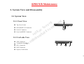
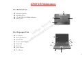
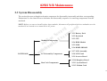
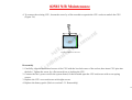
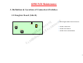
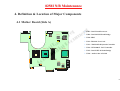
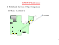
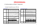
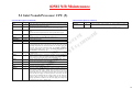
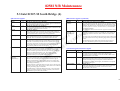
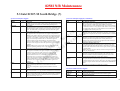
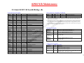
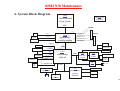
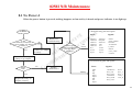
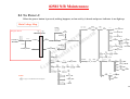
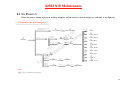
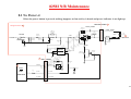
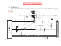
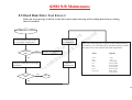
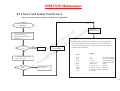
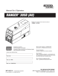
1
SERVICE MANUAL FOR
8258I
BY: Sanny Gao
Technical Maintenance Department /GTK MTC
Jun.2006 / R01
8258I N/B Maintenance
Contents
1. Hardware Engineering Specification ……………………………………………………………………
4
1.1 Introduction …………………………………………………………………………………………………………….
4
1.2 System Hardware Parts ….…………………………………………………………………………………………….
1.3 Other Functions ………………………………………………………………………………………………………..
6
1.4 Power Management …………………………..…………………………………………………………….………….
1.5 Appendix 1: Intel ICH7-M GPIO Definitions ……………………………………………………………………….
1.6 Appendix 2: W83L951DG KBC GPIO Pins Definitions ……..……………………………………………………..
38
2. System View and Disassembly …………………………………………………………………………..
49
t
t
n
e e
r
c m
e
u
S
c
c Do
a
iT ial
M t
n
e
id
f
n
o
C
2.1 System View …………………………………………………………………………………………………………….
33
41
43
49
2.2 Tools Introduction …………………………………………………………………………………………………..…. 52
2.3 System Disassembly ……………………………………………………………………………………………………. 53
3. Definition & Location of Connectors/Switches …………………………………………………………
72
3.1 Mother Board (Side A) ….………………………………………………………..……………………………………
72
3.2 Mother Board (Side B) ….…………………………...…………………………………………………………………
74
4. Definition & Location of Major Components …………………………………………………………..
76
4.1 Mother Board (Side A) ….……………………………………………………………………………………..………
76
4.2 Mother Board (Side B) ….……………………………………………………………………………………..………
77
5. Pin Description of Major Component …………………………………………………………………..
78
5.1 Intel Yonah Processor CPU ……………………………………………………………………………………………
78
1
8258I N/B Maintenance
Contents
5.2 Intel 945GM North Bridge …………………………………………………………………………………………….
83
5.3 Intel ICH7-M South Bridge ……………………………………………………………………………………………
89
6. System Block Diagram ……………………………………………………………………………………
100
7. Maintenance Diagnostics …………………………………………………………………………………
101
7.1 Introduction …………………………………………………………………………………………………………….
101
7.2 Maintenance Diagnostics ………………………………………………………………………………………………
7.3 Error Codes …………………………………………………………………………………………………………….
102
t
t
n
e e
r
c m
e
u
S
c
c Do
a
iT ial
M t
n
e
id
f
n
o
C
103
8. Trouble Shooting …………………………………………………………………………………………
105
8.1 No Power ……………………………………………………………………………………………………………….
107
8.2 No Display ………………………………………………………………………………………………………………
8.3 Memory Test Error ………………………………………….…………………………………………………………
8.4 Keyboard (K/B) or Touch Pad (T/P) Test Error ……………..…………………………………………………...…
8.5 Hard Disk Drive Test Error ………………………..………………………………………………………………….
8.6 ODD Test Error …………………………………………………………………..……………………………..……..
8.7 USB Port Test Error ……………………………………………………………………………………………………
8.8 Audio Test Error ………………………………………………………………………………………..……………...
8.9 LAN Test Error ………………………………………………………………………………………..……….……….
8.10 Mini Express (Wireless) Socket Test Error ………………………..…………………………………………….….
8.11 New Card Socket Test Error …………………………………………..……………………………………………..
113
116
118
120
122
124
126
129
131
133
2
8258I N/B Maintenance
Contents
9. Spare Parts List …………………………………………………………………………………………..
135
10. System Exploded Views ………………………………………………………………………………...
146
t
t
n
e e
r
c m
e
u
S
c
c Do
a
iT ial
M t
n
e
id
f
n
o
C
11. Reference Material ………………………………………………………………………………….…..
148
3
8258I N/B Maintenance
1. Hardware Engineering Specification
1.1 Introduction
t
t
n
e e
r
c m
e
u
S
c
1.1.2 System Overview
c Do
a
iT ial
M t
n
e
id
f
n
o
C
1.1.1 General Description
This document describes the brief introduction for MITAC 8258I portable notebook computer system.
The MITAC 8258I model is designed for Intel Mobile Pentium-M processor Yonah 533 and 667 FSB.
This system is based on PCI architecture and is fully compatible with IBM PC/AT specification, which has
standard hardware peripheral interface. The power management complies with Advanced Configuration and Power
Interface. It also provides easy configuration through CMOS setup, which is built in system bios software and can
be pop-up by pressing F2 key at system start up or warm reset. System also provides icon LEDs to display system
status, such as AC/battery power indicator, battery charger indicator, HDD/ODD, NUM LOCK, CAP LOCK,
Wireless LAN indicator. It also equipped with 10/100 LAN, 56 K fax modem, 4 USB ports, S-Video, audio Lineout/SPDIF, Line-in and internal/external microphone function.
The memory subsystem supports DDR2 SDRAM channels (64-bit wide).
The 945GM MCH host memory controller integrates a high performance host interface for Intel Yonah processor,
4
8258I N/B Maintenance
a high performance PCI Express interface, a high performance memory controller, and Direct Media Interface
(DMI) connecting with Intel ICH7-M.
The Intel ICH7-M integrates three Universal Serial Bus 2.0 Host Controllers Interface (UHCI), the audio
controller with Azalia interface, the Ethernet includes a 32-bit PCI controller, the IDE Master/Slave controllers,
the SATA controller and Direct Media Interface technology.
t
t
n
e e
r
c m
e
u
S
c
c Do
a
iT ial
M t
n
e
id
f
n
o
C
Intel graphics enhancements includes DVMT 3.0, Zone Rendering 2.0, Quad pixel pipe rendering engine, Pixel
Shader 2.0 and 4x Faster Setup Engine.
The Realtek RTL8100CL is a highly integrated, cost-effective single-chip Fast Ethernet controller that provides
32-bit performance, PCI bus master capability and full compliance with IEEE 802.3u 100Base-T specifications
and IEEE 802.3x Full Duplex Flow Control. It also supports the Advanced Configuration Power management
Interface (ACPI).
The ALC883 2-channel high definition audio codec with UAA (Universal Audio Architecture), featuring a 24-bit
two-channel DAC and two stereo 20-bit ADCs, are designed for commercial notebook PC system. The ALC883
provides 2 output channels, along with flexible mixing, mute and fine gain control functions. Also, supporting 32bit S/PDIF output functions and a sampling rate of up to 96 KHz.
The W83L951D is a high performance microcontroller on-chip supporting functions optimized for embedded
control. These include ROM, RAM, four types of timers, a serial communication interface, optional I²C bus
interface, host interface, A/D converter, D/A converter, I/O ports and other functions needed in control system
configurations, so that compact, high performance systems can be implemented easily.
A full set of software drivers and utilities are available to allow advanced operating systems such as Windows ME,
Windows 2000 and Windows XP to take full advantage of the hardware capabilities. Features such as bus
5
8258I N/B Maintenance
mastering IDE, plug and play, Advanced Power Management (APM) with application restart, software-controlled
Power shut-down.
Following chapters will have more detail description for each individual sub-systems and functions.
t
t
n
e e
r
c m
e
u
S
c
c Do
a
iT ial
M t
n
e
id
f
n
o
C
1.2 System Hardware Parts
CPU
Core logic
System BIOS
Memory
HDD
ODD
Display
Clock Generator
VGA Control
LAN
-Mobile Pentium-M Processor Yonah 533 and 667 FSB-Thermal spec 40W TDP
Intel 945GM + ICH7-M chipset
SST49LF004A
DDR2 533 256 MB: Nanya, NT256T64UH4A1FN-37B
Infineon, HYS64T32000HDL-3.7-B
DDR2 533 512 MB: Nanya, NT512T64UH8A1FN-37B
Infineon, HYS64T64020HDL-3.7-B
SATA : Fujitsu, MHV2040BH (Mercury60 series)
COMBO : Panasonic, UJDA770 or HLDS, GCC-4244N
15.4” : AUO B154EW01 V8 None Glare
Samsung LTN154X3-L01
ICS 9LPR310
-Intel 945GM
RTL8100CL
Audio System
Azalia CODEC: ALC883
Modem
56 Kbps(V.90) Fax Modem (MDC (Azalia I/F)) Askey 1456VQL-R2
Wireless LAN
Wireless LAN Intel Pro/Wireless 3945ABG (Mini PCI-E Interface IEEE802.11a, b, g)
USB
USB2.0 x 4 (individual)
New Card
MINI-PCI-E interface
6
8258I N/B Maintenance
1.2.1 Intel Yonah Processors in Micro-FCBGA Package
Intel Yonah Processors with 478 pins Micro-FCBGA package.
The Yonah processor is built on Intel’s next generation 65 nanometer process technology. Yonah is Intel’s first
dual core processor for mobile.
t
t
n
e e
r
c m
e
u
S
c
c Do
a
iT ial
M t
n
e
id
f
n
o
C
The following list provides some of the key features on this processor:
• First dual core processor for mobile
• Supports Intel architecture with dynamic execution
• On-die, primary 32-KB instruction cache and 32-KB write back data cache
• On-die, 2 MB L2 cache with advanced transfer cache architecture
• Data prefetech logic
• Streaming SIMD Extension 2 (SSE2) and Streaming SIMD Extension 3 (SSE3)
• The Yonah standard voltage and low voltage processor are offered at 667 MHz FSB
• The Yonah ultra low voltage processor is offered at 533 MHz FSB
• Advanced power management features including enhanced Intel Speed-Step technology
• Digital temperature sensor
7
8258I N/B Maintenance
• Micro-FCPGA and Micro-FCBGA package technologies
• Execute disable bit support for enhanced security
• Intel virtualization technology
t
t
n
e e
r
c m
e
u
S
c
c Do
a
iT ial
M t
n
e
id
f
n
o
C
1.2.2 Clock Generator
ICS9LPR310 is a low power CK410M-compliant clock specification. This clock synthesizer provides a single chip
solution for next generation P4 Intel processors and Intel chipsets. ICS9LPR310 is driven with a 14.318 MHz
crystal.
Output Feathers
• 2 - 0.7 V differential CPU pairs
• 8 - 0.7 V differential PCIEX pairs
• 1 - 0.7 V differential SATA pair
• 1 - 0.7 V differential LCDCLK/PCIEX selectable pair
• 4 - PCI (33 MHz)
• 2 - PCICLK_F, (33 MHz) free-running
• 1 - USB, 48 MHz
8
8258I N/B Maintenance
• 1 - DOT 96 MHz/27 MHz selectable pair
• 2 - REF, 14.318 MHz
Key Specifications
• CPU outputs cycle-cycle jitter < 85 ps
t
t
n
e e
r
c m
e
u
S
c
c Do
a
iT ial
M t
n
e
id
f
n
o
C
• PCIEX outputs cycle-cycle jitter < 125 ps
• SATA outputs cycle-cycle jitter < 125 ps
• PCI outputs cycle-cycle jitter < 500 ps
• +/- 300 ppm frequency accuracy on CPU, PCIEX and SATA clocks
• +/- 100 ppm frequency accuracy on USB clocks
Features/Benefits
• Supports tight ppm accuracy clocks for Serial-ATA and PCIEX
• Supports programmable spread percentage and frequency
• Uses external 14.318 MHz crystal, external crystal load
• PEREQ# pins to support PCIEX power management
• Low power differential clock outputs (no 50 ohm resistor to GND needed)
9
8258I N/B Maintenance
1.2.3 The Mobile Intel 945GM Express Chipset
The Mobile Intel 945GM Express chipset is designed for use in Intel’s next generation mobile platform code
named NAPA.
The Intel 945GM Express chipset come with the generation 3.5 Intel integrated graphics engine, and the Intel
Graphics Media Accelerator (GMA) 950, providing enhanced graphics support over the previous generation
(G)MCH’s.
t
t
n
e e
r
c m
e
u
S
c
c Do
a
iT ial
M t
n
e
id
f
n
o
C
The (G)MCH manages the flow of information between the four following primary interfaces:
• FSB
• System memory interface
• Graphics interface
• DMI
The (G)MCH can also be enabled to support external graphics, using the x16 PCI Express graphics attach port.
When external graphics is enabled, the internal graphics port are inactive.
Features:
Processor Support
• All Yonah variants
10
8258I N/B Maintenance
• Merom support
• 533 MHz and 667 MHz Front Side Bus (FSB) support
• Source synchronous double-pumped (2x) address
• Source synchronous quad-pumped (4x) data
t
t
n
e e
r
c m
e
u
S
c
c Do
a
iT ial
M t
n
e
id
f
n
o
C
• Other key features are
- Support for DBI (Data Bus Inversion)
- Support for MSI (Message Signaled Interrupt)
- 32-bit interface to address up to 4 GB of memory
- A 12 deep In-Order queue to pipeline FSB commands
- GTL+ bus driver with integrated GTL termination resistors
Memory System
• Support single/dual channel DDR2 SDRAM
• Maximum memory supported 2 GB
• 64-bit wide per channel
• Three memory channel configurations supported
- Single channel
11
8258I N/B Maintenance
- Dual channel symmetric
- Dual channel asymmetric
• One SO-DIMM connector per channel
• Support for DDR2 at 400 MHz, 533 MHz and 667 MHz
t
t
n
e e
r
c m
e
u
S
c
c Do
a
iT ial
M t
n
e
id
f
n
o
C
• 256 Mb, 512 Mb and 1 Gb memory technologies supported
• Support for x8 and x16 devices
• Maximum memory supported: 2 GB
• Support for DDR2 On-Die Termination (ODT)
• Supports partial writes to memory using Data Mask signals (DM)
• Intel rapid memory power management
• Dynamic row power-down
• No support for fast chip select mode
• Support for 2N timings only
12
8258I N/B Maintenance
Internal Graphics
• Intel Gen 3.5 integrated graphics engine
• 250 MHz core rendor clock at 1.05 V core voltage
• Supports TV-Out, LVDS, CRT and SDVO
t
t
n
e e
r
c m
e
u
S
c
c Do
a
iT ial
M t
n
e
id
f
n
o
C
• Intel dual frequency graphics technology
• Intel Dynamic Video Memory Technology (DVMT 3.0)
• Intel smart 2D display technology
• Intel display power saving technology 2.0
• Video capture via x1 concurrent PCIE port
• Higher performance MPEG-2 decoding
• Hardware acceleration for VLD/iDCT
• 4x pixel rate HWMC
• DX 9.1
• Hardware motion compensation
• Intermediate Z in classic rendering
13
8258I N/B Maintenance
Analog CRT
• Integrated 400 MHz RAMDAC
• Analog monitor support up to QXGA (2048 x 1536)
• Support for CRT hot plug
t
t
n
e e
r
c m
e
u
S
c
c Do
a
iT ial
M t
n
e
id
f
n
o
C
Dual Channel LVDS
• Panel support up to UXGA (1600 x 1200)
• 25-112 MHz single/dual channel
- Single channel LVDS interface support: 1 x 18 bpp
- Dual channels LVDS interface support: 2 x 18 bpp panel support up to UXGA (1600 x 1200)
- TFT panel type supported
• Pixel Dithering for 18-bit TFT panel to emulate 24 bpp true color displays
• Panel fitting, panning and center mode supported
• CPIS 1.5 compliant
• Spread spertrum clocking supported
• Panel power sequencing support
14
8258I N/B Maintenance
• Integrated PWM interface for LCD backlight inberter control
TV-OUT
• Three integrated 10-bit DACS
• Macro Vision support
• Overscaling
• NTSC/PAL
t
t
n
e e
r
c m
e
u
S
c
c Do
a
iT ial
M t
n
e
id
f
n
o
C
• Component, S-Video and composite output interfaces
• HDTV support 480p/720p/1080i/1080p
DMI
• Chip-to-chip interface between (G)MCH and Intel 82801GBM (ICH7-M)
• Configurable as x2 or x4 DMI lanes
• 2 GB/s (1 GB/s each direction) point-to-point interface to Intel 82801GBM
• 32-bit downstream address
• Direct Media Interface asynchronously coupled to core
15
8258I N/B Maintenance
• Supports 3 virtual channels for traffic class performance differentiation
• Supports both snooped and non-snooped traffic
• Supports isochronous non-snooped traffic
• Supports legacy snooped isochronous traffic
t
t
n
e e
r
c m
e
u
S
c
c Do
a
iT ial
M t
n
e
id
f
n
o
C
• Supports the following traffic types to or from Intel 82801GBM
• Peer write traffic between DMI and PCI Express graphics port
• DMI-to-DRAM
• DMI-to-CPU (FSB interrupts or MSIs only)
• CPU-to-DMI
• Messaging in both directions, including Intel Vendor-specific messages
• Supports power management state change messages
• APIC and MSI interrupt messaging support
• Supports SMI, SCI and SERR error indication
• Legacy support for ISA regime protocol (PHOLD/PHOLDA) required for parallel port DMA, floppy drive
and LPC bus masters
16
8258I N/B Maintenance
1.2.4 I/O Controller Hub: Intel ICH7-M
The ICH7 provides extensive I/O support. Functions and capabilities include:
• PCI Express base specification, revision 1.0a support
• PCI local bus specification, revision 2.3 support for 33 MHz PCI operations (supports up to six Req/Gnt pairs)
t
t
n
e e
r
c m
e
u
S
c
c Do
a
iT ial
M t
n
e
id
f
n
o
C
• ACPI power management logic support
• Enhanced DMA controller, interrupt controller and timer functions
• Integrated serial ATA host controller with independent DMA operation on four ports and AHCI (ICH7R
support
• USB host interface with support for eight USB ports; four UHCI host controllers; one EHCI high-speed USB
2.0 host controller
• System Management Bus (SMbus) specification, version 2.0 with additional support for I2C devices
• Supports audio codec ’97, revision 2.3 specification (a.k.a , AC ’97 component specification, revision 2.3)
which provides a link for audio and telephony codecs (up to 7 channels)
• Supports Intel high definition audio
• Supports Intel Matrix storage technology (ICH7R only)
• Supports Intel Active Management Technology
17
8258I N/B Maintenance
• Low Pin Count (LPC) interface
• Firmware Hub (FWH) interface support
1.2.5 Azalia Audio System: ALC880
t
t
n
e e
r
c m
e
u
S
c
c Do
a
iT ial
M t
n
e
id
f
n
o
C
ALC880 provides 7.1 channels of outputs and multiple stereo inputs, along with flexible mixing, mute and finer
gain ALC880 provides 7.1 channels of outputs and multiple stereo inputs, along with flexible mixing, mute and
finer gain control functions to provide a complete integrated audio solution for PCs. Also the highest 192 KHz
sample rate DACs and Realtek proprietary hardware content protection are applicable for DVD audio, which only
implemented in high end consumer electronics, now is achieved by PCs with ALC880 inside. ALC880 is also the
one and only high definition audio codec integrating three pairs of stereo ADCs which can support microphone
array with AEC (Acoustic Echo Cancellation), BF (Beam Forming) and NS (Noise Suppression) technology
simultaneously to significantly improve recording quality for conference call. With this unique feature (3 pairs of
Stereo ADCs), ALC880 can perform the ultimate performance of HAD like using S/PDIF to output analog data or
multiple recording application.
Feathers:
• High performance DACs with 95 dB S/N ratio
• Meets performance requirements for audio on PC2001 systems
• 8 channels of DAC support 16/20/24-bit PCM format for 7.1 audio solution
• 3 stereo ADCs support 16/20-bit PCM format, two for microphone array, one for legacy mixer recording
18
8258I N/B Maintenance
• Supports 44.1/48/96/192 KHz DAC sample rate
• All ADCs support 44.1/48/96 KHz sample rate
• Applicable for 4 ch/192 KHz and 6 ch/96 KHz DVD-Audio solution
• Up to 4 channels of microphone input are supported for AEC/BF application
t
t
n
e e
r
c m
e
u
S
c
c Do
a
iT ial
M t
n
e
id
f
n
o
C
• Support power off CD function
• Support external PCBEEP input and built in BEEP generator
• PCBEEP Pass-Through when link is in RESET state
• Software selectable 2.5 V/3.75 V VREFOUT
• Default 6 VREFOUTs are supported, additional 4 VREFOUTs are capable by sharing un-used analog I/O pins
• 2 jack detection pins each supports up to 4 jacks plugging can be detected
• 16/20/24-bit S/PDIF-OUT supports 44.1/48/96 KHz sample rate
• 16/20/24-bit S/PDIF-IN supports 44.1/48/96 KHz sample rate
• Optional EPAD (External Amplifier Power Down) is supported
• Power support digital 3.3 V, analog 3.3 V/5.0 V
• Power management and enhanced power saving features
19
8258I N/B Maintenance
• 48-pin LQFP package is compatible with AC’97
• Reserve analog mixer architecture is backward compatible with AC’97
• –64 dB ~ +30 dB with 1dB resolution of mixer gain to achieve finer volume control
• Impedance sensing capability for each re-tasking jack support power off CD function
t
t
n
e e
r
c m
e
u
S
c
c Do
a
iT ial
M t
n
e
1.2.6 MDC: Azalia MDC Modem
id Card
f
n
o
C
• All analog jacks are stereo input and output re-tasking for analog plug & play
• Built in headphone amplifier for each re-tasking jack
• Support external volume knob control
• Support 2 GPIO (General Purpose Input/Output) for customized application
• Hardware content protection for DVD-Audio supporting
Feathers:
• AC’97/MC’97 2.2 compliant
• MDC Modem support current sense, whenever the current on the line exceeds approximately 150 mA and
should immediately go back on hook
20
8258I N/B Maintenance
• ITU-T V.92 PCM Upstream and V.90 data rates with auto0fallback to V.34, V.32ter V.32 bis and fallbacks
• Virtual com port with a through put of up to 460.8 Kbps
• V.42 bis/MNP 5 data compression
• FAX send and receive rates up to 14.4kbps, V.17, V.29, V.27ter
t
t
n
e e
r
c m
e
u
S
c
c Do
a
iT ial
M t
1.2.7 System Flash Memory (BIOS)
n
e
id
f
n
o
C
• Hayes AT command set
• Supports V.42 error correction and V.44, V.42bis/MNP5 data compression
• FAX capabilities: ITU-T V.17, V.29, V.27ter, V.21 Ch2 and TIA/EIA 578 Class1 FAX
• Modem support wake up on ring
• Firmware hub for Intel® 810, 810E, 815, 815E, 815EP, 820, 840, 850 chipsets
• Flexible erase capability
- Uniform 4 KBytes sectors
- Uniform 16 KBytes overlay blocks for SST49LF002A
- Uniform 64 KBytes overlay blocks for SST49LF004A
- Top boot block protection
21
8258I N/B Maintenance
- 16 KBytes for SST49LF002A
- 64 KBytes for SST49LF004A
- Chip-Erase for PP mode
• Single 3.0-3.6 V read and write operations
• Superior reliability
t
t
n
e e
r
c m
e
u
S
c
c Do
a
iT ial
M t
n
e
id
f
n
o
C
• Firmware hub hardware interface mode
- 5-signal communication interface supporting byte read and write
- 33 MHz clock frequency operation
- WP# and TBL# pins provide hardware write protect for entire chip and/or top boot block
- Block locking register for all blocks
- Standard SDP command set
- Data# Polling and Toggle Bit for End-of-Write detection
- 5 GPI pins for system design flexibility
- 4 ID pins for multi-chip selection
22
8258I N/B Maintenance
1.2.8 Memory System
128 MB, 256 MB, 512 MB, 1 GB (x64) 200-Pin DDR2 SDRAM SODIMMs
• JEDEC-standard 200-pin, small-outline, dual in-line memory module (SODIMM)
• VDD=+1.8 V±0.1 V, VDDQ=+1.8 V±0.1 V
t
t
n
e e
r
c m
e
u
S
c
c Do
a
iT ial
M t
n
e
id
f
n
o
C
• JEDEC standard 1.8 V I/O (SSTL_18-compatible)
• Differential data strobe (DQS,DQS#) option
• Four-bit prefetch architecture
• Differential clock input (CK, CK#)
• Command entered on each rising CK edge
• DQS edge-aligned with data for reads
• DQS center-aligned with data for writes
• Duplicate output strobe (RDQS) option for x8 configuration
• DLL to align DQ and DQS transitions with CK
• Four internal banks for concurrent operation
• Data Mask (DM) for masking write data
23
8258I N/B Maintenance
• Programmable CAS Latency (CL): 2, 3, 4 and 5
• Posted CAS additive latency (AL): 0, 1, 2, 3 and 4
• Write latency = read latency – 1tCK
• Programmable burst lengths : 4 or 8
t
t
n
e e
r
c m
e
u
S
c
c Do
a
iT ial
M t
n
e
id
f
n
o
C
• Read burst interrupt supported by another read
• Write burst interrupt supported by another write
• Adjustable data – output drive strength
• Concurrent auto precharge option is supported
• Auto Refresh (CBS) and self refresh mode
• 64 ms, 8, 192-cycle refresh
• Off-Chip Drive (OCD) impedance calibration
• On-die termination (ODT)
24
8258I N/B Maintenance
1.2.9 LAN
The Realtek RTL8100C(L) is a highly integrated, cost-effective single-chip fast Ethernet controller that provides
32-bit performance, PCI bus master capability and full compliance with IEEE 802.3u 100Base-T specifications
and IEEE 802.3x full duplex flow control. It also supports the Advanced Configuration Power management
Interface (ACPI), PCI power management for modern operating systems that are capable of Operating System
Directed Power Management (OSPM) to achieve the most efficient power management possible. The RTL8100C
(L) does not support CardBus mode as the RTL8139C does. In addition to the ACPI feature, the RTL8100C(L)
also supports remote wake-up (including AMD Magic Packet, LinkChg, and Microsoft® wake-up frame) in both
ACPI and APM environments. The RTL8100C(L) is capable of performing an internal reset through the
application of auxiliary power. When auxiliary power is applied and the main power remains off, the
RTL8100C(L) is ready and waiting for the magic packet or link change to wake the system up. Also, the LWAKE
pin provides 4 different output signals including active high, active low, positive pulse and negative pulse. The
versatility of the RTL8100C(L) LWAKE pin provides motherboards with Wake-On-LAN (WOL) functionality.
The RTL8100C(L) also supports analog Auto-Power-down, that is, the analog part of the RTL8100C(L) can be
shut down temporarily according to user requirements or when the RTL8100C(L) is in a power down state with
the wakeup function disabled. In addition, when the analog part is shut down and the isolate B pin is low (i.e. the
main power is off), then both the analog and digital parts stop functioning and the power consumption of the
RTL8100C(L) will be negligible. The RTL8100C(L) also supports an auxiliary power auto-detect function and
will auto-configure related bits of their own PCI power management registers in PCI configuration space.
t
t
n
e e
r
c m
e
u
S
c
c Do
a
iT ial
M t
n
e
id
f
n
o
C
• 128-pin QFP/LQFP
• Integrated fast Ethernet MAC, physical chip and transceiver in one chip
• 10 Mb/s and 100 Mb/s operation
25
8258I N/B Maintenance
• Supports 10 Mb/s and 100 Mb/s N-way Auto-negotiation operation
• PCI local bus single-chip fast Ethernet controller
- Compliant to PCI revision 2.2
- Supports PCI clock 16.75 MHz-40 MHz
t
t
n
e e
r
c m
e
u
S
c
c Do
a
iT ial
M t
n
e
id
f
n
o
C
- Supports PCI target fast back-to-back transaction
- Provides PCI bus master data transfers and PCI memory space or I/O space mapped data transfers of
RTL8100C(L)'s operational registers
- Supports PCI VPD (Vital Product Data)
- Supports ACPI, PCI power management
• Supports 25 MHz crystal or 25 MHz OSC as the internal clock source. The frequency deviation of either
crystal or OSC must be within 50 PPM
• Compliant to PC99/PC2001 standard
• Supports Wake-On-LAN function and remote wake-up (Magic Packet*, LinkChg and Microsoft® wake-up
frame)
• Supports 4 Wake-On-LAN (WOL) signals (active high, active low, positive pulse and negative pulse)
• Supports auxiliary power-on internal reset, to be ready for remote wake-up when main power still remains off
• Supports auxiliary power auto-detect, and sets the related capability of power management registers in PCI
26
8258I N/B Maintenance
configuration space
• Includes a programmable, PCI burst size and early Tx/Rx threshold
• Supports a 32-bit general-purpose timer with the external PCI clock as clock source, to generate timerinterrupt
t
t
n
e e
r
c m
e
u
S
c
c Do
a
iT ial
M t
n
e
d
i
f
1.2.10 Keyboard System: Winbond W83L951DG
n
o
C
• Contains two large (2 KBytes) independent receive and transmit FIFOs
• Advanced power saving mode when LAN function or wakeup function is not used
• Uses 93C46 (64*16-bit EEPROM) to store resource configuration, ID parameter and VPD data
• Supports LED pins for various network activity indications
• Supports loopback capability, Half/Full duplex capability
• Supports full duplex flow control (IEEE 802.3x)
The Winbond mobile keyboard and embedded controller W83L951D/F architecture consists of a Turbo-8051 core
logic controller and surrounded by various components, 2 K+256 bytes of RAM, 64 K on-chip flash, LPC host
interface, 13 general purpose I/O port with 24 external interrupt source, 4 timers, 1 serial port, 2 SMBus interface
for master mode, 3 PS/2 port, two 8-bit and two 16-bit PWM channels, 2 D-A and 8 A-D converters, 1 Consumer
Infrared communications receiver, 2 fan tachometer, 1 real time clock generator and matrix interface. The part
number with an affix of “G” is the Lead-free package product.
27
8258I N/B Maintenance
128-pin QFP/LQFP
• 8-bit Turbo 8052 Microprocessor code based, speed up to 24 MHz
• 256 bytes internal RAM
• 64 K bytes embedded programmable flash memory
t
t
n
e e
r
c m
e
u
S
c
c Do
a
iT ial
M t
n
e
id
f
n
o
C
• 2 K bytes external SRAM
Host interface
• Software optional with LPC interface
• Primary programmable I/O address communication port in LPC mode
• Support SERIRQ in LPC interface
• Support hardware fast Gate A20 and KBRST
• Support port 92 h
SMBus
• Support 2 SMBus interface support master mode
Timers
28
8258I N/B Maintenance
• Support four timer signal with three pre-scalars
• Timer 1 and 2 Shard the Same Pre-scalar and are Free-Running Only
• Timer X and Y Have Individual Pre-scalar and Support up to Four Control Modes, Free Running, Pulse
Output, Event Counter and Pulse Width Measurement
PWM
t
t
n
e e
r
c m
e
u
S
c
c Do
a
iT ial
M t
n
e
id
f
n
o
C
• Support four PWM Channels
• PWM 0 and 1 are 8-bit and programmable frequency from 62 Hz to 7.5 KHz
• PWM 2 and 3 are 16-bit and programmable frequency from 6 Hz to 3 MHz
Fan Tachometer
• Support two fan tachometer inputs
A/D Converter
• Firmware programmable optional with 10-bit or 8-bit resolution, support eight channels
D/A Converter
• 8-bit Resolution, support two channels
29
8258I N/B Maintenance
PS2
• Support three hardware PS2 channels
• Optional PS2 clock inhibit by hardware or firmware
Keyboard Controller
t
t
n
e e
r
c m
e
u
S
c
c Do
a
iT ial
M t
n
e
id
f
n
o
C
• Support 16*8 keyboard Matrix-scan, expanding to 18*8 and 20*8
GPIO
• Support 104 useful GPIO pins totally and Bit–addressable to facility firmware coding
Flash
• Support external On-Board 64 K flash via matrix interface (GP0, 1, 3)
CIR
• Support decoding for the NEC consumer IR remote control format
RTC
• Real time clock generator with 32.768 KHz input
ACPI
30
8258I N/B Maintenance
• Support ACPI appliance secondary programmable I/O address communication port in LPC mode
Package
• 128-pin QFP and 128-pin LQFP package options
t
t
n
e e
r
c m
e
u
S
c
c Do
a
iT ial
M t
n
e
id
f
n
o
C
1.2.11 Hard Disk Drive
8258I can support SATA HDD by equipped different HDD transition board.
SATA HDD: The SATA function in the ICH7 has dual modes of operation to support different operating system
conditions. In the case of native IDE enabled operating systems, the ICH7 has separate PCI functions for
serial and parallel ATA (enhanced mode). To support legacy operating systems, there is only one PCI
function for both the serial and parallel ATA ports if functionality from both SATA and PATA devices is
desired (combined mode). SATA interface transfer rates are independent of UDMA mode settings. SATA
interface transfer rates will operate at the bus’s maximum speed, regardless of the UDMA mode reported by
the SATA device or the system BIOS.
• Up-to 150 MB/sec bus speed (Serial ATA generation 1)
• Compliant with Serial ATA 1.0a specification and Serial ATA 2 extensions 1.0
• Supports 48-bit LBA addressing
• Supports native DMA queued command (first party DMA queued)
31
8258I N/B Maintenance
• Supports legacy DMA queued command
• Supports staggered spin-up function
• Supports Hot-Plug features
• Supports Serial ATA power management (host initiated partial/slumber)
t
t
n
e e
r
c m
e
u
S
c
c Do
a
iT ial
M t
n
e
id
f
n
o
C
32
8258I N/B Maintenance
1.3 Other Functions
1.3.1 Hot Key Function
Keys Combination
Feature
Meaning
t
t
n
e e
r
c m
e
u
S
c
c Do
a
iT ial
M t
n
e
id
f
n
1.3.2 Power on/off/suspend/resume
button
o
C
Fn + F1
Wireless LAN ON/OFF
Wireless LAN ON/OFF
Fn + F2
Bluetooth ON/OFF
Fn + F3
Volume Down
Fn + F4
Volume Up
Fn + F5
LCD/external CRT switching
Rotate display mode in LCD only, CRT only, and simultaneously
Fn + F6
Brightness down
Decreases the LCD brightness
Fn + F7
Brightness up
Increases the LCD brightness
Fn + F10
Mute
Audio Mute
Fn + F11
Display Off/On
Toggle Display on/off
Fn + F12
Suspend to DRAM / HDD
Force the computer into either Suspend to HDD or Suspend to
DRAM mode depending on BIOS Setup.
APM Mode
• At APM mode, power button is on/off system power
ACPI Mode
33
8258I N/B Maintenance
• At ACPI mode, windows power management control panel set power button behavior. You could set “standby”,
“power off” or “hibernate” (must enable hibernate function in power management) to power button function.
Continue pushing power button over 4 seconds will force system off at ACPI mode.
1.3.3 Cover Switch
t
t
n
e e
r
c m
e
u
S
c
c Do
a
iT ial
M t
n
e
id
f
n
1.3.4 LED Indicators
o
C
System automatically provides power saving by monitoring cover switch. It will save battery power and prolong
the usage time when user closes the notebook cover.
At ACPI mode there are four functions to be chosen at windows power management control panel.
1.
None
2.
Standby
3.
Off
4.
Hibernate (must enable hibernate function in power management)
Six LED indicators
From left to right that indicates Power, Battery Status, HDD/ODD, NUM LOCK, CAP LOCK, WLAN.
Power: This LED lights blue when the notebook was powered by AC or battery power line, flashes (on 1 second,
34
8258I N/B Maintenance
off 1 second) when entered suspend to RAM state. The LED is off when the notebook is in power off state.
Battery status: With battery operation, this LED stays off. When the battery charge drops to 10% of capacity, the
LED lights red, flashes per 1 second and beeps per 2 seconds. When AC is connected, this indicator stays
off if the battery pack is fully charged or red if the battery is being charged.
System has four status LED indicators at front side which to display system activity: HDD/ODD, NUM LOCK,
CAPS LOCK and WLAN.
t
t
n
e e
r
c m
1.3.5 Battery Status
e
u
S
c
c Do
1.3.5.1 Battery Warning
a
iT ial
M t
n
e
id
f
n
o
C
• System also provides Battery capacity monitoring and gives users a warning signal to alarm they to store data
before battery dead. This function also protects system from mal-function while battery capacity is low
• Battery Warning: Capacity below 10%, Battery Status LED flashes per second, system beeps per 2 seconds
• System will suspend to HDD after 2 Minutes to protect users data
1.3.5.2 Battery Low State
After battery warning state, and battery capacity is below 5%, system will generate beep sound for twice per
second.
35
8258I N/B Maintenance
1.3.5.3 Battery Dead State
When the battery voltage level reaches 8.56 volts, system will shut down automatically in order to extend the
battery packs' life.
1.3.6 Fan power on/off management
t
t
n
e e
r
c m
e
u
S
c
c Do
1.3.7 CMOS Battery
a
iT ial
M t
n
e
id
f
n
1.3.8 I/O Ports
o
C
Fan is controlled by W83L951DG embedded controller-using ADM1032 to sense CPU temperature and PWM
control fan speed. Fan speed is depended on CPU temperature. Higher CPU temperature faster fan speed.
CR2032 3 V 220 mAh lithium battery, when AC in or system main battery inside, CMOS battery will consume
no power.
AC or main battery not exists, CMOS battery life at less (220 mAh/5.8 uA) 4 years
• One Power Supply Jack
• One External CRT Connector For CRT Display
• Supports four USB port for all USB devices
36
8258I N/B Maintenance
• One modem RJ-11 phone jack for PSTN line
• One RJ-45 for LAN
• One SPDIF jack
• One Microphone input jack
t
t
n
e e
r
c m
e
u
S
c
c Do
a
T Learning
l
1.3.9 Battery Current Limit i
and
a
M ti
n
e
id
f
n
o
C
• One S-Video (PAL/NTSC) connector
• One Express card jack
• One Mini PCI-E jack for WLAN card
Implanted H/W current limit and battery learning circuit to enhance protection of battery.
37
8258I N/B Maintenance
1.4 Power Management
The 8258I system has built in several power saving modes to prolong the battery usage for mobile purpose. User can
enable and configure different degrees of power management modes via ROM CMOS setup (booting by pressing F2
key). Following are the descriptions of the power management modes supported
t
t
n
e e
r
c m
e
u
S
c
c Do
a
iT ial
M t
n
e
id
f
n
o
C
1.4.1 System Management Mode
Full on mode
In this mode, each device is running with the maximal speed. CPU clock is up to its maximum.
Doze mode
In this mode, CPU will be toggling between on & stop grant mode either. The technology is clock throttling.
This can save battery power without loosing much computing capability. The CPU power consumption and
temperature is lower in this mode.
Standby mode
For more power saving, it turns of the peripheral components. In this mode, the following is the status of each
device:
- CPU: Stop grant
- LCD: Backlight off
38
8258I N/B Maintenance
- HDD: Spin down
Suspend to DRAM/HDD
The most chipset of the system is entering power down mode for more power saving. In this mode, the following is
the status of each device:
• Suspend to DRAM
- CPU: Off
t
t
n
e e
r
c m
e
u
S
c
c Do
a
iT ial
M t
n
e
id
f
n
o
C
- Intel 945GM: Partial off
- VGA: Suspend
- Audio: Off
- SDRAM: Self refresh
• Suspend to HDD
- All devices are stopped clock and power-down
- System status is saved in HDD
- All system status will be restored when powered on again
39
8258I N/B Maintenance
1.4.2 Other Power Management Functions
HDD & Video access
System has the ability to monitor video and hard disk activity. User can enable monitoring function for video
and/or hard disk individually. When there is no video and/or hard disk activity, system will enter next PMU state
depending on the application. When the VGA activity monitoring is enabled, the performance of the system will
have some impact.
t
t
n
e e
r
c m
e
u
S
c
c Do
a
iT ial
M t
n
e
id
f
n
o
C
40
8258I N/B Maintenance
1.5 Appendix 1: Intel ICH7-M GPIO Definitions-1
Pin name
GPIO0
GPIO1
GPIO2
GPIO3
GPIO4
GPIO5
GPIO6
GPIO7
GPIO8
GPIO9
GPIO10
GPIO11
GPIO12
Current Define
PM_BMBUSY#
Default
Input/output
I
Function
Bus Master busy
Power Well
CORE
t
t
n
e e
r
c m
e
u
S
c
c Do
a
iT ial
M t
n
e
id
f
n
o
C
PCI_REQ5#
I
X
CORE
PCI_INTE#
I
PCI interrupt for
LAN
CORE
PCI_INTF#
I
X
CORE
PCI_INTG#
I
X
CORE
PCI_INTH#
I
X
CORE
SMB_SEL
I
ECO Function
CORE
SCI#
I
System Control
Interrupt
CORE
EXTSMI#
I
SMI signal for
chipset
RESUME
X
I
X
RESUME
X
I
X
RESUME
SMBus alert
RESUME
SMBALERT#
Native
X
I
X
RESUME
X
I
X
RESUME
X
I
X
RESUME
X
I
X
RESUME
GPIO16
DPRSLPVR
O
Lower power in
deeper sleep
CORE
GPIO17
X
O
X
CORE
GPIO18
STOP_PCI#
O
PCI stop
CORE
GPIO13
GPIO14
GPIO15
41
8258I N/B Maintenance
1.5 Appendix 1: Intel ICH7-M GPIO Definitions-2
Continue to the previous page
Pin name
GPIO19
GPIO20
GPIO21
GPIO22
GPIO23
GPIO24
GPIO25
GPIO26
GPIO27
GPIO28
GPIO29
GPIO30
GPIO31
GPIO32
GPIO33
GPIO34
GPIO35
GPIO36
GPIO37
GPIO38
Current Define
PANEL_ID1
Default
Input/output
I
Function
X
Power Well
CORE
t
t
n
e e
r
c m
e
u
S
c
c Do
a
iT ial
M t
n
e
id
f
n
o
C
STOP_CPU#
O
CPU stop
CORE
PANEL_ID0
I
X
CORE
PCI_REQ4#
Native
X
CORE
X
Native
X
CORE
X
O
X
RESUME
X
O
X
RESUME
PWM_PWR_ON
O
ECO Switch
RESUME
SPK_OFF
O
Speaker turns off
RESUME
X
O
X
RESUME
X
Native
X
RESUME
X
Native
X
RESUME
X
Native
X
RESUME
PCLKRUN#
O
Clock run
CORE
WIRELESS_PD#
O
X
CORE
X
O
X
CORE
X
O
X
CORE
PANEL_ID2
I
X
CORE
X
I
X
CORE
MB_ID0
I
Mother Board ID
CORE
I
GPIO39
MB_ID1
Mother Board ID
CORE
GPIO48
X
Native
X
CORE
GPIO49
HPWRGD
Native
CPU power good
V_CPU_IO
42
8258I N/B Maintenance
1.6 Appendix W83L951DG KBC GPIO Pins Definitions-1
Pin Name
RESET#
TEST#
XIN
XOUT
XCIN
XCOUT
VCC1
GND
VCC2
VCC1
GND
VCC1
GND
AVCC
AVref
AGND
LPC Interface
LAD3
LAD2
LAD1
LAD0
SERIRQ
LRESET#
LFRAME#
LCKL
Port 0
GP00
GP01
Pin
50
124
122
123
125
126
23
32
60
49
55
78
69
112
103
115
59
58
57
56
54
53
52
51
94
93
951 Pin Definitions
RESET#
TEST#
System Clock
System Clock
RTC Clock
RTC Clock
I/O
I
I
I
I
I
I
I
I
I
I
I
I
I
I
I
I
Function
LPC_AD3
LPC_AD2
LPC_AD1
LPC_AD0
SERIRQ
LPC_RESET#
LPC_FRAME#
PCICLK
I/O
I/O
I/O
I/O
LPC Address/Data I/O 3
LPC Address/Data I/O 2
LPC Address/Data I/O 1
LPC Address/Data I/O 0
Serial Host Interrupt
LPC Reset
LPC Frame
LPC Clock
O
O
Key matrix scan output 0
Key matrix scan output 1
8258I
951 Chip Reset
Normal operation by direct external rom
Crystal use 24 MHZ
Crystal use 24 MHZ
Crystal use 32.768 KHZ
Crystal use 32.768 KHZ
+3.3 V
Ground
Please connect it to +3.3 V from LPC interface
+3.3 V
Ground
+3.3 V
Ground
Analog Power
Analog reference voltage
Analog Ground
t
t
n
e e
r
c m
e
u
S
c
c Do
a
iT ial
M t
n
e
id
f
n
o
C
KB OUT 0
KB OUT 1
43
8258I N/B Maintenance
1.6 Appendix W83L951DG KBC GPIO Pins Definitions-2
Continue to the previous page
Pin Name
GP02
GP03
GP04
GP05
GP06
GP07
Port 1
GP10
GP11
GP12
GP13
GP14
GP15
GP16
GP17
Port 2
GP20
GP21
GP22
GP23
GP24/PWM0
GP25/PWM1
GP26/PWM2
GP27/PWM3
Port 3
GP30
GP31
Pin
92
91
90
89
88
87
86
85
84
83
82
81
80
79
77
76
75
74
73
72
71
70
102
101
951 Pin Definitions
KB OUT 2
KB OUT 3
KB OUT 4
KB OUT 5
KB OUT 6
KB OUT 7
I/O
O
O
O
O
O
O
Function
Key matrix scan output 2
Key matrix scan output 3
Key matrix scan output 4
Key matrix scan output 5
Key matrix scan output 6
Key matrix scan output 7
t
t
n
e e
r
c m
e
u
S
c
c Do
a
iT ial
M t
n
e
id
f
n
o
C
KB OUT 8
KB OUT 9
KB OUT 10
KB OUT 11
KB OUT 12
KB OUT 13
KB OUT 14
KB OUT 15
O
O
O
O
O
O
O
O
Key matrix scan output 8
Key matrix scan output 9
Key matrix scan output 10
Key matrix scan output 11
Key matrix scan output 12
Key matrix scan output 13
Key matrix scan output 14
Key matrix scan output 15
Key Type0
Key Type1
M/B ID0
M/B ID1
I
I
I
I
Keyboard Languag select
Keyboard Languag select
Reserve for M/B version
Reserve for M/B version
FAN0_ON#
FAN1_ON#
O
O
Fan0 power PWM control
Fan1 power PWM control
KEY IN 0
KEY IN 1
I
I
Key matrix input 0
Key matrix input 1
8258I
KBD_US/JP#
PWRGD
CRT_DT#
BATTERY_TYPE
+3/5V_GD
KBC_BEEP
FANON
44
8258I N/B Maintenance
1.6 Appendix W83L951DG KBC GPIO Pins Definitions-3
Continue to the previous page
Pin Name
GP32
GP33
GP34
GP35
GP36
GP37
Port 4
GP40/FAN_TACH0
GP41/FAN_TACH1
GP42/RXD
GP43/TXD
GP44/KBRST#
GP45/GATE_A20
GP46/CLKRUN#
GP47/LPCPD#
Port 5
GP50
GP51
GP52
GP53
GP54
GP55
GP56/DA0
GP51/DA1
Port 6
GP60/AD0
GP61/AD1
Pin
100
99
98
97
96
95
68
67
66
65
64
63
62
61
121
120
119
118
117
116
114
113
111
110
951 Pin Definitions
KEY IN 2
KEY IN 3
KEY IN 4
KEY IN 5
KEY IN 6
KEY IN 7
I/O
I
I
I
I
I
I
Function
8258I
Key matrix input 2
Key matrix input 3
Key matrix input 4
Key matrix input 5
Key matrix input 6
Key matrix input 7
t
t
n
e e
r
c m
e
u
S
c
c Do
a
iT ial
M t
n
e
id
f
n
o
C
Fan0_SPD
Fan1_SPD
RXD
TXD
KBC_HRCIN#
A20_GATE
PM_CLKRUN#
PM_SUS_START
I
I
I
O
O
O
Fan0 speed input
Fan1 speed input
For Firmware debug
For Firmware debug
CPU Reset
System A20 Gate
LPC Clock Run
LPC Power-Down
FAN_SPEED
LSMI#
LSCI
KBC_WAKE#
KBC_THRM#
O
O
O
O
External SMI#
Need invert to SCI# sending to SouthBridge
Wake-up SouthBridge at ACPI mode
Thermal throttling control to SouthBridge
BLADJ
I-CTRL
O
O
Backlight inverter brightness adjust
Charging current adjust
EXTSMI
H8_SCI
H8_WAKE_UP#
H8_THRM#
WIRE_EN
BLT_DT
BLADJ
I_CTRL
BATT_VOLT
I-Limit
I
I
Battery voltage meansure
I-Limit function
BAT_VOLT
I_LIMIT
KBC_RX
KBC_TX
HRCIN#
A20GATE
PCLKRUN#
LPCPD
45
8258I N/B Maintenance
1.6 Appendix W83L951DG KBC GPIO Pins Definitions-4
Continue to the previous page
Pin Name
GP62/AD2
GP63/AD3
GP64/AD4
GP65/AD5
GP66/AD6
GP67/AD7
Port 7
GP70/PS2_1CLK
GP71/PS2_1DAT
GP72/PS2_2CLK
GP73/PS2_2DAT
GP74/PS2_3CLK
GP75/PS2_3DAT
GP76/SDA0
GP77/SCL0
Port 8
GP80/SDA1
GP81/SCL1
GP82/CNTR0
GP83/CNTR1
GP84/CIR_RX
GP85
GP86
GP87
Port9
GP90
GP91
Pin
109
108
107
106
105
104
48
47
46
45
44
43
42
41
40
39
38
37
36
35
34
33
31
30
951 Pin Definitions
3V/PWROK
Vtt
BATT_TEMP
V_Core
I_Charge
I_Discharge
I/O
I
I
I
I
I
I
Function
Monitor system on/off state
System Vtt voltage
Battery thermister temperature
CPU Vcore voltage
Reserve for Internal Gauge
Reserve for Internal Gauge
T_CLK
T_DATA
T_CLK2
T_DATA2
I/O
I/O
TouchPAD Clock
TouchPAD Data
Option for second PS2 interface
Option for second PS2 interface
BATT_DATA
BATT_CLK
I/O
I/O
SMBus Data
SMBus Clock
t
t
n
e e
r
c m
e
u
S
c
c Do
a
iT ial
M t
n
e
id
f
n
o
C
SMB_DATA1
SMB_CLK1
Prochot#
O
LEARNING#
CHARGING
KBC_ENABKL
O
O
O
Reserve for SMBus Data 1
Reserve for SMBus Clock 1
Reserve for Fan0 Speed detect
Indicate Intel CPU to do throttle function
CIR Receiver
Auto-Learning
Battery charge control
Enable Backlight
KBC_PWRON_VDD3S
KBC_RSMRST
O
O
Turn on VDD3.3 and VDD1.5
SouthBridge RSMRST#
8258I
KBC_VCCP
BAT_TEMP
KBC_CPUCORE
T_CLK
T_DATA
BLT_EN#
POWEROK
ECOBTN_SW#
PWM_PWR
BAT_DATA
BAT_CLK
H8_THRM_DATA
H8_THRM_CLK
FAN_SPEED_C
KBC_PWRON_VDD3S
LEARNING
CHARGING
H8_ENABKL
46
8258I N/B Maintenance
1.6 Appendix W83L951DG KBC GPIO Pins Definitions-5
Continue to the previous page
Pin Name
GP92
GP93
GP94
GP95
GP96
GP97
Port A
GPA0/EXTINT10
GPA1/EXTINT11
GPA2/EXTINT12
GPA3/EXTINT13
GPA4/EXTINT14
GPA5/EXTINT15
GPA6/EXTINT16
GPA7/EXTINT17
Port B
GPB0/EXTINT20
GPB1/EXTINT21
GPB2/EXTINT22
GPB3/EXTINT23
GPB4/EXTINT24
GPB5/EXTINT25
GPB6/EXTINT26
GPB7/EXTINT27
Port C
GPC0/EXTINT30
Pin
29
28
27
26
25
24
22
21
20
19
18
17
16
15
14
13
12
11
10
9
8
7
6
951 Pin Definitions
SB_PWRBTN#
PWRON_1.35V_1.5V
SW_VDD3
PWROK
PWRON_VCORE
PWRON_1.8V_1.25V
I/O
O
O
O
O
O
O
Function
SouthBridge power button
System power on
VDD3 power source switch
Reserve for other power sequence pin
Reserve for other power sequence pin
Reserve for other power sequence pin
SUSB1.5V
SUSC1.8V
SW_VDD3
SUSB_VCC_CORE
SUSB0.9V
PWRON_5V
PWRON_3V
PWRON_2.5V
PWRON_1.05V
PWRON_+3V_+5V
O
O
O
O
O
Reserve for other power sequence pin
Reserve for other power sequence pin
Reserve for other power sequence pin
Reserve for other power sequence pin
Reserve for other power sequence pin
Reserve for other power sequence pin
Reserve for other power sequence pin
Reserve for other power sequence pin
OCO5V
OCO3V
SUSB2.5V
SUSB_VCCP
SUSB3V
SUSB5V
ICH_PWRBTN#
KBC_RSMRST
LED_CAP#
LED_NUM#
LED_SCR#
LED_BATT_R#
LED_BATT_G#
LED_AC_PWR#
LED_BATT_PWR#
O
O
O
O
O
O
O
Capitals Lock LED indicator
Numeral Lock LED indicator
Scroll Lock LED indicator
Battery Charger Red LED indicator
Battery Charger Green LED indicator
AC Power LED indicator
Battery Power LED indicator
Reserve for other LED indicator
CAP#
NUM#
SCROLL#
BATT_R#
BATT_G#
AC_LED#
AC_BAT_POWER#
ECOBTN_LED#
PWRBTN#
I
Power Button
PWRBTN
t
t
n
e e
r
c m
e
u
S
c
c Do
a
iT ial
M t
n
e
id
f
n
o
C
8258I
47
8258I N/B Maintenance
1.6 Appendix W83L951DG KBC GPIO Pins Definitions-6
Continue to the previous page
Pin Name
GPC1/EXTINT31
GPC2/EXTINT32
GPC3/EXTINT33
GPC4/EXTINT34
GPC5/EXTINT35
GPC6/EXTINT36
GPC7/EXTINT37
Pin
5
4
3
2
1
128
127
951 Pin Definitions
KBC_SUSB
KBC_SUSC#
KBC_ADEN#
BATT_DEAD#
COVER_SW#
I/O
I
I
I
I
I
Function
Invert from SUSA# to wake up KBC when
system resumed by MDC modem and internal
LAN. Inform system power management status.
System to S4 (soft off) or S5
AC adaptor in detect
Battery low detect
Cover switch
Reserve for other Interrupt pin
Reserve for other Interrupt pin
t
t
n
e e
r
c m
e
u
S
c
c Do
a
iT ial
M t
n
e
id
f
n
o
C
8258I
KBC_SUSB#
SUSC#
ADEN#
BATT_DEAD#
LIDSW#
48
8258I N/B Maintenance
2. System View and Disassembly
2.1 System View
t
t
n
e e
r
c m
e
u
S
c
c Do
a
iT ial
M t
n
2.1.2 Left-side View
e
id
f
n
o
C
2.1.1 Front View
Top Cover Latch
External MIC In Connector
Line In Connector
Line Out/SPDIF Connector
CRT Connector
Ventilation Openings
RJ11 Connector
RJ45 Connector
Express Card Socket
49
8258I N/B Maintenance
2.1.3 Right-side View
ODD
USB Ports*2
t
t
n
e e
r
c m
e
u
S
c
c Do
a
2.1.4 Rear View
iT ial
M t
n
e
id
f
n
o
C
Power Connector
S-Video Port
USB Ports*2
Kensington Lock
50
8258I N/B Maintenance
2.1.5 Bottom View
Subwoofer Speaker
Hard Disk Drive
CPU & DDR2 SO-DIMM & Modem
Battery Park
t
t
n
e e
r
c m
e
u
S
c
c Do
a
2.1.6 Top-open View
iT ial
M t
n
e
id
f
n
o
C
LCD Screen
Stereo Speaker Set
Internal MIC
Device LED Indicators
Touch Pad
Keyboard
○
Power Button
ECO Button
51
8258I N/B Maintenance
2.2 Tools Introduction
1. Minus screw driver for notebook assembly & disassembly.
t
t
n
e e
r
c m
e
u
S
c
c Do
a
iT ial
M t
n
e
id
f
n
o
C
2 mm
2 mm
2. Auto screw driver for notebook assembly & disassembly.
Screw Size
1. M2.0
Tooling
Auto-Screw driver
Bit Size
#0
Tor.
Bit Size
2.0-2.5 kg/cm2
#0
52
8258I N/B Maintenance
2.3 System Disassembly
The section discusses at length each major component for disassembly/reassembly and show corresponding
illustrations.Use the chart below to determine the disassembly sequence for removing components from the
notebook.
NOTE: Before you start to install/replace these modules, disconnect all peripheral devices and make sure the
notebook is not turned on or connected to AC power.
t
t
n
e e
r
c m
e
u
S
c
c Do
a
iT ial
M t
n
e
id
f
n
o
C
2.3.1 Battery Pack
2.3.2 Keyboard
2.3.3 CPU
Modular Components
2.3.4 HDD Module
2.3.5 ODD
2.3.6 DDR2-SDRAM
2.3.7 LCD Assembly
NOTEBOOK
LCD Assembly Components
2.3.8 LCD Panel
2.3.9 Inverter Board
2.3.10 Daughter Board
Base Unit Components
2.3.11 System Board
2.3.12 Modem Card
53
8258I N/B Maintenance
2.3.1 Battery Pack
Disassembly
1. Carefully put the notebook upside down.
2. Slide two release lever outwards to the “unlock” (
compartment (). (Figure 2-1)
) position (), while take the battery pack out of the
t
t
n
e e
r
c m
e
u
S
c
c Do
a
iT ial
M t
n
e
id
f
n
o
C
Figure 2-1 Remove the battery pack
Reassembly
1. Replace the battery pack into the compartment. The battery pack should be correctly connected when you hear a
clicking sound.
2. Slide the release lever to the “lock” ( ) position.
54
8258I N/B Maintenance
2.3.2 Keyboard
Disassembly
1. Remove the battery pack. (Refer to section 2.3.1 Disassembly)
2. Push firmly to slide the easy start buttons cover to the right (). Then lift the easy start buttons cover up ().
(Figure 2-2)
3. Slightly lift up the keyboard and disconnect the cable from the system board to detach the keyboard. (Figure 2-3)
t
t
n
e e
r
c m
e
u
S
c
c Do
a
iT ial
M t
n
e
id
f
n
o
C
Figure 2-2 Remove the keyboard cover
Reassembly
Figure 2-3 Remove the keyboard
1. Reconnect the keyboard cable and fit the keyboard back into place.
2. Replace the easy start buttons cover.
3. Replace the battery pack. (Refer to section 2.3.1 Reassembly)
55
8258I N/B Maintenance
2.3.3 CPU
Disassembly
1. Remove the battery pack. (Refer to section 2.3.1 Disassembly)
2. Remove eight screws fastening the CPU cover. (Figure 2-4)
3. Remove four spring screws that secure the heatsink upon the CPU and disconnect the fan’s power cord from
system board. (Figure 2-5)
t
t
n
e e
r
c m
e
u
S
c
c Do
a
iT ial
M t
n
e
id
f
n
o
C
Figure 2-4 Remove eight screws
Figure 2-5 Free the heatsink
56
8258I N/B Maintenance
4. To remove the existing CPU, loosen the screw by a flat screwdriver,upraise the CPU socket to unlock the CPU.
(Figure 2-6)
t
t
n
e e
r
c m
e
u
S
c
c Do
a
iT ial
M t
n
e
id
f
n
o
C
Figure 2-6 Remove the CPU
Reassembly
1. Carefully, align the arrowhead corner of the CPU with the beveled corner of the socket, then insert CPU pins into
the holes. Tighten the screw by a flat screwdriver to locking the CPU.
2. Connect the fan’s power cord to the system board, fit the heatsink upon the CPU and secure with seven spring
screws.
3. Replace the CPU cover and secure with eight screws.
4. Replace the battery pack. (Refer to section 2.3.1 Reassembly)
57
8258I N/B Maintenance
2.3.4 HDD Module
Disassembly
1. Carefully put the notebook upside down. Remove the battery pack. (Refer to section 2.3.1 Disassembly)
2. Remove two screws fastening the HDD compartment cover. (Figure 2-7)
3. Remove one screw fastening the HDD module. Slide the HDD module out of the compartment. (Figure 2-8)
t
t
n
e e
r
c m
e
u
S
c
c Do
a
iT ial
M t
n
e
id
f
n
o
C
Figure 2-7 Remove the HDD
compartment cover
Figure 2-8 Remove HDD module
58
8258I N/B Maintenance
4. Remove four screws to separate the hard disk drive from the bracket, remove the hard disk drive. (Figure 2-9)
t
t
n
e e
r
c m
e
u
S
c
c Do
a
iT ial
M t
n
e
id
f
n
o
C
Figure 2-9 Remove hard disk drive
Reassembly
1. Attach the bracket to hard disk drive and secure with four screws.
2. Slide the HDD module into the compartment and secure with one screw.
3. Place the HDD compartment cover and secure with two screws.
4. Replace the battery pack. (Refer to section 2.3.1 Reassembly)
59
8258I N/B Maintenance
2.3.5 ODD
Disassembly
1. Carefully put the notebook upside down. Remove the battery pack. (Refer to section 2.3.1 Disassembly)
2. Remove one screw fastening the ODD. (Figure 2-10)
3. Insert a small rod, such as a straightened paper clip, into ODD’s manual eject hole () and push firmly to
release the tray. Then gently pull out the ODD by holding the tray that pops out (). (Figure 2-10)
t
t
n
e e
r
c m
e
u
S
c
c Do
a
iT ial
M t
n
e
id
f
n
o
C
Figure 2-10 Remove the ODD
Reassembly
1. Push the ODD into the compartment and secure with one screw.
2. Replace the battery pack. (Refer to section 2.3.1 Reassembly)
60
8258I N/B Maintenance
2.3.6 DDR2-SDRAM
Disassembly
1. Carefully put the notebook upside down. Remove the battery pack. (See section 2.3.1 Disassembly)
2. Remove eight screws fastening the CPU cover. (Refer to step 2 of section 2.3.3 Disassembly)
t
t
n
e e
r
c m
e
u
S
c
c Do
a
iT ial
M t
n
e
id
f
n
o
C
Figure 2-11 Remove the SO-DIMM
3. Pull the retaining clips outwards () and remove the SO-DIMM (). (Figure 2-11)
Reassembly
1. To install the DDR2, match the DDR2's notched part with the socket's projected part and firmly insert the
SO-DIMM into the socket at 20-degree angle. Then push down until the retaining clips lock the DDR2 into
position.
2. Replace the CPU cover and secure with eight screws. (Refer to step 3 of section 2.3.3 Reassembly)
3. Replace the battery pack. (See section 2.3.1 Reassembly)
61
8258I N/B Maintenance
2.3.7 LCD Assembly
Disassembly
1. Remove the battery pack and keyboard. (See sections 2.3.1 and 2.3.2 Disassembly)
2. Remove eight screws fastening the CPU cover. (Refer to step 2 of section 2.3.3 Disassembly)
3. Separate the antenna from the system board. (Figure 2-12)
4. Remove two hinge covers, disconnect two cables from the system board then carefully pull the antenna wires out.
(Figure 2-13)
t
t
n
e e
r
c m
e
u
S
c
c Do
a
iT ial
M t
n
e
id
f
n
o
C
Figure 2-12 Separate the antenna
Figure 2-13 Remove two hinge covers
and disconnect two cables
62
8258I N/B Maintenance
5. Remove four screws, then free the LCD assembly. (Figure 2-14)
t
t
n
e e
r
c m
e
u
S
c
c Do
a
iT ial
M t
n
e
id
f
n
o
C
Figure 2-14 Free the LCD assembly
Reassembly
1. Attach the LCD assembly to the base unit and secure with four screws.
2. Replace the antenna wires back.
3. Reconnect two cables to the system board. Then replace two hinge covers.
4. Replace the keyboard and battery pack. (Refer to sections 2.3.2 and 2.3.1 Reassembly)
63
8258I N/B Maintenance
2.3.8 LCD Panel
Disassembly
1. Remove the battery, keyboard and LCD assembly. (Refer to section 2.3.1, 2.3.2 and 2.3.7 Disassembly)
2. Remove two screws on the corners of the panel. (Figure 2-15)
3. Insert a flat screwdriver to the lower part of the LCD cover and gently pry the frame out. Repeat the process
until the cover is completely separated from the housing.
4. Remove six screws and disconnect the cable. (Figure 2-16)
t
t
n
e e
r
c m
e
u
S
c
c Do
a
iT ial
M t
n
e
id
f
n
o
C
Figure 2-15 Remove LCD cover
Figure 2-16 Remove six screws and
disconnect the cable
64
8258I N/B Maintenance
5. Remove eight screws that secure the LCD brackets. (Figure 2-17)
6. Disconnect the cable to free the LCD panel. (Figure 2-18)
t
t
n
e e
r
c m
e
u
S
c
c Do
a
iT ial
M t
n
e
id
f
n
o
C
Figure 2-17 Remove eight screws
Reassembly
Figure 2-18 Free the LCD panel
1. Replace the cable to the LCD panel.
2. Attach the LCD panel’s brackets back to LCD panel and secure with eight screws.
3. Replace the LCD panel into LCD housing and secure with six screws.
4. Reconnect one cable to inverter board.
5. Fit the LCD cover and secure with two screws and rubber pads.
6. Replace the LCD assembly, keyboard and battery pack. (See sections 2.3.7, 2.3.2 and 2.3.1 Reassembly)
65
8258I N/B Maintenance
2.3.9 Inverter Board
Disassembly
1. Remove the battery, keyboard and LCD assembly. (Refer to section 2.3.1, 2.3.2 and 2.3.7 Disassembly)
2. Remove the LCD cover and LCD panel. (Refer to the steps 1-4 of section 2.3.8 Disassembly )
3. Remove three screws fastening the inverter board to free it. (Figure 2-19)
t
t
n
e e
r
c m
e
u
S
c
c Do
a
iT ial
M t
n
e
id
f
n
o
C
Figure 2-19 Free the inverter board
Reassembly
1. Fit the inverter board back into place and secure with three screws.
2. Replace the LCD panel and LCD cover. (Refer to section 2.3.8 Reassembly)
3. Replace the LCD assembly. (Refer to section 2.3.7 Reassembly)
4. Replace the keyboard and battery pack. (Refer to sections 2.3.2 and 2.3.1 Reassembly)
66
8258I N/B Maintenance
2.3.10 Daughter Board
Disassembly
1. Remove the battery, keyboard, CPU, hard disk drive, ODD, DDR2 and LCD assembly. (Refer to sections 2.3.1,
2.3.2, 2.3.3, 2.3.4, 2.3.5, 2.3.6 and 2.3.7 Disassembly)
2. Remove fifteen screws. (Figure 2-20)
3. Disconnect two speakers’ cables and touch pad cable from the system board and remove four screws. (Figure 2-21)
t
t
n
e e
r
c m
e
u
S
c
c Do
a
iT ial
M t
n
e
id
f
n
o
C
Figure 2-20 Remove fifteen Screws
Figure 2-21 Disconnect two cables and
remove four screws
67
8258I N/B Maintenance
4. Remove two screws fixing the system board. Then free the cover assembly. (Figure 2-22)
5. Remove one screw fixing the daughter board. (Figure 2-23)
t
t
n
e e
r
c m
e
u
S
c
c Do
a
iT ial
M t
n
e
id
f
n
o
C
Figure 2-23 Free the system board
Figure 2-22 Remove two hex nuts
6. Disconnect two daughter board cables. Then free the daughter board. (Figure 2-24)
Figure 2-24 Disconnect two cables
68
8258I N/B Maintenance
Reassembly
1. Replace the daughter board and reconnect two cables.
2. Secure with one screw.
3. Replace the cover assembly and secure with four screws. Reconnect two speakers’ cables and touch pad cable.
4. Turn over the base unit. Secure with fifteen screws and reconnect two hex nuts.
5. Replace the LCD assembly, DDR2, ODD, hard disk drive, CPU, keyboard and battery pack. (Refer to previous
section reassembly)
t
t
n
e e
r
c m
e
u
S
c
c Do
a
iT ial
M t
n
e
id
f
n
o
C
69
8258I N/B Maintenance
2.3.11 System Board
Disassembly
1. Remove the battery, keyboard, CPU, hard disk drive, ODD, DDR2 and LCD assembly. (Refer to sections 2.3.1,
2.3.2, 2.3.3, 2.3.4, 2.3.5, 2.3.6 and 2.3.7 Disassembly)
2. Remove three screws, then free the mother board. (Figure 2-25)
t
t
n
e e
r
c m
e
u
S
c
c Do
a
iT ial
M t
n
e
id
f
n
o
C
Figure 2-25 Remove three screws
Reassembly
1. Replace the system board and reconnect three screws.
2. Replace the cover assembly and secure with four screws to fix the system board. Reconnect two speakers’ cables
and touch pad cable.
3. Turn over the base unit. Secure with fifteen screws and reconnect two hex nuts.
5. Replace the LCD assembly, DDR2, ODD, hard disk drive, CPU, keyboard and battery pack. (Refer to previous
section reassembly)
70
8258I N/B Maintenance
2.3.12 Modem Card
Disassembly
1. Remove the battery, keyboard, CPU, hard disk drive, ODD, DDR2, LCD assembly and system board. (Refer to
sections 2.3.1, 2.3.2, 2.3.3, 2.3.4, 2.3.5, 2.3.6, 2.3.7 and 2.3.11 Disassembly)
2. Disconnect the cable and remove two screws, then free the modem card. (Figure 2-26)
t
t
n
e e
r
c m
e
u
S
c
c Do
a
iT ial
M t
n
e
id
f
n
o
C
Figure 2-26 Remove the modem card
Reassembly
1. Replace the modem card back into the system board and secure with two screws, then reconnect the cable.
2. Replace the system board, LCD assembly, DDR2, ODD, hard disk drive, CPU, keyboard and battery pack.
(Refer to previous section reassembly)
71
8258I N/B Maintenance
3. Definition & Location of Connectors/Switches
3.1 Mother Board (Side A)
t
t
n
e e
r
c m
e
u
S
c
c Do
a
iT ial
M t
n
e
id
f
n
o
C
J505
J511
J501: CRT Connector
J501
J504
J502
PJ501: Battery Connector
J502: Fan Connector
PJ502, J503: MB to DB Connector
J507
J504: MDC Jump Wire Connector
J505: RJ11/RJ45 Connector
J506: ODD Connector
J507: MDC Connector
J508, J509: DDR2 SO-DIMM Socket
PJ501
J508
J509
J503
PJ502
J512
J510: HDD Connector
J513
J511: Mini PCI-E Connector
J514
J506
J510
J512: External MIC In Connector
J513: Line In Connector
J514: Line Out Connector
72
8258I N/B Maintenance
3. Definition & Location of Connectors/Switches
3.1 Mother Board (Side B)
t
t
n
e e
r
c m
e
u
S
c
c Do
a
iT ial
M t
n
e
id
f
n
o
C
J1: LCD Connector
MIC1
J8
J2: Left Audio Channel Connector
J1
J2
J9
J3
J3: LCD Inverter Board Connector
J4: Internal Keyboard Connector
J6: Touch Pad Connector
J7: Blue Tooth Connector
J8: Express Card Socket
SW1
J9: CMOS Battery Connector
J10: X10 Connector
SW2
J10
J6
J7
J4
SW1: Touch Pad Left Button
SW2: Touch Pad Right Button
73
8258I N/B Maintenance
3. Definition & Location of Connectors/Switches
3.2 Daughter Board (Side A)
AKPJ501
t
t
n
e e
r
c m
e
u
S
c
c Do
a
iT ial
M t
n
e
id
f
n
o
C
AKPJ501: Power Jack
AKPJ502, AKJ503: DB to MB Connector
AKJ501
AKJ502
AKJ504
AKJ503
AKJ501: S-Video Port
AKJ502, AKJ504: USB Port
AKPJ502
74
8258I N/B Maintenance
3. Definition & Location of Connectors/Switches
3.2 Daughter Board (Side B)
t
t
n
e e
r
c m
e
u
S
c
c Do
a
iT ial
M t
n
e
id
f
n
o
C
AKJ1: Right Audio Channel Connector
AKSW1
AKSW2
AKJ1
AKSW3
AKSW1: LID Switch
AKSW2: ECO Button
AKSW3: Power Switch Button
75
8258I N/B Maintenance
4. Definition & Location of Major Components
4.1 Mother Board (Side A)
t
t
n
e e
r
c m
e
u
S
c
c Do
a
iT ial
M t
n
e
id
f
n
o
C
U503 : Intel Yonah Processor
U506 : Intel 945GM North Bridge
U512
U510
U510: MDC
U514
U512: TPS2231 New Card
U513 : W83L951D Keyboard Controller
U503
U515
U506
U514 : RTL8100CL LAN Controller
U515 : Intel ICH7-M South Bridge
U518 : Audio Codec ALC883
U513
U518
76
8258I N/B Maintenance
4. Definition & Location of Major Components
4.2 Mother Board (Side B)
t
t
n
e e
r
c m
e
u
S
c
c Do
a
iT ial
M t
n
e
id
f
n
o
C
U6 : System BIOS
U6
77
8258I N/B Maintenance
5. Pin Descriptions of Major Components
5.1 Intel Yonah Processor CPU (1)
CPU Pin Description (Continued)
CPU Pin Description
Signal Name
Type
A[31:3]#
I/O
A20M#
I
ADS#
I/O
ADSTB#
I/O
BCLK[1:0]
BNR#
I
I/O
Description
t
t
n
e e
r
c m
e
u
S
c
c Do
a
iT ial
M t
n
e
id
f
n
o
C
A[31:]#(Address) define a 2*32- byte physical memory address
space. In sub-phase 1 of the address phase, these pins transmit the
address of a transaction. Must connect the appropriate pins of both
agents on the Intel Core TM Duo processor and the Intel Core TM
Solo processor FSB. A[31:3]# are source synchronous signals and are
latched into the receiving buffers by ADSTB[1:0]#. Address signals
are used as straps which are sampled before RESET# is deasserted.
If A20M#(Address-20 Mask) is asserted, the processor masks
physical address bit 20(A20#) before looking up a line in any internal
cache and before driving a read/write transaction on the bus.
Asserting A20M# emulates the 8086 processor’s address wrap-around
at the 1-Mbyte boundary. Assertion of A20M# is only supported in
real mode.
A20M# is an asynchronous signal. However, to ensure recognition of
this signal following an Input/Output write instruction, it must be
valid along with the TRDY# assertion of the corresponding
Input/Output Write bus transaction.
ADS#(Address Strobe) is asserted to indicate the validity of the
transaction address on the A[31:3]# and REQ[4:0]# pins. All bus
agents observe the ADS# activation to begin parity checking, protocol
checking, address decode, internal snoop, or deferred reply ID match
operations associated with the new transaction.
Address strobes are used to latch A[31:3]# and REQ[4:0]# on their
rising and falling edges. Strobes are associated with signals as shown
below.
Signals
Associated Strobe
REQ[4:0]#, A[16:3]#
ADSTB[0]#
A[31:17]#
ADSTB[1]#
The differential pair BCLK (Bus Clock) determines the system bus
frequency. All processor system bus agents must receive these signals
to drive their outputs and latch their inputs.
BNR# (Block Next Request) is used to assert a bus stall by any bus
agent that is unable to accept new bus transactions. During a bus stall,
the current bus owner cannot issue any new transactions.
Signal Name
BPM[2:1]#
BPM[3,0]#
Type
I/O
BPRI#
I
BR0#
I/O
BSEL[2:0]
O
COMPP3:0]
Analog
Description
BPM[3:0]# (Breakpoint Monitor) are breakpoint and performance
monitor signals. They are outputs from the processor that indicate the
status of breakpoints and programmable counters used for monitoring
processor performance. BPM[3:0]# should connect the appropriate
pins of all Intel Pentium M processor system bus agents. This
includes debug or performance monitoring tools.
BPRI# (Bus Priority Request) is used to arbitrate for ownership of the
processor system bus. It must connect the appropriate pins of both
processor system bus agents. Observing BPRI# active (as asserted by
the priority agent) causes the other agent to stop issuing new requests,
unless such requests are part of an ongoing locked operation. The
priority agent keeps BPRI# asserted until all of its requests are
completed, then releases the bus by deasserting BPRI#.
BR0# is used by the processor to request the bus. The arbitration is
done between the Intel Pentium M processor (Symmetric Agent) and
the Mobile Intel 945 Express chipset family (High Priority Agent).
BSEL[2:0] (Bus SELECT) are used to select the processor input
clock frequency. The table defines the possible combinations of the
signals and the frequency associated with each combination. The
required frequency is determined by the processor, chipset and clock
synthesizer. All agents must operate at the same frequency. The
processor operates at 667 MHz or 533 MHz system bus frequency
(166MHz or 133MHz BCLK[1:0] frequency, respectively).
BSE[2:0] Encoding for BCLK Frequency
BCLK
BSEL[2]
BSEL[1]
BSE[0]
Frequency
L
L
L
Reserved
L
L
H
133MHz
L
H
L
Reserved
L
H
H
166MHz
COMP[3:0] must be terminated on the system board using precision
(1% tolerance) resistors. Refer to the platform design guides for more
implementation details.
78
8258I N/B Maintenance
5.1 Intel Yonah Processor CPU (2)
CPU Pin Description (Continued)
CPU Pin Description (Continued)
Signal Name
Description
Signal Name
Type
D[63:0]# (Data) are the data signals. These signals provide a 64-bit
data path between the processor system bus agents, and must connect
the appropriate pins on both agents. The data driver asserts DRDY#
to indicate a valid data transfer.
D[63:0]# are quad-pumped signals and will thus be driven four
times in a common clock period. D[63:0]# are latched off the falling
edge of both DSTBP[3:0]# and DSTBN[3:0]#. Each group of 16
data signals correspond to a pair of one DSTBP# and one DSTBN#.
The following table shows the grouping of data signals to data
strobes and DINV#.
Quad-Pumped Signal Groups
Data Group
DSTBN#/DSTBP#
DINV#
D[15:0]#
0
0
D[31:16]#
1
1
D[47:32]#
2
2
D[63:48]#
3
3
Furthermore, the DINV# pins determine the polarity of the data
signals. Each group of 16 data signals corresponds to one DINV#
signal. When the DINV# signal is active, the corresponding data
group is inverted and therefore sampled active high.
DBR# (Data Bus Reset) is used only in processor systems where no
debug port is implemented on the system board. DBR# is used by a
debug port interposer so that an in-target probe can drive system
reset. If a debug port is implemented in the system, DBR# is a no
connect. DBR# is not a processor signal.
DBSY# (Data Bus Busy) is asserted by the agent responsible for
driving data on the processor system bus to indicate that the data bus
is in use. The data bus is released after DBSY# is deasserted. This
signal must connect the appropriate pins on both processor system
bus agents.
DEFER# is asserted by an agent to indicate that a transaction cannot
be guaranteed in-order completion. Assertion of DEFER# is normally
the responsibility of the addressed memory or Input/Output agent.
This signal must connect the appropriate pins of both processor
system bus agents.
DINV[3:0]#
I/O
D[63:0]#
Type
I/O
DBR#
O
DBSY#
I/O
DEFER#
I
Description
DINV[3:0]# (Data Bus Inversion) are source synchronous and
indicate the polarity of the D[63:0]# signals. The DINV[3:0]# signals
are activated when the data on the data bus is inverted. The bus agent
will invert the data bus signals if more than half the bits, within the
covered group, would change level in the next cycle.
DINV[3:0]# Assignment To Data Bus
Bus Signal
Data Bus Signals
DINV[3]#
D[63:48]#
DINV[2]#
D[47:32]#
DINV[1]#
D[31:16]#
DINV[0]#
D[15:0]#
DPRSTP# when asserted on the platform causes the processor to
transition from the Deep Sleep State to the Deeper Sleep Stated. In
order to return to the Deep Sleep State, DPRSTP# must be deasserted.
DPRSTP# is driven by the Intel ICH7M chipset.
DPSLP# when asserted on the platform causes the processor to
transition from the Sleep state to the Deep Sleep state. In order to
return to the Sleep state, DPSLP# must be deasserted. DPSLP# is
driven by the ICH7M chipset.
DRDY# (Data Ready) is asserted by the data driver on each data
transfer, indicating valid data on the data bus. In a multi-common
clock data transfer, DRDY# may be deasserted to insert idle clocks.
This signal must connect the appropriate pins of both processor
system bus agents.
Data strobe used to latch in D[63:0]#.
Signals
Associated Strobe
D[15:0]#, DINV[0]#
DSTBN[0]#
D[31:16]#, DINV[1]#
DSTBN[1]#
D[47:32]#, DINV[2]#
DSTBN[2]#
D[63:48]#, DINV[3]#
DSTBN[3]#
t
t
n
e e
r
c m
e
u
S
c
c Do
a
iT ial
M t
n
e
id
f
n
o
C
DPRSTP#
I
DPSLP#
I
DRDY#
I/O
DSTBN[3:0]#
I/O
79
8258I N/B Maintenance
5.1 Intel Yonah Processor CPU (3)
CPU Pin Description (Continued)
CPU Pin Description (Continued)
Signal Name
Type
Description
Signal Name
DSTBP[3:0]#
I/O
IGNNE#
FERR#/PBE#
O
Data strobe used to latch in D[63:0]#.
Signals
Associated Strobe
D[15:0]#, DINV[0]#
DSTBP[0]#
D[31:16]#, DINV[1]#
DSTBP[1]#
D[47:32]#, DINV[2]#
DSTBP[2]#
D[63:48]#, DINV[3]#
DSTBP[3]#
FERR# (Floating-point Error)/PBE#(Pending Break Event) is a
multiplexed signal and its meaning is qualified by STPCLK#. When
STPCLK# is not asserted, FERR#/PBE# indicates a floating point
when the processor detects an unmasked floating-point error. FERR#
is similar to the ERROR# signal on the Intel 80387 coprocessor, and
is included for compatibility with systems using MS-DOS* type
floating-point error reporting. When STPCLK# is asserted, an
assertion of FERR#/PBE# indicates that the processor has a pending
break event waiting for service. The assertion of FERR#/PBE#
indicates that the processor should be returned to the Normal state.
When FERR#/PBE# is asserted, indicating a break event, it will
remain asserted until STPCLK# is deasserted. Assertion of PREQ#
when STPCLK# is active will also cause an FERR# break event.
For additional information on the pending break event functionality,
including identification of support of the feature and enable/disable
information, refer to Volume 3 of the Intel Architecture Software
Developer’s Manual and AP-485, For termination requirements
please contact your Intel representative.
GTLREF determines the signal reference level for AGTL+ input pins.
GTLREF should be set at 2/3 VCCP . GTLREF is used by the
AGTL+ receivers to determine if a signal is a logical 0 or logical
1.Plese contact your Intel representative for more information
regarding GTLREF implementation.
HIT# (Snoop Hit) and HITM# (Hit Modified) convey transaction
snoop operation results. Either system bus agent may assert both
HIT# and HITM# together to indicate that it requires a snoop stall,
which can be continued by reasserting HIT# and HITM# together.
IERR# (Internal Error) is asserted by a processor as the result of an
internal error. Assertion of IERR# is usually accompanied by a
SHUTDOWN transaction on the processor system bus. This
transaction may optionally be converted to an external error signal
(e.g., NMI) by system core logic. The processor will keep IERR#
asserted until the assertion of RESET#, BINIT#, or INIT#.
GTLREF
I
HIT#
HITM#
I/O
I/O
IERR#
O
Type
I
Description
IGNNE# (Ignore Numeric Error) is asserted to force the processor to
ignore a numeric error and continue to execute noncontrol
floating-point instructions. If IGNNE# is deasserted, the processor
generates an exception on a noncontrol floating-point instruction if a
previous floating-point instruction caused an error. IGNNE# has no
effect when the NE bit in control register 0 (CR0) is set.
IGNNE# is an asynchronous signal. However, to ensure recognition
of this signal following an Input/Output write instruction, it must be
valid along with the TRDY# assertion of the corresponding
Input/Output Write bus transaction.
INIT#(Initialization), when asserted, resets integer registers inside the
processor without affecting its internal caches or floating-point
registers, The processor then begins execution at the power-on Reset
vector configured during power-on configuration. The processor
continues to handle snoop requests during INIT# assertion. INIT# is
an asynchronous signal. However, to ensure recognition of this signal
following an Input/Output Write Instruction, it must be valid along
with the TRDY# assertion of the corresponding Input/Output Write
bus transaction, INIT# must connect the appropriate pins of both FSB
agents.
If INIT# is sampled active on the active to inactive transition of
RESET#, then the processor executes its Built-in Selt-Test(BIST).
LINT[1:0] (Local APIC Interrupt) must connect the appropriate pins
of all APIC Bus agents. When the APIC is disabled, the LINT0 signal
becomes INTR, a maskable interrupt request signal, and LINT1
becomes NMI, a nonmaskable interrupt. INTR and NMI are
backward compatible with the signals of those names on the Pentium
processor. Both signals are asynchronous.
Both of these signals must be software configured using BIOS
programming of the APIC register space and used either as
NMI/INTR or LINT[1:0]. Because the APIC is enabled by default
after Reset, operation of these pins as LINT[1:0] is the default
configuration.
LOCK# indicates to the system that a transaction must occur
atomically. This signal must connect the appropriate pins of both
processor system bus agents. For a locked sequence of transactions,
LOCK# is asserted from the beginning of the first transaction to the
end of the last transaction.
t
t
n
e e
r
c m
e
u
S
c
c Do
a
iT ial
M t
n
e
id
f
n
o
C
INIT#
I
LINT[1:0]
I
LOCK#
I/O
80
8258I N/B Maintenance
5.1 Intel Yonah Processor CPU (4)
CPU Pin Description (Continued)
CPU Pin Description (Continued)
Signal Name
Description
Signal Name
When the priority agent asserts BPRI# to arbitrate for ownership of
the processor system bus, it will wait until it observes LOCK#
deasserted. This enables symmetric agents to retain ownership of the
processor system bus throughout the bus locked operation and ensure
the atomicity of lock.
Probe Ready signal used by debug tools to determine processor debug
readiness.
Probe Request signal used by debug tools to request debug operation
of the processor.
As an output, PROCHOT# (Processor Hot) will go active when the
processor temperature monitoring sensor detects that the processor
has reached its maximum safe operating temperature. This indicates
that the processor Thermal Control Circuit has been activated, if
enabled. As an input, assertion of PROCHOT# by the system will
activate the TCC, if enabled. TCC will remain active until the system
deasserts PRCCHOT#.
By default PROCHOT# is configured as an output only. Bidirectional
PROCHOT# must be enabled via the BIOS.
This signal may require voltage translation on the motherboard.
Processor Power Status Indicator signal. This signal is asserted when
the processor is in a lower state (HFM and LFM) and lower state
(Deep Sleep and Deeper Sleep).
PWRGOOD (Power Good) is a processor input. The processor
requires this signal as a clean indication that the clocks and power
supplies are stable and within their specifications. ‘Clean’ implies that
the signal will remain low (capable of sinking leakage current),
without glitches, from the time that the power supplies are turned on
until they come within specification. The signal must then transition
monotonically to a high state.
The PWRGOOD signal must be supplied to the processor; it is used
to protect internal circuits against voltage sequencing issues. It should
be driven high throughout the boundary scan operation.
REQ[4:0]#(Request Command) must connect the appropriate pins of
both FSB agents. They are asserted by the current bus owner to the
currently active transaction type. These signals are source
synchronous to ADSTB[0]#.
Asserting the RESET# signal resets the processor to a known state
and invalidates its internal caches without writing back any of their
contents. For a power-on Reset, RESET# must stay active for at least
two milliseconds after VCC and BCLK have reached their proper
specifications.
RESET#
Type
LOCK#
I/O
PRDY#
O
PREQ#
I
PROCHOT#
I/O
PSI#
O
PWRGOOD
I
REQ[4:0]
I/O
RESET#
I
RS[2:0]#
Type
Description
I
On observing active RESET#, both system bus agents will deassert
their outputs within two clocks. All processor straps must be valid
within the specified setup time before RESET# is deasserted.
There is a 55 (normal) on die pull up resistor on this signal.
I
RS[2:0]# (Response Status) are driven by the response agent (the
agent
responsible for completion of the current transaction), and must
connect the appropriate pins of both processor system bus agents.
Reserved/ These pins are RESERVED and must be left unconnected on the
No Connect board.
However, it is recommended that routing channels to these pins on
the board be kept open for possible future use. Please refer to the
platform design guides for more details.
I
SLP# (Sleep), when asserted in Stop-Grant state, causes the processor
to enter the Sleep state. During Sleep state, the processor stops
providing internal clock signals to all units, leaving only the
Phase-Locked Loop (PLL) still operating. Processors in this state will
not recognize snoops or interrupts. The processor will recognize only
assertion of the RESET# signal, deassertion of SLP#, and removal of
the BCLK input while in Sleep state. If SLP# is deasserted, the
processor exits Sleep state and returns to Stop-Grant state, restarting
its internal clock signals to the bus and processor core units. If
DPSLP# is asserted while in the Sleep state, the processor will exit
the Sleep state and transition to the Deep Sleep state.
I
SMI# (System Management Interrupt) is asserted asynchronously by
system logic. On accepting a System Management Interrupt, the
processor saves the current state and enter System Management Mode
(SMM). An SMI Acknowledge transaction is issued, and the
processor begins program execution from the SMM handler.
If SMI# is asserted during the deassertion of RESET# the processor
will tristate its outputs.
I
STPCLK# (Stop Clock), when asserted, causes the processor to enter
a low power Stop-Grant state. The processor issues a Stop-Grant
Acknowledge transaction, and stops providing internal clock signals
to all processor core units except the system bus and APIC units. The
processor continues to snoop bus transactions and service interrupts
while in Stop-Grant state. When STPCLK# is deasserted, the
processor restarts its internal clock to all units and resumes execution.
The assertion of STPCLK# has no effect on the bus clock; STPCLK#
is an asynchronous input.
t
t
n
e e
r
c m
e
u
S
c
c Do
a
iT ial
M t
n
e
id
f
n
o
C
RSVD
SLP#
SMI#
STPCLK#
81
8258I N/B Maintenance
5.1 Intel Yonah Processor CPU (5)
CPU Pin Description (Continued)
CPU Pin Description (Continued)
Signal Name
Description
Signal Name
TCK (Test Clock) provides the clock input for the processor Test Bus
(also known as the Test Access Port).
TDI (Test Data In) transfers serial test data into the processor. TDI
provides the serial input needed for JTAG specification support.
TDO (Test Data Out) transfers serial test data out of the processor.
TDO
provides the serial output needed for JTAG specification support.
TEST1 must have a stuffing option of separate pull down resistor to
Vss.
TEST2 must have a 51±5% pull down resistor to Vss.
Vsssense
Type
TCK
I
TDI
I
TDO
O
TEST1,
I
TEST2
I
Type
O
Description
Vsssense together with Vccsense are voltage feedback signals to
IMVP6 that control the 2.1m loadline at the processor die. It should
be used to sense ground near the silicon with little noise.
t
t
n
e e
r
c m
e
u
S
c
c Do
a
iT ial
M t
n
e
id
f
n
o
C
THERMDA
Other
Thermal Diode Anode.
THERMDC
Other
Thermal Diode Cathode.
THERMTRIP#
O
TMS
I
TRDY#
I
TRST#
I
Vcc
I
The processor protects itself from catastrophic overheating by use of
an internal thermal sensor. This sensor is set well above the normal
operating temperature to ensure that there are no false trips. The
processor will stop all execution when the junction temperature
exceeds approximately 125°C. This is signalled to the system by the
THERMTRIP# (Thermal Trip) pin.
TMS (Test Mode Select) is a JTAG specification support signal used
by debug tools.
TRDY# (Target Ready) is asserted by the target to indicate that it is
ready to receive a write or implicit writeback data transfer. TRDY#
must connect the appropriate pins of both FSB agents.
TRST# (Test Reset) resets the Test Access Port (TAP) logic. TRST#
must be driven low during power on Reset.
Processor core power supply.
Vcca
I
Vcca provides isolated power for the internal processor core PLL’s.
Vccp
I
Processor I/O Power Supply.
VID[6:0]
O
VID[6:0] (Voltage ID) pins are used to support automatic selection of
power supply voltages (Vcc). Unlike some previous generations of
processors, these are CMOS signals that are driven by the Intel
Pentium M processor. The voltage supply for these pins must be valid
before the VR can supply Vcc to the processor. Conversely, the VR
output must be disabled until the voltage supply for the VID pins
becomes valid. The VID pins are needed to support the processor
voltage specification variations. The VR must supply the voltage that
is requested by the pins, or disable itself.
82
8258I N/B Maintenance
5.2 Intel 945GM North Bridge (1)
Host Interface Signals (Continued)
Host Interface Signals
Signal Name
HADS#
HBNR#
Description
I/O
GTL+
Address Strobe:
The processor bus owner asserts HADS# to indicate the first of two
cycles of a request phase. The (G)MCH can assert this signal for
snoop cycles and interrupt messages.
Block Next Request:
HBNR# is used to block the current request bus owner from issuing
new requests. This signal is used to dynamically control the processor
bus pipeline depth.
Priority Agent Bus Request:
The (G)MCH is the only Priority Agent on the processor bus. It
asserts this signal to obtain the ownership of the address bus. This
signal has priority over symmetric bus requests and will cause the
current symmetric owner to stop issuing new transactions unless the
HLOCK# signal was asserted.
Bus Request 0:
The (G)MCH pulls the processor’s bus HBREQ0# signal low during
HCPURST#. The processor samples this signal on the
active-toinactive transition of HCPURST#. The minimum setup time
for this signal is 4 HCLKs. The minimum hold time is 2 HCLKs and
the maximum hold time is 20 HCLKs. HBREQ0# should be tristated
after the hold time requirement has been satisfied.
CPU Reset:
The HCPURST# pin is an output from the (G)MCH. The (G)MCH
asserts HCPURST# while RSTIN# is asserted and for approximately
1 ms after RSTIN# is de-asserted. The HCPURST# allows the
processors to begin execution in a known state.
Note that the Intel® ICH7 must provide processor frequency select
strap setup and hold times around HCPURST#. This requires strict
synchronization between (G)MCH HCPURST# de-assertion and the
ICH7 driving the straps.
Data Bus Busy:
This signal is used by the data bus owner to hold the data bus for
transfers requiring more than one cycle.
Defer:
HDEFER# indicates that the (G)MCH will terminate the transaction
currently being snooped with either a deferred response or with a
retry response.
I/O
GTL+
HBPRI#
O
GTL+
HBREQ0#
I/O
GTL+
HCPURST#
Signal Name
Type
O
GTL+
HDBSY#
I/O
GTL+
HDEFER#
O
GTL+
HDRDY#
HEDRDY#
Type
Description
I/O
GTL+
O
GTL+
Data Ready:
This signal is asserted for each cycle that data is transferred.
Early Data Ready:
This signal indicates that the data phase of a read transaction will start
on the bus exactly one common clock after assertion.
Dynamic Bus Inversion:
These signals are driven along with the HD[63:0] signals. They
indicate if the associated signals are inverted or not.
HDINV[3:0]# are asserted such that the number of data bits driven
electrically low (low voltage) within the corresponding 16 bit group
never exceeds 8..
HDINV[x]#
Data Bits
HDINV3#
HD[63:48]
HDINV2#
HD[47:32]
HDINV1#
HD[31:16]
HDINV0#
HD[15:0]
Host Address Bus:
HA[31:3]# connect to the processor address bus.
During processor cycles, the HA[31:3]# are inputs. The (G)MCH
drives HA[31:3]# during snoop cycles on behalf of DMI and PCI
Express* initiators.
HA[31:3]# are transferred at 2x rate.
Host Address Strobe:
These signals are the source synchronous strobes used to transfer
HA[31:3]# and HREQ[4:0] at the 2x transfer rate.
Host Data:
These signals are connected to the processor data bus. Data on
HD[63:0] is transferred at 4x rate. Note that the data signals may be
inverted on the processor bus, depending on the HDINV[3:0]#
signals.
Hit:
This signal indicates that a caching agent holds an unmodified version
of the requested line. In addition, HHIT# is driven in conjunction with
HHITM# by the target to extend the snoop window.
t
t
n
e e
r
c m
e
u
S
c
c Do
a
iT ial
M t
n
e
id
f
n
o
C
HDINV[3:0]#
I/O
GTL+
HA[31:3]#
I/O
GTL+
HADSTB[1:0]#
I/O
GTL+
HD[63:0]#
I/O
GTL+
HHIT#
I/O
GTL+
83
8258I N/B Maintenance
5.2 Intel 945GM North Bridge (2)
Host Interface Signals (Continued)
Host Interface Signals (Continued)
Signal Name
Signal Name
Type
Description
HDSTBP[3:0]#
HDSTBN[3:0]#
I/O
GTL+
Differential Host Data Strobes:
These signals are the differential source synchronous strobes used to
transfer HD[63:0]# and HDINV[3:0]# at 4x transfer rate.
These signals are named this way because they are not level sensitive.
Data is captured on the falling edge of both strobes. Hence they are
pseudo-differential, and not true differential.
Strobe
Data
Bits
HDSTBP3#, HDSTBN3#
HD[63:48]
HDINV3#
HDSTBP2#, HDSTBN2#
HD[47:32]
HDINV2#
HDSTBP1#, HDSTBN1#
HD[31:16]
HDINV1#
HDSTBP0#, HDSTBN0#
HD[15:00]
HDINV0#
Hit Modified:
This signal indicates that a caching agent holds a modified version of
the requested line and that this agent assumes responsibility for
providing the line. In addition, HHITM# is driven in conjunction with
HHIT# to extend the snoop window.
Host Lock:
All processor bus cycles sampled with the assertion of HLOCK#
and HADS#, until the negation of HLOCK# must be atomic (i.e., no
DMI or PCI Express accesses to DRAM are allowed when HLOCK#
is asserted by the processor).
Precharge Request:
The processor provides a “hint” to the (G)MCH that it is OK to close
the DRAM page of the memory read request with which the hint is
associated. The (G)MCH uses this information to schedule the read
request to memory using the special “AutoPrecharge” attribute. This
causes the DRAM to immediately close (Precharge) the page after the
read data has been returned. This allows subsequent processor
requests to more quickly access information on other DRAM pages,
since it will no longer be necessary to close an open page prior to
opening the proper page.
HPCREQ# is asserted by the requesting agent during both halves of
Request Phase. The same information is provided in both halves of
the request phase.
Host Request Command:
These signals define the attributes of the request. HREQ[4:0]# are
transferred at 2x rate. They are asserted by the requesting agent
during both halves of Request Phase. In the first half, the
signals define the transaction type to a level of detail that is sufficient
to begin a snoop request. In the second half, the signals carry
additional information to define the complete transaction type.
HHITM#
I/O
GTL+
HLOCK#
I/O
GTL+
HPCREQ#
I
GTL+
2X
HREQ[4:0]#
I/O
GTL+
2X
HTRDY#
Type
Description
O
GTL+
Host Target Ready:
This signal indicates that the target of the processor transaction is able
to enter the data transfer phase.
HRS[2:0]#
O
Host Response Status:
GTL+
These signals indicate the type of response as shown below:
000 = Idle state
001 = Retry response
010 = Deferred response
011 = Reserved (not driven by (G)MCH)
100 = Hard Failure (not driven by (G)MCH)
101 = No data response
110 = Implicit Write back
111 = Normal data response
BSEL[2:0]
I
Bus Speed Select:
COMS At the de-assertion of RSTIN#, the value sampled on these pins
determines the expected frequency of the bus.
HRCOMP
I/O
Host RCOMP:
COMS This signal is used to calibrate the Host GTL+ I/O buffers.
This signal is powered by the Host Interface termination rail (VTT).
HSCOMP
I/O
Slew Rate Compensation:
COMS This is the compensation signal for the Host Interface.
HSWING
I
Host Voltage Swing:
A
This signal provides the reference voltage used by FSB RCOMP
circuits. HSWING is used for the signals handled by HRCOMP.
HDVREF
I
Host Reference Voltage:
A
Voltage input for the data, address, and common clock signals of the
Host GTL interface.
HACCVREF
I
Host Reference Voltage:
A
Reference voltage input for the Address, and Common clock signals
of the Host GTL interface.
Note: Unless otherwise noted, the voltage level for all signals in this interface is tied to the termination
voltage of the Host Bus (VTT).
t
t
n
e e
r
c m
e
u
S
c
c Do
a
iT ial
M t
n
e
id
f
n
o
C
84
8258I N/B Maintenance
5.2 Intel 945GM North Bridge (3)
DDR2 DRAM Channel A Interface (Continued)
DDR2 DRAM Channel A Interface
Signal Name
SCLK_A[5:0]
SCLK_A[5:0]#
SCS_A[3:0]#
SMA_A[13:0]
SBS_A[2:0]
SRAS_A#
SCAS_A#
SWE_A#
SDQ_A[63:0]
SDM_A[7:0]
SDQS_A[7:0]
Type
Signal Name
Description
O
SDRAM Differential Clock:
SSTL-1.8 (3 per DIMM). SCLK_Ax and its complement SCLK_Ax# signal
make a differential clock pair output. The crossing of the positive
edge of SCLK_Ax and the negative edge of its complement
SCLK_Ax# are used to sample the command and control signals on
the SDRAM.
O
SDRAM Complementary Differential Clock:
SSTL-1.8 (3 per DIMM). These are the complementary Differential DDR2
Clock signals.
O
Chip Select:
SSTL-1.8 (1 per Rank). These signals select particular SDRAM components
during the active state. There is one chip select for each SDRAM
rank.
O
Memory Address:
SSTL-1.8 These signals are used to provide the multiplexed row and column
address to the SDRAM.
O
Bank Select:
SSTL-1.8 These signals define which banks are selected within each SDRAM
rank.
DDR2: 1-Gb technology is 8 banks.
O
Row Address Strobe:
SSTL-1.8 This signal is used with SCAS_A# and SWE_A# (along with
SCS_A#) to define the SDRAM commands.
O
Column Address Strobe:
SSTL-1.8 This signal is used with SRAS_A# and SWE_A# (along with
SCS_A#) to define the SDRAM commands.
O
Write Enable:
SSTL-1.8 This signal is used with SCAS_A# and SRAS_A# (along with
SCS_A#) to define the SDRAM commands.
I/O
Data Lines:
SSTL-1.8 The SDQ_A[63:0] signals interface to the SDRAM data bus.
2X
O
Data Mask:
SSTL-1.8 When activated during writes, the corresponding data groups in
2X
the SDRAM are masked. There is one SDM_Ax bit for every data
byte lane.
I/O
Data Strobes:
SSTL-1.8 For DDR2, SDQS_Ax and its complement SDQS_Ax# signal
2X
make up a differential strobe pair. The data is captured at the crossing
point of SDQS_Ax and its complement SDQS_Ax# during read and
write transactions.
SDQS_A[7:0]#
SCKE_A[3:0]
Type
I/O
SSTL-1.8
2X
O
SSTL-1.8
Description
Data Strobe Complements:
These are the complementary DDR2 strobe signals.
Clock Enable:
(1 per Rank). SCKE_Ax is used to initialize the SDRAMs during
power-up, to power-down SDRAM ranks, and to place all SDRAM
ranks into and out of self-refresh during Suspend-to-RAM.
O
On Die Termination:
SSTL-1.8 Active On-die Termination Control signals for DDR2 devices.
t
t
n
e e
r
c m
e
u
S
c
c Do
a
iT ial
M t
n
e
id
f
n
o
C
SODT_A[3:0]
DDR2 DRAM Channel B Interface
Signal Name
SCLK_B[5:0]
SCLK_B[5:0]#
SCS_B[3:0]#
SMA_B[13:0]
SBS_B[2:0]
SRAS_B#
Type
Description
O
SDRAM Differential Clock:
SSTL-1.8 (3 per DIMM). SCLK_Bx and its complement SCLK_Bx# signal
make a differential clock pair output. The crossing of the positive
edge of SCLK_Bx and the negative edge of its complement
SCLK_Bx# are used to sample the command and control signals on
the SDRAM.
O
SDRAM Complementary Differential Clock:
SSTL-1.8 (3 per DIMM). These are the complementary Differential DDR2
Clock signals.
O
Chip Select:
SSTL-1.8 (1 per Rank). These signals select particular SDRAM components
during the active state. There is one chip select for each SDRAM
rank.
O
Memory Address:
SSTL-1.8 These signals are used to provide the multiplexed row and column
address to the SDRAM.
O
Bank Select:
SSTL-1.8 These signals define which banks are selected within each SDRAM
rank.
DDR2: 1-Gb technology is 8 banks.
O
Row Address Strobe:
SSTL-1.8 This signal is used with SCAS_B# and SWE_B# (along with
SCS_B#) to define the SDRAM commands.
85
8258I N/B Maintenance
5.2 Intel 945GM North Bridge (4)
DDR2 DRAM Channel B Interface (Continued)
Signal Name
SCAS_B#
SWE_B#
SDQ_B[63:0]
SDM_B[7:0]
SDQS_B[7:0]
SDQS_B[7:0]#
SCKE_B[3:0]
SODT_B[3:0]
Type
O
Column Address Strobe:
SSTL-1.8 This signal is used with SRAS_B# and SWE_B# (along with
SCS_B#) to define the SDRAM commands.
O
Write Enable:
SSTL-1.8 This signal is used with SCAS_B# and SRAS_B# (along with
SCS_B#) to define the SDRAM commands.
I/O
Data Lines:
SSTL-1.8 The SDQ_B[63:0] signals interface to the SDRAM data bus.
2X
O
Data Mask:
SSTL-1.8 When activated during writes, the corresponding data groups in
the SDRAM are masked. There is one SDM_Bx bit for every data
2X
byte lane.
I/O
Data Strobes:
SSTL-1.8 For DDR2, SDQS_Bx and its complement SDQS_Bx# signal
make up a differential strobe pair. The data is captured at the crossing
2X
point of SDQS_Bx and its complement SDQS_Bx# during read and
write transactions.
I/O
Data Strobe Complements:
SSTL-1.8 These are the complementary DDR2 strobe signals.
2X
O
Clock Enable:
SSTL-1.8 (1 per Rank). SCKE_Bx is used to initialize the SDRAMs during
power-up, to power-down SDRAM ranks, and to place all SDRAM
ranks into and out of self-refresh during Suspend-to-RAM.
O
On Die Termination:
SSTL-1.8 Active On-die Termination Control signals for DDR2 devices.
PCI Express* Interface Signals
Signal Name
EXP_RXN[15:0]
EXP_RXP[15:0]
EXP_TXN[15:0]
EXP_TXP[15:0]
EXP_ICOMPO
Type
Description
Analog Display Signals (Intel® 82945G GMCH Only)
Signal Name
Description
RED
Type
O
A
Description
RED Analog Video Output:
This signal is a CRT Analog video output from the internal color
palette DAC. The DAC is designed for a 37.5 Ω routing impedance;
however, the terminating resistor to ground will be 75 Ω (e.g., 75
Ω resistor on the board, in parallel with a 75 Ω CRT load).
REDB Analog Output:
This signal is an analog video output from the internal color palette
DAC. It should be shorted to the ground plane.
GREEN Analog Video Output:
This signal is a CRT Analog video output from the internal color
palette DAC. The DAC is designed for a 37.5 Ω routing impedance:
however, the terminating resistor to ground will be 75 Ω (e.g., 75
Ω resistor on the board, in parallel with a 75 ΩCRT load).
GREENB Analog Output:
This signal is an analog video output from the internal color palette
DAC. It should be shorted to the ground plane.
BLUE Analog Video Output:
This signal is a CRT Analog video output from the internal color
palette DAC. The DAC is designed for a 37.5 Ω routing impedance;
however, the terminating resistor to ground will be 75 Ω (e.g., 75
Ω resistor on the board, in parallel with a 75 Ω CRT load).
BLUEB Analog Output:
This signal is an analog video output from the internal color palette
DAC. It should be shorted to the ground plane.
Resistor Set:
Set point resistor for the internal color palette DAC. A 255 Ω 1%
resistor is required between REFSET and motherboard ground.
CRT Horizontal Synchronization:
This signal is used as the horizontal sync (polarity is programmable)
or “sync interval”. 2.5 V output.
CRT Vertical Synchronization:
This signal is used as the vertical sync (polarity is programmable). 2.5
V output.
Monitor Control Clock:
This signal may be used as the DDC_CLK for a secondary
multiplexed digital display connector.
Monitor Control Data:
This signal may be used as the DDC_Data for a secondary
multiplexed digital display connector.
t
t
n
e e
r
c m
e
u
S
c
c Do
a
iT ial
M t
n
e
id
f
n
o
C
I/O
PCI Express* Receive Differential Pair
PCIE
O
PCI Express* Transmit Differential Pair
PCIE
I
PCI Express* Output Current and Resistance Compensation
A
EXP_COMPI
I
PCI Express* Input Current Compensation
A
Unless otherwise specified, PCI Express signals are AC coupled, so the only voltage specified is a
maximum 1.2 V differential swing.
RED#
O
A
GREEN
O
A
GREEN#
O
A
BLUE
O
A
BLUE#
O
A
REFSET
O
A
HSYNC
O
2.5V
CMOS
O
2.5V
CMOS
I/O
2.5V
CMOS
I/O
2.5V
CMOS
VSYNC
DDC_CLK
DDC_DATA
86
8258I N/B Maintenance
5.2 Intel 945GM North Bridge (5)
Clock, Reset, and Miscellaneous
Signal Name
HCLKP
HCLKN
Description
I
HCSL
Differential Host Clock In:
These pins receive a differential host clock from the external clock
synthesizer. This clock is used by all of the (G)MCH logic
that is in the Host clock domain. Memory domain clocks are also
derived from this source.
Differential PCI Express* Clock In:
These pins receive a differential 100 MHz Serial Reference clock
from the external clock synthesizer. This clock is used to generate the
clocks necessary for the support of PCI Express.
Display PLL Differential Clock In
GCLKP
GCLKN
I
HCSL
DREFCLKN
DREFCLKP
RSTIN#
I
HCSL
I
HVIN
PWROK
EXTTS#
EXP_EN
EXP_SLR
ICH_SYNC#
Clock, Reset, and Miscellaneous (Continued)
Type
Type
Description
XORTEST
Signal Name
I/O
GTL+
LLLZTEST
I/O
GTL+
XOR Test:
This signal is used for Bed of Nails testing by OEMs to execute XOR
Chain test.
All Z Test:
As an input this signal is used for Bed of Nails testing by OEMs to
execute XOR Chain test. It is used as an output for XOR chain
testing.
t
t
n
e e
r
c m
e
u
S
c
c Do
a
iT ial
M t
n
e
id
f
n
o
C
Reset In:
When asserted, this signal will asynchronously reset the (G)MCH
logic. This signal is connected to the PCIRST# output of the Intel®
ICH7. All PCI Express graphics attach output signals will also
tri-state compliant to PCI Express* Specification, Revision 1.0a.
This input should have a Schmitt trigger to avoid spurious resets.
This signal is required to be 3.3 V tolerant.
I
Power OK:
HVIN
When asserted, PWROK is an indication to the (G)MCH that core
power has been stable for at least 10 us.
I
External Thermal Sensor Input:
CMOS This signal may connect to a precision thermal sensor located on or
near the DIMMs. If the system temperature reaches a dangerously
high value, then this signal can be used to trigger the start of system
thermal management. This signal is activated when an increase in
temperature causes a voltage to cross some threshold in the sensor.
I
PCI Express SDVO Concurrent Select:
CMOS 0 = Only SDVO or PCI Express operational
1 = SDVO and PCI Express operating simultaneously via PCI
Express port
NOTES: For the 82945P MCH, this signal should be pulled low.
I
PCI Express* Lane Reversal/Form Factor Selection:
CMOS (G)MCH’s PCI Express lane numbers are reversed to differentiate
Balanced Technology Extended (BTX) or ATX form factors.
0 = (G)MCH’s PCI Express lane numbers are reversed (BTX
Platforms)
1 = Normal operation (ATX Platforms)
O
ICH Sync:
HVCMOS This signal is connected to the MCH_SYNCH# signal on the ICH7.
DDR2 DRAM Reference and Compensation
Signal Name
Type
Description
SRCOMP[1:0]
I/O
System Memory RCOMP
SOCOMP[1:0]
I/O
A
I
A
DDR2 On-Die DRAM Over Current Detection (OCD) Driver
Compensation
SDRAM Reference Voltage:
These signals are reference voltage inputs for each SDQ_x, SDM_x,
SDQS_x, and SDQS_x# input signals.
SMVREF[1:0]
Direct Media Interface (DMI)
Signal Name
Type
Description
DMI_RXP[3:0]
DMI_RXN[3:0]
DMI_TXP[3:0]
DMI_TXN[3:0]
I/O
DMI
O
DMI
Direct Media Interface:
These signals are receive differential pairs (Rx).
Direct Media Interface:
These signals are transmit differential pairs (Tx).
87
8258I N/B Maintenance
5.2 Intel 945GM North Bridge (6)
Intel® Serial DVO (SDVO) Interface (Intel® 82945G GMCH Only)
Signal Name
Type
Description
SDVOB_CLK-
O
PCIE
O
PCIE
O
PCIE
O
PCIE
O
PCIE
O
PCIE
O
PCIE
O
PCIE
O
PCIE
Serial Digital Video Channel B Clock Complement:
This signal is multiplexed with EXP_TXN12.
Serial Digital Video Channel B Clock Clock:
This signal is multiplexed with EXP_TXP12.
Serial Digital Video Channel C Red Complement:
This signal is multiplexed with EXP_TXN15.
Serial Digital Video Channel C Red:
This signal is multiplexed with EXP_TXP15.
Serial Digital Video Channel B Green Complement:
This signal is multiplexed with EXP_TXN14.
Serial Digital Video Channel B Green:
This signal is multiplexed with EXP_TXP14.
Serial Digital Video Channel B Blue Complement:
This signal is multiplexed with EXP_TXN13.
Serial Digital Video Channel B Blue:
This signal is multiplexed with EXP_TXP13.
Serial Digital Video Channel C Red Complement Channel B
Alpha Complement:
This signal is multiplexed with EXP_TXN11.
Serial Digital Video Channel C Red Complement Channel B
Alpha:
This signal is multiplexed with EXP_TXP11.
Serial Digital Video Channel C Green Complement:
This signal is multiplexed with EXP_TXN10.
Serial Digital Video Channel C Green:
This signal is multiplexed with EXP_TXP10.
Serial Digital Video Channel C Blue Complement:
This signal is multiplexed with EXP_TXN9.
Serial Digital Video Channel C Blue:
This signal is multiplexed with EXP_TXP9.
Serial Digital Video Channel C Clock Complement:
This signal is multiplexed with EXP_TXN8.
Serial Digital Video Channel C Clock:
This signal is multiplexed with EXP_TXP8.
Serial Digital Video TV-OUT Synchronization Clock
Complement:
This signal is multiplexed with EXP_RXN15.
Serial Digital Video TV-OUT Synchronization Clock:
This signal is multiplexed with EXP_RXP15.
Serial Digital Video Input Interrupt Complement:
This signal is multiplexed with EXP_RXN14.
SDVOB_CLK+
SDVOB_REDSDVOB_RED+
SDVOB_GREEN
SDVOB_GREEN
+
SDVOB_BLUESDVOB_BLUE+
SDVOC_RED-/
SDVOB_ALPHA
SDVOC_RED+/
SDVOB_ALPHA
+
SDVOC_GREEN
SDVOC_GREEN
+
SDVOC_BLUESDVOC_BLUE+
SDVOC_CLKSDVOC_CLK+
SDVO_TVCLKI
NSDVO_TVCLKI
N+
SDVOB_INT-
O
PCIE
O
PCIE
O
PCIE
O
PCIE
O
PCIE
O
PCIE
O
PCIE
I
PCIE
I
PCIE
I
PCIE
Intel® Serial DVO (SDVO) Interface (Intel® 82945G GMCH Only)
(Continued)
Signal Name
SDVOB_INT+
SDVOC_INT-
Voltage
I
PCIE
I
PCIE
I
PCIE
I
PCIE
I
PCIE
I/O
COD
I/O
COD
Description
Serial Digital Video Input Interrupt:
This signal is multiplexed with EXP_RXP14.
Serial Digital Video Input Interrupt Complement:
This signal is multiplexed with EXP_RXN10.
Serial Digital Video Input Interrupt:
This signal is multiplexed with EXP_RXP10.
Serial Digital Video Filed Stall Complement:
This signal is multiplexed with EXP_RXN13.
Serial Digital Video Filed Stall:
This signal is multiplexed with EXP_RXP13.
Serial Digital Video Device Control Clock.
t
t
n
e e
r
c m
e
u
S
c
c Do
a
iT ial
M t
n
e
id
f
n
o
C
SDVOC_INT+
SDVO_STALL-
SDVO_STALL+
SDVO_CTRLCL
K
SDVO_CTRLDA
TA
Serial Digital Video Device Control Data.
Power and Ground
Name
Voltage
Description
VCC
1.5V
Core Power
VTT
1.2V
Processor System Bus Power
VCC_EXP
1.5V
PCI Express* and DMI Power
VCCSM
1.8V
System Memory Power
VCC2
2.5V
2.5V COMS Power
VCCA_EXPPL
L
VCCA_DPLLA
(GMCH
ONLY)
VCCA_DPLLB
(GMCH
ONLY)
VCCA_HPLL
1.5V
PCI Express PLL Analog Power
1.5V
Display PLL A Analog Power
1.5V
Display PLL B Analog Power
1.5V
Host PLL Analog Power
VCCA_SMPLL
1.5V
System Memory PLL Analog Power
VCCA_DAC
2.5V
Display DAC Analog Power
VSS
0V
Ground
VSSA_DAC
0V
Ground
88
8258I N/B Maintenance
5.3 Intel ICH7-M South Bridge (1)
PCI Interface Signals (Continued)
PCI Interface Signals
Signal Name
IRDY#
Type
I/O
TRDY#
I/O
STOP#
I/O
PAR
I/O
Name
Description
Initiator Ready:
IRDY# indicates the ICH7's ability, as an initiator, to complete the
current data phase of the transaction. It is used in conjunction with
TRDY#. A data phase is completed on any clock both IRDY# and
TRDY# are sampled asserted. During a write, IRDY# indicates the
ICH7 has valid data present on AD[31:0]. During a read, it indicates
the ICH7 is prepared to latch data. IRDY# is an input to the ICH7
when the ICH7 is the target and an output from the ICH7 when the
ICH7 is an initiator. IRDY# remains tri-stated by the ICH7 until
driven by an initiator.
Target Ready:
TRDY# indicates the Intel® ICH7's ability as a target to complete the
current data phase of the transaction. TRDY# is used in conjunction
with IRDY#. A data phase is completed when both TRDY# and
IRDY# are sampled asserted. During a read, TRDY# indicates that
the ICH7, as a target, has placed valid data on AD[31:0]. During a
write, TRDY# indicates the ICH7, as a target is prepared to latch data.
TRDY# is an input to the ICH7 when the ICH7 is the initiator and an
output from the ICH7 when the ICH7 is a target. TRDY# is tri-stated
from the leading edge of PLTRST#. TRDY# remains tri-stated by the
ICH7 until driven by a target.
Stop:
STOP# indicates that the ICH7, as a target, is requesting the initiator
to stop the current transaction. STOP# causes the ICH7, as an
initiator, to stop the current transaction. STOP# is an output when the
ICH7 is a target and an input when the ICH7 is an initiator.
Calculated/Checked Parity:
PAR uses “even” parity calculated on 36 bits, AD[31:0] plus
C/BE[3:0]#. “Even” parity means that the ICH7 counts the number of
one within the 36 bits plus PAR and the sum is always even. The
ICH7 always calculates PAR on 36 bits regardless of the valid byte
enables. The ICH7 generates PAR for address and data phases and
only guarantees PAR to be valid one PCI clock after the
corresponding address or data phase. The ICH7 drives and tristates
PAR identically to the AD[31:0] lines except that the ICH7 delays
PAR by exactly one PCI clock. PAR is an output during the address
phase (delayed one clock) for all ICH7 initiated transactions. PAR is
an output during the data phase (delayed one clock) when the ICH7 is
the initiator of a PCI write transaction, and when it is the target of a
read transaction. ICH7 checks parity when it is the target of a PCI
write transaction. If a parity error is detected, the ICH7 will set the
appropriate internal status bits, and has the option to generate an
NMI# or SMI#.
AD[31:0]
Type
I/O
Description
PCI Address/Data:
AD[31:0] is a multiplexed address and data bus. During the first clock
of a transaction, AD[31:0] contain a physical address (32 bits).
During subsequent clocks, AD[31:0] contain data. The Intel® ICH7
will drive all 0s on AD[31:0] during the address phase of all PCI
Special Cycles.
Bus Command and Byte Enables:
The command and byte enable signals are multiplexed on the same
PCI pins. During the address phase of a transaction, C/BE[3:0]#
define the bus command. During the data phase C/BE[3:0]# define
the Byte Enables.
C/BE[3:0]#
Command Type
0000b
Interrupt Acknowledge
0001b
Special Cycle
0010b
I/O Read
0011b
I/O Write
0110b
Memory Read
0111b
Memory Write
1010b
Configuration Read
1011b
Configuration Write
1100b
Memory Read Multiple
1110b
Memory Read Line
1111b
Memory Write and Invalidate
All command encodings not shown are reserved. The ICH7 does not
decode reserved values, and therefore will not respond if a PCI master
generates a cycle using one of the reserved values.
Device Select:
The ICH7 asserts DEVSEL# to claim a PCI transaction. As an output,
the ICH7 asserts DEVSEL# when a PCI master peripheral attempts
an access to an internal ICH7 address or an address destined DMI
(main memory or graphics). As an input, DEVSEL# indicates the
response to an ICH7-initiated transaction on the PCI bus. DEVSEL#
is tri-stated from the leading edge of PLTRST#. DEVSEL# remains
tri-stated by the ICH7 until driven by a target device.
Cycle Frame:
The current initiator drives FRAME# to indicate the beginning and
duration of a PCI transaction. While the initiator asserts FRAME#,
data transfers continue. When the initiator negates FRAME#, the
transaction is in the final data phase. FRAME# is an input to the
ICH7 when the ICH7 is the target, and FRAME# is an output from
the ICH7 when the ICH7 is the initiator. FRAME# remains tristated
by the ICH7 until driven by an initiator.
t
t
n
e e
r
c m
e
u
S
c
c Do
a
iT ial
M t
n
e
id
f
n
o
C
C/BE[3:0]#
I/O
DEVSEL#
I/O
FRAME#
I/O
89
8258I N/B Maintenance
5.3 Intel ICH7-M South Bridge (2)
Serial ATA Interface Signals
PCI Interface Signals (Continued)
Signal Name
PERR#
REQ[0:3]#
REQ[4]#/
GPIO22
REQ[5]#/GPIO1
GNT[0:3]#
GNT[4]#/
GPIO48
GNT[5]#/
GPIO17#
PCICLK
PCIRST#
PLOCK#
Type
I/O
I
O
I
O
I/O
SERR#
I/OD
PME#
I/OD
Description
Name
Parity Error:
An external PCI device drives PERR# when it receives data that has a
parity error. The ICH7 drives PERR# when it detects a parity error.
The ICH7 can either generate an NMI# or SMI# upon detecting a
parity error (either detected internally or reported via the PERR#
signal).
PCI Requests:
The ICH7 supports up to 6 masters on the PCI bus. The REQ[4]# and
REQ5# pins can instead be used as a GPIO.
Type
O
SATA0TXP
SATA0TXN
SATA0RXP
SATA0RXN
SATA1TXP
SATA1TXN
SATA1RXP
SATA1RXN
SATA2TXP
SATA2TXN
SATA2RXP
SATA2RXN
SATA3TXP
SATA3TXN
SATA3RXP
SATA3RXN
SATARBIAS
O
SATARBIAS#
I
SATA0GP/
GPIO21
I
SATA1GP/
GPIO19
I
SATA2GP/
GPIO36
I
I
O
Description
Serial ATA 0 Differential Transmit Pair:
These are outbound high-speed differential signals to Port 0.
Serial ATA 0 Differential Receive Pair:
These are inbound high-speed differential signals from Port 0.
Serial ATA 1 Differential Transmit Pair:
These are outbound high-speed differential signals to Port 1.
Serial ATA 1 Differential Receive Pair:
These are inbound high-speed differential signals from Port 1.
Serial ATA 2 Differential Transmit Pair:
These are outbound high-speed differential signals to Port 2.
Serial ATA 2 Differential Receive Pair:
These are inbound high-speed differential signals from Port 2.
Serial ATA 3 Differential Transmit Pair:
These are outbound high-speed differential signals to Port 3.
Serial ATA 3 Differential Receive Pair:
These are inbound high-speed differential signals from Port 3.
Serial ATA Resistor Bias:
These are analog connection points for an external resistor to ground.
Serial ATA Resistor Bias Complement:
These are analog connection points for an external resistor to ground.
Serial ATA 0 General Purpose:
This is an input pin which can be configured as an interlock switch
corresponding to SATA Port 0. When used as an interlock switch
status indication, this signal should be drive to ‘0’ to indicate that the
switch is closed and to ‘1’ to indicate that the switch is open.
If interlock switches are not required, this pin can be configured as
GPIO21.
Serial ATA 1 General Purpose:
Same function as SATA0GP, except for SATA Port 1.
If interlock switches are not required, this pin can be configured as
GPIO19.
Serial ATA 2 General Purpose:
Same function as SATA0GP, except for SATA Port 2.
If interlock switches are not required, this pin can be configured as
GPIO36.
t
t
n
e e
r
c m
e
u
S
c
c Do
a
iT ial
M t
n
e
id
f
n
o
C
PCI Grants:
The ICH7 supports up to 6 masters on the PCI bus. The GNT4# and
GNT5# pins can instead be used as a GPIO. Pull-up resistors are not
required on these signals. If pull-ups are used, they should be tied to
the Vcc3_3 power rail. GNT5#/GPIO17 has an internal pull-up.
NOTE: PCI Clock:
This is a 33 MHz clock. PCICLK provides timing for all transactions
on the PCI Bus.
PCI Reset:
This is the Secondary PCI Bus reset signal. It is a logical OR of the
primary interface PLTRST# signal and the state of the Secondary Bus
Reset bit of the Bridge Control register (D30:F0:3Eh, bit 6).
PCI Lock:
This signal indicates an exclusive bus operation and may require
multiple transactions to complete. The ICH7 asserts PLOCK# when it
performs non-exclusive transactions on the PCI bus. PLOCK# is
ignored when PCI masters are granted the bus in desktop
configurations.
System Error:
SERR# can be pulsed active by any PCI device that detects a system
error condition. Upon sampling SERR# active, the ICH7 has the
ability to generate an NMI, SMI#, or interrupt.
PCI Power Management Event:
PCI peripherals drive PME# to wake the system from low-power
states S1–S5. PME# assertion can also be enabled to generate an SCI
from the S0 state. In some cases the ICH7 may drive PME# active
due to an internal wake event. The ICH7 will not drive PME# high,
but it will be pulled up to VccSus3_3 by an internal pull-up resistor.
I
O
I
O
I
90
8258I N/B Maintenance
5.3 Intel ICH7-M South Bridge (3)
Serial ATA Interface Signals (Continued)
Name
SATA3GP/
GPIO37
SATALED#
SATACLKREQ
#/GPIO35
Type
Platform LAN Connect Interface Signals
Description
Name
I
Serial ATA 3 General Purpose:
Same function as SATA0GP, except for SATA Port 3.
If interlock switches are not required, this pin can be configured as
GPIO37.
OC
Serial ATA LED:
This is an open-collector output pin driven during SATA command
activity. It is to be connected to external circuitry that can provide the
current to drive a platform LED. When active, the LED is on. When
tri-stated, the LED is off. An external pull-up resistor to Vcc3_3 is
required.
NOTE: An internal pull-up is enabled only during PLTRST#
assertion.
OD
Serial ATA Clock Request:
(Native)/ This is an open-drain output pin when configured as
I/O (GP) SATACLKREQ#. It is to connect to the system clock chip. When
active, request for SATA Clock running is asserted. When tri-stated,
it tells the Clock Chip that SATA Clock can be stopped. An external
pull-up resistor is required.
I
LAN_RXD[2:0]
I
Name
SPI_CS#
Type
I/O
SPI_MISO
I
SPI_MOSI
O
SPI _ARB
I
SPI_CLK
O
Description
Description
LAN I/F Clock:
This signal is driven by the Platform LAN Connect component. The
frequency range is 5 MHz to 50 MHz.
Received Data:
The Platform LAN Connect component uses these signals to transfer
data and control information to the integrated LAN controller. These
signals have integrated weak pull-up resistors.
Transmit Data:
The integrated LAN controller uses these signals to transfer data and
control information to the Platform LAN Connect component.
LAN Reset/Sync:
The Platform LAN Connect component’s Reset and Sync signals are
multiplexed onto this pin.
t
t
n
e e
r
c m
e
u
S
c
c Do
a
iT ial
M t
n
e
id
f
n
o
C
LAN_TXD[2:0]
O
LAN_RSTSYNC
O
Other Clock
Name
Serial Peripheral Interface (SPI) Signals
Type
LAN_CLK
SPI Chip Select:
Also used as the SPI bus request signal.
SPI Master IN Slave OUT:
Data input pin for Intel® ICH7.
SPI Master OUT Slave IN:
Data output pin for ICH7.
SPI Arbitration:
SPI arbitration signal is used to arbitrate the SPI bus with Intel PRO
82573E Gigabit Ethernet Controller when Shared Flash is
implemented.
SPI Clock:
SPI clock signal, during idle the bus owner will drive the clock signal
low. 17.86 MHz.
Type
CLK14
I
CLK48
I
SATA_CLKP
SATA_CLKN
I
DMI_CLKP,
DMI_CLKN
I
Description
Oscillator Clock:
This clock is used for 8254 timers. It runs at 14.31818 MHz. This
clock is permitted to stop during S3 (or lower) states.
48 MHz Clock:
This clock is used to run the USB controller. Runs at 48.000 MHz.
This clock is permitted to stop during S3 (or lower) states.
100 MHz Differential Clock:
These signals are used to run the SATA controller at 100 MHz. This
clock is permitted to stop during S3/S4/S5 states.
100 MHz Differential Clock:
These signals are used to run the Direct Media Interface. Runs at 100
MHz.
91
8258I N/B Maintenance
5.3 Intel ICH7-M South Bridge (4)
IDE Interface Signals (Continued)
IDE Interface Signals
Name
Type
DCS1#
O
DCS3#
O
DA[2:0]
O
DD[15:0]
I/O
DDREQ
I
DDACK#
O
DIOR#/
(DWSTB/
RDMARDY#)
O
Name
Description
IDE Device Chip Selects for 100 Range:
For ATA command register block. This output signal is connected to
the corresponding signal on the IDE connector.
IDE Device Chip Select for 300 Range:
For ATA control register block. This output signal is connected to the
corresponding signal on the IDE connector.
IDE Device Address:
These output signals are connected to the corresponding signals on
the IDE connector. They are used to indicate which byte in either the
ATA command block or control block is being addressed.
IDE Device Data:
These signals directly drive the corresponding signals on the IDE
connector. There is a weak internal pull-down resistor on DD7.
IDE Device DMA Request:
This input signal is directly driven from the DRQ signal on the IDE
connector. It is asserted by the IDE device to request a data transfer,
and used in conjunction with the PCI bus master IDE function and are
not associated with any AT compatible DMA channel. There is a
weak internal pulldown resistor on this signal.
IDE Device DMA Acknowledge:
This signal directly drives the DAK# signal on the IDE connector.
DDACK# is asserted by the Intel® ICH7 to indicate to IDE DMA
slave devices that a given data transfer cycle (assertion of DIOR# or
DIOW#) is a DMA data transfer cycle. This signal is used in
conjunction with the PCI bus master IDE function and are not
associated with any AT-compatible DMA channel.
DIOR# /Disk I/O Read (PIO and Non-Ultra DMA):
This is the command to the IDE device that it may drive data onto the
DD lines. Data is latched by the ICH7 on the deassertion edge of
DIOR#. The IDE device is selected either by the ATA register file
chip selects (DCS1# or DCS3#) and the DA lines, or the IDE DMA
acknowledge (DDAK#).
Disk Write Strobe (Ultra DMA Writes to Disk): This is the data write
strobe for writes to disk. When writing to disk, ICH7 drives valid data
on rising and falling edges of DWSTB.
Disk DMA Ready (Ultra DMA Reads from Disk): This is the DMA
ready for reads from disk. When reading from disk, ICH7 deasserts
RDMARDY# to pause burst data transfers.
DIOW#/
(DSTOP)
Type
O
Description
Disk I/O Write (PIO and Non-Ultra DMA):
This is the command to the IDE device that it may latch data from the
DD lines. Data is latched by the IDE device on the deassertion edge
of DIOW#. The IDE device is selected either by the ATA register file
chip selects (DCS1# or DCS3#) and the DA lines, or the IDE DMA
acknowledge (DDAK#).
Disk Stop (Ultra DMA): ICH7 asserts this signal to terminate a burst.
I/O Channel Ready (PIO):
This signal will keep the strobe active (DIOR# on reads, DIOW# on
writes) longer than the minimum width. It adds wait-states to PIO
transfers.
Disk Read Strobe (Ultra DMA Reads from Disk): When reading from
disk, ICH7 latches data on rising and falling edges of this signal from
the disk.
Disk DMA Ready (Ultra DMA Writes to Disk): When writing to
disk, this is deasserted by the disk to pause burst data transfers.
t
t
n
e e
r
c m
e
u
S
c
c Do
a
iT ial
M t
n
e
id
f
n
o
C
IORDY/
(DRSTB/
WDMARDY#)
I
System Management Interface Signals
Name
Type
INTRUDER#
I
SMLINK[1:0]
I/OD
LINKALERT#
I/OD
Description
Intruder Detect:
This signal can be set to disable system if box detected open.
This signal’s status is readable, so it can be used like a GPIO if the
Intruder Detection is not needed.
System Management Link:
SMBus link to optional external system management ASIC or LAN
controller. External pull-ups are required. Note that SMLINK0
corresponds to an SMBus Clock signal, and SMLINK1 corresponds
to an SMBus Data signal.
SMLink Alert:
Output of the integrated LAN and input to either the integrated ASF
or an external management controller in order for the LAN’s
SMLINK slave to be serviced.
92
8258I N/B Maintenance
5.3 Intel ICH7-M South Bridge (5)
EEPROM Interface Signals
USB Interface Signals
Name
USBP0P,
USBP0N,
USBP1P,
USBP1N
Type
I/O
USBP2P,
USBP2N,
USBP3P,
USBP3N
I/O
USBP4P,
USBP4N,
USBP5P,
USBP5N
I/O
USBP6P,
USBP6N,
USBP7P,
USBP7N
I/O
OC[4:0]#
OC5#/GPIO29
OC6#/GPIO30
OC7#/GPIO31
I
USBRBIAS
O
USBRBIAS#
I
Name
Description
Universal Serial Bus Port [1:0] Differential:
These differential pairs are used to transmit Data/Address/Command
signals for ports 0 and 1. These ports can be routed to UHCI
controller #1 or the EHCI controller.
NOTE: No external resistors are required on these signals. The Intel®
ICH7 integrates 15 kΩ pull-downs and provides an output driver
impedance of 45 Ω which requires no external series resistor.
Universal Serial Bus Port [3:2] Differential:
These differential pairs are used to transmit data/address/command
signals for ports 2 and 3. These ports can be routed to UHCI
controller #2 or the EHCI controller.
NOTE: No external resistors are required on these signals. The ICH7
integrates 15 KΩ ?pull-downs and provides an output driver
impedance of 45 Ω which requires no external series resistor.
Universal Serial Bus Port [5:4] Differential:
These differential pairs are used to transmit Data/Address/Command
signals for ports 4 and 5. These ports can be routed to UHCI
controller #3 or the EHCI controller.
NOTE: No external resistors are required on these signals. The ICH7
integrates 15 KΩ?pull-downs and provides an output driver
impedance of 45 Ω which requires no external series resistor.
Universal Serial Bus Port [7:6] Differential:
These differential pairs are used to transmit Data/Address/Command
signals for ports 6 and 7. These ports can be routed to UHCI
controller #4 or the EHCI controller.
NOTE: No external resistors are required on these signals. The ICH7
integrates 15 KΩ?pull-downs and provides an output driver
impedance of 45 Ω which requires no external series resistor.
Overcurrent Indicators:
These signals set corresponding bits in the USB controllers to indicate
that an overcurrent condition has occurred.
OC[7:4]# may optionally be used as GPIOs.
NOTE: OC[7:0]# are not 5 V tolerant.
USB Resistor Bias:
Analog connection point for an external resistor. Used to set transmit
currents and internal load resistors.
USB Resistor Bias Complement:
Analog connection point for an external resistor. Used to set transmit
currents and internal load resistors.
Type
EE_SHCLK
O
EE_DIN
I
Description
EEPROM Shift Clock:
Serial shift clock output to the EEPROM.
EEPROM Data In:
Transfers data from the EEPROM to the Intel® ICH7. This signal
has an integrated pull-up resistor.
EEPROM Data Out:
Transfers data from the ICH7 to the EEPROM.
EEPROM Chip Select:
Chip select signal to the EEPROM.
t
t
n
e e
r
c m
e
u
S
c
c Do
a
iT ial
M t
n
e
id
f
n
o
C
EE_DOUT
O
EE_CS
O
Interrupt Signals
Name
SERIRQ
Type
I/O
PIRQ[D:A]#
I/OD
PIRQ[H:E]#/
GPIO[5:2]
I/OD
IDEIRQ
I
Description
Serial Interrupt Request:
This pin implements the serial interrupt protocol.
PCI Interrupt Requests:
In non-APIC mode the PIRQx# signals can be routed to interrupts 3,
4, 5, 6, 7, 9, 10, 11, 12, 14 or 15 as described in the Interrupt Steering
section. Each PIRQx# line has a separate Route Control register.
In APIC mode, these signals are connected to the internal I/O APIC in
the following fashion: PIRQA# is connected to IRQ16, PIRQB# to
IRQ17, PIRQC# to IRQ18, and PIRQD# to IRQ19. This frees the
legacy interrupts.
PCI Interrupt Requests:
In non-APIC mode the PIRQx# signals can be routed to interrupts 3,
4, 5, 6, 7, 9, 10, 11, 12, 14 or 15 as described in the Interrupt Steering
section. Each PIRQx# line has a separate Route Control register.
In APIC mode, these signals are connected to the internal I/O APIC in
the following fashion: PIRQE# is connected to IRQ20, PIRQF# to
IRQ21, PIRQG# to IRQ22, and PIRQH# to IRQ23. This frees the
legacy interrupts. If not needed for interrupts,
these signals can be used as GPIO.
IDE Interrupt Request:
This interrupt input is connected to the IDE drive.
93
8258I N/B Maintenance
5.3 Intel ICH7-M South Bridge (6)
Power Management Interface Signals
Name
PWRBTN#
RI#
Type
I
I
SYS_RESET#
I
LAN_RST#
I
WAKE#
I
MCH_SYNC#
I
THRM#
I
THRMTRIP#
I
SUS_STAT#/
LPCPD#
O
Power Management Interface Signals (Continued)
Description
Name
Power Button:
The Power Button will cause SMI# or SCI to indicate a system
request to go to a sleep state. If the system is already in a sleep state,
this signal will cause a wake event. If PWRBTN# is pressed for more
than 4 seconds, this will cause an unconditional transition (power
button override) to the S5 state. Override will occur even if the
system is in the S1-S4 states. This signal has an internal pullup
resistor and has an internal 16 ms de-bounce on the input.
Ring Indicate:
This signal is an input from a modem. It can be enabled as a wake
event, and this is preserved across power failures.
System Reset:
This pin forces an internal reset after being debounced. The ICH7 will
reset immediately if the SMBus is idle; otherwise, it will wait up to
25 ms ± 2 ms for the SMBus to idle before forcing a reset on the
system.
LAN Reset:
When asserted, the internal LAN controller will be put into reset. This
signal must be asserted for at least 10 ms after the resume well power
(VccSus3_3 and VccSus1_5) is valid. When de-asserted, this signal is
an indication that the resume well power is stable.
NOTE: LAN_RST# should be tied to RSMEST#.
PCI Express* Wake Event:
Sideband wake signal on PCI Express asserted by components
requesting wakeup.
MCH SYNC:
This input is internally ANDed with the PWROK input.
Connected to the ICH_SYNC# output of (G)MCH.
Thermal Alarm:
Active low signal generated by external hardware to generate an
SMI# or SCI.
Thermal Trip:
When low, this signal indicates that a thermal trip from the processor
occurred, and the ICH7 will immediately transition to a S5 state. The
ICH7 will not wait for the processor stop grant cycle since the
processor has overheated.
Suspend Status:
This signal is asserted by the ICH7 to indicate that the system will be
entering a low power state soon. This can be monitored by devices
with memory that need to switch from normal refresh to suspend
refresh mode. It can also be used by other peripherals as an indication
that they should isolate their outputs that may be going to
powered-off planes. This signal is called LPCPD# on the LPC I/F.
Type
SUSCLK
O
RSMRST#
I
Description
Suspend Clock:
This clock is an output of the RTC generator circuit to use by other
chips for refresh clock.
Resume Well Reset:
This signal is used for resetting the resume power plane logic.
VRM Power Good:
This should be connected to be the processor’s VRM Power Good
signifying the VRM is stable. This signal is internally ANDed with
the PWROK input.
Platform Reset:
The Intel® ICH7 asserts PLTRST# to reset devices on the platform
(e.g., SIO, FWH, LAN, (G)MCH, IDE, TPM, etc.). The ICH7 asserts
PLTRST# during power-up and when S/W initiates a hard reset
sequence through the Reset Control register (I/O Register CF9h). The
ICH7 drives PLTRST# inactive a minimum of 1 ms after both
PWROK and VRMPWRGD are driven high. The ICH7 drives
PLTRST# active a minimum of 1 ms when initiated through the Reset
Control register (I/O Register CF9h).
NOTE: PLTRST# is in the VccSus3_3 well.
S3 Sleep Control:
SLP_S3# is for power plane control. This signal shuts off power to all
non-critical systems when in S3 (Suspend To RAM), S4 (Suspend to
Disk), or S5 (Soft Off) states.
S4 Sleep Control:
SLP_S4# is for power plane control. This signal shuts power to all
non-critical systems when in the S4 (Suspend to Disk) or S5 (Soft
Off) state.
NOTE: This pin must be used to control the DRAM power to use the
ICH7’s DRAM power-cycling feature. Refer to Chapter 5.14.10.2 for
details.
S5 Sleep Control:
SLP_S5# is for power plane control. This signal is used to shut power
off to all non-critical systems when in the S5 (Soft Off) states.
Power OK:
When asserted, PWROK is an indication to the ICH7 that core power
has been stable for 99 ms and that PCICLK has been stable for 1 ms.
An exception to this rule is if the system is in S3HOT, in which
PWROK may or may not stay asserted even though PCICLK may be
inactive. PWROK can be driven asynchronously. When PWROK is
negated, the ICH7 asserts PLTRST#.
NOTE: PWROK must deassert for a minimum of three RTC clock
periods for the ICH7 to fully reset the power and properly generate
the PLTRST# output.
t
t
n
e e
r
c m
e
u
S
c
c Do
a
iT ial
M t
n
e
id
f
n
o
C
VRMPWRGD
I
PLTRST#
O
SLP_S3#
O
SLP_S4#
O
SLP_S5#
O
PWROK
I
94
8258I N/B Maintenance
5.3 Intel ICH7-M South Bridge (7)
Processor Interface Signals
Name
Type
A20M#
O
CPUSLP#
O
FERR#
I
IGNNE#
O
INIT#
O
INIT3_3V#
O
INTR
O
Processor Interface Signals (Continued)
Description
Name
Mask A20:
A20M# will go active based on either setting the appropriate bit in the
Port 92h register, or based on the A20GATE input being active.
CPU Sleep:
This signal puts the processor into a state that saves substantial power
compared to Stop-Grant state. However, during that time, no snoops
occur. The Intel® ICH7 can optionally assert the CPUSLP# signal
when going to the S1 state.
Numeric Coprocessor Error:
This signal is tied to the coprocessor error signal on the processor.
FERR# is only used if the ICH7 coprocessor error reporting function
is enabled in the OIC.CEN register (Chipset Config Registers:Offset
31FFh: bit 1). If FERR# is asserted, the ICH7 generates an internal
IRQ13 to its interrupt controller unit. It is also used to gate the
IGNNE# signal to ensure that IGNNE# is not asserted to the
processor unless FERR# is active. FERR# requires an external weak
pull-up to ensure a high level when the coprocessor error function is
disabled.
NOTE: FERR# can be used in some states for notification by the
processor of pending interrupt events. This functionality is
independent of the OIC register bit setting.
Ignore Numeric Error:
This signal is connected to the ignore error pin on the processor.
IGNNE# is only used if the ICH7 coprocessor error reporting
function is enabled in the OIC.CEN register (Chipset Config
Registers:Offset 31FFh: bit 1). If FERR# is active, indicating a
coprocessor error, a write to the Coprocessor Error register (I/O
register F0h) causes the IGNNE# to be asserted. IGNNE# remains
asserted until FERR# is negated. If FERR# is not asserted when the
Coprocessor. Error register is written, the IGNNE# signal is not
asserted.
Initialization:
INIT# is asserted by the ICH7 for 16 PCI clocks to reset the
processor.
ICH7 can be configured to support processor Built In Self Test
(BIST).
Initialization 3.3 V:
This is the identical 3.3 V copy of INIT# intended for Firmware Hub.
Processor Interrupt:
INTR is asserted by the ICH7 to signal the processor that an interrupt
request is pending and needs to be serviced. It is an asynchronous
output and normally driven low.
Type
O
NMI
Description
Non-Maskable Interrupt:
NMI is used to force a non-Maskable interrupt to the processor. The
ICH7 can generate an NMI when either SERR# is asserted or
IOCHK# goes active via the SERIRQ# stream. The processor detects
an NMI when it detects a rising edge on NMI. NMI is reset by setting
the corresponding NMI source enable/disable bit in the NMI Status
and Control register (I/O Register 61h).
System Management Interrupt:
SMI# is an active low output synchronous to PCICLK. It is asserted
by the ICH7 in response to one of many enabled hardware or software
events.
Stop Clock Request:
STPCLK# is an active low output synchronous to PCICLK. It is
asserted by the ICH7 in response to one of many hardware or
software events. When the processor samples STPCLK# asserted, it
responds by stopping its internal clock.
Keyboard Controller Reset CPU:
The keyboard controller can generate INIT# to the processor. This
saves the external OR gate with the ICH7’s other sources of INIT#.
When the ICH7 detects the assertion of this signal, INIT# is generated
for 16 PCI clocks.
NOTE: The ICH7 will ignore RCIN# assertion during transitions to
the S3, S4, and S5 states.
A20 Gate:
A20GATE is from the keyboard controller. The signal acts as an
alternative method to force the A20M# signal active. It saves the
external OR gate needed with various other chipsets.
CPU Power Good:
This signal should be connected to the processor’s PWRGOOD input
to indicate when the CPU power is valid. This is an output signal that
represents a logical AND of the ICH7’s PWROK and VRMPWRGD
signals.
This signal may optionally be configured as a GPIO.
t
t
n
e e
r
c m
e
u
S
c
c Do
a
iT ial
M t
n
e
id
f
n
o
C
SMI#
O
STPCLK#
O
RCIN#
I
A20GATE
I
CPUPWRGD/
GPIO49
O
Firmware Hub Interface Signals
Name
FWH[3:0]/
LAD[3:0]
FWH4/
LFRAME#
Type
I/O
O
Description
Firmware Hub Signals:
These signals are multiplexed with the LPC address signals.
Firmware Hub Signals:
This signal is multiplexed with the LPC LFRAME# signal.
95
8258I N/B Maintenance
5.3 Intel ICH7-M South Bridge (8)
General Purpose I/O Signals
Name
Type Tolerance Power Well Description
GPIO49
I/O
V_CPU_IO
V_CPU_IO
General Purpose I/O Signals (Continued)
Name
Type Tolerance Power Well Description
Multiplexed with CPUPWRGD
GPIO1
I/O
5V
Core
Multiplexed with REQ5#.
I/O
3.3 V
Core
Unmultiplexed.
GPIO48
I/O
3.3 V
Core
Multiplexed with GNT4#
GPIO0
GPIO[47:40]
N/A
3.3 V
N/A
Not implemented.
GPIO[39:38]
I/O
3.3 V
Core
Unmultiplexed.
GPIO37
I/O
3.3 V
Core
Multiplexed with SATA3GP.
GPIO36
I/O
3.3 V
Core
Multiplexed with SATA2GP.
GPIO35
I/O
3.3 V
Core
Multiplexed with SATACLKREQ#.
GPIO34
I/O
3.3 V
Core
Unmultiplexed.
NOTES:
1. GPI[15:0] can be configured to cause a SMI# or SCI. Note that a GPI can be routed to either an
SMI# or an SCI, but not both.
2. Some GPIOs exist in the VccSus3_3 power plane. Care must be taken to make sure GPIO signals
are not driven high into powered-down planes. Some ICH7 GPIOs may be connected to pins on
devices that exist in the core well. If these GPIOs are outputs, there is a danger that a loss of core
power (PWROK low) or a Power Button Override event will result in the Intel ICH7 driving a pin
to a logic 1 to another device that is powered down..
GPIO33
I/O
3.3 V
Core
Unmultiplexed.
GPIO32
I/O
3.3 V
Core
GPIO31
I/O
3.3 V
Resume
Multiplexed with OC7#
GPIO30
I/O
3.3 V
Resume
Multiplexed with OC6#
GPIO29
I/O
3.3 V
Resume
Multiplexed with OC5#
t
t
n
e e
r
c m
e
u
S
c
c Do
a
iT ial
M t
n
e
id
f
n
o
C
Unmultiplexed.
GPIO28
I/O
3.3 V
Resume
GPIO27
I/O
3.3 V
Resume
Unmultiplexed.
Unmultiplexed.
GPIO26
I/O
3.3 V
Resume
Unmultiplexed.
GPIO25
I/O
3.3 V
Resume
Unmultiplexed.
GPIO24
I/O
3.3 V
Resume
GPIO23
I/O
3.3 V
Core
Unmultiplexed. Not cleared by CF9h reset
event.
Multiplexed with LDRQ1#
GPIO22
I/O
3.3 V
Core
Multiplexed with REQ4#
GPIO21
I/O
3.3 V
Core
Multiplexed with SATA0GP.
GPIO20
I/O
3.3 V
Core
Unmultiplexed.
GPIO19
I/O
3.3 V
Core
Multiplexed with SATA1GP.
GPIO18
I/O
3.3 V
Core
Unmultiplexed.
GPIO17
I/O
3.3 V
Core
Multiplexed with GNT5#.
GPIO16
I/O
3.3 V
Core
Unmultiplexed.
GPIO[15:12]
I/O
3.3 V
Resume
Unmultiplexed.
GPIO11
I/O
3.3 V
Resume
Multiplexed with SMBALERT#
GPIO[10:8]
I/O
3.3 V
Resume
Unmultiplexed.
GPIO[7:6]
I/O
3.3 V
Core
Unmultiplexed.
GPIO[5:2]
I/OD
5V
Core
Multiplexed with PIRQ[H:E]#.
PCI Express* Signals
Name
PETp[1:4],
PETn[1:4]
PERp[1:4],
PERn[1:4]
PETp[5:6],
PETn[5:6]
(Intel® ICH7R
Only)
PERp[1:4],
PERn[5:6]
(ICH7R Only)
Type
Description
O
PCI Express* Differential Transmit Pair 1:4
I
PCI Express Differential Receive Pair 1:4
O
PCI Express* Differential Transmit Pair 5:6
Reserved: ICH7
I
PCI Express Differential Receive Pair 5:6
Reserved: ICH7
SM Bus Interface Signals
Name
Type
Description
SMBDATA
I/OD
SMBCLK
I/OD
SMBus Data:
External pull-up resistor is required.
SMBus Clock:
External pull-up resistor is required.
SMBus Alert:
This signal is used to wake the system or generate SMI#. If not used
for SMBALERT#, it can be used as a GPIO.
SMBALERT#/
GPIO11
I
96
8258I N/B Maintenance
5.3 Intel ICH7-M South Bridge (9)
AC’97/Intel® High Definition Auto Link Signals
Name
Type
ACZ_RST#
O
ACZ_SYNC
O
ACZ_BIT_CLK
I/O
ACZ_SDOUT
ACZ_SDIN[2:0]
O
I
Description
AC’97/Intel® High Definition Audio Reset:
Master hardware reset to external codec(s).
AC ’97/Intel High Definition Audio Sync:
48 kHz fixed rate sample sync to the codec(s). Also used to encode
the stream number.
AC ’97 Bit Clock Input:
12.288 MHz serial data clock generated by the external codec(s). This
signal has an integrated pull-down resistor (see Note below).
Intel High Definition Audio Bit Clock Output:
24.000 MHz serial data clock generated by the Intel High Definition
Audio controller (the Intel® ICH7). This signal has an integrated
pull-down resistor so that ACZ_BIT_CLK doesn’t float when an Intel
High Definition Audio codec (or no codec) is connected but the
signals are temporarily configured as AC ’97.
AC ’97/Intel High Definition Audio Serial Data Out:
Serial TDM data output to the codec(s). This serial output is
double-pumped for a bit rate of 48 Mb/s for Intel High Definition
Audio.
NOTE: ACZ_SDOUT is sampled at the rising edge of PWROK as a
functional strap. See Function Straps for more details. There is a weak
integrated pull-down resistor on the ACZ_SDOUT pin.
AC ’97/Intel High Definition Audio Serial Data In [2:0]:
Serial TDM data inputs from the three codecs. The serial input is
single-pumped for a bit rate of 24 Mb/s for Intel® High Definition
Audio. These signals have integrated pulldown resistors, which are
always enabled.
Power and Ground Signals
Name
Description
Vcc3_3
Vcc1_05
Vcc1_5_A
t
t
n
e e
r
c m
e
u
S
c
c Do
a
iT ial
M t
n
e
id
f
n
o
C
Vcc1_5_B
V5REF
VccSus3_3
VccSus1_05
V5REF_Sus
VccRTC
VccUSBPLL
VccDMIPLL
LPC Interface Signals
Name
LAD[3:0]/
FWH[3:0]
LFRAME#/
FWH4
LDRQ[0]#
LDRQ[1]#/
GPIO23
Type
I/O
O
I
Description
3.3 V supply for core well I/O buffers (22 pins). This power may be shut off in S3,
S4, S5 or G3 states.
1.05 V supply for core well logic (20 pins). This power may be shut off in S3, S4,
S5 or G3 states.
1.5 V supply for Logic and I/O (30 pins). This power may be shut off in S3, S4, S5
or G3 states.
1.5 V supply for Logic and I/O (53 pins). This power may be shut off in S3, S4, S5
or G3 states.
Reference for 5 V tolerance on core well inputs (2 pins). This power may be shut
off in S3, S4, S5 or G3 states.
3.3 V supply for resume well I/O buffers (24 pins). This power is not expected to
be shut off unless the system is unplugged in desktop configurations.
1.05 V supply for resume well logic (5 pins). This power is not expected to be shut
off unless the system is unplugged in desktop configurations.
This voltage may be generated internally (see Function Straps for strapping
option). If generated internally, these pins should not be connected to an external
supply.
Reference for 5 V tolerance on resume well inputs (1 pin). This power is not
expected to be shut off unless the system is unplugged in desktop configurations.
3.3 V (can drop to 2.0 V min. in G3 state) supply for the RTC well (1 pin). This
power is not expected to be shut off unless the RTC battery is removed or
completely drained.
Note: Implementations should not attempt to clear CMOS by using a jumper to
pull VccRTC low. Clearing CMOS in an Intel® ICH7-based platform can be done
by using a jumper on RTCRST# or GPI.
1.5 V supply for core well logic (1 pin). This signal is used for the USB PLL. This
power may be shut off in S3, S4, S5 or G3 states. Must be powered even if USB
not used.
1.5 V supply for core well logic (1 pins. This signal is used for the DMI PLL. This
power may be shut off in S3, S4, S5 or G3 states.
1.5 V supply for core well logic (1 pins). This signal is used for the SATA PLL.
This power may be shut off in S3, S4, S5 or G3 states. Must be powered even if
SATA not used.
Powered by the same supply as the processor I/O voltage (3 pins). This supply is
used to drive the processor interface signals listed in Process Interface Signals.
Grounds (194 pins).
LPC Multiplexed Command, Address, Data:
For LAD[3:0], internal pull-ups are provided.
LPC Frame:
LFRAME# indicates the start of an LPC cycle, or an abort.
LPC Serial DMA/Master Request Inputs:
LDRQ[1:0]# are used to request DMA or bus master access. These
signals are typically connected to external Super I/O device. An
internal pull-up resistor is provided on these signals.
LDRQ1# may optionally be used as GPIO.
VccSATAPLL
V_CPU_IO
Vss
97
8258I N/B Maintenance
5.3 Intel ICH7-M South Bridge (10)
Functional Strap Definitions
Signal
Usage When Sampled Description
GNT3#
GNT2#
Top-Block
Swap Override
Reserved
XOR Chain
Selection
LINKALER Reserved
T#
No Reboot
SPKR
REQ[4:1]#
INTVRMEN Integrated
VccSus1_05
VRM Enable/
Disable
Reserved
EE_CS
EE_DOUT
GNT5#/
GPIO17#,
GNT4#/
GPIO48
Rising Edge of
PWROK
Rising Edge of
PWROK
ACZ_SDOU XOR Chain
Entrance/PCI
T
Express* Port
Config bit 1
Rising Edge of
PWROK
Always
Rising Edge of
PWROK
Rising Edge of
PWROK
t
t
n
e e
r
c m
e
u
S
c
c Do
a
iT ial
M t
n
e
id
f
n
o
C
ACZ_SYNC PCI Express
Port Config bit
0
GPIO25
Reserved
The signal has a weak internal pull-down. If the
signal is sampled high, this indicates that the
system is strapped to the “No Reboot” mode
(ICH7 will disable the TCO Timer system reboot
feature). The status of this strap is readable via
the NO REBOOT bit (Chipset Config
Registers:Offset 3410h:bit 5).
Enables integrated VccSus1_05 VRM when
sampled high.
GPIO16
Reserved
This signal has a weak internal pull-down.
NOTE: This signal should not be pulled high.
This signal has a weak internal pull-up.
NOTE: This signal should not be pulled low.
This field determines the destination of accesses
to the BIOS memory range. Signals have weak
internal pull-ups.Also controllable via Boot
BIOS Destination bit (Chipset Config
Registers:Offset 3410h:bit 11:10)
(GNT5# is MSB)
01-SPI
10-PCI
11-LPC
Rising Edge of
PWROK
Rising Edge of
RSMRST#
This signal requires an external pull-up resistor.
Reserved
Boot BIOS
Destination
Selection
The signal has a weak internal pull-up. If the
signal is sampled low, this indicates that the
system is strapped to the “top-block swap” mode
(Intel® ICH7 inverts A16 for all cycles targeting
FWH BIOS space). The status of this strap is
readable via the Top Swap bit (Chipset Config
Registers:Offset 3414h:bit 0). Note that software
will not be able to clear the Top-Swap bit until
the system is rebooted without GNT3# being
pulled down.
This signal has a weak internal pull-up.
NOTE: This signal should not be pulled low.
See Chapter 25 for functionality information.
Functional Strap Definitions (Continued)
Signal
Usage When Sampled Description
SATALED# Reserved
XOR Chain
Entrance
TP3
Rising Edge of
PWROK
Allows entrance to XOR Chain testing when TP3
pulled low at rising edge of PWROK. See
Chapter 25 for XOR Chain functionality
information.
When TP3 not pulled low at rising edge of
PWROK, sets bit 1 of RPC.PC (Chipset Config
Registers:Offset 224h). See Section 7.1.34 for
details.
This signal has a weak internal pull-down.
This signal has a weak internal pull-down.
Sets bit 0 of RPC.PC (Chipset Config
Registers:Offset 224h). See Section 7.1.34 for
details.
This signal has a weak internal pull-up.
NOTE: This signal should not be pulled low.
This signal has a weak internal pull-down.
NOTE: This signal should not be pulled high.
This signal has a weak internal pull-up enabled
only when PLTRST# is asserted.
NOTE: This signal should not be pulled low.
See Chapter 25 for functionality information.
This signal has a weak internal pull-up.
NOTE: This signal should not be pulled low
unless using XOR Chain testing.
Direct Media Interface Signals
Name
Type
Description
DMI[0:3]TXP,
DMI[0:3]TXN
DMI[0:3]RXP,
DMI[0:3]RXN
DMI_ZCOMP
O
Direct Media Interface Differential Transmit Pair 0:3
I
Direct Media Interface Differential Receive Pair 0:3
O
DMI_IRCOMP
I
Impedance Compensation Input:
Determines DMI input impedance.
Impedance/Compensation Compensation Output:
Determines DMI output impedance and bias current.
98
8258I N/B Maintenance
5.3 Intel ICH7-M South Bridge (11)
Miscellaneous Signals
Name
Type
INTVRMEN
I
SPKR
O
RTCRST#
I
TP0
I
TP1
O
TP2
O
TP3
I/O
Description
Internal Voltage Regulator Enable:
This signal enables the internal 1.05 V Suspend regulator when
connected to VccRTC. When connected to Vss, the internal regulator
is disabled.
Speaker:
The SPKR signal is the output of counter 2 and is internally
“ANDed” with Port 61h bit 1 to provide Speaker Data Enable. This
signal drives an external speaker driver device, which in turn drives
the system speaker. Upon PLTRST#, its output state is 0.
NOTE: SPKR is sampled at the rising edge of PWROK as a
functional strap. See Function Straps for more details. There is a weak
integrated pull-down resistor on SPKR pin.
RTC Reset:
When asserted, this signal resets register bits in the RTC well.
NOTES:
1. Unless CMOS is being cleared (only to be done in the G3 power
state), the RTCRST# input must always be high when all other
RTC power planes are on.
2. In the case where the RTC battery is dead or missing on the
platform, the RTCRST# pin must rise before the RSMRST# pin.
Test Point 0:
This signal must have an external pull-up to VccSus3_3.
Test Point 1:
Route signal to a test point.
Test Point 2:
Route signal to a test point.
Test Point 3:
Route signal to a test point.
Real Time Clock Interface
Name
Type
RTCX1
Special
RTCX2
Special
t
t
n
e e
r
c m
e
u
S
c
c Do
a
iT ial
M t
n
e
id
f
n
o
C
Description
Crystal Input 1:
This signal is connected to the 32.768 KHz crystal. If no external
crystal is used, then RTCX1 can be driven with the desired clock rate.
Crystal Input 2:
This signal is connected to the 32.768 KHz crystal. If no external
crystal is used, then RTCX2 should be left floating.
99
8258I N/B Maintenance
6. System Block Diagram
U503
U505
Clock Generator
ICS9LPR310
Intel Pentium M
Yonah 533/667
CPU
DIMM0
CRT
S-Video
TFT LCD
t
t
n
e e
r
c m
e
u
S
c
c Do
a
iT ial
M t
n
e
id
f
n
o
C
RGB
Channel A
U506
North Bridge
Calistoga 945GM
TV-OUT
LVDS
DIMM1
200 Pins DDR2
SO-DIMM Socket * 2
Channel B
Line in
USB2.0
USB * 4
BLUE TOOTH
ODD
SATA HDD
Mini Express
(Wireless))
New
Card
DMI
External MIC
USB2.0
Internal MIC
U515
IDE
U518
Azalia
South Bridge
SATA
Audio Codec
ALC880
ICH7-M
PCI_EXPRESS/USB
PCI_EXPRESS/USB
PCI BUS
LPC BUS
U513
U514
LAN Controller
Keyboard BIOS
U517
Amplifier
TPA0212
Internal Speaker*2
Line out/
SPDIF
J507
M.D.C
RJ-11 Jack
Internal Keyboard
Touch Pad
Winbond
RJ-45 Jack
U6
W83L951D
Fan
System BIOS
100
8258I N/B Maintenance
7. Maintenance Diagnostics
7.1 Introduction
Each time the computer is turned on, the system BIOS runs a series of internal checks on the hardware. This Power
on Self Test (post) allows the computer to detect problems as early as the power-on stage. Error messages of post can
alert you to the problems of your computer.
t
t
n
e e
r
c m
e
u
S
c
c Do
a
iT ial
M t
n
e
id
f
n
o
C
If an error is detected during these tests, you will see an error message displayed on the screen. If the error occurs
before the display is initialized, then the screen cannot display the error message. Error codes or system beeps are
used to identify a post error that occurs when the screen is not available.
The value for the diagnostic port is written at the beginning of the test. Therefore, if the test failed, the user can
determine where the problem occurred by reading the last value written to the port-80H by the debug card plug at
Mini PCI slot.
101
8258I N/B Maintenance
7.2 Maintenance Diagnostics
7.2.1 Diagnostic Tool for Mini PCI-E Slot
t
t
n
e e
r
c m
e
u
S
c
c Do
a
iT ial
M t
n
e
id
f
n
o
C
Figure 7-1 PCI-E debug card
102
8258I N/B Maintenance
7.3 Error Codes-1
Following is a list of error codes in sequent display on the Mini PCI debug board.
Code
POST Routine Description
10h
Some Type of Lone Reset
20h
Test Keyboard
11h
Turn off FAST A20 for Post
21h
Test Keyboard Controller
12h
Signal Power On Reset
22h
Check if CMOS RAM valid
13h
Initialize the Chipset
23h
Test Battery Fail & CMOS X-SUM
14h
Search for ISA Bus VGA Adapter
24h
Test the DMA Controller
15h
Reset Counter / Timer 1
25h
Initialize 8237A Controller
16h
User Register Config through CMOS
26h
Initialize Int Vectors
17h
Size Memory
27h
RAM Quick Sizing
18h
Dispatch to RAM Test
28h
Protected Mode Entered Safely
19h
Check sum the ROM
29h
RAM Test Completed
1Ah
Reset PIC’s
2Ah
Protected Mode Exit Successful
1Bh
Initialize Video Adapter(s)
2Bh
Setup Shadow
1Ch
Initialize Video (6845Regs)
2Ch
Going to Initialize Video
1Dh
Initialize Color Adapter
2Dh
Search for Monochrome Adapter
1Eh
Initialize Monochrome Adapter
2Eh
Search for Color Adapter
1Fh
Test 8237A Page Registers
2Fh
Sign on Messages Displayed
Code
POST Routine Description
t
t
n
e e
r
c m
e
u
S
c
c Do
a
iT ial
M t
n
e
id
f
n
o
C
103
8258I N/B Maintenance
7.3 Error Codes-2
Following is a list of error codes in sequent display on the Mini PCI debug board.
Code
POST Routine Description
Code
POST Routine Description
30h
Special Init of Keyboard Controller
40h
Configure the COMM and LPT ports
31h
Test if Keyboard Present
41h
Initialize the Floppies
32h
Test Keyboard Interrupt
42h
Initialize the Hard Disk
33h
Test Keyboard Command Byte
43h
Initialize Option ROMs
34h
Test, Blank and Count all RAM
44h
OEM’s Init of Power Management
35h
Protected Mode Entered Safely(2)
45h
Update NUMLOCK Status
36h
RAM Test Complete
46h
Test for Coprocessor Installed
37h
Protected Mode Exit Successful
47h
OEM functions before Boot
38h
Update Output Port
48h
Dispatch to Operate System Boot
39h
Setup Cache Controller
49h
Jump into Bootstrap Code
3Ah
Test if 18.2Hz Periodic Working
3Bh
Test for RTC ticking
3Ch
Initialize the Hardware Vectors
3Dh
Search and Init the Mouse
3Eh
Update NUMLOCK status
3Fh
Special Init of COMM and LPT Ports
t
t
n
e e
r
c m
e
u
S
c
c Do
a
iT ial
M t
n
e
id
f
n
o
C
104
8258I N/B Maintenance
8. Trouble Shooting
8.1 No Power (*1)
8.2 No Display (*2)
t
t
n
e e
r
c m
e
u
S
c
c Do
a
iT ial
M t
n
e
id
f
n
o
C
8.3 Memory Test Error
8.4 Keyboard (K/B) or Touch Pad (T/P) Test Error
8.5 Hard Disk Drive Test Error
8.6 ODD Test Error
8.7 USB Port Test Error
8.8 Audio Test Error
8.9 LAN Test Error
8.10 Mini Express (wireless) Socket Test Error
8.11 New Card Socket Test Error
105
8258I N/B Maintenance
*1: No Power Definition
Base on ACPI Spec, We define no power as while we press the power button, the system can’t leave S5 status
or none the PG signal send out from power supply.
Judge condition:
Check whether there are any voltage feedback control to turn off the power.
t
t
n
e e
r
c m
e
*2: No Display Definition
u
S
c
c Do
a
iT ial
M t
n
e
id
f
n
o
C
Check whether no CPU power will cause system can’t leave S5 status.
If there are not any diagram match these condition, we should stop analyzing the schematic in power supply sending
out the PG signal. If yes, we should add the effected analysis into no power chapter.
Base on the digital IC three basic working conditions: working power, reset, Clock. We define no display as
while system leave S5 status but can’t get into S0 status.
Judge condition:
Check which power will cause no display.
Check which reset signal will cause no display.
Check which Clock signal will cause no display.
Base on these three conditions to analyze the schematic and edit the no display chapter.
Keyword:
S5: Soft Off
S0: Working
For detail please refer the ACPI specification.
106
8258I N/B Maintenance
8.1 No Power-1
When the power button is pressed, nothing happens, no fan activity is heard and power indicator is not light up.
t
t
n
e e
r
c m
e
u
S
c
c Do
a
iT ial
M t
n
e
id
f
n
o
C
Check following parts and signals:
No Power
Parts:
Is the
notebook connected
to power (either AC adaptor
or battery)?
Yes
No
Board-level
Troubleshooting
Connect AC adaptor
or battery.
Try another known good
battery or AC adapter.
Where from
power source problem
(first use AC to
power it)?
AC
Power
AKPJ501
AKPD502
AKPL501
AKPD501
AKPU501
PL2
PU506
PQ516
Signals:
AKPQ501
AKPQ502
AKPL502
PD5
PL1
PU505
PU508
PQ517
ADPIN
+PWR_VDDIN
DVMAIN
-LEARNING
I_LIMIT
ADEN#
+CPU_CORE
+VDD3S
Check following parts and signals:
Power
OK?
No
Parts:
Replace
Motherboard
Battery
Yes
Replace the faulty AC
adaptor or battery.
PJ501
PQ7
PQ8
PQ501
PQ502
PD4
PU2
PQ503
Signals:
CHARGING
BAT_CLK
BAT_DATA
LEARNING
BAT_TEMP
BAT_VOLT
BATT
BAT_T
BAT_V
BAT_C
BAT_D
107
8258I N/B Maintenance
8.1 No Power-2
When the power button is pressed, nothing happens, no fan activity is heard and power indicator is not light up.
Main Voltage Map
PL507, PU504
PL511, PU505
Charge
Daughter Board
P29
P24
PJO506
PJO507
EL43,EL44 P20
+3V_P
PF502, PL502
PQ503, PL501
PD501, PD3
P21
+3V
t
t
n
e e
r
c m
e
u
S
c
c Do
a
iT ial
M t
n
e
id
f
n
o
C
P20
U509
EL534
EL529
P7
EL12
+3VS
+3VS-TVDACA
P26
AKPJ502 PJ502
P7
EL518
BATT
+3VS-TVDACB
PQ709
POWER IN
AKPF501
AKPL501
AKPL502
AKPR502
AKPJ501
AKPD502
P27
P27
AKPQ501
FADPIN
PD5
ADPIN
P7
EL515
Discharge
+3VS-TVDACC
P9
EL528
+3VS-PCI
DVMAIN
R45
PD4
P9
EL527
Discharge
+3VS-PCIE
P27
+FPWR_VDDIN
+PWR_VDDIN
U512
P21
EL549
+3V_LAN
P24
PU505
PU505
PU505
F502
U511, Q515
+VDD3_A
EL535
P24
+VDD5_A
P21
EL21
Q4
+VDD3
EL536
P33 : Page 33 on M/B Board circuit diagram.
Q517
EL539
P21
+VDD5
D2
P24
+5V_P
+VDD3_AVREF
PJO501
PJO502
P20
+5V
P9
+3VS-REF
P9
+3VS-VDDA
P14
CARD_+3.3VS
P15
AVDDL
CARD_+3.3V
U507, EL522
EL523
P21
+5VS
EL537
EL18
P21
EL29
+VDD5S
EL30
P20
P14
+5VS_HDD
P14
+5VS_CDROM
P17
AMPVDD
P16
+VA
EL34
P16
AVDD
+3V
P18
+KBC_VDD
NOTE :
PL510, PU503
PL509, PU505
P21
EL540
R42
P9
+3VS-USB
P14
U512
VCC
P24
R54
P11
+VDD3_RTC
U2
P21
Q510
+2.5V
P21
2.5VDDM
ELL543
P15
DVDD
P24
Q516, EL538
+VDD3S
108
8258I N/B Maintenance
8.1 No Power-3
When the power button is pressed, nothing happens, no fan activity is heard and power indicator is not light up.
Continue to the previous page
t
t
n
e e
r
c m
e
u
S
c
c Do
a
iT ial
M t
n
e
id
f
n
o
C
PF503, PL504, PL505, PQ504~PQ506
PQ508~PQ512, PL503
P25
P18
R619
+CPU_CORE
R527
+KBC_CPUCORE
EL13
P27
DVMAIN
PU506, PQ516
PQ517, PL512
PL508
P23
+1.05V_P
PJO503~505
EL10
P20
+VCCP
EL526
P23
PQ519, PL513
+1.5VS_A
PJO508
PJO509
P20
EL521
+1.5VS
EL520
EL17
PL514
PU508
EL525
P22
VTTR
PQ520, PU507
PJO508
PJO509
P22
+0.9VDDM_P
PQ520, PU507
PU508, PL515
P22
+1.8VS_DDR_P
PJO513
PJO514
PJO510~512
P20
U512
+0.9VDDM
P20
1.8VDDS
R613
P4
+VCCA
P7
+1.5VS_DPLLA
P7
+1.5VS_DPLLB
P7
+1.5VS_HPLL
P7
+1.5VS_MPLL
P7
+1.5VS_TVDAC
P7
+1.5VS_3GPLL
P7
+1.5VS_PCIE
P20
+1.5VS_A
P14
CARD_+1.5VS
P8
+DDR2_VREF
NOTE :
P33 : Page 33 on M/B Board circuit diagram.
109
8258I N/B Maintenance
8.1 No Power-4
When the power button is pressed, nothing happens, no fan activity is heard and power indicator is not light up.
Daughter Board
AKPJ502 PJ502 P20
P29
+FPWR_VDDIN
AKPD502
BAV70LT1
t
t
n
e e
r
c m
e
u
S
c
c Do
a
iT ial
M t
n
e
id
f
n
o
C
AKPL502
120Z/100M
1
AKPD501
BZV55C24
AKPR502
0.01
AKPC505
0.01U
3
2
1
AKPR505
470K
AKPR501
10
FADPIN
8
7
6
5
S
AKZJO2
AKZJO3
3
4
2
POWER IN
AKPQ501
AO4433
AKPL501
120Z/100M
D
AKPF501
7A/24V DC
G
AKPJ501
+PWR_VDDIN
PD5
PDS1040
1
ADPIN
2
PR23
4.7K
PD4
BAV70LT1
P27
DVMAIN
PR22
4.7K
AKPR504
100K
F_GND
4
3
AKPC501
0.01U
2
AKPU501
5
1
SC310B
6
AKPJO501
OPEN-SMT2
AKPQ502
2N7002
AKPR506
1M
P20
J503 AKJ503
AKZD3
AKPR503
10
AKSW3
PWRBTN#
6
P28
U513
KBC
F_PWRSW#
1
3
2
4
5
AKPC507
1U
110
R91
0
I_LIMIT
F_I_LIMIT
F_GND
W83L951D
35
LEARNING
F_LEARNING
110
8258I N/B Maintenance
8.1 No Power-5
When the power button is pressed, nothing happens, no fan activity is heard and power indicator is not light up.
Charge
PQ503
AO4419
PL502
120Z/100M
ADPIN
PL501
33UH
t
t
n
e e
r
c m
e
u
S
c
c Do
a
iT ial
M t
n
e
id
f
n
o
C
8
7
6
5
3
2
1
S
D
PF502
TR/3216FF-3A
PC506
10U
G
PC509
10U
PR41
4.7K
PR42
4.7K
PR514
100K
PD501
SSA34
BATT
PC504
10U
PC16
0.1U
PR28
20K
PD503
B340A
PD3
RLZ20C
GND
GND
PQ9
MMBT2222A
PQ5
DDTA144WCA
GND
PD6
BAS32L
BATTERY_TYPE
PR17
23.7K
PR18
0
GND
PQ4
2N7002
PR16
392K
PR15
13.7K
P18
CHARGING
P18
PQ6
2N7002
8
9
E1
PC5
0.01U
10
E2
11
C2
12
VCC
13
14
15
PC3
0.01U
PC6
0.1U
PR14
10K
16
OUTPUTCTRL
REF
2IN2IN+
C1
P26
7
GND
RT
PU2
TL594C
6
CT
DTC
FEEDBACK
1IN-
1IN+
CHARGING
P18
5
PQ3
2N7002
4
3
PR12
2.49K
2
PJS1
SHORT-SMT3
1
PC2
0.1U
PR9
6.19K
PC7
1U
PR13
100K
PC15
1000P
PR24
7.5K
PR25
0
PR10
124K
PR502
0.02
I_CTRL
PR8
0
GND
GNDB
P18
111
8258I N/B Maintenance
8.1 No Power-6
When the power button is pressed, nothing happens, no fan activity is heard and power indicator is not light up.
PQ7
AO4433
8
7
6
5
3
2
1
G
S
D
Discharge
4
PQ8
AO4433
t
t
n
e e
r
c m
e
u
S
c
c Do
a
iT ial
M t
n
e
id
f
n
o
C
8
7
6
5
3
2
1
DVMAIN
G
PC10
1000P
S
D
BATT
4
ADEN#
PQ502
2N7002
G
+PWR_VDDIN
PL1
120Z/100M
D
14
PD706
BAV70LT1
PR504
100K
PR505
4.7K
PJ501
S
PL2
120Z/100M
+VDD3_AVREF
P18
3
+VDD3_AVREF
2
1
D3
BAV70LT1
BAT_TEMP
107
C133
0.1U
KBC
C132
0.1U
P27
PR19
499K
PC9
0.1U
PR20
100K
PR79
4.99K
R90
22
BAT_T
BAT_VOLT
111
1,2
5
BAT_V
PR501
20K
R85
22
PC501
0.1U
+5VA
W83L951D
R82
2.7K
R81
2.7K
41
BAT_CLK
42
BAT_DATA
R77
33
BAT_C
PR29
0
3
BAT_D
R75
33
Battery Connector
U513
PF501
TR/SFT-10A
4
PR30
0
ZJO3
SPARKGAP-6
ZJO4
SPARKGAP-6
112
8258I N/B Maintenance
8.2 No Display-1
There is no display on both LCD and VGA monitor after power on although the LCD and monitor is known-good.
No Display
Monitor
or LCD module
OK?
No
Board-level
Troubleshooting
Yes
Make sure that CPU module,
DIMM memory are installed
Properly.
Display
OK?
Yes
1.Try another known good CPU module,
DIMM module and BIOS.
2.Remove all of I/O device (HDD,
ODD…….) from motherboard
except LCD or monitor.
No
System
BIOS writes
error code to port
378H?
Correct it.
No
Display
OK?
t
t
n
e e
r
c m
e
u
S
c
c Do
a
iT ial
M t
n
e
id
f
n
o
C
Replace monitor
or LCD.
Yes
Replace
Motherboard
Yes
Refer to port 378H
error code description
section to find out
which part is causing
the problem.
No
Check system clock,
reset circuit and
reference power
1. Replace faulty part.
2. Connect the I/O device to the M/B
one at a time to find out which part
is causing the problem.
To be continued
clock, reset and power checking
113
8258I N/B Maintenance
8.2 No Display-2
+VDD3S
****** System Clock Check ******
C551
56P
CLK_GEN-
R126
2.2K
57
R675
2.2K
55
SMBDATA
R567
0
R672
0
SMB_DATA
54
SMBCLK
R565
0
R166
0
SMB_CLK
R576
0
STOP_CPU#
1
X501
C552 14.318MHz
56P
2
CLK_GEN+
58
62
t
t
n
e e
r
c m
e
u
S
c
c Do
a
iT ial
M t
n
e
id
f
n
o
C
R578
63
P5
U506
North Bridge
Intel 945GM
DREFCLK#
R591
DREFCLK
R592
HCLK_MCH#
R571
HCLK_MCH
R572
DREFSSCLK#
R589
DREFSSCLK
R590
HCLK_MCH_3G#
R587
HCLK_MCH_3G
R588
22
15
22
14
22
48
22
49
22
18
22
17
22
20
22
19
P9
U505
8
R593
33
PCICLK_ICH
27
R583
27.4
CLK_SATA#
26
R584
27.4
CLK_SATA
25
R585
22
CLK_ICH#
24
R586
60
R574
33
12
R51
22
MCH_BSEL0
R542
1K
MCH_BSEL1
R545
1K
MCH_BSEL2
R539
1K
R544
1K
R547
1K
+VCCP
1K
Clock
Generator
ICS9LPR310
R679
10
R43
22
0 CORE_CLKEN
HCLK_CPU
R44
22
CPU
Yonah
R52
2.2K
FS_A
12
CPU_BSEL1
R573
2.2K
FS_B
60
CPU_BSEL2
R575
2.2K
FS_C
61
CORE_CLKEN#
22
PCIECLK_NCARD#
18
22
PCIECLK_NCARD
19
39
10K
+3VS
R679
0
R569
22
MINIPCIECLK1#
11
R679
0
MINIPCIECLK1
13
10K
0
PCICLK_DBC
R580
33
64
PCICLK_KBC
R595
33
51
PCICLK_FWH
R594
33
31
PCICLK_LAN
R56
33
28
PCICLK_DBC_R
P18
5
P17
MINIPCIECLKREQ1# 7
PR510
3
4
P14
NEWCARDCLKREQ# 16
+3VS
16
CPU_BSEL0
Q530
2N7002
R50
52
U503
R686
10K
R49
R661
P3
CLK_USB48
22
32
51
ICH7-M
14M_ICH
23
38
HCLK_CPU#
South Bridge
+3VS
R70
R540
P12
U515
CLK_ICH
22
34
HCLK_MCH_OE#
P11
STOP_PCI#
0
U513
KBC
51
P19
J8
New Card
Connector
J511
Wireless
Connector
U6
FWH
P15
U514
LAN
Controller
114
8258I N/B Maintenance
8.2 No Display-3
****** Power Good & Reset Circuit Check ******
P25
J503 AKJ503
P29
Daughter Board
+F_3V
AKR4
10K
P18
AKC2
0.1U
45
AKSW1
AKR5
100
H8_LIDSW#
1
AKZJO1
F_LIDSW#
1
2
3
4
t
t
n
e e
r
c m
e
u
S
c
c Do
a
iT ial
M t
n
e
id
f
n
o
C
PCIRST#
PWROK
P11
P11 U516
74AHC08_V
50
R66
4.7K
2
H8_RESET#
RESET
KBC
R78
100K
C131
0.1U
1
GND
P21 VCC
U4
IMP811 MN
W83L951D
CARD_PCIRST#
ICH_PWRBTN#
76
PWRGD
R74
10K
3
+3V
0
U512
New Card
R337
4.7K
South
Bridge
IDE_RST#
P14 Q513
Q514
J506
RSTDRV# 5
P14
ODD
Connector
VRMPWRGD
KBC_PCIRST#
ICH7-M
U506
North Bridge
Intel 945GM
P5
U704
CPU
Yonah
HCPURST#
HPWRGD
PLT_RST#
P11 U516
74AHC08_V
KBC_PCIRST#
FWH_PCIRST#
J507
MDC
11
P16
KBC_PCIRST#
2
P19
HPWRGD
MINIPCIE_PCIRST#
P16 U518
Audio Codec
ALC880
P14
1
P25
53
P4
U514
LAN Controller
27
U515
ICH_PWRBTN#
R655
0
4
C129
0.01U
16
R638
P12
+VDD3
U513
P14
LAN_RST#
11
J511
22
P17
ACZ_RST#
ACZ_RST#
R72
39
ACZ_RST#
GMCH_RST#
U6
FWH
Wireless
Connector
P5
U506
5
North Bridge
115
8258I N/B Maintenance
8.3 Memory Test Error-1
Extend DDR2 SO-DIMM is test error or system hangs up.
Memory Test Error
t
t
n
e e
r
c m
e
u
S
c
c Do
a
iT ial
M t
n
e
id
f
n
o
C
1. Check the extend SDRAM module is installed
properly. (J508, J509)
2. Confirm the SDRAM socket (J508, J509) is
ok.
Test
OK?
Yes
One of the following components or signals on the motherboard
may be defective, use an oscilloscope to check the signals or
replace the parts one at a time and test after each replacement.
Correct it.
No
If your system host bus clock running at
533/667 MHz then make sure that
SO-DIMM module meet require of
PC3200/PC4200/PC5400.
Test
OK?
Board-level
Troubleshooting
Yes
Replace
Motherboard
Parts:
Signals:
U505
U506
J508
J509
PR2~8
PR502~507
R59
+0.9VDDM
+DDR2_VREF
SA/B_MA[0..13]
CKE[0..3]
CS#[0..3]
ODT[0..3]
SA/B_BS[0..2]
SA/B_CAS#
SA/B_RAS#]
SMBDATA
SMBCLK
NB_CLK _DDR#[0..3]
NB_CLK _DDR[0..3]
SA/B_DQS[0..7]
SA/B_DM[0..7]
SA/B_DQ[0..63]
SA/B_WE#
SA/B_DQS[0..7
Replace the faulty
DDR2 SO-DIMM
module.
No
116
8258I N/B Maintenance
8.3 Memory Test Error-2
Extend DDR2 SO-DIMM is test error or system hangs up.
+0.9VS
PR2~8
PR502~507
P6
SA_BS[0..2], SA_CAS#, SA_RAS#, SA_WE#
M_A/B_A[0..13], CKE[0..3], CS#[0..3], ODT[0..3]
M_A_A[0..13], CKE[0,1], CS#[0,1], ODT[0,1]
SA/B_DQS [0..7], SA/B_DQS#[0..7]
SA_DQS [0..7], SA_DQS#[0..7]
SA/B_DM[0..7], SA/B_DQ[0..63]
SA_DM[0..7], SA_DQ[0..63]
NB_CLK_DDR[0..3], NB_CLK_DDR#[0..3], EXT_TS[0,1]#
NB_CLK_DDR[0,1], NB_CLK_DDR#[0,1], EXT_TS0#
P7
Intel 945GM
P8
SMBDATA
195
SMBCLK
197
1.8VDDS
U506
North Bridge
t
t
n
e e
r
c m
e
u
S
c
c Do
a
iT ial
M t
n
e
id
f
n
o
C
DIMM1
P5
J508
SA/B_BS[0..2], SA/B_CAS#, SA/B_RAS#, SA/B_WE#,
P9
U505
Clock
Generator
ICS9LPR310
1.8VDDS
55
GEN_SMBDATA R567
0
SMBDATA
54
GEN_SMBCLK
R565
0
SMBCLK
+DDR2_VREF
C78
2.2U
C77
0.1U
J509
+DDR2_VREF
C86
2.2U
C87
0.1U
P8
SMBCLK
197
SMBDATA
195
SB_BS[0..2], SB_CAS#, SB_RAS#, SB_WE# , EXT_TS1#
SB_B_A[0..13], CKE[2,3], CS#[2,3], ODT[2,3]
R599
75
C573
0.1U
SB_DQS [0..7], SB_DQS#[0..7]
DIMM0
R613
75
C574
2.2U
SB_DM[0..7], SB_DQ[0..63]
NB_CLK_DDR[2,3], NB_CLK_DDR#[2,3], EXT_TS0#
117
8258I N/B Maintenance
8.4 Keyboard (K/B) or touch pad (T/P) Test Error-1
Error message of keyboard or touch pad test error is shown or any key does not work.
Keyboard or touch pad
Test Error
Is K/B or T/P
cable connected to notebook
properly?
Yes
Try another known good Keyboard
or touch pad.
Test
Ok?
No
Yes
t
t
n
e e
r
c m
e
u
S
c
c Do
a
iT ial
M t
n
e
id
f
n
o
C
Board-level
Troubleshooting
No
Check
J4, J6
for cold solder?
Yes
Re-soldering.
Correct it.
No
Replace
Motherboard
Replace the faulty
Keyboard or touch pad.
One of the following parts or signals on the motherboard
may be defective, use an oscilloscope to check the signals
or replace the parts one at a time and test after each
replacement.
Parts
Signals
U515
U513
J4
J6
X502
SW1
SW2
F1
EL16
EL532
EL533
KI[0..7]
KO[0..15]
SERIRQ
KBD_US/JP#
LFRAME#
LPC_LAD[0..3]
SW_LEFT
SW_RIGHT
T_CLK
T_DATA
118
8258I N/B Maintenance
8.4 Keyboard (K/B) or touch pad (T/P) Test Error-2
Error message of keyboard or touch pad test error is shown or any key does not work.
+VDD3_A
EL535
120Z/100M
+3VS
+VDD3_AVREF
C592
10U
t
t
n
e e
r
c m
e
u
S
c
c Do
a
iT ial
M t
n
e
id
f
n
o
C
112
C610
0.1U
J4
R164
10K
103
95..102
KI[0..7]
79..94
KO[0..15]
Internal
Keyboard Connector
17..24
1..16
P18
25
KBD_US/JP#
P18
P11
+3VS
P12
R67
10K
U515
R684
10K
77
52
LFRAME#
LPC_AD[0..3]
56..59
KBC
F1
0.5A/POLYSW
R354
10K
W83L951D
T_DATA
EL533
120Z/100M
TP_DATA
5,6
9
T_CLK
EL532
120Z/100M
TP_CLK
3,4
SW_LEFT
TP_LEFT
9,10
SW_RIGHT
TP_CLK
11,12
KBC_X+ 122
R629
10M
X502
24MHz
P19
6
1
3
C629
22P
1,2
SW1
R710
200
2
J6
EL16
120Z/100M
R355
10K
1
KBC_X-
C630
22P
2
4
5
SW2
123
1
3
Touch Pad Connector
ICH7-M
+5VS
+5VS
KBD_US/JP#
South Bridge
U513
54
SERIRQ
ZJO29~32
2
4
5
119
8258I N/B Maintenance
8.5 Hard Disk Drive Test Error-1
Either an error message is shown, or the drive motor spins non-stop, while reading data from or writing
data to hard disk.
Hard Disk Drive Test Error
1. Check if BIOS setup is OK?.
2. Try another working drive.
Re-boot
OK?
Yes
No
Check the system driver for proper
installation.
Re - Test
OK?
t
t
n
e e
r
c m
e
u
S
c
c Do
a
iT ial
M t
n
e
id
f
n
o
C
Board-level
Troubleshooting
Replace the faulty parts.
Replace
Motherboard
One of the following parts or signals on the motherboard may
be defective, use an oscilloscope to check the signals or replace
the parts one at a time and test after each replacement.
Parts:
Signals:
U515
J510
EL537
D7
D8
C611
C631
C642~645
+5VS
+3VS
+5VS_HDD
SATA_RXP0
SATA_RXN0
SATA_TXP0
SATA_TXN0
HDD_LED#
SATA_LED#
Yes
End
No
120
8258I N/B Maintenance
8.5 Hard Disk Drive Test Error-2
Either an error message is shown, or the drive motor spins non-stop, while reading data from or writing
data to hard disk.
t
t
n
e e
r
c m
e
u
S
c
c Do
a
iT ial
M t
n
e
id
f
n
o
C
J510
+3VS
R111
10K
EL537
120Z/100M
R154
10K
SATA_LED#
U515
South Bridge
ICH7-M
D7
BAT54A
HDD_LED#
2
D8
LTST-C191TBKT-5A
3
+5VS
R153
68
C611
0.1U
C631
10U
P14
+3VS
C642
3900P
C643
3900P
C645
3900P
C644
3900P
SATA_RXP0
SATA HDD Connector
P11
R110
0
+5VS_HDD
SATA_RXN0
SATA_TXN0
SATA_TXP0
121
8258I N/B Maintenance
8.6 ODD Test Error-1
An error message is shown when reading data from ODD.
ODD
Test Error
1. Try another known good compact disk.
2. Check install for correctly.
Test
OK?
Yes
No
Board-level
Troubleshooting
Replace the faulty parts.
Replace
Motherboard
Check the ODD for proper
installation.
Re - Test
OK?
t
t
n
e e
r
c m
e
u
S
c
c Do
a
iT ial
M t
n
e
id
f
n
o
C
Yes
End
One of the following parts or signals on the motherboard may
be defective, use an oscilloscope to check the signals or replace
the parts one at a time and test after each replacement.
Parts:
Signals:
U515
U518
J506
EL18
L31
Q513
Q514
D7
D8
R119~124
R617~618
R153~514
+5VS
+3VS
ODD_LED#
IDE_RST#
SD_DD[0..15]
SDCS[1,3]#
SDA[0..2]
SDDACK
SDIOR#
SDIOW#
SDDREQ
RSTDRV#
No
122
8258I N/B Maintenance
8.6 ODD Test Error-2
An error message is shown when reading data from ODD.
+3VS
R154
10K
D8
R153
LTST-C191TBKT-5A
68
J506
D7
BAT54A
3
+3VS
t
t
n
e e
r
c m
e
u
S
c
c Do
a
iT ial
M t
n
e
id
f
n
o
C
EL18
120Z/100M
1
+5VS_CDROM
38..42
+5VS
R617
SD_D[0..15]
R618
P11
R1
Q513
DDTC144TCA
R1
IDE_RST#
Refer to Section 8.2 (No display-3)
IDEIRQ
SDDACK
South Bridge
SIORDY
SDIOW#
SDDREQ
ICH7-M
SDIOR#
SDCS[1, 3]#
P16
U518
Audio Codec
ALC880
18
CD_L
C670
1U
19
CD_GND
C668
1U
20
CD_R
C669
1U
10K
Q514
DDTC144TCA
R201
10K
R122
R121
6.8K
R291
4.7K
5
RSTDRV#
SDA[0..2]
31,33,34
IDEIRQ
29
SDDACK
28
SIORDY
27
SDIOW#
25
SDDREQ
22
SDIOR#
SDCS[1, 3]#
6.8K
R123
R119
100K
6..20
SD_DD[0..15]
10K
R124
R120
6.8K
P14
C79
0.1U
C76
10U
0
6.8K
ODD Connector
U515
SDA[0..2]
37
ODD_LED#
24
35,36
CDROM_LEFT
1
CDROM_COMM
3
CDROM_RIGHT
2
R57
10K
123
8258I N/B Maintenance
8.7 USB Test Error-1
An error occurs when a USB I/O device is installed.
USB Test Error
Check if the USB device is installed
properly.
t
t
n
e e
r
c m
e
u
S
c
c Do
a
iT ial
M t
n
e
id
f
n
o
C
Board-level
Troubleshooting
Test
OK?
Yes
No
Replace another known good USB
device.
Correct it.
Replace
Motherboard
Re-test
OK?
No
Yes
Correct it.
Check the following parts for cold solder or one of the following
parts on the mother-board may be defective, use an oscilloscope
to check the following signal or replace the parts one at a time
and test after each replacement.
Parts:
Signals:
U515
AKU501
AKU502
AKJ502
AKJ504
AKEL1~2
AKEL503~504
AKEL501~502
AKEL505~506
D13
AKR503
AKR505
+F5V
+F3V
SUSC#
F_SUSC#
USB_OC01#
F_USB_OC01#
USB_OC23#
F_USB_OC23#
D/USBP[0..3]+
D/USBP[0..3]F_USBP[0..3]+
F_USBP[0..3]-
124
8258I N/B Maintenance
8.7 USB Test Error-2
An error occurs when a USB I/O device is installed.
P20
J503 AKJ503 P29
+F3V
Daughter Board
AKU501
RT9702A
+F5V
D13
BAV54A
1
3
SUSC#
VIN
VOUT
P29
5
3
AKC501
150U
AKC502
470P
t
t
n
e e
r
c m
e
u
S
c
c Do
a
iT ial
M t
n
e
id
f
n
o
C
F_SUSC#
1
CE
FLG
GND
2
2
4
AKEL501
120Z/100M
AKR503
10K
OC0#
USB_OC01#
F_USB_OC01#
AKJ502
AKC503
1U
OC1#
P12
D/USBP0-
D/USBP1-
D/USBP1+
U515
1
P29
AKEL1
90Z/100M
F_USBP0-
F_USBP0+
4
1
3
2
2
3
AKEL502
120Z/100M
+VCC_USB_1
AKEL2
90Z/100M
F_USBP1-
F_USBP1+
4
1
3
2
USB Port
D/USBP0+
+VCC_USB_1
A1
A2
A3
AKZJO[5..8]
+F3V
South Bridge
+F5V
SUSC#
4
1
VIN
CE
VOUT
P29
FLG
GND
AKR505
10K
5
3
AKC506
150U
AKEL505
120Z/100M
AKC505
470P
2
ICH7-M
F_SUSC#
AKU502
RT9702A
OC2#
USB_OC23#
F_USB_OC23#
AKJ504
AKC504
1U
OC3#
D/USBP2-
F_USBP2+
P29
AKEL504
90Z/100M
F_USBP2-
4
1
3
2
2
3
AKEL506
120Z/100M
D/USBP3+
D/USBP3-
AKEL503
90Z/100M
F_USBP3+
F_USBP3-
1
+VCC_USB_4
A1
A2
4
1
3
2
USB Port
D/USBP2+
+VCC_USB_3
A3
AKZJO501~504
120Z/100M
125
8258I N/B Maintenance
8.8 Audio Test Error-1
No sound from speaker after audio driver is installed.
Audio Test error
1. Check if speaker cables are
connected properly.
2. Make sure all the drivers are
installed properly.
Yes
Test
OK?
No
Try another known good
speaker, ODD.
t
t
n
e e
r
c m
e
u
S
c
c Do
a
iT ial
M t
n
e
id
f
n
o
C
Board-level
Troubleshooting
Parts:
Yes
Signals:
Correct it.
Replace
Motherboard
Re-test
OK?
Check the following parts for cold solder or one of the following parts on the
motherboard may be defective,use an oscilloscope to check the following signal
or replace parts one at a time and test after each replacement.
Correct it.
U515
U517
U518
J506
J512
J513
J514
AKJ1
J2
EL19
EL23
Q11
Q14
Q15
Q16
EL30
EL34
EL545
EL546
EL547
EL20
EL544
+3VS
AMPVDD
MIC1_L/R
DEVICE_DECT#
DECT_HP_OPT#
SPDIFOUT
SPK_OFF
SPK_OFF#
SPK_ROUT+/ACZ_BITCLK
CDROM_LEFT
CDROM_RIGHT
+5VS
MIC_INT
LOUT+/PC_BEEP
ACZ_RST#
ACZ_SYNC
ACZ_SDIN0
ACZ_SDOUT
AMP_LEFT
AMP_RIGHT
CDROM_COMM
SBSPKR
No
126
8258I N/B Maintenance
8.8 Audio Test Error-2 (Audio In)
No sound from speaker after audio driver is installed.
MIC_INT
+5VS
AVDD
EL34
120Z/100M
EL30
120Z/100M
25,38
C169
10U
28
MIC1_VREFL
32
MIC1_VREFR
1,9
22 MIC1_R
P16
P12
U515
R73
39
ACZ_SDOUT
R71
39
ACZ_SYNC
R72
39
R624
39
ACZ_RST#
39
ACZ_BITCLK
South Bridge
U518
8
ICH7-M
To next page
SBSPKR
10
0
48
EL19
600Z/100M
EL542
220Z/100M
5
EL545
600Z/100M
4
3
6
EL544
600Z/100M
2
CAGND
J506
SPDIFOUT
To next page
R122
6.8K
CDROM_RIGHT
2
18
C669
1U
R124
6.8K
CDROM_LEFT
1
19
C668
1U
R123
0
CDROM_COMM
3
R119
100K
P14
PC_BEEP
R121
6.8K
12
LINEIN_L
36
35
C171
1U
J513
EL547
600Z/100M
R397
0
AOUT_L
R698
0
AMP_RIGHT
To next page
P16
5
4
3
6
EL546
600Z/100M
C72
1U
AOUT_R
PCBEEP
ODD
Connector
R120
6.8K
6
23
J512
External
MIC
1U
LINEIN_R
P16
1
C670
24
MIC1
Internal
MIC
ZJO33
SPARKGAP_6
20
Audio Codec
P16
R692
51
SPDIFOUT
11
C649
1U
R646
C682
1U
1
2
5
ALC880
SPK_OFF
R687
51
C680
1U
DVDD1,2
C170
10U
P11
EL23
600Z/100M
R694
4.7K
C667
0.1U
+3VS
R645
C95
47P
t
t
n
e e
r
c m
e
u
S
c
c Do
a
iT ial
M t
n
e
id
f
n
o
C
C687
0.1U
AVDD1,2
21 MIC1_L
ACZ_SDIN0
R689
4.7K
EL20
600Z/100M
Line In
2
1
ZJO511~512
C9
C10
1U
1U
AMP_LEFT
To next page
AGND
27
C686
10U
26,42
AGND
127
8258I N/B Maintenance
8.8 Audio Test Error-3 (Audio Out)
No sound from speaker after audio driver is installed.
P20
+5VS
J503 AKJ503
Daughter Board
P29
AMPVDD
EL29
120Z/100M
ROUT+
C662
0.1U
P17
C665
1U
20
23
C663
1U
R115
4.7K
Q12
DDTC144TKA
R1
SPK_OFF
From previous page
3
16
SPK_ROUT-
F_ROUT-
AKEL6
4
LOUT+
EL4
600Z/100M
SPK_LOUT+
1
9
LOUT-
EL5
600Z/100M
SPK_LOUT-
2
C684
100U
600Z/100M
1
600Z/100M
AKJ1 P29
J2
P17
Internal Speaker
Connector
L
AMPVDD
P17
R143
4.7K
R139
22
R142
1K
Audio
Internal Speaker
Connector
R
2
C679
100U
U517
SPK_OFF# 22
OPTIN# 1
LOUT-
RLINEIN
R114
100K
D4
BAW56
2
AKEL5
RHPIN
AMPVDD
AMPVDD
F_ROUT+
C666
0.1U
LOUT+
AMP_RIGHT
From previous page
SPK_ROUT+
VDD,PVDD[0,1]
ROUT-
C166
10U
21
t
t
n
e e
r
c m
e
u
S
c
c Do
a
iT ial
M t
n
e
id
f
n
o
C
7,18,19
R138
1K
Amplifier
R140
22
R699
10K
EL35
600Z/100M
5
EL37
600Z/100M
EL40
600Z/100M
EL36
C998
100P
600Z/100M 4
2
3
DECT_HP_OPT#
C996
100P
EL41
SPDIFOUT
From previous page
600Z/100M
DEVICE_DECT
Q11
DDTC144TKA
C660
1U
AMP_LEFT
From previous page
6
5
C659
1U
GAIN1
GAIN0
3
R688
100K
+3VS
AMPVDD
R141
10K
R1
2
R693
100K
IC
SPDIF Connector
Q14
AO3413
C173
1U
LHPIN
LLINEIN
DEVICE_DECT#
Drive
EL39
600Z/100M
R660
10K
15,17
LED
7
8
9
AMPVDD
TPA0212
1
EL38
600Z/100M
C167
1U
R116
1K
J514
R144
10K
DECT_HP_OPT#
Q15
DTC114TKA
OPTIN#
R1
Q16
DTC114TKA
DEVICE_DECT#
128
8258I N/B Maintenance
8.9 LAN Test Error-1
An error occurs when a LAN device is installed.
LAN Test Error
1.Check if the driver is installed properly.
2.Check if the notebook connect with the
LAN properly.
t
t
n
e e
r
c m
e
u
S
c
c Do
a
iT ial
M t
n
e
id
f
n
o
C
Board-level
Troubleshooting
Test
OK?
Yes
Correct it.
No
Check if BIOS setup is ok.
Replace
Motherboard
Re-test
OK?
Yes
Correct it.
Check the following parts for cold solder or one of the following
parts on the mother-board may be defective, use an oscilloscope
to check the following signal or replace the parts one at a time and
test after each replacement.
Parts:
Signals:
U515
U514
U510
J505
X503
Q525
EL530
EL531
EL541
EL543
EL540
R606~609
R631~639
R651
R653
+3V
DVDD
MDI[0,1]+/WAKE_UP#
LAN_RST#
PCICLK_LAN
LAN_WAKE
PCI_AD[0..31]
PCI_C/BE#[0..3]
PCI_INTE#
PCI_IRDY#
PCI_PAR
PCI_PME#
PCI_REQ0#
PCI_DEVSEL#
+2.5V
AVDDL
TX+/MCT3/4
PJ7/4
RX+/PJTX+/PJRX+/PCLK_RUN#
PCI_STOP#
PCI_TRDY#
PCI_PERR#
PCI_GNT0#
PCI_FRAME#
No
129
8258I N/B Maintenance
8.9 LAN Test Error-2
An error occurs when a LAN device is installed.
DVDD
EL541
120Z/100M
12
EL543
120Z/100M
C636
0.1U
+2.5V
26,41..
+3V
24,30..
AVDDL
C653
0.1U
C671
0.1U
C688
0.1U
C691
0.1U
C639
0.1U
C655
0.1U
C674
0.1U
EL540
120Z/100M
t
t
n
e e
r
c m
e
u
S
c
c Do
a
iT ial
M t
n
e
id
f
n
o
C
C641
0.1U
C673
0.1U
+3V
C638
0.1U
C637
0. 1U
C635
0. 1U
1
P11
P12
P15
MDI0+
MDI0-
2
7
PCICLK_LAN
From U505
R638
South Bridge
0
LAN_RST#
5
MDI1+
2
6
MDI1-
1
NS681680P
Controller
C634
0.1U
RTL8100CL
TX-
4
1
3
2
EL531
90Z/100M
RX+
RX-
4
1
3
2
14 MCT3
R608
75
PCI_GNT0#,PCI_REQ0#
PCI_PAR, PCI_PERR#, PCI_SERR#
16
TX+
11 MCT4
R633
49.9
R634
49.9
PCI_DEVSEL#,PCI_FRAME#
PCI_IRDY#, PCI_TRDY#, PCI_TNTE#
ICH7-M
U510
LAN
27
10
J505
EL530
90Z/100M
R609
75
R606
75
PJTX+
3
PJTX-
6
PJRX+
1
PJRX-
2
PJ7
7,8
PJ4
4,5
P15
RJ45 LAN Connector
U515
P15
15
C632
0.1U
P9
9
8
R631
49.9
R632
49.9
U514
C633
0.1U
R607
75
C582
1000P
PCI_STOP#, PCI_PME#
XTAL1
PCLK_RUN#
PCI_AD[0..31]
XTAL2
R651
1M
PCI_C/BE#[0..3]
WAKE_UP# R179
0
R1
Q525
DDTC144TCA
LAN_WAKE
C651
22P
X503
25MHz
C652
22P
130
8258I N/B Maintenance
8.10 Mini Express (Wireless) Socket Test Error-1
An error occurs when a wireless card device is installed.
Mini Express (Wireless) Socket
Test Error
t
t
n
e e
r
c m
e
u
S
c
c Do
a
iT ial
M t
n
e
id
f
n
o
C
Board-level
Troubleshooting
1. Check if the wireless card device is
installed properly.
2. Confirm wireless driver is installed ok.
Test
OK?
Yes
Correct it
No
Try another known good
wireless card device.
Re-test
OK?
No
Yes
Change the faulty
part then end.
Replace
Motherboard
Check the following parts for cold solder or one of the following
parts on the mother-board may be defective, use an oscilloscope
to check the following signal or replace the parts one at a time and
test after each replacement.
Parts:
Signals
U505
U515
J511
R661
R659
C191
C192
R134
R689
PR510
PR508
+3VS
SIO_48M
PCIE_PERN1
SMBCLK
PCIE_PERP1
SMBDATA
PCIE_PETN1
USBPCIEP6-/+
PCIE_PETP1
MINIPCIE_PCIRST#
LAD[0..3]
WIRELESS_PD#
LFRAME#
LDRQ0#
MINIPCIE_CLKREQ1#
MINIPCIECLK1#
MINIPCIECLK1
131
8258I N/B Maintenance
8.10 Mini Express (Wireless) Socket Test Error-2
An error occurs when a wireless card device is installed.
+3VS
J511
t
t
n
e e
r
c m
e
u
S
c
c Do
a
iT ial
M t
n
e
id
f
n
o
C
R661
10K
P9
16
U505
Clock
Generator
38
39
12
54
ICS9LPR310
55
MINIPCIE_CLKREQ1#
7
R569
22
MINIPCIECLK1#
11
R570
22
MINIPCIECLK1
13
SIO_48M
17
SMBCLK
30
SMBDATA
32
R53
22
R134
10K
P11
P12
U515
South Bridge
ICH7-M
R684
10K
PCIE_PERN1
23
PCIE_PERP1
25
31
C192
0.1U
PCIE_PETN1
C191
0.1U
PCIE_PETP1
33
LAD0
LAD0_R
37
LAD1
LAD1_R
39
LAD2
LAD2_R
41
LAD3
LAD3_R
43
LFRAME#
LFRAME#_R
45
LDRQ0#
LDRQ0#_R
47
SERIRQ
SERIRQ_R
49
WIRELESS_PD#
WIRELESS_EN
20
Mini Express (Wireless) Connector
+3VS
P17
36
USBPCIEP6-
38
USBPCIEP6+
MINIPCIE_PCIRST#
22
MINIPCIE_PCIRST#
Refer to Section 8.2 (No display-3)
132
8258I N/B Maintenance
8.11 New Card Socket Test Error-1
An error occurs when a express card device is installed.
New Card Socket
Test Error
t
t
n
e e
r
c m
e
u
S
c
c Do
a
iT ial
M t
n
e
id
f
n
o
C
Board-level
Troubleshooting
1. Check if the New Card device
is installed properly.
2. Confirm New Card driver is
installed ok.
Test
OK?
Yes
Correct it
No
Try another known good
New card device.
Re-test
OK?
No
Yes
Change the faulty
part then end.
Replace
Motherboard
Check the following parts for cold solder or one of the following
parts on the mother-board may be defective, use an oscilloscope
to check the following signal or replace the parts one at a time and
test after each replacement.
Parts:
Signals
U505
U515
U512
J8
Q524
R50
RP509
C189
C190
+3V
+3VS
+1.5VS
CARD_+3.3VS
CARD_3.3V
CARD_+1.5VS
PCIECLK_NCARD
PCIECLK_NCARD#
PCI_PME#
NEWCARD_PERN0
NEWCARD_PERP0
NEWCARD_PETN0
NEWCARD_PETP0
CPPE#
PREST#
SMBCLK
SMBDATA
133
8258I N/B Maintenance
8.11 New Card Socket Test Error-2
An error occurs when a express card device is installed.
+3VS
R70
10K
P9
32
U505
23
22
Clock
Generator
ICS9LPR310
54
55
J8
t
t
n
e e
r
c m
e
u
S
c
c Do
a
iT ial
M t
n
e
id
f
n
o
C
NEWCARDCLKREQ#
16
R49
22
PCIECLK_NCARD#
18
R50
22
PCIECLK_NCARD
19
P14
SMBCLK
7
SMBDATA
8
CARD_+3.3VS CARD_+3.3V CARD_+1.5VS
+3VS
P12
15,16
18
+3V
P11
4,5
RP509
10K*4
P14
U512
TPS2231
3
2
South Bridge
14,15
12
9,10
11
12
U515
6,7
17
13,14
19
CPPE#
17
8
PREST#
13
1
CARD_PCIRST#
CARD_PCIRST#
Refer to Section 8.2 (No display-3)
NEWCARD_PERN0
21
NEWCARD_PERP0
22
C190
0.1U
NEWCARD_PETN0
24
C189
0.1U
NEWCARD_PETP0
25
PCI_PME#
11
USBP4-
2
USBP4+
3
New Card Connector
+1.5VS
ICH7-M
Q524
DDTC144TCA
ICH_PME#
R1
+3VS
134
8258I N/B Maintenance
9. Spare Parts List --1
Part Number Description
Location(s)
Part Number Description
Location(s)
526280732003
LT SPMAX;8258IID3/G5A2/0I10I/3XES
271061203112
T F041-TH-RES;20K ,1/16W,1% ,040
PR501
416280732002
CFM-MEDION-LT PF;15.4",WXGA,LG,G
271061220308
T F041-TH-RES;22 ,1/16W,5% ,040
R139,R140,R49,R50,R51,R53,R569
442600000077
T F041-TOUCHPAD MODULE;TM61PDM1G2
271061222104
T F041-TH-RES;2.2K,1/16W,1%,0402,
R126,R52,R573,R575,R675
411807320001
T F041-PWA;PWA-8258I-MAX,MOTHER B
271061240102
T F041-TH-RES;24.9,1/16W,1% ,0402
R168,R28,R554,R582,R654,R723
411807320003
T F041-PWA;PWA-8258I-MAX,MOTHER B
271061270104
T F041-TH-RES;27.4 ,1/16W, 1%,04
R14,R522,R583,R584
271002000312
T F041-TH-RES;0 ,1/10W,5% ,080
271002102312
T F041-TH-RES;1K ,1/10W,5% ,080
271002221304
t
t
n
e e
r
c m
e
u
S
c
c Do
a
iT ial
M t
n
e
id
f
n
o
C
EL31
271061272105
T F041-TH-RES;2.7K ,1/16W,1% ,040
R81,R82
R41,R614
271061330311
T F041-TH-RES;33 ,1/16W,5% ,040
R517,R56,R574,R580,R593,R594,R
T F041-TH-RES;220,1/8W,5%,0805,SM
PR520,PR524
271061390309
T F041-TH-RES;39, 1/16W, 5%,0402
R19,R20,R39,R40,R503,R504,R61
271002472304
T F041-TH-RES;4.7K ,1/10W,5% ,080
PR22,PR23
271061471308
T F041-TH-RES;470 ,1/16W,5% ,040
PR550,PR551,R598
271061000003
T F041-TH-RES;0 ,1/16W,0402,SM
PR18,PR26,PR27,PR29,PR30
271061472312
T F041-TH-RES;4.7K ,1/16W,5% ,040
R101,R125,R143,R26,R501,R505,R
271061100103
T F041-TH-RES;10,1/16W,1%,0402,SM
PR39,PR40,PR45,PR48,PR510
271061490102
T F041-TH-RES;49.9 ,1/16W,1% ,040
R631,R632,R633,R634
271061100312
T F041-TH-RES;10 ,1/16W,5% ,040
PR74
271061492102
T F041-TH-RES;4.99K,1/16W,1% ,040
PR79,R35
271061101109
T F041-TH-RES;100 ,1/16W,1% ,040
R37,R47,R550,R556,R652
271061494101
T F041-TH-RES;499K ,1/16W,1% ,04
PR19
271061102113
T F041-TH-RES;1K ,1/16W,1% ,040
PR566,PR567,R116,R129,R138,R1
271061510306
T F041-TH-RES;51, 1/16W, 5%,0402
R524,R687,R692
271061102310
T F041-TH-RES;1K ,1/16W,5% ,040
R635
271061540102
T F041-TH-RES;54.9 ,1/16W,1% ,040
R10,R11,R12,R13,R523,R551,R555
271061103114
T F041-TH-RES;10K ,1/16W,1% ,040
PR46,PR512,PR516,PR534,PR536
271061560306
T F041-TH-RES;56 ,1/16W,5% ,040
R15,R526,R707,R724
271061103307
T F041-TH-RES;10K ,1/16W,5% ,040
PR505,R154,R617,R618
271061562107
T F041-TH-RES;5.6K ,1/16W, 1%,04
R650
271061104108
T F041-TH-RES;100K ,1/16W,1% ,040
PR13,PR20,PR514,PR546,R114,R
271061680305
T F041-TH-RES;68,1/16W,5%,0402,SM
R145,R150,R153,R158,R159,R162
271061104306
T F041-TH-RES;100K ,1/16W,5% ,040
PR521,PR532
271061682304
T F041-TH-RES;6.8K ,1/16W,5% ,04
R120,R121,R122,R124
271061105307
T F041-TH-RES;1M ,1/16W,5% ,040
PR525,PR533,PR553,PR554,R100
271061750105
T F041-TH-RES;75,1/16W,1%,0402,SM
R599,R606,R607,R608,R609,R613
271061106308
T F041-TH-RES;10M ,1/16W,5% ,040
R102,R629
271061822307
T F041-TH-RES;8.2K ,1/16W,5% ,040
R107,R127,R164,R558,R603,R667
271061151110
T F041-TH-RES;150 ,1/16W, 1%,040
R1,R2,R21,R22,R23,R3,R536,R537
271071000312
T F041-TH-RES;0 ,1/16W,5% ,060
EL25,EL27,PR25,PR506,PR70
271061153110
T F041-TH-RES;15K ,1/16W,1% ,040
R636
271071010304
T F041-TH-RES;1 ,1/16W,5% ,060
R169,R45
271061201107
T F041-TH-RES;200 ,1/16W, 1%,040
R36,R710
271071100103
T F041-TH-RES;10 ,1/16W,1% ,060
PR552,PR558
271061202104
T F041-TH-RES;2K ,1/16W,1% ,040
R520
271071102107
T F041-TH-RES;1K ,1/16W,1% ,060
PR34,PR526
135
8258I N/B Maintenance
9. Spare Parts List --2
Part Number Description
Location(s)
Part Number Description
Location(s)
271071103108
T F041-TH-RES;10K ,1/16W,1% ,060
PR14,PR564
271071362102
T F041-TH-RES;3.6K ,1/16W,1% ,060
R665
271071104108
T F041-TH-RES;100K ,1/16W,1% ,060
PR563
271071394305
T F041-TH-RES;390K ,1/16W,5% ,060
PR543
271071112106
T F041-TH-RES;1.13K,1/16W,1%,0603
PR529
271071432113
T F041-TH-RES;4.3K ,1/16W,1% ,060
PR51
271071113115
T F041-TH-RES;11.8K ,1/16W,1% ,06
271071122105
T F041-TH-RES;1.2K ,1/16W,1% ,060
271071124117
T F041-TH-RES;124K ,1/16W,1% ,060
271071133114
T F041-TH-RES;13.7K,1/16W,.1%,060
271071152107
T F041-TH-RES;1.5K ,1/16W,1% ,060
271071154115
T F041-TH-RES;150K ,1/16W,1% ,060
271071181103
T F041-TH-RES;180 ,1/16W,1% ,060
271071182216
T F041-TH-RES;18.2K,1/16W,1%,0603
271071184103
T F041-TH-RES;180K ,1/16W,1% ,060
271071203106
T F041-TH-RES;20K ,1/16W,1% ,060
271071203107
T F041-TH-RES;20K ,1/16W,.1%,060
271071213104
T F041-TH-RES;21.5K,1/16W,1% ,060
271071220106
T F041-TH-RES;22.6,1/16W,1%,0603,
271071221103
T F041-TH-RES;221 ,1/16W,1% ,060
271071224102
T F041-TH-RES;226K ,1/16W,1% ,060
271071228306
T F041-TH-RES;2.2 ,1/16W,5% ,060
271071237212
T F041-TH-RES;23.7K,1/16W,1% ,060
271071242104
T F041-TH-RES;2.49K,1/16W,1% ,060
271071251101
t
t
n
e e
r
c m
e
u
S
c
c Do
a
iT ial
M t
n
e
id
f
n
o
C
PR38
271071452101
T F041-TH-RES;4.53K ,1/16W,1% ,06
PR33
PR49,PR540,PR556
271071472309
T F041-TH-RES;4.7K ,1/16W,5% ,060
PR41,PR42
PR10
271071473103
T F041-TH-RES;47K ,1/16W,1% ,060
PR569
PR15
271071478304
T F041-TH-RES;4.7 ,1/16W,5% ,060
PR71
R533
271071512103
T F041-TH-RES;5.1K ,1/16W,1% ,060
PR509,PR68
PR69
271071612101
T F041-TH-RES;6.19K,1/16W,1% ,060
PR9
PR53
271071642101
T F041-TH-RES;6.49K,1/16W,1% ,060
PR537
PR560
271071682103
T F041-TH-RES;6.8K ,1/16W,1% ,060
PR52
R669
271071683102
T F041-TH-RES;68K ,1/16W,1% ,060
PR538
R97
271071683103
T F041-TH-RES;68.1K ,1/16W,1% ,06
PR50
PR28
271071752105
T F041-TH-RES;7.5K,1/16W,1%,0603,
PR24
PR507,PR518
271071753102
T F041-TH-RES;75K ,1/16W,1% ,060
PR568
R619,R622,R85,R90
271071800101
T F041-TH-RES;80.6 ,1/16W,1% ,060
R600,R601
R552,R553
271072263101
T F041-TH-RES;26.7K,1/10W,1% ,060
PR559
PR21
271072372101
T F041-TH-RES;37.4K ,1/10W,1% ,06
PR535
PR508,PR519,PR522,PR523,PR54
271072394102
T F041-TH-RES;392K ,1/10W,1% ,060
PR16
PR17
271072482101
T F041-TH-RES;4.87K,1/10W,1%,0603
PR35
PR12
271072562101
T F041-TH-RES;56.2K ,1/10W,1% ,06
PR555
T F041-TH-RES;255 ,1/16W,1% ,0603
R34
271611103305
T F041-TH-RP;10K*4 ,8P ,1/16W,5%
RP11,RP501,RP509,RP514
271071292101
T F041-TH-RES;2.94K ,1/16W,1% ,06
PR31
271611560305
T F041-TH-RP;56*4 ,8P ,1/16W,5%
RP2,RP3,RP4,RP5,RP502,RP503,R
271071304104
T F041-TH-RES;300K ,1/16W,1% ,060
PR544
271611822307
T F041-TH-RP;8.2K*4,8P ,1/16W,5%
RP10,RP12,RP15,RP16,RP511,RP
271071332313
T F041-TH-RES;332K ,1/16W,1% ,060
R98
271621103306
T F041-TH-RP;10K*8 ,10P,1/32W,5%
RP14
136
8258I N/B Maintenance
9. Spare Parts List --3
Part Number Description
Location(s)
Part Number Description
Location(s)
271621472306
T F041-TH-RP;4.7K*8,10P,1/32W,5%
RP9
272101224702
T F041-TH-CAP;0.22U ,10V ,+80-20%
C48,C531,C62,C69,C70
272000226501
T F041-TH-CAP;22U ,CR,6.3V,0805,X
C16,C19,C22,C26,C27,C28,C30,C3
272101473407
T F041-TH-CAP;0.047U,10V,10%,0402
C548,C549,C550,C56,C561,C563,C
272001106514
T F041-TH-CAP;10U,6.3V,+- 20%,080
C115,C123,C124,C125,C130,C166
272101474703
T F041-TH-CAP; 0.47U ,CR,10V,+80-
C529,C556,C567,C569,C570,C572
272002224405
T F041-TH-CAP;0.22U,16V,0805,10%,
272002225705
T F041-TH-CAP;2.2U ,CR,16V ,+80-2
272013106504
T F041-TH-CAP;10U,25V,+/-20%,1206
272030102411
T F041-TH-CAP;1000P,2KV,10%,1808,
272071105411
T F041-TH-CAP;1U ,10V ,10%,0603,X
272071225406
T F041-TH-CAP;2.2U ,CR,6.3V ,10%,
272071475403
T F041-TH-CAP;4.7U,6.3V,10%,0603,
272072105403
T F041-TH-CAP;0.1U ,CR,16V,10%,0
272072153405
T F041-TH-CAP;0.015U ,CR,16V,10%,
272072224405
T F041-TH-CAP;0.22U ,16V ,10%,060
272072473409
T F041-TH-CAP;0.047U,16V ,10%,060
272073104712
t
t
n
e e
r
c m
e
u
S
c
c Do
a
iT ial
M t
n
e
id
f
n
o
C
PC512,PC527
272102104708
T F041-TH-CAP;0.1U ,16V,+80-20%,
C100,C103,C106,C107,C109,C118
C547,C577,C624,C625
272102223409
T F041-TH-CAP;0.022U,16V ,+-10%,0
C44,C501,C51,C521,C522,C533,C5
PC504,PC506,PC509,PC514,PC52
272103103407
T F041-TH-CAP;0.01U ,CR,25V ,10%,
C632,C634,C659,C663,EC25,EC26
C582,HC3,HC4
272105100307
T F041-TH-CAP;10P ,CR,50V ,5%,04
EC1,EC2,EC24,EC5
PC552,PC554,PC570,PC583,PC59
272105102421
T F041-TH-CAP;1000P,CR,50V,10%,04
C1,PC10,PC15,PC20,PC35,PC525
C101,C102,C104,C105,C108,C110
272105103704
T F041-TH-CAP;0.01U ,50V,+80-20%,
C117,C119,C122,C129,C139,C195
C113,C183,C39,C542,C614,C618,C
272105220404
T F041-TH-CAP;22P ,50V ,+ -10%,0
C629,C630,EC13,EC14,EC15,EC50
PC2
272105221410
T F041-TH-CAP;220P ,CR,50V ,10%,0
PC34
PC37
272105222503
T F041-TH-CAP;2200P,50V ,+/-20%,0
C530
PC19,PC30,PC43,PC553,PC590
272105270305
T F041-TH-CAP;27P ,50V ,5%,0402,
C651,C652
PC582
272105331303
T F041-TH-CAP;330P,CR,50V,5%,0402
PC32
T F041-TH-CAP;0.1U,25V,10%,0603,X
EC7,PC534,PC538,PC543,PC559,P
272105392502
T F041-TH-CAP;3900P,50V,+/-20%,04
C642,C643,C644,C645
272073105404
T F041-TH-CAP;1UF ,25V,10%,0603,
PC31
272105470403
T F041-TH-CAP;47P ,50V ,+ -10%,0
C95
272073223408
T F041-TH-CAP;0.022U,CR,25V ,10%,
PC38
272401227001
T F041-TH-CAP;220U,4V,EEFCX0G221Y
C179,C566,C66,C703
272075103414
T F041-TH-CAP;0.01U ,CR,50V ,10%,
C517
272430227501
T F041-TH-CAP;220uF,2V,±20%,15mo
PC550,PC572,PC580
272075104710
T F041-TH-CAP;0.1U ,50V,+80-20%,
C4,PC16,PC501,PC507,PC537,PC
272430337501
T F041-TH-CAP;330uF,2V,±20%,15mo
C159
272075222704
T F041-TH-CAP;2200P,50V ,+/-20%,0
PC39
272431227005
T F041-TH-CAP;220uF,6.3V,7343,25m
PC530
272075271408
T F041-TH-CAP;270P ,50V,+-10%,060
PC560,PC563
272431337102
T F041-TH-CAP;330U,2V,-35/+10%,H1
PC40,PC510,PC515,PC518,PC519
272075470315
T F041-TH-CAP;47P ,CR,50V ,5%,060
PC561,PC562
272431477003
T F041-TH-CAP;470U,2.5V,2R5T PE470
C36,C40
272075471415
T F041-TH-CAP;470P ,50V,10%,0603,
PC591
272601107521
T F041-TH-EC;100U,6.3V,+-20%,9.3*
C679,C684
272101016401
T F041-TH-CAP;.1U ,CR,10V,10%,04
PC539
272603276503
T F041-TH-EC;27uF,25V,+/-20%,H5.7
PC517,PC520
272101105705
T F041-TH-CAP;1U ,CR,6.3V ,80-2
C10,C126,C147,C155,C161,C167,C
273000500184
T F041-TH-FERRIT E CHIP;600OHM/100
EL19,EL20,EL23,EL35,EL36,EL3
137
8258I N/B Maintenance
9. Spare Parts List --4
Part Number Description
Location(s)
Part Number Description
Location(s)
273000500267
T F041-TH-CHOKE COIL;400uH MIN,12
HL502
286302231002
T F041-TH-IC;TPS2231,POWER INTERF
U512
273000500291
T F041-TH-CHOKE COIL;0.36UH,1.1mo
PL503,PL506
286306208002
T F041-TH-IC;ISL6208CBZ-T,PWM DRI
PU501,PU502
273000610037
T F041-TH,FERRITE CHIP;120OHM/100
EL10,EL11,EL12,EL13,EL14,EL1
286306227003
T F041-TH-IC;ISL6227CAZ, PWM CONT
PU506
273000610041
T F041-TH,FERRITE CHIP;120OHM/100
EL540,EL541,EL543
286306260002
T F041-TH-IC;ISL6260,IMVP-VI,QFN4
PU3
273000501293
T F041-TH-CHOKE COIL;4.7UH,+/-30%
PL509,PL511,PL512,PL513,PL51
286388550001
T F041-TH-IC;ISL88550A,PWM,28 LD
PU508
273000996273
T F041-TH-INDUCTOR;33uH,2.3A,93mO
PL501
288100032014
T F041-TH-DIODE;BAS32L,VRRM75V,ME
D505,D506,PD6
273001050272
T F041-TH-T RANSFORMER;10/100 BASE
U510
288100034012
T F041-TH-DIODE;SSA34,40V,3A,SMA
PD501,PD502,PD503,PD504
274011431454
T F041-TH-XTAL;14.318MHZ,32PF,50P
X501
288100054034
T F041-TH-DIODE;BAT 54,30V,200mA,S
D504,D507
274012500452
T F041-TH-XTAL;25MHZ,20PF,30PPM,8
X503
288100054035
T F041-TH-DIODE;BAT 54C,SCHOTT KY D
D1,D503
274013275401
T F041-TH-XTAL;32.768KHZ,20PPM,12
X1
288100541004
T F041-TH-DIODE;BAT 54ALT1,COM. AN
D13,D4,D7,PD506
281307085005
T F041-TH-IC;NC7SZ08P5,2-INPUT &
U1
288100701003
T F041-TH-DIODE;BAV70LT1,70V,225M
D2,D3,PD4
282574008013
T F041-TH-IC;74AHC08,QUAD 2-I/P A
U516
288101040012
T F041-TH-DIODE;PDS1040,10A SCHOT
PD5
282574014007
T F041-TH-IC;74AHC14,HEX INVERTER
U520
288104148020
T F041-TH-DIODE;RLS4148,200MA,500
D501,D502
282574108008
T F041-TH-IC;74AHC1G08,SINGLE AND
U501,U502
288105520002
T F041-TH-DIODE;BZV55-C20,ZENER,5
PD3
283468470002
T F041-TH-IC;EEPROM,M93C46-WMN6T,
U519
288105524005
T F041-TH-DIODE;BZV55-C2V4,ZENER,
PD7
284500007017
T F041-TH-IC;ICH7M,SOUTH BRIDGE,3
U515
288200114010
T F041-TH-T RANS;DTC114T KA,10K,N-M
Q15,Q16,Q527,Q528
284500883002
T F041-TH-IC,ALC883-GR,AUDIO CODE
U518
288200144027
T F041-TH-T RANS;DDT C144WCA,NPN,SO
Q5,Q505
284500945002
T F041-TH-IC;945GM,NORT H BRIDGE,3
U506
288200144028
T F041-TH-T RANS;DDT C144TCA,NPN,SO
Q17,Q513,Q514,Q518,Q522,Q524
284508100015
T F041-TH-IC;RT L8100CL-LF,LAN CON
U514
288200144029
T F041-TH-T RANS;DTC144WK,NPN,SOT -
PQ501
284509310001
T F041-TH-IC;ICS9LPR310, LOW POWE
U505
288200144030
T F041-TH-T RANS;DDT C144TKA,N-MOSF
Q1,Q11,Q12,Q509,Q519,Q520,Q6
284510321002
T F041-TH-IC;ADM1032ARZ-1,TEMPERA
U504
288200301017
T F041-TH-T RANS;FDV301N_NL,N-CHAN
Q521
286100212002
T F041-TH-IC;TPA0212,AMPLIFIER,TS
U517
288202222021
T F041-TH-T RANS;PMBT2222A,NPN,SOT
PQ9
286300594004
T F041-TH-IC;TL594C,PWM CONTROL,S
PU2
288203413002
T F041-TH-T RANS;AO3413,P-MOSFET,S
Q10,Q14,Q4,Q507,Q510,Q515,Q5
286300692001
T F041-TH-IC;G692L293T CUf,RESET C
U4
288203414002
T F041-TH-IC;TRANS;AO3414,N-CHANN
Q3,Q511
286301117133
T F041-TH-IC;APL1117-25V,2.5V,1A,
U2
288204403011
T F041-TH-T RANS;AO4403,P-MOSFET,4
Q504,U507,U509
t
t
n
e e
r
c m
e
u
S
c
c Do
a
iT ial
M t
n
e
id
f
n
o
C
138
8258I N/B Maintenance
9. Spare Parts List --5
Part Number Description
Location(s)
Part Number Description
Location(s)
T F041-TH-LED;BLUE,H0.55,LTST -C19
D10,D11,D5,D8,D9
288204419002
T F041-TH-T RANS;AO4419,P-MOSFET,9
PQ503
294011200514
288204422002
T F041-TH-T RANS;AO4422,24mOHM,N-M
PQ516,PQ520
295000010207
T F041-TH-FUSE;FAST ,3A,32V,1206,S
PF502
288204433003
T F041-TH-T RANS;AO4433,P-MOS,.018
PQ7,PQ8
295000010213
T F041-TH-FUSE;0.14A/60V,POLY SWI
HF502
288204702004
T F041-TH-T RANS;AO4702, N-MOSFET,
PQ517,PU507
295000010214
T F041-TH-FUSE;0.5A/15V,POLY SWIT
F1
288204912002
T F041-TH-T RANS;AO4912,24mOHM ,SM
PQ519,PU503,PU504
295000010218
T F041-TH-FUSE;FAST ,2A,63VDC,1206
F501
288213003005
T F041-TH-T RANS;RQA130N03,N-MOSFE
PQ506,PQ508,PQ509,PQ510
295000010243
T F041-TH-FUSE;NANO,10A/125V,R451
PF501
288218003001
T F041-TH-T RANS;RQA180N03,N-MOSFE
PQ504,PQ505,PQ511,PQ512
295000010247
T F041-TH-FUSE;FAST ,7A/24V,1206,S
PF503
288227002024
T F041-TH-T RANS;2N7002LT1,N-CHANN
PQ3,PQ4,PQ502,PQ513,PQ514,PQ
297040100033
T F041-TH-SW;PUSH BUT TOM,5P,SPST ,
SW1,SW2
291000000054
T F041-TH-CON;WT B,S/T,12P,0.8MM,H
J507
331000007084
T F041-TH-CON;BATT ERY,2.5mm,7A,7P
PJ501
291000010229
T F041-TH-CON;HDR,MA,2P*1,1.25MM,
J2
331040050029
T F041-TH-CON;CDROM,C1240T-250A1-
J506
291000010327
T F041-TL-CON;HDR,MA,3P*1,1.25MM,
J502
331710015018
T F041-TH-CON;D,FM,15P,3ROW,SUYIN
J501
291000000817
T F041-TH-CON;WT B,8P,1.0MM,H2.2,R
J7
342804300004
T F041-STAND OFF;MDC,M2.0 H6MM,SA
MTG501,MT G502
291000001104
T F041-TH-CON;INVERT ER,1.0mm,1A,1
J3
342804300005
T F041-STAND OFF;MINIPCI EXP,H4.3
MTG503,MT G504
291000002205
T F041-TH-CON;SATA HDD,FM,15P+7P,
J510
481807320002
T F041-F/W ASSY;KBD CT RL,8258I-MA
U513
291000002605
T F041-TH-CON;26P,1MM,H5.4,175901
J8
316807300001
T F041-TH-PCB;PWA-8258I/M BD
R01
291000004781
T F041-TH-CON;S/T,478P,1.27MM,H4.
U503
242600000565
T F041-LABEL;BLANK,11*5MM,COMMON
291000011504
T F041-TH-CON;HDR,MA,15P*2,1MM,H4
J503
242600000562
T F041-LABEL;6*6MM,GAL,BLANK,COMM
T F041-LABEL;27*7MM,XF-5811;POLYI
t
t
n
e e
r
c m
e
u
S
c
c Do
a
iT ial
M t
n
e
id
f
n
o
C
291000013044
T F041-TH-CON;HDR,MA,15P*2,88107-
J1
242600000632
291000020001
T F041-TH-CON;HDR,1.25MM,85204-04
J10,J504
242600000560
T F041-LABEL;PAL,20*5MM,COMMON
291000020227
T F041-TH-CON;HDR,MA,2P*1,1.25MM,
J9
242600000566
T F041-LABEL;BLANK,7MM*7MM,PRC
291000012612
T F041-TL-CON;HDR,ACES,85202-2602
J4
361200001024
T F041-CLEANNER;YC-336,LIQUID,STE
291000151220
T F041-TH-CON;FPC/FFC,12P,0.5MM,H
J6
361200003064
T F041-SOLDER PASTE;SN96.5/AG3.0/
291000622025
T F041-TH-DIMM SOCKET ;DDR2,200P,0
J508
270110000015
T F041-TH-T HERMIST OR;470K,5%,RA,0
PR570
T F041-TH-T HERMIST OR;10K,5%,RA,06
PR503
T F041-TH-RES;.02,1W,1%,RL3720WT-
PR502
291000622026
T F041-TH-DIMM SOCKET ;DDR2,200P,0
J509
270110000016
291000810003
T F041-TH-CON;PHONE JACK,2 IN 1,7
J505
271125029102
139
8258I N/B Maintenance
9. Spare Parts List --6
Part Number Description
Location(s)
Part Number Description
Location(s)
T F041-TH,FINGER;EMI GROUNDING SM
ET P6
271061474304
T F041-TH-RES;470K ,1/16W,5% ,040
R510
342807300007
271061120101
T F041-TH-RES;12,1/16W,1%,0402,SM
R43,R44,R571,R572
481807320001
T F041-F/W ASSY;SYS/VGA BIOS,8258
U6
271071751104
T F041-TH-RES;750 ,1/16W,1% ,060
PR530,PR531
288100501004
T F041-TH-DIODE;ESD,PESD5V0S1BL,S
ZD3,ZD5,ZD8,ZD9
271072392102
T F041-TH-RES;3.92K,1/10W,1%,0603
272431227014
T F041-TH-CAP;220uF,4V,+10/-30%,2
273000610042
273000500185
t
t
n
e e
r
c m
e
u
S
c
c Do
a
iT ial
M t
n
e
id
f
n
o
C
R24
331000008145
T F041-TH-CON;SPDIF 8P,DLT13M1,MP
J514
PC555
271061204104
T F041-TH-RES;200K ,1/16W,1% ,040
PR504
T F041-TH,FERRITE CHIP;220OHM/100
EL542
291000005201
T F041-TH-CON;S/T,52P,0.8MM,H7.2,
J511
T F041-TH-FERRIT E CHIP;130OHM/100
EL1,EL2,EL3,EL508,EL509,EL51
272105561302
T F041-TH-CAP;56P ,50V ,5%,0402,N
C551,C552
273000500309
T F041-TH-CHOKE COIL;90OHM/100MHZ
EL530,EL531
272105120310
T F041-TH-CAP;12P ,CR,50V ,5% ,0
C127,C128
274011200427
'TF041-T H-XT AL;12MHZ,16PF,30PPM,
X502
342808300002
T F041-TH,FINGER;EMI GROUNDING SM
ET P4
286306232002
T F041-TH-IC;ISL6232,PWM ,QSOP,28
PU505
339115000074
T F041-MICROPHONE;-62dB+-2dB,D6.0
MIC1
288200144044
T F041-TH-T RANS;DDT A144WCA-F,PNP,
PQ5
365350000004
SOLDER WIRE;LEAD_FREE,ECO,RMA98S
294011200500
T F041-TH-LED;RED,H0.8,0603,LTST-
D6
242600000566
T F041-LABEL;BLANK,7MM*7MM,PRC
331000016033
T F041-TH-CON;R/A,DIP T YPE,2mm,3A
PJ502
622200030002
PE FILM;SKIN,PACKING,PRC
272101104442
T F041-TH-CAP;0.1U,CR,10V,10%,040
C189,C190,C191,C192
622200000025
T APE;SOLDER PREVENT ,1/2,LL-N15A3
295000010219
T F041-TH-FUSE;FAST ,1A,63V,1206,T
F502
340804300001
T F041-HOLDER;EXP CARD,T YCO,SABLE
271061442213
T F041-TH-RES;4.42K,1/16W,1% ,040
R697,R698
242600000564
T F041-LABEL;25*6,HI-TEMP,COMMON
271071103117
T F041-TH-RES;10.2K,1/16W,1%,0603
PR75
343803700001
T F041-HEATSINK;NORTHBRIDGE,8090
R726,R727
346804300013
T F041-INSULAT OR;CHP,SABLE GT
PR76
346804300029
T F041-INSULAT OR;SAFETY-MDC,SABLE
EC511
346806000008
T F041-SPONGE;RT C BAT TERY,8258D
271061393103
T F041-TH-RES;39K ,1/16W,1% ,0402
271071333102
T F041-TH-RES;33K ,1/16W,1% ,060
272103330403
T F041-TH-CAP;33P ,25V ,+/-10%,0
286303107003
T F041-TH-IC;AMS3107C,3.3V,1%,VOL
U511
346806000023
T F041-SPONGE;MODEM PORT ,8258D
272101683001
T F041-TH-CAP;0.068U,10V,0402,X7R
PC18
346807300001
T F041-INSULAT OR;MB,T P,8258I
291000920610
T F041-TH-CON;ST EREO JACK,6P,W9.5
J512,J513
346807300003
T F041-INSULAT OR;SPK,SLD-MB,8258I
T F041-INSULAT OR;MB,SOLDER,8258I
T F041-GASKET ;2,05,015,010
342808300004
T F041-TH,FINGER;EMI GROUNDING SM
ET P3
346807300005
342807300006
T F041-TH,FINGER;EMI GROUNDING SM
ET P501
348205015010
140
8258I N/B Maintenance
9. Spare Parts List --7
Part Number Description
Location(s)
Part Number Description
Location(s)
348208050025
T F041-GASKET ;2,08,050,025
272001105410
T F041-TH-CAP;1U ,10%,10V ,0805
AKPC507
371102010620
T F041-SCREW;M2L6,K-HD(+1),D3.3t0
272073104712
T F041-TH-CAP;0.1U,25V,10%,0603,X
AKEC501
371102010310
T F041-SCREW;M2L3,K-HD(+),D3.8,t=
272075103414
T F041-TH-CAP;0.01U ,CR,50V ,10%,
AKPC505
371102010521
T F041-SCREW;M2L5,BIN(+1),D4.1,t1
343807300001
t
t
n
e e
r
c m
e
u
S
c
c Do
a
iT ial
M t
n
e
id
f
n
o
C
272101105705
T F041-TH-CAP;1U ,CR,6.3V ,80-2
AKC503,AKC504
T F041-HEATSINK;SOUT HBRIDGE,8258I
272102104708
T F041-TH-CAP;0.1U ,16V,+80-20%,
AKC2,AKEC502,AKEC503
346805050001
T F041-INSULAT OR;DDR SOCKET,DRAGO
272105100307
T F041-TH-CAP;10P ,CR,50V ,5%,04
AKEC1,AKEC3,AKEC6,AKEC7,A
346807300006
T F041-INSULAT OR;MB,CPU,8258I
272105103704
T F041-TH-CAP;0.01U ,50V,+80-20%,
AKPC501
346807300007
T F041-INSULAT OR;MB,MINIPCI-E,825
272431157520
T F041-TH-CAP;150U,KOCAP,6.3V,20%
AKC501,AKC506
348207070020
T F041-GASKET ;2,07,070,020
273000500184
T F041-TH-FERRIT E CHIP;600OHM/100
AKEL5,AKEL6
348208035020
T F041-GASKET ;2,08,035,020
286300310001
T F041-TH-IC;SC310B,I-SENSE AMP,S
AKPU501
348210010020
T F041-GASKET ;2,10,010,020
286309702004
T F041-TH-IC;RT 9702APB,POWER DIST
AKU501,AKU502
348210015020
T F041-GASKET ;2,10,015,020
288100024013
T F041-TH-DIODE;RLZ24B,ZENER,SOD-
AKPD501
422802800003
T F041-WIRE ASSY;BATT T O MB,MOLEX
288100701003
T F041-TH-DIODE;BAV70LT1,70V,225M
AKPD502
346807300008
T F041-INSULAT OR;NEWCARD,8258I
288204433003
T F041-TH-T RANS;AO4433,P-MOS,.018
AKPQ501
411807300007
T F041-PWA;PWA-8258I_8858/DD BD
291000010229
T F041-TH-CON;HDR,MA,2P*1,1.25MM,
AKJ1
411807300009
T F041-PWA;PWA-8258I_8858/DD BD,S
291000000713
T F041-TH-CON;MINI DIN,7P,R/A,C10
AKJ501
271045107104
T F041-TH-RES;.01 ,1W ,1% ,2512
AKPR502
291000011504
T F041-TH-CON;HDR,MA,15P*2,1MM,H4
AKJ503
271061101109
T F041-TH-RES;100 ,1/16W,1% ,040
271061102310
T F041-TH-RES;1K ,1/16W,5% ,040
271061103307
T F041-TH-RES;10K ,1/16W,5% ,040
271061104108
T F041-TH-RES;100K ,1/16W,1% ,040
271061105307
J9
AKR5,AKR7,AKR8
294011200514
T F041-TH-LED;BLUE,H0.55,LTST -C19
AKD1,AKD2
AKC502,AKC505,AKR1
295000010247
T F041-TH-FUSE;FAST ,7A/24V,1206,S
AKPF501
AKR2,AKR4,AKR503,AKR505
297040100033
T F041-TH-SW;PUSH BUT TOM,5P,SPST ,
AKSW2,AKSW3
AKPR504
331000008134
T F041-TH-CON;R/A,4P*2,2MM,H15.64
AKJ502,AKJ504
T F041-TH-RES;1M ,1/16W,5% ,040
AKPR506
331910000012
T F041-TH-CON;DC POWER JACK,2DC-G
AKPJ501
271061151110
T F041-TH-RES;150 ,1/16W, 1%,040
AKR3,AKR6,AKR9
316807300002
T F041-TH-PCB;PWA-8258I_8858/DAUG
R01
271061474304
T F041-TH-RES;470K ,1/16W,5% ,040
AKPR505
288227002024
T F041-TH-T RANS;2N7002LT1,N-CHANN
AKPQ502
271071100103
T F041-TH-RES;10 ,1/16W,1% ,060
AKPR501,AKPR503
273000610041
T F041-TH,FERRITE CHIP;120OHM/100
AKEL501,AKEL502,AKEL505,AK
141
8258I N/B Maintenance
9. Spare Parts List --8
Part Number Description
Location(s)
Part Number Description
273000500185
T F041-TH-FERRIT E CHIP;130OHM/100
AKEL3,AKEL4,AKEL7
371102610412
T F041-SCREW;M2.6L4,K-HD(+1),D4.6
273000500309
T F041-TH-CHOKE COIL;90OHM/100MHZ
AKEL1,AKEL2,AKEL503,AKEL5
371102610623
T F041-SCREW;M2.6L6,K-HD(+1),D4.6
331000016032
T F041-TH-CON;V/T,DIP T YPE,2mm,3A
AKPJ502
371102010269
T F041-SCREW;M2L2.5,K-HD(+0),D4T 0
273000610037
T F041-TH,FERRITE CHIP;120OHM/100
242600000562
T F041-LABEL;6*6MM,GAL,BLANK,COMM
288100501004
T F041-TH-DIODE;ESD,PESD5V0S1BL,S
297140200013
T F041-TH-SW;COVER SWITCH,SPST,.1
346806000009
t
t
n
e e
r
c m
e
u
S
c
c Do
a
iT ial
M t
n
e
id
f
n
o
C
AKPL501,AKPL502
Location(s)
370103010617
T F041-SPC-SCREW;M3L6,K-HD(+1),D5
422806020001
T F041-CABLE FFC;TP,8258DM
AKZD4,AKZD5
344806000026
T F041-DUMMY CARD;NEWCARD,ID2,825
AKSW1
345803700008
T F041-CONDUCT IVE T APE;INVERTER,8
T F041-INSULAT OR;SPEAKER T RB,SLD,
422804300023
T F041-WIRE ASSY;HW SIGNAL,MB T O
346806000011
T F041-INSULAT OR;TRBOARD,SOLDER,8
345803700006
T F041-CONDUCT IVE T APE;LCD,8090
346806000015
T F041-SPONGE;POWER LED,8258D
340807300002
T F041-HEATSINK ASSY;MPT,8258I
348110010010
T F041-GASKET ;1,10,010,010
343804300002
T F041-SPRING SCREW;HEATSINK;SABL
348210030010
T F041-GASKET ;2,10,030,010
413000021130
CFM Medion,TFT LCD;LP154W01-TLB5
340804300009
T F041-SPEAKER ASSY;L,VECO,SABLE
412806000001
T F041-PCB ASSY;D/A BD,DA-1A08-D1
340804300011
T F041-SPEAKER ASSY;R,VECO,SABLE
365350000009
LF-SOLDER WIRE;SN96.5/AG3.0/CU0.
340806020004
T F041-COVER ASSY;KB,8258DM
411806000004
T F041-PWA;PWA-8X58 I/V BD,DA-1A0
340807320001
T F041-COVER ASSY;8258IM
242804400009
T F041-TH-LABEL;BAR CODE,20*10,BL
340806000005
T F041-COVER ASSY;CPU,8258D
271071000312
T F041-TH-RES;0 ,1/16W,5% ,060
340806000006
T F041-COVER ASSY;HDD,8258D
271071103310
T F041-TH-RES;10K ,1/16W,5% ,060
R4
340807300001
T F041-HOUSING ASSY;8258I
271071104108
T F041-TH-RES;100K ,1/16W,1% ,060
R8
340806020001
T F041-BRACKET ASSY;T P,NORMAL,825
271071105312
T F041-TH-RES;1M ,1/16W,5% ,060
R12
342803700011
T F041-STANDOFF;IO DVI,8090
271071183103
T F041-TH-RES;18K ,1/16W,1% ,060
R20
344806020013
T F041-COVER;HINGE,R,8258DM
271071184304
T F041-TH-RES;180K ,1/16W,5% ,060
R14
344806020012
T F041-COVER;HINGE,L,8258DM
271071224305
T F041-TH-RES;220K ,1/16W,5% ,060
R21
346804300031
T F041-AL-FOIL;KB,SABLE GT
271071303103
T F041-TH-RES;30K,1/16W,1%,0603,S
R1
371102010327
T F041-SCREW;M2L3,K-HD(+0),D3.7T 0
271071333102
T F041-TH-RES;33K ,1/16W,1% ,060
R7
R5
142
8258I N/B Maintenance
9. Spare Parts List --9
Part Number Description
Location(s)
Part Number Description
Location(s)
271071364102
T F041-TH-RES;360K ,1/16W,1%,060
R6
295000010397
T F041-TH-FUSE;FAST ,1.5A,63VDC,12
F1
271071395101
T F041-TH-RES;3.9M ,1/16W,1% ,060
R9
316681300005
T F041-PCB;PWA-8050 INVERTER BD,G
R0D
271071591103
T F041-TH-RES;590,1/16W,1%,0603,S
R15
361200003064
T F041-SOLDER PASTE;SN96.5/AG3.0/
271071823106
T F041-TH-RES;82K,1/16W,1%,0603,S
R2
340806020005
T F041-HOUSING ASSY;LCD,8258DM
272003105402
T F041-TH-CAP;1U ,CR,25V ,10%,0
C7
344806020007
T F041-COVER;REAR,LCD,8258DM
272010181303
T F041-TH-CAP;180P,2KV,5%,1206,NP
C3
344806020006
T F041-COVER;LCD,8258DM
272023106505
T F041-TH-CAP;10U,25V,M,1210,T2.5
C1
342806020001
T F041-BRACKET;LCD,L,8258DM
272030000301
T F041-TH-CAP;15P,3KV,5%,1808,NPO
C4
342806020002
T F041-BRACKET;LCD,R,8258DM
272071105411
T F041-TH-CAP;1U ,10V ,10%,0603,X
C13
340804300002
T F041-HINGE;L,JARLLY,SABLE GT
272072105403
T F041-TH-CAP;0.1U ,CR,16V,10%,0
C15,C8
340804300004
T F041-HINGE;R,JARLLY,SABLE GT
272072224405
T F041-TH-CAP;0.22U ,16V ,10%,060
C9
345806020001
T F041-RUBBER;COVER,LCD,8258DM
272072473409
T F041-TH-CAP;0.047U,16V ,10%,060
272073105404
T F041-TH-CAP;1UF ,25V,10%,0603,
272073223408
T F041-TH-CAP;0.022U,CR,25V ,10%,
272073332405
T F041-TH-CAP;3300P,CR,25V ,10%,0
272073682404
T F041-TH-CAP;6800P,CR,25V ,10%,0
272075103414
T F041-TH-CAP;0.01U ,CR,50V ,10%,
272075150308
T F041-TH-CAP;15P ,CR,50V ,5% ,0
272075181308
T F041-TH-CAP;180P ,50V ,5% ,0603
273001050279
t
t
n
e e
r
c m
e
u
S
c
c Do
a
iT ial
M t
n
e
id
f
n
o
C
C14
346806020005
T F041-MYLAR;COVER,LCD,8258DM
C2
346802800025
T F041-INSULAT OR;INVERTER,LCD,865
C16
371102010269
T F041-SCREW;M2L2.5,K-HD(+0),D4T 0
C12
371102010329
T F041-SCREW;M2L3,K-HD(+0),D4T0.3
C6
371102610412
T F041-SCREW;M2.6L4,K-HD(+1),D4.6
C5
370102631204
T F041-SPC-SCREW;M2.6L6,K-HD,NIW/
C11
370102610807
T F041-SPC-SCREW;M2.6L8,K-HD,NIW/
C10
422804300003
T F041-WIRE ASSY;LCD WXGA,YI YI,S
T F041-TH-XFMR;CI8.5,20T /2000T,16
T1
422804300007
T F041-WIRE ASSY;INVERTER,YI YI,S
286009910003
T F041-TH-IC;OZ9910S,CCFL CT RL ,S
U2
422806500002
T F041-WLEN ASSY;CABLE,8858I
288100099015
T F041-TH-DIODE;BAV99,70V,450MA,S
D1,D2
242664800093
T F041-LABEL;CAUT ION,INVERT BD,PI
288206602003
T F041-TH-T RANS;AO6602L,N&P-MOSFE
U1,U3
345803700006
T F041-CONDUCT IVE T APE;LCD,8090
291000020229
T F041-TH-CON;HDR,MA,2P*1,3.5MM,R
CN2
324180787522
T F041-CFM-MEDION IC,CPU;DUAL-COR
291000021109
T F041-TH-CON;HDR,MA,11P*1,ACES,8
CN1
323780340011
CFM-MEDION DDR2 SO-DIMM;HYMP564S
143
8258I N/B Maintenance
9. Spare Parts List --10
Part Number Description
Location(s)
Part Number Description
523402259065
T F041-CFM MEDION HDD DRIVE;HM100
332800002008
T F041-POWER CORD,250V2.5A 2P BL
370103011402
T F041-SPC-SCREW;M3L3,NIW,K-HD(+)
421311310002
T F041-CABLE ASSY;PHONE LINE,6P2C
340806000013
T F041-SHIELDING ASSY;HDD,8258D
561867880001
SINGLE PAGE;DISPLAY AT TENTION,GN
523405320298
CFM Medion ODD DRIVE;GMA-4082N,S
561580730003
T F041-MANUAL;USER'S,SP,MSN400182
342672200010
T F041-BRACKET;CD-ROM,8500
561880730001
T F041-SINGLE PAGE;WARRANT Y,EN/SP
370102010207
T F041-SPC-SCREW;M2L2,NIW/NLK,K-H
565180732001
CFM-MEDION,MS WIN XP MCE 2005 DV
340806000010
T F041-BEZEL ASSY;GBS,D-SM+R9,UJ8
565168680015
CFM-Medion, Nero 6.6.0 15B (w/Re
346803400017
T F041-INSULAT OR;BEZEL,0.6mm,8050
565180732002
CFM-MEDION,SUPPORT-CD MT INVES M
346800200015
T F041-MYLAR BEZEL,POLARIS
565167993012
CFM-Medion;Power Cinema Suite 2
242670800148
T F041-LABEL;WINXP,ART EMIS
422803400002
T F041-CFM Medion,AC ADPT ASSY;65
242803700008
T F041-LABEL;CLASS LASER,MICRO MA
222686820002
T F041-PE BAG; L230xW310,TWO HOLE
242807310001
T F041-LABEL;RATING,INVES,MEDION,
565167993021
CFM-MEDION;CYBERLINK POWER CINEM
242808300005
T F041-LABEL;BAR CODE,(25*7MM)*12
441807320006
T F041-BATT ASSY;LI-ION,11.1V/4.4
242807310002
T F041-NAMEPLATE;INVES,MEDION,MD9
531880730001
CFM-MEDION BLUET OOH USB ADAPT ER;
242808300010
T F041-LABEL;25*6,HI-TEMP,COMMON,
412807300003
T F041-CFM-MEDION T F041-PCB ASSY;
242807310004
T F041-CFM-MEDION;COA LABEL WIN M
222667220005
T F041-PE BAG;L560XW345,CERES
242807310003
T F041-CFM-MEDION;INTEL ST ICK CEN
222803410001
T F041-PROTECTING CLOT H;LCD,BenQ,
242803400091
T F041-LABEL;MB EOW LABEL,(18x6MM
221807320001
T F041-CARTON;INVES,MEDION,8258I
531080830011
T F041-KBD;88,SP,K011818Q5,8350MP
227806000002
T F041-END CAP;NORMAL PACKING,L/R
221803440001
T F041-BOX;AK,BenQ,8050QR
224802630001
T F041-PALLET ;1200x1000x120MM,WHA
222685000001
T F041-PE BAG;ANIT -ST AT IC,200*350
221803450012
T F041-CARD BOARD;T OP/BT M,PALLET,
242300400022
T F041-LABEL;BLANK,60*80MM,LL-261
221803450013
T F041-CARD BOARD;FRAME,PALLET ,W/
222300820002
T F041-PE BAG;50*70MM,W/SEAL,COMM
221803450009
T F041-PARTITION;PALLET ,BenQ,8050
222804920002
T F041-PE BUBBLE BAG;200x240mm,RH
242803700007
T F041-LABEL;SEAL,CART ON,∮50,MED
221803450006
T F041-PARTITION;AK BOX,BenQ,8050
221300850064
T F041-REINFORCE BRKT ;L1078X50X50
Location(s)
t
t
n
e e
r
c m
e
u
S
c
c Do
a
iT ial
M t
n
e
id
f
n
o
C
144
8258I N/B Maintenance
9. Spare Parts List --11
Part Number Description
Location(s)
221300850059
T F041-REINFORCE BRKT ;L788X50X50m
221300850051
T F041-REINFORCE BRKT ;L1032X50X50
561860000039
T F041-SINGLE PAGE;DISPLAY ATT ENT
t
t
n
e e
r
c m
e
u
S
c
c Do
a
iT ial
M t
n
e
id
f
n
o
C
P/N:526280732003
145
11. Reference Material
Intel Yonah CPU
Intel, INC
Intel 945GM North Bridge
Intel, INC
Intel ICH7-M South Bridge
Intel, INC
Winbond W83L951G KBC
Winbond, INC
8258I Hardware Engineering Specification
Technology Corp/MITAC
Explode Views
Technology Corp/MITAC
SERVICE MANUAL FOR
8258I
Sponsoring Editor : Ally Yuan
Author : Sanny Gao
Publisher : MiTAC Technology Corp.
Address : No.269, Road 2, Export Processing Zone, Kunshan, P.R.C
Tel : 086-512-57367777
Fax : 086-512-57385099
First Edition : Jun. 2006
E-mail : Ally.Yuan @ mic.com.tw
Web : http: //www.mitac.com
http: //www.mtc.mitacservice.com