1
Model 584
Constant-Fraction Discriminator
Operating and Service Manual
Printed in U.S.A.
ORTEC® Part No. 733550
Manual Revision E
0802
$GYDQFHG 0HDVXUHPHQW 7HFKQRORJ\ ,QF
a/k/a/ ORTEC®, a subsidiary of AMETEK®, Inc.
WARRANTY
ORTEC* warrants that the items will be delivered free from defects in material or workmanship. ORTEC makes
no other warranties, express or implied, and specifically NO WARRANTY OF MERCHANTABILITY OR
FITNESS FOR A PARTICULAR PURPOSE.
ORTEC’s exclusive liability is limited to repairing or replacing at ORTEC’s option, items found by ORTEC to
be defective in workmanship or materials within one year from the date of delivery. ORTEC’s liability on any
claim of any kind, including negligence, loss, or damages arising out of, connected with, or from the performance
or breach thereof, or from the manufacture, sale, delivery, resale, repair, or use of any item or services covered
by this agreement or purchase order, shall in no case exceed the price allocable to the item or service furnished
or any part thereof that gives rise to the claim. In the event ORTEC fails to manufacture or deliver items called
for in this agreement or purchase order, ORTEC’s exclusive liability and buyer’s exclusive remedy shall be release
of the buyer from the obligation to pay the purchase price. In no event shall ORTEC be liable for special or
consequential damages.
Quality Control
Before being approved for shipment, each ORTEC instrument must pass a stringent set of quality control tests
designed to expose any flaws in materials or workmanship. Permanent records of these tests are maintained for
use in warranty repair and as a source of statistical information for design improvements.
Repair Service
If it becomes necessary to return this instrument for repair, it is essential that Customer Services be contacted in
advance of its return so that a Return Authorization Number can be assigned to the unit. Also, ORTEC must be
informed, either in writing, by telephone [(865) 482-4411] or by facsimile transmission [(865) 483-2133], of the
nature of the fault of the instrument being returned and of the model, serial, and revision ("Rev" on rear panel)
numbers. Failure to do so may cause unnecessary delays in getting the unit repaired. The ORTEC standard
procedure requires that instruments returned for repair pass the same quality control tests that are used for
new-production instruments. Instruments that are returned should be packed so that they will withstand normal
transit handling and must be shipped PREPAID via Air Parcel Post or United Parcel Service to the designated
ORTEC repair center. The address label and the package should include the Return Authorization Number
assigned. Instruments being returned that are damaged in transit due to inadequate packing will be repaired at the
sender's expense, and it will be the sender's responsibility to make claim with the shipper. Instruments not in
warranty should follow the same procedure and ORTEC will provide a quotation.
Damage in Transit
Shipments should be examined immediately upon receipt for evidence of external or concealed damage. The carrier
making delivery should be notified immediately of any such damage, since the carrier is normally liable for damage
in shipment. Packing materials, waybills, and other such documentation should be preserved in order to establish
claims. After such notification to the carrier, please notify ORTEC of the circumstances so that assistance can be
provided in making damage claims and in providing replacement equipment, if necessary.
Copyright © 2002, Advanced Measurement Technology, Inc. All rights reserved.
*ORTEC® is a registered trademark of Advanced Measurement Technology, Inc. All other trademarks used
herein are the property of their respective owners.
iii
CONTENTS
STANDARD WARRANTY . . . . . . . . . . . . . . . . . . . . . . . . . . . . . . . . . . . . . . . . . . . . . . . . . . . . . . . . . . . . . ii
SAFETY INSTRUCTIONS AND SYMBOLS . . . . . . . . . . . . . . . . . . . . . . . . . . . . . . . . . . . . . . . . . . . . . . . iv
SAFETY WARNINGS AND CLEANING INSTRUCTIONS . . . . . . . . . . . . . . . . . . . . . . . . . . . . . . . . . . . . . v
1. DESCRIPTION . . . . . . . . . . . . . . . . . . . . . . . . . . . . . . . . . . . . . . . . . . . . . . . . . . . . . . . . . . . . . . . . . . .
1.1. PURPOSE . . . . . . . . . . . . . . . . . . . . . . . . . . . . . . . . . . . . . . . . . . . . . . . . . . . . . . . . . . . . . . . .
1.2. DISCRIMINATION CHARACTERISTICS . . . . . . . . . . . . . . . . . . . . . . . . . . . . . . . . . . . . . . . . .
1.3. CONSTANT-FRACTION PRINCIPLE . . . . . . . . . . . . . . . . . . . . . . . . . . . . . . . . . . . . . . . . . . . .
1.4. INPUT/OUTPUT CHARACTERISTICS . . . . . . . . . . . . . . . . . . . . . . . . . . . . . . . . . . . . . . . . . .
1
1
1
1
1
2. SPECIFICATIONS . . . . . . . . . . . . . . . . . . . . . . . . . . . . . . . . . . . . . . . . . . . . . . . . . . . . . . . . . . . . . . . .
2.1. PERFORMANCE . . . . . . . . . . . . . . . . . . . . . . . . . . . . . . . . . . . . . . . . . . . . . . . . . . . . . . . . . . .
2.2. CONTROLS . . . . . . . . . . . . . . . . . . . . . . . . . . . . . . . . . . . . . . . . . . . . . . . . . . . . . . . . . . . . . . .
2.3. INPUTS . . . . . . . . . . . . . . . . . . . . . . . . . . . . . . . . . . . . . . . . . . . . . . . . . . . . . . . . . . . . . . . . . .
2.4. OUTPUTS . . . . . . . . . . . . . . . . . . . . . . . . . . . . . . . . . . . . . . . . . . . . . . . . . . . . . . . . . . . . . . . .
2.5. ELECTRICAL AND MECHANICAL . . . . . . . . . . . . . . . . . . . . . . . . . . . . . . . . . . . . . . . . . . . . . .
2
2
2
3
3
3
3. INSTALLATION . . . . . . . . . . . . . . . . . . . . . . . . . . . . . . . . . . . . . . . . . . . . . . . . . . . . . . . . . . . . . . . . . .
3.1. GENERAL . . . . . . . . . . . . . . . . . . . . . . . . . . . . . . . . . . . . . . . . . . . . . . . . . . . . . . . . . . . . . . . .
3.2. CONNECTION TO POWER . . . . . . . . . . . . . . . . . . . . . . . . . . . . . . . . . . . . . . . . . . . . . . . . . .
3.3. INPUT CONNECTION . . . . . . . . . . . . . . . . . . . . . . . . . . . . . . . . . . . . . . . . . . . . . . . . . . . . . . .
3.4. OUTPUT CONNECTIONS . . . . . . . . . . . . . . . . . . . . . . . . . . . . . . . . . . . . . . . . . . . . . . . . . . . .
4
4
4
4
4
4. OPERATING INSTRUCTIONS . . . . . . . . . . . . . . . . . . . . . . . . . . . . . . . . . . . . . . . . . . . . . . . . . . . . . . . 5
5. CIRCUIT DESCRIPTION . . . . . . . . . . . . . . . . . . . . . . . . . . . . . . . . . . . . . . . . . . . . . . . . . . . . . . . . . . . 5
5.1. OVERVIEW . . . . . . . . . . . . . . . . . . . . . . . . . . . . . . . . . . . . . . . . . . . . . . . . . . . . . . . . . . . . . . . 5
6. APPLICATIONS . . . . . . . . . . . . . . . . . . . . . . . . . . . . . . . . . . . . . . . . . . . . . . . . . . . . . . . . . . . . . . . . . . 8
6.1. TIMING WITH FAST SCINTILATORS . . . . . . . . . . . . . . . . . . . . . . . . . . . . . . . . . . . . . . . . . . . 8
6.2. TIMING WITH Nal(TI) SCINTILLATORS . . . . . . . . . . . . . . . . . . . . . . . . . . . . . . . . . . . . . . . . . 9
6.3. TIMING WITH LARGE VOLUME HPGE DETECTORS . . . . . . . . . . . . . . . . . . . . . . . . . . . . . . 9
6.4. TIMING WITH OTHER DETECTORS . . . . . . . . . . . . . . . . . . . . . . . . . . . . . . . . . . . . . . . . . . . 10
6.5. REFERENCES . . . . . . . . . . . . . . . . . . . . . . . . . . . . . . . . . . . . . . . . . . . . . . . . . . . . . . . . . . . 10
7. FACTORY SERVICE . . . . . . . . . . . . . . . . . . . . . . . . . . . . . . . . . . . . . . . . . . . . . . . . . . . . . . . . . . . . . 11
iv
SAFETY INSTRUCTIONS AND SYMBOLS
This manual contains up to three levels of safety instructions that must be observed in order to avoid
personal injury and/or damage to equipment or other property. These are:
DANGER
Indicates a hazard that could result in death or serious bodily harm if the safety instruction
is not observed.
WARNING
Indicates a hazard that could result in bodily harm if the safety instruction is not observed.
CAUTION
Indicates a hazard that could result in property damage if the safety instruction is not
observed.
Please read all safety instructions carefully and make sure you understand them fully before attempting to
use this product.
In addition, the following symbol may appear on the product:
ATTENTION–Refer to Manual
DANGER–High Voltage
Please read all safety instructions carefully and make sure you understand them fully before attempting to
use this product.
v
SAFETY WARNINGS AND CLEANING INSTRUCTIONS
DANGER
Opening the cover of this instrument is likely to expose dangerous voltages. Disconnect the
instrument from all voltage sources while it is being opened.
WARNING Using this instrument in a manner not specified by the manufacturer may impair the
protection provided by the instrument.
Cleaning Instructions
To clean the instrument exterior:
Unplug the instrument from the ac power supply.
Remove loose dust on the outside of the instrument with a lint-free cloth.
Remove remaining dirt with a lint-free cloth dampened in a general-purpose detergent and water
solution. Do not use abrasive cleaners.
CAUTION To prevent moisture inside of the instrument during external cleaning, use only enough liquid
to dampen the cloth or applicator.
Allow the instrument to dry completely before reconnecting it to the power source.
vi
1
ORTEC MODEL 584
CONSTANT-FRACTION DISCRIMINATOR
1. DESCRIPTION
1.1. PURPOSE
The ORTEC 584 allows excellent time resolution
from all commonly used detectors such as highpurity germanium (HPGe), surface barrier, fast
plastic, Nal(TI), and photomultiplier tubes. This unit
accepts input pulses in the range of 0 to -5 V and
generates NIM fast negative outputs and a slow
positive output that are based on the constantfraction time derivation technique. The 584
operates as an integral discriminator and provides
excellent timing characteristics for a wide dynamic
range of input signal amplitudes. Three timing
modes are provided in the 584: constant fraction
(CF), constant fraction with slow rise time reject
(SRT), and leading edge (LE). Also, the 584 can be
gated by the Bin Gate, a slow positive NIM signal,
or a fast negative NIM signal.
The input impedance of the 584 is 50 , and the
NIM fast logic output signals are designed for
termination in 50 . A NIM slow positive SCA
output is also furnished with an output impedance
<10 .
blocking period. A negative NIM blocking output
pulse is provided through a front panel connector.
The width of the blocking output is determined by
the width set for the blocking one-shot.
1.3. CONSTANT-FRACTION PRINCIPLE
In the constant-fraction technique, an input signal to
the constant-fraction circuitry is delayed, and a
fraction of the undelayed pulse is subtracted from it.
A bipolar signal is generated, and its zero crossing
is detected and used to produce an output logic
pulse.
The constant-fraction shaping delay is controlled by
the length of cable that is connected externally
between the two Delay connectors on the front
panel. The shaping delay should be optimized for
each specific application. This optimization requires
prior knowledge of the rise time and nominal width
of the input signals to the 584.
1.4. INPUT/OUTPUT CHARACTERISTICS
1.2. DISCRIMINATION CHARACTERISTICS
The 584 operates as an integral discriminator. Each
input pulse that exceeds the lower-level threshold
(adjustable on the front panel) can cause a set of
timing output signals to be generated. This set of
signals includes two independent fast negative NIM
signals, nominally 5 ns in width and a slow positive
NIM signal adjustable in width from 0.5 µs to 2.5
µs.
The 584 includes a slow rise time reject function,
selectable by the operator, and a variable width
blocking one-shot. The slow rise time reject circuit
can be used to inhibit the discriminator response to
input signals that would cause leading edge timing.
A
blocking one-shot pulse is initiated
simultaneously with the timing output signals. The
blocking one-shot prohibits further timing output
signals from being produced during the adjusted
The 584 accepts negative input signals to -5 V
without saturation. If an input signal satisfies the
logic conditions established with the 584, four
output pulses are initiated simultaneously. Two
timing output signals are provided through front
panel connectors; these are independent negative
NIM fast logic pulses nominally 5 ns in width. A
positive NIM output is provided through a front
panel BNC. The blocking output is a negative
current pulse that is a NIM fast logic pulse; its width
is determined by the front panel Width control
setting. The blocking output is furnished through a
front panel connector. The width of the blocking
output is set by the period of the internal blocking
one-shot, which is variable in the range of 10 ns to
1000 ns. The purpose of the blocking one-shot is
to prohibit further timing output signals from being
generated during the blocking period.
2
2. SPECIFICATIONS
2.1. PERFORMANCE
INPUT Accepts negative input signals from 0 V to
-5 V without saturation; dc-coupled; Zin = 50 ;
reflections +5% for tr 2 ns.
THRESHOLD RANGE
-5 mV to -1 V.
THRESHOLD INTEGRAL NONLINEARITY
±0.25% of full scale.
THRESHOLD INSTABILITY
50( C.
±100 µV/(C to
PROPAGATION DELAY Nominally 25 ns, with
external CF Delay x2 ns.
MINIMUM PULSE-PAIR RESOLUTION 20 ns.
DEADTIME Nominally 20 ns or blocking output
width, whichever is greater.
LE (Leading Edge) Inhibits timing from the
constant- fraction circuitry. The timing is derived as
the leading edge of the input signal crosses the
discriminator threshold level.
CF DELAY Two front panel BNC connectors
accept 50 coaxial cable to set the required
constant-fraction shaping delay for the CF and SRT
Modes: total delay is x0.8 ns plus the delay of the
external cable. In the LE Mode, the user may either
connect a piece of 50 coaxial cable between
these two connectors or connect a 50 termination
to each of the two connectors.
WALK Front panel 20-turn screwdriver adjustment
sets the walk compensation for each application.
Adjustable from
CF MON Front panel BNC connector permits
observation of the constant-fraction bipolar timing
signal; Zo = 50 . 50 coaxial cable required; 50 termination suggested.
TIME WALK ±100 ps for the 100:1 input range
from -20 mV to -2 V; ±150 ps for the 200:1 input
range from -10 mV to -2 V. Conditions: external CF
Delay x 2 ns; input rise time 1 ns; input pulse
width x 10 ns.
WIDTH Front panel 20-turn screwdriver adjustment
sets the width of the blocking output pulse. Variable
from 10ns to 1000ns. Sets the instrument
deadtime for widths nominally >20 ns.
2.2. CONTROLS
GATING MODE SWITCH Rear panel 2-position
locking toggle switch controls the use of the Gate
Inputs. (One of three Gate Input signal paths is
selected by a printed wiring board, PWB, jumper.)
BLOCKING OUTPUT WIDTH
10 ns to 1000 ns.
Front panel 10-turn precision
THRESHOLD
locking potentiometer determines the discriminator
threshold setting in the range from -5 mV to -1 V.
TIMING MODE SWITCH Front panel 3-position
locking toggle switch selects one of the three timing
modes:
CF (Constant Fraction) Attenuation factor is
internally set at f = 0.2 (can be changed upon
request). An external 50 coaxial cable must be
provided for the constant- fraction shaping delay
(CF Delay).
SRT(Slow Rise Time Reject) Provides constant fraction timing and inhibits output signals that would
be produced by leading-edge timing from the
leading-edge arming discriminator. An input signal
that does not cross the discriminator threshold
before the constant-fraction zero-crossing time does
not produce an output pulse.
Gated A "true" logic level from the selected Gate
Input permits output signals to be generated by the
discriminator. A "false" logic level from the
selected Gate Input inhibits output signals from
being generated by the discriminator. A set of
output signals already in progress is not terminated
prematurely by a logic "false" signal from the
selected Gate Input.
Ungated The signal level of the selected Gate
input does not inhibit normal generation of output
signals from the discriminator (i.e., the discriminator
is always enabled).
LOGIC CURRENT SWITCH Rear panel 2-position
locking toggle switch selects either the -6 V or the
-12 V NIM supply line for providing current for the
high-speed ECL logic used in the discriminator.
3
NOTES:
(1) The module is within the current allotment for a
single NlM width when using the -6V position with a
NIM Class V Power Supply or equivalent.
(2) The module exceeds the current allotment for a
single NlM width on the -12V supply when using the
-12 V position. However, this position permits using
the discriminator in bins with power supplies not
providing -6 V.
GATE INPUT JUMPER (G+, G-, or BG) PWB
jumper selects one, of three Gate Input signal
paths.
G+ Selects the rear panel BNC Gate input
connector to accept slow positive NIM input signal
levels for gating; dc-coupled; Zin > 1 k.
G- Selects the rear panel BNC Gate input
connector to accept fast negative NIM input signal
levels for gating; dc-coupled; Zin = 50 .
BG Selects the Bin Gate line (pin 36 of the NIM
power connector block) to accept slow positive NIM
input signal levels >+2 V for gating; dc-coupled; Zin
> 1 k .
POSITIVE OUTPUT WIDTH (+ Width) PWB 4turn potentiometer sets the width of the slow
positive NIM output signal in the range from 0.5,
µs to 2.5 µs.
POSITIVE OUTPUT SIGNAL POLARITY (PO or
___
PO ) PWB jumper selects the slow positive NIM
output
___ signal (PO) or the complement output signal
(PO ).
2.4. OUTPUTS
TIMING Two front panel BNC connectors provide
simultaneous NIM-standard fast negative logic
signals; tr x 2 ns; tf x 3 ns; tw x 5 ns.
BK OUT Front panel BNC connector provides a
NIM-standard fast negative logic pulse that occurs
simultaneously with the timing outputs; width
variable by front panel adjustment from 10 ns to
1000 ns; tr x 2 ns.
POSITIVE Front panel BNC connector provides
NIM-standard
slow
positive
logic
pulse
simultaneously with timing outputs; Zo < 10 ; width
variable by PWB width adjustment from 0.5µs to
2.5µs. The associated LED is triggered for
approximately 3 ms (updating) by each positive
output pulse.
2.5. ELECTRICAL AND MECHANICAL
WEIGHT
Net 1.2 kg (2 lb 11 oz).
Shipping 2.25 kg (5 lb).
DIMENSIONS Standard single-width NIM module
(1.35 by 8.714 in.) per TID. 20893 (Rev).
POWER REQUIRED
Logic Current Switch*
2.3. INPUTS
INPUT Front panel BNC connector accepts fast
negative input signals from 0 V to -5 V without
saturation; dc-coupled; Zin = 50 ; reflections 5%
for tr 2 ns.
GATE INPUT Rear panel BNC connector; input
signals accepted according to PWB Gate Input
Jumper.
G+ Jumper Position Accepts slow positive NIM
input signal levels for gating; dc-coupled;
Zin > 1 k.
G- Jumper Position Accepts fast negative NIM
input signal levels for gating; dc-coupled;
Zin = 50 .
Position
-6 v
-12 V
_________(mA)
(mA)
+12 V
-12 V
100
100
100
500
+6 V
0
0
-6 V
400
0
+24 V
0
0
-24 V
80
80
0
0
117 V ac
*See "NOTES" on Logic Current Switch,
"Controls" Section of Specifications.
4
3. INSTALLATION
3.1. GENERAL
The 584 power requirements must be furnished
from a NIM-standard bin and power supply such as
the ORTEC 4001/4002 Series. The bin and power
supply into which the 584 will normally be installed
for operation is designed for rack-mounting. If the
equipment is rack-mounted, there must be
adequate ventilation to prevent any localized
heating in the 584. The temperature of equipment
mounted in racks can easily exceed the maxi mum
limit of 50(C (323 K) unless precautions are taken.
3.2. CONNECTION TO POWER
Turn off the bin power supply before inserting or
removing any modules. To be sure of proper
operation, check the dc voltage levels of the power
supply after all modules have been installed in the
bin. ORTEC bins and power supplies include
convenient monitoring test points on the power
supply control panel.
3.3. INPUT CONNECTION
The 584 Input connector on the front panel accepts
negative input pulses. This input is terminated
internally in 50 . Connect the source of negative
input signals to this connector through a 50 coaxial cable.
3.4. OUTPUT CONNECTIONS
The primary outputs of the 584 are the NIMstandard fast negative logic signals that are
provided through the front panel BNC connectors
marked Timing Outputs. The circuits driving these
two connectors are independent so that the Timing
Outputs can be used independently. Each negative
NIM output that is used must be terminated in 50 ,
and 50 cable must be used for the interconnections. Unused outputs need no termination.
The Positive Output on the front panel provides a
NIM-standard slow positive pulse that is initiated
simultaneously with the Timing Outputs on the front
panel. This output can be used with instruments
such as counters or ratemeters which require
positive input signals. The interconnection can be
made with 93 cable, terminated in 100 or more,
in most applications.
3.5 CONSTANT-FRACTION DELAY CABLE
The constant-fraction time derivation circuit is not
complete until an external length of 50 cable has
been connected between the two Delay connectors
on the front panel. The total constant-fraction
shaping delay is equal to the external constantfraction shaping delay, td(Ext), plus approximately
0.8 ns.
One important use of the 584 is in fast timing or
counting experiments with scintillators and
photomultiplier tubes (PMTs). ln these applications,
the total constant-fraction shaping delay, td(Tot), is
selected so that the zero crossing of the bipolar
timing signal occurs after the attenuated, undelayed
portion of the constant-fraction signal has reached
its maximum amplitude. Thus the zero crossing
occurs at the same fraction of the input pulse height
regardless of the amplitude of the input signal.
Selection of the constant-fraction shaping delay for
best timing performance with a given scintillator
and PMT is usually accomplished experimentally.
A useful empirical formula for the initial trial
selection of the external shaping delay is
td(Ext) x 1.1 tr 0.8 ns,
where t r is the 10% to 90% rise time of the anode
pulses. Walk adjustment can then be accomplished
while observing the delayed CF Mon signal on a
fast oscilloscope which is triggered externally by a
timing output signal from the 584.
An alternate, more accurate method is to make
repeated measurements of the timing spectra of a
timing coincidence system: first, for small (10%)
changes in the initial selection of the external
shaping delay, and second, for small changes in the
Walk adjustment.
5
Another important use of the 584 is timing with
HPGe detectors. ln this application, the constantfraction shaping delay selected is less than the
minimum signal rise time. Depending on the size
and shape of the HPGe detector, the rise time can
range from 50 to 400 ns. A typical optimal constantfraction shaping delay can range from 10 to 30 ns
with 20 ns a reasonable first choice. An ORTEC
425A Nanosecond Delay can be used to adjust the
shaping delay. Timing with HPGe detectors,
especially those with large volume, involves several
interactive parameters. Refer to Section 6, Typical
Applications, and refs. 1 and 2 in Section 6.5.
Other important uses of the 584 involve surface
barrier detectors, Nal (TI) scintillators, microchannel
plates, laser diodes, and other time pick-off
applications (Section 6). Contact your local
ORTEC representative for the latest information on
state-of-the-art timing applications.
4. OPERATING INSTRUCTIONS
The 584 accepts negative input signals in the range
of 0 to -5 V. For each input pulse that satisfies the
584 logic criteria, four output logic pulses are
initiated simultaneously. Two timing output signals
are provided: these are negative NIM fast logic
pulses that are nominally 5 ns wide. A positive slow
NIM output is provided through a front panel
connector. The front panel Blocking Output is a
negative current logic signal similar to a NIM fast
logic pulse but with a width that is set by the period
of the internal blocking one-shot, and this is
variable from 10 ns to 1000 ns.
An SRT timing mode can be employed to ensure
that leading edge time walk is not introduced by the
leading edge discriminator. Leading edge timing
can occur for input signals with exceptionally long
rise times and for amplitude-and-rise time
compensated (ARC) timing with input signals that
exceed the threshold of interest by only a slight
amount. ln the SRT mode, an input signal that does
not cross the lower level threshold before the
constant fraction zero crossing time will not produce
output signals.
5. CIRCUIT DESCRIPTION
5.1. OVERVIEW
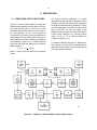
Figure 5.1 is a simplified block diagram of the
ORTEC 584 and can be used as a reference to
describe its operation.
reference level for LE is set by the front panel
Threshold control and can range from -5 mV to
-1 V. The reference level is buffered from LE by A1.
The 584 can be operated in three separate timing
modes that are selectable by a front panel locking
toggle switch. These three timing modes are
Constant Fraction (CF), Slow Rise Time Reject
(SRT), and Leading Edge (LE). The initial circuit
description will only cover CF operation. All logic
functions are implemented using ECL components
The input signal is attenuated by Rl and R2 and
delayed by the external CF Shaping Delay. The
attenuation factor is approximately f x 0.2. The
attenuated and delayed input signals are
differentially summed in the constant-fraction
amplifier, CFA. The resulting bipolar shaped signal
is fed to the zero crossing gate, G1. Note that the
CFA signal can produce an output from G1 only if
G1 is armed by the output signal from LE.
A 0 to -5 V input starts at time zero and is applied
to the leading edge discriminator, LE. The
6
Fig. 5.1. Simplified Block Diagram of the ORTEC 584
Constant Fraction Discriminator.
The CF signal crosses the logic threshold of G1 at
constant-fraction time, tcf. Constant-fraction time is
determined by the selection of the external
constant-fraction shaping delay, td(Ext), subject to the
rise times and pulse shapes of the input signals. A
fixed internal delay of about 0.8 ns must be added
to t d(Ext) to determine the total constant-fraction
shaping delay, td(Tot). Note that the time of
occurrence of the output of G1 is directly related to
t cf only if the arming signal from LE arrives at the
input of G1 prior to the negative-going excursion of
the output of CFA. If the signal from LE arrives at
G1 later in time, the output signal from G1 will have
time movement relative to the input signal. This
type of time movement is often referred to as
leading edge time walk.
Access to the inverted CF signal is provided by the
front panel CF Mon connector. This signal is
buffered by R3 and has a typical amplitude of 40
mV peak-to-peak when viewed with a 50 ohm input
impedance oscilloscope. The baseline of the CF
Mon signal has a -60 mV dc off set into 50 ohm,
and a -120 mV offset open circuit.
The G1 output signal clocks the high state at D to
the Q output of FF1. The Q output of FF1 is
delayed by DL1, inverted by A2, and applied to the
input of G6. The D input of FF2 is in the low state
since the timing mode switch in the CF position
applies a high state to the input of G3.
Note that a previous reset signal preset the Q
output of FF2 to a high state. When the G1 output
signal clocks FF2, through G4, the D input low state
is clocked to the Q output which enables G6 to pass
the timing signal from A2. The output of A2 initiates
reset for FF1 and FF2 through G5. The Q output of
FF2 is reset to a high state which produces a pulse
<10 ns wide at the output of G6.
The output signal from G6 is processed by the
output shaping circuitry. Assuming that the rear
panel switch is in the Ungated position, a high state
is present on the D inputs of FF3 and FF4. The
output of G6 clocks FF3 causing the Q output to
change states which, in turn, clocks FF4, causing
the Q output of FF4 to change states. Flip-flop FF4
is reset by A5 to produce a nominally 5-ns wide
7
pulse. This clipped pulse is furnished through
current drivers CD1 and CD2 to the timing outputs,
and to an inverting ECL-to-TTL converter to
produce the positive output. The width of the
positive output is adjustable from 0.5 µs to 2.5 µs
by a printed-wiring board mounted potentiometer.
Additional output signals are blocked by the
blocking one-shot composed of FF3, A4, C2, and
the Blocking Width control. The blocking period is
determined by the adjustable delay time to reset
FF3. The blocking period is variable from 10 ns to
1000 ns and can be monitored at the front panel
connector.
W hen operated in the Leading Edge timing mode
(LE), the timing mode switch disables G1 and G3
while enabling G2. The circuit operation is similar to
the CF mode except that the LE discriminator
output, through G2, clocks FF1 and FF2 to produce
all the output signals. The timing output signals are
no longer related in time to the zero crossing time
of the constant-fraction signal. Rather, all output
signals are related to the time the leading edge of
the input signal crosses the LE threshold level.
When operated in the Slow Rise Time Reject mode
(SRT), the timing mode switch disables G2 and
enables G1 and G3. Operation differs from the CF
only by the function of FF2. The inverted output of
the LE discriminator gates G3 causing its output to
switch to a low state on a time constant set by C1.
If the output of G3 decays below the threshold
level of FF2 prior to tcf, the unit functions the same
as in the CF mode. However, if tcf occurs prior to a
signal at the output of G3, the Q output, FF2, will
not change state when clocked by the output of G1.
Thus all output signals will be blocked at G6.
Four separate gating modes are available. A rear
panel locking toggle switch selects either Gated or
Ungated operation. When set in the Ungated
position, a high state is connected to the D inputs of
FF3 and FF4, which enables output signals to be
generated. When set in the Gated position, a
printed wiring-board jumper must be set to select
the Bin Gate (pin 36 of the NIM power connector
block), a slow positive NIM input via a rear panel
connector, or a fast negative NIM signal via the
same rear panel connector. The slow positive NIM
signal and the Bin Gate are converted to ECL signal
levels by a NIM-to-ECL converter. The fast
negative NIM signal is converted to ECL signal
levels by a fast NIM-to-ECL converter and A3. All
gating options are wired at G7.
The input power requirements are +12 V, -12 V,
-6 V, and -24 V. A rear panel switch allows use of
the -12 V supply instead of the -6 V supply to
provide the ECL logic current. These levels are all
obtained from the bin power supply. Additional
voltage levels of +5 V and -5.2 V are also required.
These voltages are obtained from regulators on the
printed wiring board.
8
6. APPLICATIONS
6.1. TIMING WITH FAST SCINTILATORS
Figure 6.1. shows a typical system for timing with
fast scintillation detectors such as Naton-136, Pilot
B, KL-236, NE-102, NE-111, NE-213, etc. A 584
Constant-Fraction Discriminator is used in each of
the two channels of the Time-to-Amplitude
Converter (TAC). Selection of the constant-fraction
shaping delay for best timing performance with a
given scintillator and PMT is usually accomplished
experimentally (Section 3.5). A useful empirical
formula for the initial trial selection of the external
shaping delay is
td(Ext) x 1.1 tr 0.8 ns
The timing resolution obtainable in a given
application with fast scintillators depends on many
variables, including the energy range selected by
the SCAs; the threshold setting, external CF Delay,
and walk adjustment of the 584; the rise time and
type of the PMT; the size and shape of the
scintillator; and the presence of noise in the system.
Typical timing resolution for a narrow dynamic
range (.1:1.1), for 60Co is 200 ps FWHM and
360 ps FWTM (Fig. 6.1.).
For additional data see Section 6.5, "References."
Also, contact your local ORTEC representative to
obtain the latest information on the state-of-the-art
in timing with fast scintillators.
where tr is the 10% to 90% rise time of the anode
pulses.
Figure 6.1. A System for Gamma-Gamma Lifetime Measurement.
9
6.2. TIMING WITH Nal(TI) SCINTILLATORS
Timing with Nal(Tl)) scintillators is similar to timing
measurements with fast scintillators. However, one
additional problem must be considered. The
photoelectron statistics for low-energy gamma-ray
applications are so poor that individual events near
the trailing edge of Nal(TI) pulses can trigger the
584. Thus a single scintillation event can produce
two or more discriminator output pulses. In the 584,
this problem is overcome by setting the Blocking
Width adjustment to 1000 ns. The 584 can also
be used successfully on longer decay scintillators,
but the maximum blocking width time may have to
be increased to prevent multiple triggering.
The timing resolution obtainable with an Na I (TI) in
a given application depends on many variables.
Typical timing resolution for a properly adjusted
system using a 1 in. x 1 in. KL-236 and an RCA
8575 PMT in the start channel, a 1 in. x 1 in. Nal(TI)
and an RCA 8575 PMT in the stop channel, and a
50:1 dynamic range with 60Co is 900 ps FWHM
and 1.9 ns FWTM.
6.3. TIMING WITH LARGE VOLUME HPGE
DETECTORS
Figure 6.2. shows a typical timing coincidence
system using a large volume HPGe detector in the
stop channel. In this application, the timing
resolution is dominated by the charge collection
characteristics of the HPGe detector. The output
signal from the HPGe detector preamplifier must be
shaped prior to processing by the 584. Either a Fast
Filter Amplifier (ORTEC Model 579) or a Timing
Filter Amplifier (ORTEC Model 474) can perform
the necessary pulse shaping. In typical applications,
the 579 is set at 200 ns differentiation time
constant and the integral time constant is set at
Out.
Figure 6.2. Gamma-Gamma Coincidence System Using a Plastic
Scintillator and a Large HPGe Coaxial Detector
10
The slow rise time reject mode is particularly useful
with HPGe detectors operated over a wide dynamic
range of energies. Operation in the SRT mode will
have minimum effect on the FWHM resolution but
can dramatically improve the FWTM and
FW(1/100)M values. The disadvantage of the SRT
mode is that the effective relative efficiency of the
HPGe detector for timing is reduced since some
events of valid energy are removed from the timing
spectra.
ORTEC conducts a continuing program aimed at
improving timing spectroscopy techniques. Please
contact your local ORTEC representative
concerning any special requirements.
The timing resolution obtainable with HPGe
detectors also depends on many variables. The
active volume of the HPGe detector is a major
factor in determining timing resolution.
The charge collection time increases as the
detector volume increases. Charge collection time
variations result in variations in the shape and rise
time of the preamplifier output signal. For this
reason, Amplitude and Rise Time Compensated
(ARC) timing is used in HPGe detector applications.
The principal difference between ARC timing and
CF timing is the selection of the CF shaping delay.
In ARC timing, the CF shaping delay selected is
less than the minimum rise time of the 579 output
signal.
The optimum CF shaping delay for an HPGe
detector is usually obtained experimentally. An
ORTEC 425A Nanosecond Delay unit can be used
to vary the shaping delay of the 584 while taking a
series of timing spectra. A typical value for the
shaping delay for a 15% HPGe detector is in the
range of 20 ns to 30 ns.
Figure 6.3. shows the timing resolution FWHM for
14 HPGe detectors ranging in size from 10% to
35% relative efficiency. Note that individual
detectors can deviate significantly from the mean
value of timing resolution.
6.4. TIMING WITH OTHER DETECTORS
The 584 can be used to provide timing information
for other detectors such as ORTEC Surface Barrier
Detectors and Low-Energy Photon Detectors. When
input signals are low level and have very fast rise
times, an ORTEC 9301 or 9305 Fast Preamplifier,
or an ORTEC 574 or 535 Quad Fast Amplifier are
recommended as accessory modules.
Fig. 6.3. Timing Resolution FWHM for 14 Detector
Systems as a Function of Efficiency for the
Energy Range 511 ± 50 keV for ‘ ’ Na.
6.5. REFERENCES
Use the following references for further information
on typical timing coincidence measurement
systems in which the ORTEC 584 ConstantFraction Discriminator can be used.
1. "Principles and Applications of Timing Spectroscopy," Application Note AN 42, ORTEC, Oak Ridge,
TN (1982).
2. T. J. Paulus, T. W. Raudorf, B. Coyne, and R. C.
Trammell, "Comparative Timing Performance of
Large Volume HPGe Germanium Detectors," IEEE
Trans. Nucl. Sci., NS-28, No. 1, pp. 544-548 (1981).
3. M. 0. Bedwell and T. J. Paulus, "A ConstantFraction Differential Discriminator for Use in Fast
Timing Coincidence Systems," IEEE Trans. Nucl.
Sci., NS-26, No. 1, p. 442 (1979).
4. M.O.Bedwell and T.J.Paulus, "A Versatile
Constant-Fraction 100-MHZ Discriminator," IEEE
Trans. Nucl. Sci., NS-25, No. 1, p. 86 (1978).
5. M. 0. Bedwell and T. J. Paulus, "A New
Constant-Fraction Timing System with Improved
Time Derivation Characteristics," IEEE Trans. Null
Sci., NS-23, p. 234 (1976).
6. G. F. Knoll, Radiation Detection and
Measurement, John Wiley and Sons, New York,
NY (1979).
11
7. FACTORY SERVICE
This instrument can be returned to the ORTEC
factory for service and repair at a nominal cost. The
ORTEC standard procedure for repair ensures that
the same quality control and checkout procedures
that are used for a new instrument will be used for
the repaired unit. Always contact Customer
Services at ORTEC, (865) 482-4411, before
sending in an instrument for repair to obtain
shipping instructions and so that the required
Return Authorization Number can be assigned to
the unit. This number should be written on the
address label and on the package.
12
Bin/Module Connector Pin Assignments For
Standard Nuclear Instrument Modules per
DOE/ER-0457T.
Pin
1
2
3
4
5
6
7
8
9
*10
*11
12
13
14
15
*16
*17
18
19
20
21
22
Function
+3 V
-3V
Spare bus
Reserved bus
Coaxial
Coaxial
Coaxial
200 V dc
Spare
+6 V
-6V
Reserved bus
Spare
Spare
Reserved
+12 V
- 12 V
Spare bus
Reserved bus
Spare
Spare
Reserved
Pin
23
24
25
26
27
*28
*29
30
31
32
*33
*34
35
36
37
38
39
40
*41
*42
G
Function
Reserved
Reserved
Reserved
Spare
Spare
+24 V
- 24 V
Spare bus
Spare
Spare
117 V ac (hot)
Power return ground
Reset (Scaler)
Gate
Reset (Auxiliary)
Coaxial
Coaxial
Coaxial
117 V ac (neutral)
High-quality ground
Ground guide pin
Pins marked (*) are installed and wired in
ORTEC’s 4001A and 4001C Modular System
Bins.