1
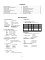
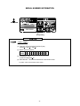
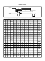
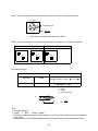
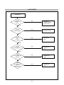
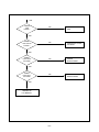
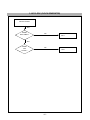
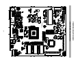
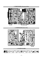
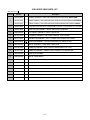
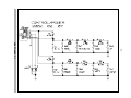
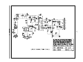
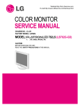
COLOR MONITOR
SERVICE MANUAL
CHASSIS NO. : CL-29
FACTORY MODEL: LN801H
ID LABEL MODEL No: L182ET
MODEL: RDT181V(BK), NX85LCD
LCD1855NX-BK
CAUTION
BEFORE SERVICING THE UNIT,
READ THE SAFETY PRECAUTIONS IN THIS MANUAL.
DiamondPoint NX85LCD
MITSUBIS
HI
CONTENTS
SPECIFICATIONS ................................................... 2
SERIAL NUMBER INFORMATION ......................... 4
PRECAUTIONS ....................................................... 5
TIMING CHART ....................................................... 6
OPERATING INSTRUCTIONS ................................ 7
WIRING DIAGRAM ................................................. 8
BLOCK DIAGRAM ................................................... 9
DESCRIPTION OF BLOCK DIAGRAM...................10
ADJUSTMENT ...................................................... 12
INSPECTION.......................................................... 17
TROUBLESHOOTING GUIDE .............................. 22
PRINTED CIRCUIT BOARD................................... 27
EXPLODED VIEW...................................................30
REPLACEMENT PARTS LIST ...............................32
PIN CONFIGURATION............................................37
SCHEMATIC DIAGRAM ......................................... 39
SPECIFICATIONS
1. LCD CHARACTERISTICS
Type
: TFT SXGA LCD
Size
: 18inch
Pixel Pitch
: 0.2805(H) x 0.2805(V)
Color Depth
: 8-bit, 16,777,216 colors
Electrical Interface
: LVDS
Surface Treatment
: Anti-Glare, Hard Coating(3H)
Operating Mode
: Normally Black
Backlight Unit
: Six-CCFL (Cold Cathode
Fluorescent Lamp)
2. OPTICAL CHARACTERISTICS
2-1. Viewing Angle by Contrast Ratio
Left
: -60° min., -80°(Typ)
Right : +60° min., +80°(Typ)
Top
: +60° min., +80°(Typ)
Bottom : -60° min., -80°(Typ)
4-1. Power Adaptor(Built-in Power)
Input
: AC 100~240V, 50/60Hz , 1.0A
4-2. Power Consumption
MODE
≥ 10
2-2. Luminance
: 200(min), 250(Typ)
2-3. Contrast Ratio
: 200(min), 350(Typ)
3. SIGNAL (Refer to the Timing Chart)
3-1. Sync Signal
• Type
: Separate, Positive/Negative
Composite, SOG (Sync On Green)
Digital
3-2. Video Input Signal
1) Type
2) Voltage Level
a) Color 0, 0
b) Color 7, 0
c) Color 15, 0
3) Input Impedance
4. POWER SUPPLY
: R, G, B Analog
: 0~0.71 V
: 0 Vp-p
: 0.467 Vp-p
: 0.714 Vp-p
: 75 Ω
H/V SYNC VIDEO POWER CONSUMPTION LED COLOR
POWER ON (NORMAL)
ON/ON
ACTIVE
less than 53 W
GREEN
STAND-BY
OFF/ON
OFF
less than 3 W
AMBER
SUSPEND
ON/OFF
OFF
less than 3 W
AMBER
DPMS OFF
OFF/OFF
OFF
less than 3 W
AMBER
POWER S/W OFF
-
-
less than 2 W
OFF
5. ENVIRONMENT
5-1. Operating Temperature: 5°C~35°C (41°F~95°F)
(Ambient)
5-2. Relative Humidity
: 10%~80%
(Non-condensing)
5-3. MTBF
: 50,000 Hours(Min)
6. DIMENSIONS (with TILT/SWIVEL)
Width
Depth
Height
: 406 mm (15.98'')
: 215 mm (8.46'')
: 427 mm (16.81'')
7. WEIGHT (with TILT/SWIVEL)
Net. Weight
Gross Weight
3-3. Operating Frequency
Horizontal
: 30 ~ 80kHz
Vertical
: 56 ~ 85Hz(Limited to 75Hz by EDID)
-2-
: 8.2kg (18.08 lbs)
: 11kg (24.25 lbs)
Signal Connector Pin Assignment
• DVI-D Connector (Digital)
1
9
17
8
16
24
Pin
1
2
3
4
5
6
7
8
9
10
11
12
13
14
15
Signal (DVI-D)
T. M. D. S. Data2T. M. D. S. Data2+
T. M. D. S. Data2/4 Shield
T. M. D. S. Data4T. M. D. S. Data4+
DDC Clock
DDC Data
NOT USED
T. M. D. S. Data1T. M. D. S. Data1+
T. M. D. S. Data1/3 Shield
T. M. D. S. Data3T. M. D. S. Data3+
+5V Power
Ground (return for +5V,
Pin
16
17
18
19
20
21
22
23
24
Signal (DVI-D)
Hot Plug Detect
T. M. D. S. Data0T. M. D. S. Data0+
T. M. D. S. Data0/5 Shield
T. M. D. S. Data5T. M. D. S. Data5+
T. M. D. S. Clock Shield
T. M. D. S. Clock+
T. M. D. S. Clock-
H. Sync. and V. Sync.)
T. M. D. S. (Transition Minimized Differential Signaling)
-3-
SERIAL NUMBER INFORMATION
206100001
Overprinting
: Y MM C SSSSS
(1) (2) (3)
(4)
(1) : Year code of Production(Last Number of year)
ex)2000
0, 2001
1, 2002
2
(2) : Month code of Production
Month
Number
1 2 3 4 5 6 7 8 9 10 11 12
01 02 03 04 05 06 07 08 09 10 11 12
(3) : Classification code
ex) RDT181V(BK) Model
1
(4) : Serial Number : This Serial number doesn’t reset at each month.
ex) 00001~01234, 01235~99999, 00001~00010.....
-4-
PRECAUTION
WARNING FOR THE SAFETY-RELATED COMPONENT.
WARNING
• There are some special components used in LCD
monitor that are important for safety. These parts are
marked on the schematic diagram and the
replacement parts list. It is essential that these critical
parts should be replaced with the manufacturer’s
specified parts to prevent electric shock, fire or other
hazard.
• Do not modify original design without obtaining written
permission from manufacturer or you will void the
original parts and labor guarantee.
TAKE CARE DURING HANDLING THE LCD MODULE
WITH BACKLIGHT UNIT.
• Must mount the module using mounting holes arranged
in four corners.
• Do not press on the panel, edge of the frame strongly
or electric shock as this will result in damage to the
screen.
• Do not scratch or press on the panel with any sharp
objects, such as pencil or pen as this may result in
damage to the panel.
• Protect the module from the ESD as it may damage the
electronic circuit (C-MOS).
• Make certain that treatment person’s body are
grounded through wrist band.
• Do not leave the module in high temperature and in
areas of high humidity for a long time.
• The module not be exposed to the direct sunlight.
• Avoid contact with water as it may a short circuit within
the module.
• If the surface of panel become dirty, please wipe it off
with a softmaterial. (Cleaning with a dirty or rough cloth
may damage the panel.)
CAUTION
Please use only a plastic screwdriver to protect yourself
from shock hazard during service operation.
-5-
BE CAREFUL ELECTRIC SHOCK !
• If you want to replace with the new backlight (CCFL) or
inverter circuit, must disconnect the AC adapter
because high voltage appears at inverter circuit about
650Vrms.
• Handle with care wires or connectors of the inverter
circuit. If the wires are pressed cause short and may
burn or take fire.
TIMING CHART
VIDEO
B
A
E
C
D
SYNC
F
<< Dot Clock (MHz), Horizontal Frequency (kHz), Vertical Frequency (Hz), Horizontal etc... (µs), Vertical etc... (ms) >>
Mode
1
2
3
4
5
6
7
8
9
10
11
12
13
14
15
16
H/V
Sort
Sync
Polarity
H
+
V
–
H
–
V
H
+
–
V
–
H
–
V
H
–
–
V
–
H
–
V
–
H
+
V
+
H
+
V
+
H
+
V
+
H
+
V
+
H
–
V
–
H
–
V
–
H
–
V
–
H
+
V
+
H
+
V
+
H
+
V
+
Dot
Clock
28.324
28.324
25.175
30.240
31.500
31.500
36.000
40.000
50.000
49.500
57.283
65.0
75.000
78.750
108.000
135.000
Frequency
Total Period Video Active Time
(E)
(A)
Back Porch
(F)
Sync Duration
(D)
Front Portch
(C)
31.469
900
720
54
108
18
70.082
449
350
60
2
37
31.469
900
720
54
108
18
70.082
31.469
449
800
400
640
35
48
2
96
12
16
59.940
525
480
33
2
10
35.000
864
640
96
64
64
66.670
37.861
525
832
480
640
39
128
3
40
3
24
72.809
520
480
28
3
9
37.500
840
640
120
64
16
75.000
500
480
16
3
1
35.156
1024
800
128
72
24
56.250
625
600
22
2
1
37.879
1056
800
88
128
40
60.317
628
600
23
4
1
48.077
1040
800
64
120
56
72.188
666
600
23
6
37
46.875
1056
800
160
80
16
75.000
625
600
21
3
1
49.725
1152
832
224
64
32
74.550
667
624
39
3
1
48.363
1344
1024
160
136
24
60.004
806
768
29
6
3
56.476
1328
1024
144
136
24
70.069
806
768
29
6
3
60.023
1312
1024
176
96
16
75.029
800
768
28
3
1
63.981
1688
1280
248
112
48
60.020
1066
1024
38
3
1
79.976
1688
1280
248
144
16
75.025
1066
1024
38
3
1
-6-
Resolution
720x350
70Hz
720x400
70Hz
640x480
60Hz
640x480
66Hz
640x480
73Hz
640x480
75Hz
800x600
56Hz
800x600
60Hz
800x600
72Hz
800x600
75Hz
832x624
75Hz
1024x768
60Hz
1024x768
70Hz
1024x768
75Hz
1280x1024
60Hz
1280x1024
75Hz
OPERATING INSTRUCTIONS
FRONT VIEW
REAR VIEW
DiamondPoint NX85LCD
Power Connect
MITSUBIS
HI
Front Control Panel
DVI Connect
D-Sub Signal
Connect
Front Control Panel
6
3
4
1. Power ON/OFF Button
Use this button to turn the monitor on or off.
1
2
4. ▼▲◀▶ Button
2. Power Indicator
This indicator lights up green when the monitor
operates normally. If the display is in DPM(Energy
Saving)mode, this indicator color change to amber.
Use these buttons to choose or adjust items in the On Screen
Display.
5. AUTO/SELECT Button
Automatically adjust vertical position, horizontal position, pixel
clock and phase.
Use this button to enter a selection in the On Screen Display.
3. MENU Button
Use these buttons to enter or exit the On Screen Display.
5
6. SOURCE Button
Use this button to make Dsub or DVI connector active.
This feature is used when two computers are connected to the
monitor. The default setting is Dsub.
-7-
WIRING DIAGRAM
Connector Ass’y P/N: 6631T25008Q
MAIN PCB
Connector Ass’y P/N:
6631T20015R
P902
J705
J801
MATAL FRAME
J702
J710
Connector Ass’y P/N:
6631T20008U
CN1
CN3
CN2
CN7
CN6
CN4
CN5
CN_C02
CN_C01
CN301
MODULE
Connector Ass’y P/N: 6631T11012P
-8-
Module CTL
Power CTL
Inverter CTL
LCD Module
12V
R,G,B
differential
Micom
68HC08-BD48
Inverter
3.3 VM
(KM416S102BT)
(LVD S823)
Out - CLK
DE ,H/V Sync out
M-CLK Address Data 48 Bit
Power Board
-9-
12V
H/V-S ync
5V
H/V Sync
D-SUB
5V
5V
2.5V
Reg.
3.3V
Reg.
3.3V
Reg.
DVDD2.5V
AVD D2.5V
PVDD 3.3V
3.3 VM
DVDD 3.3V
AVD D 3.3V
5V
R,G,B /Odd
Gm5020
including
(ADC / TMDS Rx )
AVD D3.3V
AVD D2.5V
Digital Signal
R,G,B
DVI-D
BLOCK DIAGRAM
H/V Sync
12V
Memory
LVDS
DESCRIPTION OF BLOCK DIAGRAM
1. Video Controller Part(GM5020).
This part amplifies the level of video signal for the anolog to digital conversion and converts from the analog video
signal to the digital video signal using a pixelclock.
The pixel clock for each mode is generated by the PLL.
The range of the pixel clock is from 25MHz to 135MHz.
This part consists of the Scaler and frame buffers which converts frame rate of input signal to 60Hz frame rate.
The Scaler gets the video signal converted analog to digital, interpolates input to1280 X 1024 resolution signal and
outputs 8-bit R, G, B signal to transmitter.
Especially pre-amp / ADC / Video controller are merged to one chip ‘Gm5020’ by Genesis.
Also FRC is separate.
2. Display Data Transmitter Part(LVDS).
This part transmit digital signal from the Scaler to the receiver of module.
3. Power Part.
This part consists of the one 5V, two 3.3V and one 2.5 regulators to convert power which is provided 12V, 5V in
Power Board.
12V is provided for inverter and LCD Panel, 5V is provided for Micom.
Also, 5V is converted 3.3V and 2.5V by regulator. Converted power is provided for IC in the main board.
4. MICOM Part.
This part consists of EEPROM IC which stores control data, Reset IC and the Micom.
The Micom distinguishes polarity and frequency of the H/V sync are supplied from signal cable.
The controlled data of each modes is stored in EEPROM.
5. Inverter
The inverter converts from DC12V to AC 600Vrms and operate back-light lamp of module.
- 10 -
12V
50 ~ 60Hz
EMI
COMPONENTS
INPUT RECTIFIER
AND FILTER
HVDC
ENERGY
TRANSFER
100KHz
OUTPUT RECTIFIER
AND FILTER
5V
GND
LINE
100 ~ 240V
PWM CONTROL
CIRCUIT
PHOTO-COUPLER
ISOLATION
SIGNAL
COLLECTION
SECONDA RY
PRIMARY
Operation description_Power
1. EMI components.
This part contains of EMI components to comply with global marketing EMI standards like FCC, VCCI CISPR,
the circuit included a line-filter, across line capacitor and of course the primary protection fuse.
2. Input rectifier and filter.
This part function is for transfer the input AC voltage to a DC voltage through a bridge rectifier and a bulk capacitor.
3. Energy Transfer.
This part function is transfer the primary energy to secondary through a power transformer.
4. PWM control circuit.
This part function is to make a pulse width modulation control and to provide the driver signal to power switch, to
adjust the duty cycle during different AC input and output loading condition to achieve the dc output stabilize, and
also the over power protection is also monitor by this part.
5. Photo-Coupler isolation.
This part function is to feed back the dc output changing status through a photo transistor to primary controller to
achieve the stabilized dc output voltage.
6. Signal collection.
This part function is to collect the any change from the dc output and feed back to the primary through photo
transistor.
7. Output rectifier and filter.
This part function is to achieve the dc output voltage stabilize.
- 11 -
ADJUSTMENT
1. Application
This specification shall be applied to the adjustment and inspection of the LN801H.
2. Adjustment Setup
All adjustment are thoroughly checked and corrected when the monitor leaves the factory, but sometimes several
minor adjustment may be required.
Adjustment should be following procedure and after more than 30 minutes.
Unless otherwise specified, adjustment shall be carried out under the following conditions.
- Input Power: 100~240V /50~60Hz
- Input Signal: 1280 X1024 @ 60Hz default
- Aging Time: More than 30 Minutes
- Aging Temperature: 10~35 degrees
- Adjustment equipment and equipment connection setup.
Refer to figure 1.
VG819 or equivalent,
1) IBM compatible PC
2) Adjustment program for LN801H.
3) Adapter Box
A
9
IBM
Compatible PC
Video Signal
Generator
15
10
5
11
6
1
6
1
5
C
13
se
d
PARALLEL PORT
tu
23
2C
No
RS
5V
14
ON
LL
EL
F
RA
C
PA
5V
Power inlet (required)
ON
WE
R
220
VG
CS
T
PO
S
MO
NI
TO
R
B
4.7K
OFF
74LS06
E ST Switch
B
F V-Sync On/Off Switch
(Switch must be ON.)
Figure 1. Cable Connection
- 12 -
4.7K
4.7K
5V
E
YN
A
Power Select Switch
(110V/220V)
Power LED
V-S
Control Line
1
25
OFF
74LS06
3. Adjustment
3-1. Initialization and Aging
Prior to adjustment of this model, more than 30 minutes of aging shall be carried out.
1) Display any pattern at any Mode.
2) Run adjustment program for LN801H on the IBM compatible PC.
<<
DIST. ADJ
LCD IIC ADJUST.
COLOR ADJ
PROGRAM
COMMAND
:LCD185~1. DAT >>
EDIT
EEPROM
MENU Move : Arrow or Space
QUIT
MENU Select : Enter
3) Select EEPROM → ALL INIT command and Enter.
<<
DIST. ADJ
LCD IIC ADJUST.
COLOR ADJ
PROGRAM
COMMAND
:LCD185~1. DAT >>
EDIT
EEPROM
QUIT
ALL
Init.
EDID(A) WR
EDID(D) WR
EDID Read
EEPROM Read
MENU Move : Arrow or Space
MENU Select : Enter
Quit : ESC
4) This will make all data to default state and make aging mode.
5) Remove signal cable from the monitor.
- 13 -
3-2. Adjustment of Factory Preset Mode.
1) It’s not necessary for preset mode adjustment.
All preset mode data shall be written to EEPROM at initial power on.
2) IMPORTANT
At the initial Power turn on, maintain power on status more than 3 seconds.
3-3. Adjustment for White Balance
1) Display (Full black pattern) at SXGA 60Hz.
2) Set External Bright to MAX position and Contrast to 80 Position.
3) Select COLOR ADJ → BIAS CAL command and Enter.
<<
DIST. ADJ
LCD IIC ADJUST.
COLOR ADJ
BIAS
DRIVE
PROGRAM
COMMAND
:LCD185~1. DAT >>
EDIT
EEPROM
QUIT
CAL
CAL
MENU Move : Arrow or Space
MENU Select : Enter
Quit : ESC
4) No attempt to manually adjust, BIAS data is automatically adjusted and saved to the EEPROM.
If the message of "AUTO OK OK" is displayed at front of screen,
The adjustment is succeeded.
If the message of "AUTO ERROR" is displayed at front of screen, because the adjustment is failed, do adjust
again.
5) Display (Full white pattern) at SXGA 60Hz.
6) Select DRIVE CAL command and Enter.
<<
DIST. ADJ
LCD IIC ADJUST.
COLOR ADJ
BIAS
DRIVE
MENU Move : Arrow or Space
PROGRAM
COMMAND
:LCD185~1. DAT >>
EDIT
EEPROM
QUIT
CAL
CAL
MENU Select : Enter
Quit : ESC
7) 6500K and 9300k are automatically adjusted and saved to the EEPROM.
If the message of "AUTO OK OK" is displayed at front of screen,
The adjustment is succeeded.
If the message of "AUTO ERROR" is displayed at front of screen, because the adjustment is failed. So do
adjust again.
- 14 -
8) Select PRESET EXIT command and Enter.
<<
DIST. ADJ
LCD IIC ADJUST.
COLOR ADJ
PROGRAM
COMMAND
:LCD185~1. DAT >>
EDIT
EEPROM
QUIT
PRESET START
PRESET EXIT
MENU Move : Arrow or Space
MENU Select : Enter
Quit : ESC
3-4. Adjustment for EDID
Use this procedure only when there is some problem on EDID data.
1) Connect the D-sub cable.(For Analog EDID)
2) Select EEPROM → EDID<A> WR command and Enter.
<<
DIST. ADJ
LCD IIC ADJUST.
COLOR ADJ
PROGRAM
COMMAND
:LCD185~1. DAT >>
EDIT
EEPROM
QUIT
ALL
Init.
EDID(A) WR
EDID(D) WR
EDID Read
EEPROM Read
MENU Move : Arrow or Space
MENU Select : Enter
Quit : ESC
3) Connect the DVI to D-sub cable.(For Digital EDID)
4) Select EEPROM → EDID<D> WR command and Enter.
<<
DIST. ADJ
LCD IIC ADJUST.
COLOR ADJ
PROGRAM
COMMAND
:LCD185~1. DAT >>
EDIT
EEPROM
QUIT
ALL
Init.
EDID(A) WR
EDID(D) WR
EDID Read
EEPROM Read
MENU Move : Arrow or Space
MENU Select : Enter
Quit : ESC
- 15 -
* How to change the EDID (Serial No. etc.)
1. Operate adjustment Program
2. Select EDID INFO of the EDID Menu for Analog EDID and DDC INFO for Digital EDID.
3. First. You can see the blank screen, and press "Enter" key and you can see the EDID Contents
4. Choose the Data to be changed, and press "Enter" Key.
5. After changing the Data, Press "Enter"
If more and more to be changed, go back to 4 and repeat.
6. To save and end the changed, press "F10" Key
Not to do that, Press "Esc"
<<
DIST. ADJ
LCD IIC ADJUST.
COLOR ADJ
PROGRAM
:LCD185~1. DAT >>
COMMAND
EDIT
EEPROM
QUIT
MODEL SAVE
MODEL SEL.
EDID INFO
DDC INFO
MENU Move : Arrow or Space
<<
DIST. ADJ
MENU Select : Enter
LCD IIC ADJUST.
COLOR ADJ
PROGRAM
COMMAND
Quit : ESC
:LCD185~1. DAT >>
EDIT
EEPROM
QUIT
EDID
0
1
2
3
4
5
6
7
8
9
A
B
C
D
E
F
0
00
FF
FF
FF
FF
FF
FF
00
34
AC
38
46
01
01
01
01
1
00
0C
01
03
68
24
1D
78
EA
0A
25
A2
57
4B
99
24
2
18
50
54
BF
EF
80
81
80
81
40
71
4F
01
01
01
01
3
01
01
01
01
01
01
30
2A
00
98
51
00
2A
40
30
70
4
13
00
67
1F
11
00
00
1E
00
00
00
FD
00
38
4B
1F
5
53
0E
00
0A
20
20
20
20
20
20
00
00
00
FC
00
4E
6
58
38
35
4C
43
44
0A
20
20
20
20
20
00
00
00
FF
7
00
32
30
36
30
30
30
30
30
31
0A
20
20
20
00
56
Don’t save & Exit : Esc key
Edit : Enter key
Save & Exit : F10 key
"32 30 36 30 30 30 30 30 31" shows S/No.
By changed ASCII Code, S/No equals 20600001.
- Information of S/No on the EDIDFind character string "00 00 00 FF 00" on EDID Data.
From next string of the above to "0A" is S/No.
Here, you should take care of this S/No composed by "ASCII Code"
FYI,
30H equals to 0, 31H equals to 1, … 39H equals to 9.
More information, refer to ASCII Code Table.
- 16 -
INSPECTION
1. PERFORMANCE INSPECTION
NO.
ITEMS
2
Luminance
PATTERN
Full White
INSPECTION
CRITERIA
Check Luminance on 255 g rey level
200(min.), 250(typ.)
Cd/m2 at the center
1) Measure luminance at each point
(5 point) on brightness/contrast
max condition.
2) Calculate l/u with formula.
3
Luminance
Uniformity
B2
Full White
B3
B4
B5
[B max - B min]
B max
4
White
Balance
Full White
75 % (max.)
B1
X 100
%
1) Measure color coordinate at each
color temperature. (6500k & 9300k)
2) Measure color coordinate on R,G,B
if required.
Check wattage and LED color at each
mode
5
6
DPM
DDC 2B
Full White
All Mode
All Mode
1) Normal mode (H/ V: on/on)
2) Stand-by mode (H/ V : off/on)
3) Suspend mode (H/ V : on/off)
4) DPM off mode (H/ V : off/off)
5) Power s/w off mode
Display EDID data from memory and
Compare with standard EDID format for
LN801H.
- 17 -
6500k,
Wx=0.313
Wy=0.329
9300k,
Wx=0.281
Wy=0.311
0.03
0.03
0.03
0.03
1)
53 W, Green
2)
3 W, Amber
3)
3 W, Amber
4)
3 W, Amber
5)
2W
2. COSMETIC INSPECTION
1.1 DOT DEFECT
This criteria is based on ISO-13406-2 Pixel Faults Class II
Items
Criteria
Horizontally adjacent 2 dots (R+G, G+B)
1) Bright Dots
2) Dark Dots
Adjacent Dots
Horizontally, vertically or combined adjacent 3 dots
(separately bright dots and dark dots)
3) Bright Dots
4) Dark Dots
Dot Defect
Max. 3
Max. 3
Not Allowed
Remarks
Note 1
Note 2
Note 3
Not Allowed
5) Dot defect except 1), 2)
R or G or B (Bright Dot + Dark Dot)
Max. 7
Note 4
Max. 2 for each
Note 5
color
Distance between 6) s : less than 10mm
Not Allowed Note 6
Two or more pixels or sub-pixels with more than one fault of 5) Max. 3
Note 7
Two or more pixels or sub-pixels with more than one fault of 1)
Not Allowed Note 8
Two or more pixels or sub-pixels with more than one fault of 2)
6) Distance between bright dots Distance between bright dots (R - R): less than 6.5mm
Min. Distance
7) Distance between 6) s
between bright dots
8) Fault cluster
Total amount of Dot Total amount of Bright Dot (R,G,B) and Dark Dot (R,G,B)
Defects
Total amount of Bright Dot (G)
Note 9. Every dot herein means sub-pixel (each Red, Green or Blue color)
Max. 15
-
Max. 6
-
Note 10. Bright & Dark Dots are larger than one third of sub-pixel. (Dots smaller than one third of sub-pixel are not counted as a defect dots.)
Note 11. Do not use the [ND] filter in counting a bright dot.
: Bright
Dot
: Dark
Dot
Note 1. Horizontally adjacent 2 dots (R+G, G+B)
Count as horizontally adjacent 2 dots
RG
GB
RG
GB
Do not count as adjacent 2 dots
RG
RG
RG
RG
RG
RG
etc.
Combination
with Bright
& Dark Dot
Combination except horizontally
adjacent 2 dots.
- 18 -
Note 2. 1) + 2) : Max. 3
Note 3.Horizontally, vertically or combined adjacent 3 dots
( separately bright dots and dark dots)
Count as adjacent 3 dots
Do not count as adjacent 3 dots
Note 4.Do not count the horizontally adjacent 2 dots (R-G, G-B)
Note 5. Distance between bright dots
Count as defect
R
R
G
G
Do not count as defect
B
B
Distance between the same color
R
R
G
G
B
B
Combination with Bright Dot & Dark
Dot
R
G
G
B
B
R
Combination with the different color
Note 6. Distance between the g roup of 6)’s.
Count as defect
R
R
R
R
G
G
G
- 19 -
G
B
B
B
B
Note 7.Two or more pixels or sub-pixels with more than one fault of 5) within 5x5 pixels
5x5 pixels
Dot Defect (5)
1 Cluster
The number of cluster within all screen : Max. 3
Note 8.Two or more pixels or sub-pixels with more than one fault of 1) or 2) within 5x5 pixels
Count as defect
5x5 pixels
RG
Do not count as defect
5x5 pixels
RG
5x5 pixels
RG
RG
RG
RG
1.2 Polarizer Defects
Items
Criteria
Scratches
Linear
Dent
Circular
0.01
W
0.2
0.05, 1.0
D
10.0, N
L
0.5, N
4
4
W : Width
L : Length
D : Average diameter
b
a
D=
a+b
2
Note
a . Average Diameter
b. Linear : a
2b , Circular : a 2b
c. Extraneous substances which can be wiped out, like Finger Print, Particles, are not considered
as a defect.
d. Defects which is on the Black Matrix(outside of Active Area) are not considered as a defect.
- 20 -
1.3 Foreign Material
Items
Criteria
W
0.03
Linear
Foreign
Material
0.03
W
0.3
L
0.2
Circular
0.1
0.152, (Bright),
D
D
0.10(Dark),
3.0, N
4
1.0(White/Dark),
1.3(Gray), N
10
W : Width
L : Length
D : Average diameter
b
a
Note
a. Average Diameter
b. Linear : a
2b ,
D=
Circular : a
a+b
2
2b
1.4 Line Defect
All kinds of line defects such as vertical, horizontal or cross are not allowed.
1.5 Bezel Appearance
Scratches, minor bents, stains, particles on the LCD Bezel frame are not considered
as a defect.
1.6 Display tilt and Position difference
Any part of image must not be missed by the position dif ference or the display tilt.
L1, L1 , L2, L2 , L3, L3 , L4, L4
L1
0
L1
L2
L4
Monitor Bezel
Image Area
L2
L4
L3
L3
- 21 -
TROUBLESHOOTING GUIDE
1. NO POWER
NO POWER
(POWER INDICATOR OFF)
CHECK J801
INPUT VOLTAGE
(12V) ?
NO
TROUBLE IN
BULT-IN POWER
NO
TROUBLE IN
BULT-IN POWER
NO
TROUBLE IN
U501 or X501
YES
CHECK J801
5VST VOLTAGE
(5V) ?
YES
CHECK
U501’s PIN 6.
IS THIS PIN
OSCILLATED?
YES
TROUBLE
SOMEWHERE ELSE
- 22 -
2. NO RASTER
NO RASTER
CHECK
J702 PIN 1, 2, 3
(12V) ?
NO
TROUBLE IN
POWER ADATER
or L703, L704
YES
CHECK
J702 PIN 8 (5V) ?
NO
TROUBLE IN
INVON PATTERN
NO
TROUBLE IN
X501
NO
TROUBLE IN
U201
NO
TROUBLE IN
U201
NO
TROUBLE IN
U201
YES
CHECK
X501
H. PULSE ?
YES
CHECK
U201(GM5020) ?
YES
CHECK
L201, L202, L203
PULSE?
YES
CHECK
U301, U302, U303
PIN 35
MEMORYCLK?
- 23 -
YES
CHECK
L204
PULSE ?
NO
TROUBLE IN
U201
NO
CHECK DOT CLOCK
PATTERN
NO
CHECK
DVS PATTERN
NO
CHECK
DHS PATTERN
YES
CHECK
U401 PIN 10
PULSE ?
YES
CHECK
U401 PIN 8
V.PULSE?
YES
CHECK
U401 PIN 7
V.PULSE?
YES
TROUBLE IN
LCD MODULE
- 24 -
3. NO CLOCK (CLOCK GENERATOR)
NO DOT CLOCK
YES
CHECK
X201 24MHz ?
NO
TROUBLE IN
X201
NO
TROUBLE IN
U201
YES
CHECK
L201
CLOCK ?
- 25 -
4. TROUBLE IN DPM
TROUBLE IN DPM
CHECK
R233, R234?
NO
CHECK PC
PC IS NOT GOING
INTO DPM OFF MODE
YES
CHECK
U501 PIN 6
WAVEFORM
(24MHz) ?
NO
TROUBLE IN
X501
NO
TROUBLE IN
SIGNAL CABLE
YES
CHECK
U501 PIN 11
(0V) ?
YES
TROUBLE IN PC
- 26 -
J801
L821
C850
U802
C817
C409
20
50
R746
R702
C517
R520
R517
C707
R515
R510
R582
R545
RA210
CA211
RA208
CA210
CA209
RA206
RA204
CA208
CA207
RA226
R236
RA227
50
1
R508
RA228
RA229
U401
1
L401
10
10
RA231
RA232
10
C503
C842
C872
C873
R514
RA202
RA212
RA233
RA234
RA235
C278
L206
RA240
C526
J706
30
30
J705
20
30
20
20
U301
U302
U303
C302
Q703
C318
RA238
C408
RA239
C841
C870
C160
R152
C825
C276
C152
R222
C280
R130
R220
C279
R221
L207
Q704
C301
RA230
50
1
RA241
50
PRINTED CIRCUIT BOARD
C845
R809
R810
R406
1
1. MAIN BOARD (Component Side)
L820
L810
C531
C844
U821
R807
L811
U503
C834
10
RA225
60
RA242
1
J702
C840
R581
C413
CA202
RA214
C161
R719
C533
R132
R713
R122
R224
R225
R219
R596
C548
RA236
L403
D504
40
30
80
90
100
C516
CA212
RA216
C229
R594
70
D503
J802
C871
R133
C106
R714
R731
D746
C822
C107
R129
C151
Q103
R223
ZD703
U509
C729
ZD722
R741
R740
ZD721
J710
1
C410
CA203
L402
CA204
W
R543
CA206
CA205
C230
X201
R595
R712
Y
RA218
R235
R705
D704
V
RA220
T
RA222
N
RA224
C271
C261
R704
D703
U
R544
C260
C258
C270
C259
F
R703
G
D702
R
MODEL:LD803H
D730
D701
P
DATE :2002.05.08
U201
P/N :6870T494A11/A21
C201
C202
C203
C204
C205
C206
Q102
R716
B
D731
M
R542
C828
U105
R131
R715
E
- 27 -
L
C701
C1
R586
C532
D501
R822
R585
R727
C728
L805
R744
R730
R742
R743
J704
ZD705
D
R745
R502
C831
L804
U504
R587
R729
K
R701
C502
R718
R588
ZD701
R726
C727
J
C706
R501
U502
D747
D739
D744
D738
D736
D745
U820
D734
D742
X501
U110
ZD712
D740
D732
D743
D737
H
C521
C501
D741
D735
C
C522
U803
U804
R753
D733
10 11 12 13 14 15 16 17 18 19 20
9
8
7
6
5
4
3
2
1
U501
C843
R821
R824
J708
A
R752
ZD702
D502
C715
R218
ZD704
R593
C714
R711
CA201
R597
ZD711
RA237
C861
R540
1
R523
R528
40
R529
R830
R828
R829
R820
R811
R819
R541
C510
R519
C710
R817
R813
L703
R518
R818
L704
R812
C740
R522
C511
C530
R516
10
C513
R827
R815
C833
R831
R826
R531
C832
C520
R534
R538
R536
R535
30
R816
R814
R505
R539
R580
C508
R537
C824
C830
C506
R527
C827
C505
C519
C826
R564
C504
C823
R526
R513
R525
20
R512
C507
R511
R524
C515
C514
C274
C238
C272
C257
L204
C275
C237
L203
C236
C273
C233
C269
R240
C240
C239
C226
C264
C222
C265
C218
R234
C219
C214
L205
C224
C231
C835
C232
C836
C220
C818
L201
L822
C412
C212
C208
L202
C216
C210
C262
C225
C217
C223
R233
R825
C234
C227
R239
C235
R202
R201
- 28 -
C228
C215
C221
L823
C860
C213
C209
C411
C211
C820
C263
C207
R237
R232
R238
C405
C407
R208
C406
R209
R405
R211
R402
C316
C310
C314
C402
C309
R215
R203
R210
R205
C731
C730
C738
R732
C311
C312
R207
R206
C404
R401
C313
R216
C401
C317
C315
R214
R204
R404
R403
R212
R213
C305
C306
C308
C304
C303
C819
C307
C403
2. MAIN BOARD (Solder Side)
C829
3. POWER BOARD (Component Side)
4. POWER BOARD (Solder Side)
5. CONTROL BOARD
R1
R8
R2
R3
C1
G
C2
A
G
SW5
- 29 -
SW6
SW7
LED1
SW4
R4
SW3
R6
SW2
R5
SW1
R7
J1
A
SW8
EXPLODED VIEW
a
a
b
16
3
12
15
10
11
9
14
4
13
8
6
7
c
2
5
1
- 30 -
EXPLODED VIEW PARTS LIST
* Note: Safety mark
Ref. No.
Description
Part No.
3091TKL044E
CABINET ASSEMBLY, LN801H NMV 3090TKL045 BK-EP94(JAPAN) -RDT181V(BK)
3091TKL044F
CABINET ASSEMBLY, LN801H NMV 3090TKL045A -EP94(BLACK)NEC-NORTH AMERICA-LCD1855NX-BK
3091TKL044C
CABINET ASSEMBLY, LN801H NMV 3090TKL045A EP94(BLACK)Mitsubishi-NORTH AMERICA- NX85LCD
2
6304FLP034A
LCD(LIQUID CRYSTAL DISPLAY), LM181E06-A4M1 LG PHILPS TFT COLOR SXGA 18.1" LVDS SMM
3
3809TKL025E
BACK COVER ASSEMBLY, LN801H 3808TKL030 EP94(BLACK)
4
3043TKK099A
TILT SWIVEL ASSEMBLY, LN801H . NMV BLACK
5
6871TST287A
PWB(PCB) ASSEMBLY, SUB, LB800H CONTROL TOTAL BRAND
6
6631T11012P
CONNECTOR ASSEMBLY, 30P H-H 100MM UL20276 PANEL LINK LB886F
7
6633TZA011D
INVERTER ASSEMBLY, LG-PHILIPS NMC1805A-2 6-LAMPS,18" NMV
8
4951TKS078H
METAL ASSEMBLY, FRAME MAIN - LN801H E06
9
6871TMT326A
PWB(PCB) ASSEMBLY, MAIN, LN801H ALRDG BRAND CL-29 TOTAL
10
6871TPT228A
PWB(PCB) ASSEMBLY, POWER, LN801H POWER TOTAL BRAND NMV
11
4814TKK187A
SHIELD, REAR LB886F
12
4950TKK429A
METAL, REAR LB800H
13
3550TKK282A
COVER, LN801H PIECE VESA BLACK
14
3550TKK283A
COVER, LN801H HINGE BLACK
15
6850TD9001M
CABLE, D-SUB, UL 2990-9C(7.5) DT 1870MM BLACK(9930) NMV 18" DM
16
6866TDV004M
CABLE, DVI, UL20276 DT 2000MM BLACK(9930) NMV 18" DM -ONLY JAPAN
a
1SZZTER001H
1
SCREW, DRAWING, D3.0 L10.0 MSWR/BK .
b
332-113S
SCREW, DRAWING, D3.0 L12.0 MSWR/BK .
c
332-105G
SCREW, DRAWING, PVS+4*10(MSWR/BK)
- 31 -
REPLACEMENT PARTS LIST
CAUTION: BEFORE REPLACING ANY OF THESE COMPONENTS,
READ CAREFULLY THE SAFETY PRECAUTIONS IN THIS MANUAL.
* NOTE : S SAFETY Mark
AL ALTERNATIVE PARTS
*S *AL LOC. NO.
PART NO.
DATE: 2002. 07. 02.
DESCRIPTION / SPECIFICATION
*S *AL LOC. NO.
MAIN BOARD
CAPACITORS
C1
C106
C107
C151
C160
C161
C201
C202
C203
C204
C205
C206
C207
C208
C209
C210
C211
C212
C213
C214
C215
C216
C217
C218
C219
C220
C221
C222
C223
C224
C225
C226
C227
C228
C229
C230
C231
C232
C233
C234
C235
C236
C237
C258
C259
C260
C261
C262
C264
C265
C269
C270
0CH8106F691
0CC101CK41A
0CC101CK41A
0CC102CK41A
0CK103CK51A
0CK104CK56A
0CH3103K516
0CH3103K516
0CH3103K516
0CH3103K516
0CH3103K516
0CH3103K516
0CH3103K516
0CH3103K516
0CH3103K516
0CH3103K516
0CH3103K516
0CH3103K516
0CH3103K516
0CH3103K516
0CH3103K516
0CH3103K516
0CH3103K516
0CH3104K566
0CH3103K516
0CH6330K416
0CH6330K416
0CH3103K516
0CH3103K516
0CH3103K516
0CH3103K516
0CH3103K516
0CH3104K566
0CH3103K516
0CC102CK41A
0CH6150K416
0CH6680K416
0CH6680K416
0CH3103K516
0CH3103K516
0CH6680K416
0CH6680K416
0CH3104K566
0CH6150K416
0CH3104K566
0CH3104K566
0CH3104K566
0CH6330K416
0CH6221K416
0CH6470K416
0CH3103K516
0CK104CK56A
C271
C272
C273
C274
C275
C276
C278
C279
C280
C301
C302
C303
C304
C305
C306
C307
C308
C309
C310
C311
C312
C313
C314
C315
C316
C317
C318
C401
C402
C403
C404
C405
C406
C407
C408
C409
C410
C411
C412
C413
C501
C502
C503
C504
C505
C506
C507
C508
C510
C511
C513
C514
C515
C516
10UF 16V M 105STD (CYL) R/TP
100PF 1608 50V 5% R/TP NP0
100PF 1608 50V 5% R/TP NP0
1000PF 1608 50V 5% R/TP NP0
0.01UF 1608 50V 10% R/TP B(Y5P)
0.1UF 1608 50V 10% R/TP X7R
10000PF 50V K B 2012 R/TP
10000PF 50V K B 2012 R/TP
10000PF 50V K B 2012 R/TP
10000PF 50V K B 2012 R/TP
10000PF 50V K B 2012 R/TP
10000PF 50V K B 2012 R/TP
10000PF 50V K B 2012 R/TP
10000PF 50V K B 2012 R/TP
10000PF 50V K B 2012 R/TP
10000PF 50V K B 2012 R/TP
10000PF 50V K B 2012 R/TP
10000PF 50V K B 2012 R/TP
10000PF 50V K B 2012 R/TP
10000PF 50V K B 2012 R/TP
10000PF 50V K B 2012 R/TP
10000PF 50V K B 2012 R/TP
10000PF 50V K B 2012 R/TP
0.1UF 50V K X 2012 R/TP
10000PF 50V K B 2012 R/TP
33PF 50V J NP0 2012 R/TP
33PF 50V J NP0 2012 R/TP
10000PF 50V K B 2012 R/TP
10000PF 50V K B 2012 R/TP
10000PF 50V K B 2012 R/TP
10000PF 50V K B 2012 R/TP
10000PF 50V K B 2012 R/TP
0.1UF 50V K X 2012 R/TP
10000PF 50V K B 2012 R/TP
1000PF 1608 50V 5% R/TP NP0
15PF 50V J NP0 2012 R/TP
68PF 50V J NP0 2012 R/TP
68PF 50V J NP0 2012 R/TP
10000PF 50V K B 2012 R/TP
10000PF 50V K B 2012 R/TP
68PF 50V J NP0 2012 R/TP
68PF 50V J NP0 2012 R/TP
0.1UF 50V K X 2012 R/TP
15PF 50V J NP0 2012 R/TP
0.1UF 50V K X 2012 R/TP
0.1UF 50V K X 2012 R/TP
0.1UF 50V K X 2012 R/TP
33PF 50V J NP0 2012 R/TP
220PF 50V J NP0 2012 R/TP
47PF 50V J NP0 2012 R/TP
10000PF 50V K B 2012 R/TP
0.1UF 1608 50V 10% R/TP X7R
- 32 -
PART NO.
0CK103CK51A
0CH3104K566
0CH3103K516
0CH3103K516
0CH3104K566
0CH3103K516
0CK104CK56A
0CK104CK56A
0CK104CK56A
0CK103CK51A
0CK103CK51A
0CK103CK51A
0CK103CK51A
0CK103CK51A
0CK103CK51A
0CK103CK51A
0CK103CK51A
0CK103CK51A
0CK103CK51A
0CK103CK51A
0CK103CK51A
0CK103CK51A
0CK103CK51A
0CK103CK51A
0CK103CK51A
0CK103CK51A
0CK103CK51A
0CK103CK51A
0CK103CK51A
0CK103CK51A
0CK103CK51A
0CK103CK51A
0CK103CK51A
0CK103CK51A
0CH8226F691
0CE107WF6DC
0CE107WF6DC
0CK103CK51A
0CC102CK41A
0CE107WF6DC
0CC180CK41A
0CC180CK41A
0CK104CK56A
0CC470CK41A
0CC470CK41A
0CC470CK41A
0CC470CK41A
0CK222CK51A
0CK104CK56A
0CK104CK56A
0CK104CK56A
0CC470CK41A
0CC470CK41A
0CC101CK41A
DATE: 2002. 07. 02.
DESCRIPTION / SPECIFICATION
0.01UF 1608 50V 10% R/TP B(Y5P)
0.1UF 50V K X 2012 R/TP
10000PF 50V K B 2012 R/TP
10000PF 50V K B 2012 R/TP
0.1UF 50V K X 2012 R/TP
10000PF 50V K B 2012 R/TP
0.1UF 1608 50V 10% R/TP X7R
0.1UF 1608 50V 10% R/TP X7R
0.1UF 1608 50V 10% R/TP X7R
0.01UF 1608 50V 10% R/TP B(Y5P)
0.01UF 1608 50V 10% R/TP B(Y5P)
0.01UF 1608 50V 10% R/TP B(Y5P)
0.01UF 1608 50V 10% R/TP B(Y5P)
0.01UF 1608 50V 10% R/TP B(Y5P)
0.01UF 1608 50V 10% R/TP B(Y5P)
0.01UF 1608 50V 10% R/TP B(Y5P)
0.01UF 1608 50V 10% R/TP B(Y5P)
0.01UF 1608 50V 10% R/TP B(Y5P)
0.01UF 1608 50V 10% R/TP B(Y5P)
0.01UF 1608 50V 10% R/TP B(Y5P)
0.01UF 1608 50V 10% R/TP B(Y5P)
0.01UF 1608 50V 10% R/TP B(Y5P)
0.01UF 1608 50V 10% R/TP B(Y5P)
0.01UF 1608 50V 10% R/TP B(Y5P)
0.01UF 1608 50V 10% R/TP B(Y5P)
0.01UF 1608 50V 10% R/TP B(Y5P)
0.01UF 1608 50V 10% R/TP B(Y5P)
0.01UF 1608 50V 10% R/TP B(Y5P)
0.01UF 1608 50V 10% R/TP B(Y5P)
0.01UF 1608 50V 10% R/TP B(Y5P)
0.01UF 1608 50V 10% R/TP B(Y5P)
0.01UF 1608 50V 10% R/TP B(Y5P)
0.01UF 1608 50V 10% R/TP B(Y5P)
0.01UF 1608 50V 10% R/TP B(Y5P)
22UF 16V M 105STD (CYL) R/TP
100UF MVK 16V 20% R/TP(SMD) SMD
100UF MVK 16V 20% R/TP(SMD) SMD
0.01UF 1608 50V 10% R/TP B(Y5P)
1000PF 1608 50V 5% R/TP NP0
100UF MVK 16V 20% R/TP(SMD) SMD
18PF 1608 50V 5% R/TP NP0
18PF 1608 50V 5% R/TP NP0
0.1UF 1608 50V 10% R/TP X7R
47PF 1608 50V 5% R/TP NP0
47PF 1608 50V 5% R/TP NP0
47PF 1608 50V 5% R/TP NP0
47PF 1608 50V 5% R/TP NP0
2200PF 1608 50V 10% R/TP B(Y5P)
0.1UF 1608 50V 10% R/TP X7R
0.1UF 1608 50V 10% R/TP X7R
0.1UF 1608 50V 10% R/TP X7R
47PF 1608 50V 5% R/TP NP0
47PF 1608 50V 5% R/TP NP0
100PF 1608 50V 5% R/TP NP0
*S *AL LOC. NO.
C517
C519
C520
C521
C522
C531
C532
C533
C548
C701
C706
C707
C710
C714
C715
C727
C728
C729
C730
C731
C738
C740
C817
C818
C819
C820
C822
C823
C824
C825
C826
C827
C828
C829
C830
C831
C832
C833
C834
C835
C836
C840
C841
C842
C843
C844
C845
C850
C860
C861
C870
C871
C872
C873
PART NO.
DATE: 2002. 07. 02.
DESCRIPTION / SPECIFICATION
0CC101CK41A
0CC101CK41A
0CC101CK41A
0CK103CK51A
0CK103CK51A
0CK103CK51A
0CH8106J691
0CK104CK56A
0CK104CK56A
0CE477EH618
0CC221CK41A
0CH8106J691
0CK103CK51A
0CC101CK41A
0CC101CK41A
0CC101CK41A
0CC101CK41A
0CK104CK56A
0CK103CK51A
0CK103CK51A
0CK103CK51A
0CK104CK56A
0CE107WF6DC
0CC102CK41A
0CK103CK51A
0CC102CK41A
0CE107WF6DC
0CK103CK51A
0CC102CK41A
0CE107WF6DC
0CK103CK51A
0CC102CK41A
0CE107WF6DC
0CC102CK41A
0CK103CK51A
0CE107WF6DC
0CK103CK51A
0CC102CK41A
0CE107WF6DC
0CC102CK41A
0CK103CK51A
0CE477EH618
0CC102CK41A
0CK103CK51A
0CC102CK41A
0CE107WF6DC
0CE477EH618
0CE477EH618
0CC102CK41A
0CK105CD56A
0CC102CK41A
0CH6101K416
0CC102CK41A
0CH6101K416
100PF 1608 50V 5% R/TP NP0
100PF 1608 50V 5% R/TP NP0
100PF 1608 50V 5% R/TP NP0
0.01UF 1608 50V 10% R/TP B(Y5P)
0.01UF 1608 50V 10% R/TP B(Y5P)
0.01UF 1608 50V 10% R/TP B(Y5P)
10UF 35V M 105STD (CYL) R/TP
0.1UF 1608 50V 10% R/TP X7R
0.1UF 1608 50V 10% R/TP X7R
470UF KMG 25V M FL TP 5
220PF 1608 50V 5% R/TP NP0
10UF 35V M 105STD (CYL) R/TP
0.01UF 1608 50V 10% R/TP B(Y5P)
100PF 1608 50V 5% R/TP NP0
100PF 1608 50V 5% R/TP NP0
100PF 1608 50V 5% R/TP NP0
100PF 1608 50V 5% R/TP NP0
0.1UF 1608 50V 10% R/TP X7R
0.01UF 1608 50V 10% R/TP B(Y5P)
0.01UF 1608 50V 10% R/TP B(Y5P)
0.01UF 1608 50V 10% R/TP B(Y5P)
0.1UF 1608 50V 10% R/TP X7R
100UF MVK 16V 20% R/TP(SMD) SMD
1000PF 1608 50V 5% R/TP NP0
0.01UF 1608 50V 10% R/TP B(Y5P)
1000PF 1608 50V 5% R/TP NP0
100UF MVK 16V 20% R/TP(SMD) SMD
0.01UF 1608 50V 10% R/TP B(Y5P)
1000PF 1608 50V 5% R/TP NP0
100UF MVK 16V 20% R/TP(SMD) SMD
0.01UF 1608 50V 10% R/TP B(Y5P)
1000PF 1608 50V 5% R/TP NP0
100UF MVK 16V 20% R/TP(SMD) SMD
1000PF 1608 50V 5% R/TP NP0
0.01UF 1608 50V 10% R/TP B(Y5P)
100UF MVK 16V 20% R/TP(SMD) SMD
0.01UF 1608 50V 10% R/TP B(Y5P)
1000PF 1608 50V 5% R/TP NP0
100UF MVK 16V 20% R/TP(SMD) SMD
1000PF 1608 50V 5% R/TP NP0
0.01UF 1608 50V 10% R/TP B(Y5P)
470UF KMG 25V M FL TP 5
1000PF 1608 50V 5% R/TP NP0
0.01UF 1608 50V 10% R/TP B(Y5P)
1000PF 1608 50V 5% R/TP NP0
100UF MVK 16V 20% R/TP(SMD) SMD
470UF KMG 25V M FL TP 5
470UF KMG 25V M FL TP 5
1000PF 1608 50V 5% R/TP NP0
1UF 1608 10V 10% R/TP X7R
1000PF 1608 50V 5% R/TP NP0
100PF 50V J NP0 2012 R/TP
1000PF 1608 50V 5% R/TP NP0
100PF 50V J NP0 2012 R/TP
0DS301109AA
0DS301109AA
0DS301109AA
0DS301109AA
0DS226009AA
MMBD301LT1 TP MOTOROLA SOT23 30
MMBD301LT1 TP MOTOROLA SOT23 30
MMBD301LT1 TP MOTOROLA SOT23 30
MMBD301LT1 TP MOTOROLA SOT23 30
KDS226 TP KEC SOT-23 80V 300MA
*S *AL LOC. NO.
D702
D703
D704
D730
D731
D732
D733
D734
D735
D736
D737
D738
D739
D740
D741
D742
D743
D744
D745
D746
D747
ZD701
ZD702
ZD703
ZD704
ZD705
ZD711
ZD721
ZD722
DATE: 2002. 07. 02.
DESCRIPTION / SPECIFICATION
0DS226009AA
0DS226009AA
0DS226009AA
0DS226009AA
0DS226009AA
0DS226009AA
0DS226009AA
0DS226009AA
0DS226009AA
0DS226009AA
0DS226009AA
0DS226009AA
0DS226009AA
0DS226009AA
0DS226009AA
0DS226009AA
0DS226009AA
0DS226009AA
0DS226009AA
0DS226009AA
0DS226009AA
0DZ560009DA
0DZ560009DA
0DZ560009DA
0DZ560009DA
0DZ560009DA
0DZ560009DA
0DZ560009DA
0DZ560009DA
KDS226 TP KEC SOT-23 80V 300MA
KDS226 TP KEC SOT-23 80V 300MA
KDS226 TP KEC SOT-23 80V 300MA
KDS226 TP KEC SOT-23 80V 300MA
KDS226 TP KEC SOT-23 80V 300MA
KDS226 TP KEC SOT-23 80V 300MA
KDS226 TP KEC SOT-23 80V 300MA
KDS226 TP KEC SOT-23 80V 300MA
KDS226 TP KEC SOT-23 80V 300MA
KDS226 TP KEC SOT-23 80V 300MA
KDS226 TP KEC SOT-23 80V 300MA
KDS226 TP KEC SOT-23 80V 300MA
KDS226 TP KEC SOT-23 80V 300MA
KDS226 TP KEC SOT-23 80V 300MA
KDS226 TP KEC SOT-23 80V 300MA
KDS226 TP KEC SOT-23 80V 300MA
KDS226 TP KEC SOT-23 80V 300MA
KDS226 TP KEC SOT-23 80V 300MA
KDS226 TP KEC SOT-23 80V 300MA
KDS226 TP KEC SOT-23 80V 300MA
KDS226 TP KEC SOT-23 80V 300MA
UDZ S 5.6B TP ROHM-K SOD323 200
UDZ S 5.6B TP ROHM-K SOD323 200
UDZ S 5.6B TP ROHM-K SOD323 200
UDZ S 5.6B TP ROHM-K SOD323 200
UDZ S 5.6B TP ROHM-K SOD323 200
UDZ S 5.6B TP ROHM-K SOD323 200
UDZ S 5.6B TP ROHM-K SOD323 200
UDZ S 5.6B TP ROHM-K SOD323 200
0ITI741400T
0ISS780500H
0IPRPGN001A
0IEB121616A
0IEB121616A
0IEB121616A
0ILNRTH001A
0IZZTSZ196A
0IKE704200J
0ICS240813B
0ISS524202B
0ISS524202B
0TFFC80009A
0IPMGFA003B
0TFFC80009A
0IRH033200A
0IRH033200A
SN74AC14DR 14,SOP R/TP HEX INVE
KA78M05-R 3P,D-PAK TP 5V 0.5A R
GM5020 GENESIS 292P,PBGA TRAY S
M12L16161A-7T 50P TSOP ST 16M(5
M12L16161A-7T 50P TSOP ST 16M(5
M12L16161A-7T 50P TSOP ST 16M(5
THC63LVD823 THINE MICROSYSTEMS
MOTOROLA 42P BK MICOM LN801H NM
KIA7042AF SOT-89 TP 4.2V VOLTAG
CAT24WC08J-TE13 8P,SOIC R/TP 8K
S524A40X21(SCT0) SAMSUNG ELECTR
S524A40X21(SCT0) SAMSUNG ELECTR
FAIRCHILD FDC6326L R/TP SOT-6 2
RC1117S-2.5 FAIRCHILD SOT-223 R
FAIRCHILD FDC6326L R/TP SOT-6 2
BA033FP-E2 MOLD-3 TP REGULATOR
BA033FP-E2 MOLD-3 TP REGULATOR
ICs
U105
U110
U201
U301
U302
U303
U401
U501
U502
U503
U504
U509
U802
U803
U804
U820
U821
COILs & COREs
L201
L202
L203
L204
L205
L206
L207
L401
L402
L403
DIODEs
D501
D502
D503
D504
D701
PART NO.
- 33 -
0RH0562D622
6210TCE001P
6210TCE001P
6210TCE001P
6210TCE001R
6210TCE001P
6210TCE001P
6210TCE001G
6210TCE001G
6210TCE001G
56 1/10W 5 D.R/TP
HB-1S2012-121JT CERATECH 2012MM
HB-1S2012-121JT CERATECH 2012MM
HB-1S2012-121JT CERATECH 2012MM
HB-1S2012-400JT CERATECH 2012MM
HB-1S2012-121JT CERATECH 2012MM
HB-1S2012-121JT CERATECH 2012MM
HH-1M3216-501 CERATEC 3216MM R/
HH-1M3216-501 CERATEC 3216MM R/
HH-1M3216-501 CERATEC 3216MM R/
*S *AL LOC. NO.
L703
L704
L804
L805
L810
L811
L820
L821
L822
L823
PART NO.
6210TCE001G
6210TCE001G
6210TCE001G
6210TCE001G
6210TCE001G
6210TCE001G
6210TCE001G
6210TCE001G
6210TCE001P
6210TCE001G
DATE: 2002. 07. 02.
DESCRIPTION / SPECIFICATION
*S *AL LOC. NO.
HH-1M3216-501 CERATEC 3216MM R/
HH-1M3216-501 CERATEC 3216MM R/
HH-1M3216-501 CERATEC 3216MM R/
HH-1M3216-501 CERATEC 3216MM R/
HH-1M3216-501 CERATEC 3216MM R/
HH-1M3216-501 CERATEC 3216MM R/
HH-1M3216-501 CERATEC 3216MM R/
HH-1M3216-501 CERATEC 3216MM R/
HB-1S2012-121JT CERATECH 2012MM
HH-1M3216-501 CERATEC 3216MM R/
R406
R501
R502
R505
R508
R511
R512
R513
R514
R515
R516
R517
R518
R519
R522
R523
R524
R525
R526
R527
R528
R529
R531
R534
R535
R536
R537
R538
R539
R540
R541
R542
R543
R544
R545
R564
R580
R581
R582
R585
R586
R587
R588
R593
R594
R595
R596
R597
R701
R703
R704
R705
R711
R712
R713
R714
R715
R716
R718
R719
R726
R727
TRANSISTOR
Q102
Q103
Q703
Q704
0TR390409AE
0TR390409AE
0TR162309CA
0TR162309CA
FAIRCHILD KST3904(LGEMTF) TP SO
FAIRCHILD KST3904(LGEMTF) TP SO
KSC1623 TP SAMSUNG SOT23 NPN E
KSC1623 TP SAMSUNG SOT23 NPN E
RESISTORs
R122
R129
R130
R131
R132
R133
R201
R202
R203
R204
R205
R206
R207
R208
R209
R210
R211
R212
R213
R214
R215
R216
R218
R219
R220
R221
R222
R223
R224
R225
R233
R234
R235
R236
R237
R238
R239
R240
R401
R402
R404
R405
0RJ1002D677
0RJ1002D677
0RJ4701D677
0RJ4701D677
0RJ1001D677
0RJ1001D677
0RH2001D622
0RH2001D622
0RJ1002D677
0RJ1002D677
0RJ1002D677
0RJ1002D677
0RJ1002D677
0RJ1002D677
0RJ1002D677
0RJ1002D677
0RJ1002D677
0RJ1002D677
0RJ1002D677
0RJ1002D677
0RJ1002D677
0RJ1002D677
0RJ1000D677
0RJ1000D677
0RJ0752D677
0RJ0752D677
0RJ0752D677
0RJ0752D677
0RJ0752D677
0RJ0752D677
0RH0222D622
0RH0222D622
0RJ2201D677
0RJ0000D677
0RH0000D622
0RH0000D622
0RJ0000D677
0RJ0000D677
0RJ1002D677
0RJ1002D677
0RJ1002D677
0RJ1002D677
10K OHM 1/10 W 5% 1608 R/TP
10K OHM 1/10 W 5% 1608 R/TP
4.7K OHM 1/10 W 5% 1608 R/TP
4.7K OHM 1/10 W 5% 1608 R/TP
1K OHM 1/10 W 5% 1608 R/TP
1K OHM 1/10 W 5% 1608 R/TP
2.0K 1/10W 5 D.R/TP
2.0K 1/10W 5 D.R/TP
10K OHM 1/10 W 5% 1608 R/TP
10K OHM 1/10 W 5% 1608 R/TP
10K OHM 1/10 W 5% 1608 R/TP
10K OHM 1/10 W 5% 1608 R/TP
10K OHM 1/10 W 5% 1608 R/TP
10K OHM 1/10 W 5% 1608 R/TP
10K OHM 1/10 W 5% 1608 R/TP
10K OHM 1/10 W 5% 1608 R/TP
10K OHM 1/10 W 5% 1608 R/TP
10K OHM 1/10 W 5% 1608 R/TP
10K OHM 1/10 W 5% 1608 R/TP
10K OHM 1/10 W 5% 1608 R/TP
10K OHM 1/10 W 5% 1608 R/TP
10K OHM 1/10 W 5% 1608 R/TP
100 OHM 1/10 W 5% 1608 R/TP
100 OHM 1/10 W 5% 1608 R/TP
75 OHM 1/10 W 5% 1608 R/TP
75 OHM 1/10 W 5% 1608 R/TP
75 OHM 1/10 W 5% 1608 R/TP
75 OHM 1/10 W 5% 1608 R/TP
75 OHM 1/10 W 5% 1608 R/TP
75 OHM 1/10 W 5% 1608 R/TP
22 1/10W 5 D.R/TP
22 1/10W 5 D.R/TP
2200 OHM 1/10 W 5% 1608 R/TP
0 OHM 1/10 W 5% 1608 R/TP
0 1/10W P-TYPE TAPPING
0 1/10W P-TYPE TAPPING
0 OHM 1/10 W 5% 1608 R/TP
0 OHM 1/10 W 5% 1608 R/TP
10K OHM 1/10 W 5% 1608 R/TP
10K OHM 1/10 W 5% 1608 R/TP
10K OHM 1/10 W 5% 1608 R/TP
10K OHM 1/10 W 5% 1608 R/TP
- 34 -
PART NO.
0RJ0000D677
0RJ1004D677
0RJ0000D677
0RJ1002D677
0RJ4700D677
0RJ1000D677
0RJ1000D677
0RJ1000D677
0RJ1000D677
0RJ4701D677
0RH1001D622
0RJ4700D677
0RH1001D622
0RJ4700D677
0RJ1000D677
0RJ1000D677
0RJ1000D677
0RJ1000D677
0RJ1000D677
0RJ1003D677
0RJ0222D677
0RJ1002D677
0RJ3302D677
0RJ1001D677
0RJ0000D677
0RJ1000D677
0RJ1000D677
0RJ4701D677
0RJ4701D677
0RJ0222D677
0RJ4700D677
0RJ1000D677
0RJ1000D677
0RJ4701D677
0RJ4701D677
0RJ4701D677
0RJ4701D677
0RJ1000D677
0RJ1000D677
0RJ1002D677
0RJ1002D677
0RJ0000D677
0RJ0000D677
0RJ1002D677
0RJ1002D677
0RJ0000D677
0RJ0000D677
0RJ0000D677
0RJ1002D677
0RJ0752D677
0RJ0752D677
0RJ0752D677
0RJ0332D677
0RJ0332D677
0RJ0472D677
0RJ4701D677
0RJ1002D677
0RJ0472D677
0RJ0222D677
0RJ0222D677
0RJ0332D677
0RJ0332D677
DATE: 2002. 07. 02.
DESCRIPTION / SPECIFICATION
0 OHM 1/10 W 5% 1608 R/TP
1000000 OHM 1/10 W 5% 1608 R/TP
0 OHM 1/10 W 5% 1608 R/TP
10K OHM 1/10 W 5% 1608 R/TP
470 OHM 1/10 W 5% 1608 R/TP
100 OHM 1/10 W 5% 1608 R/TP
100 OHM 1/10 W 5% 1608 R/TP
100 OHM 1/10 W 5% 1608 R/TP
100 OHM 1/10 W 5% 1608 R/TP
4.7K OHM 1/10 W 5% 1608 R/TP
1K OHM 1 / 10 W 2012 5.00% D
470 OHM 1/10 W 5% 1608 R/TP
1K OHM 1 / 10 W 2012 5.00% D
470 OHM 1/10 W 5% 1608 R/TP
100 OHM 1/10 W 5% 1608 R/TP
100 OHM 1/10 W 5% 1608 R/TP
100 OHM 1/10 W 5% 1608 R/TP
100 OHM 1/10 W 5% 1608 R/TP
100 OHM 1/10 W 5% 1608 R/TP
100K OHM 1/10 W 5% 1608 R/TP
22 OHM 1/10 W 5% 1608 R/TP
10K OHM 1/10 W 5% 1608 R/TP
33K OHM 1/10 W 5% 1608 R/TP
1K OHM 1/10 W 5% 1608 R/TP
0 OHM 1/10 W 5% 1608 R/TP
100 OHM 1/10 W 5% 1608 R/TP
100 OHM 1/10 W 5% 1608 R/TP
4.7K OHM 1/10 W 5% 1608 R/TP
4.7K OHM 1/10 W 5% 1608 R/TP
22 OHM 1/10 W 5% 1608 R/TP
470 OHM 1/10 W 5% 1608 R/TP
100 OHM 1/10 W 5% 1608 R/TP
100 OHM 1/10 W 5% 1608 R/TP
4.7K OHM 1/10 W 5% 1608 R/TP
4.7K OHM 1/10 W 5% 1608 R/TP
4.7K OHM 1/10 W 5% 1608 R/TP
4.7K OHM 1/10 W 5% 1608 R/TP
100 OHM 1/10 W 5% 1608 R/TP
100 OHM 1/10 W 5% 1608 R/TP
10K OHM 1/10 W 5% 1608 R/TP
10K OHM 1/10 W 5% 1608 R/TP
0 OHM 1/10 W 5% 1608 R/TP
0 OHM 1/10 W 5% 1608 R/TP
10K OHM 1/10 W 5% 1608 R/TP
10K OHM 1/10 W 5% 1608 R/TP
0 OHM 1/10 W 5% 1608 R/TP
0 OHM 1/10 W 5% 1608 R/TP
0 OHM 1/10 W 5% 1608 R/TP
10K OHM 1/10 W 5% 1608 R/TP
75 OHM 1/10 W 5% 1608 R/TP
75 OHM 1/10 W 5% 1608 R/TP
75 OHM 1/10 W 5% 1608 R/TP
33 OHM 1/10 W 5% 1608 R/TP
33 OHM 1/10 W 5% 1608 R/TP
47 OHM 1/10 W 5% 1608 R/TP
4.7K OHM 1/10 W 5% 1608 R/TP
10K OHM 1/10 W 5% 1608 R/TP
47 OHM 1/10 W 5% 1608 R/TP
22 OHM 1/10 W 5% 1608 R/TP
22 OHM 1/10 W 5% 1608 R/TP
33 OHM 1/10 W 5% 1608 R/TP
33 OHM 1/10 W 5% 1608 R/TP
*S *AL LOC. NO.
R729
R730
R731
R740
R741
R742
R743
R744
R745
R746
R752
R753
R807
R809
R810
R811
R812
R813
R814
R815
R816
R817
R818
R819
R820
R821
R822
R824
R826
R827
R828
R829
R830
RA202
RA204
RA206
RA208
RA210
RA212
RA214
RA216
RA218
RA220
RA222
RA224
RA225
RA226
RA227
RA228
RA229
RA230
RA231
RA232
RA233
RA234
RA235
RA236
RA237
RA238
RA239
RA240
RA241
PART NO.
0RJ4700D677
0RJ5600D677
0RJ3300D677
0RH0000D622
0RH0000D622
0RH0000D622
0RH0000D622
0RH0000D622
0RH0000D622
0RH0000D622
0RJ1003D677
0RJ4701D677
0RH0000D622
0RJ2202D677
0RH5600D622
0RH0332D622
0RH0332D622
0RH0332D622
0RH0332D622
0RH0332D622
0RH0332D622
0RH0332D622
0RH0332D622
0RH0332D622
0RH0332D622
0RJ2202D677
0RH5600D622
0RJ0000D677
0RH0332D622
0RH0332D622
0RH0332D622
0RH0332D622
0RH0332D622
0RHZTCZ001A
0RHZTCZ001A
0RHZTCZ001A
0RHZTCZ001A
0RHZTCZ001A
0RHZTCZ001A
0RHZTCZ001A
0RHZTCZ001A
0RHZTCZ001A
0RHZTCZ001A
0RHZTCZ001A
0RHZTCZ001A
0RHZTCZ001A
0RHZTCZ001A
0RHZTCZ001A
0RHZTCZ001A
0RHZTCZ001A
0RHZTCZ001A
0RHZTCZ001A
0RHZTCZ001A
0RHZTCZ001A
0RHZTCZ001A
0RHZTCZ001A
0RHZTCZ001A
0RHZTCZ001A
0RHZTCZ001A
0RHZTCZ001A
0RHZTCZ001A
0RHZTCZ001A
DATE: 2002. 07. 02.
DESCRIPTION / SPECIFICATION
470 OHM 1/10 W 5% 1608 R/TP
560 OHM 1/10 W 5% 1608 R/TP
330 OHM 1/10 W 5% 1608 R/TP
0 1/10W P-TYPE TAPPING
0 1/10W P-TYPE TAPPING
0 1/10W P-TYPE TAPPING
0 1/10W P-TYPE TAPPING
0 1/10W P-TYPE TAPPING
0 1/10W P-TYPE TAPPING
0 1/10W P-TYPE TAPPING
100K OHM 1/10 W 5% 1608 R/TP
4.7K OHM 1/10 W 5% 1608 R/TP
0 1/10W P-TYPE TAPPING
22K OHM 1/10 W 5% 1608 R/TP
560 1/10W 5 D.R/TP
33 1/10W 5 D.R/TP
33 1/10W 5 D.R/TP
33 1/10W 5 D.R/TP
33 1/10W 5 D.R/TP
33 1/10W 5 D.R/TP
33 1/10W 5 D.R/TP
33 1/10W 5 D.R/TP
33 1/10W 5 D.R/TP
33 1/10W 5 D.R/TP
33 1/10W 5 D.R/TP
22K OHM 1/10 W 5% 1608 R/TP
560 1/10W 5 D.R/TP
0 OHM 1/10 W 5% 1608 R/TP
33 1/10W 5 D.R/TP
33 1/10W 5 D.R/TP
33 1/10W 5 D.R/TP
33 1/10W 5 D.R/TP
33 1/10W 5 D.R/TP
100 OHM 1/16 W 5% 3215 R/TP CHI
100 OHM 1/16 W 5% 3215 R/TP CHI
100 OHM 1/16 W 5% 3215 R/TP CHI
100 OHM 1/16 W 5% 3215 R/TP CHI
100 OHM 1/16 W 5% 3215 R/TP CHI
100 OHM 1/16 W 5% 3215 R/TP CHI
100 OHM 1/16 W 5% 3215 R/TP CHI
100 OHM 1/16 W 5% 3215 R/TP CHI
100 OHM 1/16 W 5% 3215 R/TP CHI
100 OHM 1/16 W 5% 3215 R/TP CHI
100 OHM 1/16 W 5% 3215 R/TP CHI
100 OHM 1/16 W 5% 3215 R/TP CHI
100 OHM 1/16 W 5% 3215 R/TP CHI
100 OHM 1/16 W 5% 3215 R/TP CHI
100 OHM 1/16 W 5% 3215 R/TP CHI
100 OHM 1/16 W 5% 3215 R/TP CHI
100 OHM 1/16 W 5% 3215 R/TP CHI
100 OHM 1/16 W 5% 3215 R/TP CHI
100 OHM 1/16 W 5% 3215 R/TP CHI
100 OHM 1/16 W 5% 3215 R/TP CHI
100 OHM 1/16 W 5% 3215 R/TP CHI
100 OHM 1/16 W 5% 3215 R/TP CHI
100 OHM 1/16 W 5% 3215 R/TP CHI
100 OHM 1/16 W 5% 3215 R/TP CHI
100 OHM 1/16 W 5% 3215 R/TP CHI
100 OHM 1/16 W 5% 3215 R/TP CHI
100 OHM 1/16 W 5% 3215 R/TP CHI
100 OHM 1/16 W 5% 3215 R/TP CHI
100 OHM 1/16 W 5% 3215 R/TP CHI
*S *AL LOC. NO.
RA242
PART NO.
DATE: 2002. 07. 02.
DESCRIPTION / SPECIFICATION
0RHZTCZ001A
100 OHM 1/16 W 5% 3215 R/TP CHI
6202TST001E
6202TST001E
SX-1 SUNNY CHIP 24MHZ 30PPM 20P
SX-1 SUNNY CHIP 24MHZ 30PPM 20P
OTHERs
X201
X501
POWER BOARD
.
C901
C902
C903
C904
C905
C906
C907
C908
C909
C911
C913
C914
C915
C916
C918
C919
C921
C922
C923
C924
D901
D902
D903
D906
D907
BD901
ZD901
F901
FH1
FH2
IC901
IC904
IC905
L901
L902
LF901
LF902
P901
PC1
T901
TH902
Q902
R901
R902
R903
R906A
R906B
R907
R908
R909
R910
R911
R912
- 35 -
0CBZTBU002B
0CKZTBU004A
0CKZTBU004A
0CBZTBU002A
0CZZTAB002C
0CK10302945
0CE476EK638
0CQ2721N419
0CK1020K515
0CE228EF630
0CE108BF630
0CE228ED630
0CE228ED630
181-288L
0CE228ED630
0CKZTBU004B
0CE228EF630
0CKZTTA002E
0CKZTTA002E
0CE336BH638
0DD400709CB
0DR400409AB
0DRIR00011B
0DRIR00021A
0DS113309AA
0DD360000DA
0DZ470009BC
131-040C
430-858C
430-858C
0IPMGIH001A
0ISS431000A
0ISS780500F
150-A85F
150-A85F
6200TZZ001A
6200TZZ001A
6620TKB002A
0ILI817000E
6170TMZ125B
6322TA080AA
0TFFN10004A
0RC6803A609
0RD3902A609
0RD3902A609
0RX5102J609
0RX5102J609
0RD0102Q609
0RD0222Q609
0RD1001Q609
0RD0431A609
0RC1004A609
0RC1004A609
BULK PCX2 335 474K
SD E 222M 12.5BW1 250V BK10.0 S
SD E 222M 12.5BW1 250V BK10.0 S
BULK PCX2 335 224K
KMF 18*40 SYE / SWE 400V 120UF
0.01UF 2KV Z F TR
47UF KMG 50V M FM5 TP 5
2700PF 100V J PE NI TP
1000PF 50V K B TR
2200UF KMG 16V M FM5 BULK
1000UF KME 16V M FM5 BULK
2200UF KMG,RD 10V 20% BULK FM5
2200UF KMG,RD 10V 20% BULK FM5
MKT 100V 823JTR PHS26823
2200UF KMG,RD 10V 20% BULK FM5
SD E 332M 14.0BW1 250V BK10.0 S
2200UF KMG 16V M FM5 BULK
EKR3A102K09FK5 SAMWHA 1KV 1000P
EKR3A102K09FK5 SAMWHA 1KV 1000P
33UF KME 25V M FM5 TP5
UF4007 TP G.I DO204AL 1000V 1A
UF4004 TP G.I DO204AL 400V 1A 3
16CTQ100 I.R ST TO220 100V 16A
30CTQ060 I.R ST TO220 60V 30A 1
1SS133 TP ROHM KOREA DO34 90V 0
D3SBA60 BK SHINDENGEN 600V 2
GDZ4.7B TP GRANDE DO34 0.5W 4.7
3150MA 250V 5.2X20 CY/GL UL / C
AFC-520 BAE EUN TA
AFC-520 BAE EUN TA
ICE2AS01 INFINEON 8P,DIP ST OFF
KA431AZ (LM431AZ)
KA7805
LX31 GET BAR CHOKE,3.3UH,LB886F
LX31 GET BAR CHOKE,3.3UH,LB886F
- GO BK L/FILTER,9MH,LB886F
- GO BK L/FILTER,9MH,LB886F
BAE EUN AC UNIVERSAL 3PIN BLACK
LTV-817M B 4P BK PHOTO COUPLER
EER3016 340UH V-10PIN LB886F SI
TP8D13 DAEWOO +/- 15% 110/220V
INFINEON SPP11N60C2 ST TO220 60
680K OHM 1/2 W(7.0) 5% TA52
39K OHM 1/2 W (7.0) 5% TA52
39K OHM 1/2 W (7.0) 5% TA52
51KOHM 1 W 5% TA52
51KOHM 1 W 5% TA52
10 1/4W(3 5% TA52
22 1/4W(3 5% TA52
1K 1/4W(3 5% TA52
4.3 OHM 1/2 W (7.0) 5% TA52
1M OHM 1/2 W(7.0) 5% TA52
1M OHM 1/2 W(7.0) 5% TA52
*S *AL LOC. NO.
R913
R914
R917
R918
R920
R921
R923
R924
R925
R926
R927
R928
PART NO.
0RN1102F409
0RD1002Q609
0RD1201Q609
0RD1000Q609
0RN4702F409
0RN2701F409
0RB0330K607
0RD0752Q609
0RD1002Q609
0RN0471H609
0RD0102A609
0RD0202Q609
DATE: 2002. 07. 02.
DESCRIPTION / SPECIFICATION
11K 1/6W 1% TA52
10K 1/4W(3 5% TA52
1.20K 1/4W(3 5% TA52
100 1/4W(3 5% TA52
47K 1/6W 1% TA52
2.70K 1/6W 1% TA52
0.33 OHM 2 W 5% TA62
75 1/4W(3 5% TA52
10K 1/4W(3 5% TA52
4.7 OHM 1/2 W 5% TA52
10 OHM 1/2 W (7.0) 5% TA52
20 1/4W(3 5% TA52
CONTROL BOARD
C1
C2
LED1
R1
R2
R3
R4
R5
R6
R7
R8
SW1
SW2
SW3
SW4
SW5
SW6
SW7
SW8
0CK104CK56A
0CK104CK56A
0DLLT0148AA
0RJ4701D677
0RJ4701D677
0RJ8200D677
0RJ8200D677
0RJ1501D677
0RJ1501D677
0RJ2201D677
0RJ2201D677
140-058E
140-058E
140-058E
140-058E
140-058E
140-058E
140-058E
140-058E
0.1UF 1608 50V 10% R/TP X7R
0.1UF 1608 50V 10% R/TP X7R
LITEON LTST-C195KGJSKT R/TP GRE
4.7K OHM 1/10 W 5% 1608 R/TP
4.7K OHM 1/10 W 5% 1608 R/TP
820 OHM 1/10 W 5% 1608 R/TP
820 OHM 1/10 W 5% 1608 R/TP
1.5K OHM 1/10 W 5% 1608 R/TP
1.5K OHM 1/10 W 5% 1608 R/TP
2200 OHM 1/10 W 5% 1608 R/TP
2200 OHM 1/10 W 5% 1608 R/TP
SKHV10910B LGEC NON 12V 20A HOR
SKHV10910B LGEC NON 12V 20A HOR
SKHV10910B LGEC NON 12V 20A HOR
SKHV10910B LGEC NON 12V 20A HOR
SKHV10910B LGEC NON 12V 20A HOR
SKHV10910B LGEC NON 12V 20A HOR
SKHV10910B LGEC NON 12V 20A HOR
SKHV10910B LGEC NON 12V 20A HOR
- 36 -
PIN CONFIGURATION
GM5020
GENESIS 292P
FUNCTIONAL BLOCK DIAGRAM
Serial I/F
Host
Interface
Anolog
RGB
Triple
ADC
Digital
TMDS
Input
TMDS
RX
Image
Caputure/
Measure.
ment
Video
YUV
[8-bits]
SDRAM/I/F
Microprocessor
YUV to RGB
Converter
Brightness,
Contrast,
Hue,
Saturation
Frame Store
Interface
OSD
Zoom/
Shrink/
Filter
Frame Rate
Conversion
Control
Gamma
Control
SYSTEM BLOCK DIAGRAM
Frame Buffer
(SDRAM/SGRAM)
Anolog
RGB
gm5020
DVI
Composite
S-Video
Video
Decoder
Microcontroller
- 37 -
OSC or
XTAL
Output to
LCD
Output
Data
Path/
Timing
Control
Panel I/F
[48-bits]
Output
Control
CAT24WC08J-TE13 8P
BLOCK DIAGRAM
DIP Package(p)
SOIX Package(J)
EXTERNAL LOAD
A0
1
8
A1
2
7
A2
3
V SS
4
VCC
WP
A0
1
8
A1
2
7
VCC
WP
6
SCL
A2
3
6
SCL
5
SDA
V SS
4
5
SDA
SENSE AMPS
SHIFT REGISTERS
D OUT
ACK
V CC
V SS
COLUMN
DECODERS
WORD ADDRESS
BUFFERS
TSSOP Package(U)
SDA
A0
1
8
A1
2
7
A2
V SS
3
6
SCL
4
5
SDA
START/STOP
LOGIC
VCC
WP
XDEC
WP
E 2 PROM
CONTROL
LOGIC
PIN CONFIGURATION
PIN FUNCTION
DATA IN STORAGE
Pin Name
Function
A0, A1, A2
Device Adress Inputs
SDA
Serial Data/Address
SCL
Serial Clock
WP
Write Protect
Vcc
+1.8V to + 6.0V power Supply
Vss
Ground
HIGH VOLTAGE/
TIMING CONTROL
SCL
A0
A1
A2
- 38 -
STATE COUNTERS
SLAVE
ADDRESS
COMPARATORS
- 39 -
1. GM5020
SCHEMATIC DIAGRAM
- 40 -
2. MEMORY
- 41 -
3. LVDS
- 42 -
4. MICOM
- 43 -
5. DC/DC
- 44 -
6. CONNECTOR
7. CONTROL KEY
- 45 -
1
- 46 -
8. POWER