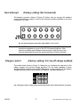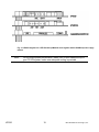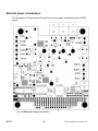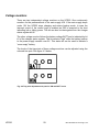
1
UPS25 Uninterruptible power supply and Ni-Mh/Ni-Cd charger unit User’s Manual BDM-610020008 Rev. E UPS25 Uninterruptible Power Supply User’s Manual RTD Embedded Technologies, INC. 103 Innovation Blvd. State College, PA 16803-0906 Phone: +1-814-234-8087 FAX: +1-814-234-5218 E-mail [email protected] [email protected] web site http://www.rtd.com UPS25 2 RTD Embedded Technologies, Inc Revision History 10/08/2000 10/07/2001 Rev A Rev B Rev C Rev D Rev E HW Release 1.0 Name of company corrected New manual naming convention Removed reference to EFAN; Included hot-swap warning Removed information about J12 Corrected backup power specifications. Included explanation of discharge circuit. Included explanation of J4 Published by: RTD Embedded Technologies, Inc. 103 Innovation Blvd. State College, PA 16803-0906 Copyright 1999, 2002, 2003, 2004, 2005 2012 by RTD Embedded Technologies, Inc. All rights reserved Printed in U.S.A. The RTD Logo is a registered trademark of RTD Embedded Technologies. cpuModule and utilityModule are trademarks of RTD Embedded Technologies. PS/2, PC/XT, PC/AT and IBM are trademarks of International Business Machines Inc. MS-DOS, Windows, Windows 95, Windows 98 and Windows NT are trademarks of Microsoft Corp. PC/104 is a registered trademark of PC/104 UPS25 3 RTD Embedded Technologies, Inc Consortium. All other trademarks appearing in this document are the property of their respective owners. UPS25 4 RTD Embedded Technologies, Inc TABLE OF CONTENTS CHAPTER 1 - INTRODUCTION ............................................................................... 8 Features ........................................................................................................................................................................ 8 Some of the key features of the UPS25 include: ................................................................................................... 8 Power supply unit ........................................................................................................................................................ 9 Charger unit ................................................................................................................................................................ 9 Host interface and control .......................................................................................................................................... 9 Mechanical description ............................................................................................................................................... 9 Connector description ................................................................................................................................................. 9 What comes with your board ................................................................................................................................... 10 When you need help .................................................................................................................................................. 11 CHAPTER 2 - BOARD SETTINGS ......................................................................... 12 Factory-Configured Jumper Settings ...................................................................................................................... 13 Charger control (Factory setting: C/2, top off charge enabled) ....................................................................... 17 CHAPTER 3 - BOARD INSTALLATION ................................................................. 18 Board installation ...................................................................................................................................................... 18 General installation guidelines: ........................................................................................................................... 18 Installation integrated with a PC/104 module stack: ........................................................................................... 18 External power connections ..................................................................................................................................... 20 CHAPTER 4 - HARDWARE DESCRIPTION .......................................................... 22 Current Limit ....................................................................................................................................................... 23 Charger power converter ......................................................................................................................................... 23 Ni-Mh/Ni-CD Battery Pack and Thermistor ....................................................................................................... 24 Ni-Mh\Ni-Cd battery charger .............................................................................................................................. 25 Discharging Ni-Mh/Ni-Cd battery pack .............................................................................................................. 25 Charger mode configuration- solder blobs B2 and B3 ........................................................................................... 26 Power switching circuitry ......................................................................................................................................... 28 CHAPTER 5 - BOARD OPERATION AND PROGRAMMING ................................ 31 Defining the Memory Map ....................................................................................................................................... 31 BA+0 Control register (Read and Write)......................................................................................................... 31 BA+1 Status register (Read) ........................................................................................................................... 32 BA+1 Status register (Write) .......................................................................................................................... 32 Programming the UPS25 .......................................................................................................................................... 32 Clearing and setting bits in an I/O port................................................................................................................... 33 INTERRUPTS ........................................................................................................................................................... 33 What is an interrupt? ........................................................................................................................................... 33 Interrupt request lines .......................................................................................................................................... 34 8259 Programmable Interrupt Controller ............................................................................................................ 34 Interrupt Mask Register (IMR) ............................................................................................................................ 34 End-of-Interrupt (EOI) Command ....................................................................................................................... 34 What exactly happens when an interrupt occurs? ................................................................................................ 35 UPS25 5 RTD Embedded Technologies, Inc Using Interrupts in your Program ........................................................................................................................ 35 Writing an Interrupt Service Routine (ISR) ......................................................................................................... 36 The following C example shows what the shell of your ISR should be like: ....................................................... 37 Saving the Startup Interrupt Mask Register (IMR) and interrupt vector ............................................................. 37 Common Interrupt mistakes ................................................................................................................................ 38 Example on Interrupt vector table setup in C-code: ............................................................................................ 39 CHAPTER 6 - UPS25 SPECIFICATIONS............................................................... 40 Host interface............................................................................................................................................................. 40 Power supply specifications ...................................................................................................................................... 40 Charger and batteries ............................................................................................................................................... 40 Electromechanical ..................................................................................................................................................... 40 CHAPTER 7 - RETURN POLICY AND WARRANTY ............................................. 42 Return Policy ............................................................................................................................................................. 42 LIMITED WARRANTY .................................................................................................. 44 UPS25 6 RTD Embedded Technologies, Inc List of Illustrations and Tables .............................................................................................................................................................. Illustrations Fig. 2-1 UPS25 Board layout showing jumper locations Fig. 2-2 Base address jumpers illustrating address 300h Fig. 2-3 Interrupt jumpers from left to right: IRQ 2,5,7,10,11,12,15 Fig. 2-4 Charger control, solder blobs, located near the left side of the PC/104 bus connector Fig. 3-1 UPS25 integrated in a RTD PC/104 cpuModule stack together with a HPWR104 power supply module Fig. 3-2 UPS25 power supply connections Fig. 4-1 Block diagram of the UPS25 Fig. 4-2 Discharging jumper Fig. 4-3 Charger configuration, solder blobs B2 and B3 Fig. 4-4 Trip point adjustment trim pots for VIN and BATT levels Fig. 4-5 I/O interface connector .......................................................................................................................................................................Tables Table 2-1 Factory configured jumper settings Table 2-2 Base address jumper settings UPS25 Table 4-1 Charger status LED functional description Table 4-2 I/O connector pin outs UPS25 7 RTD Embedded Technologies, Inc Chapter 1 - INTRODUCTION This user’s manual describes the operation of the UPS25 versatile uninterruptible power supply unit for automotive and industrial applications. Features Some of the key features of the UPS25 include: • • • • • • • • • • • • Compatible with RTD power supplies Wide input voltage range 10-40V DC Battery currents to 5 Amps Maximum 20W charge power with adequate cooling 75% total efficiency -40 to +85C ambient operating temperature Battery backup • 8 Ni-MH battery cells, 24 Watt 30 min backup time • 1500 mAh 9,6V nominal battery voltage • 24 Watt 30 min backup time • Discharge -10 to 65C battery temperature • Charge 0 to 40C • 8 Ni-Cd battery cells, 24 Watt 20 min backup time • 1000 mAh 9,6V nominal battery voltage • 24 Watt 20 min backup time • Discharge -20 to 65C battery temperature • Charge 10 to 40C Thermistor feedback charging process Complete software controlled charging process Main power fail interrupt with Software controlled shutdown of backup Adjustable backup voltage trip level Fully PC/104 compliant Part numbers: • UPS25-1 Ni-MH battery version • UPS25-2 Ni-Cd battery version The following paragraphs briefly describe the major features of the UPS25. A more detailed discussion is included in Chapter 4 (Hardware description). The board’s installation is described in Chapter 2 (Board Installation). UPS25 8 RTD Embedded Technologies, Inc Power supply unit The UPS25 uninterruptible power supply unit is designed to provide a complete backup system for your embedded computer and its peripherals. Battery charging power is generated using a wide input voltage range (8 to 40V DC) step down converter with a maximum charging output power of 25W. Battery charging power is converted from this output using a second step-up DC/DC converter. This scheme will enable charging of the batteries at +12V, while operating at an input voltage of 10V. The UPS25 input is protected against reverse voltage up to 40V, and is over voltage protected using a 5 Watt 40 V zener diode. Charger unit While the main system power is present the onboard battery charger may charge the external battery pack. However charging may be disabled by software by writing to the appropriate charger control bit. Charging will not take place if any of the following conditions are met: 1) main power is below 10V, 2) battery temperature is out of limits, 3) battery is already charged, 4) battery error exists. Host interface and control The UPS25 can be controlled and monitored from software. A host interrupt may be generated to indicate that the main power supply is below 10V and that the system is powered from the battery pack. This interrupt can be used to start required actions. The state of the UPS25 can be polled using status bits indicating battery voltage level, charger state and battery temperature state. Mechanical description The UPS25 is designed on a PC/104 form factor. An easy mechanical interface to both PC/104 and EUROCARD systems can be achieved. Stack your UPS25 directly on a PC/104 compatible power supply using the onboard mounting holes and standoffs. Connector description All power connections are made using "cable plug" type terminal blocks. This enables removing connections from the board without opening the cables from the terminal blocks. Power must be removed before connecting or disconnecting batteries. Hot swapping the battery pack may damage the UPS25. UPS25 9 RTD Embedded Technologies, Inc What comes with your board Your UPS25 package contains the following items: • • UPS25 board with mating connectors for the supported power connections User's manual Note: Software and drivers can be downloaded from our website. If any item is missing or damaged, please send an EMAIL to RTD Embedded Systems, Inc. sales service department at <[email protected] >. UPS25 10 RTD Embedded Technologies, Inc Using this manual This manual is intended to help you install your new UPS25 module and get it working quickly, while also providing enough detail about the board and it's functions so that you can enjoy maximum use of it's features even in the most demanding applications. When you need help This manual and all the example programs will provide you with enough information to fully utilize all the features on this board. If you have any problems installing or using this board, contact our Technical Support department at <[email protected]>. When sending us an Email request please include the following information: Your company's name and address, your name, your telephone number, and a brief description of the problem. UPS25 11 RTD Embedded Technologies, Inc Chapter 2 - BOARD SETTINGS The UPS25 board has jumper settings, which can be changed to suit your application and host computer configuration. The factory settings are listed and shown in the diagram at the beginning of this chapter. Make sure you completely study and understand this chapter before making changed to these settings. UPS25 12 RTD Embedded Technologies, Inc Factory-Configured Jumper Settings Table 2-1 below illustrates the factory jumper setting for the UPS25. Figure 2-1 shows the board layout of the UPS25 and the locations of the jumpers. The following paragraphs explain how to change the factory jumper settings to suit your specific application. Table 2-1 Factory configured jumper settings (Please see figure 2-1 below for more detailed locations) JUMPER NAME BASE IRQ B2/B3 blobs DESCRIPTION Base Address Host interrupt Charger control NUMBER OF JUMPERS 3 7 3+3 FACTORY SETTING 300 N.C. C/2, Top off charge enabled Battery trip adjust Input trip adjust Address Jumpers Interrupt Jumpers UPS25 13 RTD Embedded Technologies, Inc Fig. 2-1 UPS25 Board layout showing jumper locations UPS25 14 RTD Embedded Technologies, Inc Base address jumper (Factory setting: 300h) The UPS25 is I/O mapped into the memory space of your host computer. The board occupies a consecutive memory window of 2 bytes starting from the base address. The most common cause of failure when you are first setting up your module is address contention. Some of your computers I/O space is already occupied by other devices and memory resident programs. When the UPS25 attempts to use it's own reserved memory addresses (which are being already used by another peripheral device) erratic performance may occur and the data read from the board may be corrupted. To avoid this problem make sure you set up the base address by using the three jumpers marked “J14”, this allows you to choose from a number of different addresses in your host computer’s I/O map. Should the factory-installed setting of 300h be incompatible to your system configuration, you may change this setting to another using the options illustrated in Table 2-2 (overleaf). The table shows the jumper settings and their corresponding values in hexadecimal form. Ensure that you verify the correct location of the base address jumpers. When the jumper is removed it corresponds to a logical "0", connecting the jumper to a "1". When you set the base address of the module, record the setting inside the back cover of this manual. UPS25 15 RTD Embedded Technologies, Inc BASE ADDRESS JUMPER SETTINGS UPS25 Base address Hex Jumper settings A8 A7 A6 200 0 0 0 240 0 0 1 280 0 1 0 2C0 0 1 1 300 1 0 0 340 1 0 1 380 1 1 0 3C0 1 1 1 0 = JUMPER OFF 1 = JUMPER CLOSED Table 2-2 Base address jumper settings UPS25 Fig. 2-2 Base address jumpers illustrating address 300h UPS25 16 RTD Embedded Technologies, Inc Host interrupt (Factory setting: Not Connected) The header connector, shown in Figure 2-3 below, lets you connect the onboard control logic interrupt outputs to one of the interrupt channels available on the host computer XT/AT bus. Fig. 2-3 Interrupt jumpers from left to right: IRQ 2,5,7,10,11,12,15 Note: The UPS25 hardware does not support interrupt sharing! This feature is sometimes regarded as a part of the PC/104 special features. After extensive software and hardware tests we have found that error-free interrupt performance cannot be guaranteed when sharing interrupts. Charger control (Factory setting: C/2, top off charge enabled) The solder blobs shown in Figure 2-4 below let you configure the operation of the battery charger unit and the charge algorithm. Do not make changes to these settings without examining the detailed description on the operation of the battery charger described later in this manual in Chapter 4, hardware description. Fig. 2-4 Charger control, solder blobs, located near the left side of the PC/104 bus connector UPS25 17 RTD Embedded Technologies, Inc Chapter 3 - BOARD INSTALLATION The UPS25 uninterruptible power supply module is designed to directly mount on top or under your RTD PC/104 power supply unit. This chapter tells you step-bystep how to install your UPS25 into your system. Board installation Keep your board in its antistatic bag until you are ready to install it to your system! When removing it from the bag, hold the board at the edges and do not touch the components or connectors. Please handle the board in an antistatic environment and use a grounded workbench for testing and handling of your hardware. Before installing the board in your computer, check the power cabling. Failure to do so may cause the power supply unit to malfunction or even cause permanent damage. General installation guidelines: • • • • • • • • Touch the grounded metal housing of your computer to discharge any antistatic buildup and then remove the board from its antistatic bag. Hold the board by the edges and install it in an enclosure or place it on the table on an antistatic surface Install your board in your system, and wire the power supply correctly. Failure to do so may cause the power supply unit to malfunction or even cause permanent damage to the device. Check all wiring connections once and then once more again. Check the input power to the board is in the range of 10 to 40V DC Apply power to your UPS25, this will automatically power your system Installation integrated with a PC/104 module stack: • • • UPS25 Secure the four PC/104 installation holes with standoffs Connect the board to the main power supply using the power interface connectors Connect the output of your UPS25 to the input of your RTD power supply 18 RTD Embedded Technologies, Inc Fig. 3-1 UPS25 integrated in a RTD PC/104 cpuModule stack together with a HPWR104 power supply module Note: UPS25 For full output power performance, install your UPS25 toward the top of your PC/104 system, make sure adequate cooling is provided. 19 RTD Embedded Technologies, Inc External power connections The illustration 3-2 below shows the input and output power connections of the UPS25 board. Fig. 3-2 UPS25 power supply connections UPS25 20 RTD Embedded Technologies, Inc Connector descriptions: • Note: The module input power may be 5 Amp peak, this will require a cable wire diameter of 1,5 sq. mm. Make sure this input wire is kept as short as possible to reduce voltage drops and interference. • • • • UPS25 VIN: Raw input power to the UPS25. Input voltage ranges 10-40V DC This input is fed to the power supply through the UPS25 in normal operation mode (no backup from the battery pack). Batt: Connect your external 8 AA-size 1500mAh Ni-MH or 1000mAh Ni-Cd battery pack here. Batt- is connected to the system ground. NTC: Direct connection to the NTC thermistor of your battery pack. VO: Output of the UPS to the power supply module VOS: Switched output of the UPS to feed the power supply module. If this connection is used you can under software control disengage the battery backup when the shutdown procedures are complete. (See later sections for a more detailed description on the functionality of this output) 21 RTD Embedded Technologies, Inc Chapter 4 - HARDWARE DESCRIPTION This chapter describes the major hardware building blocks of the UPS25, which are: • • • • • • • The main 25W +5V step-down converter Charger power converter Ni-MH/Ni-Cd battery charger Power switching circuitry Voltage monitors UPS control circuitry I/O interface connector Fig. 4-1 Block diagram of the UPS25 UPS25 22 RTD Embedded Technologies, Inc The main 25W +5V step-down converter The power supply circuitry is implemented with a switch-mode step down DC-DC converter. The peak charge output power of this unit is 25W. This output power is only available if adequate cooling is provided. The output current is internally limited against over current and short circuit faults. Connect a 10-40V DC source to the UPS25. A reverse voltage schottky diode will withstand reverse voltages up to 40V DC. These devices are necessary to protect the device in automotive and industrial installations. This +5V converter output is not used to power any devices on the bus. This +5V-supply is only used as a raw input to the battery charger step-up converter. Current Limit To protect against fault or short-circuit conditions the +5V DC/DC converter module is equipped with a current limiting circuitry to provide continuous overload protection. After reaching the current limit point (between 5.5 and 8.5Amps), the voltage output will range between the rated output and zero depending on the amount of overload. At this point the output current will be typically 25 to 30 % of its maximum value. Once the short circuit condition is removed, the output will return to the nominal value without restarting the unit. Charger power converter A 5V to +12V step up converter with 90% efficiency generates a nominal +15V for charging the battery pack. This architecture will permit the charging of the battery pack at a higher voltage than the input of the UPS25. Charging will take place while the input is over 10V, this trip level can be flexibly modified by adjusting the trim pot controlling the UPS VIN trip voltage. This trim pot is described later in this manual on Page 22. The +15V charge supply is limited to a 1,25A-peak current. If the battery being charged draws more current, the converter will output a voltage less than the nominal +15V output, typically during fast charge the voltage is in the range of 11,5V to 12,5V depending on the charge state of the battery. UPS25 23 RTD Embedded Technologies, Inc Ni-Mh/Ni-Cd battery charger Ni-Mh/Ni-CD Battery Pack and Thermistor Battery packs using Ni-Mh/Ni-CD technology are the only ones supported by the standard UPS25. RTD Embedded Systems, Inc. can deliver UPS25 units that support Ni-Cd technology. An UPS25 that is configured for Ni-MH batteries may not be used with Ni-Cd and vice-versa. For the UPS25 to operate correctly a total of 8 AA-cells must be used connected in series. This connection will give a nominal output voltage of 9,6V over the battery pack. In real life the battery pack voltage will range from 11V fully charged to 6,5V absolutely discharged. The battery pack must contain attached to it an NTC temperature sensor called a thermistor. The output of the thermistor is monitored at periodic intervals by the charger circuitry. If no thermistor is detected, the charger will not charge the battery. Not just any kind of thermistor can be used, since many component values are trimmed to meet the characteristics of the thermistor. If an incorrect thermistor type is used the charger circuitry of the UPS25 may not work properly. Below is listed the part number and specification of the recommended thermistor: Part number: SIEMENS B576164K103J Resistance at +25C 10 K, +-5% Beta value +25C to 100C 4300, +-3% These parts can be ordered through RTD is case you wish to construct your own battery pack to use with the UPS25. For custom dimensioning of the charger to support another thermistor, please contact our technical support for assistance and formulas for component value calculation. The UPS25 is dimensioned to charge a battery pack with a maximum capacity of 1500mAh. The charging algorithm is set to a nominal charge current of 750mA i.e. C/2. This setting is used to determine the fast charge and top-off charge times of the charge process. UPS25 24 RTD Embedded Technologies, Inc Ni-Mh\Ni-Cd battery charger To ensure long battery life and reliable charging a special battery charger circuitry is used based on the BQ2003 versatile battery charger chip. This chip is used in “gated charge mode” where the charger disconnects the supply from the battery based on the current state of the charging algorithm. State output of the charger chip can be monitored using LED labeled L3 or by interrogating the charger status register bit #2. Below is a table illustrating the different states indicated by the “charger status” LED L3. Charge Action State No battery / abort Pending charge Discharging Fast charging Charge complete Top off charge Charge status LOW 1/8 sec 1 3/8 sec Continuous 1/8 sec 1/8 sec Charge status HIGH Continuous 1 3/8 sec 1/8 sec 1/8 sec 1/8 sec Table 4-1 Charger status LED functional description Pending charge can result from the battery being out of the permitted temperature range or alternatively that the voltage of the battery is out of limits. The charge controller always during startup verifies that the battery condition is good before fast charging can take place. Note that no LED’s are lit if the SHDNbit (#3 in charger control register) is set in the UPS25 control register. Discharging Ni-Mh/Ni-Cd battery pack The UPS25 supports “discharge-before-fast charge”. Discharging can be initiated in two ways. The first way is to simply close the “DISCH” jumper for a moment. This will initiate a discharging of the battery. See figure 4-2 below: Fig. 4-2 Discharging jumper UPS25 25 RTD Embedded Technologies, Inc Discharging can also be initiated by setting the discharge bit #1 in the control register to a high, and bringing this bit to low again. Care must be taken not to overheat your system since the discharged battery power is converted to heat directly into the metal heat sink. Only discharge when the ambient temperature is low enough, or when adequate cooling is present. In any case Ni-MH batteries do not require as critically periodical discharging as Ni-Cd batteries do. This procedure is recommended to do only every now and then to make sure that battery performance in maintained. For Ni-Cd systems it is recommended to periodically perform the discharge-before-charge to maintain good battery performance and reduce memory effect of the Ni-Cd battery pack. Discharging may be required if the back up is used very infrequently and for a very short period of time. The discharge resistor is pictured below as R15 and either attaches to the heat stand-alone heat sink or frame (in an IDAN). By default the discharge resistor is not populated. A suggested resistor is the Ohmite TCH35P7R50JE. This resistor is a 7.5 Ohm 35Watt power resistor. Please contact RTD if you require a discharge resistor. As an example, if one has a 1000 mAhr 9.6V battery they want to discharge and it is fully charged with no R15 present, there still exists R1 in parallel with R15. R1 is a 1 Watt 1K resistor. R1 will dissipate 0.092 Watts. The battery should discharge in about 4.3 days. If R15 is installed as a 7.5 Ohm resistor, 12.38 Watts will be dissipated. The battery will be fully discharged in about 47 minutes. Keep in mind that adding 12 Watts to the existing heat of your system should be considered. Choose a discharge resistor value that you can remove the heat from. Charger mode configuration- solder blobs B2 and B3 The solder blobs shown in Figure 4-3 below let you configure the operation of the battery charger unit and the charge algorithm. These blobs connect to GND while the top two connections are closed and to VCC while the bottom two are closed. UPS25 26 RTD Embedded Technologies, Inc Fig. 4-3 Charger configuration, solder blobs B2 and B3 B3 controls the TM1 pin of the BQ2003 and B2 controls the TM2 pin. Below is shown a table that will illustrate the allowed modes of operation. The bold setup mode is the factory default. UPS25 Fast-charge Rate TM1/B3 TM2/B2 Fast charge Top-Off -dV/MCV Hold-off Top off Rate C/2 C C/2 C Float VCC VCC GND GND GND Float VCC 180 sec 90 180 sec 90 820 sec 410 sec 820 sec 410 sec Dis Dis C/16 C/8 27 RTD Embedded Technologies, Inc If top off mode is enabled the charger will pulse charge for a period of 5 seconds and rest for 30 seconds. This mode will ensure that maximum charging capacity is reached. For long term maintaining of the charge of the backup battery a special trickle mode is supported by the UPS25. This state is entered after all other charge modes are complete. In the trickle mode the battery is charged with a constant C/36 current if the charger circuitry is powered with a Ni-MH configured UPS25, in case the UPS25 is set for Ni-Cd batteries the trickle charge rate is C/16. Power switching circuitry The UPS25 features voltage dependent automatic power switching using logic and power MOSFET transistors. These transistors are controlled based on the voltages detected by the onboard voltage monitor. The following power switches are included in the design: UPS25 Control method Description 1) Converter sw. Software control Enable the operation of the charge power step-up DC/DC converter 2) Charge power sw. BQ2003 control Control the charging of the battery (No user control over this feature) 3) Backup/Charge sw. Voltage monitors This switch pair either enables charging, while the supply is present (>10V), or enters battery backup mode where no charging can take place. 4) CPU power sw. Software / Vin This relay switch is connected to the switched VOS output (see Fig. 3-2). The relay remains closed while VIN is present during operation, and “/sleep”-bit is high while entering backup. In backup state clearing /sleep bit the system will disconnect the backup. 28 RTD Embedded Technologies, Inc Voltage monitors There are two independent voltage monitors on the UPS25. One continuously monitors for the presence/level of the main supply VIN. If the main supply drops under 10V the UPS25 stops charging and enters backup mode. In case the interrupt output of the control logic is enabled an IRQ is asserted to the host indicating low or failing power. This bit can also be interrogated from the charger status register bit #0 The other voltage monitor follows the battery voltage BATT and is indicated by bit #1 of the charger status register. This bit remains “high” while the battery backup to the power supply remains over 8V. This status bit can be used to indicate a “soon empty” battery. The levels of the trip-points of these voltage monitors can be adjusted using the onboard trim pots. See figure 4-3 below: Fig. 4-4 Trip point adjustment trim pots for VIN and BATT levels UPS25 29 RTD Embedded Technologies, Inc UPS control circuitry The UPS25 status can be monitored through the 4 bit Status register. A host interrupt can be asserted in the case that the main power VIN drops below the set trip-point, factory set to 10V. This interrupt can be disabled or enabled by the IRQ-enable bit (#0 of the control register). In case the interrupt is disabled you can monitor the status of the input power by polling the control register. Note that the control circuitry is not powered from the +5V onboard step-down converter, but from the PC/104 bus. UPS25 30 RTD Embedded Technologies, Inc Chapter 5 - BOARD OPERATION AND PROGRAMMING This chapter shows you how to program and use your UPS25. It provides a complete detailed description of the I/O map and a detailed discussion of programming operations to aid you in programming. Defining the Memory Map The memory map of the UPS25 occupies two bytes of host PC I/O space. This window is freely selectable by the user as described in Chapter 2, Table 2-2. After setting the base address you have access to the internal resources of the UPS25 control logic. These resources are described in the next sections in detail. Register Description UPS25 Control register UPS25 Status register Address in HEX BA+0 BA+1 BA = Base Address BA+0 Control register (Read and Write) The UPS25 control register gives you access to change the settings of your board. This register is reset to all zeroes after power-up and reset of your CPU. Bit 0 0 1 Interrupts disabled Interrupts enabled Bit 1 0 1 Discharge disabled Discharge enabled Bit 2 0 1 Disconnect power in backup state Maintains power in backup mode. Must be set while CPU is powered from main source. Note: Only applicable if you connect your power supply to the switched outputs of your UPS25. Bit 3 UPS25 0 1 Charger DC/DC converter active, charging can take place Charger DC/DC converter asleep, no charge possible 31 RTD Embedded Technologies, Inc BA+1 Status register (Read) The UPS25 status register gives you access to monitor the state of your board. This register is reset to all zeroes after power-up and reset of your CPU. Bit 0 0 1 Main supply voltage low / UPS25 in backup state Main power OK, charging can take place Bit 1 0 1 Battery voltage low Battery voltage still OK Bit 2 Charger status LED Bit 3 Charger temperature LED 0 1 BA+1 Status register Battery temperature out of limits, no charging can take place Battery temperature OK, charging can take place (Write) Clear the host interrupt register. Must be performed for a new interrupt to be possible to take place. Programming the UPS25 This section gives you some general information about programming the UPS25 board. It then walks you through the major programming functions of the UPS25. This will help you use the example program that is included with the board. All of the program descriptions use decimal values unless otherwise specified. The UPS25 is programmed by writing to the correct board I/O port addresses. These I/O ports were described in the previous section of this chapter. The following example shows how to perform an 8-bit write to I/O port addresses using "C"-syntax and assembly code: Write: UPS25 "C"-syntax outp(address,data); Assembly mov dx,address mov ax,data out dx,ax 32 RTD Embedded Technologies, Inc Clearing and setting bits in an I/O port When you clear or set bits in an I/O port you must be careful not to alter the status of other bits. You can preserve the status of all the bits you do not wish to change by proper use of the bitwise AND- and OR- operators. Using and /or operators, single or multiple bits can easily be set or cleared in a one-line operation. 1. To clear a single bit in a port, AND the current value of the port with the value "B", where B = 255-2(exp) bit. 2. To set a single bit in a port, OR the current value of the port with the value "B", where B = 2(exp) bit. Bits are numbered from 0-7 for the low byte of a word and from 8-15 for the high byte of a word. Setting and clearing of multiple bits in a bye or word is more complex. 3. To clear multiple bits in a port, AND the current value of the port with the value "B", where B = 255 - (the sum of the values of the bits to be cleared). Note that the bits do not have to be consecutive. 4. To set multiple bits in a port, OR the current value of the port with the value "B", where B = (sum of the individual bits to be set). INTERRUPTS What is an interrupt? An interrupt is an event that causes the processor in your computer to temporarily halt its current process and execute another routine. Upon completion of the new routine, control is returned to the original routine at the point where its execution was interrupted. Interrupts are a very flexible way of dealing with asynchronous events. Keyboard activity is a good example; your computer cannot predict when you might press a key and it would be a waste of processor time to do nothing whilst waiting for a keystroke to occur. Thus the interrupt scheme is used and the processor proceeds with other tasks. When a keystroke finally occurs, the keyboard then 'interrupts' the processor so that it can get the keyboard data .It then places it into the memory, and then returns to what it was doing before the interrupt occurred. Other common devices that use interrupts are A/D boards, network boards, serial ports etc. UPS25 33 RTD Embedded Technologies, Inc Your UPS25 can interrupt the main processor when the main power supply fails or falls below 10V if interrupts are enabled on the UPS25 board. By using interrupts you can write powerful code to interface to your UPS25. Interrupt request lines To allow different peripheral devices to generate interrupts on the same computer, the PC AT bus has interrupt request channels (IRQs). A rising edge transition on one of these lines will be latched into the interrupt controller. The interrupt controller checks to see if the interrupts are to be acknowledged from that IRQ and, if another interrupt is being processed, it decides if the new request should supercede the one in progress or if it has to wait until the one in progress has been completed. The priority level of the interrupt is determined by the number of the IRQ as follows; IRQ0 has the highest priority whilst IRQ15 has the lowest. Many of the IRQs are used by the standard system resources, IRQ0 is dedicated to the internal timer, and IRQ1 is dedicated to the keyboard input, IRQ3 for the serial port COM2, and IRQ4 for the serial port COM1. Often interrupts 2,5 and 7 are free for the user. 8259 Programmable Interrupt Controller The chip responsible for handling interrupt requests in a PC is the 8259 Interrupt Controller. To use interrupts you will need to know how to read and set the 8259's internal interrupt mask register (IMR) and how to send the end-of-interrupt (EOI) command to acknowledge the 8259 interrupt controller. Interrupt Mask Register (IMR) Each bit in the interrupt mask register (IMR) contains the mask status of the interrupt line. If a bit is set (equal to 1), then the corresponding IRQ is masked, and it will not generate an interrupt. If a bit is cleared (equal to 0), then the corresponding IRQ is not masked, and it can then generate an interrupt. The interrupt mask register is programmed through port 21h. End-of-Interrupt (EOI) Command After an interrupt service routine is complete, the 8259 Interrupt Controller must be acknowledged by writing the value 20h to port 20h. UPS25 34 RTD Embedded Technologies, Inc What exactly happens when an interrupt occurs? Understanding the sequence of events when an interrupt is triggered is necessary to correctly write interrupt handlers. When an interrupt request line is driven high by a peripheral device (such as the UPS25), the interrupt controller checks to see if interrupts are enabled for that IRQ. It then checks to see if other interrupts are active or requested and determines which interrupt has priority. The interrupt controller then interrupts the processor. The current code segment (CS), instruction pointer (IP), and flags are pushed onto the system stack., and a new set if CS and IP are loaded from the lowest 1024 bytes of memory. These memory locations are referred to as the interrupt vector table and each entry to this table is called an interrupt vector. Once the new CS and IP are loaded from the interrupt vector table, the processor starts to execute code from the new Code Segment (CS) and from the new Instruction Pointer (IP). When the interrupt routine is completed the old CS and IP is popped from the system stack and the program execution continues from the point where interruption occurred. Using Interrupts in your Program Adding interrupt support to your program is not as difficult as it may seem especially when programming under DOS. The following discussion will cover programming under DOS. Note that even the smallest mistake in your interrupt program may cause the computer to hang up and will only restart after a reboot. This can be frustrating and time-consuming. UPS25 35 RTD Embedded Technologies, Inc Writing an Interrupt Service Routine (ISR) The first step in adding interrupts to your software is to write an interrupt service routine (ISR). This is the routine that will be executed automatically each time an interrupt request occurs for the specified IRQ. An ISR is different from other subroutines or procedures. First on entrance the processor registers must be pushed onto the stack before anything else! Second, just before exiting the routine, you must clear the interrupt on the UPS25 by writing to the Status register, and write the EOI command to the interrupt controller. Finally, when exiting the interrupt routine the processor registers must be popped from the system stack and you must execute the IRET assembly instruction. This instruction pops the CS, IP and processor flags from the system stack. These were pushed onto the stack when entering the ISR. Most compilers allow you to identify a function as an interrupt type and will automatically add these instructions to your ISR with one exception: most compilers do not automatically add the EOI command to the function, you must do it yourself. Other than this and a few exceptions discussed below, you can write your ISR as any code routine. It can call other functions and procedures in your program and it can access global data. If you are writing your first ISR, we recommend you stick to the basics; just something that enables you to verify you have entered the ISR and executed it successfully. For example: set a flag in your ISR and in your main program check for the flag. Note: If you choose to write your ISR in in-line Assembly, you must push and pop registers correctly and exit the routine with the IRET instruction instead of the RET instruction. There are a few precautions you must consider when writing ISRs. The most important is, do not use any DOS functions or functions that call DOS functions from an interrupt routine. DOS is not re-entrant; that is, a DOS function cannot call itself. In typical programming, this will not happen because of the way DOS is written. But what about using interrupts? Consider then the following situation in your program: If DOS function X is being executed when an interrupt occurs and the interrupt routine makes a call to the same DOS function X, then function X is essentially being called while active. Such cases will cause the computer to crash. DOS does not support such operations. The general rule is that do not call any functions that use the screen, read keyboard input or any file I/O routines, these should not be used in ISRs. The same problem of re-reentrancy also exists for many floating-point emulators. This effectively means that you should also avoid floating point mathematical operations in your ISR. Note that the problem of reentrancy exists, no matter what programming language you use. Even, if you are writing your ISR in Assembly language, DOS and many floating-point emulators are not reentrant. Of course there are ways to avoid this problem, such as those that activate when your ISR is called. Such solutions are, however, beyond the scope of this manual. UPS25 36 RTD Embedded Technologies, Inc The second major concern when writing ISRs is to make them as short as possible in term of execution time. Spending long times in interrupt service routines may mean that other important interrupts are not serviced. Also, if you spend too long in your ISR, it may be called again before you have exited. This will lead to your computer hanging up and will require a reboot. Your ISR should have the following structure: • • • • Push any processor registers used in your ISR. Most C compiler do this automatically Put the body of your routine here Clear the interrupt bit by writing to the UPS25 status register Issue the EOI command to the 8259 by writing 20h to address 20h Pop all registers. Most C compilers do this automatically The following C example shows what the shell of your ISR should be like: /*------------------------------------------------------------------------------| Function: new_IRQ_handler | Inputs: Nothing | Returns: Nothing |-------------------------------------------------------------------------------*/ void interrupt far new_IRQ_handler(void) { IRQ_flag = 1; // Indicate to main process interrupt has occurred { // Your program code to shut down should be here } outp(BASE+0x01,0x00); // Clear interrupt on UPS25 outp(0x20, 0x20); // Acknowledge the interrupt controller } Saving the Startup Interrupt Mask Register (IMR) and interrupt vector The next step after writing the ISR is to save the start up state of the interrupt mask register, and the original interrupt vector you are using. The IMR is located in address 21h. The interrupt vector you will be using is located in the interrupt vector table (an array of pointers or addresses) and it is located in the first 1024 bytes of the memory (Segment 0 offset 0). You can read this value directly, but it is better practice to use DOS function 35h (get interrupt vector) to do this. Most C compilers have a special function available for doing this. The vectors for the hardware interrupts on the XT - bus are vectors 8-15, where IRQ0 uses vector 8 and IRQ7 uses vector 15. Thus if your UPS25 is using IRQ5 it corresponds to vector number 13. UPS25 37 RTD Embedded Technologies, Inc Before you install your ISR, temporarily mask out the IRQ you will be using. This prevents the IRQ from requesting an interrupt while you are installing and initializing your ISR. To mask the IRQ, read the current IMR at I/O port 21h, and set the bit that corresponds to the IRQ. The IMR is arranged so that bit 0 is for IRQ0 and bit 7 is for IRQ7. See the paragraph entitled Interrupt Mask Register (IMR) earlier in this discussion for help in determining your IRQs bit. After setting the bit, write the new value to I/O port 21h. With the startup IMR saved and the interrupts temporarily disabled, you can assign the interrupt vector to point to your ISR. Again you can overwrite the appropriate entry in the vector table with a direct memory write, but this is not recommended. Instead use the DOS function 25h (Set Interrupt Vector) or, if your compiler provides it, the library routine for setting up interrupt vectors. Remember that interrupt vector 8 corresponds to IRQ0, vector 9 for IRQ1 etc. If you need to program the source of your interrupts, do that next. For example, if you are using transmitted or received messages as an interrupt source program it to do that. Finally, clear the mask bit for your IRQ in the IMR. This will enable your IRQ. Common Interrupt mistakes Remember hardware interrupts are from 8-15, XT IRQs are numbered 0-7. Do not forget to clear the IRQ mask bit in the IMR Forgetting to send the EOI command after ISR code. Disables further interrupts. UPS25 38 RTD Embedded Technologies, Inc Example on Interrupt vector table setup in C-code: void far _interrupt new_IRQ1_handler(void ); /* ISR function prototype */ #define IRQ1_VECTOR 7 /* Name for selected IRQ*/ void (interrupt far *old_IRQ1_dispatcher) (es,ds,di,si,bp,sp,bx,dx,cx,ax,ip,cs,flags); /* Variable to store old IRQ_Vector */ void far _interrupt new_IRQ1_handler(void ); /*---------------------------------------------------------------------| Function: init_irq_handlers | Inputs: Nothing | Returns: Nothing | Purpose: Set the pointers in the interrupt table to point to | our funtions ie. setup for ISRs. |----------------------------------------------------------------------*/ void init_irq_handlers(void) { _disable(); old_IRQ1_handler = _dos_getvect(IRQ1_VECTOR + 8); _dos_setvect(IRQ1_VECTOR + 8, new_IRQ1_handler); Gi_old_mask = inp(0x21); outp(0x21,Gi_old_mask & ~(1 << IRQ1_VECTOR)); _enable(); } |/*---------------------------------------------------------------------| Function: restore, do this before exiting program | Inputs: Nothing | Returns: Nothing | Purpose: Restore the interrupt vector table. |----------------------------------------------------------------------*/ void restore(void) { /* Restore the old vectors */ _disable(); _dos_setvect(IRQ1_VECTOR + 8, old_IRQ1_handler); outp(0x21,Gi_old_mask); _enable(); } UPS25 39 RTD Embedded Technologies, Inc Chapter 6 - UPS25 SPECIFICATIONS Host interface 16-bit PC/104 bus Power supply specifications Input voltage range Output charge Power Efficiency Reverse voltage protection Over voltage clamp voltage 10-40V DC 25W continuous 75% aggregate efficiency -40V DC +39V DC Charger and batteries Battery technology Ni-MH part# UPS25-1 Ni-Cd part # UPS25-2 8 9.6V 1500mAh Ni-MH (24Watts for 30min.) 1000mAh Ni-Cd(24Watts for 30min.) 10.5 to 12.5V 1.25A maximum -Discharge -Fast charge -Top off charge -Trickle charge C/40, C/16 2, both adjustable with trim pots 5 Amps Max NTC 10K 4300 Required cell count Nominal battery pack voltage Battery capacity Charge voltage Charge current Charge states Voltage comparators Backup current Thermistor technology Thermistor nominal resistance Thermistor Beta Electromechanical Operating temperature range Base plate temperature (Max) Heat sink material Weight UPS25 -40 to +85 C +85C Aluminum 0.32 lb, 0.14Kg 40 RTD Embedded Technologies, Inc UPS25 41 RTD Embedded Technologies, Inc Chapter 7 - RETURN POLICY AND WARRANTY Return Policy If you wish to return a product to the factory for service, please follow this procedure: Read the Limited Warranty to become familiar with our warranty policy. Contact the factory for a Return Merchandise Authorization (RMA) number. Please have the following available: • • • Complete board name Board serial number A detailed description of the board’s behavior List the name of a contact person, familiar with the technical details of the problem or situation, along with their phone and fax numbers, address, and e-mail address (if available). List your shipping address!! Indicate the shipping method you would like used to return the product to you. We will not ship by next-day service without your pre-approval. Carefully package the product, using proper anti-static packaging. Write the RMA number in large (1") letters on the outside of the package. Return the package to: RTD Embedded Technologies, Inc. 103 Innovation Blvd. State College PA 16803-0906 USA UPS25 42 RTD Embedded Technologies, Inc UPS25 43 RTD Embedded Technologies, Inc LIMITED WARRANTY RTD Embedded Technologies, Inc. warrants the hardware and software products it manufactures and produces to be free from defects in materials and workmanship for one year following the date of shipment from RTD Embedded Technologies, INC. This warranty is limited to the original purchaser of product and is not transferable. During the one-year warranty period, RTD Embedded Technologies will repair or replace, at its option, any defective products or parts at no additional charge, provided that the product is returned, shipping prepaid, to RTD Embedded Technologies. All replaced parts and products become the property of RTD Embedded Technologies. Before returning any product for repair, customers are required to contact the factory for an RMA number. THIS LIMITED WARRANTY DOES NOT EXTEND TO ANY PRODUCTS WHICH HAVE BEEN DAMAGED AS A RESULT OF ACCIDENT, MISUSE, ABUSE (such as: use of incorrect input voltages, improper or insufficient ventilation, failure to follow the operating instructions that are provided by RTD Embedded Technologies, "acts of God" or other contingencies beyond the control of RTD Embedded Technologies), OR AS A RESULT OF SERVICE OR MODIFICATION BY ANYONE OTHER THAN RTD Embedded Technologies. EXCEPT AS EXPRESSLY SET FORTH ABOVE, NO OTHER WARRANTIES ARE EXPRESSED OR IMPLIED, INCLUDING, BUT NOT LIMITED TO, ANY IMPLIED WARRANTIES OF MERCHANTABILITY AND FITNESS FOR A PARTICULAR PURPOSE, AND RTD Embedded Technologies EXPRESSLY DISCLAIMS ALL WARRANTIES NOT STATED HEREIN. ALL IMPLIED WARRANTIES, INCLUDING IMPLIED WARRANTIES FOR MECHANTABILITY AND FITNESS FOR A PARTICULAR PURPOSE, ARE LIMITED TO THE DURATION OF THIS WARRANTY. IN THE EVENT THE PRODUCT IS NOT FREE FROM DEFECTS AS WARRANTED ABOVE, THE PURCHASER'S SOLE REMEDY SHALL BE REPAIR OR REPLACEMENT AS PROVIDED ABOVE. UNDER NO CIRCUMSTANCES WILL RTD Embedded Technologies BE LIABLE TO THE PURCHASER OR ANY USER FOR ANY DAMAGES, INCLUDING ANY INCIDENTAL OR CONSEQUENTIAL DAMAGES, EXPENSES, LOST PROFITS, LOST SAVINGS, OR OTHER DAMAGES ARISING OUT OF THE USE OR INABILITY TO USE THE PRODUCT. SOME STATES DO NOT ALLOW THE EXCLUSION OR LIMITATION OF INCIDENTAL OR CONSEQUENTIAL DAMAGES FOR CONSUMER PRODUCTS, AND SOME STATES DO NOT ALLOW LIMITATIONS ON HOW LONG AN IMPLIED WARRANTY LASTS, SO THE ABOVE LIMITATIONS OR EXCLUSIONS MAY NOT APPLY TO YOU. THIS WARRANTY GIVES YOU SPECIFIC LEGAL RIGHTS, AND YOU MAY ALSO HAVE OTHER RIGHTS WHICH VARY FROM STATE TO STATE. UPS25 44 RTD Embedded Technologies, Inc RTD Embedded Technologies, Inc. 103 Innovation Blvd. State College PA 16803-0906 USA Our website: www.rtd.com UPS25 45 RTD Embedded Technologies, Inc