1
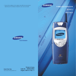
YEPP Model Name:YP-T10 Model Code :YP-T10JQB/XEO YP-T10JQB/XEU YP-T10JAB/XEU SERVICE YEPP Manual CONTENTS 1. Precaution 2. Product Specification 3. Disassembly & Reassembly 4. Troubleshooting 5. Exploded View & Part List 6. PCB Diagram 7. Schematic Diagram YP-T10 Refer to the service manual in the GSPN (see the rear cover) for the more information. GSPN (Global Service Partner Network) Area Web Site North America service.samsungportal.com Latin America latin.samsungportal.com CIS cis.samsungportal.com Europe europe.samsungportal.com China china.samsungportal.com Asia asia.samsungportal.com Mideast & Africa mea.samsungportal.com This Service Manual is a property of Samsung Electronics Co.,Ltd. Any unauthorized use of Manual can be punished under applicable International and/or domestic law. © Samsung Electronics Co.,Ltd. Oct. 2007 Printed in Korea Contents 1. Precaution 1-1 Safety Precautions............................................................................................. 1-1 1-2 Static Electricity Precautions..............................................................................1-2 2. Product Specification 2-1 Product Feature.................................................................................................. 2-1 2-2 Specifications.....................................................................................................2-2 2-3 Specifications Analysis.......................................................................................2-4 2-4 Accessories........................................................................................................2-5 3. Disassembly & Reassembly 3-1 Disassembly Method.......................................................................................... 3-1 3-2 Reassembly Method........................................................................................... 3-4 4. Troubleshooting 4-1 Checkpoints by Error Mode................................................................................4-1 4-2 Upgrade Methods............................................................................................... 4-14 5. Exploded View & Part List 5-1 Exploded View.................................................................................................... 5-1 5-2 Electrical Part List............................................................................................... 5-3 6. PCB Diagram 6-1 PCB Top.............................................................................................................6-1 6-2 PCB Bottom........................................................................................................6-3 7. Schematic Diagram 7-1 Overall Block Diagram........................................................................................7-2 7-2 POWER..............................................................................................................7-3 7-3 CPU PWR & MEM INF.......................................................................................7-4 7-4 CPU....................................................................................................................7-5 7-5 MEMORY...........................................................................................................7-6 7-6 AUDIO................................................................................................................7-7 7-7 24PIN I/O, Interface............................................................................................ 7-8 7-8 LCD Block...........................................................................................................7-9 7-9 Bluetooth Block...................................................................................................7-10 Precaution 1.Precaution 1-1 Safety Precautions 1. To remove dust from cabinet, use a dry cloth without using liquid and aerosol cleaner. 2. You should not use attachments not recommended by the company. Otherwise, it may cause critical damage. 3. You should not use this product near water such as bathtub, swimming pool or lake etc. 4. Power supply: A type of battery as displayed on the label should be only used. 5. You should not put any object or liquid into product. Otherwise, it may cause failure or mal-operation. 6. If replacement material is required, service engineer should use materials with the same standard. The use of non-standardized materials may cause failure of product. Samsung Electronics 1-1 Precaution 1-2 Static Electricity Precautions Some semi-conductor parts may be easily damaged due to static electricity. These elements are generally called as static electricity sense device (ESD). Typically examples of EST include IC, some transistor and chip element for semi-conductor with electrical field effect. The following methods should be used to reduce damage of elements occurred due to static electricity: 1. Contact and emit all the grounding objects with static electricity from your body before handling with elements for semi-conductor or devices with elements for semi-conductor. You should purchase and use static electricity arm rings or commercially available. You should remove it due to potential shock before supplying power to the device under test. 2. You should place appliance on the conductive surface like aluminum film to prevent that static electricity is accumulated or the device is disclosed outside after removing electrical appliance with the ESD device. 3. You should use only soldering iron that is ground when soldering the ESD device. 4. Minimize physical operation when handling with the ESD device for replacement without packing (Otherwise, namely friction between cloth fibers or lifting of the foot from the carpet floor may cause static electricity enough to damage the ESD device). 1-2 Samsung Electronics Product Specification 2.Product Specification 2-1 Product Feature Bluetooth, Video, Best Audio, Varity of Accessory Slim & Stylish - 11mm → 7.8mm - Back Metallic Design Advanced Video - 1.8 → 2.0" - QCIF+/15f → QVGA/30fps Advanced Bluetooth B/T support to Video/Game YP-T9 Best Audio Tone quality embodiment more than K5 YP-T10 Various Accessory Various Fashion and Technical accessory support Samsung Electronics 2-1 Product Specification 2-2 Specifications Basic Specification Model Name Capacity JQB JAB JCB JQG JAG JCG JQR JAR JCR JQU JAU JCU JQW JAW JCW 2G 4G 8G Color Midnight Black Rating DC 5.0V / 500mA Built-in Battery Power 2G 4G 8G Lime-Yellow 2G 4G 8G Maple Red 2G 4G 8G Mystic Purple 2G Earphone Output 20mW (16Ω) Output Frequency Range 20Hz ~ 20KHz Temperature Characteristics Case Weight Dimensions (WxHxD) LCD FM Frequency FM RADIO 8G 550 mAh / DC 3.7V File Compatibility Play Time 4G White Cloud AUDIO:MPEG1/2/2.5 Layer3(8kbps~320kbps, 22kHz~48kHz) WMA(5kbps~320kbps,8kHz~48kHz) VIDEO: SVI (Video: MPEG4, Audio: MP3(44.1kHz, 128Kbps), WMV(Video: WMV9 Simple Profi le, Audio: WMA Spec (Max 860kbps), Resolution: 320X240, Frame Rate: 30fps) IMAGE:JPEG(ISO/IEC 10918-1/Annex F-Sequential DCT-based mode of operation) Signal to Noise Ratio 2-2 YP-T10 90dB with 20KHz LPF(based on 1kHz 0dB) Maximum of 30 hours for music playback (based on: MP3 128kbps, Volume 15, Normal sound mode), Maximum of 4 hours for video playback -5 ~ 35°C (23 ~ 95°F) Plastic , Aluminum 43g 41.5 x 96 x 7.9 mm QVGA 2" TFT-LCD (30fps) 87.5 ~ 108.0MHz FM Signal to Noise Ratio 50dB FM T.H.D 1% FM Useable Sensitivity 30dBμ Samsung Electronics Product Specification Wireless System Emission Type RF Power F1D CLASS II Transmit Frequency 2402MHz ~ 2480MHz Receive Frequency 2402MHz ~ 2480MHz No. of channels Temperature Modulation System Communication Mode 79 CH -10°C ~ +50°C (14 ~ 122°F) GFSK Semi-duplex Operation Humidity 95% Spec Version Supported 2.0 Module Samsung Electronics BTEM48B2SA 2-3 Product Specification 2-3 Specifications Analysis Model Name YP-T10 YP-T9 iPod nano SONY A-series 41.5 x 96 x 7.9 mm 42.6 x 83 x 11 mm 40.6 x 88.9 x 6.6 mm 44.5 x 88.0 x 9.6 mm 43g 49g 39.97g 53g 2.0" QVGA 1.8" QCIF+ 1.46" 2.0" QVGA (320x240, 30fps) (220x172, 15fps) (176x132) (320x240, 30fps) Black, Pink, Lime, Blue, Black, White, Silver, Blue, Silver, Red Pink 2GB / 4GB / 8GB 2GB / 4GB / 8GB Photo Dimensions (WxDxH) Weight LCD Midnight Black Mystic Purple Color Maple Red Black, Purple, Pink Lime-Yellow White Cloud Capacity Battery Time Functions 2GB / 4GB / 8GB 1GB / 2GB / 4GB / 8GB Audio: 30Hrs Audio: 30Hrs Video: 4Hrs Video: 6Hrs Music, Video, Photo, FM Music, Video, Photo, FM Radio, Voice Rec., FM Radio, Voice Rec., FM Rec., Text Viewer Rec., Text, Game Audio: 24Hrs Audio: 30Hrs Video: 8Hrs Music, Photo, Text, Game Music, Photo, Video X X Enabled Bluetooth (Audio & Video) Enabled (Only Audio) Bluetooth 2.0 Bluetooth 1.2 (1:2 Support) 2-4 Samsung Electronics Product Specification 2-4 Accessories 2-4-1 Supplied Accessories Accessories Item Earphones Samsung Electronics Item code Black Remark AH30-00087E USB Cable AH39-00899A Program Installation CD AH46-00049A Samsung Service center 2-5 MEMO 2-6 Samsung Electronics Disassembly & Reassembly 3.Disassembly & Reassembly 3-1 Disassembly Method - Be careful to follow the disassembly sequence described in the manual. Otherwise, the product may be damaged. - Be sure to carefully read and understand the safety instructions before performing any work as the IC chips on the PCB are vulnerable to static electricity. - Assemble in the reverse order of disassembly. No. Part Name 1 CABINETBACK Description Description Photo 1) Remove Serial Label. The label must not be damaged. 2) Please unscrew 1EA from HOLDERJACK. : CH,+,B,M1.4,L5,NI PLT 3) Hook is fastened in Front top inner, Please hold up Front top and draw away hook. Samsung Electronics 3-1 Disassembly & Reassembly No. Part Name 2 CABINETFRONT Description Description Photo 1) Raise CABINET-FRONT like an arrow direction. 2) Please separate CABINET-FRONT FPC-TOUCH from YP-T10 PCB using pinset. When removing the FPC-TOUCH, be sure to use a pair of tweezers to avoid a tear. 3 TOUCH-PAD 4 LCD 1) Separate TOUCH-PAD. 1) Separate LCD from YP-T10 PCB. Be careful not to make any scratches as you remove it. 5 3-2 BATTERY 1) Separate Battery from YP-T10 PCB using pinset. Samsung Electronics Disassembly & Reassembly No. Part Name 6 MAIN BOARD Description Description Photo 1) Unscrew 1EA from MAIN BOARD. : PH,+,B,M1.4,L3,NI PLT 2) Separate MAIN BOARD from CABINET-BOTTOM. Samsung Electronics 3-3 Disassembly & Reassembly 3-2 Reassembly Method No. Part Name 1 CABINETFRONT Description Description Photo 1) Check KNOB HOLD of ASSYCABINET FRONT and HOLD SWITCH are same position. 2) Check HOLD SWITCH is center. - 3) The bottom of FRONT and “SAMSUNG” logo are in contact each other. 4) Slide in such as picture without GAP. If you assemble right position, ignore HOLD SWITCH position. Be cautious only KNOB SWITCH position. 5) Slide in ASSY FRONT to ASSY back and push touch pad at once without GAP. <Don’t push LCD because of break> <KNOB-HOLD position reaffirmation, SW secession prevention> 3-4 Samsung Electronics Disassembly & Reassembly No. Part Name 1 CABINETFRONT Description Description Photo 6) Slide KNOB-HOLDER to down not for separation. 7) Slide ASSY-FRONT to ASSY-BACK tightly. 8) Check KNOB HOLDE. 9) Check GAP. (Side, Top) - If you see a gap, don’t push. because inner hook will be broken. - But If you see a top gap, push slightly. Samsung Electronics 3-5 MEMO 3-6 Samsung Electronics Troubleshooting 4.Troubleshooting 4-1 Checkpoints by Error Mode Oscilloscope Setting Values Voltage/DIV 1V/div TIME/DIV 10ms/div 4-1-1 No Power Symptom Power does not turn on. Major Checklist Caution 1 Check the power terminal connection (battery, adapter). 2 Check if the key signal is ‘HIGH’ when the POWER key is pressed. (More than 2.5V) 3 Check if the ENABLE pin signal of the DDCON IC is ‘HIGH’. (More than 2.5V) 4 Check power. (L300: 1.08V(CORE), L301: 3.0V(MAIN), L302: 1.8V(MEMORY)) Be careful not to short anything out when checking the power line. The power does not turn on. After insert battery to PCB, Please TEST No Is battery inserted to Main PCB normally? Yes Does the power turn on after recharging the battery? Yes No A Completion Samsung Electronics 4-1 Troubleshooting A 2 Yes When power Key is on, check key signal as ‘HIGH’? (More than 2.5V) Refer to wave pattern image of Table 4-1. Yes 3 Yes Check MAIN 12Mhz clock Defective 4-2 Refer to wave pattern image of Table 4-1. Yes No No Completion No No Check DDCON enable pin signal as ‘HIGH’ (More than 2.5V) Refer to wave pattern image of Table 4-1. 4 Check power. L300: 1.08V(CORE) L301: 3.0V(MAIN) L302: 1.8V(MEMORY) Yes 1 Check BATTERY power. TP301, TP300 No Refer to wave pattern image of Table 4-1. Check power at the BATTERY (single part). Recheck after replacing the battery. Samsung Electronics Troubleshooting Test Point Result 2 IC302(1PIN, 19PIN), D301 2PIN, L300, L301, L302 Check for HIGH input - POWER ON 4 3 4 2 3 POWER Page, 7-3 4 L300 4 L301 4 4 L302 POWER Page, 7-3 4 2 CON300 4 IC302 3 4 CON801 IC900 IC303 IC600 PCB Top Page, 6-1 PCB Bottom Page, 6-3 <Table 4-1> Samsung Electronics IC701 4-3 IC601 Troubleshooting 4-1-2 No Sound Symptom No output at earphones Major Checklist Check if the earphones are normal. / Check the cold solder on the earphones jack. 1 Check if the DCVDD POWER input to the CODEC is proper. (Check for 1.8V) 2 Check if the AVDD1, AVDD2 power input to the CODEC is proper. (Check for 3.0V) No Sound Does the same symptom persist even after replacing the earphones? No Are the earphones normal? Yes Replace the earphones 2 1 Is audio codec voltage a normally? DCVDD: 1.8V Check Yes No Is audio codec voltage a normally? AVDD1, AVDD2: 3.0V Check No Does it play after supplementing the solder on the jack? No No Power Defective Refer to wave pattern image of Table 4-2. Does the YEPP Logo Song play? No Yes Yes Check if FET700 is shorted. Do R/L-CHs output normally? No No Yes Yes Are there skips and noises? Yes Check if IC701 is shorted. No Yes Are the skips and noises even when playing another file? Yes Does the same symptom persist even after upgrading the firmware to the latest version? Yes Replace the BOARD (needs thorough examination). 4-4 Samsung Electronics Troubleshooting Test Point Result AUDIO CODEC Power Check Check if 1.8V is output. / Check if 3.0V is output. 1 2 2 1 AUDIO Page, 7-7 CON801 IC900 1 IC701 2 PCB Top Page, 6-1 FET700 <Table 4-2> Samsung Electronics 4-5 Troubleshooting 4-1-3 TOUCH PAD Does Not Work Symptom Key press input malfunction or failure Major Checklist Check if FPC-TOUCH is defective. TOUCH PAD does not work Is the SWITCH in the HOLD OFF position? No Check the side of the unit to see if it is set to HOLD SW ON. Yes Is TOUCH KEY reaction? No Yes Is the TOUCH PAD malfunctioning? No Disassemble the unit and check if FPC-TOUCH is defective. If the TOUCH is poor, replace the TOUCH PAD. Replace the BOARD (needs thorough examination). Yes After change TOUCH PAD, check function 4-6 Samsung Electronics Troubleshooting 4-1-4 FM Tuner does not work. Symptom No FM radio reception 1 Check C152 FM_VDD on 1.0V 2 Check FM_Clock of 32.768KHz from RTC clock output Major Checklist Activate the FM radio. Are the earphones plugged in? No Connect an earphone & check again Yes Is BTEM48B2SA CHIP set to ENABLE?(IC100 20PIN) 1 No Check the power terminal. C152 : 1.0V Yes Refer to wave pattern image of Table 4-3. 2 Is 32.768 KHz CLOCK being inputted normally? Yes Completion No Is RTC CLOCK functioning normally? Refer to wave pattern image of Table 4-3. Yes No Yes Divide resistor check R103: 270K, R104: 1M No Replace the BOARD (needs thorough examination). Samsung Electronics 4-7 Troubleshooting Test Point Result C152, R513 C152 → 1.0V, R513 → 32.768KHz 1 2 1 IC602 Bluetooth Block Page, 7-10 2 CON900 CON IC900 CPU Page, 7-5 IC701 IC601 IC101 IC100 1 2 IC500 PCB Bottom Page, 6-3 PCB Top Page, 6-1 <Table 4-3> 4-8 Samsung Electronics Troubleshooting 4-1-5 No LCD Backlight Symptom LCD Backlight does not turn on 1 Check C905 on 3.5V 2 Check CON900 LCD B-to-B connector Major Checklist No LCD Backlight No Check Power is OK Yes Yes 1 Check C905 on 3.5V 2 Check CON900 LCD Yes B-to-B connector No Check No Power 4-1-1 Refer to wave pattern image of Table 4-4. Does the same symptom persist even after replacing the LCD? No Replace LCD Yes Replace the BOARD (needs thorough examination). Samsung Electronics 4-9 Troubleshooting Test Point Result C905 → 3.5V Check each output terminal. 1 1 LCD Block Page, 7-9 2 CON900 CON801 IC900 1 IC701 PCB Top Page, 6-1 <Table 4-4> FET700 4-10 Samsung Electronics Troubleshooting 4-1-6 Cannot Recharge Symptom Cannot recharge the BATTERY 1 Check external input voltage: DC 5V (D300) 2 Check #FULL_CHG PIN (IC302 14PIN) : HIGH → CHARGING, LOW → FULL_CHARGING 3 Check #CHARGE_STOP PIN (IC302 12PIN): HIGH → CHARGING, LOW → STOP Major Checklist Cannot Recharge Does it work when the power adapter is connected? No Yes Does it work after upgrading to the latest firmware? No Yes (after disassembling the unit) Is the Battery connector connected properly? No Disassemble the unit and check if Battery connector is defective. No Recheck after replacing the BATTERY. Yes Check power at the BATTERY (single part). Yes 1 Check external input No voltage: DC 5V (D300) Yes Refer to wave pattern image of Table 4-5. 2 Check #FULL_CHG PIN (IC302 14PIN): HIGH → CHARGING, LOW → FULL_CHARGING Yes No Refer to wave pattern image of Table 4-5. 3 Check #CHARGE_STOP PIN (IC302 12PIN): HIGH → CHARGING, LOW → STOP Yes Replace the BOARD (needs thorough examination). No Refer to wave pattern image of Table 4-5. Completion Samsung Electronics 4-11 Troubleshooting Test Point Result D300, IC302 14PIN & 12PIN D300 → 5V, IC302 14PIN & 12PIN → HIGH 1 1 2 3 2 3 POWER Page, 7-3 N300 2 3 IC302 IC602 IC303 1 IC600 PCB Bottom Page, 6-3 <Table 4-5> 4-12 Samsung Electronics IC601 Troubleshooting 4-1-7 Poor PC Connection Symptom USB cable is connected to the PC, but no connection is established USB connection Is there USB connection icon displayed on the LCD? No Is the USB connection established after a RESET? Yes No Yes Yes Does the unit show in “My Computer” as a portable device? No Is there an “Unknown Device” show in Device Manager? No Yes Yes No Recheck after installing the driver. Is it accessible? Yes Can NAND FORMAT and BOOT Update be performed with FWDN (Recovery tool)? No Can formatting be done in Explorer? No Defective Yes Completion Samsung Electronics 4-13 Troubleshooting 4-2 Upgrade Methods If the product does not power on and shows any of the following symptoms, you may try the upgrade methods in this chapter without having to disassemble the product: - The product does not turn on when the power switch is pressed. - The product powers on normally but no USB connection can be made. - The product’s icons appear garbled or malfunction. - Files are corrupted, or the product shows as a “removable storage” in Windows but cannot be accessed. 4-2-1 Firmware Upgrade Method 1. Download the firmware upgrade file to a folder and decompress it. 2. Check the contents of the folder that was decompressed. 3. Connect the YP-T10 to the PC. 4. Open the Removable Disk folder of the YP-T10. 5. Select the installation file in the folder that was decompressed, and then copy the upgrade files to the Removable Disk folder of the YP-T10. 6. Perform “Safely Remove Hardware”, and then disconnect the device from the PC. 7. When power on YP-T10, power off after “Image Upgrading...”, “AUI Upgrading...” 8. Power on again. After “Font Upgrading...”, “Image Upgrading...”, “AUI Upgrading...” set will be power off. 9. After the upgrade, go to “Menu” → “Settings” → “System” → “Firmware” and check the version. If the battery power is low, the upgrade will not start. In this case, you need to connect a USB or charging cord for the upgrade to start. 4-14 Samsung Electronics Troubleshooting 4-2-2 How to recovery system When do you perform this procedure?: When NAND data is corrupted In case of non-operation key. - Turn off the set and Restart. - If it doesn’t turn down, Press the reset button by using pointed stuff. (The reset button is located at the back near the bottom.) - Check the device if it operates properly. In case of device malfunction or serious problem. - FW Download Method through a Program(FWDN) Through this hard-recovery process, all data in the device will be totally deleted. You should be cautious. 1. If you use FWDN program for the first time, you should install VTC driver on your computer. 1) Before executing FWDN, execute intall2000XP. (FWDN\Driver\install2000XP) 2) Connect YP-T10 to PC by using USB cable. 3) Execute FWDN and open ROM file. 4) Press the POWER button and the RESET button. You should press the RESET button certainly with holding POWER button. At the same time it must have been connecting to PC by USB cable. Samsung Electronics 4-15 Troubleshooting 5) New hardware finding wizard appears. Tick “Software Setting Automatically” and click NEXT. 6) Wait for finding. 4-16 Samsung Electronics Troubleshooting 7) Press “Continue Anyway” button. 8) Press “OK” button. 9) Press “Browse...” button. 10) Select FWDN\Driver\vtcdrv.sys then OK and Finish. Samsung Electronics 4-17 Troubleshooting 11) Press “OK” button. 12) Driver establishment completion 2. Firmware downloading through FWDN 1) Set Preference. ( MENU Options > Preference ) 1 1Set INI file location. (FWDN\Driver\FWDN.INI) 2Set Sample file Path. (*.FNT, *.AUI, *.IMG) Generally, they are in the same location with ROM file. 2 4-18 The others are as like above picture. Then click "Apply" and "OK" the button. Samsung Electronics Troubleshooting 2) You can see WRITE(START) the button is activated. Click it. Then Firmware’s going to download. Samsung Electronics 4-19 Troubleshooting 3) After Firmware downloading completed, Disconnect the USB cable from the device. 3. Finishing 1) Turn on the device. You can see the message “Upgrading Firmware…” then the device turns down. 2) Turn on the device again. You can see the messages like “Image Upgrading...”, “AUI Upgrading...”, “Font Upgrading...” for a while. After that, the device will operate normally. 4-20 Samsung Electronics Troubleshooting 4-2-3 How to Set MAC Address Environment for setting MAC address: Windows XP When do you perform this procedure?: When NAND data is corrupted and after the FWDN Update How to download a MAC address 1. Disassemble the YP-T10 case and check the MAC Address sticker inside. 2. Enter the following MAC Address in a blank text file and save it with the name shown below. 3. Establish the USB connection and copy and paste the file to the Root Folder. 4. Disconnect the USB connection and Power On the YP-T10. 5. Go to “Menu” → “Bluetooth” → “Bluetooth Settings” → “My Device Info” and check the MAC Address. Samsung Electronics 4-21 Exploded View & Part List 5.Exploded View & Part List 5-1 Exploded View AA001 AA005 AH388 AT050 AC010 AC010 AC357 AH280 AS108 AA900 AK200 5-1 This Document can not be used without Samsung’s authorization. Samsung Electronics Exploded View & Part List Part List Loc. No. Part No. AA001 AH97-02334B AA005 Q’ty SNA ASSY-CABINET BACK;YP-T10,TITAN 1 SA AH97-02268B ASSY-BACK;NMT,TITAN SAMSUNG 1 SNA AA900 AH97-02352A ASSY;TOUCHPAD,YP-T10,K3, K5 #### ## 1 SA AC010 AH64-04362B CABINET-FRONT;YP-T10,-,PMMA+PCABS,-,PURP 1 SNA AC010 AH97-02335B ASSY-CABINET FRONT;YP-T10,BLACK 1 SA AC357 AH69-02042A CUSHION-LCD;YP-T10,RUB-OTH,Poron sheet,0 1 SNA AH280 AH61-02428B HOLDER-JACK;YP-T10,PC,T6,W38,L40,-,- 1 SNA AH388 AH61-02456A HOLDER-TAPE;YP-T10,9075,T0.08,-,-,CLEAR, 1 SNA AK200 AH64-04364B KNOB-HOLD;YP-T10,PC,T4,W3,L15,-,-,-,- 1 SNA AS108 AH63-01502A SHEET-PROTECTION;YP-T10,PET CLEAR,T0.13, 1 SNA AT050 AH74-01009A TAPE GASK;YP-T10,polyestar,-,gold,-,-,DK 1 SNA LCD AH07-00214A LCD;TS-200L-001A,YP-T10,-,30.6X40. 1 SA BATTERY AH43-00011A BATTERY;363744,YP-T10,polymer,550mAh,- 1 SA AH92-02739A ASSY PCB;YP-T10,MLC 2GB 1 SA QB AH92-02739B ASSY PCB;YP-T10,MLC 4GB 1 SA AB A 6003-001320 SCREW-TAPTITE;CH,+,B,M1.4,L5,NI PLT,SWRC 1 SA B 6003-001508 SCREW-TAPTITE;PH,+,B,M1.4,L3,NI PLT,SWRC 1 SA MAIN PCB Samsung Electronics Description;Specification This Document can not be used without Samsung’s authorization. Remark 5-2 Exploded View & Part List 5-2 Electrical Part List Loc. No. Part No. ANT100 C150 C151 C152 C153 C154 C155 C161 C300 C304 C305 C306 C308 C309 C310 C311 C312 C313 C315 C316 C317 C318 C319 C320 C321 C322 C323 C401 C403 C404 C405 C406 C407 C408 C409 C410 C411 C412 C413 C415 C418 C420 C421 C422 C423 C424 C425 C500 C501 C502 C504 C505 C506 C507 5-3 Description;Specification AH97-02404AASSY-KITTING BACK;YP-T10,BLACK AH97-02404CASSY-BACK KITTING;YP-T10AB (4G),SAM 4202-001305 ANTENNA-CHIP;2400-2485MHz,85MHz,1.6 2203-000254 C-CER,CHIP;10nF,10%,16V,X7R,1005 2203-006838 C-CER,CHIP;2200nF,10%,6.3V,X5R,1005 2203-006838 C-CER,CHIP;2200nF,10%,6.3V,X5R,1005 2203-002709 C-CER,CHIP;100nF,+80-20%,16V,Y5V,10 2203-006474 C-CER,CHIP;22000nF,20%,6.3V,X5R,201 2203-002709 C-CER,CHIP;100nF,+80-20%,16V,Y5V,10 2203-006093 C-CER,CHIP;1000nF,+80-20%,6.3V,Y5V, 2203-005900 C-CER,CHIP;1000NF,+80-20%,10V,Y5V,1 2203-006392 C-CER,CHIP;100NF,+-20%,6.3V,X5R,-,0 2404-001347 C-TA,CHIP;22uF,##20%,10V,-,TP,3.2x1 2404-001348 C-TA,CHIP;100UF,20%,6.3V,-,TP,3.2X1 2203-006392 C-CER,CHIP;100NF,+-20%,6.3V,X5R,-,0 2203-006392 C-CER,CHIP;100NF,+-20%,6.3V,X5R,-,0 2203-006890 C-CER,CHIP;10000nF,20%,6.3V,X5R,160 2203-006890 C-CER,CHIP;10000nF,20%,6.3V,X5R,160 2203-006683 C-CER,CHIP;4700nF,+80-20%,6.3V,Y5V, 2203-006324 C-CER,CHIP;2200nF,10%,10V,X5R,1608 2203-006392 C-CER,CHIP;100NF,+-20%,6.3V,X5R,-,0 2203-006361 C-CER,CHIP;10000nF,10%,10V,X5R,2012 2203-006093 C-CER,CHIP;1000nF,+80-20%,6.3V,Y5V, 2203-006392 C-CER,CHIP;100NF,+-20%,6.3V,X5R,-,0 2203-006392 C-CER,CHIP;100NF,+-20%,6.3V,X5R,-,0 2203-006474 C-CER,CHIP;22000nF,20%,6.3V,X5R,201 2203-005900 C-CER,CHIP;1000NF,+80-20%,10V,Y5V,1 2203-006474 C-CER,CHIP;22000nF,20%,6.3V,X5R,201 2203-006392 C-CER,CHIP;100NF,+-20%,6.3V,X5R,-,0 2203-006392 C-CER,CHIP;100NF,+-20%,6.3V,X5R,-,0 2203-006392 C-CER,CHIP;100NF,+-20%,6.3V,X5R,-,0 2203-006392 C-CER,CHIP;100NF,+-20%,6.3V,X5R,-,0 2203-006392 C-CER,CHIP;100NF,+-20%,6.3V,X5R,-,0 2203-006392 C-CER,CHIP;100NF,+-20%,6.3V,X5R,-,0 2203-006392 C-CER,CHIP;100NF,+-20%,6.3V,X5R,-,0 2203-006392 C-CER,CHIP;100NF,+-20%,6.3V,X5R,-,0 2203-006392 C-CER,CHIP;100NF,+-20%,6.3V,X5R,-,0 2203-006392 C-CER,CHIP;100NF,+-20%,6.3V,X5R,-,0 2203-006392 C-CER,CHIP;100NF,+-20%,6.3V,X5R,-,0 2203-006392 C-CER,CHIP;100NF,+-20%,6.3V,X5R,-,0 2203-006392 C-CER,CHIP;100NF,+-20%,6.3V,X5R,-,0 2203-006392 C-CER,CHIP;100NF,+-20%,6.3V,X5R,-,0 2203-006392 C-CER,CHIP;100NF,+-20%,6.3V,X5R,-,0 2203-005900 C-CER,CHIP;1000NF,+80-20%,10V,Y5V,1 2203-006392 C-CER,CHIP;100NF,+-20%,6.3V,X5R,-,0 2203-006392 C-CER,CHIP;100NF,+-20%,6.3V,X5R,-,0 2203-006890 C-CER,CHIP;10000nF,20%,6.3V,X5R,160 2203-006890 C-CER,CHIP;10000nF,20%,6.3V,X5R,160 2203-006890 C-CER,CHIP;10000nF,20%,6.3V,X5R,160 2203-000386 C-CER,CHIP;0.015nF,5%,50V,C0G,1005 2203-000330 C-CER,CHIP;0.012nF,5%,50V,C0G,1005 2203-000386 C-CER,CHIP;0.015nF,5%,50V,C0G,1005 2203-000330 C-CER,CHIP;0.012nF,5%,50V,C0G,1005 2203-006093 C-CER,CHIP;1000nF,+80-20%,6.3V,Y5V, 2203-002709 C-CER,CHIP;100nF,+80-20%,16V,Y5V,10 2203-005138 C-CER,CHIP;1.8nF,10%,50V,X7R,1005 Q’ty SNA Remark 1 1 1 1 1 1 1 1 1 1 1 1 1 1 1 1 1 1 1 1 1 1 1 1 1 1 1 1 1 1 1 1 1 1 1 1 1 1 1 1 1 1 1 1 1 1 1 1 1 1 1 1 1 1 1 1 SNA SNA SA SA SA SA SA SA SA SA SA SA SA SA SA SA SA SA SA SA SA SA SA SA SA SA SA SA SA SA SA SA SA SA SA SA SA SA SA SA SA SA SA SA SA SA SA SA SA SA SA SA SA SA SA SA QB AB Loc. No. Part No. C508 C510 C511 C601 C602 C603 C604 C605 C606 C607 C608 C609 C610 C700 C701 C702 C703 C704 C705 C706 C707 C708 C709 C710 C711 C712 C714 C715 C716 C717 C719 C720 C723 C800 C801 C802 C803 C900 C901 C902 C903 C904 C905 C906 C907 CON300 CON800 CON801 CON900 D300 D301 D302 D400 D900 D901 FET700 2203-005138 2203-002709 2203-002709 2203-002709 2203-006093 2203-006093 2203-006392 2203-006392 2203-006392 2203-006392 2203-006392 2203-006392 2203-006392 2203-002709 2203-005900 2203-002709 2203-000254 2203-006392 2203-005900 2203-006392 2404-001225 2404-001225 2203-002709 2203-006392 2203-002709 2404-001225 2404-001225 2203-006392 2404-001407 2404-001407 2203-006093 2203-006093 2203-000254 2203-006392 2404-001225 2203-006474 2203-002709 2203-006838 2203-006838 2203-005900 2203-005900 2203-005900 2203-005900 2203-002709 2203-002709 3710-001436 3710-002410 3708-002015 3711-006028 0404-001089 0401-000164 0401-000164 0401-000164 0406-001254 0406-001254 0505-002229 Description;Specification C-CER,CHIP;1.8nF,10%,50V,X7R,1005 C-CER,CHIP;100nF,+80-20%,16V,Y5V,10 C-CER,CHIP;100nF,+80-20%,16V,Y5V,10 C-CER,CHIP;100nF,+80-20%,16V,Y5V,10 C-CER,CHIP;1000nF,+80-20%,6.3V,Y5V, C-CER,CHIP;1000nF,+80-20%,6.3V,Y5V, C-CER,CHIP;100NF,+-20%,6.3V,X5R,-,0 C-CER,CHIP;100NF,+-20%,6.3V,X5R,-,0 C-CER,CHIP;100NF,+-20%,6.3V,X5R,-,0 C-CER,CHIP;100NF,+-20%,6.3V,X5R,-,0 C-CER,CHIP;100NF,+-20%,6.3V,X5R,-,0 C-CER,CHIP;100NF,+-20%,6.3V,X5R,-,0 C-CER,CHIP;100NF,+-20%,6.3V,X5R,-,0 C-CER,CHIP;100nF,+80-20%,16V,Y5V,10 C-CER,CHIP;1000NF,+80-20%,10V,Y5V,1 C-CER,CHIP;100nF,+80-20%,16V,Y5V,10 C-CER,CHIP;10nF,10%,16V,X7R,1005 C-CER,CHIP;100NF,+-20%,6.3V,X5R,-,0 C-CER,CHIP;1000NF,+80-20%,10V,Y5V,1 C-CER,CHIP;100NF,+-20%,6.3V,X5R,-,0 C-TA,CHIP;10uF,20%,6.3V,GP,TP,1608 C-TA,CHIP;10uF,20%,6.3V,GP,TP,1608 C-CER,CHIP;100nF,+80-20%,16V,Y5V,10 C-CER,CHIP;100NF,+-20%,6.3V,X5R,-,0 C-CER,CHIP;100nF,+80-20%,16V,Y5V,10 C-TA,CHIP;10uF,20%,6.3V,GP,TP,1608 C-TA,CHIP;10uF,20%,6.3V,GP,TP,1608 C-CER,CHIP;100NF,+-20%,6.3V,X5R,-,0 C-TA,CHIP;330uF,20%,2.5V,-,REEL,352 C-TA,CHIP;330uF,20%,2.5V,-,REEL,352 C-CER,CHIP;1000nF,+80-20%,6.3V,Y5V, C-CER,CHIP;1000nF,+80-20%,6.3V,Y5V, C-CER,CHIP;10nF,10%,16V,X7R,1005 C-CER,CHIP;100NF,+-20%,6.3V,X5R,-,0 C-TA,CHIP;10uF,20%,6.3V,GP,TP,1608 C-CER,CHIP;22000nF,20%,6.3V,X5R,201 C-CER,CHIP;100nF,+80-20%,16V,Y5V,10 C-CER,CHIP;2200nF,10%,6.3V,X5R,1005 C-CER,CHIP;2200nF,10%,6.3V,X5R,1005 C-CER,CHIP;1000NF,+80-20%,10V,Y5V,1 C-CER,CHIP;1000NF,+80-20%,10V,Y5V,1 C-CER,CHIP;1000NF,+80-20%,10V,Y5V,1 C-CER,CHIP;1000NF,+80-20%,10V,Y5V,1 C-CER,CHIP;100nF,+80-20%,16V,Y5V,10 C-CER,CHIP;100nF,+80-20%,16V,Y5V,10 SOCKET-BOARD TO BOARD;2P,1R,1.27mm, CONNECTOR-SOCKET;24P,1R,0.5mm,SMD-A CONNECTOR-FPC/FFC/PIC;6P,0.5mm,SMD- HEADER-BOARD TO BOARD;BOX,40P,2R,0. DIODE-SCHOTTKY;RB551V-30,20V,500MA, DIODE-SWITCHING;KDS121V,80V,100MA,V DIODE-SWITCHING;KDS121V,80V,100MA,V DIODE-SWITCHING;KDS121V,80V,100MA,V DIODE-TVS;UCLAMP0501P,6/-/-V,200W,S DIODE-TVS;UCLAMP0501P,6/-/-V,200W,S FET-SILICON;FDMA1028NZ,N,20V,3.7A,0 This Document can not be used without Samsung’s authorization. Q’ty SNA Remark 1 1 1 1 1 1 1 1 1 1 1 1 1 1 1 1 1 1 1 1 1 1 1 1 1 1 1 1 1 1 1 1 1 1 1 1 1 1 1 1 1 1 1 1 1 1 1 1 1 1 1 1 1 1 1 1 SA SA SA SA SA SA SA SA SA SA SA SA SA SA SA SA SA SA SA SA SA SA SA SA SA SA SA SA SA SA SA SA SA SA SA SA SA SA SA SA SA SA SA SA SA SA SA SA SA SA SA SA SA SA SA SA Samsung Electronics Exploded View & Part List Loc. No. Part No. Description;Specification Q’ty SNA Remark IC100 4709-001525 BLUETOOTH MODULE;3.3/1.5V dual supp IC101 1001-001336 IC-ANALOG SWITCH;-,-,QFN,10P,-,-,4. IC302 1203-004684 IC-DC/DC CONVERTER;AAT2550,QFN,24P, IC303 1203-004147 IC-DC/DC CONVERTER;MAX8640,SC-70,6P IC400 0902-002194 IC-MICROPROCESSOR;TCC780,192MHz,FBG IC401 0801-002800 IC-CMOS LOGIC;7SV08,AND GATE,SC-70, IC500 1203-004737 IC-VOL. DETECTOR;S-80122CLPF,SNT,4P IC600 1105-001820 IC-DRAM;EM488M3244LBA,SDR,256Mbit,4 IC602 1107-001663 IC-FLASH MEMORY;K9LAG08U0M,16Gbit,2 IC602 1107-001664 IC-FLASH MEMORY;K9HBG08U1M,32Gbit,4 IC701 1205-003214 IC-CODEC;WM1808GECO,QFN,28P,4x4mm,P IC900 1203-003708 IC-DC/DC CONVERTER;AAT3151,DFN,12P, JACK700 3722-002596 JACK-EAR PHONE;3P,AU,BLACK,SMD-A JFET300 0505-001930 FET-SILICON;MCH3319,P,-12V,-2.6A,MA L100 2703-002198 INDUCTOR-SMD;10nH,5%,1005 L101 2703-003296 INDUCTOR-SMD;47uH,10%,2012 L300 2703-003184 INDUCTOR-SMD;4.7uH,20%,2520 L301 2703-003184 INDUCTOR-SMD;4.7uH,20%,2520 L302 2703-003182 INDUCTOR-SMD;2.2uH,20%,2520 L701 3301-001148 BEAD-SMD;60ohm,1608,TP,-,- L702 3301-001364 BEAD-SMD;1000ohm,1608,150mA,TP,1085 L703 3301-001364 BEAD-SMD;1000ohm,1608,150mA,TP,1085 MIC700 3003-001119 MIC-CONDENSOR;3V,0.35,-22,0.3###### PCB_MAINAH41-01075A PCB-MAIN;YP-T10 PCB,FR4,8 layer,1.0 Q300 0504-001193 TR-DIGITAL;KRC408V,NPN,100MW,22K/47 Q303 0504-001193 TR-DIGITAL;KRC408V,NPN,100MW,22K/47 R101 2007-000157 R-CHIP;47Kohm,5%,1/16W,TP,1005 R102 2007-000157 R-CHIP;47Kohm,5%,1/16W,TP,1005 R103 2007-000636 R-CHIP;270KOHM,5%,1/16W,TP,1005 R104 2007-000170 R-CHIP;1Mohm,5%,1/16W,TP,1005 R107 2007-000140 R-CHIP;1Kohm,5%,1/16W,TP,1005 R109 2007-000157 R-CHIP;47Kohm,5%,1/16W,TP,1005 R301 2007-008483 R-CHIP;47Kohm,5%,1/20W,TP,0603 R302 2007-000155 R-CHIP;27KOHM,5%,1/16W,TP,1005 R303 2007-008304 R-CHIP;300Kohm,1%,1/16W,TP,1005 R304 2007-007107 R-CHIP;100Kohm,1%,1/16W,TP,1005 R305 2007-008517 R-CHIP;240Kohm,1%,1/16W,TP,1005 R307 2007-007587 R-CHIP;3.6Kohm,1%,1/16W,TP,1005 R308 2007-008213 R-CHIP;4.3Kohm,1%,1/16W,TP,1005 R309 2007-008516 R-CHIP;10Kohm,5%,1/20W,TP,0603 R310 2007-007538 R-CHIP;56Kohm,1%,1/16W,TP,1005 R312 2007-007589 R-CHIP;68Kohm,1%,1/16W,TP,1005 R313 2007-000157 R-CHIP;47Kohm,5%,1/16W,TP,1005 R314 2007-008483 R-CHIP;47Kohm,5%,1/20W,TP,0603 R315 2007-007142 R-CHIP;10Kohm,1%,1/16W,TP,1005 R316 2007-000157 R-CHIP;47Kohm,5%,1/16W,TP,1005 R317 2007-008304 R-CHIP;300Kohm,1%,1/16W,TP,1005 R318 2007-007488 R-CHIP;75KOHM,1%,1/16W,TP,1005 R320 2007-008483 R-CHIP;47Kohm,5%,1/20W,TP,0603 R322 2007-008483 R-CHIP;47Kohm,5%,1/20W,TP,0603 R323 2007-008055 R-CHIP;100Kohm,5%,1/20W,TP,0603 R328 2007-008055 R-CHIP;100Kohm,5%,1/20W,TP,0603 R329 2007-008483 R-CHIP;47Kohm,5%,1/20W,TP,0603 R400 2007-008516 R-CHIP;10Kohm,5%,1/20W,TP,0603 R401 2007-008516 R-CHIP;10Kohm,5%,1/20W,TP,0603 R402 2007-008516 R-CHIP;10Kohm,5%,1/20W,TP,0603 Samsung Electronics 1 SA 1 SA 1 SA 1 SA 1 SA 1 SA 1 SA 1 SA 1 SA 1 SA 1 SA 1 SA 1 SA 1 SA 1 SA 1 SA 1 SA 1 SA 1 SA 1 SA 1 SA 1 SA 1 SA 0.25SNA 1 SA 1 SA 1 SA 1 SA 1 SA 1 SA 1 SA 1 SA 1 SA 1 SA 1 SA 1 SA 1 SA 1 SA 1 SA 1 SA 1 SA 1 SA 1 SA 1 SA 1 SA 1 SA 1 SA 1 SA 1 SA 1 SA 1 SA 1 SA 1 SA 1 SA 1 SA 1 SA QB AB Loc. No. Part No. R403 R404 R405 R407 R408 R409 R410 R411 R412 R413 R414 R415 R501 R502 R503 R505 R507 R508 R509 R510 R511 R512 R513 R514 R515 R516 R517 R520 R523 R524 R605 R606 R607 R608 R700 R701 R702 R703 R704 R705 R706 R707 R711 R712 R718 R720 R801 R802 R803 R804 R805 R806 R807 R900 R901 R902 2007-008516 2007-008516 2007-008516 2007-008516 2007-008516 2007-008516 2007-008516 2007-008516 2007-008516 2007-008516 2007-000143 2007-008483 2007-000139 2007-007001 2007-000140 2007-000162 2007-008516 2007-007316 2007-008516 2007-000157 2007-008483 2007-007142 2007-000636 2007-000157 2007-000170 2007-000157 2007-000143 2007-008483 2007-008483 2007-007142 2007-008516 2007-008516 2007-000171 2007-000171 2007-000140 2007-000566 2007-000140 2007-008516 2007-000070 2007-008516 2007-002797 2007-002797 2007-007136 2007-007136 2007-000140 2007-000162 2007-007199 2007-007199 2007-007142 2007-000140 2007-000155 2007-000566 2007-000171 2007-008483 2007-000143 2007-000138 Description;Specification R-CHIP;10Kohm,5%,1/20W,TP,0603 R-CHIP;10Kohm,5%,1/20W,TP,0603 R-CHIP;10Kohm,5%,1/20W,TP,0603 R-CHIP;10Kohm,5%,1/20W,TP,0603 R-CHIP;10Kohm,5%,1/20W,TP,0603 R-CHIP;10Kohm,5%,1/20W,TP,0603 R-CHIP;10Kohm,5%,1/20W,TP,0603 R-CHIP;10Kohm,5%,1/20W,TP,0603 R-CHIP;10Kohm,5%,1/20W,TP,0603 R-CHIP;10Kohm,5%,1/20W,TP,0603 R-CHIP;4.7Kohm,5%,1/16W,TP,1005 R-CHIP;47Kohm,5%,1/20W,TP,0603 R-CHIP;220ohm,5%,1/16W,TP,1005 R-CHIP;3.9KOHM,5%,1/16W,TP,1005 R-CHIP;1Kohm,5%,1/16W,TP,1005 R-CHIP;100Kohm,5%,1/16W,TP,1005 R-CHIP;10Kohm,5%,1/20W,TP,0603 R-CHIP;3.3KOHM,1%,1/16W,TP,1005 R-CHIP;10Kohm,5%,1/20W,TP,0603 R-CHIP;47Kohm,5%,1/16W,TP,1005 R-CHIP;47Kohm,5%,1/20W,TP,0603 R-CHIP;10Kohm,1%,1/16W,TP,1005 R-CHIP;270KOHM,5%,1/16W,TP,1005 R-CHIP;47Kohm,5%,1/16W,TP,1005 R-CHIP;1Mohm,5%,1/16W,TP,1005 R-CHIP;47Kohm,5%,1/16W,TP,1005 R-CHIP;4.7Kohm,5%,1/16W,TP,1005 R-CHIP;47Kohm,5%,1/20W,TP,0603 R-CHIP;47Kohm,5%,1/20W,TP,0603 R-CHIP;10Kohm,1%,1/16W,TP,1005 R-CHIP;10Kohm,5%,1/20W,TP,0603 R-CHIP;10Kohm,5%,1/20W,TP,0603 R-CHIP;0ohm,5%,1/16W,TP,1005 R-CHIP;0ohm,5%,1/16W,TP,1005 R-CHIP;1Kohm,5%,1/16W,TP,1005 R-CHIP;220Kohm,5%,1/16W,TP,1005 R-CHIP;1Kohm,5%,1/16W,TP,1005 R-CHIP;10Kohm,5%,1/20W,TP,0603 R-CHIP;0ohm,5%,1/10W,TP,1608 R-CHIP;10Kohm,5%,1/20W,TP,0603 R-CHIP;560OHM,5%,1/16W,TP,1005 R-CHIP;560OHM,5%,1/16W,TP,1005 R-CHIP;4.7Kohm,1%,1/16W,TP,1005 R-CHIP;4.7Kohm,1%,1/16W,TP,1005 R-CHIP;1Kohm,5%,1/16W,TP,1005 R-CHIP;100Kohm,5%,1/16W,TP,1005 R-CHIP;2.7ohm,5%,1/16W,TP,1005 R-CHIP;2.7ohm,5%,1/16W,TP,1005 R-CHIP;10Kohm,1%,1/16W,TP,1005 R-CHIP;1Kohm,5%,1/16W,TP,1005 R-CHIP;27KOHM,5%,1/16W,TP,1005 R-CHIP;220Kohm,5%,1/16W,TP,1005 R-CHIP;0ohm,5%,1/16W,TP,1005 R-CHIP;47Kohm,5%,1/20W,TP,0603 R-CHIP;4.7Kohm,5%,1/16W,TP,1005 R-CHIP;100ohm,5%,1/16W,TP,1005 This Document can not be used without Samsung’s authorization. Q’ty SNA Remark 1 1 1 1 1 1 1 1 1 1 1 1 1 1 1 1 1 1 1 1 1 1 1 1 1 1 1 1 1 1 1 1 1 1 1 1 1 1 1 1 1 1 1 1 1 1 1 1 1 1 1 1 1 1 1 1 SA SA SA SA SA SA SA SA SA SA SA SA SA SA SA SA SA SA SA SA SA SA SA SA SA SA SA SA SA SA SA SA SA SA SA SA SA SA SA SA SA SA SA SA SA SA SA SA SA SA SA SA SA SA SA SA 5-4 Exploded View & Part List Loc. No. Part No. Description;Specification Q’ty SNA Remark R903 2007-008483 R-CHIP;47Kohm,5%,1/20W,TP,0603 R904 2007-000138 R-CHIP;100ohm,5%,1/16W,TP,1005 RESET 3404-001324 SWITCH-TACT;50mA,12VDC,0.3gf,3.9x2. S/W300 3408-001141 SWITCH-SLIDE;4V DC,0.3A,1,1-pole 3- SHEET AH63-01556A SHEET-PCB;YP-T10,3M,T0.6,W15,L22,BL SHEET-BGAAH63-01572A SHEET-BGA;YP-T10,PORON,T0.3,W8,L13, USB-GASKETAH63-01474A GASKET;YP-T10,Remark,T0.13,W5,L3,-, VR301 1405-001093 VARISTOR;14V,20A,1x0.5x0.6mm,TP VR302 1405-001093 VARISTOR;14V,20A,1x0.5x0.6mm,TP VR303 1405-001093 VARISTOR;14V,20A,1x0.5x0.6mm,TP VR500 1405-001093 VARISTOR;14V,20A,1x0.5x0.6mm,TP VR701 1405-001093 VARISTOR;14V,20A,1x0.5x0.6mm,TP VR702 1405-001093 VARISTOR;14V,20A,1x0.5x0.6mm,TP VR800 1405-001093 VARISTOR;14V,20A,1x0.5x0.6mm,TP VR803 1405-001093 VARISTOR;14V,20A,1x0.5x0.6mm,TP VR900 1405-001093 VARISTOR;14V,20A,1x0.5x0.6mm,TP X_TAL5002801-000102 CRYSTAL-SMD;12MHz,30ppm,-,12pF,100o X_TAL5012801-004339 CRYSTAL-SMD;0.032768MHZ,20PPM,SMD,9 ZD800 0406-001254 DIODE-TVS;UCLAMP0501P,6/-/-V,200W,S AH07-00214A LCD;TS-200L-001A,YP-T10,-,30.6X40. AH43-00011A BATTERY;363744,YP-T10,polymer,550mA AH68-00908HLABEL-SERIAL;YP-T9,ALL,art paper,-, AH92-02739A ASSY PCB;YP-T10,MLC 2GB AH92-02739B ASSY PCB;YP-T10,MLC 4GB AH99-10007S ASSY PCB,m;YP-T10,MLC 2GB AH97-02438YASSY MACHINERY-ACCESSORY;XEU(BLACK) AH97-02438XASSY MACHINERY-ACCESSORY;XEO(BLACK) 6801-001335 CARD-REGISTRATION;HUNGARY,SEH,HUNGA AH30-00087E PHONE-EARPHONE;BUSHING Black,-,32,1 AH39-00899A CBF CABLE;USB CABLE,49338-0001,YP-T AH46-00049A S/W CD-INSTALL;YP-T10,Same as SEC C AH68-00650CMARK RECYCLE-WARRANTY-CARD;YP-K3,XE AH68-02016E MANUAL-QG;YP-T10,XEO,ENG/POL/ROM/GR AH68-40042A CARD-WARRANTY;YEPP,SEPOL,POLISH,-,V AH69-02072A PACKING CASE-BOTTOM;YP-P2,PC,CLEAR, AH69-02074A PACKING CASE-TOP;YP-P2,PC,CLEAR,T1. AH69-02095DPACKING-SHEET BOTTOM;YP-T10,PAPER,M AH97-02492A ASSY-PACKING MIDDLE;YP-T10,- AH69-02082A PACKING-CASE MIDDLE;YP-T10,PC,,,T17 AH69-02094A PACKING-SHEET MIDDLE;YP-T10,PAPER,M AH69-02096A PACKING-SHEET HANDLER;YP-T10,OTHER, AH69-02124A CUSHION-SHEET MIDDLE;YP-T10,RUB-OTH AH68-40042CCARD WARRANTY;ALL,ENG,ART,-,L210,-, AH68-02016B MANUAL-QG;YP-T10,XEU,ENG,-,MOJO80G, 1 1 1 1 1 1 1 1 1 1 1 1 1 1 1 1 1 1 1 1 1 1 1 1 1 1 1 1 1 1 1 1 1 1 1 1 1 1 1 1 1 1 1 1 0.1 SNA 1 SNA 1 SNA 1.05SNA 0.1 SA 5-5 AH68-00508ULABEL SERIAL;COMMON,ELS,-,-,90,-,-, AH68-00701HLABEL SERIAL;YP-T7,ALL,-,-,W20,L5.6 AH68-50114S LABEL SHIPPING;ALL,XEO,-,-,-,-,-,-, AH68-50119B LABEL-EAN(B);ART-PAPER,T0.05,L29,W4 AH69-02091A MASTER CARTON;YP-P2/T10,OTHER,T6,W1 Loc. No. Part No. Description;Specification Q’ty SNA Remark SA SA SA SA SNA SA SA SA SA SA SA SA SA SA SA SA SA SA SA SA SA SNA SA SA SNA SNA SNA SNA SA SA QB AB XEO XEU SA SNA SA SNA SA SA SA SA SA SA SA SA SNA SNA XEU XEU This Document can not be used without Samsung’s authorization. Samsung Electronics PCB Diagram 6.PCB Diagram 6-1 PCB Top TP1 1 CON900 0 CON801 IC900 9 TP14 2 TP13 8 TP12 IC701 7 TP10 3 4 TP11 FET700 6 5 Samsung Electronics 1 LCD Connector 2 BATTERY TP - 3 32.768KHz System Clock 4 24MHz USB Clock 5 BATTERY TP + 6 MIC 7 Audio Codec 8 BLUETOOTH ANTENA 9 LCD BACKLIGHT DRIVER 0 Touchpad Connector 6-1 PCB Diagram 6-1-1 Pin Connection 6-1-2 Test Point Wave Form 1 LCD Connector TP14 TP1 Pin No. Signal Pin No. Signal Pin No. Signal 1 GND 15 P3.0V 29 LCD_GRN2 2 LCD_VSYNC 16 GND 30 LCD_GRN3 3 LCD_HSYNC 17 LED1- 31 LCD_GRN4 4 LCD_PCLK 18 LED2- 32 LCD_GRN5 5 LCD_DE 19 LED+ 33 LCD_BLU0 6 GND 20 LCD_DETECT 34 LCD_BLU1 7 LCD_RST 21 LCD_RED0 35 LCD_BLU2 8 LCD_CS 22 LCD_RED1 36 LCD_BLU3 9 I2C_CLK1 23 LCD_RED2 37 LCD_BLU4 10 GND 24 LCD_RED3 38 LCD_BLU5 11 P3.0V 25 LCD_RED4 39 I2C_DAT1 12 P3.0V 26 LCD_RED5 40 GND 13 LCD_STATUS 27 LCD_GRN0 14 P3.0V 28 LCD_GRN1 0 Touchpad Connector Pin No. Signal 1 GND 2 T_CLK 3 T_DATA 4 T_ACK 5 NC 6 P3.0V TP1 TP14 TP10 TP10 TP11 TP11 TP12 TP12 TP13 TP13 6-2 Samsung Electronics PCB Diagram 6-2 PCB Bottom TP3 TP7 1 TP8 CON300 IC302 TP2 2 0 TP5 IC602 IC303 TP4 9 3 IC600 TP6 IC601 IC101 IC400 IC100 8 TP15 7 4 TP9 1 BATTERY Connector 2 BATTERY CHARGER DCDC CONV 3 SDRAM 32MB 4 MAIN CPU 5 USB Connector 6 EARPHONE JACK 7 RESET SWITCH 8 BLUETOOTH MODULE 9 NAND FLASH 0 POWER/HOLD SWITCH IC500 5 Samsung Electronics CON800 6 6-3 PCB Diagram 6-2-1 Pin Connection 6-2-2 Test Point Wave Form 5 USB Connector TP2 Pin No. Signal Pin No. Signal 1 BATT ID 13 Uart RX1 2 DEVICE DET/CE 14 Uart TX1 3 JTAG_TCK/DC3.3V OUT 15 USB D+/HOST D+ 4 ADAPTOR 16 USB PWR 5 ADAPTOR 17 LINE OUT R 6 JTAG_TCK/DC3.3V OUT 18 LINE OUT L 7 JTAG_TMS/CVBS IN 19 GND 8 LINE IN R 20 REVERSE TP3 9 LINE IN L 21 BATT TP4 10 USB D-/HOST D- 22 BATT TP5 11 JTAG_RST/REVERSE 23 EXT BAT INPUT 12 GND 24 PBA CE TP2 TP3 / TP4 / TP5 TP6 / TP7 / TP8 6 EARPHONE JACK Pin No. Signal 5A GND 1 R-CH 4A NC 4B L-CH 5B HD-DET TP6 TP7 TP8 TP9 TP9 TP15 TP15 6-4 Samsung Electronics Schematic Diagram 7.Schematic Diagram 7-1 Overall Block Diagram...................................................................................... 7-2 7-2 POWER.............................................................................................................. 7-3 7-3 CPU PWR & MEM INF....................................................................................... 7-4 7-4 CPU.................................................................................................................... 7-5 7-5 MEMORY............................................................................................................ 7-6 7-6 AUDIO................................................................................................................ 7-7 7-7 24PIN I/O, Interface........................................................................................... 7-8 7-8 LCD Block.......................................................................................................... 7-9 7-9 Bluetooth Block................................................................................................ 7-10 Samsung Electronics This Document can not be used without Samsung’s authorization. 7-1 Schematic Diagram 7-1 Overall Block Diagram Battery Charge & Dual Buck Converter > P 1.2V > P 2.9V > P 1.8V > P 3.3V FM ANT EAR JACK LT3559, MAX8670, MAX8740 WM1808L LITHUM BATTERY 3.7V ~550mA Power Management 2’’ 2” QVGA QVGA LCD LCD 320X240 320X240 RGB 6:6:6 VIDEO I/O ARM926 CORE GPIO ADC RTC USB 2.0/1.1 SPDIF, DAI SD/MMC/SDIO TIMER I2C/I2S PCM UART PWM MEMORY I/O LCD CTRL I2 S T R UA I2S I2S UART UART BCM2048 SKUFBG The Main System contains basic circuit blocks, such as Processor(TCC7801), SDRAM, Flash Memory, Power Block, Audio DAC, etc., and function blocks, such as Bluetooth Block, 24pin I/O, and etc. The display is connected to a 2-inch TFT LCD. Serial Interfaces between ICs are implemented with various Protocols throughout the System. A host processor (TCC7801) UART is used to implement CODEC and FM Tuner features. The interface between the Bluetooth Module and the Host Processor is achieved through UART, and the audio DAC achieves mode setting and data transfer through I2C and I2S, respectively. Power can be turned On and Off with the Power S/W located at the top of the set. Either the built-in battery or the power adapter can be used for power supply. The power adapter is capable of 5V input. Power from the power adapter is used to recharge the battery at AAT2550 and generates power for the system (3.0V, 1.2V). Bluetooth + FM Touch Key Touch Key 192MHz ARM946 (SUB) I I-MEM /E E-MEM - NAND-FLASH NANDFLASH MEMORY MEMORY TCC 7801 256 BALL BGA 14 X14mm 0.8mm PITCH 0.40~0.45mm BALL PI 7-2 This Document can not be used without Samsung’s authorization. Samsung Electronics Schematic Diagram 7-2 POWER TP1 / TP2 POWER TP1 TP2 TP6 TP3 / TP4 / TP5 TP7 TP3 TP4 TP3 TP8 TP4 TP5 TP1 TP6 / TP7 / TP8 TP6 TP7 TP8 TP2 TP5 Samsung Electronics This Document can not be used without Samsung’s authorization. 7-3 Schematic Diagram 7-3 CPU PWR & MEM INF POWER 7-4 This Document can not be used without Samsung’s authorization. Samsung Electronics Schematic Diagram 7-4 CPU POWER TP11 TP10 TP9 / TP10 TP9 TP9 TP10 TP11 TP11 Samsung Electronics This Document can not be used without Samsung’s authorization. 7-5 Schematic Diagram 7-5 MEMORY POWER 7-6 This Document can not be used without Samsung’s authorization. Samsung Electronics Schematic Diagram 7-6 AUDIO TP12 POWER AUDIO TP12 TP12 TP13 TP13 TP13 Samsung Electronics This Document can not be used without Samsung’s authorization. 7-7 Schematic Diagram 7-7 24PIN I/O, Interface POWER 7-8 This Document can not be used without Samsung’s authorization. Samsung Electronics Schematic Diagram 7-8 LCD Block TP14 POWER TP14 TP14 Samsung Electronics This Document can not be used without Samsung’s authorization. 7-9 Schematic Diagram 7-9 Bluetooth Block TP15 POWER TP15 TP15 7-10 This Document can not be used without Samsung’s authorization. Samsung Electronics