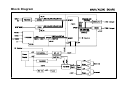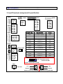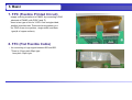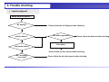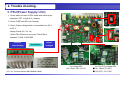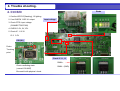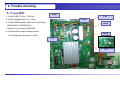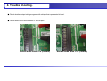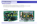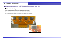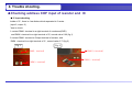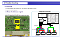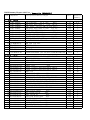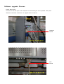
1
SERVICE MANUAL Model: PDP Safety Precaution Technical Specifications Block Diagram Circuit Diagram Basic Operations & Circuit Description Main IC Specifications Product Specification of PDP Module Trouble Shooting Manual of PDP Module Spare Part List Exploded View If you forget your V-Chip Password Software Upgrade This manual is the latest at the time of printing, and does not include the modification which may be made after the printing, by the constant improvement of product. Safety Precaution CAUTION RISK OF ELECTRIC SHOCK DO NOT OPEN CAUTION: TO REDUCE THE RISK OF ELECTRIC SHOCK, DO NOT REMOVE COVER (OR BACK). NO USER-SERVICEABLE PARTS INSIDE. REFER SERVICING TO QUALIFIED SERVICE PERSONNEL ONLY. PRECAUTIONS DURING SERVICING 1. In addition to safety, other parts and assemblies are specified for conformance with such regulations as those applying to spurious radiation. These must also be replaced only with specified replacements. Examples: RF converters, tuner units, antenna selection switches, RF cables, noise-blocking capacitors, noise-blocking filters, etc. 2. Use specified internal Wiring. Note especially: 1) Wires covered with PVC tubing 2) Double insulated wires 3) High voltage leads 3. Use specified insulating materials for hazardous live parts. Note especially: 1) Insulating Tape 2) PVC tubing 3) Spacers (insulating barriers) 4) Insulating sheets for transistors 5) Plastic screws for fixing micro switches 4. When replacing AC primary side components (transformers, power cords, noise blocking capacitors, etc.), wrap ends of wires securely about the terminals before soldering. The lightning flash with arrowhead symbol, within an equilateral triangle, is intended to alert the user to the presence of uninsulated “dangerous voltage” within the product’s enclo sure that may be of sufficient magnitude to constitute a risk of electric shock to persons. The exclamation point within an equilateral triangle is intended to alert the user to the presence of important operating and maintenance (servicing) instructions in the literature accompanying the appliance. MAKE YOUR CONTRIBUTION TO PROTECT THE ENVIRONMENT Used batteries with the ISO symbol for recycling as well as small accumulators (rechargeable batteries), mini-batteries (cells) and starter batteries should not be thrown into the garbage can. Please leave them at an appropriate depot. WARNING: Before servicing this TV receiver, read the SAFETY INSTRUCTION and PRODUCT SAFETY NOTICE. SAFETY INSTRUCTION The service should not be attempted by anyone unfamiliar with the necessary instructions on this apparatus. The following are the necessary instructions to be observed before servicing. 1. An isolation transformer should be connected in the power line between the receiver and the AC line when a service is performed on the primary of the converter transformer of the set. 2. Comply with all caution and safety related provided on the back of the cabinet, inside the cabinet, on the chassis or picture tube. 5. Make sure that wires do not contact heat generating parts (heat sinks, oxide metal film resistors, fusible resistors, etc.) 6. Check if replaced wires do not contact sharply edged or pointed parts. 7. Make sure that foreign objects (screws, solder droplets, etc.) do not remain inside the set. 3. To avoid a shock hazard, always discharge the picture tube's anode to the chassis ground before removing the anode cap. 4. Completely discharge the high potential voltage of the picture tube before handling. The picture tube is a vacuum and if broken, the glass will explode. 5. When replacing a MAIN PCB in the cabinet, always be certain that all protective are installed properly such as control knobs, adjustment covers or shields, barriers, isolation resistor networks etc. 6. When servicing is required, observe the original lead dressing. Extra precaution should be given to assure correct lead dressing in the high voltage area. PRODUCT SAFETY NOTICE Many electrical and mechanical parts in this apparatus have special safety-related characteristics. These characteristics are offer passed unnoticed by visual spection and the protection afforded by them cannot necessarily be obtained by using replacement components rates for a 7. Keep wires away from high voltage or high tempera ture components. higher voltage, wattage, etc. The replacement parts which have these 8. Before returning the set to the customer, always perform an AC leakage current check special safety characteristics are identified by marks on the schematic diagram and on the parts on the exposed metallic parts of the cabinet, such as antennas, terminals, screwheads,metal list. overlay, control shafts, etc., to be sure the set is safe to operate without danger of electrical read the parts list in this manual carefully. The use of substitute replacement parts which do not shock. Plug the AC line cord directly to the AC outlet (do not use a line isolation have the same safety characteristics as specified in the parts list may create shock, fire, or other transformer during this check). Use an AC voltmeter having 5K ohms volt sensitivity or hazards. 9. Must be sure that the ground wire of the AC more in the following manner. Connect a 1.5K ohm 10 watt resistor paralleled inlet is connected with the ground of the apparatus properly. by a 0.15µF AC type capacitor, between a good earth ground (water pipe, conductor etc.,) and the exposed metallic parts, one at a time. Measure the AC voltage across the combination of the 1.5K ohm resistor and 0.15 uF capacitor. Reverse the AC plug at the AC outlet and repeat the AC voltage measurements for each exposed metallic part. The measured voltage must not exceed 0.3V RMS. This corresponds to 0.5mA AC. Any value exceeding this limit constitutes a potential shock hazard and must be corrected immediately. The resistance measurement should be done between accessible exposed metal parts and power cord plug prongs with the power switch "ON". The resistance should be more than 6M ohms. AC VOLTMETER Good earth ground such as the water pipe, conductor, etc. Place this probe on each exposed metallic part AC Leakage Current Check Before replacing any of these components, MODEL : Technical Specifications DATE FIRST ISSUED ISSUE PDP4206EM 42” Plasma Monitor RAISED BY CHECKED BY NUMBER OF PAGES 1 REVISIONS ISSUED DATE 9 DESCRIPTION SPECIFICATION AGREED : RAISED BY : SIGNATURE DATE ...................................................................................... ...... ........................... ... ...................................................................................... ...... ........................... ... Q/A DEPARTMENT ...................................................................................... ....... ........................... ... CUSTOMER ...................................................................................... ....... ........................... ... ...................................................................................... ....... ........................... ... R & D DEPARTMENT COMMERCIAL DEPARTMENT PRODUCTION DEPARTMENT SPECIFICATION APPROVED : SIGNATURE : . NOTE : Only documents stamped “Controlled Document” to be used for manufacture of production parts. DATE : Technical 1. CONTINUATION PAGE Specifications PDP420 NUMBER 2 OF 9 PAGES Standard Test Conditions All tests shall be performed under the following conditions, unless otherwise specified. 1.1 Ambient light : 150ux (When measuring IB, the ambient luminance ≦0.1Cd/m2) 1.2 Viewing distance : 50cm in front of PDP 1.3 Warm up time : 30 minutes 1.4 PDP Panel facing : no restricted 1.5 Measuring Equipment : PC, Chroma 2225 signal generator (with Chroma digital additional card) or equivalent, Minolta CA100 photometer 1.6 Magnetic field : no restricted 1.7 Control settings : Brightness, Contrast, Tint, Color set at Center(50) 1.8 Power input : 110~120Vac 1.9 Ambient temperature : 1.10 Display mode : 1.11 Other conditions : 20°C ± 5°C (68°F ± 9°F) 31.5KHz/60Hz (Resolution 852 x 480) 1.11.1 With image sticking protection of PDP module, the luminance will descend by time on a same still screen and rapidly go down in 5 minutes. When measuring the color tracking and luminance of a same still screen, be sure to accomplish the measurement in one minute to ensure its accuracy. 1.11.2 Due to the structure of PDP, the extra-high-bright same screen should not hold over 5 minutes for fear of branding on the panel. Technical CONTINUATION PAGE Specifications PDP4206EM NUMBER 3 OF 9 PAGES ELECTRICAL CHARACTERISTICS 2. 3. Power Input 2.1 Voltage : 110 ~120VAC 2.2 Input Current : 3.5 / 1.5A 2.3 Maximum Inrush Current Test condition : : <30 A (FOR AC110V ONLY) Measured when switched off for at least 20 mins 2.4 Frequency : 50Hz to 60Hz(±3Hz) 2.5 Power Consumption Test condition : : ≤ 330W full white display with maximum brightness and contrast 2.6 Power Factor : Meets IEC1000-3-2 2.7 Withstanding voltage : 1.5kVac or 2.2kVdc for 1 sec : : : : : : : 42” Plasma monitor 16:9 852x480 1000 cd/m² (Panel module without filter) 3000:1 (Panel module without filter) Over 160° English Display 3.1 3.2 3.3 3.4 3.5 3.6 3.7 4. Screen Size Aspect Ratio Pixel Resolution Peak Brightness Contrast Ratio (Dark room) Viewing Angle OSD language Signal 4.1 AV & Graphic input 4.1.1 Composite signal 4.1.2 Y,C Signal 4.1.3 Component signal 4.1.4 Graphic I/P : : : : 4.1.5 PnP compatibility 4.1.6 I/P frequency : : CVBS S-Video Y, Pb/Cb, Pr/Cr, HDTV compatible Analog: D-sub 15pin detachable cable Digital: DVI DDC 1.0 fH: 31.5kHz to 60kHz/fV: 56.25Hz to 75Hz (640x480 recommended) Technical 4.2 4.3 4.4 5. 6. PDP4206EM Audio input Audio I/P(L/Rx5) : 1 for DVI / D-Sub 1 for Y/ Pb/Pr 1 for Y/ Cb/Cr 1 for Video 1 for S-Video Audio output Audio O/P(L/Rx1) : 1 for Line out Other function : PIP, 16:9, 4:3, Zoom Environment 5.1 Operating environment 5.1.1 Temperature : 5.1.2 Relative humidity: 5.2 CONTINUATION PAGE Specifications Storage and Transport 5.2.1 Temperature : 5.2.2 Relative humidity: NUMBER 4 OF 9 PAGES 5ºC ~ 33°C 20% ~ 85%(non-condensing) -20°C to 60°C(-4º to 140°F) 5% to 95% Panel Characteristics 6.1 6.2 Type Size : : 6.3 6.4 6.5 6.6 6.7 6.8 Aspect ratio : Viewing angle : Resolution : Weight : Color : Contrast : 6.9 Peak brightness : LG V6 42”, 1005mm(width)x597mm(height)x61mm(depth)±1 mm) 16:9 Over 160° 852x480 14.8kg ±0.5 kg (Net) 16.77 million colors by combination of 8 bits R,G,B digital Average 60:1 (In a bright room with 150Lux at center) Typical 3000:1 (In a dark room 1/25 White Window pattern at center). Typical 1000cd/㎡ (1/25 White Window) 6.10 Color Coordinate Uniformity : Test Pattern : Contrast; Brightness and Color control at normal setting Full white pattern Average of point A,B,C,D and E +/- 0.01 Technical CONTINUATION PAGE Specifications 6.11 Color temperature : PDP4206EM NUMBER 5 OF 9 PAGES Contrast at center (50); Brightness center (50); Color temperature set at Natural x=0.285±0.02 y=0.293±0.02 6.12 Cell Defect Specifications Subject to Panel supplier specification as appends. 7. Front Panel Control Button SEL. UP/Down Button : Push the key to selecting the item on OSD menu Volume Up/ Down Button : Menu Button : Push the key to increase the volume up or down. When selecting the adjusting item on OSD menu increase or decrease the data-bar. Enter to the OSD menu. Input Select Button : Push the key to select the input signals source. 7.2 Stand by Button : Switch on main power, or switch off to enter power Saving modes. 7.3 Main Power Switch : Turn on or off the unit. 7.1 8. OSD Function 8.1 Audio : Adjust or Select Volume; Bass; Treble; Balance; SRS; BBE; AVC; Int./Ext. Speaker. 8.2 Picture : Adjust or Select Brightness; Contrast; Sharpness; Scaling (Picture changes According to Fill or One to One.; DNR; Video Format; More options for Y/Pb/Pr and VGA ( H. Position, V. Position Phase, Frequency) 8.3 OSD : Position; OSD H. Position; OSD V. Position; OSD Timeout; OSD Backgroud; Language. 8.4 Tools : Factory Reset; Source Scan; Blank Color; Turn Off Timer; Screen Saver; Saver Mode. 8.5 CC-V Chip : TV Channel Blocking; Movie Blocking; Change Blocking Password; Clear Password; CC Mode; CC Background. Technical 9. Specifications CONTINUATION PAGE PDP4294LV1 NUMBER 6 OF 9 PAGES Agency Approvals Safety UL60950 Emissions FCC class B 10. Reliability 11.1 MTBF 11. Accessories : 20,000 hours(Use moving picture signal at 25°C ambient) : User manual x1, Remote control x1, Stand x1, Power cord x1, Battery x 2, Accessories box x 1. Technical CONTINUATION PAGE Specifications PDP4206EM NUMBER 7 OF 12. Supportthe Signal Mode The PDP can support the different from DVI or VGA Signal Mode in 24 kinds NO. Resolution 1# 2# 3 4 5 6 7# 8 9 10 11 12 13 14 15 16 17 18* 19 20* 21 22 23 24# 640 x400 640 x400 640 x480 640 x480 640 x480 640 x480 640 x480 800 x600 800 x600 800 x600 800 x600 800 x600 832 x624 1024 x768 1024 x768 1024 x768 1024 x768 1152x864 1152x864 1152x864 1280x1024 1280 x960 1280 x960 1280x720 Horizontal Frequency (KHz) 31.47 37.90 31.50 35.00 37.50 37.86 43.30 35.16 37.90 46.90 48.08 53.70 49.00 48.40 56.50 60.00 68.70 54.53 67.52 63.86 63.37 75.02 60.02 44.96 Vertical Frequency (Hz) 70.08 85.00 60.00 67.00 75.00 72.81 85.00 56.25 60.32 75.00 72.19 85.00 75.00 60.00 70.00 75.00 85.00 60.00 75.02 70.02 60.01 75.02 60.02 59.95 Note: DVI could not support * of signal mode. VGA could not support # of signal mode. - Press “DISPLAY” button to confirm the input signal format. Note: Some data will be updated in five seconds if you change them. Dot Clock Frequency (MHz) 25.17 31.5 25.18 30.24 31.50 31.50 36.00 36.00 40.00 49.50 50.00 56.25 57.27 65.00 75.00 78.75 94.50 80.37 108.03 94.51 111.51 126.00 108.04 74.19 9 PAGES Technical 13. Specifications CONTINUATION PAGE PDP4206EM NUMBER 8 Remote Function+ Mute YPbPr PC C/C VOL +/Menu Left/Right Up/Down Left/Right Button SRS ZOOM plus/minus Display Sleep Standby on/off PIP Video Number Buttons/ Channel up/ Channel down/ Return V-CHIP I. P. C I. S. C EXIT Button Input BBE Wide Freeze F.WHITE AUTO OF 9 PAGES Technical Specifications CONTINUATION PAGE PDP4206EM NUMBER 9 OF 9 PAGES PHYSICAL CHARACTERISTICS 14. Power Cord Length : 1.8m nominal Type : optional : “Black” colour as defined by colour plaque reference number 15. Cabinet 15.1 Color 15.2 Weight (with stand) Net weight : 84.5lbs (38.3kg) 15.3 Dimensions(with stand) Width Height Depth : : : 40-7/8 inches (1040mm) 27-1/4 inches (692mm) 11-1/4 inches (286mm) Block Diagram Product Specification of PDP Module LVDS Input Control Signal (Serial Interface) Input Interface Controller Vs(180V~190V) Memory Controller Va(55V~65V) Vcc(+5V) Driver Timing Controller APL Data Color Plasma Display Panel 852 X 480 pixels Common sustain driver Scan Driver Display data, Driver timing Address Driver ☞ Applied Voltage level is specified at the time when Full-White pattern is displayed on the panel. Block Diagram Circuit Diagram - Power supply board of PDP Module, DGP-420WXGA Power supply board of PDP Module, USP490M-42LP Main (Video) board Audio/Tuner board Keypad board Remote control receiver board External L/R Speakers board Remote control board 5 4 CN01 3-176976-2 2 1 L104 CH108200S L103 CH108200S R108 5W 15 R103 5W 20 T208 PFC COIL 200uH D102 FEP30JP PFC + PFC+ 190VS CN03 3-176976-1 C101 275VAC 1uF RELAY1 SDT-SH-118DM TNR101 14D 621K Q102,Q103,Q109 SPW20N60C3*3 R603 BD101 D25XB60 R112 R224 2.2M PFC VCC R115 1.5KF R109 1W 4.7 3K C108 680pF R106 1W 4.7 R107 1W 4.7 R116 10KF D213 LL4148 R130 240KF C114 0.68uF R133 33KF R114 R132 33KF C115 3 EN 10 C220 RYC D104 US1M R142 6.8KF R141 4.7KF Q207 KRC103M 8 0.001uF 7 CT R235 4.7KF 1 RT C211 0.001uF 2 FB R236 10KF C301,301A 10V 2200uF*2 OUT IS + 3 R608 120KF Q702 KTC3207 VR601 5K C212 0.0047uF D211 1N5234B T206 VA EER4042 D700 FSF10A60 60VA R303 1KF R704 22KF R253 2W 240K R700 VA VS R155 100KF R152 100KF R154 100KF R153 100KF R151 100KF R150 100KF R149 100KF R148 100KF R305 5W15 PFC ON/OFF C213 630V 0.01uF VA VCC D209 LL4148 PC100 PC-17K1C D303 1N5245B R706 20KF R229 1W 4.7F VA DET PC102 R707 2.7KF Q208 KTA1281 Q300 FQP17N40 Q108 KTC3198Y C701,702,704 100V 330uF Q209 SPW11N80C3 R306 5W6.8 R245 10KF GND 60VA C304 50V 4.7uF R247 1.2K R246 5W 0.2 PFC GND C215 C500 1KV0.001uF R520 470F R502 0 D202 BYV26EGP D5001 SF30SC6 PC202 C200 630V 0.01uF Q201 SPW11N80C3 IC500A KA431AZ R210 1W 10F R511 15KF 6 4.7KF SEL CABLE 2 7 7 3 11 4 12 7 171825-4 171825-7 5 1-171825-2 9 171825-9 190VS 2 1 1 1-1123723-4 1-1123723-0 4 5VCTRL 8 1-1123723-8 CN809 9VSC 8 171825-8 1 2 171825-2 3 11 100F 50V0.01uF 10KF 50V0.01uF R422 C411 10KF R416 1KF R415 15 16 17 18 19 20 21 14 INT1/RB3 11 INT0/RB2 10 BUZ/RB1 9 AN0/AVref/RB0 8 RD1 7 RD2 RD3 Xin Xout |RESET Vss RC0 RD0 6 VDD 5 AN6/RA6 AN6/RA6 4 13 2 7 6 21 20 16 18 17 19 변경 후 PH967C6 FEP30JP JSS 2209 R420 4.7KF R418 1KF R417 1KF R412 1KF 330F R411 3 13 2 12 2 15 9 4 5 8 1 RY ON/OFF 6 8 6 VS ON 6 60VA RLY ON 3 10 변경 전 DGP-420WXGA 5VD OUT 3 2 ACD OUT 5 7 9 5 3 Xout MULTI ON/OFF 4 5 5VCTRL AC DET 3 4 4 6 2004/07/28 A R423 1KF 3 5 CN805 5 방전CTL 5VSC 330F 6 8 4 4 7 50V 0.1uF R410 2 VA,VS ON/OFF 2 +30V DET 7 1 50V 0.1uF C409 +9V DET 3 1 1KF 6 5VCTRL 1KF 8 R404 2 +12V DET 5VD 24V/30V 50V 0.1uF C408 VA DET 5 1 C407 CN808 9 190VS 50V 0.1uF +5V DET 4 VS_ON 12VSC CN802 3 CN807 50V 0.1uF C406 R403 1KF 2 SB5V 10 C405 일자/사유 SW400 VS DET 1 60VA GND ACD RLY_ON 9VSC 1 4 +5VSTBY 3 CN801 50V 0.1uF R409 2KF CN806 CN804 50V 0.68uF C404 PFC ON/OFF 1 C403 1KF GND AN5/RA5 AN4/RA4 1 R519 1.5KF 2 +9V DET J2 0 GND ON/OFF GND IC401 HMS87C1304A 9VSC R518 3.9KF C514 35V 47uF RC1 R516 1KF 2 Vo C516 35V 1000uF 2 Xin +12V DET R515 1.8KF 4 Vin 3 PC-17K1C PC201 1 D10L20U 5VSC CRST400 4MHZ 1 C410 LED400 GREEN R514 2KF CN803 A R711 11KF D212 1N5234B C226 0.001uF C401 50V 0.1uF R526 D503 C227 0.001uF C219 0.01uF 1 GND C262 4.7uF VR700 5K 3 OUT IC502 KIA378R09PI C201 0.01uF Q701 KTC3207 IC202 KA7552A R421 VCC C400 50V 0.1uF +12V /1.0A C511 35V 47uF R262 1KF C520 VA ON/OFF R709 36KF PC206 3 IS + GND 1 22 3 2 Vo R532 1W 2.7K C510 35V 470uF C208 470pF R703 36KF IC400 KIA7045AP 24 Vin D502 PC202 PC-17K1C R719 18KF NO R406 VCC 1KF R402 RA3/AN3 1 31GF6 4 R401 R513 2.7KF R531 IC200 KA7552A R217 10KF R714 18KF LED401 RED R405 R219 10K Q202 KRC103M IS + R712 18KF REVISION HISTORY R510 5W 1K 2 FB 0.22uF R721 45.3KF PC205 R400 1KF 5VCTRL GND ON/OFF 2 C205 R717 45.3KF R252 1W 100R PC206 PC-17K1C C261 4.7uF IC501 KIA278R12PI C519 R718 45.3KF 5 OUT PWM0/COMP0/RB4 C507 35V 47uF 5 R220 1/4W 100R 3 R702 33KF 10KF C214 0.01uF +30V DET R512 15KF R508 0R OUT R708 18KF 12 R507 5W 2.7K GND RT R701 18KF +30V/1.0A (+24V/1.25A) R525 56KF 4 CT 1 FB CS R414 2KF Output 6 7 4.7KF GND 0.001uF R218 R710 18KF B 35V 47uF C204 2 RA0/EC0 Adj SUF30J C506 50V 220uF R216 100KF R249 10KF 2 R509 3.3KF CS 0.047uF 23 C505 1KV 0.001uF 1 R237 5W 0.1 R720 45.3KF R261 1KF PC205 PC-17K1C 3 R214 360RF 8 C218 RA2/AN2 R505 1W 4R7 Input R212 10KF D501 1uF RT GND Q200 KTA1281 C203 CT 1 R251 R504 1.8KF R522 4.7KF R716 45.3KF IC500 KA317 B C202 7 4.7KF R408 1KF D203 LL4148 0.001uF R250 3 D206 LL4148 C530 1uF C217 +5V DET R501 3.3KF GND LL4148 Q210 KRC103M R503 1KF PC201 8 1KF D200 MULTI VCC 5VSC 1uF VCC +5VCTRL VR500 2K C216 GND D500 SF30SC6 R248 100KF R407 R209 2W 240K C504,C555~C557 10V 2200uF*4 4 C550~C554 10V 2200uF*5 R715 45.3KF 35V 47uF MULTI ON/OFF L500 6*20 2.5uH RA1/AN1 R500 1W 10 C R705 20KF 1KV 100pF 1W 10 D302 US1M R307 5W6.8 방전 CTL AC DET C700 D208 BYV26EGP GND D301 US1M R615 18KF PFC + IC300 KA431AZ R156 1KF T207 MULTI EER4042 R627 120KF R607 130KF IC201 KA7552A PC101 C302 0.68uF PFC VCC PFC + R606 270KF PC204 D226 LL4148 D106 US1M R613 120KF R243 1W 47R C225 0.1uF C263 10uF R302 1.02KF R146 2W 100 C120 35V 47uF R604 120KF R628 120KF 5 PC204 PC-17K1C +5VSTBY R301 220F CS C210 R260 2.4KF D105 US1M C128 35V 470uF 1uF C117 35V 470uF 3 D108 1N5236B R175 0 C209 D111 1N4148 U100 5M0280R-YDTU 1 C118 0.01uF C126 250V 0.47uF R602 2W 100K 35V 47uF L301 PC101 PC-17K1C PC100 VCC R190 200KF FB R192 56KF 4 R195 56KF 0.1uF R198 56KF R140 7.5KF C119 R189 200KF 2 R193 56KF DRAIN R196 56KF GND R199 56KF Q107 KTC3198Y R233 100KF R136 10KF D300 SB560 C121 630V 0.01uF AC-1 C PC102 PC-17K1C 27uH D107 US1M R231 5W 0.05 R620 2W 100K R110 10KF 10KF PFC+ R145 2W 240K R232 1K R137 T100 STBY EE1927 R143 3W 470K R230 4.7KF 6 4 IS PK VR R134 24KF CA 9 VS 8 R131 33KF D GND Q206 KTA1281 4 R128 75KF VC R127 75KF GT Q105 KTA1281 R111 100F 15 R126 75KF U101 UC3854N GND R125 75KF IA R612 12KF Q106 KSP2907 R176 10KF 16 VS DET C221 630V 0.1uF 1KV 220pF 190VS Q104 KTC3209 C109 68PF 6 1W4R7 R228 1W 4.7 C123 35V 47uF D109 1N5236B 13 50V 10uF 14 0.0022uF 12 10KF 1 VI VO RE 7 R129 150KF 2 R124 220KF 11 R122 18KF C113 2.2uF RS R123 330KF 5 C112 330pF R135 R121 160KF CT R120 160KF SS R119 180KF C116 R118 180KF MO 0.1uF R117 180KF R611 300KF C601 R225 1M R144 10F R113 24KF R227 1W 4.7 C111 PFC+ C602 250V 820uF 3KF C102,103 250V 0.001uF C110 470pF D601 FSF10A60 R223 2.2M TNR102 14D 621K D 1KV 220pF Q203,204 SPW11N80C3*2 C206 630V 0.047uF VA VCC R104 10W 0.02 LL4148 L102 23mH C600 1W4R7 R610 300KF R222 2.2M D204 LL4148 D103 R600 C222 630V 0.1uF D205 BYV26EGP C105,106 450V 330uF C104 630V 1uF RYC R609 300KF R226 2W 240K R221 2.2M R102 1W 390KJ 1 D600 FSF10A60 T204,205 VS EER4042 L101 23mH 2 2 VCC 1 2 1 CN02 3-176976-1 3 VI GND F101 250VAC 8A < HIC_MICOM m D <D 1 1 USP490M-42LP 5 4 INPUT 2 AFE DVI GBAIN GGAIN RXCm RX0m GHSYNC RX1m RXCp HDCBIN HDYIN RX1p RX2p GRAIN Y RX0p RX2m GVSYNC CB HDCRIN CR D 3 RXCm RX0m RX1p RX1m RX0p GDFEOE RX2m RX2p RXCp HDCBIN HDYIN GAFEOE VGASEL GVSYNC GCOAST HDCRIN GRAIN SCL GBAIN GBLKSPL GGAIN SDA GHSYNC GRE[7:0] GPEN GBE[7:0] GVS GBO[7:0] GFBK GHS GGE[7:0] GCLK GRO[7:0] GGO[7:0] GBE[7:0] GRE[7:0] GHS GCLK GFBK GGE[7:0] GVS 04_AFE 03_DVI 02_INPUT MEMORY C VCP3230 VVINT CB RESETn Y SDA CR STBLED VUV[7:0] VVHS VY[7:0] VVCLK SCL VVVS VFIELD MUTE POWER_ON MUTE1 IR NV320 SDA SCL VVHS RESETn VVCLK NDSP_EN VY[7:0] VUV[7:0] VVVS VG[7:0] VB[7:0] VR[7:0] VCLK VVS VHS VPEN SDA SCL ROMWEn ROMOEn VPPEN D[15:0] A[19:1] 07_MEMORY 06_NV320 05_VCP3230 B POWER MISC LED-G ICSSTM ICSCLK ICSSTD LED-R ICSDAT TXD RDn D[7:0] CS1n STBLED TMDS DBO[7:0] DHS DENG DENR DGE[7:0] DRE[7:0] DGO[7:0] DRO[7:0] DCLK DVS 09_TMDS DENB DBE[7:0] LVDS DENG DCLK DVS DHS DTXON RESET-2 SCL SDA CPUGO PDPGO PDWN IRQ DGE[7:0] DRE[7:0] DBE[7:0] DCKEXT MCKEXT RXD RESET RESETn NMI POWER_ON IRRCVR1 11_POWER 10_MISC 1 PW171 D[15:0] SDA A[19:0] GFBK CS1n VPPEN RDn NMI VR[7:0] VCLK VG[7:0] VB[7:0] GHS GCLK GRE[7:0] GBO[7:0] GBE[7:0] GGO[7:0] GRO[7:0] GVS GGE[7:0] MCKEXT RXD 08_PW171 IRRCVR1 RESET DCKEXT VPEN VVS VFIELD GPEN ICSCLK ICSSTD ICSSTM ICSDAT LED-R LED-G NDSP_EN DTXON VGASEL GAFEOE GDFEOE VVINT VHS MUTE SLEEP1 PIO3 CPUGO PDPGO RESET-2 PDWN IRQ DGE[7:0] DBE[7:0] DRO[7:0] DGO[7:0] DRE[7:0] DBO[7:0] DCLK GBLKSPL GCOAST ROMWEn ROMOEn TXD DVS DENB DENG DENR DHS SCL D C B 12_LVDS A A 上海家影多媒体技术有限公司 Shanghai Jiaying Multimedia Technology Co.,Ltd Title PW171-LGPDP Size B File TOP Date: Drawn by: 5 4 3 2 Thursday, December 09, 2004 Checked by: Rev c Sheet 1 of 1 12 Approved by: AVDD AVDD AVDD VCC C34 C35 C36 C37 C38 C39 C40 C41 C42 C43 0.1uF 0.1uF 0.1uF 0.1uF 0.1uF 0.1uF 0.1uF 0.1uF 0.1uF 0.1uF U5 LM2937_SOT223 1 0.1uF V33 V33 V33 V33 V33 V33 VCC U6 LM2937_SOT223 1 C45 C46 C47 0.1uF 47uF 0.1uF VI VO AVDD 3 C48 C49 0.1uF 47uF D V33 C50 C51 C52 C53 C54 C55 C56 C57 C58 0.1uF 0.1uF 0.1uF 0.1uF 0.1uF 0.1uF 0.1uF 0.1uF 47uF PVDD AVDD V33 PVDD 34 35 PVDD 11 22 23 69 78 79 PVDD VO 26 27 39 42 45 46 51 52 59 62 D VI C44 PVDD 3 TAB AVDD GND AVDD 4 AVDD 1 2 AVDD TAB AVDD 2 GND AVDD 3 2 AVDD 4 4 5 C59 2 3.9nF 0.1uF R16 3.3K 74LVC126A GFILT FILT SDA SCL 57 56 55 SDA SCL A0 GBLKSPL GCOAST 38 29 CLAMP COAST 7 TP8 C VGASEL A/B OE HDCRIN HDYIN HDCBIN 2 5 11 14 A1 A2 A3 A4 GRAIN GGAIN GBAIN 3 6 10 13 B1 B2 B3 B4 VCC PI5V330 VCC 16 Y1 Y2 Y3 Y4 4 7 9 12 GMRED GMGRN GMBLU VCC GND 47nF C62 GRIN 54 RAIN 47nF C63 1nF C64 GGIN GSOGIN 48 49 GAIN SOGIN GBIN 43 BAIN 30 31 HSYNC VSYNC 58 37 REFBYP MIDSCV 47nF C65 0.1uF 10 B 9 GHSYNC U8C 8 GVREF GMIDV GBHSY 74LVC126A 5 U8B 6 C67 C68 0.1uF 0.1uF 47R 9 8 7 6 5 4 3 2 ADG0 ADG1 ADG2 ADG3 ADG4 ADG5 ADG6 ADG7 47R AD9883A_140 BLUE0 BLUE1 BLUE2 BLUE3 BLUE4 BLUE5 BLUE6 BLUE7 19 18 17 16 15 14 13 12 ADB0 ADB1 ADB2 ADB3 ADB4 ADB5 ADB6 ADB7 47R DATACK 67 ADCK HSOUT SOGOUT VSOUT 66 65 64 ADHS ADSOG ADVS GREEN0 GREEN1 GREEN2 GREEN3 GREEN4 GREEN5 GREEN6 GREEN7 47R 47R 47R 47R GRE[7:0] RP14 GRE0 GRE1 GRE2 GRE3 RP15 GRE4 GRE5 GRE6 GRE7 C GGE[7:0] RP16 GGE0 GGE1 GGE2 GGE3 RP17 GGE4 GGE5 GGE6 GGE7 GBE[7:0] RP18 GBE0 GBE1 GBE2 GBE3 RP19 GBE4 GBE5 GBE6 GBE7 RP20 GBVSY B GCLK GFBK ADSOGR GVS TP9 13 1 10 20 21 24 25 28 32 36 40 41 44 47 50 53 60 61 63 68 80 4 GVSYNC U7 8 C66 ADR0 ADR1 ADR2 ADR3 ADR4 ADR5 ADR6 ADR7 GND1 GND2 GND3 GND4 GND5 GND6 GND7 GND8 GND9 GND10 GND11 GND12 GND13 GND14 GND15 GND16 GND17 GND18 GND19 GND20 U9 1 15 77 76 75 74 73 72 71 70 RED0 RED1 RED2 RED3 RED4 RED5 RED6 RED7 33 TP7 PVD1 PVD2 C61 U8A 3 39nF GFLT1 VDD1 VDD2 VDD3 VDD4 VDD5 VDD6 C60 AVD1 AVD2 AVD3 AVD4 AVD5 AVD6 AVD7 AVD8 AVD9 AVD10 1 V33 14 V33 12 74LVC126A U8D 11 GHS 74LVC126A GAFEOE A A Main (Video) Drawn by: 5 4 3 2 Checked by: Approved by: 1 PVCC AVCC VCC U3 LM2937_SOT223 R15 510 SIRES C 96 EXT_RES RX0p RX0m 90 91 RX0p RX0m RX1p RX1m 85 86 RX1p RX1m RX2p RX2m 80 81 RX2p RX2m RXCp RXCm 93 94 RXCp RXCm SII161 U4 OVCC 100 4 1 7 3 9 2 99 GDFEOE OCK_INV PIXS DFO STAG_OUT ST PDO PD RSVD AGND1 AGND2 AGND3 AGND4 AGND5 PGND 8 SISCDT QE0 QE1 QE2 QE3 QE4 QE5 QE6 QE7 QE8 QE9 QE10 QE11 QE12 QE13 QE14 QE15 QE16 QE17 QE18 QE19 QE20 QE21 QE22 QE23 10 11 12 13 14 15 16 17 20 21 22 23 24 25 26 27 30 31 32 33 34 35 36 37 SIBE0 SIBE1 SIBE2 SIBE3 SIBE4 SIBE5 SIBE6 SIBE7 SIGE0 SIGE1 SIGE2 SIGE3 SIGE4 SIGE5 SIGE6 SIGE7 SIRE0 SIRE1 SIRE2 SIRE3 SIRE4 SIRE5 SIRE6 SIRE7 RP1 47R RP2 47R QO0 QO1 QO2 QO3 QO4 QO5 QO6 QO7 QO8 QO9 QO10 QO11 QO12 QO13 QO14 QO15 QO16 QO17 QO18 QO19 QO20 QO21 QO22 QO23 49 50 51 52 53 54 55 56 59 60 61 62 63 64 65 66 69 70 71 72 73 74 75 77 ODCK DE VSYNC HSYNC 44 46 47 48 CTL1 CTL2 CTL3 40 41 42 0.1uF TP1 RP3 47R RP4 47R RP5 47R RP6 47R SIBO0 SIBO1 SIBO2 SIBO3 SIBO4 SIBO5 SIBO6 SIBO7 SIGO0 SIGO1 SIGO2 SIGO3 SIGO4 SIGO5 SIGO6 SIGO7 SIRO0 SIRO1 SIRO2 SIRO3 SIRO4 SIRO5 SIRO6 SIRO7 RP7 47R RP8 47R SICLK SIDE SIVS SIHS RP13 RP9 47R RP10 47R RP11 47R RP12 47R V33T 3 VO C15 C16 0.1uF 47uF GBE[7:0] GBE0 GBE1 GBE2 GBE3 GBE4 GBE5 GBE6 GBE7 GGE0 GGE1 GGE2 GGE3 GGE4 GGE5 GGE6 GGE7 GRE0 GRE1 GRE2 GRE3 GRE4 GRE5 GRE6 GRE7 GBO0 GBO1 GBO2 GBO3 GBO4 GBO5 GBO6 GBO7 GGO0 GGO1 GGO2 GGO3 GGO4 GGO5 GGO6 GGO7 GRO0 GRO1 GRO2 GRO3 GRO4 GRO5 GRO6 GRO7 VI D V33T L15 FB_420_OHM_200MA OVCC OVCC OVCC OVCC OVCC OVCC GGE[7:0] V33T GRE[7:0] GBO[7:0] V33T L16 FB_420_OHM_200MA L17 FB_420_OHM_200MA C17 C18 C19 C20 C21 C22 10uF 0.1uF 0.1uF 0.1uF 0.1uF 0.1uF CVCC CVCC CVCC CVCC C23 C24 C25 C26 10uF 0.1uF 0.1uF 0.1uF PVCC C PVCC C27 C28 10uF 0.1uF GGO[7:0] V33T L18 FB_420_OHM_200MA AVCC GRO[7:0] TP2 TP3 TP4 TP5 AVCC AVCC AVCC AVCC C29 C30 C31 C32 C33 10uF 0.1uF 0.1uF 0.1uF 0.1uF TP6 B 47R GCLK GPEN GVS GHS GFBK 79 83 87 89 92 98 GND1 GND2 GND3 5 39 68 OGND1 OGND2 OGND3 OGND4 OGND5 B 19 28 45 58 76 C14 82 84 88 95 6 38 67 97 PVCC D AVCC1 AVCC2 AVCC3 AVCC4 AVCC VCC1 VCC2 VCC3 OVCC1 OVCC2 OVCC3 OVCC4 OVCC5 18 29 43 57 78 1 SCDT 1 TAB CVCC 2 GND OVCC 3 4 4 2 5 A A 上海家影多媒体技术有限公司 Shanghai Jiaying Multimedia Technology Co.,Ltd Title PW171-LGPDP Main (Video) Size B File DVI INPUT Date: Drawn by: 5 4 3 2 Thursday, December 09, 2004 Checked by: Rev C Sheet 1 of 3 12 Approved by: 5 4 3 2 1 D[15:0] JP1 VPPEN 1 3 FWPn 2 4 A1 A2 A3 A4 A5 A6 A7 A8 A9 A10 A11 A12 A13 A14 A15 A16 A17 A18 A19 HDR_2X2 25 24 23 22 21 20 19 18 8 7 6 5 4 3 2 1 48 17 16 A0 A1 A2 A3 A4 A5 A6 A7 A8 A9 A10 A11 A12 A13 A14 A15 A16 A17 A18 VPP VCC 37 D1 D2 D3 D4 D5 D6 D7 D8 D9 D10 D11 D12 D13 D14 D15 D16 29 31 33 35 38 40 42 44 30 32 34 36 39 41 43 45 GND1 GND2 46 27 VPP C167 D0 D1 D2 D3 D4 D5 D6 D7 D8 D9 D10 D11 D12 D13 D14 D15 R69 R70 R71 3.3K 3.3K 3.3K V33 2 D R67 1K R68 10K VP1 SCL SDA Q5 3904 1 V33 U17 VP2 6 5 SCL SDA VCC 8 1 2 3 NC0 NC1 NC2 WP 7 GND 4 C168 0.1uF 24C16 C VPPON V33 JP2 FCEn ICEn V33 Q4 3906 VP3 22uF Flash_8M C 3 1 D CE OE WE RP WP BYTE 13 3 ROMOEn ROMWEn V33 V33 U16 26 28 11 12 14 47 2 V33 1 3 2 4 HDR_2X2 C169 0.1uF VCC A2 A4 A6 A9 A11 B A12 A14 A17 A19 ROMOEn D15 D14 D5 D4 D3 D2 D9 D8 A VCC V33 JP3 1 3 5 7 9 11 13 15 17 19 21 23 25 27 29 31 33 35 37 39 41 43 45 47 49 51 53 55 57 59 2 4 6 8 10 12 14 16 18 20 22 24 26 28 30 32 34 36 38 40 42 44 46 48 50 52 54 56 58 60 IRPn R72 R73 3.3K 3.3K IA20 R74 IA21 R75 3.3K 3.3K A1 A3 A5 A7 A8 A10 B A13 A15 A16 A18 ROMWEn D7 D6 D13 D12 D11 D10 D1 D0 A HDR_30X2 Main (Video) A[19:1] 上海家影多媒体技术有限公司 Shanghai Jiaying Multimedia Technology Co.,Ltd Title PW171-LGPDP Size B File FLASH Date: Drawn by: 5 4 3 2 Thursday, December 09, 2004 Checked by: Rev C Sheet 1 of 7 12 Approved by: 5 4 3 2 HDCR L1 FB_40_OHM_500MA HDCRF L2 FB_40_OHM_500MA L3 FB_40_OHM_500MA HDYF L4 FB_40_OHM_500MA L5 FB_40_OHM_500MA HDCBF L6 FB_40_OHM_500MA 1 HDCRIN J1 CR 8 R1 R2 R3 75 75 75 3 C1 Y 9 D1 28 0.1uF RX1m RX1p GRED L7 GGREEN GBLUE FB_40_OHM_500MA GREDF L8 FB_40_OHM_500MA L9 FB_40_OHM_500MA GGREENF L10 FB_40_OHM_500MA L11 FB_40_OHM_500MA GBLUEF L12 FB_40_OHM_500MA DVI_V GVSYNC GVCC1 GVCC1 GVCC1 R10 R11 R12 75 75 75 AVDD GVCC1 GVCC1 D13 VCC 1 3 R13 2K 3 R14 2K AVDD 3 D11 AVDD 3 3 D8 3 C8 C7 D9 12pF 1 BAV70L B C9 D10 12pF 12pF D12 3 BAV70L VCC GVCC L13 NS C10 C11 VCC GVCC1 L14 NS C12 0.1uF 47uF_NS A GBAIN GVCC D14 2 GGAIN GHSYNC RXCp RXCm 1 GRAIN G5V 2 VCC 4 C 0.1uF 2 RX2m RX2p RX0m RX0p GND C4 J15 DB15HD_V 6 1 11 7 2 12 8 3 13 9 4 14 10 5 15 GDC5V 1 2 3 24LC21A 2 C1 C2 C3 C4 C5 C6 26 2 C5 NC1 NC2 NC3 BAV99L 4 SCL SDA 1 GND VCLK 6 5 2 1 2 3 7 CSCL CSDA 8 BAV99L NC1 NC2 NC3 CVCK VCC 1 SCL SDA 8 GVCC1 U1 2 6 5 3.3K BAV99L GSCL GSDA R8 3.3K 2 VCLK VCC BAV99L A_RED A_GREEN A_BLUE A_HSYNC A_GND1 NC2 A_GND2 SHELL2 12pF 1 1 7 R7 3.3K BAV99L 1 GVCK R6 GVCC U2 1 1 2 3 4 5 6 7 8 9 10 11 12 13 14 15 16 17 18 19 20 21 22 23 24 D5 16 DATA2DATA2+ DATA2/4_SHLD DATA4DATA4+ DDC_CLK DDC_DATA A_VSYNC DATA1DATA1+ DATA1/3_SHLD DATA3DATA3+ +5V GND H_PLUG_DET DATA0DATA0+ DATA0/5_SHLD DATA5DATA5+ CLK_SHLD CLK+ CLK- C3 D3 12pF 1 3 D7 1 B 25 3 GVCC1 GVCC1 GVCC1 3.3K 24LC21A SHELL1 D2 3 D4 R9 3.3K J2 NC1 3 BAV99L BAV99L GVCC R5 BAV99L BAV99L R4 3 GVCC 17 GVCC 2 2 GVCC D6 27 C2 GVCC1 2 GVCC1 3.3K C D CR YUV GVCC 3 12pF 1 CB AVDD BAV99L 7 BAV99L 6 2 CB 5 HDCBIN AVDD 2 AVDD D 2 HDCB 4 1 3 HDYIN BAV99L Y 2 1 HDY 1 C13 0.1uF 47uF_NS A 上海家影多媒体技术有限公司 Shanghai Jiaying Multimedia Technology Co.,Ltd Title PW171-LGPDP Main (Video) Size File Custom Date: Drawn by: 5 4 3 2 Rev C INPUT Thursday, December 09, 2004 Checked by: Sheet 1 2 12 of Approved by: 5 4 3 2 1 SDA SCL DBE[7:0] 47R 47R 47R C277 0.1uF 0.1uF 0.1uF 0.1uF 0.1uF DCLK ARE0 ARE1 ARE2 ARE3 ARE4 ARE5 ARE6 ARE7 AGE0 AGE1 AGE2 AGE3 AGE4 AGE5 AGE6 AGE7 ABE0 ABE1 ABE2 ABE3 ABE4 ABE5 ABE6 ABE7 DGE[7:0] B DBE[7:0] 47R 47R 47R 47R 47R RP50ARE6 ARE7 ARE0 ARE1 RP51ARE2 ARE3 ARE4 ARE5 RP52AGE6 AGE7 AGE0 AGE1 RP53AGE2 AGE3 AGE4 AGE5 RP54ABE6 ABE7 ABE0 ABE1 RP55ABE2 ABE3 ABE4 ABE5 DTXON 0 R144 CLKIN 51 52 54 55 56 3 50 2 4 6 7 11 12 14 8 10 15 19 20 22 23 24 16 18 27 28 30 25 TXIN0 TXIN1 TXIN2 TXIN3 TXIN4 TXIN6 TXIN27 TXIN5 TXIN7 TXIN8 TXIN9 TXIN12 TXIN13 TXIN14 TXIN10 TXIN11 TXIN15 TXIN18 TXIN19 TXIN20 TXIN21 TXIN22 TXIN16 TXIN17 TXIN24 TXIN25 TXIN26 TXIN23 17 32 R_F PWRDN 2 4 6 8 10 12 14 16 18 20 0 R139 0 R140 CON20A U31 DS90C383A TXOUT0 TXOUT0 47 48 TXOUT1 TXOUT1 45 46 TXOUT2 TXOUT2 41 42 TXOUT3 TXOUT3 37 38 TXCOUT TXCOUT 39 40 TXE0m TXE0p TXE1m TXE1p TXE2m TXE2p TXECKm TXECKp TXE3m TXE3p 3WSDA 0 3WSCL 0 3WSLE 0 PDWN R141 R142 R143 SCL SDA 5 13 21 29 53 36 43 49 33 35 47R 31 1 3 5 7 9 11 13 15 17 19 34 C276 44 C275 DHS DVS DENG DRE0 DRE1 DRE2 DRE3 DRE4 DRE5 DRE6 DRE7 DGE0 DGE1 DGE2 DGE3 DGE4 DGE5 DGE6 DGE7 DBE0 DBE1 DBE2 DBE3 DBE4 DBE5 DBE6 DBE7 J13 C274 C DRE[7:0] V33 C273 PVCC 47R V33 1 9 26 47R V33 VCC1 VCC2 VCC3 DGE[7:0] RP60 ARE0 ARE1 ARE2 ARE3 RP61 ARE4 ARE5 ARE6 ARE7 RP62 AGE0 AGE1 AGE2 AGE3 RP63 AGE4 AGE5 AGE6 AGE7 RP64 ABE0 ABE1 ABE2 ABE3 RP65 ABE4 ABE5 ABE6 ABE7 47R V33 GND1 GND2 GND3 GND4 GND5 OGND1 OGND2 OGND3 PGND1 PGND2 D DRE0 DRE1 DRE2 DRE3 DRE4 DRE5 DRE6 DRE7 DGE0 DGE1 DGE2 DGE3 DGE4 DGE5 DGE6 DGE7 DBE0 DBE1 DBE2 DBE3 DBE4 DBE5 DBE6 DBE7 V33 OVCC V33 DRE[7:0] D 3WSDA 3WSCL 3WSLE PDWN J14 1 2 3 4 5 6 7 8 9 10 11 12 13 14 15 16 17 18 19 20 21 22 23 24 25 26 27 28 29 30 31 C JEA31 B A A Main (Video) 上海家影多媒体技术有限公司 Shanghai Jiaying Multimedia Technology Co.,Ltd Title PW171-LGPDP Size B File LVDS OUTPUT Date: Drawn by: 5 4 3 2 Thursday, December 09, 2004 Checked by: Rev C Sheet 1 of 12 12 Approved by: 4 3 2 1 V33 LED V33 13 ICSCLK ICSDAT ICSSTM D VDD 3 CLK1 11 CLK2 6 GND 5 OE 8 12 9 SCLK DATA STROBE 1 16 X1 X2 MCKEXT1 47 RMCK ICSREF V33 ICSSTD IX1 IX2 Y3 13 OE 8 12 9 SCLK DATA STROBE 1 16 X1 X2 VDD 3 CLK1 11 CLK2 6 GND 5 MCKEXT C232 D19 V33 C231 0.1uF 0.1uF 47 +5VIN R102 V33 DCKEXT NMI1 1 R106 ICS307 4 R107 SW1 SW_MOM_4P 2 1 2 3 4 0.1uF V33 VDD 8 RESET 6 RESET 5 SENSE RSTINn 2 RESIN TLCCT 3 CT 1 CONTROL C234 R389 0.1uF STBLED PH-6A STBLED IR 3906 3 2 1 JP5 HDR_4X1 0.1uF GND IRRCVR1 Q6 1 +5V 1K C C242 4.7uF R108 J9 IR V33 U24 7 10K 3 C241 4.7uF VCC C233 R103 4.7K C240 PH-3A V33 4 CON5 FROM PDP 1 2 3 4 5 6 NMI 3 C 1 1K SW2 SW_MOM_4P V33 1 2 3 4 5 +5V J8 2 XTAL14.31818 D J16 +5V DCKEXT1 RDCK +5VIN 0.1uF LED RED C230 V33 U23 VCC 510 R99 V33 ICS307 R98 20K U25 RESET RESETn 4 200 RXD R104 MC1P MC1M 1 3 RRXD 12 9 ROUT1 ROUT2 11 10 4 5 TLC7733 R105 TXD MC2P MC2M 1K B R109 R110 R111 R112 R113 R114 R115 10K 10K 10K 10K 10K 10K 10K V33 V33 V33 V33 V33 V33 V33 POWER_ON R116 10K V33 C238 C239 0.1uF 0.1uF VCC VCC VP 16 2 RIN1 RIN2 13 8 MRXD TIN1 TIN2 T1OUT TOUT2 14 7 MTXD C2P C2M VM GND 6 15 MVM C1P C1M 10 CLOCK GENERATOR MVP MAX232A C235 C236 C237 0.1uF 0.1uF 0.1uF J7 5 9 4 8 3 7 2 6 1 DB9_V B 11 U21 2 V33 3 5 Remove for Production +5V U26 D[7:0] D7 D6 D5 D4 D3 D2 D1 D0 A 10 GND 11 12 13 14 15 16 17 18 O7 O6 O5 O4 O3 O2 O1 O0 20 VCC +5VIN 74LVC541AD I7 I6 I5 I4 I3 I2 I1 I0 OE2 OE1 9 8 7 6 5 4 3 2 R118 19 1 NS CS1n RDn VOL_UP VOL_DOWN MUNE P_UP P_DOWN TV_AV POWER_ON(MUNE) IR STBLED J10 1 2 3 4 5 6 7 8 9 10 11 12 13 14 A 上海家影多媒体技术有限公司 Shanghai Jiaying Multimedia Technology Co.,Ltd Title PW171-LGPDP PH-14A V33 C243 C244 C245 C246 C247 C248 0.1uF 0.1uF 0.1uF 0.1uF 0.1uF 0.1uF 5 Main (Video) C249 0.1uF 4 Size B File MISC Date: Drawn by: 3 2 Thursday, December 09, 2004 Checked by: Rev C Sheet 1 of 10 12 Approved by: 5 4 3 U12 C125 0.1uF 0.1uF C126 0.1uF C127 0.1uF C128 0.1uF C129 0.1uF MA9 MA10 19 BA LDQM UDQM DQM0 14 36 CLK_M 35 34 CLK CKE MWECASRASMCS- 15 16 17 18 WE CAS RAS CS 1 25 VDD VDD 7 13 38 44 VDDQ VDDQ VDDQ VDDQ V33N V33N C140 0.1uF C141 0.1uF C142 0.1uF C143 0.1uF C144 0.1uF C145 0.1uF C146 0.1uF C147 0.1uF V33N 2 3 5 6 8 9 11 12 39 40 42 43 45 46 48 49 NC NC 33 37 MD0 MD1 MD2 MD3 MD4 MD5 MD6 MD7 MD8 MD9 MD10 MD11 MD12 MD13 MD14 MD15 MA0 MA1 MA2 MA3 MA4 MA5 MA6 MA7 MA8 MA9 MA10 DQM1 A0 A1 A2 A3 A4 A5 A6 A7 A8 A9 A10 19 BA 14 36 LDQM UDQM CLK_M 35 34 CLK CKE MWECASRASMCS- 15 16 17 18 WE CAS RAS CS V33N V33N 21 22 23 24 27 28 29 30 31 32 20 VSS VSS 26 50 1 25 VDD VDD VSSQ VSSQ VSSQ VSSQ 47 41 10 4 7 13 38 44 VDDQ VDDQ VDDQ VDDQ B RESETn SDA SCL NDSP_EN V33N R64 204 RESET 118 119 116 115 34 35 107 VSSQ VSSQ VSSQ VSSQ 47 41 10 4 V33N C113 0.1uF X7R 0603 C130 0.1uF X7R 0603 YQ0 YQ1 YQ2 YQ3 YQ4 YQ5 YQ6 YQ7 YQ8 YQ9 72 67 66 60 59 52 49 47 46 45 GRN_Y0 GRN_Y1 GRN_Y2 GRN_Y3 GRN_Y4 GRN_Y5 GRN_Y6 GRN_Y7 UQ0 UQ1 UQ2 UQ3 UQ4 UQ5 UQ6 UQ7 UQ8 UQ9 91 90 88 87 86 84 82 81 80 73 BLU_Cb0 BLU_Cb1 BLU_Cb2 BLU_Cb3 BLU_Cb4 BLU_Cb5 BLU_Cb6 BLU_Cb7 RP30 5 6 7 8 5 6 7 8 RP31 VQ0 VQ1 VQ2 VQ3 VQ4 VQ5 VQ6 VQ7 VQ8 VQ9 106 105 103 100 99 97 96 95 94 92 RED_Cr0 RED_Cr1 RED_Cr2 RED_Cr3 RED_Cr4 RED_Cr5 RED_Cr6 RED_Cr7 RP32 1 2 3 4 1 2 3 4 RP33 PCLK VSQ HSQ HVQ VBQ DVQ 37 41 38 39 42 109 MA0 MA1 MA2 MA3 MA4 MA5 MA6 MA7 MA8 MA9 MA10 DQM0 DQM1 MWECASRASMCS- 124 123 122 120 33 32 30 29 125 26 127 21 137 136 135 129 128 51 50 68 77 75 CSA0 CSA1 I2C3W SCS SDA SCL TEST RSET VREFOUT VREFIN 43 74 76 YA RED-VDD RED-GND 56 57 58 114 113 111 110 RFLOCK APLLF OEQ P60 BYA GRN-VDD GRN-GND 63 64 65 132 XI 133 69 70 71 XO RYA BLU-VDD BLU-GND NV320XO V33N R66 C165 22pF L27 VCC320P + C161 2M C132 0.1uF X7R 0603 C133 0.1uF X7R 0603 C121 0.1uF X7R 0603 C122 0.1uF X7R 0603 C134 0.1uF X7R 0603 C135 0.1uF X7R 0603 C136 0.1uF X7R 0603 C117 0.1uF X7R 0603 C118 0.1uF X7R 0603 C119 0.1uF X7R 0603 C137 0.1uF X7R 0603 C138 0.1uF X7R 0603 C139 0.1uF X7R 0603 D + C149 VG0 VG1 VG2 VG3 VG4 VG5 VG6 VG7 47R 4 3 2 1 4 3 2 1 47R VB0 VB1 VB2 VB3 VB4 VB5 VB6 VB7 47R 8 7 6 5 8 7 6 5 47R VR0 VR1 VR2 VR3 VR4 VR5 VR6 VR7 22uF C150 0.1uF U14 LM2937_TO263 VO 3 VI V33N + C148 22uF 22uF C VB[7:0] VB[7:0] VR[7:0] VR[7:0] TPVCK TPVS TPHS VCLK VVS VHS VPEN R62 0 V33N COMP320 + C152 1uF RSET320 C153 0.1uF X7R 0603 B R63 100 REF320 C155 0.1uF X7R 0603 10uF C162 0.1uF X7R 0603 C163 0.1uF X7R 0603 10uH C164 0.1uF X7R 0603 L28 VCC320A + C156 10uF C157 0.1uF X7R 0603 C158 0.1uF X7R 0603 C159 0.1uF X7R 0603 C160 0.1uF X7R 0603 A C166 22pF Main (Video) 上海家影多媒体技术有限公司 Shanghai Jiaying Multimedia Technology Co.,Ltd Title PW171-LGPDP Size C Date: Drawn by: 5 + C151 V33N 10uH A C131 0.1uF X7R 0603 C120 0.1uF X7R 0603 VG[7:0] VG[7:0] RP26 47R 4 3 2 1 1 2 3 4 47R 5 6 7 8 8 7 6 5 RP27 10uF Y1 10.000MHZ HC-49/SD C116 0.1uF X7R 0603 1 V33N NV320XI 0 C115 0.1uF X7R 0603 V33N + C154 R65 C114 0.1uF X7R 0603 VCC ADVDD ADGND COMP DAC-VCC DAC-GND NV320 100 NO STUFF 26 50 DQM0 DQM1 WE CAS RAS CS ODD VS HS HREF CREF LLC HRC LLAD2 HRA CLV HREFO LLA A0 A1 A2 A3 A4 A5 A6 A7 A8 A9 A10 197 198 199 200 201 202 203 24 27 167 168 169 DQ0 DQ1 DQ2 DQ3 DQ4 DQ5 DQ6 DQ7 DQ8 DQ9 DQ10 DQ11 DQ12 DQ13 DQ14 DQ15 DQ16 DQ17 DQ18 DQ19 DQ20 DQ21 DQ22 DQ23 DQ24 DQ25 DQ26 DQ27 DQ28 DQ29 DQ30 DQ31 DVDLLC DVDB DVDHS DVDVS VSS VSS GND1 GND2 GND3 GND4 GND5 GND6 GND7 GND8 GND9 GND10 GND11 GND12 GND13 GND14 GND15 GND16 GND17 GND_CORE1 GND_CORE2 GND_CORE3 GND_CORE4 VVCLK 159 163 164 165 NC NC 33 37 MD16 MD17 MD18 MD19 MD20 MD21 MD22 MD23 MD24 MD25 MD26 MD27 MD28 MD29 MD30 MD31 7 15 23 36 44 53 79 89 98 108 117 126 139 148 157 166 207 25 78 134 177 LLC320 V0 V1 V2 V3 V4 V5 V6 V7 101 GND_PLL1 205 GND_PLL2 161 GND_PLL3 VVVS VVHS 189 190 191 192 193 194 195 196 102 VCC_PLL1 206 VCC_PLL2 160 VCC_PLL3 RP29 47R U0 U1 U2 U3 U4 U5 U6 U7 VCC_CORE_1 VCC_CORE_2 VCC_CORE_3 VCC_CORE_4 VUV0 VUV1 VUV2 VUV3 VUV4 VUV5 VUV6 VUV7 180 181 183 184 185 186 187 188 28 85 131 182 VUV[7:0] Y0 Y1 Y2 Y3 Y4 Y5 Y6 Y7 VCCIO_1 VCCIO_2 VCCIO_3 VCCIO_4 VCCIO_5 VCCIO_6 VCCIO_7 VCCIO_8 VCCIO_9 VCCIO_10 VCCIO_11 VCCIO_12 VCCIO_13 VCCIO_14 VCCIO_15 VCCIO_16 VCCIO_17 5 6 7 8 5 6 7 8 RP28 47R 4 3 2 1 4 3 2 1 171 172 173 174 175 176 178 179 3 11 19 31 40 48 61 83 93 104 112 121 130 144 153 162 170 C VY0 VY1 VY2 VY3 VY4 VY5 VY6 VY7 9 8 6 5 4 2 1 208 20 18 17 16 14 13 12 10 147 146 145 143 142 141 140 138 158 156 155 154 152 151 150 149 U15 VY[7:0] 2 3 5 6 8 9 11 12 39 40 42 43 45 46 48 49 HY57V161610D-7 MD0 MD1 MD2 MD3 MD4 MD5 MD6 MD7 MD8 MD9 MD10 MD11 MD12 MD13 MD14 MD15 MD16 MD17 MD18 MD19 MD20 MD21 MD22 MD23 MD24 MD25 MD26 MD27 MD28 MD29 MD30 MD31 HY57V161610D-7 DQ0 DQ1 DQ2 DQ3 DQ4 DQ5 DQ6 DQ7 DQ8 DQ9 DQ10 DQ11 DQ12 DQ13 DQ14 DQ15 GND D C123 0.1uF DQ0 DQ1 DQ2 DQ3 DQ4 DQ5 DQ6 DQ7 DQ8 DQ9 DQ10 DQ11 DQ12 DQ13 DQ14 DQ15 2 V33N C124 A0 A1 A2 A3 A4 A5 A6 A7 A8 A9 A10 CLK_M 0.1uF 1 22 C112 21 22 23 24 27 28 29 30 31 32 20 CLK MA0 MA1 MA2 MA3 MA4 MA5 MA6 MA7 MA8 VCC 2 U13 4 3 2 File DEINTERLACE Rev C Thursday, December 09, 2004 Checked by: 1 Sheet 6 12 of Approved by: 5 4 U27 LM317S C251 0.1uF + 0.1uF 1 + C250 22uF 1 C253 VO TAB 1 D VI ADJ 3 2 1 V25 4 VCC 3 2 R126 510 D C252 22uF 2 2 C254 V25ADJ 1000uF-16V R129 510 +5VIN VCC C 1 C + 2 C259 220uF-16V VCC V33 C267 0.1uF C269 0.1uF 1 ADJ U29 LM3940IS-3.3 3 VI VO 2 + C268 22uF B 2 1 B C261 0.1uF C262 1000pF 上海家影多媒体技术有限公司 Shanghai Jiaying Multimedia Technology Co.,Ltd Title PW171-LGPDP A Main (Video) 5 4 3 Size A File POWER Date: Drawn by: A Rev C Thursday, December 09, 2004 Checked by: 2 Sheet 11 12 of Approved by: 1 5 4 3 GFBK GGE[7:0] GBE[7:0] C GRO[7:0] GGO[7:0] GBO[7:0] B U26 V24 V23 V25 V26 W25 W24 W23 GGE0 GGE1 GGE2 GGE3 GGE4 GGE5 GGE6 GGE7 H23 G26 H25 P23 P24 P25 P26 R23 GBE0 GBE1 GBE2 GBE3 GBE4 GBE5 GBE6 GBE7 B25 A26 D24 E23 C25 B26 C26 E24 GBE0 GBE1 GBE2 GBE3 GBE4 GBE5 GBE6 GBE7 GRO0 GRO1 GRO2 GRO3 GRO4 GRO5 GRO6 GRO7 R24 R25 R26 T23 T24 T25 T26 U25 GRO0 GRO1 GRO2 GRO3 GRO4 GRO5 GRO6 GRO7 F23 D25 D26 F24 E25 E26 F25 F26 GGO0 GGO1 GGO2 GGO3 GGO4 GGO5 GGO6 GGO7 GBO0 GBO1 GBO2 GBO3 GBO4 GBO5 GBO6 GBO7 D21 B22 C22 A23 B23 D22 C23 A24 GBO0 GBO1 GBO2 GBO3 GBO4 GBO5 GBO6 GBO7 R80 R79 R78 R81 4.7K 4.7K 4.7K 4.7K C171 R86 18pF 18pF 0 F4 WDTEN D1 D2 RXD TXD E3 E2 IRRCVR0 IRRCVR1 C1 C2 B1 B2 D5 B3 A2 A3 PORTA0 PORTA1 PORTA2 PORTA3 PORTA4 PORTA5 PORTA6 PORTA7 C5 D6 B4 A4 C6 B5 A5 B6 PORTB0 PORTB1 PORTB2 PORTB3 PORTB4 PORTB5 PORTB6 PORTB7 A6 D8 C8 B7 A7 B8 D9 C9 PORTC0 PORTC1 PORTC2 PORTC3 PORTC4 PORTC5 PORTC6 PORTC7 PDWN 3WSCL 3WSDA 3WSLE U18A PW365 Graphics Port VCLK B16 VCLK VPEN B18 A21 B21 A22 C21 VPEN VLAV VVS VHS VFIELD VVS VHS VFIELD VR[7:0] VG[7:0] VB[7:0] PW365 VR0 VR1 VR2 VR3 VR4 VR5 VR6 VR7 A9 B10 A10 D11 C11 B11 A11 D12 VR0 VR1 VR2 VR3 VR4 VR5 VR6 VR7 VG0 VG1 VG2 VG3 VG4 VG5 VG6 VG7 C12 B12 A12 B13 A13 D14 C14 B14 VG0 VG1 VG2 VG3 VG4 VG5 VG6 VG7 VB0 VB1 VB2 VB3 VB4 VB5 VB6 VB7 A14 D15 C15 B15 A15 D16 C16 A16 VB0 VB1 VB2 VB3 VB4 VB5 VB6 VB7 NDSP_EN VGASEL GAFEOE ICSDAT ICSCLK ICSSTD ICSSTM R379 R378 U18B 4.7K U18E 4.7K R380 4.7K MUTE SLEEP1 PIO4 PIO5 VPPEN V3P PW365 Video Port PC7 V3P V3P V3P 4.7K 4.7K 0 R387 R87 R85 R88 A0 A1 A2 A3 A4 A5 A6 A7 A8 A9 A10 A11 A12 A13 A14 A15 A16 A17 A18 A19 U2 V1 V2 W1 V3 V4 W3 W4 AA1 AB2 AA3 AC1 AB3 AD1 AE1 AD2 AB4 AC3 AF1 AE2 A0 A1 A2 A3 A4 A5 A6 A7 A8 A9 A10 A11 A12 A13 A14 A15 A16 A17 A18 A19 D0 D1 D2 D3 D4 D5 D6 D7 D8 D9 D10 D11 D12 D13 D14 D15 H3 H2 J4 J3 K1 K2 L1 L2 L3 L4 M3 M4 N1 N2 N3 N4 D0 D1 D2 D3 D4 D5 D6 D7 D8 D9 D10 D11 D12 D13 D14 D15 RD WR BHEN ROMOE ROMWE RAMOE RAMWE CS0 CS1 CS2 CS3 EXTINT0 EXTINT1 EXTINT2 NMI T3 T4 U1 R2 R1 P2 P1 R3 R4 T1 T2 G2 G1 H1 F1 CPUEN RESET CLKIN MCKEXT DCKEXT UCSRC XTALI XTALO B17 B9 AE4 AF2 CPUTMS CPUTCLK CPUTDI CPUTDO E4 AC5 A8 MODE0 MODE1 MODE2 U18D PW365 Misc D[15:0] V3P FB_11_OHM_500MA V25 V25 V25 V25 V25 V25 V25 V25 V25 V25 C183 C184 C185 C186 C187 C188 C189 C190 C191 V25 0.1uF 0.1uF 0.1uF 0.1uF 0.1uF 0.1uF 0.1uF 0.1uF 0.1uF V25 C202 C203 C204 22uF 0.1uF 0.1uF Y25 AA26 AA25 AB26 AA24 AA23 AC26 AC25 RRE0 47R RRE1 RRE2 RRE3 RRE4 47R RRE5 RRE6 RRE7 RP34DRE0 DRE1 DRE2 DRE3 RP35DRE4 DRE5 DRE6 DRE7 DGE0 DGE1 DGE2 DGE3 DGE4 DGE5 DGE6 DGE7 AB23 AC24 AD26 AD23 AC22 AE24 AF25 AF24 RGE0 47R RGE1 RGE2 RGE3 RGE4 47R RGE5 RGE6 RGE7 RP36DGE0 DGE1 DGE2 DGE3 RP37DGE4 DGE5 DGE6 DGE7 DBE0 DBE1 DBE2 DBE3 DBE4 DBE5 DBE6 DBE7 AE23 AF23 AD21 AE22 AE19 AE18 AD18 AE17 RBE0 47R RBE1 RBE2 RBE3 RBE4 47R RBE5 RBE6 RBE7 RP38DBE0 DBE1 DBE2 DBE3 RP39DBE4 DBE5 DBE6 DBE7 DRO0 DRO1 DRO2 DRO3 DRO4 DRO5 DRO6 DRO7 AF13 AC12 AD12 AE12 AF12 AE11 AF11 AE10 RRO0 47R RRO1 RRO2 RRO3 RRO4 47R RRO5 RRO6 RRO7 RP40DRO0 DRO1 DRO2 DRO3 RP41DRO4 DRO5 DRO6 DRO7 DGO0 DGO1 DGO2 DGO3 DGO4 DGO5 DGO6 DGO7 AF10 AD9 AC9 AE9 AD8 AC8 AF8 AF7 RGO0 47R RGO1 RGO2 RGO3 RGO4 47R RGO5 RGO6 RGO7 RP42DGO0 DGO1 DGO2 DGO3 RP43DGO4 DGO5 DGO6 DGO7 DBO0 DBO1 DBO2 DBO3 DBO4 DBO5 DBO6 DBO7 AE7 AF6 AE6 AC6 AE5 AD5 AF4 AE3 RBO0 47R RBO1 RBO2 RBO3 RBO4 47R RBO5 RBO6 RBO7 RP44DBO0 DBO1 DBO2 DBO3 RP45DBO4 DBO5 DBO6 DBO7 U18C ROMOEn ROMWEn R83 NS R84 CS0N1 CS1n CS2N1 CS3N1 VVINT EINT1 EINT2 NMI CS3n EINT0 EINT1 EINT2 22uF V25 DRE0 DRE1 DRE2 DRE3 DRE4 DRE5 DRE6 DRE7 Display Port NS C182 V25 RDK RDn CS0n V25 V25 V25 R76 AD13 AD15 AC15 AF17 AC16 AD16 PW365 V25 Power and Ground 4 A[19:0] 47 DCLK DVS DHS DENR DENG DENB R89 10K 10K V33 L30 GDFEOE DTXON MUTE SLEEP1 in/ext PC6 V25 V3P V3P V3P DCLK DVS DHS DENR DENG DENB V3P DRE[7:0] D DGE[7:0] DBE[7:0] C DRO[7:0] DBO[7:0] B V3P C172 C173 C174 C175 C176 C177 C178 C179 C180 C181 0.1uF 0.1uF 0.1uF 0.1uF 0.1uF 0.1uF 0.1uF 0.1uF 0.1uF 0.1uF V25 V25P V25P V3P V3P V3P V3P DGO[7:0] V3P V3P C192 C193C194 C195 C196 C197 C198 C199 C200 C201 0.1uF 0.1uF22uF 0.1uF 22uF 0.1uF 0.1uF 0.1uF 0.1uF 0.1uF A A1 GND1 A17 GND2 A18 GND3 A19 GND4 B19 GND5 B20 GND6 B24 GND7 D4 GND8 D7 GND9 D10 GND10 D13 GND11 D17 GND12 D20 GND13 D23 GND14 G4 GND15 G23 GND16 H24 GND17 J2 GND18 K4 GND19 K23 GND20 M2 GND21 M23 GND22 N23 GND23 N25 GND24 P4 GND25 U4 GND26 U23 GND27 W26 GND28 Y1 GND29 D3 GND30 Y23 GND31 AA4 GND32 AB1 GND33 AB25 GND34 AC4 GND35 AC7 GND36 AC10GND37 AC11GND38 AC13GND39 AC14GND40 AC17GND41 AC18GND42 AC20GND43 AC23GND44 AD22GND45 AE14 GND46 AE20 GND47 AE25 GND48 AE26 GND49 AF3 GND50 AF5 GND51 AF9 GND52 AF16 GND53 AF20 GND54 AF21 GND55 AF22 GND56 5 WDTEN RXD TXD SDA SCL PDWN PA4 FB_11_OHM_500MA VDD1 VDD2 VDD3 VDD4 VDD5 VDD6 VDD7 VDD8 VDD9 VDD10 VDD11 VDD12 VDD13 VDD14 VDD15 VDD16 VDD17 VDD18 C170 Y2 UCSRC XTALI XTALO CLKIN1 PA3 V25P A MCKEXT DCKEXT F2 E1 Y2 AE15 AF15 F3 Y3 Y4 CLKIN IRRCVR1 V25 L29 CPUEN R77 XTAL14.31818 GGE0 GGE1 GGE2 GGE3 GGE4 GGE5 GGE6 GGE7 GGO0 GGO1 GGO2 GGO3 GGO4 GGO5 GGO6 GGO7 4.7K RESET GBLKSPL GCOAST GRE0 GRE1 GRE2 GRE3 GRE4 GRE5 GRE6 GRE7 A20 A25 C4 C7 C10 C17 C18 C19 C20 D18 D19 G3 G24 K3 K24 N26 U3 U24 V25 GRE0 GRE1 GRE2 GRE3 GRE4 GRE5 GRE6 GRE7 M25 H26 J25 J23 J24 M24 M26 C3 C13 C24 G25 H4 J1 M1 N24 P3 W2 Y26 AB24 AC2 AC21 AD3 AD6 AD11 AD14 AD24 AE8 AE13 AE16 GRE[7:0] GCLKOUT GFBK GREF GBLKSPL GCOAST GHSFOUT GADCCLK VCC1 VCC2 VCC3 VCC4 VCC5 VCC6 VCC7 VCC8 VCC9 VCC10 VCC11 VCC12 VCC13 VCC14 VCC15 VCC16 VCC17 VCC18 VCC19 VCC20 VCC21 VCC22 NS GCLK GPEN GVS GHS GSOG GFIELD PLLCLK Y24 AA2 AC19 AD4 AD7 AD10 AD17 AD19 AD20 AD25 AE21 AF14 AF18 AF19 AF26 D 1 V3P V3P V3P V3P V3P L24 K26 L25 J26 R82 K25 L26 L23 VDD20 VDD21 VDD22 VDD23 VDD24 VDD25 VDD26 VDD27 VDD28 VDD29 VDD30 VDD31 VDD32 VDD33 VDD34 GCLK GPEN GVS GHS 2 上海家影多媒体技术有限公司 Shanghai Jiaying Multimedia Technology Co.,Ltd Title PW171-LGPDP Size B Main (Video) 3 File PW171 Date: Drawn by: 2 Thursday, December 09, 2004 Checked by: Rev C Sheet 1 of 8 12 Approved by: 5 4 3 2 1 V33L L31 C207 330pF D DRE[7:0] DGE[7:0] DBE[7:0] DRO[7:0] DRO0 DRO1 DRO2 DRO3 DRO4 DRO5 DRO6 DRO7 DGO0 DGO1 DGO2 DGO3 DGO4 DGO5 DGO6 DGO7 DBO0 DBO1 DBO2 DBO3 DBO4 DBO5 DBO6 DBO7 V33L C R92 DGO[7:0] R94 10K NC R95 R96 NU 10K DRE0 DRE1 DRE2 DRE3 DRE4 DRE5 DRE6 DRE7 DGE0 DGE1 DGE2 DGE3 DGE4 DGE5 DGE6 DGE7 DBE0 DBE1 DBE2 DBE3 DBE4 DBE5 DBE6 DBE7 DBO[7:0] DCLK DENG DHS DVS B C208 330pF C210 330pF U20 LM2937_SOT223 0.1uF 2 C227 VO TAB GND VI 4 1 97 96 95 94 93 92 91 90 6 5 4 3 2 1 100 99 16 15 14 13 12 11 10 9 DIE16 DIE17 DIE18 DIE19 DIE20 DIE21 DIE22 DIE23 DIE8 DIE9 DIE10 DIE11 DIE12 DIE13 DIE14 DIE15 DIE0 DIE1 DIE2 DIE3 DIE4 DIE5 DIE6 DIE7 55 54 53 52 51 50 49 48 65 64 63 62 61 60 59 58 75 74 73 72 71 70 69 68 DIO16 DIO17 DIO18 DIO19 DIO20 DIO21 DIO22 DIO23 DIO8 DIO9 DIO10 DIO11 DIO12 DIO13 DIO14 DIO15 DIO0 DIO1 DIO2 DIO3 DIO4 DIO5 DIO6 DIO7 80 78 76 77 84 83 82 24 25 IDCK DE HSYNC VSYNC CTL1 CTL2 CTL3 EDGE PIXS 8 30 56 88 17 66 81 98 36 38 44 18 85 C216 330pF 47uF C214 330pF C205 1uF C218 330pF C219 C220 10uF 10uF L33 C222 100pF 46 45 TX2+ TX2- TX1+ TX1- 43 42 TX1+ TX1- TX0+ TX0- 40 39 TX0+ TX0- TXC+ TXC- 35 34 TXC+ TXC- EXT_SWING 32 PD 26 RESERVED RESERVED RESERVED RESERVED RESERVED RESERVED RESERVED RESERVED 20 21 22 23 27 28 29 87 GND GND GND GND GND GND AGND AGND AGND AGND PGND1 PGND2 7 31 57 67 79 89 33 37 41 47 19 86 TX2+ TX2- C217 330pF + C223 10uF C215 0.1uF V33L + C224 22uF 200+ Ohm C221 0.1uF V33L V33T C225 200+ Ohm 0.1uF C226 0.1uF R90 R91 0 0 J6 25 R93 400 V33L V33L V33L VCC DENR DENG DENB A DCLK DRE0 DRE1 DRE2 DRE3 DRE4 DRE5 DRE6 DRE7 DGE0 DGE1 DGE2 DGE3 DGE4 DGE5 DGE6 DGE7 DBE0 DBE1 DBE2 DBE3 DBE4 DBE5 DBE6 DBE7 1 3 5 7 9 11 13 15 17 19 21 23 25 27 29 31 33 35 37 39 41 43 45 47 49 51 53 55 57 59 61 63 65 67 2 4 6 8 10 12 14 16 18 20 22 24 26 28 30 32 34 36 38 40 42 44 46 48 50 52 54 56 58 60 62 64 66 68 DRO0 DRO1 DRO2 DRO3 DRO4 DRO5 DRO6 DRO7 DGO0 DGO1 DGO2 DGO3 DGO4 DGO5 DGO6 DGO7 DBO0 DBO1 DBO2 DBO3 DBO4 DBO5 DBO6 DBO7 4 C1 C2 C3 C4 C5 C6 26 A_RED A_GREEN A_BLUE A_HSYNC A_GND1 A_GND2 NC2 SHELL2 27 C 28 B DGO[7:0] DBO[7:0] A 上海家影多媒体技术有限公司 Shanghai Jiaying Multimedia Technology Co.,Ltd Title PW171-LGPDP Size File Custom 3 NC1 DATA2DATA2+ DATA2/4_SHLD DATA4DATA4+ DDC_CLK DDC_DATA A_VSYNC DATA1DATA1+ DATA1/3_SHLD DATA3DATA3+ +5V GND H_PLUG_DET DATA0DATA0+ DATA0/5_SHLD DATA5DATA5+ CLK_SHLD CLK+ CLK- DRO[7:0] Date: Drawn by: 5 1 2 3 4 5 6 7 8 9 10 11 12 13 14 15 16 17 18 19 20 21 22 23 24 DHS DVS HDR_34X2 Main (Video) SHELL1 DVI_V JP4 DRE[7:0] DBE[7:0] 0.1uF C213 330pF L32 V33L C229 C212 330pF D VCC VCC VCC VCC IVCC IVCC IVCC IVCC AVCC AVCC AVCC PVCC1 PVCC2 3 C228 C211 330pF U19 Sil150 DGE[7:0] VCC C206 200+ Ohm 10uF + C209 330pF 2 Rev C TMDS OUTPUT Thursday, December 09, 2004 Checked by: Sheet 1 9 12 of Approved by: 4 3 R17 VCCV 3.3K VVINT VCCV C280 U10 CCV2 R22 R25 C69 NC 33 R30 470 0.1uF 10 560pF 4 6 1 R32 VCCV VDD 12 BOX 17 R20 8.2K VIN INTRO RED HIN GREEN BLUE VIDED CSYNC REF LPF SEN SMS ASEL VSSA 18 2 3 R23 R26 R28 13K 13K 13K 10K C74 C75 47uF 0.1uF VCC R18 22K VCCR Q1 R19 22K VCCG SDA 2 S D SDA5V 3 D VCCB 8 SN7002 9 C286 R31 11 C287 6.8K Z86229 C71 C72 C73 6.8nF 68nF 0.1uF 33pF 2K R33 C285 33pF 2K R34 2K D15 C284 33pF 2K 1 2 33pF V33 1N1183A VCC R36 R35 R37 22K Q2 R38 22K G L19 FB_420_OHM_200MA 13 5 7 C70 +5VT SCL SDA SDO V33 220nF VBOX 1 VVVS VVHS D 15 14 16 1 G SCL5V SDA5V 2 1 5 SCL L20 CB R39 75 3uH R40 75 C77 2 S D SCL5V 3 VCBIN C76 220nF SN7002 330pF D16 1 VVPA 2 1N1183A 3 1 +5VIN +5VT A C89 680nF VDOEn V33 R50 10K +5V R54 51K XTAL_20.25 VTV RESETn C91 18pF IR in/ext STBLED MUTE POWER_ON SLEEP1 V33 C101 0.1uF V33 C102 0.1uF VCC V33 C103 0.1uF R60 R61 SCL SDA VAAV C105 22uF 4 5 6 B2/CB2IN G2/Y2IN R2/CR2IN 71 72 73 74 75 CIN VIN1 VIN2 VIN3 VIN4 17 VGAV 18 YCOEQ 15 RESQ 13 14 SCL SDA 62 63 XTAL1 XTAL2 67 I2CSEL 16 TEST 8 61 NC1 NC2 9 C97 0.1uF C98 0.1uF 59 69 76 LLC1 LLC2 28 27 VLLC1 Y7 Y6 Y5 Y4 Y3 Y2 Y1 Y0 31 32 33 34 37 38 39 40 VVY7 VVY6 VVY5 VVY4 VVY3 VVY2 VVY1 VVY0 RP22 47R RP23 47R C7 C6 C5 C4 C3 C2 C1 C0 41 42 43 44 47 48 49 50 VVUV7 VVUV6 VVUV5 VVUV4 VVUV3 VVUV2 VVUV1 VVUV0 RP24 47R RP25 47R FFOE FFRE FFRSTW FFWE FFIE 23 22 21 20 19 FSY/HC FPDAT CLK20 CLK5 55 58 24 60 VOUT VREF VRT 70 78 66 VPC3230D_C5 VSUPCAP VVGCAP 47R 53 57 56 54 U11 VVSCAP 0 0 L26 FB_420_OHM_200MA C104 0.1uF C92 18pF FB1IN B1/CB1IN G1/Y1IN R1/CR1IN VSTBY VSUPF VSUPAI 10 26 29 36 45 52 680nF Z1 V33 C100 0.1uF C87 VVIN3 R53 0 CON19 V33 680nF VX1 VX2 1 2 3 4 5 6 7 8 9 10 11 12 13 14 15 16 17 18 19 J4 C88 R49 75 6 5 S+AV VCVID L24 3uH R48 75 680nF VVIN1 1nF 3uH L25 LUMA R47 75 C85 79 1 2 3 RP21 INTLC VS MSY/HS AVO 47 VFIELD VVVS VVHS R45 VVCLK VY[7:0] VY7 VY6 VY5 VY4 VY3 VY2 VY1 VY0 VUV[7:0] VUV7 VUV6 VUV5 VUV4 VUV3 VUV2 VUV1 VUV0 B VAAV R51 2K C90 VVREF VVRT C93 0.1uF R52 47 3 7 4 2 B 3uH CHROM 4 2 3 1 VCHROMA C86 220nF 220nF 220nF VBOX VCCB VCCG VCCR 330pF VLUMA L23 C81 C82 C83 C84 C R55 470 4.7uF Q3 3904 1 C94 22uF C95 0.1uF C96 22uF R57 2K R58 470 VVGPA C99 0.1uF A VAAV C106 0.1uF VAAV C107 0.1uF VAAV C108 0.1uF VAAV C109 0.1uF VAAV C110 0.1uF VAAV 上海家影多媒体技术有限公司 Shanghai Jiaying Multimedia Technology Co.,Ltd Title PW171-LGPDP Main (Video) C111 0.1uF Size File CustomVIDEO INPUT Date: Drawn by: 5 CCV2 2 3uH CVID 8 VCRIN VAAV VSUPD VSUPPA VSUPLLC VSUPY VSUPC VSUPSY R43 75 R44 75 J3 C80 220nF V33 330pF L22 CR C79 VYIN ASGF1 ASGF2 GNDY GNDF GNDAI GNDC GNDSY ISGND AISGND R42 75 C78 220nF 7 64 35 65 77 46 51 68 80 R41 75 3uH 12 25 30 11 Y GNDCAP GNDPA GNDLLC GNDD1 L21 C 4 3 2 Rev C Thursday, December 09, 2004 Checked by: 1 Sheet of 5 12 Approved by: 5 4 3 02_INPUT OUTA OUTB AUDIO OUTL AUDIO OUTB SIF SDA5V SCL5V SDA D C 2 1 03_AUDIO IR MUTE MUTE1 POWER_ON SCL SIF SCL5V SDA5V AUDIO OUTL AUDIO OUTR D C 02_INPUT 03_AUDIO 04_MCU+AMP POWER_ON RELAY MUTE OUTA OUTB MUTE1 IR B B 04_MCU+AMP A A 5 4 3 2 1 "U3(UVS7305M.FH) only for the Model with Turner" Audio/Tuner Audio/Tuner "U8(TDA9850) only for the Model with Turner" Audio/Tuner Keypad Remote control receiver External L/R Speakers Remote control Basic Operations & Circuit Description MODULE There are 1 pc. panel and 8 pc.s PCB including 2 pc.s Y/Z Sustainer board, 2 pc.s Y Drive board, 2 pc.s X (left and right) Extension PCB, 1 pc. Control (Signal Input) and 1 pc. Power board in the Module. SET There are 5 pc.s PCBs including 1 pc. Tuner/Audio board, 1 pc. Keypad board, 1 pc. Remote Control Receiver board, 1 pc. L/R Speakers and 1 pc. Main (Video) board in the SET. Parts position Internal Speaker (Right) Power Supply Internal Speaker (Left) Y-Drive Top Z-Sustainer Y-Sustainer External Speaker Terminals Y-Drive Bottom Power SW X left Extension EMI filter + AC Inlet only for the Model with Turner Remote control Receiver Local key Main (Video) Stand Tuner/Audio Control (Signal Input) X right Extension PCB function 1. Power: (1). Input voltage: AC 110V~240V, 47Hz~63Hz. Input range: AC 90V(Min)~265V(Max) auto regulation. (2). To provide power for PCBs. 2. Main (Video InterFace) board: To converter TV signals, S signals, AV signals, Y Pb/ Cb Pr/Cr signals, DVI signals and D-SUB signals to digital ones and to transmit to Control board. 3. Control board: Dealing with the digital signal for output to panel. 4. Y-Sustainer / Z-Sustainer board: (1). Receiving the signals from Control and high voltage supply. (2). Output scanning waveform for Module. 5. Y-Drive board: Receive signal from Y sustainer, output horizontal scanning waveform to the panel. 6. X (left and right) extension board: Output addressing signals. : Amplifying the audio signal to the internal or external speakers 7. Tuner/Audio Board: of which selected. PCB failure analysis 1. CONTROL: a. Abnormal noise on screen. b. No picture. 2. MAIN (VIDEO): a. Lacking color, Bad color scale. b. No voice. c. No picture but with signals output, OSD and back light. d. Abnormal noise on screen. 3. POWER: No picture, no power output. 4. Z - Sustainer: a. No picture. b. Color not enough. c. Flash on screen. 5. Y - Sustainer: Darker picture with signals. 6. Audio Bard: a. No voice. (Make sure status: Mute / Internal, External speaker) b. Noise 7. Y/Z - Sustainer: The component working temperature is about 55oC. If the temperature rises abnormal, this may be a error point. Basic operation of Plasma Display 1. After turning on power switch, power board sends 5Vst-by Volt to Micro Processor IC waiting for ON signals from Key Switch or Remote Receiver. 2. When the ON signal from Key Switch or Remote Receiver is detected, Micro Processor will send ON Control signals to Power. Then Power sends (5Vsc, 9Vsc, 24V and RLY ON, Vs ON) to PCBs working. This time VIF will send signals to display back light, OSD on the panel and start to search available signal sources. If the audio signals input, them will be amplified by Audio AMP and transmitted to Speakers. 3. If some abnormal signals are detected (for example: over volts, over current, over temperature and under volts), the system will be shut down by Power off. Main IC Specifications - PW171 Image Processor AD9883A 110MSPS/140MSPS Analog Interface for Flat Panel Displays NV320 Video Enhancement Processor VCP 323XD comb Filter Video Processor SiI161B Panel Link Receiver Z86229 NTSC Line 21 CCD Decoder TDA9850 BTSC stereo/SAP decoder(only for the Model with Turner) NJW1144 Audio Processor Product Specification: PW171 ImageProcessor XGA/SXGA/UXGA Flat Panel Display Controller IC P r e li m i n a r y d to result in a personal injury or loss of life. Customers using or selling Pixelworks devices for use in such applications do so at their ris General Description PW171 is a highly integrated “system-on-a-chip” that interfaces analog, digital, and video inputs in virtually any format to a flat panel monitor or multimedia display. PW171 is pin-compatible with the PW364. An embedded SDRAM frame buffer and memory controller perform frame rate conversion. Computer images from VGA to UXGA at almost any refresh rate can be resized to fit on a fixed-frequency target display device with any resolution up to UXGA with full 24-bit color. PW171 includes advanced second-generation image scaling that provides completely programmable, horizontal and vertical image scaling. PW171 also includes advanced second-generation sync decoding which provides full support for a wide variety of sync types. This includes interlaced, progressive, sync-on-green, and TMDS DE (Data Enable) only. PW171 ImageProcessor supports NTSC or PAL video data with a 4:3 aspect ratio and 16:9 aspect ratio sources, such as DVD or HDTV. Nonlinear scaling and separate horizontal and vertical scalers allow these inputs to be resized optimally for the native resolution and aspect ratio of the display device. PW171 uses an integrated PLL to synchronize the display interface timing to the input timing. This requires only a single external crystal to generate all necessary clocks for the system. An integrated OSD controller provides bit-mapped based OSDs with 16 colors from a 64K color palette. The OSD controller supports transparent and translucent functions. PW171 provides a Pulse Width Modulation (PWM) output for low cost backlight or audio control. With reference source code and an on-chip microprocessor, manufacturers can develop feature-rich products with rapid time-tomarket. Programmable features include the user interface, custom start-up screen, all automatic imaging features, and special screen effects. PW171 incorporates new features while maintaining backward compatibility with the PW264 and PW364 ImageProcessors. Features !Second-generation Image Scaling !Second-generation Automatic Image Optimization !Color Space Converter for graphics inputs !Video processing !Picture-In-Picture (PIP) !Frame rate conversion !Color matrix for improved color temperature adjustment !On-board PLLs to generate MCLK and DCLK !On-screen display !On-chip microprocessor !JTAG debugging port !8-bit, 9-bit, or 10-bit display outputs !24-bit CPU Addressing !Hardware 2-Wire serial bus support !Hardware PWM output Applications !LCD Monitors !Plasma Displays !Multimedia Displays a 110 MSPS/140 MSPS Analog Interface for Flat Panel Displays AD9883A FEATURES 140 MSPS Maximum Conversion Rate 300 MHz Analog Bandwidth 0.5 V to 1.0 V Analog Input Range 500 ps p-p PLL Clock Jitter at 110 MSPS 3.3 V Power Supply Full Sync Processing Sync Detect for “Hot Plugging” Midscale Clamping Power-Down Mode Low Power: 500 mW Typical 4:2:2 Output Format Mode FUNCTIONAL BLOCK DIAGRAM RAIN CLAMP A/D GAIN CLAMP A/D BAIN CLAMP A/D GENERAL DESCRIPTION The AD9883A is a complete 8-bit, 140 MSPS monolithic analog interface optimized for capturing RGB graphics signals from personal computers and workstations. Its 140 MSPS encode rate capability and full power analog bandwidth of 300 MHz supports resolutions up to SXGA (1280 × 1024 at 75 Hz). The AD9883A includes a 140 MHz triple ADC with internal 1.25 V reference, a PLL, and programmable gain, offset, and clamp control. The user provides only a 3.3 V power supply, analog input, and Hsync and COAST signals. Three-state CMOS outputs may be powered from 2.5 V to 3.3 V. The AD9883A’s on-chip PLL generates a pixel clock from the Hsync input. Pixel clock output frequencies range from 12 MHz to 8 8 ROUTA GOUTA BOUTA MIDSCV HSYNC APPLICATIONS RGB Graphics Processing LCD Monitors and Projectors Plasma Display Panels Scan Converters Microdisplays Digital TV 8 COAST CLAMP DTACK SYNC PROCESSING AND CLOCK GENERATION HSOUT VSOUT SOGOUT FILT REF SCL SDA A0 SERIAL REGISTER AND POWER MANAGEMENT REF BYPASS AD9883A 140 MHz. PLL clock jitter is 500 ps p-p typical at 140 MSPS. When the COAST signal is presented, the PLL maintains its output frequency in the absence of Hsync. A sampling phase adjustment is provided. Data, Hsync, and clock output phase relationships are maintained. The AD9883A also offers full sync processing for composite sync and sync-on-green applications. A clamp signal is generated internally or may be provided by the user through the CLAMP input pin. This interface is fully programmable via a 2-wire serial interface. Fabricated in an advanced CMOS process, the AD9883A is provided in a space-saving 80-lead LQFP surface-mount plastic package and is specified over the 0°C to 70°C temperature range. REV. A Information furnished by Analog Devices is believed to be accurate and reliable. However, no responsibility is assumed by Analog Devices for its use, nor for any infringements of patents or other rights of third parties that may result from its use. No license is granted by implication or otherwise under any patent or patent rights of Analog Devices. One Technology Way, P.O. Box 9106, Norwood, MA 02062-9106, U.S.A. Tel: Fax: nD S P C o r po r a t io n NV 3 2 0 D a ta S he et NV320 Video Enhancement Processor 1.0 Introduction The NV320 is a single-chip, programmable video display processor providing advanced features for progressive scan, high frame-rate TV. The NV320 improves upon the functionality of the NV320P by handling non-standard video input signals. Other feature enhancements include DCTI, Black Level Stretch, and Saturation Control. The NV320 offers the following features. 1.1 Highly Integrated Video Processor • Three, on-chip, 10-bit Digital-to-Analog • • • • Converters (DACs) Built-in memory controller supporting SDRAM or SGRAM 0.35µ CMOS process 3.3V power supply with 5V tolerant I/Os Standard 208-pin PQFP 1.2 Video Input • Multiple video input modes - Data acquisition mode - Line-locked mode - DVD mode • Multiple video input data formats - Digital 16-bit YUV (4:2:2) or 12-bit YUV (4:1:1) - Digital 8-bit YUV (ITU-R 656) - Digital 24-bit YUV (4:4:4) 1.3 Noise Reduction • Motion adaptive noise reduction filter 1.4 Color Processing • Built-in color space conversion • Selectable output color space: YUV or RGB 1.5 Video Processing • • • • • Advanced, non-linear video processing Motion compensated deinterlacing Programmable peaking Non-linear interpolation Background coloring • Anti-flickering circuitry • NTSC/PAL to SDTV 480p format conver• • • • sion Frame rate up-conversion (50Hz up to 75Hz for PAL, 60Hz up to 90Hz for NTSC) DCTI (Digital Color Transient Improvement) Black Level Stretch Saturation Control 1.6 Host Interface • I2C interface • No programming needed for default mode application 1.7 General Description and Applications The NV320 is a single chip digital video processor for progressive and digital TV applications. It provides high quality video processing including video noise reduction, motion compensation, sharpness enhancement, and resolution enhancement. It also provides frame rate conversion and progressive scan conversion with deinterlacing. The NV320 is a CMOS mixed signal circuit highly integrated with three, 10-bit digital-toanalog converters controlled by the I2C interface. The NV320 accepts 16-bit YUV (4:2:2), 12-bit YUV (4:1:1), and 8-bit YUV (ITU-R 656) simultaneously, or it accepts 24-bit YUV (4:4:4) input from a front-end digital video color decoder or from an analog-to-digital converter. Additionally, NV320 supports multiple video input modes: acquisition mode, linelocked mode, and DVD mode. The NV320 has an on-chip detection logic block that corrects non-standard input signals before processing. Applications for the NV320 chip are listed here. • Progressive scan televisions • Digital televisions (the chip is DTV/HDTV ready) nD S P C o r po r a t io n NV 3 2 0 D a ta S he et • Internet televisions • Home theater and multimedia televisions • Video conferencing 2.0 Ordering Information Part Number NV320 Package PQFP 208 Description Plastic quad flat package, 208 leads Version 1.0 3.0 Block Diagram of NV320 8-bit YUV ITU R-656 Input Video Selector & Formatter Digital YUV/RGB nDSP Video Enhancement Processor 10-Bit DAC Y/G 10-Bit DAC U/B 10-Bit DAC V/R LLC LLAD2 HS/CLP VS Timing PCLK Controller LLA CLV HREFO Memory Controller SCL SDA Timing HSQ HBQ Generator Host Interface VSQ VBQ SDRAM/SGRAM Interface Figure 1. Block Diagram of NV320 VPC 323xD Comb Filter Video Processor 1. Introduction The VPC 323xD is a high-quality, single-chip video front-end, which is targeted for 4:3 and 16:9. 50/60 Hz and 100/120 Hz TV sets. It can be combined with other members of the DIGIT3000 IC family (such as DDP 331x) and/or it can be used with 3rd-party products. The main features of the VPC 323xD are - High-performance adaptive 4H comb filter Y/C separator with adjustable vertical peaking. - Multi-standard color decoder PAL/NTSC/SECAM including all substandards. - Four CVBS, one S-VHS input, one CVBS output. - Two RGB/YCrCb component inputs, one Fast Blank (FB) input. - Integrated high-quality A/D converters and associated clamp and AGC circuits. - Multi-standard sync processing. - Linear horizontal scaling (0.25......4), as well as nonlinear horizontal scaling 'Panoramavision'. - PAL+ preprocessing. - Line-locked clock, data and sync, or 656-output interface. - Peaking, contrast, brightness, color saturation and tint for RGB/YCrCb and CVBS/S-VHS. - High-quality soft mixer controlled by Fast Blank. - PIP processing for four picture sizes (1/4, 1/9, 1/16, or 1/36 of normal size) with 8-bit resolution. - Control interface for external field memory. - I2C-bus interface. - One 20.25-MHz crystal, few external components. - 80-pin PQFP package. ® SiI 161B PanelLink Receiver Data Sheet August 2002 General Description Features The SiI 161B receiver uses PanelLink Digital technology to support high-resolution displays up to UXGA (25-165MHz). This receiver supports up to true color panels (24 bits per pixel, 16M colors) with both one and two pixels per clock. • All PanelLink products are designed on a scaleable CMOS architecture, ensuring support for future performance enhancements while maintaining the same logical interface. System designers can be assured that the interface will be stable through a number of technology and performance generations. PanelLink Digital technology simplifies PC and display interface design by resolving many of the system level issues associated with high-speed mixed signal design, providing the system designer with a digital interface solution that is quicker to market and lower in cost. • • • • • • • • • Low Power Operation: 280mA max. current consumption at 3.3V core operation Time staggered data output for reduced ground bounce and lower EMI Sync Detect feature for Plug & Display Cable Distance Support: over 5m with twistedpair, fiber-optics ready ESD tolerant to 5kV (HBM on all pins) Compliant with DVI 1.0 (DVI is backwards ® TM TM compatible with VESA P&D , FPDI-2 and DFP) HSYNC de-jitter circuitry enables stable operation even when HSYNC contains jitter Low power standby mode Automatic entry into standby mode with clock detect circuitry Standard and Pb-free packages (see page 25). 4'.+/+0#4; 41&7%6#2'%+(+%#6+10 < +0' '%1&'4 !" • Preprogrammed to Provide Full Compliance with EIA–608 Specifications for Extended Data Services Minimal Communications and Control Overhead Provide Simple Implementation of Violence Blocking, Closed Captioning, and Auto Clock Set Features • Automatic Extraction and Serial Output of Special XDS Packets (Time of Day, Local Time Zone, and Program Blocking) Programmable, On-Screen Display (OSD) for Creating Full Screen OSD or Captions inside a Picture-inPicture (PiP) Window • User-Programmable Horizontal Display Position for easy OSD Centering and Adjustment • • I2C Serial Data and Control Communication • Complete Stand-Alone Line 21 Decoder for ClosedCaptioned and Extended Data Services (XDS) • • • • #$ % &% " ' Programmable XDS Filter for a Specific XDS Packet Cost-Effective Solution for NTSC Violence Blocking inside Picture-in-Picture (PiP) Windows Supports 2 Selectable I2C Addresses Capable of processing Vertical Blanking Interval (VBI) data from both fields of the video frame in data, the Z86229 Line 21 Decoder offers a feature-rich solution for any television or set-top application. The robust nature of the Z86229 helps the device conform to the transmission format defined in the Television Decoder Circuits Act of 1990, and in accordance with the Electronics Industry Association specification 608 (EIA–608). The Line 21 data stream can consist of data from several data channels multiplexed together. Field 1 consists of four data channels: two Captions and two Texts. Field 2 consists of five additional data channels: two Captions, two Texts, and Extended Data Services (XDS). The XDS data structure is defined in EIA–608. The Z86229 can recover and display data transmitted on any of these nine data channels. The Z86229 can recover and output to a host processor via the I2C serial bus. The recovered XDS data packet is further defined in the EIA–608 specification. The on-chip XDS filters in the Z86229 are fully programmable, enabling recovery of only those XDS data packets selected by the user. This functionality allows the device to extract the required XDS information with proper XDS filter setup for compatibility in a variety of TVs, VCRs, and Set-Top boxes. In addition, the Z86229 is ideally suited to monitor Line 21 video displayed in a PiP window for violence blocking, CCD, and other XDS data services. A block diagram of the Z86229 is illustrated in Figure 1. I2C-bus controlled BTSC stereo/SAP decoder TDA9850 FEATURES - Quasi alignment-free application due to automatic adjustment of channel separation via I2C-bus - Dbx noise reduction circuit - Dbx decoded stereo, Second Audio Program (SAP) or mono selectable at the AF outputs - Additional SAP output without dbx, including de-emphasis - High integration level with automatically tuned integrated filters - Input level adjustment I2C-bus controlled - Alignment-free SAP processing - Stereo pilot PLL circuit with ceramic resonator, automatic adjustment procedure for stereo channel separation, two pilot thresholds selectable via I2C-bus - Automatic pilot cancellation - Composite input noise detector with I2C-bus selectable thresholds for stereo and SAP off - I2C-bus transceiver. NJW1144 AUDIO PROCESSOR GENERAL DESCRIPTION The NJW1144 is a sound processor includes all of the functions required to process the audio signal for TV, such as tone control, balance, volume, mute, and AGC functions. Also the NJW1144 performs BBE sound enhancement and SRS 3D Stereo. The BBE regenerates high definitive and nearly real sound, and SRS 3D Stereo regenerates 3D surround sound with only two speakers. All of the internal stats and variables are controlled by I2C BUS interface. FEATURES - Operating Voltage - I2C BUS Interface 8 to 13V - BBE Sound Enhancement (Low Boost and High Boost: 15dB max.) - Internal 6 Input Audio Selectors and Monitor Output - The AGC circuit reduces volume difference among input sources. - Variable AGC Compression Level via I2C (4-levels) - SRS 3D Stereo and Simulated Stereo - Variable Surround Effect Level via I2C - Low Noise VCA - Bi-CMOS Technology - Package Outline SOP40 Product Specification of PDP Module 0. Warnings and Cautions 9 WARNING indicates hazards that may lead to death or injury if ignored. 9 CAUTION indicates hazards that may lead to injury or damage to property if ignored. WARNING 1) This product uses a high voltage (450 V max.). Do not touch the circuitry of this product with your hands when power is supplied to the product or immediately after turning off the power. Be sure to confirm that the voltage is dropped to a sufficiently low level. 2) Do not supply a voltage higher than that specified to this product. This may damage the product and may cause a fire. 3) Do not use this product in locations where the humidity is extremely high, where it may be splashed with water, or where flammable materials surround it. Do not install or use the product in a location that does no satisfy the specified environmental conditions. This may damage the product and may cause a fire. 4) If a foreign substance (such as water, metal, or liquid) gets inside the product, immediately turn off the power. Continuing to use the products it may cause fire or electric shock. 5) If the product emits smoke, an abnormal smell, or makes an abnormal sound, immediately turn off the power. If noting is displayed or if the display goes out during use, immediately turn off the power. Continuing to use the product as it is may cause fire or electric shock. 6) Do not disconnect or connect the connector while power to the product is on. It takes some time for the voltage to drop to a sufficiently low level after the power has been turned off. Confirm that the voltage has dropped to a safe level before disconnecting or connecting the connector. Otherwise, this may cause fire, electric shock, or malfunction. 7) Do not pull out or insert the power cable from/to an outlet with wet hands. It may cause electric shock. 8) Do not damage or modify the power cable. It may cause fire or electric shock. 9) If the power cable is damaged, or if the connector is loose, do not use the product; otherwise, this can lead to fire or electric shock. 10) If the power connector or the connector of the power cable becomes dirty or dusty, wipe it with a dry cloth. Otherwise, this can lead to fire. Product Specification of PDP Module CAUTION General 1) Do not place this product in a location that is subject to heavy vibration, or on an unstable surface such as an inclined surface. The product may fall off or fall over, causing injuries. 2) When moving the product, be sure to turn off the power and disconnect all the cables. While moving the product, watch your step. The product may be dropped or fall, leading to injuries of electric shock. 3) Do not place this product in a location that is subject to heavy vibration, or on an unstable surface such as an inclined surface. The product may fall off or fall over, causing injuries. 4) Before disconnecting cable from the product, be sure to turn off the power. Be sure to hold the connector when disconnecting cables. Pulling a cable with excessive force may cause the core of the cable to be exposed or break the cable, and this can lead to fire or electric shock. 5) This product should be moved by two or more persons. If one person attempts to carry this product alone, he/she may be injured. 6) This product contains glass. The glass may break, causing injuries, if shock, vibration, heat, or distortion is applied to the product. 7) The temperature of the glass surface of the display may rise to 80°C or more depending on the conditions of use. If you touch the glass inadvertently, you may be burned. 8) Do not poke or strike the glass surface of the display with a hard object. The glass may break or be scratched. If the glass breaks, you may be injured. 9) If you glass surface of the display breaks or is scratched, do not touch the broken pieces or the scratches with bare hands. You may be injured. 10) Do not place an object on the glass surface of the display. The glass may break or be scratched. Product Specification of PDP Module USE 1) Because this product uses a high voltage, connecting or disconnecting the connectors while power is supplied to the product may cause malfunctioning. Never connect or disconnect the connectors while the power is on. Immediately after power has been turned off, a residual voltage remains in the product. Be sure to confirm that the voltage has dropped to a sufficiently low level. 2) Watching the display for a long time can tire the eyes. Take a break at appropriate intervals. 3) PDP ’s brightness and contrast ratio is lower than that of the CRT. The picture is dimmer with surrounding light and better for viewing in dark condition. 4) Do not cover or wrap the product with a cloth or other covering while power is supplied to the product. 5) Before turning on power to the product, check the wiring of the product and confirm that the supply voltage is within the rated voltage range. If the wiring is wrong or if a voltage outside the rated range is applied, the product may malfunction or be damaged. 6) Do not store this product in a location where temperature and humidity are high. This may cause the product to malfunction. Because this product uses a discharge phenomenon, it may take time to light (operation may be delayed) when the product is used after it has been stored for a long time. In this case, it is recommended to light all cells for about 2hours (aging). 7) If the glass surface of the display becomes dirty, wipe it with a soft cloth moistened with a neutral detergent. Do not use acidic or alkaline liquids, or organic solvents. 8) Do not tilt or turn upside down while the module package is carried, the product may be damaged. 9) This product is made from various materials such as glass, metal, and plastic. When discarding it, be sure to contact a professional waste disposal operator. Repair and Maintenance Because this product combines the display panel and driver circuits in a single module, it cannot be repaired or maintained at user’s office or plant. Arrangements for maintenance and repair will be determined later Product Specification of PDP Module 1. GENERAL DESCRIPTION DESCRIPTION The PDP42V6#### is a 42-inch 16:9 color plasma display module with resolution of 852(H) × 480(V) pixels. This is the display device which offers vivid colors with adopting AC plasma technology by LG Electronics Inc. FEARURES High peak brightness (1000cd/m2 Typical) and high contrast ratio (3000:1 Typical) enables user to create high performance PDP SETs. APPLICATIONS 9 Public information display 9 Video conference systems 9 Education and training systems Product Specification of PDP Module ELECTRICAL INTERFACE OF PLASMA DISPLAY The PDP42V6#### requires only 8bits of digital video signals for each RGB color. In addition to the video signals, six different DC voltages are required to operate the display. The PDP42V6#### is equipped with P-CUBE function which analyzes display signals to optimize system control factor for showing the best display performance. GENERAL SPECFICATIONS 9 Model Name 9 Number of Pixels 9 Pixel Pitch 9 Cell Pitch 9 Display Area 9 Outline Dimension 9 Pixel Type 9 Number of Gradations 9 Weight 9 Aspect Ratio 9 Peak Brightness 9 Contrast Ratio 9 Power Consumption 9 Life-time : PDP42V6#### (42V6#### Model) : 852(H) × 480(V) (1pixel=3 RGB cells) : 1080㎛ (H) × 1080㎛ (V) : 367㎛ (H) × 1080㎛ (V) (Green Cell basis) : 920.1(H) × 518.4(V) ±0.5mm : 1005(H) × 597(V) × 61(D)±1mm : RGB Closed type : (R)256 × (G)256 × (B)256 (16.7 Mega colors) : 14.8 Kg ± 0.5 Kg (Net 1EA) 111 Kg ± 5 Kg (5EA/1BOX) : 16:9 : Typical 1000cd/㎡ (1/25 White Window) : Average 60:1 (In a bright room with 150Lux at center) : Typical 3000:1 (In a dark room 1/25 White Window pattern at center) : Typical 220 W (Full White) : more than 60,000 Hours of continuous operation ☞ Life-time is defined as the time when the brightness level becomes half of its initial value. 9 Display Dot Diagram 1st pixel column Pixel Pitch(width) 2nd pixel column Cell pitch 1.080㎜ 851th pixel column R:0.338㎜ G:0.367㎜ B:0.374㎜ 852th pixel column cell R G B R G B R G B R G B R G B R G B R G B R G B 479th pixel row R G B R G B R G B R G B 480th pixel row R G B R G B R G B R G B 3rd pixel row 1.080㎜ R G B R G B pitch(height) R G B R G B 1st pixel row 2nd pixel row pixel Product Specification of PDP Module 7. CONNECTORS and CONNECTIONS Power Input Connector ¾ Connector P3001 Pin Assignment Pin No. Symbol Pin No. Symbol 1 Vs 5 GND 2 Vs 6 Va 3 nc 7 GND 4 GND 8 +5V 8 7 6 5 4 3 2 1 1-1123723-8 Pin numbers (Top View, viewed from the pin connection side) 9 Module side connector : 1-1123723-8 (Header) 9 Mating Connector : 1-1123722-8 (Housing) 9 Connector Supplier : AMP ¾ Connector P2005 Pin Assignment Pin No. Symbol Pin No. Symbol 1 VS 6 GND 2 VS 7 GND 3 VS 8 GND 4 nc 9 nc 5 GND 10 nc 9 Module side connector : 1-1123723-10 (Header) 9 Mating Connector : 1-1123722 –10 (Housing) 9 Connector Supplier : AMP 10 9 8 7 6 5 4 3 2 1 1-1123723-10 Pin numbers (Top View, viewed from the pin connection side) ¾ Connector P2006 Pin Assignment Pin No. Symbol Pin No. Symbol 1 GND 3 5V 2 GND 4 5V 9 Module side connector : 1-1123723-4 (Header) 9 Mating Connector : 1-1123722-4 (Housing) 9 Connector Supplier : AMP 4 3 2 1 1-1123723-4 Pin numbers (Top View, viewed from the pin connection side) ¨ Pin Assignment Product Specification of Power Supply Unit 8. Input/Output pin assignment & specification 10 9 8 7 6 5 4 3 2 1 CN808 1 2 3 4 5 6 7 8 CN804 1 2 3 4 5 6 7 8 9 CN803 1 2 3 4 5 6 7 8 9 10 11 12 CN805 #1 ~ #3 : 5Vsc #4 ~ #6 : GND #7, #8 : 12Vsc #9, #10 : GND #11, #12 : NC CN809 1 2 CN802 1 2 3 4 CN801 1 2 3 4 5 6 7 #1 : 9Vsc #2: GND #1 ~#2 : 30V or 24V #3 ~ #4 : GND Selection S/W 24V 30V #1 : ACD #2 : RLY ON #3 : 5Vst_by #4 : GND #5 : Vs ON #6 : 5VD #7 : NC 8 7 6 5 4 3 2 1 #1 : Va #2 : Va #3 : GND #4 : GND #5 : GND #6 : GND #7 : NC #8 : Vs #9 : Vs #10 : Vs #1 ~#2 : 5Vctrl #3 ~ #4 : GND #1 : 9Vsc #2 : 9Vsc #3 : GND #4 : 5Vsc #5 : 5Vsc #6 : 5Vsc #7 : GND #8 : GND #9 : GND CN807 CN806 4 3 2 1 #1 ~ #4 : +5Vctrl #5 ~ #8 : GND #1 : Vs #2 : Vs #3 : NC #4 : GND #5 : GND #6 : Va #7 : GND #8 : +5V Location No. Specification Vendor CN01 3-176976-2(Red) AMP CN02 3-176976-1(Natural) AMP CN03 3-176976-1(Natural) AMP CN801 171825-7 AMP CN802 171825-4 AMP CN803 1-171825-2 AMP CN804 171825-9 AMP CN805 1-1123723-4 AMP CN806 1-1123723-0 AMP CN807 1-1123723-8 AMP CN808 171825-8 AMP CN809 171825-2 AMP * PSU operation method S/W 1 2 Auto : Automatic On/Off without Vsc B/D Normal : On/Off with Vsc B/D CN01 1 CN02 2 1 2 Neutral Live 2 Live 1 From inlet CN03 Neutral Before connecting with S/W After connecting with S/W ¨ Adjustment detail Product Specification of Power Supply Unit 9. Adjustment detail 10 9 8 7 6 5 4 3 2 1 CN808 CN805 1 2 3 4 5 6 7 8 8 7 6 5 4 3 2 1 Vs adj. CN804 1 2 3 4 5 6 7 8 9 CN807 CN806 4 3 2 1 * Vs Voltage Variabe Resistor - Turn right, increase Voltage Turn left, decrease Voltage Selection S/W Va adj. CN803 24V 30V 1 2 3 4 5 6 7 8 9 10 11 12 * Va Voltage Variabe Resistor - Turn right, increase Voltage Turn left, decrease Voltage * You can select output Audio Voltage(24V or 30V) CN809 1 2 Selection S/W CN802 1 2 3 4 Normal (Mode1) Auto (Mode2) * PSU driving method S/W Auto(Mode2) : Driving without 1 2 interface B/D CN801 1 2 3 4 5 6 7 Normal(Mode1) : Driving with interface B/D * Connect with Noisefilter Cable * Connect with S/W Cable CN02 2 Neutral Live 2 Live 1 2 CN03 1 1 * Connect with S/W Cable Neutral CN01 ※ The color of CN01 is red.(The color of CN02, CN03 are natural.) Product Specification of PDP Module 8. LABEL LABEL Sticking Position Coner Plate E/X Tube ⓐ ⓑ ⓒ ⓓ ⓔ ⓕ ⓖ 3211QKE008A Z - SUS Y-SUS CONTROLLER Signal Input (R,G,B,H/Vsync.) X left X right Identification Label : LABEL ⓐ 7.0 ㎝ ① ② 2.5 ㎝ ③ ⑦ ④ ⑤ ⑥ ① Model Name ② Bar Code (Code 128, Contains the manufacture No.) ③ Manufacture No. ④ The trade name of LG Electronics ⑤ Manufactured date (Year & Month) ⑥ Manufactured place P/N (carved) Trouble Shooting Manual of PDP Module - Introduction Precautions Basic Trouble shooting 1. Introduction COMPOSITION OF PDP BOARDS PSU 42” V6 MODEL. Y-DRIVE Z-SUS B/D TOP Y-SUS B/D IPM IPM Y-DRIVE BOTTOM X-LEFT B/D COF COF CONTROL B/D X-RIGHT B/D 1. Introduction Definitions ■ Definition of MODULE position long 1 * Back side of module Exhaust hole short 1 long 2 COF long2-1 •••••••• short 2 COF long 2-7 ■ Identification label ① ② ③ 6#### 402K242V6000266.ASLGA ⑦ 2004.02 ④ ⑤ ⑥ ① Model Name ② Bar Code (Code 128, Contains the manufacture No.) ③ Manufacture No. ④ The trade name of LG Electronics ⑤ Manufactured date (Year & Month) ⑥ The place Origin ⑦ Model Suffix 1. Introduction ■ Voltage label (Attached on back side of module) Vsetup -Vy Vsc BOARD ASS`Y PART NO. ■ Part No. label (Attached on board) BOARD NAME BOARD SERIAL NO. PCB PART NO. ■ COF serial No. label (attached on COF) COF SERIAL NO. 1. Introduction ■ Terms of defect Term Appearance Add short (line on) Add open (line off) Sus short (line on) Sus open (line off) 8 /40 2. Precaution Safety precautions Be sure to read this before service. When using/ handling this PDP module, Please pay attention to the below warning and cautions. 1. Before repairing there must be a preparation for 10 min. 2. Do not impress a voltage that higher than represented on the product. 3. Since PDP module uses high voltages, Be careful a electric shock and after removing power some current remains in drive circuit. so you can touch circuit after 1 min. 4. Drive circuits must be protected from static electricity. 5. The PDP module must be Moved by two man. 6. Be careful with short circuit of PDP boards when measuring any voltages. Before request service 1. Check panel surface and appearance of B/D. 2. Check the model label. Whether it is boards of same model with label. 3. Before requesting Service, please inform us a detail defect phenomenon and history of module. it can be helpful to us for a smooth sevice. Ex) COF long 2-1 fail ,address 1 line open, Y b/d problem , mis-discharge. 9 /40 2. Precaution Handle with care (COF) COF is the most important component in the PDP module. Even a little imperfection of COF can make a serious screen problem. SCRATCHING BENDING TEARING CHOPING BEING PUSHED 3. Basic 1. X B/D : receiving LOGIC signal from CONTROL B/D and make ADDRESS PULSE(generates Address discharge)by ON/OFF operation, and supplies this waveform to COF(data) Signal part Power part X RIGHT B/D X LEFT B/D <COF Separating> Lift up lock as shown in narrow. Pull COF as shown in narrow. 3. Basic 2. Z sustain B/D : make SUSTAIN PULSE and ERASE PULSE that generates SUSTAIN discharge in panel by receiving LOGIC signal from CONTROL B/D. this waveform is supplied to panel through FPC(Z). *composed with IPM,FET,DIODE, electrolytic capacitor ,E/R coil. * IPM (Intelligent Power Module) <FPC Separating> Separate the fixed Screw of Z-Board. Pull out Lock as shown in arrow. E/R(Energy recovery) Condition in Lock part is pulled 12 /40 Pull FPC Connector as shown in arrow. 3. Basic 3. Y drive B/D 1) This is a path to supply SUSTAIN ,RESET waveform which made from Y SUSTAIN B/D to panel through SCAN DRIVER IC. 2) Supply a wave form that select Horizontal electrode (Y SUSTAIN electrode) sequentially. - potential difference is 0V between GND and Vpp of DRIVER IC in SUSTAIN period. - being generated potential difference between GND and Vpp only in SCAN period. * In case of 42” V6 use DRIVER IC IC 8 EA (TOP, BOTTOM: each 4EA) 13 /40 3. Basic 4. Y sustain B/D : generates SUSTAIN,RESET waveform, Vsc(SCAN)voltage. and supplies it Y DRIVER B/D. * Composed with IPM,DIODE, electrolytic capacitor ,FET. 5. Control Board : creates signal processing (Contour noise,reduction ISM,..) and an order of many FET on/off of each DRIVER B/D with R,G,B each 8bit input. * Use 3.3V/5V 2 kinds of power . 14 /40 3. Basic DC/DC con. part 6. DC/DC Converter part : Being impressed 5V, Va ,Vs, DC/DC converter makes 5V,Va,Vs,Vset_up,Vsc which is essential for each B/D. There is no DC/DC B/D in model 40 〞 /42 〞(1 POWER B/D). * 50 〞 60 〞embedded DC/DC B/D separately because of high power consumption. 15 /40 3. Basic 7. FPC (Flexible Printed Circuit) : supply a driving waveform to PANEL by connecting a PAD electrode of PANEL with PCB(Y and Z). * there is two type of this for Y B/D. One is single-sided, another is double-side. These are having pattern on it * for Z B/D, there is no pattern , single-sided, and Beta type(all of copper surface). 8. FFC (Flat Flexible Cable) : for connecting a Logic signal between B/D and B/D. *There is 0.5mm pitch,50pin type 1mm pitch ,30pin type. 16 /40 3. Basic 9. COF (Chip On Film) : supply a waveform which made from X B/D to panel and select a output pin that is controlled by COF when be on or off. 96 output pin per IC. ─ the more the resolution higher, the less spare space where can set IC on it in B/D. without using IC PACKAGE, we can use a BARE IC , so we can get IC with LOW COST ─ because we do not solder IC on PCB directly, a soldering defect rate decrease. * composition Bare IC 1) FPC + Heat /Sink ⇒ FPC for COF must have a Low Spec decline with getting damp 2) CHIP resistor + CHIP CAPACITOR 3) BARE IC (STV7610A/WAF) + GOLD WIRE/AL WIRE 4) EPOXY MOLDING * 42 V6 COF is the same as 42V5. 3. Basic 10. IPM(Intelligent Power Module) : composition HEATSINK,CAPACITOR DIODE IC LINEAR RESISTORTANSISTOR,FETS. : description Attached at Z B/D and Y B/D, make Sustain waveform. Sustainer : supply a square wave to panel to make a video. IPM 18 /40 4. Trouble shooting. Fast check updefect? what kind of defect Check model No. of module ,all connectors and cables. No display? Check panel appearance Check Y, Z b/dinput voltage Replace Y, Z b/d Replace ctrl b/d vertical defect? Check panel appearance Horizontal defect? Check FPC Mis –discharge on screen? Check PSU output (Va,Vs,5v) Check COF Replace Y drv b/d Replace Y drv b/d Replace Y sus b/d Replace Y sus b/d 19 /40 Replace X b/d Replace ctrl b/d Replace ctrl b/d Replace ctrl b/d 4. Trouble shooting. Logical judgment what kind of defect? What kind of defect ? No display? vertical defect? Please follow the no display trouble shooting. Bar defect appeared? Please follow bar defect trouble shooting. Line defect Horizontal defect? Please follow the line defect trouble shooting. Mis –discharge on screen? Please follow the mis discharge trouble shooting. 20 /40 4. Trouble shooting. No display Check each section with following method if there is problem, replace or repair that part. If not go to the next section. 1. Connector Confirm every Connector (PSU, Y-SUS, CTRL, Z-SUS) ⇒ module may not be normal by mis-connection which can not send signal and power. Also Mis connection for a long time has a specific b/d failed. CTRL B/D + Y-SUS CTRL B/D + Z-SUS CTRL B/D + X-B/D 21 /40 Signal input(LVDS) 4. Trouble shooting. 2. Exhaust tip Crack Confirm exhausting Tip and find Crack with naked eyes to check vacuum state. If there is problem replace the module . ⇒ in case of vacuum breakdown, module makes a shaking noise because of inside gas ventilation. (there may be a small crack which could not see with naked eyes. And this noise is different from Capacitor noise. ) NORMAL CRACKED 22 /40 4. Trouble shooting. 3. PSU(Power Supply Unit) 1. Check each unit part of PSU inside with naked eyes. (capacitor, FET, a kind of IC, resistor) 2. Check FUSE and SW1 (on Normal). 3. Check Output voltage which is converted from AC V SW1 Normal to DC V. voltage Check (5V, Va, Vs) ※ When PSU Protection occurred. Check Short between Y-SUS, Z-SUS B/D . Confirm input voltage Fuse open check Adjust if not same Multi-meter Touch point (5V, Va ,Vs must accord with Module Label) voltages Vs Voltage ADJ (Vs : About 180 ~195 V) Va, 5V(VCC) Voltage ADJ ■ Va : About 55 ~65 V ■ 5V(VCC) : 5V~5.5V) 4. Trouble shooting. Diode 4. Ctrl B/D 1. Confirm LED D17(flashing) ,13 lighting 2. If not CHECK OSC X1 output. Input voltage 3. Check CTRL input voltage (CONNECTOR P300) 4. CHECK 3.3V, 5V,15V. 5. Check IC 11 3.3V IC 3 2.5V OSC(X1) Probe Touching point Check IC 11,13 DMM + Check oscillating state. (normal 100 MHZ) Be careful with physical shock. DMM – (GND) 4. Trouble shooting. 5. Y-sus B/D 1. Check FUSE [FS1(5v) ,FS2(Vs)]. Vscw FS2 2. Check voltages(Vsetup,-Vy, Vscw) Vsetup 3. Check DIODE between GND and Y SUS output. setdn [SUSUP(OC2) SUSDN(OC1)]. forward=0.4 ,reverse=OVERLOAD. 4. Check whether output voltages agrees setup with voltage that represented in label. -Vy FS1 25 /40 4. Trouble shooting. ■ Check whether output voltages agrees with voltage that represented in label. ■ Check diode value GND between Y-SUS output. Normal diode value= 0.4 (forward) Normal diode value = OL (reverse) 4. Trouble shooting. 6. Z-sus B/D 1. Check the FUSE. 2. Check input voltages.(Va, 5V,15V) 3. Check FPC out put diode value. 4. Check ramp waveform. ■ Check input voltages ■ Check the FUSE 5V FUSE Va FUSE 6.3A Vs FUSE 2A or 4A 4. Trouble shooting. ■ Variable resistance of Z RAMP waveform slope. ■ Check FPC output diode value. caution: check certainly after removing FPC. Normal diode value=0.375(forward) Normal diode value=OVER LOAD(reverse) 4. Trouble shooting. ◎ Power protection It is power protection when power is off automatically within 2~3 min. from power on. Power protection function protect the boards when occurred short on circuits of PDP module or power problem. If can not impress power even after replacing PSU, find out where the short occurred. * PSU makers. DAEGIL PSU UNICON PSU 29 /40 4. Trouble shooting. Vertical defect (bar) Check each section with following method if there is problem, replace or repair that part. If not go to the next section. 1. Connector Check here Bar Check COF connector. If not connected well,it will Make a bar defect . Check here Off 2. Checking COF Confirm whether COF was torn. And then check input of COF resistor and IC. COF 6 is torn partly Tearing 30 /40 4. Trouble shooting. ◎ Checking address COF input of resistor and IC ■ COF resistor checking Check the both side of resistor With Digital multi meter(DMM) . If the resistor is normal, the resistor value will be 10.2 ~ 10.8 Ω But if not, the value will be 0 or infinity and replace the resistor. 31 /40 4. Trouble shooting. ◎ Checking address COF input of resistor and IC ■ IC input checking Inside of IC , there is 4 ea diodes which separated in 2 series . (input 2, output 2) *how to check 1.contact DMM - terminal to a right terminal of condenser(GND) and DMM + terminal to a right terminal of IC, normal value 0.66 (fig.1) 2.contact DMM - terminal to Output terminal of resistor, and DMM + terminal to a right terminal of IC , normal value 0.73 (fig.2) Fig. 2 Fig. 1 DMM(- terminal) ` DMM (+ terminal) DMM (- terminal) DMM( + terminal) 4. Trouble shooting. 3. Ctrl B/D CTRL B/D supplies video signal to COF. So if there is a bar defect on screen, It may be the ctrl b/d problem. <Diagram of ctrl b/d> A flow of address signal In this figure, we can easily suppose MCM what will be appeared on screen when a specific part failed. Buffer IC Array저항 각각 16 line COF IC1 96 output COF IC2 COF IC3 COF IC4 4. Trouble shooting. Vertical defect (line) In case of 1 line open or short , check foreign substances in COF connector. First blow up foreign substances with your mouth. And then if the same line appears, replace the panel. 1 line open or short This phenomenon is due to COF IC inside short or adherence part of the Film and rear panel electrode problem. In this case, replace the panel. 1 electrode open 1 line open Line open or short with same distance. This is MCM of Ctrl b/d defect. MCM can not be replaced separately. So replace the ctrl b/d. MCM (Multi Chip Module) 4. Trouble shooting. line defect from each parts • Case 1: Buffer IC fail 16 line open COF IC 1,2 ⇒ 192 line(96+96) open. COF IC 3,4 ⇒ 64 line open (with fixed interval there is on,off ……. Repetition) • case 2 : Array resistor fail COF IC1 ⇒ 16 line , COF IC2 ⇒ 16 line open • case3 : COF IC fail 96 line open 96 line open. /40 4. Trouble shooting. Horizontal (bar) Most horizontal defects can be repaired. In case of adherence part of the Film and rear panel electrode defect or panel electrode open,short , replace the panel. 1. Connector It can make a horizontal bar that connector on Y b/d and Z b/d did not plugged well. Because sustain voltage can not be supplied to panel. So check connectors (FPC, Y drv –Y drv) first. Disconnected Disconnected Horizontal bar Screen off 4. Trouble shooting. 2. Scan IC check Check diode value of the right side part of output pin. Normal diode value. (in case of Panasonic IC=1.035) Defect diode value= 0.018 * It can be different from each IC Maker. (in case of TI IC= 0.6~0.7) DMM + DMM - Check here with DMM(either forward or reverse is ok) 37 /40 4. Trouble shooting. Horizontal (line) 1. Check FPC In case of horizontal 1 or more line, it is due to FPC or panel inside . ctrl b/d, Y b/d is just normal. FPC electrode open Panel electrode Insulation break down Horizontal 1 line. 2. Check scan IC Check with same method that presented in Horizontal (bar). 38 /40 4. Trouble shooting. ◎ How to check IPM Forward : test 1 GND(+) , Sus-out(-) 2 Sus-out(+),Vs(-) 3 ER-DN(-),ER-COM(+) 4 ER-COM(-),ER-UP(+) when each 4 TEST Diode value is over 0.4V => OK Reverse : test 1 GND(-) , Sus-out(+) 2 Sus-out(-),Vs(+) 3 ER-DN(+),ER-COM(-) 4 ER-COM(+),ER-UP(-) when each 4 nodes TEST Diode value is infinity => OK ※ Specially, the value of ER-UP,COM,DN in the Y/Z board, should be checked all of them. but, the terminal of Vs,Sus-out,GND, we must aware to know after check one of IPM because it is parallel. Æ if no problems, check 15V(Y,Z B/D) with GND, Î Forward value 0.3V, Reverse value infinite. If no problems, 40 /40 BOM Summry Report with Cost ( Report For PDP4206EM ) Item Component 一. ElEC Parts 1 E3403-004001 2 E3421-926004 3 E3421-926006 4 E3421-926007 5 E4406-068001 6 E4406-069001 7 E4850-003001 8 E4850-004001 9 E6205-001003 10 771-42D103-01 11 771-42D102-01 12 771-42D101-01 13 774P42D101-01 14 771E42D101-01 15 771L42D101-05 二. Mech Parts 1 200-42D121-21A 2 244-34B801-01 3 248-46D201-01 4 263-42D101-01S 5 269-42D101-01L 6 326-050010-40 7 326-095010-40 8 361-101261-01 9 367-42D101-01 10 367-42D102-01 11 384-42D101-03 12 384-42D102-01 13 387-42D101-06H 14 388-42D102-01 15 388-42D103-01H 16 388-42SB02-01H 17 388-42SB04-01H 18 402-42D112-01 19 423-42D107-01 20 423-42D108-01 21 423-42D10C-01 22 423-42D10F-01 23 423-42D113-01 24 423-42D114-01 25 423-42D115-01 Description/Country Origin Unit Quantity Summary TUBE SUMITUBE D5.0 BLK 600V WIRE ASSY 1H2.5-2H2.5 L270 12P/2+ WIRE ASSY TJC3-4Y/AMP-4Y/210 FOR S WIRE ASSY 1H2.5-2H2.5 L330 31P (LV FILTER EMI CTRC-0930-1B FOR 42 FILTER EMI CTNF-100B FOR 4 SPEAKER SUB(FOR 42TD1) 16 OHM SPEAKER SUB (FOR 42TD1) 16 OHM DISPLAY PDP LG-V6 42" WITH FI REMOTE RECEIVE PCB ASSY SPK JACK PCB ASSY KEY PCB ASSY POWER ASSY PDP42 Main PCB AUDIO PCB ASSY (LG/V6) W/O TUNER FOR USA M PCS PCS PCS PCS PCS PCS PCS PCS PCS PCS PCS PCS Sect Sect 0.3 1 1 1 3 1 1 1 1 1 1 1 1 1 1 FRONT CABINET BLACK ENG 42TD1 W/O TV GIFT BOX HANDLE 34B8 HANDLE FOR PLASMA POWER LENS 42D1 REMOTE LENS 42D1 SPONGE CUSHION 500X10X4.0MM W/ADHESI SPONGE CUSHION 950X10X4.0MM W/ADHESI CABLE TIE EDGE SADDLE 14MM 42D1 EDGE SADDLE 27MM 42D1 TUNER BOARD PLATE ENG 42TD1 W/O RF PVC SHEET FOR MAIN BOARD 42D1 MODEL PLATE AKAI ENG 42TD1(JIAYING) PC SHEET FOR REMOTE PCB42D1 94V0 0.3 CAUTION PLATE ENG 42D1 H SPK PLATE MAIN SANSUI 42" 42SB POWER PLATE SANSUI 42SB BACK COVER FOR V6 42D1 PANEL PATCH V6 42D1 PATCH FOR SHIELD BOX 42D1 SUPPORT FOR PW BKT 42D1 CONNECT SHEET 42D1 FILTER SUPPORT TOP 42D1 MAIN BKT FOR V6 42D1 POWER BKT FOR V5/V6 42D1 PCS PCS PCS PCS PCS PCS PCS PCS PCS PCS PCS PCS PCS PCS PCS PCS PCS PCS PCS PCS PCS PCS PCS PCS PCS 1 2 2 1 1 2 2 28 4 2 1 1 1 1 1 1 1 1 4 1 1 2 1 2 1 26 423-42D122-01 27 423-42SD21-01S 28 430-42D101-01 29 436-42D105-01 30 457-42D101-01 31 481-42D111-01 32 481-42D112-01 33 483-42D101-01 34 483-42D102-01 35 512-42D101-01 36 512-42D102-01 37 553-002007-40A 38 553-002509-25A 39 553-004009-40A 40 553-005009-25A 41 553-012509-40A 42 553-017009-25A 43 553-020009-40A 44 553-024509-40A 45 553-056009-40A 46 553-095009-40A 47 554-080030-01 48 563-11949 568-P46T02-02 50 579-42D102-09 51 579-42D102-14 52 579-42D103-02 53 579-42D105-01 54 590-42D101-06 55 600-305008-00 56 601-305008-00 57 602-305006-10 58 604-305005-30 59 604-601020-00 60 60D-407010-40 61 610-300210-00 62 612-300210-00 63 614-260208-10 64 614-400408-10 65 614-400412-00 66 615-400214-00 67 619-300210-10 68 900-42D103-01 三. Packing 1 300-42D111-02C 2 300-42D112-02C 3 310-504004-01 FILTER SUPPORT L&R 42D1 FILTER SUPPORT BOTTOM 42SD HEATSINK FOR AUDIO IC 42D1 TERMINAL SHEET W/O RF HOLE CLAMP ID=4.3MM L=46MM SHIELD BOX FOR MAIN PCB JIAYING SHIELD BOX FOR TUNER PCB JIAYING SHIELD COVER A 42D1 SHIELD COVER B 42D1 SHEET 1160X1160 42D1 SHEET 1160X1480 42D1 SHIELD GASKET 20X7X4.0MM W/CONDUCTIV SHIELD GASKET 25X9X2.5MM W/CONDUCTIV SHIELD GASKET 40X9X4.0MM W/CONDUCTIV SHIELD GASKET 50X9X2.5MM W/CONDUCTIV SHIELD GASKET 125X9X4.0MM W/CONDUCTI SHIELD GASKET 170X9X2.5 SHIELD GASKET 200X9X4.0MM W/CONDUCTI SHIELD GASKET 245X9X4.0MM W/CONDUCTI SHIELD GASKET 560X9X4.0 W/CONDUCTIVE SHIELD GASKET 950X9X4.0 W/CONDUCTIVE SHIELD CLOTH 80X30MM W/CONDUCTIVE AD SERIAL NO. LABEL WARNING LB ENG 42SF NIL SERIAL NO/BAR CODE LABEL 42D1 BAR CODE LABEL AKAI PD4206EM(USA) ON/OFF LB ENG 42D1 NIL PROTECTIVE EARTH LABEL FOR ESA 42TD1 WARRANTY CARD AKAI PDP4206EM(USA) MACH.SCREW PAN 3X8 BZN + MACH.SCREW CTS 3X8 BZN + MACH.SCREW WHR 3X6 NIP + MACH.SCREW BID 3X5 BNI + MACHINE SCREW BINDING M6X1.0PX20MM B MACH. SCREW W/SPRING WASHER M4.0X0.7 S-TAP.SCREW RND 3X10 A BZN + S-TAP.SCREW WHR 3X10 A BZN + S-TAP.SCREW BID 2.6X8 A NIP + S-TAP.SCREW BID 4X8 D NIP + S-TAP.SCREW BID 4X12 T BZN + SELF-TAPPING SCREW W/BIG WASHER SPECIAL SCREW 3X10 NP "+" PANEL DISPLAY FILTER OPTIMAX PCS PCS PCS PCS PCS PCS PCS PCS PCS PCS PCS PCS PCS PCS PCS PCS PCS PCS PCS PCS PCS PCS PCS PCS PCS PCS PCS PCS PCS PCS PCS PCS PCS PCS PCS PCS PCS PCS PCS PCS PCS PCS PCS 2 1 1 1 7 1 1 1 1 0.2857 0.2857 4 2 1 1 11 2 4 2 2 2 2.5 1 1 1 2 1 1 1 2 2 17 22 6 21 2 7 2 2 34 1 23 1 POLYFOAM FOR MAIN UNIT 42D1 TOP POLYFOAM FOR MAIN UNIT 42D1 BOTTOM POLYBAG EPF 50"X40"X0.04 PCS PCS PCS 1 1 1 4 510-42D104-01K 5 511-42D101-01K 四. ACCESSORY 1 511-42D102-01A 2 790-003603-A9 3 580-42D101-11 4 310-111404-07V 5 E3404-157001 6 E7301-010002 7 734-BM0305-01 GIFT BOX AKAI 1154(W)X320(D)X1032(H) CARTON BOX FOR BTM 42D1 PCS PCS 1 1 ACCESSORY BOX AKAI Remote 0036 for PDP4206EM INSTRUCTION BOOKLET E FOR AKAI PDP42 POLYBAG 11"X14"X0.04 AC CORD UL 1.88M MET-4D7+SJT 16AWG/ BATTERY AAA R03P1.5V <2> SECC STAND BASE 42" B/G BOX W/O POLY PCS PCS PCS PCS PCS PCS SET 1 1 1 1 1 2 1 Exploded View 56 55 54 53 52 51 50 49 48 47 46 45 44 43 42 41 40 39 38 37 36 35 34 33 32 31 30 29 28 27 26 25 24 23 22 21 20 19 18 17 16 15 14 13 12 11 10 9 8 7 6 5 4 3 2 1 ITEM 614-400412-00 615-400412-00 423-42D10C-01 423-42D108-01 367-42D102-01 604-601020-00 248-P46U02-01 622-302408-10 23845857 560-42D101-01 384-42D102-01 384-42D101-01 402-42D10X-01 483-42D102-01 602-305006-10 E7801-043004 612-300210-00 604-305005-630 436-42D101-01 481-42D102-01 SCREW 4x12 SCREW 4x14 SUPPORT FOR PW BKT PATCH FOR SHIELD BOX EDGE SADDLE 27MM MACH.SCREW M6x20 HANDLE STP SCREW 3x8 CLAMP MODEL PLATE PVC SHEET FOR TUNER BOARD PVC SHEET FOR MAIN BOARD VACK COVER SHIELD COVER B MACH. SCREW 3x6 TUNER BOARD STP SCREW 3x10 MACH. SCREW 3x5 BAK TERMINAL SHEET SHIELD BOX B 483-42D101-01 E7801-043006 367-42D101-01 481-42D101-01 614-300210-00 423-42D115-01 E4405-035001 601-306008-10 E4101-027001 771-42D102-01 423-42D114-01 423-42D107-01 60D-407010-10 E4850-002001 614-400416-00 E6205-001003 322-501004-01 322-951004-01 610-300210-10 423-42D101-01 423-42D102-01 423-42D103-01 559-500925-01 559-950925-01 900-42D101-01 614-400480-10 277-42D101-XXS 771-42D101-01 388-42D101-01 614-260208-10 388-42D102-01 771-42D103-01 269-42D101-01L 263-42D101-01S 200-42D101-XXS PART NO. SHIELD COVER A MAIN BOARD EDGE SADDLE 14MM SHIELD BOX A STP SCREW 3x10 POWER BKT FOR V5/V6 AC LINE FILTER MACH. SCREW 3x8 POWER SWITCH AV JACK PCB MAIN BKT FOR V6/FORMOSA PANEL PATCH FOR V6 MACH. SCREW W/SP WASHER 4x10 SPK BOX STP SCREW 4x16 PLASMAS PANEL CUSHION 500x10x4MM CUSHION 950x10x4MM STP SCREW 3x10 FILTER SUPPORT BTM FILTER SUPPORT L&R FILTER SUPPORT TOP SHIELD GASKET 500x9x2.5MM SHIELD GASKET 950x9x2.5MM DISPLAY FILTER LG STP SCREW 4x8 FUNCTION KNOG KEY PCB PC SHEET FOR KEY PCB STP SCREW 2.6x8 PC SHEET FOR REMOTE PCB REMOTE PCB REMOTE LENS POWER LEN FRONT CABINET DESCRIPTION 1 1 1 1 2 4 2 2 4 1 1 1 1 1 14 1 7 22 1 1 1 1 4 1 2 1 1 2 1 1 2 4 20 1 33 1 2 2 22 1 2 1 2 2 1 2 5 1 1 5 1 1 1 1 1 QTY REMARK If you forget your V-Chip Password - Omnipotence V-Chip Password: 363200. - Press MENU Right button. - Press CH+, CH- or Up, Down buttons to highlight "CC-VChip" Control. - Press MENU Right and Up, Down buttons to highlight "Change Blocking Password". - Press Right button to pop up "Old Password". - Use the Number buttons (0~9) to enter an omnipotence Password. - Press Right button to confirm and will pop up "Password Change Successful". - Suggest: Change to your familiar Password again. Software upgrade - Connect the RS-232C input jack to an external control device (such as a computer) and software upgrade. Type of connector; D-Sub 9-pin male No. 1 2 3 4 5 6 7 8 9 1 Pin name No connection RXD (Receive data) TXD (Transmit data) DTR (DTE side ready) GND DSR (DCE side ready) RTS (Ready to send) CTS (Clear to send) No Connection 5 9 6 RS-232C configurations 3-wire configuration (Not standard) 7-wire configuration (Standard RS-232C cable) RXD TXD GND DTR DSR RTS CTS PC PDP 2 3 5 4 6 7 8 3 2 5 6 4 8 7 D-Sub 9 D-Sub 9 TXD RXD GND DSR DTR CTS RTS RXD TXD GND DTR DSR RTS CTS PC PDP 2 3 5 4 6 7 8 3 2 5 4 6 7 8 D-Sub 9 D-Sub 9 TXD RXD GND DTR DSR RTS CTS Software upgrade Process - Power Switch OFF. - Connect the RS-232 jack of the computer to the RS-232 jack on the plasma back panel. RS-232C connection cables are not supplied with the Plasma. Computer RS-232 PDP RS-232 - Power Switch ON. The power indicator on the front of the panel should now display red, that the Plasma is in standby mode. - Copy the software (Flash Upgrader) to the computer. - Open the software (Flash Upgrader.exe) - Point "Flash" on the interface of the Flash Upgrader.exe. Flash - Press STANDBY button on the front panel or POWER button of Remote control, Power indicator is green, the Plasma is in power ON mode, software start upgrader immediately. - Hard Reset after the upgrader is finished. Method: 1. Power Switch Off 2. Power Switch On again 3. Sequence press F.WHITE, VIDEO, I.P.C. button on the Remote control enter factory Menu select "Misc.", "Hard Reset", press Menu Right button to Hard Reset is finished. 4. If the color of picture is abnormal, Hard Reset again. Misc. Hard Reset - After the Hard Reset is finished, shut down the power switch, take out the RS-232C connection cables after the power indicator is extinguished. Note: The computer and plasma must be keep Power ON in the software upgrade processing. If the function is abnormal, software upgrade again.