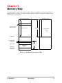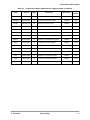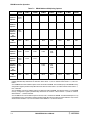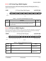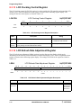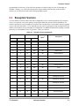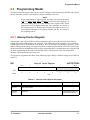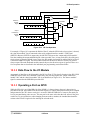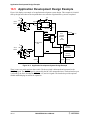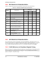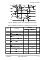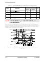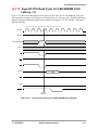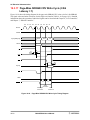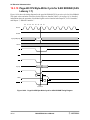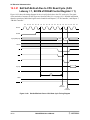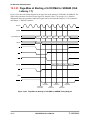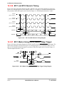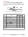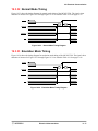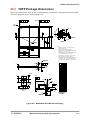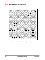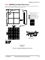
1
MC68VZ328 Integrated Processor
User’s Manual
MC68VZ328UM/D
Rev. 0, 02/2000
MFAX and DragonBall are trademarks of Motorola, Inc.
This document contains information on a new product. Specifications and information herein are subject to change
without notice.
Motorola reserves the right to make changes without further notice to any products herein. Motorola makes no warranty,
representation or guarantee regarding the suitability of its products for any particular purpose, nor does Motorola assume any liability
arising out of the application or use of any product or circuit, and specifically disclaims any and all liability, including without limitation
consequential or incidental damages. “Typical” parameters which may be provided in Motorola data sheets and/or specifications can
and do vary in different applications and actual performance may vary over time. All operating parameters, including “Typicals” must
be validated for each customer application by customer’s technical experts. Motorola does not convey any license under its patent
rights nor the rights of others. Motorola products are not designed, intended, or authorized for use as components in systems
intended for surgical implant into the body, or other applications intended to support life, or for any other application in which the
failure of the Motorola product could create a situation where personal injury or death may occur. Should Buyer purchase or use
Motorola products for any such unintended or unauthorized application, Buyer shall indemnify and hold Motorola and its officers,
employees, subsidiaries, affiliates, and distributors harmless against all claims, costs, damages, and expenses, and reasonable
attorney fees arising out of, directly or indirectly, any claim of personal injury or death associated with such unintended or
unauthorized use, even if such claim alleges that Motorola was negligent regarding the design or manufacture of the part.
Motorola and
are registered trademarks of Motorola, Inc. Motorola, Inc. is an Equal Opportunity/Affirmative Action Employer.
All other tradenames, trademarks, and registered trademarks are the property of their respective owners.
How to reach us:
USA/EUROPE/Locations Not Listed: Motorola Literature Distribution; P.O. Box 5405, Denver, Colorado, 80217
1-303-675-2140 or 1-800-441-2447
JAPAN: Motorola Japan, Ltd.; SPS, Technical Information Center, 3-20-1, Minami-Azabu, Minato-ku,
Tokyo 106-8573 Japan. 81-3-3440-3569
ASIA/PACIFIC: Motorola Semiconductors H.K. Ltd., Silicon Harbour Centre, 2 Dai King Street,
Tai Po Industrial Estate, 2 Tai Po, N.T., Hong Kong. 852-26668334
Customer Focus Center: 1-800-521-6274
Mfax™: [email protected]
–TOUCHTONE 1-602-244-6609
–US & Canada ONLY 1-800-774-184
–http://sps.motorola.com/mfax/
HOME PAGE: http://motorola.com/sps
Motorola DragonBall Products Home Page: http://www.motorola.com/dragonball
© Copyright Motorola, Inc., 2000
Contents
About This Book
Audience . . . . . . . . . . . . . . . . . . . . . . . . . . . . . . . . . . . . . . . . . . . . . . . . . . . . . . . . . . . xxvii
Organization . . . . . . . . . . . . . . . . . . . . . . . . . . . . . . . . . . . . . . . . . . . . . . . . . . . . . . . . xxvii
Suggested Reading . . . . . . . . . . . . . . . . . . . . . . . . . . . . . . . . . . . . . . . . . . . . . . . . . . . . xxix
Conventions . . . . . . . . . . . . . . . . . . . . . . . . . . . . . . . . . . . . . . . . . . . . . . . . . . . . . . . . . xxix
Definitions, Acronyms, and Abbreviations . . . . . . . . . . . . . . . . . . . . . . . . . . . . . . . . . . xxx
Chapter 1
Introduction
1.1
Features of the MC68VZ328 . . . . . . . . . . . . . . . . . . . . . . . . . . . . . . . . . . . . . . . . . . . . . 1-2
1.2
CPU. . . . . . . . . . . . . . . . . . . . . . . . . . . . . . . . . . . . . . . . . . . . . . . . . . . . . . . . . . . . . . . . . 1-4
1.2.1
CPU Programming Model . . . . . . . . . . . . . . . . . . . . . . . . . . . . . . . . . . . . . . . . . . . . 1-5
1.2.2
Data and Address Mode Types . . . . . . . . . . . . . . . . . . . . . . . . . . . . . . . . . . . . . . . . . 1-6
1.2.3
FLX68000 Instruction Set . . . . . . . . . . . . . . . . . . . . . . . . . . . . . . . . . . . . . . . . . . . . 1-6
1.3
Modules of the MC68VZ328 . . . . . . . . . . . . . . . . . . . . . . . . . . . . . . . . . . . . . . . . . . . . . 1-8
1.3.1
Memory Controller . . . . . . . . . . . . . . . . . . . . . . . . . . . . . . . . . . . . . . . . . . . . . . . . . . 1-8
1.3.2
Clock Generation Module and Power Control Module . . . . . . . . . . . . . . . . . . . . . . 1-8
1.3.3
System Control . . . . . . . . . . . . . . . . . . . . . . . . . . . . . . . . . . . . . . . . . . . . . . . . . . . . . 1-9
1.3.4
Chip-Select Logic . . . . . . . . . . . . . . . . . . . . . . . . . . . . . . . . . . . . . . . . . . . . . . . . . . . 1-9
1.3.5
DRAM Controller . . . . . . . . . . . . . . . . . . . . . . . . . . . . . . . . . . . . . . . . . . . . . . . . . . . 1-9
1.3.6
LCD Controller . . . . . . . . . . . . . . . . . . . . . . . . . . . . . . . . . . . . . . . . . . . . . . . . . . . . . 1-9
1.3.7
Interrupt Controller . . . . . . . . . . . . . . . . . . . . . . . . . . . . . . . . . . . . . . . . . . . . . . . . . . 1-9
1.3.8
General-Purpose I/O (GPIO) Lines . . . . . . . . . . . . . . . . . . . . . . . . . . . . . . . . . . . . 1-10
1.3.9
Real-Time Clock. . . . . . . . . . . . . . . . . . . . . . . . . . . . . . . . . . . . . . . . . . . . . . . . . . . 1-10
1.3.10
General-Purpose Timer. . . . . . . . . . . . . . . . . . . . . . . . . . . . . . . . . . . . . . . . . . . . . . 1-10
1.3.11
Serial Peripheral Interfaces (SPI) . . . . . . . . . . . . . . . . . . . . . . . . . . . . . . . . . . . . . . 1-10
1.3.12
Universal Asynchronous Receiver/Transmitter (UART) Modules . . . . . . . . . . . . 1-10
1.3.13
Pulse-Width Modulators (PWM) . . . . . . . . . . . . . . . . . . . . . . . . . . . . . . . . . . . . . . 1-11
1.3.14
In-Circuit Emulation Module . . . . . . . . . . . . . . . . . . . . . . . . . . . . . . . . . . . . . . . . . 1-11
1.3.15
Bootstrap Mode. . . . . . . . . . . . . . . . . . . . . . . . . . . . . . . . . . . . . . . . . . . . . . . . . . . . 1-11
Chapter 2
Signal Descriptions
2.1
2.2
2.3
2.4
2.5
2.6
Signals Grouped by Function . . . . . . . . . . . . . . . . . . . . . . . . . . . . . . . . . . . . . . . . . . . . .
Power and Ground Signals . . . . . . . . . . . . . . . . . . . . . . . . . . . . . . . . . . . . . . . . . . . . . . .
Clock and System Control Signals . . . . . . . . . . . . . . . . . . . . . . . . . . . . . . . . . . . . . . . . .
Address Bus Signals . . . . . . . . . . . . . . . . . . . . . . . . . . . . . . . . . . . . . . . . . . . . . . . . . . . .
Data Bus Signals . . . . . . . . . . . . . . . . . . . . . . . . . . . . . . . . . . . . . . . . . . . . . . . . . . . . . . .
Bus Control Signals . . . . . . . . . . . . . . . . . . . . . . . . . . . . . . . . . . . . . . . . . . . . . . . . . . . .
Table of Contents
2-2
2-4
2-4
2-5
2-5
2-6
iii
2.7
2.8
2.9
2.10
2.11
2.12
2.13
2.14
2.15
2.16
Interrupt Controller Signals . . . . . . . . . . . . . . . . . . . . . . . . . . . . . . . . . . . . . . . . . . . . . . 2-6
LCD Controller Signals . . . . . . . . . . . . . . . . . . . . . . . . . . . . . . . . . . . . . . . . . . . . . . . . . 2-7
UART 1 and UART 2 Controller Signals. . . . . . . . . . . . . . . . . . . . . . . . . . . . . . . . . . . . 2-8
Timer Signals . . . . . . . . . . . . . . . . . . . . . . . . . . . . . . . . . . . . . . . . . . . . . . . . . . . . . . . . . 2-8
Pulse-Width Modulator Signals . . . . . . . . . . . . . . . . . . . . . . . . . . . . . . . . . . . . . . . . . . . 2-9
Serial Peripheral Interface 1 Signals. . . . . . . . . . . . . . . . . . . . . . . . . . . . . . . . . . . . . . . . 2-9
Serial Peripheral Interface 2 Signals. . . . . . . . . . . . . . . . . . . . . . . . . . . . . . . . . . . . . . . . 2-9
Chip-Select and EDO RAM Interface Signals . . . . . . . . . . . . . . . . . . . . . . . . . . . . . . . 2-10
SDRAM Interface Signals . . . . . . . . . . . . . . . . . . . . . . . . . . . . . . . . . . . . . . . . . . . . . . 2-10
In-Circuit Emulation (ICE) Signals . . . . . . . . . . . . . . . . . . . . . . . . . . . . . . . . . . . . . . . 2-11
Chapter 3
Memory Map
3.1
Programmer’s Memory Map . . . . . . . . . . . . . . . . . . . . . . . . . . . . . . . . . . . . . . . . . . . . . 3-2
Chapter 4
Clock Generation Module and Power Control Module
4.1
Introduction to the Clock Generation Module . . . . . . . . . . . . . . . . . . . . . . . . . . . . . . . . 4-2
4.2
CGM Operational Overview. . . . . . . . . . . . . . . . . . . . . . . . . . . . . . . . . . . . . . . . . . . . . . 4-3
4.3
Detailed CGM Clock Descriptions . . . . . . . . . . . . . . . . . . . . . . . . . . . . . . . . . . . . . . . . . 4-4
4.3.1
CLK32 Clock Signal. . . . . . . . . . . . . . . . . . . . . . . . . . . . . . . . . . . . . . . . . . . . . . . . . 4-4
4.3.2
PLLCLK Clock Signal . . . . . . . . . . . . . . . . . . . . . . . . . . . . . . . . . . . . . . . . . . . . . . . 4-4
4.3.2.1
PLLCLK Initial Power-up Sequence . . . . . . . . . . . . . . . . . . . . . . . . . . . . . . . . . 4-5
4.3.2.2
PLL Frequency Selection . . . . . . . . . . . . . . . . . . . . . . . . . . . . . . . . . . . . . . . . . . 4-6
4.3.2.3
PLLCLK Frequency Selection Programming Example . . . . . . . . . . . . . . . . . . . 4-6
4.3.2.4
Programming Considerations When Changing Frequencies . . . . . . . . . . . . . . . 4-7
4.4
CGM Programming Model . . . . . . . . . . . . . . . . . . . . . . . . . . . . . . . . . . . . . . . . . . . . . . . 4-8
4.4.1
PLL Control Register . . . . . . . . . . . . . . . . . . . . . . . . . . . . . . . . . . . . . . . . . . . . . . . . 4-8
4.4.2
PLL Frequency Select Register . . . . . . . . . . . . . . . . . . . . . . . . . . . . . . . . . . . . . . . 4-10
4.5
Introduction to the Power Control Module. . . . . . . . . . . . . . . . . . . . . . . . . . . . . . . . . . 4-10
4.5.1
Operating the PCM . . . . . . . . . . . . . . . . . . . . . . . . . . . . . . . . . . . . . . . . . . . . . . . . . 4-11
4.5.1.1
Normal Mode . . . . . . . . . . . . . . . . . . . . . . . . . . . . . . . . . . . . . . . . . . . . . . . . . . 4-11
4.5.1.2
Burst Mode . . . . . . . . . . . . . . . . . . . . . . . . . . . . . . . . . . . . . . . . . . . . . . . . . . . . 4-11
4.5.1.3
Doze Mode . . . . . . . . . . . . . . . . . . . . . . . . . . . . . . . . . . . . . . . . . . . . . . . . . . . . 4-11
4.5.1.4
Sleep Mode . . . . . . . . . . . . . . . . . . . . . . . . . . . . . . . . . . . . . . . . . . . . . . . . . . . . 4-12
4.5.2
CGM Operation During Sleep Mode . . . . . . . . . . . . . . . . . . . . . . . . . . . . . . . . . . . 4-12
4.5.3
Burst Mode Operation . . . . . . . . . . . . . . . . . . . . . . . . . . . . . . . . . . . . . . . . . . . . . . 4-12
4.5.4
Power Control Register. . . . . . . . . . . . . . . . . . . . . . . . . . . . . . . . . . . . . . . . . . . . . . 4-14
Chapter 5
System Control
5.1
5.1.1
5.2
5.2.1
iv
System Control Operation . . . . . . . . . . . . . . . . . . . . . . . . . . . . . . . . . . . . . . . . . . . . . . .
Bus Monitors and Watchdog Timers . . . . . . . . . . . . . . . . . . . . . . . . . . . . . . . . . . . .
Programming Model . . . . . . . . . . . . . . . . . . . . . . . . . . . . . . . . . . . . . . . . . . . . . . . . . . . .
System Control Register . . . . . . . . . . . . . . . . . . . . . . . . . . . . . . . . . . . . . . . . . . . . . .
MC68VZ328 User’s Manual
5-1
5-1
5-2
5-2
5.2.2
5.2.3
5.2.4
Peripheral Control Register . . . . . . . . . . . . . . . . . . . . . . . . . . . . . . . . . . . . . . . . . . . 5-4
ID Register . . . . . . . . . . . . . . . . . . . . . . . . . . . . . . . . . . . . . . . . . . . . . . . . . . . . . . . . 5-5
I/O Drive Control Register . . . . . . . . . . . . . . . . . . . . . . . . . . . . . . . . . . . . . . . . . . . . 5-6
Chapter 6
Chip-Select Logic
6.1
6.2
6.2.1
6.2.2
6.2.3
6.3
6.3.1
6.3.2
6.3.3
6.3.4
6.3.5
6.3.6
6.3.7
Overview of the CSL . . . . . . . . . . . . . . . . . . . . . . . . . . . . . . . . . . . . . . . . . . . . . . . . . . . 6-1
Chip-Select Operation. . . . . . . . . . . . . . . . . . . . . . . . . . . . . . . . . . . . . . . . . . . . . . . . . . . 6-2
Memory Protection . . . . . . . . . . . . . . . . . . . . . . . . . . . . . . . . . . . . . . . . . . . . . . . . . . 6-2
Programmable Data Bus Size . . . . . . . . . . . . . . . . . . . . . . . . . . . . . . . . . . . . . . . . . . 6-3
Overlapping Chip-Select Registers. . . . . . . . . . . . . . . . . . . . . . . . . . . . . . . . . . . . . . 6-4
Programming Model . . . . . . . . . . . . . . . . . . . . . . . . . . . . . . . . . . . . . . . . . . . . . . . . . . . . 6-4
Chip-Select Group Base Address Registers . . . . . . . . . . . . . . . . . . . . . . . . . . . . . . . 6-4
Chip-Select Upper Group Base Address Register . . . . . . . . . . . . . . . . . . . . . . . . . . 6-6
Chip-Select Registers . . . . . . . . . . . . . . . . . . . . . . . . . . . . . . . . . . . . . . . . . . . . . . . . 6-8
Emulation Chip-Select Register . . . . . . . . . . . . . . . . . . . . . . . . . . . . . . . . . . . . . . . 6-16
Chip-Select Control Register 1 . . . . . . . . . . . . . . . . . . . . . . . . . . . . . . . . . . . . . . . . 6-16
Chip-Select Control Register 2 . . . . . . . . . . . . . . . . . . . . . . . . . . . . . . . . . . . . . . . . 6-18
Chip-Select Control Register 3 . . . . . . . . . . . . . . . . . . . . . . . . . . . . . . . . . . . . . . . . 6-20
Chapter 7
DRAM Controller
7.1
Introduction to the DRAM Controller . . . . . . . . . . . . . . . . . . . . . . . . . . . . . . . . . . . . . . 7-1
7.2
DRAM Controller Operation . . . . . . . . . . . . . . . . . . . . . . . . . . . . . . . . . . . . . . . . . . . . . 7-3
7.2.1
Address Multiplexing . . . . . . . . . . . . . . . . . . . . . . . . . . . . . . . . . . . . . . . . . . . . . . . . 7-3
7.2.2
DTACK Generation . . . . . . . . . . . . . . . . . . . . . . . . . . . . . . . . . . . . . . . . . . . . . . . . . 7-7
7.2.3
Refresh Control. . . . . . . . . . . . . . . . . . . . . . . . . . . . . . . . . . . . . . . . . . . . . . . . . . . . . 7-7
7.2.4
LCD Interface . . . . . . . . . . . . . . . . . . . . . . . . . . . . . . . . . . . . . . . . . . . . . . . . . . . . . . 7-8
7.2.5
8-Bit Mode . . . . . . . . . . . . . . . . . . . . . . . . . . . . . . . . . . . . . . . . . . . . . . . . . . . . . . . . 7-9
7.2.6
Low-Power Standby Mode . . . . . . . . . . . . . . . . . . . . . . . . . . . . . . . . . . . . . . . . . . . . 7-9
7.2.7
Data Retention During Reset . . . . . . . . . . . . . . . . . . . . . . . . . . . . . . . . . . . . . . . . . 7-10
7.2.8
Data Retention Sequence . . . . . . . . . . . . . . . . . . . . . . . . . . . . . . . . . . . . . . . . . . . . 7-11
7.3
Programming Model . . . . . . . . . . . . . . . . . . . . . . . . . . . . . . . . . . . . . . . . . . . . . . . . . . . 7-12
7.3.1
DRAM Memory Configuration Register . . . . . . . . . . . . . . . . . . . . . . . . . . . . . . . . 7-12
7.3.2
DRAM Control Register . . . . . . . . . . . . . . . . . . . . . . . . . . . . . . . . . . . . . . . . . . . . . 7-14
7.3.3
SDRAM Control Register. . . . . . . . . . . . . . . . . . . . . . . . . . . . . . . . . . . . . . . . . . . . 7-16
7.3.4
SDRAM Power-down Register . . . . . . . . . . . . . . . . . . . . . . . . . . . . . . . . . . . . . . . 7-18
Chapter 8
LCD Controller
8.1
LCD Controller Features . . . . . . . . . . . . . . . . . . . . . . . . . . . . . . . . . . . . . . . . . . . . . . . .
8.2
LCD Controller Operation . . . . . . . . . . . . . . . . . . . . . . . . . . . . . . . . . . . . . . . . . . . . . . .
8.2.1
Connecting the LCD Controller to an LCD Panel . . . . . . . . . . . . . . . . . . . . . . . . . .
8.2.1.1
Panel Interface Timing . . . . . . . . . . . . . . . . . . . . . . . . . . . . . . . . . . . . . . . . . . . .
8.2.2
Controlling the Display. . . . . . . . . . . . . . . . . . . . . . . . . . . . . . . . . . . . . . . . . . . . . . .
Table of Contents
8-1
8-2
8-3
8-3
8-4
v
8.2.2.1
Format of the LCD Screen . . . . . . . . . . . . . . . . . . . . . . . . . . . . . . . . . . . . . . . . . 8-4
8.2.2.2
Format of the Cursor. . . . . . . . . . . . . . . . . . . . . . . . . . . . . . . . . . . . . . . . . . . . . . 8-5
8.2.2.3
Mapping the Display Data . . . . . . . . . . . . . . . . . . . . . . . . . . . . . . . . . . . . . . . . . 8-6
8.2.2.4
Generating Grayscale Tones . . . . . . . . . . . . . . . . . . . . . . . . . . . . . . . . . . . . . . . . 8-6
8.2.3
Using Low-Power Mode. . . . . . . . . . . . . . . . . . . . . . . . . . . . . . . . . . . . . . . . . . . . . . 8-8
8.2.4
Using the DMA Controller . . . . . . . . . . . . . . . . . . . . . . . . . . . . . . . . . . . . . . . . . . . . 8-8
8.2.4.1
Bus Bandwidth Calculation Example . . . . . . . . . . . . . . . . . . . . . . . . . . . . . . . . . 8-8
8.2.5
Self-Refresh Mode . . . . . . . . . . . . . . . . . . . . . . . . . . . . . . . . . . . . . . . . . . . . . . . . . . 8-9
8.2.5.1
Entering Self-Refresh Mode . . . . . . . . . . . . . . . . . . . . . . . . . . . . . . . . . . . . . . . . 8-9
8.2.5.2
Canceling Self-Refresh Mode. . . . . . . . . . . . . . . . . . . . . . . . . . . . . . . . . . . . . . . 8-9
8.3
Programming Model . . . . . . . . . . . . . . . . . . . . . . . . . . . . . . . . . . . . . . . . . . . . . . . . . . . 8-10
8.3.1
LCD Screen Starting Address Register . . . . . . . . . . . . . . . . . . . . . . . . . . . . . . . . . 8-10
8.3.2
LCD Virtual Page Width Register . . . . . . . . . . . . . . . . . . . . . . . . . . . . . . . . . . . . . 8-11
8.3.3
LCD Screen Width Register . . . . . . . . . . . . . . . . . . . . . . . . . . . . . . . . . . . . . . . . . . 8-11
8.3.4
LCD Screen Height Register . . . . . . . . . . . . . . . . . . . . . . . . . . . . . . . . . . . . . . . . . 8-12
8.3.5
LCD Cursor X Position Register . . . . . . . . . . . . . . . . . . . . . . . . . . . . . . . . . . . . . . 8-12
8.3.6
LCD Cursor Y Position Register . . . . . . . . . . . . . . . . . . . . . . . . . . . . . . . . . . . . . . 8-13
8.3.7
LCD Cursor Width and Height Register. . . . . . . . . . . . . . . . . . . . . . . . . . . . . . . . . 8-14
8.3.8
LCD Blink Control Register . . . . . . . . . . . . . . . . . . . . . . . . . . . . . . . . . . . . . . . . . . 8-14
8.3.9
LCD Panel Interface Configuration Register . . . . . . . . . . . . . . . . . . . . . . . . . . . . . 8-15
8.3.10
LCD Polarity Configuration Register . . . . . . . . . . . . . . . . . . . . . . . . . . . . . . . . . . . 8-16
8.3.11
LACD Rate Control Register . . . . . . . . . . . . . . . . . . . . . . . . . . . . . . . . . . . . . . . . . 8-16
8.3.12
LCD Pixel Clock Divider Register . . . . . . . . . . . . . . . . . . . . . . . . . . . . . . . . . . . . . 8-17
8.3.13
LCD Clocking Control Register . . . . . . . . . . . . . . . . . . . . . . . . . . . . . . . . . . . . . . . 8-18
8.3.14
LCD Refresh Rate Adjustment Register. . . . . . . . . . . . . . . . . . . . . . . . . . . . . . . . . 8-18
8.3.15
LCD Panning Offset Register . . . . . . . . . . . . . . . . . . . . . . . . . . . . . . . . . . . . . . . . . 8-19
8.3.16
LCD Frame Rate Control Modulation Register . . . . . . . . . . . . . . . . . . . . . . . . . . . 8-19
8.3.17
LCD Gray Palette Mapping Register . . . . . . . . . . . . . . . . . . . . . . . . . . . . . . . . . . . 8-20
8.3.18
PWM Contrast Control Register. . . . . . . . . . . . . . . . . . . . . . . . . . . . . . . . . . . . . . . 8-20
8.3.19
Refresh Mode Control Register . . . . . . . . . . . . . . . . . . . . . . . . . . . . . . . . . . . . . . . 8-21
8.3.20
DMA Control Register . . . . . . . . . . . . . . . . . . . . . . . . . . . . . . . . . . . . . . . . . . . . . . 8-22
8.4
Programming Example . . . . . . . . . . . . . . . . . . . . . . . . . . . . . . . . . . . . . . . . . . . . . . . . . 8-22
Chapter 9
Interrupt Controller
9.1
9.2
9.3
9.3.1
9.3.2
9.4
9.4.1
9.4.2
9.5
9.6
9.6.1
9.6.2
vi
Interrupt Processing . . . . . . . . . . . . . . . . . . . . . . . . . . . . . . . . . . . . . . . . . . . . . . . . . . . .
Exception Vectors. . . . . . . . . . . . . . . . . . . . . . . . . . . . . . . . . . . . . . . . . . . . . . . . . . . . . .
Reset . . . . . . . . . . . . . . . . . . . . . . . . . . . . . . . . . . . . . . . . . . . . . . . . . . . . . . . . . . . . . . . .
Operation Mode Selection During Reset . . . . . . . . . . . . . . . . . . . . . . . . . . . . . . . . .
Data Bus Width for Boot Device Operation. . . . . . . . . . . . . . . . . . . . . . . . . . . . . . .
Interrupt Controller Operation . . . . . . . . . . . . . . . . . . . . . . . . . . . . . . . . . . . . . . . . . . . .
Interrupt Priority Processing . . . . . . . . . . . . . . . . . . . . . . . . . . . . . . . . . . . . . . . . . . .
Interrupt Vectors . . . . . . . . . . . . . . . . . . . . . . . . . . . . . . . . . . . . . . . . . . . . . . . . . . . .
Vector Generation. . . . . . . . . . . . . . . . . . . . . . . . . . . . . . . . . . . . . . . . . . . . . . . . . . . . . .
Programming Model . . . . . . . . . . . . . . . . . . . . . . . . . . . . . . . . . . . . . . . . . . . . . . . . . . . .
Interrupt Vector Register . . . . . . . . . . . . . . . . . . . . . . . . . . . . . . . . . . . . . . . . . . . . .
Interrupt Control Register . . . . . . . . . . . . . . . . . . . . . . . . . . . . . . . . . . . . . . . . . . . . .
MC68VZ328 User’s Manual
9-2
9-3
9-4
9-5
9-5
9-5
9-5
9-6
9-6
9-7
9-7
9-8
9.6.3
9.6.4
9.6.5
9.6.6
9.7
9.8
Interrupt Mask Register . . . . . . . . . . . . . . . . . . . . . . . . . . . . . . . . . . . . . . . . . . . . .
Interrupt Status Register . . . . . . . . . . . . . . . . . . . . . . . . . . . . . . . . . . . . . . . . . . . . .
Interrupt Pending Register . . . . . . . . . . . . . . . . . . . . . . . . . . . . . . . . . . . . . . . . . . .
Interrupt Level Register . . . . . . . . . . . . . . . . . . . . . . . . . . . . . . . . . . . . . . . . . . . . .
Keyboard Interrupts . . . . . . . . . . . . . . . . . . . . . . . . . . . . . . . . . . . . . . . . . . . . . . . . . . .
Pen Interrupts . . . . . . . . . . . . . . . . . . . . . . . . . . . . . . . . . . . . . . . . . . . . . . . . . . . . . . . .
9-10
9-12
9-16
9-19
9-20
9-20
Chapter 10
I/O Ports
10.1 Port Configuration . . . . . . . . . . . . . . . . . . . . . . . . . . . . . . . . . . . . . . . . . . . . . . . . . . . . 10-1
10.2 Status of I/O Ports During Reset. . . . . . . . . . . . . . . . . . . . . . . . . . . . . . . . . . . . . . . . . . 10-2
10.2.1
Warm Reset. . . . . . . . . . . . . . . . . . . . . . . . . . . . . . . . . . . . . . . . . . . . . . . . . . . . . . . 10-2
10.2.2
Power-up Reset . . . . . . . . . . . . . . . . . . . . . . . . . . . . . . . . . . . . . . . . . . . . . . . . . . . . 10-3
10.2.3
Summary of Port Behavior During Reset . . . . . . . . . . . . . . . . . . . . . . . . . . . . . . . . 10-4
10.3 I/O Port Operation . . . . . . . . . . . . . . . . . . . . . . . . . . . . . . . . . . . . . . . . . . . . . . . . . . . . 10-4
10.3.1
Data Flow from the I/O Module . . . . . . . . . . . . . . . . . . . . . . . . . . . . . . . . . . . . . . . 10-4
10.3.2
Data Flow to the I/O Module . . . . . . . . . . . . . . . . . . . . . . . . . . . . . . . . . . . . . . . . . 10-5
10.3.3
Operating a Port as GPIO . . . . . . . . . . . . . . . . . . . . . . . . . . . . . . . . . . . . . . . . . . . . 10-5
10.3.4
Port Pull-up and Pull-down Resistors . . . . . . . . . . . . . . . . . . . . . . . . . . . . . . . . . . . 10-6
10.4 Programming Model . . . . . . . . . . . . . . . . . . . . . . . . . . . . . . . . . . . . . . . . . . . . . . . . . . . 10-6
10.4.1
Port A Registers . . . . . . . . . . . . . . . . . . . . . . . . . . . . . . . . . . . . . . . . . . . . . . . . . . . 10-6
10.4.1.1
Port A Direction Register . . . . . . . . . . . . . . . . . . . . . . . . . . . . . . . . . . . . . . . . . 10-7
10.4.1.2
Port A Data Register . . . . . . . . . . . . . . . . . . . . . . . . . . . . . . . . . . . . . . . . . . . . . 10-7
10.4.1.3
Port A Pull-up Enable Register. . . . . . . . . . . . . . . . . . . . . . . . . . . . . . . . . . . . . 10-8
10.4.2
Port B Registers . . . . . . . . . . . . . . . . . . . . . . . . . . . . . . . . . . . . . . . . . . . . . . . . . . . 10-8
10.4.2.1
Port B Direction Register . . . . . . . . . . . . . . . . . . . . . . . . . . . . . . . . . . . . . . . . . 10-8
10.4.2.2
Port B Data Register . . . . . . . . . . . . . . . . . . . . . . . . . . . . . . . . . . . . . . . . . . . . . 10-9
10.4.2.3
Port B Dedicated I/O Functions . . . . . . . . . . . . . . . . . . . . . . . . . . . . . . . . . . . 10-10
10.4.2.4
Port B Pull-up Enable Register. . . . . . . . . . . . . . . . . . . . . . . . . . . . . . . . . . . . 10-10
10.4.2.5
Port B Select Register . . . . . . . . . . . . . . . . . . . . . . . . . . . . . . . . . . . . . . . . . . . 10-11
10.4.3
Port C Registers . . . . . . . . . . . . . . . . . . . . . . . . . . . . . . . . . . . . . . . . . . . . . . . . . . 10-11
10.4.3.1
Port C Direction Register . . . . . . . . . . . . . . . . . . . . . . . . . . . . . . . . . . . . . . . . 10-12
10.4.3.2
Port C Data Register . . . . . . . . . . . . . . . . . . . . . . . . . . . . . . . . . . . . . . . . . . . . 10-12
10.4.3.3
Port C Dedicated I/O Functions . . . . . . . . . . . . . . . . . . . . . . . . . . . . . . . . . . . 10-13
10.4.3.4
Port C Pull-down Enable Register . . . . . . . . . . . . . . . . . . . . . . . . . . . . . . . . . 10-13
10.4.3.5
Port C Select Register . . . . . . . . . . . . . . . . . . . . . . . . . . . . . . . . . . . . . . . . . . . 10-14
10.4.4
Port D Operation . . . . . . . . . . . . . . . . . . . . . . . . . . . . . . . . . . . . . . . . . . . . . . . . . . 10-15
10.4.5
Port D Registers . . . . . . . . . . . . . . . . . . . . . . . . . . . . . . . . . . . . . . . . . . . . . . . . . . 10-16
10.4.5.1
Port D Direction Register . . . . . . . . . . . . . . . . . . . . . . . . . . . . . . . . . . . . . . . . 10-16
10.4.5.2
Port D Data Register . . . . . . . . . . . . . . . . . . . . . . . . . . . . . . . . . . . . . . . . . . . . 10-17
10.4.5.3
Port D Interrupt Options . . . . . . . . . . . . . . . . . . . . . . . . . . . . . . . . . . . . . . . . . 10-18
10.4.5.4
Port D Pull-up Enable Register. . . . . . . . . . . . . . . . . . . . . . . . . . . . . . . . . . . . 10-18
10.4.5.5
Port D Select Register. . . . . . . . . . . . . . . . . . . . . . . . . . . . . . . . . . . . . . . . . . . 10-19
10.4.5.6
Port D Polarity Register . . . . . . . . . . . . . . . . . . . . . . . . . . . . . . . . . . . . . . . . . 10-19
10.4.5.7
Port D Interrupt Request Enable Register. . . . . . . . . . . . . . . . . . . . . . . . . . . . 10-20
10.4.5.8
Port D Keyboard Enable Register. . . . . . . . . . . . . . . . . . . . . . . . . . . . . . . . . . 10-20
10.4.5.9
Port D Interrupt Request Edge Register . . . . . . . . . . . . . . . . . . . . . . . . . . . . . 10-20
Table of Contents
vii
10.4.6
10.4.6.1
10.4.6.2
10.4.6.3
10.4.6.4
10.4.6.5
10.4.7
10.4.7.1
10.4.7.2
10.4.7.3
10.4.7.4
10.4.7.5
10.4.8
10.4.8.1
10.4.8.2
10.4.8.3
10.4.8.4
10.4.8.5
10.4.8.6
10.4.9
10.4.9.1
10.4.9.2
10.4.9.3
10.4.9.4
10.4.9.5
10.4.10
10.4.10.1
10.4.10.2
10.4.10.3
10.4.10.4
10.4.10.5
10.4.11
10.4.11.1
10.4.11.2
10.4.11.3
10.4.11.4
10.4.11.5
Port E Registers . . . . . . . . . . . . . . . . . . . . . . . . . . . . . . . . . . . . . . . . . . . . . . . . . .
Port E Direction Register . . . . . . . . . . . . . . . . . . . . . . . . . . . . . . . . . . . . . . . .
Port E Data Register . . . . . . . . . . . . . . . . . . . . . . . . . . . . . . . . . . . . . . . . . . . .
Port E Dedicated I/O Functions . . . . . . . . . . . . . . . . . . . . . . . . . . . . . . . . . . .
Port E Pull-up Enable Register . . . . . . . . . . . . . . . . . . . . . . . . . . . . . . . . . . . .
Port E Select Register . . . . . . . . . . . . . . . . . . . . . . . . . . . . . . . . . . . . . . . . . . .
Port F Registers. . . . . . . . . . . . . . . . . . . . . . . . . . . . . . . . . . . . . . . . . . . . . . . . . . .
Port F Direction Register . . . . . . . . . . . . . . . . . . . . . . . . . . . . . . . . . . . . . . . .
Port F Data Register . . . . . . . . . . . . . . . . . . . . . . . . . . . . . . . . . . . . . . . . . . . .
Port F Dedicated I/O Functions . . . . . . . . . . . . . . . . . . . . . . . . . . . . . . . . . . .
Port F Pull-up/Pull-down Enable Register . . . . . . . . . . . . . . . . . . . . . . . . . . .
Port F Select Register . . . . . . . . . . . . . . . . . . . . . . . . . . . . . . . . . . . . . . . . . . .
Port G Registers . . . . . . . . . . . . . . . . . . . . . . . . . . . . . . . . . . . . . . . . . . . . . . . . . .
Port G Direction Register . . . . . . . . . . . . . . . . . . . . . . . . . . . . . . . . . . . . . . . .
Port G Data Register . . . . . . . . . . . . . . . . . . . . . . . . . . . . . . . . . . . . . . . . . . . .
Port G Dedicated I/O Functions . . . . . . . . . . . . . . . . . . . . . . . . . . . . . . . . . . .
Port G Operational Considerations . . . . . . . . . . . . . . . . . . . . . . . . . . . . . . . . .
Port G Pull-up Enable Register. . . . . . . . . . . . . . . . . . . . . . . . . . . . . . . . . . . .
Port G Select Register. . . . . . . . . . . . . . . . . . . . . . . . . . . . . . . . . . . . . . . . . . .
Port J Registers . . . . . . . . . . . . . . . . . . . . . . . . . . . . . . . . . . . . . . . . . . . . . . . . . . .
Port J Direction Register. . . . . . . . . . . . . . . . . . . . . . . . . . . . . . . . . . . . . . . . .
Port J Data Register . . . . . . . . . . . . . . . . . . . . . . . . . . . . . . . . . . . . . . . . . . . .
Port J Dedicated I/O Functions . . . . . . . . . . . . . . . . . . . . . . . . . . . . . . . . . . . .
Port J Pull-up Enable Register . . . . . . . . . . . . . . . . . . . . . . . . . . . . . . . . . . . .
Port J Select Register . . . . . . . . . . . . . . . . . . . . . . . . . . . . . . . . . . . . . . . . . . .
Port K Registers . . . . . . . . . . . . . . . . . . . . . . . . . . . . . . . . . . . . . . . . . . . . . . . . . .
Port K Direction Register . . . . . . . . . . . . . . . . . . . . . . . . . . . . . . . . . . . . . . . .
Port K Data Register . . . . . . . . . . . . . . . . . . . . . . . . . . . . . . . . . . . . . . . . . . . .
Port K Dedicated I/O Functions . . . . . . . . . . . . . . . . . . . . . . . . . . . . . . . . . . .
Port K Pull-up/Pull-down Enable Register. . . . . . . . . . . . . . . . . . . . . . . . . . .
Port K Select Register. . . . . . . . . . . . . . . . . . . . . . . . . . . . . . . . . . . . . . . . . . .
Port M Registers . . . . . . . . . . . . . . . . . . . . . . . . . . . . . . . . . . . . . . . . . . . . . . . . . .
Port M Direction Register. . . . . . . . . . . . . . . . . . . . . . . . . . . . . . . . . . . . . . . .
Port M Data Register . . . . . . . . . . . . . . . . . . . . . . . . . . . . . . . . . . . . . . . . . . .
Port M Dedicated I/O Functions . . . . . . . . . . . . . . . . . . . . . . . . . . . . . . . . . . .
Port M Pull-up/Pull-down Enable Register . . . . . . . . . . . . . . . . . . . . . . . . . .
Port M Select Register . . . . . . . . . . . . . . . . . . . . . . . . . . . . . . . . . . . . . . . . . .
10-21
10-21
10-22
10-22
10-23
10-23
10-24
10-24
10-25
10-26
10-27
10-27
10-28
10-28
10-28
10-29
10-30
10-30
10-30
10-31
10-31
10-32
10-32
10-33
10-33
10-34
10-34
10-34
10-35
10-36
10-36
10-37
10-37
10-38
10-39
10-39
10-40
Chapter 11
Real-Time Clock
11.1 RTC Overview . . . . . . . . . . . . . . . . . . . . . . . . . . . . . . . . . . . . . . . . . . . . . . . . . . . . . . .
11.1.1
Prescaler . . . . . . . . . . . . . . . . . . . . . . . . . . . . . . . . . . . . . . . . . . . . . . . . . . . . . . . . .
11.1.2
Time-of-Day Counter . . . . . . . . . . . . . . . . . . . . . . . . . . . . . . . . . . . . . . . . . . . . . . .
11.1.3
Alarm . . . . . . . . . . . . . . . . . . . . . . . . . . . . . . . . . . . . . . . . . . . . . . . . . . . . . . . . . . .
11.1.4
Watchdog Timer . . . . . . . . . . . . . . . . . . . . . . . . . . . . . . . . . . . . . . . . . . . . . . . . . . .
11.1.5
Real-Time Interrupt Timer . . . . . . . . . . . . . . . . . . . . . . . . . . . . . . . . . . . . . . . . . . .
11.1.6
Minute Stopwatch . . . . . . . . . . . . . . . . . . . . . . . . . . . . . . . . . . . . . . . . . . . . . . . . . .
viii
MC68VZ328 User’s Manual
11-2
11-2
11-3
11-3
11-4
11-4
11-4
11.1.6.1
Minute Stopwatch Application Example . . . . . . . . . . . . . . . . . . . . . . . . . . . . . 11-4
11.2 Programming Model . . . . . . . . . . . . . . . . . . . . . . . . . . . . . . . . . . . . . . . . . . . . . . . . . . . 11-5
11.2.1
RTC Time Register . . . . . . . . . . . . . . . . . . . . . . . . . . . . . . . . . . . . . . . . . . . . . . . . . 11-5
11.2.2
RTC Day Count Register . . . . . . . . . . . . . . . . . . . . . . . . . . . . . . . . . . . . . . . . . . . . 11-6
11.2.3
RTC Alarm Register . . . . . . . . . . . . . . . . . . . . . . . . . . . . . . . . . . . . . . . . . . . . . . . . 11-7
11.2.4
RTC Day Alarm Register . . . . . . . . . . . . . . . . . . . . . . . . . . . . . . . . . . . . . . . . . . . . 11-8
11.2.5
Watchdog Timer Register . . . . . . . . . . . . . . . . . . . . . . . . . . . . . . . . . . . . . . . . . . . . 11-9
11.2.6
RTC Control Register . . . . . . . . . . . . . . . . . . . . . . . . . . . . . . . . . . . . . . . . . . . . . . 11-10
11.2.7
RTC Interrupt Status Register. . . . . . . . . . . . . . . . . . . . . . . . . . . . . . . . . . . . . . . . 11-10
11.2.8
RTC Interrupt Enable Register . . . . . . . . . . . . . . . . . . . . . . . . . . . . . . . . . . . . . . . 11-12
11.2.9
Stopwatch Minutes Register . . . . . . . . . . . . . . . . . . . . . . . . . . . . . . . . . . . . . . . . . 11-14
Chapter 12
General-Purpose Timers
12.1 GP Timer Overview . . . . . . . . . . . . . . . . . . . . . . . . . . . . . . . . . . . . . . . . . . . . . . . . . . . 12-1
12.1.1
Clock Source and Prescaler . . . . . . . . . . . . . . . . . . . . . . . . . . . . . . . . . . . . . . . . . . 12-2
12.1.2
Timer Events and Modes of Operation. . . . . . . . . . . . . . . . . . . . . . . . . . . . . . . . . . 12-2
12.1.2.1
Restart Mode. . . . . . . . . . . . . . . . . . . . . . . . . . . . . . . . . . . . . . . . . . . . . . . . . . . 12-2
12.1.2.2
Free-Running Mode . . . . . . . . . . . . . . . . . . . . . . . . . . . . . . . . . . . . . . . . . . . . . 12-2
12.1.3
Timer Capture Register. . . . . . . . . . . . . . . . . . . . . . . . . . . . . . . . . . . . . . . . . . . . . . 12-3
12.1.4
TOUT/TIN/PB6 Pin . . . . . . . . . . . . . . . . . . . . . . . . . . . . . . . . . . . . . . . . . . . . . . . . 12-3
12.1.5
Cascaded Timers. . . . . . . . . . . . . . . . . . . . . . . . . . . . . . . . . . . . . . . . . . . . . . . . . . . 12-4
12.1.5.1
Compare and Capture Using Cascaded Timers . . . . . . . . . . . . . . . . . . . . . . . . 12-4
12.2 Programming Model . . . . . . . . . . . . . . . . . . . . . . . . . . . . . . . . . . . . . . . . . . . . . . . . . . . 12-6
12.2.1
Timer Control Registers 1 and 2. . . . . . . . . . . . . . . . . . . . . . . . . . . . . . . . . . . . . . . 12-6
12.2.2
Timer Prescaler Registers 1 and 2 . . . . . . . . . . . . . . . . . . . . . . . . . . . . . . . . . . . . . 12-8
12.2.3
Timer Compare Registers 1 and 2 . . . . . . . . . . . . . . . . . . . . . . . . . . . . . . . . . . . . . 12-9
12.2.4
Timer Capture Registers 1 and 2 . . . . . . . . . . . . . . . . . . . . . . . . . . . . . . . . . . . . . 12-10
12.2.5
Timer Counter Registers 1 and 2 . . . . . . . . . . . . . . . . . . . . . . . . . . . . . . . . . . . . . 12-11
12.2.6
Timer Status Registers 1 and 2 . . . . . . . . . . . . . . . . . . . . . . . . . . . . . . . . . . . . . . . 12-12
Chapter 13
Serial Peripheral Interface 1 and 2
13.1 SPI 1 Overview . . . . . . . . . . . . . . . . . . . . . . . . . . . . . . . . . . . . . . . . . . . . . . . . . . . . . . . 13-1
13.2 SPI 1 Operation. . . . . . . . . . . . . . . . . . . . . . . . . . . . . . . . . . . . . . . . . . . . . . . . . . . . . . . 13-2
13.2.1
Using SPI 1 as Master. . . . . . . . . . . . . . . . . . . . . . . . . . . . . . . . . . . . . . . . . . . . . . . 13-2
13.2.2
Using SPI 1 as Slave . . . . . . . . . . . . . . . . . . . . . . . . . . . . . . . . . . . . . . . . . . . . . . . . 13-2
13.2.3
SPI 1 Phase and Polarity Configurations . . . . . . . . . . . . . . . . . . . . . . . . . . . . . . . . 13-3
13.2.4
SPI 1 Signals . . . . . . . . . . . . . . . . . . . . . . . . . . . . . . . . . . . . . . . . . . . . . . . . . . . . . . 13-3
13.3 SPI 1 Programming Model . . . . . . . . . . . . . . . . . . . . . . . . . . . . . . . . . . . . . . . . . . . . . . 13-4
13.3.1
SPI 1 Receive Data Register . . . . . . . . . . . . . . . . . . . . . . . . . . . . . . . . . . . . . . . . . . 13-4
13.3.2
SPI 1 Transmit Data Register . . . . . . . . . . . . . . . . . . . . . . . . . . . . . . . . . . . . . . . . . 13-5
13.3.3
SPI 1 Control/Status Register . . . . . . . . . . . . . . . . . . . . . . . . . . . . . . . . . . . . . . . . . 13-6
13.3.4
SPI 1 Interrupt Control/Status Register . . . . . . . . . . . . . . . . . . . . . . . . . . . . . . . . . 13-8
13.3.5
SPI 1 Test Register . . . . . . . . . . . . . . . . . . . . . . . . . . . . . . . . . . . . . . . . . . . . . . . . 13-10
13.3.6
SPI 1 Sample Period Control Register . . . . . . . . . . . . . . . . . . . . . . . . . . . . . . . . . 13-10
Table of Contents
ix
13.4 SPI 2 Overview . . . . . . . . . . . . . . . . . . . . . . . . . . . . . . . . . . . . . . . . . . . . . . . . . . . . . .
13.5 SPI 2 Operation. . . . . . . . . . . . . . . . . . . . . . . . . . . . . . . . . . . . . . . . . . . . . . . . . . . . . .
13.5.1
SPI 2 Phase and Polarity Configurations . . . . . . . . . . . . . . . . . . . . . . . . . . . . . . .
13.5.2
SPI 2 Signals . . . . . . . . . . . . . . . . . . . . . . . . . . . . . . . . . . . . . . . . . . . . . . . . . . . . .
13.6 SPI 2 Programming Model . . . . . . . . . . . . . . . . . . . . . . . . . . . . . . . . . . . . . . . . . . . . .
13.6.1
SPI 2 Data Register. . . . . . . . . . . . . . . . . . . . . . . . . . . . . . . . . . . . . . . . . . . . . . . .
13.6.2
SPI 2 Data Register Timing . . . . . . . . . . . . . . . . . . . . . . . . . . . . . . . . . . . . . . . . .
13.6.3
SPI 2 Control/Status Register . . . . . . . . . . . . . . . . . . . . . . . . . . . . . . . . . . . . . . . .
13-11
13-12
13-13
13-13
13-14
13-14
13-14
13-15
Chapter 14
Universal Asynchronous Receiver/Transmitter 1 and 2
14.1 Introduction to the UARTs . . . . . . . . . . . . . . . . . . . . . . . . . . . . . . . . . . . . . . . . . . . . . . 14-1
14.2 Serial Operation . . . . . . . . . . . . . . . . . . . . . . . . . . . . . . . . . . . . . . . . . . . . . . . . . . . . . . 14-2
14.2.1
NRZ Mode . . . . . . . . . . . . . . . . . . . . . . . . . . . . . . . . . . . . . . . . . . . . . . . . . . . . . . . 14-2
14.2.2
IrDA Mode . . . . . . . . . . . . . . . . . . . . . . . . . . . . . . . . . . . . . . . . . . . . . . . . . . . . . . . 14-3
14.2.3
Serial Interface Signals . . . . . . . . . . . . . . . . . . . . . . . . . . . . . . . . . . . . . . . . . . . . . . 14-3
14.3 UART Operation. . . . . . . . . . . . . . . . . . . . . . . . . . . . . . . . . . . . . . . . . . . . . . . . . . . . . . 14-4
14.3.1
Transmitter Operation. . . . . . . . . . . . . . . . . . . . . . . . . . . . . . . . . . . . . . . . . . . . . . . 14-4
14.3.1.1
TxFIFO Buffer Operation . . . . . . . . . . . . . . . . . . . . . . . . . . . . . . . . . . . . . . . . . 14-4
14.3.1.2
CTS Signal Operation . . . . . . . . . . . . . . . . . . . . . . . . . . . . . . . . . . . . . . . . . . . . 14-5
14.3.2
Receiver Operation . . . . . . . . . . . . . . . . . . . . . . . . . . . . . . . . . . . . . . . . . . . . . . . . . 14-6
14.3.2.1
Rx FIFO Buffer Operation . . . . . . . . . . . . . . . . . . . . . . . . . . . . . . . . . . . . . . . . 14-6
14.3.3
Baud Rate Generator Operation . . . . . . . . . . . . . . . . . . . . . . . . . . . . . . . . . . . . . . . 14-6
14.3.3.1
Divider . . . . . . . . . . . . . . . . . . . . . . . . . . . . . . . . . . . . . . . . . . . . . . . . . . . . . . . 14-7
14.3.3.2
Non-Integer Prescaler . . . . . . . . . . . . . . . . . . . . . . . . . . . . . . . . . . . . . . . . . . . . 14-7
14.3.3.3
Integer Prescaler . . . . . . . . . . . . . . . . . . . . . . . . . . . . . . . . . . . . . . . . . . . . . . . . 14-9
14.4 Programming Model . . . . . . . . . . . . . . . . . . . . . . . . . . . . . . . . . . . . . . . . . . . . . . . . . . 14-10
14.4.1
UART 1 Status/Control Register . . . . . . . . . . . . . . . . . . . . . . . . . . . . . . . . . . . . . 14-10
14.4.2
UART 1 Baud Control Register . . . . . . . . . . . . . . . . . . . . . . . . . . . . . . . . . . . . . . 14-12
14.4.3
UART 1 Receiver Register . . . . . . . . . . . . . . . . . . . . . . . . . . . . . . . . . . . . . . . . . . 14-13
14.4.4
UART 1 Transmitter Register. . . . . . . . . . . . . . . . . . . . . . . . . . . . . . . . . . . . . . . . 14-14
14.4.5
UART 1 Miscellaneous Register . . . . . . . . . . . . . . . . . . . . . . . . . . . . . . . . . . . . . 14-16
14.4.6
UART 1 Non-Integer Prescaler Register . . . . . . . . . . . . . . . . . . . . . . . . . . . . . . . 14-18
14.4.7
Non-Integer Prescaler Programming Example . . . . . . . . . . . . . . . . . . . . . . . . . . . 14-19
14.4.8
UART 2 Status/Control Register . . . . . . . . . . . . . . . . . . . . . . . . . . . . . . . . . . . . . 14-20
14.4.9
UART 2 Baud Control Register . . . . . . . . . . . . . . . . . . . . . . . . . . . . . . . . . . . . . . 14-22
14.4.10
UART 2 Receiver Register . . . . . . . . . . . . . . . . . . . . . . . . . . . . . . . . . . . . . . . . . . 14-23
14.4.11
UART 2 Transmitter Register. . . . . . . . . . . . . . . . . . . . . . . . . . . . . . . . . . . . . . . . 14-24
14.4.12
UART 2 Miscellaneous Register . . . . . . . . . . . . . . . . . . . . . . . . . . . . . . . . . . . . . 14-26
14.4.13
UART 2 Non-Integer Prescaler Register . . . . . . . . . . . . . . . . . . . . . . . . . . . . . . . 14-28
14.4.14
FIFO Level Marker Interrupt Register . . . . . . . . . . . . . . . . . . . . . . . . . . . . . . . . . 14-29
Chapter 15
Pulse-Width Modulator 1 and 2
15.1 Introduction to PWM Operation . . . . . . . . . . . . . . . . . . . . . . . . . . . . . . . . . . . . . . . . . . 15-1
15.1.1
PWM Clock Signals . . . . . . . . . . . . . . . . . . . . . . . . . . . . . . . . . . . . . . . . . . . . . . . . 15-2
x
MC68VZ328 User’s Manual
15.2 PWM 1 . . . . . . . . . . . . . . . . . . . . . . . . . . . . . . . . . . . . . . . . . . . . . . . . . . . . . . . . . . . . . 15-2
15.3 PWM Operation . . . . . . . . . . . . . . . . . . . . . . . . . . . . . . . . . . . . . . . . . . . . . . . . . . . . . . 15-3
15.3.1
Playback Mode . . . . . . . . . . . . . . . . . . . . . . . . . . . . . . . . . . . . . . . . . . . . . . . . . . . . 15-3
15.3.1.1
Tone Mode . . . . . . . . . . . . . . . . . . . . . . . . . . . . . . . . . . . . . . . . . . . . . . . . . . . . 15-3
15.3.1.2
D/A Mode . . . . . . . . . . . . . . . . . . . . . . . . . . . . . . . . . . . . . . . . . . . . . . . . . . . . . 15-3
15.4 Programming Model . . . . . . . . . . . . . . . . . . . . . . . . . . . . . . . . . . . . . . . . . . . . . . . . . . . 15-4
15.4.1
PWM 1 Control Register . . . . . . . . . . . . . . . . . . . . . . . . . . . . . . . . . . . . . . . . . . . . 15-4
15.4.2
PWM 1 Sample Register. . . . . . . . . . . . . . . . . . . . . . . . . . . . . . . . . . . . . . . . . . . . . 15-6
15.4.3
PWM 1 Period Register . . . . . . . . . . . . . . . . . . . . . . . . . . . . . . . . . . . . . . . . . . . . . 15-7
15.4.4
PWM 1 Counter Register . . . . . . . . . . . . . . . . . . . . . . . . . . . . . . . . . . . . . . . . . . . . 15-7
15.5 PWM 2 . . . . . . . . . . . . . . . . . . . . . . . . . . . . . . . . . . . . . . . . . . . . . . . . . . . . . . . . . . . . . 15-8
15.5.1
PWM 2 Control Register . . . . . . . . . . . . . . . . . . . . . . . . . . . . . . . . . . . . . . . . . . . . 15-8
15.5.2
PWM 2 Period Register . . . . . . . . . . . . . . . . . . . . . . . . . . . . . . . . . . . . . . . . . . . . . 15-9
15.5.3
PWM 2 Pulse Width Register. . . . . . . . . . . . . . . . . . . . . . . . . . . . . . . . . . . . . . . . 15-10
15.5.4
PWM 2 Counter Register . . . . . . . . . . . . . . . . . . . . . . . . . . . . . . . . . . . . . . . . . . . 15-10
Chapter 16
In-Circuit Emulation
16.1 ICE Operation . . . . . . . . . . . . . . . . . . . . . . . . . . . . . . . . . . . . . . . . . . . . . . . . . . . . . . . . 16-2
16.1.1
Entering Emulation Mode. . . . . . . . . . . . . . . . . . . . . . . . . . . . . . . . . . . . . . . . . . . . 16-2
16.1.2
Detecting Breakpoints. . . . . . . . . . . . . . . . . . . . . . . . . . . . . . . . . . . . . . . . . . . . . . . 16-2
16.1.2.1
Execution Breakpoints vs. Bus Breakpoints. . . . . . . . . . . . . . . . . . . . . . . . . . . 16-3
16.1.3
Using the Signal Decoder . . . . . . . . . . . . . . . . . . . . . . . . . . . . . . . . . . . . . . . . . . . . 16-3
16.1.4
Using the Interrupt Gate Module . . . . . . . . . . . . . . . . . . . . . . . . . . . . . . . . . . . . . . 16-3
16.1.5
Using the A-Line Insertion Unit . . . . . . . . . . . . . . . . . . . . . . . . . . . . . . . . . . . . . . . 16-3
16.2 Programming Model . . . . . . . . . . . . . . . . . . . . . . . . . . . . . . . . . . . . . . . . . . . . . . . . . . . 16-4
16.2.1
In-Circuit Emulation Module Address Compare and Mask Registers . . . . . . . . . . 16-4
16.2.2
In-Circuit Emulation Module Control Compare and Mask Register . . . . . . . . . . . 16-6
16.2.3
In-Circuit Emulation Module Control Register . . . . . . . . . . . . . . . . . . . . . . . . . . . 16-8
16.2.4
In-Circuit Emulation Module Status Register . . . . . . . . . . . . . . . . . . . . . . . . . . . 16-10
16.3 Typical Design Programming Example . . . . . . . . . . . . . . . . . . . . . . . . . . . . . . . . . . . 16-10
16.3.1
Host Interface . . . . . . . . . . . . . . . . . . . . . . . . . . . . . . . . . . . . . . . . . . . . . . . . . . . . 16-11
16.3.2
Dedicated Debug Monitor Memory . . . . . . . . . . . . . . . . . . . . . . . . . . . . . . . . . . . 16-11
16.3.3
Emulation Memory Mapping FPGA and Emulation Memory . . . . . . . . . . . . . . . 16-12
16.3.4
Optional Extra Hardware Breakpoint . . . . . . . . . . . . . . . . . . . . . . . . . . . . . . . . . . 16-12
16.3.5
Optional Trace Module . . . . . . . . . . . . . . . . . . . . . . . . . . . . . . . . . . . . . . . . . . . . . 16-12
16.4 Plug-in Emulator Design Example . . . . . . . . . . . . . . . . . . . . . . . . . . . . . . . . . . . . . . . 16-12
16.5 Application Development Design Example . . . . . . . . . . . . . . . . . . . . . . . . . . . . . . . . 16-14
Chapter 17
Bootstrap Mode
17.1 Bootstrap Mode Operation . . . . . . . . . . . . . . . . . . . . . . . . . . . . . . . . . . . . . . . . . . . . . .
17.1.1
Entering Bootstrap Mode . . . . . . . . . . . . . . . . . . . . . . . . . . . . . . . . . . . . . . . . . . . .
17.1.2
Bootstrap Record Format . . . . . . . . . . . . . . . . . . . . . . . . . . . . . . . . . . . . . . . . . . . .
17.1.2.1
Data B-Record Format . . . . . . . . . . . . . . . . . . . . . . . . . . . . . . . . . . . . . . . . . . .
17.1.2.2
Execution B-Record Format . . . . . . . . . . . . . . . . . . . . . . . . . . . . . . . . . . . . . . .
Table of Contents
17-1
17-2
17-2
17-2
17-2
xi
17.1.3
Setting Up the RS-232 Terminal . . . . . . . . . . . . . . . . . . . . . . . . . . . . . . . . . . . . . .
17.1.4
Changing the Speed of Communication . . . . . . . . . . . . . . . . . . . . . . . . . . . . . . . . .
17.1.5
System Initialization Programming Example . . . . . . . . . . . . . . . . . . . . . . . . . . . . .
17.1.6
Application Programming Example . . . . . . . . . . . . . . . . . . . . . . . . . . . . . . . . . . . .
17.1.7
Example of Instruction Buffer Usage . . . . . . . . . . . . . . . . . . . . . . . . . . . . . . . . . . .
17.2 Bootloader Flowchart . . . . . . . . . . . . . . . . . . . . . . . . . . . . . . . . . . . . . . . . . . . . . . . . . .
17.3 Special Notes . . . . . . . . . . . . . . . . . . . . . . . . . . . . . . . . . . . . . . . . . . . . . . . . . . . . . . . .
17-3
17-3
17-4
17-5
17-6
17-6
17-8
Chapter 18
Application Guide
18.1 Design Checklist . . . . . . . . . . . . . . . . . . . . . . . . . . . . . . . . . . . . . . . . . . . . . . . . . . . . . .
18.1.1
Determining the Chip ID and Version . . . . . . . . . . . . . . . . . . . . . . . . . . . . . . . . . .
18.1.2
8-Bit Bus Width Issues . . . . . . . . . . . . . . . . . . . . . . . . . . . . . . . . . . . . . . . . . . . . . .
18.1.3
Clock and Layout Considerations. . . . . . . . . . . . . . . . . . . . . . . . . . . . . . . . . . . . . .
18.1.4
Bus and I/O Considerations . . . . . . . . . . . . . . . . . . . . . . . . . . . . . . . . . . . . . . . . . .
18-1
18-1
18-1
18-2
18-2
Chapter 19
Electrical Characteristics
19.1 Maximum Ratings. . . . . . . . . . . . . . . . . . . . . . . . . . . . . . . . . . . . . . . . . . . . . . . . . . . . . 19-1
19.2 DC Electrical Characteristics . . . . . . . . . . . . . . . . . . . . . . . . . . . . . . . . . . . . . . . . . . . . 19-2
19.3 AC Electrical Characteristics . . . . . . . . . . . . . . . . . . . . . . . . . . . . . . . . . . . . . . . . . . . . 19-2
19.3.1
CLKO Reference to Chip-Select Signals Timing. . . . . . . . . . . . . . . . . . . . . . . . . . 19-2
19.3.2
Chip-Select Read Cycle Timing . . . . . . . . . . . . . . . . . . . . . . . . . . . . . . . . . . . . . . . 19-3
19.3.3
Chip-Select Write Cycle Timing . . . . . . . . . . . . . . . . . . . . . . . . . . . . . . . . . . . . . . 19-5
19.3.4
Chip-Select Flash Write Cycle Timing. . . . . . . . . . . . . . . . . . . . . . . . . . . . . . . . . . 19-6
19.3.5
Chip-Select Timing Trim . . . . . . . . . . . . . . . . . . . . . . . . . . . . . . . . . . . . . . . . . . . . 19-8
19.3.6
DRAM Read Cycle 16-Bit Access (CPU Bus Master). . . . . . . . . . . . . . . . . . . . . . 19-8
19.3.7
DRAM Write Cycle 16-Bit Access (CPU Bus Master) . . . . . . . . . . . . . . . . . . . . 19-10
19.3.8
DRAM Hidden Refresh Cycle (Normal Mode) . . . . . . . . . . . . . . . . . . . . . . . . . . 19-11
19.3.9
DRAM Hidden Refresh Cycle (Low-Power Mode) . . . . . . . . . . . . . . . . . . . . . . . 19-12
19.3.10
LCD SRAM/ROM DMA Cycle 16-Bit Mode Access (1 Wait State) . . . . . . . . . 19-13
19.3.11
LCD DRAM DMA Cycle 16-Bit EDO RAM Mode Access (LCD Bus Master). 19-14
19.3.12
LCD DRAM DMA Cycle 16-Bit Fast Page Mode Access (LCD Bus Master) . . 19-16
19.3.13
LCD Controller Timing . . . . . . . . . . . . . . . . . . . . . . . . . . . . . . . . . . . . . . . . . . . . 19-17
19.3.14
Page-Miss SDRAM CPU Read Cycle (CAS Latency = 1) . . . . . . . . . . . . . . . . . 19-19
19.3.15
Page-Hit SDRAM CPU Read Cycle (CAS Latency = 1) . . . . . . . . . . . . . . . . . . . 19-20
19.3.16
Page-Hit CPU Read Cycle for 8-Bit SDRAM (CAS Latency = 1) . . . . . . . . . . . 19-21
19.3.17
Page-Miss SDRAM CPU Write Cycle (CAS Latency = 1) . . . . . . . . . . . . . . . . . 19-22
19.3.18
Page-Hit SDRAM CPU Write Cycle (CAS Latency = 1) . . . . . . . . . . . . . . . . . . 19-23
19.3.19
Page-Hit CPU Byte-Write Cycle for 8-Bit SDRAM (CAS Latency = 1) . . . . . . 19-24
19.3.20
Page-Hit CPU Read Cycle in Power-down Mode (CAS Latency = 1, Bit APEN of
SDRAM Power-down Register = 1). . . . . . . . . . . . . . . . . . . . . . . . . . . . . . . . 19-25
19.3.21
Exit Self-Refresh Due to CPU Read Cycle (CAS Latency = 1, Bit RM of DRAM
Control Register = 1) . . . . . . . . . . . . . . . . . . . . . . . . . . . . . . . . . . . . . . . . . . . 19-26
19.3.22
Enter Self-Refresh Due to No Activity for 64 Clocks (Bit RM of DRAM Control
Register = 1) . . . . . . . . . . . . . . . . . . . . . . . . . . . . . . . . . . . . . . . . . . . . . . . . . . 19-27
xii
MC68VZ328 User’s Manual
19.3.23
19.3.24
19.3.25
19.3.26
19.3.27
19.3.28
19.3.29
19.3.30
19.3.31
19.3.32
19.3.33
19.3.34
Page-Miss at Starting of LCD DMA for SDRAM (CAS Latency = 1) . . . . . . . .
Page-Miss at Start and in Middle of LCD DMA (CAS Latency = 1) . . . . . . . . .
Page-Hit LCD DMA Cycle for SDRAM (CAS Latency = 1) . . . . . . . . . . . . . . .
SPI 1 and SPI 2 Generic Timing. . . . . . . . . . . . . . . . . . . . . . . . . . . . . . . . . . . . . .
SPI 1 Master Using DATA_READY Edge Trigger . . . . . . . . . . . . . . . . . . . . . . .
SPI 1 Master Using DATA_READY Level Trigger . . . . . . . . . . . . . . . . . . . . . .
SPI 1 Master “Don’t Care” DATA_READY . . . . . . . . . . . . . . . . . . . . . . . . . . . .
SPI 1 Slave FIFO Advanced by Bit Count . . . . . . . . . . . . . . . . . . . . . . . . . . . . . .
SPI 1 Slave FIFO Advanced by SS Rising Edge . . . . . . . . . . . . . . . . . . . . . . . . .
Normal Mode Timing . . . . . . . . . . . . . . . . . . . . . . . . . . . . . . . . . . . . . . . . . . . . . .
Emulation Mode Timing. . . . . . . . . . . . . . . . . . . . . . . . . . . . . . . . . . . . . . . . . . . .
Bootstrap Mode Timing . . . . . . . . . . . . . . . . . . . . . . . . . . . . . . . . . . . . . . . . . . . .
19-28
19-29
19-30
19-32
19-32
19-33
19-33
19-33
19-34
19-35
19-35
19-36
Chapter 20
Mechanical Data and Ordering Information
20.1
20.2
20.3
20.4
20.5
20.6
Ordering Information . . . . . . . . . . . . . . . . . . . . . . . . . . . . . . . . . . . . . . . . . . . . . . . . . .
TQFP Pin Assignments. . . . . . . . . . . . . . . . . . . . . . . . . . . . . . . . . . . . . . . . . . . . . . . . .
TQFP Package Dimensions . . . . . . . . . . . . . . . . . . . . . . . . . . . . . . . . . . . . . . . . . . . . .
MAPBGA Pin Assignments . . . . . . . . . . . . . . . . . . . . . . . . . . . . . . . . . . . . . . . . . . . . .
MAPBGA Package Dimensions . . . . . . . . . . . . . . . . . . . . . . . . . . . . . . . . . . . . . . . . . .
PCB Finish Requirement . . . . . . . . . . . . . . . . . . . . . . . . . . . . . . . . . . . . . . . . . . . . . . .
20-1
20-2
20-3
20-4
20-5
20-6
Index
Table of Contents
xiii
xiv
MC68VZ328 User’s Manual
List of Figures
Figure 1-1
Figure 1-2
Figure 1-3
Figure 2-1
Figure 2-2
Figure 3-1
Figure 4-1
Figure 4-2
Figure 4-3
Figure 4-4
Figure 4-5
Figure 6-1
Figure 7-1
Figure 7-2
Figure 7-3
Figure 8-1
Figure 8-2
Figure 8-3
Figure 8-4
Figure 9-1
Figure 10-1
Figure 10-2
Figure 10-3
Figure 11-1
Figure 12-1
Figure 12-2
Figure 13-1
Figure 13-2
Figure 13-3
Figure 13-4
Figure 14-1
Figure 14-2
Figure 14-3
Figure 14-4
MC68VZ328 Block Diagram . . . . . . . . . . . . . . . . . . . . . . . . . . . . . . . . . . . . . . . 1-2
User Programming Model . . . . . . . . . . . . . . . . . . . . . . . . . . . . . . . . . . . . . . . . . 1-5
Supervisor Programming Model Supplement. . . . . . . . . . . . . . . . . . . . . . . . . . . 1-5
Signals Grouped by Function . . . . . . . . . . . . . . . . . . . . . . . . . . . . . . . . . . . . . . . 2-2
Typical Crystal Connection . . . . . . . . . . . . . . . . . . . . . . . . . . . . . . . . . . . . . . . . 2-4
MC68VZ328 System Memory Map . . . . . . . . . . . . . . . . . . . . . . . . . . . . . . . . . . 3-1
Clock Generation Module (CGM) Simplified Block Diagram . . . . . . . . . . . . . 4-3
Example of External Crystal Connection . . . . . . . . . . . . . . . . . . . . . . . . . . . . . . 4-4
Initial Power-up Sequence Timing . . . . . . . . . . . . . . . . . . . . . . . . . . . . . . . . . . . 4-5
Power Control Module Block Diagram . . . . . . . . . . . . . . . . . . . . . . . . . . . . . . 4-13
Power Control Operation in Burst Mode . . . . . . . . . . . . . . . . . . . . . . . . . . . . . 4-13
Size Selection and Memory Protection for CSB0 and CSB1 . . . . . . . . . . . . . . . 6-3
DRAM Controller Block Diagram . . . . . . . . . . . . . . . . . . . . . . . . . . . . . . . . . . . 7-2
LCD Controller and DRAM Controller Interface. . . . . . . . . . . . . . . . . . . . . . . . 7-8
Data Retention for the Reset Cycle. . . . . . . . . . . . . . . . . . . . . . . . . . . . . . . . . . 7-10
LCD Controller Block Diagram . . . . . . . . . . . . . . . . . . . . . . . . . . . . . . . . . . . . . 8-2
LCD Interface Timing for 4-, 2-, and 1-Bit Data Widths . . . . . . . . . . . . . . . . . . 8-4
LCD Screen Format . . . . . . . . . . . . . . . . . . . . . . . . . . . . . . . . . . . . . . . . . . . . . . 8-5
Mapping Memory Data on the Screen . . . . . . . . . . . . . . . . . . . . . . . . . . . . . . . . 8-6
Interrupt Processing Flowchart . . . . . . . . . . . . . . . . . . . . . . . . . . . . . . . . . . . . . . 9-2
I/O Port Warm Reset Timing . . . . . . . . . . . . . . . . . . . . . . . . . . . . . . . . . . . . . . 10-3
I/O Port Operation . . . . . . . . . . . . . . . . . . . . . . . . . . . . . . . . . . . . . . . . . . . . . . 10-5
Interrupt Port Operation . . . . . . . . . . . . . . . . . . . . . . . . . . . . . . . . . . . . . . . . . 10-15
Real-Time Clock Module Simplified Block Diagram . . . . . . . . . . . . . . . . . . . 11-1
General-Purpose Timer Block Diagram . . . . . . . . . . . . . . . . . . . . . . . . . . . . . . 12-1
Compare Routine for 32-Bit Cascaded Timers. . . . . . . . . . . . . . . . . . . . . . . . . 12-5
SPI 1 Block Diagram . . . . . . . . . . . . . . . . . . . . . . . . . . . . . . . . . . . . . . . . . . . . 13-1
SPI 1 Generic Timing . . . . . . . . . . . . . . . . . . . . . . . . . . . . . . . . . . . . . . . . . . . . 13-2
SPI 2 Block Diagram . . . . . . . . . . . . . . . . . . . . . . . . . . . . . . . . . . . . . . . . . . . 13-11
SPI 2 Generic Timing . . . . . . . . . . . . . . . . . . . . . . . . . . . . . . . . . . . . . . . . . . . 13-12
UART Simplified Block Diagram . . . . . . . . . . . . . . . . . . . . . . . . . . . . . . . . . . 14-2
NRZ ASCII “A” Character with Odd Parity . . . . . . . . . . . . . . . . . . . . . . . . . . 14-3
IrDA ASCII “A” Character with Odd Parity . . . . . . . . . . . . . . . . . . . . . . . . . . 14-3
Baud Rate Generator Block Diagram . . . . . . . . . . . . . . . . . . . . . . . . . . . . . . . . 14-7
List of Figures
xv
Figure 15-1
Figure 15-2
Figure 15-3
Figure 15-4
Figure 16-1
Figure 16-2
Figure 16-3
Figure 16-4
Figure 17-1
Figure 17-2
Figure 19-1
Figure 19-2
Figure 19-3
Figure 19-4
Figure 19-5
Figure 19-6
Figure 19-7
Figure 19-8
Figure 19-9
Figure 19-10
Figure 19-11
Figure 19-12
Figure 19-13
Figure 19-14
Figure 19-15
Figure 19-16
Figure 19-17
Figure 19-18
Figure 19-19
Figure 19-20
Figure 19-21
Figure 19-22
Figure 19-23
Figure 19-24
Figure 19-25
Figure 19-26
Figure 19-27
xvi
PWM 1 and PWM 2 System Configuration Diagram . . . . . . . . . . . . . . . . . . . 15-1
PWM 1 Block Diagram . . . . . . . . . . . . . . . . . . . . . . . . . . . . . . . . . . . . . . . . . . 15-2
Audio Waveform Generation . . . . . . . . . . . . . . . . . . . . . . . . . . . . . . . . . . . . . . 15-3
PWM 2 Block Diagram . . . . . . . . . . . . . . . . . . . . . . . . . . . . . . . . . . . . . . . . . . 15-8
In-Circuit Emulation Module Block Diagram . . . . . . . . . . . . . . . . . . . . . . . . . 16-1
Typical Emulator Design Example. . . . . . . . . . . . . . . . . . . . . . . . . . . . . . . . . 16-11
Plug-in Emulator Design Example . . . . . . . . . . . . . . . . . . . . . . . . . . . . . . . . . 16-13
Application Development System Design Example. . . . . . . . . . . . . . . . . . . . 16-14
Bootstrap Mode Reset Timing . . . . . . . . . . . . . . . . . . . . . . . . . . . . . . . . . . . . . 17-2
Bootloader Program Operation . . . . . . . . . . . . . . . . . . . . . . . . . . . . . . . . . . . . . 17-7
CLKO Reference to Chip-Select Signals Timing Diagram . . . . . . . . . . . . . . . 19-3
Chip-Select Read Cycle Timing Diagram . . . . . . . . . . . . . . . . . . . . . . . . . . . . 19-4
Chip-Select Write Cycle Timing Diagram . . . . . . . . . . . . . . . . . . . . . . . . . . . . 19-5
Chip-Select Flash Write Cycle Timing Diagram . . . . . . . . . . . . . . . . . . . . . . . 19-7
Chip-Select Timing Trim Timing Diagram . . . . . . . . . . . . . . . . . . . . . . . . . . . 19-8
DRAM Read Cycle 16-Bit Access (CPU Bus Master) Timing Diagram. . . . . 19-9
DRAM Write Cycle 16-Bit Access (CPU Bus Master) Timing Diagram . . . 19-10
DRAM Hidden Refresh Cycle (Normal Mode) Timing Diagram . . . . . . . . . 19-12
DRAM Hidden Refresh Cycle (Low-Power Mode) Timing Diagram . . . . . . 19-12
LCD SRAM/ROM DMA Cycle 16-Bit Mode Access Timing Diagram . . . . 19-13
LCD DRAM DMA Cycle 16-Bit EDO RAM Mode Access (LCD Bus Master)
Timing Diagram . . . . . . . . . . . . . . . . . . . . . . . . . . . . . . . . . . . . . . . . . . . . 19-14
LCD DRAM DMA Cycle 16-Bit Fast Page Mode Access (LCD Bus Master)
Timing Diagram . . . . . . . . . . . . . . . . . . . . . . . . . . . . . . . . . . . . . . . . . . . . 19-16
LCD Controller Timing Diagram (Normal Mode) . . . . . . . . . . . . . . . . . . . . . 19-17
LCD Controller Timing Diagram (Self-Refresh Mode) . . . . . . . . . . . . . . . . . 19-18
Page-Miss SDRAM CPU Read Cycle Timing Diagram . . . . . . . . . . . . . . . . 19-19
Page-Hit SDRAM CPU Read Cycle Timing Diagram . . . . . . . . . . . . . . . . . . 19-20
Page-Hit CPU Read Cycle for 8-Bit SDRAM Timing Diagram . . . . . . . . . . 19-21
Page-Miss SDRAM CPU Write Cycle Timing Diagram . . . . . . . . . . . . . . . . 19-22
Page-Hit SDRAM CPU Write Cycle Timing Diagram . . . . . . . . . . . . . . . . . 19-23
Page-Hit CPU Byte-Write Cycle for 8-Bit SDRAM Timing Diagram . . . . . 19-24
Page-Hit CPU Read Cycle in Power-down Mode Timing Diagram . . . . . . . 19-25
Exit Self-Refresh Due to CPU Read Cycle Timing Diagram. . . . . . . . . . . . . 19-26
Enter Self-Refresh Due to No Activity Timing Diagram . . . . . . . . . . . . . . . . 19-27
Page-Miss at Starting of LCD DMA for SDRAM Timing Diagram . . . . . . . 19-28
Page-Miss at Start and in Middle of LCD DMA Timing Diagram . . . . . . . . 19-29
Page-Hit LCD DMA Cycle for SDRAM Timing Diagram . . . . . . . . . . . . . . 19-30
SPI 1 and SPI 2 Generic Timing Diagram . . . . . . . . . . . . . . . . . . . . . . . . . . . 19-32
MC68VZ328 User’s Manual
Figure 19-28
Figure 19-29
Figure 19-30
Figure 19-31
Figure 19-32
Figure 19-33
Figure 19-34
Figure 19-35
Figure 20-1
Figure 20-2
Figure 20-3
Figure 20-4
SPI 1 Master Using DATA_READY Edge Trigger Timing Diagram . . . . . . 19-32
SPI 1 Master Using DATA_READY Level Trigger Timing Diagram . . . . . 19-33
SPI 1 Master “Don’t Care” DATA_READY Timing Diagram . . . . . . . . . . . 19-33
SPI 1 Slave FIFO Advanced by Bit Count Timing Diagram . . . . . . . . . . . . . 19-33
SPI 1 Slave FIFO Advanced by SS Rising Edge Timing Diagram . . . . . . . . 19-34
Normal Mode Timing Diagram . . . . . . . . . . . . . . . . . . . . . . . . . . . . . . . . . . . 19-35
Emulation Mode Timing Diagram . . . . . . . . . . . . . . . . . . . . . . . . . . . . . . . . . 19-35
Bootstrap Mode Timing Diagram. . . . . . . . . . . . . . . . . . . . . . . . . . . . . . . . . . 19-36
MC68VZ328 TQFP Pin Assignments—Top View . . . . . . . . . . . . . . . . . . . . . 20-2
MC68VZ328 TQFP Mechanical Drawing . . . . . . . . . . . . . . . . . . . . . . . . . . . . 20-3
MC68VZ328 MAPBGA Pin Assignments—Top View. . . . . . . . . . . . . . . . . . 20-4
MC68VZ328 MAPBGA Mechanical Drawing . . . . . . . . . . . . . . . . . . . . . . . . 20-5
List of Figures
xvii
xviii
MC68VZ328 User’s Manual
List of Tables
Table 1-1
Table 1-2
Table 2-1
Table 3-1
Table 3-2
Table 4-1
Table 4-2
Table 4-3
Table 4-4
Table 4-5
Table 5-1
Table 5-2
Table 5-3
Table 5-4
Table 6-1
Table 6-2
Table 6-3
Table 6-4
Table 6-5
Table 6-6
Table 6-7
Table 6-8
Table 6-9
Table 6-10
Table 6-11
Table 6-12
Table 6-13
Table 6-14
Table 7-1
Table 7-2
Table 7-3
Table 7-4
Table 7-5
Table 7-6
Address Modes . . . . . . . . . . . . . . . . . . . . . . . . . . . . . . . . . . . . . . . . . . . . . . . . . . 1-6
Instruction Set . . . . . . . . . . . . . . . . . . . . . . . . . . . . . . . . . . . . . . . . . . . . . . . . . . . 1-7
Signal Function Groups . . . . . . . . . . . . . . . . . . . . . . . . . . . . . . . . . . . . . . . . . . . 2-3
Programmer’s Memory Map (Sorted by Address) . . . . . . . . . . . . . . . . . . . . . . . 3-2
Programmer’s Memory Map (Sorted by Register Name) . . . . . . . . . . . . . . . . . 3-8
CGM Clock Signal Distribution . . . . . . . . . . . . . . . . . . . . . . . . . . . . . . . . . . . . . 4-2
PLL Control Register Description . . . . . . . . . . . . . . . . . . . . . . . . . . . . . . . . . . . 4-8
WKSEL Field (PLLCR) Delay Settings . . . . . . . . . . . . . . . . . . . . . . . . . . . . . . . 4-9
PLL Frequency Select Register Settings . . . . . . . . . . . . . . . . . . . . . . . . . . . . . 4-10
Power Control Register Description . . . . . . . . . . . . . . . . . . . . . . . . . . . . . . . . . 4-14
System Control Register Description . . . . . . . . . . . . . . . . . . . . . . . . . . . . . . . . . 5-2
Peripheral Control Register Description. . . . . . . . . . . . . . . . . . . . . . . . . . . . . . . 5-4
ID Register Description . . . . . . . . . . . . . . . . . . . . . . . . . . . . . . . . . . . . . . . . . . . 5-5
I/O Drive Control Register Description . . . . . . . . . . . . . . . . . . . . . . . . . . . . . . . 5-6
Chip-Select and Memory Types . . . . . . . . . . . . . . . . . . . . . . . . . . . . . . . . . . . . . 6-2
Chip-Select Group A Base Address Register Description . . . . . . . . . . . . . . . . . 6-4
Chip-Select Group B Base Address Register Description . . . . . . . . . . . . . . . . . 6-5
Chip-Select Group C Base Address Register Description . . . . . . . . . . . . . . . . . 6-5
Chip-Select Group D Base Address Register Description . . . . . . . . . . . . . . . . . 6-6
Chip-Select Upper Group Base Address Register Description . . . . . . . . . . . . . 6-6
Chip-Select Register A Description . . . . . . . . . . . . . . . . . . . . . . . . . . . . . . . . . . 6-8
Chip-Select Register B Description . . . . . . . . . . . . . . . . . . . . . . . . . . . . . . . . . 6-10
Chip-Select Register C Description . . . . . . . . . . . . . . . . . . . . . . . . . . . . . . . . . 6-12
Chip-Select Register D Description . . . . . . . . . . . . . . . . . . . . . . . . . . . . . . . . . 6-14
Emulation Chip-Select Register Description . . . . . . . . . . . . . . . . . . . . . . . . . . 6-16
Chip-Select Control Register 1 Description . . . . . . . . . . . . . . . . . . . . . . . . . . . 6-17
Chip-Select Control Register 2 Description . . . . . . . . . . . . . . . . . . . . . . . . . . . 6-18
Chip-Select Control Register 3 Description . . . . . . . . . . . . . . . . . . . . . . . . . . . 6-20
DRAM Address Multiplexing Options. . . . . . . . . . . . . . . . . . . . . . . . . . . . . . . . 7-4
16 Mbit SDRAM—256 (16-Bit) and 512 (8-Bit) Page Size . . . . . . . . . . . . . . . 7-5
64 Mbit SDRAM—256 (16-Bit) and 512 (8-Bit) Page Size . . . . . . . . . . . . . . . 7-5
128 Mbit SDRAM—512 (16-Bit) and 1024 (8-Bit) Page Size . . . . . . . . . . . . . 7-6
256 Mbit SDRAM—512 (16-Bit) and 1024 (8-Bit) Page Size . . . . . . . . . . . . . 7-6
DRAM Memory Configuration Register Description . . . . . . . . . . . . . . . . . . . 7-12
List of Tables
xix
Table 7-7
Table 7-8
Table 7-9
Table 7-10
Table 8-1
Table 8-2
Table 8-3
Table 8-4
Table 8-5
Table 8-6
Table 8-7
Table 8-8
Table 8-9
Table 8-10
Table 8-11
Table 8-12
Table 8-13
Table 8-14
Table 8-15
Table 8-16
Table 8-17
Table 8-18
Table 8-19
Table 8-20
Table 9-1
Table 9-2
Table 9-3
Table 9-4
Table 9-5
Table 9-6
Table 9-7
Table 9-8
Table 10-1
Table 10-2
Table 10-3
Table 10-4
Table 10-5
Table 10-6
Table 10-7
xx
DRAM Control Register Description . . . . . . . . . . . . . . . . . . . . . . . . . . . . . . . . 7-14
SDRAM Control Register Description . . . . . . . . . . . . . . . . . . . . . . . . . . . . . . . 7-16
SDRAM Bank Address Programming Examples . . . . . . . . . . . . . . . . . . . . . . . 7-17
SDRAM Power-down Register Description. . . . . . . . . . . . . . . . . . . . . . . . . . . 7-18
Grey Palette Density . . . . . . . . . . . . . . . . . . . . . . . . . . . . . . . . . . . . . . . . . . . . . . 8-7
LCD Screen Starting Address Register Description. . . . . . . . . . . . . . . . . . . . . 8-10
LCD Virtual Page Width Register Description . . . . . . . . . . . . . . . . . . . . . . . . 8-11
LCD Screen Width Register Description . . . . . . . . . . . . . . . . . . . . . . . . . . . . . 8-11
LCD Screen Height Register Description. . . . . . . . . . . . . . . . . . . . . . . . . . . . . 8-12
LCD Cursor X Position Register Description. . . . . . . . . . . . . . . . . . . . . . . . . . 8-12
LCD Cursor Y Position Register Description. . . . . . . . . . . . . . . . . . . . . . . . . . 8-13
LCD Cursor Width and Height Register Description . . . . . . . . . . . . . . . . . . . . 8-14
LCD Blink Control Register Description . . . . . . . . . . . . . . . . . . . . . . . . . . . . . 8-15
LCD Panel Interface Configuration Register Description . . . . . . . . . . . . . . . . 8-15
LCD Polarity Configuration Register Description . . . . . . . . . . . . . . . . . . . . . . 8-16
LACD Rate Control Register Description . . . . . . . . . . . . . . . . . . . . . . . . . . . . 8-17
LCD Pixel Clock Divider Register Description . . . . . . . . . . . . . . . . . . . . . . . . 8-17
LCD Clocking Control Register Description . . . . . . . . . . . . . . . . . . . . . . . . . . 8-18
LCD Refresh Rate Adjustment Register Description . . . . . . . . . . . . . . . . . . . . 8-18
LCD Panning Offset Register Description . . . . . . . . . . . . . . . . . . . . . . . . . . . . 8-19
LCD Gray Palette Mapping Register Description . . . . . . . . . . . . . . . . . . . . . . 8-20
PWM Contrast Control Register Description . . . . . . . . . . . . . . . . . . . . . . . . . . 8-20
Refresh Mode Control Register Description . . . . . . . . . . . . . . . . . . . . . . . . . . 8-21
DMA Control Register Description . . . . . . . . . . . . . . . . . . . . . . . . . . . . . . . . . 8-22
Exception Vector Assignment . . . . . . . . . . . . . . . . . . . . . . . . . . . . . . . . . . . . . . 9-3
Interrupt Vector Numbers . . . . . . . . . . . . . . . . . . . . . . . . . . . . . . . . . . . . . . . . . . 9-6
Interrupt Vector Register Description. . . . . . . . . . . . . . . . . . . . . . . . . . . . . . . . . 9-7
Interrupt Control Register Description . . . . . . . . . . . . . . . . . . . . . . . . . . . . . . . . 9-8
Interrupt Mask Register Description. . . . . . . . . . . . . . . . . . . . . . . . . . . . . . . . . 9-10
Interrupt Status Register Description . . . . . . . . . . . . . . . . . . . . . . . . . . . . . . . . 9-12
Interrupt Pending Register Description . . . . . . . . . . . . . . . . . . . . . . . . . . . . . . 9-16
Interrupt Level Register Field Values. . . . . . . . . . . . . . . . . . . . . . . . . . . . . . . . 9-19
Dedicated I/O Functions of Ports . . . . . . . . . . . . . . . . . . . . . . . . . . . . . . . . . . . 10-2
MC68VZ328 I/O Port Status During the Reset Assertion Time Length . . . . . 10-4
Pull-up and Pull-down Resistors by Port . . . . . . . . . . . . . . . . . . . . . . . . . . . . . 10-6
Port A Direction Register Description . . . . . . . . . . . . . . . . . . . . . . . . . . . . . . . 10-7
Port A Data Register Description . . . . . . . . . . . . . . . . . . . . . . . . . . . . . . . . . . . 10-7
Port A Pull-up Enable Register Description . . . . . . . . . . . . . . . . . . . . . . . . . . . 10-8
Port B Direction Register Description . . . . . . . . . . . . . . . . . . . . . . . . . . . . . . . 10-9
MC68VZ328 User’s Manual
Table 10-8
Table 10-9
Table 10-10
Table 10-11
Table 10-12
Table 10-13
Table 10-14
Table 10-15
Table 10-16
Table 10-17
Table 10-18
Table 10-19
Table 10-20
Table 10-21
Table 10-22
Table 10-23
Table 10-24
Table 10-25
Table 10-26
Table 10-27
Table 10-28
Table 10-29
Table 10-30
Table 10-31
Table 10-32
Table 10-33
Table 10-34
Table 10-35
Table 10-36
Table 10-37
Table 10-38
Table 10-39
Table 10-40
Table 10-41
Table 10-42
Table 10-43
Table 10-44
Table 10-45
Table 10-46
Port B Data Register Description . . . . . . . . . . . . . . . . . . . . . . . . . . . . . . . . . . . 10-9
Port B Dedicated Function Assignments . . . . . . . . . . . . . . . . . . . . . . . . . . . . 10-10
Port B Pull-up Enable Register Description . . . . . . . . . . . . . . . . . . . . . . . . . . 10-11
Port B Select Register Description . . . . . . . . . . . . . . . . . . . . . . . . . . . . . . . . . 10-11
Port C Direction Register Description . . . . . . . . . . . . . . . . . . . . . . . . . . . . . . 10-12
Port C Data Register Description . . . . . . . . . . . . . . . . . . . . . . . . . . . . . . . . . . 10-12
Port C Dedicated Function Assignments . . . . . . . . . . . . . . . . . . . . . . . . . . . . 10-13
Port C Pull-down Enable Register Description . . . . . . . . . . . . . . . . . . . . . . . 10-13
Port C Select Register Description . . . . . . . . . . . . . . . . . . . . . . . . . . . . . . . . . 10-14
Port D Direction Register Description . . . . . . . . . . . . . . . . . . . . . . . . . . . . . . 10-16
Port D Data Register Description . . . . . . . . . . . . . . . . . . . . . . . . . . . . . . . . . . 10-17
Port D Dedicated Function Assignments . . . . . . . . . . . . . . . . . . . . . . . . . . . . 10-17
Port D Pull-up Enable Register Description . . . . . . . . . . . . . . . . . . . . . . . . . . 10-18
Port D Select Register Description . . . . . . . . . . . . . . . . . . . . . . . . . . . . . . . . . 10-19
Port D Polarity Register Description . . . . . . . . . . . . . . . . . . . . . . . . . . . . . . . 10-19
Port D Interrupt Request Enable Register Description . . . . . . . . . . . . . . . . . . 10-20
Port D Keyboard Enable Register Description . . . . . . . . . . . . . . . . . . . . . . . . 10-20
Port D Interrupt Request Edge Register Description . . . . . . . . . . . . . . . . . . . 10-21
Port E Direction Register Description . . . . . . . . . . . . . . . . . . . . . . . . . . . . . . 10-21
Port E Data Register Description . . . . . . . . . . . . . . . . . . . . . . . . . . . . . . . . . . 10-22
Port E Dedicated Function Assignments . . . . . . . . . . . . . . . . . . . . . . . . . . . . 10-22
Port E Pull-up Enable Register Description . . . . . . . . . . . . . . . . . . . . . . . . . . 10-23
Port E Select Register Description . . . . . . . . . . . . . . . . . . . . . . . . . . . . . . . . . 10-23
Port F Direction Register Description . . . . . . . . . . . . . . . . . . . . . . . . . . . . . . 10-24
Port F Data Register Description . . . . . . . . . . . . . . . . . . . . . . . . . . . . . . . . . . 10-25
Port F Dedicated I/O Function Assignments . . . . . . . . . . . . . . . . . . . . . . . . . 10-26
Port F Pull-up/Pull-down Enable Register Description . . . . . . . . . . . . . . . . . 10-27
Port F Select Register Description . . . . . . . . . . . . . . . . . . . . . . . . . . . . . . . . . 10-27
Port G Direction Register Description . . . . . . . . . . . . . . . . . . . . . . . . . . . . . . 10-28
Port G Data Register Description . . . . . . . . . . . . . . . . . . . . . . . . . . . . . . . . . . 10-29
Port G Dedicated I/O Function Assignments . . . . . . . . . . . . . . . . . . . . . . . . . 10-29
Port G Pull-up Enable Register Description . . . . . . . . . . . . . . . . . . . . . . . . . . 10-30
Port G Select Register Description . . . . . . . . . . . . . . . . . . . . . . . . . . . . . . . . . 10-31
Port J Direction Register Description . . . . . . . . . . . . . . . . . . . . . . . . . . . . . . . 10-31
Port J Data Register Description. . . . . . . . . . . . . . . . . . . . . . . . . . . . . . . . . . . 10-32
Port J Dedicated I/O Function Assignments. . . . . . . . . . . . . . . . . . . . . . . . . . 10-32
Port J Pull-up Enable Register Description . . . . . . . . . . . . . . . . . . . . . . . . . . 10-33
Port J Select Register Description . . . . . . . . . . . . . . . . . . . . . . . . . . . . . . . . . 10-33
Port K Direction Register Description . . . . . . . . . . . . . . . . . . . . . . . . . . . . . . 10-34
List of Tables
xxi
Table 10-47
Table 10-48
Table 10-49
Table 10-50
Table 10-51
Table 10-52
Table 10-53
Table 10-54
Table 10-55
Table 11-1
Table 11-2
Table 11-3
Table 11-4
Table 11-5
Table 11-6
Table 11-7
Table 11-8
Table 11-9
Table 11-10
Table 11-11
Table 12-1
Table 12-2
Table 12-3
Table 12-4
Table 12-5
Table 12-6
Table 12-7
Table 13-1
Table 13-2
Table 13-3
Table 13-4
Table 13-5
Table 13-6
Table 13-7
Table 13-8
Table 14-1
Table 14-2
Table 14-3
Table 14-4
xxii
Port K Data Register Description . . . . . . . . . . . . . . . . . . . . . . . . . . . . . . . . . . 10-35
Port K Dedicated I/O Function Assignments . . . . . . . . . . . . . . . . . . . . . . . . . 10-35
Port K Pull-up/Pull-down Enable Register Description . . . . . . . . . . . . . . . . . 10-36
Port K Select Register Description . . . . . . . . . . . . . . . . . . . . . . . . . . . . . . . . . 10-36
Port M Direction Register Description . . . . . . . . . . . . . . . . . . . . . . . . . . . . . . 10-37
Port M Data Register Description. . . . . . . . . . . . . . . . . . . . . . . . . . . . . . . . . . 10-38
Port M Dedicated I/O Function Assignments. . . . . . . . . . . . . . . . . . . . . . . . . 10-39
Port M Pull-up/Pull-down Enable Register Description. . . . . . . . . . . . . . . . . 10-39
Port M Select Register Description . . . . . . . . . . . . . . . . . . . . . . . . . . . . . . . . 10-40
RTC Interrupt Mapping . . . . . . . . . . . . . . . . . . . . . . . . . . . . . . . . . . . . . . . . . . 11-2
RTC Hours, Minutes, and Seconds Register Description. . . . . . . . . . . . . . . . . 11-5
RTC Day Counter Register Description . . . . . . . . . . . . . . . . . . . . . . . . . . . . . . 11-6
RTC Alarm Register Description . . . . . . . . . . . . . . . . . . . . . . . . . . . . . . . . . . . 11-7
RTC Day Alarm Register Description . . . . . . . . . . . . . . . . . . . . . . . . . . . . . . . 11-8
Watchdog Timer Register Description . . . . . . . . . . . . . . . . . . . . . . . . . . . . . . . 11-9
RTC Control Register Description . . . . . . . . . . . . . . . . . . . . . . . . . . . . . . . . . 11-10
RTC Interrupt Status Register Description. . . . . . . . . . . . . . . . . . . . . . . . . . . 11-11
Real-Time Interrupt Frequency Settings. . . . . . . . . . . . . . . . . . . . . . . . . . . . . 11-12
RTC Interrupt Enable Register Description . . . . . . . . . . . . . . . . . . . . . . . . . . 11-13
Stopwatch Minutes Register Description . . . . . . . . . . . . . . . . . . . . . . . . . . . . 11-14
Cascade Timer Settings . . . . . . . . . . . . . . . . . . . . . . . . . . . . . . . . . . . . . . . . . . 12-4
Timer Control Register Description . . . . . . . . . . . . . . . . . . . . . . . . . . . . . . . . . 12-6
Timer Prescaler Register Description . . . . . . . . . . . . . . . . . . . . . . . . . . . . . . . . 12-8
Timer Compare Register Description . . . . . . . . . . . . . . . . . . . . . . . . . . . . . . . . 12-9
Timer Capture Register Description . . . . . . . . . . . . . . . . . . . . . . . . . . . . . . . . 12-10
Timer Counter Register Description. . . . . . . . . . . . . . . . . . . . . . . . . . . . . . . . 12-11
Timer Status Register Description . . . . . . . . . . . . . . . . . . . . . . . . . . . . . . . . . 12-12
SPI 1 Receive Data Register Description . . . . . . . . . . . . . . . . . . . . . . . . . . . . . 13-4
SPI 1 Transmit Data Register Description . . . . . . . . . . . . . . . . . . . . . . . . . . . . 13-5
SPI 1 Control/Status Register Description . . . . . . . . . . . . . . . . . . . . . . . . . . . . 13-6
SPI 1 Interrupt Control/Status Register Description. . . . . . . . . . . . . . . . . . . . . 13-8
SPI 1 Test Register Description . . . . . . . . . . . . . . . . . . . . . . . . . . . . . . . . . . . 13-10
SPI 1 Sample Period Control Register Description . . . . . . . . . . . . . . . . . . . . 13-11
SPI 2 Data Register Description . . . . . . . . . . . . . . . . . . . . . . . . . . . . . . . . . . . 13-14
SPI 2 Control/Status Register Description . . . . . . . . . . . . . . . . . . . . . . . . . . . 13-15
Non-Integer Prescaler Values . . . . . . . . . . . . . . . . . . . . . . . . . . . . . . . . . . . . . . 14-8
Non-Integer Prescaler Settings . . . . . . . . . . . . . . . . . . . . . . . . . . . . . . . . . . . . . 14-8
Selected Baud Rate Settings . . . . . . . . . . . . . . . . . . . . . . . . . . . . . . . . . . . . . . . 14-9
UART 1 Status/Control Register Description . . . . . . . . . . . . . . . . . . . . . . . . 14-10
MC68VZ328 User’s Manual
Table 14-5
Table 14-6
Table 14-7
Table 14-8
Table 14-9
Table 14-10
Table 14-11
Table 14-12
Table 14-13
Table 14-14
Table 14-15
Table 14-16
Table 14-17
Table 15-1
Table 15-2
Table 15-3
Table 15-4
Table 15-5
Table 15-6
Table 15-7
Table 15-8
Table 16-1
Table 16-2
Table 16-3
Table 16-4
Table 16-5
Table 16-6
Table 17-1
Table 19-1
Table 19-2
Table 19-3
Table 19-4
Table 19-5
Table 19-6
Table 19-7
Table 19-8
Table 19-9
Table 19-10
Table 19-11
UART 1 Baud Control Register Description . . . . . . . . . . . . . . . . . . . . . . . . . 14-12
UART 1 Receiver Register Description . . . . . . . . . . . . . . . . . . . . . . . . . . . . . 14-13
UART 1 Transmitter Register Description. . . . . . . . . . . . . . . . . . . . . . . . . . . 14-14
UART 1 Miscellaneous Register Description . . . . . . . . . . . . . . . . . . . . . . . . 14-16
UART 1 Non-Integer Prescaler Register Description . . . . . . . . . . . . . . . . . . 14-18
UART 2 Status/Control Register Description . . . . . . . . . . . . . . . . . . . . . . . . 14-20
UART 2 Baud Control Register Description . . . . . . . . . . . . . . . . . . . . . . . . . 14-22
UART 2 Receiver Register Description . . . . . . . . . . . . . . . . . . . . . . . . . . . . . 14-23
UART 2 Transmitter Register Description. . . . . . . . . . . . . . . . . . . . . . . . . . . 14-24
UART 2 Miscellaneous Register Description . . . . . . . . . . . . . . . . . . . . . . . . 14-26
UART 2 Non-Integer Prescaler Register Description . . . . . . . . . . . . . . . . . . 14-28
FIFO Level Marker Interrupt Register Description . . . . . . . . . . . . . . . . . . . . 14-29
FIFO Level Marker Settings . . . . . . . . . . . . . . . . . . . . . . . . . . . . . . . . . . . . . . 14-30
PWM 1 Control Register Description. . . . . . . . . . . . . . . . . . . . . . . . . . . . . . . . 15-4
PWM 1 Sample Register Description. . . . . . . . . . . . . . . . . . . . . . . . . . . . . . . . 15-6
PWM 1 Period Register Description . . . . . . . . . . . . . . . . . . . . . . . . . . . . . . . . 15-7
PWM 1 Counter Register Description . . . . . . . . . . . . . . . . . . . . . . . . . . . . . . . 15-7
PWM 2 Control Register Description. . . . . . . . . . . . . . . . . . . . . . . . . . . . . . . . 15-8
PWM 2 Period Register Description . . . . . . . . . . . . . . . . . . . . . . . . . . . . . . . . 15-9
PWM 2 Pulse Width Control Register Description . . . . . . . . . . . . . . . . . . . . 15-10
PWM 2 Counter Register Description . . . . . . . . . . . . . . . . . . . . . . . . . . . . . . 15-10
ICE Module Address Compare and Mask Registers Description. . . . . . . . . . . 16-5
ICE Module Control Compare Register Description . . . . . . . . . . . . . . . . . . . . 16-6
ICE Control Mask Register Description. . . . . . . . . . . . . . . . . . . . . . . . . . . . . . 16-6
ICE Module Control Register Description . . . . . . . . . . . . . . . . . . . . . . . . . . . . 16-8
Emulation Mode Hard Coded Memory Locations . . . . . . . . . . . . . . . . . . . . . . 16-9
ICE Module Status Register Description . . . . . . . . . . . . . . . . . . . . . . . . . . . . 16-10
Bootstrap Record Format . . . . . . . . . . . . . . . . . . . . . . . . . . . . . . . . . . . . . . . . . 17-2
Maximum Ratings. . . . . . . . . . . . . . . . . . . . . . . . . . . . . . . . . . . . . . . . . . . . . . . 19-1
Maximum and Minimum DC Characteristics. . . . . . . . . . . . . . . . . . . . . . . . . . 19-2
CLKO Reference to Chip-Select Signals Timing Parameters . . . . . . . . . . . . . 19-3
Chip-Select Read Cycle Timing Parameters . . . . . . . . . . . . . . . . . . . . . . . . . . 19-4
Chip-Select Write Cycle Timing Parameters . . . . . . . . . . . . . . . . . . . . . . . . . . 19-6
Chip-Select Flash Write Cycle Timing Parameters . . . . . . . . . . . . . . . . . . . . . 19-7
Chip-Select Timing Trim Timing Parameters . . . . . . . . . . . . . . . . . . . . . . . . . 19-8
DRAM Read Cycle 16-Bit Access (CPU Bus Master) Timing Parameters . . . 19-9
DRAM Write Cycle 16-Bit Access (CPU Bus Master) Timing Parameters . 19-11
DRAM Hidden Refresh Cycle (Normal Mode) Timing Parameters . . . . . . . 19-12
DRAM Hidden Refresh Cycle (Low-Power Mode) Timing Parameters . . . . 19-13
List of Tables
xxiii
Table 19-12
Table 19-13
Table 19-14
Table 19-15
Table 19-16
Table 19-17
Table 19-18
Table 20-1
xxiv
LCD SRAM/ROM DMA Cycle 16-Bit Mode Access Timing Parameters . . 19-14
LCD DRAM DMA Cycle 16-Bit EDO RAM Mode Access (LCD Bus Master)
Timing Parameters . . . . . . . . . . . . . . . . . . . . . . . . . . . . . . . . . . . . . . . . . . 19-15
LCD DRAM DMA Cycle 16-Bit Fast Page Mode Access (LCD Bus Master)
Timing Parameters . . . . . . . . . . . . . . . . . . . . . . . . . . . . . . . . . . . . . . . . . . 19-16
LCD Controller Timing Parameters . . . . . . . . . . . . . . . . . . . . . . . . . . . . . . . . 19-18
Timing Parameters for Figure 19-15 Through Figure 19-26 . . . . . . . . . . . . . 19-31
Timing Parameters for Figure 19-27 Through Figure 19-32 . . . . . . . . . . . . . 19-34
Timing Parameters for Figure 19-33 Through Figure 19-35 . . . . . . . . . . . . . 19-36
MC68VZ328 Ordering Information . . . . . . . . . . . . . . . . . . . . . . . . . . . . . . . . . 20-1
MC68VZ328 User’s Manual
List of Examples
Example 4-1
Example 4-2
Example 6-1
Example 6-2
Example 7-1
Example 8-1
Example 14-1
Example 17-1
Example 17-2
Example 17-3
Configuring the PLLCLK Frequency . . . . . . . . . . . . . . . . . . . . . . . . . . . . . . . . . 4-7
Shutdown Example . . . . . . . . . . . . . . . . . . . . . . . . . . . . . . . . . . . . . . . . . . . . . . 4-12
Unprotected Memory Size Calculation. . . . . . . . . . . . . . . . . . . . . . . . . . . . . . . 6-18
Programming Example . . . . . . . . . . . . . . . . . . . . . . . . . . . . . . . . . . . . . . . . . . . 6-21
Calculating REF Field Values for Refresh Times . . . . . . . . . . . . . . . . . . . . . . 7-13
Programming Example . . . . . . . . . . . . . . . . . . . . . . . . . . . . . . . . . . . . . . . . . . . 8-22
Sample Divisor Calculation . . . . . . . . . . . . . . . . . . . . . . . . . . . . . . . . . . . . . . . 14-8
System Initialization Programming Example . . . . . . . . . . . . . . . . . . . . . . . . . . 17-4
Application Programming Example . . . . . . . . . . . . . . . . . . . . . . . . . . . . . . . . . 17-5
Using Instruction Buffers . . . . . . . . . . . . . . . . . . . . . . . . . . . . . . . . . . . . . . . . . 17-6
List of Examples
xxv
xxvi
MC68VZ328 User’s Manual
About This Book
This user’s manual describes the features and operation of the MC68VZ328 (DragonBall™ VZ)
microprocessor, the third generation of the DragonBall family of products. It provides the details of how to
initialize, configure, and program the MC68VZ328. The manual presumes basic knowledge of 68000
architecture.
Audience
The MC68VZ328 user’s manual is intended to provide a design engineer with the necessary data to
successfully integrate the MC68VZ328 into a wide variety of applications. It is assumed that the reader has
a good working knowledge of the 68000 CPU. For programming information about the 68000, see the
documents listed in the Suggested Reading section of this preface.
Organization
The MC68VZ328 user’s manual is organized into 20 chapters that cover the operation and programming of
the DragonBall VZ device. Summaries of the chapters follow.
Chapter 1
Introduction: This chapter contains a device overview, system block diagrams,
and an operational overview of 68000 CPU operation.
Chapter 2
Signal Descriptions: This chapter contains listings of the MC68VZ328 input and
output signals, organized into functional groups.
Chapter 3
Memory Map: This chapter summarizes the memory organization,
programming information, and registers’ addresses and reset values.
Chapter 4
Clock Generation Module and Power Control Module: This chapter provides
detailed information about the operation and programming of the clock
generation module as well as the recommended circuit schematics for external
clock circuits. It also describes and provides programming information about the
operation of the power control module and the system power states.
Chapter 5
System Control: This chapter describes the operation of and programming
models for the system control, peripheral control, ID, and I/O drive control
registers.
Chapter 6
Chip-Select Logic: This chapter describes the operation and programming of the
chip-select logic. It includes information related to the operation of the DRAM
controller and other memory-related applications.
Chapter 7
DRAM Controller: The operation and programming of the DRAM controller is
described in this chapter. This module provides a glueless interface to 8-bit or
16-bit DRAM supporting EDO RAM, Fast Page Mode, and synchronous DRAM.
Chapter 8
LCD Controller: This chapter describes the operation and programming of the
LCD controller, which provides display data for external LCD drivers or for an
LCD panel.
About This Book
xxvii
Chapter 9
Interrupt Controller: This chapter provides a description and operational
considerations for interrupt controller operation. It includes a description of the
vector generator and pen and keyboard interrupts.
Chapter 10
I/O Ports: This chapter covers all 76 GPIO lines found in the MC68VZ328.
Because each pin is individually configurable, a detailed description of the
operation of and programming information for each pin is provided.
Chapter 11
Real-Time Clock: This chapter describes the operation of the real-time clock
(RTC) module, which is composed of a prescaler, time-of-day (TOD) clock, TOD
alarm, programmable real-time interrupt, watchdog timer, and minute stopwatch
as well as control registers and bus interface hardware.
Chapter 12
General-Purpose Timers: This chapter describes the two 16-bit timers that can
be used as both watchdogs and alarms. It also describes how the timers can be
combined into a single 32-bit timer.
Chapter 13
Serial Peripheral Interface 1 and 2: This chapter describes the features of the
DragonBall VZ’s two serial peripheral interfaces and how they are used to
communicate with external devices.
Chapter 14
Universal Asynchronous Receiver/Transmitter 1 and 2: The two universal
asynchronous receiver/transmitter (UART) ports allow the incorporation of serial
communication in existing and new designs. This section describes how data is
transported in character blocks using the standard “start-stop” format. It also
discusses how to configure and program the UART modules.
Chapter 15
Pulse-Width Modulator 1 and 2: This chapter describes both pulse-width
modulators. Programming information is also provided.
Chapter 16
In-Circuit Emulation: This chapter describes the in-circuit emulation (ICE)
module and how it is used to support low-cost emulator designs for the
MC68VZ328 microprocessor.
Chapter 17
Bootstrap Mode: The operation of bootstrap models is described in detail in this
chapter. This chapter describes programming information necessary to allow a
system to initialize a target system and download a program or data to the target
system’s RAM using the UART 1 or UART 2 controller.
Chapter 18
Application Guide: This chapter contains information that will assist during the
integration of the MC68VZ328 into an existing or a new design. It includes a
design checklist and instructions for using the MC68VZ328 Application
Development System (ADS) board to get started with the design process.
Chapter 19
Electrical Characteristics: This chapter describes the electrical characteristics
of the MC68VZ328 integrated processor.
Chapter 20
Mechanical Data and Ordering Information: This chapter provides
mechanical data, including illustrations, and ordering information.
xxviii
MC68VZ328 User’s Manual
Suggested Reading
The following documents are required for a complete description of the MC68VZ328 and are necessary to
design properly with the part. Especially for those not familiar with the 68000 CPU, the following
documents will be helpful when used in conjunction with this manual.
M68000 Family Programmer’s Reference Manual (order number M68000PM/AD)
M68000 User’s Manual (order number M68000UM/D)
M68000 User’s Manual Addendum (order number M68000UMAD/AD)
MC68EZ328 User’s Manual (order number MC68EZ328UM/D)
MC68EZ328 User’s Manual Addendum (order number MC68EZ328UMA/D)
MC68VZ328 Product Brief (order number MC68VZ328P/D)
The manuals may be found at the Motorola Web site at http://www.Motorola.com/DragonBall. These
documents may be downloaded from the Web site, or a printed version may be obtained from a local sales
office. The Web site also may have useful application notes.
Conventions
This user’s manual uses the following conventions:
•
OVERBAR is used to indicate a signal that is active when pulled low: for example, RESET.
•
Logic level one is a voltage that corresponds to Boolean true (1) state.
•
Logic level zero is a voltage that corresponds to Boolean false (0) state.
•
To set a bit or bits means to establish logic level one.
•
To clear a bit or bits means to establish logic level zero.
•
A signal is an electronic construct whose state conveys or changes in state convey information.
•
A pin is an external physical connection. The same pin can be used to connect a number of signals.
•
Asserted means that a discrete signal is in active logic state.
— Active low signals change from logic level one to logic level zero.
— Active high signals change from logic level zero to logic level one.
•
Negated means that an asserted discrete signal changes logic state.
— Active low signals change from logic level zero to logic level one.
— Active high signals change from logic level one to logic level zero.
•
LSB means least significant bit or bits, and MSB means most significant bit or bits. References to
low and high bytes or words are spelled out.
•
Numbers preceded by a percent sign (%) are binary. Numbers preceded by a dollar sign ($) or 0x
are hexadecimal.
About This Book
xxix
Definitions, Acronyms, and Abbreviations
The following list defines the acronyms and abbreviations used in this document.
BCD
binary coded decimal
CGM
clock generation module
DRAM
dynamic RAM
FIFO
first in first out
ICE
in-circuit emulation
MAP
mold array process
MAPBGA
mold array process ball grid array
MIPS
million instructions per second
PWM
pulse-width modulator
RTC
real-time clock
SIM
system integration module
SPI
serial peripheral interface
SRAM
static RAM
TQFP
thin quad flat pack
UART
universal asynchronous receiver/transmitter
XTAL
crystal
xxx
MC68VZ328 User’s Manual
Chapter 1
Introduction
This chapter describes the overall system architecture of the MC68VZ328 (DragonBall™ VZ) integrated
processor. It provides an overview of the 68000 CPU and the operational blocks of the MC68VZ328 at a
system level.
The MC68VZ328 builds on the success of the earlier DragonBall processors and features a synthesizable
68000 core that utilizes an advanced process technology. Thus, the DragonBall VZ can provide system
designers with more performance—the capability of running at higher speed while achieving lower power
consumption using a true static core. Additionally, the new DragonBall VZ integrates the logic needed to
support color LCD panels on-chip. The DragonBall VZ is the integrated processor of choice for some of
the most popular PDA designs, and it can be used in a wide variety of other applications including exercise
monitors, games, smart toys, depth finders, navigation systems, and smart phones.
All these features combine to make the MC68VZ328 microprocessor attractive to many system designers.
Its functionality and glue logic are all optimally connected and timed with the same clock. Also, only the
essential signals are brought out to the pins, allowing the MC68VZ328’s primary packages (TQFP and
MAPBGA) to occupy the smallest possible footprint on the circuit board.
To improve total system throughput and reduce component count, board size, and the cost of system
implementation, the MC68VZ328 combines a powerful FLX68000 processor with intelligent peripheral
modules and typical system interface logic. The architecture of the MC68VZ328, shown in Figure 1-1 on
page 1-2, consists of the following blocks:
•
FLX68000 CPU
•
Chip-select logic and 8-/16-bit bus interface
•
Clock generation module (CGM) and power control
•
Interrupt controller
•
76 GPIO lines grouped into 10 ports
•
Two pulse-width modulators (PWM 1 and PWM 2)
•
Two general-purpose timers
•
Two serial peripheral interfaces (SPI 1 and SPI 2)
•
Two UARTs (UART 1 and UART 2) and infrared communication support
•
LCD controller
•
Real-time clock
•
DRAM controller that supports EDO RAM, Fast Page Mode, and SDRAM
•
In-circuit emulation module
•
Bootstrap mode
Introduction
1-1
Features of the MC68VZ328
CGM &
Power
Control
Real-Time
Clock
In-Circuit
Emulation
Interrupt
Controller
Memory
Controller
Bootstrap
Mode
8/16-Bit 68000
Bus Interface
SPI 1
SPI 2
16-Bit
PWM 2
UART 1 with
IrDA1.0
8-Bit
PWM 1
UART 2 with
IrDA1.0
GPIO Ports
16-Bit
Timers (2)
LCD
Controller
68000 Internal Bus
GPIO Ports
FLX68000
Static
CPU
Figure 1-1. MC68VZ328 Block Diagram
1.1 Features of the MC68VZ328
The features of the DragonBall VZ include the following:
•
Static FLX68000 CPU—identical to the MC68EC000 microprocessor
— Full compatibility with MC68000 and MC68EC000
— 32-bit internal address bus
— Static design that allows processor clock to be stopped to provide power savings
— 5.4 MIPS performance at 33 MHz processor clock
— External M68000 bus interface with selectable bus sizing for 8-bit and 16-bit data ports
•
System integration module (SIM) that incorporates many functions typically related to external
array logic, reducing parts counts in design, with functions that include the following:
— System configuration and programmable address mapping
— Glueless interface to SRAM, DRAM, SDRAM, EPROM, and flash memory
— Eight programmable chip-selects with wait-state generation logic
— Four programmable interrupt I/Os, with keyboard interrupt capability
1-2
MC68VZ328 User’s Manual
Features of the MC68VZ328
— Five general-purpose, programmable edge/level/polarity interrupt IRQs
— Other programmable I/O, multiplexed with peripheral functions of up to 76 GPIO lines
— Programmable interrupt vector response for on-chip peripheral modules
— Low-power mode control
•
DRAM controller
— Support for CAS-before-RAS refresh cycles and self-refresh mode DRAM
— Support for 8-bit and 16-bit port DRAM and synchronous DRAM
— EDO RAM or automatic Fast Page Mode for LCD access
— Programmable refresh rate
— Support for up to two banks of DRAM and EDO RAM
— Programmable column address size
•
76 GPIO lines grouped into 10 ports
•
Two UART ports
•
Two serial peripheral interface (SPI) ports
•
Two 16-bit general-purpose counters/timers
— Automatic interrupt generation
— 30 ns resolution at 33 MHz system clock
— Timer input/output pin
•
Real-time clock/sampling timer
— Separate power supply for the RTC
— One programmable alarm
— Capability of counting up to 512 days
— Sampling timer with selectable frequency (4 Hz, 8 Hz, 16 Hz, 32 Hz, 64 Hz, 256 Hz, 512 Hz,
1 kHz)
— Interrupt generation for digitizer sampling or keyboard debouncing
•
LCD controller
— Software-programmable screen size (up to 640 × 512) to support single (nonsplit) monochrome
and color STN panels
— Capability of directly driving popular LCD drivers and modules from Motorola, Sharp, Hitachi,
Toshiba, and numerous other manufacturers
— Support for up to 16 gray levels out of a palette of 16 density levels
— Utilization of system memory as display memory
— LCD contrast control using 8-bit PWM
•
Two pulse-width modulator (PWM) modules
— Audio effects support
— 16- and 8-bit resolution
— 5-byte FIFO that provides more flexibility on performance
— Sound and melody generation
Introduction
1-3
CPU
•
Built-in emulation function
— Dedicated memory space for emulator debug monitor with chip-select
— Dedicated interrupt (interrupt level 7) for in-circuit emulation (ICE)
— One address-signal comparator and one control-signal comparator, with masking to support
single or multiple hardware execution
— Breakpoint
— One breakpoint instruction insertion unit
•
Bootstrap mode function
— Capability to initialize system and download programs and data to system memory through
UART
— Acceptance of execution command to run program stored in system memory
— 8-byte-long instruction buffer for 68000 instruction storage and execution
•
Power management
— Fully static HCMOS technology
— Programmable clock synthesizer using 32.768 kHz or 38.4 kHz external crystal for full
frequency control
— Low-power stop capabilities
— Modules that can be individually shut down
— Operation from DC to 33 MHz (processor clock)
— Operating voltage of 2.7 V to 3.3 V
— Compact 144-lead thin quad flat pack (TQFP) and MAPBGA
1.2 CPU
The FLX68000 CPU in the MC68VZ328 is an updated implementation of the 68000 32-bit microprocessor
architecture. The main features of the CPU are the following:
•
Low-power, fully static HCMOS implementation
•
32-bit address bus and 16-bit data bus
•
Sixteen 32-bit data and address registers
•
56 powerful instruction types that support high-level development languages
•
14 addressing modes and 5 main data types
•
Seven priority levels for interrupt control
The CPU is completely code compatible with other members of the M68000 families, which means it has
access to a broad base of established real-time kernels, operating systems, languages, applications, and
development tools.
1-4
MC68VZ328 User’s Manual
CPU
1.2.1 CPU Programming Model
The CPU has 32-bit registers and a 32-bit program counter, which are shown in Figure 1-2. The first eight
registers (D7–D0) are data registers that are used for byte (8-bit), word (16-bit), and long-word (32-bit)
operations. When being used to manipulate data, the data registers affect the status register (SR). The next
seven registers (A6–A0) and the user stack pointer (USP) can function as software stack pointers and base
address registers. These registers can be used for word and long-word operations, but they do not affect the
status register. The D7–D0 and A6–A0 registers can be used as index registers.
31
16 15
8 7
0
D0
D1
D2
D3
D4
D5
D6
D7
31
16 15
Data Registers
0
A0
A1
A2
A3
A4
A5
A6
31
16 15
Address Registers
0
A7 (USP) User Stack Pointer
31
0
7
PC
Program Counter
SR
Status Register
0
Figure 1-2. User Programming Model
In supervisor mode, the upper byte of the status register and the supervisor stack pointer (SSP) can also be
programmed, as shown in Figure 1-3.
31
16 15
0
A7 (SSP) Supervisor Stack
Pointer
15
8 7
0
SR
Status Register
Figure 1-3. Supervisor Programming Model Supplement
The status register contains the interrupt mask with seven available levels, as well as an extend (X),
negative (N), zero (Z), overflow (V), and carry (C) condition code. The T bit indicates when the processor
is in trace mode, and the S bit indicates when it is in supervisor or user mode.
Introduction
1-5
CPU
1.2.2 Data and Address Mode Types
The CPU supports five types of data and six main types of address modes. The five types of data are bits,
binary-coded decimal (BCD) digits, bytes, words, and long words. The six types of address modes are
shown in Table 1-1.
Table 1-1. Address Modes
Address Mode
Register direct address
• Data register direct
• Address register direct
Absolute data address
• Absolute short
• Absolute long
Syntax
Dn
An
xxx.W
xxx.L
Program counter relative address
• Relative with offset
• Relative with index offset
d16(PC)
d8(PC, Xn)
Register indirect address
• Register indirect
• Postincrement register indirect
• Predecrement register indirect
• Register indirect with offset
• Indexed register indirect with offset
(An)
(An)+
–(An)
d16(An)
d8(An, Xn)
Immediate data address
• Immediate
• Quick immediate
Implied address
• Implied register
#xxx
#1–#8
SR/USP/SP/PC
Note:
Dn = Data register
An = Address register
Xn = Address or data register used as index register
SR = Status register
PC = Program counter
SP = Stack pointer
USP = User stack pointer
( ) = Effective address
d8 = 8-bit offset (displacement)
d16 = 16-bit offset (displacement)
#xxx = Immediate data
1.2.3 FLX68000 Instruction Set
The FLX68000 CPU instruction set supports high-level languages that facilitate programming. Almost
every instruction operates on bytes, words, and long words, and most of them can use any of the 14 address
modes. Combining instruction types, data types, and address modes provides access to over 1,000 possible
instructions. These instructions, shown in Table 1-2 on page 1-7, include signed and unsigned multiply and
divide, quick arithmetic operations, binary-coded decimal (BCD) arithmetic, and expanded operations
(through traps).
1-6
MC68VZ328 User’s Manual
CPU
Table 1-2. Instruction Set
Mnemonic
Description
Mnemonic
Description
ABCD
Add decimal with extend
MOVEM
Move multiple registers
ADD
Add
MOVEP
Move peripheral data
ADDA
Add address
MOVEQ
Move quick
ADDQ
Add quick
MOVE from SR
Move from status register
ADDI
Add immediate
MOVE to SR
Move to status register
ADDX
Add with extend
MOVE to CCR
Move to condition codes
AND
Logical AND
MOVE USP
Move user stack pointer
ANDI
AND immediate
MULS
Signed multiply
ANDI to CCR
AND immediate to condition codes
MULU
Unsigned multiply
ANDI to SR
AND immediate to status register
NBCD
Negate decimal with extend
ASL
Arithmetic shift left
NEG
Negate
ASR
Arithmetic shift right
NEGX
Negate with extend
Bcc
Branch conditionally
NOP
No operation
BCHG
Bit test and change
NOT
One’s-complement
BCLR
Bit test and clear
OR
Logical OR
BRA
Branch always
ORI
OR immediate
BSET
Bit test and set
ORI to CCR
OR immediate to condition codes
BSR
Branch to subroutine
ORI to SR
OR immediate to status register
BTST
Bit test
PEA
Push effective address
CHK
Check register against bounds
RESET
Reset external devices
CLR
Clear operand
ROL
Rotate left without extend
CMP
Compare
ROR
Rotate right without extend
CMPA
Compare address
ROXL
Rotate left with extend
CMPM
Compare memory
ROXR
Rotate right with extend
CMPI
Compare immediate
RTE
Return from exception
DBcc
Test conditionally, decrement, and branch
RTR
Return and restore
DIVS
Signed divide
RTS
Return from subroutine
DIVU
Unsigned divide
SBCD
Subtract decimal with extend
EOR
Exclusive OR
Scc
Set conditional
Introduction
1-7
Modules of the MC68VZ328
Table 1-2. Instruction Set (Continued)
Mnemonic
Description
Mnemonic
Description
EORI
Exclusive OR immediate
STOP
Stop
EORI to CCR
Exclusive OR immediate to condition codes
SUB
Subtract
EORI to SR
Exclusive OR immediate to status register
SUBA
Subtract address
EXG
Exchange registers
SUBI
Subtract immediate
EXT
Sign extend
SUBQ
Subtract quick
JMP
Jump
SUBX
Subtract with extend
JSR
Jump to subroutine
SWAP
Swap data register halves
LEA
Load effective address
TAS
Test and set operand
LINK
Link stack
TRAP
Trap
LSL
Logical shift left
TRAPV
Trap on overflow
LSR
Logical shift right
TST
Test
MOVE
Move
UNLK
Unlink
MOVEA
Move address
1.3 Modules of the MC68VZ328
In addition to the powerful 68000 processor, the DragonBall VZ contains a wide variety of peripheral
interface and control modules. The following subsections provide brief descriptions of these modules and
how they operate.
1.3.1 Memory Controller
The memory controller provides a glueless interface to most memory chips on the market. It supports flash,
ROM, SRAM, different DRAM types (EDO RAM and Fast Page Mode), and synchronous DRAM. Either
one or two banks of DRAM may be used, and each bank can be a maximum of 32 Mbyte. For a more
complete explanation of how memory is configured and controlled, see Chapter 3, “Memory Map.”
1.3.2 Clock Generation Module and Power Control Module
The module containing the clock synthesizer operates with either an external crystal or an external
oscillator to provide a stable clock source for the internal clock generation module (CGM). The output
frequency can be adjusted by writing to the CGM frequency select register. The CGM can be disabled to
shut down the system clock divider chain for maximum power saving, while the real-time clock (RTC) and
DRAM controller remain active. The power control module can be configured to control the CPU cycles to
optimize power consumption. The power control module offers three power-saving modes: normal, doze,
1-8
MC68VZ328 User’s Manual
Modules of the MC68VZ328
and sleep. When in sleep mode, the CGM wakes up automatically when any unmasked external or internal
interrupt occurs. See Chapter 4, “Clock Generation Module and Power Control Module,” for more detailed
information.
1.3.3 System Control
The primary function of the system control module is to provide configuration control of several other
modules in the DragonBall VZ. These registers grant permission for access to many of the internal
peripheral registers. In addition, the module controls address space of the internal peripheral registers and
the bus time-out control and status (bus error generator). System control also is used to program the drive
current of the GPIO lines. See Chapter 5, “System Control,” for more information.
1.3.4 Chip-Select Logic
The MC68VZ328 provides eight programmable general-purpose chip-select signals to allow the selection
of a wide variety of memory or external peripherals. Each chip-select signal provides a write-protect
option, internal and external DTACK generation, and 8-bit and 16-bit data port size selection. For more
detailed information about using the chip-select logic, see Chapter 6, “Chip-Select Logic.”
1.3.5 DRAM Controller
The DRAM controller provides a glueless interface for either 8-bit or 16-bit DRAM. It supports EDO
RAM, Fast Page Mode, and synchronous DRAM. The DRAM controller provides row address strobe
(RAS) and column address strobe (CAS) signals for up to a maximum of two banks of DRAM. In addition
to controlling DRAM, the DRAM controller supports access for LCD controller burst accesses. See
Chapter 7, “DRAM Controller,” for more information about this module.
1.3.6 LCD Controller
The LCD controller provides display data for external LCD drivers or for an LCD panel. The LCD
controller fetches display data directly from system memory through periodic DMA transfer cycles. For
this reason, an understanding of the DRAM controller is recommended. For more information, please refer
to Chapter 7, “DRAM Controller,” as well as Chapter 8, “LCD Controller.”
1.3.7 Interrupt Controller
The interrupt controller prioritizes internal and external interrupt requests and generates a vector number
during the CPU interrupt-acknowledge cycle. Interrupt nesting is also provided so that an interrupt service
routine of a lower-priority interrupt may be suspended by a higher-priority interrupt request. The on-chip
interrupt controller features prioritized interrupts, a fully nested interrupt environment, programmable
vector generation, and unique vector number generation for each interrupt level. For additional information
about this module, see Chapter 9, “Interrupt Controller.”
Introduction
1-9
Modules of the MC68VZ328
1.3.8 General-Purpose I/O (GPIO) Lines
The MC68VZ328 supports a maximum of 76 GPIO lines grouped together in ports A–G, J, K, and M.
These ports can be configured as GPIO pins or dedicated peripheral interface pins. Each pin can be
independently programmed as a GPIO pin even when other pins related to that on-chip peripheral are used
as dedicated pins. For detailed information about programming these GPIO lines, see Chapter 10, “I/O
Ports.”
1.3.9 Real-Time Clock
A real-time clock provides the time of day with 1-second resolution. Using an external crystal (either
32.768 kHz or 38.4 kHz) as a clock source, it keeps time as long as power is applied to the chip, even when
it is in sleep or doze mode. The watchdog clock timer protects against system failures by providing a way
of escape from unexpected input conditions, external events, or programming errors. Once started, this
timer must be cleared by software on a regular basis so that it never reaches its time-out value. When it
does reach its time-out value, the watchdog timer assumes that a system failure has occurred and the
software watchdog logic resets or interrupts the CPU. For detailed information about configuring and
programming this module, refer to Chapter 11, “Real-Time Clock.”
1.3.10 General-Purpose Timer
The MC68VZ328 has two 16-bit timers that can be used in various modes to capture the timer value with
an external event, to trigger an external event or interrupt when the timer reaches a set value, or to count
external events. Each timer has an 8-bit prescaler to allow a programmable clock input frequency to be
derived from the system clock. The two timers can also be cascaded together as one 32-bit timer. This
module is described in detail in Chapter 12, “General-Purpose Timers.”
1.3.11 Serial Peripheral Interfaces (SPI)
The MC68VZ328 contains two serial peripheral interface (SPI) modules, SPI 1 and SPI 2. The serial
peripheral interfaces are mainly used for controlling external peripherals. The passed data is synchronized
with the SPI clock, and it is transmitted and received with the same SPI clock. One SPI module (SPI 2)
only operates in master mode, which initiates SPI transfers from the MC68VZ328 to the peripheral. The
other SPI (SPI 1) may be configured as either master or slave. Chapter 13, “Serial Peripheral Interface 1
and 2,” provides detailed information about the configuration and operation of the SPIs.
1.3.12 Universal Asynchronous Receiver/Transmitter (UART)
Modules
The two UART ports in the MC68VZ328 may be used to communicate with external serial devices.
UART 1 is identical to the UART in the DragonBall EZ processor, while UART 2 represents an enhanced
version of UART 1. One of the enhancements to the UART 2 design consists of an enlarged RxFIFO and
TxFIFO to reduce the number of software interrupts. An improvement to both UARTs is the system clock
input frequency, which is 33.16 MHz, doubling the 16.58 MHz frequency of the MC68EZ328. For a
33.16 MHz system clock, software written for the MC68EZ328 version of the chip is not compatible
unless the divider and prescaler are adjusted to compensate for the increased clock speed. For more
information about the programming and configuration of these two modules, see Chapter 14, “Universal
Asynchronous Receiver/Transmitter 1 and 2.”
1-10
MC68VZ328 User’s Manual
Modules of the MC68VZ328
1.3.13 Pulse-Width Modulators (PWM)
The MC68VZ328 has two pulse-width modulators (PWMs). Each of the pulse-width modulators has three
modes of operation—playback, tone, and digital-to-analog (D/A) conversion. Using these three modes, the
PWM can be used to play back high-quality digital sounds, produce simple tones, or convert digital data
into analog waveforms. The 8-bit PWM contains a 5-byte FIFO that enhances the system performance by
reducing the number of interrupts to the CPU. The 16-bit PWM provides higher resolution for better sound
quality. Users can enable both PWMs at the same time to generate a mixed PWMO signal. See Chapter 15,
“Pulse-Width Modulator 1 and 2,” for more detailed information about the configuration and operation of
these devices.
1.3.14 In-Circuit Emulation Module
The in-circuit emulation module is designed for low-cost emulator development purposes. System memory
space, which is 0xFFFC0000 to 0xFFFCFFFF, is covered by the EMUCS signal and primarily dedicated to
the emulator debug monitor. However, the EMUCS signal can be used to select the monitor ROM or
system I/O port. Keep in mind that if the monitor ROM is selected, the system must boot up in emulator
mode. Refer to Chapter 16, “In-Circuit Emulation,” for more details.
1.3.15 Bootstrap Mode
The bootstrap mode is designed to allow the initialization of a target system and the ability to download
programs or data to the target system RAM using either the UART 1 or UART 2 controller. See
Chapter 14, “Universal Asynchronous Receiver/Transmitter 1 and 2,” for information on operating and
programming the UART controllers. Once a program is downloaded to the MC68VZ328, it can be
executed, providing a simple debugging environment for failure analysis and a channel to update programs
stored in flash memory. Simple hardware debug functions may be performed on the target system using the
bootstrap utility program BBUGV.EXE, which is available on the following World Wide Web site:
http://www.Motorola.com/DragonBall. See Chapter 17, “Bootstrap Mode,” for more information about
this mode.
Introduction
1-11
Modules of the MC68VZ328
1-12
MC68VZ328 User’s Manual
Chapter 2
Signal Descriptions
This chapter describes the MC68VZ328’s input and output signals, which are organized into functional
groups, as illustrated in Figure 2-1 on page 2-2. The MC68VZ328 uses a standard M68000 bus to
communicate with on-chip and external peripherals. This single continuous bus exists both on and off the
chip. CPU read cycles to internal memory-mapped registers of the device are invisible on the external bus,
but write cycles to internal or external memory-mapped locations are visible.
Signal Descriptions
2-1
Signals Grouped by Function
FLX68000
Static
CPU
Port A
PA[7:0]/D[7:0]
Memory
Controller
VDD
LVDD
VSS
Port M
Voltage
Regulator
D[15:8]
A[19:17]
PG0/BUSW/DTACK
PG1/A0
LWE/LB
UWE/UB
OE
PK[2:1]/UDS/LDS/RW
8/16-Bit
68000
Bus
Interface
Chip-Select
16-Bit
Timer
Port B
MA[15:0/A[16:1]
PM0/SDCLK
PM1/SDCE
PM2/DQMH
PM3/DQML
PM4/SDA10
PM5/DMOE
CSA0
PF7/CSA1
PB0/CSB0
PB1/CSB1/SDWE
PB2/CSC0/RAS0
PB3/CSC1/RAS1
PB4/CSD0/CAS0
PB5/CSD1/CAS1
PB6/TOUT/TIN
PC[3:0]/LD[3:0]
PC4/LFLM
PC5/LLP
PC6/LCLK
PC7/LACD
PF0/LCONTRAST
PK[7:4]/LD[7:4]
PE0/SPITXD
PE1/SPIRXD
PE2/SPICLK2
PE3/DWE/UCLK
PE4/RXD1
PE5/TXD1
PE6/RTS1
PE7/CTS1
PJ0/MISO
PJ1/MOSI
PJ2/SPICLK1
PJ3/SS
PJ4/RXD2
PJ5/TXD2
PJ6/RTS2
PJ7/CTS2
PK0/DATA_READY/PWMO2
Master
SPI
EXTAL
XTAL
Clock
Synthesizer
&
Power
Control
Real-Time
Clock
Port G
RESET
PG2/EMUIRQ
PG3/HIZ/P/D
PG4/EMUCS
PG5/EMUBRK
LCD
Controller
Ports C, F, & K
Interrupt
Controller
16-Bit
Timer
PB7/PWMO1
Port E
PD0/INT0
PD1/INT1
PD2/INT2
PD3/INT3
PD4/IRQ1
PD5/IRQ2
PD6/IRQ3
PD7/IRQ6
Port D
PF1/IRQ5
8/16-Bit
PWM
Ports J & K
System
Integration
Module
68000 Internal Bus
PF2/CLKO
Port F
PF[6:3]/A[23:20]
Processor
Control
Emulation
&
Bootstrap
UART with
IRDA1.0
UART
M/S SPI
with FIFO
Figure 2-1. Signals Grouped by Function
2.1 Signals Grouped by Function
Table 2-1 on page 2-3 groups the MC68VZ328 signals according to their function.
2-2
MC68VZ328 User’s Manual
Signals Grouped by Function
Table 2-1. Signal Function Groups
Number of Pins
Function Group
Signals
TQFP
PBGA
Power
VDD
9
5
Ground
VSS
16
28
Regulator output
LVDD
5
1
Clocks/PCIO
XTAL, EXTAL, CLKO/PF2
3
3
System control
RESET
1
1
Address bus/PFIO
PF[3:6]/A[23:20], A[19:14], A0/PG1,
MA[15:0]/A[16:1]
24
24
Lower data bus/PAIO
PA[7:0]/D[7:0]
8
8
Upper data bus
D[15:8]
8
8
Bus control/PCIO/PEIO/
PKIO
BUSW/DTACK/PG0, OE, LWE/LB, UWE/UB,
PE3/DWE/UCLK, PK2/LDS, PK3/UDS, PK1/RW
8
8
Interrupt controller/PMIO
INT0/PD0, INT1/PD1, INT2/PD2, INT3/PD3,
IRQ1/PD4, IRQ2/PD5, IRQ3/PD6, IRQ6/PD7,
IRQ5/PF1
9
9
LCD controller/PCIO
LACD/PC7, LCLK/PC6, LLP/PC5, LFLM/PC4,
LD[7:4]/PK[7:4], LD[3:0]/PC[3:0], LCONTRAST/PF0
13
13
UART1/PEIO, UART2/PJIO
PE4/RXD1, PE5/TXD1, PE6/RTS1, PE7/CTS1,
PJ4/RXD2, PJ5/TXD2, PJ6/RTS2, PJ7/CTS2
8
8
Timer/PBIO
TOUT/TIN/PB6
1
1
Pulse-width modulator/PBIO
PWMO1/PB7 (PM5/DATA_READY/PWMO2)
1
1
Master SPI/PEIO, configurable SPI/PJIO/PKIO
SPITXD/PE0, SPIRXD/PE1, SPICLK2/PE2,
PJ0/MOSI, PJ1/MISO, PJ2/SPICLK1, PJ3/SS,
PK0/DATA_READY/PWMO2
8
8
Chip-select,
EDO RAM/PBIO, PMIO
CSA[1:0]/PF7, CSB[1:0]/PB[1:0]/SDWE,
CSC[1:0]/PB[3:2]/RAS[1:0],
CSD[1:0]/PB[5:4]/CAS[1:0], PM5/DMOE
9
9
SDRAM/PMIO
PM0/SDCLK, PM1/SDCE, PM2/DQMH,
PM3/DQML, PM4/SDA10, (SDWE, SDCAS[1:0],
SDRAS[1:0] )—multiplexed with chip-select signals
5
5
Emulator pins
EMUIRQ/PG2, EMUBRK/PG5, HIZ/P/D/PG3,
EMUCS/PG4
4
4
No connect pins
NC
4
0
Signal Descriptions
2-3
Clock and System Control Signals
2.2 Power and Ground Signals
The MC68VZ328 microprocessor has three types of power pins. They are VDD, VSS, and LVDD.
•
VDD—External power supply to drive all I/O pins and for the internal voltage regulator. It is
recommended to place a 0.1 µF bypass capacitor close to each of these pins.
•
VSS—Signal return pin for both digital and analog circuits.
•
LVDD—Internal voltage regulator output signal that is used by the internal circuitry. The LVDD pins
should not be used as an external circuit power supply due to current supply limitations. Each
package has unique bypass capacitor requirements. The TQFP package requires that an external
bypass capacitor circuit of 0.01 µF and 0.0001 µF (in parallel) be placed close to each of the LVDD
pins, except pin 35, which requires a 270 nF and a 0.0001 µF bypass capacitor. The PBGA has a
single LVDD pin (M1) requiring only a 270 nF and a 0.0001 µF bypass capacitor.
NOTE:
For maximum noise immunity, ensure that external bypass capacitors are
placed as close to the pins as possible.
2.3 Clock and System Control Signals
There are four clock and system control signals.
•
EXTAL—External Clock/Crystal. This input signal connects to the external low frequency crystal.
The MC68VZ328 microprocessor supports both a 32.768 kHz and a 38.4 kHz crystal frequency.
For a 32.768 kHz input, the internal phase-locked loop generates a PLLCLK signal that passes
through two prescalers, and the resulting output (DMACLK and SYSCLK) clock is 16.58 MHz.
Figure 2-2 illustrates how a crystal is usually connected to the MC68VZ328. For specific circuit
design values, see Figure 4-2 on page 4-4.
32.768 kHz or 38.4 kHz
EXTAL
C1
XTAL
C2
Figure 2-2. Typical Crystal Connection
2-4
•
XTAL—Crystal. This output signal connects the on-chip oscillator output to an external crystal.
•
CLKO/PF2—Clock Out or bit 2 of Port F. This output clock signal is derived from the on-chip clock
oscillator and is internally connected to the clock output of the internal CGM. This signal is
provided for external reference. The output can be disabled in the PLL control register to reduce
power consumption and electromagnetic emission. See Section 4.4.1, “PLL Control Register,” on
page 4-8 for more information. The CLKO/PF2 signal defaults to the Port F pin 2 input signal. For
detailed information, refer to Section 10.4.7.3, “Port F Dedicated I/O Functions,” on page 10-26.
•
RESET—Reset. This active low, Schmitt trigger input signal resets the entire MC68VZ328
processor (CPU and peripherals). The threshold of this Schmitt trigger device is 1.2 V high and
0.8 V low. After the MC68VZ328 powers up, this reset input signal should be driven low for at least
MC68VZ328 User’s Manual
Data Bus Signals
1.2 s before its voltage is higher than 1.2 V to ensure that the crystal oscillator starts and stabilizes.
See Section 4.3.1, “CLK32 Clock Signal,” on page 4-4 for details about selecting circuit values.
This signal is inactive while the CPU is executing the RESET instruction.
NOTE:
When an R/C circuit is being used to generate the RESET signal to the
MC68VZ328, the R/C circuit must be placed as close to the chip as
possible.
2.4 Address Bus Signals
The address bus pins A[23:0] are the address lines driven by the CPU or LCD controller for panel refresh
DMA. In sleep mode, all address signals are in an active state of the last bus cycle. Refer to
Section 4.5.1.4, “Sleep Mode,” on page 4-12 for more detailed information.
•
A0/PG1—Address 0 or Port G bit 1. After system reset, this signal defaults to A0.
•
MA[15:0]/A[16:1]—Multiplexed DRAM bits 15–0 or Address bits 16–1. These address output
lines are multiplexed with the DRAM row and column address signals. The MA signal is selected
on DRAM access cycles.
•
A[19:17]—Address lines 19–17.
•
A[23:20]/PF[6:3]—Address bits 23–20 or Port F bits 6–3. These address lines are multiplexed with
Port F. These signals default to address functions after reset.
2.5 Data Bus Signals
The flexible data bus interface design of the MC68VZ328 microprocessor allows programming of the
lower byte of the data bus (in an 8-bit-only system) to operate as general-purpose I/O signals. In sleep
mode, all of the data bus pins (D15–D0) are individually pulled up with 1-megaohm resistors. Refer to
Section 4.5.1.4, “Sleep Mode,” on page 4-12 for more detailed information.
•
D[15:8]—Data bits 15–8. The upper byte of the data bus is not multiplexed with any other signal.
In pure 8-bit systems, this is the data bus. In mixed 8- and 16-bit systems, 8-bit memory blocks or
peripherals should be connected to this bus.
•
D[7:0]/PA[7:0]—Data bits 7–0 or Port A bits 7–0. This bus is the lower data byte or general-purpose
I/O. In pure 8-bit systems, this bus can serve as a general-purpose I/O. The WDTH8 bit in the SCR
register (0xFFF000) should be set to 1 by software before the port can be used. See Section 5.2.1,
“System Control Register,” on page 5-2 for details on setting this bit. In 16-bit or mixed 8- and
16-bit systems, these pins must function as the lower data byte.
Signal Descriptions
2-5
Interrupt Controller Signals
2.6 Bus Control Signals
The bus control signals are used for both the configuration and operation of the MC68VZ328 bus. The
following descriptions provide detailed information about programming the signals and their use.
•
LWE/LB, UWE/UB—Lower Byte Write-Enable and Upper Byte Write-Enable, or Lower Byte and
Upper Byte data strobes. For all chip-select cycles except CSB[1:0], these two pins are LWE and
UWE. They are used as lower and upper write-enable signals to a 16-bit port. If the chip-select is
set to 8-bit port (the BSW bit is clear), use only the UWE signal for write-enable control. UWE can
be used as a DRAM write-enable if DRAM refresh does not require that UWE stay high. Otherwise,
DWE should be used. For CSB[1:0] cycles, if the SR16 bit is clear in the CSCTRL1 register, these
two pins are LWE and UWE and function as previously described. If the SR16 bit is set, these two
pins are UB and LB. These two data strobe signals are normally used to connect to UDS and LDS
of the 16-bit memory chip.
•
DWE/UCLK/PE3—DRAM Write-Enable, UART Clock, or Port E bit 3. Use the DWE signal with
DRAM, which requires an independent write-enable signal rather than one that is shared with
UWE. This signal stays high during refresh cycles. This pin defaults to a PE3 input signal. To select
the DWE function, program Port E to DWE and enable the DWE signal by writing a 1 to the DWE
bit of the DRAMC register, which is described in Section 7.3.2, “DRAM Control Register,” on
page 7-14. If this bit is not enabled, the UCLK signal function is selected, which is an input clock
to the UART module. For a description of the UCLK signal, refer to Section 14.2.3, “Serial
Interface Signals,” on page 14-3. This pin defaults to GPIO input pulled high.
•
BUSW/DTACK/PG0—Bus Width, Data Transfer Acknowledge, or Port G bit 0. BUSW is the
default bus width for the CSA0 signal. The DTACK signal is the external input data acknowledge
signal. The MC68VZ328 microprocessor will latch the BUSW signal at the rising edge of the
RESET signal. Its mode will determine the default bus width for CSA0. For example, a logic low
of BUSW on reset means that CSA0 connects to an 8-bit memory device, and a logic high of BUSW
on reset means that CSA0 connects to a 16-bit memory device. After reset, this pin defaults to the
DTACK input signal. DTACK can be configured as output by programming the Port G DIR register.
If it is input, only those chip-select cycles using external DTACK will be affected. Chip-select
cycles of internal DTACK will ignore the input status. This pin can be configured to GPIO after
system reset. For a 16-bit CSA0-selected memory device, it is recommended that this signal be
pulled up, externally.
•
OE—Output Enable. This active low signal is asserted during a read cycle of the MC68VZ328
microprocessor, which enables the output of either ROM or SRAM.
•
UDS/PK3, LDS/PK2—Data strobes or GPIO. UDS and LDS are 68000 CPU data strobe signals.
These pins default to GPIO input pulled high.
•
RW/PK1—Read/Write or Port K bit 1. RW is the 68000 CPU read/write signal. This pin defaults to
GPIO input pulled high.
2.7 Interrupt Controller Signals
This section describes signals that are used by the MC68VZ328 interrupt controller.
•
2-6
INT[3:0], IRQ[3:1], IRQ6/PD[7:0]—Interrupt bits 3–0, Interrupt Request bits 3-1, or Port D bits
7–0. INT[3:0], IRQ[3:1], and IRQ6 can be configured as edge or level trigger interrupt signals. To
support keyboard applications, the I/O function can be used with interrupt capabilities, which are
described in Chapter 9, “Interrupt Controller.” These pins default to GPIO input pulled high.
MC68VZ328 User’s Manual
LCD Controller Signals
•
IRQ5/PF1—Interrupt Request 5 or Port F bit 1. This signal can be programmed as GPIO or as an
interrupt input. When configured as an interrupt input, the signal may be programmed as a level high
or level low trigger interrupt. This pin defaults to GPIO input pulled high.
•
EMIQ—Emulator Interrupt Status. This bit indicates that the in-circuit emulation module or
EMUIRQ pin is requesting a level 7 interrupt. This bit can be generated from three interrupt
sources—two breakpoint interrupts from the in-circuit emulation module and an external interrupt
from EMUIRQ, which is an active low, edge-sensitive interrupt. To clear this interrupt, read the
ICEMSR register to identify the interrupt source and write a 1 to the corresponding bit in the
ICEMSR. See Section 9.6.4, “Interrupt Status Register,” on page 9-12 for more information.
2.8 LCD Controller Signals
The MC68VZ328 contains all necessary circuitry to support an external LCD display panel. This section
describes the signals used by the LCD controller. It also provides some programming information about
the use of these signals.
•
LD[3:0]/PC[3:0], LD[7:4]/PK[7:4]—LCD Data Bus bits 7–0, or Port C bits 3–0 and Port K bits
7–4. LD signals output bus transfers of pixel data to the LCD panel to which it will be displayed.
The pixel data is arranged to accommodate the programmable panel mode data width selection.
Panel interfaces of 1, 2, 4, or 8 bits are supported.
NOTE:
The MC68VZ328’s LCD interface data bus uses the LSB (LD0) to display
pixel 0,0. Some LCD panel manufacturers program their LCD panel data
bus so that the MSB of the panel displays pixel 0,0. For these panels, the
connection between the MC68VZ328’s LCD data bus and the LCD panel’s
data bus may have a reversed bit significance. For a 4-bit LCD panel of this
type, connect the MC68VZ328’s LD0 signal to the LCD panel’s data bit 3,
and then connect LD1 to LCD data 2, LD2 to LCD data 1, and LD3 to LCD
data 0. The four pins can also be programmed as I/O ports from Port C.
These signals default as GPIO input with Port C being pulled low and Port
K pulled high.
•
LFLM/PC4—First Line Marker or Port C bit 4. This signal indicates the start of a new display
frame. LFLM becomes active after the first line pulse of the frame and remains active until the next
line pulse, at which point it deasserts and remains inactive until the next frame. LFLM can be
programmed to be an active high or an active low signal. It can also be programmed as an I/O port.
This pin defaults to GPIO input pulled low.
•
LLP/PC5—LCD Line Pulse or Port C bit 5. The LLP signal is used to latch a line of shifted data
onto an LCD panel. The LLP can be programmed to be an active high or active low signal in
software. See Section 8.3.10, “LCD Polarity Configuration Register,” on page 8-16 for more
information.
•
LCLK/PC6—LCD Shift Clock or Port C bit 6. This is the clock output to which the output data to
the LCD panel is synchronized. LCLK can be programmed to be either an active high or an active
low signal. This pin can also be programmed as an I/O port. This pin defaults to GPIO input pulled
low.
•
LACD/PC7—LCD Alternate Crystal Direction or Port C bit 7. This output is toggled to alternate
the crystal polarization on the panel. This signal can be programmed to toggle at a period of 1 to
128 frames or lines. This pin also can also be programmed as an I/O port. This pin defaults to GPIO
input pulled low.
Signal Descriptions
2-7
Timer Signals
•
LCONTRAST/PF0—LCD Contrast and Port F bit 0. This output is generated by the pulse-width
modulator (PWM) inside the LCD controller to adjust the supply voltage to the LCD panel. This
pin can also be programmed as an I/O port. This pin defaults to GPIO input pulled high.
2.9 UART 1 and UART 2 Controller Signals
There are two Universal Asynchronous Receive Transmit (UART) modules in the MC68VZ328. This
section describes the signals that are used to interface with external serial devices.
•
RXD1/PE4, RXD2/PJ4—UART 1 and UART 2 Receive Data or Port E bit 4 and Port J bit 4. RXD
is the receiver serial input. During normal operation, NRZ data is expected, but in IrDA mode, a
narrow pulse of 1.6 µs minimum is expected for each zero bit received. External circuitry must be
used to convert the IrDA signal to an electrical signal. RS-232 applications need an external RS-232
receiver to convert voltage levels. These pins default to GPIO input pulled high.
•
TXD1/PE5, TXD2/PJ5—UART 1 and UART 2 Transmit Data or Port E bit 5 and Port J bit 5. TXD
is the transmitter serial output. During normal operation, they output NRZ data signals. In IrDA
mode, they output a selectable pulse width of three-sixteenths bit period or 1.6 µs minimum bit
period for each zero bit transmitted. For RS-232 applications, this pin must be connected to an
RS-232 transmitter. For IrDA applications, this pin can directly drive an IrDA LED. These pins
default to GPIO input pulled high.
•
RTS1/PE6, RTS2/PJ6—UART 1 and UART 2 Request to Send or Port E bit 6 and Port J bit 6. RTS
indicates that it is ready to receive data by asserting this pin (low). This pin would be connected to
the far-end transmitter’s CTS pin. When the receiver detects a pending overrun, it negates this pin.
These pins default to GPIO input pulled high.
•
CTS1/PE7, CTS2/PJ7—UART 1 and UART 2 Clear to Send or Port E bit 7 and Port J bit 7. CTS
controls the transmitter. Normally, the transmitter waits until this signal is active (low) before a
character is transmitted. If the NOCTSx bit is set in the UTX register, the transmitter sends a
character whenever a character is ready to transmit. These pins default to GPIO input pulled high.
2.10 Timer Signals
There are several external timer and clock signal functions available using the MC68VZ328. This section
describes the signals and how they are programmed.
2-8
•
TOUT/TIN/PB6—Timer 1 Output, Timer 1 Input, or Port B bit 6. TOUT can be programmed to
toggle or generate a pulse of 1-system-clock duration when the timer/counter reaches a reference
value. TIN is used as the external clock source of Timer 1 or used as a capture function. This pin
defaults to GPIO input pulled high.
•
UCLK/DWE/PE3—UART Clock input/output, DRAM Write-Enable, or Port E bit 3. The UCLK
function is selected when DWE is disabled and PESEL3 is written 0. The direction of UCLK is
controlled by the UCLKDIR bit of UART 1 and UART 2. For UCLK output, the UCLK bit of
peripheral control register selects the clock output signal from UART 1 or UART 2. This pin
defaults to GPIO input pulled high.
MC68VZ328 User’s Manual
Serial Peripheral Interface 2 Signals
2.11 Pulse-Width Modulator Signals
There are two pulse-width modulator (PWM) modules in the MC68VZ328. This section describes the
signals available to communicate with these PWM modules.
•
PWMO1/PB7—Pulse-Width Modulator Output 1 or Port B bit 7. PWMO1 is an output signal from
the logical operation (AND or OR) of both the PWM 1 and PWM 2 modules. This pin defaults to
GPIO input pulled high.
•
PWMO2/DATA_READY/PK0—Pulse-Width Modulator Output 2, SPI Data Ready, or Port K bit 0.
PWMO2 is an output signal from the PWM 2 module. If this pin is configured for dedicated I/O
function and PKDIR0 is 1, the PWMO2 signal is selected. If PKDIR0 is 0, SPI Data Ready
(DATA_READY) is selected. This pin defaults to GPIO input pulled high.
2.12 Serial Peripheral Interface 1 Signals
There are two serial peripheral interface (SPI) modules in the MC68VZ328. This section describes the
signals that are used with SPI 1 to interface with external devices.
•
MOSI/PJ0—SPI Transmit Data or Port J bit 0. MOSI is the master output/slave input signal for the
SPI shift register. This pin defaults to GPIO input pulled high.
•
MISO/PJ1—SPI Receive Data or Port J bit 1. MISO is the master input/slave output signal for the
SPI shift register. This pin defaults to GPIO input pulled high.
•
SPICLK1/PJ2—SPI Clock or Port J bit 2. SPICLK1 is the master clock output/slave clock input
signal for SPI. In polarity = 0 mode, this signal is low while the serial peripheral interface master is
idle. In polarity = 1 mode, this signal is high during idle. This pin defaults to GPIO input pulled
high.
•
SS/PJ3—SPI Slave Select or Port J bit 3. SS is the master output/slave input chip-select signal. This
pin defaults to GPIO input pulled high.
•
DATA_READY/PWMO2/PK0—SPI Data Ready or Port K bit 0. DATA_READY can be used in
master mode to signal the SPI master to clock out data. To select the DATA_READY function, the
PKDIR0 and PKSEL0 bits are written 0. This pin defaults to GPIO input pulled high.
2.13 Serial Peripheral Interface 2 Signals
This section describes the signals that are used with SPI 2, the second serial peripheral interface (SPI)
module in the MC68VZ328, to interface with external devices.
•
SPITXD/PE0—SPI Master Transmit Data or Port E bit 0. SPITXD is the master SPI shift register
output signal. This pin defaults to GPIO input pulled high.
•
SPIRXD/PE1—SPI Master Receive Data or Port E bit 1. SPIRXD is the input to the master SPI shift
register. This pin defaults to GPIO input pulled high.
•
SPICLK2/PE2—SPI Master Clock or Port E bit 2. SPICLK2 is the clock output when the serial
peripheral interface master is enabled. In polarity = 0 mode, this signal is low while the serial
peripheral interface master is idle. In polarity = 1 mode, this signal is high during idle. This pin
defaults to GPIO input pulled high.
Signal Descriptions
2-9
SDRAM Interface Signals
2.14 Chip-Select and EDO RAM Interface Signals
Chip-select logic is used to provide maximum compatibility with a wide variety of memory logic. This
section and Section 2.15, “SDRAM Interface Signals,” describe the signals used to interface with RAM,
SDRAM, and EDO RAM.
•
CSA0—Chip-Select A bit 0. CSA0 is a default chip-select signal after reset. It is set to 6 wait states
and decodes all address ranges, except internal register address space, emulator space, and bootstrap
space (0xFFFC0000–0xFFFFFFFF). It can be reprogrammed during the boot sequence to another
address range or different wait states. The default data bus width for CSA0 is determined by the state
of the BUSW signal.
•
CSA1/PF7, CSB[1:0]/PB[1:0], CSC[1:0]/PB[3:2]/RAS[1:0], CSD[1:0]/PB[5:4]/CAS[1:0]—
Chip-Select A, B, C, and D bits 0 and 1, Port F bit 7, Port B bits 5–0, or row and column select
signals. These pins comprise the remainder of the Group A, B, C, and D chip-selects and are
individually programmable. Pins that are not needed as chip-selects can be programmed as
general-purpose I/O. In addition, CSC[1:0] and CSD[1:0] are designed to support DRAM as CAS
and RAS signals. These pins default to GPIO input pulled high.
•
PM5/DMOE—Port M bit 5 or DRAM Continuous Page Mode Output Enable. DMOE is similar to
the OE signal. However, DMOE only goes active on DRAM read cycles, while OE is active for all
memory read cycles. In continuous page mode, RAS is held low until a page-miss, refresh required,
or RAS duration time out. During an RAS low period there may be other memory access cycles,
and if OE is used to enable the DRAM data output, DRAM will drive data, producing bus
contention. Therefore, a dedicated output enable, DMOE, is required, connecting to DRAM if
continuous page mode is enabled. Using this mode will minimize the number of clocks per DRAM
access. This pin defaults to GPIO input pulled high.
2.15 SDRAM Interface Signals
•
CSD0, CSD1—These two signals are multiplexed with SDRAM CS0 and CS1. When SDRAM is
enabled, CSD0 and CSD1 are SDRAM bank 1 and bank 2 chip-select signals. Also see Chapter 6,
“Chip-Select Logic,” for more details.
•
CSC0—This signal is multiplexed with SDRAM RAS. When SDRAM is enabled, this signal
becomes an SDRAM RAS signal. For additional information about this subject, see Chapter 6,
“Chip-Select Logic.”
•
CSC1—This signal is multiplexed with SDRAM CAS. When SDRAM is enabled, this signal
becomes an SDRAM RAS signal. For more details, see Chapter 6, “Chip-Select Logic.”
•
SDWE—SDRAM WE. When SDRAM is enabled, this signal becomes an SDRAM Write-Enable
signal. There is additional programming information about this subject in Chapter 6, “Chip-Select
Logic.”
•
PM0/SDCLK—Port M bit 0 or SDRAM Clock. This pin defaults to GPIO input pulled low.
•
PM1/SDCE—Port M bit 1 or SDRAM Clock Enable. This pin defaults to GPIO pulled low.
•
PM2/DQMH, PM3/DQML—Port M bits 2–3 or SDRAM input/output mask. These pins default to
GPIO pulled low.
•
PM4/SDA10—Port M bit 4 or SDRAM Address A10. This pin defaults to GPIO input pulled low.
2-10
MC68VZ328 User’s Manual
In-Circuit Emulation (ICE) Signals
2.16 In-Circuit Emulation (ICE) Signals
The ICE module is designed to support low-cost emulator designs using the MC68VZ328 microprocessor.
There are four interface signals that are extended to external pins.
•
HIZ/P/D/PG3—High Impedance, Program/Data, or Port G bit 3. During system reset, a logic low
of this input signal will put the MC68VZ328 into Hi-Z mode, in which all MC68VZ328 pins are
three-stated after reset release. For normal operation, this pin must be pulled high during system
reset or left unconnected. This pin defaults to GPIO input pulled high, but can be programmed as
the P/D function. P/D is a status signal that shows whether the current bus cycle is in program space
or in data space during emulation mode.
•
EMUIRQ/PG2—Emulator Interrupt Request or Port G bit 2. During system reset, a logic low of this
input signal will put the MC68VZ328 into emulation mode, which is described in Chapter 16,
“In-Circuit Emulation.” For normal operation, this pin must be pulled high during system reset or
left unconnected. After system reset, this pin defaults to an EMUIRQ function in normal or
emulation mode. EMUIRQ is an active low, level 7 interrupt input signal.
•
EMUBRK/PG5—Emulator Breakpoint or Port G bit 5. During system reset, a logic low of this
input signal will put the MC68VZ328 into bootstrap mode, which is described in Chapter 17,
“Bootstrap Mode.” For normal operation, this pin must be pulled high during system reset or left
unconnected. After system reset, this pin defaults to the EMUBRK function, which is an I/O signal
used in emulation mode for breakpoint control.
•
EMUCS/PG4—Emulator Chip-Select or Port G bit 4. EMUCS is an 8-bit data bus width chip-select
signal that selects the dedicated memory space from 0xFFFC0000 to 0xFFFDFFFF. It cannot be
used to select 16-bit data bus memory devices. EMUCS is not only activated in emulation mode,
but in normal and bootstrap modes as well. See Chapter 16, “In-Circuit Emulation,” for more
information about EMUCS operation. This pin defaults to an EMUCS signal.
Signal Descriptions
2-11
In-Circuit Emulation (ICE) Signals
2-12
MC68VZ328 User’s Manual
Chapter 3
Memory Map
The memory map is a guide to all on-chip resources. When you configure your chip, refer to Figure 3-1
and either Table 3-1 on page 3-2, which is sorted by address, or Table 3-2 on page 3-8, which is sorted
alphabetically by register name.
User’s Memory Map
Supervisor Memory Map
Monitor Program
(Defined by User)
512 Mbyte
System Memory
Program / Data
Memory
0x1FFFFFFF
0xFFFC0000
0xFFFDFFFF
Emulator
Monitor
Reserved
0xFFFFF000
0xFFFFFDff
0xFFFFFF00
0xFFFFFfff
MC68VZ328
Register
Bootstrap
Figure 3-1. MC68VZ328 System Memory Map
Memory Map
3-1
Programmer’s Memory Map
3.1 Programmer’s Memory Map
On reset the base address used in the table is 0xFFFFF000 (or 0xXXFFF000, where XX is “don’t care”). If
a double-mapped bit is cleared in the system control register, then the base address is 0xFFFFF000 only.
Unpredictable results occur if you write to any 4K register space not documented in Table 3-1 or Table 3-2
on page 3-8.
Table 3-1. Programmer’s Memory Map (Sorted by Address)
Reset Value
Page
Number
System control register
0x1C
5-2
8
Peripheral control register
0x00
5-4
IDR
32
Silicon ID register
0x56000000
5-5
0xFFFFF008
IODCR
16
I/O drive control register
0x1FFF
5-6
0xFFFFF100
CSGBA
16
Chip-select group A base register
0x0000
6-4
0xFFFFF102
CSGBB
16
Chip-select group B base register
0x0000
6-4
0xFFFFF104
CSGBC
16
Chip-select group C base register
0x0000
6-4
0xFFFFF106
CSGBD
16
Chip-select group D base register
0x0000
6-4
0xFFFFF108
CSUGBA
16
Chip-select upper group address
register
0x0000
6-6
0xFFFFF10A
CSCR
16
Chip-select control register
0x0000
6-16
0xFFFFF110
CSA
16
Group A chip-select register
0x00B0
6-8
0xFFFFF112
CSB
16
Group B chip-select register
0x0000
6-8
0xFFFFF114
CSC
16
Group C chip-select register
0x0000
6-8
0xFFFFF116
CSD
16
Group D chip-select register
0x0200
6-8
0xFFFFF118
EMUCS
16
Emulation chip-select register
0x0060
6-16
0xFFFFF200
PLLCR
16
PLL control register
0x24B3
4-8
0xFFFFF202
PLLFSR
16
PLL frequency select register
0x0347
4-10
0xFFFFF204
RES
—
Reserved
—
—
0xFFFFF207
PCTLR
8
Power control register
0x1F
4-14
0xFFFFF300
IVR
8
Interrupt vector register
0x00
9-7
0xFFFFF302
ICR
16
Interrupt control register
0x0000
9-8
0xFFFFF304
IMR
32
Interrupt mask register
0x00FFFFFF
9-10
0xFFFFF308
RES
32
Reserved
—
—
0xFFFFF30C
ISR
32
Interrupt status register
0x00000000
9-12
Address
Name
Width
0xFFFFF000
SCR
8
0xFFFFF003
PCR
0xFFFFF004
3-2
Description
MC68VZ328 User’s Manual
Programmer’s Memory Map
Table 3-1. Programmer’s Memory Map (Sorted by Address) (Continued)
Description
Reset Value
Page
Number
32
Interrupt pending register
0x00000000
9-16
ILCR
16
Interrupt level control register
0x6533
9-19
0xFFFFF400
PADIR
8
Port A direction register
0x00
10-6
0xFFFFF401
PADATA
8
Port A data register
0xFF
10-6
0xFFFFF402
PAPUEN
8
Port A pull-up enable register
0xFF
10-6
0xFFFFF403
RES
8
Reserved
—
—
0xFFFFF408
PBDIR
8
Port B direction register
0x00
10-8
0xFFFFF409
PBDATA
8
Port B data register
0xFF
10-8
0xFFFFF40A
PBPUEN
8
Port B pull-up enable register
0xFF
10-8
0xFFFFF40B
PBSEL
8
Port B select register
0xFF
10-8
0xFFFFF410
PCDIR
8
Port C direction register
0x00
10-11
0xFFFFF411
PCDATA
8
Port C data register
0x00
10-11
0xFFFFF412
PCPDEN
8
Port C pull-down enable register
0xFF
10-11
0xFFFFF413
PCSEL
8
Port C select register
0xFF
10-11
0xFFFFF418
PDDIR
8
Port D direction register
0x00
10-16
0xFFFFF419
PDDATA
8
Port D data register
0xFF
10-16
0xFFFFF41A
PDPUEN
8
Port D pull-up enable register
0xFF
10-16
0xFFFFF41B
PDSEL
8
Port D select register
0xF0
10-16
0xFFFFF41C
PDPOL
8
Port D polarity register
0x00
10-16
0xFFFFF41D
PDIRQEN
8
Port D interrupt request enable
register
0x00
10-16
0xFFFFF41E
PDKBEN
8
Port D keyboard enable register
0x00
10-16
0xFFFFF41F
PDIRQEG
8
Port D interrupt request edge register
0x00
10-16
0xFFFFF420
PEDIR
8
Port E direction register
0x00
10-21
0xFFFFF421
PEDATA
8
Port E data register
0xFF
10-21
0xFFFFF422
PEPUEN
8
Port E pull-up enable register
0xFF
10-21
0xFFFFF423
PESEL
8
Port E select register
0xFF
10-21
0xFFFFF428
PFDIR
8
Port F direction register
0x00
10-24
0xFFFFF429
PFDATA
8
Port F data register
0xFF
10-25
Address
Name
Width
0xFFFFF310
IPR
0xFFFFF314
Memory Map
3-3
Programmer’s Memory Map
Table 3-1. Programmer’s Memory Map (Sorted by Address) (Continued)
Reset Value
Page
Number
Port F pull-up/pull-down enable
register
0xFF
10-27
8
Port F select register
0x87
10-27
PGDIR
8
Port G direction register
0x00
10-28
0xFFFFF431
PGDATA
8
Port G data register
0x3F
10-28
0xFFFFF432
PGPUEN
8
Port G pull-up enable register
0x3D
10-30
0xFFFFF433
PGSEL
8
Port G select register
0x08
10-31
0xFFFFF438
PJDIR
8
Port J direction register
0x00
10-31
0xFFFFF439
PJDATA
8
Port J data register
0xFF
10-32
0xFFFFF43A
PJPUEN
8
Port J pull-up enable register
0xFF
10-33
0xFFFFF43B
PJSEL
8
Port J select register
0xEF
10-33
0xFFFFF440
PKDIR
8
Port K direction register
0x00
10-34
0xFFFFF441
PKDATA
8
Port K data register
0x0F
10-35
0xFFFFF442
PKPUEN
8
Port K pull-up/pull-down enable
register
0xFF
10-36
0xFFFFF443
PKSEL
8
Port K select register
0xFF
10-36
0xFFFFF448
PMDIR
8
Port M direction register
0x00
10-37
0xFFFFF449
PMDATA
8
Port M data register
0x20
10-38
0xFFFFF44A
PMPUEN
8
Port M pull-up/pull-down enable register
0x3F
10-39
0xFFFFF44B
PMSEL
8
Port M select register
0x3F
10-40
0xFFFFF500
PWMC1
16
PWM unit 1 control register
0x0020
15-4
0xFFFFF502
PWMS1
16
PWM unit 1 sample register
0xxxxx
15-6
0xFFFFF504
PWMP1
8
PWM unit 1 period register
0xFE
15-7
0xFFFFF505
PWMCNT1
8
PWM unit 1 counter register
0x00
15-7
0xFFFFF506
RES
16
Reserved
—
—
0xFFFFF510
PWMC2
16
PWM unit 2 control register
0x0000
15-8
0xFFFFF512
PWMP2
16
PWM unit 2 period register
0x0000
15-9
0xFFFFF514
PWMW2
16
PWM unit 2 width register
0x0000
15-10
0xFFFFF516
PWMCNT2
16
PWM unit 2 counter register
0x0000
15-10
Address
Name
Width
0xFFFFF42A
PFPUEN
8
0xFFFFF42B
PFSEL
0xFFFFF430
3-4
Description
MC68VZ328 User’s Manual
Programmer’s Memory Map
Table 3-1. Programmer’s Memory Map (Sorted by Address) (Continued)
Reset Value
Page
Number
Timer unit 1 control register
0x0000
12-6
16
Timer unit 1 prescaler register
0x0000
12-8
TCMP1
16
Timer unit 1 compare register
0xFFFF
12-9
0xFFFFF606
TCR1
16
Timer unit 1 capture register
0x0000
12-10
0xFFFFF608
TCN1
16
Timer unit 1 counter register
0x0000
12-11
0xFFFFF60A
TSTAT1
16
Timer unit 1 status register
0x0000
12-12
0xFFFFF610
TCTL2
16
Timer unit 2 control register
0x0000
12-6
0xFFFFF612
TPRER2
16
Timer unit 2 prescaler register
0x0000
12-8
0xFFFFF614
TCMP2
16
Timer unit 2 compare register
0xFFFF
12-9
0xFFFFF616
TCR2
16
Timer unit 2 capture register
0x0000
12-10
0xFFFFF618
TCN2
16
Timer unit 2 counter register
0x0000
12-10
0xFFFFF61A
TSTAT2
16
Timer unit 2 status register
0x0000
12-12
0xFFFFF700
SPIRXD
16
SPI unit 1 receive data register
0x0000
13-4
0xFFFFF702
SPITXD
16
SPI unit 1 transmit data register
0x0000
13-5
0xFFFFF704
SPICONT1
16
SPI unit 1 control/status register
0x0000
13-6
0xFFFFF706
SPIINTCS
16
SPI unit 1 interrupt control/status
register
0x0000
13-8
0xFFFFF708
SPITEST
16
SPI unit 1 test register
0x0000
13-10
0xFFFFF70A
SPISPC
16
SPI unit 1 sample period control
register
0x0000
13-11
0xFFFFF800
SPIDATA2
16
SPI unit 2 data register
0x0000
13-14
0xFFFFF802
SPICONT2
16
SPI unit 2 control/status register
0x0000
13-15
0xFFFFF900
USTCNT1
16
UART unit 1 status/control register
0x0000
14-10
0xFFFFF902
UBAUD1
16
UART unit 1 baud control register
0x003F
14-12
0xFFFFF904
URX1
16
UART unit 1 receiver register
0x0000
14-13
0xFFFFF906
UTX1
16
UART unit 1 transmitter register
0x0000
14-14
0xFFFFF908
UMISC1
16
UART unit 1 miscellaneous register
0x0000
14-16
0xFFFFF90A
NIPR1
16
UART unit 1 non-integer prescaler
register
0x0000
14-18
0xFFFFF910
USTCNT2
16
UART unit 2 status/control register
0x0000
14-10
Address
Name
Width
0xFFFFF600
TCTL1
16
0xFFFFF602
TPRER1
0xFFFFF604
Description
Memory Map
3-5
Programmer’s Memory Map
Table 3-1. Programmer’s Memory Map (Sorted by Address) (Continued)
Reset Value
Page
Number
UART unit 2 baud control register
0x003F
14-12
16
UART unit 2 receiver register
0x0000
14-13
UTX2
16
UART unit 2 transmitter register
0x0000
14-14
0xFFFFF918
UMISC2
16
UART unit 2 miscellaneous register
0x0000
14-16
0xFFFFF91A
NIPR2
16
UART unit 2 non-integer prescaler
register
0x0000
14-18
0xFFFFF91C
HMARK
16
UART unit 2 FIFO half mark register
0x0102
14-29
0xFFFFFA00
LSSA
32
LCD screen starting address register
0x00000000
8-10
0xFFFFFA05
LVPW
8
LCD virtual page width register
0xFF
8-11
0xFFFFFA08
LXMAX
16
LCD screen width register
0x03F0
8-12
0xFFFFFA0A
LYMAX
16
LCD screen height register
0x01FF
8-12
0xFFFFFA18
LCXP
16
LCD cursor X position register
0x0000
8-12
0xFFFFFA1A
LCYP
16
LCD cursor Y position register
0x0000
8-13
0xFFFFFA1C
LCWCH
16
LCD cursor width and height register
0x0101
8-14
0xFFFFFA1F
LBLKC
8
LCD blink control register
0x7F
8-14
0xFFFFFA20
LPICF
8
LCD panel interface configuration
register
0x00
8-15
0xFFFFFA21
LPOLCF
8
LCD polarity configuration register
0x00
8-16
0xFFFFFA23
LACDRC
8
LACD rate control register
0x00
8-16
0xFFFFFA25
LPXCD
8
LCD pixel clock divider register
0x00
8-17
0xFFFFFA27
LCKCON
8
LCD clocking control register
0x00
8-18
0xFFFFFA29
LRRA
8
LCD refresh rate adjustment register
0xFF
8-18
0xFFFFFA2B
RES
8
Reserved
—
—
0xFFFFFA2D
LPOSR
8
LCD panning offset register
0x00
8-19
0xFFFFFA31
LFRCM
8
LCD frame rate control modulation
register
0x00
8-19
0xFFFFFA33
LGPMR
8
LCD gray palette mapping register
0x84
8-20
0xFFFFFA36
PWMR
16
PWM contrast control register
0x0000
8-20
0xFFFFFA38
RMCR
8
Refresh mode control register
0x00
8-21
0xFFFFFA39
DMACR
8
DMA control register
0x62
8-22
Address
Name
Width
0xFFFFF912
UBAUD2
16
0xFFFFF914
URX2
0xFFFFF916
3-6
Description
MC68VZ328 User’s Manual
Programmer’s Memory Map
Table 3-1. Programmer’s Memory Map (Sorted by Address) (Continued)
Reset Value
Page
Number
0xXXXX00XX
11-3
0x00000000
11-3
Watchdog timer register
0x0001
11-4
8
RTC control register
0x0080
11-10
RTCISR
16
RTC interrupt status register
0x0000
11-10
0xFFFFFB10
RTCIENR
16
RTC interrupt enable register
0x0000
11-12
0xFFFFFB12
STPWCH
8
Stopwatch minutes register
0x003F
11-14
0xFFFFFB1A
DAYR
16
RTC day count register
0x0xxx
11-6
0xFFFFFB1C
DAYALARM
16
RTC day alarm register
0x0000
11-8
0xFFFFFC00
DRAMMC
16
DRAM memory configuration register
0x0000
7-12
0xFFFFFC02
DRAMC
16
DRAM control register
0x0000
7-14
0xFFFFFC04
SDCTRL
16
SDRAM control register
0x003C
7-16
0xFFFFFC06
SDPWDN
16
SDRAM power down register
0x0000
7-18
0xFFFFFC80
RES
—
Reserved
—
—
0xFFFFFD00
ICEMACR
32
ICEM address compare register
0x00000000
16-4
0xFFFFFD04
ICEMAMR
32
ICEM address mask register
0x00000000
16-4
0xFFFFFD08
ICEMCCR
16
ICEM control compare register
0x0000
16-6
0xFFFFFD0A
ICEMCMR
16
ICEM control mask register
0x0000
16-6
0xFFFFFD0C
ICEMCR
16
ICEM control register
0x0000
16-8
0xFFFFFD0E
ICEMSR
16
ICEM status register
0x0000
16-10
0xFFFFFExx
Bootloader
—
Bootloader microcode space
—
—
Address
Name
Width
0xFFFFFB00
RTCTIME
32
RTC time of day register
0xFFFFFB04
RTCALRM
32
RTC alarm register
0xFFFFFB0A
WATCHDOG
16
0xFFFFFB0C
RTCCTL
0xFFFFFB0E
Description
Memory Map
3-7
Programmer’s Memory Map
Table 3-2. Programmer’s Memory Map (Sorted by Register Name)
Reset Value
Page
Number
Bootloader microcode space
—
—
16
Group A chip-select register
0x00B0
6-8
0xFFFFF112
16
Group B chip-select register
0x0000
6-8
CSC
0xFFFFF114
16
Group C chip-select register
0x0000
6-8
CSCR
0xFFFFF10A
16
Chip-select control register
0x0000
6-16
CSD
0xFFFFF116
16
Group D chip-select register
0x0200
6-8
CSGBA
0xFFFFF100
16
Chip-select group A base register
0x0000
6-4
CSGBB
0xFFFFF102
16
Chip-select group B base register
0x0000
6-4
CSGBC
0xFFFFF104
16
Chip-select group C base register
0x0000
6-4
CSGBD
0xFFFFF106
16
Chip-select group D base register
0x0000
6-4
CSUGBA
0xFFFFF108
16
Chip-select upper group address
register
0x0000
6-6
DAYALARM
0xFFFFFB1C
16
RTC day alarm register
0x0000
11-8
DAYR
0xFFFFFB1A
16
RTC day count register
0x0xxx
11-6
DMACR
0xFFFFFA39
8
DMA control register
0x62
8-22
DRAMC
0xFFFFFC02
16
DRAM control register
0x0000
7-14
DRAMMC
0xFFFFFC00
16
DRAM memory configuration register
0x0000
7-12
EMUCS
0xFFFFF118
16
Emulation chip-select register
0x0060
6-16
HMARK
0xFFFFF91C
16
UART unit 2 FIFO half mark register
0x0102
14-29
ICEMACR
0xFFFFFD00
32
ICEM address compare register
0x00000000
16-4
ICEMAMR
0xFFFFFD04
32
ICEM address mask register
0x00000000
16-4
ICEMCCR
0xFFFFFD08
16
ICEM control compare register
0x0000
16-6
ICEMCMR
0xFFFFFD0A
16
ICEM control mask register
0x0000
16-6
ICEMCR
0xFFFFFD0C
16
ICEM control register
0x0000
16-8
ICEMSR
0xFFFFFD0E
16
ICEM status register
0x0000
16-10
ICR
0xFFFFF302
16
Interrupt control register
0x0000
9-8
IDR
0xFFFFF004
32
Silicon ID register
0x56000000
5-5
ILCR
0xFFFFF314
16
Interrupt level control register
0x6533
9-19
IMR
0xFFFFF304
32
Interrupt mask register
0x00FFFFFF
9-10
Name
Address
Width
Bootloader
0xFFFFFExx
—
CSA
0xFFFFF110
CSB
3-8
Description
MC68VZ328 User’s Manual
Programmer’s Memory Map
Table 3-2. Programmer’s Memory Map (Sorted by Register Name) (Continued)
Reset Value
Page
Number
I/O drive control register
0x1FFF
5-6
32
Interrupt pending register
0x00000000
9-16
0xFFFFF30C
32
Interrupt status register
0x00000000
9-12
IVR
0xFFFFF300
8
Interrupt vector register
0x00
9-7
LACDRC
0xFFFFFA23
8
LACD rate control register
0x00
8-16
LBLKC
0xFFFFFA1F
8
LCD blink control register
0x7F
8-14
LCKCON
0xFFFFFA27
8
LCD clocking control register
0x00
8-18
LCWCH
0xFFFFFA1C
16
LCD cursor width and height register
0x0101
8-14
LCXP
0xFFFFFA18
16
LCD cursor X position register
0x0000
8-12
LCYP
0xFFFFFA1A
16
LCD cursor Y position register
0x0000
8-13
LFRCM
0xFFFFFA31
8
LCD frame rate control modulation
register
0x00
8-19
LGPMR
0xFFFFFA33
8
LCD gray palette mapping register
0x84
8-20
LPICF
0xFFFFFA20
8
LCD panel interface configuration
register
0x00
8-15
LPOLCF
0xFFFFFA21
8
LCD polarity configuration register
0x00
8-16
LPOSR
0xFFFFFA2D
8
LCD panning offset register
0x00
8-19
LPXCD
0xFFFFFA25
8
LCD pixel clock divider register
0x00
8-17
LRRA
0xFFFFFA29
8
LCD refresh rate adjustment register
0xFF
8-18
LSSA
0xFFFFFA00
32
LCD screen starting address register
0x00000000
8-10
LVPW
0xFFFFFA05
8
LCD virtual page width register
0xFF
8-11
LXMAX
0xFFFFFA08
16
LCD screen width register
0x03F0
8-12
LYMAX
0xFFFFFA0A
16
LCD screen height register
0x01FF
8-12
NIPR1
0xFFFFF90A
16
UART unit 1 non-integer prescaler
register
0x0000
14-18
NIPR2
0xFFFFF91A
16
UART unit 2 non-integer prescaler
register
0x0000
14-18
PADATA
0xFFFFF401
8
Port A data register
0xFF
10-6
PADIR
0xFFFFF400
8
Port A direction register
0x00
10-6
PAPUEN
0xFFFFF402
8
Port A pull-up enable register
0xFF
10-6
PBDATA
0xFFFFF409
8
Port B data register
0xFF
10-8
Name
Address
Width
IODCR
0xFFFFF008
16
IPR
0xFFFFF310
ISR
Description
Memory Map
3-9
Programmer’s Memory Map
Table 3-2. Programmer’s Memory Map (Sorted by Register Name) (Continued)
Reset Value
Page
Number
Port B direction register
0x00
10-8
8
Port B pull-up enable register
0xFF
10-8
0xFFFFF40B
8
Port B select register
0xFF
10-8
PCDATA
0xFFFFF411
8
Port C data register
0x00
10-11
PCDIR
0xFFFFF410
8
Port C direction register
0x00
10-11
PCPDEN
0xFFFFF412
8
Port C pull-down enable register
0xFF
10-11
PCR
0xFFFFF003
8
Peripheral control register
0x00
5-4
PCSEL
0xFFFFF413
8
Port C select register
0xFF
10-11
PCTLR
0xFFFFF207
8
Power control register
0x1F
4-14
PDDATA
0xFFFFF419
8
Port D data register
0xFF
10-16
PDDIR
0xFFFFF418
8
Port D direction register
0x00
10-16
PDIRQEG
0xFFFFF41F
8
Port D interrupt request edge register
0x00
10-16
PDIRQEN
0xFFFFF41D
8
Port D interrupt request enable
register
0x00
10-16
PDKBEN
0xFFFFF41E
8
Port D keyboard enable register
0x00
10-16
PDPOL
0xFFFFF41C
8
Port D polarity register
0x00
10-16
PDPUEN
0xFFFFF41A
8
Port D pull-up enable register
0xFF
10-16
PDSEL
0xFFFFF41B
8
Port D select register
0xF0
10-16
PEDATA
0xFFFFF421
8
Port E data register
0xFF
10-21
PEDIR
0xFFFFF420
8
Port E direction register
0x00
10-21
PEPUEN
0xFFFFF422
8
Port E pull-up enable register
0xFF
10-21
PESEL
0xFFFFF423
8
Port E select register
0xFF
10-21
PFDATA
0xFFFFF429
8
Port F data register
0xFF
10-25
PFDIR
0xFFFFF428
8
Port F direction register
0x00
10-24
PFPUEN
0xFFFFF42A
8
Port F pull-up/pull-down enable
register
0xFF
10-27
PFSEL
0xFFFFF42B
8
Port F select register
0x87
10-27
PGDATA
0xFFFFF431
8
Port G data register
0x3F
10-28
PGDIR
0xFFFFF430
8
Port G direction register
0x00
10-28
PGPUEN
0xFFFFF432
8
Port G pull-up enable register
0x3D
10-30
Name
Address
Width
PBDIR
0xFFFFF408
8
PBPUEN
0xFFFFF40A
PBSEL
3-10
Description
MC68VZ328 User’s Manual
Programmer’s Memory Map
Table 3-2. Programmer’s Memory Map (Sorted by Register Name) (Continued)
Reset Value
Page
Number
Port G select register
0x08
10-31
8
Port J data register
0xFF
10-32
0xFFFFF438
8
Port J direction register
0x00
10-31
PJPUEN
0xFFFFF43A
8
Port J pull-up enable register
0xFF
10-33
PJSEL
0xFFFFF43B
8
Port J select register
0xEF
10-33
PKDATA
0xFFFFF441
8
Port K data register
0x0F
10-35
PKDIR
0xFFFFF440
8
Port K direction register
0x00
10-34
PKPUEN
0xFFFFF442
8
Port K pull-up/pull-down enable
register
0xFF
10-36
PKSEL
0xFFFFF443
8
Port K select register
0xFF
10-36
PLLCR
0xFFFFF200
16
PLL control register
0x24B3
4-8
PLLFSR
0xFFFFF202
16
PLL frequency select register
0x0347
4-10
PMDATA
0xFFFFF449
8
Port M data register
0x20
10-38
PMDIR
0xFFFFF448
8
Port M direction register
0x00
10-37
PMPUEN
0xFFFFF44A
8
Port M pull-up/pull-down enable
register
0x3F
10-39
PMSEL
0xFFFFF44B
8
Port M select register
0x3F
10-40
PWMC1
0xFFFFF500
16
PWM unit 1 control register
0x0020
15-4
PWMC2
0xFFFFF510
16
PWM unit 2 control register
0x0000
15-8
PWMCNT1
0xFFFFF505
8
PWM unit 1 counter register
0x00
15-7
PWMCNT2
0xFFFFF516
16
PWM unit 2 counter register
0x0000
15-10
PWMP1
0xFFFFF504
8
PWM unit 1 period register
0xFE
15-7
PWMP2
0xFFFFF512
16
PWM unit 2 period register
0x0000
15-9
PWMR
0xFFFFFA36
16
PWM contrast control register
0x0000
8-20
PWMS1
0xFFFFF502
16
PWM unit 1 sample register
0xxxxx
15-6
PWMW2
0xFFFFF514
16
PWM unit 2 width register
0x0000
15-10
RES
0xFFFFF204
—
Reserved
—
—
RES
0xFFFFF308
32
Reserved
—
—
RES
0xFFFFF403
8
Reserved
—
—
RES
0xFFFFF506
16
Reserved
—
—
Name
Address
Width
PGSEL
0xFFFFF433
8
PJDATA
0xFFFFF439
PJDIR
Description
Memory Map
3-11
Programmer’s Memory Map
Table 3-2. Programmer’s Memory Map (Sorted by Register Name) (Continued)
Reset Value
Page
Number
Reserved
—
—
—
Reserved
—
—
0xFFFFFA38
8
Refresh mode control register
0x00
8-21
RTCALRM
0xFFFFFB04
32
RTC alarm register
0x00000000
11-3
RTCCTL
0xFFFFFB0C
8
RTC control register
0x0080
11-10
RTCIENR
0xFFFFFB10
16
RTC interrupt enable register
0x0000
11-12
RTCISR
0xFFFFFB0E
16
RTC interrupt status register
0x0000
11-10
RTCTIME
0xFFFFFB00
32
RTC time of day register
0xXXXX00XX
11-3
SCR
0xFFFFF000
8
System control register
0x1C
5-2
SDCTRL
0xFFFFFC04
16
SDRAM control register
0x003C
7-16
SDPWDN
0xFFFFFC06
16
SDRAM power down register
0x0000
7-18
SPICONT1
0xFFFFF704
16
SPI unit 1 control/status register
0x0000
13-6
SPICONT2
0xFFFFF802
16
SPI unit 2 control/status register
0x0000
13-15
SPIDATA2
0xFFFFF800
16
SPI unit 2 data register
0x0000
13-14
SPIINTCS
0xFFFFF706
16
SPI unit 1 interrupt control/status
register
0x0000
13-8
SPIRXD
0xFFFFF700
16
SPI unit 1 receive data register
0x0000
13-4
SPISPC
0xFFFFF70A
16
SPI unit 1 sample period control
register
0x0000
13-11
SPITEST
0xFFFFF708
16
SPI unit 1 test register
0x0000
13-10
SPITXD
0xFFFFF702
16
SPI unit 1 transmit data register
0x0000
13-5
STPWCH
0xFFFFFB12
8
Stopwatch minutes register
0x003F
11-14
TCMP1
0xFFFFF604
16
Timer unit 1 compare register
0xFFFF
12-9
TCMP2
0xFFFFF614
16
Timer unit 2 compare register
0xFFFF
12-9
TCN1
0xFFFFF608
16
Timer unit 1 counter register
0x0000
12-11
TCN2
0xFFFFF618
16
Timer unit 2 counter register
0x0000
12-10
TCR1
0xFFFFF606
16
Timer unit 1 capture register
0x0000
12-10
TCR2
0xFFFFF616
16
Timer unit 2 capture register
0x0000
12-10
TCTL1
0xFFFFF600
16
Timer unit 1 control register
0x0000
12-6
TCTL2
0xFFFFF610
16
Timer unit 2 control register
0x0000
12-6
3-12
Name
Address
Width
RES
0xFFFFFA2B
8
RES
0xFFFFFC80
RMCR
Description
MC68VZ328 User’s Manual
Programmer’s Memory Map
Table 3-2. Programmer’s Memory Map (Sorted by Register Name) (Continued)
Reset Value
Page
Number
Timer unit 1 prescaler register
0x0000
12-8
16
Timer unit 2 prescaler register
0x0000
12-8
0xFFFFF60A
16
Timer unit 1 status register
0x0000
12-12
TSTAT2
0xFFFFF61A
16
Timer unit 2 status register
0x0000
12-12
UBAUD1
0xFFFFF902
16
UART unit 1 baud control register
0x003F
14-12
UBAUD2
0xFFFFF912
16
UART unit 2 baud control register
0x003F
14-12
UMISC1
0xFFFFF908
16
UART unit 1 miscellaneous register
0x0000
14-16
UMISC2
0xFFFFF918
16
UART unit 2 miscellaneous register
0x0000
14-16
URX1
0xFFFFF904
16
UART unit 1 receiver register
0x0000
14-13
URX2
0xFFFFF914
16
UART unit 2 receiver register
0x0000
14-13
USTCNT1
0xFFFFF900
16
UART unit 1 status/control register
0x0000
14-10
USTCNT2
0xFFFFF910
16
UART unit 2 status/control register
0x0000
14-10
UTX1
0xFFFFF906
16
UART unit 1 transmitter register
0x0000
14-14
UTX2
0xFFFFF916
16
UART unit 2 transmitter register
0x0000
14-14
WATCHDOG
0xFFFFFB0A
16
Watchdog timer register
0x0001
11-4
Name
Address
Width
TPRER1
0xFFFFF602
16
TPRER2
0xFFFFF612
TSTAT1
Description
Memory Map
3-13
Programmer’s Memory Map
3-14
MC68VZ328 User’s Manual
Chapter 4
Clock Generation Module and Power
Control Module
This chapter describes the clock generation module (CGM) and power control module (PCM). The
description of both modules comprises a single chapter because their operation is so closely integrated.
The programmability of the individual clock signals makes the CGM a flexible clock source for the
MC68VZ328 and its associated peripherals.
The CGM uses a low-frequency oscillator in conjunction with a multiplier/divider chain to produce the
clock signals used throughout the MC68VZ328 integrated processor. The frequency of all clock signals
(except the low-frequency reference) are individually selectable through software control. The
MC68VZ328 has four different power modes to provide optimum power efficiency.
The PCM controls the power consumption of the CPU by applying clock signals to the CPU at reduced
burst widths. For maximum power savings, the MC68VZ328 can be placed in sleep mode in which all
clocks (except for the low-frequency clock) are disabled.
NOTE:
The CGM module is designated as the PLL module in earlier versions of
the DragonBall family. The nomenclature changed from PLL to CGM to
be consistent with Motorola naming and standards conventions. The term
PLL is used only to describe the actual PLL circuit within the CGM.
Clock Generation Module and Power Control Module
4-1
Introduction to the Clock Generation Module
4.1 Introduction to the Clock Generation Module
The CGM produces four clock signals:
•
CLK32—A low-frequency reference clock used by almost every module
•
DMACLK—Used to create the remaining two clocks, and serves as DMA clock for the LCD
controller
•
SYSCLK—Used by most modules, including the CPU
•
LCDCLK—Used as reference by the LCD
The distribution of the clock signals generated by the CGM is shown in Table 4-1. With the exception of
the CLK32 signal, the frequency of the clock signals can be individually programmed.
Table 4-1. CGM Clock Signal Distribution
Used by or Available To
CLK32
CLKO/PF2 pin
DRAM controller
SYSCLK
X
X
X
PWM
X
RTC
X
SPIs
4-2
X
X
PCM
UARTs
LCDCLK
X
LCD controller
Timers
DMACLK
X
X
X
X
X
X
MC68VZ328 User’s Manual
CGM Operational Overview
4.2 CGM Operational Overview
The CGM consists of six major parts, as shown in the simplified block diagram in Figure 4-1. The clock
source for the CGM is a crystal oscillator that is comprised of an external crystal connected to the internal
XTAL oscillator circuit. The output of the XTAL oscillator is the CLK32 signal, whose frequency is
determined by the frequency of the external crystal. The CLK32 clock signal serves as a source for the
PLL and many other modules within the MC68VZ328.
The output frequency of the PLL (PLLCLK) is determined by the frequency of CLK32 and by the values
of the PC and QC fields of the PLL frequency select register (PLLFSR). The output of the PLL is applied
to a divider chain composed of two prescalers. The PLLCLK clock is first input into prescaler 1. Its output
frequency is selected by the prescaler select 1 (PRESC1) bit in the PLLCR. The output of the prescaler 1
(PR1CLK) is applied to prescaler 2, whose output frequency (DMACLK) is controlled by the prescaler
select 2 (PRESC2) bit in the PLLCR. The DMACLK signal is applied to the LCD controller in the
MC68VZ328 and also serves as the clock source for the LCD clock divider and the SYSCLK divider.
The output of the LCD clock divider is LCDCLK, whose frequency is controlled by the LCD clock
selection (LCDCLK) field in the PLLCR. The LCDCLK signal is only used by the LCD controller. The
SYSCLK divider produces a SYSCLK clock signal that is used throughout the MC68VZ328. SYSCLK is
also used as the CPU clock signal (CPUCLK) by the internal FLX68000 CPU. SYSCLK is the only
CGM-generated clock signal that can be made available to external devices via the buffered output of the
clock out/Port F bit 2 pin (CLKO/PF2). See Section 10.4.7.3, “Port F Dedicated I/O Functions,” on
page 10-26 for more information. The output is available when the clock enable bit of the PLLCR is
enabled and bit 2 in the Port F select register (PFSEL) is cleared.
PLLCR
DSPL
PLL
PRESC1
PRESC2
LCDCLK SEL SYSCLK SEL
CLKEN
Enable
Buffer
PLLCLK
LCD Clock
Divider
PC
CLKO/
PF2
LCDCLK
QC
PLLFSR
Prescaler 1
Prescaler 2
DMACLK
PR1CLK
CLK32
EXTAL
SYSCLK
Divider
XTAL
Oscillator
SYSCLK
CLK32
XTAL
Figure 4-1. Clock Generation Module (CGM) Simplified Block Diagram
Clock Generation Module and Power Control Module
4-3
Detailed CGM Clock Descriptions
4.3 Detailed CGM Clock Descriptions
Section 4.3.1, “CLK32 Clock Signal,” and Section 4.3.2, “PLLCLK Clock Signal,” describe in detail the
operation of each clock signal produced by the CGM.
4.3.1 CLK32 Clock Signal
The low-frequency output of the XTAL oscillator (CLK32) is available within a few hundred milliseconds
after initial power is applied to the circuit. The frequency of the CLK32 signal is determined by the
frequency of the external crystal. The CGM supports either a 32.768 kHz or a 38.4 kHz crystal.
NOTE:
Regardless of the crystal frequency used, the output is always labeled
CLK32.
Figure 4-2 represents a suggestion of how a crystal may be connected to the MC68VZ328. The values of
C1 and C2 in Figure 4-2 are determined by using the crystal load capacitance (CL), PCB stray capacitance,
Cstray (measured or approximated), and DragonBall input capacitance (Cdbvz << 1.0 pf) according to the
following formula:
Eqn. 4-1
CL = Cstray + Cdbvz + (C1 * C2) / (C1 + C2)
Typical design values are C1 = C2 = 20 pf. The user should consult the crystal manufacturer for
appropriate circuit layout and circuit values.
The CLK32 clock signal is unique in that while the other clock sources are disabled when the MC68VZ328
is placed in sleep mode, the CLK32 clock is available as long as power is applied. See Section 4.5.1.4,
“Sleep Mode,” for detailed information on sleep mode.
MC68VZ328
EXTAL
Crystal
32.768 kHz or
38.4 kHz
XTAL
C1*
C2*
*See Equation 4-1 for design values.
Figure 4-2. Example of External Crystal Connection
4.3.2 PLLCLK Clock Signal
The PLL output frequency, PLL clock (PLLCLK), is determined by a combination of the CLK32 signal’s
input frequency and the values in the PC and QC fields of the PLLFSR. Section 4.3.2.2, “PLL Frequency
Selection,” describes the procedure for frequency selection.
4-4
MC68VZ328 User’s Manual
Detailed CGM Clock Descriptions
4.3.2.1 PLLCLK Initial Power-up Sequence
Refer to Figure 4-3 for a graphical representation of the following power-up sequence description. When
power is initially applied to the MC68VZ328, the XTAL oscillator begins to oscillate. Due to the
low-power design on the oscillator pads, the RESET signal must be asserted (low) for at least 1.2 s to
ensure that the crystal oscillator starts and stabilizes. This is a significant change from the 250 ms required
with the previous DragonBall and DragonBall EZ processors. The length of the delay (1.2 s) is an
approximate value and should only be used as a starting point. The RESET pin (input) is a Schmitt trigger
device with a threshold of 1.4 V high and 1.0 V low.
NOTE:
On power up, the RESET signal should be deasserted after the crystal has
energized and its output has stabilized, as shown in Figure 4-3. While most
crystal oscillators typically operate with a value of 1.2 seconds, the
optimum value will be determined experimentally. Due to the inherent
nature of crystals, refer to manufacturers documentation for optimum
circuit design information.
After RESET is deasserted, the PLLCLK signal is available to the divider chain, resulting in the
availability of DMACLK from prescaler 2.
1.2 s
VDD
XTAL OSC
RESET
DMACLK
Figure 4-3. Initial Power-up Sequence Timing
Clock Generation Module and Power Control Module
4-5
Detailed CGM Clock Descriptions
4.3.2.2 PLL Frequency Selection
Using the default settings for the PC and QC fields of the PLLFSR and a CLK32 input frequency of
32.768 kHz produces a PLLCLK output of 66.322 MHz. For a 38.400 kHz crystal, the same default
settings produce a 77.722 MHz PLLCLK. The PLLCLK clock is phase locked to the CLK32 clock input
signal.
WARNING:
The value of prescaler 1 must always be set to divide-by-two to prevent
DMACLK and SYSCLK from operating beyond their design limits.
The PLL uses a dual-modulus counter to multiply the CLK32 frequency before it is input to the prescaler
and the rest of the divider chain. Dual-modulus counters operate differently from other counters in that the
overall multiplication ratio depends on two separate values, PC and QC.
In the following equation, the value of Q is defined as 1 < Q < 14, and the value of P is defined as
P > Q + 1.
Multiplier = 2 ( 14 ( P + 1 ) + Q + 1 )
Eqn. 4-2
For example, if Q = 3 and P = 71, then the following equations obtain:
Multiplier = 2 * (14 (71 + 1) + 3 + 1) = 2 * (1008 + 4) = 2024
2024 * 32.768 kHz = 66.322432 MHz
The default multiplier value is 2024. Using any multiplier equal to or greater than 794 (decimal) allows
changing the PLLCLK in 32.768 kHz or 38.4 kHz steps. The minimum PC and QC values are P = 0x1B
and Q = 0x04 (which produce a multiplier of 794 decimal).
4.3.2.3 PLLCLK Frequency Selection Programming Example
Example 4-1 on page 4-7 demonstrates the recommended sequence of events to change the PLLCLK
frequency. The assumptions are:
•
All peripherals have been disabled using chip-select. See Chapter 6, “Chip-Select Logic,” for
details.
•
SYSCLK is operating at the highest possible frequency (SYSCLK SEL = 100).
In Example 4-1, the variable NEWFREQ is the new frequency value (P and Q values) to be programmed.
The MC68VZ328 is placed in sleep mode before the stop command. See Section 4.5.1.4, “Sleep Mode,”
for detailed information about sleep modes. This routine enables the timer to wake up the PLL after 96
CLK32 periods. When the PLL wakes up, it will be at the new frequency. The interrupt service routine for
the temporary timer interrupt should clear the timer interrupt and then return. In addition, the PLLCLK
should only be changed during an early phase of the boot-up sequence.
NOTE:
Example 4-1 is designed for clarity, and is not necessarily efficient.
4-6
MC68VZ328 User’s Manual
Detailed CGM Clock Descriptions
Example 4-1. Configuring the PLLCLK Frequency
NEWFREQ equ somevalue
PLLCONTROL equ $FFFFF200
PLLFREQ equ $FFFFF202
TCOMPARE equ $FFFFF604
TCONTROL equ $FFFFF600
IMR equ $FFFFF304
;P and Q value of new frequency
;PLL Control Register
;PLL Frequency Control Register
;Timer Compare Value Register
;Timer Control Register
;Interrupt Mask Register
move.l IMR,-(SP)
;save the Interrupt Mask register
move.l #$fffffffd,IMR
;enable ONLY Timer interrupt
move.w #$0001,TCOMPARE
;set compare value to 2
move.w #$0119,TCONTROL
;enable Timer 2 with CLK32 source
SYNC1
btst.b #$7,PLLFREQ
;synchronize to CLK32 high level
beq.s SYNC1
;CLK32 is still not high, go back
SYNC2
btst.b #$7,PLLFREQ
;synchronize to CLK32 low level
bne.s SYNC2
;CLK32 is still not low, go back
move.w #NEWFREQ,PLLFREQ
;load the new frequency
ori.b #$8,PLLCONTROL+1
;disable the PLL (in 30 clocks)-sleep mode
stop #$2000
;stop, enable all interrupts
; the PLL shuts down here and waits for the Timer interrupt
; interrupt service for Timer occurs here
move.w (SP)+,IMR
;restore the Interrupt Mask Register
rts
;PLL is now at the new frequency
; The PLL has reacquired lock and SYSCLK is stable
4.3.2.4 Programming Considerations When Changing Frequencies
The following information is provided to assist the user in programming the MC68VZ328.
•
When programming the SYSCLK frequency, ensure that it does not exceed 33.161216 MHz at any
time.
•
Since the PRESC1 and PRESC2 bits are set to %1 by default, the DMACLK output is
approximately 16 MHz.
•
Because most of the modules—such as the UART, SPI, general-purpose timers, and PWM—use the
SYSCLK for bit-rate generation, changing the PLLCLK frequency will also change SYSCLK and
overall system timing (except for CLK32). Therefore, once a PLLCLK frequency is selected, it
should not be changed during system operation.
•
To reduce power consumption, the output of the PLL can be disabled using the DISPLL bit in the
PLL control register, which places the chip in sleep mode. See Section 4.5.1.4, “Sleep Mode,” for
more details. When the MC68VZ328 is awakened from sleep mode by a wake-up event, the PLL
output (PLLCLK) is available after a delay determined by the setting in the WKSEL field of
PLLCR. Unlike the initial power-up sequence, the crystal oscillator is already on, so the crystal
startup time is not a factor.
Clock Generation Module and Power Control Module
4-7
CGM Programming Model
4.4 CGM Programming Model
This section describes the two registers that enable and control the frequency of the CGM clocks.
4.4.1 PLL Control Register
The PLL control register (PLLCR) controls the frequency selection of the LCDCLK, SYSCLK, and
DMACLK. It also enables the output of the PLL and clock out/Port F pin 2 (CLKO/PF2). The settings for
each bit and field in the register are described in Table 4-2.
PLLCR
PLL Control Register
BIT
15
14
TYPE
RESET
0
0
13
12
11
10
9
8
7
0xFFFFF200
6
5
4
3
2
LCDCLK SEL
SYSCLK SEL
PRESC1
PRESC2
CLKEN
DISPLL
rw
rw
rw
rw
rw
rw
rw
rw
rw
rw
1
0
0
1
0
0
1
1
1
0
0
1
BIT
0
WKSEL
0
rw
rw
1
1
0x24B3
Table 4-2. PLL Control Register Description
Name
Description
Setting
Reserved
Bits 15–14
Reserved
These bits are reserved and should be set to
0.
LCDCLK SEL
Bits 13–11
LCD Clock Select—This field controls the
divide ratio used by the LCD clock divider to
convert DMACLK to LCDCLK. This field can
be changed at any time.
000 = DMACLK ÷ 2.
001 = DMACLK ÷ 4.
010 = DMACLK ÷ 8.
011 = DMACLK ÷ 16.
1xx = DMACLK ÷ 1 (%100 after reset).
SYSCLK SEL
Bits 10–8
System Clock Select—This field controls the
divide ratio used by the SYSCLK divider to
convert DMACLK to SYSCLK. This field can
be changed at any time.
000 = DMACLK ÷ 2.
001 = DMACLK ÷ 4.
010 = DMACLK ÷ 8.
011 = DMACLK ÷ 16.
1xx = DMACLK ÷ 1 (%100 after reset).
PRESC1
Bit 7
Prescaler 1 Select—This bit selects the divide
ratio of the prescaler 1.
0 = PLLCLK ÷ 1.
1 = PLLCLK ÷ 2 (default).
Reserved
Bit 6
Reserved
This bit is reserved and should be set to 0.
PRESC2
Bit 5
Prescaler 2 Select—This bit selects the divide
ratio used by the prescaler 2 to divide the output of prescaler 1, producing DMACLK. This
field can be changed at any time.
0 = PR1CLK ÷ 1.
1 = PR1CLK ÷ 2 (default).
CLKEN
Bit 4
Clock Enable—This bit enables the buffered
output of the SYSCLK at the CLKO/PF2 pin
when bit 2 of the PFSEL register is also
cleared.
0 = CLKO enabled.
1 = CLKO disabled (default).
4-8
MC68VZ328 User’s Manual
CGM Programming Model
Table 4-2. PLL Control Register Description (Continued)
Name
Description
Setting
DISPLL
Bit 3
Disable PLL—This bit, when set, disables the
output of the PLL, placing the chip in sleep
mode, its lowest power state.
0 = PLL enabled (default).
1 = PLL disabled.
Reserved
Bit 2
Reserved
This bit is reserved and should be set to 0.
WKSEL
Bits 1–0
Wake-up Clock Select—This field selects the
delay of the PLL output from the initiation of
the wake up until an output is available. Since
the delay time is calculated by counting CLK32
cycles, the frequency of the crystal oscillator
will determine the amount of delay that each
setting produces.
See Table 4-3 for delay settings.
Table 4-3. WKSEL Field (PLLCR) Delay Settings
Bits 1–0
CLK32 Periods
Delay in Milliseconds
(32.768 kHz)
Delay in Milliseconds
(38.4 kHz)
00
32
0.976
0.833
01
48
1.465
1.250
10
64
1.953
1.667
11
96
2.93 (default)
2.500 (default)
Clock Generation Module and Power Control Module
4-9
Introduction to the Power Control Module
4.4.2 PLL Frequency Select Register
The PLL frequency select register (PLLFSR) controls the two dividers of the dual-modulus counter. It also
contains the write-protect bit for the QC and PC counters and the CLK32 status bit. Although PLLFSR
register can be accessed in bytes, it should always be written as a 16-bit word. The settings for each bit and
field in the register is described in Table 4-4.
PLLFSR
PLL Frequency Select Register
BIT 15
14
CLK32
PROT
r
rw*
0
0
TYPE
RESET
13
12
11
10
9
8
7
6
0x(FF)FFF202
5
4
QC
0
0
3
2
1
BIT 0
PC
rw
rw
rw
rw
rw
rw
rw
rw
rw
rw
rw
rw
0
0
1
1
0
1
0
0
0
1
1
1
0x0347
*This bit can be set by software but is cleared only by reset.
Table 4-4. PLL Frequency Select Register Settings
Name
Description
Setting
CLK32
Bit 15
Clock32 Status—This read-only bit indicates
the status of the CLK32 clock signal. The bit
switches with each cycle of the CLK32 clock.
0 = CLK32 low.
1 = CLK32 high.
PROT
Bit 14
Protect Bit—This bit write protects the QC
and PC fields of the PLLFSR. After this bit is
set by software, the register is write protected
until a reset clears this bit.
0 = PLLFSR is not protected.
1 = PLLFSR is write protected.
Reserved
Bits 13–12
Reserved
These bits are reserved and must remain at
their default value.
QC
Bits 11–8
Q Counter—This field contains the Q value
that is used by the PLL to produce the
PLLCLK.
Field value range is 1 < Q < 14.
PC
Bits 7–0
P Counter—This field contains the P value
that is used by the PLL to produce the
PLLCLK.
Field value range is P > Q + 1.
4.5 Introduction to the Power Control Module
The purpose of the power control module (PCM) is to optimize the power consumption of the FLX68000
CPU by turning the CPU off for a programmed number of clock pulses. The CPU consumes more power
than any component in the MC68VZ328, so to conserve power while the CPU is relatively idle, the PCM
can disable the CPU clock or apply the clock in bursts. When the MC68VZ328 is in one of these
reduced-power modes, it is restored to normal operation by a wake-up event. When this occurs, the clock is
immediately enabled, allowing the CPU to service the request. The DMA controller is not affected by the
PCM having full access to the bus while the CPU is idle, keeping the LCD screen refreshed.
4-10
MC68VZ328 User’s Manual
Introduction to the Power Control Module
4.5.1 Operating the PCM
The power control module has four modes of operation: normal, burst, doze and sleep. In normal mode, the
PCM is off. The MC68VZ328 enters burst mode when the PCM is enabled. In burst mode, the PCM
controls the burst width of the CPUCLK signal to the CPU. If the burst width of the CPU clock is reduced
to zero, CPUCLK is disabled and the MC68VZ328 is in doze mode. The lowest power mode setting is
sleep mode. It is entered by setting the disable PLL (DISPLL) bit in the PLLCR, which disables the PLL
and thus disables every clock signal in the CGM except CLK32. Section 4.5.1.1, “Normal Mode,” through
Section 4.5.1.4, “Sleep Mode,” give detailed information about each of the four power modes.
4.5.1.1 Normal Mode
After reset, the PCM is disabled, the CPU clock runs continuously, and the MC68VZ328 consumes
maximum power. This is normal mode.
4.5.1.2 Burst Mode
Setting the PCEN bit in the power control register (PCTRL) enables the PCM, causing the clock burst
width of the CPU clock to be under the control of the PCTLR WIDTH settings in increments of 3 percent
(one thirty-first of a cycle). Initially, the burst width is set to 100 percent. Software can then change the
burst width to a lower value, and the clock is applied to the CPU in bursts. The burst-width register can be
programmed for burst widths of any value between zero thirty-firsts and thirty-one thirty-firsts. This
effectively produces a system clock with a variable burst width (and power dissipation) between 3 percent
and 100 percent in incremental steps of 3 percent.
When the PCM is enabled, if a wake-up event is received, the PCM is immediately disabled, restoring the
continuous CPU clock. It is the responsibility of the wake-up service routine to reenable the PCM.
4.5.1.3 Doze Mode
Setting the width field of PCTLR to %00000 reduces the burst width of the CPU clock to zero, causing the
MC68VZ328 to enter doze mode. As with burst mode, the CPUCLK is immediately enabled when it
receives a wake-up event. At the end of the service routine, the PCM can be reenabled with a width of
%00000, putting the CPU back into doze mode. Once the CPU is placed in doze mode, only a wake-up
event or hardware reset will reenable it.
NOTE:
The most effective power-control strategy is to run the CPU in normal
mode until CPU action is not needed and then to enter doze mode by
writing 0x80 into the PCTLR. This disables the CPU clock at the earliest
possible moment, but allows the CPU to immediately respond to wake-up
events. The peripheral devices, including the LCD controller, are not
affected by the PCM.
Clock Generation Module and Power Control Module
4-11
Introduction to the Power Control Module
4.5.1.4 Sleep Mode
Unlike burst or doze mode, sleep mode disables all of the clocks in the MC68VZ328 with the exception of
the CLK32. The output of the PLL in the CGM is disabled in sleep mode through setting the DISPLL bit in
the PLLCR register. Only the 32 kHz clock works to keep the real-time clock operational. Wake-up events
activate the PLL, and the system clock starts operating after a delay determined by the WKSEL setting in
the PLLCR.
Other events that occur during sleep mode include:
•
All Address Bus signals are in the active state of the last bus cycle.
•
All data bus pins (D15–D0) are individually pulled up with 1-megaohm resistors.
•
If CLK32 is selected as the clock source, the general-purpose timer operates even while the PLL is
in sleep mode.
•
The RTC interrupt status register can post interrupts while the system clock is in doze or sleep mode.
4.5.2 CGM Operation During Sleep Mode
Shutting down the PLL to place the system in sleep mode is similar to the process used to change the
frequency. The difference is that the system can be awakened only by a wake-up event or reset. Before
shutting the PLL down, make sure that all peripheral devices are prepared for shutdown. The PLL shuts
down 30 clock cycles of SYSCLK after the DISPLL bit is set in the PLLCR, allowing sufficient time to
execute the stop instruction. When a wake-up event occurs, the PLL is enabled, and after a delay
determined by the WKSEL setting in the PLLCR, the PLLCLK begins, as do as the rest of the clocks in the
divider chain of the CGM. The CPU executes an interrupt service routine for the level of the wake-up
event.
After the rte instruction in the wake-up service routine, the CPU returns and starts execution on the
instruction following the stop instruction. Example 4-2 illustrates a typical shutdown sequence. It assumes
that all peripherals have been shut down before the PLL is stopped.
Example 4-2. Shutdown Example
IRQMASK equ wake-up_mask_level
ori.b #$8,PLLCONTROL+1
stop #IRQMASK
;disable the PLL (in 30 clocks)
;stop, enable wake-up events
;the PLL shuts down here
;The PLL has reacquired lock and SYSCLK is stable
;interrupt service occurs here
rts
;the system is operating
4.5.3 Burst Mode Operation
Figure 4-4 on page 4-13 shows a simplified block diagram of the PCM. When operating at 100 percent, the
SYSCLK input is unaffected by burst-width control appearing as CPUCLK from the clock control. When a
value has been placed in the width field of the PCTLR, the burst-width control allows the SYSCLK signal
through to the clock control until the CPU clock’s time slot has expired and is to be disabled. At that time
the clock control requests the bus from the CPU. After the bus is granted, the CPUCLK stops. A bus grant
to the DMA controller is asserted, allowing the DMA controller complete access to the bus.
4-12
MC68VZ328 User’s Manual
Introduction to the Power Control Module
CPU Bus
Request
CPU Bus
Grant
CPU Bus
CPU Interface
CLK32
Burst-Width
Control
SYSCLK
Clock
Control
Width
CPUCLK
DMA Bus
Grant
PCTLR
Wake-up
DMA Bus
Request
Figure 4-4. Power Control Module Block Diagram
If a wake-up event occurs while CPUCLK is disabled, the PCM is disabled and CPUCLK is immediately
restored, allowing the CPU to process the event. The DMA controller always has priority, so if a DMA
access is in progress, the CPU will wait until the DMA controller has completed its access before servicing
the wake-up routine. Note that the LCD DMA controller has access to the bus at all times and the SYSCLK
(master clock to all peripherals) is continuously active.
Figure 4-5 illustrates how the PCM operates. As described previously, a width setting of %11111
represents 31 periods of CLK32, or approximately 1 ms. In this example, the width setting in the PCTLR is
00011. The clock bursts are applied at a burst width of three thirty-firsts, or approximately at 10 percent on
time, making the CPU active about 10 percent of the time. The remainder of the time, the CPU is in doze
mode. When a wake-up event occurs, CPUCLK immediately returns to 100 percent so the CPU can service
the wake-up event interrupt.
31 cycles
1 ms
CLK32
Enabled
PCEN
Disabled
SYSCLK
Clock Burst Width = %00011
CPUCLK
CPU Active
CPU Inactive
CPU Active
CPU Inactive
CPU Active Wake-up Event
Figure 4-5. Power Control Operation in Burst Mode
Clock Generation Module and Power Control Module
4-13
Introduction to the Power Control Module
4.5.4 Power Control Register
The power control register (PCTLR) enables the power control module and determines when the CPUCLK
signal is applied to the CPU. The settings for each bit and field in the register are described in Table 4-5.
PCTLR
Power Control Register
BIT 7
6
5
0x(FF)FFF207
4
3
rw
rw
RESET
rw
0
1
1
BIT 0
rw
rw
rw
1
1
1
WIDTH
PCEN
TYPE
2
0
0
1
0x1F
Table 4-5. Power Control Register Description
Name
Description
Setting
PCEN
Bit 7
Power Control Enable—This bit controls the
operation of the power control module. While
this bit is low, the CPU clock is on continuously. When this bit is high, the pulse-width
comparator presents the clock to the CPU in
bursts or disables it. When this bit is high, a
masked interrupt can disable the power control
module.
0 = Power control is disabled (default).
1 = Power control is enabled.
Reserved
Bits 6–5
Reserved
These bits are reserved and should remain set
to 0.
WIDTH
Bits 4–0
Width—This field controls the width of the
CPU clock bursts in increments of one
thirty-first. While this bit is set to 1 and the
PCM is enabled, the clock is applied to the
CPU in burst widths of one thirty-first (3 percent). When the width field is 0x1F, the clock is
always on, and when it is 0, the clock is always
off. You can immediately wake it up again without waiting for the PLL to reacquire lock. The
contents of this field are not affected by the
PCEN bit. When an interrupt disables the
power control module, these bits are not
changed.
00000 = 0/31 clock burst width.
00001 = 1/31 clock burst width.
00010 = 2/31 clock burst width.
.
.
.
11111 = 31/31 clock burst width.
4-14
MC68VZ328 User’s Manual
Chapter 5
System Control
This chapter describes the system control register of the MC68VZ328 microprocessor. The system control
register enables system software to control and customize the following functions:
•
Access permission from the internal peripheral registers
•
Address space of the internal peripheral registers
•
Bus time-out control and status (bus error generator)
5.1 System Control Operation
The on-chip resources use a reserved 4,096-byte block of address space for their registers. This block is
mapped beginning at location 0xFFFFF000 (32-bit) or 0xXXFFF000 (24-bit, where XX is “don’t care”) on
reset. The DMAP bit in the system control register disables double mapping in a 32-bit system. If this bit is
cleared, the on-chip peripheral registers appear only at the top of the 4 Gbyte address range starting at
0xFFFFF000.
The system control register provides control of system operation functions such as bus interface and
watchdog protection. The system control register contains status bits that allow exception handler code to
interrogate the cause of both exceptions and resets. The bus time-out monitor and the watchdog timer
provide system protection. The bus time-out monitor generates a bus error when a bus cycle is not
terminated by the DTACK signal after 128 clock cycles have elapsed.
5.1.1 Bus Monitors and Watchdog Timers
The bus error time-out logic consists of a bus time-out monitor that, when enabled, begins to count clock
cycles as the internal AS pin is asserted for internal or external bus accesses. The deassertion of AS
normally terminates the count, but if the count reaches terminal count before AS is deasserted, BERR is
asserted until AS is deasserted. The bus error time-out logic consists of 1 control bit and 1 status bit in the
system control register. The BETO bit in the system control register is set after a bus time out, which may
indicate a write-protect violation or privilege.
The watchdog timer resets the MC68VZ328 if it is enabled and not cleared or disabled before reaching
terminal count. The watchdog timer is enabled at reset.
System Control
5-1
Programming Model
5.2 Programming Model
The following sections provide detailed programming information about the system control register and
the other registers associated with its operation.
5.2.1 System Control Register
The 8-bit read/write system control register (SCR) resides at the address 0xFFFFF000 or 0xXXFFF000
(where XX is “don’t care”) after reset. The SCR and all other internal registers cannot be accessed in the
68000’s user mode if the SO bit is set to 1. The bit assignments for the register are shown in the following
register display. The settings for the bits in the register are listed in Table 5-1.
SCR
System Control Register
TYPE
0x(FF)FFF000
BIT 7
6
5
4
3
2
1
BIT 0
BETO
WPV
PRV
BETEN
SO
DMAP
WDTH8
rw
rw
rw
rw
rw
rw
rw
0
0
0
1
1
1
0
0
RESET
0x1C
Table 5-1. System Control Register Description
Name
Description
Setting
BETO
Bit 7
Bus Error Time Out—This status bit indicates
whether or not a bus-error-timer time out has
occurred. When a bus cycle is not terminated by
the DTACK signal after 128 clock cycles have
elapsed, the BETO bit is set. However, the
BETEN bit must be set for a bus error time out to
occur. This bit is cleared by writing a 1 (writing a
0 has no effect).
0 = A bus-error-timer time out did not occur.
1 = A bus-error-timer time out has occurred
because an undecoded address space has
been accessed or because a write-protect or
privilege violation has occurred.
WPV
Bit 6
Write-Protect Violation—This status bit indicates that a write-protect violation has occurred.
If a write-protect violation occurs and the BETEN
bit is not set, the current bus cycle will not terminate. The BETEN bit must be set for a bus error
exception to occur during a write-protect violation. This bit is cleared by writing a 1 (writing a 0
has no effect).
0 = A write-protect violation did not occur.
1 = A write-protect violation has occurred.
PRV
Bit 5
Privilege Violation—This status bit indicates
that if a privilege violation occurs and the BETEN
bit is not set, the cycle will not terminate. The
BETEN bit must be set for a bus error exception
to occur during a privilege violation. This bit is
cleared by writing a 1 (writing a 0 has no effect).
0 = A privilege violation did not occur.
1 = A privilege violation has occurred.
BETEN
Bit 4
Bus Error Time-Out Enable—This control bit
enables the bus error timer.
0 = Disable the bus error timer.
1 = Enable the bus error timer.
SO
Bit 3
Supervisor Only—This control bit limits on-chip
registers to supervisor accesses only.
0 = User and supervisor mode.
1 = Supervisor-only mode.
5-2
MC68VZ328 User’s Manual
Programming Model
Table 5-1. System Control Register Description (Continued)
Name
Description
Setting
DMAP
Bit 2
Double Map—This control bit controls the
double-mapping function.
0 = The on-chip registers are mapped at
0xFFFFF000–0xFFFFFFFF.
1 = The on-chip registers are mapped at
0xFFFFF000–0xFFFFFFFF and
0xXXFFF000–0xXXFFFFF (XX = “don’t
care”).
Reserved
Bit 1
Reserved
This bit is reserved and reads 0.
WDTH8
Bit 0
8-Bit Width Select—This control bit allows the
D[7:0] pins to be used for Port A input/output.
0 = Not an 8-bit system.
1 = 8-bit system.
System Control
5-3
Programming Model
5.2.2 Peripheral Control Register
This register controls the PWM logical block operation, timer TIN/TOUT signal, and UART UCLK
signal. The bit assignments for the register are shown in the following register display. The settings for the
bits in the register are listed in Table 5-2.
PCR
Peripheral Control Register
BIT 7
6
5
4
3
UCLK
TYPE
0
0
0
0x(FF)FFF003
2
1
P[1:0]
BIT 0
T[1:0]
rw
rw
rw
rw
rw
0
0
0
0
0
RESET
0x00
Table 5-2. Peripheral Control Register Description
Name
Description
Setting
Reserved
Bits 7–5
Reserved
Do not use these bits.
UCLK
Bit 4
UART Clock Pin Configuration—When UCLK
of UART 1 and UART 2 is configured to output
signal, this bit selects UART 1’s or UART 2’s
UCLK for UCLK pin output. When UCLK of
UART 1 and UART 2 is configured as input, this
bit is “don’t care,” and UCLK pin is an input signal.
0 = UCLK pin is connected to UART 1.
1 = UCLK pin is connected to UART 2.
P[1:0]
Bits 3–2
PWM Outputs Logic Operation—These bits
select the logical combination for final PWM pin
output.
00 = 8-bit PWM out only (default).
01 = 16-bit PWM out only.
10 = Logic OR of both PWM outputs.
11 = Logic AND of both PWM outputs.
T[1:0]
Bits 1–0
TIN/TOUT Signal Configuration—These 2 bits
are used to configure the external TIN/TOUT signal when pin PB6/TIN/TOUT is selected as
TIN/TOUT function. For detailed information on
using this function, see Section 12.1.4,
“TOUT/TIN/PB6 Pin,” on page 12-3.
00 = TIN/TOUT is connected to Timer 1.
01 = TIN/TOUT is connected to Timer 2.
10 = Timer 2 OUT -> Timer 1 IN; TIN -> Timer 2
(DIR6 = 0), or TOUT -> Timer 1 (DIR6 = 1).
11 = Timer 1 OUT -> Timer 2 IN; TIN -> Timer 1
(DIR6 = 0), or TOUT -> Timer 2 (DIR6 = 1).
5-4
MC68VZ328 User’s Manual
Programming Model
5.2.3 ID Register
This 32-bit read-only register shows the chip identification. The bit assignments for the register are shown
in the following register display. The settings for the bits in the register are listed in Table 5-3.
IDR
ID Register
BIT 31
30
29
28
27
26
25
24
0x(FF)FFF004
23
22
21
CHIPID
TYPE
20
19
18
17
BIT 16
MASKID
r
r
r
r
r
r
r
r
r
r
r
r
r
r
r
r
0
1
0
1
0
1
1
0
0
0
0
0
0
0
0
0
7
6
5
4
3
2
1
BIT 0
RESET
0x5600
BIT 15
14
13
12
11
10
9
8
SWID
TYPE
r
r
r
r
r
r
r
r
r
r
r
r
r
r
r
r
0
0
0
0
0
0
0
0
0
0
0
0
0
0
0
0
RESET
0x0000
Table 5-3. ID Register Description
Name
Description
Setting
CHIPID
Bits 31–24
Chip ID Field—This field contains the chip identification number for the
DragonBall series MPU.
See description
MASKID
Bits 23–16
Maskset ID Field—This field contains the maskset number for the silicon.
See description
SWID
Bits 15–0
Software ID—This field contains the custom software ID. It is normally “0000.”
See description
System Control
5-5
Programming Model
5.2.4 I/O Drive Control Register
This register controls the driving strength of all I/O signals. By default, all pins are defaulted to 4 mA
driving current. After reset, system software should select 2 mA driving for those signals that do not need
high-current driving for power saving. The bit assignments for the register are shown in the following
display. The settings for the bits in the register are listed in Table 5-4.
IODCR
I/O Drive Control Register
BIT 15
14
13
TYPE
0
0
0
0x(FF)FFF008
12
11
10
9
8
7
6
5
4
3
2
1
BIT 0
AB
DB
CB
PM
PK
PJ
PG
PF
PE
PD
PC
PB
PA
rw
rw
rw
rw
rw
rw
rw
rw
rw
rw
rw
rw
rw
1
1
1
1
1
1
1
1
1
1
1
1
1
RESET
0x1FFF
Table 5-4. I/O Drive Control Register Description
Name
Description
Setting
Reserved
Bits 15–13
Reserved
Do not use these bits.
AB
Bit 12
Address Bus Signals I/O Drive Control—It should be
noted that A[23:20] are controlled by the PF bit.
0 = I/O drive current for each pin is 2 mA.
1 = I/O drive current for each pin is 4 mA.
DB
Bit 11
Upper Data Bus Signals I/O Drive Control—The
lower data bus is controlled by the PA bit.
0 = I/O drive current for each pin is 2 mA.
1 = I/O drive current for each pin is 4 mA.
CB
Bit 10
Control Bus Signals—Only those signals or functions
not multiplexed with GPIO are controlled by this bit.
0 = I/O drive current for each pin is 2 mA.
1 = I/O drive current for each pin is 4 mA.
PM–PA
Bits 9–0
Port M to Port A Group I/O Drive Control—Each bit
controls the drive current for the lines in the respective
port.
0 = I/O drive current for each pin is 2 mA.
1 = I/O drive current for each pin is 4 mA.
5-6
MC68VZ328 User’s Manual
Chapter 6
Chip-Select Logic
This chapter describes the chip-select logic’s function and operation and provides programming
information for controlling its operation.
6.1 Overview of the CSL
The MC68VZ328 microprocessor contains eight general-purpose, programmable chip-select signals,
which are used to select external devices on the address and data bus. The signals are arranged in four
groups of two—CSA[1:0], CSB[1:0], CSC[1:0], and CSD[1:0].
CSA0 is a special-purpose chip-select signal, which is the boot device chip-select. After reset, in normal
mode all the addresses are mapped to CSA0 until such time that the group base address A is programmed
and the chip-select enable (EN) bit is set in the appropriate chip-select register. From that point forward,
CSA0 does not decode globally and is only asserted when decoded from the programming information in
the chip-select register.
Group C (CSC0/CSC1) and Group D (CSD0/CSD1) chip-selects are unique in that they can also be
programmed as row address strobe (RAS0/RAS1) and column address strobe (CAS0/CAS1) for the
DRAM interface. For details, refer to Section 7.3.2, “DRAM Control Register,” on page 7-14 and
Section 6.3.3, “Chip-Select Registers,” in this chapter.
Each memory area can be defined as an internally generated cycle-termination signal, called DTACK, with
a programmable number of wait states. This feature saves board space that would otherwise be used for
cycle-termination logic. Using CDL, the system designer can adopt a flexible memory configuration based
on cost and availability. Up to four different classes of devices and memory can be used in a system
without the need for external decode or wait-state generation logic. Specifically, 8- or 16-bit combinations
of ROM, SRAM, flash memory and DRAM (EDO RAM, Fast Page Mode, or synchronous) are supported,
as shown in Table 6-1 on page 6-2.
Chip-Select Logic
6-1
Chip-Select Operation
Table 6-1. Chip-Select and Memory Types
Chip-Select Signal
Memory Supported
CSA0
ROM, SRAM, flash memory chip
CSA1
ROM, SRAM, flash memory chip
CSB0
ROM, SRAM, flash memory chip
CSB1
ROM, SRAM, flash memory chip
CSC0/RAS0
DRAM, ROM, SRAM, flash memory chip-select
CSC1/RAS1
DRAM, ROM, SRAM, flash memory chip-select
CSD0/CAS0
DRAM, ROM, SRAM, flash memory chip-select
CSD1/CAS1
DRAM, ROM, SRAM, flash memory chip-select
The basic chip-select model allows the chip-select output signal to assert in response to an address match.
The signals are asserted externally shortly after the internal Address Strobe (AS) signal goes low. The
address match is described in terms of a group base address register and a chip-select register. The memory
size of the chip-select can be selected from a set of predefined ranges (32K, 64K, 128K, 256K, 512K,
1 Mbyte, 2 Mbyte, 4 Mbyte, 8 Mbyte, or 16 Mbyte). These memory ranges represent the most popular
memory sizes available on the market and apply to the registers CSB, CSC, and CSD. The CSA register
primarily supports ROM, which is usually 128K to 16 Mbyte. Using this scheme, it is easy to design
software without the necessity of programming a chip-select mask register.
The chip-select can be programmed to allow read-only or read/write accesses. Other parameters that can be
programmed include the number of wait states (from 0 to 13), data bus size selection, and whether a
DTACK signal is automatically generated for the chip-select logic.
6.2 Chip-Select Operation
A chip-select output signal is asserted when an address is matched and after the AS signal goes low. The
base address and address mask registers are used in the compare logic to generate an address match. The
byte size of the matching block must be a power of two and the base address must be an integer multiple of
this size. Therefore, an 8K block size must begin on an 8K boundary, and a 64K block size can only begin
on a 64K boundary. Each chip-select is programmable, and the registers have read/write capability so that
the programmed values can be read back.
NOTE:
The chip-select logic does not allow an address match during interrupt
acknowledge (Function Code 7) cycles.
6.2.1 Memory Protection
The chip-select range of the four chip-selects can be programmed as read-only or read/write. Chip-selects
that control the crucial system data are usually programmed as supervisor-only and read-only so they can
be protected from system misuse (for example, a low battery). However, a certain area of this
6-2
MC68VZ328 User’s Manual
Chip-Select Operation
chip-select–controlled area can be programmed as read/write, which provides optimal memory use, as
shown in Figure 6-1. This area can be defined by programming the UPSIZ bits in the CSB, CSC, and CSD
registers to between 32K and the entire chip-select area.
Unprotected Memory (Read/Write)
Up to 4 Mbyte
Memory
RAM
CSB0
Up to 16 Mbyte
Map
CSB1
Up to 16 Mbyte
Protected Memory
(Supervisor-Only, Read-Only)
Figure 6-1. Size Selection and Memory Protection for CSB0 and CSB1
6.2.2 Programmable Data Bus Size
Each chip-select can be configured to address an 8- or 16-bit space. Both 16- and 8-bit contiguous address
memory devices can be mixed on a 16-bit data bus system. If the CPU performs a 16-bit data transfer in an
8-bit memory space, then two 8-bit cycles will occur. However, the address and data strobes remain
asserted until the end of the second 8-bit cycle. In this case, only the external CPU data bus upper byte
(D[15:8]) is used, and the least significant bit of the address (A0) increments automatically from one to the
next. A0 should be ignored in 16-bit data bus cycles even if only the upper or lower byte is being read or
written. For an external peripheral that only needs an 8-bit data bus interface and does not require
contiguous address locations (unused bytes on empty addresses), use a chip-select configured to a 16-bit
data bus width and connect to the D[7:0] pins. This balances the load of the two data bus halves in an 8-bit
system. The internal data bus is 16 bits wide. All internal registers can be read or written in a zero
wait-state cycle.
Except for CSA0 and EMUCS, all chip-select signals are disabled by default. The data bus width (BSW)
field of the chip-select option register enables 16- and 8-bit data bus widths for each of the 16 chip-select
ranges. The initial bus width for the boot chip-select can be selected by placing a logic 0 or 1 on the BUSW
pin at reset to specify the width of the data bus. This allows a boot EPROM of the data bus width to be used
in any given system. All external accesses that do not match one of the chip-select address ranges are
assumed to be a 16-bit device. This results in a single access performed for a 16-bit transfer. If it is applied
to an 8-bit port, the port is accessed every other byte.
The boot chip-select is initialized from reset to assert in response to any address except the on-chip register
space (0xFFFFF000 to 0xFFFFFFFF). This ensures that a chip-select to the boot ROM or EPROM will
fetch the reset vector and execute the initialization code, which should set up the chip-select ranges.
A logic 0 on the BUSW pin sets the boot device’s data bus to be 8 bits wide, and a logic 1 sets it to be 16
bits wide. At reset, the data bus port size for CSA0 and the data width of the boot ROM device are
determined by the state of BUSW. The other chip-selects are initialized to be nonvalid, so they will not
assert until they are programmed and the EN bit is set in the chip-select registers.
Chip-Select Logic
6-3
Programming Model
6.2.3 Overlapping Chip-Select Registers
Do not program group address and chip-select registers to overlap, or the chip-select signals will overlap.
Unused chip-selects must be disabled. Map them to an unused space, if possible.
When the CPU tries to write to a read-only location that has already been programmed, the chip-select and
DTACK signals will not be generated internally. BERR will be asserted internally if the bus error time-out
function is enabled.
NOTE:
The chip-select logic does not allow an address match during interrupt
acknowledge cycles.
6.3 Programming Model
The chip-select module contains registers that are programmed to control external devices, such as
memory. Chip-selects do not operate until the register in a particular group of devices is initialized and the
EN bit is set in the corresponding chip-select register. The only exception is the CSA0 signal, which is the
boot device chip-select.
6.3.1 Chip-Select Group Base Address Registers
The upper 15 bits of each base address register selects the starting address for the chip-select address
range. The GBAx field is compared to the address on the address bus to determine if the group is decoded.
The chip-select base address must be set according to the size of the corresponding chip-select signals of
the group. For example, if CSA1 and CSA0 are each assigned a 2 Mbyte memory space, the CSGBA
register must be set in a 4 Mbyte space boundary, such as system address 0 × 0, 0 × 4 Mbyte, 0 × 8 Mbyte,
and so on. It cannot be set at 0 × 1 Mbyte, 0 × 2 Mbyte, 0 × 3 Mbyte, 0 × 5 Mbyte, and so on.
CSGBA
TYPE
Chip-Select Group A Base Address Register
0x(FF)FFF100
BIT
15
14
13
12
11
10
9
8
7
6
5
4
3
2
1
GB
A28
GB
A27
GB
A26
GB
A25
GB
A24
GB
A23
GB
A22
GB
A21
GB
A20
GB
A19
GB
A18
GB
A17
GB
A16
GB
A15
GB
A14
rw
rw
rw
rw
rw
rw
rw
rw
rw
rw
rw
rw
rw
rw
rw
0
0
0
0
0
0
0
0
0
0
0
0
0
0
0
RESET
BIT 0
0
0x0000
Table 6-2. Chip-Select Group A Base Address Register Description
Name
Description
Setting
GBAx
Bits 15–1
Group A Base Address—These bits select
the high-order bits (28–14) of the starting
address for the chip-select range.
The chip-select base address must be set
according to the size of the corresponding
chip-select signals of the group.
Reserved
Bit 0
Reserved
This bit is reserved and should be set to 0.
6-4
MC68VZ328 User’s Manual
Programming Model
CSGBB
TYPE
RESET
Chip-Select Group B Base Address Register
0x(FF)FFF102
BIT
15
14
13
12
11
10
9
8
7
6
5
4
3
2
1
GB
B28
GB
B27
GB
B26
GB
B25
GB
B24
GB
B23
GB
B22
GB
B21
GB
B20
GB
B19
GB
B18
GB
B17
GB
B16
GB
B15
GB
B14
rw
rw
rw
rw
rw
rw
rw
rw
rw
rw
rw
rw
rw
rw
rw
0
0
0
0
0
0
0
0
0
0
0
0
0
0
0
BIT
0
0
0x0000
Table 6-3. Chip-Select Group B Base Address Register Description
Name
Description
Setting
GBBx
Bits 15–1
Group B Base Address—These bits select
the high-order bits (28–14) of the starting
address for the chip-select range.
The chip-select base address must be set
according to the size of the corresponding
chip-select signals of the group.
Reserved
Bit 0
Reserved
This bit is reserved and should be set to 0.
CSGBC
TYPE
RESET
Chip-Select Group C Base Address Register
0x(FF)FFF104
BIT
15
14
13
12
11
10
9
8
7
6
5
4
3
2
1
GB
C2
8
GB
C2
7
GB
C2
6
GB
C2
5
GB
C2
4
GB
C2
3
GB
C2
2
GB
C2
1
GB
C2
0
GB
C1
9
GB
C1
8
GB
C1
7
GB
C1
6
GB
C1
5
GB
C1
4
rw
rw
rw
rw
rw
rw
rw
rw
rw
rw
rw
rw
rw
rw
rw
0
0
0
0
0
0
0
0
0
0
0
0
0
0
0
BIT
0
0
0x0000
Table 6-4. Chip-Select Group C Base Address Register Description
Name
Description
Setting
GBCx
Bits 15–1
Group C Base Address—These bits select
the high-order bits (28–14) of the starting
address for the chip-select range.
The chip-select base address must be set
according to the size of the corresponding
chip-select signals of the group.
Reserved
Bit 0
Reserved
This bit is reserved and should be set to 0.
Chip-Select Logic
6-5
Programming Model
CSGBD
TYPE
RESET
Chip-Select Group D Base Address Register
0x(FF)FFF106
BIT
15
14
13
12
11
10
9
8
7
6
5
4
3
2
1
GB
D2
8
GB
D2
7
GB
D2
6
GB
D2
5
GB
D2
4
GB
D2
3
GB
D2
2
GB
D2
1
GB
D2
0
GB
D1
9
GB
D1
8
GB
D1
7
GB
D1
6
GB
D1
5
GB
D1
4
rw
rw
rw
rw
rw
rw
rw
rw
rw
rw
rw
rw
rw
rw
rw
0
0
0
0
0
0
0
0
0
0
0
0
0
0
0
BIT
0
0
0x0000
Table 6-5. Chip-Select Group D Base Address Register Description
Name
Description
Setting
GBDx
Bits 15–1
Group D Base Address—These bits select
the high-order bits (28–14) of the starting
address for the chip-select range.
The chip-select base address must be set
according to the size of the corresponding
chip-select signals of the group.
Reserved
Bit 0
Reserved
This bit is reserved and should be set to 0.
6.3.2 Chip-Select Upper Group Base Address Register
The default setting for chip-select decoding limits addressing to A28. When the full address decode enable
(UGEN) bit is set, it allows full address decoding. Full address decoding is enabled for all four of the
chip-select registers by the UGEN bit in the chip-select upper group base address register (CSUGBA). The
bit value of the MSB for each of the four chip-select registers can be written into each of the four MSB
fields in this register. The settings for this register are shown in Table 6-6.
CSUGBA
Chip-Select Upper Group Base Address Register
BIT
15
14
UG
EN
TYPE
RESET
13
12
11
10
9
8
7
6
BGBA[31:29]
AGBA[31:29]
rw
rw
rw
rw
0
0
0
0
0
5
4
0x(FF)FFF108
3
CGBA[31:29]
rw
rw
rw
0
0
0
0
2
1
BIT
0
DGBA[31:29]
rw
rw
rw
0
0
0
0
rw
rw
rw
0
0
0
0x0000
Table 6-6. Chip-Select Upper Group Base Address Register Description
Name
Description
Setting
UGEN
Bit 15
Full Address Decode Enable—This bit
enables full address range decoding for all
chip-select registers.
0 = Ignores A31, A30, and A29.
1 = Decoding includes A31, A30, and A29.
AGBA[31:29]
Bits 14–12
MSB for Chip-Select A—The upper most significant bits for chip-select group A base
address. The value will be ignored if UGEN is
disabled.
Enter value for bits 31–29 of chip-select register A.
6-6
MC68VZ328 User’s Manual
Programming Model
Table 6-6. Chip-Select Upper Group Base Address Register Description (Continued)
Name
Description
Setting
Reserved
Bit 11
Reserved
This bit is reserved and should be set to 0.
BGBA[31:29]
Bits 10–8
MSB for Chip-Select B—The upper most significant bits for chip-select group B base
address. The value will be ignored if UGEN is
disabled.
Enter value for bits 31–29 of chip-select register B.
Reserved
Bit 7
Reserved
This bit is reserved and should be set to 0.
CGBA[31:29]
Bits 6–4
MSB for Chip-Select C—The upper most significant bits for chip-select group C base
address. The value will be ignored if UGEN is
disabled.
Enter value for bits 31–29 of chip-select register C.
Reserved
Bit 3
Reserved
This bit is reserved and should be set to 0.
DGBA[31:29]
Bits 2–0
MSB for Chip-Select D—The upper most significant bits for chip-select group D base
address. The value will be ignored if UGEN is
disabled.
Enter value for bits 31–29 of chip-select register D.
Chip-Select Logic
6-7
Programming Model
6.3.3 Chip-Select Registers
There are four 16-bit chip-select (CSA, CSB, CSC, and CSD) registers for each corresponding chip-select
base address register. Each register controls two chip-select signals and can be configured to select the
memory type and size of the memory range supported as well as to program the required wait states or use
the external DTACK signal. The settings for the registers are described in Table 6-7 through Table 6-10 on
page 6-14.
CSA
Chip-Select Register A
BIT
15
14
13
12
11
10
9
RO
TYPE
RESET
rw
0
0
0
0
0
0
0
0x(FF)FFF110
6
5
4
3
7
FLASH
BSW
rw
rw
rw
rw
rw
rw
rw
rw
w
0
1
0
1
1
0
0
0
0
WS3–1
2
1
BIT
0
8
SIZ
EN
0x00B0
Table 6-7. Chip-Select Register A Description
Name
Description
Setting
RO
Bit 15
Read-Only—This bit sets the chip-select to
read-only. Otherwise, read and write accesses
are allowed. A write to a read-only area will
generate a bus error if the BETEN bit of the
SCR is set. See Section 5.2.1, “System Control
Register,” on page 5-2 for more information.
0 = Read/write.
1 = Read-only.
Reserved
Bits 14–9
Reserved
These bits are reserved and should be set to 0.
FLASH
Bit 8
Flash Memory Support—When enabled, this
bit provides support for flash memory by forcing the LWE/UWE signal to go active after
chip-select.
0 = The chip-select and LWE/UWE signals go active
at the same clock edge.
1 = The chip-select signal goes low 1 clock before
LWE/UWE.
Note: This bit is used for expanded memory
size for CSD when the DRAM bit in the CSD
register is enabled.
BSW
Bit 7
Data Bus Width—This bit sets the data bus
width for this chip-select area.
0 = 8 bit.
1 = 16 bit.
WS3–1
Bits 6–4
Wait State—This field determines the number
of wait states added before an internal DTACK
signal is returned for this chip-select.
000 = 0 + WS0 wait states.
001 = 2 + WS0 wait states.
010 = 4 + WS0 wait states.
011 = 6 + WS0 wait states.
100 = 8 + WS0 wait states.
101 = 10 + WS0 wait states.
110 = 12 + WS0 wait states.
111 = External DTACK.
Note: When using the external DTACK
signal, you must configure the
BUSW/DTACK/PG0 pin.
When using the external DTACK signal, you must
select DTACK function in Port G.
WS0 is the DWS0, CWS0, BWS0, or AWS0 bit in
the CSCTRL1 register.
6-8
MC68VZ328 User’s Manual
Programming Model
Table 6-7. Chip-Select Register A Description (Continued)
Name
SIZ
Bits 3–1
Description
Setting
Chip-Select Size—This field determines the
memory range of the chip-select. For CSAx
and CSBx, the chip-select size is between
128K and 16 Mbyte. For CSCx and CSDx, the
chip-select size is between 32K and 16 Mbyte.
000 = 128K (32K or 8 Mbyte* for CSCx and CSDx).
001 = 256K (64K or 16 Mbyte* for CSCx and CSDx).
010 = 512K (128K for CSCx and CSDx).
011 = 1 Mbyte (256K for CSCx and CSDx).
100 = 2 Mbyte (512K for CSCx and CSDx).
101 = 4 Mbyte (1 Mbyte for CSCx and CSDx).
110 = 8 Mbyte (2 Mbyte for CSCx and CSDx).
111 = 16 Mbyte (4 Mbyte for CSCx and CSDx).
* Note: Large DRAM size selection requires the
DSIZ3 bit in the chip-select control register to be set.
EN
Bit 0
Chip-Select Enable—This write-only bit
enables each chip-select.
0 = Disabled.
1 = Enabled.
Chip-Select Logic
6-9
Programming Model
CSB
Chip-Select Register B
BIT
15
14
13
RO
SOP
ROP
rw
rw
rw
0
0
0
TYPE
RESET
12
11
10
9
UPSIZ
rw
0
0
0
0
0x(FF)FFF112
6
5
4
3
7
FLASH
BSW
rw
rw
rw
rw
rw
rw
rw
rw
w
0
0
0
0
0
0
0
0
0
WS3–1
2
1
BIT
0
8
SIZ
EN
0x0000
Table 6-8. Chip-Select Register B Description
Name
Description
Setting
RO
Bit 15
Read-Only—This bit sets the chip-select
to read-only. Otherwise, read and write
accesses are allowed. A write to a
read-only area will generate a bus error if
the BETEN bit of the SCR is set. See
Section 5.2.1, “System Control Register,”
on page 5-2 for more information.
0 = Read/write.
1 = Read-only.
SOP
Bit 14
Supervisor-Use-Only Protected Memory Block—This bit sets the protected
memory block to supervisor-only; otherwise, both supervisor and user accesses
are allowed. Attempts to access the supervisor-only area result in a bus error if the
BETEN bit of the SCR is set. See
Section 5.2.1, “System Control Register,”
on page 5-2 for more information.
0 = Supervisor/user.
1 = Supervisor-only.
ROP
Bit 13
Read-Only for Protected Memory
Block—This bit sets the protected memory block to read-only. Otherwise, read
and write accesses are allowed. If you
write to a read-only area, you will get a bus
error.
0 = Read/write.
1 = Read-only.
UPSIZ
Bits 12–11
Unprotected Memory Block Size—This
field determines the unprotected memory
range of the chip-select.
00 = 32K.
01 = 64K.
10 = 128K.
11 = 256K.
Reserved
Bits 10–9
Reserved
These bits are reserved and should be set to 0.
FLASH
Bit 8
Flash Memory Support—When enabled,
this bit provides support for flash memory
by forcing the LWE/UWE signal to go
active after chip-select.
0 = The chip-select and LWE/UWE signals go active at
the same clock edge.
1 = The chip-select signal goes low 1 clock before
LWE/UWE.
Note: This bit is used for expanded
memory size for CSD when the DRAM bit
in the CSD register is enabled.
BSW
Bit 7
6-10
Data Bus Width—This bit sets the data
bus width for this chip-select area.
0 = 8 bit.
1 = 16 bit.
MC68VZ328 User’s Manual
Programming Model
Table 6-8. Chip-Select Register B Description (Continued)
Name
WS3–1
Bits 6–4
Description
Setting
Wait State—This field determines the
number of wait states added before an
internal DTACK signal is returned for this
chip-select.
Note: When using the external DTACK
signal, you must configure the
BUSW/DTACK/PG0 pin.
000 = 0 + WS0 wait states.
001 = 2 + WS0 wait states.
010 = 4 + WS0 wait states.
011 = 6 + WS0 wait states.
100 = 8 + WS0 wait states.
101 = 10 + WS0 wait states.
110 = 12 + WS0 wait states.
111 = External DTACK.
When using the external DTACK signal, you must
select DTACK function in Port G.
WS0 is the DWS0, CWS0, BWS0, or AWS0 bit in the
CSCTRL1 register.
SIZ
Bits 3–1
Chip-Select Size—This field determines
the memory range of the chip-select. For
CSAx and CSBx, the chip-select size is
between 128K and 16 Mbyte. For CSCx
and CSDx, the chip-select size is between
32K and 16 Mbyte.
000 = 128K (32K or 8 Mbyte* for CSCx and CSDx).
001 = 256K (64K or 16 Mbyte* for CSCx and CSDx).
010 = 512K (128K for CSCx and CSDx).
011 = 1 Mbyte (256K for CSCx and CSDx).
100 = 2 Mbyte (512K for CSCx and CSDx).
101 = 4 Mbyte (1 Mbyte for CSCx and CSDx).
110 = 8 Mbyte (2 Mbyte for CSCx and CSDx).
111 = 16 Mbyte (4 Mbyte for CSCx and CSDx).
* Note: Large DRAM size selection requires the DSIZ3
bit in the chip-select control register to be set.
EN
Bit 0
Chip-Select Enable—This write-only bit
enables each chip-select.
0 = Disabled.
1 = Enabled.
Chip-Select Logic
6-11
Programming Model
CSC
TYPE
RESET
Chip-Select Register C
BIT
15
14
13
RO
SOP
ROP
rw
rw
rw
0
0
0
12
11
10
9
UPSIZ
rw
0
0
0
0
0x(FF)FFF114
6
5
4
3
7
FLASH
BSW
rw
rw
rw
rw
rw
rw
rw
rw
w
0
0
0
0
0
0
0
0
0
WS3–1
2
1
BIT
0
8
SIZ
EN
0x0000
Table 6-9. Chip-Select Register C Description
Name
Description
Setting
RO
Bit 15
Read-Only—This bit sets the chip-select
to read-only. Otherwise, read and write
accesses are allowed. A write to a
read-only area will generate a bus error if
the BETEN bit of the SCR is set. See
Section 5.2.1, “System Control Register,”
on page 5-2 for more information.
0 = Read/write.
1 = Read-only.
SOP
Bit 14
Supervisor-Use-Only Protected Memory Block—This bit sets the protected
memory block to supervisor-only; otherwise, both supervisor and user accesses
are allowed. Attempts to access the supervisor-only area result in a bus error if the
BETEN bit of the SCR is set. See
Section 5.2.1, “System Control Register,”
on page 5-2 for more information.
0 = Supervisor/user.
1 = Supervisor-only.
ROP
Bit 13
Read-Only for Protected Memory
Block—This bit sets the protected memory block to read-only. Otherwise, read
and write accesses are allowed. If you
write to a read-only area, you will get a bus
error.
0 = Read/write.
1 = Read-only.
UPSIZ
Bits 12–11
Unprotected Memory Block Size—This
field determines the unprotected memory
range of the chip-select.
00 = 32K.
01 = 64K.
10 = 128K.
11 = 256K.
Reserved
Bits 10–9
Reserved
These bits are reserved and should be set to 0.
FLASH
Bit 8
Flash Memory Support—When enabled,
this bit provides support for flash memory
by forcing the LWE/UWE signal to go
active after chip-select.
0 = The chip-select and LWE/UWE signals go active at
the same clock edge.
1 = The chip-select signal goes low 1 clock before
LWE/UWE.
Note: This bit is used for expanded
memory size for CSD when the DRAM bit
in the CSD register is enabled.
BSW
Bit 7
6-12
Data Bus Width—This bit sets the data
bus width for this chip-select area.
0 = 8 bit.
1 = 16 bit.
MC68VZ328 User’s Manual
Programming Model
Table 6-9. Chip-Select Register C Description (Continued)
Name
WS3–1
Bits 6–4
Description
Setting
Wait State—This field determines the
number of wait states added before an
internal DTACK signal is returned for this
chip-select.
Note: When using the external DTACK
signal, you must configure the
BUSW/DTACK/PG0 pin.
000 = 0 + WS0 wait states.
001 = 2 + WS0 wait states.
010 = 4 + WS0 wait states.
011 = 6 + WS0 wait states.
100 = 8 + WS0 wait states.
101 = 10 + WS0 wait states.
110 = 12 + WS0 wait states.
111 = External DTACK.
When using the external DTACK signal, you must
select DTACK function in Port G.
WS0 is the DWS0, CWS0, BWS0, or AWS0 bit in the
CSCTRL1 register.
SIZ
Bits 3–1
Chip-Select Size—This field determines
the memory range of the chip-select. For
CSAx and CSBx, the chip-select size is
between 128K and 16 Mbyte. For CSCx
and CSDx, the chip-select size is between
32K and 16 Mbyte.
000 = 128K (32K or 8 Mbyte* for CSCx and CSDx).
001 = 256K (64K or 16 Mbyte* for CSCx and CSDx).
010 = 512K (128K for CSCx and CSDx).
011 = 1 Mbyte (256K for CSCx and CSDx).
100 = 2 Mbyte (512K for CSCx and CSDx).
101 = 4 Mbyte (1 Mbyte for CSCx and CSDx).
110 = 8 Mbyte (2 Mbyte for CSCx and CSDx).
111 = 16 Mbyte (4 Mbyte for CSCx and CSDx).
* Note: Large DRAM size selection requires the DSIZ3
bit in the chip-select control register to be set.
EN
Bit 0
Chip-Select Enable—This write-only bit
enables each chip-select.
0 = Disabled.
1 = Enabled.
Chip-Select Logic
6-13
Programming Model
CSD
TYPE
RESET
Chip-Select Register D
BIT
15
14
13
RO
SOP
ROP
rw
rw
rw
0
0
0
12
9
8
7
UPSIZ
COMB
DRAM
FLASH
BSW
rw
rw
rw
rw
rw
rw
rw
rw
rw
rw
rw
w
0
1
0
0
0
0
0
0
0
0
0
0
6
5
4
3
WS3–1
2
1
BIT
0
10
0
11
0x(FF)FFF116
SIZ
EN
0x0200
Table 6-10. Chip-Select Register D Description
Name
Description
Setting
RO
Bit 15
Read-Only—This bit sets the chip-select to
read-only. Otherwise, read and write
accesses are allowed. A write to a read-only
area will generate a bus error if the BETEN bit
of the SCR is set. See Section 5.2.1, “System
Control Register,” on page 5-2 for more information.
0 = Read/write.
1 = Read-only.
SOP
Bit 14
Supervisor-Use-Only Protected Memory
Block—This bit sets the protected memory
block to supervisor-only; otherwise, both
supervisor and user accesses are allowed.
Attempts to access the supervisor-only area
result in a bus error if the BETEN bit of the
SCR is set. See Section 5.2.1, “System Control Register,” on page 5-2 for more information.
0 = Supervisor/user.
1 = Supervisor-only.
ROP
Bit 13
Read-Only for Protected Memory
Block—This bit sets the protected memory
block to read-only. Otherwise, read and write
accesses are allowed. If you write to a
read-only area, you will get a bus error.
0 = Read/write.
1 = Read-only.
UPSIZ
Bits 12-11
Unprotected Memory Block Size—This field
determines the unprotected memory range of
the chip-select.
00 = 32K.
01 = 64K.
10 = 128K.
11 = 256K.
COMB
Bit 10
Combining—This bit controls combining
RAS0 and RAS1 memory space to generate
RAS0. When this bit is set to 1, RAS1 can be
used as a general-purpose I/O signal.
0 = RAS0 to RAS0 memory space.
1 = RAS0 covers both RAS0 and RAS1 memory
space B.
DRAM
Bit 9
DRAM Selection—This bit is used to enable
RAS and CAS signals. Configuring the CSC
register as a non-DRAM memory type
requires clearing the DRAM bit of the CSD
register.
0 = Select CSC[1:0] and CSD[1:0].
1 = Select CAS and RAS.
Note:
6-14
The DRAM bit overrides the flash bit.
MC68VZ328 User’s Manual
Programming Model
Table 6-10. Chip-Select Register D Description (Continued)
Name
FLASH
Bit 8
Description
Setting
Flash Memory Support—When enabled,
this bit provides support for flash memory by
forcing the LWE/UWE signal to go active after
chip-select.
0 = The chip-select and LWE/UWE signals go active
at the same clock edge.
1 = The chip-select signal goes low 1 clock before
LWE/UWE.
Note: This bit is used for expanded memory
size for CSD when the DRAM bit is enabled.
BSW
Bit 7
Data Bus Width—This bit sets the data bus
width for this chip-select area.
0 = 8 bit.
1 = 16 bit.
WS3–1
Bits 6–4
Wait State—This field contains the 3 most
significant bits of the 4-bit wait-state value.
The least significant bit is located in the
chip-select control register 1. The value of
these 4 bits determines the number of wait
states added to a bus cycle before an internal
DTACK is asserted to terminate the
chip-select cycle.
000 = 0 + WS0 wait states.
001 = 2 + WS0 wait states.
010 = 4 + WS0 wait states.
011 = 6 + WS0 wait states.
100 = 8 + WS0 wait states.
101 = 10 + WS0 wait states.
110 = 12 + WS0 wait states.
111 = External DTACK.
When using the external DTACK signal, you must
select DTACK function in Port G.
WS0 is the DWS0, CWS0, BWS0, or AWS0 bit in
the CSCTRL1 register.
SIZ
Bits 3–1
Chip-Select Size—This field determines the
memory range of the chip-select. For CSAx
and CSBx, the chip-select size is between
128K and 16 Mbyte. For CSCx and CSDx, the
chip-select size is between 32K and
16 Mbyte.
000 = 128K (32K or 8 Mbyte* for CSCx and CSDx).
001 = 256K (64K or 16 Mbyte* for CSCx and CSDx).
010 = 512K (128K for CSCx and CSDx).
011 = 1 Mbyte (256K for CSCx and CSDx).
100 = 2 Mbyte (512K for CSCx and CSDx).
101 = 4 Mbyte (1 Mbyte for CSCx and CSDx).
110 = 8 Mbyte (2 Mbyte for CSCx and CSDx).
111 = 16 Mbyte (4 Mbyte for CSCx and CSDx).
* Note: Large DRAM size selection requires the
DSIZ3 bit in the chip-select control register to be set.
EN
Bit 0
Chip-Select Enable—This write-only bit
enables each chip-select.
0 = Disabled.
1 = Enabled.
Chip-Select Logic
6-15
Programming Model
6.3.4 Emulation Chip-Select Register
In addition to the eight general-purpose chip-select signals, the MC68VZ328 has an emulation chip-select
register (EMUCS) that is specifically designed for the in-circuit emulation module. This register provides
wait states 12–0, depending on the type of chip used. External logic (DTACK) may also be used to have
longer wait states. EMUCS is only valid for the 0xFFFC0000–0xFFFDFFFF memory location.
EMUCS
Emulation Chip-Select Register
BIT
15
14
13
12
11
10
9
8
7
6
0x(FF)FFF118
5
4
3
2
1
BIT
0
0
0
0
0
WS3–1
TYPE
RESET
0
0
0
0
0
0
0
0
0
rw
rw
rw
1
1
0
0x0060
Table 6-11. Emulation Chip-Select Register Description
Name
Description
Setting
Reserved
Bits 15–7
Reserved
These bits are reserved and should be set to 0.
WS3–1
Bits 6–4
Wait State—This field contains the 3 most
significant bits of the 4-bit wait-state value.
The least significant bit is located in the
chip-select control register 1. The value of
these 4 bits determines the number of wait
states added to a bus cycle before an internal
DTACK is asserted to terminate the
chip-select cycle.
000 = 0 + WS0 wait states.
001 = 2 + WS0 wait states.
010 = 4 + WS0 wait states.
011 = 6 + WS0 wait states.
100 = 8 + WS0 wait states.
101 = 10 + WS0 wait states.
110 = 12 + WS0 wait states.
111 = External DTACK.
When using the external DTACK signal, you
must select DTACK function in Port G.
WS0 is the EWS0 bit in the CSCTRL1 register.
Reserved
Bits 3–0
Reserved
These bits are reserved and should be set to 0.
6.3.5 Chip-Select Control Register 1
The chip-select control register 1 (CSCTRL1) is one of three registers that provide features to control a
wide variety of different memory types. The CSCTRL1 register provides supplemental memory-control
features for chip-select logic. Control features include 16-bit SRAM support, extended size for unprotected
memory space, and extended size for DRAM. See the following register display and Table 6-12 on
page 6-17.
6-16
MC68VZ328 User’s Manual
Programming Model
CSCTRL1
BIT 15
TYPE
RESET
0
Chip-Select Control Register 1
14
13
12
11
10
9
8
EUP
EN
SR
16
EW
S0
DW
S0
CW
S0
BW
S0
AW
S0
rw
rw
rw
rw
rw
rw
rw
0
0
0
0
0
0
0
7
6
0x(FF)FFF10A
5
DSI
Z3
rw
0
0
4
3
DUP
S2
rw
0
0
2
1
CUP
S2
BIT 0
BUP
S2
rw
0
0
rw
0
0
0x0000
Table 6-12. Chip-Select Control Register 1 Description
Name
Description
Setting
Reserved
Bit 15
Reserved
This bit is reserved and should be set to 0.
EUPEN
Bit 14
Extra UPSIZ Bit Enable—This bit enables the
BUPS2, CUPS2, and DUPS2 bits to work with
the corresponding UPSIZ configuration bits.
Hence, it provides a larger dynamic range with
smaller granularity for the unprotected memory
sizing.
0 = EUPEN bit not set.
1 = EUPEN bit set.
SR16
Bit 13
16-Bit SRAM Enable—This bit enables the
use of 16-bit SRAM in chip-select group B
memory space. It determines the functions of
the UWE/UB and LWE/LB pins in CSB
read/write cycles.
0 = UWE and LWE are selected for all CSB
read/write cycles.
1 = UB and LB are selected for all CSB
read/write cycles.
EWSO
Bit 12
Emulation Chip-Select Wait State
Bit 0—This bit is the lowest significant bit of
the EMU wait state register.
Refer to Table 6-11 on page 6-16 on the emulation chip-select register for the wait state setting.
DWSO
Bit 11
CSD Wait State Bit 0—This bit is the lowest
significant bit of the CSD wait state register.
Refer to Table 6-10 on page 6-14 on the
chip-select register D for the wait state setting.
CWSO
Bit 10
CSC Wait State Bit 0—This bit is the lowest
significant bit of the CSC wait state register.
Refer to Table 6-9 on page 6-12 on the
chip-select register C for the wait state setting.
BWSO
Bit 9
CSB Wait State Bit 0—This bit is the lowest
significant bit of the CSB wait state register.
Refer to Table 6-8 on page 6-10 on the
chip-select register B for the wait state setting.
AWS0
Bit 8
CSA Wait State Bit 0—This bit is the lowest
significant bit of the CSA wait state register.
Refer to Table 6-7 on page 6-8 on the
chip-select register A for the wait state setting.
Reserved
Bit 7
Reserved
This bit is reserved and should be set to 0.
DSIZ3
Bit 6
Size Bit 3 for DRAM Chip-Select Addressing Space—When set, this bit extends the
DRAM size.
If SIZ[2:0] = 000, the CSD0 and CSD1 spaces
are each 8 Mbyte. For 001, each space is
16 Mbyte. Only valid when the DRAM bit of the
CSD register is set.
Reserved
Bit 5
Reserved
This bit is reserved and should be set to 0.
DUPS2
Bit 4
UPSIZ Bit 2 for CSD Register—This is the
most significant bit for UPSIZ[2:0] when the
EUPEN bit is set.
For information on calculating unprotected
memory size, see Example 6-1 on page 6-18.
Chip-Select Logic
6-17
Programming Model
Table 6-12. Chip-Select Control Register 1 Description (Continued)
Name
Description
Setting
Reserved
Bit 3
Reserved
This bit is reserved and should be set to 0.
CUPS2
Bit 2
UPSIZ Bit 2 CSC Register—This is the most
significant bit for UPSIZ[2:0] when the EUPEN
bit is set.
For information on calculating unprotected
memory size, see Example 6-1.
Reserved
Bit 1
Reserved
This bit is reserved and should be set to 0.
BUPS2
Bit 0
UPSIZ Bit 2 CSB Register—This is the most
significant bit for UPSIZ[2:0] when the EUPEN
bit is set.
For information on calculating unprotected
memory size, see Example 6-1.
The unprotected memory size is calculated according to the chip-select addressing space and the UPSIZ
value.
Example 6-1. Unprotected Memory Size Calculation
SizeUnprotected Size = Chip-Select
--------------------------------------( 7 – UPSIZ )
2
For example, if SIZ[2:0] in CSD = 111 and UPSIZ[2:0] = 011, the unprotected size is calculated as
follows:
4 Mbyte / 2(7-3) = 256K
6.3.6 Chip-Select Control Register 2
This register controls early cycle detection for both static and dynamic types of memory. It improves CPU
access performance by generally removing one CPU wait state or by relaxing the timing requirement for
the memory.
CSCTRL2
TYPE
RESET
Chip-Select Control Register 2
BIT 15
14
13
12
ECDD
ECDS
ECDT
EASP
rw
rw
rw
rw
0
0
0
1
11
10
9
8
0x(FF)FFF10C
7
6
5
4
3
2
1
BIT 0
0
0
0
0
0
0
0
0
EASDLY[1:0]
0
0
rw
rw
0
0
0x1000
Table 6-13. Chip-Select Control Register 2 Description
Name
ECDD
Bit 15
6-18
Description
Early Cycle Detection for Dynamic
Memory—This bit advances the timing, allowing the CPU to be used with dynamic memory
access. It reduces wait states by one.
Setting
0 = Disabled.
1 = Enabled.
MC68VZ328 User’s Manual
Programming Model
Table 6-13. Chip-Select Control Register 2 Description (Continued)
Name
Description
Setting
ECDS
Bit 14
Early Cycle Detection for Static
Memory—This bit advances the chip-select
signals for SRAM, ROM, or flash memory. It
allows more setup time for slow memory without adding CPU wait states.
0 = Disabled.
1 = Enabled.
ECDT
Bit 13
Early Cycle Detection Type—When the master enable for early cycle detection is on (that
is, ECDD = 1), this bit selects what signal from
the CPU is used to trigger the bus cycle.
0 = Use the early ASB from the CPU as the
triggering signal for early cycle detection.
1 = Use the TSCAE from the CPU as the
triggering signal for early cycle detection.
EASP
Bit 12
Early ASB Delay Processing for Static
Memory Early Cycle Detection—To prevent
the early ASB signal from the CPU from being
asserted before a valid address is present
from the CPU, the early ASB can be programmed so it is delayed before going to the
chip-select generator. This bit must be programmed appropriately when early ASB is
chosen as the early cycle detection signal.
0 = Use selectable delay chain as the delay
processing method.
1 = Use negative CPU edge synchronization as
the delay processing method (default
setting).
Reserved
Bits 11–10
Reserved
These bits are reserved and should be set to
0.
EASDLY[1:0]
Bits 9–8
Early ASB Delay Value—When delay chain is
chosen as the delay processing method for
early ASB (that is, the EASP bit is clear), these
bits select the level of the delay element for the
early ASB to get through.
00 = No delay.
01 = 1 level.
10 = 2 levels.
11 = 3 levels.
Reserved
Bits 7–0
Reserved
These bits are reserved and should be set to
0.
Chip-Select Logic
6-19
Programming Model
6.3.7 Chip-Select Control Register 3
This register controls minor timing trims for static memory access.
CSCTRL3
TYPE
RESET
Chip-Select Control Register 3
BIT 15
14
13
12
11
10
EWE
WPEXT
LCWS
AST
DST
CST
rw
rw
rw
rw
rw
rw
1
0
0
1
1
1
0x(FF)FFF150
9
8
7
6
5
4
3
2
1
BIT 0
0
0
0
0
0
0
0
0
0
0
0x9C00
Table 6-14. Chip-Select Control Register 3 Description
Name
Description
Setting
EWE
Bit 15
End Write Early—When this bit is set, the
RAM write-enable signal negates before the
CS signal is negated.
0 = Disabled.
1 = Enabled.
WPEXT
Bit 14
Write Pulse to CS Negation Margin
Extension—When EWE is set, WPEXT is set
to extend the WE negation to CS negation by
one more clock.
0 = Disabled.
1 = Enabled.
LCWS
Bit 13
Wait State Trim for LCD-SRAM
Access—When this bit is set, one additional
wait state is added to the LCD-SRAM access
cycle. For example, if the wait state is set to
zero, all CPU accesses require 4 cycles to
complete, the chip-select signal to SRAM lasts
2.5 CPU clock cycles, and 2 cycles are used
for LCD access. When LCWS is enabled, the
LCD access is delayed; the access is
increased from 2 to 3 clock cycles.
0 = No additional wait state added.
1 = One additional wait state added.
AST
Bit 12
AS Toggle Enable—Enables AS toggling
between two 8-bit transfers.
0 = Disable AS toggling between two 8-bit
transfers.
1 = Enable AS toggling between two 8-bit
transfers.
DST
Bit 11
DS Toggle Enable—Enables DS toggling
between two 8-bit transfers.
0 = Disable DS toggling between two 8-bit
transfers.
1 = Enable DS toggling between two 8-bit
transfers.
CST
Bit 10
CS Toggle Enable—Enables CS toggling
between two 8-bit transfers.
0 = Disable CS toggling between two 8-bit
transfers.
1 = Enable CS toggling between two 8-bit
transfers.
Reserved
Bits 9–0
Reserved
These bits are reserved and should be set to
0.
Example 6-2 on page 6-21 demonstrates how to initialize the chip-select with a particular memory
configuration.
6-20
MC68VZ328 User’s Manual
Programming Model
Example 6-2. Programming Example
************************************************
*
Chip-Select registers
************************************************
REGSBASE
equ
0xFFFFF000internal registers base address
BASEA
equ
REGSBASE+0x100
group A base register
BASEB
equ
REGSBASE+0x102
group B base register
BASEC
equ
REGSBASE+0x104
group C base register
BASED
equ
REGSBASE+0x106
group D base register
CSA
equ
REGSBASE+0x110
group A chip-select register
CSB
equ
REGSBASE+0x112
group B chip-select register
CSC
equ
REGSBASE+0x114
group C chip-select register
CSD
equ
REGSBASE+0x116
group D chip-select register
************************************************
*
PORT control registers
************************************************
PORTBASE
equ
REGSBASE+0x400 port B registers base address
PBDir
equ
PORTBASE+0x08 port B direction register
PBData
equ
PORTBASE+0x09 port B data register
PBPU
equ
PORTBASE+0x0A port B pullup enable register
PBSel
equ
PORTBASE+0x0B port B select register
************************************************
*
Initialization
************************************************
START
move.b
#0x00,PBSel
disable PortB, select chip-selects
move.w
move.w
#0x0000,BASEA
#0x8081,CSA
set base address 0x0000000
read-only,16-bit,0 wait state,128K
move.w
move.w
#0x2000,BASEB
#0x0093,CSB
set base address 0x4000000
read/write,16-bit,1 wait state,256K
move.w
move.w
#0x2040,BASEC
#0x0191,CSC
set base addrs 0x4080000
read/write,flash,16-bit,1 ws,32K
move.w
#0x0000,CSD
config CSC,CSD as non-DRAM memory type
* The preceding initialization will configure the CSA and CSB chip-selects as
* follows :
*
*
CSA0 0x0000000-0x001ffff,read-only, 16-bit,0 wait state,128K
*
CSA1 0x0020000-0x003ffff,read-only, 16-bit,0 wait state,128K
*
CSB0 0x4000000-0x403ffff,read/write,16-bit,1 wait state,256K
*
CSB1 0x4040000-0x407ffff,read/write,16-bit,1 wait state,256K
*
CSC0 0x4080000-0x4087fff,read/write,flash,16-bit,1 wait state, 32K
*
CSC1 0x4088000-0x408ffff,read/write,flash,16-bit,1 wait state, 32K
*
CSD0 disabled
*
CSD1 disabled
Chip-Select Logic
6-21
Programming Model
6-22
MC68VZ328 User’s Manual
Chapter 7
DRAM Controller
This chapter describes the DRAM controller for the MC68VZ328. The operation of the DRAM controller
is closely linked to the chip-select logic. Please refer to Chapter 6, “Chip-Select Logic,” for more details.
7.1 Introduction to the DRAM Controller
The DRAM controller provides a glueless interface for either 8-bit or 16-bit DRAM. It supports EDO
RAM, Fast Page Mode, and synchronous DRAM. The DRAM controller provides Row Address Strobe
(RAS) and Column Address Strobe (CAS) signals for up to a maximum of two banks of DRAM. In
addition to controlling DRAM, the DRAM controller provides support for LCD controller burst accesses.
The DRAM controller has the following features:
•
68000 CPU zero wait-state operation support
•
CAS-before-RAS refresh cycles and self-refresh mode DRAM support
•
8- and 16-bit port DRAM support
•
Fast Page Mode and EDO RAM modes or synchronous burst for LCD DMA access cycles
•
Programmable refresh rate
•
Support for a maximum of two banks of DRAM
•
Programmable row and column address size with symmetrical or asymmetrical addressing
•
Support for up to 16 Mbyte × 16 or 32 Mbyte × 8 DRAM or SDRAM
A block diagram of the DRAM controller appears in Figure 7-1 on page 7-2.
DRAM Controller
7-1
Introduction to the DRAM Controller
Mode
Control
Address
Data
Control
CSD0
MPU Interface
CLK32
SYSCLK
Refresh
Control
RAS0
DRAM
Signal
Control
RAS1
CAS0
CAS1
CSD1
Page Access
(from LCD)
8-Bit Port
(from SIM)
A[31:1]
DTACK
Control
DRAM Address
Control
MD[15:0]
Figure 7-1. DRAM Controller Block Diagram
7-2
MC68VZ328 User’s Manual
DRAM Controller Operation
7.2 DRAM Controller Operation
This section describes the DRAM controller’s operation.
7.2.1 Address Multiplexing
The address multiplexer can support a wide variety of memory devices in either 8- or 16-bit mode. The
upper internal address lines from the CPU or LCD controller provide the row address, and the lower
internal address lines are used as the column address. This scheme enables the use of Fast Page Mode or
EDO RAM mode read accesses to the DRAM during LCD DMA cycles. The DRAM multiplexer also
supports different row and column configurations, depending on the arrangement of the DRAM rows and
columns and the data port size (8 or 16 bit) of the DRAM.
For 4 Mbyte (512K × 8) DRAM, there are usually only 10 row addresses and 9 column addresses. For this
configuration in 8-bit mode, the internal address bus PA[8:0] is used for column addresses, and PA[18:9] is
used for row addresses. Similarly, if we use 16-bit DRAM with the same number of row and column
addresses, the column addresses require PA[9:1], and PA[19:10] is used for the row addresses.
The address multiplexing options are provided in Table 7-1 on page 7-4. The MC68VZ328’s DRAM
controller uses PA[8:1] as the column addresses for MD[7:0] and then allows software to select either PA0
or PA9 for column address MD8. Similar address selection options are provided for MD9 and MD10
column addresses, the MD0 row address, and the row addresses MD8 through MD12 .
The MD[12:0] signals share the same address pins that output as nonmultiplexed addresses A[13:1] for
non-DRAM external accesses. Since the internal addresses (PA[13:1]) are present as the column address
selection from the DRAM address multiplexer, these addresses may be used as the nonmultiplexed
addresses A[13:1] for non-DRAM external accesses. This simplifies the overall multiplexing scheme for
the MC68VZ328.
NOTE:
The A0 signal is not used as a DRAM address pin connection.
Table 7-1 on page 7-4 contains the address multiplexing options for the VZ pins listed. All the options are
programmed in the DRAM memory configuration (DRAMMC) register except as noted in the table. The
row labeled “Column Address Options” is used for Fast Page Mode and EDO RAM and is enabled when
the SDEN bit (bit 15) in the SDRAM control register (0xFFFFFC04) is 0. The row labeled “Column
Address Options Specific for SDRAM” is used for SDRAM and is enabled when the SDEN bit in the
SDRAM control register is 1.
DRAM Controller
7-3
DRAM Controller Operation
Table 7-1. DRAM Address Multiplexing Options
A1/MD0
A2/MD1
A3/MD2
A4/MD3
A5/MD4
A6/MD5
A7/MD6
A8/MD7
Row
Address
Options
PA23
PA22
PA11
PA12
PA13
PA14
PA15
PA16
PA17
PA18
Column
Address
Options
PA1
PA2
PA3
PA4
PA5
PA6
PA7
PA8
Column
Address
Options
for
SDRAM
PA11
PA0
PA2
PA3
PA4
PA5
PA6
PA7
PA8
MD
Address
MD0
MD1
MD2
MD3
MD4
MD5
MD6
MD7
A9/MD8
A10/MD9
A11/MD10
A12/MD11
A13/MD12
A14/MD13
A15/MD14
A16/MD15
Row
Address
Options
PA10
PA20
PA9
PA19
PA19
PA21
PA20
PA22
PA10
PA21
PA23
PA22
PA23
PA24
Column
Address
Options
PA0
(PA1)
PA9
PA0
PA10
PA0
PA11
PA12
PA13
PA22
PA23
PA24
Column
Address
Options
for
SDRAM
PA12
PA9
PA1
0
PA203
PA22
PA104
PA21
PA23
PA22
PA23
PA24
MD
Address
MD8
MD9
MD10
MD11
MD12
MD13
MD14
MD15
1.Pin A1/MD0 has column address options of PA0 and PA1 for SDRAM. The SCOL bit (bit 6) of the SDRAM control
register (0xFFFFFC04) determines the selection. When SCOL = 0, PA1 is selected. When SCOL = 1, PA0 is selected.
2.Pin A9/MD8 has column address options of PA1 and PA9 for SDRAM. The COL8 bit (bit 5) of the DRAM memory
configuration register (0xFFFFFC00) determines the selection. When COL8 = 0, PA9 is selected. When COL8 = 1,
PA1 is selected.
3.Pin A12/MD11 has column address options of PA20 and PA22 for SDRAM. The ROW11 bit (bit 11) of the DRAM
memory configuration register (0xFFFFFC00) determines the selection. When ROW11 = 0, PA20 is selected.
When ROW11 = 1, PA22 is selected.
4.Pin A13/MD12 has column address options of PA10, PA21, and PA23 for SDRAM. The ROW12 field (bits 15–14)
of the DRAM memory configuration register (0xFFFFFC00) determines the selection. When ROW12 = 00, PA10 is
selected. When ROW12 = 01, PA21 is selected. When ROW12 = 10, PA23 is selected.
7-4
MC68VZ328 User’s Manual
DRAM Controller Operation
Table 7-2 through Table 7-5 on page 7-6 provide recommendations for MC68VZ328–to–SDRAM
connections and for selecting multiplexing options for different types of SDRAM.
Table 7-2. 16 Mbit SDRAM—256 (16-Bit) and 512 (8-Bit) Page Size
SDRAM
Pins
A0
A1
A2
A3
A4
A5
A6
A7
A8
A9
A10
BS
VZ Pins
A1/
MD0
A2/
MD1
A3/
MD2
A4/
MD3
A5/
MD4
A6/
MD5
A7/
MD6
A8/
MD7
A9/
MD8
A10/
MD9
A11/
MD10
A12/
MD11
Row
Address
Options
PA11
PA12
PA13
PA14
PA15
PA16
PA17
PA18
PA10
PA9
PA19
PA20
Column
Address
Options
(16-Bit)
PA1
PA2
PA3
PA4
PA5
PA6
PA7
PA8
X
X
0
PA20
Column
Address
Options
(8-Bit)
PA0
PA2
PA3
PA4
PA5
PA6
PA7
PA8
PA1
X
0
PA20
Note:
X = “don’t care”
Table 7-3. 64 Mbit SDRAM—256 (16-Bit) and 512 (8-Bit) Page Size
SDRAM
Pins
A0
A1
A2
A3
A4
A5
A6
A7
A8
A9
A10
A11
BS0
BS1
VZ Pins
A1/
MD
0
A2/
MD
1
A3/
MD
2
A4/
MD
3
A5/
MD
4
A6/
MD
5
A7/
MD
6
A8/
MD
7
A9/
MD
8
A10
/MD
9
A11
/MD
10
A12
/MD
11
A13/
MD
12
A14/
MD
13
Row
Address
Options
PA
11
PA
12
PA
13
PA
14
PA
15
PA
16
PA
17
PA
18
PA
10
PA
9
PA
19
PA
20
PA21
PA22
Column
Address
Options
(16-Bit)
PA
1
PA
2
PA
3
PA
4
PA
5
PA
6
PA
7
PA
8
X
X
0
X
PA21
PA22
Column
Address
Options
(8-Bit)
PA
0
PA
2
PA
3
PA
4
PA
5
PA
6
PA
7
PA
8
PA
1
X
0
X
PA21
PA22
Note:
X = “don’t care”
DRAM Controller
7-5
DRAM Controller Operation
Table 7-4. 128 Mbit SDRAM—512 (16-Bit) and 1024 (8-Bit) Page Size
SDRAM
Pins
A0
A1
A2
A3
A4
A5
A6
A7
A8
A9
A10
BS0
A11
BS1
VZ Pins
A1/
MD
0
A2/
MD
1
A3/
MD
2
A4/
MD
3
A5/
MD
4
A6/
MD
5
A7/
MD
6
A8/
MD
7
A9/
MD
8
A10
/MD
9
A11
/MD
10
A12/
MD
11
A13
/MD
12
A15/
MD
14
Row
Address
Options
PA
11
PA
12
PA
13
PA
14
PA
15
PA
16
PA
17
PA
18
PA
20
PA
19
PA
21
PA22
PA
10
PA23
Column
Address
Options
(16-Bit)
PA
1
PA
2
PA
3
PA
4
PA
5
PA
6
PA
7
PA
8
PA
9
X
0
PA22
X
PA23
Column
Address
Options
(8-Bit)
PA
0
PA
2
PA
3
PA
4
PA
5
PA
6
PA
7
PA
8
PA
9
PA
1
0
PA22
X
PA23
Note:
X = “don’t care”
Table 7-5. 256 Mbit SDRAM—512 (16-Bit) and 1024 (8-Bit) Page Size
SDRAM
Pins
A0
A1
A2
A3
A4
A5
A6
A7
A8
A9
A10
A11
A12
BS
0
BS
1
VZ Pins
A1/
MD
0
A2/
MD
1
A3/
MD
2
A4/
MD
3
A5/
MD
4
A6/
MD
5
A7/
MD
6
A8/
MD
7
A9/
MD
8
A10
/MD
9
A11
/MD
10
A12
/MD
11
A13
/MD
12
A15
/MD
14
A16
/MD
15
Row
Address
Options
PA
11
PA
12
PA
13
PA
14
PA
15
PA
16
PA
17
PA
18
PA
20
PA
19
PA
21
PA
22
PA
10
PA
23
PA
24
Column
Address
Options
(16-Bit)
PA
1
PA
2
PA
3
PA
4
PA
5
PA
6
PA
7
PA
8
PA
9
X
0
X
X
PA
23
PA
24
Column
Address
Options
(8-Bit)
PA
0
PA
2
PA
3
PA
4
PA
5
PA
6
PA
7
PA
8
PA
9
PA
1
0
X
X
PA
23
PA
24
Note:
7-6
X = “don’t care”
MC68VZ328 User’s Manual
DRAM Controller Operation
7.2.2 DTACK Generation
In a 16 MHz system frequency, 60 ns DRAM can support a zero wait state (4 clocks per access) for CPU
bus cycles. Therefore, DTACK is only delayed for refresh operations that occur before a read/write access
cycle. The value of N clocks (N is the number of system clock cycles required for refresh) will be inserted
into a read or write cycle when the CPU cycle collides with a refresh cycle. Refresh, in this case, has a
higher priority.
NOTE:
The value of N can be 1–4 clocks, depending on the collision overlap of
the refresh cycle and CPU bus cycle.
7.2.3 Refresh Control
During normal operation, the MC68VZ328 DRAM cycles are distributed evenly over the refresh period.
The DRAM refresh rate requirement may vary between different DRAM chips. Users can program the
REF field in the DRAM configuration register (DRAMMC) to select the required refresh frequency.
The following examples demonstrate refresh values using two different settings and clock sources:
•
When CLK32 = 32.768 kHz:
— CLK = 0
— DRAMMC register value (REF) = 0
— refresh period = 15.2 µs
•
If SYSCLK = 16.58 MHz:
— CLK = 1
— DRAMMC register value (REF) = 7
— refresh period = 15.44 µs
DRAM Controller
7-7
DRAM Controller Operation
7.2.4 LCD Interface
Figure 7-2 illustrates the LCD controller and DRAM controller interface. The DRAM controller supports
page bursting accesses. When the PAGE_ACCESS signal is active and CSD[1:0] is active, Fast Page
Mode or EDO RAM mode will be initiated.
In Fast Page Mode mode, the first access will always be 4 clocks. Additional clocks may be added to the
access cycle for the second and subsequent access cycles using the BC0 and BC1 bits of the DRAMC
register. One, two, three, and four additional clocks are supported by the DRAM controller. The notation
for the additional clock cycles is to display the first three numbers, separated by hyphens, followed by an
ellipsis and the final number: first clock-second clock-third clock-...-last clock. For example, the notation
4-2-2-...-2 represents 4 clocks for the first transfer and 2 clocks for the second and subsequent transfers.
The first access is always 4 clocks.
Single clocks and transfers are only supported in EDO RAM mode, allowing the fastest LCD DMA
transfers. However, in EDO RAM mode, the BC0 and BC1 bits are ignored by the DRAM controller. For
additional information about operation using an LCD display, see Chapter 8, “LCD Controller.”
When an LCD controller cycle and a refresh request collide before the LCD controller cycle starts, refresh
will go first, and N more clocks will be added to the first access (N is the number of system clock cycles
required for refresh). Therefore, in EDO RAM mode, for a 4-1-1-...-1 cycle, the access will become
(4+N)-1-1-...-1.
When consecutive LCD controller burst accesses cross a memory page boundary, the DRAM controller
will hold the LCD controller that is negating the internal DTACK signal to change the row address and
wait for a precharge time. When a refresh request occurs in the middle of an LCD controller cycle transfer,
refresh will be deferred until the end of the LCD controller cycle. Since the LCD controller cycle only lasts
for 8 cycles, the deferred refresh cycle will not overlap with the next refresh request.
The DTACK signal is used to hold the LCD controller after the address changes on each word of an LCD
transfer. If DTACK is asserted, the LCD controller will assume a fixed wait-state transfer per the setup
within the LCD controller. The LCD controller will hold as long as DTACK is not asserted.
The PAGE_ACCESS signal from the LCD controller indicates to the DRAM controller and system
integration module that an LCD DMA burst transfer is about to begin. The associated chip-select signal
will hold active throughout the LCD controller’s access cycle. In this mode, the DRAM controller supports
page accesses.
PAGE_ACCESS
MD[12:0]
DTACK
LCD
Controller
Address
DRAM
Controller
External
Address
External
Data
Data
Figure 7-2. LCD Controller and DRAM Controller Interface
7-8
MC68VZ328 User’s Manual
DRAM Controller Operation
7.2.5 8-Bit Mode
From the system integration module (SIM), 8-bit operation on the fly can be selected using the signal 8-bit
port. If one of the CSDx signals is programmed as 8-bit mode, the 8-bit mode signal will be active at the
same time that CSDx is active. In 8-bit mode, the DRAM address multiplexer will use PA0 instead of PA1
as the least significant multiplexed address, and the remainder of the multiplexed address lines will be
adjusted to fit the 8-bit operation of the selected DRAM device. RAS, CAS, and refresh signal functions
will remain the same. Depending on the DRAM type used, the system software may need to adjust the
address multiplexer options in the DRAMMC register.
7.2.6 Low-Power Standby Mode
If DRAM that supports self-refresh mode is being used, the RM bit in the DRAMC register can be
programmed to self-refresh mode before entering sleep mode. The DRAM controller will generate one
CAS-before-RAS cycle, negate RAS and CAS for the required precharge time, then assert
CAS-before-RAS, and continue to assert them until the mode is changed in the RM bit. DRAMs that
support self-refresh mode will enter self-refresh typically 100 µs after RAS and CAS are held in the
asserted state. After a wake up, one CAS-before-RAS refresh cycle will occur, and then normal-mode
operation will continue.
For DRAMs without self-refresh mode, ensure that the LPR bit in the DRAMC register is set for
CAS-before-RAS refresh mode to continue while the processor is shut down and all other modules are
disabled.
DRAM Controller
7-9
DRAM Controller Operation
7.2.7 Data Retention During Reset
DRAM needs to retain data during reset, whether it is an external reset or an internal watchdog reset. The
DRAM controller itself has a special design to support this feature. Figure 7-3 illustrates the timing for
data retention.
32 kHz
External
RESET
(Hardware reset)
Internal
RESET
DRAM
Refresh
15.6 µs
CPCRESET
DRAM Reset
Port (CSCx, CSDx) Reset
DRAM Sync. with
System Clock
System
Clock
Sleep with No SYSCLK
Reprogram
DRAM Controller,
Chip-Selects (CSCx,CSDx), I/O Port
Figure 7-3. Data Retention for the Reset Cycle
7-10
MC68VZ328 User’s Manual
DRAM Controller Operation
7.2.8 Data Retention Sequence
Data is retained in the following sequence:
1. The external RESET signal is sent to the MC68VZ328.
2. The internal RESET signal is generated by synchronizing the external RESET signal with
the CLK32 signal.
3. When the internal RESET is asserted, the DRAM controller will stop the current refresh
operation and enter burst refresh mode, which is a consecutive CAS-before-RAS refresh
cycle.
4. The external RESET signal continues asserting.
5. The external RESET signal is negated.
6. The internal RESET signal is negated.
7. The DRAM controller terminates the burst CAS-before-RAS refresh cycle.
8. The internal CPCRESET signal is generated for 16 clocks to reset the DRAM controller
and the CSCx and CSDx port signals.
9. The chip is now reset.
10. The core processor programs the DRAM controller and the port pins after this reset to
resume DRAM controller operation.
NOTE:
The initialization code should program or initialize the DRAM controller
and the general-purpose I/O port signals within the DRAM’s specified
refresh time.
DRAM Controller
7-11
Programming Model
7.3 Programming Model
This section describes the programming model for the DRAM controller.
7.3.1 DRAM Memory Configuration Register
The DRAM memory configuration register (DRAMMC) is used to set the DRAM refresh interval and
configure the address multiplexer for the specific memory device being used. The bit position and values
are shown in the following register display. The details about the register settings are described in
Table 7-6.
DRAMMC
BIT
15
DRAM Memory Configuration Register
14
ROW12
TYPE
RESET
13
12
ROW0
0x(FF)FFFC00
11
10
9
8
7
6
5
ROW
11
ROW
10
ROW
9
ROW
8
COL
10
COL
9
COL
8
rw
rw
rw
rw
rw
rw
0
0
0
0
0
0
rw
rw
rw
rw
rw
rw
rw
0
0
0
0
0
0
0
4
3
1
BIT
0
rw
rw
rw
0
0
0
2
REF
0x0000
Table 7-6. DRAM Memory Configuration Register Description
Name
Description
Setting
ROW12
Bits 15–14
Row Address MD12—This field selects the row address bit
for multiplexed address MD12.
00 = PA10
01 = PA21
10 = PA23
11 = Not valid
ROW0
Bits 13–12
Row Address MD0—This field selects the row address bit
for multiplexed address MD0.
00 = PA11
01 = PA22
10 = PA23
11 = Not valid
ROW11
Bit 11
Row Address MD11—This bit selects the row address bit
for multiplexed address MD11.
0 = PA20
1 = PA22
ROW10
Bit 10
Row Address MD10—This bit selects the row address bit
for multiplexed address MD10.
0 = PA19
1 = PA21
ROW9
Bit 9
Row Address MD9—This bit selects the row address bit for
multiplexed address MD9.
0 = PA9
1 = PA19
ROW8
Bit 8
Row Address MD8—This bit selects the row address bit for
multiplexed address MD8.
0 = PA10
1 = PA20
COL10
Bit 7
Column Address MD10—This bit selects the column
address bit for multiplexed address MD10.
0 = PA11
1 = PA0
COL9
Bit 6
Column Address MD9—This bit selects the column
address bit for multiplexed address MD9.
0 = PA10
1 = PA0
COL8
Bit 5
Column Address MD8—This bit selects the column
address bit for multiplexed address MD8.
0 = PA9
1 = PA0
7-12
MC68VZ328 User’s Manual
Programming Model
Table 7-6. DRAM Memory Configuration Register Description (Continued)
Name
REF
Bits 4–0
Description
Refresh Cycle—This value determines the refresh rate for
the DRAM controller. The refresh rate can be calculated
using the equation shown in Example 7-1.
Setting
See description
The REF value is the time of 1 refresh cycle.
Example 7-1. Calculating REF Field Values for Refresh Times
When CLK = 0, 32 kHz (or 34.8 kHz) is used for refresh control.
•
If REF = 0, the refresh rate = 2 × 32 kHz.
•
If REF = 1, the refresh rate = 32 kHz.
•
If REF = (2 to 15), the refresh rate = 32 kHz / (REF + 1).
When CLK = 1, the system clock is used for refresh control.
•
The refresh rate = SYSCLK / (32 × (REF + 1)).
DRAM Controller
7-13
Programming Model
7.3.2 DRAM Control Register
The DRAM control (DRAMC) register is used to control the operation of the DRAM controller. The bit
position and values are shown in the following register display. The details about the register settings are
described in Table 7-7.
DRAMC
TYPE
RESET
DRAM Control Register
BIT 15
14
13
12
EN
RM
rw
rw
rw
rw
0
0
0
0
BC1–0
11
10
9
8
CLK
EDO
rw
rw
rw
rw
0
0
0
0
7
6
PGSZ
0
0x(FF)FFFC02
5
4
3
2
1
BIT 0
MSW
LSP
SLW
LPR
RST
DWE
rw
rw
rw
rw
rw
rw
0
0
0
0
1
0
0
0x0000
Table 7-7. DRAM Control Register Description
Name
Description
Setting
EN
Bit 15
Master DRAM Controller Enable—This bit
enables and disables the DRAM controller.
0 = Disable the DRAM controller.
1 = Enable the DRAM controller.
RM
Bit 14
Refresh Mode—This bit sets the refresh mode.
0 = CAS-before-RAS refresh mode.
1 = Self-refresh mode.
BC1–0
Bit 13–12
Page Access Clock Cycle (Fast Page
Mode)—These bits determine the number of
additional clocks for the second and subsequent
accesses within a Fast Page Mode read cycle
after the first data word.1
00 = 1 additional clock (2 clocks/transfer).
01 = 2 additional clocks (3 clocks/transfer).
10 = 3 additional clocks (4 clocks/transfer).
11 = 4 additional clocks (5 clocks/transfer).
CLK
Bit 11
Clock—This bit selects the clock that is provided
to the refresh timer.
0 = CLK32 (Period A) is selected.
1 = System clock (Period B) is selected.
EDO
Bit 10
Extended Data Out—This bit selects the page
access mode for LCD DMA DRAM accesses.
This bit should only be set if the DRAM supports
EDO RAM transfers. When the EDO bit is set,
BC0 and BC1 do not affect the number of clocks
for LCD DMA DRAM accesses. EDO RAM mode
is the fastest LCD DMA transfer mode.
0 = Fast Page Mode mode is selected.
1 = EDO enables 1 clock for each LCD DMA data
word transfer after the first word transfer.
Bits BC1–0 are ignored.
PGSZ
Bits 9–8
Page Size—This field determines the page size
in the word for Fast Page Mode mode access.
00 = 256
01 = 512
10 = 1,024
11 = 2,048
Reserved
Bits 7–6
Reserved
These bits are reserved and should be set to 0.
MSW
Bit 5
Slow Multiplexing—Setting this bit adds a system clock for DRAM address multiplexing, which
allows for a heavily loaded A/DMA bus. Setting
this bit causes an additional wait state for all core
accesses and the first LCD DMA word access.
0 = Normal address multiplexing.
1 = Slower address multiplexing.
7-14
MC68VZ328 User’s Manual
Programming Model
Table 7-7. DRAM Control Register Description (Continued)
Name
Description
Setting
LSP
Bit 4
Light Sleep—Setting this bit enables the core or
LCD controller to access the DRAM when the RM
bit is set (DRAM is in self-refresh mode).
Self-refresh mode is temporarily interrupted for
the DRAM access and automatically returns to
self-refresh mode once the transfer is complete.
Transfers in this mode are much slower than normal. Therefore, it is best to clear the RM bit if the
DRAM is to be awake for extended periods of
time. If this bit is clear, DRAM accesses will not
occur when RM is set, and attempts will cause
the bus to time out.
0 = Self-refresh is interrupted only by clearing the
RM bit.
1 = Self-refresh is temporarily interrupted by core
or LCD controller accesses to DRAM.
SLW
Bit 3
Slow RAM—Setting this bit extends the RAS
precharge period for slower DRAM devices. This
bit should be set if the RAS precharge time
requirement for the device being used is greater
than 60 ns (33 MHz system clock) or 120 ns
(16.58 MHz system clock).
0 = Normal RAS precharge (2 system clocks).
1 = Extended RAS precharge for slower DRAM
devices (4 system clocks).
LPR
Bit 2
Low-Power Refresh Enable—This bit is used to
control the refresh during low-power modes.
0 = Disable low-power refresh mode.
1 = Enable low-power refresh mode.
RST
Bit 1
Reset Burst Refresh Enable—This bit controls
the refresh type during RESET assertion.
0 = Normal distributed refresh operation during
DRAM reset function.
1 = Continuous burst refresh operation during
DRAM reset function.
DWE
Bit 0
DRAM Write-Enable—This bit is used to enable
the DWE signal, which can be employed when a
DRAM is being used that needs an independent
write-enable signal, rather than sharing one with
the UWE signal.
0 = Disable DWE.
1 = Enable DWE.
1.The first Fast Page Mode access will always be 4 clocks. When an LCD controller cycle and a refresh request
collide before the LCD controller cycle starts, refresh will go first, and N more clocks will be added to the first
access (N is the number of system clock cycles required for refresh).
DRAM Controller
7-15
Programming Model
7.3.3 SDRAM Control Register
This register controls operation when SDRAM is being used. The bit position and values are shown in the
following register display. The details about the register settings are described in Table 7-8.
SDCTRL
SDRAM Control Register
BIT
15
14
SDEN
CPM
rw
rw
0
0
TYPE
RESET
13
0
12
11
10
RE
IP
MR
rw
rw
rw
0
0
0
9
8
7
6
SCOL
0
0
0
0x(FF)FFFC04
5
4
BNKADDH
3
2
BNKADDL
1
BIT 0
CL
RACL
rw
rw
rw
rw
rw
rw
rw
0
1
1
1
1
0
0
0x003C
Table 7-8. SDRAM Control Register Description
Name
Description
Setting
SDEN
Bit 15
SDRAM Enable—When this bit is set, together with
the DRAM enable bit (bit 9 of the CSD register) being
set and the EDO bit (DRAMC register bit 10) being
cleared, the SDRAM operation is enabled.
0 = SDRAM disable.
1 = SDRAM enable (see description for
other bits that must be set).
CPM
Bit 14
Continuous Page Mode—This bit enables the DRAM
to operate in continuous page mode. DRAM will only
be precharged during a page-miss condition.
0 = SDRAM not in continuous page mode.
1 = SDRAM in continuous page mode.
Reserved
Bit 13
Reserved
This bit is reserved and must be set to 0.
RE
Bit 12
Refresh Enable—This bit enables the refresh cycle for
SDRAM.
0 = SDRAM Refresh cycle not enabled.
1 = SDRAM refresh cycle enabled.
IP
Bit 11
Initiate All Bank Precharge Command—Setting this
bit triggers the precharge command for all banks of
SDRAM.
0 = IP command to SDRAM disabled.
1 = IP command to SDRAM enabled.
MR
Bit 10
Initiate Mode Register Set Command—Setting this
bit triggers the load mode register command to
SDRAM.
0 = MR command to SDRAM disabled.
1 = MR command to SDRAM enabled.
Reserved
Bits 9–7
Reserved
These bits are reserved and should be set
to 0.
SCOL
Bit 6
SDRAM Column Option—This bit selects the SDRAM
column address MD0.
0 = PA1 (normally for 16-bit SDRAM).
1 = PA0 (normally for 8-bit SDRAM).
BNKADDH
Bits 5–4
SDRAM High Order Bank Address Line
Selection—A 2-bit bank register selection address is
generated by selecting the appropriate CPU address
line. This register bit allows selection of the high order
bit.
00 = PA20.
01 = PA22.
10 = PA24.
11 = Force this bank address line to 0.
See Table 7-9 on page 7-17 for programming examples.
7-16
MC68VZ328 User’s Manual
Programming Model
Table 7-8. SDRAM Control Register Description (Continued)
Name
Description
BNKADDL
Bits 3–2
Setting
SDRAM Low Order Bank Address Line
Selection—A 2-bit bank register selection address is
generated by selecting the appropriate CPU address
line. This register bit allows selection of the low order
bit.
00 = PA19.
01 = PA21.
10 = PA23.
11 = Force this bank address line to 0.
See Table 7-9 for programming examples.
CL
Bit 1
CAS Latency—This bit selects the CAS latency for the
SDRAM cycle. The bit must be programmed before the
initialization sequence.
0 = CAS latency is 1 clock count.
1 = CAS latency is 2 clock counts.
RACL
Bit 0
Refresh to Active Command Latency—This bit
selects the latency for SDRAM from refresh to active
cycle.
0 = 3 Clock counts.
1 = 6 Clock counts.
Table 7-9. SDRAM Bank Address Programming Examples
Application
BNKADDH
BNKADDL
Make all SDRAM appear as one
single bank
11
11
None
Two banks of SDRAM—for example, 16 Mbyte
00
11
Choose PA20 as bank selection address
Four banks of SDRAM—for
example, 64 Mbyte
01
10
Choose PA22 and PA21 as bank selection
address
Four banks of SDRAM—for
example, 128 Mbyte
01
10
Choose PA22 and PA23 as bank selection
address
Four banks of SDRAM—for
example, 256 Mbyte
10
10
Choose PA24 and PA23 as bank selection
address
Note:
Remarks
These bits are all set in EDO RAM or Fast Page Mode, allowing the use of only one page register.
DRAM Controller
7-17
Programming Model
7.3.4 SDRAM Power-down Register
This register controls how the SDRAM and the MC68VZ328 operate during a power-down operation. The
bit position and values are shown in the following register display. The details about the register settings
are described in Table 7-10.
SDPWDN
SDRAM Power-down Register
BIT
15
14
APEN
PDEN
rw
rw
0
0
TYPE
RESET
13
12
11
10
9
8
0x(FF)FFFC06
7
6
5
4
3
2
1
BIT
0
0
0
0
0
0
0
0
0
PDTOUT[3:0]
0
0
rw
rw
rw
rw
0
0
0
0
0x0000
Table 7-10. SDRAM Power-down Register Description
Name
Description
Settings
APEN
Bit 15
SDRAM Active Power-down Enable—The bit is set to
make the SDRAM Chip Enable signal go low immediately
when the DRAM controller is not sending a command, writing data, or reading data with the SDRAM.
0 = APEN disabled.
1 = APEN enabled.
PDEN
Bit 14
SDRAM Precharged Power-down Enable—The bit is set
to make the SDRAM Chip Enable signal go low when the
DRAM controller is not sending a command after the
SDRAM is precharged for a certain time. The time depends
on the value in PDTOUT[3:0].
0 = PDEN disabled.
1 = PDEN enabled.
Reserved
Bits 13–12
Reserved
These bits are reserved and
should be set to 0.
PDTOUT [3:0]
Bits 11–8
SDRAM Precharged Power-down Time Out—The bit is
set to make the SDRAM Chip Enable signal go low when a
time out occurs when the PDEN bit is set. Each binary unit
represents a maximum of 128 clocks. When in power-down
mode, SDRAM can be woken by a CPU or LCD access.
See the description.
Reserved
Bits 7–0
Reserved
These bits are reserved and
should be set to 0.
7-18
MC68VZ328 User’s Manual
Chapter 8
LCD Controller
This chapter describes the operation of the liquid crystal display (LCD) controller and supplies the
programming information necessary to implement it in design projects. The LCD controller provides
display data for external LCD drivers or for an LCD panel. The LCD controller fetches display data
directly from system memory through periodic DMA transfer cycles. For this reason, an understanding of
the DRAM controller is recommended. For more information, please refer to Chapter 7, “DRAM
Controller.” The LCD controller uses very little bus bandwidth, giving the core sufficient processing time.
8.1 LCD Controller Features
The following list describes the features of the LCD controller.
•
Both system and display memory that is shared, so that dedicated video memory is not required
•
Standard panel interface for industry-standard LCD drivers
•
Support for single (nonsplit) monochrome screen and color STN LCD panels through preprocessing
of image data with software
•
Fast fly-by-type, 16-bit-wide, burst DMA screen-refresh transfers from system memory
•
Maximum display size of 640 × 512 pixels
•
Panel interface for 8-, 4-, 2-, and 1-bit-wide LCD data bus
•
16 simultaneous grayscale levels from a palette of 16 density levels
•
Hardware blinking cursor that is programmable to a maximum of 31 × 31 pixels
•
Hardware panning (soft horizontal and vertical scrolling)
•
8-bit PWM for software contrast control
•
New FRC algorithm that improves the flickering effect found in 4- and 16-grayscale LCD panels
•
Support for self-refresh-type LCD panels
LCD Controller
8-1
LCD Controller Operation
Address Data
Bus
Bus
DMACLK
CPU
Interface
Registers
Pixel
Clock
LCD Controller
LCD
Interface
CPU
BR
Control
Logic
Frame
Rate
Control
BG
Screen
DMA
SIM
CSxx
LCD
Driver
Cursor
Logic
OE
Line Buffer
System
Memory
PWM
LCD Bias
Voltage Control
Figure 8-1. LCD Controller Block Diagram
8.2 LCD Controller Operation
The LCD controller consists of CPU interface registers, control logic, a screen DMA controller, a line
buffer, cursor logic, frame rate control, and an LCD panel interface. Figure 8-1 illustrates how these blocks
are organized.
The CPU interface registers provide control of different features of the LCD controller. Connected to the
CPU bus, the control logic provides the internal control and counting signals for other blocks in the LCD
controller. The DMA generates a bus request (BR) signal to the core, and when the bus is granted, it
performs a few memory bursts to fill up the line buffer. The number of DMA clock cycles in each burst is
the programmable number of clocks per transfer, which makes it easier to support a system with memory
with different speed grades.
The line buffer collects display data from system memory during DMA cycles and outputs it to the cursor
logic block. The input is synchronized with the fast DMA clock, while the output is synchronized to the
relatively slow LCD pixel clock. The cursor control logic, when enabled, is used to generate a
block-shaped cursor on the display screen. The height and width of the cursor can be changed, as long as a
number between 1 and 31 is used. The cursor may also be completely black or reversed video, and the
blinking rate is adjustable when the BKEN bit in the LCD blink control (LBLKC) register is set.
Frame rate control is mainly used for grayscale displays and generates a maximum of 16 grayscale levels
out of 16 density levels, as shown in Table 8-1 on page 8-7. The density level corresponds to the number of
times that a pixel is turned on when the display is refreshing. Since crystal formulations and driving
voltage may vary, the quality of the grayscale can be fine-tuned by programming the LCD gray palette
mapping register (LGPMR).
8-2
MC68VZ328 User’s Manual
LCD Controller Operation
The LCD interface logic is used to pack the display data into the correct size and output it to the LCD
panel’s data bus. The polarity of the LFLM, LP, and LCLK signals and pixel data can all be programmed
to suit different LCD panel requirements.
8.2.1 Connecting the LCD Controller to an LCD Panel
The following signals are used to connect the LCD controller to an LCD panel:
•
LD[7:0]—The LCD Data bus lines transfer pixel data to the LCD panel so that it can be displayed.
Data is arranged differently on the bus, depending on which LCD panel mode is selected. The
output pixel data can be negated through programming. See Section 8.3.10, “LCD Polarity
Configuration Register,” for more information. The LCD controller is initially configured to drive
single-screen monochrome LCD panels. The data bus size for an LCD panel can be configured to
1, 2, 4, or 8 bits by programming the LPICF register.
•
LFLM—The LCD Frame Marker signal indicates the start of a new display frame. LFLM becomes
active after the last line pulse of the frame and remains active until the next line pulse, at which point
it deasserts and remains inactive until the next frame. The LFLM can be programmed to be an active
high or active low signal in software. See Section 8.3.10, “LCD Polarity Configuration Register,”
for more information.
•
LLP—The LCD Line Pulse signal is used to latch a line of shifted data onto an LCD panel. The LLP
can be programmed to be an active high or active low signal in software. See Section 8.3.10, “LCD
Polarity Configuration Register,” for more information.
•
LCLK—The LCD Shift Clock signal is the clock output to which the output data to the LCD panel
is synchronized. The LCLK can be programmed to be an active high or active low signal in
software. See Section 8.3.10, “LCD Polarity Configuration Register,” for more information.
•
LACD—The LCD Alternate Crystal Direction output signal is toggled to alternate the crystal
polarization on the panel. This signal can be programmed to toggle for a period of 1 to 16 frames.
The LACD signal will toggle after a preprogrammed number of FLM or LP pulses. It can be
programmed so that the LACD will toggle once every 1 to N frames or LLP pulse. The targeted
number N is equal to the alternation code’s 7-bit value plus one. The default value for LACDRC is
0, which enables the LACD signal to toggle on every frame. See Section 8.3.11, “LACD Rate
Control Register,” for more information.
8.2.1.1 Panel Interface Timing
The LCD controller continuously passes the pixel data into the LCD panel via the LCD data bus. The bus
is timed by the LCLK, LLP, and LFLM signals. The LCLK signal clocks the pixel data into the display
drivers’ internal shift register. The LLP signal latches the shifted pixel data into a wide latch at the end of a
line, while the LFLM signal marks the first line of the displayed page.
The LCD controller is designed to support most monochrome LCD panels. Figure 8-2 on page 8-4
illustrates the LCD interface timing for 1-, 2-, and 4-bit LCD data bus operation. The LLP signal signifies
the end of the current line of serial data. The LLP signal enclosed by the LFLM signal marks the end of the
first line of the current frame.
Some LCD panels can use an active low LFLM, LLP, or LCLK signal and reversed pixel data. To change
the polarity of these signals, set the FLMPOL, LPPOL, LCKPOL, and PIXPOL bits in the LCD polarity
configuration (LPOLCF) register to 1. In addition to the interface timing pins, the LACD pin will toggle
after a preprogrammed number of LFLM pulses. The purpose of this pin is to prevent the crystal in the
LCD panel from degrading.
LCD Controller
8-3
LCD Controller Operation
LFLM
LLP
LINE 1
LINE 2
LINE 3
LINE 4
LINE n
LINE 1
LLP
1
2
3
20
21
m-1
m
LCLK
4-bit LCD data bus (PBSIZ = 10)
LD3
[0,0]
[4,0]
[8,0]
[76,0]
[80,0]
[m-8,0]
[m-4,0]
LD2
[1,0]
[5,0]
[9,0]
[77,0]
[81,0]
[m-7,0]
[m-3,0]
LD1
[2,0]
[6,0]
[10,0]
[78,0]
[82,0]
[m-6,0]
[m-2,0]
LD0
[3,0]
[7,0]
[11,0]
[79,0]
[83,0]
[m-5,0]
[m-1,0]
2-bit LCD data bus (PBSIZ = 01)
LD1
[0,0]
[2,0]
[4,0]
[38,0]
[40,0]
[m-4,0]
[m-2,0]
LD0
[1,0]
[3,0]
[5,0]
[39,0]
[41,0]
[m-3,0]
[m-1,0]
1- bit LCD data bus (PBSIZ = 00)
LD0
[0,0]
[1,0]
[2,0]
[19,0]
[20,0]
[m-2,0]
[m-1,0]
Figure 8-2. LCD Interface Timing for 4-, 2-, and 1-Bit Data Widths
8.2.2 Controlling the Display
The LCD controller is designed to drive single-screen monochrome STN LCD panels with up to 640 × 512
pixels in black-and-white display and 320 × 240 pixels in gray level display. A screen size larger than
320 × 240 for gray level display may cause flickering due to a slow refresh rate. The best efficiency is
achieved when the screen width is a multiple of the DMA controller’s 16-bit bus width.
8.2.2.1 Format of the LCD Screen
The screen width and height of the LCD panel are programmable through software. Figure 8-3 on page 8-5
illustrates the relationship between the portion of a large graphics file displayed on the screen and the
actual page. The units in the figure are measured in pixel counts.
8-4
MC68VZ328 User’s Manual
LCD Controller Operation
Virtual Page Width
Screen Starting Address
Cursor X Position
Cursor Height
Cursor Y Position
Screen Height
Virtual Page Height
Screen Width
Cursor Width
Figure 8-3. LCD Screen Format
The LCD screen width (LXMAX) and LCD screen height (LYMAX) registers are where the size of the
LCD panel is specified. The LCD controller will start scanning the display memory at the location pointed
to by the LCD screen starting address (LSSA) register. Therefore, the shaded area in Figure 8-3 will be
displayed on the LCD panel.
The maximum page width and page height are specified by the LCD virtual page width (LVPW) and LCD
virtual page height parameters. By changing the LSSA register, a screen-sized window can be vertically or
horizontally scrolled (panned) anywhere inside the virtual page boundaries. However, it is up to the
programmer, through software, to position the starting address so that the scanning logic’s system memory
pointer does not stretch beyond the virtual page width or height. Otherwise, strange objects will appear on
the screen. The LVPH parameter shows the bottom of the page, but it is not used by the LCD controller.
8.2.2.2 Format of the Cursor
To define the position of the hardware cursor, the LCD controller maintains a vertical line counter (YCNT)
to keep track of the current pixel’s vertical position. YCNT, in conjunction with XCNT (the horizontal
pixel counter), specifies the screen position of the pixel data being processed. When the pixel falls within a
window specified by the cursor’s reference position, cursor width, and cursor height, the original pixel bits
can be shown with different properties. These properties can be transparent (cursor is disabled), full (black
cursor), reversed video, full (white cursor), or blinking. The hardware cursor blink can be made to blink by
setting the BKEN bit in the LBLKC register to 1, which alternates the original signal and cursor
periodically. The speed at which the cursor blinks may be controlled by selecting the BDx bit in the
LBLKC register. The half-period may be as long as 2 seconds.
LCD Controller
8-5
LCD Controller Operation
8.2.2.3 Mapping the Display Data
The LCD controller supports 1 or 2 bits per pixel graphics mode. In the 1-bit mode, each bit in the display
memory corresponds to a pixel in the LCD panel. The corresponding pixel on the screen is either fully on
or fully off. In 2-bit mode, each pixel is represented by two bits of display memory. To map the data to the
LCD panel, program the appropriate bit in the corresponding address of the display memory. Figure 8-4
illustrates how the system memory data in both modes are mapped.
LCD Drivers
(1,0)
(2,0)
(X-1,0)
LCD Drivers
(0,0)
(0,Y-1)
(X-1,Y-1)
(1,Y-1) (2,Y-1)
1-bit-per-pixel mode
Display
Mapping
7
(0,0)
6
(1,0)
5
(2,0)
4
(3,0)
3
(4,0)
2
(5,0)
1
(6,0)
0
(7,0)
(X-8,Y-1)
(X-7,Y-1)
(X-6,Y-1)
(X-5,Y-1)
(X-4,Y-1)
(X-3,Y-1)
(X-2,Y-1)
(X-1,Y-1)
7
6
5
2
1
0
2-bits-per-pixel mode
Display
Mapping
4
3
(0,0)
(1,0)
(2,0)
(3,0)
(X-4,Y-1)
(X-3,Y-1)
(X-2,Y-1)
(X-1,Y-1)
Figure 8-4. Mapping Memory Data on the Screen
8.2.2.4 Generating Grayscale Tones
In 2-bits-per-pixel mode, circuitry inside the LCD controller generates intermediate grayscale tones on the
LCD panel by adjusting the density of ones and zeroes that appear over the frames. The LCD controller
can generate 16 simultaneous grayscale levels out of a palette consisting of 16 shades. The two levels
between black and white can be selected using the information in Table 8-1 on page 8-7. Use the LGPMR
registers to program the grayscale level.
8-6
MC68VZ328 User’s Manual
LCD Controller Operation
Table 8-1. Grey Palette Density
Gray Code (Hex)
Density
Density (in Decimal)
0
0
0
1
1/8
0.125
2
1/5
0.2
3
1/4
0.25
4
1/3
0.333
5
2/5
0.4
6
4/9
0.444
7
1/2
0.5
8
5/9
0.555
9
3/5
0.6
A
2/3
0.666
B
3/4
0.75
C
4/5
0.8
D
7/8
0.875
E
14/15
0.933
F
1
1
Since crystal formulations and driving voltages vary, the visual grayscale effect may or may not be linearly
related to the frame rate. For certain types of graphics, a logarithmic scale like zero, one-fourth, one-half,
and one might be more visually pleasing than a linearly spaced scale like zero, five-sixteenths,
eleven-sixteenths, and one. This flexible mapping scheme allows optimizing the visual effect for the
specific panel or application during a four-level grayscale display mode.
NOTE:
The Controlling Frame Rate Modulation function available in previous
versions of the DragonBall integrated processor is not available in the
MC68VZ328.
LCD Controller
8-7
LCD Controller Operation
8.2.3 Using Low-Power Mode
Some panels may have a PANEL_OFF signal, which is used to turn off the panel for low-power mode. In
an MC68VZ328 system, this signal is not supported, but can be easily implemented using a parallel I/O
pin. The software can be programmed to achieve PANEL_OFF by using parallel I/O in the following
sequence:
1. Drive the LCD bias voltage to 0 V.
2. Set the LCDON bit to 0 in the LCD clocking control (LCKCON) register, turning off the
LCD controller.
To turn the LCD controller back on, follow the following steps:
1. Set the LCDON bit to 1 in the LCKCON register, which turns on the LCD controller.
2. Pause for 1 or 2 ms.
3. Drive the LCD bias voltage to +15 V or -15 V.
When setting the LCDON bit in the CLKCON register to 0, the LCD controller will enter low-power mode
by stopping its own pixel clock prior to the next line buffer fill DMA. Further screen DMA and display
refresh operations will then be halted in this mode. When the LCD controller is turned back on, DMA and
screen refresh activities will resume synchronously.
8.2.4 Using the DMA Controller
The LCD DMA controller is a fly-by-type, 16-bit-wide, fast data transfer device. Since the LCD screen has
to be continuously refreshed at a rate of 50 Hz to 70 Hz, the pixel bits in the memory will be read and
transferred to the corresponding pixels on the screen. To minimize bus obstruction, a burst type and fly-by
transfer is required. Each cycle is evenly distributed across the time frame. Every time the internal line
buffer needs data, it asserts the BR signal to request the bus from the core. Once the core grants the bus
(BG is asserted), the DMA controller gets control of the bus signal and issues a number of words read from
memory. The read data is then internally passed to the internal pixel buffer. During the LCD access cycles,
output enable and chip-select signals for the corresponding system memory chip are asserted by the
chip-select logic inside the system integration module. It is possible to minimize bus bandwidth
obstruction by using zero LCD access wait-states (one clock per access).
8.2.4.1 Bus Bandwidth Calculation Example
Since LCD screen refresh occurs periodically, the load that the LCD controller puts on the host data bus
becomes an important consideration to the high-performance handheld system designer. There are many
issues involved in estimating bandwidth overhead to the data bus. Consider a typical scenario:
•
Screen size: 320 × 240 pixels
•
Bits per pixel: 2 bits per pixel
•
Screen refresh rate: 60 Hz
•
System clock: 16.58 MHz
•
Host bus size: 16 bit
•
DMA access cycle: 2 cycles per 16-bit word
The following Tl period is used by the LCD controller to update one line of the screen:
8-8
MC68VZ328 User’s Manual
LCD Controller Operation
1
1
T l = --------------- × ---------------------60 Hz 240 lines
= 69.4 µs
During the same period, the line buffer must be filled. The following TDMA duration is how long the DMA
cycle will hold up the bus:
pixels × 2 bits per pixel × 2 clocksTDMA = 320
---------------------------------------------------------------------------------------------------16.67 MHz × 16-bit bus
= 4.8 µs
Thus, the percentage of host bus time taken up by the LCD controller’s DMA is PDMA:
4.8‘ µsP DMA = -------------------69.4‘ µs
= 6.92‘%
8.2.5 Self-Refresh Mode
The LCD driver from Epson was used as a reference for the design of the refresh mode. In self-refresh
mode, the LCD module will update the screen periodically from internal RAM using the LP and FRM
pulse.
8.2.5.1 Entering Self-Refresh Mode
Setting the self-refresh register bit 7 to 1 means that the LSCLK and LD will remain 0 when the end of the
frame is reached. The LP and FRM pulse continue as in normal mode, but there are no pulses on either the
LSCLK or LD.
8.2.5.2 Canceling Self-Refresh Mode
Setting the self-refresh register bit 7 to 0 means that the normal mode is entered when the end of the frame
is reached. On entering normal mode, data is sent out from the beginning of the page.
LCD Controller
8-9
Programming Model
8.3 Programming Model
The remaining sections of this chapter provide detailed descriptions of the registers, their settings, and
sample programming examples.
8.3.1 LCD Screen Starting Address Register
The LCD screen starting address (LSSA) register is used to inform the LCD panel where to fetch the data
to be displayed. The bit assignments for the register are shown in the following register display. The
settings for the bits in the register are listed in Table 8-2.
LSSA
TYPE
RESET
TYPE
RESET
LCD Screen Starting Address Register
0x(FF)FFFA00
BIT
31
30
29
28
27
26
25
24
23
22
21
20
19
18
17
BIT
16
SSA
31
SS
A30
SS
A29
SS
A28
SS
A27
SS
A26
SS
A25
SS
A24
SS
A23
SS
A22
SS
A21
SS
A20
SS
A19
SS
A18
SS
A17
SSA
16
rw
rw
rw
rw
rw
rw
rw
rw
rw
rw
rw
rw
rw
rw
rw
rw
0
0
0
0
0
0
0
0
0
0
0
0
0
0
0
0
0
0x0000
15
14
13
12
11
10
9
8
7
6
5
4
3
2
1
SSA
15
SS
A14
SS
A13
SS
A12
SS
A11
SS
A10
SS
A9
SS
A8
SS
A7
SS
A6
SS
A5
SS
A4
SS
A3
SS
A2
SS
A1
rw
rw
rw
rw
rw
rw
rw
rw
rw
rw
rw
rw
rw
rw
rw
0
0
0
0
0
0
0
0
0
0
0
0
0
0
0
0
0x0000
Table 8-2. LCD Screen Starting Address Register Description
Name
Description
SSAx
Bits 31–1
Screen Starting Address 31–1—This field is the screen starting address
of the LCD panel. The LCD controller will start fetching pixel data from system memory at this address. This field must start at a location that will
enable a complete picture to be stored in 1 Mbyte memory boundary
(A[19:00]). In other words, A[31:20] has a fixed value for a picture’s image.
See description.
Reserved
Bit 0
Reserved
This bit is reserved
and should be set to 0.
8-10
MC68VZ328 User’s Manual
Setting
Programming Model
8.3.2 LCD Virtual Page Width Register
The LCD virtual page width (LVPW) register contains the width of the displayed image. The bit
assignments for the register are shown in the following register display. The settings for the bits in the
register are listed in Table 8-3.
LVPW
LCD Virtual Page Width Register
0x(FF)FFFA05
BIT 7
6
5
4
3
2
1
BIT 0
VP8
VP7
VP6
VP5
VP4
VP3
VP2
VP1
rw
rw
rw
rw
rw
rw
rw
rw
1
1
1
1
1
1
1
1
TYPE
RESET
0xFF
Table 8-3. LCD Virtual Page Width Register Description
Name
Description
Setting
VPx
Bits 7–0
Virtual Page Width 8–1—These bits specify the virtual page width of the LCD panel
in terms of word count. The virtual page width is the virtual width in pixels divided by
16 for a black-and-white display, by 8 for a 4-grayscale display, and by 4 for a
16-grayscale display.
See description
8.3.3 LCD Screen Width Register
The LCD screen width register (LXMAX) is used to specify the width of the LCD panel’s screen in pixels.
This register must be a multiple of 16. The bit assignments for the register are shown in the following
register display. The settings for the bits in the register are listed in Table 8-4.
LXMAX
LCD Screen Width Register
BIT 15
14
13
12
11
10
TYPE
RESET
0
0
0
0
0
0
0x(FF)FFFA08
9
8
7
6
5
4
XM9
XM8
XM7
XM6
XM5
XM4
rw
rw
rw
rw
rw
rw
1
1
1
1
1
1
3
2
1
BIT 0
0
0
0
0
0x03F0
Table 8-4. LCD Screen Width Register Description
Name
Description
Setting
Reserved
Bits 15–10
Reserved
These bits are reserved and
should be set to 0.
XMx
Bits 9–4
Maximum Width 9–4—These bits represent the width of the LCD
panel in the number of pixels.
See description.
Reserved
Bits 3–0
Reserved
These bits are reserved and
should be set to 0.
LCD Controller
8-11
Programming Model
8.3.4 LCD Screen Height Register
The LCD screen height register (LYMAX) is used to define the height of the LCD panel’s screen in pixels.
The bit assignments for the register are shown in the following register display. The settings for the bits in
the register are listed in Table 8-5.
LYMAX
LCD Screen Height Register
BIT 15
14
13
12
11
10
9
TYPE
RESET
0
0
0
0
0
0
0
0x(FF)FFFA0A
8
7
6
5
4
3
2
1
BIT 0
YM8
YM7
YM6
YM5
YM4
YM3
YM2
YM1
YM0
rw
rw
rw
rw
rw
rw
rw
rw
rw
1
1
1
1
1
1
1
1
1
0x01FF
Table 8-5. LCD Screen Height Register Description
Name
Description
Setting
Reserved
Bits 15–9
Reserved
These bits are reserved and
should be set to 0.
YMx
Bits 8–0
Maximum Height 8–0—These bits represent the height of the
LCD panel in the number of pixels, which is equal to YMAX + 1.
See description.
8.3.5 LCD Cursor X Position Register
The LCD cursor X position (LCXP) register is used to determine the horizontal pixel position of the cursor
on the LCD panel. The bit assignments for the register are shown in the following register display. The
settings for the bits in the register are listed in Table 8-6.
LCXP
LCD Cursor X Position Register
BIT 15
TYPE
RESET
14
CC1
CC0
rw
rw
0
0
13
0
12
0
11
0
10
0
0x(FF)FFFA18
9
8
7
6
5
4
3
2
1
BIT 0
CX
P9
CX
P8
CX
P7
CX
P6
CX
P5
CX
P4
CX
P3
CX
P2
CX
P1
CXP0
rw
rw
rw
rw
rw
rw
rw
rw
rw
rw
0
0
0
0
0
0
0
0
0
0
0x0000
Table 8-6. LCD Cursor X Position Register Description
Name
Description
Setting
CCx
Bits 15–14
Cursor Control 1 and 0—These bits are used to control
the format of the cursor.
00 = Transparent, cursor is disabled.
01 = Full (black) cursor.
10 = Reversed video.
11 = Full (white) cursor.
Reserved
Bits 13–10
Reserved
These bits are reserved and should
be set to 0.
8-12
MC68VZ328 User’s Manual
Programming Model
Table 8-6. LCD Cursor X Position Register Description (Continued)
Name
Description
CXPx
Bits 9–0
Setting
Cursor X Position 9–0—These bits represent the cursor’s
horizontal starting position, X, in terms of pixel count (from 0
to XMAX).
See description.
8.3.6 LCD Cursor Y Position Register
The LCD cursor Y position (LCYP) register is used to determine the vertical pixel position of the cursor on
the LCD panel. The bit assignments for the register are shown in the following register display. The
settings for the bits in the register are listed in Table 8-7.
LCYP
LCD Cursor Y Position Register
BIT 15
14
13
12
11
10
9
TYPE
RESET
0
0
0
0
0
0
0
0x(FF)FFFA1A
8
7
6
5
4
3
2
1
BIT 0
CYP
8
CYP
7
CYP
6
CYP
5
CYP
4
CYP
3
CYP
2
CYP
1
CYP0
rw
rw
rw
rw
rw
rw
rw
rw
rw
0
0
0
0
0
0
0
0
0
0x0000
Table 8-7. LCD Cursor Y Position Register Description
Name
Description
Setting
Reserved
Bits 15–9
Reserved
These bits are reserved
and should be set to 0.
CYPx
Bits 8–0
Cursor Vertical Y Pixel 8–0—These bits represent the cursor’s vertical
starting position, Y, in terms of pixel count (from 0 to YMAX).
See description.
LCD Controller
8-13
Programming Model
8.3.7 LCD Cursor Width and Height Register
The LCD cursor width and height (LCWCH) register is used to determine the width and height of the
cursor, in screen pixels. The bit assignments for the register are shown in the following register display.
The settings for the bits in the register are listed in Table 8-8.
LCWCH
LCD Cursor Width and Height Register
BIT
15
14
13
TYPE
0
RESET
0
0
12
11
10
9
8
CW4
CW3
CW2
CW1
CW0
rw
rw
rw
rw
rw
0
0
0
0
1
7
0
6
0
0x(FF)FFFA1C
4
3
2
1
BIT
0
CH4
CH3
CH2
CH1
CH0
rw
rw
rw
rw
rw
0
0
0
0
1
5
0
0x0101
Table 8-8. LCD Cursor Width and Height Register Description
Name
Description
Setting
Reserved
Bits 15–13
Reserved
These bits are reserved
and should be set to 0.
CWx
Bits 12–8
Cursor Width 4–0—These bits specify the width of the
hardware cursor in pixel count (from 1 to 31).
See description.
Reserved
Bits 7–5
Reserved
These bits are reserved
and should be set to 0.
CHx
Bits 4–0
Cursor Height 4–0—These bits specify the height of the
hardware cursor in pixel count (from 1 to 31).
See description.
Note:
The cursor is disabled if the CWx or CHx bits are set to 0.
8.3.8 LCD Blink Control Register
The LCD blink control register (LBLKC) is used to control how the cursor blinks. The bit assignments for
the register are shown in the following register display. The settings for the bits in the register are listed in
Table 8-9 on page 8-15.
8-14
MC68VZ328 User’s Manual
Programming Model
LBLKC
LCD Blink Control Register
TYPE
0x(FF)FFFA1F
BIT 7
6
5
4
3
2
1
BIT 0
BKEN
BD6
BD5
BD4
BD3
BD2
BD1
BD0
rw
rw
rw
rw
rw
rw
rw
rw
0
1
1
1
1
1
1
1
RESET
0x7F
Table 8-9. LCD Blink Control Register Description
Name
Description
Setting
BKEN
Bit 7
Blink Enable—This bit determines if the cursor will blink or remain
steady.
1 = Blink is enabled
0 = Blink is disabled (default)
BDx
Bits 6–0
Blink Divisor 6–0—These bits determine if the cursor will toggle
once per a specified number of internal frame pulses plus one. The
half-period may be as long as 2 seconds.
See description
8.3.9 LCD Panel Interface Configuration Register
The LCD panel interface configuration (LPICF) register is used to determine the data bus width of the
LCD panel and to determine if it is a black-and-white or grayscale display. The bit assignments for the
register are shown in the following register display. The settings for the bits in the register are listed in
Table 8-10.
LPICF
LCD Panel Interface Configuration Register
BIT 7
6
5
4
3
0x(FF)FFFA20
2
1
PBSIZ1–0
TYPE
0
RESET
0
0
0
BIT 0
GS1–0
rw
rw
rw
rw
0
0
0
0
0x00
Table 8-10. LCD Panel Interface Configuration Register Description
Name
Description
Setting
Reserved
Bits 7–4
Reserved
These bits are reserved and should be set to 0.
PBSIZ1–0
Bits 3–2
Panel Bus Width 1–0—These bits specify
the bus width of the LCD panel.
00 = 1 bit.
01 = 2 bit.
10 = 4 bit.
11 = 8 bit.
GS1–0
Bits 1–0
Grayscale Mode Selection 1–0—These
bits determine the mode of operation of the
grayscale display device.
00 = Black-and-white mode.
01 = Four-level grayscale mode.
10 = Sixteen-level grayscale mode.
11 = Reserved.
LCD Controller
8-15
Programming Model
8.3.10 LCD Polarity Configuration Register
The LCD polarity configuration (LPOLCF) register controls the polarity of the interface signal that goes to
the LCD panel. The bit assignments for the register are shown in the following register display. The
settings for the bits in the register are listed in Table 8-11.
LPOLCF
LCD Polarity Configuration Register
BIT 7
6
5
4
3
2
1
BIT 0
LCKPOL
FLMPOL
LPPOL
PIXPOL
rw
rw
rw
rw
0
0
0
0
TYPE
0
RESET
0
0
0x(FF)FFFA21
0
0x00
Table 8-11. LCD Polarity Configuration Register Description
Name
Description
Setting
Reserved
Bits 7–4
Reserved
These bits are reserved and should
be set to 0.
LCKPOL
Bit 3
LCD Shift Clock Polarity—This bit controls the polarity of the
active edge of the LCD shift clock.
0 = Active negative edge of LCLK.
1 = Active positive edge of LCLK.
FLMPOL
Bit 2
Frame Marker Polarity—This bit controls the polarity of the
frame marker.
0 = Frame marker is active high.
1 = Frame marker is active low.
LPPOL
Bit 1
Line Pulse Polarity—This bit controls the polarity of the line
pulse.
0 = Line pulse is active high.
1 = Line pulse is active low.
PIXPOL
Bit 0
Pixel Polarity—This bit controls the polarity of the pixels.
0 = Pixel polarity is active high.
1 = Pixel polarity is active low.
8.3.11 LACD Rate Control Register
The LCD alternate crystal direction rate control (LACDRC) register is used to control the alternate rates of
the liquid crystal direction. The bit assignments for the register are shown in the following register display.
The settings for the bits in the register are listed in Table 8-12 on page 8-17.
8-16
MC68VZ328 User’s Manual
Programming Model
LACDRC
LACD Rate Control Register
0x(FF)FFFA23
BIT 7
6
5
4
3
2
1
BIT 0
ACDSLT
ACD6
ACD5
ACD4
ACD3
ACD2
ACD1
ACD0
rw
rw
rw
rw
rw
rw
rw
rw
0
0
0
0
0
0
0
0
TYPE
RESET
0x00
Table 8-12. LACD Rate Control Register Description
Name
Description
Setting
ACDSLT
Bit 7
Clock Source Select—This bit selects the clock source for the
internal counter that generates an LACD signal.
0 = Select frame pulse as input
clock
1 = Select line pulse as input
clock
ACDx
Bits 6–0
Alternate Crystal Direction Control 6–0—These bits represent
the ACD toggle rate control code. The LACD signal will toggle
once every 1 to 128 FLM/LP cycles based on the value specified
in this register. The actual number of FLM cycles is the value programmed plus one. Shorter cycles tend to give better results.
See description
8.3.12 LCD Pixel Clock Divider Register
The LCD pixel clock divider (LPXCD) register is used to program the divider, which generates the pixel
clock. The bit assignments for the register are shown in the following register display. The settings for the
bits in the register are listed in Table 8-13.
LPXCD
LCD Pixel Clock Divider Register
BIT 7
6
TYPE
0
RESET
0
0x(FF)FFFA25
5
4
3
2
1
BIT 0
PCD5
PCD4
PCD3
PCD2
PCD1
PCD0
rw
rw
rw
rw
rw
rw
0
0
0
0
0
0
0x00
Table 8-13. LCD Pixel Clock Divider Register Description
Name
Description
Setting
Reserved
Bits 7–6
Reserved
These bits are reserved
and should be set to 0.
PCDx
Bits 5–0
Pixel Clock Divider 5–0—These bits represent the pixel clock divisor.
The LCDCLK signal from the PLL is divided by N (PCD5–0 + 1) to yield
the actual pixel clock. Values of 1–63 will yield N = 2 to N = 64. If these
bits are set to 0 (N = 1), the PIX clock will be used directly, bypassing
the divider circuit. Refer to Chapter 4, “Clock Generation Module and
Power Control Module,” for more information.
See description.
LCD Controller
8-17
Programming Model
8.3.13 LCD Clocking Control Register
The LCD clocking control (LCKCON) register is used to enable the LCD controller and control the LCD
memory cycle. The bit assignments for the register are shown in the following register display. The
settings for the bits in the register are listed in Table 8-14.
LCKCON
LCD Clocking Control Register
BIT 7
6
5
4
rw
rw
rw
rw
0
0
0
0
3
LCDON
TYPE
RESET
0x(FF)FFFA27
2
1
BIT 0
rw
rw
rw
rw
0
0
0
0
Unused
0x00
Table 8-14. LCD Clocking Control Register Description
Name
Description
Setting
LCDON
Bit 7
LCD Control—This bit enables the LCD controller. Default is
off.
0 = Disable the LCD controller
1 = Enable the LCD controller
Unused
Bits 6–0
These bits are not used by the chip and may be used for temporary storage. At reset these bits are cleared.
See description
8.3.14 LCD Refresh Rate Adjustment Register
The LCD refresh rate adjustment (LRRA) register is used to fine-tune the display refresh rate by
introducing an idle interval between alternate LCD DMA and display cycles. The bit assignments for the
register are shown in the following register display. The settings for the bits in the register are listed in
Table 8-15.
LRRA
LCD Refresh Rate Adjustment Register
BIT 15
14
13
12
11
10
9
8
7
6
5
0x(FF)FFFA28
4
3
2
1
BIT 0
RRA[9:0]
TYPE
RESET
0
0
0
0
0
0
rw
rw
rw
rw
rw
rw
rw
rw
rw
rw
0
0
1
1
1
1
1
1
1
1
0x00FF
Table 8-15. LCD Refresh Rate Adjustment Register Description
Name
Reserved
Bits 15–10
8-18
Description
Reserved
Setting
These bits
are reserved
and should
be set to 0.
MC68VZ328 User’s Manual
Programming Model
Table 8-15. LCD Refresh Rate Adjustment Register Description (Continued)
Name
RRAx
Bits 9–0
Description
Setting
Refresh Rate 9–0—These bits contain the frame period, which can be calculated as
follows:
FRAME PERIOD = (12 + XMAX + RRA) x YMAX x (PXCD + 1) x LCDCLK_PERIOD
where:
Frame period = time for each screen update
XMAX = screen width in number of pixels
RRA = hexadecimal value stored in the LRRA register
YMAX = screen height in number of pixels
PXCD = hexadecimal value stored in the LPXCD register
LCDCLK_PERIOD: refer to Section 4.4.1, “PLL Control Register,” on page 4-8 for
setting LCDCLK period
See description.
8.3.15 LCD Panning Offset Register
The LCD panning offset register (LPOSR) is used to control how many pixels the picture is shifted to the
left. The bit assignments for the register are shown in the following register display. The settings for the
bits in the register are listed in Table 8-16.
LPOSR
LCD Panning Offset Register
BIT 7
6
5
4
TYPE
0
RESET
0
0
0
0x(FF)FFFA2D
3
2
1
BIT 0
POS3
POS2
POS1
POS0
rw
rw
rw
rw
0
0
0
0
0x00
Table 8-16. LCD Panning Offset Register Description
Name
Description
Setting
Reserved
Bits 7–4
Reserved
These bits are reserved and should be set to
0.
POSx
Bits 3–0
Pixel Offset Code—These bits specify the number
of pixels being shifted to the left of the display panel.
This is independent of the black-and-white or gray
mode.
0001 = Picture is shifted 1 pixel to the left.
0010 = Picture is shifted 2 pixels to the left.
.
.
.
1111 = Picture is shifted 15 pixels to the left.
Note:
When the LOPSR register is being modified, the software must adjust the cursor’s reference position.
8.3.16 LCD Frame Rate Control Modulation Register
This register of address space 0x(FF)FFFA31 is used for frame rate modulation control in the
MC68EZ328, but it is unused in the MC68VZ328. This register is removed and not available for the
temporary storage of data.
LCD Controller
8-19
Programming Model
8.3.17 LCD Gray Palette Mapping Register
For four-level grayscale displays, full black and full white are the two predefined display levels. The other
two intermediate grayscale shading densities can be adjusted in the LCD gray palette mapping register
(LGPMR). The bit assignments for the register are shown in the following register display. The settings for
the bits in the register are listed in Table 8-17.
LGPMR
LCD Gray Palette Mapping Register
TYPE
RESET
0x(FF)FFFA33
BIT 7
6
5
4
3
2
1
BIT 0
G23
G22
G21
G20
G13
G12
G11
G10
rw
rw
rw
rw
rw
rw
rw
rw
1
0
0
0
0
1
0
0
0x84
Table 8-17. LCD Gray Palette Mapping Register Description
Name
Description
Setting
G23–G20
Bits 7–4
Grayscale 23–20—These bits represent one of the two grayscale shading densities.
See description
G13–G10
Bits 3–0
Grayscale 13–10—These bits represent the other grayscale
shading density.
See description
8.3.18 PWM Contrast Control Register
The pulse-width modulator contrast control register (PWMR) is used to control the PWMO signal, which
adjusts the contrast of the LCD panel. The bit assignments for the register are shown in the following
register display. The settings for the bits in the register are listed in Table 8-18.
PWMR
PWM Contrast Control Register
BIT
15
14
13
12
11
10
9
SRC1–0
TYPE
RESET
0
0
0
0
0
0x(FF)FFFA36
8
7
6
5
4
3
2
1
BIT
0
CCPE
N
PW
7
PW
6
PW
5
PW
4
PW
3
PW
2
PW
1
PW
0
rw
rw
rw
rw
rw
rw
rw
rw
0
0
0
0
0
0
0
0
rw
rw
rw
0
0
0
0x0000
Table 8-18. PWM Contrast Control Register Description
Name
Description
Setting
Reserved
Bits 15–11
Reserved
These bits are reserved and should
be set to 0.
SRC1–0
Bits 10–9
Source 1–0—These bits select the input clock source for the
PWM counter. The PWM output frequency is equal to the frequency of the input clock divided by 256.
00 = Line pulse.
01 = Pixel clock.
10 = LCD clock.
11 = Reserved.
8-20
MC68VZ328 User’s Manual
Programming Model
Table 8-18. PWM Contrast Control Register Description (Continued)
Name
Description
Setting
CCPEN
Bit 8
Contrast Control Enable—This bit is used to enable or disable the contrast control function.
0 = Contrast control is off.
1 = Contrast control is on.
PWx
Bits 7–0
Pulse Width 7–0—This bit controls the pulse-width of the
built-in pulse-width modulator, which controls the contrast of
the LCD screen. See Chapter 15, “Pulse-Width Modulator 1
and 2,” for more information.
See description.
8.3.19 Refresh Mode Control Register
Only a single bit in this register is used to enable or disable LCD self-refresh mode. The remaining bits are
reserved. The bit assignment for the register is shown in the following register display. The settings for the
bit in the register is listed in Table 8-19.
RMCR
Refresh Mode Control Register
BIT 7
6
5
0
0
0x(FF)FFFA38
4
3
2
1
BIT 0
0
0
0
0
0
REF_ON
TYPE
rw
0
RESET
0x00
Table 8-19. Refresh Mode Control Register Description
Name
Description
Setting
REF_ON
Bit 7
Self-Refresh On—Setting this bit enables the self-refresh
mode of operation with the LCD panel.
0 = Disable self-refresh mode.
1 = Enter self-refresh mode.
Reserved
Bits 6–0
Reserved
These bits are reserved and should
be set to 0.
Note:
On entering self-refresh mode, the LSCLK and LD[7:0] signals stay low. FRM and LP work as normal.
LCD Controller
8-21
Programming Example
8.3.20 DMA Control Register
The LCD controller contains an 8 × 16 pixel buffer, which stores DMA-in data from system memory. This
data is then passed to the LCD for display. When enough data has been removed from the buffer that it
needs to be refilled, a new DMA transfer must be initiated. The DMA control register controls when the
buffer should be refilled and the DMA burst length used when refilling. The bit assignments for the
register are shown in the following register display. The settings for the bits are listed in Table 8-20.
DMACR
DMA Control Register
BIT 7
6
5
4
0x(FF)FFFA39
3
2
DMABL[3:0]
TYPE
RESET
1
BIT 0
DMATM[2:0]
rw
rw
rw
rw
0
1
1
0
0
rw
rw
rw
0
1
0
0x62
Table 8-20. DMA Control Register Description
Name
Description
Setting
DMABL[3:0]
Bits 7–4
DMA Burst Length—This field sets the number of words to be
loaded to the pixel buffer in each DMA cycle.
See description and table
footnote.
Reserved
Bit 3
Reserved
This bit is reserved and
should be set to 0.
DMATM[2:0]
Bits 2–0
DMA Trigger Mark—This field sets the low-level mark in the pixel
buffer to trigger a DMA request. The low-level mark equals to the
number of words left in the pixel buffer.
See description and table
footnote.
Note: Since the FIFO size is 8 × 16, DMABL and DMATM must be programmed based on the following criteria:
F_HI + F_LO <= 8
1 <= F_HI <= 8
1<= F_LO <= 6
8.4 Programming Example
The following is an example of how to program the related registers to properly configure an LCD panel
with a resolution of 240 × 160 pixels, 4 levels of grayscale, and a 4-bit LCD data interface. The virtual
image is 320 pixels wide and panned by 3 pixels.
Example 8-1. Programming Example
LCDINT
8-22
move.l
move.w
move.w
move.b
move.b
move.b
move.b
move.b
move.b
#$A80000,#$FFFA00
#240,#$FFFA08
#159,#$FFFA0A
#40,#$FFFA05
#$09,#$FFFA20
#3,#$FFFA25
#10,#$FFFA29
#$03,#$FFFA2D
#$82,#$FFFA27
;display data address starts at $A80000
;LCD horizontal size is 240
;LCD vertical size is 160
;4 level gray and 320 pixels wide image
;LCD panel data bus is 4 bits,4 level gray
;pixel clock rate equal 1/4 of LCDCLK from PLL
;refresh rate adjustment
;shift picture by 3 pixels
;switch on LCDC, 2 wait state for memory cycle
MC68VZ328 User’s Manual
Chapter 9
Interrupt Controller
This chapter describes the interrupt controller and all of the signals associated with it. The interrupt
controller of the MC68VZ328 supports all internal interrupts as well as external edge- and level-sensitive
interrupts. There are seven interrupt levels. Level 7 has the highest priority and level 1 has the lowest.
Interrupts can originate from the following sources:
•
EMUIRQ or hardware breakpoint interrupt (level 7)
•
IRQ6 external interrupt (level 6)
•
Timer unit 1 (level 6)
•
Timer unit 2 (configurable from level 1 to 6)
•
Pulse-width modulator unit 1 (level 6)
•
Pulse-width modulator unit 2 (configurable from level 1 to 6)
•
IRQ5 external interrupt—pen (level 5)
•
Serial peripheral interface unit 1 (configurable from level 1 to 6)
•
Serial peripheral interface unit 2 (level 4)
•
UART unit 1 (level 4)
•
UART unit 2 (configurable from level 1 to 6)
•
Software watchdog timer interrupt (level 4)
•
Real-time clock (level 4)
•
Real-time interrupt (level 4)
•
Keyboard interrupt (level 4)
•
General-purpose interrupt INT[3:0] (level 4)—these pins can be used as keyboard interrupts
•
IRQ3 external interrupt (level 3)
•
IRQ2 external interrupt (level 2)
•
IRQ1 external interrupt (level 1)
Interrupt Controller
9-1
Interrupt Processing
9.1 Interrupt Processing
Interrupts on the MC68VZ328 are processed as illustrated in the flowchart shown in Figure 9-1. Details on
each stage of the flow diagram are as follows:
1. The interrupt controller collects interrupt events from both on- and off-chip peripherals.
Next, it prioritizes them and presents the highest priority request to the CPU if there are no
higher interrupts pending; otherwise, the highest priority interrupt is served first.
2. The CPU responds to the interrupt request by executing an interrupt acknowledge bus cycle
after the completion of the current instruction.
3. The interrupt controller recognizes the interrupt acknowledge (IACK) cycle and places the
interrupt vector for that interrupt request onto the CPU bus.
4. The CPU reads the vector and address of the interrupt handler in the exception vector table
and begins execution at that address.
External or Internal
Interrupt
2
Interrupt Controller
Prioritizes Interrupt
3
1
Higher Interrupt
?
Yes
Process Interrupt
No
FLX68000 CPU
4
0xFFF...
Interrupt Handler
Figure 9-1. Interrupt Processing Flowchart
Steps 2 and 4 are the responsibility of the CPU, whereas steps 1 and 3 are the responsibility of the interrupt
controller. External devices must not respond to IACK cycles with a vector because the response is solely
the responsibility of the interrupt controller.
On the MC68VZ328, steps 2 and 4 operate exactly as they would on other M68000 devices, which are
described in the M68000 User’s Manual. In step 2, the CPU’s status register (SR) is available to mask
interrupts globally to determine which priority levels can currently generate interrupts. Also in step 2, the
interrupt acknowledge cycle is executed.
In step 4, the CPU reads the vector number, multiplies it by four to get the vector address, fetches a 4-byte
program address from that vector address, and then jumps to that 4-byte address. This 4-byte address is the
location of the first instruction in the interrupt handler.
The interrupt priority is based on the interrupt level. The interrupts with the same interrupt level are
prioritized by the software during the execution of the interrupt service routine. The MC68VZ328 provides
one interrupt vector for each interrupt level. The most significant 5 bits of the interrupt vector are
9-2
MC68VZ328 User’s Manual
Exception Vectors
programmable, but the lower 3 bits reflect the interrupt level that is being serviced. All interrupts are
maskable. Writing a 1 to a bit in the interrupt mask register disables that interrupt. If an interrupt is
masked, you can find out its status in the interrupt pending register.
9.2 Exception Vectors
A vector number is an 8-bit number that can be multiplied by four to obtain the address of an exception
vector. An exception vector is the memory location from which the processor fetches the address of a
software routine that is used to handle an exception. Each exception has a vector number and an exception
vector, as described in Table 9-1. User interrupts are part of the exception processing on the MC68VZ328,
and the vector numbers for user interrupts are configurable. For additional information regarding exception
processing, see the M68000 Family Programmer’s Reference Manual.
Table 9-1. Exception Vector Assignment
Vector Number
Address Number
Space1
Assignment
000
SP
Reset: initial SSP2
4
004
SP
Reset: initial PC
2
8
008
SD
Bus error
3
3
12
00C
SD
Address error
4
4
16
010
SD
Illegal instruction
5
5
20
014
SD
Divide-by-zero
6
6
24
018
SD
CHK instruction
7
7
28
01C
SD
TRAPV instruction
8
8
32
020
SD
Privilege violation
9
9
36
024
SD
Trace
A
10
40
028
SD
Line 1010 emulator
B
11
44
02C
SD
Line 1111 emulator
C
12
48
030
SD
Unassigned, reserved3
D
13
52
034
SD
Unassigned, reserved3
E
14
56
038
SD
Unassigned, reserved3
F
15
60
03C
SD
Uninitialized interrupt vector
10–17
16–23
64–92
040–05C
SD
Unassigned, reserved3
18
24
96
060
SD
Spurious interrupt4
19
25
100
064
SD
Level 1 interrupt autovector
Hex
Decimal
Decimal
Hex
0
0
0
1
1
2
Interrupt Controller
9-3
Reset
Table 9-1. Exception Vector Assignment (Continued)
Vector Number
Address Number
Space1
Assignment
Hex
Decimal
Decimal
Hex
1A
26
104
068
SD
Level 2 interrupt autovector
1B
27
108
06C
SD
Level 3 interrupt autovector
1C
28
112
070
SD
Level 4 interrupt autovector
1D
29
116
074
SD
Level 5 interrupt autovector
1E
30
120
078
SD
Level 6 interrupt autovector
1F
31
124
07C
SD
Level 7 interrupt autovector
20–2F
32–47
128–188
080–0BC
SD
TRAP instruction vectors5
30–3F
48–63
192–255
0C0–0FF
SD
Unassigned, reserved3
40–FF
64–255
256–1020
100–3FC
SD
User interrupt vectors
1.SP denotes supervisor program space and SD denotes supervisor data space.
2.Reset vector 0 requires four words, unlike the other vectors which only require two words, and it is located
in the supervisor program space.
3.Vector numbers 12–14, 16–23, and 48–63 are reserved for future enhancements by Motorola. No peripheral
devices should be assigned to these numbers.
4.The spurious interrupt vector is taken when there is a bus error indication during interrupt processing.
5.TRAP #n uses vector number 32 + n (decimal).
NOTE:
The MC68VZ328 does not provide autovector interrupts. At system
startup, the user interrupt vector must be programmed, thereby allowing
the processor to handle interrupts properly.
9.3 Reset
The reset exception corresponds to the highest exception level. A reset exception is processed for system
initialization and to recover from a catastrophic failure. Any processing that is in progress at the time of the
reset is aborted and cannot be recovered. Neither the program counter nor the status register is saved. The
processor is forced into the supervisor state. The interrupt priority mask is set at level 7. The address in the
first two words of the reset exception vector is fetched by the processor as the initial SSP (supervisor stack
pointer), and the address in the next two words of the reset exception vector is fetched as the initial
program counter.
At startup or reset, the default chip-select (CSA0) is asserted and all other chip-selects are negated. The
CSA0 signal should be used to decode an EPROM/ROM memory space. In this case, the first two long
words of the EPROM/ROM memory space should be programmed to contain the initial SSP and PC. The
initial SSP should point to a RAM space, and the initial PC should point to the startup code within the
EPROM/ROM space so that the processor can execute the startup code to bring up the system.
9-4
MC68VZ328 User’s Manual
Interrupt Controller Operation
NOTE:
The MC68VZ328 supports the reset instruction. However, it only resets the
CPU, and the RESET pin will not go low when this instruction is issued
because it is an input-only signal.
The MC68VZ328’s RESET signal should be held low for at least 1.2 s after VDD is applied. See
Section 4.3.2.1, “PLLCLK Initial Power-up Sequence,” on page 4-5 for detailed information about
selecting the optimum RESET delay. After reset, all peripheral function signals and parallel I/O signals
appear as inputs with pull-up resistors turned on, unless otherwise specified. The multiplexed, parallel I/O
D[7:0]/PA[7:0] function is controlled by the WDTH8 bit in the system control register. If the value of
WDTH8 is 0, it is D[7:0]. If WIDTH8 is 1, it is PA[7:0].
9.3.1 Operation Mode Selection During Reset
The MC68VZ328 supports three modes of operation: normal mode, emulation mode, and bootstrap mode.
The selection of the modes is controlled by the EMUIRQ, EMUBRK, and HIZ signals during system reset,
so special attention should be paid when using these signals. Refer to Chapter 2, “Signal Descriptions,” for
more information.
9.3.2 Data Bus Width for Boot Device Operation
The word size of the boot device (ROM/EPROM/FLASH) is determined by the BUSW signal. If it is high
during the rising edge of the RESET signal, the 16-bit boot device will be configured. Otherwise, it will be
configured as an 8-bit boot device.
9.4 Interrupt Controller Operation
When interrupts are received by the controller, they are prioritized, and the highest enabled, pending
interrupt is posted to the CPU. Before the CPU responds to this interrupt, the status register is copied
internally, and then the supervisor bit of the CPU status register is set, placing the processor into supervisor
mode. The CPU then responds with an interrupt acknowledge cycle in which the lower 3 bits of the address
bus reflect the priority level of the current interrupt. The interrupt controller generates a vector number
during the interrupt acknowledge cycle, and the CPU uses this vector number to generate a vector address.
Except for the reset exception, the CPU saves the current processor status, including the program counter
value (which points to the next instruction to be executed after the interrupt) and the saved copy of the
interrupt status register. The new program counter is updated to the content of the interrupt vector, which
points to the interrupt service routine. The CPU then resumes instruction execution to execute the interrupt
service routine.
9.4.1 Interrupt Priority Processing
Interrupt priority is based on the priority level of the interrupt. If the CPU is currently processing an
interrupt service routine and a higher priority interrupt is posted, the process described in Section 9.4,
“Interrupt Controller Operation,” repeats, and the higher priority interrupt is serviced. If the priority of the
newer interrupt is lower than or equal to the priority of the current interrupt, execution of the current
interrupt handler continues. The newer interrupt is postponed until its priority becomes the highest.
Interrupts within the same level should be prioritized in software by the interrupt handler. The interrupt
service routine should end with the rte instruction, which restores the processing state prior to the interrupt.
Interrupt Controller
9-5
Vector Generation
9.4.2 Interrupt Vectors
The MC68VZ328 provides one interrupt vector for each of the seven user interrupt levels. These interrupt
vectors form the user interrupt vector section of Table 9-1 on page 9-3. The user interrupt vectors can be
located anywhere within the 0x100 to 0x400 address range. The 5 most significant bits of the interrupt
vector number are programmable, but the lower 3 bits reflect the interrupt level being serviced. All
interrupts are maskable by the interrupt controller. If an interrupt is masked, its status can still be accessed
in the interrupt pending register (IPR).
9.5 Vector Generation
The interrupt controller provides a vector number to the core. You can program the upper 5 bits of the
interrupt vector register (IVR) to allow the interrupt vector number to point to any address in the exception
vector table. However, many of the vector addresses are assigned to the core’s internal exceptions and
cannot be reused. This leaves only a small range of address space (0x100 to 0x400) to which you can
configure the IVR to locate user interrupt vectors. For example, if you write a value of 0x40 to the IVR, the
interrupt vector base is set to point to 0x100 (0x40<<2), which is the beginning of the user interrupt vectors
shown in Table 9-1 on page 9-3. The coding for the vector numbers is provided in Table 9-2.
Table 9-2. Interrupt Vector Numbers
Interrupt
Vector Number
Level 7
xxxxx111
Level 6
xxxxx110
Level 5
xxxxx101
Level 4
xxxxx100
Level 3
xxxxx011
Level 2
xxxxx010
Level 1
xxxxx001
Note: xxxxx is replaced by the upper 5 bits of the
interrupt vector register.
9-6
MC68VZ328 User’s Manual
Programming Model
9.6 Programming Model
This section describes registers that you may need to configure so that the interrupt controller can properly
process interrupts, generate vector numbers, and post interrupts to the core.
NOTE:
When programmed as edge-triggered interrupts, all external interrupts
(INT[3:0], IRQ1, IRQ2, IRQ3, and IRQ6) can be cleared by writing a 1 to
the corresponding status bit in the interrupt status register (ISR). When
programmed as level-triggered interrupts, these interrupts are cleared at
the requesting sources. All interrupts from internal peripheral devices are
level-triggered interrupts to the interrupt handler, and they are cleared at
the requesting sources.
9.6.1 Interrupt Vector Register
The interrupt vector register (IVR) is used to program the upper 5 bits of the interrupt vector number.
During the interrupt acknowledge cycle, the lower 3 bits, encoded from the interrupt level, are combined
with the upper 5 bits to form an 8-bit vector number. The CPU uses the vector number to generate a vector
address. During system startup, this register should be configured so that the MC68VZ328’s external and
internal interrupts can be handled properly by their software handlers. If an interrupt occurs before the IVR
has been programmed, the interrupt vector number 0x0F is returned to the CPU as an uninitialized
interrupt, which has the interrupt vector 0x3C.
The register bit assignments are shown in the following register display, and their settings are described in
Table 9-3.
IVR
Interrupt Vector Register
BIT 7
6
5
4
3
0x(FF)FFF300
2
1
BIT 0
0
0
0
VECTOR
TYPE
RESET
rw
rw
rw
rw
rw
0
0
0
0
0
0x00
Table 9-3. Interrupt Vector Register Description
Name
Description
Settings
VECTOR
Bits 7–3
Vector Number—This field represents the upper 5 bits of the interrupt vector number.
See description.
Reserved
Bits 2–0
Reserved
These bits are reserved
and should be set to 0.
Interrupt Controller
9-7
Programming Model
9.6.2 Interrupt Control Register
The interrupt control register (ICR) controls the behavior of the external interrupt inputs. It informs the
interrupt controller whether the interrupt signal is an edge-triggered or a level-sensitive interrupt, as well as
whether it has positive or negative polarity. The bit assignments for this register are shown in the following
register display, and the settings for the bit positions are listed in Table 9-4.
ICR
TYPE
RESET
Interrupt Control Register
0x(FF)FFF302
BIT 15
14
13
12
11
10
9
8
7
POL1
POL2
POL3
POL6
ET1
ET2
ET3
ET6
POL5
rw
rw
rw
rw
rw
rw
rw
rw
rw
0
0
0
0
0
0
0
0
0
6
5
4
3
2
1
BIT 0
0
0
0
0
0
0
0
0x0000
Table 9-4. Interrupt Control Register Description
Name
Description
Setting
POL1
Bit 15
Polarity Control 1—This bit controls interrupt polarity for the IRQ1 signal. In
level-sensitive mode, negative polarity produces an interrupt when the signal is
at logic level low. Positive polarity produces an interrupt when the signal is at
logic level high. In edge-triggered mode, negative polarity produces an interrupt
when the signal goes from logic level high to logic level low. Positive polarity
generates an interrupt when the signal goes from logic level low to logic level
high.
0 = Negative
polarity.
1 = Positive
polarity.
POL2
Bit 14
Polarity Control 2—This bit controls interrupt polarity for the IRQ2 signal. In
level-sensitive mode, negative polarity produces an interrupt when the signal is
at logic level low. Positive polarity produces an interrupt when the signal is at
logic level high. In edge-triggered mode, negative polarity produces an interrupt
when the signal goes from logic level high to logic level low. Positive polarity
generates an interrupt when the signal goes from logic level low to logic level
high.
0 = Negative
polarity.
1 = Positive
polarity.
POL3
Bit 13
Polarity Control 3—This bit controls interrupt polarity for the IRQ3 signal. In
level-sensitive mode, negative polarity produces an interrupt when the signal is
at logic level low. Positive polarity produces an interrupt when the signal is at
logic level high. In edge-triggered mode, negative polarity produces an interrupt
when the signal goes from logic level high to logic level low. Positive polarity
generates an interrupt when the signal goes from logic level low to logic level
high.
0 = Negative
polarity.
1 = Positive
polarity.
POL6
Bit 12
Polarity Control 6—This bit controls interrupt polarity for the IRQ6 signal. In
level-sensitive mode, negative polarity produces an interrupt when the signal is
at logic level low. Positive polarity produces an interrupt when the signal is at
logic level high. In edge-triggered mode, negative polarity produces an interrupt
when the signal goes from logic level high to logic level low. Positive polarity
generates an interrupt when the signal goes from logic level low to logic level
high.
0 = Negative
polarity.
1 = Positive
polarity.
ET1
Bit 11
IRQ1 Edge Trigger Select—When this bit is set, the IRQ1 signal is an
edge-triggered interrupt. In edge-triggered mode, a 1 must be written to the
IRQ1 bit in the interrupt status register to clear this interrupt. When this bit is
low, IRQ1 is a level-sensitive interrupt. In this case, the external source of the
interrupt must be cleared.
0 = Level-sensitive
interrupt.
1 = Edge-sensitive
interrupt.
9-8
MC68VZ328 User’s Manual
Programming Model
Table 9-4. Interrupt Control Register Description (Continued)
Name
Description
Setting
ET2
Bit 10
IRQ2 Edge Trigger Select—When this bit is set, the IRQ2 signal is an
edge-triggered interrupt. In edge-triggered mode, a 1 must be written to the
IRQ2 bit in the interrupt status register to clear this interrupt. When this bit is
low, IRQ2 is a level-sensitive interrupt. In this case, the external source of the
interrupt must be cleared.
0 = Level-sensitive
interrupt.
1 = Edge-sensitive
interrupt.
ET3
Bit 9
IRQ3 Edge Trigger Select—When this bit is set, the IRQ3 signal is an
edge-triggered interrupt. In edge-triggered mode, a 1 must be written to the
IRQ3 bit in the interrupt status register to clear this interrupt. When this bit is
low, IRQ3 is a level-sensitive interrupt. In this case, the external source of the
interrupt must be cleared.
0 = Level-sensitive
interrupt.
1 = Edge-sensitive
interrupt.
ET6
Bit 8
IRQ6 Edge Trigger Select—When this bit is set, the IRQ6 signal is an
edge-triggered interrupt. In edge-triggered mode, a 1 must be written to the
IRQ6 bit in the interrupt status register to clear this interrupt. When this bit is
low, IRQ6 is a level-sensitive interrupt. In this case, the external source of the
interrupt must be cleared.
0 = Level-sensitive
interrupt.
1 = Edge-sensitive
interrupt.
POL5
Bit 7
Polarity Control 5—This bit controls interrupt polarity for the IRQ5 signal. In
level-sensitive mode, negative polarity produces an interrupt when the signal is
at logic level low. Positive polarity produces an interrupt when the signal is at
logic level high. In edge-triggered mode, negative polarity produces an interrupt
when the signal goes from logic level high to logic level low. Positive polarity
generates an interrupt when the signal goes from logic level low to logic level
high.
0 = Negative
polarity.
1 = Positive
polarity.
Reserved
Bits 6–0
Reserved
These bits are
reserved and
should remain at
their default value.
Note: Clear interrupts after changing modes. When modes are changed from level to edge interrupts, an edge
can be created, which causes an interrupt to be posted.
Interrupt Controller
9-9
Programming Model
9.6.3 Interrupt Mask Register
The interrupt mask register (IMR) can mask out a particular interrupt if the corresponding bit for the
interrupt is set. There is one control bit for each interrupt source. When an interrupt is masked, the interrupt
controller will not generate an interrupt request to the CPU, but its status can still be observed in the
interrupt pending register. At reset, all the interrupts are masked and all the bits in this register are set to 1.
IMR
Interrupt Mask Register
BIT
31
30
29
28
27
26
25
24
TYPE
0
RESET
0
0
0
0
0
0
0
0x(FF)FFF304
23
22
21
20
19
18
17
BIT
16
ME
MIQ
MR
TI
MS
PI1
MIR
Q5
MIR
Q6
MIR
Q3
MIR
Q2
MIR
Q1
rw
rw
rw
rw
rw
rw
rw
rw
1
1
1
1
1
1
1
1
0x00FF
BIT
15
14
TYPE
RESET
0
0
13
12
11
10
9
8
7
6
5
4
3
2
1
BIT
0
MP
WM
2
MU
AR
T2
MI
NT
3
MI
NT
2
MI
NT
1
MI
NT
0
MP
WM
1
MK
B
MT
MR
2
MR
TC
MW
DT
MU
AR
T1
MT
MR
1
MS
PI2
rw
rw
rw
rw
rw
rw
rw
rw
rw
rw
rw
rw
rw
rw
1
1
1
1
1
1
1
1
1
1
1
1
1
1
0xFFFF
Table 9-5. Interrupt Mask Register Description
Name
Description
Settings
Reserved
Bits 31–24
Reserved
These bits are reserved and should
be set to 0.
MEMIQ
Bit 23
Mask Emulator Interrupt—When set, this bit indicates that
the EMUIRQ pin and in-circuit emulation breakpoint interrupt
functions are masked. It is set to 1 after reset. These interrupts are level 7 interrupts to the CPU.
0 = Enable EMUIRQ interrupt
1 = Mask EMUIRQ interrupt
MRTI
Bit 22
Timer for Real-Time Clock—When set, this bit indicates
that the real-time interrupt timer is masked. It is set to 1 after
reset.
0 = Enable real-time interrupt timer
interrupt.
1 = Masked real-time interrupt
timer interrupt.
MSPI1
Bit 21
Mask SPI1 Interrupt—When set, this bit indicates that the
SPI 1 interrupt is masked. It is set to 1 after reset.
0 = Enable SPI 1 interrupt.
1 = Mask SPI 1 interrupt.
MIRQ5
Bit 20
Mask IRQ5 Interrupt—When set, this bit indicates that IRQ5
is masked. It is set to 1 after reset.
0 = Enable IRQ5 interrupt.
1 = Mask IRQ5 interrupt.
MIRQ6
Bit 19
Mask IRQ6 Interrupt—When set, this bit indicates that IRQ6
is masked. It is set to 1 after reset.
0 = Enable IRQ6 interrupt.
1 = Mask IRQ6 interrupt.
MIRQ3
Bit 18
Mask IRQ3 Interrupt—When set, this bit indicates that IRQ3
is masked. It is set to 1 after reset.
0 = Enable IRQ3 interrupt.
1 = Mask IRQ3 interrupt.
9-10
MC68VZ328 User’s Manual
Programming Model
Table 9-5. Interrupt Mask Register Description (Continued)
Name
Description
Settings
MIRQ2
Bit 17
Mask IRQ2 Interrupt—When set, this bit indicates that IRQ2
is masked. It is set to 1 after reset.
0 = Enable IRQ2 interrupt.
1 = Mask IRQ2 interrupt.
MIRQ1
Bit 16
Mask IRQ1 Interrupt—When set, this bit indicates that IRQ1
is masked. It is set to 1 after reset.
0 = Enable IRQ1 interrupt.
1 = Mask IRQ1 interrupt.
Reserved
Bits 15–14
Reserved
These bits are reserved and should
be set to 0.
MPWM2
Bit 13
Mask PWM 2 Interrupt—When set, this bit indicates that
PWM 2 is masked. It is set to 1 after reset.
0 = Enable pulse-width modulator 2
interrupt.
1 = Mask pulse-width modulator 2
interrupt.
MUART2
Bit 12
Mask UART 2 Interrupt—When set, this bit indicates that
UART 2 is masked. It is set to 1 after reset.
0 = Enable UART 2 interrupt.
1 = Mask UART 2 interrupt.
MINT3
Bit 11
Mask External INT3 Interrupt—Setting this bit masks the
INT3 interrupt. It is set to 1 after reset.
0 = Enable INT3 interrupt.
1 = Mask INT3 interrupt.
MINT2
Bit 10
Mask External INT2 Interrupt—Setting this bit masks the
INT2 interrupt. It is set to 1 after reset.
0 = Enable INT2 interrupt.
1 = Mask INT2 interrupt.
MINT1
Bit 9
Mask External INT1 Interrupt—Setting this bit masks the
INT1 interrupt. It is set to 1 after reset.
0 = Enable INT1 interrupt.
1 = Mask INT1 interrupt.
MINT0
Bit 8
Mask External INT0 Interrupt—Setting this bit masks the
INT0 interrupt. It is set to 1 after reset.
0 = Enable INT0 interrupt.
1 = Mask INT0 interrupt.
MPWM1
Bit 7
Mask PWM 1 Interrupt—Setting this bit masks the PWM 1
interrupt. It is set to 1 after reset.
0 = Enable pulse-width modulator 1
interrupt.
1 = Mask pulse-width modulator 1
interrupt.
MKB
Bit 6
Mask Keyboard Interrupt—Setting this bit masks the keyboard interrupt. It is set to 1 after reset.
0 = Enable keyboard interrupt.
1 = Mask keyboard interrupt.
MTMR2
Bit 5
Mask Timer 2 Interrupt—Setting this bit masks the timer
interrupt. It is set to 1 after reset.
0 = Enable timer 2 interrupt.
1 = Mask timer 2 interrupt.
MRTC
Bit 4
Mask RTC Interrupt—Setting this bit masks the real-time
clock (time of day) interrupt. It is set to 1 after reset.
0 = Enable real-time clock interrupt.
1 = Mask real-time clock interrupt.
MWDT
Bit 3
Mask Watchdog Timer Interrupt—Setting this bit masks the
watchdog timer interrupt. It is set to 1 after reset.
0 = Enable watchdog timer
interrupt.
1 = Mask watchdog timer interrupt.
MUART1
Bit 2
Mask UART 1 Interrupt—When set, this bit indicates that
UART 1 is masked. It is set to 1 after reset.
0 = Enable UART 1 interrupt.
1 = Mask UART 1 interrupt.
MTMR1
Bit 1
Mask Timer 1 Interrupt—Setting this bit masks the timer
interrupt. It is set to 1 after reset.
0 = Enable timer 1 interrupt.
1 = Mask timer 1 interrupt.
MSPI2
Bit 0
Mask SPI 2 Interrupt—When set, this bit indicates that the
SPI 2 interrupt is masked. It is set to 1 after reset.
0 = Enable SPI 2 interrupt.
1 = Mask SPI 2 interrupt.
Interrupt Controller
9-11
Programming Model
9.6.4 Interrupt Status Register
During the interrupt service, the interrupt handler determines the source of interrupts by examining the
interrupt status register (ISR). When the bits in this register are set, they indicate that the corresponding
interrupt is posted to the core. If there are multiple interrupt sources at the same level, the software handler
may need to prioritize them, depending on the application.
Each interrupt status bit in this register reflects the interrupt request from its respective interrupt source.
When programmed as edge-triggered interrupts, external interrupts INT[3:0], IRQ1, IRQ2, IRQ3, and
IRQ6 can be cleared by writing a 1 to the corresponding status bit in the register. When programmed as
level-triggered interrupts, these interrupts are cleared at the requesting sources. All interrupts from internal
peripheral devices are level-triggered interrupts to the interrupt handler, and they are cleared at the
requesting sources.
ISR
Interrupt Status Register
BIT
31
30
29
28
27
26
25
24
TYPE
RESET
0
0
0
0
0
0
0
0
0xFFFFF30C
23
22
21
20
19
18
17
BIT
16
EMI
Q
RTI
SPI
1
IRQ
5
1R
Q6
IRQ
3
IRQ
2
IRQ
1
rw
rw
rw
rw
rw
rw
rw
rw
0
0
0
0
0
0
0
0
0x00000000
BIT
15
13
12
11
10
9
8
7
6
5
4
3
2
1
BIT
0
PW
M2
UA
RT
2
INT
3
INT
2
INT
1
INT
0
PW
M1
KB
TM
R2
RT
C
WD
T
UA
RT
1
TM
R1
SPI
2
rw
rw
rw
rw
rw
rw
rw
rw
rw
rw
rw
rw
rw
rw
0
0
0
0
0
0
0
0
0
0
0
0
0
0
14
TYPE
RESET
0
0
0x00000000
Table 9-6. Interrupt Status Register Description
Name
Description
Settings
Reserved
Bits 31–24
Reserved
These bits are reserved
and should be set to 0.
EMIQ
Bit 23
Emulator Interrupt Status—When set, this bit indicates that the
in-circuit emulation module or EMUIRQ pin is requesting an interrupt
on level 7. This bit can be generated from three interrupt sources:
two breakpoint interrupts from the in-circuit emulation module and an
external interrupt from EMUIRQ, which is an active low, edge-sensitive interrupt. To clear this interrupt, you must read the ICEMSR register to identify the interrupt source and write a 1 to the
corresponding bit of that register. See Section 16.2.4, “In-Circuit
Emulation Module Status Register,” on page 16-10 for more information.
0 = No emulator interrupt is
pending.
1 = An emulator interrupt is
pending.
9-12
MC68VZ328 User’s Manual
Programming Model
Table 9-6. Interrupt Status Register Description (Continued)
Name
Description
Settings
RTI
Bit 22
Real-Time Interrupt Status (Real-Time Clock)—When set, this bit
indicates that the real-time timer has reached its predefined frequency count. The frequency can be selected inside the real-time
clock module, which can function as an additional timer.
0 = Real-time timer has not
reached predefined
frequency count.
1 = Real-time timer has
reached predefined
frequency count.
SPI1
Bit 21
SPI 1 Interrupt Status—When set, this bit indicates an interrupt
event from SPI unit 1.
0 = No SPI 1 interrupt is
pending.
1 = An SPI 1 interrupt is
pending.
IRQ5
Bit 20
Interrupt Request Level 5—This bit, when set, indicates that an
external device is requesting an interrupt on level 5. If the IRQ5 signal is set to be a level-sensitive interrupt, the source of the interrupt
must first be cleared.
0 = No level 5 interrupt is
pending.
1 = A level 5 interrupt is
pending.
IRQ6
Bit 19
Interrupt Request Level 6—This bit, when set, indicates that an
external device is requesting an interrupt on level 6. If the IRQ6 signal is set to be a level-sensitive interrupt, the source of the interrupt
must first be cleared. If IRQ6 is set to be an edge-triggered interrupt,
the interrupt must be cleared by writing a 1 to this bit. Writing a 0 to
this bit has no effect.
0 = No level 6 interrupt is
pending.
1 = A level 6 interrupt is
pending.
IRQ3
Bit 18
Interrupt Request Level 3—This bit, when set, indicates that an
external device is requesting an interrupt on level 3. If the IRQ3 signal is set to be a level-sensitive interrupt, the source of the interrupt
must first be cleared. If IRQ3 is set to be an edge-triggered interrupt,
the interrupt must be cleared by writing a 1 to this bit. Writing a 0 to
this bit has no effect.
0 = No level 3 interrupt is
pending.
1 = A level 3 interrupt is
pending.
IRQ2
Bit 17
Interrupt Request Level 2—This bit, when set, indicates that an
external device is requesting an interrupt on level 2. If the IRQ2 signal is set to be a level-sensitive interrupt, the source of the interrupt
must first be cleared. If IRQ2 is set to be an edge-triggered interrupt,
the interrupt must be cleared by writing a 1 to this bit. Writing a 0 to
this bit has no effect.
0 = No level 2 interrupt is
pending.
1 = A level 2 interrupt is
pending.
IRQ1
Bit 16
Interrupt Request Level 1—This bit, when set, indicates that an
external device is requesting an interrupt on level 1. If the IRQ1 signal is set to be a level-sensitive interrupt, the source of the interrupt
must first be cleared. If IRQ1 is set to be an edge-triggered interrupt,
the interrupt must be cleared by writing a 1 to this bit. Writing a 0 to
this bit has no effect.
0 = No level 1 interrupt is
pending.
1 = A level 1 interrupt is
pending.
Reserved
Bits 15–14
Reserved
These bits are reserved
and should be set to 0.
PWM2
Bit 13
Pulse-Width Modulator 2 Interrupt—This bit indicates that an
interrupt event from PWM unit 2 is pending. The interrupt level is
configurable from level 1 to level 6. See Section 9.6.6, “Interrupt
Level Register,” for more details.
0 = No PWM 2 interrupt is
pending.
1 = A PWM 2 interrupt is
pending.
Interrupt Controller
9-13
Programming Model
Table 9-6. Interrupt Status Register Description (Continued)
Name
Description
Settings
UART2
Bit 12
UART 2 Interrupt Request—When set, this bit indicates that the
UART 2 module needs service. The interrupt level is configurable
from level 1 to level 6. See Section 9.6.6, “Interrupt Level Register,”
for more details.
0 = No UART 2 interrupt
request is pending.
1 = UART 2 interrupt
request is pending.
INT3
Bit 11
External INT3 Interrupt—This bit, when set, indicates that a level 4
interrupt has occurred. It is usually for a keyboard interface. When it
is programmed as edge-triggered, it can only be cleared by writing a
1 to the port D register. See Section 10.4.5, “Port D Registers,” on
page 10-16 for details.
0 = No INT3 interrupt is
pending.
1 = An INT3 interrupt is
pending.
INT2
Bit 10
External INT2 Interrupt—This bit, when set, indicates that a level 4
interrupt has occurred. It is usually for a keyboard interface. When it
is programmed as edge-triggered, it can only be cleared by writing a
1 to the port D register. See Section 10.4.5, “Port D Registers,” on
page 10-16 for details.
0 = No INT2 interrupt is
pending.
1 = An INT2 interrupt is
pending.
INT1
Bit 9
External INT1 Interrupt—This bit, when set, indicates that a level 4
interrupt has occurred. It is usually for a keyboard interface. When it
is programmed as edge-triggered, it can only be cleared by writing a
1 to the port D register. See Section 10.4.5, “Port D Registers,” on
page 10-16 for details.
0 = No INT1 interrupt is
pending.
1 = An INT1 interrupt is
pending.
INT0
Bit 8
External INT0 Interrupt—This bit, when set, indicates that a level 4
interrupt has occurred. It is usually for a keyboard interface. When it
is programmed as edge-triggered, it can only be cleared by writing a
1 to the port D register. See Section 10.4.5, “Port D Registers,” on
page 10-16 for details.
0 = No INT0 interrupt is
pending.
1 = An INT0 interrupt is
pending.
PWM1
Bit 7
Pulse-Width Modulator (PWM 1) Interrupt—This bit, when set,
indicates that there is a level 6 interrupt event from PWM unit 1
pending.
0 = No PWM 1 interrupt is
pending.
1 = A PWM 1 interrupt is
pending.
KB
Bit 6
Keyboard Interrupt Request—This bit, when set, indicates that
there is a level 4 interrupt event from a keyboard pending.
0 = No keyboard interrupt is
pending.
1 = A keyboard interrupt is
pending.
TMR2
Bit 5
Timer 2 Interrupt Status—This bit indicates that a timer 2 event has
occurred. This is a level 4 interrupt.
0 = No timer 2 event
occurred.
1 = A timer 2 event has
occurred.
RTC
Bit 4
Real-Time Clock Interrupt Request—This bit, when set, indicates
that there is a level 4 interrupt event from the real-time clock that is
pending.
0 = No real-time clock
interrupt is pending.
1 = A real-time clock
interrupt is pending.
WDT
Bit 3
Watchdog Timer Interrupt Request—This bit indicates that a
watchdog timer interrupt is pending. This is a level 4 interrupt.
0 =No watchdog timer
interrupt is pending.
1 = A watchdog timer
interrupt is pending.
9-14
MC68VZ328 User’s Manual
Programming Model
Table 9-6. Interrupt Status Register Description (Continued)
Name
Description
Settings
UART1
Bit 2
UART 1 Interrupt Request—When set, this bit indicates that the
UART 1 module needs service. This is a level 4 interrupt.
0 = No UART1 service
request is pending.
1 = UART1 service is
needed.
TMR1
Bit 1
Timer 1 Interrupt Status—This bit indicates that a timer 1 event has
occurred. This is a level 6 interrupt.
0 = No timer 1 event
occurred.
1 = A timer 1 event has
occurred.
SPI2
Bit 0
SPI Unit 2 Interrupt Status—When set, this bit indicates an interrupt event from SPI unit 2.
0 = No SPI 2 interrupt is
pending.
1 = An SPI 2 interrupt is
pending.
Interrupt Controller
9-15
Programming Model
9.6.5 Interrupt Pending Register
The read-only interrupt pending register (IPR) indicates which interrupts are pending. If an interrupt
source requests an interrupt, but that interrupt is masked by the interrupt mask register, then that interrupt
bit will be set in this register, but not in the interrupt status register. If the pending interrupt is not masked,
the interrupt bit will be set in both registers.
IPR
Interrupt Pending Register
BIT
31
30
29
28
27
26
25
24
TYPE
RESET
0
0
0
0
0
0
0
0
0x(FF)FFF310
23
22
21
20
19
18
17
BIT
16
EMI
Q
RTI
SPI
1
IRQ
5
IRQ
6
IRQ
3
IRQ
2
IRQ
1
rw
rw
rw
rw
rw
rw
rw
rw
0
0
0
0
0
0
0
0
0x00000000
BIT
15
14
TYPE
RESET
0
0
13
12
11
10
9
8
7
6
5
4
3
2
1
BIT
0
PW
M2
UA
RT
2
INT
3
INT
2
INT
1
INT
0
PW
M1
KB
TM
R2
RT
C
WD
T
UA
RT
1
TM
R1
SPI
2
rw
rw
rw
rw
rw
rw
rw
rw
rw
rw
rw
rw
rw
rw
0
0
0
0
0
0
0
0
0
0
0
0
0
0
0x00000000
Table 9-7. Interrupt Pending Register Description
Name
Description
Settings
Reserved
Bits 31–24
Reserved
These bits are reserved and
should be set to 0.
EMIQ
Bit 23
Emulator Interrupt Pending—When set, this bit indicates that the
in-circuit emulation module or EMUIRQ pin is requesting an interrupt
on level 7. This bit can be generated from three interrupt sources:
two breakpoint interrupts from the in-circuit emulation module and an
external interrupt from EMUIRQ, which is an active low, edge-sensitive interrupt. To clear this interrupt, you must read the ICEMSR register to identify the interrupt source and write a 1 to the
corresponding bit of that register. See Section 16.2.4, “In-Circuit
Emulation Module Status Register,” on page 16-10 for more information.
0 = No emulator interrupt is
pending.
1 = An emulator interrupt is
pending.
RTI
Bit 22
Real-Time Interrupt Pending (Real-Time Clock)—When set, this
bit indicates that the real-time timer interrupt is pending. The frequency can be selected inside the real-time clock module, which can
function as an additional timer.
0 = No real-time timer
interrupt is pending.
1 = A real-time timer interrupt
is pending.
SPI1
Bit 21
SPI 1 Interrupt Pending—When set, this bit indicates an interrupt
event from SPI unit 1.
0 = No SPI 1 interrupt is
pending.
1 = An SPI 1 interrupt is
pending.
9-16
MC68VZ328 User’s Manual
Programming Model
Table 9-7. Interrupt Pending Register Description (Continued)
Name
Description
Settings
IRQ5
Bit 20
Interrupt Request Level 5—This bit, when set, indicates that an
external device is requesting an interrupt on level 5. If the IRQ5 signal is set to be a level-sensitive interrupt, the source of the interrupt
must first be cleared.
0 = No level 5 interrupt is
pending.
1 = A level 5 interrupt is
pending.
IRQ6
Bit 19
Interrupt Request Level 6—This bit, when set, indicates that an
external device is requesting an interrupt on level 6. If the IRQ6 signal is set to be a level-sensitive interrupt, the source of the interrupt
must first be cleared. If IRQ6 is set to be an edge-triggered interrupt,
the interrupt must be cleared by writing a 1 to this bit. Writing a 0 to
this bit has no effect.
0 = No level 6 interrupt is
pending.
1 = A level 6 interrupt is
pending.
IRQ3
Bit 18
Interrupt Request Level 3—This bit, when set, indicates that an
external device is requesting an interrupt on level 3. If the IRQ3 signal is set to be a level-sensitive interrupt, the source of the interrupt
must first be cleared. If IRQ3 is set to be an edge-triggered interrupt,
the interrupt must be cleared by writing a 1 to this bit. Writing a 0 to
this bit has no effect.
0 = No level 3 interrupt is
pending.
1 = A level 3 interrupt is
pending.
IRQ2
Bit 17
Interrupt Request Level 2—This bit, when set, indicates that an
external device is requesting an interrupt on level 2. If the IRQ2 signal is set to be a level-sensitive interrupt, the source of the interrupt
must first be cleared. If IRQ2 is set to be an edge-triggered interrupt,
the interrupt must be cleared by writing a 1 to this bit. Writing a 0 to
this bit has no effect.
0 = No level 2 interrupt is
pending.
1 = A level 2 interrupt is
pending.
IRQ1
Bit 16
Interrupt Request Level 1—This bit, when set, indicates that an
external device is requesting an interrupt on level 1. If the IRQ1 signal is set to be a level-sensitive interrupt, the source of the interrupt
must first be cleared. If IRQ1 is set to be an edge-triggered interrupt,
the interrupt must be cleared by writing a 1 to this bit. Writing a 0 to
this bit has no effect.
0 = No level 1 interrupt is
pending.
1 = A level 1 interrupt is
pending.
Reserved
Bits 15–14
Reserved
These bits are reserved and
should be set to 0.
PWM2
Bit 13
Pulse-Width Modulator 2 Interrupt—This bit indicates an interrupt
event from PWM unit 2 is pending. The interrupt level is configurable
from level 1 to level 6. See Section 9.6.6, “Interrupt Level Register,”
for more details.
0 = No PWM 2 interrupt.
1 = A PWM 2 interrupt is
pending.
UART2
Bit 12
UART 2 Interrupt Request—When this bit is set, it indicates that the
UART 2 module needs service. The interrupt level is configurable
from level 1 to level 6. See Section 9.6.6, “Interrupt Level Register,”
for more details.
0 = No UART 2 interrupt
request is pending.
1 = UART 2 interrupt request
is pending.
INT3
Bit 11
External INT3 Interrupt—This bit, when set, indicates that a level 4
interrupt has occurred. It is usually for a keyboard interface. When it
is programmed as edge-triggered, it can only be cleared by writing a
1 to the port D register. See Section 10.4.5, “Port D Registers,” on
page 10-16 for details.
0 = No INT3 interrupt is
pending.
1 = An INT3 interrupt is
pending.
Interrupt Controller
9-17
Programming Model
Table 9-7. Interrupt Pending Register Description (Continued)
Name
Description
Settings
INT2
Bit 10
External INT2 Interrupt—This bit, when set, indicates that a level 4
interrupt has occurred. It is usually for a keyboard interface. When it
is programmed as edge-triggered, it can only be cleared by writing a
1 to the port D register. See Section 10.4.5, “Port D Registers,” on
page 10-16 for details.
0 = No INT2 interrupt is
pending.
1 = An INT2 interrupt is
pending.
INT1
Bit 9
External INT1 Interrupt—This bit, when set, indicates that a level 4
interrupt has occurred. It is usually for a keyboard interface. When it
is programmed as edge-triggered, it can only be cleared by writing a
1 to the port D register. See Section 10.4.5, “Port D Registers,” on
page 10-16 for details.
0 = No INT1 interrupt is
pending.
1 = An INT1 interrupt is
pending.
INT0
Bit 8
External INT0 Interrupt—This bit, when set, indicates that a level 4
interrupt has occurred. It is usually for a keyboard interface. When it
is programmed as edge-triggered, it can only be cleared by writing a
1 to the port D register. See Section 10.4.5, “Port D Registers,” on
page 10-16 for details.
0 = No INT0 interrupt is
pending.
1 = An INT0 interrupt is
pending.
PWM1
Bit 7
Pulse-Width Modulator (PWM 1) Interrupt—This bit, when set,
indicates that there is a level 6 interrupt event from PWM unit 1
pending.
0 = No PWM 1interrupt.
1 = A PWM 1 interrupt is
pending.
KB
Bit 6
Keyboard Interrupt Request—This bit, when set, indicates that
there is a level 4 interrupt event from a keyboard pending.
0 = No keyboard interrupt is
pending.
1 = A keyboard interrupt is
pending.
TMR2
Bit 5
Timer 2 Interrupt Pending—This bit indicates that a timer 2 event
has occurred. This is a level 4 interrupt.
0 = No timer 2 event
occurred.
1 = A timer 2 event has
occurred.
RTC
Bit 4
Real-Time Clock Interrupt Request—This bit, when set, indicates
that there is a level 4 interrupt event from the real-time clock that is
pending.
0 = No real-time clock
interrupt is pending.
1 = A real-time clock interrupt
is pending.
WDT
Bit 3
Watchdog Timer Interrupt Request—This bit indicates that a
watchdog timer interrupt is pending. This is a level 4 interrupt.
0 =No watchdog timer
interrupt is pending.
1 = A watchdog timer
interrupt is pending.
UART1
Bit 2
UART 1 Interrupt Request—When this bit is set, it indicates that the
UART 1 module needs service. This is a level 4 interrupt.
0 = No UART 1 service
request is pending.
1 = UART 1 service is
needed.
TMR1
Bit 1
Timer 1 Interrupt Pending—This bit indicates that a timer 1 event
has occurred. This is a level 6 interrupt.
0 = No timer 1 event
occurred.
1 = A timer 1 event has
occurred.
SPI2
Bit 0
SPI Unit 2 Interrupt Pending—When set, this bit indicates an interrupt event from SPI unit 2.
0 = No SPI 2 interrupt is
pending.
1 = An SPI 2 interrupt is
pending.
9-18
MC68VZ328 User’s Manual
Programming Model
9.6.6 Interrupt Level Register
TIMER 2, UART 2, PWM 2, and SPI 1 are new modules to the MC68VZ328 compared to the previous
version, MC68EZ328. Interrupts generated from these modules are level configurable. The interrupt level
control register (ILCR) controls the interrupt level for these interrupts.
ILCR
Interrupt Level Register
BIT
15
14
13
12
11
SPI1_LEVEL
TYPE
RESET
0
10
9
8
7
UART2_LEVEL
rw
rw
rw
1
1
0
0
rw
rw
rw
1
0
1
6
0x(FF)FFF314
5
4
3
PWM2_LEVEL
0
rw
rw
rw
0
1
1
2
1
BIT
0
TMR2_LEVEL
0
rw
rw
rw
0
1
1
0x6533
Programming register bits 14–12, 10–8, 6–4, and 2–0 with the values shown in Table 9-8 causes the
corresponding interrupt source to generate different interrupt levels.
Table 9-8. Interrupt Level Register Field Values
Interrupt Level
Value in Register Bits
14–12, 10–8, 6–4, and 2–0
Undefined level
111
Level 6
110
Level 5
101
Level 4
100
Level 3
011
Level 2
010
Level 1
001
Undefined level
000
Note: Values 000 and 111 are not allowed to be programmed into
these register bits.
After reset, each of these four interrupts is set to the default level indicated:
•
TIMER2IRQ (level 3)
•
UART2IRQ (level 5)
•
PWM2IRQ (level 3)
•
SPI2IRQ (level 6)
Interrupt Controller
9-19
Pen Interrupts
9.7 Keyboard Interrupts
Keyboard interrupt features provide a smart power-management capability. The CPU core can be put to
sleep when no key is being pressed. Once a key is pressed, however, the core wakes up to service the
request. This event-driven approach significantly reduces power consumption. KB0 to KB7 (multiplexed
with INT[3:0], IRQ1, IRQ2, IRQ3, and IRQ6) are input pins for the keyboard interface. They are internally
ORed together and generate an interrupt that indicates to the core that a key has been pressed.
9.8 Pen Interrupts
The MC68VZ328 is designed to support pen and touch panel inputs. In most of these systems, the setup
involves a touch panel connected to an analog-to-digital (A/D) converter and the microprocessor. To
achieve low power consumption and system performance, the A/D is usually connected to an interrupt of
the microprocessor. When the touch panel is touched, the CPU is activated through the interrupt and the
A/D starts collecting data. On the MC68VZ328, IRQ5 is a level 5 interrupt with pull-up properties that is
normally used as a pen interrupt. Connecting the IRQ5 to a transistor network with the A/D, a pen-down
interrupt can be implemented with the MC68VZ328 system. With the special design circuitry inside, this
pen interrupt supports both pen-down and pen-up interrupts. The polarity of the pen interrupt can be set by
programming the POL5 bit of the interrupt control register.
9-20
MC68VZ328 User’s Manual
Chapter 10
I/O Ports
This chapter describes the 10 multipurpose ports of the MC68VZ328. It also describes how to use the ports
for external I/O control and to determine the status of the external signals. All 10 ports (A–G, J, K, and M)
are programmable I/O ports with pull-up and pull-down capability. Each port can be used as a
general-purpose I/O (GPIO) port, or it can be connected to its dedicated I/O function. Every signal line
connects to an external pin. Although each port consists of a group of five to eight signal lines, all
commands and actions occur at the pin level because each pin of a port is individually configured. The pin
name reflects the functions assigned to the pin. For example, the name PB/CSB1/SDWE indicates that the
pin is used for any of three separate signals: Port B data, Chip-Select B 1, and SDRAM Write-Enable. This
chapter describes pin assignments either programmed as GPIO or programmed to dedicated I/O functions.
When pins are programmed as GPIO, the direction of individual pins (input or output) can be configured,
and pull-up resistors (or pull-down resistors in some ports) can be enabled or disabled. When pins are
programmed as dedicated I/O, a pin’s direction cannot be controlled. A few exceptions to this rule are
noted in the programming information about the specific ports.
10.1 Port Configuration
With the exception of Port A, every port is multiplexed with at least one other dedicated I/O function.
Several ports have pins that can be configured for one of several dedicated I/O functions. Table 10-1 on
page 10-2 shows the I/O functions available for each port.
Ports are programmed by four dedicated 8-bit registers: direction, data, pull-up enable, and select. The
exceptions are Port A and Port D. Port A does not have a select register since it can only be used as a
GPIO. The remaining registers have select registers controlling whether the pin is assigned as a GPIO or a
dedicated I/O function. Some pins have multiple dedicated functions assigned to them. Selection of these
functions is controlled by other registers in the MC68VZ328. Port D is unique in that it is used for handling
external interrupts. It has four dedicated interrupt control registers in addition to the previously referenced
four registers.
The I/O drive control register (IOCR) in system control controls the drive strength (in mA) of all I/O
signals, including all of the ports. By default, all I/O pins on the MC68VZ328 default to a 4 mA driving
current. After reset, it is recommended the user select 2 mA drive strength for those signals not requiring
high current to ensure maximum power savings.
I/O Ports
10-1
Status of I/O Ports During Reset
Table 10-1. Dedicated I/O Functions of Ports
Port
A
Dedicated I/O Module
Dedicated I/O Module
Dedicated I/O Module
Dedicated I/O Module
DRAM controller
GP timers
PWM output
Lower byte of data bus
B
Chip-select
C
LCD controller
D
Interrupt controller
E
SPI
DRAM controller
UART
Bus control
F
DRAM controller
CGM
Address bits 23–20
Interrupt request 5
LCD contrast
Chip-select
G
Bus control
In-circuit emulation
J
UART
SPI
K
Bus control
LCD controller
M
DRAM controller
Address bit 0
SPI
10.2 Status of I/O Ports During Reset
Two types of resets affect the states of the MC68VZ328’s I/O ports: warm reset and power-up reset. A
warm reset refers to any reset initiated while power to the processor remains uninterrupted. A power-up
reset occurs the first time power is supplied to the MC68VZ328. Power-up resets are also called cold start
resets.
10.2.1 Warm Reset
Figure 10-1 on page 10-3 details timing during a warm reset. All I/O ports, except Ports B and M, reset to
their default states on assertion of the reset signal and remain at their default states during the time period
labeled Reset Assertion Time Length. The port default state is determined by the register reset values of
the I/O port registers. Register reset values are found in Table 3-1 on page 3-2 and Table 3-2 on page 3-8.
Ports B and M maintain their previous programmed states on reset assertion and retain their states during
the Reset Assertion Time Length. The previous states of Ports B and M before reset assertion are, for the
purposes of the figure, assumed.
10-2
MC68VZ328 User’s Manual
Status of I/O Ports During Reset
System Clock
(SYSCLK)
32 kHz Clock
External Reset
(Hardware Reset)
External Reset Time Length
Internal Reset
16 SYSCLK Cycles
Internal Reset
Pulse
Ports A, C, D, E,
F, G, J, & K
Default State
Reset Assertion Time Length
Default State
Ports B & M
Figure 10-1. I/O Port Warm Reset Timing
As shown in Figure 10-1, resets for Ports A, C–G, J, and K are triggered by the assertion of the internal
reset signal. The internal reset signal is synchronized with the first falling edge of the 32 kHz clock after
the external reset has been asserted. The resets for Ports B and M are triggered by the negation of the
internal reset pulse signal. The sequence of events (as shown in Figure 10-1) leading to the assertion of the
internal reset pulse signal are as follows:
1. The external reset signal is negated.
2. The first falling edge of 32 kHz occurs.
3. After 16 cycles of SYSCLK, the internal reset pulse, whose width is 1 SYSCLK cycle, is
generated.
Port B and Port M are designed to maintain or hold their previous states during the Reset Assertion Time
Length to support the “data retention during reset” feature of the DRAM controller. Holding the previous
states of Port B and Port M allows multiplexed DRAM control signals to remain active during the system
Reset Assertion Time Length. This feature allows the DRAM controller to maintain the refresh cycles for
DRAM during unpredictable reset time lengths, thereby preserving DRAM data after reset negation. More
details appear in Chapter 7, “DRAM Controller.”
10.2.2 Power-up Reset
The power-up reset sequence of events is the same as for a warm reset, except that the I/O states of Port B
and Port M are unknown during the Reset Assertion Time Length. Because Port B and Port M do not reset
until the negation of the internal reset pulse signal, they do not have a previous state on a power-up reset.
While preliminary testing indicates that, on power-up reset, Ports B and M are configured as inputs with
internal resistors enabled, this cannot be guaranteed. For any external device that may be sensitive to the
brief unknown states of Port B or Port M on power-up resets, it is recommended that the device be
connected to other available ports whose state can be ascertained.
I/O Ports
10-3
I/O Port Operation
10.2.3 Summary of Port Behavior During Reset
Table 10-2 summarizes the behavior of all MC68VZ328 I/O ports during the Reset Assertion Time Length
(see Figure 10-1 on page 10-3) for power-up resets and warm resets.
Table 10-2. MC68VZ328 I/O Port Status During the Reset Assertion Time Length
I/O Ports
Warm Reset
Power-up Reset
A
Resets to default state
Resets to default state
B
Maintains previous state
Unknown state
C
Resets to default state
Resets to default state
D
Resets to default state
Resets to default state
E
Resets to default state
Resets to default state
F
Resets to default state
Resets to default state
G
Resets to default state
Resets to default state
J
Resets to default state
Resets to default state
K
Resets to default state
Resets to default state
M
Maintains previous state
Unknown state
Note: The default state is defined by the reset values of the corresponding I/O port’s registers. Please refer to
Table 3-1 on page 3-2 and Table 3-2 on page 3-8 for details.
10.3 I/O Port Operation
The following subsections describe details of the I/O ports’ operation.
10.3.1 Data Flow from the I/O Module
The operation of a port connected to another module in the MC68VZ328 is illustrated in Figure 10-2 on
page 10-5.
10-4
MC68VZ328 User’s Manual
I/O Port Operation
Data to
Module
Signal
Pull-up Enable Register
Data from
Module
Signal
Pad Buffer
0
Pad
Data Register
1
SEL
Output
Enable from
Module
Signal
0
Direction Register
1
SEL
Select Register
Figure 10-2. I/O Port Operation
For example, if Figure 10-2 represents the D0 bit of Port E, when the SEL0 in the select register is cleared,
the “data from module” line is connected to the serial peripheral interface module’s TXD signal
(SPITXD). Because SPITXD is output-only, the MC68VZ328 asserts the “output enable from module”
line, thus enabling the output and disabling the “data to module” line. As long as the SELx bit of the port’s
select register is clear (the default is set at reset), the SPI module pin function is enabled. Bit D0 of Port E
is the master SPMTXD signal. The SPI module controls the direction of data flow for the pin, which is
always output. When the dedicated module controls the port, the direction register is ignored. There are a
few exceptions that are described in the individual port programming sections that follow.
10.3.2 Data Flow to the I/O Module
An example of data flow to the I/O module is the D1 bit of Port E. This signal’s function is the SPI’s RXD
(SPIRXD) signal. In this case, SPIRXD is input-only; thus, the chip negates the “output enable from
module” line, and the “data from module” line is not disabled (see Figure 10-2). The “data to module”
signal is connected to the SPIRXD input of the SPI.
10.3.3 Operating a Port as GPIO
While the SELx bit is set (if the DIRx bit of the PxDIR is 1), data written to the port’s data register is
presented to the pin. If the DIRx bit in the direction register is 0 (input), data present on the pin is sampled
and presented to the CPU when a read cycle is executed. While the DIRx bit is 0 (output), the actual pin
level is presented during write accesses. This may not be the same as the data that was written if the pin is
overdriven. To prevent data loss when changing from one mode to another, the intended data should be
written to the PxDATA register before entering the selected mode.
I/O Ports
10-5
Programming Model
10.3.4 Port Pull-up and Pull-down Resistors
The pull-up and pull-down resistors are enabled by setting the pull-up or pull-down enable register’s bits to
1. Pull-up and pull-down resistors can be selected individually regardless of whether the I/O port is
selected or not. After reset, Ports A–F, J, K, and M default to the I/O function with internal pull-up or
pull-down enabled. Resistor assignments for individual ports is shown in Table 10-3. Meanwhile, Port G
defaults to the dedicated function, except for the HIZ/P/D/PG3 pin, which defaults to the PG3 function.
Table 10-3. Pull-up and Pull-down Resistors by Port
Port
Pull-up
Pull-down
A, B, D, E, G, and J
All bits
None
C
None
All bits
F
Bits 7, 2–0
Bits 6–3
K
Bits 3–0
Bits 7–4
M
Bit 5
Bits 4–0
10.4 Programming Model
The chapter’s remaining sections provide programming information about individual ports.
10.4.1 Port A Registers
The Port A registers are general-purpose 8-bit I/O registers. They consist of the following:
•
Port A direction register (PADIR)
•
Port A data register (PADATA)
•
Port A pull-up enable register (PAPUEN)
Port A functions either as a GPIO (PA[7:0]) or the lower data byte of the data bus (D[7:0]). Port A can be
used as PA[7:0] only when the MC68VZ328 is operating as an 8-bit system by setting the WDTH8 bit in
the system control register (0xFFFFF000). If the MC68VZ328 is operating in either 16-bit or mixed 8- and
16-bit systems, the pins only function as D[7:0].
At reset the WDTH8 bit of the SCR is cleared, resulting in Port A becoming the lower data byte of the data
bus (D[7:0]) with internal pull-up resistors enabled.
In sleep mode, all of the data bus pins (D[15:0]) are individually pulled up with 1 M Ω resistors.
10-6
MC68VZ328 User’s Manual
Programming Model
10.4.1.1 Port A Direction Register
The Port A direction register controls the direction (input or output) of the line associated with the
PADATA bit position. The settings for the bit positions are shown in Table 10-4.
PADIR
Port A Direction Register
TYPE
RESET
0x(FF)FFF400
BIT 7
6
5
4
3
2
1
BIT 0
DIR7
DIR6
DIR5
DIR4
DIR3
DIR2
DIR1
DIR0
rw
rw
rw
rw
rw
rw
rw
rw
0
0
0
0
0
0
0
0
0x00
Table 10-4. Port A Direction Register Description
Name
DIRx
Bits 7–0
Description
Setting
Direction—These bits control the direction of the pins in an 8-bit
system.
0 = Input
1 = Output
10.4.1.2 Port A Data Register
The eight PADATA bits control or report the data on the pins while the associated SELx bits are high.
While the DIRx bits are high (output), the Dx bits control the pins. While the DIRx bits are low (input), the
Dx bits report the signal driving the pins. The Dx bits can be written at any time. Bits that are configured as
inputs will accept the data, but the data written to each cannot be accessed until the respective pin is
configured as an output. The actual value on the pin is reported when these bits are read, regardless of
whether they are configured as input or output. The settings for the bit positions are shown in Table 10-5.
PADATA
Port A Data Register
TYPE
0x(FF)FFF401
BIT 7
6
5
4
3
2
1
BIT 0
D7
D6
D5
D4
D3
D2
D1
D0
rw
rw
rw
rw
rw
rw
rw
rw
1
1
1
1
1
1
1
1
RESET
0xFF*
*Actual bit value depends on external circuits connected to pin.
Table 10-5. Port A Data Register Description
Name
Dx
Bits 7–0
Description
Data—These bits reflect the
status of the I/O signal in an
8-bit system.
Setting
0 = Drives the output signal low when DIRx is set to 1 or the
external signal is low when DIRx is set to 0
1 = Drives the output signal high when DIRx is set to 1 or the
external signal is high when DIRx is set to 0
I/O Ports
10-7
Programming Model
10.4.1.3 Port A Pull-up Enable Register
The Port A pull-up enable register (PAPUEN) controls the pull-up resistors for each line in Port A. The
settings for the bit positions are shown in Table 10-6.
PAPUEN
TYPE
RESET
Port A Pull-up Enable Register
0x(FF)FFF402
BIT 7
6
5
4
3
2
1
BIT 0
PU7
PU6
PU5
PU4
PU3
PU2
PU1
PU0
rw
rw
rw
rw
rw
rw
rw
rw
1
1
1
1
1
1
1
1
0xFF
Table 10-6. Port A Pull-up Enable Register Description
Name
PUx
Bits 7–0
Description
Pull-up—These bits enable the pull-up resistors on
the port.
Setting
0 = Pull-up resistors are disabled
1 = Pull-up resistors are enabled
10.4.2 Port B Registers
Port B is made up of the following 8-bit general-purpose I/O registers:
•
Port B direction register (PBDIR)
•
Port B data register (PBDATA)
•
Port B pull-up enable register (PBPUEN)
•
Port B select register (PBSEL)
Each signal line connects to an external pin. Each bit on Port B is individually configured.
10.4.2.1 Port B Direction Register
The Port B direction register controls the direction (input or output) of the line associated with the
PBDATA bit position. When the data bit is assigned to a dedicated I/O function, the direction bits are
ignored. The settings for the bit positions are shown in Table 10-7 on page 10-9.
10-8
MC68VZ328 User’s Manual
Programming Model
PBDIR
TYPE
RESET
Port B Direction Register
0x(FF)FFF408
BIT 7
6
5
4
3
2
1
BIT 0
DIR7
DIR6
DIR5
DIR4
DIR3
DIR2
DIR1
DIR0
rw
rw
rw
rw
rw
rw
rw
rw
0
0
0
0
0
0
0
0
0x00
Table 10-7. Port B Direction Register Description
Name
DIRx
Bits 7–0
Description
Setting
Direction—These bits control the direction of the pins. They reset
to 0. With the exception of bit 6, if a bit is selected as a dedicated
I/O in PBSEL, the DIR bit is ignored.
0 = Inputs
1 = Output
10.4.2.2 Port B Data Register
The settings for the PBDATA bit positions are shown in Table 10-8.
PBDATA
TYPE
RESET
Port B Data Register
0x(FF)FFF409
BIT 7
6
5
4
3
2
1
BIT 0
D7
D6
D5
D4
D3
D2
D1
D0
rw
rw
rw
rw
rw
rw
rw
rw
1
1
1
1
1
1
1
1
0xFF*
*Actual bit value depends on external circuits connected to pin.
Table 10-8. Port B Data Register Description
Name
Dx
Bits 7–0
Description
Data—These bits reflect the
status of the I/O signal in an
8-bit system.
Setting
0 = Drives the output signal low when DIRx is set to 1 or the
external signal is low when DIRx is set to 0
1 = Drives the output signal high when DIRx is set to 1 or the
external signal is high when DIRx is set to 0
Port B is multiplexed with chip-select, DRAM control, TIN/TOUT, and PWM dedicated I/O signals.
These pins can be programmed as GPIO when these other assignments are not used.
These bits control or report the data on the pins while the associated SELx bits are high. While the DIRx
bits are high (output), the Dx bits control the pins. While the DIRx bits are low (input), the Dx bits report
the signal driving the pins. The Dx bits can be written at any time. Bits that are configured as inputs will
accept the data, but the data written to each cannot be accessed until the corresponding pin is configured as
an output. The actual value on the pin is reported when these bits are read, regardless of whether they are
configured as input or output.
I/O Ports
10-9
Programming Model
10.4.2.3 Port B Dedicated I/O Functions
The eight PBDATA lines are multiplexed with the chip-select, DRAM control, TIN/TOUT, and PWM
dedicated I/O signals whose assignments are shown in Table 10-9.
Table 10-9. Port B Dedicated Function Assignments
Bit
GPIO Function
Dedicated I/O Functions
0
Data bit 0
CSB0
1
Data bit 1
CSB1/SDWE
2
Data bit 2
CSC0/RAS0
3
Data bit 3
CSC1/RAS1
4
Data bit 4
CSD0/CAS0
5
Data bit 5
CSD1/CAS1
6
Data bit 6
TIN/TOUT
7
Data bit 7
PWMO1
Bits 1–5 operate as chip-select signals or DRAM signals. Signal selection is controlled by bit 9 (DRAM) in
the chip-select D (CSD) register, which is described in Section 6.3.3, “Chip-Select Registers,” on page 6-8.
Bit 0 is used only as D0 or CSB0. No additional programming is required.
The TIN/TOUT line can be specified as either timer-input or timer-output by programming bit 6 in the
PBDIR register. Clearing the bit makes the line TIN. Setting the bit to 1 makes it TOUT. Unlike other port
register pins, the TOUT/TIN/PB6 pin direction is still controlled by the DIR6 bit in the Port B register even
though the pin is assigned to the GP timers. Refer to Section 12.1.4, “TOUT/TIN/PB6 Pin,” on page 12-3
for details about the operation and programming of the pin.
The PWMO1 signal is an output signal resulting from the logical operation (AND or OR) of both the
PWM 1 and PWM 2 modules. Bits 3–2 (P[1:0]) of the peripheral control register (PCR) select the logic
used for combining the modules. The PB7/PWMO1 pin defaults to a GPIO input pulled high. Refer to
Chapter 15, “Pulse-Width Modulator 1 and 2,” for additional information.
10.4.2.4 Port B Pull-up Enable Register
The Port B pull-up enable register (PBPUEN) controls the pull-up resistors for each line in Port B. The
settings for the bit positions are shown in Table 10-10 on page 10-11.
10-10
MC68VZ328 User’s Manual
Programming Model
PBPUEN
Port B Pull-up Enable Register
TYPE
RESET
0x(FF)FFF40A
BIT 7
6
5
4
3
2
1
BIT 0
PU7
PU6
PU5
PU4
PU3
PU2
PU1
PU0
rw
rw
rw
rw
rw
rw
rw
rw
1
1
1
1
1
1
1
1
0xFF
Table 10-10. Port B Pull-up Enable Register Description
Name
Description
PUx
Bits 7–0
Setting
Pull-up—These bits enable the pull-up resistors on the port.
0 = Pull-up resistors are disabled
1 = Pull-up resistors are enabled
10.4.2.5 Port B Select Register
The Port B select register (PBSEL) determines if a bit position in the data register (PBDATA) is assigned
as a general purpose I/O or to a dedicated I/O function. The settings for the bit positions are shown in
Table 10-11.
PBSEL
Port B Select Register
TYPE
RESET
0x(FF)FFF40B
BIT 7
6
5
4
3
2
1
BIT 0
SEL7
SEL6
SEL5
SEL4
SEL3
SEL2
SEL1
SEL0
rw
rw
rw
rw
rw
rw
rw
rw
1
1
1
1
1
1
1
1
0xFF
Table 10-11. Port B Select Register Description
Name
SELx
Bits 7–0
Description
Setting
Select —These bits select whether the internal chip
function or I/O port signals are connected to the
pins.
0 = The dedicated function pins are connected.
1 = The I/O port function pins are connected.
10.4.3 Port C Registers
Port C is composed of the following 8-bit general-purpose I/O registers:
•
Port C direction register (PCDIR)
•
Port C data register (PCDATA)
•
Port C pull-down enable register (PCPDEN)
•
Port C select register (PCSEL)
Each signal in the PCDATA register connects to an external pin. As with the other ports, each bit on Port C
is individually configured.
I/O Ports
10-11
Programming Model
10.4.3.1 Port C Direction Register
The Port C direction register controls the direction (input or output) of the line associated with the
PCDATA bit position. When the data bit is assigned to a dedicated I/O function by the PCSEL register, the
DIR bits are ignored. The settings for the bit positions are shown in Table 10-12.
PCDIR
TYPE
RESET
Port C Direction Register
0x(FF)FFF410
BIT 7
6
5
4
3
2
1
BIT 0
DIR7
DIR6
DIR5
DIR4
DIR3
DIR2
DIR1
DIR0
rw
rw
rw
rw
rw
rw
rw
rw
0
0
0
0
0
0
0
0
0x00
Table 10-12. Port C Direction Register Description
Name
DIRx
Bits 7–0
Description
Setting
Direction—These bits control the direction of the pins in an 8-bit system. They reset to 0.
0 = Input
1 = Output
10.4.3.2 Port C Data Register
The settings for the PCDATA bit positions are shown in Table 10-13.
PCDATA
TYPE
Port C Data Register
0x(FF)FFF411
BIT 7
6
5
4
3
2
1
BIT 0
D7
D6
D5
D4
D3
D2
D1
D0
rw
rw
rw
rw
rw
rw
rw
rw
0
0
0
0
0
0
0
0
RESET
0x00*
*Actual bit value depends on external circuits connected to pin.
Table 10-13. Port C Data Register Description
Name
Dx
Bits 7–0
Description
Setting
Data—These bits reflect the
status of the I/O signal.
0 = Drives the output signal low when DIRx is set to 1 or the
external signal is low when DIRx is set to 0
1 = Drives the output signal high when DIRx is set to 1 or the
external signal is high when DIRx is set to 0
Port C is primarily multiplexed with the LCD controller’s signals. These pins can be programmed as GPIO
when the LCD controller is not used. See Section 8.2.1, “Connecting the LCD Controller to an LCD
Panel,” on page 8-3 for more detailed information.
These bits control or report the data on the pins while the associated SELx bits are high. While the DIRx
bits are high (output), the Dx bits control the pins. While the DIRx bits are low (input), the Dx bits report
the signal driving the pins. The Dx bits can be written at any time. Bits that are configured as inputs will
10-12
MC68VZ328 User’s Manual
Programming Model
accept the data, but the data written to each cannot be accessed until the corresponding pin is configured as
an output. The actual value on the pin is reported when these bits are read, regardless of whether they are
configured as input or output.
10.4.3.3 Port C Dedicated I/O Functions
The eight PCDATA lines are multiplexed with the LCD controller dedicated I/O signals whose
assignments are shown in Table 10-14.
Table 10-14. Port C Dedicated Function Assignments
Bit
GPIO Function
Dedicated I/O Function
0
Data bit 0
LD0
1
Data bit 1
LD1
2
Data bit 2
LD2
3
Data bit 3
LD3
4
Data bit 4
LFLM
5
Data bit 5
LLP
6
Data bit 6
LCLK
7
Data bit 7
LACD
10.4.3.4 Port C Pull-down Enable Register
The Port C pull-down enable register (PCPDEN) controls the pull-down resistors for each line in Port C.
The settings for the bit positions are shown in Table 10-15.
PCPDEN
Port C Pull-down Enable Register
TYPE
RESET
0x(FF)FFF412
BIT 7
6
5
4
3
2
1
BIT 0
PD7
PD6
PD5
PD4
PD3
PD2
PD1
PD0
rw
rw
rw
rw
rw
rw
rw
rw
1
1
1
1
1
1
1
1
0xFF
Table 10-15. Port C Pull-down Enable Register Description
Name
PDx
Bits 7–0
Description
Setting
Pull-down—These bits enable the pull-down resistors on the
port.
0 = Pull-down resistors are disabled
1 = Pull-down resistors are enabled
I/O Ports
10-13
Programming Model
10.4.3.5 Port C Select Register
The Port C select register (PCSEL) determines if a bit position in the Port C data register (PCDATA) is
assigned as a GPIO or to a dedicated I/O function. The settings for the bit positions are shown in
Table 10-16.
PCSEL
TYPE
RESET
Port C Select Register
0x(FF)FFF413
BIT 7
6
5
4
3
2
1
BIT 0
SEL7
SEL6
SEL5
SEL4
SEL3
SEL2
SEL1
SEL0
rw
rw
rw
rw
rw
rw
rw
rw
1
1
1
1
1
1
1
1
0xFF
Table 10-16. Port C Select Register Description
Name
SELx
Bits 7–0
10-14
Description
Setting
Select—These bits select whether the internal chip
function or I/O port signals are connected to the
pins.
0 = The dedicated function pins are
connected.
1 = The I/O port function pins are connected.
MC68VZ328 User’s Manual
Programming Model
10.4.4 Port D Operation
Port D has the same functionality as other GPIO ports, except that it also has interrupt capabilities. It
should be used as either a general-purpose, interrupt-generating port or as a keyboard input port.
Figure 10-3 illustrates how this type of port operates.
Pull-up Enable Register
Edge
Detect
Polarity Register
Interrupt Request Edge Register
0
SEL
Data Register
1
Bit IRQ
Interrupt Request Enable Register
••
•
Pad
Buffer
Keyboard Interrupt
Pad
Direction Register
Figure 10-3. Interrupt Port Operation
Port D generates nine interrupt signals. Eight of these interrupts are generated by the bits of each port. One
bit is the logical OR result of all eight bits, which is applied to the MC68VZ328 interrupt controller as a
level 4 keyboard interrupt (KB) in the interrupt status register. See Section 9.6.4, “Interrupt Status
Register,” on page 9-12 for more details.
I/O Ports
10-15
Programming Model
10.4.5 Port D Registers
Unlike the other ports, Port D is unique in that it is comprised of eight 8-bit I/O registers. They consist of
the following:
•
Port D direction register (PDDIR)
•
Port D data register (PDDATA)
•
Port D pull-up enable register (PDPUEN)
•
Port D select register (PDSEL)
•
Port D polarity register (PDPOL)
•
Port D interrupt request enable register (PDIRQEN)
•
Port D keyboard enable register (PDKBEN)
•
Port D interrupt request edge register (PDIRQEG)
10.4.5.1 Port D Direction Register
The Port D direction register controls the direction (input or output) of the line associated with the
PDDATA bit position. When the data bit is assigned to a dedicated I/O function by the PDSEL register, the
DIR bits are ignored. The settings for the PDDIR bit positions are shown in Table 10-17.
PDDIR
TYPE
RESET
Port D Direction Register
0x(FF)FFF418
BIT 7
6
5
4
3
2
1
BIT 0
DIR7
DIR6
DIR5
DIR4
DIR3
DIR2
DIR1
DIR0
rw
rw
rw
rw
rw
rw
rw
rw
0
0
0
0
0
0
0
0
0x00
Table 10-17. Port D Direction Register Description
Name
DIRx
Bits 7–0
10-16
Description
Direction—These bits control the direction of the pins in an 8-bit system. They reset to 0.
MC68VZ328 User’s Manual
Setting
0 = Input
1 = Output
Programming Model
10.4.5.2 Port D Data Register
The settings for the PDDATA bit positions are shown in Table 10-18.
PDDATA
Port D Data Register
TYPE
0x(FF)FFF419
BIT 7
6
5
4
3
2
1
BIT 0
D7
D6
D5
D4
D3
D2
D1
D0
rw
rw
rw
rw
rw
rw
rw
rw
1
1
1
1
1
1
1
1
RESET
0xFF*
*Actual bit value depends on external circuits connected to pin.
Table 10-18. Port D Data Register Description
Name
Dx
Bits 7–0
Description
Data—These bits reflect the
status of the I/O signal.
Setting
0 = Drives the output signal low when DIRx is set to 1 or the
external signal is low when DIRx is set to 0
1 = Drives the output signal high when DIRx is set to 1 or the
external signal is high when DIRx is set to 0
The eight PDDATA lines are multiplexed with the INT and IRQ dedicated I/O signals whose assignments
are shown in Table 10-19. Port D signals can be programmed as GPIO when not used for handling external
interrupts.
These bits control or report the data on the pins while the associated SELx bits are high. While the DIRx
bits are high (output), the Dx bits control the pins. While the DIRx bits are low (input), the Dx bits report
the signal driving the pins. The Dx bits can be written at any time. Bits that are configured as inputs will
accept the data, but the data written to each cannot be accessed until the corresponding pin is configured as
an output. The actual value on the pin is reported when these bits are read, regardless of whether they are
configured as input or output.
Table 10-19. Port D Dedicated Function Assignments
Bit
GPIO Function
Dedicated I/O Function
0
INT0
1
INT1
2
INT2
3
INT3
4
Data bit 4
IRQ1
5
Data bit 5
IRQ2
6
Data bit 6
IRQ3
7
Data bit 7
IRQ6
I/O Ports
10-17
Programming Model
10.4.5.3 Port D Interrupt Options
Interrupt bits 3–0 (INT[3:0]), interrupt request bits 3–1 (IRQ[3:1]), interrupt request bit 6 (IRQ6), or Port
D bits 7–0 can be configured as edge- or level-triggered interrupt signals.
NOTE:
When external interrupts INT[3:0], IRQ1, IRQ2, IRQ3, and IRQ6 are
programmed as edge-triggered interrupts, they can be cleared by writing a
1 to the corresponding status bit in the interrupt status register in the
interrupt controller. When programmed as level-triggered interrupts, these
interrupts are cleared at the requesting sources.
To support keyboard applications, the I/O function can be used with interrupt capabilities, which are
described in Chapter 9, “Interrupt Controller.”
The individual interrupt bits can be masked on a bit-by-bit basis. The KB is enabled or disabled by the
KBENx bits of the PDKBEN register. Individual interrupts can be configured as either edge- or
level-sensitive by asserting or clearing the IQEGx bits of the PDIRQEG register. Likewise, the polarity of
the interrupt is determined by the POLx bits of the PDPOL register.
All of the interrupt signals in the table can be used as system wake-up interrupts, except for the edge
interrupt on INT[3:0]. Edge interrupts on INT[3:0] can only interrupt the CPU when the system is awake.
The INT[3:0] signals are all level 4 interrupts, but IRQx has its own level. Any combination of Port D
signals and OR (negative logic) can be selected to generate keyboard (KB) interrupts to the CPU. The KBx
signal is an active low, level-sensitive interrupt of the selected pins. Like the other ports, each pin can be
configured as an input or output on a bit-by-bit basis. When they are configured as inputs, each pin can
generate a CPU interrupt.
10.4.5.4 Port D Pull-up Enable Register
The Port D pull-up enable register (PDPUEN) controls the pull-up resistors for each line in Port D. The
settings for the bit positions in PDPUEN are shown in Table 10-20.
PDPUEN
TYPE
RESET
Port D Pull-up Enable Register
0x(FF)FFF41A
BIT 7
6
5
4
3
2
1
BIT 0
PU7
PU6
PU5
PU4
PU3
PU2
PU1
PU0
rw
rw
rw
rw
rw
rw
rw
rw
1
1
1
1
1
1
1
1
0xFF
Table 10-20. Port D Pull-up Enable Register Description
Name
PUx
Bits 7–0
10-18
Description
Pull-up—These bits enable the pull-up resistors on the port.
MC68VZ328 User’s Manual
Setting
0 = Pull-up resistors are disabled
1 = Pull-up resistors are enabled
Programming Model
10.4.5.5 Port D Select Register
The Port D select register (PDSEL) determines if a bit position in the Port D data register (PDDATA) is
assigned as a GPIO or to a dedicated I/O function. The settings for the bit positions of PDSEL are shown in
Table 10-21.
PDSEL
Port D Select Register
TYPE
RESET
BIT 7
6
5
4
SEL7
SEL6
SEL5
SEL4
rw
rw
rw
rw
1
1
1
1
0x(FF)FFF41B
3
2
1
BIT 0
0
0
0
0
0xF0
Table 10-21. Port D Select Register Description
Name
Description
Setting
SELx
Bits 7–4
Select—These bits select whether the internal
chip function or I/O port signals are connected to
the pins.
0 = The dedicated function pins are connected.
1 = The I/O port function pins are connected.
Reserved
Bits 3–0
Reserved
These bits are reserved and should be set to 0.
10.4.5.6 Port D Polarity Register
These bits select the input signal polarity of INT[3:0]. The polarity of the rising or falling edge is selected
by the POLx bits. Interrupts are active high (or rising edge) when these bits are low. Interrupts are active
low (or falling edge) while these bits are high. The settings for the bit positions of PDPOL are shown in
Table 10-22.
PDPOL
Port D Polarity Register
BIT 7
6
5
4
TYPE
0
RESET
0
0
0
0x(FF)FFF41C
3
2
1
BIT 0
POL3
POL2
POL1
POL0
rw
rw
rw
rw
0
0
0
0
0x00
Table 10-22. Port D Polarity Register Description
Name
Description
Setting
Reserved
Bits 7–4
Reserved
These bits are reserved and should be set to 0.
POLx
Bits 3–0
Polarity—These bits determine the input signal
polarity of INT[3:0] interrupts.
0 = Data is unchanged.
1 = The input data is inverted before being
presented to the holding register.
I/O Ports
10-19
Programming Model
10.4.5.7 Port D Interrupt Request Enable Register
The interrupt enable bits (IQEN[3:0]) determine which INT[3:0] will generate an interrupt to the interrupt
controller module. The settings for the bit positions of PDIRQEN are shown in Table 10-23.
PDIRQEN
Port D Interrupt Request Enable Register
BIT 7
6
5
4
3
2
1
BIT 0
IQEN3
IQEN2
IQEN1
IQEN0
rw
rw
rw
rw
0
0
0
0
TYPE
RESET
0
0
0
0x(FF)FFF41D
0
0x00
Table 10-23. Port D Interrupt Request Enable Register Description
Name
Description
Setting
Reserved
Bits 7–4
Reserved
These bits are reserved and should be set
to 0.
IQENx
Bits 3–0
Interrupt Enable—These bits select the INT[3:0]
pins that are presented to the interrupt controller.
0 = Interrupt disabled.
1 = Interrupt enabled.
10.4.5.8 Port D Keyboard Enable Register
All the selected signals are active low in reference to the external pins, and those that are asserted will
generate a keyboard interrupt to the interrupt controller. When a KBENx bit is selected, the DIRx bits need
to be configured as an input. The SELx, POLx, IQENx, and IQEGx bits have no effect on the functionality
of KBENx. Deasserting the interrupt source is the only way to clear a keyboard interrupt. The settings for
the bit positions of PDKBEN are shown in Table 10-24.
PDKBEN
TYPE
RESET
Port D Keyboard Enable Register
0x(FF)FFF41E
BIT 7
6
5
4
3
2
1
BIT 0
KBEN7
KBEN6
KBEN5
KBEN4
KBEN3
KBEN2
KBEN1
KBEN0
rw
rw
rw
rw
rw
rw
rw
rw
0
0
0
0
0
0
0
0
0x00
Table 10-24. Port D Keyboard Enable Register Description
Name
KBENx
Bits 7–0
Description
Keyboard Enable—These bits select the INT[3:0]
pins that are presented to the interrupt controller.
Setting
0 = The keyboard interrupt is disabled.
1 = The keyboard interrupt is enabled.
10.4.5.9 Port D Interrupt Request Edge Register
The polarity of the rising or falling edge is selected by the POLx bits. It should be noted that the edge-level
interrupt for INT[3:0] cannot be used for system wake up. The level-sensitive interrupt should be used. The
settings for the bit positions of PDIRQEG are shown in Table 10-25 on page 10-21.
10-20
MC68VZ328 User’s Manual
Programming Model
PDIRQEG
Port D Interrupt Request Edge Register
BIT 7
6
5
4
TYPE
0
RESET
0
0
0
0x(FF)FFF41F
3
2
1
BIT 0
IQEG3
IQEG2
IQEG1
IQEG0
rw
rw
rw
rw
0
0
0
0
0x00
Table 10-25. Port D Interrupt Request Edge Register Description
Name
Description
Setting
Reserved
Bits 7–4
Reserved
These bits are reserved and should be set to 0.
IQEGx
Bits 3–0
Edge Enable—The polarity of the rising or
falling edge is selected by the POLx bits.
0 = Level-sensitive interrupts are selected.
1 = INT[3:0] edge-sensitive interrupts are selected.
10.4.6 Port E Registers
Port E is composed of the following 8-bit general-purpose I/O registers:
•
Port E direction register (PEDIR)
•
Port E data register (PEDATA)
•
Port E pull-up enable register (PEPUEN)
•
Port E select register (PESEL)
Each signal in the PEDATA register connects to an external pin. As with the other ports, each bit on Port E
is individually configured. Port E is multiplexed with the serial peripheral interface (SPI) and UART
signals.
10.4.6.1 Port E Direction Register
The Port E direction register controls the direction (input or output) of the line associated with the
PEDATA bit position. When the data bit is assigned to a dedicated I/O function by the PESEL register, the
DIR bits are ignored. The settings for the bit positions of the PEDIR register are shown in Table 10-26.
PEDIR
Port E Direction Register
TYPE
RESET
0x(FF)FFF420
BIT 7
6
5
4
3
2
1
BIT 0
DIR7
DIR6
DIR5
DIR4
DIR3
DIR2
DIR1
DIR0
rw
rw
rw
rw
rw
rw
rw
rw
0
0
0
0
0
0
0
0
0x00
Table 10-26. Port E Direction Register Description
Name
DIRx
Bits 7–0
Description
Direction—These bits control the direction of the pins in an 8-bit
system. They reset to 0.
I/O Ports
Setting
0 = Input
1 = Output
10-21
Programming Model
10.4.6.2 Port E Data Register
The settings for the bit positions of the PEDATA register are shown in Table 10-27.
PEDATA
TYPE
Port E Data Register
0x(FF)FFF421
BIT 7
6
5
4
3
2
1
BIT 0
D7
D6
D5
D4
D3
D2
D1
D0
rw
rw
rw
rw
rw
rw
rw
rw
1
1
1
1
1
1
1
1
RESET
0xFF*
*Actual bit value depends on external circuits connected to pin.
Table 10-27. Port E Data Register Description
Name
Dx
Bits 7–0
Description
Setting
Data—These bits reflect the
status of the I/O signal in an
8-bit system.
0 = Drives the output signal low when DIRx is set to 1 or the
external signal is low when DIRx is set to 0
1 = Drives the output signal high when DIRx is set to 1 or the
external signal is high when DIRx is set to 0
Port E is multiplexed with the serial peripheral interface (SPI), UART, and bus control signals. These pins
can be programmed as GPIO when the SPI, UART, and bus control features are not used. See Chapter 13,
“Serial Peripheral Interface 1 and 2,” and Section 2.6, “Bus Control Signals,” on page 2-6 for more
detailed information.
These bits control or report the data on the pins while the associated SELx bits are high. While the DIRx
bits are high (output), the Dx bits control the pins. While the DIRx bits are low (input), the Dx bits report
the signal driving the pins. The Dx bits can be written at any time. Bits that are configured as inputs will
accept the data, but the data written to each cannot be accessed until the corresponding pin is configured as
an output. The actual value on the pin is reported when these bits are read, regardless of whether they are
configured as input or output.
10.4.6.3 Port E Dedicated I/O Functions
The eight PEDATA lines are multiplexed with the SPI and UART dedicated I/O signals whose
assignments are shown in Table 10-28.
Table 10-28. Port E Dedicated Function Assignments
10-22
Bit
GPIO Function
Dedicated I/O Function
0
Data bit 0
SPITXD
1
Data bit 1
SPIRXD
2
Data bit 2
SPICLK2
3
Data bit 3
DWE/UCLK
4
Data bit 4
RXD1
5
Data bit 5
TXD1
MC68VZ328 User’s Manual
Programming Model
Table 10-28. Port E Dedicated Function Assignments (Continued)
Bit
GPIO Function
Dedicated I/O Function
6
Data bit 6
RTS1
7
Data bit 7
CTS1
10.4.6.4 Port E Pull-up Enable Register
The Port E pull-up enable register (PEPUEN) controls the pull-up resistors for each line in Port E. The
settings for the bit positions of the PEPUEN register are shown in Table 10-29.
PEPUEN
Port E Pull-up Enable Register
TYPE
RESET
0x(FF)FFF422
BIT 7
6
5
4
3
2
1
BIT 0
PU7
PU6
PU5
PU4
PU3
PU2
PU1
PU0
rw
rw
rw
rw
rw
rw
rw
rw
1
1
1
1
1
1
1
1
0xFF
Table 10-29. Port E Pull-up Enable Register Description
Name
Description
PUx
Bits 7–0
Setting
Pull-up—These bits enable the pull-up resistors on the port
0 = Pull-up resistors are disabled
1 = Pull-up resistors are enabled
10.4.6.5 Port E Select Register
The Port E select register (PESEL) determines if a bit position in the Port E data register (PEDATA) is
assigned as a GPIO or to a dedicated I/O function. The settings for the bit positions of the PEDIR register
are shown in Table 10-30.
PESEL
Port E Select Register
TYPE
RESET
0x(FF)FFF423
BIT 7
6
5
4
3
2
1
BIT 0
SEL7
SEL6
SEL5
SEL4
SEL3
SEL2
SEL1
SEL0
rw
rw
rw
rw
rw
rw
rw
rw
1
1
1
1
1
1
1
1
0xFF
Table 10-30. Port E Select Register Description
Name
Description
Setting
SELx
Bits 7–0
Select—These bits select whether the internal chip
function or I/O port signals are connected to the pins.
0 = The dedicated function pins are connected.
1 = The I/O port function pins are connected.
I/O Ports
10-23
Programming Model
10.4.7 Port F Registers
Port F is composed of the following 8-bit general-purpose I/O registers:
•
Port F direction register (PFDIR)
•
Port F data register (PFDATA)
•
Port F pull-up enable register (PFPUEN)
•
Port F select register (PFSEL)
Each signal in the PFDATA register connects to an external pin. As on the other ports, each bit on Port F is
individually configured.
10.4.7.1 Port F Direction Register
The Port F direction register controls the direction (input or output) of the line associated with the
PFDATA bit position. When the data bit is assigned to a dedicated I/O function by the PFSEL register, the
DIR bits are ignored. The settings for the PFDIR bit positions are shown in Table 10-31.
PFDIR
TYPE
RESET
Port F Direction Register
0x(FF)FFF428
BIT 7
6
5
4
3
2
1
BIT 0
DIR7
DIR6
DIR5
DIR4
DIR3
DIR2
DIR1
DIR0
rw
rw
rw
rw
rw
rw
rw
rw
0
0
0
0
0
0
0
0
0x00
Table 10-31. Port F Direction Register Description
Name
DIRx
Bits 7–0
10-24
Description
Direction—These bits control the direction of the pins in an 8-bit
system. They reset to 0.
MC68VZ328 User’s Manual
Setting
0 = Input
1 = Output
Programming Model
10.4.7.2 Port F Data Register
The settings for the bit positions of the PFDATA register are shown in Table 10-32.
PFDATA
Port F Data Register
TYPE
0x(FF)FFF429
BIT 7
6
5
4
3
2
1
BIT 0
D7
D6
D5
D4
D3
D2
D1
D0
rw
rw
rw
rw
rw
rw
rw
rw
1
1
1
1
1
1
1
1
RESET
0xFF*
*Actual bit value depends on external circuits connected to pin.
Table 10-32. Port F Data Register Description
Name
Dx
Bits 7–0
Description
Data—These bits reflect the
status of the I/O signal in an
8-bit system.
Setting
0 = Drives the output signal low when DIRx is set to 1 or the external
signal is low when DIRx is set to 0
1 = Drives the output signal high when DIRx is set to 1 or the external
signal is high when DIRx is set to 0
Port F is multiplexed with address lines A[23:20] and several dedicated functions. These pins can be
programmed as GPIO when the address bus and the dedicated I/O signals are not in use.
These bits control or report the data on the pins while the associated SELx bits are high. While the DIRx
bits are high (output), the Dx bits control the pins. While the DIRx bits are low (input), the Dx bits report
the signal driving the pins. The Dx bits can be written at any time. Bits that are configured as inputs will
accept the data, but the data written to each cannot be accessed until the corresponding pin is configured as
an output. The actual value on the pin is reported when these bits are read, regardless of whether they are
configured as input or output.
I/O Ports
10-25
Programming Model
10.4.7.3 Port F Dedicated I/O Functions
The eight PFDATA lines are multiplexed with the dedicated I/O signals whose assignments are shown in
Table 10-33.
Table 10-33. Port F Dedicated I/O Function Assignments
Bit
GPIO Function
Dedicated I/O Function
0
Data bit 0
LCONTRAST
1
Data bit 1
IRQ5
2
Data bit 2
CLKO
3
Data bit 3
A20
4
Data bit 4
A21
5
Data bit 5
A22
6
Data bit 6
A23
7
Data bit 7
CSA1
The LCONTRAST function controls the pulse-width modulator (PWM) inside the LCD controller to
adjust the supply voltage to the LCD panel. Bit 1 can be programmed as IRQ5, an external level 5
interrupt.
The CLKO output clock signal is internally connected to the SYSCLK clock output of the internal CGM.
This signal is provided for external reference. The output can be disabled to reduce power consumption
and electromagnetic emission. This signal defaults to a PF2 input signal. See Section 4.2, “CGM
Operational Overview,” on page 4-3 for more information about this signal.
Bit 7 is used for the chip-select signal CSA1. See Section 6.2, “Chip-Select Operation,” on page 6-2 for
detailed information.
10-26
MC68VZ328 User’s Manual
Programming Model
10.4.7.4 Port F Pull-up/Pull-down Enable Register
The Port F pull-up/pull-down enable register (PFPUEN) controls the pull-up resistors for each line in Port
F. The settings for the PFPUEN bit positions are shown in Table 10-34.
PFPUEN
Port F Pull-up/Pull-down Enable Register
TYPE
RESET
0x(FF)FFF42A
BIT 7
6
5
4
3
2
1
BIT 0
PU7
PD6
PD5
PD4
PD3
PU2
PU1
PU0
rw
rw
rw
rw
rw
rw
rw
rw
1
1
1
1
1
1
1
1
0xFF
Table 10-34. Port F Pull-up/Pull-down Enable Register Description
Name
Description
Setting
PU7
Bit 7
Pull-up—This bit enables the pull-up
resistor on the port.
0 = Pull-up resistor is disabled
1 = Pull-up resistor is enabled
PDx
Bits 6–3
Pull-down—These bits enable the
pull-down resistors on the port.
0 = Pull-down resistors are disabled
1 = Pull-down resistors are enabled
PUx
Bits 2–0
Pull-up—These bits enable the pull-up
resistors on the port.
0 = Pull-up resistors are disabled
1 = Pull-up resistors are enabled
10.4.7.5 Port F Select Register
The Port F select register (PFSEL) determines if a bit position in the data register (PFDATA) is assigned as
a GPIO or to a dedicated I/O function. The settings for the PFSEL bit positions are shown in Table 10-35.
PFSEL
Port F Select Register
TYPE
RESET
0x(FF)FFF42B
BIT 7
6
5
4
3
2
1
BIT 0
SEL7
SEL6
SEL5
SEL4
SEL3
SEL2
SEL1
SEL0
rw
rw
rw
rw
rw
rw
rw
rw
1
0
0
0
0
1
1
1
0x87
Table 10-35. Port F Select Register Description
Name
Description
Setting
SELx
Bits 7–0
Select—These bits select whether the internal chip
function or I/O port signals are connected to the pins.
0 = The dedicated function pins are connected.
1 = The I/O port function pins are connected.
I/O Ports
10-27
Programming Model
10.4.8 Port G Registers
Port G is comprised of the following 8-bit general-purpose I/O registers:
•
Port G direction register (PGDIR)
•
Port G data register (PGDATA)
•
Port G pull-up enable register (PGPUEN)
•
Port G select register (PGSEL)
Each signal in the PGDATA register connects to an external pin. It should be noted that pins 6 and 7 are
not connected to external pins. Port G provides a total of six pins, and each bit is individually configured.
10.4.8.1 Port G Direction Register
The Port G direction register controls the direction (input or output) of the line associated with the
PGDATA bit position. When the data bit is assigned to a dedicated I/O function by the PGSEL register, the
DIR bits are ignored. The settings for the PGDIR bit positions are shown in Table 10-36.
PGDIR
Port G Direction Register
BIT 7
6
TYPE
RESET
0
0x(FF)FFF430
5
4
3
2
1
BIT 0
DIR5
DIR4
DIR3
DIR2
DIR1
DIR0
rw
rw
rw
rw
rw
rw
0
0
0
0
0
0
0
0x00
Table 10-36. Port G Direction Register Description
Name
Description
Setting
Reserved
Bits 7–6
Reserved
These bits are reserved and should be set to
0.
DIRx
Bits 5–0
Direction—These bits control the direction of
the pins in an 8-bit system. They reset to 0.
0 = Input
1 = Output
10.4.8.2 Port G Data Register
The settings for the bit positions of the PGDATA register are shown in Table 10-37 on page 10-29.
10-28
MC68VZ328 User’s Manual
Programming Model
PGDATA
Port G Data Register
BIT 7
6
TYPE
0
0
RESET
0x(FF)FFF431
5
4
3
2
1
BIT 0
D5
D4
D3
D2
D1
D0
rw
rw
rw
rw
rw
rw
1
1
1
1
1
1
0x3F*
*Actual bit value depends on external circuits connected to pin.
Table 10-37. Port G Data Register Description
Name
Description
Setting
Reserved
Bits 7–6
Reserved
These bits are reserved and should be set to 0.
Dx
Bits 5–0
Data—These bits reflect the
status of the I/O signal in an
8-bit system.
0 = Drives the output signal low when DIRx is set to 1 or the external
signal is low when DIRx is set to 0
1 = Drives the output signal high when DIRx is set to 1 or the external
signal is high when DIRx is set to 0
Port G is multiplexed with address line A0 and several dedicated I/O functions. These pins can be
programmed as GPIO when the address bus and the dedicated I/O signals are not in use.
All of the bits control or report the data on the pins while the associated SELx bits are high. While the
DIRx bits are high (output), the Dx bits control the pins. While the DIRx bits are low (input), the Dx bits
report the signal driving the pins. The Dx bits can be written at any time. Bits that are configured as inputs
will accept the data, but the data written to each cannot be accessed until the corresponding pin is
configured as an output. The actual value on the pin is reported when these bits are read, regardless of
whether they are configured as input or output. See Table 10-36 on page 10-28 for information about
setting the bits in the PGDIR register.
10.4.8.3 Port G Dedicated I/O Functions
The six PGDATA lines are multiplexed with the dedicated I/O signals whose assignments are shown in
Table 10-38.
Table 10-38. Port G Dedicated I/O Function Assignments
Bit
GPIO Function
Dedicated I/O Function
0
Data bit 0
BUSW/DTACK
1
Data bit 1
A0
2
Data bit 2
EMUIRQ
3
Data bit 3
HIZ/P/D
4
Data bit 4
EMUCS
5
Data bit 5
EMUBRK
6
7
I/O Ports
10-29
Programming Model
BUSW is the default bus width for the CSA0 signal. The DTACK signal is the external input data
acknowledge signal. The MC68VZ328 microprocessor will latch the BUSW signal at the rising edge of the
Reset signal. Its mode will determine the default bus width for CSA0. Bit 1 is Address 0. After system
reset, this signal defaults to A0.
Bit 3 is HIZ/P/D (High Impedance or Program/Data). During system reset, a logic low of this input signal
will put the MC68VZ328 into Hi-Z mode, in which all MC68VZ328 pins are three-stated after reset
release. For normal operation, this pin must be pulled high during system reset or left unconnected. This
pin defaults to a GPIO input pulled high, but can be programmed as the P/D function. P/D is a status signal
used in conjunction with in-circuit emulation that shows whether the current bus cycle is in program space
or in data space during emulation mode. The remaining bits are dedicated in-circuit emulation controls.
See Chapter 16, “In-Circuit Emulation,” for detailed information on their operation.
10.4.8.4 Port G Operational Considerations
Port G can be used as a GPIO as long as caution is exercised. After reset, the Port G pins default to the
dedicated function, except bit 3, which has an I/O function. To ensure normal operation, the EMUIRQ and
EMUBRK pins must stay high or not be connected during system reset. Otherwise, the chip will enter
emulation mode.
When bits 2–5 are used as I/O, the emulation mode cannot be used during development and debugging.
Once development is complete, bits 2–5 can be used as I/O in the final system. Bit 1 (A0) can be used as
I/O when the system is 16-bit and there is no pull-up after reset for this pin.
10.4.8.5 Port G Pull-up Enable Register
The pull-up enable register (PGPUEN) controls the pull-up resistors for each line in Port G. See
Table 10-39 for the bit settings of the PGPUEN register.
PGPUEN
Port G Pull-up Enable Register
BIT 7
6
TYPE
0
RESET
0
0x(FF)FFF432
5
4
3
2
1
BIT 0
PU5
PU4
PU3
PU2
PU1
PU0
rw
rw
rw
rw
rw
rw
1
1
1
1
0
1
0x3D
Table 10-39. Port G Pull-up Enable Register Description
Name
Description
Setting
Reserved
Bits 7–6
Reserved
These bits are reserved and should be set to 0.
PUx
Bits 5–0
Pull-up—These bits enable the pull-up
resistors on the port.
0 = Pull-up resistors are disabled
1 = Pull-up resistors are enabled
10.4.8.6 Port G Select Register
The select register (PGSEL) determines if a bit position in the data register (PGDATA) is assigned as a
GPIO or to a dedicated I/O function. See Table 10-40 on page 10-31 for information about setting the bits
in the PGSEL register.
10-30
MC68VZ328 User’s Manual
Programming Model
PGSEL
Port G Select Register
BIT 7
6
TYPE
0
RESET
0x(FF)FFF433
5
4
3
2
1
BIT 0
SEL5
SEL4
SEL3
SEL2
SEL1
SEL0
rw
rw
rw
rw
rw
rw
0
0
1
0
0
0
0
0x08
Table 10-40. Port G Select Register Description
Name
Description
Setting
Reserved
Bits 7–6
Reserved
These bits are reserved and should be set to 0.
SELx
Bits 5–0
Select—These bits select whether the internal chip
function or I/O port signals are connected to the pins.
0 = The dedicated function pins are connected.
1 = The I/O port function pins are connected.
10.4.9 Port J Registers
Port J is composed of the following four general-purpose I/O registers:
•
Port J direction register (PJDIR)
•
Port J data register (PJDATA)
•
Port J pull-up enable register (PJPUEN)
•
Port J select register (PJSEL)
Each signal in the PJDATA register connects to an external pin. As on the other ports, each bit on Port J is
individually configured.
10.4.9.1 Port J Direction Register
The direction register controls the direction (input or output) of the line associated with the PJDATA bit
position. When the data bit is assigned to a dedicated I/O function by the PJSEL register, the DIR bits are
ignored. The settings for the bit positions are shown in Table 10-41.
PJDIR
TYPE
RESET
Port J Direction Register
0x(FF)FFF438
BIT 7
6
5
4
3
2
1
BIT 0
DIR7
DIR6
DIR5
DIR4
DIR3
DIR2
DIR1
DIR0
rw
rw
rw
rw
rw
rw
rw
rw
0
0
0
0
0
0
0
0
0x00
Table 10-41. Port J Direction Register Description
Name
DIRx
Bits 7–0
Description
Direction—These bits control the direction of the pins in
an 8-bit system. They reset to 0.
I/O Ports
Setting
0 = Input
1 = Output
10-31
Programming Model
10.4.9.2 Port J Data Register
The bit settings for the PJDATA register are shown in Table 10-42.
PJDATA
TYPE
Port J Data Register
0x(FF)FFF439
BIT 7
6
5
4
3
2
1
BIT 0
D7
D6
D5
D4
D3
D2
D1
D0
rw
rw
rw
rw
rw
rw
rw
rw
1
1
1
1
1
1
1
1
RESET
0xFF*
*Actual bit value depends on external circuits connected to pin.
Table 10-42. Port J Data Register Description
Name
Dx
Bits 7–0
Description
Setting
Data—These bits reflect the
status of the I/O signal in an
8-bit system.
0 = Drives the output signal low when DIRx is set to 1 or the
external signal is low when DIRx is set to 0
1 = Drives the output signal high when DIRx is set to 1 or the
external signal is high when DIRx is set to 0
Port J is multiplexed with the configurable SPI (with internal FIFO) and UART 2 signals. These pins can
be programmed as GPIO when the dedicated I/O signals are not in use.
These bits control or report the data on the pins while the associated SELx bits are high. While the DIRx
bits are high (output), the Dx bits control the pins. While the DIRx bits are low (input), the Dx bits report
the signal driving the pins. The Dx bits can be written at any time. Bits that are configured as inputs will
accept the data, but the data written to each cannot be accessed until the corresponding pin is configured as
an output. The actual value on the pin is reported when these bits are read, regardless of whether they are
configured as input or output.
10.4.9.3 Port J Dedicated I/O Functions
The eight PJDATA lines are multiplexed with the dedicated I/O signals whose assignments are shown in
Table 10-43.
Table 10-43. Port J Dedicated I/O Function Assignments
10-32
Bit
GPIO Function
Dedicated I/O Function
0
Data bit 0
MOSI
1
Data bit 1
MISO
2
Data bit 2
SPICLK1
3
Data bit 3
SS
4
Data bit 4
RXD2
5
Data bit 5
TXD2
6
Data bit 6
RTS2
MC68VZ328 User’s Manual
Programming Model
Table 10-43. Port J Dedicated I/O Function Assignments (Continued)
Bit
GPIO Function
Dedicated I/O Function
7
Data bit 7
CTS2
Bits 0–3 are control signals connected to SPI 1. Their operation is detailed in Section 13.2.4, “SPI 1
Signals,” on page 13-3. The remaining 4 bits are control signals for UART 2; more information appears in
Section 14.2.3, “Serial Interface Signals,” on page 14-3.
10.4.9.4 Port J Pull-up Enable Register
The pull-up enable register (PJPUEN) controls the pull-up resistors for each line in Port J. The bit settings
for the PJPUEN register are shown in Table 10-44.
PJPUEN
Port J Pull-up Enable Register
TYPE
RESET
0x(FF)FFF43A
BIT 7
6
5
4
3
2
1
BIT 0
PU7
PU6
PU5
PU4
PU3
PU2
PU1
PU0
rw
rw
rw
rw
rw
rw
rw
rw
1
1
1
1
1
1
1
1
0xFF
Table 10-44. Port J Pull-up Enable Register Description
Name
Description
PUx
Bits 7–0
Setting
Pull-up—These bits enable the pull-up resistors on the port
0 = Pull-up resistors are disabled
1 = Pull-up resistors are enabled
10.4.9.5 Port J Select Register
The select register (PJSEL) determines if a bit position in the data register (PJDATA) is assigned as a
GPIO or to a dedicated I/O function. The bit settings for the PJSEL register are shown in Table 10-45.
PJSEL
Port J Select Register
TYPE
RESET
0x(FF)FFF43B
BIT 7
6
5
4
3
2
1
BIT 0
SEL7
SEL6
SEL5
SEL4
SEL3
SEL2
SEL1
SEL0
rw
rw
rw
rw
rw
rw
rw
rw
1
1
1
0
1
1
1
1
0xEF
Table 10-45. Port J Select Register Description
Name
Description
Setting
SELx
Bits 7–0
Select—These bits select whether the internal chip
function or I/O port signals are connected to the pins.
0 = The dedicated function pins are connected.
1 = The I/O port function pins are connected.
I/O Ports
10-33
Programming Model
10.4.10 Port K Registers
Port K is composed of the following 8-bit general-purpose I/O registers:
•
Port K direction register (PKDIR)
•
Port K data register (PKDATA)
•
Port K pull-up/-down enable register (PKPUEN)
•
Port K select register (PKSEL)
Each signal in the PKDATA register connects to an external pin. As on the other ports, each bit on Port K
is individually configured.
10.4.10.1 Port K Direction Register
The direction register controls the direction (input or output) of the line associated with the PKDATA bit
position. When the data bit is assigned to a dedicated I/O function by the PKSEL register, the DIR bits are
ignored. The settings for the PKDIR register bit positions are shown in Table 10-46.
PKDIR
TYPE
RESET
Port K Direction Register
0x(FF)FFF440
BIT 7
6
5
4
3
2
1
BIT 0
DIR7
DIR6
DIR5
DIR4
DIR3
DIR2
DIR1
DIR0
rw
rw
rw
rw
rw
rw
rw
rw
0
0
0
0
0
0
0
0
0x00
Table 10-46. Port K Direction Register Description
Name
DIRx
Bits 7–0
Description
Direction—These bits control the direction of
the pins in an 8-bit system. They reset to 0.
Setting
0 = The pins are inputs.
1 = The pins are outputs.
10.4.10.2 Port K Data Register
The settings for the PKDATA register bit positions are shown in Table 10-47 on page 10-35.
10-34
MC68VZ328 User’s Manual
Programming Model
PKDATA
TYPE
Port K Data Register
0x(FF)FFF441
BIT 7
6
5
4
3
2
1
BIT 0
D7
D6
D5
D4
D3
D2
D1
D0
rw
rw
rw
rw
rw
rw
rw
rw
0
0
0
0
1
1
1
1
RESET
0x0F*
*Actual bit value depends on external circuits connected to pin.
Table 10-47. Port K Data Register Description
Name
Dx
Bits 7–0
Description
Setting
Data—These bits reflect the status of
the I/O signal in an 8-bit system.
0 = Drives the output signal low when DIRx is set to 1 or the
external signal is low when DIRx is set to 0
1 = Drives the output signal high when DIRx is set to 1 or the
external signal is high when DIRx is set to 0
Port K is multiplexed with the IrDA, SPI, and LCD controller signals. These pins can be programmed as
GPIO when the dedicated I/O signals are not in use.
These bits control or report the data on the pins while the associated SELx bits are high. While the DIRx
bits are high (output), the Dx bits control the pins. While the DIRx bits are low (input), the Dx bits report
the signal driving the pins. The Dx bits can be written at any time. Bits that are configured as inputs will
accept the data, but the data written to each cannot be accessed until the corresponding pin is configured as
an output. The actual value on the pin is reported when these bits are read, regardless of whether they are
configured as input or output.
10.4.10.3 Port K Dedicated I/O Functions
The eight PKDATA lines are multiplexed with the dedicated I/O signals whose assignments are shown in
Table 10-48.
Table 10-48. Port K Dedicated I/O Function Assignments
Bit
GPIO Function
Dedicated I/O Function
0
Data bit 0
DATA_READY/PWM2
1
Data bit 1
RW
2
Data bit 2
LDS
3
Data bit 3
UDS
4
Data bit 4
LD4
5
Data bit 5
LD5
6
Data bit 6
LD6
7
Data bit 7
LD7
I/O Ports
10-35
Programming Model
When bit 0 is set as DATA_READY, it can be used in master mode to signal the SPI master to clock out
data. PWMO2 is an output signal from the PWM 2 module. If this pin is configured as this dedicated
function and PKDIR0 is set to 1, the PWMO2 signal is selected. If PKDIR0 is 0, DATA_READY is
selected. This pin defaults to Port K data bit 0, GPIO input, pulled high.
When selected bit 1 (RW) is connected to the 68000 CPU Read/Write signal, this pin defaults to Port K
bit 1, GPIO input, pulled high.
The remaining bits are involved with bus control. See Section 2.6, “Bus Control Signals,” on page 2-6 for
more detailed information.
10.4.10.4 Port K Pull-up/Pull-down Enable Register
The pull-up/pull-down enable register (PKPUEN) controls the pull-up and the pull-down resistors for each
line in Port K. The settings for the PKPUEN register bit positions are shown in Table 10-49.
PKPUEN
TYPE
RESET
Port K Pull-up/Pull-down Enable Register
0x(FF)FFF442
BIT 7
6
5
4
3
2
1
BIT 0
PD7
PD6
PD5
PD4
PU3
PU2
PU1
PU0
rw
rw
rw
rw
rw
rw
rw
rw
1
1
1
1
1
1
1
1
0xFF
Table 10-49. Port K Pull-up/Pull-down Enable Register Description
Name
Description
PUx
Bits 7–0
Setting
Pull-up/Pull-down Enable—These bits enable
the pull-up and pull-down resistors on the port.
0 = Pull-up and pull-down resistors are disabled
1 = Pull-up and pull-down resistors are enabled
10.4.10.5 Port K Select Register
The select register (PKSEL) determines if a bit position in the data register (PKDATA) is assigned as a
GPIO or to a dedicated I/O function. The settings for the PKSEL register bit positions are shown in
Table 10-50.
PKSEL
Port K Select Register
TYPE
RESET
0x(FF)FFF443
BIT 7
6
5
4
3
2
1
BIT 0
SEL7
SEL6
SEL5
SEL4
SEL3
SEL2
SEL1
SEL0
rw
rw
rw
rw
rw
rw
rw
rw
1
1
1
1
1
1
1
1
0xFF
Table 10-50. Port K Select Register Description
Name
Description
Setting
SELx
Bits 7–0
Select—These bits select whether the internal chip
function or I/O port signals are connected to the pins.
0 = The dedicated function pins are connected.
1 = The I/O port function pins are connected.
10-36
MC68VZ328 User’s Manual
Programming Model
10.4.11 Port M Registers
Port M is composed of the following four general-purpose I/O registers:
•
Port M direction register (PMDIR)
•
Port M data register (PMDATA)
•
Port M pull-up enable register (PMPUEN)
•
Port M select register (PMSEL)
Each signal in the PMDATA register connects to an external pin. It should be noted that pins 6 and 7 are
not connected to external pins.
10.4.11.1 Port M Direction Register
The direction register controls the direction (input or output) of the line associated with the PMDATA bit
position. When the data bit is assigned to a dedicated I/O function by the PMSEL register, the DIR bits are
ignored. The settings for the PMDIR register bit positions are shown in Table 10-51.
PMDIR
Port M Direction Register
BIT 7
6
TYPE
RESET
0
0x(FF)FFF448
5
4
3
2
1
BIT 0
DIR5
DIR4
DIR3
DIR2
DIR1
DIR0
rw
rw
rw
rw
rw
rw
0
0
0
0
0
0
0
0x00
Table 10-51. Port M Direction Register Description
Name
Description
Setting
Reserved
Bits 7–6
Reserved
These bits are reserved and should be set to
0.
DIRx
Bits 5–0
Direction—These bits control the direction of
the pins in an 8-bit system. They reset to 0.
0 = The pins are inputs.
1 = The pins are outputs.
I/O Ports
10-37
Programming Model
10.4.11.2 Port M Data Register
The settings for the PMDATA register bit positions are shown in Table 10-52.
PMDATA
Port M Data Register
BIT 7
6
TYPE
0
0
RESET
0x(FF)FFF449
5
4
3
2
1
BIT 0
D5
D4
D3
D2
D1
D0
rw
rw
rw
rw
rw
rw
1
0
0
0
0
0
0x20*
*Actual bit value depends on external circuits connected to pin.
Table 10-52. Port M Data Register Description
Name
Description
Setting
Reserved
Bits 7–6
Reserved
These bits are reserved and should be set to 0.
Dx
Bits 5–0
Data—These bits reflect the
status of the I/O signal in an
8-bit system.
0 = Drives the output signal low when DIRx is set to 1 or the
external signal is low when DIRx is set to 0
1 = Drives the output signal high when DIRx is set to 1 or the
external signal is high when DIRx is set to 0
Port M is multiplexed with the SDRAM controller signals. These pins can be programmed as GPIO when
the SDRAM I/O signals are not in use.
These bits control or report the data on the pins while the associated SELx bits are high. While the DIRx
bits are high (output), the Dx bits control the pins. While the DIRx bits are low (input), the Dx bits report
the signal driving the pins. The Dx bits can be written at any time. Bits that are configured as inputs will
accept the data, but the data written to each cannot be accessed until the corresponding pin is configured as
an output. The actual value on the pin is reported when these bits are read, regardless of whether they are
configured as input or output.
10-38
MC68VZ328 User’s Manual
Programming Model
10.4.11.3 Port M Dedicated I/O Functions
The six PMDATA lines are multiplexed with the dedicated I/O signals whose assignments are shown in
Table 10-53.
Table 10-53. Port M Dedicated I/O Function Assignments
Bit
GPIO Function
Dedicated I/O Function
0
Data bit 0
SDCLK
1
Data bit 1
SDCE
2
Data bit 2
DQMH
3
Data bit 3
DQML
4
Data bit 4
SDA10
5
Data bit 5
DMOE
6
7
All of the dedicated I/O functions are involved in the operation of the DRAM controller. See Chapter 7,
“DRAM Controller,” for more details.
10.4.11.4 Port M Pull-up/Pull-down Enable Register
The pull-up/pull-down enable register (PMPUEN) controls the pull-up and pull-down resistors for each
line in Port M. The settings for the PMPUEN register bit positions are shown in Table 10-54.
PMPUEN
Port M Pull-up/Pull-down Enable Register
BIT 7
6
TYPE
0
RESET
0
0x(FF)FFF44A
5
4
3
2
1
BIT 0
PU5
PD4
PD3
PD2
PD1
PD0
rw
rw
rw
rw
rw
rw
1
1
1
1
1
1
0x3F
Table 10-54. Port M Pull-up/Pull-down Enable Register Description
Name
Description
Setting
Reserved
Bits 7–6
Reserved
These bits are reserved and should be set to 0.
PUx
Bits 5–0
Pull-up/Pull-down Enable—These bits enable
the pull-up and pull-down resistors on the port.
0 = Pull-up and pull-down resistors are disabled
1 = Pull-up and pull-down resistors are enabled
I/O Ports
10-39
Programming Model
10.4.11.5 Port M Select Register
The select register (PMSEL) determines if a bit position in the data register (PMDATA) is assigned as a
GPIO or to a dedicated I/O function. The settings for the PMSEL register bit positions are shown in
Table 10-55.
PMSEL
Port M Select Register
BIT 7
6
TYPE
RESET
0
0
0x(FF)FFF44B
5
4
3
2
1
BIT 0
SEL5
SEL4
SEL3
SEL2
SEL1
SEL0
rw
rw
rw
rw
rw
rw
1
1
1
1
1
1
0x3F
Table 10-55. Port M Select Register Description
Name
Description
Setting
Reserved
Bits 7–6
Reserved
These bits are reserved and should be set to
0.
SELx
Bits 5–0
Select—These bits select whether the internal chip
function or I/O port signals are connected to the pins.
0 = The dedicated function pins are connected.
1 = The I/O port function pins are connected.
10-40
MC68VZ328 User’s Manual
Chapter 11
Real-Time Clock
This chapter describes the real-time clock (RTC) module, which is composed of six blocks as shown in
Figure 11-1: the prescaler, time-of-day (TOD) clock, TOD alarm, programmable real-time interrupt,
watchdog timer, and minute stopwatch, as well as control registers and bus interface hardware. The RTC
module can generate three different level 4 interrupts to the interrupt controller. The RTC can also generate
a watchdog system reset. The following sections describe how each block operates and interacts with other
modules in both the RTC and the MC68VZ328.
TOD Clock
CLK32
Real-Time
Interrupt
1 Pulse
per
Second
1 Pulse
per
Minute
1 Pulse
per
Hour
1 Pulse
per
Day
Prescaler
Second
Counter
Minute
Counter
Hour
Counter
Day
Counter
Real-Time Interrupt
TOD Alarm & Comparator
RTC Interrupt
Watchdog Interrupt
Watchdog Reset
Control
Registers
Watchdog Timer
Minute Stopwatch
Figure 11-1. Real-Time Clock Module Simplified Block Diagram
Real-Time Clock
11-1
RTC Overview
11.1 RTC Overview
The prescaler uses the CLK32 clock to create a 1 Hz clock used by all of the blocks in the RTC, as shown
in Figure 11-1 on page 11-2. The 1 Hz signal is used to increment the counters in the TOD clock. The TOD
clock is composed of second, minute, hour, and day counters. If enabled, the TOD alarm generates an RTC
interrupt when programmed alarm settings coincide with the TOD counters. The programmable real-time
interrupt timer is designed to support application software by providing a fully programmable event timer
that generates real-time interrupts to the interrupt controller. In addition, the RTC contains a 2-second
watchdog timer and a minute stopwatch.
The RTC can generate 15 event-related interrupts producing three level 4 interrupts to the interrupt
controller: a watchdog interrupt, a real-time interrupt, and an RTC interrupt. Each interrupt produced by
the RTC, both internally and externally, can be individually enabled or disabled in the real-time interrupt
enable register. The mapping of the RTC internal interrupts to the interrupt controller is shown in
Table 11-1.
Table 11-1. RTC Interrupt Mapping
Internal Name
Interrupt Controller
Resolution
Real-time interrupt
Real-time interrupt
Eight different rates
Stopwatch
Real-time clock
Minutes
1HZ
Real-time clock
Seconds
MIN
Real-time clock
Minutes
HR
Real-time clock
Hours
DAY
Real-time clock
Days
ALM
Real-time clock
Seconds
Watchdog
Watchdog
Minutes
The watchdog timer and the entire RTC can also be enabled and disabled. In the following descriptions it is
assumed that the real-time clock enable (RTCEN) bit in the real-time control register is set (default),
enabling the RTC.
11.1.1 Prescaler
The prescaler divides the CLK32 reference clock down to 1 pulse per second, resulting in a signal labeled
1HZ. After an initial power up, the CLK32 signal is always available, even when the unit is in a reduced
power mode. See Section 4.3.1, “CLK32 Clock Signal,” on page 4-4 for more information about the
CLK32; see Section 4.5, “Introduction to the Power Control Module,” on page 4-10 for detailed
information on the power modes of the MC68VZ328. The actual frequency of the CLK32 is determined by
the external crystal used as the crystal oscillator. The MC68VZ328 supports either a 32.768 kHz or a
38.4 kHz frequency crystal.
NOTE:
If a 38.4 kHz crystal is used as the crystal oscillator, the REFREQ bit in the
real-time control register (RTCCTL) must be set. Failure to set this bit will
make the RTC timing incorrect.
11-2
MC68VZ328 User’s Manual
RTC Overview
The prescaler stages are tapped to support real-time interrupt features. A periodic interrupt at 1 Hz is
available, as well as an interrupt at the midnight rollover of the hours counter.
11.1.2 Time-of-Day Counter
Although the four counters that constitute the time-of-day counter are not restricted to operation as a
time-of-day counter, most designs use the counters in this fashion. The four counters (seconds, minutes,
hours, and days) are toggled by the 1 Hz clock from the prescaler. The seconds and minutes counters (each
6 bits) and the hours counter (5 bits) are maintained in the RTC timer register (RTCTIME). The day
counter (9 bits) can count up to 512 days and is located in its own register (DAYR). The four counters can
be read at any time. The seconds, minutes, and hours data is maintained in 24-hour time format, which
increments in day counts.
NOTE:
To allow maximum flexibility in design, each of the four counters in the
TOD clock can accept values that exceed their valid range. The
MC68VZ328 does not check for range validity. If an out-of-range value is
entered, the counter will reset to zero the next time it is incremented. For
example, if 26 is written to the hours counter, the counter will remain 26
until incremented by the minutes counters. When incremented, the hours
counter will return to zero. It is the responsibility of the user to ensure the
range validity of data in the TOD clock.
Each of the four counters may be enabled to produce an interrupt when it rolls over. Upon reaching 59, the
seconds and minutes counters each produce an MIN or HR interrupt (if enabled) the next time they are
incremented. Both counters reset to 00 and increment the next counter. Likewise, the hours counter, after
reaching a count of 23, produces an interrupt (DAY) with the next increment from the minutes counter.
The counter resets to 00 and increments the day counter.
11.1.3 Alarm
The alarm is composed of four registers that mirror those found in the time-of-day counter. The seconds,
minutes, and hours counters are in the RTC alarm register (RTCALRM). The day alarm register
(DAYALRM) contains the 9-bit DAYSAL field.
An alarm is set by accessing the RTCALRM and DAYALRM register and loading the days, hours,
minutes, and seconds for the time that the alarm is to generate an interrupt. The alarm is enabled when the
AL bit in the real-time interrupt enable register (RTCIENR) is set. When the time in the TOD counter
matches the time in the TOD alarm, the ALM bit in the real-time interrupt status register (RTCISR) is set.
If the alarm is not disabled, it will recur every 24 hours. If a single event alarm is desired, then the interrupt
service routine should change the values in the alarm registers or disable the ALM bit.
Real-Time Clock
11-3
RTC Overview
11.1.4 Watchdog Timer
The watchdog timer is an added check that a program is running and sequencing properly. When the
application software is running, it is responsible for keeping the 2-second watchdog timer from timing out.
If the watchdog timer times out, it is an indication that the software is no longer being executed in the
intended sequence. At this time the watchdog timer generates either an interrupt or a reset signal to the
system.
Programming the watchdog timer (WATCHDOG) register determines if the 2-second rollover produces a
watchdog interrupt or a system reset. At reset, the watchdog timer is enabled and generates a system reset.
The watchdog timer is clocked by the 1 Hz clock from the prescaler and therefore has 1-second resolution.
It is recommended that the watchdog timer be periodically cleared by software once it is enabled.
Otherwise, either a software reset or watchdog interrupt will be generated when the timer reaches a binary
value of 10. The timer can be reset by writing any value into it.
11.1.5 Real-Time Interrupt Timer
There is a real-time interrupt available to the user. This interrupt will occur at one of eight different
selected rates. Applications for the real-time interrupt can include digitizer sampling, keyboard
debouncing, or communication polling.
Each of the eight real-time interrupts operates at a fixed frequency. The frequencies of the real-time
interrupts are shown in Table 11-9 on page 11-12. Bits RTE0–RTE7 in the RTC interrupt enable register
(RTCIENR) enable each of the eight different predefined rates. When the real-time interrupt occurs, it
applies a level 4 interrupt to the MC68VZ328 interrupt controller. The real-time clock (RTCEN bit in the
RTCCTL) or the watchdog timer (EN bit in the watchdog register) must be enabled for the real-time
interrupt timer to operate. If the RTC and watchdog timer are disabled, the real-time interrupt stops.
11.1.6 Minute Stopwatch
When enabled, the minute stopwatch performs a countdown that has a 1-minute resolution. The minute
stopwatch counts down and remains at decimal -1 until it is reprogrammed. The minute stopwatch can be
used to generate an interrupt after a certain number of minutes have elapsed. If the SW bit in the RTCIENR
register is enabled with -1 (decimal) in the STPWCH register, an interrupt will be posted on the next
minute tick.
11.1.6.1 Minute Stopwatch Application Example
The minute stopwatch can be used to turn off the LCD controller after 5 minutes of inactivity. To
accomplish this, the minute stopwatch is programmed with a value of 5 minutes, and then the stopwatch
interrupt (SW bit) in the RTCIENR is enabled. At consecutive minute increments, the minute stopwatch
value is decremented. An SW interrupt is generated when the counter counts to -1. The stopwatch interrupt
(SW bit) in the RTCISR occurs after 5 minutes. In addition to the 5 minutes of the stopwatch, there is an
unknown number of seconds from the time the stopwatch is set until the first minute.
11-4
MC68VZ328 User’s Manual
Programming Model
11.2 Programming Model
Section 11.2.1, “RTC Time Register,” through Section 11.2.9, “Stopwatch Minutes Register,” provide
programming information on the real-time clock.
11.2.1 RTC Time Register
The real-time clock hours, minutes, and seconds (RTCTIME) register is used to program the hours,
minutes, and seconds. It can be read or written at any time. After a write, the current time assumes the new
values. This register cannot be reset since the real-time clock is always enabled at reset. The settings for the
RTCTIME register are described in Table 11-2.
RTCTIME
RTC Hours, Minutes, and Seconds Register
BIT
31
30
29
28
27
rw
rw
X
X
26
25
24
rw
rw
rw
X
X
X
23
22
0
RESET
0
0
17
BIT
16
rw
rw
rw
X
X
X
X
3
2
1
BIT
0
rw
rw
rw
X
X
X
21
20
rw
rw
rw
0
X
X
6
5
4
rw
rw
rw
X
X
X
HOURS
TYPE
0x(FF)FFFB00
19
18
MINUTES
0
0xXXXX
BIT
15
14
13
12
11
10
9
8
7
SECONDS
TYPE
RESET
0
0
0
0
0
0
0
0
0
0
0x00XX
Table 11-2. RTC Hours, Minutes, and Seconds Register Description
Name
Description
Setting
Reserved
Bits 31–29
Reserved
These bits are reserved and should be set to 0.
HOURS
Bits 28–24
Hours—These bits indicate the current hour.
The bits can be set to any value between 0 and
23.
Reserved
Bits 23–22
Reserved
These bits are reserved and should be set to 0.
MINUTES
Bits 21–16
Minutes—These bits indicate the current
minute.
The bits can be set to any value between 0 and
59.
Reserved
Bits 15–6
Reserved
These bits are reserved and should be set to 0.
SECONDS
Bit 5–0
Seconds—These bits indicate the current second.
The bits can be set to any value between 0 and
59.
Real-Time Clock
11-5
Programming Model
11.2.2 RTC Day Count Register
The real-time clock day count register (DAYR) contains the data from the day counter. The maximum
value of DAYR is 512. When the hours counter in RTCTIME reaches 23, the next time increment resets it
to 00 and increments the day counter. This register can be read or written at any time. After a write, the
current day assumes the new value. This register cannot be reset since it is used to keep the time. The
settings for the DAYR register are described in Table 11-3.
DAYR
RTC Day Counter Register
BIT
15
14
13
12
11
10
9
8
7
6
0x(ff)FFFB1A
5
4
3
2
1
BIT
0
DAYS
TYPE
RESET
0
0
0
0
0
0
0
rw
rw
rw
rw
rw
rw
rw
rw
rw
?
?
?
?
?
?
?
?
?
0x0XXX
Table 11-3. RTC Day Counter Register Description
Name
Description
Setting
Reserved
Bits 15–9
Reserved
These bits are reserved and should be set to
0.
DAYS
Bits 8–0
Days—This field indicates the current setting
of the day.
The bits can be set to any value between 0
and 511.
11-6
MC68VZ328 User’s Manual
Programming Model
11.2.3 RTC Alarm Register
The real-time clock alarm (RTCALRM) register is used to configure the alarm. The hours, minutes, and
seconds can be read or written at any time. After a write, the current time assumes the new values. The
settings for the RTCTIME register are described in Table 11-4.
RTCALRM
BIT
31
RTC Alarm Register
30
29
28
27
26
25
24
23
0x(ff)FFFB04
22
21
20
HOURS
TYPE
0
RESET
0
0
19
18
17
BIT
16
MINUTES
rw
rw
rw
rw
rw
0
0
0
0
0
0
rw
rw
rw
rw
rw
rw
0
0
0
0
0
0
0
6
5
4
3
2
1
0
0x00000000
15
14
13
12
11
10
9
8
7
SECONDS
TYPE
RESET
0
0
0
0
0
0
0
0
0
0
rw
rw
rw
rw
rw
rw
0
0
0
0
0
0
0x00000000
Table 11-4. RTC Alarm Register Description
Name
Description
Setting
Reserved
Bits 31–29
Reserved
These bits are reserved and should be set to
0.
HOURS
Bits 28–24
Hours—These bits indicate the value of the
hours field in the current alarm setting.
This field can be set to any value between 0
and 23. Default is value 0.
Reserved
Bits 23–22
Reserved
These bits are reserved and should be set to
0.
MINUTES
Bits 21–16
Minutes—These bits indicate the value of
the minutes field in the current alarm setting.
This field can be set to any value between 0
and 59. Default is value 0.
Reserved
Bits 15–6
Reserved
These bits are reserved and should be set to
0.
SECONDS
Bit 5–0
Seconds—These bits indicate the value of
the seconds field in the current alarm setting.
This field can be set to any value between 0
and 59. Default is value 0.
Real-Time Clock
11-7
Programming Model
11.2.4 RTC Day Alarm Register
The real-time clock day alarm (DAYALRM) register contains the numerical value of the day that
generates the alarm. It can be read or written at any time. After a write, the current time assumes the new
values. The settings for the DAYALRM register are described in Table 11-5.
DAYALRM
BIT
15
RTC Day Alarm Register
14
13
12
11
10
9
8
7
6
0x(ff)FFFB1C
5
4
3
2
1
BIT
0
DAYSAL
TYPE
RESET
0
0
0
0
0
0
0
rw
rw
rw
rw
rw
rw
rw
rw
rw
0
0
0
0
0
0
0
0
0
0x0000
Table 11-5. RTC Day Alarm Register Description
Name
Description
Setting
Reserved
Bits 15–9
Reserved
These bits are reserved and should be set
to 0.
DAYSAL
Bits 8–0
Days Alarm—This field indicates the numerical
setting of the day that will enable the alarm.
The bits can be set to any value between
0 and 511.
11-8
MC68VZ328 User’s Manual
Programming Model
11.2.5 Watchdog Timer Register
The watchdog timer (WATCHDOG) register provides all of the control of the watchdog timer. It provides
bits to enable the watchdog timer and to determine if the result of a time out is an interrupt or a system
reset. The settings for the WATCHDOG register are described in Table 11-6.
WATCHDOG
BIT
15
14
Watchdog Timer Register
13
12
11
10
9
8
CNTR
TYPE
RESET
0
0
0
0
0
0
7
6
0x(ff)FFFB0A
5
4
3
2
INTF
rw
rw
rw
0
0
0
0
0
0
0
0
1
BIT
0
ISEL
EN
rw
rw
0
1
0x0001
Table 11-6. Watchdog Timer Register Description
Name
Description
Setting
Reserved
Bits 15–10
Reserved
These bits are reserved and should
be set to 0.
CNTR
Bits 9–8
Counter—These bits represent the value of the watchdog counter, which counts up in 1-second increments.
When the watchdog counter counts to 10, it generates
a watchdog interrupt.
Writing any value to these bits will
reset the counter to 00 (default).
Note: Because the watchdog counter is incremented
by a 1 Hz signal from the real-time clock, the average
tolerance of the counter is 0.5 seconds. Greater
accuracy is obtained by polling the 1 Hz flag of the
RTCISR.
INTF
Bit 7
Interrupt Flag—When this bit is set, a watchdog interrupt has occurred. This bit can be cleared by writing a
1 to it.
0 = No watchdog interrupt occurred.
1 = A watchdog interrupt occurred.
Reserved
Bits 6–2
Reserved
These bits are reserved and should
be set to 0.
ISEL
Bit 1
Interrupt Selection—This bit selects the watchdog
reset. It is cleared at reset.
0 = Selects the watchdog reset
(default).
1 = Select the watchdog interrupt.
EN
Bit 0
Watchdog Timer Enable—This bit enables the
watchdog timer. It is set at reset.
0 = Disable the watchdog timer.
1 = Enable the watchdog timer
(default).
Real-Time Clock
11-9
Programming Model
11.2.6 RTC Control Register
The real-time clock control (RTCCTL) register is used to enable the real-time clock and provide reference
frequency information to the prescaler. The settings for the RTCCTL register are described in Table 11-7.
RTCCTL
BIT
15
RTC Control Register
14
13
12
11
10
9
8
7
6
RTCEN
TYPE
RESET
0
0
0
0
0
0
0
1
5
4
3
2
1
BIT
0
0
0
0
0
0
REFREQ
rw
0
0x(ff)FFFB0C
rw
0
0
0x0080
Table 11-7. RTC Control Register Description
Name
Description
Setting
Reserved
Bits 15–8
Reserved
These bits are reserved and should be set to
0.
RTCEN
Bit 7
Real-Time Clock Enable—This bit, when set,
enables the real-time clock.
0 = Disable the real-time clock
1 = Enable the real-time clock (default)
Reserved
Bit 6
Reserved
This bit is reserved and should be set to 0.
REFREQ
Bit 5
Reference Frequency—This bit is set to the frequency of the crystal oscillator.
0 = Reference frequency is 32.768 kHz
(default).
1 = Reference frequency is 38.4 kHz.
Reserved
Bits 4–0
Reserved
These bits are reserved and should be set to
0.
11.2.7 RTC Interrupt Status Register
The real-time clock interrupt status register (RTCISR) indicates the status of the various real-time clock
interrupts. Each bit is set when the corresponding event occurs. You must clear these bits by writing ones,
which also clears the interrupt. This register can post interrupts while the system clock is idle or in sleep
mode. The settings for the RTCISR register are described in Table 11-8 on page 11-11. For more
information about the frequency of the RTC interrupts, refer to Table 11-9 on page 11-12.
11-10
MC68VZ328 User’s Manual
Programming Model
RTCISR
TYPE
RESET
RTC Interrupt Status Register
BIT
15
14
13
12
11
10
9
8
RIS7
RIS6
RIS5
RIS4
RIS3
RIS2
RIS1
RIS0
rw
rw
rw
rw
rw
rw
rw
rw
0
0
0
0
0
0
0
0
7
0
6
0
0x(ff)FFFB0E
5
4
3
2
1
BIT
0
HR
1HZ
DAY
ALM
MIN
SW
rw
rw
rw
rw
rw
rw
0
0
0
0
0
0
0x0000
Table 11-8. RTC Interrupt Status Register Description
Name
Description
Setting
RIS7
Bit 15
Real-Time Interrupt Status Bit 7—This bit
shows the status of real-time interrupt 7.
0 = No RIS7 interrupt occurred.
1 = RIS7 interrupt occurred.
RIS6
Bit 14
Real-Time Interrupt Status Bit 6—This bit
shows the status of real-time interrupt 6.
0 = No RIS6 interrupt occurred.
1 = RIS6 interrupt occurred.
RIS5
Bit 13
Real-Time Interrupt Status Bit 5—This bit
shows the status of real-time interrupt 5.
0 = No RIS5 interrupt occurred.
1 = RIS5 interrupt occurred.
RIS4
Bit 12
Real-Time Interrupt Status Bit 4—This bit
shows the status of real-time interrupt 4.
0 = No RIS4 interrupt occurred.
1 = RIS4 interrupt occurred.
RIS3
Bit 11
Real-Time Interrupt Status Bit 3—This bit
shows the status of real-time interrupt 3.
0 = No RIS3 interrupt occurred.
1 = RIS3 interrupt occurred.
RIS2
Bit 10
Real-Time Interrupt Status Bit 2—This bit
shows the status of real-time interrupt 2.
0 = No RIS2 interrupt occurred.
1 = RIS2 interrupt occurred.
RIS1
Bit 9
Real-Time Interrupt Status Bit 1—This bit
shows the status of real-time interrupt 1.
0 = No RIS1 interrupt occurred.
1 = RIS1 interrupt occurred.
RIS0
Bit 8
Real-Time Interrupt Status Bit 0—This bit
shows the status of real-time interrupt 0.
0 = No RIS0 interrupt occurred.
1 = RIS0 interrupt occurred.
Reserved
Bits 7–6
Reserved
These bits are reserved and should be set to 0.
HR
Bit 5
Hour Flag—This bit is set on every increment
of the hour counter in the TOD clock.
0 = No 1-hour interrupt occurred.
1 = A 1-hour interrupt occurred.
1HZ
Bit 4
1 Hz Flag—If enabled, this bit is set on every
increment of the second counter in the TOD
clock.
0 = No 1 Hz interrupt occurred.
1 = A 1 Hz interrupt occurred.
DAY
Bit 3
Day Flag—If enabled, this bit is set for every
24-hour clock increment (at midnight) of the
day counter in the TOD clock, and an interrupt
is posted .
0 = No 24-hour rollover interrupt occurred.
1 = A 24-hour rollover interrupt occurred.
ALM
Bit 2
Alarm Flag—If this bit is enabled, an alarm
flag is set on a compare match between the
real-time clock and the alarm register’s value.
0 = No alarm interrupt occurred.
1 = An alarm interrupt occurred.
Note: The alarm will recur every 24 hours.
For a single alarm, clear the interrupt enable in
the interrupt service routine.
Real-Time Clock
11-11
Programming Model
Table 11-8. RTC Interrupt Status Register Description (Continued)
Name
Description
Setting
MIN
Bit 1
Minute Flag—If enabled, this bit is set every
increment of the minute counter in the TOD
clock.
0 = No 1-minute interrupt occurred.
1 = A 1-minute interrupt has occurred.
SW
Bit 0
Stopwatch Flag—If enabled, the stopwatch
flag is set when the stopwatch minute countdown times out.
0 = The stopwatch did not time out.
1 = The stopwatch timed out.
Table 11-9. Real-Time Interrupt Frequency Settings
Real-Time
Interrupt
Frequency
32.768 kHz
Reference Clock
38.4 kHz
Reference Clock
RFE7
512 Hz
1.9531 ms
600 Hz
1.6666 ms
RFE6
256 Hz
3.9062 ms
300 Hz
3.3333 ms
RFE5
128 Hz
7.8125 ms
150 Hz
6.6666 ms
RFE4
64 Hz
15.625 ms
75 Hz
13.3333 ms
RFE3
32 Hz
31.25 ms
37.5 Hz
26.6666 ms
RFE2
16 Hz
62.5 ms
18.75 Hz
53.3333 ms
RFE1
8 Hz
125 ms
9.375 Hz
106.6666 ms
RFE0
4 Hz
250 ms
4.6875 Hz
213.3333 ms
11.2.8 RTC Interrupt Enable Register
The RTC interrupt enable register (RTCIENR) is used to enable the interrupts in the RTCSIR if the
corresponding bit is set. The settings for the RTCIENR register are described in Table 11-10 on
page 11-13. For information about the frequency of the real-time interrupts, refer to Table 11-9.
11-12
MC68VZ328 User’s Manual
Programming Model
RTCIENR
RTC Interrupt Enable Register
BIT
15
14
13
12
11
10
9
8
RIE7
RIE6
RIE5
RIE4
RIE3
RIE2
RIE1
RIE0
rw
rw
rw
rw
rw
rw
rw
rw
0
0
0
0
0
0
0
0
TYPE
RESET
7
0
6
0
0x(ff)FFFB10
5
4
3
2
1
BIT
0
HR
1HZ
DAY
ALM
MIN
SW
rw
rw
rw
rw
rw
rw
0
0
0
0
0
0
0x0000
Table 11-10. RTC Interrupt Enable Register Description
Name
Description
Setting
RIE7
Bit 15
Real-Time Interrupt Enable Bit 7—This bit enables the
real-time interrupt 7. The frequency of this interrupt is
shown in Table 11-9 on page 11-12.
0 = RIE7 interrupt is disabled.
1 = RFE7 interrupt is enabled.
RIE6
Bit 14
Real-Time Interrupt Enable Bit 6—This bit enables the
real-time interrupt 6. The frequency of this interrupt is
shown in Table 11-9 on page 11-12.
0 = RIE6 interrupt is disabled.
1 = RIE6 interrupt is enabled.
RIE5
Bit 13
Real-Time Interrupt Enable Bit 5—This bit enables the
real-time interrupt 5. The frequency of this interrupt is
shown in Table 11-9 on page 11-12.
0 = RIE5 interrupt is disabled.
1 = RIE5 interrupt is enabled.
RIE4
Bit 12
Real-Time Interrupt Enable Bit 4—This bit enables the
real-time interrupt 4. The frequency of this interrupt is
shown in Table 11-9 on page 11-12.
0 = RIE4 interrupt is disabled.
1 = RIE4 interrupt is enabled.
RIE3
Bit 11
Real-Time Interrupt Enable Bit 3—This bit enables the
real-time interrupt 3. The frequency of this interrupt is
shown in Table 11-9 on page 11-12.
0 = RIE3 interrupt is disabled.
1 = RIE3 interrupt is enabled.
RIE2
Bit 10
Real-Time Interrupt Enable Bit 2—This bit enables the
real-time interrupt 2. The frequency of this interrupt is
shown in Table 11-9 on page 11-12.
0 = RIE2 interrupt is disabled.
1 = RIE2 interrupt is enabled.
RIE1
Bit 9
Real-Time Interrupt Enable Bit 1—This bit enables the
real-time interrupt 1. The frequency of this interrupt is
shown in Table 11-9 on page 11-12.
0 = RIE1 interrupt is disabled.
1 = RIE1 interrupt is enabled.
RIE0
Bit 8
Real-Time Interrupt Enable Bit 0—This bit enables the
real-time interrupt 0. The frequency of this interrupt is
shown in Table 11-9 on page 11-12.
0 = RIE0 interrupt is disabled.
1 = RIE0 interrupt is enabled.
Reserved
Bits 7–6
Reserved
These bits are reserved and should
be set to 0.
HR
Bit 5
Hour Flag—This bit enables interrupts occurring at a
one-per-hour rate.
0 = 1-hour interrupt disabled.
1 = 1-hour interrupt enabled.
1HZ
Bit 4
1 Hz Flag—This bit enables interrupts occurring at a
1 Hz rate.
0 = 1 Hz interrupt disabled.
1 = 1 Hz interrupt enabled.
DAY
Bit 3
Day Interrupt Enable—This bit enables the day interrupt occurring at a midnight rollover (0000 hours) of the
day counter.
0 = 24-hour rollover interrupt is
disabled.
1 = 24-hour rollover interrupt is
enabled.
Real-Time Clock
11-13
Programming Model
Table 11-10. RTC Interrupt Enable Register Description (Continued)
Name
Description
Setting
ALM
Bit 2
Alarm Interrupt Enable—This bit enables the alarm
interrupt.
0 = Alarm interrupt is disabled.
1 = Alarm interrupt is enabled.
MIN
Bit 1
Minute Interrupt Enable—This bit enables the MIN
interrupt at the rate of one interrupt per minute.
0 = 1-minute interrupt is disabled.
1 = 1-minute interrupt is enabled.
SW
Bit 0
Stopwatch Interrupt Enable—This bit enables the
stopwatch interrupt.
0 = 1-minute interrupt is disabled.
1 = 1-minute interrupt is enabled.
Note: The stopwatch counts down and remains at
decimal -1 until it is reprogrammed. If this bit is enabled
with -1 (decimal) in the STPWCH register, an interrupt
will be posted on the next minute tick.
11.2.9 Stopwatch Minutes Register
The stopwatch minutes (STPWCH) register contains the current stopwatch countdown value. The
stopwatch counter is decremented by the minute (MIN) output from the TOD clock. The average tolerance
of the count is 0.5 minutes. The settings for the STPWCH register are described in Table 11-11.
NOTE:
For improved accuracy, enable the stopwatch by polling the MIN bit of the
RTCISR register or by polling the minute interrupt service routine.
STPWCH
BIT
15
Stopwatch Minutes Register
14
13
12
11
10
9
8
7
6
0x(FF)FFFB12
2
1
BIT
0
rw
rw
rw
rw
1
1
1
1
5
4
3
rw
rw
1
1
CNT
TYPE
RESET
0
0
0
0
0
0
0
0
0
0
0x003F
Table 11-11. Stopwatch Minutes Register Description
Name
Description
Setting
Reserved
Bits 15–6
Reserved
These bits are reserved and should be set to 0.
CNT
Bits 5–0
Stopwatch Count—This field contains
the stopwatch countdown value.
The highest possible value is 62 minutes. The
countdown will not be activated again until a nonzero value, which is less than 63 minutes, is written
to this register.
11-14
MC68VZ328 User’s Manual
Chapter 12
General-Purpose Timers
This chapter describes in detail the operation of the general-purpose timer modules of the MC68VZ328.
The GP timers consist of two general-purpose 16-bit timers, a prescaler, and compare and capture
registers. Each timer counter value can be captured using an external event and can be configured to trigger
a capture event on either the leading or trailing edges of an input pulse. The timer can also generate an
interrupt when the timer reaches a programmed value. Each timer has an 8-bit prescaler providing a
programmable clock frequency derived from SYSCLK. The two timers may also be cascaded together to
operate as a single 32-bit timer.
12.1 GP Timer Overview
The two 16-bit timers (Timer 1 and Timer 2) that make up the general-purpose timers are identical.
Figure 12-1 illustrates the general-purpose timer block diagram. The following sections describe the
operation of the GP timers in detail.
SYSCLK
÷ 16
Compare1
SYSCLK
Prescaler1
PCLK
Counter1
CLK32
Output
Logic
TIMER1IRQ
TOUT
MUX
TOUT/TIN
Output
Logic
TIMER2IRQ
Capture1
TIN
System Control
Edge
Detect
TOUT/TIN
TIN
MUX
T[1:0]
PCR
TIN
Capture2
CLK32
Prescaler2
PCLK
Counter2
SYSCLK
SYSCLK
÷ 16
Compare2
Figure 12-1. General-Purpose Timer Block Diagram
General-Purpose Timers
12-1
GP Timer Overview
12.1.1 Clock Source and Prescaler
The clock source for each timer is individually selectable through software. The selected clock source is
fed to a prescaler that acts as a divider with a programmable division ratio ranging from 1 to 256. The
output of each prescaler drives its respective counter.
The clock sources are SYSCLK, SYSCLK/16, CLK32, and an external clock from the timer I/O pin (TIO).
The clock input source is selected by the CLKSOURCE field of the timer control registers (TCTLx). The
PRESCALER field of the timer prescaler register (TPRERx) selects the divide ratio of the input clock
(PCLK) that drives the counter. The prescaler divides the input clock by a value between 1 and 256. The
programmable prescaler allows a maximum period of 512 seconds when using a 32.768 kHz crystal
oscillator or 436 seconds using a 38.4 kHz oscillator.
Of the four clock sources, only CLK32 continues to operate while the MC68VZ328 is in sleep mode. See
Section 4.5.2, “CGM Operation During Sleep Mode,” on page 4-12 for more information on CLK32
operation during sleep mode.
NOTE:
Ensure that the timer is disabled by clearing the TEN bit in the TCTLx
register before changing either the clock source or prescaler setting.
12.1.2 Timer Events and Modes of Operation
There are two types of events that produce interrupts: compare events and capture events. Compare events
occur when the value in the counter matches the contents of the compare register. Capture events occur
when a defined transition of the TOUT/TIN pin is detected.
The counter can be programmed to run in one of two modes: restart or free-running. The
free-running/restart bit in the TCTLx register only controls how the counter operates after a compare event
occurs. It does not affect counter operation following capture events. A description of each mode follows.
12.1.2.1 Restart Mode
In restart mode, the following actions occur when the compare value in the timer compare register
(TCMPx) matches the value in the timer counter register (TCNx):
1. The counter resets to 0x0000.
2. The compare event (COMP) bit of the timer status register (TSTATx) is set.
3. The TIMERx interrupt is issued to the interrupt controller if the IRQEN bit of the TCTLx
register is set.
4. The timer counter resumes counting.
This mode is useful when you need to generate periodic events or, when it is used with the timer output
signals, audio tones.
12.1.2.2 Free-Running Mode
Free-running mode is similar in operation to restart mode, except that when a compare event occurs, the
counter continues counting without resetting to 0x0000. When 0xFFFF is reached, the counter rolls over to
0x0000 and continues counting.
12-2
MC68VZ328 User’s Manual
GP Timer Overview
12.1.3 Timer Capture Register
Each timer has a 16-bit capture register that takes a “snapshot” of the timer counter when a defined
transition of the signal applied to the TIN pin is detected by the capture edge detector. There are three
transitions of the TIN that can trigger a capture event:
•
Capture on rising edge
•
Capture on falling edge
•
Capture on rising or falling edge
The type of transition that triggers the capture is selected by the CAP field of the TCTLx register. Pulses
that produce the capture edge can be as short as 20 ns. The minimum time between pulses is two PCLK
periods.
When a capture event occurs, the CAPT status bit is set in the TSTATx register. A TIMERx interrupt is
sent to the MC68VZ328 interrupt controller if the capture function is enabled and the IRQEN bit of the
TCTLx register is set. The timer is disabled at reset.
12.1.4 TOUT/TIN/PB6 Pin
The TOUT/TIN pins are multiplexed with bit 6 of the Port B registers. The Port B registers determine if the
pin is assigned to the GP timers or to pin 6 of Port B (the default setting), as described in Section 10.4.2.3,
“Port B Dedicated I/O Functions,” on page 10-10. Because the TOUT/TIN/PB6 is a bidirectional pin, the
direction of the pin is also controlled in the Port B registers.
NOTE:
Unlike other port register pins, the TOUT/TIN/PB6 pin direction is still
controlled by the DIR6 bit in the Port B direction register even though the
pin is assigned to the GP timers.
When the in direction is selected, the pin (TIN) is available as a clock input to the timer or as the input
trigger to the edge-detect circuit for the capture registers. The T[1:0] field in the peripheral control register
(PCR) switches the TIN input between capture register 1 and capture register 2. When T = 0x00 the TIN is
connected to Timer 1, and when T = 0x01 the TIN is connected to Timer 2.
When the out direction is enabled, the pin (TOUT) is used to toggle or output a pulse when a timer
compare event occurs.
General-Purpose Timers
12-3
GP Timer Overview
12.1.5 Cascaded Timers
Both timers can be cascaded together to create a 32-bit counter. The cascade configuration is controlled by
the T[1:0] field of the PCR. See Section 5.2.2, “Peripheral Control Register,” on page 5-4 for more details.
Table 12-1 shows the two possible configurations of cascaded timers. When T[1:0] = 0x10, Timer 1 and
Timer 2 are cascaded together. Timer 1 becomes the MSW, and Timer 2 is the LSW. If the direction of the
pin is in (DIR6 = 0), the TIN signal is applied to Timer 2. If the direction is out (DIR6 = 1), the TOUT is
connected to Timer 1.
When T[1:0] = 0x11, Timer 2 becomes the MSW and Timer 1 is the LSW. If the direction of the pin is in
(DIR6 = 0), the TIN signal is applied to Timer 1. If the direction is out (DIR6 = 1), the TOUT is connected
to Timer 2.
Table 12-1. Cascade Timer Settings
T[1:0] PCR
MSW
LSW
TIN To
TOUT From
10
Timer 1
Timer 2
Timer 2
Timer 1
11
Timer 2
Timer 1
Timer 1
Timer 2
12.1.5.1 Compare and Capture Using Cascaded Timers
When the timers are cascaded, the associated compare and capture registers are not. The flow diagram in
Figure 12-2 on page 12-5 suggests one method for 32-bit compares using a cascaded timer. Captures can
also be accomplished using the CAPT status bit instead of the COMP status bit.
After the compare to Timers 1 and 2 is written, the COMP or CAPT status bit of the MSW is checked.
When the MSW status bit sets, check the status bit of the LSW. If it is not set, loop until it does set.
12-4
MC68VZ328 User’s Manual
GP Timer Overview
Wait on MSW
No
MSW status bit set?
Yes
Yes
LSW status bit set?
No
Set flag
32-bit
compare
Figure 12-2. Compare Routine for 32-Bit Cascaded Timers
General-Purpose Timers
12-5
Programming Model
12.2 Programming Model
The following sections provide programming information about the settings of the two 16-bit timers in the
GP timers module. Because the two timers are identical, the register description and the associated table
describing the register settings apply to both registers.
12.2.1 Timer Control Registers 1 and 2
Each timer control (TCTLx) register controls the overall operation of its corresponding GP timer. The
settings for the registers are described in Table 12-2. The TCTL registers control the following:
•
Selecting the free-running or restart mode after a compare event
•
Selecting the capture trigger event
•
Controlling the output compare mode
•
Enabling the compare event interrupt
•
Selecting the prescaler clock source
•
Enabling and disabling the GP Timer
TCTL1
Timer Control Register 1
BIT
15
14
13
12
11
10
9
8
7
FRR
TYPE
RESET
0
0
0
0
0
0
0
CAP
5
4
1
BIT
0
CLKSOURCE
TEN
3
2
OM
IRQEN
rw
rw
rw
rw
rw
rw
rw
rw
rw
0
0
0
0
0
0
0
0
0
0x0000
TCTL2
Timer Control Register 2
BIT
15
14
13
12
11
10
9
8
7
FRR
TYPE
RESET
6
0x(FF)FFF600
0
0
0
0
0
0
0
6
CAP
0x(FF)FFF610
5
4
1
BIT
0
CLKSOURCE
TEN
3
2
OM
IRQEN
rw
rw
rw
rw
rw
rw
rw
rw
rw
0
0
0
0
0
0
0
0
0
0x0000
Table 12-2. Timer Control Register Description
Name
Description
Setting
Reserved
Bits 15–9
Reserved
These bits are reserved and should be set to 0.
FRR
Bit 8
Free-Running/Restart—This bit controls the
counter mode of operation after a compare
event occurs. In free-running mode, the
counter continues after the compare. In restart
mode, the counter resets to 0x0000 and
resumes counting.
0 = Restart mode (default).
1 = Free-running mode.
12-6
MC68VZ328 User’s Manual
Programming Model
Table 12-2. Timer Control Register Description (Continued)
Name
CAP
Bits 7–6
Description
Capture Edge—This field selects the type of
transition on the TIN input that triggers a capture event.
Note: To use TIN/TOUT as a TIN input,
ensure that the SEL6 bit in the Port B select
register (PBSEL) is cleared.
Setting
00 = Disable capture function (default).
01 = Capture on rising edge.
10 = Capture on falling edge.
11 = Capture on rising or falling edges.
OM
Bit 5
Output Mode—This bit selects the output
mode of the timer after a compare event
occurs. The output appears for one SYSCLK
period.
0 = Active-low pulse (default).
1 = Toggle output.
IRQEN
Bit 4
Interrupt Request Enable—This bit enables
an interrupt on a compare event.
00 = Disable the compare interrupt (default).
01 = Enable the compare interrupt.
CLKSOURCE
Bit 3–1
Clock Source—This field controls the clock
source to the prescaler. The stop count
freezes the counter at its current value.
000 = Stop counter (default).
001 = SYSCLK to prescaler.
010 = SYSCLK/16 to prescaler.
011 = TIN to prescaler.
1xx = CLK32 to prescaler.
Note: To use TIN/TOUT as a TIN input,
ensure that the SEL6 bit in the Port B select
register (PBSEL) is cleared. Also ensure that
DIR6 = 0.
TEN
Bit 0
Timer Enable—This bit enables or disables
the associated timer.
0 = Timer is disabled (default).
1 = Timer is enabled.
General-Purpose Timers
12-7
Programming Model
12.2.2 Timer Prescaler Registers 1 and 2
Each timer prescaler register (TPRERx) controls the divide ratio of the associated prescaler. The settings
for the registers are described in Table 12-3.
TPRER1
Timer Prescaler Register 1
BIT 15
14
13
12
rw
rw
rw
rw
0
0
0
0
11
0x(FF)FFF602
10
9
8
7
6
5
4
rw
rw
rw
rw
rw
rw
rw
rw
0
0
0
0
0
0
0
0
Not Used
TYPE
RESET
1
BIT 0
rw
rw
rw
rw
0
0
0
0
Prescaler
Timer Prescaler Register 2
BIT 15
14
13
12
rw
rw
rw
rw
0
0
0
0
11
0x(FF)FFF612
10
9
8
7
6
5
4
rw
rw
rw
rw
rw
rw
rw
rw
0
0
0
0
0
0
0
0
Not Used
RESET
2
0x0000
TPRER2
TYPE
3
3
2
1
BIT 0
rw
rw
rw
rw
0
0
0
0
Prescaler
0x0000
Table 12-3. Timer Prescaler Register Description
Name
Description
Not used
Bits 15–8
These bits are not used.
PRESCALER
Bits 7–0
Prescaler—This field controls the frequency
output of the prescaler. The clock source is
divided by the value contained in this register.
The value range of this field is between 1 and
256.
12-8
Setting
—
0x00 = Divide by 1
.
.
.
0xFF = Divide by 256
MC68VZ328 User’s Manual
Programming Model
12.2.3 Timer Compare Registers 1 and 2
Each timer compare (TCMPx) register contains the value that is compared with the counter. A compare
event is generated when the counter matches the value in this register. This register is set to 0xFFFF at
system reset. The settings for the registers are described in Table 12-4.
TCMP1
Timer Compare Register 1
BIT 15
14
13
12
11
10
9
8
rw
rw
rw
rw
rw
rw
rw
1
1
1
1
1
1
1
0x(FF)FFF604
7
6
5
4
3
2
1
BIT 0
rw
rw
rw
rw
rw
rw
rw
rw
rw
1
1
1
1
1
1
1
1
1
COMPARE
TYPE
RESET
0xFFFF
TCMP2
Timer Compare Register 2
BIT 15
14
13
12
11
10
9
rw
rw
rw
rw
rw
rw
rw
1
1
1
1
1
1
1
8
0x(FF)FFF614
7
6
5
4
3
2
1
BIT 0
rw
rw
rw
rw
rw
rw
rw
rw
rw
1
1
1
1
1
1
1
1
1
COMPARE
TYPE
RESET
0xFFFF
Table 12-4. Timer Compare Register Description
Name
COMPARE
Bits 15–0
Description
Compare Value—Write this field’s value to
generate a compare event when the counter
matches this value.
Setting
This field has a valid range 0x0000 to 0xFFFF.
General-Purpose Timers
12-9
Programming Model
12.2.4 Timer Capture Registers 1 and 2
Each timer capture register (TCRx) stores the counter value when a capture event occurs. The settings for
the registers are described in Table 12-5.
TCR1
Timer Capture Register 1
BIT 15
14
13
12
11
10
9
rw
rw
rw
rw
rw
rw
rw
0
0
0
0
0
0
0
8
0x(FF)FFF606
7
6
5
4
3
2
1
BIT 0
rw
rw
rw
rw
rw
rw
rw
rw
rw
0
0
0
0
0
0
0
0
0
CAPTURE
TYPE
RESET
0x0000
TCR2
Timer Capture Register 2
BIT 15
14
13
12
11
10
9
rw
rw
rw
rw
rw
rw
rw
0
0
0
0
0
0
0
8
0x(FF)FFF616
7
6
5
4
3
2
1
BIT 0
rw
rw
rw
rw
rw
rw
rw
rw
rw
0
0
0
0
0
0
0
0
0
CAPTURE
TYPE
RESET
0x0000
Table 12-5. Timer Capture Register Description
Name
CAPTURE
Bits 15–0
12-10
Description
Capture Value—This field stores the counter
value that existed at the time of the capture
event.
Setting
This field has a valid range 0x0000 to 0xFFFF.
MC68VZ328 User’s Manual
Programming Model
12.2.5 Timer Counter Registers 1 and 2
Each read-only timer counter (TCNx) register contains the current count. The TCNx can be read at any
time without affecting the current count. The settings for the registers are described in Table 12-6.
TCN1
Timer Counter Register 1
BIT 15
14
13
12
11
10
9
r
r
r
r
r
r
r
0
0
0
0
0
0
0
8
0x(FF)FFF608
7
6
5
4
3
2
1
BIT 0
r
r
r
r
r
r
r
r
r
0
0
0
0
0
0
0
0
0
COUNT
TYPE
RESET
0x0000
TCN2
Timer Counter Register 2
BIT 15
14
13
12
11
10
9
r
r
r
r
r
r
r
0
0
0
0
0
0
0
8
0x(FF)FFF618
7
6
5
4
3
2
1
BIT 0
r
r
r
r
r
r
r
r
r
0
0
0
0
0
0
0
0
0
COUNT
TYPE
RESET
0x0000
Table 12-6. Timer Counter Register Description
Name
COUNT
Bits 15–0
Description
Timer Counter Value—This 16-bit field contains the current count value.
Setting
This field has a valid range 0x0000 to 0xFFFF.
General-Purpose Timers
12-11
Programming Model
12.2.6 Timer Status Registers 1 and 2
Each timer status (TSTATx) register indicates the corresponding timer’s status. When a capture event
occurs, it is indicated by setting the CAPT bit. When a compare event occurs, the COMP bit is set. Both
bits are cleared by writing 0x0. To be cleared, these bits must first be examined, and the bit must have a
value of 0x1. This ensures that an interrupt will not be missed if it occurs between the status read and when
the interrupt is cleared. The settings for the registers are described in Table 12-7.
TSTAT1
Timer Status Register 1
BIT
15
14
13
12
11
10
9
8
7
6
0x(FF)FFF60A
5
4
3
2
Not Used
TYPE
RESET
CAPT
COMP
rw
rw
rw
rw
rw
rw
rw
rw
rw
rw
rw
rw
rw
rw
rw
0
0
0
0
0
0
0
0
0
0
0
0
0
0
0
0
0x0000
Timer Status Register 2
BIT
15
14
13
12
11
10
9
8
7
6
0x(FF)FFF61A
5
4
3
2
Not Used
RESET
BIT 0
rw
TSTAT2
TYPE
1
1
BIT 0
CAPT
COMP
rw
rw
rw
rw
rw
rw
rw
rw
rw
rw
rw
rw
rw
rw
rw
rw
0
0
0
0
0
0
0
0
0
0
0
0
0
0
0
0
0x0000
Table 12-7. Timer Status Register Description
Name
Description
Setting
Not used
Bits 15–2
These bits are not used.
CAPT
Bit 1
Capture Event—This status bit, when set,
indicates that a capture event occurred.
0 = No capture event occurred.
1 = A capture event has occurred.
COMP
Bit 0
Compare Event—This status bit, when set,
indicates when a compare event occurs.
0 = No compare event occurred.
1 = A compare event has occurred.
12-12
—
MC68VZ328 User’s Manual
Chapter 13
Serial Peripheral Interface 1 and 2
The MC68VZ328 contains two serial peripheral interface (SPI) modules, SPI 1 and SPI 2. This chapter
describes the operation and programming of both SPI modules.
While SPI 2 operates as a master-mode-only SPI module, SPI 1 represents an enhanced version of the
SPI 2 design. Equipped with a data FIFO, SPI 1 may operate as a master- or slave-configurable SPI
interface module, allowing the MC68VZ328 to interface with either an external SPI master or an SPI slave
device.
13.1 SPI 1 Overview
This section discusses how SPI 1 may be used to communicate with external devices. SPI 1 contains an
8 × 16 data-in FIFO and an 8 × 16 data-out FIFO. Incorporating the DATA_READY and SS control
signals enables faster data communication with fewer software interrupts. Figure 13-1 illustrates the
configurable serial peripheral interface block diagram.
CPU Interface
Clock
Generator
Clock
Control
DATA_READY
SS
SPICLK1
MISO
Shift Register
MOSI
RxFIFO
TxFIFO
Figure 13-1. SPI 1 Block Diagram
Serial Peripheral Interface 1 and 2
13-1
SPI 1 Operation
13.2 SPI 1 Operation
The SPI 1 signal pins are multiplexed with bit 0 (DATA_READY) of the Port K register and bits 3–0
(MOSI, MISO, and SPICLK1) of the Port J register. Therefore, before SPI 1 is used, it is necessary to write
0 to these bits in the PKSEL and PJSEL registers, respectively. See Section 10.4.9.5, “Port J Select
Register,” on page 10-33 and Section 10.4.10.5, “Port K Select Register,” on page 10-36 for detailed
information.
13.2.1 Using SPI 1 as Master
If SPI 1 is configured as master, it uses a serial link to transfer data between the MC68VZ328 and a
peripheral device. A chip-enable signal and a clock signal are used to transfer data between the two
devices. If the external device is a transmit-only device, the SPI master’s output port can be ignored and
used for other purposes. In order to utilize the internal TxD and RxD data FIFOs, two auxiliary output
signals, SS and DATA_READY, are used for data transfer rate control. The user may also program the
sample period control register to a fixed data transfer rate.
13.2.2 Using SPI 1 as Slave
If SPI 1 is configured as slave, the SPI 1 control register can be configured to match the external SPI
master’s timing. SS becomes an input signal and can be used for data latching from and loading to the
internal data shift registers, as well as to increment the data FIFO. Figure 13-2 shows the generic SPI
timing.
(POL=1, PHA=1)
SPICLK1
(POL=1, PHA=0)
SPICLK1
(POL=0, PHA=1)
SPICLK1
(POL=0, PHA=0)
SPICLK1
MISO
Bn Bn-1 Bn-2 Bn-3
...
...
b1
b0
MOSI
Bn Bn-1 Bn-2 Bn-3 ...
...
b1
b0
Figure 13-2. SPI 1 Generic Timing
NOTE:
SPI 1 does not consume any power when it is disabled.
13-2
MC68VZ328 User’s Manual
SPI 1 Operation
13.2.3 SPI 1 Phase and Polarity Configurations
When SPI 1 is used as master, the SPICLK1 signal is used to transfer data in and out of the shift register.
Data is clocked using any one of four programmable clock phase and polarity variations. During phase 0
operation, output data changes on the falling clock edges, and input data is shifted in on rising edges. The
most significant bit is output when the CPU loads the transmitted data. In phase 1 operation, output data
changes on the rising edges of the clock and is shifted in on falling edges. The most significant bit is output
on the first rising SPICLK1 edge. The polarity of SPICLK1 may be configured (to invert the SPICLK1
signal), but it does not change the edge-triggered events that are internal to the SPI 1. This flexibility
allows it to operate with most serial peripheral devices available in the marketplace.
13.2.4 SPI 1 Signals
The following signals are used to control SPI 1:
•
MOSI—Master Out/Slave In bidirectional signal, which is multiplexed with PJ0, is the TxD output
signal from the data shift register when in master mode. In slave mode it is the RxD input to the data
shift register.
•
MISO—Master In/Slave Out bidirectional signal, which is multiplexed with PJ1, is the RxD input
signal to the data shift register in master mode. In slave mode it is the TxD output from the data shift
register.
•
SPICLK1—SPI Clock bidirectional signal, which is multiplexed with PJ2, is the SPI clock output
in master mode. In slave mode it is the input SPI clock signal.
•
SS—Slave Select bidirectional signal, which is multiplexed with PJ3, is output in master mode and
input in slave mode.
•
DATA_READY—SPI 1 Data Ready input signal is used only in master mode. It is multiplexed with
PK0 and will edge- or level-trigger an SPI burst if used.
Serial Peripheral Interface 1 and 2
13-3
SPI 1 Programming Model
13.3 SPI 1 Programming Model
This section provides information for programming SPI 1.
13.3.1 SPI 1 Receive Data Register
This read-only register holds the top of the 8 × 16 RxFIFO, which receives data from an external SPI
device during data transaction. The bit position assignments for this register are shown in the following
register display. The settings for this register are described in Table 13-1.
SPIRXD
SPI 1 Receive Data Register
BIT 7
6
5
4
3
0x(FF)FFF700
2
1
BIT 0
DATA
TYPE
RESET
r
r
r
r
r
r
r
r
0
0
0
0
0
0
0
0
0x0000
Table 13-1. SPI 1 Receive Data Register Description
Name
DATA
Bits 7–0
13-4
Description
Data—Top of SPI 1’s RxFIFO (8 × 16)
Setting
The data in this register has no meaning if the RR bit
in the interrupt control/status register is cleared.
MC68VZ328 User’s Manual
SPI 1 Programming Model
13.3.2 SPI 1 Transmit Data Register
This write-only data register is the top of the 8 × 16 TxFIFO. Writing to TxFIFO is permitted as long as
TxFIFO is not full, even if the XCH bit is set. For example, a user may write to TxFIFO during the SPI
data exchange process. In either master or slave mode, a maximum of 8 data words are loaded. Data
written to this register can be of either 8-bit or 16-bit size. The number of bits to be shifted out of a 16-bit
FIFO element is determined by the bit count setting in the SPI 1 status/control register. The unused MSBs
are discarded and may be written with any value. For example, to transfer 10-bit data, a 16-bit word is
written to the SPITXD register, and the 6 MSBs are treated as “don’t care” and will not be shifted out. In
slave mode, if no data is loaded to the TxFIFO, zeros are shifted out serially as the TxD signal. Writes to
this register are ignored while the SPIEN bit in the SPI 1 control/status register is clear. The bit position
assignments for this register are shown in the following register display. The settings for this register are
described in Table 13-2.
SPITXD
SPI 1 Transmit Data Register
BIT 7
6
5
4
w
w
w
w
0
0
0
0
0x(FF)FFF702
3
2
1
BIT 0
w
w
w
w
0
0
0
0
DATA
TYPE
RESET
0x00
Table 13-2. SPI 1 Transmit Data Register Description
Name
DATA
Bits 7–0
Description
Data—Top SPI data to be loaded to the 8 × 16 TxFIFO
Serial Peripheral Interface 1 and 2
Setting
See description
13-5
SPI 1 Programming Model
13.3.3 SPI 1 Control/Status Register
This register controls the configuration and operation of the SPI 1 module. The bit position assignments for
this register are shown in the following register display. The settings for this register are described in
Table 13-3.
SPICONT1
BIT
15
SPI 1 Control/Status Register
14
13
DATA RATE
TYPE
RESET
12
11
DRCTL
0x(FF)FFF704
10
9
8
7
6
5
4
MODE
SPIEN
XCH
SS
POL
SS
CTL
PHA
POL
3
2
1
BIT
0
BIT COUNT
rw
rw
rw
rw
rw
rw
rw
rw
rw
rw
rw
rw
rw
rw
rw
rw
0
0
0
0
0
0
0
0
0
0
0
0
0
0
0
0
0x0000
Table 13-3. SPI 1 Control/Status Register Description
Name
Description
Setting
DATA RATE
Bits 15–13
Data Rate—This field selects the bit rate of the
SCLK based on the division of the system
clock. The master clock for SPI 1 in master
mode is SYSCLK.
000 = Divide SYSCLK by 4
001 = Divide SYSCLK by 8
010 = Divide SYSCLK by 16
011 = Divide SYSCLK by 32
100 = Divide SYSCLK by 64
101 = Divide SYSCLK by 128
110 = Divide SYSCLK by 256
111 = Divide SYSCLK by 512
DRCTL
Bits 12–11
DATA_READY Control—In master mode,
these 2 bits select the waveform of the
DATA_READY input signal. In slave mode,
they have no effect.
00 = Don’t care DATA_READY
01 = Falling edge trigger input
10 = Active low level trigger input
11 = RSV
MODE
Bit 10
SPI 1 Mode Select—This bit selects the mode
of SPI 1.
0 = SPI 1 is slave mode
1 = SPI 1 is master mode
SPIEN
Bit 9
SPI 1 Enable—This bit enables SPI 1. This bit
must be asserted before initiating an
exchange. Writing a 0 to this bit flushes the Rx
and Tx FIFOs.
0 = Serial peripheral interface is disabled
1 = Serial peripheral interface is enabled
XCH
Bit 8
Exchange—In master mode, writing a 1 to this
bit triggers a data exchange. This bit remains
set while either the exchange is in progress or
SPI 1 is waiting for active DATA_READY input
while DATA_READY is enabled. This bit is
cleared automatically when all data in the
TxFIFO and shift registers are shifted out. In
slave mode, this bit must be clear.
1 = Initiates exchange (write) or busy (read)
0 = Idle
SSPOL
Bit 7
SS Polarity Select—In both master and slave
modes, this bit selects the polarity of SS signal.
0 = Active low
1 = Active high
13-6
MC68VZ328 User’s Manual
SPI 1 Programming Model
Table 13-3. SPI 1 Control/Status Register Description (Continued)
Name
Description
Setting
SSCTL
Bit 6
SS Waveform Select—In master mode, this
bit selects the output wave form for the SS signal. In slave mode, this bit controls RxFIFO
advancement.
Master Mode:
0 = SS stays low between SPI 1 bursts
1 = Insert pulse between SPI 1 bursts
Slave Mode:
0 = RxFIFO advanced by Bit Count
1 = RxFIFO advanced by SS rising edge
PHA
Bit 5
Phase—This bit controls the clock/data phase
relationship.
0 = Phase 0 operation
1 = Phase 1 operation
POL
Bit 4
Polarity—This bit controls the polarity of the
SCLK signal.
0 = Active high polarity (0 = idle)
1 = Active low polarity (1 = idle)
BIT COUNT
Bits 3–0
Bit Count—This field selects the length of the
transfer. A maximum of 16 bits can be transferred.
0000 = 1-bit transfer
0001 = 2-bit transfer
.
.
.
1110 = 15-bit transfer
1111 = 16-bit transfer
In master mode, a 16-bit data word is loaded
from TxFIFO to the shift register, and only the
least significant n bits (n = BIT COUNT) are
shifted out. The next 16-bit word is then loaded
to the shift register.
In slave mode, when the SSCTL bit is 0, this
field controls the number of bits received as a
data word loaded to RxFIFO. When the
SSCTL bit is 1, this field is ignored.
Serial Peripheral Interface 1 and 2
13-7
SPI 1 Programming Model
13.3.4 SPI 1 Interrupt Control/Status Register
This register is used to provide interrupt control and status of various operations in SPI 1. The bit position
assignments for this register are shown in the following register display. The settings for this register are
described in Table 13-4.
SPIINTCS
TYPE
RESET
SPI 1 Interrupt Control/Status Register
0x(FF)FFF706
BIT
15
14
13
12
11
10
9
8
7
6
5
4
3
2
1
BIT
0
BO
EN
RO
EN
RFE
N
RHE
N
RRE
N
TFE
N
THE
N
TEE
N
B
O
R
O
R
F
R
H
R
R
T
F
T
H
TE
rw
rw
rw
rw
rw
rw
rw
rw
rw
rw
rw
rw
rw
rw
rw
rw
0
0
0
0
0
0
0
0
0
0
0
0
0
0
0
0
0x0000
Table 13-4. SPI 1 Interrupt Control/Status Register Description
Name
Description
Setting
BOEN
Bit 15
Bit Count Overflow Interrupt Enable—This bit,
when set, allows an interrupt to be generated
when an overflow bit count condition exists. See
the description of the BO (bit 7) for details.
0 = Disable bit count overflow interrupt.
1 = Enable bit count overflow interrupt.
ROEN
Bit 14
RxFIFO Overflow Interrupt Enable—This bit,
when set, allows an interrupt to be generated
when an overflow occurs in the RxFIFO. See the
description of the RO (bit 6) for details.
0 = Disable RxFIFO overflow interrupt.
1 = Enable RxFIFO overflow interrupt.
RFEN
Bit 13
RxFIFO Full Interrupt Enable—This bit, when
set, allows an interrupt to be generated when
there are 8 data words in the RxFIFO. See the
description of the RF (bit 5) for details.
0 = Disable RxFIFO full interrupt enable.
1 = Enable RxFIFO full interrupt enable.
RHEN
Bit 12
RxFIFO Half Interrupt Enable—This bit, when
set, allows an interrupt to be generated when the
contents of the RxFIFO is more than or equal to
4 data words. See the description of the RH (bit
4) for details.
0 = Disable half interrupt enable.
1 = Enable half interrupt enable.
RREN
Bit 11
RxFIFO Data Ready Interrupt Enable—This
bit, when set, allows an interrupt to be generated
when at least 1 data word is ready in the
RxFIFO. See the description of the RR (bit 3) for
details.
0 = Disable data ready interrupt enable.
1 = Enabled data ready interrupt enable.
TFEN
Bit 10
TxFIFO Full Interrupt Enable—This bit, when
set, causes an interrupt to be generated when
the TxFIFO buffer is full and the RFEN bit is set.
0 = Disable TxFIFO full interrupt.
1 = Enable TxFIFO full interrupt.
THEN
Bit 9
TxFIFO Half Interrupt Enable—This bit, when
set, causes an interrupt to be generated when
the TxFIFO buffer is half empty and the THEN
bit is set.
0 = Disable TxFIFO half interrupt.
1 = Enable TxFIFO half interrupt.
13-8
MC68VZ328 User’s Manual
SPI 1 Programming Model
Table 13-4. SPI 1 Interrupt Control/Status Register Description (Continued)
Name
Description
Setting
TEEN
Bit 8
TxFIFO Empty Interrupt Enable—This bit,
when set, causes an interrupt to be generated
when the TxFIFO buffer is empty and the TE bit
is set.
0 = Disable TxFIFO empty interrupt.
1 = Enable TxFIFO empty interrupt.
BO
Bit 7
Bit Count Overflow—This bit is set when the
SPI is in “slave SPI FIFO advanced by SS rising
edge” mode and the slave is receiving more than
16 bits in one burst. This bit is cleared after a
data read from the SPIRXD register.
0 = No bit count overflow.
1 = At least 1 data word in RxFIFO has bit
count overflow error.
Note: There is nothing to indicate which data
word has overflowed; hence, the bad data word
may still be in the FIFO if it is not empty.
RO
Bit 6
RxFIFO Overflow—This bit indicates that the
RxFIFO has overflowed and at least 1 data word
is has been overwritten. The RO flag is automatically cleared after a data read.
0 = RxFIFO has not overflowed.
1 = RxFIFO has overflowed. At least 1 data
word in the RxFIFO is overwritten.
RF
Bit 5
RxFIFO Full Status—This bit, when set, indicates that there are 8 data words in RxFIFO.
0 = Less than 8 data words in RxFIFO.
1 = 8 data words in RxFIFO.
RH
Bit 4
RxFIFO Half Status—This bit, when set, indicates the contents of the RxFIFO is more than or
equal to 4 data words.
0 = Contents of RxFIFO is less than 4 data
words.
1 = Contents of RxFIFO is greater than or
equal to 4 data words.
RR
Bit 3
RxFIFO Data Ready Status—This bit, when
set, indicates that at least 1 data word is ready in
the Rx FIFO.
0 = RxFIFO is empty.
1 = At least 1 data word is ready in the
RxFIFO.
TF
Bit 2
TxFIFO Full Status—This bit, when set, indicates there are 8 data words in the TxFIFO.
0 = Less than 8 data words in TxFIFO.
1 = 8 data words in TxFIFO.
TH
Bit 1
TxFIFO Half Status—This bit, when set, indicates that the contents of the TxFIFO is more
than or equal to 4 data words.
0 = Less than four empty slots in TxFIFO.
1 = More than or equal to four empty slots in
TxFIFO.
TE
Bit 0
TxFIFO Empty Status—This bit, when set,
causes an interrupt to be generated when the
TxFIFO buffer is empty and the TEEN bit is set.
0 = At least 1 data word is in Tx FIFO.
1 = TxFIFO is empty.
Note: When the FIFO is empty, data shifting
may still be ongoing. To ensure no data
transaction is ongoing, read the XCH bit in
control register.
Serial Peripheral Interface 1 and 2
13-9
SPI 1 Programming Model
13.3.5 SPI 1 Test Register
The configurable SPI test (SPITEST) register indicates the state machine status of SPI 1 as well as the
number of words currently in the TxFIFO and RxFIFO. The bit position assignments for this register are
shown in the following register display. The settings for this register are described in Table 13-5.
SPITEST
BIT
15
SPI 1 Test Register
14
13
12
11
10
9
8
7
SSTATUS
TYPE
RESET
0
0
0
0
0x(FF)FFF708
6
5
4
3
2
RXCNT
1
BIT
0
TXCNT
rw
rw
rw
rw
rw
rw
rw
rw
rw
rw
rw
rw
0
0
0
0
0
0
0
0
0
0
0
0
0x0000
Table 13-5. SPI 1 Test Register Description
Name
Description
Setting
Reserved
Bits 15–12
Reserved
These bits are reserved and
should be set to 0.
SSTATUS
Bits 11–8
State Machine Status—This field indicates the state
machine status. These bits are used for test purposes only.
See description.
RXCNT
Bits 7–4
RxFIFO Counter—This field indicates the number of data
words in the RxFIFO.
0000 = RXFIFO is empty.
0001 = 1 data word in RXFIFO.
0010 = 2 data words in RXFIFO.
0011 = 3 data words in RXFIFO.
0100 = 4 data words in RXFIFO.
0101 = 5 data words in RXFIFO.
0110 = 6 data words in RXFIFO.
0111 = 7 data words in RXFIFO.
1000 = 8 data words in RXFIFO.
TXCNT
Bits 3–0
TxFIFO Counter—This field indicates the number of data
words in the TxFIFO.
0000 = TxFIFO is empty.
0001 = 1 data word in TxFIFO.
0010 = 2 data words in TxFIFO.
0011 = 3 data words in TxFIFO.
0100 = 4 data words in TxFIFO.
0101 = 5 data words in TxFIFO.
0110 = 6 data words in TxFIFO.
0111 = 7 data words in TxFIFO.
1000 = 8 data words in TxFIFO.
13.3.6 SPI 1 Sample Period Control Register
This register controls the time inserted between data transactions in master mode. The time inserted
between samples can be from 0 to about 1 second at the resolution of the data rate clock (SPICLK1) or the
CLK32 signal. Unless a different crystal is used, the CLK32 signal is 32.768 kHz. The bit position
assignments for this register are shown in the following register display. The settings for this register are
described in Table 13-6 on page 13-11.
13-10
MC68VZ328 User’s Manual
SPI 2 Overview
SPISPC
SPI 1 Sample Period Control Register
BIT 15
14
13
12
11
10
9
8
CSRC
TYPE
RESET
7
0x(FF)FFF70A
6
5
4
3
2
1
BIT 0
WAIT
rw
rw
rw
rw
rw
rw
rw
rw
rw
rw
rw
rw
rw
rw
rw
rw
0
0
0
0
0
0
0
0
0
0
0
0
0
0
0
0
0x0000
Table 13-6. SPI 1 Sample Period Control Register Description
Name
Description
Setting
CSRC
Bit 15
Counter Clock Source—This bit selects the
clock source for the sample period counter.
0 = SPICLK1 clock
1 = CLK32 (32.68 kHz normal crystal used)
WAIT
Bits 14–0
Wait—Number of clock periods inserted
between data transactions in master mode
0000 = 0 clocks
0001 = 1 clock
0002 = 2 clocks
.
.
.
7FFF = 32767 clocks (approximately 1 second)
13.4 SPI 2 Overview
This section discusses how SPI 2 can be used to communicate with external devices, such as EEPROMs,
analog-to-digital converters, and other peripherals. The SPI 2 module is a 3- or 4-wire system, depending
on whether you are using unidirectional or bidirectional communication mode. It provides the clock for
data transfer and can only function as a master device. It is fully compatible with the serial peripheral
interface on Motorola’s 68HC05 and 68HC11 microprocessors. Figure 13-3 shows the SPI 2 block
diagram.
MPU Interface
Clock
Generator
MSB
Control
SPICLK2
Shift Register
SPIRXD
SPITXD
Figure 13-3. SPI 2 Block Diagram
Serial Peripheral Interface 1 and 2
13-11
SPI 2 Operation
13.5 SPI 2 Operation
The serial peripheral interface 2 operates as a master-mode-only SPI module using a serial link to transfer
data between the MC68VZ328 and a peripheral device. A chip-enable signal and a clock signal are used to
transfer data between the two devices. If the external device is a transmit-only device, SPI 2’s output port
is freed to be used for other purposes. See Figure 13-4.
(POL=1, PHA=1)
SPICLK2
(POL=1, PHA=0)
SPICLK2
(POL=0, PHA=1)
SPICLK2
(POL=0, PHA=0)
SPICLK2
SPITXD
Bn Bn-1 Bn-2 Bn-3 ...
...
b1
b0
SPIRXD
Bn Bn-1 Bn-2 Bn-3 ...
...
b1
b0
Figure 13-4. SPI 2 Generic Timing
The SPI 2 pins are multiplexed with bits 2–0 of the Port E registers, so when you use SPI 2, you must write
000 to these bits in the PESEL register. See Section 10.4.6, “Port E Registers,” on page 10-21 for more
information.
NOTE:
The SPI 2 module does not consume any power when it is disabled.
You must enable the ENABLE bit in the SPICONT2 register before you can change any other bits. To
perform a serial data transfer, set the ENABLE bit; then, in a separate write cycle, set the appropriate
control bits. The SPI 2 module is then ready to accept data into the SPIDATA2 register, which cannot be
written while the SPI 2 module is disabled or busy. Once the data is loaded, the XCH bit is set in the
SPICONT2 register, which triggers an exchange. The XCH bit remains set until the transfer is complete. If
you clear the MSPI bit in the interrupt mask register before you trigger an exchange, an interrupt will be
posted when the exchange is complete. See Section 9.6.3, “Interrupt Mask Register,” on page 9-10 for
more information. You can discover the status of the interrupt in the IRQ bit of the SPICONT2 register,
and you can clear this bit by writing a 0 to it.
For systems that need more than 16 clocks to transfer data, the ENABLE bit can remain asserted between
exchanges. The enable signal required by some SPI slave devices should be provided by an I/O port pin.
13-12
MC68VZ328 User’s Manual
SPI 2 Operation
13.5.1 SPI 2 Phase and Polarity Configurations
The SPI 2 module uses the SPICLK2 signal to transfer data in and out of the shift register. Data is clocked
using any one of four programmable clock phase and polarity variations. In phase 0 operation, output data
changes on the falling clock edges and input data is shifted in on rising edges. The most significant bit is
output when the CPU loads the transmitted data. In phase 1 operation, output data changes on the rising
edges of the clock and is shifted in on falling edges. The most significant bit is output on the first rising
SPICLK2 edge. Polarity inverts SPICLK2, but does not change the edge-triggered events that are internal
to the SPI 2 module. This flexibility allows it to operate with most serial peripheral devices on the market.
13.5.2 SPI 2 Signals
The following signals are used to control the SPI 2 module:
•
SPITXD—The Transmit Data pin, which is multiplexed with PE0, is the output of the shift register.
A new data bit is presented, but it depends on whether you have selected phase or polarity.
•
SPIRXD—The Receive Data pin, which is multiplexed with PE1, is the input to the shift register.
A new bit is shifted in, but it depends on whether you have selected phase or polarity.
•
SPICLK2—The SPI 2 master Clock output pin is multiplexed with PE2. When the SPI 2 module is
triggered, the selected number of clock pulses are issued. In polarity 0 mode, this signal is low while
the SPI 2 module is idle, and it is high in polarity 1 mode.
NOTE:
A chip-select signal may be required by the external device. A GPIO pin
may be assigned to this function.
Serial Peripheral Interface 1 and 2
13-13
SPI 2 Programming Model
13.6 SPI 2 Programming Model
This section provides information for programming SPI 2.
13.6.1 SPI 2 Data Register
The SPI 2 data (SPIDATA2) register exchanges data with external slave devices. The bit position
assignments for this register are shown in the following register display. The settings for this register are
described in Table 13-7.
SPIDATA2
BIT
15
SPI 2 Data Register
14
13
12
11
10
9
8
0x(FF)FFF800
7
6
5
4
3
2
1
BIT
0
DATA
TYPE
RESET
rw
rw
rw
rw
rw
rw
rw
rw
rw
rw
rw
rw
rw
rw
rw
rw
0
0
0
0
0
0
0
0
0
0
0
0
0
0
0
0
0x0000
Table 13-7. SPI 2 Data Register Description
Name
DATA
Bits 15–0
Description
Setting
Data—Top of SPI 2’s RxFIFO (8 × 16)
The data in this register has no meaning if the RR
bit in the interrupt control/status register is clear.
13.6.2 SPI 2 Data Register Timing
The data bits are exchanged with the external device. The data must be loaded before the XCH bit in the
SPICONT2 register is set. In phase 0, data is presented on the SPITXD pin when this register is written. In
phase 1, the first data bit is presented on the first SPICLK2 edge. At the end of the exchange, data from the
peripheral is present in this register and bit 0 is the least significant bit. As data is shifted MSB first,
outgoing data is automatically MSB justified. For example, if the exchange length is 10 bits, the first bit
presented to the external device will be bit 9, followed by the remaining bits.
NOTE:
Writes to this field are ignored while the ENABLE bit is clear or while the
XCH bit is set. This field contains unknown data if it is read while the XCH
bit is set.
13-14
MC68VZ328 User’s Manual
SPI 2 Programming Model
13.6.3 SPI 2 Control/Status Register
The SPI 2 control/status (SPICONT2) register controls how the SPI 2 module operates and reports its
status. The bit position assignments for this register are shown in the following register display. The
settings for this register are described in Table 13-8.
SPICONT2
BIT
15
SPI 2 Control/Status Register
14
13
12
11
10
DATA RATE
TYPE
rw
rw
rw
0
0
0
RESET
0
0
0
0x(FF)FFF802
3
2
BIT
0
9
8
7
6
5
4
1
ENABLE
XCH
IRQ
IRQEN
PHA
POL
rw
rw
rw
rw
rw
rw
rw
rw
rw
rw
0
0
0
0
0
0
0
0
0
0
BIT COUNT
0x0000
Table 13-8. SPI 2 Control/Status Register Description
Name
Description
Setting
DATA RATE
Bits 15–13
Data Rate—This field selects the bit rate of the
SPICLK2 signal based on the division of the
system clock. The master clock for the SPI 2
module is SYSCLK.
000 = Divide SYSCLK by 4.
001 = Divide SYSCLK by 8.
010 = Divide SYSCLK by 16.
011 = Divide SYSCLK by 32.
100 = Divide SYSCLK by 64.
101 = Divide SYSCLK by 128.
110 = Divide SYSCLK by 256.
111 = Divide SYSCLK by 512.
Reserved
Bits 12–10
Reserved
These bits are reserved and should be set to 0.
ENABLE
Bit 9
Enable—This bit enables the SPI 2 module.
This bit must be asserted before initiating an
exchange and should be deasserted after the
exchange is complete.
0 = The SPI 2 module is disabled.
1 = The SPI 2 module is enabled.
XCH
Bit 8
Exchange—This bit triggers a data exchange
and remains set while the exchange is in
progress. During the busy period, the
SPIDATA2 register cannot be written.
0 = Idle.
1 = Initiate an exchange (write) or busy (read).
IRQ
Bit 7
Interrupt Request—This bit is set when an
exchange is finished. If the IRQEN bit is set, an
interrupt is generated. The MSPI bit of the
interrupt mask register must be cleared for the
interrupt to be posted to the core. See
Section 9.6.3, “Interrupt Mask Register,” on
page 9-10 for more information. This bit
remains asserted until it is cleared by writing a
0. You can write a 1 to this bit to generate an
interrupt request for system debugging.
0 = An exchange is in progress or idle.
1 = The exchange is complete.
Serial Peripheral Interface 1 and 2
13-15
SPI 2 Programming Model
Table 13-8. SPI 2 Control/Status Register Description (Continued)
Name
Description
Setting
IRQEN
Bit 6
Interrupt Request Enable—This bit enables
an interrupt to be generated when an SPI 2
module exchange is finished. This bit does not
affect the operation of the IRQ bit; it only
affects the interrupt signal to the interrupt controller.
0 = Disable interrupt generation.
1 = Allow interrupt generation.
PHA
Bit 5
Phase—This bit controls the clock and data
phase relationship.
0 = Phase 0 operation.
1 = Phase 1 operation.
POL
Bit 4
Polarity—This bit controls the polarity of the
SCLK signal.
0 = Active high polarity (0 = idle).
1 = Active low polarity (1 = idle).
BIT COUNT
Bits 3–0
Bit Count—This field selects the length of the
transfer. A maximum of 16 bits can be transferred.
0000 = 1-bit transfer.
0001 = 2-bit transfer.
.
.
.
1110 = 15-bit transfer.
1111 = 16-bit transfer.
In master mode, a 16-bit data word is loaded
from the TxFIFO to the shift register, and only
the least significant n bits (n = BIT COUNT)
are shifted out. The next 16-bit word is then
loaded to the shift register.
In slave mode (when the SSCTL bit is 0), this
field controls the number of bits received as a
data word loaded to the RxFIFO. When the
SSCTL bit is 1, this field is ignored.
13-16
MC68VZ328 User’s Manual
Chapter 14
Universal Asynchronous
Receiver/Transmitter 1 and 2
This chapter describes both UARTs in the DragonBall VZ integrated processor. The two UART ports in
the MC68VZ328 may be used to communicate with external serial devices. UART 1 in the DragonBall VZ
processor is identical to the UART in the DragonBall EZ processor, while UART 2 represents an enhanced
version of UART 1. One of the enhancements in the UART 2 design is an enlarged RxFIFO and TxFIFO
to reduce the number of software interrupts. An improvement to both UARTs is the system clock input
frequency, which is 33.16 MHz, doubling the 16.58 MHz frequency of the MC68EZ328. For the
33.16 MHz system clock, software written for the MC68EZ328 version of the chip is not compatible
unless the divider and prescaler are adjusted accordingly to compensate for the increased clock speed.
Because the two UART modules are nearly identical, the signal nomenclature throughout this chapter uses
an x suffix to represent either 1 or 2. For example, TXDx represents either TXD1 or TXD2 depending on
which UART is being used.
14.1 Introduction to the UARTs
This section describes how data is transported in character blocks using the standard “start-stop” format. It
also discusses how to configure and program the UART modules, which have the following features:
•
Full-duplex operation
•
Flexible 5-wire serial interface
•
Direct “glueless” support of IrDA physical layer protocol
•
Robust receiver data sampling with noise filtering
•
12-byte FIFO for receive, 8-byte FIFO for transmit (UART 1)
•
“Old data” timer on receive FIFO
•
7- and 8-bit operation with optional parity
•
Break generation and detection
•
Baud rate generator
•
Flexible clocking options
•
Standard baud rates of 600 bps to 230.4 kbps with 16x sample clock
•
External 1x clock for high-speed synchronous communication
•
Eight maskable interrupts
•
Low-power idle model
Universal Asynchronous Receiver/Transmitter 1 and 2
14-1
Serial Operation
The UART 2 module is an enhanced version of the UART 1. The features listed above are enhanced by the
following modifications in the UART 2 module:
•
The size of the RxFIFO and TxFIFO is increased to 64 bytes each.
•
Both the RxFIFO and TxFIFO half mark levels are user selectable.
•
The RTS signal can be triggered by either a near RxFIFO full condition or at the level defined by
the RxFIFO level marker, rather than the RxFIFO half-full bit as is UART 1.
Both the UART 1 and UART 2 modules perform all of the normal operations associated with start-stop
asynchronous communication. Serial data is transmitted and received at standard bit rates using the
internal baud rate generator. For those applications that need other bit rates, a 1x clock mode is available
providing a data-bit clock. Figure 14-1 illustrates a high-level block diagram of both UART modules.
RxFIFO
Receiver
Infrared
Interface
RxDx
TxDx
CPU
TxFIFO Transmitter
Serial
Interface
UCLK
CTSx
Baud Rate
Generator
RTSx
Figure 14-1. UART Simplified Block Diagram
14.2 Serial Operation
The UART modules have two modes of operation—NRZ and IrDA. Section 14.2.1, “NRZ Mode,” and
Section 14.2.2, “IrDA Mode,” describe these two modes of operation.
14.2.1 NRZ Mode
The nonreturn to zero (NRZ) mode is primarily associated with RS-232. Each character is transmitted as a
frame delimited by a start bit at the beginning and a stop bit at the end. Data bits are transmitted least
significant bit first, and each bit occupies a period of time equal to 1 full bit. If parity is used, the parity bit
is transmitted after the most significant bit. Figure 14-2 on page 14-3 illustrates a character in NRZ mode.
14-2
MC68VZ328 User’s Manual
Stop Bit
Parity Bit
Bit 7
Bit 6
Bit 5
Bit 4
Bit 3
Bit 2
Bit 1
Bit 0
Start Bit
Serial Operation
Figure 14-2. NRZ ASCII “A” Character with Odd Parity
14.2.2 IrDA Mode
Stop Bit
Parity Bit
Bit 7
Bit 6
Bit 5
Bit 4
Bit 3
Bit 2
Bit 1
Bit 0
Start Bit
Infrared (IrDA) mode uses character frames as NRZ mode does, but, instead of driving ones and zeros for
a full bit-time period, zeros are transmitted as three-sixteenth (or less) bit-time pulses, and ones remain
low. The polarity of transmitted pulses and expected receive pulses can be inverted so that a direct
connection can be made to external IrDA transceiver modules that uses active low pulses. Figure 14-3
illustrates a character in IrDA mode.
Figure 14-3. IrDA ASCII “A” Character with Odd Parity
14.2.3 Serial Interface Signals
The UART module has five signals that are used to communicate with external UART-compatible devices.
The pins of both UART modules operate identically. Exceptions in pin and register nomenclature are noted
in the following descriptions:
•
TXD1/TXD2—The RS-232 Transmit Data signal, which is multiplexed with PE5 in UART 1 (PJ5
in UART 2), is the RS-232 transmitter serial output. This pin connects to standard RS-232 or
infrared transceiver modules. While the UART is in NRZ mode, normal data is output with “marks”
transmitted as logic high and “spaces” transmitted as logic low. In IrDA mode, this pin, which is a
configurable narrow pulse, is output for each zero bit that is transmitted.
•
CTS1/CTS2—The Clear to Send signal, which is multiplexed with PE7 (PJ7 in UART 2), is an
active low input used for transmitter flow control. The transmitter waits until this signal is asserted
(low) before it starts transmitting a character. If this signal is negated while a character is being
transmitted, the character will be completed, but no additional characters are transmitted until this
signal is asserted again. The current value of this pin can be read in the CTSx STAT bit of the
corresponding UART transmitter (UTX) register.
NOTE:
If the NOCTSx bit of the UTX register is set, the transmitter sends a
character whenever a character is ready to be transmitted. The CTSx pin
can be programmed to post an interrupt on rising and falling edges if the
CTSD bit is set in the corresponding UART control (USTCNT) register.
Universal Asynchronous Receiver/Transmitter 1 and 2
14-3
UART Operation
•
RXD1/RXD2—The Receive Data signal, which is multiplexed with PE4 (PJ4 in UART 2), is the
receiver serial input. As for the TXDx pin, while the UART is in NRZ mode, standard NRZ data is
expected. In IrDA mode, a pulse of at least 1.63 µs is expected for each zero bit received. The
required pulse polarity is controlled by the RXPOL bit of the corresponding UART miscellaneous
(UMISC) register. This pin interfaces to standard RS-232 and infrared transceiver modules.
•
RTS1/RTS2—The Request to Send signal, which is multiplexed with PE6 (PJ6 in UART 2), serves
two purposes. Normally, this signal is used for flow control, in which the receiver indicates that it
is ready to receive data by asserting this pin (low). This pin is then connected to the far-end
transmitter’s CTS pin. When the receiver FIFO is nearly full (four slots are remaining), which
indicates a pending FIFO overrun, this pin is negated (high). When not being used for flow control,
this pin can be used as a general-purpose output controlled by the RTS1 bit (RTS2 bit in UART 2)
of the corresponding UMISC register.
•
UCLK—The UART Clock input/output signal serves two purposes. It can serve as the source of the
clock to the baud rate generator, or it can output the bit clock at the selected baud rate for
synchronous operation. The external UCLK pin connects to the UCLK of both UART 1 and
UART 2. For UCLK output, only one UART at a time is selected to drive this signal. Please refer to
Section 5.2.2, “Peripheral Control Register,” on page 5-4 for more details.
14.3 UART Operation
Both UART modules consist of three sub-blocks:
•
Transmitter
•
Receiver
•
Baud rate generator
Section 14.3.1, “Transmitter Operation,” through Section 14.3.3, “Baud Rate Generator Operation,”
discuss these sub-blocks in detail.
14.3.1 Transmitter Operation
The transmitter accepts a character (byte) from the CPU bus and transmits it serially. While the FIFO is
empty, the transmitter outputs a continuous idle (which is 1 bit in NRZ mode and selectable polarity in
IrDA mode). When a character is available for transmission, the start, stop, and parity (if enabled) bits are
added to the character, and it is serially shifted (LSB first) at the selected bit rate. The transmitter presents
a new bit on each falling edge of the bit clock.
14.3.1.1 TxFIFO Buffer Operation
The transmitter posts a maskable interrupt when it needs parallel data (TX AVAIL). There are three
maskable interrupts. To take maximum advantage of the 8-byte FIFO (64-byte FIFO in UART 2), the
FIFO EMPTY interrupt should be enabled. The interrupt service routine should load data until the
TX AVAIL bit in the UTX register is clear or until there is no more data to transmit. The transmitter does
not generate another interrupt until the FIFO has completely emptied.
14-4
MC68VZ328 User’s Manual
UART Operation
If the driver software has excessive interrupt service latency time, use the FIFO HALF interrupt. With
UART 1, the transmitter generates an interrupt when the FIFO has fewer than 4 bytes remaining. Because
UART 2 has a larger FIFO buffer, the transmitter generates an interrupt when the FIFO has a number of
empty slots that is less than or equal to the number specified by the TxFIFO level marker of the FIFO level
marker interrupt register.
If the FIFO buffer is not needed, only the TX AVAIL interrupt is required. This interrupt is generated
when at least one space is available in the FIFO. Any data that is written to the FIFO while the TX AVAIL
bit is clear is ignored.
14.3.1.2 CTS Signal Operation
CTSx is used for hardware flow control. If CTSx is negated (high), the transmitter finishes sending the
character in progress (if any) and then waits for CTSx to become asserted (low) again before starting the
next character. The current state of the CTSx pin is sampled by the bit clock and can be monitored by
reading the CTSx STAT bit of the UTX register. An interrupt can be generated when the CTSx pin
changes state. The CTSx DELTA bit of the UTX register goes high when the CTSx pin toggles. For
applications that do not need hardware flow control, such as IrDA, the NOCTSx bit of the UTX register
should be set. While this bit is set, characters will be sent as soon as they are available in the FIFO. Parity
errors can be generated for debugging purposes by setting the FORCE PERR bit in the corresponding
UMISC register.
The SEND BREAK bit of the corresponding UTX register is used to generate a Break character
(continuous zeros). Use the following procedure to send the minimum number of valid Break characters.
1. Make sure the BUSY bit in the UTX register is set.
2. Wait until the BUSY bit goes low.
3. Clear the TXEN bit in the USTCNT register, which flushes the FIFO.
4. Wait until the BUSY bit goes low.
5. Set the TXEN bit.
6. Set the SEND BREAK bit in the UTX register.
7. Load a dummy character into the FIFO.
8. Wait until the BUSY bit goes low.
9. Clear the SEND BREAK bit.
After the procedure finishes, the FIFO should be empty and the transmitter should be idle and waiting for
the next character.
If the TXEN bit of the USTCNT register is negated while a character is being transmitted, the character
will be completed before the transmitter returns to IDLE. The transmit FIFO is immediately flushed when
the TXEN bit is cleared. When the message has been completely sent and the UART is to be disabled,
monitor the BUSY bit to determine when the transmitter has actually completed sending the final
character. Remember that there may be a long time delay, depending on the baud rate. It is safe to clear the
UEN bit of the corresponding USTCNT register after the BUSY bit becomes clear. The BUSY bit can also
be used to determine when to disable the transmitter and turn the link around to receive IrDA applications.
When IrDA mode is enabled, the transmitter produces a pulse that is less than or equal to three-sixteenths
of bit time for each zero bit sent. Ones are sent as “no pulse.” When the TXPOL bit of the UMISC register
is low, pulses are active high. When the TXPOL bit is high, pulses are active low and idle is high.
Universal Asynchronous Receiver/Transmitter 1 and 2
14-5
UART Operation
14.3.2 Receiver Operation
The receiver block of the UART accepts a serial data stream, converting it into parallel characters. The
receiver operates in two modes—asynchronous and synchronous. In asynchronous mode, it searches for a
start bit, qualifies it, and then samples the succeeding data bits at the perceived bit center. Jitter tolerance
and noise immunity are provided by sampling 16 times per bit and using a voting circuit to enhance
sampling. IrDA operation must use asynchronous mode. In synchronous mode, RXDx is sampled on each
rising edge of the bit clock, which is generated by the UART module or supplied externally. When a start
bit is identified, the remaining bits are shifted in and loaded into the FIFO.
If parity is enabled, the parity bit is checked and its status is reported in the URX register. Similarly, frame
errors, breaks, and overruns are checked and reported. The 4 character status bits in the high byte (bits
11–8) of the URX register are valid only when read as a 16-bit word with the received character byte.
14.3.2.1 Rx FIFO Buffer Operation
As with the transmitter, the receiver FIFO is flexible. If the software being used has short interrupt latency
time, the FIFO FULL interrupt in the URX register can be enabled. The FIFO has no remaining space
available when this interrupt is generated. If the DATA READY bit in the URX register indicates that
more data is remaining in the FIFO, the FIFO can then be emptied byte by byte. If the software has a
longer latency time, the FIFO HALF interrupt of the URX register can be used. This interrupt is generated
when no more than 4 empty bytes remain in the FIFO. If the FIFO is not needed, the DATA READY
interrupt should be used. This interrupt is generated when one or more characters are present in the FIFO.
The OLD DATA bit in the URX register indicates that there is data in the FIFO and that the receive line
has been idle for more than 30 bit times. This is useful in determining the end of a block of characters.
When IrDA mode is enabled, the receiver expects narrow (1.63 µs at a minimum) pulses for each zero bit
received. Otherwise, normal NRZ is expected. An infrared transceiver directly connected to the RXDx pin
transforms the infrared signal into an electrical signal. Polarity is programmable so that RXDx can be
connected directly to an external IrDA transceiver.
14.3.3 Baud Rate Generator Operation
The baud generator provides the bit clocks to the transmitter and receiver blocks. It consists of two
prescalers, an integer prescaler, and a second non-integer prescaler, as well as a 2n divider. Figure 14-4 on
page 14-7 illustrates a block diagram of the baud rate generator.
14-6
MC68VZ328 User’s Manual
UART Operation
PRE SEL
Master Clock
BAUD SRC
Integer
Prescaler
SYSCLK
0
UCLK IN
1
0
1
Non-Integer
PCLK
IRCLK
Prescaler
CLK16
1
Divide
by
16
Divider
n
(Divide by 2 )
0
CLK1
0
1
CLK MODE
CLK SRC
Figure 14-4. Baud Rate Generator Block Diagram
The baud rate generator’s master clock source can be the system clock (SYSCLK), or it can be provided by
the UCLK pin (input mode). By setting the BAUD SRC bit of the corresponding UART baud control
(UBAUD) register to 1, an external clock can directly drive the baud rate generator. For synchronous
applications, the UCLK signal can be configured as an input or output for the 1x bit clock.
14.3.3.1 Divider
The divider is a 2n binary divider with eight taps—1, 2, 4, 8, 16, 32, 64, and 128. The selected tap is the
16x clock (CLK16) for the receiver. This clock is further divided by 16 to provide a 50-percent duty-cycle
1x clock (CLK1) to the transmitter. While the CLKM bit of the USTCNT register is high, CLK1 is directly
sourced by the CLK16 signal.
14.3.3.2 Non-Integer Prescaler
The non-integer prescaler is used to generate special, nonstandard baud frequencies. When IrDA mode is
enabled, zeros are transmitted as three-sixteenth bit-time pulses.
NOTE:
If the integer prescaler is used in IrDA operation, the baud rate will be
determined by the integer prescaler. The non-integer prescaler will then be
used for controlling the pulse width, but it must be less than or equal to
three-sixteenths of bit time.
For example, in IrDA mode, the non-integer prescaler provides a clock at 1.843200 MHz
(115.200 kHz × 16). This clock is used to generate transmit pulses, which are three-sixteenths of a
115.200 kHz bit time.
Table 14-1 on page 14-8 contains the values to use for IrDA operation.
Universal Asynchronous Receiver/Transmitter 1 and 2
14-7
UART Operation
Table 14-1. Non-Integer Prescaler Values
Select (Binary)
Minimum Divisor
Maximum Divisor
Step Size
000
2
3 127/128
1/128
001
4
7 63/64
1/64
010
8
15 31/32
1/32
011
16
31 15/16
1/16
100
32
63 7/8
1/8
101
64
127 3/4
1/4
110
128
255 1/2
1/2
111
—
—
—
Example 14-1 provides a sample divisor calculation.
Example 14-1. Sample Divisor Calculation
33.16 MHz sysclk / 1.8432 MHz for IrDA bit time = 18.0
18.0 = 16 + ($20 × 1/16)
Where:
16 = minimum divisor
$20 = step value
1/16 = step size
Table 14-2 contains the values to program into the non-integer prescaler register for IrDA operation.
Table 14-2. Non-Integer Prescaler Settings
14-8
Mode
Select (Binary)
Step Value (Hex)
IrDA
011
0x20
MC68VZ328 User’s Manual
UART Operation
14.3.3.3 Integer Prescaler
The baud rate generator can provide standard baud rates from many system clock frequencies. Table 14-3
contains the values that should be used in the UBAUD register for a default 33.16 MHz system clock
frequency.
Table 14-3. Selected Baud Rate Settings
Baud Rate
Divider
Prescaler (Hex)
230400
0
0x38
115200
1
0x38
57600
2
0x38
28800
3
0x38
14400
4
0x38
38400
1
0x26
19200
2
0x26
9600
3
0x26
4800
4
0x26
2400
5
0x26
1200
6
0x26
600
7
0x26
Universal Asynchronous Receiver/Transmitter 1 and 2
14-9
Programming Model
14.4 Programming Model
Section 14.4.1, “UART 1 Status/Control Register,” through Section 14.4.14, “FIFO Level Marker
Interrupt Register,” describe the UART registers and detailed information about their settings. The
UART 1 registers are described first.
14.4.1 UART 1 Status/Control Register
The UART 1 status/control register (USTCNT1) controls the overall operation of the UART 1 module.
The bit position assignments for this register are shown in the following register display. The settings for
this register are described in Table 14-4.
USTCNT1
TYPE
RESET
UART 1 Status/Control Register
0x(FF)FFF900
BIT
15
14
13
12
11
10
9
8
7
6
5
4
3
2
1
BIT
0
UEN
RX
EN
TX
EN
CL
KM
PE
N
O
DD
ST
OP
8/7
OD
EN
CT
SD
RX
FE
RX
HE
RX
RE
TX
EE
TX
HE
TX
AE
rw
rw
rw
rw
rw
rw
rw
rw
rw
rw
rw
rw
rw
rw
rw
rw
0
0
0
0
0
0
0
0
0
0
0
0
0
0
0
0
0x0000
Table 14-4. UART 1 Status/Control Register Description
Name
UEN
Bit 15
Description
UART 1 Enable—This bit enables the UART 1 module. This bit
resets to 0.
Setting
0 = UART 1 module is disabled
1 = UART 1 module is enabled
Note: When the UART 1 module is first enabled after a hard
reset and before the interrupts are enabled, set the UEN and
RXEN bits and perform a word read operation on the URX
register to initialize the FIFO and character status bits.
RXEN
Bit 14
Receiver Enable—This bit enables the receiver block. This bit
resets to 0.
0 = Receiver is disabled and the
receive FIFO is flushed
1 = Receiver is enabled
TXEN
Bit 13
Transmitter Enable—This bit enables the transmitter block.
This bit resets to 0.
0 = Transmitter is disabled and the
transmit FIFO is flushed
1 = Transmitter is enabled
CLKM
Bit 12
Clock Mode Selection—This bit selects the receiver’s operating mode. When this bit is low, the receiver is in 16x mode, in
which it synchronizes to the incoming datastream and samples
at the perceived center of each bit period. When this bit is high,
the receiver is in 1x mode, in which it samples the datastream
on each rising edge of the bit clock. In 1x mode, the bit clock is
driven by CLK16. This bit resets to 0.
0 = 16x clock mode (asynchronous
mode)
1 = 1x clock mode (synchronous
mode)
PEN
Bit 11
Parity Enable—This bit controls the parity generator in the
transmitter and the parity checker in the receiver.
0 = Parity is disabled
1 = Parity is enabled
ODD
Bit 10
Odd Parity—This bit controls the sense of the parity generator
and checker. This bit has no function if the PEN bit is low.
0 = Even parity
1 = Odd parity
14-10
MC68VZ328 User’s Manual
Programming Model
Table 14-4. UART 1 Status/Control Register Description (Continued)
Name
Description
Setting
STOP
Bit 9
Stop Bit Transmission—This bit controls the number of stop
bits transmitted after a character. This bit has no effect on the
receiver, which expects one or more stop bits.
0 = One stop bit is transmitted
1 = Two stop bits are transmitted
8/7
Bit 8
8- or 7-Bit—This bit controls the character length. When this
bit is set to 7-bit operation, the transmitter ignores data bit 7
and, when receiving, the receiver forces data bit 7 to 0.
0 = 7-bit transmit-and-receive
character length
1 = 8-bit transmit-and-receive
character length
ODEN
Bit 7
Old Data Enable—This bit enables an interrupt when the OLD
DATA bit in the URX register is set.
0 = OLD DATA interrupt is disabled
1 = OLD DATA interrupt is enabled
CTSD
Bit 6
CTS1 Delta Enable—When this bit is high, it enables an interrupt when the CTS1 pin changes state. When it is low, this
interrupt is disabled. The current status of the CTS1 pin is read
in the UTX register.
0 = CTS1 interrupt is disabled
1 = CTS1 interrupt is enabled
RXFE
Bit 5
Receiver Full Enable—When this bit is high, it enables an
interrupt when the receiver FIFO is full. This bit resets to 0.
0 = RX FULL interrupt is disabled
1 = RX FULL interrupt is enabled
RXHE
Bit 4
Receiver Half Enable—When this bit is high, it enables an
interrupt when the receiver FIFO is more than half full. This bit
resets to 0.
0 = RX HALF interrupt is disabled
1 = RX HALF interrupt is enabled
RXRE
Bit 3
Receiver Ready Enable—When this bit is high, it enables an
interrupt when the receiver has at least 1 data byte in the FIFO.
When it is low, this interrupt is disabled.
0 = RX interrupt is disabled
1 = RX interrupt is enabled
TXEE
Bit 2
Transmitter Empty Enable—When this bit is high, it enables
an interrupt when the transmitter FIFO is empty and needs
data. When it is low, this interrupt is disabled.
0 = TX EMPTY interrupt is disabled
1 = TX EMPTY interrupt is enabled
TXHE
Bit 1
Transmitter Half Empty Enable—When this bit is high, it
enables an interrupt when the transmit FIFO is less than half
full. When it is low, the TX HALF interrupt is disabled. This bit
resets to 0.
0 = TX HALF interrupt is disabled
1 = TX HALF interrupt is enabled
TXAE
Bit 0
Transmitter Available for New Data—When this bit is high, it
enables an interrupt if the transmitter has a slot available in the
FIFO. When it is low, this interrupt is disabled. This bit resets to
0.
0 = TX AVAIL interrupt is disabled
1 = TX AVAIL interrupt is enabled
Universal Asynchronous Receiver/Transmitter 1 and 2
14-11
Programming Model
14.4.2 UART 1 Baud Control Register
The UART 1 baud control (UBAUD1) register controls the operation of the baud rate generator, the
integer prescaler, and the UCLK signal. The bit position assignments for this register are shown in the
following register display. The settings for this register are described in Table 14-5.
UBAUD1
UART 1 Baud Control Register
BIT 15
14
13
12
UCL
KDI
R
RESET
0
0
0
10
BAU
D
SRC
rw
TYPE
11
0
9
8
7
6
0x(FF)FFF902
5
4
3
2
1
BIT 0
PRESCALER
DIVIDE
rw
rw
rw
rw
0
0
0
0
0
0
rw
rw
rw
rw
rw
rw
1
1
1
1
1
1
0x003F
Table 14-5. UART 1 Baud Control Register Description
Name
Description
Setting
Reserved
Bits 15–14
Reserved
These bits are reserved and should be set to
0.
UCLKDIR
Bit 13
UCLK Direction—This bit controls the direction
of the UCLK signal. When this bit is low, the signal is an input, and when it is high, it is an output.
However, the SELx bit in the Port E registers
must be 0. See Section 10.4.6, “Port E Registers,” on page 10-21 for more information.
0 = UCLK is an input.
1 = UCLK is an output.
Reserved
Bit 12
Reserved
This bit is reserved and should be set to 0.
BAUD SRC
Bit 11
Baud Source—This bit controls the clock source
to the baud rate generator.
0 = Baud rate generator source is from
system clock.
1 = Baud rate generator source is from
UCLK pin (UCLKDIR must be set to 0).
DIVIDE
Bits 10–8
Divide—These bits control the clock frequency
produced by the baud rate generator.
000 = Divide by 1.
001 = Divide by 2.
010 = Divide by 4.
011 = Divide by 8.
100 = Divide by 16.
101 = Divide by 32.
110 = Divide by 64.
111 = Divide by 128.
Reserved
Bits 7–6
Reserved
These bits are reserved and should be set to
0.
PRESCALER
Bits 5–0
Prescaler—These bits control the division value
of the baud generator prescaler. The division
value is determined by the following formula:
See description.
Prescaler division value =
65 (decimal) – PRESCALER
14-12
MC68VZ328 User’s Manual
Programming Model
14.4.3 UART 1 Receiver Register
The UART 1 receiver (URX1) register indicates the status of the receiver FIFO and character data. The
FIFO status bits reflect the current status of the FIFO. At initial power up, these bits contain random data.
Before enabling the receiver interrupts, the UEN and RXEN bits in the USTCNT register should be set.
Reading the UART 1 receiver register initializes the FIFO status bits. The receiver interrupts can then be
enabled. However, the character status bits are only valid when read with the character bits in a 16-bit read
access. The bit position assignments for this register are shown in the following register display. The
settings for this register are described in Table 14-6.
URX1
TYPE
RESET
UART 1 Receiver Register
0x(FF)FFF904
BIT
15
14
13
12
11
10
9
8
FIFO
FULL
FIFO
HALF
DATA
READY
OLD
DATA
OV
RU
N
FRAME
ERROR
BREAK
PARITY
ERROR
7
6
5
4
3
2
BIT
0
1
RX DATA
r
r
r
r
r
r
r
r
r
r
r
r
r
r
r
r
0
0
0
0
0
0
0
0
0
0
0
0
0
0
0
0
0x0000
Table 14-6. UART 1 Receiver Register Description
Name
Description
Setting
FIFO
FULL
Bit 15
FIFO Full (FIFO Status)—This read-only bit indicates that the
receiver FIFO is full and may generate an overrun. This bit generates a maskable interrupt.
0 = Receiver FIFO is not full
1 = Receiver FIFO is full
FIFO
HALF
Bit 14
FIFO Half (FIFO Status)—This read-only bit indicates that the
receiver FIFO has four or fewer slots remaining in the FIFO.
This bit generates a maskable interrupt.
0 = Receiver FIFO has more than
four slots remaining
1 = Receiver FIFO has four or fewer
slots remaining
DATA
READY
Bit 13
Data Ready (FIFO Status)—This read-only bit indicates that at
least 1 byte is present in the receive FIFO. The character bits
are valid only while this bit is set. This bit generates a maskable
interrupt.
0 = No data in the receiver FIFO
1 = Data in the receiver FIFO
OLD
DATA
Bit 12
Old Data (FIFO Status)—This read-only bit indicates that data
in the FIFO is older than 30 bit times. It is useful in situations
where the FIFO FULL or FIFO HALF interrupts are used. If
there is data in the FIFO, but the amount is below the FIFO
HALF interrupt threshold, a maskable interrupt can be generated to alert the software that unread data is present. This bit
clears when the character bits are read.
0 = FIFO is empty or the data in the
FIFO is < 30 bit times old
1 = Data in the FIFO is > 30 bit times
old
OVRUN
Bit 11
FIFO Overrun (Character Status)—This read-only bit indicates that the receiver overwrote data in the FIFO. The character with this bit set is valid, but at least one previous character
was lost. In normal circumstances, this bit should never be set.
It indicates the software is not keeping up with the incoming
data rate. This bit is updated and valid for each received character.
0 = No FIFO overrun occurred
1 = A FIFO overrun was detected
Universal Asynchronous Receiver/Transmitter 1 and 2
14-13
Programming Model
Table 14-6. UART 1 Receiver Register Description (Continued)
Name
Description
Setting
FRAME
ERROR
Bit 10
Frame Error (Character Status)—This read-only bit indicates
that the current character had a framing error (missing stop bit),
which indicates that there may be corrupted data. This bit is
updated for each character read from the FIFO.
0 = Character has no framing error
1 = Character has a framing error
BREAK
Bit 9
Break (Character Status)—This read-only bit indicates that
the current character was detected as a BREAK. The data bits
are all 0 and the stop bit is also 0. The FRAME ERROR bit will
always be set when this bit is set, and if odd parity is selected,
PARITY ERROR will also be set. This bit is updated and valid
with each character read from the FIFO.
0 = Character is not a break
character
1 = Character is a break character
PARITY
ERROR
Bit 8
Parity Error (Character Status)—This read-only bit indicates
that the current character was detected with a parity error,
which indicates that there may be corrupted data. This bit is
updated and valid with each character read from the FIFO.
While parity is disabled, this bit always reads 0.
See description
RX
DATA
Bits 7–0
Rx Data (Character Data)—This read-only field is the top
receive character in the FIFO. The bits have no meaning if the
DATA READY bit is 0. In 7-bit mode, the most significant bit is
forced to 0, and in 8-bit mode, all bits are active.
See description
14.4.4 UART 1 Transmitter Register
The UART 1 transmitter (UTX1) register controls how the transmitter operates. The bit position
assignments for this register are shown in the following register display. The settings for this register are
described in Table 14-7.
UTX1
TYPE
RESET
UART 1 Transmitter Register
0x(FF)FFF906
BIT 15
14
13
12
11
10
9
8
FIFO
EMPTY
FIFO
HALF
TX
AVAI
L
SEND
BREAK
NO
CTS1
BUSY
CTS1
STAT
CTS1
DELTA
7
6
5
4
3
2
1
BIT
0
TX DATA
r
r
r
rw
rw
rw
rw
rw
w
w
w
w
w
w
w
w
0
0
0
0
0
0
0
0
0
0
0
0
0
0
0
0
0x0000
Table 14-7. UART 1 Transmitter Register Description
Name
FIFO
EMPTY
Bit 15
14-14
Description
FIFO Empty (FIFO Status)—This read-only bit indicates that
the transmitter FIFO is empty. This bit generates a maskable
interrupt.
MC68VZ328 User’s Manual
Setting
0 = Transmitter FIFO is not empty
1 = Transmitter FIFO is empty
Programming Model
Table 14-7. UART 1 Transmitter Register Description (Continued)
Name
Description
Setting
FIFO
HALF
Bit 14
FIFO Half (FIFO Status)—This read-only bit indicates that the
transmitter FIFO is less than half full. This bit generates a
maskable interrupt.
0 = Transmitter FIFO is more than
half full
1 = Transmitter FIFO is less than
half full
TX
AVAIL
Bit 13
Transmit FIFO Available (FIFO Status)—This read-only bit
indicates that the transmitter FIFO has at least one slot available for data. This bit generates a maskable interrupt.
0 = Transmitter does not need data
1 = Transmitter needs data
SEND
BREAK
Bit 12
Send Break (Tx Control)—This bit forces the transmitter to
immediately send continuous zeros, which creates a break
character. See Section 14.3.1.2, “CTS Signal Operation,” for a
description of how to generate a break.
0 = Normal transmission
1 = Send break (continuous zeros)
NOCTS1
Bit 11
Ignore CTS1 (Tx Control)—When this bit is high, it forces the
CTS1 signal that is presented to the transmitter to always be
asserted, which effectively ignores the external pin.
0 = Transmit only while the CTS1
signal is asserted
1 = Ignore the CTS1 signal
BUSY
Bit 10
Busy (Tx Status)—When this bit is high, it indicates that the
transmitter is busy sending a character. This bit is asserted
while the transmitter state machine is not idle or the FIFO has
data in it.
0 = Transmitter is not sending a
character
1 = Transmitter is sending a
character
CTS1
STAT
Bit 9
CTS1 Status (CTS1 Bit)—This bit indicates the current status
of the CTS1 signal. A “snapshot” of the pin is taken immediately before this bit is presented to the data bus. While the
NOCTS1 bit is high, this bit can serve as a general-purpose
input.
0 = CTS1 signal is low
1 = CTS1 signal is high
CTS1
DELTA
Bit 8
CTS1 Delta (CTS1 Bit)—When this bit is high, it indicates that
the CTS1 signal changed state and generates a maskable
interrupt. The current state of the CTS1 signal is available on
the CTS1 STAT bit. An immediate interrupt may be generated
by setting this bit high. The CTS1 interrupt is cleared by writing
0 to this bit.
0 = CTS1 signal did not change
state since it was last cleared
1 = CTS1 signal has changed state
TX
DATA
Bits 7–0
Tx Data (Character) (Write-Only)—This write-only field is the
parallel transmit-data input. In 7-bit mode, bit 7 is ignored, and
in 8-bit mode, all of the bits are used. Data is transmitted with
the least significant bit first. A new character is transmitted
when this field is written and has passed through the FIFO.
See description
Universal Asynchronous Receiver/Transmitter 1 and 2
14-15
Programming Model
14.4.5 UART 1 Miscellaneous Register
The UART 1 miscellaneous (UMISC1) register contains miscellaneous bits to control test features of the
UART 1 module. Some bits, however, are only used for factory testing and should not be used. The bit
position assignments for this register are shown in the following register display. The settings for this
register are described in Table 14-8.
UMISC1
TYPE
RESET
UART 1 Miscellaneous Register
BIT
15
14
13
12
11
10
BA
UD
TES
T
CLK
SRC
FORCE
PERR
LO
OP
BAUD
RESET
IR
TES
T
rw
rw
rw
rw
rw
rw
0
0
0
0
0
0
9 8
0 0
0x(FF)FFF908
7
6
5
4
3
2
RT
S1
CO
NT
RT
S1
IRD
AEN
IRD
A
LO
OP
R
X
P
OL
TX
P
OL
rw
rw
rw
rw
rw
rw
0
0
0
0
0
0
1
BIT
0
0
0
0x0000
Table 14-8. UART 1 Miscellaneous Register Description
Name
Description
Setting
BAUD
TEST
Bit 15
Baud Rate Generator Testing—This bit puts the baud rate
generator in test mode. The integer and non-integer prescalers, as well as the divider, are broken into 4-bit nibbles for testing. This bit should remain 0 for normal operation.
0 = Normal mode.
1 = Test mode.
CLKSRC
Bit 14
Clock Source—This bit selects the source of the 1x bit clock
for transmission and reception. When this bit is high, the bit
clock is derived directly from the UCLK pin (it must be configured as an input). When it is low (normal), the bit clock is supplied by the baud rate generator. This bit allows high-speed
synchronous applications, in which a clock is provided by the
external system.
0 = Bit clock is generated by the
baud rate generator.
1 = Bit clock is supplied by the
UCLK pin.
FORCE
PERR
Bit 13
Force Parity Error—When this bit is high, it forces the transmitter to generate parity errors, if parity is enabled. This bit is
for system debugging.
0 = Generate normal parity.
1 = Generate inverted parity (error).
LOOP
Bit 12
Loopback—This bit controls loopback for system testing purposes. When this bit is high, the receiver input is internally connected to the transmitter and ignores the RXD1 pin. The TXD1
pin is unaffected by this bit.
0 = Normal receiver operation.
1 = Internally connects the
transmitter output to the
receiver input.
BAUD
RESET
Bit 11
Baud Rate Generator Reset—This bit resets the baud rate
generator counters.
0 = Normal operation.
1 = Reset baud counters.
IRTEST
Bit 10
Infrared Testing—This bit connects the output of the IrDA circuitry to the TXD1 pin. This provides test visibility to the IrDA
module.
0 = Normal operation.
1 = IrDA test mode.
Reserved
Bits 9–8
Reserved
These bits are reserved and should
be set to 0.
14-16
MC68VZ328 User’s Manual
Programming Model
Table 14-8. UART 1 Miscellaneous Register Description (Continued)
Name
Description
Setting
RTS1
CONT
Bit 7
RTS1 Control—This bit selects the function of the RTS1 pin.
0 = RTS1 pin is controlled by the
RTS1 bit.
1 = RTS1 pin is controlled by the
receiver FIFO. When no more
than four slots are available,
RTS1 is negated.
RTS1
Bit 6
Request to Send Pin—This bit controls the RTS1 pin when
the RTS1 CONT bit is 0.
0 = RTS1 pin is 1.
1 = RTS1 pin is 0.
IRDAEN
Bit 5
Infrared Enable—This bit enables the IrDA interface.
0 = Normal NRZ operation.
1 = IrDA operation.
IRDA
LOOP
Bit 4
Loop Infrared—This bit controls the loopback from the transmitter to the receiver in the IrDA interface. This bit is used for
system testing purposes.
0 = No infrared loop.
1 = Connect the infrared transmitter
to an infrared receiver.
RXPOL
Bit 3
Receive Polarity—This bit controls the polarity of the received
data.
0 = Normal polarity (1 = idle).
1 = Inverted polarity (0 = idle).
TXPOL
Bit 2
Transmit Polarity—This bit controls the polarity of the transmitted data.
0 = Normal polarity (1 = idle).
1 = Inverted polarity (0 = idle).
Reserved
Bits 1–0
Reserved
These bits are reserved and should
be set to 0.
Universal Asynchronous Receiver/Transmitter 1 and 2
14-17
Programming Model
14.4.6 UART 1 Non-Integer Prescaler Register
The UART 1 non-integer prescaler register (NIPR1) contains the control bits for the non-integer prescaler.
The bit position assignments for this register are shown in the following register display. The settings for
this register are described in Table 14-9.
NIPR1
UART 1 Non-Integer Prescaler Register
BIT 15
14
13
12
11
10
PRE
SEL
TYPE
RESET
8
7
6
5
SELECT
rw
0
9
0
0
0
0
0x(FF)FFF90A
4
3
2
1
BIT 0
STEP VALUE
rw
rw
rw
rw
rw
rw
rw
rw
rw
rw
rw
0
0
0
0
0
0
0
0
0
0
0
0x0000
Table 14-9. UART 1 Non-Integer Prescaler Register Description
Name
Description
Setting
PRESEL
Bit 15
Prescaler Selection—This bit selects
the input to the baud rate generator
divider. Refer to Figure 14-4 on
page 14-7 for information about selecting the prescaler.
0 = Divider source is from the integer prescaler.
1 = Divider source is from the non-integer prescaler.
Reserved
Bits 14–11
Reserved
These bits are reserved and should be set to 0.
SELECT
Bits 10–8
Tap Selection—This field selects a tap
from the non-integer divider.
000 = Divide range is 2 to 3 127/128 in 1/128 steps.
001 = Divide range is 4 to 7 63/64 in 1/64 steps.
010 = Divide range is 8 to 15 31/32 in 1/32 steps.
011 = Divide range is 16 to 31 15/16 in 1/16 steps.
100 = Divide range is 32 to 63 7/8 in 1/8 steps.
101 = Divide range is 64 to 127 3/4 in 1/4 steps.
110 = Divide range is 128 to 255 1/2 in 1/2 steps.
111 = Disable the non-integer prescaler.
STEP
VALUE
Bits 7–0
Step Value—This field selects the
non-integer prescaler’s step value.
0000 0000. Step = 0.
0000 0001. Step = 1.
.
.
.
1111 1110. Step = 254.
1111 1111. Step = 255.
14-18
MC68VZ328 User’s Manual
Programming Model
14.4.7 Non-Integer Prescaler Programming Example
The following steps show how to generate a 3.072 MHz clock frequency from a 16.580608 MHz clock
source.
1. Calculate the divisor:
divisor = 16.580608 MHz ÷ 3.072000 MHz = 5.397333
2. Find the value for the SELECT field in the NIPR. The divisor is between four and eight, so
Table 14-1 on page 14-8 indicates that the SELECT field is 001. The divisor step size for
the selected range is one sixty-fourth.
3. Find the number of steps to program into the STEP VALUE field by subtracting the
minimum divisor from the divisor (5.397333 - 4 = 1.397333) and dividing this value by the
step size, which is one sixty-fourth or 0.015625 (1.397333 ÷ 0.015625 = 89.42). The result
should be rounded to the nearest integer value and converted to the hex equivalent:
89 (decimal) = 59 (hex)
The actual divisor will be 5.390625, which will produce a frequency of 3.075823 MHz
(0.12 percent above the preferred frequency).
Universal Asynchronous Receiver/Transmitter 1 and 2
14-19
Programming Model
14.4.8 UART 2 Status/Control Register
The UART 2 status/control register (USTCNT2) controls the overall operation of the UART 2 module.
The bit position assignments for this register are shown in the following register display. The settings for
this register are described in Table 14-10.
USTCNT2
TYPE
RESET
UART 2 Status/Control Register
0x(FF)FFF910
BIT
15
14
13
12
11
10
9
8
7
6
5
4
3
2
1
BIT
0
UEN
RX
EN
TX
EN
CL
KM
PE
N
OD
D
ST
OP
8/7
OD
EN
CT
SD
RX
FE
RX
HE
RX
RE
TX
EE
TX
HE
TX
AE
rw
rw
rw
rw
rw
rw
rw
rw
rw
rw
rw
rw
rw
rw
rw
rw
0
0
0
0
0
0
0
0
0
0
0
0
0
0
0
0
0x0000
Table 14-10. UART 2 Status/Control Register Description
Name
UEN
Bit 15
Description
UART 2 Enable—This bit enables the UART 2 module. This bit
resets to 0.
Setting
0 = UART 2 module is disabled
1 = UART 2 module is enabled
Note: When the UART 2 module is first enabled after a hard
reset and before the interrupts are enabled, set the UEN and
RXEN bits and perform a word read operation on the URX
register to initialize the FIFO and character status bits.
RXEN
Bit 14
Receiver Enable—This bit enables the receiver block. This bit
resets to 0.
0 = Receiver is disabled and the
receive FIFO is flushed
1 = Receiver is enabled
TXEN
Bit 13
Transmitter Enable—This bit enables the transmitter block.
This bit resets to 0.
0 = Transmitter is disabled and the
transmit FIFO is flushed
1 = Transmitter is enabled
CLKM
Bit 12
Clock Mode Selection—This bit selects the receiver’s operating mode. When this bit is low, the receiver is in 16x mode, in
which it synchronizes to the incoming datastream and samples
at the perceived center of each bit period. When this bit is high,
the receiver is in 1x mode, in which it samples the datastream
on each rising edge of the bit clock. In 1x mode, the bit clock is
driven by CLK16. This bit resets to 0.
0 = 16x clock mode (asynchronous
mode)
1 = 1x clock mode (synchronous
mode)
PEN
Bit 11
Parity Enable—This bit controls the parity generator in the
transmitter and the parity checker in the receiver.
0 = Parity is disabled
1 = Parity is enabled
ODD
Bit 10
Odd Parity—This bit controls the sense of the parity generator
and checker. This bit has no function if the PEN bit is low.
0 = Even parity
1 = Odd parity
STOP
Bit 9
Stop Bit Transmission—This bit controls the number of stop
bits transmitted after a character. This bit has no effect on the
receiver, which expects one or more stop bits.
0 = One stop bit is transmitted
1 = Two stop bits are transmitted
8/7
Bit 8
8- or 7-Bit—This bit controls the character length. When this
bit is set to 7-bit operation, the transmitter ignores data bit 7
and, when receiving, the receiver forces data bit 7 to 0.
0 = 7-bit transmit-and-receive
character length
1 = 8-bit transmit-and-receive
character length
14-20
MC68VZ328 User’s Manual
Programming Model
Table 14-10. UART 2 Status/Control Register Description (Continued)
Name
Description
Setting
ODEN
Bit 7
Old Data Enable—This bit enables an interrupt when the OLD
DATA bit in the URX register is set.
0 = OLD DATA interrupt is disabled
1 = OLD DATA interrupt is enabled
CTSD
Bit 6
CTS2 Delta Enable—When this bit is high, it enables an interrupt when the CTS2 pin changes state. When it is low, this
interrupt is disabled. The current status of the CTS2 pin is read
in the UTX register.
0 = CTS2 interrupt is disabled
1 = CTS2 interrupt is enabled
RXFE
Bit 5
Receiver Full Enable—When this bit is high, it enables an
interrupt when the receiver FIFO is full. This bit resets to 0.
0 = RX FULL interrupt is disabled
1 = RX FULL interrupt is enabled
RXHE
Bit 4
Receiver Half Enable—When this bit is high, it enables an
interrupt when the receiver FIFO is more than half full. This bit
resets to 0.
0 = RX HALF interrupt is disabled
1 = RX HALF interrupt is enabled
RXRE
Bit 3
Receiver Ready Enable—When this bit is high, it enables an
interrupt when the receiver has at least 1 data byte in the FIFO.
When it is low, this interrupt is disabled.
0 = RX interrupt is disabled
1 = RX interrupt is enabled
TXEE
Bit 2
Transmitter Empty Enable—When this bit is high, it enables
an interrupt when the transmitter FIFO is empty and needs
data. When it is low, this interrupt is disabled.
0 = TX EMPTY interrupt is disabled
1 = TX EMPTY interrupt is enabled
TXHE
Bit 1
Transmitter Half Empty Enable—When this bit is high, it
enables an interrupt when the transmit FIFO is less than half
full. When it is low, the TX HALF interrupt is disabled. This bit
resets to 0.
0 = TX HALF interrupt is disabled
1 = TX HALF interrupt is enabled
TXAE
Bit 0
Transmitter Available for New Data—When this bit is high, it
enables an interrupt if the transmitter has a slot available in the
FIFO. When it is low, this interrupt is disabled. This bit resets to
0.
0 = TX AVAIL interrupt is disabled
1 = TX AVAIL interrupt is enabled
Universal Asynchronous Receiver/Transmitter 1 and 2
14-21
Programming Model
14.4.9 UART 2 Baud Control Register
The UART 2 baud control (UBAUD2) register controls the operation of the baud rate generator, the
integer prescaler, and the UCLK signal. The bit position assignments for this register are shown in the
following register display. The settings for this register are described in Table 14-11.
UBAUD2
UART 2 Baud Control Register
BIT 15
14
13
12
UCLK
DIR
RESET
0
0
0
10
BAUD
SRC
rw
TYPE
11
0
9
8
7
6
0x(FF)FFF912
5
4
DIVIDE
3
2
1
BIT 0
PRESCALER
rw
rw
rw
rw
0
0
0
0
0
0
rw
rw
rw
rw
rw
rw
1
1
1
1
1
1
0x003F
Table 14-11. UART 2 Baud Control Register Description
Name
Description
Setting
Reserved
Bits 15–14
Reserved
These bits are reserved and should be set to 0.
UCLKDIR
Bit 13
UCLK Direction—This bit controls the
direction of the UCLK signal. When this bit
is low, the signal is an input, and when it is
high, it is an output. However, the SELx bit
in the Port E registers must be 0. See
Section 10.4.6, “Port E Registers,” on
page 10-21 for more information.
0 = UCLK is an input.
1 = UCLK is an output.
Reserved
Bit 12
Reserved
This bit is reserved and should be set to 0.
BAUD SRC
Bit 11
Baud Source—This bit controls the clock
source to the baud rate generator.
0 = Baud rate generator source is from system
clock.
1 = Baud rate generator source is from UCLK pin
(UCLKDIR must be set to 0).
DIVIDE
Bits 10–8
Divide—These bits control the clock frequency produced by the baud rate generator.
000 = Divide by 1.
001 = Divide by 2.
010 = Divide by 4.
011 = Divide by 8.
100 = Divide by 16.
101 = Divide by 32.
110 = Divide by 64.
111 = Divide by 128.
Reserved
Bits 7–6
Reserved
These bits are reserved and should be set to 0.
PRESCALER
Bits 5–0
Prescaler—These bits control the division
value of the baud generator prescaler. The
division value is determined by the following formula:
See description.
Prescaler division value =
65 (decimal) – PRESCALER
14-22
MC68VZ328 User’s Manual
Programming Model
14.4.10 UART 2 Receiver Register
The UART 2 receiver (URX2) register indicates the status of the receiver FIFO and character data. The
FIFO status bits reflect the current status of the FIFO. At initial power up, these bits contain random data.
Before the receiver interrupts are enabled, the UEN and RXEN bits in the USTCNT register should be set.
Reading the UART 2 receiver register initializes the FIFO status bits. The receiver interrupts can then be
enabled. However, the character status bits are only valid when read with the character bits in a 16-bit read
access. The bit position assignments for this register are shown in the following register display. The
settings for this register are described in Table 14-12.
URX2
TYPE
RESET
UART 2 Receiver Register
0x(FF)FFF914
BIT
15
14
13
12
11
10
9
8
FIF
O
FU
LL
FIFO
HALF
DATA
READY
OLD
DATA
OVR
UN
FRAME
ERROR
BREAK
PARIT
Y
ERRO
R
7
6
5
4
3
2
BIT
0
1
RX DATA
r
r
r
r
r
r
r
r
r
r
r
r
r
r
r
r
0
0
0
0
0
0
0
0
0
0
0
0
0
0
0
0
0x0000
Table 14-12. UART 2 Receiver Register Description
Name
Description
Setting
FIFO
FULL
Bit 15
FIFO Full (FIFO Status)—This read-only bit indicates that the
receiver FIFO is full and may generate an overrun. This bit generates a maskable interrupt.
0 = Receiver FIFO is not full
1 = Receiver FIFO is full
FIFO
HALF
Bit 14
FIFO Half (FIFO Status)—This read-only bit indicates that the
receiver FIFO has four or fewer slots remaining in the FIFO.
This bit generates a maskable interrupt.
0 = Receiver FIFO has more than
four slots remaining
1 = Receiver FIFO has four or fewer
slots remaining
DATA
READY
Bit 13
Data Ready (FIFO Status)—This read-only bit indicates that at
least 1 byte is present in the receive FIFO. The character bits
are valid only while this bit is set. This bit generates a maskable
interrupt.
0 = No data in the receiver FIFO
1 = Data in the receiver FIFO
OLD
DATA
Bit 12
Old Data (FIFO Status)—This read-only bit indicates that data
in the FIFO is older than 30 bit times. It is useful in situations
where the FIFO FULL or FIFO HALF interrupts are used. If
there is data in the FIFO, but the amount is below the FIFO
HALF interrupt threshold, a maskable interrupt can be generated to alert the software that unread data is present. This bit
clears when the character bits are read.
0 = FIFO is empty or the data in the
FIFO is < 30 bit times old
1 = Data in the FIFO is > 30 bit times
old
OVRUN
Bit 11
FIFO Overrun (Character Status)—This read-only bit indicates that the receiver overwrote data in the FIFO. The character with this bit set is valid, but at least one previous character
was lost. In normal circumstances, this bit should never be set.
It indicates the software is not keeping up with the incoming
data rate. This bit is updated and valid for each received character.
0 = No FIFO overrun occurred
1 = A FIFO overrun was detected
Universal Asynchronous Receiver/Transmitter 1 and 2
14-23
Programming Model
Table 14-12. UART 2 Receiver Register Description (Continued)
Name
Description
Setting
FRAME
ERROR
Bit 10
Frame Error (Character Status)—This read-only bit indicates
that the current character had a framing error (missing stop bit),
which indicates that there may be corrupted data. This bit is
updated for each character read from the FIFO.
0 = Character has no framing error
1 = Character has a framing error
BREAK
Bit 9
Break (Character Status)—This read-only bit indicates that
the current character was detected as a BREAK. The data bits
are all 0 and the stop bit is also 0. The FRAME ERROR bit will
always be set when this bit is set, and if odd parity is selected,
PARITY ERROR will also be set. This bit is updated and valid
with each character read from the FIFO.
0 = Character is not a break
character
1 = Character is a break character
PARITY
ERROR
Bit 8
Parity Error (Character Status)—This read-only bit indicates
that the current character was detected with a parity error,
which indicates that there may be corrupted data. This bit is
updated and valid with each character read from the FIFO.
While parity is disabled, this bit always reads 0.
See description
RX
DATA
Bits 7–0
Rx Data (Character Data)—This read-only field is the top
receive character in the FIFO. The bits have no meaning if the
DATA READY bit is 0. In 7-bit mode, the most significant bit is
forced to 0, and in 8-bit mode, all bits are active.
See description
14.4.11 UART 2 Transmitter Register
The UART 2 transmitter (UTX2) register controls how the transmitter operates. The bit position
assignments for this register are shown in the following register display. The settings for this register are
described in Table 14-13.
UTX2
UART 2 Transmitter Register
BIT 15
FIFO
EMPTY
TYPE
RESET
14
13
FIFO
HALF
12
11
10
9
8
CTS2
STAT
CTS2
DELTA
TX
AVAIL
SEND
BREAK
NO
CTS2
B
U
S
Y
0x(FF)FFF916
7
6
5
4
3
2
1
BIT 0
TX DATA
r
r
r
rw
rw
rw
rw
rw
w
w
w
w
w
w
w
w
0
0
0
0
0
0
0
0
0
0
0
0
0
0
0
0
0x0000
Table 14-13. UART 2 Transmitter Register Description
Name
FIFO
EMPTY
Bit 15
14-24
Description
FIFO Empty (FIFO Status)—This read-only bit indicates that
the transmitter FIFO is empty. This bit generates a maskable
interrupt.
MC68VZ328 User’s Manual
Setting
0 = Transmitter FIFO is not empty
1 = Transmitter FIFO is empty
Programming Model
Table 14-13. UART 2 Transmitter Register Description (Continued)
Name
Description
Setting
FIFO
HALF
Bit 14
FIFO Half (FIFO Status)—This read-only bit indicates that the
transmitter FIFO is less than half full. This bit generates a
maskable interrupt.
0 = Transmitter FIFO is more than
half full
1 = Transmitter FIFO is less than
half full
TX
AVAIL
Bit 13
Transmit FIFO Has a Slot Available (FIFO Status)—This
read-only bit indicates that the transmitter FIFO has at least
one slot available for data. This bit generates a maskable
interrupt.
0 = Transmitter does not need data
1 = Transmitter needs data
SEND
BREAK
Bit 12
Send Break (Tx Control)—This bit forces the transmitter to
immediately send continuous zeros, which creates a break
character. See Section 14.3.1.2, “CTS Signal Operation,” for a
description of how to generate a break.
0 = Normal transmission
1 = Send break (continuous zeros)
NOCTS2
Bit 11
Ignore CTS2 (Tx Control)—When this bit is high, it forces the
CTS2 signal that is presented to the transmitter to always be
asserted, which effectively ignores the external pin.
0 = Transmit only while the CTS2
signal is asserted
1 = Ignore the CTS2 signal
BUSY
Bit 10
Busy (Tx Status)—When this bit is high, it indicates that the
transmitter is busy sending a character. This bit is asserted
while the transmitter state machine is not idle or the FIFO has
data in it.
0 = Transmitter is not sending a
character
1 = Transmitter is sending a
character
CTS2
STAT
Bit 9
CTS2 Status (CTS2 Bit)—This bit indicates the current status
of the CTS2 signal. A “snapshot” of the pin is taken immediately before this bit is presented to the data bus. While the
NOCTS2 bit is high, this bit can serve as a general-purpose
input.
0 = CTS2 signal is low
1 = CTS2 signal is high
CTS2
DELTA
Bit 8
CTS2 Delta (CTS2 Bit)—When this bit is high, it indicates that
the CTS2 signal changed state and generates a maskable
interrupt. The current state of the CTS2 signal is available on
the CTS2 STAT bit. An immediate interrupt may be generated
by setting this bit high. The CTS2 interrupt is cleared by writing
0 to this bit.
0 = CTS2 signal did not change
state since it was last cleared
1 = CTS2 signal has changed state
TX
DATA
Bits 7–0
Tx Data (Character) (Write-Only)—This write-only field is the
parallel transmit-data input. In 7-bit mode, bit 7 is ignored, and
in 8-bit mode, all of the bits are used. Data is transmitted with
the least significant bit first. A new character is transmitted
when this field is written and has passed through the FIFO.
See description
Universal Asynchronous Receiver/Transmitter 1 and 2
14-25
Programming Model
14.4.12 UART 2 Miscellaneous Register
The UART 2 miscellaneous (UMISC2) register contains miscellaneous bits to control test features of the
UART 2 module. Some bits, however, are only used for factory testing and should not be used. The bit
position assignments for this register are shown in the following register display. The settings for this
register are described in Table 14-14.
UMISC2
TYPE
RESET
UART 2 Miscellaneous Register
BIT
15
14
13
12
11
10
BA
UD
TES
T
CLK
SR
C
FOR
CE
PER
R
LO
OP
BAU
D
RES
ET
IR
TES
T
rw
rw
rw
rw
rw
rw
0
0
0
0
0
0
9
0
8
0
0x(FF)FFF918
7
6
5
4
3
2
RTS
2
CO
NT
RT
S2
IR
DA
EN
IRD
A
LO
OP
RX
PO
L
TX
PO
L
rw
rw
rw
rw
rw
rw
0
0
0
0
0
0
1
BIT
0
0
0
0x0000
Table 14-14. UART 2 Miscellaneous Register Description
Name
Description
Setting
BAUD
TEST
Bit 15
Baud Rate Generator Testing—This bit puts the baud rate
generator in test mode. The integer and non-integer prescalers, as well as the divider, are broken into 4-bit nibbles for testing. This bit should remain 0 for normal operation.
0 = Normal mode.
1 = Test mode.
CLKSRC
Bit 14
Clock Source—This bit selects the source of the 1x bit clock
for transmission and reception. When this bit is high, the bit
clock is derived directly from the UCLK pin (it must be configured as an input). When it is low (normal), the bit clock is supplied by the baud rate generator. This bit allows high-speed
synchronous applications, in which a clock is provided by the
external system.
0 = Bit clock is generated by the
baud rate generator.
1 = Bit clock is supplied by the
UCLK pin.
FORCE
PERR
Bit 13
Force Parity Error—When this bit is high, it forces the transmitter to generate parity errors, if parity is enabled. This bit is
for system debugging.
0 = Generate normal parity.
1 = Generate inverted parity (error).
LOOP
Bit 12
Loopback—This bit controls loopback for system testing purposes. When this bit is high, the receiver input is internally connected to the transmitter and ignores the RXD2 pin. The TXD2
pin is unaffected by this bit.
0 = Normal receiver operation.
1 = Internally connects the
transmitter output to the
receiver input.
BAUD
RESET
Bit 11
Baud Rate Generator Reset—This bit resets the baud rate
generator counters.
0 = Normal operation.
1 = Reset baud counters.
IRTEST
Bit 10
Infrared Testing—This bit connects the output of the IrDA circuitry to the TXD2 pin. This provides test visibility to the IrDA
module.
0 = Normal operation.
1 = IrDA test mode.
Reserved
Bits 9–8
Reserved
These bits are reserved and should
be set to 0.
14-26
MC68VZ328 User’s Manual
Programming Model
Table 14-14. UART 2 Miscellaneous Register Description (Continued)
Name
Description
Setting
RTS2
CONT
Bit 7
RTS2 Control—This bit selects the function of the RTS2 pin.
0 = RTS2 pin is controlled by the
RTS2 bit.
1 = RTS2 pin is controlled by the
receiver FIFO. When no more
than four slots are available,
RTS2 is negated.
RTS2
Bit 6
Request to Send Pin—This bit controls the RTS2 pin when
the RTS2 CONT bit is 0.
0 = RTS2 pin is 1.
1 = RTS2 pin is 0.
IRDAEN
Bit 5
Infrared Enable—This bit enables the IrDA interface.
0 = Normal NRZ operation.
1 = IrDA operation.
IRDA
LOOP
Bit 4
Loop Infrared—This bit controls the loopback from the transmitter to the receiver in the IrDA interface. This bit is used for
system testing purposes.
0 = No infrared loop.
1 = Connect the infrared transmitter
to an infrared receiver.
RXPOL
Bit 3
Receive Polarity—This bit controls the polarity of the received
data.
0 = Normal polarity (1 = idle).
1 = Inverted polarity (0 = idle).
TXPOL
Bit 2
Transmit Polarity—This bit controls the polarity of the transmitted data.
0 = Normal polarity (1 = idle).
1 = Inverted polarity (0 = idle).
Reserved
Bits 1–0
Reserved
These bits are reserved and should
be set to 0.
Universal Asynchronous Receiver/Transmitter 1 and 2
14-27
Programming Model
14.4.13 UART 2 Non-Integer Prescaler Register
The UART 2 non-integer prescaler register (NIPR2) contains the control bits for the non-integer prescaler.
The bit position assignments for this register are shown in the following register display. The settings for
this register are described in Table 14-15.
NIPR2
UART 2 Non-Integer Prescaler Register
BIT 15
14
13
12
11
10
PRE
SEL
TYPE
RESET
8
7
6
5
SELECT
rw
0
9
0
0
0
0
0x(FF)FFF91A
4
3
2
1
BIT 0
STEP VALUE
rw
rw
rw
rw
rw
rw
rw
rw
rw
rw
rw
0
0
0
0
0
0
0
0
0
0
0
0x0000
Table 14-15. UART 2 Non-Integer Prescaler Register Description
Name
Description
Setting
PRESEL
Bit 15
Prescaler Selection—This bit selects the
input to the baud rate generator divider.
Refer to Figure 14-4 on page 14-7 for information about selecting the prescaler.
0 = Divider source is from the integer prescaler.
1 = Divider source is from the non-integer prescaler.
Reserved
Bits 14–11
Reserved
These bits are reserved and should be set to 0.
SELECT
Bits 10–8
Tap Selection—This field selects a tap from
the non-integer divider.
000 = Divide range is 2 to 3 127/128 in 1/128 steps.
001 = Divide range is 4 to 7 63/64 in 1/64 steps.
010 = Divide range is 8 to 15 31/32 in 1/32 steps.
011 = Divide range is 16 to 31 15/16 in 1/16 steps.
100 = Divide range is 32 to 63 7/8 in 1/8 steps.
101 = Divide range is 64 to 127 3/4 in 1/4 steps.
110 = Divide range is 128 to 255 1/2 in 1/2 steps.
111 = Disable the non-integer prescaler.
STEP
VALUE
Bits 7–0
Step Value—This field selects the non-integer prescaler’s step value.
0000 0000. Step = 0.
0000 0001. Step = 1.
.
.
.
1111 1110. Step = 254.
1111 1111. Step = 255.
14-28
MC68VZ328 User’s Manual
Programming Model
14.4.14 FIFO Level Marker Interrupt Register
The UART FIFO level marker register configures the level at which either the RxFIFO or the TxFIFO
reports a half-full condition. The bit position assignments for this register are shown in the following
register display. The settings for this register are described in Table 14-16.
HMARK
FIFO Level Marker Interrupt Register
BIT 15
14
13
12
TYPE
RESET
0
0
0
0
11
10
9
8
7
6
5
0x(FF)FFF91C
4
3
2
1
BIT 0
TXFIFO LEVEL MARKER
RXFIFO LEVEL MARKER
rw
rw
rw
rw
rw
rw
0
0
0
0
1
0
rw
rw
0
1
0
0
0
0
0x0102
Table 14-16. FIFO Level Marker Interrupt Register Description
Name
Description
Setting
Reserved
Bits 15–12
Reserved
These bits are reserved and should
be set to 0.
TXFIFO
LEVEL
MARKER
Bits 11–8
TxFIFO Level Marker—This field defines the level at which
the TxFIFO marker is set. When the TxFIFO status matches
the level marker selected here, the TxFIFO half status bit is set
and the TXFIFO HALF interrupt is generated if it is enabled.
See Table 14-17 on page 14-30 for
settings.
Reserved
Bits 7–4
Reserved
These bits are reserved and should
be set to 0.
RXFIFO
LEVEL
MARKER
Bits 3–0
RxFIFO Level Marker—This field defines the level at which
the RxFIFO marker is set. When the RxFIFO status matches
the level marker selected here, the RxFIFO half status bit is
set and the RXFIFO HALF interrupt is generated if it is
enabled.
See Table 14-17 on page 14-30 for
settings.
Universal Asynchronous Receiver/Transmitter 1 and 2
14-29
Programming Model
Table 14-17. FIFO Level Marker Settings
14-30
Tx FIFO
Level
Marker
Number
of Slots
Empty
Rx FIFO
Level
Marker
Number
of Bytes
Received
0000
Disable
0000
Disable
0001
>= 4
0001
>= 4
0010
>= 8
0010
>= 8
0011
>= 12
0011
>= 12
0100
>= 16
0100
>= 16
0101
>= 20
0101
>= 20
0110
>= 24
0110
>= 24
0111
>= 28
0111
>= 28
1000
>= 32
1000
>= 32
1001
>= 36
1001
>= 36
1010
>= 40
1010
>= 40
1011
>= 44
1011
>= 44
1100
>= 48
1100
>= 48
1101
>= 52
1101
>= 52
1110
>= 56
1110
>= 56
1111
>= 60
1111
>= 60
MC68VZ328 User’s Manual
Chapter 15
Pulse-Width Modulator 1 and 2
This chapter describes the DragonBall VZ’s two pulse-width modulators (PWMs). Each of the pulse-width
modulators has three modes of operation—playback, tone, and digital-to-analog (D/A) conversion. Using
these modes, the PWM can be used to play back high-quality digital sounds, produce simple tones, or
convert digital data into analog waveforms.
15.1 Introduction to PWM Operation
PWM 1 uses 8-bit resolution, which is compatible with the MC68EZ328 (DragonBall EZ). PWM 2 uses
16-bit resolution, which is compatible with the MC68328 (the original DragonBall). The output PWMO1
is generated by logically combining the output of both PWMs. The output is available at the PWMO1
external pin. The PWMO2 output is generated solely by PWM 2 and is brought to the PWMO2 external
pin. See Figure 15-1.
Data
PWM 1 (8-bit)
Logical
PWMO1
Operation
PWM 2 (16-bit)
PWMO2
Figure 15-1. PWM 1 and PWM 2 System Configuration Diagram
The operation of the logical block combining the output of PWM 1 and PWM 2 is controlled by
programming the P[1:0] bits in the peripheral control register. See Section 5.2.2, “Peripheral Control
Register,” on page 5-4 for details about the settings of these bits.
Pulse-Width Modulator 1 and 2
15-1
PWM 1
15.1.1 PWM Clock Signals
Figure 15-2 shows a simplified block diagram of PWM 1. The prescaler and divider generate the PCLK
signal from one of two clock signals—SYSCLK (the default) or CLK32. Selection of the source clock
used by the pulse width modulator is made by the clock source (CLKSRC) bit in the PWM 1 control
register.
The CLKSEL (clock selection) field in the PWMC1 selects the frequency of the output of the divider
chain. The incoming clock source is divided by a binary value between 2 and 16.
For 16 kHz audio applications, CLKSEL is equal to %01, divide by 4. For DC-level applications,
CLKSEL is equal to %11, divide by 16. In both cases, the following assumptions apply:
•
SYSCLK = 16.58 MHz
•
Prescaler = 0
•
Period = default value
The 7-bit prescaler may be adjusted to achieve lower sampling rates by programming the prescaler field in
the PWM 1 control register with any number between 0 and 127, which scales down the incoming clock
source by a factor from 1 to 128, respectively.
15.2 PWM 1
PWM 1 is an 8-bit PWM module that is optimized to generate high-quality sound from stored sample
audio files. It can also generate simple or complex tones. It uses 8-bit resolution and a 5-byte FIFO to
generate sound. Figure 15-2 illustrates the block diagram of the pulse-width modulator unit 1.
SYSCLK
CLK32
MPU Interface
5-Byte FIFO
CLKSRC
PCLK
Sample Compare
Divider
Prescaler
Output
Control
PWMO
Counter
Period
Figure 15-2. PWM 1 Block Diagram
15-2
MC68VZ328 User’s Manual
PWM Operation
15.3 PWM Operation
The pulse-width modulator has three modes of operation—playback, tone, and D/A.
15.3.1 Playback Mode
In playback mode, the pulse-width modulator uses the data from a sound file to output the resulting audio
through an external speaker. Although the PWM can reproduce the contents of a sound file, it is necessary
to use a sampling frequency that is equal to or an even multiple of the one used to originally record the
sound for the best quality reproduction.
PWM 1 produces variable-width pulses at a constant frequency. The width of the pulse is proportional to
the analog voltage of a particular audio sample. At the beginning of a sample period cycle, the PWMO pin
is set to 1 and the counter begins counting up from 0x00. The sample value is compared on each count of
the prescaler clock. When the sample and count values match, the PWMO signal is cleared to 0. The
counter continues counting, and when it overflows from 0xFF to 0x00, another sample period cycle begins.
The prescaler clock (PCLK) runs 256 times faster than the sampling rate when the PERIOD field of the
PWMP register is at its maximum value; for 16 kHz sampling, PCLK is 4.096 MHz. For
human-voice-quality sound, the sampling frequency is either 8 kHz or 16 kHz.
Figure 15-3 illustrates how variable-width pulses affect an audio waveform.
Pulse-Width Modulation Stream
Filtered Audio
Figure 15-3. Audio Waveform Generation
Digital sample values can be loaded into the pulse-width modulator either as packed 2-sample 16-bit words
(big endian format) or as individual 8-bit bytes. A 5-byte FIFO minimizes interrupt overhead. A maskable
interrupt is generated when there are 1 or 0 bytes in the FIFO, in which case the software can write either
four 1-byte samples or two 2-sample words into the FIFO. When a 16 kHz sampling frequency is being
used to play back 8 kHz sampled data while writing 4 bytes at each interrupt, interrupts occur every
500 µs.
15.3.1.1 Tone Mode
In tone mode, the pulse-width modulator generates a continuous tone at a single frequency when the PWM
registers are programmed. The lowest frequency that can be generated is 0.25 Hz.
15.3.1.2 D/A Mode
The pulse-width modulator can output a frequency with a different pulse width if a low-pass filter is added
at the PWMO signal. It can be used to produce a different DC level when programmed using the sample
fields in the PWMS1 register. When used in this manner, it becomes a D/A converter.
Pulse-Width Modulator 1 and 2
15-3
Programming Model
15.4 Programming Model
This section contains programming information about both PWM 1 and PWM 2.
15.4.1 PWM 1 Control Register
This register controls the operation of the pulse-width modulator, and it also contains the status of the
PWM 1 FIFO. The register bit assignments are shown in the following register display. The register
settings are described in Table 15-1.
PWMC1
PWM 1 Control Register
BIT 15
14
13
CLKSRC
TYPE
RESET
12
11
10
9
8
PRESCALER
0x(FF)FFF500
7
6
5
4
IRQ
IRQEN
FIFOAV
EN
REPEAT
3
2
1
BIT 0
CLKSEL
rw
rw
rw
rw
rw
rw
rw
rw
rw
rw
rw
rw
w
w
rw
rw
0
0
0
0
0
0
0
0
0
0
1
0
0
0
0
0
0x0020
Table 15-1. PWM 1 Control Register Description
Name
CLKSRC
Bit 15
Description
Clock Source—This bit is used to select the
clock source to the pulse-width modulator.
Setting
0 = SYSCLK source is selected (default).
1 = CLK32 is selected.
Note: 32.768 kHz clock source is selected
when using a 32.768 kHz crystal. If a 38.4 kHz
crystal is used, 38.4 kHz is selected.
PRESCALER
Bits 14–8
Prescaler—This field is used to scale down
the incoming clock to divide by the
prescaler + 1. The prescaler is normally used
to generate a low single-tone PWMO signal.
For voice modulation, these bits are set to 0
(divide by 1). The default value is 0.
Any value between 0 and 127.
IRQ
Bit 7
Interrupt Request—This bit indicates that the
FIFO has one or no bytes remaining, which
can be a signal of the need to fill the FIFO by
writing no more than two 16-bit words into the
PWMS register. This bit automatically clears
itself after this register is read, thus eliminating
an extra write cycle in the interrupt service routine. If the IRQEN bit is 0, this bit can be polled
to indicate the status of the period comparator.
This bit can be set to immediately post a PWM
interrupt for debugging purposes.
0 = The FIFO is not empty.
1 = The FIFO has one or no sample bytes
remaining.
IRQEN
Bit 6
Interrupt Request Enable—This bit controls
the pulse-width modulator interrupt. While this
bit is low, the interrupt is disabled.
0 = The PWM interrupt is disabled (default).
1 = The PWM interrupt is enabled.
15-4
MC68VZ328 User’s Manual
Programming Model
Table 15-1. PWM 1 Control Register Description (Continued)
Name
Description
Setting
FIFOAV
Bit 5
FIFO Available—This bit indicates that the
FIFO is available for at least 1 byte of sample
data. Data bytes can be loaded into the FIFO
as long as this bit is set. If the FIFO is loaded
while this bit is cleared, the write will be
ignored.
0 = FIFO not available.
1 = FIFO available (default).
EN
Bit 4
Enable—This bit enables or disables the
pulse-width modulator. If this bit is not enabled,
writing to other pulse-width modulator registers
is ignored.
0 = Disabled*
1 = Enabled**
REPEAT
Bits 3–2
Sample Repeats—These write-only bits select
the number of times each sample is repeated.
The repeat feature reduces the interrupt overhead, thus reducing CPU loading when audio
data is played back at a higher rate, and allows
the use of a lower cost low-pass filter. For
example, if the audio data is sampled at 8 kHz
and the data is played back at 8 kHz again, an
8 kHz humming noise (carrier) is generated
during playback. To filter this carrier, a
high-quality low-pass filter is required. For a
higher playback rate, it is possible to reconstruct samples at 16 kHz by using the sample
twice. This method shifts the carrier from an
audible 8 kHz to a less sensitive 16 kHz frequency range, thus providing better
sound-quality output.
00 = No samples are repeated (play sample
once). This is the default.
01 = Repeat one time (play sample twice).
10 = Repeat three times (play sample four
times).
11 = Repeat seven times (play sample eight
times).
CLKSEL
Bits 1–0
Clock Selection—This field selects the output
of the divider chain. The approximate sampling
rates are calculated using a 16.58 MHz clock
source (PRESCALER = 0 and
PERIOD = default).
00 = Divide by 2. Provides an approximate
32 kHz sampling rate (default).
01 = Divide by 4. Provides an approximate
16 kHz sampling rate.
10 = Divide by 8. Provides an approximate
8 kHz sampling rate.
11 = Divide by 16. Provides an approximate
4 kHz sampling rate.
Note:
*When the pulse-width modulator is disabled, it is in low-power mode, the output pin is forced to 0, and the following
events occur:
• The clock prescaler is reset and frozen.
• The counter is reset and frozen.
• The FIFO is flushed.
**When the pulse-width modulator is enabled, it begins a new period, and the following events occur:
• The output pin is set to start a new period.
• The prescaler and counter are released and begin counting.
• The IRQ bit is set, thus indicating that the FIFO is empty.
Pulse-Width Modulator 1 and 2
15-5
Programming Model
15.4.2 PWM 1 Sample Register
This register serves as the input to the FIFO. When successive audio sample values are written to this
register, they are automatically loaded into the FIFO in big-endian format. If 16-bit words are loaded, high
byte is first placed into the 8-bit FIFO, and then low byte. When individual sample bytes are being written,
they must be written to the low byte (SAMPLE1) only. The pulse-width modulator will revert to free
running at the duty-cycle setting that was set last until the FIFO is reloaded or the pulse-width modulator is
disabled. If the value in this register is higher than the PERIOD + 1, the output will never be reset, which
results in a 100-percent duty cycle. The register bit assignments are shown in the following register
display. The register settings are described in Table 15-2.
PWMS1
PWM 1 Sample Register
BIT
15
14
13
rw
rw
rw
X
X
X
12
0x(FF)FFF502
11
10
9
8
7
6
5
rw
rw
rw
rw
rw
rw
rw
rw
rw
X
X
X
X
X
X
X
X
X
SAMPLE0
TYPE
RESET
4
2
1
BIT
0
rw
rw
rw
rw
X
X
X
X
3
SAMPLE1
0xXXXX
Table 15-2. PWM 1 Sample Register Description
Name
Description
Setting
SAMPLE0
Bits 15–8
Sample 0—This field represents the high byte of a two-sample word. This byte is presented to the pulse-width modulator before the SAMPLE1 field.
None
SAMPLE1
Bits 7–0
Sample 1—This field represents the low byte of a two-sample word. This byte will be
presented to the pulse-width modulator after the SAMPLE0 field. When used with single
8-bit samples, data must be written to this byte.
None
15-6
MC68VZ328 User’s Manual
Programming Model
15.4.3 PWM 1 Period Register
This register controls the pulse-width modulator period. When the counter value matches PERIOD + 1, the
counter is reset to start another period. Therefore, the following equation applies:
Eqn. 15-1
PWMO (Hz) = PCLK (Hz) / (PERIOD + 2)
Writing 0xFF to this register achieves the same result as writing 0xFE.
The register bit assignments are shown in the following register display. The register settings are described
in Table 15-3.
PWMP1
PWM 1 Period Register
BIT 7
6
5
4
rw
rw
rw
rw
1
1
1
1
0x(FF)FFF504
3
2
1
BIT 0
rw
rw
rw
rw
1
1
1
0
PERIOD
TYPE
RESET
0xFE
Table 15-3. PWM 1 Period Register Description
Name
PERIOD
Bits 7–0
Description
Setting
Period—This field represents the pulse-width modulator’s period control value.
None
15.4.4 PWM 1 Counter Register
This register contains the current count value and can be read at any time without disturbing the counter.
The register bit assignments are shown in the following register display. The register settings are described
in Table 15-4.
PWMCNT1
PWM 1 Counter Register
BIT 7
6
5
4
r
r
r
r
0
0
0
0
0x(FF)FFF505
3
2
1
BIT 0
r
r
r
r
0
0
0
0
COUNT
TYPE
RESET
0x00
Table 15-4. PWM 1 Counter Register Description
Name
COUNT
Bits 7–0
Description
Count—This field represents the value of the current count.
Pulse-Width Modulator 1 and 2
Setting
None
15-7
PWM 2
15.5 PWM 2
PWM 2 is a 16-bit PWM module that is compatible with the one used in the original DragonBall processor,
MC68328. Besides the difference in the PWM code size (8-bit versus 16-bit), the major difference between
PWM 2 and PWM 1 is that PWM 2 does not have a data FIFO. Figure 15-4 illustrates the block diagram of
the pulse-width modulator unit 2.
Width Compare
SYSCLK
Prescaler
Output
Control
Counter
PWMO
Period Compare
Figure 15-4. PWM 2 Block Diagram
15.5.1 PWM 2 Control Register
This register controls how the overall pulse-width modulator operates. Output pin status is also maintained
in this register. The register bit assignments are shown in the following register display. The register
settings are described in Table 15-5.
PWMC2
PWM 2 Control Register
BIT 15
14
PWMIRQ
rw
0
0
TYPE
RESET
13
8
7
IRQEN
LOAD
rw
rw
0
0
0
12
0
11
0
10
0
9
0
6
0x(FF)FFF510
5
4
PIN
POL
PWMEN
rw
rw
rw
0
0
0
3
2
1
BIT
0
CLKSEL
0
rw
rw
rw
0
0
0
0x0000
Table 15-5. PWM 2 Control Register Description
Name
Description
Setting
PWMIRQ
Bit 15
PWM Interrupt—This bit indicates that a period compare posted
an interrupt. This bit may also be set to immediately post a PWM
interrupt for debugging purposes. This bit is cleared after it is
read while set. If the IRQEN bit is 0, this bit can be polled for the
period comparator status.
0 = No PWM period rollover.
1 = PWM period rolled over.
IRQEN
Bit 14
Interrupt Enable—This bit enables the PWM interrupt.
0 = Disable PWM interrupt.
1 = Enable PWM interrupt.
Reserved
Bits 13–9
Reserved
These bits are reserved and
should be set to 0.
LOAD
Bit 8
Load New Setting—This bit forces a new period value and width
data to the registers. It automatically clears itself after the loading
operation has been performed.
See description.
15-8
MC68VZ328 User’s Manual
PWM 2
Table 15-5. PWM 2 Control Register Description (Continued)
Name
Description
Setting
PIN
Bit 7
Pin Status Indicator—This bit indicates the current status of the
PWM.
0 = PWM output is high.
1 = PWM output is low.
Reserved
Bit 6
Reserved
This bit is reserved and
should be set to 0.
POL
Bit 5
Output Polarity—This bit controls the PWM output polarity.
0 = Normal polarity.
1 = Inverted polarity.
PWMEN
Bit 4
PWM Enable—This bit enables PWM 2.
0 = PWM 2 disabled.
1 = PWM 2 enabled.
Reserved
Bit 3
Reserved
This bit is reserved and
should be set to 0.
CLKSEL
Bits 2–0
Clock Selection—These bits select the output of the divider
chain.
000 = Divide by 4.
001 = Divide by 8.
010 = Divide by 16.
011 = Divide by 32.
100 = Divide by 64.
101 = Divide by 128.
110 = Divide by 256.
111 = Divide by 512.
15.5.2 PWM 2 Period Register
This register controls the period of PWM 2. When the counter value matches the value, an interrupt is
generated and the counter is reset to start another period. The register bit assignments are shown in the
following register display. The register settings are described in Table 15-6.
PWMP2
PWM 2 Period Register
BIT
15
14
13
12
11
10
9
rw
rw
rw
rw
rw
rw
rw
0
0
0
0
0
0
0
0x(FF)FFF512
7
6
5
4
3
2
1
BIT
0
rw
rw
rw
rw
rw
rw
rw
rw
rw
0
0
0
0
0
0
0
0
0
8
PERIOD
TYPE
RESET
0x0000
Table 15-6. PWM 2 Period Register Description
Name
Description
PERIOD
Bits 15–0
Period—This field represents the pulse-width modulator’s period control value.
Setting
None
NOTE:
There is an special case: when the register is set to $00, the output will
never go high. The pulse signal duty cycle will be 0 percent.
Pulse-Width Modulator 1 and 2
15-9
PWM 2
15.5.3 PWM 2 Pulse Width Register
This register controls the pulse width of PWM 2. The register bit assignments are shown in the following
register display. The register settings are described in Table 15-7.
PWMW2
PWM 2 Pulse Width Control Register
BIT
15
14
13
12
11
10
9
8
0x(FF)FFF514
7
6
5
4
3
2
1
BIT
0
WIDTH
TYPE
RESET
rw
rw
rw
rw
rw
rw
rw
rw
rw
rw
rw
rw
rw
rw
rw
rw
0
0
0
0
0
0
0
0
0
0
0
0
0
0
0
0
0x0000
Table 15-7. PWM 2 Pulse Width Control Register Description
Name
Description
WIDTH
Bits 15-0
Setting
Width—When the counter matches the value in this register, the output is
reset.
None
NOTE:
If PWMW2 is greater than the period register PWMP2, the output will
never be reset. The resulting duty cycle is 100 percent.
15.5.4 PWM 2 Counter Register
This register indicates the current counter value for PWM 2. The register bit assignments are shown in the
following register display. The register settings are described in Table 15-8.
PWMCNT2
PWM 2 Counter Register
BIT 15
14
13
12
11
10
9
rw
rw
rw
rw
rw
rw
rw
0
0
0
0
0
0
0
8
7
0x(FF)FFF516
6
5
4
3
2
1
BIT 0
COUNT
TYPE
RESET
rw
rw
rw
rw
rw
rw
rw
rw
rw
0
0
0
0
0
0
0
0
0
0x0000
Table 15-8. PWM 2 Counter Register Description
Name
COUNT
Bits 15–0
15-10
Description
Count—Indicates the current counter value.
MC68VZ328 User’s Manual
Setting
None
Chapter 16
In-Circuit Emulation
This chapter describes the in-circuit emulation (ICE) module of the MC68VZ328 and provides detailed
information about its operation and registers. The ICE module is designed to support low-cost emulator
designs using the MC68VZ328 microprocessor. Using four interface signals that are extended to external
pins, the ICE module has access to the 68000 CPU resources, with minimal restrictions. The features of the
in-circuit emulation module are as follows:
•
Dedicated chip-select for emulator debug monitor (using the EMUCS signal)
•
Dedicated level 7 interrupt for in-circuit emulation
•
One address signal comparator and one control signal comparator with masking to support single
or multiple hardware execution and bus breakpoints
•
One breakpoint instruction insertion unit
Figure 16-1 illustrates the block diagram of the in-circuit emulation module.
Internal CPU Bus
External D[15:0]
Breakpoint
Insertion
A[31:0]
D[15: 0]
Control
Unit
Breakpoint
Detection
EMUBRK
BBIRG
BRKIRQ
EMUCS
Emulator
Signal
P/D
Decoder
Interrupt
IRQ7
Controller
Interrupt
Gate
EMUIRQ
Module
Figure 16-1. In-Circuit Emulation Module Block Diagram
In-Circuit Emulation
16-1
ICE Operation
16.1 ICE Operation
The in-circuit emulation module’s operation consists of the following tasks:
•
Entering emulation mode
•
Detecting breakpoints
•
Using the signal decoder
•
Using the interrupt gate module
•
Using the A-line insertion unit
16.1.1 Entering Emulation Mode
The in-circuit emulation module latches the state of the EMUIRQ signal on the rising edge of the RESET
signal. To put the MC68VZ328 in emulation mode, the EMUIRQ signal must be driven low (externally)
during system reset. After system reset, EMUIRQ becomes a falling edge trigger signal, which generates a
level 7 interrupt when active. For emulation mode, the CSA0 signal is not asserted for reset fetch, since it
is in normal operation mode. The in-circuit emulation module internally generates a reset vector to the
processor on reset vector fetch cycles.
This hard-coded reset vector is PC = 0xFFFC0020 and SSP = 0xFFFCFFFC, which means that the
monitor or boot code must start at 0xFFFC0020. The EMUCS signal is designed to cover system memory
space from 0xFFFC0000 to 0xFFFCFFFF, and it is an 8-bit data bus width chip-select signal. If EMUIRQ
is logic high during system reset, the in-circuit emulation module is disabled and the MC68VZ328 begins
another operation mode.
16.1.2 Detecting Breakpoints
The execution breakpoint detector has one 32-bit address comparator and one control signal comparator.
When the in-circuit emulation module is configured to operate in single breakpoint mode, in which
EMUBRK is an output, the generation of the EMUBRK signal is internally qualified by the AS signal. The
active time for this signal will vary, depending on the setting and width (wait state) of the bus cycle. The
EMUBRK signal is asserted throughout the address matched cycle. When the in-circuit emulation module
is in multiple breakpoint mode, EMUBRK is an input that is asserted by the external address comparator.
The external address comparator will compare the lower address while the internal comparator, with
masking, compares the hidden address signals. The EMUBRK signal, together with the internal compare
result, generates the match signal to the breakpoint insertion unit.
Since the processor does not have built-in emulation support, the execution breakpoint is implemented
external to the core and will use the A-line instruction and level 7 interrupt. To accurately catch the
execution breakpoint, the in-circuit emulation module inserts the 0xA0000 opcode at the location where a
breakpoint is set. For more information regarding the insertion mechanism, refer to Section 16.1.5, “Using
the A-Line Insertion Unit.” When the 0xA000 opcode is being executed, which means the breakpoint is
reached, an exception vector fetch for an A-line exception will occur. At this point, EMUBRK is asserted
to stop the process and switch control to the emulation monitor (selected by the EMUCS signal).
An exception vector fetch for an A-line exception consists of two consecutive word reads at addresses
0x28 and 0x2A. The A-line exception vector fetch will cause an IRQ7 assertion if a breakpoint is activated
in emulation mode. However, normal memory reads to these two words will not cause an IRQ7 assertion.
16-2
MC68VZ328 User’s Manual
ICE Operation
16.1.2.1 Execution Breakpoints vs. Bus Breakpoints
An execution breakpoint is a breakpoint at which the current program execution stops and gives control to
the monitor. To set up a single execution breakpoint, initialize the compare and mask registers; set the SB,
PBEN, and CEN bits in the in-circuit emulation module control register (ICEMCR); and then clear the
BBIEN and HMDIS bits in the same register. For multiple execution breakpoint mode, clear the SB bit. A
bus breakpoint is a breakpoint at which the current program execution stops when there is a memory write
or read at a defined address location. To enter single bus breakpoint mode, set the SB, BBIEN, and CEN
bits, and then clear the PBEN and HMDIS bits. For multiple bus breakpoint mode, clear the SB bit.
16.1.3 Using the Signal Decoder
The emulator requires a local resident debug monitor to be mapped at a specific location that is transparent
to the user. This monitor resides in the dedicated memory space 0xFFFC0000–0xFFFCFFFF (64K), which
is selected by the EMUCS signal with internal DTACK generation. In emulation mode, the respected
memory map is reserved for the emulator, and memory should not be assigned to this area. The port size of
this monitor is 8-bit and the data bus is D[15:8].
The P/D signal indicates the characteristics of the current cycle. A 0 indicates a data access cycle
(FC[2:0] = x01), and a 1 indicates a program access (FC[2:0] = x10). The emulator uses this signal to
disassemble assembly code during trace.
16.1.4 Using the Interrupt Gate Module
There are three level 7 interrupt sources: two are internal and one is external. An internal level 7 interrupt
is generated, if it is enabled, when a program or bus breakpoint is hit. An external level 7 interrupt is
directly connected to the EMUIRQ pin, which is a falling edge trigger signal. The level 7 interrupt vector
is hard coded to 0xFFFC0010 if the HMDIS bit in the ICEMCR register is clear. If HMDIS is set, refer to
Chapter 9, “Interrupt Controller,” for information about generating a level 7 interrupt vector number.
When there is a level 7 interrupt, the software needs to check the in-circuit emulation module status
register (ICEMSR) to determine the source of the interrupt. Each of these interrupts can be cleared by
writing a 1 to the associated status bit. If the in-circuit emulation module is disabled, the EMUIRQ pin is
the only source for level 7 interrupts.
16.1.5 Using the A-Line Insertion Unit
The A-line insertion unit will physically replace the data bus contents with 0xA000 in an instruction fetch
cycle when the address of this bus cycle matches the breakpoint address. When an A-line insertion occurs,
the in-circuit emulation module will wait for an A-line exception to occur. If an A-line exception occurs, a
level 7 interrupt is generated to the signal that a program breakpoint hits.
In-Circuit Emulation
16-3
Programming Model
16.2 Programming Model
This section contains information about the ICE registers and programming information about their
settings.
16.2.1 In-Circuit Emulation Module Address Compare and
Mask Registers
The in-circuit emulation module address compare register (ICEMACR) is used to store the address of the
breakpoint, and the in-circuit emulation module address mask register (ICEMAMR) is used to mask the
corresponding address bit in the ICEMACR. The in-circuit emulation module’s address comparator will
compare the address bus value together with the control bus value to generate the EMUBRK signal. A
range can be set by using the address mask bits to break in a range of memory so that the external address
comparator can take action if extra hardware breakpoints are needed. The register bit assignments are
shown in the following register displays, and the settings of the bit assignments for both registers are
described in Table 16-1 on page 16-5.
16-4
MC68VZ328 User’s Manual
Programming Model
ICEMACR
TYPE
RESET
TYPE
RESET
ICE Module Address Compare Register
BIT
31
30
29
28
27
26
25
24
23
22
21
20
19
18
17
BIT
16
AC3
1
AC
30
AC2
9
AC2
8
AC2
7
AC2
6
AC
25
AC
24
AC
23
AC
22
AC
21
AC
20
AC
19
AC
18
AC
17
AC16
rw
rw
rw
rw
rw
rw
rw
rw
rw
rw
rw
rw
rw
rw
rw
rw
0
0
0
0
0
0
0
0
0
0
0
0
0
0
0
0
0x0
BIT
15
14
13
12
11
10
9
8
7
6
5
4
3
2
1
BIT 0
AC1
5
AC
14
AC1
3
AC1
2
AC1
1
AC1
0
AC
9
AC
8
AC
7
AC
6
AC
5
AC
4
AC
3
AC
2
AC
1
AC0
rw
rw
rw
rw
rw
rw
rw
rw
rw
rw
rw
rw
rw
rw
rw
rw
0
0
0
0
0
0
0
0
0
0
0
0
0
0
0
0
0x0
ICEMAMR
TYPE
RESET
TYPE
RESET
0x(FF)FFFFFD00
ICE Module Address Mask Register
0x(FF)FFFFFD04
BIT
31
30
29
28
27
26
25
24
23
22
21
20
19
18
17
BIT
16
AM3
1
AM
30
AM2
9
AM2
8
AM2
7
AM2
6
A
M2
5
A
M2
4
A
M2
3
A
M2
2
A
M2
1
A
M2
0
A
M1
9
A
M1
8
A
M1
7
AM1
6
rw
rw
rw
rw
rw
rw
rw
rw
rw
rw
rw
rw
rw
rw
rw
rw
0
0
0
0
0
0
0
0
0
0
0
0
0
0
0
0
0x0000
BIT
15
14
13
12
11
10
9
8
7
6
5
4
3
2
1
BIT 0
AM1
5
AM
14
AM1
3
AM1
2
AM1
1
AM1
0
A
M9
A
M8
A
M7
A
M6
A
M5
A
M4
A
M3
A
M2
A
M1
AM0
rw
rw
rw
rw
rw
rw
rw
rw
rw
rw
rw
rw
rw
rw
rw
rw
0
0
0
0
0
0
0
0
0
0
0
0
0
0
0
0
0x0000
Table 16-1. ICE Module Address Compare and Mask Registers Description
Name
Description
Setting
ACx
Bits 31–0
Address Compare 31–0—These bits represent the value of the
execution/bus breakpoint address. A match of address bits 31–0
with qualification of AS will generate a match signal.
See description.
AMx
Bits 31–0
Address Mask 31–0—These bits mask the corresponding bits in
the ACx field. With this masking scheme, a break can be made
when the core is accessing a certain range of addresses.
0 = The address is compared
to the current address
cycle.
1 = Forces a true comparison
(“don’t care”) on the
corresponding bit.
In-Circuit Emulation
16-5
Programming Model
16.2.2 In-Circuit Emulation Module Control Compare and
Mask Register
The in-circuit emulation module control compare (ICEMCCR) register is used to set the breakpoint at a
specific bus cycle, and the in-circuit emulation module control mask register (ICEMCMR) is used to mask
the corresponding control bit in the ICEMCMR. In bus breakpoint mode, the control signal comparator
will compare the predefined control signals with the address compare match signal to generate the
EMUBRK signal in single breakpoint mode. In multiple breakpoint mode, EMUBRK is an input signal
and will AND with the result from the address comparator and control comparator to generate the internal
match signal. For program break mode, these two registers are “don’t care.” The register bit assignments
for both the compare and mask registers are shown in the following register displays. The settings for the
bits are described in Table 16-2 and Table 16-3.
ICEMCCR
ICE Module Control Compare Register
BIT 15
14
13
12
11
10
9
8
7
6
5
0x(FF)FFFFFD08
4
3
2
TYPE
RESET
0
0
0
0
0
0
0
0
0
0
0
0
0
0
1
BIT 0
RW
PD
rw
rw
0
0
0x0000
Table 16-2. ICE Module Control Compare Register Description
Name
Description
Setting
Reserved
Bits 15–2
Reserved
These bits are reserved and
should be set to 0.
RW
Bit 1
Read or Write Cycle Selection—This bit is used to select the
break at a read cycle or write cycle. When a break at a read cycle
is selected, a breakpoint at the ROM location is possible.
0 = Write cycle breakpoint.
1 = Read cycle breakpoint.
PD
Bit 0
Program or Data Cycle Selection—This bit is used to select the
break at a program cycle or data cycle.
0 = Data bus cycle.
1 = Instruction bus cycle.
ICEMCMR
BIT 15
ICE Control Mask Register
14
13
12
11
10
9
8
7
6
0x(FF)FFFFFD0A
5
4
3
2
TYPE
RESET
0
0
0
0
0
0
0
0
0
0
0
0
0
0
1
BIT 0
RWM
PDM
rw
rw
0
0
0x0000
Table 16-3. ICE Control Mask Register Description
Name
Reserved
Bits 15–2
16-6
Description
Reserved
Setting
These bits are reserved and should be set to 0.
MC68VZ328 User’s Manual
Programming Model
Table 16-3. ICE Control Mask Register Description (Continued)
Name
Description
Setting
RWM
Bit 1
Read or Write Cycle Mask—This
bit masks the RW bit of the
ICEMCCR.
0 = Enable the comparator to compare itself against the RW bit.
1 = Force a true comparison (“don’t care”) on the corresponding
bit.
PDM
Bit 0
Program or Data Cycle
Mask—This bit masks the PD bit
of the ICEMCCR.
0 = Enable the comparator to compare itself against the PD bit.
1 = Force a true comparison (“don’t care”) on the corresponding
bit.
In-Circuit Emulation
16-7
Programming Model
16.2.3 In-Circuit Emulation Module Control Register
The in-circuit emulation module control register (ICEMCR) is used to control the in-circuit emulation
module. The bit assignments for the ICE module control register are shown in the following register
display. The settings for the bits are described in Table 16-4.
ICEMCR
ICE Module Control Register
BIT 15
14
13
12
11
10
9
8
7
TYPE
RESET
0
0
0
0
0
0
0
0
0
6
4
3
2
1
BIT 0
SWEN
BBIEN
HMDIS
SB
PBEN
CEN
rw
rw
rw
rw
rw
rw
0
0
0
0
0
0
5
0x(FF)FFFFFD0C
0
0x0000
Table 16-4. ICE Module Control Register Description
Name
Description
Setting
Reserved
Bits 15–7
Reserved
These bits are reserved and should
be set to 0.
SWEN
Bit 6
Software Enable EMU Module—In normal mode, writing to
this bit enables the breakpoint function.
0 = Disable breakpoint function.
1 = Enable breakpoint function.
Reserved
Bit 5
Reserved
This bit is reserved and should be
set to 0.
BBIEN
Bit 4
Bus Break Interrupt Enable—When set, this bit enables the
generation of a level 7 interrupt on a bus breakpoint.
0 = Disable level 7 interrupt
generation on a bus breakpoint.
1 = Enable level 7 interrupt
generation on a bus breakpoint.
HMDIS
Bit 3
Hard-Map Disable—In emulation mode, this bit activates the
internal hard-map operation. When this bit is clear, some
memory locations are hard-coded to the specific values
shown in Table 16-5 on page 16-9. If this bit is set or in normal mode, memory reads to these locations refer to the external memory.
See Table 16-5 on page 16-9.
Note: It is important to note that when writing to these
locations, all writes are occurring to external memory. When
the HMDIS bit is disabled, reads to these addresses are in
word or long-word sizes.
SB
Bit 2
Single BreakPoint—This bit controls the direction of the
EMUBRK signal. In multiple breakpoint mode, the external
address comparator will compare the lower address bits and
the internal comparator will compare the higher address bits
to generate a breakpoint matched signal.
0 = Configure the EMUBRK signal as
an input (multiple breakpoint
mode with external address
compare for the lower
addresses).
1 = Configure the EMUBRK signal as
an output (single breakpoint
based on the internal address
compare register).
PBEN
Bit 1
Program Break Enable—This bit is used to select a program
or bus break.
0 = Select a bus break.
1 = Select a program break.
16-8
MC68VZ328 User’s Manual
Programming Model
Table 16-4. ICE Module Control Register Description (Continued)
Name
CEN
Bit 0
Description
Setting
Compare Enable—This bit is used to activate the comparison logic. It is recommended that the address compare and
mask registers be programmed before setting this bit to valid.
0 = Disable the breakpoint
comparison logic.
1 = Enable the breakpoint
comparison logic.
Table 16-5. Emulation Mode Hard Coded Memory Locations
Address
Hard Code
0x0
0xFFFC
0x2
0xFFFC
0x4
0xFFFC
0x6
0x0020
0x28
0xFFFC
0x2A
0x0010
(IRQ7 vector upper word)
0xFFFC
(IRQ7 vector lower word)
0x0010
In-Circuit Emulation
16-9
Typical Design Programming Example
16.2.4 In-Circuit Emulation Module Status Register
The in-circuit emulation module status register (ICEMSR) is used to determine the source of an interrupt.
The bit assignments for the ICE module status register are shown in the following register display. The
settings for the bits are described in Table 16-6.
ICEMSR
ICE Module Status Register
BIT 15
14
13
12
11
10
9
8
7
6
5
4
TYPE
RESET
0
0
0
0
0
0
0
0
0
0
0
0
0x(FF)FFFFFD0E
3
2
1
BIT 0
EMUEN
BBIRQ
BRKIRQ
EMIRQ
rw
rw
rw
rw
0
0
0
0
0x0000
Table 16-6. ICE Module Status Register Description
Name
Description
Setting
Reserved
Bits 15–4
Reserved
These bits are reserved and should be
set to 0.
EMUEN
Bit 3
Emulation Enable—This bit, when set, enables ICE
mode.
0 = Normal mode.
1 = ICE mode.
BBIRQ
Bit 2
Bus Break Interrupt Detected—This bit is set when a
bus breakpoint is hit. Writing a 1 to this bit clears it.
0 = Bus breakpoint has not occurred.
1 = Bus breakpoint has occurred.
BRKIRQ
Bit 1
Line Vector Fetch Detected—This bit is set when a program breakpoint is hit. Writing a 1 to this bit clears it.
0 = Program breakpoint has not
occurred.
1 = Program breakpoint has occurred.
EMIRQ
Bit 0
EMUIRQ Falling Edge Detected—This bit is set when
the EMUIRQ pin is going from high to low. Writing a 1 to
this bit clears it.
See description.
16.3 Typical Design Programming Example
Figure 16-2 on page 16-11 illustrates an example of a typical emulator design. It is a simple and low-cost
design that uses the MC68VZ328 as the processor to be emulated. Other functional units include the host
control to the PC or workstation via an RS-232 or a dedicated parallel interface, an optional address
comparator for extra breakpoint expansion, optional map FPGA for emulation memory remapping, a data
bus MUX for hardware breakpoint insertion, and a MC68VZ328 pin-out extension to connect to the
solder-on emulator pod. The entire MC68VZ328 bus should be buffered using level-shifting buffers when
the emulator is designed in 5 V and the processor is running at 3.3 V.
16-10
MC68VZ328 User’s Manual
Typical Design Programming Example
Select/Control
PC
MOCLK
Host
Control
BUSW
CSxx
Address
Comparator
FPGA for
More
Hardware
Breakpoint
Expansion
(Optional)
Select/control
EMUBRK
EMUCS
A[23:0]
EMUIRQ
MC68VZ328
CPU
CS
MAP
FPGA
CS
CSxx
3.3 V / 5 V Buffer
Debug
ROM
Emulation
Memory
4M Maximum
(Optional)
DTACK
D[15:0]
D[15:0]
P/D
D[15:0]
MC68VZ328
Bus
CLKO
Optional
Trace
Module
Solder-on
Emulator Pod
Footprint
Target Board
Figure 16-2. Typical Emulator Design Example
16.3.1 Host Interface
The host interface can be a processor-based or state-machine-based circuit that is used to coordinate the
activities between the emulation processor and the PC host. The interface can be an RS-232 or printer
parallel I/O. The interface runs on the PC, and it will translate its requests to low-level commands and send
them to the emulator’s controller if there is one.
16.3.2 Dedicated Debug Monitor Memory
When a breakpoint is matched, the CPU must report its status and grab the necessary contents, such as
internal registers, in the system. This information is then transmitted to the host control processor to be
translated before it is passed to the interface on the PC. The monitor program is located in ROM at
0xFFFC0000–0xFFFCFFFF and is enabled or disabled by the EMUCS signal.
In-Circuit Emulation
16-11
Plug-in Emulator Design Example
16.3.3 Emulation Memory Mapping FPGA and Emulation
Memory
Since the memory on the target board may not be fully built or debugged, it is necessary to have some
memory that replaces the target memory for debugging at the initial stage. In some cases, ROM codes are
downloaded to a shadowed RAM area for debugging purposes. The map FPGA will work with those
chip-select signals to map them to the emulation memory, instead of going directly to the target board.
16.3.4 Optional Extra Hardware Breakpoint
The FPGA address comparator can be added to enhance the number of hardware breakpoints in the
emulator. As discussed in Section 16.1.2, “Detecting Breakpoints,” in multiple breakpoint mode the
external FPGA address comparator compares the lower address, the internal comparator compares the
upper hidden address line, and then a EMUIRQ signal is generated to tell the in-circuit emulation module
to generate a breakpoint.
16.3.5 Optional Trace Module
A trace module may also be added to enhance the function of the emulator. Trace captures the bus signals
of all of the cycles, so that when a stop is encountered, the interface software can report all the cycle traces
back for that breakpoint. This action is based on the timebase of the CLKO signal, P/D signal, and DTACK
signal to decide whether the trace capture is a program or data fetch.
16.4 Plug-in Emulator Design Example
Figure 16-3 on page 16-13 displays an example of a plug-in emulator design. The design is simple and
low-cost, and it creates a very basic debugging environment.
16-12
MC68VZ328 User’s Manual
Plug-in Emulator Design Example
Emulation Module
RS-232/ADI
PC
Host
Interface
68HC681
or
ADI
EMUCS
PAL
/3.3 V
/5 V
Buffer
A[15:14]
EMUIRQ
DTACK
MC68VZ328
CPU
16K Debug
ROM
CSxx
16K Debug
SRAM
On-Board
Memory
RAM/ROM
3.3 V to 5 V Buffer
D[15:0]
D[15:0]
D[15:8] / A[13:0]
Figure 16-3. Plug-in Emulator Design Example
Although there is only one hardware breakpoint in this design, all other software breakpoints can be
generated by replacing the memory content of the A0 instruction. The EMUCS is decoded by a PAL to
generate chip-select signals to the UART (68HC681) or ADI interface and the debug RAM or ROM or
both RAM and ROM. The emulation module is buffered with 3.3 V to 5.0 V buffers so that it can
communicate with the PC without causing any problems.
The entire emulation module only uses 29 pins, including a ground signal. A very low-cost cable can be
built to ship with the software debugger package. These pins can remain on the production version of the
system board for production testing, as well as diagnostic and failure analysis.
In-Circuit Emulation
16-13
Application Development Design Example
16.5 Application Development Design Example
Figure 16-4 displays an example of an application development system design. This example is for initial
start-up designs and software development that occurs after the target hardware system is completed.
1M
VDD
10K
1N4148
Reset
Switch
1M
TR
VDD
0.47 µ
R
CV
0.1 µ
10K
Q
DIS
THR
MC1455
0.47 µ
RESET
RS-232
EMUCS
A14
PAL
A13
Host
Interface
68HC681
and
ADI Port
PC
MC68VZ328
CPU
VDD
Abort
Debug
ROM/RAM
10K
EMUIRQ
Switch
VDD
CSxx
On-Board
Memory
RAM/ROM
10K
D[15:0]
D[15:0]
D[15:0]
Figure 16-4. Application Development System Design Example
There is one reset switch and one abort switch. The abort switch is debounced and connected to the
EMUIRQ signal. The RESET signal is generated by the MC1455 monostable timer. The host interface port
is selected by the PAL decoding the EMUCS, A13, and A14 signals. The board also provides optional
SRAM and ROM plug-in sockets for expansion.
16-14
MC68VZ328 User’s Manual
Chapter 17
Bootstrap Mode
This chapter describes the operation and programming information of the bootstrap mode of the
MC68VZ328. The bootstrap mode is designed to allow the initialization of a target system and the ability
to download programs or data to the target system RAM using either the UART 1 or UART 2 controller.
See Chapter 14, “Universal Asynchronous Receiver/Transmitter 1 and 2,” for information on operating
and programming the UART controllers. Once a program is downloaded to the MC68VZ328, it can be
executed, providing a simple debugging environment for failure analysis and a channel to update programs
stored in flash memory. The features of bootstrap mode are as follows:
•
Allows system initialization and the ability to download both programs and data to system memory
using UART 1 or UART 2
•
Accepts execution commands to run programs stored in system memory
•
Provides a 32-byte instruction buffer for 68000 instruction storage and execution
17.1 Bootstrap Mode Operation
In bootstrap mode, the MC68VZ328’s UART 1 and UART 2 controllers are initialized to 19,200 baud, no
parity, 8-bit character, and 1 stop bit, and then they are ready to accept bootstrap data download. The first
character received is used to instruct the MC68VZ328 whether the PLL input clock is 32.768 kHz or
38.4 kHz crystal, as well as to determine which UART port is being used for bootstrapping. The first
character can be any value and is not part of the program or data being downloaded. Downloading the data
or program requires the user convert the code to a bootstrap format file, which is a text file that contains
bootstrap records. A DOS-executable program, STOB.EXE, can be downloaded from the DragonBall Web
site (http://www.Motorola.com/DragonBall) to convert an S-record file to a bootstrap format file.
Before a program is downloaded to system memory, the MC68VZ328’s internal registers should be set to
initialize the target system. Since internal registers are treated as a type of memory, each of them can be
initialized by issuing a bootstrap record.
The bootstrap design provides a 32-byte instruction buffer to which 68000 instructions may be
downloaded. This feature enables the 68000 instructions to execute even if the memory systems are
disabled or the MC68VZ328 is operating in a CPU standalone system. The instruction buffer starts at
0xFFFFC0. Whether initializing internal registers, downloading a program to system RAM, or issuing a
core instruction, bootstrap mode will only accept bootstrap record transfers that are made using the UART.
The record type determines what occurs.
Bootstrap Mode
17-1
Bootstrap Mode Operation
17.1.1 Entering Bootstrap Mode
Bootstrap mode is one of the three operation modes (normal, emulation, and bootstrap) of the
MC68VZ328. Of the three modes, bootstrap has the highest priority. To enter bootstrap mode, the
EMUBRK signal must be driven low and a system reset must be performed. After reset, bootstrap reset
vectors are internally generated for reset vector fetch cycles. Figure 17-1 illustrates bootstrap mode reset
vector fetch timing. These two-long-word reset vectors are loaded to the stack pointer and program counter
of the CPU, and then the built-in bootstrap program runs and accepts data transfers.
addr
0000
data
fffc
0002
0004
0006
fffc
ffff
ff00
ffffff00
ffffff02
EMUBRK
RESET
Figure 17-1. Bootstrap Mode Reset Timing
17.1.2 Bootstrap Record Format
Bootstrap mode data transfers will only accept bootstrap records (b-records) whose format is shown in
Table 17-1. The two major attributes of b-records are that they are in uppercase and end with a carriage
return.
Table 17-1. Bootstrap Record Format
4-Byte
1-Byte
N(Count)-Byte
Address
Count
Data
17.1.2.1 Data B-Record Format
There are two types of b-records that use the same format. The data b-record contains data to be
transferred. The 4-byte address field indicates where the data will be stored, and this address could be any
MC68VZ328 internal register location. The count field of the record contains the number of data bytes to
be transferred. The data field contains the data to be transferred.
17.1.2.2 Execution B-Record Format
The execution b-record tells the bootloader to run a program starting at the location specified by the
address field of the b-record. The count field for an execution b-record always contains 0x00, and no data
is in the data field.
An execution b-record is used in two situations:
•
After a program is downloaded to system RAM, issuing an execution b-record initiates program
execution. In this case, the address field of the b-record will be the start address of the program.
•
When loading a 68000 instruction into the instruction buffer and filling the remainder of the unused
buffer space with nop--$4e71, issuing an execution b-record executes the 68000 instruction that
is stored in IBUFF and returns to bootloader mode. In this case, the address field of the b-record
will be the start address of IBUFF.
17-2
MC68VZ328 User’s Manual
Bootstrap Mode Operation
17.1.3 Setting Up the RS-232 Terminal
To set up communication between your target system and the PC, set the communication specifications to
19,200 bps, no parity, 8-bit, and 1 stop bit. It is permissible to pause after each line (b-record) is transferred
to ensure that each transferred ASCII character is echoed.
After the hardware is set up, the system is powered up, and bootstrap mode is entered, sending any ASCII
character to the target system will initiate the link. The bootloader automatically determines which UART
port is being used for bootstrap by sensing the receive FIFO in each UART. The first UART to have data is
selected. Next, the bootloader adjusts the baud rate to match the 32.768 kHz or 38.400 kHz crystal by
reading the first received character. If the link is successful, the bootloader returns a unique character (@)
as an acknowledgement. In addition, the bootloader echoes to the target system the same ASCII character
that the target system initially transmitted.
NOTE:
The TXD2 pin of UART 2 is not enabled by default. Therefore, no
character is echoed before bit 5 (TXD2) of the Port J select register is
cleared. To re-enable the TXD2 pin in bootstrap mode, download the
following b-record: “FFFFF43B01CF.”
17.1.4 Changing the Speed of Communication
The communication baud rate may be changed after 19,200 bps is initially used to set up the RS-232
terminal. Simply issue a b-record to reinitialize the baud control register of the UART controller, which is
described in Section 14.4.2, “UART 1 Baud Control Register,” on page 14-12. For example, if the system
uses a 32.768 kHz external crystal, the baud control register is initialized to 0x0126 after 19,200 bps is set
up, assuming that the system clock is 16.58 MHz (the default). Changing the baud control register from
0x0126 to 0x0026 will switch the baud rate from 19,200 bps to 38,400 bps by issuing a b-record. After the
last character of this b-record is sent (0), the echo of this last character will be in the new speed
(38,400 bps). At this time, the host speed must immediately be adjusted to 38,400 bps.
The baud control register is a 2-byte register, and bootstrap mode data transfers are byte-sized write cycles.
Therefore, changing both bytes of the baud control register requires two steps, and each byte change must
be issued at the standard communication speed for the host to set up new communication. For example, to
change the speed from 19,200 bps to 115,200 bps, follow these steps:
1. Issue the b-record “FFFFF9020100” to change the baud control register from 0x0126 to
0x0026, and the new speed changes to 38,400 bps. Next, change the host speed to 38,400 bps
to synchronize with the target system.
2. Issue another b-record to change the baud control register from 0x0026 to 0x0038 of the
final 115,200 bps speed, and readjust the host speed to 115,200 bps.
Bootstrap Mode
17-3
Bootstrap Mode Operation
17.1.5 System Initialization Programming Example
Before downloading a program to system memory, the target system may need to be initialized using the
internal registers. An init file can be built using a text editor. Example 17-1 is an initialization file for the
MC68VZ328ADS board.
Example 17-1. System Initialization Programming Example
*************************************************
* init.b -- Init ADS to default monitor config
* date: 04/20/98
*
*************************************************
FFFFF1180130 emucs init
FFFFF000011C SCR init
FFFFFB0A0100 Disable WD
FFFFF42B0183 enable clko
FFFFF40B0100 enable chip select
FFFFFD0D0108 disable hardmap
FFFFFD0E0107 clear level 7 interrupt
FFFFF100020100 CSA 2M - 4M
FFFFF1100201A7
FFFFF102020000 CSB 0 - 256K
FFFFF112020091
FFFFFC00028F00 DRAM Config
FFFFFC02029667 DRAM Control
FFFFF106020200 CSD init -- RAS0 4M-6M, RAS1 6M-8M
FFFFF11602029D enable DRAM cs
FFFFF3000140
IVR
FFFFF30404007FFFFF IMR
NOTE:
The bootloader starts receiving a new b-record when a nonhexadecimal
digit is received. Therefore, comments can be made in the b-record file as
long as it contains no more than eight consecutive hexadecimal digits.
17-4
MC68VZ328 User’s Manual
Bootstrap Mode Operation
17.1.6 Application Programming Example
The code shown in Example 17-2 can be used to calculate a CRC value. The example demonstrates how
assembly code is assembled and downloaded to system RAM.
Example 17-2. Application Programming Example
section code
START:
copy clr.l
d1
clr.w
d2
nextwd move.w (a0,d2),d6
move.w d6,(a1)+
add.l
#2,d1
add.w
#2,d2
cmpi.w #16,d2
blt
nextwd
clr.w
d2
cmp.l
d0,d1
blt
nextwd
crc
lp2
;d1 is used to count the number of words copied.
;d2 is used to count the number of words copied.
;Count the number of words copied.
;Count the number of words copied.
;until the whole section has been copied.
;Copy the next word (nextwd)
;until the whole section has been copied.
clr.l D0
add.l (A0)+,D0
cmp.l A0,A1
bpl.b lp2
nop
rts
After assembling and linking the program in Example 17-2, generate the following s-record file.
S0030000FC
S1134000428142423C30200032C6548154420C4228
S113401000106DF04242B2806DEA4280D098B3C87D
S10940206AFA4E714E75B0
S9030000FC
Run the DOS program STOB.EXE to convert the preceding s-records to bootstrap format.
0000400010428142423C30200032C6548154420C42
000040101000106DF04242B2806DEA4280D098B3C8
00004020066AFA4E714E75
Download the preceding b-record file to the target system using the UART port in bootstrap mode. Since
this b-record file will be loaded into system RAM, initialize the system by downloading an init b-record
file.
To run the preceding program after it is downloaded to RAM, issue an execution b-record “0000400000”,
where 00004000 is the start address of the program and the last two zeros identify the record as an
execution b-record and not a data record.
To resume bootstrap mode operation after running a program, make the last instruction in the application
program a jmp $FFFFFF5A to start receiving a new b-record.
Any b-record may be entered in a RS-232 terminal environment, but when a key is pressed, the character
produced by the keystroke is sent to the bootloader to be assembled. Although the backspace capability is
not implemented, the b-record can be terminated at any time by pressing the ENTER key. As long as a
program execution b-record is not issued, the MC68VZ328 will remain in bootstrap mode.
Bootstrap Mode
17-5
Bootloader Flowchart
17.1.7 Example of Instruction Buffer Usage
Example 17-3 demonstrates how to run a 68000 instruction using the instruction buffer.
Example 17-3. Using Instruction Buffers
ORG.L
$FFFFFFC0
move.w #$55,D0
nop
nop
; instruction buffer location
; 4-byte long instruction(303C0055)
; fill the rest of IBUFF
nop
nop
end
After the data is assembled and converted to b-record format, it appears as in the following lines (where
FFFFFFC0 is the IBUFF address location):
FFFFFFC00C303C00554E714E714E714E71
FFFFFFC000
The first b-record loads the instruction buffer. The second b-record tells the bootloader to run the
instruction in the instruction buffer. When the execution is complete, it accepts new b-record transfers. The
CPU registers D0–D6 and A0 are used by the bootloader program. Writing to these registers may corrupt
the bootloader program.
17.2 Bootloader Flowchart
The following flowchart illustrates how the bootloader program operates inside the MC68VZ328. The
bootloader starts when the MC68VZ328 enters bootstrap mode.
17-6
MC68VZ328 User’s Manual
Bootloader Flowchart
Start
Test receive FIFO;
Initialize appropriate UART
Receive a bootstrap
record
NO
CNT = 0?
Store DATA to
ADDR
YES
YES
ADDR = IBUFF?
Execute
instruction in
IBUFF
NO
Run program starting
at ADDR
Figure 17-2. Bootloader Program Operation
Bootstrap Mode
17-7
Special Notes
17.3 Special Notes
The following information may be useful when the MC68VZ328 is in bootstrap mode.
•
A b-record is a string of uppercase hex characters with optional comments that follow.
•
Comments in a b-record or b-record file must not contain any word or symbol that is longer than
nine characters. However, the following characters can be used in a string of any length (all of these
have an ASCII code value that is less than 0x30):
— space
— ! (exclamation point)
— “ (quotation mark)
— # (number sign)
— $ (dollar sign)
— % (percentage symbol)
— & (ampersand)
— ( (opening parenthesis)
— ) (closing parenthesis)
— * (asterisk)
— + (plus sign)
— - (minus sign)
— . (period)
— / (forward slash)
•
The bootloader program echoes all characters being received, but only those having an ASCII code
value greater than or equal to 0x30 are kept for b-record assembling. Sending a character that is not
a b-record (ASCII code value < 0x30) will force the bootloader to start a new b-record.
•
The D[6:0] and A0 registers are used by the bootloader program. Writing to these registers may
corrupt the bootloader program.
•
Visit the DragonBall Web site at http://www.Motorola.com/DragonBall for bootstrap utility
programs.
17-8
MC68VZ328 User’s Manual
Chapter 18
Application Guide
This chapter contains helpful information that will assist with integrating the MC68VZ328 into new or
existing designs. It includes a design checklist and instructions for using the MC68VZ328 Application
Development System (ADS) board to get the design process started as quickly as possible.
18.1 Design Checklist
When the MC68VZ328 microprocessor is being integrated into an application, the following items can be
used as guides during the design process. These guidelines are the result of issues that frequently occurred
during debugging or in the process of operating actual designs.
18.1.1 Determining the Chip ID and Version
Each chip has different sets of numbers etched onto it, and one of these sets is the mask and revision
number for that particular chip. The mask number and the revision number are combined into one. For
example, with the number 0F98S, 0 is the revision number and F98S is the mask number. This information
is necessary for obtaining the correct errata information for that version of the chip, ensuring more efficient
product design. Once the mask and revision numbers are known, go to the DragonBall Web site
(http://www.Motorola.com/DragonBall) and look for any MC68VZ328 chip errata pertaining to those
numbers. If Web access is not available, contact the local Motorola sales office.
18.1.2 8-Bit Bus Width Issues
To ensure maximum flexibility, the MC68VZ328 supports both 8- and 16-bit data bus modes. Except the
chip-select group A, which carries the boot chip select signal CSA0 and is normally connected to boot
ROM, all the chip select signals are programmable to 8-bit or 16-bit mode after reset. The data bus width
for the CSA0 and CSA1 signals is only controlled by the BUSW/DTACK/PG0 signal. For a system with
16-bit data boot ROM, BUSW is pulled high or left unconnected during system reset. For an 8-bit data
boot ROM system, BUSW must be externally driven low during system reset. The BUSW status is latched
by the rising edge of the RESET signal, and the latched BUSW status is indicated by the BSW bit of the
chip-select A control register. See Section 6.3.3, “Chip-Select Registers,” on page 6-8 for more details.
Also, after reset, the BUSW/DTACK/PG0 pin can be selected as a DTACK or PG0 function, but it defaults
to the DTACK function. This signal should be permanently driven low for an 8-bit system to force all bus
cycles to a zero wait state until this pin is reconfigured to the PG0 function. Fortunately, the system clock
is divided by two (the PRESC bit in the PLLCR register is set) after reset, which doubles the length of each
bus cycle and provides ample access time to memories. Therefore, BUSW/DTACK/PG0 should be
programmed to the PG0 function before the system clock is configured to divide by one (the PRESC bit in
the PLLCR register is cleared).
Application Guide
18-1
Application Guide
18.1.3 Clock and Layout Considerations
This section covers layout considerations affecting DragonBall timing issues during operation and also
during the initial power up.
•
Place the crystal within 0.5 inches of the MC68VZ328. The crystal and the capacitors must be as
close to the chip as possible.
•
If an RC reset circuit is being used, place the resistor and capacitor within 0.5 inches of the
MC68VZ328. The RESET pin is a Schmitt trigger input signal. A simple power-up RC reset circuit
can be used. Since the internal module takes time to complete the reset operation, a minimum
250 ms power-up reset pulse is required.
•
Use multiple power and ground planes. It is strongly recommended to use at least one ground plane,
one 3.3 V VDD plane, and one 5 V VSS plane (if 5 V parts exist in the system). This helps improve
the power stability and enhance the noise immunity of the system.
18.1.4 Bus and I/O Considerations
Several of the items that are warned against in this section appear to be good design practice. However,
experience has demonstrated that not heeding the following suggestions can lead to problems.
•
Do not leave unused input pins floating. Unused inputs should be tied high or low, but not left
floating. Unused inputs can be tied directly to VSS or VDD or through pull-ups or pull-downs to VSS
or VDD.
•
Use the port pins efficiently. When port pins are not used, they should be configured as inputs with
pull-up enabled or as an output with pull-up disabled to reduce power consumption.
•
Apply internal pull-ups to dedicated function pins. Many pins are mixed with a dedicated function.
The internal pull-up or pull-down resistors apply to both the dedicated function and the general I/O
function. For instance, when using the RXD/PE4 signal and the RXD function, the associated
internal pull-up resistor can be used to pull up the RXD input signal.
•
Do not rely solely on the value of internal pull-up resistors. The internal resistors are nominally
1 megaohm, but their deviation is large.
•
Always provide a development interface port on your design. The MC68VZ328 has bootstrap mode
and a bootstrap utility program that can be used to download programs and data to a target system
and perform simple hardware debugging functions. However, bootstrap mode only uses the RXD
and TXD signals of the UART port, so it is recommended that a UART port be included in the
design for system debugging and flash memory updating.
18-2
MC68VZ328 User’s Manual
Chapter 19
Electrical Characteristics
This chapter documents electrical characteristics and provides timing information necessary to design
systems using the MC68VZ328 microprocessor. Section 19.2, “DC Electrical Characteristics,” provides
detailed information about both maximum and minimum DC characteristics of the MC68VZ328.
Section 19.3, “AC Electrical Characteristics,” consists of output delays, input setup and hold times, and
signal skew times. It also contains timing information for working with RAM, DRAM, and other
memory-related modules and peripherals.
19.1 Maximum Ratings
Table 19-1 provides information on maximum ratings.
Table 19-1. Maximum Ratings
Rating
Symbol
Value
Unit
Supply voltage
VDD
–0.3 to 7.0
V
Input voltage
VIN
–0.3 to 7.0
V
Maximum operating temperature range
TA
TL to TH
0 to 70
°C
Test
–55 to 150
°C
Storage temperature
Electrical Characteristics
19-1
AC Electrical Characteristics
19.2 DC Electrical Characteristics
Table 19-2 contains both maximum and minimum DC characteristics of the MC68VZ328.
Table 19-2. Maximum and Minimum DC Characteristics
Number or
Symbol
(3.0 ± 0.3) V
Characteristic
Unit
Minimum
Typical
Maximum
1
Full running operating current at 33 MHz
—
20
40
mA
2
Standby current1
—
35
60
µA
VIH
Input high voltage
0.7 VDD
—
—
V
VIL
Input low voltage
—
—
0.4
V
VOH
Output high voltage (IOH = 2.0 mA)
0.7 VDD
—
—
V
VOL
Output low voltage (IOL = -2.5 mA)
—
—
0.4
V
IIL
Input low leakage current
(VIN = GND, no pull-up or pull-down)
—
—
±1
µA
IIH
Input high leakage current
(VIN = VDD, no pull-up or pull-down)
—
—
±1
µA
IOH
Output high current
(VOH = 0.8 VDD, VDD = 2.9 V)
4.0
—
—
mA
IOL
Output low current
(VOL = 0.4V, VDD = 2.9 V)
—
—
-4.0
mA
IOZ
Output leakage current
(Vout = VDD, output is three-stated)
—
—
±5
µA
1.Standby current is measured only when the real-time clock is running.
19.3 AC Electrical Characteristics
The AC characteristics consist of output delays, input setup and hold times, and signal skew times. All
signals are specified relative to an appropriate edge of other signals. All timing specifications are specified
at an operating frequency from 0 MHz to 33 MHz with an operating supply voltage from VDD min to
VDD max under an operating temperature from TL to TH. All timing is measured at 95 pF loading.
19.3.1 CLKO Reference to Chip-Select Signals Timing
Figure 19-1 on page 19-3 compares the chip-select signal time referenced with the CLKO signal. Note that
WS is the number of wait states in the current memory access cycle. The signal values and units of
measure for this figure are found in Table 19-3 on page 19-3. For detailed information about the individual
signals, see Chapter 6, “Chip-Select Logic.”
19-2
MC68VZ328 User’s Manual
AC Electrical Characteristics
S4
S2
S0
WS
S6
S0
CLKO
1
2
CSx
3
4
RASx
5
6
CASx
Figure 19-1. CLKO Reference to Chip-Select Signals Timing Diagram
Table 19-3. CLKO Reference to Chip-Select Signals Timing Parameters
(3.0 ± 0.3) V
Number
Characteristic
Unit
Minimum
Maximum
1
CLKO high to CSx asserted
—
10
ns
2
CLKO low to CSx negated
—
12
ns
3
CLKO high to RASx asserted
—
10
ns
4
CLKO high to RASx negated
—
12
ns
5
CLKO high to CASx asserted
—
10
ns
6
CLKO high to CASx negated
—
12
ns
19.3.2 Chip-Select Read Cycle Timing
Figure 19-2 on page 19-4 shows the read cycle timing used by chip-select. The signal values and units of
measure for this figure are found in Table 19-4 on page 19-4. For detailed information about the individual
signals, see Chapter 6, “Chip-Select Logic.”
Electrical Characteristics
19-3
AC Electrical Characteristics
A[31:0]
1
6
CSx
2
UWE/LWE
3
9
OE
4
8
D[15:0]
5
7
DTACK
UDS/LDS
10
11
UB/LB
Figure 19-2. Chip-Select Read Cycle Timing Diagram
Table 19-4. Chip-Select Read Cycle Timing Parameters
(3.0 ± 0.3) V
Number
19-4
Characteristic
Unit
Minimum
Maximum
20, 20 - T/2
—
ns
1
Address valid to CSx asserted
(bit ECDS = 0, bit ECDS = 1)
2
UWE/LWE negated before row address valid
0
—
ns
3
CSx asserted to OE asserted
—
0
ns
4
Data-in valid from CSx asserted
—
35 + nT
ns
5
External DTACK input setup from CSx asserted
—
20 + nT
ns
6
CSx pulse width
(bit ECDS = 0, bit ECDS = 1)
60 + nT,
(60 + T/2) + nT
—
ns
7
External DTACK input hold after CSx is negated
0
—
ns
8
Data-in hold after CSx is negated
0
—
ns
9
OE negated after CSx is negated
0
10
ns
10
UB/LB asserted to CSx asserted (16-bit SRAM)
10
—
ns
MC68VZ328 User’s Manual
AC Electrical Characteristics
Table 19-4. Chip-Select Read Cycle Timing Parameters (Continued)
(3.0 ± 0.3) V
Number
11
Characteristic
Unit
Minimum
Maximum
10
—
CSx negated to UB/LB negated (16-bit SRAM)
ns
Note:
n is the number of wait states in the current memory access cycle.
T is the system clock period.
The external DTACK input requirement is eliminated when CSx is programmed to use internal DTACK.
CSx stands for CSA0, CSA1, CSB0, CSB1, CSC0, CSC1, CSD0, or CSD1.
A value in parentheses is used when early cycle detection is turned on.
19.3.3 Chip-Select Write Cycle Timing
Figure 19-3 shows the write cycle timing used by chip-select. The signal values and units of measure for
this figure are found in Table 19-5 on page 19-6. For detailed information about the individual signals, see
Chapter 6, “Chip-Select Logic.”
A[31:0]
1
5
CSx
2
6
UWE/LWE
OE
9
3
8
D[15:0]
4
7
DTACK
UDS/LDS
UB/LB
10
11
WE
Figure 19-3. Chip-Select Write Cycle Timing Diagram
Electrical Characteristics
19-5
AC Electrical Characteristics
Table 19-5. Chip-Select Write Cycle Timing Parameters
(3.0 ± 0.3) V
Number
Characteristic
Unit
Minimum
Maximum
20, 20 - T/2
—
ns
1
Address valid to CSx asserted
(bit ECDS = 0, bit ECDS = 1)
2
CSx asserted to UWE/LWE asserted
0
4
ns
3
CSx asserted to data-out valid
—
30
ns
4
External DTACK input setup from CSx asserted
—
20 + nT
ns
5
CSx pulse width
(bit ECDS = 0, bit ECDS = 1)
60 + nT,
(60 + T/2) + nT
—
ns
6
UWE/LWE negated before CSx is negated
10
20
ns
7
External DTACK input hold after CSx is negated
0
—
ns
8
Data-out hold after CSx is negated
8
—
ns
9
CSx negated to data-out in Hi-Z
—
18
ns
10
CSx asserted to WE asserted (16-bit SRAM)
0
4
ns
11
WE negated before CSx is negated (16-bit SRAM)
10
20
ns
Note:
n is the number of wait-states in the current memory access cycle.
T is the system clock period.
The external DTACK input requirement is eliminated when CSx is programmed to use the internal DTACK.
CSx stands for CSA0, CSA1, CSB0, CSB1, CSC0, CSC1, CSD0, or CSD1.
A value in parentheses is used when early detection is turned on.
19.3.4 Chip-Select Flash Write Cycle Timing
Figure 19-4 on page 19-7 shows the flash write cycle timing used by chip-select. The signal values and
units of measure for this figure are found in Table 19-6 on page 19-7. For detailed information about the
individual signals, see Chapter 6, “Chip-Select Logic.”
19-6
MC68VZ328 User’s Manual
AC Electrical Characteristics
A[31:0]
1
5
CSx
2
6
UWE/LWE
OE
9
3
8
D[15:0]
4
7
DTACK
Figure 19-4. Chip-Select Flash Write Cycle Timing Diagram
Table 19-6. Chip-Select Flash Write Cycle Timing Parameters
(3.0 ± 0.3) V
Number
Characteristic
Unit
Minimum
Maximum
20, 20 - T/2
—
ns
1
Address valid to CSx asserted
(bit ECDS = 0, bit ECDS = 1)
2
CSx asserted to UWE/LWE asserted
20
40
ns
3
CSx asserted to data-out valid
—
30
ns
4
External DTACK input setup from CSx asserted
—
20 + nT
ns
5
CSx pulse width
(bit ECDS = 0, bit ECDS = 1)
60 + nT,
(60 + T/2) + nT
—
ns
6
UWE/LWE negated before CSx is negated
10
20
ns
7
External DTACK input hold after CSx is negated
0
—
ns
8
Data-out hold after CSx is negated
8
—
ns
9
CSx negated to data-out in Hi-Z
—
18
ns
Note:
n is the number of wait states in the current memory access cycle.
T is the system clock period.
The external DTACK input requirement is eliminated when CSx is programmed to use the internal DTACK.
CSx stands for CSA0, CSA1, CSB0, CSB1, CSC0, CSC1, CSD0, or CSD1.
A value in parentheses is used when early detection is turned on.
Electrical Characteristics
19-7
AC Electrical Characteristics
19.3.5 Chip-Select Timing Trim
Figure 19-5 shows the timing diagram for the chip-select timing trim. The signal values and units of
measure for this figure are found in Table 19-7. For detailed information about the individual signals, see
Chapter 6, “Chip-Select Logic.”
S0
S4
S2
WS
S6
S0
CLKO
1
CSx
2
CSx
3
UWE/LWE
4
UWE/LWE
Figure 19-5. Chip-Select Timing Trim Timing Diagram
Table 19-7. Chip-Select Timing Trim Timing Parameters
(3.0 ± 0.3) V
Number
Characteristic
Unit
Minimum
Maximum
1
CLKO high to CSx asserted (bit ECDS = 0)
—
10
ns
2
CLKO low to CSx asserted (bit ECDS = 1)
—
10
ns
3
UWE/LWE negated before CSx is negated (bit WPEXT = 0)
10
20
ns
4
UWE/LWE negated before CSx is negated (bit WPEXT = 1)
40
50
ns
19.3.6 DRAM Read Cycle 16-Bit Access (CPU Bus Master)
Figure 19-6 on page 19-9 shows the DRAM read cycle timing diagram for 16-bit access (CPU bus master).
The signal values and units of measure for this figure are found in Table 19-8 on page 19-9. Detailed
information about the operation of individual signals can be found in Chapter 7, “DRAM Controller,” and
Chapter 6, “Chip-Select Logic.”
19-8
MC68VZ328 User’s Manual
AC Electrical Characteristics
MD[12:0]
Row
1
Column
4
Row
12
14
5
RASx
6
CASx
8
13
2
7
DWE
3
11
OE
9
10
D[15:0]
Figure 19-6. DRAM Read Cycle 16-Bit Access (CPU Bus Master) Timing Diagram
Table 19-8. DRAM Read Cycle 16-Bit Access (CPU Bus Master) Timing Parameters
(3.0 ± 0.3) V
Number
Characteristic
Unit
Minimum
Maximum
1
Row address valid to RASx asserted
40
—
ns
2
DWE negated before row address valid
0
—
ns
3
OE asserted before RASx is asserted
0
—
ns
4
RASx asserted before row address invalid
(MSW = 0,1)
12,27
—
ns
5
Column address valid to CASx asserted
(MSW = 0,1)
10,25
—
ns
6
RASx asserted to CASx asserted
(MSW = 0,1)
28,58
32
ns
7
RASx pulse width (SLW = 0,1)
90,120
—
ns
8
CASx pulse width (BC[1:0] = 00,01,10,11)
28,58,88,118
—
ns
9
CASx asserted to data-in valid
(BC[1:0] = 00,01,10,11 for FPM)
—
15,45,75,105 (FPM)
20 (EDO)
ns
10
Data-in hold after CASx is negated
0 (FPM)
30 (EDO)
—
ns
11
OE negated after CASx is negated
0 (FPM)
30 (EDO)
35
ns
Electrical Characteristics
19-9
AC Electrical Characteristics
Table 19-8. DRAM Read Cycle 16-Bit Access (CPU Bus Master) Timing Parameters (Continued)
(3.0 ± 0.3) V
Number
Characteristic
Unit
Minimum
Maximum
12
CASx asserted before column address
invalid
50
—
ns
13
RASx negated after CASx is negated
28
—
ns
14
RASx precharge time (SLW= 0,1)
58,118
—
ns
Note:
RASx stands for RAS0 and RAS1. CASx stands for CAS0 and CAS1.
Note: MSW is bit 5, SLW is bit 3, and BC[1:0] comprises bits 13–12 in the DRAMC register. When the table
identifies these bits, the sequence of their listed values corresponds to the sequence of timing data provided.
19.3.7 DRAM Write Cycle 16-Bit Access (CPU Bus Master)
Figure 19-7 shows the DRAM write cycle timing diagram for 16-bit access (CPU bus master). The signal
values and units of measure for this figure are found in Table 19-9 on page 19-11. Detailed information
about the operation of individual signals can be found in Chapter 7, “DRAM Controller,” and Chapter 6,
“Chip-Select Logic.”
MD[12:0]
Row
Column
4
1
Row
12
14
5
RASx
6
CASx
8
13
3
7
DWE
2
11
OE
9
10
D[15:0]
Figure 19-7. DRAM Write Cycle 16-Bit Access (CPU Bus Master) Timing Diagram
19-10
MC68VZ328 User’s Manual
AC Electrical Characteristics
Table 19-9. DRAM Write Cycle 16-Bit Access (CPU Bus Master) Timing Parameters
(3.0 ± 0.3) V
Number
Characteristic
Unit
Minimum
Maximum
1
Row address valid to RASx asserted
40
—
ns
2
DWE asserted before CASx asserted
25
—
ns
3
OE negated before RASx asserted
0
—
ns
4
RASx asserted before row address invalid
(MSW = 0,1)
12,27
—
ns
5
Column address valid to CASx asserted
(MSW = 0,1)
10,25
—
ns
6
RASx asserted to CASx asserted (MSW = 0,1)
28,58
—
ns
7
RASx pulse width (SLW = 0,1)
90,120
—
ns
8
CASx pulse width (BC[1:0] = 00,01,10,11)
28,58,88,118
—
ns
9
Data-out valid before CASx asserted
25
—
ns
10
Data-out hold after CASx negated
25
—
ns
11
DWE negated after CASx negated
0
—
ns
12
CASx asserted before column address invalid
50
—
ns
13
RASx negated after CASx negated
28
—
ns
14
RASx precharge time (SLW = 0,1)
50,118
—
ns
Note:
RASx stands for RAS0 and RAS1. CASx stands for CAS0 and CAS1.
Note: MSW is bit 5, SLW is bit 3, and BC[1:0] comprises bits 13–12 in the DRAMC register. When the table
identifies these bits, the sequence of their listed values corresponds to the sequence of timing data provided.
19.3.8 DRAM Hidden Refresh Cycle (Normal Mode)
Figure 19-8 on page 19-12 shows the DRAM hidden refresh cycle timing diagram for normal mode. The
signal values and units of measure for this figure are found in Table 19-10 on page 19-12. Detailed
information about the operation of individual signals can be found in Chapter 7, “DRAM Controller.”
Electrical Characteristics
19-11
AC Electrical Characteristics
1
5
CASx
3
2
4
RASx
6
DWE
Figure 19-8. DRAM Hidden Refresh Cycle (Normal Mode) Timing Diagram
Table 19-10. DRAM Hidden Refresh Cycle (Normal Mode) Timing Parameters
(3.0 ± 0.3) V
Number
Characteristic
Unit
Minimum
Maximum
1
CASx pulse width
88
—
ns
2
RASx pulse width
88
—
ns
3
CASx asserted to RASx asserted
28
32
ns
4
RASx negated to CASx negated
-28
—
ns
5
CASx negated to next CASx asserted
88
—
ns
6
DWE negated before CASx asserted
58
—
ns
Note:
RASx stands for RAS0 and RAS1. CASx stands for CAS0 and CAS1.
19.3.9 DRAM Hidden Refresh Cycle (Low-Power Mode)
Figure 19-9 shows the DRAM hidden refresh cycle timing diagram for low-power mode. The signal values
and units of measure for this figure are found in Table 19-11 on page 19-13. Detailed information about
the operation of individual signals can be found in Chapter 7, “DRAM Controller.”
5
1
CASx
3
4
RASx
6
2
DWE
Figure 19-9. DRAM Hidden Refresh Cycle (Low-Power Mode) Timing Diagram
19-12
MC68VZ328 User’s Manual
AC Electrical Characteristics
Table 19-11. DRAM Hidden Refresh Cycle (Low-Power Mode) Timing Parameters
(3.0 ± 0.3) V
Number
Characteristic
Unit
Minimum
Maximum
1
CASx pulse width
120
—
ns
2
RASx pulse width
120
—
ns
3
CASx asserted to RASx asserted
30
—
ns
4
CASx negated to RASx negated
30
—
ns
5
Refresh cycle (using 32.768 KHz crystal)
15
—
us
5
Refresh cycle (using 38.400 KHz crystal)
13
—
us
6
DWE negated before CASx asserted
58
—
ns
Note:
RASx stands for RAS0 and RAS1. CASx stands for CAS0 and CAS1.
19.3.10 LCD SRAM/ROM DMA Cycle 16-Bit Mode Access (1
Wait State)
Figure 19-10 shows the LCD SRAM/ROM DMA cycle timing diagram for 16-bit access (1 wait state).
Note that WS is the number of wait states in the current memory access cycle. The signal values and units
of measure for this figure are found in Table 19-12 on page 19-14. Detailed information about the
operation of individual signals can be found in Chapter 7, “DRAM Controller,” and Chapter 8, “LCD
Controller.”
2+1WS
2+1WS
2+1WS
CLKO
4
A[31:0]
Addr
Addr+1
Addr+2
Addr+n
5
CSx
1
UWE/LWE
2
OE
3
D[15:0]
Figure 19-10. LCD SRAM/ROM DMA Cycle 16-Bit Mode Access Timing Diagram
Electrical Characteristics
19-13
AC Electrical Characteristics
Table 19-12. LCD SRAM/ROM DMA Cycle 16-Bit Mode Access Timing Parameters
(3.0 ± 0.3) V
Number
Characteristic
Unit
Minimum
Maximum
1
Address valid to CSx asserted
20
—
ns
2
UWE/LWE to CSx asserted
28
—
ns
3
Data setup time
16
—
ns
4
CLKO to address valid
—
10
ns
5
CLKO high to CSx
—
10
ns
19.3.11 LCD DRAM DMA Cycle 16-Bit EDO RAM Mode Access
(LCD Bus Master)
Figure 19-11 shows the timing diagram for the LCD DRAM DMA cycle for 16-bit EDO RAM mode
access (LCD bus master). The signal values and units of measure for this figure are found in Table 19-13
on page 19-15. Detailed information about the operation of individual signals can be found in Chapter 7,
“DRAM Controller,” and Chapter 8, “LCD Controller.”
Row
MD[12:0]
Col 1
Col 2
4
Col 3
8
5
RASx
1
11
CASx
2
10
12
DWE
6
14
9
7
OE
3
7
13
D[15:0]
Figure 19-11. LCD DRAM DMA Cycle 16-Bit EDO RAM Mode Access (LCD Bus Master)
Timing Diagram
19-14
MC68VZ328 User’s Manual
AC Electrical Characteristics
Table 19-13. LCD DRAM DMA Cycle 16-Bit EDO RAM Mode Access (LCD Bus Master)
Timing Parameters
(3.0 ± 0.3) V
Number
Characteristic
Unit
Minimum
Maximum
1
Row address valid to RASx asserted
45
—
ns
2
DWE negated before row address valid
0
—
ns
3
OE asserted before RASx asserted
0
—
ns
4
RASx asserted before row address invalid
(MSW = 0,1)
12,27
—
ns
5
Column address valid to CASx asserted
(MSW = 0,1)
10,25
—
ns
6
RASx asserted to CASx asserted (MSW = 0,1)
28,58
—
ns
7
CASx asserted to data-in valid
—
20
ns
8
CASx asserted before column address invalid
20
—
ns
9
RASX pulse width
(2N + 1)T
—
ns
10
CASx pulse width
28
—
ns
11
CASx precharge time
26
—
ns
12
RASx negated to CASx negated
-28
—
ns
13
Data-in hold after CASx negated
30
—
ns
14
OE negated after CASx negated
28
32
ns
Note:
N is the number of words in one DMA transfer.
T is the system clock period.
RASx stands for RAS0 and RAS1. CASx stands for CAS0 and CAS1.
MSW is bit 5 in the DRAMC register. When this bit is set to 0, the first timing number applies; when it is set to 1, the
second timing number applies.
Electrical Characteristics
19-15
AC Electrical Characteristics
19.3.12 LCD DRAM DMA Cycle 16-Bit Fast Page Mode Access
(LCD Bus Master)
Figure 19-12 shows the timing diagram for the LCD DRAM DMA cycle for 16-bit Fast Page Mode mode
access (LCD bus master). The signal values and units of measure for this figure are found in Table 19-14.
Detailed information about the operation of individual signals can be found in Chapter 7, “DRAM
Controller,” and Chapter 8, “LCD Controller.”
MD[12:0]
Row
Col 1
Col 2
4
Col 3
Col n
Col n+1
8
5
RASx
1
11
CASx
2
10
12
DWE
6
14
9
OE
3
7
13
D[15:0]
Figure 19-12. LCD DRAM DMA Cycle 16-Bit Fast Page Mode Access (LCD Bus Master)
Timing Diagram
Table 19-14. LCD DRAM DMA Cycle 16-Bit Fast Page Mode Access (LCD Bus Master)
Timing Parameters
(3.0 ± 0.3) V
Number
19-16
Characteristic
Unit
Minimum
Maximum
1
Row address valid to RASx asserted
45
—
ns
2
DWE negated before row address valid
0
—
ns
3
OE asserted before RASx asserted
0
—
ns
4
RASx asserted before row address invalid
(MSW = 0,1)
12,27
—
ns
5
Column address valid to CASx asserted
(MSW = 0,1)
10,25
—
ns
6
RASx asserted to CASx asserted (MSW = 0,1)
28,58
—
ns
7
Data setup time
15
—
ns
8
CASx asserted before column address invalid
20
—
ns
MC68VZ328 User’s Manual
AC Electrical Characteristics
Table 19-14. LCD DRAM DMA Cycle 16-Bit Fast Page Mode Access (LCD Bus Master)
Timing Parameters (Continued)
(3.0 ± 0.3) V
Number
Characteristic
Unit
Minimum
Maximum
(2N + 1)T
—
ns
28,58,88,118
—
ns
9
RASx pulse width
10
CASx pulse width (BC[1:0] = 00,01,10,11 in FPM)
11
CASx precharge time
26
—
ns
12
RASx negated to CASx negated
-28
—
ns
13
Data-in hold after CASx negated
0
—
ns
14
OE negated after CASx negated
0
2
ns
Note:
N is the number of words in one DMA transfer.
T is the system clock period.
RASx stands for RAS0 and RAS1. CASx stands for CAS0 and CAS1.
MSW is bit 5 and BC[1:0] comprises bits 13–12 in the DRAMC register. When the table identifies these bits, the
sequence of their listed values corresponds to the sequence of timing data provided.
19.3.13 LCD Controller Timing
Figure 19-13 shows the LCD controller timing diagram for normal mode, and Figure 19-14 on page 19-18
displays the timing diagram for self-refresh mode. The signal values and units of measure for both figures
are found in Table 19-15 on page 19-18. Detailed information about the operation of individual signals can
be found in Chapter 8, “LCD Controller,” and Chapter 7, “DRAM Controller.”
LFLM
1
LLP
2
LD[7:0]
3
4
LCLK
Figure 19-13. LCD Controller Timing Diagram (Normal Mode)
Electrical Characteristics
19-17
AC Electrical Characteristics
Self-Refresh Mode
LFLM
LLP
LD[7:0]
LREF
LCLK
Figure 19-14. LCD Controller Timing Diagram (Self-Refresh Mode)
Table 19-15. LCD Controller Timing Parameters
(3.0 ± 0.3) V
Number
Characteristic
Unit
Minimum
Maximum
1
Line pulse to frame signal
(4 * pixclk) - 2
—
ns
2
Line pulse width
(4 * pixclk) - 2
—
ns
3
LCLK to data valid
-2
2
ns
4
Shift clock to line pulse
(2 * pixclk) - 2
(2 * pixclk) + 2
ns
Note:
The preceding data is measured by summing the polarity bits LFLM, LLP, and LCLK in the POLCF register.
The variable pixclk = LCD_CLK / (pcd + 1).
The self-refresh mode timing between LFRM, LSCLK, LD, and LLP are the same as in normal mode.
The self-refresh mode is entered and exited on the positive edge of LFRM.
In self-refresh mode, the LFRM and LLP waveforms are identical to the waveforms in normal mode, while LD and
LCLK remain in inactive level.
19-18
MC68VZ328 User’s Manual
AC Electrical Characteristics
19.3.14 Page-Miss SDRAM CPU Read Cycle (CAS
Latency = 1)
Figure 19-15 shows the timing diagram for the page-miss SDRAM CPU read cycle. The signal values and
units of measure for this figure are found in Table 19-16 on page 19-31. Detailed information about the
operation of individual signals can be found in both Chapter 8, “LCD Controller,” and Chapter 7, “DRAM
Controller.”
S0
S1
S2
S3
S4
S4
S4
S4
S4
S4
S4
S5
S6
S7
S0
S1
S2
S3
S4
SDCLK
1
SCKEN
2
A[16:1]/MD[15:0]
Bank
Row
Col
3
SDA10
1=All Bank
4
CS
RAS
5
CAS
16
D[15:0]
WE
DQM
DTACK
Active
Command
Precharge
Command
Read
Command
Figure 19-15. Page-Miss SDRAM CPU Read Cycle Timing Diagram
Electrical Characteristics
19-19
AC Electrical Characteristics
19.3.15 Page-Hit SDRAM CPU Read Cycle (CAS Latency = 1)
Figure 19-16 shows the timing diagram for the page-hit SDRAM CPU read cycle. The signal values and
units of measure for this figure are found in Table 19-16 on page 19-31. Detailed information about the
operation of individual signals can be found in both Chapter 8, “LCD Controller,” and Chapter 7, “DRAM
Controller.”
S0
S1
S2
S3
S4
S4
S4
S5
S6
S7
SDCLK
SCKEN
Col
A[16:1]/MD[15:0]
SDA10
CS
RAS
6
CAS
D[15:0]
WE
DQM
DTACK
Read
Command
Figure 19-16. Page-Hit SDRAM CPU Read Cycle Timing Diagram
19-20
MC68VZ328 User’s Manual
AC Electrical Characteristics
19.3.16 Page-Hit CPU Read Cycle for 8-Bit SDRAM (CAS
Latency = 1)
Figure 19-17 shows the timing diagram for the page-hit CPU read cycle for 8-bit SDRAM. The signal
values and units of measure for this figure are found in Table 19-16 on page 19-31. Detailed information
about the operation of individual signals can be found in both Chapter 8, “LCD Controller,” and Chapter 7,
“DRAM Controller.”
S0
S1
S2
S3
S4
S4
S4
S4
S4
S5
S6
S7
SDCLK
SCKEN
A[16:1]/MD[15:0]
Col
SDA10
CS
RAS
CAS
D[15:0]
Upper Byte Lower Byte
WE
DQM
DTACK
Read
Command
Figure 19-17. Page-Hit CPU Read Cycle for 8-Bit SDRAM Timing Diagram
Electrical Characteristics
19-21
AC Electrical Characteristics
19.3.17 Page-Miss SDRAM CPU Write Cycle (CAS
Latency = 1)
Figure 19-18 shows the timing diagram for the page-miss SDRAM CPU write cycle for 8-bit SDRAM.
The signal values and units of measure for this figure are found in Table 19-16 on page 19-31. Detailed
information about the operation of individual signals can be found in both Chapter 8, “LCD Controller,”
and Chapter 7, “DRAM Controller.”
S0
S1
S2
S3
S4
S4
S4
S5
S6
S7
SDCLK
SCKEN
Bank
A[16:1]/MD[15:0]
SDA10
Row
Col
1=All Bank
CS
8
RAS
CAS
17
D[15:0]
WE
DQM
11
15
DTACK
Active
Command
Precharge
Command
Write
Command
Figure 19-18. Page-Miss SDRAM CPU Write Cycle Timing Diagram
19-22
MC68VZ328 User’s Manual
AC Electrical Characteristics
19.3.18 Page-Hit SDRAM CPU Write Cycle (CAS Latency = 1)
Figure 19-19 shows the timing diagram for the page-hit SDRAM CPU write cycle for 8-bit SDRAM. The
signal values and units of measure for this figure are found in Table 19-16 on page 19-31. Detailed
information about the operation of individual signals can be found in both Chapter 8, “LCD Controller,”
and Chapter 7, “DRAM Controller.”
S0
S1
S2
S3
S4
S5
S6
S7
SDCLK
SCKEN
Col
A[16:1]/MD[15:0]
SDA10
CS
RAS
CAS
D[15:0]
10
WE
DQM
14
DTACK
Write
Command
Figure 19-19. Page-Hit SDRAM CPU Write Cycle Timing Diagram
Electrical Characteristics
19-23
AC Electrical Characteristics
19.3.19 Page-Hit CPU Byte-Write Cycle for 8-Bit SDRAM (CAS
Latency = 1)
Figure 19-20 shows the timing diagram for the page-hit SDRAM CPU byte-write cycle for 8-bit SDRAM.
The signal values and units of measure for this figure are found in Table 19-16 on page 19-31. Detailed
information about the operation of individual signals can be found in both Chapter 8, “LCD Controller,”
and Chapter 7, “DRAM Controller.”
S0
S1
S2
S3
S4
S5
S6
S7
SDCLK
SCKEN
Col
A[16:1]/MD[15:0]
SDA10
CS
RAS
CAS
D[15:0]
Upper Byte Lower Byte
WE
12
DQM
13
DTACK
Write
Command
Figure 19-20. Page-Hit CPU Byte-Write Cycle for 8-Bit SDRAM Timing Diagram
19-24
MC68VZ328 User’s Manual
AC Electrical Characteristics
19.3.20 Page-Hit CPU Read Cycle in Power-down Mode (CAS
Latency = 1, Bit APEN of SDRAM Power-down
Register = 1)
Figure 19-21 shows the timing diagram for the page-hit CPU read cycle in power-down mode. The signal
values and units of measure for this figure are found in Table 19-16 on page 19-31. Detailed information
about the operation of individual signals can be found in both Chapter 8, “LCD Controller,” and Chapter 7,
“DRAM Controller.”
S0
S1
S2
S3
S4
S4
S4
S4
S4
S4
S4
S5
S6
S7
SDCLK
7
SCKEN
A[16:1]/MD[15:0]
Col
SDA10
CS
RAS
CAS
D[15:0]
WE
DQM
DTACK
Read
Command
Figure 19-21. Page-Hit CPU Read Cycle in Power-down Mode Timing Diagram
Electrical Characteristics
19-25
AC Electrical Characteristics
19.3.21 Exit Self-Refresh Due to CPU Read Cycle (CAS
Latency = 1, Bit RM of DRAM Control Register = 1)
Figure 19-22 shows the timing diagram for the exit self-refresh due to the CPU read cycle. The signal
values and units of measure for this figure are found in Table 19-16 on page 19-31. Detailed information
about the operation of individual signals can be found in both Chapter 8, “LCD Controller,” and Chapter 7,
“DRAM Controller.”
S2
S3
S4
S4
S4
S4
S4
S4
S4
S4
S4
S4
S4
S4
S4
S4
S4
S5
S6
S7
SDCLK
SCKEN
A[16:1]/MD[15:0]
Row
Col
SDA10
CS
RAS
CAS
D[15:0]
WE
9
DQM
DTACK
Active
Command
Read
Command
Figure 19-22. Exit Self-Refresh Due to CPU Read Cycle Timing Diagram
19-26
MC68VZ328 User’s Manual
AC Electrical Characteristics
19.3.22 Enter Self-Refresh Due to No Activity for 64 Clocks
(Bit RM of DRAM Control Register = 1)
Figure 19-23 shows the timing diagram for enter self-refresh due to no activity. The signal values and units
of measure for this figure are found in Table 19-16 on page 19-31. Detailed information about the
operation of individual signals can be found in both Chapter 8, “LCD Controller,” and Chapter 7, “DRAM
Controller.”
SDCLK
SCKEN
A[16:1]/MD[15:0]
SDA10
CS
RAS
CAS
WE
Auto Refresh (SCKEN = 0)
Command
Precharge
Command
Figure 19-23. Enter Self-Refresh Due to No Activity Timing Diagram
Electrical Characteristics
19-27
AC Electrical Characteristics
19.3.23 Page-Miss at Starting of LCD DMA for SDRAM (CAS
Latency = 1)
Figure 19-24 shows the timing diagram for the page-miss at the starting of LCD DMA for SDRAM. The
signal values and units of measure for this figure are found in Table 19-16 on page 19-31. Detailed
information about the operation of individual signals can be found in both Chapter 8, “LCD Controller,”
and Chapter 7, “DRAM Controller.”
SDCLK
SCKEN
A[16:1]/MD[15:0]
SDA10
Bank
Row
Col n
Col n+1
Col n+2
Col n+3
1=All Bank
CS
RAS
CAS
Data n
D[15:0]
Data n+1 Data n+2 Data n+3
WE
DQM
DTACK
Active
Command
Precharge
Command
Read
Command
Read
Command
Read
Command
Read
Command
Figure 19-24. Page-Miss at Starting of LCD DMA for SDRAM Timing Diagram
19-28
MC68VZ328 User’s Manual
AC Electrical Characteristics
19.3.24 Page-Miss at Start and in Middle of LCD DMA (CAS
Latency = 1)
Figure 19-25 shows the timing diagram for the page-miss at the start and in the middle of LCD DMA. The
signal values and units of measure for this figure are found in Table 19-16 on page 19-31. Detailed
information about the operation of individual signals can be found in both Chapter 8, “LCD Controller,”
and Chapter 7, “DRAM Controller.”
SDCLK
SCKEN
A[16:1]/MD[15:0]
SDA10
Bank
Row
Col m
1=All Bank
Bank
Row
Col n
Col n+1
Col n+2
Data n
Data n+1
1=All Bank
CS
RAS
CAS
D[15:0]
Data m
WE
DQM
DTACK
Active
Command
Precharge
Command
Precharge
Command
Read
Command
Read
Command
Read
Command
Active
Command
Read
Command
Figure 19-25. Page-Miss at Start and in Middle of LCD DMA Timing Diagram
Electrical Characteristics
19-29
AC Electrical Characteristics
19.3.25 Page-Hit LCD DMA Cycle for SDRAM (CAS
Latency = 1)
Figure 19-26 shows the timing diagram for the page-hit LCD DMA cycle for SDRAM. The signal values
and units of measure for this figure are found in Table 19-16 on page 19-31. Detailed information about
the operation of individual signals can be found in both Chapter 8, “LCD Controller,” and Chapter 7,
“DRAM Controller.”
SDCLK
SCKEN
A[16:1]/MD[15:0]
Col n
Col n+1
Col n+2
Col n+3
SDA10
CS
RAS
CAS
D[15:0]
Data n
Data n+1 Data n+2 Data n+3
WE
DQM
DTACK
Read
Command
Read
Command
Read
Command
Read
Command
Figure 19-26. Page-Hit LCD DMA Cycle for SDRAM Timing Diagram
19-30
MC68VZ328 User’s Manual
AC Electrical Characteristics
Table 19-16. Timing Parameters for Figure 19-15 Through Figure 19-26
(3.0 ± 0.3) V
Number
Characteristic
Unit
Minimum
Maximum
1
Clock high pulse time
12
—
ns
2
Clock low pulse time
13
—
ns
3
Clock high to address valid
3
13
ns
4
Clock high to chip-select
3
12
ns
5
Read to data sample latency
CAS latency
—
CLK
6
Clock high to CAS asserted
3
12
ns
7
Clock high to SCKEN asserted
8
12
ns
8
Clock high to RAS asserted
3
12
ns
9
Self-refresh exit to active command asserted
4 (7)*
—
CLK
10
Clock high to WE asserted
3
12
ns
11
Precharge command to active command
1 (2)**
—
CLK
12
Clock high to DQM asserted
3
12
ns
13
DQM width asserted
28
—
ns
14
Clock high to DTACK asserted
10
—
ns
15
Active command to read/write command
1 (2)**
—
CLK
16
Data setup time
13
—
ns
17
Data valid to clock high
10
—
ns
* Note: The value inside the parentheses is used if the value of bit RACL of the SDRAM control register is 1.
** Note: The value inside the parentheses is used if the value of bit CL of the SDRAM control register is 1.
Electrical Characteristics
19-31
AC Electrical Characteristics
19.3.26 SPI 1 and SPI 2 Generic Timing
Figure 19-27 shows the timing diagram for SPI 1 and SPI 2. The signal values and units of measure for
Figure 19-27 through Figure 19-32 are found in Table 19-17 on page 19-34. Detailed information about
the operation of individual signals can be found in Chapter 13, “Serial Peripheral Interface 1 and 2.”
SPICLK
(POL=1, PHA=1)
SPICLK
(POL=1, PHA=0)
SPICLK
(POL=0, PHA=1)
SPICLK
(POL=0, PHA=0)
1
Bn
TxD/MOSI
Bn–1
Bn–2
Bn–3
B1
2
Bn
RxD/MISO
Bn–1
B0
3
Bn–2
Bn–3
B1
B0
Figure 19-27. SPI 1 and SPI 2 Generic Timing Diagram
19.3.27 SPI 1 Master Using DATA_READY Edge Trigger
Figure 19-28 shows the timing diagram for the SPI 1 master using the DATA_READY edge trigger. The
signal values and units of measure for Figure 19-27 through Figure 19-32 are found in Table 19-17 on
page 19-34. Detailed information about the operation of individual signals can be found in Chapter 13,
“Serial Peripheral Interface 1 and 2.”
4
8
SS
(Output)
5
DATA_READY
(Input)
7
SCLK,
MOSI, MISO
6
Figure 19-28. SPI 1 Master Using DATA_READY Edge Trigger Timing Diagram
19-32
MC68VZ328 User’s Manual
AC Electrical Characteristics
19.3.28 SPI 1 Master Using DATA_READY Level Trigger
Figure 19-29 shows the timing diagram for the SPI 1 master using the DATA_READY level trigger. The
signal values and units of measure for Figure 19-27 through Figure 19-32 are found in Table 19-17 on
page 19-34. Detailed information about the operation of individual signals can be found in Chapter 13,
“Serial Peripheral Interface 1 and 2.”
SS
(Output)
DATA_READY
(Input)
SCLK,
MOSI, MISO
Figure 19-29. SPI 1 Master Using DATA_READY Level Trigger Timing Diagram
19.3.29 SPI 1 Master “Don’t Care” DATA_READY
Figure 19-30 shows the timing diagram for the SPI 1 master with DATA_READY “don’t care.” The signal
values and units of measure for Figure 19-27 through Figure 19-32 are found in Table 19-17 on
page 19-34. Detailed information about the operation of individual signals can be found in Chapter 13,
“Serial Peripheral Interface 1 and 2.”
SS
(Output)
SCLK,
MOSI, MISO
Figure 19-30. SPI 1 Master “Don’t Care” DATA_READY Timing Diagram
19.3.30 SPI 1 Slave FIFO Advanced by Bit Count
Figure 19-31 shows the timing diagram for the SPI 1 slave FIFO advanced by bit count. The signal values
and units of measure for Figure 19-27 through Figure 19-32 are found in Table 19-17 on page 19-34.
Detailed information about the operation of individual signals can be found in Chapter 13, “Serial
Peripheral Interface 1 and 2.”
SS
(Input)
SCLK,
MOSI, MISO
Figure 19-31. SPI 1 Slave FIFO Advanced by Bit Count Timing Diagram
Electrical Characteristics
19-33
AC Electrical Characteristics
19.3.31 SPI 1 Slave FIFO Advanced by SS Rising Edge
Figure 19-32 shows the timing diagram for the SPI 1 slave FIFO advanced by SS rising edge. The signal
values and units of measure for Figure 19-27 through Figure 19-32 are found in Table 19-17. Detailed
information about the operation of individual signals can be found in Chapter 13, “Serial Peripheral
Interface 1 and 2.”
10
SS
(Input)
9
SCLK,
MOSI, MISO
11
Figure 19-32. SPI 1 Slave FIFO Advanced by SS Rising Edge Timing Diagram
Table 19-17. Timing Parameters for Figure 19-27 Through Figure 19-32
(3.0 ± 0.3) V
Number
Characteristic
Unit
Minimum
Maximum
1
Clock edge to TxD data ready
—
0.25T
ns
2
RxD data ready to clock edge
0.25T
—
ns
3
Clock edge to RxD data hold time
0.25T
—
ns
4
DATA_READY to SS output low
—
2T
ns
5
SS output low to first SCLK edge
2T
—
ns
6
Last SCLK edge to SS output high
T
—
ns
7
SS output high to DATA_READY low
T
—
ns
8
SS output pulse width
2T + WAIT
—
ns
9
SS input low to first SCLK edge
T
—
ns
10
SS input pulse width
0
—
ns
11
Pause between data word
0
—
ns
Note:
T = SPI clock period
WAIT = Number of sysclk or 32.768 KHz clocks per sample period control register
19-34
MC68VZ328 User’s Manual
AC Electrical Characteristics
19.3.32 Normal Mode Timing
Figure 19-33 shows the timing diagram for normal mode timing of the MC68VZ328. The signal values
and units of measure for Figure 19-33 through Figure 19-35 are found in Table 19-18 on page 19-36.
RESET
1
2
EMUIRQ
EMUBRK
HIZ
Figure 19-33. Normal Mode Timing Diagram
19.3.33 Emulation Mode Timing
Figure 19-34 shows the timing diagram for emulation mode timing of the MC68VZ328. The signal values
and units of measure for Figure 19-33 through Figure 19-35 are found in Table 19-18 on page 19-36.
RESET
1
2
EMUIRQ
EMUBRK
HIZ
Figure 19-34. Emulation Mode Timing Diagram
Electrical Characteristics
19-35
AC Electrical Characteristics
19.3.34 Bootstrap Mode Timing
Figure 19-35 shows the timing diagram for bootstrap mode timing of the MC68VZ328. The signal values
and units of measure for Figure 19-33 through Figure 19-35 are found in Table 19-18.
RESET
1
2
EMUIRQ
EMUBRK
HIZ
Figure 19-35. Bootstrap Mode Timing Diagram
Table 19-18. Timing Parameters for Figure 19-33 Through Figure 19-35
(3.0 ± 0.3) V
Number
19-36
Characteristic
Unit
Minimum
Maximum
1
EMUIRQ, EMUBRK, and HIZ setup time
10
—
ns
2
EMUIRQ, EMUBRK, and HIZ hold time
20
—
ns
MC68VZ328 User’s Manual
Chapter 20
Mechanical Data and Ordering
Information
This chapter provides mechanical data, including illustrations, and ordering information.
20.1 Ordering Information
Table 20-1 provides ordering information for the two package types: the 144-lead, plastic, thin quad flat
package (TQFP) and the 144-lead mold array process ball grid array (MAPBGA) package.
Table 20-1. MC68VZ328 Ordering Information
Package Type
Frequency (MHz)
Temperature
Order Number
144-lead TQFP
33
0 OC to 70 OC
MC68VZ328PV33V
144-lead MAPBGA
33
0 OC to 70 OC
MC68VZ328VF33V
144-lead TQFP
33
-40 OC to 85 OC
MC68VZ328CPV33V
144-lead MAPBGA
33
-40 OC to 85 OC
MC68VZ328CVF33V
Mechanical Data and Ordering Information
20-1
TQFP Pin Assignments
20.2 TQFP Pin Assignments
MC68VZ328
Top View
108
107
106
105
104
103
102
101
100
99
98
97
96
95
94
93
92
91
90
89
88
87
86
85
84
83
82
81
80
79
78
77
76
75
74
73
37
38
39
40
41
42
43
44
45
46
47
48
49
50
51
52
53
54
55
56
57
58
59
60
61
62
63
64
65
66
67
68
69
70
71
72
1
2
3
4
5
6
7
8
9
10
11
12
13
14
15
16
17
18
19
20
21
22
23
24
25
26
27
28
29
30
31
32
33
34
35
36
VDD
D0/PA0
D1/PA1
D2/PA2
D3/PA3
D4/PA4
D5/PA5
D6/PA6
D7/PA7
VSS
VSS
D8
D9
D10
D11
D12
D13
D14
D15
LVDD
VDD
PK7/LD7
PK6/LD6
PK5/LD5
PK4/LD4
PK3/UDS
PK2/LDS
CSA0
PF7/CSA1
VSS
PB0/CSB0
PB1/CSB1/SDWE
PB2/CSC0/RAS0
PB3/CSC1/RAS1
PB4/CSD0/CAS0
VSS
VDD
NC
PJ3/SS
PJ2/SPICLK1
PJ1/MISO
PJ0/MOSI
PF2/CLKO
PF1/IRQ5
PD7/IRQ6
PD6/IRQ3
PD5/IRQ2
VSS
VSS
PD4/IRQ1
PD3/INT3
PD2/INT2
PD1/INT1
PD0/INT0
PF0/CONTRAST
PC7/LACD
PC6/LCLK
LVDD
VDD
PC5/LLP
PC4/LFRM
PC3/LD3
PC2/LD2
PC1/LD1
PC0/LD0
PB7/PWMO1
PB6/TOUT/TIN
VSS
PK0/DATA_READY/PWMO2
PK1/RW
PB5/CSD1/CAS1
VDD
VSS
A17
A18
A19
PF3/A20
PF4/A21
PF5/A22
PF6/A23
LVDD
VDD
PJ4/RXD2
PJ5/TXD2
PJ6/RTS2
PJ7/CTS2
VSS
VSS
PE0/SPITXD
PE1/SPIRXD
PE2/SPICLK2
PE3/DWE/UCLK
PE4/RXD1
PE5/TXD1
PE6/RTS1
PE7/CTS1
NC
VDD
PG2/EMUIRQ
PG3/HIZ/P/D
PG4/EMUCS
PG5/EMUBRK
VSS
VSS
EXTAL
XTAL
LVDD
VSS
144
143
142
141
140
139
138
137
136
135
134
133
132
131
130
129
128
127
126
125
124
123
122
121
120
119
118
117
116
115
114
113
112
111
110
109
VSS
MA15/A16
MA14/A15
MA13/A14
VDD
MA12/A13
MA11/A12
MA10/A11
MA9/A10
MA8/A9
MA7/A8
MA6/A7
MA5/A6
MA4/A5
VSS
VSS
MA3/A4
MA2/A3
MA1/A2
MA0/A1
PG1/A0
LWE/LB
UWE/UB
OE
LVDD
VDD
RESET
PG0/BUSW/DTACK
NC
PM5/DMOE
PM4/SDA10
PM3/DQML
PM2/DQMH
PM1/SDCE
PM0/SDCLK
VSS
Figure 20-1 provides a top view of TQFP pin assignments.
Figure 20-1. MC68VZ328 TQFP Pin Assignments—Top View
20-2
MC68VZ328 User’s Manual
TQFP Package Dimensions
20.3 TQFP Package Dimensions
Figure 20-2 illustrates the TQFP 20 mm × 20 mm package, which has 0.5 mm spacing between the pads.
The device designator for the TQFP package is PV.
0.20 T L-M N
4X
PIN 1
IDENT
0.20 T L-M N
4X 36 TIPS
109
144
1
108
4X
J1
P
J1
L
M
C
L
B
V
X
X=L, M OR N
140X
B1 V1
VIEW Y
36
G
VIEW Y
73
37
NOTES:
1. DIMENSIONS AND TOLERANCING PER
ASME Y14.5M, 1994.
2. DIMENSIONS IN MILLIMETERS.
3. DATUMS L, M, N TO BE DETERMINED AT THE
SEATING PLANE, DATUM T.
4. DIMENSIONS S AND V TO BE DETERMINED
AT THE SEATING PLANE, DATUM T.
5. DIMENSIONS A AND B DO NOT INCLUDE
MOLD PROTRUSION. ALLOWABLE
PROTRUSION IS 0.25 PER SIDE. DIMENSIONS
A AND B DO INCLUDE MOLD MISMATCH
AND ARE DETERMINED AT DATUM PLANE
H.
72
N
A1
S1
A
S
VIEW AB
C
0.1 T
θ2
144X
SEATING
PLANE
θ2
T
PLATING
J
AA
F
C2
0.05
R2
θ
R1
BASE
METAL
D
0.08 M T L-M N
SECTION J1-J1
(ROTATED 90 ° )
144 PL
(K)
C1
E
(Y)
VIEW AB
(Z)
MILLIMETERS
DIM MIN MAX
A
20.00 BSC
A1
10.00 BSC
B
20.00 BSC
B1
10.00 BSC
C
1.40
1.60
C1
0.05
0.15
C2
1.35
1.45
D
0.17
0.27
E
0.45
0.75
F
0.17
0.23
G
0.50 BSC
J
0.09
0.20
K
0.50 REF
P
0.25 BSC
R1
0.13
0.20
R2
0.13
0.20
S
22.00 BSC
S1
11.00 BSC
V
22.00 BSC
0.25
V1
11.00 BSC
0.25 REF
GAGE PLANE Y
Z
1.00 REF
AA
0.09
0.16
θ
0°
θ1
0°
7°
θ2
11°
13°
θ1
CASE 918-03
ISSUE C
Figure 20-2. MC68VZ328 TQFP Mechanical Drawing
Mechanical Data and Ordering Information
20-3
MAPBGA Pin Assignments
20.4 MAPBGA Pin Assignments
Figure 20-3 provides a top view of the MAPBGA pin assignments.
1
2
3
4
5
6
7
8
9
10
11
12
A
A16
A14
VDD
MD11/
A12
MD8/
A9
MD5/
A6
MD3/
A4
MD1/
A2
PG1/
A0
VDD
RESET
PG0/
BUSW/
DTACK
B
A19
A15
MD12/
A13
MD10/
A11
MD7/
A8
MD4/
A5
MD2/
A3
MD0/
A1
UWE/
UB
OE
PA1/
D1
PA0/
D0
C
PF5/
A22
A18
A17
MD9/
A10
MD6/
A7
VSS
PM5/
DMOE
PM4/
SDA10
LWE/
LB
PA4/
D4
PA3/
D3
PA2/
D2
D
PF6/
A23
PF4/
A21
PF3/
A20
VSS
VSS
VSS
PM3/
DOML
PM2/
DQMH
PM1/
SDCE
PM0/
SDCLK
PA6/
D6
PA5/
D5
E
PE1/
SPMRXD
PE0/
SPMTXD
PJ4/
RXD2
PJ5/
TXD2
VSS
VSS
VSS
VSS
VSS
D9
D8
PA7/
D7
F
PE3/
DWE/
UCLK
PE2/
SPMCLK
PJ6/
RTS2
PJ7/
CTS2
VSS
VSS
VSS
VSS
PK6/
LD6
PK7/
LD7
D11
D10
G
PE5/
TXD1
PE4/
RXD1
PJ3/
SS
PJ2/
SPICLK1
VSS
VSS
VSS
VSS
PK4/
LD4
PK5/
LD5
D13
D12
H
VDD
PE7/
CTS1
PE6/
RTS1
PJ1/
MISO
VSS
VSS
VSS
VSS
PK3/
UDS
D14
D15
VDD
J
PG2/
EMUIRQ
PG3/
HIZ/
P/D
PG4/
EMUCS
VSS
PJ0/
MOSI
VSS
VSS
PK0/
DATA_READY
PK2/
LDS
PC0/
LD0
PF7/
CSA1
CSA0
K
EXTAL
PG5/
EMUBRK
VSS
VSS
PD2/
INT2
VSS
VSS
PC5/
LLP
PC3/
LD3
PK1/
RW
PB2/
CSC0/
RAS0
PB0/
CSB0
L
XTAL
PF2/
CLKO
PD7/
IRQ6
PD5/
IRQ2
PD3/
INT3
PD0/
INT0
PC7/
LACD
PC4/
LFRM
PC2/
LD2
PB7/
PWMO
PB3/
CSC1/
RAS1
PB1/
CSB1
M
LVDD
PF1/
IRQ5
PD6/
IRQ3
PD4/
IRQ1
PD1/
INT1
PF0/
CONTRAST
PC6/
LCLK
VDD
PC1/
LD1
PB6/
TOUT/
TIN
PB5/
CSD1/
CAS1
PB4/
CSD0/
CAS0
Top View
Figure 20-3. MC68VZ328 MAPBGA Pin Assignments—Top View
20-4
MC68VZ328 User’s Manual
MAPBGA Package Dimensions
20.5 MAPBGA Package Dimensions
Figure 20-4 illustrates the MAPBGA 13 mm × 13 mm package, which has 1 mm spacing between the
pads. The device designator for the MAPBGA package is VF.
D
X
DETAIL K
LASER MARK FOR PIN 1
IDENTIFICATION IN
THIS AREA
M
NOTES:
1. DIMENSIONS ARE IN MILLIMETERS.
2. INTERPRET DIMENSIONS AND TOLERANCES
PER ASME Y14.5M, 1994.
3. DIMENSION b IS MEASURED AT THE
MAXIMUM SOLDER BALL DIAMETER,
PARALLEL TO DATUM PLANE Z.
4. DATUM Z (SEATING PLANE) IS DEFINED BY
THE SPHERICAL CROWNS OF THE SOLDER
BALLS.
5. PARALLELISM MEASUREMENT SHALL
EXCLUDE ANY EFFECT OF MARK ON TOP
SURFACE OF PACKAGE.
E
0.2
DIM
A
A1
A2
b
D
E
e
S
M
Y
e
11X
METALIZED MARK
FOR PIN 1 IDENTIFICATION
IN THIS AREA
S
12 11 10
9
8
5
4
3
MILLIMETERS
MIN MAX
--1.60
0.27
0.47
1.16 REF
0.40
0.60
13.00 BSC
13.00 BSC
1.00 BSC
0.50 BSC
2
1
A
e
D
S
C
11X
B
5
E
F
0.2 Z
A A2
G
H
J
A1
Z
4
0.12 Z
K
L
M
DETAIL K
ROTATED 90 ° CLOCKWISE
3
VIEW M-M
144X
b
0.25 Z X Y
0.1 Z
CASE 1242A-03
ISSUE B
Figure 20-4. MC68VZ328 MAPBGA Mechanical Drawing
Mechanical Data and Ordering Information
20-5
PCB Finish Requirement
20.6 PCB Finish Requirement
For a more reliable BGA assembly process, use HASL finish on PCB. EMNI AU finish is not
recommended. When EMNI AU finish is used on PCB, brittle intermetallic fractures occasionally occur at
the BGA pad–to–PCB pad solder joint.
20-6
MC68VZ328 User’s Manual
Index
Numerics
B
16-Bit SRAM enable bit, see SR16 bit
32-bit counter, see cascaded timers
8- or 7-bit bit, see 8/7 bit
8/7 bit
USTCNT1 register, 14-11
USTCNT2 register, 14-20
Baud rate generator
baud rates affected by PLL frequencies, 14-9
block diagram, 14-7
divider, binary, 14-7
divisor calculation, 14-8
non-integer prescaler, 14-7
operation, 14-6
reset bit, see BAUD RESET bit
testing bit, see BAUD TEST bit
BAUD RESET bit
UMISC1 register, 14-16
UMISC2 register, 14-26
Baud source bit, see BAUDSRC bit
BAUD TEST bit
UMISC1 register, 14-16
UMISC2 register, 14-26
BAUDSRC bit
UBAUD1 register, 14-12
UBAUD2 register, 14-22
BC1–0 field, 7-14
BDx field, 8-15
BGBA field, 6-7
BIT COUNT field
SPICONT1 register, 13-7
SPICONT2 register, 13-16
Bit count overflow bit, see BO bit
Bit count overflow interrupt enable bit, see BOEN bit
BKEN bit, 8-15
Blink divisor field, see BDx field
Blink enable bit, see BKEN bit
BO bit, 13-9
BOEN bit, 13-8
Boot device chip-select signal, see CAS0/CAS1 signal
Bootstrap mode
application programming example, 17-5
bootloader flowchart, 17-6
changing communication speed, 17-3
data b-record format, 17-2
entering, 17-2
execution b-record, when to use, 17-2
helpful information, 17-8
instruction buffer usage example, 17-6
introduction, 17-1
legal ASCII code values, 17-8
operation, 17-1
record format, 17-2
A
A[19:17] pins, 2-5
A[23:20]/PF[6:3] pins, 2-5
A0/PG1 pin, 2-5
Abbreviations, general, xxx
AC electrical characteristics, see electrical
characteristics
ACDSLT bit, 8-17
ACDx field, 8-17
Acronyms, general, xxx
ACx bits, 16-5
Address bus signals
address bit 0, see A0/PG1 pin
address bits 16–1, see MA[15:0]/A[16:1] pins
address bits 19–17, see A[19:17] pins
address bits 23–20, see A[23:20]/PF[6:3] pins
multiplexed DRAM bits 15–0, see
MA[15:0]/A[16:1] pins
Port F bits 6–3, see A[23:20]/PF[6:3] pins
Address compare bits 31–0, see ACx bits
Address mask bits 31–0, see AMx bits
AGBA field, 6-6
Alternate crystal direction control 6–0 field, see ACDx
field
AMx bits, 16-5
Application guide
bus and I/O considerations, 18-2
bus width issues (8-bit), 18-1
clock and layout considerations, 18-1
design checklist, 18-1
introduction, 18-1
AS pin, 5-1
AS signal, 6-2
AS toggle enable bit, see AST bit
AST bit, 6-20
Autovector interrupts, 9-4
AWS0 bit, 6-17
Index
Index-i
reset timing diagram, 17-2
setting up RS-232 terminal, 17-3
Break (character status) bit, see BREAK bit
BREAK bit
URX1 register, 14-14
URX2 register, 14-24
Break characters, generating, 14-5
BSW bit
CSA register, 6-8
CSB register, 6-10
CSC register, 6-12
CSD register, 6-15
BUPS2 bit, 6-18
Burst mode
during wake-up event, 4-13
operation, 4-12
operational example, 4-13
setting the PEN bit, effects of, 4-11
Bus control signals
bus width, see BUSW/DTACK/PG0 pin
data strobe signals, see UDS/PK3, LDS/PK2 pin
data transfer acknowledge, see
BUSW/DTACK/PG0 pin
DRAM write-enable, see DWE/UCLK/PE3 pin
introduction, 2-6
lower byte write-enable, see LWE/LB pin
output enable, see OE pin
Port E bit 3, see DWE/UCLK/PE3 pin
Port G bit 0, see BUSW/DTACK/PG0 pin
read/write signal, see RW/PK1 pin
UART clock, see DWE/UCLK/PE3 pin
upper byte write-enable, see UWE/UB pin
BUSW/DTACK/PG0 pin, 2-6
Busy (Tx status) bit, see BUSY bit
BUSY bit
UTX1 register, 14-15
UTX2 register, 14-25
BWSO bit, 6-17
C
CAP field
TCTL1 register, 12-7
TCTL2 register, 12-7
CAPT bit
TSTAT1 register, 12-12
TSTAT2 register, 12-12
Capture edge field, see CAP field
Capture event bit, see CAPT bit
Capture events, 12-2
CAPTURE field
TCR1 register, 12-10
TCR2 register, 12-10
Capture value field, see CAPTURE field
CAS0/CAS1 signal, 6-1
Index-ii
Cascaded timers
available configurations, 12-4
description of, 12-4
methods to compare and capture, 12-4
CCPEN bit, 8-21
CCx field, 8-12
CGBA field, 6-7
CGM, see clock generation module
Chip ID and version, determining, 18-1
Chip-select
and EDO RAM interface signals, 2-10
logic
address select signal, see AS signal
configuring memory, 6-2
data bus size programming, 6-3
during reset, 9-4
group base address registers A–D,
overview, 6-1
memory devices supported, 6-1
memory protection, 6-2
memory size ranges, 6-2
memory size selection, 6-2
overlapping registers, hazards of, 6-4
overview, 6-1 to 6-2
unprotected memory size calculation, 6-18
registers
control register 1, see CSCTRL1 register
control register 2, see CSCTRL2 register
control register 3, see CSCTRL3 register
group A base address register, see CSGBA
register
group B base address register, see CSGBB
register
group C base address register, see CSGBC
register
group D base address register, see CSGBD
register
register A, see CSA register
register B, see CSB register
register C, see CSC register
register D, see CSD register
upper group base address register, see
CSUGBA register
timing
flash write cycle timing, 19-6
read cycle timing, 19-3
timing parameters referenced to CLKO
reference, 19-3
timing trim, 19-8
write cycle timing, 19-5
Chip-select enable bit, see EN bit
Chip-select size field, see SIZ field
CHx field, 8-14
CLK bit, 7-14
MC68VZ328 User’s Manual
CLK32 bit, 4-10
CLK32 clock signal
crystal frequency range, 4-4
crystal oscillator circuit example, 4-4
crystal ramp-up time, 4-4
description, 4-4
CLKEN bit, 4-8
CLKM bit
USTCNT1 register, 14-10
USTCNT2 register, 14-20
CLKO/PF2 pin, 2-4
CLKSEL field
PWMC1 register, 15-5
PWMC2 register, 15-9
CLKSOURCE field
TCTL1 register, 12-7
TCTL2 register, 12-7
CLKSRC bit
PWMC1 register, 15-4
UMISC1 register, 14-16
UMISC2 register, 14-26
Clock bit, see CLK bit
Clock enable bit, see CLKEN bit
Clock generation module (CGM)
changing frequencies, 4-7
clock signal distribution, 4-2
clock signals
CLK32, 4-4
LCD clock divider, 4-3
PLLCLK, 4-4 to 4-7
introduction, 4-2
operational overview, 4-3
programming model, 4-8 to 4-10
Clock mode selection bit, see CLKM bit
Clock output, see CLKO/PF2 pin
Clock source bit, see CLKSRC bit
Clock source field, see CLKSOURCE field
Clock source select bit, see ACDSLT bit
Clock32 status bit, see CLK32 bit
COL10 bit, 7-12
COL8 bit, 7-12
COL9 bit, 7-12
Column address MD10, see COL10 bit
Column address MD8, see COL8 bit
Column address MD9 bit, see COL9 bit
COMB bit, 6-14
Combining bit, see COMB bit
COMP bit
TSTAT1 register, 12-12
TSTAT2 register, 12-12
Compare 12-12
Compare event bit, see COMP bit
COMPARE field
TCMP1 register, 12-9
TCMP2 register, 12-9
Compare value field, see COMPARE field
Contrast control enable bit, see CCPEN bit
Controlling Frame Rate Modulation function, absence
of, 8-7
Conventions of formatting used in this manual, xxix
COUNT field
PWMCNT1 register, 15-7
PWMCNT2 register, 15-10
TCN1 register, 12-11
TCN2 register, 12-11
Count field, see COUNT field
Counter clock source bit, see CSRC bit
CPU
data and address mode types, 1-6
FLX68000 instruction set, 1-6
programming model, 1-5 to 1-8
status register, description, 1-5
Crystal input pin, see XTAL signal pin
Crystal oscillator, see XTAL oscillator
CS toggle enable bit, see CST bit
CSA register, 6-8
CSA wait state bit 0, see AWSO bit
CSA0/CSA1 signal, 6-1
CSB register, 6-10
CSB wait state bit 0, see BWSO bit
CSB0/CSB1 signal, 6-1
CSC register, 6-12
CSC wait state bit 0, see CWSO bit
CSC0/CSC1 signal, 6-1
CSCTRL1 register, 6-17
CSCTRL2 register, 6-18
CSCTRL3 register, 6-20
CSD register, 6-14
CSD wait state bit 0, see DWSO bit
CSD0/CSD1 signal, 6-1
CSGBA register, 6-4
CSGBB register, 6-5
CSGBC register, 6-5
CSGBD register, 6-6
CSRC bit, 13-11
CST bit, 6-20
CSUGBA register, 6-6
CTS signal (UART), operation, 14-5
CTS1 DELTA bit, 14-15
CTS1 delta enable bit, see CTSD bit
CTS1 STAT bit, 14-15
CTS1 status bit, see CTS1 STAT bit
CTS1/CTS2 serial interface description, 14-3
CTS1/PE7 pin, 2-8
CTS2 DELTA bit, 14-25
CTS2 STAT bit, 14-25
CTS2 status bit, see CTS2 STAT bit
CTS2/PJ7 pin 2-8
Index
Index-iii
CTSD bit
USTCNT1 register, 14-11
USTCNT2 register, 14-21
CTSx pin, programming to post interrupt, 14-3
CUPS2 bit, 6-18
Cursor control 1 and 0 field, see CCx field
Cursor height 4–0 field, see CHx field
Cursor vertical Y pixel 8–0 field, see CYPx field
Cursor width 4–0 field, see CWx field
Cursor X position 9–0 field, see CXPx field
CWSO bit, 6-17
CWx field, 8-14
CXPx field, 8-13
CYPx field, 8-13
D
D[15:8] pins, 2-5
D[7:0]/PA[7:0] pins, 2-5
Data and address mode types, see CPU
Data b-record format, see bootstrap mode
Data bus
mixing 16- and 8-bit address devices, 6-3
programming bus width, 6-3
selecting initial width, 6-3
signals
data bits 15–8, see D[15:8] pins
data bits 7–0, see D[7:0]/PA[7:0] pins
introduction, 2-5
Port A bits 7–0, see D[7:0]/PA[7:0] pins
Data bus width bit, see BSW bit
Data bus width, boot device operation, 9-5
DATA field
SPIDATA2 register, 13-14
SPIRXD register, 13-4
SPITXD register, 13-5
Data field, see Dx field
DATA RATE field
SPICONT1, 13-6
SPICONT2 register, 13-15
Data ready (FIFO status) bit, see DATA READY bit
DATA READY bit
URX1 register, 14-13
URX2 register, 14-23
DATA_READY control field, see DRCTL field
DATA_READY signal, 13-3
DC characteristics, see electrical characteristics
Definitions, general, xxx
DGBA field, 6-7
Direction field, see DIRx field
DIRx field
PADIR register, 10-7
PBDIR register, 10-9
PCDIR register, 10-12
PDDIR register, 10-16
Index-iv
PEDIR register, 10-21
PFDIR register, 10-24
PGDIR register, 10-28
PJDIR register, 10-31
PKDIR register, 10-34
PMDIR register, 10-37
Disable PLL bit, see DISPLL bit
DISPLL bit, 4-9
DIVIDE field
UBAUD1 register, 14-12
UBAUD2 register, 14-22
DMA burst length field, see DMABL[3:0] field
DMA control register, see DMACR register
DMA trigger mark field, see DMATM[2:0] field
DMABL[3:0] field, 8-22
DMACR register, 8-22
DMATM[2:0] field, 8-22
Doze mode
operation, 4-11
recommended power settings, 4-11
DRAM bit, 6-14
DRAM control register, see DRAMC register
DRAM controller
block diagram, 7-2
collisions, 7-8
data retention during reset, 7-10
data retention sequence, 7-11
DTACK (description), 7-8
features, 7-1
operation
8-bit mode, 7-9
address multiplexing, 7-3
low-power standby mode, 7-9
PAGE_ACCESS signal from LCD controller, 7-8
refresh
control, 7-7
example values, 7-7
timing diagrams, 19-8 to 19-31
DRAM memory configuration register, see DRAMMC
register
DRAM selection bit, see DRAM bit
DRAM write-enable, see DWE/UCLK/PE3 pin
DRAMMC register, 7-12
DRCTL field, 13-6
DS toggle enable bit, see DST bit
DSIZ3 bit, 6-17
DST bit, 6-20
DTACK generation, 7-7
DUPS2 bit, 6-17
DWE/UCLK/PE3 pin, 2-6
DWSO bit, 6-17
Dx field
PADATA register, 10-7
PBDATA register, 10-9
MC68VZ328 User’s Manual
PCDATA register, 10-12
PDDATA register, 10-17
PEDATA register, 10-22
PFDATA register, 10-25
PGDATA register, 10-29
PJDATA register, 10-32
PKDATA register, 10-35
PMDATA register, 10-38
E
Early ASB delay processing for static memory early
detection bit, see EASP bit
Early ASB delay value field, see EASDLY[1:0] field
Early cycle detection for dynamic memory bit, see
ECDD bit
Early cycle detection for static memory bit, see ECDS
bit
Early cycle detection type bit, see ECDT bit
EASDLY[1:0] field, 6-19
EASP bit, 6-19
ECDD bit, 6-18
ECDS bit, 6-19
ECDT bit, 6-19
Edge enable field, see IQEGx field
EDO bit, 7-14
Electrical characteristics
AC, 19-2
DC maximum and minimum values, 19-2
maximum ratings, 19-1
EMIQ bit
IPR register, 9-16
ISR register, 9-12
EMIQ signal pin, 2-7
EMUCS register, 6-16
Emulation chip-select register, see EMUCS register
Emulation chip-select wait state bit, see EWSO bit
Emulation memory mapping, see ICE module
Emulator interrupt pending bit, see EMIQ bit
Emulator interrupt status bit, see EMIQ bit
EN bit
CSA register, 6-9
CSB register, 6-11
CSC register, 6-13
CSD register, 6-15
DRAMC register, 7-14
PWMC1 register, 15-5
ENABLE bit, 13-15
Enable bit, see EN bit, PWMC1 register
End write early bit, see EWE bit
ET1 bit, 9-8
ET2 bit, 9-9
ET3 bit, 9-9
ET6 bit, 9-9
EUPEN bit, 6-17
EWE bit, 6-20
EWSO bit, 6-17
Exception vector
assignments, 9-3 to 9-4
definition, 9-3
Exchange bit, see XCH bit
Execution b-record format, see bootstrap mode
EXTAL pin, description, 2-4
Extended data out, see EDO bit
External clock/crystal, see EXTAL pin
External INT0 interrupt bit, see INT0 bit
External INT1 interrupt bit, see INT1 bit
External INT2 interrupt bit, see INT2 bit
External INT3 interrupt bit, see INT3 bit
Extra UPSIZ bit enable bit, see EUPEN bit
F
Features of MC68VZ328, 1-2 to 1-4
FIFO available bit, see FIFOAV bit
FIFO empty (FIFO status) bit, see FIFO EMPTY bit
FIFO EMPTY bit
UTX1 register, 14-14
UTX2 register, 14-24
FIFO full (FIFO status) bit, see FIFO FULL bit
FIFO FULL bit
URX1 register, 14-13
URX2 register, 14-23
FIFO half (FIFO status) bit, see FIFO HALF bit
FIFO HALF bit
URX1 register, 14-13
URX2 register, 14-23
UTX1 register, 14-15
UTX2 register, 14-25
FIFO level marker interrupt register, see HMARK
register
FIFO overrun (character status) bit, see OVRUN bit
FIFOAV bit, 15-5
FLASH bit
CSA register, 6-8
CSC register, 6-12
CSD register, 6-15
Flash memory support bit, see FLASH bit
FLMPOL bit, 8-16
FLX68000, see CPU
Force parity error bit, see FORCE PERR bit
FORCE PERR bit
UMISC1 register, 14-16
UMISC2 register, 14-26
FPGA address comparator, see ICE module
Frame error (character status) bit, see FRAME ERROR
bit
FRAME ERROR bit
URX1 register, 14-14
URX2 register, 14-24
Index
Index-v
Frame marker polarity bit, see FLMPOL bit
Frame rate modulation, absence of control function, 8-7
Free-running/restart bit, see FRR bit
FRR bit, 12-6
Full address decode enable bit, see UGEN bit
G
G13–G10 field, 8-20
G23–G20 field, 8-20
GBAx field, 6-4
GBBx field, 6-5
GBCx field, 6-5
GBDx field, 6-6
General-purpose timers, see GP timers
GP timers
block diagram, 12-1
changing clock source, precautions, 12-2
clock sources, 12-2
description, 12-1
events
capture events, 12-2
compare events, 12-2
interrupt events, 12-2
modes
counter modes of operation, 12-2
free-running mode, 12-2
restart mode, 12-2
sleep mode, CLK32 operation, 12-2
programming model, 12-6 to 12-12
GPIO
assigning pins as, 10-1
configuring pull-up resistors, 10-1
Grayscale 13–10 field, see G13–G10 field
Grayscale 23–20 field, see G23–G20 field
Grayscale mode selection 1–0 field, see GSx field
Group A base address field, see GBAx field
Group B base address field, see GBBx field
Group base address registers
group A base address register, see CSGBA register
group B base address register, see CSGBB register
group C base address register, see CSGBC register
group D base address register, see CSGBD register
upper group base address register, see CSUGBA
register
using, 6-4
Group C base address field, see GBCx field
Group D base address field, see GBDx field
GSx field, 8-15
H
Hardware flow control, UART, see CTS signal
HASL finish, see PCB finish requirements
HMARK register, 14-29
Index-vi
I
I/O ports
configuration, 10-1
data flow from I/O module, 10-4
data flow to I/O module, 10-5
data loss when changing modes, preventing, 10-5
dedicated functions, 10-2
drive current levels, setting, 10-1
introduction, 10-1
operating port as GPIO, 10-5
operation, 10-4 to 10-6
pin names, understanding, 10-1
programming model, 10-6 to 10-40
pull-down resistors, 10-6
pull-up resistors, 10-6
select registers, using, 10-1
ICE module
A-line insertion unit, 16-3
application development design example, 16-14
block diagram, 16-1
clearing interrupts, 16-3
dedicated debug monitor memory, 16-11
detecting breakpoints, 16-2
emulation memory mapping, 16-12
emulation mode, starting, 16-2
exception vector fetch, 16-2
execution and bus breakpoints compared, 16-3
execution breakpoint, 16-2
FPGA address comparator, 16-12
host interface, 16-11
interrupt gate module, using, 16-3
introduction, 16-1
operation, 16-2
plug-in emulator design example, 16-12
programming example, 16-10
programming model, 16-4 to 16-14
registers
address compare register, see ICEMACR
register
address mask register, see ICEMAMR register
control compare register, see ICEMCCR
register
control mask register, see ICEMCMR register
control register, see ICEMCR register
status register, see ICEMSR register
reset vector, 16-2
signal decoder, 16-3
signals, 2-11
trace module, 16-12
ICEMACR register, 16-5
ICEMAMR register, 16-5
ICEMCCR register, 16-6
ICEMCMR register, 16-6
MC68VZ328 User’s Manual
ICEMCR register, 16-8
ICEMSR register, 16-10
ICR register, 9-8
Ignore CTS1 (Tx control) bit, see NOCTS1 bit
Ignore CTS2 (Tx control) bit, see NOCTS2 bit
ILCR register, 9-19
IMR register, 9-10
In-circuit emulation module, see ICE module
Infrared enable bit, see IRDAEN bit
Infrared testing bit see IRTEST bit
Infrared, see IrDA
INT[3:0] pins, 2-6
INT0 bit
IPR register, 9-18
ISR register, 9-14
INT1 bit
IPR register, 9-18
ISR register, 9-14
INT2 bit
IPR register, 9-18
ISR register, 9-14
INT3 bit
IPR register, 9-17
ISR register, 9-14
Interrupt control register , see ICR register
Interrupt controller
interrupts
keyboard, 9-20
pen, 9-20
processing of, 9-2
introduction, 9-1
operation, 9-5
priority processing, 9-5
programming model, 9-7 to 9-19
signals
emulator interrupt status, see EMIQ signal pin
interrupt bits 3–0, see INT[3:0] pins
interrupt request 5, see IRQ5/PF1 pin
interrupt request bits 3–1, see IRQ[3:1] pins
introduction, 2-6
Port F bit 1, see IRQ5/PF1 pin
vectors
exception, 9-3
generation of, 9-6
interrupt, 9-6
Interrupt enable bit, see IRQEN bit
Interrupt enable field, see IQENx field
Interrupt level register, see ILCR register
Interrupt mask register, see IMR register
Interrupt pending register , see IPR register
Interrupt priority mask, 9-4
Interrupt request bit, see IRQ bit
Interrupt request enable bit, see IRQEN bit
Interrupt request level 1 bit, see IRQ1 bit
Interrupt request level 2 bit, see IRQ2 bit
Interrupt request level 3 bit, see IRQ3 bit
Interrupt request level 5 bit, see IRQ5 bit
Interrupt request level 6 bit, see IRQ6 bit
Interrupt service routine, programming
considerations, 9-5
Interrupt sources, control bits, 9-10
Interrupt vector register, see IVR register
Interrupts, external as edge triggered, 9-12
Introduction to MC68VZ328
bootstrap mode, 1-11
chip-select logic, 1-9
clock generation and power control modules, 1-8
component modules, 1-1
CPU, 1-4
DRAM controller, 1-9
in-circuit emulation module, 1-11
memory controller, 1-8
PWM modules, 1-11
real-time clock, 1-10
system control logic, 1-9
IPR register, 9-16
IQEGx field, 10-21
IQENx field, 10-20
IRDA LOOP bit
UMISC1 register, 14-17
UMISC2 register, 14-27
IrDA, definition, 14-3
IRDAEN bit
UMISC1 register, 14-17
UMISC2 register, 14-27
IRQ bit
PWMC1 register, 15-4
SPICONT2 register, 13-15
IRQ[3:1] pins, 2-6
IRQ1 edge trigger select bit, see ET1 bit
IRQ1 bit
IPR register, 9-17
ISR register, 9-13
IRQ2 edge trigger select bit, see ET2 bit
IRQ2 bit
IPR register, 9-17
ISR register, 9-13
IRQ3 edge trigger select bit, see ET3 bit
IRQ3 bit
IPR register, 9-17
ISR register, 9-13
IRQ5 bit
IPR register, 9-17
ISR register, 9-13
IRQ5/PF1 pin, 2-7
IRQ6 edge trigger select bit, see ET6 bit
IRQ6 bit
IPR register, 9-17
Index
Index-vii
ISR register, 9-13
IRQ6/PD[7:0] pin, 2-6
IRQEN bit
PWMC1 register, 15-4
PWMC2 register, 15-8
SPICONT2 register, 13-16
TCTL1 register, 12-7
TCTL2 register, 12-7
IRTEST bit
UMISC1 register, 14-16
UMISC2 register, 14-26
ISR register, 9-12
IVR register, 9-7
K
KB bit
IPR register, 9-18
ISR register, 9-14
KBENx field, 10-20
Keyboard enable field, see KBENx field
Keyboard interrupt request bit, see KB bit
KPUEN register, 10-36
L
LACD/PC7 pin, 2-7
LACDRC register, 8-17
LBLKC register, 8-15
LCD alternate crystal direction output signal, see
LACD/PC7 pin
LCD blink control register, see LBLKC register
LCD blink divisor 6–0 field, see BDx field
LCD bus bandwidth, see LCD controller
LCD clock select field, see LCDCLK SEL field
LCD clock source select bit, see ACDSLT bit
LCD clocking control register, see LBLKC register
LCD contrast signal, see LCONTRAST/PF0 pin
LCD control bit, see LCDON bit
LCD controller
connection to LCD panel, 8-2
cursor formatting, 8-5
DMA bus bandwidth, calculating, 8-8
DMA, using, 8-8
features, 8-1
first line marker, see LFLM/PC4 pin
graphics modes, 8-6
introduction, 8-1
maximum page width and height, 8-5
operation, 8-2
PANEL_OFF procedure, 8-8
self-refresh mode, 8-9
signals
introduction, 2-7
LACD/PC7, 8-3
Index-viii
LCLK/PC6, 8-3
LD[3:0]/PC[3:0], LD[7:4]/PK[7:4], 8-3
LFLM/PC4, 8-3
LLP/PC5, 8-3
system block diagram, 8-2
timing diagrams, 19-13 to 19-31
using with LCD panel when MSB is pixel 0,0, 2-7
LCD cursor control 1 and 0 field, see CCx field
LCD cursor height 4–0 field, see CHx field
LCD cursor vertical Y pixel 8–0 field, see CYPx field
LCD cursor width 4–0 field, see CWx field
LCD cursor width and height register, see LCWCH
register
LCD cursor X position 9–0 field, see CXPx field
LCD cursor X position register, see LCXP register
LCD cursor Y position register, see LCYP register
LCD data bus bits 7–0, see LD[3:0]/PC[3:0],
LD[7:4]/PK[7:4] pins
LCD frame marker polarity bit, see FLMPOL bit
LCD frame period, calculating, 8-19
LCD frame rate control modulation register, absence
of, 8-19
LCD graphic modes, see LCD controller
LCD gray palette mapping register, see LGPMR register
LCD grayscale 13–10 field, see G13–G10 field
LCD grayscale 23–20 field, see G23–G20 field
LCD line pulse polarity bit, see LPPOL bit
LCD line pulse signal, see LLP/PC5 pin
LCD maximum height field, see YMx field
LCD maximum width field, see XMx field
LCD panel
display mapping illustrated, 8-6
grayscale density, adjusting, 8-20
interface timing diagram, 8-4
interface timing, 8-3
PANEL_OFF signal using GPIO pin, 8-8
panels supported, 8-3
polarity signals, changing, 8-3
screen format illustrated, 8-5
using larger screen sizes, 8-4
LCD panel bus width 1–0 field, see PBSIZ1-0 field
LCD panel interface configuration register, see LPICF
register
LCD panning offset register, see LPOSR register
LCD pixel clock divider register, see LPXCD register
LCD pixel polarity bit, see PIXPOL bit
LCD polarity configuration register, see LPOLCF
register
LCD pulse width 7–0 field, see PWx field
LCD refresh rate 9–0 field, see RRAx field
LCD refresh rate adjustment register, see LRRA register
LCD screen height register, see LYMAX register
LCD screen starting address field, see SSAx field
LCD screen starting address register, see LSSA register
MC68VZ328 User’s Manual
LCD screen width register, see LXMAX register
LCD self-refresh on bit, see REF_ON bit
LCD shift clock polarity bit, see LCKPOL bit
LCD source field for PWM counter, see SRC1-0 field
LCD SRAM/ROM DMA cycle 16-bit mode access
timing (1 wait state), 19-13
LCD virtual page width field, see VPx field
LCDCLK SEL field, 4-8
LCDON bit, 8-18
LCKCON register, 8-18
LCKPOL bit, 8-16
LCLK/PC6 pin, 2-7
LCONTRAST/PF0 pin, 2-8
LCWCH register, 8-14
LCWS bit, 6-20
LCXP register, 8-12
LCYP register, 8-13
LD[3:0]/PC[3:0], LD[7:4]/PK[7:4] pins, 2-7
LFLM/PC4 pin, 2-7
LGPMR register, 8-20
Light sleep bit, see LSP bit
Line pulse polarity bit, see LPPOL bit
LLP/PC5 pin, 2-7
LOAD bit, 15-8
Load new setting bit, see LOAD bit
LOOP bit
UMISC1 register, 14-16
UMISC2 register, 14-26
Loop infrared bit, see IRDA LOOP bit
Loopback bit, see LOOP bit
Low-power mode, 8-8
Low-power refresh enable bit, see LPR bit
LPICF register, 8-15
LPOLCF register, 8-16
LPOSR register, 8-19
LPPOL bit, 8-16
LPR bit, 7-15
LPXCD register, 8-17
LRRA register, 8-18
LSP bit, 7-15
LSSA register, 8-10
LVPW register, 8-11
LWE/LB pin, 2-6
LXMAX register, 8-11
LYMAX register, 8-12
M
MA[15:0]/A[16:1] pins, 2-5
MAPBGA
mechanical drawing, 20-5
package dimensions, 20-5
pin assignments, 20-4
Mask emulator interrupt bit, see MEMIQ bit
Mask external INT0 interrupt bit, see MINT0 bit
Mask external INT1 interrupt bit, see MINT1 bit
Mask external INT2 interrupt bit, see MINT2 bit
Mask external INT3 interrupt bit, see MINT3 bit
Mask IRQ1 interrupt bit, see MIRQ1 bit
Mask IRQ2 interrupt bit, see MIRQ2 bit
Mask IRQ3 interrupt bit, see MIRQ3 bit
Mask IRQ5 interrupt bit, see MIRQ5 bit
Mask IRQ6 interrupt bit, see MIRQ6 bit
Mask keyboard interrupt bit, see MKB bit
Mask PWM 1 interrupt bit, see MPWM1 bit
Mask PWM 2 interrupt bit, see MPWM2 bit
Mask RTC interrupt bit, see MRTC bit
Mask SPI 1 interrupt bit, see MSPI1 bit
Mask SPI 2 interrupt bit, see MSPI2 bit
Mask timer 2 interrupt bit, see MTMR2 bit
Mask UART 1 interrupt bit, see MUART1 bit
Mask UART 2 interrupt bit, see MUART2 bit
Mask watchdog timer interrupt bit, see MWDT bit
Master DRAM controller enable bit, see EN bit
Maximum ratings, see electrical characteristics
Maximum width field, see XMx field
MC68VZ328–to–SDRAM connections,
recommendations, 7-5 to 7-6
MEMIQ bit, 9-10
Memory map, see programmer’s memory map
Memory, defining areas, 6-1
MINT0 bit, 9-11
MINT1 bit, 9-11
MINT2 bit, 9-11
MINT3 bit, 9-11
MIRQ1 bit, 9-11
MIRQ2 bit, 9-11
MIRQ3 bit, 9-10
MIRQ5 bit, 9-10
MIRQ6 bit, 9-10
MISO signal, 13-3
MISO/PJ1 pin, 2-9
MKB bit, 9-11
MODE bit, 13-6
MOSI signal, 13-3
MOSI/PJ0 pin, 2-9
MPWM1 bit, 9-11
MPWM2 bit, 9-11
MRTC bit, 9-11
MRTI bit, 9-10
MSB for chip-select A field, see AGBA field
MSB for chip-select B field, see BGBA field
MSB for chip-select C field, see CGBA field
MSB for chip-select D field, see DGBA field
MSPI1 bit, 9-10
MSPI2 bit, 9-11
MSW bit, 7-14
MTMR1 bit, 9-11
MTMR2 bit, 9-11
Index
Index-ix
MUART1 bit, 9-11
MUART2 bit, 9-11
multiplexing options for SDRAM, selecting, 7-5 to 7-6
MWDT bit, 9-11
N
NIPR1 register, 14-18
NIPR2 register, 14-28
NOCTS1 bit, 14-15
NOCTS2 bit, 14-25
Nonreturn to zero mode, see NRZ mode
Normal mode
definition, 4-11
timing, 19-35
NRZ mode, 14-2
O
ODD bit
USTCNT1 register, 14-10
USTCNT2 register, 14-20
Odd parity bit, see ODD bit
ODEN bit
USTCNT1 register, 14-11
USTCNT2 register, 14-21
OE pin, 2-6
Old data (FIFO status) bit, see OLD DATA bit
OLD DATA bit
URX1 register, 14-13
URX2 register, 14-23
Old data enable bit, see ODEN bit
OM bit
TCTL1 register, 12-7
TCTL2 register, 12-7
Operational modes
description, 9-5
priority assignment, 17-2
timing diagrams
bootstrap mode, 19-35
emulation mode, 19-35
normal mode, 19-35
Ordering information, 20-1
Output mode bit, see OM bit
Output polarity bit, see POL bit
OVRUN bit
URX1 register, 14-13
URX2 register, 14-23
P
P counter field, see PC field
Package dimensions
MAPBGA, 20-5
TQFP, 20-3
Package types, 20-1
Index-x
PADATA register, 10-7
PADIR register, 10-7
Page access clock cycle (fast page mode) field, see
BC1–0 field
Page size field, see PGSZ field
Panel bus width 1–0 field, see PBSIZ1–0 field
PAPUEN register, 10-8
Parity enable bit, see PEN bit
Parity error (character status) bit, see PARITY ERROR
bit
PARITY ERROR bit
URX1 register, 14-14
URX2 register, 14-24
PBDATA register, 10-9
PBDIR register, 10-9
PBPUEN register, 10-11
PBSEL register, 10-11
PBSIZ1–0 field, 8-15
PC field, 4-10
PCB finish requirements, 20-6
PCDATA register, 10-12
PCDIR register, 10-12
PCDx field, 8-17
PCEN bit, 4-14
PCPDEN register, 10-13
PCSEL register, 10-14
PCTLR register, 4-14
PDDATA register, 10-17
PDDIR register, 10-16
PDIRQEG register, 10-21
PDIRQEN register, 10-20
PDKBEN register, 10-20
PDPOL register, 10-19
PDPUEN register, 10-18
PDSEL register, 10-19
PDx field, 10-13
PEDATA register, 10-22
PEDIR register, 10-21
PEN bit
USTCNT1 register, 14-10
USTCNT2 register, 14-20
PEPUEN register, 10-23
PERIOD field
PWMP1 register, 15-7
PWMP2 register, 15-9
PESEL register, 10-23
PFDATA register, 10-25
PFDIR register, 10-24
PFPUEN register, 10-27
PFSEL register, 10-27
PGDATA register, 10-29
PGDIR register, 10-28
PGPUEN register, 10-30
PGSEL register, 10-31
MC68VZ328 User’s Manual
PGSZ field, 7-14
PHA bit
SPICONT1 register, 13-7
SPICONT2 register, 13-16
Phase bit, see PHA bit
Phase-locked loop, see PLLCLK output frequency
PIN bit, 15-9
Pin status indicator bit, see PIN bit
Pixel clock divider 5–0 field, see PCDx field
Pixel offset code field, see POSx field
Pixel polarity bit, see PIXPOL bit
PIXPOL bit, 8-16
PJDATA register, 10-32
PJDIR register, 10-31
PJPUEN register, 10-33
PJSEL register, 10-33
PKDATA register, 10-35
PKDIR register, 10-34
PKPUEN register, 10-36
PKSEL register, 10-36
PLL control register, see PLLCR register
PLL frequency select register, see PLLFSR register
PLL module, see clock generation module
PLLCLK
frequency selection, 4-6
initial power-up sequence, 4-5
output frequency, selecting, 4-3
PLLCR register, 4-8
PLLFSR register, 4-10
PMDATA register, 10-38
PMDIR register, 10-37
PMPUEN register, 10-39
PMSEL register, 10-40
POL bit
PWMC1 register, 15-9
SPICONT1 register, 13-7
SPICONT2 register, 13-16
POL1 bit, 9-8
POL2 bit, 9-8
POL3 bit, 9-8
POL5 bit, 9-9
POL6 bit, 9-8
Polarity bit, see POL bit
Polarity control 1 bit, see POL1 bit
Polarity control 2 bit, see POL2 bit
Polarity control 3 bit, see POL3 bit
Polarity control 5 bit, see POL5 bit
Polarity control 6 bit, see POL6 bit
Polarity field, see POLx field
POLx field, 10-19
Port A
introduction, 10-6
registers
data register, see PADATA register
direction register , see PADIR register
pull-up enable register , see PAPUEN register
register summary, 10-6
Port B
bit 6, see TOUT/TIN/PB6 pin
bit 7, see PWMO1/PB7 pin
dedicated I/O functions, 10-9 to 10-10
registers
data register , see PBDATA register
direction register , see PBDIR register
pull-up enable register , see PBPUEN register
register summary, 10-8
select register , see PBSEL register
Port C
bit 4, see LFLM/PC4 pin
bit 5, see LLP/PC5 pin
bit 7, see LACD/PC7 pin
bits 3–0, see LD[3:0]/PC[3:0], LD[7:4]/PK[7:4]
pins
dedicated I/O functions, 10-12
registers
data register , see PCDATA register
direction register , see PCDIR register
pull-down enable register , see PCPDEN
register
register summary, 10-11
select register, see PCSEL register
Port D
bits 7–0, see IRQ6/PD[7:0] pin
dedicated I/O functions, 10-17
interrupts
interrupt handling, overview, 10-1
interrupt options, 10-18
interrupt port operation, 10-15
masking interrupt bits, 10-18
using interrupts for system wake up, 10-18
keyboard applications, 10-18
registers
data register, see PDDATA register
direction register, see PDDIR register
interrupt request edge register, see PDIRQEG
register
interrupt request enable register, see
PDIRQEN register
keyboard enable register, see PDKBEN
register
polarity register, see PDPOL register
pull-up enable register, see PDPUEN register
register summary, 10-16
select register , see PDSEL register
Port E
bit 0, see SPITXD/PE0 pin
bit 1, see SPIRXD/PE1 pin
bit 2, see SPICLK2/PE2 pin
Index
Index-xi
bit 4, see RXD1/PE4 pin
bit 5, see TXD1/PE5 pin
bit 6, see RTS1/PE6 pin
dedicated I/O functions, 10-22
registers
data register, see PEDATA register
direction register, see PEDIR register
pull-up enable register, see PEPUEN register
register summary, 10-21
select register, see PESEL register
Port F
bit 0, see LCONTRAST/PF0 pin
bit 2, see CLKO/PF2 pin
dedicated I/O functions, 10-25
registers
data register, see PFDATA register
direction register, see PFDIR register
pull-up enable register, see PFPUEN register
register summary, 10-24
select register, see PFSEL register
Port G
bit 1, see A0/PG1 pin
dedicated I/O functions, 10-29
operational considerations, 10-30
registers
data register, see PGDATA register
direction register, see PGDIR register
pull-up enable register, see PGPUEN register
register summary, 10-28
select register, see PGSEL register
Port J
bit 0, see MOSI/PJ0 pin
bit 1, see MISO/PJ1 pin
bit 2, see SPICLK1/PJ2 pin
bit 3, see SS/PJ3 pin
bit 4, see RXD2/PJ4 pin
bit 5, see TXD2/PJ5 pin
bit 7, see RTS2/PJ6 pin
dedicated I/O functions, 10-32
registers
data register, see PJDATA register
direction register, see PJDIR register
pull-up enable register, see PJPUEN register
register summary, 10-31
select register, see PJSEL register
Port K
bit 0, see PWMO2/DATA_READY/PK0 pin
bits 7–4, see LD[3:0]/PC[3:0], LD[7:4]/PK[7:4]
pins
dedicated I/O functions, 10-35
registers
data register, see PKDATA register
direction register, see PKDIR register
Index-xii
pull-up/pull-down enable register, see
PKPUEN register
register summary, 10-34
select register, see PKSEL register
Port M
dedicated I/O functions, 10-39
registers
data register, see PMDATA register
direction register, see PMDIR register
pull-up/pull-down enable register, see
PMPUEN register
register summary, 10-37
select register, see PMSEL register
POSx field, 8-19
Power control enable bit, see PCEN bit
Power control module (PCM)
introduction, 4-10
modes of operation
burst, 4-11
normal, 4-11
sleep, 4-12
waking up, 9-20
Power control register , see PCTLR register
PRESC1 bit, 4-8
PRESC2 bit, 4-8
Prescaler 1 select bit, see PRESC1 bit
Prescaler 2 select bit, see PRESC2 bit
PRESCALER bit, 15-4
PRESCALER field
UBAUD1 register, 14-12
UBAUD2 register, 14-22
Prescaler selection bit, see PRESEL bit
PRESEL bit
NIPR1 register, 14-18
NIPR2 register, 14-28
Programmer’s memory map
diagram, 3-1
introduction, 3-1
sorted by address, 3-2 to 3-7
sorted by register name, 3-8 to 3-13
Programming examples
bootstrap system initialization, 17-4
chip-select initialization, 6-21
configuring PLLCLK frequency, 4-7
LCD controller, 8-22
power control shutdown, 4-12
Programming model
CGM, 4-8 to 4-10
chip-select, 6-4 to 6-21
CPU, 1-5 to 1-8
DRAM controller, 7-12 to 7-18
GP timers, 12-6 to 12-12
I/O ports, 10-6 to 10-40
ICE module, 16-4 to 16-14
MC68VZ328 User’s Manual
interrupt controller, 9-7 to 9-19
LCD controller, 8-10 to 8-22
PWM 1, 15-4 to 15-7
PWM 2, 15-8 to 15-10
SPI 1, 13-4 to 13-11
SPI 2, 13-14 to 13-16
system control, 5-2 to 5-6
UARTs, 14-10 to 14-30
PROT bit, 4-10
Protect bit bit, see PROT bit
Pull-down field, see PDx field
Pull-down resistors, see I/O ports
Pull-up field, see PUx field
Pull-up resistors, see I/O ports
Pull-up/pull-down enable field, see PUx field
Pulse width 7–0 field, see PWx field
Pulse-width modulator 1, see PWM 1
Pulse-width modulator 2 interrupt bit, see PWM2 bit
Pulse-width modulator 2, see PWM 2
Pulse-width modulators, see PWM, PWM 1, and
PWM 2
PUx field
PAPUEN register, 10-8
PBPUEN register, 10-11
PDPUEN register, 10-18
PEPUEN register, 10-23
PFPUEN register, 10-27
PGPUEN register, 10-30
PJPUEN register, 10-33
PKPUEN register, 10-36
PMPUEN register, 10-39
PWM
clock signals, 15-2
clock source selection, 15-2
introduction, 15-1
modes of operation, 15-3
period frequency, calculating, 15-7
programming model, 15-4
signals
PWM output 1, see PWMO1/PB7 pin
PWM output 2, see
PWMO2/DATA_READY/PK0 pin
PWM 1
compared to PWM 2, 15-8
D/A mode, 15-3
description, 15-2
playback mode
digital sample values, 15-3
introduction, 15-3
maskable interrupt generation, 15-3
variable pulse width, 15-3
tone mode, 15-3
PWM 1 control register, see PWMC1 register
PWM 1 counter register, see PWMCNT1 register
PWM 1 interrupt bit, see PWM1 bit
PWM 1 period register, see PWMP1 register
PWM 1 sample register, see PWMS1 register
PWM 2
compared to PWM 1, 15-8
period register, setting to $00, 15-9
width and period settings, 15-10
PWM 2 counter register, see PWMC2 register
PWM 2 period register, see PWMP2 register
PWM 2 pulse width control register, see PWMW2
register
PWM contrast control register, see PWMR register
PWM counter input clock selection, see SRC1–0 field
PWM enable bit, see PWMEN bit
PWM interrupt bit, see PWMIRQ bit
PWM1 bit, 9-14, 9-18
PWM2 bit, 9-13, 9-17
PWMC1 register, 15-4
PWMC2 register, 15-8
PWMCNT1 register, 15-7
PWMEN bit, 15-9
PWMIRQ bit, 15-8
PWMO1/PB7 pin, 2-9
PWMO2/DATA_READY/PK0 pin, 2-9
PWMP1 register, 15-7
PWMP2 register, 15-9
PWMR register, 8-20
PWMS1 register, 15-6
PWMW2 register, 15-10
PWx field, 8-21
Q
Q counter field, see QC field
QC field, 4-10
R
Read-only bit, see RO bit
Read-only for protected memory block bit, see ROP bit
Real-time clock interrupt request bit, see RTC bit
Real-time interrupt pending (real-time clock) bit, see
RTI bit
Real-time interrupt status (real-time clock) bit, see RTI
bit
Receive polarity bit, see RXPOL bit
Receiver (UART)
FIFO buffer operation, 14-6
operation, general, 14-6
Receiver enable bit, see RXEN bit
Receiver full enable bit, see RXFE bit
Receiver half enable bit, see RXHE bit
Receiver ready enable bit, see RXRE bit
REF field, 7-13
REF_ON bit, 8-21
Index
Index-xiii
Refresh cycle field, see REF field
Refresh cycle, calculation of REF field values, 7-13
Refresh mode bit, see RM bit
Refresh mode control register, see RMCR register
Refresh rate field, see RRAx field
REPEAT field, 15-5
Request to send pin bit, see RTS1 bit and RTS2 bit
Reset
exception, 9-4
instruction, 9-5
interrupt controller, 9-4
pin, see RESET pin
status of RESET pin, 9-5
RESET pin
description, 2-4
status during reset, 9-5
RESET signal
delay for Dragonball and Dragonball EZ, 4-5
startup requirements, 9-5
RF bit, 13-9
RFEN bit, 13-8
RH bit, 13-9
RHEN bit, 13-8
RM bit, 7-14
RMCR register, 8-21
RO bit
CSA register, 6-8
CSB register, 6-10
CSC register, 6-12
CSD register, 6-14
SPIINTCS register, 13-9
ROEN bit, 13-8
ROP bit
CSB register, 6-10
CSC register, 6-12
CSD register, 6-14
Row address MD0 field, see ROW0 field
Row address MD10 bit, see ROW10 bit
Row address MD11 bit, see ROW11 bit
Row address MD12 field, see ROW12 field
Row address MD8 bit, see ROW8 bit
Row address MD9 bit, see ROW9 bit
ROW0 field, 7-12
ROW10 bit, 7-12
ROW11 bit, 7-12
ROW12 field, 7-12
ROW8 bit, 7-12
ROW9 bit, 7-12
RR bit, 13-9
RRAx field, 8-19
RREN bit, 13-8
RTC bit 9-18
IPR register, 9-18
ISR register, 9-14
Index-xiv
RTI bit
IPR register, 9-16
ISR register, 9-13
RTS1 bit, 14-17
RTS1 control bit, see RTS1CONT bit
RTS1/PE6 pin, 2-8
RTS1/RTS2 pin, 14-4
RTS1CONT bit, 14-17
RTS2 bit, 14-27
RTS2 control bit, see RTS2CONT bit
RTS2/PJ6 pin, 2-8
RTS2CONT bit, 14-27
RW/PK1 pin, 2-6
Rx data (character data) field, see RXDATA field
RX DATA field
URX1 register, 14-14
URX2 register, 14-24
RXCNT field, 13-10
RXD1/PE4 pin, 2-8
RXD2/PJ4 pin, 2-8
RXEN bit
USTCNT1 register, 14-10
USTCNT2 register, 14-20
RXFE bit
USTCNT1 register, 14-11
USTCNT2 register, 14-21
RxFIFO counter field, see RXCNT field
RxFIFO data ready interrupt enable, see RREN bit
RxFIFO data ready status bit, see RR bit
RxFIFO full interrupt enable bit, see RFEN bit
RxFIFO full status bit, see RF bit
RxFIFO half interrupt enable, see RHEN bit
RxFIFO half status bit, see RH bit
RXFIFO LEVEL MARKER field, 14-29
RxFIFO level marker field, see RXFIFO LEVEL
MARKER field
RxFIFO overflow bit, see RO bit
RxFIFO overflow interrupt enable bit, see ROEN bit
RXHE bit
USTCNT1 register, 14-11
USTCNT2 register, 14-21
RXPOL bit
UMISC1 register, 14-17
UMISC2 register, 14-27
RXRE bit
USTCNT1 register, 14-11
USTCNT2 register, 14-21
S
Sample 0 field, see SAMPLE0 field
Sample 1 field, see SAMPLE1 field
Sample repeats field, see REPEAT field
SAMPLE0 field, 15-6
SAMPLE1 field, 15-6
MC68VZ328 User’s Manual
SB bit, 16-8
SCR register, 5-2
Screen starting address 31–1 field, see SSAx field
SDRAM interface signals, 2-10
SDRAM, selecting multiplexing options, 7-5 to 7-6
SDRAM–to–MC68VZ328 connections,
recommendations, 7-5 to 7-6
SELECT field
NIPR1 register, 14-18
NIPR2 register, 14-28
Self-refresh mode, see LCD controller
Self-refresh on bit, see REF_ON bit
SELx field
PBSEL register, 10-11
PCSEL register 10-14
PDSEL register, 10-19
PESEL register, 10-23
PFSEL register, 10-27
PGSEL register, 10-31
PJSEL register, 10-33
PKSEL register, 10-36
PMSEL register, 10-40
Send break (Tx control) bit, see SEND BREAK bit
SEND BREAK bit
UTX1 register, 14-15
UTX2 register, 14-25
Serial peripheral interface 1 signals, see SPI 1
Serial peripheral interface 1, see SPI 1
Serial peripheral interface 2 signals, see SPI 2
Serial peripheral interface 2, see SPI 2
Serial peripheral interface, see SPI, SPI 1, and SPI 2
Signals
CLKO, 2-4
clock and system control, 2-4
grouped by function, block diagram, 2-2
grouped by function, table, 2-3
introduction, 2-1
power and ground signals, 2-4
XTAL, 2-4
Single breakpoint bit, see SB bit
SIZ field
CSA register, 6-9
CSB register, 6-11
CSC register, 6-13
CSD register, 6-15
Size bit 3 for DRAM chip-select addressing space, see
DSIZ3 bit
Sleep mode
events occuring during sleep mode, 4-12
operation, 4-12
Slow multiplexing bit, see MSW bit
Slow RAM bit, see SLW bit
SLW bit, 7-15
SOP bit
CSB register, 6-10
CSC register, 6-12
CSD register, 6-14
Source field, see SRC1–0 field
SPI 1
block diagram, 13-1
data
bad data word indication, 13-9
ensuring none is lost, 13-9
transferring between devices, 13-2
overview, 13-1
phase and polarity, 13-3
programming model, 13-4 to 13-11
registers
control and status register, see SPICONT1
register,
interrupt control/status register, see SPIINTCS
register
receive data register, see SPIRXD register
sample period control register, see SPISPC
register
test register, see SPITEST register
transmit data register, see SPITXD register
RxFIFO, top of, see DATA field
signals
master in/slave out, see MISO signal
master out/slave in, see MOSI signal
slave select, see SS signal
SPI clock, see SPICLK1 signal
SPI data ready, see DATA_READY signal
SPI receive data, see MISO/PJ1 pin
SPI transmit data, see MOSI/PJ0 pin
SPICLK1 polarity, configuring, 13-3
timing diagrams
control signals, 19-32 to 19-34
generic, 13-2, 19-32
using as master, 13-2
using as slave, 13-2
writing to TxFIFO
denied, 13-5
when permitted, 13-5
SPI 1 enable bit, see SPIEN bit
SPI 1 interrupt pending bit, see SPI1 bit
SPI 1 interrupt status bit, see SPI1 bit
SPI 1 mode select bit, see MODE bit
SPI 2
debugging, generating an interrupt for, 13-15
operation, 13-12
overview, 13-11
phase 0 operation, 13-13
phase 1 operation, 13-13
phase and polarity configuration, 13-13
programming model, 13-14 to 13-16
Index
Index-xv
programming with ENABLE bit
disabling writes, 13-14
setting before changing other bits, 13-12
registers
control/status register, see SPICONT2 register
data register, see SPIDATA2 register
signals
clock pin, see SPICLK2 pin
introduction, 2-9
SPI master clock, see SPICLK2/PE2 pin
SPI master receive data, see SPIRXD/PE1 pin
SPI master transmit data, see SPITXD/PE0 pin
timing diagrams, generic, 13-12, 19-32
using GPIO as chip-select, 13-13
SPI unit 2 interrupt pending bit, see SPI2 bit
SPI unit 2 interrupt status bit, see SPI2 bit
SPI, introduction, 13-1
SPI1 bit
IPR register, 9-16
ISR register, 9-13
SPI2 bit
IPR reigster, 9-18
ISR register, 9-15
SPICLK1 signal, 13-3
SPICLK1/PJ2 pin, 2-9
SPICLK2 pin, 13-13
SPICLK2/PE2 pin, 2-9
SPICONT1 register, 13-6
SPICONT2 register, 13-15
SPIDATA2 register
description, 13-14
timing, 13-14
SPIEN bit, 13-6
SPIINTCS register, 13-8
SPIRXD register, 13-4
SPIRXD/PE1 pin, 2-9
SPISPC register, 13-11
SPITEST register, 13-10
SPITXD register, 13-5
SPITXD/PE0 pin, 2-9
SR16 bit, 6-17
SRC1–0 field, 8-20
SS polarity select bit, see SSPOL bit
SS signal, 13-3
SS waveform select bit, see SSCTL bit
SS/PJ3 pin, 2-9
SSAx field, 8-10
SSCTL bit, 13-7
SSPOL bit, 13-6
SSTATUS field, 13-10
State machine status field, see SSTATUS field
STEP VALUE field
NIPR1 register, 14-18
NIPR2 register, 14-28
Index-xvi
STOP bit
USTCNT1 register, 14-11
USTCNT2 register, 14-20
Stop bit transmission bit, see STOP bit
Suggested reading, xxix
Supervisor-use-only protected memory block bit, see
SOP bit
SYSCLK SEL field, 4-8
System clock select field, see SYSCLK SEL field
System control register, see SCR register
System integration module, 5-1
T
Tap selection field, see SELECT field
TCMP1 register, 12-9
TCMP2 register, 12-9
TCN1 register, 12-11
TCN2 register, 12-11
TCR1 register, 12-11
TCR2 register, 12-10
TCTL1 register, 12-6
TCTL2 register, 12-6 to 12-7
TE bit, 13-9
TEEN bit, 13-9
TEN bit, 12-7
TF bit, 13-9
TFEN bit, 13-8
TH bit, 13-9
THEN bit, 13-8
Timer 1 interrupt pending bit, see TMR1 bit
Timer 1 interrupt status bit, see TMR1 bit
Timer 2 interrupt pending bit, see TMR2 bit
Timer 2 interrupt status bit, see TMR2 bit
Timer capture register 1, see TCR1 register
Timer capture register 2, see TCR2 register
Timer capture registers, overview
CAP field transition selection, 12-3
CAPT status bit, setting, 12-3
TIN input, switching, 12-3
Timer compare register 1, see TCMP1 register
Timer compare register 2, see TCMP2 register
Timer control register 1, see TCTL1 register
Timer control register 2, see TCTL2 register
Timer counter register 1, see TCN1 register
Timer counter register 2, see TCN2 register
Timer counter value field, see COUNT field
Timer enable bit, see TEN bit
Timer for real-time clock bit, see MRTI bit
Timer prescaler register 1, see TPRER1 register
Timer prescaler register 2, see TPRER2 register
Timer signals
introduction, 2-8
timer 1 input, see TOUT/TIN/PB6 pin
timer 1 output, see TOUT/TIN/PB6 pin
MC68VZ328 User’s Manual
UART clock I/O, see UCLK/DWE/PE3 pin
Timer status register 1, see TSTAT1 register
Timer status register 2, see TSTAT2 register
TIN pin
as a clock input, 12-3
transitions that trigger capture events, 12-3
TMR1 bit
IPR register, 9-18
ISR register, 9-15
TMR2 bit
IPR register, 9-18
ISR register, 9-14
TOUT pin, using to output a pulse on compare, 12-3
TOUT/TIN/PB6 pin
description, 12-3
direction control, 12-3
signals, 2-8
TPRER1 register, 12-8
TPRER2 register, 12-8
TQFP
mechanical drawing, 20-3
package dimensions, 20-3
pin assignments, 20-2
Transmit FIFO has slot available (FIFO status) bit, see
TX AVAIL bit
Transmit polarity bit, see TXPOL bit
Transmitter available for new data bit, see TXAE bit
Transmitter empty enable bit, see TXEE bit
Transmitter enable bit, see TXEN bit
Transmitter half empty enable bit, see TXHE bit
TSTAT1 register, 12-12
TSTAT2 register, 12-12
TX AVAIL bit
UTX1 register, 14-15
UTX2 register, 14-25
Tx data (character) (write-only) field, see TX DATA
field
TX DATA field
UTX1 register, 14-15
UTX2 register, 14-25
TXAE bit
USTCNT1 register, 14-11
USTCNT2 register, 14-21
TXCNT field, 13-10
TXD1/PE5 pin, 2-8
TXD2/PJ5 pin, 2-8
TXEE bit
USTCNT1 register, 14-11
USTCNT2 register, 14-21
TXEN bit
USTCNT1 register, 14-10
USTCNT2 register, 14-20
TxFIFO
buffer operation
UART 1, 14-4
UART 2, 14-5
data for, see DATA field
TxFIFO counter field, see TXCNT field
TxFIFO empty interrupt enable bit, see TEEN bit
TxFIFO empty status bit, see TE bit
TxFIFO full interrupt enable bit, see TFEN bit
TxFIFO full status bit, see TF bit
TxFIFO half interrupt enable bit, see THEN bit
TxFIFO half status bit, see TH bit
TXFIFO LEVEL MARKER field, 14-29
TxFIFO level marker field, see TXFIFO LEVEL
MARKER field
TXHE bit
USTCNT1 register, 14-11
USTCNT2 register, 14-21
TXPOL bit
UMISC1 register, 14-17
UMISC2 register, 14-27
U
UART 1 baud control register, see UBAUD1 register
UART 1 enable bit, see UEN bit
UART 1 interrupt request bit, see UART1 bit
UART 1 miscellaneous register, see UMISC1 register
UART 1 non-integer prescaler register, see NIPR1
register
UART 1 receiver register, see URX1 register
UART 1 status/control register, see USTCNT1 register
UART 1 transmitter register, see UTX1 register
UART 2 baud control register, see UBAUD2 register
UART 2 enable bit, see UEN bit
UART 2 interrupt request bit, see UART2 bit
UART 2 miscellaneous register, see UMISC2 register
UART 2 non-integer prescaler register, see NIPR2
register
UART 2 receiver register, see URX2 register
UART 2 status/control register, see USTCNT2 register
UART 2 transmitter register, see UTX2 register
UART clock, see DWE/UCLK/PE3 pin
UART1 bit, 9-15, 9-18
UART2 bit, 9-14, 9-17
UARTs
features, 14-1
introduction, 14-1
operation
general, 14-2
NRZ mode, 14-2
serial, 14-2
sub-blocks, 14-4
transmitter, 14-4
serial interface signals, 14-3 to 14-4
Index
Index-xvii
signal nomenclature conventions, 14-1
signals
UART 1 clear to send, see CTS1/PE7 pin
UART 1 receive data, see RXD1/PE4 pin
UART 1 request to send, see RTS1/PE6 pin
UART 1 transmit data, see TXD1/PE5 pin
UART 2 clear to send, see CTS2/PJ7 pin
UART 2 receive data, see RXD2/PJ4 pin
UART 2 request to send, see RTS2/PJ6 pin
UART 2 transmitter data, see TXD2/PJ5 pin
UART 1, compared to DragonBall EZ, 14-1
UBAUD1 register, 14-12
UBAUD2 register 14-22
UCLK direction bit, see UCLKDIR bit
UCLK pin, connections, 14-4
UCLK signal, 14-4
UCLK/DWE/PE3 pin, 2-8
UCLKDIR bit
UBAUD1 register, 14-12
UBAUD2 register, 14-22
UDS/PK3, LDS/PK2 pin, 2-6
UEN bit
USTCNT1 register, 14-10
USTCNT2 register, 14-20
UGEN bit, 6-6
UMISC1 register, 14-16
UMISC2 register, 14-26
Universal asynchronous receiver/transmitter, see
UARTs
Unprotected memory block size field, see UPSIZ field
UPSIZ bit 2
CSB register, 6-18
CSC register, 6-18
CSD register, 6-17
UPSIZ field
CSB register, 6-10
CSC register, 6-12
CSD register, 6-14
URX1 register, 14-13
URX2 register, 14-23
USTCNT1 register, 14-10
USTCNT2 register, 14-20
UTX1 register, 14-14
UTX2 register, 14-24
UWE/UB pin, 2-6
VPx field, 8-11
W
WAIT field, 13-11
Wait state field, see WS3–1 field
Wait state trim for LCD-SRAM access bit, see LCWS
bit
Wake-up clock select field, see WKSEL field
Wake-up interrupts, 10-18
Watchdog timer interrupt request bit, see WDT bit
WDT bit, 9-14, 9-18
WIDTH field
PCTLR register, 4-14
PWMW2 register, 15-10
WKSEL bit, 4-9
WPEXT bit, 6-20
Write pulse to CS negation margin extension bit, see
WPEXT bit
WS3–1 field
CSA register, 6-8
CSB register, 6-11
CSC register, 6-13
CSD register, 6-15
EMUCS register, 6-16
X
XCH bit
SPICONT1 register, 13-6
SPICONT2 register, 13-15
XMx field, 8-11
XTAL
oscillator, see CLK32 clock signal
signal pin, 2-4
Y
YMx field, 8-12
V
VCO frequency, changing, 4-6
VECTOR field, 9-7
Vector number
coding, 9-6
description, 9-3
Vector number field, see VECTOR field
Virtual page width 8–1, see VPx field
Index-xviii
MC68VZ328 User’s Manual