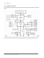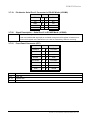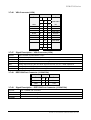
1
User’s Manual ECM-5716 Series All-in-One Pentium-M Single Board with LVDS, TMDS, AC97 Audio, IEEE-1394A, PCMCIA, Dual 10/100Base-Tx Ethernet Interfaces, 4USB 2.0, 2COMs & Intel Gigabit Ethernet Interface (optional) 3rd Ed. – 16 November 2004 Part No. 2047571600 ECM-5716 Series FCC STATEMENT THIS DEVICE COMPLIES WITH PART 15 FCC RULES. OPERATION IS SUBJECT TO THE FOLLOWING TWO CONDITIONS: (1) THIS DEVICE MAY NOT CAUSE HARMFUL INTERFERENCE. (2) THIS DEVICE MUST ACCEPT ANY INTERFERENCE RECEIVED INCLUDING OPERATION. INTERFERENCE THAT MAY CAUSE UNDESIRED THIS EQUIPMENT HAS BEEN TESTED AND FOUND TO COMPLY WITH THE LIMITS FOR A CLASS "A" DIGITAL DEVICE, PURSUANT TO PART 15 OF THE FCC RULES. THESE LIMITS ARE DESIGNED TO PROVIDE REASONABLE PROTECTION AGAINTST HARMFUL INTERFERENCE WHEN THE EQUIPMENT IS OPERATED IN A COMMERCIAL ENVIRONMENT. THIS EQUIPMENT GENERATES, USES, AND CAN RADIATE RADIO FREQUENCY ENERGY AND, IF NOT INSTATLLED AND USED IN ACCORDANCE WITH THE INSTRUCTION MANUAL, MAY CAUSE HARMFUL INTERFERENCE TO RADIO COMMUNICATIONS. OPERATION OF THIS EQUIPMENT IN A RESIDENTIAL AREA IS LIKELY TO CAUSE HARMFUL INTERFERENCE IN WHICH CASE THE USER WILL BE REQUIRED TO CORRECT THE INTERFERENCE AT HIS OWN EXPENSE. Evalue Technology Inc. User’s Manual Copyright Notice Copyright 2004 Evalue Technology Inc., ALL RIGHTS RESERVED. No part of this document may be reproduced, copied, translated, or transmitted in any form or by any means, electronic or mechanical, for any purpose, without the prior written permission of the original manufacturer. Trademark Acknowledgement Brand and product names are trademarks or registered trademarks of their respective owners. Disclaimer Evalue Technology Inc. reserves the right to make changes, without notice, to any product, including circuits and/or software described or contained in this manual in order to improve design and/or performance. Evalue Technology assumes no responsibility or liability for the use of the described product(s) and conveys no license or title under any patent, copyright or mask work rights to these products, and makes no representations or warranties that these products are free from patent, copyright, or mask work right infringement, unless otherwise specified. Applications that are described in this manual are for illustration purposes only. Evalue Technology Inc. makes no representation or warranty that such application will be suitable for the specified use without further testing or modification. Life Support Policy Evalue Technology’s PRODUCTS ARE NOT FOR USE AS CRITICAL COMPONENTS IN LIFE SUPPORT DEVICES OR SYSTEMS WITHOUT THE PRIOR WRITTEN APPROVAL OF Evalue Technology Inc. As used herein: 1. Life support devices or systems are devices or systems which, (a) are intended for surgical implant into body, or (b) support or sustain life and whose failure to perform, when properly used in accordance with instructions for use provided in the labelling, can be reasonably expected to result in significant injury to the user. 2. A critical component is any component of a life support device or system whose failure to perform can be reasonably expected to cause the failure of the life support device or system, or to affect its safety or effectiveness. Evalue Technology Inc. ECM-5716 Series A Message to the Customer Evalue Customer Services Each and every Evalue’s product is built to the most exacting specifications to ensure reliable performance in the harsh and demanding conditions typical of industrial environments. Whether your new Evalue device is destined for the laboratory or the factory floor, you can be assured that your product will provide the reliability and ease of operation for which the name Evalue has come to be known. Your satisfaction is our primary concern. Here is a guide to Evalue’s customer services. To ensure you get the full benefit of our services, please follow the instructions below carefully. Evalue Technology Inc. User’s Manual Technical Support We want you to get the maximum performance from your products. So if you run into technical difficulties, we are here to help. For the most frequently asked questions, you can easily find answers in your product documentation. These answers are normally a lot more detailed than the ones we can give over the phone. So please consult this manual first. To receive the latest version of the user manual, please visit our Web site at: http://www.evalue-tech.com/ If you still cannot find the answer, gather all the information or questions that apply to your problem, and with the product close at hand, call your dealer. Our dealers are well trained and ready to give you the support you need to get the most from your Evalue’s products. In fact, most problems reported are minor and are able to be easily solved over the phone. In addition, free technical support is available from Evalue’s engineers every business day. We are always ready to give advice on application requirements or specific information on the installation and operation of any of our products. Please do not hesitate to call or e-mail us. Headquarters Evalue Technology Inc. 7F, 228, Lian-Cheng Road, Chung-ho City, Taipei, Taiwan Tel: +886-2-82262345 Fax: +886-2-82262777 http://www.evalue-tech.com E-mail: [email protected] Europe Branch Office Evalue Europe A/S Nordre Strandvej 119C, 3150 Hellebaek, Denmark Tel : +45-7025-0310 Fax : +45-4975-5026 http://www.evalue-tech.com E-mail: [email protected] China Branch Office Evalue Technology Shanghai Inc. Room 909, 9F, Section B, No.900, Yisan Road, Caohejing Hi-tech Park, Shanghai 200233, China Tel : +86-21-6470-3454 Fax : +86-21-6470-3454 http://www.evalue-tech.com E-mail: [email protected] US Branch Office Evalue Technology Inc. Suite 210, 200 Tornillo Way, Tinton Falls, NJ 07712 USA Tel: +1-732-578-0200 Fax: +1-732-578-0250 http://www.evalue-tech.com E-mail: [email protected] Evalue Technology Inc. ECM-5716 Series Product Warranty Evalue warrants to you, the original purchaser, that each of its products will be free from defects in materials and workmanship for two years from the date of purchase. This warranty does not apply to any products which have been repaired or altered by persons other than repair personnel authorized by Evalue, or which have been subject to misuse, abuse, accident or improper installation. Evalue assumes no liability under the terms of this warranty as a consequence of such events. Because of Evalue’s high quality-control standards and rigorous testing, most of our customers never need to use our repair service. If an Evalue’s product is defective, it will be repaired or replaced at no charge during the warranty period. For out-of-warranty repairs, you will be billed according to the cost of replacement materials, service time, and freight. Please consult your dealer for more details. If you think you have a defective product, follow these steps: 1. Collect all the information about the problem encountered. (For example, CPU type and speed, Evalue’s products model name, hardware & BIOS revision number, other hardware and software used, etc.) Note anything abnormal and list any on-screen messages you get when the problem occurs. 2. Call your dealer and describe the problem. Please have your manual, product, and any helpful information readily available. 3. If your product is diagnosed as defective, obtain an RMA (return material authorization) number from your dealer. This allows us to process your good return more quickly. 4. Carefully pack the defective product, a complete Repair and Replacement Order Card and a photocopy proof of purchase date (such as your sales receipt) in a shippable container. A product returned without proof of the purchase date is not eligible for warranty service. 5. Write the RMA number visibly on the outside of the package and ship it prepaid to your dealer. Evalue Technology Inc. User’s Manual Packing List Before you begin installing your single board, please make sure that the following materials have been shipped: n n n 1 ECM-5716 series All-in-One Pentium-M Computing Module 1 Quick Installation Guide 1 CD-ROM contains the followings: — User’s Manual (this manual in PDF file) — Ethernet driver and utilities — VGA drivers and utilities — Audio drivers and utilities n Cable set includes the followings: — 1 ATA100 IDE cable (40-pin, pitch 2.54mm) — 1 FDD cable (34-pin, pitch 2.54mm) — 1 Daughter board supports Audio / 2USB (P/N: 9697000105) — 1 Flat cable for audio (16-pin, pitch 2.0mm/16-pin, 2.54mm) — 1 Flat cable for USB 2.0 (10-pin, pitch 2.54mm) — 1 Bracket with 1 serial & 1 printer cable (10-pin 2.54mm/26-pin 2.54mm) — 1 PS/2 KB/Mouse Y cable If any of these items are missing or damaged, please contact your distributor or sales representative immediately. Evalue Technology Inc. ECM-5716 Series 1. MANUAL OBJECTIVES ............................................................................................ 1 2. INTRODUCTION........................................................................................................ 2 2.1 System Overview................................................................................................... 2 2.2 System Specifications .......................................................................................... 3 2.3 Architecture Overview .......................................................................................... 6 2.3.1 2.3.2 2.3.3 2.3.4 2.3.5 2.3.6 2.3.7 2.3.8 2.3.9 2.3.10 3. 855GME and 82801DB ............................................................................................... 7 DRAM Interface........................................................................................................... 9 Chrontel CH7301 DVI Transmitter............................................................................... 9 PCI Interface ............................................................................................................... 9 IDE Interface (Bus Master Capability and Synchronous DMA Mode).......................... 9 USB 2.0..................................................................................................................... 10 Ethernet .................................................................................................................... 11 Winbond W83627HF ................................................................................................ 13 RICOH R5C551 IEEE1394A Host & PCMCIA Controller .......................................... 13 Compact Flash Interface ........................................................................................... 14 HARDWARE CONFIGURATION ............................................................................. 15 3.1 Installation Procedure......................................................................................... 15 3.2 Safety Precautions .............................................................................................. 15 3.2.1 3.2.2 3.3 Warning! ................................................................................................................... 15 Caution!..................................................................................................................... 15 Socket 479 Processor......................................................................................... 16 3.3.1 3.3.2 Installing Pentium M CPU.......................................................................................... 16 Removing CPU ......................................................................................................... 16 3.4 Main Memory ....................................................................................................... 16 3.5 Jumper & Connector........................................................................................... 17 3.5.1 3.5.2 Jumper & Connector Layout ..................................................................................... 17 Jumper & Connector List........................................................................................... 18 Connectors ................................................................................................................... 19 3.6 Setting Jumpers .................................................................................................. 20 3.6.1 3.6.2 3.6.3 3.7 Clear CMOS (JBAT) .................................................................................................. 21 COM2 RS-232/422/485 Select (JP1, JP2) ................................................................ 21 COM1 Pin 9 Signal Select (JP3) ............................................................................... 21 Connector Definitions......................................................................................... 22 3.7.1 3.7.2 3.7.3 3.7.4 3.7.5 ATX Power Connector (ATX) .................................................................................... 22 Serial Port 1 Connector (COM1) ............................................................................... 22 Signal Description – Serial Port 1 Connector (COM1)............................................... 23 CPU Fan Connector (FAN1) ..................................................................................... 23 Signal Description – CPU Fan Connector ................................................................. 23 Evalue Technology Inc. User’s Manual 3.7.6 3.7.7 3.7.8 3.7.9 3.7.10 3.7.11 3.7.12 3.7.13 3.7.14 3.7.15 3.7.16 3.7.17 3.7.18 3.7.19 3.7.20 3.7.21 3.7.22 3.7.23 3.7.24 3.7.25 3.7.26 3.7.27 3.7.28 3.7.29 3.7.30 3.7.31 3.7.32 3.7.33 3.7.34 3.7.35 3.7.36 3.7.37 3.7.38 3.7.39 3.7.40 3.7.41 3.7.42 3.7.43 3.7.44 3.7.45 3.7.46 3.7.47 3.7.48 3.7.49 4. Floppy Connector (FLP)............................................................................................ 24 Signal Description – Floppy Disk Connector (FLP) ................................................... 25 Primary IDE Connector (IDE_1) ................................................................................ 26 Secondary IDE Connector (IDE_2) ........................................................................... 27 Signal Description – IDE Device Connector (IDE_1 / IDE_2) .................................... 28 Audio Connector (JAUDIO) ....................................................................................... 29 Signal Description – Audio Connector (JAUDIO) ...................................................... 29 LCD Inverter Connector (JBKL)................................................................................. 29 Signal Description – LCD Inverter Connector (JBKL)................................................ 29 Serial Port 2 Connector (JCOM2).............................................................................. 30 Signal Description – Serial Port 2 Connector in RS-232 Mode (JCOM2) .................. 30 Pin Header Serial Port 2 Connector in RS-422 Mode (JCOM2) ................................ 30 Signal Description – Serial Port 2 in RS-422 Mode (JCOM2).................................... 30 Pin Header Serial Port 2 Connector in RS-485 Mode (JCOM2) ................................ 31 Signal Description – Serial Port 2 in RS-485 Mode (JCOM2).................................... 31 Front Panel Connector (JFP) .................................................................................... 31 IrDA Connector (JIR) ................................................................................................. 32 Signal Description – IR Connector (JIR).................................................................... 32 Keyboard and PS/2 mouse connector (JKBMS) ....................................................... 32 Signal Description – Keyboard and PS/2 Mouse Connector (JKBMS) ...................... 32 Miscellaneous Setting Connector (JMISC) ................................................................ 33 Signal Description – JMISC Connector ..................................................................... 33 LVDS Connector (JLVDS)......................................................................................... 34 Signal Description – LVDS Connector (JLVDS) ..........................錯誤! 尚未定義書籤。 TMDS Connector (JTMDS)........................................................................................ 35 Signal Description – TMDS Connector (JTMDS)....................................................... 35 USB Connector (JUSB)............................................................................................. 36 Signal Description – USB Connector (JUSB) ............................................................ 36 PS/2 Keyboard & Mouse Connector (KB_MS) .......................................................... 36 Signal Description – PS/2 Keyboard & Mouse Connector......................................... 36 10/100 BASE-Tx Ethernet Connector (LAN1/LAN2) ................................................. 37 Signal Description – 10/100Base-Tx Ethernet Connector ......................................... 37 10/100/1000 BASE-Tx Ethernet Connector (LAN2: 82540EM Optional)................... 37 Signal Description – 10/100/1000Base-Tx Ethernet Connector ................................ 38 Parallel Port Connector (LPT) ................................................................................... 38 DB25 Parallel Port Connector (LPT) ......................................................................... 39 Signal Description – Parallel Port (LPT) .................................................................... 40 System Fan Connector 1 (S_FAN1).......................................................................... 40 System Fan Connector 2 (S_FAN2).......................................................................... 40 Signal Description – System Fan Connector............................................................. 40 VGA Connector (VGA) .............................................................................................. 41 Signal Description – VGA Connector (VGA) ............................................................. 41 IEEE1394 Port Connector (J1394/1394)................................................................... 41 Signal Description – IEEE1394 Port Connector (J1394/1394) .................................. 41 AWARD BIOS SETUP ............................................................................................. 42 4.1 Starting Setup...................................................................................................... 42 4.2 Using Setup ......................................................................................................... 43 4.2.1 4.2.2 4.3 Navigating Through The Menu Bar ........................................................................... 43 To Display a Sub Menu ............................................................................................. 43 Getting Help......................................................................................................... 44 Evalue Technology Inc. ECM-5716 Series 4.4 In Case of Problems............................................................................................ 44 4.5 Main Menu............................................................................................................ 44 4.5.1 4.5.2 4.5.3 4.5.4 4.5.5 4.5.6 4.5.7 4.5.8 4.5.9 4.5.10 4.5.11 4.5.12 4.5.13 5. Setup Items ............................................................................................................... 44 Standard CMOS Setup ............................................................................................. 46 Advanced BIOS Features ......................................................................................... 49 Advanced Chipset Features...................................................................................... 52 Integrated Peripherals............................................................................................... 54 Power Management Setup........................................................................................ 57 PnP/PCI Configuration Setup.................................................................................... 60 PC Health Status....................................................................................................... 62 Frequency / Voltage Control ..................................................................................... 62 Load Fail-Safe Defaults ............................................................................................ 63 Load Optimized Defaults........................................................................................... 63 Supervisor / User Password Setting.......................................................................... 64 Exit Selecting ............................................................................................................ 65 DRIVER INSTALLATION......................................................................................... 67 5.1 Driver Installation for Ethernet Adapter ............................................................ 67 5.1.1 5.1.2 5.2 Driver Installation for Display Adapter .............................................................. 83 5.2.1 5.2.2 5.3 6. Windows 9x............................................................................................................... 83 Windows 2000 or Windows XP Display Installation .................................................. 86 Driver Installation for Audio Adapter................................................................. 89 5.3.1 5.4 Windows 9x............................................................................................................... 67 Windows 2000 , XP Ethernet Installation .................................................................. 74 Windows 9x, Windows 2000, Windows XP............................................................... 89 Driver Installation for Intel 855 Chipset............................................................. 91 POST MESSAGES .................................................................................................. 93 6.1 POST Beep........................................................................................................... 93 6.2 Error Messages ................................................................................................... 93 6.2.1 6.2.2 6.2.3 6.2.4 6.2.5 6.2.6 6.2.7 6.2.8 6.2.9 6.2.10 6.2.11 6.2.12 6.2.13 6.2.14 6.2.15 6.2.16 6.2.17 CMOS BATTERY HAS FAILED ................................................................................ 93 CMOS CHECKSUM ERROR .................................................................................... 93 DISK BOOT FAILURE, INSERT SYSTEM DISK AND PRESS ENTER..................... 93 DISKETTE DRIVES OR TYPES MISMATCH ERROR - RUN SETUP....................... 93 DISPLAY SWITCH IS SET INCORRECTLY ............................................................. 94 DISPLAY TYPE HAS CHANGED SINCE LAST BOOT ............................................. 94 EISA Configuration Checksum Error PLEASE RUN EISA CONFIGURATION UTILITY94 EISA Configuration Is Not Complete PLEASE RUN EISA CONFIGURATION UTILITY94 ERROR ENCOUNTERED INITIALIZING HARD DRIVE ............................................ 94 ERROR INITIALIZING HARD DISK CONTROLLER.................................................. 94 FLOPPY DISK CNTRLR ERROR OR NO CNTRLR PRESENT ................................ 94 Invalid EISA Configuration PLEASE RUN EISA CONFIGURATION UTILITY ........... 95 KEYBOARD ERROR OR NO KEYBOARD PRESENT ............................................. 95 Memory Address Error at ... ...................................................................................... 95 Memory parity Error at .............................................................................................. 95 MEMORY SIZE HAS CHANGED SINCE LAST BOOT.............................................. 95 Memory Verify Error at ... .......................................................................................... 95 Evalue Technology Inc. User’s Manual 6.2.18 OFFENDING ADDRESS NOT FOUND ..................................................................... 95 6.2.19 OFFENDING SEGMENT:.......................................................................................... 95 6.2.20 PRESS A KEY TO REBOOT .................................................................................... 96 6.2.21 PRESS F1 TO DISABLE NMI, F2 TO REBOOT ....................................................... 96 6.2.22 RAM PARITY ERROR - CHECKING FOR SEGMENT ... .......................................... 96 6.2.23 Should Be Empty But EISA Board Found PLEASE RUN EISA CONFIGURATION UTILITY.................................................................................................................................. 96 6.2.24 Should Have EISA Board But Not Found PLEASE RUN EISA CONFIGURATION UTILITY.................................................................................................................................. 96 6.2.25 Slot Not Empty .......................................................................................................... 96 6.2.26 SYSTEM HALTED, (CTRL-ALT-DEL) TO REBOOT ... ............................................. 96 6.2.27 Wrong Board In Slot PLEASE RUN EISA CONFIGURATION UTILITY .................... 97 6.2.28 FLOPPY DISK(S) fail (80) → Unable to reset floppy subsystem............................... 97 6.2.29 FLOPPY DISK(S) fail (40) → Floppy Type dismatch................................................. 97 6.2.30 Hard Disk(s) fail (80) → HDD reset failed.............................................................. 97 6.2.31 Hard Disk(s) fail (40) → HDD controller diagnostics failed. ................................... 97 6.2.32 Hard Disk(s) fail (20) → HDD initialization error. ................................................... 97 6.2.33 Hard Disk(s) fail (10) → Unable to recalibrate fixed disk. ...................................... 97 6.2.34 Hard Disk(s) fail (08) → Sector Verify failed.......................................................... 97 6.2.35 Keyboard is locked out - Unlock the key. .................................................................. 97 6.2.36 Keyboard error or no keyboard present. ................................................................... 97 6.2.37 Manufacturing POST loop......................................................................................... 97 6.2.38 BIOS ROM checksum error - System halted. ............................................................ 97 6.2.39 Memory test fail......................................................................................................... 97 6. MEASUREMENT DRAWING ................................................................................... 98 APPENDIX A: BIOS REVISIONS ................................................................................... 100 APPENDIX B: SYSTEM RESOURCES .......................................................................... 101 Memory Map ........................................................................................................................ 101 I/O – Map ............................................................................................................................. 102 Interrupt Usage .................................................................................................................... 104 DMA-channel Usage ............................................................................................................ 105 APPENDIX C: AWARD BIOS POST MESSAGES ......................................................... 106 POST Beep ................................................................................................................. 106 Error Messages .......................................................................................................... 106 CMOS BATTERY HAS FAILED ........................................................................................... 106 CMOS CHECKSUM ERROR ............................................................................................... 106 DISK BOOT FAILURE, INSERT SYSTEM DISK AND PRESS ENTER ............................... 106 DISKETTE DRIVES OR TYPES MISMATCH ERROR - RUN SETUP ................................. 106 DISPLAY SWITCH IS SET INCORRECTLY ........................................................................ 107 DISPLAY TYPE HAS CHANGED SINCE LAST BOOT........................................................ 107 EISA Configuration Checksum Error PLEASE RUN EISA CONFIGURATION UTILITY....... 107 EISA Configuration Is Not Complete PLEASE RUN EISA CONFIGURATION UTILITY....... 107 ERROR ENCOUNTERED INITIALIZING HARD DRIVE....................................................... 107 ERROR INITIALIZING HARD DISK CONTROLLER ............................................................ 107 FLOPPY DISK CNTRLR ERROR OR NO CNTRLR PRESENT........................................... 107 Invalid EISA Configuration PLEASE RUN EISA CONFIGURATION UTILITY ...................... 108 KEYBOARD ERROR OR NO KEYBOARD PRESENT ........................................................ 108 Evalue Technology Inc. ECM-5716 Series Memory Address Error at ... ................................................................................................. 108 Memory parity Error at ......................................................................................................... 108 MEMORY SIZE HAS CHANGED SINCE LAST BOOT ........................................................ 108 Memory Verify Error at ... ..................................................................................................... 108 OFFENDING ADDRESS NOT FOUND................................................................................ 108 OFFENDING SEGMENT:..................................................................................................... 108 PRESS A KEY TO REBOOT ............................................................................................... 109 PRESS F1 TO DISABLE NMI, F2 TO REBOOT .................................................................. 109 RAM PARITY ERROR - CHECKING FOR SEGMENT ........................................................ 109 Should Be Empty But EISA Board Found PLEASE RUN EISA CONFIGURATION UTILITY109 Should Have EISA Board But Not Found PLEASE RUN EISA CONFIGURATION UTILITY 109 Slot Not Empty ..................................................................................................................... 109 SYSTEM HALTED, (CTRL-ALT-DEL) TO REBOOT ... ........................................................ 109 Wrong Board In Slot PLEASE RUN EISA CONFIGURATION UTILITY ............................... 110 FLOPPY DISK(S) fail (80) → Unable to reset floppy subsystem.......................................... 110 FLOPPY DISK(S) fail (40) → Floppy Type dismatch............................................................ 110 Hard Disk(s) fail (80) → HDD reset failed......................................................................... 110 Hard Disk(s) fail (40) → HDD controller diagnostics failed. .............................................. 110 Hard Disk(s) fail (20) → HDD initialization error. .............................................................. 110 Hard Disk(s) fail (10) → Unable to recalibrate fixed disk. ................................................. 110 Hard Disk(s) fail (08) → Sector Verify failed..................................................................... 110 Keyboard is locked out - Unlock the key. ............................................................................. 110 Keyboard error or no keyboard present. .............................................................................. 110 Manufacturing POST loop.................................................................................................... 110 BIOS ROM checksum error - System halted. ....................................................................... 110 Memory test fail.................................................................................................................... 110 POST CODES................................................................................................................. 111 APPENDIX E: AUDIO / USB DAUGHTER BOARD USER’S GUIDE ............................. 117 Jumper & Connector Layout ......................................................... 錯誤! 尚未定義書籤。 Jumper & Connector List .............................................................. 錯誤! 尚未定義書籤。 Measurement Drawing ................................................................... 錯誤! 尚未定義書籤。 Evalue Technology Inc. User’s Manual Document Amendment History Revision Date st 1 Feb. 2004. nd 2 June, 2004 3rd Nov. 2004 By Stephen Tsao Stephen Tsao Leo Chen Comment Initial Release Modify 1. JCOM2 RS422/485 pin definition 2. JTMDS pin 19, 20 Modify 1. TMDS Connector pin signal 2. Jumper & Connector layout list 3. USB Connector pin define 4. Add in 3.3 Pentium M processor 5. Headquarters address updated. 6. US branch added. 7. Latest BIOS deleted. 8. APPENDIX F: AUDIO / USB DAUGHTER BOARD USER’S MANUAL updated. Evalue Technology Inc. ECM-5716 Series 1. Manual Objectives This manual describes in detail the Evalue Technology ECM-5716 series Single Board. We have tried to include as much information as possible but we have not duplicated information that is provided in the standard IBM Technical References, unless it proved to be necessary to aid in the understanding of this board. We strongly recommend that you study this manual carefully before attempting to interface with ECM-5716 series or change the standard configurations. Whilst all the necessary information is available in this manual we would recommend that unless you are confident, you contact your supplier for guidance. Please be aware that it is possible to create configurations within the CMOS RAM that make booting impossible. If this should happen, clear the CMOS settings, (see the description of the Jumper Settings for details). If you have any suggestions or find any errors concerning this manual and want to inform us of these, please contact our Customer Service department with the relevant details. ECM-5716 Series User’s Manual 1 User’s Manual 2. 2.1 Introduction System Overview The ECM-5716 series is a compact 5.25” CD-ROM size Single Board Computer that equips with Intel Banias Chipset, LCD Interfaces, AC97 Audio, dual 10/100Base-Tx Ethernet, four USB2.0 interfaces, dual IEEE1394 interfaces, PCMCIA, and Compact Flash. The ECM-5716 series support Intel Pentium M series CPU, which are powerful in performance and low power in system consumption. Its display is bolstered up with the chipset Intel 855GME Integrated graphics which supports LVDS flat panel, DVO, and CRT interfaces. This makes this PC engine a perfect solution for Retail / Financial Transaction Terminals, and high-end multimedia POS / KIOSK Terminals. Furthermore, the ECM-5716 series is outstanding in a 5.25" form factors designed with Intel 82801DB ICH4 built-in and 82551ER or Intel 82551QM PCI-bus Ethernet 10/100Base-Tx Ethernet controllers (optional an Intel 82540EM PCI-bus Ethernet controller onboard support Gigabit Ethernet function) making it the ideal solution for popular networking devices like Gateway, Router, Thin Server, Firewall and E-Box. In addition, the on board IEEE1394 and 4 USB2.0 interfaces make the ECM-5716 series also ideal for demanding high-end Entertainment Devices that require high integration multimedia Single Board Computer. Other impressive features include a built-in 40-pin TFT LCD interface (LVDS), a TMDS interface, the AC97 Audio, a Compact Flash socket for type I/ II Compact Flash storage card, one parallel port, one PCMCIA socket, and one 184-pin DDR SDRAM DIMM sockets allowing for up to 1GB of DDR SDRAM to be installed, and a PCI slot for future expansion. 2 ECM-5716 Series User’s Manual ECM-5716 Series 2.2 System Specifications General Functions • CPU: Supports Intel Pentium-M series processors • BIOS: Award 512 KB FWH BIOS • Chipset: Intel 855GME + Intel 82801DB (ICH4) • I/O Chipset: Winbond W83627HF-AW • Memory: Onboard one DDR SDRAM socket supports up to 1 Gbytes DDR 333/266/200 SDRAM • Enhanced IDE: Supports up to four IDE devices. Supports Ultra DMA/100 mode with data transfer rate up to 100MB/sec. (Primary: 20 x 2 box header; Secondary: 22 x 2, pitch 2.0mm box header onboard for DiskOnModule) • FDD Interface: Supports up to two floppy disk drives, 5.25" (360KB and 1.2MB) and /or 3.5" (720KB, 1.44MB, and 2.88MB). Supports Mode-3 FDD • Parallel Port: An Internal header for bi-directional parallel port x 1. Supports SPP, ECP, and EPP modes • Serial Port: Supports Two RS-232 serial ports. Ports can be configured as COM1, COM2, COM3, COM4, or disabled individually. (16C550 equivalent) (COM1 with DSub 9, COM2 with 5 x 2, pitch 2.54 box header) COM2 can be set as RS232/422/485. • IR Interface: Supports one IrDA Tx/Rx header • KB/Mouse Connector: External mini-DIN PS2 Keyboard/Mouse connector x 1, Internal KB/Mouse connector 4X2 header pitch 2.54mm • USB 2.0 Connectors: Two external USB 2.0 connectors. One 5 x 2, pitch 2.54mm header supports additional dual USB 2.0 • Watchdog Timer: Can generate a system reset, IRQ10/11 or NMI. Software selectable time out interval (1 sec. ~ 255 min., 1 sec. or 1 min. /step) • Power Management: Supports ATX power supply. Supports PC97, LAN wake up and modem ring-in functions. I/O peripheral devices support power saving and doze/standby/suspend modes. ACPI 2.0 & APM 1.2 compliant. ECM-5716 Series User’s Manual 3 User’s Manual IEEE1394 Interface • Chipset: RICOH R5C551 • IEEE1394 Interface: Integrated 400 Mbit 2-Port PHY supports 2 IEEE1394A Ports Flat Panel/CRT Interface • Chipset: Intel 855 Chipset Graphics Memory Controller Hub (GMCH) integrated AGP high performance 256-bit GUI, 3D engine • Display Memory: Programmable frame buffer size up to 64MBytes • Display Type: Simultaneously supports CRT and TFT displays • Resolution: CRT displays support up to 1600 x 1200 @ 85-Hz PanelLink Interface • Chipset: Chrontel CH7301A DVI / TV output device • Display Type: DVI display at a pixel rate of up to 165MHz, supporting UXGA resolution displays. LVDS Interface • Chipset: Intel 855GME Chipset • Display Memory: Programmable frame buffer size up to 64MBytes • Display Type: 24-bit to 48-bit flat panel displays • Scalable bandwidth: Single or dual channel LVDS panel support up to UXGA panel solution with frequency range from 25 MHz to 112 MHz per channel. Audio Interface • Chipset: Intel ICH4 integrated Audio controller with AC97 interface • AC97 Codec: VIA VT1616 • Audio Controller: AC97 ver. 2.3 compliant interface. Supports Audio Out (5.1channel playback) 4 ECM-5716 Series User’s Manual ECM-5716 Series Ethernet Interface • Chipset: Intel 82801DB (ICH4) built-in and 82551ER PCI-bus Ethernet controller onboard support dual Ethernet function • Ethernet Interface: PCI 100/10 Mbps, IEEE 802.3U compatible Gigabit Ethernet Interface (Optional) • Chipset: Intel 82540EM PCI-bus Ethernet controller onboard support Gigabit Ethernet function • Ethernet Interface: PCI 1000/100/10 Mbps, IEEE 802.3x compatible. SSD Interface One CF socket supports Type I/II Compact Flash memory devices Expansion Interface • PCI Slot: One 32-bit PCI slot onboard Mechanical and Environmental • Power Supply Voltage: ATX type, +5V and +12V • Operating Temperature: 32 to 140°F (0 to 60°C) • Board Size: 8"(L) x 5.75"(W) (203mm x 146mm) • Weight: 0.5 Kg ECM-5716 Series User’s Manual 5 User’s Manual 2.3 Architecture Overview The following block diagram shows the architecture and main components of ECM-5716 series. The following sections provide detail information about the functions provided onboard. 6 ECM-5716 Series User’s Manual ECM-5716 Series 2.3.1 855GME and 82801DB The Intel 855GM/855GME GMCH components provide the processor interface, DDR SDRAM interface, display interface, and Hub interface. The Intel 855GME also has an option for AGP external graphics port, in addition to integrated graphics support for added board flexibility options. The Intel 855GM GMCH is in a 732-pin Micro-FCBGA package and contains the following functionality listed below: • AGTL+ host bus supporting 32-bit host addressing with Enhanced Intel SpeedStep technology support • Supports a single channel of DDR SDRAM memory • System memory supports DDR200/266 MHz (SSTL_2) DDR SDRAM • Integrated graphics capabilities: Display Core frequency at 133 MHz or 200 MHz • Render Core frequency at 100 MHz ,133 MHz, and 200 MHz • Provides supports four display ports: one progressive scan analog monitor, dual channel LVDS interface and two DVO port. The Intel 855GME GMCH is in a 732-pin Micro-FCBGA package and contains all features listed above and the additional functionality list below: • Display Core frequency at 133 MHz, 200 MHz, or 250 MHz • Render Core frequency at 100 MHz ,133 MHz, 166 MHz, 200 MHz, or 250 MHz • System memory supports 200/266/333- MHz (SSTL_2) DDR SDRAM. • Enhanced Power Management Graphics features The GMCH IGD provides a highly integrated graphics accelerator delivering high performance 2D, 3D, and video capabilities. With its interfaces to UMA using a DVMT configuration, an analog display, a LVDS port, and two digital display ports (e.g. flat panel), the GMCH can provide a complete graphics solution. The GMCH also provides 2D hardware acceleration for block transfers of data (BLTs). The BLT engine provides the ability to copy a source block of data to a destination and perform raster operations (e.g., ROP1, ROP2, and ROP3) on the data using a pattern, and/or another destination. Performing these common tasks in hardware reduces CPU load, and thus improves performance. High bandwidth access to data is provided through the system memory interface. The GMCH uses Tiling architecture to increase system memory efficiency and thus maximize effective rendering bandwidth. The Intel 855GM/855GME GMCH improves 3D performance and quality with 3D Zone rendering technology. The Intel 855GME GMCH also supports Video Mixer rendering, and Bi-Cubic filtering. The Intel 855GM/855GME GMCH has four display ports, one analog and three digital. With these interfaces, the GMCH can provide support for a progressive scan analog monitor, a dedicated dual channel LVDS LCD panel, and two DVO devices. Each port can transmit data according to one or more protocols. The data that is sent out the display port is selected from one of the two possible sources, Pipe A or Pipe B. ECM-5716 Series User’s Manual 7 User’s Manual The Intel 855GM/855GME GMCH have an integrated dual channel LFP Transmitter interface to support LVDS LCD panel resolutions up to UXGA The display pipe provides panel up-scaling to fit a smaller source image onto a specific native panel size, as well as provides panning and centering support. The LVDS port is only supported on Pipe B. The LVDS port can only be driven by Pipe B, either independently or simultaneously with the Analog Display port. Spread Spectrum Clocking is supported: center and down spread support of 0.5%, 1%, and 2.5% utilizing an external SSC clock. The DVO B/C interface is compliant with the DVI Specification 1.0. When combined with a DVI compliant external device (e.g. TMDS Flat Panel Transmitter, TV-out encoder, etc.), the GMCH provides a high-speed interface to a digital or analog display (e.g. flat panel, TV monitor, etc.). The DVO ports are connected to an external display device. Examples of this are TV-out encoders, external DACs, LVDS transmitters, and TMDS transmitters. Each display port has control signals that may be used to control, configure and/or determine the capabilities of an external device. The GMCH provides two DVO ports that are each capable of driving a 165-MHz pixel clock at the DVO B or DVO C interface. When DVO B and DVO C are combined into a single DVO port, then an effective pixel rate of 330 MHz can be achieved. The DVO B/C ports can be driven by Pipe A or Pipe B. If driven on Pipe B, then the LVDS port must be disabled. The ICH4 is a highly integrated multifunctional I/O Controller Hub that provides the interface to the PCI Bus and integrates many of functions needed in today’s PC platform. The GMCH and ICH4 communicate over a dedicated hub interface. The 82801DB ICH4 functions and capabilities include: n PCI Rev. 2.2 compliant with support for 33MHz PCI operations n Supports up to 6 Request/Grant pairs (PCI slots) n Power management logic support n Enhanced DMA controller, interrupt controller, and timer functions n Integrated IDE controller; Ultra ATA/100/66/33 n USB host interface; 3 host controllers and supports 6 USB ports; includes a EHCI high-speed 2.0 USB controller n Integrated LAN controller n System Management Bus (SMBus) compatible with most IC devices; ICH4 has both bus master and slave capability n AC ’97 2.3 compliant link for audio and telephony codecs; up to 6 channels n Low Pin Count (LPC) interface n FWH Interface (FWH Flash BIOS support) n Alert on LAN* (AOL and AOL2) 8 ECM-5716 Series User’s Manual ECM-5716 Series 2.3.2 DRAM Interface The GMCH system memory controller directly supports the following: • One channel of PC1600/2100 SO-DIMM DDR SDRAM memory (Intel 855GM GMCH) • One channel of PC1600/2100/2700 SO-DIMM DDR SDRAM memory (Intel 855GME GMCH) • DDR SDRAM devices with densities of 128-Mb, 256-Mb, and 512-Mb technology • Up to 1 GB (512-Mb technology) with two SO-DIMMs • Up to 2 GB (512-Mb technology) using high density devices with two SO-DIMMs 2.3.3 Chrontel CH7301 DVI Transmitter The Chrontel CH7301 is a display controller device which accepts a digital graphics input signal, and encodes and transmitter data through a DVI or DFP (Digital flat panel). The device accepts data over one 12-bit wide variable voltage data port which supports four different RGB data formats. The DVI processor includes a low jitter PLL for generation of the high frequency serialized clock, and all circuitry required to decode, serialized and transmit data. The CH7301 comes in versions able to drive a DFP display at a pixel arte up to 165MHz, supporting UXGA resolution displays. No scaling of input data is performed on the data output to the DVI device. 2.3.4 PCI Interface The ICH4 PCI interface provides a 33 MHz, Rev. 2.2 compliant implementation. All PCI signals are 5V tolerant, except PME#. The ICH2 integrates a PCI arbiter that supports up to six external PCI bus masters in addition to the internal ICH4 requests. 2.3.5 IDE Interface (Bus Master Capability and Synchronous DMA Mode) The fast IDE interface supports up to four IDE devices providing an interface for IDE hard disks and ATAPI devices. Each IDE device can have independent timings. The IDE interface supports PIO IDE transfers up to 16 Mbytes/sec and Ultra ATA transfers up 100 Mbytes/sec. It does not consume any ISA DMA resources. The IDE interface integrates 16x32-bit buffers for optimal transfers. The ICH4’s IDE system contains two independent IDE signal channels. They can be electrically isolated independently. They can be configured to the standard primary and secondary channels (four devices). There are integrated series resistors on the data and control lines. Access to these controllers is provided by two standard IDC 40-pin connectors. ECM-5716 Series User’s Manual 9 User’s Manual 2.3.6 USB 2.0 The ICH4 contains an Enhanced Host Controller Interface (EHCI) compliant host controller that supports USB high-speed signaling. High-speed USB 2.0 allows data transfers up to 480Mb/s which is 40 times faster than full-speed USB. The ICH4 also contains three Universal Host Controller Interface (UHCI) controllers that support USB full-speed and low-speed signaling. The ICH4 supports 6 USB 2.0 ports. All six USB ports are high-speed, full-speed, and low-speed capable. ICH4’s port-routing logic determines whether a USB port is controlled by one of the UHCI controllers or by the EHCI controller. 10 ECM-5716 Series User’s Manual ECM-5716 Series 2.3.7 Ethernet 2.3.7.1 ICH4 LAN Controller ICH4’s integrated LAN Controller includes a 32-bit PCI controller that provides enhanced scatter-gather bus mastering capabilities and enables the LAN Controller to perform highspeed data transfers over the PCI bus. Its bus master capabilities enable the component to process high level commands and perform multiple operations, this lowers processor utilization by off-loading communication tasks from the processor. Two large transmit and receive FIFOs of 3 KB each help prevent data under runs and overruns while waiting for bus accesses. This enables the integrated LAN Controller to transmit data with minimum interframe spacing (IFS). The LAN Controller can operate in either full duplex or half duplex mode. In full duplex mode the LAN Controller adheres with the IEEE 802.3x Flow Control specification. Half duplex performance is enhanced by a proprietary collision reduction mechanism. The integrated LAN controller also includes an interface to a serial (4-pin) EEPROM. The EEPROM provides power-on initialization for hardware and software and software configuration parameters. From a software perspective, the integrated LAN controller appears to reside on the secondary side of the ICH4’s virtual PCI to PCI Bridge. This is typically Bus 1, but may be assigned a different number, depending on system configuration. The following summarizes the ICH4 LAN controller features: n Compliance with Advanced Configuration and Power Interface and PCI Power Management standard. n Support for wake-up on interesting packets and link status change n Support for remote power-up using Wake on LAN (WOL) technology n Deep power-down node support n Support of Wired for management (WfM) Rev 2.0 n Backward compatible software with 82447, 82558 and 82559 n TCP/UDP checksum of f load capabilities n Support for Intel’s Adaptive Technology ECM-5716 Series User’s Manual 11 User’s Manual 2.3.7.2 Intel 82551ER Ethernet Controller The Intel® 82551ER Integrated 10BASE-T/100BASE-TX Ethernet Controller expands the family of Intel® 8255x controllers. As part of Intel’s fourth generation of fully integrated Fast Ethernet MAC/PHY solutions, the 82551ER is optimized for low-cost, embedded applications. The 82551ER provides excellent performance with offloading of TCP, UDP and IP checksums. Its optimized 32-bit interface and efficient scatter-gather bus mastering capabilities enable the controller to perform high-speed data transfers over the PCI bus. These capabilities accelerate the processing of high-level commands and operations, lowering CPU utilization. The device’s architecture enables efficient data flow from the bus interface unit to the 3KB transmit and receive FIFOs, providing the perfect balance between the wire and system bus. In addition, multiple priority queues augment Quality of Service (QoS) performance. The 82551ER is pin-compatible with the Intel® 82559ER Fast Ethernet controller, and it is layoutcompatible with Intel® 82540 Gigabit Ethernet controller. Intel-supported 82551ER drivers run on the standard Intel® 82551QM Fast Ethernet PCI/CardBus Controller, providing OEMs an upgrade path to the 82551QM for additional features and increased functionality. 2.3.7.3 Intel 82540EM Ethernet Controller (Optional) The Intel 82540EM Gigabit Ethernet Controller is a single, compact component with an integrated Gigabit Ethernet Media Access Control (MAC) and physical layer (PHY) functions. For desktop, workstation and mobile PC network designs with critical space constrains, the Intel 82540EM allows for a Gigabit Ethernet implementation in a very small area that is footprint compatible with current 10/100 Mbps Fast Ethernet designs. The Intel 82540EM integrates Intel’s fourth generation gigabit MAC design with fully integrated, physical layer circuitry to provide a standard IEEE 802.3 Ethernet interface for 1000BASE-T, 100BASE-TX, and 10BASE-T applications (802.3, 802.3u, and 802.3ab). The controller is capable of transmitting and receiving data at rates of 1000M bps, 100 Mbps, or 10 Mbps. In addition to managing MAC and PHY layer functions, the controller provides a 32-bit wide direct Peripheral Component Interconnect (PCI) 2.2 compliant interface capable of operating at 33 or 66 MHz. The Intel 82540EM’s on-board System Management Bus (SMB) port enables network manageability implementations required by information technology personnel for remote control and alerting via the LAN. With SMB, management packets can be routed to or from a management processor. The SMB port enables industry standard, such as Intelligent Platform Management Interface (IPMI) and Alert Standard Forum (ASF), to be implemented using the 82540EM. In addition, on chip ASF 1.0 circuitry provides alerting and remote control capabilities with standardized interfaces. The 82540EM Gigabit Ethernet Controller architecture is designed to deliver high performance and PCI bus efficiency. Wide internal data paths eliminate performance bottlenecks by efficiently handling large address and data words. The 82540EM controller includes advanced interrupt handling features to limit PCI bus traffic and a PCI interface that maximizes the use of bursts for efficient PCI bandwidth use. A large 64 KByte on-chip packet buffer maintains superior performance as available PCI bandwidth changes. In addition, using hardware acceleration, the controller offloads tasks from the host controller, such as TCP/UDP/IP checksum calculations and TCP segmentation. The 82540EM is packed in a 15mm2 196-ball grid array and is pin compatible with the Intel 82551QM 10/100 Mbps Fast Ethernet Multifunction PCI/CardBus Controller. 12 ECM-5716 Series User’s Manual ECM-5716 Series 2.3.8 Winbond W83627HF The Winbond W83627F/HF is made to fully comply with Mocrosoft PC98 and PC99 Hardware Design Guide. Moreover, W83627F/HF is made to meet the specification of PC98/PC99’s requirement in the power management: ACPI and DPM (Device Power Management). Super I/O chip provides features as the following: n Meet LPC Spec. 1.0 n Support LDRQ# (LPC DMA), SERIRQ (serial IRQ) n Include all features of Winbond I/O W83977TF and W83977EF n Integrate Hardware Monitor functions n Compliant with Microsoft PC98/PC99 Hardware Design Guide. n Support DPM (Device Power Management), ACPI n Programmable configuration settings n Single 24 or 48 MHz clock input 2.3.9 RICOH R5C551 IEEE1394A Host & PCMCIA Controller The 5C551 is the single chip solution offering PCI bus-PC Card bridges and PCI busIEEE 1394 OHCI bridge with integrated PHY. The R5C551 is compliant with th e latest specification in both PC card and IEEE 1394. The R5C551 has two PCI functions compliant, the PC card interface and the IEEE1394 interface. The PC card controller of the R5C551 is compliant with PC Card Standard Release 7.0. The R5C551 provides features that make it the best choice for bridging between the PCI bus PC Cards, and supports any combination of 16-bit (Card-16) and CardBus (Card-32) PC Cards in one socket, powered at 5V or 3.3V, as required. The R5C551’s 16-bit card control register is compatible with the Intel 82365SL and Ricoh’s RF5C396/366 in order to maintain backward compatibility with the existing 16-bit PC Card compliant with PCMCIA2.1/JEIDA4.2. All PC card interface signals are individually buffered to allow direct connection to CardBus and Hot Insertion/Removal without external buffers. The R5C551 also allows direct connection to PCI bus. The R5C551 provides the IEEE1394 OHCI-Link and two ports the IEEE1394 PHY that are compliant with the IEEE1394 -1995, IEEE1394a-2000 and the latest 1394 OHCI specifications (Release 1.1/1.0). The R5C551 data rate is capable of 100/200, and 400Mbits per second. The R5C551 has the large FIFO buffer and the DMA engine, which work independently to achieve the high speed transmission rate. The R5C551 is compliant with the latest PCI Bus Power Management Specification, and provides several low-power modes that enable the host power system to further reduce power consumption. ECM-5716 Series User’s Manual 13 User’s Manual 2.3.10 Compact Flash Interface A Compact Flash type II connector is connected to the secondary IDE controller. The Compact Flash storage card is IDE compatible. It is an ideal replacement for standard IDE hard drives. The solid-state design offers no seek errors even under extreme shock and vibration conditions. The Compact Flash storage card is extremely small and highly suitable for rugged environments, thus providing an excellent solution for mobile applications with space limitations. It is fully compatible with all consumer applications designed for data storage PC card, PDA, and Smart Cellular Phones, allowing simple use for the end user. The Compact Flash storage card is O/S independent, thus offering an optimal solution for embedded systems operating in non-standard computing environments. The Compact Flash storage card is IDE compatible and offers various capacities. 14 ECM-5716 Series User’s Manual ECM-5716 Series 3. Hardware Configuration This chapter explains you the instructions of how to setup your system. 3.1 Installation Procedure 1. Turn off the power supply. 2. Insert the DIMM module (be careful with the orientation). 3. Insert all external cables for hard disk, floppy, keyboard, mouse, USB etc. except for flat panel. A CRT monitor must be connected in order to change CMOS settings to support flat panel. 4. Connect power supply to the board via the PWR1. 5. Turn on the power. 6. Enter the BIOS setup by pressing the delete key during boot up. Use the “LOAD BIOS DEFAULTS” feature. The Integrated Peripheral Setup and the Standard CMOS Setup Window must be entered and configured correctly to match the particular system configuration. 7. If TFT panel display is to be utilised, make sure the panel voltage is correctly set before connecting the display cable and turning on the power. 3.2 3.2.1 Safety Precautions Warning! Always completely disconnect the power cord from your chassis or power cable from your board whenever you work with the hardware. Do not make connections while the power is on. Sensitive electronic components can be damaged by sudden power surges. Only experienced electronics personnel should open the PC chassis. 3.2.2 Caution! Always ground yourself to remove any static charge before touching the board. Modern electronic devices are very sensitive to static electric charges. As a safety precaution, use a grounding wrist strap at all times. Place all electronic components in a static-dissipative surface or staticshielded bag when they are not in the chassis. ECM-5716 Series User’s Manual 15 User’s Manual 3.3 Socket 479 Processor 3.3.1 Installing Pentium M CPU n Align the processor pins with pin holes on the socket. Make sure that the notched corner or dot mark (pin 1) of the CPU corresponds to the socket’s bevel end. Then press the CPU gently until it fits into place. If this operation is not easy or smooth, don’t do it forcibly. You need to check and rebuild the CPU pin uniformly. n Use a screw driver to revolve the screw till the processor chip is locked into the socket. n Follow the installation guide of cooling fan or heat sink to mount it on CPU surface and lock it on the socket 479. n Be sure to follow particular CPU speed and voltage type to adjust the jumper settings properly. 3.3.2 Removing CPU n Unlock the cooling fan first. n Lift the lever of CPU socket outwards and upwards to the other end. n Carefully lift up the existing CPU to remove it from the socket. n Follow the steps of installing a CPU to change to another one or place handling bar to close the opened socket. 3.4 Main Memory ECM-5716 provides one 184-pin DDR SDRAM DIMM sockets to support DDR SDRAM. The total maximum memory size is 1GB. Watch out the contact and lock integrity of memory module with socket, it will influence the system’s reliability. Follow the normal procedure to install your DDR SDRAM module into the DIMM socket. Before locking the DIMM module, make sure that the memory module has been completely inserted into the DIMM socket. Note: Please do not change any DDR SDRAM parameter in BIOS setup to increase your system’s performance without acquiring technical information in advance. 16 ECM-5716 Series User’s Manual ECM-5716 Series 3.5 3.5.1 Jumper & Connector Jumper & Connector Layout ECM-5716 Series User’s Manual 17 User’s Manual 3.5.2 Jumper & Connector List Connectors on the board are linked to external devices such as hard disk drives, a keyboard, or floppy drives. In addition, the board has a number of jumpers that allow you to configure your system to suit your application. The following tables list the function of each of the board's jumpers and connectors. JBAT Clear CMOS 3 x 1 header, pitch 2.54mm JP1, JP2 COM2 RS-232/422/485 select JP3 COM1 pin 9 signal select 3 x 2 header, pitch 2.54mm 4 x 3 header, pitch 2.54mm (JP1) 3 x 2 header, pitch 2.54mm 18 ECM-5716 Series User’s Manual ECM-5716 Series Connectors Label Function ATXPWR ATX Power connector ATX power connector COM1 Serial port 1 connector 9-pin male D-sub connector DIMM1 C_FAN1 184-pin DIMM socket CPU fan connector 3 x 1 wafer, pitch 2.54mm FLP Floppy connector 17 x 2 header, pitch 2.54mm IDE_1 Primary IDE connector 20 x 2 header, pitch 2.54mm IDE_2 Secondary IDE connector 22 x 2 header, pitch 2.0mm JAUDIO 8 x 2 header, pitch 2.0mm JBKL Audio connector LCD inverter connector JCOM2 Serial port 2 connector 5 x 2 header, pitch 2.54mm JFP Front panel connector 8 x 2 header, pitch 2.54mm JIR IrDA connector 5 x 1 header, pitch 2.54mm JKBMS Keyboard and PS/2 mouse connector 4 x 2 header, pitch 2.54mm JMISC Miscellaneous Setting Connector 5 x 2 header, pitch 2.54mm JLVDS LVDS connector HIROSE DF13-40DP-1.25V JTMDS TMDS connector HIROSE DF13-20DP-1.25V JUSB 5 x 2 header, pitch 2.54mm J1394 USB connector IEEE1394 port 2 connector KB_MS Keyboard and PS/2 mouse connector 6-pin mini Din LAN1 10/100Base-Tx Ethernet 1 connector RJ-45 LAN2 10/100Base-Tx Ethernet 1 connector RJ-45 LPT Parallel port connector 13 x 2 header, pitch 2.54mm PCI PCI connector S_FAN1 System fan connector 1 3 x 1 wafer, pitch 2.54mm S_FAN2 System fan connector 2 3 x 1 wafer, pitch 2.54mm USB USB connector VGA VGA connector IEEE1394 port 1 connector 1394 Note 5 x 1 wafer, pitch 2.0mm 15-pin female D-sub connector ECM-5716 Series User’s Manual 19 User’s Manual 3.6 Setting Jumpers You can configure your board to match the needs of your application by setting jumpers. A jumper is the simplest kind of electric switch. It consists of two metal pins and a small metal clip (often protected by a plastic cover) that slides over the pins to connect them. To “close” a jumper you connect the pins with the clip. To “open” a jumper you remove the clip. Sometimes a jumper will have three pins, labeled 1, 2, and 3. In this case, you would connect either two pins. The jumper settings are schematically depicted in this manual as follows: A pair of needle-nose pliers may be helpful when working with jumpers. If you have any doubts about the best hardware configuration for your application, contact your local distributor or sales representative before you make any changes. 20 ECM-5716 Series User’s Manual ECM-5716 Series 3.6.1 Clear CMOS (JBAT) You can use JBAT to clear the CMOS data if necessary. To reset the CMOS data, set JBAT to 2-3 closed for just a few seconds, and then move the jumper back to 1-2 closed. Clear CMOS (JBAT) Protect* Clear CMOS 3 2 1 JBAT 3 2 1 * default 3.6.2 COM2 RS-232/422/485 Select (JP1, JP2) The ECM-5716 COM2 serial port can be selected as RS-232, RS-422, or RS-485 by setting JP1 & JP2. COM2 Select (JP1, JP2) RS-232* 6 4 2 JP2 RS-422 5 3 1 RS-485 6 4 2 5 3 1 6 4 2 5 3 1 10 7 4 1 10 7 4 1 10 7 4 1 12 9 6 3 12 9 6 3 12 9 6 3 JP1 * default 3.6.3 COM1 Pin 9 Signal Select (JP3) The ECM-5716 COM1 pin 9 signal can be selected as +12V, +5V, or Ring by setting JP3. COM1 Select (JP3) Ring* JP3 6 4 2 +5V 5 3 1 6 4 2 +12V 5 3 1 6 4 2 5 3 1 * default ECM-5716 Series User’s Manual 21 User’s Manual 3.7 3.7.1 Connector Definitions ATX Power Connector (ATX) Signal 3.7.2 PIN Signal 3.3V 11 1 3.3V -12V 12 2 3.3V GND 13 3 GND PS-ON 14 4 +5V GND 15 5 GND GND 16 6 +5V GND 17 7 GND -5V 18 8 PWROK +5V 19 9 5V SB +5V 20 10 +12V Serial Port 1 Connector (COM1) Signal DCD RxD TxD DTR GND 22 ECM-5716 Series User’s Manual PIN Signal 1 6 DSR 7 RTS 8 CTS 9 RI 2 3 4 5 ECM-5716 Series 3.7.3 TxD Signal Description – Serial Port 1 Connector (COM1) Serial output. This signal sends serial data to the communication link. The signal is set to a marking state on hardware reset when the transmitter is empty or when loop mode operation is initiated. RxD Serial input. This signal receives serial data from the communication link. DTR Data Terminal Ready. This signal indicates to the modem or data set that the on-board UART is ready to establish a communication link. DSR Data Set Ready. This signal indicates that the modem or data set is ready to establish a communication link. RTS Request To Send. This signal indicates to the modem or data set that the on-board UART is ready to exchange data. CTS Clear To Send. This signal indicates that the modem or data set is ready to exchange data. DCD Data Carrier Detect. This signal indicates that the modem or data set has detected the data carrier. RI Ring Indicator. This signal indicates that the modem has received a telephone ringing signal. 3.7.4 3.7.5 TAC CPU Fan Connector (FAN1) SIGNAL PIN TAC 3 +12V 2 GND 1 Signal Description – CPU Fan Connector Fan speed monitor ECM-5716 Series User’s Manual 23 User’s Manual 3.7.6 Floppy Connector (FLP) Signal PIN Signal DSKCHG# 34 33 GND SIDE1# 32 31 GND RDATA# 30 29 GND WPT# 28 27 GND TRAK0# 26 25 GND WE# 24 23 GND WD# 22 21 GND STEP# 20 19 GND DIR# 18 17 GND MOB# 16 15 GND DSA# 14 13 GND DSB# 12 11 GND MOA# 10 9 GND INDEX# 8 7 GND NC 6 5 GND NC 4 3 GND DRVDEN0# 2 1 GND 24 ECM-5716 Series User’s Manual ECM-5716 Series 3.7.7 Signal Description – Floppy Disk Connector (FLP) RDATA# The read data input signal from the FDD. WD# Write data. This logic low open drain writes pre-compensation serial data to the selected FDD. An open drain output. WE# Write enable. An open drain output. MOA# Motor A On. When set to 0, this pin enables disk drive 0. This is an open drain output. MOB# Motor B On. When set to 0, this pin enables disk drive 1. This is an open drain output. DSA# Drive Select A. When set to 0, this pin enables disk drive A. This is an open drain output. DSB# Drive Select B. When set to 0, this pin enables disk drive B. This is an open drain output. SIDE1# This output signal selects side of the disk in the selected drive. DIR# Direction of the head step motor. An open drain output Logic 1 = outward motion Logic 0 = inward motion STEP# Step output pulses. This active low open drain output produces a pulse to move the head to another track. DRVDEN0# This output indicates whether a low drive density (250/300kbps at low level) or a high drive density (500/1000kbps at high level) has been selected. TRAK0# Track 0. This Schmitt-triggered input from the disk drive is active low when the head is positioned over the outermost track. INDEX# This Schmitt-triggered input from the disk drive is active low when the head is positioned over the beginning of a track marked by an index hole. WP# Write protected. This active low Schmitt input from the disk drive indicates that the diskette is write-protected. DSKCHG# Diskette change. This signal is active low at power on and whenever the diskette is removed. ECM-5716 Series User’s Manual 25 User’s Manual 3.7.8 Primary IDE Connector (IDE_1) Signal PIN Signal RESET# 1 2 GND PDD7 3 4 PDD8 PDD6 5 6 PDD9 PDD5 7 8 PDD10 PDD4 9 10 PDD11 PDD3 11 12 PDD12 PDD2 13 14 PDD13 PDD1 15 16 PDD14 PDD0 17 18 PDD15 GND 19 20 NC PDREQ 21 22 GND PDIOW# 23 24 GND PDIOR# 25 26 GND PIORDY 27 28 GND PDDACK# 29 30 GND IRQ14 31 32 NC PDA1 33 34 NC PDA0 35 36 PDA2 PDCS1# 37 38 PDCS3# IDEACTP# 39 40 GND 26 ECM-5716 Series User’s Manual ECM-5716 Series 3.7.9 Secondary IDE Connector (IDE_2) Signal PIN Signal RESET# 1 2 GND SDD7 3 4 SDD8 SDD6 5 6 SDD9 SDD5 7 8 SDD10 SDD4 9 10 SDD11 SDD3 11 12 SDD12 SDD2 13 14 SDD13 SDD1 15 16 SDD14 SDD0 17 18 SDD15 GND 19 20 NC SDREQ 21 22 GND SDIOW# 23 24 GND SDIOR# 25 26 GND SIORDY 27 28 GND SDDACK# 29 30 GND IRQ15 31 32 NC SDA1 33 34 NC SDA0 35 36 SDA2 SDCS1# 37 38 SDCS3# IDEACTS# 39 40 GND VCC 41 42 VCC GND 43 44 NC ECM-5716 Series User’s Manual 27 User’s Manual 3.7.10 Signal Description – IDE Device Connector (IDE_1 / IDE_2) The IDE interface supports PIO modes 0 to 4 and Bus Master IDE. Data transfer rates up to 100 MB/Sec is possible. DA [2:0] IDE Address Bits. These address bits are used to access a register or data port in a device on the IDE bus. DCS1#, DCS3# IDE Chip Selects. The chip select signals are used to select the command block registers in an IDE device. DCS1# selects the primary hard disk. D [15:0] IDE Data Lines. D [15:0] transfers data to/from the IDE devices. IOR# IDE I/O Read. Signal is asserted on read accesses to the corresponding IDE port addresses. IOW# IDE I/O Write. Each signal is asserted on write accesses to corresponding the IDE port addresses. IORDY When deasserted, these signals extend the transfer cycle of any host register access when the device is not ready to respond to the data transfer request. RESET# IDE Reset. This signal resets all the devices that are attached to the IDE interface. IRQ14 Interrupt line from hard disk. Connected directly to PC-AT bus. DREQ The DREQ is used to request a DMA transfer from the South Bridge. The direction of the transfers is determined by the IOR#/IOW# signals. DACK# DMA Acknowledge. The DACK# acknowledges the DREQ request to initiate DMA transfers. DACT# Signal from hard disk indicating hard disk activity. The signal level depends on the hard disk type, normally active low. The signal is routed directly to the LED1. 28 ECM-5716 Series User’s Manual ECM-5716 Series 3.7.11 Audio Connector (JAUDIO) Signal 3.7.12 PIN Mic_In 1 2 Signal AREF AUDGND 3 4 AUDGND Line_Out L 5 6 Line_Out R SPK R 7 8 SPK L Line_In L 9 10 Line_In R AUDGND GND 11 12 13 14 Reserved Reserved GND 15 16 Reserved Signal Description – Audio Connector (JAUDIO) SPK L/R Left and right speaker output. These are the speaker outputs directly from the speaker amplifier. Mic_In The MIC signal is used for microphone input. This input is fed to the left microphone channel. Line-In L/R Left and right line in signals. Line-Out L/R Left and right line out signals. Both signals are capacitor coupled and should have GND as return. 3.7.13 3.7.14 LCD Inverter Connector (JBKL) Signal PIN +12V 1 GND 2 ENBKL 3 Bright 4 VCC 5 Signal Description – LCD Inverter Connector (JBKL) Bright Bright Adjust ENBKL LCD backlight ON/OFF control signal. ECM-5716 Series User’s Manual 29 User’s Manual 3.7.15 Serial Port 2 Connector (JCOM2) Signal 3.7.16 PIN Signal DCD 1 2 RXD TXD 3 4 DTR GND 5 6 DSR RTS 7 8 CTS NRI 9 10 NC Signal Description – Serial Port 2 Connector in RS-232 Mode (JCOM2) TxD Serial output. This signal sends serial data to the communication link. The signal is set to a marking state on hardware reset when the transmitter is empty or when loop mode operation is initiated. RxD Serial input. This signal receives serial data from the communication link. DTR Data Terminal Ready. This signal indicates to the modem or data set that the on-board UART is ready to establish a communication link. DSR Data Set Ready. This signal indicates that the modem or data set is ready to establish a communication link. RTS Request To Send. This signal indicates to the modem or data set that the on-board UART is ready to exchange data. CTS Clear To Send. This signal indicates that the modem or data set is ready to exchange data. DCD Data Carrier Detect. This signal indicates that the modem or data set has detected the data carrier. RI Ring Indicator. This signal indicates that the modem has received a telephone ringing signal. 3.7.17 Pin Header Serial Port 2 Connector in RS-422 Mode (JCOM2) Signal 3.7.18 PIN Signal TX- 1 2 RX+ TX+ 3 4 RX- GND 5 6 NC NC 7 8 NC NC 9 10 NC Signal Description – Serial Port 2 in RS-422 Mode (JCOM2) Tx +/- Serial output. This differential signal pair sends serial data to the communication link. Data is transferred from Serial Port 2 Transmit Buffer Register to the communication link, if the RTS register of the Serial Port 2 is set to LOW. Rx +/- Serial input. This differential signal pair receives serial data from the communication link. Received data is available in Serial Port 2 Receiver Buffer Register. 30 ECM-5716 Series User’s Manual ECM-5716 Series 3.7.19 Pin Header Serial Port 2 Connector in RS-485 Mode (JCOM2) Signal 3.7.20 DATA +/- 3.7.21 PIN Signal TX- 1 2 NC TX+ 3 4 NC- GND 5 6 NC NC 7 8 NC NC 9 10 NC Signal Description – Serial Port 2 in RS-485 Mode (JCOM2) This differential signal pair sends and receives serial data to the communication link. The mode of this differential signal pair is controlled through the RTS register of Serial Port 2. Set the RTS register of the Serial Port 2 to LOW for transmitting, HIGH for receiving. Front Panel Connector (JFP) Signal 1, 3 Reset SW 9, 11 Power SW 10, 12 Suspend LED 13, 15 Suspend SW PIN Signal HWRST# 1 2 VCC5SBY GND 3 4 GND VCC5 5 6 VCC5 HDLED 7 8 GND VCC5SBY 9 10 VCC5SBY PWRBT 11 12 SUSLED EXTSM# 13 14 VCC5 GND 15 16 SPKIN ECM-5716 Series User’s Manual 31 User’s Manual 3.7.22 3.7.23 IrDA Connector (JIR) PIN IRTX 5 GND 4 IRRX 3 NC 2 VCC 1 Signal Description – IR Connector (JIR) IRRX Infrared Receiver input IRTX Infrared Transmitter output 3.7.24 Signal Keyboard and PS/2 mouse connector (JKBMS) Signal 3.7.25 PIN Signal 4 NC MCLK 7 3 MDAT VCC 6 2 GND KCLK 5 1 KDAT Signal Description – Keyboard and PS/2 Mouse Connector (JKBMS) KCLK Bi-directional clock signal used to strobe data/commands from/to the PC-AT keyboard. KDAT Bi-directional serial data line used to transfer data from or commands to the PC-AT keyboard. MCLK Bi-directional clock signal used to strobe data/commands from/to the PS/2 mouse. MDAT Bi-directional serial data line used to transfer data from or commands to the PS/2 mouse. 32 ECM-5716 Series User’s Manual ECM-5716 Series 3.7.26 Miscellaneous Setting Connector (JMISC) Signal 3.7.27 PIN Signal CASEOPEN# 1 2 VTIN3 GND 3 4 THRMDN VCC5 5 6 VCC5 BRIGHT 7 8 #MASTER GND 9 10 GND Signal Description – JMISC Connector 1, 3 Case open detection 5, 7, 9 LCD brightness setting 2,4 Thermal detection 6, 8, 10 CF Master/Slave setting 8-10 short (default: Master) ECM-5716 Series User’s Manual 33 User’s Manual 3.7.28 LVDS Connector (JLVDS) Signal 3.7.29 DDCPCLK YAM YBP YBM CLKAP CLKAM CLKAP CLKAM Signal VDDSAFE5 2 1 VDDSAFE3 VDDSAFE5 4 3 VDDSAFE3 DDCPDATA 6 5 DDCPCLK GND 8 7 GND YAP0 10 9 YAP1 YAM0 12 11 YAM1 GND 14 13 GND YAP2 16 15 YAP3 YAM2 18 17 YAM3 GND 20 19 GND YBP0 22 21 YBP1 YBM0 24 23 YBM1 GND 26 25 GND YBP2 28 27 YBP3 YBM2 30 29 YBM3 GND 32 31 GND CLKAP 34 33 CLKBP CLKAM 36 35 CLKBM GND 38 37 GND RESERVED 40 39 RESERVED Signal Description – LVDS Connector (JLVDS) DDCPDATA YAP PIN I/O CMOS I/O CMOS O LVDS O LVDS O LVDS O LVDS O LVDS O LVDS O LVDS O LVDS Panel DDC Data: This signal is used as the DDC data signal between the LFP and the GMCH. Panel DDC Clock: This signal is used as the DDC clock signal between the LFP and the GMCH. Channel A differential data pair 3:0 output (true): 245-800 MHz. Channel A differential data pair 3:0 output (compliment): 245--800 MHz Channel B differential data pair 3:0 output (true): 245-800 MHz. Channel B differential data pair 3:0 output (compliment): 245- 800 MHz. Channel A differential clock pair output (true): 245-800 MHz Channel A differential clock pair output (compliment): 245- 800 MHz. Channel B differential clock pair output (true): 245-800 MHz Channel B differential clock pair output (compliment): 245- 800 MHz. 34 ECM-5716 Series User’s Manual ECM-5716 Series 3.7.30 TMDS Connector (JTMDS) Signal 3.7.31 PIN Signal VCC5 2 1 TDC0# GND 4 3 TDC0 NC 6 5 NC NC 8 7 NC HPDET 10 9 TDC1# MDVIDATA 12 11 TDC1 MDVICLK 14 13 NC GND 16 15 NC TLC# 18 17 TDC2# TLC 20 19 TDC2 Signal Description – TMDS Connector (JTMDS) TDC0, TDC0# O DVI Data Channel 0 Outputs: These pins provide the DVI differential outputs for data channel 0 (blue). O DVI Data Channel 1 Outputs: These pins provide the DVI differential outputs for TDC1, TDC1# data channel 1 (green). O TDC2, TDC2# DVI Data Channel 2 Outputs: These pins provide the DVI differential outputs for data channel 2 (red). Hot Plug Detect (internal pull-down): This input pin determines whether the I DVI is connected to a DVI monitor. When terminated, the monitor is required to apply a voltage greater than 2.4 volts. Changes on the status of this pin will be relayed to the graphics controller via the P-OUT/TLDET* or GPIO (1)/TLDET* pin pulling low. I/O DVO I2C Data: This signal is used as the I2C_DATA for a digital display (i.e. TV- HPDET MDVIDATA Out Encoder, TMDS transmitter). This signal is tri-stated during a hard reset. I/O MDVICLK connector (i.e. primary digital monitor). This signal is tri-stated during a hard reset. O TLC, TLC# DVI DDC Clock: This signal is used as the DDC clock for a digital display DVI Clock Outputs: These pins provide the differential clock outputs for the DVI interface corresponding to data on TDC (0:2) outputs. ECM-5716 Series User’s Manual 35 User’s Manual 3.7.32 USB Connector (JUSB) PIN CH3 CH2 Signal 3.7.33 Signal VCC3 1 2 GND D3- 3 4 GND D3+ 5 6 D2+ GND 7 8 D2- GND 9 10 VCC2 Signal Description – USB Connector (JUSB) D2+ / D2- Differential bi-directional data signal for USB channel 2. Clock is transmitted along with the data using NRZI encoding. The signalling bit rate is up to 12 Mbs. D3+ / D3- Differential bi-directional data signal for USB channel 3. Clock is transmitted along with the data using NRZI encoding. The signalling bit rate is up to 12 Mbs. VCC 5 V DC supply for external devices. Maximum load according to USB standard. 3.7.34 PS/2 Keyboard & Mouse Connector (KB_MS) Signal PIN MCLK 6 5 KCLK VCC 4 3 GND MDAT 3.7.35 Signal 2 1 KDAT Signal Description – PS/2 Keyboard & Mouse Connector KCLK Bi-directional clock signal used to strobe data/commands from/to the PC-AT keyboard. KDAT Bi-directional serial data line used to transfer data from or commands to the PC-AT keyboard. MCLK Bi-directional clock signal used to strobe data/commands from/to the PS/2 mouse. MDAT Bi-directional serial data line used to transfer data from or commands to the PS/2 mouse. 36 ECM-5716 Series User’s Manual ECM-5716 Series 3.7.36 3.7.37 10/100 BASE-Tx Ethernet Connector (LAN1/LAN2) Signal PIN TXD+ 1 TXD- 2 RXD+ 3 NC 4 NC 5 RXD- 6 NC 7 NC 8 Signal Description – 10/100Base-Tx Ethernet Connector TXD+ / TXD- Ethernet 10/100Base-Tx differential transmitter outputs. RXD+ / RXD- Ethernet 10/100Base-Tx differential receiver inputs. 3.7.38 10/100/1000 BASE-Tx Ethernet Connector (LAN2: 82540EM Optional) Signal PIN MDI0+ 1 MDI0- 2 MDI1+ 3 MDI2+ 4 MDI2- 5 MDI1- 6 MDI3+ 7 MDI3- 8 ECM-5716 Series User’s Manual 37 User’s Manual 3.7.39 Signal Description – 10/100/1000Base-Tx Ethernet Connector MDI (0) +/- Media Dependent Interface (0) 1000BASE-T: In MDI configuration, MDI (0)+/- corresponds to BI_DA+/-, and in MDI-X configuration, MDI (0) +/- corresponds to BI_DB+/-. 100BASE-TX: In MDI configuration, MDI (0)+/- is used for the transmit pair, and in MDI-X configuration, MDI (0) +/- is used for the receive pair. 10BASE-T: In MDI configuration, MDI (0)+/- is used for the transmit pair, and in MDI-X configuration, MDI (0) +/- is used for the receive pair. MDI (1) +/- Media Dependent Interface (1) 1000BASE-T: In MDI configuration, MDI (1)+/- corresponds to BI_DB+/-, and in MDI-X configuration, MDI (1) +/- corresponds to BI_DA+/-. 100BASE-TX: In MDI configuration, MDI (1)+/- is used for the receive pair, and in MDI-X configuration, MDI (1) +/- is used for the transit pair. 10BASE-T: In MDI configuration, MDI (1)+/- is used for the receive pair, and in MDI-X configuration, MDI (1) +/- is used for the transit pair. MDI (2) +/- Media Dependent Interface (2) 1000BASE-T: In MDI configuration, MDI (2) +/- corresponds to BI_DC+/-, and MDI-X configuration, MDI (2) +/- corresponds to BI_DD+/-. 100BASE-TX: Unused. 10BASE-T: Unused. MDI (3) +/- Media Dependent Interface (3) 1000BASE-T: In MDI configuration, MDI (3) +/- corresponds to BI_DD+/-, and MDI-X configuration, MDI (3) +/- corresponds to BI_DC+/-. 100BASE-TX: Unused. 10BASE-T: Unused. 3.7.40 Parallel Port Connector (LPT) Signal PIN Signal NC 26 13 SLCT GND 25 12 PE GND 24 11 BUSY GND 23 10 ACK# GND 22 9 GND 21 8 PD7 PD6 GND 20 7 PD5 GND 19 6 PD4 GND 18 5 PD3 SLIN# 17 4 PD2 INIT# 16 3 PD1 ERR# 15 2 PD0 AFD# 14 1 STB# 38 ECM-5716 Series User’s Manual ECM-5716 Series 3.7.41 DB25 Parallel Port Connector (LPT) Signal STB# PD0 PD1 PD2 PD3 PD4 PD5 PIN 1 ERR# 16 INIT# 17 SLIN# 18 GND 19 GND 20 GND 21 GND 22 GND 23 GND 24 GND 25 GND 5 6 7 9 SLCT 15 4 PD7 PE# AFD# 3 8 BUSY 14 2 PD6 ACK# Signal 10 11 12 13 ECM-5716 Series User’s Manual 39 User’s Manual 3.7.42 Signal Description – Parallel Port (LPT) The following signal description covers the signal definitions, when the parallel port is operated in standard centronic mode. The parallel port controller also supports the fast EPP and ECP modes. PD [7:0] Parallel data bus from PC board to printer. The data lines are able to operate in PS/2 compatible bi-directional mode. SLIN# Output line for detection of printer selection. This pin is pulled high internally. SLCT An active high input on this pin indicates that the printer is selected. This pin is pulled high internally. STB# An active low output is used to latch the parallel data into the printer. This pin is pulled high internally. BUSY An active high input indicates that the printer is not ready to receive data. This pin is pulled high internally. ACK# An active low input on this pin indicates that the printer has received data and is ready to accept more data. This pin is pulled high internally. INIT# Output line for the printer initialization. This pin is pulled high internally. AFD# An active low output from this pin causes the printer to auto feed a line after a line is printed. This pin is pulled high internally. ERR# An active low input on this pin indicates that the printer has encountered an error condition. This pin is pulled high internally. PE# An active high input on this pin indicates that the printer has detected the end of the paper. This pin is pulled high internally. 3.7.43 3.7.44 3.7.45 TAC System Fan Connector 1 (S_FAN1) SIGNAL PIN GND 1 +12V 2 TAC 3 System Fan Connector 2 (S_FAN2) SIGNAL PIN GND 1 +12V 2 TAC 3 Signal Description – System Fan Connector Fan speed monitor 40 ECM-5716 Series User’s Manual ECM-5716 Series 3.7.46 VGA Connector (VGA) Signal RED PIN Signal 6 ANA-GND 1 11 7 GREEN ANA-GND 2 12 8 BLUE NC DDCDAT ANA-GND 3 13 HSYNC 9 NC VCC 4 14 10 DIG-GND 3.7.47 VSYNC DIG-GND 5 15 DDCCLK Signal Description – VGA Connector (VGA) HSYNC CRT horizontal synchronisation output. VSYNC CRT vertical synchronisation output. DDCCLK Display Data Channel Clock. Used as clock signal to/from monitors with DDC interface. DDCDAT RED Display Data Channel Data. Used as data signal to/from monitors with DDC interface. Analog output carrying the red colour signal to the CRT. For 75 O cable impedance. GREEN Analog output carrying the green colour signal to the CRT. For 75 O cable impedance. BLUE Analog output carrying the blue colour signal to the CRT. For 75 O cable impedance. 3.7.48 IEEE1394 Port Connector (J1394/1394) Signal 3.7.49 Signal XTPA0P 6 5 XTPA0M XTPB0P 4 3 XTPB0M GND 2 1 +12V Signal Description – IEEE1394 Port Connector (J1394/1394) XTPA0P Port 1 Twisted Pair A Positive. XTPA0M Port 1 Twisted Pair A Negative. XTPB0P Port 1 Twisted Pair B Positive. Port 1 Twisted Pair B Negative. XTPB0M PIN ECM-5716 Series User’s Manual 41 User’s Manual 4. 4.1 AWARD BIOS Setup Starting Setup The AwardBIOS™ is immediately activated when you first power on the computer. The BIOS reads the system information contained in the CMOS and begins the process of checking out the system and configuring it. When it finishes, the BIOS will seek an operating system on one of the disks and then launch and turn control over to the operating system. While the BIOS is in control, the Setup program can be activated in one of two ways: By pressing <Del> immediately after switching the system on, or By pressing the <Del> key when the following message appears briefly at the bottom of the screen during the POST (Power On Self Test). Press DEL to enter SETUP If the message disappears before you respond and you still wish to enter Setup, restart the system to try again by turning it OFF then ON or pressing the "RESET" button on the system case. You may also restart by simultaneously pressing <Ctrl>, <Alt>, and <Delete> keys. If you do not press the keys at the correct time and the system does not boot, an error message will be displayed and you will again be asked to. Press F1 To Continue, DEL to enter SETUP 42 ECM-5716 Series User’s Manual ECM-5716 Series 4.2 Using Setup In general, you use the arrow keys to highlight items, press <Enter> to select, use the PageUp and PageDown keys to change entries, press <F1> for help and press <Esc> to quit. The following table provides more detail about how to navigate in the Setup program using the keyboard. Up arrow Move to previous item Down arrow Move to next item Left arrow Move to the item in the left hand Right arrow Move to the item in the right hand Esc key Main Menu -- Quit and not save changes into CMOS Status Page Setup Menu and Option Page Setup Menu -- Exit current page and return to Main Menu PgUp key Increase the numeric value or make changes PgDn key Decrease the numeric value or make changes + key Increase the numeric value or make changes - key Decrease the numeric value or make changes F1 key General help, only for Status Page Setup Menu and Option Page Setup Menu (Shift) F2 key Change color from total 16 colors. F2 to select color forward, (Shift) F2 to select color backward F3 key Calendar, only for Status Page Setup Menu F4 key Reserved F5 key Restore the previous CMOS value from CMOS, only for Option Page Setup Menu F6 key Load the default CMOS value from BIOS default table, only for Option Page Setup Menu F7 key Load the default F8 key Reserved F9 key Reserved F10 key Save all the CMOS changes, only for Main Menu Table 1 : Legend Keys 4.2.1 Navigating Through The Menu Bar Use the left and right arrow keys to choose the menu you want to be in. 4.2.2 To Display a Sub Menu Use the arrow keys to move the cursor to the sub menu you want. Then press <Enter>. A “Ø” pointer marks all sub menus. ECM-5716 Series User’s Manual 43 User’s Manual 4.3 Getting Help Press F1 to pop up a small help window that describes the appropriate keys to use and the possible selections for the highlighted item. To exit the Help Window press <Esc> or the F1 key again. 4.4 In Case of Problems If, after making and saving system changes with Setup, you discover that your computer no longer is able to boot, the AwardBIOS™ supports an override to the CMOS settings which resets your system to its defaults. The best advice is to only alter settings which you thoroughly understand. To this end, we strongly recommend that you avoid making any changes to the chipset defaults. These defaults have been carefully chosen by both Award and your systems manufacturer to provide the absolute maximum performance and reliability. Even a seemingly small change to the chipset setup has the potential for causing you to use the override. 4.5 Main Menu Once you enter the AwardBIOS™ CMOS Setup Utility, the Main Menu will appear on the screen. The Main Menu allows you to select from several setup functions and two exit choices. Use the arrow keys to select among the items and press <Enter> to accept and enter the sub-menu. Note that a brief description of each highlighted selection appears at the bottom of the screen. 4.5.1 Setup Items The main menu includes the following main setup categories. Recall that some systems may not include all entries. 44 ECM-5716 Series User’s Manual ECM-5716 Series 4.5.1.1 Standard CMOS Features Use this menu for basic system configuration. 4.5.1.2 Advanced BIOS Features Use this menu to set the Advanced Features available on your system. 4.5.1.3 Advanced Chipset Features Use this menu to change the values in the chipset registers and optimize your system's performance. 4.5.1.4 Integrated Peripherals Use this menu to specify your settings for integrated peripherals. 4.5.1.5 Power Management Setup Use this menu to specify your settings for power management. 4.5.1.6 PNP / PCI Configuration This entry appears if your system supports PnP / PCI. 4.5.1.7 PC Health Status This entry appears your system Hardware Monitor Status ECM-5716 Series User’s Manual 45 User’s Manual 4.5.1.8 Frequency / Voltage Control Use this menu to specify your settings for frequency/voltage control. 4.5.1.9 Load Fail-Safe Defaults Use this menu to load the BIOS default values for the minimal/stable performance for your system to operate. 4.5.1.10 Load Optimized Defaults Use this menu to load the BIOS default values that are factory settings for optimal performance system operations. While Award has designed the custom BIOS to maximize performance, the factory has the right to change these defaults to meet their needs. 4.5.1.11 Supervisor / User Password Use this menu to set User and Supervisor Passwords. 4.5.1.12 Save & Exit Setup Save CMOS value changes to CMOS and exit setup. 4.5.1.13 Exit Without Save Abandon all CMOS value changes and exit setup. 4.5.2 Standard CMOS Setup The items in Standard CMOS Setup Menu are divided into 10 categories. Each category includes no, one or more than one setup items. Use the arrow keys to highlight the item and then use the <PgUp> or <PgDn> keys to select the value you want in each item. 46 ECM-5716 Series User’s Manual ECM-5716 Series 4.5.2.1 Main Manu Selection This table shows the selections that you can make on the Main Menu. Item Date Time Options Month DD YYYY HH : MM : SS Description Set the system date. Note that the ‘Day’automatically changes when you set the date Set the system time IDE Primary Master Options are in its sub menu Press <Enter> to enter the sub menu (described in Table 3) of detailed options IDE Primary Slave Options are in its sub menu Press <Enter> to enter the sub menu (described in Table 3) of detailed options IDE Secondary Master Options are in its sub menu Press <Enter> to enter the sub menu (described in Table 3) of detailed options IDE Secondary Slave Options are in its sub menu Press <Enter> to enter the sub menu (described in Table 3) of detailed options Drive A Drive B None 360K, 5.25 in 1.2M, 5.25 in 720K, 3.5 in 1.44M, 3.5 in 2.88M, 3.5 in Select the type of floppy disk drive installed in your system Boot Display CRT LFP (LVDS) CRT+LFP(LVDS) EFP(PANEL-LINK) CRT+EFP Panel Type 640x480 TFT 800x600 TFT 1024x768 TFT 1280x1024 TFT Select the LCD panel type format Halt On All Errors No Errors All, but Keyboard All, but Diskette All, but Disk/Key Select the situation in which you want the BIOS to stop the POST process and notify you Base Memory N/A Displays the amount of conventional memory detected during boot up Extended Memory N/A Displays the amount of extended memory detected during boot up Total Memory N/A Displays the total memory available in the system Select the Display Device Table 2 : Main Menu Selections ECM-5716 Series User’s Manual 47 User’s Manual 4.5.2.2 IDE Adapters The IDE adapters control the hard disk drive. Use a separate sub menu to configure each hard disk drive. Figure 2 shows the IDE primary master sub menu. Use the legend keys to navigate through this menu and exit to the main menu. Use Table 3 to configure the hard disk. Item IDE HDD Auto-detection IDE Primary Master Capacity Access Mode Options Description Press Enter Press Enter to auto-detect the HDD on this channel. If detection is successful, it fills the remaining fields on this menu. None Auto Manual Selecting ‘manual’lets you set the remaining fields on this screen. Selects the type of fixed disk. "User Type" will let you select the number of cylinders, heads, etc. Note: PRECOMP=65535 means NONE ! Disk drive capacity (Approximated). Note that this size is usually slightly Auto Display your disk drive greater than the size of a formatted size disk given by a disk checking program. Normal LBA Large Auto Choose the access mode for this hard disk The following options are selectable only if the ‘IDE Primary Master’item is set to ‘Manual’ Cylinder Min = 0 Max = 65535 Set the number of cylinders for this hard disk. Head Min = 0 Max = 255 Set the number of read/write heads Precomp Min = 0 Max = 65535 Landing zone Sector Min = 0 **** Warning: Setting a value of 65535 means no hard disk **** Max = 65535 Min = 0 Max = 255 Number of sectors per track Table 3 : Hard disk selections 48 ECM-5716 Series User’s Manual ECM-5716 Series 4.5.3 Advanced BIOS Features This section allows you to configure your system for basic operation. You have the opportunity to select the system’s default speed, boot-up sequence, keyboard operation, shadowing and security. 4.5.3.1 Virus Warning Allows you to choose the VIRUS Warning feature for IDE Hard Disk boot sector protection. If this function is enabled and someone attempt to write data into this area, BIOS will show a warning message on screen and alarm beep. 4.5.3.2 Enabled Activates automatically when the system boots up causing a warning message to appear when anything attempts to access the boot sector or hard disk partition table. Disabled No warning message will appear when anything attempts to access the boot sector or hard disk partition table. CPU L1 & L2 Cache This item allows you to speed up memory access. However, it depends on CPU design. Enabled Enable cache Disabled Disable cache 4.5.3.3 Hyper-Threading Technology This item allows you to enable/disable CPU Hyper-Threading 4.5.3.4 Quick Power On Self Test This category speeds up Power On Self Test (POST) after you power up the computer. If it is set to Enable, BIOS will shorten or skip some check items during POST. Enabled Enable quick POST Disabled Normal POST ECM-5716 Series User’s Manual 49 User’s Manual 4.5.3.5 First/Second/Third/Other Boot Device The BIOS attempts to load the operating system from the devices in the sequence selected in these items. 4.5.3.6 Floppy Floppy Device LS120 LS120 Device HDD-0 First Hard Disk Device SCSI SCSI Device CDROM CDROM Device HDD-1 Secondary Hard Disk Device HDD-2 Third Hard Disk Device HDD-3 Fourth Hard Disk Device ZIP100 ZIP-100 Device USB-FDD USB Floppy Device USB-ZIP USB ZIP Device USB-CDROM USB CDROM Device USB-HDD USB Hard Disk Device LAN Network Device Disabled Disabled any boot device Boot Up Floppy Seek Seeks disk drives during boot up. Disabling speeds boot up. 4.5.3.7 Enabled Enable Floppy Seek Disabled Disable Floppy Seek Boot Up NumLock Status Select power on state for NumLock. 4.5.3.8 Enabled Enable NumLock Disabled Disable NumLock Gate A20 Option Select if chipset or keyboard controller should control GateA20. Normal A pin in the keyboard controller controls GateA20 Fast 4.5.3.9 Lets chipset control GateA20 Typematic Rate Setting Key strokes repeat at a rate determined by the keyboard controller. When enabled, the typematic rate and typematic delay can be selected. The choice: Enabled/Disabled. 50 ECM-5716 Series User’s Manual ECM-5716 Series 4.5.3.10 Typematic Rate (Chars/Sec) Sets the number of times a second to repeat a key stroke when you hold the key down. The choice: 6, 8, 10, 12, 15, 20, 24, or 30. 4.5.3.11 Typematic Delay (Msec) Sets the delay time after the key is held down before it begins to repeat the keystroke. The choice: 250, 500, 750, or 1000. 4.5.3.12 Security Option Select whether the password is required every time the system boots or only when you enter setup. System Setup The system will not boot and access to Setup will be denied if the correct password is not entered at the prompt. The system will boot, but access to Setup will be denied if the correct password is not entered at the prompt. Note: To disable security, select PASSWORD SETTING at Main Menu and then you will be asked to enter password. Do not type anything and just press <Enter>, it will disable security. Once the security is disabled, the system will boot and you can enter Setup freely. 4.5.3.13 APIC Mode The BIOS supports versions 1.4 of the Intel multiprocessor specification. When enabled, The MPS Version 1.4 Control for OS can be activated. The choice: Enabled/Disabled. 4.5.3.14 OS Select for DRAM > 64MB Select the operating system that is running with greater than 64MB of RAM on the system. The choice: Non-OS2, OS2. 4.5.3.15 Report No FDD For WIN 95 The original Windows95 requires the presence of a floppy. Unless the BIOS tells it to disregard the absence of the drive, it will generate an error message. For other operating systems as Win98 etc this field is without relevance. No Yes Don’t generate error message Generate error message ECM-5716 Series User’s Manual 51 User’s Manual 4.5.3.16 Small Logo (EPA) Show This item allows you enabled/disabled the small EPA logo show on screen at the POST step, Enabled Disabled 4.5.4 EPA Logo show is enabled EPA Logo show is disabled Advanced Chipset Features This section allows you to configure the system based on the specific features of the installed chipset. This chipset manages bus speeds and access to system memory resources, such as DRAM and the external cache. It also coordinates communications between the conventional ISA bus and the PCI bus. It must be stated that these items should never need to be altered. The default settings have been chosen because they provide the best operating conditions for your system. The only time you might consider making any changes would be if you discovered that data was being lost while using your system. The first chipset settings deal with CPU access to dynamic random access memory (DRAM). The default timings have been carefully chosen and should only be altered if data is being lost. Such a scenario might well occur if your system had mixed speed DRAM chips installed so that greater delays may be required to preserve the integrity of the data held in the slower memory chips. 4.5.4.1 DRAM Timing Selectable This item allows you to select the DRAM timing value by SPD data or Manual by yourself. The choice: Manual, By SPD. 4.5.4.2 System BIOS Cacheable This feature is only valid when the system BIOS is shadowed. It enables or disables the caching of the system BIOS ROM at F0000h-FFFFFh via the L2 cache. This greatly speeds up accesses to the system BIOS. However, this does not translate into better system performance because the OS does not need to access the system BIOS much. The Choice: Disabled,Enabled. 4.5.4.3 Video BIOS Cacheable This feature is only valid when the video BIOS is shadowed. It enables or disables the caching of the video BIOS ROM at C0000h-C7FFFh via the L2 cache. This greatly speeds up accesses to the video BIOS. However, this does not translate into better system performance because the OS bypasses the BIOS using the graphics driver to access the video card's hardware directly. The Choice: Enabled, Disabled. 52 ECM-5716 Series User’s Manual ECM-5716 Series 4.5.4.4 Memory Hole At 15M-16M Enabling this feature reserves 15MB to 16MB memory address space to ISA expansion cards that specifically require this setting. This makes the memory from 15MB and up unavailable to the system. Expansion cards can only access memory up to 16MB. The choice: Enable, Disable. 4.5.4.5 Delayed Transaction This feature is used to meet the latency of PCI cycles to and from the ISA bus. The ISA bus is much, much slower than the PCI bus. Thus, PCI cycles to and from the ISA bus take a longer time to complete and this slows the PCI bus down. However, enabling Delayed Transaction enables the chipset's embedded 32-bit posted write buffer to support delayed transaction cycles. This means that transactions to and from the ISA bus are buffered and the PCI bus can be freed to perform other transactions while the ISA transaction is underway. This option should be enabled for better performance and to meet PCI 2.1 specifications. Disable it only if your PCI cards cannot work properly or if you are using an ISA card that is not PCI 2.1 compliant. The Choice: Enabled, Disabled. 4.5.4.6 Delay Prior to Thermal When you system temperature higher, you can set the DRAM access time slowdown between on 4 min – 32 min delay. The choice: 4 Min, 8 Min, 16 Min, and 32 Min. 4.5.4.7 AGP Aperture Size Select the size of Accelerated Graphics Port (AGP) aperture. The aperture is a portion of the PCI memory address range dedicated for graphics memory address space. Host cycles that hit the aperture range are forwarded to the AGP without any translation. The Choice: 4MB,8MB,16MB.32MB, 64MB,128MB,256MB ECM-5716 Series User’s Manual 53 User’s Manual 4.5.5 4.5.5.1 Integrated Peripherals On-Chip Primary PCI IDE The chipset contains a PCI IDE interface with support for two IDE channels. Select Enabled to activate the primary IDE interface. Select Disabled to deactivate this interface. The choice: Enabled, Disabled. 4.5.5.2 On-Chip Senondary PCI IDE The chipset contains a PCI IDE interface with support for two IDE channels. Select Enabled to activate the secondary IDE interface. Select Disabled to deactivate this interface. The choice: Enabled, Disabled. 4.5.5.3 Primary/Secondary Master/Slave PIO The four IDE PIO (Programmed Input/Output) fields let you set a PIO mode (0-4) for each of the four IDE devices that the onboard IDE interface supports. Modes 0 through 4 provide successively increased performance. In Auto mode, the system automatically determines the best mode for each device. The choice: Auto, Mode 0, Mode 1, Mode 2, Mode 3, or Mode 4. 4.5.5.4 Primary/Secondary Master/Slave UDMA Ultra DMA/33 implementation is possible only if your IDE hard drive supports it and the operating environment includes a DMA driver (Windows 95 OSR2 or a third-party IDE bus master driver). If your hard drive and your system software both support Ultra DMA/33, select Auto to enable BIOS support. The Choice: Auto, Disabled. 4.5.5.5 USB Controller This item allows you to set the USB Controller to Enabled/Disabled. The choice: Enabled , Disabled. 4.5.5.6 USB Keyboard Support This item allows you to set the system’s USB keyboard to Enabled/Disabled. The choice: Enabled , Disabled. 4.5.5.7 Init Display First This item allows you to decide to active whether PCI Slot or AGP first. The choice: PCI Slot, AGP/Onboard 54 ECM-5716 Series User’s Manual ECM-5716 Series 4.5.5.8 AC97 Audio This item allows you to decide to enable/disable the 815 chipset family to support AC97 Audio. The choice: Enabled , Disabled. 4.5.5.9 IDE HDD Block Mode Block mode is also called block transfer, multiple commands, or multiple sector read/write. If your IDE hard drive supports block mode (most new drives do), select Enabled for automatic detection of the optimal number of block read/writes per sector the drive can support. The Choice: Enabled, Disabled. 4.5.5.10 Onboard FDC Controller Select Enabled if your system has a floppy disk controller (FDC) installed on the system board and you wish to use it. If you install and-in FDC or the system has no floppy drive, select Disabled in this field. The Choice: Enabled, Disabled. 4.5.5.11 Onboard Serial Port 1/Port2 Select an address and corresponding interrupt for the first and second serial ports. The choice: 3F8/IRQ4, 2E8/IRQ3, 3E8/IRQ4, 2F8/IRQ3, Disabled. 4.5.5.12 UART Mode Select UART 2 mode as standard serial port or IR port. The choice: IrDA , ASKIR, Normal 4.5.5.13 UR2 Duplex Mode Select the value required by the IR device connected to the IR port. Full-duplex mode permits simultaneous two-direction transmission. Half-duplex mode permits transmission in one direction only at a time. The Choice: Half, Full. 4.5.5.14 Onboard Parallel Port Select a logical LPT port name and matching address for the physical parallel (printer) port. The choice: 378H/IRQ7, 278H/IRQ5, 3BCH/IRQ7, Disabled. ECM-5716 Series User’s Manual 55 User’s Manual 4.5.5.15 Onboard Parallel Mode Select an operating mode for the onboard parallel port. Select Compatible or Extended unless you are certain both your hardware and software support EPP or ECP mode. The choice: SPP, EPP, ECP, ECP+EPP, Normal 4.5.5.16 ECP Mode Use DMA Select a DMA channel for the port. The choice: 3, 1. 4.5.5.17 Parallel Port EPP Type Select EPP port type 1.7 or 1.9. The choice: EPP1.7, EPP1.9. 4.5.5.18 Watch Dog Timer Select This option will determine watch dog timer. The choice: Disabled,10 ,20 ,30 ,40 Sec,1,2,4 Min 56 ECM-5716 Series User’s Manual ECM-5716 Series 4.5.6 Power Management Setup The Power Management Setup allows you to configure you system to most effectively save energy while operating in a manner consistent with your own style of computer use. 4.5.6.1 ACPI Function This item allows you to enable/disable the ACPI function. The choice: Enable, Disable. 4.5.6.2 ACPI Suspend Type This item will set which ACPI suspend type will be used. The choice: S1(POS), S3(STR).S1&S3 4.5.6.3 Power Management This category allows you to select the type (or degree) of power saving and is directly related to the following modes: 1. HDD Power Down There are three selections for Power Management , both of them have fixed mode settings. 4.5.6.4 Min. Power Saving Minimum power management, HDD Power Down = 15 Min, Max. Power Saving Maximum power management, HDD Power Down =1 Min, User Defined Allows you to set each mode individually. When not disabled, each of the ranges are from 1 min. to 1 hr. except for HDD Power Down which ranges from 1 min. to 15 min. and disable. Video Off Method This determines the manner in which the monitor is blanked. V/H SYNC+Blank This selection will cause the system to turn off the vertical and horizontal synchronization ports and write blanks to the video buffer. Blank Screen This option only writes blanks to the video buffer. DPMS Initial display power management signaling. ECM-5716 Series User’s Manual 57 User’s Manual 4.5.6.5 Video Off In Suspend This determines the manner in which the monitor is blanked. The choice: No , Yes. 4.5.6.6 Suspend Type Select the suspend type. The choice: Stop Grant , Pwron suspend. 4.5.6.7 MODEM Use IRQ This determines the IRQ in which the MODEM can use. The choice: 3, 4, 5, 7, 9, 10, 11, or NA. 4.5.6.8 Suspend Mode When enabled and after the set time of system inactivity,all devices except the CPU will be shut off. The choice:1/2/4/8/12/20/30/40 Min , 1 Hour , Disabled. 4.5.6.9 HDD Power Down When enabled and after the set time of system inactivity,the hard disk drive will be powered down while all other devices remain active. The choice:1/2/3/4/5/6/7/8/9/10/11/12/13/14/15 Min , Disabled. 4.5.6.10 Soft-Off by PWRBTN Pressing the power button for more than 4 seconds forces the system to enter the Soft-Off state when the system has “hung”.(Only could working on ATX Power supply) The choice: Delay 4 Sec, Instant-Off. 4.5.6.11 Wake Up by PCI Card This will enable the system to wake up through PCI Card peripheral. The Choice. Enable, Disabled. 4.5.6.12 Power On By Ring This determines whether the system boot up if there’s an incoming call from the Modem. The Choice. Enable, Disabled. 58 ECM-5716 Series User’s Manual ECM-5716 Series 4.5.6.13 USB KB Wake-up From S3 This option is used to enabled/disabled USB keyboard wake up with suspend to RAM. The Choice. Enable, Disabled 4.5.6.14 Resume By Alarm This function is for setting date and time for your computer to boot up. Reload Global Timer Events 4.5.6.15 Primary IDE 0/1,Secondary IDE 0/1,FDD,COM,LPT PORT,PCI PIRQ[A-D]# Reload Global Timer events are I/O events whose occurrence can prevent the system from entering a power saving mode or can awake the system from such a mode. In effect ,the system remain alert for anything which occurs to a device which is configured as Enabled ,even when the system is in a power down mode. ECM-5716 Series User’s Manual 59 User’s Manual 4.5.7 PnP/PCI Configuration Setup This section describes configuring the PCI bus system. PCI, or Personal Computer Interconnect, is a system which allows I/O devices to operate at speeds nearing the speed the CPU itself uses when communicating with its own special components. This section covers some very technical items and it is strongly recommended that only experienced users should make any changes to the default settings. 4.5.7.1 Reset Configuration Data Normally, you leave this field Disabled. Select Enabled to reset Extended System Configuration Data (ESCD) when you exit Setup if you have installed a new add-on and the system reconfiguration has caused such a serious conflict that the operating system cannot boot. The choice: Enabled, Disabled. 4.5.7.2 Resource Controlled by The Award Plug and Play BIOS has the capacity to automatically configure all of the boot and Plug and Play compatible devices. However, this capability means absolutely nothing unless you are using a Plug and Play operating system such as Windows95. If you set this field to “manual” choose specific resources by going into each of the sub menu that follows this field (a sub menu is preceded by a “Ø”). The choice: Auto, Manual. 60 ECM-5716 Series User’s Manual ECM-5716 Series 4.5.7.3 IRQ Resources When resources are controlled manually, assign each system interrupt a type, depending on the type of device using the interrupt. 4.5.7.4 IRQ3/4/5/7/9/10/11/12/14/15 Assigned to This item allows you to determine the IRQ assigned to the ISA bus and is not available to any PCI slot. Legacy ISA for devices compliant with the original PC AT bus specification, PCI/ISA PnP for devices compliant with the Plug and Play standard whether designed for PCI or ISA bus architecture. The Choice: Legacy ISA and PCI/ISA PnP. 4.5.7.5 PCI / VGA Palette Snoop Leave this field at Disabled. Choices are Enabled, Disabled. ECM-5716 Series User’s Manual 61 User’s Manual 4.5.8 PC Health Status This section show the status of your CPU , Fan & System status. 4.5.9 4.5.9.1 Frequency / Voltage Control Auto Detect PCI Clk This item allows you to enable/disable auto detect PCI Clock. The choice: Enable, Disable. 4.5.9.2 CPU Host /PCI Clock, Spread Spectrum These option allows you to set Host clock/Spread Spectrum into various types of frequencies. . 62 ECM-5716 Series User’s Manual ECM-5716 Series 4.5.10 Load Fail-Safe Defaults When you press <Enter> on this item you get a confirmation dialog box with a message similar to: Pressing ‘Y’ loads the BIOS default values for the most stable, minimal-performance system operations. 4.5.11 Load Optimized Defaults When you press <Enter> on this item you get a confirmation dialog box with a message similar to: Pressing ‘Y’ loads the default values that are factory settings for optimal performance system operations. ECM-5716 Series User’s Manual 63 User’s Manual 4.5.12 Supervisor / User Password Setting You can set either supervisor or user password, or both of them. The differences between are: supervisor password: can enter and change the options of the setup menus. user password: just can only enter but do not have the right to change the options of the setup menus. When you select this function, the following message will appear at the center of the screen to assist you in creating a password. ENTER PASSWORD: Type the password, up to eight characters in length, and press <Enter>. The password typed now will clear any previously entered password from CMOS memory. You will be asked to confirm the password. Type the password again and press <Enter>. You may also press <Esc> to abort the selection and not enter a password. To disable a password, just press <Enter> when you are prompted to enter the password. A message will confirm the password will be disabled. Once the password is disabled, the system will boot and you can enter Setup freely. PASSWORD DISABLED. 64 ECM-5716 Series User’s Manual ECM-5716 Series When a password has been enabled, you will be prompted to enter it every time you try to enter Setup. This prevents an unauthorized person from changing any part of your system configuration. Additionally, when a password is enabled, you can also require the BIOS to request a password every time your system is rebooted. This would prevent unauthorized use of your computer. You determine when the password is required within the BIOS Features Setup Menu and its Security option (see Section 3). If the Security option is set to “System”, the password will be required both at boot and at entry to Setup. If set to “Setup”, prompting only occurs when trying to enter Setup. 4.5.13 4.5.13.1 Exit Selecting Save & Exit Setup Pressing <Enter> on this item asks for confirmation: Pressing “Y” stores the selections made in the menus in CMOS – a special section of memory that stays on after you turn your system off. The next time you boot your computer, the BIOS configures your system according to the Setup selections stored in CMOS. After saving the values the system is restarted again. ECM-5716 Series User’s Manual 65 User’s Manual 4.5.13.2 Exit Without Saving Pressing <Enter> on this item asks for confirmation: This allows you to exit Setup without storing in CMOS any change. The previous selections remain in effect. This exits the Setup utility and restarts your computer. 66 ECM-5716 Series User’s Manual ECM-5716 Series 5. Driver Installation 5.1 Driver Installation for Ethernet Adapter 5.1.1 Windows 9x A driver for the PCI Fast Ethernet controller on board is included in the attached supporting CD-ROM. The driver for this adapter are denoted ’Intel GD82551ER PCI Fast Ethernet Adapter’and ‘Intel Pro/100 VE Ethernet Controller’. The best way to install the driver for the Ethernet controller is to use the plug and play system of Windows 9x. The following procedures illustrate how the installation can be done. 1. Start the control panel by clicking the ‘Start’ button, click‘Settings’ and ‘Control Panel’ from the sub-menu. Double click the ‘System’ icon in the control panel as shown below. • Double click the ‘System’icon (highlighted above). • Select the ‘Device Manager’tab. ECM-5716 Series User’s Manual 67 User’s Manual 2. Double click ‘PCI Ethernet Controller’. This will show the following window. Click the ‘Reinstall Driver’button. 68 ECM-5716 Series User’s Manual ECM-5716 Series 3. Click the ‘Next’button to run Add New Hardware wizard to install device driver. ECM-5716 Series User’s Manual 69 User’s Manual 4. Specify the location of network adapter and click ‘Next’(see below). Another PCI Ethernet Controller is Intel-82551ER, the driver location are show as below: 70 ECM-5716 Series User’s Manual ECM-5716 Series 5. Click the ‘Next’button. Or ECM-5716 Series User’s Manual 71 User’s Manual 6. Click the ‘Finish’button. Or 72 ECM-5716 Series User’s Manual ECM-5716 Series 7. Depending on the configuration, a request for the windows disks or CD-ROM may be necessary. Insert the disk / CD-ROM and click the ‘OK’ button. An entry of the directory for the files may then be required. After typing the path name, click the ‘OK’ button. 8. To complete the installation, reboot the computer by clicking the ‘Yes’ button in the window shown below. 9. After the system restarts, the network adapter should be installed. Protocols, clients etc. may now be installed for the network in use. Further configuration of the adapter may be made in the ‘Advanced’ section of the driver properties. These options may be accessed through the ‘Network’ icon in the control panel (Select the network adapter, click the ‘Properties’ button and select the ‘Advanced’ tab). ECM-5716 Series User’s Manual 73 User’s Manual 5.1.2 Windows 2000 , XP Ethernet Installation A driver for the PCI Fast Ethernet controller on board is included in the attached supporting CD-ROM. The driver for this adapter are denoted ’Intel 82551ER PCI Fast Ethernet Adapter’and ‘Intel Pro/100 VE Ethernet Adapter’. 1. Start the control panel by clicking the ‘Start’ button, click‘Settings’ and ‘Control Panel’ from the sub-menu. Double click the ‘System’ icon in the control panel as shown below. 74 ECM-5716 Series User’s Manual ECM-5716 Series 2. On the System properties window, click the ‘Hardware’tab as shown below. 3. Click the ‘Device Manager… ’button to show the Device Manager. ECM-5716 Series User’s Manual 75 User’s Manual 4. Double click ‘Ethernet Controller’. This will show the following window. Click the ‘Reinstall Driver’button. 5. Click the ‘Next’button to run Update Device Driver Wizard. 76 ECM-5716 Series User’s Manual ECM-5716 Series 6. Click the ‘Next’button to continue run upgrade device driver wizard. 7. Select the ‘Specify a location’check item, click the ‘Next’button to continue. ECM-5716 Series User’s Manual 77 User’s Manual 8. The directory for the drivers may now be entered or click the ‘Browse… ’ button to select the directory. Click the ‘OK’button to continue. Or 78 ECM-5716 Series User’s Manual ECM-5716 Series 9. After system search the driver, click the ‘Next’button to continue upgrade driver. Or ECM-5716 Series User’s Manual 79 User’s Manual 10. If the system show the Digital Signature not Found message, Click ‘Yes’to continue the driver installation 80 ECM-5716 Series User’s Manual ECM-5716 Series 11. After system install to drivers, the follow windows should appear, click the ‘Finish’ button to finish the driver installation. Or ECM-5716 Series User’s Manual 81 User’s Manual 12. After finish the driver installation, system will return to Properties windows as shown below. Click the ‘OK’button to return the Device Manager. Or 82 ECM-5716 Series User’s Manual ECM-5716 Series 5.2 5.2.1 Driver Installation for Display Adapter Windows 9x The following steps will install the display driver for the Intel 855GM display controller. 1. Click the ‘Start’ button on the task bar, select ‘Run’ and specify the location of Intel 855GM Video driver setup program. This should start the driver setup program as shown below: 2. Click the ‘Next’as shown below. ECM-5716 Series User’s Manual 83 User’s Manual 3. Click the ‘Next’as shown below. 4. Click the ‘Next’as shown below. 84 ECM-5716 Series User’s Manual ECM-5716 Series 5. Click the ‘Yes’as shown below. 6. Click the ‘Finish’button to complete the driver setup. ECM-5716 Series User’s Manual 85 User’s Manual 5.2.2 Windows 2000 or Windows XP Display Installation A display driver for Windows 2000 and Windows XP is supplied with the system on the Supporting CD-ROM. The driver installation may be performed by following steps shown below: 1. Click the ‘Start’ button on the task bar, select ‘Run’ and specify the location of Intel 855GM Video driver setup program. This should start the driver setup program as shown below: 2. Click the ‘Next’as shown below. 86 ECM-5716 Series User’s Manual ECM-5716 Series 3. Click the ‘Next’as shown below. 4. Click the ‘Yes’as shown below. ECM-5716 Series User’s Manual 87 User’s Manual 5. Click the ‘Finish’button to complete the driver setup. 88 ECM-5716 Series User’s Manual ECM-5716 Series 5.3 Driver Installation for Audio Adapter 5.3.1 Windows 9x, Windows 2000, Windows XP The following steps will install the audio driver for the ‘Intel 82801DB AC97 Audio ’ controller, the board use VIA 1616 AC97 Codec. 1. Click the ‘Start’ button on the task bar, select ‘Run’ and specify the location of Intel AC97 Audio driver setup program. This should start the Audio driver setup program as shown below: 2. Select ‘Next >’as shown below. ECM-5716 Series User’s Manual 89 User’s Manual 3. Select ‘Next >’as shown below. 4. Click the ‘Finish’button to complete the driver setup. 90 ECM-5716 Series User’s Manual ECM-5716 Series 5.4 Driver Installation for Intel 855 Chipset The following steps show how to install the Intel 855 chipset driver. 1. Click the ‘Start’button on the task bar, select ‘Run’and specify the location of Intel 855 chipset driver setup program. This should start the Intel Chipset driver setup program as shown below: 2. Press ‘Next’to continue installation. ECM-5716 Series User’s Manual 91 User’s Manual 3. Press ‘Next’to continue installation. 4. Click the ‘Finish’button to complete the driver setup. 92 ECM-5716 Series User’s Manual ECM-5716 Series 5. To complete the driver installation and start the driver services, please reboot the computer. 6. POST Messages During the Power On Self-Test (POST), if the BIOS detects an error requiring you to do something to fix, it will either sound a beep code or display a message. If a message is displayed, it will be accompanied by: PRESS F1 TO CONTINUE, CTRL-ALT-ESC OR DEL TO ENTER SETUP 6.1 POST Beep Currently there are two kinds of beep codes in BIOS. This code indicates that a video error has occurred and the BIOS cannot initialize the video screen to display any additional information. This beep code consists of a single long beep followed by two short beeps. The other code indicates that your DRAM error has occurred. This beep code consists of a single long beep repeatedly. 6.2 Error Messages One or more of the following messages may be displayed if the BIOS detects an error during the POST. This list includes messages for both the ISA and the EISA BIOS. 6.2.1 CMOS BATTERY HAS FAILED CMOS battery is no longer functional. It should be replaced. 6.2.2 CMOS CHECKSUM ERROR Checksum of CMOS is incorrect. This can indicate that CMOS has become corrupt. This error may have been caused by a weak battery. Check the battery and replace if necessary. 6.2.3 DISK BOOT FAILURE, INSERT SYSTEM DISK AND PRESS ENTER No boot device was found. This could mean that either a boot drive was not detected or the drive does not contain proper system boot files. Insert a system disk into Drive A: and press <Enter>. If you assumed the system would boot from the hard drive, make sure the controller is inserted correctly and all cables are properly attached. Also be sure the disk is formatted as a boot device. Then reboot the system. 6.2.4 DISKETTE DRIVES OR TYPES MISMATCH ERROR - RUN SETUP Type of diskette drive installed in the system is different from the CMOS definition. Run Setup to reconfigure the drive type correctly. ECM-5716 Series User’s Manual 93 User’s Manual 6.2.5 DISPLAY SWITCH IS SET INCORRECTLY Display switch on the motherboard can be set to either monochrome or color. This indicates the switch is set to a different setting than indicated in Setup. Determine which setting is correct, and then either turn off the system and change the jumper, or enter Setup and change the VIDEO selection. 6.2.6 DISPLAY TYPE HAS CHANGED SINCE LAST BOOT Since last powering off the system, the display adapter has been changed. You must configure the system for the new display type. 6.2.7 EISA Configuration Checksum Error PLEASE RUN EISA CONFIGURATION UTILITY The EISA non-volatile RAM checksum is incorrect or cannot correctly read the EISA slot. This can indicate either the EISA non-volatile memory has become corrupt or the slot has been configured incorrectly. Also be sure the card is installed firmly in the slot. 6.2.8 EISA Configuration Is Not Complete PLEASE RUN EISA CONFIGURATION UTILITY The slot configuration information stored in the EISA non-volatile memory is incomplete. Note: When either of these errors appear, the system will boot in ISA mode, which allows you to run the EISA Configuration Utility. 6.2.9 ERROR ENCOUNTERED INITIALIZING HARD DRIVE Hard drive cannot be initialized. Be sure the adapter is installed correctly and all cables are correctly and firmly attached. Also be sure the correct hard drive type is selected in Setup. 6.2.10 ERROR INITIALIZING HARD DISK CONTROLLER Cannot initialize controller. Make sure the cord is correctly and firmly installed in the bus. Be sure the correct hard drive type is selected in Setup. Also check to see if any jumper needs to be set correctly on the hard drive. 6.2.11 FLOPPY DISK CNTRLR ERROR OR NO CNTRLR PRESENT Cannot find or initialize the floppy drive controller. make sure the controller is installed correctly and firmly. If there are no floppy drives installed, be sure the Diskette Drive selection in Setup is set to NONE. 94 ECM-5716 Series User’s Manual ECM-5716 Series 6.2.12 Invalid EISA Configuration PLEASE RUN EISA CONFIGURATION UTILITY The non-volatile memory containing EISA configuration information was programmed incorrectly or has become corrupt. Re-run EISA configuration utility to correctly program the memory. NOTE: When this error appears, the system will boot in ISA mode, which allows you to run the EISA Configuration Utility. 6.2.13 KEYBOARD ERROR OR NO KEYBOARD PRESENT Cannot initialize the keyboard. Make sure the keyboard is attached correctly and no keys are being pressed during the boot. If you are purposely configuring the system without a keyboard, set the error halt condition in Setup to HALT ON ALL, BUT KEYBOARD. This will cause the BIOS to ignore the missing keyboard and continue the boot. 6.2.14 Memory Address Error at ... Indicates a memory address error at a specific location. You can use this location along with the memory map for your system to find and replace the bad memory chips. 6.2.15 Memory parity Error at ... Indicates a memory parity error at a specific location. You can use this location along with the memory map for your system to find and replace the bad memory chips. 6.2.16 MEMORY SIZE HAS CHANGED SINCE LAST BOOT Memory has been added or removed since the last boot. In EISA mode use Configuration Utility to reconfigure the memory configuration. In ISA mode enter Setup and enter the new memory size in the memory fields. 6.2.17 Memory Verify Error at ... Indicates an error verifying a value already written to memory. Use the location along with your system's memory map to locate the bad chip. 6.2.18 OFFENDING ADDRESS NOT FOUND This message is used in conjunction with the I/O CHANNEL CHECK and RAM PARITY ERROR messages when the segment that has caused the problem cannot be isolated. 6.2.19 OFFENDING SEGMENT: This message is used in conjunction with the I/O CHANNEL CHECK and RAM PARITY ERROR messages when the segment that has caused the problem has been isolated. ECM-5716 Series User’s Manual 95 User’s Manual 6.2.20 PRESS A KEY TO REBOOT This will be displayed at the bottom screen when an error occurs that requires you to reboot. Press any key and the system will reboot. 6.2.21 PRESS F1 TO DISABLE NMI, F2 TO REBOOT When BIOS detects a Non-maskable Interrupt condition during boot, this will allow you to disable the NMI and continue to boot, or you can reboot the system with the NMI enabled. 6.2.22 RAM PARITY ERROR - CHECKING FOR SEGMENT ... Indicates a parity error in Random Access Memory. 6.2.23 Should Be Empty But EISA Board Found PLEASE RUN EISA CONFIGURATION UTILITY A valid board ID was found in a slot that was configured as having no board ID. NOTE; When this error appears, the system will boot in ISA mode, which allows you to run the EISA Configuration Utility. 6.2.24 Should Have EISA Board But Not Found PLEASE RUN EISA CONFIGURATION UTILITY The board installed is not responding to the ID request, or no board ID has been found in the indicated slot. NOTE: When this error appears, the system will boot in ISA mode, which allows you to run the EISA Configuration Utility. 6.2.25 Slot Not Empty Indicates that a slot designated as empty by the EISA Configuration Utility actually contains a board. NOTE: When this error appears, the system will boot in ISA mode, which allows you to run the EISA Configuration Utility. 6.2.26 SYSTEM HALTED, (CTRL-ALT-DEL) TO REBOOT ... Indicates the present boot attempt has been aborted and the system must be rebooted. Press and hold down the CTRL and ALT keys and press DEL. 96 ECM-5716 Series User’s Manual ECM-5716 Series 6.2.27 Wrong Board In Slot PLEASE RUN EISA CONFIGURATION UTILITY The board ID does not match the ID stored in the EISA non-volatile memory. NOTE: When this error appears, the system will boot in ISA mode, which allows you to run the EISA Configuration Utility. 6.2.28 FLOPPY DISK(S) fail (80) → Unable to reset floppy subsystem. 6.2.29 FLOPPY DISK(S) fail (40) → Floppy Type dismatch. 6.2.30 Hard Disk(s) fail (80) → HDD reset failed 6.2.31 Hard Disk(s) fail (40) → HDD controller diagnostics failed. 6.2.32 Hard Disk(s) fail (20) → HDD initialization error. 6.2.33 Hard Disk(s) fail (10) → Unable to recalibrate fixed disk. 6.2.34 Hard Disk(s) fail (08) → Sector Verify failed. 6.2.35 Keyboard is locked out - Unlock the key. BIOS detect the keyboard is locked. P17 of keyboard controller is pulled low. 6.2.36 Keyboard error or no keyboard present. Cannot initialize the keyboard. Make sure the keyboard is attached correctly and no keys are being pressed during the boot. 6.2.37 Manufacturing POST loop. System will repeat POST procedure infinitely while the P15 of keyboard controller is pull low. This is also used for M/B burn in test. 6.2.38 BIOS ROM checksum error - System halted. The checksum of ROM address F0000H-FFFFFH is bad. 6.2.39 Memory test fail. BIOS reports the memory test fail if the onboard memory is tested error. ECM-5716 Series User’s Manual 97 User’s Manual 6. Measurement Drawing 98 ECM-5716 Series User’s Manual ECM-5716 Series ECM-5716 Series User’s Manual 99 User’s Manual Appendix A: BIOS Revisions BIOS Rev. New Features Bugs/Problems Solved Known Problems 100 ECM-5716 Series User’s Manual ECM-5716 Series Appendix B: System Resources Memory Map The following table indicates memory map of ECM-5716 series. The address ranges specify the runtime code length. Address Range Description 00000000 - 0009FFFF System board 000A0000 - 000BFFFF PCI bus 000A0000 - 000BFFFF Intel(R) 82852/82855 GM/GME Graphics Controller 000A0000 - 000DFFFF PCI bus 000CD400 - 000CFFFF 000E0000 - 000EFFFF System board Ricoh R/RL/RT/RC/5C475(II), R5C520 or Compatible CardBus Controller System board 000F0000 - 000F7FFF System board 000F8000 - 000FBFFF System board 000FC000 - 000FFFFF System board 00100000 - 1DFEFFFF System board 1DFF0000 - 1DFFFFFF System board 1E000000 - FEBFFFFF PCI bus D8000000 – DFFFFFFF Intel(R) 82852/82855 GM/GME Graphics Controller E0000000 - E7FFFFFF Intel(R) 82852/82855 GM/GME Graphics Controller E8000000 - E801FFFF Intel(R) 8255xER PCI Adapter E8024000 - E80247FF OHCI Compliant IEEE 1394 Host Controller E8025000 - E8025FFF E8027000 - E8027FFF Intel(R) 8255xER PCI Adapter Ricoh R/RL/RT/RC/5C475(II), R5C520 or Compatible CardBus Controller Intel(R) PRO/100 VE Network Connection E8100000 - E817FFFF Intel(R) 82852/82855 GM/GME Graphics Controller E8180000 - E81FFFFF Intel(R) 82852/82855 GM/GME Graphics Controller E8200000 - E82003FF Intel(r) 82801DB/DBM USB 2.0 Enhanced Host Controller - 24CD E8201000 - E82011FF VIA AC'97 Audio Codec (WDM) E8202000 - E82020FF FEBFFC00 - FEBFFFFF VIA AC'97 Audio Codec (WDM) Ricoh R/RL/RT/RC/5C475(II), R5C520 or Compatible CardBus Controller Ricoh R/RL/RT/RC/5C475(II), R5C520 or Compatible CardBus Controller Intel(R) 82801DB Ultra ATA Storage Controller - 24CB FEC00000 - FECFFFFF System board FEE00000 - FEEFFFFF System board FFB00000 - FFB7FFFF System board FFB80000 - FFBFFFFF Intel(r) 82802 Firmware Hub Device 000DF000 - 000DFFFF E8026000 - E8026FFF FABFE000 - FEBFDFFF FEBFE000 - FEBFEFFF Note Note: The usage of these I/O addresses depends on the choices made in the Evalue setup screen. The I/O addresses are fully usable for PCI interface if the corresponding on-board unit is removed from the board. ECM-5716 Series User’s Manual 101 User’s Manual I/O – Map Certain I/O addresses are subject to change during boot as PnP managers may relocate devices or functions. The addresses shown in the table are typical locations. I/O Port 00000000 – 00000CF7 00000000 - 0000000F 00000010 - 0000001F 00000020 – 00000021 00000022 - 0000003F 00000040 – 00000043 00000044 - 0000005F 00000060 – 00000060 00000061 – 00000061 00000062 – 00000063 00000064 – 00000064 00000065 - 0000006F 00000070 – 00000073 00000074 - 0000007F 00000080 – 00000090 00000091 – 00000093 00000094 - 0000009F 000000A0 - 000000A1 000000A2 - 000000BF 000000C0 - 000000DF 000000E0 - 000000EF 000000F0 - 000000FF 00000170 – 00000177 000001F0 - 000001F7 00000274 - 00000277 00000279 - 00000279 000002F8 - 000002FF 00000376 - 00000376 00000378 - 0000037F 000003B0 - 000003BB 000003C0 - 000003DF 000003F0 - 000003F5 000003F6 - 000003F6 000003F7 - 000003F7 000003F8 - 000003FF 00000400 - 000004BF 000004D0 - 000004D1 00000500 - 0000051F 00000778 - 0000077B 00000A78 - 00000A7B Description PCI bus Direct memory access controller Motherboard resources Programmable interrupt controller Motherboard resources System timer Motherboard resources Standard 101/102-Key or Microsoft Natural PS/2 System speaker Motherboard resources Standard 101/102-Key or Microsoft Natural PS/2 Motherboard resources System CMOS/real time clock Motherboard resources Direct memory access controller Motherboard resources Direct memory access controller Programmable interrupt controller Motherboard resources Direct memory access controller Motherboard resources Numeric data processor Secondary IDE Channel Primary IDE Channel ISAPNP Read Data Port ISAPNP Read Data Port Communications Port (COM2) Secondary IDE Channel Printer Port (LPT1) Intel(R) 82852/82855 GM/GME Graphics Controller Intel(R) 82852/82855 GM/GME Graphics Controller Standard floppy disk controller Primary IDE Channel Standard floppy disk controller Communications Port (COM1) Motherboard resources Motherboard resources Intel(R) 82801DB/DBM SMBus Controller - 24C3 Printer Port (LPT1) Motherboard resources 102 ECM-5716 Series User’s Manual Note ECM-5716 Series I/O Port 00000B78 - 00000B7B 00000BBC - 00000BBF 00000D00 - 0000FFFF 00000E78 - 00000E7B 00000F78 - 00000F7B 00000FBC - 00000FBF 0000B000 - 0000B03F 0000B400 - 0000B43F 0000C000 - 0000C01F 0000C400 - 0000C41F 0000C800 - 0000C81F 0000CC00 - 0000CC07 0000D400 - 0000D4FF 0000D800 - 0000D83F 0000F000 - 0000F00F 0000FE00 - 0000FEFF 0000FF00 - 0000FFFF Description Note Motherboard resources Motherboard resources PCI bus Motherboard resources Motherboard resources Motherboard resources Intel(R) 8255xER PCI Adapter Intel(R) PRO/100 VE Network Connection Intel(R) 82801DB/DBM USB Universal Host Controller - 24C2 Intel(R) 82801DB/DBM USB Universal Host Controller - 24C4 Intel(R) 82801DB/DBM USB Universal Host Controller - 24C7 Intel(R) 82852/82855 GM/GME Graphics Controller VIA AC'97 Audio Codec (WDM) VIA AC'97 Audio Codec (WDM) Intel(R) 82801DB Ultra ATA Storage Controller - 24CB Ricoh R/RL/RT/RC/5C475(II), R5C520 or Compatible CardBus Controller Ricoh R/RL/RT/RC/5C475(II), R5C520 or Compatible CardBus Controller Note: The usage of these I/O addresses depends on the choices made in the Evalue setup screen. The I/O addresses are fully usable for PCI interface if the corresponding on-board unit is removed. ECM-5716 Series User’s Manual 103 User’s Manual Interrupt Usage The actual interrupt settings depend on the PnP handler, the table below indicates the typical settings. Interrupt Description (ISA)0 System timer (ISA)1 Standard 101/102-Key or Microsoft Natural PS/2 Keyboard (ISA)3 Communications port (COM2) (ISA)4 Communications port (COM1) (ISA)6 Standard floppy disk controller (ISA)8 (ISA)9 System CMOS/Real time clock Microsoft ACPI-Compliant System (PCI)11 Intel(R) 82801DB/DBM SMBus Controller - 24C3 (PCI)12 PS/2 compatible mouse (PCI)13 Numeric data processor (PCI)14 Primary IDE Channel (PCI)15 Secondary IDE Channel (PCI)16 Intel(R) 82852/82855 GM/GME Graphics Controller (PCI)16 Intel(R) 82801DB/DBM USB Universal Host Controller - 24C2 (PCI)16 Ricoh R/RL/RT/RC/5C475(II), R5C520 or Compatible CardBus Controller (PCI)17 OHCI Compliant IEEE 1394 Host Controller (PCI)17 (PCI)17 Intel(R) 8255xER PCI Adapter VIA AC'97 Audio Codec (WDM) (PCI)18 Intel(R) 82801DB/DBM USB Universal Host Controller - 24C7 (PCI)19 Intel(R) 82801DB/DBM USB Universal Host Controller - 24C4 (PCI)20 Intel(R) PRO/100 VE Network Connection (PCI)23 Intel(r) 82801DB/DBM USB 2.0 Enhanced Host Controller - 24CD Note Note: 1. The usage of these interrupts depends on the choices made in the Evalue setup screen. The interrupts are fully useable for PCI interface if the corresponding onboard unit is removed. 2. These interrupt lines are managed by the PnP handler and are subject to change during system initialisation. Disabling the hard disk controller in the Evalue setup screen may not release the interrupt line. 104 ECM-5716 Series User’s Manual ECM-5716 Series DMA-channel Usage DMA-channel Description DMA2 Standard floppy disk controller DMA4 Direct memory access controller Note Note: The usage of these DMA-channels depends on the choices made in the Evalue setup screen. The DMA-channels are fully usable for PCI interface if the corresponding onboard unit is disabled in the setup screen. ECM-5716 Series User’s Manual 105 User’s Manual Appendix C: AWARD BIOS POST Messages During the Power on Self-Test (POST), if the BIOS detects an error requiring you to do something to fix, it will either sound a beep code or display a message. If a message is displayed, it will be accompanied by: PRESS F1 TO CONTINUE, CTRL-ALT-ESC OR DEL TO ENTER SETUP POST Beep Currently there are two kinds of beep codes in BIOS. This code indicates that a video error has occurred and the BIOS cannot initialize the video screen to display any additional information. This beep code consists of a single long beep followed by two short beeps. The other code indicates that your DRAM error has occurred. This beep code consists of a single long beep repeatedly. Error Messages One or more of the following messages may be displayed if the BIOS detects an error during the POST. This list includes messages for both the ISA and the EISA BIOS. CMOS BATTERY HAS FAILED CMOS battery is no longer functional. It should be replaced. CMOS CHECKSUM ERROR Checksum of CMOS is incorrect. This can indicate that CMOS has become corrupt. This error may have been caused by a weak battery. Check the battery and replace if necessary. DISK BOOT FAILURE, INSERT SYSTEM DISK AND PRESS ENTER No boot device was found. This could mean that either a boot drive was not detected or the drive does not contain proper system boot files. Insert a system disk into Drive A: and press <Enter>. If you assumed the system would boot from the hard drive, make sure the controller is inserted correctly and all cables are properly attached. Also be sure the disk is formatted as a boot device. Then reboot the system. DISKETTE DRIVES OR TYPES MISMATCH ERROR - RUN SETUP Type of diskette drive installed in the system is different from the CMOS definition. Run Setup to reconfigure the drive type correctly. 106 ECM-5716 Series User’s Manual ECM-5716 Series DISPLAY SWITCH IS SET INCORRECTLY Display switch on the motherboard can be set to either monochrome or color. This indicates the switch is set to a different setting than indicated in Setup. Determine which setting is correct, and then either turn off the system and change the jumper, or enter Setup and change the VIDEO selection. DISPLAY TYPE HAS CHANGED SINCE LAST BOOT Since last powering off the system, the display adapter has been changed. You must configure the system for the new display type. EISA Configuration Checksum Error PLEASE RUN EISA CONFIGURATION UTILITY The EISA non-volatile RAM checksum is incorrect or cannot correctly read the EISA slot. This can indicate either the EISA non-volatile memory has become corrupt or the slot has been configured incorrectly. Also be sure the card is installed firmly in the slot. EISA Configuration Is Not Complete PLEASE RUN EISA CONFIGURATION UTILITY The slot configuration information stored in the EISA non-volatile memory is incomplete. Note: When either of these errors appear, the system will boot in ISA mode, which allows you to run the EISA Configuration Utility. ERROR ENCOUNTERED INITIALIZING HARD DRIVE Hard drive cannot be initialized. Be sure the adapter is installed correctly and all cables are correctly and firmly attached. Also be sure the correct hard drive type is selected in Setup. ERROR INITIALIZING HARD DISK CONTROLLER Cannot initialize controller. Make sure the cord is correctly and firmly installed in the bus. Be sure the correct hard drive type is selected in Setup. Also check to see if any jumper needs to be set correctly on the hard drive. FLOPPY DISK CNTRLR ERROR OR NO CNTRLR PRESENT Cannot find or initialize the floppy drive controller. make sure the controller is installed correctly and firmly. If there are no floppy drives installed, be sure the Diskette Drive selection in Setup is set to NONE. ECM-5716 Series User’s Manual 107 User’s Manual Invalid EISA Configuration PLEASE RUN EISA CONFIGURATION UTILITY The non-volatile memory containing EISA configuration information was programmed incorrectly or has become corrupt. Re-run EISA configuration utility to correctly program the memory. NOTE: When this error appears, the system will boot in ISA mode, which allows you to run the EISA Configuration Utility. KEYBOARD ERROR OR NO KEYBOARD PRESENT Cannot initialize the keyboard. Make sure the keyboard is attached correctly and no keys are being pressed during the boot. If you are purposely configuring the system without a keyboard, set the error halt condition in Setup to HALT ON ALL, BUT KEYBOARD. This will cause the BIOS to ignore the missing keyboard and continue the boot. Memory Address Error at ... Indicates a memory address error at a specific location. You can use this location along with the memory map for your system to find and replace the bad memory chips. Memory parity Error at ... Indicates a memory parity error at a specific location. You can use this location along with the memory map for your system to find and replace the bad memory chips. MEMORY SIZE HAS CHANGED SINCE LAST BOOT Memory has been added or removed since the last boot. In EISA mode use Configuration Utility to reconfigure the memory configuration. In ISA mode enter Setup and enter the new memory size in the memory fields. Memory Verify Error at ... Indicates an error verifying a value already written to memory. Use the location along with your system's memory map to locate the bad chip. OFFENDING ADDRESS NOT FOUND This message is used in conjunction with the I/O CHANNEL CHECK and RAM PARITY ERROR messages when the segment that has caused the problem cannot be isolated. OFFENDING SEGMENT: This message is used in conjunction with the I/O CHANNEL CHECK and RAM PARITY ERROR messages when the segment that has caused the problem has been isolated. 108 ECM-5716 Series User’s Manual ECM-5716 Series PRESS A KEY TO REBOOT This will be displayed at the bottom screen when an error occurs that requires you to reboot. Press any key and the system will reboot. PRESS F1 TO DISABLE NMI, F2 TO REBOOT When BIOS detects a Non-maskable Interrupt condition during boot, this will allow you to disable the NMI and continue to boot, or you can reboot the system with the NMI enabled. RAM PARITY ERROR - CHECKING FOR SEGMENT ... Indicates a parity error in Random Access Memory. Should Be Empty But EISA Board Found PLEASE RUN EISA CONFIGURATION UTILITY A valid board ID was found in a slot that was configured as having no board ID. NOTE; When this error appears, the system will boot in ISA mode, which allows you to run the EISA Configuration Utility. Should Have EISA Board But Not Found PLEASE RUN EISA CONFIGURATION UTILITY The board installed is not responding to the ID request, or no board ID has been found in the indicated slot. NOTE: When this error appears, the system will boot in ISA mode, which allows you to run the EISA Configuration Utility. Slot Not Empty Indicates that a slot designated as empty by the EISA Configuration Utility actually contains a board. NOTE: When this error appears, the system will boot in ISA mode, which allows you to run the EISA Configuration Utility. SYSTEM HALTED, (CTRL-ALT-DEL) TO REBOOT ... Indicates the present boot attempt has been aborted and the system must be rebooted. Press and hold down the CTRL and ALT keys and press DEL. ECM-5716 Series User’s Manual 109 User’s Manual Wrong Board In Slot PLEASE RUN EISA CONFIGURATION UTILITY The board ID does not match the ID stored in the EISA non-volatile memory. NOTE: When this error appears, the system will boot in ISA mode, which allows you to run the EISA Configuration Utility. FLOPPY DISK(S) fail (80) → Unable to reset floppy subsystem. FLOPPY DISK(S) fail (40) → Floppy Type dismatch. Hard Disk(s) fail (80) → HDD reset failed Hard Disk(s) fail (40) → HDD controller diagnostics failed. Hard Disk(s) fail (20) → HDD initialization error. Hard Disk(s) fail (10) → Unable to recalibrate fixed disk. Hard Disk(s) fail (08) → Sector Verify failed. Keyboard is locked out - Unlock the key. BIOS detect the keyboard is locked. P17 of keyboard controller is pulled low. Keyboard error or no keyboard present. Cannot initialize the keyboard. Make sure the keyboard is attached correctly and no keys are being pressed during the boot. Manufacturing POST loop. System will repeat POST procedure infinitely while the P15 of keyboard controller is pull low. This is also used for M/B burn in test. BIOS ROM checksum error - System halted. The checksum of ROM address F0000H-FFFFFH is bad. Memory test fail. BIOS reports the memory test fail if the onboard memory is tested error. 110 ECM-5716 Series User’s Manual ECM-5716 Series POST Codes POST (hex) CFh C0h C1h C3h C5h 0h1 02h 03h 04h 05h 06h 07h 08h 09h 0Ah 0Bh 0Ch 0Dh 0Eh 0Fh 10h 11h 12h 13h 14h 15h Description Test CMOS R/W functionality. Early chipset initialization: -Disable shadow RAM -Disable L2 cache (socket 7 or below) -Program basic chipset registers Detect memory -Auto-detection of DRAM size, type and ECC. -Auto-detection of L2 cache (socket 7 or below) Expand compressed BIOS code to DRAM Call chipset hook to copy BIOS back to E000 & F000 shadow RAM. Expand the Xgroup codes locating in physical address 1000:0 Reserved Initial Superio_Early_Init switch. Reserved 1. Blank out screen 2. Clear CMOS error flag Reserved 1. Clear 8042 interface 2. Initialize 8042 self-test 1. Test special keyboard controller for Winbond 977 series Super I/O chips. 2. Enable keyboard interface. Reserved 1. Disable PS/2 mouse interface (optional). 2. Auto detect ports for keyboard & mouse followed by a port & interface swap (optional). 3. Reset keyboard for Winbond 977 series Super I/O chips. Reserved Reserved Reserved Test F000h segment shadow to see whether it is R/W-able or not. If test fails, keep beeping the speaker. Reserved Auto detect flash type to load appropriate flash R/W codes into the run time area in F000 for ESCD & DMI support. Reserved Use walking 1’s algorithm to check out interface in CMOS circuitry. Also set real-time clock power status, and then check for override. Reserved Program chipset default values into chipset. Chipset default values are MODBINable by OEM customers. Reserved ECM-5716 Series User’s Manual 111 User’s Manual POST (hex) 16h 17h 18h 19h 1Ah 1Bh 1Ch 1Dh 1Eh 1Fh 20h 21h 22h 23h 24h 25h 26h 27h 28h 29h 2Ah 2Bh 2Ch Description Initial Early_Init_Onboard_Generator switch. Reserved Detect CPU information including brand, SMI type (Cyrix or Intel) and CPU level (586 or 686). Reserved Reserved Initial interrupts vector table. If no special specified, all H/W interrupts are directed to SPURIOUS_INT_HDLR & S/W interrupts to SPURIOUS_soft_HDLR. Reserved Initial EARLY_PM_INIT switch. Reserved Load keyboard matrix (notebook platform) Reserved HPM initialization (notebook platform) Reserved 1. Check validity of RTC value: e.g. a value of 5Ah is an invalid value for RTC minute. 2. Load CMOS settings into BIOS stack. If CMOS checksum fails, use default value instead. 3. Prepare BIOS resource map for PCI & PnP use. If ESCD is valid, take into consideration of the ESCD’s legacy information. 4. Onboard clock generator initialization. Disable respective clock resource to empty PCI & DIMM slots. 5. Early PCI initialization: -Enumerate PCI bus number -Assign memory & I/O resource -Search for a valid VGA device & VGA BIOS, and put it into C000:0. Reserved Reserved Reserved Initialize INT 09 buffer Reserved 1. Program CPU internal MTRR (P6 & PII) for 0-640K memory address. 2. Initialize the APIC for Pentium class CPU. 3. Program early chipset according to CMOS setup. Example: onboard IDE controller. 4. Measure CPU speed. 5. Invoke video BIOS. Reserved Reserved Reserved 112 ECM-5716 Series User’s Manual ECM-5716 Series POST (hex) 2Dh 2Eh 2Fh 30h 31h 32h 33h 34h 35h 36h 37h 38h 39h 3Ah 3Bh 3Ch 3Dh 3Eh 3Fh 40h 41h 42h 43h 44h 45h 46h 47h 48h 49h 4Ah 4Bh 4Ch 4Dh 4Eh 4Fh 50h Description 1. Initialize multi-language 1. Put information on screen display, including Award title, CPU type, CPU speed … . Reserved Reserved Reserved Reserved Reserved Reset keyboard except Winbond 977 series Super I/O chips. Reserved Reserved Reserved Reserved Reserved Reserved Reserved Reserved Test 8254 Reserved Test 8259 interrupt mask bits for channel 1. Reserved Test 8259 interrupt mask bits for channel 2. Reserved Reserved Test 8259 functionality. Reserved Reserved Reserved Initialize EISA slot Reserved 1. Calculate total memory by testing the last double word of each 64K page. 2. Program writes allocation for AMD K5 CPU. Reserved Reserved Reserved Reserved 1. Program MTRR of M1 CPU 2. Initialize L2 cache for P6 class CPU & program CPU with proper cacheable range. 3. Initialize the APIC for P6 class CPU. 4. On MP platform, adjust the cacheable range to smaller one in case the cacheable ranges between each CPU are not identical. Reserved Initialize USB ECM-5716 Series User’s Manual 113 User’s Manual POST (hex) 51h 52h 53h 54h 55h 56h 57h 58h 59h 5Ah 5Bh 5Ch 5Dh 5Eh 5Fh 60h 61h 62h 63h 64h 65h 66h 67h 68h 69h 6Ah 6Bh 6Ch 6Dh 6Eh 6Fh 70h 71h 72h Description Reserved Test all memory (clear all extended memory to 0) Reserved Reserved Display number of processors (multi-processor platform) Reserved 1. Display PnP logo 2. Early ISA PnP initialization -Assign CSN to every ISA PnP device. Reserved Initialize the combined Trend Anti-Virus code. Reserved (Optional Feature) Show message for entering AWDFLASH.EXE from FDD (optional) Reserved 1. Initialize Init_Onboard_Super_IO switch. 2. Initialize Init_Onbaord_AUDIO switch. Reserved Reserved Okay to enter Setup utility; i.e. not until this POST stage can users enter the CMOS setup utility. Reserved Reserved Reserved Reserved Initialize PS/2 Mouse Reserved Prepare memory size information for function call: INT 15h ax=E820h Reserved Turn on L2 cache Reserved Program chipset registers according to items described in Setup & Auto-configuration table. Reserved 1. Assign resources to all ISA PnP devices. 2. Auto assign ports to onboard COM ports if the corresponding item in Setup is set to “AUTO”. Reserved 1. Initialize floppy controller 2. Set up floppy related fields in 40:hardware. Reserved Reserved Reserved 114 ECM-5716 Series User’s Manual ECM-5716 Series POST (hex) 73h 74h 75h 76h 77h 78h 79h 7Ah 7Bh 7Ch 7Dh 7Eh 7Fh 80h 81h 82h 83h 84h 85h 86h 87h 88h 89h 90h 91h 92h 93h Description (Optional Feature) Enter AWDFLASH.EXE if : -AWDFLASH is found in floppy drive. -ALT+F2 is pressed Reserved Detect & install all IDE devices: HDD, LS120, ZIP, CDROM… .. Reserved Detect serial ports & parallel ports. Reserved Reserved Detect & install co-processor Reserved Reserved Reserved Reserved 1. Switch back to text mode if full screen logo is supported. -If errors occur, report errors & wait for keys -If no errors occur or F1 key is pressed to continue: wClear EPA or customization logo. Reserved Reserved 1. Call chipset power management hook. 2. Recover the text fond used by EPA logo (not for full screen logo) 3. If password is set, ask for password. Save all data in stack back to CMOS Initialize ISA PnP boot devices 1. USB final Initialization 2. NET PC: Build SYSID structure 3. Switch screen back to text mode 4. Set up ACPI table at top of memory. 5. Invoke ISA adapter ROMs 6. Assign IRQs to PCI devices 7. Initialize APM 8. Clear noise of IRQs. Reserved Reserved Reserved Reserved Reserved Reserved Reserved Read HDD boot sector information for Trend Anti-Virus code ECM-5716 Series User’s Manual 115 User’s Manual POST (hex) 94h 95h 96h FFh Description 1. Enable L2 cache 1. Program boot up speed 2. Chipset final initialization. 3. Power management final initialization 4. Clear screen & display summary table 5. Program K6 write allocation 6. Program P6 class write combining 1. Program daylight saving 1. Update keyboard LED & typematic rate 1. Build MP table 2. Build & update ESCD 3. Set CMOS century to 20h or 19h 4. Load CMOS time into DOS timer tick 5. Build MSIRQ routing table. Boot attempt (INT 19h) 116 ECM-5716 Series User’s Manual ECM-5716 Series Appendix E: Audio / USB Daughter Board User’s Guide Jumper & Connector Layout Jumper and Connector List Connector Label Function Note CN1, CN2 CN4 CN5 CN6 JP1 JP3 JP4 JP5 USB connector Line out connector Line in connector Mic in connector 2.54mm USB connector 1 Audio connector 2.54mm USB 2.0 connector 2 2.0mm USB connector JP6 Line out / Speaker out select JP7 TV / Audio connector Phone Jack Phone Jack Phone Jack 5 x 2 header, pitch 2.54mm 5 x 2 header, pitch 2.0mm 5 x 2 header, pitch 2.54mm 5 x 2 header, pitch 2.0mm 1-3, 2-4 Speaker out 3-5, 4-6 Line out (Default) 8 x 2 header, pitch 2.54mm ECM-5716 Series User’s Manual 117 User’s Manual Connector Definitions 2.54mm USB Connector (JP1) GND GND D1+ D1- VCC1 9 10 7 8 5 6 3 4 1 2 VCC2 D2- D2+ GND GND Signal CH1 CH2 Signal Note: Wrong USB cable configuration with your USB devices might cause your USB devices damaged. Audio Connector (JP3) SPK R 9 10 SPK L Mic 7 8 Mic Bais Line-In R 5 6 Line-In L AGND 3 4 AGND Line-Out R 1 2 Line-Out L Signal CH1 CH2 Signal D1+ 5 6 D2+ D13 4 D2- VCC1 1 2 VCC2 Signal CH1 CH2 Signal D1+ 5 6 D2+ D13 4 USBGND VCC1 1 2 GND Signal CH1 CH2 Signal 2.54mm USB 2.0 Connector 2 (JP4) NC 9 10 NC GND 7 8 GND 2.0mm USB Connector (JP5) GND 9 10 VCC2 USBGND 7 8 D2- TV / Audio Connector (JP7) TVGND TVGND GND Line-In L SPK L Line-Out L GND Mic Signal 15 13 11 9 7 5 3 1 CH1 16 COMP 14 Cout 12 Yout 10 Line-In R 8 SPK R 6 Line-Out R 4 GND 2 Mic Bais CH2 Signal 118 ECM-5716 Series User’s Manual