1
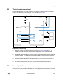
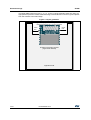
SP1ML
SPIRIT1 868 and 915 MHz low power RF modules with integrated
microcontroller
Datasheet - production data
Applications
• Home & building automation
• Wireless sensor network
• Data acquisition equipment
• Security systems
• Mobile health and medical
• Industrial monitor and control
• Wireless metering, WMBUS
• Internet of things (IoT)
Description
Features
• Complete RF-ready SPIRIT1 module based
on:
– SPIRIT1 low data rate, low power sub-GHz
transceiver
– STM32L1 Ultra low power microcontroller
at 32 MHz (32 kB RAM and 128 kB Flash)
– BALF-SPI-01D3 868/915 MHz balun with
integrated harmonic filter
– Integrated antenna and crystal
• Compact size: 14 mm x 13.4 mm x 2.5 mm
• 863 to 870 MHz operation (SP1ML-868)
• 902 to 928 MHz operation (SP1ML-915)
• Operates from a single 1.8 V to 3.6 V supply
• Output power up to +11.6 dBm
• Data rates up to 500 kbps
• Modulation schemes: 2-FSK, GFSK, GMSK,
OOK, and ASK
• Operating temperature: -40 °C to 85 °C
• UART interface with AT command set
• FCC and CE regulatory approvals
The SP1ML-868 and SP1ML-915 are ultra-low
power & fully integrated RF modules operating
respectively in the 868 MHz SRD and 915 MHz
ISM bands.
The SP1ML module is a compact-size module,
integrating an on-board antenna with easy-to-use
interface, allowing users to easily add wireless
connectivity in designs without requiring in-depth
RF experience, and has all necessary FCC
modular approvals and CE compliance, reducing
time-to-market.
These modules are based on the SPIRIT1 RF
sub-GHz transceiver (with integrated SMPS),
STM32L1 microcontroller, integrated filter/balun
and chip antenna. The UART host interface
allows simple connection to an external
microcontroller with a standard firmware, allowing
AT commands to facilitate RF configuration, data
transmission and reception, using simple point-topoint communication. Selected STM32L1 GPIO
and peripherals are available for interfacing to
external devices in the user application.
Advanced features of the SPIRIT1 radio are also
accessible. The serial wire debug interface
(SWD) is also available.
The modules are CE compliant and FCC certified
(FCC ID S9NSP1ML).
April 2015
This is information on a product in full production.
DocID026906 Rev 3
1/27
www.st.com
Contents
SP1ML
Contents
1
2
Hardware specification . . . . . . . . . . . . . . . . . . . . . . . . . . . . . . . . . . . . . . . 6
1.1
Recommended operating conditions . . . . . . . . . . . . . . . . . . . . . . . . . . . . . 6
1.2
Absolute maximum ratings . . . . . . . . . . . . . . . . . . . . . . . . . . . . . . . . . . . . . 6
1.3
I/O operating characteristics . . . . . . . . . . . . . . . . . . . . . . . . . . . . . . . . . . . . 6
1.4
Current consumption . . . . . . . . . . . . . . . . . . . . . . . . . . . . . . . . . . . . . . . . . 7
1.5
RF compliance limits . . . . . . . . . . . . . . . . . . . . . . . . . . . . . . . . . . . . . . . . . 7
1.6
Pin assignment . . . . . . . . . . . . . . . . . . . . . . . . . . . . . . . . . . . . . . . . . . . . . . 8
1.7
Pin placement . . . . . . . . . . . . . . . . . . . . . . . . . . . . . . . . . . . . . . . . . . . . . . . 9
1.8
Hardware block diagram . . . . . . . . . . . . . . . . . . . . . . . . . . . . . . . . . . . . . . 9
Hardware design . . . . . . . . . . . . . . . . . . . . . . . . . . . . . . . . . . . . . . . . . . . 10
2.1
Pin usage . . . . . . . . . . . . . . . . . . . . . . . . . . . . . . . . . . . . . . . . . . . . . . . . . 10
2.2
Typical application circuit . . . . . . . . . . . . . . . . . . . . . . . . . . . . . . . . . . . . . .11
Optional functionality . . . . . . . . . . . . . . . . . . . . . . . . . . . . . . . . . . . . . . . . . . . . . . . 11
3
2.3
Layout guidelines . . . . . . . . . . . . . . . . . . . . . . . . . . . . . . . . . . . . . . . . . . . .11
2.4
Recommended footprint . . . . . . . . . . . . . . . . . . . . . . . . . . . . . . . . . . . . . . 13
2.5
Module reflow installation . . . . . . . . . . . . . . . . . . . . . . . . . . . . . . . . . . . . . 13
Module operation . . . . . . . . . . . . . . . . . . . . . . . . . . . . . . . . . . . . . . . . . . 15
3.1
Operating mode . . . . . . . . . . . . . . . . . . . . . . . . . . . . . . . . . . . . . . . . . . . . 15
3.2
Command mode . . . . . . . . . . . . . . . . . . . . . . . . . . . . . . . . . . . . . . . . . . . . 15
3.3
Command reference . . . . . . . . . . . . . . . . . . . . . . . . . . . . . . . . . . . . . . . . . 15
3.4
Configuration registers . . . . . . . . . . . . . . . . . . . . . . . . . . . . . . . . . . . . . . . 17
3.5
Information registers . . . . . . . . . . . . . . . . . . . . . . . . . . . . . . . . . . . . . . . . . 21
3.6
Example command sequence . . . . . . . . . . . . . . . . . . . . . . . . . . . . . . . . . 21
4
ECOPACK®
5
Package mechanical data . . . . . . . . . . . . . . . . . . . . . . . . . . . . . . . . . . . . 22
6
Regulatory compliance . . . . . . . . . . . . . . . . . . . . . . . . . . . . . . . . . . . . . . 23
6.1
2/27
. . . . . . . . . . . . . . . . . . . . . . . . . . . . . . . . . . . . . . . . . . . . . . . . . . . . . . . . . . . . 22
CE certification . . . . . . . . . . . . . . . . . . . . . . . . . . . . . . . . . . . . . . . . . . . . . 23
DocID026906 Rev 3
SP1ML
Contents
6.2
FCC certification . . . . . . . . . . . . . . . . . . . . . . . . . . . . . . . . . . . . . . . . . . . . 23
6.3
Labeling instructions . . . . . . . . . . . . . . . . . . . . . . . . . . . . . . . . . . . . . . . . . 23
6.4
Product manual instructions . . . . . . . . . . . . . . . . . . . . . . . . . . . . . . . . . . . 24
7
Ordering Information . . . . . . . . . . . . . . . . . . . . . . . . . . . . . . . . . . . . . . . 25
8
Revision history . . . . . . . . . . . . . . . . . . . . . . . . . . . . . . . . . . . . . . . . . . . 26
DocID026906 Rev 3
3/27
27
List of tables
SP1ML
List of tables
Table 1.
Table 2.
Table 3.
Table 4.
Table 5.
Table 6.
Table 7.
Table 8.
Table 9.
Table 10.
Table 11.
Table 12.
Table 13.
Table 14.
4/27
Recommended operating conditions . . . . . . . . . . . . . . . . . . . . . . . . . . . . . . . . . . . . . . . . . . 6
Absolute maximum ratings . . . . . . . . . . . . . . . . . . . . . . . . . . . . . . . . . . . . . . . . . . . . . . . . . . 6
I/O operating characteristics . . . . . . . . . . . . . . . . . . . . . . . . . . . . . . . . . . . . . . . . . . . . . . . . . 6
Current consumption . . . . . . . . . . . . . . . . . . . . . . . . . . . . . . . . . . . . . . . . . . . . . . . . . . . . . . 7
RF compliance limits. . . . . . . . . . . . . . . . . . . . . . . . . . . . . . . . . . . . . . . . . . . . . . . . . . . . . . . 7
Pin assignment . . . . . . . . . . . . . . . . . . . . . . . . . . . . . . . . . . . . . . . . . . . . . . . . . . . . . . . . . . . 8
Module pin usage . . . . . . . . . . . . . . . . . . . . . . . . . . . . . . . . . . . . . . . . . . . . . . . . . . . . . . . . 10
Soldering profile . . . . . . . . . . . . . . . . . . . . . . . . . . . . . . . . . . . . . . . . . . . . . . . . . . . . . . . . . 13
Command reference . . . . . . . . . . . . . . . . . . . . . . . . . . . . . . . . . . . . . . . . . . . . . . . . . . . . . . 16
Configuration registers . . . . . . . . . . . . . . . . . . . . . . . . . . . . . . . . . . . . . . . . . . . . . . . . . . . . 18
Information registers . . . . . . . . . . . . . . . . . . . . . . . . . . . . . . . . . . . . . . . . . . . . . . . . . . . . . . 21
Example configuration AT sequence . . . . . . . . . . . . . . . . . . . . . . . . . . . . . . . . . . . . . . . . . 21
Ordering information . . . . . . . . . . . . . . . . . . . . . . . . . . . . . . . . . . . . . . . . . . . . . . . . . . . . . . 25
Document revision history . . . . . . . . . . . . . . . . . . . . . . . . . . . . . . . . . . . . . . . . . . . . . . . . . 26
DocID026906 Rev 3
SP1ML
List of figures
List of figures
Figure 1.
Figure 2.
Figure 3.
Figure 4.
Figure 5.
Figure 6.
Figure 7.
Pin placement . . . . . . . . . . . . . . . . . . . . . . . . . . . . . . . . . . . . . . . . . . . . . . . . . . . . . . . . . . . . 9
Hardware block diagram . . . . . . . . . . . . . . . . . . . . . . . . . . . . . . . . . . . . . . . . . . . . . . . . . . . . 9
Typical application circuit . . . . . . . . . . . . . . . . . . . . . . . . . . . . . . . . . . . . . . . . . . . . . . . . . . 11
Layout guidelines . . . . . . . . . . . . . . . . . . . . . . . . . . . . . . . . . . . . . . . . . . . . . . . . . . . . . . . . 12
Recommended footprint . . . . . . . . . . . . . . . . . . . . . . . . . . . . . . . . . . . . . . . . . . . . . . . . . . . 13
Soldering profile . . . . . . . . . . . . . . . . . . . . . . . . . . . . . . . . . . . . . . . . . . . . . . . . . . . . . . . . . 14
Package mechanical data. . . . . . . . . . . . . . . . . . . . . . . . . . . . . . . . . . . . . . . . . . . . . . . . . . 22
DocID026906 Rev 3
5/27
27
Hardware specification
1
SP1ML
Hardware specification
General conditions (VIN = 3 V and TA = 25 °C).
1.1
Recommended operating conditions
Table 1. Recommended operating conditions
Symbol
Min.
Typ.
Max.
Unit
Operating ambient temperature range
-40
-
85
˚C
Operating supply voltage
1.8
3
3.6
V
FREQ
RF frequency (SP1ML-868)
863
-
870
MHz
FREQ
RF frequency (SP1ML-915)
902
-
928
MHz
Min.
Typ.
Max.
Unit
TA
VDD
1.2
Parameter
Absolute maximum ratings
Table 2. Absolute maximum ratings
Symbol
Parameter
TSTG
Storage temperature range
-40
-
85
˚C
VDD
Operating supply voltage
-0.3
-
3.9
V
VIO
I/O pin voltage
-0.3
-
5.5
V
Min.
Typ.
Max.
Unit
1.3
I/O operating characteristics
Table 3. I/O operating characteristics
Symbol
Parameter
VIL(1)
I/O input low level voltage
-0.3
-
0.3 VDD
V
VIH(1)
I/O input high level voltage
0.7 VIN
-
VDD+0.3
V
1. For more details see the STM32L151RB datasheet, I/O port characteristics.
6/27
DocID026906 Rev 3
SP1ML
1.4
Hardware specification
Current consumption
Table 4. Current consumption
Symbol
Parameter
IDD
1.5
Supply current
Test conditions
Typ.
Unit
Operating mode
Tx, +11 dBm, 2-FSK, 915 MHz
20
mA
Operating mode
Tx, -7 dBm, 2-FSK, 915 MHz
8
mA
Operating mode
Rx, 915 MHz
13.5
mA
Command mode
2.2
mA
Standby
1.4
µA
RF compliance limits
The RF compliance limits are those tested for FCC and CE certification. These limits are
enforced by the factory loaded firmware. Care must be taken with custom firmware to
ensure these limits are not exceeded, voiding the FCC and CE certification.
Table 5. RF compliance limits
Modulation
Standards
2-FSK
GFSK
MSK
FCC Part 15.207 (1)
FCC Part 15.247 (1)
EN 300 220-2 V2.4.1 (2)
EN 301 489-01 V1.9.2 (2)
EN 301 489-03 V1.4.1 (2)
OOK
ASK
FCC Part 15.207 (1)
FCC Part 15.249 (1)
EN 300 220-2 V2.4.1 (2)
EN 301 489-01 V1.9.2 (2)
EN 301 489-03 V1.4.1 (2)
Parameter
Max.
Unit
Data rate
500
kbps
Output power
+11.6
dBm
Data rate
250
kbps
Output power
+8.5
dBm
1. FCC standards are only applicable to the SP1ML-915 module.
2. EN standards are only applicable to the SP1ML-868 module.
DocID026906 Rev 3
7/27
27
Hardware specification
1.6
SP1ML
Pin assignment
Table 6. Pin assignment
Description
STM32L pin(1)
Pin
Name
Type
1
TXRXLED
O
Active low Tx/Rx LED drive(2)
PA2
2
SHDN
I
Shutdown
PA0
3
GPIO0
I/O
General purpose input/output 0(3)
PB15
4
GPIO1
I/O
General purpose input/output 1 (3)
PB14
5
MODE0
I
Protocol mode selection 0(2)
PB13
6
MODE1
I
Protocol mode selection 1(2)
PB12
7
VDD
Power
Supply input voltage
-
8
GND
Power
Ground
-
9
SWDIO
I/O
10
SWCLK
11
Serial wire I/O
PA13
I
Serial wire clock
PA14
BOOTMODE
I
Boot mode selection
12
RESET
I
Reset input, active low
13
TXD
O
UART transmit data
PA9
14
RXD
I
UART receive data
PA10
15
GPIO2
I/O
General input/output 2 (3)
PB6
16
GPIO3
I/O
General purpose input/output 3 (3)
PB7
BOOT0
NRST
1. For further details, see the STM32L151RB datasheet, Pin descriptions section. Alternate functions of any given pin are
dependent on the user application firmware that is loaded into the module and is beyond the scope of this document.
2. Refer to Hardware design section for details regarding TXRXLED and protocol mode selection.
3. The GPIO signals are not used by the default firmware integrated in the module. They are accessible with user application
firmware. See note 1.
8/27
DocID026906 Rev 3
SP1ML
1.7
Hardware specification
Pin placement
Figure 1. Pin placement
1
16
2
15
3
14
4
13
5
12
6
11
7
10
8
9
GSPG1409141830SMD
1.8
Hardware block diagram
Figure 2. Hardware block diagram
XTAL
1.8V to 3.6V Supply
UART
SPI
STM32L
GPIO
Microcontroller
GPIO
SMPS
Spirit1
RXp
RXn
TX
Filter/Balun
GSPG1409141831SMD
DocID026906 Rev 3
9/27
27
Hardware design
SP1ML
2
Hardware design
2.1
Pin usage
If used with the default firmware and interfaced to a host MCU, at a minimum the SP1ML
module requires power, ground and UART transmit and receive signals to be connected.
Other signals are optional and provide additional functionality. These signals are outlined in
Table 7 below. Unused signals must not be connected.
Table 7. Module pin usage
Pin
Name
Description
Optional
1
TXRXLED
An active-low open drain output that can drive an external LED for
TX/RX activity status indication. TXRXLED must be enabled by setting
the value to 1 in register S24.
Yes
2
SHDN
Drive this signal low to put the module into a low power shutdown
mode. Drive the signal high to wake the module.
Yes
3
GPIO0
Reserved for future use, do not connect.
Yes
4
GPIO1
Reserved for future use, do not connect.
Yes
5
MODE0
Drive this signal high to force the module into operating mode. Drive
this signal low to force the module into command mode. This enables
faster switching between modes and obviates the need for escape
sequences. After setting the MODE0 value, do a RESET to make the
new setting effective.
Yes
6
MODE1
Reserved for future use, do not connect.
Yes
7
VDD
Connect to power supply, 1.8V to 3.6V.
No
8
GND
Connect to system ground.
No
9
SWDIO
Yes
10
SWCLK
These signals are the serial wire debug (SWD) interface to the
STM32L microcontroller, supporting the development and loading of
custom firmware.
11
BOOTMODE
Drive this signal high at power up or reset to start the boot loader and
allow device firmware update over the UART interface.
Yes
12
RESET
Drive this signal low to hold the module in reset. Drive this signal high
to release the module from reset.
Yes
13
TXD
Connect to the host system UART RXD input.
No
14
RXD
Connect to the host system UART TXD output.
No
15
GPIO2
Reserved for future use.
Yes
16
GPIO3
Reserved for future use.
Yes
10/27
DocID026906 Rev 3
Yes
SP1ML
2.2
Hardware design
Typical application circuit
In a typical application the SP1ML module is connected to a host MCU using a standard
UART, with transmit and receive signals. This is illustrated in Figure 3.
Figure 3. Typical application circuit
VDD
VDD
1
10uF
VDD
HOST
MCU
TXD
TXD
RXD
RXD
TXRXLED
SP1ML
MODULE
RTS
CTS
VDD
GPIO
MODE0
GPIO
SHDN
SWCLK
SWDIO
2
SWD
HEADER
RESET
GPIO
BOOTMODE
GPIO
RESET
3
4
GND
Optional functionality
2.3
1.
When the TXRX_LED (S24) configuration register (see Table 10) is set to 1, the
TXRXLED signal is an active-low open drain output that can be used to drive an
external LED for status indication when data is sent or received.
2.
The MODE0 signal provides a hardware method for switching between command and
operating modes. The SHDN signal allows the module to be placed into a low power
shutdown mode and woken up again.
3.
The BOOTMODE AND RESET signals should be connected if module firmware will
need to be updated over the UART interface.
4.
To support custom module firmware, the serial wire debug signals need to be
accessible for programming and debugging.
Layout guidelines
The application PCB requires a flooded ground plane. Care must be taken to ensure there
are no traces or ground planes under the area surrounding the antenna, with the exception
DocID026906 Rev 3
11/27
27
Hardware design
SP1ML
of minimal width traces from pins 1, 2, 3, 4, 13 and 14 of the module if these are used. It is
appropriate to place the module toward the edge of the PCB with no traces or ground planes
from the antenna to the board edge.
Figure 4. Layout guidelines
No copper on any layer surrounding antenna, except
minimal traces from pins 1,2,3,4,13 and14
6 mm
min .
6 mm
min .
Flooded ground plane required
(signal traces allowed)
Application PCB
12/27
DocID026906 Rev 3
SP1ML
2.4
Hardware design
Recommended footprint
Figure 5. Recommended footprint
PP
PP
PP
PP
PP
PP
*63*60'
2.5
Module reflow installation
The SP1ML is a surface mount module supplied on a 16-pin, 4-layer PCB. The final
assembly recommended reflow profile is indicated below, based on IPC/JEDEC JSTD020C, July 2004 recommendations.
Table 8. Soldering profile
Profile feature
Lead-free assembly
Average ramp-up rate (TSMAX to TP)
3 °C/sec max
Preheat:
– Temperature min. (TS min.)
– Temperature max. (TS max.)
– Time (ts min. to ts max.)(ts)
150 °C
200 °C
60-100 sec
DocID026906 Rev 3
13/27
27
Hardware design
SP1ML
Table 8. Soldering profile (continued)
Profile feature
Lead-free assembly
Time maintained above:
– Temperature TL
– Temperature TL
217 °C
60-70 sec
Peak temperature (TP)
240 °C
Time within 5 °C of actual peak temperature (TP)
10-20 sec
Ramp-down rate
6 °C/sec
Time from 25 °C to peak temperature
8 minutes max.
Figure 6. Soldering profile
GSPG1409141835SMD
14/27
DocID026906 Rev 3
SP1ML
3
Module operation
Module operation
The SP1ML module is provided with firmware that supports wireless serial cable
replacement. There are two operational modes, command mode and operating mode. The
command mode allows module configuration and status interrogation using an extended
‘AT’ style command set. In operating mode the module serves its primary purpose as a
wireless transceiver. Following power-up or reset, the module starts in operating mode with
the current configuration loaded from EEPROM.
3.1
Operating mode
In operating mode, data received from the host on the UART interface will be wirelessly
transmitted by the SPIRIT1 radio using the current configuration settings for frequency, data
rate, modulation and output power. Conversely, any data received by the SPIRIT1 that
meets the configured filtering criteria will be output to the UART interface.
Care must be taken to ensure that the escape sequence to enter command mode does not
occur in the data stream sent by the host to the UART interface.
3.2
Command mode
In command mode, the module will accept commands to configure module settings and
interrogate module status. To enter command mode, the ‘+++’ escape sequence is issued to
the module from operating mode. The escape sequence should be preceded by minimum
delay of 500 milliseconds where no other data is transmitted. The three ‘+’ characters of the
sequence must be sent within 500 milliseconds of each other. The module issues the
response ‘OK’ if command mode is entered successfully.
Commands issued to the module are in ‘AT’ style format, and use ASCII characters, starting
with ‘A’ and ‘T’, then one or more characters for the specific command, followed by any
additional command specific data and terminated with a carriage return <CR>.
The delay between each consecutive character of a command must be less than 8 seconds,
else the module will time out and discard any characters already received.
If the module receives an invalid command, it will send the ‘ERROR’ response. All
responses issued by the module are terminated with a line feed and carriage return,
<LF><CR>.
3.3
Command reference
Table 9: Command reference provides a summary of the AT commands available for
module configuration. A detailed description of each command is provided following the list.
DocID026906 Rev 3
15/27
27
Module operation
SP1ML
Table 9. Command reference
16/27
Command
Description
ATO
Enter operating mode
This command is issued to exit command mode and enter operating mode where the
module fulfills its primary purpose as a wireless transceiver using the current configuration.
Response: OK
AT/V
Read module version information
Reports the module hardware and firmware version information.
Response:
SP1ML-xxx HW:Vy FW:Vy.zz
Where xxx is 868 or 915, y is a single digit major version number and zz is a double digit
minor version number.
ATIn
Read an information register
Reads the current value from an information register, where n is the information register
number.
See information registers table.
Response:
<REGISTER NUMBER>:<REGISTER NAME>=<VALUE>
ERROR PARAM if an invalid register is specified.
ATSnn?
Read a configuration register
Reads the current value from a configuration register, where nn is the configuration register
number.
See configuration registers section.
Response:
<REGISTER NUMBER>:<REGISTER NAME>=<VALUE>
ERROR PARAM if an invalid register number is specified.
ATSnn=x
Write a configuration register
Writes a new value to a configuration register, where nn is the configuration register number
and x is the value. The new configuration will be in effect until the next module reset.
See configuration registers section.
Response: OK if the value is written successfully.
ERROR PARAM if an invalid register number is specified.
ERROR VALUE if an invalid value is specified.
AT/S
Read all configuration registers
Reads the current values of all configuration registers.
See the configuration registers section.
Response: (one line for each register)
<REGISTER NUMBER>:<REGISTER NAME>=<VALUE>
AT/C
Store the current configuration
Stores the current module configuration registers. The stored configuration will be reloaded
anytime the module is reset.
Response: OK if the configuration is stored successfully.
ERROR if storing the configuration failed.
DocID026906 Rev 3
SP1ML
Module operation
Table 9. Command reference (continued)
Command
ATR
Reset configuration to the default values
This command resets all module configuration registers to their factory default values.
Response: OK
ERROR if resetting the configuration failed.
ATZ
Restart the module
Restarts the module and reloads the current configuration. This generates a soft reset of the
microcontroller and start execution of the firmware from the reset vector.
Response: OK
AT/SRnn?
AT/SRnn=xx
AT/Tn
3.4
Description
Read a SPIRIT1 radio register
Reads the current value from a SPIRIT1 radio register, where nn is the two digit
hexadecimal register address.
Response:
<ADDRESS>=<VALUE>
ERROR PARAM if an invalid register number is specified.
ERROR if reading the register failed.
Write a SPIRIT1 radio register
Writes a new value to a SPIRIT1 radio register, where nn is the two digit hexadecimal
register address and xx is the two digit hexadecimal value to write.
Response: OK
ERROR PARAM if an invalid register number is specified.
ERROR if writing the register failed.
Set RF test mode
Set the RF test mode, where n is the test mode number from one of the following options:
0 = Disable RF test mode.
1 = Pseudorandom binary sequence RF test mode (PN9).
2 = Continuous wave RF test mode (CW).
Response: OK if the test mode is set successfully
ERROR PARAM if an invalid test mode number is specified.
Configuration registers
The configuration registers contain the radio, packet and general configuration settings for
the module. They are read and written in command mode. Table 10 details each
configuration register.
DocID026906 Rev 3
17/27
27
Module operation
SP1ML
Table 10. Configuration registers
#
S00
S01
S02
Name
Description
BAUD_RATE
General: Baud rate of the UART interface in bps. The baud rate is
stored when the configuration is stored.
Values:
Most standard baud rates from 9600 to 921600.
Default: 115200
FREQUENCY
Radio: Frequency in Hz.
Values:
Must be within the operating frequency range of the module.
Default:
868000000 (for SP1ML-868)
915000000 (for SP1ML-915)
DATA_RATE
Radio: Data rate in bps. The data rate for OOK and ASK modulation
schemes is limited to 250000bps.
Values:
From 1000 to 500000
Default: 38400
Radio: Modulation scheme.
Values:
0 = 2-FSK
1 = GFSK05
2 = GFSK1
3 = GMSK
4 = OOK
5 = ASK
Default: 0
S03
MODULATION
S04
OUTPUT_POWER
Radio: Output power in dBm.
Values: -34 to +11.6
Default: +11.6
S05
FREQ_DEVIATION
Radio: Frequency deviation in kHz.
Values: Up to 732
Default: 20
S06
RX_FILTER
Radio: RX digital filter cutoff frequency in kHz.
Values: Up to 769
Default: 100
CS_MODE
Radio: Carrier sense mode.
Values:
0 = Static sensing
1 = Dynamic sensing with 6 dB dynamic threshold
2 = Dynamic sensing with 12 dB dynamic threshold
3 = Dynamic sensing with 18 dB dynamic threshold
Default: 0
S07
18/27
DocID026906 Rev 3
SP1ML
Module operation
Table 10. Configuration registers (continued)
#
Name
Description
Radio: Carrier sense RSSI threshold in dBm.
Values: -130 to -3
Default: -130
S08
RSSI_THRESHOLD
S09
PREAMBLE_LEN
Packet: Preamble length in bytes.
Values: 1 to 32 bytes.
Default: 8
S10
SYNC_LENGTH
Packet: Sync length in bytes.
Values: 1 to 4
Default: 4
S11
SYNC_VALUE
S12
S13
S14
S15
S16
S17
Packet: 32-bit sync value.
Values: Any 32-bit hexadecimal value.
Default: 0x88888888
CRC_MODE
Packet: CRC mode.
Values:
1 = POLY_0x07
2 = POLY_0x8005
3 = POLY_0x1021
4 = POLY_0x864CFB
Default: 2
WHITENING
Packet: Data whitening mode.
Values:
0 = Disabled
1 = Enabled
Default: 1
FEC
Packet: Forward error correction.
Values:
0 = Disabled
1 = Enabled
Default: 0
SOURCE_ADDR
Address: The 8-bit address for the module, used to indicate the
source of transmitted packets and for destination filtering of received
packets.
Values: Any 8-bit hexadecimal value.
Default: 0x00
DESTINATION_ADDR
Address: The 8-bit destination address, used to indicate the
destination for transmitted packets and for source filtering of received
packets.
Values: Any 8-bit hexadecimal value.
Default: 0xff
MULTICAST_ADDR
Address: The 8-bit multicast address, used for multicast filtering on
received packets.
Values: Any 8-bit hexadecimal value.
Default: 0xee
DocID026906 Rev 3
19/27
27
Module operation
SP1ML
Table 10. Configuration registers (continued)
#
S18
S19
S20
S21
S22
S23
S24
S26
20/27
Name
Description
BROADCAST_ADDR
Address: The 8-bit broadcast address, used for broadcast filtering on
received packets.
Values: Any 8-bit hexadecimal value.
Default: 0xff
FILTER_CRC
FILTER_SOURCE
Address: Filter packets that have an invalid CRC.
Values:
0 = Disabled, 1 = Enabled
Default: 0
Address: Filter packets that do not have a source address that
matches the address specified in register S16.
Values:
0 = Disabled, 1 = Enabled
Default: 0
FILTER_DESTINATION
Address: Filter packets that do not have a destination address that
matches the modules source address specified in register S15.
Values:
0 = Disabled, 1 = Enabled
Default: 0
FILTER_MULTICAST
Address: Filter packets that do not have a destination address that
matches the multicast address in specified in register S17.
Values:
0 = Disabled, 1 = Enabled
Default: 0
FILTER_BROADCAST
Address: Filter packets that do not have a destination address that
matches the broadcast address in specified in register S18.
Values:
0 = Disabled, 1 = Enabled
Default: 0
TXRX_LED
General: Enable or disable the TX/RX LED output on module pin 1.
When enabled, the LED output will be flashed when data is sent or
received by the radio.
Values:
0 = Disabled, 1 = Active-Low Open Drain Output, 2 = Push Pull Output
Default: 0
ESCAPE_SEQ
General: Enable or disable the ‘+++’ escape sequence used to enter
command mode. This configuration is never stored and will be enabled
at module reset.
Values:
0 = Disabled, 1 = Enabled
Default: 1
DocID026906 Rev 3
SP1ML
Module operation
Table 10. Configuration registers (continued)
#
Name
Description
S27
Source_FILT_MASK
S28
PAYLOAD_SIZE
3.5
Address: An 8-bit source filter mask, used when source filtering is
enabled.
Values: Any 8-bit hexadecimal value.
Default: 0x00
Packet: Packet payload size in bytes.
Values: 1 to 96
Default: 32
Information registers
Table 11. Information registers
#
Name
Description
I0
PER
Packet error rate (%).
I1
RSSI
Received signal strength indicator.
I2
LQI
Link quality indicator.
I3
PQI
Preamble quality indicator.
I4
SQI
Synchronization quality indicator.
I5
PACKET_COUNT
Count of packets received.
I6
PACKETS_LOST
Count of packets lost.
3.6
Example command sequence
Table 12 shows a typical command sequence to enter command mode, issue AT
commands to configure settings of the SPIRIT1 radio and then exit back to operating mode.
Table 12. Example configuration AT sequence
Host command
Module response
Description
+++
OK<LF><CR>
Escape sequence to put module into command mode
from operating mode.
ATS02=38400
OK<LF><CR>
Set the radio data rate to 38400 bps.
ATS03=2
OK<LF><CR>
Set the modulation scheme to GFSK1.
ATS04=+8
OK<LF><CR>
Set the output power to +8 dBm.
AT/C
OK<LF><CR>
Write configuration to EEPROM.
ATO
OK<LF><CR>
Return to operating mode.
DocID026906 Rev 3
21/27
27
ECOPACK®
4
SP1ML
ECOPACK®
In order to meet environmental requirements, ST offers these devices in different grades of
ECOPACK® packages, depending on their level of environmental compliance. ECOPACK®
specifications, grade definitions and product status are available at: www.st.com.
ECOPACK® is an ST trademark.
5
Package mechanical data
Figure 7. Package mechanical data
PP
PP
PP
PP
PP
PP
5 PP
PP
PD[
*63*60'
22/27
DocID026906 Rev 3
SP1ML
Regulatory compliance
6
Regulatory compliance
6.1
CE certification
The module has been certified in accordance with the following standards:
EN 300 220-2 V2.4.1
EN 301 489-01 V1.9.2
EN 301 489-03 V1.4.1
6.2
FCC certification
This module has been tested and found to comply with the FCC part 15 rules. These limits
are designed to provide reasonable protection against harmful interference in approved
installations. This equipment generates, uses, and can radiate radio frequency energy and,
if not installed and used in accordance with the instructions, may cause harmful interference
to radio communications.
However, there is no guarantee that interference may not occur in a particular installation.
This device complies with part 15 of the FCC rules. Operation is subject to the following two
conditions: (1) This device may not cause harmful interference, and (2) this device must
accept any interference received, including interference that may cause undesired
operation.
Modifications or changes to this equipment not expressly approved by STMicroelectronics
may render void the user's authority to operate this equipment.
Modular approval
FCC ID: S9NSP1ML
In accordance with FCC part 15, the SP1ML-915 is listed as a modular transmitter device.
This module is evaluated for stand-alone use only. Finished products incorporating multiple
transmitters must comply with collocation and RF exposure requirements in accordance
with FCC multi-transmitter product procedures. Collocated transmitters operating in portable
RF exposure conditions (e.g. <20 cm from persons including but not limited to body-worn
and hand-held devices) may require separate approval.
6.3
Labeling instructions
When integrating the SP1ML-915 into the final product, the OEM must ensure that the FCC
labeling requirements are satisfied. A statement must be included on the exterior of the final
product which indicates the product includes a certified module. The label should state the
following (or similar wording that conveys the same meaning):
Contains FCC ID: S9NSP1ML
OR
This product contains FCC ID: S9NSP1ML
DocID026906 Rev 3
23/27
27
Regulatory compliance
SP1ML
The OEM must include the following statements on the exterior of the final product unless
the product is too small (e.g. less than 4 x 4 inches):
This device complies with Part 15 of the FCC Rules. Operation is subject to the
following two conditions: (1) this device may not cause harmful interference, and (2)
this device must accept any interference received, including any interference that may
cause undesired operation.
6.4
Product manual instructions
This section applies to OEM final products containing the SP1ML-915 module, subject to
FCC compliance. The final product manual must contain the following statement (or a
similar statement that conveys the same meaning):
WARNING: Changes or modifications not expressly approved by the party responsible
for compliance could void the user’s authority to operate the equipment
In cases where an OEM seeks Class B (residential) limits for the final product, the following
statement must be included in the final product manual:
NOTE: This equipment has been tested and found to comply with the limits for a Class
B digital device, pursuant to part 15 of the FCC Rules. These limits are designed to
provide reasonable protection against harmful interference in a residential installation.
This equipment generates, uses and can radiate radio frequency energy and, if not
installed and used in accordance with the instructions, may cause harmful interference
to radio communications. However, there is no guarantee that interference will not
occur in a particular installation. If this equipment does cause harmful interference to
radio or television reception, which can be determined by turning the equipment off and
on, the user is encouraged to try to correct the interference by one or more of the
following measures:
–
Reorient or relocate the receiving antenna.
–
Increase the separation between the equipment and receiver.
–
Connect the equipment into an outlet on a circuit different from that to which the
receiver is connected.
–
Consult the dealer or an experienced radio/TV technician for help.
In cases where an OEM seeks the lesser category of a Class A digital device for the final
product, the following statement must be included in the final product manual:
NOTE: This equipment has been tested and found to comply with the limits for a Class
A digital device, pursuant to part 15 of the FCC Rules. These limits are designed to
provide reasonable protection against harmful interference when the equipment is
operated in a commercial environment. This equipment generates, uses, and can
radiate radio frequency energy and, if not installed and used in accordance with the
instruction manual, may cause harmful interference to radio communications.
Operation of this equipment in a residential area is likely to cause harmful interference
in which case the user will be required to correct the interference at his expense.
24/27
DocID026906 Rev 3
SP1ML
7
Ordering Information
Ordering Information
Table 13. Ordering information
Order code
Description
SP1ML-868
868 MHz SPIRIT1 antenna module (Region 1, Europe)
SP1ML-915
915 MHz SPIRIT1 antenna module (Region 2, The Americas)
DocID026906 Rev 3
25/27
27
Revision history
8
SP1ML
Revision history
Table 14. Document revision history
26/27
Date
Revision
Changes
24-Oct-2014
1
Initial release.
17-Dec-2014
2
– Document status promoted from preliminary to production data.
– Updated operating temperature range in Features and Table 1.
27-Apr-2015
3
Updated: Features and Description.
DocID026906 Rev 3
SP1ML
IMPORTANT NOTICE – PLEASE READ CAREFULLY
STMicroelectronics NV and its subsidiaries (“ST”) reserve the right to make changes, corrections, enhancements, modifications, and
improvements to ST products and/or to this document at any time without notice. Purchasers should obtain the latest relevant information on
ST products before placing orders. ST products are sold pursuant to ST’s terms and conditions of sale in place at the time of order
acknowledgement.
Purchasers are solely responsible for the choice, selection, and use of ST products and ST assumes no liability for application assistance or
the design of Purchasers’ products.
No license, express or implied, to any intellectual property right is granted by ST herein.
Resale of ST products with provisions different from the information set forth herein shall void any warranty granted by ST for such product.
ST and the ST logo are trademarks of ST. All other product or service names are the property of their respective owners.
Information in this document supersedes and replaces information previously supplied in any prior versions of this document.
© 2015 STMicroelectronics – All rights reserved
DocID026906 Rev 3
27/27
27