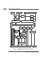
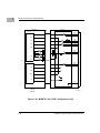
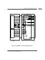
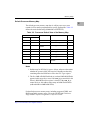
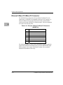
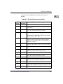
1
MVME2700 Series
Single Board Computer
Installation and Use
V2700A/IH4
September 2001 Edition
© Copyright 1997, 1999, 2000, 2001 Motorola, Inc.
All rights reserved.
Printed in the United States of America.
Motorola® and the Motorola symbol are registered trademarks of Motorola, Inc.
AIX® is a registered trademark of International Business Machines Corporation.
PowerPC® is a registered trademark of International Business Machines.
SNAPHAT®, TIMEKEEPER®, and ZEROPOWER® are registered trademarks of
STMicroelectronics.
All other products mentioned in this document are trademarks or registered trademarks of
their respective holders.
Safety Summary
The following general safety precautions must be observed during all phases of operation, service, and repair of this
equipment. Failure to comply with these precautions or with specific warnings elsewhere in this manual could result
in personal injury or damage to the equipment.
The safety precautions listed below represent warnings of certain dangers of which Motorola is aware. You, as the user
of the product, should follow these warnings and all other safety precautions necessary for the safe operation of the
equipment in your operating environment.
Ground the Instrument.
To minimize shock hazard, the equipment chassis and enclosure must be connected to an electrical ground. If the
equipment is supplied with a three-conductor AC power cable, the power cable must be plugged into an approved
three-contact electrical outlet, with the grounding wire (green/yellow) reliably connected to an electrical ground
(safety ground) at the power outlet. The power jack and mating plug of the power cable meet International
Electrotechnical Commission (IEC) safety standards and local electrical regulatory codes.
Do Not Operate in an Explosive Atmosphere.
Do not operate the equipment in any explosive atmosphere such as in the presence of flammable gases or fumes.
Operation of any electrical equipment in such an environment could result in an explosion and cause injury or damage.
Keep Away From Live Circuits Inside the Equipment.
Operating personnel must not remove equipment covers. Only Factory Authorized Service Personnel or other
qualified service personnel may remove equipment covers for internal subassembly or component replacement or any
internal adjustment. Service personnel should not replace components with power cable connected. Under certain
conditions, dangerous voltages may exist even with the power cable removed. To avoid injuries, such personnel should
always disconnect power and discharge circuits before touching components.
Use Caution When Exposing or Handling a CRT.
Breakage of a Cathode-Ray Tube (CRT) causes a high-velocity scattering of glass fragments (implosion). To prevent
CRT implosion, do not handle the CRT and avoid rough handling or jarring of the equipment. Handling of a CRT
should be done only by qualified service personnel using approved safety mask and gloves.
Do Not Substitute Parts or Modify Equipment.
Do not install substitute parts or perform any unauthorized modification of the equipment. Contact your local
Motorola representative for service and repair to ensure that all safety features are maintained.
Observe Warnings in Manual.
Warnings, such as the example below, precede potentially dangerous procedures throughout this manual. Instructions
contained in the warnings must be followed. You should also employ all other safety precautions which you deem
necessary for the operation of the equipment in your operating environment.
Warning
To prevent serious injury or death from dangerous voltages, use extreme
caution when handling, testing, and adjusting this equipment and its
components.
Flammability
All Motorola PWBs (printed wiring boards) are manufactured with a flammability rating
of 94V-0 by UL-recognized manufacturers.
EMI Caution
!
Caution
This equipment generates, uses and can radiate electromagnetic energy. It
may cause or be susceptible to electromagnetic interference (EMI) if not
installed and used with adequate EMI protection.
Lithium Battery Caution
This product contains a lithium battery to power the clock and calendar circuitry.
!
Caution
!
Attention
!
Vorsicht
Danger of explosion if battery is replaced incorrectly. Replace battery only
with the same or equivalent type recommended by the equipment
manufacturer. Dispose of used batteries according to the manufacturer’s
instructions.
Il y a danger d’explosion s’il y a remplacement incorrect de la batterie.
Remplacer uniquement avec une batterie du même type ou d’un type
équivalent recommandé par le constructeur. Mettre au rebut les batteries
usagées conformément aux instructions du fabricant.
Explosionsgefahr bei unsachgemäßem Austausch der Batterie. Ersatz nur
durch denselben oder einen vom Hersteller empfohlenen Typ. Entsorgung
gebrauchter Batterien nach Angaben des Herstellers.
CE Notice (European Community)
Motorola Computer Group products with the CE marking comply with the EMC Directive
(89/336/EEC). Compliance with this directive implies conformity to the following
European Norms:
EN55022 “Limits and Methods of Measurement of Radio Interference Characteristics
of Information Technology Equipment”; this product tested to Equipment Class B
EN55024 “Information technology equipment—Immunity characteristics—Limits and
methods of measurement”
Board products are tested in a representative system to show compliance with the above
mentioned requirements. A proper installation in a CE-marked system will maintain the
required EMC performance.
In accordance with European Community directives, a “Declaration of Conformity” has
been made and is available on request. Please contact your sales representative.
Notice
While reasonable efforts have been made to assure the accuracy of this document,
Motorola, Inc. assumes no liability resulting from any omissions in this document, or from
the use of the information obtained therein. Motorola reserves the right to revise this
document and to make changes from time to time in the content hereof without obligation
of Motorola to notify any person of such revision or changes.
Electronic versions of this material may be read online, downloaded for personal use, or
referenced in another document as a URL to the Motorola Computer Group website. The
text itself may not be published commercially in print or electronic form, edited, translated,
or otherwise altered without the permission of Motorola, Inc.
It is possible that this publication may contain reference to or information about Motorola
products (machines and programs), programming, or services that are not available in your
country. Such references or information must not be construed to mean that Motorola
intends to announce such Motorola products, programming, or services in your country.
Limited and Restricted Rights Legend
If the documentation contained herein is supplied, directly or indirectly, to the U.S.
Government, the following notice shall apply unless otherwise agreed to in writing by
Motorola, Inc.
Use, duplication, or disclosure by the Government is subject to restrictions as set forth in
subparagraph (b)(3) of the Rights in Technical Data clause at DFARS 252.227-7013 (Nov.
1995) and of the Rights in Noncommercial Computer Software and Documentation clause
at DFARS 252.227-7014 (Jun. 1995).
Motorola, Inc.
Computer Group
2900 South Diablo Way
Tempe, Arizona 85282
Contents
About This Manual
Summary of Changes ...............................................................................................xviii
Overview of Contents ..............................................................................................xviii
Comments and Suggestions .......................................................................................xix
Conventions Used in This Manual.............................................................................. xx
CHAPTER 1
Hardware Preparation and Installation
Overview....................................................................................................................1-1
Equipment Required ..................................................................................................1-3
Overview of Startup Procedure..................................................................................1-3
Unpacking Instructions ..............................................................................................1-5
Hardware Configuration ............................................................................................1-5
MVME2700 Base Board Preparation ........................................................................1-6
Flash Bank Selection (J9) ...................................................................................1-8
Serial Port 4 Receive Clock Configuration (J16) ...............................................1-8
Serial Port 4 Transmit Clock Configuration (J17) ..............................................1-9
Serial Port 4 Transmit Clock Receiver Buffer Control (J19)..............................1-9
Serial Port 3 Transmit Clock Configuration (J18) ............................................1-10
System Controller Selection (J20) ....................................................................1-11
Remote Status and Control (J1) ........................................................................1-11
MVME712M Transition Module Preparation .........................................................1-12
Serial Ports 1-4 DCE/DTE Configuration ........................................................1-14
Serial Port 4 Clock Configuration ....................................................................1-15
P2 Adapter Preparation .....................................................................................1-22
MVME761 Transition Module Preparation .............................................................1-23
Serial Ports 1 and 2 ...........................................................................................1-25
Configuration of Serial Ports 3 and 4 ...............................................................1-25
P2 Adapter Preparation .....................................................................................1-44
Three-Row Adapter ...................................................................................1-44
Five-Row Adapter .....................................................................................1-45
Hardware Installation...............................................................................................1-46
RAM200 Memory Mezzanine Installation .......................................................1-47
PMC Module Installation..................................................................................1-49
PMC Carrier Board Installation........................................................................1-51
MVME2700 VME Module Installation............................................................1-53
vii
MVME712M Transition Module Installation .................................................. 1-55
MVME761 Transition Module Installation...................................................... 1-58
System Considerations ............................................................................................ 1-61
MVME2700 VME Module .............................................................................. 1-62
CHAPTER 2
Operating Instructions
Overview ................................................................................................................... 2-1
Power-up the System ................................................................................................. 2-1
Switches and LEDs ............................................................................................ 2-1
ABORT Switch (S1) ................................................................................... 2-2
RESET Switch (S2)..................................................................................... 2-2
Front Panel Indicators (DS1 – DS6)................................................................... 2-3
Memory Maps............................................................................................................ 2-4
Processor Memory Map ..................................................................................... 2-4
Default Processor Memory Map ................................................................. 2-5
PCI Local Bus Memory Map ............................................................................. 2-6
VMEbus Memory Map ...................................................................................... 2-6
Programming Considerations .................................................................................... 2-7
PCI Arbitration ................................................................................................... 2-8
Interrupt Handling .............................................................................................. 2-9
DMA Channels................................................................................................. 2-10
Sources of Reset ............................................................................................... 2-10
Endian Issues .................................................................................................... 2-11
Processor/Memory Domain ...................................................................... 2-12
PCI Domain............................................................................................... 2-12
VMEbus Domain ...................................................................................... 2-13
CHAPTER 3
Functional Description
Overview ................................................................................................................... 3-1
Features...................................................................................................................... 3-1
General Description ................................................................................................... 3-3
Block Diagram........................................................................................................... 3-5
SCSI Interface .................................................................................................... 3-6
SCSI Termination........................................................................................ 3-7
Ethernet Interface ............................................................................................... 3-7
PCI Mezzanine Interface .................................................................................... 3-8
VMEbus Interface .............................................................................................. 3-9
ISA Super I/O Device (ISASIO) ...................................................................... 3-10
Asynchronous Serial Ports ........................................................................ 3-10
viii
Parallel Port ...............................................................................................3-10
Disk Drive Controller ................................................................................3-11
Keyboard and Mouse Interface..................................................................3-11
PCI-ISA Bridge (PIB) Controller .....................................................................3-12
Real-Time Clock/NVRAM/Timer Function .....................................................3-13
About the Battery.......................................................................................3-13
Programmable Timers.......................................................................................3-14
Interval Timers ..........................................................................................3-14
16-Bit Timers.............................................................................................3-15
Serial Communications Interface......................................................................3-15
Z8536 CIO Device.....................................................................................3-16
Base Module Feature Register ..........................................................................3-16
P2 Signal Multiplexing .....................................................................................3-17
ABORT Switch (S1) .........................................................................................3-18
RESET Switch (S2) ..........................................................................................3-19
Front Panel Indicators (DS1 – DS6) .................................................................3-20
Polyswitches (Resettable Fuses).......................................................................3-21
I/O Power...................................................................................................3-21
Speaker Control ................................................................................................3-22
MPC750 Processor ...........................................................................................3-22
Flash Memory............................................................................................3-22
RAM200 Memory Module ...............................................................................3-23
MVME712M Transition Module......................................................................3-24
MVME761 Transition Module .........................................................................3-25
Serial Interface Modules............................................................................3-26
CHAPTER 4
Connector Pin Assignments
MVME2700 Connectors ............................................................................................4-1
Common Connectors .................................................................................................4-2
LED Mezzanine Connector (J1) .........................................................................4-2
Debug Connector (J2) .........................................................................................4-3
Floppy/LED Connector (J3) ...............................................................................4-7
PCI Expansion Connector (J4) ...........................................................................4-8
Keyboard and Mouse Connectors (J5, J7) ........................................................4-10
DRAM Mezzanine Connector (J6) ...................................................................4-11
RISCwatch Connector (J8) ...............................................................................4-14
PCI Mezzanine Card Connectors (J11-J14)......................................................4-15
P1 and P2 Connectors .......................................................................................4-18
MVME712M-Compatible Versions.........................................................................4-19
VMEbus Connector P2 .....................................................................................4-19
ix
SCSI Connector ................................................................................................ 4-21
Serial Ports 1-4 ................................................................................................. 4-22
Parallel Connector ............................................................................................ 4-23
Ethernet AUI Connector................................................................................... 4-24
MVME761-Compatible Versions ............................................................................ 4-25
VMEbus Connector P2..................................................................................... 4-25
Serial Ports 1 and 2........................................................................................... 4-27
Serial Ports 3 and 4........................................................................................... 4-27
Parallel Connector ............................................................................................ 4-29
Ethernet 10BaseT/100BaseTX Connector ....................................................... 4-30
CHAPTER 5
PPCBug Firmware
Overview ................................................................................................................... 5-1
Memory Requirements ....................................................................................... 5-2
Implementation................................................................................................... 5-2
Use the Debugger ...................................................................................................... 5-3
Debugger Commands ......................................................................................... 5-4
Diagnostic Tests.................................................................................................. 5-8
CHAPTER 6
CNFG and ENV Commands
Overview ................................................................................................................... 6-1
CNFG – Configure Board Information Block ........................................................... 6-2
ENV – Set Environment ............................................................................................ 6-3
Configure the PPCBug Parameters .................................................................... 6-3
Configure the VMEbus Interface ..................................................................... 6-12
APPENDIX A
Specifications
MVME2700 Board Specifications ........................................................................... A-1
Cooling Requirements .............................................................................................. A-2
EMC Compliance ..................................................................................................... A-3
APPENDIX B
Serial Interconnections
Introduction .............................................................................................................. B-1
Asynchronous Serial Ports ................................................................................ B-1
Synchronous Serial Ports................................................................................... B-1
EIA-232-D Connections ........................................................................................... B-2
Interface Characteristics .................................................................................... B-4
x
EIA-530 Connections................................................................................................ B-5
Interface Characteristics .................................................................................... B-8
Proper Grounding...................................................................................................... B-9
APPENDIX C
Troubleshooting CPU Boards: Solving Startup Problems
Introduction............................................................................................................... C-1
APPENDIX D
Related Documentation
Motorola Computer Group Documents ....................................................................D-1
Manufacturers’ Documents.......................................................................................D-2
Related Specifications...............................................................................................D-5
xi
List of Figures
Figure 1-1. MVME2700 Base Board Block Diagram ...............................................1-2
Figure 1-2. MVME2700 Switches, Headers, Connectors, Fuses, LEDs ...................1-7
Figure 1-3. MVME712M Connector and Header Locations ...................................1-13
Figure 1-4. J15 Clock Line Configuration ...............................................................1-15
Figure 1-5. MVME712M Serial Port 1 DCE/DTE Configuration ..........................1-16
Figure 1-6. MVME712M Serial Port 2 DCE/DTE Configuration ..........................1-17
Figure 1-7. MVME712M Serial Port 3 DCE Configuration ...................................1-18
Figure 1-8. MVME712M Serial Port 3 DTE Configuration....................................1-19
Figure 1-9. MVME712M Serial Port 4 DCE Configuration ...................................1-20
Figure 1-10. MVME712M Serial Port 4 DTE Configuration..................................1-21
Figure 1-11. MVME712M Three-Row P2 Adapter.................................................1-22
Figure 1-12. MVME761 Connector and Header Locations.....................................1-24
Figure 1-13. MVME761 Serial Ports 1 and 2 (DCE Only)......................................1-27
Figure 1-14. MVME761 EIA-232-D Port 3 DCE Configuration ............................1-28
Figure 1-15. MVME761 EIA-232-D Port 3 DTE Configuration ............................1-29
Figure 1-16. MVME761 EIA-232-D Port 4 DCE Configuration ............................1-30
Figure 1-17. MVME761 EIA-232-D Port 4 DTE Configuration ............................1-31
Figure 1-18. MVME761 EIA-530-DCE Configuration Port 3 ................................1-32
Figure 1-19. MVME761 EIA-530-DTE Configuration Port 3 ................................1-33
Figure 1-20. MVME761 EIA-530-DCE Configuration Port 4 ................................1-34
Figure 1-21. MVME761 EIA-530-DTE Port Configuration Port 4 ........................1-35
Figure 1-22. MVME761 V.35-DCE Configuration Port 3.......................................1-36
Figure 1-23. MVME761 V.35-DTE Configuration Port 3.......................................1-37
Figure 1-24. MVME761 V.35-DCE Configuration Port 4.......................................1-38
Figure 1-25. MVME761 V.35-DTE Configuration Port 4.......................................1-39
Figure 1-26. MVME761 X.21-DCE Configuration Port 3 ......................................1-40
Figure 1-27. MVME761 X.21-DTE Configuration Port 3 ......................................1-41
Figure 1-28. MVME761 X.21-DCE Configuration Port 4 ......................................1-42
Figure 1-29. MVME761 X.21-DTE Configuration Port 4 ......................................1-43
Figure 1-30. MVME761 Three-Row P2 Adapter ....................................................1-44
Figure 1-19. MVME761 Five-Row P2 Adapter ......................................................1-45
Figure 1-20. RAM200 Placement on MVME2700..................................................1-48
Figure 1-21. PMC Module Placement on MVME2700...........................................1-50
Figure 1-22. PMC Carrier Board Placement on MVME2700 .................................1-52
xiii
Figure 1-23. MVME712M/MVME2700 Cable Connections.................................. 1-57
Figure 1-24. MVME761/MVME2700 Cable Connections ..................................... 1-59
Figure 2-1. PPCBug Firmware System Startup......................................................... 2-2
Figure 2-2. VMEbus Master Mapping ...................................................................... 2-7
Figure 2-3. MVME2700 Interrupt Architecture ........................................................ 2-9
Figure 3-1. MVME2700 Block Diagram .................................................................. 3-5
xiv
List of Tables
Table 1-1. Startup Overview ......................................................................................1-3
Table 1-2. Jumper Settings.........................................................................................1-6
Table 1-3. MVME712M Port/Jumper Correspondence...........................................1-14
Table 2-1. MVME2700 LEDs....................................................................................2-3
Table 2-2. Processor Default View of the Memory Map ...........................................2-5
Table 2-3. PCI Arbitration Assignments....................................................................2-8
Table 2-4. IBC DMA Channel Assignments ...........................................................2-10
Table 2-5. Classes of Reset and Effectiveness .........................................................2-11
Table 3-1. MVME2700 Features ...............................................................................3-1
Table 3-2. P2 Multiplexing Sequence ......................................................................3-18
Table 3-3. MVME2700 LEDs..................................................................................3-20
Table 3-4. Fuse Assignments ...................................................................................3-21
Table 3-5. RAM200 Memory Modules....................................................................3-24
Table 3-6. SIM Type Identification..........................................................................3-26
Table 4-1. LED Mezzanine Connector J1 ..................................................................4-3
Table 4-2. Debug Connector J2..................................................................................4-3
Table 4-3. Floppy/LED Connector J3 ........................................................................4-7
Table 4-4. PCI Expansion Connector J4 ....................................................................4-8
Table 4-5. Keyboard Connector J5 ..........................................................................4-10
Table 4-6. Mouse Connector J7 ...............................................................................4-10
Table 4-7. DRAM Mezzanine Connector J6............................................................4-11
Table 4-8. RISCwatch Connector J8........................................................................4-14
Table 4-8. PCI Mezzanine Card Connectors J11-J14 ..............................................4-15
Table 4-9. VMEbus Connector P1 ...........................................................................4-18
Table 4-10. VMEbus Connector P2 (MVME712M I/O Mode)...............................4-20
Table 4-11. SCSI Connector (MVME712M)...........................................................4-21
Table 4-12. Serial Connections—MVME712M Ports 1-4.......................................4-22
Table 4-13. Parallel I/O Connector (MVME712M).................................................4-23
Table 4-14. Ethernet AUI Connector (MVME712M) .............................................4-24
Table 4-15. VMEbus Connector P2 (MVME761 I/O Mode) ..................................4-25
Table 4-16. Serial Connections—Ports 1 and 2 (MVME761) .................................4-27
Table 4-17. Serial Connections—Ports 3 and 4 (MVME761) .................................4-27
Table 4-18. Parallel I/O Connector (MVME761) ....................................................4-29
Table 4-19. Ethernet 10BaseT/100BaseTX Connector (MVME761)......................4-30
xv
Table 5-1. Debugger Commands ............................................................................... 5-4
Table 5-2. Diagnostic Test Groups ............................................................................ 5-8
Table A-1. MVME2700 Specifications ................................................................... A-1
Table B-1. EIA-232-D Interconnect Signals ........................................................... B-3
Table B-2. EIA-232-D Interface Transmitter Characteristics ................................. B-4
Table B-3. EIA-232-D Interface Receiver Characteristics ...................................... B-5
Table B-4. MVME761 EIA-530 Interconnect Signals ............................................ B-6
Table B-5. EIA-530 Interface Transmitter Characteristics ..................................... B-8
Table B-6. EIA-530 Interface Receiver Characteristics .......................................... B-9
Table C-1. Troubleshooting MVME2700 Boards ................................................... C-2
Table D-1. Motorola Computer Group Documents ................................................. D-1
Table D-2. Manufacturers’ Documents ................................................................... D-2
Table D-3. Related Specifications ........................................................................... D-5
xvi
About This Manual
This manual provides general information, hardware preparation and
installation instructions, operating instructions, and a functional
description of the MVME2700 family of single board computers.
As of the publication date, the information presented in this manual applies
to the following MVME2700 models:
Model Number
Description
MVME2700-1221A to
MVME2700-1251A
233 MHz MPC750, 16MB–128MB ECC DRAM, 1MB
L2 cache, 9MB Flash
MVME2700-3221A to
MVME2700-3251A
233 MHz MPC750, 16MB–128MB ECC DRAM, 1MB
L2 cache, 9MB Flash
MVME2700-4221A to
MVME2700-4251A
233 MHz MPC750, 16MB–128MB ECC DRAM, 1MB
L2 cache, 9MB Flash
MVME2700-1321 to
MVME2700-1361
266 MHz MPC750, 16MB–256MB ECC DRAM, 1MB
L2 cache, 5MB Flash
MVME2700-3321 to
MVME2700-3361
266 MHz MPC750, 16MB–256MB ECC DRAM, 1MB
L2 cache, 5MB Flash
MVME2700-4321 to
MVME2700-4361
266 MHz MPC750, 16MB–256MB ECC DRAM, 1MB
L2 cache, 5MB Flash
MVME2700-1421 to
MVME2700-1461
366 MHz MPC750, 16MB–256MB ECC DRAM, 1MB
L2 cache, 9MB Flash
MVME2700-3421 to
MVME2700-3461
366 MHz MPC750, 16MB–256MB ECC DRAM, 1MB
L2 cache, 9MB Flash
MVME2700-4421 to
MVME2700-4461
366 MHz MPC750, 16MB–256MB ECC DRAM, 1MB
L2 cache, 9MB Flash
xvii
Summary of Changes
This is the fourth edition of the Installation and Use manual. It
incorporates the following updates.
Date
Changes
September 2001
Corrected pin 6 of Figure 1-17 in Chapter 1, Hardware Preparation
and Installation.
July 2001
All data referring to the VME CSR Bit Set Register (VCSR_SET)
and VME CSR Bit Clear Register (VCSR_CLR) has been deleted.
These registers of the Universe II are unavailable for
implementation as intended by the MVME materials and the
Universe II User Manual.
August 2000
Corrected pin assignment description for A21 and A22.
Updated VME board model numbers.
September 1999
Corrected pin assignment descriptor for C31 and C32.
May 1999
Corrected Related Documentation table and updated sources for
additional documentation. Appendix D, Related Documentation.
Updated VME board model numbers.
Added P2 adapter board features for the MVME761 transition
module.
April 1999
Corrected signal information for Row C pins 1-6, 31, 32 on the
VMEbus Connector P2.
Universe ASIC replaced with Universe II ASIC
Overview of Contents
Chapter 1, Hardware Preparation and Installation, provides hardware
preparation and installation instructions for the MVME2700 single board
computer.
Chapter 2, Operating Instructions, supplies information for use of the
MVME2700 series of single board computers in a system configuration.
Chapter 3, Functional Description, describes the MVME2700 series
single board computer on a block diagram level.
xviii
Chapter 4, Connector Pin Assignments, summarizes the pin assignments
for the interconnect signals for the MVME2700 series single board
computer.
Chapter 5, PPCBug Firmware, describes the basics of PPCBug and its
architecture, describes the monitor (interactive command portion of the
firmware) in detail, and gives information on actually using the PPCBug
debugger and the special commands.
Chapter 6, CNFG and ENV Commands, contains information about the
CNFG and ENV commands. These two commands are used to change
configuration information and command parameters interactively.
Appendix A, Specifications, lists the general specifications for
MVME2700 base boards.
Appendix B, Serial Interconnections, describes the MVME2700 serial
communications interfaces.
Appendix C, Troubleshooting CPU Boards: Solving Startup Problems,
supplies the user with troubleshooting tips before having to call for help.
Appendix D, Related Documentation, lists all documentation related to the
MVME2700 series boards.
Comments and Suggestions
Motorola welcomes and appreciates your comments on its documentation.
We want to know what you think about our manuals and how we can make
them better. Mail comments to:
Motorola Computer Group
Reader Comments DW164
2900 S. Diablo Way
Tempe, Arizona 85282
You can also submit comments to the following e-mail address:
[email protected]
xix
In all your correspondence, please list your name, position, and company.
Be sure to include the title and part number of the manual and tell how you
used it. Then tell us your feelings about its strengths and weaknesses and
any recommendations for improvements.
Conventions Used in This Manual
The following typographical conventions are used in this document:
bold
is used for user input that you type just as it appears; it is also used for
commands, options and arguments to commands, and names of
programs, directories and files.
italic
is used for names of variables to which you assign values. Italic is also
used for comments in screen displays and examples, and to introduce
new terms.
courier
is used for system output (for example, screen displays, reports),
examples, and system prompts.
<Enter>, <Return> or <CR>
<CR> represents the carriage return or Enter key.
Ctrl
represents the Control key. Execute control characters by pressing the
Ctrl key and the letter simultaneously, for example, Ctrl-d.
xx
1Hardware Preparation and
Installation
1
Overview
This manual provides general information, hardware preparation and
installation instructions, operating instructions, and a functional
description of the MVME2700 family of single board computers.
The MVME2700 is a single-slot VME module equipped with a PowerPC®
750 microprocessor, 32KB L1 cache (Level 1 cache memory) and 1MB L2
cache (Level 2 “backside” cache memory) are available on all versions.
The complete MVME2700 consists of the base board plus:
❏
An ECC DRAM module (RAM200 series) for memory
❏
An optional PCI mezzanine card (PMC) for additional versatility
❏
An optional carrier board (PMCspan) for additional PCI expansion
The block diagram in Figure 1-1 illustrates the architecture of the
MVME2700 base board. For a view of the overall board architecture, refer
to Figure 3-1 in Chapter 3, Functional Description.
1-1
Hardware Preparation and Installation
PROCESSOR BUS
DEBUG CONNECTOR
L2 CACHE
1MB
PROCESSOR
MPC750
MEMORY EXPANSION CONNECTORS
FLASH
4MB or 8MB
FLASH
1MB
SYSTEM
REGISTERS
PHB & MPIC
RAVEN ASIC
MEMORY CONTROLLER
FALCON CHIPSET
PCI EXPANSION
CLOCK
GENERATOR
64-BIT PMC SLOT
33MHz 32/64-BIT PCI LOCAL BUS
FLOPPY & LED
PIB
W83C553
ISA
REGISTERS
ETHERNET
DEC21140
SCSI
53C825A
VME BRIDGE
UNIVERSE II
BUFFERS
RTC/NVRAM/WD
M48T559
KBD
ISA BUS
AUI/10BT/100BTX
FRONT PANEL
ESCC
85230
CIO
Z8536
SERIAL
PARALLEL
SUPER I/O
PC87308
MOUSE
PMC FRONT I/O SLOT
1
712/761 P2 I/O OPTIONS
VME P2
VME P1
Figure 1-1. MVME2700 Base Board Block Diagram
1-2
Computer Group Literature Center Web Site
Equipment Required
Equipment Required
The following equipment is required to complete an MVME2700 system:
❏
VME system enclosure
❏
System console terminal
❏
Operating system (and/or application software)
❏
Disk drives (and/or other I/O) and controllers
❏
Transition module (MVME712M or MVME761) and connecting
cables
MVME2700 VME modules are factory-configured for I/O handling via
either MVME712M or MVME761 transition modules.
Overview of Startup Procedure
The following table lists the things you will need to do before you can use
this board and tells where to find the information you need to perform each
step. Be sure to read this entire chapter, including all Caution and Warning
notes, before you begin.
Table 1-1. Startup Overview
What you need to do...
Refer to...
Unpack the hardware.
Unpacking Instructions on page 1-5
Configure the hardware by
setting jumpers on the boards
and transition modules.
MVME2700 Base Board Preparation on page 1-6
and MVME712M Transition Module Preparation
on page 1-12 or MVME761 Transition Module
Preparation on page 1-23
Ensure that mezzanine boards
are properly installed.
Hardware Installation on page 1-46, RAM200
Memory Mezzanine; PMC Module; PMC Carrier
Board
Install the MVME2700 VME
module in the chassis.
MVME2700 VME Module Installation on page 1-53
http://www.motorola.com/computer/literature
1-3
1
1
Hardware Preparation and Installation
Table 1-1. Startup Overview
What you need to do...
Refer to...
Install the transition module
in the chassis.
MVME712M Transition Module Installation on
page 1-55 or MVME761 Transition Module
Installation on page 1-58
Connect a console terminal.
System Considerations on page 1-61, MVME2700
VME module
Connect any other equipment
you will be using.
Chapter 4, Connector Pin Assignments
For more information on optional devices and
equipment, refer to the documentation provided
with the equipment.
Power up the system.
Power-up the System on page 2-1
Appendix C, Troubleshooting CPU Boards: Solving
Startup Problems
1-4
Note that the debugger
initializes the MVME2700.
Use the Debugger on page 5-3
Initialize the system clock.
Use the Debugger on page 5-3, Debugger
Commands
Examine and/or change
environmental parameters.
Configure the PPCBug Parameters on page 6-3,
Displaying the Board Configuration Block
Program the board as needed
for your applications.
Chapter 6, CNFG and ENV Commands
You may also wish to obtain the PPCBug Firmware
User’s Manual, listed in Appendix D, Related
Documentation.
Computer Group Literature Center Web Site
Unpacking Instructions
Unpacking Instructions
Note
If the shipping carton is damaged upon receipt, request that the
carrier’s agent be present during the unpacking and inspection of
the equipment.
Unpack the equipment from the shipping carton. Refer to the packing list
and verify that all items are present. Save the packing material for storing
and reshipping of equipment.
!
Avoid touching areas of integrated circuitry; static discharge can damage
these circuits.
Caution
Hardware Configuration
To produce the desired configuration and ensure proper operation of the
MVME2700, you may need to carry out certain hardware modifications
before installing the module.
The MVME2700 provides software control over most options: by setting
bits in control registers after installing the module in a system, you can
modify its configuration. The MVME2700 control registers are described
in Chapter 3, Functional Description, and/or in the MVME2600/2700
Series Single Board Computer Programmer’s Reference Guide listed
under Appendix D, Related Documentation.
Some options, however, are not software-programmable. Such options are
controlled through manual installation or removal of header jumpers or
interface modules on the base board or the associated transition module.
http://www.motorola.com/computer/literature
1-5
1
1
Hardware Preparation and Installation
MVME2700 Base Board Preparation
Figure 1-2 illustrates the placement of the switches, jumper headers,
connectors, and LED indicators on the MVME2700. Manually
configurable items on the base board are listed in the following table. Refer
to the sections or figures listed along side the jumper function for more
information.
Table 1-2. Jumper Settings
Jumper
Function
J9
Flash Bank Selection (J9) on page 1-8
J20
System Controller Selection (J20) on page 1-11
J18
Serial Port 3 Transmit Clock Configuration (J18) on page 1-10
J16
Serial Port 4 Receive Clock Configuration (J16) on page 1-8
J17
Serial Port 4 Transmit Clock Configuration (J17) on page 1-9
J19
Serial Port 4 Transmit Clock Receiver Buffer Control (J19) on
page 1-9
In conjunction with the serial port settings on the base board, serial ports
on the associated MVME712M or MVME761 transition module are also
manually configurable. For a discussion of the configurable items on the
transition module, refer to the MVME712M Transition Module
Preparation and MVME761 Transition Module Preparation sections. For
further information, refer to Appendix D, Related Documentation.
The MVME2700 is factory tested and shipped with the configurations
described in the following sections. The MVME2700’s required and
factory-installed debug monitor, PPCBug, operates with those factory
settings.
1-6
Computer Group Literature Center Web Site
2
1
BATTERY
U8
P1
89
90
BFL
Z1
A1
B1
C1
D1
14
13
1
2
26
27
FUS
J3
CHS
FLOPPY/LED
RST
190
Z32
A32
B32
C32
D32
5
29
30
4
2
1
F2
XU1
J6
29
30
J4
21
20
5
XU2
4 2 1 3
J5
5
4
6
14
13
F1
KEYBOARD
21
20
114
113
J7
5
1
2
4 2 1 3
14
13
6
MOUSE
2
1
2
1
J12
J11
2
1
2
P2
64
2
1
64
1
63
63
J8
16
15
PCI MEZZANINE CARD
J14
J13
63
64
63
64
Z32
A32
B32
C32
D32
J8 and J10 connectors are unpopulated
Z1
A1
B1
C1
D1
F3
3
1
2
1
3
1
3
3
1
1
8
1
3
1
1-7
http://www.motorola.com/computer/literature
J20
J19
J18
J17
J16
J10
J9
2
J2
J1
25
24
49
50
ABT
1
189
CPU
PCI
SYS
11865.00 9709
Figure 1-2. MVME2700 Switches, Headers, Connectors, Fuses, LEDs
1
MVME2700 Base Board Preparation
1
Hardware Preparation and Installation
Flash Bank Selection (J9)
The MVME2700 base board has provision for 1MB of 16-bit Flash
memory. The RAM200 memory mezzanine accommodates 4MB or 8MB
of additional 64-bit Flash memory.
The Flash memory is organized in either one or two banks, each bank
either 16 or 64 bits wide.
To enable Flash bank A (4MB or 8MB of firmware resident on solderedin devices on the RAM200 mezzanine), place a jumper across header J9
pins 1 and 2. To enable Flash bank B (1MB of firmware located in sockets
on the base board), place a jumper across header J9 pins 2 and 3.
J9
J9
3
3
2
2
1
1
Flash Bank A Enabled (4MB/8MB, Soldered)
Flash Bank B Enabled (1MB, Sockets)
(factory configuration)
Serial Port 4 Receive Clock Configuration (J16)
In synchronous serial communications, you can configure serial port 4 on
the MVME2700 to use the clock signals provided by the RxC signal line.
The configurations for the MVME712M-compatible and MVME761compatible versions of the base board require different settings for port 4
to either drive or receive RxC (default).
J16
3
3
2
2
1
1
Drive RxC
1-8
J16
Receive RxC
(factory configuration)
Computer Group Literature Center Web Site
MVME2700 Base Board Preparation
Serial port configurations for the MVME712M are illustrated in figures
1-5 through 1-10.
Serial port configurations for the MVME761 are illustrated in figures 1-12
through 1-29.
Serial Port 4 Transmit Clock Configuration (J17)
In synchronous serial communications, you can configure serial port 4 on
the MVME2700 to use the clock signals provided by the TxC signal line.
Header J17 configures port 4 to either drive or receive TxC (default). The
factory configuration has port 4 set to receive TxC.
A complete configuration of serial port 4 requires that you set additional
jumper headers on the MVME2700 or the transition module.
J17
J17
3
3
2
2
1
1
Drive TxC
Receive TxC
(factory configuration)
Serial port configurations for the MVME712M are illustrated in figures
1-5 through 1-10.
Serial port configurations for the MVME761 are illustrated in figures 1-12
through 1-29.
Serial Port 4 Transmit Clock Receiver Buffer Control (J19)
A transmit clock receiver buffer (controlled by header J19) is associated
with serial port 4. Installing a jumper on J19 enables the buffer. Removing
the jumper disables the buffer. The factory configuration has the serial port
4 buffer enabled.
http://www.motorola.com/computer/literature
1-9
1
1
Hardware Preparation and Installation
As described in other sections, a complete configuration of serial port 4
requires that you set additional jumper headers on the MVME2700 or the
transition module.
J19
J19
2
2
1
1
Buffer Enabled
(factory configuration)
Buffer Disabled
Serial port configurations for the MVME712M are illustrated in figures
1-5 through 1-10.
Serial port configurations for the MVME761 are illustrated in figures 1-12
through 1-29.
Serial Port 3 Transmit Clock Configuration (J18)
On MVME761-compatible versions only of the base board, this header
configures port 3 to either drive or receive TxC. The factory configuration
has serial port 3 set to receive TxC. On MVME761-compatible versions,
you must set J2 on the transition module to complete the configuration of
serial port 3.
J18
J18
3
3
2
2
1
1
Drive TxC
Receive TxC
(factory configuration)
Serial port configurations for the MVME712M are illustrated in figures
1-5 through 1-10.
Serial port configurations for the MVME761 are illustrated in figures 1-12
through 1-29.
1-10
Computer Group Literature Center Web Site
MVME2700 Base Board Preparation
System Controller Selection (J20)
The MVME2700 is factory-configured as a VMEbus system controller by
jumper header J20. If you select the “automatic” system controller
function by placing a jumper on J20 pins 2 and 3, the MVME2700
determines whether it is the system controller by its position on the bus. If
the board is in the first slot from the left, it configures itself as the system
controller. If the MVME2700 is not to be system controller under any
circumstances, place the jumper on J20 pins 1 and 2. When the board is
functioning as system controller, the SCON LED is turned on.
J20
J20
J20
3
3
3
2
2
2
1
1
1
Not System Controller
Auto System Controller
(factory configuration)
System Controller
Remote Status and Control (J1)
The MVME2700 front panel LEDs and switches are mounted on a
removable mezzanine board. Removing the LED mezzanine makes the
mezzanine connector (J1, a keyed, double-row 14-pin connector) available
for service as a remote status and control connector. In this application, J1
can be connected to a user-supplied external cable to carry the Reset and
Abort signals and the LED lines to a control panel located apart from the
MVME2700. Maximum cable length is 15 feet.
Table 4-1 lists the pin numbers and signal mnemonics for J1.
http://www.motorola.com/computer/literature
1-11
1
1
Hardware Preparation and Installation
MVME712M Transition Module Preparation
The MVME712M transition module and P2 adapter board are used in
conjunction with certain models of the MVME2700 VME module:
For a description of the MVME712M features, refer to MVME712M
Transition Module on page 3-24.
For installations in VME64 backplanes, you may wish to use the five-row
P2 adapter and cable supplied with the MVME761 transition module.
Although the MVME712M itself does not support the additional I/O
capability on rows D and Z of the MVME2700’s five-row P2 connector,
those signals remain available for user-specific applications. To gain
access to the 16-bit SCSI and PMC I/O present on rows D and Z when the
MVME2700 is installed in a VME64 backplane, use the five-row P2
adapter.
1-12
Computer Group Literature Center Web Site
MVME712M
2
1
J20
J17
20
19
1
J19
J21
14
J14
13
J11
14 2
6
DS1
8
15
DS2
J6
ETHERNET
SCSI
INTERFACE
PRIMARY SIDE
13
14
13 1
J18
14 2
13 1
14 2
13 1
J16
14 2
14 2
12
11
J8
J10
1
14
1
14
13 1
J13
13 1
J15 2
1
13
25
13
25
2
14 2
1
14
1
14
1
J1
13 1
J7
J9
SERIAL PORT 2 / TTY
SERIAL PORT 4
R50
C2
J2
1
C3
8
C32
A32
1
J4
2
1 R51
50
J3
8
49
C1
8
49
R49
2
1
50
18
36
1
19
1
A1
C1
1
9
PRINTER
J5
1-13
http://www.motorola.com/computer/literature
2
1
13
25
13
25
SERIAL PORT 1 /CONSOLE
SERIAL PORT 3
cb228 9212
Figure 1-3. MVME712M Connector and Header Locations
1
MVME712M Transition Module Preparation
1
Hardware Preparation and Installation
Serial Ports 1-4 DCE/DTE Configuration
Serial ports 1 through 4 are configurable as modems (DCE) for connection
to terminals, or as terminals (DTE) for connection to modems. The
MVME712M is shipped with the serial ports configured for DTE
operation. Serial port DCE/DTE configuration is accomplished by
positioning jumpers on one of two headers per port. The following table
lists the serial ports with their corresponding jumper headers.
Table 1-3. MVME712M Port/Jumper Correspondence
Serial
Port
Board
Connector
Panel Connector
Jumper Header
DCE/DTE
Port 1
J7
Serial port 1/ Console
J1/J11
Port 2
J8
Serial port 2/ TTY
J16/J17
Port 3
J9
Serial port 3
J13/J14
Port 4
J10
Serial port4
J18/J19
Figures 1-5 through 1-10 illustrate the MVME2700 base board and
MVME712M transition module with the interconnections and jumper
settings for DCE/DTE configuration on each serial port.
1-14
Computer Group Literature Center Web Site
MVME712M Transition Module Preparation
Serial Port 4 Clock Configuration
Serial port 4 can be configured via J15 (Figure 1-4) to use the TrxC4 and
RtxC4 signal lines. Part of the configuration is done with headers J16, J17,
and J19 on the MVME2700 (Figure 1-9 and Figure 1-10).
J15
1
3
5
7
9
11
TRXC4 TO PORT 4 PIN 15
RTXC4 TO PORT 4 PIN 24
TRXC4 TO PORT 4 PIN 17
RTXC4 TO PORT 4 PIN 17
TRXC4 TO PORT 4 PIN 24
RTXC4 TO PORT 4 PIN 15
Figure 1-4. J15 Clock Line Configuration
http://www.motorola.com/computer/literature
1-15
1
1
Hardware Preparation and Installation
MVME2700 SERIES
VME MODULE
P2 ADAPTER
BOARD
64-PIN
CABLE
MVME712M
MODULE
PC87308
RXD
SOUT1
CTS
RTS1#
DTR1#
DCE
NC
+12V
DCD
3
5
8
TXD
SIN1
2
DB25
CONNECTOR
RTS
CTS1#
4
DSR
DCD1#
NC
DSR1#
NC
RI1#
NC
6
+12V
GND
7
Install all jumpers on J1
Remove all jumpers on J11
MVME2700 SERIES
VME MODULE
P2 ADAPTER
BOARD
64-PIN
CABLE
11551.00 9609 (1-8)
11551.00 9609 (2-8)
MVME712M
MODULE
PC87308
TXD
SOUT1
RTS
RTS1#
DTR1#
DTE
NC
+12V
DTR
2
4
20
RXD
SIN1
3
DB25
CONNECTOR
CTS
CTS1#
5
DCD1#
NC
DSR1#
NC
RI1#
NC
GND
7
Install all jumpers on J11
Remove all jumpers on J1
Figure 1-5. MVME712M Serial Port 1 DCE/DTE Configuration
1-16
Computer Group Literature Center Web Site
MVME712M Transition Module Preparation
MVME2700 SERIES
VME MODULE
P2 ADAPTER
BOARD
64-PIN
CABLE
MVME712M
MODULE
PC87308
RXD
SOUT2
CTS
RTS2#
DCD
DTR2#
DCE
3
5
8
TXD
SIN2
2
DB25
CONNECTOR
RTS
CTS2#
4
DTR
DCD2#
20
DSR2#
NC
RI2#
NC
+12V
DSR
GND
6
7
Install all jumpers on J16
Remove all jumpers on J17
11551.00 9609 (3-8)
11551.00 9609 (4-8)
MVME2700 SERIES
VME MODULE
P2 ADAPTER
BOARD
64-PIN
CABLE
MVME712M
MODULE
PC87308
TXD
2
SOUT2
RTS
RTS2#
4
DTR
DTR2#
DTE
20
RXD
SIN2
3
DB25
CONNECTOR
CTS
CTS2#
5
DCD
DCD2#
8
DSR2#
NC
RI2#
NC
GND
7
Install all jumpers on J17
Remove all jumpers on J16
Figure 1-6. MVME712M Serial Port 2 DCE/DTE Configuration
http://www.motorola.com/computer/literature
1-17
1
1
Hardware Preparation and Installation
MVME2700 SERIES
VME MODULE
P2
ADAPTER
64-PIN
CABLE
MVME712M
MODULE
Z85230
RXD
TXDA
CTS
RTSA#
3
5
DTR
DCDA#
20
TXD
RXDA
2
RTS
CTSA#
DCE
4
TRXCA#
NC
RTXCA#
NC
DB25
CONNECTOR
Z8536
DCD
DTR3#
8
LLB3#
NC
RLB3#
NC
DSR3#
NC
RI3#
NC
TM3#
NC
DSR
+12V
6
GND
Header J18 is open
7
Install all jumpers on J13
Remove all jumpers on J14
11551.00 9609 (5-8)
Figure 1-7. MVME712M Serial Port 3 DCE Configuration
1-18
Computer Group Literature Center Web Site
MVME712M Transition Module Preparation
MVME2700 SERIES
VME MODULE
P2
ADAPTER
64-PIN
CABLE
MVME712M
MODULE
Z85230
TXD
TXDA
RTS
RTSA#
DCD
DCDA#
2
4
8
RXD
RXDA
3
CTS
CTSA#
DTE
5
TRXCA#
NC
RTXCA#
NC
DB25
CONNECTOR
Z8536
DTR
DTR3#
LLB3#
NC
RLB3#
NC
DSR3#
NC
RI3#
NC
TM3#
NC
Header J18 is open
GND
20
7
Install all jumpers on J14
Remove all jumpers on J13
11551.00 9609 (6-8)
Figure 1-8. MVME712M Serial Port 3 DTE Configuration
http://www.motorola.com/computer/literature
1-19
1
1
Hardware Preparation and Installation
P2
ADAPTER
MVME2700 SERIES
VME MODULE
Z85230
64-PIN
CABLE
MVME712M
MODULE
TXD
2
TXDB
RTS
RTSB#
4
DCD
DCDB#
8
RXD
3
RXDB
CTS
CTSB#
5
J17
1
2
J19
3
J15
TXCI
RXCI
TXCO
15
17
24
J16
TRXCB
1
2
RTXCB
3
DB25
CONNECTOR
DTE
Z8536
DCD
DTR4#
LLB4#
NC
RLB4#
NC
DSR4#
NC
RI4#
NC
TM4#
NC
20
GND
Headers: J16 2-3
J17 2-3
J19 1-2
7
Install all jumpers on J18
Remove all jumpers on J19
11551.00 9609 (7-8)
NOTE: No jumpers on J15. Refer to Figure 1-4 on page 1-15.
Figure 1-9. MVME712M Serial Port 4 DCE Configuration
1-20
Computer Group Literature Center Web Site
MVME712M Transition Module Preparation
P2
ADAPTER
MVME2700 SERIES
VME MODULE
Z85230
64-PIN
CABLE
MVME712M
MODULE
TXD
TXDB
RTS
RTSB#
DCD
DCDB#
2
4
8
RXD
3
RXDB
CTS
CTSB#
5
J17
1
2
J19
3
J15
TXCI
RXCI
TXCO
15
17
24
J16
TRXCB
1
2
RTXCB
3
DB25
CONNECTOR
DTE
Z8536
DCD
DTR4#
LLB4#
NC
RLB4#
NC
DSR4#
NC
RI4#
NC
TM4#
NC
20
GND
Headers: J16 2-3
J17 2-3
J19 1-2
7
Install all jumpers on J19
Remove all jumpers on J18
11551.00 9609 (8-8)
NOTE: No jumpers on J15. Refer to Figure 1-4 on page 1-15.
Figure 1-10. MVME712M Serial Port 4 DTE Configuration
http://www.motorola.com/computer/literature
1-21
1
1
Hardware Preparation and Installation
P2 Adapter Preparation
In its factory configuration, the MVME712M transition module uses a
three-row P2 adapter to transfer synchronous/asynchronous serial,
parallel, and Ethernet signals to and from the MVME2700 series VME
module. A 50-pin male connector (J3) on the P2 adapter carries 8-bit SCSI
signals from the MVME2700.
Preparation of the three-row P2 adapter for the MVME712M consists of
removing or installing the SCSI terminating resistors, R1-R3. Figure 1-11
illustrates the location of the resistors, the connectors, and SCSI terminator
power fuse F1. For further information on the preparation of the transition
module and this P2 adapter, refer to the user’s manual for the
MVME712M, listed in Appendix D, Related Documentation.
J2
A1
B1
C1
A32
B32
C32
J3
2
50
1
49
1
R1
C1
R2
C2
1
2
R3
C3
F1
CR1
C1
B1
A1
C32
B32
A32
P2
cb211 9212
Figure 1-11. MVME712M Three-Row P2 Adapter
If you plan to connect the MVME712M to a VME64 backplane with a
five-row P2 adapter refer to instructions on page 1-45 for preparing the
adapter.
1-22
Computer Group Literature Center Web Site
MVME761 Transition Module Preparation
MVME761 Transition Module Preparation
The MVME761 transition module (Figure 1-12) and P2 adapter board are
used in conjunction with certain models of the MVME2700 VME module:
For a description of the MVME761M features, refer to MVME761
Transition Module on page 3-25.
Use the MVME761’s three-row P2 adapter board in three-row VME
backplanes. Use the five-row adapter in VME64 backplanes, which are
equipped with five-row P2 connectors.
http://www.motorola.com/computer/literature
1-23
1
1
Hardware Preparation and Installation
MVME
761-001
COM1
J5
COM2
J6 DTE
1
SERIAL 3
J7
SERIAL 4
J8
DCE
J2
3
60
J1
59
60
J12
59
DTE
2
1
2
1
DCE
J3
1
3
PARALLEL
J4
P2
10/100 BASET
J9
1910 9609
Figure 1-12. MVME761 Connector and Header Locations
1-24
Computer Group Literature Center Web Site
MVME761 Transition Module Preparation
Serial Ports 1 and 2
On MVME761-compatible models of the MVME2700, the asynchronous
serial ports (serial ports 1 and 2) are configured permanently as data
circuit-terminating equipment (DCE). The port configuration is illustrated
in Figure 1-13.
Configuration of Serial Ports 3 and 4
The synchronous serial ports, serial port 3 and serial port 4, are
configurable through a combination of serial interface module (SIM)
selection and jumper settings. The following table lists the SIM connectors
and jumper headers corresponding to each of the synchronous serial ports.
Synchronous Port
Board Connector
SIM Connector
Jumper
Header
Port 3
J7
J1
J2
Port 4
J8
J12
J3
Serial port 3 is routed to board connector J7. Serial port 4 is routed to board
connector J8. Eight serial interface modules are available:
❏
EIA-232-D (DCE and DTE)
❏
EIA-530 (DCE and DTE)
❏
V.35 (DCE and DTE)
❏
X.21 (DCE and DTE)
You can configure serial ports 3 and 4 for any of the above serial protocols
by installing the appropriate serial interface module and setting the
corresponding jumper. Refer to Figure 1-13 on page 1-27 through Figure
1-29 on page 1-43. SIMs can be ordered separately as required.
Note
Part numbers of the various SIMs are listed in Table 3-6, SIM
Type Identification.
http://www.motorola.com/computer/literature
1-25
1
1
Hardware Preparation and Installation
Headers J2 and J3 are used to configure serial port 3 and serial port 4,
respectively, in tandem with SIM selection. With the jumper in position
1-2, the port is configured as a DTE. With the jumper in position 2-3, the
port is configured as a DCE. The jumper setting of the port should match
the configuration of the corresponding SIM module.
J2
J2
Serial Port 3 jumper settings
1
2
3
1
2
DCE
DTE
J3
J3
3
Serial Port 4 jumper settings
1
2
DCE
3
1
2
3
DTE
When installing the SIM modules, note that the headers are keyed for
proper orientation.
For further information on the preparation of the transition module, refer
to the user’s manual for the MVME761, listed in Appendix D, Related
Documentation.
The next figures illustrate the MVME2700 base board and MVME761
transition module with the interconnections and jumper settings for
DCE/DTE configuration on each serial port.
1-26
Computer Group Literature Center Web Site
MVME761 Transition Module Preparation
MVME2700 SERIES
MVME761
DB9
DCE
SOUT1
3
RTS1#
7
DTR1#
4
SIN1
2
CTS1#
8
DSR1#
6
DCD1#
1
RI1#
9
PC87308
P2/P2MX
COM1
CONNECTOR
5
DB9
SOUT2
RTS2#
3
7
DTR2#
4
SIN2
2
CTS2#
8
DSR2#
6
DCD2#
1
RI2#
9
COM2
CONNECTOR
5
11552.00 9802 (1-5)
Figure 1-13. MVME761 Serial Ports 1 and 2 (DCE Only)
http://www.motorola.com/computer/literature
1-27
1
1
Hardware Preparation and Installation
MVME761
VME MODULE
Z85230 SCC
HD26
EIA232-DCE SIM
TXD
3
RTS#
5
RXD
2
CTS#
4
DCD#
20
J18
TRXC
J2
3
2
3
2
1
1
15
17
24
RTXC
P2/P2MX
DCE
Z8536 CIO
DTR#
8
LLB#
25
RLB#
22
DSR#
6
RI#
21
TM#
18
7
Header J18 1-2
Header J2 2-3
11552 9902 (2-5)
Figure 1-14. MVME761 EIA-232-D Port 3 DCE Configuration
1-28
Computer Group Literature Center Web Site
MVME761 Transition Module Preparation
VME MODULE
MVME761
Z85230 SCC
HD26
EIA232-DTE SIM
TXD
2
RTS#
4
RXD
3
CTS#
5
DCD#
8
J18
TRXC
J2
3
2
3
1
1
24
2
15
17
RTXC
P2/P2MX
DTE
Z8536 CIO
DTR#
20
LLB#
18
RLB#
21
DSR#
6
RI#
22
TM#
25
7
Header J18 2-3
Header J2 1-2
11552 9902(4-5)
Figure 1-15. MVME761 EIA-232-D Port 3 DTE Configuration
http://www.motorola.com/computer/literature
1-29
1
1
Hardware Preparation and Installation
VME MODULE
MVME761
Z85230 SCC
HD26
EIA232-DCE SIM
TXD
3
RTS#
5
RXD
2
CTS#
4
DCD#
20
J17
J19
J3
1
2
3
2
3
1
15
17
J16
TRXC
1
2
RTXC
3
24
P2/P2MX
DCE
Z8536 CIO
DTR#
8
LLB#
25
RLB#
22
DSR#
6
RI#
21
TM#
18
7
Headers: J16 2-3
J17 1-2
J19 1-2
Header J3 2-3
11552 9902 (3-5)
Figure 1-16. MVME761 EIA-232-D Port 4 DCE Configuration
1-30
Computer Group Literature Center Web Site
MVME761 Transition Module Preparation
MVME761
VME MODULE
Z85230 SCC
HD26
EIA232-DTE SIM
TXD
2
RTS#
4
RXD
3
CTS#
5
DCD#
8
J17
J19
J3
1
2
3
3
1
24
2
15
J16
TRXC
1
2
RTXC
3
17
P2/P2MX
DTE
Z8536 CIO
DTR#
20
LLB#
18
RLB#
21
DSR#
6
RI#
22
TM#
25
7
Headers: J16 2-3
J17 2-3
J19 1-2
Header J3 1-2
11552 9902 (5-5)
Figure 1-17. MVME761 EIA-232-D Port 4 DTE Configuration
http://www.motorola.com/computer/literature
1-31
1
1
Hardware Preparation and Installation
MVME761
VME MODULE
EIA530-DCE SIM
Z85230 SCC
DB25
RXDB
RXDA
TXD
CTSB
RTS#
CTSA
16
3
13
5
TXDB
+
-
RXD
TXDA
RTSB
CTS#
+
-
DCD#
+
-
RTSA
DTRB
DTRA
J18
TRXC
TXCB
3
3
2
2
1
1
P2/P2MX
TXCA
RXCB
RXCA
J2
ETXCB
+
-
RTXC
ETXCA
14
2
19
4
23
20
12
15
9
17
11
24
DCE
Z8536 CIO
DCDB
DTR#
DCDA
TM
LLB#
26
DSRB
DSR#
DSRA
RI#
+
-
-V
TM#
+
-
-V
8
25
RI
RLB#
10
22
6
RL
21
LL
18
GND
7
Header J18 1-2
Header J2 2-3
2191 9902
Figure 1-18. MVME761 EIA-530-DCE Configuration Port 3
1-32
Computer Group Literature Center Web Site
MVME761 Transition Module Preparation
MVME761
VME MODULE
EIA530-DTE SIM
Z85230 SCC
DB25
TXDB
TXDA
TXD
RTSB
RTS#
RTSA
RXDB
+
-
RXD
RXDA
CTSB
CTS#
+
-
DCD#
+
-
CTSA
DTRB
DTRA
J18
TRXC
ETXCB
3
3
2
2
1
1
P2/P2MX
ETXCA
+
J2
TXCB
TXCA
RXCB
+
-
RTXC
RTXCA
14
2
19
4
16
3
13
5
10
8
11
24
12
15
9
17
DTE
Z8536 CIO
DTRB
DTR#
DTRA
LL
LLB#
21
DSRB
DSR#
RI#
TM#
DSRA
+
+
-
-V
-V
20
18
RL
RLB#
23
(RI)
22
6
26
TM
25
GND
7
Header J18 2-3
Header J2 1-2
2194 9902
Figure 1-19. MVME761 EIA-530-DTE Configuration Port 3
http://www.motorola.com/computer/literature
1-33
1
1
Hardware Preparation and Installation
MVME761
VME MODULE
EIA-530 DCE SIM
Z85230 SCC
DB25
RXDB
16
3
RXDA
TXD
CTSB
RTS#
13
5
CTSA
TXDB
RXD
+
-
CTS#
+
-
DCD#
+
-
14
2
TXDA
RTSB
19
4
RTSA
DTRB
J19
TXCB
1
2
3
3
1
RTXC
12
15
TXCA
2
J16
TRXC
23
20
DTRA
J17
RXCB
RXCA
9
17
J3
ETXCB
1
2
+
-
3
11
24
ETXCA
P2/P2MX
DCE
Z8536 CIO
DCDB
DTR#
10
DCDA
8
TM
LLB#
25
RI
RLB#
26
DSRB
DSR#
22
DSRA
RI#
+
-
-V
TM#
+
-
-V
6
RL
21
LL
18
GND
7
Headers: J16 2-3
J17 1-2
J19 1-2
Header J3 2-3
2197 9804
Figure 1-20. MVME761 EIA-530-DCE Configuration Port 4
1-34
Computer Group Literature Center Web Site
MVME761 Transition Module Preparation
MVME761
VME MODULE
EIA530-DTE SIM
Z85230 SCC
DB25
TXDB
TXDA
TXD
RTSB
RTS#
RTSA
RXDB
+
-
RXD
RXDA
CTSB
CTS#
+
-
DCD#
+
-
CTSA
DTRB
DTRA
J17
J19
ETXCB
1
2
3
3
1
J16
TRXC
RTXC
ETXCA
2
+
-
TXCB
TXCA
14
2
19
4
16
3
13
5
10
8
11
15
24
12
17
15
J3
RXCB
1
2
+
-
RTXCA
9
17
3
P2/P2MX
DTE
Z8536 CIO
DTRB
DTR#
DTRA
LL
LLB#
21
DSRB
DSR#
DSRA
RI#
+
-
TM#
+
-
-V
-V
20
18
RL
RLB#
23
(RI)
22
6
26
TM
25
GND
7
Headers: J16 2-3
J17 2-3
J19 1-2
Header J3 1-2
2200 9804
Figure 1-21. MVME761 EIA-530-DTE Port Configuration Port 4
http://www.motorola.com/computer/literature
1-35
1
1
Hardware Preparation and Installation
MVME761
VME MODULE
V.35 DCE SIM
Z85230 SCC
DB25
Term
RXDA
TXD
CTS
RTS#
Term
+
-
RXD
RTS
DTR
DCD#
Term
J18
3
3
2
2
1
1
P2/P2MX
RTXC
TXCB
TXCA
Term
J2
Term
+
-
16
3
5
TXDB
TXDA
CTS#
TRXC
RXDB
RXCB
RXCA
ETXCB
ETXCA
14
2
4
20
12
15
9
17
11
24
DCE
Z8536 CIO
DCD
DTR#
TM
LLB#
25
RI
RLB#
22
DSR
DSR#
RL
RI#
8
6
21
LL
18
TM#
GND
7
Term = V.35 Termination Network
Header J18 1-2
Header J2 2-3
2192 9902
Figure 1-22. MVME761 V.35-DCE Configuration Port 3
1-36
Computer Group Literature Center Web Site
MVME761 Transition Module Preparation
MVME761
VME MODULE
V.35 DTE SIM
Z85230 SCC
DB25
Term
RTS
RTS#
Term
+
-
RXD
4
RXDB
16
3
RXDA
CTS
CTS#
5
DCD
DCD#
Term
J18
3
3
2
2
1
1
P2/P2MX
RTXC
DTE
14
2
TXDA
TXD
TRXC
TXDB
20
8
ETXCB
11
15
24
ETXCA
Term
J2
+
Term
+
-
TXCB
TXCA
12
17
15
RXCB
9
RXCA
17
Z8536 CIO
DTR
DTR#
20
LL
LLB#
18
RL
RLB#
21
DSR
DSR#
6
RI
RI#
22
TM
TM#
25
GND
7
Term = V.35 Termination Network
Header J18 2-3
Header J2 1-2
2195 9902
Figure 1-23. MVME761 V.35-DTE Configuration Port 3
http://www.motorola.com/computer/literature
1-37
1
1
Hardware Preparation and Installation
MVME761
VME MODULE
V.35 DCE SIM
Z85230 SCC
DB25
Term
RXDB
RXDA
TXD
CTS
RTS#
Term
TXDA
RTS
CTS#
Term
J17
J19
1
2
3
3
1
J16
RTXC
Term
RXCB
RXCA
J3
Term
1
2
ETXCB
+
-
2
20
TXCB
TXCA
2
14
4
DTR
DCD#
TRXC
5
TXDB
+
-
RXD
16
3
ETXCA
12
15
9
17
17
11
24
3
P2/P2MX
DCE
Z8536 CIO
DCD
DTR#
8
TM
LLB#
25
RI
RLB#
22
DSR
DSR#
6
RL
RI#
21
LL
TM#
18
GND
7
Term = V.35 Termination Network
Headers J16 2-3
J17 1-2
J19 1-2
Header J3 2-3
2198 9902
Figure 1-24. MVME761 V.35-DCE Configuration Port 4
1-38
Computer Group Literature Center Web Site
MVME761 Transition Module Preparation
MVME761
VME MODULE
V.35-DTE SIM
Z85230 SCC
DB25
Term
TXDB
TXDA
TXD
RTS
RTS#
Term
RXDA
CTS
CTS#
Term
J17
J19
1
2
3
3
1
2
J3
J16
RTXC
+
Term
1
2
8
ETXCB
Term
ETXCA
11
24
TXCB
TXCA
12
RXCB
+
-
16
3
5
DCD
DCD#
TRXC
4
RXDB
+
-
RXD
14
2
RXCA
15
9
17
3
P2/P2MX
DTE
Z8536 CIO
DTR
DTR#
20
LL
LLB#
18
RL
RLB#
21
DSR
DSR#
6
RI
RI#
22
TM
TM#
25
GND
7
Term = V.35 Termination Network
Headers J16 2-3
J17 2-3
J19 1-2
Header J3 1-2
2201 9902
Figure 1-25. MVME761 V.35-DTE Configuration Port 4
http://www.motorola.com/computer/literature
1-39
1
1
Hardware Preparation and Installation
MVME761
VME MODULE
X.21-DCE SIM
Z85230 SCC
DB25
RXDB
16
3
RXDA
TXD
RTS#
TXDB
RXD
+
-
CTS#
+
-
14
2
TXDA
CTRLB
CTRLA
11
14
DCD#
J18
TRXC
3
3
2
2
1
1
P2/P2MX
SETB
12
15
SETA
+V
J2
RTXC
DCE
Z8536 CIO
INDB
DTR#
9
INDA
LLB#
NC
RLB#
NC
17
DSR#
RI#
+V
TM#
+V
GND
Header J18 1-2
7
Header J2 2-3
2193 9902
Figure 1-26. MVME761 X.21-DCE Configuration Port 3
1-40
Computer Group Literature Center Web Site
MVME761 Transition Module Preparation
MVME761
VME MODULE
X.21-DTE SIM
Z85230 SCC
DB25
TXDB
TXDA
TXD
CTRLB
RTS#
CTRLA
14
2
11
24
RXDB
+
-
RXD
RXDA
16
3
CTS#
INDB
+
-
DCD#
9
17
INDA
J18
TRXC
3
3
2
2
1
1
P2/P2MX
NC
SETB
+
-
12
15
SETA
J2
RTXC
DTE
Z8536 CIO
DTR#
LLB#
NC
RLB#
NC
DSR#
RI#
+V
TM#
+V
GND
Header J18 2-3
7
Header J2 1-2
2196 9902
Figure 1-27. MVME761 X.21-DTE Configuration Port 3
http://www.motorola.com/computer/literature
1-41
1
1
Hardware Preparation and Installation
VME MODULE
MVME761
DB25
X.21-DCE SIM
Z85230 SCC
RXDB
16
3
RXDA
TXD
RTS#
TXDB
RXD
+
-
CTS#
+
-
14
2
TXDA
CTRLB
CTRLA
11
14
DCD#
J17
J19
1
2
3
3
1
SETB
2
J16
12
15
SETA
+V
J3
TRXC
1
2
RTXC
3
P2/P2MX
DCE
Z8536 CIO
INDB
DTR#
9
INDA
LLB#
NC
RLB#
NC
17
DSR#
RI#
+V
TM#
+V
GND
Headers: J16 2-3
J17 1-2
J19 1-2
7
Header J3 2-3
2199 9804
Figure 1-28. MVME761 X.21-DCE Configuration Port 4
1-42
Computer Group Literature Center Web Site
MVME761 Transition Module Preparation
MVME761
VME MODULE
DB25
X.21-DTE SIM
Z85230 SCC
TXDB
TXDA
TXD
CTRLB
RTS#
CTRLA
14
2
11
24
RXDB
+
-
RXD
RXDA
16
3
CTS#
INDB
+
-
DCD#
INDA
9
17
J17
J19
1
2
3
3
1
2
J16
NC
SETB
+
-
SETA
12
15
J3
TRXC
1
2
RTXC
3
P2/P2MX
DTE
Z8536 CIO
DTR#
LLB#
NC
RLB#
NC
DSR#
RI#
+V
TM#
+V
GND
Headers J16 2-3
J17 2-3
J19 1-2
7
Header J3 1-2
2202 9902
Figure 1-29. MVME761 X.21-DTE Configuration Port 4
http://www.motorola.com/computer/literature
1-43
1
1
Hardware Preparation and Installation
P2 Adapter Preparation
The MVME761 transition module uses a three-row or five-row P2 adapter
to transfer serial, parallel, and Ethernet signals to and from the
MVME2700 series VME module.
Three-Row Adapter
On the MVME761-001, three-row P2 adapter, a 50-pin male connector
(J2) also carries 8-bit SCSI signals from the MVME2700 board.
Preparation of a three-row P2 adapter for the MVME761 consists of
installing a jumper on header J1 to enable the SCSI terminating resistors if
necessary. Figure 1-30 illustrates the location of the jumper header and
connectors on the MVME761’s three-row P2 adapter.
For basic preparation of the five-row P2 adapter, refer to the next section.
50
49
J2 2
1
J3
2
1
64
63
C1
1
J1
25
R1
9
C5
C6
C4
+
17
C3
C7
R2
U1
C 1
B
A
C2
CR1
U2
+
32 C
B
A
P1
1933 9610
Figure 1-30. MVME761 Three-Row P2 Adapter
1-44
Computer Group Literature Center Web Site
MVME761 Transition Module Preparation
Five-Row Adapter
On the MVME761-011, five-row adapter for the MVME761, a 68-pin
female connector (J1) carries 16-bit SCSI signals from the MVME2700
base board.
Preparation of a five-row P2 adapter for the MVME761 consists of
installing a jumper on header J5 to enable the SCSI terminating resistors if
necessary. Figure 1-19 illustrates the location of the jumper header, the
connectors, and SCSI terminator power fuse (polyswitch) R4.
For further information on the preparation of the transition module and the
P2 adapter, refer to the user’s manual for the MVME761, listed in
Appendix D, Related Documentation.
J1
1
J3
33
2
1
64
63
2
1
64
63
J5
J4
1
25
1
17
9
U1
9
U3
C8
25
+
U2
C9
R4
17
+
1
D
C
B
A
Z
CR1
32
D
C
B
A
Z
P1
1999 9701
Figure 1-19. MVME761 Five-Row P2 Adapter
http://www.motorola.com/computer/literature
1-45
1
1
Hardware Preparation and Installation
Hardware Installation
The following sections discuss the placement of mezzanine cards on the
MVME2700 base board, the installation of the complete MVME2700
VME module assembly and transition module into a VME chassis, and the
system considerations relevant to the installation. Before installing the
MVME2700, ensure that the serial ports and all header jumpers are
configured as desired.
In most cases, the mezzanine cards—the RAM200 ECC DRAM module,
the optional PCI mezzanine (if applicable), and the optional carrier board
for additional PCI expansion (if applicable)—are already in place on the
MVME2700. The user-configurable jumpers are accessible with the
mezzanines installed.
Should it be necessary to install mezzanines on the base board, refer to the
following sections for a brief description of the installation procedure.
Use ESD
Wrist Strap
Motorola strongly recommends that you use an antistatic wrist strap and a
conductive foam pad when installing or upgrading a system. Electronic
components, such as disk drives, computer boards, and memory modules,
can be extremely sensitive to electrostatic discharge (ESD). After
removing the component from its protective wrapper or from the system,
place the component flat on a grounded, static-free surface (and, in the case
of a board, component side up). Do not slide the component over any
surface.
If an ESD station is not available, you can avoid damage resulting from
ESD by wearing an antistatic wrist strap (available at electronics stores)
that is attached to an active electrical ground. Note that a system chassis
may not be grounded if it is unplugged.
1-46
Computer Group Literature Center Web Site
Hardware Installation
RAM200 Memory Mezzanine Installation
The RAM200 DRAM mezzanine mounts on top of the MVME2700 base
board. To upgrade or install a RAM200 mezzanine, refer to Figure 1-20
and proceed as follows:
1. Attach an ESD strap to your wrist. Attach the other end of the ESD
strap to the chassis as a ground. The ESD strap must be secured to
your wrist and to ground throughout the procedure.
2. Perform an operating system shutdown. Turn the AC or DC power
off and remove the AC cord or DC power lines from the system.
Remove chassis or system cover(s) as necessary for access to the
VME modules.
!
Inserting or removing modules with power applied may result in damage
to module components.
Caution
!
Dangerous voltages, capable of causing death, are present in this
equipment. Use extreme caution when handling, testing, and adjusting.
Warning
3. Carefully remove the MVME2700 from its VMEbus card slot and
lay it flat, with connectors P1 and P2 facing you.
!
Avoid touching areas of integrated circuitry; static discharge can damage
these circuits.
Caution
4. Place the RAM200 mezzanine module on top of the base board.
Connector J9 on the underside of the RAM200 should connect
smoothly with the corresponding connector J6 on the MVME2700.
http://www.motorola.com/computer/literature
1-47
1
1
Hardware Preparation and Installation
11871.00 (1-3) 9710
Figure 1-20. RAM200 Placement on MVME2700
5. Insert the four short Phillips screws through the holes at the corners
of the RAM200, into the standoffs on the MVME2700. Tighten the
screws.
6. Reinstall the MVME2700 assembly in its proper card slot. Be sure
the module is well seated in the backplane connectors. Do not
damage or bend connector pins.
7. Replace the chassis or system cover(s), reconnect the system to the
AC or DC power source, and turn the equipment power on.
1-48
Computer Group Literature Center Web Site
Hardware Installation
PMC Module Installation
PCI mezzanine card (PMC) modules mount beside the RAM200
mezzanine on top of the MVME2700 base board. To install a PMC
module, refer to Figure 1-21 and proceed as follows:
1. Attach an ESD strap to your wrist. Attach the other end of the ESD
strap to the chassis as a ground. The ESD strap must be secured to
your wrist and to ground throughout the procedure.
2. Perform an operating system shutdown. Turn the AC or DC power
off and remove the AC cord or DC power lines from the system.
Remove chassis or system cover(s) as necessary for access to the
VME modules.
!
Inserting or removing modules with power applied may result in damage
to module components.
Caution
!
Dangerous voltages, capable of causing death, are present in this
equipment. Use extreme caution when handling, testing, and adjusting.
Warning
3. Carefully remove the MVME2700 from its VMEbus card slot and
lay it flat, with connectors P1 and P2 facing you.
!
Avoid touching areas of integrated circuitry; static discharge can damage
these circuits.
Caution
4. Remove the PCI filler from the front panel.
http://www.motorola.com/computer/literature
1-49
1
1
Hardware Preparation and Installation
11871.00 (2-3) 9710
Figure 1-21. PMC Module Placement on MVME2700
5. Slide the edge connector of the PMC module into the front panel
opening from behind and place the PMC module on top of the base
board. The four connectors on the underside of the PMC module
should then connect smoothly with the corresponding connectors
(J11/12/13/14) on the MVME2700.
6. Insert the two short Phillips screws through the holes at the forward
corners of the PMC module, into the standoffs on the MVME2700.
Tighten the screws.
7. Reinstall the MVME2700 assembly in its proper card slot. Be sure
the module is well seated in the backplane connectors. Do not
damage or bend connector pins.
8. Replace the chassis or system cover(s), reconnect the system to the
AC or DC power source, and turn the equipment power on.
1-50
Computer Group Literature Center Web Site
Hardware Installation
PMC Carrier Board Installation
PCI mezzanine card (PMC) carrier boards mount above the RAM200
mezzanine and (if installed) PMC module on the MVME2700. You can
stack up to two PMC carrier boards on the MVME2700 base board for
additional PCI expansion. To install the lower PMC carrier board, refer to
Figure 1-22 and proceed as follows:
1. Attach an ESD strap to your wrist. Attach the other end of the ESD
strap to the chassis as a ground. The ESD strap must be secured to
your wrist and to ground throughout the procedure.
2. Perform an operating system shutdown. Turn the AC or DC power
off and remove the AC cord or DC power lines from the system.
Remove chassis or system cover(s) as necessary for access to the
VME modules.
!
Inserting or removing modules with power applied may result in damage
to module components.
Caution
!
Dangerous voltages, capable of causing death, are present in this
equipment. Use extreme caution when handling, testing, and adjusting.
Warning
3. Carefully remove the MVME2700 from its VMEbus card slot and
lay it flat, with connectors P1 and P2 facing you.
!
Avoid touching areas of integrated circuitry; static discharge can damage
these circuits.
Caution
4. If PMC modules are to be installed on the carrier board, install the
modules at this point.
http://www.motorola.com/computer/literature
1-51
1
1
Hardware Preparation and Installation
11871.00 (3-3) 9710
Figure 1-22. PMC Carrier Board Placement on MVME2700
1-52
Computer Group Literature Center Web Site
Hardware Installation
5. Remove the LED module screw located at the upper front corner of
the base board. Install a short (0.394 inch) standoff in its place.
6. At the other three corners of the base board, install long (0.737 inch)
standoffs.
7. Place the PMC carrier board on top of the base board. The connector
on the underside of the carrier board should connect smoothly with
the corresponding connector J4 (located between P1 and P2) on the
MVME2700.
– If you plan to install a second carrier board as well, secure the
bottom board to the MVME2700 by threading a set of long
standoffs through the holes at the corners of the board. Then seat
the second carrier board upon it.
8. Insert the four short Phillips screws through the holes at the corners
of the carrier board, into the standoffs on the MVME2700 (or, if
applicable, the lower carrier board). Tighten the screws.
9. Reinstall the MVME2700 assembly in the proper card slots. Be sure
the assembly is well seated in the backplane connectors. Do not
damage or bend connector pins.
10. Replace the chassis or system cover(s), reconnect the system to the
AC or DC power source, and turn the equipment power on.
MVME2700 VME Module Installation
With mezzanine board(s) installed and headers properly configured,
proceed as follows to install the MVME2700 in the VME chassis:
1. Attach an ESD strap to your wrist. Attach the other end of the ESD
strap to the chassis as a ground. The ESD strap must be secured to
your wrist and to ground throughout the procedure.
2. Perform an operating system shutdown. Turn the AC or DC power
off and remove the AC cord or DC power lines from the system.
Remove chassis or system cover(s) as necessary for access to the
VME modules.
http://www.motorola.com/computer/literature
1-53
1
1
Hardware Preparation and Installation
!
Inserting or removing modules with power applied may result in damage
to module components.
Caution
!
Dangerous voltages, capable of causing death, are present in this
equipment. Use extreme caution when handling, testing, and adjusting.
Warning
3. Remove the filler panel from the card slot where you are going to
install the MVME2700.
– If you intend to use the MVME2700 as system controller, it must
occupy the left-most card slot (slot 1). The system controller
must be in slot 1 to correctly initiate the bus-grant daisy-chain
and to ensure proper operation of the IACK daisy-chain driver.
– If you do not intend to use the MVME2700 as system controller,
it can occupy any unused double-height card slot.
4. Slide the MVME2700 into the selected card slot. Be sure the module
is well seated in the P1 and P2 connectors on the backplane. Do not
damage or bend connector pins.
!
Avoid touching areas of integrated circuitry; static discharge can damage
these circuits
Caution
5. Secure the MVME2700 in the chassis with the screws provided,
making good contact with the transverse mounting rails to minimize
RF emissions.
6. On the chassis backplane, remove the INTERRUPT ACKNOWLEDGE
(IACK) and BUS GRANT (BG) jumpers from the header for the card
slot occupied by the MVME2700.
Note
1-54
Some VME backplanes, such as those used in Motorola
“Modular Chassis” systems, have an auto-jumpering feature for
automatic propagation of the IACK and BG signals. Step 6 does
not apply to such backplane designs.
Computer Group Literature Center Web Site
Hardware Installation
7. If necessary, install an MVME712M or MVME761 transition
module and cable it to the MVME2700 as described in the following
sections of this document.
8. Replace the chassis or system cover(s), cable peripherals to the
panel connectors as appropriate, reconnect the system to the AC or
DC power source, and turn the equipment power on.
MVME712M Transition Module Installation
This section applies to MVME712M-compatible models of the
MVME2700 VME module. With the MVME2700 installed, refer to
Figure 1-23 and proceed as follows to install an MVME712M transition
module:
1. Attach an ESD strap to your wrist. Attach the other end of the ESD
strap to the chassis as a ground. The ESD strap must be secured to
your wrist and to ground throughout the procedure.
2. Perform an operating system shutdown. Turn the AC or DC power
off and remove the AC cord or DC power lines from the system.
Remove chassis or system cover(s) as necessary for access to the
VME modules.
Caution
The MVME2700, MVME712-compatible models, will be damaged if it is
mistakenly connected to the MVME761 transition modules instead of the
correct MVME712 family of boards.
!
Inserting or removing modules with power applied may result in damage
to module components.
!
Caution
!
Dangerous voltages, capable of causing death, are present in this
equipment. Use extreme caution when handling, testing, and adjusting.
Warning
http://www.motorola.com/computer/literature
1-55
1
1
Hardware Preparation and Installation
3. Remove the filler panel(s) from the appropriate card slot(s) at the
front or rear of the chassis. You may need to shift other modules in
the chassis to allow space for the MVME712M, which has a doublewide front panel.
4. Attach the P2 adapter board to the P2 backplane connector at the slot
occupied by the MVME2700 VME module.
5. Route the 64-conductor cable furnished with the MVME712M from
J2 on the P2 adapter board to J2 on the transition module. Be sure to
orient cable pin 1 with connector pin 1.
!
Avoid touching areas of integrated circuitry; static discharge can damage
these circuits.
Caution
6. Secure the MVME712M in the chassis with the screws provided,
making good contact with the transverse mounting rails to minimize
RF emissions.
7. Referring to the user’s manual for the MVME712M, listed in
Appendix D, Related Documentation, route the 50-conductor cable
to the internal or external SCSI devices as appropriate to your
system configuration. Be sure to orient cable pin 1 with connector
pin 1.
Note
The SCSI cabling can be installed in a number of ways to suit
various device and system configurations. Figure 1-23 shows a
possible configuration for use with internal SCSI devices. For
more information on installing the P2 adapter board and the
MVME712M transition module, refer to the user’s manual listed
in Appendix D, Related Documentation.
8. Replace the chassis or system cover(s), making sure no cables are
pinched. Cable the peripherals to the panel connectors, reconnect
the system to the AC or DC power source, and turn the equipment
power on.
1-56
Computer Group Literature Center Web Site
Hardware Installation
Note
Not all peripheral cables are provided with the MVME712M.
You may need to fabricate or purchase certain cables. To
minimize radiation, Motorola recommends shielded cable for
peripheral connections where possible.
TERMINATORS
INSTALLED
T
SCSI
DEVICE
SCSI
DEVICE
MVME712M
MVME2700
J9
J7
P1
50-CONDUCTOR
CABLE
J10
J8
64-CONDUCTOR
CABLE
P2 ADAPTER
J6
J4
J2
J3
J3
J2
P2
P2
J5
TERMINATORS
REMOVED
TERMINATORS
INSTALLED
ENCLOSURE BOUNDARY
cb2349301
Figure 1-23. MVME712M/MVME2700 Cable Connections
http://www.motorola.com/computer/literature
1-57
1
1
Hardware Preparation and Installation
MVME761 Transition Module Installation
This section applies to MVME761-compatible models of the MVME2700
VME module. With the MVME2700 installed, refer to Figure 1-23 and
proceed as follows to install an MVME761 transition module:
1. Attach an ESD strap to your wrist. Attach the other end of the ESD
strap to the chassis as a ground. The ESD strap must be secured to
your wrist and to ground throughout the procedure.
2. Perform an operating system shutdown. Turn the AC or DC power
off and remove the AC cord or DC power lines from the system.
Remove chassis or system cover(s) as necessary for access to the
VME modules.
Caution
The MVME2700, MVME761-compatible models, will be damaged if it is
mistakenly connected to the MVME712 family of boards instead of the
correct MVME761 transition modules.
!
Inserting or removing modules with power applied may result in damage
to module components.
!
Caution
!
Dangerous voltages, capable of causing death, are present in this
equipment. Use extreme caution when handling, testing, and adjusting.
Warning
3. Remove the filler panel(s) from the appropriate card slot(s) at the
front or rear of the chassis. (You may need to shift other modules in
the chassis to allow space for the cabling to the MVME761.)
4. Attach the P2 adapter board to the P2 backplane connector at the slot
occupied by the MVME2700 VME module.
1-58
Computer Group Literature Center Web Site
Hardware Installation
MVME761-001
MVME2700
P1
64-CONDUCTOR
CABLE
P2 ADAPTER
J2
P2
P2
P2
J3
ENCLOSURE BOUNDARY
11635.00 9610
Figure 1-24. MVME761/MVME2700 Cable Connections
5. Route the 64-conductor cable furnished with the MVME761 from
J3 on the P2 adapter board to P2 on the transition module. Be sure
to orient cable pin 1 with connector pin 1.
!
Avoid touching areas of integrated circuitry; static discharge can damage
these circuits
Caution
http://www.motorola.com/computer/literature
1-59
1
1
Hardware Preparation and Installation
6. Secure the MVME761 in the chassis with the screws provided,
making good contact with the transverse mounting rails to minimize
RF emissions.
Note
The cabling can be configured in a number of ways to
accommodate various device and system configurations.
Figure 1-23 shows one possible configuration. For more detailed
information on installing the P2 adapter board and the
MVME761 transition module, refer to the user’s manual listed in
Appendix D, Related Documentation.
7. Replace the chassis or system cover(s), making sure no cables are
pinched. Cable the peripherals to the panel connectors, reconnect
the system to the AC or DC power source, and turn the equipment
power on.
Note
1-60
Not all peripheral cables are provided with the MVME761. You
may need to fabricate or purchase certain cables. To minimize
radiation, Motorola recommends shielded cable for peripheral
connections where possible.
Computer Group Literature Center Web Site
System Considerations
System Considerations
The MVME2700 draws power from VMEbus backplane connectors P1
and P2. P2 is also used for the upper 16 bits of data in 32-bit transfers, and
for the upper eight address lines in extended addressing mode. The
MVME2700 may not function properly without its main board connected
to VMEbus backplane connectors P1 and P2.
Whether the MVME2700 operates as a VMEbus master or as a VMEbus
slave, it is configured for 32 bits of address and 32 bits of data (A32/D32).
However, it handles A16 or A24 devices in the address ranges. D8 and/or
D16 devices in the system must be handled by the PowerPC processor
software. Refer to the memory maps in Chapter 2, Operating Instructions.
The MVME2700 contains shared onboard DRAM and secondary cache
memory whose base address is software-selectable. Both the onboard
processor and offboard VMEbus devices see this local DRAM at base
physical address $00000000, as programmed by the firmware. This may be
changed via software to any other base address. Refer to the
MVME2600/2700 Series Single Board Computer Programmer’s
Reference Guide for more information.
If the MVME2700 tries to access offboard resources in a nonexistent
location and is not system controller, and if the system does not have a
global bus timeout, the MVME2700 waits forever for the VMEbus cycle
to complete. This causes the system to lock up. There is only one situation
when the system might lack this global bus timeout: when the MVME2700
is not the system controller and there is no global bus timeout elsewhere in
the system.
Multiple MVME2700s may be installed in a single VME chassis. In
general, hardware multiprocessor features are supported.
Other MPUs on the VMEbus can interrupt, disable, communicate with,
and determine the operational status of the processor(s). One register of the
GCSR (global control/status register) set includes four bits that function as
location monitors to allow one MVME2700 processor to broadcast a signal
to any other MVME2700 processors. All eight registers are accessible
from any local processor as well as from the VMEbus.
http://www.motorola.com/computer/literature
1-61
1
1
Hardware Preparation and Installation
The MVME2700 VME module draws +5V DC, +12V DC, and
–12V DC power from the VMEbus backplane through connectors P1 and
P2. The 3.3V DC and 2.5V DC power is derived on-board from the
+5V DC.
MVME2700 VME Module
The MVME2700 VME module furnishes +12V DC and (in MVME761
I/O mode) –12V DC power to the transition module through polyswitches
(resettable fuses) F2 and F3 respectively. These voltage sources power the
serial port drivers and any LAN transceivers connected to the transition
module. Fused +5V DC power is supplied through polyswitch F1 to the
base board’s keyboard and mouse connectors and to the 14-pin combined
LED-mezzanine/remote-reset connector, J1. The FUS LED (DS5) on the
MVME2700 front panel illuminates when all three voltages are available.
In MVME712M I/O mode, the yellow DS1 LED on the MVME712M also
signals the availability of +12V DC LAN power, indicating in turn that
polyswitch F2 is good. If the Ethernet transceiver fails to operate, check
polyswitch F2.
In MVME712M I/O mode, the MVME2700 supplies SCSI terminator
power through a 1A fuse (F1) located on the P2 adapter board. If the fuse
is blown, the SCSI device(s) may function erratically or not at all. With the
P2 adapter board cabled to a transition module and with an SCSI bus
connected to the transition module, the green SCSI LED on the module
illuminates when SCSI terminator power is available. If the SCSI LED on
the transition module flickers during SCSI bus operation, check fuse F1 on
the P2 adapter board.
Note
1-62
Because any device on the SCSI bus can provide the TERMPWR
signal, and because the MVME2700 FUS LED monitors the
status of several voltages, the LED does not directly indicate the
condition of any single fuse. If the FUS LED flickers or goes out,
check all the fuses (polyswitches).
Computer Group Literature Center Web Site
System Considerations
In MVME761 I/O mode, the MVME2700 supplies SCSI terminator power
through a polyswitch (resettable fuse) located on the P2 adapter board.
The MVME2700 supplies a SPEAKER_OUT signal to the 14-pin combined
LED-mezzanine/remote-reset connector, J1. When J1 is used as a remote
reset connector with the LED mezzanine removed, the SPEAKER_OUT
signal can be cabled to an external speaker. For the pin assignments of J1,
refer to Table 4-1.
On the MVME2700 series VME module, the standard serial console port
COM1, accessible through the transition module, serves as the firmware
console port. The firmware console should be set up as follows:
❏
Eight bits per character
❏
One stop bit per character
❏
Parity disabled (no parity)
❏
Baud rate of 9600 baud
9600 baud is the power-up default for serial ports on MVME2700 boards.
After power-up you can reconfigure the baud rate if you wish, using the
PPCBug PF (Port Format) command via the command line interface.
Whatever the baud rate, some type of hardware handshaking — either
XON/OFF or via the RTS/CTS line — is desirable if the system supports
it.
http://www.motorola.com/computer/literature
1-63
1
2Operating Instructions
2
Overview
This chapter supplies information for use of the MVME2700 series of
single board computers in a system configuration. Here you will find the
power-up procedure and descriptions of the switches and LEDs, memory
maps, and software initialization.
Power-up the System
After you have verified that all necessary hardware preparation has been
done, that all connections have been made correctly, and that the
installation is complete, you can power up the system. The MPU,
hardware, and firmware initialization process is performed by the PPCBug
firmware at power-up or system reset. The firmware initializes the devices
on the MVME2700 module in preparation for booting the operating
system.
The firmware is shipped from the factory with an appropriate set of
defaults. In most cases there is no need to modify the firmware
configuration before you boot the operating system.
The flowchart in Figure 2-1 shows the basic initialization process that
takes place during system startup.
For further information on PPCBug firmware, refer to Chapter 5, PPCBug
Firmware and to the PPCBug Firmware User’s Manual, listed in
Appendix D, Related Documentation.
Switches and LEDs
The MVME2700 front panel has ABORT and RESET switches and six LED
(light-emitting diode) status indicators (CHS, BFL, CPU, PCI, FUS, SYS).
The switches and LEDs are mounted on an LED mezzanine board that
plugs into the base board.
2-1
Operating Instructions
2
STARTUP
SYSTEM
INITIALIZATION
CONSOLE
DETECTION
STARTUP SCRIPT
EXECUTION
(IF ENABLED)
OPERATING
SYSTEM
11734.00 9702
Figure 2-1. PPCBug Firmware System Startup
ABORT Switch (S1)
The ABORT switch sends an interrupt signal to the processor. The interrupt
is normally used to abort program execution and return control to the
debugger firmware located in the MVME2700 EPROM and Flash
memory.
The interrupter connected to the ABORT switch is an edge-sensitive circuit,
filtered to remove switch bounce.
RESET Switch (S2)
The RESET switch resets all onboard devices; it also drives a SYSRESET∗
signal if the MVME2700 is the system controller. SYSRESET∗ signals may
be generated by the RESET switch, a power-up reset, a watchdog timeout,
or by a control bit in the Miscellaneous Control Register (MISC_CTL) in
the Universe II ASIC. For further details, refer to RESET Switch (S2) on
page 3-19.
2-2
Computer Group Literature Center Web Site
Power-up the System
Front Panel Indicators (DS1 – DS6)
2
There are six LEDs on the MVME2700 front panel. The LEDs perform the
functions listed below.
Table 2-1. MVME2700 LEDs
LED
Function
(DS1, yellow)
Checkstop; lights when a halt condition from the
processor is detected.
BFL
(DS2, amber)
Board failure; indicates a fault is present on the
MVME2700.
CPU
(DS3, green)
CPU activity; lights when the MPC750 processor bus is
active.
PCI
(DS4, green)
PCI activity; lights when the PCI bus is active.
FUS
(DS5, green
Fuse OK; indicates that +5V DC, +12V DC, and
–12V DC power is available on the board.
SYS
(DS6, green)
System Controller; lights when the MVME2700 is
functioning as VMEbus system controller.
CHS
Notes
1. At reset, a lamp test function illuminates all the LEDs.
2. Because the FUS LED monitors the status of several voltages on the
MVME2700, it does not directly indicate the condition of any single
fuse. If the LED flickers or goes out, check all the fuses
(polyswitches) described in Chapter 3, Functional Description.
http://www.motorola.com/computer/literature
2-3
Operating Instructions
2
Memory Maps
There are three points of view for memory maps:
❏
The mapping of all resources as viewed by the processor (MPU bus
memory map)
❏
The mapping of onboard resources as viewed by PCI local bus
masters (PCI bus memory map)
❏
The mapping of onboard resources as viewed by VMEbus masters
(VMEbus memory map)
The following sections give a general description of the MVME2700
memory organization from the above three points of view. Detailed
memory maps can be found in the MVME2600/2700 Series Single Board
Computer Programmer’s Reference Guide, which is also applicable to the
MVME2700.
Processor Memory Map
The processor memory map configuration is under the control of the
Raven bridge controller ASIC and the Falcon memory controller chip set.
The Raven and Falcon devices adjust system mapping to suit a given
application via programmable map decoder registers. At system power-up
or reset, a default processor memory map takes over.
2-4
Computer Group Literature Center Web Site
Memory Maps
Default Processor Memory Map
2
The default processor memory map that is valid at power-up or reset
remains in effect until reprogrammed for specific applications. Table 2-2
defines the entire default map ($00000000 to $FFFFFFFF).
Table 2-2. Processor Default View of the Memory Map
Processor Address
Size
Definition
Start
End
00000000
7FFFFFFF
2GB
Not Mapped
80000000
8001FFFF
128KB
PCI/ISA I/O Space
80020000
FEF7FFFF
2GB-16MB640KB
Not Mapped
FEF80000
FEF8FFFF
64KB
Falcon Registers
FEF90000
FEFEFFFF
384KB
Not Mapped
FEFF0000
FEFFFFFF
64KB
Raven Registers
FF000000
FFEFFFFF
15MB
Not Mapped
FFF00000
FFFFFFFF
1MB
ROM/Flash Bank A or
Bank B
Notes
1
2
Notes
1. Default map for PCI/ISA I/O space. Allows software to determine
whether the system is MPC105-based or Falcon/Raven-based by
examining either the PHB Device ID or the CPU Type register.
2. The first 1MB of ROM/Flash bank A (socketed 1MB ROM/Flash)
appears in this range after a reset if the rom_b_rv control bit in the
Falcon’s ROM B Base/Size register is cleared. If the rom_b_rv
control bit is set, this address range maps to ROM/Flash bank B
(soldered 4MB or 8MB ROM/Flash).
For detailed processor memory maps, including suggested CHRP- and
PREP-compatible memory maps, refer to the MVME2600/2700 Series
Single Board Computer Programmer’s Reference Guide.
http://www.motorola.com/computer/literature
2-5
Operating Instructions
2
PCI Local Bus Memory Map
The PCI memory map is controlled by the Raven MPU/PCI bus bridge
controller ASIC and by the Universe II PCI/VME bus bridge ASIC. The
Raven and Universe devices adjust system mapping to suit a given
application via programmable map decoder registers.
No default PCI memory map exists. Resetting the system turns the PCI
map decoders off, and they must be reprogrammed in software for the
intended application.
For detailed PCI memory maps, including suggested CHRP- and PREPcompatible memory maps, refer to the MVME2600/2700 Series Single
Board Computer Programmer’s Reference Guide.
VMEbus Memory Map
The VMEbus is programmable. Like other segments of the MVME2700
memory map, the mapping of local resources as viewed by VMEbus
masters varies among applications.
The Universe II PCI/VME bus bridge ASIC includes a user-programmable
map decoder for the VMEbus-to-local-bus interface. The address
translation capabilities of the Universe II enable the processor to access
any range of addresses on the VMEbus.
Recommendations for VMEbus mapping, including suggested CHRP- and
PREP-compatible memory maps, can be found in the MVME2600/2700
Series Single Board Computer Programmer’s Reference Guide. Figure 2-2
shows the overall mapping approach from the standpoint of a VMEbus
master.
2-6
Computer Group Literature Center Web Site
Programming Considerations
Programming Considerations
2
Good programming practice dictates that only one MPU at a time have
control of the MVME2700 control registers. Of particular note are:
❏
Registers that modify the address map
❏
Registers that require two cycles to access
❏
VMEbus interrupt request registers
PROCESSOR
VMEBUS
PCI MEMORY
ONBOARD
MEMORY
PROGRAMMABLE
SPACE
NOTE 2
PCI MEMORY
SPACE
NOTE 1
VME A24
VME A16
NOTE 3
VME A24
VME A16
NOTE 1
PCI/ISA
MEMORY SPACE
VME A24
VME A16
PCI
I/O SPACE
VME A24
VME A16
MPC
RESOURCES
NOTES:
1. Programmable mapping done by Raven ASIC.
2. Programmable mapping performed via PCI Slave images in Universe II ASIC.
3. Programmable mapping performed via Special Slave image (SLSI) in Universe ASIC.
11553.00 9609
Figure 2-2. VMEbus Master Mapping
http://www.motorola.com/computer/literature
2-7
Operating Instructions
2
PCI Arbitration
There are seven potential PCI bus masters on the MVME2700 single board
computer:
❏
Raven ASIC (MPU/PCI bus bridge controller)
❏
Winbond W83C553 PIB (PCI/ISA bus bridge controller)
❏
DECchip 21140 Ethernet controller
❏
SYM53C825A SCSI controller
❏
Universe II ASIC (PCI/VME bus bridge controller)
❏
PMC Slot 1 (PCI mezzanine card)
❏
PMCspan (PCI expansion)
The Winbond W83C553 PIB device supplies the PCI arbitration support
for these seven types of devices. The PIB supports flexible arbitration
modes of fixed priority, rotating priority, and mixed priority, as
appropriate in a given application. Details on PCI arbitration can be found
in the MVME2600/2700 Series Single Board Computer Programmer’s
Reference Guide.
The arbitration assignments for the MVME2700 are shown in the
following table.
Table 2-3. PCI Arbitration Assignments
2-8
PCI Bus Request
PCI Master(s)
PIB (Internal)
PIB
CPU
Raven ASIC
Request 0
PMCspan (PCIX)
Request 1
PMC Slot 1
Request 2
Ethernet
Request 3
SCSI
Request 4
VMEbus (Universe II ASIC)
Computer Group Literature Center Web Site
Programming Considerations
Interrupt Handling
2
The Raven ASIC, which controls PHB (PCI Host Bridge) MPU/local bus
interface functions on the MVME2700, performs interrupt handling as
well. Sources of interrupts may be any of the following:
❏
The Raven ASIC itself (timer or transfer error interrupts)
❏
The processor (processor self-interrupts)
❏
The Falcon chip set (memory error interrupts)
❏
The PCI bus (interrupts from PCI devices)
❏
The ISA bus (interrupts from ISA devices)
The following figure illustrates interrupt architecture on the MVME2700.
For details on interrupt handling, refer to the MVME2600/2700 Series
Single Board Computer Programmer’s Reference Guide.
INT
INT_
PIB
(8529 Pair)
RavenMPIC
Processor
MCP_
SERR_& PERR_
PCI Interrupts
ISA Interrupts
11559.00 9609
Figure 2-3. MVME2700 Interrupt Architecture
http://www.motorola.com/computer/literature
2-9
Operating Instructions
2
DMA Channels
The PIB supports seven DMA channels. Channels 0 through 3 support
8-bit DMA devices. Channels 5 through 7 are dedicated to 16-bit DMA
devices. The channels are allocated as follows:
Table 2-4. IBC DMA Channel Assignments
IBC
Priority
IBC
Label
Controller
DMA Assignment
1
Channel 0
DMA1
Serial Port 3 Receiver (Z85230 Port A Rx)
2
Channel 1
Serial Port 3 Transmitter (Z85230 Port A Tx)
3
Channel 2
Floppy Drive Controller
4
Channel 3
Parallel Port
5
Channel 4
6
Channel 5
Serial Port 4 Receiver (Z85230 Port B Rx)
7
Channel 6
Serial Port 4 Transmitter (Z85230 Port B Tx)
8
Channel 7
Not Used
DMA2
Not available — Cascaded from DMA1
Sources of Reset
The MVME2700 single board computer has several potential sources of
reset:
1. Power-on reset
2. RESET switch (resets the VMEbus when the MVME2700 is system
controller)
3. Watchdog timer Reset function controlled by the SGS-Thomson
M48T559 timekeeper device (resets the VMEbus when the
MVME2700 is system controller)
4. ALT_RST∗ function controlled by the Port 92 register in the PIB
(resets the VMEbus when the MVME2700 is system controller)
5. PCI/ISA I/O Reset function controlled by the Clock Divisor register
in the PIB
2-10
Computer Group Literature Center Web Site
Programming Considerations
6. The VMEbus SYSRESET∗ signal
2
7. VMEbus Reset sources from the Universe II ASIC (PCI/VME bus
bridge controller): the System Software reset and Local Software
reset
The following table shows which devices are affected by the various types
of resets. For details on using resets, refer to the MVME2600/2700 Series
Single Board Computer Programmer’s Reference Guide.
Table 2-5. Classes of Reset and Effectiveness
Device Affected
Processor
Raven
ASIC
Falcon
Chip
Set
PCI
Devices
Power-On reset
√
√
√
√
√
√
Reset switch
√
√
√
√
√
√
Watchdog reset
√
√
√
√
√
√
VME
SYSRESET∗signal
√
√
√
√
√
√
VME System SW
reset
√
√
√
√
√
√
VME Local SW
reset
√
√
√
√
√
Hot reset (Port 92)
√
√
√
√
√
√
√
Reset Source
PCI/ISA reset
ISA
Devices
VMEbus
(as system
controller
Endian Issues
The PowerPC processor and the VMEbus are inherently big-endian, while
the PCI bus is inherently little-endian. The following sections summarize
how the MVME2700 handles software and hardware differences in bigand little-endian operations. For further details on endian considerations,
refer to the MVME2600/2700 Series Single Board Computer
Programmer’s Reference Guide.
http://www.motorola.com/computer/literature
2-11
Operating Instructions
2
Processor/Memory Domain
The MPC750 processor can operate in both big-endian and little-endian
mode. However, it always treats the external processor/memory bus as
big-endian by performing address rearrangement and reordering when
running in little-endian mode. The MPC registers in the Raven MPU/PCI
bus bridge controller ASIC and the Falcon memory controller chip set, as
well as DRAM, ROM/Flash, and system registers, always appear as
big-endian.
Role of the Raven ASIC
Because the PCI bus is little-endian, the Raven performs byte swapping in
both directions (from PCI to memory and from the processor to PCI) to
maintain address invariance while programmed to operate in big-endian
mode with the processor and the memory subsystem.
In little-endian mode, the Raven reverse-rearranges the address for PCIbound accesses and rearranges the address for memory-bound accesses
(from PCI). In this case, no byte swapping is done.
PCI Domain
The PCI bus is inherently little-endian. All devices connected directly to
the PCI bus operate in little-endian mode, regardless of the mode of
operation in the processor’s domain.
PCI and SCSI
SCSI is byte-stream-oriented; the byte having the lowest address in
memory is the first one to be transferred regardless of the endian mode.
Since the Raven ASIC maintains address invariance in both little-endian
and big-endian modes, no endian issues should arise for SCSI data.
Big-endian software must still take the byte-swapping effect into account
when accessing the registers of the PCI/SCSI device, however.
PCI and Ethernet
Ethernet is also byte-stream-oriented; the byte having the lowest address
in memory is the first one to be transferred regardless of the endian mode.
Since the Raven maintains address invariance in both little-endian and
2-12
Computer Group Literature Center Web Site
Programming Considerations
big-endian mode, no endian issues should arise for Ethernet data.
Big-endian software must still take the byte-swapping effect into account
when accessing the registers of the PCI/Ethernet device, however.
Role of the Universe II ASIC
Because the PCI bus is little-endian while the VMEbus is big-endian, the
Universe PCI/VME bus bridge ASIC performs byte swapping in both
directions (from PCI to VMEbus and from VMEbus to PCI) to maintain
address invariance, regardless of the mode of operation in the processor’s
domain.
VMEbus Domain
The VMEbus is inherently big-endian. All devices connected directly to
the VMEbus must operate in big-endian mode, regardless of the mode of
operation in the processor’s domain.
In big-endian mode, byte-swapping is performed first by the Universe II
ASIC and then by the Raven. The result is transparent to big-endian
software (a desirable effect).
In little-endian mode, however, software must take the byte-swapping
effect of the Universe II ASIC and the address reverse-rearranging effect
of the Raven into account.
For further details on endian considerations, refer to the MVME2600/2700
Series Single Board Computer Programmer’s Reference Guide.
http://www.motorola.com/computer/literature
2-13
2
3Functional Description
3
Overview
This chapter describes the MVME2700 series single board computer on a
block diagram level. Figure 3-1 shows a block diagram of the overall board
architecture. The General Description provides an overview of the
MVME2700, followed by a detailed description of several blocks of
circuitry.
Detailed descriptions of other MVME2700 blocks, including
programmable registers in the ASICs and peripheral chips, can be found in
the MVME2600/2700 Series Single Board Computer Programmer’s
Reference Guide, listed in Appendix D, Related Documentation. Refer to
it for a functional description of the MVME2700 in greater depth.
Features
The next table summarizes the features of the MVME2700 series single
board computer.
Table 3-1. MVME2700 Features
Feature
Description
Microprocessor
233 MHz, 266 MHz or 366 MHz MPC750 PowerPC®
processor
ECC DRAM
16MB–256MB on RAM200 module
L2 cache memory
1MB on base board
Flash Memory
1MB 16-bit Flash on base board (two 32-pin PLCC
sockets)
4MB or 8MB 64-bit Flash (two banks) on RAM200
module
Real-time clock
8KB x 8 NVRAM with RTC and battery backup
Switches
RESET and ABORT
Status LEDs
Six: CHS, BFL, CPU, PCI, FUS, and SYS
3-1
Functional Description
Table 3-1. MVME2700 Features (Continued)
Feature
3
Description
Raven PCI-MPU
Bridge
Adjusts system mapping to suit a given application
via programmable map decoder registers
Tick timers
Four programmable 32-bit timers (one in SL82C565 ISA
bridge; three in Z8536 CIO device)
Watchdog timer
Provided in SGS-Thomson M48T559
Interrupts
Software interrupt handling via Raven (PCI-MPU bridge)
and Winbond (PCI-ISA bridge) controllers
VME I/O
VMEbus P2 connector
Serial I/O
Parallel I/O
SCSI I/O
MVME712M-compatible models: three async ports,
one sync/async port via P2 and transition module
MVME761-compatible models: two async ports,
two sync/async ports via P2 and transition module
MVME712M-compatible models: Centronics parallel
port (PC87308 SIO) via P2 and transition module
MVME761-compatible models: IEEE 1284 bidirectional
parallel port (PC87308 SIO) via P2 and transition module
MVME712M-compatible models: 8-bit/16-bit
single-ended fast SCSI-2 interface (SYM53C825A) via
P2 and transition module
MVME761-compatible models: 8-bit/16-bit single-ended
fast SCSI-2 interface (SYM53C825A) via P2
Ethernet I/O
3-2
MVME712M-compatible models: AUI connections via
P2 and transition module
MVME761-compatible models: 10BaseT/100BaseTX
connections via P2 and transition module
PCI interface
One IEEE P1386.1 PCI Mezzanine Card (PMC) slot; one
114-pin Mictor connector for additional PMC carrier
board (PMCspan)
Keyboard/mouse
interface
Support for keyboard and mouse input (PC87308 SIO)
via front panel
Floppy disk
controller
Support for floppy disk drive (PC87308 SIO) via front
panel connector
Computer Group Literature Center Web Site
General Description
Table 3-1. MVME2700 Features (Continued)
Feature
Description
VMEbus system controller functions
3
VMEbus-to-local-bus interface (A24/A32,
D8/D16/D32/block transfer [D8/D16/D32/D64])
Local-bus-to-VMEbus interface (A16/A24/A32,
D8/D16/D32)
VMEbus interface
VMEbus interrupter
VMEbus interrupt handler
Global control/status register for interprocessor
communications
DMA for fast local memory/VMEbus transfers
(A16/A24/A32, D16/D32/D64)
General Description
The MVME2700 is a VME module single board computer equipped with
a PowerPC 750 microprocessor. All versions of the board offer 32KB L1
cache (Level 1 cache memory) and 1MB L2 cache (Level 2 backside cache
memory).
As shown in the Features section, the MVME2700 offers many standard
features desirable in a computer system, such as:
❏
Synchronous and asynchronous serial ports
❏
Parallel port
❏
Boot ROM and DRAM
❏
SCSI bus
❏
Ethernet or AUI
❏
Floppy drive, tape drive
❏
SCSI drive devices, internal/external
❏
Keyboard and mouse
http://www.motorola.com/computer/literature
3-3
Functional Description
❏
Mezzanine architecture allows flexible, easy upgrades in memory
and functionality
A key feature of the MVME2700 family is the PCI (Peripheral Component
Interconnect) bus. In addition to the on-board local bus peripherals, the
PCI bus supports an industry-standard mezzanine interface, IEEE P1386.1
PMC (PCI Mezzanine Card). PMC modules offer a variety of possibilities
for I/O expansion through FDDI (Fiber Distributed Data Interface), ATM
(Asynchronous Transfer Mode), graphics, Ethernet, or SCSI ports. The
base board supports PMC front panel I/O. There is also provision for
additional expansion via a PMC carrier board.
3
3-4
Computer Group Literature Center Web Site
Block Diagram
Block Diagram
Figure 3-1 is a block diagram of the MVME2700’s overall architecture.
3
PS/2 Floppy
Processor
L2 Cache
Parallel
Keyboard
Mouse
Async Serial
60X System Bus
RAM200-04x
Nonstackable
Mezzanine
ISA SIO
Sync Serial
Falcon
Dram
Falcon
ISA Local Resource Bus
FLASH
NVRAM
Raven
PIB
ISA CSR
RTC
Sys CSR
Socketed
Boot Flash
33MHz 32/64-BIT PCI Local Bus
PMC
Slot 1
PMC/PCIX
Slot 2
VME
SCSI
Ethernet
11540.00 96111 (3-3)
Figure 3-1. MVME2700 Block Diagram
http://www.motorola.com/computer/literature
3-5
Functional Description
SCSI Interface
The MVME2700 VME module supports mass storage subsystems through
the industry-standard SCSI bus. These subsystems may include hard and
floppy disk drives, streaming tape drives, and other mass storage devices.
The SCSI interface is implemented using the Symbios 53C825A SCSI I/O
controller at a clock speed of 40 MHz. The SCSI I/O controller connects
directly to the PCI local bus.
3
MVME712M-compatible versions of the MVME2700 route the SCSI
lines through the P2 connector to the MVME712M transition module. The
SCSI control lines have filter networks to minimize the effects of VMEbus
signal noise at P2.
In the MVME761-compatible version, the SCSI lines are routed through
the P2 connector up to connector J2 on the P2 adapter board. The
MVME761 itself has no SCSI support, however, SCSI devices are
supported via the use of a three-row or five-row adapter board included
with the MVME761 transition board.
The SCSI bus is 16 bits wide in systems that support the VME64 extension
(those equipped with 5-row, 160-pin VME backplane connectors). The
SCSI bus is 8 bits wide in VME systems with three-row backplanes. Refer
to the MVME712M Transition Module and P2 Adapter Board Installation
and Use manual for the pin assignments of the SCSI connectors used on
the transition module. Refer to the Symbios 53C825A data manual, listed
in Appendix D, Related Documentation, for detailed programming
information.
3-6
Computer Group Literature Center Web Site
Block Diagram
SCSI Termination
The individual configuring the system must ensure that the SCSI bus is
properly terminated at both ends.
In MVME712M I/O mode, the base board uses the sockets provided for
SCSI bus terminators on the three-row P2 adapter board supplied with the
MVME712M. If the SCSI bus ends at the adapter board, termination
resistors must be installed there. +5V DC power to the SCSI bus TERMPWR
signal and termination resistors is supplied through a fuse located on the
adapter board. The five-row P2 adapter, MVME761P2-011 is compatible
with the MVME712M for support of 16-bit SCSI and PMC I/O. It requires
a five-row backplane.
In MVME761 I/O mode, the P2 adapter board used with the MVME761
has a jumper to enable/disable SCSI bus terminators. +5V DC power for
SCSI termination is supplied through a polyswitch located on the adapter
board.
Ethernet Interface
The MVME2700 VME module uses Digital Equipment’s DEC21140 PCI
Fast Ethernet LAN controller to implement an Ethernet interface that
supports both AUI (via MVME712M) and 10BaseT/100BaseTX (via
MVME761) connections. The balanced differential transceiver lines are
coupled via on-board transformers.
The MVME2700 routes its AUI or 10BaseT/100BaseTX lines through the
P2 connector to the transition module. The MVME712M front panel has
an industry-standard DB-15 connector for an AUI connection. The
MVME761 supports 10BaseT/100BaseTX connections.
Every MVME2700 is assigned an Ethernet station address. The address is
$08003E2xxxxx, where xxxxx is the unique 5-nibble number assigned to
the board (every board has a different value for xxxxx).
Each MVME2700 displays its Ethernet station address on a label attached
to the base board in the PMC connector keepout area just behind the front
panel. In addition, the six bytes including the Ethernet station address are
stored in the NVRAM (BBRAM) configuration area specified by boot
http://www.motorola.com/computer/literature
3-7
3
Functional Description
ROM. That is, the value 08003E2xxxxx is stored in NVRAM. At an
address of $FFFC1F2C, the upper four bytes (08003E2x) can be read. At
an address of $FFFC1F30, the lower two bytes (xxxx) can be read. The
MVME2700 debugger (the PPCBug firmware) has the capability to
retrieve or set the Ethernet station address.
3
Note
The unique Ethernet address is set at the factory and should not
be changed. Any attempt to change this address may create node
or bus contention and thereby render the board inoperable.
If the data in NVRAM is lost, use the number on the label in the PMC
connector keepout area to restore it.
For the pin assignments of the transition module AUI or
10BaseT/100BaseTX connector, refer to the user’s manual for the
MVME712M or MVME761. Refer to the BBRAM/TOD Clock memory
map description in the MVME2600/2700 Series Single Board Computer
Programmer’s Reference Guide for detailed programming information.
PCI Mezzanine Interface
A key feature of the MVME2700 family is the PCI (Peripheral Component
Interconnect) bus. In addition to the on-board local bus devices (SCSI,
Ethernet, graphics, etc.), the PCI bus supports an industry-standard
mezzanine interface, IEEE P1386.1 PMC (PCI Mezzanine Card).
PMC modules offer a variety of possibilities for I/O expansion through
FDDI (Fiber Distributed Data Interface), ATM (Asynchronous Transfer
Mode), graphics, Ethernet, or SCSI ports. The base board supports PMC
front panel and rear P2 I/O. There is also provision for stacking a PMC
carrier board on the base board for additional expansion.
3-8
Computer Group Literature Center Web Site
Block Diagram
The MVME2700 supports one PMC slot. Four 64-pin connectors on the
base board (J11, J12, J13, and J14) interface with 32-bit IEEE P1386.1
PMC-compatible mezzanines to add any desirable function. The PCI
Mezzanine Card slot has the following characteristics:
Mezzanine Type
PMC (PCI Mezzanine Card)
Mezzanine Size
S1B: Single width, standard depth (75 mm x 150 mm)
with front panel
PMC Connectors
J11, J12, J13, J14 (32/64-bit PCI with front and rear
I/O)
Signaling Voltage
Vio = 5.0V DC
The PMC carrier board connector (J4) is a 114-pin Mictor connector.
Refer to Chapter 4, Connector Pin Assignments for the pin assignments of
the PMC connectors. For detailed programming information, refer to the
PCI bus descriptions in the MVME2600/2700 Series Programmer’s
Reference Guide and to the user documentation for the PMC modules you
intend to use.
VMEbus Interface
The VMEbus interface is implemented with the CA91C142 ‘Universe II
ASIC. The Universe chip interfaces the 32/64-bit PCI local bus to the
VMEbus. The Universe II ASIC provides:
❏
The PCI-bus-to-VMEbus interface
❏
The VMEbus-to-PCI-bus interface
❏
The DMA controller functions of the local VMEbus
The Universe II chip includes Universe Control and Status Registers
(UCSRs) for interprocessor communications. It can provide the VMEbus
system controller functions as well. For detailed programming
information, refer to the Universe II User’s Manual and to the discussions
in the MVME2600/2700 Series Programmer's Reference Guide.
http://www.motorola.com/computer/literature
3-9
3
Functional Description
ISA Super I/O Device (ISASIO)
The MVME2700 uses a PC87308 ISASIO chip from National
Semiconductor to implement certain segments of the P2 and front-panel
I/O:
3
❏
Two asynchronous serial ports (COM1 and COM2) via P2 and
transition module
❏
Parallel port via P2 and transition module:
– Centronics printer port in MVME712M-compatible models
– IEEE1284 bidirectional parallel port in MVME761-compatible
models
❏
Floppy disk drive support via drive/power connector J3
❏
Keyboard and mouse interface via circular DIN connectors J5 and
J7
Asynchronous Serial Ports
The two asynchronous ports provided by the ISASIO device employ TTLlevel signals that are buffered through EIA-232-D drivers and receivers
and routed to the P2 connector.
Hardware initializes the two serial ports as COM1 and COM2 with ISA
I/O base addresses of $3F8 and $2F8 respectively. This default
configuration also assigns COM1 to PIB (PCI/ISA Bridge Controller)
interrupt request line IRQ4 and COM2 to line IRQ3. To change the default
configuration, reprogram the ISASIO device. For detailed programming
information, refer to the PCI and ISA bus discussions in the
MVME2600/2700 Series Programmer’s Reference Guide and to the
vendor documentation for the ISASIO device.
Parallel Port
The parallel port is a Centronics printer interface in MVME712Mcompatible models, and a full IEEE1284 bidirectional parallel port in
MVME761-compatible models. Both versions are implemented with the
ISASIO device. All parallel I/O interface signals are routed to P2 through
series damping resistors.
3-10
Computer Group Literature Center Web Site
Block Diagram
Hardware initializes the parallel port as PPT1 with an ISA IO base address
of $3BC. This default configuration also assigns the parallel port to PIB
(PCI/ISA Bridge Controller) interrupt request line IRQ7. You can change
the default configuration by reprogramming the ISASIO device. For
detailed programming information, refer to the PCI and ISA bus
discussions in the MVME2600/2700 Series Programmer’s Reference
Guide and to the vendor documentation for the ISASIO device.
Disk Drive Controller
The ISASIO device incorporates a PS/2-compatible low- and high-density
disk drive controller for use with an optional external disk drive. The drive
interfaces with the ISASIO controller via base board connector J3, which
relays both power and control signals.
The ISASIO disk drive controller is compatible with the DP8473, 765A,
and N82077 devices commonly used to implement floppy disk controllers.
Software written for those devices may be used without change to operate
the ISASIO controller. The ISASIO device may be used to support any of
the following devices:
❏
3 1/2-inch 1.44MB floppy disk drive
❏
5 1/4-inch 1.2MB floppy disk drive
❏
Standard 250kbps to 2mbps tape drive system
Keyboard and Mouse Interface
The National Semiconductor PC87308 ISASIO chip used to implement
certain segments of the P2 and front-panel I/O provides ROM-based
keyboard and mouse interface control. The front panel of the MVME2700
board has two 6-pin circular DIN connectors for the keyboard and mouse
connections.
http://www.motorola.com/computer/literature
3-11
3
Functional Description
PCI-ISA Bridge (PIB) Controller
The MVME2700 uses a Winbond W83C553 bridge controller to supply
the interface between the PCI local bus and the ISA system I/O bus
(diagrammed in Figure 1-1).
3
The PIB controller provides the following functions:
❏
PCI bus arbitration for:
– ISA (Industry Standard Architecture) bus DMA
– The PHB (PCI Host Bridge) MPU/local bus interface function,
implemented by the Raven ASIC
– All on-board PCI devices
– The PMC (PCI Mezzanine Card) slot
❏
ISA (Industry Standard Architecture) bus arbitration for DMA
devices
❏
ISA interrupt mapping for four PCI interrupts
❏
Interrupt controller functionality to support 14 ISA interrupts
❏
Edge/level control for ISA interrupts
❏
Seven independently programmable DMA channels
❏
One 16-bit timer
❏
Three interval counters/timers
Accesses to the configuration space for the PIB (PCI/ISA Bridge)
controller are performed by way of the CONADD and CONDAT
(Configuration Address and Data) registers in the Raven bridge controller
ASIC. The registers are located at offsets $CF8 and $CFC, respectively,
from the PCI I/O base address.
3-12
Computer Group Literature Center Web Site
Block Diagram
Real-Time Clock/NVRAM/Timer Function
The MVME2700 employs an SGS-Thomson surface-mount M48T59
RAM and clock chip to provide 8KB of nonvolatile static RAM, a realtime clock, and a watchdog timer function. This chip supplies a clock,
oscillator, crystal, power failure detection, memory write protection, 8KB
of NVRAM, and a battery in a package consisting of two parts:
❏
A 28-pin 330mil SO device containing the real-time clock, the
oscillator, power failure detection circuitry, timer logic, 8KB of
static RAM, and gold-plated sockets for a battery
❏
A SNAPHAT® battery housing a crystal along with the battery
The SNAPHAT battery package is mounted on top of the M48T559
device. The battery housing is keyed to prevent reverse insertion.
The clock furnishes seconds, minutes, hours, day, date, month, and year in
BCD 24-hour format. Corrections for 28-, 29- (leap year), and 30-day
months are made automatically. The clock generates no interrupts.
Although the M48T559 is an 8-bit device, 8-, 16-, and 32-bit accesses from
the ISA bus to the M48T559 are supported. Refer to the MVME2600/2700
Series Programmer’s Reference Guide and to the M48T559 data sheet for
detailed programming and battery life information.
About the Battery
The power source for the real-time clock is an M4T28-BR12 SH1 lithium
battery which is socketed for easy removal and replacement.
The battery has a storage life of 50 years at 55° C. The length of its service
lifetime is very dependent on the ambient temperature of the board and the
power-on duty cycle. At 70° C, the anticipated time span for battery
protection (100% duty cycle) is 10 years. At lower ambient temperatures,
the backup time is correspondingly longer.
If you intend to place the board in storage, putting the M48T559 in powersave mode by stopping the oscillator will extend the service life of the
battery. This is especially important at high ambient temperatures. To enter
power-save mode, execute the PPCBug PS command. Refer to Debugger
Commands on page 5-4 or its equivalent application-specific command.
http://www.motorola.com/computer/literature
3-13
3
Functional Description
When restoring the board to service, execute the PPCBug SET command
(set mmddyyhhmm) after installation to restart the oscillator and initialize
the clock.
3
!
Warning
Lithium batteries incorporate flammable materials such as lithium and
organic solvents. If lithium batteries are mistreated or handled incorrectly,
they may burst open and ignite, possible resulting in injury and/or fire.
When dealing with lithium batteries, carefully follow the precautions listed
below in order to prevent accidents.
❏
Do not short circuit.
❏
Do not disassemble, deform, or apply excessive pressure.
❏
Do not heat or incinerate.
❏
Do not apply solder directly.
❏
Do not use different models, or new and old batteries together.
❏
Do not charge.
❏
Always check proper polarity.
Programmable Timers
Among the resources available to the local processor are a number of
programmable timers. Timers are incorporated into the PIB controller and
the Z8536 CIO device as diagrammed in Figure 1-1 and Figure 3-1. They
can be programmed to generate periodic interrupts to the processor.
Interval Timers
The PCI-ISA Bridge controller has three built-in counters that serve as
programmable interval timers. The counters are grouped into one timer
unit, Timer 1, in the PIB controller. Each counter output has a specific
function:
3-14
Computer Group Literature Center Web Site
Block Diagram
❏
Counter 0 is associated with interrupt request line IRQ0. It can be
used for system timing functions, such as a timer interrupt for a
time-of-day function.
❏
Counter 1 generates a refresh request signal for ISA memory. This
timer is not used in the MVME2700.
❏
Counter 2 provides the tone for the speaker output function on the
PIB controller (the SPEAKER_OUT signal which can be cabled to an
external speaker via the remote reset connector).
The interval timers use the OSC clock input as their clock source. The
MVME2700 drives the OSC pin with a 14.31818 MHz clock source.
16-Bit Timers
Four 16-bit timers are available on the MVME2700. The PIB controller
supplies one 16-bit timer; the Z8536 CIO device provides the other three.
For information on programming these timers, refer to the data sheets for
the Winbond W83C553 PIB controller and the Zilog Z8536 CIO device.
Serial Communications Interface
The MVME2700 uses a Zilog Z85230 ESCC (Enhanced Serial
Communications Controller) to implement the two serial communications
interfaces, which are routed through P2. The Z85230 supports
synchronous (SDLC/HDLC) and asynchronous protocols. The
MVME2700 hardware supports asynchronous serial baud rates of 110B/s
to 38.4Kb/s.
Each interface supports the CTS, DCD, RTS, and DTR control signals as
well as the TxD and RxD transmit/receive data signals, and TxC/RxC
synchronous clock signals. Since not all modem control lines are available
in the Z85230, a Z8536 CIO is used to provide the missing modem lines.
A PAL device performs decoding of register accesses and pseudo interrupt
acknowledge cycles for the Z85230 and the Z8536 in ISA I/O space. The
PIB controller supplies DMA support for the Z85230.
http://www.motorola.com/computer/literature
3-15
3
Functional Description
The Z85230 receives a 10 MHz clock input. The Z85230 supplies an
interrupt vector during pseudo interrupt acknowledge cycles. The vector is
modified within the Z85230 according to the interrupt source. Interrupt
request levels are programmed via the PIB controller. Refer to the Z85230
data sheet and to the MVME2600/2700 Series Single Board Computer
Programmer’s Reference Guide for further information.
3
Z8536 CIO Device
The Z8536 CIO device complements the Z85230 ESCC by supplying
modem control lines not provided by the Z85230 ESCC. In addition, the
Z8536 CIO device has three independent 16-bit counters/ timers. The
Z85230 receives a 5 MHz clock input.
Base Module Feature Register
The Base Module Feature Register contains the details of the MVME2700
single board computer’s configuration. It is an 8-bit read-only register
located on the base board at ISA I/O address $0802.
Base Module Feature Register — Offset $0802
BIT
SD7
FIELD
Not Used
SD6
SD5
SD4
SD3
SD2
SCCP∗ PMC2P∗ PMC1P∗ VMEP∗ Not Used
SD1
SD0
LANP∗
SCSIP∗
OPER
R
R
R
R
R
R
RESET
N/A
1
N/A
N/A
N/A
N/A
3-16
SCCP∗
Z85230 ESCC present. If set, there is no on-board
synchronous serial support (the ESCC is not present). If
cleared, the Z85230 ESCC is installed and there is on-board
support for synchronous serial communication.
PMC2P∗
PMC/PMCIX slot 2 present. If set, no PCI mezzanine card (or
PCI expansion device) is installed in PMC slot 2. If cleared,
PMC/PMCIX slot 2 contains a PCI mezzanine card (or PCI
expansion device).
PMC1P∗
PMC slot 1 present. If set, no PCI mezzanine card is installed
in PMC slot 1. If cleared, PMC slot 1 contains a PCI
mezzanine card.
Computer Group Literature Center Web Site
Block Diagram
VMEP∗
VMEbus present. If set, there is no VMEbus interface. If
cleared, the VMEbus interface is supported.
LANP∗
Ethernet present. If set, no Ethernet transceiver interface is
installed. If cleared, there is on-board Ethernet support.
SCSIP∗
SCSI present. If set, there is no on-board SCSI interface. If
cleared, on-board SCSI is supported.
P2 Signal Multiplexing
Due to the limited supply of available pins in the P2 backplane connectors
of MVME2700 models that are configured for MVME761 I/O mode,
certain signals are multiplexed through VMEbus connector P2 for
additional I/O capacity.
The signals affected are synchronous I/O control signals that pass between
the base board and the MVME761 transition module. The multiplexing is
a hardware function that is entirely transparent to software.
Four signals are involved in the P2 multiplexing function: MXDO, MXDI,
MXCLK, and MXSYNC∗.
MXDO is a time-multiplexed data output line from the main board and
MXDI is a time-multiplexed line from the MVME761 module. MXCLK
is a 10 MHz bit clock for the MXDO and MXDI data lines. MXSYNC∗ is
asserted for one bit time at time slot 15 (refer to the following table) by the
MVME2700 base board. The MVME761 transition module uses
MXSYNC∗ to synchronize with the base board.
http://www.motorola.com/computer/literature
3-17
3
Functional Description
A 16-to-1 multiplexing scheme is used with MXCLK’s 10 MHz bit rate.
16 time slots are defined and allocated as follows:
Table 3-2. P2 Multiplexing Sequence
3
MXDO (From Base Board)
Time Slot
Signal Name
MXDI (From MVME761)
Time Slot
Signal Name
0
RTS3
0
CTS3
1
DTR3
1
DSR3/MID1
2
LLB3/MODSEL
2
DCD3
3
RLB3
3
TM3/MID0
4
RTS4
4
RI3
5
DTR4
5
CTS4
6
LLB4
6
DSR4/MID3
7
RLB4
7
DCD4
8
IDREQ∗
8
TM4/MID2
9
DTR1
9
RI4
10
DTR2
10
RI1
11
Reserved
11
DSR1
12
Reserved
12
DCD1
13
Reserved
13
RI2
14
Reserved
14
DSR2
15
Reserved
15
DCD2
ABORT Switch (S1)
The ABORT switch is located on the LED mezzanine. It can be actuated by
software as well as by hand. When enabled by software, the ABORT switch
can generate an interrupt signal to the processor. The interrupt is normally
used to abort program execution and return control to the debugger
firmware located in the MVME2700 EPROM and Flash memory. The
interrupt signal reaches the processor module via ISA bus interrupt line
IRQ8∗. The signal is also available at pin PB7 of the Z8536 CIO device,
which handles various status signals, serial I/O lines, and counters.
3-18
Computer Group Literature Center Web Site
Block Diagram
The interrupter connected to the ABORT switch is an edge-sensitive circuit,
filtered to remove switch bounce.
3
RESET Switch (S2)
The RESET switch is located on the LED mezzanine. The RESET switch
resets all onboard devices; it also drives a SYSRESET∗ signal if the
MVME2700 is the system controller.
The Universe II ASIC includes both a global and a local reset driver. When
the Universe II operates as the VMEbus system controller, the reset driver
provides a global system reset by asserting the VMEbus signal SYSRESET∗.
A SYSRESET∗ signal may be generated by the RESET switch, a power-up
reset, a watchdog timeout, or by a control bit in the Miscellaneous Control
Register (MISC_CTL) in the Universe II ASIC. SYSRESET∗ remains
asserted for at least 200 ms, as required by the VMEbus specification.
Similarly, the Universe II ASIC supplies an input signal and a control bit
to initiate a local reset operation. By setting a control bit, software can
maintain a board in a reset state, disabling a faulty board from participating
in normal system operation. The local reset driver is enabled even when
the Universe II ASIC is not system controller. Local resets may be
generated by the RESET switch, a power-up reset, a watchdog timeout, a
VMEbus SYSRESET∗, or a control bit in the MISC_CTL register.
http://www.motorola.com/computer/literature
3-19
Functional Description
Front Panel Indicators (DS1 – DS6)
There are six LEDs on the MVME2700 front panel. The LEDs monitor the
status of the board as described below.
3
Table 3-3. MVME2700 LEDs
LED
CHS
(DS1,
yellow)
Function
Checkstop; driven by the MPC750 status lines on the
MVME2700. Lights when a halt condition from the processor
is detected. Should extinguish when the board is reset.
BFL
(DS2,
amber)
Board failure; lights when the BRDFAIL∗ signal line is active,
indicating a fault is present on the MVME2700.
CPU
(DS3, green)
CPU activity; lights when the DBB∗ (Data Bus Busy) signal
line on the MPC750 processor bus is active.
PCI
(DS4, green)
PCI activity; lights when the IRDY∗ (Initiator Ready) signal
line on the PCI bus is active. Indicates that the PCI mezzanine
(if installed) is active
FUS
(DS5, green
Fuse OK; lights when +5V DC, +12V DC, and –12V DC power
is available from the base board to the transition module and
remote devices.
SYS
(DS6, green)
System Controller; lights when the Universe II ASIC in the
MVME2700 is functioning as VMEbus system controller.
Notes
1. At reset, a lamp test function illuminates all the LEDs.
2. Because the FUS LED monitors the status of several voltages on the
MVME2700, it does not directly indicate the condition of any single
fuse. If the LED flickers or goes out, check all the fuses
(polyswitches).
3-20
Computer Group Literature Center Web Site
Block Diagram
Polyswitches (Resettable Fuses)
The MVME2700 base board draws fused +5V DC, +12V DC, and
–12V DC power from the VMEbus backplane through connectors P1 and
P2. The 3.3V DC and 2.5V DC power is derived on-board from the
+5V DC. The following table lists the fuses with the voltages they protect.
Table 3-4. Fuse Assignments
Fuse
Voltage
F1
+5V DC
F2
+12V DC
F3
–12V DC (used on
MVME761 versions)
I/O Power
The MVME2700 base board furnishes +12V DC and (in MVME761 I/O
versions) –12V DC power to the transition module through polyswitches
(resettable fuses) F2 and F3 respectively. These voltage sources power the
serial port drivers and any LAN transceivers connected to the transition
module. Fused +5V DC power is supplied through polyswitch F1to the
base board’s keyboard and mouse connectors and to the 14-pin combined
LED-mezzanine/remote-reset connector, J1. The FUS LED (DS5) on the
MVME2700 front panel illuminates when all three voltages are available.
In MVME712M I/O mode, the yellow DS1 LED on the MVME712M also
signals the availability of +12V DC LAN power, indicating in turn that
polyswitch F2 is good. If the Ethernet transceiver fails to operate, check
polyswitch F2.
In MVME712M I/O mode, the MVME2700 supplies SCSI terminator
power through a 1A fuse (F1) located on the P2 adapter board. If the fuse
is blown, the SCSI device(s) may function erratically or not at all. With the
P2 adapter board cabled to a transition module and with an SCSI bus
connected to the transition module, the green SCSI LED on the module
illuminates when SCSI terminator power is available. If the SCSI LED on
the transition module flickers during SCSI bus operation, check fuse F1 on
the P2 adapter board.
http://www.motorola.com/computer/literature
3-21
3
Functional Description
Note
3
Because any device on the SCSI bus can provide TERMPWR, and
because the FUS LED on the MVME2700 monitors the status of
several voltages, the LED does not directly indicate the condition
of any single fuse. If the LED flickers or goes out, check all the
fuses (polyswitches).
In MVME761 I/O mode, the MVME2700 supplies SCSI terminator power
through a polyswitch (resettable fuse) located on the P2 adapter board.
Speaker Control
The MVME2700 base board supplies a SPEAKER_OUT signal to the 14-pin
combined LED-mezzanine/remote-reset connector, J1. When J1 is used as
a remote reset connector with the LED mezzanine removed, the
SPEAKER_OUT signal can be cabled to an external speaker to obtain a beep
tone. For the pin assignments of J1, refer to Table 4-1.
MPC750 Processor
The PowerPC 750 is a 32-bit microprocessor whose 32KB on-chip cache
is composed of 32KB/32KB L1 cache. The L2 cache and 1MB of 16-bit
Flash memory reside on the MVME2700 base board. The 16MB to
256MB ECC DRAM and 4MB or 8MB of additional (64-bit) Flash
memory are located on the RAM200 memory mezzanine.
The Raven bridge controller ASIC provides the bridge between the
PowerPC microprocessor bus and the PCI local bus. Electrically, the
Raven chip is a 64-bit PCI connection. Four programmable map decoders
in each direction provide flexible addressing between the PowerPC
microprocessor bus and the PCI local bus.
Flash Memory
The MVME2700 base board has provision for 1MB of 16-bit Flash
memory in two 8-bit sockets. The RAM200 memory mezzanine
accommodates 4MB or 8MB of additional 64-bit Flash memory.
3-22
Computer Group Literature Center Web Site
Block Diagram
The onboard monitor/debugger, the PPCBug firmware, resides in the Flash
chips. PPCBug provides functionality for:
❏
Booting and resetting the system
❏
Initializing a request
❏
Displaying and modifying configuration variables
❏
Running self-tests and diagnostics
❏
Updating firmware ROM
3
A jumper header (J9) tells the Falcon chip set where in memory to fetch
the board reset vector. Depending on the configuration of J9, resets
execute either from Flash memory bank A (64-bit Flash) or from bank B
(16-bit Flash).
In normal operation the Flash devices are in “read-only” mode, their
contents are predefined, and they are protected against inadvertent writes
due to loss of power conditions. For ease in programming, however,
programming voltage is continuously supplied to the devices; you can
modify the Flash contents by simply executing the proper program
command sequence. Refer to the third-party data sheet and/or to the
PPCBug Firmware Package User’s Manual for further device-specific
information on modifying Flash contents.
RAM200 Memory Module
The RAM200 is the ECC DRAM memory mezzanine module that
(together with an LED mezzanine and an optional PCI mezzanine card)
plugs into the base board to make a complete MVME2700 single board
computer.
http://www.motorola.com/computer/literature
3-23
Functional Description
The ECC DRAM is controlled by the Falcon memory controller chip set.
The Falcon ASICs perform two-way interleaving, with double-bit error
detection and single-bit error correction. RAM200 modules available for
MVME2700 memory expansion are listed in the following table.
3
Table 3-5. RAM200 Memory Modules
Part Number
Characteristics
RAM200-043a
32MB ECC DRAM mezzanine, 8MB Flash
RAM200-044a
64MB ECC DRAM mezzanine, 8MB Flash
RAM200-045a
128MB ECC DRAM mezzanine, 8MB Flash
RAM200-046a
256MB ECC DRAM mezzanine, 8MB Flash
In addition to the ECC DRAM, the RAM200 module supplies 4MB to
8MB of additional 64-bit Flash memory in two banks (A and B). A jumper
header (J9) tells the Falcon chip set where in memory to fetch the board
reset vector. Depending on the configuration of J9, resets execute either
from Flash memory bank A or from bank B.
MVME712M Transition Module
The MVME712M transition module (Figure 1-3) and P2 adapter board are
used in conjunction with models of the MVME2700 VME modules.
The features of the MVME712M include:
3-24
❏
A parallel printer port (via P2 adapter)
❏
An Ethernet interface supporting AUI connections (via P2 adapter)
❏
Four EIA-232-D multiprotocol serial ports (via P2 adapter)
❏
An SCSI interface (via P2 adapter) for connection to both internal
and external devices
❏
Socket-mounted SCSI terminating resistors for end-of-cable or
middle-of-cable configurations
❏
Provision for modem connection
Computer Group Literature Center Web Site
Block Diagram
❏
Green LED for SCSI terminator power; yellow LED for Ethernet
transceiver power
The features of the P2 adapter board include:
3
❏
A 50-pin connector for SCSI cabling to the MVME712M and/or to
other SCSI devices
❏
Socket-mounted SCSI terminating resistors for end-of-cable or
middle-of-cable configurations
❏
Fused SCSI terminator power developed from the +5V DC present
at connector P2
❏
A 64-pin DIN connector to interface the EIA-232-D, parallel, SCSI,
and Ethernet signals to the MVME712M
MVME761 Transition Module
The MVME761 transition module (Figure 1-12) and P2 adapter board are
used in conjunction with models of the MVME2700 VME module.
The features of the MVME761 include:
❏
A parallel printer port (IEEE 1284-I compliant)
❏
An Ethernet interface supporting 10BaseT/100BaseTX connections
❏
Two EIA-232-D asynchronous serial ports (identified as COM1 and
COM2 on the front panel)
❏
Two synchronous serial ports (SERIAL 3 and SERIAL 4 on the front
panel), configurable for EIA-232-D, EIA-530, V.35, or X.21
protocols
❏
Two 60-pin serial interface module (SIM) connectors
The features of the P2 adapter board include:
❏
A 50-pin (3-row VME backplane) or 68-pin (5-row VME
backplane) connector for SCSI cabling to the MVME761 and/or to
other SCSI devices
http://www.motorola.com/computer/literature
3-25
Functional Description
❏
Jumper-selectable active SCSI terminating resistors
❏
Fused SCSI terminator power developed from the +5V DC present
at connector P2
❏
A 64-pin VME connector to the MVME761
3
Serial Interface Modules
The synchronous serial ports on the MVME761 are configurable via serial
interface modules (SIMs), used in conjunction with the appropriate jumper
settings on the transition module and base board. The SIMs are small plugin printed circuit boards which contain all the circuitry needed to convert
a TTL-level port to the standard voltage levels needed by various industrystandard serial interfaces, such as EIA-232, EIA-530, etc. SIMs are
available for the following configurations:
Table 3-6. SIM Type Identification
Model Number
Module Type
SIM232DCE
EIA-232 DCE
SIM232DTE
EIA-232 DTE
SIM530DCE
EIA-530 DCE
SIM530DTE
EIA-530 DTE
SIMV35DCE
V.35 DCE
SIMV35DTE
V.35 DTE
SIMX21DCE
X.21 DCE
SIMX21DTE
X.21 DTE
For additional information about the serial interface modules, refer to the
MVME761 Transition Module Installation and Use manual, listed in
Appendix D, Related Documentation.
3-26
Computer Group Literature Center Web Site
4Connector Pin Assignments
4
MVME2700 Connectors
This chapter summarizes the pin assignments for the following groups of
interconnect signals for the MVME2700:
❏
Connectors with pin assignments common to MVME712M as well
as MVME761-compatible versions of the base board
Connector
LED Mezzanine Connector (J1) on page 4-2
Debug Connector (J2) on page 4-3
Floppy/LED Connector (J3) on page 4-7
PCI Expansion Connector (J4) on page 4-8
Keyboard and Mouse Connectors (J5, J7) on page 4-10
DRAM Mezzanine Connector (J6) on page 4-11
RISCwatch Connector (J8) on page 4-14
PCI Mezzanine Card Connectors (J11-J14) on page 4-15
P1 and P2 Connectors on page 4-18
❏
Connectors with pin assignments specific to MVME712Mcompatible versions of the base board
Connector
VMEbus Connector P2 on page 4-19
SCSI Connector on page 4-21
Serial Ports 1-4 on page 4-22
Parallel Connector on page 4-23
Ethernet AUI Connector on page 4-24
4-1
Connector Pin Assignments
❏
Connectors with pin assignments specific to MVME761compatible versions of the base board
Connector
VMEbus Connector P2 on page 4-25
Serial Ports 1 and 2 on page 4-27
4
Serial Ports 3 and 4 on page 4-27
Parallel Connector on page 4-29
Ethernet 10BaseT/100BaseTX Connector on page 4-30
The following tables furnish pin assignments only. For detailed
descriptions of the various interconnect signals, consult the support
information documentation package for the MVME2700 single board
computer or the support information sections of the transition module
documentation as necessary.
Common Connectors
The following tables describe connectors used with the same pin
assignments by MVME712M- as well as MVME761-compatible versions
of the base board.
LED Mezzanine Connector (J1)
A 14-pin connector (J1 on the base board) supplies the interface between
the base board and the LED mezzanine module. On the base board, this
connector is a 2x7 header. On the LED mezzanine, it is a 2x7 surfacemount socket strip.
Removing the LED mezzanine makes the mezzanine connector available
for service as a remote status and control connector. In this application, J1
can be connected to a user-supplied external cable to carry the Reset and
4-2
Computer Group Literature Center Web Site
Common Connectors
Abort signals and the LED lines to a control panel located apart from the
MVME2700. Maximum cable length is 15 feet. The pin assignments are
as follows:
Table 4-1. LED Mezzanine Connector J1
1
GND
RESETSW∗
2
3
No Connection
ABORTSW∗
4
5
PCILED∗
FAILLED∗
6
7
LANLED∗
STATLED∗
8
9
FUSELED∗
RUNLED∗
10
11
SBSYLED∗
SCONLED∗
12
13
+5V
SPKR
14
4
Debug Connector (J2)
A 190-pin connector (J2 on the MVME2700 base board) provides access
to the processor bus (MPU bus) and some bridge/memory controller
signals. It can be used for debugging purposes. The pin assignments are
listed in the following table.
Table 4-2. Debug Connector J2
1
PA0
PA1
2
3
PA2
PA3
4
5
PA4
PA5
6
7
PA6
PA7
8
9
PA8
PA9
10
11
PA10
PA11
12
13
PA12
PA13
14
15
PA14
PA15
16
17
PA16
PA17
18
19
PA18
PA19
20
21
PA20
PA21
22
23
PA22
PA23
24
http://www.motorola.com/computer/literature
GND
4-3
Connector Pin Assignments
Table 4-2. Debug Connector J2 (Continued)
4
4-4
25
PA24
PA25
26
27
PA26
PA27
28
29
PA28
PA29
30
31
PA30
PA31
32
33
PA_PAR0
PA_PAR1
34
35
PA_PAR2
PA_PAR3
36
37
APE∗
RSRV∗
38
39
PD0
PD1
40
41
PD2
PD3
42
43
PD4
PD5
44
45
PD6
PD7
46
47
PD8
PD9
48
49
PD10
PD11
50
51
PD12
PD13
52
53
PD14
PD15
54
55
PD16
PD17
56
57
PD18
PD19
58
59
PA20
PD21
60
61
PD22
PD23
62
63
PD24
PD25
64
65
PD26
PD27
66
67
PD28
PD29
68
69
PD30
PD31
70
71
PD32
PD33
72
73
PD34
PD35
74
75
PD36
PD37
76
77
PD38
PD39
78
79
PD40
PD41
80
81
PD42
PD43
82
83
PD44
PD45
84
+5V
Computer Group Literature Center Web Site
Common Connectors
Table 4-2. Debug Connector J2 (Continued)
85
PD46
PD47
86
87
PD48
PD49
88
89
PA50
PD51
90
91
PD52
PD53
92
93
PD54
PD55
94
95
PD56
PD57
96
97
PD58
PD59
98
99
PD60
PD61
100
101
PD62
PD63
102
103
PDPAR0
PDPAR1
104
105
PDPAR2
PDPAR3
106
107
PDPAR4
PDPAR5
108
109
PDPAR6
PDPAR7
110
111
No Connection
No Connection
112
113
DPE∗
DBDIS∗
114
115
TT0
TSIZ0
116
117
TT1
TSIZ1
118
119
TT2
TSIZ2
120
121
TT3
TC0
122
123
TT4
TC1
124
125
CI∗
TC2
126
127
WT∗
CSE0
128
129
GLOBAL∗
CSE1
130
131
SHARED∗
DBWO∗
132
133
AACK∗
TS∗
134
135
ARTY∗
XATS∗
136
137
DRTY∗
TBST∗
138
139
TA∗
No Connection
140
141
TEA∗
No Connection
142
143
No Connection
DBG∗
144
http://www.motorola.com/computer/literature
GND
+3.3V
4-5
4
Connector Pin Assignments
Table 4-2. Debug Connector J2 (Continued)
4
4-6
145
No Connection
DBB∗
146
147
No Connection
ABB∗
148
149
TCLK_OUT
CPUGNT∗
150
151
L2PRSNT0∗
CPUREQ∗
152
153
L2ADSC∗
IBCINT∗
154
155
L2BAA∗
MCHK∗
156
157
L2DIRTYI∗
SMI∗
158
159
L2DIRTYO∗
CKSTPI∗
160
161
L2DOE∗
CKSTPO∗
162
163
L2DWE1∗
HALTED (N/C)
164
165
L2HIT∗
TLBISYNC∗
166
167
L2TALE
TBEN
168
169
L2TALOE∗
SUSPEND∗
170
171
L2TOE∗
DRVMOD0
172
173
L2TWE∗
DRVMOD1 (N/C
174
175
L2TV
NAPRUN (N/C
176
177
L2PRSNT1∗
QREQ∗
178
179
SRESET∗
QACK∗
180
181
HRESET∗
CPUTDO
182
183
GND
CPUTDI
184
185
CPUCLK1
CPUTCK
186
187
CPUCLK2
CPUTMS
188
189
CPUCLK3
CPUTRST∗
190
GND
Computer Group Literature Center Web Site
Common Connectors
Floppy/LED Connector (J3)
A 50-pin high-density connector (J3 on the MVME2700 base board)
supplies the interface between the base board and an optional external
floppy disk drive. In addition to the disk drive control signals, a set of 16
lines is available to drive an external LED array. The pin assignments are
listed in the following table.
Table 4-3. Floppy/LED Connector J3
1
+5VF
+5VF
2
3
LEDDISP0
LEDDISP1
4
5
LEDDISP2
LEDDISP3
6
7
LEDDISP4
LEDDISP5
8
9
LEDDISP6
LEDDISP7
10
11
LEDDISP8
LEDDISP9
12
13
LEDDISP10
LEDDISP11
14
15
LEDDISP12
LEDDISP13
16
17
LEDDISP14
LEDDISP15
18
19
LEDBLNK
F_DENSEL
20
21
GND
F_MSEN0
22
23
GND
F_INDEX∗
24
25
GND
F_MTR0∗
26
27
GND
F_DR1∗
28
29
GND
F_DR0∗
30
31
GND
F_MTR1∗
32
33
GND
F_DIR∗
34
35
GND
F_STEP∗
36
37
GND
F_WDATA∗
38
39
GND
F_WGATE∗
40
41
GND
F_TRK0∗
42
http://www.motorola.com/computer/literature
4-7
4
Connector Pin Assignments
Table 4-3. Floppy/LED Connector J3 (Continued)
4
43
GND
F_WP∗
44
45
GND
F_RDATA∗
46
47
GND
F_HDSEL∗
48
49
GND
F_DSKCHG∗
50
PCI Expansion Connector (J4)
The MVME2700 has provision for stacking a PMC carrier board on the
base board for additional PCI expansion. A 114-pin connector (J4 on the
base board) supplies the interface between the MVME2700 and the carrier
board. The pin assignments are listed in the following table.
Table 4-4. PCI Expansion Connector J4
4-8
1
+3.3V
+3.3V
2
3
PCICLK3
PMCINTA∗
4
5
GND
PMCINTB∗
6
7
PURESET∗
PMCINTC∗
8
9
HRESET∗
PMCINTD∗
10
11
PMC2DO
PHYTDO
12
13
TMS
TCK
14
15
TRST∗
PMC2P∗
16
17
PMC2GNT∗
PMC2REQ∗
18
19
+12V
–12V
20
21
PERR∗
SERR∗
22
23
LOCK∗
SDONE
24
25
DEVSEL∗
SBO∗
26
27
GND
GND
28
29
TRDY∗
IRDY∗
30
31
STOP∗
FRAME∗
32
33
GND
GND
34
35
ACK64∗
Reserved
36
GND
Computer Group Literature Center Web Site
Common Connectors
Table 4-4. PCI Expansion Connector J4 (Continued)
37
REQ64∗
Reserved
38
39
PAR
PCIRST∗
40
41
CBE1∗
CBE0∗
42
43
CBE3∗
CBE2∗
44
45
AD1
AD0
46
47
AD3
AD2
48
49
AD5
AD4
50
51
AD7
AD6
52
53
AD9
AD8
54
55
AD11
AD10
56
57
AD13
AD12
58
59
AD15
AD14
60
61
AD17
AD16
62
63
AD19
AD18
64
65
AD21
AD20
66
67
AD23
AD22
68
69
AD25
AD24
70
71
AD27
AD26
72
73
AD29
AD28
74
75
AD31
AD30
76
77
PAR64
Reserved
78
79
CBE5∗
CBE4∗
80
81
CBE7∗
CBE6∗
82
83
AD33
AD32
84
85
AD35
AD34
86
87
AD37
AD36
88
89
AD39
AD39
90
91
AD41
AD40
92
93
AD43
AD42
94
95
AD45
AD44
96
http://www.motorola.com/computer/literature
+5V
GND
4
4-9
Connector Pin Assignments
Table 4-4. PCI Expansion Connector J4 (Continued)
4
97
AD47
AD46
98
99
AD49
AD48
100
101
AD51
AD50
102
103
AD53
AD52
104
105
AD55
AD54
106
107
AD57
AD56
108
109
AD59
AD58
110
111
AD61
AD60
112
113
AD63
AD62
114
Keyboard and Mouse Connectors (J5, J7)
The MVME2700 has two 6-pin circular DIN connectors located on the
front panel for the keyboard (J5) and mouse (J7). The pin assignments for
those connectors are listed in the following two tables.
Table 4-5. Keyboard Connector J5
1
K_DATA
2
No Connection
3
GND
4
+5VF
5
K_CLK
6
No Connection
Table 4-6. Mouse Connector J7
4-10
1
M_DATA
2
No Connection
Computer Group Literature Center Web Site
Common Connectors
Table 4-6. Mouse Connector J7 (Continued)
3
GND
4
+5VF
5
M_CLK
6
No Connection
4
DRAM Mezzanine Connector (J6)
A 190-pin connector (J6 on the MVME2700 base board) supplies the
interface between the processor bus (MPU bus) and the RAM200 DRAM
mezzanine. The pin assignments are listed in the following table.
Table 4-7. DRAM Mezzanine Connector J6
1
A_RAS∗
A_CAS∗
2
3
B_RAS∗
B_CAS∗
4
5
C_RAS∗
C_CAS∗
6
7
D_RAS∗
D_CAS∗
8
9
OEL∗
OEU∗
10
11
WEL∗
WEU∗
12
13
ROMACS∗
ROMBCS∗
14
15
RAMAEN
RAMBEN
16
17
RAMCEN
EN5VPWR
18
19
RAL0
RAL1
20
21
RAL2
RAL3
22
23
RAL4
RAL5
24
25
RAL6
RAL7
26
27
RAL8
RAL9
28
29
RAL10
RAL11
30
31
RAL12
RAU0
32
33
RAU1
RAU2
34
35
RAU3
RAU4
36
37
RAU5
RAU6
38
http://www.motorola.com/computer/literature
GND
4-11
Connector Pin Assignments
Table 4-7. DRAM Mezzanine Connector J6 (Continued)
4
4-12
39
RAU7
RAU8
40
41
RAU9
RAU10
42
43
RAU11
RAU12
44
45
RDL0
RDL1
46
47
RDL2
RDL3
48
49
RDL4
RDL5
50
51
RDL6
RDL7
52
53
RDL8
RDL9
54
55
RDL10
RDL11
56
57
RDL12
RDL13
58
59
RDL14
RDL15
60
61
RDL16
RDL17
62
63
RDL18
RDL19
64
65
RDL20
RDL21
66
67
RDL22
RDL23
68
69
RDL24
RDL25
70
71
RDL26
RDL27
72
73
RDL28
RDL29
74
75
RDL30
RDL31
76
77
RDL32
RDL33
78
79
RDL34
RDL35
80
81
RDL36
RDL37
82
83
RDL38
RDL39
84
85
RDL40
RDL41
86
87
RDL42
RDL43
88
89
RDL44
RDL45
90
91
RDL46
RDL47
92
93
RDL48
RDL49
94
95
RDL50
RDL51
96
97
RDL52
RDL53
98
+5V
GND
Computer Group Literature Center Web Site
Common Connectors
Table 4-7. DRAM Mezzanine Connector J6 (Continued)
99
RDL54
RDL55
100
101
RDL56
RDL57
102
103
RDL58
RDL59
104
105
RDL60
RDL61
106
107
RDL62
RDL63
108
109
CDL0
CDL1
110
111
CDL2
CDL3
112
113
CDL4
CDL5
114
115
CDL6
CDL7
116
117
No Connection
No Connection
118
119
RDU0
RDU1
120
121
RDU2
RDU3
122
123
RDU4
RDU5
124
125
RDU6
RDU7
126
127
RDU8
RDU9
128
129
RDU10
RDU11
130
131
RDU12
RDU13
132
133
RDU14
RDU15
134
135
RDU16
RDU17
136
137
RDU18
RDU19
138
139
RDU20
RDU21
140
141
RDU22
RDU23
142
143
RDU24
RDU25
144
145
RDU26
RDU27
146
147
RDU28
RDU39
148
149
RDU30
RDU31
150
151
RDU32
RDU33
152
153
RDU34
RDU35
154
155
RDU36
RDU37
156
157
RDU38
RDU39
158
http://www.motorola.com/computer/literature
+3.3V
4-13
4
Connector Pin Assignments
Table 4-7. DRAM Mezzanine Connector J6 (Continued)
4
159
RDU40
RDU41
160
161
RDU42
RDU43
162
163
RDU44
RDU45
164
165
RDU46
RDU47
166
167
RDU48
RDU49
168
169
RDU50
RDU51
170
171
RDU52
RDU53
172
173
RDU54
RDU55
174
175
RDU56
RDU57
176
177
RDU58
RDU59
178
179
RDU60
RDU61
180
181
RDU62
RDU63
182
183
CDU0
CDU1
184
185
CDU2
CDU3
186
187
CDU4
CDU5
188
189
CDU6
CDU7
190
GND
RISCwatch Connector (J8)
Connector J8 has been designated for RISCwatch/JTAG, however it
remains unpopulated on the base board. The pin assignment are listed in
the following table.
Table 4-8. RISCwatch Connector J8
4-14
1
CPUT D0
NC
2
3
CPUT D1
CPUT RST_L
4
5
NC
1KPU_3.3V
6
7
CPUT CK
NC
8
Computer Group Literature Center Web Site
Common Connectors
Table 4-8. RISCwatch Connector J8 (Continued)
9
CPUT MS
NC
10
11
SRESET_L
NC
12
13
MPURST_L
KEYPIN
14
15
CKSTPO_L
GND
6
4
PCI Mezzanine Card Connectors (J11-J14)
Four 64-pin connectors (J11/12/13/14 on the MVME2700) supply the
interface between the base board and an optional PCI mezzanine card
(PMC). The pin assignments are listed in the tables on the next two pages.
Note
Each PMC can draw a maximum of 7.5W of power, per the IEEE
P1386.1 Specification. This can be with any single PMC voltage
(+3.3V, +5V, or +12V) or any combination, as long as the total
does not exceed 7.5W per PMC slot.1
Table 4-8. PCI Mezzanine Card Connectors J11-J14
J11
J12
1
TCK
–12V
2
1
+12V
TRST∗
2
3
GND
PMCINTA∗
4
3
TMS
TDO
4
5
PMCINTB∗
PMCINTC∗
6
5
PMC2TDO
GND
6
7
PMC1P∗
+5V
8
7
GND
Not Used
8
9
PMCINTD∗
Not Used
10
9
Not Used
Not Used
10
11
GND
Not Used
12
11
Pull-up
+3.3V
12
13
PCICLK4
GND
14
13
PCIRST∗
Pull-down
14
15
GND
PMC1GNT∗
16
15
+3.3V
Pull-down
16
17
PMC1REQ∗
+5V
18
17
Not Used
GND
18
19
+5V
AD31
20
19
AD30
AD29
20
21
AD28
AD27
22
21
GND
AD26
22
23
AD25
GND
24
23
AD24
+3.3V
24
http://www.motorola.com/computer/literature
4-15
Connector Pin Assignments
Table 4-8. PCI Mezzanine Card Connectors J11-J14 (Continued)
4
25
GND
CBE3∗
26
25
IDSEL
AD23
26
27
AD22
AD21
28
27
+3.3V
AD20
28
29
AD19
+5V
30
29
AD18
GND
30
31
+5V
AD17
32
31
AD16
CBE2∗
32
33
FRAME∗
GND
34
33
GND
Not Used
34
35
GND
IRDY∗
36
35
TRDY∗
+3.3V
36
37
DEVSEL∗
+5V
38
37
GND
STOP∗
38
39
GND
LOCK∗
40
39
PERR∗
GND
40
41
SDONE∗
SBO∗
42
41
+3.3V
SERR∗
42
43
PAR
GND
44
43
CBE1∗
GND
44
45
+5V
AD15
46
45
AD14
AD13
46
47
AD12
AD11
48
47
GND
AD10
48
49
AD09
+5V
50
49
AD08
+3.3V
50
51
GND
CBE0∗
52
51
AD07
Not Used
52
53
AD06
AD05
54
53
+3.3V
Not Used
54
55
AD04
GND
56
55
Not Used
GND
56
57
+5V
AD03
58
57
Not Used
Not Used
58
59
AD02
AD01
60
59
GND
Not Used
60
61
AD00
+5V
62
61
ACK64∗
+3.3V
62
63
GND
REQ64∗
64
63
GND
Not Used
64
J13
4-16
J14
1
Not Used
GND
2
1
PMCIO0
PMCIO1
2
3
GND
CBE7∗
4
3
PMCIO2
PMCIO3
4
5
CBE6∗
CBE5∗
6
5
PMCIO4
PMCIO5
6
7
CBE4∗
GND
8
7
PMCIO6
PMCIO7
8
9
+5V
PAR64
10
9
PMCIO8
PMCIO9
10
11
AD63
AD62
12
11
PMCIO10
PMCIO11
12
13
AD61
GND
14
13
PMCIO12
PMCIO13
14
15
GND
AD60
16
15
PMCIO14
PMCIO15
16
17
AD59
AD58
18
17
PMCIO16
PMCIO17
18
Computer Group Literature Center Web Site
Common Connectors
Table 4-8. PCI Mezzanine Card Connectors J11-J14 (Continued)
19
AD57
GND
20
19
PMCIO18
PMCIO19
20
21
+5V
AD56
22
21
PMCIO20
PMCIO21
22
23
AD55
AD54
24
23
PMCIO22
PMCIO23
24
25
AD53
GND
26
25
PMCIO24
PMCIO25
26
27
GND
AD52
28
27
PMCIO26
PMCIO27
28
29
AD51
AD50
30
29
PMCIO28
PMCIO29
30
31
AD49
GND
32
31
PMCIO30
PMCIO31
32
33
GND
AD48
34
33
Not Used
Not Used
34
35
AD47
AD46
36
35
Not Used
Not Used
36
37
AD45
GND
38
37
Not Used
Not Used
38
39
+5V
AD44
40
39
Not Used
Not Used
40
41
AD43
AD42
42
41
Not Used
Not Used
42
43
AD41
GND
44
43
Not Used
Not Used
44
45
GND
AD40
46
45
Not Used
Not Used
46
47
AD39
AD38
48
47
Not Used
Not Used
48
49
AD37
GND
50
49
Not Used
Not Used
50
51
GND
AD36
52
51
Not Used
Not Used
52
53
AD35
AD34
54
53
Not Used
Not Used
54
55
AD33
GND
56
55
Not Used
Not Used
56
57
+5V
AD32
58
57
Not Used
Not Used
58
59
Not Used
Not Used
60
59
Not Used
Not Used
60
61
Not Used
GND
62
61
Not Used
Not Used
62
63
GND
Not Used
64
63
Not Used
Not Used
64
http://www.motorola.com/computer/literature
4-17
4
Connector Pin Assignments
P1 and P2 Connectors
Two 160-pin connectors (P1 and P2) supply the interface between the
MVME2700 and the VMEbus. P1 provides power and VME signals for
24-bit addressing and 16-bit data. Its pin assignments are set by the
VMEbus specification. They are listed in Table 4-9.
4
Table 4-9. VMEbus Connector P1
4-18
Row Z
Row A
Row B
Row C
Row D
1
Not Used
VD0
VBBSY∗
VD8
Not Used
1
2
GND
VD1
VBCLR∗
VD9
GND
2
3
Not Used
VD2
VACFAIL∗
VD10
Not Used
3
4
GND
VD3
VBGIN0∗
VD11
Not Used
4
5
Not Used
VD4
VBGOUT0∗
VD12
Not Used
5
6
GND
VD5
VBGIN1∗
VD13
Not Used
6
7
Not Used
VD6
VBGOUT1∗
VD14
Not Used
7
8
GND
VD7
VBGIN2∗
VD15
Not Used
8
9
Not Used
GND
VBGOUT2∗
GND
VMEGAP∗
9
10
GND
VSYSCLK
VBGIN3∗
VSYSFAIL∗
VMEGA0∗
10
11
Not Used
GND
VBGOUT3∗
VBERR∗
VMEGA1∗
11
12
GND
VDS1∗
VBR0∗
VSYSRESET∗
Not Used
12
13
Not Used
VDS0∗
VBR1∗
VLWORD
VMEGA2∗
13
14
GND
VWRITE∗
VBR2∗
VAM5
Not Used
14
15
Not Used
GND
VBR3∗
VA23
VMEGA3∗
15
16
GND
VDTACK∗
VAM0
VA22
Not Used
16
17
Not Used
GND
VAM1
VA21
VMEGA4∗
17
18
GND
VAS∗
VAM2
VA20
Not Used
18
19
Not Used
GND
VAM3
VA19
Not Used
19
20
GND
VIACK∗
GND
VA18
Not Used
20
21
Not Used
VIACKIN∗
VSERCLK
VA17
Not Used
21
22
GND
VIACKOUT∗
VSERDAT
VA16
Not Used
22
23
Not Used
VAM4
GND
VA15
Not Used
23
24
GND
VA7
VIRQ7∗
VA14
Not Used
24
Computer Group Literature Center Web Site
MVME712M-Compatible Versions
Table 4-9. VMEbus Connector P1 (Continued)
25
Not Used
VA6
VIRQ6∗
VA13
Not Used
25
26
GND
VA5
VIRQ5∗
VA12
Not Used
26
27
Not Used
VA4
VIRQ4∗
VA11
Not Used
27
28
GND
VA3
VIRQ3∗
VA10
Not Used
28
29
Not Used
VA2
VIRQ2∗
VA9
Not Used
29
30
GND
VA1
VIRQ1∗
VA8
Not Used
30
31
Not Used
–12V
+5VSTDBY
+12V
GND
31
32
GND
+5V
+5V
+5V
Not Used
32
MVME712M-Compatible Versions
The next tables summarize the pin assignments of connectors specific to
MVME2700 modules that are configured for use with MVME712M
transition modules.
VMEbus Connector P2
Two 160-pin connectors (P1 and P2) supply the interface between the
MVME2700 and the VMEbus.
P1 provides power and VME signals for 24-bit addressing and 16-bit data.
Its pin assignments are set by the VMEbus specification.
P2 rows A, C, Z, and D provide power and interface signals to the
MVME712M transition module. P2 row B supplies the MVME2700 with
power, with the upper eight VMEbus address lines, and with an additional
16 VMEbus data lines. The pin assignments for P2 in the MVME712M I/O
configuration are listed in Table 4-10.
http://www.motorola.com/computer/literature
4-19
4
Connector Pin Assignments
Table 4-10. VMEbus Connector P2 (MVME712M I/O Mode)
4
4-20
Row Z
Row A
Row B
Row C
Row D
1
SDB8∗
SDB0∗
+5V
C-
PMCIO0
1
2
GND
SDB1∗
GND
C+
PMCIO1
2
3
SDB9∗
SDB2∗
RETRY∗
T-
PMCIO2
3
4
GND
SDB3∗
VA24
T+
PMCIO3
4
5
SDB10∗
SDB4∗
VA25
R-
PMCIO4
5
6
GND
SDB5∗
VA26
R+
PMCIO5
6
7
SDB11∗
SDB6∗
VA27
+12VF
PMCIO6
7
8
GND
SDB7∗
VA28
PR_STB∗
PMCIO7
8
9
SDB12∗
SDBP0
VA29
PR_DATA0
PMCIO8
9
10
GND
SATN∗
VA30
PR_DATA1
PMCIO9
10
11
SDB13∗
SBSY∗
VA31
PR_DATA2
PMCIO10
11
12
GND
SACK∗
GND
PR_DATA3
PMCIO11
12
13
SDB14∗
SRST∗
+5V
PR_DATA4
PMCIO12
13
14
GND
SMSG∗
VD16
PR_DATA5
PMCIO13
14
15
SDB15∗
SSEL∗
VD17
PR_DATA6
PMCIO14
15
16
GND
SCD∗
VD18
PR_DATA7
PMCIO15
16
17
SDBP1
SREQ∗
VD19
PR_ACK∗
PMCIO16
17
18
GND
SIO∗
VD20
PR_BUSY
PMCIO17
18
19
Not Used
TxD3
VD21
PR_PE
PMCIO18
19
20
GND
RxD3
VD22
PR_SLCT
PMCIO19
20
21
Not Used
RTS3
VD23
PR_INIT∗
PMCIO20
21
22
GND
CTS3
GND
PR_ERR∗
PMCIO21
22
23
Not Used
DTR3
VD24
TxD1
PMCIO22
23
24
GND
DCD3
VD25
RxD1
PMCIO23
24
25
Not Used
TxD4
VD26
RTS1
PMCIO24
25
26
GND
RxD4
VD27
CTS1
PMCIO25
26
27
Not Used
RTS4
VD28
TxD2
PMCIO26
27
28
GND
TRxC4
VD29
RxD2
PMCIO27
28
Computer Group Literature Center Web Site
MVME712M-Compatible Versions
Table 4-10. VMEbus Connector P2 (MVME712M I/O Mode)
29
PMCIO30
CTS4
VD30
RTS2
PMCIO28
29
30
GND
DTR4
VD31
CTS2
PMCIO29
30
31
PMCIO31
DCD4
GND
DTR2
GND
31
32
GND
RTxC4
+5V
DCD2
Not Used
32
SCSI Connector
The SCSI connector for the MVME2700 is a 50-pin connector located on
the front panel of the MVME712M transition module. The pin
assignments for the SCSI connector are listed in Table 4-11.
Table 4-11. SCSI Connector (MVME712M)
1
GND
DB00∗
26
2
GND
DB01∗
27
3
GND
DB02∗
28
4
GND
DB03∗
29
5
GND
DB04∗
30
6
GND
DB05∗
31
7
GND
DB06∗
32
8
GND
DB07∗
33
9
GND
DBP∗
34
10
GND
GND
35
11
GND
GND
36
12
GND
GND
37
13
Reserved
TERMPWR
38
14
GND
GND
39
15
GND
GND
40
16
GND
ATN∗
41
17
GND
GND
42
18
GND
BSY∗
43
19
GND
ACK∗
44
http://www.motorola.com/computer/literature
4-21
4
Connector Pin Assignments
Table 4-11. SCSI Connector (MVME712M) (Continued)
4
20
GND
RST∗
45
21
GND
MSG∗
46
22
GND
SEL∗
47
23
GND
D/C∗
48
24
GND
REQ∗
49
25
GND
O/I∗
50
Serial Ports 1-4
The MVME2700 provides both asynchronous (ports 1 and 2) and
synchronous/asynchronous (ports 3 and 4) serial connections,
implemented with four EIA-232-D DB25 connectors (J7-J10). These
connectors are located on the front panel of the MVME712M transition
module. The pin assignments for serial ports 1-4 on the MVME712M are
listed in the next table.
Table 4-12. Serial Connections—MVME712M Ports 1-4
4-22
1
No Connection
2
ETxDn
3
ERxDn
4
ERTSn
5
ECTSn
6
EDSRn
7
GND
8
EDCDn
9
No Connection
10
No Connection
11
No Connection
12
No Connection
13
No Connection
14
No Connection
15
ERTxC (Port 4 only)
Computer Group Literature Center Web Site
MVME712M-Compatible Versions
Table 4-12. Serial Connections—MVME712M Ports 1-4
16
No Connection
17
ERRxC (Port 4 only)
18
No Connection
19
No Connection
20
EDTRn
21
No Connection
22
No Connection
23
No Connection
24
ETTxC (Port 4 only)
25
No Connection
4
Parallel Connector
Both versions of the base board provide parallel I/O connections. For
MVME712M-compatible base boards, the parallel interface is
implemented with a 36-pin Centronics-type socket connector. The
connector is located on the MVME712M transition module. The pin
assignments are listed in the next table.
Table 4-13. Parallel I/O Connector (MVME712M)
1
PRSTB∗
GND
19
2
PRD0
GND
20
3
PRD1
GND
21
4
PRD2
GND
22
5
PRD3
GND
23
6
PRD4
GND
24
7
PRD5
GND
25
8
PRD6
GND
26
9
PRD7
GND
27
10
PRACK∗
GND
28
11
PRBSY
GND
29
http://www.motorola.com/computer/literature
4-23
Connector Pin Assignments
Table 4-13. Parallel I/O Connector (MVME712M) (Continued)
4
12
PRPE
GND
30
13
PRSEL
INPRIME∗
31
14
No Connection
PRFAULT∗
32
15
No Connection
No Connection
33
16
GND
No Connection
34
17
No Connection
No Connection
35
18
No Connection
No Connection
36
Ethernet AUI Connector
The MVME2700 provides both AUI and 10BaseT/100BaseTX LAN
connections. For MVME712M-compatible base boards, the LAN interface
is an AUI connection implemented with a DB-15 connector (J6) located on
the MVME712M transition module. The pin assignments are listed in the
next table.
Table 4-14. Ethernet AUI Connector (MVME712M)
4-24
1
GND
2
C+
3
T+
4
GND
5
R+
6
GND
7
No Connection
8
No Connection
9
C–
10
T–
11
No Connection
Computer Group Literature Center Web Site
MVME761-Compatible Versions
Table 4-14. Ethernet AUI Connector (MVME712M) (Continued)
12
R–
13
+12V
14
No Connection
15
No Connection
4
MVME761-Compatible Versions
The next tables summarize the pin assignments of connectors specific to
MVME2700 modules that are configured for use with MVME761
transition modules.
VMEbus Connector P2
Two 160-pin connectors (P1 and P2) supply the interface between the
MVME2700 and the VMEbus.
P1 provides power and VME signals for 24-bit addressing and 16-bit data.
Its pin assignments are set by the VMEbus specification.
P2 rows A, C, Z, and D provide power and interface signals to the
MVME761 transition module. P2 row B supplies the MVME2700 with
power, with the upper eight VMEbus address lines, and with an additional
16 VMEbus data lines. The pin assignments for P2 in the MVME761 I/O
configuration are listed in the next table.
Table 4-15. VMEbus Connector P2 (MVME761 I/O Mode)
Row Z
Row A
Row B
Row C
Row D
1
SDB8∗
SDB0∗
+5V
RD– (10/100)
PMCIO0
1
2
GND
SDB1∗
GND
RD+ (10/100)
PMCIO1
2
3
SDB9∗
SDB2∗
RETRY∗
TD– (10/100)
PMCIO2
3
4
GND
SDB3∗
VA24
TD+ (10/100)
PMCIO3
4
5
SDB10∗
SDB4∗
VA25
Not Used
PMCIO4
5
6
GND
SDB5∗
VA26
Not Used
PMCIO5
6
http://www.motorola.com/computer/literature
4-25
Connector Pin Assignments
Table 4-15. VMEbus Connector P2 (MVME761 I/O Mode)
4
4-26
7
SDB11∗
SDB6∗
VA27
+12VF
PMCIO6
7
8
GND
SDB7∗
VA28
PR_STB∗
PMCIO7
8
9
SDB12∗
SDBP0
VA29
PR_DATA0
PMCIO8
9
10
GND
SATN∗
VA30
PR_DATA1
PMCIO9
10
11
SDB13∗
SBSY∗
VA31
PR_DATA2
PMCIO10
11
12
GND
SACK∗
GND
PR_DATA3
PMCIO11
12
13
SDB14∗
SRST∗
+5V
PR_DATA4
PMCIO12
13
14
GND
SMSG∗
VD16
PR_DATA5
PMCIO13
14
15
SDB15∗
SSEL∗
VD17
PR_DATA6
PMCIO14
15
16
GND
SCD∗
VD18
PR_DATA7
PMCIO15
16
17
SDBP1
SREQ∗
VD19
PR_ACK∗
PMCIO16
17
18
GND
SIO∗
VD20
PR_BUSY
PMCIO17
18
19
Not Used
AFD∗
VD21
PR_PE
PMCIO18
19
20
GND
SLIN∗
VD22
PR_SLCT
PMCIO19
20
21
Not Used
TxD3
VD23
PR_INIT∗
PMCIO20
21
22
GND
RxD3
GND
PR_ERR∗
PMCIO21
22
23
Not Used
RTxC3
VD24
TxD1
PMCIO22
23
24
GND
TRxC3
VD25
RxD1
PMCIO23
24
25
Not Used
TxD4
VD26
RTS1
PMCIO24
25
26
GND
RxD4
VD27
CTS1
PMCIO25
26
27
Not Used
RTxC4
VD28
TxD2
PMCIO26
27
28
GND
TRxC4
VD29
RxD2
PMCIO27
28
29
PMCIO30
Not Used
VD30
RTS2
PMCIO28
29
30
GND
–12VF
VD31
CTS2
PMCIO29
30
31
PMCIO31
MSYNC∗
GND
MDO
GND
31
32
GND
MCLK
+5V
MDI
VPC
32
Computer Group Literature Center Web Site
MVME761-Compatible Versions
Serial Ports 1 and 2
The MVME2700 provides both asynchronous (ports 1 and 2) and
synchronous/asynchronous (ports 3 and 4) serial connections. The
asynchronous interface is implemented with a pair of EIA-574-compliant
DB9 connectors (COM1 and COM2) located on the MVME761 transition
module. The pin assignments are listed in the following table.
Table 4-16. Serial Connections—Ports 1 and 2 (MVME761)
1
SPnDCD
2
SPnRxD
3
SPnTxD
4
SPnDTR
5
GND
6
SPnDSR
7
SPnRTS
8
SPnCTS
9
SPnRI
Serial Ports 3 and 4
For MVME761-compatible versions of the base board, the
synchronous/asynchronous interface for ports 3 and 4 is implemented with
a pair of HD26 connectors (J7 and J8) located on the front panel of the
transition module. The pin assignments for serial ports 3 and 4 are listed in
the following table.
Table 4-17. Serial Connections—Ports 3 and 4 (MVME761)
1
No Connection
2
TXDn
3
RXDn
4
RTSn
5
CTSn
6
DSRn
http://www.motorola.com/computer/literature
4-27
4
Connector Pin Assignments
Table 4-17. Serial Connections—Ports 3 and 4 (MVME761)
4
4-28
7
GND
8
DCDn
9
SPn_P9
10
SPn_P10
11
SPn_P11
12
SPn_P12
13
SPn_P13
14
SPn_P14
15
TXCIn
16
SPn_P16
17
RXCIn
18
LLBn
19
SPn_P19
20
DTRn
21
RLBn
22
RIn
23
SPn_P23
24
TXCOn
25
TMn
26
No Connection
Computer Group Literature Center Web Site
MVME761-Compatible Versions
Parallel Connector
Both versions of the base board provide parallel I/O connections. For
MVME761-compatible models, the parallel interface is implemented with
an IEEE P1284 36-pin connector (J10) located on the MVME761
transition module. The pin assignments are listed in the following table.
4
Table 4-18. Parallel I/O Connector (MVME761)
1
PRBSY
GND
19
2
PRSEL
GND
20
3
PRACK∗
GND
21
4
PRFAULT∗
GND
22
5
PRPE
GND
23
6
PRD0
GND
24
7
PRD1
GND
25
8
PRD2
GND
26
9
PRD3
GND
27
10
PRD4
GND
28
11
PRD5
GND
29
12
PRD6
GND
30
13
PRD7
GND
31
14
INPRIME∗
GND
32
15
PRSTB∗
GND
33
16
SELIN∗
GND
34
17
AUTOFD∗
GND
35
18
Pull-up
No Connection
36
http://www.motorola.com/computer/literature
4-29
Connector Pin Assignments
Ethernet 10BaseT/100BaseTX Connector
The MVME2700 provides both AUI and 10BaseT/100BaseTX LAN
connections. For MVME761-compatible boards, the LAN interface is a
10BaseT/100BaseTX connection implemented with a standard RJ45
socket located on the MVME761 transition module. The pin assignments
are listed in the following table.
4
Table 4-19. Ethernet 10BaseT/100BaseTX Connector
(MVME761)
1
TD+
2
TD–
3
RD+
4
Terminated
5
Terminated
6
RD–
7
Terminated
8
Terminated
For detailed descriptions of the various interconnect signals, consult the
support information documentation package for the MVME2700 single
board computer or the support information sections of the transition
module documentation as necessary.
4-30
Computer Group Literature Center Web Site
5PPCBug Firmware
5
Overview
The PowerPC debugger, PPCBug, is a versatile tool used to evaluate and
debug systems built around Motorola PowerPC microcomputers. Its
primary uses are to test and initialize the system hardware, determine the
hardware configuration, and boot the operating system. Facilities are also
available for loading and executing user programs under complete
operator control for system evaluation.
The PowerPC debugger provides a high degree of functionality and user
friendliness, and yet stresses portability and ease of maintenance. It
achieves these features because it was written entirely in the C
programming language, except where necessary to use assembler
functions.
PPCBug includes commands for display and modification of memory,
breakpoint and tracing capabilities, a powerful assembler and disassembler
useful for patching programs, and a “self-test at power-up” feature which
verifies the integrity of the main CPU board. Various PPCBug routines
that handle I/O, data conversion, and string functions are available to user
programs through the System Call handler. PPCBug consists of three
parts:
❏
A command-driven user-interactive software debugger, also called
PPCBug.
❏
A set of command-driven diagnostics.”
❏
A user interface which accepts commands from the system console
terminal.
When using PPCBug, you operate from within either the debugger
directory (PPC1-Bug) or the diagnostic directory (PPC1-Diag) which
tells you the current directory.
5-1
PPCBug Firmware
Because PPCBug is command-driven, it performs its various operations in
response to user commands entered at the keyboard. When you enter a
command, PPCBug executes the command and the prompt reappears.
However, if you enter a command that causes execution of user target code
(for instance, GO), then control may or may not return to PPCBug,
depending on the outcome of the user program. The flow of control in
PPCBug is described in the PPCBug Firmware Package User’s Manual,
listed in Appendix D, Related Documentation.
PPCBug is similar to previous Motorola firmware debugging packages
(MVME147Bug, MVME167Bug, MVME187Bug), with differences due
to microprocessor architectures. These are primarily reflected in the
instruction mnemonics, register displays, addressing modes of the
assembler/disassembler, and the passing of arguments to the system calls.
5
Memory Requirements
PPCBug requires a total of 768KB of read/write memory (for example,
DRAM). The debugger allocates this space from the top of memory. For
example, a system containing 64MB ($04000000) of read/write memory
will place the PPCBug memory page at locations $03F80000 to
$03FFFFFF.
Implementation
PPCBug is written largely in the C programming language, providing
benefits of portability and maintainability. Where necessary, assembly
language has been used in the form of separately compiled program
modules containing only assembler code. No mixed-language modules are
used.
Physically, PPCBug is contained in two socketed 32-pin PLCC Flash
devices that together provide 1MB of storage. The executable code is
checksummed at every power-on or reset firmware entry, and the result
(which includes a precalculated checksum contained in the Flash devices),
is verified against the expected checksum.
5-2
Computer Group Literature Center Web Site
Use the Debugger
Use the Debugger
PPCBug is command-driven and performs its various operations in
response to commands that you enter at the keyboard. When the
PPC1-Bug prompt appears on the screen, the debugger is ready to accept
debugger commands. When the PPC1-Diag prompt appears on the
screen, the debugger is ready to accept diagnostics commands. To switch
from one mode to the other, enter SD.
What you key in is stored in an internal buffer. Execution begins only after
you press the <Return> or <Enter> key. This allows you to correct entry
errors, if necessary, with the control characters described in the PPCBug
Firmware Package User’s Manual.
After the debugger executes the command, the prompt reappears.
However, if the command causes execution of user target code (for
example GO) then control may or may not return to the debugger,
depending on what the user program does. For example, if a breakpoint has
been specified, then control returns to the debugger when the breakpoint is
encountered during execution of the user program. Alternately, the user
program could return to the debugger by means of the System Call Handler
routine RETURN. For more about this, refer to the GD, GO, and GT
commands.
For information on control characters and debugger commands, refer to
the PPCBug Firmware Package User’s Manual.
A debugger command is made up of the following parts:
❏
The command name, either uppercase or lowercase (for example,
MD or md)
❏
Any required arguments, as specified by command
❏
At least one space before the first argument. Precede all other
arguments with either a space or comma
❏
One or more options. Precede an option or a string of options with
a semicolon (;). If no option is entered, the command’s default
option conditions are used.
http://www.motorola.com/computer/literature
5-3
5
PPCBug Firmware
Debugger Commands
The individual debugger commands are listed in the following table.
Note
You can list all the available debugger commands by entering the
Help (HE) command alone. You can view the syntax for a
particular command by entering HE and the command
mnemonic, as listed below.
5
Table 5-1. Debugger Commands
5-4
Command
Description
AS
One Line Assembler
BC
Block of Memory Compare
BF
Block of Memory Fill
BI
Block of Memory Initialize
BM
Block of Memory Move
BR
Breakpoint Insert
NOBR
Breakpoint Delete
BS
Block of Memory Search
BV
Block of Memory Verify
CM
Concurrent Mode
NOCM
No Concurrent Mode
CNFG
Configure Board Information Block
CS
Checksum
CSAR
PCI Configuration Space READ Access
CSAW
PCI Configuration Space WRITE Access
DC
Data Conversion
DMA
Block of Memory Move
DS
One Line Disassembler
DU
Dump S-Records
ECHO
Echo String
ENV
Set Environment
Computer Group Literature Center Web Site
Use the Debugger
Table 5-1. Debugger Commands (Continued)
Command
Description
FORK
Fork Idle MPU at Address
FORKWR
Fork Idle MPU with Registers
GD
Go Direct (Ignore Breakpoints)
GEVBOOT
Global Environment Variable Boot
GEVDEL
Global Environment Variable Delete
GEVDUMP
Global Environment Variable(s) Dump
GEVEDIT
Global Environment Variable Edit
GEVINIT
Global Environment Variable Initialization
GEVSHOW
Global Environment Variable(s) Display
GN
Go to Next Instruction
GO
Go Execute User Program
GT
Go to Temporary Breakpoint
HE
Help
IDLE
Idle Master MPU
IOC
I/O Control for Disk
IOI
I/O Inquiry
IOP
I/O Physical (Direct Disk Access)
IOT
I/O Teach for Configuring Disk Controller
IRD
Idle MPU Register Display
IRM
Idle MPU Register Modify
IRS
Idle MPU Register Set
LO
Load S-Records from Host
MA
Macro Define/Display
NOMA
Macro Delete
MAE
Macro Edit
MAL
Enable Macro Listing
NOMAL
Disable Macro Listing
MAR
Load Macros
MAW
Save Macros
http://www.motorola.com/computer/literature
5
5-5
PPCBug Firmware
Table 5-1. Debugger Commands (Continued)
5
5-6
Command
Description
MD, MDS
Memory Display
MENU
System Menu
MM
Memory Modify
MMD
Memory Map Diagnostic
MS
Memory Set
MW
Memory Write
NAB
Automatic Network Boot
NAP
Nap MPU
NBH
Network Boot Operating System, Halt
NBO
Network Boot Operating System
NIOC
Network I/O Control
NIOP
Network I/O Physical
NIOT
Network I/O Teach (Configuration)
NPING
Network Ping
OF
Offset Registers Display/Modify
PA
Printer Attach
NOPA
Printer Detach
PBOOT
Bootstrap Operating System
PF
Port Format
NOPF
Port Detach
PFLASH
Program Flash Memory
PS
Put RTC into Power Save Mode
RB
ROMboot Enable
NORB
ROMboot Disable
RD
Register Display
REMOTE
Remote
RESET
Cold/Warm Reset
RL
Read Loop
RM
Register Modify
Computer Group Literature Center Web Site
Use the Debugger
Table 5-1. Debugger Commands (Continued)
!
Caution
Command
Description
RS
Register Set
RUN
MPU Execution/Status
SD
Switch Directories
SET
Set Time and Date
SROM
SROM Examine/Modify
SYM
Symbol Table Attach
NOSYM
Symbol Table Detach
SYMS
Symbol Table Display/Search
T
Trace
TA
Terminal Attach
TIME
Display Time and Date
TM
Transparent Mode
TT
Trace to Temporary Breakpoint
VE
Verify S-Records Against Memory
VER
Revision/Version Display
WL
Write Loop
5
Although a command to allow the erasing and reprogramming of Flash
memory is available to you, keep in mind that reprogramming any portion
of Flash memory will erase everything currently contained in Flash,
including the PPC1Bug debugger.
Note
Flash bank B contains the PPCBug debugger.
http://www.motorola.com/computer/literature
5-7
PPCBug Firmware
Diagnostic Tests
The individual diagnostic test sets are listed in the following table. The
diagnostics are described in the PPC1Bug Diagnostics Manual, listed in
Appendix D, Related Documentation.
Table 5-2. Diagnostic Test Groups
Test Set
DEC21x40
5
Falcon
ISABRDGE
KBD8730x
L2CACHE
MPIC
UART
Universe II
VGA543x
Multiprocessor Interrupt Controller
Tests
NCR 53C825/53C810 SCSI-2 I/O
Processor Tests
Nonvolatile RAM tests
PC8730x Parallel Port Test
Generic PCI/PMC Slot Test
Random Access Memory Tests
Raven PCI Bridge Tests
Real-Time Clock Tests
Serial Communications Controller
Tests
PC16550 (or PC87308) UART Tests
VMEbus to PCI Interface ASIC Tests
Video Graphics Tests
Z8536
Z8536 Counter/Timer Tests
NCR
NVRAM
PAR8730x
PCIBUS
RAM
Raven
RTC
SCC
5-8
Description
DEC 21x40 Ethernet Controller Chip
Tests
Falcon ECC Memory Controller
Tests
PCI/ISA Bridge Tests
PC8730x Keyboard/Mouse Tests
Level 2 Cache Tests
Applicability
All boards
All boards *
All boards
All boards
All boards with L2
cache
All boards *
All boards
All boards
All boards
All boards
All boards
All boards *
All boards
All boards
All boards
All boards *
All MVME3600/4600
boards; not applicable
to MVME2600 or
MVME2700 series
boards
All boards
Computer Group Literature Center Web Site
Use the Debugger
Notes
1. You may enter command names in either uppercase or lowercase
characters.
2. Some diagnostics depend on restart defaults that are set up only in a
particular restart mode. Refer to the documentation on a particular
diagnostic for the correct mode. Test Sets marked with an asterisk
(*) are not available on PPCBug Release 3.1 and earlier.
5
http://www.motorola.com/computer/literature
5-9
6CNFG and ENV Commands
6
Overview
You can use the factory-installed debug monitor, PPCBug, to modify
certain parameters contained in the PowerPC board’s Non-Volatile RAM
(NVRAM), also known as Battery Backed-up RAM (BBRAM).
❏
The Board Information Block in NVRAM contains various
elements relating to the operating parameters of the hardware itself.
Use the PPCBug command CNFG to change those parameters.
❏
Use the PPCBug command ENV to change configurable PPCBug
parameters in NVRAM.
The CNFG and ENV commands are both described in the PPCBug
Firmware Package User’s Manual, listed in Appendix D, Related
Documentation. Refer to that manual for general information about their
use and capabilities.
The following paragraphs present additional information about CNFG and
ENV that is specific to the debugger, along with the PPCBug parameters
that can be configured with the ENV command.
6-1
CNFG and ENV Commands
CNFG – Configure Board Information Block
Use this command to display and configure the Board Information Block,
which is resident within the NVRAM. The Board Information Block
contains various elements that correspond to specific operational
parameters of the PowerPC board. The board structure for the MVME2700
is as shown in the following example:
6
Board (PWA) Serial Number
= “2717994
”
Board Identifier
= “MVME2700
”
Artwork (PWA) Identifier
= “01-w3287F01B
”
MPU Clock Speed
= “233
”
Bus Clock Speed
= “067
”
Ethernet Address
= 08003E25C4C9
Local SCSI Identifier
= “07”
System Serial Number
= “1463725
System Identifier
= “Motorola MVME2700
License Identifier
= “12345678 “
”
”
The parameters that are quoted are left-justified character (ASCII) strings
padded with space characters, and the quotes (“) are displayed to indicate
the size of the string. Parameters that are not quoted are considered data
strings, and data strings are right-justified. The data strings are padded
with zeroes if the length is not met.
The Board Information Block is factory-configured before shipment.
There is no need to modify block parameters unless the NVRAM is
corrupted.
Refer to the MVME2600/2700 Series Single Board Computer
Programmer’s Reference Guide (applicable to the MVME2700) for the
actual location and other information about the Board Information Block.
Refer to the PPCBug Firmware Package User’s Manual for a description
of CNFG and examples.
6-2
Computer Group Literature Center Web Site
ENV – Set Environment
ENV – Set Environment
Use the ENV command to view and/or configure interactively all PPCBug
operational parameters that are kept in Non-Volatile RAM (NVRAM).
Refer to the PPCBug Firmware Package User’s Manual for a description
of the use of ENV. Additional information on registers in the Universe II
ASIC that affect these parameters can be found in the Programmer’s
Reference Guide for your PowerPC board.
Listed and described below are the parameters that you can configure
using ENV. The default values shown are those in effect when this
publication went to print.
6
Configure the PPCBug Parameters
The parameters that can be configured using ENV are:
Bug or System environment [B/S] = B?
B
Bug is the mode where no system type of support is
displayed. However, system-related items are still
available. (Default)
S
System is the standard mode of operation, and is the
default mode if NVRAM should fail. System mode is
defined in the PPCBug Firmware Package User’s
Manual.
Field Service Menu Enable [Y/N] = N?
Y
Display the field service menu.
N
Do not display the field service menu.(Default)
http://www.motorola.com/computer/literature
6-3
CNFG and ENV Commands
Remote Start Method Switch [G/M/B/N] = B?
The Remote Start Method Switch is used when the MVME2600/
MVME2700/MVME3600/MVME4600 is cross-loaded from another
VME-based CPU, to start execution of the cross-loaded program.
G
Use the Global Control and Status Register on the
Universe II chip to pass and start execution of the
cross-loaded program. (Not applicable to MVME4600
boards.)
M
Use the Multiprocessor Control Register (MPCR) in
shared RAM to pass and start execution of the crossloaded program.
B
Use both the GCSR and the MPCR methods to pass
and start execution of the cross-loaded program.
(Default)
N
Do not use any Remote Start Method.
6
Probe System for Supported I/O Controllers [Y/N] = Y?
Y
Accesses will be made to the appropriate system
buses (e.g., VMEbus, local MPU bus) to determine
the presence of supported controllers. (Default)
N
Accesses will not be made to the VMEbus to
determine the presence of supported controllers.
Auto-Initialize of NVRAM Header Enable [Y/N] = Y?
6-4
Y
NVRAM (PReP partition) header space will be
initialized automatically during board initialization,
but only if the PREP partition fails a sanity check.
(Default)
N
NVRAM header space will not be initialized
automatically during board initialization.
Computer Group Literature Center Web Site
ENV – Set Environment
Network PReP-Boot Mode Enable [Y/N] = N?
Y
Enable PReP-style network booting (same boot image
from a network interface as from a mass storage
device).
N
Do not enable PReP-style network booting. (Default)
Negate VMEbus SYSFAIL* Always [Y/N] = N?
Y
Negate the VMEbus SYSFAIL∗ signal during board
initialization.
N
Negate the VMEbus SYSFAIL∗ signal after
successful completion or entrance into the bug
command monitor. (Default)
6
SCSI Bus Reset on Debugger Startup [Y/N] = N?
Y
Local SCSI bus is reset on debugger setup.
N
Local SCSI bus is not reset on debugger setup.
Default)
Primary SCSI Bus Negotiations Type [A/S/N] = A?
A
Asynchronous SCSI bus negotiation. (Default)
S
Synchronous SCSI bus negotiation.
N
None.
Primary SCSI Data Bus Width [W/N] = N?
W
Wide SCSI (16-bit bus).
N
Narrow SCSI (8-bit bus). (Default)
Secondary SCSI Identifier = “07”?
The address representing the MVME2700 VME module on the secondary
SCSI bus. The value is application-specific.
(Default = device number 07)
http://www.motorola.com/computer/literature
6-5
CNFG and ENV Commands
NVRAM Bootlist (GEV.fw-boot-path) Boot Enable [Y/N] = N?
Note
Y
Give boot priority to devices defined in the fw-bootpath global environment variable (GEV).
N
Do not give boot priority to devices listed in the fwboot-path GEV. (Default)
When enabled, the GEV (Global Environment Variable) boot
takes priority over all other boots, including Autoboot and
Network Boot.
6
NVRAM Bootlist (GEV.fw-boot-path) Boot at power-up only [Y/N] = N?
Y
Give boot priority to devices defined in the fw-bootpath GEV at power-up reset only.
N
Give power-up boot priority to devices listed in the
fw-boot-path GEV at any reset. (Default)
NVRAM Bootlist (GEV.fw-boot-path) Boot Abort Delay = 5?
The time in seconds that a boot from the NVRAM boot list delays before
starting the boot. The purpose for the delay is to allow you the option of
stopping the boot by use of the <Break> key. The time value is from 0-255
seconds. (Default = 5 seconds)
Auto Boot Enable [Y/N] = N?
Y
The Autoboot function is enabled.
N
The Autoboot function is disabled.(Default)
Auto Boot at power-up only [Y/N] = N?
6-6
Y
Autoboot is attempted at power-up reset only.
N
Autoboot is attempted at any reset.(Default)
Computer Group Literature Center Web Site
ENV – Set Environment
Auto Boot Scan Enable [Y/N] = Y?
Y
If Autoboot is enabled, the Autoboot process attempts
to boot from devices specified in the scan list (e.g.,
FDISK/CDROM/TAPE/HDISK). (Default)
N
If Autoboot is enabled, the Autoboot process uses the
Controller LUN and Device LUN to boot.
Auto Boot Scan Device Type List = FDISK/CDROM/TAPE/HDISK?
The listing of boot devices displayed if the Autoboot Scan option is
enabled. If you modify the list, follow the format shown above (uppercase
letters, using forward slash as separator).
Auto Boot Controller LUN = 00?
Refer to the PPCBug Firmware Package User’s Manual for a listing of
disk/tape controller modules currently supported by PPCBug. (Default =
$00)
Auto Boot Device LUN = 00?
Refer to the PPCBug Firmware Package User’s Manual for a listing of
disk/tape devices currently supported by PPCBug.
(Default = $00)
Auto Boot Partition Number = 00?
Which disk “partition” is to be booted, as specified in the PowerPC
Reference Platform (PRP) specification. If set to zero, the firmware
searches the partitions in order (1, 2, 3, 4) until it finds the first “bootable”
partition. That is then the partition that will be booted. Other acceptable
values are 1, 2, 3, or 4. In these four cases, the partition specified will be
booted without searching.
http://www.motorola.com/computer/literature
6-7
6
CNFG and ENV Commands
Auto Boot Abort Delay = 7?
The time in seconds that the Autoboot sequence delays before starting the
boot. The purpose for the delay is to allow you the option of stopping the
boot by use of the <Break> key. The time value is from 0-255 seconds.
(Default = 7 seconds)
Auto Boot Default String [NULL for an empty string] = ?
You may specify a string (filename) which is passed on to the code being
booted. The maximum length of this string is 16 characters. (Default = null
string)
6
ROM Boot Enable [Y/N] = N?
Y
The ROMboot function is enabled.
N
The ROMboot function is disabled. (Default)
ROM Boot at power-up only [Y/N] = Y?
Y
ROMboot is attempted at power-up only. (Default)
N
ROMboot is attempted at any reset.
ROM Boot Enable search of VMEbus [Y/N] = N?
Y
VMEbus address space, in addition to the usual areas
of memory, will be searched for a ROMboot module.
N
VMEbus address space will not be accessed by
ROMboot. (Default)
ROM Boot Abort Delay = 5?
The time in seconds that the ROMboot sequence delays before starting the
boot. The purpose for the delay is to allow you the option of stopping the
boot by use of the <Break> key. The time value is from 0-255 seconds.
(Default = 5 seconds)
ROM Boot Direct Starting Address = FFF00000?
The first location tested when PPCBug searches for a ROMboot module.
(Default = $FFF00000)
6-8
Computer Group Literature Center Web Site
ENV – Set Environment
ROM Boot Direct Ending Address = FFFFFFFC?
The last location tested when PPCBug searches for a ROMboot module.
(Default = $FFFFFFFC)
Network Auto Boot Enable [Y/N] = N?
Y
The Network Auto Boot (NETboot) function is
enabled.
N
The NETboot function is disabled. (Default)
Network Auto Boot at power-up only [Y/N] = N?
Y
NETboot is attempted at power-up reset only.
N
NETboot is attempted at any reset. (Default)
6
Network Auto Boot Controller LUN = 00?
Refer to the PPCBug Firmware Package User’s Manual for a listing of
disk/tape controller modules currently supported by PPCBug.
(Default = $00)
Network Auto Boot Device LUN = 00?
Refer to the PPCBug Firmware Package User’s Manual for a listing of
disk/tape controller modules currently supported by PPCBug.
(Default = $00)
Network Auto Boot Abort Delay = 5?
The time in seconds that the NETboot sequence delays before starting the
boot. The purpose for the delay is to allow you the option of stopping the
boot by use of the <Break> key. The time value is from 0-255 seconds.
(Default = 5 seconds)
Network Auto Boot Configuration Parameters Offset (NVRAM) =
00001000?
The address where the network interface configuration parameters are to
be saved/retained in NVRAM; these parameters are the necessary
parameters to perform an unattended network boot. A typical offset might
be $1000, but this value is application-specific.
(Default = $00001000)
http://www.motorola.com/computer/literature
6-9
CNFG and ENV Commands
!
Caution
If you use the NIOT debugger command, these parameters need to be
saved somewhere in the offset range $00000000 through $00000FFF. The
NIOT parameters do not exceed 128 bytes in size. The setting of this ENV
pointer determines their location. If you have used the same space for your
own program information or commands, they will be overwritten and lost.
You can relocate the network interface configuration parameters in this
space by using the ENV command to change the Network Auto Boot
Configuration Parameters offset from its default of $00001000 to the value
you need to be clear of your data within NVRAM.
6
Memory Size Enable [Y/N] = Y?
Y
Memory will be sized for Self Test diagnostics.
(Default)
N
Memory will not be sized for Self Test diagnostics.
Memory Size Starting Address = 00000000?
The default Starting Address is $00000000.
Memory Size Ending Address = 02000000?
The default Ending Address is the calculated size of local memory. If the
memory start is changed from $00000000, this value also needs to be
adjusted.
DRAM Speed in NANO Seconds = 60?
The default setting for this parameter varies depending on the speed of the
DRAM memory parts installed on the board. The default is set to the
slowest speed found on the available banks of DRAM memory.
6-10
Computer Group Literature Center Web Site
ENV – Set Environment
ROM First Access Length (0 - 31) = 10?
This is the value programmed into the MPC105 “ROMFAL” field
(Memory Control Configuration Register 8: bits 23-27) to indicate the
number of clock cycles used in accessing the ROM. The lowest allowable
ROMFAL setting is $00; the highest allowable is $1F. The value to enter
depends on processor speed. The default value varies according to the
system’s bus clock speed.
Note
ROM First Access Length is not applicable to the
MVME2600/MVME2700/MVME3600/MVME4600. PPCBUG
ignores the configured value.
ROM Next Access Length (0 - 15) = 0?
The value programmed into the MPC105 “ROMNAL” field (Memory
Control Configuration Register 8: bits 28-31) to represent wait states in
access time for nibble (or burst) mode ROM accesses. The lowest
allowable ROMNAL setting is $0; the highest allowable is $F. The value
to enter depends on processor speed. The default value varies according to
the system’s bus clock speed.
Note
ROM Next Access Length is not applicable to the
MVME2600/MVME2700/MVME3600/MVME4600. PPCBUG
ignores the configured value
DRAM Parity Enable [On-Detection/Always/Never - O/A/N] = O?
Note
O
DRAM parity is enabled upon detection. (Default)
A
DRAM parity is always enabled.
N
DRAM parity is never enabled.
This parameter also applies to enabling ECC for DRAM.
http://www.motorola.com/computer/literature
6-11
6
CNFG and ENV Commands
L2 Cache Parity Enable [On-Detection/Always/Never - O/A/N] = O?
O
L2 Cache parity is enabled upon detection. (Default)
A
L2 Cache parity is always enabled.
N
L2 Cache parity is never enabled.
PCI Interrupts Route Control Registers (PIRQ0/1/2/3) = 0A0B0E0F?
Initializes the PIRQx (PCI Interrupts) route control registers in the IBC
(PCI/ISA bus bridge controller). The ENV parameter is a 32-bit value that
is divided by 4 to yield the values for route control registers PIRQ0/1/2/3.
The default is determined by system type. For details on PCI/ISA interrupt
assignments and for suggested values to enter for this parameter, refer to
the 8259 Interrupts section in the MVME2600/2700 Series Single Board
Computer Programmer’s Reference Guide.
6
Serial Startup Code Master Enable [Y/N] = N?
Y
Set up and enable the serial I/O ports.
N
Do not set up or enable the serial I/O ports (Default).
Serial Startup Code LF Enable [Y/N] = N?
Y
Enable line feeds at the serial I/O ports.
N
Do not enable line feeds at the serial I/O ports
(Default).
Configure the VMEbus Interface
ENV asks the following series of questions to set up the VMEbus interface
for MVME2600/MVME2700/MVME3600/MVME4600 series VME
modules. To perform this configuration, you should have a working
knowledge of the Universe II ASIC as described in the Programmer’s
Reference Guide.
6-12
Computer Group Literature Center Web Site
ENV – Set Environment
VME3PCI Master Master Enable [Y/N] = Y?
Y
Set up and enable the VMEbus Interface (Default)
N
Do not set up or enable the VMEbus Interface.
PCI Slave Image 0 Control = 00000000?
The configured value is written into the LSI0_CTL register of the Universe
II chip.
PCI Slave Image 0 Base Address Register = 00000000?
The configured value is written into the LSI0_BS register of the Universe
II chip.
PCI Slave Image 0 Bound Address Register = 00000000?
The configured value is written into the LSI0_BD register of the Universe
II chip.
PCI Slave Image 0 Translation Offset = 00000000?
The configured value is written into the LSI0_TO register of the Universe
II chip.
PCI Slave Image 1 Control = C0820000?
The configured value is written into the LSI1_CTL register of the Universe
II chip.
PCI Slave Image 1 Base Address Register = 01000000?
The configured value is written into the LSI1_BS register of the Universe
II chip.
PCI Slave Image 1 Bound Address Register = 20000000?
The configured value is written into the LSI1_BD register of the Universe
II chip.
PCI Slave Image 1 Translation Offset = 00000000?
The configured value is written into the LSI1_TO register of the Universe
II chip.
http://www.motorola.com/computer/literature
6-13
6
CNFG and ENV Commands
PCI Slave Image 2 Control = C0410000?
The configured value is written into the LSI2_CTL register of the Universe
II chip.
PCI Slave Image 2 Base Address Register = 20000000?
The configured value is written into the LSI2_BS register of the Universe
II chip.
PCI Slave Image 2 Bound Address Register = 22000000?
The configured value is written into the LSI2_BD register of the Universe
II chip.
6
PCI Slave Image 2 Translation Offset = D0000000?
The configured value is written into the LSI2_TO register of the Universe
II chip.
PCI Slave Image 3 Control = C0400000?
The configured value is written into the LSI3_CTL register of the Universe
II chip.
PCI Slave Image 3 Base Address Register = 2FFF0000?
The configured value is written into the LSI3_BS register of the Universe
II chip.
PCI Slave Image 3 Bound Address Register = 30000000?
The configured value is written into the LSI3_BD register of the Universe
II chip.
PCI Slave Image 3 Translation Offset = D0000000?
The configured value is written into the LSI3_TO register of the Universe
II chip.
VMEbus Slave Image 0 Control = E0F20000?
The configured value is written into the VSI0_CTL register of the
Universe II chip.
VMEbus Slave Image 0 Base Address Register = 00000000?
The configured value is written into the VSI0_BS register of the Universe
II chip.
6-14
Computer Group Literature Center Web Site
ENV – Set Environment
VMEbus Slave Image 0 Bound Address Register = (Local DRAM Size)?
The configured value is written into the VSI0_BD register of the Universe
II chip. The value is the same as the Local Memory Found number already
displayed.
VMEbus Slave Image 0 Translation Offset = 80000000?
The configured value is written into the VSI0_TO register of the Universe
II chip.
VMEbus Slave Image 1 Control = 00000000?
The configured value is written into the VSI1_CTL register of the
Universe II chip.
6
VMEbus Slave Image 1 Base Address Register = 00000000?
The configured value is written into the VSI1_BS register of the Universe
II chip.
VMEbus Slave Image 1 Bound Address Register = 00000000?
The configured value is written into the VSI1_BD register of the Universe
II chip.
VMEbus Slave Image 1 Translation Offset = 00000000?
The configured value is written into the VSI1_TO register of the Universe
II chip.
VMEbus Slave Image 2 Control = 00000000?
The configured value is written into the VSI2_CTL register of the
Universe II chip.
VMEbus Slave Image 2 Base Address Register = 00000000?
The configured value is written into the VSI2_BS register of the Universe
II chip.
VMEbus Slave Image 2 Bound Address Register = 00000000?
The configured value is written into the VSI2_BD register of the Universe
II chip.
http://www.motorola.com/computer/literature
6-15
CNFG and ENV Commands
VMEbus Slave Image 2 Translation Offset = 00000000?
The configured value is written into the VSI2_TO register of the Universe
II chip.
VMEbus Slave Image 3 Control = 00000000?
The configured value is written into the VSI3_CTL register of the
Universe II chip.
VMEbus Slave Image 3 Base Address Register = 00000000?
The configured value is written into the VSI3_BS register of the Universe
II chip.
6
VMEbus Slave Image 3 Bound Address Register = 00000000?
The configured value is written into the VSI3_BD register of the Universe
II chip.
VMEbus Slave Image 3 Translation Offset = 00000000?
The configured value is written into the VSI3_TO register of the Universe
II chip.
PCI Miscellaneous Register = 10000000?
The configured value is written into the LMISC register of the Universe II
chip.
Special PCI Slave Image Register = 00000000?
The configured value is written into the SLSI register of the Universe II
chip.
Master Control Register = 80C00000?
The configured value is written into the MAST_CTL register of the
Universe II chip.
Miscellaneous Control Register = 52060000?
The configured value is written into the MISC_CTL register of the
Universe II chip.
User AM Codes = 00000000?
The configured value is written into the USER_AM register of the
Universe II chip.
6-16
Computer Group Literature Center Web Site
ASpecifications
A
MVME2700 Board Specifications
Table A-1 lists the general specifications for MVME2700 series VME
modules. Subsequent sections detail cooling requirements and FCC
compliance.
A complete functional description of the MVME2700 appears in
Chapter 3, Functional Description. Specifications for the optional PCI
mezzanines can be found in the documentation for those modules.
Table A-1. MVME2700 Specifications
Characteristics
Specifications
Power requirements
(Excluding PMC module,
transition module, external
AUI transceiver)
+5V DC (±5%), 5.5 A typ., 6.5 A max.
+12V DC (±10%), 250 mA typ., 500 mA max.
–12V DC (±10%), 100 mA typ., 250 mA max.
Operating temperature
0° C to 55° C entry air with forced-air cooling
(refer to Cooling Requirements)
Nonoperating/storage
temperature
–40° C to +85° C
Relative humidity
5% to 90% (non-condensing)
Physical dimensions
Base board only
Height
Depth
Width
Base board with front panel
and connectors
Height
Depth
Front panel width
Double-high VME board
9.2 in. (233 mm)
6.3 in. (160 mm)
0.8 in. (19.8mm)
10.3 in. (262 mm)
7.4 in. (188 mm)
0.8 in. (20mm)
A-1
A
Specifications
Cooling Requirements
The Motorola MVME2700 family of single board computers is specified,
designed, and tested to operate reliably with an incoming air temperature
range from 0° to 55° C (32° to 131° F) with forced air cooling of the entire
assembly (base board and modules) at a velocity typically achievable by
using a 100 CFM axial fan. Temperature qualification is performed in a
standard Motorola VME system chassis. Twenty-five-watt load boards are
inserted in two card slots, one on each side, adjacent to the board under
test, to simulate a high power density system configuration. An assembly
of three axial fans, rated at 100 CFM per fan, is placed directly under the
VME card cage. The incoming air temperature is measured between the
fan assembly and the card cage, where the incoming airstream first
encounters the module under test. Test software is executed as the module
is subjected to ambient temperature variations. Case temperatures of
critical, high power density integrated circuits are monitored to ensure
component vendors’ specifications are not exceeded.
While the exact amount of airflow required for cooling depends on the
ambient air temperature and the type, number, and location of boards and
other heat sources, adequate cooling can usually be achieved with 10 CFM
and 490 LFM flowing over the module. Less airflow is required to cool the
module in environments having lower maximum ambients. Under more
favorable thermal conditions, it may be possible to operate the module
reliably at higher than 55° C with increased airflow. It is important to note
that there are several factors, in addition to the rated CFM of the air mover,
which determine the actual volume and speed of air flowing over a
module.
A-2
Computer Group Literature Center Web Site
EMC Compliance
EMC Compliance
The MVME2700 is a board-level product and is meant to be used in
standard VME applications. As such, it is the responsibility of system
integrators to meet the regulatory guidelines pertaining to a given
application. The MVME2700 has been tested in a representative chassis
for CE class B EMC certification. Compliance was achieved under the
following conditions:
❏
Shielded cables on all external I/O ports.
❏
Cable shields connected to earth ground via metal shell connectors
bonded to a conductive module front panel.
❏
Conductive chassis rails connected to earth ground. This provides
the path for connecting shields to earth ground.
❏
Front panel screws properly tightened.
For minimum RF emissions, it is essential that the conditions above be
implemented. Failure to do so could compromise the EMC compliance of
the equipment containing the module.
http://www.motorola.com/computer/literature
A-3
A
BSerial Interconnections
B
Introduction
As described in previous chapters of this manual, the MVME2700 serial
communications interface has four ports. Two of them are combined
synchronous/asynchronous ports; the other two are asynchronous only.
Both synchronous and asynchronous ports supply an EIA-232-D
DCE/DTE interface via P2 and the MVME712M transition module.
Asynchronous Serial Ports
The MVME2700 uses a PC87308 ISASIO chip from National
Semiconductor to implement the two asynchronous serial ports (in
addition to the disk drive controller, parallel I/O, and keyboard/mouse
interface).
The asynchronous ports provided by the ISASIO device are routed through
P2 and the associated transition module. The TTL-level signals from the
ISASIO chip are buffered through TTL drivers and series resistors, then
routed through EIA-232-D drivers and receivers to complete the
asynchronous serial interface enroute to the MVME712M transition
module.
The MVME2700 hardware supports asynchronous serial baud rates of
110B/s to 38.4Kb/s. For detailed programming information, refer to the
PCI and ISA bus discussions in the MVME2600/2700 Series Single Board
Computer Programmer’s Reference Guide and to the vendor
documentation for the ISASIO device (listed in Appendix D, Related
Documentation.
Synchronous Serial Ports
The MVME2700 uses a Zilog Z85230 ESCC (Enhanced Serial
Communications Controller) with a 10 MHz clock to implement the two
synchronous/asynchronous serial communications ports, which are routed
B-1
Serial Interconnections
through P2 to the transition module. The Z85230 handles both
synchronous (SDLC/HDLC) and asynchronous protocols. The hardware
supports asynchronous serial baud rates of 110B/s to 38.4Kb/s and
synchronous baud rates of up to 2.5Mb/s.
B
Each port supports the CTS, DCD, RTS, and DTR control signals, as well
as the TxD and RxD transmit/receive data signals and TxC/RxC
synchronous clock signals. Since not all modem control lines are available
in the Z85230, a Z8536 CIO device is used to provide the missing modem
lines.
EIA-232-D Connections
The EIA-232-D standard defines the electrical and mechanical aspects of
this serial interface. The interface employs unbalanced (single-ended)
signaling and is generally used with DB-25 connectors, although other
connector styles (such as DB-9 and RJ-45) are sometimes used as well.
Table B-1 lists the standard EIA-232-D interconnections. Not all pins
listed in the table are necessary in every application.
To interpret the information correctly, remember that the EIA-232-D serial
interface was developed to connect a terminal to a modem. Serial data
leaves the sending device on a Transmit Data (TxD) line and arrives at the
receiving device on a Receive Data (RxD) line. When computing
equipment is interconnected without modems, one of the units must be
configured as a terminal (Data Terminal Equipment: DTE) and the other
as a modem (Data Circuit-terminating Equipment: DCE). Since computers
are normally configured to work with terminals, they are said to be
configured as a modem in most cases.
Notes
1. A high EIA-232-D signal level is +3 to +15 volts. A low level is −3
to −15 volts. Connecting units in parallel may produce out-of-range
voltages and is contrary to specifications.
2. The EIA-232-D interface is intended to connect a terminal to a
modem. When computers are connected without modems, one
B-2
Computer Group Literature Center Web Site
EIA-232-D Connections
computer must be configured as a modem and the other as a
terminal.
B
Table B-1. EIA-232-D Interconnect Signals
Pin
Number
Signal
Mnemonic
1
Signal Name and Description
Not used.
2
TxD
Transmit Data. Data to be transmitted; input to modem
from terminal.
3
RxD
Receive Data. Data which is demodulated from the
receive line; output from modem to terminal.
4
RTS
Request To Send. Input to modem from terminal when
required to transmit a message. With RTS off, the modem
carrier remains off. When RTS is turned on, the modem
immediately turns on the carrier.
5
CTS
Clear To Send. Output from modem to terminal to
indicate that message transmission can begin. When a
modem is used, CTS follows the off-to-on transition of
RTS after a time delay.
6
DSR
Data Set Ready. Output from modem to terminal to
indicate that the modem is ready to send or receive data.
7
SG
Signal Ground. Common return line for all signals at the
modem interface.
8
DCD
Data Carrier Detect. Output from modem to terminal to
indicate that a valid carrier is being received.
9-14
15
Not used.
TxC
16
17
Not used.
RxC
18, 19
20
21
Transmit Clock (DCE). Output from modem to terminal;
clocks data from the terminal to the modem.
Receive Clock. Output from terminal to modem; clocks
input data from the terminal to the modem.
Not used.
DTR
Data Terminal Ready. Input to modem from terminal;
indicates that the terminal is ready to send or receive data.
Not used.
http://www.motorola.com/computer/literature
B-3
Serial Interconnections
Table B-1. EIA-232-D Interconnect Signals (Continued)
B
Pin
Number
Signal
Mnemonic
22
RI
23
Signal Name and Description
Ring Indicator. Output from modem to terminal;
indicates that an incoming call is present. The terminal
causes the modem to answer the phone by carrying DTR
true while RI is active.
Not used.
24
TxC
Transmit Clock (DTE). Input to modem from terminal;
same function as TxC on pin 15.
25
BSY
Busy. Input to modem from terminal; a positive EIA
signal applied to this pin causes the modem to go off-hook
and make the associated phone busy.
Interface Characteristics
The EIA-232-D interface standard specifies all parameters for serial binary
data interchange between DTE and DCE devices using unbalanced lines.
EIA-232-D transmitter and receiver parameters applicable to the
MVME2700 are listed in the following tables.
Table B-2. EIA-232-D Interface Transmitter Characteristics
Parameter
Value
Minimum
Output voltage (with load resistance of
3000Ω to 7000Ω)
Maximum
±8.5
V
Open circuit output voltage
±12
V
Short circuit output current (to ground or
any other interconnection cable conductor)
±100
mA
Power-off output resistance
B-4
Unit
300
W
Output transition time (for a transition
region of –3V to +3V and with total load
capacitance, including connection cable, of
less than 2500pF)
2
µs
Open circuit slew rate
30
V/µs
Computer Group Literature Center Web Site
EIA-530 Connections
The MVME2700 conforms to EIA-232-D specifications. Note that
although the EIA-232-D standard recommends the use of short
interconnection cables not more than 50 feet (15m) in length, longer cables
are permissible provided the total load capacitance measured at the
interface point and including signal terminator does not exceed 2500pF.
Table B-3. EIA-232-D Interface Receiver Characteristics
Parameter
Value
Minimum
Unit
Maximum
Input signal voltage
±25
V
Input high threshold voltage
2.25
V
Input low threshold voltage
0.75
V
Input hysteresis
1.0
V
Input impedance (−15V < Vin < +15V)
3000
7000
W
EIA-530 Connections
The EIA-530 interface complements the EIA-232-D interface in function.
The EIA-530 standard defines the mechanical aspects of this interface,
which is used for transmission of serial binary data, both synchronous and
asynchronous. It is adaptable to balanced (double-ended) as well as
unbalanced (single-ended) signaling and offers the possibility of higher
data rates than EIA-232-D with the same DB-25 connector.
http://www.motorola.com/computer/literature
B-5
B
Serial Interconnections
Table B-4 lists the EIA-530 interconnections that are available at
MVME761 serial ports 3 and 4 (J7 and J8 on the board surface) when those
ports are configured via serial interface modules as EIA-530 DCE or DTE
ports.
B
Table B-4. MVME761 EIA-530 Interconnect Signals
Pin
Number
Signal
Mnemonic
1
B-6
Signal Name and Description
Not used.
2
TxD_A
Transmit Data (A). Data to be transmitted; output from
DTE to DCE.
3
RxD_A
Receive Data (A). Data which is demodulated from the
receive line; input from DCE to DTE.
4
RTS_A
Request to Send (A). Output from DTE to DCE when
required to transmit a message.
5
CTS_A
Clear to Send (A). Input to DTE from DCE to indicate
that message transmission can begin.
6
DSR_A
Data Set Ready (A). Input to DTE from DCE to indicate
that the DCE is ready to send or receive data. In DCE
configuration, always true.
7
SG
8
DCD_A
Data Carrier Detect (A). Receive line signal detector
output from DCE to DTE to indicate that valid data is
being transferred to the DTE on the RxD line.
9
RxC_B
Receive Signal Element Timing—DCE (B). Control
signal that clocks input data.
10
DCD_B
Data Carrier Detect (B). Receive line signal detector
output from DCE to DTE to indicate that valid data is
being transferred to the DTE on the RxD line.
11
TxCO_B
Transmit Signal Element Timing—DTE (B). Control
signal that clocks output data.
12
TxC_B
Transmit Signal Element Timing—DCE (B). Control
signal that clocks input data.
13
CTS_B
Clear to Send (B). Input to DTE from DCE to indicate
that message transmission can begin.
Signal Ground. Common return line for all signals.
Computer Group Literature Center Web Site
EIA-530 Connections
Table B-4. MVME761 EIA-530 Interconnect Signals (Continued)
Pin
Number
Signal
Mnemonic
Signal Name and Description
14
TxD_B
Transmit Data (B). Data to be transmitted; output from
DTE to DCE.
15
TxC_A
Transmit Signal Element Timing—DCE (A). Control
signal that clocks input data.
16
RxD_B
Receive Data (B). Data which is demodulated from the
receive line; input from DCE to DTE.
17
RxC_A
Receive Signal Element Timing—DCE (A). Control
signal that clocks input data.
18
RTS_B
Request to Send (B). Output from DTE to DCE when
required to transmit a message.
19
LL_A
Local Loopback (A). Reroutes signal within local DCE.
In DTE configuration, always tied inactive and driven
false. In DCE configuration, ignored
20
DTR_A
Data Terminal Ready (A). Output from DTE to DCE
indicating that the DTE is ready to send or receive data.
21
RL_A
Remote Loopback (A). Reroutes signal within remote
DCE. In DTE configuration, always tied inactive and
driven false. In DCE configuration, ignored.
22
DSR_B
Data Set Ready (B). Input to DTE from DCE to indicate
that the DCE is ready to send or receive data. In DCE
configuration, always true.
23
DTR_B
Data Terminal Ready (B). Output from DTE to DCE
indicating that the DTE is ready to send or receive data.
24
TxCO_A
Transmit Signal Element Timing—DTE (A). Control
signal that clocks output data.
25
TM_A
Test Mode (A). Indicates whether the local DCE is
under test. In DTE configuration, ignored. In DCE
configuration, always tied inactive and driven false.
http://www.motorola.com/computer/literature
B-7
B
Serial Interconnections
B
Interface Characteristics
In specifying parameters for serial binary data interchange between DTE
and DCE devices, the EIA-530 standard assumes the use of balanced lines,
except for the Remote Loopback, Local Loopback, and Test Mode lines,
which are single-ended. Balanced-line data interchange is generally
employed in preference to unbalanced-line data interchange where any of
the following conditions prevail:
❏
The interconnection cable is too long for effective unbalanced
operation.
❏
The interconnection cable is exposed to extraneous noise sources
that may cause an unwanted voltage in excess of ±1V measured
differentially between the signal conductor and circuit ground at the
load end of the cable, with a 50Ω resistor substituted for the
transmitter.
❏
It is necessary to minimize interference with other signals.
❏
Inversion of signals may be required (for example, plus polarity
MARK to minus polarity MARK may be achieved by inverting the
cable pair).
EIA-530 interface transmitter and receiver parameters applicable to the
MVME2700 are listed in the following tables.
Table B-5. EIA-530 Interface Transmitter Characteristics
Parameter
Value
Minimum
Differential output voltage (absolute, with
100Ω load)
Open circuit differential voltage output
(absolute)
B-8
Unit
Maximum
2.0
V
6.0
V
Computer Group Literature Center Web Site
Proper Grounding
Table B-5. EIA-530 Interface Transmitter Characteristics
Parameter
Value
Minimum
Output offset voltage (with 100Ω load)
B
Unit
Maximum
2.0
V
Short circuit output current (for any
voltage between −7V and +7V)
±180
mA
Power off output current (for any voltage
between −7V and +7V)
±100
µA
Output transition time (with 100Ω, 15pF
load)
15
ns
Table B-6. EIA-530 Interface Receiver Characteristics
Parameter
Value
Minimum
Unit
Maximum
Differential input voltage
±12
V
Input offset voltage
±12
V
Differential input high threshold voltage
200
mV
Differential input low threshold voltage
−200
V
Input hysteresis
Input impedance (−15V < Vin < +15V)
1.0
3000
V
7000
W
Proper Grounding
An important subject to consider is the use of ground pins. There are two
pins labeled GND. Pin 7 is the signal ground and must be connected to the
distant device to complete the circuit. Pin 1 is the chassis ground, but it
must be used with care. The chassis is connected to the power ground
through the green wire in the power cord and must be connected to be in
compliance with the electrical code.
The problem is that when units are connected to different electrical outlets,
there may be several volts of difference in ground potential. If pin 1 of each
device is interconnected with the others via cable, several amperes of
http://www.motorola.com/computer/literature
B-9
Serial Interconnections
current could result. This condition may not only be dangerous for the
small wires in a typical cable, but may also produce electrical noise that
causes errors in data transmission. That is why Table B-1 and Table B-4
show no connection for pin 1. Normally, pin 7 (signal ground) should only
be connected to the chassis ground at one point; if several terminals are
used with one computer, the logical place for that point is at the computer.
The terminals should not have a connection between the logic ground
return and the chassis.
B
B-10
Computer Group Literature Center Web Site
CTroubleshooting CPU Boards:
Solving Startup Problems
C
Introduction
In the event of difficulty with your CPU board, try the simple
troubleshooting steps on the following pages before calling for help or
sending the board back for repair. Some of the procedures will return the
board to the factory debugger environment. The board was tested under
these conditions before it left the factory. The self-tests may not run in all
user-customized environments.
C-1
Troubleshooting CPU Boards: Solving Startup Problems
Table C-1. Troubleshooting MVME2700 Boards
C
Condition
Possible
Problem
Try This:
I. Nothing
works, no
display on the
terminal.
A. If the FUS (or
CPU) LED is
not lit, the
board may
not be getting
correct
power.
1. Make sure the system is plugged in.
2. Check that the board is securely installed in its
backplane or chassis.
3. Check that all necessary cables are connected
to the board, per this manual.
4. Check for compliance with System
Considerations, per this manual.
5. Review the Installation and Startup procedures,
per this manual. They include a step-by-step
powerup routine. Try it.
B. If the LEDs
are lit, the
board may be
in the wrong
slot.
1. For VMEmodules, the CPU board should be in
the first (leftmost) slot.
2. Also check that the “system controller”
function on the board is enabled, per this
manual.
C. The “system
console”
terminal may
be configured
incorrectly.
Configure the system console terminal per this
manual.
A. The keyboard
or mouse
may be
connected
incorrectly.
Recheck the keyboard and/or mouse connections
and power.
B. Board
jumpers may
be configured
incorrectly.
Check the board jumpers per this manual.
C. You may
have invoked
flow control
by pressing a
HOLD or
PAUSE key,
or by typing:
Ctrl-S
Press the HOLD or PAUSE key again.
If this does not free up the keyboard, type in:
Ctrl-Q
II. There is a
display on the
terminal, but
input from
the keyboard
and/or mouse
has no effect.
C-2
Computer Group Literature Center Web Site
Introduction
Table C-1. Troubleshooting MVME2700 Boards (Continued)
Condition
Possible
Problem
III. Debug
prompt
PPC1Bug> does
not appear at
powerup,
and the
board does
not autoboot.
A. Debugger
EPROM/Flas
h may be
missing
IV. Debug
prompt
PPC1Bug>
appears at
powerup, but
the board
does not
autoboot.
A. The initial
debugger
environment
parameters
may be set
incorrectly.
B. The board
may need to
be reset.
B. There may be
some fault in
the board
hardware.
Try This:
1. Disconnect all power from your system.
2. Check that the proper debugger EPROM or
debugger Flash memory is installed per this
manual.
3. Reconnect power.
4. Restart the system by “double-button reset”:
press the RESET and ABORT switches at the
same time; release RESET first, wait seven
seconds, then release ABORT.
5. If the debug prompt appears, go to step IV or
step V, as indicated. If the debug prompt does
not appear, go to step VI.
1. Start the onboard calendar clock and timer.
Type:
set mmddyyhhmm <CR>
where the characters indicate the month, day,
year, hour, and minute. The date and time will
be displayed.
!
Caution
Performing the next step
(env;d) will change some
parameters that may affect
your system’s operation.
(continues>)
http://www.motorola.com/computer/literature
C-3
C
Troubleshooting CPU Boards: Solving Startup Problems
Table C-1. Troubleshooting MVME2700 Boards (Continued)
Condition
C
IV. Continued
C-4
Possible
Problem
Try This:
2. At the command line prompt, type in:
env;d <CR>
This sets up the default parameters for the
debugger environment.
3. When prompted to Update Non-Volatile RAM,
type in:
y <CR>
4. When prompted to Reset Local System, type
in:
y <CR>
5. After clock speed is displayed, immediately
(within five seconds) press the Return key:
<CR>
or
<Break>
to exit to the System Menu. Then enter a 3 for
“Go to System Debugger” and Return:
3 <CR>
Now the prompt should be:
PPC1-Diag>
6. You may need to use the cnfg command (see
your board Debugger Manual) to change clock
speed and/or Ethernet Address, and then later
return to:
env <CR>
and step 3.
7. Run the self-tests by typing in:
st <CR>
The tests take as much as 10 minutes,
depending on RAM size. They are complete
when the prompt returns. (The onboard selftest is a valuable tool in isolating defects.)
8. The system may indicate that it has passed all
the selftests. Or, it may indicate a test that
failed. If neither happens, enter:
de <CR>
Any errors should now be displayed. If there
are any errors, go to step VI. If there are no
errors, go to step V.
Computer Group Literature Center Web Site
Introduction
Table C-1. Troubleshooting MVME2700 Boards (Continued)
Condition
Possible
Problem
Try This:
V. The debugger
is in system
mode and
the board
autoboots, or
the board has
passed selftests.
A. No apparent
problems —
troubleshooti
ng is done.
No further troubleshooting steps are required.
VI. The board
has failed
one or more
of the tests
listed above,
and cannot
be corrected
using the
steps given.
A. There may be
some fault in
the board
hardware or
the on-board
debugging
and
diagnostic
firmware.
1. Document the problem and return the board for
service.
2. Phone 1-800-222-5640.
C
TROUBLESHOOTING PROCEDURE COMPLETE.
http://www.motorola.com/computer/literature
C-5
DRelated Documentation
D
Motorola Computer Group Documents
The Motorola publications listed below are referenced in this manual. You
can obtain paper or electronic copies of Motorola Computer Group
publications by:
❏
Visiting Motorola Computer Group’s World Wide Web literature
site, http://www.motorola.com/computer/literature
❏
Contacting your local Motorola sales office
Table D-1. Motorola Computer Group Documents
Document Title
Publication
Number
MVME2700 Series Single Board Computer Installation
and Use
V2700A/IH
MVME2600/2700 Series Single Board Computer
Programmer’s Reference Guide
V2600A/PG
PPCBug Firmware Package User’s Manual (Parts 1 and 2)
PPCBUGA1/UM
PPCBUGA2/UM
PPC1Bug Diagnostics Manual
PPC1DIAA/UM
MVME712M Transition Module and P2 Adapter Board
Installation and Use
VME712MA/IH
MVME761 Transition Module Installation and Use
VME761A/IH
PMCspan PMC Adapter Carrier Board Installation and
Use
PMCSPANA/IH
To obtain the most up-to-date product information in PDF or HTML
format, visit http://www.motorola.com/computer/literature.
D-1
Related Documentation
Manufacturers’ Documents
For additional information, refer to the following table for manufacturers’
data sheets and user’s manuals. For your convenience, a source for the
listed document is also provided.
It is important to note that in many cases, the information shown is
preliminary and the revision levels of the documents are subject to change
without notice.
D
Table D-2. Manufacturers’ Documents
Document Title and Source
D-2
Publication
Number
PowerPC® 750 RISC Microprocessor Technical Summary
Literature Distribution Center for Motorola
Telephone: (800) 441-2447
FAX: (602) 994-6430 or (303) 675-2150
Web Site: http://e-www.motorola.com/webapp/DesignCenter/
E-mail: [email protected]
MPC750/D
PowerPC® 750 RISC Microprocessor User’s Manual
Literature Distribution Center for Motorola
Telephone: (800) 441-2447
FAX: (602) 994-6430 or (303) 675-2150
Web Site: http://e-www.motorola.com/webapp/DesignCenter/
E-mail: [email protected]
OR
IBM Microelectronics
Mail Stop A25/862-1
PowerPC Marketing
1000 River Street
Essex Junction, Vermont 05452-4299
Telephone: 1-800-PowerPC
Telephone: 1-800-769-3772
FAX: 1-800-POWERfax
FAX: 1-800-769-3732
MPC750UM/AD
MPR750UMU01
Computer Group Literature Center Web Site
Manufacturers’ Documents
Table D-2. Manufacturers’ Documents (Continued)
Document Title and Source
PowerPCTM Microprocessor Family: The Programming
Environment for 32-Bit Microprocessors
Literature Distribution Center for Motorola
Telephone: 1-800- 441-2447
FAX: (602) 994-6430 or (303) 675-2150
Web Site: http://e-www.motorola.com/webapp/DesignCenter/
E-mail: [email protected]
OR
IBM Microelectronics
Programming Environment Manual
Web Site:
http://www.chips.ibm.com/techlib/products/powerpc/manuals
Publication
Number
MPCFPE/AD
D
G522-0290-01
DECchip 21140 PCI Fast Ethernet LAN Controller Hardware
Reference Manual
Web Site:
http://developer.intel.com/design/network/mature/21140a.htm
21140-AF
Revision 1.0
PC87308VUL (Super I/O Enhanced Sidewinder Lite) Floppy
Disk Controller, Keyboard Controller, Real-Time Clock, Dual
UARTs, IEEE 1284 Parallel Port, and IDE Interface
National Semiconductor Corporation
Telephone: 1-800-272-9959
Web Site: http://www.national.com/pf/PC/PC87308.html
PC87308.html
M48T59 CMOS 8K x 8 TIMEKEEPERTM SRAM Data Sheet
STMicroelectronics;
Web Site: http://eu.st.com/stonline/index.shtml
M48T59
SYM 53CXX (was NCR 53C8XX) Family PCI-SCSI I/O
Processor Data Manual
LSI Logic Corporation
Web Site: http://www.lsilogic.com
SYM53C875/875
E Data Manual
http://www.motorola.com/computer/literature
D-3
Related Documentation
Table D-2. Manufacturers’ Documents (Continued)
Document Title and Source
D
D-4
Publication
Number
SCC (Serial Communications Controller) User’s Manual
(for Z85230 and other Zilog parts)
Web Site:
http://www.zilog.com/pdfs/serial/scc_escc_iscc_manual/conte
nts.html
SCC/ESCC
User’s Manual
Z8536 CIO Counter/Timer and Parallel I/O Unit
Product Specification and User’s Manual
(in Z8000® Family of Products Data Book)
Web Site: http://www.zilog.com/products/zx80dev.html#um
DM10001176
W83C553 Enhanced System I/O Controller with PCI Arbiter
(PIB)
Winbond Electronics Corporation;
Web Site: http://www.winbond.com.tw/product/
W83C553F
Universe II User Manual
Tundra Semiconductor Corporation
Web Site:
http://www.tundra.com/page.cfm?tree_id=100008#Universe II
(CA91C142)
8091142_MD300
_01.pdf
Computer Group Literature Center Web Site
Related Specifications
Related Specifications
For additional information, refer to the following table for related
specifications. For your convenience, a source for the listed document is
also provided. It is important to note that in many cases, the information is
preliminary and the revision levels of the documents are subject to change
without notice.
Table D-3. Related Specifications
Document Title and Source
ANSI Small Computer System Interface-2 (SCSI-2), Draft
Document
Global Engineering Documents
Web Site: http://global.ihs.com/index.cfm
Publication
Number
X3.131.1990
VME64 Specification
VITA (VMEbus International Trade Association)
Web Site: http://www.vita.com/
ANSI/VITA 11994
Versatile Backplane Bus: VMEbus
Institute of Electrical and Electronics Engineers, Inc.
OR
Microprocessor system bus for 1 to 4 byte data
Bureau Central de la Commission Electrotechnique
Internationale
3, rue de Varembé
Geneva, Switzerland
ANSI/IEEE
Standard 10141987
IEC 821 BUS
Web Site: http://standards.ieee.org/catalog/
IEEE - Common Mezzanine Card Specification (CMC)
Institute of Electrical and Electronics Engineers, Inc.
Web Site: http://standards.ieee.org/catalog/
P1386 Draft 2.0
IEEE - PCI Mezzanine Card Specification (PMC)
Institute of Electrical and Electronics Engineers, Inc.
Web Site: http://standards.ieee.org/catalog/
P1386.1 Draft 2.0
Bidirectional Parallel Port Interface Specification
Institute of Electrical and Electronics Engineers, Inc.
Web Site: http://standards.ieee.org/catalog/
IEEE Standard
1284
http://www.motorola.com/computer/literature
D-5
D
Related Documentation
Table D-3. Related Specifications (Continued)
Document Title and Source
D
Peripheral Component Interconnect (PCI) Local Bus
Specification,
Revision 2.0
PCI Special Interest Group
Web Site: http://www.pcisig.com/
PCI Local Bus
Specification
PowerPC Microprocessor Common Hardware Reference
Platform: A System Architecture (CHRP), Version 1.0
Literature Distribution Center for Motorola
Telephone: 1-800- 441-2447
FAX: (602) 994-6430 or (303) 675-2150
Web Site: http://ewww.motorola.com/webapp/DesignCenter/
E-mail: [email protected]
OR
Morgan Kaufmann Publishers, Inc.
Telephone: (415) 392-2665
Telephone: 1-800-745-7323
Web Site: http://www.mkp.com/books_catalog/
ISBN
1-55860-394-8
PowerPC Reference Platform (PRP) Specification,
Third Edition, Version 1.0, Volumes I and II
International Business Machines Corporation
Web Site: http://www.ibm.com
IEEE Standard for Local Area Networks: Carrier Sense
Multiple Access with Collision Detection (CSMA/CD)
Access Method and Physical Layer Specifications
Institute of Electrical and Electronics Engineers, Inc.
Web Site: http://standards.ieee.org/catalog/
D-6
Publication
Number
MPR-PPC-RPU02
IEEE 802.3
Computer Group Literature Center Web Site
Related Specifications
Table D-3. Related Specifications (Continued)
Document Title and Source
Publication
Number
Information Technology - Local and Metropolitan
Networks - Part 3:
Carrier Sense Multiple Access with Collision Detection
(CSMA/CD)
Access Method and Physical Layer Specifications
Global Engineering Documents;
Web Site: http://global.ihs.com/index.cfm (for
publications)
(This document can also be obtained through the national
standards body of member countries.)
ISO/IEC 8802-3
Interface Between Data Terminal Equipment and Data
Circuit-Terminating Equipment Employing Serial Binary
Data Interchange;
Electronic Industries Alliance;
Web Site: http://global.ihs.com/index.cfm (for
publications)
TIA/EIA-232
Standard
http://www.motorola.com/computer/literature
D
D-7
Index
A
abort (interrupt) signal 2-2, 3-18
adapter board, P2
for MVME712M 3-24
for MVME761 3-25
installation 1-56, 1-58
preparation 1-22, 1-44
termination 3-7
addressing considerations 1-61
air temperature range A-2
ambient air temperature A-2
ASICs
Falcon 2-9, 2-11, 3-24
Raven 2-4, 2-6, 2-8, 2-9, 2-12, 3-12, 3-22
Universe 2-2, 2-6, 2-8, 2-13, 3-9, 3-19
assembly language 5-2
asynchronous ports 3-10, B-1
B
backplane connectors 3-17
backplane jumpers 1-54
base board layout 1-6
base board specifications A-1
base module feature register 3-16
battery 3-13
battery location 3-13
block diagram, MVME2700 3-5
board
architecture 3-1
configuration 1-5
information block (NVRAM) 6-2
placement 1-54
board information block 6-1
bridge controller 2-4
bus masters 2-8
C
cable
connections for MVME712M 1-57
connections for MVME761 1-59
interconnection B-8
peripheral connections 1-57
cables A-3
cache memory 1-1, 3-1, 3-3
changing parameters 6-1
chassis dimensions A-1
chassis rails, grounding A-3
checksum 5-2
chip set
Falcon 3-23, 3-24
Falcon/Raven 2-4
commands
CNFG 6-1, 6-2
debugger 5-4 to 5-7, 6-1
ENV 6-1, 6-3 to 6-16
NIOT 6-10
communication ports B-1
conductive chassis rails A-3
configuration
base board 1-6
base board serial port 1-8, 1-9, 1-10
board information block 6-2
I/O 1-3, 1-12, 1-23
MVME712M transition module 1-12
MVME761 transition module 1-23
PPCBug parameters 6-3
IN-1
Index
transition module serial port 1-14, 1-25
VMEbus interface 6-12
configure operational parameters 6-3 to 6-12
connector pin assignments 4-1 to 4-30
connectors
AUI 3-7, 3-8
mezzanine 1-11
MVME2700 1-7
debug (J2) 4-3
DRAM mezzanine (J6) 4-11
floppy/LED (J3) 4-7
keyboard/mouse (J5/J7) 4-10
LED mezzanine (J1) 4-2
PCI expansion (J4) 4-8
PCI mezzanine card (J11 J14) 4-15
VMEbus P1 4-18
MVME712M 1-14
Ethernet AUI 4-24
locations 1-13
parallel I/O 4-23
SCSI 4-21
serial port 4-22
VMEbus P2 4-19
MVME761 1-25
Ethernet 4-30
locations 1-24
parallel I/O 4-29
serial port 4-27
VMEbus P2 4-25
P2, VMEbus 1-22, 1-44, 1-45, 1-61, 3-17
PMC carrier board 1-53, 3-9
PMC module 1-50
RAM200 1-47
remote reset 3-22
SCSI 3-6
unpopulated
J8 4-14
I
N
D
E
X
IN-2
control registers 2-7
control/status registers 1-61
controllers 3-15
DECchip 21140 LAN 3-7
disk drive 3-11
PCI-ISA bridge 3-12, 3-14
Symbios 53C825A 3-6
system 3-19
Winbond PCI/ISA 3-12, 3-15
cooling requirements A-2
counters 3-14
D
data circuit-terminating equipment (DCE)
B-2
data interchange B-8
data sheets D-2
data strings 6-2
data terminal equipment (DTE) B-2
DCE B-2
debugger commands 5-3, 5-4
debugger description 5-1
debugger firmware, PPCBug 3-23, 5-1, 6-1
debugger mode 5-3
DECchip 21140 LAN controller 2-8, 3-7
diagnostic mode 5-3
diagnostics 5-1
diagnostics, test groups 5-8
disk drive
connector 4-7
controller 3-10, 3-11
disk drives, supported 3-11
DMA channels 2-10
domains
memory 2-12
PCI 2-12
processor 2-12
VMEbus 2-13
DRAM base address 1-61
DTE B-2
Computer Group Literature Center Web Site
E
ECC DRAM 3-23
EIA-232-D, interconnections B-2
EIA-232-D, interface characteristics B-4
EIA-530, interconnections B-6
EIA-530, interface characteristics B-8
EMC compliance A-3
endian issues
function of Raven ASIC 2-12
function of Universe ASIC 2-13
PCI domain 2-12
processor/memory domain 2-12
VMEbus domain 2-13
ENV command (firmware) 6-3
environment parameters, setting 6-3
environmental parameters 6-1
ESD precautions 1-46
Ethernet 1-62, 3-21
station address 3-7
F
Falcon memory controller chip set 2-4, 2-9,
2-12, 3-24
feature register, base module 3-16
features
hardware 3-1
MVME712M transition module 3-24
MVME761 transition module 3-25
firmware 3-23, 5-1, 6-1
Flash memory 1-8, 3-22
Flash memory, reprogramming 5-7
floppy disk drive connector 4-7
forced air cooling A-2
front panel controls 2-1
fuses (polyswitches) 1-62, 3-20, 3-21
G
global bus timeout 1-61
ground connections B-9
H
hardware features 3-1
http://www.motorola.com/computer/literature
hardware preparation 1-23
hardware preparation, base board 1-6
headers, setting 1-6, 1-11
I
I/O configuration 1-3
I/O expansion 3-4
I/O handling 1-3, 1-12, 1-23
IBC DMA channel assignments 2-10
installation
MVME2700 VMEmodule 1-53
MVME712M transition module 1-55
MVME761 transition module 1-58
PMC carrier board 1-51
PMC module 1-49
RAM200 mezzanine 1-47
VMEmodule assembly 1-53
installation considerations 1-61
interconnect signals xix, 4-1
interconnections, serial B-2, B-6
interface
Ethernet 3-7
keyboard/mouse 3-11, 4-10
parallel 3-10
PCI bus 3-8
SCSI 3-6
serial 3-10
serial communications 3-15, B-1
VMEbus 3-9
interrupt
architecture, MVME2700 2-9
handling 2-9
signals 3-18
support 2-9
ISA bus 2-9, 3-13, 3-18
ISA Super I/O device (ISASIO) 3-9, 3-10
J
JTAG 4-14
jumper headers
MVME2700 base board 1-6
MVME712M 1-14
IN-3
I
N
D
E
X
Index
keyboard/mouse interface 3-10, 4-10
connector locations 1-13
installation 1-55
P2 adapter board 1-22
preparation 1-12
serial port configuration 1-14 to 1-21
MVME761
cable connections 1-59
connector locations 1-24
installation 1-58
P2 adapter board 1-32
preparation 1-23
serial port configuration 1-25 to 1-31
L
N
L1 and L2 cache 1-1, 3-1, 3-3
LAN transceiver 1-62, 3-21
LED functions 2-3, 3-20
LED mezzanine 1-11, 2-3, 3-20, 3-22, 4-2
lithium battery 3-13
local reset (LRST) 2-2, 3-19
lowercase characters, use of 5-9
non-volatile RAM (NVRAM) 6-1, 6-3
NVRAM 6-1
NVRAM (BBRAM) configuration area 3-7
MVME761 transition module 1-25
jumpers
J17 (SP4 transmit clock) 1-9
J18 (SP3 transmit clock) 1-10
J19 (SP4 clock receiver buffer) 1-9
J20 (system controller) 1-11
J9 (Flash bank selection) 1-8
jumpers, backplane 1-54
jumpers, setting 1-6, 1-11
K
M
I
N
D
E
X
M48T59 RAM and clock chip 3-13
manufacturers’ documents D-2
memory capacities 3-24
memory maps
default processor 2-5
overview 2-4
PCI local bus 2-6
VMEbus 2-6
memory mezzanine module 1-47, 3-23
memory requirements, PPCBug 5-2
multiplexing function (P2) 3-17
MVME2700
board structure 6-2
connector locations 1-7
installation 1-53
power distribution 1-62
preparation 1-6
MVME712M
cable connections 1-57
IN-4
O
operatiang atemperature, storage temperature, humidity specifications A-1
operating parameters 6-1
P
P2 adapter
MVME712M 1-22
MVME761 1-44, 1-45
termination 3-7
P2 multiplexing 3-17
packing instructions 1-5
parallel port 2-10, 3-2, 3-10, 3-24, 3-25, 4-23,
4-29
parameter syntax 6-2
parameters
autoboot 6-6
auto-initialize NVRAM header 6-4
boot priority 6-6
cross-loaded program 6-4
DRAM parity 6-11
DRAM speed 6-10
L2 cache parity 6-12
memory size 6-10
Computer Group Literature Center Web Site
network auto boot 6-9
network booting 6-5
PCI interrupts 6-12
probe for I/O controllers 6-4
relocate 6-10
reset SCSI bus 6-5
ROM access length 6-11
ROM boot 6-8
SCSI bus negotiation 6-5
SCSI bus width 6-5
SCSI identifier, secondary 6-5
serial startup code 6-12
VMEbus SYSFAIL 6-5
parameters, configure 6-3
PC87308 ISASIO chip 3-10, B-1
PCI 2-8
PCI arbitration 2-8
PCI bus 3-4, 3-8, 3-12
PCI bus masters 2-8
PCI bus requests 2-8
PCI expansion 1-1, 1-46, 3-8, 3-16, 4-8
PCI local bus memory map 2-6
PCI mezzanine card (PMC) 1-49
PCI-ISA bridge controller (PIB)
functions 3-12
PIB (See controllers)
pin assignments
debug connector 4-3
DRAM mezzanine connector 4-11
Ethernet AUI connector, MVME712M
4-24
Ethernet connector, MVME761 4-30
floppy/LED connector 4-7
J8 4-14
keyboard connector 4-10
LED mezzanine 4-2
mouse connector 4-10
parallel I/O connector, MVME712M
4-23
parallel I/O connector, MVME761 4-29
PCI expansion connector 4-8
PCI mezzanine card connectors 4-15
http://www.motorola.com/computer/literature
SCSI connector (MVME712M) 4-21
serial connectors, MVME712M 4-22
serial connectors, MVME761 4-27
VMEbus connector 4-18
VMEbus connector P2 (MVME712M
I/O) 4-20
VMEbus connector P2, MVME761 I/O
4-25
PMC expansion 3-4
polyswitches (fuses) 1-62, 3-20, 3-21
port 3 configuration
EIA-530-DCE 1-32
V.35-DCE 1-36
V.35-DTE 1-37
X.21-DCE 1-40
X.21-DTE 1-41
port 4 configuration
EIA-530-DCE 1-34
EIA-530-DTE 1-35
V.35-DCE 1-38
V.35-DTE 1-39
X.21-DCE 1-42
X.21-DTE 1-43
ports, serial 3-10, B-1
power distribution 1-62, 3-21
power requirements, board A-1
power-on system 2-10
PPCBug
control flow 5-2
description 5-1
firmware 5-1
implementation 5-2
location 5-2
memory requirements 5-2
PPCBug firmware 3-23, 6-1
PPCBug parameters 6-1
processor memory map 2-5
programming considerations 2-7
R
RAM200 memory module 3-24
IN-5
I
N
D
E
X
Index
Raven MPU/PCI bus bridge controller ASIC
2-4, 2-8, 2-9, 2-12, 2-13, 3-12, 3-22
real-time clock 3-13
registers 6-3
registers, programmable 3-1
regulatories A-3
related specifications D-5
relocate configuration parameters 6-10
remote control/status connector 3-15
remote LED connector 4-7
remote status/control connector 1-11, 4-2
required equipment 1-3
resetting the system 2-2, 2-10, 3-19, 5-9
restart mode, diagnostics 5-9
RF emissions A-3
RISCwatch 4-14
RTC battery 3-13
S
I
N
D
E
X
SCSI
cabling 1-56
device failure 1-62
interface 3-6
support via MVME712M 3-6
support via MVME761EXT 3-6
termination 3-7
terminator power 1-62, 3-21
serial communications B-1
interface 3-10, 3-15, B-1, B-2
interface parameters B-4
serial interface modules (SIMs) 3-26
serial port
asynchronous B-1
configuration, base board 1-8, 1-9, 1-10
configuration, transition module 1-14,
1-25
programming 3-10
synchronous B-1
via transition module 3-10
SGS-Thomson M48T559 timekeeper device
2-10
shielded cables A-3
IN-6
signal multiplexing, P2 3-17
SIMs (See serial interface modules)
sources of reset 2-10
speaker output 1-63, 3-15, 3-22
specifications D-5
specifications, base board A-1
startup overview 1-3
storage subsystems 3-6
switches
abort (S1) 3-18
reset (S2) 3-19
Symbios 53C825A SCSI controller 2-8, 3-6
synchronous ports B-1
system 1-61
system controller function 1-54, 3-19
system locks up 1-61
system reset signal 3-19
system startup 2-1, C-1
T
tape drive, supported 3-11
termination, SCSI 3-7
test groups for diagnostics 5-8
third-party documents D-2
timers, programmable 3-14
transition module
preparation 1-25
transition modules 1-3, 3-21, 3-24
install 1-55, 1-58
power distribution 1-62
preparation 1-12, 1-23
transmitters, EIA-232-D B-4
transmitters, EIA-530 B-8
troubleshooting procedures C-1
U
Universe VMEbus interface ASIC 2-6, 2-8,
2-11, 2-13, 3-9, 3-19
uppercase characters, use of 5-9
user manuals D-2
using the board 1-3
Computer Group Literature Center Web Site
V
VME64 bus extension 1-12, 1-22, 1-23, 3-6
VMEbus
address/data configurations 1-61
Universe ASIC and 3-9
VMEbus interface, set up 6-12 to 6-16
VMEbus memory map 2-6
VMEmodule specifications A-1
W
watchdog timer 3-13
Winbond PCI/ISA bus bridge controller 2-8,
3-12
Z
Zilog Z85230 B-1
Zilog Z85230 ESCC 3-15
I
N
D
E
X
http://www.motorola.com/computer/literature
IN-7