1
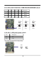
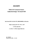
CI270CW
533MHz FSB / VGA / DVI / Multi-COMs / LAN /
Mini PCI / PCIe mini card
Intel Atom N270 . 533MHz FSB . All-In-One .
Audio . LAN . Mini PCI . PCIe mini card
SATA . 8 USB . CF . Wide range DC-input
Multi-COM Board
NO. CI270CW
Release date: OCT . 01 . 2009
Contents
CI270CW
Warning!........................................................................................................................... 1
Hardware Notice Guide ............................................................................................. 2
CHAPTER 1 GENERAL INFORMATION ........................................................................ 4
1-1 MAJOR FEATURE........................................................................................................ 5
1-2 SPECIFICATION .......................................................................................................... 6
1-3 VERTICAL SODIMM ASSEMBLY GUIDE..................................................................... 7
1-4 DIRECTIONS FOR INSTALLING THE MINI CARD ..................................................... 8
1-5 INSTALLING THE MINI PCI CARD ............................................................................. 9
1-6 PACKING LIST..............................................................................................................10
CHAPTER 2 HARDWARE INSTALLATION ...................................................................11
2-1 UNPACKING PRECAUTION .......................................................................................11
2-2 UNPACKING CHECKUP .............................................................................................12
2-3 DIMENSION-CI270CW (200 x 150m) .........................................................................13
2-4 LAYOUT-CI270CW ......................................................................................................14
2-5 DIAGRAM-CI270CW ...................................................................................................15
2-5-1 BOTTOM SIDE DIAGRAM-CI270CW ......................................................................16
2-6 INSTALL MEMORY ..................................................................................................... 17
2-7 LIST OF JUMPERS .................................................................................................... 18
2-8 JUMPER SETTING DESCRIPTION .......................................................................... 19
2-9 JSB1: CMOS DATA SET ............................................................................................. 19
2-10 JVF1: CF CARD POWER VOLTAGE SELECT ....................................................... 20
2-11 JSF1 CF CARD MASTER AND SLAVE SELEC ....................................................... 21
2-12 JSP1: AT / ATX POWER SELECT ............................................................................ 21
2-13 COM PORT PIN9 SELECT RI SIGNAL OR VOLTAGE SOURCE ........................... 22
2-14 JSC3,JSC31/32/33/34: COM3 RS232/422/RS485 SELECT ................................... 23
2-15 JVL1: LVD PANEL POWER SELECT ........................................................................23
2-16 JVP1: LVDS PANEL INVERTER POWER SELECT ................................................ 24
2-17 JVU8: USB PORT 8 VOLTAGE SELECT ................................................................. 24
2-18 JSD1: DPC DUTY SET ............................................................................................. 25
CHAPTER 3 CONNECTION ........................................................................................ 26
3-1 LIST OF CONNECTORS ........................................................................................... 26
3-2 FAN CONNECTOR .................................................................................................... 28
3-3 SATA INTERFACE ...................................................................................................... 28
3-4 IDE CONNECTORS ................................................................................................... 29
3-5 COMPACT - FLASH MEMORY SOCKET ............................................................... 30
3-6 VGA CONNECTOR .................................................................................................... 31
3-7 DVI-D CONNECTOR ................................................................................................ 31
3-8 KEYBOARD AND MOUSE CINNECTOR ................................................................... 32
i
3-9 USB PORT .................................................................................................................. 33
3-10 LAN CONNECTOR ................................................................................................... 34
3-11 COM PORT CONNECTOR ....................................................................................... 35
3-12 AUDIO PORT CONNECTOR .................................................................................... 38
3-13 AUDIO AMPLIFIER CLASS D TWO CHANNEL 6W/CH .......................................... 39
3-14 LPT PORT ................................................................................................................. 39
3-15 WDT/DIO FUNCTION PORT .................................................................................... 40
3-15-1 FOR F75111N I2C WATCH DOG TIMER DEVICE: .............................................. 40
3-16 I2C WDT/DIO W75IO.H REFERENCE SAMPLE CODE: ........................................ 41
3-16-1 I2C WDT/DIO F75111N REFERENCE SAMPLE CODE: ..................................... 45
3-17 LVDS INTERFACE CONNECTOR ........................................................................... 55
3-18 PANEL POWER CONNECTOR ................................................................................ 55
3-19 TOUCH SCREEN DEVICE ....................................................................................... 56
3-20 DC 12V IN ................................................................................................................. 57
3-21 DC +5/+12V OUTPUT CONNECTOR ...................................................................... 57
3-22 I2C BUS INTERFACE ............................................................................................... 58
3-23 MINI CARD ................................................................................................................58
3-24 FRONT-PANEL ..........................................................................................................59
CHAPTER 4 INTRODUCTION OF BIOS....................................................................... 60
4-1 ENTER SETUP ........................................................................................................... 60
4-2 GETTING HELP .......................................................................................................... 61
4-3 THE MAIN MENU ....................................................................................................... 61
4-4 STANDARD CMOS FEATURES ................................................................................ 63
4-5 ADVANCED BIOS FEATURES ................................................................................... 64
4-5-1 HARD DISK BOOT PRIORITY ................................................................................ 66
4-5-2 USB BOOT PRIORITY ............................................................................................ 66
4-6 ADVANCED CHIPSET FEATURES ............................................................................ 67
4-6-1 PCI EXPRESS ROOT PORT FUNC ........................................................................69
4-7 INTEGRATED PERIPHERALS ................................................................................... 70
4-7-1 ONCHIP IDE DEVICE FUNCTION ......................................................................... 71
4-7-2 SUPER IO FUNCTION ............................................................................................ 73
4-7-3 USB DEVICE FUNCTION ....................................................................................... 74
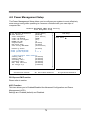
4-8 POWER MANAGEMENT SETUP .............................................................................. 75
4-8-1 PCI EXPRESS PM FUNCTION .............................................................................. 76
4-9 PNP/ PCI CONFIGURATION SETUP ........................................................................ 77
4-9-1 IRQ RESOURCES .................................................................................................. 78
4-10 PC HEALTH STATUS ............................................................................................... 78
4-11 FREQUENCY / VOLTAGE CONTROL ..................................................................... 79
4-12 LOAD FAIL-SAFE DEFAULTS ................................................................................. 79
4-13 SET SUPERVISOR / USER PASSWORD ............................................................... 80
ii
CHAPTER 5 DRIVER INSTALLATION........................................................................ 81
5-1 INF INSTALL INTEL 945GSE CHIPSET SYSTEM DRIVER .................................. 83
5-2 VGA INSTALL INTEL 945GSE VGA DRIVER ........................................................... 85
5-3 SOUND INSTALL VIA HID AUDIO CODEC DRIVER ............................................... 87
5-4 HOW TO UPDATE BIOS ............................................................................................ 89
APPENDIX A: POWER CONSUMPTION TEST .............................................................. 90
APPENDIX B: RESOLUTION LIST .................................................................................. 91
iii
2009
OCT . 01. 2009
Warning !
1. Battery
Battery on board is consumables. We doesn’t guarantee the life time of it.
2. Fanless solution with HDD
Please be aware of specification & limitation for HDD when fanless solution
is implemented.
3. We will not give further notification if there is any change about the product
information and the manual.
4. SATA does not support Hot SWAP
5. There would be +-20% difference of WDT at room temperature.
6.
Please make sure the voltage specification meet the requirement
of the equipment before plugging into the power.
7. SSD has 2 types, commercial grade and industrial grade, which provide
different read/write speed, operation temperature and life cycle.
Please contact sales for further information before ordering.
8. Caution ! Please notice that the heat dissipation problem could cause the
MB system unstable. Please handle the heat dissipation properly when
buying single MB.
9. Please avoid to approach the heat sink area and prevent being scalded when
using the Fanless products.
10. If the users repair, modify or destroy any component of product
unauthorized, We would not take responsibility or provide warranty.
1
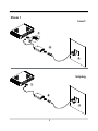
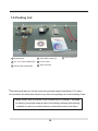
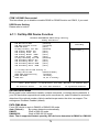
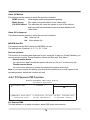
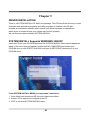
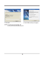
* Hardware Notice Guide
1. Before installing the power supply with this motherboard, please attach the 12V/DC
( 4 pin connector )of the adapter to motherboard first.
After that, plug the adapter power to AC outlet.
Always normally shut down the computer before you move the system unit or remove
the power supply from the motherboard.
Please unplug the 12V/DC ( 4 pin connector ) of the adapter from motherboard first.
Then unplug the adapter from the AC outlet.
Please refer to procedure from the photo 1
2. There will be high possibility to burn out the CPU if you change/ modify any parts of the
CPU cooler.
3. Please wear wrist strap and attach it to a metal part of the system unit before handling a
component.
You can also touch an object that is of ground connection or with metal surface if you don't
have wrist strap.
4. Please be careful when you handle this product. Pay attention to & don't touch the
sharp-pointed components at the bottom PCB .
5. Please pay attention to this: Remove or change any components form the motherboard
will VOID the warranty of the motherboard you purchased .
6. Before you install/remove any components or make any jumper setting on the motherboard,
please make sure to disconnect the power first.
( Please follow the instructions as of this guide )
7. Please follow this instruction carefully when using the "POWERON after PWR-Fair" function.
When the DC power adaptor runs out of power, unplug it from the DC current;
when power returns plug it back in only after 5 seconds. If there is a power outage,
unplug it from the AC current, when power returns plug it back in only after 30 seconds.
Otherwise it will cause system locking or serious damage.
Remark 1:
Always insert/unplug the 12V/DC ( 4 pin connector ) horizontally & directly from the
motherboard.
DO NOT twist the 12V/DC ( 4 pin connector ) gently, it is designed to fit snugly .
Moreover, erratic pull / push testing with the DC Jack might cause the unpredictable
damage to the component & system unit.
2
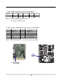
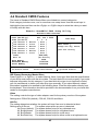
Photo 1
Insert
1
2
3
Unplug
1
2
3
3
Chapter-1
General lnformation
The CI270CW is an All-In-One POS / Automation control Board. The board's design combines
all necessary input and output effects interfaces, which makes itself an ideal all-in-one
control board for demanding POS or automation control applications. CI270CW is the perfect
platform for a whole range of mobile and low-power devices.
A high-performance and power-efficient communication platform, the embedded motherboard
CI270CW is especially designed for advanced embedded car PC or POS system applications
where the economical use of power is in high demand.
With the sizable memory bandwidth of on board 1GB DDR2 module and the flexibility of
expanding the memory to 2GB with DDR2 SODIMM, CI270CW ensures the high performance
levels required of today's most popular POS/Automation control applications including
Embedded Car PC, POS, ATM, Kiosk and Panel PC.
CI270CW is supported with two 10/100/1G Ethernet for seamless broadband connectivity.
With Wake On LAN function and the PXE function in BIOS for Realtek LAN chipset only,
this is also ideal for networking applications. The built-in LAN options are two Intel 82574L with
RJ45 for 10/100M/1Gbps Ethernet or two Realtek RLT8111C 10/100/1Gbps Ethernet.
CI270CW also supports as many as five RS232 and one RS422/485 to meet the needs of
multi-COM connectivity.
Except Compact Flash and 40 pin IDE socket, CI270CW can be integrated with PCIe mini card
and Mini PCI Card. In addition, with the eight hi-speed USB version 2.0 enhanced host
controller interface, it ensures the high performance level and also the powerful and
flexible expansion.
The Compact Flash reader supports IDE/ATA interface. A single Flash chip holds the
system BIOS, and you can change the Flash BIOS by the Utility Update.
The CI270C All-In-One motherboard is fully compatible with industry standards,
plus technical enhancements, and thousands of software applications developed for
IBM PC/AT compatible computers. The control logic provides high-speed performance for the
most advanced multi user and multitasking applications available today.
4
1-1 Major Feature
1. Intel Atom N270 CPU ( FSB 533 Mhz )
2. Intel 945GSE Chipset on board, Graphic Chip Integrated
3. On board DDR2 module 1GB and support DDR2 SODIMM up to 2GB (option)
4. On board SSD 1/2/4/8 Gbytes (option)
5. Support 2 x 10 / 100 / 1000 Mbps LAN on Board ( Realtek or Intel LAN Chip )
6. Support CRT resolutions up to SXGA+
7. 18 bits/ 36 bits LVDS Interface on Board. (option)
8. Support DVI.
9. Support 1 x Compact Flash Card Socket and 40 pin IDE socket on Board
10. Support 2 x SATA ports.
11. Support Mini PCI Socket on board and 1 x PCIe mini card for USB and PCIe interface
Support one PCIe x 1 interface.
12. Optional Wide range power supply
13. PCB Dimensions: 200 x 150 mm
14. Support dimming control function
5
1-2 Specification
1. CPU: Intel Atom N270 CPU ( FSB 533 Mhz )
2. ChipSet: Intel 945GSE and Intel ICH7M (82801GBM)
3. Memory: On board DDR2 module 1 GB or support DDR2 SODIMM up to 2GB
4. VGA: Internal Graphics Memory with dynamic video memory technology (DVMT3.0)
5. I/O Chip: ITE IT8712F and F81216AD IO chipset
6. SATA: Two SATA ports with independent DMA operation supported
7. NAND flash memory (option): Support Compact Flash card type II for ATA interface
On board SSD 1/2/4/8 GBytes
8. LAN: 2 x Reltek RLT8111C 10/100/1000 Mbps or Intel 82574L LAN chip for PCIe x 1 interface
9. Storage Device: 1 x 50 pins Compact Flash Socket
Ultra ATA 100/66/33, 1 x 40 pin 2.54 mm
10. Serial Port: 5 x RS232 + 1 x RS422/485 or 5 x RS485 + 1 x RS232 (optional)
11. USB: 8 x USB 2.0 (4 external+4 internal ports)
12. DVI: Chrontel DVI transmitter up to 165M pixels/second
13. Audio: Intel HD audio specification Rev. 1.0 Compliant
14. LVDS (option): support 18bits/ 36 bits LVDS interface resolution up to SXGA+
15. WDT/DIO: Hardware watch dog timer support, 0~255 sec programmable
Hardware digital Input & Output, 8xDI / 8xDO
16. Touch screen (option): C8051F321 USB/COM interface touch screen controller,
support 4-, 5-, 8- wire Analog resistive touch screen
17. Audio Amplifier (option): 6-W/CH into an 8-Ω Load from a 12-V Supply.
Up to 92% Efficient, Class-D operation (optional)
18. Expand interface: 1 x Mini PCI socket for PCI Rev. 2.2 interface &
1 x PCIe mini card support USB and PCIe interface
1x PCIe x 1 interface
19. BIOS: Award BIOS version V6.1
20. Dimensions: 200 x 150 mm
21. Power (option): Wide range DC-IN from +9V to +32V or fix to +12V DC input convert
into power +12VAD to +5V/±5% and +3.3V/±5%, and +12V/±5%
22. Power Consumption: Please refer to page 90
6
1-3 Vertical SODIMM assembly guide
1. Install the memory into SODIMM.
2. Press down firmly to ensure the memory
is locked.
Uninstall
1. Pull open both sides of the memory slot.
2. Take out the memory.
7
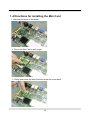
1-4 Directions for installing the Mini Card
1. Unscrew the screw on the board
2. Plug in the Mini Card in a 45 angle
3. Gently push down the Mini Card and screw the screw back.
8
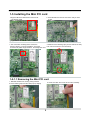
1-5 Installing the Mini PCI card
1.Align the Mini PCI card with the connector at
a 45 degree angle.
2. Press the Mini PCI into the connector until you hear
a click.
Notices:
2. Make sure the retaining clips (on two sides of the slot)
1.The connectors are designed to ensure the
lock onto the notches of the card firmly
correct insertion. If you feel resistance, check the
connectors & golden finger direction, and realign the card.
1-5-1.1 Removing the Mini PCI card
1. Release the Mini PCI card by pulling outward
the two retaining clips and the card pops up slightly.
2. Lift the mini PCI card out of its connector carefully.
9
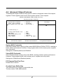
1-6 Packing List
1
5
3
2
6
4
7
1 MotherBoard
4 SATA HDD Cable(7P)
2 DC 12V Power Adapter(4P)
5 Power Cable
3 ATA 66 HDD Cable(40P)
6 Utility CD Disk
7 User’s Manual
*The packing list above is for the users who purchase single motherboard. The users
who purchase the board with chassis may refer to the packing list in the Assembly Guide.
Please contact with your dealer if any of these items is missing or damaged
on delivery. And please keep all parts of the delivery package with packing
materials in case if you need to deliver or store the product in the future.
10
Chapter-2
Hardware Installation
This chapter provides the information how to install the hardware of CI270CW.
Please follow section 1-6, 2-1 and 2-2 to check the delivery package and unpack
carefully. Please follow the jumper setting procedure.
2-1 Unpacking Precaution
The CI270CW board has been well packed with an anti-static bag to protect its
sensitive components and circuitry from damage due to static electric discharge.
NOTE!
1. Do not touch the board or any other sensitive components without all necessary
anti-static protection.
2. Please pay attention to the voltage limitation of DC-IN12 V +- 5 %.
Overuse of DC-IN voltage limitation or change to another power adapter
( not provided with this system ) will VOID warranty.
You should follow these
steps to protect the board from the static electric
discharge whenever you handle the board:
1. Ground yourself by a grounded wrist strap at all times when you
handle the CI270CW.
Well secure the ALLIGATOR clip of the strap to the end of the shielded wire lead from
a grounded object. Please put on and connect the strap before handling the
CI270CW for harmlessly discharge any static electricity through the strap.
2. Please use anti-static pad to put any components, parts, or tools on the pad whenever
you work on them outside the computer. You may also use the anti-static bag instead of
the pad. Please ask your local supplier for necessary parts on anti-static requirement.
3. Do not plug any connector or set any jumper when the power is on.
11
2-2 Unpacking checkup
First of all, please follow all necessary steps of section 2-1 to protect CI270CW
from electricity discharge. With reference to section 1-6, please check the delivery package
again with following steps:
1. Unpack the CI270CW board and keep all packing material, manual
and driver disc etc, do not dispose !
2. Is there any components lose or drops from the board? DO NOT CONTINUE
TO INSTALL THIS BOARD! CONTACT THE DEALER YOU PURCHASED THIS
BOARD FROM, IMMEDIATELY.
3. Is there any visible damage on the board? DO NOT CONTINUE TO INSTALL
THIS BOARD!CONTACT THE DEALER YOU PURCHASED THIS
BOARD FROM, IMMEDIATELY.
4. Check your optional parts (i.e. DDR, CF etc.), all necessary jumpers
setting to jumper pin-set, and CMOS setup correctly.
Please also refer to all information of jumper settings in this manual.
5. Check your external devices (i.e. Add-On-Card, Driver Type etc.)
for complete add-in or connection and CMOS setup correctly.
Please also refer to all information of connector connection in this manual.
6. Please keep all necessary manual and driver disc in a good condition for future
re-installation if you change your Operating System.
12
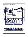
2-3 Dimension
200 x 150 mm
135.000
130.900
93.000
19.100
7.100
116.000
CI270C-M0.1
19.100
rj45
rj45
16.600
34.000
2009,02,25
9.5
25.48
5.100
53.44
84.68
105.56
13
6.5
6.28
22.16
22.6
13.02
4.22
5
6.79
7
19
21.59
20.88
132.65
168.71
191.87
200
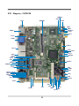
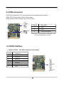
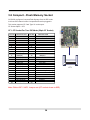
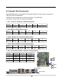
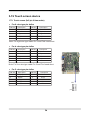
2-4 Layout - CI270CW
SWP13
SODIM1
CPI1
FAN1
CFP2
JSP1
SWP1
SWP12
CFP1
LED1
CPI11
CKM11
CKM1
LED2
CG11
LVDS1
CDG1
CUL2
JSD1
JVL1
JVP1
CUL1
FAN2
CU7
LPT1
CC6
CC12 CC22
CC5 CC23
MPCE1 CC11
JVC1
CC21
JVC2
JSC3
CVO1
CPP1
SATA2
SATA1
CA3
JSB1
JSV1 CVO11
JSC31 CC34
JSC32JSC33
JSC34 CVI1
JVC3
JVC4
CA1
CA2
CU8
CU12
JUSB1
JUSB2
CA12
CAL1
CF1
CAR1
14
JSF1
CO1
CT1
JVF1
CIO1
CIO2
IDE1
JVU8
CPO1
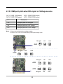
2-5 Diagram - CI270CW
CPI1
SWP13
FAN1
CFP2
SODIM1
JSP1
SWP1
SWP12
CFP1
CKM1
LED1
CG11
CDG1
LVDS1
CUL2
JSD1
JVL1
JVP1
CPP1
SATA2
CUL1
FAN2
CU7
LPT1
CC6
CC12
CC5
JVC1
MPCE1
CC21
JVC2
JSC3
SATA1
CA3
JSB1
CA1
JSC31 CC34
JSC32 JSC33
JSC34 CVI1
JVC3
JVC4
CA2
CU8
CU12
CA12
JSF1
CAL1
CAR1
CF1
15
CO1
CT1
JVF1 CIO2 CIO1
IDE1
JVU8
CPO1
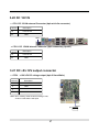
2-5-1 Bottom Side Diagram- CI270CW
MPCI: Mini PCI Socket
Back Panel-CI270CW
PS/2 Mouse
VGA
LAN 2
LAN 1
COM 1
COM 3
COM 2
COM 4
Line-out
DC 12V IN
PS/2 Keyboard
DVI
USB
Front Panel-CI270CW
USB
Line-out phone jack
Mic-in phone jack
16
Mic-in
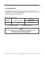
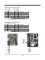
2-6 Install Memory
This motherboard provides one 200-pin Small Outline Dual In-line Memory Module
(SODIMM) socket for memory expansion available from minimum memory size of 256MB
to maximum memory size of 2GB DDR2 SDRAM.
DDR2 clock supports: DDR2 533, DDR2 667
Valid Memory Configurations
Total Memory
DIMM1
System Accept or Not
DS/SS
Accept
DS: Double Sided DIMM
Min. ~ Max.
256MB~2GB
SS: Single Sided DIMM
NOTE!
The detected memory size is less than actual installed memory size since
some memory has been allocated for system use.
That’s how PC works with system memory.
17
NOTE!
When you install DIMM module fully into the DIMM socket, the eject tab should be
locked into the DIMM module very firmly and fit into its indention on both sides.
Please refer to page7 for installation of memory module.
WARNING!
Once you hear " Beep Beep Beep" sounds after turning on the power ,
please check if the DRAM is installed properly or not.
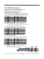
2-7 List of Jumpers
1. JSB1: CMOS clear select
2. JSC3, JSC31 / 32 / 33 / 34: COM3 RS232/422/RS485 select
3. JSP1: ATX / AT Power type select
4. JSV1: S Video / HDTV select
5. JSD1: DPC Duty select
6. JSF1: CF card master and slave select
7. JVF1: CF card Power +5V/+3.3V select
8. JVC1: COM1 voltage select
9. JVC2: COM2 voltage select
10. JVC3: COM3 voltage select
11. JVC4: COM4 voltage select
12. JVL1: LCD Panel power select
13. JVP1: Panel Inverter power select
14. JVU8: USB8 voltage select
18
2-8 Jumper Setting Description
A jumper is ON as a closed circuit with a plastic cap covering two pins. A jumper is OFF
as an open circuit without the plastic cap. Some jumpers have three pins, labeled 1, 2,
and 3. You could connect either pin 1 and 2 or 2 and 3.
The below figure 2.2 shows the examples of different jumper settings in this manual.
Figure 2.2
All jumpers already have its default setting with the plastic cap inserted as ON,
or without the plastic cap as OFF. The default setting may be referred in this
manual with a " " symbol .
*
2-9 JSB1: CMOS Data Set
A battery must be used to retain the motherboard configuration in CMOS RAM.
Close pin 1and pin 2 of JSB1 to store the CMOS data.
To clear the CMOS, follow the procedures below:
1. Turn off the system and unplug the AC power
2. Remove DC 12V power cable from DC 12V power connector
3. Locate JSB1 and close pin 2-3 for a few seconds
4. Return to its normal setting by shorting pin 1-2
5. Connect DC 12V power cable back to DC 12V power connector
19
Note: Do not clear CMOS unless
1. Troubleshooting
2. Forget password
3. You fail over-clocking system
JSB1
*1-2
2-3
Description
*Normal Set
CMOS Data clear
JSB1
3
2
1
3
2
1
*Normal
Clear Setting
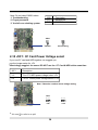
2-10 JVF1: CF Card Power Voltage select
If you use CF card and HDD together, we suggest you
use the jumper setup for +5V.
*We strongly suggest the users: DO NOT use the CF Card & HDD at the same time.
JVF1
Description
*1-2
*For CF CARD power voltage select +5V
2-3
For CF CARD power voltage select +3.3V
Note: Please be cautious about voltage setting.
JVF1
* We use
3 2 1
3 2 1
+5V*
3.3V
to refer to as pin1
20
2-11 JSF1: CF Card Master and Slave select
If you use CF card and SSD together, please set CF as Slave and SSD as Master.
*We strongly suggest the users: DO NOT use the SSD & CF Card at the same time.
JSF1
Description
*1-2
*For CF CARD Master
2-3
For CF CARD Slave
JSF1
3 2 1
3 2 1
Master*
Slave
2-12 JSP1: AT / ATX power select
JSP1
Description
*1-2
*ATX Power mode
2-3
AT Power mode
JSP1
1 2 3
1 2 3
ATX Power*
21
AT Power
2-13 COM port pin9 select RI signal or Voltage source
JVC1: COM1 PIN9 select
JVC3: COM3 PIN9 select
JVC1 / 2 / 3 / 4
*1-2
JVC2: COM2 PIN9 select
JVC4: COM4 PIN9 select
Description
*COM port pin9 use RI signal
3-4
COM port pin9 use +5V voltage
5-6
COM port pin9 use +12V voltage
Note: 1. Please be cautious about voltage setting.
2. If want to use +5V/+12V need check system power design spec.
*RI signal
JVC1
*RI signal
JVC2
+5V
+12V
5 3 1
5 3 1
5 3 1
6 4 2
6 4 2
6 4 2
1
3
5
*RI signal
+5V
2
4
6
1
3
5
+12V
2
4
6
2
4
6
1
3
5
+5V
+12V
5 3 1
5 3 1
5 3 1
6 4 2
6 4 2
6 4 2
5 3 1
5 3 1
5 3 1
JVC3
JVC4
6 4 2
*RI signal
22
6 4 2
+5V
6 4 2
+12V
2-14 JSC3,JSC31/32/33/34: COM3 RS232/422/RS485 select
Description
JSC3
JSC31 JSC32 JSC33 JSC34
*1-2
*1-2
*1-2
*1-2
*1-2
RS232*
3-4
2-3
2-3
2-3
2-3
RS422
5-6
2-3
2-3
2-3
2-3
RS485
5 3 1
5 3 1
JSC3
5 3 1
JSC3
6 4 2
JSC31
6 4 2
JSC31
JSC32
JSC32
JSC33
JSC34
1-2
+5V
*2-3
*+3.3V
JSC33
JSC34
3 2 1
3 2 1
3 2 1
*RS232
RS422
RS485
2-15 JVL1: LVD panel power select
Description
JSC31
JSC32
JSC33
JSC34
JVL1
JSC3
6 4 2
Note: Please be cautious about voltage setting.
JVL1
3 2 1
3 2 1
+3.3V*
+5V
23
2-16 JVP1: LVDS Panel Inverter power select
JVP1
Description
*1-2
*+12V
2-3
+5V
Note: Please be cautious about voltage setting.
JVP1
3 2 1
3 2 1
+12V*
+5V
2-17 JVU8: USB Port 8 Voltage select
JVU8
Description
*1-2
*+5V
2-3
+3.3V
Note: Please be cautious about voltage setting.
JVU8
3
2
1
3
2
1
+5V*
+3.3V
24
2-18 JSD1: DPC Duty set
JSD1
Description
1-2
Low 0% (Low level )
*2-3
*Hi 100% (3.3V level)
Note: Please be cautious about voltage setting.
JSD1
3 2 1
3 2 1
Low
3.3V*
25
Chapter-3
Connection
This chapter provides all necessary information of the peripheral's connections,
switches and indicators. Always power off the board before you install the peripherals.
3-1 List of Connectors
CA1: Line-out phone jack
CA2: Mic-in phone jack
CA12: Mic-in (down side) / Line out (up side) phone jack
CA3: Line-out/Line-in/Mic-in 2x4 pin (2.0mm) Header
CAR1: Amplifier Line-out Right channel connector
CAL1: Amplifier Line-out Left channel connector
CC12: COM1(up side)/COM2(down side) DB9p connector
CC34: COM3(up side)/COM4(down side) DB9p connector
CC11: COM1 2x5pin(2.0mm) Wafer (Share to LPT1) (Option)
CC21: COM2 5pin (1.25mm) Wafer (Share to CC12 COM2)
CC22: COM2 DB9p connector (Share to CC12 COM2) (Option)
CC23: COM2 2x5pin(2.0mm) Wafer (Share to CC12 COM2) (Option)
CC5: COM5 2x5pin(2.0mm) Wafer
CC6: COM6 2x5pin(2.0mm) Wafer
CDG1: DVI-D / VGA DB15p connector
CG11: VGA port 2x5pin (2.0mm) Wafer connector
IDE1: IDE 40 pin (2.54mm) Connector
CF1: CF socket 50pin
CIO1,CIO2: Two DIO 2x5 pin (2.0mm) Wafer
CKM1: PS2 Keyboard / Mouse connector
CKM11: KB/MS port 1x6 pin (1.25mm) Wafer connector (Share to CKM1) (Option)
CO1: I2C bus connector 1x4 pin (1.25mm) Wafer (Option)
CPI1: DC 12V-IN DIN external Connector (4pin mini din connector)
CPI11: DC 12V-IN Internal Connector (4pin connector) (Option)
CPO1: DC +5/+12V output connector (2.5mm) Wafer
LVDS1: LVDS 18 /36Bits 2x15 pin (1.25mm) connector
26
List of Connectors
CPP1: Panel inverter power connector 1x5 pin (2.0mm) Wafe
CT1: Touch screen device 2x5 pin (2.0mm) Wafer
CU12: USB 1 ports (Down side Type A jack )
CU2: USB 0 port 4pin (2.54mm) Header (Share with CU12)
CU7 : USB 7 port 4pin(1.25mm) Wafer (Share with PCIe Mini card soket)
CU8 : USB 8 port 4pin(1.25mm) Wafer (Share with Touch)
CUL1: USB port 3/4 and LAN1 RJ45 Connector
CUL2: USB port 5/6 and LAN2 RJ45 Connector
FAN1: CPU FAN connector 1x3 pin (2.54mm) Wafer
FAN2: System FAN connector 1x3 pin (2.54mm) Wafer
LPT1: LPT port 2x13pin(2.0mm) Wafer Header (Option)
SATA1: SATA connector 7pin
SATA2: SATA connector 7pin
MPCE1: PCIe Mini card socket
MPCI1: Mini PCI socket
SODIM1: DDRII RAM Socket
CFP1: Power LED 1x2 pin (2.54mm) Header.
CFP2: Power reset 1x2 pin (2.54mm) Header.
27
3-2 FAN Connector
CI270CW provides one CPU fan connector and one system fan connector.
FAN1: CPU FAN connector (3pin 2.5mm wafer)
FAN2: System FAN connector (3pin 2.5mm wafer)
FAN1
pin1
PIN NO.
FAN2
pin1
Description
1
GND
2
+12V
3
FAN speed detect
Note: DC in +12V by switch to FAN power +12V,
so DC in need stable +12V input
3-3 SATA Interface
.
SATA1 / SATA2 : Two SATA connector (7pin wafer)
PIN NO.
Description
1
GND
2
DATA TX+
3
DATA TX-
4
GND
5
DATA RX-
6
DATA RX+
7
GND
SATA2
SATA1
28
3-4 IDE Connectors
IDE1 40 pin (2.54mm box Header) Connector
PIN NO.
Description
PIN NO.
Description
1
RESET#
2
GND
3
DATA7
4
DATA8
5
DATA6
6
DATA9
7
DATA5
8
DATA10
9
DATA4
10
DATA11
11
DATA3
12
DATA12
13
DATA2
14
DATA13
15
DATA1
16
DATA14
17
DATA0
18
19
GND
20
21
DREQ
22
DATA15
+5V
GND
23
IOW#
24
GND
25
26
28
GND
27
IOR#
IORDY
29
DACK#
GND
31
IRQ15
30
32
33
SA 1
34
ATA 33/66/100
CABLE SELECT
SA 2
pin1
PULL DOWN
NC
35
SA 0
36
37
HD CS0#
38
HD CS1#
39
HD LED
40
GROUND
IDE1
Note!
PIN 20 connector +5V of IDE 1 could
provide the power of DOM.
29
3-5 Compact - Flash Memory Socket
CI270CW configures CompactFlash Storage Card in IDE mode.
It will use IDE channel when CompactFlash card is plugged in.
This socket supports CF Card Type I/II socket spec.
CF Socket 50pin----CF1
CF1: CF Socket For True IDE Mode (50pin CF Socket)
PIN NO.
1
2
3
4
5
6
7
8
9
10
11
12
13
14
15
16
17
18
19
20
21
22
23
24
25
DESCRIPTION
GND
DATA3
DATA4
DATA5
DATA6
DATA7
-CS0
GND(A10)
GND(-ATA_SEL)
GND(A9)
GND(A8)
GND(A7)
+5V
GND (A6)
GND (A5)
GND (A4)
GND (A3)
SDA2
SDA1
SDA0
DATA0
DATA1
DATA2
NC(-IOCS16)
GND(-CD2)
PIN NO.
26
27
28
29
30
31
32
33
34
35
36
37
38
39
40
41
42
43
44
45
46
47
48
49
50
DESCRIPTION
GND(-CD1)
DATA11
DATA12
DATA13
DATA14
DATA15
-CS1
GND(-VS1)
-IOR
-IOW
-WE(PH)
INTR
+5V
-CSEL
NC(-VS2)
RESET
IORDY
DMAREG(-INPACK)
DMAACK[-REG(PH)]
-DASP
-PDIAG
DATA8
DATA9
DATA10
GND
Note: Refer JSF1 / JVF1 Jumper set (CF socket share to IDE)
30
CF1
3-6 VGA Connector
. CG11: VGA 2 x 5pin 2.0mm wafer connector
PIN NO.
Description
PIN NO.
Description
1
BULE
2
GND
3
GND
4
DDC CLOCK
5
GREEN
6
V-SYNC
7
GND
8
H-SYNC
9
RED
10
DDC DATA
*Note : VGA signal CG11 share with CG1
pin1
CG11
3-7 DVI-D Connector
.
CDG1 : DVI 12bit connector Down side (DB Connector)
PIN NO.
Description
PIN NO.
1
Data 2 -
9
Data 1 -
17
Data 0 -
2
Data 2 +
10
Data 0 +
GND
11
Data 1+
GND
18
3
19
GND
4
NC
12
NC
20
NC
5
NC
13
I2C-CLK
14
21
22
NC
6
NC
+5V
7
I2C-DATA
15
GND
23
CLK+
8
NC
16
DVI-DETECT
24
CLK-
PIN NO.
.
Description
Description
GND
CDG1: VGA DB15 Connector Up side (D SUB 15PIN)
PIN NO.
Description
PIN NO.
PIN NO.
Description
Description
1
RED
6
GND
11
NC
2
GREEN
7
12
DDC DATA
3
BULE
8
GND
GND
13
H-SYNC
4
NC
9
NC
14
Y-SYNC
GND
15
DDC CLOCK
5
GND
10
CDG1 VGA
CDG1 DVI
31
3-8 Keyboard and Mouse Connector
. CKM1: PS2 Keyboard Din connector(down side)
PIN NO.
Description
1
KB DATA
2
MS DATA
3
GND
4
+5V
5
KB CLOCK
6
MS CLOCK
CKM1
PS/2 Mouse
CKM1
PS/2 Keyboard
.
CKM1: PS2 Mouse Din Connector (up side)
PIN NO.
Description
1
MS DATA
2
NC
3
GND
4
+5V
5
MS CLOCK
6
NC
. CKM11: 6PIN(1.25mm Wafer connector) Internal Keyboard / Mouse Connector
PIN NO.
Description
1
+5V
2
KB DATA
3
KB CLOCK
4
GND
5
MS DATA
6
MS CLOCK
CKM11
pin1
32
3-9 USB Port
. CU12: USB 0/1 ports (Down side Type A jack )
PIN NO.
Description
1
+5V
2
USB DATA 0 / 1-
3
USB DATA 0 / 1+
4
GND
CU12
. CU2: USB0 port 4pin (2.54mm) Header
(Share with CU12)
PIN NO.
Description
1
+5V
2
USB DATA 0 -
3
USB DATA 0 +
4
GND
pin1
CU7
pin1
CU8
. CU7: USB7 port (4pin 1.25mm Wafer)
. CU8: USB8 port (4pin 1.25mm Wafer)
PIN NO.
Description
PIN NO.
Description
1
+5V
1
+5V or +3.3V
2
USB DATA -
2
USB DATA -
3
USB DATA +
3
USB DATA +
4
GND
4
GND
Note: CU7 USB7 share with PCIe Mini card
Note : 1. PIN 1 Voltage select from JVU8
2. CU8 USB8 share with on board Touch controller
. CUL1/CUL2 (Down side): USB ports 2/3/4/5 Type A jack
PIN NO.
Description
1
+5V
2
USB DATA / 2 / 3 / 4 / 5-
3
USB DATA / 2 / 3 / 4 / 5+
4
GND
CUL2
33
CUL1
3-10 LAN connector
The Fast Ethernet controller provides 32-bit performance, PCIe bus master capability,
and full compliance with IEEE 802.3 10/100/1000 Based-T specification.
For 10/100/1000 Base-T operation, please connect the network connection
by plugging one end of the cable into the RJ-45 jack of the CUL1/CUL2 Connector.
Besides 10/100/1000 Base-T, CI270CW can provide Intel Giga LAN solution through
CUL1/CUL2 once equipped with Intel 82574L chipset.
.
CUL1 / CUL2 (Up side) :LAN Giga/100Mb Jack
PIN NO.
Description
PIN NO.
CUL2
Description
1
TD0-/TX+
5
2
TD0+/TX-
6
TD2+/RX-
3
TD1-/RX+
7
TD3-/NC
4
TD1+/NC
8
TD3+/NC
CUL1
TD2-/NC
LAN LED
Intel 82574L
LAN LED
Speed
10 Mbps
Back Side
1000 Mbps
100 Mbps
Fornt Side
Back Side
Fornt Side
Back Side
Fornt Side
Indicate
LAN light
Link Led
ACT Led
ACT Led
Link Led
ACT Led
ACT Led
Link Led
ACT Led
ACT Led
Orange
Orange
Orange
Green
Orange
Orange
Red
Orange
Orange
Realtek RTL8111C
LAN LED
Speed
10 Mbps
Back Side
100 Mbps
Fornt Side
Back Side
1000 Mbps
Fornt Side
Back Side
Fornt Side
Indicate
Link Led
LAN light
Orange
ACT Led
ACT Led
Link Led
Orange
Green
ACT Led
34
ACT Led
Link Led
Orange
Red
ACT Led
ACT Led
Orange
3-11 COM Port Connector
COM3 default support RS232/RS422/RS485 mode
COM1/2/4/5/6 default support RS232 mode
RS232 Mode conector ( D-SUB 9pin)
. CC12: COM1 (up side) / COM2 (down side) port Connector
. CC34: COM3 (up side) / COM4 (down side) port Connector
PIN NO.
Description
1
DCD
PIN NO.
6
Description
DSR
2
RXD
7
RTS
3
TXD
8
CTS
4
DTR
9
RI / VOLTAGE
5
GND
Note: 1. Pin 9 RI and Voltage setting only for COM 1/2/3/4 ports
JVC1 for COM1, JVC2 for COM2, JVC3 for COM3, JVC4 for COM4
2. COM3 default support RS232/RS422/RS485
. CC12 / CC34: RS485 Mode conector ( D-SUB 9pin)
PIN NO.
Description
PIN NO.
1
RS485 TX+
6
Description
2
RS485 TX-
7
NC
3
NC
8
NC
4
NC
9
NC
5
GND
NC
Note : This type by OEM BOM select
. CC34: COM3 (up side) for RS422 /RS485 ( D-SUB 9pin)
PIN NO.
Description
1
TXD-
PIN NO.
6
Description
NC
2
TXD+
7
NC
3
RXD+
8
NC
4
RXD-
9
RI / VOLTAGE
5
GND
Note: 1. CC34 (COM3) default support RS232/RS422/485 function
2. BIOS need setting to RS485/422 mode
CC12: COM1
CC12: COM2
35
CC34: COM3
CC34: COM4
. RS232 ports (2x5pin 2.0mm Wafer)
CC11: COM1
CC5: COM5
CC23: COM2
CC6 : COM6
PIN NO.
Description
1
DCD
PIN NO.
2
Description
3
TXD
4
DTR
5
GND
6
DSR
7
RTS
8
CTS
9
RI
10
NC
RXD
Note: 1. CC11 share with LPT1 connector for OEM
2. CC23 share with CC12 connector for OEM
. RS485 ports (2x5pin 2.0mm Wafer)
CC5: COM5 CC6 : COM6
PIN NO.
Description
PIN NO.
1
RS485 TX-
2
Description
RS485 TX+
3
NC
4
NC
5
GND
6
NC
7
NC
8
NC
9
NC
10
NC
Note : This type by OEM BOM select
CC23
pin1
CC6
CC11
pin1
CC5
pin1
pin1
36
. CC21: COM2 RS232 port (5pin 1.25mm Wafer)
PIN NO.
Description
1
2
3
4
5
+5V
GND
RTS
TX
RX
Note: 1. CC21(COM2) share with CC12
2. All signal are RS232 level .
. CC22: COM2 RS232 Mode single conector ( D-SUB 9pin)
PIN NO.
Description
1
DCD
PIN NO.
6
Description
DSR
2
RXD
7
RTS
3
TXD
8
CTS
4
DTR
9
RI / VOLTAGE
5
GND
Note: 1. CC22 share with CC12 COM2 connector for OEM
CC22
CC21
pin1
37
3-12 Audio Port Connector
The CI270CW has an on-board AC'97 3D sound interface. There are the connectors of
LINE OUT, MIC-IN connectors.
The MIC-IN Jack header are for audio sound input. The LINE-OUT
connector is a 4-pin Jack for audio sound output.
. CA1 : Line out connector (3.5mm Phone jack )
PIN NO.
Description
1
2
3
4
5
GND
FRONT OUT-L
NC
NC
FRONT OUT-R
. CA2: MIC IN (3.5mm Phone jack )
PIN NO.
Description
1
2
3
4
5
GND
MIC-PW
GND
NC
MIC-IN
. CA12: Up side Line out (3.5mm phone jack)
PIN NO.
Description
1
2
3
4
5
GND
Line OUT-L
NC
NC
Line OUT_R
. CA12: Down side Mic in (3.5mm phone jack)
PIN NO.
Description
1
2
3
4
5
GND
Mic IN-L
NC
NC
Mic IN_R
. CA3: Line-out/Line-in/Mic-in 2x4 pin (2.0mm) Header
PIN NO.
Description
PIN NO.
Description
1
Line-out-R
2
Line-out-L
3
GND
4
GMD
5
Line-in-R
6
Line-in-L
7
MIC-IN
8
MIC-IN
CA3
pin1
CA1
Line-out CA12
Mic-in CA12
38
CA2
3-13 Audio Amplifier class D Two channel 6W/ch
● CAR1: Audio Amplifier Line Out Right (2pin 2.0mm wafer)
PIN NO.
Description
1
LINE-OUT_R+
2
LINE-OUT_R-
● CAL1: Audio Amplifier Line Out Left (2pin 2.0mm wafer)
PIN NO.
Description
1
LINE-OUT_L+
2
LINE-OUT_L-
pin1
CAR1
pin1
CAL1
Note : Audio Amplifier is option function
3-14 LPT Port
. LPT1: port 2x13pin(2.0mm) Wafer Header
PIN NO.
Description
STROBE#
2
3
DATA0
4
ERROR#
5
DATA1
6
INITIALIZE
7
DATA2
8
9
DATA3
10
GND
11
DATA4
12
GND
13
DATA5
14
GND
15
DATA6
16
GND
DATA7
18
GND
20
GND
22
GND
19
21
ACKNOWLEDGE
BUSY
26
AUTO FROM FEED#
1
17
LPT1
Description
PIN NO.
PRINTER SELECT LN#
23
PARER EMPTY
24
GND
25
PRINTER SELECT
26
NC
Note: BOM default haven’t this function by OEM
39
pin1
3-15 WDT/DIO Function port
WDT/DIO Function port (2x5 2.0mm Header)
● CIO1 DIO 0—3 (2x5pin 2.0mm wafer)
PIN NO.
Description
1
DI-0
PIN NO.
2
DO-3
Description
3
DI-1
4
DO-2
5
DI-2
6
DO-1
7
DI-3
8
DO-0
9
GND
10
+5V
● CIO2 DIO 4—7 (2x5pin 2.0mm wafer)
PIN NO.
Description
1
DI-4
PIN NO.
2
DO-7
Description
3
DI-5
4
DO-6
5
DI-6
6
DO-5
7
DI-7
8
DO-4
9
GND
10
+5V
pin1
CIO2 CIO1
3-15-1 For F75111N I2C watch dog timer device:
DC spec :
Input low Voltage (VIL):+0.8 Max ,
Input High Voltage(VIH) : +2V Min
Output low Current (IOL):10mA (Min) VOL=0.4V
Output High Current (IOH):-10mA (Min) VOL=2.4V
Watch Dog Time value 0~255 sec
The system will be issued reset. When WDT is enable the hardware start down
counter to zero. The reset timer have 10~20% tolerance upon the Temperature.
Note: If want to SDK support . please contact to sales window.
Please refer to page 41 for WDT/DIO sample code.
-----------------------------------------------------------------Sample W75IO Demo Program
-----------------------------------------------------------------1.
DI
2.
DO
3.
WatchDog
4.
Exit
-----------------------------------------------------------------Please select demo function<1-4>?
1.
DI: Input DI value (0~FF, DI bit 0~7 HI level)
2.
DO: Input DO value (0~FF, DO bit 0~7 HI level)
3.
WatchDog: Input WatchDog Value (0~256 sec)
4.
Exit: Exit program
40
3-16 I2C WDT/DIO W75IO.h Reference sample code:
Compile platform:TC30 & DOS 6.22
// Sample.cpp : Defines the entry point for the console application.
//
#include
#include
#include
#include
"stdafx.h"
"conio.h"
<string.h>
<stdlib.h>
#include <iostream>
#include "W75IO.h"
#define
#define
#define
#define
DEMO_DI
DEMO_DO
DEMO_WDT
DEMO_EXIT
/* include W75IO.h
1
2
3
4
/* demo function */
int
BOOL
void
void
void
int
{
menu();
W75IO_init();
W75IO_DO();
W75IO_DI();
W75IO_WDT();
stoi(char* str)
if (( strlen(str) < 0 ) || ( strlen(str) >= 3 ))
return -1;
int value = 0;
for (int i=0; i<strlen(str) ;i=i+1)
{
int result=0;
switch (str[i])
{
case '0':result=0;
break;
case
case
case
case
case
case
case
case
case
case
case
case
case
case
case
case
case
case
case
case
case
'1':result=1;break;
'2':result=2;break;
'3':result=3;break;
'4':result=4;break;
'5':result=5;break;
'6':result=5;break;
'7':result=7;break;
'8':result=8;break;
'9':result=9;break;
'a':
'A':result=10;break;
'b':
'B':result=11;break;
'c':
'C':result=12;break;
'd':
'D':result=13;break;
'e':
'E':result=14;break;
'f':
'F':result=15;break;
41
*/
}
default:
result=-1;
break;
if (result == -1)
return -1;
if (strlen(str) == 1 )
value=value+result;
}
}
if (strlen(str) == 2 )
{
if ( i == 0 )
{
value=value+result*16;
}
if ( i == 1 )
{
value=value+result;
}
}
return value;
BOOL W75IO_init()
{
/* First step :to init W75IO.DLL */
if (InitializeW75IO())
{
/* init onboard W75IO chipset */
if (InitInternalW75IO())
return TRUE;
else
{
printf("ERROR:init Onboard W75IO chipset!!!!.\n");
return FALSE;
}
}
else
{
printf("ERROR:Can't init W75IO.DLL!!!.\n");
return FALSE;
}
}
return FALSE;
void W75IO_DO()
{
int value;
printf("Please enter your want output value (0-255) \n");
cin>>value;
}
/* use onboard W75IO output value*/
InterDigitalOutput(value);
void W75IO_DI()
{
/* read & show onboard W75IO input value*/
42
printf("read input input value %d\n",InterDigitalInput());
getch();
}
void W75IO_WDT()
{
/* get WDT timer value*/
int value;
printf("Please enter WatchDog Timer value (0-255)\n");
cin>>value;
/* check value */
int timer=value;
if (timer > 255)
{
printf("must be > 255\n");
getch();
}
return;
/* sete onboard W75IO use secord as WatchDog Timer unit */
SetInterWDTUnit(FALSE);
/* Enable onboard W75IO WatchDog Timer */
EnableInterWDT(timer);
}
/* show message... */
for (int i=0;i<timer;i++)
{
printf("the System will reboot after %3d sec ....\n",timer-i);
Sleep(1000);
}
int menu()
{
int iOption;
/* First clean screen */
system("cls");
/* show demo menu()*/
printf("\n");
printf("---------------------------------- \n");
printf("Sample W75IO Demo Program \n");
printf("-----------------------------------\n");
printf("1.DI\n");
printf("2.DO\n");
printf("3.WatchDog\n");
printf("4.Exit\n");
printf("----------------------------------- \n");
printf("Please select demo function(1-4)?");
/* get user select */
cin>>iOption;
return iOption;
43
}
int main(int argc, char* argv[])
{
/* get user enter value*/
if (W75IO_init())
{
while (1)
{
int option =menu();
if ( option == 4 )
break;
switch (option)
{
case DEMO_DI:
W75IO_DI();
break;
case DEMO_DO:
W75IO_DO();
break;
case DEMO_WDT:
W75IO_WDT();
break;
}
}
}
case DEMO_EXIT:
break;
}
return 0;
44
3-16-1 I2C WDT/DIO F75111N reference sample code:
Compile platform: Windows (include SMBus.h)
Contents
1. Introduction
1.1 Initial Internal F75111 port address (0x9c)
1.2 Set F75111 DI/DO ( sample code as below Get Input value/Set output value)
1.3 Enable/Disable WDT
1.4 PULSE mode
2. Initial internal F75111
3. Set output value
4. Get input value
5. Enable Watch Dog
6. Disable Watch Dog
7. Define F75111 pin
1. Introduction
1-1. Initial Internal F75111 port address (0x9c)
define GPIO1X, GPIO2X, GPIO3X to input or output and Enable WDT function pin
1-2. Set F75111 DI/DO ( sample code as below Get Input value/Set output value )
DO: InterDigitalOutput(BYTE byteValue))
DI: InterDigitalInput()
1-3. Enable/Disable WDT
Enable : F75111_SetWDTEnable (BYTE byteTimer)
Disable: F75111_SetWDTDisable ()
1-4. PULSE mode
Sample to setting GP33, 32, 31, 30 output 1mS low pulse signal.
{
//This is setting low pulse output
this->Write_Byte(F75111_INTERNAL_ADDR, GPIO3X_PULSE_CONTROL,
0x00);
//This selects the pulse width to 1mS
this->Write_Byte(F75111_INTERNAL_ADDR, GPIO3X_PULSE_WIDTH_CONTROL, 0x01);
//This is setting the GP33, 32, 31, 30 to output function.
this->Write_Byte(F75111_INTERNAL_ADDR, GPIO3X_CONTROL_MODE,
0x0F);
//This is setting the GP33, 32, 31, 30
this->Write_Byte(F75111_INTERNAL_ADDR, GPIO3X_Output_Data ,
}
45
0x0F);
2. Initial internal F75111
void F75111::InitInternalF75111()
{
//set GPIO1X to Input function
this->Write_Byte(F75111_INTERNAL_ADDR,GPIO1X_CONTROL_MODE ,0x00);
//set GPIO3X to Input function
this->Write_Byte(F75111_INTERNAL_ADDR,GPIO3X_CONTROL_MODE ,0x00);
//set GPIO2X to Output function
this->Write_Byte(F75111_INTERNAL_ADDR,GPIO2X_CONTROL_MODE ,0xFF);
//Enable WDT OUT function
this->Write_Byte(F75111_INTERNAL_ADDR,F75111_CONFIGURATION, 0x03);
}
3. Set output value
void F75111::InterDigitalOutput(BYTE byteValue)
{
BYTE byteData = 0;
byteData = (byteData & 0x01 )? byteValue + 0x01 : byteValue;
byteData = (byteData & 0x02 )? byteValue + 0x02 : byteValue;
byteData = (byteData & 0x04 )? byteValue + 0x04 : byteValue;
byteData = (byteData & 0x80 )? byteValue + 0x08 : byteValue;
byteData = (byteData & 0x40 )? byteValue + 0x10 : byteValue;
byteData = (byteData & 0x20 )? byteValue + 0x20 : byteValue;
byteData = (byteData & 0x10 )? byteValue + 0x40 : byteValue;
byteData = (byteData & 0x08 )? byteValue + 0x80 : byteValue;
// get value bit by bit
// write byteData value via GPIO2X output pin
this->Write_Byte(F75111_INTERNAL_ADDR,GPIO2X_OUTPUT_DATA,byteData);
}
4. Get Input value
BYTE F75111::InterDigitalInput()
{
BYTE byteGPIO1X = 0;
BYTE byteGPIO3X = 0;
BYTE byteData
= 0;
// Get value from GPIO1X
this->Read_Byte(F75111_INTERNAL_ADDR,GPIO1X_INPUT_DATA,&byteGPIO1X) ;
// Get value from GPIO3X
this->Read_Byte(F75111_INTERNAL_ADDR,GPIO3X_INPUT_DATA,&byteGPIO3X) ;
46
byteGPIO1X = byteGPIO1X & 0xF0;
// Mask unuseful value
byteGPIO3X = byteGPIO3X & 0x0F;
// Mask unuseful value
byteData = ( byteGPIO1X & 0x10 )? byteData + 0x01 : byteData;
byteData = ( byteGPIO1X & 0x80 )? byteData + 0x02 : byteData;
byteData = ( byteGPIO1X & 0x40 )? byteData + 0x04 : byteData;
byteData = ( byteGPIO3X & 0x01 )? byteData + 0x08 : byteData;
byteData = ( byteGPIO3X & 0x02 )? byteData + 0x10 : byteData;
byteData = ( byteGPIO3X & 0x04 )? byteData + 0x20 : byteData;
byteData = ( byteGPIO3X & 0x08 )? byteData + 0x40 : byteData;
byteData = ( byteGPIO1X & 0x20 )? byteData + 0x80 : byteData;
// Get correct DI value from GPIO1X & GPIO3X
return byteData;
}
5. Enable WatchDog
void F75111_SetWDTEnable (BYTE byteTimer)
{
// set WatchDog range and timer
WriteByte(F75111_INTERNAL_ADDR,WDT_TIMER_RANGE ,byteTimer);
// Enable WatchDog, Setting WatchDog configure
WriteByte(F75111_INTERNAL_ADDR,WDT_CONFIGURATION,WDT_TIMEOUT_FLAG | WDT_ENABLE |
WDT_PULSE | WDT_PSWIDTH_100MS);
}
6. Disable WatchDog
void F75111_SetWDTDisable ()
{
WriteByte(F75111_INTERNAL_ADDR,WDT_CONFIGURATION,0x00);
}
47
7. Define F75111 pin in F75111.h
//-------------------------------------------------------------------------------------------------------#define
F75111_INTERNAL_ADDR
0x9C
// OnBoard F75111 Chipset
#define
F75111_EXTERNAL_ADDR
0x6E
// External F75111 Chipset
//-------------------------------------------------------------------------------------------------------#define
F75111_CONFIGURATION
0x03
// Configure GPIO13 to WDT2 Function
//-------------------------------------------------------------------------------------------------------#define
GPIO1X_CONTROL_MODE
0x10
// Select Output Mode or Input Mode
#define
GPIO2X_CONTROL_MODE
0x20
// Select GPIO2X Output Mode or Input Mode
#define
GPIO3X_CONTROL_MODE
0x40
// Select GPIO3X Output Mode or Input Mode
//-------------------------------------------------------------------------------------------------------#define
GPIO1X_INPUT_DATA
0x12
// GPIO1X Input
#define
GPIO3X_INPUT_DATA
0x42
// GPIO3X Input
//-------------------------------------------------------------------------------------------------------#define
GPIO2X_OUTPUT_DATA
0x21
// GPIO2X Output
//-------------------------------------------------------------------------------------------------------#define
GPIO1X_PULSE_CONTROL
0x13
// GPIO1x Level/Pulse Control Register
// 0:Level Mode
// 1:Pulse Mode
#define
GPIO1X_PULSE_WIDTH_CONTROL
0x14
// GPIO1x Pulse Width Control Register
#define
GP1_PSWIDTH_500US
0x00
// When select Pulse mode:500us.
#define
GP1_PSWIDTH_1MS
0x01
// When select Pulse mode:1ms.
#define
GP1_PSWIDTH_20MS
0x02
// When select Pulse mode:20ms.
#define
GP1_PSWIDTH_100MS
0x03
// When select Pulse mode:100ms.
//-------------------------------------------------------------------------------------------------------#define
GPIO2X_PULSE_CONTROL
0x23
// GPIO2x Level/Pulse Control Register
// 0:Level Mode
// 1:Pulse Mode
#define
GPIO2X_PULSE_WIDTH_CONTROL
0x24
// GPIO2x Pulse Width Control Register
#define
GP2_PSWIDTH_500US
0x00
// When select Pulse mode:500us.
#define
GP2_PSWIDTH_1MS
0x01
// When select Pulse mode:1ms.
#define
GP2_PSWIDTH_20MS
0x02
// When select Pulse mode:20ms.
#define
GP2_PSWIDTH_100MS
0x03
// When select Pulse mode:100ms.
//-------------------------------------------------------------------------------------------------------#define
GPIO3X_PULSE_CONTROL
0x43
// GPIO3x Level/Pulse Control Register
// 0:Level Mode
// 1:Pulse Mode
#define
GPIO3X_Output_Data
0x41
// GPIO3x Output Data Register
#define
GPIO3X_PULSE_WIDTH_CONTROL
0x44
// GPIO3x Pulse Width Control Register
#define
GP3_PSWIDTH_500US
0x00
// When select Pulse mode:500us.
#define
GP3_PSWIDTH_1MS
0x01
// When select Pulse mode:1ms.
48
#define
GP3_PSWIDTH_1MS
0x01
// When select Pulse mode: 1
#define
GP3_PSWIDTH_20MS
0x02
// When select Pulse mode: 20 ms.
ms.
#define
GP3_PSWIDTH_100MS
0x03
// When select Pulse mode:100 ms.
//-------------------------------------------------------------------------------------------------------#define
WDT_TIMER_RANGE
0x37
// 0-255 (secord or minute program by
//
WDT_UNIT)
#define
WDT_CONFIGURATION
0x36
// Configure WDT Function
#define
WDT_TIMEOUT_FLAG
0x40
// When watchdog timeout.this bit will be set
to 1.
#define
WDT_ENABLE
0x20
// Enable watchdog timer
#define
WDT_PULSE
0x10
// Configure WDT output mode
// 0:Level Mode
// 1:Pulse Mode
#define
WDT_UNIT
0x08
// Watchdog unit select.
// 0:Select second.
// 1:Select minute.
#define
WDT_LEVEL
0x04
// When select level output mode:
// 0:Level low
// 1:Level high
#define
WDT_PSWIDTH_1MS
0x00
// When select Pulse mode:
1
ms.
#define
WDT_PSWIDTH_20MS
0x01
// When select Pulse mode:
20
ms.
#define
WDT_PSWIDTH_100MS
0x02
// When select Pulse mode:
100 ms.
#define
WDT_PSWIDTH_4000MS
0x03
// When select Pulse mode:
4
49
s.
Contents
1. Write_Byte Mode
2. Read_Byte Mode
3. Check Device (F75111)
4. SMBus_Clear
5 SMBus_Wait
6. SMBus_Busy
7. IO_Write
8. IO_Read
9. Define SMBus IO address
10. Define SMBus pin in SMBus.
1. Write Byte Mode
int SMBus::Write_Byte(WORD dwSlave, BYTE pCmd, BYTE pByte)
{
this->SMBus_Clear();
if (this->SMBus_Busy())
// Clear SMBus data first
// Check SMBus busy or not, return busy if busy
return SMBUS_BUSY;
this->IO_Write(SMBHSTADD , dwSlave & ~1 );
// write address in first variable
this->IO_Write(SMBHSTCMD , pCmd );
// write command in second variable
this->IO_Write(SMBHSTDAT0 , pByte );
// write data in third variable
this->IO_Write(SMBHSTCNT , SMBHSTCNT_START | SMBHSTCNT_BYTE);
// Sent start command to SMBus control register
return (int)this->SMBus_Wait();
// return wait command when SMBus finish the job
}
2. Read Byte Mode
int SMBus::Read_Byte(WORD dwSlave, BYTE pCmd, BYTE *pByte)
{
this->SMBus_Clear();
// Clear SMBus data first
if (this->SMBus_Busy())
// Check SMBus busy or not, return busy if busy
return SMBUS_BUSY;
this->IO_Write(SMBHSTADD , dwSlave | 1 );
// write address in first variable
this->IO_Write(SMBHSTCMD , pCmd );
// write command in second variable
this->IO_Write(SMBHSTCNT , SMBHSTCNT_START | SMBHSTCNT_BYTE);
// Sent start command to SMBus control register
50
int ret = this->SMBus_Wait();
// Check SMBus Status
if (ret == SMBUS_OK)
// If SMBus Stand by
{
*pByte = (BYTE)this->IO_Read(SMBHSTDAT0) &0xFF; // Get SMBus host data value
}
return ret;
// reture SMBus status
}
3. Check Device (F75111)
BOOL SMBus::CheckDevice(WORD wDeviceAddress)
{
int ret;
this->SMBus_Clear();
// Clear SMBus data first
if (this->SMBus_Busy())
// Check SMBus busy or not, return busy if busy
return SMBUS_BUSY;
this->IO_Write(SMBHSTADD , wDeviceAddress & ~1 );
// write address in first variable
this->IO_Write(SMBHSTCNT , SMBHSTCNT_START | SMBHSTCNT_SENDRECV);
// Sent start command to SMBus control register
ret = this->SMBus_Wait();
// Check SMBus Status
if (ret == SMBUS_OK)
// Check device exist or not, if exist return ture else false
return TRUE;
else
return FALSE;
}
4. SMBus_Clear
void SMBus::SMBus_Clear()
{
this->IO_Write(SMBHSTSTS ,0xFF);
// Clear SMBus status
this->IO_Write(SMBHSTDAT0,0x0 );
// Clear SMBus data
}
51
5. SMBus_Wait
int SMBus::SMBus_Wait()
{
int
timeout = SMBUS_TIMEOUT;
DWORD dwValue;
while (timeout--)
{
Sleep(10);
// I/O Delay
dwValue = IO_Read(SMBHSTSTS) & 0x00FF;
// Read Host Status Register
if( dwValue & SMBHSTSTS_INTR )
// if status value equal
SMBHSTSTS_INTR, return SMBus_OK
{
return SMBUS_OK;
}
// if status value equal SMBHSTSTS_FAILED, return SMBHSTSTS_FAILED
if( dwValue & SMBHSTSTS_FAILED )
{
printf("SMBus Action FAILED! %x\n",dwValue);
return SMBHSTSTS_FAILED;
}
// if status value equal SMBHSTSTS_COLLISION, return SMBHSTSTS_COLLISION
if(dwValue & SMBHSTSTS_COLLISION)
{
printf("SMBus Action COLLISION! %x\n",dwValue);
return SMBHSTSTS_COLLISION;
}
// if status value equal SMBHSTSTS_ERROR, return SMBHSTSTS_ERROR
if(dwValue & SMBHSTSTS_ERROR)
{
printf("SMBus Action ERROR! %x\n",dwValue);
return SMBHSTSTS_ERROR;
}
}
return SMBUS_BUSY;
}
52
6. SMBus_Busy
BOOL SMBus::SMBus_Busy()
{
// Check SMBus status if equal SMBHSTSTS_BUSY
if( (this->IO_Read(SMBHSTSTS) & SMBHSTSTS_BUSY ) == 1 )
return TRUE;
// return true
return FALSE;
// else retrun false
else
}
7. IO_Write
void SMBus::IO_Write(WORD dwOffset, BYTE dwData)
{
// Set dwData value to assigned address
SetPortVal(this->m_MapIOAddress+dwOffset, dwData,1);
}
8. IO_Read
BYTE SMBus::IO_Read(WORD dwOffset)
{
DWORD dwAddrVal;
// Get dwAddrVal value from assigned address
GetPortVal(this->m_MapIOAddress+dwOffset,&dwAddrVal,1);
return (BYTE)(dwAddrVal & 0x0FF);
}
9. Define SMBus IO address
SMBus::SMBus()
{
this->m_MapIOAddress = 0x500;
}
53
10. Define SMBus pin in SMBus.h
#define
SMBHSTSTS
#define
SMBHSTSTS_BUSY
0x00
#define
SMBHSTSTS_INTR
0x02
// SMBus Host -> 0000-0010 Interrupt / complection
#define
SMBHSTSTS_ERROR
0x04
// SMBus Host -> 0000-0100 Error
#define
SMBHSTSTS_COLLISION
0x08
// SMBus Host -> 0000-1000 Collistion
#define
SMBHSTSTS_FAILED
0x10
// SMBus Host -> 0001-0000 Failed
0x01
// SMBus Host Status Register Offset
// SMBus Host -> 0000-0001 Busy
//---------------------------------------------------------------------------------#define
SMBHSTCNT
0x02
#define
SMBHSTCNT_KILL
0x02
// SMBus Host Contorl Register Offset
// SMBus Host Contorl -> 0000 0010 Kill
#define
SMBHSTCNT_QUICK
0x00
// SMBus Host Contorl -> 0000 0000 quick (default)
#define
SMBHSTCNT_SENDRECV
0x04
// SMBus Host Contorl -> 0000 0100 Byte
#define
SMBHSTCNT_BYTE
0x08
// SMBus Host Contorl -> 0000 1000 Byte Data
#define
SMBHSTCNT_WORD
0x0c
// SMBus Host Contorl -> 0000 1100 Word Data
#define
SMBHSTCNT_BLOCK
0x14
// SMBus Host Contorl -> 0001 0100 Block
#define
SMBHSTCNT_START
0x40
// SMBus Host Contorl -> 0100 0000 Start
//---------------------------------------------------------------------------------#define
SMBHSTCMD
0x03
// SMBus Host Command
#define
SMBHSTADD
0x04
// SMBus Host Address
Register Offset
#define
SMBHSTDAT0
0x05
// SMBus Host Data0
Register Offset
#define
SMBHSTDAT1
0x06
// SMBus Host Data1
Register Offset
#define
SMBBLKDAT
0x07
// SMBus Host Block Data Register Offset
//---------------------------------------------------------------------------------//
SMBus Bus Status Code
//---------------------------------------------------------------------------------#define
SMBUS_OK
0x0
#define
SMBUS_BUSY
0x1
// SMBUS OK
// SMBUS BUSY
#define
SMBUS_INT
0x2
// SMBUS INTR
#define
SMBUS_ERROR
0x4
// SMBUS ERROR
//---------------------------------------------------------------------------------#define
SMBUS_TIMEOUT
100
54
Register Offset
3-17 LVDS Interface Connector
. LVDS1: 18bit LVDS interface from 945GSE chipset (2x15 pin 1.25mm wafer)
PIN NO.
Description
1
PWM dimming
3
+LCD (5V or 3.3V)
PIN NO.
2
4
5
NC
6
7
NC
8
+LCD (5V or 3.3V)
NC
NC
Channel-0-DATA2+
10
Channel-0-CLK+
11
Channel-0-DATA2-
12
Channel-0-CLK-
GND
14
Channel-0-DATA1+
16
Channel-0-DATA0+
17
Channel-0-DATA1-
18
Channel-0-DATA0GND
+LCD(5V or 3.3V)
GND
21
20
+LCD(5V or 3.3V)
22
23
NC
24
NC
25
27
29
NC
26
NC
NC
28
30
NC
NC
pin1
GND
15
19
30
+5V
9
13
LVDS1
Description
NC
Note: 1. JVL1: LVDS panel +5V/+3.3V Voltage select
2. LVDS1 PIN 1 for panel backlight active default Hi or Low by JSD1 jumper setting.
3. Pin 1 back light dimming control.
provided 200Hz / 275Hz / 380Hz / 20KHz /25KHz
and adjust PWM duty cycle by software program .
3-18 Panel Power Connector
. CPP1: Panel Inverter power (5pin 2.0mm wafer)
PIN NO.
Description
1
+12V or +5V
2
GND
3
PWM dimming
4
ENBKL(3.3V)
5
ENBKL(5V)
Note : 1. JVP1 Inverter Voltage select
2. CCP1 PIN 3 and LVDS1 PIN1 is same signal.
Default active setup by JSD1
3. Pin 3 back light dimming control .
provided 200Hz / 275Hz / 380Hz / 20KHz /25KHz
and adjust PWM duty cycle by software program .
55
pin1
CPP1
3-19 Touch screen device
CT1: Touch screen (2x5 pin 2.0mm wafer)
.
For 8- wire type pin define
PIN NO.
Description
1
Bottom
PIN NO.
2
Description
Bottom Sense
3
Top Sense
4
Top
5
Right
6
Right Sense
7
Left Sense
8
Left
9
GND
10
KEY
Note: For eight wire type cable Pin 3 and Pin4 need short.
.
For 4- wire type pin define
PIN NO.
Description
1
Left
PIN NO.
2
Description
N/A
3
N/A
4
Top
5
Right
6
N/A
7
Bottom
8
N/A
9
GND
10
KEY
Note: For four wire type cable Pin 3 and Pin4 need short.
.
For 5- wire type pin define
PIN NO.
Description
1
UR(H)
PIN NO.
2
Description
N/A
3
Sense
4
UL(Y)
5
LR(X)
6
N/A
7
LL(L)
8
N/A
9
GND
10
KEY
CT1
pin1
56
3-20 DC 12V IN
. CPI1: DC 12V-IN external Connector (4pin mini din connector)
PIN NO.
Description
1,2
+12V DC-IN
GND
3,4
CPI1
. CPI11: DC 12V-IN Internal Connector (4pin connector) (Option)
PIN NO.
Description
1,2
+12V DC-IN
GND
3,4
3-21 DC +5/+12V output connector
. CPO1 : +12V/+5V DC voltage output (4pin 2.5mm Wafer)
PIN NO.
Description
1
+5V
2
GND
3
GND
4
+12V*
*Note: DC in +12V by switch to DC-out voltage +12V,
so DC in need stable +12V input
CPO1
pin1
57
3-22 I2C Bus Interface
. CO1: I2C(SM) bus connector (4 pin 1.25mm wafer)
PIN NO.
Description
1
+3.3V
2
GND
3
I2C CLK
4
I2C DATA
CO1
Note: BOM default haven’t this function by OEM
pin1
3-23 Mini card
. MPCE1: Support USB and PCIe by one Interface
(Mini card socket 52pin)
MPCE1
pin1
pin52
58
3-24 Front-Panel
. Power switch: PW-ON--- SWP1
SWP1 / SWP12 / SWP13 : system push button power switch
Based on case design , there may be a power switch or a 2-pin header connected to the
case-mounted power switch. It is used to power ON/OFF the system.
. Power LED: PW-LED / CFP1
The Power LED is lit while the system power is on.
. IDE Activity LED: HDD-LED
HDD-LED shows the activity of the hard disk.
. LAN LED Activity LED
LAN LED shows the activity of network
HDD LED
CFP2: system reset pin header.
SWP1
LAN LED
SWP13
CFP2
SWP1
SWP12
CFP1
59
Power LED
Chapter 4
Introduction of BIOS
The BIOS is a program located in the Flash Memory on the motherboard. This program is
a bridge between motherboard and operating system. When you start the computer, the
BIOS program gains control. The BIOS first operates an auto-diagnostic test called POST
(Power on Self Test) for all the necessary hardware, it detects the entire hardware devices
and configures the parameters of the hardware synchronization. After these tasks are
completed, BIOS will give control of the computer back to operating system (OS). Since the
BIOS is the only channel for hardware and software to communicate with, it is the key factor
of system stability and of ensuring your system performance at best.
In the BIOS Setup main menu, you can see several options. We will explain these options
in the following pages. First, let us see the function keys you may use here:
Press <Esc> to quit the BIOS Setup.
Press ↑↓←→(up, down, left, right) to choose the option you want to confirm or modify.
Press <F10> to save these parameters and to exit the BIOS Setup menu after you
complete the setup of BIOS parameters.
Press Page Up/Page Down or +/- keys to modify the BIOS parameters for the active option.
4-1 Enter Setup
Power on the computer and press <Del> key immediately to enter Setup.
If the message disappears before your respond but you still wish to enter Setup,
restart the system by turning it OFF then ON button on the system case.
You may also restart the system by simultaneously pressing <Ctrl>,
<Alt> and <Delete> keys.
60
4-2 Getting Help
Main Menu
The on-line description of the highlighted setup function is displayed at the bottom of
the screen.
Status Page Setup Menu/ Option Page Setup Menu
Press F1 to pop up a small help window that describes the appropriate keys to use and
the possible selections for the highlighted item. To exit the Help Window, press <Esc>.
4-3 The Main Menu
Once you enter Award BIOS CMOS Setup Utility, the Main Menu will appear on the
screen. The Main Menu has fourteen setup functions and two exit choices. Use arrow keys
to select among these items. Press <Enter> to accept or enter the sub-menu.
Phoenix-AwardBIOS CMOS Setup Utility
Standard CMOS Features
Frequency/Voltage Control
Advanced BIOS Features
Load Optimized Defaults
Advanced Chipset Features
Set Supervisor Password
Integrated Peripherals
Set User Password
Power Management Setup
Save & Exit Setup
PnP/PCI Configurations
Exit Without Saving
PC Health Status
↑↓→ ← : Select Item
Esc : Quit
F10 : Save & Exit Setup
Time, Date, Hard Disk Type…
61
Standard CMOS Features
This Menu is for basic system configurations.
Advanced BIOS Features
This menu is to set the Advanced Features available in your system.
Advanced Chipset Features
This menu is to change the values in the chipset registers and optimize your system
performance.
Integrated Peripherals
This menu is to specify your settings for integrated peripherals.
Power Management Setup
This menu is to specify your settings for power management.
PnP/PCI configurations
This entry appears if your system supports PnP/PCI.
PC Health Status
This entry shows your PC health status.
Load Optimized Defaults
Use this menu to load the BIOS default values for optimal system performances.
Set Supervisor/User Password
This menu is to set User and Supervisor Passwords.
Save & Exit Setup
Save CMOS values modified to CMOS and exit setup.
Exit Without Saving
Abandon all the CMOS values modified and exit setup.
62
4-4 Standard CMOS Features
The items in Standard CMOS Setup Menu are divided into several categories.
Each category includes none, one or more than one setup items. Use the arrow keys to
highlight the item and then use the <PgUp> or <PgDn> keys to select the value you want
to modify with this item.
Phoenix - AwardBIOS CMOS Setup Utility
Standard CMOS Features
Date (mm:dd:yy)
Sat, Jun 1 2009
Time (hh:mm:ss)
0 : 0 : 0
IDE
IDE
IDE
IDE
IDE
IDE
Channel
Channel
Channel
Channel
Channel
Channel
0
0
2
2
3
3
Master
Slave
Master
Slave
Master
Slave
[
[
[
[
[
[
None
None
None
None
None
None
]
]
]
]
]
]
Video
[EGA/VGA]
Halt On
[No
Base Memory
Extended Memory
Total Memory
Item Help
Menu Level
Change the day, Month,
year and century
Errors]
640K
1038336K
1039360K
↑↓→← :Move Enter:Select +/-/PU/PD:Value F10:Save ESC:Exit F1:General Help
F5:Previous Values
F6:Fail-Safe Defaults
F7:Optimized Defaults
IDE Primary/Secondary Master/Slave
Press PgUp/<+> or PgDn/<-> to select Manual, None, Auto type. Note that the specifications
of your drive must match with the drive table. The hard disk will not work properly if you enter
improper information for this category. If your hard disk drive type is not matched or listed,
you can use Manual to define your own drive type manually. If you select Manual, related
information is asked to be entered to the following items. Enter the information directly from
the keyboard. This information should be provided in the documentation from your hard disk
vendor or the system manufacturer.
Video
The setting controls the type of video adapter used for the primary monitor of the system.
Settings are: EGA/VGA (default), CGA 40, CGA 80 and Mono.
Halt On
The setting determines whether the system will stop if an error is detected at boot.
Settings are: All Errors:
The system stops when any error is detected.
No Errors (default): The system doesn’t stop for any detected error.
All, But Keyboard: The system doesn’t stop for a keyboard error.
All, But Diskette:
The system doesn’t stop for a disk error.
All, But Disk/ Key: The system doesn’t stop for either a disk or a keyboard error.
63
4-5 Advanced BIOS Features
Phoenix - AwardBIOS CMOS Setup Utility
Advanced BIOS Features
Hard Disk Boot Priority
USB Boot Priority
Virus Warning
Quick Power On Self Test
First Boot Device
Second Boot Device
Third Boot Device
Boot Other Device
Boot Up NumLock Status
Gate A20 Option
Typematic Rate Setting
X Typematic
Rate <Chars/Sec>
X Typematic
Delay <Msec>
OS Select For DRAM > 64MB
HDD S.M.A.R.T. Capability
Full Screen LOGO Show
Small Logo<EPA> Show
↑↓→←:Move
Enter:Select
F5:Previous Values
[ Press Enter]
[ Press Enter]
[ Disabled]
[ Enabled ]
[ USB-FDD ]
[ USB-CDROM ]
[ Hard Disk ]
[ Enabled ]
[ On ]
[ Fast ]
[ Disabled ]
[6 ]
[ 250 ]
[ Non-OS2 ]
[ Disabled]
[ Enabled ]
[Disabled ]
+/-/PU/PD:Value
F10:Save
F6: Fail-Safe Defaults
Item Help
Menu Level
ESC:Exit
F1:General Help
F7:Optimized Defaults
Hard Disk Boot Priority
Please refer section.
USB Boot Priority
Please refer section.
Virus Warning
The Virus Warning feature can help you protect IDE Hard Disk boot sector.
If this function is enabled, BIOS will show a warning message on screen and alarm beep
when someone attempts to write data into this area without permission.
Disabled (Default) No warning message appears when anything attempts to access
the boot sector or hard disk partition table.
Enabled
Activate automatically when the system boots up. The system will
show the warning message if anything attempts to access the boot
sector of hard disk partition table.
64
Quick Power On Self Test
This category speeds up Power On Self Test (POST) after you power on the
computer. If this is set to Enabled, BIOS will shorten or skip some check items
during POST.
Enabled (Default) Enable quick POST
Disabled
Normal POST
First/Second/Third Boot Device
The BIOS attempts to load the operating system from the devices in the sequence
selected in these items.
Settings are: LS120, Hard Disk, CDROM, USB-Device, ZIP100, USB-FDD, USB-ZIP,
USB-CDROM, LAN and Disabled
Boot Other Device
Setting the option to Enabled allows the system to try to boot from other devices if the
system fails to boot from the 1st/2nd/3rd boot device.
Boot Up NumLock Status
On (Default) Keypad is numeric keys.
Off
Keypad is arrow keys.
Gate A20 Option
Normal
The A20 signal is controlled by keyboard controller or chipset
hardware.
Fast (Default) The A20 signal is controlled by port 92 or chipset specific method.
Typematic Rate Setting
Keystrokes repeat at a rate determined by the keyboard controller. When enabled, the
typematic rate and typematic delay can be selected. The settings are: Enabled/Disabled.
Typematic Rate (Chars/Sec)
Sets the number of times a second to repeat a keystroke when you hold the key
down.
Settings are: 6, 8, 10, 12, 15, 20, 24, and 30.
Typematic Delay (Msec)
Sets the delay time after the key is held down before is begins to repeat the keystroke.
Settings are 250, 500, 750, and 1000.
OS Select For DRAM > 64MB
Allows OS2 to be used with >64MB or DRAM. Settings are Non-OS/2 (Default) and OS2.
Set to OS/2 if using more than 64MB and running OS/2
65
4-5-1
Hard Disk Boot Priority
Phoenix – AwardBIOS CMOS Setup Utility
Hard Disk Boot Priority
1. Ch1 S. :xxx-xxxxx
2. Ch2 P. :xxx-xxxxx
3. Bootable Add-in Cards
Item Help
Menu Level
↑↓→← :Move Enter:Select
F5:Previous Values
+/-/PU/PD:Value F10:Save
F6:Fail-Safe Defaults
ESC:Exit
F1:General Help
F7:Optimized Defaults
Ch1 S/Ch2 P
It allows you to set the priority for hard disk boot. When you press enter, the selections
shows the current hard disks used in your system
Bootable Add-in Cards
that is relevant to other boot sources media such as SCSI cards and LAN cards.
4-5-2 USB Boot Priority
Phoenix – AwardBIOS CMOS Setup Utility
USB Boot Priority
1.
2.
USB HDD0
USB HDD1
: XXX-XXXXX
: XXX-XXXXX
Item Help
Menu Level
↑↓→← :Move Enter:Select
F5:Previous Values
+/-/PU/PD:Value F10:Save
F6:Fail-Safe Defaults
ESC:Exit
F1:General Help
F7:Optimized Defaults
USB HDD0/USB HDD1
It allows you to set the priority for USB storage boot. When you press enter,
the selections shows the current USB storage used in your system
66
4-6 Advanced Chipset Features
The Advanced Chipset Features Setup option is used to change the values of the chipset
registers. These registers control most of the system options in the computer.
Phoenix-AwardBIOS CMOS Setup Utility
Advanced Chipset Features
System BIOS Cacheable
Video BIOS Cacheable
PCI Express Root Port Func
[ Enabled ]
[ Disabled ]
[ Press Enter ]
Item Help
Menu Level
** VGA Setting **
On-Chip Frame Buffer Size
DVMT Mode
DVMT/FIXED Memory Size
Boot Display
Panel Number
[
[
[
[
[
8MB ]
DVMT ]
128MB ]
CRT+LVDS ]
1024 X 768 18Bit ]
↑↓→← :Move Enter:Select
F5:Previous Values
+/-/PU/PD:Value F10:Save
F6:Fail-Safe Defaults
ESC:Exit
F1:General Help
F7:Optimized Defaults
System BIOS Cacheable
Selecting Enabled allows caching of the system BIOS ROM at F0000h-FFFFFh, resulting in
better system performance. However, if any program writes to this memory area, a system
error may result.
Settings are: Enabled (default) and Disabled.
Video BIOS Cacheable
Select Enabled allows caching of the video BIOS, resulting in better system performance.
However, if any program writes to this memory area, a system error may result.
Settings are: Enabled and Disabled (default).
PCI Express Root Port Func
Please refer to section
On-chip Frame Buffer Size
This item allows you to select on-chip buffer size
The item choice: 1MB, 8MB (default)
67
DVMT Mode
This item allows you to select the DVMT mode.
The choice: FIXED, DVMT (default), BOTH
DVMT/FIXED Memory Size
This item allows you to select the DVMT or FIXED graphics memory size.
The memory size choice: 64MB, 128MB (default), 224MB
Boot Display
This item allows you to select the display device.
Display Device: CRT, DVI,LVDS, CRT+LVDS (default),CRT+DVI
Panel Number
This item allows you to select the panel resolution
1.
640 X 480 18bit
2.
800 X 600 18bit *
3.
1024 X 768 18bit * (default)
4.
1280 X 1024 18bit
5.
1400 X 1050 18bit (Reduced Blanking LVDS)
6.
1400 X 1050 18bit (Non-Reduced Blanking LVDS)
7.
1600 X 1200 18bit
8.
1280 X 768 18bit
9.
1680 X 1050 18bit
10.
1920 X 1200 18bit
11.
1280 X 800 18bit
12.
1280 X 600 18bit
68
4-6-1 PCI Express Root Port Func
Phoenix-AwardBIOS CMOS Setup Utility
PCI Express Root Port Func
PCI Express Port
PCI Express Port
PCI Express Port
PCI Express Port
PCI-E Compliancy
1
2
3
4
Mode
[
[
[
[
[
Auto ]
Auto ]
Auto ]
Auto ]
v1.0a ]
↑↓→← :Move Enter:Select
F5:Previous Values
Item Help
Menu Level
+/-/PU/PD:Value F10:Save
F6:Fail-Safe Defaults
ESC:Exit
F1:General Help
F7:Optimized Defaults
PCI Express Port 1/2/3/4
These items are Disable or Enable port 1 to port 4 of PCIe device.
Note: Port 1 to port 4 will all disables, if you select “Disable” on Port 1 item.
PCI-E Compliancy Mode
This item determines PCI Express bus in mode?
V1.0a (default)
it’s compliant PCI Express in v1.0a specification.
V1.0
it’s compliant PCI Express in v1.0 specification.
69
4-7 Integrated Peripherals
Phoenix-AwardBIOS CMOS Setup Utility
Integrated Peripherals
OnChip IDE Device
Super IO Device
Onboard Serial Port 3
Serial Port 3 Use IRQ
Onboard Serial Port 4
Serial Port 4 Use IRQ
Onboard Serial Port 5
Serial Port 5 Use IRQ
Onboard Serial Port 6
Serial Port 6 Use IRQ
COM3 422/485 flow control
USB Device Setting
↑↓→←:Move
Enter:Select
F5:Previous Values
[
[
[
[
[
[
[
[
[
[
[
[
Press Enter ]
Press Enter ]
3E8 ]
IRQ10 ]
2E8 ]
IRQ10 ]
4F8 ]
IRQ11 ]
4E8 ]
IRQ11 ]
Disable ]
Press Enter ]
+/- /PU/PD:Value
F10:Save
F6: Fail-Safe Defaults
OnChip IDE Device Function
Please refer to section
Super IO Device Function
Please refer to section
Onboard Serial Port 3~6
Select an address for the third to the sixth serial ports.
Settings are: 3F8, 2F8, 3E8, 2E8, Disabled.
Serial Port 3 ~ 6 Use IRQ
Select an interrupt for the third to the sixth serial ports.
Settings are: IRQ3,IRQ4,IRQ5,IRQ6,IRQ7,IRQ10,IRQ11.
The Serial Port 3 ~ 6 default value below:
PORT
ADDR/IRQ
COM 3
3E8/IRQ10
COM 4
2E8/IRQ10
COM 5
4F8/IRQ11
COM 6
4E8/IRQ11
70
Item Help
Menu Level
ESC:Exit
F1:General Help
F7:Optimized Defaults
COM 3 422/485 flow control
This item allows you to disable or enable RS422 or RS485 function on COM 3, if you need.
USB Device Setting
Please refer to section
4-7-1 OnChip IDE Device Function
Phoenix-AwardBIOS CMOS Setup Utility
OnChip IDE Device
IDE HDD Block Mode
IDE DMA transfer access
PATA DMA Mode
On-Chip Primary PCI IDE
IDE Primary Master PIO
IDE Primary Slave PIO
IDE Primary Master UDMA
IDE Primary Slave
UDMA
On-Chip Secondary PCI IDE
IDE Secondary Master PIO
IDE Secondary Slave PIO
IDE Secondary Master UDMA
IDE Secondary Slave UDMA
[Enabled]
[Disabled]
[Auto]
[Enabled]
[Auto]
[Auto]
[Auto]
[Auto]
[Enabled]
[Auto]
[Auto]
[Auto]
[Auto]
Item Help
Menu Level
*** On-Chip Serial ATA Setting ***
On-Chip Serial ATA
[Enhanced Mode]
SATA PORT Speed Setting
Disabled
Secondary
X PATA IDE Mode
SATA Port
P0,P2 is Primary
↑↓→←:Move
Enter:Select
F5:Previous Values
+/- /PU/PD:Value
F10:Save
F6: Fail-Safe Defaults
ESC:Exit
F1:General Help
F7:Optimized Defaults
IDE HDD Block Mode
Block mode is also called block transfer, multiple commands, or multiple sector read/write. If
your IDE hard drive supports block mode (most new drives do), select Enabled for automatic
detection of the optimal number of block read/writes per sector the drive can support. The
settings are: Disabled, Enabled (default).
PATA DMA Mode
Force IDE device to work in DMA33 or DMA66/100 mode.
Auto ( Default )
By system determine automatically.
DMA33
Work in DMA 33 mode.
DMA66/100
Work in DMA 66/100 mode.
Note: That is supported fastest speed by IDE device to determine in DMA66 or DMA100.
71
OnChip IDE Primary/Secondary
The integrated peripheral controller contains an IDE interface with support for two IDE
channels.
Select Enabled to activate each channel separately.
Settings are: Enabled (default), Disabled.
Primary/Secondary Master/Slave PIO
The four IDE PIO (Programmed Input/Output) fields let you set a PIO mode (0-4) for each
of the four IDE devices that the onboard IDE interface supports. Modes 0 through 4 provide
successively increased performance. In Auto mode, the system automatically determines
the best mode for each device.
The settings are: Auto (default), Mode 0, Mode 1, Mode 2, Mode 3 and Mode 4.
Primary/Secondary Master/Slave UDMA
Ultra DMA/33 implementation is possible only if your IDE hard drive supports it and the
operating environment includes a DMA driver (Windows 95 OSR2 or a third-party IDE bus
master driver)You’re your hard drive and your system software both support Ultra DMA/33
and Ultra DMA/66, select Auto to enable BIOS support.
Settings are: Auto(default) , Disabled.
OnChip Serial SATA
That it has 5 choices as below:
Disable
Disable SATA Controller.
Auto
By system determine automatically.
Combined Mode
PATA and SATA are combined. Max of 2 IDE drives
in each channel.
Enhanced Mode ( default ) Enable both SATA and PATA. Max of 6 IDE drives
are supported.
SATA Only
SATA is operating in legacy mode.
72
4-7-2 Super IO Function
Phoenix-AwardBIOS CMOS Setup Utility
Super IO Function
Onboard Serial Port 1
Onboard Serial Port 2
PWRON After PWR-Fail
↑↓→←:Move
Enter:Select
F5:Previous Values
Item Help
[ 3F8/IRQ4 ]
[ 2F8/IRQ3 ]
[ Former-Sts ]
+/- /PU/PD:Value
F10:Save
F6: Fail-Safe Defaults
Menu Level
ESC:Exit
F1:General Help
F7:Optimized Defaults
Onboard Serial Port 1&2
Select an address and corresponding interrupt for the first and the second serial ports.
Settings are: 3F8/IRQ4, 2E8/IRQ3, 3E8/IRQ4, 2F8/IRQ3, Disabled, Auto.
PWRON After PWR-fail
This item specifies whether your system will reboot after a power failure or interrupt occurs.
Settings are: Off: Leaves the computer in the power off state.
On: Leaves the computer in the power on state.
Former-Sts: Restores the system to the status before power failure or interrupt
occurred (Default).
73
4-7-3 USB Device Function
Phoenix-AwardBIOS CMOS Setup Utility
USB Device Function
USB
USB
USB
USB
USB
USB
1.0 Controller
2.0 Controller
Operation Mode
Keyboard Function
Mouse Function
Storage Function
↑↓→←:Move
Enter:Select
F5:Previous Values
[
[
[
[
[
[
Enabled ]
Enabled ]
High Speed ]
Enabled ]
Enabled ]
Enabled ]
+/- /PU/PD:Value
F10:Save
F6: Fail-Safe Defaults
Item Help
Menu Level
ESC:Exit
F1:General Help
F7:Optimized Defaults
USB 1.0 Controller
Select Enabled if your system contains a Universal Serial Bus (USB) controller and you have
a USB peripherals.
Settings are: Enabled (default), Disabled.
USB 2.0 Controller
Select Enabled if your system contains a Enhanced Serial Bus (USB) controller and you have
a USB peripherals.
Settings are: Enabled (default), Disabled.
USB Operation Mode
High speed:
If USB device was high speed device, then it operated on high speed mode. If USB device
was full/low speed device, then it operated on full/low speed mode.
Full/Low Speed:
All of USB device operated on full/low speed mode.
USB Keyboard Function/ USB MOUSE Function/USB Storage Function
Select Enabled if your system contains a Universal Serial Bus (USB) controller and you have
a USB keyboard or USB mouse and USB storage.
Settings are: Enabled (default), Disabled.
74
4-8 Power Management Setup
The Power Management Setup allows you to configure your system to most effectively
save energy saving while operating in a manner consistent with your own style of
computer use.
Phoenix-AwardBIOS CMOS Setup Utility
Power Management Setup
PCI Express PM Function
ACPI Function
Power Management
Video Off Method
Video Off In Suspend
MODEM Use IRQ
Suspend Mode
HDD Power Down
Soft-Off by RWR-BTTN
Resume by Alarm
x Date (of Month)Alarm
x Time (hh:mm:ss)Alarm
[Press Enter]
[Enabled]
[User Define]
[DPMS]
[Yes]
[3]
[Disable]
[Disable]
[Instant-Off]
Item Help
Menu Level
[Disable]
0
0: 0: 0
** Reload Global Timer Events**
Primary IDE 0
[Disabled]
Primary IDE 1
[Disabled]
Secondary IDE 0
[Disabled]
Secondary IDE 1
[Disabled]
FDD, COM, LPT Port
[Disabled]
PCI PIRQ[A-D]#
[Disabled]
↑↓→←:Move
Enter:Select
F5:Previous Values
+/- /PU/PD:Value
F10:Save
F6: Fail-Safe Defaults
ESC:Exit
F1:General Help
F7:Optimized Defaults
PCI Express PM Function
Please refer to section
ACPI Function
This item allows you to Enabled/Disabled the Advanced Configuration and Power
Management (ACPI).
Settings are: Enabled (default) and Disabled.
75
Video Off Method
This determines the manner in which the monitor is blanked.
DPMS (default)
Initial display power management signaling.
Blank Screen
This option only writes blanks to the video buffer.
V/H SYNC+Blank This selection will cause the system to turn off the vertical
and horizontal synchronization ports and write blanks to the
video buffer.
Video Off in Suspend
This determines the manner in which the monitor is blanked.
Yes Video will off.
No Video always On.
MODEM Use IRQ
This determines the IRQ in which the MODEM can use.
The settings are: 3(default), 4, 5, 7, 9, 10, 11, NA.
Resume by Alarm
This function is for setting date and time for your computer to boot up. During Disabled, you
cannot use this function. During Enabled, choose the Date and Time Alarm:
Date(of month) Alarm
You can choose which month the system will boot up. Set to 0, to boot every day.
Time(hh:mm:ss) Alarm
You can choose what hour, minute and second the system will boot up.
Note: If you have change the setting, you must let the system boot up until it goes to the
operating system, before this function will work
4-8-1 PCI Express PM Function
Phoenix-AwardBIOS CMOS Setup Utility
PCI Express PM Function
Item Help
PCI Express PME
[
Disabled
]
Menu Level
↑↓→←:Move
↑↓→←
Enter:Select
F5:Previous Values
+/-/PU/PD:Value
F10:Save
F6:Fail-Safe Defaults
ESC:Exit
F1:General Help
F7:Optimized
Defaults
PCI Express PME
This item allows you to wake-up system, when PME event has presence.
76
4-9 PnP/PCI Configuration Setup
This section describes how to configure the PCI bus system. PCI, or Personal Computer
Interconnect, is a system which allows I/O devices to operate at the speed the CPU itself
keeps when CPU communicates with its own special components. This section covers some
very technical items and we strongly recommended that only experienced users should make
any change to the default settings.
Phoenix-AwardBIOS CMOS Setup Utility
PnP/PCI Configurations
Item Help
Init Display First
Reset Configuration Data
[ PCI Slot ]
[ Disabled ]
Resources Controlled By
[ Auto(ESCD) ]
Menu Level
x IRQ Resources
Press Enter
PCI/VGA Palette Snoop
↑↓→←:Move
↑↓→←
Enter:Select
F5:Previous Values
[ Disabled ]
+/-/PU/PD:Value
F10:Save
F6:Fail-Safe Defaults
ESC:Exit
F1:General Help
F7:Optimized
Defaults
Reset Configuration Data
Normally, you leave this field Disabled. Select Enabled to reset Extended System Configuration
Data (ESCD) when you exit Setup if you have installed a new add-on and the system
reconfiguration has caused such a serious conflict that the operating system can not boot. The
settings are: Enabled and Disabled.
Resource Controlled By
The Award Plug and Play BIOS can automatically configure all of the boot and Plug and Play
compatible devices. However, this capability means absolutely nothing unless you are using
a Plug and Play operating system such as Windows 95/98. If you set this field to "manual",
choose a specific resource by going into each sub menu that follows this field.
Settings are: Auto(ESCD) (default) or Manual.
IRQ Resources
Please refer section.
PCI/VGA Palette Snoop
Leave this field at Disabled. The settings are Enabled or Disabled.
77
4-9-1 IRQ Resources
When resources are controlled manually, each system interrupt is assigned a type,
depending on the type of device using the interrupt.
Phoenix-AwardBIOS CMOS Setup Utility
IRQ Resources
IRQ-3
IRQ-4
IRQ-5
IRQ-7
IRQ-9
IRQ-10
IRQ-11
IRQ-12
IRQ-14
IRQ-15
assigned
assigned
assigned
assigned
assigned
assigned
assigned
assigned
assigned
assigned
↑↓→← :Move
to
to
to
to
to
to
to
to
to
to
[PCI
[PCI
[PCI
[PCI
[PCI
[PCI
[PCI
[PCI
[PCI
[PCI
Enter:Select
Device]
Device]
Device]
Device]
Device]
Device]
Device]
Device]
Device]
Device]
+/-/PU/PD:Value
F5:Previous Values
Item Help
Menu Level
Legacy ISA for devices
Compliant with the
original PC AT bus
specification,
PCI/ISA PnP for devices
compliant with the Plug
and Play standard whether
designed for PCI or ISA
bus architecture.
F10:Save
F6:Fail-Safe Defaults
ESC:Exit
F1:General Help
F7:Optimized Defaults
4-10 PC Health Status
This section shows the status of your CPU, Fan, and overall system.
This is only available when there is Hardware Monitor function onboard.
Phoenix-AwardBIOS CMOS Setup Utility
PC Health Status
Vcore
+ 1.05V
+ 3.33V
+ 5.00V
+ 12.0V
Voltage Battery
System Temp.
CPU Temp.
CPU Fan Speed.
System Fan Speed.
↑↓→← :Move
Enter:Select
F5:Previous Values
0.86V
1.02V
3.29V
5.02V
11.84V
3.02V
55 0C
63 0C
4017 RPM
3924 RPM
+/-/PU/PD:Value
F10:Save
F6:Fail-Safe Defaults
Current CPU Temperature/Current System Temp
Vcore/+1.05V/+3.3V/+5V/+12V
This will show the CPU/FAN/System voltage chart.
78
Item Help
Menu Level
ESC:Exit
F1:General Help
F7:Optimized Defaults
4-11 Frequency/Voltage Control
This section is to set CPU Frequency Control.
Phoenix-AwardBIOS CMOS Setup Utility
Frequency/Voltage Control
Spread Spectrum
Item Help
[Enabled]
Menu Level
↑↓→← :Move
Enter:Select
F5:Previous Values
+/-/PU/PD:Value
F10:Save
F6:Fail-Safe Defaults
ESC:Exit
F1:General Help
F7:Optimized Defaults
Spread Spectrum
This item allows you to set the CPU Host/PCI clock Spread Spectrum.
Settings are: Disabled or Enabled. (default)
4-12 Load Fail-Safe Defaults
When you press <Enter> on this item, you get a confirmation dialog box with a message
similar to:
Load Optimized Defaults ( Y/N )? N
Press <Y> to load the default values that are factory settings for optimal
system operation performance.
79
4-13 Set Supervisor/ User Password
You can set supervisor password, user password, or both. The differences are:
Supervisor password: You can enter the setup menus and change the options.
User password:
You can enter the setup menus but do not have the right to
change the options. When you select this function, the
following message will appear at the center of the screen to
assist you in creating a password.
ENTER PASSWORD:
Type the password, up to eight characters in length, and press <Enter>. The password
typed will clear any previous password from CMOS memory. You will be asked to confirm
the password. Type the password again and press <Enter>. You may also press <Esc> to
abort the selection without entering password. To disable a password, just press <Enter>
when you are prompted to enter the password. A message will confirm if you want to disable
the password. Once the password is disabled, the system will boot and you can enter Setup
menus freely.
PASSWORD DISABLED.
When a password has been enabled, you have to enter it every time before you enter the
Setup. This prevents an unauthorized person from changing any part of your system
configuration.
80
Chapter 5
DRIVER INSTALLATION
There is a SYSTEM INSTALL CD disk in the package. This CD has all the drivers you need
and some free application programs and utility programs. In addition, this CD also
includes an auto-detect software which can tell you which hardware is installed and
which driver is needed so that your system can function properly.
We call this auto detect software SYSTEM INSTALL.
SYSTEM INSTALL Supports WINDOWS 2000/XP
Insert the CD into your CD-ROM drive and the SYSTEM INSTALL Menu should appear as
below. If the menu does not appear, double-click MY COMPUTER and double-click
CD-ROM drive or click START, click RUN, and type X:\SETUP.EXE (assuming X is your
CD-ROM drive).
From SYSTEM INSTALL MENU you may make 3 selections:
1 . Auto detect main board and OS Into auto install driver Menu
2 . Explore CD to explore the contents of the CD
3 . EXIT to exit from SYSTEM INSTALL menu
81
Auto install driver Menu
1. INF
install Intel 945 GSE chipset system driver
2. VGA
install on-board VGA driver
3. SOUND
install VIA HID Audio Codec Audio driver
4. DIRECTX
install DirectX 9 driver
5. LAN
to LAN install driver readme file
Each selection is illustrated as below:
82
5-1 Inf Install INTEL 945GSE Chipset system driver
1.Click INF when System Install MENU
appears
2.Click NEXT when Chipset Software
Install Utility appears
3. This license agreement appear,
click Yes, the Click NEXT.
4. This is Readme information appear,
Click NEXT.
83
5. Click Next.
6. Click Finish to restart computer
NOTE: SYSTEM INSTALL will auto detect file path
X:\driver\INTEL\I945\INF\infinst_autol.exe
This driver supports WINDOWS 2000\XP\Vista
84
5-2 VGA Install Intel 945GSE VGA Driver
1. Clic k VGA when System Install MENU
appears.
2.Click NEXT when Intel ® Chipset
Graphics Driver Software Setup appears.
3. Click NEXT when Intel ® Graphics Media
Accelerator Driver Software appear
4.Click YES, This Announce CopyRight
85
5. Click Next.
6. Click FINISH to Restart Computer
NOTE: The path of the file
For WINDOWS XP/2000
X:\driver\INTEL\I945\VGA\win2k_xp\Setup.exe
For WINDOWS Vista
X:\driver\INTEL\I945\VGA\winvista\Setup.exe
For WINDOWS Vista 64
X:\driver\INTEL\I945\VGA\winvista64\ Setup.exe
For WINDOWS XP 64
X:\driver\INTEL\I945\VGA\winxp64\ Setup.exe
86
5-3 SOUND Install VIA HID Audio Codec Driver
1.Click SOUND when System Install
MENU appears.
2.Click Next.
3. Click Next.
4.Click Next to begin installing driver.
The program might be few minutes.
87
5. Click Next
6. Click FINISH to Restart Computer
NOTE: The path of the file For 2000 \ XP
X:\driver\INTEL\I945\SOUND\setup.exe
88
5-4 HOW TO UPDATE BIOS
Under DOS Mode
STEP 1. Prepare a bootable disc.
(Storage device could be USB FDD, CF card, or USB pen drive.)
STEP 2. Copy utility program to your bootable disc. You may copy it from DRIVER CD
X:\Dirver\bios\AWDFLASH.EXE or download it from our web site.
STEP 3. Copy the latest BIOS for your LEX motherboard from our web site to
your bootable disc.
STEP 4. (Here take CI270C as an example, please enter your motherboard’s name)
Insert your bootable disc into X: (X could be C:, A: or others.
It depends on which type of storage device you use. )
Start the computer and type
X:\ Awdflash CI270Cxx.BIN /SN/PY/WB/CP/CD/CC/R
CI270Cxxx.BIN is the file name of the latest BIOS. It may be CI270CA1.BIN or
CI270CA2.BIN, etc. Please leave one space between .BIN & /SN/PY/WB/CP/CD/CC/R
By 945GSE series mainboard, pls type
X:\Awdflash CI270Cxxx.BIN /SN/PY/WB/CP/CD/CC/R
SN
PY
WB
CP
CD
CC
R
: don't save the current BIOS data
: renew the current BIOS data
: always programming Boot Block
: clear PnP(ESCD) data after programming
: clear DMI data after programming
: clear the current CMOS data
: restart computer
STEP 5. Press ENTER and the BIOS will be updated,
Computer will restart automatically.
89
In put
Voltage
0.11A
3.23A
1.85A
3.01A
2.20A
9V
0.09A
2.38A
1.36A
2.07A
1.59A
12V
0.05A
1.19A
0.69A
1.00A
0.81A
24V
0.04A
0.91A
0.53A
0.83A
0.62A
32V
0.11A
2.04A
1.35A
2.23A
1.68A
9V
0.10A
1.53A
1.03A
1.67A
1.25A
12V
0.05A
0.75A
0.52A
0.81A
0.64A
24V
0.04A
0.60A
0.41A
0.64A
0.49A
32V
90
Appendix B: Resolution list
640 x 480 x ( 256 / 16bit / 32bit )
800 x 600 x ( 256 / 16bit / 32bit )
1024 x 768 x ( 256 / 16bit / 32bit )
1152 x 864 x ( 256 / 16bit / 32bit )
1280 x 600 x ( 256 / 16bit / 32bit )
1280 x 720 x ( 256 / 16bit / 32bit )
1280 x 768 x ( 256 / 16bit / 32bit )
1280 x 800 x ( 256 / 16bit / 32bit )
1280 x 960 x ( 256 / 16bit / 32bit )
1280 x 1024 x ( 256 / 16bit / 32bit )
1400 x 1050 x ( 256 / 16bit / 32bit )
1440 x 900 x ( 256 / 16bit / 32bit )
1600 x 900 x ( 256 / 16bit / 32bit )
1600 x 1200 x ( 256 / 16bit / 32bit )
1920 x 1080 x ( 256 / 16bit / 32bit )
1920 x 1200 x ( 256 / 16bit / 32bit )
91