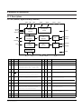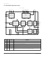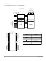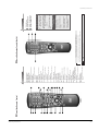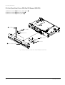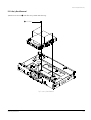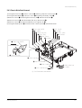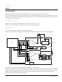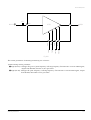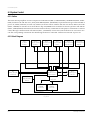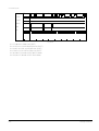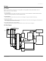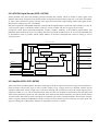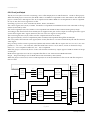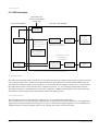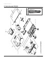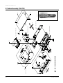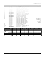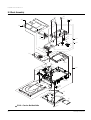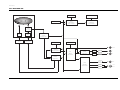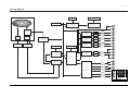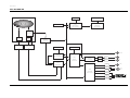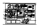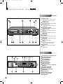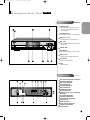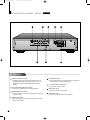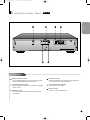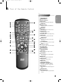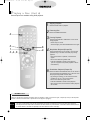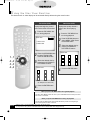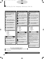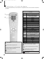
1
DVD PLAYER DVD-909 DVD-709 SERVICE MANUAL SERVICE Manual DVD-909/709 DVD PLAYER CONTENTS 1. Precautions 2. Reference Information ELECTRONICS 3. Product Specification 4. Operating Instructions 5. Disassembly and Reassembly SKIP STANDBY PHONE DVD/VIDEO-CD/CD PLAYER DVD-909 LEVEL OPEN/ OPEN/ OPEN/ CLOSE CLOSE CLOSE POWER MIN MAX ADVANCED DOLBY DIGITAL DECORDER BUILT-IN SPATIALIZER N-2-2 DIGITAL VIDEO DVD-909 6. Circuit Descriptions 7. Troubleshooting 8. Exploded Views and Parts List 9. Electrical Parts List 10. Block Diagrams SKIP STANDBY 11. PCB Diagrams DVD/VIDEO-CD/CD PLAYER DVD-709 OPEN/ OPEN/ CLOSE CLOSE POWER 24bit 96kHz AUDIO D/A CONVERTER SPATIALIZER N-2-2 DIGITAL VIDEO DVD-709 © Samsung Electronics Co., Ltd. NOV. 1999 Printed in Korea AH68-00137A REV.-2 12. Wiring Diagram 13. Schematic Diagrams 1. Precautions 1-1 Safety Precautions 1) Before returning an instrument to the customer, always make a safety check of the entire instrument, including, but not limited to, the following items: (1) Be sure that no built-in protective devices are defective or have been defeated during servicing. (1)Protective shields are provided to protect both the technician and the customer. Correctly replace all missing protective shields, including any remove for servicing convenience. (2)When reinstalling the chassis and/or other assembly in the cabinet, be sure to put back in place all protective devices, including, but not limited to, nonmetallic control knobs, insulating fish papers, adjustment and compartment covers/shields, and isolation resistor/capacitor networks. Do not operate this instrument or permit it to be operated without all protective devices correctly installed and functioning. (2) Be sure that there are no cabinet openings through which adults or children might be able to insert their fingers and contact a hazardous voltage. Such openings include, but are not limited to, excessively wide cabinet ventilation slots, and an improperly fitted and/or incorrectly secured cabinet back cover. (3) Leakage Current Hot Check-With the instrument completely reassembled, plug the AC line cord directly into a 120V AC outlet. (Do not use a isolation transformer during this test.) Use a leakage current tester or a metering system that complies with American National Standards institute (ANSI) C101.1 Leakage Current for Appliances and Underwriters Laboratories (UL) 1270 (40.7). With the instrumentÕs AC switch first in the ON position and then in the OFF position, measure from a known earth ground (metal water pipe, conduit, etc.) to all exposed metal parts of the instrument (antennas, handle brackets, metal cabinets, screwheads, metallic overlays, control shafts, etc.), especially any exposed metal parts that offer an electrical return path to the chassis. Any current measured must not exceed 0.5mA. Reverse the instrument power cord plug in the outlet and repeat the test. See Fig. 1-1. Any measurements not within the limits specified herein indicate a potential shock hazard that must be eliminated before returning the instrument to the customer. (READING SHOULD NOT BE ABOVE 0.5mA) LEAKAGE CURRENT TESTER DEVICE UNDER TEST TEST ALL EXPOSED METER SURFACES 2-WIRE CORD ALSO TEST WITH PLUG REVERSED (USING AC ADAPTER PLUG AS REQUIRED) EARTH GROUND Fig. 1-1 AC Leakage Test (4) Insulation Resistance Test Cold Check-(1) Unplug the power supply cord and connect a jumper wire between the two prongs of the plug. (2) Turn on the power switch of the instrument. (3) Measure the resistance with an ohmmeter between the jumpered AC plug and all exposed metallic cabinet parts on the instrument, such as screwheads, antenna, control shafts, handle brackets, etc. When an exposed metallic part has a return path to the chassis, the reading should be between 1 and 5.2 megohm. When there is no return path to the chassis, the reading must be infinite. If the reading is not within the limits specified, there is the possibility of a shock hazard, and the instrument must be re-pared and rechecked before it is returned to the customer. See Fig. 1-2. Antenna Terminal Exposed Melal Part ohm ohmmeter Fig. 1-2 Insulation Resistance Test Samsung Electronics 1-1 Precautions 2) Read and comply with all caution and safety related notes non or inside the cabinet, or on the chassis. 3) Design Alteration Warning-Do not alter of add to the mechanical or electrical design of this instrument. Design alterations and additions, including but not limited to, circuit modifications and the addition of items such as auxiliary audio output connections, might alter the safety characteristics of this instrument and create a hazard to the user. Any design alterations or additions will make you, the service, responsible for personal injury or property damage resulting therefrom. 4) Observe original lead dress. Take extra care to assure correct lead dress in the following areas: (1) near sharp edges, (2) near thermally hot parts (be sure that leads and components do not touch thermally hot parts), (3) the AC supply, (4) high voltage, and (5) antenna wiring. Always inspect in all areas for pinched, out-of-place, or frayed wiring, Do not change spacing between a component and the printed-circuit board. Check the AC power cord for damage. 1-2 5) Components, parts, and/or wiring that appear to have overheated or that are otherwise damaged should be replaced with components, parts and/ or wiring that meet original specifications. Additionally, determine the cause of overheating and/or damage and, if necessary, take corrective action to remove any potential safety hazard. 6) Product Safety Notice-Some electrical and mechanical parts have special safety-related characteristics which are often not evident from visual inspection, nor can the protection they give necessarily be obtained by replacing them with components rated for higher voltage, wattage, etc. Parts that have special safety characteristics are identified by shading, an ( )or a ( )on schematics and parts lists. Use of a substitute replacement that does not have the same safety characteristics as the recommended replacement part might created shock, fire and/or other hazards. Product safety is under review continuously and new instructions are issued whenever appropriate. Samsung Electronics Precautions 1-2 Servicing Precautions CAUTION : Before servicing Instruments covered by this service manual and its supplements, read and follow the Safety Precautions section of this manual. Note : If unforseen circument create conflict between the following servicing precautions and any of the safety precautions, always follow the safety precautions. Remember: Safety First. 1-2-1 General Servicing Precautions (1) a. Always unplug the instrumentÕs AC power cord from the AC power source before (1) re-moving or reinstalling any component, circuit board, module or any other instrument assembly, (2) disconnecting any instrument electrical plug or other electrical connection, (3) connecting a test substitute in parallel with an electrolytic capacitor in the instrument. b. Do not defeat any plug/socket B+ voltage interlocks with which instruments covered by this service manual might be equipped. c. Do not apply AC power to this instrument and /or any of its electrical assemblies unless all solid-state device heat sinks are correctly installed. d. Always connect a test instrumentÕs ground lead to the instrument chassis ground before connecting the test instrument positive lead. Always remove the test instrument ground lead last. (4) An insulation tube or tape is sometimes used and some components are raised above the printed wiring board for safety. The internal wiring is sometimes clamped to prevent contact with heating components. Install such elements as they were. (5) After servicing, always check that the removed screws, components, and wiring have been installed correctly and that the portion around the serviced part has not been damaged and so on. Further, check the insulation between the blades of the attachment plug and accessible conductive parts. 1-2-2 Insulation Checking Procedure Disconnect the attachment plug from the AC outlet and turn the power ON. Connect the insulation resistance meter (500V) to the blades of the attachment plug. The insulation resistance between each blade of the attachment plug and accessible conductive parts(see note) should be more than 1 Megohm. Note : Accessible conductive parts include metal panels, input terminals, earphone jacks, etc. Note : Refer to the Safety Precautions section ground lead last. (2) The service precautions are indicated or printed on the cabinet, chassis or components. When servicing, follow the printed or indicated service precautions and service materials. (3) The components used in the unit have a specified flame resistance and dielectric strength. When replacing components, use components which have the same ratings. Components i-entified by shading, by( ) or by ( ) in the circuit diagram are important for safety or for the characteristics of the unit. Always replace them with the exact replacement components. Samsung Electronics 1-3 Precautions 1-3 ESD Precautions Electrostatically Sensitive Devices (ESD) Some semiconductor (solid state) devices can be damaged easily by static electricity. Such components commonly are called Electrostatically Sensitive Devices(ESD). Examples of typical ESD devices are integrated circuits and some field-effect transistors and semiconductor chip components. The following techniques should be used to help reduce the incidence of component damage caused by static electricity. (1) Immediately before handling any semiconductor component or semiconductor-equipped assembly, drain off any electrostatic charge on your body by touching a known earth ground. Alternatively, obtain and wear a commercially available discharging wrist strap device, which should be removed for potential shock reasons prior to applying power to the unit under test. (7) Immediately before removing the protective materials from the leads of a replacement ESD device, touch the protective material to the chassis or circuit assembly into which the device will be installed. CAUTION : Be sure no power is applied to the chassis or circuit, and observe all other safety precautions. (8) Minimize bodily motions when handling unpackaged replacement ESD devices. (Otherwise harmless motion such as the brushing together of your clothes fabric or the lifting of your foot from a carpeted floor can generate static electricity sufficient to damage an ESD device). (2) After removing an electrical assembly equipped with ESD devices, place the assembly on a conductive surface such as aluminum foil, to prevent electrostatic charge buildup or exposure of the assembly. (3) Use only a grounded-tip soldering iron to solder or unsolder ESD devices. (4) Use only an anti-static solder removal devices. Some solder removal devices not classified as Òanti-staticÓ can generate electrical charges sufficient to damage ESD devices. (5) Do not use freon-propelled chemicals. These can generate electrical charges sufficient to damage ESD devices. (6) Do not remove a replacement ESD device from its protective package until immediately before your are ready to install it.(Most replacement ESD devices are packaged with leads electrically shorted together by conductive foam, aluminum foil or comparable conductive materials). 1-4 Samsung Electronics Precautions 1-4 Handling the optical pick-up The laser diode in the optical pick up may suffer electrostatic breakdown because of potential static electricity from clothing and your body. WRIST-STRAP FOR GROUNDING 1M The following method is recommended. (1) Place a conductive sheet on the work bench (The black sheet used for wrapping repair parts.) (2) Place the set on the conductive sheet so that the chassis is grounded to the sheet. (3) Place your hands on the conductive sheet(This gives them the same ground as the sheet.) (4) Remove the optical pick up block (5) Perform work on top of the conductive sheet. Be careful not to let your clothes or any other static sources to touch the unit. THE UNIT 1M CONDUCTIVE SHEET Fig.1-3 (6) Short the short terminal on the PCB, which is inside the Pick-Up ASSÕY, before replacing the PickUp. (The short terminal is shorted when the PickUp AssÕy is being lifted or moved.) (7) After replacing the Pick-up, open the short terminal on the PCB. 3 Be sure to put on a wrist strap grounded to the sheet. 3 Be sure to lay a conductive sheet made of copper etc. Which is grounded to the table. Samsung Electronics 1-5 Precautions 1-5 Pick-up disassembly and reassembly 1-5-1 Disassembly 1-5-2 Assembly 1) Remove the power cable. 2) Switch SW3 on deck PCB to ÒOFFÓ before removing the FPC. ( Inserted into Main PCB CN6. See Fig. 1-4) 3) Disassemble the deck. 4) Disassemble the deck PCB. 1) Replace the Pick-up. 2) Assemble the deck PCB. 3) Reassemble the deck. 4) Insert FPC into Main PCB CN6 and switch SW3 on deck PCB to ÒONÓ. (See Fig 1-4) Note : If the assembly and disassembly are not done in correct sequence, the Pick-up may be damaged. FPC SW3 OFF TO MAIN PCB (CN6) ON Fig. 1-4 1-6 Samsung Electronics 2. Reference Information 2-1 IC Dsecriptions 2-1-1 AIC1 (AK4324 ; Digital-to-Analog Converter) DIF0 LRCK BICK SDATA DIF1 DIF2 DEM0 AVDD AVSS De-emphasis Control Serial Input Interface PD DEM1 DZFL AOUTL+ 8X Interpolator ∆∑ Modulator SCF 8X Interpolator ∆∑ Modulator SCF AOUTL- SMUTE DFS AOUTR+ AOUTR- Clock Divider DZFR MCLK PIN I / O NAME CKS DVDD FUNCTION DVSS VREF PIN I / O NAME FUNCTION 13 I DIF0 Digital input format pin 1 - DVSS Digital ground pin 2 I DVDD Digital power supply 14 I DIF1 Digital input format pin 3 I CKS Master clock select pin (Internal pull-down pin) Nomal speed "L":MCLK = 256fs, "H":MCLK = 384fs Double speed "L":MCLK = 128fs, "H":MCLK = 192fs 15 I DIF2 Digital input format pin 4 I MCLK Master clock input pin 16 0 AOUTR- Rch negative analog output pin 5 I PD Power-Down mode pin. When at "L", the AK4324 is in power-down and is held in rest. The AK4324 should always be reset upon power-pin 17 O AOUTR+ Rch positive analog output pin 6 I BICK Audio serial data input pin 64fs clock is recommended to be input on this pin 18 O AOUTL- Lch negative analog output pin 7 I SDATA Audio serial data input pin 2's complement MSB-first data is input on this pin. 19 O AOUTL+ Lch positive analog output pin 8 I LRCK L/R clock pin. 20 - AVSS Analog ground pin 9 I SMUTE Soft mute pin When this pin goes "H", soft mute cycle is initiated When returning "L", the output mute releases. 21 O VREF Voltage reference input pin 10 I DFS Double speed sampling mode pin (Internal pull-down pin) "L":normal speed, "H":double speed 22 O AVDD Analog power supply pin. 11 I DEM0 De-emphasis frequency select pin 23 O DZFR Rch zero input detect pin 12 I DEM1 De-emphasis frequency select pin 24 O DZFL Lch zero input detect pin Note : Allinput pins except internal pull-down pins should not be left floating. Samsung Electronics 2-1 Reference Information 2-1-2 RIC1 (KS1461 ; RF) 83 82 81 80 79 78 77 76 AGC-HOLD(OOH) ADVD 5 AGC_DET RF MUX BCA BLOCK 74 BCAI RF Equalizer RF SLM & AGC C D BCA RFRP GAIN_EQ(02H) CDRSEL(00H) TE1RES DELAY_SEL(OOH) PLLCTL TBAL(O1H) RREFEQ 10 VREF GENERATOR DELAY D GCA RREF 11 CD1 S12 DVD1 DVD2 LDONB FLT_CTL CDRSEL TESEL AGC-HOLD TBAL GAIN_TE3 ENV_SEL DVCTL_SEL DPD_MUTE GAIN_EQ GAIN_FE GAIN_ABCD TE_OFST FE_OFST ABCD_OFST DELAY_CD DELAY_AB PDLIMIT ga_RFSUM HOLD_CTL ga_PLLDP ga_PLLDN HOLD_CTL(O8H) DPDMUTE DPD_MUTE(O2H) SEOFHOLD FLT_CTL(OOH) CAL_ENDB(O2H) DPDEQ1 9 PD,LPF COM EQ D TEOPST(04H) MUX3 PDLIMITRES TE1_LIMIT D GCA COM EQ D DPDEQ2 FAULTOUT VREFEQ 12 EQ VC AMP GAIN_TE3(02H) E 13 DELAY_SEL(00H) PLLCTL TE38 F 14 AUTO OFSTCTL RFCT & MIRR CD1 S12 DVD1.2 RREFBF CB 2 84 RFCT 85 CP 2 86 RFRP 87 RFRPN 88 CB 1 B 8 89 MROFST A 4 DDVD CP 1 3 DCD 7 MIRRI 2 6 90 75 BCAO BCD BDVD 91 MUX CCD CDVD EQVCC 1 RFEQO ACD BCATH EQGND to RF EQ TUNING BLOCK EQIN AGCLEVEL 92 RFAGCO AGCB 93 AGCI AGCP 94 AGCC RDPF 95 EQF PLLGF 99 98 97 96 EQG VZOCTL 100 72 OSC 71 STB S/IF BLOCK 70 CLOCK 69 DATA 68 RREFDLY DPD BLOCK 67 VREFDPD 66 DPDGND 65 TE1RES GCA 64 PLLCTL OFSTHOLD TBAL(01H) TEOFST(04H) 63 DPDMUTE to DPD BLOCK 62 FAUL TOUT CDRSEL(OOH) GAIN_ABCD(OOH) ADVD1 15 61 DPDEQ2 60 DPDEQ1 BDVD1 16 CDVD1 17 DDVD1 18 SUB RF MUX ACD1 19 BCD1 20 D1 B1 C1 A1 ABCD SUM EQIN 59 TE30FST ENV_SEL(02H) GAIN_FE(03H) 58 BCA 57 MIRR OFSTHOLD MUX CCD1 21 ABCD_OFST(O6H) FE 56 DPDVCC FE_0FST(05H) DCD1 22 OFSTHOLD AVCC 23 VREFA 24 73 RESET CDRSEL(00H) LDONB(00H) ANALOG VC AMP 55 DFCT2 MUX 54 DFCT1 TESEL(OOH) ENVELOPE FOK 53 DFCTTH1 DEFECT 52 DFCTTH2 ALPC FOFST 25 FOFST 35 36 37 38 39 40 41 42 43 44 45 46 47 48 49 50 VREFLP_BGI LDODVD AGND FE FEN TEN TE PDLIMITRES ABCD ABCDI ENVP DGND FOKTH FOKB DFCT_CP1 DFCT_CP2 CC1 CC2 ENV 34 ENVB 33 ABCDN 32 PDCD 28 29 30 31 LDOCD 27 PDVD 26 OFSTHOLD 2-2 51 DVCC Samsung Electronics Samsung Electronics CD optical main beam F input port for SERVO CD optical main beam F input port for SERVO Power voltage input port for analog part CD optical laser monitor diode voltage input port Power GND port for analog part FE AMP output port I I P -/O O I I O I O I P O CCD1 DCD1 AVCC VREFA FOFST OFSTHOLD VREFLP_BGI LDODVD PDDVD LDOCD PDCD AGND FE 21 22 23 24 25 26 27 28 29 30 31 32 33 FEN FOKTH FOKB 45 46 DVCC DVCTTH2 51 52 BCA TE3OFST DPDEQ1 DPDEQ2 58 59 60 61 CD optical laser diode driving voltage output port DVD optical laser monitor diode voltage input port DVD optical laser diode driving voltage output port BANDGAP voltage input port for ALPC 64 63 PLLCTL DPDMUTE FAULTOUT MIRR 57 ON/OFF connection port for auto offset block (L : auto offset adjustment H : serial offset adjustment) 62 DPDVCC 56 center voltage, Use at other block CAP connection port for focus auto offset (OPEN) DFCT1 DFCT2 54 DFCTTH1 CC2 50 53 CC1 DFCT_CP2 49 48 DFCT_CP1 DGND 44 47 ENV ENVB ENVP ABCDI ABCD ABCDN PDLIMTRES TE TEN 43 42 41 40 39 38 37 36 35 34 PIN NAME 55 CAP connection port for analog part CD optical main beam F input port for SERVO I DVD optical main beam C input port for SERVO I BCD1 DVD optical main beam B input port for SERVO I 20 DVD optical main beam A input port for SERVO I CD optical main beam F input port for SERVO CD optical sub beam F input port for SERVO I I CD optical sub beam E input port for SERVO I ACD1 CAP connection port for RF EQ center voltage O 19 Analog block bias resistance connection port - DVD optical main beam D input port for SERVO RF EQ bias resistance connection port - I RF AMP I/O buffer bias resistance connection port - DDVD1 DVD optical main beam D AC coupling input port for RF I 18 DVD optical main beam C AC coupling input port for RF I CDVD1 DVD optical main beam B AC coupling input port for RF I 17 DVD optical main beam A AC coupling input port for RF I BDVD1 CD optical main beam D AC coupling input port for RF I 16 E 13 CD optical main beam C AC coupling input port for RF I F VREFEQ 12 CD optical main beam B AC coupling input port for RF I ADVD1 RREF 11 CD optical main beam A AC coupling input port for RF I 15 RREFEQ 10 FUNCTION I/O 14 RREFBF BDVD 6 9 ADVD 5 CDVD DCD 4 DDVD CCD 3 8 BCD 7 ACD 1 2 PIN NAME BCA output port Resistance connection port for 3BTE offset DPD EQ (A+C) output port DPD EQ (B+D) output port O O O I I DPD TE PLL variable input port DPD TE MUTE control port (H : MUTE) DPD defect waveform output port (MONITOR) Mirror output port O Power voltage input port for DPD TE P Defect output port for SERVO parating level setting ing level setting Resistance connection port for SERVO defect com- Resistance connection port for PLL defect comparat- Power voltage input port for digital circuit AC coupling input port for defect Output port of peak detector for defect min. time setting (L: FOCUS OK) Peak hold time constant connection port SERVO defect max. time setting Peak hold time constant connection port PLL defect Focus OK comparator output port Focus OK comparing level input port Power GND input port for digital circuit RF envelope detect output port 95 94 93 92 91 90 AGCP AGCB AGCLEVEL EQGND AGCI AGCC RFAGCO EQIN 88 89 BCATH RFEQO EQVCC MIRRI CP1 CB1 MROFST RFRPN RFRP CP2 CB2 RFCT BCAO BCAI 87 86 85 84 83 82 81 80 79 78 77 76 75 74 RESET 73 connection port for RF envelope detect OSC 72 STB CLOCK DATA RREFDLY VREFDPD 71 Defect output port for PLL O TE1RES DPDGND ABCD AC coupling input port for SERVO monitor 70 69 68 67 66 65 PIN NAME Peak hold time constant setting RC connection port for RF envelope detect Bottom hold time constant setting RC ABCD AMP output port Input port for ABCD AMP GAIN setting Bias resistance port for PDLIMIT TE AMP output port Input port for TE AMP GAIN setting FE Input port for AMP GAIN setting FUNCTION O O - - P I O - - O I P O - - I O I - O I I I/O - - I P I - RF peak hold time constant RC connection port for RF AGC RF bottom hold time constant RC connection port for RF AGC AGC level control voltage input port Power GND input port for RF EQ When AGC is “HOLD”, AGC voltage input port AGC time constant CAP connection port RF AGC AMP output port RFAGCO input port for RF EQ O BCA comparating level control port I RF EQ output port Power voltage input port for RF EQ Input port for MIRR signal generation RFCT generation Peak hold time constant RC connection port for RFCT generation Bottom hold time constant RC connection port for RF ripple offset control port for mirror RF ripple AMP GAIN input port for mirror RF ripple AMP output port for mirror Bottom hold time constant RC connection port for RFCT generation Peak hold time constant RC connection port for RFCT generation RF ripple center voltage output port for mirror BCA FILTER2 BCA FILTER1 Reset input port for auto offset block (L : RESET) OSC time constant input port for auto offset block Data enable input port Clock input port Data input port Bias resistance connection port for delta block CAP connection port for DPD TE center Power GND input port for DPD TE DPD TE PLL variable bias resistance FUNCTION I O P I - - I I O - - O O I I I I I - O P I I/O 100 VZOCTL PLLGF EQF 98 99 EQG RDPF 97 96 PIN NAME RF EQ control port (When No. PLLG isn’t adjusted, apply DC CTL voltage.) RF EQ peak frequency control voltage input port I I RF EQ boost gain control voltage input port I RF EQ boost, peak frequency gain control port corresponding to wideband PLL (PLLG. PLLF resistance internal design) Bias resistance connection port for RF EQ frequency setting - I FUNCTION I/O Reference Information 2-3 2-4 EFMOA EFM ASYCD ASYDVD RFI EFMI DVCTL TBAL FBAL SPD SLD TRD FOD RSTB COUT TILTO FE EFM ASYMETRY D/A CONVERTER BLOCK TRACK COUNTER ROM DSP CORE FOR DIGITAL SERVO PS1 WIDE CAPTURE RANGE PLL SYSCON INTERFACE BLOCK SUB CODE READ BLOCK SSTOP /PSO TE TEST SME XI A/D CONVERTER BLOCK XO TZCO XOUT I/O INTERFACE BLOCK LOCK TIMING GENERATOR SMON ENV VREF PLLHD INTO_224 FDCTL MAGICO EQCTL VCTRL RVCO PLCK EFMRTD RPD PLLLOCK RFD MDOUT[3:0] PSB SENSE MDATA[7:0] MRDB MWRB CSB DAB SCOR SQSI SQCK LDONB TLKB FLKB Reference Information 2-1-3 SIC1 (KS1452 ; Digital Servo) DIRC DFCT FOKB MIRR TZCA PHI1 TILTI Samsung Electronics Samsung Electronics Micom data pin 2 Micom data pin 3 Micom data pin 4 Micom data pin 5 Micom data pin 6 Micom data pin 7 Internal status monitor pin Servo logic & ROM VDD power supply pin System clock signal input pin System clock signal output pin Clock out (33.9688MHz) to DSP Servo logic & ROM VSS power supply pin Clock output pin for subcode data read Subcode data input pin Timing detection input pin for subcode data read Motor ON signal input pin Lock signal input pin Direct jump control (for 1 track jump) I/O I/O I/O I/O I/O I/O O P I O O P O I I I I I XOUT DVSS SQCK SQSI 25 26 27 28 29 DIRC XO 24 33 XI 23 LOCK DVDD 22 32 SENSE 21 SCOR MDATA7 20 SMON MDATA6 19 31 MDATA5 18 30 MDATA3 MDATA4 17 MDATA2 16 Micom data pin 1 I/O MDATA1 Micom data pin 0 15 Micom read clock signal input pin I I/O MRDB Micom write clock signal input pin I MWRB 12 MDATA0 Micom data/address select pin I DAB 11 14 Micom chip select pin I CSB 13 System reset signal input pin I RSTB 9 10 1 : 8BIT 0 : 1BIT I PSB 8 Tracking servo lock signal output pin O TLKB Focus servo lock signal output pin O 7 Counter clock FLKB Test pin (L : normal H : test) I O 6 Sled motor position sensor input pin 1 I TEST Limit switch/sled position sensor input pin0 I COUT 3 Mode data3 out controlled by micom O FUNCTION 5 PS1 2 I/O 4 MDOUT3 SSTOP/PSO 1 PIN NAME 64 63 62 61 60 59 58 57 56 55 54 53 52 51 50 49 48 47 46 45 44 43 42 41 40 39 38 37 36 35 34 TE VREF SME AVSS SVSS RFI LPFCD LPFDVD EFMO EFMI EQCTL SVDD TZCO EFMOA MAGICO VCTL RPD RFD RVCO PVSS EFMRTD PLLLOCK PLCK PVDD INTO_224 PLLHD MIRR DFCT LDONB FDCTL FOKB PIN NAME I I I P P I I I O I O P O I I I I I I P O O O P O I I I O I I I/O Tracking error signal input pin Reference voltage input pin Spindle error input pin Analog block VSS power supply pin Servo CPU VSS power supply pin RF input signal Asymmetric input signal for CD Asymmetric input signal for DVD EFM signal EFM signal for test EQ control signal Servo CPU VDD power supply pin Tracking zero cross output pin EFM offset adjustment pin Input for hysteresis control of FD output (for test) Control voltage for VCO Gain adjust resister for phase detector Gain adjust resister for frequence detector Resistor pin for VCO GAIN PLL logic block VSS power supply pin Latched EFM output signal (H : Lock L : Unlock) Frequency lock detect output PLCK PLL logic block VDD power supply pin Servo interrupt monitor pin PLL hold signal from micom Mirror signal input pin Defect Detection signal input pin Laser diode ON signal output pin PLL frequency detect control input pin Focus OK signal input pin FUNCTION 72 71 70 69 68 67 66 65 FBAL TBAL DVCTL TILTO AVDD TILTI ENV FE PIN NAME O O O O P I I I I/O Focus balance signal output pin Tracking balance signal output pin Depth variation control signal output pin Tilt out (reserved) Analog block VDD power supply pin Tilt in (reserved) RF envelope input pin Focus error signal input pin FUNCTION TRD TZCA MDOUT0 MDOUT1 MDOUT2 78 79 80 75 77 FOD 74 76 SLD SPD 73 PIN NAME Mode data 1 out controlled by micom Mode data 2 out controlled by micom O O Tracking actuator drive signal output pin O TE signal for tracking zero cross input pin Focus actuator drive signal output pin O Mode data 0 out controlled by micom Spindle motor drive signal output pin O O Sled motor drive signal output pin O I FUNCTION I/O Reference Information 2-5 2-6 FG MON MDP MDS FSW PLL_LOCK CLV_LOCK SERVO_LOCK XTI1 XTO1 CK33MI CK33MO TO (12) EFMI PLCK BCARZ FROM R/F, PLL(3) CD CLV/CAV WFCK 17.58/7.35KHz M SUBCODE I/F 23BIT SR CD-G M SQ-VCD DVDP, MICOM I/F M TEST0, TEST1, TEST2 V-CD, CD-DA DEINTERLEAVE & RAM CONTROL (6, 4, 3) trans ID ECC EDC DESCRAMBLER TO MICOM (15) MDAT(7:0), MRZA, ZCS, MWR, MRD, ZIRQZD, ZWAIT, ZRST Power(34)=VDD(11)+GND(23) Test Pin(3) EFM DEMOD (32, 28, 5) (28, 24, 5) CIRC 75Hz 676.08Hz (208, 192, 17) (182, 172, 11) ECC (6, 4, 3) efmwr ID ECC 16-8 DEMOD FRAME SYNC DET/PROT/INS (7.35KHz) VCO TIMING GENERATOR 7.35KHz = 4.3218M/588 17.58KHz = 26.16M/1488 ECSY Monitor(8) GFS, FRSYZ, TX, EFMO, WFCK, RFCK, CK 16M, DEMPHA M DVD CLV/CAV RFCK 17.58/7.35KHz X'TAL & TIMING GEN VCO TIMING GENERATOR 26.16MHz FRAME SYNC DET/PROT/INS (17.57KHz) 32BIT SR PWMO(7:0) TO D-EQ (8) SDATA[0] / CDATA SDATA[1] / LRCK SDATA[2] / BCLK SDATA[3] / C2PO SDATA[4] / SQDT SDATA[5] / WFSY SDATA[6] / SOS1 SDATA[7] / SQCK DATREQ CSTROBE DTER DATACK TOS TO AV (13) DD(15:0) DADR(8:0) ZRAS ZUCAS ZLCAS ZOE(1:0) ZWE(1:0) TO DRAM 256K*16 (32) Reference Information 2-1-4 DIC1 (KS1453 ; DVD Data Processor) Samsung Electronics Samsung Electronics DD5_BI DVSS DD9_BI 31 32 20 DD10_BI DD1_BI 19 30 DD14_BI 18 29 DD0_BI 17 DD4_BI DD15_BI 16 28 DVSS 15 DD11_BI XTO_OUT 14 27 XTI_IN 13 DVDD DVDD 12 DD3_BI MDAT0_BI 11 26 MDAT1_BI 10 25 MDAT2_BI 9 DD12_BI MDAT3_BI 8 24 MDAT4_BI 7 DD2_BI MDAT5_BI 6 23 MDAT6_BI 5 DVSS MDAT7_BI 4 DD13_BI DVSS 3 21 MRZA_IN 2 22 DVSS ZCS_IN 1 NAME PIN DRAM data bus Digital GND (0V) DRAM data bus DRAM data bus DRAM data bus DRAM data bus Digital power (+5V) DRAM data bus DRAM data bus DRAM data bus DRAM data bus Digital GND (0V) DRAM data bus DRAM data bus DRAM data bus DRAM data bus Digital GND (0V) System clock output for 26.16 MHz System clock input for 26.16 MHz Digital power (+5V) Micom data bus Micom data bus Micom data bus Micom data bus Micom data bus Micom data bus Micom data bus Micom data bus Digital GND (0V) (L -> Register H -> Data) Micom register select Chip select (Active Low) Digital GND (0V) FUNCTION 65 64 63 62 61 60 59 58 57 56 55 54 53 52 51 50 49 48 47 46 45 44 43 42 41 40 39 38 37 SDATA5_OUT SDATA4_OUT SDATA3_OUT SDATA2_OUT SDATA1_OUT SDATA0_OUT DVDD DATACK_OUT TOS_OUT DVSS DVSS DADR3_OUT DADR4_OUT DADR2_OUT DADR5_OUT DADR1_OUT DADR6_OUT DADR0_OUT DVSS DADR7_OUT DADR8_OUT ZRAS_OUT ZOEO_OUT DVDD ZOE1_OUT ZWE0_OUT ZWE1_OUT ZUCAS_OUT ZLCAS_OUT DVSS DD7_BI 35 36 DD8_BI DD6_BI NAME 34 33 PIN DVD data/Sub code frame sink (WFSY) DVD data/Sub code serial data (SQDT) DVD data/CD data error flag (C2P0) DVD data/CD data bit clock (BLCK) DVD data/CD data L/R clock (LRCK) DVD data/CD data bitstream output Digital power (+5V) Data acknowledge signal output Top of sector Digital GND (0V) Digital GND (0V) DRAM address bus DRAM address bus DRAM address bus DRAM address bus DRAM address bus DRAM address bus DRAM address bus Digital GND (0V) DRAM address bus DRAM address bus DRAM row address strobe DRAM output enable 0 Digital power (+5V) DRAM output enable 1 (16M, --------, 16M) DRAM write enable 0 (4M, 8M, 16M) DRAM write enable 1 (8M ONLY) DRAM upper column address strobe DRAM row column address strobe Digital GND (0V) DRAM data bus DRAM data bus DRAM data bus FUNCTION 97 96 95 94 93 92 91 90 89 88 87 86 85 84 83 82 81 80 79 78 77 76 75 74 73 72 71 70 69 68 67 66 PIN DVSS CK33MO_OUT CK33MI_IN DVSS GFS_OUT TX_OUT FRSYZ_OUT DVSS DVSS DVSS DVSS DVDD DVDD DVSS DVSS DVSS PWM00_OUT PWM01_OUT PWM02_OUT PWM03_OUT DVDD PWM04_OUT PWM05_OUT PWM06_OUT PWM07_OUT DVSS DTER_OUT DATREQ_IN CSTROBE_OUT DVSS SDATA7_BI SDATA6_OUT NAME Digital GND (+5V) System clock output for 33.8688MHz System clock input for 33.8688MHz Digital GND (0V) active) Good frame sync detection result output (“H” Digital out Frame sync out Digital GND (0V) Digital GND (0V) Digital GND (0V) Digital GND (0V) Digital power (+5V) Digital power (+5V) Digital GND (0V) Digital GND (0V) Digital GND (0V) PWM output signal PWM output signal PWM output signal PWM output signal Digital power (+5V) PWM output signal PWM output signal PWM output signal PWM output signal Digital GND (0V) DVD data error output Data request from A/V decoder or ROM decoder Data strobe (clock) output Digital GND (0V) DVD data/Sub code serial clock (SQCK) DVD data/Sub code block sink (S0S1) FUNCTION 128 127 126 125 124 123 122 121 120 119 118 117 116 115 114 113 112 111 110 109 108 107 106 105 104 103 102 101 100 99 98 PIN MWR_IN MRD_IN ZIRQZD_OUT ZWAIT_OUT ZRST_IN DVSS BCARZ_IN DEMPHA_OUT CK16M_OUT DVDD DVDD DVDD EFMI_IN FSW_OUT FG_IN MON_OUT DVSS DVSS MDS_OUT MDP_OUT SERLOCK_OUT CLVLOCK_OUT PLLLOCK_OUT DVSS PLCK_IN RFCK_OUT WFCK_OUT EFMO_OUT TEST2_IN TEST1_IN TEST0_IN NAME Micom write strobe (schmidt trigger) Micom read strobe (schmidt trigger) Interrupt request from micom Micom read/write access wait (“L” wait) Hardware reset active low Digital GND (0V) BCA input signal When DEEMPHASIS is ON, “HIGH”. 2∫–¡÷ clock of CK33M/16.934MHz Digital power (+5V) Digital power (+5V) Digital power (+5V) EFM/EFM+ signal input Spindle motor output filter conversion output (3state) Reference signal for CAV Spindle motor ON/OFF control output Digital GND (0V) Digital GND (0V) Spindle motor speed control signal (3-state) (3-state) Spindle motor phase control signal Lock signal for SERVO Lock signal for CLV Lock signal for PLL Digital GND (0V) Phase locked clock Reference frame pulse Write frame pulse EFM out Test mode setting port Test mode setting port Test mode setting port FUNCTION Reference Information 2-7 Reference Information 2-1-5 DIC2 (KM416C254BJ-6 ; CMOS DRAM) BLOCK DIAGRAM RAS UCAS Control LCAS Clocks Vcc VBB Generator Vss W Refresh Timer Row Decoder Lower Data in Buffer Refresh Control Lower DQ0 to DQ7 Data out Memory Array Refresh Counter Buffer 262,144 x 16 Upper Cells Data in Buffer Row Address Buffer AO . . Upper OE DQ8 to DQ15 Data out Col. Address Buffer A8 Column Decoder FUNCTION NAME A0-A8 DQ0-15 Address Inputs Data in/Out VSS Ground RAS Row Address Strobe UCAS Upper Column Address Strobe LCAS Lower Column Address Strobe W Read/Write Input OE Data Output Enable V CC Buffer Power (+5V) Power (+3.3V) N.C 2-8 No Connection Samsung Electronics Reference Information 2-1-6 VIC1 (ZiVA-3 ; Audio/Video Decoder) BLOCK DIAGRAM ZiVA-3 Decoder OSD Decoder SDRAM/ EDO/ROM Interface Memory Controller Subpicture Decoder Host Interface Host Interface Control Logic MPEG Video Decoder Secure View CD-DA and LPCM Decoder CSS Descrambling Program DVD/CD Interface Stream Decoder Bus Key Dolby Digital Audio Decoder Authentication (Optional) Audio DSP Video Mixer Video Interface Digital Audio Interface Audio Interface Scrambled, Compressed Content Descrambled, Compressed Content MPEG Audio Decoder Decompressed Content Display Content LOGIC DIAGRAM DA-DATA[0:3] CS Host Interface Signals DTACKSEL DA-LRCK HADDR[2:0] DA-BCK Interface RD DA-XCK Signals DA-IEC HDATA[7:0] WAIT/DTACK INT EDO-CAS HOST8SEL EDO-RAS R/W Video Audio LDQM VDATA[7:0] MDATA[15:0] Interface HSYNC MADDR[20:0] Signals VSYNC MWE VCLK ROM-CS SDRAM/EDO Interface Signals SD-CAS DVD-DATA0/CD-DATA SD-RAS DVD-DATA1/CD-LRCK SD-CLK DVD-DATA2/CD-BCK SD-CAS[1:0] DVD-DATA3/CD-C2PO UDQM DVD-DATA4/CDG-SDATA DVD/CD Interface Signals DVD-DATA5/CDG-VFSY DVD-DATA6/CDG-SOS1 SYSCLK DVD-DATA7/CDG-SCLK VDD VSS VREQUEST A_VSS VSTROBE A_VDD ERROR AREQUEST Samsung Electronics Interface Signals P10[10:0] V-DACK/ASTROBE A-DACK Global RESET ZiVA Decoder 2-9 Reference Information 2-1-7 VIC50 (SAA7128 ; Digital Video Encoder) BLOCK DIAGRAM LLC1 VDDA XCLK TTXRQ RCV2 RCV1 XTAL XTALI SCL SDA RESN 25,28,31,36 4 37 8 43 7 34 35 41 42 40 20 VDD I2C 21 I2 C- SYNC/ INTERFACE CLOCK SA Clock&Timing I2 C-Control I2 C-Control 9..16 I2 C-Control Y Y MP MP(7:0) FADER CbCr D 30 CVBS (CSYNC) 27 VBS (CVBS) 24 C (CVBS) OUTPUT- ENCODER C MP INTERFACE A 44 I2 C-Control TTX 22,32,33 I2 C-Control VSSA 23 Y D R(Cr) RGBCbCr G(Y) 29 B(Cb) 19 RTC1 AP SP FUNCTION NAME res. 1 3 2 VDD VSS I/O 26 A 6,17,39 5,18,38 PIN PROCESSOR Reserved pin, do not connect 2 I SP Test Pin;connected to digital ground for normal operation 3 I AP Test Pin;connected to digital ground for normal operation 4 I LLC1 Line-Locked Clock input;this is the 27 MHz master clock 5 I V SS1 Digital supply ground 1 6 I V DD1 Digital supply 1 7 I/O RCV1 Raster Contral 1 for video port. This pin receives/provides a VS/FS/FSEQ signal. 8 I/O RCV2 Raster Contral 2 for video port. This pin provides an HS pulse of programmable length or receives an HS pulse. 2-10 Samsung Electronics Reference Information PIN I/O 9 I MP7 10 I MP6 11 I MP5 12 I MP4 13 I MP3 14 I MP2 15 I MP1 16 I MP0 17 I V DD2 Digital supply voltage 2 18 I V SS2 Digital ground 2 19 I RTCI 20 I 21 I SA 22 I V SSA1 Analog ground 1 for Red (Cr), C(CVBS), Green(Y) outputs 23 O R(Cr) Analog output of Red (Cr)signal 24 O C 25 I V DDA1 Analog supply voltage 1 for R(Cr), C(CVBS) outputs 26 O G(Y) Analog output of Green(Y) signal 27 O VBS Analog output of VBS (CVBS) signal 28 I V DDA2 Analog supply voltage 2 for VBS(CVBS), Green(Y) outputs 29 O B(Cb) Analog output of Blue(Cb) signal 30 O CVBS Analog output of CVBS(CSYNC) signal 31 I V DDA3 Analog supply voltage 3 for Blue(Cb)and CVBS(CSYNC), outputs 32 I V SSA2 Analog ground 2 for VBS (CVBS), Blue(Cb), CVBS(CSYNC)outputs 33 I V SSA3 Analog ground 3 for the DAC reference ladder and the oscillator 34 O XTAL Crystal oscillator output 35 I XTAL1 36 I V DDA4 Analog supply voltage 4 for the DAC reference ladder and the oscillator 37 O XCLK Clock output of the crystal oscillator 38 I V SS3 Digital supply ground 3 39 I V DD3 Digital supply 3 40 I RESN 41 I SCL 12C serial clock input 42 I/O SDA 12C serial data input/output 43 O TTXRQ 44 I TTX Samsung Electronics FUNCTION NAME VDD 12C Double speed 54 MHzMPEG port. It is an input for "CCIR 656" style multiplexed Cb, Y, Cr data. Data are sampled on the rising and falling clock edge;data sampled on the risting edge then are sent to the encoding part of the device, data sampled on the falling edge are sent to the RGB part of the device. (or vice verse, depending on programming) Real Time Control input. If the LLC1 clock is provided by an SAA7111 or SAA7151B, RTCI should be connected to the RTCO pin of the respective decoder to improve the signal quality. Sense input for 12C bus voltage;connect to 12C bus supply Select 12C address; low selects slave address 88h, high selects slave address 8Ch. Analog output of Chrominance (CVBS) signal Crystal oscillator input; if the oscillator is not used, this pin should be connected to ground. Reset input, active LOW. After reset is applied, all digital I/Os are in input mode; PALBlackburst on CVBS, VBS and C;RGB outputs set to lowest voltage. The 12C-bus receiver waits for the START condition. Teletext Request output, indicating when text bits are requested Teletext bit stream input 2-11 Reference Information 2-1-8 MIC1 (TMP93CM41F ; Main Micom) PAO~PA6 PA7(SCOUT) PORT A VCC[3] VSS[3] 900L-CPU P50 to P57 (ANO to AN7) AVCC AVSS VREFH VREFL 10-BIT 8CH A/D CONVERTER XWA XBC ADE XHL XIX XIY XIZ XSP W B D H A C E L (TXD1)P93 (RXD1)P94 (SCLK1)P95 SERIAL I/O OSC IX IY IZ SP 32bit (TXD0)P90 (RXD0)P91 (SCLK0/CTS0)P92 High Frequency SR (CH,0) P C CLK Low F Frequency OSC SERIAL I/O (CH,1) INTERRUPT (PG 00)P60 (PG 01)P61 (PG 02)P62 (PG 03)P63 (PG 10)P64 (PG 11)P65 (PG 12)P66 (PG 13)P67 (T10)P70 X1 X2 XT1 XT2 AM8/16 EA RESET ALE TEST2,1 CONTROLLER NMI WATCH-DOG WDTOUT PATTERN GENERATOR (CH,0) PATTERN TIMER GENERATOR (CH,1) 2KB RAM PORT 0 P00 to P07 (AD0 to AC7) PORT 1 P10 to P17 (AD8 to AD15/A8 toA15 PORT 2 P20 to P27 (A0 to A7/A16 to A23) 8BIT TIMER (TIMER 0) 8BIT TIMER (T01)P71 (T02)P72 (TIMER 1) 8BIT PWM (TIMER 2) (T03)P73 8BIT PWM (TIMER 3) PORT 3 (INT4/T14)P80 (INT5/T15)P81 (T04)P82 (T05)P83 (INT6/T16)P84 (INT7/T17)P85 (T06)P86 16BIT TIMER (TIMER 4) P30(RD) P31(WR) P32(HWR) P33(WAIT) P34(BUSRQ) P35(BUSAK) P36(R/W) P37(RAS) 16BIT TIMER (TIMER 5) CS/WAIT CONTROLLER (3-BLOCK) P40(CS0/CAS0) P41(CS1/CAS1) P42(CX2/CAS2) (INTO)P87 2-12 Samsung Electronics Samsung Electronics MC AM8 CLK VCC GND X1 X2 /EA SCLK1 AM8/16 CLK Vcc Vss X1 X2 /EA /RESET 22 23 24 25 26 27 28 29 30 /MRST STB 094 21 RF control data O MD TXD1 20 Serial data clock I SCLK SCLKO Serial data input 19 Serial data output I TXD O RXD TXDO RXDO Interrupt from DSP I ZINT INTO 16 18 45 Request to front micom O RRQ P86 15 17 44 I - INT7 14 Interrupt from spindle motor FG I FGINT /INT6 13 Close switch I CLOSE P83 12 Open switch I OPEN 52 RF control clock Address mode (H: 8 bit mode) Clock output (System clock÷2) O I O High frequency OSC out External access CS41/CS40 O I Master reset from FRONT High frequency OSC in I I 56 GND - 60 59 58 57 55 - 54 53 51 I/O RF data latch 50 49 48 47 46 43 42 41 40 39 P82 Interrupt from front micom I 38 11 Interrupt from AV-DEC I SRQ Open/close blinking O 37 36 INT5 AV-DEC H/W reset O 10 Master clock select O 35 34 LED DSP H/W reset DVDINT Non-maskable interrupt I O 33 P73 A/D VCC input - 32 31 /INT4 A/D GND input No 9 A/D Ref input (L) I - FUNCTION 8 MCK_SEL ZIVA_RST P70 5 P71 /NMI 4 P72 - ZRST AVcc 3 7 AVCC AVss 2 6 GND AGND VREFL 1 ASSIGNED I/O NAME PORT NAME No A15 A14 A13 A12 A11 A10 A9 A8 AD7 AD6 AD5 AD4 AD3 AD2 AD1 AD0 Vcc ALE PA7 PA6 PA5 PA4 PA3 PA2 PA1 PA0 TEST2 TEST1 P97 P96 PORT NAME HA15 HA14 HA13 HA12 HA11 HA10 HA9 HA8 HAD7 HAD6 HAD5 HAD4 HAD3 HAD2 HAD1 HAD0 VCC ALE - - - - - EWC EDT ECK TEST2 TEST1 XT2 XT1 EEPROM CLOCK Test pin. connect to TEST1 Test pin. connect to TEST2 - - FUNCTION Address latch enable EEPROM WRITE PROTECT O O O O O O O O Address 15 Address 14 Address 13 Address 12 Address 11 Address 10 Address 9 Address 8 I/O Address/Data 7 I/O Address/Data 6 I/O Address/Data 5 I/O Address/Data 4 I/O Address/Data 3 I/O Address/Data 2 I/O Address/Data 1 I/O Address/Data 0 - O O O O O O O I/O EEPROM DATA I/O O - - O O ASSIGNED I/O NAME /CS1 P40/CS0 80 81 P37 P36 P35 P34 /WAIT P32 /WR /RD A23 A22 A21 A20 A19 A18 A17 A16 Vcc VSS /WDTOUT PORT NAME 79 78 77 76 75 74 73 72 71 70 69 68 67 66 65 64 63 62 61 No /CS1 - - - - RCODE /MWAIT - /WR /RD HA23 HA22 HA21 HA20 HA19 HA18 HA17 HA16 VCC GND WDTOUT Address 18 (Data processor) Address 19 Address 20 (D. SERVO) Address 21 Address 22 Address 23 /Read strobe /Write strobe O O O O O O O O 98 99 100 O I/O O - 97 I/O Chip select 1 (SRAM, 1M Bit, 128KB) 96 95 I I/O 94 93 92 91 90 89 88 87 86 I/O /Wait Address 17 (AV-DECODER) O 85 84 Address 16 O 82 No 83 Watch dog timer output FUNCTION - - O ASSIGNED I/O NAME VREFH P57 P56 P55 P54 P53 P52 P51 P50 Vss P67 P66 P65 P64 P63 P62 P61 P60 /CS2 PORT NAME AVCC VREFO RFO RFRP1 FOKB SENSE FR TILTO SLOCK GND RSTB CSB DAB SDA SCL TRAY-OUT TRAY-IN - /CS2 IIC clock (VIDEO ENCODER) Tray out control output Tray in control output Chip slect 2 (EPROM, 4M Bit, 512KB) FUNCTION I I I I I I I I - O O O A/D Ref input (H) RF sum signal Tracking lock monitor from SERVO Focus lock monitor from RF SENSE monitor from SERVO Spindle direction from SP driver Monitor signal LOCK monitor from DSP D.Servo IC reset D.Servo IC chip select D.Servo IC data/Address select I/O IIC clock (VIDEO ENCODER) O O O I/O O ASSIGNED I/O NAME Reference Information 2-13 Reference Information 2-1-9 MIC8 (M27C801 ; 8MB (1M x 8-bit) CMOS EPROM) BLOCK DIAGRAM Data Outputs DQ0-DQ7 Vcc Vss OE/VPP Output Enable Chip Enable and Prog Logic CE Y Decoder A0-A19 Address Inputs X Decoder Output Buffers Y Gating . . . . . . . 2,097,152-Bit Cell Matrix TOP VIEW 2-14 A19 1 32 Vcc A16 2 31 A18 A15 3 30 A17 A12 4 29 A14 A7 5 28 A13 A6 6 27 A8 A5 7 26 A9 A4 8 25 A11 A3 9 NAME FUNCTION A0-A19 Address Inputs CE Chip Enable Input DQ0-DQ7 Data Input/Outputs OE Output Enable Input 24 OE/VPP Vcc Vcc Syply Voltage A2 10 23 A10 Vss A1 11 22 CE A0 12 21 DQ7 DQ0 13 20 DQ6 DQ1 14 19 DQ4 DQ2 15 18 DQ4 Vss 16 17 DQ3 Ground Samsung Electronics Samsung Electronics TEST1 *RES XT1 11 12 13 VDD AN0/P80 AN1/P81 AN2/P82 AN3/P83 AN4/P84 AN5/P85 AN6/P86 AN7/P87 P70/INT0 P71/INT1 P72/INT2 P73/INT3 18 19 20 21 22 23 24 25 26 27 28 29 30 CF2 P27 17 P26 9 10 CF1 P25 8 16 P24 7 XT2 P23 6 VSS P22 5 15 DIF2 P21 4 14 DIF1 P20 3 REMOCON - - RRQ MODE4 MODE3 MODE2 MODE1 MODE0 - MIC_DET ECHO_VR VDD - - GND - GND - DARST1 DIF0 DARST DEMO1 DEMO0 DFS - MRST P52 PWM1 2 D/A Control D/A Control D/A Control D/A Control D/A Control D/A Control O O O O O O HARDWARE MODE SELECT HARDWARE MODE SELECT HARDWARE MODE SELECT Request to front micom I I I I 58 59 60 I I 57 56 55 54 I REMOCON data in HARDWARE MODE SELECT I 53 52 HARDWARE MODE SELECT I 50 51 MIC detect I 49 48 47 46 45 44 I ECHO volume A/D input I High frequency OSC out High frequency OSC in Low frequency OSC out 43 42 Low frequency OSC in 41 I 40 39 38 37 36 35 - Reset D/A Control O 34 33 D/A Control O 31 No 32 Front end reset FUNCTION - O ASSIGNED I/O NAME 1 PORT NAME No S27 S26 S25 S24 S23 S22 S21 S20 S19 S18 S17 S16 VP VDD S15/T15 S14/T14 S13/T13 S12/T12 S11/T11 S10/T10 S9/T9 S8/T8 S7/T7 S6/T6 S5/T5 S4/T4 S3/T3 S2/T2 S1/T1 S0/T0 PORT NAME GRID8 SEG5 SEG6 SEG7 SEG8 SEG9 SEG10 SEG11 SEG12 SEG13 SEG14 SEG15 SEG16 -28V +5V SEG17 SEG18 SEG19 SEG20 SEG21 - - - GRID1 GRID2 GRID3 GRID4 GRID5 GRID6 GRID7 FLT SEGMENT CONTROL FLT SEGMENT CONTROL FLT SEGMENT CONTROL FLT SEGMENT CONTROL O O O O FLT SEGMENT CONTROL FLT SEGMENT CONTROL O FLT SEGMENT CONTROL O O FLT SEGMENT CONTROL FLT SEGMENT CONTROL O FLT SEGMENT CONTROL O O FLT SEGMENT CONTROL O FLT SEGMENT CONTROL 80 79 78 O - 76 77 FLT SEGMENT CONTROL O 75 74 - FLT SEGMENT CONTROL FLT SEGMENT CONTROL O FLT SEGMENT CONTROL O O 72 73 71 FLT SEGMENT CONTROL 70 69 68 67 66 65 64 63 62 61 No O FLT GRID CONTROL FLT GRID CONTROL FLT GRID CONTROL FLT GRID CONTROL FLT GRID CONTROL FLT GRID CONTROL FLT GRID CONTROL FLT GRID CONTROL FUNCTION O O O O O O O O O O O ASSIGNED I/O NAME P17/PWMO P16/BUZ P15/SCK1 P14/S11 P13/S01 P12/SCK0 P11/S10 P10/S00 P07 P06 P05 P04 P03 P02 P01 P00 S31 S30 S29 S28 PORT NAME - - - - SCLK RXD TXD SRQ - - - GND KEY2 KEY1 KEY0 SEG1 SEG2 SEG3 SEG4 P35 P36 P37 VSS VDD 87 88 89 90 I O O TV TYPE TV TYPE I I FRONT MUTE STANDBY LED POWER ON/OFF CONTROL O O O AMUTE1 AMUTE0 LED ON/OFF P43 P44 P45 P46 P47 P50 P51 94 95 96 97 98 99 100 SERIAL DATA IN SERIAL CLOCK I SCART CONTROL O AMUTE2 AMUTE3 WIDE - SCART CONTROL SUB WOOPER MUTE CENTER MUTE REAR MUTE O O O O O P42 93 SERIAL DATA OUT O SCART CONTROL O P41 92 SCON_B P40 91 O - Request to MAIN Micom RGBCTL JOG DATA I - SHUTTLE DATA JOG DATA I SHUTTLE DATA I I SHUTTLE DATA I FUNCTION SHUTTLE DATA I O GND +5 V AD AT J2 J1 S4 S3 S2 S1 ASSIGNED I/O NAME O KEY SCAN I 86 KEY SCAN I P34 85 KEY SCAN P33 I P32 84 FLT SEGMENT CONTROL O 83 FLT SEGMENT CONTROL O P31 82 FLT SEGMENT CONTROL O P30 81 FLT SEGMENT CONTROL O PORT NAME FUNCTION No ASSIGNED I/O NAME Reference Information 2-1-10 FIC2 (LC866232 ; Front Micom) 2-15 Reference Information MEMO 2-16 Samsung Electronics 3. Product Specifications NTSC GENERAL Power Requirements AC 120V, 60Hz Power Consumption DVD-909 ; 19W, Weight Dimensions Operating Temperature Range Operating Humidity Range DVD (Digital Versatile Disc) CD : 5 inches DISC DVD-709 ; 17W 7.5lbs W 16.9 in X D 11.0 in X H 3.5 in +41°F ~ +95°F 10% to 75% Reading Speed : 11.45 ft/sec. Approx. Play Time (Single Sided, Single Layer Disc) : 135 min. Reading Speed : 3.9 to 4.6 ft/sec. (Compact Disc) Maximum Play Time : 74min. CD : 31/2 inches Reading Speed : 3.9 to 4.6 ft/sec. (Compact Disc) Maximum Play Time : 20min. VCD : 5 inches Composite Video Reading Speed : 3.9 to 4.6 ft/sec. Maximum Play Time : 74min. (Video + Audio) DVD-909 ; 2 channel : 1.0Vp-p (75ohm load) DVD-709 ; 1 channel : 1.0Vp-p (75ohm load) Y : 1.0Vp-p (75ohm load) ; <DVD-909 Only> Video Output RCA-Jack Pr : 0.70Vp-p (75ohm load) ; <DVD-909 Only> Pb : 0.70Vp-p (75ohm load) ; <DVD-909 Only> S-Video Mixed Audio Out Analog Audio Out Luminance Signal : 1Vp-p (75ohm load) Color Signal : 0.286Vp-p (75ohm load) DVD-709 : L, R DVD-909 : L1/L2, R1/R2 F/L, F/R, R/L, R/R, C/T, S/W ; DVD-909 Only Analog : 2Vrms (1KHz, odBFS) Output Level Digital : DVD-709 ; 500mVp-p (Coaxial) Audio Output DVD-909 ; 500mVp-p (Coaxial), 1.15Vp-p (Optical) * Frequency Response 48KHz Sampling : 4Hz to 22 KHz 96KHz Sampling : 4Hz to 44KHz * S/N Ratio 110dB * Dynamic Range 96dB * Total Harmonic Distortion 0.003% * : Nominal specification Samsung Electronics 3-1 Product Specification PAL GENERAL Power Requirements AC 110V ~ 240V, 50/60Hz Power Consumption DVD-909 ; 19W, Weight Dimensions W 430mm X D 280mm X H 89mm +5°C ~ 35°C Operating Humidity Range 10% ~ 75% (Digital Versatile Disc) CD : 12cm DISC 3.4Kg Operating Temperature Range DVD (Compact Disc) CD : 8cm (Compact Disc) VCD : 12cm DVD-709 ; 17W Reading Speed : 3.49m/sec. Approx. Play Time (Single Sided, Single Layer Disc) : 135 min. Reading Speed : 1.2 to 1.4m/sec. Maximum Play Time : 74min. Reading Speed : 1.2 to 1.4m/sec. Maximum Play Time : 20min. Reading Speed : 1.2 to 1.4m/sec. Maximum Play Time : 74min. (Video + Audio) R (Red) : 0.714Vp-p (75ohm load) Scart Jack (Option) G (Green) : 0.714Vp-p (75ohm load) B (Blue) : 0.714Vp-p (75ohm load) Composite Video : 1.0Vp-p (75ohm load) Video Output Composite Video - DVD-909 ; 2 channel : 1.0Vp-p (75ohm load) DVD-709 ; 1 channel : 1.0Vp-p (75ohm load) Component Video Y : 1.0Vp-p (75ohm load) ; <DVD-909 Only> RCA-Jack (Option) Pr : 0.70Vp-p (75ohm load) ; <DVD-909 Only> Pb : 0.70Vp-p (75ohm load) ; <DVD-909 Only> RCA-Jack S-Video Scart Jack RCA-Jack Component Video Channel : 1.0Vp-p (75ohm load) ; <DVD-709 Only> 2 Channel : 1.0Vp-p (75ohm load) ; <DVD-909 Only> Luminance Signal : 1Vp-p (75ohm load) Color Signal : 0.286Vp-p (75ohm load) 2 Channel : L, R 2 Channel : L (1/L), R (2/R) 5.1 Channel : F/L, L/R, R/L, R/R, C/T, S/W - (DVD-909 Only) Analog : 2Vrms (1KHz, 0dBFS) Output Level Digital : DVD-709 ; 500mVp-p (Coxial) Audio Output DVD-909 ; 500mVp-p (Coxial), 1.15Vp-p (Optical) * Frequemvy Response 48KHz Sampling : 4Hz to 22KHz 96KHz Sampling : 4Hz to 44KHz * S/N Ratio 110dB * Dynamic Range 96dB * Total Harmonic Distortion 0.003% * : Nominal specification 3-2 Samsung Electronics Samsung Electronics PHONE MIN LEVEL MAX ADVANCED DOLBY DIGITAL DECODER BUILT-IN POWER STANDBY OPEN/ OPEN/ OPEN/ CLOSE CLOSE CLOSE DVD-909 DVD/VIDEO-CD/CD PLAYER DVD-909 Description-Front Panel SKIP SPATIALIZER N-2-2 DIGITAL VIDEO DVD/VIDEO-CD/CD PLAYER DVD-709 OPEN/ OPEN/ CLOSE CLOSE SPATIALIZER N-2-2 SKIP DIGITAL VIDEO • When the unit is first plugged in, the indicator lights. When power is pressed on, the lamp goes out. DISC OPERATION ROTARY INDICATOR OPERATION INDICATOR DISC TYPE INDICATOR TRACK INDICATOR 3D SOUND INDICATOR ANGLE INDICATOR CHAPTER INDICATOR REPEAT INDICATOR CHAPTER, TITLE, TRACK & MESSAGE INDICATOR ALL REPEAT INDICATOR A-B REPEAT INDICATOR PROGRAM PLAY INDICATOR MPEG INDICATOR DOLBY DIGITAL INDICATOR LINEAR PCM INDICATOR DTS INDICATOR Front Display 24bit 96kHz AUDIO D/A CONVERTER POWER • Use to turn the power on and off. HEADPHONES JACK • You can attach headphones here for private listening. HEADPHONES VOLUME • Use to adjust headphones volume level. DISPLAY (See below) • Operation indicators are displayed here. DISC TRAY • Press OPEN/CLOSE to open and close the disc tray. GREEN LAMP SKIP/SEARCH • Use to skip or search a scene or music. OPEN/CLOSE • Press to open and close the disc tray. PLAY/PAUSE • Begin or pause disc play. JOG DIAL • Operates frame by frame playback. In CD mode, performs track search. SHUTTLE DIAL • Performs fast or slow motion playback. STOP • Stops disc play. DISC OPERATION ROTARY INDICATOR OPERATION INDICATOR DISC TYPE INDICATOR TRACK INDICATOR 3D SOUND INDICATOR ANGLE INDICATOR CHAPTER INDICATOR REPEAT INDICATOR CHAPTER, TITLE, TRACK & MESSAGE INDICATOR ALL REPEAT INDICATOR A-B REPEAT INDICATOR PROGRAM PLAY INDICATOR MPEG INDICATOR DOLBY DIGITAL INDICATOR LINEAR PCM INDICATOR DTS INDICATOR Front Display STOP • Stops disc play. PLAY/PAUSE • Begin or pause disc play. OPEN/CLOSE • Press to open and close the disc tray. SKIP/SEARCH • Use to skip or search a scene or music. GREEN LAMP DISC TRAY • Press OPEN/CLOSE to open and close the disc tray. • Operation indicators are displayed here. DISPLAY (See below) POWER • Use to turn the power on and off. POWER STANDBY LAMP Front Panel Controls • When the unit is first plugged in, the indicator lights. When power is pressed on, the lamp goes out. STANDBY DVD-709 STANDBY LAMP Front Panel Controls Description-Front Panel 4. Operating Instructions 4-1 NTSC (DVD-909/709) 4-1 4-2 L L R L • Connect to the Audio input jacks of your television, audio/video receiver, or VCR. MIXED AUDIO OUT JACKS • Use these jacks if you have a TV with component video in jacks. These jacks provide Pr, Pb and Y video. Along with SVideo, Component Video provides the best picture quality. COMPONENT VIDEO OUT JACKS • Use the S-Video cable to connect this jack to the S-Video jack on your television for a higher quality picture. • Connect to the Audio input jacks of your television, audio/video receiver, or VCR. • Connect to an amplifier with 5.1ch analog input jacks. S-VIDEO OUT JACK ANALOG AUDIO OUT JACKS • Use the S-Video cable to connect this jack to the S-Video jack on your television for a higher quality picture. S-VIDEO OUT S-VIDEO OUT JACK VIDEO OUT 5.1CH ANALOG AUDIO OUT JACKS ANALOG AUDIO OUT • Use a video cable to connect this jack to the Video input on your television. Rear Panel DIGITAL AUDIO OUT VIDEO OUT JACK COMPONENT VIDEO OUT Y • Use a coaxial digital cable to connect to an A/V Amplifier that contains a Dolby Digital decoder or DTS decoder. S-VIDEO OUT Pr Pb DIGITAL AUDIO OUT JACK VIDEO OUT V2 V1 • Use a video cable to connect one of these jacks to the Video input on your television. L2 L1 DVD-709 VIDEO OUT JACKS MIXED AUDIO OUT R2 R1 Description-Rear Panel • Use either an optical or coaxial digital cable to connect to a compatible Dolby Digital receiver. Use to connect to an A/V Amplifier that contains the Dolby Digital decoder or DTS decoder. S/W CENTER ANALOG AUDIO OUT FRONT SURROUND R R DVD-909 DIGITAL AUDIO OUT JACK Rear Panel COAXIAL DIGITAL AUDIO OUT OPTICAL Description-Rear Panel Operating Instructions Samsung Electronics A Tour of the Remote Control Samsung Electronics • Use to mark a segment to repeat between A and B. SUBTITLE Button A-B REPEAT Button • Use to access various camera angles on a DVD. ANGLE Button • This button functions as a toggle switch. ENTER/DIRECTION Button (UP/DOWN or LEFT/RIGHT Button) • Brings up the Disc menu. MENU Button • Displays the current disc mode. DISPLAY Button • Allows you to program a specific order. MODE Button • Use to remove menus or status displays from the screen. CLEAR Button • Use to skip the title, chapter, or track. NOTE This icon indicates an invalid button press. • Before connecting, set headphone volume at minimum. Then adjust to a suitable volume. Connect headphones with a standard stereo plug to the headphone jack (M6). • Check if there is any fluorescent lighting nearby. • Check if remote sensor is blocked by obstacles. • Check if the batteries are drained. • Begin/Pause disc play. SKIP Buttons • Check the polarity + - of the batteries (Dry-Cell) To Connect Headphones (not included) (DVD-909 only) Replace the battery cover. Insert two AA batteries. Make sure that the polarities (+ and -) are aligned correctly. Open the battery cover on the back of the remote. If remote doesn’t operate properly: 3. 1. 2. Install Batteries in the Remote VOLUME UP/DOWN Buttons CHANNEL UP/DOWN Buttons 3D SOUND Button BOOKMARK Button PLAY/PAUSE Button • To control the master volume of the player. VOLUME CON. Button • Use to set the remote to control a compatible TV. TV POWER Button • Allows you to repeat play a title, chapter, track, or disc. REPEAT Button • Use this button to access various audio functions on a disc. AUDIO Button • Accesses a music or video display directly. TOP MENU Button • Returns to a previous menu. RETURN Button • Advances playback one frame at a time. STOP Button STEP Button • Allows you to search forward/backward through a disc. ZOOM Button SEARCH Buttons • Brings up the DVD player’s Setup menu. TV POWER Button DVD POWER Button NUMBER Buttons OPEN/CLOSE Button SETUP Button TV/VIDEO Selection Button TV Function Buttons DVD Function Buttons A Tour of the Remote Control (Cont’d) Operating Instructions 4-3 4-4 DVD-909 DVD PLAYER TV Better picture Good picture Basic Audio V2 V1 OR OR S-Video Cable (included) S-Video Jack S-VIDEO OUT L2 L1 AV Cable (included) Video Input Jack Method 2 Y Y Best picture COMPONENT VIDEO OUT Pr Pb Pb Pr Component Video Jacks Method 3 Video Cables (not included) • Method 3 DVD Player + TV with Component Video Jacks • Method 2 DVD Player + TV with S-Video Input Jack VIDEO OUT L Method 1 Connecting to a TV (For Video) • Method 1 DVD Player + TV with Video Input Jack MIXED AUDIO OUT R2 R1 R Audio Input Jacks TV (Normal, Widescreen, Projection, etc..) Connecting to a TV • Refer to owner’s manual of the components you are connecting for more information on those particular components. • Always turn off the DVD player, TV, and other components before you connect or disconnect any cables. Before Connecting the DVD Player The following show examples of connections commonly used to connect the DVD player with a TV and other components. Choosing a Connection L2 L1 COAXIAL DIGITAL AUDIO OUT OPTICAL R R L L S/W CENTER ANALOG AUDIO OUT SURROUND FRONT Rear Panel Mixed Audio Out MIXED AUDIO OUT R2 R1 L R1 L1 V1 MIXED AUDIO OUT R2 L2 VIDEO OUT V2 L L S/W CENTER ANALOG AUDIO OUT SURROUND S-VIDEO OUT Y COMPONENT VIDEO OUT Pr Pb COAXIAL COAXIAL Connecting to an Audio System Digital Audio Out DIGITAL AUDIO OUT OPTICAL OR OPTICAL Digital Audio Input Jacks Dolby Digital Decoder Method 3 • Method 3 DVD Player + Amplifier with Dolby Digital Decoder/DTS Decoder • Method 2 DVD Player + Amplifier with 5.1ch Analog Input Jacks • Method 1 DVD Player + 2ch Stereo Amplifier or Dolby Pro Logic Decoder Subwoofer Center Analog Audio Out R FRONT Rear (LH) Rear (RH) R Front (LH) Front (RH) Audio Input Jacks R 5.1ch Analog Amplifier 2ch Amplifier Method 2 Audio Input Jacks Method 1 Connecting to an Audio System Choosing a Connection (Cont’d) DVD PLAYER AUDIO SYSTEM Operating Instructions Samsung Electronics DVD-709 Samsung Electronics DVD PLAYER TV S-VIDEO OUT Best picture Basic Audio OR S-Video Cable (included) VIDEO OUT AV Cable (included) Method 2 S-Video Jack Better picture L L Video Input Jack Method 1 • Method 2 DVD Player + TV with S-Video Input Jack • Method 1 DVD Player + TV with Video Input Jack Connecting to a TV (For Video) ANALOG AUDIO OUT R R Audio Input Jacks TV (Normal, Widescreen, Projection, etc..) Connecting to a TV • Refer to owner’s manual of the additional components you are connecting for more information for those particular components. • Always turn off the DVD player, TV, and other components before you connect or disconnect any cables. Before Connecting the DVD Player The following show examples of connections commonly used to connect the DVD player with a TV and other components. Choosing a Connection DIGITAL AUDIO OUT Rear Panel R L ANALOG AUDIO OUT VIDEO OUT S-VIDEO OUT DVD PLAYER AUDIO SYSTEM • Method 2 DVD Player + Amplifier with Dolby Digital Decoder/DTS Decoder • Method 1 DVD Player + 2ch Stereo Amplifier or Dolby Pro Logic Decoder Connecting to an Audio System Digital Audio Out ANALOG AUDIO OUT Analog Audio Out L DIGITAL AUDIO OUT R L Digital Audio Input Jack Audio Input Jacks R Dolby Digital Decoder Method 2 2ch Amplifier Method 1 Connecting to an Audio System Choosing a Connection (Cont’d) Operating Instructions 4-5 4-6 PHONE MIN LEVEL MAX ADVANCED DOLBY DIGITAL DECODER BUILT-IN POWER STANDBY DVD/VIDEO-CD/CD PLAYER DVD-909 Description-Front Panel OPEN/ OPEN/ OPEN/ CLOSE CLOSE CLOSE DVD-909 SKIP SPATIALIZER N-2-2 DIGITAL VIDEO DVD/VIDEO-CD/CD PLAYER DVD-709 OPEN/ OPEN/ CLOSE CLOSE SPATIALIZER N-2-2 SKIP DIGITAL VIDEO • When the unit is first plugged in, the indicator lights. When power is pressed on, the lamp goes out. DISC OPERATION ROTARY INDICATOR OPERATION INDICATOR DISC TYPE INDICATOR TRACK INDICATOR 3D SOUND INDICATOR ANGLE INDICATOR CHAPTER INDICATOR REPEAT INDICATOR CHAPTER, TITLE, TRACK & MESSAGE INDICATOR ALL REPEAT INDICATOR A-B REPEAT INDICATOR PROGRAM PLAY INDICATOR PAL INDICATOR MPEG INDICATOR DOLBY DIGITAL INDICATOR LINEAR PCM INDICATOR DTS INDICATOR Front Display 24bit 96kHz AUDIO D/A CONVERTER POWER • Use to turn the power on and off. HEADPHONES JACK • You can attach headphones here for private listening. HEADPHONES VOLUME • Use to adjust headphones volume level. DISPLAY (See below) • Operation indicators are displayed here. DISC TRAY • Press OPEN/CLOSE to open and close the disc tray. GREEN LAMP SKIP/SEARCH • Use to skip or search a scene or music. OPEN/CLOSE • Press to open and close the disc tray. PLAY/PAUSE • Begin or pause disc play. JOG DIAL • Operates frame by frame playback. In CD mode, performs track search. SHUTTLE DIAL • Performs fast or slow motion playback. STOP • Stops disc play. DISC OPERATION ROTARY INDICATOR OPERATION INDICATOR DISC TYPE INDICATOR TRACK INDICATOR 3D SOUND INDICATOR ANGLE INDICATOR CHAPTER INDICATOR REPEAT INDICATOR CHAPTER, TITLE, TRACK & MESSAGE INDICATOR ALL REPEAT INDICATOR A-B REPEAT INDICATOR PROGRAM PLAY INDICATOR PAL INDICATOR MPEG INDICATOR DOLBY DIGITAL INDICATOR LINEAR PCM INDICATOR DTS INDICATOR Front Display STOP • Stops disc play. PLAY/PAUSE • Begin or pause disc play. OPEN/CLOSE • Press to open and close the disc tray. SKIP/SEARCH • Use to skip or search a scene or music. GREEN LAMP DISC TRAY • Press OPEN/CLOSE to open and close the disc tray. • Operation indicators are displayed here. DISPLAY (See below) POWER • Use to turn the power on and off. POWER STANDBY LAMP Front Panel Controls • When the unit is first plugged in, the indicator lights. When power is pressed on, the lamp goes out. STANDBY DVD-709 STANDBY LAMP Front Panel Controls Description-Front Panel Operating Instructions 4-2 PAL (DVD-909/709) Samsung Electronics Samsung Electronics L L R • Use a video cable to connect one of these jacks to the Video input on your television. VIDEO OUT JACKS • Connect to the Audio input jacks of your television, audio/video receiver, or VCR. MIXED AUDIO OUT JACKS • Connect to a video recorder or other equipment. SCART AV2 JACK • Connect to a TV with scart input jack. SCART AV1 JACK • Use a video cable to connect this jack to the Video input on your television. VIDEO OUT JACK • Connect to the Audio input jacks of your television, audio/video receiver, or VCR. • Connect to an amplifier with 5.1ch analog input jacks. L ANALOG AUDIO OUT ANALOG AUDIO OUT JACKS 5.1CH ANALOG AUDIO OUT JACKS DIGITAL AUDIO OUT JACK Rear Panel DIGITAL AUDIO OUT • Use the switch to set TV system. AV2 AV1 TV SYSTEM SELECT SWITCH S-VIDEO OUT TV SYSTEM SELECT PAL SECAM NTSC • Use a coaxial digital cable to connect to an A/V Amplifier that contains a Dolby Digital decoder or DTS decoder. VIDEO OUT V2 V1 • Use the S-Video cable to connect this jack to the S-Video jack on your television for a higher quality picture. L2 L1 DVD-709 S-VIDEO OUT JACK MIXED AUDIO OUT R2 R1 Description-Rear Panel • Use either an optical or coaxial digital cable to connect to a compatible Dolby Digital receiver. Use to connect to an A/V Amplifier that contains the Dolby Digital decoder or DTS decoder. S/W CENTER ANALOG AUDIO OUT FRONT SURROUND R R DVD-909 DIGITAL AUDIO OUT JACK Rear Panel COAXIAL DIGITAL AUDIO OUT OPTICAL Description-Rear Panel SCART JACK VIDEO OUT TV SYSTEM SELECT PAL SECAM NTSC AV • Connect to a TV with scart input jack. SCART AV JACK • Use the switch to set TV system. TV SYSTEM SELECT SWITCH • Use the S-Video cable to connect this jack to the S-Video jack on your television for a higher quality picture. S-VIDEO OUT JACK S-VIDEO OUT Operating Instructions 4-7 4-8 FRONT L VIDEO OUT S-VIDEO OUT V2 V1 Pr Y COMPONENT VIDO OUT Pb TV SYSTEM SELECT TV SYSTEM SELECT SWITCH • Use the switch to set TV system. • Connect to an amplifier with 5.1ch analog input jacks. MIXED AUDIO OUT JACKS • Connect to the Audio input jacks of your television, audio/video receiver, or VCR. COMPONENT VIDEO OUT JACKS • Use these jacks if you have a TV with Component Video in jacks. These jacks provide Pr, Pb and Y video. Along with SVideo, Component Video provides the best picture quality. • Use a video cable to connect one of these jacks to the Video input on your television. VIDEO OUT JACKS 5.1CH ANALOG AUDIO OUT JACKS Rear Panel L • Use a video cable to connect this jack to the Video input on your television. VIDEO OUT JACK • Connect to the Audio input jacks of your television, audio/video receiver, or VCR. ANALOG AUDIO OUT JACKS • Use a coaxial digital cable to connect to an A/V Amplifier that contains a Dolby Digital decoder, MPEG-2 decoder or DTS decoder. DIGITAL AUDIO OUT JACK ANALOG AUDIO OUT VIDEO OUT S-VIDEO OUT • Use the switch to set TV system. TV SYSTEM SELECT SWITCH • Use the S-Video cable to connect this jack to the S-Video jack on your television for a higher quality picture. S-VIDEO OUT JACK TV SYSTEM SELECT PAL NTSC PAL SECAM R DVD-709 SECAM DIGITAL AUDIO OUT Description-Rear Panel NTSC • Use the S-Video cable to connect this jack to the S-Video jack on your television for a higher quality picture. L2 L1 S-VIDEO OUT JACK MIXED ADUIO OUT R2 R1 • Use either an optical or coaxial digital cable to connect to a compatible Dolby Digital receiver. Use to connect to an A/V Amplifier that contains the Dolby Digital decoder, MPEG-2 decoder or DTS decoder. SW CENTER ANALOG AUDIO OUT R SURROUND L R DVD-909 DIGITAL AUDIO OUT JACK Rear Panel DIGITAL AUDIO OUT OPTICAL COAXIAL Description-Rear Panel COMPONENT VIDEO RCA JACK Operating Instructions Samsung Electronics A Tour of the Remote Control Samsung Electronics • Use to mark a segment to repeat between A and B. SUBTITLE Button A-B REPEAT Button • Use to access various camera angles on a DVD. ANGLE Button • This button functions as a toggle switch. ENTER/DIRECTION Button (UP/DOWN or LEFT/RIGHT Button) • Brings up the Disc menu. MENU Button • Displays the current disc mode. DISPLAY Button • Allows you to program a specific order. MODE Button • Use to remove menus or status displays from the screen. CLEAR Button • Use to skip the title, chapter, or track. NOTE This icon indicates an invalid button press. Turn the headphone volume down to the minimum setting before connecting. Adjust to your desired volume after connection. • Check if there is any fluorescent lighting nearby. • Check if remote sensor is blocked by obstacles. • Check if the batteries are drained. • Begin/Pause disc play. SKIP Buttons • Check the polarity + - of the batteries (Dry-Cell) To Connect Headphones (not included) (DVD-909 only) Replace the battery cover. Insert two AA batteries. Make sure that the polarities (+ and -) are aligned correctly. Open the battery cover on the back of the remote. If remote doesn’t operate properly: 3. 1. 2. Install Batteries in the Remote VOLUME UP/DOWN Buttons CHANNEL UP/DOWN Buttons 3D SOUND Button BOOKMARK Button PLAY/PAUSE Button • To control the master volume of the player. VOLUME CON. Button • Use to set the remote to control a compatible TV. TV POWER Button • Allows you to repeat play a title, chapter, track, or disc. REPEAT Button • Use this button to access various audio functions on a disc. AUDIO Button • Accesses a music or video display directly. TOP MENU Button • Returns to a previous menu. RETURN Button • Advances playback one frame at a time. STOP Button STEP Button • Allows you to search forward/backward through a disc. ZOOM Button SEARCH Buttons • Brings up the DVD player’s Setup menu. TV POWER Button DVD POWER Button NUMBER Buttons OPEN/CLOSE Button SETUP Button TV/VIDEO Selection Button TV Function Buttons DVD Function Buttons A Tour of the Remote Control (Cont’d) Operating Instructions 4-9 4-10 DVD-909 DVD PLAYER TV L2 R2 Basic Audio (In case of Method 1 or 2) MIXED AUDIO OUT L1 L R1 R Audio Input Jacks Method 1 VIDEO OUT V2 V1 Good picture AV Cable (included) OR Video Input Jack TV (Normal, Widescreen, Projection, etc..) Connecting to a TV • Refer to owner’s manual of the components you are connecting for more information on those particular components. • Always turn off the DVD player, TV, and other components before you connect or disconnect any cables. Before Connecting the DVD Player Better picture S-VIDEO OUT OR S-Video Cable (included) S-Video Jack Method 2 Best picture (If RGB is selected in SETUP MENU) Scart Input Jack Method 3 AV1 Scart Cable (not included) • Method 3 DVD Player + TV with Scart Input Jack (Audio & Video) • Method 2 DVD Player + TV with S-Video Input Jack • Method 1 DVD Player + TV with Video Input Jack Connecting to a TV (For Video) The following diagrams show common connection examples that can be used for connecting your DVD player to a TV or other equipment. Choosing a Connection L2 L1 NOTE S/W COAXIAL COAXIAL DVD PLAYER AUDIO SYSTEM TV AV2 AV1 AV2/OTHER EQUIPMENT AV1/TV OTHER EQUIPMENT VIDEO DVD An Example of Connecting DVD with Other Equipment Digital Audio Out DIGITAL AUDIO OUT OPTICAL OR OPTICAL Digital Audio Input Jacks Dolby Digital Decoder Method 3 You can build up the optimum AV system by following the connection examples on this page and the previous page. • Method 3 DVD Player + Amplifier with Dolby Digital Decoder/DTS Decoder • Method 2 DVD Player + Amplifier with 5.1ch Analog Input Jacks • Method 1 DVD Player + 2ch Stereo Amplifier or Dolby Pro Logic Decoder L CENTER ANALOG AUDIO OUT SURROUND L Subwoofer Center Analog Audio Out R FRONT Rear (LH) Rear (RH) R Front (LH) Front (RH) Connecting to an Audio System Mixed Audio Out MIXED AUDIO OUT R2 R1 L Audio Input Jacks R 5.1ch Analog Amplifier 2ch Amplifier Method 2 Audio Input Jacks Method 1 Connecting to an Audio System Choosing a Connection (Cont’d) SCART JACK Operating Instructions Samsung Electronics Samsung Electronics DVD-709 DVD PLAYER TV Good picture OR Connecting to a TV (For Video) Method 2 Better picture S-VIDEO OUT AV Scart Cable (not included) Best picture (If RGB is selected in SETUP MENU) Scart Input Jack Method 3 • Method 3 DVD Player + TV with Scart Input Jack (Audio & Video) • Method 2 DVD Player + TV with S-Video Input Jack • Method 1 DVD Player + TV with Video Input Jack S-Video Jack S-Video Cable (included) Basic Audio (In case of Method 1 or 2) AV Cable (included) VIDEO OUT L L Method 1 Video Input Jack ANALOG AUDIO OUT R R Audio Input Jacks TV (Normal, Widescreen, Projection, etc..) Connecting to a TV • Refer to owner’s manual of the additional components you are connecting for more information for those particular components. • Always turn off the DVD player, TV, and other components before you connect or disconnect any cables. Before Connecting the DVD Player The following diagrams show common connection examples that can be used for connecting your DVD player to a TV or other equipment. Choosing a Connection Connecting to an Audio System L ANALOG AUDIO OUT VIDEO OUT S-VIDEO OUT TV SYSTEM SELECT PAL SECAM NTSC You can build up the optimum AV system by following the connection examples on this page and the previous page. • Method 2 DVD Player + Amplifier with Dolby Digital Decoder/DTS Decoder Rear Panel DIGITAL AUDIO OUT Digital Audio Out ANALOG AUDIO OUT L Analog Audio Out R • Method 1 DVD Player + 2ch Stereo Amplifier or Dolby Pro Logic Decoder NOTE R Digital Audio Input Jack L Audio Input Jacks R Dolby Digital Decoder Method 2 2ch Amplifier Method 1 Connecting to an Audio System Choosing a Connection (Cont’d) SCART JACK AV DVD PLAYER AUDIO SYSTEM Operating Instructions 4-11 4-12 DVD-909 DVD PLAYER TV Better picture Good picture Basic Audio V2 V1 OR OR S-Video Cable (included) S-Video Jack S-VIDEO OUT L2 L1 AV Cable (included) Video Input Jack Method 2 Y Y Best picture COMPONENT VIDEO OUT Pb Pr Pr Pb Component Video Jacks Method 3 Video Cables (not included) • Method 3 DVD Player + TV with Component Video Jacks • Method 2 DVD Player + TV with S-Video Input Jack VIDEO OUT L Method 1 Connecting to a TV (For Video) • Method 1 DVD Player + TV with Video Input Jack MIXED AUDIO OUT R2 R1 R Audio Input Jacks TV (Normal, Widescreen, Projection, etc..) Connecting to a TV • Refer to owner’s manual of the components you are connecting for more information on those particular components. • Always turn off the DVD player, TV, and other components before you connect or disconnect any cables. Before Connecting the DVD Player The following show examples of connections commonly used to connect the DVD player with a TV and other components. Choosing a Connection L2 L1 DIGITAL AUDIO OUT OPTICAL COAXIAL FRONT L SW CENTER ANALOG AUDIO OUT R SURROUND L R Rear Panel MIXED ADUIO OUT R2 R1 Mixed Audio Out MIXED AUDIO OUT R2 R1 L L1 L2 V1 VIDEO OUT S-VIDEO OUT V2 Pr Y COMPONENT VIDO OUT Pb L S/W CENTER ANALOG AUDIO OUT SURROUND L TV SYSTEM SELECT PAL SECAM NTSC COAXIAL COAXIAL Connecting to an Audio System Digital Audio Out DIGITAL AUDIO OUT OPTICAL OR OPTICAL Digital Audio Input Jacks Dolby Digital Decoder Method 3 DVD PLAYER AUDIO SYSTEM • Method 3 DVD Player + Amplifier with Dolby Digital Decoder/MPEG-2 Decoder/DTS Decoder • Method 2 DVD Player + Amplifier with 5.1ch Analog Input Jacks • Method 1 DVD Player + 2ch Stereo Amplifier or Dolby Pro Logic Decoder Subwoofer Center Analog Audio Out R FRONT Rear (LH) Rear (RH) R Front (LH) Front (RH) Audio Input Jacks R 5.1ch Analog Amplifier 2ch Amplifier Method 2 Audio Input Jacks Method 1 Connecting to an Audio System Choosing a Connection (Cont’d) COMPONENT VIDEO RCA JACK Operating Instructions Samsung Electronics Samsung Electronics DVD-709 DVD PLAYER TV S-VIDEO OUT Best picture Basic Audio OR S-Video Cable (included) VIDEO OUT AV Cable (included) Method 2 S-Video Jack Better picture L L Video Input Jack Method 1 • Method 2 DVD Player + TV with S-Video Input Jack • Method 1 DVD Player + TV with Video Input Jack Connecting to a TV (For Video) ANALOG AUDIO OUT R R Audio Input Jacks TV (Normal, Widescreen, Projection, etc..) Connecting to a TV • Refer to owner’s manual of the additional components you are connecting for more information for those particular components. • Always turn off the DVD player, TV, and other components before you connect or disconnect any cables. Before Connecting the DVD Player The following show examples of connections commonly used to connect the DVD player with a TV and other components. Choosing a Connection DIGITAL AUDIO OUT L NTSC VIDEO OUT S-VIDEO OUT TV SYSTEM SELECT PAL SECAM DVD PLAYER AUDIO SYSTEM • Method 2 DVD Player + Amplifier with Dolby Digital Decoder/MPEG-2 Decoder/DTS Decoder • Method 1 DVD Player + 2ch Stereo Amplifier or Dolby Pro Logic Decoder Connecting to an Audio System DIGITAL AUDIO OUT Digital Audio Out L ANALOG AUDIO OUT R Analog Audio Out ANALOG AUDIO OUT R Rear Panel Digital Audio Input Jack L Audio Input Jacks R Dolby Digital Decoder Method 2 2ch Amplifier Method 1 Connecting to an Audio System Choosing a Connection (Cont’d) COMPONENT VIDEO RCA JACK Operating Instructions 4-13 4-14 TV SYSTEM SELECT NTSC TV SYSTEM SELECT PAL PAL-encoded (DVD/VIDEO-CD) TV SYSTEM SELECT TV SYSTEM SELECT TV SYSTEM SELECT TV SYSTEM SELECT • VIDEO-CD only. PAL SECAM PAL SECAM NTSC PAL PAL NTSC SECAM NTSC NTSC SECAM PAL PAL SECAM TV SECAM NTSC-encoded (DVD/VIDEO-CD) DISC NTSC You should set TV SYSTEM to 'NTSC'. If you use NTSC-TV TV SYSTEM SELECT PAL SECAM NTSC PAL-N/M-encoded (DVD/VIDEO-CD) TV SYSTEM SELECT PAL-N PAL-M NTSC TV SYSTEM SELECT PAL-M NTSC PAL-N TV SYSTEM SELECT TV TV SYSTEM SELECT PAL-N PAL-M NTSC • VIDEO-CD only. TV SYSTEM SELECT PAL-N PAL-M NTSC TV SYSTEM SELECT PAL-N PAL-M NTSC NTSC You should set TV SYSTEM to 'NTSC'. If you use NTSC-TV TV SYSTEM SELECT PAL-N PAL-M NTSC TV SYSTEM SELECT PAL-N PAL-M NTSC PAL-M TV SYSTEM SELECT PAL-N PAL-M NTSC You should set TV SYSTEM to 'PAL-M'. If you use PAL-M-TV • When you playback NTSC-encoded disc with PAL-N/M-TV, some discs may produce black bands at the top and bottom of the screen. • Select the TV-SYSTEM when in stop mode. • When the selected TV-SYSTEM doesn't coincide with the system of your TV, normal color picture may not be displayed. PAL-N NTSC-encoded (DVD/VIDEO-CD) DISC TV SYSTEM SELECT PAL-N PAL-M NTSC You should set TV SYSTEM to 'PAL-N'. If you use PAL-N * This switch is located in the rear of DVD player. TV SYSTEM SELECT PAL-N PAL-M NTSC PAL SECAM NTSC SECAM TV SYSTEM SELECT PAL SECAM NTSC You should set TV SYSTEM to 'SECAM'. If you use SECAM-TV • When you playback NTSC-encoded disc with PAL-TV, some discs may produce black bands at the top and bottom of the screen. • Select the TV-SYSTEM when in stop mode. NTSC You should set TV SYSTEM to 'PAL'. If you use PAL-TV * This switch is located in the rear of DVD player. TV SYSTEM SELECT PAL SECAM • When the selected TV-SYSTEM doesn't coincide with the system of your TV, normal color picture may not be displayed. • Only when you playback PAL-N/M-encoded DVD with NTSC-TV, the player can not playback the disc. • Only when you playback PAL-encoded DVD with NTSC-TV. The player can not playback the disc. NTSC You can enjoy NTSC or PAL-N/M encoded discs by using your TV SYSTEM SELECT switch to choose the appropriate system. TV system select (PAL-N/M) You can enjoy NTSC or PAL encoded discs by using your TV SYSTEM SELECT switch to choose the appropriate system. TV system select (PAL/SECAM) Operating Instructions Samsung Electronics 5. Disassembly and Reassembly 5-1 Cabinet and PCB 5-1-1 Door-Tray Removal 1) Supply power and open Tray Œ. 2) Disassemble the Door-Tray ´ in direction of arrow ÒAÓ. 3) Close Tray Œ and power off. Note : If Tray Œ doesnÕt open, insert a Screw driver ¨ into the Emergency hole ˇ(as shown in detailed drawing) and then turn it in the direction of arrow ÒBÓ. Open Tray manually. Œ TRAY ´ DOOR-TRAY "A" ˇ EMERGENCY HOLE "B" ¨ SCREW DRIVER <Bottom View> Fig. 5-1 Door-Tray Removal Samsung Electronics 5-1 Disassembly/Reaasembly 5-1-2 Top Cabinet Removal 1) Remove 3 Screws Œ on the back Top Cabinet. 2) Remove 2 Screws ´, ˇ on the left and right side. 3) Lift up the Top Cabinet in direction of arrow. Œ 3 SCREWS ´ 1 SCREW ˇ 1 SCREW Fig. 5-2 Top Cabinet Removal 5-2 Samsung Electronics Disassembly/Reaasembly 5-1-3 Ass’y Front-Panel, Phone/Power PCB, Play PCB Removal (DVD-909) 1) Remove 2 Screws Œ and AssÕy Front Panel ´. 2) Remove Knob-Volume ˇ and 2 Screws ¨. 3) Remove Bracket-Phone ˆ and Phone/Power PCB Ø. 4) Remove Knob-Jog ∏ and Knob-Shuttle ”. 5) Remove 4 Screws ’ and Play PCB ˝. ¨ 2 SCREWS Œ 2 SCREWS ˆ BRACKET-PHONE Ø PHONE/POWER PCB ’ 4 SCREWS ˝ PLAY PCB ˇ KNOB-VOLUME ´ ASS'Y FRONT-PANEL ” KNOB-SUHTTLE ∏ KNOB -JOG Fig. 5-3 Ass’y Front-Panel, Phone/Power PCB, Play PCB Removal (DVD-909) Samsung Electronics 5-3 Disassembly/Reaasembly 5-1-4 Ass’y Front-Panel, Power PCB, Play PCB Removal (DVD-709) 1) Remove 2 Screws Œ and AssÕy Front Panel ´. 2) Remove 2 Screws ˇ and Power PCB ¨. 3) Remove 3 Screws ˆ and Play PCB Ø. Œ 2 SCREWS ˇ 2 SCREWS ¨ POWER PCB ˆ 3 SCREWS Ø PLAY PCB ´ ASS'Y FRONT-PANEL Fig. 5-4 Ass’y Front-Panel, Power PCB, Play PCB Removal (DVD-709) 5-4 Samsung Electronics Disassembly/Reaasembly 5-1-5 Main PCB, Jack PCB Removal (DVD-909 ; Component Video RCA Jack Model) 1) Remove 4 Screws Œ and 5 Screws ´. 2) Lift up the Jack PCB ˇ. 3) Remove 3 Screws ¨ and lift up the Main PCB ˆ. Œ 4 SCREWS ˇ JACK PCB ¨ 3 SCREWS ˆ MAIN PCB ´ 5 SCREWS Fig. 5-5 Main PCB, Jack PCB Removal (DVD-909 ; Component Video RCA Jack Model) Samsung Electronics 5-5 Disassembly/Reaasembly 5-1-6 Main PCB, Jack PCB Removal (DVD-709 ; Component Video RCA Jack Model) 1) Remove 4 Screws Œ and 1 Screw ´. 2) Lift up the Jack PCB ˇ. 3) Remove 3 Screws ¨ and lift up the Main PCB ˆ. Œ 4 SCREWS ˇ JACK PCB ¨ 3 SCREWS ˆ MAIN PCB ´ 1 SCREW Fig. 5-6 Main PCB, Jack PCB Removal (DVD-709 ; Component Video RCA Jack Model) 5-6 Samsung Electronics Disassembly/Reaasembly 5-1-7 Main PCB, Jack PCB Removal (DVD-909 ; Scart Jack Model) 1) Remove 4 Screws Œ and 6 Screws ´. 2) Lift up the Jack PCB ˇ. 3) Remove 3 Screws ¨ and lift up the Main PCB ˆ. Œ 4 SCREWS ˇ JACK PCB ¨ 3 SCREWS ˆ MAIN PCB ´ 6 SCREWS Fig. 5-7 Main PCB, Jack PCB Removal (DVD-909 ; Scart Jack Model) Samsung Electronics 5-7 Disassembly/Reaasembly 5-1-8 Main PCB, Jack PCB Removal (DVD-709 ; Scart Jack Model) 1) Remove 4 Screws Œ and 3 Screws ´. 2) Lift up the Jack PCB ˇ. 3) Remove 3 Screws ¨ and lift up the Main PCB ˆ. Œ 4 SCREWS ˇ JACK PCB ¨ 3 SCREWS ˆ MAIN PCB ´ 3 SCREWS Fig. 5-8 Main PCB, Jack PCB Removal (DVD-709 ; Scart Jack Model) 5-8 Samsung Electronics Disassembly/Reaasembly 5-1-9 Ass’y Deck Removal 1) Remove 4 Screws Œ from the AssÕy Deck and lift it up. Œ 4 SCREWS Fig. 5-9 Ass’y Deck Removal Samsung Electronics 5-9 Disassembly/Reaasembly 5-2 PCB Location DVD-909 JACK PCB MAIN PCB PHONE/POWER PCB PLAY PCB DVD-709 JACK PCB POWER PCB MAIN PCB PLAY PCB Fig. 5-10 PCB Location 5-10 Samsung Electronics Disassembly/Reaasembly 5-3 Connector Diagram DVD-909 CT1 ´ JACK PCB Œ Ô ˆ PHONE/POWER PCB ¨ CT6 CT2 ∏ CT3 ˇ CT4 CT5 PLAY PCB ’ ” ˝ Ø MAIN PCB NO. CONNECTOR NO. Œ CON23-A ´ CN18 ˇ CON21 ¨ DIRECTION CONNECTOR NO. PHONE/POWER PCB CT1 JACK PCB JACK PCB CT1 PHONE/POWER PCB PLAY PCB CT2 JACK PCB CN15 CN15 JACK PCB CT2 PLAY PCB CON21 ˆ CN12 JACK PCB CT3 MAIN PCB CN7 Ø CN7 MAIN PCB CT3 JACK PCB CN12 ∏ CN11 JACK PCB CT4 MAIN PCB CN8 ” CN8 MAIN PCB CT4 JACK PCB CN11 ’ CN5 DECK PCB CT5 MAIN PCB CN6 ˝ CN6 MAIN PCB CT5 DECK PCB CN5 Ô CON23 PHONE/POWER PCB CT6 JACK PCB CN17 CN17 JACK PCB CT6 PHONE/POWER PCB CON23 CN18 CON23-A Fig. 5-11 Connector Diagram (DVD-909) Samsung Electronics 5-11 Disassembly/Reaasembly DVD-709 POWER PCB Œ ´ JACK PCB CT1 ˆ ¨ CT2 ∏ CT3 ˇ CT4 PLAY PCB CT5 ’ ” ˝ Ø MAIN PCB NO. CONNECTOR NO. Œ KCN2 ´ CN18 ˇ CON22 ¨ DIRECTION CONNECTOR NO. POWER PCB CT1 JACK PCB CN18 JACK PCB CT1 POWER PCB KCN2 PLAY PCB CT2 JACK PCB CN16 CN16 JACK PCB CT2 PLAY PCB CON22 ˆ CN12 JACK PCB CT3 MAIN PCB CN7 Ø CN7 MAIN PCB CT3 JACK PCB CN12 ∏ CN11 JACK PCB CT4 MAIN PCB CN8 ” CN8 MAIN PCB CT4 JACK PCB CN11 ’ CN5 DECK PCB CT5 MAIN PCB CN6 ˝ CN6 MAIN PCB CT5 DECK PCB CN5 Fig. 5-12 Connector Diagram (DVD-709) 5-12 Samsung Electronics Disassembly/Reaasembly 5-4 Deck 5-4-1 Tray Removal 1) Remove 2 Screws Œ and lift up the Cover Sheet ´, AssÕy-Deck Clamper ˇ. 2) Insert a Screw driver ˆ into Emergency hole ¨ and push it in the direction of arrow ÒAÓ. When the Tray Ø comes out a little, pull it in the direction of arrow ÒBÓ by hand. 3) Pull the Tray Ø to disassemble, while simultaneously pushing the Hook ∏, ” in direction of arrow ÒAÓ, ÒBÓ. Œ 2 SCREWS ´ COVER SHEET ˇ ASS'Y - DECK CLAMPER ∏ HOOK "C" "B" "D" ” HOOK Ø TRAY ˆ SCREW DRIVER "A" ¨ EMERGENCY HOLE <Bottom View> Fig. 5-13 Tray Removal Samsung Electronics 5-13 Disassembly/Reaasembly 5-4-2 Ass’y-Deck Sub Removal 1) Remove 2 Screws Œ and disassemble the AssÕy-PCB deck ´. 2) Disassemble the AssÕy-Deck Sub ¨ in direction of arrow ÒBÓ, while simultaneously pushing the Hook ˇ in direction of arrow ÒAÓ. ¨ ASS'Y - DECK SUB "B" "A" ˇ HOOK ´ ASS'Y - PCB DECK Œ 2 SCREWS Fig. 5-14 Ass’y-Deck Sub Removal 5-14 Samsung Electronics Disassembly/Reaasembly 5-4-3 Chassis-Main Parts Removal 1) Lift up the Gear-Tray Œ, remove 1 Screw ´ and lift up the Gear-Cam Center ˇ. 2) Lift up the Belt-Pulley ¨, remove 1 Screw ˆ and lift up the Pulley-Gear Ø. 3) Remove 1 Screw ∏ and lift up the Gear-Tray A ” and Gear-Cam Sub ’. 4) Remove 2 Screws ˝ and disassemble the AssÕy-Motor Load Ô. 5) Remove 1 Screw and disassemble the Lever-Open S/W Ò. 6) Lift up the Shaft-Syncro Ú and remove the 2 Gear-Syncro Æ in both directions. ˇ GEAR - CAM CENTER ´ 1 SCREW ’ GEAR - CAM SUB Œ GEAR - TRAY ” GEAR - TRAY A ∏ 1 SCREW ¨ BELT - PULLEY ˆ 1 SCREW Ø PULLEY - GEAR ˝ 2 SCREWS ˇ GEAR - CAM CENTER TIMING ALIGN TWO ARROWS ’ GEAR - CAM SUB Æ GEAR - SYNCRO Ú SHAFT - SYNCRO Æ GEAR - SYNCRO Ô ASS'Y - MOTOR LOAD Ò LEVER - OPEN S/W 1 SCREW Fig. 5-15 Chassis-Main Parts Removal Samsung Electronics 5-15 Disassembly/Reaasembly 5-4-4 Ass’y-Brkt Deck Removal 1) Remove 4 Screws Œ. 2) Lift up the AssÕy-Brkt Deck ´. Œ 4 SCREWS ´ ASS'Y - BRKT DECK Fig. 5-16 Ass’y-Brkt Deck Removal 5-16 Samsung Electronics Disassembly/Reaasembly 5-4-5 Ass’y- Deck Parts Removal 1) Remove 3 Screws Œ and disassemble 3 Holder-Cams ´. 2) Disassemble the Rack-Slide ˆ and AssÕy-Pickup Ø, 2 Screws ¨ while simultaneously removing the Shaft-P/U ˇ. 3) Remove 3 Screws ∏ and disassemble the AssÕy-Motor Spindle ”. 4) Remove the Washer-Plain ’ and disassemble the AssÕy-Gear Feed AU/AL ˝. 5) Remove the Washer-Plain Ô and disassemble the Gear-Feed B . 6) Remove the Washer-Plain Ò and disassemble the AssÕy-Gear Feed CU/CL Ú. ´ HOLDER - CAM Œ 2 SCREWS ” ASS'Y - MOTOR SPINDLE ˝ ASS'Y - GEAR FEED AU/AL ∏ 3 SCREWS ’ WASHER - PLAIN ˇ SHAFT - P/U GEAR - FEED B Ø ASS'Y - PICK UP Ô WASHER - PLAIN ˇ SHAFT - P/U Ú ASS'Y GEAR - FEED CU/CL Ò WASHER - PLAIN ˆ RACK - SLIDE ¨ 2 SCREWS Fig. 5-17 Ass’y- Deck Parts Removal Samsung Electronics 5-17 Disassembly/Reaasembly MEMO 5-18 Samsung Electronics 6. Circuit Descriptions 6-1 S.M.P.S. 6-1-1 Comparsion between Linear Power Supply and S.M.P.S. 6-1-1 (a) Linear Vout Vreg REGULATOR + Vp (Np) – Common power (Ex.120/220V 50/60Hz) + Vs – (Ns) + Fig. 6-1 Linear Power Supply 3 Waveform/Description Vs 0 Input : Common power to transformer (Vp). t Fig. 6-2 Vs 0 The output Vs of transformer is determined by the ratio of 1st Np and 2nd Ns. Vs = (Ns/Np) x Vp t Fig. 6-3 Vout 0 t Vout is output (DC) by diode and condensor. Fig. 6-4 Samsung Electronics 6-1 Circuit Descriptions 3 Advantages and disadvantages of linear power supply Change by common power 1) Advantages : Little noise because the output waveform of transformer is sine wave. 2) Disadvantages : Œ Additional margin is required because Vs is changed (depending on power source). (The regulator loss is caused by margin design). ´ Greater core size and condensor capacity are needed, because the transformer works on a single power frequency. v Vout Vreg 0 t Regulator loss Fig. 6-5 6-1-1 (b) S.M.P.S. (Pulse width modulation method) Vout Transformer (Np) (Ns) + + (Vp) (Vs) – – REGULATOR + + Vin Switch ON/OFF Control + Vs switch – I switch Fig. 6-6 3 Terms 1) 1st : Common power input to 1st winding. 2) 2nd : Circuit followings output winding of transformer. 3) f (Frequency) : Switching frequency (T : Switching cycle) 4) Duty : (Ton/T) x 100 6-2 Samsung Electronics Circuit Descriptions 6-1-2 Circuit description (FLY-Back PWM (Plise Width Modulation) Control) 6-1-2 (a) AC Power Rectification/Smoothing Terminal 1) PD01,PD02,PD03,PD04 : Convert AC power to DC(Wave rectification) 2) PE3 : Smooth the voltage converted to DC(Refer to VIN of Fig. 6-7) 3) PC01, PC02, PC10, PC11, PC12, PC13, PL01, PL02, PL03 : Noise removal at power input/output 4) PVA1 : SMPS protection at power surge input (PVA1 pattern open is to remove noise) 5) PR10 : Rush current limit resistance at the moment of power cord insertion. Œ Rush current = (AC input voltage x 1.414 - Diode drop voltage) / Pattern resistance + PL02,01 resistance + PC10 resistance + PR10) (AC230V based : approx. 26A) ´ Without PR10, the bridge diode might be damaged as the rush current increases. 6-1-2 (b) SNUBBER Circuit : PR15, PR16, PC04, PC05, PD11, PR17 1) Prevent residual high voltage at the terminals of switch during switch off/Suppress noise. High inverted power occurs at switch (PIC1) off, because of the 1st winding of transformer : (V= LI xdi/dt. LI : Leakage Induction) A very high residual voltage exists on both terminals of PIC1 because dt is a very short. Vswitch Inverted power by leakage inductance dt 2) SNUBBER circuit protects PIC1 from damage through leakage voltage suppression by RC, (Charges the leakage voltage to PD11 and PC04, and discharges to PR15 and PR16). 0 t 3) PC05, PR17 : For noise removal Toff Fig. 6-7 6-1-2 (c) PIC1 Vcc circuit 1) PR11, PR12, PR13, PR14 : PIC1 driving resistance (PIC1 works through driving resistance at power cord in) 2) PIC1 Vcc : PR18, PD12, PE6 Œ Use the output of transformer as Vcc, because the current starts to flow into transformer while PIC1 is active. ´ Rectify to PD12 and smooth to PE6. ˇ Use the output of transformer as PIC1 Vcc : The loads are different before and after PIC1 driving. (Vcc of PIC1 decreases below OFF voltage, using only the resistance due to load increase after PIC1 driving.) Samsung Electronics 6-3 Circuit Descriptions 6-1-2 (d) Feedback Control Circuit Trans PD33 PIC1 STR-G6153T PL34 PE33 5.8V PC34 OCP GND # DRAIN ! @ % PR35 $ F/B VCC C A E K PIC2 PC09 PR36 PC44 PR37 PR38 K 1st GND P PIC3 2.5V A PR39 2nd GND Fig. 6-8 1) F/B terminal of PIC1 determines output duty cycle. 2) C-E(Collector-Emitter) of PIC2 and F/B potential of PIC1 are same. 3 Operation descriptions 1) Internal OP-Amp Ô+Õ base potential of PIC3 is 2.5V and external Ò-Ó input potential is connected with PR38 and PR39 to maintain Vout of 5.8V. (Vout = ((PR36 x PR39) / PR39) x 2.5V) 2) If load of 5.8 V terminal increases(or AC input voltage decreases) and Vout decreases below 5.8V, then : PIC3 ÔPÕ potential down below 2.5V --> PIC3 A-K of base current down --> PIC3 of A-K current down --> PIC2 Diode current down --> PIC2 C-E current down --> PIC2 C-E voltage up --> PIC1 F/B voltage up --> Out Duty up --> Transformer 1st current up --> Transformer 1st power up --> Vout up --> Maintain Vout 5.8V 3) If load of 5.8 V terminal decreases(or AC input voltage rises) and Vout rises above 5.8V, then : Reverse sequence of the above description --> Duty down --> Vout down --> Maintain 5.8V (i.e., the feedback to maintains 5.8V). Œ PR35, PR36 : Reduce 5.8V overshoot ´ PR37, PC44 : Prevent PIC3 oscillation(for phase correction) ˇ PC09 : Adjust feedback response rate 6-4 Samsung Electronics Circuit Descriptions 6-1-3 Internal Block Diagram 6-1-3 (a) Internal Block Diagram of S.M.P.S. Circuit FLT Driving Circuit Smoothing Circuit Noise Removal (SNUBBER) Converter Rectified Circuit 3.3V Rectified VoltageCircuit 5V Rectified Smoothing Circuit 5V Rectified VoltageCircuit (x2) O U T P U T Motor 8V 1 Port PWM Control Circuit (1L0380) Line Filter 3.3V Rectified Smoothing Circuit Voltage Detection Circuit Power IN (85~265V) 8V Rectified Smoothing Circuit 8V Rectified VoltageCircuit -8V Rectified Smoothing Circuit -8V Rectified VoltageCircuit Fig. 6-9 6-1-3 (b) PIC1 (STR-G6153T) Internal Block Diagram Vcc 5 6.3V 2uA + _ 32V Sync. Voltage Ref. UVLO Vck 1mA OSC. Feedback 1 Drain 3 Source GND 4 2.5R S Q R R LEB Voffset Sense Rsense 5v Reset 7.5V Reset + _ Sense FET S Q Thermal Protection R OVP Control IC 2 OCP Fig. 6-10 Samsung Electronics 6-5 Circuit Descriptions 6-2 RF 6-2-1 RIC1 (KS1461) KS1461 is combined with KS1452 and KS1453 as bipolar IC developed for DVD SERVO system. Main features include DVD waveform equalizing, CD waveform equalizing, focus error signal generation, 3-beam tracking error signal generation, DPD 1-beam tracking error, defect, envelope, MIRR output, etc. after receiving the pick-up output converted into I/V. 6-2-1 (a) Basic Potentiometer KS1461 uses a single power method and each circuit is based on V of 2.5V. V (Pin 12, 20, 24, 67) terminal is needed for IC, which uses the peripheral V. 6-2-1(b) RF signal Fig. 6-11 shows the flow of signal generated by the pick-up. A, B, C, D signals detected from pick-up are converted in to RF signal(A+B+C+D) via RF summing AMP. 104 MIRRI RFAGCO 474 EQIN ? . m A B C PICK-UP D PD LD F 104 % 104 ^ 104 & 104 * MIRR RE SUM & AGC RF EG G MIRR , TESEL E DPD TE Mhx y TE 3 4 TE 5 6 7 i ABCD SUM 8 ABCDI 103 ENV FOK DEFECT FE w E RFEQO I P [ F d T ABCD ENV FOKB DFCT2 DFCT1 FE ALPC Fig. 6-11 Fig. 6-12 shows the waveform-equalizing block diagram for the RF signal. It outputs to EQout (Pin 86) terminal by initially changing switching AMP gain of DVD and CD, and then adjusting the level in RF SUM & AGC. It controls RF SUM & AGC gain by means of Pin 89-95 and interfaces with PWM signal, (output from PWM terminal of KS1453, via low-pass filter to adjust boost gain and peak frequency. EQout terminal is connected with EQin (Pin 86). 6-6 Samsung Electronics Circuit Descriptions EQIN , VZOCTL ‚ RFEQO RFDVCC · VREFEQ PLLGF EQG PWM1 ° RF EQ EQF . ‡ REAGCO ? PWM2 474 Fig. 6-12 The control parameters of DVD EQ and CD EQ are as follows. 1) DVD CD EQ control parameter Œ EQG (Pin 97) : Changes the gain of peak frequency with EQ frequency characteristic. Convert PWM signal, output from KS1453, into DC via low-pass filter. ´ EQF (Pin 98) : Changes the peak frequency with EQ frequency characteristic. Convert PWM signal, output from KS1453, into DVD via low-pass filter. Samsung Electronics 6-7 Circuit Descriptions 6-3 System Control 6-3-1 Outline The main micom peripheral circuit is composed of 16bit Micom (MIC1 ; TMP93CM41F), 8M EPROM (MIC8 ; AM27C080) for Microcode and data save, 512 byte EE-PROM (MIC5 ; KS24C020) for permanent storage of data needed at power off, MIC4 (74AC573) to latch only address in the bus where address and data are mixed, address decoder (MIC7 ; 74HC00) for selection of ex-ternal device chip and 20MHz clock oscillator for micom operation. The Micom (MIC1 ; TMP93CM41F) mounted in main board analizes the key commands of front panel or instructions of remote control through communication with Micom (FIC1 ; LC86P6232) of front and controls the devices on board to execute the corresponding commands after initializing the devices connected with micom on board at power on. 6-3-2 Block Diagram RIC1 RF AMP KS1461 SIC1 DIGITAL SERVO KS1452 DIC1 DATA PROCESSOR KS1453 FIC1 FRONT MICOM LC86P6232 MIC1 MAIN MICOM TMP93CM41F MIC7 ADDR DECODER 74HC00 MICOM BLOCK VIC1 A/V DECODER ZIVA-3 VIC50 VIDEO ENCODER SAA7128/7120 AIC1,2,3,4 D/A CONVERTER AK4324 MIC2 ADDR LATCH 74AC573 DATA BUS MIC5 EEPROM KS24C020 MIC8 EPROM AT27C080 LOW ADDRESS HIGH ADDRESS Fig. 6-13 6-8 Samsung Electronics Circuit Descriptions 6-3-3 Waveform Description When micom accesses each device sharing bus, it falls the chip select signal of corresponding chip to (CS2:MIC8-22, /DSPCS:DIC1-2, /DVDCS:VIC1-206/SRVCS:SIC1-10) 0 (Low) before trial. So to speak, the bus is used by time-division as shown in Fig 6-14, 6-15, 6-16. Two and more devices can't be accessed simultaneously. /CS2 /DSPCS /DVDCS /SRVCS /WR /RD Fig. 6-14 • CH1 : CS2 (MIC8-22, EPROM CHIP SELECT) • CH2 : DSPCS (DIC1-2, DATA PROCESSOR CHIP SELECT) • CH3 : DVDCS (VIC1-206, A/V DECODER CHIP SELECT) • CH4 : SRVCS (SIC1-10, DIGITAL SERVO CHIP SELECT) • CH5 : WR (MIC1-73, MICOM OUTPUT WRITE SIGNAL) • CH6 : RD (MIC1-72, MICOM OUTPUT READ SIGNAL) /CS2 /DSPCS /DVDCS /SRVCS /WR /RD Fig. 6-15 • CH1 : CS2 (MIC8-22, EPROM CHIP SELECT) • CH2 : DSPCS (DIC1-2, DATA PROCESSOR CHIP SELECT) • CH3 : DVDCS (VIC1-206, A/V DECODER CHIP SELECT) • CH4 : SRVCS (SIC1-10, DIGITAL SERVO CHIP SELECT) • CH5 : WR (MIC1-73, MICOM OUTPUT WRITE SIGNAL) • CH6 : RD (MIC1-72, MICOM OUTPUT READ SIGNAL) Samsung Electronics 6-9 Circuit Descriptions /CS2 /DSPCS /DVDCS /SRVCS /WR /RD Fig. 6-16 • CH1 : CS2 (MIC8-22, EPROM CHIP SELECT) • CH2 : DSPCS (DIC1-2, DATA PROCESSOR CHIP SELECT) • CH3 : DVDCS (VIC1-206, A/V DECODER CHIP SELECT) • CH4 : SRVCS (SIC1-10, DIGITAL SERVO CHIP SELECT) • CH5 : WR (MIC1-73, MICOM OUTPUT WRITE SIGNAL) • CH6 : RD (MIC1-72, MICOM OUTPUT READ SIGNAL) 6-10 Samsung Electronics Circuit Descriptions 6-4 Servo 6-4-1 Outline SERVO system of DVD is divided into Focusing SERVO, Tracking SERVO, SLED Linked SERVO and CLV SERVO (DISC Motor Control SERVO). 1) Focusing SERVO Focuses the optical spot output from object lens onto the disc surface. Maintains a uniform distance between object lens of Pick-up and disc (for surface vibration of disc). 2) Tracking SERVO Make the object lens follow the disc track in use of tracking error signal (created from Pick-up). 3) SLED Linked SERVO When the tracking actuator inclines outwardly as the object lens follows the track during play, the SLED motor moves slightly (and counteracts the incline). 4) CLV SERVO (DISC Motor Control SERVO) Controls the disc motor to maintain a constant linear velocity (necessary for RF signal). 6-4-2 Block Diagram DISC SLED M/T HALL PCB LD PD SPINDLE M/T › FOCUSING TRACKING CN1 HA1+ HA1– HA2– HA2+ SLED+ SLED– AO DO CO BO FO EO PD LD F– T+ T– F+ SPINDLE # @ SIC8 % NJM2903 ^ MIC1 TMP 93CS41F RIC1 KS1461 + t SIC1 KS1452 1 & 2 8 7 DRIC2 KA3010D ! @ ! x DRIC1 0 KA3011D“ Fig. 6-17 Samsung Electronics 6-11 Circuit Descriptions 6-4-3 Operation 1) FOCUSING SERVO (1) FOCUS INPUT The focus loop is changed from open loop to closed loop, and the triangular waveform moves the object lens up and down (at pin 75 of SIC1 during Focus SERVO ON.) At that time, S curve is input to pin 65 of SIC1. ABAD (pin 39 of RIC1) signal, summing signal of PD A, B, C, D, is generated, and zero cross(2.5V) point occurs when S curve is focused and ABAD signal exceeds a preset,constant value. The focus loop is changed to closed loop, and the object lens follows the disc movement, maintaining a constant distance from the disc. (these operations are same in CD and DVD). Vref Pin75 of SIC1 (FOD) Pin65 of SIC1 (FEI) Vref Pin39 of RIC1 (ABCD) 1.5V Fig. 6-18 (2) PLAY When focus loop closes the loop during focus servo on, both pin 65 and pin 75 of SIC1 are controlled by VREF voltage (approx. 2.5V), and pin 1, 2 of DRIC2 are approximately 4.5V. 2) TRACKING SERVO (1) NORMAL PLAY MODE Œ For DVD Composite : The signal output from PD A, B, C, D of Pick-up, the tracking error signal (pin36 of RIC1) uses the phase difference of A+C and B+D in RIC1, and inputs to terminal 64 of SIC1. Then, it is output to SIC1 pin 76 via digital equalizer, and applied to the tracking actuator through DRIC2. Pins 17, 18 of SIC1 are controlled by VREF(approx. 2.5V) during normal play. Meanwhile, DVD repeats the track jump from 1 to 4 in inner direction at normal play (because data- read speed from disc is faster than data output speed on screen). ´ For CD, VCD Receive the signal output through E, F of Pick-up, from RIC1. The tracking error signal is similar to DVD. 6-12 Samsung Electronics Circuit Descriptions (2) SEARCH Mode : Search mode : Fine seek,(Moving the tracking actuator slightly little below 255 track) and coarse search, moving much in use of sled motor. The coarse search will be described in sled linked servo and now, the fine seek is explained shortly. If the object lens is located near target, cut off the tracking loop and give the control signal as many as desired count to move the tracking actuator via SIC1 pin 76 terminal(TRD). 3) SLED LINKED SERVO ¥ Normal play mode Move SLED motor slightly by means of PWM signal in SIC1 pin 73, as the tracking actuator moves along with track during play. Control to move the entire Pick-up as the tracking actuator moves. ¥ Coarse serach mode In case of long-distance search (such as chapter serach), SIC1 uses sled FG (SIC8 pin 1, 7, which is generated) by rotation of sled motor via hall PCB. Then, read ID and compute the existing track count after input of next track. If the existing track count is within fine seek range, tracking begins using fine seek. 4) CLV SERVO(DISC MOTOR CONTROL SERVO) Input RF signal (from Pick-up) to SIC1 pin59. Detect SYNC signal from RF in SIC1, and output PWM signal to SIC1 pin 55 for constant linear velocity. Samsung Electronics 6-13 Circuit Descriptions 6-5 DVD Data Processor 6-5-1 Outline DIC1(KS1453) performs Sync detection, EFM/EFM demodulation and error correction and Spindle motor control (CLV control) after inputting sliced EFM signal of RF signal at disc playback and EFM read clock (PLCK) signal generated from PLL. Outputs data which converted to the last audio and video from A/V decoder(VIC1). KS1453 uses external memory(4M DRAM) as buffer as well as for error correction and carries out Variable Bit Rate transfer function. VBR function uses the external buffer as buffer to absorb the difference of transfer rate occurring because the transfer rate of disc playback is faster than data transfer rate demanded by A/V decoder(Video/Audio Signal Process Chip). In case of general disc refresh, the memory is almost filled up periodically. It is because Write rate to memory after disc playback and signal process is faster than Read of A/V decoder. When the memory is filled, this status is reported by interrupt to main micom, which controls the servo to kick back the pick-up to the previous track after memorizing the last data read from disc until now. It takes some times to jump to the previous track and return to the original(jump location) again. The memory will have an empty space because A/V decoder reads out data of memory. When the memory has an empty space, where data can be processed and written and the pick-up correctly gets to the original location(before kick back location) again, it reads data again avoids the interrupt of data read previously. The basic operation repeats to perform as described above. 6-5-2 Block Diagram DIC2 (KM416C254) [ D A D R 8. . 0 [ [ D D 1 5. . 0 [ MDP 109 MDS 110 [ R C A A S S W E Z R A S Z Z W O E E O O Z C A S CLOCK 27MHz CLOCK 33.8688MHz CLOCK 27MHz O E SDATA[7..0] CSTROBE DATREQ DIC1 DATACK (KS1453) DTER TOS MDAT[7:0] MRZA(3) ZCS(2) MWR(128) MRD(127) ZIRQZD(126) 14 95 177, 178 [ EFM 116 EFMI PLCK 104 PLCK A 8. . 0 [ [ D 1 5. . 0 192 191 196 200 69 70 58 71 57 AD[7..0] HA[23..8] *WR(73) VIC1 DVD-D[7..0] VSTROBE (ZiVA-3) REQUEST DACK HDATA[7..0] *ERR HADDR[3..0] /CS /RD /WR /INT INTO(ZIRQZD) INT4(/INT) *RD(72) MIC1 TMP93CM41F Fig. 6-19 6-14 Samsung Electronics Circuit Descriptions 6-5-3 Waveform Description It measures the timing that data processed in DIC1 at DVD playback. STROBE REQ DACK SDATA all 2 2 0 1 0 Fig. 6-20 • CH1 : STROBE (DIC1-69, CLOCK) • CH2 : REQ (DIC1-70, DATA REQUEST) • CH3 : DACK (DIC1-58, DATA ACKNOWLEDGE) • CH4 : SDATA (DIC1-60~67, DATA) Samsung Electronics 6-15 Circuit Descriptions 6-6 Video 6-6-1 Outline VIC50 sends VSYNC and HSYNC from VIC1(A/V decoder) and receives 8bit video data. VIC50 does RGB encoding, copy guard processing and D/A conversion of 8bit video data inputted from VIC1(A/V decoder) by control of MIC1(Micom). Video signal converted into analog signal is outputted via amplifier of analog part. (Main Board) (Output Board) CVBS-1 VIC1 A/V Decoder ZiVA-3 MIC1 Main Micom TMP93CM41F Video data VIC52 Amplifier BA7660 CVBS-2 Y VIC50 SAA7128 C Video encoder Y VIC51 Amplifier BA7660 Pr Pb Fig. 6-21 Video Output Block Diagram 6-16 Samsung Electronics Circuit Descriptions 6-6-2 NTSC/PAL Digital Encoder (VIC50 : SAA7128) VIC50 inputted from pin4 with 27MHz generates HSYNC and VSYNC which are based on video signal. Each HSYNC and VSYNC outputted from Pin8 and Pin7 are inputted to Pin157 and Pin158 of A/V decoder VIC1(ZIVA3). VIC1 is the synchronous signals with the video signal and control the output timing of 8bit video signal of ITUR601 format. (Pin180, 182, 184 ~ 189 (MSP)) 8bit data is inputted to Pin9(MSB) and Pin16 of VIC50 and the inputted data is demuxed with each 8bit of Y/R-Y/BY. The separate signal is encoded to NTSC or PAL by control of MIC1. The above signals, that is CVBS (Composite Video Burst Synchronized)(Pin30), S-Video (Y:Pin27, C:Pin24), Y/Pb/Pr(Pin27/Pin29/Pin23) and GB(Pin26/Pin29/Pin23). In course of encoding, 8bit data can extend to 10bit or more. To convert the extended data to quantization noise as possible, VIC50 adopts 10bit D/A converter. VIC50 perform video en-coding as well as copy protection. VIC1 (SSA7128) CR-CB 9~16 Demultiplexer VDATA [7:0] RGB encoding Luminace processing Y Trap VSYNC HSYNC 27M 7 8 4 Chrominance processor MRST SDA SCL 40 42 41 CTRL+CFG register Cloed captions CGMS 10-bit DAC MACROVISION 7.0.1/6.1 30 CVBS 27 Y 24 C 23 Cr/R 26 G 29 Cb/B Fig. 6-22 6-6-3 Amplifier (VIC51, VIC52 : BA7660) VIC51 and VIC52 are 6dB amplifier. Based on CVBS signal, the final output level must be 2Vpp without 75ohm terminal resistance. Because the level of video encoder output is only 1.1Vpp, the level is adjusted with the special amplifier. When mute of pin1 is high active, if the pin is floating and connected to power, the output signal is never outputted. CVBS, Y, C, Cr and Cb outputted from video encoder are inputted to VIC52 (Pin7, Pin2 and Pin4) and VIC51 (Pin7 and Pin4) respectively and outputted from VIC52 (Pin10, Pin15 and Pin13) and VIC51 (Pin10 and Pin 13). Pin9, Pin12 and Pin14 of VIC51 and VIC52 are feedback pin to SAG compensation(DC characteristic compensation of signal). Resistance(VR3-VR14) which is inserted to input terminal is bias resistance for input offset. The signal to which gain is adjusted by amplifier is outputted from jack via 75ohm. Samsung Electronics 6-17 Circuit Descriptions 6-6-4 Scart Jack Output The AV1 of scart jacks is used for connecting a TV or other display devices and the AV2 for a VCR or other players. When the DVD player is turned on, the RGB, CVBS, or S-VIDEO is outputted to AV1 and CVBS to AV2. When the player is turned off, CVBS signal of the TV is inputted and CVBS or RGB of a VCR inputted via AV2 is outputted. In case of AV2, the reverse signal flow to that. Switching of power on/off is controlled by SCIC1, SCIC2, and SCIC5. The control signal (Pin 9,10,11) of SCIC1 and SCIC2 is outputted from PIN100 of FIC1 and connected to the signal(Pin 4) inverted by FIC3. The control signal(Pin 9,10,11) of SCIC5 is also outputted from Pin100 of FIC1 and inverted again by SCQ8. According to the characteristics that SCART Jack is supplied same pins for the output of CVBS signal and Y signal and for the R signal and C signal, SCIC3 lets the user select two signals in setup menu. This control signal (Pin 9,10,11) of the switch is outputted from Pin 92 of FIC1. The signal selected by switch is amplified by SIC4 and SIC6 and outputted through the SCART jack. The scart jack has the function select signal (Pin 8 of AV1) that the TV can select automatically RF and the external video signal. SCQ1 to SCQ7 are the circuit to point, FIC1 (Pin100, 94) controls. When the TV aspect ratio is 4/3 or 16/9, it is outputted 4.5 ~ 7V or 9.5 ~ 12V each. But, when the DVD video source is 16/9 and 16/9 wide is selected in setup menu, 4.5 ~ 7V is outputted. Otherwise, 9.5 ~ 12V is outputted. When the player is turned off, the TV works with function selection by output signal of VCR in relation of SCQ9 and SCQ10. RGB control signal (Pin 16 of AV1) is outputted that the TV can select between RGB and CVBS. SCQ11 ~ SCQ14 and SCQ17 are for RGB control and controlled by FIC1 (Pin91). When the player is turned off, receives VCR input (Pin 37 of AV2) and buffers in this circuit and then outputs to Pin 16 of AV1. CVBS_TV_IN CVBS_VCR_IN CVBS_S Y_S SIC2 (14053) Switch CVBS_TV_IN SIC1 (14053) Switch C_S R_S R_VCR_IN G_S G_VCR_IN B_S B_VCR_IN SIC3 (14053) Switch SIC4 (NJM2267) Amplifier CVBS_VCR_OUT SIC5 (14053) Switch R/C_TV_OUT SIC6 G_TV_OUT (BA7660) Amplifier B_TV_OUT CVBS/Y_VCR_OUT R_TV_OUT G_TV_OUT AV1 TV B_TV_OUT R_VCR_IN G_VCR_IN B_VCR_IN AV2 VCR CVBS_VCR_OUT Fig. 6-23 6-18 Samsung Electronics Circuit Descriptions 6-7 Audio 6-7-1 Outline The four data (Data 0~3) outputted from A/V decoder (VIC1 ; ZiVA-3) are supplied to DATA 0 for 2-channel mixed audio output and to DATA 1~3 for Analog audio output (5.1-channel). The audio data (0~3) transmitted from A/V decoder (VIC1 ; ZiVA-3) are converted into analog signal via audio D/A converter and outputted via post filter and amplifier. CD and VCD are outputted with only 2 channels audio data and transmit them to Data 0 and Data 1. Front L/R channel is outputted in mixed audio output (L/R output) and analog audio output and surround L/R, center and subwoofer arenÕt outputted. If DVD of 2 channels source disc is used, it is outputted by the same way with CD and VCD. If 5.1-channel source disc, front L/R channel is outputted in Data 1, Surround L/R in Data 2 and Center/Subwoofer in Data 3. At that time, 5.1 channel can be downmixed in 2 channel in Data 0. Mixed Audio Output (2-Channel) DATA0 LRCK BCK AIC1 AK4324 D/A CONVERTER POST FILTER POST FILTER AIC2 AK4324 D/A CONVERTER POST FILTER POST FILTER AMP FRONT-L AMP FRONT-R AIC3 AK4324 D/A CONVERTER POST FILTER POST FILTER AMP SURROUND-L AMP SURROUND-R AIC4 AK4324 D/A CONVERTER POST FILTER POST FILTER AMP CENTER AMP SUB WOOFER AMP L AMP R Analog Audio Output (5.1-Channel) DATA1 VIC1 (ZiVA-3) A/V Decoder DATA2 DATA3 Fig. 6-24 Audio Output Block Diagram Samsung Electronics 6-19 Circuit Descriptions 6-7-2 DVD Audio Output Source Data Types : MPEG-1,-2, Dolby Digital, CD-DA, LPCM VIC4, 10 (LOCAL DRAM) VIC1 (ZiVA-3 ; A/V DECODER) HOST or DVD/CD INTERFACE IEC-958/1937 OUTPUT PROCESS AUDIO INPUT BUFFER Compressed Data (MPEG, Dolby Digital), CD-DA, LPCM AUDIO DECODER (MPEG, DOLBY DIGITAL, CD-DA, LPCM AUDIO OUTPUT BUFFER IEC-958/1937 INTERFACE RECEIVER or DECODER (IEC-958/1937) 2-Channel LPCM, Decoder Dolby Digital, Decoded MPEG Uncompressed 16- or 24-bit LPCM camples at fs=44.1,48,96KHz 2-, 4, or 6CHANNEL OUTPUT PROCESS DIGITAL AUDIO INTERFACE AUDIO DAC Fig. 6-25 Audio Decoder and Output Interface Datapath 1) Compressed Data The audio data inputted to VIC1 (ZiVA-3) A/V decoder is divided into compressed data and uncompressed data. It is compressed data that is compressed with multi-channel audio data such as Dolby digital, MPEG, DTS, etc. The compressed data inputted to VIC1 (ZiVA-3) is converted into the uncompressed data of 2, 4, and 6 channels through ZiVA-3 built-in audio decoder and is outputted to Data 0, 1, 2, and 3 through digital audio interface. The compressed data is transmitted to external AC-3 amplifier or MPEG/DTS amplifier as IEC-958/1937 transmission data format compressed by ZiVA-3 built-in IEC-958 output process. 2) Uncompressed Data The uncompressed data is that data isnÕt compressed, so it is called CD-DA, LPCM data. The 2 channels data is converted through audio decoder 2-channel data and Data 0 and Data 1 are outputted in digital audio interface.Via IEC-958 output process, they is transmitted to digital amplifier or AC-3/MPEG/DTS amplifier built in the external digital input source with IEC-958/1937 transmission format. 6-20 Samsung Electronics Samsung Electronics See "Fine Seek Check" Yes TE occurs in search range? Yes Actual velocity occurs at DRIC2-11, 12 terminal? Yes Actual velocity occurs at SIC1-73 terminal? Yes PS0, PS1 is input SIC1-2, 3 terminal from SIC8-1, 7? No Search Operation No No No No Focus On? No No Replace Hall PCB Check DRIC2 peripheral circuit. Check SIC1 peripheral circuit. Yes 0.1Vp-p sine wave occurs at search at SIC8-2, 6 terminal? Check SIC8 peripheral circuit. A Check SIC1 peripheral circuit. Yes Pick-up transfer smooth. Yes TE is within 2V and 3V? Yes Track incomming is delayed? Yes TZCO signal (SIC1-52) is occurs? Yes FINE SEEK MIRR signal (RIC1-57) is missing? FINE SEEK Check Check SIC1 Peripheral curcuit. Check RIC1 Peripheral curcuit. No Check RIC1-36 terminal. No Check DRIC2 peripheral circuit. Check CN6 and pick-up. Yes DRIC2-17, 18 terminal outputs are normal? Yes SIC1-76 output is normal? Time out due to many jump counts. Check MECHA. No No No No Yes 7. Troubleshooting 7-1 7-2 Check or replace disc motor. Yes DRIC1-23 signal MON is "H" ? Yes No No No No Yes RIC1-86 output are normal? Yes RIC1-88 output is normal? Check DRIC1 soldering and power. Check DIC1, MIC1. No Check RIC1 peripheral circuit and A, B, C, D. No Check RIC1 soldering and power. Check path to RIC1 and SIC1. After resoldering SIC1. DRIC1-24 output (FG) is normal? Yes SPD output is normal? (SIC1-74) Yes Input of RF signal is normal? (SIC1-59) Abnormal rotation of disc motor Check signal line state from DRIC1-26, 27 to tray motor. Yes Check DRIC2-26, 27 output at open/close Yes MIC1-84, 85 is Open ; "L", "L" ? Close ; "H", "H"? No Tray open/close No No Check DRIC2 Micom (MIC1) erroe. Troubleshooting Samsung Electronics Samsung Electronics A No focus incoming and no disc occurs. Yes LD is outputted from object lens at play key input? No Disc recognition No B Check open state from DRIC4 to pick-up. Yes DRIC4-1, 2 output are normal? Yes FE in SIC1-65 is within specified range? A No focus incoming No No Check DRIC4 Check RIC1 and A, B, C, D input. Troubleshooting 7-3 7-4 Check SIC1 soldering and power. Yes SELED FG Ps0, PS1 is input normally. (SIC1-2, 3) No pick-up home positing No Check SIC8, DRIC2 signal transfer system Yes RIC1-29 output is 200mV? Yes RIC1-28 is 5V? LD out pick-up replace. Yes Current exceeds 0.1A? Yes Divide RQ1 emitter terminal voltage and 5V real voltage difference into 33ohm. B NO LD ON No Yes Check MIC1 LD MPD error. Replace pick-up Open check in related circuit. No No RIC1-50 output is 0V? No Troubleshooting Samsung Electronics Samsung Electronics Check AVJ2 peripheral soldering shot. Yes Base terminal level of AQ1, 2, 3, 4 are "L"? Yes AOP1-1, 7 output is normal? Yes Analog output of AIC1-16, 17, 18, 19 is normal? Yes Normal DATA 0 is input in AIC1-7? CD/VCD/DVD L/R output error (Mixed Audio output) No No No No Check FIC1-98 mute. Check AOP1 peripheral circuit. Check VIC1-169 (CD/VCD ; 16.9344MHz, DVD ; 18.432MHz) Check VIC1-161 output. Check AVJ3 peripheral soldering shot. Yes Base terminal level of AQ5, 6, 7, 8 are "L"? Yes AOP2-1, 7 output is normal? Yes Analog output of AIC2-16, 17, 18, 19 is normal? Yes Normal DATA 1 is input in AIC2-7? Front L/R output error (Analog Audio output) No No No No Check FIC1-98 mute. Check AOP2 peripheral circuit. Check VIC1-169 (CD/VCD ; 16.9344MHz, DVD ; 18.432MHz) Check VIC1-163 output. Troubleshooting 7-5 7-6 Check AVJ3 peripheral soldering shot. Yes Base terminal level of AQ9, 10, 11, 12 are "L"? Yes AOP3-1, 7 output is normal? Yes Analog output of AIC3-16, 17, 18, 19 is normal? Yes Normal DATA 2 is input in AIC3-7? Yes No No No No Check FIC1-97 mute. Check AOP3 peripheral circuit. Check VIC1-169 DVD ; 18.432MHz Check VIC1-164 output. Check AVJ3 peripheral soldering shot. Yes Base terminal level of AQ13, 14, 15, 16 are "L"? Yes AOP4-1, 7 output is normal? Yes Analog output of AIC4-16, 17, 18, 19 is normal? Yes Normal DATA 3 is input in AIC4-7? Yes 5.1-channel is contained in playing disc? Output only in 2-channel (stereo channel) 5.1-channel is contained in playing disc? No Center/Sub-Woofer output error (Analog Audio output) Surround L/R output error (Analog Audio output) No No No No No Check FIC1-95, 96 mute. Check AOP4 peripheral circuit. Check VIC1-169 DVD ; 18.432MHz Check VIC1-165 output. Output only in 2-channel (stereo channel) Troubleshooting Samsung Electronics Samsung Electronics Check AVJ4 peripheral soldering shot. Yes Check VIC5. Replace PIC1. No Pulse is missing in PIC1-5? Yes Voltage exists in PIC1-5? Yes PIC1 drain (pin 1) voltage is missing? No PD01 voltage is missing? No PF01 error? Output in AIC5-6, 8, 10 is normal? Check VIC1 peripheral circuit. No No No Power (Standby LED OFF) Yes Output in VIC1-159 is normal? Digital output error Yes No No Yes Yes Replace PIC1. Check feed back. Check PR11, 12, 13, 14. Check 2d voltage. Check PR10. Replace fuse. Troubleshooting 7-7 7-8 If the problem persists ; Check after replacing Jack PCB, with another one. Check other parts for abnormal front operation persists. Yes Key of STOP, PLAY, OPEN work normally? No Operational waveform is missing in FIC3 (FLT) pin? Yes FIC1 soldering is OK? Yes Reset working in FIC1-12? Yes 12MHz oscillation (FY1)? Yes REF +/-, 5V-all, -28V power is supplied. No front (SET) operation No Yes No No No No Check S/W interface. Check communication status with main micom (Check FIC1 pins 27, 72, 73, 74, 75) Check FIC1 peripheral circuit. Check FIC1 soldering. Check reset peripheral circuit of FIC2. Check X-TAL peripheral circuit. Check power status. VIC1 peripheral soldering and short check. Yes Signals are output from SIC1-42, 44? Yes 27MHz clock is input in DIC1-14? Yes 'NO DISK' appears after pick-up moves up and down twice at power on? DVD play error No No No Replace SIC1. Check 27MHz oscillating part. Check DIC1, MIC1 peripheral short. Troubleshooting Samsung Electronics Check A/V decoder signal process block. Samsung Electronics C Yes Play works? Yes /CS2, /RD, /WR signal occur? Yes All clocks (20MHz, 33.8688MHz, 27MHz) of main PCB oscillate normally? Yes No No No Check VIC1 peripheral unit. Yes Check short pin out of micom common-bus (8-bit). Check short or operating of micom. Check soldering of micom and communication devices. Yes Check all clock oscillating parts. Yes Check eith article "No Front (SET) Operation" No MIC1-10, 19 waveform state (0, 1) changes whenever pressing front key? No MIC7-4, 5 pin is fixed to 0V? No MIC1-9 is fixed to 0V? All power is measured correctly and front cable is properly connected? Yes C Key operation or remote control error Yes Yes Yes Check MIC1 peripheral soldering. Check DVD signal process block. Check A/V decoder signal process block. Troubleshooting 7-9 7-10 D Yes Analog signals output normally at pin 30, 27, 24, 29, 23, in VIC50? Yes Video data are inputed normally at pin 9 ~ 16 in VIC50? Yes SYNC signal is normal at pin 7, 8 in VIC50? Yes Control signal is normal at pin 41, 42 in VIC50? (When power on or open) Yes MRST is high state at pin 40 in VIC50? Yes 27MHz clock input is normal at pin 4 in VIC50? Yes Power level is normal at pin 6, 17, 20, 25, 28, 31, 36, 39 in VIC50? Video output error in RCA Jacks No No No No No No No Change VIC50. No Check the soldering of VIC50. Change VIC50. No Check the connection with pin 180, 182, 184 ~ 189 in VIC1. Check the soldering of VIC50. Check the connection between pin 86, 87 in MIC1 and pin 41, 42 in VIC50. Check the connection between pin 1 in FIC1 and pin 40 in VIC50. Check the connection between pin 10 in VIC6 and pin 4 in VIC50. Check the connection between pin 2 in PIC6 and Emmiter in PQ24. Check the RCA cable. Yes Video signals of about 1V appear at output jacks? Yes Video signals of about 2V appear at pin 10, 13, 15 in VIC51, 52? Yes Pin 1 in VIC51, 52 is in Low state? Yes Power is normal at pin 16 in VIC51, 52? Yes Analog signals are inputed normally at pin 2, 4, 7 in VIC51, 52? D No No No No No Change VIC51, 52. No Check the connection between VIC51, 52 and output jacks. Check the soldering of VIC51, 52. Connect to ground. Check the connection between VIC51, 52 and Emmiter of PQ24. Check the connection between VIC50 and VIC51, 52. Troubleshooting Samsung Electronics Samsung Electronics Check the SCART cable. Yes CVBS signal is outputed at pin 19 in AV1? Yes CVBS signal is outputed at pin 5 in SCIC4? Yes CVBS signal is outputed at pin 14 in SCIC3? Yes CVBS signal is outputed at pin 14 in SCIC2? Yes CVBS signal is inputed at pin 12 in SCIC2? Yes Function select signal is 9.5~12V at pin 8 in AV1? Yes Video signal outputs normally in RCA jack? No No No No No No No Fix the TV ASPECT in setup menu to 4/3 LB. Connect to 4/3 ASPECT TV. CVBS output error at AV1 Check the connection between pin 5 in SCIC4 and SCART jack. Œ Check the connection between pin 14 in SCIC3 and pin 8 in SCIC4. ´ Check the power level at pin 7 in SCIC4. Œ Check the connection between pin 14 in SCIC2 and pin 12 in SCIC3. ´ Check the connection between pin 9, 10, 11 in SCIC3 and pin 92 in FIC1 --> "L" stare. Check the connection between pin 9, 10, 11 in SCIC2 and SCQ8 --> "L" state. Check the connection with pin 30 in VIC50. Check the connection between SCQ1~SCQ7 block and pin 100 in FIC1. See "Video output error in RCA Jacks" Check the SCART cable. Yes CVBS signal is outputed at pin 19 in AV2? Yes CVBS signal is outputed at pin 4 in SCIC4? Yes CVBS signal is outputed at pin 14 in SCIC1? Yes CVBS signal is inputed at pin 12 in SCIC1? Yes Video signal outputs normally in RCA jack? CVBS output error at AV2 No No No No No Check the connection between pin 4 in SCIC4 and SCART jack. Œ Check the connection between pin 14 in SCIC3 and pin 8 in SCIC4. ´ Check the power level at pin 7 SCIC4. Check the connection betweenpin 9, 10, 11 in SCIC2 and SCQ8 --> "L" state Check the connection with pin 30 in VIC50. See "Video output error in RCA Jacks" Troubleshooting 7-11 7-12 Check the SCART cable. Yes RGB signal is outputed at pin 7, 11, 15 in AV1? Yes RGB signal is inputed at pin 2, 4, 7 in SCIC6? Yes RGB signal is outputed at pin 4, 13, 15 in SCIC5? Yes RGB signal is inputed at pin 1, 3, 13 in SCIC5? Yes R signal is outputed normally at pin 15 in SCIC3? Yes RGB signal is outputed at pin 23, 26, 29 in VIC50? Yes No No No No No No Check the connection with pin 10, 13, 15 in SCIC6. Check the connection with pin 4, 13, 15 in SCIC5. Check pin 9, 10, 11 in SCIC5 --> "H" state Œ Check the connection between pin 5 in SCIC3 and pin 2 in SCIC5. ´ Check the connection between pin 26 in VIC50 and pin 13 in SCIC5. ˇ Check the connection between pin 29 in VIC50 and pin 3 in SCIC5. Œ Check the connection between pin 23 in VIC50 and pin 2 in SCIC3. ´ Check the pin 9, 10, 11 in SCIC3 --> "L" state. See "Video output error in RCA jacks" See "CVBS output error at AV1" and "RGB output error at AV1". Yes Y, C signals are outputed at pin 14, 15 in SCIC3? Yes Y, C signals are inputed at pin 1, 13 in SCIC3? Yes S-VIDEO signals are outputed normally in the UPPER jack? No Y, C signals are outputed at pin 15, 19 in AV1? Output voltage at pin in AV1 is in 1V ~ 3V? Check the pin 91 in FIC1 --> "H" state. Check SCQ 11, 12, 17 circuit. Change the SCART output in setup menu to S-VIDEO. Change the SCART output in setup menu to RGB. No S-Video output error at AV1 RGB output error at AV1 No No No Yes Check the pin 9, 10, 11 in SCIC3 --> "H" state. Œ Check the connection between pin 27 in VIC50 and pin 13 in SCIC3. ´ Check the connection between pin 24 in VIC5 and pin 1 in SCIC3. See "Video output error in RCA jacks" Check the SCART cable. Check the TV which is capable accept S-VIDEO. Troubleshooting Samsung Electronics 8. Exploded View and Parts List Page 8-1 Cabinet Assembly (DVD-909) - - - - - - - - - - - - - - - - - - - - - - - - - - - - - - - - - - 8-2 8-2 Cabinet Assembly (DVD-709) - - - - - - - - - - - - - - - - - - - - - - - - - - - - - - - - - - 8-4 8-3 Deck Assembly - - - - - - - - - - - - - - - - - - - - - - - - - - - - - - - - - - - - - - - - - - - 8-6 Samsung Electronics 8-1 8-2 2 1 3 5 4 701 S.N.A 151 S.N.A. : Service Not Available 151 602 (ASSY-PCB-JACK) 151 702 151 11 13 12 CN11A 605 14 12 151 101 610 S.N.A. (CABINET-BOTTOM) S.N.A. (CHASSIS-REAR) 601 (ASSY-PCB-MAIN) 151 150 S.N.A. (DECK-DVD MECHA) UT01 150 150 Exploded Views and Parts List 8-1 Cabinet Assembly (DVD-909) Samsung Electronics Exploded Views and Parts List Loc. No Parts No. 1 2 3 4 5 11 12 13 14 101 150 151 601 602 605 610 Refer to table below Refer to table below Refer to table below Refer to table below Refer to table below AH61-00194A AH64-80001E AH61-00194B AH61-00194C Refer to table below Refer to table below 6003-000276 Refer to table below Refer to table below AH63-00040A AH39-00034A AH39-00129A AH39-00042A AH39-10002R AH39-00041A AH92-00169A AH92-00168A 3809-001133 Refer to table below 701 702 CN11A UT01 REGIONAL NUMBER 1 2 Description ; Specification 1 Remark ASSY-CABINET FRONT;DVD-909,ASSY,EXPORT ASSY-DOOR TRAY;DVD-739,ABS,XAA KNOB-VOLUME;-,ABS94,HB,L/GRAY,-,DVD-909 KNOB-JOG;-,ABS94,HB,BLK,-,DVD-909 KNOB-SHUTTLE;-,ABS94,HB,BLK,-,DVD-909 HOLDER-DECK A;-,ABS 94HB,-,DVD-909 FOOT-FRONT;-,ABS94,HB,T2,SIL,H/STAMP,DVD HOLDER-DECK B;-,ABS 94HB,-,BLK,-,DVD-909 HOLDER-DECK C;-,ABS 94HB,-,BLK,-,DVD-909 ASSY-CABINET TOP;ABS, SCREW-TAPTITE;BH,+,B,M3,L10,SWCH1018 SCREW-TAPTITE;BH,+,B,M3,L10,ZPC(YEL),SWC ASSY-PCB-MAIN;DVD-909,MAIN PCB ASSY-PCB-JACK;DVD-909,JACK PCB GROUND-REAR;-,PBS,T0.2,-,DVD-909 POWER CORD;-,1.83M,CONNECTOR (EP-2) POWER CORD;-,1.83M,CONNECTOR POWER CORD;-,1.83M,CONNECTOR (BS) POWER CORD;-,1.83M,CONNECTOR (AP-2) POWER CORD;-,1.83M,CONNECTOR (CP-2) ASSY-PCB-PHONE POWER;DVD-909,PHONE ASSY-PCB-PLAY;DVD-909,PLAY CABLE-FLAT;30V,80C,200MM,35P,1.25MM,UL28 REMOCON-ASS’Y;-,-,-,48,DVD-909,S.S 2 3 4 5 101 NORTH AMERICA LATIN AMERICA U.K AUSTRALIA COMMON 150 601 602 UT01 AH95-10353K AH95-50369E AH64-11306C AH64-11346A AH64-11345A AH97-00188A 6003-000275 AH92-00052A AH92-00053A AH59-10141A EUROPE AH95-10353L AH95-50369A AH64-11306E AH64-11346B AH64-11345B AH97-00188C AH60-00025A AH92-00054A AH92-00055A AH59-10141B TRKEY AH95-10353H AH95-50369E AH64-11306C AH64-11346A AH64-11345A AH97-00188C AH60-00025A AH92-00054A AH92-00055A AH59-10141B 4 AH95-10353L AH95-50369A AH64-11306E AH64-11346B AH64-11345B AH97-00188C AH60-00025A AH92-00436A AH92-00437A AH59-10141B 5 AH95-10353L AH95-50369A AH64-11306E AH64-11346B AH64-11345B AH97-00188C AH60-00025A AH92-00413A AH92-00412A AH59-10141B Samsung Electronics 8-3 8-4 1 2 701 702 151 S.N.A. : Service Not Available 151 602 (ASSY-PCB-JACK) 151 11 151 13 12 CN11A 605 14 12 151 101 610 S.N.A. (CABINET-BOTTOM) S.N.A. (CHASSIS-REAR) 601 (ASSY-PCB-MAIN) 151 150 S.N.A. (DECK-DVD MECHA) UT01 150 150 Exploded Views and Parts List 8-2 Cabinet Assembly (DVD-709) Samsung Electronics Exploded Views and Parts List Loc. No Parts No. 1 2 11 12 13 14 101 150 151 601 602 605 610 Description ; Specification Refer to table below Refer to table below AH61-00194A AH64-80001E AH61-00194B AH61-00194C Refer to table below Refer to table below 6003-000276 Refer to table below Refer to table below AH63-00040A AH39-00034A AH39-00129A AH39-00042A AH39-10002R AH39-00041A AH92-00167A AH92-00166A 3809-001133 Refer to table below 701 702 CN11A UT01 Remark ASSY-CABINET FRONT;DVD-709,ASSY,EXPORT ASSY-DOOR TRAY;DVD-709,ABS HOLDER-DECK A;-,ABS 94HB,-,DVD-909 FOOT-FRONT;-,ABS94,HB,T2,SIL,H/STAMP,DVD HOLDER-DECK B;-,ABS 94HB,-,BLK,-,DVD-909 HOLDER-DECK C;-,ABS 94HB,-,BLK,-,DVD-909 ASSY-CABINET TOP;DVD-709,ABS SCREW-TAPTITE;BH,+,B,M3,L10,BLK,SWCH1018 SCREW-TAPTITE;BH,+,B,M3,L10,ZPC(YEL),SWC ASSY-PCB-MAIN;DVD-709,MAIN PCB ASSY-PCB-JACK;DVD-709,JACK PCB GROUND-REAR;-,PBS,T0.2,-,DVD-909 POWER CORD;-,1.83M,CONNECTOR (EP-2) POWER CORD;-,1.83M,CONNECTOR POWER CORD;-,1.83M,CONNECTOR (BS) POWER CORD;-,1.83M,CONNECTOR (AP-2) POWER CORD;-,1.83M,CONNECTOR (CP-2) ASSY-PCB-POWER;DVD-709,POWER ASSY-PCB-PLAY;DVD-709,PLAY CABLE-FLAT;30V,80C,200MM,35P,1.25MM,UL28 REMOCON-ASS’Y;-,-,-,48,DVD-909,S.S NORTH AMERICA LATIN AMERICA U.K AUSTRALIA COMMON REGIONAL NUMBER 1 2 101 150 601 602 UT01 1 AH95-10355A AH95-50369C AH97-00188A 6003-000275 AH92-00056A AH92-00057A AH59-10141A EUROPE AH95-10355C AH95-50369A AH97-00188C AH60-00025A AH92-00058A AH92-00059A AH59-10141B TRKEY AH95-10355L AH95-50369C AH97-00188C AH60-00025A AH92-00058A AH92-00059A AH59-10141B 4 AH95-10355C AH95-50369A AH97-00188C AH60-00025A AH92-00450A AH92-00273A AH59-10141B 5 AH95-10355C AH95-50369A AH97-00188C AH60-00025A AH92-00439A AH92-00440A AH59-10141B 2 Samsung Electronics 8-5 Exploded Views and Parts List 8-3 Deck Assembly 903 225 903 903 225 225 903 224 215 906 S.N.A. 219 222 220 905 216 223 204 221 220 220 216 214 218 217 201 909 S.N.A. 212 901 211 907 901 210 206 213 908 209 208 S.N.A. 230 229 230 207 904 231 205 203 202 227 S.N.A. : Service Not Available 8-6 902 Samsung Electronics Exploded Views and Parts List Loc. No 201 202 203 204 205 206 207 208 209 210 211 212 213 214 215 216 217 218 219 220 221 222 223 224 225 227 229 230 231 901 902 903 904 905 906 907 908 909 Parts No. AH91-60117A AH92-00035A 3809-001125 AH91-60147A AH66-90054A AH91-60154A AH66-30087A AH66-20194A AH66-20183A AH66-20185A AH66-10024A AH66-60033A AH66-20184A AH97-00178A BG61-20031A AH61-50327A AH66-20228A AH30-20001B AH91-60151A AH60-30020A AH91-60120A AH66-20182A AH91-60121A AH63-30245B AH73-10017A 3809-001123 AH61-50323A AH66-22005A AH97-00179A AH60-10151A AC60-10051A AH60-10143U AH60-10145A AH60-10147A AC60-10059A AH60-00010A AC60-10042A BG60-10020A Samsung Electronics Description ; Specification Remark ASSY-DECK CLAMPER;DVD860,-,DP-1 ASSY-PCB-DECK;DP-3,CABLE-FLAT;30V,80C,140MM,8P,1MM,UL2896 ASSY-BRKT DECK;DP-3,DVD-909,TRAY-DVD;DP,ABS,-,BLK,-,DP-1 ASSY-DECK HOUSING;DP-3,DVD-909,LEVER-OPEN SW;DP,KEPITAL,T0.7,L26,F20-03 GEAR-CAM CENTER;DP,KEPITAL F20-03,M1.2,Z GEAR-CAM SUB;DP,KEPITAL FT2020,M1,2,Z7,GEAR-TRAY A;DP,KEPITAL F20-03,M0.4/M0.5, PULLEY-GEAR;DP,KEPITAL F20-03,BLK,DP-1 BELT-PULLEY;DP,CR,T1.5,0.08,L82.7,BLK,DP GEAR-TRAY;DP,KEPITAL F20-03,M0.5/M0.6,Z4 ASSY-BRKT FEED;DP-3,-,SOH-DP1 HOLDER-CAM;-,POM,-,-,-,DDR-4 SHAFT-P/U;DP,SUS420J2,OD3,L84.7,S/FINISH RACK-SLIDE;DP,KEPITAL F20-03,WHT,M0.4,P1 PICK-UP;SPU-DP1 DVD-909 ASSY-MOTOR SPINDLE;DP-3,DVD-909,WASHER-PLAIN;DP,-,ID3.1,OD6,T0.3,RED COL ASSY-GEAR-FEED-AU/AL;DP-1,DVD-860,GEAR-FEED B;DP,KEPITAL F20-03,M0.4,Z44,W ASSY-GEAR-FEED-CU/CL;DP-1,DVD-860,COVER-sheet;-,-,-,T0.7,CLR,-,BLK CARBON, RUBBER-INSULATOR;RUBBER(LB-40),OD11,DP-1 CABLE-FLAT;30V,80C,90MM,40P,1.25MM,UL289 SHAFT-SYNCRO;-,sus304,2.1,119,-,-,dvd-90 GEAR-SYNCRO-A;KEPITAL F20-03,M0.8,Z9,-,P ASSY-HOUSING MOTOR;DP-3,-,SOH-DP1 SCREW-TAP TITE;DP,SPEC6.8 ,PH,+,CP,M2,L SCREW-TAPPING;BH,-,-,M3,L8,FZY SCREW-TAP TITE;DP,PH,+,SPEC,TAP1.7,L5,ZP SCREW-TAP TITE;DP,PH,+,SPEC OD5.5 FP,TAP SCREW-MACHINE;DP,CH,+,FP,M2,L4,ZPC,SWRCH SCREW-TAPPING;BH,+,-,1.7,X5,ZPC2 SCREW-MACHINE-MOTOR;-,+,SWCH18AK,M1.7,L2 SCREW-TAPPING;PWH,+,-,M3,L8,SCREW-SP MOTOR;-,BHW TOOTH,-,-,M1.7,L3,- 8-7 Exploded Views and Parts List MEMO 8-8 Samsung Electronics 9. Electrical Parts List Loc.No Part No 601 AR1 AR2 AR3 AR4 AR5 AR6 AR7 AR8 AR9 CN6 CN7 CN8 DC1 DC10 DC11 DC12 DC13 DC14 DC15 DC16 DC2 DC23 DC24 DC3 DC4 DC5 DC6 DC7 DC8 DC9 DE1 DIC1 DIC2 DIC7 DL1 DRC1 DRC10 DRC11 DRC2 DRC3 DRC4 DRC5 DRC6 DRC7 DRC8 DRC9 DRE1 DRE2 DRE3 DRE4 DRE5 DRE6 DRE7 DRE8 DRE9 DRIC1 DRIC2 DRL1 DRL2 Description ; Specification Remark ASSY-PCB-MAIN 2007-000074 2007-000074 2007-000074 2007-000074 2007-000074 2007-000074 2007-000070 2007-000074 2007-000070 3708-001085 3711-003358 3708-001364 2203-000560 2203-000189 2203-000189 2203-000189 2203-000189 2203-000189 2203-001567 2203-000189 2203-000560 2203-000189 2203-000189 2203-000560 2203-000189 2203-000189 2203-000189 2203-000189 2203-000189 2203-000189 2401-002144 AH13-10030P 1105-001233 0801-002097 3301-000353 2203-000189 2203-000189 2203-000189 2203-000189 2203-000189 2203-000189 2203-000189 2203-000189 2203-000189 2203-000189 2203-000189 2401-002075 2401-002075 2401-002075 2401-002144 2401-002144 2401-002144 2401-002144 2401-002144 2401-002144 1003-001130 1003-001067 3301-000353 3301-000353 Samsung Electronics R-CHIP;100ohm,5%,1/16W,DA,TP,1608 R-CHIP;100ohm,5%,1/16W,DA,TP,1608 R-CHIP;100ohm,5%,1/16W,DA,TP,1608 R-CHIP;100ohm,5%,1/16W,DA,TP,1608 R-CHIP;100ohm,5%,1/16W,DA,TP,1608 R-CHIP;100ohm,5%,1/16W,DA,TP,1608 R-CHIP;0ohm,5%,1/16W,DA,TP,1608 R-CHIP;100ohm,5%,1/16W,DA,TP,1608 R-CHIP;0ohm,5%,1/16W,DA,TP,1608 CONNECTOR-FPC/FC/PIC;40P,1.25mm,STRAIGHT CONNECTOR-HEADER;BOX,8P,1R,2.5mm,STRAIGH CONNECTOR-FPC/FC/PIC;35P,1.25MM,STRAIGHT C-CERAMIC,CHIP;220nF,+80-20%,25V,Y5V,TP, C-CERAMIC,CHIP;100nF,+80-20%,25V,Y5V,TP, C-CERAMIC,CHIP;100nF,+80-20%,25V,Y5V,TP, C-CERAMIC,CHIP;100nF,+80-20%,25V,Y5V,TP, C-CERAMIC,CHIP;100nF,+80-20%,25V,Y5V,TP, C-CERAMIC,CHIP;100nF,+80-20%,25V,Y5V,TP, C-CERAMIC,CHIP;10pF,0.5pF,50V,CH,1608,1. C-CERAMIC,CHIP;100nF,+80-20%,25V,Y5V,TP, C-CERAMIC,CHIP;220nF,+80-20%,25V,Y5V,TP, C-CERAMIC,CHIP;100nF,+80-20%,25V,Y5V,TP, C-CERAMIC,CHIP;100nF,+80-20%,25V,Y5V,TP, C-CERAMIC,CHIP;220nF,+80-20%,25V,Y5V,TP, C-CERAMIC,CHIP;100nF,+80-20%,25V,Y5V,TP, C-CERAMIC,CHIP;100nF,+80-20%,25V,Y5V,TP, C-CERAMIC,CHIP;100nF,+80-20%,25V,Y5V,TP, C-CERAMIC,CHIP;100nF,+80-20%,25V,Y5V,TP, C-CERAMIC,CHIP;100nF,+80-20%,25V,Y5V,TP, C-CERAMIC,CHIP;100nF,+80-20%,25V,Y5V,TP, C-AL;47uF,20%,16V,GP,TP,5x11,5 IC-ASIC;-,KS1453,TQFP,128P,DATA PRO. I IC-DRAM;416C256,256KX16BIT,SOJ,40P,400MI IC-CMOS LOGIC;7SET08,AND GATE,SOP,5P,110 CORE-FERRITE BEAD;AB,2.0x1.25x0.9mm,-,C-CERAMIC,CHIP;100nF,+80-20%,25V,Y5V,TP, C-CERAMIC,CHIP;100nF,+80-20%,25V,Y5V,TP, C-CERAMIC,CHIP;100nF,+80-20%,25V,Y5V,TP, C-CERAMIC,CHIP;100nF,+80-20%,25V,Y5V,TP, C-CERAMIC,CHIP;100nF,+80-20%,25V,Y5V,TP, C-CERAMIC,CHIP;100nF,+80-20%,25V,Y5V,TP, C-CERAMIC,CHIP;100nF,+80-20%,25V,Y5V,TP, C-CERAMIC,CHIP;100nF,+80-20%,25V,Y5V,TP, C-CERAMIC,CHIP;100nF,+80-20%,25V,Y5V,TP, C-CERAMIC,CHIP;100nF,+80-20%,25V,Y5V,TP, C-CERAMIC,CHIP;100nF,+80-20%,25V,Y5V,TP, C-AL;4.7uF,20%,50V,GP,TP,5x11,5 C-AL;4.7uF,20%,50V,GP,TP,5x11,5 C-AL;4.7uF,20%,50V,GP,TP,5x11,5 C-AL;47uF,20%,16V,GP,TP,5x11,5 C-AL;47uF,20%,16V,GP,TP,5x11,5 C-AL;47uF,20%,16V,GP,TP,5x11,5 C-AL;47uF,20%,16V,GP,TP,5x11,5 C-AL;47uF,20%,16V,GP,TP,5x11,5 C-AL;47uF,20%,16V,GP,TP,5x11,5 IC-MOTOR DRIVER;KA3011DTF,SOP,28P,-,QUAD IC-MOTOR DRIVER;KA3010D,SOP,28P,375MIL,Q CORE-FERRITE BEAD;AB,2.0x1.25x0.9mm,-,CORE-FERRITE BEAD;AB,2.0x1.25x0.9mm,-,- Loc.No Part No DRR10 DRR11 DRR12 DRR13 DRR14 DRR3 DRR4 DRR7 DRR9 MC1 MC10 MC11 MC12 MC13 MC14 MC16 MC18 MC19 MC2 MC20 MC3 MC4 MC5 MC6 MC7 MC8 MC9 MIC1 MIC2 MIC5 MIC6 MIC7 MIC8 MIC8A ML1 MQ1 MR1 MR10 MR12 MR13 MR14 MR15 MR16 MR17 MR18 MR19 MR2 MR22 MR23 MR24 MR25 MR3 MR33 MR34 MR35 MR36 MR37 MR38 MR39 MR4 MR40 MR43 2007-000084 2007-000087 2007-000087 2007-000090 2007-000070 2007-007157 2007-007157 2007-001179 2007-000616 2203-000189 2203-000189 2203-000189 2203-000189 2203-000189 2203-000189 2203-001656 2203-001656 2203-001656 2203-000189 2203-000189 2203-000426 2203-000426 2203-000189 2203-000189 2203-000189 2203-000189 2203-000189 0903-001144 0801-002207 1103-001133 0801-002143 0801-000379 S.N.A. 3704-000472 3301-000353 0504-000128 2007-000084 2007-000084 2007-000074 2007-000074 2007-000074 2007-000074 2007-000074 2007-000074 2007-000074 2007-000074 2007-000109 2007-000074 2007-000074 2007-000074 2007-000070 2007-000084 2007-000070 2007-000084 2007-000084 2007-000124 2007-000090 2007-000090 2007-000103 2007-000084 2007-000402 2007-000102 Description ; Specification Remark R-CHIP;4.7Kohm,5%,1/16W,DA,TP,1608 R-CHIP;6.8Kohm,5%,1/16W,DA,TP,1608 R-CHIP;6.8Kohm,5%,1/16W,DA,TP,1608 R-CHIP;10Kohm,5%,1/16W,DA,TP,1608 R-CHIP;0ohm,5%,1/16W,DA,TP,1608 R-CHIP;1ohm,5%,1/4W,DA,TP,3216 R-CHIP;1ohm,5%,1/4W,DA,TP,3216 R-CHIP;8.2Kohm,5%,1/16W,DA,TP,1608 R-CHIP;24Kohm,5%,1/16W,DA,TP,1608 C-CERAMIC,CHIP;100nF,+80-20%,25V,Y5V,TP, C-CERAMIC,CHIP;100nF,+80-20%,25V,Y5V,TP, C-CERAMIC,CHIP;100nF,+80-20%,25V,Y5V,TP, C-CERAMIC,CHIP;100nF,+80-20%,25V,Y5V,TP, C-CERAMIC,CHIP;100nF,+80-20%,25V,Y5V,TP, C-CERAMIC,CHIP;100nF,+80-20%,25V,Y5V,TP, C-CERAMIC,CHIP;470pF,5%,50V,CH,TP,1608,1 C-CERAMIC,CHIP;470pF,5%,50V,CH,TP,1608,1 C-CERAMIC,CHIP;470pF,5%,50V,CH,TP,1608,1 C-CERAMIC,CHIP;100nF,+80-20%,25V,Y5V,TP, C-CERAMIC,CHIP;100nF,+80-20%,25V,Y5V,TP, C-CERAMIC,CHIP;18pF,5%,50V,NPO,1608,-,TP C-CERAMIC,CHIP;18pF,5%,50V,NPO,1608,-,TP C-CERAMIC,CHIP;100nF,+80-20%,25V,Y5V,TP, C-CERAMIC,CHIP;100nF,+80-20%,25V,Y5V,TP, C-CERAMIC,CHIP;100nF,+80-20%,25V,Y5V,TP, C-CERAMIC,CHIP;100nF,+80-20%,25V,Y5V,TP, C-CERAMIC,CHIP;100nF,+80-20%,25V,Y5V,TP, IC-MICROCONTROLLER;93CM41,8BIT,QFP,100P, IC-CMOS LOGIC;74AC573,LATCH,SOP,20P,300M IC-EEPROM;24C020,256x8BIT,SOP,8P,150MIL, IC-CMOS LOGIC;7S32,OR GATE,SOT-25,5P,63M IC-CMOS LOGIC;74HC00,NAND GATE,SOP,14P,1 IC-EPROM;27C081,1MX8BIT,DIP,32P,600MIL,1 SOCKET-IC;32P,DIP,SN,2.54mm CORE-FERRITE BEAD;AB,2.0x1.25x0.9mm,-,TR-DIGITAL;-,NPN,200MW,22K/22K,SOT-23,TP R-CHIP;4.7Kohm,5%,1/16W,DA,TP,1608 R-CHIP;4.7Kohm,5%,1/16W,DA,TP,1608 R-CHIP;100ohm,5%,1/16W,DA,TP,1608 R-CHIP;100ohm,5%,1/16W,DA,TP,1608 R-CHIP;100ohm,5%,1/16W,DA,TP,1608 R-CHIP;100ohm,5%,1/16W,DA,TP,1608 R-CHIP;100ohm,5%,1/16W,DA,TP,1608 R-CHIP;100ohm,5%,1/16W,DA,TP,1608 R-CHIP;100ohm,5%,1/16W,DA,TP,1608 R-CHIP;100ohm,5%,1/16W,DA,TP,1608 R-CHIP;1Mohm,5%,1/16W,DA,TP,1608 R-CHIP;100ohm,5%,1/16W,DA,TP,1608 R-CHIP;100ohm,5%,1/16W,DA,TP,1608 R-CHIP;100ohm,5%,1/16W,DA,TP,1608 R-CHIP;0ohm,5%,1/16W,DA,TP,1608 R-CHIP;4.7Kohm,5%,1/16W,DA,TP,1608 R-CHIP;0ohm,5%,1/16W,DA,TP,1608 R-CHIP;4.7Kohm,5%,1/16W,DA,TP,1608 R-CHIP;4.7Kohm,5%,1/16W,DA,TP,1608 R-CHIP;2.2Kohm,5%,1/16W,DA,TP,1608 R-CHIP;10Kohm,5%,1/16W,DA,TP,1608 R-CHIP;10Kohm,5%,1/16W,DA,TP,1608 R-CHIP;120Kohm,5%,1/16W,DA,TP,1608 R-CHIP;4.7Kohm,5%,1/16W,DA,TP,1608 R-CHIP;150ohm,5%,1/16W,DA,TP,1608 R-CHIP;100Kohm,5%,1/16W,DA,TP,1608 9-1 Electrical Parts List Loc.No Part No MR5 MR6 MR7 MR8 MR9 MXTAL1 PC1 PC2 PC3 PC4 PE1 PE2 PE3 PE4 RC1 RC10 RC11 RC12 RC13 RC14 RC15 RC16 RC17 RC2 RC20 RC21 RC22 RC23 RC24 RC25 RC26 RC27 RC28 RC29 RC3 RC31 RC32 RC33 RC34 RC35 RC36 RC37 RC38 RC39 RC4 RC40 RC41 RC42 RC43 RC44 RC45 RC46 RC47 RC5 RC50 RC51 RC52 RC53 RC54 RC55 RC6 RC7 RC8 RC9 RD1 RD2 2007-000084 2007-000084 2007-000084 2007-000084 2007-000084 2801-000199 2203-000189 2203-000189 2203-000189 2203-000189 2401-002165 2401-002165 2401-002165 2401-002165 2203-000189 2203-000257 2203-000189 2203-000560 2203-000560 2203-000440 2203-000189 2203-000189 2203-000189 2203-000189 2203-000189 2203-000384 2203-000189 2203-000189 2203-001697 2203-000189 2203-000189 2203-000189 2203-001052 2203-000189 2203-000189 2203-000189 2203-000189 2203-000189 2203-000189 2203-000236 2203-000140 2203-000189 2203-000189 2203-000531 2203-000236 2203-000257 2203-000189 2203-000189 2203-000189 2203-000189 2203-001652 2203-000560 2203-000189 2203-000189 2203-000189 2203-000189 2203-000189 2203-000189 2203-000189 2203-000888 2203-001052 2203-001640 2203-000384 2203-000257 0401-000008 0403-001079 9-2 Description ; Specification R-CHIP;4.7Kohm,5%,1/16W,DA,TP,1608 R-CHIP;4.7Kohm,5%,1/16W,DA,TP,1608 R-CHIP;4.7Kohm,5%,1/16W,DA,TP,1608 R-CHIP;4.7Kohm,5%,1/16W,DA,TP,1608 R-CHIP;4.7Kohm,5%,1/16W,DA,TP,1608 CRYSTAL-UNIT;20MHz,50ppm,28-AAA,16pF,50o C-CERAMIC,CHIP;100nF,+80-20%,25V,Y5V,TP, C-CERAMIC,CHIP;100nF,+80-20%,25V,Y5V,TP, C-CERAMIC,CHIP;100nF,+80-20%,25V,Y5V,TP, C-CERAMIC,CHIP;100nF,+80-20%,25V,Y5V,TP, C-AL;100uF,20%,16V,GP,TP,6.3x7,5 C-AL;100uF,20%,16V,GP,TP,6.3x7,5 C-AL;100uF,20%,16V,GP,TP,6.3x7,5 C-AL;100uF,20%,16V,GP,TP,6.3x7,5 C-CERAMIC,CHIP;100nF,+80-20%,25V,Y5V,TP, C-CERAMIC,CHIP;10nF,10%,50V,X7R,TP,1608, C-CERAMIC,CHIP;100nF,+80-20%,25V,Y5V,TP, C-CERAMIC,CHIP;220nF,+80-20%,25V,Y5V,TP, C-CERAMIC,CHIP;220nF,+80-20%,25V,Y5V,TP, C-CERAMIC,CHIP;1nF,10%,50V,X7R,TP,1608,C-CERAMIC,CHIP;100nF,+80-20%,25V,Y5V,TP, C-CERAMIC,CHIP;100nF,+80-20%,25V,Y5V,TP, C-CERAMIC,CHIP;100nF,+80-20%,25V,Y5V,TP, C-CERAMIC,CHIP;100nF,+80-20%,25V,Y5V,TP, C-CERAMIC,CHIP;100nF,+80-20%,25V,Y5V,TP, C-CERAMIC,CHIP;15pF,5%,50V,NPO,TP,1608,C-CERAMIC,CHIP;100nF,+80-20%,25V,Y5V,TP, C-CERAMIC,CHIP;100nF,+80-20%,25V,Y5V,TP, C-CERAMIC,CHIP;.082NF,5%,50V,NPO,TP,1608 C-CERAMIC,CHIP;100nF,+80-20%,25V,Y5V,TP, C-CERAMIC,CHIP;100nF,+80-20%,25V,Y5V,TP, C-CERAMIC,CHIP;100nF,+80-20%,25V,Y5V,TP, C-CERAMIC,CHIP;560pF,10%,50V,X7R,TP,1608 C-CERAMIC,CHIP;100nF,+80-20%,25V,Y5V,TP, C-CERAMIC,CHIP;100nF,+80-20%,25V,Y5V,TP, C-CERAMIC,CHIP;100nF,+80-20%,25V,Y5V,TP, C-CERAMIC,CHIP;100nF,+80-20%,25V,Y5V,TP, C-CERAMIC,CHIP;100nF,+80-20%,25V,Y5V,TP, C-CERAMIC,CHIP;100nF,+80-20%,25V,Y5V,TP, C-CERAMIC,CHIP;100pF,5%,50V,NPO,TP,1608, C-CERAMIC,CHIP;1.5nF,10%,50V,X7R,TP,1608 C-CERAMIC,CHIP;100nF,+80-20%,25V,Y5V,TP, C-CERAMIC,CHIP;100nF,+80-20%,25V,Y5V,TP, C-CERAMIC,CHIP;2.7nF,10%,50V,X7R,TP,1608 C-CERAMIC,CHIP;100pF,5%,50V,NPO,TP,1608, C-CERAMIC,CHIP;10nF,10%,50V,X7R,TP,1608, C-CERAMIC,CHIP;100nF,+80-20%,25V,Y5V,TP, C-CERAMIC,CHIP;100nF,+80-20%,25V,Y5V,TP, C-CERAMIC,CHIP;100nF,+80-20%,25V,Y5V,TP, C-CERAMIC,CHIP;100nF,+80-20%,25V,Y5V,TP, C-CERAMIC,CHIP;470NF,+80-20%,16V,Y5V,TP, C-CERAMIC,CHIP;220nF,+80-20%,25V,Y5V,TP, C-CERAMIC,CHIP;100nF,+80-20%,25V,Y5V,TP, C-CERAMIC,CHIP;100nF,+80-20%,25V,Y5V,TP, C-CERAMIC,CHIP;100nF,+80-20%,25V,Y5V,TP, C-CERAMIC,CHIP;100nF,+80-20%,25V,Y5V,TP, C-CERAMIC,CHIP;100nF,+80-20%,25V,Y5V,TP, C-CERAMIC,CHIP;100nF,+80-20%,25V,Y5V,TP, C-CERAMIC,CHIP;100nF,+80-20%,25V,Y5V,TP, C-CERAMIC,CHIP;4.7nF,10%,50V,X7R,TP,1608 C-CERAMIC,CHIP;560pF,10%,50V,X7R,TP,1608 C-CERAMIC,CHIP;390pF,10%,50V,X7R,TP,1608 C-CERAMIC,CHIP;15pF,5%,50V,NPO,TP,1608,C-CERAMIC,CHIP;10nF,10%,50V,X7R,TP,1608, DIODE-SWITCHING;DAN217,80V,100mA,SOT-23, DIODE-ZENER;UDZ3.9B,7%,200MW,SOD-323,TP Remark Loc.No RD6 RD7 RE10 RE11 RE12 RE13 RE17 RE2 RE8 RE9 RIC1 RIC2 RIC3 RIC4 RIC6 RL2 RL3 RL4 RQ1 RQ2 RR1 RR10 RR11 RR12 RR13 RR14 RR15 RR16 RR17 RR18 RR19 RR2 RR20 RR21 RR22 RR23 RR24 RR25 RR26 RR27 RR28 RR29 RR3 RR30 RR31 RR32 RR32A RR33 RR34 RR35 RR36 RR37 RR38 RR39 RR4 RR40 RR41 RR42 RR43 RR44 RR45 RR46 RR47 RR48 RR49 RR5 Part No 0407-000114 0407-000114 2401-002036 2401-000913 2401-002144 2401-000414 2401-002144 2401-000414 2401-000414 2401-002144 AH13-10030M 0801-002279 1202-000121 1201-000163 0801-002097 2703-000398 3301-000353 3301-000353 0501-000279 0504-000128 2007-000091 2007-001179 2007-000509 2007-000093 2007-001179 2007-000091 2007-001179 2007-000704 2007-000092 2007-000102 2007-000102 2007-000092 2007-000084 2007-000081 2007-000102 2007-000102 2007-000078 2007-000091 2007-000090 2007-000130 2007-000078 2007-000078 2007-000091 2007-000091 2007-001179 2007-000102 2007-000108 2007-000082 2007-000090 2007-000092 2007-000102 2007-000102 2007-000102 2007-000102 2007-000090 2007-000129 2007-000708 2007-000090 2007-000090 2007-000090 2007-000090 2007-000084 2007-000102 2007-000102 2007-000084 2007-001056 Description ; Specification Remark DIODE-ARRAY;DAN202K,80V,100mA,CA2-3,SOTDIODE-ARRAY;DAN202K,80V,100mA,CA2-3,SOTC-AL;1uF,20%,50V,GP,TP,5x11,2.5mm C-AL;22uF,20%,16V,GP,TP,5x11mm,2.5m C-AL;47uF,20%,16V,GP,TP,5x11,5 C-AL;10uF,20%,16V,GP,TP,4x7,5 C-AL;47uF,20%,16V,GP,TP,5x11,5 C-AL;10uF,20%,16V,GP,TP,4x7,5 C-AL;10uF,20%,16V,GP,TP,4x7,5 C-AL;47uF,20%,16V,GP,TP,5x11,5 IC-ASIC;-,KS1461,VQFP,100P,RF IC IC-CMOS LOGIC;74VHC4053,MUX,SOP,16P,150M IC-VOLTAGE COMP.;2903,SOP,8P,150MIL,DUAL IC-OP AMP;4560,SOP,8P,150MIL,DUAL,100V/M IC-CMOS LOGIC;7SET08,AND GATE,SOP,5P,110 INDUCTOR-SMD;10UH,10%,3.2X2.5X2.2MM CORE-FERRITE BEAD;AB,2.0x1.25x0.9mm,-,CORE-FERRITE BEAD;AB,2.0x1.25x0.9mm,-,TR-SMALL SIGNAL;KSA1182-Y,PNP,150mW,SOTTR-DIGITAL;-,NPN,200MW,22K/22K,SOT-23,TP R-CHIP;12Kohm,5%,1/16W,DA,TP,1608 R-CHIP;8.2Kohm,5%,1/16W,DA,TP,1608 R-CHIP;2.4Kohm,1%,1/16W,DA,TP,1608 R-CHIP;20Kohm,5%,1/16W,DA,TP,1608 R-CHIP;8.2Kohm,5%,1/16W,DA,TP,1608 R-CHIP;12Kohm,5%,1/16W,DA,TP,1608 R-CHIP;8.2Kohm,5%,1/16W,DA,TP,1608 R-CHIP;3.6Kohm,5%,1/16W,DA,TP,1608 R-CHIP;15Kohm,5%,1/16W,DA,TP,1608 R-CHIP;100Kohm,5%,1/16W,DA,TP,1608 R-CHIP;100Kohm,5%,1/16W,DA,TP,1608 R-CHIP;15Kohm,5%,1/16W,DA,TP,1608 R-CHIP;4.7Kohm,5%,1/16W,DA,TP,1608 R-CHIP;2.7Kohm,5%,1/16W,DA,TP,1608 R-CHIP;100Kohm,5%,1/16W,DA,TP,1608 R-CHIP;100Kohm,5%,1/16W,DA,TP,1608 R-CHIP;1Kohm,5%,1/16W,DA,TP,1608 R-CHIP;12Kohm,5%,1/16W,DA,TP,1608 R-CHIP;10Kohm,5%,1/16W,DA,TP,1608 R-CHIP;39Kohm,5%,1/16W,DA,TP,1608 R-CHIP;1Kohm,5%,1/16W,DA,TP,1608 R-CHIP;1Kohm,5%,1/16W,DA,TP,1608 R-CHIP;12Kohm,5%,1/16W,DA,TP,1608 R-CHIP;12Kohm,5%,1/16W,DA,TP,1608 R-CHIP;8.2Kohm,5%,1/16W,DA,TP,1608 R-CHIP;100Kohm,5%,1/16W,DA,TP,1608 R-CHIP;510Kohm,5%,1/16W,DA,TP,1608 R-CHIP;3.3Kohm,5%,1/16W,DA,TP,1608 R-CHIP;10Kohm,5%,1/16W,DA,TP,1608 R-CHIP;15Kohm,5%,1/16W,DA,TP,1608 R-CHIP;100Kohm,5%,1/16W,DA,TP,1608 R-CHIP;100Kohm,5%,1/16W,DA,TP,1608 R-CHIP;100Kohm,5%,1/16W,DA,TP,1608 R-CHIP;100Kohm,5%,1/16W,DA,TP,1608 R-CHIP;10Kohm,5%,1/16W,DA,TP,1608 R-CHIP;27Kohm,5%,1/16W,DA,TP,1608 R-CHIP;3.9Kohm,1%,1/16W,DA,TP,1608 R-CHIP;10Kohm,5%,1/16W,DA,TP,1608 R-CHIP;10Kohm,5%,1/16W,DA,TP,1608 R-CHIP;10Kohm,5%,1/16W,DA,TP,1608 R-CHIP;10Kohm,5%,1/16W,DA,TP,1608 R-CHIP;4.7Kohm,5%,1/16W,DA,TP,1608 R-CHIP;100Kohm,5%,1/16W,DA,TP,1608 R-CHIP;100Kohm,5%,1/16W,DA,TP,1608 R-CHIP;4.7Kohm,5%,1/16W,DA,TP,1608 R-CHIP;6.2Kohm,5%,1/16W,DA,TP,1608 Samsung Electronics Electrical Parts List Loc.No RR50 RR51 RR52 RR53 RR56 RR57 RR58 RR59 RR6 RR62 RR63 RR65 RR67 RR68 RR69 RR69A RR7 RR70 RR71 RR8 RR9 SC1 SC10 SC11 SC14 SC15 SC16 SC17 SC18 SC19 SC2 SC20 SC21 SC26 SC29 SC3 SC30 SC31 SC32 SC33 SC34 SC36 SC37 SC38 SC39 SC4 SC5 SC6 SC7 SC9 SD2 SD3 SE1 SE2 SE3 SE4 SE5 SIC1 SIC2 SIC3 SIC8 SL2 SL3 SL4 SQ1 SR1 Part No 2007-000084 2007-000134 2007-000084 2007-001179 2007-000084 2007-000088 2007-000091 2007-000082 2007-000092 2007-000084 2007-000090 2007-000082 2007-000092 2007-000129 2007-000091 2007-000431 2007-000072 2007-000134 2007-000070 2007-000077 2007-000783 2203-000189 2203-001222 2203-000189 2203-000491 2203-000491 2203-000189 2203-000560 2203-000189 2203-000140 2203-001573 2203-000189 2203-001567 2203-002398 2203-000372 2203-001573 2203-000372 2203-000491 2203-000491 2203-000560 2203-000405 2203-000189 2203-000189 2203-000189 2203-000189 2203-000189 2203-000189 2203-000189 2203-000189 2203-000560 0407-000114 0407-000114 2401-002144 2401-002144 2401-002144 2401-000240 2401-000913 AH13-10030N 0801-002097 0801-002097 1202-000121 3301-000353 3301-000353 3301-000353 0504-000128 2007-000090 Samsung Electronics Description ; Specification R-CHIP;4.7Kohm,5%,1/16W,DA,TP,1608 R-CHIP;33Kohm,5%,1/16W,DA,TP,1608 R-CHIP;4.7Kohm,5%,1/16W,DA,TP,1608 R-CHIP;8.2Kohm,5%,1/16W,DA,TP,1608 R-CHIP;4.7Kohm,5%,1/16W,DA,TP,1608 R-CHIP;7.5Kohm,5%,1/16W,DA,TP,1608 R-CHIP;12Kohm,5%,1/16W,DA,TP,1608 R-CHIP;3.3Kohm,5%,1/16W,DA,TP,1608 R-CHIP;15Kohm,5%,1/16W,DA,TP,1608 R-CHIP;4.7Kohm,5%,1/16W,DA,TP,1608 R-CHIP;10Kohm,5%,1/16W,DA,TP,1608 R-CHIP;3.3Kohm,5%,1/16W,DA,TP,1608 R-CHIP;15Kohm,5%,1/16W,DA,TP,1608 R-CHIP;27Kohm,5%,1/16W,DA,TP,1608 R-CHIP;12Kohm,5%,1/16W,DA,TP,1608 R-CHIP;16Kohm,5%,1/16W,DA,TP,1608 R-CHIP;47ohm,5%,1/16W,DA,TP,1608 R-CHIP;33Kohm,5%,1/16W,DA,TP,1608 R-CHIP;0ohm,5%,1/16W,DA,TP,1608 R-CHIP;470ohm,5%,1/16W,DA,TP,1608 R-CHIP;33OHM,5%,1/8W,DA,TP,3216 C-CERAMIC,CHIP;100nF,+80-20%,25V,Y5V,TP, C-CERAMIC,CHIP;820pF,10%,50V,X7R,TP,1608 C-CERAMIC,CHIP;100nF,+80-20%,25V,Y5V,TP, C-CERAMIC,CHIP;2.2nF,10%,50V,X7R,TP,1608 C-CERAMIC,CHIP;2.2nF,10%,50V,X7R,TP,1608 C-CERAMIC,CHIP;100nF,+80-20%,25V,Y5V,TP, C-CERAMIC,CHIP;220nF,+80-20%,25V,Y5V,TP, C-CERAMIC,CHIP;100nF,+80-20%,25V,Y5V,TP, C-CERAMIC,CHIP;1.5nF,10%,50V,X7R,TP,1608 C-CERAMIC,CHIP;12pF,5%,50V,CH,1608,1.6mm C-CERAMIC,CHIP;100nF,+80-20%,25V,Y5V,TP, C-CERAMIC,CHIP;10pF,0.5pF,50V,CH,1608,1. C-CERAMIC,CHIP;22nF,10%,50V,X7R,TP,1608, C-CERAMIC,CHIP;15nF,10%,50V,X7R,TP,1608, C-CERAMIC,CHIP;12pF,5%,50V,CH,1608,1.6mm C-CERAMIC,CHIP;15nF,10%,50V,X7R,TP,1608, C-CERAMIC,CHIP;2.2nF,10%,50V,X7R,TP,1608 C-CERAMIC,CHIP;2.2nF,10%,50V,X7R,TP,1608 C-CERAMIC,CHIP;220nF,+80-20%,25V,Y5V,TP, C-CERAMIC,CHIP;180pF,5%,50V,NPO,TP,1608, C-CERAMIC,CHIP;100nF,+80-20%,25V,Y5V,TP, C-CERAMIC,CHIP;100nF,+80-20%,25V,Y5V,TP, C-CERAMIC,CHIP;100nF,+80-20%,25V,Y5V,TP, C-CERAMIC,CHIP;100nF,+80-20%,25V,Y5V,TP, C-CERAMIC,CHIP;100nF,+80-20%,25V,Y5V,TP, C-CERAMIC,CHIP;100nF,+80-20%,25V,Y5V,TP, C-CERAMIC,CHIP;100nF,+80-20%,25V,Y5V,TP, C-CERAMIC,CHIP;100nF,+80-20%,25V,Y5V,TP, C-CERAMIC,CHIP;220nF,+80-20%,25V,Y5V,TP, DIODE-ARRAY;DAN202K,80V,100mA,CA2-3,SOTDIODE-ARRAY;DAN202K,80V,100mA,CA2-3,SOTC-AL;47uF,20%,16V,GP,TP,5x11,5 C-AL;47uF,20%,16V,GP,TP,5x11,5 C-AL;47uF,20%,16V,GP,TP,5x11,5 C-AL;100uF,20%,10V,GP,TP,5x11,5 C-AL;22uF,20%,16V,GP,TP,5x11mm,2.5m IC-ASIC;-,KS1452,QFP,80P,DSSP IC IC-CMOS LOGIC;7SET08,AND GATE,SOP,5P,110 IC-CMOS LOGIC;7SET08,AND GATE,SOP,5P,110 IC-VOLTAGE COMP.;2903,SOP,8P,150MIL,DUAL CORE-FERRITE BEAD;AB,2.0x1.25x0.9mm,-,CORE-FERRITE BEAD;AB,2.0x1.25x0.9mm,-,CORE-FERRITE BEAD;AB,2.0x1.25x0.9mm,-,TR-DIGITAL;-,NPN,200MW,22K/22K,SOT-23,TP R-CHIP;10Kohm,5%,1/16W,DA,TP,1608 Remark Loc.No SR10 SR11 SR12 SR13 SR14 SR15 SR16 SR17 SR18 SR19 SR2 SR20 SR21 SR22 SR23 SR24 SR26 SR3 SR31 SR32 SR33 SR34 SR35 SR36 SR37 SR38 SR39 SR4 SR40 SR42 SR44 SR45 SR46 SR47 SR48 SR49 SR5 SR50 SR51 SR52 SR53 SR54 SR6 SR7 SR8 SR9 SY1 VC1 VC10 VC11 VC12 VC13 VC14 VC15 VC16 VC17 VC18 VC19 VC20 VC21 VC22 VC23 VC24 VC25 VC26 VC27 Part No 2007-000084 2007-000107 2007-001235 2007-000070 2007-000450 2007-000102 2007-000131 2007-000093 2007-000093 2007-000092 2007-000109 2007-000092 2007-000070 2007-000070 2007-000130 2007-000070 2007-000091 2007-000090 2007-000080 2007-000080 2007-000080 2007-000124 2007-000124 2007-000124 2007-000124 2007-000092 2007-000458 2007-001179 2007-000090 2007-000090 2007-000078 2007-000078 2007-000078 2007-000078 2007-000109 2007-000109 2007-000084 2007-000082 2007-000082 2007-000704 2007-000123 2007-000077 2007-000098 2007-000799 2007-000070 2007-000084 2801-000261 2203-000189 2203-000189 2203-000189 2203-000189 2203-000189 2203-000189 2203-000189 2203-000189 2203-000189 2203-000189 2203-000189 2203-000189 2203-000189 2203-000189 2203-000189 2203-000189 2203-000189 2203-000189 2203-000189 Description ; Specification Remark R-CHIP;4.7Kohm,5%,1/16W,DA,TP,1608 R-CHIP;470Kohm,5%,1/16W,DA,TP,1608 R-CHIP;910Kohm,5%,1/16W,DA,TP,1608 R-CHIP;0ohm,5%,1/16W,DA,TP,1608 R-CHIP;180ohm,5%,1/16W,DA,TP,1608 R-CHIP;100Kohm,5%,1/16W,DA,TP,1608 R-CHIP;91Kohm,5%,1/16W,DA,TP,1608 R-CHIP;20Kohm,5%,1/16W,DA,TP,1608 R-CHIP;20Kohm,5%,1/16W,DA,TP,1608 R-CHIP;15Kohm,5%,1/16W,DA,TP,1608 R-CHIP;1Mohm,5%,1/16W,DA,TP,1608 R-CHIP;15Kohm,5%,1/16W,DA,TP,1608 R-CHIP;0ohm,5%,1/16W,DA,TP,1608 R-CHIP;0ohm,5%,1/16W,DA,TP,1608 R-CHIP;39Kohm,5%,1/16W,DA,TP,1608 R-CHIP;0ohm,5%,1/16W,DA,TP,1608 R-CHIP;12Kohm,5%,1/16W,DA,TP,1608 R-CHIP;10Kohm,5%,1/16W,DA,TP,1608 R-CHIP;2Kohm,5%,1/16W,DA,TP,1608 R-CHIP;2Kohm,5%,1/16W,DA,TP,1608 R-CHIP;2Kohm,5%,1/16W,DA,TP,1608 R-CHIP;2.2Kohm,5%,1/16W,DA,TP,1608 R-CHIP;2.2Kohm,5%,1/16W,DA,TP,1608 R-CHIP;2.2Kohm,5%,1/16W,DA,TP,1608 R-CHIP;2.2Kohm,5%,1/16W,DA,TP,1608 R-CHIP;15Kohm,5%,1/16W,DA,TP,1608 R-CHIP;18Kohm,5%,1/16W,DA,TP,1608 R-CHIP;8.2Kohm,5%,1/16W,DA,TP,1608 R-CHIP;10Kohm,5%,1/16W,DA,TP,1608 R-CHIP;10Kohm,5%,1/16W,DA,TP,1608 R-CHIP;1Kohm,5%,1/16W,DA,TP,1608 R-CHIP;1Kohm,5%,1/16W,DA,TP,1608 R-CHIP;1Kohm,5%,1/16W,DA,TP,1608 R-CHIP;1Kohm,5%,1/16W,DA,TP,1608 R-CHIP;1Mohm,5%,1/16W,DA,TP,1608 R-CHIP;1Mohm,5%,1/16W,DA,TP,1608 R-CHIP;4.7Kohm,5%,1/16W,DA,TP,1608 R-CHIP;3.3Kohm,5%,1/16W,DA,TP,1608 R-CHIP;3.3Kohm,5%,1/16W,DA,TP,1608 R-CHIP;3.6Kohm,5%,1/16W,DA,TP,1608 R-CHIP;1.5Kohm,5%,1/16W,DA,TP,1608 R-CHIP;470ohm,5%,1/16W,DA,TP,1608 R-CHIP;56Kohm,5%,1/16W,DA,TP,1608 R-CHIP;360ohm,5%,1/16W,DA,TP,1608 R-CHIP;0ohm,5%,1/16W,DA,TP,1608 R-CHIP;4.7Kohm,5%,1/16W,DA,TP,1608 CRYSTAL-UNIT;33.8688MHZ,50PPM,28-AAA,12P C-CERAMIC,CHIP;100nF,+80-20%,25V,Y5V,TP, C-CERAMIC,CHIP;100nF,+80-20%,25V,Y5V,TP, C-CERAMIC,CHIP;100nF,+80-20%,25V,Y5V,TP, C-CERAMIC,CHIP;100nF,+80-20%,25V,Y5V,TP, C-CERAMIC,CHIP;100nF,+80-20%,25V,Y5V,TP, C-CERAMIC,CHIP;100nF,+80-20%,25V,Y5V,TP, C-CERAMIC,CHIP;100nF,+80-20%,25V,Y5V,TP, C-CERAMIC,CHIP;100nF,+80-20%,25V,Y5V,TP, C-CERAMIC,CHIP;100nF,+80-20%,25V,Y5V,TP, C-CERAMIC,CHIP;100nF,+80-20%,25V,Y5V,TP, C-CERAMIC,CHIP;100nF,+80-20%,25V,Y5V,TP, C-CERAMIC,CHIP;100nF,+80-20%,25V,Y5V,TP, C-CERAMIC,CHIP;100nF,+80-20%,25V,Y5V,TP, C-CERAMIC,CHIP;100nF,+80-20%,25V,Y5V,TP, C-CERAMIC,CHIP;100nF,+80-20%,25V,Y5V,TP, C-CERAMIC,CHIP;100nF,+80-20%,25V,Y5V,TP, C-CERAMIC,CHIP;100nF,+80-20%,25V,Y5V,TP, C-CERAMIC,CHIP;100nF,+80-20%,25V,Y5V,TP, C-CERAMIC,CHIP;100nF,+80-20%,25V,Y5V,TP, 9-3 Electrical Parts List Loc.No VC28 VC29 VC3 VC30 VC31 VC32 VC33 VC34 VC35 VC36 VC37 VC38 VC39 VC4 VC40 VC41 VC42 VC43 VC44 VC45 VC47 VC48 VC5 VC50 VC51 VC52 VC53 VC54 VC55 VC6 VC61 VC62 VC65 VC66 VC67 VC68 VC69 VC7 VC70 VC71 VC72 VC73 VC74 VC75 VC76 VC77 VC78 VC8 VC81 VC82 VC83 VC84 VC85 VC9 VE1 VE2 VIC1 VIC10 VIC10 VIC3 VIC4 VIC4 VIC6 VL1 VL10 VL11 9-4 Part No 2203-000189 2203-000189 2203-000189 2203-000189 2203-000189 2203-000189 2203-000189 2203-000189 2203-000189 2203-000560 2203-000560 2203-000560 2203-000560 2203-000189 2203-000560 2203-000560 2203-000189 2203-000189 2203-000189 2203-000189 2203-000626 2203-000681 2203-000189 2203-000560 2203-000560 2203-000560 2203-000560 2203-000560 2203-000560 2203-000189 2203-001636 2203-001636 2203-001636 2203-001636 2203-001636 2203-001636 2203-000626 2203-000189 2203-000626 2203-000626 2203-000626 2203-000626 2203-000626 2203-000626 2203-000626 2203-000626 2203-000626 2203-000189 2203-000851 2203-000851 2203-001071 2203-000236 2203-000236 2203-000189 2401-002165 2401-002165 1204-001438 1105-001165 1105-001259 0801-002097 1105-001165 1105-001259 AH14-10004R 3301-000353 2007-000029 3301-000353 Description ; Specification C-CERAMIC,CHIP;100nF,+80-20%,25V,Y5V,TP, C-CERAMIC,CHIP;100nF,+80-20%,25V,Y5V,TP, C-CERAMIC,CHIP;100nF,+80-20%,25V,Y5V,TP, C-CERAMIC,CHIP;100nF,+80-20%,25V,Y5V,TP, C-CERAMIC,CHIP;100nF,+80-20%,25V,Y5V,TP, C-CERAMIC,CHIP;100nF,+80-20%,25V,Y5V,TP, C-CERAMIC,CHIP;100nF,+80-20%,25V,Y5V,TP, C-CERAMIC,CHIP;100nF,+80-20%,25V,Y5V,TP, C-CERAMIC,CHIP;100nF,+80-20%,25V,Y5V,TP, C-CERAMIC,CHIP;220nF,+80-20%,25V,Y5V,TP, C-CERAMIC,CHIP;220nF,+80-20%,25V,Y5V,TP, C-CERAMIC,CHIP;220nF,+80-20%,25V,Y5V,TP, C-CERAMIC,CHIP;220nF,+80-20%,25V,Y5V,TP, C-CERAMIC,CHIP;100nF,+80-20%,25V,Y5V,TP, C-CERAMIC,CHIP;220nF,+80-20%,25V,Y5V,TP, C-CERAMIC,CHIP;220nF,+80-20%,25V,Y5V,TP, C-CERAMIC,CHIP;100nF,+80-20%,25V,Y5V,TP, C-CERAMIC,CHIP;100nF,+80-20%,25V,Y5V,TP, C-CERAMIC,CHIP;100nF,+80-20%,25V,Y5V,TP, C-CERAMIC,CHIP;100nF,+80-20%,25V,Y5V,TP, C-CERAMIC,CHIP;22pF,5%,50V,NPO,TP,1608,C-CERAMIC,CHIP;27pF,5%,50V,NPO,1608,-,TP C-CERAMIC,CHIP;100nF,+80-20%,25V,Y5V,TP, C-CERAMIC,CHIP;220nF,+80-20%,25V,Y5V,TP, C-CERAMIC,CHIP;220nF,+80-20%,25V,Y5V,TP, C-CERAMIC,CHIP;220nF,+80-20%,25V,Y5V,TP, C-CERAMIC,CHIP;220nF,+80-20%,25V,Y5V,TP, C-CERAMIC,CHIP;220nF,+80-20%,25V,Y5V,TP, C-CERAMIC,CHIP;220nF,+80-20%,25V,Y5V,TP, C-CERAMIC,CHIP;100nF,+80-20%,25V,Y5V,TP, C-CERAMIC,CHIP;33pF,5%,50V,NPO,TP,1608,1 C-CERAMIC,CHIP;33pF,5%,50V,NPO,TP,1608,1 C-CERAMIC,CHIP;33pF,5%,50V,NPO,TP,1608,1 C-CERAMIC,CHIP;33pF,5%,50V,NPO,TP,1608,1 C-CERAMIC,CHIP;33pF,5%,50V,NPO,TP,1608,1 C-CERAMIC,CHIP;33pF,5%,50V,NPO,TP,1608,1 C-CERAMIC,CHIP;22pF,5%,50V,NPO,TP,1608,C-CERAMIC,CHIP;100nF,+80-20%,25V,Y5V,TP, C-CERAMIC,CHIP;22pF,5%,50V,NPO,TP,1608,C-CERAMIC,CHIP;22pF,5%,50V,NPO,TP,1608,C-CERAMIC,CHIP;22pF,5%,50V,NPO,TP,1608,C-CERAMIC,CHIP;22pF,5%,50V,NPO,TP,1608,C-CERAMIC,CHIP;22pF,5%,50V,NPO,TP,1608,C-CERAMIC,CHIP;22pF,5%,50V,NPO,TP,1608,C-CERAMIC,CHIP;22pF,5%,50V,NPO,TP,1608,C-CERAMIC,CHIP;22pF,5%,50V,NPO,TP,1608,C-CERAMIC,CHIP;22pF,5%,50V,NPO,TP,1608,C-CERAMIC,CHIP;100nF,+80-20%,25V,Y5V,TP, C-CERAMIC,CHIP;39pF,5%,50V,NPO,TP,1608,C-CERAMIC,CHIP;39pF,5%,50V,NPO,TP,1608,C-CERAMIC,CHIP;56pF,5%,50V,NPO,TP,1608,C-CERAMIC,CHIP;100pF,5%,50V,NPO,TP,1608, C-CERAMIC,CHIP;100pF,5%,50V,NPO,TP,1608, C-CERAMIC,CHIP;100nF,+80-20%,25V,Y5V,TP, C-AL;100uF,20%,16V,GP,TP,6.3x7,5 C-AL;100uF,20%,16V,GP,TP,6.3x7,5 IC-DECODER;ZIVA-3,VQFP,208P,1098MIL,PLAS IC-SDRAM;416S1020,512Kx16BITx2,TSOP,50P IC-DRAM;416S1020,16BIT,TSOP,50P,400MIL,8 IC-CMOS LOGIC;7SET08,AND GATE,SOP,5P,110 IC-SDRAM;416S1020,512Kx16BITx2,TSOP,50P IC-DRAM;416S1020,16BIT,TSOP,50P,400MIL,8 IC;M74HCU04,SOP,TAPE 14P CORE-FERRITE BEAD;AB,2.0x1.25x0.9mm,-,R-CHIP;0OHM,5%,1/10W,DA,TP,2012 CORE-FERRITE BEAD;AB,2.0x1.25x0.9mm,-,- Remark NTSC PAL NTSC PAL Loc.No VL12 VL13 VL14 VL15 VL16 VL17 VL18 VL19 VL2 VL20 VL21 VL22 VL23 VL24 VL25 VL26 VL27 VL28 VL29 VL3 VL4 VL5 VL6 VR10 VR100 VR101 VR102 VR103 VR104 VR2 VR21 VR22 VR23 VR24 VR25 VR26 VR27 VR28 VR3 VR30 VR31 VR32 VR33 VR34 VR35 VR36 VR37 VR38 VR39 VR4 VR40 VR41 VR42 VR43 VR44 VR45 VR46 VR47 VR48 VR49 VR50 VR51 VR52 VR54 VR55 VR56 Part No 3301-000353 3301-000353 3301-000353 3301-000353 3301-000353 3301-000353 3301-000353 3301-000353 3301-000353 3301-000353 3301-000353 3301-000353 3301-000353 3301-000353 3301-000353 3301-000353 3301-000353 3301-000353 3301-000353 3301-000353 3301-000353 3301-000353 3301-000353 2007-000084 2007-001134 2007-001134 2007-000113 2007-000113 2007-000113 2007-000084 2007-000090 2007-000090 2007-000090 2007-000090 2007-000090 2007-000090 2007-000090 2007-000090 2007-000074 2007-000113 2007-000113 2007-000113 2007-000113 2007-000113 2007-000113 2007-000113 2007-000113 2007-000113 2007-000113 2007-000084 2007-000113 2007-000113 2007-000074 2007-000074 2007-000074 2007-000074 2007-000074 2007-000074 2007-000074 2007-000074 2007-000074 2007-000074 2007-000074 2007-000074 2007-000074 2007-000070 Description ; Specification Remark CORE-FERRITE BEAD;AB,2.0x1.25x0.9mm,-,CORE-FERRITE BEAD;AB,2.0x1.25x0.9mm,-,CORE-FERRITE BEAD;AB,2.0x1.25x0.9mm,-,CORE-FERRITE BEAD;AB,2.0x1.25x0.9mm,-,CORE-FERRITE BEAD;AB,2.0x1.25x0.9mm,-,CORE-FERRITE BEAD;AB,2.0x1.25x0.9mm,-,CORE-FERRITE BEAD;AB,2.0x1.25x0.9mm,-,CORE-FERRITE BEAD;AB,2.0x1.25x0.9mm,-,CORE-FERRITE BEAD;AB,2.0x1.25x0.9mm,-,CORE-FERRITE BEAD;AB,2.0x1.25x0.9mm,-,CORE-FERRITE BEAD;AB,2.0x1.25x0.9mm,-,CORE-FERRITE BEAD;AB,2.0x1.25x0.9mm,-,CORE-FERRITE BEAD;AB,2.0x1.25x0.9mm,-,CORE-FERRITE BEAD;AB,2.0x1.25x0.9mm,-,CORE-FERRITE BEAD;AB,2.0x1.25x0.9mm,-,CORE-FERRITE BEAD;AB,2.0x1.25x0.9mm,-,CORE-FERRITE BEAD;AB,2.0x1.25x0.9mm,-,CORE-FERRITE BEAD;AB,2.0x1.25x0.9mm,-,CORE-FERRITE BEAD;AB,2.0x1.25x0.9mm,-,CORE-FERRITE BEAD;AB,2.0x1.25x0.9mm,-,CORE-FERRITE BEAD;AB,2.0x1.25x0.9mm,-,CORE-FERRITE BEAD;AB,2.0x1.25x0.9mm,-,CORE-FERRITE BEAD;AB,2.0x1.25x0.9mm,-,R-CHIP;4.7Kohm,5%,1/16W,DA,TP,1608 R-CHIP;68ohm,5%,1/16W,DA,TP,1608 R-CHIP;68ohm,5%,1/16W,DA,TP,1608 R-CHIP;33ohm,5%,1/16W,DA,TP,1608 R-CHIP;33ohm,5%,1/16W,DA,TP,1608 R-CHIP;33ohm,5%,1/16W,DA,TP,1608 R-CHIP;4.7Kohm,5%,1/16W,DA,TP,1608 R-CHIP;10Kohm,5%,1/16W,DA,TP,1608 R-CHIP;10Kohm,5%,1/16W,DA,TP,1608 R-CHIP;10Kohm,5%,1/16W,DA,TP,1608 R-CHIP;10Kohm,5%,1/16W,DA,TP,1608 R-CHIP;10Kohm,5%,1/16W,DA,TP,1608 R-CHIP;10Kohm,5%,1/16W,DA,TP,1608 R-CHIP;10Kohm,5%,1/16W,DA,TP,1608 R-CHIP;10Kohm,5%,1/16W,DA,TP,1608 R-CHIP;100ohm,5%,1/16W,DA,TP,1608 R-CHIP;33ohm,5%,1/16W,DA,TP,1608 R-CHIP;33ohm,5%,1/16W,DA,TP,1608 R-CHIP;33ohm,5%,1/16W,DA,TP,1608 R-CHIP;33ohm,5%,1/16W,DA,TP,1608 R-CHIP;33ohm,5%,1/16W,DA,TP,1608 R-CHIP;33ohm,5%,1/16W,DA,TP,1608 R-CHIP;33ohm,5%,1/16W,DA,TP,1608 R-CHIP;33ohm,5%,1/16W,DA,TP,1608 R-CHIP;33ohm,5%,1/16W,DA,TP,1608 R-CHIP;33ohm,5%,1/16W,DA,TP,1608 R-CHIP;4.7Kohm,5%,1/16W,DA,TP,1608 R-CHIP;33ohm,5%,1/16W,DA,TP,1608 R-CHIP;33ohm,5%,1/16W,DA,TP,1608 R-CHIP;100ohm,5%,1/16W,DA,TP,1608 R-CHIP;100ohm,5%,1/16W,DA,TP,1608 R-CHIP;100ohm,5%,1/16W,DA,TP,1608 R-CHIP;100ohm,5%,1/16W,DA,TP,1608 R-CHIP;100ohm,5%,1/16W,DA,TP,1608 R-CHIP;100ohm,5%,1/16W,DA,TP,1608 R-CHIP;100ohm,5%,1/16W,DA,TP,1608 R-CHIP;100ohm,5%,1/16W,DA,TP,1608 R-CHIP;100ohm,5%,1/16W,DA,TP,1608 R-CHIP;100ohm,5%,1/16W,DA,TP,1608 R-CHIP;100ohm,5%,1/16W,DA,TP,1608 R-CHIP;100ohm,5%,1/16W,DA,TP,1608 R-CHIP;100ohm,5%,1/16W,DA,TP,1608 R-CHIP;0ohm,5%,1/16W,DA,TP,1608 Samsung Electronics Electrical Parts List Loc.No VR57 VR58 VR59 VR60 VR61 VR62 VR63 VR64 VR65 VR66 VR67 VR68 VR69 VR7 VR70 VR71 VR72 VR73 VR74 VR75 VR76 VR77 VR78 VR79 VR80 VR81 VR82 VR83 VR84 VR85 VR86 VR87 VR88 VR89 VR9 VR90 VR91 VR92 VR93 VR94 VR95 VR96 VR97 VR98 VR99 VY1 Part No 2007-000070 2007-000075 2007-000075 2007-000075 2007-000075 2007-000075 2007-000075 2007-000075 2007-000075 2007-000074 2007-000074 2007-000074 2007-000074 2007-000116 2007-000074 2007-000074 2007-000074 2007-000074 2007-000074 2007-000074 2007-000074 2007-000074 2007-000074 2007-000074 2007-000074 2007-000074 2007-000402 2007-001134 2007-001134 2007-001134 2007-001134 2007-001134 2007-001134 2007-001134 2007-000109 2007-001134 2007-001134 2007-001134 2007-001134 2007-001134 2007-001134 2007-001134 2007-001134 2007-001134 2007-000070 2801-003554 Samsung Electronics Description ; Specification R-CHIP;0ohm,5%,1/16W,DA,TP,1608 R-CHIP;220ohm,5%,1/16W,DA,TP,1608 R-CHIP;220ohm,5%,1/16W,DA,TP,1608 R-CHIP;220ohm,5%,1/16W,DA,TP,1608 R-CHIP;220ohm,5%,1/16W,DA,TP,1608 R-CHIP;220ohm,5%,1/16W,DA,TP,1608 R-CHIP;220ohm,5%,1/16W,DA,TP,1608 R-CHIP;220ohm,5%,1/16W,DA,TP,1608 R-CHIP;220ohm,5%,1/16W,DA,TP,1608 R-CHIP;100ohm,5%,1/16W,DA,TP,1608 R-CHIP;100ohm,5%,1/16W,DA,TP,1608 R-CHIP;100ohm,5%,1/16W,DA,TP,1608 R-CHIP;100ohm,5%,1/16W,DA,TP,1608 R-CHIP;120ohm,5%,1/16W,DA,TP,1608 R-CHIP;100ohm,5%,1/16W,DA,TP,1608 R-CHIP;100ohm,5%,1/16W,DA,TP,1608 R-CHIP;100ohm,5%,1/16W,DA,TP,1608 R-CHIP;100ohm,5%,1/16W,DA,TP,1608 R-CHIP;100ohm,5%,1/16W,DA,TP,1608 R-CHIP;100ohm,5%,1/16W,DA,TP,1608 R-CHIP;100ohm,5%,1/16W,DA,TP,1608 R-CHIP;100ohm,5%,1/16W,DA,TP,1608 R-CHIP;100ohm,5%,1/16W,DA,TP,1608 R-CHIP;100ohm,5%,1/16W,DA,TP,1608 R-CHIP;100ohm,5%,1/16W,DA,TP,1608 R-CHIP;100ohm,5%,1/16W,DA,TP,1608 R-CHIP;150ohm,5%,1/16W,DA,TP,1608 R-CHIP;68ohm,5%,1/16W,DA,TP,1608 R-CHIP;68ohm,5%,1/16W,DA,TP,1608 R-CHIP;68ohm,5%,1/16W,DA,TP,1608 R-CHIP;68ohm,5%,1/16W,DA,TP,1608 R-CHIP;68ohm,5%,1/16W,DA,TP,1608 R-CHIP;68ohm,5%,1/16W,DA,TP,1608 R-CHIP;68ohm,5%,1/16W,DA,TP,1608 R-CHIP;1Mohm,5%,1/16W,DA,TP,1608 R-CHIP;68ohm,5%,1/16W,DA,TP,1608 R-CHIP;68ohm,5%,1/16W,DA,TP,1608 R-CHIP;68ohm,5%,1/16W,DA,TP,1608 R-CHIP;68ohm,5%,1/16W,DA,TP,1608 R-CHIP;68ohm,5%,1/16W,DA,TP,1608 R-CHIP;68ohm,5%,1/16W,DA,TP,1608 R-CHIP;68ohm,5%,1/16W,DA,TP,1608 R-CHIP;68ohm,5%,1/16W,DA,TP,1608 R-CHIP;68ohm,5%,1/16W,DA,TP,1608 R-CHIP;0ohm,5%,1/16W,DA,TP,1608 CRYSTAL-UNIT;27MHz,10ppm,28-AAM,12pF,40o Remark Loc.No 602 AC1 AC10 AC11 AC12 AC16 AC17 AC18 AC19 AC2 AC20 AC21 AC22 AC23 AC25 AC26 AC27 AC29 AC3 AC30 AC31 AC32 AC33 AC34 AC35 AC36 AC38 AC39 AC4 AC40 AC42 AC43 AC44 AC45 AC46 AC47 AC48 AC49 AC5 AC51 AC52 AC53 AC56 AC57 AC58 AC59 AC6 AC60 AC61 AC7 AC71 AC73 AC74 AC75 AC76 AC77 AC78 AC79 AC8 AC80 AC90 AC91 AC92 AC93 Part No Description ; Specification Remark ASSY-PCB-JACK 2203-000192 C-CERAMIC,CHIP;100nF,+80-20%,50V,Y5V,TP, 2203-000444 C-CERAMIC,CHIP;1nF,10%,50V,X7R,TP,2012,2202-000806 C-CERAMIC,MLC-AXIAL;220pF,10%,50V,Y5P,TP 2203-000595 C-CERAMIC,CHIP;220pF,5%,50V,NPO,TP,2012, 2203-000192 C-CERAMIC,CHIP;100nF,+80-20%,50V,Y5V,TP, DVD-909 ONLY 2203-000192 C-CERAMIC,CHIP;100nF,+80-20%,50V,Y5V,TP, DVD-909 ONLY 2202-002037 C-CERAMIC,MLC-AXIAL;100nF,80-20%,50V, DVD-909 ONLY 2203-000444 C-CERAMIC,CHIP;1nF,10%,50V,X7R,TP,2012,- DVD-909 ONLY 2203-000192 C-CERAMIC,CHIP;100nF,+80-20%,50V,Y5V,TP, 2203-000595 C-CERAMIC,CHIP;220pF,5%,50V,NPO,TP,2012, DVD-909 ONLY 2203-000595 C-CERAMIC,CHIP;220pF,5%,50V,NPO,TP,2012, DVD-909 ONLY 2203-000192 C-CERAMIC,CHIP;100nF,+80-20%,50V,Y5V,TP, DVD-909 ONLY 2203-000192 C-CERAMIC,CHIP;100nF,+80-20%,50V,Y5V,TP, DVD-909 ONLY 2203-000444 C-CERAMIC,CHIP;1nF,10%,50V,X7R,TP,2012,- DVD-909 ONLY 2202-000806 C-CERAMIC,MLC-AXIAL;220pF,10%,50V,Y5P,TP DVD-909 ONLY 2203-000595 C-CERAMIC,CHIP;220pF,5%,50V,NPO,TP,2012, DVD-909 ONLY 2203-000192 C-CERAMIC,CHIP;100nF,+80-20%,50V,Y5V,TP, DVD-909 ONLY 2202-002037 C-CERAMIC,MLC-AXIAL;100nF,80-20%,50V,Y5V 2203-000192 C-CERAMIC,CHIP;100nF,+80-20%,50V,Y5V,TP, DVD-909 ONLY 2202-002037 C-CERAMIC,MLC-AXIAL;100nF,80-20%,50V,Y5V DVD-909 ONLY 2203-000444 C-CERAMIC,CHIP;1nF,10%,50V,X7R,TP,2012,DVD-909 ONLY 2203-000595 C-CERAMIC,CHIP;220pF,5%,50V,NPO,TP,2012, DVD-909 ONLY 2203-000595 C-CERAMIC,CHIP;220pF,5%,50V,NPO,TP,2012, DVD-909 ONLY 2203-000192 C-CERAMIC,CHIP;100nF,+80-20%,50V,Y5V,TP, DVD-909 ONLY 2203-000192 C-CERAMIC,CHIP;100nF,+80-20%,50V,Y5V,TP, DVD-909 ONLY 2203-000444 C-CERAMIC,CHIP;1nF,10%,50V,X7R,TP,2012,- DVD-909 ONLY 2202-000806 C-CERAMIC,MLC-AXIAL;220pF,10%,50V,Y5P,TP DVD-909 ONLY 2203-000444 C-CERAMIC,CHIP;1nF,10%,50V,X7R,TP,2012,2203-000595 C-CERAMIC,CHIP;220pF,5%,50V,NPO,TP,2012, DVD-909 ONLY 2203-000192 C-CERAMIC,CHIP;100nF,+80-20%,50V,Y5V,TP, DVD-909 ONLY 2203-000192 C-CERAMIC,CHIP;100nF,+80-20%,50V,Y5V,TP, DVD-909 ONLY 2203-000192 C-CERAMIC,CHIP;100nF,+80-20%,50V,Y5V,TP, DVD-909 ONLY 2203-000444 C-CERAMIC,CHIP;1nF,10%,50V,X7R,TP,2012,- DVD-909 ONLY 2203-000595 C-CERAMIC,CHIP;220pF,5%,50V,NPO,TP,2012, DVD-909 ONLY 2203-000595 C-CERAMIC,CHIP;220pF,5%,50V,NPO,TP,2012, DVD-909 ONLY 2203-000192 C-CERAMIC,CHIP;100nF,+80-20%,50V,Y5V,TP, DVD-909 ONLY 2203-000192 C-CERAMIC,CHIP;100nF,+80-20%,50V,Y5V,TP, DVD-909 ONLY 2203-000595 C-CERAMIC,CHIP;220pF,5%,50V,NPO,TP,2012, 2203-000444 C-CERAMIC,CHIP;1nF,10%,50V,X7R,TP,2012,- DVD-909 ONLY 2202-000806 C-CERAMIC,MLC-AXIAL;220pF,10%,50V,Y5P,TP DVD-909 ONLY 2203-000595 C-CERAMIC,CHIP;220pF,5%,50V,NPO,TP,2012, DVD-909 ONLY 2203-000192 C-CERAMIC,CHIP;100nF,+80-20%,50V,Y5V,TP, 2203-000192 C-CERAMIC,CHIP;100nF,+80-20%,50V,Y5V,TP, DVD-909 ONLY 2203-000192 C-CERAMIC,CHIP;100nF,+80-20%,50V,Y5V,TP, 2202-002037 C-CERAMIC,MLC-AXIAL;100nF,80-20%,50V,Y5V 2203-000595 C-CERAMIC,CHIP;220pF,5%,50V,NPO,TP,2012, 2202-002037 C-CERAMIC,MLC-AXIAL;100nF,80-20%,50V,Y5V 2202-002037 C-CERAMIC,MLC-AXIAL;100nF,80-20%,50V,Y5V DVD-909 ONLY 2203-000192 C-CERAMIC,CHIP;100nF,+80-20%,50V,Y5V,TP, 2203-000192 C-CERAMIC,CHIP;100nF,+80-20%,50V,Y5V,TP, 2301-000161 C-FILM,PEF;12nF,5%,50V,6.5X5.5X3.0X5,5mm 2301-000161 C-FILM,PEF;12nF,5%,50V,6.5X5.5X3.0X5,5mm 2301-000161 C-FILM,PEF;12nF,5%,50V,6.5X5.5X3.0X5,5mm DVD-909 ONLY 2301-000161 C-FILM,PEF;12nF,5%,50V,6.5X5.5X3.0X5,5mm DVD-909 ONLY 2301-000161 C-FILM,PEF;12nF,5%,50V,6.5X5.5X3.0X5,5mm DVD-909 ONLY 2301-000161 C-FILM,PEF;12nF,5%,50V,6.5X5.5X3.0X5,5mmDVD-909 ONLY 2301-000161 C-FILM,PEF;12nF,5%,50V,6.5X5.5X3.0X5,5mm DVD-909 ONLY 2203-000192 C-CERAMIC,CHIP;100nF,+80-20%,50V,Y5V,TP, 2301-000161 C-FILM,PEF;12nF,5%,50V,6.5X5.5X3.0X5,5mm DVD-909 ONLY 2202-000849 C-CERAMIC,MLC-AXIAL;18pF,5%,50V,CH,TP,3. 2202-000849 C-CERAMIC,MLC-AXIAL;18pF,5%,50V,CH,TP,3. DVD-909 ONLY 2202-000849 C-CERAMIC,MLC-AXIAL;18pF,5%,50V,CH,TP,3. DVD-909 ONLY 2202-000849 C-CERAMIC,MLC-AXIAL;18pF,5%,50V,CH,TP,3. DVD-909 ONLY 9-5 Electrical Parts List Loc.No AC94 AC95 AC98 AD1 AD10 AD12 AD13 AD14 AD15 AD2 AD3 AD4 AD5 AD6 AD7 AD8 AD9 AE1 AE10 AE11 AE12 AE13 AE14 AE15 AE16 AE17 AE18 AE19 AE2 AE20 AE21 AE22 AE23 AE24 AE25 AE26 AE27 AE28 AE29 AE3 AE30 AE31 AE32 AE33 AE34 AE35 AE36 AE37 AE38 AE39 AE4 AE40 AE5 AE6 AE7 AE8 AE9 AIC1 AIC2 AIC3 AIC4 AIC5 AL1 AL11 AL12 AL15 9-6 Part No 2202-000849 2202-000849 2203-000361 0407-000114 0407-000114 0407-000114 0407-000114 0407-000114 0407-000114 0407-000114 0407-000116 0401-000101 0401-000101 0407-000114 0407-000114 0407-000114 0407-000114 2401-002042 2401-002144 2401-002144 2401-002042 2401-002042 2401-002042 2401-002068 2401-002068 2401-000913 2401-002068 2401-002068 2401-002042 2401-000913 2401-002042 2401-002042 2401-002042 2401-002068 2401-002068 2401-000913 2401-002068 2401-002068 2401-000913 2401-002042 2401-000302 2401-001969 2401-002042 2401-002042 2401-002042 2401-002068 2401-002068 2401-000913 2401-002068 2401-002068 2401-002068 2401-000913 2401-002068 2401-000913 2401-002068 2401-002068 2401-000913 1002-001129 1002-001129 1002-001129 1002-001129 AH14-10004R 3301-000353 3301-000353 3301-000353 3301-000353 Description ; Specification Remark C-CERAMIC,MLC-AXIAL;18pF,5%,50V,CH,TP,3. C-CERAMIC,MLC-AXIAL;18pF,5%,50V,CH,TP,3. C-CERAMIC,CHIP;150pF,5%,50V,NPO,TP,2012, DIODE-ARRAY;DAN202K,80V,100mA,CA2-3,SOTDIODE-ARRAY;DAN202K,80V,100mA,CA2-3, DVD-909 ONLY DIODE-ARRAY;DAN202K,80V,100mA,CA2-3 DVD-909 ONLY DIODE-ARRAY;DAN202K,80V,100mA,CA2-3, DVD-909 ONLY DIODE-ARRAY;DAN202K,80V,100mA,CA2-3, DVD-909 ONLY DIODE-ARRAY;DAN202K,80V,100mA,CA2-3, DVD-909 ONLY DIODE-ARRAY;DAN202K,80V,100mA,CA2-3,SOTDIODE-ARRAY;DAP202K,80V,100mA,CK2-3, DVD-909 ONLY DIODE-SWITCHING;1N4148,100V,200mA,DO-35, DIODE-SWITCHING;1N4148,100V,200mA,DO-35, DIODE-ARRAY;DAN202K,80V,100mA,CA2-3,SOTDIODE-ARRAY;DAN202K,80V,100mA,CA2-3,SOTDIODE-ARRAY;DAN202K,80V,100mA,CA2-3, DVD-909 ONLY DIODE-ARRAY;DAN202K,80V,100mA,CA2-3, DVD-909 ONLY C-AL;220uF,20%,10V,GP,TP,6.3x11,5 C-AL;47uF,20%,16V,GP,TP,5x11,5 C-AL;47uF,20%,16V,GP,TP,5x11,5 C-AL;220uF,20%,10V,GP,TP,6.3x11,5 DVD-909 ONLY C-AL;220uF,20%,10V,GP,TP,6.3x11,5 DVD-909 ONLY C-AL;220uF,20%,10V,GP,TP,6.3x11,5 DVD-909 ONLY C-AL;33uF,20%,16V,GP,TP,5x11,5 DVD-909 ONLY C-AL;33uF,20%,16V,GP,TP,5x11,5 DVD-909 ONLY C-AL;22uF,20%,16V,GP,TP,5x11mm,2.5m DVD-909 ONLY C-AL;33uF,20%,16V,GP,TP,5x11,5 DVD-909 ONLY C-AL;33uF,20%,16V,GP,TP,5x11,5 DVD-909 ONLY C-AL;220uF,20%,10V,GP,TP,6.3x11,5 C-AL;22uF,20%,16V,GP,TP,5x11mm,2.5m DVD-909 ONLY C-AL;220uF,20%,10V,GP,TP,6.3x11,5 DVD-909 ONLY C-AL;220uF,20%,10V,GP,TP,6.3x11,5 DVD-909 ONLY C-AL;220uF,20%,10V,GP,TP,6.3x11,5 DVD-909 ONLY C-AL;33uF,20%,16V,GP,TP,5x11,5 DVD-909 ONLY C-AL;33uF,20%,16V,GP,TP,5x11,5 DVD-909 ONLY C-AL;22uF,20%,16V,GP,TP,5x11mm,2.5m DVD-909 ONLY C-AL;33uF,20%,16V,GP,TP,5x11,5 DVD-909 ONLY C-AL;33uF,20%,16V,GP,TP,5x11,5 DVD-909 ONLY C-AL;22uF,20%,16V,GP,TP,5x11mm,2.5m DVD-909 ONLY C-AL;220uF,20%,10V,GP,TP,6.3x11,5 C-AL;100uF,20%,25V,GP,TP,6.3x11,5 C-AL;470uF,20%,25V,GP,TP,10x12.5,5 C-AL;220uF,20%,10V,GP,TP,6.3x11,5 DVD-909 ONLY C-AL;220uF,20%,10V,GP,TP,6.3x11,5 DVD-909 ONLY C-AL;220uF,20%,10V,GP,TP,6.3x11,5 DVD-909 ONLY C-AL;33uF,20%,16V,GP,TP,5x11,5 DVD-909 ONLY C-AL;33uF,20%,16V,GP,TP,5x11,5 DVD-909 ONLY C-AL;22uF,20%,16V,GP,TP,5x11mm,2.5m DVD-909 ONLY C-AL;33uF,20%,16V,GP,TP,5x11,5 DVD-909 ONLY C-AL;33uF,20%,16V,GP,TP,5x11,5 DVD-909 ONLY C-AL;33uF,20%,16V,GP,TP,5x11,5 C-AL;22uF,20%,16V,GP,TP,5x11mm,2.5m DVD-909 ONLY C-AL;33uF,20%,16V,GP,TP,5x11,5 C-AL;22uF,20%,16V,GP,TP,5x11mm,2.5m C-AL;33uF,20%,16V,GP,TP,5x11,5 C-AL;33uF,20%,16V,GP,TP,5x11,5 C-AL;22uF,20%,16V,GP,TP,5x11mm,2.5m IC-D/A CONVERTER;AK4324VF,24BIT,VSOP,24P IC-D/A CONVERTER;AK4324VF,24BIT,VSOP,24P DVD-909 ONLY IC-D/A CONVERTER;AK4324VF,24BIT,VSOP,24P DVD-909 ONLY IC-D/A CONVERTER;AK4324VF,24BIT,VSOP,24P DVD-909 ONLY IC;M74HCU04,SOP,TAPE 14P CORE-FERRITE BEAD;AB,2.0x1.25x0.9mm,-,CORE-FERRITE BEAD;AB,2.0x1.25x0.9mm,-,DVD-909 ONLY CORE-FERRITE BEAD;AB,2.0x1.25x0.9mm,-,DVD-909 ONLY CORE-FERRITE BEAD;AB,2.0x1.25x0.9mm,-,DVD-909 ONLY Loc.No AL16 AL19 AL2 AL20 AL21 AL22 AL5 AL6 AL7 AL8 AOP1 AOP2 AOP3 AOP4 AOP5 AQ1 AQ10 AQ11 AQ12 AQ13 AQ14 AQ15 AQ16 AQ17 AQ18 AQ19 AQ2 AQ20 AQ21 AQ22 AQ23 AQ24 AQ25 AQ26 AQ27 AQ28 AQ29 AQ3 AQ30 AQ31 AQ32 AQ33 AQ4 AQ5 AQ6 AQ7 AQ8 AQ9 AR1 AR10 AR100 AR101 AR104 AR106 AR107 AR108 AR109 AR11 AR110 AR111 AR112 AR113 AR116 AR118 AR119 AR12 Part No 3301-000353 2901-001125 3301-000353 2901-001125 3301-000353 3301-000353 3301-000353 3301-000353 3301-000353 3301-000353 1201-000163 1201-000163 1201-000163 1201-000163 1201-000163 0501-000341 0501-000341 0501-000341 0501-000341 0501-000341 0501-000341 0501-000341 0501-000341 0504-000118 0504-000118 0504-001003 0501-000341 0504-000156 0504-000128 0504-000156 0504-000128 0504-000156 0504-000128 0504-000156 0504-000128 0504-000156 0504-000128 0501-000341 0504-000156 0504-000128 0504-000156 0504-000128 0501-000341 0501-000341 0501-000341 0501-000341 0501-000341 0501-000341 2007-000290 2001-000878 2007-001055 2001-000290 2001-000429 2007-000766 2001-000878 2001-000878 2001-000331 2001-000878 2007-001055 2007-001055 2007-000355 2001-000290 2001-000429 2007-000766 2007-000766 2007-001055 Description ; Specification Remark CORE-FERRITE BEAD;AB,2.0x1.25x0.9mm,-,DVD-909 ONLY FILTER-EMI ON BOARD;50V,0.5A,-,220pF,7x7 CORE-FERRITE BEAD;AB,2.0x1.25x0.9mm,-,FILTER-EMI ON BOARD;50V,0.5A,-,220pF,7x7 DVD-909 ONLY CORE-FERRITE BEAD;AB,2.0x1.25x0.9mm,-,DVD-909 ONLY CORE-FERRITE BEAD;AB,2.0x1.25x0.9mm,-,DVD-909 ONLY CORE-FERRITE BEAD;AB,2.0x1.25x0.9mm,-,CORE-FERRITE BEAD;AB,2.0x1.25x0.9mm,-,CORE-FERRITE BEAD;AB,2.0x1.25x0.9mm,-,DVD-909 ONLY CORE-FERRITE BEAD;AB,2.0x1.25x0.9mm,-,DVD-909 ONLY IC-OP AMP;4560,SOP,8P,150MIL,DUAL,100V/M IC-OP AMP;4560,SOP,8P,150MIL,DUAL,100V/M DVD-909 ONLY IC-OP AMP;4560,SOP,8P,150MIL,DUAL,100V/M DVD-909 ONLY IC-OP AMP;4560,SOP,8P,150MIL,DUAL,100V/M DVD-909 ONLY IC-OP AMP;4560,SOP,8P,150MIL,DUAL,100V/M TR-SMALL SIGNAL;KSC1623-L,NPN,200mW,SOTTR-SMALL SIGNAL;KSC1623-L,NPN,200mW, DVD-909 ONLY TR-SMALL SIGNAL;KSC1623-L,NPN,200mW, DVD-909 ONLY TR-SMALL SIGNAL;KSC1623-L,NPN,200mW, DVD-909 ONLY TR-SMALL SIGNAL;KSC1623-L,NPN,200mW, DVD-909 ONLY TR-SMALL SIGNAL;KSC1623-L,NPN,200mW, DVD-909 ONLY TR-SMALL SIGNAL;KSC1623-L,NPN,200mW, DVD-909 ONLY TR-SMALL SIGNAL;KSC1623-L,NPN,200mW, DVD-909 ONLY TR-DIGITAL;KSR1003,NPN,300MW,22K/22K,TOTR-DIGITAL;KSR1003,NPN,300MW,22K/22K,TOTR-DIGITAL;KSR2003,PNP,300MW,22K/22K,TOTR-SMALL SIGNAL;KSC1623-L,NPN,200mW,SOTTR-DIGITAL;DTA124EKA,PNP,200mW,22K-22K TR-DIGITAL;-,NPN,200MW,22K/22K,SOT-23,TP TR-DIGITAL;DTA124EKA,PNP,200mW,22K-22K TR-DIGITAL;-,NPN,200MW,22K/22K,SOT-23,TP DVD-909 ONLY TR-DIGITAL;DTA124EKA,PNP,200mW,22K-22K DVD-909 ONLY TR-DIGITAL;-,NPN,200MW,22K/22K,SOT-23,TP DVD-909 ONLY TR-DIGITAL;DTA124EKA,PNP,200mW,22K-22K DVD-909 ONLY TR-DIGITAL;-,NPN,200MW,22K/22K,SOT-23,TP DVD-909 ONLY TR-DIGITAL;DTA124EKA,PNP,200mW,22K-22K DVD-909 ONLY TR-DIGITAL;-,NPN,200MW,22K/22K,SOT-23,TP DVD-909 ONLY TR-SMALL SIGNAL;KSC1623-L,NPN,200mW,SOTTR-DIGITAL;DTA124EKA,PNP,200mW,22K-22K DVD-909 ONLY TR-DIGITAL;-,NPN,200MW,22K/22K,SOT-23,TP DVD-909 ONLY TR-DIGITAL;DTA124EKA,PNP,200mW,22K-22K DVD-909 ONLY TR-DIGITAL;-,NPN,200MW,22K/22K,SOT-23,TP TR-SMALL SIGNAL;KSC1623-L,NPN,200mW,SOTTR-SMALL SIGNAL;KSC1623-L,NPN,200mW, DVD-909 ONLY TR-SMALL SIGNAL;KSC1623-L,NPN,200mW, DVD-909 ONLY TR-SMALL SIGNAL;KSC1623-L,NPN,200mW, DVD-909 ONLY TR-SMALL SIGNAL;KSC1623-L,NPN,200mW, DVD-909 ONLY TR-SMALL SIGNAL;KSC1623-L,NPN,200mW, DVD-909 ONLY R-CHIP;100OHM,5%,1/10W,DA,TP,2012 R-CARBON;6.2KOHM,5%,1/8W,AA,TP,1.8X3.2MM R-CHIP;6.2KOHM,5%,1/10W,DA,TP,2012 DVD-909 ONLY R-CARBON;10KOHM,5%,1/8W,AA,TP,1.8X3. DVD-909 ONLY R-CARBON;1KOHM,5%,1/8W,AA,TP,1.8X3. DVD-909 ONLY R-CHIP;330OHM,5%,1/10W,DA,TP,2012 DVD-909 ONLY R-CARBON;6.2KOHM,5%,1/8W,AA,TP,1.8X3. DVD-909 ONLY R-CARBON;6.2KOHM,5%,1/8W,AA,TP,1.8X3. DVD-909 ONLY R-CARBON;12KOHM,5%,1/8W,AA,TP,1.8X3. DVD-909 ONLY R-CARBON;6.2KOHM,5%,1/8W,AA,TP,1.8X3.2MM R-CHIP;6.2KOHM,5%,1/10W,DA,TP,2012 DVD-909 ONLY R-CHIP;6.2KOHM,5%,1/10W,DA,TP,2012 DVD-909 ONLY R-CHIP;12KOHM,5%,1/10W,DA,TP,2012 DVD-909 ONLY R-CARBON;10KOHM,5%,1/8W,AA,TP,1.8X3. DVD-909 ONLY R-CARBON;1KOHM,5%,1/8W,AA,TP,1.8X3. DVD-909 ONLY R-CHIP;330OHM,5%,1/10W,DA,TP,2012 DVD-909 ONLY R-CHIP;330OHM,5%,1/10W,DA,TP,2012 R-CHIP;6.2KOHM,5%,1/10W,DA,TP,2012 Samsung Electronics Electrical Parts List Loc.No Part No AR121 AR13 AR130 AR131 AR132 AR133 AR134 AR138 AR14 AR15 AR150 AR151 AR152 AR153 AR154 AR155 AR156 AR18 AR19 AR2 AR20 AR21 AR22 AR23 AR24 AR25 AR26 AR27 AR28 AR29 AR30 AR31 AR32 AR33 AR34 AR35 AR36 AR37 AR38 AR39 AR40 AR41 AR42 AR43 AR44 AR45 AR46 AR47 AR48 AR49 AR50 AR51 AR52 AR53 AR54 AR55 AR56 AR57 AR58 AR59 AR60 AR61 AR62 AR63 AR64 AR65 2007-001247 2007-001055 2001-000281 2001-000281 2001-000281 2001-000281 2001-000281 2007-000029 2007-001055 2001-000290 2001-000429 2001-000429 2001-000429 2001-000429 2001-000429 2001-000429 2001-000429 2001-000429 2001-000429 2001-000281 2001-000003 2001-000878 2001-000878 2001-000878 2007-001055 2007-001055 2007-001055 2007-000300 2001-000003 2001-000281 2001-000429 2001-000429 2007-000766 2007-000308 2001-000878 2001-000878 2001-000878 2007-001055 2007-001055 2007-001055 2007-000300 2001-000003 2001-000281 2001-000429 2001-000429 2007-000766 2001-000878 2001-000878 2001-000878 2007-001055 2007-001055 2007-001055 2007-000300 2001-000003 2001-000281 2001-000429 2001-000429 2007-000766 2007-000308 2001-000878 2001-000878 2001-000878 2007-001055 2007-001055 2007-001055 2007-000300 Samsung Electronics Description ; Specification Remark R-CHIP;91OHM,5%,1/10W,DA,TP,2012 R-CHIP;6.2KOHM,5%,1/10W,DA,TP,2012 R-CARBON;100OHM,5%,1/8W,AA,TP,1.8X3.2MM R-CARBON;100OHM,5%,1/8W,AA,TP,1.8X3. DVD-909 ONLY R-CARBON;100OHM,5%,1/8W,AA,TP,1.8X3. DVD-909 ONLY R-CARBON;100OHM,5%,1/8W,AA,TP,1.8X3. DVD-909 ONLY R-CARBON;100OHM,5%,1/8W,AA,TP,1.8X3.2MM R-CHIP;0OHM,5%,1/10W,DA,TP,2012 R-CHIP;6.2KOHM,5%,1/10W,DA,TP,2012 R-CARBON;10KOHM,5%,1/8W,AA,TP,1.8X3.2MM R-CARBON;1KOHM,5%,1/8W,AA,TP,1.8X3.2MM R-CARBON;1KOHM,5%,1/8W,AA,TP,1.8X3.2MM R-CARBON;1KOHM,5%,1/8W,AA,TP,1.8X3 DVD-909 ONLY R-CARBON;1KOHM,5%,1/8W,AA,TP,1.8X3 DVD-909 ONLY R-CARBON;1KOHM,5%,1/8W,AA,TP,1.8X3 DVD-909 ONLY R-CARBON;1KOHM,5%,1/8W,AA,TP,1.8X3 DVD-909 ONLY R-CARBON;1KOHM,5%,1/8W,AA,TP,1.8X3 DVD-909 ONLY R-CARBON;1KOHM,5%,1/8W,AA,TP,1.8X3.2MM R-CARBON;1KOHM,5%,1/8W,AA,TP,1.8X3.2MM R-CARBON;100OHM,5%,1/8W,AA,TP,1.8X3 DVD-909 ONLY R-CARBON;330OHM,5%,1/8W,AA,TP,1.8X3.2MM R-CARBON;6.2KOHM,5%,1/8W,AA,TP,1.8X3.2MM R-CARBON;6.2KOHM,5%,1/8W,AA,TP,1.8X3.2MM R-CARBON;6.2KOHM,5%,1/8W,AA,TP,1.8X3.2MM R-CHIP;6.2KOHM,5%,1/10W,DA,TP,2012 R-CHIP;6.2KOHM,5%,1/10W,DA,TP,2012 R-CHIP;6.2KOHM,5%,1/10W,DA,TP,2012 R-CHIP;10KOHM,5%,1/10W,DA,TP,2012 R-CARBON;330OHM,5%,1/8W,AA,TP,1.8X3.2MM R-CARBON;100OHM,5%,1/8W,AA,TP,1.8X3.2MM R-CARBON;1KOHM,5%,1/8W,AA,TP,1.8X3.2MM R-CARBON;1KOHM,5%,1/8W,AA,TP,1.8X3.2MM R-CHIP;330OHM,5%,1/10W,DA,TP,2012 R-CHIP;10OHM,5%,1/10W,DA,TP,2012 DVD-909 ONLY R-CARBON;6.2KOHM,5%,1/8W,AA,TP,1.8X3 DVD-909 ONLY R-CARBON;6.2KOHM,5%,1/8W,AA,TP,1.8X3 DVD-909 ONLY R-CARBON;6.2KOHM,5%,1/8W,AA,TP,1.8X3 DVD-909 ONLY R-CHIP;6.2KOHM,5%,1/10W,DA,TP,2012 DVD-909 ONLY R-CHIP;6.2KOHM,5%,1/10W,DA,TP,2012 DVD-909 ONLY R-CHIP;6.2KOHM,5%,1/10W,DA,TP,2012 DVD-909 ONLY R-CHIP;10KOHM,5%,1/10W,DA,TP,2012 DVD-909 ONLY R-CARBON;330OHM,5%,1/8W,AA,TP,1.8X3.2MM R-CARBON;100OHM,5%,1/8W,AA,TP,1.8X3.2MM R-CARBON;1KOHM,5%,1/8W,AA,TP,1.8X3 DVD-909 ONLY R-CARBON;1KOHM,5%,1/8W,AA,TP,1.8X3 DVD-909 ONLY R-CHIP;330OHM,5%,1/10W,DA,TP,2012 DVD-909 ONLY R-CARBON;6.2KOHM,5%,1/8W,AA,TP,1.8X3 DVD-909 ONLY R-CARBON;6.2KOHM,5%,1/8W,AA,TP,1.8X3 DVD-909 ONLY R-CARBON;6.2KOHM,5%,1/8W,AA,TP,1.8X3 DVD-909 ONLY R-CHIP;6.2KOHM,5%,1/10W,DA,TP,2012 DVD-909 ONLY R-CHIP;6.2KOHM,5%,1/10W,DA,TP,2012 DVD-909 ONLY R-CHIP;6.2KOHM,5%,1/10W,DA,TP,2012 DVD-909 ONLY R-CHIP;10KOHM,5%,1/10W,DA,TP,2012 DVD-909 ONLY R-CARBON;330OHM,5%,1/8W,AA,TP,1.8X3 DVD-909 ONLY R-CARBON;100OHM,5%,1/8W,AA,TP,1.8X3 DVD-909 ONLY R-CARBON;1KOHM,5%,1/8W,AA,TP,1.8X3 DVD-909 ONLY R-CARBON;1KOHM,5%,1/8W,AA,TP,1.8X3 DVD-909 ONLY R-CHIP;330OHM,5%,1/10W,DA,TP,2012 DVD-909 ONLY R-CHIP;10OHM,5%,1/10W,DA,TP,2012 DVD-909 ONLY R-CARBON;6.2KOHM,5%,1/8W,AA,TP,1.8X3 DVD-909 ONLY R-CARBON;6.2KOHM,5%,1/8W,AA,TP,1.8X3 DVD-909 ONLY R-CARBON;6.2KOHM,5%,1/8W,AA,TP,1.8X3 DVD-909 ONLY R-CHIP;6.2KOHM,5%,1/10W,DA,TP,2012 DVD-909 ONLY R-CHIP;6.2KOHM,5%,1/10W,DA,TP,2012 DVD-909 ONLY R-CHIP;6.2KOHM,5%,1/10W,DA,TP,2012 DVD-909 ONLY R-CHIP;10KOHM,5%,1/10W,DA,TP,2012 DVD-909 ONLY Loc.No AR66 AR67 AR68 AR69 AR70 AR71 AR72 AR73 AR74 AR75 AR76 AR77 AR78 AR79 AR8 AR80 AR81 AR82 AR83 AR84 AR85 AR86 AR87 AR88 AR89 AR9 AR90 AR91 AR92 AR93 AR94 AR95 AR96 AR97 AR98 AR99 AVJ1 AVJ2 AVJ3 AVJ4 AVJ5 AZD1 CN11 CN12 CN15 CN17 CN18 FC1 FC10 FC14 FC15 FC16 FC2 FC3 FC4 FC6 FD10 FD6 FD7 FD8 FD9 FE1 FE12 FE13 FE2 FE5 Part No 2001-000003 2001-000281 2001-000429 2001-000429 2007-000766 2001-000878 2001-000878 2001-000878 2007-001055 2007-001055 2007-001055 2007-000300 2001-000003 2001-000281 2007-000308 2001-000429 2001-000429 2007-000766 2001-000003 2001-000281 2001-000429 2001-000003 2001-000281 2001-000429 2001-000003 2001-000878 2001-000241 2001-000281 2001-000281 2001-000281 2007-000308 2001-000878 2001-000878 2001-000878 2007-001055 2007-001055 3722-001355 3722-001353 3722-001352 3722-001053 3707-001005 0403-000551 3708-000277 AH39-00035A 3711-000665 AH39-00037A 3711-000967 2202-002037 2202-002037 2202-002037 2202-002037 2202-000173 2203-000389 2203-000389 2202-002037 2202-002037 0401-000101 0401-000101 0401-000101 0401-000101 0403-000551 2401-000913 2401-000240 2401-000240 2401-002144 2401-002144 Description ; Specification Remark R-CARBON;330OHM,5%,1/8W,AA,TP,1.8X3 DVD-909 ONLY R-CARBON;100OHM,5%,1/8W,AA,TP,1.8X3 DVD-909 ONLY R-CARBON;1KOHM,5%,1/8W,AA,TP,1.8X3 DVD-909 ONLY R-CARBON;1KOHM,5%,1/8W,AA,TP,1.8X3 DVD-909 ONLY R-CHIP;330OHM,5%,1/10W,DA,TP,2012 DVD-909 ONLY R-CARBON;6.2KOHM,5%,1/8W,AA,TP,1.8X3 DVD-909 ONLY R-CARBON;6.2KOHM,5%,1/8W,AA,TP,1.8X3 DVD-909 ONLY R-CARBON;6.2KOHM,5%,1/8W,AA,TP,1.8X3 DVD-909 ONLY R-CHIP;6.2KOHM,5%,1/10W,DA,TP,2012 DVD-909 ONLY R-CHIP;6.2KOHM,5%,1/10W,DA,TP,2012 DVD-909 ONLY R-CHIP;6.2KOHM,5%,1/10W,DA,TP,2012 DVD-909 ONLY R-CHIP;10KOHM,5%,1/10W,DA,TP,2012 DVD-909 ONLY R-CARBON;330OHM,5%,1/8W,AA,TP,1.8X3 DVD-909 ONLY R-CARBON;100OHM,5%,1/8W,AA,TP,1.8X3 DVD-909 ONLY R-CHIP;10OHM,5%,1/10W,DA,TP,2012 R-CARBON;1KOHM,5%,1/8W,AA,TP,1.8X3 DVD-909 ONLY R-CARBON;1KOHM,5%,1/8W,AA,TP,1.8X3 DVD-909 ONLY R-CHIP;330OHM,5%,1/10W,DA,TP,2012 DVD-909 ONLY R-CARBON;330OHM,5%,1/8W,AA,TP,1.8X3 DVD-909 ONLY R-CARBON;100OHM,5%,1/8W,AA,TP,1.8X3 DVD-909 ONLY R-CARBON;1KOHM,5%,1/8W,AA,TP,1.8X3 DVD-909 ONLY R-CARBON;330OHM,5%,1/8W,AA,TP,1.8X3 DVD-909 ONLY R-CARBON;100OHM,5%,1/8W,AA,TP,1.8X3 DVD-909 ONLY R-CARBON;1KOHM,5%,1/8W,AA,TP,1.8X3 DVD-909 ONLY R-CARBON;330OHM,5%,1/8W,AA,TP,1.8X3 DVD-909 ONLY R-CARBON;6.2KOHM,5%,1/8W,AA,TP,1.8X3 R-CARBON;1.5KOHM,5%,1/8W,AA,TP,1.8X3 R-CARBON;100OHM,5%,1/8W,AA,TP,1.8X3 R-CARBON;100OHM,5%,1/8W,AA,TP,1.8X3 R-CARBON;100OHM,5%,1/8W,AA,TP,1.8X3 DVD-909 ONLY R-CHIP;10OHM,5%,1/10W,DA,TP,2012 DVD-909 ONLY R-CARBON;6.2KOHM,5%,1/8W,AA,TP,1.8X3 DVD-909 ONLY R-CARBON;6.2KOHM,5%,1/8W,AA,TP,1.8X3 DVD-909 ONLY R-CARBON;6.2KOHM,5%,1/8W,AA,TP,1.8X3 DVD-909 ONLY R-CHIP;6.2KOHM,5%,1/10W,DA,TP,2012 DVD-909 ONLY R-CHIP;6.2KOHM,5%,1/10W,DA,TP,2012 DVD-909 ONLY JACK-RCA;3P(4P),3.2MM,NI,GRN/RED/ DVD-909 NTSC ONLY JACK-RCA;6P,3.2MM,NI,YEL/WHT/RED,DVD-909 ONLY JACK-RCA;6P,3.2MM,NI,BLK/WHT/RED,DVD-909 ONLY JACK-RCA;1P,3.2mm,NI,BLK,CONNECTOR-OPTICAL;PLUG,SM,-,4.4/2.0MM DVD-909 ONLY DIODE-ZENER;MTZ3.9B,3.9V,3.89-4.16V,500m CONNECTOR-FPC/FC/PIC;35P,1.25mm,ANGLE,SN LEAD CONNECTOR-ASSY;-,5264-08,35023-08,8 CONNECTOR-HEADER;BOX,12P,1R,2mm,ANGLE DVD-909 ONLY LEAD CONNECTOR-ASSY;-,51004-06,35023-06, DVD-909 ONLY CONNECTOR-HEADER;BOX,4P,1R,2mm,ANGLE,SN C-CERAMIC,MLC-AXIAL;100nF,80-20%,50V,Y5V C-CERAMIC,MLC-AXIAL;100nF,80-20%,50V,Y5V C-CERAMIC,MLC-AXIAL;100nF,80-20%,50V,Y5V C-CERAMIC,MLC-AXIAL;100nF,80-20%,50V,Y5V C-CERAMIC,MLC-AXIAL;1nF,10%,50V,Y5P,TP,1 C-CERAMIC,CHIP;15pF,5%,50V,NPO,TP,2012,C-CERAMIC,CHIP;15pF,5%,50V,NPO,TP,2012,C-CERAMIC,MLC-AXIAL;100nF,80-20%,50V,Y5V C-CERAMIC,MLC-AXIAL;100nF,80-20%,50V,Y5V DIODE-SWITCHING;1N4148,100V,200mA,DO-35, DIODE-SWITCHING;1N4148,100V,200mA,DO-35, DIODE-SWITCHING;1N4148,100V,200mA,DO-35, DIODE-SWITCHING;1N4148,100V,200mA,DO-35, DIODE-ZENER;MTZ3.9B,3.9V,3.89-4.16V,500m C-AL;22uF,20%,16V,GP,TP,5x11mm,2.5m C-AL;100uF,20%,10V,GP,TP,5x11,5 C-AL;100uF,20%,10V,GP,TP,5x11,5 C-AL;47uF,20%,16V,GP,TP,5x11,5 C-AL;47uF,20%,16V,GP,TP,5x11,5 9-7 Electrical Parts List Loc.No FE8 FIC1 FIC2 FIC3 FIC4 FL1 FL2 FR1 FR10 FR101 FR102 FR103 FR104 FR105 FR106 FR11 FR12 FR13 FR16 FR17 FR18 FR19 FR20 FR21 FR24 FR25 FR26 FR31 FR32 FR33 FR34 FR35 FR36 FR37 FR43 FR44 FR45 FR46 FR5 FR53 FR54 FR57 FR58 FR59 FY1 HC01 HC01 HC02 HC02 HR03 HR04 JP203 JP204 JP211 JP213 JP214 JP215 JP216 JP217 JP219 JP220 JP221 JP224 JP226 JP228 JP229 9-8 Part No 2401-002144 AH09-00010A 1203-001252 0801-002166 AH59-60010A 2701-000114 2701-000113 2001-000273 2001-000281 2001-000273 2001-000273 2001-000273 2001-000273 2001-000273 2001-000273 2001-000281 2001-000281 2001-000281 2001-000027 2001-000027 2001-000449 2001-000449 2001-000449 2001-000435 2001-000281 2001-000780 2001-000281 2007-000282 2007-000282 2007-000282 2007-000282 2007-000282 2007-000282 2007-000282 2001-000793 2001-000429 2001-000429 2001-000273 2001-000325 2001-000273 2001-000273 2001-000290 2007-000029 2007-000029 2802-000108 2401-002299 2401-002075 2401-002299 2401-002075 2001-000273 2001-000273 2007-000033 2007-000033 2007-000033 2007-000033 2007-000033 2007-000033 2007-000033 2007-000033 2007-000033 2007-000033 2007-000033 2007-000033 2007-000033 2007-000033 2007-000033 Description ; Specification Remark C-AL;47uF,20%,16V,GP,TP,5x11,5 IC-MICOM MASKING;LC866232,100PIN,QIP,FLT IC-VOL. DETECTOR;7545,TO-92,3P,-,PLASTIC IC-CMOS LOGIC;7SHU04,INVERTER,SSOP,5P,63 MODULE-REMOCON;-,GP1U281Q,38KHZ,940,MESH INDUCTOR-AXIAL;10uH,10%,2.5x3.4mm INDUCTOR-AXIAL;100uH,5%,2.5x3.4mm R-CARBON;100KOHM,5%,1/8W,AA,TP,1.8X3.2MM R-CARBON;100OHM,5%,1/8W,AA,TP,1.8X3.2MM R-CARBON;100KOHM,5%,1/8W,AA,TP,1.8X3.2MM R-CARBON;100KOHM,5%,1/8W,AA,TP,1.8X3.2MM R-CARBON;100KOHM,5%,1/8W,AA,TP,1.8X3.2MM R-CARBON;100KOHM,5%,1/8W,AA,TP,1.8X3.2MM R-CARBON;100KOHM,5%,1/8W,AA,TP,1.8X3.2MM R-CARBON;100KOHM,5%,1/8W,AA,TP,1.8X3.2MM R-CARBON;100OHM,5%,1/8W,AA,TP,1.8X3.2MM R-CARBON;100OHM,5%,1/8W,AA,TP,1.8X3.2MM R-CARBON;100OHM,5%,1/8W,AA,TP,1.8X3.2MM R-CARBON;100OHM,5%,1/4W,AA,TP,2.4X6.4MM R-CARBON;100OHM,5%,1/4W,AA,TP,2.4X6.4MM R-CARBON;2.2KOHM,5%,1/8W,AA,TP,1.8X3.2MM R-CARBON;2.2KOHM,5%,1/8W,AA,TP,1.8X3.2MM R-CARBON;2.2KOHM,5%,1/8W,AA,TP,1.8X3.2MM R-CARBON;1MOHM,5%,1/8W,AA,TP,1.8X3.2MM R-CARBON;100OHM,5%,1/8W,AA,TP,1.8X3.2MM R-CARBON;470OHM,5%,1/8W,AA,TP,1.8X3.2MM R-CARBON;100OHM,5%,1/8W,AA,TP,1.8X3.2MM R-CHIP;100KOHM,5%,1/10W,DA,TP,2012 R-CHIP;100KOHM,5%,1/10W,DA,TP,2012 R-CHIP;100KOHM,5%,1/10W,DA,TP,2012 R-CHIP;100KOHM,5%,1/10W,DA,TP,2012 R-CHIP;100KOHM,5%,1/10W,DA,TP,2012 R-CHIP;100KOHM,5%,1/10W,DA,TP,2012 R-CHIP;100KOHM,5%,1/10W,DA,TP,2012 R-CARBON;47OHM,5%,1/8W,AA,TP,1.8X3.2MM R-CARBON;1KOHM,5%,1/8W,AA,TP,1.8X3.2MM R-CARBON;1KOHM,5%,1/8W,AA,TP,1.8X3.2MM R-CARBON;100KOHM,5%,1/8W,AA,TP,1.8X3.2MM R-CARBON;120OHM,5%,1/8W,AA,TP,1.8X3.2MM R-CARBON;100KOHM,5%,1/8W,AA,TP,1.8X3 PAL ONLY R-CARBON;100KOHM,5%,1/8W,AA,TP,1.8X3 DVD-909 ONLY R-CARBON;10KOHM,5%,1/8W,AA,TP,1.8X3 NTSC ONLY R-CHIP;0OHM,5%,1/10W,DA,TP,2012 R-CHIP;0OHM,5%,1/10W,DA,TP,2012 RESONATOR-CERAMIC;12MHZ,0.5%,BK,10.0X5.0 C-AL;4.7uF,20%,50V,GP,TP,5x7,5 NTSC C-AL;4.7uF,20%,50V,GP,TP,5x11,5 PAL C-AL;4.7uF,20%,50V,GP,TP,5x7,5 NTSC C-AL;4.7uF,20%,50V,GP,TP,5x11,5 PAL R-CARBON;100KOHM,5%,1/8W,AA,TP,1.8X3.2MM R-CARBON;100KOHM,5%,1/8W,AA,TP,1.8X3.2MM R-CHIP;0OHM,5%,1/8W,DA,TP,3216 R-CHIP;0OHM,5%,1/8W,DA,TP,3216 DVD-909 PAL ONLY R-CHIP;0OHM,5%,1/8W,DA,TP,3216 DVD-909 ONLY R-CHIP;0OHM,5%,1/8W,DA,TP,3216 R-CHIP;0OHM,5%,1/8W,DA,TP,3216 R-CHIP;0OHM,5%,1/8W,DA,TP,3216 R-CHIP;0OHM,5%,1/8W,DA,TP,3216 R-CHIP;0OHM,5%,1/8W,DA,TP,3216 R-CHIP;0OHM,5%,1/8W,DA,TP,3216 DVD-909 PAL ONLY R-CHIP;0OHM,5%,1/8W,DA,TP,3216 R-CHIP;0OHM,5%,1/8W,DA,TP,3216 R-CHIP;0OHM,5%,1/8W,DA,TP,3216 R-CHIP;0OHM,5%,1/8W,DA,TP,3216 PAL ONLY R-CHIP;0OHM,5%,1/8W,DA,TP,3216 R-CHIP;0OHM,5%,1/8W,DA,TP,3216 DVD-909 PAL ONLY Loc.No JP230 JP231 JP232 JP233 JP236 JP238 JP239 JP240 JP242 JP246 JP312 JP317 JP324 JP325 JP97 PC01 PC02 PC04 PC05 PC07 PC09 PC10 PC11 PC12 PC13 PC14 PC15 PC44 PCN01 PCN01 PD01 PD02 PD03 PD04 PD11 PD12 PD3 PD31 PD32 PD33 PD34 PD35 PD37 PD38 PE10 PE11 PE12 PE13 PE3 PE31 PE32 PE33 PE35 PE36 PE37 PE38 PE39 PE4 PE41 PE42 PE43 PE44 PE6 PF0A PF0A PIC1 Part No 2007-000033 2007-000033 2007-000033 2007-000033 2007-000033 2007-000033 2007-000033 2007-000033 2007-000033 2007-000033 2007-000033 2007-000033 2007-000033 2007-000033 2007-000033 2305-001021 2305-001021 2301-000140 2201-000129 2301-000129 2301-000415 2201-000916 2201-000916 2203-000575 2203-000575 2203-000575 2203-000575 2301-000129 3711-000178 3711-000190 0402-001009 0402-001009 0402-001009 0402-001009 0402-000378 0402-001013 0402-001013 0402-001013 0402-000430 0402-001251 0402-001251 0402-001013 0402-000132 0402-000132 2401-001353 2401-000302 2401-000302 2401-000302 2401-001682 2401-000302 2401-001998 2401-001998 2401-000360 2401-001998 2401-001134 2401-002144 2401-001134 2401-000302 2401-002036 2401-002144 2401-002144 2401-002036 2401-001583 3601-000403 3601-001123 1203-001721 Description ; Specification Remark R-CHIP;0OHM,5%,1/8W,DA,TP,3216 PAL ONLY R-CHIP;0OHM,5%,1/8W,DA,TP,3216 DVD-909 PAL ONLY R-CHIP;0OHM,5%,1/8W,DA,TP,3216 DVD-909 PAL ONLY R-CHIP;0OHM,5%,1/8W,DA,TP,3216 DVD-909 PAL ONLY R-CHIP;0OHM,5%,1/8W,DA,TP,3216 DVD-909 PAL ONLY R-CHIP;0OHM,5%,1/8W,DA,TP,3216 PAL ONLY R-CHIP;0OHM,5%,1/8W,DA,TP,3216 R-CHIP;0OHM,5%,1/8W,DA,TP,3216 R-CHIP;0OHM,5%,1/8W,DA,TP,3216 R-CHIP;0OHM,5%,1/8W,DA,TP,3216 DVD-909 PAL ONLY R-CHIP;0OHM,5%,1/8W,DA,TP,3216 R-CHIP;0OHM,5%,1/8W,DA,TP,3216 R-CHIP;0OHM,5%,1/8W,DA,TP,3216 R-CHIP;0OHM,5%,1/8W,DA,TP,3216 R-CHIP;0OHM,5%,1/8W,DA,TP,3216 C-FILM,MPEF;100nF,20%,275V,TP,17.5x7x13. C-FILM,MPEF;100nF,20%,275V,TP,17.5x7x13. C-FILM,PEF;10nF,10%,630V,BK,16.5X9.5X5.7 C-CERAMIC,DISC;100pF,10%,1KV,Y5P,TP,6x5, C-FILM,PEF;100nF,5%,50V,TP,10X9X4.3X5,5m C-FILM,PEF;22nF,5%,50V,TP,6.5x10.5x4mm,5 C-CERAMIC,DISC;100pF,10%,400V,Y5U,TP,10x C-CERAMIC,DISC;100pF,10%,400V,Y5U,TP,10x C-CERAMIC,CHIP;220NF,10%,25V,X7R,TP,2012 C-CERAMIC,CHIP;220NF,10%,25V,X7R,TP,2012 C-CERAMIC,CHIP;220NF,10%,25V,X7R,TP,2012 C-CERAMIC,CHIP;220NF,10%,25V,X7R,TP,2012 C-FILM,PEF;100nF,5%,50V,TP,10X9X4.3X5,5m CONNECTOR-HEADER;1WALL,2P,1R,3.96mm,STRA NTSC CONNECTOR-HEADER;1WALL,2P,1R,7.92mm,STRA PAL DIODE-RECTIFIER;1SR139,600V,1A,MSR,TP DIODE-RECTIFIER;1SR139,600V,1A,MSR,TP DIODE-RECTIFIER;1SR139,600V,1A,MSR,TP DIODE-RECTIFIER;1SR139,600V,1A,MSR,TP DIODE-RECTIFIER;EG01C,1000V,500mA,DO-41 DIODE-RECTIFIER;1SR153-400,400V,800mA,DO DIODE-RECTIFIER;1SR153-400,400V,800mA,DO DIODE-RECTIFIER;1SR153-400,400V,800mA,DO DIODE-RECTIFIER;FML-G02S,200V,3.0A,TO-22 DIODE-RECTIFIER;FMG-22R,200V,10A,TO-220F DIODE-RECTIFIER;FMG-22R,200V,10A,TO-220F DIODE-RECTIFIER;1SR153-400,400V,800mA,DO DIODE-RECTIFIER;1N4004,400V,1A,DO-41,TP DIODE-RECTIFIER;1N4004,400V,1A,DO-41,TP C-AL;470uF,20%,10V,GP,TP,8x11.5,5 C-AL;100uF,20%,25V,GP,TP,6.3x11,5 C-AL;100uF,20%,25V,GP,TP,6.3x11,5 C-AL;100uF,20%,25V,GP,TP,6.3x11,5 C-AL;82uF,20%,400V,GP,BK,22x25,10mm C-AL;100uF,20%,25V,GP,TP,6.3x11,5 C-AL;1000uF,20%,25V,GP,TP,10x20,5mm C-AL;1000uF,20%,25V,GP,TP,10x20,5mm C-AL;100uF,20%,50V,GP,TP,8x11.5,5 C-AL;1000uF,20%,25V,GP,TP,10x20,5mm C-AL;330uF,20%,35V,WT,TP,10x16,5 C-AL;47uF,20%,16V,GP,TP,5x11,5 C-AL;330uF,20%,35V,WT,TP,10x16,5 C-AL;100uF,20%,25V,GP,TP,6.3x11,5 C-AL;1uF,20%,50V,GP,TP,5x11,2.5mm C-AL;47uF,20%,16V,GP,TP,5x11,5 C-AL;47uF,20%,16V,GP,TP,5x11,5 C-AL;1uF,20%,50V,GP,TP,5x11,2.5mm C-AL;47uF,20%,50V,WT,TP,6.3x11,5 FUSE-FERRULE;250V,1.6A,SLOW-BLOW,GLASS,5 NTSC FUSE-FERRULE;250V,1.6A,TIME-LAG,CERAMIC, PAL IC-PWM CONTROLLER;STR-G6153T,T0-220,5P,1 Samsung Electronics Electrical Parts List Loc.No PIC2 PIC3 PIC4 PIC5 PIC6 PL01 PL02 PL03 PL11 PQ1 PQ2 PQ21 PQ22 PQ23 PQ24 PQ3 PQ4 PR10 PR11 PR12 PR13 PR14 PR15 PR16 PR17 PR18 PR2 PR20 PR3 PR31 PR32 PR33 PR34 PR35 PR36 PR37 PR38 PR39 PR4 PR40 PR5 PR6 PR7 PT01 PVA01 PZD31 RC12 RC13 RL03 SCC1 SCC10 SCC11 SCC12 SCC13 SCC14 SCC2 SCC3 SCC4 SCC5 SCC6 SCC7 SCC8 SCC9 SCD1 SCD2 SCD3 Part No 0604-000186 AC14-12006D 1203-000122 1203-001697 1203-001083 AC29-30050A AC27-92001Q 3301-000297 3301-000297 0501-000398 0501-000616 0504-000142 0504-000118 0502-000298 0502-000298 0504-000118 0504-000142 2006-000262 2001-000073 2001-000073 2001-000073 2001-000073 2003-000273 2003-000273 2003-000148 2001-000666 2003-000148 2001-000429 2001-000734 2001-000034 2001-000429 2001-000429 2001-000440 2001-000362 2001-000221 2001-000429 2004-000869 2004-000459 2001-000429 2003-000111 2001-000281 2001-000429 2001-000429 AH26-00008A 1405-000186 0403-000717 2201-000812 2201-000812 3301-000297 2203-000192 2203-000239 2202-002037 2203-000192 2202-002037 2203-000192 2203-000192 2202-000121 2202-000121 2202-000121 2202-000121 2203-000239 2203-000239 2203-000239 0407-000114 0407-000114 0407-000114 Samsung Electronics Description ; Specification Remark PHOTO-COUPLER;TR,-,200mW,DIP-4,ST IC;KA431Z,TO-92,TAPING IC-NEGA.FIXED REG.;7908,TO-220,3P,-,PLAS IC-VOLTAGE REGULATOR;78R08,TO-220,4P,-,P IC-VOLTAGE REGULATOR;3RF23,TO-202,4P,12. FILTER-LINE NOISE;-,400UH,-,250V,COIL-LINE FILTER;BSF-2120Z,25MH,-,-,CORE-FERRITE BEAD;AA,3.6x1.2x5.7mm,1400, CORE-FERRITE BEAD;AA,3.6x1.2x5.7mm,1400, TR-SMALL SIGNAL;KSC945,NPN,250mW,TO-92 NTSC ONLY TR-SMALL SIGNAL;KSC2328A-Y,NPN,1W,TO-92L NTSC ONLY TR-DIGITAL;KSR2001,PNP,300MW,4.7K/4.7K,T TR-DIGITAL;KSR1003,NPN,300MW,22K/22K,TOTR-POWER;KSD73,NPN,30W,TO-220,-,120-240 TR-POWER;KSD73,NPN,30W,TO-220,-,120-240 TR-DIGITAL;KSR1003,NPN,300MW,22K/22K,TO- NTSC ONLY TR-DIGITAL;KSR2001,PNP,300MW,4.7K/4.7K,T NTSC ONLY R-CEMENT;2.7ohm,10%,2W,CB,ST,7.5x11x20. R-CARBON;33KOHM,5%,1/4W,AA,TP,2.4X6.4MM R-CARBON;33KOHM,5%,1/4W,AA,TP,2.4X6.4MM R-CARBON;33KOHM,5%,1/4W,AA,TP,2.4X6.4MM R-CARBON;33KOHM,5%,1/4W,AA,TP,2.4X6.4MM R-METAL OXIDE;33Kohm,5%,2W,AA,TP,6x16mm R-METAL OXIDE;33Kohm,5%,2W,AA,TP,6x16mm R-METAL OXIDE;100OHM,5%,2W,AE,TP,6X16MM R-CARBON;33OHM,5%,1/8W,AA,TP,1.8X3.2MM R-METAL OXIDE;100OHM,5%,2W,AE,TP,6X16MM R-CARBON;1KOHM,5%,1/8W,AA,TP,1.8X3.2MM R-CARBON;4.7KOHM,5%,1/8W,AA,TP,1.8X3 NTSC ONLY R-CARBON;220OHM,5%,1/4W,AA,TP,2.4X6.4MM R-CARBON;1KOHM,5%,1/8W,AA,TP,1.8X3.2MM R-CARBON;1KOHM,5%,1/8W,AA,TP,1.8X3.2MM R-CARBON;1OHM,5%,1/8W,AA,TP,1.8X3.2MM R-CARBON;150OHM,5%,1/8W,AA,TP,1.8X3.2MM R-CARBON;1.2KOHM,5%,1/8W,AA,TP,1.8X3.2MM R-CARBON;1KOHM,5%,1/8W,AA,TP,1.8X3.2MM R-METAL;3Kohm,1%,1/8W,AA,TP,1.8x3.2mm R-METAL;2.2Kohm,1%,1/8W,AA,TP,1.8x3.2m R-CARBON;1KOHM,5%,1/8W,AA,TP,1.8X3 NTSC ONLY R-METAL OXIDE;0.47ohm,5%,1W,AD,TP,4.3x12 R-CARBON;100OHM,5%,1/8W,AA,TP,1.8X3 NTSC ONLY R-CARBON;1KOHM,5%,1/8W,AA,TP,1.8X3 NTSC ONLY R-CARBON;1KOHM,5%,1/8W,AA,TP,1.8X3.2MM PAL ONLY TRANS-SWITCHING;-,85V-240V,UL/CSA,EE2821 VARISTOR;470V,4500A,17x12mm,TP DIODE-ZENER;MTZJ5.1B,5.1V,4.94-5.2V,500m C-CERAMIC,DISC;2.2nF,20%,400V,Y5U,BK,11x C-CERAMIC,DISC;2.2nF,20%,400V,Y5U,BK,11x CORE-FERRITE BEAD;AA,3.6x1.2x5.7mm,1400, C-CERAMIC,CHIP;100nF,+80-20%,50V,Y5V, DVD-909 PAL ONLY C-CERAMIC,CHIP;100pF,5%,50V,NPO, DVD-909 PAL ONLY C-CERAMIC,MLC-AXIAL;100nF,80-20%,50V,Y5V PAL ONLY C-CERAMIC,CHIP;100nF,+80-20%,50V,Y5V,TP, PAL ONLY C-CERAMIC,MLC-AXIAL;100nF,80-20%,50V, DVD-909 PAL ONLY C-CERAMIC,CHIP;100nF,+80-20%,50V,Y5V,TP, PAL ONLY C-CERAMIC,CHIP;100nF,+80-20%,50V,Y5V DVD-909 PAL ONLY C-CERAMIC,MLC-AXIAL;100pF,10%,50V,Y5P,TP PAL ONLY C-CERAMIC,MLC-AXIAL;100pF,10%,50V,Y5P,TP PAL ONLY C-CERAMIC,MLC-AXIAL;100pF,10%,50V,Y5P DVD-909 PAL ONLY C-CERAMIC,MLC-AXIAL;100pF,10%,50V,Y5P, DVD-909 PAL ONLY C-CERAMIC,CHIP;100pF,5%,50V,NPO,TP, DVD-909 PAL ONLY C-CERAMIC,CHIP;100pF,5%,50V,NPO,TP, DVD-909 PAL ONLY C-CERAMIC,CHIP;100pF,5%,50V,NPO,TP, DVD-909 PAL ONLY DIODE-ARRAY;DAN202K,80V,100mA,CA2- DVD-909 PAL ONLY DIODE-ARRAY;DAN202K,80V,100mA,CA2-3,SOT- PAL ONLY DIODE-ARRAY;DAN202K,80V,100mA,CA2-3,SOT- PAL ONLY Loc.No SCE1 SCE10 SCE11 SCE12 SCE13 SCE14 SCE15 SCE16 SCE17 SCE2 SCE3 SCE4 SCE5 SCE6 SCE7 SCE8 SCE9 SCIC1 SCIC2 SCIC3 SCIC4 SCIC5 SCIC6 SCJ1 SCL1 SCL10 SCL11 SCL2 SCL3 SCL4 SCQ1 SCQ10 SCQ11 SCQ12 SCQ13 SCQ14 SCQ17 SCQ18 SCQ19 SCQ2 SCQ3 SCQ4 SCQ5 SCQ6 SCQ7 SCQ8 SCQ9 SCR1 SCR10 SCR11 SCR12 SCR13 SCR14 SCR15 SCR16 SCR17 SCR18 SCR19 SCR2 SCR20 SCR21 SCR22 SCR23 SCR24 SCR25 SCR26 Part No 2401-002075 2401-000369 2401-000913 2401-000369 2401-000913 2401-000369 2401-000913 2401-002042 2401-001353 2401-000913 2401-000369 2401-002075 2401-000913 2401-000369 2401-002144 2401-002144 2401-002144 AH14-10004T AH14-10004T AH14-10004T 1201-001063 AH14-10004T 1201-001419 3722-001354 2701-000181 3301-000353 3301-000353 2701-000181 2701-000181 2701-000181 0504-000128 0504-000156 0504-000128 0504-000156 0504-000128 0504-000156 0501-000341 0501-000341 0501-000341 0504-000156 0504-000128 0504-000128 0501-000314 0501-000341 0501-000314 0504-000128 0504-000128 2001-000734 2007-001118 2001-000281 2001-000958 2001-000281 2001-000780 2001-000969 2001-000281 2001-000958 2001-000969 2001-000857 2007-000981 2001-000857 2001-000857 2001-000857 2007-001201 2007-001201 2007-001166 2007-001201 Description ; Specification Remark C-AL;4.7uF,20%,50V,GP,TP,5x11,5 DVD-909 PAL ONLY C-AL;100UF,20%,6.3V,GP,-,6.3X11,5 PAL ONLY C-AL;22uF,20%,16V,GP,TP,5x11mm,2.5m PAL ONLY C-AL;100UF,20%,6.3V,GP,-,6.3X11,5 PAL ONLY C-AL;22uF,20%,16V,GP,TP,5x11mm,2.5m PAL ONLY C-AL;100UF,20%,6.3V,GP,-,6.3X11,5 PAL ONLY C-AL;22uF,20%,16V,GP,TP,5x11mm,2.5m PAL ONLY C-AL;220uF,20%,10V,GP,TP,6.3x11,5 PAL ONLY C-AL;470uF,20%,10V,GP,TP,8x11.5,5 PAL ONLY C-AL;22uF,20%,16V,GP,TP,5x11mm,2.5m DVD-909 PAL ONLY C-AL;100UF,20%,6.3V,GP,-,6.3X11,5 DVD-909 PAL ONLY C-AL;4.7uF,20%,50V,GP,TP,5x11,5 PAL ONLY C-AL;22uF,20%,16V,GP,TP,5x11mm,2.5m PAL ONLY C-AL;100UF,20%,6.3V,GP,-,6.3X11,5 PAL ONLY C-AL;47uF,20%,16V,GP,TP,5x11,5 PAL ONLY C-AL;47uF,20%,16V,GP,TP,5x11,5 PAL ONLY C-AL;47uF,20%,16V,GP,TP,5x11,5 PAL ONLY IC-ANALOG M/PLEXER;MC14053BD,SOP, DVD-909 PAL ONLY IC-ANALOG M/PLEXER;MC14053BD,SOP, DVD-909 PAL ONLY IC-ANALOG M/PLEXER;MC14053BD,SOP,TAPE 16 PAL ONLY IC-OP AMP;2267,SOP,8P,300MIL,DUAL,6.7dB, PAL ONLY IC-ANALOG M/PLEXER;MC14053BD,SOP, DVD-909 PAL ONLY IC-VIDEO AMP;7660,SSOP,16P,173MIL,3,6DB, PAL ONLY JACK-SCART;42P/2R,-,SN,BLK,PAL ONLY INDUCTOR-AXIAL;33UH,5%,2.4X3.4MM PAL ONLY CORE-FERRITE BEAD;AB,2.0x1.25x0.9mm,-,PAL ONLY CORE-FERRITE BEAD;AB,2.0x1.25x0.9mm,-,PAL ONLY INDUCTOR-AXIAL;33UH,5%,2.4X3.4MM PAL ONLY INDUCTOR-AXIAL;33UH,5%,2.4X3.4MM DVD-909 PAL ONLY INDUCTOR-AXIAL;33UH,5%,2.4X3.4MM DVD-909 PAL ONLY TR-DIGITAL;-,NPN,200MW,22K/22K,SOT-23,TP PAL ONLY TR-DIGITAL;DTA124EKA,PNP,200mW,22K DVD-909 PAL ONLY TR-DIGITAL;-,NPN,200MW,22K/22K,SOT-23,TP PAL ONLY TR-DIGITAL;DTA124EKA,PNP,200mW,22K-22KDVD-909 PAL ONLY TR-DIGITAL;-,NPN,200MW,22K/22K,SOT-23, DVD-909 PAL ONLY TR-DIGITAL;DTA124EKA,PNP,200mW,22K DVD-909 PAL ONLY TR-SMALL SIGNAL;KSC1623-L,NPN,200mW,SOT- PAL ONLY TR-SMALL SIGNAL;KSC1623-L,NPN,200mW,SOT- PAL ONLY TR-SMALL SIGNAL;KSC1623-L,NPN,200mW,SOT- PAL ONLY TR-DIGITAL;DTA124EKA,PNP,200mW,22K-22K PAL ONLY TR-DIGITAL;-,NPN,200MW,22K/22K,SOT-23,TP PAL ONLY TR-DIGITAL;-,NPN,200MW,22K/22K,SOT-23,TP PAL ONLY TR-SMALL SIGNAL;KSA812,PNP,150mW,SOT-23, PAL ONLY TR-SMALL SIGNAL;KSC1623-L,NPN,200mW,SOT- PAL ONLY TR-SMALL SIGNAL;KSA812,PNP,150mW,SOT-23, PAL ONLY TR-DIGITAL;-,NPN,200MW,22K/22K,SOT-23,TP PAL ONLY TR-DIGITAL;-,NPN,200MW,22K/22K,SOT-23 DVD-909 PAL ONLY R-CARBON;4.7KOHM,5%,1/8W,AA,TP,1.8X3.2MM PAL ONLY R-CHIP;680OHM,5%,1/10W,DA,TP,2012 PAL ONLY R-CARBON;100OHM,5%,1/8W,AA,TP,1.8X3.2MM PAL ONLY R-CARBON;750OHM,5%,1/8W,AA,TP,1.8X3.2MM PAL ONLY R-CARBON;100OHM,5%,1/8W,AA,TP,1.8X3.2MM PAL ONLY R-CARBON;470OHM,5%,1/8W,AA,TP,1.8X3.2MM PAL ONLY R-CARBON;75OHM,5%,1/8W,AA,TP,1.8X3.2MM PAL ONLY R-CARBON;100OHM,5%,1/8W,AA,TP,1.8X3.2MM PAL ONLY R-CARBON;750OHM,5%,1/8W,AA,TP,1.8X3.2MM PAL ONLY R-CARBON;75OHM,5%,1/8W,AA,TP,1.8X3 DVD-909 PAL ONLY R-CARBON;560OHM,5%,1/8W,AA,TP,1.8X3 PAL ONLY R-CHIP;5.6KOHM,5%,1/10W,DA,TP,2012 DVD-909 PAL ONLY R-CARBON;560OHM,5%,1/8W,AA,TP,1.8X3 PAL ONLY R-CARBON;560OHM,5%,1/8W,AA,TP,1.8X3 DVD-909 PAL ONLY R-CARBON;560OHM,5%,1/8W,AA,TP,1.8X3 DVD-909 PAL ONLY R-CHIP;820OHM,5%,1/10W,DA,TP,2012 DVD-909 PAL ONLY R-CHIP;820OHM,5%,1/10W,DA,TP,2012 DVD-909 PAL ONLY R-CHIP;75OHM,5%,1/10W,DA,TP,2012 DVD-909 PAL ONLY R-CHIP;820OHM,5%,1/10W,DA,TP,2012 DVD-909 PAL ONLY 9-9 Electrical Parts List Loc.No SCR27 SCR28 SCR32 SCR33 SCR34 SCR35 SCR36 SCR37 SCR4 SCR42 SCR43 SCR44 SCR45 SCR46 SCR5 SCR50 SCR51 SCR52 SCR53 SCR54 SCR55 SCR6 SCR66 SCR67 SCR7 SCR8 SCR9 SVJ1 VC1 VC10 VC100 VC101 VC102 VC103 VC104 VC105 VC105 VC106 VC11 VC12 VC13 VC14 VC2 VC3 VC4 VC5 VC6 VC7 VC8 VC9 VE51 VE54 VE55 VE58 VE58A VE60 VE61 VE66 VE67 VE69 VE70 VE71 VE72 VE73 VFD1 VIC50 9-10 Part No 2007-001201 2007-001166 2007-001166 2007-001166 2007-001166 2007-001166 2007-001166 2001-000969 2007-000981 2001-000969 2007-000030 2007-000468 2007-000300 2007-000300 2007-000686 2007-000774 2007-000774 2007-000774 2007-000981 2007-000981 2007-000981 2007-000686 2007-000872 2007-000872 2007-000518 2007-000981 2007-000686 3722-001375 2203-000192 2202-000849 2203-000192 2203-000192 2202-002037 2202-002037 2202-002037 2007-000029 2203-000192 2203-000192 2202-000849 2202-000849 2202-000849 2202-000849 2203-000192 2203-000192 2202-000849 2202-000849 2202-000849 2202-000849 2202-000849 2202-000849 2401-002042 2401-000369 2401-000913 2401-000369 2401-000913 2401-001353 2401-000913 2401-001353 2401-000913 2401-001353 2401-002042 2401-002042 2401-002042 2401-002042 AH07-00002A 1204-001366 Description ; Specification Remark R-CHIP;820OHM,5%,1/10W,DA,TP,2012 DVD-909 PAL ONLY R-CHIP;75OHM,5%,1/10W,DA,TP,2012 DVD-909 PAL ONLY R-CHIP;75OHM,5%,1/10W,DA,TP,2012 DVD-909 PAL ONLY R-CHIP;75OHM,5%,1/10W,DA,TP,2012 DVD-909 PAL ONLY R-CHIP;75OHM,5%,1/10W,DA,TP,2012 DVD-909 PAL ONLY R-CHIP;75OHM,5%,1/10W,DA,TP,2012 PAL ONLY R-CHIP;75OHM,5%,1/10W,DA,TP,2012 PAL ONLY R-CARBON;75OHM,5%,1/8W,AA,TP,1.8X3.2MM PAL ONLY R-CHIP;5.6KOHM,5%,1/10W,DA,TP,2012 PAL ONLY R-CARBON;75OHM,5%,1/8W,AA,TP,1.8X3.2MM PAL ONLY R-CHIP;560OHM,5%,1/10W,DA,TP,2012 PAL ONLY R-CHIP;1KOHM,5%,1/10W,DA,TP,2012 PAL ONLY R-CHIP;10KOHM,5%,1/10W,DA,TP,2012 DVD-909 PAL ONLY R-CHIP;10KOHM,5%,1/10W,DA,TP,2012 PAL ONLY R-CHIP;3.3KOHM,5%,1/10W,DA,TP,2012 PAL ONLY R-CHIP;33KOHM,5%,1/10W,DA,TP,2012 PAL ONLY R-CHIP;33KOHM,5%,1/10W,DA,TP,2012 PAL ONLY R-CHIP;33KOHM,5%,1/10W,DA,TP,2012 PAL ONLY R-CHIP;5.6KOHM,5%,1/10W,DA,TP,2012 PAL ONLY R-CHIP;5.6KOHM,5%,1/10W,DA,TP,2012 PAL ONLY R-CHIP;5.6KOHM,5%,1/10W,DA,TP,2012 PAL ONLY R-CHIP;3.3KOHM,5%,1/10W,DA,TP,2012 PAL ONLY R-CHIP;4.7KOHM,5%,1/10W,DA,TP,2012 PAL ONLY R-CHIP;4.7KOHM,5%,1/10W,DA,TP,2012 PAL ONLY R-CHIP;2.7KOHM,5%,1/10W,DA,TP,2012 PAL ONLY R-CHIP;5.6KOHM,5%,1/10W,DA,TP,2012 PAL ONLY R-CHIP;3.3KOHM,5%,1/10W,DA,TP,2012 PAL ONLY JACK-DIN;4P,-,NI,BLK,C-CERAMIC,CHIP;100nF,+80-20%,50V,Y5V,TP, C-CERAMIC,MLC-AXIAL;18pF,5%,50V,CH,TP,3. C-CERAMIC,CHIP;100nF,+80-20%,50V,Y5V,TP, C-CERAMIC,CHIP;100nF,+80-20%,50V,Y5V,TP, C-CERAMIC,MLC-AXIAL;100nF,80-20%,50V,Y5V C-CERAMIC,MLC-AXIAL;100nF,80-20%,50V,Y5V C-CERAMIC,MLC-AXIAL;100nF,80-20%,50V,Y5V R-CHIP;0OHM,5%,1/10W,DA,TP,2012 NTSC C-CERAMIC,CHIP;100nF,+80-20%,50V,Y5V,TP, PAL C-CERAMIC,CHIP;100nF,+80-20%,50V,Y5V,TP, PAL ONLY C-CERAMIC,MLC-AXIAL;18pF,5%,50V,CH,TP,3. C-CERAMIC,MLC-AXIAL;18pF,5%,50V,CH,TP,3. C-CERAMIC,MLC-AXIAL;18pF,5%,50V,CH,TP,3. C-CERAMIC,MLC-AXIAL;18pF,5%,50V,CH,TP,3. C-CERAMIC,CHIP;100nF,+80-20%,50V,Y5V,TP, C-CERAMIC,CHIP;100nF,+80-20%,50V,Y5V,TP, C-CERAMIC,MLC-AXIAL;18pF,5%,50V,CH,TP,3. C-CERAMIC,MLC-AXIAL;18pF,5%,50V,CH,TP,3. C-CERAMIC,MLC-AXIAL;18pF,5%,50V,CH,TP,3. C-CERAMIC,MLC-AXIAL;18pF,5%,50V,CH,TP,3. C-CERAMIC,MLC-AXIAL;18pF,5%,50V,CH,TP,3. C-CERAMIC,MLC-AXIAL;18pF,5%,50V,CH,TP,3. C-AL;220uF,20%,10V,GP,TP,6.3x11,5 C-AL;100UF,20%,6.3V,GP,-,6.3X11,5 DVD-909 NTSC ONLY C-AL;22uF,20%,16V,GP,TP,5x11mm,2.5m DVD-909 NTSC ONLY C-AL;100UF,20%,6.3V,GP,-,6.3X11,5 DVD-909 NTSC ONLY C-AL;22uF,20%,16V,GP,TP,5x11mm,2.5m DVD-909 NTSC ONLY C-AL;470uF,20%,10V,GP,TP,8x11.5,5 C-AL;22uF,20%,16V,GP,TP,5x11mm,2.5m C-AL;470uF,20%,10V,GP,TP,8x11.5,5 C-AL;22uF,20%,16V,GP,TP,5x11mm,2.5m C-AL;470uF,20%,10V,GP,TP,8x11.5,5 C-AL;220uF,20%,10V,GP,TP,6.3x11,5 C-AL;220uF,20%,10V,GP,TP,6.3x11,5 C-AL;220uF,20%,10V,GP,TP,6.3x11,5 C-AL;220uF,20%,10V,GP,TP,6.3x11,5 VF-DISPLAY;SVV-08M,21SEG,25X100MM,DVD-90 IC-VIDEO ENCODER;SAA7128,QFP,44P,-,PLAST Loc.No VIC51 VIC52 VL100 VL110 VL111 VL112 VL113 VL115 VL116 VL117 VL118 VL119 VR10 VR100 VR108 VR109 VR11 VR110 VR111 VR112 VR113 VR114 VR115 VR116 VR117 VR12 VR121 VR122 VR123 VR125 VR13 VR130 VR131 VR132 VR133 VR14 VR146 VR15 VR16 VR17 VR175 VR176 VR177 VR178 VR18 VR192 VR193 VR3 VR4 VR4 VR5 VR5 VR7 VR8 VR9 VSW1 Part No 1201-001419 1201-001419 3301-000353 3301-000297 3301-000297 3301-000353 2701-000138 2701-000002 2701-000002 2701-000002 2701-000002 3301-000353 2001-000008 2001-000281 2001-000969 2001-000666 2001-000008 2001-000666 2001-000666 2001-000666 2001-000666 2001-000666 2001-000666 2001-000666 2001-000969 2001-000591 2007-000572 2001-000515 2001-000290 2001-000290 2001-000591 2001-000969 2001-000780 2001-000780 2001-000780 2001-000591 2001-000969 2001-000734 2001-000734 2001-000666 2001-000969 2001-000554 2001-000780 2001-000003 2001-000666 2001-000969 2001-000969 2001-000258 2001-000221 2001-000258 2001-000221 2001-000258 2001-000977 2001-000977 2001-000008 3408-000277 Description ; Specification Remark IC-VIDEO AMP;7660,SSOP,16P,173MIL, DVD-909 NTSC ONLY IC-VIDEO AMP;7660,SSOP,16P,173MIL,3,6DB, CORE-FERRITE BEAD;AB,2.0x1.25x0.9mm,-,CORE-FERRITE BEAD;AA,3.6x1.2x5.7mm,1400, CORE-FERRITE BEAD;AA,3.6x1.2x5.7mm,1400, CORE-FERRITE BEAD;AB,2.0x1.25x0.9mm,-,INDUCTOR-AXIAL;18uH,5%,2.4x3.4mm INDUCTOR-AXIAL;100uH,10%,4.2x9.8mm INDUCTOR-AXIAL;100uH,10%,4.2x9.8mm INDUCTOR-AXIAL;100uH,10%,4.2x9.8mm PAL ONLY INDUCTOR-AXIAL;100uH,10%,4.2x9.8mm PAL ONLY CORE-FERRITE BEAD;AB,2.0x1.25x0.9mm,-,R-CARBON;15KOHM,5%,1/8W,AA,TP,1.8X3.2MM R-CARBON;100OHM,5%,1/8W,AA,TP,1.8X3.2MM R-CARBON;75OHM,5%,1/8W,AA,TP,1.8X3.2MM R-CARBON;33OHM,5%,1/8W,AA,TP,1.8X3.2MM R-CARBON;15KOHM,5%,1/8W,AA,TP,1.8X3.2MM R-CARBON;33OHM,5%,1/8W,AA,TP,1.8X3.2MM R-CARBON;33OHM,5%,1/8W,AA,TP,1.8X3.2MM R-CARBON;33OHM,5%,1/8W,AA,TP,1.8X3.2MM R-CARBON;33OHM,5%,1/8W,AA,TP,1.8X3.2MM R-CARBON;33OHM,5%,1/8W,AA,TP,1.8X3.2MM R-CARBON;33OHM,5%,1/8W,AA,TP,1.8X3.2MM R-CARBON;33OHM,5%,1/8W,AA,TP,1.8X3.2MM R-CARBON;75OHM,5%,1/8W,AA,TP,1.8X3 DVD-909 NTSC ONLY R-CARBON;3.3KOHM,5%,1/8W,AA,TP,1.8X3.2MM R-CHIP;220OHM,5%,1/10W,DA,TP,2012 PAL ONLY R-CARBON;220OHM,5%,1/8W,AA,TP,1.8X3.2MM PAL ONLY R-CARBON;10KOHM,5%,1/8W,AA,TP,1.8X3.2MM PAL ONLY R-CARBON;10KOHM,5%,1/8W,AA,TP,1.8X3.2MM PAL ONLY R-CARBON;3.3KOHM,5%,1/8W,AA,TP,1.8X3.2MM R-CARBON;75OHM,5%,1/8W,AA,TP,1.8X3 DVD-909 NTSC ONLY R-CARBON;470OHM,5%,1/8W,AA,TP,1.8X3.2MM PAL ONLY R-CARBON;470OHM,5%,1/8W,AA,TP,1.8X3.2MM R-CARBON;470OHM,5%,1/8W,AA,TP,1.8X3.2MM R-CARBON;3.3KOHM,5%,1/8W,AA,TP,1.8X3.2MM R-CARBON;75OHM,5%,1/8W,AA,TP,1.8X3 DVD-909 NTSC ONLY R-CARBON;4.7KOHM,5%,1/8W,AA,TP,1.8X3.2MM R-CARBON;4.7KOHM,5%,1/8W,AA,TP,1.8X3.2MM R-CARBON;33OHM,5%,1/8W,AA,TP,1.8X3.2MM R-CARBON;75OHM,5%,1/8W,AA,TP,1.8X3.2MM R-CARBON;270OHM,5%,1/8W,AA,TP,1.8X3.2MM R-CARBON;470OHM,5%,1/8W,AA,TP,1.8X3.2MM R-CARBON;330OHM,5%,1/8W,AA,TP,1.8X3.2MM R-CARBON;33OHM,5%,1/8W,AA,TP,1.8X3.2MM R-CARBON;75OHM,5%,1/8W,AA,TP,1.8X3.2MM R-CARBON;75OHM,5%,1/8W,AA,TP,1.8X3 DVD-909 ONLY R-CARBON;1.8KOHM,5%,1/8W,AA,TP,1.8X3.2MM PAL ONLY R-CARBON;1.2KOHM,5%,1/8W,AA,TP,1.8X3.2MM NTSC R-CARBON;1.8KOHM,5%,1/8W,AA,TP,1.8X3.2MM PAL R-CARBON;1.2KOHM,5%,1/8W,AA,TP,1.8X3.2MM NTSC R-CARBON;1.8KOHM,5%,1/8W,AA,TP,1.8X3.2MM PAL R-CARBON;8.2KOHM,5%,1/8W,AA,TP, DVD-909 NTSC ONLY R-CARBON;8.2KOHM,5%,1/8W,AA,TP DVD-909 NTSC ONLY R-CARBON;15KOHM,5%,1/8W,AA,TP,1.8X3.2MM SWITCH-SLIDE;50V,300mA,DP3T,-,KSA-2372 PAL ONLY Samsung Electronics Electrical Parts List Loc.No Part No 701 CON23 CON23-A HP2 HPJ01 HR1 KC1 KC2 KCE10 KCE11 KCE8 KCE9 KD1 KOP03 KR3 KR32 KR33 KR34 KR35 KR4 KSW1 KVR4 3711-001062 AH39-00030A 2001-000666 3722-000345 2001-000666 2202-002037 2202-002037 2401-001226 2401-001226 2401-002009 2401-002009 0601-001238 1201-000191 2001-000290 2001-000331 2001-000734 2001-000331 2001-000734 2001-000290 3404-000160 2101-001054 701 CON24 KD2 KSW2 702 CON22 FSW1 FSW2 FSW4 FSW5 FSW6 CONNECTOR-HEADER;BOX,6P,1R,2mm,STRAIGHT, LEAD CONNECTOR-ASSY;-,51004-04,35023-04, R-CARBON;33OHM,5%,1/8W,AA,TP,1.8X3.2MM JACK-PHONE;3P,6.4mm,AG,BLK,R-CARBON;33OHM,5%,1/8W,AA,TP,1.8X3.2MM C-CERAMIC,MLC-AXIAL;100nF,80-20%,50V,Y5V C-CERAMIC,MLC-AXIAL;100nF,80-20%,50V,Y5V C-AL;4.7uF,20%,16V,BP,TP,4x7,5mm C-AL;4.7uF,20%,16V,BP,TP,4x7,5mm C-AL;100uF,20%,16V,GP,TP,6.3x7,5 C-AL;100uF,20%,16V,GP,TP,6.3x7,5 LED;ROUND,RED,3.1mm,697nm IC-OP AMP;4558,DIP,8P,300MIL,DUAL,20V/mV R-CARBON;10KOHM,5%,1/8W,AA,TP,1.8X3.2MM R-CARBON;12KOHM,5%,1/8W,AA,TP,1.8X3.2MM R-CARBON;4.7KOHM,5%,1/8W,AA,TP,1.8X3.2MM R-CARBON;12KOHM,5%,1/8W,AA,TP,1.8X3.2MM R-CARBON;4.7KOHM,5%,1/8W,AA,TP,1.8X3.2MM R-CARBON;10KOHM,5%,1/8W,AA,TP,1.8X3.2MM SWITCH-TACT;12V,50mA,160gf+-50gf,6.55x7. VR-ROTARY;10KOHM,20%,1/20W,SIDE CN1 CN2 CN3 CN4 CN5 DC1 DC2 DC3 DC4 DE1 DE2 DJP1 DJP10 DJP11 DJP12 DJP13 DJP14 DJP15 DJP16 DJP17 DJP18 DJP19 DJP2 DJP20 DJP21 DJP22 DJP3 DJP4 DJP5 DJP6 DJP7 DJP8 DJP9 DL1 DLED DR1 DR2 DR3 DR4 DR5 SW1 SW2 SW3 LEAD CONNECTOR-ASSY;-,51004-04,35023-04, LED;ROUND,RED,3.1mm,697nm SWITCH-TACT;12V,50mA,160gf+-50gf,6x6mm,S LEAD CONNECTOR-ASSY;-,51004-12,35023-12, SWITCH-TACT;12V,50mA,160gf+-50gf,6x6mm,S SWITCH-TACT;12V,50mA,160gf+-50gf,6x6mm,S SWITCH-TACT;12V,50mA,160gf+-50gf,6x6mm,S SWITCH-TACT;12V,50mA,160gf+-50gf,6x6mm,S SWITCH-TACT;12V,50mA,160gf+-50gf,6x6mm,S JOG-SHUTTLE DIAL;-,-,-,-,-,SRGPPJ-012A ASSY-PCB-PLAY;DVD-709 AH39-00028A 3404-000165 3404-000165 3404-000165 3404-000165 3404-000165 Samsung Electronics Loc.No 202 ASSY-PCB-PLAY;DVD-909 AH39-00029A 3404-000165 3404-000165 3404-000165 3404-000165 3404-000165 AC21-12001A Remark ASSY-PCB-PHONE POWER;DVD-909 ASSY-PCB-POWER;DVD-709 AH39-00033A 0601-001238 3404-000165 702 CON21 FSW1 FSW2 FSW3 FSW4 FSW7 JOG01 Description ; Specification LEAD CONNECTOR-ASSY;-,51004-06,35023-06, SWITCH-TACT;12V,50mA,160gf+-50gf,6x6mm,S SWITCH-TACT;12V,50mA,160gf+-50gf,6x6mm,S SWITCH-TACT;12V,50mA,160gf+-50gf,6x6mm,S SWITCH-TACT;12V,50mA,160gf+-50gf,6x6mm,S SWITCH-TACT;12V,50mA,160gf+-50gf,6x6mm,S Part No Description ; Specification Remark ASSY-PCB-DECK;DP-3 3708-001081 3708-001001 3711-000827 3708-001108 3708-001084 2203-000208 2203-000208 2203-000208 2203-000612 2404-000259 2404-000259 2007-000033 2007-000033 2007-000033 2007-000033 2007-000033 2007-000033 2007-000033 2007-000033 2007-000033 2007-000033 2007-000033 2007-000033 2007-000033 2007-000033 2007-000033 2007-000033 2007-000033 2007-000033 2007-000033 2007-000033 2007-000033 2007-000033 3301-000325 0601-001372 2007-000800 2007-000451 2007-000451 2007-000303 2007-000303 AH34-30001A 3403-001001 3408-000323 CONNECTOR-FPC/FC/PIC;11P,1mm,STRAIGHT,SN CONNECTOR-FPC/FC/PIC;20P,1mm,SMD-A,SN CONNECTOR-HEADER:BOX,2P,1R,2mm,STRAIGHT, CONNECTOR-FPC/FC/PIC;8P,1.0MM,ANGLE,SN CONNECTOR-FPC/FC/PIC;40P,1.25mm,ANGLE,SN C-CERAMIC,CHIP;100nF,10%,50V,X7R,TP,3216 C-CERAMIC,CHIP;100nF,10%,50V,X7R,TP,3216 C-CERAMIC,CHIP;100nF,10%,50V,X7R,TP,3216 C-CERAMIC,CHIP;22nF,10%,50V,X7R,TP,3216, C-TA,CHIP;47uF,20%,6.3V,-,TP,6032,C-TA,CHIP;47uF,20%,6.3V,-,TP,6032,R-CHIP;0OHM,5%,1/8W,DA,TP,3216 R-CHIP;0OHM,5%,1/8W,DA,TP,3216 R-CHIP;0OHM,5%,1/8W,DA,TP,3216 R-CHIP;0OHM,5%,1/8W,DA,TP,3216 R-CHIP;0OHM,5%,1/8W,DA,TP,3216 R-CHIP;0OHM,5%,1/8W,DA,TP,3216 R-CHIP;0OHM,5%,1/8W,DA,TP,3216 R-CHIP;0OHM,5%,1/8W,DA,TP,3216 R-CHIP;0OHM,5%,1/8W,DA,TP,3216 R-CHIP;0OHM,5%,1/8W,DA,TP,3216 R-CHIP;0OHM,5%,1/8W,DA,TP,3216 R-CHIP;0OHM,5%,1/8W,DA,TP,3216 R-CHIP;0OHM,5%,1/8W,DA,TP,3216 R-CHIP;0OHM,5%,1/8W,DA,TP,3216 R-CHIP;0OHM,5%,1/8W,DA,TP,3216 R-CHIP;0OHM,5%,1/8W,DA,TP,3216 R-CHIP;0OHM,5%,1/8W,DA,TP,3216 R-CHIP;0OHM,5%,1/8W,DA,TP,3216 R-CHIP;0OHM,5%,1/8W,DA,TP,3216 R-CHIP;0OHM,5%,1/8W,DA,TP,3216 R-CHIP;0OHM,5%,1/8W,DA,TP,3216 R-CHIP;0OHM,5%,1/8W,DA,TP,3216 CORE-FERRITE BEAD;AB,3.2x2.5x1.3mm,-,LED;ROUND,GRN,3.5MM,621NM R-CHIP;360ohm,5%,1/8W,DA,TP,3216 R-CHIP;180OHM,5%,1/8W,DA,TP,3216 R-CHIP;180OHM,5%,1/8W,DA,TP,3216 R-CHIP;10KOHM,5%,1/8W,DA,TP,3216 R-CHIP;10KOHM,5%,1/8W,DA,TP,3216 SWITCH-PUSH;2EA,6.65X7.5,-,DC5V SWITCH-PUSH;5V,5mA,-,OFF-ON SWITCH-SLIDE;SSSS712GD011/12VDC 100ma 9-11 Electrical Parts List MEMO 9-12 Samsung Electronics 10. Block Diagrams 10-1 NTSC DVD-909 DECK ASS'Y MIC8 8M EPROM 2K EEPROM Remote Control MIC1 (TMP93CM41F) Main Controller FIC1 (LC86P6232) Front Controller Optical Coaxial Pick-UP & I/V Amp Disc Motor Disc Motor Driver Feed Motor RIC1 (KS1461) RF Amp & DPD Actuator & Motor Driver DIC2 4M DRAM VIC4/10 32M SDRAM AIC4 (AK4324) Audio DAC LPF AMP S/W LPF AMP C/T AIC3 (AK4324) Audio DAC LPF AMP R/L LPF AMP R/R AIC2 (AK4324) Audio DAC LPF AMP F/L LPF AMP F/R L1T AIC1 (AK4324) Audio DAC DIC1 (KS1453) DVD & CD Processor LPF AMP L2T LPF AMP R1T VIC1 (ZiVA-3) A/V Decoder R2T SIC1 (KS1452) Digital Servo CVBS1 AMP CVBS2 AMP VIC50 (SAA7128) Video Encoder Samsung Electronics Yout Cout AMP AMP Y AMP Pb AMP Pr 10-1 Block Diagrams 10-2 NTSC DVD-709 DECK ASS'Y 2K EEPROM Remote Control MIC8 8M EPROM MIC1 (TMP93CM41F) Main Controller FIC1 (LC86P6232) Front Controller DIC2 4M DRAM VIC4/10 32M SDRAM Pick-UP & I/V Amp Disc Motor Disc Motor Driver Feed Motor RIC1 (KS1461) RF Amp & DPD Actuator & Motor Driver Coaxial DIC1 (KS1453) DVD & CD Processor VIC1 (ZiVA-3) A/V Decoder AIC1 (AK4324) Audio DAC LPF AMP LT LPF AMP RT AMP CVBS AMP Yout Cout SIC1 (KS1452) Digital Servo VIC50 (SAA7128) Video Encoder AMP 10-2 Samsung Electronics Block Diagrams 10-3 PAL DVD-909 DECK ASS'Y MIC8 8M EPROM 2K EEPROM Remote Control MIC1 (TMP93CM41F) Main Controller FIC1 (LC86P6232) Front Controller Optical Coaxial Pick-UP & I/V Amp Disc Motor Disc Motor Driver Feed Motor RIC1 (KS1461) RF Amp & DPD Actuator & Motor Driver DIC2 4M DRAM VIC4/10 32M SDRAM AIC4 (AK4324) Audio DAC LPF AMP S/W LPF AMP C/T AIC3 (AK4324) Audio DAC LPF AMP R/L LPF AMP R/R AIC2 (AK4324) Audio DAC LPF AMP F/L LPF AMP F/R L1T AIC1 (AK4324) Audio DAC DIC1 (KS1453) DVD & CD Processor LPF AMP L2T LPF AMP R1T VIC1 (ZiVA-3) A/V Decoder R2T SIC1 (KS1452) Digital Servo CVBS1 AMP CVBS2 AMP VIC50 (SAA7128) Video Encoder Yout Cout AMP AMP Y AV1 AMP Pb AV2 AMP Pr RCA JACK SCART JACK OPTION Samsung Electronics 10-3 Block Diagrams 10-4 PAL DVD-709 DECK ASS'Y 2K EEPROM Remote Control MIC8 8M EPROM MIC1 (TMP93CM41F) Main Controller FIC1 (LC86P6232) Front Controller DIC2 4M DRAM VIC4/10 32M SDRAM Pick-UP & I/V Amp Disc Motor Disc Motor Driver Feed Motor RIC1 (KS1461) RF Amp & DPD Actuator & Motor Driver Coaxial DIC1 (KS1453) DVD & CD Processor VIC1 (ZiVA-3) A/V Decoder AIC1 (AK4324) Audio DAC SIC1 (KS1452) Digital Servo VIC50 (SAA7128) Video Encoder LPF AMP LT LPF AMP RT AMP CVBS AMP Yout Cout AMP AMP AMP AV AMP 10-4 Samsung Electronics 11. PCB Diagrams 11-1 Main - - - - - - - - - - - - - - - - - - - - - - - - - - - - - - - - - - - - - - - - - - - - - - - - 11-2 11-2 Jack - - - - - - - - - - - - - - - - - - - - - - - - - - - - - - - - - - - - - - - - - - - - - - - - 11-3 11-3 Phone/Power (DVD-909 Only) - - - - - - - - - - - - - - - - - - - - - - - - - - - - - - - 11-4 11-4 Power (DVD-709 Only) - - - - - - - - - - - - - - - - - - - - - - - - - - - - - - - - - - - - 11-4 11-5 Play - - - - - - - - - - - - - - - - - - - - - - - - - - - - - - - - - - - - - - - - - - - - - - - - - 11-4 11-6 Deck - - - - - - - - - - - - - - - - - - - - - - - - - - - - - - - - - - - - - - - - - - - - - - - - 11-4 Samsung Electronics 11-1 PCB Diagrams 11-2 SOLDER SIDE COMPONENT SIDE 11-1 Main Samsung Electronics PCB Diagrams 11-2 Jack Samsung Electronics 11-3 PCB Diagrams 11-3 Phone/Power (DVD-909 Only) 11-6 Deck 11-4 Power (DVD-709 Only) 11-5 Play 11-4 Samsung Electronics 12. Wiring Diagram MAIN PCB JACK PCB DVD-909 (DVD-709) <PIN1 ~ 6> (DVD-909) <PIN1 ~ 12> DVD-709 PHONE/POWER PCB (DVD-909 ONLY) (DVD-909) <PIN1 ~ 12> (DVD-709) <PIN1 ~ 6> PLAY PCB DECK PCB POWER PCB (DVD-709 ONLY) Samsung Electronics 12-1 Wiring Diagram MEMO 12-2 Samsung Electronics 13. Schematic Diagrams Block Identification of PCB 13-1 S.M.P.S. - - - - - - - - - - - - - - - - - - - - - - - - - - - - - - - - - - - - - - - - - - - - - - 13-2 13-2 Main Power Supply - - - - - - - - - - - - - - - - - - - - - - - - - - - - - - - - - - - - - - 13-3 13-3 Main Micom - - - - - - - - - - - - - - - - - - - - - - - - - - - - - - - - - - - - - - - - - - - 13-4 13-4 Servo - - - - - - - - - - - - - - - - - - - - - - - - - - - - - - - - - - - - - - - - - - - - - - - - 13-5 13-5 Video - - - - - - - - - - - - - - - - - - - - - - - - - - - - - - - - - - - - - - - - - - - - - - - - 13-6 13-6 Audio- - - - - - - - - - - - - - - - - - - - - - - - - - - - - - - - - - - - - - - - - - - - - - - - 13-7 13-7 5.1 Channel Audio (DVD-909 Only) - - - - - - - - - - - - - - - - - - - - - - - - - - - - 13-8 13-8 RF - - - - - - - - - - - - - - - - - - - - - - - - - - - - - - - - - - - - - - - - - - - - - - - - - - 13-9 13-9 ZiVA - - - - - - - - - - - - - - - - - - - - - - - - - - - - - - - - - - - - - - - - - - - - - - - - - 13-10 13-10 DSP - - - - - - - - - - - - - - - - - - - - - - - - - - - - - - - - - - - - - - - - - - - - - - - - 13-11 13-11 Front Micom/VFD Display - - - - - - - - - - - - - - - - - - - - - - - - - - - - - - - - - 13-12 13-12 Component (DVD-909 Only ; Option) - - - - - - - - - - - - - - - - - - - - - - - - - - 13-13 13-13 Scart Jack (DVD-909 PAL Only) - - - - - - - - - - - - - - - - - - - - - - - - - - - - - 13-14 13-14 Mute - - - - - - - - - - - - - - - - - - - - - - - - - - - - - - - - - - - - - - - - - - - - - - - 13-15 13-15 Play & Phone/Power (DVD-909 Only) - - - - - - - - - - - - - - - - - - - - - - - - - - 13-16 13-16 Play & Power (DVD-709 Only) - - - - - - - - - - - - - - - - - - - - - - - - - - - - - - 13-16 13-17 Deck - - - - - - - - - - - - - - - - - - - - - - - - - - - - - - - - - - - - - - - - - - - - - - - 13-17 13-18 Remote Control - - - - - - - - - - - - - - - - - - - - - - - - - - - - - - - - - - - - - - - - 13-18 Main PCB (Component Side) Jack PCB (Conductor Side) Samsung Electronics 13-1 Schematic Diagrams 13-1 S.M.P.S. 13-2 Samsung Electronics Schematic Diagrams 13-2 Main Power Supply Samsung Electronics 13-3 Schematic Diagrams 13-3 Main Micom 13-4 Samsung Electronics Schematic Diagrams 13-4 Servo Samsung Electronics 13-5 Schematic Diagrams 13-5 Video (DVD-909 OPTION) (DVD-909 OPTION) Y Output 13-6 C Output CVBS Output Samsung Electronics Schematic Diagrams 13-6 Audio (DVD-909 OPTION) Samsung Electronics 13-7 Schematic Diagrams 13-7 5.1 Channel Audio (DVD-909 Only) 13-8 Samsung Electronics Schematic Diagrams 13-8 RF Samsung Electronics 13-9 Schematic Diagrams 13-9 ZiVA 13-10 Samsung Electronics Schematic Diagrams 13-10 DSP Samsung Electronics 13-11 Schematic Diagrams 13-11 Front Micom/VFD Display U.S.A. FRANCE CON23-A (DVD-909) CON24 (DVD-709) TO KEY CN18 CN15 (DVD-909 ; PIN12) CN16 (DVD-709 ; PIN6) TO KEY CON22 (PIN6) TO KEY CON21 (PIN12) 13-12 Samsung Electronics Schematic Diagrams 13-12 Component (DVD-909 Only ; Option) Samsung Electronics 13-13 Schematic Diagrams 13-13 Scart Jack (DVD-909 PAL Only) R Output (Scart Jack) 13-14 G Output (Scart Jack) B Output (Scart Jack) Samsung Electronics Schematic Diagrams 13-14 Mute Samsung Electronics 13-15 Schematic Diagrams 13-15 Play & Phone/Power (DVD-909 Only) PLAY PHONE/POWER 13-16 Play & Power (DVD-709 Only) PLAY 13-16 POWER Samsung Electronics Schematic Diagrams 13-17 Deck Samsung Electronics 13-17 Schematic Diagrams 13-18 Remote Control 13-18 Samsung Electronics DVD-YURO909/709 11/4/95 9:59 AM Page 2 S afety Information RISK OF ELECTRIC SHOCK DO NOT OPEN This symbol indicates “dangerous voltage” inside the product that presents a risk of electric shock or personal injury. TO REDUCE THE RISK OF ELECTRIC SHOCK, DO NOT REMOVE THE COVER(OR BACK). NO USER-SERVICEABLE PARTS ARE INSIDE. REFER SERVICING TO QUALIFIED SERVICE PERSONNEL. This symbol indicates important instructions accompanying the product. CAUTION: DVD PLAYERS USE AN INVISIBLE LASER BEAM WHICH CAN CAUSE HAZARDOUS RADIATION EXPOSURE IF DIRECTED. BE SURE TO OPERATE PLAYER CORRECTLY AS INSTRUCTED. CAUTIONS Caution: To prevent electric shock, match wide blade of plug to wide slot, fully insert. WARNING To reduce the risk of fire or shock hazard, do not expose this DVD player to rain or moisture. CAUTION THIS PRODUCT UTILIZES A LASER. USE OF CONTROLS OR ADJUSTMENTS OR PERFORMANCE OF PROCEDURES OTHER THAN THOSE SPECIFIED HEREIN MAY RESULT IN HAZARDOUS RADIATION EXPOSURE. DO NOT OPEN COVER AND DO NOT REPAIR YOURSELF. REFER SERVICING TO QUALIFIED PERSONNEL. To prevent electromagnetic interference with electric appliances, such as radios and televisions, use shielded cables and connectors for connections. Note: Caution Protect the unit from damp and excess heat. Disconnect the power cable from the mains electricity supply when the unit malfunctions. In particular, you should ensure that the motor driven disc drawer is not prevented from moving properly. If the disc loading system is hindered, the loading mechanism may be damaged. Install the DVD player horizontally, away from a source of heat (fireplace) or equipment creating strong magnetic or electric fields. • Do not place anything heavy on it. • Do not stack components on it. CAUTION The battery used in this product contains the chemicals that are harmful to the environment. Do not dispose of batteries in the general household waste. It is recommended that the replacement of the battery should be done by a technician. • This unit can be used only where the power supply is AC 110-240V, 50/60Hz. It cannot be used elsewhere. • This DVD player is designed and manufactured to respond to the Region Management Information. If the Region number of a DVD disc does not correspond to the Region number of this DVD player, this DVD player cannot play the disc. • This device is protected by U.S. patent numbers 4,631,603 and 4,577,216 and 4,819,098 and other intellectual property rights. The use of Macrovision’s copy protection technology in the device must be authorized by Macrovision and is intended for home and other limited pay-per-view uses only, unless otherwise authorized in writing by Macrovision. Reverse engineering or disassembly is prohibited. CLASS 1 LASER PRODUCT LUOKAN 1 LASER LAITE KLASS 1 LASER APPARAT 2 DVD-YURO909/709 11/4/95 9:59 AM C are Page 3 & Maintenance For trouble free operation, follow the instructions shown below. Handling Cautions • Before connecting other components to this player, be sure to turn them all off. Accessories Remote Control • Do not move the player while a disc is being played, or the disc may be scratched or broken, and the player’s internal parts may be damaged. • Do not put a flower vase filled with water or any small metal objects on the player. • Be careful not to put your hand into the disc tray. • Do not place anything other than the disc in the disc tray. • Exterior interference such as lightning and static electricity can affect normal operation of this player. If this occurs, turn the player off and on again with the POWER button, or disconnect and then reconnect the AC power cord to the AC power outlet. The player will operate normally. Batteries for Remote Control (AA Size) • Be sure to remove the disc and turn off the player after use. • Disconnect the AC power cord from the AC outlet when you don’t intend to use the player for long periods of time. • Clean the disc by wiping in a straight line from the inside to the outside of the disc. Video/Audio Connection Cable Disc Storage Be careful not to harm the disc because the data on these discs is highly vulnerable to the environment. • Do not keep under direct sunlight. • Keep in a cool ventilated area. • Store vertically. • Keep in a clean protection jacket. S-Video Cable Maintenance of Cabinet User’s Manual For safety reasons, be sure to disconnect the AC power cord from the AC outlet. • Do not use benzene, thinner, or other solvents for cleaning. • Wipe the cabinet with a soft cloth. Formation of Condensation Due to sharp changes in temperature and humidity, condensation may form if warm air comes in contact with any cold parts inside the player. • When condensation forms inside the player, the player may not operate correctly. If this occurs, leave the player at room temperature until the inside of the player becomes dry and operational. • If condensation forms on a disc, wipe the disc with a soft and dry cloth by moving the cloth from the center hole toward the outer edge. 3 DVD-YURO909/709 11/4/95 9:59 AM Page 4 TABLE OF CONTENTS 4 DVD-YURO909/709 11/4/95 9:59 AM Page 5 Disc Features ..........................................................6 Disc Type and Characteristics ................................7 Description ..............................................................8 • Front Panel (DVD-909) ................................................8 • Front Panel (DVD-709) ................................................9 • Rear Panel (DVD-909) ..............................................10 • Rear Panel (DVD-709)................................................11 Choosing a Connection (DVD-909) ......................15 • Connecting to a TV ..................................................15 • Connecting to an Audio System ..................................16 Choosing a Connection (DVD-709) ......................17 • Connecting to a TV ..................................................17 • Connecting to an Audio System ..................................18 Playing a Disc ......................................................19 Searching & Skipping through a Chapter or Track ....21 Using the Display Function ..................................22 Repeat Play ..........................................................23 Using the A-B Repeat Function ............................24 Program Playback in a Specific Order ................25 Using the Disc View Function ..............................26 Selecting Audio ....................................................27 Selecting the Subtitle Language ..........................28 Selecting the Desired Screen Angle ....................29 Using the Bookmark Function ..............................30 Using the Zoom and 3D Sound Functions ..........31 Using the Setup Menu ..........................................32 Setting Up the Language Features ......................33 Setting Up the Parental Level ..............................35 Setting Up Audio Options ....................................36 Surround Sound Speaker Setup(DVD-909 only) ..37 Setting Up Display Options ..................................38 Controlling a TV with the Remote ........................40 Troubleshooting Guide ..........................................41 Specifications (DVD-909) ....................................42 Specifications (DVD-709) ....................................43 SETUP SETUP TV System Select ................................................12 A Tour of the Remote Control ..............................13 • DVD Function Buttons ................................................13 • TV Function Buttons ................................................14 CONNECTIONS BASIC FUNCTIONS ADVANCED FUNCTIONS CHANGING SETUP MENU REFERENCE 5 DVD-YURO909/709 11/4/95 9:59 AM Page 6 D isc Features The combination of DVD, Video-CD, and CD in one unit provides excellent picture quality and dynamic sound. Excellent Sound Parental Level Control The Dolby Digital system developed by Dolby Labs provides crystal clear sound reproduction. The parental level control allows users to set the level necessary to prohibit children from viewing harmful movies such as those with violence, adult subject matter, etc. Screen Video with MPEG2 compression technology. Both regular and widescreen(16:9) pictures can be viewed. Various On-Screen Menu Functions You can select various languages(Audio/Subtitle) and screen angles while enjoying movies. Slow Motion Repeat An important scene can be viewed in slow motion. You can repeat a song or movie simply by pressing the REPEAT button. Programmed Play You can program tracks to play in desired order. DVD-909 SKIP STANDBY/ON PHONE DVD/VIDEO-CD/CD PLAYER DVD-909 LEVEL OPEN/ OPEN/ OPEN/ CLOSE CLOSE CLOSE / MIN MAX ADVANCED DOLBY DIGITAL DECODER BUILT-IN SPATIALIZER N-2-2 DIGITAL VIDEO DVD-709 SKIP STANDBY/ON / 24bit 96kHz AUDIO D/A CONVERTER DVD/VIDEO-CD/CD PLAYER DVD-709 OPEN/ OPEN/ CLOSE CLOSE SPATIALIZER N-2-2 DIGITAL VIDEO COPY PROTECTION • Many DVD discs are encoded with copy protection. Because of this, you should only connect your DVD player directly to your TV, not to a VCR. Connecting to a VCR results in a distorted picture from copy-protected DVD discs. • This product incorporates copyright protection technology that is protected by methods claims of certain U.S. patents and other intellectual property rights owned by Macrovision Corporation and other rights owners. Use of this copyright protection technology must be authorized by Macrovision Corporation, and is intended for home and other limited viewing uses only unless otherwise authorized by Macrovision Corporation. Reverse engineering or disassembly is prohibited. 6 DVD-YURO909/709 11/4/95 9:59 AM D isc Type Page 7 and Characteristics Your DVD player is capable of playing discs with the following logos. Disc Types Logos Disc Size Max. Playing Time 12 cm Single-sided 240 min. Double-sided 480 min. 8 cm Single-sided 80 min. Double-sided 160 min. 12 cm 74 min. DVD Audio + Video VIDEO-CD Audio + Video Characteristics SETUP Recording Types • DVD contains excellent sound and video due to Dolby Digital and MPEG2 system. • Various screen and audio functions can be easily selected through the on-screen menu. • Video with CD sound, VHS quality & MPEG1 compression technology. 8 cm 20 min. 12 cm 74 min. 8 cm 20 min. AUDIO-CD Audio • An LP is recorded as an analog signal with more distortion. CD is recorded as a Digital Signal with better audio quality, less distortion and less deterioration of audio quality over time. *DO NOT play CD-ROM, CD-I, CD-R and DVD-ROM in this player! (CDGs play audio only, not graphics.) Disc Markings DIGITAL SOUND 2 • Region Code of DVDs you can play on this unit. • PAL broadcast system in U.K, France, Germany, etc. • Dolby Digital disc • Digital Audio disc STEREO • Stereo disc • DTS disc Playback Region Number Both the DVD player and the discs are coded by region. These regional codes must match in order for the disc to play. If the codes do not match, the disc will not play. The Region Number for this player is described on the rear panel of the player. Your DVD player has a region code printed on the back of the unit and will only play DVDs that are labled with identical region codes. 7 DVD-YURO909/709 11/4/95 9:59 AM Page 8 D escription-Front Panel DVD-909 Front Panel Controls STANDBY LAMP • When the unit is first plugged in, the indicator lights. When power is pressed on, the lamp goes out. STANDBY ON/OFF • Use to switch your player on and off (standby). SKIP STANDBY/ON PHONE DVD/VIDEO-CD/CD PLAYER DVD-909 LEVEL OPEN/ OPEN/ OPEN/ CLOSE CLOSE CLOSE / MIN MAX ADVANCED DOLBY DIGITAL DECODER BUILT-IN SPATIALIZER N-2-2 DIGITAL VIDEO HEADPHONES JACK • You can attach headphones here for private listening. HEADPHONES VOLUME • Use to adjust headphones volume level. DISPLAY (See below) • Operation indicators are displayed here. DISC TRAY • Press OPEN/CLOSE to open and close the disc tray. GREEN LAMP SKIP/SEARCH • Use to skip or search a scene or music. OPEN/CLOSE • Press to open and close the disc tray. PLAY/PAUSE • Begin or pause disc play. JOG DIAL • Operates frame by frame playback. In CD mode, performs track search. SHUTTLE DIAL • Performs fast or slow motion playback. STOP • Stops disc play. Front Display DISC OPERATION ROTARY INDICATOR OPERATION INDICATOR DISC TYPE INDICATOR TRACK INDICATOR 3D SOUND INDICATOR ANGLE INDICATOR CHAPTER INDICATOR REPEAT INDICATOR CHAPTER, TITLE, TRACK & MESSAGE INDICATOR ALL REPEAT INDICATOR A-B REPEAT INDICATOR PROGRAM PLAY INDICATOR PAL INDICATOR MPEG INDICATOR DOLBY DIGITAL INDICATOR LINEAR PCM INDICATOR DTS INDICATOR 8 DVD-YURO909/709 11/4/95 9:59 AM Page 9 D escription-Front Panel DVD-709 Front Panel Controls SETUP STANDBY LAMP • When the unit is first plugged in, the indicator lights. When power is pressed on, the lamp goes out. STANDBY ON/OFF • Use to switch your player on and off (standby). DISPLAY (See below) • Operation indicators are displayed here. DISC TRAY • Press OPEN/CLOSE to open and close the disc tray. SKIP STANDBY/ON / 24bit 96kHz AUDIO D/A CONVERTER DVD/VIDEO-CD/CD PLAYER DVD-709 OPEN/ OPEN/ CLOSE CLOSE SPATIALIZER N-2-2 DIGITAL VIDEO GREEN LAMP SKIP/SEARCH • Use to skip or search a scene or music. OPEN/CLOSE • Press to open and close the disc tray. PLAY/PAUSE • Begin or pause disc play. STOP • Stops disc play. Front Display DISC OPERATION ROTARY INDICATOR OPERATION INDICATOR DISC TYPE INDICATOR TRACK INDICATOR 3D SOUND INDICATOR ANGLE INDICATOR CHAPTER INDICATOR REPEAT INDICATOR CHAPTER, TITLE, TRACK & MESSAGE INDICATOR ALL REPEAT INDICATOR A-B REPEAT INDICATOR PROGRAM PLAY INDICATOR PAL INDICATOR MPEG INDICATOR DOLBY DIGITAL INDICATOR LINEAR PCM INDICATOR DTS INDICATOR 9 DVD-YURO909/709 11/4/95 9:59 AM Page 10 D escription-Rear Panel R FRONT L CENTER DVD-909 R1 L1 V1 R2 L2 V2 NTSC SECAM R SURROUND L S/W AV1 PAL TV SYSTEM SELECT OPTICAL COAXIAL DIGITAL AUDIO OUT ANALOG AUDIO OUT MIXED AUDIO OUT VIDEO OUT S-VIDEO OUT AV2 Rear Panel DIGITAL AUDIO OUT JACK S-VIDEO OUT JACK • Use either an optical or coaxial digital cable to connect to a compatible Dolby Digital receiver. Use to connect to an A/V Amplifier that contains the Dolby Digital decoder or DTS decoder. • Use the S-Video cable to connect this jack to the S-Video jack on your television for a higher quality picture. TV SYSTEM SELECT SWITCH • Use the switch to set TV system. 5.1CH ANALOG AUDIO OUT JACKS • Connect to an amplifier with 5.1ch analog input jacks. SCART AV1 JACK • Connect to a TV with scart input jack. MIXED AUDIO OUT JACKS • Connect to the Audio input jacks of your television, audio/video receiver, or VCR. VIDEO OUT JACKS • Use a video cable to connect one of these jacks to the Video input on your television. 10 SCART AV2 JACK • Connect to a video recorder or other equipment. DVD-YURO909/709 11/4/95 9:59 AM Page 11 D escription-Rear Panel DVD-709 SETUP NTSC SECAM R L AV PAL DIGITAL AUDIO OUT ANALOG AUDIO OUT VIDEO OUT S-VIDEO OUT TV SYSTEM SELECT Rear Panel DIGITAL AUDIO OUT JACK S-VIDEO OUT JACK • Use a coaxial digital cable to connect to an A/V Amplifier that contains a Dolby Digital decoder or DTS decoder. • Use the S-Video cable to connect this jack to the S-Video jack on your television for a higher quality picture. ANALOG AUDIO OUT JACKS TV SYSTEM SELECT SWITCH • Connect to the Audio input jacks of your television, audio/video receiver, or VCR. • Use the switch to set TV system. SCART AV JACK VIDEO OUT JACK • Connect to a TV with scart input jack. • Use a video cable to connect this jack to the Video input on your television. 11 DVD-YURO909/709 11/4/95 9:59 AM TV Page 12 system select You can enjoy NTSC or PAL encoded discs by using your TV SYSTEM SELECT switch to choose the appropriate system. • Only when you playback PAL-encoded DVD with NTSC-TV. The player can not playback the disc. NTSC • When the selected TV-SYSTEM doesn't coincide with the system of your TV, normal color picture may not be displayed. SECAM PAL • Select the TV-SYSTEM when in stop mode. TV SYSTEM SELECT * This switch is located in the rear of DVD player. • When you playback NTSC-encoded disc with PAL-TV, some discs may produce black bands at the top and bottom of the screen. If you use PAL-TV If you use NTSC-TV You should set TV SYSTEM to 'PAL'. If you use SECAM-TV You should set TV SYSTEM to 'NTSC'. You should set TV SYSTEM to 'SECAM'. NTSC NTSC NTSC SECAM SECAM SECAM PAL PAL PAL TV SYSTEM SELECT TV SYSTEM SELECT TV SYSTEM SELECT TV NTSC PAL SECAM DISC NTSC-encoded (DVD/VIDEO-CD) NTSC NTSC NTSC SECAM SECAM SECAM PAL PAL PAL TV SYSTEM SELECT TV SYSTEM SELECT TV SYSTEM SELECT PAL-encoded (DVD/VIDEO-CD) NTSC NTSC NTSC SECAM SECAM SECAM PAL PAL PAL TV SYSTEM SELECT TV SYSTEM SELECT TV SYSTEM SELECT • 12 VIDEO-CD only. DVD-YURO909/709 A 11/4/95 9:59 AM Page 13 Tour of the Remote Control DVD Function Buttons SETUP DVD POWER Button NUMBER Buttons OPEN/CLOSE Button SETUP Button • Brings up the DVD player’s Setup menu. ZOOM Button SEARCH Buttons • Allows you to search forward/backward through a disc. STOP Button STEP Button • Advances playback one frame at a time. RETURN Button • Returns to a previous menu. TOP MENU Button • Accesses a music or video display directly. AUDIO Button • Use this button to access various audio functions on a disc. REPEAT Button • Allows you to repeat play a title, chapter, track, or disc. TV POWER Button • Use to set the remote to control a compatible TV. VOLUME CON. Button • To control the master volume of the player. 3D SOUND Button BOOKMARK Button PLAY/PAUSE Button • Begin/Pause disc play. SKIP Buttons • Use to skip the title, chapter, or track. CLEAR Button • Use to remove menus or status displays from the screen. MODE Button • Allows you to program a specific order. DISPLAY Button • Displays the current disc mode. MENU Button • Brings up the Disc menu. ENTER/DIRECTION Button (UP/DOWN or LEFT/RIGHT Button) • This button functions as a toggle switch. ANGLE Button • Use to access various camera angles on a DVD. SUBTITLE Button A-B REPEAT Button • Use to mark a segment to repeat between A and B. 13 DVD-YURO909/709 A 11/4/95 9:59 AM Page 14 Tour of the Remote Control (Cont d) TV Function Buttons TV POWER Button TV/VIDEO Selection Button CHANNEL UP/DOWN Buttons VOLUME UP/DOWN Buttons Install Batteries in the Remote 1. 2. Open the battery cover on the back of the remote. 3. Replace the battery cover. Insert two AA batteries. Make sure that the polarities (+ and -) are aligned correctly. If remote doesn’t operate properly: • Check the polarity + - of the batteries (Dry-Cell) • Check if the batteries are drained. • Check if remote sensor is blocked by obstacles. • Check if there is any fluorescent lighting nearby. To Connect Headphones (not included) (DVD-909 only) Turn the headphone volume down to the minimum setting before connecting. Adjust to your desired volume after connection. NOTE 14 This icon indicates an invalid button press. DVD-YURO909/709 11/4/95 9:59 AM C hoosing Page 15 a Connection DVD-909 The following diagrams show common connection examples that can be used for connecting your DVD player to a TV or other equipment. Before Connecting the DVD Player Connecting to a TV (For Video) • Always turn off the DVD player, TV, and other components before you connect or disconnect any cables. • Method 2 DVD Player + TV with S-Video Input Jack CONNECTIONS • Refer to owner’s manual of the components you are connecting for more information on those particular components. • Method 1 DVD Player + TV with Video Input Jack • Method 3 DVD Player + TV with Scart Input Jack (Audio & Video) Connecting to a TV TV (Normal, Widescreen, Projection, etc..) Audio Input Jacks TV R Method 1 Method 2 Video Input Jack S-Video Jack Scart Input Jack L S-Video Cable (included) AV Cable (included) OR DVD PLAYER Method 3 R1 L1 V1 R2 L2 V2 Scart Cable (not included) OR AV1 MIXED AUDIO OUT Basic Audio (In case of Method 1 or 2) VIDEO OUT S-VIDEO OUT Good picture Better picture Best picture (If RGB is selected in SETUP MENU) 15 DVD-YURO909/709 11/4/95 9:59 AM C hoosing Page 16 a Connection (Cont d) Connecting to an Audio System Method 1 Method 2 Method 3 2ch Amplifier 5.1ch Analog Amplifier Audio Input Jacks Audio Input Jacks R L AUDIO SYSTEM Dolby Digital Decoder Digital Audio Input Jacks OPTICAL Front (RH) Front (LH) Center Rear (RH) Rear (LH) Subwoofer COAXIAL OR R1 L1 R2 L2 R R FRONT SURROUND L CENTER L DVD PLAYER S/W OPTICAL MIXED AUDIO OUT Mixed Audio Out ANALOG AUDIO OUT Analog Audio Out Connecting to an Audio System COAXIAL DIGITAL AUDIO OUT Digital Audio Out An Example of Connecting DVD with Other Equipment • Method 1 DVD Player + 2ch Stereo Amplifier or Dolby Pro Logic Decoder • Method 2 DVD Player + Amplifier with 5.1ch Analog Input Jacks • Method 3 DVD Player + Amplifier with Dolby Digital Decoder/DTS Decoder NOTE 16 AV1 DVD TV VIDEO AV2 AV1/TV AV2/OTHER EQUIPMENT OTHER EQUIPMENT You can build up the optimum AV system by following the connection examples on this page and the previous page. DVD-YURO909/709 11/4/95 9:59 AM C hoosing Page 17 a Connection DVD-709 The following diagrams show common connection examples that can be used for connecting your DVD player to a TV or other equipment. Before Connecting the DVD Player Connecting to a TV (For Video) • Always turn off the DVD player, TV, and other components before you connect or disconnect any cables. • Method 1 DVD Player + TV with Video Input Jack • Method 2 DVD Player + TV with S-Video Input Jack CONNECTIONS • Refer to owner’s manual of the additional components you are connecting for more information for those particular components. • Method 3 DVD Player + TV with Scart Input Jack (Audio & Video) Connecting to a TV TV (Normal, Widescreen, Projection, etc..) Method 2 Method 3 S-Video Jack Scart Input Jack Method 1 Audio Input Jacks TV R Video Input Jack L AV Cable (included) S-Video Cable (included) Scart Cable (not included) OR DVD PLAYER R L AV ANALOG AUDIO OUT Basic Audio (In case of Method 1 or 2) VIDEO OUT S-VIDEO OUT Good picture Better picture Best picture (If RGB is selected in SETUP MENU) 17 DVD-YURO909/709 11/4/95 9:59 AM C hoosing Page 18 a Connection (Cont d) Connecting to an Audio System Method 1 Method 2 AUDIO SYSTEM 2ch Amplifier Dolby Digital Decoder Audio Input Jacks Digital Audio Input Jack R L R L DVD PLAYER ANALOG AUDIO OUT DIGITAL AUDIO OUT Analog Audio Out Digital Audio Out Rear Panel Connecting to an Audio System • Method 1 DVD Player + 2ch Stereo Amplifier or Dolby Pro Logic Decoder NTSC • Method 2 DVD Player + Amplifier with Dolby Digital Decoder/DTS Decoder NOTE 18 SECAM R L PAL ANALOG AUDIO OUT VIDEO OUT S-VIDEO OUT TV SYSTEM SELECT You can build up the optimum AV system by following the connection examples on this page and the previous page. AV DVD-YURO909/709 11/4/95 9:59 AM Page 19 DVD/VCD/CD P laying a Disc Before Playback • Turn on a TV and press the TV/VIDEO button to select video mode. • Turn on your Audio System to select AUX, CD or DVD. • Refer to your AUDIO Owner’s Manual. 1.,3. After plugging in the player, the first time you press the DVD POWER button, this screen comes up : SELECT MENU LANGUAGE PRESS PRESSEZ DRUCKEN SLE PULSAR PREMERE TRYCK 3. 1 2 3 4 5 6 FOR ENGLISH POUR FRANCAIS DEUTSCH PARA ESPANOL PER ITALIANO NEDERLANDS BASIC FUNCTIONS 1-6 RETURN If you want to select the language, press a NUMBER button. (This screen will only appear the very first time you plug in the player.) Playback 1. Press the OPEN/CLOSE button. The STANDBY indicator light goes out and the tray opens. 2. Place a disc gently into the tray with the disc’s label facing up. 3. Press the PLAY/PAUSE button or OPEN/CLOSE button to close the disc tray. 19 DVD-YURO909/709 11/4/95 10:00 AM Page 20 DVD/VCD/CD P laying a Disc (Cont d) Several options are available during DVD playback. 1. Stopping Playback Press the STOP button in playback. 2. Removing Disc 2. Press the OPEN/CLOSE button. 3. Pausing Playback 5. 1. 3.,4.,5. 5. 3. Press the PLAY/PAUSE or STEP button on the remote during playback. - Screen stops, no sound. - To resume again, press PLAY/PAUSE button once again. 4. Step Motion Playback (Except CD) 5. Press the STEP button on the remote or turn JOG dial (DVD-909 only) on the front of the DVD player during playback. - Each time the button is pressed, a new frame will appear. - No sound is heard during STEP mode. - Press PLAY/PAUSE to resume normal playback. (You can only perform step motion playback in the forward direction.) Slow Motion Playback (Except CD) Press the FWD or REV SEARCH button on the remote or turn the SHUTTLE dial (DVD-909 only) on the front of the DVD player during PAUSE or STEP mode. - By pressing or shuttling, you can select slow motion playback for 1/2, 1/4 or 1/8 of normal speed. - No sound is heard during slow mode. - Press PLAY/PAUSE to resume normal playback. - When playing a VCD, the reverse slow motion playback will not work. RESUME function When you stop disc play, the player remembers where you stopped, so when you press PLAY again, it will pick up where you left off (unless the disc is removed, the STOP button is pressed twice or the player is unplugged.). NOTE 20 • If the player is left for 5 minutes in pause mode, it will stop. • The power is automatically turned off after approximately 30 minutes have elapsed in the stop mode (auto power-off feature). • If the player is left in the stop mode for more than one minute without any user interaction, a screensaver will be activated, and the TV screen will fade in and fade out repeatedly. Press PLAY button to resume normal play. DVD-YURO909/709 11/4/95 10:00 AM Page 21 DVD/VCD/CD S earching & Skipping through a Chapter or Track During playback, you can search quickly through a chapter or track or use the skip function to jump to the next selection. Searching through a Chapter or Track 1. Press the FWD or REV SEARCH button on the remote or turn the SHUTTLE dial (DVD-909 only) on the front of the DVD player during PLAY mode. • Press the REVERSE or FORWARD SEARCH button on the remote and press again to search at a faster speed(2X/8X/16X/32X/normal speed, in order) on DVD. • Press the REVERSE or FORWARD SEARCH button on the remote and press again to search at a faster speed(4X/8X/normal speed in order) on VCD and CD. 1. 2. 1. 2. • To return to normal speed playback, press the PLAY/ PAUSE button. 2. Press the NEXT SKIP or BACK SKIP button during playback. BASIC FUNCTIONS Skipping Tracks • When playing a DVD, if you press the NEXT SKIP button, it moves to next chapter. If you press the BACK SKIP button, it moves to the beginning of the chapter. One more press makes it move to the beginning of the previous chapter. • When playing a VCD 2.0 in MENU OFF mode, a VCD 1.1 or a CD, if you press NEXT SKIP button, it moves to next track. If you press BACK SKIP button, it moves to the the beginning of the track. One more press makes it move to the beginning of the previous track. • If a track exceeds 15 minutes when playing a VCD and you press NEXT SKIP button, it moves forward 5 minutes. If you press BACK SKIP button, it moves backward 5 minutes. • When playing a VCD 2.0 in the MENU MODE or Track View function, if you press NEXT SKIP button, it moves to the next MENU or the next Track View display. If you press BACK SKIP button, it moves to the previous MENU or the previous Track View display. (Refer to page 26.) NOTE • While in search (8X/16X/32X) on DVD or high-speed playback on VCD, no sound will be heard. • Though 2X SCAN is ON in SETUP MENU, no sound will be heard on discs which are recorded with LPCM, DTS or MPEG-2 AUDIO. • Depending on the disc, audio may or may not be heard when a disc is in 2X playback mode. 21 DVD-YURO909/709 11/4/95 10:00 AM Page 22 DVD/VCD/CD U sing the Display Function If you want to display the title, chapter, time, audio and subtitle information on a DVD, press the DISPLAY button. If you want to display the track and time information on a VCD or CD, press the DISPLAY button. When Playing a DVD 1. 1 - Current title, chapter number and elapsed time will be displayed. - Current track number and elapsed time will be displayed. During playback, press the DISPLAY button on the remote. T: 01 1.,1 2.,2 1.,1 When Playing a CD/VCD C: 04 TIME 0:06:54 During playback, press the DISPLAY button on the remote. T: 01 TIME 0:12:43 • Use the LEFT/RIGHT button to select a title or a chapter number. Use the UP/DOWN button or Number buttons to enter a different title or chapter number, then press the ENTER button. • To enter the time from which you want to start, use the LEFT/RIGHT button to select, then use the Number buttons to enter the time. Then press the ENTER button. • Use the LEFT/RIGHT button to select a track. Use the UP/DOWN button or Number buttons to enter a different track number, then press the ENTER button. • To enter the time from which you want to start, use the LEFT/RIGHT button to select, then use the Number buttons to enter the time. Then press the ENTER button. 2. 2 - Current audio and subtitle information will appear. - Elapsed time and remain time will appear. Press the DISPLAY button on the remote twice. AUDIO : ENG DOLBY DIGITAL 5.1CH SUBTITLE : ENG ON Press the DISPLAY button on the remote twice. T:02 0:00:03 T:01 1:07:47 REMAIN What is a Chapter? Each Title on a DVD can be divided into chapters (similar to tracks on an audio CD). NOTE What is a Title? A DVD may contain several different titles. : for example, if a disc contains four different movies, each might be considered a title. 22 - To make the screen disappear, press the DISPLAY button again. - To make the screen disappear, press the DISPLAY button again. DVD-YURO909/709 11/4/95 10:00 AM Page 23 DVD/VCD/CD R epeat Play Repeat play allows you to repeat a track, title, or the entire disc. When playing a DVD 1. Press the REPEAT button once to display the current status. 2. Press the REPEAT button twice to repeat the chapter currently playing. REPEAT : CHAPTER Press the REPEAT button a third time to repeat the title currently playing. REPEAT : TITLE 1 Press the REPEAT button once to display the current status. 2 Press the REPEAT button twice to repeat the current track. REPEAT : TRACK 3 Press the REPEAT button a third time to repeat all tracks. BASIC FUNCTIONS 3. When playing a CD/VCD REPEAT : ALL 1.,1 2.,2 3.,3 4.,4 4. Press the REPEAT button again to turn off the repeat feature. REPEAT : OFF NOTE 4 Press the REPEAT button again to turn off the repeat feature. REPEAT : OFF • DVD repeats playback by chapter or title, CD and VCD repeat playback by disc or track. • Depending on the disc, the Repeat function may not work. • When in VCD 2.0 mode (MENU ON mode), this function does not work. 23 DVD-YURO909/709 11/4/95 10:00 AM Page 24 DVD/VCD/CD U sing the A-B Repeat Function The A-B Repeat function lets you mark the beginning (A) and the end (B) of a segment. Marking the segment allows you to review it by pressing the REPEAT button. To set up A-B Repeat 1. Press the A-B REPEAT button at the beginning (A) of the segment you want to review. REPEAT : A - 2. Press the A-B REPEAT button again at the end (B) of the segment you want to review. The segment will begin repeating. REPEAT : A - B 1.,2. 1 To clear A-B Repeat 1 Press the A-B REPEAT button. REPEAT : OFF NOTE 24 • • • • New titles or tracks must be marked separately. If the title or track is completed before marking the end (B), the end of title or track becomes B automatically. Depending on the disc, the A-B Repeat function may not work. When in VCD 2.0 mode (MENU ON mode), this function does not work. DVD-YURO909/709 11/4/95 10:00 AM Page 25 DVD/VCD/CD P rogram Playback in a Specific Order Program playback lets you set up an order of playback for the titles, chapters, or tracks of a specific disc. Your player must be in stop mode for this feature to work. Program VCD or CD Program DVD e.g To program chapters 5 and 7 in order. 1. 1 2 In stop mode, press the MODE button. TITLE CHAPTER 01 02 03 04 05 06 07 08 09 10 11 12 13 14 15 16 ----- ----- ----- e.g ----- 4.,4 To program tracks 5 and 7 in order. In stop mode, press the MODE button. Use the LEFT/RIGHT button to select PROGRAM. Press the ENTER button. TRACK 01 05 09 13 02 06 10 14 PROGRAM ORDER 03 07 11 15 04 08 12 16 ----- ----- ----- ----- CLEAR LAST TRACK CLEAR ALL TRACKS 2. 2.,2 3.,3 3. 3 Use the LEFT/RIGHT or UP/DOWN button to select 05 and press ENTER. Then select 07 and press the ENTER button. 4. 4 Press the PLAY/PAUSE button. The disc will be played back in programmed order. Use the LEFT/RIGHT button to select CHAPTER. Press the ENTER button. Use the LEFT/RIGHT or UP/DOWN button to select 05 and press ENTER. Then select 07 and press ENTER button. Press the PLAY/PAUSE button. The disc will be played back in programmed order. PRESS PLAY TO START RETURN e.g When you make a wrong selection during programming BASIC FUNCTIONS 1.,1 To start RANDOM playback. • Press the MODE button while in stop mode. • Use the LEFT/RIGHT button to select RANDOM and press the ENTER button. The disc will be played back in random order. • Use the UP/DOWN button to select CLEAR LAST TRACK (or CHAPTER, or TITLE). • Press the ENTER button to delete the last track (or chapter, or title) in the program order. When you want to delete the entire program • Use the UP/DOWN button to select CLEAR ALL TRACKS (or CHAPTERS, or TITLES). • Press the ENTER button to delete all tracks, chapters or titles in the program order. All programmed tracks, chapters or titles are also deleted when the disc is removed or the DVD player is turned off. NOTE • Depending on the disc, the Program Playback function may not work. • To resume normal playback, press the CLEAR button. 25 DVD-YURO909/709 11/4/95 10:00 AM Page 26 DVD/VCD/CD U sing the Disc View Function The desired music or video display can be accessed directly without using the menu function. Track View (VCD) Index View (VCD) Displays the beginning view of each track and the track number. 1. Press the TOP MENU button during playback. DISC VIEW 1 TRACK VIEW Displays the equally divided 9 views of the current playing track. 1 2 Press the TOP MENU button during playback. 3 Select the desired view by pressing UP/DOWN or LEFT/RIGHT buttons. Press UP/DOWN button to select INDEX VIEW. Press the ENTER button. 2 INDEX VIEW 1.,1 2.,2 3.,3 4.,4 2. Press the UP/DOWN button to select TRACK VIEW. Press the ENTER button. INDEX VIEW 3. Select the desired view by pressing the UP/DOWN or LEFT/RIGHT buttons. TRACK VIEW 1 2 3 4 5 6 7 8 9 4 1 2 3 4 5 6 7 8 9 Press the ENTER button. (An example of a Track View) 4. Press the ENTER button. When you press TOP MENU button during DVD playback The disc’s TITLE MENU function will come up. The TITLE MENU function will only work if the disc has two or more titles. When you press TOP MENU button during CD playback The unit enters the INTRO SCAN mode. INTRO SCAN lets you listen to the beginning of each music segment for about 10 seconds. NOTE 26 • When in VCD 1.1 & 2.0 mode (MENU OFF mode), this function works. • In stop mode on VCD, press the TOP MENU button and the TRACK VIEW will be displayed directly. DVD-YURO909/709 11/4/95 10:00 AM Page 27 DVD/VCD/CD S electing Audio You can select a desired language quickly and easily with the AUDIO button. If a menu is encoded on the disc, you can also select by using the MENU button. Using the Audio Button 1. 2. Using the Menu Button During playback, press the AUDIO button. Use the UP/DOWN button to select the desired language on a DVD. AUDIO: ENG When playing a DVD 1 2 DOLBY DIGITAL 5.1CH Press the MENU button. Use the UP/DOWN button to select AUDIO information. 1 AUDIO 2 SUBTITLE - The audio and subtitle languages are represented by abbreviations. (An example of a disc menu) 3. Use the UP/DOWN button to select STEREO, R CHANNEL or L CHANNEL. (On VCD/CD) AUDIO: STEREO 3 4 Press the ENTER button. Use the UP/DOWN button to select ‘ENGLISH’. 1 ENGLISH 2 FRANCAIS ADVANCED FUNCTIONS 1 2.,2 3.,3 4,5 1. (An example of a disc menu) 5 Press the ENTER button. When playing a VCD How to have the same audio language come up whenever you play back a DVD. Refer to “Setting Up the Language Features” on page 34. NOTE • This function depends on what languages are encoded on the disc and may not work with all DVDs. • A DVD disc can contain up to 8 audio languages. In disc version 2.0, the MENU button works as a conversion switch between MENU ON and MENU OFF mode. When playing a VCD 1.1 or CD, the MENU button will not work. 27 DVD-YURO909/709 11/4/95 10:00 AM Page 28 DVD S electing the Subtitle Language When a DVD is recorded with subtitles, you can use the Subtitle feature to view the subtitles on-screen. If a menu is encoded on the disc, you can also select by using the MENU button. Using the SUBTITLE button 1. 2. Press the SUBTITLE button. Use the UP/DOWN button to select the desired subtitle language. SUBTITLE: ENG Using the MENU button 1 2 Press the MENU button. Use the UP/DOWN button to select SUBTITLE information. OFF 1 AUDIO 2 SUBTITLE (An example of a disc menu) 1 2.,2 3.,3 4,5 3. Use the LEFT/RIGHT button to determine whether or not the subtitle will be displayed. SUBTITLE: ENG ON 3 4 Press the ENTER button. Use the UP/DOWN button to select the desired language. 1. - Initially, the subtitling will not appear on screen. - The audio and subtitle languages are represented by abbreviations. 1 ENGLISH 2 FRANCAIS (An example of a disc menu) 5 Press the ENTER button. When playing a VCD How to have the same subtitle language come up whenever you play back a DVD. Refer to “Setting Up the Language Features” on page 34. NOTE 28 • This function depends on what languages are encoded on the disc and may not work with all DVDs. • A DVD disc can contain up to 32 subtitle languages. In disc version 2.0, the MENU button works as a conversion switch between MENU ON and MENU OFF mode. When playing a VCD 1.1 or CD, the MENU button will not work. DVD-YURO909/709 11/4/95 10:00 AM Page 29 DVD S electing the Desired Screen Angle When a DVD contains multiple angles of a particular scene, you can use the Angle function. Using the ANGLE button Check to see if an ‘ANGLE ( )’ mark is present at the upper right hand corner of the screen. 1. When an ‘ANGLE’ mark is shown, press the ANGLE button. ANGLE: 1/6 MARK: ON (Angle information display example) 2. Use the UP/DOWN button to select the desired screen angle. Then press the ENTER button. 2.,3. 1. ANGLE: 5/6 MARK: ON ADVANCED FUNCTIONS ( Angle information display example) 3. Use the LEFT/RIGHT button to determine whether or not the ‘ANGLE’ mark will be displayed. ANGLE: 5/6 NOTE MARK: OFF • This function is disc-dependent, and may not work with all DVDs. • This function does not work when a DVD has not been recorded with a multi-camera angle system. 29 DVD-YURO909/709 11/4/95 10:00 AM Page 30 DVD/VCD U sing the Bookmark Function The Bookmark function lets you select parts of a DVD or VCD (MENU OFF mode) so that you can quickly find the section at a later time. Using the Bookmark Function (DVD/VCD) 1. During playback, press the BOOKMARK button on the remote. Then ‘MARKER’ will be displayed. MARKER: --- MARK ENTER 1.,1, 1 . 3 3. 2., 2 . 2. 3. 4. Use the LEFT/RIGHT button to move to the desired bookmark icon. When you reach the scene you want to mark, press the ENTER button. The icon will change to a number (1, 2, or 3). Press the BOOKMARK button to turn off the display. Recalling a Marked Scene NOTE 30 Clearing a Bookmark 1 During playback, press the BOOKMARK button on the remote. 1. During playback, press the BOOKMARK button on the remote. 2 Use the LEFT/RIGHT button to select a marked scene. 2. Use the LEFT/RIGHT button to select the bookmark number you want to delete. 3 Press the PLAY/PAUSE button to skip to the marked scene. 3. Press the CLEAR button to delete a bookmark number. Press the BOOKMARK button to turn off display. • Up to three scenes may be marked at the same time. • When in VCD 2.0 mode (MENU ON mode), this function does not work. • Depending on the disc, the Bookmark function may not work. DVD-YURO909/709 11/4/95 10:01 AM Page 31 DVD/VCD U sing the Zoom and 3D Sound Using the Zoom Function (DVD/VCD) 1. During playback or pause mode, press the ZOOM button on the remote. The square frame will be displayed on screen. 2. 3. Use the UP/DOWN or LEFT/RIGHT button to select the part of the screen you want to zoom. Press the ENTER button. 1. 1 - During DVD playback, press ENTER to zoom in 2X/4X/normal in order. - During VCD playback, press ENTER to zoom in 2X/normal in order. Using the 3D Sound Function 2.,2 ADVANCED FUNCTIONS The simulated surround effect (SPATIALIZER N-2-2) depends on the disc contents. If you connect the unit to your stereo system, you can enhance sound quality and produce a greater surround effect. This feature is useful when you are using the DVD player with a two channel stereo through the analog outputs. (Discs which are recorded with LPCM or DTS will not work. When the DOLBY DIGITAL OUT or MPEG-2 DIGITAL OUT is set to BITSTREAM in the SETUP MENU, the 3D Sound function will not work.) Using the Master Volume Control Function Press the VOLUME CON. button. Use the UP/DOWN button to select a suitable volume. • Master Volume Control function lets you adjust the volume of the player's output. This is useful for matching the player's output level to other equipment in your system. • Master Volume Control function on CD titles with DTS will not work under VOLUME : 96 level. • When the Dolby DIGITAL OUT or MPEG-2 DIGITAL OUT is set to BITSTREAM in the SETUP MENU, the Volume Control function will not work. NOTE 1 During playback, press the 3D SOUND button. The 3D SOUND mark will be displayed on screen. (Be sure the DOLBY DIGITAL OUT and MPEG-2 DIGITAL OUT are set to PCM.) 2 Press the LEFT/RIGHT button to turn the 3D Sound feature on or off. • 3D Sound is possible only on discs recorded using DOLBY SURROUND or DOLBY DIGITAL. However, some of these discs do not contain the rear sound signal. • Depending on the disc, the Zoom and 3D Sound function may not work. • Certain audio feature of this product manufactured under a license from Desper Products, Inc., Spatializer® and circle-in-square are trademarks owned by Desper Products Inc. • DTS : A digital surround sound format that, like Dolby Digital, provides six separate audio channels. To hear a DTS soundtrack, you must connect the player's DIGITAL AUDIO OUT jack to a compatible DTS-equipped receiver. • LPCM : Linear Pulse Code Modulation-a digital recording process. 31 DVD-YURO909/709 11/4/95 10:01 AM Page 32 DVD U sing the Setup Menu The Setup Menu allows you to customize your DVD player by adjusting the settings for such things as language preference, parental level, and type of television screen used. 1. Press the SETUP button on the remote in the play or stop mode. SETUP MENU 1 2 3 4 5 6 7 1. PLAYER MENU ENGLISH DISC MENU ENGLISH AUDIO ENGLISH SUBTITLE AUTOMATIC PARENTAL UNLOCKED AUDIO OPTIONS DISPLAY OPTIONS PLAYER MENU : Setup of the Display Language (See P33) Use the Player preference menu to select the language for the player's on-screen displays. DISC MENU : Setup of the Menu Language (See P34) Use the Menu preference menu to select the language you want a DVD's disc menu to be displayed in. AUDIO : Setup of the Audio Language (See P34) 2. Use the Audio preference menu to select the soundtrack language. SUBTITLE : Setup of the Subtitle Language (See P34) Use the Subtitle preference menu to select the language the disc's subtitles are to be displayed in. PARENTAL : Setup of the Parental Level (See P35) Allows users to set the level necessary to prevent children from viewing unsuitable movies such as those with violence, X rating, etc. AUDIO OPTIONS : Setup of the Audio Options (See P36) Use to set up the audio options such as speaker setup. DISPLAY OPTIONS : Setup of the Display Options (See P38, 39) Use to select which type of screen you want to watch and several display options. 2. 3. Use the UP/DOWN button on the remote to access the different features. Press the ENTER button to access the sub features. To make the setup screen disappear after setting up, press the SETUP button again. NOTE 32 Depending on the disc, some SETUP menu selections may not work. DVD-YURO909/709 11/4/95 10:01 AM Page 33 DVD S etting Up the Language Features You can set the language for your DVD player in advance. Using the Player Menu e.g Setting up in ENGLISH. 1. 2. Press the SETUP button when in play or stop mode. Use the UP/DOWN button to select the PLAYER MENU. 1. SETUP MENU 1 2 3 4 5 6 7 2. PLAYER MENU DISC MENU AUDIO SUBTITLE PARENTAL AUDIO OPTIONS DISPLAY OPTIONS ENGLISH ENGLISH ENGLISH AUTOMATIC UNLOCKED 3. 4. Press the ENTER button. Use the UP/DOWN button to select ‘ENGLISH’. PLAYER MENU LANGUAGE ENGLISH FRANCAIS DEUTSCH ESPAÑOL ITALIANO NEDERLANDS 5. Press the ENTER button. CHANGING SETUP MENU 1 2 3 4 5 6 - ENGLISH is selected and the screen returns to SETUP MENU. - To make the SETUP MENU disappear, press the RETURN button. 33 DVD-YURO909/709 11/4/95 10:01 AM Page 34 DVD S etting Up the Language Features (Cont d) Using the Disc Menu Language This function changes the language only for the text on the disc menu screens. e.g Setting up in ENGLISH. Using the Audio Language e.g Setting up in ENGLISH. 1. 2. 3. 4. Press the SETUP button when in play or stop mode. Press the UP/DOWN button to move to AUDIO. 1 2 3 4 Press the SETUP button when in play or stop mode. Use the UP/DOWN button to select DISC MENU. Press the UP/DOWN button to select ENGLISH . e.g Setting up in ENGLISH. A B C D Press the SETUP button when in play or stop mode. Use the UP/DOWN button to select SUBTITLE. Press the ENTER button. Use the UP/DOWN button to select ‘ENGLISH’. Press the ENTER button. SUBTITLE LANGUAGE AUDIO LANGUAGE Use the UP/DOWN button to select ‘ENGLISH’. DISC MENU LANGUAGE 1 2 3 4 5 6 7 ENGLISH FRANCAIS DEUTSCH ESPAÑOL ITALIANO NEDERLANDS OTHERS - Select "OTHERS" if the language you want is not listed. 5 Press the ENTER button. Using the Subtitle Language Press the ENTER button. - ENGLISH is selected and the screen returns to SETUP MENU. 1 2 3 4 5 6 7 8 1 2 3 4 5 6 7 8 ENGLISH FRANCAIS DEUTSCH ESPAÑOL ITALIANO NEDERLANDS ORIGINAL OTHERS - Select "ORIGINAL" if you want the default soundtrack language to be the original language the disc is recorded in. - Select "OTHERS" if the language you want is not listed. 5. Press the ENTER button. - ENGLISH is selected and the screen returns to SETUP MENU. AUTOMATIC ENGLISH FRANCAIS DEUTSCH ESPAÑOL ITALIANO NEDERLANDS OTHERS - Select "AUTOMATIC" if you want the subtitle language to be the same as the language selected as the audio preference. - Select "OTHERS" if the language you want is not listed. Some discs may not contain the language you select as your initial language; in that case the disc will use its original language setting. E Press the ENTER button. - ENGLISH is selected and the screen returns to SETUP MENU. How to make the SETUP MENU disappear or return to menu screen during set up. Press RETURN button. NOTE 34 If the selected language is not recorded on the disc, the original pre-recorded language is selected. DVD-YURO909/709 11/4/95 10:01 AM Page 35 DVD S etting Up the Parental Level The Parental Level function works in conjunction with DVDs that have been assigned a rating - which helps you control the types of DVDs that your family watches. There are up to 8 rating levels on a disc. SETTING THE PASSWORD 1 2 3 1.,1 Press the SETUP button when in play or stop mode. Press the UP/DOWN button to select PARENTAL. Press the ENTER button and enter your 4-digit password by pressing the 0-9 button. SETTING THE PARENTAL LEVEL e.g Setting up in LEVEL 6 1. 2. 3. Press the SETUP button when in play or stop mode. Press the UP/DOWN button to select PARENTAL. Press the ENTER button and enter your 4-digit password by pressing the 0-9 button. - ‘7777’ is the original password that has been encrypted in the player. 4 2.,2 3.,3 4.,4 5.,5 4. Move to the RATING LEVEL by using the UP/DOWN button and press the ENTER button. PARENTAL CONTROL PARENTAL CONTROL 1 2 The player alerts you when you try to play a DVD with a rating that exceeds the level you've set. The message, "Your selection exceeds the rating level for this player." appears on screen. Some discs are authored with a rating override feature included. When you play a disc with this feature, the message, “Your selection exceeds the rating level for this player. Override the level?” is displayed. Select “Override” or “Cancel.” If you choose to override the rating level, you will need to enter your 4-digit password to begin playback. 5 RATING LEVEL CHANGE PASSWORD Enter the new password. - After entering the new password, reenter it one more times to make sure the password works. - The Parental Level function is compatible only with parental level encoded discs. 1 2 RATING LEVEL CHANGE PASSWORD 5. Move to LEVEL 6 by using the UP/DOWN button and press the ENTER button. RATING LEVEL UNLOCK LOCK LEVEL 8 ADULT LEVEL 7 LEVEL 6 LEVEL 5 LEVEL 4 LEVEL 3 LEVEL 2 LEVEL 1 KIDS SAFE CHANGING SETUP MENU What if a DVD's rating exceeds the player's rating level? NOTE Move to CHANGE PASSWORD by using the UP/DOWN button and press the ENTER button. - The disc which contains LEVEL 7 or LEVEL 8 will now not play. How to make the SETUP MENU disappear or return to menu screen during set up. Press RETURN button. 35 DVD-YURO909/709 11/4/95 10:01 AM Page 36 DVD S etting Up Audio Options 1. 2. Press the SETUP button when in play or stop mode. Use the UP/DOWN button to select AUDIO OPTIONS. Then press the ENTER button. 3. Use the UP/DOWN button to select the desired item. Then press the ENTER button. 1. SPEAKER SETUP (DVD-909 only) To select the SPEAKER SETUP to hear surround sound. 4. Use the UP/DOWN button to select the desired item. Then press the ENTER button. DOLBY DIGITAL OUT 1 AUDIO OPTIONS 1 2 3 4 5 6 DOLBY DIGITAL OUT MPEG-2 DIGITAL OUT DTS DYNAMIC COMPRESSION 2X SCAN AUDIO SPEAKER SETUP PCM PCM OFF ON OFF 2 909 only PCM : Converts to PCM (2CH) 48kHz/16Bit audio. Select PCM when using the Analog Audio Outputs. BITSTREAM : Converts to Dolby Digital BITSTREAM (1CH-5.1CH). Select BITSTREAM when using the Digital Audio Output. MPEG-2 DIGITAL OUT 1 DOLBY DIGITAL OUT/ 2 DIGITAL OUT 2. MPEG- A digital surround sound format that is recorded by Dolby Digital/MPEG-2 Audio. Select the suitable output signal type of DIGITAL AUDIO OUT/MPEG-2 DIGITAL OUT (Bitstream/PCM) during playback. DTS This program features discrete 5.1 channel sound-track and must be played through DTS-capable equipment. When played through DTS equipment, sound will be heard from all five system speakers and a subwoofer. 2 Note : Be sure to select the correct Digital Output or no audio will be heard. DTS 1 2 How to make the SETUP MENU disappear or return to menu screen during set up. Press RETURN button. NOTE 36 Compresses the dynamic range (quietest to loudest sound) of a disc’s soundtrack. This function is disc-dependent, and may not work with all DVDs. 2X SCAN AUDIO Turns audio off or on when a disc is in 2X playback mode. ON : Outputs DTS BITSTREAM via digital output only. Select DTS when connecting to a DTS DECODER. OFF : Doesn’t output digital signal. DYNAMIC COMPRESSION 1 2 DYNAMIC COMPRESSION PCM : Converts to PCM (2CH) of 48kHz/16Bit. Select PCM when using the Analog Audio Outputs. BITSTREAM : Converts to MPEG-2 Audio BITSTREAM (1CH-7.1CH). Select BITSTREAM when using the Digital Audio Output. ON : To select dynamic compression. OFF : To select the standard range. 2X SCAN AUDIO 1 2 ON : Turns 2X audio on. OFF : Turns 2X audio off. Though 2X SCAN AUDIO is ON in the SETUP MENU, no sound will be heard on discs which are recorded with LPCM, DTS or MPEG-2 AUDIO. SPEAKER SETUP Refer to page 37. • Manufactured under license from Dolby Laboratories. "Dolby", "Pro Logic" and the double-D symbol are trademarks of Dolby Laboratories. Confidential unpublished works. ©1992-1997 Dolby Laboratories Inc. All rights reserved. DVD-YURO909/709 11/4/95 10:01 AM Page 37 DVD S urround Sound Speaker Setup (DVD-909 only) The DVD-909 has a Speaker Setup feature that allows you to customize your surround sound setup. Only when the DVD disc is played or the disc isn’t loaded, this feature will be activated. 1. 2. 3. Press the SETUP button in play or stop mode. Press the UP/DOWN button to select AUDIO OPTIONS. Then press the ENTER button. 4. Use the UP/DOWN or LEFT/RIGHT button to select the desired item. Then press the ENTER button. 5. Use the UP/DOWN button to select OPTION. Then press the ENTER button. Use the UP/DOWN button to select SPEAKER SETUP. Then press the ENTER button. Setting up SPEAKER MODE • If you have connected the system to a speaker with low frequencies of 100Hz or below, select 'Found(Large)'. • If you have connected the system to a speaker without low frequencies of 100Hz or below, select 'Found(Small)'. But if you don't connect to a subwoofer, always select 'Found(Large)' for Front Speakers(L/R). • When you don't connect to speaker, select 'Not found'. SPEAKER SETUP Speaker Mode (Front L) Channel Balance (Center) OdB Speaker Mode (Center) TEST Speaker Mode (Surround L) Channel Balance (Surround L) OdB Delay Time (Surround L/R) Oms Delay Time (Center) Oms Speaker Mode (Front R) Channel Balance (Subwoofer) OdB Speaker Mode (Subwoofer) Channel Balance (Surround R) OdB Speaker Mode (Surround R) Setting up DELAY TIME SPEAKER MODE You can set a mode in the system that's currently used. Initially it is set as follows: • Front speaker (L/R) : Found (Large) • Center speaker : Not found • Subwoofer : Not found • Surround speaker (L/R) : Not found • When 5.1CH Surround Sound is played, you can enjoy the best sound if the distance between you and each speaker is the same. You can set Delay Time in the Center/Surround Speaker to customize the sound to the acoustic of your room. • Setting CENTER SPEAKER Ideal CENTER SPEAKER position If the distance of Dc is equal to or longer than • Arrange all speakers the distance of Df in the within circle. left figure, set the mode as Oms. Otherwise, change the setting according to the table below. (A) = Df - Dc Distance of (A)(cm) Setting(ms) Ideal SURROUND SPEAKER position 2.6 150 3.9 200 5.3 Distance of (B)(cm) Setting(ms) TEST It sends test signals memorized in the system to each speaker except Subwoofer. 200 5.3 400 10.6 600 15.9 CHANGING SETUP MENU You can customize the sound to conform to the acoustics of your room by adding a delay effect to the sound of the Center Speaker and Surround Speaker. Initially it is set as "Oms (milliseconds)". Setting up TEST The test output signals come clockwise starting from the Front Speaker(L). Adjust Channel Balance to match to the volume of test signals memorized in the system. FRONT(L) CENTER FRONT(R) SUBWOOFER SURROUND(R) SURROUND(L) CHANNEL BALANCE Adjust the output level of a speaker by using test signals that are memorized in the system. Initially it is set as "OdB". Press RETURN button. 1.3 • Setting SURROUND SPEAKERS If the distance of Df is equal to the distance of Ds in the above, set the mode as Oms. Otherwise, change the setting according to the table below. (B) = Df - Ds DELAY TIME How to make the SETUP MENU disappear or return to menu screen during set up. 50 100 N O T E • The subwoofer test output signal is lower than the other speakers. • The MPEG Multichannel logo is a trademark registered by PHILIPS Corporation. 37 DVD-YURO909/709 11/4/95 10:02 AM Page 38 DVD S etting Up Display Options 1. Press the SETUP button in play or stop mode. Use the UP/DOWN button to select DISPLAY 2. OPTIONS. Then press the ENTER button. the UP/DOWN button to select the desired 3. Use item. Then press the ENTER button. DISPLAY OPTIONS 1. 1 2 3 4 5 6 7 8 TV ASPECT ANGLE MARK STILL MODE SCREEN MESSAGES FRONT DISPLAY BLACK LEVEL QUASI-PAL SCART OUT 4:3 LB ON AUTO ON AUTO OFF ON VIDEO TV ASPECT Depending on the type of television you have, you may want to adjust the screen setting (aspect ratio). 2.,3. ANGLE MARK Use to turn on or off the on-screen displays when the DVDs play multiple angles of a particular scene. STILL MODE Prevents picture distortion in still mode and displays small letters clearly. SCREEN MESSAGES Use to turn on-screen messages on or off. FRONT DISPLAY Adjust the brightness of the unit’s front panel display. BLACK LEVEL QUASI-PAL SCART OUT 38 DVD-YURO909/709 11/4/95 10:02 AM Page 39 DVD S etting Up Display Options (Cont d) 4. Use the UP/DOWN button to select the desired item. Then press the ENTER button. TV ASPECT 1 4:3 LETTER BOX : Select when you want to see the total 16:9 ratio screen DVD supplies, even though you have a TV with a 4:3 ratio screen. Black bars will appear at the top and bottom of the screen. 2 4:3 PAN-SCAN : Select this for conventional size TVs when you want to see the central portion of the 16:9 screen. (Extreme left and right side of movie picture will be cut off.) 3 16:9 WIDE : You can view the full 16:9 picture in your widescreen TV. ANGLE MARK 1 2 ON : Displays ANGLE MARK in the upper right corner of screen. OFF : Doesn’t display it. STILL MODE 1 2 4. 3 FIELD : Select this feature when the screen shakes in the AUTO mode. FRAME : Select this feature when you want to see small letters more clearly in the AUTO mode. AUTO : When selecting AUTO, FIELD/FRAME mode will be automatically converted. SCREEN MESSAGES Use this feature to turn the on-screen displays that appear in screen on or off. FRONT DISPLAY 1 2 3 BRIGHT : It makes the Front Panel Display bright. DIM : It makes the Front Panel Display dim. AUTO DIM : It makes the Front Panel Display dim automatically when playing a DVD. BLACK LEVEL QUASI-PAL Depending on a disc, you can play a NTSC DVD disc by QUASI-PAL mode. SCART OUT 1 2 3 NOTE CHANGING SETUP MENU Adjust the brightness of screen. RGB : If "RGB" has been selected, RGB signal will emit from the AV JACK(SCART terminal). VIDEO : If "VIDEO" has been selected, COMPOSITE VIDEO signal will emit from the AV JACK(SCART terminal). S-VIDEO : If "S-VIDEO" has been selected, S-VIDEO signal will emit from the AV JACK(SCART terminal). • If you change the INPUT of TV from VIDEO mode to TV mode while the DVD player's power is on and the SCART OUT has been selected to "RGB", TV screen might not appear in a normal mode. Then please watch TV with the DVD player turned off. • When you playback 16:9 encoded DVD disc on a 4:3 TV when SCART OUT selection is "RGB" and TV ASPECT selection is "16:9 WIDE", TV screen might not appear in normal mode. Then please set the SCART OUT to "VIDEO" or change the TV ASPECT to "4:3 LETTER BOX" or "4:3 PAN-SCAN". 39 DVD-YURO909/709 11/4/95 10:02 AM C ontrolling Page 40 a TV with the Remote The remote can also be set up to control most TVs. To program the remote, use the code that corresponds to your brand. TV Codes 1. CODE BRAND 0 SAMSUNG D SAMSUNG F, LG A, LOEWE, PHILPS, FINLUX A, YOKO, LOEWE OPTA A, MITSUBISHI A, PHONOLA A, RADIOLA A,SCHNEIDER SAMSUNG A SAMSUNG B SAMSUNG C SAMSUNG E TOSHIBA A PANASONIC A GRUNDIG A, BLAUPUNKT, SIEMENS SHARP A HITACHI A SANYO A, AKAI, FISHER HITACH B, SABA A, THOMSON A, NORDMENDE A THOMSON B, SABA B, TELEFUNKEN A, NORDMENDE B BRANDT, FERGUSON, PIONEER A, TELEAVIA, HITACH C SONY A TOSHIBA B, SANYO B, SHARP B, SONY B, MITSUBISHI B TOSHIBA C, GRUNDIG B, FINLUX B TOSHIBA D TOSHIBA E PHILIPS A, PHONOLA B, RADIOLA B TOSHIBA F, GRUNDIG C, CGE, IMPERIAL, MIVAR SABA C, BANG&OLUFSEN, LOEWE OPTA B, BRIONVEGA FINLUX C, FORMENTI, PHILIPS B, SINGER, SINUDYNE METZ, WEGA, PHONOLA C, RADIOMARELLI NOKIA, PANASONIC B, SABA D, PIONEER B REX, SELECO, SALORA HITACHI D, NORDMENDE C, PANASONIC C,THOMSON C SABA E, TELEFUNKEN B, CONTINENTAL EDISON PANASONIC D PANASONIC E PANASONIC F TELEFUNKEN C MIVAL LG B SHARP C JVC 1 3. 2 3 4 5 6 7 8 9 SETUP DISPLAY OPEN/CLOSE AUDIO SUB TITLE DVD POWER ANGLE TOP MENU MENU RETURN REV SEARCH REPEAT FWD SEARCH BACK SKIP 1. 2. 3. Turn on the TV. Point the DVD’s remote at the TV. While holding the TV POWER button down, enter the code for your brand. e.g For Samsung D TVs While holding down the TV button, enter 0. 40 PLAY/PAUSE NEXT SKIP STOP STEP CLEAR MODE A-B REPEAT BOOKMARK 4. If the TV turns off, setup is complete. Enter other codes of the same brand if the first code does not work. 5. To operate the TV, use the “TV Function Buttons” described on page 14. NOTE The remote may not be able to control every model TV of the brands listed. DVD-YURO909/709 11/4/95 10:02 AM Page 41 T roubleshooting Guide Proper functioning of your DVD player is mostly dependent on the discs you play. When some of the functioning indicated in the User’s Manual do not work properly, it is highly probable that the disc is responsible. We strongly recommend you review the instruction book before you start using the player. For your convenience, we have enlisted some tips to help solve problems you might encounter while using the DVD player. However, if the same problem occurs repeatedly, please contact your nearest service center. Problem Action I/B No operations can be performed with remote. • Check the batteries in the remote. May need replacing. • Operate the remote control at a distance of no more than 20 feet. • Remove batteries and hold down one or more buttons for several minutes to drain the microprocessor inside the remote to reset it. Reinstall batteries and try remote again. P 14 Disc does not play. • Ensure that the disc is installed with the label side facing up. • Check the region number of the DVD. • This player cannot play CD-ROMs, DVD-ROMs, CD-R, etc. Insert a DVD, VIDEO-CD or CD. P 7, 19, 20 5.1 channel sound is not being reproduced. • 5.1 channel sound is reproduced only when the following conditions are met. : 1)The DVD player is connected with the proper amplifier 2)The disc is recorded with 5.1 channel sound. • Check whether the disc being played has the “Dolby 5.1 ch” mark on the outside. • Check if your audio system is connected and working properly. P 7, 16, 18, 36, 37 The icon appears on screen. • The features or action cannot be completed at this time because: 1) The DVD’s software restricts it. 2) The DVD’s software doesn’t support the feature (e.g., angles). 3) The feature is not available at the moment. 4) You’ve requested a title or chapter number or search time that is out of range. P 14, P 23 ~ 31 Disc Menu doesn’t appear. • Check if the disc has a Menu. P 27 ~ 28 Playback mode differs from the Setup Menu selection. • Some of the functions selected in the Setup Menu may not work properly if the disc is not encoded with the corresponding function. P 32 ~ 39 The screen ratio cannot be changed. • The Screen Ratio is fixed on your DVDs. No audio • Make sure you have selected the correct Dolby Digital Out/MPEG-2 Digital Out in the Audio Options Menu. P 37 Forgot parental level • With the power on, press and hold the STOP and PLAY/PAUSE button on the player. This resets the password feature and all other settings to the initial factory settings. You may be required to select a menu language. P 35 If you experience other problems. • Go to the contents and find the section of the instruction book that contains the explanations regarding the current problem, and follow the procedure once again. • If the problem still cannot be solved, please contact your nearest authorized service center or call 1-800-SAMSUNG. P 38, 39 REFERENCE 41 DVD-YURO909/709 11/4/95 10:02 AM Page 42 S pecifications General DVD-909 Power Requirements AC 110 ~ 240V, 50/60Hz Power Consumption 19 W Weight 3.4 kg Dimensions Operating Temperature Range Operating Humidity Range DVD (DIGITAL VERSATILE DISC) W 430 mm x D 280 mm x H 89 mm +5°C to +35°C 10% to 75% Reading Speed : 3.49 m/sec. Approx. Play Time (Single Sided, Single Layer Disc) : 135 min. CD : 12 cm (COMPACT DISC) Reading Speed : 1.2 to 1.4 m/sec. CD : 8 cm (COMPACT DISC) Reading Speed : 1.2 to 1.4 m/sec. Disc VCD : 12 cm Maximum Play Time : 74 min. Maximum Play Time : 20 min. Reading Speed : 1.2 to 1.4 m/sec. Maximum Play Time : 74 min. (Video + Audio) R(Red) : 0.714 Vp-p (75 Ω load) G(Green) : 0.714 Vp-p (75 Ω load) SCART JACK Video Output B(Blue) : 0.714 Vp-p (75 Ω load) Composite Video : 1.0 Vp-p (75 Ω load) Luminance Signal : 1.0 Vp-p (75 Ω load) Color Signal : 0.286 Vp-p (75 Ω load) Composite Video S-VIDEO SCART JACK RCA-JACK 2 Channel : 1.0 Vp-p (75 Ω load) Luminance Signal : 1.0 Vp-p (75 Ω load) Color Signal : 0.286 Vp-p (75 Ω load) 2 Channel : L(1/L), R(2/R) 5.1 Channel : F/L, L/R, R/L, R/R, C/T, S/W 2 Channel : L(1/L), R(2/R) Output Level Analog : 2 Vrms (1 kHz) Digital : 1.15 Vp-p Audio Output *Frequency Response 48 kHz Sampling : 4 Hz to 22 kHz 96 kHz Sampling : 4 Hz to 44 kHz *S/N Ratio 110 dB *Dynamic Range 96 dB *Total Harmonic Distortion 0.003 % *: Nominal specification 42 DVD-YURO909/709 11/4/95 10:02 AM Page 43 S pecifications General DVD-709 Power Requirements AC 110 ~ 240V, 50/60Hz Power Consumption 17 W Weight 3.4 kg Dimensions Operating Temperature Range Operating Humidity Range W 430 mm x D 280 mm x H 89 mm +5°C to +35°C 10% to 75% Reading Speed : 3.49 m/sec DVD (DIGITAL VERSATILE DISC) Approx. Play Time (Single Sided, Single Layer Disc) : 135 min. Disc CD : 12 cm (COMPACT DISC) Reading Speed : 1.2 to 1.4 m/sec. CD : 8 cm (COMPACT DISC) Reading Speed : 1.2 to 1.4 m/sec. VCD : 12 cm Maximum Play Time : 74 min. Maximum Play Time : 20 min. Reading Speed : 1.2 to 1.4 m/sec. Maximum Play Time : 74 min. (Video + Audio) R(Red) : 0.714 Vp-p (75 Ω load) G(Green) : 0.714 Vp-p (75 Ω load) SCART JACK Video Output B(Blue) : 0.714 Vp-p (75 Ω load) Composite Video : 1.0 Vp-p (75 Ω load) Luminance Signal : 1.0 Vp-p (75 Ω load) Color Signal : 0.286 Vp-p (75 Ω load) Composite Video S-VIDEO 1 Channel : 1.0 Vp-p (75 Ω load) Luminance Signal : 1.0 Vp-p (75 Ω load) Color Signal : 0.286 Vp-p (75 Ω load) SCART JACK 2 Channel : L(1/L), R(2/R) RCA-JACK 2 Channel : L(1/L), R(2/R) Analog : 2 Vrms (1 kHz) Output Level REFERENCE Audio Output Digital : 0.50 Vp-p 48 kHz Sampling : 4 Hz to 22 kHz *Frequency Response 96 kHz Sampling : 4 Hz to 44 kHz *S/N Ratio 110 dB *Dynamic Range 96 dB *Total Harmonic Distortion 0.003 % *: Nominal specification 43